1
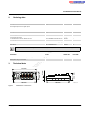
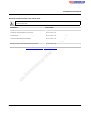
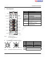
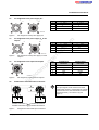
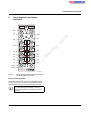
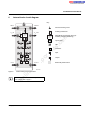
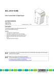
FLS PB M12 DIO 4/4 M12-2A
X10
0 2
4
6
8
7
98
X1
0 1
2
9
3
4
6 5
Fieldline Stand-Alone device for PROFIBUS DP
with four digital inputs
and four digital outputs
Data sheet
6631_en_03
© PHOENIX CONTACT - 01/2009
co
1
Description
s.
This device is used to acquire and output digital signals.
ne
po
om
–
in
ec
–
–
–
on
l
–
–
–
Connection to PROFIBUS DP
using M12 connectors (B-encoded)
Baud rate with up to 12 Mbaud autobaud
Connection of digital sensors using M12 connectors
Connection of digital actuators using M12 connectors,
each with a load capacity of 2 A (nominal current)
Flexible power supply concept
Diagnostic and status indicators
Short-circuit and overload protection
of the outputs and sensor supply
IP 65/IP 67 protection
nt
Features
–
m
AUTOMATION
Make sure you always use the latest documentation.
It can be downloaded at www.phoenixcontact.com.
This data sheet is only valid in association with the FLS FLM SYS INST UM E and FLS FLM PB SYS PRO UM E
user manuals.
FLS PB M12 DIO 4/4 M12-2A
2
Ordering data
Products
Description
Type
Order No.
Pcs./Pkt.
FLS PB M12 DIO 4/4 M12-2A
2736107
1
Accessories
Description
Type
Order No.
Pcs./Pkt.
Protective caps (for unused female connectors)
PROT-M12
1680539
5
Protective caps (for unused male connectors)
PROT-M12-FS
1513596
5
5-pos. shielded female connector, M12 B-encoded,
for the incoming remote bus
SACC-M12FSB-5CON-PG9 SH AU
1507777
1
5-pos. shielded male connector, M12 B-encoded,
for the outgoing remote bus
SACC-M12MSB-5CON-PG9 SH AU
m
Fieldline Stand-Alone device for PROFIBUS
with four digital inputs and four digital outputs
1
co
1507764
SAC-M12T/2XM12 PB DP
1507780
1
SAC-5P-M12MS PB TR
1507803
1
Marking labels
ZBF 12:UNBEDRUCKT
0809735
10
s.
PROFIBUS M12 T-piece, 12 Mbaud
PROFIBUS M12 termination resistor
Documentation
Description
Type
168 mm
–
FLS FLM PB SYS PRO UM E
–
–
21 mm
49.3 mm
IN
60 mm
UA12
O4
UA11
O3
O1
I1
ULS
I3
on
l
US
168 mm (xy inch)
UA
O2
I4
U
OUT
in
ec
I2
ULS
2
3
7
6 5 4
98 6
X1
9 0 1
8
UL
IN
BUS
BF
X10
0 2
4
BUS
OUT
178 mm
PB DIO 4/4
Technical data
6631_en_03
Pcs./Pkt.
–
om
"Configuring a PROFIBUS system using devices in the
Fieldline product range" user manual
Figure 1
Order No.
FLS FLM SYS INST UM E
po
"Installation of devices in the Fieldline product range" user manual
3
ne
nt
For additional accessories for connecting the sensors and actuators, please refer to the Phoenix Contact PLUSCON catalog.
168 mm
6631C011
Dimensions of the device
PHOENIX CONTACT
2
FLS PB M12 DIO 4/4 M12-2A
General data
Order designation
FLS PB M12 DIO 4/4 M12-2A
Order No.
2736107
Housing dimensions (width x height x depth)
60 mm x 178 mm x 49.3 mm
Weight
340 g, approximately
Process data mode with 8 bits
Connection method for sensors
2, 3 or 4-wire technology
Connection method for actuators
2 or 3-wire technology
Permissible temperature (operation)
-25°C to +60°C
Permissible temperature (storage/transport)
-25°C to +85°C
Permissible humidity (storage/transport)
95%
m
Operating mode
co
For a short period, slight condensation may appear on the outside of the housing.
Permissible air pressure (operation)
80 kPa to 106 kPa (up to 2000 m above sea level)
70 kPa to 106 kPa (up to 3000 m above sea level)
Degree of protection
IP65/IP67 according to IEC 60529
Protection class
Class 3 according to VDE 0106, IEC 60536
nt
s.
Permissible air pressure (storage/transport)
Mechanical requirements
5g load in each space direction
ne
Vibration test, sinusoidal vibrations according to EN 60068-2-6
Shock test according to EN 60068-2-27
30g load, half sinusoidal wave positive and negative in each space direction
po
For additional information about mechanical requirements and ambient conditions, please contact Phoenix Contact.
Supply voltage
Range
Current consumption at UL+ at 24 V DC
in
ec
Current consumption at US at 24 V DC
Current consumption at UAxx at 24 V DC
Digital inputs
Number
on
l
Input design
om
Power supply
24 V DC
18 V DC to 30 V DC
40 mA, typical (100 mA, maximum)
4.5 mA + sensor current, typical (700 mA, maximum)
6 mA + actuator current, typical (4 A, maximum)
4
According to IEC 61131-2 Type 1
Definition of switching thresholds
Maximum low-level voltage
Minimum high-level voltage
Nominal input voltage
ULmax < 5 V
UHmin > 11 V
24 V DC
Range
-30 V DC < UIN < +30 V DC
Nominal input current
5 mA
Current flow
Linear in the range 1 V < UIN < 30 V
Delay time
tON < 3.1 ms, typical
tOFF = 4.1 ms, typical
Permissible cable length to the sensor
100 m
6631_en_03
PHOENIX CONTACT
3
FLS PB M12 DIO 4/4 M12-2A
Input characteristic curve
Input voltage (V)
Typical input current (mA)
30 < UIN < 0.7
0
3
0.5
1.0
1.6
12
2.3
15
3.0
18
3.8
21
4.5
24
5.2
27
6.0
m
6
9
6.7
co
30
Minimum sensor voltage
US - 1 V
Nominal current per channel
75 mA
s.
Sensor supply
300 mA
Overload protection
Electronic per device
Short-circuit protection
Electronic per device
nt
Nominal current per device
ne
Error messages to the higher-level control or computer system
Sensor supply short circuit
Yes
Yes
po
Sensor supply overload
If an error is triggered by an overload or short circuit of the sensor supply, the device switches off the sensor supply to all the channels and
sends an error message to the master.
om
If the sensor supply US is too low, the device sends an error message to the master (see "Diagnostic data" on page 14).
Digital outputs
Nominal output voltage UOUT
Differential voltage at Inom
in
ec
Number
Nominal current Inom per channel
Total current
on
l
Possible output current during short circuit
4
UAxx - 1 V
≤1V
2A
8 A (observe derating)
22 A, maximum for 300 µs
Please take this value into account when selecting the power supply unit.
Protection
Short circuit; overload
Single chip structure, i.e., all channels are thermally isolated.
6631_en_03
PHOENIX CONTACT
4
FLS PB M12 DIO 4/4 M12-2A
Digital outputs (continued)
Derating at 100% simultaneity
I [A]
8
6
4
2
10 20 30 40 50 60 TA [°C]
6631A012
– Ohmic
48 W
– Inductive
48 VA (1.2 H, 12 Ω)
– Lamp
48 W
co
Signal delay upon power up of:
m
Nominal load per channel
– Nominal ohmic load
Approximately 200 µs, typical
Depending on inductive time constant
– Nominal lamp load
Approximately 200 µs, typical
s.
– Nominal inductive load
Signal delay upon power down of:
Approximately 250 µs, typical
nt
– Nominal ohmic load
150 ms (1.2 H, 12 Ω), approximately; depending on inductive time constant
– Nominal lamp load
250 µs, approximately
ne
– Nominal inductive load
Switching frequency with:
500 Hz, maximum
po
– Nominal ohmic load
This switching frequency is limited by the number of bus devices, the bus configuration, the software used, and the control or computer
system used.
0.1 Hz (1.2 H, 12 Ω), maximum
Overload response
Restart frequency with ohmic overload (2 Ω)
in
ec
Response with inductive overload
om
– Nominal inductive load
– Nominal lamp load
Reverse voltage protection against short pulses
500 Hz
Auto restart
45 Hz, approximately
Output may be damaged
Protected against reverse voltages
Resistance to permanently applied reverse voltages
No
Response upon power down
The output follows the supply voltage without delay
5 ms, typical
-11 V, approximately
on
l
Validity of output data after connecting the power supply (power up)
Limitation of the voltage induced on circuit interruption
Single maximum energy in free running
1500 W
Protective circuit type
Integrated free-wheeling diode for each channel
Overcurrent shutdown
2.6 A, minimum
Output current when switched off
20 µA, maximum
Output current with ground connection interrupt when switched off
5 mA, maximum
Error messages to the higher-level control or computer system
Overload of outputs
Yes
If an error is triggered at the outputs by an overload, the device switches off the corresponding output and sends an error message to the
master (see "Diagnostic data for device diagnostics" on page 14).
6631_en_03
PHOENIX CONTACT
5
FLS PB M12 DIO 4/4 M12-2A
Output characteristic curve when switched on (typical)
Output current (A)
Differential output voltage (V)
0
0
0.20
0.01
0.03
0.05
1.0
0.07
1.5
0.12
1.75
0.13
2.00
0.17
1000
Output voltage (V)
1.5
co
Output characteristic curve when switched off (UAxx = 30 V DC, typical)
Load resistance (kΩ)
∞
m
0.40
0.75
0.9
100
0.1
s.
10
0.001
nt
1
0.01
ne
Output characteristic curve for ground connection interrupt (UAxx = 30 V DC)
Load resistance (kΩ)
Output voltage (V)
29.9
∞
1000
po
100
10
Interface
Bus system
Incoming bus
Transmission speed
Outgoing bus
in
ec
Coupling of shield connection
om
1
28.8
25.0
13.6
3.8
PROFIBUS DP
Directly to FE
12 Mbaud, maximum
Directly to FE
Transmission speed
12 Mbaud, maximum
on
l
Coupling of shield connection
For transmission speeds of more than 3 Mbaud, T-pieces with integrated series inductance must be used.
6631_en_03
PHOENIX CONTACT
6
FLS PB M12 DIO 4/4 M12-2A
Electrical isolation/isolation of the voltage areas
For device connection, please note the instructions and regulations in the "Installation of devices in the Fieldline product range" user manual,
FLS FLM SYS INST UM E.
Separate potentials in the FLS PB M12 DIO 4/4 M12-2A I/O device
Test distance
Test voltage
500 V AC, 50 Hz, 1 min.
500 V AC, 50 Hz, 1 min.
24 V supply (bus logic)/digital inputs (sensor supply)
500 V AC, 50 Hz, 1 min.
24 V supply (bus logic)/digital outputs (actuator supply)
500 V AC, 50 Hz, 1 min.
Bus connection/FE
500 V AC, 50 Hz, 1 min.
Bus connection/digital inputs (sensor supply)
500 V AC, 50 Hz, 1 min.
Bus connection/digital outputs (actuator supply)
500 V AC, 50 Hz, 1 min.
500 V AC, 50 Hz, 1 min.
FE/digital outputs (actuator supply)
500 V AC, 50 Hz, 1 min.
Digital outputs (actuator supply)/digital outputs (actuator supply)
500 V AC, 50 Hz, 1 min.
s.
co
FE/digital inputs (sensor supply)
m
24 V supply (bus logic)/bus connection
24 V supply (bus logic)/FE
Approvals
on
l
in
ec
om
po
ne
nt
For the latest approvals, please visit www.download.phoenixcontact.com or eshop.phoenixcontact.com.
6631_en_03
PHOENIX CONTACT
7
FLS PB M12 DIO 4/4 M12-2A
Pin assignment
X 1 0
0
2
O U T
6
9 8
X 1
9 0 1
U L
8
I1
IN 3
I3
O U T 1
O 1
O U T 3
U
A
IN
O 3
U
A
U
L S
1 1
U A
1 2
IN 2
I4
IN 4
O 2
O U T 2
O U T
in
ec
4 /4
O U T
L S
I2
IN1 to IN4
OUT1 to
OUT4
UA IN
UA OUT
Power supply IN
of the outputs (OUT1 to OUT4)
with voltages UA11 and UA12
Power supply OUT
for additional devices
O U T 4
U
U A
U
A
O U T
6 6 3 1 B 0 0 2
Connections of the
FLS PB M12 DIO 4/4 M12-2A
on
l
4.1
U
O 4
IN
P B D IO
Figure 2
4
( x y in c h )
IN 1
5
nt
U S
L S
ne
6
U
po
IN
1 6 8 m m
L S
ULS OUT
2
3
7
U
B U S
O U T
4
IN
om
B U S IN
m
B U S
B F
F E
Meaning
Functional earth ground
PROFIBUS IN
PROFIBUS OUT
Power supply IN
(logic and sensors)
Power supply OUT
(logic and sensors) for additional devices
Inputs 1 to 4
Outputs 1 to 4
co
B U S
Designation
FE
BUS IN
BUS OUT
ULS IN
s.
4
Pin assignment of the PROFIBUS connection
B U S IN
B U S O U T
Pin
1
2
3
4
5
IN
VP
RxD/TxD-N (A)
DGND
RxD/TxD-P (B)
Shield
OUT
VP
RxD/TxD-N (A)
DGND
RxD/TxD-P (B)
Shield
6 6 2 5 A 0 0 4
The thread is used for additional shielding.
Figure 3
6631_en_03
PROFIBUS pin assignment (M12 B-encoded)
PHOENIX CONTACT
8
FLS PB M12 DIO 4/4 M12-2A
4.2
Pin assignment of the power supply ULS
IN
O U T
Pin
1
2
3
4
IN
UL +24 V
US GND
UL GND
US +24 V
Pin
1
2
3
4
IN
UA11 +24 V
UA12 GND
UA11 GND
UA12 +24 V
OUT
UL +24 V
US GND
UL GND
US +24 V
6 6 2 5 A 0 0 5
Figure 4
Pin assignment of the inputs and outputs
in
ec
om
po
4.4
Pin assignment of the power supply UA of the
outputs
ne
6 6 2 5 A 0 0 5
Figure 5
co
O U T
s.
IN
m
Pin assignment of the power supply UA of the
outputs
OUT
UA11 +24 V
UA12 GND
UA11 GND
UA12 +24 V
nt
4.3
Pin assignment of the power supply ULS
Pin
1
2
3
4
5
Female input
connector
US +24 V
See Figure 7
GND
Input
FE
Female output
connector
Not used
Not used
GND
Output
FE
6 6 2 5 A 0 0 6
Figure 6
Assignment of the female input connectors
IN
5
2
6631_en_03
5
4
IN
Female connector 1
Female connector 3
Figure 7
1
3
+ 24 V
4
NOTE:
Internal
2
3
Two input signals can be connected to each
female input connector. If both inputs of a female
connector are used, the other female connector
must not be used (1 or 2 and 3 or 4) (see
Figure 7).
+ 24 V
1
on
l
4.5
Pin assignment of the inputs and outputs
Female connector 2
Female connector 4
Assignment of the female input connectors
PHOENIX CONTACT
9
FLS PB M12 DIO 4/4 M12-2A
Local diagnostic and status
indicators
B U S
B U S
B F
B F
4
O U T
6
9 8
X 1
9 0 1
U L
8
I1
X X
Z Z
O 1
Y Y
( x y in c h )
I3
X X
4
U
X 1
L S
I2
X X
I4
X X
Z Z
O 2
Y Y
Z Z
Z Z
O 3
A
U A
1 2
O U T
4 /4
6 6 3 1 B 0 0 3
Indicators and rotary encoding switches of the
FLS PB M12 DIO 4/4 M12-2A
on
l
Figure 8
1 1
IN
P B D IO
U
U A
Y Y
om
U A 1 1
U A 1 2
U
O 4
in
ec
Y Y
m
1 6 8 m m
U S
5
co
6
U S
L S
s.
7
U
X 1 0
2
3
nt
IN
ne
U L
X 1 0
0
2
po
5
Rotary encoding switches
The station address is set using rotary encoding switches
X10 (for tens) and X1 (for units). The PROFIBUS master
addresses the device by means of this station address.
The valid value range is between 1 and 99.
A new address value is only applied on device
power up.
6631_en_03
PHOENIX CONTACT
10
FLS PB M12 DIO 4/4 M12-2A
ZZ
UA11
ne
po
on
l
UA12
om
YY
in
ec
XX
nt
s.
US
Meaning
Bus error (bus failure)
No cyclic data transmission:
– PROFIBUS not connected, master not active
– Incorrect settings (configuration via master, station address)
– Synchronization or parameterization running
– Timeout elapsed
OFF:
– Device is addressed by PROFIBUS and is in the "cyclic process data exchange"
state
– Device supply not present (In this state the "UL" LED is also off due to the missing
24 V communications power.)
Green LED
Communications power
ON:
Communications power present
OFF:
Communications power too low
Red/green LED Power supply for IN1 to IN4
ON (red):
Power supply overloaded
ON (green):
Power supply present
OFF:
Power supply too low
Yellow LED
Status indicators for the inputs
ON:
Input active
OFF:
Input not active
Yellow LED
Status indicators for the outputs
ON:
Output active
OFF:
Output not active
Red LED
Overload of outputs
ON:
Output overloaded
OFF:
Output not overloaded
Green LED
Power supply for OUT1 and OUT2
ON:
Power supply for OUT1 and OUT2 present
OFF:
Power supply for OUT1 and OUT2 too low
Green LED
Power supply for OUT3 and OUT4
ON:
Power supply for OUT3 and OUT4 present
OFF:
Power supply for OUT3 and OUT4 too low
co
UL
Color
Red LED
ON:
m
Designation
BF
6631_en_03
PHOENIX CONTACT
11
FLS PB M12 DIO 4/4 M12-2A
6
Internal basic circuit diagram
Key:
P B IN
P B O U T
Functional earth ground
2 4 V
IN
U
P B
2 4 V
L S
O U T
P r o to k o ll
C h ip
5 V
P B
P r o to k o ll
C h ip
4
PROFIBUS protocol chip (bus logic
including voltage conditioning)
Optocoupler
4
#
Isolating transformer
5 V
m
L S
co
U
#
#
s.
LED
#
ne
nt
Transistor
po
# #
A
IN
U
in
ec
U
om
# #
O U T
Output
Electrically isolated area
6 6 3 1 A 0 0 9
Internal wiring of the connections
on
l
Figure 9
A
Input
For information about the electrically isolated
areas, please refer to page 7.
6631_en_03
PHOENIX CONTACT
12
FLS PB M12 DIO 4/4 M12-2A
Typical connection of sensors and actuators
Connection notes
9
NOTE: Meet noise immunity requirements
6625B009
Configuration data
ID number
066Ahex
Input address area
8 bits
Output address area
8 bits
om
po
Connect FE using a mounting screw or a cable
connection to the FE connection latch (when
mounting on the side or on a non-conductive
surface).
+24 V
m
IN4
OUT2
O2
co
O1
ne
8
I4
nt
Figure 10
I3
s.
OUT1
+24 V
Connection example
IN3
7
NOTE: Ensure degree of protection
in
ec
To ensure IP65/IP67 protection, cover unused
female connectors with protective caps.
NOTE: Avoid damage to the electronics
on
l
Only supply the sensors with the voltage US
provided at the terminal points.
NOTE: Avoid polarity reversal
Avoid polarity reversal of the supply voltages UL,
US, and UA in order to prevent damage to the
device.
NOTE: Observe connection assignment
When connecting the sensors and actuators,
observe the assignment of the connections to the
PROFIBUS input and output data (see "Process
data" on page 14).
6631_en_03
PHOENIX CONTACT
13
FLS PB M12 DIO 4/4 M12-2A
10
Process data
10.1
Assignment of the terminal points to the IN process data
Device
Byte
Bit
Input
Byte 0
7
0
6
0
5
0
4
0
3
4
2
3
1
2
0
1
3
4
m
(Byte.bit) view
1
2
0
1
For bits 0.4 to 0.7 of the inputs the value is "0".
10.2
Assignment of the terminal points to the OUT process data
(Byte.bit) view
Byte 0
7
X
6
X
5
X
4
X
2
3
co
Device
Byte
Bit
Output
Diagnostic data
11.1
Mapping of diagnostic data in PROFIBUS
Bit 4
X
X
X
X
0
0
0
M.4
0
0
0
0
0
Bit 3
X
X
X
X
0
1
0
M.3
0
0
0
0
0
po
Bit 5
X
X
X
X
0
1
0
M.5
0
0
0
0
0
om
Bit 6
X
X
X
X
0
1
0
M.6
0
0
0
0
X
in
ec
Bit 7
X
X
X
X
0
0
0
M.7
0
0
0
0
X
on
l
Diagnostic data
Byte 0
Byte 1
Byte 2
Byte 3
Byte 4
Byte 5
Byte 6
Byte 7
Byte 8
Byte 9
Byte 10
Byte 11
Byte 12
Bit 2
X
X
X
X
1
0
1
M.2
0
0
0
0
0
ne
11
nt
s.
The assignment of bits 0.4 to 0.7 of the outputs has no effect on the output state.
Bit 1
X
X
X
X
1
1
1
M.1
0
0
0
0
0
Bit 0
X
X
X
X
0
0
1
M.0
0
0
0
0
0
Remark
Station status 1
Station status 2
Station status 3
Diagnostic master address
High ID number
Low ID number
Diagnostic header
Device diagnostics
Reserved
Reserved
Reserved
Reserved
Reserved
Bytes 0 to 6 are PROFIBUS standard. Bytes 7 to 12 are device-specific.
11.2
Diagnostic data for device diagnostics
Bit
M.0 - M.2
M.3
M.4
M.5
M.6
M.7
Remark
Reserved
Status of the sensor supply US
Reserved
Overload status of the outputs
Status of the device supply UL
Overload status of the sensor supply US
Assignment
0
1, if US is too low
0
OUT1 to OUT4
1, if UL too low
1, if sensor supply is overloaded
If a diagnostic event occurs, the diagnostic data is sent to the master by means of a diagnostic telegram generated
once by the device. The current status of the data can be read by the device at any time.
6631_en_03
PHOENIX CONTACT GmbH & Co. KG • 32823 Blomberg • Germany • Phone: +49 - 52 35 - 30 0
PHOENIX CONTACT • P.O.Box 4100 • Harrisburg • PA 17111-0100 • USA • Phone: +717-944-1300
www.phoenixcontact.com
14