1
To our customers,
Old Company Name in Catalogs and Other Documents
On April 1st, 2010, NEC Electronics Corporation merged with Renesas Technology
Corporation, and Renesas Electronics Corporation took over all the business of both
companies. Therefore, although the old company name remains in this document, it is a valid
Renesas Electronics document. We appreciate your understanding.
Renesas Electronics website: http://www.renesas.com
April 1st, 2010
Renesas Electronics Corporation
Issued by: Renesas Electronics Corporation (http://www.renesas.com)
Send any inquiries to http://www.renesas.com/inquiry.
Notice
1.
2.
3.
4.
5.
6.
7.
All information included in this document is current as of the date this document is issued. Such information, however, is
subject to change without any prior notice. Before purchasing or using any Renesas Electronics products listed herein, please
confirm the latest product information with a Renesas Electronics sales office. Also, please pay regular and careful attention to
additional and different information to be disclosed by Renesas Electronics such as that disclosed through our website.
Renesas Electronics does not assume any liability for infringement of patents, copyrights, or other intellectual property rights
of third parties by or arising from the use of Renesas Electronics products or technical information described in this document.
No license, express, implied or otherwise, is granted hereby under any patents, copyrights or other intellectual property rights
of Renesas Electronics or others.
You should not alter, modify, copy, or otherwise misappropriate any Renesas Electronics product, whether in whole or in part.
Descriptions of circuits, software and other related information in this document are provided only to illustrate the operation of
semiconductor products and application examples. You are fully responsible for the incorporation of these circuits, software,
and information in the design of your equipment. Renesas Electronics assumes no responsibility for any losses incurred by
you or third parties arising from the use of these circuits, software, or information.
When exporting the products or technology described in this document, you should comply with the applicable export control
laws and regulations and follow the procedures required by such laws and regulations. You should not use Renesas
Electronics products or the technology described in this document for any purpose relating to military applications or use by
the military, including but not limited to the development of weapons of mass destruction. Renesas Electronics products and
technology may not be used for or incorporated into any products or systems whose manufacture, use, or sale is prohibited
under any applicable domestic or foreign laws or regulations.
Renesas Electronics has used reasonable care in preparing the information included in this document, but Renesas Electronics
does not warrant that such information is error free. Renesas Electronics assumes no liability whatsoever for any damages
incurred by you resulting from errors in or omissions from the information included herein.
Renesas Electronics products are classified according to the following three quality grades: “Standard”, “High Quality”, and
“Specific”. The recommended applications for each Renesas Electronics product depends on the product’s quality grade, as
indicated below. You must check the quality grade of each Renesas Electronics product before using it in a particular
application. You may not use any Renesas Electronics product for any application categorized as “Specific” without the prior
written consent of Renesas Electronics. Further, you may not use any Renesas Electronics product for any application for
which it is not intended without the prior written consent of Renesas Electronics. Renesas Electronics shall not be in any way
liable for any damages or losses incurred by you or third parties arising from the use of any Renesas Electronics product for an
application categorized as “Specific” or for which the product is not intended where you have failed to obtain the prior written
consent of Renesas Electronics. The quality grade of each Renesas Electronics product is “Standard” unless otherwise
expressly specified in a Renesas Electronics data sheets or data books, etc.
“Standard”:
8.
9.
10.
11.
12.
Computers; office equipment; communications equipment; test and measurement equipment; audio and visual
equipment; home electronic appliances; machine tools; personal electronic equipment; and industrial robots.
“High Quality”: Transportation equipment (automobiles, trains, ships, etc.); traffic control systems; anti-disaster systems; anticrime systems; safety equipment; and medical equipment not specifically designed for life support.
“Specific”:
Aircraft; aerospace equipment; submersible repeaters; nuclear reactor control systems; medical equipment or
systems for life support (e.g. artificial life support devices or systems), surgical implantations, or healthcare
intervention (e.g. excision, etc.), and any other applications or purposes that pose a direct threat to human life.
You should use the Renesas Electronics products described in this document within the range specified by Renesas Electronics,
especially with respect to the maximum rating, operating supply voltage range, movement power voltage range, heat radiation
characteristics, installation and other product characteristics. Renesas Electronics shall have no liability for malfunctions or
damages arising out of the use of Renesas Electronics products beyond such specified ranges.
Although Renesas Electronics endeavors to improve the quality and reliability of its products, semiconductor products have
specific characteristics such as the occurrence of failure at a certain rate and malfunctions under certain use conditions. Further,
Renesas Electronics products are not subject to radiation resistance design. Please be sure to implement safety measures to
guard them against the possibility of physical injury, and injury or damage caused by fire in the event of the failure of a
Renesas Electronics product, such as safety design for hardware and software including but not limited to redundancy, fire
control and malfunction prevention, appropriate treatment for aging degradation or any other appropriate measures. Because
the evaluation of microcomputer software alone is very difficult, please evaluate the safety of the final products or system
manufactured by you.
Please contact a Renesas Electronics sales office for details as to environmental matters such as the environmental
compatibility of each Renesas Electronics product. Please use Renesas Electronics products in compliance with all applicable
laws and regulations that regulate the inclusion or use of controlled substances, including without limitation, the EU RoHS
Directive. Renesas Electronics assumes no liability for damages or losses occurring as a result of your noncompliance with
applicable laws and regulations.
This document may not be reproduced or duplicated, in any form, in whole or in part, without prior written consent of Renesas
Electronics.
Please contact a Renesas Electronics sales office if you have any questions regarding the information contained in this
document or Renesas Electronics products, or if you have any other inquiries.
(Note 1) “Renesas Electronics” as used in this document means Renesas Electronics Corporation and also includes its majorityowned subsidiaries.
(Note 2) “Renesas Electronics product(s)” means any product developed or manufactured by or for Renesas Electronics.
8
CPUBD-38024F
H8/300L Super Low Power Series Low-Cost CPU Board
Microcomputer Development Environment System
2004.01
www.rss.renesas.com
CPUBD-38024F – CPU Board for H8/300L Super Low Power Series Microcomputer
User’s Manual
Published by
: Renesas System Solutions Asia Pte. Ltd.
Date
: January 7th, 2004, Version 2.0
Copyright(C) Renesas System Solutions Asia Pte. Ltd. All rights reserved.
Trademarks
a) General
All brand or product names used in this manual are trademarks or registered trademarks of their respective
companies or organizations.
b) Specific
Microsoft, MS and MS-DOS is registered trademark.
Windows and Windows NT are trademarks of Microsoft Corporation.
Pentium is a registered trademark of Intel.
i
IMPORTANT INFORMATION
•
READ this user’s manual before using this emulator product.
•
KEEP the user’s manual handy for future reference.
Do not attempt to use the product until you fully understand its mechanism.
CPUBD:
Throughout this document, the term “CPUBD” shall be defined as the H8/300L Super Low Power Series Low-cost
CPU Board, CPUBD-38024F produced only by Renesas System Solutions Asia Pte. Ltd. excludes all subsidiary
products.
The user system or a host computer is not included in this definition.
Purpose of the Product:
This product is a development-supporting unit for use as training and evaluation tool. The product must only be
used for the above purpose.
Improvement Policy:
Renesas System Solutions Asia Pte. Ltd. (hereafter collectively referred to as Renesas) pursues a policy of
continuing improvement in design, performance, and safety of the emulator product. Renesas reserves the right to
change, wholly or partially, the specifications, design, user’s manual, and other documentation at any time without
notice.
Target User of the Product:
This product should only be used by those who have carefully read and thoroughly understood the information as
well as restrictions contained in the user’s manual. Do not attempt to use the product until you fully understand its
mechanism.
It is highly recommended that first-time users. Be instructed by users that are well versed in the operation of
emulator product.
ii
LIMITED WARRANTY
Renesas warrants its products to be manufactured in accordance with published specifications and free
from defects in material and/or workmanship. The foregoing warranty does not cover damage caused
by fair wear and tear, abnormal store condition, incorrect use, accidental misuse, abuse, neglect,
corruption, misapplication, addition or modification or by the use with other hardware or software, as
the case may be, with which the product is incompatible. No warranty of fitness for a particular purpose
is offered. The user assumes the entire risk of using the product. Any liability of Renesas is limited
exclusively to the replacement of defective materials or workmanship.
DISCLAIMER
RENESAS MAKES NO WARRANTIES, EITHER EXPRESS OR IMPLED, ORAL OR WRITTEN,
EXCEPT AS PROVIDED HEREIN, INCLUDING WITHOUT LIMITATION THEREOF,
WARRANTIES AS TO MARKETABILITY, MECRCHANTABILITY, FITNESS FOR ANY
PARTICULAR PURPOSE OR USE, OR AGAINST INFRINGEMENT OF ANY PATENT. IN NO
EVENT SHALL RENESAS BE LIABLE FOR ANY DIRECT, INCIDENTAL OR
CONSEQUENTIAL DAMAGES OF ANY NATURE, OR LOSSES OR EXPENSES RESULTING
FROM ANY DEFECTIVE EMULATOR PRODUCT, THE USE OF ANY EMULATOR
PRODUCT OR ITS DOCUMENTATION, EVEN IF ADVISED OF THE POSSIBILITY OF SUCH
DAMAGES. EXCEPT AS EXPRESSLY STATED OTHERWISE IN THIS WARRANTY, THIS
EMULATOR PRODUCT IS SOLD “AS IS”. AND YOU MUST ASSUME ALL RISK FOR THE
USE AND RESULTS OBTAINED FROM THE EMULATOR PRODUCT.
iii
State Law:
Some states do not allow the exclusion or limitation of implied warranty or liability for incidental or consequential
damages, so the above limitation or exclusion may not apply to you. This warranty gives you specific legal rights,
and you may have other rights which may varies from state to state.
The Warranty is Void in the Following Cases:
Renesas shall have no liability or legal responsibility for any problems caused by misuse, abuse, misapplication,
neglect, improper handling, installation, repair or modifications of the emulator product without Renesas’s prior
written consent or any problems caused by the user system.
Restrictions:
1.
Earthing (applies only to manual for Renesas hardware products)
This hardware is designed for use with equipment that is fully earthed.
Ensure that all equipments used are appropriately earthed.
Failure to do so could lead to danger for the operator or damaged to equipments.
2.
Electrostatic Discharge Precautions (applies only to manuals for Renesas hardware products)
This hardware contains devices that are sensitive to electrostatic discharge.
Ensure appropriate precautions are observed during handling and accessing connections.
Failure to do so could result in damage to the equipment.
All Right Reserved:
This user’s manual and emulator product are copyrighted and all rights are reserved by Renesas. No part of this
user’s manual, all or part, any be reproduced or duplicated in any form, in hardcopy or machine-readable form, by
any means available without Renesas‘s prior written consent.
Other Important Things to Keep in Mind:
1.
Circuitry and other examples described herein are meant merely to indicate the characteristics and
performance of Renesas Technology‘s semiconductor products. Renesas assumes no responsibility for any
intellectual property claims or other problems that may result from applications based on the examples
described herein.
2.
No license is granted by implication or otherwise under any patents or other rights of any third party or
Renesas.
3.
MEDICAL APPLICATIONS: Renesas Technology’s products are not authorized for use in MEDICAL
APPLICATIONS without the written consent of the appropriate officer of Renesas Technology (Asia Sales
company). Such use includes, but is not limited to, use in life support systems. Buyers of Renesas Technology’s
products are requested to notify the relevant Renesas Technology (Asia Sales offices) when planning to use the
products in MEDICAL APPLICATIONS.
Figures:
Some figures in this user’s manual may show items different from your actual system.
Limited Anticipation of Danger:
Renesas cannot anticipate every possible circumstance that might involve a potential hazard. The
warnings in this user’s manual and on the emulator product are therefore not all inclusive. Therefore,
you must use the emulator product safely at your own risk.
iv
PREFACE
About this manual
This manual explains how to install and setup the H8/38024F CPU board for evaluating the performance
of the H8/38024F microcomputer. Hereafter, the H8/38024F CPU board shall term as ‘CPUBD’.
Operation using the HEW pure debugger is also detailed in the manual.
1. Introduction
Gives an introduction about the CPU board, package, specification and functions.
2. Installation
Explains how to install the hardware and accompanied software to a host computer.
3. Setup of HEW (Pure Debugger) for CPU Board
Describes the setup steps before embarking on a new project development.
4. Performing Emulation
Describes the various functions available in HEW
5. Usage Constraints
Highlights the various constraints that may encounter by user when operating the CPU board.
6. Hardware
Explains the various hardware blocks in the CPU board.
7. Monitor software
Explains the purpose of the monitor software, the implementation requirements and how to use the
monitor software.
8. Flash Programming
Explains the difference between two programming modes and how CPU board operates in these
modes.
9. Tutorial
Provides a step-by-step guide in using the CPU board to perform debugging.
10. Demonstration Program
Provides two demonstration programs for user to have hands-on experience with the CPU board.
v
11. Trouble-Shooting
Advises on some basic fault finding methods and commonly make mistakes.
Appendix A - CPUBD-38024F Board Layout
Appendix B – H8/38024F Memory Map
Appendix C – Pin Assignment for JP1 ~ JP4
Appendix D - Pin assignment for CON1 & CON2
Appendix E – Schematic drawings
Appendix G – Bill of Materials
Technical Support
The CPUBD is a product for evaluation purposes only. We do NOT supply the same level of support as
for the development tools, however, you may contact the sales offices for downloads and documents.
Related Manuals:
H8S, H8/300 series C/C++ Compiler, Assembler, Optimizing Linkage Editor User’s Manual
H8/38024 Series, H8/38024F-ZTATTM Series Hardware Manual
vi
Table of Contents
SECTION 1.
INTRODUCTION........................................................................................................... 1
1.1.
SPECIFICATION ............................................................................................................................... 2
1.1.1.
General.................................................................................................................................. 2
1.1.2.
Serial Communication .......................................................................................................... 2
1.1.3.
Power Input........................................................................................................................... 2
1.1.4.
Memory Map ......................................................................................................................... 2
1.1.5.
Interface with Application Board.......................................................................................... 2
1.1.6.
Interface with E10T/ E7 emulator......................................................................................... 2
1.1.7.
Monitor software................................................................................................................... 2
1.2.
CPUBD FUNCTIONAL BLOCKS ...................................................................................................... 3
1.3.
PACKAGE ....................................................................................................................................... 5
1.3.1.
Hardware Components ......................................................................................................... 5
1.3.2.
Software Components ........................................................................................................... 5
1.4.
SUMMARY OF CPUBD-38024F FUNCTIONS .................................................................................. 6
SECTION 2.
INSTALLATION ............................................................................................................ 7
2.1.
LABEL OF PARTS ON CPU BOARD ................................................................................................. 7
2.2.
INSTALLING THE CPU BOARD ....................................................................................................... 8
2.3.
COMMUNICATION PORT BAUD RATE ............................................................................................. 8
2.4.
POWER SUPPLY FOR CPU BOARD .................................................................................................. 9
2.5.
JUMPERS OPTIONS.......................................................................................................................... 9
2.5.1.
Power Supply Selection Jumpers for MCU......................................................................... 10
2.5.2.
Boot Mode Selection Jumpers............................................................................................. 10
2.5.3.
User Mode [Standalone] Selection Jumpers [Default] ...................................................... 10
2.5.4.
User Mode – Interface with Application Board Selection Jumpers.................................... 11
2.5.5.
E10T/ E7 Emulation Selection Jumpers.............................................................................. 11
2.6.
INSTALLATION OF HEW (PURE DEBUGGER) FOR CPU BOARD ................................................... 12
SECTION 3.
3.1.
3.2.
3.3.
SETUP OF HEW (PURE DEBUGGER) FOR CPU BOARD.................................. 17
RUNNING HEW (PURE DEBUGGER) FOR CPU BOARD ................................................................ 17
CREATING A NEW WORKSPACE ................................................................................................... 18
SELECTING THE TARGET (DEBUG SETTINGS) ............................................................................... 20
SECTION 4.
PERFORMING EMULATION................................................................................... 21
4.1.
HIGH-PERFORMANCE EMBEDDED WORKSHOP ............................................................................. 21
4.2.
COMPILER CONFIGURATION & DEBUGGER SESSION .................................................................... 23
4.3.
DEBUG SETTINGS ......................................................................................................................... 25
4.4.
CONNECTING & DISCONNECTING WITH THE EMULATOR ............................................................. 25
4.5.
EMULATOR SETTING .................................................................................................................... 26
4.5.1.
Configure Platform ............................................................................................................. 26
4.5.2.
Memory Mapping................................................................................................................ 29
4.6.
VIEWING OF PROGRAM ................................................................................................................ 31
4.6.1.
Source Code level................................................................................................................ 31
4.6.2.
Disassembly level................................................................................................................ 32
4.7.
MCU RELATED INFORMATION ..................................................................................................... 33
4.7.1.
Registers.............................................................................................................................. 33
4.7.2.
Memory ............................................................................................................................... 34
vii
4.7.3.
I/O ....................................................................................................................................... 34
4.7.4.
Status................................................................................................................................... 35
4.7.5.
Break Functions .................................................................................................................. 40
4.7.6.
Stack Trace.......................................................................................................................... 41
4.8.
MCU MEMORY MANIPULATION ................................................................................................... 42
4.9.
EXECUTION OF MCU CODE ......................................................................................................... 43
4.9.1.
Reset CPU ........................................................................................................................... 43
4.9.2.
Go, Reset Go, Goto Cursor, Set PC to Cursor, Run… ....................................................... 44
4.9.3.
Step Functions..................................................................................................................... 45
4.10.
C-SOURCE LEVEL DEBUGGING................................................................................................. 47
SECTION 5.
5.1.
5.2.
5.3.
5.4.
5.5.
5.6.
5.7.
5.8.
5.9.
5.10.
CORRUPTION OF MONITOR SOFTWARE ........................................................................................ 48
INTERRUPT ................................................................................................................................... 48
TIMING ISSUES ............................................................................................................................. 48
WATCHDOG TIMER ....................................................................................................................... 49
SOFTWARE BREAKPOINT .............................................................................................................. 49
STEP ............................................................................................................................................. 49
POWER-DOWN MODES................................................................................................................. 50
SCI3 ............................................................................................................................................ 50
E10T /E7 INTERFACE .................................................................................................................. 50
OTHER CONSTRAINTS .............................................................................................................. 50
SECTION 6.
6.1.
6.2.
6.3.
6.4.
6.5.
6.6.
6.7.
6.8.
6.9.
6.10.
HARDWARE ................................................................................................................ 51
H8/38024F MICRO-CONTROLLER ................................................................................................ 51
POWER SUPPLY CIRCUITRY.......................................................................................................... 51
CLOCK CIRCUITRY ....................................................................................................................... 51
RESET CIRCUITRY ........................................................................................................................ 51
SERIAL COMMUNICATION BLOCK [VIA SCI3].............................................................................. 52
FLASH ROM & RAM................................................................................................................ 52
LEDS ........................................................................................................................................... 52
BOOT MODE ENABLE ................................................................................................................... 52
E10T/ E7 INTERFACE .................................................................................................................. 52
EXTERNAL USER INTERFACE ................................................................................................... 53
SECTION 7.
7.1.
7.2.
7.3.
7.4.
7.5.
7.6.
7.7.
USAGE PRECAUTIONS............................................................................................. 48
MONITOR SOFTWARE............................................................................................. 54
INTRODUCTION TO MONITOR SOFTWARE ..................................................................................... 54
PROGRAM DEVELOPMENT ............................................................................................................ 54
MONITOR SOFTWARE REQUIREMENTS ......................................................................................... 54
MODE TRANSITION ...................................................................................................................... 55
USING MONITOR SOFTWARE ........................................................................................................ 56
INTERRUPTS USED BY THE MONITOR ............................................................................................ 56
BREAKPOINTS .............................................................................................................................. 57
SECTION 8.
FLASH PROGRAMMING.......................................................................................... 58
8.1.
FLASH PROGRAMMING THE CPUBD ......................................................................................... 58
8.1.1.
Boot Mode:.......................................................................................................................... 58
8.1.2.
User Program Mode: .......................................................................................................... 59
8.2.
OPERATION DURING PROGRAMMING KERNEL EXECUTION .......................................................... 59
SECTION 9.
9.1.
TUTORIAL (300L_TUT)............................................................................................. 61
INTRODUCTION ............................................................................................................................ 61
viii
9.2.
OVERVIEW ................................................................................................................................... 61
9.3.
TUTORIAL SETUP ......................................................................................................................... 64
9.3.1.
Downloading the tutorial Program .................................................................................... 64
9.3.2.
Displaying the Program Listing.......................................................................................... 67
9.4.
USING BREAKPOINTS ................................................................................................................... 69
9.4.1.
Setting a Program Count (PC) Breakpoint......................................................................... 69
9.4.2.
Executing the Program ....................................................................................................... 70
9.4.3.
Reviewing the Breakpoints.................................................................................................. 72
9.4.4.
Examining MCU Registers.................................................................................................. 73
9.5.
EXAMINING MEMORY AND VARIABLES ....................................................................................... 74
9.5.1.
Viewing Memory ................................................................................................................. 74
9.5.2.
Watching Variables............................................................................................................. 75
9.6.
STEPPING THROUGH A PROGRAM................................................................................................. 77
9.7.
WATCHING LOCAL VARIABLES.................................................................................................... 78
9.8.
SAVES THE SESSION ..................................................................................................................... 79
9.9.
WHAT NEXT?............................................................................................................................... 79
SECTION 10.
10.1.
10.2.
DEMONSTRATION PROGRAM .......................................................................... 80
BLINKING LEDS ...................................................................................................................... 80
RUNNING LEDS ....................................................................................................................... 81
SECTION 11.
TROUBLE-SHOOTING .......................................................................................... 82
APPENDIX A
CPUBD-38024F BOARD LAYOUT ....................................................................... 83
APPENDIX B
H8/38024F MEMORY MAP.................................................................................... 85
APPENDIX C
PIN ASSIGNMENT FOR JP1~JP4 ........................................................................ 86
APPENDIX D
PIN ASSIGNMENT FOR CON1 & CON2 ............................................................ 87
APPENDIX E
CPUBD-38024F SCHEMATIC DRAWINGS ........................................................ 89
APPENDIX F
BILL OF MATERIALS ........................................................................................... 91
ix
Figures & Tables
FIGURE 1.1
FIGURE 1.2
FIGURE 1.3
FIGURE 2.1
FIGURE 2.2
FIGURE 2.3
FIGURE 2.4
FIGURE 2.5
FIGURE 2.6
FIGURE 2.7
FIGURE 2.8
FIGURE 2.9
FIGURE 2.10
FIGURE 2.11
FIGURE 3.1
FIGURE 3.2
FIGURE 3.3
FIGURE 3.4
FIGURE 3.5
FIGURE 3.6
FIGURE 4.1
FIGURE 4.2
FIGURE 4.3
FIGURE 4.4
FIGURE 4.5
FIGURE 4.6
FIGURE 4.7
FIGURE 4.8
FIGURE 4.9
FIGURE 4.10
FIGURE 4.11
FIGURE 4.12
FIGURE 4.13
FIGURE 4.14
FIGURE 4.15
FIGURE 4.16
FIGURE 4.17
FIGURE 4.18
FIGURE 4.19
FIGURE 4.20
FIGURE 4.21
FIGURE 4.22
FIGURE 4.23
FIGURE 4.24
FIGURE 4.25
FIGURE 4.26
FIGURE 4.27
H8/38024F CPU BOARD [CPUBD-38024F]......................................................................... 1
CPU BOARD FUNCTIONAL BLOCKS ....................................................................................... 3
CPUBD-38024F PACKAGE ................................................................................................... 5
NAMES OF PARTS ON CPU BOARD ........................................................................................ 7
SERIAL COMMUNICATION CONNECTIONS ............................................................................... 8
POWER CONNECTOR & DC PLUG .......................................................................................... 9
RUN DIALOGUE BOX............................................................................................................ 12
HEW FOR CPUBD INSTALLER WELCOME! SCREEN ........................................................... 12
UPDATE INFORMATION (README) DIALOGUE BOX ............................................................. 13
SELECT DESTINATION DIRECTORY SCREEN ......................................................................... 13
SELECT COMPONENTS SCREEN ............................................................................................ 14
DIRECTORY CONFIRMATION SCREEN ................................................................................... 15
INSTALLING SCREEN ............................................................................................................ 15
COMPLETION SCREEN .......................................................................................................... 16
HEW (PURE DEBUGGER) FOR CPUBD ICON ...................................................................... 17
SELECT PLATFORM DIALOGUE BOX..................................................................................... 18
HEW START-UP WINDOW (WITHOUT TOOLCHAIN) ............................................................. 18
SELECT TARGET ................................................................................................................... 19
DEBUGGER SETTING SUMMARY WINDOW ........................................................................... 19
SELECT PLATFORM DIALOGUE BOX..................................................................................... 20
HIGH-PERFORMANCE EMBEDDED WORKSHOP WINDOW ..................................................... 21
TOOLBAR SHOWING THE SESSION AND CONFIGURATION ..................................................... 23
TOOLBAR SHOWING THE SESSIONS AND CONFIGURATIONS AVAILABLE .............................. 23
OPTION - EMULATOR ........................................................................................................... 26
TARGET CONFIGURATION DIALOGUE BOX .......................................................................... 26
ENABLING STANDALONE FLASH OPTION .............................................................................. 27
DIALOGUE BOX FOR DOWNLOADING USER TARGET PROGRAM.............................................. 27
DIALOGUE BOX FOR RUNNING USER TARGET PROGRAM ....................................................... 28
MEMORY MAPPING DIALOGUE BOX .................................................................................... 29
TARGET MEMORY CONFIGURATION DIALOGUE ................................................................... 30
SOURCE LEVEL .................................................................................................................... 31
DISASSEMBLY WINDOW....................................................................................................... 32
VIEW – CPU ........................................................................................................................ 33
REGISTER ............................................................................................................................. 33
SET MEMORY ....................................................................................................................... 34
INPUT AND OUTPUT REGISTER ............................................................................................. 34
STATUS – MEMORY WINDOW ............................................................................................... 35
STATUS – PLATFORM WINDOW ............................................................................................ 36
STATUS – EVENTS WINDOW ................................................................................................. 36
VIEW - SYMBOL ................................................................................................................... 37
LABEL .................................................................................................................................. 37
WATCH ................................................................................................................................ 38
LOCALS ................................................................................................................................ 39
TOOLTIP ............................................................................................................................... 39
VIEW CODE .......................................................................................................................... 40
STACK TRACE ...................................................................................................................... 41
MEMORY FUNCTIONS........................................................................................................... 42
x
FIGURE 4.28
FIGURE 4.29
FIGURE 4.30
FIGURE 5.1
FIGURE 7.1
FIGURE 8.1
FIGURE 8.2
FIGURE 9.1
FIGURE 9.2
FIGURE 9.3
FIGURE 9.4
FIGURE 9.5
FIGURE 9.6
FIGURE 9.7
FIGURE 9.8
FIGURE 9.9
FIGURE 9.10
FIGURE 9.11
FIGURE 9.12
FIGURE 9.13
FIGURE 9.14
FIGURE 9.15
FIGURE 9.16
FIGURE 9.17
FIGURE 9.18
FIGURE 9.19
FIGURE 9.20
FIGURE 9.21
FIGURE 9.22
DEBUG FUNCTIONS .............................................................................................................. 43
STEP PROGRAM .................................................................................................................... 45
STEP MODE .......................................................................................................................... 46
TIMING DIAGRAM OF HEW .................................................................................................. 48
MODE TRANSITION DIAGRAM .............................................................................................. 55
OVERVIEW OF BOOT MODE ................................................................................................. 59
OVERVIEW OF USER PROGRAM MODE ................................................................................. 60
DEBUG SETTINGS WITH LOAD OBJECT FILE DIALOGUE ....................................................... 65
CONFIGURE LOAD OBJECT FILE DIALOGUE ......................................................................... 65
DOWNLOAD THE SELECTED OBJECT FILE ............................................................................ 66
SOURCE-WINDOW “RESETPRG.C”......................................................................................... 67
SOURCE-WINDOW “300L_TUT.C”......................................................................................... 68
SETTING A BREAKPOINT ...................................................................................................... 69
PROGRAM BREAK ................................................................................................................ 70
SYSTEM STATUS WINDOW ................................................................................................... 71
BREAKPOINTS WINDOW ....................................................................................................... 72
POPUP IN BREAKPOINTS WINDOW........................................................................................ 72
CPU REGISTERS WINDOW ................................................................................................... 73
CHANGING REGISTER VALUE............................................................................................... 73
OPEN MEMORY-WINDOW ..................................................................................................... 74
MEMORY-WINDOW .............................................................................................................. 74
INSTANT WATCH DIALOGUE BOX ........................................................................................ 75
WATCH WINDOW ................................................................................................................. 75
ADD WATCH DIALOGUE BOX .............................................................................................. 76
WATCH WINDOW ................................................................................................................. 76
DISPLAYING INDIVIDUAL ELEMENTS IN AN ARRAY ............................................................. 76
EXECUTING UP TO A FUNCTION CALL .................................................................................. 77
LOCALS WINDOW ................................................................................................................ 78
DISPLAYING INDIVIDUAL ELEMENTS IN AN ARRAY ............................................................. 78
TABLE 2.1
TABLE 2.2
TABLE 2.3
TABLE 2.4
TABLE 2.5
TABLE 2.6
TABLE 4.1
LIST OF JUMPERS.................................................................................................................... 9
POWER SUPPLY SELECTION JUMPERS FOR MCU.................................................................. 10
BOOT MODE SELECTION JUMPERS ....................................................................................... 10
USER MODE [STANDALONE] SELECTION JUMPERS [DEFAULT]............................................ 10
USER MODE - INTERFACE WITH APPLICATION BOARD SELECTION JUMPERS ....................... 11
E10T/ E7 EMULATION SELECTION JUMPERS ....................................................................... 11
TYPES OF BREAKS ENCOUNTERED DURING EMULATION ..................................................... 40
xi
Section 1. Introduction
H8/38024F CPU board (CPUBD-38024F)
is a low cost training and MCU performance
evaluation tool for the H8/300L Super Low Power family series of microcomputers.
It is also implemented with flash programming feature for the H8/38024 F-ZTAT microcomputer. It
contains a QFP-80A package H8/38024F microcomputer on the board.
The H8/38024F CPU board adopts the common HEW that also contains a pure debugger as the user
interface.
The diagram below shows the H8/38024F CPU Board:
Figure 1.1
H8/38024F CPU Board [CPUBD-38024F]
1
1.1.
Specification
1.1.1.
General
H8/38024F microcomputer (using HD64F38024H FP-80A device)
32Kbytes of FLASH memory (Monitor software uses approx. 6Kbytes)
1Kbytes of on-chip RAM (Monitor software work area uses 1 Kbytes)
Two user LED indicators
One push button for reset control
One boot mode LED indicator
One Power LED indicator
All Input/Output signals are being pulled out for user connection via CON1 & CON2
1.1.2.
Serial Communication
Utilizes Serial Communication Interface 3 via RS-232 DB-9F socket and RS-232 transceiver chip.
Supports communication at a baud rate of 38,400bps [non-configurable during debugging].
1.1.3.
Power Input
Accept dual DC power supply at +5.0 volt. ~ +9.0 volt only. [Ripple Rejection ratio more then 60dbm]
1.1.4.
Memory Map
If the CPUBD is to be used with debugger, a section in the memory area is reserved for monitor
software. See Appendix B for memory map diagrams.
1.1.5.
Interface with Application Board
It is designed to interface with any application board via two 30x2pin connector sockets.
It can be interfaced with the H8/3800 application board (APPBD – 3800) for immediate evaluation.
[For information about H8/3800 application board (APPBD – 3800), please contact the sales office.]
1.1.6.
Interface with E10T/ E7 emulator
Supports E10T and E7 emulator.
1.1.7.
Monitor software
A FLASH -resident debugging monitor software hosted on the CPUBD for performing debugging
operations.
2
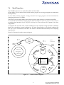
1.2.
CPUBD Functional Blocks
The CPUBD comprises of a H8/38024F microcomputer, serial port, and boot mode control and user
interface.
H8/38024 FZTAT
OSC1
TxD32
Host
Interface
UART
RxD32
OSC2
X1
X2
FLASH
Control
P34
P95
TEST
Power-ON
Reset
RES_N
RES_SW
*1
AVcc
AVss
Straight Header
– Test points
Vcc
I/O Ports
except
P34,P95
47K
Interface
Connector to
External Board
Vss
NOTE: *1
All signals from MCU are brought out to
2x60-ways straight header pins.
Legend
3V3
Figure 1.2
: Gnd
CPU Board Functional Blocks
The boot mode circuitry is necessary to place the CPUBD into Boot mode for programming the FLASH.
To enter into Boot mode, respective jumper headers on the CPUBD must be shorted. SCI3 is used to
program the board’s on-chip flash memory, using the flash programming software built-into the HEW
pure debugger. If the user is not using the serial port for flash programming the CPUBD or debugging,
this serial port is available to user.
3
The HEW with pure debugger software combined with the monitor software programmed into the
device provides high level debugging via SCI3.
When connecting external analogue signals, it is important that CPUBD is configured properly with
respect to analogue voltage supply and reference. There are two user LEDs on board that can be used by
user for their evaluation and are driven directly by the MCU.
All the I/O signals are being tracked out to four 20-way straight header connectors for user access as well
as to two 60-way sockets to allow connection to a target board. These I/O signals are available to user if
either flash programming or debugging is not used.
4
1.3.
Package
The CPUBD is supplied in a package containing the following components:
Figure 1.3
1.3.1.
CPUBD-38024F Package
Hardware Components
The hardware components included in the package are listed below.
1 x H8/38024F CPU Board
1 x RS-232 Serial cable
1 x DC Power Input Jack free-end cable
1 x 7x2pin connector [not assembled]
2 x 30x2pin connectors [not assembled]
1.3.2.
Software Components
1 x CD ROM containing HEW installer, User’s Manual, Tutorial program Source code, Schematic
drawings
Before proceeding, user has to check that all the items listed in the packing list. Please contact the
relevant Renesas Technology sales office in Asia if any item is missing.
5
1.4.
Summary of CPUBD-38024F functions
Items
Specifications
Supported Microcomputers
H8/38024F
Operating Frequency
9.8304MHz (System clock)
32.768KHz (Sub clock)
Supported
3.3 Volts. only
Operating Voltage
Host Machine
Minimum PentiumTM III or equivalent processor PC
Recommended 128Mbytes RAM and 100Mbytes hard disk
space
Microsoft Windows 98, Windows Me, Windows NT 4.0,
Windows 2000 or Windows XP
One Serial port
Host Interface
RS-232 Serial Interface
Baud rate @ 38400 bps
Supported File Format
Motorola S-type
ELF/Dwarf2
Interface Software
HEW pure debugger
Emulation Functions
C – source level debugging (e.g. instant watch….)
Modify and display MCU registers
Perform real-time emulation of a target program
Memory Functions
Copy, Search, Fill, Load and Save memory functions
Modifies and displays memory content
Break Function
PC breakpoint (max. 256)
Step
Step In/ Step Out/ Step Over
On-board Programming
Support on-board programming - Boot mode and User mode
User LEDs
Supports two user’s LEDs
Interface with E10T/ E7
Emulator
Supports E10T and E7 emulator
Interface with Target system
Supports emulation on a target system.
Power Supply for CPU board
DC +5.0 Volt. to +9.0 Volt. supplied from external input
Environmental
Operating Temperature: 10 °C to 35 °C
Humidity: 30% to 85% RH
No condensation
No corrosive gas
6
Section 2.
2.1.
Installation
Label of Parts on CPU Board
Figure 2.1 shows the name of each part of the CPUBD.
JP8: User LED Select
D3: User LED
D4: User LED
J2: VCC Select
CON1, CON2:
Application Board
Interface Connector
JP3,JP4: External User
Interface
P1: RS-232 Serial
Interface Connector
JP9: Boot Mode
Enable
JP7: E10T
Interface
Connector
D5: Boot LED
J1: Power
Connector
JP9: Boot Mode
Enable
Figure 2.1
D1: Power LED S1: Reset Switch
Names of Parts on CPU Board
7
JP1,JP2: External User
Interface
2.2.
Installing the CPU Board
Installing the CPUBD requires power and serial connection to a host computer. The serial
communication cable for connecting the CPUBD to a host computer is supplied. The serial connection
cable uses a 1:1 connectivity.
The diagram below shows how to connect the CPUBD to a host machine or notebook computer
equipped with a DB-9P connector.
HOST PC
DB9P
CPUBD
DB9S
DB9S
RXD (2)
(2) TXD
TXD (3)
(3) RXD
GND (5)
(5) GND
Figure 2.2
2.3.
DB9P
Serial Communication connections
Communication Port Baud Rate
The baud rate utilized by the CPUBD is FIXED at 38,400bps.
8
2.4.
Power Supply for CPU Board
The CPUBD requires a D.C. power supply from +5 VDC ~ +9 VDC at approximately 100mA supplied to
the J1 connector. Prepare the D.C. power supply separately. The power cable is included with this
product. Since total power consumption can vary widely due to external connections, use a power
supply capable of providing at least 250mA at +5VDC ± 5%.
When power is supplied to the CPUBD, a PWR LED, D1 is lit; otherwise, check the power connection for
polarity reversal.
Figure 2.3 and Figure 2.4 show the specification of the power connector and the DC plug respectively.
Electrode (+VE)
Electrode (-VE)
9.5mm
φ 2.1mm
Figure 2.3
2.5.
Power Connector & DC Plug
Jumpers Options
The CPUBD has several jumpers to allow various settings for the user:
Designator
Jumper Name
Jumper Descriptions
J2
VCC SEL
Select source of power supply
JP8
LED SEL
Select either to use D3 or P93 and D4 or P92
JP10
E10T/ E7 EN
Select either to use E10T/ E7 or P33, P34, P35
JP9
BOOT MODE EN
Select either BOOT or USER mode or P95
Table 2.1
List of Jumpers
9
2.5.1.
Power Supply Selection Jumpers for MCU
This is the jumper switch to select the power supply to the MCU. As shown in Table 2.1 below, any
setting not listed in Table 2.1 is not allowed.
Connect to
Application
Board
Jumper
Jumper
Name
Designator
Not
Connected
VCC SEL
J2
Connected
Jumper Selection
Descriptions
Short Pin 2 to Pin 3
[Default]
Power of MCU is supplied
from the CPUBD.
[Do not short Pin 1 to Pin 2]
Operating voltage: +3.3V
Short Pin 1 to Pin 2
Power of MCU is supplied
from an application board
[+5.0V (max.)]
[Do not short Pin 2 to Pin 3]
Table 2.2
2.5.2.
Power Supply Selection Jumpers for MCU
Boot Mode Selection Jumpers
This is the jumper switch to place the CPUBD into the boot mode. This is necessary for flashing the
kernel software and monitor software into the FLASH ROM of the H8/38024F microcomputer.
Jumper Designator
Jumper Selection
Descriptions
JP9 (P95 = ‘0’)
Short Pin 1 to Pin 3
To place CPUBD into Boot mode.
JP10 (P34 = ‘1’)
Short Pin 3 to Pin 5
Table 2.3
2.5.3.
Boot Mode Selection Jumpers
User Mode [Standalone] Selection Jumpers [Default]
This is the jumper switch to place the CPUBD into the user mode for standalone operation. This is
necessary for flashing of the user software into the FLASH ROM of the H8/38024F.
Jumper Designator
Jumper Selection
Descriptions
JP8 (P92 => LED)
Short Pin 1 to Pin 3
To place CPUBD into User mode
[Normal mode]
(P93 => LED)
Short Pin 2 to Pin 4
JP9 (P95 = ‘1’)
Short Pin 3 to Pin 5 [Default]
JP10(P34 = ‘1’)
Short Pin 3 to Pin 5 [Default]
Table 2.4
User Mode [Standalone] Selection Jumpers [Default]
10
2.5.4.
User Mode – Interface with Application Board Selection Jumpers
This is the jumper switch to place the CPUBD into the user mode and allow debugging operation with
Application board.
Jumpers Designator
Jumper Selection
Descriptions
JP8 (P92 => CON1)
Short Pin 3 to Pin 5
(P93 => CON1)
Short Pin 4 to Pin 6
To enable debugging with Application board
in User Mode.
JP9 (P33 => CON1)
Short Pin 2 to Pin 4
(P95 = ‘1’)
Short Pin 3 to Pin 5
JP10 (P34 => CON1)
Short Pin 1 to Pin 3
(P35 => CON1)
Short Pin 2 to Pin 4
Table 2.5
2.5.5.
User Mode - Interface with Application Board Selection Jumpers
E10T/ E7 Emulation Selection Jumpers
This is the jumper switch to allow CPUBD to debug with an E10T / E7emulator.
Jumpers Designator
Jumper Selection
Descriptions
JP8
Don’t Care
JP9 (P95 = ‘1’)
Short Pin 3 to Pin 5
To support RENESAS TECHNOLOGY CORP.
E10T / E7 Emulator
(P33 => E10T)
Short Pin 4 to Pin 6
JP10(P34 => E10T)
Short Pin 3 to Pin 5
(P35 => E10T)
Short Pin 4 to Pin 6
Table 2.6
E10T/ E7 Emulation Selection Jumpers
11
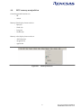
2.6.
Installation of HEW (Pure Debugger) for CPU Board
To install the HEW (Pure Debugger) for CPUBD from the installation disk, proceed as follows:
Insert the HEW (Pure Debugger) for CPUBD installation CD.
Run Windows if it is not already running.
Close all other applications that are running.
Choose Run from the Program Manager File menu.
Type Setup and click OK:
Figure 2.4
Run Dialogue Box
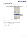
This runs the HEW (Pure Debugger) for CPUBD installer, and the following Welcome! Screen is
displayed:
Figure 2.5
HEW for CPUBD Installer Welcome! Screen
Click Next to proceed with the installation.
12
Check the License Agreement concerning installation and then click Yes to proceed.
Figure 2.6
Update Information (Readme) Dialogue Box
The following dialogue box enables the selection of directory in which user can install the HEW (Pure
Debugger) for CPUBD.
Ensure each selection is selected in turn to confirm the correct directory it is installing into.
Figure 2.7
Select Destination Directory Screen
13
Click Next to install into the default directory C:\HEW3 or C:\Program Files\Hew3, or specify an
alternative directory by clicking on Browse-button.
NOTE:
1. User may install this HEW debugger in the same directory as the previously setup HEW
toolchain (Make sure both are in the same version).
2. User may install the debugger into another directory, and register this component into the
other HEW tool administration menu.
3. Do not install a HEW toolchain over (in the same directory) the HEW debugger
4. A new Toolchain can be installed if it is installed to another directory (different from the
toolchain directory) and register either component to the respective HEW tool
administration menu.
Figure 2.8
Select Components Screen
Select the components to be installed.
Ensure each selection is selected in turn to confirm the correct directory it is installing into.
If user chooses Next, the following dialogue box will confirm each installation directory you selected
[Note: Always ensure that all components are installed in the same required directory]
14
Figure 2.9
Directory Confirmation Screen
Click Next to begin installation.
The installer then copies the HEW (Pure Debugger) for CPUBD files to the specified directory:
Figure 2.10
Installing Screen
The installation will complete with the Completion screen:
15
Figure 2.11
Completion Screen
At the end of the installation, icons for HEW (Pure Debugger) CPUBD will be created into the Start Menu
and ready for execution.
16
Section 3.
Setup of HEW (Pure Debugger) for CPU Board
In this section, the focus is to highlight the basic steps for any initial setup for a project. On subsequent
HEW activation, user will just be required to select the desired workspace/session, and the setup will be
done automatically.
Ensure that the CPUBD is linked up i.e. the serial cable is linked between the CPUBD and PC, and the
CPUBD is powered up.
3.1.
Running HEW (Pure Debugger) for CPU Board
Execute HEW (Pure Debugger) for CPUBD by selecting HEW.
Figure 3.1
HEW (Pure Debugger) for CPUBD Icon
17
3.2.
Creating a New Workspace
This step is to create a workspace, to inform the HEW environment, what type of tool is to be used. This
will enable user to have the same setup (workspace) at the following activation of the tool.
Click on [Create a new project workspace]
Figure 3.2
Select Platform Dialogue Box
Select a directory and key the workspace name as required
Figure 3.3
HEW Start-Up Window (without toolchain)
18
Select 38024F CPU Board as the target by selecting
o
CPU Series: SLP(Super Low Power)
o
CPU Type: 38024F
Figure 3.4
Select Target
Complete the workspace setup by clicking on [Finish] button
Figure 3.5
Debugger Setting Summary Window
A summary window shows the project files that will be generated
Click OK to proceed
19
3.3.
Selecting the Target (Debug Settings)
HEW (Pure Debugger) for CPUBD can be extended to support multiple target emulators or platforms (if
the system is setup for more than one platform), user will have to choose a platform for the session from
Debug Settings… in the Options menu.
Figure 3.6
Select Platform Dialogue Box
Select ‘38024F CPU Board’ and click OK to continue
A warning message will pop up. Click “OK” to proceed
NOTE: User can change the target platform at any time by choosing Debug Settings… from the
Options menu. Under the Download Modules, User can also define the Download Module/s for
Debugging.
When the emulator has been successfully setup, the HEW (Pure Debugger) for CPUBD desktop window
will be displayed. A message Connected is displayed in the Output Window.
20
Section 4.
4.1.
Performing Emulation
High-performance Embedded Workshop
The following shows a snap shot of the HEW Pure Debugger desktop Window:
Title bar
Help
button
Menu
bar
Toolbars
Workspace
Memory
Flash
button
Program
window
Source
Address
Output
window
Status bar
Figure 4.1
High-Performance Embedded Workshop Window
The key features of HEW (Pure Debugger) for CPUBD are described in the following sections:
Title Bar
:
Displays the name of the currently open workspace, project and file.
Menu Bar
:
Give you access to the HEW (Pure Debugger) for CPUBD debugging
commands for controlling CPUBD.
Toolbars
:
Provides convenient buttons as shortcuts for the most frequently used menu
commands. The tool bar can be docked or floated. It can be created, modified and
removed.
Program Window
:
Displays the source code of the program being debugged as well as the
source address.
21
Workspace
:
Display the detail of current workspace, and provide a quick & easy mean of
navigation.
Output Window
:
Displays the various outputs from HEW. For example, build details, results
of find files.
Status Bar
:
Displays the status of the CPUBD. For example, progress information about
downloads.
Help Button
:
Activates context sensitive help about any feature of the HEW (Pure
Debugger) for CPUBD software.
Memory Flash
Button
:
Flash contents of the memory window for on-chip ROM area into the MCU.
User is required to press this button when he/she manually updates the
contents of the memory window for on-chip ROM* area. This is not
required for RAM* area.
NOTE: * Please refer to the Appendix B – H8/38024F Memory Map for the on-chip ROM and RAM
areas.
The major topics are highlighted as follows.
1
Menu
Option
General Description
Emulation Setting
Sub Menu
Debug Settings
Emulator
Usage
Target Selection
View memory mapping and Configure
Platform
2
View
MCU related information
Disassembly
CPU
Symbol
Code
View disassembly window
Register, memory, Status, I/O
Label
Breakpoints
3
Memory
MCU memeory
manipulation
Fill
Refresh
4
Debug
Execution of MCU Code
Reset CPU
Go/Reset Go /Go to Cursor/
Set PC to Cursor /Run
Step In/ Over/ Out/ … Step
mode
Initialize
22
4.2.
Compiler Configuration & Debugger Session
In HEW compiler, every setting is stored in a configuration.
Session is not directly related to a configuration. This means that multiple sessions can share the same
download module and avoid unnecessary program rebuilds.
Users can create new configuration & session under the [Options\Build Configuration…] and
[Options\Debug Session…] pull down menu respectively.
Figure 4.2
Toolbar Showing the Session and Configuration
At the HEW (Pure Debugger) environment with a toolchain, a default debugger Session, [Debug] is
created to store information of
- Target platform
- Downloadable program
- Window positioning
- Registers value settings
Figure 4.3
Toolbar Showing the Sessions and Configurations Available
Generally, the HEW organized the configuration & session of a workspace as follows
Root Directory
Workspace directory Files
Configuration directory Files
Debug (DIR)
Release (DIR)
Configuration Information & Output (abs,lst…)
Configuration Information & Output (abs,lst…)
(xxx.hws)
Default Session (hsf)
Release Session (hsf)
C & header files
23
Example of usage:
User may use [Debug Session] to link to CPUBD, & [Debug] configuration setting to debug on the
project output file (xxx.abs) store in the Debug sub directory. User may switch the configuration to
[Release] and debug on the new setting (e.g optimization on…).
On the other hand, user may add sessions and may switch the configuration from [Release] to [Debug],
so as to debug on the generated output (xxx.abs) in the simulator environment.
NOTE: The path name defined in the [Options\Debug Setting..] must be relative to
[$(CONFIGDIR)\$(PROJECTNAME).abs]. Otherwise, when the session is switch, the download
module will not be able to switch correctly.
24
4.3.
Debug Settings
The Debug Settings in [Options\Debug Settings…] is to set the environment for a session.
In HEW Pure Debugger with a toolchain, users have been provided with two sessions
- Debug Session
- Release Session
In each session, users are to set
- Target (38024F, Simulator…)
- Default Debug Format (Elf\Dwaf2, S-record, IntelHex…)
- Download module ($(CONFIGDIR)\$(PROJECTNAME).abs)
In each session, users can set a list of command chain to be executed at the [option] tab.
4.4.
-
At connecting the emulator
-
Immediately before downloading
-
Immediately after downloading
Connecting & Disconnecting with the Emulator
The open (activation) or close (exit) of the HEW and/or workspace will determine the emulator and
HEW connectivity.
The alternative method is to use the “session” control:
In HEW (Pure Debugger) environment with a toolchain, user is provided with two sessions
- Debug Session (linking with emulator)
- Release Session (no target)
Thus by switching between the sessions, the emulator can be connected & disconnected from the HEW.
25
4.5.
Emulator Setting
The emulator setting, which consists of the system configuration & memory mapping, has to done
before any emulation.
Figure 4.4
4.5.1.
Option - Emulator
Configure Platform
The configure platform enables the user to set their target device and mode at startup.
To setup the system configuration:
From the Options menu, choose Emulator, System… or click on the following icon on the Toolbar:
The following Configure Platform dialogue will appear:
Figure 4.5
Target Configuration Dialogue Box
The user has the option of using standalone flashing by enabling the Standalone Flash in the Control
option.
26
4.5.1.1.
Standalone Flash
Standalone Flashing downloads the user target program directly into the memory. Monitor program
would not reside in the memory and hence no debugging is available if this option is used. This option
should only be used when the user has finalized his/her user target program and wants to run it on the
CPU Board.
Figure 4.6
Enabling Standalone Flash option
Click on the check box and click OK to enable standalone flashing.
When user downloads the selected object file, the following dialogue box would appear, prompting the
user to switch to Boot Mode to download the user target program.
Figure 4.7
Dialogue box for downloading user target program
After downloading the user target program, the dialogue box would prompt the user to switch to User
Program Mode to run the user target program. The user can either click YES to exit HEW or click NO to
re-download the user target program or Flash monitor Program.
27
Figure 4.8
Dialogue box for running user target program
NOTE: After pressing the reset switch when jumper JP9 is in the User Mode position, the user
target program will run in standalone mode, that is, no connection to HEW is required to run the
user target program, no debugging is available to user.
28
4.5.2.
Memory Mapping
Once the device and operating mode are selected, the default memory mapping will be set. The main
objective of memory mapping is to ensure that the emulator has the correct internal memory (Internal
ROM, RAM, IO) access.
To display the current memory mapping:
From the Options menu, choose Emulator, Memory resource… or click the Open memory mapping
button in the toolbar:
The memory mapping is shown in the following figure:
Figure 4.9
Memory Mapping Dialogue Box
29
Alternatively, the CPU memory map can be viewed from the status window:
From the View menu, choose CPU then Status, or click the View Status button in the toolbar:
Select the Memory tab in Status window to show the Memory Mapping configured:
Figure 4.10
Target Memory Configuration Dialogue
NOTE: CPUBD Memory Map is for display and information purpose, user cannot configure it.
The following explains the target memory configuration dialogue:
CPU Memory Map
:
Display the memory configuration of the specific target
device selected.
Program Name
:
Display the Downloaded Module’s name (User Target
Program) and the memory space that it has occupied
30
4.6.
Viewing of Program
Programs can be viewed as
-
Source Code level (C or assembly-language)
-
Disassembly level (assembly-language)
4.6.1.
Source Code level
Users may double-click on the file located in the workspace window to open and view the source code.
However this is merely in “editor” point of view. Users have to download the code to the emulator.
Once the code is downloaded, user can observe that “address values” have appeared in the source
address column of the source file.
NOTE:
When a break condition occurred during a running program, HEW will open up the source code or
disassembly window.
1. If the source code information is not available, the disassembly window will be opened.
2. If the downloaded project is a Elf/Dwarf2-based file, and the project has been moved from its
original path, the source file may not be automatically found. In this case, HEW will open a source
file browser dialogue box to allow user to manually locate the file.
Figure 4.11
Source Level
Information available:
Corresponding address for source file
PC location
Bookmark
Breakpoint
31
4.6.2.
Disassembly level
User can open the disassembly window:
Choose Disassembly from the View Menu, or right click on the source window, and select Goto
Disassembly
Figure 4.12
Disassembly Window
32
4.7.
MCU related information
User can be monitor & control the MCU information under the view menu.
Figure 4.13
4.7.1.
View – CPU
Registers
User can access these registers directly through the Register windows during break mode only.
Figure 4.14
33
Register
4.7.2.
Memory
Users will have to set a pre-defined address range to be monitored, before user can access the memory
through the memory windows. The memory window will not refresh constantly by itself. The access
methodology is different when emulation is in different mode (Run or Break). More memory functions
are explained in Memory manipulation.
Figure 4.15
4.7.3.
Set Memory
I/O
The IO window provides an easy access to MCU IO registers. The Address & Data values of respective
peripherals & MCU control registers are displayed in the IO window.
Figure 4.16
Input and Output Register
34
4.7.4.
Status
The status window uses three different tabs to monitor the emulator setting.
4.7.4.1.
Status - Memory
The memory tab display
- the available memory setting for the selected target device & mode.
- the address range where the User Target Program is loaded
Figure 4.17
Status – memory window
35
4.7.4.2.
Status - Platform
This platform tab shows the current emulation condition
- Target device
- CPU
- Run Status
- Break Cause
Figure 4.18
4.7.4.3.
Status – Platform window
Status - Events
The events tab shows the usage of
- PC Breakpoints
Figure 4.19
Status – Events window
36
4.7.4.4.
Symbol
This enables easy monitoring of declared variables in the assembly or C files. If debug information is not
included, the Watch and Locals sub menus will not appeared.
Figure 4.20
4.7.4.5.
View - Symbol
Label
When debug information is included, detail of all labels will be displayed in the Label window. User can
add new label into the window for simple reference too.
Figure 4.21
Label
NOTE: When a label value matches an operand, the corresponding instruction’s operand is
replaced by the label. If two or more labels have the same value, the earlier label (alphabetical
order) will be displayed.
37
4.7.4.6.
Watch
User will have to add the variables into the watch window.
Figure 4.22
Watch
NOTE: The variables can be displayed only if debug information is included in the absolute file (abs)
- The variables have not been excluded after the complier optimization
- The variables are not cleared as macro.
38
4.7.4.7.
Local
The Local variables will appear in the Locals window when user code has break/stop at a sub-routine.
NOTE: Local variables are temporary data stored in stack. Therefore it can only be viewed when
execution stops within a routine.
Figure 4.23
Locals
Tooltip watch - place the cursor at the variable and the general information of the variable will appear.
Figure 4.24
39
Tooltip
4.7.5.
Break Functions
Various breakpoints setting are discussed as follows.
Figure 4.25
View Code
Breaks are events used to intercept the normal program execution when a specific condition is matched.
There are two types of break in the CPUBD, hardware and software break.
For Hardware Event break, the preset break condition will cause the break event to occur after an
instruction is executed. For Software PC break, the break condition causes the break event to occur
before the break condition.
Types of Break
1
PC Break
(Software Break)
Description
A break occurs at the program address specified by PC Break window.
The instruction at this address is replaced with a system instruction
before the execution of code. If a PC breakpoint is detected, the
emulation stops at the specified address before executing the subsequent
instruction.
There are 3 scenarios when a hardware break occurs:
2
User Break
Pressing the ESC key of the host PC
(Hardware Break)
Pressing STOP button of HEW
Pressing reset switch of CPUBD
Table 4.1
Types of Breaks Encountered During Emulation
40
4.7.6.
Stack Trace
The Stack Trace window can be selected if only debug information has been supplied.
Stack Trace window shows the function call history.
Figure 4.26
Stack Trace
The following items can be displayed:
Kind
Indicate the symbol type
F:
Function
P:
Function parameter
L:
Local variable
Name
Indicate the symbol name
Value
Indicate the value, address and symbol type
At default, the function parameter and local variable are not displayed.
To enable all the items, right click in the Stack Trace window and select View Setting….
41
4.8.
MCU memory manipulation
General supported functions are
- fill
- refresh
Memory Data display format can be in
- Byte (x1)
- Word (x2)
- Long (x4)
- Double (x8)
Memory value display format can be in
- ANSI character
- unsigned char
- signed char
Figure 4.27
Memory Functions
42
4.9.
Execution of MCU Code
The MCU executes the user code either in “RUN” or “STEP” modes.
Figure 4.28
4.9.1.
Debug Functions
Reset CPU
When RESET CPU command is activated, the following actions will take place,
PC
=
Power on Reset vector value
ER7
=
H’FF7E
ER0-6 =
H’00000000
CCR
H’00
=
The microcomputer is reset.
i.e all internal peripherals registers will be at default state.
43
4.9.2.
Go, Reset Go, Goto Cursor, Set PC to Cursor, Run…
Near Real-time execution [Debug] by the MCU based on the user setting. These commands will cause
the HEW Debugger to steal a cycle from the running chip, in order to probe a response from the MCU to
verify that the communication link between the PC and CPUBD is still active.
NOTE: [Go To Cursor] will not halt if the running program never executes the code at the cursor.
Stopping of the execution is possible via [ESC] key, pressing the RESET switch on the CPUBD or
STOP button of HEW.
44
4.9.3.
Step Functions
There are four types of Step Functions:
- Step-In,
- Step-Out &
- Step-Over.
- Step…
- Step Mode (Auto, Assembly and Source)
Single Step executes the instruction at the current program counter. If an interrupt is asserted, the
interrupt service routine will not be serviced unless a “Go” command is issued.
Step-In will execute a single instruction only. For C source file, a single step will execute a “single C
source code”; whereas for an assembly file, a single step will execute a single assembly instruction code.
Step-Out executes till it has branched out of the current routine. It is used to perform stepping to exit
from the subroutine. Instructions in the subroutine function will be executed and PC will be set to the
line of code after the subroutine return instruction RTS.
Step-Over executes a function call (and any function call called by the function) and halt at the next
instruction.
Step… will execute multiple Step-in as specified by the user. The delay enables a visual view of the code
running sequence.
Figure 4.29
Step program
45
Step Mode setting configures how the step instruction operates.
Figure 4.30
Step Mode
- Auto: The execution mode will depend on the active window. i.e. when step instruction is activated in a
C Source window, a C-source level step will be invoked.
- Source: When Step instruction is executed, user will see a C-source level step. i.e. a series of assembly
code is run in the background.
- Assembly: When step is executed, the current assembly code located at current PC will be executed. The
disassembly window will pop up if the current window is a C source window.
46
4.10.
C-source Level Debugging
If user compiles and links the code (when a toolchain is used) with the Debug option enabled, the
ELF/DWARF2 (.abs) file with the debugging information is generated.
This enables user to debug the code in C-source level i.e. ,
- Display code in C source level,
- Step in, out & over code in C source level,
- View label,
- Go To label (address),
- View local
- Instant/add watches (local and user defined)
- Stack Trace
In other words, C-source Level debugging is only available when a ELF/DWARF2 (.abs) file is
downloaded. User would not be able to perform debugging if other file formats like S-Record, Intel Hex
and Binary are used.
47
Section 5.
Usage Precautions
Users may need to observe several constraints while operating the CPUBD. They are described as below:
5.1.
Corruption of Monitor Software
The monitor software occupies predefined locations in the flash memory area as the user program. Due
to unforeseen reason, user might access to this area and corrupt the monitor code. As a result, debugging
on the CPUBD could not performed and loss of communication between HEW and CPUBD.
Please refer to the Appendix B – H8/38024F Memory Map to take note of the area occupies by the monitor
code.
5.2.
Interrupt
Users, who want to perform debugging operation on the CPUBD, must enable the interrupt.
The example provided below, would result in a loss of communication between HEW and CPUBD.
Referring to the following code, after single stepping the line, set_imask_ccr(1);, I bit is set to ‘1’, disabling
interrupts.
Therefore, if another single step is performed, SCI3 interrupt would not occur and HEW will timeout
and a dialogue box “Error in communication” will be displayed as follow:set_imask_ccr(1);
light_LED();
5.3.
Timing Issues
Execution time to complete an interrupt subroutine must not be longer than 3sec, else HEW will timeout
and a dialogue box “Error in communication” will be displayed. If the frequency of interrupts generated
is less than 300msec, MCU will not be able to respond to the SCI3 interrupt sent by HEW. This will also
cause HEW to timeout.
The following shows the timing diagram when using HEW.
HEW
Monitor
≈300 ms
HEW
Monitor
Available to User
≈ 3 seconds
Figure 5.1
≈300 ms
Timing diagram of HEW
48
Available to User
≈ 3 seconds
5.4.
Watchdog timer
Watchdog timer must not be used to generate an internal reset when performing debugging operation.
This is because when counter in watchdog timer overflows, a signal is generated, resetting the MCU. At
this instance, if HEW performs a debug operation, the operation will not be completed as the MCU has
been reset. This will result in a timeout in HEW.
5.5.
Software Breakpoint
User shall not set a software breakpoint in the following address:
•
An area other than the flash memory or RAM
•
An area of address H'6A00 to H'7FFF [Monitor code resident]
•
An area of address H'F780 to H'FB7F [Monitor work area]
User shall not set any breakpoints in the interrupt service routines.
When execution resumes from the breakpoint address, single-step execution is performed before
execution resumes.
5.6.
Step
Step function (step in, step out and step over) is a simulated operation in the CPBD. It is not
implemented by the conventional hardware break mechanism.
No interrupts will be serviced during stepping.
Do not step into interrupt service routines as interrupts will be masked and HEW cannot
communicate with the CPUBD.
Stepping of SLEEP instructions are not allowed in HEW. User needs to use “Go to cursor” in order to
proceed to the next instruction.
49
5.7.
Power-Down Modes
User must not place the MCU in any of the following power-down modes when performing debugging
operation:
Watch Mode
Sub-active Mode
Subsleep Mode
Software Standby Mode
Serial Communication function is disabled/ reset in these modes, hence HEW is unable to communicate
with the CPUBD.
5.8.
SCI3
If debugging operation is required, user is not allowed to make use of SCI3 in his/her program because
SCI3 is used by HEW to communicate with the CPUBD.
5.9.
E10T /E7 Interface
When interfacing with E10T/ E7, the following limitations have to be observed:
The Port 9 pin 5 is not available for use because it is dedicated to E10T/ E7.
The Port 3 pin3, Port 3 pin 4, and Port3 pin 5 are also not available for use. To use these pins,
additional hardware is required on the user's board.
When E10T/ E7 emulator is used, the Port 9 pin 5 is designated as I/O, the Port 3 pin 3 and Port 3 pin
4 pins are designated as input, and the Port 3 pin 5 is designated as output.
User is prohibited from accessing the address regions, H'7000 to H'7FFF because E10T/ E7 emulator
uses them.
Access to address regions, H'F780 to H'FB7F is prohibited.
5.10.
Other Constraints
When viewing memory content in HEW, user may access to memory area above the available
memory area on H8/38024F MCU. This is because the H8/38024F MCU has only 64K address space
so the top bits of any address above 16 bits are ignored. This results in address error if data is written
to these wrong addresses.
User must be aware that they are not allowed to place the MCU into hardware standby mode as this
condition is exited by reset interrupt only. This would restart the monitor software, and DESTROYS
the current context of the user target program. Sleep mode and software standby mode may be
entered, but may not be exited by the use of the reset interrupt for the same reason mentioned.
When SLEEP instruction is executed, the MCU is unable to stay in SLEEP mode as HEW will send
data via SCI3 and wake up the MCU.
50
Section 6.
Hardware
The CPUBD comprises of the following blocks:
H8/38024F Micro-controller
Power Supply circuitry
Clock circuitry
Reset circuitry
Serial Communication block [via SCI3]
LEDs
Boot Mode Enable
E10T/ E7 Emulator Interface
External User Interface
6.1.
H8/38024F Micro-controller
The H8/38024F series has a system-on-chip architecture that includes peripheral functions and can be
used as embedded microcomputer in application systems. Its on-chip ROM offers flexibility as it can be
reprogrammed in no time to cope with all situations from early stages of mass production to full-scale
mass production. Users reconfiguring processor I/O ports are cautioned that pull-up resistors may be
needed for proper operation in some configurations.
6.2.
Power Supply Circuitry
The power supply circuitry supplies the DC power to the CPUBD from an external power supply. This is
also known as the system DC power. The CPUBD either accepts +5V DC or +9V DC voltage. This power
input is further stepped down to +3.3V DC that is acceptable by the MCU. In addition, user can select the
source of power supply to the MCU via a jumper selection between the system power supply or from a
target system.
6.3.
Clock Circuitry
The clock circuitry comprises of a quartz crystal of 9.8304MHz, system clock oscillator and a system
clock divider. The system clock divider halved the input clock from the quartz crystal [via OSC1 &
OSC2]. A sub clock is also provided by a quartz crystal of 32.768KHz on the CPUBD.
6.4.
Reset Circuitry
The reset circuitry comprises of RC circuit and a push button, S1 also known as the RST SW. During
power-on, the RC circuit asserts a reset signal to MCU to reset the MCU. If the RST SW, S1, is pressed, a
reset signal of approximately 20msec. duration is generated to allow proper reset to be performed.
51
6.5.
Serial Communication Block [via SCI3]
The CPUBD supports a three-wire serial channel using the on-chip serial communication channel [SCI3]
on the H8/38024F. SCI3 is used, both to flash the device using a flash programming software and to
connect to HEW. If neither flashing nor debugging with HEW is required, then the serial channel is
available to user. The SCI3 port provides transmit and receive signals to the RS3232 transceiver device
on the board. The transmit and receive signals from the transceiver device is then connected to the 9-pin
D-type connector, P1 on the CPUBD. The RS3232 transceiver device translates the RS232 signals to logic
levels and vice versa.
6.6.
FLASH ROM & RAM
The H8/38024F does not have any interface to external memory; it could only be used in single chip
mode. The chip has 32Kbytes of FLASH ROM and 1Kbytes of RAM for user. If debugging by user is
necessary, a monitor software would be downloaded together with the user program. A total of 6 Kbytes
of FLASH ROM and 1 Kbytes of RAM must be reserved for the monitor software.
6.7.
LEDs
There are two Red LEDs on the CPUBD available to user. LED D3 can be driven by port 9 bit 3 of the
H8/38024F. This can be selected by a jumper selection of the JP8 header, see section 2.5.3.
The second LED D4 can be driven by port 9 bit 2 of the H8/38024F. This can be selected by a jumper
selection of JP8 header, see section 2.5.3.
Note that a LOW output level from H8/38024F will set the LED ON and a HIGH output level would set
the LED OFF.
6.8.
Boot Mode Enable
Boot Mode is necessary to flash the FLASH kernel software and monitor software or user program if
required into the FLASH ROM when the CPUBD is placed into Boot mode. This is done via the Boot
Mode Enable jumper selection, JP9. Boot mode is required at the Power-On stage only. For the jumper
selection, see section 2.5.2.
6.9.
E10T/ E7 Interface
Interface the CPUBD to E10T/ E7 emulator is only allowed when the E10T/ E7 Enable jumper selection,
JP9 & JP10 on the CPUBD are set. See section 2.5.5.
This interface allows user to extend the debugging function of the CPUBD if an E10T/ E7 emulator is
available.
52
6.10.
External User Interface
The external user interface makes all H8/38024F signals available to user. These signals are connected to
the following connectors.
Four 2x10-pin connector [JP1 ~ JP4]
Two 2x30-pin socket connector [CON1, CON2]
The four 2x10-pin connectors [JP1~JP4] are placed closed to the H8/38024F QFP-80A on the CPUBD.
The two 2x30-pin socket connector [CON1, CON2] is placed to the edge of the CPUBD for ease of
connection to an external system. These connectors should be mounted on the solder side.
Both connector types use commonly available 2.54mm [0.100inch] pitch male header and female socket
with 0.635mm[0.025inch] square posts.
These connectors are all connected to the H8/38024F QFP-80A, and can be used to access the pins of the
chip and labeled with reference to the actual chip QFP-80A pin-out.
In addition, jumper selection must also be made, see section 2.5.4.
See appendix C, appendix D for the pin assignment for JP1~JP4 and CON1, CON2.
NOTE: External interface should be powered by an independent power supply.
53
Section 7.
7.1.
Monitor Software
Introduction to Monitor software
The Monitor Software is a FLASH-resident debugging program hosted on the CPUBD. Monitor software
may be used to download, run, and debug programs developed on a PC. The monitor software provides
all the necessary control and communications to operate under the HEW. This allows users to perform
high-level C debugging on the CPUBD.
Using the powerful debugging features of HEW, user may explore features of the H8/38024F microcontroller and the CPUBD by directly running sample programs.
The CPUBD comprises of limited RAM and is also a single chip micro-controller. To debug the user
program, both the user code and the monitor software must be programmed into the FLASH ROM. The
monitor software is built separately from the user program into S-record format. Without the monitor
software flashed into the FLASH ROM of the micro-controller, no debug can be performed with the
HEW software.
7.2.
Program Development
The tutorial program which accompanied the CPUBD contain examples you may use as a basic reference
code to explore and evaluate the architecture of the H8/38024F micro-controller.
When you install the High-Performance Embedded Workshop [HEW] with free Tiny/SLP tool-chain,
user obtain faster turn-around-time for a complete design cycle from ‘Code Entry’
‘Compile’
‘Linkage’
‘Download S-record file to MCU’
‘Execute User Program’
‘Debug User Program’
within an integrated environment (HEW with 38024F pure debugger).
7.3.
Monitor software Requirements
The monitor software makes use of the following peripheral function and input/output pins of
H8/38024F micro-controller, which cannot be used by user program during debugging. These are:
SCI3 Port for communication to the PC running HEW
IO Port 3 Pin 4
IO Port 9 Pin 5
54
7.4.
Mode Transition
The CPUBRD operates in two modes: Boot Mode and User Mode.
In Boot Mode, user can either download the monitor program or user target program (for Stand-alone
flash operation).
In User Mode, monitor program is being executed. User target program can be downloaded for
debugging purposes in User Mode.
The MCU loops in the Break Mode of the monitor program while waiting for commands from HEW.
To execute the downloaded user target program, user can either Run at current program counter, Reset Go
or perform Step functions (Step-In, Step-Over and Step-Out). This will cause it to operate in the User
Target Mode.
To terminate the User Run state, a break condition has to be asserted to bring the MCU to the Break
Mode. This can either be a preset condition (e.g. PC Break, Event Break) or a force break condition (Hit
ESC key or press STOP button). The MCU also returns to Break Mode automatically after completing
Step functions.
Figure 5.1 illustrates the mode transition diagram.
P95 = 0
P34 = 1
RESET
State
P95 = 1
P34 = X
BOOT
MODE
Legend:
X = Don’t care
USER
MODE
MONITOR
BREAK
MODE
DOWNLOAD
Monitor Program
OR
User Target Program
SCI Interrupt
Others
Command
Command
Processor
SCI Interrupt /
Break
Run, Step
USER
TARGET
MODE
Figure 7.1
Mode Transition Diagram
55
7.5.
Using Monitor software
The monitor software is used with the CPUBD. A manual is supplied in PDF format on a CD-ROM
covering installation and basic usage of the HEW.
All monitor software functions are accessed through the HEW graphical user interface and they are not
accessible by user commands via the serial interface.
The following functions are supported by monitor software:
Program
Download
- Supported file formats are:
•
Elf/Dwarf2
•
Motorola S-Record
•
SYSROF format
Breakpoint
- Only ONE breakpoint is allowed at a time when executing with the monitor
software
Types of Execution
- Three execution modes:
Memory
Read/Write
•
RUN mode
•
STOP
•
Single Step
- •
Memory Write
•
Memory Read
•
Fill Memory
Register
Read/Write
- •
Read CPU Register
•
Write CPU Register
Others
- •
•
7.6.
Mapping
Read or Write I/O registers [I/O windows]
Interrupts used by the Monitor
The monitor uses several interrupts to communicate with the host PC and control user program
execution.
The Following lists the interrupts reserved by the monitor, and their purpose:
Exception Source
Vector Number
Vector address
Reset
0
H’0000 to H’0001
Reserve
1
H’0002 to H’0003
SCI channel 3
18
H’0024 to H’0025
56
7.7.
Breakpoints
The CPUBD allows multiple breakpoints to be assigned at a time when executing with the monitor
software.
The breakpoint is controlled through software means, the line of code where the breakpoint is placed is
NOT executed and the program stops at the same instruction where the breakpoint is set.
NOTE:
When user inserts breakpoints, always use the ‘Disassembly window’.
Beware of instruction pre-fetches after branch instructions.
A breakpoint inserted on a branch instruction halt on the line of code where the instruction
branches. A breakpoint inserted on a line of code after a conditional branch such as BNE may
never be triggered because the line of code may always be pre-fetched and thus not seen by the
break control.
57
Section 8.
FLASH Programming
For programming of the FLASH ROM, FLASH Kernel software is developed. This FLASH Kernel is
downloaded together with the monitor software to the FLASH ROM at power on. It performs Write or
Erase control program operation in Boot mode and User mode.
The MCU’s serial communication port, SCI3 is used for flash programming and S-Record file format is
used during flash programming.
Please refer to specific device manual to enter boot mode.
8.1.
FLASH Programming the CPUBD
There are several methods to flash the CPUBD
38024F HEW (pure debugger)
FDT version 2.1
E10T/ E7 emulator for H8/38024F
While we had included in this manual about some 3rd parties tools to flash the CPUBD, however, the
correct operation of the CPUBD with these 3rd party tools is limited to the software version mentioned in
this manual.
In this context, only HEW is discussed, for other software, please refer to respective user manual.
Flash programming is performed in the HEW under the following modes:
Boot mode – the writing or erasing is performed in batches,
User program mode - the range of writing or erasing can be defined independently for each program
block.
8.1.1.
Boot Mode:
Boot Mode is necessary under the following operation:
Upgrade or Recovery of monitor software
Stand-alone flash operation of user program.
Hardware jumpers are required to be set accordingly to trigger MCU to enter boot mode. For jumper
settings, please refer to section 2.5.2 “Boot Mode Selection Jumpers”.
The sequence to trigger MCU into boot mode is described below:
Short JP9 [1-3] and short JP10 [3-5 default]
Power-on the CPU Board
Press RST SW to put MCU in the boot mode.
The boot program then start to transfers the write control program received from the host machine to the
MCU internal ram. When the write control program has been received, the entire internal flash memory
area is erased.
58
After entire flash memory has been erased, the execution transferred from the boot program to the write
control program being transferred to the MCU’s internal RAM, and the application program (Monitor
program or user program) received from the host machine is written to the flash memory.
8.1.2.
User Program Mode:
User Program mode is used only when the monitor program is resident in the flash memory.
Most of the time, user program mode is used to download user program and modify Flash memory
content.
The advantage of using user program mode is no jumper setting needed and the range of writing or
erasing can be defined independently for each program block (reduce programming time).
When monitor program is started, host machine sends flash memory command to MCU. The monitor
program copies the write / erase control program into internal RAM, this is followed by having
execution transferred to write / erase control program.
HEW sends address that needs to be programmed and the entire flash memory block is erased. The
MCU starts receiving program data from HEW and write to the flash memory. After completing the
flash programming, write / erase control program returns the execution control to the monitor program
waiting for debugging command from HEW.
8.2.
Operation during Programming Kernel Execution
Figure 8.1
Overview of Boot Mode
59
Figure 8.2
Overview of User Program Mode
60
Section 9. Tutorial (300l_tut)
The following describes a simple debugging session, designed to introduce the main features of the
CPUBD used in conjunction with the HEW (Pure Debugger) for CPUBD software.
The tutorial is designed to run in the CPUBD’s Flash memory so that it can be used without connecting
the CPUBD to any external user system.
User has to setup the CPUBD as stated in section 2 before the tutorial can begin.
9.1.
Introduction
The 300l_tut is based on a simple Assembler / C program located in your installed directory
“…\Tools\Renesas\DebugComp\Platform\Emulator\Evb38024F\300l_tut”.
Before reading this chapter, ensure the followings would certainly ease the learning process:
Setup the CPUBD and verify that it is working correctly with the HEW software (Pure Debugger) for
CPUBD.
User has to be familiar with the architecture and instruction set of the H8/300L Series MCU.
For more information please refer to the H8/300L Series Programming Manual and H8/38024F Series
Hardware Manual.
Refer to H8S, H8/300 Series High-Performance Embedded Workshop 3 in your installed directory
(install directory/Manuals/Renesas/PDFS/EH8HTU36.pdf) for more detailed information on using HEW.
9.2.
Overview
This program is an infinite loop that sort elements based on NAME in the alphabetical order, and AGE
and ID in the numerical ascending order.
The 300l_tut workspace is provided on the installation CD. A compiled version of the 300l_tut is
provided in Motorola S-Record in the file 300l_tut.mot.
61
How the 300l_tut Program Works:
The first part of the program includes a series of header files:
#include "machine.h"
#include "string.h"
The program then gives prototypes for the constants, structures, and function initial values:
#define
#define
#define
#define
NAME
AGE
ID
LENGTH
(short)0
(short)1
(short)2
8
struct namelist {
char
name[LENGTH];
short
age;
long
idcode;
};
struct namelist section1[] = {
"Naoko", 17, 1234,
"Midori", 22, 8888,
"Rie",
19, 7777,
"Eri",
20, 9999,
"Kyoko", 26, 3333,
"",
0,
0
};
int count;
void sort();
Followed by the main program below.
main( )
{
count = 0;
for ( ; ; ){
sort(section1, NAME);
count++;
sort(section1, AGE);
count++;
sort(section1, ID);
count++;
}
}
62
The remainder of the program defines the functions called from main:
void sort(list, key)
struct namelist list[];
short key;
{
short i,j,k;
long min;
char *name;
struct namelist worklist;
switch(key){
case NAME :
for (i = 0 ; *list[i].name != 0 ; i++){
name = list[i].name;
k = i;
for (j = i+1 ; *list[j].name != 0 ; j++){
if (strcmp(list[j].name , name) < 0){
name = list[j].name;
k = j;
}
}
worklist = list[i];
list[i] = list[k];
list[k] = worklist;
}
break;
case AGE :
for (i = 0 ; list[i].age != 0 ; i++){
min = list[i].age;
k = i;
for (j = i+1 ; list[j].age != 0 ; j++){
if (list[j].age < min){
min = list[j].age;
k = j;
}
}
worklist = list[i];
list[i] = list[k];
list[k] = worklist;
}
break;
case ID
:
for (i = 0 ; list[i].idcode != 0 ; i++){
min = list[i].idcode;
k = i;
for (j = i+1 ; list[j].idcode != 0 ; j++){
if (list[j].idcode < min){
min = list[j].idcode;
k = j;
}
}
worklist = list[i];
list[i] = list[k];
list[k] = worklist;
}
break;
}
}
63
9.3.
Tutorial Setup
Open tutorial workspace in:
“install directory\Tools\Renesas\DebugComp\Platform\Emulator\Evb38024F\300l_tut”.
NOTE: On a first time loading of the tutorial, a dialogue box prompting the move of workspace
from previous installed directory is displayed. Please click [YES] and the workspace would be
configured to the current installed directory permanently.
The setup of HEW is detailed in section 3.
Thus these steps will not be fully illustrated in this section.
Before downloading a program to the CPUBD, check the following items and user target program
(Download Module) to be debugged:
Device type
Memory map
NOTE: Refer to Section 4.5 for these emulation settings.
9.3.1.
Downloading the tutorial Program
Once the emulation settings of the CPUBD have been setup, user can download the object program for
debugging.
First load the object file, as follows:
Open the Debug Settings window by choosing Options menu and Debug Settings…
Select Elf/Dwarf2 for the Default Debug Format.
64
Figure 9.1
Debug Settings with Load Object File Dialogue
Click on the Add… button.
Select the download Format to be the ELF/DWARF2.
Click the Browse button and select the file ‘300l_tut.abs’.
Click OK to exit from Download Module window and click OK again to exit the Debug Settings
window.
Figure 9.2
Configure Load Object File Dialogue
A new folder, Download Modules, with the ‘300l_tut.abs’ file is created in the workspace window.
65
Download the file into the memory as follows:
Right click on the ‘300l_tut.abs’ in the workspace window and select Download module.
Figure 9.3
Download the Selected Object File
When the file has been downloaded, the Status-window Memory Tab will show the downloaded
Memory Address.
NOTE: All the code should lie within the on-chip ROM.
66
9.3.2.
Displaying the Program Listing
HEW (Pure Debugger) for CPUBD allows user to debug a program at source level, so that a listing of the
program can be seen alongside the disassembled code. To do this, user needs to read in a copy of the
source program from which the object file is compiled.
Choose Reset CPU from the Debug menu.
User will be prompted for the ‘Resetprg.c’ source file corresponding to the loaded object file if HEW
could not automatically locate the required file.
Figure 9.4
Source-window “Resetprg.c”
Run the program until Address H’0000040c (Set breakpoint at H’0000040c and select Reset Go, see
section 9.4).
Single step (see section 9.6 for Single Step) again to Jump into the 300l_tut.c main program window
67
Figure 9.5
Source-window “300l_tut.c”
If necessary, choose Format Views… from the Tools menu to select a font and size suitable for your
computer.
The above source-window has it font change to Courier New, 8-point font.
NOTE: If change of font or size did not take place in the window, close the window and re-open
the file again.
68
9.4.
Using Breakpoints
The simplest debugging aid is the program breakpoint (or PC breakpoint), it causes execution to stop
when a particular point in the program is reached. You can then examine the state of the MCU and
memory at that point in the program.
9.4.1.
Setting a Program Count (PC) Breakpoint
The program window provides a very simple way of setting a program breakpoint.
For example, set a breakpoint at address H’00000808 as follows:
Click once on the line containing address H’00000808 and right-click for the pop-up menu and select
Toggle Breakpoint OR
Click once on the line containing address H’00000808 and press F9.
A red dot will be displayed there to indicate that a program breakpoint is set at that address.
Figure 9.6
Setting a Breakpoint
69
9.4.2.
Executing the Program
To run the program from reset:
Choose Reset Go from the Debug menu, or click the Reset Go button in the toolbar icon.
The yellow arrow will appear on the read dot, indicating that the program is executed up to the
breakpoint you have inserted.
Figure 9.7
Program Break
70
The message Break = PC Break is displayed in the status bar to show the cause of the break.
This can be viewed under Break Cause of the last break in the System Status window.
From the View menu, choose CPU then Status, or click the Status Window button in the toolbar:
Figure 9.8
System Status Window
The cause of last break line shows that the break was a User PC Break.
71
9.4.3.
Reviewing the Breakpoints
The list of all the breakpoints set in the program can be viewed in the Breakpoints window.
Choose Source Breakpoints from the Edit menu, or click the Breakpoint Window button in the toolbar:
Figure 9.9
Breakpoints Window
The Breakpoints window also allows user to perform the following:
•
Define new breakpoints
•
Delete existing breakpoints
•
Disable existing breakpoints
Right-mouse click on a breakpoint in the Breakpoint-window to show the following pop-up:
Figure 9.10
Popup in Breakpoints Window
72
9.4.4.
Examining MCU Registers
While the program is halted, you can examine the contents of the MCU registers. These are displayed in
the Registers Window.
Choose CPU: Registers from the View menu, or click the Registers Window button in the toolbar:
Figure 9.11
CPU Registers Window
As expected, the value of the program counter (PC) is the same as the position of the yellow arrow,
H'00000808.
The registers’ values can be changed from the Registers window by double-clicking on respective
registers in the Registers window.
The Register-PC dialogue box allows you to edit the value.
Figure 9.12
Changing Register Value
73
9.5.
Examining Memory and Variables
The behavior of a program can be monitored by examining the contents of an area of memory, or by
displaying the values of variables used in the program.
9.5.1.
Viewing Memory
The contents of a block of memory can be viewed in the Memory Window.
For example, to view the memory corresponding to the array section1 in ASCII:
Choose CPU: Memory… from the View menu, or click the Memory Window button in the toolbar:
Enter “_section1” (a label valid only after downloading of Download Module- .abs file) in the Begin
Address field and “ffff” in the End field, and keep the Format as Byte (x1).
Figure 9.13
Open Memory-window
Click OK to open the Memory window showing the specified memory area.
Figure 9.14
Memory-window
Leave the Memory window open so that you can monitor the contents of the array label “_section1”.
74
9.5.2.
Watching Variables
It is useful to be able to watch the values of variables as the program is being stepped.
For example, set a watch on the structure (STRUCT) variable section1, which is declared at the beginning
of the program, using the following procedure:
Scroll up in the program window until you see the line:
sort(section1, ID);
In the Program windows, position the cursor on the word section1 and perform a right mouse button
click to display a pop-up menu.
Choose Instant Watch.
The Instant Watch dialogue box will be displayed:
Figure 9.15
Instant Watch Dialogue Box
Click Add button to add the variable to the Watch Window.
Figure 9.16
Watch Window
A variable watch can be added to the Watch Window by specifying its name. Use this method to add a
Watch on the variable ‘count’ as follows:
Click with the right mouse button within the Watch window and choose Add Watch… from the
pop-up menu.
75
The Add Watch… dialogue box appears.
Figure 9.17
Add Watch Dialogue Box
Type the variable ‘count’ and click OK.
The Watch Window will show the content of the variable label ‘count’.
NOTE: You might be getting different result of ‘count’.
Figure 9.18
Watch Window
You can double-click on the ‘+’ symbol to the left of any symbol in the Watch window to expand it and
display the individual elements in the array.
Figure 9.19
Displaying Individual Elements in an Array
76
9.6.
Stepping Through a Program
The CPUBD provides a range of options for stepping through a program (Step In, Step Out and Step
Over), executing an instruction or statement.
Execute up to the breakpoint from the current position by choosing Go from the Debug menu, or
clicking the Go button in the toolbar.
Issue one Step In from the Debug menu, or click on the Step In button in the toolbar command to
execute into the function sort(section1, NAME).
The yellow arrow will point to the first instruction in the function sort(section1, ID).
Figure 9.20
Executing up to a Function Call
Issue another Step In command to execute the next instruction.
User can also single step the assembly codes by selecting Step Mode: Assembly in Debug menu.
NOTE: After performing several Step In, there will be a time when the Code window will be
displayed showing the assembled codes. These codes are included into the user target program to
handle certain tasks such as saving or restoring CPU registers etc. C Compiler generates these
codes automatically.
77
9.7.
Watching Local Variables
The localized variables within a function can be viewed using the Locals Window.
For example, in order to examine the local variables in the function sort(), performs the following:
Open the Locals window by choosing Symbol: Local… from the View menu or clicking the Locals
Window button in the toolbar.
NOTE: The Local Window will be empty if there is no local variable declared or local variables
have not yet been entered. In another words, user target program execution should halt within a
function with local variables to show any variables within Locals Window.
In this 300l_tut, once when the execution halts within the function sort(), the local variables within
function sort() will be shown in Locals Window:
Figure 9.21
Locals Window
Double-click on the ‘+’ symbol in front of the variable ‘list’ in the Locals window to display the
individual elements of the array ‘list’.
Figure 9.22
Displaying Individual Elements in an Array
78
9.8.
Saves the Session
Before exiting, it is good practice to save the session so that debugging work can be resumed instantly
with the same configuration at the next debugging session.
Choose Save Session from the File menu.
Choose Exit from the File menu to exit from HEW (Pure Debugger) for CPUBD.
9.9.
What Next?
This 300l_tut has introduced the key features of the CPUBD, and their use in conjunction with the HEW
(Pure Debugger) for CPUBD. By combining the debugging tools provided in the CPUBD, user can
perform basic debugging to trace for any hardware and software problems by identifying the conditions
under which they occur.
79
Section 10.
Demonstration Program
There are two demonstration programs provided for user to have hands-on experience with the CPUBD.
Use the search key in the Windows OS under the installed directory to search for the keyword:
“install
and
directory\Tools\Renesas\DebugComp\Platform\Emulator\Evb38024\Sample\Blinking_LED”
“install directory\Tools\Renesas\DebugComp\Platform\Emulator\Evb38024\Sample\Running_LED”
You may select to change the ON/OFF speed of the LEDs by changing the value in the delay routine.
10.1.
Blinking LEDs
Start
Initialisation of IO
ports 9 register
Set ‘0’ to Port 92 & 93
(Turn On LED P92 & LED P93)
Delay Loop
Set ‘1’ to Port 92 & 93
(Turn Off LED P92 & LED P93)
80
10.2.
Running LEDs
Start
Initialisation of IO
ports 9 register
Set ‘0’ to Port 92
(Turn On LED P92)
Delay Loop
Set ‘1’ to Port 92
(Turn Off LED P92)
Set ‘0’ to Port 93
(Turn On LED P93)
Delay Loop
Set ‘1’ to Port 93
(Turn Off LED P93)
81
Section 11.
Trouble-Shooting
Common Failures
Actions
Remarks
1. Wrong Settings of
Jumpers and Switches
Check the manual and set
them accordingly.
2. Power LED off
Check DC input voltage
(+5.0V /+9.0V)
Check voltage across zener
diode D2 (≈3.9v)
Check PWR LED D1
3. Unable to detect
CPUBD in “USER
MODE”
If Power supply failure:
measure TP1 = 2.8v to
3.7v?
PWR LED broken?
Check JP9 3-5 short?
Check J2 2-3 short?
No monitor program at
Flash Memory
Check other software using
communication port?
Serial cable connects to
COMM 1-4?
Check U2 pin 12 for serial
data
Check Y2 (9.8304MHz) for
clock oscillation?
4. Unable detect CPUBD
in “BOOT MODE”
Check JP9 1-3 short?
Check J2 2-3 short?
Check other software using
communication port?
Serial cable connects to
COMM 1 ~ 4 ?
Check U2 pin 12 for serial
data
Check Y2 (9.8304MHz) for
clock oscillation?
5. Flashing
failure
Memory
6. Current
Overdrawn
[Current draws more
than 0.05 A]
Typical number of write
Time to change a new IC cycle = 10,000 times
U1 (H8/38024F)
Measure low resistance
Identify short traces and between Vcc with respect to
then
rework
as the ground.
accordingly.
82
10.2.
Running LEDs
Start
Initialisation of IO
ports 9 register
Set ‘0’ to Port 92
(Turn On LED P92)
Delay Loop
Set ‘1’ to Port 92
(Turn Off LED P92)
Set ‘0’ to Port 93
(Turn On LED P93)
Delay Loop
Set ‘1’ to Port 93
(Turn Off LED P93)
81
Appendix B
H8/38024F Memory Map
Memory Map Monitor Code
Memory Map –
H8/38024F
Interrupt Vector Area
H’0029
H’002A
H’69FF
H’6A00
H’7FFF
H’F780
H’FB7F
H’FB80
H’0029
H’002A
Free FLASH
for User code
26Kbytes
Interrupt Vector Area
Free FLASH
for User code
32Kbytes
Monitor Code
6Kbytes
H’7FFF
Not Used
Not Used
Internal I/O Register
Internal I/O Register
Not Used
Not Used
LCD RAM
LCD RAM
Not Used
Not Used
Internal RAM for
Monitor Work Area
1 Kbytes
H’F780
Internal RAM for
User Code 1 Kbytes
H’FB80
H’FB7F
Internal RAM for
FLASH Programming
Work Area 1Kbytes
Internal RAM for
User code 1 Kbytes
H’FF7F
H’FF7F
Internal I/O Registers
Internal I/O Registers
85
Appendix C
Pin Assignment for JP1~JP4
QFP-80A
Descriptions
Descriptions
QFP-80A
1
AVCC
1
JP1
2
P13/TMIG
2
3
P14/IRQ4*/ADTRG*
3
4
P16
4
5
P17/IRQ3*/TMIF
5
6
X1
6
7
X2
7
8
AVSS
8
9
OSC2
9
10
OSC1
10
11
TEST
11
12
RES*
12
13
P50/WKP0*/SEG1
13
14
P51/WKP1*/SEG2
14
15
P52/WKP2*/SEG3
15
16
P53/WKP3*/SEG4
16
17
P54/WKP4*/SEG5
17
18
P55/WKP5*/SEG6
18
19
P56/WKP6*/SEG7
19
20
P57/WKP7*/SEG8
20
QFP-80A
Descriptions
Descriptions
QFP-80A
21
P60/SEG9
1
2
P61/SEG10
22
23
P62/SEG11
3
4
P63/SEG12
24
25
P64/SEG13
5
6
P65/SEG14
26
27
P66/SEG15
7
8
P67/SEG16
28
29
P70/SEG17
9
10
P71/SEG18
30
31
P72/SEG19
11
12
P73/SEG20
32
33
P74/SEG21
13
14
P75/SEG22
34
35
P76/SEG23
15
16
P77/SEG24
36
37
P80/SEG25
17
18
P81/SEG26
38
39
P82/SEG27
19
20
P83/SEG28
40
QFP-80A
Descriptions
Descriptions
QFP-80A
41
P84/SEG29
1
2
P85/SEG30
42
43
P86/SEG31
3
4
P87/SEG32
44
45
PA3/COM4
5
6
PA2/COM3
46
47
PA1/COM2
7
8
PA0/COM1
48
49
V3
9
10
V2
50
51
V1
11
12
VCC
52
53
VSS
13
14
P90/PWM1
54
55
P91/PWM2
15
16
P92
56
57
P93
17
18
P94
58
59
P95
19
20
IRQAEC
60
QFP-80A
Descriptions
Descriptions
QFP-80A
61
P30/UD
1
2
P31/TMOFL
62
63
P32/TMOFHd
3
4
P63/SEG12
64
65
P64/SEG13
5
6
P65/SEG14
66
67
P66/SEG15
7
8
P67/SEG16
68
69
P70/SEG17
9
10
P71/SEG18
70
JP2
JP3
JP4
71
P72/SEG19
11
12
P73/SEG20
72
73
P74/SEG21
13
14
P75/SEG22
74
75
P76/SEG23
15
16
P77/SEG24
76
77
P80/SEG25
17
18
P81/SEG26
78
79
P82/SEG27
19
20
P83/SEG28
80
86
Appendix D
Pin Assignment for CON1 & CON2
Signal Name
CON 1
Signal Name
OSC1
1
2
AVCC
GND
3
4
AVSS
X1
5
6
UVCC
GND
7
8
GND
P11
9
10
P10
P13
11
12
P12
P15
13
14
P14
P17
15
16
P16
NC
17
18
NC
NC
19
20
NC
NC
21
22
NC
NC
23
24
NC
P31/TM0FL
25
26
P30
P33
27
28
P32/TM0FH
P35
29
30
P34
P37/AEVL
31
32
P36/AEVH
RES_N
33
34
GND
IRQAEC
35
36
NC
P81/SEG26
37
38
P80/SEG25
P83/SEG28
39
40
P82/SEG27
P85/SEG30
41
42
P84/SEG29
P87/SEG32
43
44
P86/SEG31
P91/PWM2
45
46
P90/PWM1
P93
47
48
P92
P95
49
50
P94
NC
51
52
NC
PA1/COM2
53
54
PA0/COM1
PA3/COM4
55
56
PA2/COM3
NC
57
58
NC
NC
59
60
NC
87
Signal Name
CON 2
Signal Name
GND
1
2
GND
V1
3
4
NC
V3
5
6
V2
GND
7
8
UVCC
P41/RXD32
9
10
P40/SCK32
P43/IRQ_N
11
12
P42/TXD32
P51/SEG2
13
14
P50/SEG1
P53/SEG4
15
16
P52/SEG3
P55/SEG6
17
18
P54/SEG5
P57/SEG8
19
20
P56/SEG7
P61/SEG10
21
22
P60/SEG9
P63/SEG12
23
24
P62/SEG11
P65/SEG14
25
26
P64/SEG13
P67/SEG16
27
28
P66/SEG15
P71/SEG18
29
30
P70/SEG17
P73/SEG20
31
32
P72/SEG19
P75/SEG22
33
34
P74/SEG21
P77/SEG24
35
36
P76/SEG23
NC
37
38
NC
PB1/AN1
39
40
PB0/AN0
PB3/AN3
41
42
PB2/AN2
PB5
43
44
PB4
PB7
45
46
PB6
NC
47
48
NC
NC
49
50
NC
NC
51
52
NC
NC
53
54
NC
NC
55
56
NC
NC
57
58
NC
GND
59
60
GND
88
Micon Block
C1
0.1u
3
2
1
JP1
AVCC
P14
P17
X2
OSC2
TEST
P50
P52
P54
P56
UVCC
+3.3V
R2
220
BC847
2
HEADER 10X2
D2
3.9V
DC CN
C3
10u
C4
0.1u
D1
JP2
P60
P62
P64
P66
P70
P72
P74
P76
P80
P82
PWR LED
+5V/+9V
Only
Socket DC
Jack 2.1mm
PCB Mt
P/N code :
KP-99503-0
Diode Zener
BZV55C3V9 1/2W
P/N:DZ-45503-9
1
3
5
7
9
11
13
15
17
19
P61
P63
P65
P67
P71
P73
P75
P77
P81
P83
2
4
6
8
10
12
14
16
18
20
P30
P31
P32
P33
P34
P35
P36
P37
P40
P41
P42
P43
PB0
PB1
PB2
PB3
PB4
PB5
PB6
PB7
HEADER 10X2
C5
0.1u
VCC
Serial Comm
Block
U1
R5F
10k 7PACK SIP
7
C12
1u
1
3
C14
1u
4
5
T1 OUT
R1 OUT
T2 IN
R2 IN
T2 OUT
R2 OUT
C1+
C1-
V+
V-
14
12
7
9
C8
15p
C9
15p
Crystal 32.7680KHz
Cylinder 2x6
P/N:XC-05181-0
P30
P32
P34
P36
P40
P42
PB0
PB2
PB4
PB6
1
3
5
7
9
11
13
15
17
19
P31
P33
P35
P37
P41
P43
PB1
PB3
PB5
PB7
2
4
6
8
10
12
14
16
18
20
HEADER 10X2
Sub-Board Interface Block
OSC2
9.8304MHz
C10
C11
12p
12p
OSC1
GND
X1
GND
Crystal 9.8304MHz
HC49-U-S
P/N:XC-06709-0
P31
P33A
P35A
P37
RES_N
IRQAEC
P81
P83
P85
P87
P91
P93A
P95
C15
1u
IC SP3232ECT
RS232 Driver/
Receiver
P/N : UF-53232-0
VCC
PA1
PA3
C
VCC
C
C
RES_N
C
E10T Enable &
Boot Mode Enable
Block
C
4
R4
1M
P17
LED Enable
Block
R5C
HEADER 10X2
JP4
H8/38024 F-ZTAT
FP-80A
P/N : HD64f38024F
P13
CONNECTOR DB9
Using Direct
NULL Modem
Serial Cable
C13
1u
C2+
C2MAX3232
P85
P87
PA2
PA0
V2
+3.3V
P90
P92
P94
IRQAEC
2
4
6
8
10
12
14
16
18
20
Y2
5
9
4
8
3
7
2
6
1
P41
RXD
2
6
1
3
5
7
9
11
13
15
17
19
X2
R5D
10k 7PACK SIP
5
10
8
T1 IN
R1 IN
P83
P82
P81
P80
P77
P76
P75
P74
P73
P72
P71
P70
P67
P66
P65
P64
P63
P62
P61
P60
32.768KHz
P1
R5A
10k 7PACK SIP
R5G
10k 7PACK SIP
8
X1
C
C
11
13
P83
P82
P81
P80
P77
P76
P75
P74
P73
P72
P71
P70
P67
P66
P65
P64
P63
P62
P61
P60
40
39
38
37
36
35
34
33
32
31
30
29
28
27
26
25
24
23
22
21
Crystal Oscillator
Block
Y1
U2
P42
TXD
JP3
P84
P86
PA3
PA1
V3
V1
VSS
P91
P93
P95
C6
0.1u
OSC1
C7
1u
H8/38024
R6
220
R3
100k
61
62
63
64
65
66
67
68
69
70
71
72
73
74
75
76
77
78
79
80
AVCC 1
P13
2
P14
3
P16
4
P17
5
X1
6
X2
7
AVSS 8
OSC2 9
OSC110
TEST 11
RES_N
12
P50 13
P51 14
P52 15
P53 16
P54 17
P55 18
P56 19
P57 20
3
CON1
1
3
5
7
9
11
13
15
17
19
21
23
25
27
29
31
33
35
37
39
41
43
45
47
49
51
53
55
57
59
2
4
6
8
10
12
14
16
18
20
22
24
26
28
30
32
34
36
38
40
42
44
46
48
50
52
54
56
58
60
AVCC
AVSS
UVCC
GND
GND
V1
V3
GND
P41
P43
P51
P53
P55
P57
P61
P63
P65
P67
P71
P73
P75
P77
P14
P16
P30
P32
P34A
P36
GND
P80
P82
P84
P86
P90
P92A
P94
PB1
PB3
PB5
PB7
PA0
PA2
GND
HEADER 30X2
CON2
1
3
5
7
9
11
13
15
17
19
21
23
25
27
29
31
33
35
37
39
41
43
45
47
49
51
53
55
57
59
2
4
6
8
10
12
14
16
18
20
22
24
26
28
30
32
34
36
38
40
42
44
46
48
50
52
54
56
58
60
GND
V2
UVCC
P40
P42
P50
P52
P54
P56
P60
P62
P64
P66
P70
P72
P74
P76
PB0
PB2
PB4
PB6
GND
HEADER 30X2
S1
Reset
Block
R7
220
D3
C16
0.1u
R8
220
D4
LED
LED
JP8
P93
P93A
1
3
5
2
4
6
P92
P92A
HEADER 3X2
TP3
T P GND
VCC
JP8
1-3 : LED D3 EN
2-4 : LED D4 EN
3-5
4-6
: P93 EN
: P92 EN
2
4
6
8
10
12
14
1
3
5
7
9
11
13
HEADER 7X2
RES_N
JP9
P33
P33A
JP9
3-5 : Normal Mode / E10T EN
1-3 : Boot Mode
Caution! Do not change when power is on.
JP10
3-5 : E10T EN
4-6 : E10T EN
1-3 : P34 EN
2-4 : P35 EN
P35
P35A
6
4
2
5
3
1
P95
D5
BOOT LED
JP7
VSS
10k 7PACK SIP
SPST SW
J1
P30
P31
P32
P33
P34
P35
P36
P37
P40
P41
P42
P43
PB0
PB1
PB2
PB3
PB4
PB5
PB6
PB7
R5B
10k 7PACK SIP
3
1
Q1
P13
P16
X1
AVSS
OSC1
RES_N
P51
P53
P55
P57
2
4
6
8
10
12
14
16
18
20
R5E
10k 7PACK SIP
6
C17
0.1u
R1 470
TP1
VCC
T P VCC
1
3
5
7
9
11
13
15
17
19
TP4
T P GND
60
59
58
57
56
55
54
53
52
51
50
49
48
47
46
45
44
43
42
41
Power Supply
Block
C2
0.01u
IRQAEC
P95
P94
P93
P92
P91
P90
VSS
VCC
V1
V2
V3
PA0
PA1
PA2
PA3
P87
P86
P85
P84
J2
HEADER 3
IRQAEC
P95
P94
P93
P92
P91
P90
VSS
+3.3V
V1
V2
V3
PA0
PA1
PA2
PA3
P87
P86
P85
P84
CPUBD-38024F Schematic Drawings
AVCC
P13
P14
P16
P17
X1
X2
AVSS
OSC2
OSC1
TEST
RES_N
P50
P51
P52
P53
P54
P55
P56
P57
Appendix E
VCC
TP2
T P VCC
HEADER 3X2
JP10
6
4
2
5
3
1
HEADER 3X2
P34
P34A
Renesas System Solutions Asia Pte Ltd - Singapore Design Centre
Title
Size
A3
Date:
89
SLP Micon Application Board with Debug - CPU Board
Document Number
<Doc>
Friday, September 05, 2003
Drawn by = C.L. Sam
Sheet
1
of
1
Rev
1.1
Appendix F
Bill of Materials
Items
Designator
A) Board H8/38024F CPU
1
2
C10 C11
3
C8
C9
4
C2
5
C4
C6
C16 C17
6
C1
C5
7
C7
C12 C13 C14 C15
8
C3
9
D2
10
J2
11
JP8 JP9 JP10
12
JP1 JP2 JP3 JP4
13
J2(2-3) JP8(1-3) JP8(2-4) JP9(3-5)
14
JP9(4-6) JP10(3-5) JP10(4-6)
15
J1
16
P1
17
D1
18
D3
D4
D5
19
Q1
20
R2
R6
R7
R8
21
R3
22
R4
23
R1
24
R5
25
S1
26
U2
27
Y1
28
Y2
29
30
31
B) Packaging
32
33
34
JP7
35
CON1 CON2
36
37
38
39
40
C) Optional Items
41
42
P/N Code
Part Description
Qty
Package Mfg
AA-02129-2
CA-70121-6
CA-70151-6
CA-73101-3
CA-74101-3
CE-14105-1
CE-15105-1
CE-16105-1
DZ-45503-9
KH-20103-1
KH-20153-1
KH-20160-1
KH-22004-0
PCB CPU Board Ver 1.1
Capacitor SMD 0805 12pF / 50V 5%
Capacitor SMD 0805 15pF / 50V 5%
Capacitor SMD 0805 10nF / 50V 10%
Capacitor SMD 0805 100nF / 50V 10%
Capacitor Ele GSS-R 100nF/50V
Capacitor Ele GSS-R 1uF/50V
Capacitor Ele GSS-R 10uF/50V
Diode Zener BZV55C3V9 1/2W
Header Pin 0.100" 1x3-Way Gold
Header Pin 0.100" 2x3-Way Gold
Header Pin 0.100" 2x10-Way Gold
0.100" Micro Shunt JH6
1
2
2
1
4
2
5
1
1
1
3
4
7
KP-99501-0
KS-60309-0
LE-03121-0
LE-03321-0
QB-02847-1
RA-63222-0
RA-66102-0
RA-67102-0
RA-73471-0
RL-00941-0
SP-10011-0
UF-53232-0
XC-05181-0
XC-06709-0
Connector DC Jack 2.1mm PCB Mt
Connector D-Sub Female 9-Way RA
LED 3mm Green Diffused
LED 3mm Red Diffused
Transistor BC847B
Resistor SMD 1206 1/4W 2% 220R
Resistor SMD 1206 1/4W 2% 100K
Resistor SMD 1206 1/4W 2% 1M
Resistor SMD 2010 1/2W 1% 470R
Resistor Netwk-A SIL 1/8W 5% 10Kx9-Pin
Switch Tactile Round
IC SP3232ECT RS232 Driver /Receiver
Crystal 32.7680 KHz Cylinder 2x6
Crystal 9.8304 MHZ HC49/U-S
Anti-Static Bag
Label for Serial Number
IC H8/38024 FZTAT, FP-80A
1
1
1
3
1
4
1
1
1
1
1
1
1
1
1
1
1
Rubber Foot Stick On SJ5008
Box RSC ST-04 320"x340"x190"
Header Pin 0.100" 2x7-Way Gold
Connector PCB Mt 0.100" 2x30-Way
Anti-Static Bag for Accessories
Bubble Foam
Checking List Form
Label for Carton Box
Manual in CR-ROM format w/Label & Cover
4
1
1
2
6
1
1
1
1
***
BA-61007-0
BZ-00053-0
KH-20157-1
KH-27180-0
WL-64004-0 Supply Cable Assembly Rev 1.0
WL-64004-1 Serial Cable M/M 9-Way
91
1
1
0805
0805
0805
0805
thru-hole
thru-hole
thru-hole
thru-hole
thru-hole
thru-hole
thru-hole
thru-hole
thru-hole
thru-hole
thru-hole
thru-hole
SOT23
1206
1206
1206
2010
thru-hole
thru-hole
SO 150
thru-hole
thru-hole
FP-80A
AVS
Panasonic
Panasonic
AVX / any
AVX / any
Rubycon / any
Rubycon / any
Rubycon / any
Philips Semi
AUK
AUK
AUK
AUK
AUK
AUK
MIC
MIC
Philips Semi
any
any
any
any
Toma Resistor
KIE / any
Sipex
TSC
TSC
any
any
Hitachi
3M
Renesas Technology (Asia Sales Offices)
URL: http://www.renesas.com
URL: http://www.sg.renesas.com/sales
ASIA HEADQUARTERS & TECHNICAL SUPPORT :
South Asia Headquarters : Singapore
Renesas Technology Singapore Pte. Ltd.
1, HarbourFront Avenue,
#06-10, Keppel Bay Tower,
Singapore 098632.
Tel : (65)-6213-0200
Fax : (65)-6278-8001
Email : [email protected]
North Asia Headquarters : Hong Kong
Renesas Technology Hong Kong Ltd.
7/F., North Tower, World Finance Centre,
Harbour City, Canton Road,
Hong Kong.
Tel: (852) 2265-6688
Fax: (852) 2375-6836
Email : [email protected]
ASIA SALES OFFICES :
China
Renesas Technology Hong Kong Ltd
Shenzhen Representative Office
Unit 1511-12, Shun Hing Square Di Wang Commercial Centre,
5002 Shennan Road East, Shenzhen City 518008, China
Tel : (86) (755) 8246-1711
Fax : (86) (755) 8246-1728
Email : [email protected]
URL : http://www.cn.renesas.com
Renesas Technology (Shanghai) Co., Ltd.
26/F., Ruijin Building,
No. 205 Maoming Road (S),
Shanghai 200020, China
Tel : (86) (21) 6472-1001
Fax : (86) (21) 6415-2952
Email : [email protected]
URL : http://www.cn.renesas.com
Renesas Technology (Shanghai) Co., Ltd. Beijing Office
Room 1654, Office Building, New Century Hotel,
No. 6 Southern Rd. Capital GYM.,
Beijing 100044, China
Telex : 210509 HTCBJ CN
Tel : (86) (10) 6849-2430
Fax : (86) (10) 6849-2819
Email : [email protected]
URL : http://www.cn.renesas.com
Taipei
Renesas Technology Taiwan Co., Ltd.
(effective July 1, 2003)
FL. 10, #99, Fu-Hsing N. Rd., Taipei, Taiwan
Tel : (886)(2) 2715-2888
Fax : (886)(2) 2713-2999
Email : [email protected]
URL : http://www.tw.renesas.com
Technical Support
Renesas System Solutions Asia Pte. Ltd.
1, Harbourfront Avenue,
#06-06, Keppel Bay Tower,
Singapore 098632.
Tel : (65)-6213-0333 and 6387-2839
Fax : (65)-6278-1226
CPUBD-38024F