1
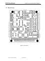
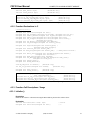
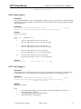
User Manual for CS210-12 (/14) 10 MSPS, 12-bit, PC/104, (ISA) Analog Input Module CHASE SCIENTIFIC COMPANY P.O. Box 1487 Langley, WA 98260 Tel: 360-221-8455 Fax: 360-221-8457 Email: [email protected] Web: http://www.chase2000.com CS210_manual_2030629.odt Copyright 1998-2003 by Chase Scientific Company This manual, the CS210 module, and the software drivers outlined in this document are copyrighted with all rights reserved. Under the copyright laws, the above mentioned may not be copied, in whole or in part, without the express written consent of Chase Scientific Company. CS210 User Manual 10 MSPS, PC/104 ANALOG INPUT MODULE TABLE OF CONTENTS 1 GENERAL INFORMATION...........................................................................................................................4 1.1 INTRODUCTION..................................................................................................................................................4 1.2 REFERENCES.................................................................................................................................................... 4 1.3 DELIVERABLES................................................................................................................................................. 4 1.3.1 Software................................................................................................................................................ 4 1.3.2 Hardware.............................................................................................................................................. 5 1.3.3 Checklist................................................................................................................................................5 1.4 PRODUCT SPECIFICATION....................................................................................................................................6 1.5 TECHNICAL SUPPORT / SOFTWARE UPDATES......................................................................................................... 7 1.6 WARRANTY..................................................................................................................................................... 7 2 HARDWARE DESCRIPTION........................................................................................................................ 9 2.1 INTRODUCTION..................................................................................................................................................9 2.2 BLOCK DIAGRAM..............................................................................................................................................9 2.3 BOARD DRAWING........................................................................................................................................... 10 2.4 BOARD I/O................................................................................................................................................... 11 2.4.1 Header Pinouts and Pin Descriptions................................................................................................ 11 2.4.1.1 40-Pin Analog I/O.......................................................................................................................................... 11 2.4.1.2 34-Pin Digital I/O........................................................................................................................................... 12 2.4.1.3 40-Pin Memory Expansion.............................................................................................................................12 2.4.2 Board Configuration...........................................................................................................................13 2.4.2.1 Base Address...................................................................................................................................................13 2.4.2.2 IRQ Selection..................................................................................................................................................14 2.4.3 I/O Map...............................................................................................................................................14 2.5 REGISTER DEFINITIONS.................................................................................................................................... 15 2.6 ANALOG INPUT RANGES AND RESOLUTION......................................................................................................... 15 2.7 ANALOG OUTPUT RANGE AND RESOLUTION....................................................................................................... 16 2.8 DIGITAL I/O DESCRIPTION............................................................................................................................... 16 3 THEORY OF OPERATION.......................................................................................................................... 17 3.1 INTRODUCTION................................................................................................................................................17 3.2 ACQUIRING ANALOG INPUT DATA.....................................................................................................................17 3.3 AUXILIARY INPUTS..........................................................................................................................................17 4 SOFTWARE DRIVERS................................................................................................................................. 17 4.1 INTRODUCTION................................................................................................................................................17 4.2 DRIVER INSTALLATION.....................................................................................................................................18 4.2.1 DOS / Windows 3.1............................................................................................................................. 18 4.2.2 Windows 95......................................................................................................................................... 18 4.2.3 Windows NT........................................................................................................................................ 18 4.3 FUNCTION CALLS............................................................................................................................................18 4.3.1 Function Declarations in Pascal........................................................................................................ 18 4.3.2 Function Declarations in C................................................................................................................ 19 4.3.3 Function Call Descriptions / Usage................................................................................................... 19 4.3.3.1 Initialize ()...................................................................................................................................................... 19 4.3.3.2 Set_Frequency ().............................................................................................................................................20 4.3.3.3 Select_Channel ()............................................................................................................................................20 4.3.3.4 Select_Gain ()................................................................................................................................................. 21 4.3.3.5 Set_Trigger ()..................................................................................................................................................21 4.3.3.6 Set_Memory_Size ()....................................................................................................................................... 22 4.3.3.7 Set_Pretrigger ()..............................................................................................................................................22 4.3.3.8 Digitize ()........................................................................................................................................................23 © Chase Scientific Company (360)221-8455 2 CS210 User Manual 10 MSPS, PC/104 ANALOG INPUT MODULE 4.3.3.9 Transfer_Data () [DOS Only]........................................................................................................................ 23 4.3.3.10 Read_Long ()................................................................................................................................................ 24 4.3.3.11 Write_Port ().................................................................................................................................................24 4.3.3.12 Read_Port ()..................................................................................................................................................25 4.3.3.13 Set_DAC ()................................................................................................................................................... 25 4.3.3.14 Trigger_Done ()............................................................................................................................................ 26 4.3.3.15 Board_Detected ().........................................................................................................................................26 4.3.3.16 HW_IRQ ()................................................................................................................................................... 27 4.3.3.17 Open_Driver () [Win95/NT Only].............................................................................................................. 27 4.3.3.18 Close_Driver () [Win95/NT Only].............................................................................................................. 27 4.3.3.19 Set_IRQ () [Win95/NT Only] { ADVANCE INFORMATION }............................................................. 28 4.3.3.20 Is_IRQ_Set () [Win95/NT Only] { ADVANCE INFORMATION }........................................................ 28 4.3.3.21 Destroy_IRQ () [Win95/NT Only] { ADVANCE INFORMATION }......................................................29 4.3.3.22 Simulate_HW_Int () [Win95/NT Only] { ADVANCE INFORMATION }............................................... 29 4.4 PROGRAMMING EXAMPLES............................................................................................................................... 29 4.4.1 DOS / Windows 3.1 Example Using Borland C++ 5.02.................................................................... 29 4.4.2 Windows 95/NT DLL Example using Borland C++ 5.02..................................................................32 4.5 ERROR RETURN CODE LIST............................................................................................................................. 34 5 MISCELLANEOUS........................................................................................................................................ 35 5.1 CALIBRATION................................................................................................................................................. 35 5.2 MAINTENANCE............................................................................................................................................... 35 ILLUSTRATIONS / TABLES FIGURE 1 – BLOCK DIAGRAM...................................................................................................................... 9 FIGURE 2 – BOARD LAYOUT....................................................................................................................... 10 FIGURE 3 - 40-PIN ANALOG I/O CONNECTOR........................................................................................11 FIGURE 4 - 34-PIN DIGITAL I/O CONNECTOR........................................................................................ 12 FIGURE 5 - 40-PIN MEMORY EXPANSION CONNECTOR.................................................................... 13 FIGURE 6 - PORT I/O...................................................................................................................................... 15 “CS210_man_V97_v1p5a.doc” was created on 29/06/2003 21:07:00 and last modified on 2/14/2010 02:52:49 PM © Chase Scientific Company (360) 221-8455 3 CS210 User Manual 1 10 MSPS, PC/104 ANALOG INPUT MODULE GENERAL INFORMATION 1.1 Introduction The CS210-12 is a PC/104 (ISA) analog I/O module which features two (2) 12-bit, high speed differential/synchronous input channels, each capable of capturing data at 10 MSPS with a minimum bandwidth of 5 MHz. The CS210 module comes configured with additional features including: (4) 10 MSPS multiplexed/differential analog input channels. (32) channels of CMOS/TTL compatible digital I/O (16 input/16 output ) (4) unipolar voltage outputs with 12-bit resolution (1) external clock input (1) external trigger input An extended temperature version is available to support -40°C to 85°C operation. All analog I/O is available on a 40-pin header while all digital I/O is available on a separate 34-pin header. Each high speed channel has 1KB, 8KB or 32 KB per channel of software selectable onboard memory. Post/pre-triggering is selectable in 1 sample increments. Sources for the trigger include either one of the (2) high speed analog inputs using 1 of 256 levels of software selectable trigger thresholds, a software generated trigger, or an external TTL signal. Timing is controlled by an onboard clock circuit referenced to a 10 MHz crystal oscillator and is divided down by a programmable 16-bit divider circuit. A software command or external TTL trigger can also be used to initiate the A/D conversion sequence. Once the A/D conversions are completed, data can be transferred from the module to main memory by direct I/O port reads or through an interrupt service routine. The CS210 stores up to 32 K samples for each channel. 1.2 References “P996.1 Standard for Compact Embedded-PC Modules”; PC/104 Specification, Version 2.3, June 1996 by PC/104 Consortium. “IEEE P996 draft standard”, 1987 by IEEE Standards Committee. This bus standard was the basis for the first PC/104 standard released in 1992. 1.3 Deliverables 1.3.1 Software The CS210 comes with drivers for MSDOS, Windows 3.xx, and Windows 95/NT. Software comes on a single 3.5” diskette. Call Chase Scientific for the latest information on drivers for other operating system platforms. MSDOS / Windows 3.xx software drivers include both Borland Turbo Pascal V6.0 and Borland Turbo C V4.02 source code. © Chase Scientific Company (360)221-8455 4 CS210 User Manual 10 MSPS, PC/104 ANALOG INPUT MODULE Windows 95/NT software drivers are provided as a Dynamic Link Library (*.DLL) which is compatible with most 32-bit windows based development software including Microsoft C/C++, Borland C/C++, Borland Delphi, and Visual Basic. This DLL uses the “cdecl” calling convention which is default capatible with the compilers above and provides easy to use function calls to the system drivers “Vichw11.vxd” for Windows 95 and “Vichw11.sys” for Windows NT. Actual Listing of files on Diskette: ----------D I R E C T O R I E S / F I L E S ---------------- 2030629 BASE_DIR | | | readme.txt // This file. | cs210dbg.zip // Debug program for AD210/CS210 (Win31/95/98) | CS210_manual_2030629.doc // User manual for AD210/CS210 in MSWord 97. | | | 16-Bit Versions for DOS_Win31 | | | | Bc4_16_DOS // Borland C++ V4.02 for DOS | | Bc5_16_DOS // Borland C++ V5.02 for DOS | | | 32-Bit Versions for Win95_98_NT | | | | Bc5_32_Console_95NT_DLL // Includes DLL, *.lib, *.h, *.exe example | | Borland C++ Builder 3.0 // Includes DLL, *.lib, *.h, *.exe example | | | | cdecl calling convention | | | Borland Lib File | | | MSVisual Lib File | | | | Win95-NT Device Drivers // Kernel Drivers | | | | | | Vichw11.vxd // Windows 95/98/ME Driver - copy this virtual driver | | | // to c:\<windows95>\system\ | | | | | | Vichw11.sys // Windows NT/2000/XP Driver - copy this virtual driver | | | // to c:\<winNT>\system32\drivers\ | | | | | | Tvichw32.ini // run "regini.exe tvichw32.ini" to install | | | regini.exe // proper registry keys for NT only. | | -------------E N D ---------------- 1.3.2 Hardware The CS210 hardware consists of a single PC/104 compliant module. The module is shipped with a manual with complete hardware and software descriptions. 1.3.3 Checklist © Chase Scientific Company (360) 221-8455 5 CS210 User Manual 1.4 10 MSPS, PC/104 ANALOG INPUT MODULE Item # Qty Part Number Description 1 1 CS210-SB-DF or CS210-SU-DF 2 1 CS210-Drivers 3.5” diskette with DOS Pascal/C source drivers plus Dynamic Link Libraries for Windows 3.1/95/NT. Includes examples. 3 1 CS210-Manual User manual for CS210 board and software drivers. Bipolar inputs analog/digital I/O PC/104 module Unipolar inputs analog/digital I/O PC/104 module Product Specification (all specifications are at 25C unless otherwise specified) HIGH SPEED ANALOG INPUTS (CH1-2) (2) Synchronous, Differential A/D Resolution 12-bit (1 part in 4096) Input Bandwidth 5 MHz minimum @ 5V pk to pk (Av=1) Input Ranges (software programmable) +/- 0.5V, +/- 1.0V, +/- 2.5V, +/- 5.0V standard. Number of inputs [ Optional unipolar version => 0-0.5V, 0-1.0V, 0-2.5V, 0-5V; use part number CS210-12-U instead of CS210-12-B ] Acquisition Time to Full-Scale Step Input Bias Current Input Coupling Overvoltage Protection Nonlinearity Conversion Rate / channel Memory Acquisition Mode Timebase 500 ns typical to 0.01% (1/2 LSB) 110 pA typical DC +/- 50V +/- 1 LSB max 10 MHz maximum 1,1K, 8K, 32K bytes software selectable Single-shot initiated by software, external or internal triggering (see trigger sources) 10 MHz, 5 MHz, 2.5 MHz, 1.25 MHz, etc. down to 152Hz (user programmable 16-bit divider) Trigger Location Sources Slope Coupling Post / Pretriggering selectable in 1 sample increments ch1, ch2, external TTL signal Positive, Negative DC AUXILLARY, LOW SPEED ANALOG INPUTS (CH1-4) (4) Mulitiplexed (sequential), Differential Number of inputs A/D Resolution Input Bandwidth (Full Scale) Input Ranges (software programmable) 12 bits (1 part in 4096) 500 KHz minimum +/- 0.5V, +/- 1.0V, +/- 2.5V, +/- 5.0V standard. [ Optional unipolar version => 0-0.5V, 0-1.0V, 0-2.5V, 0-5V; use part number CS210-12-U instead of CS210-12-B ] Acquisition Time to Full-Scale Step Input Bias Current Input Coupling Overvoltage Protection Nonlinearity Conversion Rate / Channel Conversion Trigger Pre/Postrigger Capability 1.5 microseconds maximum 25 pA typical DC -35V, +55V +/- 1 LSB max 10 MHz maximum Software trigger, internal clock, or external TTL signal Same as high speed inputs. ANALOG OUTPUTS Number of Outputs © Chase Scientific Company 4 voltage outputs (360)221-8455 6 CS210 User Manual Resolution Fixed Output Ranges Settling Time Accuracy Integral Nonlinearity Differential Nonlinearity Output Current Minimum Load Update Method DIGITAL I/O 12 bits (1 part in 4096) 0-5V unipolar [Optional 0-10V unipolar] 12µs max to +/- 0.01% +/- 2.0 LSB max +/- 2 LSB max +/- 2 LSB max, guaranteed monotonic +/- 5 mA max per channel 2K ohm Update can be performed independently or simultaneously on all 4 channels Number of Input Lines 16, CMOS / TTL compatible 16, CMOS / TTL compatible Number of Output Lines Input Voltage Logic 0 Logic 1 Output Voltage Logic 0 Logic 1 Output Current External Trigger Reset GENERAL Power Supply (Vcc) Current Requirement Operating Temperature Operating Humidity Size Data Bus 1.5 10 MSPS, PC/104 ANALOG INPUT MODULE -0.5V min, 0.8V max 2.0V min, 5.5V max 0.0V min, 0.4V max 2.5V min, VCC max +/- 3mA max per line TTL / CMOS compatible, active high edge All digital output data lines are set to logic low +5VDC +/- 10% 1.0A typical [ both channels on at 10Ms/sec ] 0 to 70 degrees C standard -40 to +85 degrees C extended 5 to 95% non-condensing PC/104: 3.55" x 3.775" ISA: Short AT Style Card (6.5” L x 4.5” T) 16-bits Technical Support / Software Updates For technical support: Phone Fax Email Mail (360) 221-8455 (360) 221-8457 [email protected] Chase Scientific Company P.O. Box 1487 Langley, WA 98260 For software updates: Email Web 1.6 [email protected] http://www.chase2000.com Warranty © Chase Scientific Company (360) 221-8455 7 CS210 User Manual 10 MSPS, PC/104 ANALOG INPUT MODULE Chase Scientific Company (hereafter called Chase Scientific) warrants to the original purchaser that its CS210Sx-DF-A-5V, and the component parts thereof, will be free from defects in workmanship and materials for a period of ONE YEAR from the data of purchase. Chase Scientific will, without charge, repair or replace at its option, defective or component parts upon delivery to Chase Scientific’s service department within the warranty period accompanied by proof of purchase date in the form of a sales receipt. EXCLUSIONS: This warranty does not apply in the event of misuse or abuse of the product or as a result of unauthorized alterations or repairs. It is void if the serial number is altered, defaced or removed. Chase Scientific shall not be liable for any consequential damages, including without limitation damages resulting from loss of use. Some states do not allow limitation or incidental or consequential damages, so the above limitation or exclusion may not apply to you. This warranty gives you specific rights. You may also have other rights that vary from state to state. Chase Scientific warrants products sold only in the USA and Canada. In countries other than the USA, each distributor warrants the Chase Scientific products that it sells. NOTICE: Chase Scientific reserves the right to make changes and/or improvements in the product(s) described in this manual at any time without notice. © Chase Scientific Company (360)221-8455 8 CS210 User Manual 2 10 MSPS, PC/104 ANALOG INPUT MODULE HARDWARE DESCRIPTION 2.1 Introduction The CS210 hardware consists of the following major functions: • (2) 12-bit, 10 MSPS synchronous, differential, bipolar/unipolar A/D Inputs • (4) 12-bit, 10 MSPS sequential, differential, bipolar/unipolar A/D Inputs • (4) 12-bit, single ended, unipolar, D/A outputs • (16) TTL Outputs, (16) TTL Inputs 2.2 Block Diagram Figure 1 – Block Diagram © Chase Scientific Company (360) 221-8455 9 CS210 User Manual 2.3 10 MSPS, PC/104 ANALOG INPUT MODULE Board Drawing Figure 2 – Board Layout © Chase Scientific Company (360)221-8455 10 CS210 User Manual 2.4 10 MSPS, PC/104 ANALOG INPUT MODULE Board I/O 2.4.1 Header Pinouts and Pin Descriptions 2.4.1.1 40-Pin Analog I/O Connector JP5 (standard 100 mil dual right angle) AGND AGND n/c +VIN1_HS n/c +VIN2_HS n/c n/c AGND AGND n/c +VIN1_LS +VIN2_LS +VIN3_LS +VIN4_LS n/c DAC_OUT1 DAC_OUT3 AGND EXT_CLK TOP VIEW 1 2 3 4 5 6 7 8 9 10 11 12 13 14 15 16 17 18 19 20 21 22 23 24 25 26 27 28 29 30 31 32 33 34 35 36 37 38 39 40 AGND AGND n/c -VIN1_HS [SE=AGND] n/c -VIN2_HS [SE=AGND] n/c n/c AGND AGND n/c -VIN1_LS -VIN2_LS -VIN3_LS -VIN4_LS n/c DAC_OUT2 DAC_OUT4 AGND EXT_TRIG_IN Figure 3 - 40-Pin Analog I/O Connector Signal Name AGND +VIN1_HS, -VIN1_HS, +VIN2_HS, -VIN2_HS +VIN1_LS, -VIN1_LS, +VIN2_LS, -VIN2_LS, +VIN3_LS, -VIN3_LS, +VIN4_LS, -VIN4_LS DAC_OUT1, DAC_OUT2, DAC_OUT3, DAC_OUT4 EXT_CLK EXT_TRIG_IN © Chase Scientific Company Definition Analog Ground (2) Channels of synchronous, differential, 10MHz, 12- bit, 5MHz bandwidth A/D inputs. (4) Channels of sequential, differential, 10MHz, 12-bit, 500KHz bandwidth A/D inputs. (4) Channels of single ended, 12-bit, D/A outputs. External TTL clock input. Maximum frequency is 10MHz. External TTL trigger input. (360) 221-8455 11 CS210 User Manual 2.4.1.2 10 MSPS, PC/104 ANALOG INPUT MODULE 34-Pin Digital I/O I/O CONNECTOR JP8/9 (standard 100 mil dual right angle) INPUT_A0 INPUT_A1 INPUT_A2 INPUT_A3 INPUT_A4 INPUT_A5 INPUT_A6 INPUT_A7 DGND OUTPUT_A0 OUTPUT_A1 OUTPUT_A2 OUTPUT_A3 OUTPUT_A4 OUTPUT_A5 OUTPUT_A6 OUTPUT_A7 TOP VIEW 1 2 3 4 5 6 7 8 9 10 11 12 13 14 15 16 17 18 19 20 21 22 23 24 25 26 27 28 29 30 31 32 33 34 INPUT_B0 INPUT_B1 INPUT_B2 INPUT_B3 INPUT_B4 INPUT_B5 INPUT_B6 INPUT_B7 DGND OUTPUT_B0 OUTPUT_B1 OUTPUT_B2 OUTPUT_B3 OUTPUT_B4 OUTPUT_B5 OUTPUT_B6 OUTPUT_B7 Figure 4 - 34-Pin Digital I/O Connector Signal Name INPUT_A0 – INPUT_A7 INPUT_B0 – INPUT_B7 DGND OUTPUT_A0 – OUTPUT_A7 OUTPUT_B0 – OUTPUT_B7 2.4.1.3 Definition Digital input byte A. Digital input byte B. Digital ground. Digital output byte A. Digital output byte B. 40-Pin Memory Expansion Note: The following connector pinout is for documentation purposes only. The user must not connect anything to this connector other than Chase Scientific compatible boards. For customization and timing information, contact factory. CONNECTOR JP10 (uses 50 mil by 100 mil dual connector) CH1_BIT_11_BUFF CH1_BIT_10_BUFF CH1_BIT_9_BUFF CH1_BIT_8_BUFF CH1_BIT_7_BUFF CH1_BIT_6_BUFF CH1_BIT_5_BUFF CH1_BIT_4_BUFF CH1_BIT_3_BUFF © Chase Scientific Company TOP VIEW 1 2 3 4 5 6 7 8 9 10 11 12 13 14 15 16 17 18 (360)221-8455 CH2_BIT_11_BUFF CH2_BIT_10_BUFF CH2_BIT_9_BUFF CH2_BIT_8_BUFF CH2_BIT_7_BUFF CH2_BIT_6_BUFF CH2_BIT_5_BUFF CH2_BIT_4_BUFF CH2_BIT_3_BUFF 12 CS210 User Manual 10 MSPS, PC/104 ANALOG INPUT MODULE CH1_BIT_2_BUFF CH1_BIT_1_BUFF CH1_BIT_0_BUFF n/c nEXT_RAM_CS MASTER_CLK SEL_MEM_0 SEL_MEM_1 n/a n/a n/a 19 21 23 25 27 29 31 33 35 37 39 20 22 24 26 28 30 32 34 36 38 40 CH2_BIT_2_BUFF CH2_BIT_1_BUFF CH2_BIT_0_BUFF n/c TRIG_EN_SYNC TRIG_DETECT n/a n/a n/a n/a n/a Figure 5 - 40-Pin Memory Expansion Connector Signal Name CH1_BIT_0_BUFF – CH1_BIT_11_BUFF CH2_BIT_0_BUFF – CH2_BIT_11_BUFF nEXT_RAM_CS MASTER_CLK SEL_MEM_0, SEL_MEM_1 TRIG_EN_SYNC TRIG_DETECT Definition Buffered TTL output from high speed channel #1 Buffered TTL output from high speed channel #2 Output TTL low on this pin selects external RAM circuits. Output TTL A/D clock (rising edge synchronized with A/D’s). Output TTL Memory selection control logic. Output TTL synchronized trigger enable (active high). Output TTL synchronized trigger detection (active high). 2.4.2 Board Configuration 2.4.2.1 Base Address CS210 Rev. B : The default Address is 0x240 (240 Hex or 576 Decimal). There is no jumper option for the user to modify the base address on this board revision. The base address is programmed at the factory during the in-circuit programming procedure. If you need an address other than the default, inform Chase Scientific in writing and the board will be shipped with the specified address. The board can also be reprogrammed at the factory with a one-day turn. The board will always be marked with the address value programmed. CS210 Rev. C : JP11 1 2 Shunt Position # 1 3 4 Shunt Position #2 Base Address Hex 240* 2C0 © Chase Scientific Company Header JP7 Position Shunt #1 Shunt #2 Open Open Open SHORT Decimal 576* 704 (360) 221-8455 13 CS210 User Manual 10 MSPS, PC/104 ANALOG INPUT MODULE 300 340 768 832 Open SHORT SHORT SHORT *Default 2.4.2.2 IRQ Selection (See description in software driver section on “HW_IRQ()” which can activate/deactivate interrupts) JP7 1 2 Shunt Position # 1 3 4 Shunt Position #2 5 6 Shunt Position # 3 7 8 Shunt Position #4 IRQ Jumper Setting Table IRQ # IRQ 10 IRQ 11 IRQ 12 IRQ 15 Shunt #1 SHORT Open Open Open Shunt #2 Open SHORT Open Open Shunt #3 Open Open SHORT Open Shunt #4 Open Open Open SHORT 2.4.3 I/O Map The CS210 occupies 13 consecutive 8-bit locations in I/O space. For example, the default base address is 240 Hex. In this case the board occupies addresses 240 – 24C Hex. NOTE: The following table provides a general overview of port operation. Due to hardware protocol complexity, the details on how to use these ports are beyond the scope of this manual. The software drivers should provide an effortless integration path for the typical user. However, if the need arises that is beyond what the software drivers can provide, please call the factory for technical support. Base + 0 Bits 0–7 Write Function 82C54_00 (16-bit clk divider) 1 2 3 4 0–7 0–7 0–7 0 1 2 82C54_01 (pretrigger value) 82C54_10 (postrigger value) 82C54_11 (control word) A0_ADG439 A1_ADG439 DIN_MAX534, DIN_MAX525 SCLK_MAX534, 3 © Chase Scientific Company Bits 0 1 2-6 7 0–7 0–7 0–7 0 - 15 (360)221-8455 Read Function Board_Sense Trigger_Done not used not used not used not used nREAD_CH1 (A/D Buffer #1) 14 CS210 User Manual 6 8 9 10 11 12 4 5 6 7 0 1 2 3 4 5 6 7 0 1 2 3 4 5 6 7 0 1 2 3 4 5 6 7 0-7 0-7 0 1-7 10 MSPS, PC/104 ANALOG INPUT MODULE SCLK_MAX525 nCS_MAX525 nCS_MAX534 nEN_OUTPUT CD MUX_4CHAN (used by CS402) TRIG_EN SEL_TRIG_0 SEL_TRIG_1 TRIG_POL CH1_GAIN_0 CH1_GAIN_1 CH2_GAIN_0 CH2_GAIN_1 SE_HS_0 SE_HS_1 MUX_HS_0 (not used by CS210) MUX_HS_1 (not used by CS210) MUX_HS_2 (not used by CS210) nRAM_CS nCH1_OUT_EN nCH2_OUT_EN SEL_MEM_0 SEL_MEM_1 SEL_CLK_DIV EXT_CLK_SEL nEXT_RAM_CS DMA_SEL not used DMA_EN OUTPUT_A0-A7 OUTPUT_B0-B7 SHUTDOWN (CS210 rev. C) not used 0 – 15 nREAD_CH2 (A/D Buffer #2) 0–7 nRD_PORT_A 0–7 nRD_PORT_B 0–7 not used 0-7 not used Figure 6 - Port I/O 2.5 Register Definitions The table in Figure 6 2.4.3 provides a general overview of port operation. Due to hardware protocol complexity, the details on how to use these ports are beyond the scope of this manual. The software drivers should provide an effortless integration path for the user. However, if the need arises that is beyond what the software drivers can provide, please call the factory for technical support. 2.6 Analog Input Ranges and Resolution All analog input offsets and gain are calibrated at the factory to be within +/- 2LSB at 25ºC. CS210-SB-DF-A-5V (bipolar standard) GAIN © Chase Scientific Company INPUT RANGE (360) 221-8455 RESOLUTION 15 CS210 User Manual 1 2 5 10 10 MSPS, PC/104 ANALOG INPUT MODULE +/- 5.00 Volts +/- 2.50 Volts +/- 1.00 Volts +/- 0.50 Volts 2.441 mV 1.221 mV 488 µV 244 µV CS210-SU-DF-A-5V (unipolar input option) GAIN 1 2 5 10 2.7 INPUT RANGE 0 - 5.00 Volts 0 - 2.50 Volts 0 - 1.00 Volts 0 - 0.50 Volts RESOLUTION 1.221 mV 610 µV 244 µV 122 µV Analog Output Range and Resolution The output range is 0-5V and has a 12-bit output resolution of 1.221 mV. The absolute accuracy and offset is adjusted at the factory to be within +/- 2 LSB at 25ºC. 2.8 Digital I/O Description The digital I/O is relatively straightforward. Their inputs and outputs are both CMOS and TTL compatible and can be accessed by reading and writing directly to the boards I/O ports (see 2.4.3) using the drivers provided (see section 4.xx for software driver documentation). The user can also access these ports without driver intervention since there is no underlying protocol required in this case. Example code in C or Pascal (same for both): Read_Port_Value = Read_Port(PortNum); // Reads byte from PortNum = 1,2. Write_Port(PortNum, Enable, PortValue); // Writes PortValue to PortNum = 1,2; // Enable (low) = tristate. © Chase Scientific Company (360)221-8455 16 CS210 User Manual 3 10 MSPS, PC/104 ANALOG INPUT MODULE THEORY OF OPERATION 3.1 Introduction Because the PC/104 bus is much slower than the digitizing rate of the CS210, the data must first be digitized and stored on the CS210 and then transferred to system memory at the slower bus speed. 3.2 Acquiring Analog Input Data Before capturing data, the user must first setup the correct digitizing rate, trigger input channel, trigger threshold (if applicable), analog input channel, gain, memory size, and pretrigger value. After proper setup is performed, you’re ready to digitize. When the digitize function is called, the A/D converter is activated and begins storing data into buffer RAM. The trigger detect circuit will initially be suppressed until the user programmed pretrigger time has elapsed. Then, after the pretrigger timer has completed and the trigger event has occurred, the A/D data will continue to be stored into the onboard buffer RAM until the postrigger timer has run out. The buffer memory is circular in design and will actually wrap around on itself during acquisition while it is waiting for a trigger event. For example, if the memory were set to 1024 words and the pretrigger were set to 400 words, the digitizing clock will stop 624 words after the trigger event (1024 – 400). This creates a buffer with 400 words before the trigger event and 624 words after the trigger event. Anything that occurred more than 400 words before the trigger event is written over by the postrigger data. Reading the buffer memories (1 for each high speed input) is done in a sequential manner and does not require any address information to be sent to the CS210. This allows data transfer to be very fast regardless whether you use memory map I/O or port I/O techniques. The only drawback is that if you only wanted a few words out towards the end of the buffer you would have to read through everything up to that point. This can usually be minimized by selecting the right post/pretriggering values. 3.3 Auxiliary Inputs The (4) lower bandwidth analog inputs are multiplexed with the High Speed CH#1. So, while the two highspeed channels are actually synchronous (converted at the same time and stored into different buffers), the auxiliary inputs are multiplexed sequentially at different times. Note that the auxiliary inputs cannot be used while the high speed CH1 is digitizing. Also note that all the settings for CH1 apply to the auxiliary channels when they are selected. 4 SOFTWARE DRIVERS 4.1 Introduction Our primary objective in designing software drivers is to get the user up and running as quickly as possible. While the details on individual function calls are listed in sections 4.2.xx, the programming examples in section 4.3.x will show you how to include them into your programs. Please note that the general structures of the © Chase Scientific Company (360) 221-8455 17 CS210 User Manual 10 MSPS, PC/104 ANALOG INPUT MODULE function calls are the same whether you are calling them under DOS, Windows 3.1, Windows 95, or Windows NT. 4.2 Driver Installation 4.2.1 DOS / Windows 3.1 Complete source code is provided in Turbo Pascal 6.0 and Turbo C 4.02. The only installation required to use these drivers is to simply insert them into your code. See the examples in section titled “DOS / Windows 3.1 Using Pascal / C Source”. 4.2.2 Windows 95 To use with Windows 95, copy the “vichw11.vxd” file to your Windows 95 system directory (e.g., C:\<WIN95>\SYSTEM). Then copy cs210drv32.dll to your current directory where your program is and/or to “\<windows95>\system” directory. See example code in section titled “Using Windows 95/NT DLL” on how to use this DLL in an actual program. 4.2.3 Windows NT To use with Windows NT, copy the “vichw11.sys” file to your Windows NT drivers directory (e.g., C:\<WINNT>\SYSTEM32\DRIVERS) Then copy cs210drv32.dll to your current directory where your program is or to \<winNT>\system32\ directory” directory. See example code in section titled “Using Windows 95/NT DLL” on how to use this DLL in an actual program. 4.3 Function Calls 4.3.1 Function Declarations in Pascal Pascal Function Calls => function function function function function function function Initialize(Port: word): byte; Set_Frequency(Divider: word; Clk_Src: byte): byte; Select_Channel(SE_Num,Diff: byte): byte; Select_Gain(Chan,Gain: byte): byte; Set_Trigger(Chan,Polarity,Level: byte): byte; Set_Memory_Size(MemSize: byte): byte; Set_Pretrigger(Pretrig_Value: word): byte; function Digitize(Transfer_Mode,Auto_Trigger: byte): byte; function Transfer_Data(Buffer_Num: integer): byte; function Read_Long(Buffer_Num: byte): word; {Debug Only} function Write_Port(PortNum, Enable, PortValue : byte): byte; function Read_Port(PortNum: byte): byte; function Set_DAC(DAC_Num,DAC_Value,Latch_Out: word): byte; function Trigger_Done: boolean; function Board_Detected: boolean; procedure HW_IRQ(Enable: integer); [Win95/NT only] function Get_Var_Pointer(VarNum: byte) : Pointer; [Win95/NT only] © Chase Scientific Company (360)221-8455 18 CS210 User Manual 10 MSPS, PC/104 ANALOG INPUT MODULE function Open_Driver: byte; function Close_Driver: byte; function function function function [Win95/NT only] [Win95/NT only] Set_IRQ(IRQ_Num: byte; UserIntHandler: pointer): byte; [Win95/NT only] Is_IRQ_Set(IRQ_Num: byte): byte; [Win95/NT only] Destroy_IRQ(IRQ_Num: byte): byte; [Win95/NT only] Simulate_HW_Int(IRQ_Num: byte): byte; [Win95/NT only] => Advance information. These functions are not available as of date of printing. 4.3.2 Function Declarations in C C Function Calls => unsigned unsigned unsigned unsigned unsigned char char char char char Initialize(unsigned int Port); Set_Frequency(unsigned int Divider, unsigned Select_Channel(unsigned char SE_Num,unsigned Select_Gain(unsigned char Chan,unsigned char Set_Trigger(unsigned char Chan,unsigned char unsigned char Level); unsigned char Set_Memory_Size(unsigned char MemSize); unsigned char Set_Pretrigger(unsigned int Pretrig_Value); unsigned char Digitize(unsigned unsigned unsigned char Transfer_Data(int unsigned int Read_Long(unsigned char Clk_Src); char Diff); Gain); Polarity,\ char Transfer_Mode, \ char Auto_Trigger); Buffer_Num); char Buffer_Num); /* Debug Read from PCB */ unsigned char Write_Port(unsigned char PortNum,unsigned char Enable,\ unsigned char PortValue); unsigned char Read_Port(unsigned char PortNum); unsigned char Set_DAC(unsigned int DAC_Num,unsigned int DAC_Value,\ unsigned int Latch_Out); unsigned char Trigger_Done(); unsigned char Board_Detected(); void HW_IRQ(short int Enable); [Win95/NT only] far Get_Var_Pointer(unsigned char VarNum); [Win95/NT only] unsigned char Open_Driver(); unsigned char Close_Driver(); [Win95/NT only] [Win95/NT only] unsigned char Set_IRQ(unsigned char IRQ_Num, \ void *UserIntHandler); unsigned char Is_IRQ_Set(unsigned char IRQ_Num); unsigned char Destroy_IRQ(unsigned char IRQ_Num); unsigned char Simulate_HW_Int(unsigned char IRQ_Num); [Win95/NT [Win95/NT [Win95/NT [Win95/NT only] only] only] only] => Advance information. These functions are not available as of date of printing. 4.3.3 Function Call Descriptions / Usage 4.3.3.1 Initialize () Description Initializes the CS210 to a known state using the Base Address passed to the software driver. Declaration function Initialize(Port: word): byte; unsigned char Initialize(unsigned int Port); © Chase Scientific Company (360) 221-8455 // Pascal // C 19 CS210 User Manual 10 MSPS, PC/104 ANALOG INPUT MODULE Remarks Returns 0 if successful. “Port” is the Base port value that all I/O ports are offset from. See Figure 6 for overall port structure. Examples Initialize($240); Initialize(0x240); // Pascal // C 4.3.3.2 Set_Frequency () Description Sets sampling clock rate. Declaration function Set_Frequency(Divider: word; Clk_Src: byte): byte; // Pascal unsigned char Set_Frequency(unsigned int Divider, unsigned char Clk_Src);// C Remarks Returns 0 if successful. Divider: 1 <= Divider <= 65535 Clk_Src: 0 = 10 MHz onboard clock source 1 = External clock source (see Figure 3 for input pin location on Analog I/O Connector) Example Set_Frequency(4,0); // Set Update frequency to 2.5MHz using 10MHz // onboard clock. 4.3.3.3 Select_Channel () Description Selects High or Low speed input channels on CH1. For the CS210, the only options are 1) select both high speed channel inputs or 2) swap one of the 4 low speed channel inputs with CH1 high speed channel. Declaration function Select_Channel(SE_Num,Diff: byte): byte; // Pascal unsigned char Select_Channel(unsigned char SE_Num,unsigned char Diff); // C Remarks Returns 0 if successful. SE_Num: 1 : Only available option if Diff = 1. This is normal High Speed, Dual Channel mode. 1 – 4 : This range is valid if Diff = 2. In this case SE_Num represents 1 of the 4 Low Speed channels. Diff: 1: Diffential High Speed mode. 2: Differential Low Speed Mode. Note: Only values consistent with the above definitions are allowed. Example Select_Channel (1,1); // Selects normal High Speed CH1 & CH2. Select_Channel (3,2); // Selects High Speed CH2 and Low Speed CH3 is © Chase Scientific Company (360)221-8455 20 CS210 User Manual 10 MSPS, PC/104 ANALOG INPUT MODULE // swapped with High Speed CH1 4.3.3.4 Select_Gain () Description Selects gain independently for each of the High Speed Channels. If a Low Speed channel is swapped with High Speed CH1 using “Select_Channel” function, then the Low Speed channel will use the same gain stage as High Speed channel CH1. Declaration function Select_Gain(Chan,Gain: byte): byte; unsigned char Select_Gain(unsigned char Chan,unsigned char Gain); // Pascal // C Remarks Returns 0 if successful. Chan: Gain: 1 1,2 [channels 1 or 2] = Gain of 1, input range of 0 to 5.0V for CS210-SU Gain of 1, input range of –5.0V to +5.0V for CS210-SB 2 = Gain of 2, input range of 0 to 2.5V for CS210-SU Gain of 2, input range of –2.5V to +2.5V for CS210-SB 5 = Gain of 5, input range of 0 to 1.0V for CS210-SU Gain of 5, input range of –1.0V to +1.0V for CS210-SB 10 = Gain of 10, input range of 0 to 0.5V for CS210-SU Gain of 10, input range of –0.5V to +0.5V for CS210-SB Example Select_Gain(2,1); // Sets CH2 gain for +/- 5V range 4.3.3.5 Set_Trigger () Description Selects inputs used for triggering. Options are CH1, CH2, or external TTL input (see figure 3 for pin location of “EXT_TRIG_IN”). Also sets trigger polarity, and trigger threshold level if an analog input is used. Declaration function Set_Trigger(Chan,Polarity,Level: byte): byte; // Pascal unsigned char Set_Trigger(unsigned char Chan,unsigned char Polarity,\ unsigned char Level); // C Remarks Returns 0 if successful. Chan: 1 = 2 3 = = Selects High Speed Channel 1 as trigger channel (or low speed channel if swap mode – see section titled “Select_Channel”) Selects High Speed Channel 2 as trigger channel. Selects External TTL Trigger Input. © Chase Scientific Company (360) 221-8455 21 CS210 User Manual 10 MSPS, PC/104 ANALOG INPUT MODULE Polarity: 1 2 = = positive edge causes trigger. negative edge causes trigger. Gain of 2, input range of –2.5V to +2.5V for CS210-SB Level: 0 <= Level <= 255. Example Set_Trigger(1,1,127); // Selects CH1 as trigger input. Sets Polarity // to positive edge triggered and sets trigger // level to 0V (127) for a bipolar input. 4.3.3.6 Set_Memory_Size () Description Selects onboard buffer memory size. Declaration function Set_Memory_Size(MemSize: byte): byte; unsigned char Set_Memory_Size(unsigned char MemSize); // Pascal // C Remarks Returns 0 if successful. MemSize: 1 = 2 = 3 = 4 = Sets buffer size to 1 Word for each of CH1 & CH2. Sets buffer size to 1K (1024) Word for each of CH1 & CH2. Sets buffer size to 8K (8192) Word for each of CH1 & CH2. Sets buffer size to 32K (32768) Word for each of CH1 & CH2. Example Set_Memory_Size(2); // Selects 1K memory size for each of CH1, CH2 buffers // on the CS210 PC/104 module 4.3.3.7 Set_Pretrigger () Description Selects the number of words of data that will be available (after digitization) before the trigger event. To calculate the number of words of data that will be available after the trigger event simply subract the Pretrigger value from the Total Memory size (i.e Mem_Size – Pretrig_Value). Declaration function Set_Pretrigger(Pretrig_Value: word): byte; unsigned char Set_Pretrigger(unsigned int Pretrig_Value); // Pascal // C Remarks Returns 0 if successful. Pretrig_Value: 1 <= Pretrig_Value <= Memory_Size Note: Postrigger value is (Memory_Size – Pretrig_Value) Example Set_Pretrigger(512); © Chase Scientific Company // If Memory_Size was set to 1024, then the trigger (360)221-8455 22 CS210 User Manual 10 MSPS, PC/104 ANALOG INPUT MODULE // // // // point will be centered in memory. After digitizing there will be 512 data points (12-bit words) available before the trigger and 512 data points after the trigger. 4.3.3.8 Digitize () Description Enables trigger circuitry and selects method of data transfer from board to system RAM. Declaration function Digitize(Transfer_Mode,Auto_Trigger: byte): byte; unsigned char Digitize(unsigned char Transfer_Mode, \ unsigned char Auto_Trigger); // Pascal // C Remarks Returns 0 if successful. Automatically enables board interrupt function if Transfer_Mode is set to 1 by making a call to HW_IRQ(1). You can manually reset it by “HW_IRQ(0)” when the interrupt has been serviced. “Transfer_Data” will also reset the interrupt when called. Transfer_Mode: 0 = Disables hardware interrupt function. 1 = Enables hardware interrupt (jumper must be present for system detection) Auto_Trigger: 0 = Programs board to wait for trigger event. Normal operation. 1 = Creates an artificial trigger to occur immediately after trigger circuitry is enabled. Example Digitize(0,1); // Enables auto-trigger. If no interrupt handler is // installed, user must check “Trigger_Done”, then // transfer data manually using “Transfer_Data”. 4.3.3.9 Transfer_Data () [DOS Only] Description Transfers data from CS210 buffer RAM to variable “DataArray [ 0..1 ] [ 0..32767 ]”. Declaration function Transfer_Data(Buffer_Num: integer): byte; unsigned char Transfer_Data(int Buffer_Num); // Pascal // C Remarks Returns 0 if successful. Hardware interrupt is also disabled by calling “HW_IRQ(0)”. If using DLL, then you must assign a variable with same structure as DataArray to the far pointer retrieved by calling “Get_Var_Pointer(1)”. See description of Get_Var_Pointer() for more information. Buffer_Ram: 1 = Transfer CH1 (Buffer #1) to “DataArray [ 0 ] [ 0..32767 ]”. 2 = Transfer CH2 (Buffer #2) to “DataArray [ 1 ] [ 0..32767 ]”. 3 = Transfer CH1,2 (Buffer #1,2) to “DataArray [ 0..1 ] [ 0..32767 ]”. Example Transfer_Data(1); © Chase Scientific Company // Transfers data from CH1 (buffer#1) to (360) 221-8455 23 CS210 User Manual 10 MSPS, PC/104 ANALOG INPUT MODULE // DataArray[0][0..32767]. 4.3.3.10Read_Long () Description Reads individual data words. It is used for factory debug and is intended for in-house reference only. Extremely slow for single or multiple transfers. Not recommended for user applications. Declaration function Read_Long(Buffer_Num: byte): word; unsigned int Read_Long(unsigned char Buffer_Num); // Pascal // C Remarks Buffer_Num: 1 2 = = Returns 16-bit word from Buffer #1. Buffer address is auto-incremented. Returns 16-bit word from Buffer #2. Buffer address is auto-incremented. Example By repeating the same command 3 times, successive words can be retrieved from Buffer#1 board memory => var Port_Value : array[1..10] of word; x : integer; // Pascal example for x := 1 to 10 do begin Port_Value[x] := Read_Long(1); end; 4.3.3.11Write_Port () Description Writes user byte to output ports A or B. See Figure #4 for pinout information on user output ports. Declaration function Write_Port(PortNum, Enable, PortValue : byte): byte; // Pascal unsigned char Write_Port(unsigned char PortNum,unsigned char Enable,\ unsigned char PortValue); // C Remarks Returns 0 if successful. PortNum: 1 2 = = Selects user output port A Selects user output port B. = = Output is tristated. Output is enabled. Enable: 0 1 PortValue: 0 <= PortValue <= 255. Example © Chase Scientific Company (360)221-8455 24 CS210 User Manual Write_Port(1,1,130); 10 MSPS, PC/104 ANALOG INPUT MODULE // Writes output port A with byte value 130. Output // is enabled. 4.3.3.12Read_Port () Description Reads byte from input port A or B. See Figure #4 for pinout information on user output ports. Declaration function Read_Port(PortNum: byte): byte; unsigned char Read_Port(unsigned char PortNum); // Pascal // C Remarks Returns Port Value. See Figure 4 for pinout information on user input ports. PortNum: 1 2 = = Selects user input port A Selects user input port B. Example unsigned byte Port_Value; Port_Value = Read_Port(1); // C Example // Reads input port A into variable // “Port_Value”. 4.3.3.13Set_DAC () Description Updates 12-bit output DAC’s independently or simultaneously. See Figure #3 for pinouts on output DACs. Declaration function Set_DAC(DAC_Num,DAC_Value,Latch_Out: word): byte; // Pascal unsigned char Set_DAC(unsigned int DAC_Num,unsigned int DAC_Value,\ unsigned int Latch_Out); // C Remarks Returns 0 if successful. DAC_Num: 1 2 3 4 = = = = Selects 12-bit DAC output #1. Selects 12-bit DAC output #2. Selects 12-bit DAC output #3. Selects 12-bit DAC output #4. DAC_Value: 0 <= DAC_Value <= 4095. Latch_Out: 0 1 2 = = = DAC_Value is stored in register, but DAC output voltage is not updated. All (4) DAC’s are updated with last respective register values. All (4) DAC’s are updated with current DAC_Value. © Chase Scientific Company (360) 221-8455 25 CS210 User Manual 10 MSPS, PC/104 ANALOG INPUT MODULE Example Set_DAC(1,2010,1); // // // // // // Stores DAC_Value into register of DAC#1, then updates output voltage of all DAC’s. If the only change since the last “all DAC update” was to DAC#1, then DAC#1 is the output voltage that will change. 4.3.3.14Trigger_Done () Description Returns TRUE (or “1” for C) if trigger has occurred after Digitize () function has been called. Used to determine if buffered data (on CS210 card) is ready for reading/transferring. Declaration function Trigger_Done: boolean; unsigned char Trigger_Done(); // Pascal // C Remarks Returns 1 if TRUE, otherwise returns 0. If Trigger_Done returns TRUE, then the hardware interrupt (if enabled) is disabled by calling HW_IRQ(0). Example if (Trigger_Done) then Transfer_Data(1); // Pascal Example if (Trigger_Done > 0) { Transfer_Data(1); } // C Example 4.3.3.15Board_Detected () Description Returns TRUE (1) if CS210 board is present on the PC/104 bus. Declaration function Board_Detected: boolean; // Pascal unsigned char Board_Detected(); // C Remarks Returns 1 if TRUE, otherwise returns 0. Function Initialize() must be called with correct base port address before calling Board_Detected. This function is generally only used by Initialize() to verify board is present during startup. © Chase Scientific Company (360)221-8455 26 CS210 User Manual 10 MSPS, PC/104 ANALOG INPUT MODULE Example Initialize($240); if (Board_Detected) then Digitize(0,1); // Pascal Example Initialize(0x240); if (Board_Detected) then Digitize(0,1); // C Example 4.3.3.16HW_IRQ () Description Enables and disables the hardware interrupt circuitry on the CS210 module. Declaration procedure HW_IRQ(Enable: integer); void HW_IRQ(short int Enable); // Pascal // C Remarks Normally, interrupts are enabled when Digitize is called and disabled when Transfer_Data() is called. Note that the interrupt jumper must be properly in place for interrupts to occur. Example HW_IRQ(0); // Resets (disables) hardware interrupt on CS210 module. 4.3.3.17Open_Driver () [Win95/NT Only] Description Loads and initializes Windows 95 (vichw32.vxd) or NT (vichw32.sys) software driver depending on which operation system is detected. This function must be used successfully before any other calls are executed. Declaration function Open_Driver: byte; // Pascal unsigned char Open_Driver(void); // C Remarks Returns 0 if successful. . User must load interface program “cs210drv.dll” before executing this function. See section “Using Windows 95/NT DLL” for example on importing a DLL using Delph and Visual C++ programs. Example Open_Driver; 4.3.3.18Close_Driver () [Win95/NT Only] Description Closes software driver and removes it from memory. Declaration function Close_Driver: byte; // Pascal unsigned char Close _Driver(void); // C Remarks © Chase Scientific Company (360) 221-8455 27 CS210 User Manual 10 MSPS, PC/104 ANALOG INPUT MODULE Returns 0 if successful. . Example Open_Driver(); 4.3.3.19Set_IRQ () [Win95/NT Only] { ADVANCE INFORMATION } Description Specifies which hardware interrupt (IRQ10,11,12,15) is to be unmasked for processing. Also passes pointer to UserInterruptHandler. Declaration function Set_IRQ(IRQ_Num: byte; UserIntHandler: pointer): byte; // Pascal unsigned char Set_IRQ(unsigned char IRQ_Num, void *UserIntHandler); // C Remarks Returns 0 if successful. IRQ_Num: 10,11,12,15 are only valid IRQ numbers. Any other value will be treated as nil. UserIntHandler: Pointer to user interrupt handler function or procedure. Example Set_IRQ(10,@Transfer_Data_Handler); 4.3.3.20Is_IRQ_Set () // Unmasks hardware interrupt 10 and // points to interrupt handler routine // Transfer_Data_Handler. [Win95/NT Only] { ADVANCE INFORMATION } Description Determines if hardware IRQ_Num is set. Declaration function Is_IRQ_Set(IRQ_Num: byte): byte; unsigned char Is_IRQ_Set(unsigned char IRQ_Num); // Pascal // C Remarks Returns 1 if TRUE. IRQ_Num: 10,11,12,15 are only valid IRQ numbers. Any other value will be treated as nil. Example if (Is_IRQ_Set(10) != 1) { Set_IRQ(10,@Transfer_Data_Handler); } © Chase Scientific Company ; // Sets interrupt if not already set. (360)221-8455 28 CS210 User Manual 10 MSPS, PC/104 ANALOG INPUT MODULE 4.3.3.21Destroy_IRQ () [Win95/NT Only] { ADVANCE INFORMATION } Description Disables hardware interrupt specified by user. Declaration function Destroy_IRQ(IRQ_Num: byte): byte; unsigned char Destroy_IRQ(unsigned char IRQ_Num); // Pascal // C Remarks Returns 0 if successful. Sets interrupt vector to nil. IRQ_Num: 10,11,12,15 are only valid IRQ numbers. Any other value will be treated as nil. Example Destroy_IRQ(10); // Masked interrupt IRQ10. 4.3.3.22Simulate_HW_Int () [Win95/NT Only] { ADVANCE INFORMATION } Description Simulates a hardware interrupt. Used for debugging purposes. Declaration function Simulate_HW_Int(IRQ_Num: byte): byte; // Pascal unsigned char Simulate_HW_Int(unsigned char IRQ_Num); // C Remarks Returns 1 if successful. IRQ_Num: 10,11,12,15 are only valid IRQ numbers. Any other value will be treated as nil. Example Simulate_HW_Int(10); 4.4 // Simulates hardware interrupt IRQ10. Programming Examples 4.4.1 DOS / Windows 3.1 Example Using Borland C++ 5.02 // // // // // // // // // // // // CS210 Sample File - Calls "cs210drv.c" ================================================= 16-Bit DOS/Win31 Version Filename: cs210tst.c Web site: http://www.chase2000.com Email: [email protected] (c) Chase Scientific 1998 © Chase Scientific Company (360) 221-8455 29 CS210 User Manual 10 MSPS, PC/104 ANALOG INPUT MODULE // #include #include #include #include #include #include #include <dos.h> <stdio.h> <stdlib.h> <string.h> <conio.h> <alloc.h> <math.h> #include "cs210drv.c" // Actual driver routines for CS210 /*********************************************************************/ main () { unsigned long x; int i,j; BYTE TempReadByte; FILE *fout1, *fout2; // Allocate memory for dynamic variable DataArray. See cs210drv.c // for declaration of DataArray. if ((DataArray = (Array) calloc(2,sizeof(WORD *))) == NULL) { printf( "Not Enough Memory\n" ) ; exit(1) ; } for (x = 0; x < 2; x++) { if ( (DataArray[x] = (WORD *) calloc(32767,sizeof(WORD))) == NULL ) { printf( "Not Enough Memory\n" ) ; exit(1); } else if (x == 1) printf ("calloc Successful\n" ) ; } fout1 = fopen("data1.dat", "w") ; fout2 = fopen("data2.dat", "w") ; Initialize(0x240); // Initialize base port to 240 Hex if (Board_Detected()) printf("CS210 Board Detected. \n") ; else { printf("CS210 Board NOT Detected. \n") ; exit(1) ; } printf("Setting up paramters ... \n") ; Set_Frequency(4,0); // Set update clock rate to 2.5MHz using 10MHz // onboard clock. Select_Channel (1,1); Select_Gain(1,1); Select_Gain(2,1); // Selects normal High Speed CH1 & CH2 // Sets CH1 gain to +/- 5V range // Sets CH2 gain to +/- 5V range Set_Trigger(1,1,128); // Selects CH1 as trigger input. Sets polarity // to positive edge triggered and sets trigger © Chase Scientific Company (360)221-8455 30 CS210 User Manual 10 MSPS, PC/104 ANALOG INPUT MODULE // level to 0V (128) for bipolar input. Set_Memory_Size(4); // "4" Selects 32K memory size for each of CH1, CH2 // buffers on the CS210 PC/104 module. Set_Pretrigger(512); points before the trigger // Centers trigger point in memory. There will be // 512 12-bit data // event and 512 data points after trigger event. printf("Start Digitize. \n") ; Digitize(0,1); // 2nd Parameter "1" Enables auto-trigger. printf("Waiting for PostTriggering to Complete ... \n") ; while (!Trigger_Done()); printf("Digitize Complete! \n\n") ; printf("Transfer Data from Board to System Memory. \n") ; Transfer_Data(3); // Manually transfers data from CH1 & CH2 buffer // data to DataArray[][]. Write_Port(1,1,130); // Write output port A with byte value 130. Output // is enabled. TempReadByte = Read_Port(1); Set_DAC(1,0,2); // Reads user input port 1 into TempReadByte // Updates all DACs with zeros printf("Writing CH1, CH2 Data from Memory to Files Data1.dat, Data2.dat \n") ; for ( i = 0; i < Memory_Size; i++ ) { fprintf( fout1, "%d\n", DataArray[0][i] ) ; fprintf( fout2, "%d\n", DataArray[1][i] ) ; } printf("Writing Complete. \n\n") ; for (i = 0; i < 2; i++) free(DataArray[i]); free(DataArray); // Release memory for dynamic variable DataArray fclose( fout1 ) ; fclose( fout2 ) ; printf(""); char buffer[83]; char *p; printf("Hit return key to exit"); p = cgets(buffer); return (0); } © Chase Scientific Company (360) 221-8455 31 CS210 User Manual 10 MSPS, PC/104 ANALOG INPUT MODULE 4.4.2 Windows 95/NT DLL Example using Borland C++ 5.02 // // // // // // // // // // // // // CS210 Example File for Borland C++ 5.02 ================================================= 32-Bit Win95/NT Version for "cs210drv32.dll" Filename: cs210tst_dll.cpp Web site: http://www.chase2000.com Email: [email protected] (c) Chase Scientific 1998 #include #include #include #include #include #include #include <dos.h> <stdio.h> <stdlib.h> <string.h> <conio.h> <alloc.h> <math.h> #include "cs210drv.h" // Header file for cs210 DLL #pragma link "cs210drv32.lib" /*********************************************************************/ main () { unsigned long x; int i,j; BYTE TempReadByte; FILE *fout1, *fout2; typedef WORD **Array; Array DataArray; WORD Memory_Size = 32767; // Allocate memory for dynamic variable DataArray. See cs210drv.c // for declaration of DataArray. if ((DataArray = (Array) calloc(2,sizeof(WORD *))) == NULL) { printf( "Not Enough Memory\n" ) ; exit(1) ; } for (x = 0; x < 2; x++) { if ( (DataArray[x] = (WORD *) calloc(32767,sizeof(WORD))) == NULL ) { printf( "Not Enough Memory\n" ) ; exit(1); } else if (x == 1) printf ("calloc Successful\n" ) ; } fout1 = fopen("data1.dat", "w") ; fout2 = fopen("data2.dat", "w") ; Open_Driver(); CS210_Initialize(0x240); © Chase Scientific Company // Initialize base port to 240 Hex (360)221-8455 32 CS210 User Manual 10 MSPS, PC/104 ANALOG INPUT MODULE if (Board_Detected()) printf("CS210 Board Detected. \n") ; else { printf("CS210 Board NOT Detected. \n") ; exit(1) ; } printf("Setting up paramters ... \n") ; Set_Frequency(4,0); // Set update clock rate to 2.5MHz using 10MHz // onboard clock. Select_Channel (1,1); Select_Gain(1,1); Select_Gain(2,1); // Selects normal High Speed CH1 & CH2 // Sets CH1 gain to 1V/V, +/- 5V range // Sets CH2 gain to 1V/V, +/- 5V range Set_Trigger(1,1,128); // Selects CH1 as trigger input. Sets polarity // to positive edge triggered and sets trigger // level to 0V (128) for bipolar input. Set_Memory_Size(4); // "4" Selects 32K memory size for each of CH1, CH2 // buffers on the CS210 PC/104 module. Set_Pretrigger(512); // Centers trigger point in memory. There will be // 512 12-bit data points before the trigger // event and 512 data points after trigger event. printf("Start Digitize. \n") ; Digitize(0,1); // 2nd Parameter "1" Enables auto-trigger. printf("Waiting for PostTriggering to Complete ... \n") ; while (!Trigger_Done()); printf("Digitize Complete! \n\n") ; printf("Transfer Data from Board to System Memory. \n") ; Transfer_Data(1,DataArray[0]); Transfer_Data(2,DataArray[1]); Write_Port(1,1,130); // Write output port A with byte value 130. Output // is enabled. TempReadByte = Read_Port(1); Set_DAC(1,0,2); // Reads user input port 1 into TempReadByte // Updates all DACs with zeros printf("Writing CH1, CH2 Data from Memory to Files Data1.dat, Data2.dat \n") ; for ( i = 0; i <= Memory_Size; i++ ) { fprintf( fout1, "%d\n", DataArray[0][i] ) ; fprintf( fout2, "%d\n", DataArray[1][i] ) ; } printf("Writing Complete. \n\n") ; for (i = 0; i < 2; i++) free(DataArray[i]); free(DataArray); // Release memory for dynamic variable DataArray fclose( fout1 ) ; fclose( fout2 ) ; © Chase Scientific Company (360) 221-8455 33 CS210 User Manual 10 MSPS, PC/104 ANALOG INPUT MODULE printf(""); char buffer[83]; char *p; printf("Hit return key to exit"); p = cgets(buffer); Close_Driver(); return (0); } // // // // // // // // // // // // // CS210 Header File for 32-Bit DLL ================================================= 32-Bit Win95/NT Version for "cs210drv32.dll" Filename: cs210drv.h Web site: http://www.chase2000.com Email: [email protected] (c) Chase Scientific 1998 #ifndef cs210drvH #define cs210drvH typedef unsigned short WORD; typedef unsigned char BYTE; #define IMPORT extern "C" __stdcall IMPORT IMPORT IMPORT IMPORT IMPORT IMPORT IMPORT IMPORT IMPORT IMPORT BYTE BYTE BYTE BYTE BYTE BYTE BYTE BYTE BYTE WORD CS210_Initialize(WORD Port); Set_Frequency(WORD Divider, BYTE Clk_Src); Select_Channel(BYTE SE_Num,BYTE Diff); Select_Gain(BYTE Chan,BYTE Gain); Set_Trigger(BYTE Chan,BYTE Polarity,BYTE Level); Set_Memory_Size(BYTE MemSize); /*1,2,3,4: 1,1K,8K,32K*/ Set_Pretrigger(WORD Pretrig_Value); Digitize(BYTE Transfer_Mode,BYTE Auto_Trigger); Transfer_Data(int Buffer_Num, void *UserPtr); Read_Long(BYTE Buffer_Num); /* Debug Read from PCB */ IMPORT IMPORT IMPORT IMPORT IMPORT IMPORT BYTE BYTE BYTE BYTE BYTE void Write_Port(BYTE PortNum,BYTE Enable,BYTE PortValue); Read_Port(BYTE PortNum); Set_DAC(WORD DAC_Num,WORD DAC_Value,WORD Latch_Out); Trigger_Done(void); Board_Detected(void); /*0 = not detected, 1= detected*/ HW_IRQ(int Enable); IMPORT void Set_8Bit_DAC(BYTE DAC_Num, BYTE Value); IMPORT BYTE Open_Driver(void); IMPORT BYTE Close_Driver(void); #endif 4.5 Error Return Code List Code Constant Name © Chase Scientific Company Description (360)221-8455 34 CS210 User Manual 0 1 2 5 Successful Par_Out_Of_Range Board_Not_Detected 10 MSPS, PC/104 ANALOG INPUT MODULE Normal operation. Successful function execution. Parameter passed to function is out of range. Unable to detect presence of CS210 module on bus. MISCELLANEOUS 5.1 Calibration The CS210 has no user feature to calibrate for input and output gain accuracy or offsets. The gains and offsets are calibrated at the factory to be within 2 LSB at 25ºC and nominal voltages. 5.2 Maintenance No maintenance is required. However, a yearly calibration is recommended if the user desires to maintain the CS210 modules’ specified accuracy. Call factory for maintenance and/or extended warranty information. Trademarks: MS-DOS, Windows 3.1, Windows 95, and Windows NT are registered trademarks of Microsoft Corporation. © Chase Scientific Company (360) 221-8455 35