1
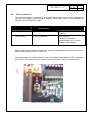
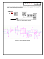
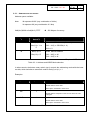
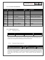
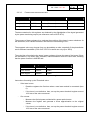
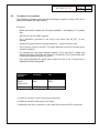
USER MANUAL
Function: Optical to RF
(DIGITAL)
Class: VME
PH/ESS document
No:
PH-ESS-02-01
Created :
11.10.2006
Modified:
date
Page
Rev.No.
1 of 17
1
RF_TX_D v1.0
RF to Digital Optical VMEbus Interface Card
and S/W
Summary:
This document describes the functionality of the RF_Tx_Digital card as well as the generic
S/W that has been developed for it.
Prepared by :
Checked by :
Approved by :
Markus Joos, PH/ESS
for information,
you can contact :
Tel.
Fax.
E-Mails
Markus Joos
+41.22.7672364
+41.22.7671025
[email protected]
Angel Monera
+41.22.7678925
+41.22.7678925
[email protected]
PH/ESS Document. No.
PH – ESS – ## – ##
Page
Rev. No.
2 of 17
1
Table of Contents
1.
Introduction ........................................................................................................................... 3
2.
RF_TX_D Hardware............................................................................................................... 4
2.1.
Power description ........................................................................................................................ 4
2.2.
Optical Interface ........................................................................................................................... 5
2.3.
VMEbus interface ......................................................................................................................... 7
2.3.1. Addr module sellection ................................................................................................................................8
2.3.2. Software: Vme addres map .........................................................................................................................9
2.3.3. Registers Description...................................................................................................................................9
2.3.3.1.
EDA Identification .................................................................................................................................9
2.3.3.2.
Reference Power threshold..................................................................................................................9
2.3.3.3.
Power monitoring registers.................................................................................................................10
2.3.3.4.
VRef Registers ...................................................................................................................................11
2.3.3.5.
Tx_Enable registers............................................................................................................................12
2.3.3.6.
Board Identification.............................................................................................................................13
2.4.
Calibration procedures.............................................................................................................. 14
2.5.
Board configuration Jumpers and switch ............................................................................... 15
2.6.
Fibre / cable connections .......................................................................................................... 15
2.7.
Front-panel LEDs ....................................................................................................................... 16
2.8.
References or more information............................................................................................... 16
3.
TTC common software ....................................................................................................... 17
3.3.
3.3.1.
3.3.2.
Introduction ................................................................................................................................ 17
H/W Environment.......................................................................................................................................17
S/W Environment .......................................................................................................................................17
3.4.
Test programs ............................................................................................................................ 17
3.5.
The user library .......................................................................................................................... 17
PH/ESS Document. No.
PH – ESS – ## – ##
Page
Rev. No.
3 of 17
1
1. INTRODUCTION
The RF_TX_D (RF to digital Optical VMEbus car) is an interface card developed as
triple optical transmitter.
The two boards used together provide 3 digital optical channels, with an 1bit analog to digital
converter (comparator), and output LVPECL ac coupled*.
This document contains a hardware description of the board and all accessible registers of
the RF_TX_D card as well as description of the generic S/W that has been developed for
this card. At the end of this document, some basic examples of configuration procedures are
proposed.
PH/ESS Document. No.
PH – ESS – ## – ##
Page
Rev. No.
4 of 17
1
2. RF_TX_D HARDWARE
2.1.
POWER DESCRIPTION
This board requires a VME crate with the standard VME64 power supply, with 12, -12, and 5
Volts available. The nominal consumption for these lines is:
Voltage
Current (A)
Fuse Current
5V
650mA
1.5A
+12V
30mA
0.1A
-12V
30mA
0.1A
Table 2.1: Power consumption
In order to check the power supplied to the board, three LEDs have been installed to indicate
the presence of +12V, -12V and +3.3V* (generated from +5 V, indicating with this light both
voltages).
*If this LED is not lighting, proceed checking the +5V fuse state.
PH/ESS Document. No.
PH – ESS – ## – ##
2.2.
Page
Rev. No.
5 of 17
1
OPTICAL INTERFACE
The Optical interface is composed of three equal blocks based on two laser modules that
use the same footprint and connection diagram. Each laser module is recommended to
transmit a specific frequency range.
LASER MODULE
Recommended
Frequencies
Notes
OCP STX 03
From 0 to 100 MHz
Up to 500 MHz (>250Mhz: out
of specs)
OCP STX 24
From 0 to 400 MHz
Up to 600 MHz
Expensive Photodiode,
recommended only to ensure
400MHz Transmissions
Table 2.2: Signal supported for each Laser module
Each channel admits analog or digital input through a coaxial SMA connector and offers an
Optical output through a ST/PC connector.
Immediately after the coaxial connector, there is a capacitor that blocks the DC component
of the signal. This capacitor can be removed in order to make a full DC coupled channel.
Picture 2.2.a: Location of Input Capacitor
PH/ESS Document. No.
PH – ESS – ## – ##
Page
Rev. No.
6 of 17
1
In order to control and monitor the Tx module, an AD and DA converters have been installed
in the purpose of controlling the Reference value of the comparator and monitoring the
power of the Laser during the transmission.
SMA
CONNECTOR
PECL
COMPARATOR
LASER MODULE
ADC
Power monitoring
Tx_Enalble
DAC
Comparator Reference Control
Picture 2.2.b: Optical Interface Diagram
Picture 2.2.c: Optical Interface schematic
FPGA
PH/ESS Document. No.
PH – ESS – ## – ##
2.3.
Page
Rev. No.
7 of 17
1
VMEBUS INTERFACE
The VMEbus interface of the RF_TX_D cards is implemented in its FPGA and based on a
VHDL Module developed by the AB/RF group. This Module has been developed especially
for VME64 but adapted for using some functionality of VME64X (like automatic addressing).
The firmware installed has been configured to work in the addressing mode of: A24/D16 and
works as a memory decoder, where all the memory space is available.
The access modes (dictated by address modifier) are only available for 0x39 and 0x3D,
where the there is no distinction between privilege user and normal user
From this 24bits of memory address, 6 bits are used for the module address [A23 to A18].
This address can be set up using the two rotary switches.
SW1
SW2
Picture 2.3: Module address selector
In addition, it is possible to fix automatically the module address by using the geographical
address of VME64x.
In order to select the source of the module address (rotary switches or GEO addr.),
from the 8 bits of the R.S. the 2 lower bits are designated to select it.
PH/ESS Document. No.
Page
PH – ESS – ## – ##
Rev. No.
8 of 17
1
2.3.1. ADDR MODULE SELLECTION
Address space available:
Note:
M represent XXXX (any combination of 4 bits)
N represent XX (any combination of 2 bits)
0xM(N+0)0000 to 0xM(N+3) FFFF
Rotary Switch
1
Rotary
Switch 2
M
Bits(3:2)= N
Bits(1:0)= “1 to
3”
M
Î 256 Kbytes of memory
Module address (MA)
Automatic GEO Address (5bits + 0)*
[A23…A19] <= GEOGA(4 : 0)
A18 <= 0
Bits(3:2)= N
0xMN Manual Address
Bits(1:0)= “0”
[A23…A20] <= M
[A19…A18] <= N
*Requires VME64X crate
Table 2.3.1: Address and ADDR Mode selection
In others words, the bottom rotary switch (sw1) controls the addressing mode with the lower
two bits, which switches to automatic mode if the b(0) or b(1) = 1.
Examples:
Rotary Switch 1
Rotary Switch 2
0xF
0
Module MODO / ADDRESS / SPACE
Manual address
Module address: 0xF0 0000
Board space: 0xF00000 to 0xF3 FFFF
0xF
1
Automatic address
Module address: Depends on the slot into which the card
is plugged
0xF
4
Manual address
Module address: 0xF4 0000
Board space: 0xF40000 to 0xF7 FFFF
Table2.3.1.b: Examples of Module Addr
PH/ESS Document. No.
Page
PH – ESS – ## – ##
9 of 17
Rev. No.
1
2.3.2. SOFTWARE: VME ADDRES MAP
Offset
Size (bytes)
Function
Mode
Remarks
0x0000
2
EDA ID
Read
0x1380
0x0002
2
REF_POWER_COMPARATO
R
Read/Write
0x000A
2
CH1_ POWER
Read
0x000C
2
CH2_ POWER
Read
0x000E
2
CH3_ POWER
Read
0x0010
2
CH1_REF (COMPARATOR)
Read / Write
0x0012
2
CH2_REF (COMPARATOR)
Read / Write
0x0014
2
CH3_REF (COMPARATOR)
Read / Write
Default for pulse transmission
0x0020
2
TX_ENABLE
Read/Write
Enable Transmitters (bits 1 to 3)
0x003A
2
BOARD ID (CERN ID)
Read
0x016D
Others
Default for pulse transmission
Unused
Table 2.3.2: VME Memory Map
2.3.3. REGISTERS DESCRIPTION
2.3.3.1.
EDA IDENTIFICATION
Name
Offset
Size
Access
EDA ID
0x0000
16 bits
R
The card ID is just a register that can be used to identify the board. This default value is
0x1380, which correspond to the EDA project number of the board
2.3.3.2.
REFERENCE POWER THRESHOLD
Name
Offset
Size
Access
REF_POWER_COMPARATOR
0x0004
16 bits (8bits used)
R/W
The reference Power threshold is a register used as reference to be compared to the power
that the laser is transmitting. The result of the comparison is indicated in the front panel with
a LED (Green light indicates power emitted > Power threshold, Red light indicates the
opposite).
PH/ESS Document. No.
Page
PH – ESS – ## – ##
2.3.3.3.
Rev. No.
10 of 17
1
POWER MONITORING REGISTERS
Name
Offset
Size
Access
CH1_POWER
0x000A
16 bits (8bits used)
R
CH2_POWER
0x000C
16 bits (8bits used)
R
CH3_POWER
0x000E
16 bits (8bits used)
R
The data contained in this registers are obtained by the digitalisation of the signal generated
by the power monitoring output (see reference notes of OCP-STX).
The purpose of these registers is to evaluate the evolution of the lasers’ power emissions. At
the same time, their values indicates if the lasers are transmitting of not.
The expected value may change from one photodiode to other, especially if the photodiodes
are for different bandwidth. (From OCP STX 03 to stx24 can vary up to 100%)
The main idea of monitoring the lasers’ power registers is know the state of the lasers (if they
are activated or not) and if they activated, make estimation about the laser state, knowing
that the power function is LINEAR and:
Laser Module
Register
State
OCP STX 03 & 24
0x0000
Disable or broken
OCP STX 03
0x0070
~0dbm
OCP STX 24
0x00E0
~0dbm
Table 2.3.3.3: Normal Lasers’ power registers values
Instructions for setting up the Threshold value:
−
−
If the laser is new
-
Read the registers the first time when a new laser module is connected (time
0):
-
if the laser is not defective, then, set up the power threshold register around
10% less of the value measured
If is not new
-
Measure the Optical power emitted with a power optical metre
-
Measure the register and generate a linear approximation to the original
values
-
if the laser is not defective, then, set up the power threshold register around
10% less of the value measured
PH/ESS Document. No.
Page
PH – ESS – ## – ##
2.3.3.4.
Rev. No.
11 of 17
1
VREF REGISTERS
Name
Offset
Size
Access
CH1_REF
0x0010
16 bits (8bits used)
R/W
CH2_REF
0x0012
16 bits (8bits used)
R/W
CH3_REF
0x0014
16 bits (8bits used)
R/W
CHX_REF are a group of register that controls the 1bit ADC situate in the RF input.
These registers are 8Bits long and are controlling a linear DAC that will provide a value
between 0 and 1.2Volts.
This register generates a reference value which is compared to the input signal. As result of
this comparison, a PECL square signal will be generated and sent by the laser module,
Vref (mV ) = Vref _ value • 4.7mv
Where:
Vref_value: is the value of the register in decimal
Examples:
Hex Value
Vref
Recommended
0x00
5mv
For any signal centred in zero, (example 10 to
400Mhz sinusoidal or square signal)
0x70
531mV
Recommended for Pulse transmission (1V peak)
0xFF
1.2V
Recommended to Block input signal and transmit a
permanent 0
0x25
190mv
Recommended for Pulse transmission (0.5V peak)
Table 2.3.3.4: Example of Vref values and recommendations
PH/ESS Document. No.
Page
PH – ESS – ## – ##
2.3.3.5.
12 of 17
Rev. No.
1
TX_ENABLE REGISTERS
Name
TX_ENABLE
Offset
Size
Access
Default
0x0020
8 bits (bits 3 to
1)
R/W
0x0E
By default, the lasers are enabled in order to offer a transmission as soon as the board is
plugged.
It is nevertheless possible to disable the laser transmission when is nor required.
Function
Bit
Function
TX1_ENABLE
1
*1 Enable / 0 disable
TX2_ENABLE
2
*1 Enable / 0 disable
TX3_ENABLE
3
*1 Enable / 0 disable
TX1_ENABLE
others
*0 (not writeable, always 0)
* Default values
Examples:
Hex Value
Tx1 En.
Tx2 En.
Tx3 En.
0x00
0x02
X
X
X
0x08
0x0A
X
0x0C
0x0E
Nothing: disable
X
0x04
0x06
X: enable
X
X
X
X
X
X
X
Table 2.3.3.5: Tx_Enalble combinatios
PH/ESS Document. No.
Page
PH – ESS – ## – ##
2.3.3.6.
Rev. No.
13 of 17
1
BOARD IDENTIFICATION
Name
Offset
Size
Access
BOARD ID
0x003A
16 bits
R
The card ID is just a register that can be used for identify the board… this register is situated
in offset 0X003A. Its normal value is 365(decimal), the ESS board number.
PH/ESS Document. No.
PH – ESS – ## – ##
2.4.
Page
Rev. No.
CALIBRATION PROCEDURES
The calibration procedure must be done knowing the signals or using a RF_RX_D
board (both boards with VME access)
Procedure:
-
Reset the board or enable the TX writing (0x000E -> all enabled) in Tx_enable
Reg
-
Write 0x10 in all the VREF registers
-
Do a calibration procedure in the RX_D vme board (see RF_RX_ D user
manual)
-
Identify the signals used or no signal presence… and the receiver used
-
If the receiver board is full OCP, the signal detection circuit will indicate which
channel is working
-
For knowing the connection diagram between TX_D and RX_D, enable and
disable the Lasers and check the frequency variations in RX_D (remember wait
54 seconds between Disable procedure).
-
After having identified the signal types, adjust the Vref in the Tx boards as is
indicated in the following table:
Frequency /
signals
Hex Value
Vref
clocks or
signal
centred in 0**
0x00*1
~0mv
Pulses
0x70*2
~531mV
Table 2.4: Calibration Values
*1: default in channels 1 and 2 after plug on the board
*2: default in channel 3 after plug on the board
** Remember that exist a capacitor in the output that removes the DC component.
14 of 17
1
PH/ESS Document. No.
PH – ESS – ## – ##
2.5.
Page
Rev. No.
1
BOARD CONFIGURATION JUMPERS AND SWITCH
Element
Description
LSB rotary switch
See Table x
MSB rotary switch
See Table x
Reset(Front Panel)
push button
Generate a Soft reset in the FPGA when is pressed
ST4
Always ON
ST5
Always OFF
TP25
Frequency selector0 for the JTAG
TP26
Frequency selector1 for the JTAG
ST3
If ST3 is ON -> the FPGA will be reprogrammed when the VME
crate reset will be activated (Sysreset)
Table 2.5: Jumpers and Switch descriptions
2.6.
15 of 17
FIBRE / CABLE CONNECTIONS
Connector name
To be connected to
Format
CH1 out Optical Link
RF Digital RX
Optical: Digital
CH1 RF In
50omhs Generator
Analog or Digital
CH2 Out Optical Link
RF Digital RX
Optical: Digital
CH2 RF In
50omhs Generator
Analog or Digital
CH3 Out Optical Link
RF Digital RX
Optical: Digital (to ch3 Pulse default)
CH3 RF In
50omhs Generator
Analog or Digital (pulse Default in)
J5
JTAG
JTAG MODE (FPGA)
J6
JTAG
BIT BLASTER MODE (EEPROM)
Table 2.6: Connectors and Descriptions
PH/ESS Document. No.
PH – ESS – ## – ##
2.7.
Page
Rev. No.
FRONT-PANEL LEDS
LED
Description
VME COMM
Indicates if the last VME cycle was successful or wrong
ERROR LED
Indicates an error in ?????
CH1 LED (SD CH1)
Indicates Power transmitted > Threshold
CH2 LED (SD CH2)
Indicates Power transmitted > Threshold
CH3 LED (SD CH3)
Indicates Power transmitted > Threshold
Table 2.7: Front Panel LEDS
2.8.
REFERENCES OR MORE INFORMATION
Lasers and Photodiodes evaluation (by Angel Monera)
EDA documents (https://edms.cern.ch/nav/eda-01380)
RF_TX_D TCL console Manual
RF_RX_D User Manual
16 of 17
1
PH/ESS Document. No.
PH – ESS – ## – ##
3.
TTC COMMON SOFTWARE
3.3.
INTRODUCTION
3.3.1. H/W ENVIRONMENT
3.3.2. S/W ENVIRONMENT
.
3.4.
TEST PROGRAMS
.
3.5.
THE USER LIBRARY
Page
Rev. No.
17 of 17
1