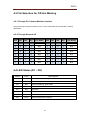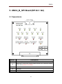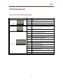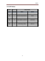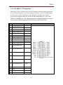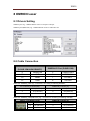
1
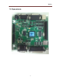
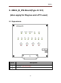
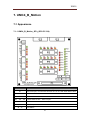
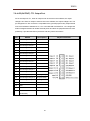
UMC4 UMC4 User Manual Version: 20150320 UMC4 Table of Content 1. INTRODUCTION ............................................................................................................................... 4 1-1 SPECIFICATION ................................................................................................................... 4 1-2 APPEARANCE ..................................................................................................................... 5 1-3 LAYOUT ............................................................................................................................ 6 2. PIN ASSIGNMENT ........................................................................................................................... 7 2-1 LASER CONTROL CONNECTOR ........................................................................................... 7 2-1-1 P1 (SCANHEAD):XY2-100 INTERFACE PORT ...................................................... 7 2-1-2 P2 (LASER CONNECTOR):LASER CONTROL PORT ........................................... 7 2-1-3 P3 (RS232):PLC COMMUNICATION PORT.............................................................. 8 2-1-4 P4 (I/O CONNECTOR):ROTARY, ENCODER AND I/O PORT ................................. 8 3. INSTALLATION AND CABLE CONNECTION........................................................................................ 9 3-1 UMC4 INSTALLATION.......................................................................................................... 9 3-2 XY2-100 DIGITAL SCANNER ............................................................................................. 14 3-3 PULSE/DIRECTION SIGNAL CONNECTION .......................................................................... 15 3-3-1 DIFFERENTIAL SIGNAL............................................................................................... 15 3-3-2 COMMON ANODE TTL ............................................................................................... 15 3-3-3 COMMON CATHODE TTL ........................................................................................... 15 3-4 AXIS CONTROL SIGNAL CONNECTION ............................................................................... 16 3-4-1 COMMON CATHODE SENSOR(NPN) ......................................................................... 16 3-4-2 COMMON ANODE SENSOR(PNP) ............................................................................. 16 3-5 TTL SIGNAL CONNECTION ................................................................................................ 17 3-6 ENCODER SIGNAL CONNECTION ....................................................................................... 17 3-7 PHOTO COUPLE SIGNAL CONNECTION ............................................................................. 18 3-7-1 OPTO IN CONNECTION ............................................................................................ 18 3-7-2 OPTO OUT CONNECTION......................................................................................... 18 3-8 START & STOP SIGNAL CONNECTION............................................................................ 19 3-8-1 CONNECT WITH GENERAL BUTTONS.......................................................................... 19 3-8-2 CONNECT WITH SENSORS ......................................................................................... 19 3-8-3 INPUT TTL SIGNAL ..................................................................................................... 20 3-9 HWCONFIG SETTING DESCRIPTION .................................................................................. 21 3-9-1 SCANNER ALIGNMENT:SET P1 (XY2-100). ........................................................... 21 3-9-2 DAC SETTING:SET P2 (ANALOG OUT VOLTAGE). ................................................ 22 3-9-3 INPUT SENSOR TYPE:SET P2、P4(START、STOP). ............................................ 22 3-9-4 EXTENSTION .............................................................................................................. 22 3-9-5 SIGNAL POLARITY (ENABLE ACTIVE LOW) ................................................................ 22 4. OTHERS ....................................................................................................................................... 23 4-1 CLOCK .............................................................................................................................. 23 1 UMC4 4-1-1 HARDWARE CONFIGURATION .................................................................................... 23 4-1-2 SOFTWARE CONFIGURATION (TIME REFLASH) ......................................................... 23 4-2OFFLINE M ARKING SIGNAL TIME SERIES........................................................................... 24 4-3 FILE SELECTION FOR OFF-LINE MARKING......................................................................... 25 4-3-1 THROUGH PLC HUMAN-MACHINE INTERFACE ......................................................... 25 4-3-2 THROUGH EXTERNAL I/O .......................................................................................... 25 4-4 LED STATUS (D1 ~ D8).................................................................................................... 25 5. UMC4_B_SPI BOARD(SPI G3 / G4) .......................................................................................... 26 5-1 APPEARANCE ................................................................................................................... 26 5-2 PIN ASSIGNMENT .............................................................................................................. 27 5-2-1 J4~J7 (LASER EXTEND CONNECTOR)....................................................................... 27 5-3 LED STATUS .................................................................................................................... 28 6. UMC4_B_IPG BOARD(TYPE D / D1) (ALSO APPLY FOR RAYCUS AND JPT LASER) ................. 29 6-1 APPEARANCE ................................................................................................................... 29 6-2 PIN ASSIGNMENT .............................................................................................................. 30 6-2-1 J4~J5 (LASER EXTEND CONNECTOR)....................................................................... 30 6-3 LED STATUS .................................................................................................................... 30 7. UMC4_B_MOTION ...................................................................................................................... 32 7-1 APPEARANCE ................................................................................................................... 32 7-1-1 UMC4_B_MOTION_SPI:(SPI G3 / G4) ............................................................... 32 7-1-2 UMC4_B_MOTION_IPG:(IPG TYPE D / D1) ....................................................... 33 7-2 PIN ASSIGNMENT .............................................................................................................. 34 7-2-1 P1 LASER CONTROL CONNECTOR ........................................................................... 34 7-2-2 P2~P4 CONTROL PORT............................................................................................ 34 7-2-3 JF1 (INPUT): TTL INPUT PORT ............................................................................... 35 7-2-4 JF2(OUTPUT): TTL OUTPUT PORT........................................................................ 36 7-2-5 J4~J7 (LASER EXTEND CONNECTOR)....................................................................... 37 7-2-6 JF4~JF6 SENSOR CONTROL PORT:(TERMINAL BLOCK) ...................................... 38 7-2-7 D1~D19 LASER LED STATUS DESCRIPTIONS ......................................................... 38 7-2-8 D20~D46 MOTION LED STATUS ............................................................................. 40 7-3 CABLE CONNECTION ........................................................................................................ 41 7-3-1 PULSE/DIRECTION SIGNAL CONNECTION ................................................................. 41 7-3-2 CONNECT WITH SENSORS ......................................................................................... 42 7-3-3 ENCODER SIGNAL CONNECTION............................................................................... 43 7-3-4 TTL SIGNAL CONNECTION (JF1、JF2) ................................................................... 43 7-3-5 SPI STATUS SIGNAL CONNECTION (J6、J7) ......................................................... 44 8 OMRON LASER ........................................................................................................................... 45 8-1 DRIVERS SETTING............................................................................................................. 45 8-2 CABLE CONNECTION ........................................................................................................ 45 2 UMC4 9 USING RS-232 .............................................................................................................................. 46 9-1 WHAT IS RS-232 .............................................................................................................. 46 9-2 SETTING TO USE RS-232 TO CONTROL LASER .................................................................. 46 APPENDIX1: VARIOUS LASER SETTING MODES................................................................................ 47 TYPE 1:CO2 MODE ............................................................................................................ 47 TYPE2:YAG 1、2、3 MODE .............................................................................................. 48 TYPE 3:R05 MODE ............................................................................................................. 49 APPENDIX2:HOW TO CONNECT WITH PLC .................................................................................... 50 APPENDIX3:PLC ADDRESS DEFINITION TABLE .............................................................................. 51 3 UMC4 1. Introduction UMC4 is a high performance USB interface card designed for Laser Marking System. The card supports digital galvo motor, compatible with XY2-100 protocol, and through DA2-16 daughter board can control analog galvo motor precisely. UMC4 built-in full offline marking functions, could access up to 16 files, each file contains up to 8 sets auto-text and 8 kinds of fonts. Through I/O signal or PLC human-machine interface, users could easily choose the file and start marking. The card also features complete rotary and mark-on-fly functions. Besides, it provides a variety of expanded boards for all kinds of connection requirements. 1-1 Specification Built-in DSP, marking computing do not occupy computer CPU time. Support one XY2-100 digital control signal output, 10μs cycle update galvo motor position. FPK, PPK, R05 first pulse suppression. Support offline marking, could access 16 files each contains 8 sets auto-text and 8 Two 10-bits analog control signals. PWM maximum output frequency is 10MHz, minimum pulse width is 0.08μs. kinds of fonts. One RS232 Communication Port for PLC communication. Support one encoder input for mark-on-fly function. Support 1-way pulse/direction or CW/CCW step/servo motor control signals, the maximum output frequency is 2MHz. Contain expansion connectors for connecting with a variety of daughter boards. Support Windows XP/Vista/Windows 7. 4 UMC4 1-2 Appearance 5 UMC4 1-3 LAYOUT Ø =0.4cm Name Purpose Descriptions P1 Scan head Main marking port (D-SUB 25-Pin female connector ) P2 Laser Connector Laser control and analog output port (D-SUB 15-Pin 3 row female connector) P3 RS232 PLC control port (D-SUB 9-Pin female connector) P4 I/O Connector Rotary, Encoder and I/O port.(D-SUB 15-Pin 2 row female connector) J1,13 Power +5V 3A power J3 USB USB port J4,5,6 Expansion Connector Expansion Connector port[1] J7 Battery Connector External battery port for timer (+1.5V~+5V) J12 SD Card SD Card port J14 RS232 OMRON Laser RS232 D1~D8 LED Status lights JP1(BOT) FPK / R0 1、2 Close : FPK 2、3Close : R05 ※[1]Caution:DO NOT mistake connecting to J4, J5, and J6 Expansion Connector ports, for wrong connection may cause the board damaged. ※[2] Please refer to 8 OMRON Laser. 6 UMC4 2. Pin Assignment 2-1 Laser Control Connector 2-1-1 P1 (SCANHEAD):XY2-100 Interface Port 25-pin Female Connector Pin Descriptions 1, 14 Differential Out (CLOCK) 2, 15 Differential Out (SYNC) 3, 16 Differential Out (CHAN1) 4, 17 Differential Out (CHAN2) 5, 18 Differential Out (CHAN3) 6, 19 Differential In (STATUS) 8, 21 Differential In (/STATUS) 11, 23, 24 GND 2-1-2 P2 (LASER CONNECTOR):Laser Control Port 15-pin Female Connector Pin Descriptions CO2 2 Power 1 Analog Out1 2 Analog Out2 3 GND 4 Laser1 (PWM) [1] 5 Laser2 (FPK) or R05 [1] 6 L0 (Laser On/Off) 7 L1 (Leading Light On/Off) 8 L2 (Shutter) 9 L3 (CW select) 10 L4 (Lamp On/Off) L5 (Start power saving mode) 11 Power 1 YAG Current Frequency 2 Frequency 1 12 /START (Dry connect input) (Let Pin12 & Pin15 short-circuit will get START signal) 13 /STOP (Dry connect input) (Let Pin13 & Pin15 short-circuit will get STOP signal) 14 DC:+5V 1A 15 GND ※[1] The output signal of Laser1 and Laser2 depend on the selected laser control mode. CO2 Mode YAG Mode RO5 Laser1 Modulation Pulse 1 Q-Switch signal Q-Switch signal Laser2 Modulation Pulse 2 First Pulse Killer Analog out R05 7 UMC4 2-1-3 P3 (RS232):PLC Communication Port 9-pin Connector Pin Descriptions 2 TX 3 RX 5 GND 2-1-4 P4 (I/O CONNECTOR):Rotary, Encoder and I/O Port 26-pin Connector Pin Descriptions 1 11 Encoder A+ Encoder A- 2 12 Encoder B+ Encoder B- 3 13 Pulse+ / CW+ [1] Pulse- / CW- [1] 4 14 Direction+ / CCW+ [1] Direction- / CCW- [1] Home+ Home- 5 15 Pre-View On+ Pre-View On- 6、10 DC:+5V 1A OPTO IN5:System On 7 /START(Dry connect input) (Let Pin8 & Pin18 short-circuit will get START signal) /STOP(Dry connect input) (Let Pin9 & Pin18 short-circuit will get STOP signal) 8 9 ※[1] Please refer to 3-9 16 OPTO IN1 Input of File Selection 17 OPTO IN2 Input of File Selection / InPosition 25 OPTO IN3 Input of File Selection / Limit- 26 OPTO IN4 Input of File Selection / Limit+ 18 GND 19 OPTO V+:5 ~ 24V Input 20 OPTO OUT1:Program Ready 21 OPTO OUT2:Mark Ready 22 OPTO OUT3:Mark End 23 OPTO OUT4:Mark Busy / Busy [1] 24 OPTO GND : 0V Input(Pin24 & Pin18 open circtui) HWConfig Setting Description。 8 UMC4 3. Installation and Cable Connection 3-1 UMC4 Installation If your computer is not installed MM-SA software yet, please install the MM-SA first. During MM-SA installation, system will run "UMC4-USB Driver Setup" automatically. While "UMC4-USB Driver Setup" is executing, please press "Continue Anyway" button. This step may need to repeat 3 times. 9 UMC4 After the installation completed, you could plug-in power of UMC4 and connect to computer via USB cable. Normally, Windows system will appear a message " Found New Hardware UMC4-USB LASER MARKING CONTROL CARD". Please press "Next" under the recommended setting. Wait for wizard searching the driver, 10 UMC4 After system founded UMC4 Driver, please press "Continue Anyway". After driver installed, please press "Finish". 11 UMC4 When the message "Your new hardware is installed and ready to use" appeared you could use UMC4 now. If UMC4 installed properly, you could see the UMC4 device information appeared in Device Manager, as below: 12 UMC4 13 UMC4 3-2 XY2-100 Digital Scanner Currently common seen digital galvanometer could divide into the following 2 types: 3-2-1 Type 1: With one D-SUB 25Pin connector。 3-2-2 Type 2: With D-SUB 25Pin connector + D-SUB 9Pin connector。 Notice: UMC4P1 is corresponding to digital galvanometer D-SUB25Pin. User could easily connect them by 25-pin 1 to 1 cable; however, if using type 1 galvanometer, user has to wire to power source from the cable. For the power source: User has to wire all pins of them, which means has to wire 3 pins of the +VCC, 3 pins of the –VCC, and 3 pins of the GND. Only wire to 1 pin of +VCC, 1 pin of –VCC, or 1 pin of GND is forbidden. 14 UMC4 3-3 Pulse/Direction Signal Connection According to the different types of Motor Driver, there are three ways of connection between Motor Driver and UMC4’s P4 connectors. 3-3-1 Differential Signal UMC4 Different Signal Connection Motor Driver P4.3 Pulse R+ Pulse+ P4.13 Pulse R- Pulse- P4.4 Direction R+ Direction+ P4.14 Direction R- Direction- 3-3-2 Common Anode TTL UMC4 Different Signal Connection Motor Driver P4.3 Pulse R+ Pulse+ P4.13 Pulse R- Pulse- P4.4 Direction R+ Direction+ P4.14 Direction R- Direction- 3-3-3 Common Cathode TTL UMC4 P4.3 Pulse R+ Common Cathode TTL Connection Motor Driver Pulse P4.4 Direction R+ Direction GND GND 15 UMC4 3-4 Axis Control Signal Connection 3-4-1 Common Cathode Sensor(NPN) SENSOR UMC4 Vcc(5V~24V) 1kΩ V1 Vcc P4.5 Home R+ Out P4.15 1 21 Sensor 1 2 4 2 Home R- 3 PC817 GND Power 0V 3-4-2 Common Anode Sensor(PNP) SENSOR UMC4 Vcc(5V~24V) Vcc V1 Sensor 1 2 1kΩ Out P4.5 Home R+ GND 1 21 4 2 P4.15 Home R- Power 0V 16 3 PC817 UMC4 3-5 TTL Signal Connection TTL signal is connected by one to one as below. UMC4 USER TTL Signal Signal GND GND 3-6 Encoder Signal Connection UMC4 Encoder Encoder Encoder Encoder GND Different Signal Connection A+ AB+ B- Encoder Encoder Encoder Encoder Encoder GND 17 A+ AB+ B- UMC4 3-7 Photo Couple Signal Connection 3-7-1 OPTO IN Connection Power 5V~24V USER OPTO-isolator 1 2 UMC4 Imax = 50mA 4 Pin7、 16、 17、 25、 26: OPTO IN1 - IN5 3 Pin24: OPTO GND R1 1k 1/2W 1 2 PC817 4 3 PC817 Power 0V UMC4 OPGO GND 3-7-2 OPTO Out Connection Power 5V~24V UMC4 Pin19: OPTO V+ R1 1k 1/2W 1 2 4 Pin20、 21、 22、 23 OPTO OUT1 ~ OUT4 3 Pin24: OPTO GND Imax = 50mA USER Relay Imax = 50mA PC817 UMC4 OPGO GND Power 0V PS: The Max. current for Relay is 50 mA 18 RE2 RELAY SPDT UMC4 3-8 START & STOP Signal Connection 3-8-1 Connect with general buttons UMC4 D LL4148 C P2.12、 P4.8 P2.13、 P4.9 /Start /STOP 1 R 1 R 100 A 2 2 1k 2 1 1 GND 2 4 2 P2.15、 P4.18 SW VCC5V Switch 1 3 PC817 Note: Please set Common Cathode for HWConfig, Please refer to 3-8 HWConfig Setting Description. 3-8-2 Connect with sensors a. For Common Cathode Sensor(NPN), short circuit the sensor output with GND. SENSOR UMC4 Power 5V~24V D LL4148 C Vcc V1 Sensor 1 2 P2.12、 P4.8 P2.13、 P4.9 Out /Start /STOP 1 R GND R 100 A 2 2 1k VCC5V 1 Switch 1 1 4 2 P2.15、 P4.18 GND 2 3 PC817 Power 0V Note: Please set Common Cathode for HWConfig, Please refer to 3-8 HWConfig Setting Description. 19 UMC4 b. For Common Anode Sensor(PNP), short circuit the sensor output with Vcc. SENSOR UMC4 Power 5V~24V D LL4148 C Vcc Sensor 1 2 V1 P2.12、 P4.8 P2.13、 P4.9 Out Start STOP 1 R R 100 A 2 VCC5V 1 2 1k Switch 1 2 1 GND 4 2 P2.15、 P4.18 3 GND PC817 Power 0V Note: Please set Common Cathode for HWConfig, Please refer to 3-8 HWConfig Setting Description. 3-8-3 Input TTL signal UMC4 USER D LL4148 C +5V TTL 0V START、 STOP P2.12、 P4.8 P2.13、 P4.9 Start STOP 1 R GND R 100 A 2 2 1k VCC5V 1 Switch 1 1 4 2 P2.15、 P4.18 GND 2 3 PC817 Note: Please set Common Cathode for HWConfig, Please refer to 3-8 HWConfig Setting Description. 20 UMC4 3-9 HWConfig Setting Description File Address:C:\Program Files\MM-SA\Drivers\UMC4\HWConfig.exe. 3-9-1 Scanner alignment:Set P1 (XY2-100). XY Data Swap:Exchanging X and Y coordinate will not affect correction file. X Mirror、Y Mirror、Z Mirror:X and Y and Z Mirror。 XY Lines Exchange:X and Y output exchange。 21 UMC4 3-9-2 DAC Setting:Set P2 (Analog Out Voltage). Select DAC1& DAC2 as 0~5V or 0~10V。 3-9-3 Input Sensor Type:Set P2、P4(Start、Stop). Common Anode:Figure Switch Close, /Start、/Stop LOW action. UMC4 D LL4148 C P2.12、 P4.8 P2.13、 P4.9 Start STOP 1 R R 100 A 2 2 1k VCC5V 1 Switch 1 2 1 4 2 P2.3、 P4.18 GND 3 PC817 Commoun Cathode:Figure Switch Open, Start、Stop High action. UMC4 D LL4148 C P2.12、 P4.8 P2.13、 P4.9 /Start /STOP 1 R R 100 A 2 2 1k VCC5V 1 Switch 1 1 4 2 P2.3、 P4.18 GND 2 3 PC817 3-9-4 Extenstion Pulse Direction / CW CCW:Select Motion output Pulse/Dir or CW/CCW。 Enable Multi Start: While in automation mode, multiple start marking signal trigger is allowed. 3-9-5 Signal Polarity (Enable Active Low) Setting Start、Stop drive phase with P2、P4, Check for reverse. Setting TTL signal with P2, Check for reverse. Setting photo couple phase with P4, Check for reverse. Selecting FPK or R05 Out(Applies Old Card IP1.2.1),The new card changed JP1setting. Setting Limit + - with P4 IN3、IN4, Check for Limit+ -、InPosition with P4 IN2. Setting motion with P4, Selecting X、Y、Z、R axis, By default the R axis. 22 UMC4 4. Others 4-1 Clock UMC4 is equipped with clock counter, capable to mark current date and time. 4-1-1 Hardware Configuration a. J7 is needed to connect with +1.5V~+5V battery. Without battery, the current date and time will be erased as long as UMC4 been cut-off power. b. Lifetime of Carbon-zinc battery is approximated 3 years. Note: Even UMC4 is plug in the power, the battery is still consumed by minimum current. 4-1-2 Software Configuration (Time Reflash) a. Date and time will be updated to computer’s current time when MM-SA is executing. b. Could be configured through PLC human-machine interface. 23 UMC4 4-2Offline Marking Signal Time Series Name IN/OUT Pin System On IN P4.7 Stand-alone marking standby Program Ready OUT P4.20 System standby Mark Ready OUT P4.21 Mark standby Mark End OUT P4.22 Mark complete Busy OUT P4.23 Laser busy Mark Busy OUT P4.23 System busy Start IN P4.8 External trigger start Stop IN P4.9 External trigger stop Pre-View On IN P4.5 P4.15 Definition External trigger mark preview 24 UMC4 4-3 File Selection for Off-line Marking 4-3-1 Through PLC Human-Machine Interface Using the human-machine interface of PLC, users could select file and set basic marking parameters. 4-3-2 Through External I/O IN4 IN3 IN2 IN1 File Name IN4 IN3 IN2 IN1 File Name 0 0 0 0 #01 1 0 0 0 #09 0 0 0 1 #02 1 0 0 1 #10 0 0 1 0 #03 1 0 1 0 #11 0 0 1 1 #04 1 0 1 1 #12 0 1 0 0 #05 1 1 0 0 #13 0 1 0 1 #06 1 1 0 1 #14 0 1 1 0 #07 1 1 1 0 #15 0 1 1 1 #08 1 1 1 1 #16 4-4 LED Status (D1 ~ D8) Name Color Descriptions D1 Red Executing status. Keep light while function is normal. D2 Red Light flashing while data is transferring. D3 Red UMC4 is initializing, please wait. D4 Yellow Reserved. D5 Red Reserved. D6 Green D7 Red D8 Green Ready to use. Power in. USB connected with computer. 25 UMC4 5. UMC4_B_SPI Board(SPI G3 / G4) 5-1 Appearance Name P1 P2 Descriptions SPI Laser port, connect with SPI laser one on one with SCSI 68Pin cable. RS232 port, connect with computer RS232 (Serial) port for SPI laser software mode control.(Default not available) J4 SPI RS232 J5 SPI Estop J6、J7 SPI Status 26 UMC4 5-2 Pin Assignment 5-2-1 J4~J7 (Laser extend connector) Connector J4 PIN J4.1 GND J4.2 SPI_RS232_RX J4.3 SPI_RS232_TX J5.1 J5 J6、J7 Descriptions /Estop Dry connect input(Let GND short-circuit will get Estop signal) J5.2 GND J6.1 Seed laser temperature fault J6.2 Base plate temperature fault J6.3 Pre-amplifier current fault J6.4 Power-amplifier current fault J6.5 GND J6.6 5V J7.1 Beam collimator fault J7.2 Reserved fault indicator J7.3 Laser Ready (no fault) J7.4 Power Supply Fault J7.5 GND J7.6 5V 27 UMC4 5-3 LED Status Name SPI Pin Descriptions LED SCSI 68Pin SPI G3 SPI G4 D1 7 Global Enable Laser enable D2 6 Alignment laser enable Pilot laser enable D3 3 Seed laser temperature fault Monitor D4 8 Base plate temperature fault Laser temperature D5 9 Pre-amplifier current fault Alarm D6 10 Power-amplifier current fault System fault D7 11 Beam collimator fault Beam delivery D8 12 Reserved fault indicator Laser deactivated D9 14 Laser Ready (no fault) Laser is on D10 16 Power Supply Fault Laser emission warning 28 UMC4 6. UMC4_B_IPG Board(Type D / D1) (Also apply for Raycus and JPT Laser) 6-1 Appearance Name Descriptions P1 IPG Laser port, connect with IPG laser one on one with D-sub 25Pin cable. J4 IPG E-Stop:(Dry connect input) J5 IPG Status:(TTL Output) 29 UMC4 6-2 Pin Assignment 6-2-1 J4~J5 (Laser extend connector) Connector PIN J4.1 J4 J5 Description /Estop (Dry connect input)(Short with GND to trigger) J4.2 GND J5.1 GND J5.2 IPG Pin 11 J5.3 IPG Pin 12 J5.4 IPG Pin 16 J5.5 IPG Pin 21 J5.6 GND 6-3 LED Status Name IPG Pin (D-SUB 25-pin) Descriptions D1 20 PWM D2 19 Laser On D3 22 Guide Light D4 18 MO D5 1 Power Bit0 D6 2 Power Bit1 D7 3 Power Bit2 D8 4 Power Bit3 D9 5 Power Bit4 D10 6 Power Bit5 D11 7 Power Bit6 D12 8 Power Bit7 D13 9 Latch D14 12 INPUT1 D15 16 INPUT2 D16 21 INPUT3 D17 11 INPUT4 30 UMC4 IPG_Fiber.cfg For IPG Laser IPG_Fiber_RS232.cfg For RS232 control IPG Laser IPG_GLPM.cfg For IPG GLPM Laser IPG_YLP_B.cfg For IPG YLP-B Laser IPG_YLPM.cfg For IPG YLPM Laser raycus.cfg For Raycus Laser JPT_YDFLP_10_20.cfg For JPT YDFLP 10-20 Laser JPT_YDFLP_20_DP1_S.cfg For JPT YDFLP 20-DP1 Laser JPT_YDFLP_20_DP1_S_L.cfg For JPT YDFLP 20-DP1-S Laser JPT_YDFLP_20_PRO_S_L.cfg For JPT YDFLP 20-PRO-S Laser 31 UMC4 7. UMC4_B_Motion 7-1 Appearance 7-1-1 UMC4_B_Motion_SPI:(SPI G3 / G4) Name P1 P2、P3、P4 Descriptions SPI Laser port, connect with SPI laser one on one with SCSI 68Pin cable. D-SUB 15F:X、Y、Z Motion、Encoder connector. JF3 Terminal Block 2Pin:+5V and 0V. JF4、JF5、JF6 Terminal Block 8Pin:Sensor Input. J4 SPI RS232 J5 SPI Estop J6、J7 SPI Status 32 UMC4 7-1-2 UMC4_B_Motion_IPG:(IPG Type D / D1) Name P1 P2、P3、P4 Descriptions IPG Laser port, connect with IPG laser one on one with D-sub 25Pin cable. D-SUB 15F:X、Y、Z Motion、Encoder connector. JF3 Terminal Block 2Pin:+5V and 0V. JF4、JF5、JF6 Terminal Block 8Pin:Sensor Input. J4 IPG E-Stop:(Dry connect input) J5 IPG Status:(TTL Output) 33 UMC4 7-2 Pin Assignment 7-2-1 P1 Laser Control Connector Reference SPI G3 / G4 User Manual or IPG Type D / D1 User Manual.Connect with laser one on one with cable. 7-2-2 P2~P4 Control Port 15-pin Female Connector Pin 1 +5V 2、10 Encoder Z+、Encoder Z- 3、11 Encoder B+、Encoder B- 4、12 Encoder A+、Encoder A- 5、13 Direction+、Direction- 6、14 Pulse+、Pulse- 7、8、15 9 34 Descriptions Undefined GND UMC4 7-2-3 JF1 (INPUT): TTL Input Port When there is no any connection to TTL input, the program receives 0 value; while if input 0V, the program will read 0, if input 5V, the program will read 1. You must consider about the noise issue. The pin assignment of JF1 connector is compatible to the general purpose input daughter boards such as PCLD-782 of Advantech Co., Ltd. or the DB-16P of ICPDAS Co., Ltd. Using these kinds of daughter boards can isolate power source while provide protection and easy cable connections. Pin Name 1 General Digital Input 0 2 General Digital Input 1 3 General Digital Input 2 4 General Digital Input 3 5 General Digital Input 4 6 General Digital Input 5 7 General Digital Input 6 8 General Digital Input 7 9 General Digital Input 8 10 General Digital Input 9 11 General Digital Input Descriptions 20-pin Connector 10 12 General Digital Input 11 13 General Digital Input 12 14 General Digital Input 13 15 General Digital Input Start 14 16 General Digital Input E. Stop 15 17 GND 18 GND 19 +5V 20 Do Not Connect 35 UMC4 7-2-4 JF2(OUTPUT): TTL Output Port As for the output of TTL, when an output is set as inactive in the software; the output voltage is 0V. When an output is set as active in the software; the output voltage is 5V. The pin assignment of JF2 connector is compatible to the general purpose relay output boards such as PCLD-885 of Advantech Co., Ltd. or the DB-16R of ICPDAS Co., Ltd. Using these kinds of daughter boards can isolate external power and drive the peripheral devices more powerfully, it provides benefits of protection and easy cable connections. Pin Name Descriptions 1 General Digital Output 0 2 General Digital Output 1 3 General Digital Output 2 4 General Digital Output 3 5 General Digital Output 4 6 General Digital Output 5 7 General Digital Output 6 8 General Digital Output 7 9 General Digital Output 8 10 General Digital Output 9 11 General Digital Output 10 12 General Digital Output 11 13 General Digital Output 12 14 General Digital Output 13 Marking Ready 15 General Digital Output 14 Program Ready 16 General Digital Output 15 Marking End 17 GND 18 GND 19 +5V 20 Do Not Connect (Undefined) 36 20-pin Connector UMC4 7-2-5 J4~J7 (Laser extend connector) 7-2-5-1 UMC4-B-Motion-SPI Connector J4 PIN J4.1 GND J4.2 SPI_RS232_RX J4.3 SPI_RS232_TX J5.1 J5 J6、J7 Descriptions /Estop Dry connect input(Let GND short-circuit will get Estop signal) J5.2 GND J6.1 Seed laser temperature fault J6.2 Base plate temperature fault J6.3 Pre-amplifier current fault J6.4 Power-amplifier current fault J6.5 GND J6.6 5V J7.1 Beam collimator fault J7.2 Reserved fault indicator J7.3 Laser Ready (no fault) J7.4 Power Supply Fault J7.5 GND J7.6 5V 7-2-5-2 UMC4-B-Motion-IPG Connector PIN J4.1 J4 J5 Description /Estop (Dry connect input)(Short with GND to trigger) J4.2 GND J5.1 GND J5.2 IPG Pin 11 J5.3 IPG Pin 12 J5.4 IPG Pin 16 J5.5 IPG Pin 21 J5.6 GND 37 UMC4 7-2-6 JF4~JF6 Sensor Control Port:(Terminal Block) Name Descriptions LPX+、LPY+、LPZ+ Positive Limit + (X、Y、Z) LPX-、LPY-、LPZ- Positive Limit - (X、Y、Z) LNX+、LNY+、LNZ+ Negative Limit + (X、Y、Z) LNX-、LNY-、LNZ- Negative Limit - (X、Y、Z) HX+、HY+、HZ+ Home + (X、Y、Z) HX-、HY-、HZ- Home -(X、Y、Z) IX+、IY+、IZ+ InPosition + (X、Y、Z) IX-、IY-、IZ- InPosition - (X、Y、Z) 7-2-7 D1~D19 Laser LED Status Descriptions 7-2-7-1 UMC4_B_Motion_SPI Name Pin LED SCSI68Pin SPI G3 SPI G4 D1 13 External Pulse Trigger Pulse_trigger_h D2 5 Laser Emission Gate Laser_emission_gate_h D3 21 Pulsed/CW Mode select Laser_Pulse_CW_h D4 17 State Select: bit 0 DI_0 D5 18 State Select: bit 1 DI_1 D6 19 State Select: bit 2 DI_2 D7 20 State Select: bit 3 DI_3 D8 51 State Select: bit 4 DI_4 D9 52 State Select: bit 5 DI_5 D10 7 Global Enable Laser_enable_h D11 6 Alignment laser enable Pilot_laser_enable_h D12 3 Seed laser temperature fault Monitor D13 8 Base plate temperature fault Laser temperature D14 9 Pre-amplifier current fault Alarm D15 10 Power-amplifier current fault System fault D16 11 Beam collimator fault Beam delivery D17 12 Reserved fault indicator Laser deactivated D18 14 Laser Ready (no fault) Laser is on D19 16 Power Supply Fault Laser emission warning Descriptions 38 UMC4 7-2-7-2 UMC4_B_Motion_IPG Name IPG Pin (D-SUB 25-pin) Descriptions D1 20 Sync D2 19 Modulation D3 22 Guide D4 18 EE D5 1 Power Setting D0 D6 2 Power Setting D1 D7 3 Power Setting D2 D8 4 Power Setting D3 D9 5 Power Setting D4 D10 6 Power Setting D5 D11 7 Power Setting D6 D12 8 Power Setting D7 D13 9 Latch D14 12 Laser alarms status D15 16 Laser alarms status D16 21 Laser alarms status D17 11 Laser alarms status 39 UMC4 7-2-8 D20~D46 Motion LED Status Name Descriptions Name Descriptions D20 Pulse X D34 Positive Limit Z D21 Direction X D35 Negative Limit Z D22 Pulse Y D36 Home Z D23 Direction Y D37 InPosition Z D24 Pulse Z D38 Encoder AX D25 Direction Z D39 Encoder BX D26 Positive Limit X D40 Encoder ZX D27 Negative Limit X D41 Encoder AY D28 Home X D42 Encoder BY D29 InPosition X D43 Encoder ZY D30 Positive Limit Y D44 Encoder AZ D31 Negative Limit Y D45 Encoder BZ D32 Home Y D46 Encoder ZZ D33 InPosition Y 40 UMC4 7-3 Cable Connection 7-3-1 Pulse/Direction Signal Connection According to the different types of Motor Driver, there are three ways of connection between Motor Driver and UMC4_B_Motion’s P2 ~ P4 connectors. 7-3-1-1 Different Signal UMC4_B_Motion Different Signal Connection +5V Pulse + Pulse Dir + Dir GND Step / Servo Motor Driver Pulse + Pulse Dir + Dir GND 7-3-1-2 Common Anode TTL UMC4_B_Motion Common Anode TTL Connection Step / Servo Motor Driver +5V +5V Pulse - Pulse Dir - Dir 7-3-1-3 Common Cathode TTL UMC4_B_Motion Common Cathode TTL Connection Step / Servo Motor Driver Pulse + Pulse Dir + Dir GND GND 41 UMC4 7-3-2 Connect with sensors 7-3-2-1 Common Cathode Sensor (NPN) SENSOR UMC4_B_Motion JF4、 JF5、 JF6 Vcc(5V~24V) LPX+ / LNX+ / HX+ / IX+ 1kΩ LPY+ / LNY+ / HY+ / IY+ 1 LPZ+ / LNZ+ / HZ+ / IZ+ Vcc V1 Sensor 1 2 Out LPX- / LNX- / HX- / IXLPY- / LNY- / HY- / IYLPZ- / LNZ- / HZ- / IZ- 21 4 2 3 PC817 GND Power 0V SENSOR UMC4_B_Motion Vcc 5V JF4、 JF5、 JF6 Vcc(5V~24V) JF3 +5V LPX+ / LNX+ / HX+ / IX+ 1kΩ LPY+ / LNY+ / HY+ / IY+ 1 LPZ+ / LNZ+ / HZ+ / IZ+ Vcc V1 Sensor 1 2 Out LPX- / LNX- / HX- / IXLPY- / LNY- / HY- / IYLPZ- / LNZ- / HZ- / IZ- 21 4 2 3 PC817 GND JF3 GND Power 0V 7-3-2-2 Common Anode Sensor (PNP) SENSOR UMC4_B_Motion JF4、 JF5、 JF6 Vcc(5V~24V) Vcc V1 LPX+ / LNX+ / HX+ / IX+ 1kΩ LPY+ / LNY+ / HY+ / IY+ 1 LPZ+ / LNZ+ / HZ+ / IZ+ Sensor 1 2 Out LPX- / LNX- / HX- / IXLPY- / LNY- / HY- / IYLPZ- / LNZ- / HZ- / IZ- GND Power 0V 42 21 4 2 3 PC817 UMC4 7-3-3 Encoder Signal Connection User Encoder Encoder Encoder Encoder GND Different Signal Connection A+ AB+ B- UMC4_B_Motion Encoder Encoder Encoder Encoder GND A+ AB+ B- 7-3-4 TTL Signal Connection (JF1、JF2) User UMC4_B_Motion TTL Signal Signal GND GND 43 UMC4 7-3-5 SPI STATUS Signal Connection (J6、J7) 7-3-5-1 Use internal power UMC4-B-Motion-SPI User VCC 5V 4.7k J6.6、J7.6 1 21 U17 4 2 3 1 1k PC817 J6.1、J6.2、J6.3、J6.4 2 J7.1、J7.2、J7.3、J7.4 21 SPI G3 / G4 1 U17 4 2 3 J6.5、J7.5 PC817 7-3-5-2 Use external power UMC4-B-Motion-SPI User VCC 5V VCC 5V 4.7k J6.6、J7.6 1 21 U17 4 2 3 1 1k PC817 21 J6.1、J6.2、J6.3、J6.4 2 J7.1、J7.2、J7.3、J7.4 SPI G3 / G4 1 U17 4 2 3 J6.5、J7.5 PC817 VSS 0V PS:SPI suggest external power is +5V, and series connect to 4.7kΩ. Please refer to SPI User`s manual. 44 UMC4 8 OMRON Laser 8-1 Drivers Setting OMRON_Fiber.cfg:OMRON RS232 connect to computer COM port. OMRON_Fiber(DIRCTRL).cfg:OMRON RS232 connect to UMC4 Port J14. 8-2 Cable Connection UMC4 P2 (D-SUB 15M HIGH DENSITY) OMRON I/O Port (D-SUB 15M) 6 LASER ON 5 LASER ON H 15 GND 6 LASER ON L 10 LAMP 7 LD ON H 15 GND 8 LD ON L While use “OMRON_Fiber.cfg”, connection is according to following definition: PC RS232 (D-SUB 9M) 2 RX (Receive) OMRON (D-SUB 9F) 3 TX (Transmit) 3 TX (Transmit) 2 RX (Receive) 5 GND 5 GND While use “OMRON_Fiber(DIRCTRL).cfg”, connection is according to following definition: UMC4 J14 (Wafer 3Pin) 1 TX (Transmit) OMRON (D-SUB 9F) 2 RX (Receive) 2 RX (Receive) 3 TX (Transmit) 3 GND 5 GND 45 UMC4 9 Using RS-232 9-1 What is RS-232 RS-232 is a kind of serial port. Common type of RS-232 connector is 9 pin D-Sub. Some kinds of laser types needed to control by RS-232 port for tuning laser parameter, such as power percentage, frequency…etc. 9-2 Setting to use RS-232 to control laser Take SPI G4 HS laser controlled by RS-232 as example. After user has executed \MarkingMate\DM.exe , chosen UMC4 at Driver Name column, and picked SPI_fiber_RS232_G4_HS.cfg at Mode column, to apply the setting by clicking OK. The location of cfg file is \MarkingMate\Drivers\UMC4\cfg\. Refer to the following picture: Open the given file by favorite text editor. There should be two instructions under [ENV] sector, such as RS232=1 and COMPORT=XXX. RS232=1 means control laser by RS-232. XXX within COMPORT=XXX means the using Com Port number. Default value is 1 which means using COM port 1 to control laser. Manually change this value to assign other port if necessary. 46 UMC4 Appendix1: Various Laser Setting Modes TYPE 1:CO2 Mode 47 UMC4 TYPE2:YAG 1、2、3 Mode 48 UMC4 TYPE 3:R05 Mode 49 UMC4 Appendix2:How to Connect with PLC UMC4 provides a RS232 (P3) port for PLC connection. PLC communication protocol is Mitsubishi FX series. RS232 communication parameters: Baud 115200 BPS Parity Check Even Data Bit 8 Stop Bit 1 Flow Control none The connection diagram of UMC4, PLC, and Laser is as below: 50 UMC4 Appendix3:PLC Address definition table D0 – D255 (0x1000 – 0x11ff) System Reg Addr Name Name Type 0x5800 PWM Mode D0 Unsigned Short 0x5802 Laser Mode D1 Unsigned Short 0x5804 Test Execute D2 Unsigned Short 0x5806 FLASH Update D3 Unsigned Short 0x5808 Standby Half Period D4 Unsigned Long 0x580c Standby Width D6 Unsigned Long 0x5810 CorTable D8 Unsigned Short 0x5812 FLY_MODE_X D9 Unsigned Short 0x5814 FLY_MODE_Y D10 Unsigned Short 0x5816 FLY_MODE_Z D11 Unsigned Short 0x5818 FLY_VALUE_X D12 Long 0x581c FLY_VALUE_Y D14 Long 0x5820 FLY_VALUE_Z D16 Long 0x5824 FLY_DELAY_X D18 Unsigned Long 0x5828 FLY_DELAY_Y D20 Unsigned Long 0x582c FLY_DELAY_Z D22 Unsigned Long 0x5830 Laser Test : HPeriod D24 Unsigned Long 0x5834 Laser Test : PWidth D26 Unsigned Long 0x5838 Laser Test: Power D28 Unsigned Short 0x583a Preview File D29 Unsigned Short 0x583c Preview Speed D30 Unsigned Long 0x5840 Preview Offset X D32 Short 0x5842 Preview Offset Y D33 Short 0x5844 Preview Matrix 0 D34 Long 0x5848 Preview Matrix 1 D36 Long 0x584c Preview Matrix 2 D38 Long 0x5850 Preview Matrix 3 D40 Long 0x5854 PreLoadFile D42 Unsigned Long 0x5858 Device Name D44 Char (16) 51 UMC4 D256 – D511 (0x1200 – 0x13ff) Laser Reg Addr Name Name Type 0x5870 SPI_ENABLE_OUT D256 Unsigned Short 0x5872 SPI_CW_OUT D257 Unsigned Short 0x5874 SPI_ALIGN_OUT D258 Unsigned Short 0x5876 SPI_WAVEFORM_OUT0 D259 Unsigned Short 0x5878 SPI_WAVEFORM_OUT1 D260 Unsigned Short 0x587a SPI_WAVEFORM_OUT2 D261 Unsigned Short 0x587c SPI_WAVEFORM_OUT3 D262 Unsigned Short 0x587e SPI_WAVEFORM_OUT4 D263 Unsigned Short 0x5880 SPI_WAVEFORM_OUT5 D264 Unsigned Short 0x5882 IPG_POWER_OUT0 D265 Unsigned Short 0x5884 IPG_POWER_OUT1 D266 Unsigned Short 0x5886 IPG_POWER_OUT2 D267 Unsigned Short 0x5888 IPG_POWER_OUT3 D268 Unsigned Short 0x588a IPG_POWER_OUT4 D269 Unsigned Short 0x588c IPG_POWER_OUT5 D270 Unsigned Short 0x588e IPG_POWER_OUT6 D271 Unsigned Short 0x5890 IPG_POWER_OUT7 D272 Unsigned Short 0x5892 IPG_LATCH_OUT D273 Unsigned Short 0x5894 IPG_MO_OUT D274 Unsigned Short 0x5896 IPG_GUIDE_OUT D275 Unsigned Short 0x5898 IPG_LATCH_TIME D276 Unsigned Long 0x589c IPG_MO_DELAY D278 Unsigned Long 0x58a0 SoftStartMode D280 Unsigned Short 0x58a2 SoftStartNum D281 Unsigned Short 0x58a4 SoftStartLevel0 D282 Unsigned Short 0x58a6 SoftStartLevel1 D283 Unsigned Short 0x58a8 SoftStartLevel2 D284 Unsigned Short 0x58aa SoftStartLevel3 D285 Unsigned Short 0x58ac SoftStartLevel4 D286 Unsigned Short 0x58ae SoftStartLevel5 D287 Unsigned Short 0x58b0 SoftStartLevel6 D288 Unsigned Short 0x58b2 SoftStartLevel7 D289 Unsigned Short 0x58b4 SoftStartLevel8 D290 Unsigned Short 0x58b6 SoftStartLevel9 D291 Unsigned Short 52 UMC4 0x58b8 SoftStartLevel10 D292 Unsigned Short 0x58ba SoftStartLevel11 D293 Unsigned Short 0x58bc SoftStartLevel12 D294 Unsigned Short 0x58be SoftStartLevel13 D295 Unsigned Short 0x58c0 SoftStartLevel14 D296 Unsigned Short 0x58c2 SoftStartLevel15 D297 Unsigned Short 0x58c4 R05Init D298 Unsigned Long 0x58c8 R05Interval D300 Unsigned Long 0x58cc R05Level0 D302 Unsigned Short 0x58ce R05Level1 D303 Unsigned Short 0x58d0 R05Level2 D304 Unsigned Short 0x58d2 R05Level3 D305 Unsigned Short 0x58d4 R05Level4 D306 Unsigned Short 0x58d6 R05Level5 D307 Unsigned Short 0x58d8 R05Level6 D308 Unsigned Short 0x58da R05Level7 D309 Unsigned Short 0x58dc R05Level8 D310 Unsigned Short 0x58de R05Level9 D311 Unsigned Short 0x58e0 R05Level10 D312 Unsigned Short 0x58e2 R05Level11 D313 Unsigned Short 0x58e4 R05Level12 D314 Unsigned Short 0x58e6 R05Level13 D315 Unsigned Short 0x58e8 R05Level14 D316 Unsigned Short 0x58ea R05Level15 D317 Unsigned Short 0x58ec IPG Setting D318 Unsigned Short 0x58ee CO2 Setting D319 Unsigned Short 0x58f0 YAG Setting D320 Unsigned Short 0x58f2 SPI Setting D321 Unsigned Short 0x58f4 SPI Align Off Delay D322 Unsigned Long 0x58f8 SPI Enable Delay D324 Unsigned Long 53 UMC4 D8000 – D8255 (0x0e00 – 0x0fff) Layer Reg Addr Name Name Type 0x0X00 Power D8000 Unsigned Short 0x0X02 Simmer Current D8001 Unsigned Short 0x0X04 HalfPeriod D8002 Unsigned Long 0x0X08 Duty width D8004 Unsigned Long 0x0X0c FPK D8006 Unsigned Long 0x0X10 FPKLeadTime D8008 Unsigned Long 0x0X14 Jump Speed D8010 Unsigned Long 0x0X18 Mark Speed D8012 Unsigned Long 0x0X1c LaserON Delay D8014 Long 0x0X20 LaserOFF Delay D8016 Unsigned Long 0x0X24 Jump Delay D8018 Unsigned Long 0x0X28 Poly Delay D8020 Unsigned Long 0x0X2c Mark Delay D8022 Unsigned Long 0x0X30 OffsetX D8024 Short 0x0X32 OffsetY D8025 Short 0x0X34 Matrix 0 D8026 Long 0x0X38 Matrix 1 D8028 Long 0x0X3c Matrix 2 D8030 Long 0x0X40 Matrix 3 D8032 Long 0x0X44 Waveform D8034 Unsigned Short 0x0X46 CW Mode D8035 Unsigned Short 0x0x48 Wobble Frequency D8036 Unsigned Long 0x0x4c Wobble Amp D8038 Unsigned Long 0x0x50 Spot Time D8040 Unsigned Long 54 UMC4 T0 – T255 (0x0800 – 0x09ff) AutoTxt Reg Addr Name Addr Name 0x1X00 Map Table T0 Unsigned Short 0x1X02 Digital T1 Unsigned Short 0x1X04 Carry T2 Unsigned Short 0x1X06 Increase T3 Short 0x1X08 Repeat T4 Unsigned Long 0x1X0c Interval_x T6 Unsigned Short 0x1X0e Interval_y T7 Unsigned Short 0x1X10 TxtDirType T8 Unsigned Short 0x1X12 BasedZero T9 Unsigned Short 0x1X14 Padding T10 Unsigned Short 0x1X16 TimeType T11 Unsigned Short 0x1X18 Separate T12 Unsigned Short 0x1X1a Year character T13 Unsigned Short 0x1X1c Month character T14 Unsigned Short 0x1X1e Week Day character T15 Unsigned Short 0x1X20 InitValue_Digital0 T16 Unsigned Short 0x1X22 InitValue_Digital1 T17 Unsigned Short 0x1X24 InitValue_Digital2 T18 Unsigned Short 0x1X26 InitValue_Digital3 T19 Unsigned Short 0x1X28 InitValue_Digital4 T20 Unsigned Short 0x1X2a InitValue_Digital5 T21 Unsigned Short 0x1X2c InitValue_Digital6 T22 Unsigned Short 0x1X2e InitValue_Digital7 T23 Unsigned Short 0x1X30 InitValue_Digital8 T24 Unsigned Short 0x1X32 InitValue_Digital9 T25 Unsigned Short 0x1X34 InitValue_Digital10 T26 Unsigned Short 0x1X36 InitValue_Digital11 T27 Unsigned Short 0x1X38 InitValue_Digital12 T28 Unsigned Short 0x1X3a InitValue_Digital13 T29 Unsigned Short 0x1X3c InitValue_Digital14 T30 Unsigned Short 0x1X3e InitValue_Digital15 T31 Unsigned Short 0x1X40 MaxValue_Digital0 T32 Unsigned Short 0x1X42 MaxValue_Digital1 T33 Unsigned Short 0x1X44 MaxValue_Digital2 T34 Unsigned Short 55 UMC4 0x1X46 MaxValue_Digital3 T35 Unsigned Short 0x1X48 MaxValue_Digital4 T36 Unsigned Short 0x1X4a MaxValue_Digital5 T37 Unsigned Short 0x1X4c MaxValue_Digital6 T38 Unsigned Short 0x1X4e MaxValue_Digital7 T39 Unsigned Short 0x1X50 MaxValue_Digital8 T40 Unsigned Short 0x1X52 MaxValue_Digital9 T41 Unsigned Short 0x1X54 MaxValue_Digital10 T42 Unsigned Short 0x1X56 MaxValue_Digital11 T43 Unsigned Short 0x1X58 MaxValue_Digital12 T44 Unsigned Short 0x1X5a MaxValue_Digital13 T45 Unsigned Short 0x1X5c MaxValue_Digital14 T46 Unsigned Short 0x1X5e MaxValue_Digital15 T47 Unsigned Short 0x1X60 CurValue_Digital0 T48 Unsigned Short 0x1X62 CurValue_Digital1 T49 Unsigned Short 0x1X64 CurValue_Digital2 T50 Unsigned Short 0x1X66 CurValue_Digital3 T51 Unsigned Short 0x1X68 CurValue_Digital4 T52 Unsigned Short 0x1X6a CurValue_Digital5 T53 Unsigned Short 0x1X6c CurValue_Digital6 T54 Unsigned Short 0x1X6e CurValue_Digital7 T55 Unsigned Short 0x1X70 CurValue_Digital8 T56 Unsigned Short 0x1X72 CurValue_Digital9 T57 Unsigned Short 0x1X74 CurValue_Digital10 T58 Unsigned Short 0x1X76 CurValue_Digital11 T59 Unsigned Short 0x1X78 CurValue_Digital12 T60 Unsigned Short 0x1X7a CurValue_Digital13 T61 Unsigned Short 0x1X7c CurValue_Digital14 T62 Unsigned Short 0x1X7e CurValue_Digital15 T63 Unsigned Short 0x1X80 First Padding 0 T64 Unsigned Short 0x1X82 First Padding 1 T65 Unsigned Short 0x1X84 First Padding 2 T66 Unsigned Short 0x1X86 First Padding 3 T67 Unsigned Short 0x1X88 First Padding 4 T68 Unsigned Short 0x1X8a First Padding 5 T69 Unsigned Short 0x1X8c First Padding 6 T70 Unsigned Short 0x1X8e First Padding 7 T71 Unsigned Short 56 UMC4 0x1X90 Last Padding 0 T72 Unsigned Short 0x1X92 Last Padding 1 T73 Unsigned Short 0x1X94 Last Padding 2 T74 Unsigned Short 0x1X96 Last Padding 3 T75 Unsigned Short 0x1X98 Last Padding 4 T76 Unsigned Short 0x1X9a Last Padding 5 T77 Unsigned Short 0x1X9c Last Padding 6 T78 Unsigned Short 0x1X9e Last Padding 7 T79 Unsigned Short 0x1Xa0 Size Scale X T80 Unsigned Long 0x1Xa4 Size Scale Y T82 Unsigned Long 0x1Xa8 SpacingMode T84 Unsigned Short 0x1Xaa TxtMode T85 Unsigned Short 0x1Xac First Padding Num T86 Unsigned Short 0x1Xae Last Padding Num T87 Unsigned Short 0x1Xb0 RECT_SHOW T88 Unsigned Short 0x1Xb2 RECT_Width T89 Unsigned Short 0x1Xb4 RECT_Height T90 Unsigned Short 0x1Xb6 RECT_UpSpace T91 Unsigned Short 0x1Xb8 RECT_DownSpace T92 Unsigned Short 0x1Xba RECT_LeftSpace T93 Unsigned Short 0x1Xbc RECT_RightSpace T94 Unsigned Short 0x1Xbe ARC_SHOW T95 Unsigned Short 0x1Xc0 ARC_DISTYPE T96 Unsigned Long 0x1Xc4 ARC_LINESPACE T98 Long 0x1Xc8 ARC_DISVALUE T100 Long 0x1Xcc ARC_BASEANGLE T102 Long 0x1Xd0 ARC_BLTYPE T104 Unsigned Short 0x1Xd2 ARC_NEGARRAY T105 Unsigned Short 0x1Xd4 ARC_CENTERX T106 Unsigned Short 0x1Xd6 ARC_CENTERY T107 Unsigned Short 0x1Xd8 ARC_RADIUS T108 Unsigned Long 57 UMC4 File Reg (AA = 0x59 – 0x68) C0 – C199 (0x0a00 – 0x0b8f) Addr Name Name Type 0xAA00 File Addr C0 Unsigned Long 0xAA04 File Name C2 Char(16) 0xAA14 File Length C10 Unsigned Long 0xAA18 CharTb Addr C12 Unsigned Long 0xAA1c CharTb Length C14 Unsigned Long 0xAA20 MarkData Addr C16 Unsigned Long 0xAA24 MarkData Length C18 Unsigned Long 0xAA28 Layer Param Num C20 Unsigned Short 0xAA2a AutoTxt Param Num C21 Unsigned Short 0xAA2c CharTb Num C22 Unsigned Short 0xAA2e TempData C23 Unsigned Short 0xAA30 MaxWorkCnt C24 Unsigned Long 0xAA34 WorkCnt C26 Unsigned Long 0xAA38 MarkTime C28 Unsigned Long 0xAA3c comment C30 Char(64) 58 UMC4 C160 – C199 (0x0b40 – 0x0b8f) Special Reg Addr Name Name Type 0xf000 Hardware Config C160 Unsigned Long 0xf004 Program Config C162 Unsigned Long 0xf008 IP Version C164 Unsigned Long 0xf00c Execute Register C166 Unsigned Long 0xf010 Current File C168 Unsigned Short 0xf012 DataTime Status C169 Unsigned Short 0xf014 DataTime (Sec) C170 Unsigned Short 0xf016 DataTime(Min) C171 Unsigned Short 0xf018 DataTime(Hour) C172 Unsigned Short 0xf01a DataTime(day) C173 Unsigned Short 0xf01c DataTime(Week Day) C174 Unsigned Short 0xf01e DataTime(Month) C175 Unsigned Short 0xf020 DataTime(Year) C176 Unsigned Short 0xf022 TempData C177 Unsigned Short 0xf024 PLC File Sel C178 Unsigned Long 0xf028 PLC Layer Sel C180 Unsigned Long 0xf02c PLC Autotxt Sel C182 Unsigned Long 0xf030 Cor Offset X 1 C200 0xf034 Cor Offset X 2 C201 0xf038 Cor Offset Y 1 C202 0xf03c Cor Offset Y 2 C203 0xf040 Cor Scale X 1 C204 0xf044 Cor Scale X 2 C205 0xf048 Cor Scale Y 1 C206 0xf04c Cor Scale Y 2 C207 0xf050 Cor Matrix 0 1 C208 0xf054 Cor Matrix 0 2 C209 0xf058 Cor Matrix 1 1 C210 0xf05c Cor Matrix 2 2 C211 0xf060 Cor Matrix 3 1 C212 0xf064 Cor Matrix 3 2 C213 0xf068 Cor Matrix 4 1 C214 0xf06c Cor Matrix 4 2 C215 59