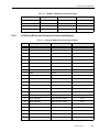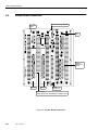
1
USP-2 Hardware Manual
Version 1.4 — March 8, 2001
Themis Computer—Americas and Pacific Rim
3185 Laurelview Court
Fremont, CA 94538, USA
Phone (510) 252-0870
Fax (510) 490-5529
World Wide Web http://www.themis.com
Themis Computer—Rest of World
20 rue du Tour de l’Eau
38400 St Martin d’Heres
France
Phone +33 476 59 60 46
Fax +33 476 59 60 49
Copyright © 2001 Themis Computer, Inc.
ALL RIGHTS RESERVED. No part of this publication may be reproduced in any form, by
photocopy, microfilm, retrieval system, or by any other means now known or hereafter invented without
the prior written permission of Themis Computer.
The information in this publication has been carefully checked and is believed to be accurate. However,
Themis Computer assumes no responsibility for inaccuracies. Themis Computer retains the right to
make changes to this publication at any time without prior notice. Themis Computer does not assume
any liability arising from the application or use of this publication or the product(s) described herein.
RESTRICTED RIGHTS LEGEND: Use, duplication, or disclosure by the United States Government
is subject to the restrictions set forth in DFARS 252.227-7013 (c)(1)(ii) and FAR 52.227-19.
TRADEMARKS
SOLARIS™ is a registered trademark of Sun Microsystems
UltraSPARC™ is a registered trademark of SPARC International
All other trademarks used in this publication are the property of their respective owners.
Themis Customer Support
North America, South America, and Pacific Rim
Telephone:
Fax:
E-mail:
Web Site:
USP-2 Hardware Manual
March 8, 2001
Part Number: 108084
510-252-0870
510-490-5529
[email protected]
http://www.themis.com
.
Version Revision History
Version 1.4: Miscellaneous typos and errors corrected. Also,
• Added VME bus addressing data-transfer mode tables..................................... page 2-6
• Modified audio parameters........................................................................ pages 3-3, 8-7
• Modified board jumper-pin diagrams........................................................ pages 7-2, 7-3
• Divided Table 8-1 Signal Name column into Serial Port A and Port B ........... page 8-3
• Modified System Board VME P2 connector pin descriptions ............... pages 8-9, 8-10
March 8, 2001
Version 1.3: Reorganized sections. Re-created “Reset” chapter. Added
description of LED and Temperature monitoring in Chapter 4. Added paddle
board diagram in Chapter 8. Fixed minor errors.
June 30, 2000
Version 1.2: Misc. typos and errors corrected (Jumper 2001). Added jumper
and front panel drawings
May 18, 1999
Version 1.1: Misc. typos and errors corrected.
Version 1.0 (Rev X1.3): Preliminary
March 20, 1999
May 30, 1998
Themis Computer
iii
USP-2 Hardware Manual
iv
Themis Computer
Table of Contents
Table of Contents
1
2
3
Introduction
1.1
Introduction................................................................................................................
1.2
Scope..........................................................................................................................
1.3
USP-2 Systems Overview..........................................................................................
1.4
Getting Started ...........................................................................................................
1.4.1
How to Start Quickly .................................................................................
1.4.1.1 Product Warranty and Registration............................................
1.4.1.2 Unpacking the USP-2 ................................................................
1.4.2
In Case of Difficulties................................................................................
1-1
1-1
1-1
1-2
1-2
1-2
1-3
1-3
Installation
2.1
Registering .................................................................................................................
2.2
Configuring the USP-2 ..............................................................................................
2.3
Installing the USP-2 and its Paddleboard in the VME chassis ..................................
2.4
Configuring The VME Interface................................................................................
2.4.1
VMEbus Memory Allocation ....................................................................
2.5
Attaching the USP-2 To A Network..........................................................................
2.6
Attaching a Keyboard and Mouse .............................................................................
2.7
VME Bus Addressing Data-Transfer Modes.............................................................
2-1
2-1
2-2
2-3
2-5
2-5
2-5
2-6
USP-2 Hardware Specifications
3.1
Hardware and Performance Specifications................................................................
3.2
Environmental Specifications ....................................................................................
3-1
3-3
Themis Computer
v
USP-2 Hardware Manual
4
Hardware Overview
4.1
4.2
4.3
Overview....................................................................................................................
Themis USP-2 Block Diagram ..................................................................................
UPA Interconnect ......................................................................................................
4.3.1
UPA Interconnect Overview......................................................................
4.3.2
UPA Data Transfer ....................................................................................
4.3.3
UPA Address Bus ......................................................................................
4.3.4
UPA Data Bus............................................................................................
4.3.5
UPA Arbitration.........................................................................................
4.3.6
Processor Sub-system ................................................................................
Memory System .........................................................................................................
4.4.1
System Controller (DSC)...........................................................................
4.4.1.1 Port Interface Controller (PIF)...................................................
4.4.1.2 Data Path Scheduler (DPS)........................................................
4.4.1.3 Memory Controller (MC) ..........................................................
4.4.1.4 EBus...........................................................................................
4.4.2
Buffered Crossbar Chip (XB1) ..................................................................
I/O System .................................................................................................................
4.5.1
U2S ............................................................................................................
4.5.1.1 PIO Operation ............................................................................
4.5.1.2 DVMA Operation ......................................................................
4.5.1.3 Interrupt Dispatching .................................................................
4.5.1.4 UPA Interface ............................................................................
4.5.1.5 ECC Checking / Generation ......................................................
4.5.1.6 SBus Interface............................................................................
4.5.1.7 Streaming Buffer........................................................................
4.5.1.8 IOMMU ....................................................................................
4.5.1.9 Timer / Counter..........................................................................
4.5.2
FEPS #1 and #2..........................................................................................
4.5.3
Audio (APC) ..............................................................................................
4.5.4
SLAVIO.....................................................................................................
4.5.5
EBus Devices .............................................................................................
RIC ASIC...................................................................................................................
USP-2 Flow Diagram.................................................................................................
User LEDs..................................................................................................................
Temperature Monitoring............................................................................................
4-1
4-1
4-3
4-3
4-4
4-5
4-6
4-6
4-6
4-6
4-8
4-8
4-8
4-8
4-8
4-8
4-9
4-9
4-10
4-10
4-10
4-10
4-10
4-10
4-10
4-11
4-11
4-11
4-11
4-12
4-12
4-12
4-13
4-14
4-14
Reset
5.1
Overview....................................................................................................................
5.2
Reset Sources .............................................................................................................
5.2.1
Hardware Reset Sources ............................................................................
5.2.1.1 Power Supply POR ....................................................................
5.2.1.2 Push-button POR .......................................................................
5-1
5-1
5-2
5-3
5-3
4.4
4.5
4.6
4.7
4.8
4.9
5
vi
Themis Computer
Table of Contents
5.2.1.3 Push-button XIR ........................................................................
5.2.1.4 Scan POR ...................................................................................
5.2.1.5 Scan XIR....................................................................................
5.2.1.6 SYSRESET*..............................................................................
5.2.2
Software Reset ...........................................................................................
5.2.2.1 Software POR ............................................................................
5.2.2.2 Software XIR .............................................................................
5.2.3
Error Reset .................................................................................................
5.2.4
Wake-up Reset ...........................................................................................
5.2.5
UPA Arbitration Reset...............................................................................
Effects of Resets ........................................................................................................
5.3.1
Major System Activities as a Function of Reset........................................
5.3.2
Bus Conditions at Power up.......................................................................
5.3.2.1 UPA Address Bus 0 ...................................................................
5.3.2.2 UPA Processor Data Bus ...........................................................
5.3.2.3 Memory Data Bus ......................................................................
5.3.2.4 SBus ...........................................................................................
5.3.2.5 EBus...........................................................................................
5-3
5-3
5-3
5-4
5-4
5-4
5-4
5-4
5-4
5-4
5-5
5-5
5-5
5-6
5-6
5-6
5-6
5-6
Clocks
6.1
Overview....................................................................................................................
6.2
General Description ...................................................................................................
6.3
UPA, Processor and SBus Clocks..............................................................................
6.4
Other Clocks ..............................................................................................................
6-1
6-1
6-2
6-3
5.3
6
7
Jumper and Solder Bead Configurations
7.1
7.2
7.3
7.4
7.5
7.6
7.7
7.8
7.9
7.10
7.11
8
Overview....................................................................................................................
Location of USP-2 Jumpers .......................................................................................
CPU Clock Settings ...................................................................................................
SCSI Interface Settings ..............................................................................................
Keyboard and Mouse Settings - Serial Ports C/D settings ........................................
Serial Port Settings (RS232/RS422) ..........................................................................
Ethernet 100BaseT Settings.......................................................................................
VME jumpers settings ...............................................................................................
Flash Prom Settings ...................................................................................................
General Purpose DIP switch ......................................................................................
Printer/Floppy (available on the paddle board) Configuration ..................................
7-1
7-2
7-5
7-5
7-6
7-7
7-8
7-8
7-9
7-9
7-10
Connectors and Pinouts
8.1
Introduction................................................................................................................
8.2
Front Panel Connectors..............................................................................................
8.2.1
TTY A and TTYB Connectors (Female) ...................................................
8-1
8-2
8-3
Themis Computer
vii
USP-2 Hardware Manual
8.3
8.4
8.5
8.2.2
Keyboard / Mouse Connector (Female).....................................................
8.2.3
Ethernet 100BaseTX A and B - RJ45 Connector ......................................
8.2.4
SCSI A and B Fast wide Connector (Female, High Density)....................
8.2.5
Audio Ports ................................................................................................
VME Connectors .......................................................................................................
8.3.1
VMEbus P2 Connector (System Board)....................................................
8.3.2
VMEbus P1 Connector (I/O Board) ..........................................................
8.3.3
VMEbus P2 connector (I/O board). ...........................................................
SBus Connectors #1 and #2 .......................................................................................
Paddle board connectors ............................................................................................
8.5.1
Serial Ports C/D DB9 connector (J0603):..................................................
8.5.2
Fast wide SCSI port A and B (J0801 and J0802) ......................................
8.5.3
Parallel port (J0702)...................................................................................
8.5.4
Floppy connector (J0701) ..........................................................................
Reader Comment Card
viii
Themis Computer
8-4
8-4
8-5
8-7
8-8
8-9
8-10
8-12
8-13
8-14
8-15
8-16
8-18
8-18
List of Figures
List of Figures
Figure 2-1.
Figure 3-1.
Figure 4-2.
Figure 3-3.
Figure 4-4.
Figure 4-5.
Figure 5-1.
Figure 5-2.
Figure 6-1.
Figure 6-2.
Figure 6-3.
Figure 7-1.
Figure 7-2.
Figure 7-3.
Figure 8-1.
Figure 8-2.
Figure 8-3.
Figure 8-4.
Figure 8-5.
USP-2 Assembly........................................................................................................
USP-2 System Board Block Diagram........................................................................
UPA Interface Block Diagram...................................................................................
Memory System Block Diagram ...............................................................................
I/O System Block Diagram........................................................................................
USP-2 Flow Diagram.................................................................................................
Reset Block Diagram .................................................................................................
Block Diagram ...........................................................................................................
Simplified Block Diagram of Clock Generator .........................................................
USP2 CPU and System Clock Schematic..................................................................
USP2 SBUS Clock Schematic ...................................................................................
Base Board Jumpers...................................................................................................
I/O Board Jumpers .....................................................................................................
VSIC Jumpers ............................................................................................................
USP2 Front panel.......................................................................................................
Keyboard / Mouse Connector Pinouts .......................................................................
100Base-T Ethernet Connector Pinouts.....................................................................
SBus Connectors #1 and #2 Pinouts ..........................................................................
Paddle Board Connectors...........................................................................................
Themis Computer
2-3
4-2
4-4
4-7
4-9
4-13
5-2
5-7
6-2
6-3
6-4
7-2
7-3
7-4
8-2
8-4
8-4
8-13
8-14
ix
USP-2 Hardware Manual
x
Themis Computer
List of Tables
List of Tables
Table 2-1.
Table 3-1.
Table 3-2.
Table 3-3.
Table 4-1.
Table 4-2.
Table 4-3.
Table 4-4.
Table 5-1.
Table 6-1.
Table 7-1.
Table 7-2.
Table 7-3.
Table 7-4.
Table 7-5.
Table 7-6.
Table 7-7.
Table 7-8.
Table 7-9.
Table 8-1.
Table 8-2.
Table 8-3.
Table 8-4.
Table 8-5.
Table 8-6.
Table 8-7.
Table 8-8.
Table 8-9.
VME Bus Addressing Data-Transfer Modes.................................................................2-6
USP-2 Hardware and Performance Specifications .......................................................3-1
USP-2 Operating Environmental Specifications ..........................................................3-4
USP-2 Non-operating Environmental Specifications ....................................................3-4
UPA Port ID Assignments .............................................................................................4-5
Audio Specifications......................................................................................................4-11
LED Description ............................................................................................................4-14
Indicative Ambient Temperature Thresholds ................................................................4-15
System Reset Effects .....................................................................................................5-5
CPU to UPA Speed ratio ...............................................................................................6-2
CPU Clock Settings .......................................................................................................7-5
SCSI Interface Setting ...................................................................................................7-5
Keyboard/Mouse, Ports C/D Settings ............................................................................7-6
Serial Port A and B settings ...........................................................................................7-7
Ethernet 100 Base T Settings.........................................................................................7-8
VME Settings.................................................................................................................7-8
Flash Prom Settings .......................................................................................................7-9
General Purpose DIP switch ..........................................................................................7-9
Printer/floppy Configuration..........................................................................................7-10
Serial Ports A/B Connector Pinouts...............................................................................8-3
Keyboard / Mouse Connector Pinouts ...........................................................................8-4
100Base-T Ethernet Connector Pinouts.........................................................................8-4
Fast wide SCSI A and B Connector Pinout ...................................................................8-5
Audio Port Signals .........................................................................................................8-7
Audio Port Functions .....................................................................................................8-7
VMEbus P1 connector description (system board). ......................................................8-8
VMEbus P2 connector description (system board) .......................................................8-9
VMEbus P1 connector description (I/O board) .............................................................8-10
Themis Computer
xi
USP-2 Hardware Manual
Table 8-10.
Table 8-11.
Table 8-12.
Table 8-13.
Table 8-14.
xii
VMEbus P2 connector description (I/O board) .............................................................8-12
Serial Ports C/D DB9 connector ....................................................................................8-15
Paddle board SCSI A and B connectors ........................................................................8-16
Paddle board parallel port ..............................................................................................8-18
Paddle board floppy connector ......................................................................................8-18
Themis Computer
1
1Introduction
1.1
Introduction
Thank you for purchasing the Themis USP-2 single board computer with VMEbus interface. Themis
Computer is a leading manufacturer of SPARC based processor boards for the VMEbus market. We value our
customers comments and concerns. Our Marketing department is eager to know what you think of our
products. A “Reader Comment Card” is located at the end of this manual for your use.
!
1.2
Caution — Before you begin, carefully read each of the procedures in this manual. Improper handling can
cause serious damage to the equipment.
Scope
The purpose of this document is to provide a hardware overview of the USP-2. This manual is written for
system integrators and programmers. It contains all the necessary information to install and configure the
USP-2 processor board. It is assumed that the Sun Open Boot PROM (OBP) is installed. If you intend to use
another operating system or a real-time kernel such as VxWorks, please consult the appropriate
documentation accompanying your OS or kernel software.
The reader is assumed to be familiar with and have a working knowledge of the UltraSPARC-II processor
architecture and current VMEbus, SBus, Ethernet, and SCSI specifications. Although all USP-2 specific
hardware and software features are described in detail in this manual, programmers wishing to code the USP2 without the benefit of an operating system or real-time kernel will require additional data sheets and
documentation for the system components comprising the USP-2 design.
1.3
USP-2 Systems Overview
The USP-2 is a high-end dual-processor desktop workstation based on Sun4u, formerly known as Sun5,
system architecture.
Themis Computer
1-1
USP-2 Hardware Manual
Features of the USP-2 are
• Up to 2x64-bit V9 UltraSPARC-II processors.
• Use of Themis proprietary memory modules. Up to 2GB of memory.
• UPA coherent memory interconnect.
• Thermal management: The USP2 will shutdown if over-temp detected (2 thresholds)
• 2 RS232/RS422 serial ports (TTYA/TTYB) supporting both synchronous and asynchronous protocols.
Available on the front panel.
• 2 asynchronous mode serial ports for SUN Type 5 keyboard or mouse interface that can be configured
as 2 RS232 serial ports (TTYC/TTYD) on the P2 connector. Note that the SUN keyboard can be
plugged on front panel or on the P2 paddle board.
• Centronic compatible parallel port interface. Available on the paddle board (P2)
• Built-in audio interface. Available on Front panel.
• 2 SBus expansion slots.(Only one is available in case of graphic configuration)
• DUAL Ethernet 10/100baseT.
• DUAL 20 Mbyte/sec fast and wide SCSI.
• VME64 Interface
Note — Themis distinguishes between two types of options: field options, which the customer may set in
the field and factory options, which Themis sets before shipping the board or when the board is returned to
Themis for re-configuration. Factory configurable options are not to be configured by the customer. An
example of a field option is a jumper. An example of a factory option is a solder bead. Not all factory
options are re-configurable and the customer should decide upon the desired configuration before shipment
of the board.
1.4
Getting Started
1.4.1
How to Start Quickly
This document presents the Theory of Operation of the USP-2. It is intended to be a general purpose guide to
the USP-2 for system architects, programmers, technicians, and other users. Technical discussions begin from
an architectural perspective of a given topic and then proceed to those aspects of a general Sun architecture as
it is implemented in the USP-2. board from a programmer’s view. The information presented here is also
written for the technician. In most cases, all that will be needed in the laboratory is this document and the
appropriate toolkit. Finally the discussion retains a global view that is useful to a less technical user.
1.4.1.1
Product Warranty and Registration
Please review the computer warranty information packaged with your USP-2 processor board. Your USP-2
single board computer is automatically registered when it leaves the factory based on the information
provided in the sales order. All computers are tracked via the serial number. The warranty service period is
based on the original shipment date from the factory.
1-2
Themis Computer
1. Introduction
1.4.1.2
!
Unpacking the USP-2
Caution — The USP-2 contains statically sensitive components. Industry standard measures (use of a
grounded wrist strap) must be observed when removing the USP-2 from it’s shipping container and during
any subsequent handling.
Remove the USP-2 and accessories from its shipping container and check the contents against the packing
list. The package should include:
• Themis USP-2
• USP-2 Warranty Information
• Integration Kit (if ordered separately)
– Paddleboard
– A/B Serial Cable
– Front Panel SCSI Cable
– Flat Ribbon SCSI Cable
• USP-2 User Manual (if ordered separately).
Please report any discrepancies to the Themis Computer Customer Support department immediately.
1.4.2
In Case of Difficulties
Our Customer Support department is committed to providing the best product support in the industry.
Customer support is available 8am - 5pm (PST), Monday through Friday via telephone, fax, e-mail or our
World Wide Web site.
Themis Customer Support
Telephone:
Fax:
E-mail:
Web Site:
510-252-0870
510-490-5529
[email protected]
http://www.themis.com
Themis Computer
1-3
USP-2 Hardware Manual
1-4
Themis Computer
2
2Installation
2.1
Registering
Please review the Themis Computer warranty and complete the product registration card delivered with your
UPS-2 board(s). Return of the registration card is not required to activate your product warranty but, by
registering your USP-2, Themis Computer will be able to better provide you with timely updated information
and product enhancement notifications.
At Themis Computer we value our customers comments and concerns. We have a marketing department that
is eager to know what you think of our products and a customer support department that is committed to
providing the best product support in the industry.
Customer support is available 8AM to 5PM PST, Monday through Friday via telephone, fax, email, or our
web site.
Customer Support:
Phone: 510-252-0870 Fax: 510-490-5529
Email: [email protected]
Web site: www.themis.com
2.2
Configuring the USP-2
Confirm the installation of all factory default jumpers. The default configuration is as follows:
• USP-2 as VME System Controller
• Keyboard/Mouse ports connect to front panel
• Active SCSI termination enabled on base and I/O boards
• Drive / Receive SYSRESET*
• Serial Port A/B is EIA-232-E/EIA-423A compatible
Themis Computer
2-1
USP-2 Hardware Manual
• Boot from FLASH
• FLASH programming disabled
• Manual Ethernet port selection enabled
• Use normal twisted pair squelch threshold for 10BASE-T
• Bypass VMEbus interface in JTAG scan chain.
If the default jumper settings meet your requirements you are now ready to install the SPARC USP-2 in a
standard VME chassis. To check the default configurations or if reconfiguration is required, refer to Chapter
4, Configurations and Options, for information concerning board jumper settings, solder bead, and memory
configurations.
Note — If you are not installing the USP-2 as a system controller, jumper J1201 must be removed.
In addition to the USP-2 hardware a standard VME chassis with P1/P2 backplane is required. If you intend to
use the USP-2 in a workstation configuration instead of as an embedded controller, you will also need a hard
disk and graphics frame buffer or serial terminal.
2.3
Installing the USP-2 and its Paddleboard in the VME chassis
The USP2 VME board takes 5 VME slots in width (see Figure 2-1). The “active” VME slot of the USP2 is
slot #4; This means that the USP2 VME controller drives the VME signal from slot#4. In case you don’t have
an automatic jumpering VME chassis, this requires daisy chain signals to be jumpered on your VME chassis
backplane. Failure to do so, may prevent proper interrupt and arbitration function in your VME chassis.
Note: If you are only planning to have “slave-only” VME boards, along with the USP2, you don’t need to
jumper any of those daisy chain signals:
• VME slot#1 IACKIN/OUT
• VME slot#2 IACKIN/OUT
• VME slot#3 IACKIN/OUT
• VME slot#4 : Do not place any daisy chain jumpers here
• VME slot#5 IACKIN/OUT
• VME slot#5 BUS GRANT0 IN/OUT
• VME slot#5 BUS GRANT1 IN/OUT
• VME slot#5 BUS GRANT2 IN/OUT
• VME slot#5 BUS GRANT3 IN/OUT
2-2
Themis Computer
2. Installation
Figure 2-1. USP-2 Assembly
VME
Slot 5
SBus / Graphics Board
VME
Slot 4
(Active)
VSIC Board (includes VME I/F)
I/O Board
VME
Slot 3
Memory Board
System Board
VME
Slot 2
Memory Board
Processor Module 2
VME
Slot 1
Processor Module 1
Power Supply
Board
Mid-Plane
The paddle board is a daughter board that permits access to I/O signals on the back of the USP-2. This is
done through the user defined pins (row A and row C) available on the USP-2 VME P2 connectors of the
System board and the I/O board. The paddle board has 5 VME P2 connectors that plug opposite to the 5 slots
occupied by the USP-2. It provides industry standard connectors for Serial Ports C and D, Ethernet, SCSI, and
printer. It contains no statically sensitive components but should be handled with care to avoid bending pins
on the connectors.
Caution — Always make sure the USP2 and the paddle board are properly aligned
Refer to Chapter 8, "Connectors and Pinouts", for a description of all connectors.
2.4
Configuring The VME Interface
Themis has implemented a variable and flexible VMEbus interface using both on-board jumpers, OpenBoot
PROM (OBP) commands, and environment variables specific to the USP-2 board.
Themis Computer
2-3
USP-2 Hardware Manual
The USP-2 is typically reconfigured when VMEbus boards are added, removed, or changed in the chassis.
Board configuration normally involves allocation of VMEbus master access address, interrupts, and slave
base address of the USP-2.
A small number of VME interface capabilities are configured using jumpers or solder beads, including:
• the VMEbus System Controller capability
• the VMEbus isolation
All other VMEbus interface related options are configured using extensions to the Sun OpenBoot PROM
monitor program. OBP stores system configuration parameters in non-volatile storage (NVRAM) using a
setenv mechanism familiar to UNIX shell users.
The default configuration upon delivery of the USP-2 (or after restoring the factory default values by pressing
L1-N) is:
• VME slave accesses disabled
• VME slave base address at 0x00
• Mailbox interrupts disabled
• Mailbox interrupt at CPU level 9.
The OBP command setenv must be used to set the values of the environment variables. The printenv
command will list all supported environment variables and can be used to verify proper setting. You must be
at the OpenBoot command prompt to enter and execute OpenBoot commands.
If autoboot is enabled, interrupt the boot sequence by pressing L1-A (STOP-A); on an serial terminal press
BREAK.
If BOOTMON compatibility mode is enabled, you will initially see the BOOTMON prompt. Enter n to start
OpenBoot:
Type b (boot), c (continue), or n (new command mode)
>n
ok
At the ok prompt you are now able to enter OBP commands. Use setenv to modify the environment variables
necessary to configure the USP-2 for your VMEbus configurations or execute the appropriate OBP commands
listed above.
The following example moves the slave window for A32 accesses to 0x80000000 (decimal 2147483648) and
enables slave accesses.
ok setenv vme32-slave-base 2147483648
ok
The OBP automatically programs the SCV64 interface chip with the correct register values and retains your
settings in NVRAM. Please refer to the USP2 Programmer’s manual for more information.
2-4
Themis Computer
2. Installation
!
2.4.1
Warning — Unless you are familiar with the Forth Monitor and are experienced in interacting with your
system PROM, restrict yourself to the most basic Forth Monitor operations. That is, to syncing your disks,
ejecting floppies from the diskette drive, booting your system and configuring the VME interface. More
advanced commands can do damage to your system’s operation.
VMEbus Memory Allocation
The U2S SBus address space contains seven (7) physical SBus slots, with 256 MBytes assigned to each slot
(Refer to USP-2 Programmer’s Guide for the USP-2 Memory Map). Each slot is logically divided into sixteen
(16), 16 MByte segments. Any unused 16 MByte segment may be mapped to the VMEbus address space
through the VME MMU translation table located on the VSIC. Any segment allocated to the VMEbus can be
programmed to access anywhere in the 4GByte VMEbus address space using any data path option supported
2.5
Attaching the USP-2 To A Network
The USP-2 features both a 10Base-T and AUI Ethernet interface connectors. OBP determines the active
interface upon power-up.
After attaching the USP-2 to a network, you can verify proper physical connection by executing the FORTH
network selftest (test net). This test will indicate external loopback failure on each of the network interfaces
when there is not a proper physical connection. As only one interface can be active, the inactive network
interface will always return an external loopback error.
ok test net
Using AUI Ethernet Interface
Lance Register test -- succeeded
Internal loopback test -- succeeded
External loopback test -- Lost Carrier (transceiver cable problem?)
send failed
Using TP Ethernet Interface
Lance Register test -- succeeded
Internal loopback test -- succeeded
External loopback test -- succeeded
send ok
net selftest succeeded
2.6
Attaching a Keyboard and Mouse
A standard SUN type 4 or type 5 keyboard/mouse combination can be attached to the front panel keyboard
connector or on the paddle board if you prefer to have it connected to the back of the board.
Themis Computer
2-5
USP-2 Hardware Manual
Note — The POST (power on self test) displays the message “Warning: no keyboard detected”
if no keyboard is attached to the USP-2. This message may alternately indicate that configuration jumpers
J0301 and J0302 (on the I/O board) are not configured for the front panel mouse/keyboard interface.
2.7
VME Bus Addressing Data-Transfer Modes
Table 2-1 describes the VME bus addressing data-transfer modes supported by the USP-2:
Table 2-1. VME Bus Addressing Data-Transfer Modes
Master
2-6
DMA
A16
A24
A32
D08
Y
Y
Y
D16
Y
Y
D32
N
D32:BLT
MBLT (D64)
Slave
A16
A24
A32
D08
N
N
N
Y
D16
N
Y
Y
Y
D32
N
N
N
N
D32:BLT
N
N
N
MBLT
Themis Computer
A16
A24
A32
D08
N
Y
Y
Y
D16
N
Y
Y
Y
Y
D32
N
Y
Y
N
Y
Y
D32:BLT
N
Y
Y
N
N
Y
MBLT
N
Y
Y
D16:BLT
N
Y
Y
3
3USP-2 Hardware Specifications
This chapter describes these USP-2 specifications:
• Hardware and performance specifications
• Electrical power specifications
• Environmental specifications.
3.1
Hardware and Performance Specifications
.
Table 3-1.
USP-2 Hardware and Performance Specifications
Physical Dimensions
CPU Board Size
6U
Number of VME slots taken:
5
CPU Performance
Number of Processors
One or two UltraSparcII CPU
Estimated SPECint95 Performance
12.10 (est. single 300MHZ)
Estimated SPECfp95 Performance
20.2(est. single 300MHZ)
Estimated SPECint_rate95
219 (est. dual 300MHZ)
Power requirement
The CPU modules utilizes a large amount of 3.3V power in addition to standard 5V. Since 3.3V is not
distributed on standard VME backplanes, a pair of DC/DC converters are provided on board to convert 5V to
3.3V. The two converters generate 3.3V and 3.3V_CORE respectively. A five slot wide power and I/O
distribution paddle board is connected to the P2 connectors of both boards at the rear of the backplane. This
paddle board distributes additional 5V power to the boards via auxiliary power pins. An auxiliary power
connector on the paddle board couples directly to the backplane power lugs, in order to deliver the required 5V
power. Please contact factory for power requirement values.
Thermal Management
Themis Computer
3-1
USP-2 Hardware Manual
Table 3-1.
USP-2 Hardware and Performance Specifications
An on-board thermal sensor circuitry ensures that the USP2 functions at an acceptable temperature. The
monitoring is done thru a thermistor placed on the CPU module. In case of over temperature, the system
defines two thresholds:
Warning threshold: The thermal circuitry sends an interrupt to Solaris which prints the following message:
WARNING: Severe over-temperature condition detected!
WARNING: Powering down
THE SYSTEM IS BEING SHUT DOWN NOW!!!! Log off now or risk your files being damaged.
Shutdown threshold: The thermal circuitry will shutdown the DC TO DC converters that are powering the
CPU modules. The front panel SHUTDOWN LED will be ON.
Input / Output
3-2
SBus Slots
Two physical slots (One only if Creator graphic option)
SBus Standard
SBus specifications, IEEE 1496 - 1993
SBus Data Size
64-Bit Full Master / Slave
Sbus Clock Rate
25MHz
SBus Write Sizes
Maximum 64-byte burst
Sbus Writes
64/32/16/8-byte burst mode supported
SCSI Port #1
A 68-pin, high density connector located on the front
panel AND on the Paddle Board via the P2 (I/O).
SCSI Port #2
A 68-pin, high density connector located on the front
panel AND on the Paddle Board via the P2 (I/O).
SCSI Standard
ANSI X3.133
SCSI Types
Dual FAST/WIDE - 20MB/sec
Ethernet #1 Connectors
RJ-45 jack for 10Base-T (twisted-pair)
Standard connector (T-bases 10/100) on the Front
Panel.
Standard connector (DB-15) on the Paddle Board via
P2 (I/O)
Ethernet #2 Connectors
#2 will be twisted-pair.
Ethernet Standard
IEEE 802.3
Printer (Parallel)
DB-25 Connector on the Paddle Board via P2 (I/O)
Printer Standards
IEEE 1284
Serial A/B Ports
One 26-pin D-Sub
Serial Standard
EIA-232-E / EIA-423-A
Serial Types
Synchronous / Asynchronous
Serial Configuration
DTE
Serial Performance
19,200 (19.2-Kbit) baud
Hardware to 76.8 Kbaud
Solaris to 38.4 Kbaud
Keyboard / Mouse Port
8-pin mini-circular jack
Floppy Diskette Drive (Intel 82077 compatible)
34-pin ribbon connector
Themis Computer
3. USP-2 Hardware Specifications
Table 3-1.
USP-2 Hardware and Performance Specifications
Audio Headphone
Audio jack connector (stereo)
(EIA standard 3.5mm/0.125” jacks)
Audio Line In
Audio Jack connector (stereo)
(EIA standard 3.5mm/0.125” jacks)
Audio Performance
Voice standard (8-bit, 8 Khz) and CD quality (16-bit,
48 Khz)
On-board Main Memory
Description of Memory
Up to 2 Modules mounted on top of the System board.
Any combination of 512 MBytes and 1 GByte modules
may be used.
NVRAM / TOD Clock
The module provides 8KB of NVRAM space
implemented via a SGS Thomson M48T59 hybrid
module. The module contains an encapulated lithium
cell for non-volatility.
PROM
The I/O Board provides mounting sites for two Flash
EPROM devices. It is intended that two 2MB devices
be used, providing a total of 4MB of Flash space.
The devices are sector erasable and operate from a
single 5V supply. The flash space is accessible on the
SBus through the Slave I/O ASIC as 8 bit space.
A connector is provided on board which allows the
Flash EPROM to be factory programmed on board.
The device can also be reprogrammed over the
network or from CD-ROM, in the field, to support
upgrades to the OBP or Power Up Self Test.
SBus
SBus Controller Chip
SBus Connectors
3.2
Sun STP 2220BGA U2S ASIC
2 Female SBus headers (Only one in graphic configuration)
Environmental Specifications
Table 3-2 and Table 3-3 on page 3-4 contain the environmental specifications for the USP-2 under operating
and non-operating conditions.
When measuring the operating environment air temperature for the USP-2, measure the air temperature as
close to the air intake port on the enclosure as possible.
For cooling purposes, maximum air flow should be across the USP-2 board processor section, including the
UltraSPARC processor, external cache SRAMS, and UDBs.
Themis Computer
3-3
USP-2 Hardware Manual
Table 3-2.
USP-2 Operating Environmental Specifications
Description
Minimum Value
Maximum Value
Temperature Range
0C
50 C
Humidity Range (relative
non-condensing at 104 F (40 C)
5%
95%
Wet Bulb Maximum
Not applicable
77 F (25 C)
Altitude Range
0 feet (0 meters)
10,000 feet (3,408meters)
Air Flow
300 lfm airfow at 50 C
Table 3-3. USP-2 Non-operating Environmental Specifications
3-4
Description
Minimum Value
Maximum Value
Temperature Range
-40 C
+85 C
Humidity Range (relative non-condensing at 104 F (40 C)
5%
95%
Wet Bulb Maximum
Not applicable
115 F (46 C)
Altitude Range
0 feet (0 meters)
38,370 feet (12000 meters)
Themis Computer
4
4Hardware Overview
4.1
Overview
This chapter provides a brief hardware overview of the USP-2. Detailed information about each component
can be found in the respective component specification. Operations of individual peripheral devices will not
be covered.
The UPA interconnect provides interconnection at the highest level. Components interfacing through the UPA
interconnect are processor subsystem, System Controller, Buffered Crossbar Chip, memory, and I/O
subsystem. Processor subsystem includes the UltraSPARC-II processor, E-cache Tag and Data RAM, and the
UDBs. The System Controller provides overall control to the UPA interconnect and memory. The I/O
subsystem consists of the SCV64, VMEbus, U2S, SBus slots, FEPS, SLAVIO, APC/CS4231, and other onboard devices. The RIC ASIC is independent of system interconnects. It provides JTAG, reset and clock
control functions that are important to the system. The RIC ASIC communicates with other chips through
direct interfaces.
4.2
Themis USP-2 Block Diagram
The CPU board at the block level is described below:
• Processor - a dual-processor system with the processor subsystem on the CPU board.
• SBus Slots - supports up to two external SBus slots.
• Memory Modules - supports from one 512 MByte and up to two 1 GByte Memory Modules.
Themis Computer
4-1
Figure 3-1. USP-2 System Board Block Diagram
CPU
Module
CPU
Module
Clock
Generator
Tag SRAM
144
16+3
Addr + Ctrl
15
Data
UPA Clocks
UPA_ADDR0[35:0]
Dual
System
Controller
(DSC)
144
UPA_ADDR1[28:0]
BMX_CMD<3..0>
MRB_CTRL, MWB_CTRL
BMX
Muxes
Memory
Connectors
UPA64S
Connector*
Interrupts
UPA to SBus
Interface
(U2S)
SBus
BANK_SEL
MEM_DAT
288
RAS, CAS, WE, ADDR
Resets
UPA64S_DATA[63:0]
EBus
UPA_DATA[143:0]
Mid-Plane Riser
I/O Board
Connector
* Graphics connector is located on the I/O Board but coupled directly to the System Board.
Themis Computer
4-2
4. Hardware Overview
4.3
UPA Interconnect
Note — Throughout the UPA documentation, the term MID, master ID, is used. At times this is confusing
because it is really a UPA port ID. For devices which are masters, there is no difference between port ID
and master ID; however, devices which are slaves only have a port ID. Slave Devices can not have a
Master ID. Port IDs are unique.
4.3.1
UPA Interconnect Overview
The UPA interconnect is a packet based, cache coherent interconnect. Non-coherent operations are also
provided for accesses to I/O devices and other devices that do not support cache coherency. The physical
connection among devices can be a bus or point to point. The USP-2 adopts multiple buses to achieve cost /
performance requirements. The major components defined in the UPA Interconnects are UPA Ports, System
Controller, Data Path and Memory. Physical connections among these devices are provided by Address Bus,
Data Bus and Data Path Control, and Snoop Bus. A distributed arbitration algorithm is used to arbitrate
among master ports sharing the same Address Bus. It is described in Chapter 3.3.5, UPA Arbitration.
Each UPA port can support one or more of the following functions: master, slave, interrupter, and interrupt
receiver. A UPA master is a device capable of issuing UPA transactions to the interconnect. A UPA slave
receives and services transactions requested by a UPA master or the System Controller. An interrupter is a
device capable of generating interrupts to the interconnect and handling interrupt flow control as defined by
the interconnect. An interrupt receiver is a device capable of handling interrupt and providing necessary flow
control on interrupt packet across the interconnect.
The System Controller is the key element of the UPA interconnect. The services it provides are coherence
control, memory control, datapath control, flow control, transaction ordering, and address routing. A brief
description of the System Controller will be provided in a later section.
Figure 4-2 shows the physical connections among UPA devices in the USP-2 system. The following sections
provide introductory information about the UPA. For more detailed description of how the UPA works, please
refer to 'UPA Interconnect Architecture’.
Themis Computer
4-3
USP-2 Hardware Manual
Processor
System
Controller
(DSC)
UPA Address Bus 0
83 MHz
or
100 MHz
UPA Processor Data Bus
144
UPA to
SBus
(U2S)
UPA 64-bit Data Bus
83 MHz
or
100 MHz
Buffered
Crossbar Chip
(XB1)
Memory Data Bus
288
Memory
Modules
SBus
25 MHz
Figure 4-2. UPA Interface Block Diagram
4.3.2
UPA Data Transfer
Data transfers can happen between UPA devices or between a UPA device and memory. Data transfer is
initiated by the master interface of a UPA port. The UPA port first asserts a request and waits for its turn to
get the ownership of UPA Address Bus. It then sends a transaction request to the UPA Address Bus together
with UPA_Addr_Valid signal. Examples of simplified data transfer operations are given here to help in
understanding how the UPA works.
• Non-cacheable Read: The System Controller decodes the request packet and makes a transaction
request to arbitrate for the address bus where the selected device resides. It then forwards the packet to
the UPA slave. The UPA slave services the request and returns a P_Reply to the System Controller
when data is available or there is an error. The UPA slave must respond to the transaction request which
is directed to it. Failing to do so may cause the system to hang. Based on the P_Reply received, the
System Controller schedules the datapath and sends a separate S_Reply to both parties involved in the
transaction. The S_Reply tells the UPA slave to send data on the data bus and UPA master to receive
data from the data bus.
• Non-cacheable Write: The System Controller forwards the request packet to the UPA slave. It then
schedules the datapath and issues a separate S_Reply to both UPA master and UPA slave. The S_Reply
tells the master port to drive data to its data bus and slave port to receive data from its data bus. Either
the address packet or data can arrive to the slave port earlier than the other. If the slave port needs to use
the data to schedule internal operations, it has to wait until data is received on its UPA port. After the
slave port drains the data out of its UPA port interface, it can send a P_Reply to the System Controller.
The purpose of this P_Reply is to provide flow control of data. It informs the System Controller that it
has room for further incoming data. Precise transfer errors cannot be reported by a P_Reply. The error
will be dropped, or reported as an interrupt.
4-4
Themis Computer
4. Hardware Overview
• Coherent Read: When the System Controller detects a coherent request, it will perform a snoop
operation to the external dual tag if DTAG is provided. It also starts a memory request in parallel with
snoop operation. In the case of a snoop miss, data will be provided by memory. The System Controller
schedules the datapath based on the availability of memory data and issues S_Reply to the requesting
master. In the case of a snoop hit, the System Controller issues a copyback, or copyback invalidate
request to the UPA port that owns the block. If the coherent read also requires invalidation of another
cache, invalidate requests will be issued to other UPA ports that also have this block in their cache.
When the UPA slave port is ready to send out copyback data, it issues a P_Reply to the System
Controller. If no invalidation is involved, the System Controller will schedule the datapath and issue a
S_Reply to both the UPA slave port and the UPA master port to send / receive data. Otherwise, the
System Controller has to wait until all invalidate operations are completed before issuing a S_Reply.
• Coherent Write: Coherent write requests are handled in the same fashion as coherent reads. The tag
state is updated in the dual tags.
4.3.3
UPA Address Bus
The UPA Address Bus is a 35-bit wide packet-switched bus. The address bus is protected by a parity bit
(UPA_Address_Parity). Odd parity is generated by the UPA masters; that is, the total number of bits,
including parity, is odd. The UPA address bus carries transaction request packets generated by the master
ports. The packet includes information such as transaction type, address, class, master ID (MID), and others.
Forty-one bits of physical address are carried in the packet, bits <40:4> come directly from the packet. Bits
<3:0> can be derived from the 16 bits of Byte Mask field in the packet. The Master ID is a 5-bit field used to
identify the master that initiated the transaction. Each slot gets its port ID from hardwired inputs to the UPA
connector, from a software programmable register (in the case of U2S), or from its implicit location in the
system. Table 4-1 below shows the UPA Port ID assignments in the USP-2 system.
Table 4-1. UPA Port ID Assignments
UPA Slot Number
UPA Port ID <4:0>
Processor slot 0
0x0
U2S
0x1F
Processor slot 1
0x1
The UPA interconnect allows multiple UPA address busses in the system. UPA address bus 0 is shared by the
processor port(s) and U2S. The System Controller is the only master device on the bus. Arbitration among
device in accessing the address bus 0 is described in a later section. The USP-2 may implement a second
address bus used for graphics (I/O Graphic option).
The UPA interconnect uses geographical addressing to select the target device. Each port is assigned with an
address range to respond to. The System Controller hardwires the address range of each UPA slave port and
routes UPA packets to the proper destination. The UPA_Address_Valid signal is driven active to indicate a
valid address on the address bus.
Associated with each address packet is a reply packet. There are two sets of reply signals for each UPA port:
a UPA port reply and a System Controller reply. Each port has to supply dedicated UPA port reply signals to
the System Controller. The System Controller also needs to supply each port with a dedicated System
Controller reply signals. UPA protocol requires that each UPA device respond to the access targeted to its
slave port. Failure to reply to a slave access may hang the system indefinitely. The encoding of replies is such
Themis Computer
4-5
USP-2 Hardware Manual
that connected ports indicate a P_REPLY code representing idle immediately after reset. Unconnected ports
normally return a P_REPLY code of “UPA read time out,” if they are present. Ports which are present must
return idle after being reset. Any other code is interpreted as device not present.
4.3.4
UPA Data Bus
The UPA data bus provides data path connections between both UPA ports and memory and among UPA
ports themselves. Three data busses, the processor data bus, the memory data bus, and the UPA 64-bit data
bus, are implemented in USP-2 systems. They are interconnected by the Buffer Crossbar chip (XB1).
The Processor data bus is 144 bits wide with 128 bits of data and 16 ECC check bits. The Memory data bus,
connecting the memory modules and the XB1 chip, is 288 bits wide with 256 bits of data and 32 ECC check
bits. The UPA 64-bit data bus provides connection between the U2S and the XB1 chip. It is 72 bits wide with
64 bits of data and 8 ECC check bits.
4.3.5
UPA Arbitration
The UPA Interconnect uses a distributed arbitration protocol to decide which master port has the ownership of
the UPA address bus. It allows a maximum of four UPA master ports and an System Controller port. Every
master interface has its own arbitration logic and uses the same algorithm. The master interfaces run
synchronously.
Each master port presents one request and that request is connected to all other master ports and the System
Controller. The System Controller also provides a request that is connected to all the UPA master ports.
System Controller requests have a higher priority than other ports in order to access the address bus if
multiple requests are active at the same time. Among other master ports, the priority assignment is based on
round-robin according to the value of current master. No matter which master port gets ownership of the bus,
the value of current master is incremented by 1 and wraps around to 0 after it reaches 3. The current master
has to give up the bus when another request is asserted.
4.3.6
Processor Sub-system
The USP-2 is a next-generation SPARC CPU incorporating, on chip, 16 KByte Instruction and 16 Kilobyte
Data caches, integrated Level 2 cache management, a floating point unit, fixed point units, multi-instruction
issue logic, and a 128-bit wide data bus.
The processor requires external synchronous SRAMs for the second level cache plus cache tags, and two data
bus interface chips (UDBs). The processor complex is soldered onto the CPU Module Subsystem.
4.4
Memory System
The USP-2 memory system consists of three major components:
4-6
•
the System Controller
•
DRAM Memory Modules
•
Buffered Crossbar Chips (XB1).
Themis Computer
Figure 3-3. Memory System Block Diagram
288
BANK_SEL
RAS, CAS, WE, ADDR
Memory Board
Connector
CBT
Switches
MEM_DAT
BUF
BUF
BUF
BUF
BUF
BUF
BUF
BUF
ADDR0
RAS0,CAS0,WE0
ADDR1
RAS0,CAS1,WE0
288
MEM_DAT
288
Memory Bank 0
Memory Bank 1
Block 0
Block 0
(9 DRAMs)
(9 DRAMs)
Block 1
Block 1
(9 DRAMs)
(9 DRAMs)
Block 2
Block 2
(9 DRAMs)
(9 DRAMs)
Block 3
Block 3
(9 DRAMs)
(9 DRAMs)
ADDR0
RAS0,CAS0,WE0
ADDR1
RAS0,CAS1,WE0
ADDR0
RAS0,CAS0,WE0
ADDR1
RAS0,CAS1,WE0
ADDR0
RAS0,CAS0,WE0
ADDR1
RAS0,CAS1,WE0
Note: Strobe assignments shown are for base memory board up to 512 MBytes, it is slightly different
configuration for 1 GByte Base memory board.
Themis Computer
4-7
USP-2 Hardware Manual
4.4.1
System Controller (DSC)
The System Controller contains several major blocks:
• Port Interface Controller (PIF)
• Data Path Scheduler (DPS)
• Memory Controller (MC)
• EBus.
4.4.1.1
Port Interface Controller (PIF)
This block of logic considers all UPA transactions and determines the intended target of the transaction. The
PIF is responsible for the control flow for packets. It also performs the function of the Coherence Controller
(CC).
4.4.1.2
Data Path Scheduler (DPS)
The Data Path Scheduler (DPS) controls all of the data flow in the machine coordinating the activity of the
XB1 chips.
4.4.1.3
Memory Controller (MC)
This block implements all of the memory control for the system. All operations affecting DRAM are
contained in this block. These include sizing, timing, and refresh
4.4.1.4
EBus
Since pins are limited on the DSC a low pin count interface was chosen. This block provides an interface to
the generic bus. Reset functionality is located in this block.
4.4.2
Buffered Crossbar Chip (XB1)
The Buffered Crossbar Chip (XB1) is the hub of all data transfers in the system. It coordinates activity among
memory (at 288 bits wide), the processor UPA bus (at 144 bits wide), and the system UPA bus (at 72 bits
wide). Transfers can take place among any of the ports. To minimize the cost, the chip is bit-sliced such that
18 parts are required to implement a full connection to the system.
4-8
Themis Computer
4. Hardware Overview
4.5
I/O System
Paddle Board
EBus
Front Panel
SBus
RST
Interrupts
Resets
I/O Board
Connector
FLASH
(4Mx8)
NVRAM
(8Kx8)
RIC
ASIC
Keybrd/Mse
XIR
TTY C&D
SLAVIO
ASIC
Serial Ports
P1
Floppy (Option)
VSIC
Module
Line In
APC
ASIC
Interrupts
P2
Codec
Line Out
10/100BaseT
Xcvr
SBus Slot
MII
FEPS
ASIC
SCSI-2
SCSI-2
Xcvr
Clk
Gen.
SBus Clocks
FEPS
ASIC
10/100BaseT
SCSI-3
SCSI-3
Parallel Port
Located on System Board
Figure 4-4. I/O System Block Diagram
4.5.1
U2S
The U2S is the bridge chip between the UPA and the SBus. In addition to providing simple bridge functions,
it acts as the I/O hub and provides such necessary features as the IOMMU and Streaming Buffers. This is
done to speed up sequential I/O accesses.
Themis Computer
4-9
USP-2 Hardware Manual
4.5.1.1
PIO Operation
A processor which wishes to access the SBus makes a UPA request which is forwarded to the U2S. The U2S
processes the request, and if it is intended for the SBus, routes it down to that bus. Write operations are
buffered. Errors are reported asynchronously. Refer to Chapter 9 of the Programmer’s Guide, Error Handling,
for more details on the error behavior.
Note — Hardware detection of synchronization between DVMA writes and PIO reads to the SBus is not
provided.
4.5.1.2
DVMA Operation
All DMA transactions from SBus are actually DVMA transactions. This means that a virtual address is put on
the SBus, and the U2S chip performs translation of that virtual address into a physical address recognized by
the system. Translation is performed by the IOMMU. Bypass is provided for when translation is not desired.
4.5.1.3
Interrupt Dispatching
All interrupts on the UPA are performed as transactions (packets). The U2S works in conjunction with the
RIC ASIC to translate level sensitive interrupts into packets which are delivered to the processor. Registers
are present to control the mapping between the physical interrupt wire, and the corresponding code delivered
in the interrupt packet. Registers also control the target of the interrupt. Interrupt transactions which go out on
the UPA will never pass DVMA transactions which occurred prior to the interrupt. DVMA transactions may
pass an interrupt.
4.5.1.4
UPA Interface
The U2S implements a 72 bit UPA interface.
4.5.1.5
ECC Checking / Generation
All packets to or from the UPA have ECC. The U2S logic performs ECC generation and checking.
4.5.1.6
SBus Interface
One of the major functions of the U2S is to bridge the UPA and SBus. It implements an IEEE P1496
compliant SBus interface.
4.5.1.7
Streaming Buffer
Streaming Buffers perform read-ahead / write-behind transfers to speed up sequential I/O activity. The
transfers act to buffer data on the way to or from memory.
4-10
Themis Computer
4. Hardware Overview
4.5.1.8
IOMMU
As mentioned in § 4.5.1.2 DVMA Operation, the IOMMU performs translation between the virtual SBus
address and a physical address. In addition, it supports bypass operation for devices not needing address
translation, and pass through when not enabled.
4.5.1.9
Timer / Counter
Two Timer / Counters generate interrupts when the counter matches the programmed timer value and are
useful for interrupting the system at specified intervals in the future. Two Timer / Counters are provided by
the U2S.
4.5.2
FEPS #1 and #2
The FEPS chips implement the SBus interface to three master I/O devices: Ethernet, SCSI, and the parallel
port. It contains three DMA channels implemented in its DMA2 block, one for each device supported.
Note — On FEPS #2, the parallel port is not supported.
4.5.3
Audio (APC)
The APC audio chip supports 16-bit digital audio along with an SBus interface. It provides an interface to a
16 bit CODEC with DMA.
The specifications below assume use of the Audio Tool format setting “CDROM” or “DAT” has been
selected. The microphone input specifications are for the Sun Microphone II.
Table 4-2. Audio Specifications
Stereo
Line In
Frequency Response
Specifications
2V typical, 4V max.; 5-50 ohm impedance
20 Hz- 17 kHz +/-0.5 dB
Internal CD Input
Input Level
0.1 Vrms typical at 10 kohm; 2Vpp max.
Distortion
0.01%, typical at 1kHz
S/N Ratio
84 dB, typical IEC 179 A-weighted
Frequency Response
Microphone Input
Headphones Output
Line Out
20 Hz-17 kHz +/-0.5 dB
15mV typical, 0.6-1.0 kohm impedance;
+5 VDC input bias via a 2.2 kohm resistor
1V typical, 2.4V max.; 16ohm- 1 kohm impedance
1V typical, 2.4V max.; 5-50 kohm impedance
Themis Computer
4-11
USP-2 Hardware Manual
4.5.4
SLAVIO
The SLAVIO is an I/O chip implementing three slave devices on the SBus. These are the serial ports, a
keyboard / mouse, and the floppy disk controller.
4.5.5
EBus Devices
Auxiliary devices not conveniently fitting into an existing chip are implemented on the 8-bit expansion bus
called the ’EBus’. Devices found on this interface include the Flash EPROM, the NVRAM/TOD chip, the
System Controller interface, and the frequency margining registers.
4.6
RIC ASIC
The RIC ASIC contains logic for dock generation, reset control, interrupt concentration, and JTAG control.
4-12
Themis Computer
4. Hardware Overview
4.7
USP-2 Flow Diagram
Cache
CPU
Module # 1
CPU
UDB
Module # 0
144
Cross Bar
Switch
UPA
72
data I/O
- message oriented
- bidirectional
- decoupled
- packet oriented
UPA to
- request
- reply
SBus
Interface
U2S
288
data
Dual-Processor
System Controller
(UPA to Memory
Interface) DSC
Memory
Controller
STP2200
I/O
Controller
VNE
STP2220
VNE I/F
Module
Memory
SBus Slot 0
SBus
SBus Slot 1
SCSI
Ethernet
FEPS #1
APC
Serial
FEPS #2
Slave
(SLAVIO)
Printer
Audio
SCSI
Floppy
Prom
Ethernet
Figure 4-5. USP-2 Flow Diagram
Themis Computer
4-13
USP-2 Hardware Manual
4.8
User LEDs
The following table contains a description of the LEDs located on the front panel of the USP-2.
Table 4-3. LED Description
LED
Description
SYSTEM
“Board is running”.
Controlled by SLAVIO Aux1 register (see USP-2 programmer’s manual).
This LED is cleared on Reset and set by OBP initial code
Green
SYS CON
“Board is VMEbus System Controller”
Reflects status of jumper JP1201
Green
SYS FAIL
“VMEbus SYSFAIL is asserted”
Red
Reflects status of the SYSFAIL signal. This signal can be controlled by
the SCV64, bit SYSFAIL in register MISC
SYSFAIL is asserted on Reset and cleared by OBP once SCV64 initialization is complete
LED is also set when another VME board is driving VMEbus SYSFAIL
SHUT DOWN
“Over-temperature shutdown”
Asserted when board reaches shutdown (critical) temperature. See§ 4.9
Temperature Monitoring
Red
VME ACCESS
“Accessing VMEbus”
Asserted during access to a SBus address decoded by VMMU as a VME
region
Green
ENET-LINK [A/B]
“Ethernet Port is connected”
This LED is connected to pin LED3 of the DP83840 Ethernet Physical
Layer chips. It is set in accordance with IEEE 802.3 “Link loss timer”
Red
SCSI-TERM [A/B]
“On-board SCSI termination is on”
See § 7.4 SCSI Interface Settings
Red
User defined. Controlled by EPLD LED register (see USP-2 programmer’s
manual
Red
USR LED [0..3]
4.9
Color
Temperature Monitoring
Temperature monitoring is based on a thermistor placed on the CPU module under the CPU on the bottom
side. Thermistor signals from each module are routed to the system board circuitry. Temperature cannot be
read by software, but is used to generate two hardwired temperature thresholds:
• Warning temperature:
A “PowerFail” interrupt is sent. With Solaris, the default behavior is to broadcast a warning message
and shutdown (reboot) the system:
WARNING: Severe over-temperature condition detected!
WARNING: Powering down...
4-14
Themis Computer
4. Hardware Overview
• Shutdown temperature:
The USP-2 DC/DC converters are turned off to protect the CPU modules. The front panel “SHUT
DOWN” LED is turned on.
Solaris’s action on Warning temperature is controlled by an entry in /etc/inittab:
p3:s1234:powerfail:/usr/sbin/shutdown -y -i5 -g0 >/dev/console 2>&1
This entry can be changed by the system administrator.
Table 4-4. Indicative Ambient Temperature Thresholds
CPU type
Warning temperature
(deg C)
Shutdown temperature
(deg C)
300 MHz
59
73
400 MHz
55
60
Caution — Although the USP-2 temperature monitoring system provides a reasonable way to protect the
board against over-temperature, it is not an absolute protection or a substitute for a full monitoring of
system temperature. System integrators must take into account all operating conditions that will affect
. air velocity, humidity, etc.
cooling efficiency, like
Themis Computer
4-15
USP-2 Hardware Manual
4-16
Themis Computer
5
5Reset
5.1
Overview
This chapter covers system generated resets. Other types of resets, generated and observed only by the local
processor, are not described in this chapter. Examples of resets not covered in this chapter are SoftwareInitiated Reset (SIR) and Watchdog Reset (WDR).
Resets are used to force all or part of the system into a known state. In the USP-2, resets are sourced from
power supply, push-button, scan interface, software, error conditions, and power management logic. They are
converted into three types of resets in the system, power-on-reset (POR), externally initiated reset (XIR), and
UPA arbiter reset. Their assertions have different level of effects on the system. Information stored in the
USC Control Register allows software to determine where the reset originated.
5.2
Reset Sources
Resets come form various sources. They are converted by the System Controller into two sets of signals,
UPA_RESET_L <1:0> and UPA_XIR_L. Processor(s) receiving UPA_RESET_L <0> will treat the assertion
of this signal as a POR. The U2S receives both UPA_RESET_L <1:0> reset signals. The UPA_RESET_L
<0> signal is used by the U2S as an UPA Arbiter Reset. UPA graphic devices receive an
UPA_RESET_L<1>. Separate UPA_RESET_L signals are needed for the processor and U2S / Graphics for
power management reasons. The U2S will use the UPA_RESET_L<1> signal to derive an SBUS_RESET_
for on-board I/O devices and SBus slots. The XIR reset is only observed by the processor. The System
Controller will assert UPA_XIR_L for one clock cycle when it detects an XIR condition. The following block
diagram in Figure 5-1 shows how resets are generated and distributed in the system.
Themis Computer
5-1
USP-2 Hardware Manual
Power
Supply
DSC
POWER_OK
SYS_RESET_L
BUTTON_POR
Push Button
P_RESET_L
RIC
BUTTON_XIR
Scan
Interface
Software,
Error,
and
Wakeup
Reset
UPA_XIR_L
UPA_RESET_L<0>
Processor(s)
X_RESET_L
UPA
Graphics
Device
SCAN CONTROL
UPA_RESET_L<1>
SLAVIO_RESET_L
VSIC
VME_RESET_IN_L
U2S
SLA_RST_L
SYSRESET*
(VMEbus)
SBUS_RESET_
SBus
Slot 0
SBus
Slot 1
SLAVIO
FEPS
APC
SLA_RST_OUT_L
Figure 5-1. Reset Block Diagram
The assertion of UPA-RESET_L<1:0> is asynchronous with the UPA clock while UPA_XIR_L is
synchronous with the UPA clock. The deassertion edge of the resets has to be synchronous with UPA clock.
The assertion of SBUS_RESET_ can be asynchronous with SBus clock. The deassertion edge of
SBUS_RESET_ must be synchronous with SBus clock.
5.2.1
Hardware Reset Sources
The five different resets that RIC detects are: Power Supply POR, Push-button POR, Push-button XIR, Scan
POR, and Scan XIR. The RIC chip combines the five reset conditions into three signals to the System
Controller. Based on these signals from the RIC, the System Controller will set the proper bit(s) in the USC
Control Register to allow software to identify the reset source.
5-2
Themis Computer
5. Reset
5.2.1.1
Power Supply POR
After the system power supply is turned on and before the power supply output stabilizes, the power supply
will drive the POWER_OK signal inactive to put the system in a reset state. When the supply voltage reaches
a level to support a functional system, the power supply will drive the POWER_OK active. The RIC chip
uses this signal to generate power-on-reset (POR) during the period POWER_OK is inactive to reset the entire
system. It extends the reset period for 12.8 ms after the POWER_OK signal becomes active. The extra time
is needed to allow the PLL circuitry to stabilize. The RIC chip asserts SYS_RESET_L to the System
Controller during the whole reset period. Since the SBus clock is also derived from the synthesizer which has
PLL circuitry in it, the RIC chip cannot use it as the source for the internal counter. The RIC chip will use a
10 MHz clock to count the extended reset time.
5.2.1.2
Push-button POR
An external push-button is provided to allow the user to trigger a reset to the system. Two types of pushbutton resets are available, Push-button POR and Push-button XIR. A Push-button POR has the same effect
as a Power Supply POR. The only difference between these two is the status bits in USC Control Register
and the state of refresh (unchanged with B_POR). The P_BUTTON bit will be set to indicate the reset is
initiated by a push-button POR.
5.2.1.3
Push-button XIR
A push-button XIR is provided to allow the user to reset part of the processor without resetting the whole
system. The System Controller will set the X_BUTTON bit in the USC Control Register when a Push-button
XIR is detected. An XIR affects processors only. It has no effect on the rest of the system, such as the USC,
the U2S, memory, and any I/O devices. The effect of an XIR on the UltraSPARC-II processor is different
from POR. Additional detailed information can be found in the USP-2 Programmer's Reference Manual.
5.2.1.4
Scan POR
The scan controller can also assert reset to the system through the scan interface. A Scan POR has the same
effect as a POR from the power supply. It shares the same status bit as the Push-button POR. The System
Controller does not see the difference between Scan POR and Push-button POR. The same status bit
P_BUTTON will be set in the USC Control Register.
5.2.1.5
Scan XIR
The scan controller can scan in a command to the RIC to cause a Scan XIR. This has the same effect as a
Push-button XIR. The Scan XIR and Push-button XIR share the same status information in the USC Control
Register.
Note — Do not assert a Push-button POR or Push-button XIR while coming out of a system reset (power
on condition). This activates a special test mode in the USC chip which results in a shortened reset.
Themis Computer
5-3
USP-2 Hardware Manual
5.2.1.6
SYSRESET*
If SYSRESET* is asserted by another VMEbus board and the USP-2 is jumpered to receive it, the U2S will
assert an SBus reset (SB_RESET_L) to the system I/O devices.
5.2.2
Software Reset
5.2.2.1
Software POR
Software can also generate a POR equivalent reset by setting the SOFT_POR bit in the USC Control Register.
This is different from SIR supported in UltraSPARC-II, which is only observed by the initiating processor. A
Software POR has the same effect as POR except that the refresh is unchanged.
5.2.2.2
Software XIR
Software can also issue an XIR to the processors by setting the SOFT_MR bit in the USC Control Register.
A Software XIR has the same effect as other XlRs. Once the bit is set it will remain set until software clears
it. This allow software to find out what triggers previous XIR.
5.2.3
Error Reset
A fatal error in the system can also cause a system reset. A reset will be initiated if a fatal system error is
detected. A fatal error reset has the same effect as other PORs. If the reset is caused by a fatal error, the
FATAL bit in the USC Control Register will be set to indicate the reset source. The Themis USP-2 system
detects the following fatal error conditions:
• UPA Address Parity Error detected by the USC
• Fatal Error conditions reported by UPA devices through a P_FERR UPA reply
• Master Request Queue Overflow in the USC.
5.2.4
Wake-up Reset
The UltraSPARC-II processor and Themis USP-2 system provide power management support. One of the
supported features is to allow the UltraSPARC-II processor to enter a power-down mode by executing a
shutdown instruction. A reset is the only method to wake up the processor after the UltraSPARC-II / Cache /
Tag / UDB are in power-down mode. The wake-up reset is generated by the USC when it detects an interrupt
packet being directed to a port in power-down mode. This reset will only reset the processor(s) and UPA
arbitration, not other system resources, such as memory, I/O devices. The UPA graphics interface will not be
reset. The wake-up reset generated to the processor has the same effect as a POR. The WAKEUP status bit
will be set in the USC Control Register to indicate the reset source.
5.2.5
UPA Arbitration Reset
The UPA uses distributed arbitration for master devices to gain control of the address bus. Each master
device has its own arbiter to keep track of which master device owns the address bus and which master device
should get the ownership of the bus if multiple requests are present.
5-4
Themis Computer
5. Reset
A UPA_RESET_L <1:0> will reset the devices connected to it. During the wake-up sequence, a
UPA_RESET_L <0> will be asserted to reset the processor and the U2S arbiter. A UPA_RESET_L <1> will
not be asserted. This leaves the states of I/O devices and UPA Graphics unchanged.
5.3
Effects of Resets
All system resets are software visible and insure proper hardware operation. For example, all buses are
tristated at power up.
5.3.1
Major System Activities as a Function of Reset
Table 5-1 shows the effects of the various different resets in an Themis USP-2 system.
Table 5-1. System Reset Effects
Reset Sources
USC
Registera
Memory
Refresh
Reset
I/O
Devices
Reset
UPA
Graphics
Reset
UPA
Arbiter
CPU
XIR
UPA
Reset to
the CPU
Power Supply POR
Reset
Disable
Yes
Yes
Yes
No
Yes
Push-button POR
Reset
NC
Yes
Yes
Yes
No
Yes
Push-button XIR
NC
NC
No
No
No
Yes
No
Scan POR
Reset
NC
Yes
Yes
Yes
No
Yes
Scan XIR
NC
NC
No
No
No
Yes
No
Software POR
Reset
NC
Yes
Yes
Yes
No
Yes
Software XIR
NC
NC
No
No
No
Yes
No
Reset
NC
Yes
Yes
Yes
No
Yes
NC
NC
No
No
Yes
No
Yes
Error Reset
Wake-up Reset
a.
5.3.2
NC = No Change. Bits in the DSC Control Register will be set to the proper value based on the type of reset received by the DSC.
Bus Conditions at Power up
It is important to insure that all buses are tristated at power up. This prevents drive fights. To be completely
safe, these buses must tristate whether or not the device interfacing to them is being clocked. Otherwise,
failure of a clock generator could cause permanent damage to a chip on the board. Bused system signals are:
• UPA Address Bus 0
• UPA Processor Data Bus
• UPA 64 bit Data Bus
• Memory Data Bus
• SBus
• EBus
Themis Computer
5-5
USP-2 Hardware Manual
5.3.2.1
UPA Address Bus 0
The two devices on this bus are the processor(s) and the U2S. The processor(s) and U2S tristate
asynchronously upon detection of RESET.
5.3.2.2
UPA Processor Data Bus
This bus is shared by the UDBs and the BMX. The UDB chips tristate the data bus at reset. The BMX has a
POR circuit which causes tristate its buses at power up time.
5.3.2.3
Memory Data Bus
This bus is driven by the DRAM and the BMX chip. The RAS* and CAS* signals driven by the USC are
asynchronously deasserted. BMX tristates its data output pins at power up.
5.3.2.4
SBus
All expansion slots (U2S, FEPS, SLAVIO, and APC) share this bus. The U2S asynchronously tristates this
bus. It also asynchronously de-asserts the AS line.
5.3.2.5
EBus
The PROM, TOD/NVRAM, and the USC share this bus. The RIC chip drives the PROM CS, and the USC
chip select. All signals driven by the RIC asynchronously deassert. Unfortunately, SLAVIO does not
asynchronously deassert its signals, so it is possible to have READ and the chip selects to the TOD and the
PROM active if the SBus clock is not operational.
5-6
Themis Computer
5. Reset
UPA
CPU1
Creator
Graphic
UDB
Up to 4 128 MByte
Memory Modules
Cache
XB1
USC
RIC
U2S
SBus
FEPS #2
FEPS #1
APC
ParallelPort
SCSI #3
Microphone
Line in
FLASH
SCSI #2
16 Bit
Digital
Audio
Headphones
SBus
Slot 0
SLAVIO
NVRAM
VSIC
XCVR
MII
Floppy
TTY A/B
Keyboard/Mouse or TTY C/D
10Base-T
Line out
VMEbus
Figure 5-2. Block Diagram
Themis Computer
5-7
USP-2 Hardware Manual
5-8
Themis Computer
6
6Clocks
6.1
Overview
The USP2 uses a programmable clock generator based on the speed of the UltraSPARC-II processor. The
clock generator consists of a PLL synthesizer, a frequency divider and a few clock drivers. A low frequency
input clock (16 MHz) should be used along with programmable counters in a Phase Locked Loop (PLL)
design to generate necessarily higher system frequencies and SBus frequencies. This is called PLL
synthesization. The frequencies generated through the synthesizer are further divided to generate CPU and
UPA clocks, or to generate U2S and SBus clocks.
The USP2 board will start up at a predetermined frequency (160 MHz) based on a hardware resistor network.
This is done through loading a hardwired speed code, from the resistor network, to the parallel interface of the
clock generator. After bootup, Open Boot PROM (OBP)will take the control of the operating frequency setup.
Since the processor complex sits on the module, the CPU speed varies from module to module. The OBP will
take speed settings from all CPU modules and select the lowest one as the speed code. Based on the speed
code, OBP will look up a table and adjust the operating frequency accordingly.
The clock generator has two different input ports, parallel load and serial load. Parallel load is used by the
power up sequence to initialize the CPU and system. After the initialization, OBP will use serial load to adjust
the CPU and system to operating frequency. Note that power up frequency and operating frequency are
different. Their difference and usage will be further discussed in the following paragraphs.
6.2
General Description
Clock generation for the major clocks is done through the use of a Motorola MC 12439 frequency PLL
synthesizers. It combines a VCO (Voltage Controlled Oscillator) and programmable divider to derive a high
speed clock from a much lower speed crystal oscillator. Its internal VCO will operate over a range of
frequencies up to 800 MHz. The differential PECL output can be configured to be the VCO frequency divided
by 16. With the output configured to divide the VCO frequency by 1, and with a 16.000 MHz external quartz
crystal used to provide the reference frequency, the output frequency can be specified in 16 MHz steps. See
Figure 6-1 for a simplified diagram of the PLL synthesizer chip. In the USP2, the parallel load port is used for
power up frequency programming, and the serial load port is used for frequency adjustment, to set the correct
operating frequency (under control of OBP).
Themis Computer
6-1
USP-2 Hardware Manual
Phase
Detector
Div 8
VCO
OSC
Four
Divide M
Divide N
Fvco
S_LOAD
S_DATA
S_CLOCK
Configuration Interface Logic
3
2
9
M
P_LOAD
N
Figure 6-1. Simplified Block Diagram of Clock Generator
6.3
UPA, Processor and SBus Clocks
Figure 6-2 shows the detail of the clock generator for the CPU and UPA. UltraSPARC-II modules start with
hardwired frequency of 160MHz CPU clock (This means that the ultraSPARC-II is running at 160Mhz) and
53.33MHz UPA clock. After power up, OBP will identify the type of module residing in the systems.
UltraSPARC-II will be identified by the UPA_CONFIG register. This register will also identify the speed
table to use in programming the frequency synthesizer. UPA_CONFIG register is read for the proper UPA/
module speed. Both processors must have the same speed setup. Different module speed values are allowed the slowest will be used by OBP to set final operating speed. Depending on the determined CPU speed, the
UPA will run on a 3:1 or 4:1 ratio, in accordance to Table 6-1.
Table 6-1. CPU to UPA Speed ratio
Module Speed
UPA Speed
248 Mhz
82.67 Mhz
296 Mhz
98.67 Mhz
400 Mhz
100 Mhz
The U2S and SBus clock generator is very similar to the UPA and CPU clock. It has a fixed 2:1 frequency
ratio. Figure 6-3 shows the SBus clock generator. While software programmable, the U2S and SBus clock
values are correct at power up. They default to 50 MHz and 25 MHz, respectively. Both clocks are TTL
levels.
6-2
Themis Computer
6. Clocks
Figure 6-2. USP2 CPU and System Clock Schematic
6.4
Other Clocks
In addition to the clocks listed above, the following clocks or crystals are present in the system:
• 10 MHz - for Ethernet and U2S timers
• 24 MHz - for the Floppy Controller
• 40 MHz - for SCSI
Themis Computer
6-3
USP-2 Hardware Manual
Figure 6-3. USP2 SBUS Clock Schematic
MC10H64
50 MHz to U2S
/2
25 MHz to SBus
Devices on the
VSIC
QS5917T*
MC12439
xta1
25 MHz to SBus
Devices on the
I/O
freq.
generator
and PLL
QS5917T*
/4
25 MHz to
SBus Devices
25 MHz to SBus
Devices on the
CPU
QS5917T*
* Used to distribute the SBus clocks.
6-4
Themis Computer
7
7Jumper and Solder Bead Configurations
7.1
Overview
This chapter provides a summary of the jumpers and solder beads configurations on the USP-2. Jumpers are
considered to be “field configurable” and may be altered by a user on site. Solder beads are considered to be
“factory configurable”. Solder beads may not be altered by a user. If solder beads require reconfiguration,
please contact customer service.
!
Caution —
Attempting to alter solder bead configuration could seriously damage the
USP-2
Themis Computer
7-1
USP-2 Hardware Manual
7.2
Location of USP-2 Jumpers
Figure 7-1. Base Board Jumpers
3
2 1
JP1702
JP 1701
JP3401
3 2 1
JP2501
7-2
Themis Computer
321
7. Jumper and Solder Bead Configurations
Figure 7-2. I/O Board Jumpers
JP2101
SW2101
1
2
3
JP1
SW502
1 2 3
Parked position*
SW501
JP301
JP301
JP302
SW402 SW401
JP302
Timekeeper/NVRAM
JP2001
1
2
3
1 2 3
JP2001
1
2
3
1 2 3
JP1101
JP2102
* JP1: Jumper on pins 1-2 will cause
a bypass of the VSIC module
in the JTAG chain.
Themis Computer
7-3
USP-2 Hardware Manual
Figure 7-3. VSIC Jumpers
J1201
JP0401
JP1002
JP1001
7-4
Themis Computer
7. Jumper and Solder Bead Configurations
7.3
CPU Clock Settings
Table 7-1. CPU Clock Settings
Reference
Location
Default
setting
Description
JP1701
System
Board
2-3
Cpu clock ratio mode :
The CPU clock ratio can be set automatically based on
the logic level of the signal Cpu_Ratio generated by the
RIC controller or can be forced to a specific value based
on the setting of the jumper JP1702, Cpu clock ratio
select.
In position 1-2 :
see jumper JP1702 setting description.
In position 2-3 :
Cpu_ratio = 0 then Raw clock/ Cpu clock = 2
Cpu_ratio = 1 then Raw clock/ Cpu clock = 4
JP1702
System
Board
1-2
Clock clock ratio select :
When the JP1701 is set in position 1-2 (manual mode),
this jumper becomes effective and defines the ratio
between the raw clock generated by the PLL MC12349
and the Cpu clock provided to the Cpu modules.
In position 1-2 : Raw clock/Cpu clock = 4
In position 2-3 : Raw clock/Cpu clock = 2
7.4
SCSI Interface Settings
Table 7-2. SCSI Interface Setting
Reference
Location
JP1101:
for port A
JP2501:
for port B
JP1101:
on I/O
Board.
JP250: on
system
board
Default
setting
2-3
Description
1-2 : Disable on-board SCSI termination
2-3 : On-board termination is automatically disabled
when a SCSI device is plugged on front AND on the
back (P2 paddle board)
In all other situations, on-board termination is
enabled
Themis Computer
7-5
USP-2 Hardware Manual
7.5
Keyboard and Mouse Settings - Serial Ports C/D settings
Table 7-3. Keyboard/Mouse, Ports C/D Settings
Combination
Description
JP301 and JP302 (I/O board): 1-2
- Sun keyboard/mouse port available at the front on
JP0601 and JP0602 (paddle board): J3 (circular 8-pin DIN connector)
any position
- No serial port C/D
This is the default setting (with no jumper
installed on JP0601-0602)
JP301 and JP302 (I/O board): 2-3
- Sun keyboard/mouse port available on the paddle
JP0601 and JP0602 (paddle board): board on J0602 (circular 8-pin DIN connector)
2-3
- No serial port C/D
JP301 and JP302 (I/O board): 2-3
- No Sun keyboard/mouse port
JP0601 and JP0602 (paddle board): - Serial port C/D (TTY C/D) available on the paddle
1-2
board on J0603 (DB9)
7-6
Themis Computer
7. Jumper and Solder Bead Configurations
7.6
Serial Port Settings (RS232/RS422)
Table 7-4. Serial Port A and B settings
Reference
Location
Default
setting
BD2:
I/O Board Off
for port A
Description
Controls the serial port transceivers.
On : Serial port transceivers are disabled.
Off : Serial port transceivers are enabled.
BD1:
for port B
SW401:
I/O Board RS232
for port A
(see set- RS232/RS422 selection. These switches control
ting
serial ports A/B transceivers mode thru pins TCE3-0
SW501:
shown) of the serial port drivers SP504.
for port B
Mode
TCE3 TCE2 TCE1 TCE0
Disable
RS232
RS422
On
On
On
On
On
Off
On
Off
On
On
On
On
On
(RS232 setting shown)
Off
SW402:
I/O Board RS232
for port A
(see setting
SW502:
shown)
for port B
RS232/RS422 selection. These switches control
serial port A/B receivers mode thru pins RCE3-0 of
the serial port driver SP504.
Mode
Disable
RS232
RS422
RCE3 RCE2 RCE1 RCE0
On
On
On
On
On
Off
On
Off
On
On
On
On
On
(RS232 setting shown)
Off
Themis Computer
7-7
USP-2 Hardware Manual
7.7
Ethernet 100BaseT Settings
Table 7-5. Ethernet 100 Base T Settings
Reference
Location
BD3:
I/O Board
for port A
BD2:
for port B
7.8
Description
OFF
This solder bead may have three different settings :
No connection : Normal mode
1-2 to increase the transmit signal amplitude
2-3 to decrease the transmit signal amplitude
It controls the RTX input of the DB83840 of the main
Ethernet interface.
OFF
The setting shall be identical to BD2.:
It controls the REQ input of the DP83840 of the main
Ethernet interface.
System
Board
BD4:
I/O Board
for port A
BD1:
for port B
Default
setting
System
Board
VME jumpers settings
Table 7-6. VME Settings
Reference
Location
Default
setting
Description
JP1201
VSIC
board
ON
ON: USP2 is the VME system controller
OFF: USP2 is not the VME system controller
JP2001
I/O Board
2-3a
Controls the action of the VME sysreset connection to the board.
1-2 : Board isolated from VME SYSRESET.
2-3 : Board connected to VME SYSRESET.
JP401
VSIC
ON
-ON: Enable TRANSMIT/RECEIVE of SYSRESET to VMEbus.
-OFF: Disable TRANSMIT/RECEIVE of SYSRESET to VMEbus.
JP1
I/O Board
1-2
Connects signal VSIC_TDO to SLAVIO_TDO.
Not user configurable.
JP1001
JP1002
VSIC
Board
Both
jumpers
OFF.
Determine the size of the VME slave window:
-JP1001 ON / JP1002 ON : Window is 128MB
-JP1001 ON / JP1002 OFF : Window is 64MB
-JP1001 OFF / JP1002 ON : Window is 32MB
-JP1001 OFF / JP1002 OFF: Window is 8MB
a.
7-8
Settings on both the JP2001 and JP401 must be the same (JP2001 jumper is on 2-3 and JP401 jumper is ON).
Themis Computer
7. Jumper and Solder Bead Configurations
7.9
Flash Prom Settings
Table 7-7. Flash Prom Settings
Reference
7.10
Location
Default
setting
Description
JP2101
I/O Board 1-2
Selects the boot device (located at 1ff.f000.0000).
1-2 : Flash #1 (U201) is selected
2-3 : Flash #0 (Rombo connector) is selected.
JP2102
I/O Board 1-2
Control the write protect feature on Flash Prom
(Flash #1 and Flash #2)
1-2 : Flash devices are all write-protected.
2-3 : Flash devices are writable.
General Purpose DIP switch
Table 7-8. General Purpose DIP switch
Reference
SW2101
7.11
Location
Default
setting
I/O Board n/a
Description
These 4 switches are user-configurable. They are
readable thru a register described in the USP2 Programmer’s manual.
Printer/Floppy (available on the paddle board) Configuration
NOTE: The printer interface and the floppy interface use the same pins on P2. That means they cannot
be used at the same time.
Table 7-9. Printer/floppy Configuration
Reference
JP3401
Location
System
board
Default
setting
Printer
Description
-All jumpers on 1-2: Printer selected
-All jumpers on 2-3: Floppy selected
Themis Computer
7-9
USP-2 Hardware Manual
7-10
Themis Computer
8
8Connectors and Pinouts
8.1
Introduction
The USP-2 has various connectors located on the front panel, the baseboard (CPU Board), the I/O board, and
the optional paddle board. Each of these connectors are listed below and described in a separate section with
illustrations and/or tables featuring a complete listing of the connector pinouts.
• Front Panel Connectors
• TTY A. This is the console port
• TTY B
• Sun Keyboard / Mouse
• 100BaseTx Ethernet port A and B
• Fast wide SCSI port A and B
• Audio
• System Board VME Connectors
• VMEbus P1 Connector
• VMEbus P2 Connector
• I/O Board VME Connectors
• VMEbus P1 Connector
• VMEbus P2 Connector
• I/O Board SBus Connectors
• SBus Connectors #1 and #2
• Paddle Board Connectors
• F/W SCSI (2)
• TTY C/D
• MII Ethernet (2)
• Parallel Port
• Floppy Port
Themis Computer
8-1
USP-2 Hardware Manual
8.2
Front Panel Connectors
Described below are the connectors located on the front panel of the USP-2. Included are illustrations and/or
tables featuring a complete listing of the connector pinouts. The views presented are taken while looking at
the front panel.
Figure 8-1. USP2 Front panel
AUDIO IN
AUDIO OUT
SUN Keyboard/Mouse
SYSTEM
SYS CON
SYS FAIL
SHUT DOWN
VME ACCESS
SERIAL Port B
SERIAL Port A
RESET
ABORT
ENET-LINK B
SCSI-TERM B
USR-LED 0
USR-LED 2
ETHERNET Port B
SCSI B
SCSI A
8-2
Themis Computer
A
A
1
3
ETHERNET Port A
8. Connectors and Pinouts
8.2.1
TTY A and TTYB Connectors (Female)
Table 8-1. Serial Ports A/B Connector Pinouts
Signal Name
Description
Direction
Level
Pin
Serial Port A
Serial Port B
1
SER_TXDA_A
SER_TXDA_B
Transmit Data
Input
EIA232 / EIA423
2
SER_TRXCA_A_L
SER_TRXCA_B_L
Transmit clock
Input
EIA232 / EIA423
3
GND
GND
Ground
4
SER_DTRA_A_L
SER_DTRA_B_L
Data terminal ready
Input
EIA232 / EIA423
5
SER_RTSA_A_L
SER_RTSA_B_L
Request to send
Input
EIA232/EIA423
6
NC
NC
Non connected
7
SER_SYNCA_A_L SER_SYNCA_B_L
8
NC
NC
Non connected
9
SER_DCDA_A_L
SER_DCDA_B_L
Carrier detect
Output
EIA232 / EIA423
10
SER_CTSA_A_L
SER_CTSA_B_L
Clear to send
Output
EIA232 / EIA423
11
GND
GND
Ground
12
SER_RTXCA_A_L
SER_RTXCA_B_L
Receive clock
Output
EIA232 / EIA423
13
SER_RXDA_A
SER_RXDA_B
Receive Data
Output
EIA232 / EIA423
14
SER_TXDB_A
SER_TXDB_B
Transmit Data
Input
EIA232 / EIA423
15
SER_TRXCB_A_L
SER_TRXCB_B_L
Transmit clock
Input
EIA232 / EIA423
16
GND
GND
Ground
Input
EIA232 / EIA423
17
SER_DTRB_A_L
SER_DTRB_B_L
Data terminal ready
Input
EIA232 / EIA423
18
SER_RTSB_A_L
SER_RTSB_B_L
Request to send
Input
EIA232 / EIA423
19
NC
NC
Non connected
20
SER_SYNCB_A_L SER_SYNCB_B_L
Output
EIA232 / EIA423
21
NC
NC
Non connected
Output
EIA232 / EIA423
22
SER_DCDB_A_L
SER_DCDB_B_L
Carrier detect
Output
EIA232 / EIA423
23
SER_CTSB_A_L
SER_CTSB_B_L
Clear to send
Output
EIA232 / EIA423
24
GND
GND
Ground
25
SER_RTXCB_A_L
SER_RTXCB_B_L
Receive clock_B
Output
EIA232 / EIA423
26
SER_RXDB_A
SER_RXDB_B
Receive data
Output
EIA232 / EIA423
Themis Computer
8-3
USP-2 Hardware Manual
8.2.2
Keyboard / Mouse Connector (Female)
5
GND
2
GND
1
5
KB_OUT
8 KBM_5VF
7 POWER_ON
MOUSE_IN
6 KB_IN
KBM_5VF
4
3
8
2
4
1
3
7
6
Figure 8-2. Keyboard / Mouse Connector Pinouts
Table 8-2. Keyboard / Mouse Connector Pinouts
Pin
Description
Direction
1
GND
Ground
--
2
GND
Ground
--
3
KBM_5VF
+5 VDC
Input
4
MOUSE_IN
Mouse in
Input
5
KB_OUT
Keyboard Out
6
KB_IN
Keyboard In
7
POWER_ON
RTC Alarm or Frequency Test
8
KBM_5VF
+5 VDC
Output
Input
Output
Ethernet 100BaseTX A and B - RJ45 Connector
TWI-
8
NC
NC
1
NC
NC
TWO+
TWOTWI+
1
2
3
4
5
6
7
8
8.2.3
Signal Name
Figure 8-3. 100Base-T Ethernet Connector Pinouts
Table 8-3. 100Base-T Ethernet Connector Pinouts
Pin
8-4
Signal Name
Description
Direction
1
TWO+
Transmit Data (+)
Output
2
TWO-
Transmit Data (-)
Output
3
TWI+
Receive Data (+)
Input
4
NC
Not Connected
Themis Computer
8. Connectors and Pinouts
Table 8-3. 100Base-T Ethernet Connector Pinouts
Pin
8.2.4
Signal Name
Description
5
NC
Not Connected
6
TWI-
Receive Data (-)
7
NC
Not Connected
8
NC
Not Connected
Direction
Input
SCSI A and B Fast wide Connector (Female, High Density)
Table 8-4. Fast wide SCSI A and B Connector Pinout
Pin
Signal Name
Description
Direction
1
GND
Ground
2
GND
Ground
3
GND
Ground
4
GND
Ground
5
GND
Ground
6
GND
Ground
7
GND
Ground
8
GND
Ground
9
GND
Ground
10
GND
Ground
11
GND
Ground
12
GND
Ground
13
GND
Ground
14
GND
Ground
15
GND
Ground
16
GND
Ground
17
SCSI_TRMPWR
SCSI termination sensing
Input
18
SCSI_TRMPWR
SCSI termination sensing
Input
19
SCSI_FRONT_L
Ground
20
GND
Ground
21
GND
Ground
22
GND
Ground
23
GND
Ground
Output
Themis Computer
8-5
USP-2 Hardware Manual
Table 8-4. Fast wide SCSI A and B Connector Pinout (Continued)
Pin
8-6
Signal Name
Description
Direction
24
GND
Ground
25
GND
Ground
26
GND
Ground
27
GND
Ground
28
GND
Ground
29
GND
Ground
30
GND
Ground
31
GND
Ground
32
GND
Ground
33
GND
Ground
34
GND
Ground
35
SCSI_DAT(12)
Data
Input/Output
36
SCSI_DAT(13)
Data
Input/Output
37
SCSI_DAT(14)
Data
Input/Output
38
SCSI_DAT(15)
Data
Input/Output
39
SCSI_PAR1_L
Parity
Input/Output
40
SCSI_DAT(0)
Data
Input/Output
41
SCSI_DAT(1)
Data
Input/Output
42
SCSI_DAT(2)
Data
Input/Output
43
SCSI_DAT(3)
Data
Input/Output
44
SCSI_DAT(4)
Data
Input/Output
45
SCSI_DAT(5)
Data
Input/Output
46
SCSI_DAT(6)
Data
Input/Output
47
SCSI_DAT(7)
Data
Input/Output
48
SCSI_PAR0_L
Parity
Input/Output
49
GND
Ground
50
Non connected
51
SCSI_TRMPWR
SCSI termination
Input
52
SCSI_TRMPWR
SCSI termination
Input
53
Non connected
54
GND
Themis Computer
Ground
8. Connectors and Pinouts
Table 8-4. Fast wide SCSI A and B Connector Pinout (Continued)
Pin
8.2.5
Signal Name
Description
Direction
55
SCSI_ATN_L
Attention
Input/Output
56
GND
Ground
57
SCSI_BSY_L
Busy
Input/Output
58
SCSI_ACK_L
Acknowledge
Input/Output
59
SCSI_RST_L
Reset
Input/Output
60
SCSI_MSG_L
Message
Input/Output
61
SCSI_SEL_L
Selection
Input/Output
62
SCSI_CD_L
Input/Output
63
SCSI_REQ_L
Input/Output
64
SCSI_IO_L
65
SCSI_DAT(8)
Data
Input/Output
66
SCSI_DAT(9)
Data
Input/Output
67
SCSI_DAT(10)
Data
Input/Output
68
SCSI_DAT(11)
Data
Input/Output
Audio Ports
All Audio Ports use EIA standard 3.5mm / .0125-inch jacks.
Table 8-5. Audio Port Signals
Headphone
Line in
Tip
Left Channel
Left Channel
Ring(Center)
Right Channel
Right Channel
Shield
Ground
Ground
Table 8-6. Audio Port Functions
Port
Headphones
Line In
Function
Connects stereophonic headphones for private listening of audio output.
Connects external stereophonic audio sources such a compact disc
player or cassette tape player to the system.
Themis Computer
8-7
USP-2 Hardware Manual
8.3
VME Connectors
Described below are the VME connectors located on the system board of the USP-2.VMEbus P1 Connector
(System Board)
The following table contains signal description for the VMEbus P1 system board connection. Unused
connections are specified as “NC” (Non connected).
Table 8-7. VMEbus P1 connector description (system board).
8-8
Pin #
Row A
Row B
Row C
1
NC
NC
NC
2
NC
NC
NC
3
NC
NC
NC
4
NC
Connected to B5
(BG0IN=BG0OUT)
NC
5
NC
Connected to B4
(BG0IN=BG0OUT)
NC
6
NC
Connected to B7
(BG1IN=BG1OUT)
NC
7
NC
Connected to B6
(BG1IN=BG1OUT)
NC
8
NC
Connected to B9
(BG02N=BG2OUT)
NC
9
GND
Connected to B8
(BG2IN=BG2OUT)
GND
10
NC
Connected to B11
(BG3IN=BG3OUT)
NC
11
GND
Connected to B11
(BG3IN=BG3OUT)
GND
12
NC
NC
NC
13
NC
NC
NC
14
NC
NC
NC
15
GND
NC
NC
16
NC
NC
NC
17
GND
NC
NC
18
NC
NC
NC
19
GND
NC
NC
20
NC
GND
NC
21
Connected to A22
(IACKIN=IACKOUT)
NC
NC
Themis Computer
8. Connectors and Pinouts
Table 8-7. VMEbus P1 connector description (system board). (Continued)
8.3.1
Pin #
Row A
Row B
Row C
22
Connected to A21
(IACKIN=IACKOUT)
NC
NC
23
NC
GND
NC
24
NC
GND
NC
25
NC
NC
NC
26
NC
NC
NC
27
NC
NC
NC
28
NC
NC
NC
29
NC
NC
NC
30
NC
NC
NC
31
NC
NC
+12V
32
+5V
+5V
+5V
VMEbus P2 Connector (System Board)
The VMEbus P2 Connector accommodates user-defined signals on row A and C. The optional paddleboard is
one way of easily accessing the USP-2 VMEbus P2 Connector user-defined signals.
.
Table 8-8. VMEbus P2 connector description (system board)
Pin #
Row A
Row B
Row C
1
+5V
+5V
+5V
2
GND
GND
GND
3
NC
NC
SCSIB_TRMPWR
4
GND
NC
SCSIB_ATN_L
5
+5V
NC
SCSIB_BSY_L
6
+5V
NC
SCSIB_ACK_L
7
+5V
NC
SCSIB_RST_L
8
NC
NC
SCSIB_MSG_L
Parallel Port
Floppy Port
9
PP_STRB_L
NC
NC
SCSIB_SEL_L
10
PP_ACK_L
FD_DEN_SEL
NC
SCSIB_CD_L
11
PP_BUSY
FD_INDEX
NC
SCSIB_REQ_L
12
PP_PE
FD_MOT_EN
GND
SCSIB_IO_L
13
PP_ERROR_L
FD_DRV_SEL
+5V
SCSIB_DAT(0)
Themis Computer
8-9
USP-2 Hardware Manual
Table 8-8. VMEbus P2 connector description (system board) (Continued)
Pin #
8.3.2
Row A
Row B
Row C
14
PP_SLCT
FD_DIR
NC
SCSIB_DAT(1)
15
PP_INIT_L
FD_STEP
NC
SCSIB_DAT(2)
16
PP_AFXN_L
FD_WR_DAT
NC
SCSIB_DAT(3)
17
PP_SLCT_IN_L
FD_WR_GATE
NC
SCSIB_DAT(4)
18
PP_DAT<0>
FD_TRK0
NC
SCSIB_DAT(5)
19
PP_DAT<1>
FD_WR_PROT
NC
SCSIB_DAT(6)
20
PP_DAT<2>
FD_RD_DAT
NC
SCSIB_DAT(7)
21
PP_DAT<3>
FD_HD_SEL
NC
SCSIB_PAR0_L
22
PP_DAT<4>
FD_DEN_IN
NC
SCSIB_DAT(8)
23
PP_DAT<5>
FD_EJECT
NC
SCSIB_DAT(9)
24
PP_DAT<6>
FD_DSK_CHNG
NC
SCSIB_DAT(10)
25
PP_DAT<7>
NC
NC
SCSIB_DAT(11)
26
+5V
NC
SCSIB_DAT(12)
27
+5V
NC
SCSIB_DAT(13)
28
+5V
NC
SCSIB_DAT(14)
29
GND
NC
SCSIB_DAT(15)
30
GND
NC
SCSIB_PAR1_L
31
GND
GND
SCSIB_REAR_L
32
+5V
+5V
+5V
VMEbus P1 Connector (I/O Board)
Table 8-9. VMEbus P1 connector description (I/O board)
8-10
Pin #
Row A
Row B
Row C
1
D00
BBSY
D08
2
D01
BCLR
D09
3
D02
ACFAIL
D10
4
D03
BG0IN
D11
5
D04
BG0OUT
D12
6
D05
BG1IN
D13
7
D06
BG1OUT
D14
8
D07
BG2IN
D15
9
GND
BG2OUT
GND
Themis Computer
8. Connectors and Pinouts
Table 8-9. VMEbus P1 connector description (I/O board) (Continued)
Pin #
Row A
Row B
Row C
10
SYSCLK
BG3IN
SYSFAIL
11
GND
BG3OUT
SYSFAIL
12
DS1
BR0
SYSRESET
13
DS0
BR1
LWORD
14
WRITE
BR2
AM5
15
GND
BR3
A23
16
DTACK
AM0
A22
17
GND
AM1
A21
18
AS
AM2
A19
19
GND
AM3
A19
20
IACK
GND
A18
21
IACKIN
NC
A17
22
IACKOUT
NC
A16
23
AM4
GND
A15
24
A07
IRQ7
A14
25
A06
IRQ6
A13
26
A05
IRQ5
A12
27
A04
IRQ4
A11
28
A03
IRQ3
A10
29
A02
IRQ2
A09
30
A01
IRQ1
A06
31
-12V
NC
+12V
32
+5V
+5V
+5V
Themis Computer
8-11
USP-2 Hardware Manual
8.3.3
VMEbus P2 connector (I/O board).
Table 8-10. VMEbus P2 connector description (I/O board)
8-12
Pin #
Row A
Row B
Row C
1
MIIA_PWR
+5V
+5V
2
+5V
GND
GND
3
MIIA_PWR
RETRY
SCSIA_TRMPWR
4
+5V
A24
SCSIA_ATN
5
GND
A25
SCSIA_BBSY
6
KEYB_IN_P2
A26
SCSIA_ACK
7
KEYB_OUT_P2
A27
SCSIA_RST
8
MIIA_MDIO
A28
SCSIA_MSG
9
MIIA_MDC
A29
SCSIA_SEL
10
MIIA_RXD(3)
A30
SCSIA_CD
11
MIIA_RXD(2)
A31
SCSIA_REQ
12
MIIA_RXD(1)
GND
SCSIA_IO
13
MIIA_RXD(0)
+5V
SCSIA_DAT(0)
14
MIIA_RX_DV
D16
SCSIA_DAT(1)
15
MIIA_RX_CLK
D17
SCSIA_DAT(2)
16
MIIA_RX_ER
D18
SCSIA_DAT(3)
17
MIIA_TX_ER
D19
SCSIA_DAT(4)
18
MIIA_TX_CLK
D20
SCSIA_DAT(5)
19
MIIA_TX_EN
D21
SCSIA_DAT(6)
20
MIIA_TXD(0)
D22
SCSIA_DAT(7)
21
MIIA_TXD(1)
D23
SCSIA_PAR0
22
MIIA_TXD(2)
GND
SCSIA_DAT(8)
23
MIIA_TXD(3)
D24
SCSIA_DAT(9)
24
MIIA_COL
D25
SCSIA_DAT(10)
25
MIIA_CRS
D26
SCSIA_DAT(11)
26
MOUSE_IN
D27
SCSIA_DAT(12)
27
MOUSE_OUT
D28
SCSIA_DAT(13)
28
+5V
D30
SCSIA_DAT(14)10
29
+5V
D31
SCSIA_DAT(15)
30
GND
GND
SCSIA_PAR1
31
GND
+5V
SCSIA_REAR
32
+5V
+5V
+5V
Themis Computer
8. Connectors and Pinouts
8.4
SBus Connectors #1 and #2
GND
BR0/1*
SEL0/1*
SINT1
D0
D2
D4
INT2
D6
D8
D10
INT3
D12
D14
D16
INT4
D19
D21
D23
INT5
D25
D27
D29
INT6
D31
SIZ0
SIZ2
INT7
PA0
PA2
PA4
LERR*
PA6
PA8
PA10
ACK0*
A12
A14
A16*
ACK1
A18
A20
A22
ACK2*
A24
A26
DP
-12V
1
2
3
4
5
6
7
8
9
10
11
12
13
14
15
16
17
18
19
20
21
22
23
24
25
26
27
28
29
30
31
32
33
34
35
36
37
38
39
40
41
42
43
44
45
46
47
48
49
50
51
52
53
54
55
56
57
58
59
60
61
62
63
64
65
66
67
68
69
70
71
72
73
74
75
76
77
78
79
80
81
82
83
84
85
86
87
88
89
90
91
92
93
94
95
96
CLK0/1
BG0/1
AS*
GND
D1
D3
D5
+5V
D7
D9
D11
GND
D13
D15
D17
+5V
D18
D20
D22
GND
D24
D26
D28
+5V
D30
SIZ1
RD
GND
A1
A3
A5
+5V
A7
A9
A11
GND
A13
A15
A17
+5V
A19
A21
A23
GND
A25
A27
RST*
+12V
Figure 8-4. SBus Connectors #1 and #2 Pinouts
Themis Computer
8-13
USP-2 Hardware Manual
8.5
Paddle board connectors
SUN KEYBOARD/MOUSE
TTY C/D
D89S
MIT
DB25S
PARALLEL
PORT
SCSI A
SCSI B
IDC 34
FLOPPY I/F
MICRO D68
FAST WIDE SCSI STANDARD CONNECTION
Figure 8-5. Paddle Board Connectors
8-14
Themis Computer
8. Connectors and Pinouts
8.5.1
Serial Ports C/D DB9 connector (J0603):
A certain combination of jumpers allows to use the Sun keyboard/mouse ports as two general-purpose RS232
serial ports, ports C and D. Please refer to § 8.2.2 Keyboard / Mouse Connector (Female) on page 8-4 for a
description. With that combination, ports C and D are accessible on the paddle board J0603 connector as
follows:.
Table 8-11. Serial Ports C/D DB9 connector
Pin #
Signal
1
GND
2
RxD port C
3
TxD port C
4
NC
5
NC
6
NC
7
TxD port D
8
RxD port D
9
NC
Themis Computer
8-15
USP-2 Hardware Manual
8.5.2
Fast wide SCSI port A and B (J0801 and J0802)
Table 8-12. Paddle board SCSI A and B connectors
Pin
8-16
Signal Name
Description
Direction
1
GND
Ground
2
GND
Ground
3
GND
Ground
4
GND
Ground
5
GND
Ground
6
GND
Ground
7
GND
Ground
8
GND
Ground
9
GND
Ground
10
GND
Ground
11
GND
Ground
12
GND
Ground
13
GND
Ground
14
GND
Ground
15
GND
Ground
16
GND
Ground
17
SCSI_TRMPWR
SCSI termination sensing
Input
18
SCSI_TRMPWR
SCSI termination sensing
Input
19
SCSI_FRONT_L
Ground
20
GND
Ground
21
GND
Ground
22
GND
Ground
23
GND
Ground
24
GND
Ground
25
GND
Ground
26
GND
Ground
27
GND
Ground
28
GND
Ground
29
GND
Ground
30
GND
Ground
31
GND
Ground
32
GND
Ground
33
GND
Ground
Themis Computer
Output
8. Connectors and Pinouts
Table 8-12. Paddle board SCSI A and B connectors (Continued)
Pin
Signal Name
Description
Direction
34
GND
Ground
35
SCSI_DAT(12)
Data
Input/Output
36
SCSI_DAT(13)
Data
Input/Output
37
SCSI_DAT(14)
Data
Input/Output
38
SCSI_DAT(15)
Data
Input/Output
39
SCSI_PAR1_L
Parity
Input/Output
40
SCSI_DAT(0)
Data
Input/Output
41
SCSI_DAT(1)
Data
Input/Output
42
SCSI_DAT(2)
Data
Input/Output
43
SCSI_DAT(3)
Data
Input/Output
44
SCSI_DAT(4)
Data
Input/Output
45
SCSI_DAT(5)
Data
Input/Output
46
SCSI_DAT(6)
Data
Input/Output
47
SCSI_DAT(7)
Data
Input/Output
48
SCSI_PAR0_L
Parity
Input/Output
49
GND
Ground
50
Non connected
51
SCSI_TRMPWR
SCSI termination
Input
52
SCSI_TRMPWR
SCSI termination
Input
53
Non connected
54
GND
Ground
55
SCSI_ATN_L
Attention
56
GND
Ground
57
SCSI_BSY_L
Busy
Input/Output
58
SCSI_ACK_L
Acknowledge
Input/Output
59
SCSI_RST_L
Reset
Input/Output
60
SCSI_MSG_L
Message
Input/Output
61
SCSI_SEL_L
Selection
Input/Output
62
SCSI_CD_L
Input/Output
63
SCSI_REQ_L
Input/Output
64
SCSI_IO_L
65
SCSI_DAT(8)
Data
Input/Output
66
SCSI_DAT(9)
Data
Input/Output
67
SCSI_DAT(10)
Data
Input/Output
68
SCSI_DAT(11)
Data
Input/Output
Input/Output
Themis Computer
8-17
USP-2 Hardware Manual
8.5.3
Parallel port (J0702)
NOTE: The parallel printer interface can’t be used if the USP2 is configured to use the floppy interface.
Please check Jumpers 3401.
Table 8-13. Paddle board parallel port
8.5.4
Pin #
Description
Pin #
Description
1
STROBE
14
AFXN
2
DAT00
15
ERR
3
DAT01
16
INIT
4
DAT02
17
SLCT_IN
5
DAT03
18
GND
6
DAT04
19
GND
7
DAT05
20
GND
8
DAT06
21
GND
9
DAT07
25
GND
10
ACK
11
BUSY
12
PE
13
SLCT
Floppy connector (J0701)
NOTE: The floppy interface can’t be used if the USP2 is configured to use the printer interface. Please check
Jumpers 3401.
Table 8-14. Paddle board floppy connector
8-18
Themis Computer
Pin #
Description
Pin #
Description
1
FD_EJECT
18
FD_DIR
2
FD_DENSEL
19
GND
3
GND
20
FD_STEP
4
FD_DEN_IN
21
GND
5
GND
22
FD_WR_DAT
6
NC
23
GND
7
GND
24
FD_WR_GATE
8
FD_INDEX
25
GND
9
GND
26
FD_TRK0
10
FD_DRVSEL
27
GND
11
GND
28
FD_WR_PROT
8. Connectors and Pinouts
Table 8-14. Paddle board floppy connector (Continued)
Pin #
Description
Pin #
Description
12
NC
29
GND
13
GND
30
FD_RD_DAT
14
NC
31
GND
15
GND
32
FD_HDSEL
16
FD_MOT_EN
33
GND
17
GND
34
FD_DSK_CHNG
Themis Computer
8-19
USP-2 Hardware Manual
8-20
Themis Computer
Place
Stamp
Here
Themis Computer
3185 Laurelview Court
Fremont, CA 94538
Attn: Publications Department
Reader Comment Card
We welcome your comments and suggestions to help improve the USP-2 Hardware Manual. Please
take time to let us know what you think about these manuals.
•
The information provided in the maunal was complete.
Agree___
•
Not Applicable___
Disagree___
Not Applicable___
Disagree___
Not Applicable___
The manuals were useful.
Agree___
•
Disagree___
The information was easily accessible.
Agree___
•
Not Applicable___
The information was well documented and easy to follow.
Agree___
•
Disagree___
Please write down any additional comments you may have about these manuals:
___________________________________________________________
___________________________________________________________
___________________________________________________________
___________________________________________________________
___________________________________________________________
___________________________________________________________
___________________________________________________________
___________________________________________________________
Name:
_____________________________________________________
Title:
_____________________________________________________
Company:
_____________________________________________________
Address:
_____________________________________________________