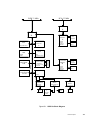
1
USPIIi-3v User’s Manual
Version 2.1 — September, 2000
Themis Computer—Americas and Pacific Rim
3185 Laurelview Court
Fremont, CA 94538
Phone (510) 252-0870
Fax (510) 490-5529
World Wide Web http://www.themis.com
Themis Computer—Rest of World
1, Rue Des Essarts
Z.A. De Mayencin
38610 Gieres, France
Phone 33 76 59 60 61
Fax 33 76 63 00 30
Copyright © 1999-2000 Themis Computer, Inc.
ALL RIGHTS RESERVED. No part of this publication may be reproduced in any form, by
photocopy, microfilm, retrieval system, or by any other means now known or hereafter invented without
the prior written permission of Themis Computer.
The information in this publication has been carefully checked and is believed to be accurate. However,
Themis Computer assumes no responsibility for inaccuracies. Themis Computer retains the right to
make changes to this publication at any time without prior notice. Themis Computer does not assume
any liability arising from the application or use of this publication or the product(s) described herein.
RESTRICTED RIGHTS LEGEND: Use, duplication, or disclosure by the United States Government
is subject to the restrictions set forth in DFARS 252.227-7013 (c)(1)(ii) and FAR 52.227-19.
TRADEMARKS
SOLARIS™ is a registered trademark of Sun Microsystems
SPARC™ is a registered trademark of SPARC International
All other trademarks used in this publication are the property of their respective owners.
Themis Customer Support
North America, South America, and Pacific Rim
Telephone:
Fax:
E-mail:
Web Site:
USPIIi-3v User’s Manual
September 2000
Part Number: 105622
510-252-0870
510-490-5529
[email protected]
http://www.themis.com
Version Revision History
Version 1.0
November 1998
Version 2.0
September 1999
Version 2.1
September 2000
Table of Contents
1
2
3
4
Getting Started ......................................................................................................
1.1
How to Use This Manual .......................................................................................
1.2
Intended Audience .................................................................................................
1.2.1
Product Warranty and Registration........................................................
1.3
Unpacking ..............................................................................................................
1.4
How to Start Quickly .............................................................................................
1.5
Related References ................................................................................................
Installation .............................................................................................................
2.1
OpenBOOT PROM (OBP) Configuration.............................................................
2.2
Configuring The VME Interface............................................................................
2.3
Installing The USPIIi-3v Paddle Board.................................................................
2.4
Attaching the USPIIi-3v to a Network ..................................................................
2.5
Attaching a Keyboard and Mouse .........................................................................
2.6
Attaching a TTY Terminal ....................................................................................
Specification..........................................................................................................
3.1
System....................................................................................................................
3.1.1
Block Diagram.......................................................................................
3.2
System Specification..............................................................................................
3.2.1
Processor Module & Memory Subsystems............................................
3.2.2
I/O Subsystem........................................................................................
3.2.3
Auxiliary Functions ...............................................................................
3.3
Environmental Specification..................................................................................
Hardware Overview...............................................................................................
4.1
Major Components ................................................................................................
4.1.1
UltraSPARC-IIi CPU Module ...............................................................
4.1.2
SME Advanced PCI Bridge (APB) .......................................................
4.1.3
SME Reset, Interrupt, and Clock (RIC).................................................
Themis Computer
1-1
1-1
1-1
1-2
1-2
1-3
1-3
2-1
2-1
2-1
2-2
2-2
2-3
2-3
3-1
3-1
3-2
3-4
3-4
3-5
3-5
3-6
4-1
4-1
4-1
4-2
4-2
i
USPIIi-3v User’s Manual
5
6
ii
4.1.4
Tundra Universe II.................................................................................
4.1.5
SME PCI I/O Controller ........................................................................
4.1.6
Symbios SCSI Controller.......................................................................
4.1.7
FPGA .....................................................................................................
4.1.8
National Super I/O.................................................................................
4.1.9
Seimens SAB 82532 ..............................................................................
4.1.10
Boot FLASH PROM and Non-volatile Storage ...................................
4.1.11
TOD and NVRAM.................................................................................
4.2
Memory Subsytem.................................................................................................
4.2.1
Data Path and Interface to Motherboard................................................
4.2.2
Memory Addressing ..............................................................................
4.2.3
PMC Carrier Subsystem ........................................................................
4.2.4
Creator Graphics (FFB) .........................................................................
4.3
Open Boot Program...............................................................................................
Connector Pinouts.................................................................................................
5.1
Introduction............................................................................................................
5.2
Front Panel.............................................................................................................
5.2.1
Serial A and Serial B .............................................................................
5.2.2
Keyboard / Mouse..................................................................................
5.2.3
SCSI A and SCSI B ...............................................................................
5.2.4
Ethernet A and Ethernet B.....................................................................
5.3
P2 Paddle Board ....................................................................................................
5.3.1
Parallel Port............................................................................................
5.3.2
Ethernet MII A and Ethernet MII B Ports .............................................
5.3.3
SCSI A and SCSI B Ports ......................................................................
5.3.4
Serial C and Serial D Ports ....................................................................
5.3.5
PMC I/O.................................................................................................
5.4
P1 / P2 Connectors.................................................................................................
5.4.1
Base Board P1 / P2 Connectors .............................................................
5.4.2
Middle Board P2 Connector ..................................................................
5.4.3
PMC Carrier Board Connectors.............................................................
5.5
Base Board Connectors..........................................................................................
5.5.1
JTAG Connector ....................................................................................
5.5.2
ROMBO Connector ...............................................................................
Universe-II...............................................................................................................
6.1
Features ..................................................................................................................
6.2
VMEbus Configuration..........................................................................................
6.3
Universe II as the VMEbus Slave..........................................................................
6.3.1
Universe II as the VMEbus Master........................................................
6.3.2
VMEbus First Slot Detector ..................................................................
6.3.2.1
Automatic Slot Identification.............................................
6.3.2.2
Registered Access at the power up ....................................
Themis Computer
4-3
4-3
4-3
4-3
4-4
4-4
4-4
4-4
4-4
4-5
4-5
4-5
4-5
4-5
5-1
5-1
5-2
5-3
5-4
5-4
5-7
5-8
5-9
5-10
5-10
5-12
5-13
5-15
5-15
5-17
5-19
5-22
5-22
5-23
6-1
6-1
6-2
6-2
6-3
6-4
6-5
6-5
Table of Contents
7
8
9
6.3.3
Universe II’s hardware Power -Up Options ..........................................
6.4
Slave Image Programming.....................................................................................
6.4.1
VME Slave Images ................................................................................
6.4.1.1
VMEbus Fields ..................................................................
6.4.1.2
PCI Bus Fields ...................................................................
6.4.1.3
Control Fields ....................................................................
6.4.2
PCI Bus Target Images ..........................................................................
6.4.2.1
PCI Bus Fields ...................................................................
6.4.2.2
VMEbus Fields ..................................................................
6.4.2.3
Control Fields ....................................................................
6.4.2.4
Special PCI Target Image ..................................................
6.5
Universe II’s Interrupt and Interrupt Handler........................................................
6.5.1
VME and PCI Interrupters:....................................................................
6.5.2
VMEbus Interrupt Handling:.................................................................
6.5.3
Universe II’s Mailbox Registers: ...........................................................
6.5.4
Universe II’s Semaphores......................................................................
6.5.5
Programmable slave images on the VMEbus and PCI bus: ..................
Resets ....................................................................................................................
7.1
Overview................................................................................................................
7.2
Reset Generation....................................................................................................
7.2.1
Resets .....................................................................................................
7.2.1.1
Push-button POR...............................................................
7.2.1.2
Push-button XIR................................................................
7.2.1.3
Scan Power On Reset.........................................................
7.2.1.4
Scan XIR............................................................................
7.2.2
Reset related functions in the FPGA......................................................
7.2.2.1
Watchdog timer level 3 interrupt.......................................
7.2.2.2
Watchdog timer level 2 interrupt.......................................
7.2.2.3
FPGA Reset Logics ...........................................................
7.2.2.4
Reset Turnaround Logics...................................................
7.2.2.5
VDD/CORE Voltage Protection........................................
7.2.2.6
VME Reset Resolution Logics ..........................................
Interrupts ...............................................................................................................
8.1
Interrupt System.....................................................................................................
8.1.1
Interrupt Description..............................................................................
8.1.2
RIC Implementation ..............................................................................
FPGA ......................................................................................................................
9.1
Introduction............................................................................................................
9.2
ROMBO and Flash Selection Signals....................................................................
9.3
User LEDs..............................................................................................................
9.4
Watchdog Timers...................................................................................................
9.4.1
Watchdog Registers ...............................................................................
Themis Computer
6-5
6-7
6-7
6-7
6-8
6-9
6-9
6-9
6-10
6-10
6-11
6-13
6-13
6-14
6-14
6-14
6-14
7-1
7-1
7-1
7-2
7-2
7-2
7-2
7-2
7-2
7-4
7-4
7-4
7-4
7-4
7-4
8-1
8-1
8-3
8-3
9-1
9-1
9-1
9-2
9-2
9-2
iii
USPIIi-3v User’s Manual
9.5
10
11
iv
Reset Logics...........................................................................................................
9.5.1
Reset Control Register (RCR) ...............................................................
9.5.2
Reset Status Register (RSR) ..................................................................
9.6
Voltage and Temperature Monitoring and Shutdown...........................................
9.7
Reset Workarounds................................................................................................
Temperature Sensing and Monitoring .................................................................
10.1
Introduction............................................................................................................
10.1.1
Temperature Sensing and Monitoring Hardware...................................
10.1.2
Temperature Sensing and Monitoring in the OBP.................................
Jumpers and Solder Beads...................................................................................
11.1
Overview................................................................................................................
11.2
Jumpers ..................................................................................................................
11.2.1
SCSI Termination ..................................................................................
11.2.2
VME SYSCLK Source ..........................................................................
11.2.3
Flash 0 Write Enable..............................................................................
11.2.4
Flash 1 and Flash 2 Write Enable ..........................................................
11.2.5
Keyboard / TTYC ..................................................................................
11.2.6
Mouse / TTYD.......................................................................................
11.2.7
Serial Port B Transceiver Mode.............................................................
11.2.8
Serial Port B Loop Back Mode..............................................................
11.2.9
ROMBO / PROM Boot Source .............................................................
11.2.10 Temperature Shut Down........................................................................
11.2.11 Temperature Fail Interrupt.....................................................................
11.2.12 Temperature Warning Interrupt.............................................................
11.3
Solder Beads ..........................................................................................................
11.3.1
FPGA Bypass for SYS_RST (System Reset) ........................................
11.3.2
FPGA Bypass for PB_RST (Push Button POR Reset)..........................
11.3.3
FPGA Bypass for X_RST (Push Button XIR Reset).............................
11.3.4
Reset from VME to CPU.......................................................................
11.3.5
Reset from CPU to VME .......................................................................
11.3.6
Primary PCI Processor Bus Speed.........................................................
11.3.7
Serial Port C ...........................................................................................
11.3.8
Serial Port D...........................................................................................
11.3.9
Watchdog Control Mask........................................................................
11.3.10 Watchdog Control Mode .......................................................................
11.3.11 Watchdog Control Request....................................................................
11.3.12 JTAG......................................................................................................
11.3.13 VDD Core Voltage ................................................................................
11.3.14 Carrier Board .........................................................................................
Glossary..................................................................................................................
A.1
Terminology...........................................................................................................
Themis Computer
9-3
9-3
9-3
9-4
9-4
10-1
10-1
10-1
10-1
11-1
11-1
11-1
11-3
11-3
11-3
11-4
11-4
11-4
11-5
11-5
11-5
11-6
11-6
11-6
11-7
11-9
11-9
11-9
11-10
11-10
11-10
11-11
11-11
11-11
11-12
11-12
11-12
11-13
11-13
A-1
A-1
List of Tables
Table 3-1.
Table 3-2.
Table 3-3.
Table 3-4.
Table 3-5.
Table 3-6.
Processor Specifications ............................................................................................
Memory Specification................................................................................................
I/O Sub-system Specification ....................................................................................
Auxiliary Functions Specifications............................................................................
USPIIi-3v Operating Environmental Specifications.................................................
USPIIi-3v Non-operating Environmental Specifications ..........................................
3-4
3-4
3-5
3-5
3-6
3-6
Table 5-1.
Table 5-2.
Table 5-3.
Table 5-4.
Table 5-5.
Table 5-6.
Table 5-7.
Table 5-8.
Table 5-9.
Table 5-10.
Table 5-11.
Table 5-12.
Table 5-13.
Table 5-14.
Table 5-15.
Table 5-16.
Table 5-17.
Table 5-18.
Table 5-19.
Front Panel Serial A Connector Pinout......................................................................
Front Panel Serial B Connector Pinout......................................................................
Front Panel Keyboard / Mouse Connector Pinout.....................................................
Front Panel SCSI A Connector Pinout ......................................................................
Front Panel SCSI B Connector Pinout.......................................................................
Baseboard RJ45 Ethernet A & B Pinouts ..................................................................
P2 Paddle Board Parallel Connector Pinout ..............................................................
P2 Paddle Board Ethernet MII A and Ethernet MII B Connector Pinout..................
P2 Paddle Board SCSI A and SCSI B Connector Pinout ..........................................
Serial Port C (PS/2 Keyboard) Connector Pinout......................................................
Serial Port D (PS/2 Mouse) Connector Pinout ..........................................................
P2 Paddle Board PMC I/O Connector Pinout............................................................
Base Board P1 Connector Pinout...............................................................................
Base Board P2 Connector Pinout...............................................................................
Middle Board P2 Connector Pinout...........................................................................
PMC Carrier Board P1 Connector Pinout..................................................................
PMC Carrier Board I/O P2 Connector Pinout ...........................................................
Base Board JTAG Connector Pinout .........................................................................
Base Board ROMBO Connector Pinout ....................................................................
5-3
5-3
5-4
5-5
5-6
5-7
5-9
5-10
5-11
5-12
5-12
5-13
5-15
5-16
5-18
5-19
5-20
5-22
5-23
Themis Computer
v
USPIIi-3v User’s Manual
Table 6-1.
Table 6-2.
Table 6-3.
Table 6-4.
Table 6-5.
Table 6-6.
Table 6-7.
Table 6-8.
Table 6-9.
Table 6-10.
Table 6-11.
Table 6-12.
Table 6-13.
Table 6-14.
Universe II Miscellaneous Control Register (MISC_CTL).......................................
Universe II Power Up Options...................................................................................
PCI Configuration Base Address 0 Register (PCI_BS0)...........................................
PCI Configuration Base Address 1 Register (PCI_BS1)...........................................
VMEbus Fields for VMEbus Slave Image ................................................................
PCI Bus Fields for VMEbus Slave Image .................................................................
Control Fields for VMEbus Slave Image ..................................................................
PCI Bus Fields for PCI Bus Target Image.................................................................
PCI Bus Fields for PCI Bus Target Image.................................................................
Control Fields for PCI Bus Target Image ..................................................................
PCI Bus Fields for Special PCI Bus Target Image....................................................
PCI Bus Fields for Special PCI Bus Target Image....................................................
Control Fields for Special PCI Bus Target Image .....................................................
Special PCI Target Image Register (Offset 188).......................................................
6-4
6-5
6-6
6-7
6-8
6-8
6-9
6-9
6-10
6-10
6-11
6-11
6-11
6-12
Table 7-1.
Effects of Resets ........................................................................................................
7-5
Table 8-1.
Interrupt inputs to RIC...............................................................................................
8-1
Table 9-1.
Table 9-2.
Table 9-3.
Watchdog Registers ...................................................................................................
Reset Control Register ...............................................................................................
Reset Status Register (RSR) ......................................................................................
9-2
9-3
9-3
Table 11-1.
Table 11-2.
Table 11-3.
Table 11-4.
Table 11-5.
Table 11-6.
Table 11-7.
Table 11-8.
Table 11-9.
Table 11-10.
Table 11-11.
Table 11-12.
Table 11-13.
Table 11-14.
Table 11-15.
Table 11-16.
Table 11-17.
USPIIi-3v Jumpers.....................................................................................................
SCSI Termination Jumper Settings............................................................................
VME SYSCLK Source Jumper Settings ...................................................................
Flash 0 Write Enable Jumper Settings .......................................................................
Flash 1 and Flash 2 Write Enable Jumper Settings ...................................................
Keyboard / TTYC Jumper Settings ...........................................................................
Mouse / TTYD Jumper Settings ................................................................................
Serial Port B Transceiver Mode Jumper Settings......................................................
Serial Port B Loop Back Mode Jumper Settings .......................................................
ROMBO / PROM Boot Source Jumper Settings.......................................................
Temperature Shut Down Jumper Settings .................................................................
Temperature Fail Interrupt Jumper Settings ..............................................................
Temperature Warning Interrupt Jumper Settings ......................................................
USPIIi-3v Solder Beads.............................................................................................
FPGA Bypass for SYS_RST (System Reset) Solder Bead Settings .........................
FPGA Bypass for PB_RST (Push Button POR Reset) Solder Bead Settings ...........
FPGA Bypass for X_RST (Push Button XIR Reset) Solder Bead Settings ..............
11-1
11-3
11-3
11-3
11-4
11-4
11-4
11-5
11-5
11-5
11-6
11-6
11-6
11-7
11-9
11-9
11-9
vi
Themis Computer
List of Tables
Table 11-18.
Table 11-19.
Table 11-20.
Table 11-21.
Table 11-22.
Table 11-23.
Table 11-24.
Table 11-25.
Table 11-26.
Table 11-27.
Table 11-28.
Reset from VME to CPU Solder Bead Settings ........................................................
Reset from CPU to VME Solder Bead Settings ........................................................
Primary PCI Processor Bus Speed Solder Bead Settings ..........................................
Serial Port C Solder Bead Settings ............................................................................
Serial Port D Solder Bead Settings ............................................................................
Watchdog Control Mask Solder Bead Settings .........................................................
Watchdog Control Mode Solder Bead Settings.........................................................
Watchdog Control Request Solder Bead Settings .....................................................
JTAG Solder Bead Settings .......................................................................................
VDD Core Voltage Solder Bead Settings..................................................................
Carrier Board Jumper Settings...................................................................................
Themis Computer
11-10
11-10
11-10
11-11
11-11
11-11
11-12
11-12
11-12
11-13
11-13
vii
USPIIi-3v User’s Manual
viii
Themis Computer
List of Figures
Figure 3-1.
USPIIi-3v Block Diagram .........................................................................................
3-2
Figure 5-1.
Figure 5-2.
Figure 5-3.
Figure 5-4.
Figure 5-5.
Figure 5-6.
Figure 5-7.
Figure 5-8.
Figure 5-9.
Figure 5-10.
Figure 5-11.
Figure 5-12.
Figure 5-13.
Figure 5-14.
Figure 5-15.
Figure 5-16.
Front Panel Layout.....................................................................................................
Front Panel Serial A and Serial B Connector Orientation.........................................
Front Panel Keyboard / Mouse Connector Orientation.............................................
Front Panel SCSI A and SCSI B Connector Orientation...........................................
Front Panel Ethernet A and Ethernet B Connector Orientation.................................
P2 Paddle Board.........................................................................................................
P2 Paddle Board Parallel Port Connector Orientation...............................................
P2 Paddle Board Ethernet MII A and Ethernet MII B Connector Orientation..........
P2 Paddle Board SCSI A and SCSI B Connector Orientation ..................................
P2 Paddle Board Serial C and Serial D Connector Orientation.................................
P2 Paddle Board PMC I/O Connector Orientation....................................................
Base Board P1 and P2 Connector Orientation...........................................................
Middle Board P2 Connector Orientation...................................................................
PMC Carrier Board P1 and P2 Connector Orientation..............................................
Base Board JTAG Connector Orientation.................................................................
Base Board ROMBO Connector Orientation ............................................................
5-2
5-3
5-4
5-4
5-7
5-8
5-9
5-10
5-10
5-12
5-13
5-15
5-17
5-19
5-22
5-23
Figure 6-1.
Figure 6-2.
Figure 6-3.
Figure 6-4.
Universe II Architectural Diagram............................................................................
Address Translation for VMEbus to PCI Bus Transfers ...........................................
Address Translation for PCI Bus to VMEbus Transfers ...........................................
Memory Mapping in the Special PCI Target Image..................................................
6-3
6-8
6-10
6-13
Figure 7-1.
USPIIi-3v Reset Block Diagram...............................................................................
7-3
Figure 11-1.
Figure 11-2.
USPIIi-3v Baseboard with Jumper Locations ...........................................................
USPIIi-3v Baseboard with Solder Bead Locations....................................................
11-2
11-8
Themis Computer
ix
List of Figures
Themis Computer
x
1
1Getting Started
1.1
How to Use This Manual
Thank you for purchasing the Themis USPIIi-3v computer. The USPIIi-3v system is composed of two 6U
VME boards and requires 3 VME slots. The USPIIi-3v is a SPARC V9.0 compliant computer with a VMEbus
interface and an UltraSPARC-IIi processor.
Before you begin, carefully read each of the procedures in this manual and the associated CPU manual.
Improper handling of the equipment can cause serious damage.
We value our customer’s comments and concerns. Our Marketing department is eager to know what you think
of our products. A “Reader Comment Card” is located at the end of this manual for your use. Please take the
time fill it out and return it to Themis Computer.
1.2
Intended Audience
This manual is written for system integrators and programmers. The USPIIi-3v is targeted at a technically
sophisticated customer who will integrate the product as part of an overall system solution. This manual
contains all necessary information for installation and configuration of the USPIIi-3v. The OpenBoot PROM
(OBP) code is installed in the system flash. The USPIIi-3v system must run all sun4u application binaries
unmodified. It must also boot a Solaris CDROM and run an unmodified sun4u kernel. Additional device
drivers (such as a VME nexus driver) are required to use all the features of the board, but no part of the
standard Solaris OS can be modified. Themis-supplied software for the USPIIi-3v is installed on top of a
standard Solaris installation and will minimize the potential for any conflict with Solaris patches which may
be released by SunSoft.
The reader should have a working knowledge of the VMEbus specifications, SPARC processor architecture,
Ethernet, and SCSI (ANSI X3.131-1986).
Themis Computer
1-1
USPIIi-3v User’s Manual
1.2.1
Product Warranty and Registration
Please review the Themis Computer warranty and complete the product registration card delivered with your
USPIIi-3v system. Return of the registration card is not required to activate your product warranty but, by
registering your USPIIi-3v, Themis Computer will be able to better provide you with timely updated
information and product enhancement notifications.
Our Customer Support department is committed to providing the best product support in the industry.
Customer Support is available 8am - 5pm (PST), Monday through Friday via telephone, fax, e-mail or our
World Wide Web site.
Themis Customer Support
Telephone:
Fax:
E-mail:
Web Site:
1.3
510-252-0870
510-490-5529
[email protected]
http://www.themis.com
Unpacking
Caution — The USPIIi-3v contains static sensitive components. Industry standard anti-static measures
must be observed when removing the USPIIi-3v from its shipping container and during any subsequent
handling.
A wrist strap (or grounding strap) provides grounding for static electricity between your body and the chassis
of the system unit. Electric current and voltage do not pass through the wrist strap.
Remove the USPIIi-3v and accessories from the shipping container and check the contents against the
packing list. The package should include:
• An assembled USPIIi-3v system consisting of:
– Front Panel
– Base Board
– CPU Module
– Memory Boards
– OpenBoot PROM installed in the system flash
• P2 Paddle Board for I/O
• Set of cables for the Front Panel Serial Ports
• USPIIi-3v User’s Manual (if ordered)
Report any discrepancies to the Themis Computer Customer Support department immediately.
1-2
Themis Computer
1. Getting Started
1.4
How to Start Quickly
To start quickly with the USPIIi-3v Themis Computer recommends that you read the following sections:
• Appendix A contains vital information on configuring the USPIIi-3v and the design and setup of
VMEbus based systems.
• Consult, Chapter 11, "Jumpers and Solder Beads,", This chapter contains a complete listing of all user
configurable jumpers and the default settings. Verify that the jumpers on your board are set to meet
your application requirements.
1.5
Related References
The following is a list of related references.
• PCI Local Bus Specification, Revision 2.1, PCI Special Interest Group, Portland
• American National Standard for VME64, ANSI/VITA, 1994
• IEEE Standard 1275-1994, Standard For Boot (Initialization, Configuration) Firmware, Core Practices
and Requirements
• IEEE Standard 1275.1-1994, Standard For Boot (Initialization, Configuration) Firmware, ISA
Supplement for IEEE P1754 (SPARC)
• IEEE Standard P1275.6/D4, Standard For Boot (Initialization, Configuration) Firmware, 64 Bit
Extensions
• PCI Bus Binding to IEEE 1275-1994, Standard for Boot (Initialization, Configuration) Firmware,
Revision 1.0, 14 April 1994, Prepared by the Open Firmware Task Force of the PCI Alliance
• The SPARC Architecture Manual, Version 9, David L. Weaver and Tom Germond, editors, PTR
Prentice Hall
Themis Computer
1-3
USPIIi-3v User’s Manual
1-4
Themis Computer
2
2Installation
2.1
OpenBOOT PROM (OBP) Configuration
The OpenBOOT PROM (OBP) code is used to boot the operating system, run diagnostics, modify system
start-up parameters, and to load and execute programs. The version of the OBP code used on the USPIIi-3v is
OBP Release 3.10.13 and later.
At power-up, the processor fetches instructions starting at physical address (ADDRESS) from the FLASH
device, where the OBP code is stored to execute an appropriate start-up sequence.
Themis Computer provides an OBP Configuration pre-programmed in the FLASH. However, this
configuration may be modified to fit an individual user’s needs. OBP modifications are made using the
FORTH Monitor.
2.2
Configuring The VME Interface
Themis has implemented a variable and flexible VMEbus interface using both on-board jumpers, OpenBoot
PROM (OBP) commands, and environment variables specific to the USPIIi-3v board.
The USPIIi-3v is typically re-configured when VMEbus boards are added, removed, or changed in the
chassis. Board configuration normally involves allocation of VMEbus master access address, interrupts, and
slave base address of the USPIIi-3v.
All other VMEbus interface related options are configured using extensions to the Sun OpenBoot PROM
monitor program. OBP stores system configuration parameters in non-volatile storage (NVRAM) using a
setenv mechanism familiar to UNIX shell users.
The OBP command setenv must be used to set the values of the environment variables. The printenv
command will list all supported environment variables and can be used to verify proper setting. You must be
at the OpenBoot command prompt to enter and execute OpenBoot commands.
Themis Computer
2-1
USPIIi-3v User’s Manual
If autoboot is enabled, interrupt the boot sequence by pressing L1-A (STOP-A); on a serial terminal press
BREAK.
If BOOTMON compatibility mode is enabled, you will initially see the BOOTMON prompt. Enter n to start
OpenBoot:
Type b (boot), c (continue), or n (new command mode)
>n
ok>
At the ok> prompt you are now able to enter OBP commands. Use setenv to modify the environment
variables necessary to configure the USPIIi-3v for your VMEbus configurations or execute the appropriate
OBP commands listed above.
The following example moves the slave window for A32 accesses to 0x80000000 and enables slave accesses.
ok> setenv vme32-slave-base 0x8000.0000
The OBP automatically programs the Universe II VMEbus interface chip with the correct register values and
retains your settings in NVRAM.
!
2.3
Warning — Unless you are familiar with the Forth Monitor and are experienced in interacting with your
system PROM, restrict yourself to the most basic Forth Monitor operations. That is, to synching your disks,
ejecting floppies from the diskette drive, booting your system and configuring the VME interface. More
advanced commands can do damage to your system’s operation.
Installing The USPIIi-3v Paddle Board
The “paddle board”, also referred to as a “transition board”, delivered with the USPIIi-3v attaches to the rear
of the P2 backplane and provides connectors for Serial Port C & D (PS/2 KB & MS), MII 1, MII 2 (or PMC
slot 1) SCSI A & B, Parallel port.
2.4
Attaching the USPIIi-3v to a Network
The USPIIi-3v features two RJ-45 for 10/100 Base-T ethernet interface connections. ethernet 1 & 2 MII
interface are provided on the paddle board. The interface has auto-detection capabilities and no configuration
is necessary
2-2
Themis Computer
2. Installation
If only the baseboard is present, there is only a single network connection (Ethernet A) available, either
through the RJ45 connector or MII. If the I/O Board is present a second ethernet (Ethernet B) is available.
Both Ethernets A and B may be active.
After attaching the USPIIi-3v to a network, you can verify proper physical connection by executing the
FORTH network selftest (test net). This test will indicate external loopback failure on each of the network
interfaces when there is not a proper physical connection. As only one interface can be active, the inactive
network interface will always return an external loopback error.
ok> test net (for Ethernet 1) Test net 2 (for Ethernet 2)
Using MII Ethernet Interface
Lance Register test -- succeeded
Internal loopback test -- succeeded
External loopback test -- Lost Carrier (transceiver cable problem?)
send failed
Using TP Ethernet Interface
Lance Register test -- succeeded
Internal loopback test -- succeeded
External loopback test -- succeeded
send ok
net selftest succeeded
2.5
Attaching a Keyboard and Mouse
A standard Sun Keyboard/Mouse combination can be attached to the front panel KB/M connector.
2.6
Attaching a TTY Terminal
A TTY display terminal can be attached to the Serial A port on the front panel. Use the serial cable from the
accessories delivered with the USPIIi-3v.
Themis Computer
2-3
USPIIi-3v User’s Manual
2-4
Themis Computer
3
3Specification
3.1
System
The USPIIi-3v system is an UltraSPARC-IIi based design supporting PMC PCI mezzanine cards, Sun FFB
and VME64 modules. The USPIIi-3v system consists of two 6U VME boards and occupies 3 VME slots. The
design is largely based on the Panther Board design from Sun Microelectronics and the Nordica Board design
from Themis Computer It has been optimized for embedded systems industries. The memory sub-system
utilizes a family of proprietary, co-planar, stackable DRAM memory modules of either 64 MB, 128MB,
256MB, or 512MB per module. Memory configurations of 64 MB, 128 MB, 256 MB, 512 MB, and 1GB are
supported.
The local I/O subsystem is PCI based, with separate PCI channels provided for I/O functions and external
VMEbus backplane access. The front panel of the USPIIi-3v system provides two SCSI ports, two Ethernet
ports, two serial ports, and Sun Keyboard/Mouse connections.
The back panel VMEbus interface provides signals via the P2 Paddle Board, delivered with the USPIIi-3v, for
Serial Port C & D (P/S2 Kb & MS), MII 1, MII 2 (or PMC slot 1 & 2), SCSI A & B, Parallel port.
A triple PMC Carrier Board is available for vendor specific, PMC board expansions.
Themis Computer
3-1
USPIIi-3v User’s Manual
3.1.1
Block Diagram
RIC
6
Driver
LVC16374
Drivers
3xLPT16244
UPA64S
Creator Graphics
6
Address/
CNTL
Address/
CNTL
UltraSPARC-IIi
Processor Module
EDO
DRAM
Data/72
X
C
V
R
Proc: SME1040-266 -300 -333
Cache: 512K (64+8P&T(14+2+P) or 2 M
66 MHz PCI Interface
APB
(128 + 16)
Min: 64 MByte
Max: 1 GByte
6xSN74ALVC162268
SME2411
PCIA
33 MHz
PCIB
33 MHz
Data/144
32
32
32
PMC0
PCI Mezzanine Board
32
I/O
P2
PMC1
32
PCI Mezzanine Board
I/O
P2
Dual Wide
Ultra SCSI
Interface
A&B and
On-Board
Termination
PCI Mezzanine Board
PCI - VME
Bridge
SYM53C876
2xUCC3912
Tundra
Universe II
6xUC5606PLUS
Drivers
A
PMC2
32
B
64 VME
Front
Panel
P2
Figure 3-1. USPIIi-3v Block Diagram
3-2
Themis Computer
PCIA 33 MHz
PCIB 33 MHz
Cheerio
A
Cheerio
B
Ebus Address
Latch
ROMBO
Connector
EB_LADR<23..8>
P2
NVRAM
8KB
Front Panel
RJ45
A
Ethernet 2
DP83840
DP83223
2xPE68510
2xABT827
P2
MII 2
EPLD
Altera
EPF8820ATC144-4
Dual Serial
Interface A&B
Ebus
Primary Boot
Flash PROM
2 MB
SAB 82532
2xUC5180, UC5170
3xACA5020
A
B
10/100 Mbit
Ethernet
Front Panel
M48T59
LM393
Secondary User
Flash PROM
2x2 MB
10/100 Mbit
Ethernet
B
Front Panel
RJ45
Ethernet 1
DP83840
DP83223
2xPE68510
2xABT827
P2
MII 1
Super I/O
PC87307
Sun Keyboard
Mouse
Parallel Port
Data/Clock Lines
Filters
2xIPEC1284
3xACA5020
P2
PS/2 Keyboard
Mouse
P2
or
Serial Port
C and D
Data/Clock Lines
Front
Panel
P2
Figure B-1. USPIIi-3v Block Diagram
Themis Computer
3-3
USPIIi-3v User’s Manual
3.2
System Specification
3.2.1
Processor Module & Memory Subsystems
Table 3-1, "Processor Specifications," on page 3-4, and Table 3-2, "Memory Specification," on page 3-4,
summarize the processor and memory subsystems.
Table 3-1. Processor Specifications
Feature/Function
Specifications
Processor
UltraSPARC-IIi
Processor Speed
Grade 1 - 300 MHz
Grade 2 - 333 MHz
Grade 3 - 360 MHz
Performance
12.1 SPECint95 @ 300 MHz w/ 256KB cache (estimate)
12.9 SPECfp95 @ 300 MHz w/ 256KB cache (estimate)
External Cache
2 MB SRAM, fast Register-Latch access mode
(for the 333 MHz and 360MHz)
Table 3-2. Memory Specification
Feature/Function
3-4
Specifications
Main Memory
Proprietary Coplanar Modules
One (1) to two (2) Modules
Memory Bus Interface
72 bit Data Path from CPU, including 8 bit ECC
2 to 1 Interleave to DRAM
13 bit Address Bus
3.3V Level Interface
Memory Modules
Four Module Types
64 MB, using 9 - 4Mx16 EDO DRAMs
128 MB, using 18 - 4Mx16 EDO DRAMs
256 MB, using 36 - 4Mx16 EDO DRAMs
512 MB, using 36 - 16Mx8 EDO DRAMs
Memory Configurations
64 MB - One (1) 64 MB Module
128 MB - One (1) 128 MB Module
256 MB - One (1) 256 MB Module
512 MB - Two (2) 256 MB Modules
- One (1) 512 MB Module
1 GByte - Two (2) 512 MB Modules
Themis Computer
3. Specification
3.2.2
I/O Subsystem
Table 3-3, "I/O Sub-system Specification," on page 3-5, summarizes the I/O subsystem functionality.
Table 3-3. I/O Sub-system Specification
Function
Sun Keyboard / Mouse Port
Front Panel
PS/2 Compatible KB/Mouse Port
Paddle Board
Serial Port A (RS-232)
Front Panel (sync/asynch)
Serial Port B (RS-232/422)
Front Panel (sync/asynch)
Serial Port C (RS-232)
(If Sun KB/MS is not in use)
Paddle Board (asynch)
Serial Port D (RS232)
(If Sun KB/MS is not in use)
Paddle Board (asynch)
Parallel Port (Bi-Directional IEEE1284)
Paddle Board
Ethernet Port 1
RJ45:Front Panel (10/100BaseT)
MII 1 Interface:Paddle Board
Ethernet Port 2a
RJ45:Front Panel (10/100BaseT)
MII 2 Interface:Paddle Board
SCSI Port A
Single Ended Ultra/Wide SCSI
Front Panel/ Paddle Board
SCSI Port B
Single Ended Ultra/Wide SCSI
Front Panel/ Paddle Board
PMC 0 and PMC 1 I/O (upper 32 bits)
Paddle Board
PMC Expansion
Three PMC Slots in a single VME slot.
On Carrier Board
Creator Graphics (FFB)
On Base Board
a.
3.2.3
Location
MII 2 and 19 of the upper 32 bits of the I/O from PMC 1 are accessible only on the P2 Paddle Board. The default selection is MII 2.
Auxiliary Functions
Table 3-4, "Auxiliary Functions Specifications," on page 3-5 summarizes the functional specifications of the
auxiliary functions.
Table 3-4. Auxiliary Functions Specifications
Feature/Function
Description
Boot Flash
2 MB (2Mx8)
One 29F016 Device
User Flash
4 MB (2x2Mx8)
Two 29F016 Devices
NVRAM/TOD
8 KB (8Kx8), Battery Backed
M48T59
Themis Computer
3-5
USPIIi-3v User’s Manual
Table 3-4. Auxiliary Functions Specifications
Feature/Function
System Status LEDs
Ten different colored LED’s
Located on Front Panel
User LEDs
2 Red and 2 Green LED’s
Located on Front Panel
Reset Switches: Reset, Abort
Momentary Push-button
Located on Front Panel (recessed)
Watchdog Timers
Three Level Watchdog
Level One: Interrupt
Level Two: XIR
Level Three: POR Reset
(Level Three: Solder Bead disabled/enabled)
Voltage Sensors
Monitors +5,+3.3V and 2.6VSupply
Reset if out of range
DC -DC converters are shut down if out of range
Temperature Sensors
Two Level
Level One: warning Interrupt
Level Twoa: Fail Interrupt
Jumper enabled/disabled
a.
3.3
Description
FailshutsdownDC-DCconvertersifjumpersareenabled.
Environmental Specification
When measuring the operating environment air temperature for the USPIIi-3v, measure the air temperature as
close to the air intake port on the enclosure as possible. Although the thermal characteristics of the USPIIi-3v
are quite good, the maximum air flow should be across the USPIIi-3v board processor section.
Table 3-5.
USPIIi-3v Operating Environmental Specifications
Description
Minimum Value
Maximum Value
Temperature Range
0C
55 C
Humidity Range (relative
non-condensing at 104 F (40 C)
5%
95%
Altitude Range
-500 meters
9,843 feet (3,000meters)
Air Flow
300 lfm airflow at 50 C
Table 3-6. USPIIi-3v Non-operating Environmental Specifications
3-6
Description
Minimum Value
Maximum Value
Temperature Range
-40 C
150 C
Humidity Range (relative non-condensing at 104 F (40 C)
5%
95%
Altitude Range
0 feet (0 meters)
38,370 feet (12000 meters)
Themis Computer
4
4Hardware Overview
4.1
Major Components
4.1.1
UltraSPARC-IIi CPU Module
The UltraSPARC-IIi CPU Modules (SME5421MCZ-300/333/360) consist of the following components:
– UltraSPARC-IIi Processor
– 2MB E-cache (333MHJz and 360MHz) and .5MB E-cache (300MHz)
– Clock generator
– External PCI/JTAG (temperature sense interface connector)
– External Memory (UPA64S connector)
The UltraSPARC-IIi CPU Modules are high performance, SPARC V9-compliant, small form-factor processor
modules based on the UltraSPARC-IIi single chip solution. They interface to the UltraSPARC Port
Architecture (UPA64S) interconnect bus, main memory, and the primary PCI bus. All UltraSPARC IIi
modules include fully integrated external cache. The UltraSPARC IIi microprocessor incorporates a CPU, PCI
bus interface, and memory controller. The UltraSPARC IIi modules are available in three configurations
300MHz with .5MB E-cache clocked at 150 MHz; 333MHz with 2 MB E-cache clocked at 167 MHz, and
360MHz with 2MB E-cache clocked at half CPU frequency.
The 300 MHz UltraSPARC-IIi module consists of one UltraSPARC-IIi CPU microprocessor, one 64K x 18
tag SRAM, four 64K x 18 data SRAMS, and circuitry for generating the processor, and UPA64S clocks. PCI
clocks are generated externally. The module runs at 300 MHz internal processor frequency. Clock synthesizer
and division circuitry on the module set the UPA frequency to one third of the internal processor frequency.
The module interface is implemented using two high-speed, impedance-controlled connectors.
The 333 MHz UltraSPARC-IIi module consists of one UltraSPARC-IIi CPU microprocessor, one 64K x 18
cache-tag SRAM, four 256K x 18 cache-data SRAMS, and circuitry for generating the processor, SRAM, and
UPA64S interfaces. PCI clocks are generated externally. The module runs at 333 MHz internal processor
frequency. The clock synthesizer sets the frequency and division circuitry operates the UPA frequency at one
third of the internal processor frequency. The module interface uses two high-speed, impedance-controlled
connectors.
Themis Computer
4-1
USPIIi-3v User’s Manual
The 360 MHz UltraSPARC-IIi module consists of one UltraSPARC-IIi CPU microprocessor, one 64K x 18
cache-tag SRAM, four 256K x 18 cache-data SRAMS, and circuitry for generating the processor, SRAM, and
UPA64S interfaces. PCI clocks are generated externally. The module runs at 360 MHz internal processor
frequency. The clock synthesizer sets the frequency and division circuitry operates the UPA frequency at one
third of the internal processor frequency. The module interface uses two high-speed, impedance-controlled
connectors.
The E-Cache (also referred to as “Level 2 Cache”) is a unified, write-back, allocating-on-misses, direct
mapped cache. The E-Cache is physically indexed and physically tagged (PIPT) and has no virtual or context
information. Except for stable storage and error management, the operating system requires no knowledge of
the E-Cache after initialization. The E-Cache always includes the content of the Instruction Cache (I-Cache)
and the Data Cache (D-Cache).
The USPIIi-3v E-cache uses a fast Register-Latch access mode. In the Register-Latched mode (also referred
to as “2-2”) the E-Cache Static RAMs have a cycle time equal to half of the processor cycle time. Depending
on the grade of UltraSPARC-IIi processor ordered, the SRAM cycle time will either be 1.51 nano-seconds,
for the 330 MHz processor, or 1.66 nano-seconds for the 300 MHz processor. In the Register-Latched mode,
two processor clocks are used to send the address and two processor clocks are used to return the E-Cache
data giving a 4-cycle pin-to-pin latency. As a result of the tight control over the SRAM turn on and turn off
times, no dead cycles are necessary when alternating between reads and writes.
Memory accesses to the E-Cache must be cacheable. Consequently, no E-Cache enable bit is present in the
LSU_Control_Register (Refer to Table 5-4, “LSU_Control_Register,”). Instruction fetches are directed to
non-cacheable PCI or UPA64S space when any of the following conditions are true:
• The I-MMU is disabled
• The UltraSPARC-IIi is in RED_state
• The access is mapped by the I-MMU as physically non-cacheable
• Data accesses to non-cacheable PCI or UPA64S space occur when either
• The D-MMU enable bit (DM) in the LSU_Control_Register is clear, or
• The access is mapped by the D-MMU as non-physical cacheable (unless ASI_PHYS_USE-EC is used).
Note — When non-cacheable accesses are used, the associated addresses must be legal according to the
UltraSPARC-IIi physical address map.
4.1.2
SME Advanced PCI Bridge (APB)
The SME Advanced PCI Bridge (SME: SME2411) interfaces directly with the UltraSPARC-IIi
microprocessor and concentrates two (2), +5V, 33MHz PCI buses into one +3.3V, 66 MHz PCI bus that
interface directly with the UltraSPARC-IIi. The 66 MHz PCI-to-CPU can achieve a peak bandwidth of 2
GBits/sec. Within the USPIIi-3v, the two (2), 33 MHz PCI busses are referred to as PCIA and PCIB.
4.1.3
SME Reset, Interrupt, and Clock (RIC)
The SME Reset, Interrupt and Clock (SME: STP2210QFP) ASIC provides a variety of functions on the
USPIIi-3v. The RIC manages system resets, system interrupts, system scans, and system clock control
functions. These functions are divided into independent functional blocks on the RIC.
4-2
Themis Computer
4. Hardware Overview
The interrupt controller on the RIC accepts all interrupts from the USPIIi-3v sub-systems (up to 41 interrupts)
and delivers encoded interrupts on the six (6) interrupt lines going into the UltraSPARC-IIi microprocessor.
Interrupts are accepted by the RIC in a round-robin priority scheme. The interrupts received by the RIC are
not passed to the UltraSPARC-IIi in the order they are received. Instead, a priority level is assigned. Eight (8)
interrupt levels are implemented. For more information concerning the SME RIC ASIC, refer to Chapter 8,
“Resets.”
4.1.4
Tundra Universe II
The Tundra Universe II (Tundra: CA91C142) ASIC interfaces the local 32-bit PCI bus to the VMEbus. The
Universe II includes a 33 MHz, 32-bit PCI bus interface, a fully compliant, high performance, 64-bit VMEbus
interface as well as a broad range of VMEbus address and data transfer modes of:
• A32/A24/A16 master and slave transfer, except for A64 and A40
• D64/D32/D16/D08 master and slave transfer, except for MD32
• MBLT, BLT, ADOH, RMW, LOCK, and location monitors
The Universe II also includes support for full VMEbus System Controller, nine user programmable slave
images, and seven interrupt lines. For more information on the Universe II, refer to Chapter 8, “Resets.” and
the Tundra Universe II User Manual, published by Tundra (Tundra Document Number 8091142.MD300.01).
4.1.5
SME PCI I/O Controller
The SME PCI I/O Controller (SME: STP2003QFP) is a +5 Volt ASIC that provides a Master / Slave interface
bus compliant with PCI Local Bus Specification, Revision 2.1. The PCI I/O is connected to the SME APB via
the local PCI bus. MII support for 10base-T (802.3) and 100base-T (802.30) Ethernet is provided by PCI I/O
as well as an IEEE 1149.1 JTAG compliant architecture, a 40 MHz SCSI clock oscillator, a 10MHz real-time
clock and an expansion bus interface (EBus2).
Support for the National PC87303 Super I/O, the Siemens SAB82532 Dual 16C550 Synchronous/
Asynchronous Serial Port controllers, the NVRAM, Time-of-Day, and a boot PROM control port is provided
via the EBus2. The boot PROM control port interfaces directly to the FPGA.
4.1.6
Symbios SCSI Controller
The Symbios SCSI Controller (SYM53C876) provides two (2) UltraWide SCSI interfaces (40 MB/sec). In
order to maximize speed, it is attached directly to the SME APB through local 33 MHz PCI Bus A. A
maximum burst rate of up to 132 MB/sec is supported.
4.1.7
FPGA
The FPGA device on the USPIIi-3v is the Altera EPF8820. It resides on the Ebus of the PCI I/O ASICs.The
FPGA implements a voltage monitor, boot address decoder, a three-level watchdog timer, the User LED
register, reset logic, and Ebus control logic. At power-on the FPGA self loads from a serial EPROM (Altera
EPC1213PC8) to program itself for these features. For more information on the FPGA, refer to Chapter 9,
"FPGA."
Themis Computer
4-3
USPIIi-3v User’s Manual
4.1.8
National Super I/O
The National Super I/O (PC87307-ICE) is an industry standard, single-chip solution that provides support for
Sun KB/MS, two (2) fast full function asynchronous serial ports (Serial Ports C and D), and an IEEE 1284 bidirectional parallel port. Each component is individually configured to maximize the performance of the
USPIIi-3v.
4.1.9
Seimens SAB 82532
The Seimens SAB 82532 Enhanced Serial Communication Controller provides support for Serial Ports A and
B and used for TTYA and TTYB. Serial Ports A and B are supported entirely independent of one another.
4.1.10
Boot FLASH PROM and Non-volatile Storage
The Boot FLASH PROM is the AMD 29F016. This is a 2MBit x 8 Flash Prom memory device. The access
time of this device shall be at least 90 nanoseconds.
The User FLASH shall consist of two (2) erasable 16MBit (AMD 29F016) devices organized in 2Mbit x 8
configurations. The device uses a +5V power supply and a 90 nanosecond access time. The total user FLASH
in the UltraIIi-3V design is 4 MBytes.
Using the RP signal of the FLASH for protection during power up and reset requires several microsecond
delay after the RP goes inactive and before the first read from the FLASH. This delay normally is guaranteed
because the reset to the CPU is delayed by the RIC by several ms relative to the POWER_OK signal.
4.1.11
TOD and NVRAM
The Non-Volatile Memory NVRAM and a Time of Day (TOD) clock are both contained in the NVRAM
memory (SGS-Thompson, M48T59Y-70MH1). The NVRAM has its own lithium battery to operate the clock
and maintain the contents of the NVRAM during power-off situations. The battery device is an SGS Thomson
Microelectronics BT1402. This single lithium battery provides backup for approximately 10 years and the
real-time clock circuitry provides accuracy of +/- one (1) second per day.
NVRAM and TOD are programmed using the FORTH toolkit in Open Boot Program (OBP).
4.2
Memory Subsytem
The USPIIi-3v supports up to two (2) coplanar memory modules of either 64MB, 128MB, 256MB, or 512MB
each. Each module of 64/128/128MB consists of 1, 2, or 4 banks of 64MB organized as nine (9) 4Mx16 EDO
DRAMs (NEC, UP4265165). These modules provide 64MB, 128MB, 256MB of system memory.
Additionally there is a 512MB memory module consisting of 36 16Mx8 EDO DRAM chips.
The memory design includes Error Correction Code (ECC). A single bit error in a 64 bit word is corrected
without loss of a cycle. CAS before RAS refresh is used and CAS, RAS, and WE are buffered on the memory
module.
4-4
Themis Computer
4. Hardware Overview
4.2.1
Data Path and Interface to Motherboard
The memory data path contains a 144 bit data bus (128 data bit and 16 ECC bits). The data bus interfaces with
the Bus Exchanger Devices on the motherboard (Texas Instruments 74LVT162244) which combine the 144
bits of memory data to 72 bits for the UltraSPARC-IIi’s memory data bus.
4.2.2
Memory Addressing
The total address limitation of the memory controller is one (1) GByte.
The 16/128/256MB memory is addressed using 13 bits of ROW address and 10 bits of column address. The
memory board uses the 4Mx16 memory devices and uses 12 bits for row addressing and 10 bits for column
addressing. The write and read control signals are controlled by the ROW address 13.
The 512MB memory is addressed using 13 bits of ROW address and 11 bits of column address.
Note — The 10 and 11 bit column address memory modules can not be mixed within one USPIIi-3v
system. The OBP probes the memory boards for column addressing and automatically sets the proper
addressing mode.
4.2.3
PMC Carrier Subsystem
The PMC Carrier Board subsystem supports up to three (3) standard PMC boards located in the third VME
slot.
PMC slots 0 and 1 have the J4 I/O connectors installed and the upper 32 pins (33-64) of these connectors are
routed to the P2 backplane connector and are available on the P2 Paddle Board.
The I/O lines 46-63 of PMC slot 1 share pins on the P2 backplane connector with the MII 2 signals. A set of
19 solder beads on the Carrier Board selects the source of the shared P2 backplane pins. The default setting is
the MII 2 signals.
4.2.4
Creator Graphics (FFB)
The Fast Frame Buffer (FFB) is a high performance UPA based 24-bit frame buffer with an integer rendering
pipeline for use in demanding graphic applications. It is a UPA slave-only, non-cached, PIO graphics output
device.
4.3
Open Boot Program
The Open Boot Program (OBP) can be accessed through the EBus2. OBP code is contained in Flash Memory
and provides the following functionality:
• Runs start-up diagnostic tests.
• Initializes the host machine.
Themis Computer
4-5
USPIIi-3v User’s Manual
• Reads non-volatile RAM (NVRAM) and executes the boot sequence. The Diagnostic Executive or
standalone programs can also be executed.
• Includes the abbreviated system monitor. Entry into the system monitor is signified by the “>” prompt.
If a boot attempt fails, the OBP tries to start the abbreviated system monitor.
• Supplies program code for the FORTH Toolkit; the on-board diagnostics contain the FORTH Toolkit
and the FORTH language interpreter. Entry into the FORTH Toolkit is signified by the “ok” prompt.
For more information on the OBP please refer to the OpenBoot Command Reference from Sun Microsystems.
4-6
Themis Computer
5
5Connector Pinouts
5.1
Introduction
This chapter details the connector pinouts for the user interfaces on the USPIIi-3v. The Front Panel, Paddle
Board, P1/P2 Connectors, and On-Board Baseboard connector pinouts are presented as individual sections.
Themis Computer
5-1
USPIIi-3v User’s Manual
5.2
Front Panel
SERIALA
SERIALB
PMC1
KB/M
GRAPHIC
SCSI A
SCSI B
Status LED’s
PMC2
ETHERNET1
There are 14 LED’s with the following
functions (LED Color):
2) SHUTDOWN (Red)
SYSTEM
SHUTDOWN
3) VME ACTIVE (Orange)
VME ACTIVE
4) VME SYSCON (Green)
VME SYSCON
SYSFAIL IN
5) VME SYSFAIL IN (Red)
SYSFAIL OUT
6) VME SYSFAIL OUT (Red)
ETHERNET 1
ETHERNET 2
7) ETHERNET 1 (Orange)
SCSI B
SCSI A
8) ETHERNET 2 (Orange)
USER #1
USER #2
USER #3
RESET
USER #4
9) SCSI B (Orange)
PMC3
ABORT
1) SYSTEM (Green)
10) SCSI A (Orange)
11) USER #1 (Red)
ETHERNET2
12) USER #2 (Red)
13) USER #3 (Green)
14) USER #4 (Green)
Figure 5-1. Front Panel Layout
5-2
Themis Computer
5. Connector Pinouts
5.2.1
Serial A and Serial B
• Connector Type:
•
Part Number: ITT CANNON: MDSM-30PE-Z10-VR22
A8
A1
Serial A
A9
B1
A15
B8
Serial B
B15
B9
Figure 5-2. Front Panel Serial A and Serial B Connector Orientation
Table 5-1. Front Panel Serial A Connector Pinout
Pin
Signal Name
Pin
Signal Name
1
Receive Clock Port B (N)
9
Receive Clock Port A
2
Clear_To_Send Port B (N)
10
Transmit Clock Port A
3
Transmit Clock Port B (N)
11
Data Terminal Ready Port B (N)
4
GND
12
Not Used
5
Data Terminal Ready Port A
13
Clear_To_Send Port A
6
Transmit Data Port A
14
Request To Send Port A
7
Receive Data Port A
15
Not Used
8
Data Carrier Detect Port A
Table 5-2. Front Panel Serial B Connector Pinout
Pin
Signal Name
1
Request To Send Port B (N)
2
Pin
Signal Name
9
Receive Clock Port B (P)
Receive Data Port B (N)
10
Transmit Clock Port B (P)
3
Transmit Data Port B (N)
11
Data Carrier Detect Port B (N)
4
GND
12
Not Used
5
Data Terminal Ready Port B (P)
13
Clear_to_Send Port B (P)
6
Transmit Data Port B (P)
14
Request To Send Port B (P)
7
Receive Data Port B (P)
15
Not Used
8
Data Carrier Detect Port B (P)
Themis Computer
5-3
USPIIi-3v User’s Manual
5.2.2
Keyboard / Mouse
• Connector Type: Circular DIN-8
•
Part Number: AMP-749179-1 (TH102113)
8
7
5
6
4
2
3
1
Front View
Figure 5-3. Front Panel Keyboard / Mouse Connector Orientation
Table 5-3. Front Panel Keyboard / Mouse Connector Pinout
Pin
5.2.3
Signal Name
1
GND
2
GND
3
+5V_KB (fused)
4
MOUSE_IN_L
5
KBD_OUT_L
6
KBD_IN_L
7
POWERON
8
+5V_KB (fused)
SCSI A and SCSI B
• Connector Type: Honda Dual SCSI-3 (40 MB/sec) Connector, 68 Pin, 0.8 mm Pitch
•
Part Number: Honda - HDRA-E68WILfdT-SL (TH106874)
68
35
SCSI A
1
34
34
1
SCSI B
68
35
Front View of PCB
Figure 5-4. Front Panel SCSI A and SCSI B Connector Orientation
5-4
Themis Computer
5. Connector Pinouts
Table 5-4. Front Panel SCSI A Connector Pinout
Pin
Signal Name
Pin
Signal Name
1
GND
35
SCSI_A_DAT<12>
2
GND
36
SCSI_A_DAT<13>
3
GND
37
SCSI_A_DAT<14>
4
GND
38
SCSI_A_DAT<15>
5
GND
39
SCSI_A_PAR<1>
6
GND
40
SCSI_A_DAT<0>
7
GND
41
SCSI_A_DAT<1>
8
GND
42
SCSI_A_DAT<2>
9
GND
43
SCSI_A_DAT<3>
10
GND
44
SCSI_A_DAT<4>
11
GND
45
SCSI_A_DAT<5>
12
GND
46
SCSI_A_DAT<6>
13
GND
47
SCSI_A_DAT<7>
14
GND
48
SCSI_A_PAR<0>
15
GND
49
GND
16
GND
50
GND
17
TERMPWRA
51
TERMPWRA
18
TERMPWRA
52
TERMPWRA
19
GND
53
NC
20
SCSI_A FRONT_CONN_L
54
GND
21
GND
55
SCSI_A_ATN_L
22
GND
56
GND
23
GND
57
SCSI_A_BSY_L
24
GND
58
SCSI_A_ACK_L
25
GND
59
SCSI_A_RST_L
26
GND
60
SCSI_A_MSG_L
27
GND
61
SCSI_A_SEL_L
28
GND
62
SCSI_A_CD_L
29
GND
63
SCSI_A_REQ_L
30
GND
64
SCSI_A_IO_L
31
GND
65
SCSI_A_DAT<8>
32
GND
66
SCSI_A_DAT<9>
33
GND
67
SCSI_A_DAT<10>
34
GND
68
SCSI_A_DAT<11>
Themis Computer
5-5
USPIIi-3v User’s Manual
Table 5-5. Front Panel SCSI B Connector Pinout
Pin
5-6
Signal Name
Pin
Signal Name
1
GND
35
SCSI_B_DAT<12>
2
GND
36
SCSI_B_DAT<13>
3
GND
37
SCSI_B_DAT<14>
4
GND
38
SCSI_B_DAT<15>
5
GND
39
SCSI_B_PAR<1>
6
GND
40
SCSI_B_DAT<0>
7
GND
41
SCSI_B_DAT<1>
8
GND
42
SCSI_B_DAT<2>
9
GND
43
SCSI_B_DAT<3>
10
GND
44
SCSI_B_DAT<4>
11
GND
45
SCSI_B_DAT<5>
12
GND
46
SCSI_B_DAT<6>
13
GND
47
SCSI_B_DAT<7>
14
GND
48
SCSI_B_PAR<0>
15
GND
49
GND
16
GND
50
GND
17
SCSI_TRMPWR
51
SCSI_TRMPWR
18
SCSI_TRMPWR
52
SCSI_TRMPWR
19
FRONT_SCSI_L
53
GND
20
SCSI _B_FRONT _CONN_L
54
GND
21
GND
55
SCSI_B_ATN_L
22
GND
56
GND
23
GND
57
SCSI_B_BSY_L
24
GND
58
SCSI_B_ACK_L
25
GND
59
SCSI_B_RST_L
26
GND
60
SCSI_B_MSG_L
27
GND
61
SCSI_B_SEL_L
28
GND
62
SCSI_B_CD_L
29
GND
63
SCSI_B_REQ_L
30
GND
64
SCSI_B_IO_L
31
GND
65
SCSI_B_DAT<8>
32
GND
66
SCSI_B_DAT_<9>
33
GND
67
SCSI_B_DAT<10>
34
GND
68
SCSI_B_DAT<11>
Themis Computer
5. Connector Pinouts
5.2.4
Ethernet A and Ethernet B
• Connector Type: RJ-45 TPE
• Part Number: STEWART SS-6488S-A-NF
8
1
Front View of PCB
Figure 5-5. Front Panel Ethernet A and Ethernet B Connector Orientation
Table 5-6. Baseboard RJ45 Ethernet A & B Pinouts
Pin
Signal Name
1
RJ_TXD+_CONN
2
RJ_TXD-_CONN
3
RJ_RXD+_CONN
4
RJ_4T_D3P_CONN
5
RJ_4T_D3P_CONN
6
RJ_RXD-_CONN
7
RJ_4T_D4P_CONN
8
RJ_4T_D4P_CONN
Themis Computer
5-7
USPIIi-3v User’s Manual
SERIAL C
SERIAL D
CONNECTORS
PMC I/O
PARALLEL
MII
SERIAL
SCSI
SCSI B
SCSI A
PARALLEL
PMC I/O
MII B
P2 Paddle Board
MII A
5.3
DIMENSION 2.38” x 4.5”
Figure 5-6. P2 Paddle Board
5-8
Themis Computer
AMP
AMP
AMP
AMP
AMP
-
749070-9
745967-7
173279-2
786554-1
749070-7
5. Connector Pinouts
5.3.1
Parallel Port
• Connector Type: DB25 Female
• Connector Part Number: AMP 745967-7
13
1
25
14
Figure 5-7. P2 Paddle Board Parallel Port Connector Orientation
Table 5-7. P2 Paddle Board Parallel Connector Pinout
Pins
Signal Name
Pins
Signal Name
1
PAR-STRB_
14
PP_AFXN
2
PP_DAT[0]
15
PP_ERROR
3
PP_DAT[1]
16
PP_INIT
4
PP_DAT[2]
17
PP_SLCT_IN
5
PP_DAT[3]
18
GND
6
PP_DAT[4]
19
GND
7
PP_DAT[5]
20
GND
8
PP_DAT[6]
21
GND
9
PP_DAT[7]
22
GND
10
PP_ACK
23
GND
11
PP_BUSY
24
GND
12
PP_PE
25
GND
13
PP_SLCT
Themis Computer
5-9
USPIIi-3v User’s Manual
5.3.2
Ethernet MII A and Ethernet MII B Ports
• Connector Type: 40 Pin Mini-D
• Connector Part Number: AMP 173279-2
19
1
40
20
Figure 5-8. P2 Paddle Board Ethernet MII A and Ethernet MII B Connector Orientation
Table 5-8. P2 Paddle Board Ethernet MII A and Ethernet MII B Connector Pinout
Pins
5.3.3
Signal Name
Pins
Signal Name
1
MII_PWR (+5V)
21
MII_PWR(+5V)
2
MDIO
22
SGND
3
MDC
23
SGND
4
RXD[3]
24
SGND
5
RXD[2]
25
SGND
6
RXD[1]
26
SGND
7
RXD[0]
27
SGND
8
RX_DV
28
SGND
9
RX_CLK
29
SGND
10
RX_ER
30
SGND
11
TX_ER
31
SGND
12
TX_CLK
32
SGND
13
TX_EN
33
SGND
14
TXD[0]
34
SGND
15
TXD[1]
35
GND
16
TXD[2]
36
GND
17
TXD[3]
37
GND
18
COL
38
SGND
19
CRS
39
SGND
20
MII_PWR (+5V)
40
MII_PWR (+5V)
SCSI A and SCSI B Ports
• Connector Type: 68 Pin, Female, Shielded Subminiature-D
• Connector Part Number: AMP 749070-7
34
1
35
68
Figure 5-9. P2 Paddle Board SCSI A and SCSI B Connector Orientation
5-10
Themis Computer
5. Connector Pinouts
Table 5-9. P2 Paddle Board SCSI A and SCSI B Connector Pinout
Pin
Signal Name
Pin
Signal Name
1
GND
35
SCSI_DAT12
2
GND
36
SCSI_DAT13
3
GND
37
SCSI_DAT14
4
GND
38
SCSI_DAT15
5
GND
39
SCSI_PARH_L
6
GND
40
SCSI_DAT0
7
GND
41
SCSI_DAT1
8
GND
42
SCSI_DAT2
9
GND
43
SCSI_DAT3
10
GND
44
SCSI_DAT4
11
GND
45
SCSI_DAT5
12
GND
46
SCSI_DAT6
13
GND
47
SCSI_DAT7
14
GND
48
SCSI_PARL_L
15
GND
49
GND
16
GND
50
GND
17
SCSI_TERMPWR
51
SCSI_TERMPWR
18
SCSI_TERMPWR
52
SCSI_TERMPWR
19
FRONT_SCSI_L
53
NC
20
GND
54
GND
21
GND
55
SCSI_ATN_L
22
GND
56
GND
23
GND
57
SCSI_BSY_L
24
GND
58
SCSI_ACK_L
25
GND
59
SCSI_ RESET_L
26
GND
60
SCSI_MSG_L
27
GND
61
SCSI_SEL_L
28
GND
62
SCSI_CD_L
29
GND
63
SCSI_REQ_L
30
GND
64
SCSI_IO_L
31
GND
65
SCSI_DAT8
32
GND
66
SCSI_DAT9
33
GND
67
SCSI_DAT10
34
GND
68
SCSI_DAT11
Themis Computer
5-11
USPIIi-3v User’s Manual
5.3.4
Serial C and Serial D Ports
• Connector Type: 20 Pin SUB-D
• Connector Part Number: AMP 786554-1
10
1
20
11
Figure 5-10. P2 Paddle Board Serial C and Serial D Connector Orientation
Table 5-10. Serial Port C (PS/2 Keyboard) Connector Pinout
Pin #
Signal Name
Pin #
Signal Name
1
TXD(C)
2
DTR(C)
3
GND
4
RXD(C)
5
DCD(C)
6
GND
7
RI(C)
8
KEYB_DATA
9
+5V(Fused)
10
+5V(Fused)
11
RTS(C)
12
GND
13
GND
14
DSR(C)
15
CTS(C)
16
GND
17
KEYB_CLK
18
GND
19
GND
20
GND
Table 5-11. Serial Port D (PS/2 Mouse) Connector Pinout
Pin #
5-12
Signal Name
Pin #
Signal Name
1
TXD(D)
2
DTR(D)
3
GND
4
RXD(D)
5
DCD(D)
6
GND
7
RI(D)
8
MOUSE_DATA
9
+5V(Fused)
10
+5V(Fused)
11
RTS(D)
12
GND
13
GND
14
DSR(D)
15
CTS(D)
16
GND
17
MOUSE_CLK
18
GND
19
GND
20
GND
Themis Computer
5. Connector Pinouts
5.3.5
PMC I/O
• Connector Type: 100 Pin
• Connector Part Number: AMP 749070-9
50
1
100
51
Figure 5-11. P2 Paddle Board PMC I/O Connector Orientation
Table 5-12. P2 Paddle Board PMC I/O Connector Pinout
Pin
Signal Name
Pin
Signal Name
1
PMC Slot #1 P14-34
51
PMC Slot #1 P14-33
2
GND
52
GND
3
PMC Slot #1 P14-36
53
PMC Slot #1 P14-35
4
PMC Slot #1 P14-38
54
PMC Slot #1 P14-37
5
GND
55
GND
6
PMC Slot #1 P14-40
56
PMC Slot #1 P14-39
7
PMC Slot #1 P14-42
57
PMC Slot #1 P14-41
8
GND
58
GND
9
PMC Slot #1 P14-44
59
PMC Slot #1 P14-43
10
MII_TXCLK(A) or PMC Slot #1
60
PMC Slot #1 P14-45
11
MII_CRS(A) or PMC Slot #1 P14-48
61
MII_RXCLK(A) or PMC Slot #1 P14-47
12
GND
62
GND
13
MII_RX_ER(A) or PMC Slot #1 P14-50
63
MII_COLL(A) or PMC Slot #1
14
MII_RXD0(A) or PMC Slot #1
64
MII_RX_DV(A) or PMC Slot #1
15
GND
65
GND
16
MII_RXD2(A) or PMC Slot #1
P14-54
66
MII_RXD1(A) or PMC Slot #1
P14-53
17
MII_TXD3(A) or PMC Slot #1
P14-56
67
MII_RXD3(A) or PMC Slot #1
P14-55
18
GND
68
GND
19
MII_TXD1(A) or PMC Slot #1
P14-58
69
MII_TXD2(A) or PMC Slot #1 P14-57
20
MII_TXEN(A) or PMC Slot #1
P14-60
70
MII_TXD0(A) or PMC Slot #1 P14-59
21
GND
71
GND
22
MII_TX_ER(A) or PMC Slot #1
72
MII_MDC(A) or PMC Slot #1 P14-61
23
MII_PWR(A) or PMC Slot #1
73
MII_MDIO(A) or PMC Slot #1 P14-63
24
GND
74
GND
P14-46
P14-52
P14-62
P14-64
P14-49
P14-51
Themis Computer
5-13
USPIIi-3v User’s Manual
Table 5-12. P2 Paddle Board PMC I/O Connector Pinout
Pin
5-14
Signal Name
Pin
Signal Name
25
PMC Slot #0 P14-34
75
PMC Slot #0 P14-33
26
PMC Slot #0 P14-36
76
PMC Slot #0 P14-35
27
GND
77
GND
28
PMC Slot #0 P14-38
78
PMC Slot #0 P14-37
29
PMC Slot #0 P14-40
79
PMC Slot #0 P14-39
30
GND
80
GND
31
PMC Slot #0 P14-42
81
PMC Slot #0 P14-41
32
PMC Slot #0 P14-44
82
PMC Slot #0 P14-43
33
GND
83
GND
34
PMC Slot #0 P14-46
84
PMC Slot #0 P14-45
35
PMC Slot #0 P14-48
85
PMC Slot #0 P14-47
36
GND
86
GND
37
PMC Slot #0 P14-50
87
PMC Slot #0 P14-49
38
PMC Slot #0 P14-52
88
PMC Slot #0 P14-51
39
GND
89
GND
40
PMC Slot #0 P14-54
90
PMC Slot #0 P14-53
41
PMC Slot #0 P14-56
91
PMC Slot #0 P14-55
42
GND
92
GND
43
PMC Slot #0 P14-58
93
PMC Slot #0 P14-57
44
PMC Slot #0 P14-60
94
PMC Slot #0 P14-59
45
GND
95
GND
46
PMC Slot #0 P14-62
96
PMC Slot #0 P14-61
47
PMC Slot #0 P14-64
97
PMC Slot #0 P14-63
48
GND
98
GND
49
GND
99
GND
50
GND
100
GND
Themis Computer
5. Connector Pinouts
5.4
P1 / P2 Connectors
5.4.1
Base Board P1 / P2 Connectors
• Connector Type:
• Part Number: ROBINSON NUGENT P08-100SL-B-TG
(Top View)
PCB Edge
Row Z
Row A
Row B
Row C
Row D
1
32
Figure 5-12. Base Board P1 and P2 Connector Orientation
Table 5-13. Base Board P1 Connector Pinout
Signal Name
Pin
Row Z
Row A
Row B
Row C
Row D
1
NC
VME_<D00>
VME_BBSY_L
VME_<D08>
NC
2
GND
VME_<D01>
VME_BCLR_L
VME_<D09>
NC
3
NC
VME_<D02>
VME_ACFAIL_L
VME_<D10>
NC
4
GND
VME_<D03>
VME_BGIN_L<0>
VME_<D11>
NC
5
NC
VME_<D04>
VME_BGOUT_L<0>
VME_<D12>
NC
6
GND
VME_<D05>
VME_BGIN_L<1>
VME_<D13>
NC
7
NC
VME_<D06>
VME_BGOUT_L<1>
VME_<D14>
NC
8
GND
VME_<D07>
VME_BGIN_L<2>
VME_<D15>
NC
9
NC
GND
VME_BGOUT_L<2>
GND
NC
10
GND
VME_SYSCLK
VME_BGIN_L<3>
VME_SYSFAIL_L
NC
11
NC
GND
VME_BGOUT_L<3>
VME_BERR_L
NC
12
GND
VME_DS_L<1>
VME_BR_L<0>
VME_SYSRESET_L
NC
13
NC
VME_DS_L<0>
VME_BR_L<1>
VME_LWORD_L
NC
14
GND
VME_WRITE_L
VME_BR_L<2>
VME_AM<5>
NC
15
NC
GND
VME_BR_L<3>
VME_A<23>
NC
16
GND
VME_DTACK_L
VME_AM<0>
VME_A<22>
NC
17
NC
GND
VME_AM<1>
VME_A<21>
NC
Themis Computer
5-15
USPIIi-3v User’s Manual
Table 5-13. Base Board P1 Connector Pinout
Signal Name
Pin
Row Z
Row A
Row B
Row C
Row D
18
GND
VME_AS_L
VME_AM<2>
VME_A<20>
NC
19
NC
GND
VME_AM<3>
VME_A<19>
NC
20
GND
VME_IACK_L
GND
VME_A<18>
NC
21
NC
VME_IACKIN_L
NC
VME_A<17>
NC
22
GND
VME_IACKOUT_L
NC
VME_A<16>
NC
23
NC
VME_AM<04>
GND
VME_A<15>
NC
24
GND
VME_A<07>
VME_IRQ_L<7>
VME_A<14>
NC
25
NC
VME_A<06>
VME_IRQ_L<6>
VME_A<13>
NC
26
GND
VME_A<05>
VME_IRQ_L<5>
VME_A<12>
NC
27
NC
VME_A<04>
VME_IRQ_L<4>
VME_A<11>
NC
28
GND
VME_A<03>
VME_IRQ_L<3>
VME_A<10>
NC
29
NC
VME_A<02>
VME_IRQ_L<2>
VME_A<09>
NC
30
GND
VME_A<01>
VME_IRQ_L<1>
VME_A<08>
NC
31
NC
-12V
NC
+12V
NC
32
GND
VCC
VCC
VCC
NC
Table 5-14. Base Board P2 Connector Pinout
Signal Name
Pin
Row Z
Row A
Row B
Row C
Row D
1
NC
+5V *
+5V
+5V *
NC
2
GND
GND *
GND
GND *
NC
3
NC
SCSI_TRMPWR (B)
RETRY_L
SCSI_TRMPWR (A)
NC
4
GND
SCSI_ATN(B)
A24
SCSI_ATN(A)
NC
5
NC
SCSI_BSY(B)
A25
SCSI_BSY(A)
NC
6
GND
SCSI_ACK(B)
A26
SCSI_ACK(A)
NC
7
NC
SCSI_RESET(B)
A27
SCSI_RESET(A)
NC
8
GND
SCSI_MSG(B)
A28
SCSI_MSG(A)
NC
9
NC
SCSI_SEL(B)
A29
SCSI_SEL(A)
NC
10
GND
SCSI_CD(B)
A30
SCSI_CD(A)
NC
11
NC
SCSI_REQ(B)
A31
SCSI_REQ(A)
NC
12
GND
SCSI_IO(B)
GND
SCSI_IO(A)
NC
13
NC
SCSI_DAT0(B)
+5V
5-16
Themis Computer
SCSI_DAT0(A)
NC
5. Connector Pinouts
Table 5-14. Base Board P2 Connector Pinout
Signal Name
Pin
Row Z
Row A
Row B
Row C
Row D
14
GND
SCSI_DAT1(B)
D16
SCSI_DAT1(A)
NC
15
NC
SCSI_DAT2(B)
D17
SCSI_DAT2(A)
NC
16
GND
SCSI_DAT3(B)
D18
SCSI_DAT3(A)
NC
17
NC
SCSI_DAT4(B)
D19
SCSI_DAT4(A)
NC
18
GND
SCSI_DAT5(B)
D20
SCSI_DAT5(A)
NC
19
NC
SCSI_DAT6(B)
D21
SCSI_DAT6(A)
NC
20
GND
SCSI_DAT7(B)
D22
SCSI_DAT7(A)
NC
21
NC
SCSI_PAR0(B)
D23
SCSI_PAR0(A)
NC
22
GND
SCSI_DAT8(B)
GND
SCSI_DAT8(A)
NC
23
NC
SCSI_DAT9(B)
D24
SCSI_DAT9(A)
NC
24
GND
SCSI_DAT10(B)
D25
SCSI_DAT10(A)
NC
25
NC
SCSI_DAT11(B)
D26
SCSI_DAT11(A)
NC
26
GND
SCSI_DAT12(B)
D27
SCSI_DAT12(A)
NC
27
NC
SCSI_DAT13(B)
D28
SCSI_DAT13(A)
NC
28
GND
SCSI_DAT14(B)
D29
SCSI_DAT14(A)
NC
29
NC
SCSI_DAT15(B)
D30
SCSI_DAT15(A)
NC
30
GND
SCSI_PAR1(B)
D31
SCSI_PAR1(A)
NC
31
NC
SCSI_REAR(B)
GND
SCSI_REAR(A)
NC
32
GND
5V *
5V
5V* *
NC
5.4.2
Middle Board P2 Connector
• Connector Type:
• Part Number: FUJITSU FCN234J096-G/V
(Top View)
PCB Edge
Row A
Row B
Row C
1
32
Figure 5-13. Middle Board P2 Connector Orientation
Themis Computer
5-17
USPIIi-3v User’s Manual
Table 5-15. Middle Board P2 Connector Pinout
Signal Name
Pin
Row A
5-18
Row B
Row C
1
+5V *
+5V
+5V *
2
GND *
GND
GND *
3
TXD(C)
RETRY_L
TXD(D)
4
RTS(C)
A24
RTS(D)
5
DTR(C)
A25
DTR(D)
6
RXD(C)
A26
RXD(D)
7
DSR(C)
A27
DSR(D)
8
DCD(C)
A28
DCD(D)
9
CTS(C)
A29
CTS(D)
10
RI(C)
A30
RI(D)
11
MOUSE(PS2) CLK
A31
KEYB(PS2) CLK
12
MOUSE(PS2) DATA
GND
KEYB(PS2) DATA
13
GND
+5V
MII_TXCLK(B)
14
PP_STROBE
D16
MII_RXCLK(B)
15
PP_DATA0
D17
MII_CRS(B)
16
PP_DATA1
D18
MII_COLL(B)
17
PP_DATA2
D19
MII_RX_ER(B)
18
PP_DATA3
D20
MII_RX_DV(B)
19
PP_DATA4
D21
MII_RXD0(B)
20
PP_DATA5
D22
MII_RXD1(B)
21
PP_DATA6
D23
MII_RXD2(B)
22
PP_DATA7
GND
MII_RXD3(B)
23
PP_ACK
D24
MII_TXD3(B)
24
PP_BUSY
D25
MII_TXD2(B)
25
PP_PAPER_EMPTY
D26
MII_TXD1(B)
26
PP_SELECT
D27
MII_TXD0(B)
27
PP_AUTOFEED
D28
MII_TXEN(B)
28
PP_ERROR
D29
MII_MDC(B)
29
PP_INIT
D30
MII_TX_ER(B)
30
PP_SELECTIN
D31
MII_MDIO(B)
31
GND *
GND
MII_PWR(B)
32
5V*
5V
5V*
Themis Computer
5. Connector Pinouts
5.4.3
PMC Carrier Board Connectors
• Connector Type:
• Part Number: FUJITSU FCN234J096-G/V
(Top View)
PCB Edge
Row A
Row B
Row C
32
1
Figure 5-14. PMC Carrier Board P1 and P2 Connector Orientation
Table 5-16. PMC Carrier Board P1 Connector Pinout
Signal Name
Pin
Row A
Row B
Row C
1
NC
NC
NC
2
NC
NC
NC
3
NC
NC
NC
4
NC
DAISY_CHAIN_BG0#
NC
5
NC
DAISY_CHAIN_BG0#
NC
6
NC
DAISY_CHAIN_BG1#
NC
7
NC
DAISY_CHAIN_BG1#
NC
8
NC
DAISY_CHAIN_BG2#
NC
9
GND
DAISY_CHAIN_BG2#
GND
10
NC
DAISY_CHAIN_BG3#
NC
11
GND
DAISY_CHAIN_BG3#
NC
12
NC
NC
NC
13
NC
NC
NC
14
NC
NC
NC
15
GND
NC
NC
16
NC
NC
NC
17
GND
NC
NC
18
NC
NC
NC
19
GND
NC
NC
20
NC
NC
NC
21
DAISY_CHAIN_IACK#
NC
NC
22
DAISY_CHAIN_IACK#
NC
NC
Themis Computer
5-19
USPIIi-3v User’s Manual
Table 5-16. PMC Carrier Board P1 Connector Pinout
Signal Name
Pin
Row A
Row B
Row C
23
NC
NC
NC
24
NC
NC
NC
25
NC
NC
NC
26
NC
NC
NC
27
NC
NC
NC
28
NC
NC
NC
29
NC
NC
NC
30
NC
NC
NC
31
-12V
NC
+12V
32
VCC
VCC
VCC
Table 5-17. PMC Carrier Board I/O P2 Connector Pinout
Signal Name
Pin
Row A
5-20
Row B
Row C
1
PMC Slot #1 P14-34
+5V
PMC Slot #1 P14-33
2
PMC Slot #1 P14-36
GND
PMC Slot #1 P14-35
3
PMC Slot #1 P14-38
RETRY
PMC Slot #1 P14-37
4
PMC Slot #1 P14-40
A24
PMC Slot #1 P14-39
5
PMC Slot #1 P14-42
A25
PMC Slot #1 P14-41
6
PMC Slot #1 P14-44
A26
PMC Slot #1 P14-43
7
MII_TXCLK(A) or PMC Slot #1
A27
PMC Slot #1 P14-45
8
MII_CRS(A) or PMC Slot #1
A28
MII_RXCLK(A) or PMC Slot #1 P14-47
9
MII_RX_ER(A) or PMC Slot #1
A29
MII_COLL(A) or PMC Slot #1 P14-49
10
MII_RXD0(A) or PMC Slot #1
P14-52
A30
MII_RX_DV(A) or PMC Slot #1 P14-51
11
MII_RXD2(A) or PMC Slot #1
P14-54
A31
MII_RXD1(A) or PMC Slot #1 P14-53
12
MII_TXD3(A) or PMC Slot #1
P14-56
GND
MII_RXD3(A) or PMC Slot #1 P14-55
13
MII_TXD1(A) or PMC Slot #1
P14-58
+5V
MII_TXD2(A) or PMC Slot #1 P14-57
14
MII_TXEN(A) or PMC Slot #1
P14-60
D16
MII_TXD0(A) or PMC Slot #1 P14-59
15
MII_TX_ER(A) or PMC Slot #1
D17
MII_MDC(A) or PMC Slot #1 P14-61
16
MII_PWR(A) or PMC Slot #1
D18
MII_MDIO(A) or PMC Slot #1 P14-63
17
PMC Slot #0 P14-34
D19
PMC Slot #0 P14-33
18
PMC Slot #0 P14-36
D20
PMC Slot #0 P14-35
Themis Computer
P14-46
P14-48
P14-50
P14-62
P14-64
5. Connector Pinouts
Table 5-17. PMC Carrier Board I/O P2 Connector Pinout
Signal Name
Pin
Row A
Row B
Row C
19
PMC Slot #0 P14-38
D21
PMC Slot #0 P14-37
20
PMC Slot #0 P14-40
D22
PMC Slot #0 P14-39
21
PMC Slot #0 P14-42
D23
PMC Slot #0 P14-41
22
PMC Slot #0 P14-44
GND
PMC Slot #0 P14-43
23
PMC Slot #0 P14-46
D24
PMC Slot #0 P14-45
24
PMC Slot #0 P14-48
D25
PMC Slot #0 P14-47
25
PMC Slot #0 P14-50
D26
PMC Slot #0 P14-49
26
PMC Slot #0 P14-52
D27
PMC Slot #0 P14-51
27
PMC Slot #0 P14-54
D28
PMC Slot #0 P14-53
28
PMC Slot #0 P14-56
D29
PMC Slot #0 P14-55
29
PMC Slot #0 P14-58
D30
PMC Slot #0 P14-57
30
PMC Slot #0 P14-60
D31
PMC Slot #0 P14-59
31
PMC Slot #0 P14-62
GND
PMC Slot #0 P14-61
32
PMC Slot #0 P14-64
5V
PMC Slot #0 P14-63
Themis Computer
5-21
USPIIi-3v User’s Manual
5.5
Base Board Connectors
5.5.1
JTAG Connector
• Connector Type: Dual Row 0.1 Socket
• Part Number: BERG 92084-308
2
8
1
7
Figure 5-15. Base Board JTAG Connector Orientation
Table 5-18. Base Board JTAG Connector Pinout
Pin
5-22
Themis Computer
Signal Name
1
JTAG_TDI
2
JTAG_TAS
3
JTAG_TMS
4
JTAG_MPR_L
5
JTAG_TDO
6
JTAG_TCLK
7
JTAG_RESET_L
8
GND
5. Connector Pinouts
5.5.2
ROMBO Connector
• Connector Type: Two Straight Line 18 Pin Connectors
• Part Number: BERG 92084-318
2
36
1
35
Figure 5-16. Base Board ROMBO Connector Orientation
Table 5-19. Base Board ROMBO Connector Pinout
Pin
Signal Name
Pin
Signal Name
1
B_EB_LADR20
2
B_EB_LADR21
3
B_EB_LADR19
4
VCC
5
B_EB_LADR16
6
B_EB_LADR18
7
B_EB_LADR15
8
B_EB_LADR17
9
B_EB_LADR12
10
B_EB_LADR14
11
B_EB_ADR7
12
B_EB_LADR13
13
B_EB_ADR6
14
B_EB_LADR08
15
B_EB_ADR5
16
B_EB_LADR09
17
B_EB_ADR4
18
B_EB_LADR11
19
B_EB_ADR3
20
B_EB_RD_L
21
B_EB_ADR2
22
B_EB_LADR10
23
B_EB_ADR1
24
ROMBO_CS_L
25
B_EB_ADR0
26
B_EB_DAT7
27
B_EB_DAT0
28
B_EB_DAT6
29
B_EB_DAT1
30
B_EB_DAT5
31
B_EB_DAT2
32
B_EB_DAT4
33
GND
34
B_EB_DAT3
35
B_EB_CS_L2
36
B_EB_WR_L
Themis Computer
5-23
USPIIi-3v User’s Manual
5-24
Themis Computer
6
6Universe-II
6.1
Features
Tundra’s Universe II (CA91C142) interfaces the local 32-bit PCI bus to the VMEbus. The following lists
some of the Universe II’s features on the USPIIi-3v board:
• 33 MHz, 32-bit PCI bus interface
• Fully compliant, high performance 64-bit VMEbus interface
• Integral FIFOs buffer with multiple transactions from the PCI bus to the VMEbus and from the
VMEbus to the PCI (both directions)
• Programmable DMA controller with linked list support
• A broad range of VMEbus address and data transfer modes of:
– A32/A24/A16 master and slave transfer, except for A64 and A40
– D64/D32/D16/D08 master and slave transfer, except for MD32
– MBLT, BLT, ADOH, RMW, LOCK, and location monitors
• Support for full VMEbus System Controller
• Nine user programmable slave images on the VMEbus and the PCI bus ports
• Seven interrupt lines
• Auto initialization for the slave only applications
• Programmable registers from both the VMEbus and the PCI bus
• Support for four mailbox registers
• Support for four location monitors
• Support for eight semaphores
• Support for RMW cycles and lock cycles
This chapter is intended to outline the VMEbus to PCI Bus interface on the USPIIi-3v. If more detailed
information is need, please refer to the Tundra “Universe II User’s Manual”
Note — All registers on the Universe II are little-endian.
Themis Computer
6-1
USPIIi-3v User’s Manual
6.2
VMEbus Configuration
The following lists the initial configuration of the VMEbus system:
• VMEbus First Slot Detector
• Two methods of Auto Slot ID
• Register Access at the power up
6.3
Universe II as the VMEbus Slave
The Universe II’s VMEbus Slave Channel supports all of the addressing and data transfer modes which are
documented in the VME64 specification. The Universe II does not support the A64 mode and the ones that
are intended to augment the 3U applications, i.e. A40 and MD32. The Universe II becomes a slave when one
of its eight programmed slave images or register images are accessed by a VMEbus master (not that the
Universe II cannot reflect a cycle on the VMEbus and access itself). Depending on the programmed values of
the VMEbus slave images or the incoming write transaction from the VMEbus may be treated as either posted
or coupled. If the post write operation is selected then the data is written to a Posted Write Receive FIFO
(RXFIFO), and then the VMEbus master receives the data acknowledgment from the Universe II. The
Universe II transfers the write data from the RXFIFO without the involvement of the initiating VMEbus
master (refer to “Posted Writes” on page 2-15 of the Universe II manual for a complete explanation of this
operation). If the coupled cycle operation is selected, the transaction is completed on the PCI bus first, and
then the data acknowledgment is sent to the VMEbus master. With the coupled cycle, the VMEbus is not
available to other masters while the PCI bus is executing the transaction.
Read transactions may either be pre-fetched or coupled. A pre-fetched read is initiated when it is enabled by
the user and when a VMEbus master requests for a block read transaction (BLT or MBLT). When the
Universe II receives a request for the block transfer, using burst transactions from the PCI bus resource, it
begins to fill its Read Data FIFO (RDFIFO). The initiating VMEbus master then obtains its block read data
from the RDFIFO of the Universe II rather than the PCI resources directly.
A RMW cycle allows a VMEbus master to read from a VMEbus slave and then write to the same resource
without releasing the bus between the two operations. Each one of the Universe II slave images can be
programmed to map RMW cycles to the PCI Locked cycles. RWM cycles are not supported with the
unaligned or D24 Cycles.
In order to support the VMEbus broadcast capability, Universe II has four Location Monitors. The location
monitor’s image consist of a 4Kbyte image in A32, A24, or A16 space on the VMEbus. If the Location
Monitor is enabled, an access to a Location Monitor would cause the PCI Master Interface to issue an
interrupt.
The Universe II supports the VMEbus lock commands as they are described in the VME64 Specification. The
ADOH cycles are used to execute the lock command with a special AM code. A locked resource can not be
accessed by any other resource as long as the VMEbus master has the bus ownership. It Target-Abort or
Master-Abort occurs during a locked transaction on the PCI bus, the Universe II will reliquaries its lock on
the bus, in accordance with the PCI Specification.
6-2
Themis Computer
6. Universe-II
6.3.1
Universe II as the VMEbus Master
The Universe II becomes the VMEbus master when the VMEbus Master Interface is internally requested by
the Interrupt Channel, the PCI Bus Target Channel, or the DMA channels. The Interrupt Channel always has
the highest priority over the other two channels and will request the VMEbus Master Interface when it
receives an enabled VMEbus interrupt request.
The PCI Bus Target Channel and the DMA Channel compete for the VMEbus Master Interface and are
awarded it in a fair manner. There are several methods available for user to configure the relative priority that
the DMA channel and the PCI Bus Target Channel have over the ownership of the VMEbus Master Interface.
The PCI Target Channel requests the VMEbus Master Interface when:
• the TXFIFO contains a completed transaction
• if there is a coupled cycle request.
The DMA Channel requests the VMEbus Master Interface when:
• the DMAFIFO has 64 bytes available when reading from the VMEbus
• the DMAFIFO has 64 bytes in its FIFO when writing to the VMEbus
• the DMA block is complete.
Bi-Directional DMA FIFO
VMEbus Slave Channel
PCI
Master
PCI Bus
posted writes
pre-fetch reads
coupled read
VME
Slave
PCI
Slave
PCI Bus Slave Channel
posted writes with FIFO
coupled read logic
VME
Master
PCI
Interrupts
Interrupt Channel
Interrupt Handler
Interrupter
VME
Interrupts
VMEbus
Bi-Directional DMA FIFO
Figure 6-1. Universe II Architectural Diagram
The Universe II’s VMEbus Master Interface supports all of the addressing and data transfer modes as
specified by the VME64 specification. The Universe II does not support the A64 mode and modes intended to
augment the 3U applications, i.e. A40 and MD32. The Universe II is compatible with all the VMEbus
modules that conform to pre-VME64 specification. The Universe II as the VMEbus Master supports RMW,
and ADOH. The Universe II accepts BERR# and DTACK# as cycle terminations from the VMEbus.The
Themis Computer
6-3
USPIIi-3v User’s Manual
Universe II does not accept the RETRY# as a termination from the VMEbus Slave. DTACK# indicates the
successful completion of a transaction. The Universe II utilizes the ADOH cycle to implement the VMEbus
Lock command allowing a PCI bus master to lock the VMEbus resources.
6.3.2
VMEbus First Slot Detector
As defined by the VME64 specification, the Universe II samples the BG3IN# right after the reset to determine
if the USPIIi-3v resides in slot 1. If the BG3IN# is sampled low right after the reset, then the USPIIi-3v board
becomes the SYSCON otherwise the SYSCON Module of the Universe II is disabled. The software can set or
clear the SYSCON bit the MISC_CTL register of the Universe II. The offset of this register is 0x404.
Table 6-1. Universe II Miscellaneous Control Register (MISC_CTL) a
BIts
Name
Description
Reset
State
Access
[31:28]
VBTO
VMEbus Time-out:
0000 = Disable; 0001 = 16 µs; 0010 = 32 µs; 0011 = 64 µs;
0100 = 128 µs; 0101 = 256 µs; 0110 = 512 µs;
0111 = 1024 µs; Others = RESERVED
0011
R/W
26
VARB
VMEbus Arbitration Mode: 0 = Round Robin; 1 = Priority
0
R/W
[25:24]
VARBTO
VMEbus Arbitration Time-out
00 = Disable Timer; 01 = 16 µs (minimum value of 8 µs,
due to the 8 µs clock granularity); 10 = 256 µs;
others - RESERVED
01
R/W
23
SW_LST
PCI Reset: 0 = no effect; 1 = initiate PCI bus LRST#
0
W
22
SW_SYSRST
Software VMEbus SYSRESET: 0 = no effect; 1 = Initiate
VMEbus SYSRST
0
W
20
BI
BI- Mode: 0 = Universe II is in BI-mode;
1 = Universe II is not in BI mode
Power-up
Option
R/W
19
ENGBI
Enable Global BI-mode Initiator:
0 = Assertion of VIRQ1 ignored; 1 = Assertion of VIRQ1
puts the Universe II in BI-mode
0
R/W
18
RESCIND
Unused on the Universe II
1
R/W
17
SYSCON
SYSCON:
0 = Universe II is not a VMEbus System Controller;
1 = Universe II is a VMEbus System Contoller
Power-up
Option
R/W
16
V64AUTO
VME64 Auto ID:
Write: 0 = no effect; 1 = Initiate sequence
This bit initiates the Universe II VME64 Auto ID Slave participation.
Power-up
Option
R/W
a.
All unspecified bits in this table are RESERVED for the Universe II and should not be accessed by the user.
When the Universe II is configured as the System Controller, it provides the following functions on the
VMEbus:
– A 16MHz Clock Driver
– An Arbitration Module
6-4
Themis Computer
6. Universe-II
– A bus timer
– An IACK Daisy Chain Driver (DCD).
The USPIIi-3v supports Round-Robin arbitration. The VMEbus arbitrator time out is also controlled by the
MISC_CNT register described above. The timer may be set to either 16 µs, 256 µs, or disabled. The default
setting is 16 µs. The arbitration timer has a granularity of 8 µs; setting the timer to 16 µs means the timer
may expire in as little as 8 µs or as much as 24 µs. It should also be noted that disabling the arbitration timer
means that the Universe II will not recover from an access error. Disabling the arbitration timer is not
recommended.
6.3.2.1
Automatic Slot Identification
The Universe II supports two types of Auto ID functionality:
• Auto Slot ID as described by the VME64 specification
• Proprietary Method which is developed by Tundra
Refer to the following sections for a detailed description of “Auto Slot ID: VME64 Specified”, on page 2-24,
and “Auto-ID: A Proprietary Tundra Method”, on page 2-25 of the Universe II Manual for more information.
6.3.2.2
Registered Access at the power up
Register access at the power up is used in a system where either the Universe II is independent of the local
CPU or there a CPU is not present. Since the Universe II and the UltraSPARC-IIi are present on the USPIIi3v, registered access at power up is not supported.
6.3.3
Universe II’s hardware Power -Up Options
The Universe II power up options are determined right after the PWRRST# based on the level of VMEbus
Address VA[31..1] and VMEbus Data VD[31..27]. Refer to Table F-2 for the Universe II’s power up options
on the USPIIi-3v.
The Universe II is automatically configured at power up to operate in the default configuration. It should be
noted that all power up options are latched only at the positive edge of PWRRST#; they are loaded when
SYSRST#, PWRRST#, and RST# are negated.
Table 6-2. Universe II Power Up Options
Option
VMEbus Register
Access Slave
Image
VMEbus CR/CSR
Slave Image
Register
VRAI_CTL
Field
Default
Pins
EN
Disabled
VA[31]
VAS
A16
VA[30..29]
VRAI_BS
BS
0x00
VA[28..21]
VCSR_CTL
LAS[0]a
Memory
VA[20]
VCSR_TO
TO
0x00
VA[19..15]
Themis Computer
6-5
USPIIi-3v User’s Manual
Table 6-2. Universe II Power Up Options
Option
Register
Auto-ID
Field
Default
Pins
MISC_STAT
DY4AUTO
Disabled
VD[30]
MISC_CTL
V64AUTO
Disabled
VD[29]
VINT_EN
SW_INT
0
VINT_STAT
SW_INT
0
VINT_MAP1
SW_INT
000
BI-Mod)
MISC_CTL
BI
Disabled
VD[28]
AUTO_SYSCON
Detect
MISC_CTL
SYSCON
Enabled
VBG3IN#
SYSFAIL# Assertion
VCSR_SET
SYSFAIL
Asserted
VD[27]
VCSR_CLR
SYSFAIL
--
--
PCI Target IMAGE
LSI0_CTL
EN
Disabled
VA[13]
LAS[0]
Memory
VA[12]
VAS
A16
VA[11..10]
LSI0_BS
BS
0x0
VA[9..6]
LSI0_BD
BD
0x0
VA[5..2]
PCI Bus Sizeb
MISC_STAT
LCLSIZE
32-bit
REQ64#
PCI CSR Image
Space
PCI_CSR
BM
Disabled
VA[14]
PCI Register
Access
PCI_BS0
PCI_BS1
SPACE
Refer to table F-3
and
table F-4.
VA[1]
PCI Bus Sizec
MISC_STAT
LCLSIZE
32-bit
REQ64#
PCI CSR Image
Size
PCI_CSR
BM
disabled
VA[14]
a.
The LAS field will enable the PCI_CSR registers IOS or MS field if the EN FIELD of the LSIO_CTL register is set.
b.
As per PCI 2.1 Specification, the PCI Bus Size is loaded on any RST# event.
c.
Following the PCI 2.1 Specification, the PCI Bus Size is loaded on any RST# event.
The PCI Configuration Base Address 0 and Base Address 1 Registers offsets are 0x010 and 0x014,
respectively. The registers specify the 4KB aligned base address of the 4 KB Universe II register space on
PCI. The power-up options determine if the registers are mapped into Memory or I/O space.
Table 6-3. PCI Configuration Base Address 0 Register (PCI_BS0) a
BIts
6-6
Name
Description
Reset
State
[31:12]
BS
Base Address
0
00
SPACE
PCI Bus Address Space: 0 = Memory; 1 = I/O
Power-up
Options
Themis Computer
Access
R/W
R
6. Universe-II
a.
All other bits are Read 0.
Table 6-4. PCI Configuration Base Address 1 Register (PCI_BS1) a
BIts
6.4
Name
Description
Reset
State
[31:12]
BS
Base Address
0
00
SPACE
PCI Bus Address Space: 0 = Memory; 1 = I/O
Power-up
Options
a.
All other bits are Read 0.
Access
R/W
R
Slave Image Programming
The Universe II recognizes two types of accesses on its bus interfaces: accesses destined for the other bus, and
accesses decoded for its own register space.
6.4.1
VME Slave Images
A VMEbus slave image is used to access the resources of the PCI bus when the Universe II is not the
VMEbus master. The user may control the type of accesses by programming specific attributes of the
VMEbus slave image. The Universe II will only accept accesses to the VMEbus from with the programmed
limits of the VMEbus slave image.
Note — The Bus Master Enable (BM) bit of the PCI_CS register must be set in order for the image to
accept posted writes from an external VMEbus master. If this bit is cleared while there is data in the
VMEbus Slave Posted Write FIFO, the data will be written to the PCI bus. No further data is accepted into
this FIFO until the bit is set.
6.4.1.1
VMEbus Fields
Before the Universe II responds to a VMEbus Master (other than itself), the address must lie between the base
and bound addresses and the address modify must match modifier specified by the address space, access
mode, and type fields. A description of the VMEbus fields for VMEbus Slave Images in presented in Table 65, "VMEbus Fields for VMEbus Slave Image," on page 6-8.
Themis Computer
6-7
USPIIi-3v User’s Manual
The Universe II eight VMEbus slave images (0-7) are bounded by A32 space. Slave images 0 and 5 have a 4
KB resolution. Typically, these images would be used as an A16 image since they provided the finest
granularity. Slave images 1 to 3 and 6 to 8 have a 64-KB resolution. The maximum image size of 4 GB.
Table 6-5. VMEbus Fields for VMEbus Slave Image
Field
!
6.4.1.2
Register Bits
Description
base
BS[31:12] or BS[31:16] in VSIx_BS
Multiples of 4 or 64 KBytes (base to
bound: maximum of 4 GB)
bound
BD[31:12] or BD[31:16] in VSIx_BD
address space
VAS in VSIx_CTL
A16, A24, A32, User 1, User 2
mode
SUPER in VSIx_CTL
Supervisor and /or non-privileged
type
PGm in VSIx_CTL
Program and/or data
Warning — The address space of a VMEbus slave image must not overlap with the address space for the
Universe II’s control and status registers.
PCI Bus Fields
The PCI bus fields specifies the mapping of a VMEbus transaction to the appropriate PCI bus transaction and
allows users to translate a VMEbus address to a different address on the PCI bus. the translation of VMEbus
transactions beyond 4 GB results in a wrap-around to the low portion of the address range.
Table 6-6. PCI Bus Fields for VMEbus Slave Image
Field
Register Bits
Description
Translation Offset
TO[31:12] or TO[31:16] in
VSIx_TO
Offsets VMEbus slave address to a
selected PCI address
Address space
LAS in VSIx_CTL
Memory, I/O, Configuration
RMW
LLRMW in VSIx_CTL
RMW enable bit
A32 Image
Offset [31..12]
VME [31..12]
VME[11..0]
+
PCI [31..12]
PCI [11..0]
Figure 6-2. Address Translation for VMEbus to PCI Bus Transfers
6-8
Themis Computer
6. Universe-II
6.4.1.3
Control Fields
A VMEbus slave image is enabled using the EN bit of the control field. The control field also specifies how
reads and writes are processed: either as a coupled transfer or a posted write. At power up, all images are
disabled and configured for coupled reads and writes.
Table 6-7. Control Fields for VMEbus Slave Image
Field
Register Bits
Description
image enable
EN in VSIx_CTL
enable bit
posted write
PWEN in VSIx_CTL
posted writed enable bit
prefetched read
PREN in VSIx_CTL
prefetched read enable bit
enable PCI64
LD64EN in VSIx_CTL
enables 64-bit PIC bus transactions
Note — For a VMEbus slave image to respond to an incoming cycle, the PCI Master Interface must be
enabled (bit BM in the PCI_CSR register).
6.4.2
PCI Bus Target Images
The Universe II accepts accesses from the PCI bus with specific programmed PCI target images that open
windows to the VMEbus and control to the type of access to the VMEbus. There are eight (0-7) standard PCI
target images and one special PCI target image. The special PCI target image may be used for A16 and A24
transaction, freeing the other 8 images for standard A32 transactions.
6.4.2.1
PCI Bus Fields
Decoding for VMEbus accesses is based on the address and command information produced by a PCI bus
master. The PCI Target Interface claims a cycle if there is an address match and if the command matches
certain criteria.
The PCI target images are A32-capable only. For accesses other than A32 the Special PCI Target Image may
be used ( refer to Section 6.4.2.4, "Special PCI Target Image," on page 6-11 ). Of the eight standard PCI target
images, the first and fifth (PCI target images 0 and 4) have a 4 KB resolution. PCI target images 1 to 3 and 5
to 8 have a 64 KB resolution
.
Table 6-8. PCI Bus Fields for PCI Bus Target Image
Field
!
Register Bits
base
BS[31:12] or BS[31:16] in LSIx_BS
bound
BD[31:12] or BD[31:16] in LSIx_BD
address space
LAS in LSIx_CTL
Description
Multiples of 4 or 64 KBytes (base to
bound: maximum of 4 GB)
Memory or I/O
Warning — The address space of a VMEbus slave image must not overlap with the address space for the
Universe II’s control and status registers.
Themis Computer
6-9
USPIIi-3v User’s Manual
6.4.2.2
VMEbus Fields
The VMEbus fields cause the Universe II to generate the appropriate VMEbus address, AM code, and cycle
type, allowing PCI transactions to be mapped to a VMEbus transaction. It is possible to use invalid
combinations, such as block transfers in A16 space. This may cause illegal transactions on the VMEbus. All
accesses beyond the 4 GB limit will wrap around to the low address range.
A32 Image
Offset [31..12]
VME [31..12]
VME[11..0]
+
PCI [31..12]
PCI [11..0]
Figure 6-3. Address Translation for PCI Bus to VMEbus Transfers
Table 6-9. PCI Bus Fields for PCI Bus Target Image
Field
6.4.2.3
Register Bits
Description
base
BS[31:12] or BS[31:16] in LSIx_BS
Translates PCI Bus Address to
VMEbus Address
bound
BD[31:12] or BD[31:16] in LSIx_BD
8, 16, 32, or 64 bits
address space
LAS in LSIx_CTL
A16, A24, A32, User 1, User 2
mode
SUPER in LSIx_CTL
Supervisor or non-privileged
type
PGM in LSIx_CTL
Program or data
cycle
VCT in LSIx_CTL
Single or Block
Control Fields
Through the control fields, the user specify how writes are processes and enable a PCI target image. The PCI
target image is enabled by setting the EN bit.
Posted Writes are performed when the PWEN bit is set and the particular PCI target image is accessed. Posted
writes are only decoded within PCI Memory space. Access from other memory spaces are performed with
coupled cycles, regardless of the setting of the PWEN bit.
Table 6-10. Control Fields for PCI Bus Target Image
Field
6-10
Register Bits
Description
image enable
EN in LSIx_CTL
enable bit
posted write
PWEN in LSIx_CTL
posted write enable bit
Themis Computer
6. Universe-II
Note — For a VMEbus slave image to respond to an incoming cycle, the PCI Master Interface must be
enabled (bit BM in the PCI_CSR register).
6.4.2.4
Special PCI Target Image
A special PCI target image is provided to expedite A16 and A24 transaction. The other eight, standard, PCI
target images are typically programmed to access A32 space. The special PCI target image is a 64 MB space,
located either within memory or I/O space, that is decoded using PCI address lines [31:26]. Its base address is
aligned on 64 MB boundaries and no offsets are provided. Therefore, PCI address information is mapped
directly to the VMEbus. The special PCI target image has a lower priority than any other PCI target image.
The 64 MB space is divided into four (4), 16 MB spaces that are selected using AD[25:16]. For each region,
the upper 64 KB map to VMEbus A16 space, while the remaining portion map to VMEbus A24 space. The
addressing of this slave image is depicted in Figure 6-2 "Address Translation for VMEbus to PCI Bus
Transfers," on page 6-8.
Table 6-11. PCI Bus Fields for Special PCI Bus Target Image
Field
Register Bits
Description
base
BS[05] in
64 MB aligned base address for the
image
address space
LAS in
Places Image in Memory or I/O
Table 6-12. PCI Bus Fields for Special PCI Bus Target Image
Field
Register Bits
Description
maximum data width
VDW in
separately set each region for 16 or
32 bits
mode
SUPER in
separately set each region for
supervisor or non-privileged
type
PGM in
Program or data
cycle
VCT in
Separately sets each region as program or data
.
Table 6-13. Control Fields for Special PCI Bus Target Image
Field
Register Bits
Description
image enable
EN in
enable bit
posted write
PWEN in
posted write enable bit
Themis Computer
6-11
USPIIi-3v User’s Manual
The special PCI target image register is described below.
Table 6-14. Special PCI Target Image Register (Offset 188)
Bits
Name
Type
Reset
State
31
EN
R/W
0
Image Enable
0 = Disable, 1 = Enable
30
PWEN
R/W
0
Posted Write Enable
0 = Disable, 1 = Enable
29:24
23:20
Reserved
VDW [3..0]
R/W
0
19:16
VMEbus Maximum Datawidth. Each of the four bits specifies a
data width for the corresponding 16 MB regions. The lower order
bits correspond to the lower order address regions.
0 = 16 bit, 1 = 32 bit
Reserved
15:12
PGM [3..0]
R/W
0
Program/Data AM Code
Each of the four bits specifies Program/Data AM code for the corresponding 16 mB region. The lower order bits correspond to the
lower order address regions.
0 = Data, 1 = Program
11:8
SUPER [3..0]
R/W
0
Supervisor/User AM Code
Each of the four bits specifies Supervisor/User AM code for the
corresponding 16 MB region. Lower order bits correspond to the
lower address regions.
0 = Non-Privileged, 1 = Supervisor
07-02
BS [5..0]
R/W
0
Base Address
Specifies a 64 MB aligned base address for this 64 MB image
01
00
6-12
Description
Themis Computer
Reserved
LAS
R/W
0
PCI Bus Address Space
0 = PCI Bus Memory Space, 1 = PCI Bus I/O Space
6. Universe-II
64 MB
BASE+0x400.0000
A16
BASE+0x3FF.FFFF
3
A24
16 MB
BASE+0x300.0000
A16
BASE+0x2FF.0000
2
A24
BASE+0x200.0000
A16
BASE+0x1FF.0000
1
A24
BASE+0x100.0000
A16
BASE+0x0FF.0000
0
A24
BASE+0x000.0000
Figure 6-4. Memory Mapping in the Special PCI Target Image
6.5
Universe II’s Interrupt and Interrupt Handler
6.5.1
VME and PCI Interrupters:
For the VMEbus, the interrupt source can be mapped to any of the VMEbus interrupt output pins such as
VIRQ#[7..0]. If a hardware and software source are assigned to the same VMEbus VIRQn# pin, the software
source always has higher priority. Interrupt sources mapped to the PCI bus interrupts are generated via the
PCI Interrupt pin, INT#0.
For the VMEbus interrupt outputs, the Universe II interrupter provides an 8-bit STATUS/ID to a VMEbus
interrupt handler. Optionally, the Universe II generates an internal interrupt to signal that the interrupt vector
has been provided.
Themis Computer
6-13
USPIIi-3v User’s Manual
Interrupts mapped to the PCI bus interrupt output pin (INT0#) are serviced by the PCI Interrupt Controller.
The UltraSPARC-IIi determines which interrupt sources are active by reading the interrupt status register in
the Universe II. The interrupt is negated after being serviced by the UltraSPARC-IIi.
6.5.2
VMEbus Interrupt Handling:
A VMEbus interrupt causes the Universe II to issue a normal VMEbus IACK cycle and to generate the
specified interrupt output. When the IACK cycle is completed, the Universe II relinguishes the VMEbus.
The interrupt vector is read by the PCI resource servicing the interrupt output. Hardware and internal
interrupts are RORA. Software interrupts are ROAK.
6.5.3
Universe II’s Mailbox Registers:
Universe II contains four 32-bit mailbox registers that provide an additional communication path between the
PCI bus and the VMEbus. The mailboxes support read and write accesses from either bus. The mailboxes
may be enabled to generate interrupts on either bus whenever written to. The mailboxes are accessed from the
same address spaces and in the same method as other Universe II registers.
6.5.4
Universe II’s Semaphores
The Universe II contains two general purpose semaphore registers such as SEMA0 and SEMA1; each register
contains four semaphores. To obtain the ownership of a semaphore, a processor writes a logic one to the
semaphore bit and an unique pattern to the associated tag field; if a subsequent read of the tag field returns the
same pattern, then the processor has gained the ownership of the semaphore. In order to release the
semaphore, the processor writes a value of 0 to it.
6.5.5
Programmable slave images on the VMEbus and PCI bus:
There are two types of accesses that the Universe II recognizes on its bus interfaces: accesses for its own
register space and accesses destined for elsewhere.
For the VME Slave Images, the Universe II accepts accesses from the VMEbus within specific programmed
slave images. Each one of the VMEbus slave image opens a window to the resources on the PCI bus, and
through the specific attributes, the VMEbus slave images allow the user to control the type of access to the
PCI resources. The VMEbus slave images are divided into VMEbus, PCI bus, and Control fields
For the PCI Slave Images, the Universe II accepts accesses from the PCI bus with the specific programmed
PCI target images. Each one of the PCI bus slave image opens a window to the resources on the VMEbus, and
it allows the user to control the type of access to the VMEbus resources. The PCI bus slave images are
divided into VMEbus, PCI bus, and control fields. There is one special PCI target image which is separate
from the VMEbus, PCI bus, and the control fields DMA Controller
The Universe II utilizes an internal DMA controller for high performance data transfer between the VMEbus
and the PCI bus. Universe II’s parameters for the DMA transfer are software configurable. DMA operations
between the source and destination bus are decoupled via the use of a single bidirectional FIFO (DMAFIFO).
6-14
Themis Computer
6. Universe-II
There are two modes of operation for the DMA: Linked List Mode and Direct Mode. In Linked List Mode,
the Universe II loads the DMA registers from PCI memory and executes the transfers described by these
registers. In the direct mode, the PCI master directly programs the DMA registers.
The DMA controller also utilizes the command packet. A command packet is a block of DMA registers stored
in PCI memory. A command packet may be linked to another command packet so that when the DMA has
finished the operations described by one command packet, the DMA controller can automatically move on to
the next command packet in the linked-list of command packets.
Themis Computer
6-15
USPIIi-3v User’s Manual
6-16
Themis Computer
7
7Resets
7.1
Overview
This chapter presents a brief discussion of the reset structure of the USPIIi-3v. The various types of resets,
some possible reset sources, and reset effects are explained.
Resets are used to force all or part of the system into a known state. A Reset is defined as any action or signal
that places the UltraSPARC-IIi in Reset, Error, and Debug State (RED_State). This state will be entered under
any of the following conditions:
• A Trap is taken when:
– Trap_Level = Max_Trap_Level - 1
• One of the Reset request signals (POR, XIR, WDR) becomes active
• A reset request, SIR, is issued when the Trap_Level < Max_Trap_Level (If Trap_Level =
Max_Trap_Level, the UltraSPARC-IIi enters and error_state)
• Internal_processor_error exception or catastrophic_error exception occurs
• The setting of PSTATE.RED by system software
The RED_state is indicated by the PSTATE.RED bit being set. For more information on the RED_state
consult Section 17.3, RED_state, of the UltraSPARC-IIi User’s Manual.
The system, or part of the system, may also be reset by a Watchdog Reset (WDR) or a Software-Initiated
Reset (SIR). These resets originate within the UltraSPARC-IIi core and are only observed by the processor
core. Depending on the conditions and type of the reset, the processor may propagate the reset throughout the
system, in the case of a POR, or reset part of the system, i.e.: the processor core itself.
Note that, unlike other UltraSPARC based systems, the UltraSPARC-IIi does not support a wake-up reset for
power management.
7.2
Reset Generation
The block diagram of the reset system for the Ultra IIi-3V can be seen in Figure 7-1 "USPIIi-3v Reset Block
Diagram," on page 7-3.
Themis Computer
7-1
USPIIi-3v User’s Manual
7.2.1
Resets
The RIC chip detects 5 different resets: POWER_OK from power supply voltage monitoring system, Pushbutton POR (Power-On-Reset), Push-button XIR (eXternally Initiated Reset), ScanPOR and ScanXIR. The
RIC chip combines the 5 reset conditions into 3 signals to the UltraSPARC-IIi. A table describing the effects
of resets is provided in Table 7-1 Effects of Resets on page 7-5.
7.2.1.1
Push-button POR
Push-button POR reset is equivalent to the POWER_OK except some minor effects. Both reset force the CPU
to generate RESET_L signal which is the general reset signal used by the system components.
7.2.1.2
Push-button XIR
Push-button XIR allows a user-reset of the processor without resetting the entire system. It is a non-maskable
interrupt.
7.2.1.3
Scan Power On Reset
Scan POR, generated in the RIC, has the same effect as Push-button POR.
7.2.1.4
Scan XIR
Scan XIR, generated in the RIC, has the same effect as Push-button XIR.
There is an additional source of reset at the Ultra IIi-3V: the VME_SYSRST_L signal. Correct handling of
this reset source is extremely important because this signal is also a target
during power up sequence. To break a possible latching loop, extra logics are inserted between the VME reset
signal and the CPU reset inputs. This logics blocks the VME reset signal from the CPU reset inputs during
POR or SYS reset whenever RESET_L signal is generated by the CPU. The multiple reset capability of the
Universe II PCI-VME bridge gives more complications to the correct realization of the USPIIi-3v reset
system.
To facilitate the correct handling of the 3-level reset system of the CPU a FPGA is used to implement the
necessary logics. A jumper set is added to select between the RIC and the FPGA outputs. During diagnostic
period using directly the RIC outputs can be convenient.
The notes in the reset block diagram are very important to consider.
7.2.2
Reset related functions in the FPGA
Here only those functions are listed which are in relation with the reset procedure.
7-2
Themis Computer
Voltag e
Monito r Q
MAX700
Voltage
Monito r Q
MAX700
V oltage
Monitor Q
MAX700
OR
OR
+5V
USER
FLASH-2
USER
FLASH-1
+5V
+5V
+5V
NOTE3
PLD_UNIVPW R_L
POWER_OK_VCC
VME_SYSRST_L
NOTE1
3 x Reset
Logics;
Reset
Turnaround
Logics;
VDD/CORE
Voltage
Protection;
VME Reset
Resolution
Logics
Reset Related
Parts Only:
3 x Watchdog
Timers;
+5V
+3.3V
XXIR_B_OUT
+5V
VME_RST_UNIV_L
UNIV_PW RRST_L
VME_B_ SYSRST_L
VME_SYSRST_2 _L
PLD_VXSYSRST
NOTE4
BR_VXSYSRST
XRST_RQ_OUT_ L
VDD_CORE_DOW N_L
PLD_UNIVPW R_L
PLD_VX SYSRST
VME_RST_ UNI V_L
PCI _UNIV_RST_L
VME_SYS_RST_ L
VME_POR_L
VME_XI R_L
+3 .3V
+3.3 V
XINT_WD1_L
X_RST
+5V
PB_RST
SYS_ RST
+5V
CPU
>=5 ms Delay
NOTE2
RESET_L
>200ms Delay
VME_ RESET#
PWRRST#
VRSYSRST#
VXSYSRST
UNIVERSE
POWER_OK_CORE
POW ER_OK_VDD
POWER_OK_VCC
SYS_RST_PLD_RIC_ L
+3 .3V
X_RST_CPU_L
MODULE
Trailing Edg e
Delay>=5.5ms
LRST#
RST#
BOARD
TO
BOARD
APB
PCI_UNIV_RST_L
BR_P CIRST_L
SCSI
PHY
A
A
CHEERIO
CREATOR
GRAPHICS
NOTE1: Low voltage (0.3-0.4V) diodes. Using this diode OR ga te the POWER_OK sig nal preserv es the MAX7 00 output behavior.
NOTE2: The 200ms delay in the Universe requires to monito r the VME_B_SYSRST_L by the CPU to initialize the Universe only after
it finished the VME res et.
NOTE3: To reset the Univers e a nd VME the CPU reset (PCI Reset) should not be us ed directly if the VME res et can genera te CPU reset.
NOTE4: The inserted OC gates convert the logical levels and keep the proces sor in reset during the PLD co nfiguration and initializatio n
when the PLD o utputs are supposed to be in high impedance s tate.
XRST_RQ_IN_L
POWER_OK
POWER_OK_CORE
POW ER_ OK_VDD
BR_PCIRST_L
VME_B_ SYSRST_L
BR_VXSYSRST
VME_ACFAIL_L
B_ EB_RD_L
PRST_L
FPGA
A_RST_L
BOOT
FLASH
POW ER_OK_ CORE
POWER_ OK_VDD
POW ER_OK_ VCC
POW ER_OK
SCAN
From PAL Block
OPOROUT
Delay o f
Trailing Edge
>= 2 .8 ms
PB_RST_ RIC_L
X_RST_RIC_L
SYS_RST_RIC_L
B_RST_L
+2.6V
+3.3V
+5V
PRST_L
XIR_PB_L
POR_PB_L
POW ER_OK
RIC
SYS_RST_CPU_ L
PB_RST_ CPU_L
PMC2
PMC1
PMC0
SUPER I/O
B
PHY
B
CHEERIO
PRST_L
7. Resets
B_RST_L
Figure 7-1. USPIIi-3v Reset Block Diagram
Themis Computer
7-3
USPIIi-3v User’s Manual
7.2.2.1
Watchdog timer level 3 interrupt
When the level 3-Watchdog expires, both level 2 and level 1-Watchdog have previously expired.
If the jumper between XRST_RQ_OUT_L Output and XRST_RQ_IN_L input is connected, the Watchdog
timer level 3 interrupt generates a reset being equivalent to the POR push-button reset.
The only difference between these two resets is that the level 3-watchdog expired bit in the timer status
register is set if the reset was initiated by the watchdog timer. This bit must be cleared during the initialization
after a reset recovery.
7.2.2.2
Watchdog timer level 2 interrupt
Watchdog timer level 2 interrupt has the same effect as Push-button XIR. The only difference between these
two resets is that the level 2-watchdog expired bit in the timer status register is set if the reset was initiated by
the watchdog. This bit must be cleared during the initialization, after a XIR reset recovery.
Note — When the level 2 Watchdog Timer expires, both the corresponding internal bit of the USPIIi-3v
and the status bit of the Watchdog are set. When the level 2 Watchdog expires, the level 1 Watchdog
should have previously expired.
7.2.2.3
FPGA Reset Logics
For each level of reset the FPGA contains logics to combine all the reset sources into three possible groups.
Additionally to the actual signal sources there are programmable register bits as inputs/outputs to the reset
logics. Detailed description can be found in "Chapter 9, FPGA".
7.2.2.4
Reset Turnaround Logics
This is a patch to assure the start of the system when the processor can not come out from the reset procedure.
In this case this logics re-resets the processor.
7.2.2.5
VDD/CORE Voltage Protection
As part of the reset/power management this logics shuts off the DC-DC converters for the VDD and CORE
whenever any of the voltages (VCC, VDD or CORE) fails.
7.2.2.6
VME Reset Resolution Logics
The complexity of the reset of the UNIVERSE PCI-VME bridge requires special handling of its reset inputs/
outputs to be able to integrate the bidirectional VME reset smoothly into the USPIIi-3v reset system.
When the UltraSPARC-IIi asserts its reset output, the reset is propagated to the whole board.
7-4
Themis Computer
7. Resets
After a reset, all the components are in a known state. Note that for many of these components, the presence
of one or multiple clocks is required.
Table 7-1. Effects of Resets
Bit Set
Memory
Refresha
Reset PCI
Devices
Reset
UPA64S
Effect on
UltraSPARC-IIi
CPU / PCI
POR
Disable
Yes
Yes
POR
B_POR
NC
Yes
Yes
POR
B_XIR
NC
No
No
XIR
Soft POR
SOFT_POR
NC
Yes
Yes
POR
Soft XIR
SOFT_XIR
NC
No
No
XIR
Reset
Sources
POWER_OK
Push-button POR
b
Push-button XIR
a.NC = No Change.
b.causes jump to XIR trap vector
Note — The USPIIi-3v system can behave as either Master or slave in the VME environment. From a reset
point of view the USPIIi-3v system can initiate a VME reset and as a slave has to accept a VME reset. The
default setup programmed in the FPGA for power on. By this setup the system sends out a VME reset as
long as the processor outputs the reset plus the time by the reset is extended in the Universe-II chip. The
FPGA blocks the incoming reset from the VME to avoid the latch up condition. On the other hand the
USPIIi-3v system has to accept a VME reset as a slave if it was generated by some other device on the
VMEbus. As a result the slave has to pull down the reset until the slave becomes ready. This behavior is
also default to the USPIIi-3v system. The default behavior of the USPIIi-3v system obeys the VME
specification, however it can result in a serious problem if more than one USPIIi-3v is connected to the
same VMEbus. During the power up sequence the two systems can reset each other continuously thereby
blocking the boot up of the USPIIi-3v systems. At the present time we have not found a solution to this
problem which also satisfies the VME specification. For applications which use multiple USPIIi-3v
systems in a single enclosure the FPGA can be modified to avoid this continuous reset situation. The FPGA
can be modified though the NVRAM which takes effect during boot up. The continuous reset problem is
the result of an extra reset from the CPU which appears between the POST and the OBP. The POST
executes at slightly different speeds on different systems and therefore the reset appears at different times
on the different systems. The quickest system will reset the reset of the systems and then the next quickest
will reset the reset of the systems, and so on. The reset related part of the FPGA will be described in more
detail in "Chapter 9, FPGA".
Themis Computer
7-5
USPIIi-3v User’s Manual
7-6
Themis Computer
8
8Interrupts
8.1
Interrupt System
There are two main sources for the interrupts in the Ultra IIi-3V system:
• The standard peripheral devices which have inputs in the RIC already assigned by Sun. (The new
interrupt lines of the additional “standard” devices have to be assigned to the available inputs of the
RIC.)
• The slot-type PCI devices (PMCs) which may have maximum 4 interrupts per slot. Sun produced an
assignment rule for these interrupt lines using the Sbus interrupt inputs of the RIC Table 8-1 Interrupt
inputs to RIC shows this assignment together with the selections for the Ultra IIi-3V additional interrupt
lines.
Table 8-1. Interrupt inputs to RIC
RIC pin name
RIC
Pin #
SB3_IRQ7
35
SB3_IRQ6
34
SB3_IRQ5
Source at Ultra IIi-3V
PCI ID
Select
Sabre/Panthera PCI slot
--
--
PMC3_A
B3/B1
B_AD13
33
Serial C/Sun Keyboard
(A1/A2)b
--
SB3_IRQ4
32
PMC3_B
B3/B1
B_AD13
SB3_IRQ3
30
PMC3_C
B3/B1
B_AD13
SB3_IRQ2
29
--
--
SB3_IRQ1
28
PMC3_D
B3/B1
B_AD13
SB2_IRQ7
27
SCSI_B
--
A_AD12
SB2_IRQ6
25
PMC2_A
B2/B3
B_AD15
SB2_IRQ5
24
Ethernet_A
(A0/A1)b
A_AD13
SB2_IRQ4
23
PMC2_B
B2/B3
B_AD15
SB2_IRQ3
22
PMC2_C
B2/B3
B_AD15
SB2_IRQ2
20
--
--
SB2_IRQ1
19
PMC2_D
B2/B3
B_AD15
SB1_IRQ7
18
Temperature_Fail
(A1/A2)b
--
Themis Computer
8-1
USPIIi-3v User’s Manual
Table 8-1. Interrupt inputs to RIC
RIC pin name
SB1_IRQ6
8-2
RIC
Pin #
17
Source at Ultra IIi-3V
PMC1_A
PCI ID
Select
Sabre/Panthera PCI slot
B1/B2
B_AD14
b
SB1_IRQ5
15
Serial D/Sun Mouse
(A1/A2)
--
SB1_IRQ4
14
PMC1_B
B1/B2
B_AD14
SB1_IRQ3
13
PMC1_C
B1/B2
B_AD14
b
SB1_IRQ2
12
VME_L(0)
(A1/A2)
A_AD14
SB1_IRQ1
10
PMC1_D
B1/B2
B_AD14
SB0_IRQ7
9
--
--
SB0_IRQ6
8
B0/A3
B_AD16c
SB0_IRQ5
7
--
--
SB0_IRQ4
5
PMC0_B
B0/A3
B_AD16c
SB0_IRQ3
4
PMC0_C
B0/A3
B_AD16c
SB0_IRQ2
3
Watchdod_Level1
(A0/A1)b
--
SB0_IRQ1
2
PMC0_D
B0/A3
B_AD16c
SCSI_INT
42
SCSI_A
--
A_AD12
ETHERNET_INT
43
Ethernet_B
FLOPPY_NT
52
KEYBOARD_INT
50
PARALLEL_INT
44
AUDIO_INT
47
GRAPHIC2_INT
49
GRAPHIC1_INT
45
FFB
SPARE_INT
53
Temperature_Warning
POWER_FAIL_INT
48
Power_Fail
SKEY_INT_L
54
PS/2 Keyboard
SMOU_INT_L
55
PS/2 Mouse
SSER_INT_L
57
Serial_Port A and B
PMC0_A
B_AD12
Parallel_Port
a.
“Sabre” refers to “Sabre PRM: Additions to the US-II, SUN Microelectronics, Rev. 1.1, 8 Jan., 1997” as source for PCI slot definition.
“Panther” refers to the Sun Panther schematic as source for PCI slot definition.
b.
The slot-pair closed into ( ) means that the source is actually is not a “slot” type device but uses one interrupt input from th at particular
group.
c.
In the Sun Panther design A_AD15 is used for ID select. USPIIi-3v uses only B_AD* signals on the PMC carrier board.
Themis Computer
8. Interrupts
8.1.1
Interrupt Description
The interrupt controller is the RIC ASIC. The RIC accepts all interrupts from the USPIIi-3v. It delivers
encoded interrupts on the six (6) interrupt lines (INT_NUM<5..0>) presented to the UltraSPARC-IIi
microprocessor. The interrupts are sampled on the rising edge of the PCI_CLK.
The Mondo Interface, which is integrated in the UltraSPARC-IIi CPU implements 8 interrupt priority levels.
The Mondo Interface does not pass interrupts to the CPU core in the same order as received. The interrupt
priorities assigned to at the Mondo Interface are described in the Interrupt Mapping Section. For more
information on the priority scheme of the Mondo Interface see Chapter 8 of the Sabre PRM.
All interrupts except X_RESET_L input are maskable. X_RESET_L resets only the CPU core and does not
effect the rest of the system.
8.1.2
RIC Implementation
The RIC component, a round robin priority binary encoder, accepts up to 41 interrupts and delivers encoded
interrupts to the 6 interrupt lines of the UltraSPARC-IIi CPU.
Themis Computer
8-3
USPIIi-3v User’s Manual
8-4
Themis Computer
9
9FPGA
9.1
Introduction
The FPGA device on the USPIIi-3v is the Altera EP8820ATC144-4 and resides on the Ebus2 of the PCI I/O
ASIC (Cheerio B). The FPGA implements a voltage and temperature monitor/controller, boot address
decoder, three-level watchdog timer, user LEDs control register, reset logics, Ebus2 interface (internal), clock
generators (internal) and CPU reset workaround logics.
At boot-up the FPGA self-loads from a serial EPROM (Altera EPC1213PC8) to program itself for the features
above.
The FPGA base address is 1FF.F120.0000 (the Audio CS from the Cheerio B). In the rest of the chapter the
addresses are given as an offset in hex format relative to the base address.
9.2
ROMBO and Flash Selection Signals
The ROMBO connector on the USPIIi-3v (J2201 and J2202 adjacent connectors together) allows the system
to boot from external boot source. Additional boot sources are the System Flash PROM and the two User
Flash PROMs.
The 2MB initial boot space starts at 1FF.F000.000. Depending on the JP2902 and JP2901 jumpers the initial
boot space address selects the ROMBO (11), Flash0 (00), Flash1 (01) and Flash2 (10) sources for boot.
Independently from the jumper settings the following mapping is valid:
• Flash0 can be accessed at 1FF.F020.0000 (2MB long);
• Flash1 can be accessed at 1FF.F040.0000 (2MB long);
• Flash2 can be accessed at 1FF.F060.0000 (2MB long).
Themis Computer
9-1
USPIIi-sv Software Manual
9.3
User LEDs
The lower four bits of the Register 0x4C control the User LEDs. Bit 0 corresponds to USER #1 LED.
9.4
Watchdog Timers
Note — At the time of this writing there is no supporting software for the three Watchdog Timers. The use
of these timers is up to user discretion.
The watchdog counters are 10 bit wide and the clock is 10 Hz. The longest time for one watchdog is 102.4
second.
When the Level1 Watchdog (Wdg1) expires it initiates a Watchdog Interrupt and starts Level2 Watchdog
(Wgd2) if it is enabled.
When Wdg2 expires it generates an XIR interrupt and initiates Level3 Watchdog (Wdg3) if it is enabled.
When Wdg3 expires it generates a POR interrupt if the SD0803 solder bead is shorted.
9.4.1
Watchdog Registers
There is a common register for the three watchdogs:
0x30: Interrupt Mask Register. The access to this register is controlled by SB2902 solder bead.
– Bit0: 0/1 disable/enable Wdg1;
– Bit1: 0/1 disable/enable Wdg2;
– Bit2: 0/1 disable/enable Wdg3.
Table 9-1. Watchdog Registers
Address
9-2
Themis Computer
Register Name and Function
Register
Length
0x00
Wdg1 Down Counter (Big-endian)
10 bits
0x04
Wdg1 Limit register (Big-endian)
10 bits
0x08
Wdg1 Status Register
2 bits
0x10
Wdg2 Down Counter (Big-endian)
10 bits
0x14
Wdg2 Limit register (Big-endian)
10 bits
0x18
Wdg2 Status Register
2 bits
0x20
Wdg3 Down Counter (Big-endian)
10 bits
0x24
Wdg3 Limit register (Big-endian)
10 bits
0x28
Wdg3 Status Register
2 bits
9. FPGA
9.5
Reset Logics
The main function of the Reset Logics is to prevent the “latch-up” situation what the system prone to owing
to the closed reset loop between the CPU and the VME.
According to the default behavior (after the boot) of the USPIIi-3v the reset from the CPU (PCI Reset)
propagates to the VME backplane and the VME reset from the backplane forces the CPU to reset. The Reset
Logics prevents closing the loop and the latch-up.
After boot different reset behavior can be programmed using the reset registers.
9.5.1
Reset Control Register (RCR)
– Address: 0x44.
Table 9-2. Reset Control Register
Bit
9.5.2
Function
Default
Value
7
Clears XIR bit in RSR
WR/RD 1/0
6
Reset VME bridge on POR
1
5
Reset VME through the bridge on POR
1
4
Reset CPU on VME Reset
1
3
Send XIR to CPU on VME Reset
0
2
Send POR to CPU on Universe Soft Reset
1
1
Send XIR to CPU on Universe Soft Reset
0
0
Reset VME on Universe Soft Reset
1
Reset Status Register (RSR)
– Address: 0x48.
Table 9-3. Reset Status Register (RSR)
Bit
Function
5
POR resulted from VME Reset
4
XIR resulted from VME Reset
3
Too long VME Reset is present (VME Reset stucked)
2
POR resulted from Universe soft reset
1
XIR resulted from Universe soft reset
0
VME Reset resulted from Universe soft reset
Themis Computer
9-3
USPIIi-sv Software Manual
9.6
Voltage and Temperature Monitoring and Shutdown
During the +5V power up the system is not protected. Monitoring starts when the +5V reaches the working
range. From the start of the monitoring within 500 ms all voltages (+5V, +3.3V, +2.6V) must be above the
minimum allowable value otherwise the monitor shuts down the 3.3V and 2.6V DC-DC converters after 500
ms.
If the system comes up normally and later one of the 3.3V and 2.6V voltages drops below the minimum
value, the monitor shuts down both DC-DC converters within 100 ms.
The monitor also shuts down the DC-DC converters if the temperature around the CPU exceeds the failure
level and the jumper enables the temperature shut down.
If a shut down happens for any reason the system remains in this state until a power cycle is executed to avoid
oscillation.
9.7
Reset Workarounds
According to Sun experience the CPU not always comes out from the reset state when the reset inputs are
deactivated. If it happens the CPU needs an additional reset at the input. The Reset Workaround monitors the
input reset to the CPU and the Read signal from the CPU. If the read signal does not appear within 100 ms
after the reset input has been deactivated, the Workaround circuit repeats the reset to the CPU input.
9-4
Themis Computer
10
10Temperature Sensing and Monitoring
10.1
Introduction
The CPU Module contains a thermistor placed on the opposite side of the PCB relative to the processor to
monitor the temperature. A series of measurements showed that the temperature difference between the
thermistor and the processor heat sink is about 5-10 Celsius degree depending on the airflow intensity. The
purpose of these measurements were to find a relation between the processor heat sink (ultimately the
junction) and the thermistor temperature. The result allows only estimation as you see above. Using a
conservative estimation the Warning temperature is set to 70 Celsius degree and the Critical or Fail
temperature is set to 75 Celsius degree.
10.1.1
Temperature Sensing and Monitoring Hardware
A resistance-to-voltage converter amplifier generates a voltage level proportional to the temperature at the
thermistor. Two EEPROM-based digital potentiometer are used to set the Warning and Fail levels. These
levels are compared to the amplifier output level by two comparators.
The output of the Warning level comparator goes to the JP3203 jumper. If the jumper is in position 1-2, the
low level of the comparator generates the Temperature Warning interrupt.
The output of the Fail level comparator goes to the JP3202 and JP3201 jumpers. If the JP3202 jumper is in 12 position, the low level of the Fail comparator generates the Temperature Fail interrupt. If the JP3201 jumper
is in 1-2 position, the low comparator output shuts down the 3.3V and 2.6V DC-DC converters.
Note — Before using the temperature interrupts consult with Themis Computer.
10.1.2
Temperature Sensing and Monitoring in the OBP
There are two environmental variables in the OBP to set the Warning and Fail temperatures in Celsius degree:
temp-warning and temp-critical.
After the boot the following OBP command reads back the two values from the digital potentiometer: readds1867-setting.
Themis Computer
10-1
USPIIi-sv Software Manual
Even if the digital potentiometers save the settings at power down, the OBP rewrites the potentiometers at
each boot. At power up the potentiometers must have good values not to shut down the system immediately if
the JP3201 jumper is in position 1-2.
The shut down state is visible by the red SHUTDOWN LED on the front panel.
10-2
Themis Computer
11
11Jumpers and Solder Beads
11.1
Overview
This chapter provides a listing of the jumper settings and solder bead configurations used on the USPIIi-3v.
Jumpers are considered ‘user configurable’ and may be altered by a user on site. Solder beads are considered
factory settings and may not be altered by the user. If solder beads require a configuration other than the
default settings, please contact the Customer Service department.
!
11.2
Warning — Attempting to alter solder bead configurations could seriously damage the USPIIi-3v. DO
NOT ATTEMPT TO ALTER SOLDER BEAD CONFIGURATIONS - CONTACT CUSTOMER
SERVICE.
Jumpers
The USPIIi-3v has fourteen user configurable jumper settings. Location of the jumpers is shown below in
Figure 11-1 USPIIi-3v Baseboard with Jumper Locations. These jumpers provide the following functionality:
Table 11-1. USPIIi-3v Jumpers
Function
SCSI Termination
Reference
Default
JP1202 / JP1203
2 - 3 Closed
VME SYSCLK Source
JP1701
1 - 2 Closed
Flash 0 Write Enable
JP2201
1 - 2 Closed
Flash 1 and Flash 2 Write Enable
JP-2301
1 - 2 Closed
Keyboard / TTYC
JP2401
2 - 3 Closed
Mouse / TTYD
JP2402
2 - 3 Closed
Serial Port B Transciever Mode
JP2601
1 - 2 Closed
Serial Port B Loop Back Mode
JP2602
2 - 3 Closed
ROMBO / PROM Boot Source
JP2901 / JP2902
2 - 3 Closed
JP3201
1 - 2 Closed
Temperature Shut Down
Themis Computer
11-1
USPIIi-3v User Manual
Table 11-1. USPIIi-3v Jumpers
Function
11-2
Reference
Default
Temperature Fail Interrupt
JP3202
1 - 2 Closed
Temperature Warning Interrupt
JP3203
1 - 2 Closed
Themis Computer
11. Jumpers and Solder Beads
Figure 11-1. USPIIi-3v Baseboard with Jumper Locations
Themis Computer
11-3
USPIIi-3v User Manual
11.2.1
SCSI Termination
SCSI termination is controlled by jumpers JP1202 (SCSI Channel A) and JP1203 (SCSI Channel B) as
described below. The settings for jumpers JP1202 and JP1203 are identical.
Table 11-2. SCSI Termination Jumper Settings
Open
Positions 1-2 Closed
Positions 2-3 Closed
Reserved
On-board SCSI termination
is disabled.
Autosensing logic automatically
disables on-board SCSI
termination when a SCSI device is
attached via the front panel connectors or the P2 Paddle Board.
Factory Default
11.2.2
VME SYSCLK Source
The current VME-PCI bridge does not deliver a VME SYSCLK during reset. The function of jumper JP1701
is to provide a continuous VME SYSCLK source from the clock divider.
Table 11-3. VME SYSCLK Source Jumper Settings
Open
Positions 1-2 Closed
Positions 2-3 Closed
Reserved
Clock signal comes from clock
divider (16MHz) for the SYSCLK.
Clock signal comes from the Universe-II. Not valid during reset.
Factory Default
11.2.3
Flash 0 Write Enable
The function of jumper JP2201 is to enable or disable the write function to the Flash 0 device.
Table 11-4. Flash 0 Write Enable Jumper Settings
Open
Positions 1-2 Closed
Positions 2-3 Closed
Reserved
Write to Flash 0 is disabled.
Write to Flash 0 is enabled.
Factory Default
11-4
Themis Computer
11. Jumpers and Solder Beads
11.2.4
Flash 1 and Flash 2 Write Enable
The function of jumper JP2301 is to enable or disable the write function to the Flash 1 and Flash 2 devices.
Table 11-5. Flash 1 and Flash 2 Write Enable Jumper Settings
Open
Positions 1-2 Closed
Positions 2-3 Closed
Reserved
Write to User’s Flash 1
and Flash 2 is disabled.
Write to User’s Flash 1
and Flash 2 is enabled.
Factory Default
11.2.5
Keyboard / TTYC
The function of jumper JP2401 is to select between serial input from the keyboard connector located on the
front panel or from TTYC located on the P2 Paddle Board.
Table 11-6. Keyboard / TTYC Jumper Settings
Open
Positions 1-2 Closed
Positions 2-3 Closed
Reserved
Serial input source is TTYC on the
P2 Paddle Board.
Serial input source is the
keyboard connector on the
front panel.
Factory Default
11.2.6
Mouse / TTYD
The function of jumper JP2402 is to select between serial input from the mouse connector located on the front
panel or from TTYD located on the P2 Paddle Board.
Table 11-7. Mouse / TTYD Jumper Settings
Open
Positions 1-2 Closed
Positions 2-3 Closed
Reserved
Serial input source is TTYD on the
P2 Paddle Board.
Serial input source is the
mouse connector on the
front panel.
Factory Default
Themis Computer
11-5
USPIIi-3v User Manual
11.2.7
Serial Port B Transceiver Mode
The function of jumper JP2601 is to select the transceiver mode for Serial Port B.
Table 11-8. Serial Port B Transceiver Mode Jumper Settings
Open
Positions 1-2 Closed
Positions 2-3 Closed
Reserved
RS232 Mode.
RS422 Mode.
Factory Default
11.2.8
Serial Port B Loop Back Mode
The function of jumper JP2602 is to select the loop back mode for Serial Port B.
Table 11-9. Serial Port B Loop Back Mode Jumper Settings
Open
Positions 1-2 Closed
Positions 2-3 Closed
Reserved
Loop Back Mode.
Normal Mode.
Factory Default
11.2.9
ROMBO / PROM Boot Source
The function of jumpers JP2901 and JP2902 is to select the boot source. Proper selection of the boot source
requires that JP2901 and JP2902 be set in conjunction with one another.
Table 11-10. ROMBO / PROM Boot Source Jumper Settings
Positions 2-3 Closed &
Positions 1-2 Closed
Positions 2-3 Closed
JP2901
JP2901
JP2901
JP2901
JP2902
JP2902
JP2902
JP2902
ROMBO is Boot Source
(via connector pair
J2201 and J2202).
Flash 0 is Boot Source.
Factory Default
11-6
Positions 1-2 Closed &
Positions 2-3 Closed
Positions 1-2 Closed
Themis Computer
Flash 1 is Boot Source.
Flash 2 is Boot Source.
11. Jumpers and Solder Beads
11.2.10
Temperature Shut Down
The function of jumper JP3201 is to connect / disconnect the Temperature Shut Down signal during normal
system operation. During initial power-up and system diagnostics the signal is always disconnected
Table 11-11. Temperature Shut Down Jumper Settings
Open
Positions 1-2 Closed
Positions 2-3 Closed
Reserved
Temperature Shut Down signal is
connected.
Temperature Shut Down signal is
disconnected.
Factory Default
11.2.11
Temperature Fail Interrupt
The function of jumper JP3202 is to connect / disconnect the Temperature Fail Interrupt Request signal during
normal system operation. During initial power-up and system diagnostics the signal is always disconnected
Table 11-12. Temperature Fail Interrupt Jumper Settings
Open
Positions 1-2 Closed
Positions 2-3 Closed
Reserved
Temperature Fail Interrupt
Request signal is connected.
Temperature Fail Interrupt
Request signal is disconnected.
Factory Default
11.2.12
Temperature Warning Interrupt
The function of jumper JP3203 is to connect / disconnect the Temperature Warning Interrupt Request signal
during normal system operation. During initial power-up and system diagnostics the signal is always
disconnected
Table 11-13. Temperature Warning Interrupt Jumper Settings
Open
Positions 1-2 Closed
Positions 2-3 Closed
Reserved
Temperature Warning Interrupt
Request signal is connected.
Temperature Warning Interrupt
Request signal is disconnected.
Factory Default
Themis Computer
11-7
USPIIi-3v User Manual
11.3
Solder Beads
The USPIIi-3v has fourteen factory configurable solder bead settings. The Customer Service department
should be contacted if something other than default functionality is desired. Location of the solder beads is
shown below in Figure 11-2 USPIIi-3v Baseboard with Solder Bead Locations . These solder beads provide
the following functionality:
Table 11-14. USPIIi-3v Solder Beads
Function
Reference
Default
FPGA Bypass for SYS_RST (System Reset)
SB0102
1 - 2 Closed
FPGA Bypass for PB_RST (Push Button POR Reset)
SB0103
1 - 2 Closed
FPGA Bypass for X_RST (Push Button XIR Reset)
SB0104
1 - 2 Closed
Reset from VME to CPU
SB1601
Closed
Reset from CPU to VME
SB1602
Closed
SB0602 / SB0603
1 - 2 Closed
Serial Port C
SB2501
2 - 3 Closed
Serial Port D
SB2502
2 - 3 Closed
Watchdog Control Mask
SB2902
Open
Watchdog Control Mode
SB2903
Open
Watchdog Control Request
SB0803
Open
SB3101 / SB3102
Open
Reset Related Solder Beads:
Primary PCI Processor Bus Speed Solder Beads:
Primary PCI Processor Bus Speed
Serial Port C and Serial Port D Solder Beads:
Watchdog Control Solder Beads:
JTAG Solder Beads (See Table 11-26)
Power Board Solder Beads:
VDD Core Voltage
Carrier Board Solder Beads (See Table 11-28)
11-8
Themis Computer
11. Jumpers and Solder Beads
Figure 11-2. USPIIi-3v Baseboard with Solder Bead Locations
Themis Computer
11-9
USPIIi-3v User Manual
11.3.1
FPGA Bypass for SYS_RST (System Reset)
The function of solder bead SB0102 is to select whether a System Reset to the CPU is passed through the
FPGA or comes directly from the RIC. For diagnostic purposes the FPGA should be bypassed.
Table 11-15. FPGA Bypass for SYS_RST (System Reset) Solder Bead Settings
Open
Positions 1-2 Closed
Positions 2-3 Closed
Reserved
Reset to the CPU module from the
RIC is passed through the FPGA.
Reset to the CPU module comes
directly from the RIC.
Factory Default
11.3.2
FPGA Bypass for PB_RST (Push Button POR Reset)
The function of solder bead SB0103 is to select whether a Push Button POR Reset to the CPU is passed
through the FPGA or comes directly from the RIC. For diagnostic purposes the FPGA should be bypassed.
Table 11-16. FPGA Bypass for PB_RST (Push Button POR Reset) Solder Bead Settings
Open
Positions 1-2 Closed
Positions 2-3 Closed
Reserved
Reset to the CPU module from the
RIC is passed through the FPGA.
Reset to the CPU module comes
directly from the RIC.
Factory Default
11.3.3
FPGA Bypass for X_RST (Push Button XIR Reset)
The function of solder bead SB0104 is to select whether a Push Button XIR Reset to the CPU is passed
through the FPGA or comes directly from the RIC. For diagnostic purposes the FPGA should be bypassed.
Table 11-17. FPGA Bypass for X_RST (Push Button XIR Reset) Solder Bead Settings
Open
Positions 1-2 Closed
Positions 2-3 Closed
Reserved
Reset to the CPU module from the
RIC is passed through the FPGA.
Reset to the CPU module comes
directly from the RIC.
Factory Default
11-10
Themis Computer
11. Jumpers and Solder Beads
11.3.4
Reset from VME to CPU
The function of solder bead SB1601 is to select whether the reset line from the VME to the CPU is
continuous or broken.
Table 11-18. Reset from VME to CPU Solder Bead Settings
Open
Closed
Reset line from VME to CPU is
broken.
Reset line from VME to CPU is
continuous.
Factory Default
11.3.5
Reset from CPU to VME
The function of solder bead SB1602 is to select whether the reset line from the CPU to the VME is
continuous or broken.
Table 11-19. Reset from CPU to VME Solder Bead Settings
Open
Closed
Reset line from CPU to VME is
broken.
Reset line from CPU to VME is
continuous.
Factory Default
11.3.6
Primary PCI Processor Bus Speed
The function of solder beads SB0602 and SB0603 is to select the Primary PCI Processor Bus Speed of
66MHz or 33MHz. Proper selection of the Primary PCI Processor Bus Speed requires that SB0602 and
SB0603 have identical settings.
Table 11-20. Primary PCI Processor Bus Speed Solder Bead Settings
Open
Positions 1-2 Closed
Positions 2-3 Closed
Reserved
PPCI Bus Speed is 66MHz.
PPCI Bus Speed is 33MHz.
Factory Default
Themis Computer
11-11
USPIIi-3v User Manual
11.3.7
Serial Port C
The function of solder bead SB2501 is to select between normal mode or shut down mode for the Serial Port
C Drivers / Receivers.
Table 11-21. Serial Port C Solder Bead Settings
Open
Open
Positions 2-3 Closed
Serial Port C Drivers / Receivers
are in shutdown mode.
Pin 1 is not used.
Serial Port C Drivers / Receivers
are in normal mode.
Factory Default
11.3.8
Serial Port D
The function of solder bead SB2502 is to select between normal mode or shut down mode for the Serial Port
D Drivers / Receivers.
Table 11-22. Serial Port D Solder Bead Settings
Open
Open
Positions 2-3 Closed
Serial Port D Drivers / Receivers
are in shutdown mode.
Pin 1 is not used.
Serial Port D Drivers / Receivers
are in normal mode.
Factory Default
11.3.9
Watchdog Control Mask
The function of solder bead SB2902 is to enable or disable the Watchdog Control Mask.
Table 11-23. Watchdog Control Mask Solder Bead Settings
Open
Closed
Watchdog Control Mask enabled.
Watchdog Control Mask disabled.
Factory Default
11-12
Themis Computer
11. Jumpers and Solder Beads
11.3.10
Watchdog Control Mode
The function of solder bead SB2903 is to select normal mode or test mode for the Watchdog Control Mode.
Table 11-24. Watchdog Control Mode Solder Bead Settings
Open
Closed
Normal Mode.
Test Mode.
Factory Default
11.3.11
Watchdog Control Request
The function of solder bead SB0803 is to select whether the Request Feedback signal is connected or
disconnected.
Table 11-25. Watchdog Control Request Solder Bead Settings
Open
Closed
Request Feed Back
is disconnected.
Request Feed Back
is connected.
Factory Default
11.3.12
JTAG
This information is provided for reference only. These solder bead settings are only for Themis Engineering
staff use.
Table 11-26. JTAG a Solder Bead Settings
Solder Bead
SB0101
SB0401
SB0501
SB0601
SB0801
SB1001
SB1201
SB1501
SB1801
SB2001
SB0804
a.
Function
CPU Module
Memory
Creator Graphics
PCI Bridge
Cheerio A (PCIO)
Ethernet PHY A
Dual SCSI Controller
Universe PCI-VME Bridge
Cheerio B (PCIO)
Ethernet PHY B
PLD
Positions 1-2 Closed
Included in JTAG Chain
Positions 2-3 Closed
Not Included in JTAG Chain
Default
Default
Default
Default
Default
Default
Default
Default
Default
Default
Default
When the Carrier Board is not connected the following temporary connection must be made. SB0804 pin 2(3) to SB0401 pin 3(2)
Themis Computer
11-13
USPIIi-3v User Manual
11.3.13
VDD Core Voltage
The function of solder beads SB3101 and SB3102 is to select the VDD Core Voltage setting. Proper selection
of the VDD Core Voltage setting requires that SB3101 and SB3102 be set in conjunction with one another.
Table 11-27. VDD Core Voltage Solder Bead Settings
Open
Closed
SB3101
SB3101
SB3102
SB3102
2.6 V
Reserved
Factory Default
11.3.14
Carrier Board
There are 19 signals on the P2 connector of the Carrier Board which can be configured to one of two sources,
sending Ethernet MII B signals or sending the PMC1 I/O signal. These solder points and jumpers are
configured at the factory. For more information please contact customer service.se.
Table 11-28. Carrier Board Jumper Settings
Function / References
Ethernet MII B (Default)
R0201 R0203 R0204 R0207 R0208 R0211 R0212
R0214 R0216 R0218 R0221 R0222 R0225 R0226
R0228 R0230 R0232 R0235 R0236
PMC1I/O
R0202 R0205 R0206 R0209 R0210 R0213 R0215
R0217 R0219 R0220 R0223 R0224 R0227 R0229
R0231 R0233 R0234 R0237 R0238
11-14
Themis Computer
A
Glossary
A.1
Terminology
The terminology used in this manual generally follows industry conventions. The following list defines the
specific meanings of words and terms as used in this section.
A16: Addressing on address line A[15..1], as specified in ANSI VME64 Specification.
A24: Addressing on address line A[24..1], as specified in ANSI VME64 Specification.
A32: Addressing on address line A[32..1], as specified in ANSI VME64 Specification.
A40: Addressing on address line A[40..1], as specified in ANSI VME64 Specification.
A64: Addressing on address line A[64..1], as specified in ANSI VME64 Specification.
Arbitration: The process of assigning the data transfer bus to a Master or Slave.
ASI: An abbreviation for “Address Space Identifier.”
Boot: The process of initializing the hardware to execute and run an operating System such as Solaris 2.6.
CPI: Cycles per Instruction. The number of clock cycles required to execute one instruction.
Devicetree: The OBP probing process constructs a hierarchal representation of the hardware devices that are
found on the bus, the host-bus being the root. The device tree includes several device nodes, (PCI bus is a
device-node).
DMA: Accesses by a master on the secondary bus to a target on the primary bus. DMA is equivalent to
“Upstream.”
Firmware: This is software which stays with the hardware usually in a PROM or similar device. Referred to
as OBP in IEEE 1275 standards. In the USPIIi-3v implementation, release version 3.10.x and later are
supported. This version comes with the motherboard. The user may upgrade the OBP to a newer version if
needed.
Hardware: On the USPIIi-3v, CPU module, cables, peripheral devices are typical examples of hardware.
Themis Computer
A-1
USPIIi-3v User’s Manual
may: A keyword indicating flexibility of choice with no impied preference.
MMU: Memory Management Unit.
NVRAMRC: Acronym for Non-Volatile Random-Access Memory Run Command. This refers to the
executable OBP script that is written in the NV-RAM. Other text information or binary data may exist in the
NVRAM, but is not referred as NVRAMRC.
OBP: Acronym for Open Boot Program. This refers to a memory device which consists of executable code
by the UltraSPARCIIi CPU. The Code is responsible for initialization of the hardware and booting the system
to bring up the Solaris operating system.
PCI: Peripheral Component Interconnect (bus). A high-performance 32- or 64-bit bus with multiplexed
address and data lines, as specified in the PCI Local Bus Specification, Revision 2.1, June 1, 1995.
PhysicalAddress: An address that maps to real physical memory or I/O device space.
PIO: Accesses by a Master on the primary bus to a Slave on the secondary bus. PIO is equivalent to
“Downstream.”
Probing: A process implemented in the firmware and software to identify onboard hardware devices and addon cards on the PCI bus. The probing process creates the device-tree.
R0: An abbreviation used to indicate “Read Zero.” When software attempts to read an R0 area, zero will be
returned. Writes to R0 are not permitted.
Read Cycle: A VMEbus cycle used to transfer 1, 2, 3, 4, or 8 bytes from a Slave to a master.
Read-Modify-Write Cycle: A VMEbus cycle used to read from, and then write to, a Slave location without
permitting any other Master to access that location during that cycle.
RED_state: The Reset, Error, and Debug state of the UltraSPARC-IIi processor. The UltraSPARC-IIi enter
the RED_state when PSTATE.RED=1.
Software: A collection of machine readable information, instructions, data and procedures that enable the
computer to perform specific functions. Typically stored on removable media.
Solaris: The best known operating system from Sun.
TLB: Translation Lookaside Buffer. A hardware cache that contains copies of recently used translations.
Separate TLBs reside both in the MMU and the IOM.
TSB: Translation Storage Buffer. A one-level, software data structure that maintains address translation
information. Separate TSBs reside both in the MMU and the IOM.
Virtual Address: An address produced by a processor that maps all system-wide, program-visible memory.
Virtual addresses usually are translated by a combination of hardware and software to physical addresses,
which can be used to access physical memory.
WriteCycle: A VMEbus cycle used to transfer 1, 2, 3, 4 or 8 bytes from a Master to a Slave.
A-2
Themis Computer
Place
Stamp
Here
Themis Computer
3185 Laurel View Court
Fremont, CA 94538
Attn: Publications Department
Reader Comment Card
We welcome your comments and suggestions to help improve the USPIIi-3v User’s Manual. Please
take time to let us know what you think about these manuals.
•
The information provided in the manuals was complete.
Agree___
•
Not Applicable___
Disagree___
Not Applicable___
Disagree___
Not Applicable___
The manuals were useful.
Agree___
•
Disagree___
The information was easily accessible.
Agree___
•
Not Applicable___
The information was well documented and easy to follow.
Agree___
•
Disagree___
Please write down any additional comments you may have about these manuals:
___________________________________________________________
___________________________________________________________
___________________________________________________________
___________________________________________________________
Name:
_____________________________________________________
Title:
_____________________________________________________
Company:
_____________________________________________________
Address:
_____________________________________________________