1
Microcontroller-Based
Digital System Design
featuring the Motorola 68HC12
P RELIMINARY Edition
E dition
of
Chapters 2 & 3
David G. Meyer
Copyright 2001 by D. G. Meyer
Copyright Notice
All rights reserved. No part of this Lecture-Workbook or
Text may be reproduced, in any form or by any means,
without permission in writing from the author.
Preface
The purpose of this book is to teach students how to design and implement a
microcontroller-based digital system. As such, it contains material that might typically
be covered in a sequence of two courses: (1) a junior-level “microprocessor” course
covering the basics of how a microprocessor works, how to program it to perform basic
functions, and how to interface it to various external devices using integrated
peripherals; and (2) a senior-level “digital system design project” course covering more
advanced topics on microprocessor programming and interfacing, along with a series of
practical system design considerations. Note that a background in basic digital system
design is a necessary prerequisite, ideally obtained during the student’s sophomore
year. While there are a number of reasonably good texts currently available that
provide such an introduction, one of the best (and my long-time personal favorite) is
John F. Wakerly’s Digital Design Principles and Practices (Third Edition), Prentice Hall,
2000.
A unique feature of Microcontroller-Based Digital System Design (sub-titled Bigger
Bytes of Digital Wisdom, or Bigger Bytes for short) is the availability of what I refer to as
a “Lecture Workbook”, i.e., a set of lecture slides (provided in PowerPointTM format) with
carefully chosen portions to be annotated or completed in class. The Lecture Workbook
concept is based on the premise that notes taken during a classroom lecture serve
more than mere archival of information – an encoding process occurs in the student’s
brain as he/she writes. By focusing this encoding process on key words or selected
aspects of hardware/software design, the time and effort spent in class can be
optimized. A special set of PowerPointTM slides, which include an animated, successive
annotation of the Lecture Workbook slides (including completed exercises), is available
for instructor use.
(The “skeleton” slides can also be made into overhead
transparencies and annotated “manually”, for those instructors who prefer that mode of
presentation.)
Another student- and instructor-friendly feature is the availability of an “Exercise
Workbook” that contains a set of (full-size) printable homework problems in PDF format
along with solutions to selected exercises. Also included are a number of source files
that are to be completed as part of these problems. Individual students can print out
selected problems and complete them in a structured, “easy-to-grade” fashion.
The availability of a complete “Lab Workbook” – based on a low-cost evaluation board
(EVB) available directly from Motorola University Support – is another feature of this
text. The Motorola EVBs have a small prototyping area that makes them ideal not only
for introductory courses on microcontrollers, but also for use in senior design projects.
Table of Contents
2
3
DESIGN OF A SIMPLE COMPUTER
2.1
Computer Design Basics
2.2
Simple Computer Big Picture
2.3
Simple Computer Floor Plan
2.4
Simple Computer Programming Example
2.5
Simple Computer Block Diagram
2.6
Instruction Execution Tracing
3.7
Bottom-Up Implementation of Simple Computer
3.7.1 Memory
3.7.2 Program Counter
3.7.3 Instruction Register
3.7.4 Arithmetic Logic Unit
3.7.5 Instruction Decoder and Micro-sequencer
3.8
System Timing Analysis
3.9
Simple Computer Extensions
3.9.1 Input/Output Instructions
3.9.2 Transfer-of-Control Instructions
3.9.3 Multiple Execute Cycle Instructions
3.9.4 Stack Manipulation Instructions
3.9.5 Subroutine Linkage Instructions
3.9.6 Other Possibilities
2.10 Summary and References
Problems
3
5
7
9
15
18
24
24
28
30
31
35
40
42
42
47
50
53
58
63
64
65
INTRODUCTION TO MICROCONTROLLER ARCHITECTURE
AND PROGRAMMING MODEL
3.1
Differing World Views
3.2
Characteristics That Distinguish Microprocessors
3.3
Taxonomy of Microprocessors
3.4
Choosing an Education-Appropriate Microprocessor
3.5
Tools of the Trade
3.6
Motorola 68HC12 Architecture and Programming Model
3.10
Addressing Modes
3.7.1 Non-Indexed Modes
3.7.2 Indexed Modes
3.7.3 Addressing Mode Summary
3.8
Motorola 68HC12 Instruction Set Overview
3.8.1 Data Transfer Group Instructions
3.8.2 Arithmetic Group Instructions
3.8.3 Logical Group Instructions
3.8.4 Transfer-of-Control Group Instructions
3.8.5 Machine Control Group Instructions
3.8.6 Special Group Instructions
3.9
Summary and References
Problems
2
4
6
9
12
26
30
31
33
38
40
40
46
57
64
76
79
82
83
Microcontroller-Based Digital System Design
Chapter 2 - Page 1
CHAPTER 2
DESIGN OF A SIMPLE COMPUTER
Before we launch into the details associated with a relatively complex,
contemporary microcontroller, it will be helpful for us to examine the
design and implementation of a simple computer. In particular, the
overall approach – based on a top-down specification of functionality, top-down,
followed by a bottom-up implementation of the various functional bottom-up
blocks – will prove useful to our basic understanding of how a “real”
microcontroller works.
In Chapter 1, we reviewed a number of digital system building blocks.
This included combinational elements such as decoders, priority
encoders, and multiplexers as well as sequential elements such as
latches and flip-flops. We then reviewed how these combinational and
sequential elements can be combined to build digital systems. We
also reviewed how digital systems could be specified using a hardware
description language and subsequently implemented using programmable
logic devices
programmable logic devices (PLDs).
Our purpose here is to apply this background to the design of a simple
computer. Before we go any further, though, some basic definitions
are in order. First, what is a computer? What distinguishes computers computer
from random combinations of logic or from simple “light flashing” state
machines? Simply stated, a computer is a device that sequentially stored program
executes a stored program. The program executed is typically called
software if it is a user-programmable (“general purpose”) computer software
system; or called firmware if it is a single-purpose, non-user- firmware
programmable system (also referred to as a “turn-key” system). A
given program consists of a series of instructions that the machine
understands. Instructions are simply bit patterns that tell the computer
what operation to perform on specified data. That a program is stored
implies the existence of memory. To perform the series of instructions memory
stored in memory, two basic operations need to be performed. First, an
instruction must be fetched (read) from memory.
Second, that
instruction must be executed, e.g., two numbers are added together to
produce a result. The memory that is used to store a program can take
many different forms – ranging from removable media devices such as
CD-ROMs to patterns in the metal layer of an integrated circuit. While
the physical implementation of the memory in which the program is
Preliminary Edition
©2001 by D. G. Meyer
Microcontroller-Based Digital System Design
Chapter 2 - Page 2
stored may vary, the information stored in memory is interpreted (i.e.,
fetched and executed) the same way.
Given the basic definition of a computer, above, what is a
microprocessor? Classically, it is a single-chip embodiment of the microprocessor
major functional blocks of a computer. Today, though, the term
“microprocessor” is often applied to a wide range of single- and multichip computational devices, ranging from “mainframes on a chip” (used
in personal computers and workstations) to small dedicated controllers
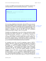
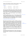
(used in a wide variety of “intelligent” devices). They can range in
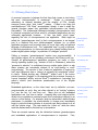
physical size from packages with several hundred pins to packages
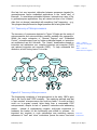
with only a few pins; some examples are illustrated in Figure 2-1. They
can range in cost from less than one dollar to hundreds of dollars. The
simple computer we will be designing here can be implemented using
a modest-size PLD; we could therefore rightfully call this single-chip
embodiment of our simple computer a “microprocessor.”
(a)
(b)
(c)
Figure 2-1 Contrasting contemporary microprocessors: (a) an 8-bit
PIC microcontroller; (b) a 16-bit Motorola 68HC12 microcontroller;
and (c) a 64-bit MIPS microprocessor.
Finally, what is a microcontroller, and how does it differ from a microcontroller
microprocessor? Typically a microcontroller integrates, in addition to a
microprocessor, a number of peripheral devices that are commonly peripheral devices
used in control-type applications onto a single integrated circuit (and
are thus often referred to as “single-chip microcontrollers”). Peripheral
devices get their name from the fact that they provide interfaces with
devices that are external (i.e., “peripheral”) to the computer. For
example, a common series of operations often performed in control
applications is: (1) input analog signals from sensors, (2) process them
according to some algorithm, (3) and output analog control voltages to
actuators. A device that digitizes an analog input voltage is called an
analog-to-digital (A-to-D) converter. Conversely, a device that
produces an analog output voltage based on a digital code is called a
digital-to-analog (D-to-A) converter. A-to-D and D-to-A converters are
examples of peripherals one might find integrated onto a
microcontroller chip.
Preliminary Edition
©2001 by D. G. Meyer
Microcontroller-Based Digital System Design
Chapter 2 - Page 3
Other common peripherals include communication controllers, timer
modules, and pulse-width modulation (PWM) generators. Later, we
will see a variety of applications for all of these integrated peripherals.
2.1 Computer Design Basics
How can we apply what we have learned thus far about basic digital
system building blocks toward building a simple computer? Basically,
what we need is some way to structure and break down this design
problem, because now it is a somewhat bigger than drawing a single
state transition diagram or filling out a truth table. We will need a
structured approach that enables us to take a written description of the
functions performed by our simple computer and create a high-level
block diagram. Based on this diagram, we can proceed to define what
each block does, and ultimately design the circuitry required to
implement each block.
Before starting this process, though, we need to define what we mean
by the structure of a computer. “Architecture” is a word commonly architecture
used to depict the arrangement and interconnection of a computer’s
functional blocks. While some might argue that this definition of
computer architecture is a bit simplistic, it will serve our purposes for
the discussion that follows.
Before starting to design our simple computer, let us first consider a
“real world” analogy: building a house. Where is the logical place to
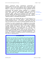
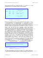
start? Probably with a “big picture” – i.e., an exterior elevation or plan big picture
view of the entire project. Of course, the floor plan and exterior
elevation are greatly influenced by the size, shape, and grade of the lot
chosen for the house. Once we know the physical constraints dictated
by our choice of lot, we can then begin to develop a floor plan. At this
stage we can define the overall “functionality” of the house, i.e., the
purpose of each room. Once we have defined the functionality of each
room, the next step is to determine their arrangement and
interconnection. Once we have a working floor plan, we can begin to
embellish it with a number of details – for example, the location and
size of windows, the location of light fixtures and their associated wall
switches, the location of power outlets, the routing of plumbing, etc.
The important thing to note from this analogy is that we have described
a top-down design process: starting with a “big picture”, and
progressively embellishing it with layers of details. Figure 2-2 depicts
such a progression.
Preliminary Edition
©2001 by D. G. Meyer
Microcontroller-Based Digital System Design
(a)
Chapter 2 - Page 4
(b)
(c)
Figure 2-2 Top-down design of a house: (a) the “big picture”, (b) the
floor plan, (c) details of a particular room.
Once all the design specifications have been formulated, how would
we proceed to build our house? From the ground up – assuming we
have adequate financing, of course. We have to dig a hole first
(perhaps analogous to going into debt), then pour a foundation, “stickbuild” the basic structure, put a roof on it, complete the exterior walls,
and finally embellish each room with its finishing details. Note that the
order in which this “bottom up” implementation proceeds is quite
important – certainly one would not wish to start hanging drywall before
the roof is in place, or run plumbing lines before the floor joists are in
place. Clearly, there is a structured, ordered way in which the entire
process must take place – an approach strikingly similar to the one we
will follow in designing our simple computer.
What would be a good name for the overall process described above?
Ignoring the financial aspects for a moment, we could aptly call it the
top-down specification of functionality followed by bottom-up
implementation of each basic step (or “block”). More succinctly, we
could call it top-down specification and bottom-up implementation.
This is the process we will apply to the design and implementation of
our simple computer.
First, a disclaimer. The initial machine we design will be very, very
simple. It will be an 8-bit machine with just a few instructions. Further,
there will be a single instruction format (layout of bit patterns) as well
as a single addressing mode (way that the processor accesses
operands in memory). By the time we finish this “first phase” design,
however, we will find out that even this rather simple machine is fairly
complex in terms of implementation details.
top-down
specification
bottom-up
implementation
instruction
format
addressing
mode
Once we have mastered our simple computer, we will then add
“modern conveniences” such as input and output (or “I/O”), transfer of
control instructions, stack manipulation instructions, and subroutine
Preliminary Edition
©2001 by D. G. Meyer
Microcontroller-Based Digital System Design
Chapter 2 - Page 5
linkage instructions.
We will have the makings of a “socially socially
redeeming” computer once we get done, plus have a firm footing upon redeeming
which to understand the architecture and instruction set of a “real”
computer.
2.2 Simple Computer Big Picture
Just as one might begin the design of a house by sketching an exterior
elevation view, we will begin the design of our simple computer with a
“big picture” of its control console. In the “old days” (which was actually old days
not so long ago), computers had lots of lights and switches on their
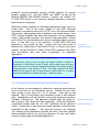
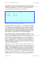
front panels. The Digital Equipment Corporation PDP-8 (the first
commercial “minicomputer”), illustrated in Figure 2-3, was a good minicomputer
example of such a computer. The Intellect 8 microcomputer system
(one of the first commercially-available microprocessor development
systems) from Intel, based on the 8008 microprocessor, was another
example. Frankly, these ground-breaking computer systems were a lot crunch numbers
more interesting (and fun) to watch “crunch numbers” than today’s
computers…and a lot less irritating than the “this application has
performed an illegal function and will be shut down” message we’ve all
become accustomed to today.
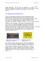
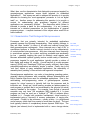
LED Output Port
Switch Input Port
Start
Figure 2-3 World’s first “desktop”
minicomputer, the PDP-8.
Clock
Figure 2-4 Our simple
computer console.
Our computer’s console, then, will have some lights that indicate the
result of the most recent computation along with some switches that
will be used to input data. A “START” pushbutton will be included to
get the machine into a known initial state (in preparation for “running” a
program), and a “CLOCK” pushbutton will be included to facilitate
debugging (as we manually clock the machine from state-to-state). An
“artist’s conception” of our simple computer’s console is shown in
Figure 2-4.
Preliminary Edition
©2001 by D. G. Meyer
Microcontroller-Based Digital System Design
Chapter 2 - Page 6
Returning to the “house analogy” for a moment, the floor plan of a
computer is basically its instruction set and programming model. The
instruction set is simply the list of operations that the computer
performs. There are five fundamental groups (or categories) of
machine instructions: data transfer, arithmetic, logical (or “Boolean”),
transfer of control, and machine control. (Some computers include a
sixth group dedicated to specific applications, e.g., multimedia
extensions or graphics support.)
The addressing modes that
instructions can use to access operands in memory are also a key
aspect of a computer’s instruction set.
instruction set
programming
model
addressing modes
The programming model of a computer is the software writer’s view of
the machine. Basically, it tells what resources are available for the
programmer’s use, in particular, the machine’s registers. A register is
simply a “memory location” within the processor that can be used to
store intermediate results and/or as an operand (or as a pointer to an pointer
operand) used in a computation.
As alluded to above, the programming model and instruction set of our
computer will be relatively simple. Initially there will only be one
register, called the accumulator (or “A” register), so-named because it
is the register in which the result of computations accumulate. Our
computer will also include several condition code bits: a zero flag (ZF),
negative flag (NF), overflow flag (VF), and carry/borrow flag (CF).
Before we complete this chapter, we will add a stack pointer register
and discuss the role of index registers.
condition
code bits
ZF
NF
VF
CF
The instructions executed by our simple computer will be of the fixedlength variety (i.e., all 8-bits in size, hence its designation as an “8-bit”
computer) that consist of two fixed-length fields. The upper 3-bits of
each instruction will indicate the operation to be performed, and is
therefore called the operation code field (or “opcode” field). The lower opcode field
5-bits will indicate the memory address in which the operand is located
(or, a result is to be stored). The 5-bit memory address dictates a
maximum memory size of 25 = 32 locations. For those who have
become jaded by multi-megabyte programs that appear to do trivial
things, this may not seem like much memory! Fortunately, though, it
will be enough to illustrate basic principles of instruction execution,
despite being too small to contain a “practical” (i.e., useful and socially
redeeming) program.
In addition to fixed-field decoding, another simplification in our initial addressing
design will be a single addressing mode. An addressing mode is the mode
mechanism (or “function”) used to generate what is often called the
Preliminary Edition
©2001 by D. G. Meyer
Microcontroller-Based Digital System Design
Chapter 2 - Page 7
effective address of an operand, i.e., the actual address in memory
where an operand is stored. The addressing mode our machine will
support might aptly be called “absolute” addressing, based on the fact
that this 5-bit field directly indicates the effective address in memory
where the operand is stored. It is important to note at this point that
not all manufacturers of microprocessors agree on the names ascribed
to certain addressing modes. What we have just referred to as an
“absolute” addressing mode is typically called “extended” (by Motorola)
or “direct” (by Intel).
effective
address
absolute
addressing
mode
One other bit of terminology worth mentioning before delving into the
instruction set concerns the number of addresses a given instruction
(or more generally, a machine) can accommodate.
Our simple
two-address
computer here could be described as a “two address” machine, which
means that two different locations (at two different addresses) are used machine
in a given operation, e.g., ADD. In our computer, one location will be
the “A” register (the accumulator), and the other will be contained in
memory. Note that a “side-effect” of such an arrangement is that the
result of the computation will overwrite one of the operands, here the
value in the “A” register (the operand in memory will be unaffected).
As one might guess, there are a lot of variations in instruction format
and addressing capability, ranging from single-address instructions to
three-address (or more) instructions.
2.3 Simple Computer Floor Plan
We are now ready to introduce the “floor plan” (instruction set) of our
simple computer. Note that we will initially define six of the eight
possible instructions afforded by our 3-bit opcode field. We will save
the last two opcode bit patterns to define some extensions to our
instruction set later in this chapter. Our simple computer’s instruction
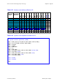
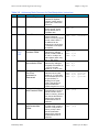
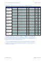
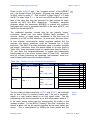
set is given in Table 2-1.
Table 2-1 Simple computer instruction set.
Opcode Mnemonic
Function Performed
LDA
addr
0 0 0
Load A with contents of location addr
STA
addr
0 0 1
Store contents of A at location addr
ADD addr Add contents of addr to contents of A
0 1 0
SUB addr Subtract contents of addr from contents of A
0 1 1
AND addr AND contents of addr with contents of A
1 0 0
HLT
1 0 1
Halt – Stop, discontinue execution
Preliminary Edition
©2001 by D. G. Meyer
Microcontroller-Based Digital System Design
Chapter 2 - Page 8
The first two instructions, “LDA” and “STA”, are examples of data
transfer group instructions. As their assembly mnemonics imply, these
instructions transfer data between the “A” register (accumulator) and
memory. For the “load A” (LDA) instruction, the source of the data is
memory location addr, and the destination is the “A” register. For the
“store A” (STA) instruction, it is just the opposite: here, addr indicates
the location in memory where the value in A (also referred to as the
contents of A) is to be stored.
As it turns out, “load” and “store”
instructions are the “most popular” instructions in any machine’s
instruction set, often comprising as much as 30% of the compiled code
for typical applications.
data transfer
group instructions
assembly
mnemonics
LDA
STA
A “shorthand” notation we will use throughout the remainder of this text
is the use of parenthesis to indicate “the contents of” a particular
register or memory location. This allows us to describe what an LDA
instruction does as simply “(A) ← (addr)” and what an STA does as
“(addr) ← (A)”. An important point to note in both cases is that the
source of the data transfer – i.e., (addr) for LDA and (A) for STA –
does not change (or, is unaffected) as a result of the instruction
execution.
Continuing down the list of available instructions, we next find two
arithmetic group instructions: ADD and SUB. The ADD instruction
performs the operation (A) ← (A) + (addr) using radix (or two’s
complement) arithmetic, and sets the condition code bits based on the
result obtained. (Details on radix arithmetic and condition codes can be
found in the review material presented in Chapter 1.) The SUB
instruction performs the operation (A) ← (A) – (addr) and sets the
condition code bits accordingly. Recall that there is an important
difference regarding how the carry flag (CF) is affected in an addition
versus a subtraction. Following an ADD, the carry flag is the carry out
of the most significant (or sign) position; whereas following a SUB, the
carry flag is the complement of the carry out of the sign position (based
on its interpretation as a borrow). Because of this difference between
ADD and SUB, the CF bit is sometimes referred to as the
“carry/borrow” flag – which is the way we will formally refer to it. If
what we just described seems a bit “fuzzy”, now would be a good time
to review the material in Chapter 1.
arithmetic group
instructions
Moving down the chart, we find that our next instruction, AND, is from
the logical (or “Boolean”) group. Because logical group instructions
perform bit-wise operations, they are sometimes referred to as bit
manipulation instructions. At minimum, most microprocessors worth
their silicon generally have at least three Boolean instructions: AND,
logical group
instructions
Preliminary Edition
ADD
SUB
two’s complement
arithmetic
carry/borrow
flag
bit manipulation
instructions
©2001 by D. G. Meyer
Microcontroller-Based Digital System Design
Chapter 2 - Page 9
AND
OR, and NOT (many also include XOR). Our simple computer, OR
however, will just implement the first of these operations, which can be NOT
described using the notation (A) ← (A) ∩ (addr), where the “∩” symbol XOR
is used to denote the bit-wise logical AND of the two operands to
produce the corresponding result bits.
No instruction set would be complete without a way to stop the HLT
machine. Our sixth (and final, for now) instruction, HLT (for “halt”)
serves this purpose. The HLT instruction is an example of a machine machine control
control group instruction. Execution of the HLT instruction will “freeze” group instructions
the machine at its current point in the program being executed, and
prevent the machine from fetching or executing any additional
instructions until it is restarted (by pressing the START pushbutton
described previously).
2.4 Simple Computer Programming Example
To better understand how our simple computer operates, we will “walk
through” the execution of a short program. This program will exercise
each instruction in our simple computer’s repertoire. An important
point to consider before proceeding is that it would be rather difficult to
design a “simple” computer that directly interprets the instruction
mnemonics (i.e., LDA, STA, etc.) we have defined. Rather, it is much
easier to design a machine that directly interprets bit patterns (0’s and
1’s) that represent these instructions. This means that, before we can
place our program in memory, we must translate the instruction
mnemonics into bit patterns (“code”) the machine understands, called
machine code. This translation process is called assembly, since
machine code is created directly (“assembled”) based on instruction
mnemonics. As one might guess, instruction mnemonics are typically
referred to as assembly level mnemonics, or simply assembly
language.
A software program that translates assembly level
mnemonics into machine code is called an assembler. If one is
unfortunate enough to perform the translation by hand, the process is
called hand assembly.
machine code
assembly
language
hand assembly
Fortunately, most computer programming is done at a higher level of
abstraction, using high-level languages such as “C”. Here, a compiler high-level
language
program is used to translate code written in high-level language into compiler
assembly code. An assembler program is then used to translate the
compiler’s output into machine code for the target processor. We will
find, though, that a firm grasp of assembly language programming
techniques is essential for effectively utilizing the resources integrated
Preliminary Edition
©2001 by D. G. Meyer
Microcontroller-Based Digital System Design
Chapter 2 - Page 10
into a modern microcontroller. Once we master assembly-level
programming, we’ll consider how to program a microcontroller using
“C”. But to get there, we need to start at the “basic bit” level – so let’s
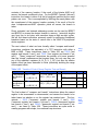
return to the illustrative simple computer program in Table 2-2.
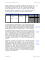
Table 2-2
Addr
00000
00001
00010
00011
00100
00101
00110
00111
01000
01001
Programming example.
Instruction
Comments
LDA 01011 Load A with contents of location 01011
ADD 01100 Add contents of location 01100 to A
STA 01101 Store contents of A at location 01101
LDA 01011 Load A with contents of location 01011
AND 01100 AND contents of 01100 with contents of A
STA 01110 Store contents of A at location 01110
LDA 01011 Load A with contents of location 01011
SUB 01100 Subtract contents of location 01100 from A
STA 01111 Store contents of A at location 01111
HLT
Stop – discontinue execution
One of the first things we need to know is where in memory our
program needs to be located. The logical thing to do is place our
program at the beginning of memory, i.e., starting at location 000002.
We can then design the circuitry that, after the START pushbutton is
pressed, begins fetching instructions from memory at location 000002.
Recalling that instructions are of fixed length (8 bits) and that memory
locations are 8-bits wide, we realize that consecutive instructions will
occupy consecutive memory locations. We can then imagine a
“pointer” that tells us which instruction is to be executed, and that gets
incremented after each instruction is fetched. Such a pointer is instruction pointer
typically referred to as either an instruction pointer or a program program counter
counter.
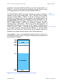
A “snapshot” of what our short program looks like in memory prior to
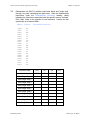
execution is provided in Figure 2-5 (just the “first half” of memory, from
locations 000002 to 011112 is shown). The lightly shaded part
corresponds to the assembled machine code. Referring back to Table
2-2, note that the first instruction (at address 000002) is load
accumulator (LDA) with the contents of memory location 010112.
Since the 3-bit opcode for LDA is “000”, this instruction is encoded as
the bit pattern “000 01011” in memory. Stated another way, the
instruction “LDA 01011” has been assembled into the machine code
“000 01011”. We could go through a similar “hand assembly” process
for the rest of the instructions that comprise the program, up to and
Preliminary Edition
©2001 by D. G. Meyer
Microcontroller-Based Digital System Design
Chapter 2 - Page 11
including the HLT instruction at location 010012 (note that the address
field of this instruction is not used, and is shown here to be “00000”).
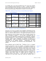
Location
00000
00001
00010
00011
00100
00101
00110
00111
01000
01001
01010
01011
01100
01101
01110
01111
Contents
00001011
01001100
00101101
00001011
10001100
00101110
00001011
01101100
00101111
10100000
10101010
01010101
Beam in the Bits, Scotty!
One important detail we will ignore for
the moment is how these bit patterns
get loaded into memory. In a later
chapter, we’ll discuss how to write
what’s called a “loader” program,
which – as its name implies – does
just that. For now, assume Scotty (of
Star Trek fame, for those of you much
younger than the author) has used a
molecular beam transporter to “beam
the bits” into memory.
Figure 2-5 Memory snapshot
prior to program execution.
The operands used by each arithmetic (ADD, SUB) or logical (AND)
operation will be stored at locations 010112 and 011002 (in the darker
shaded area of Figure 2-5); note that we have initialized these two
locations to arbitrarily chosen values. The results of each operation
(ADD, AND, SUB) will be stored in three consecutive locations, starting
at location 011012. Note that our computer’s memory will contain a mix
of instructions and data (operands and results).
No Stopping It Now
What happens if the HLT instruction is omitted? Perhaps even worse than
“not stopping”, the computer will start executing data, which, as one might
imagine, is not a pretty sight (or, stated less formally, causes “bits to fly all
over the place”) and, at best, leads to very strange program behavior. Any
“honest” programmer (not to be confused with an honest politician),
however, will confess that he/she has inadvertently done this “at least
once…”
executing data
honest
programmer
Given that our computer only understands 0’s and 1’s rather than the
more human-friendly assembly mnemonics, the question that begs is:
“How is our computer able to distinguish between instructions and
data?” The hopefully obvious answer is: “It can’t!” Rather, it has to be
Preliminary Edition
©2001 by D. G. Meyer
Microcontroller-Based Digital System Design
Chapter 2 - Page 12
told which locations contain instructions and which contain data. The
convention we will use to make this distinction is that our programs will
always start at location 000002 and continue until they reach a “halt”
(HLT) instruction; any locations following the HLT instruction may be
used for data (operands or results).
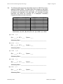
Location
00000
00001
00010
00011
00100
00101
00110
00111
01000
01001
01010
01011
01100
01101
01110
01111
Contents
00001011
01001100
00101101
00001011
10001100
00101110
00001011
01101100
00101111
10100000
10101010
01010101
11111111
Add:
10101010
+01010101
11111111
Add
CF = 0
NF = 1
VF = 0
ZF = 0
Figure 2-6 Result after executing the first three instructions.
We are now ready to step through the execution of this program.
Referring back to Table 2-2, we see that the purpose of the first three
instructions is to add the two operands (at locations 010112 and
011002, respectively) and store the result at location 011012. As
illustrated in Figure 2-6, the result obtained will be 111111112 (recall
that this is the 8-bit representation for “–1” in two’s complement
notation). Also, the negative flag (NF) will be set to “1”, the carry flag
(CF) will be cleared to “0”, the overflow flag (VF) will be cleared to “0”,
and the zero flag (ZF) will be cleared to “0”.
Self-Perpetrating Programs
It is entirely possible to contrive a program that writes data into locations
that contain instructions yet to be executed. The name “self-modifying
code” has been used to describe such a creation. A self-modifying
program, as one might guess, could prove to be excruciatingly difficult to
debug. In a word, don’t try this at home! (And, don’t try to convince your
boss that you’ve invented a new way to write “interesting” programs!).
Preliminary Edition
self-modifying
code
©2001 by D. G. Meyer
Microcontroller-Based Digital System Design
Chapter 2 - Page 13
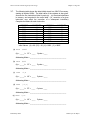
Again referring back to Table 2-2, we see that the purpose of the next
three instructions is to logically AND the two operands and store the
result at location 011102. Note that, for the AND operation, the carry
flag (CF) and overflow flag (VF) are meaningless, and therefore should
be unaffected by the execution of the AND instruction. The result
obtained, however, may be negative (in a two’s complement sense) or
zero, so the negative flag (NF) and zero flag (ZF) should be affected.
A snapshot of memory following execution of the three AND-related
instructions is provided in Figure 2-7. Note that, since the result
obtained is 000000002, the zero flag is set to “1”.
Location
00000
00001
00010
00011
00100
00101
00110
00111
01000
01001
01010
01011
01100
01101
01110
01111
Contents
00001011
01001100
00101101
00001011
10001100
00101110
00001011
01101100
00101111
10100000
10101010
01010101
11111111
00000000
AND:
10101010
∩01010101
00000000
CF = <unaffected>
NF = 0
VF = <unaffected>
ZF = 1
AND
Figure 2-7 Result after executing the “middle” three instructions.
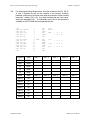
The purpose of the next group of three instructions is to take the
difference of the two operands at locations 010112 and 011002.
Specifically, we are going to subtract (SUB) the operand at location
011002 from the operand at location 010112, and place the result at
location 011112. Recall from Chapter 1 that a radix subtraction is
realized by forming the two’s complement of the subtrahend (here, the
operand at location 011002) and adding it to the minuend (the operand
at location 010112). Further, the easiest way to generate the radix
complement of a signed number is to add one to its diminished radix
complement (or ones’ complement). Figure 2-8 shows what happens.
Note that, while the result 010101012 will be stored at location 011112,
it will be invalid because overflow has occurred (denoted by VF set to
“1”). Note also that CF (the carry/borrow flag) is cleared to “0” due to its
interpretation here as a borrow flag – recall that, following a subtract
operation, CF is set to the complement of the carry out of the sign
position (which in this case was “1”). A borrow flag of “0” following a
Preliminary Edition
©2001 by D. G. Meyer
Microcontroller-Based Digital System Design
Chapter 2 - Page 14
subtract operation essentially means that “no borrow is propagated
forward.”
Location
00000
00001
00010
00011
00100
00101
00110
00111
01000
01001
01010
01011
01100
01101
01110
01111
Contents
00001011
01001100
00101101
00001011
10001100
00101110
00001011
01101100
00101111
10100000
10101010
01010101
11111111
00000000
01010101
Sub:
10101010
-01010101
CF = 0
NF = 0
VF = 1
ZF = 0
10101010
10101010
+
1
1)01010101
Overflow!
Sub
Figure 2-8 Result after executing the last group of three instructions.
threethreenstructions.
Bumbling Borrows
Perhaps the single-most issue that causes students consternation is that of
the carry/borrow flag. The interpretation of a “carry propagated forward”
following an addition is no problem; but when it gets to subtraction, all “bits
are off” (pardon the very bad pun). Here, the proper interpretation is as a
“borrow propagated forward” to the next-most significant group of digits in
an extended precision subtraction. The borrow flag (still called CF), when
set, is basically telling that next group of digits to “reduce its result by one”
because the previous stage “has borrowed from it.” The best real-world
analogy that comes to mind is that of a statement from your friendly, local
banking institution listing the service charge they have extracted from your
account for the privilege of serving you. The point is: since they have
already taken the money, you need to adjust your idea of how much money
you have left!
Before we leave this last block of code, yet another question that
comes to mind is: “How should error conditions like overflow be
handled?” As one might guess, we will need some “new” instructions
that allow us to test the state of the various condition codes (here, VF)
and transfer control to a different part of the program (typically called
an “exception handler”) if an error has occurred. Before we finish this
chapter, we will learn how to implement such “conditional transfer of
control” instructions.
Preliminary Edition
©2001 by D. G. Meyer
Microcontroller-Based Digital System Design
Chapter 2 - Page 15
The final instruction in our short program, HLT, simply tells our
computer to “stop executing”. Once the program has stopped, we
could presumably look at the contents of each location to determine
the results of the program execution. What we should find is the
memory image depicted in Figure 2-8 (note that memory location
010102 was unused by our example program and may contain a
“random” value).
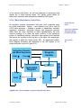
2.5 Simple Computer Block Diagram
Now that we know how our simple computer works, we are ready to
consider the functional blocks necessary to make it work. Basically we
want to build what appears to be a “big state machine” that performs
the calculations just done by hand. At a fundamental level, there are
two basic steps associated with the processing of each instruction.
The first step is to read the instruction from memory, called an
instruction fetch cycle. The second step is to extract the opcode and
address fields from the instruction just fetched and perform the
operation specified by the opcode on the data located at the specified
address; this step is referred to as an instruction execute cycle.
What are the basic functional blocks, then, that are necessary to
implement the simple computer described here? Clearly, a memory
unit – for storing instructions and data – is one of the major functional
blocks necessary. This memory unit needs to be capable of reading
the contents of a specified location (indicated on its address lines) as
well as writing a new value to a specified location.
instruction
fetch cycle
instruction
execute cycle
memory unit
Another major functional block needed is one that will keep track of
which instruction is next in line to be executed. In our simple
computer, the instructions are stored in consecutive memory locations,
starting at location 000002. What is needed is a pointer that keeps
track of which instruction is next. Because this block is nothing more
than a binary counter, we will call it the program counter (PC).
program counter
PC
Once it is fetched from memory, a place is needed to temporarily
“stage” an instruction while the opcode field is decoded and the
address field is extracted. We can think of this block as a place to hold
the instruction just fetched while it is being “digested”. While more
creative, biologically inspired names for it are certainly possible, we will
simply call this functional block the instruction register (IR).
instruction register
IR
Preliminary Edition
©2001 by D. G. Meyer
Microcontroller-Based Digital System Design
Chapter 2 - Page 16
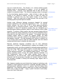
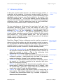
Opcode Address
Data Bus
Memory
Address
ALU
Data
Flags
Data
Instruction
Register
Address Bus
Program
Counter
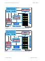
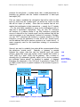
Figure 2-9 Simple computer core block diagram.
Next we realize the need for a functional block that performs the
arithmetic and logical operations we have defined in the simple
computer’s instruction set. Not surprisingly, this block is usually called
an arithmetic logic unit, or simply ALU. Note that the accumulator (“A”
register) and condition code bits (CF, NF, VF, ZF) are part of the ALU.
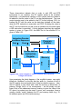
Finally, we realize that our simple computer needs a “manager” – a
functional block that orchestrates the activities of all the other
functional blocks delineated above. This “manager” is responsible for
indicating whether a fetch or an execute cycle is to be performed and,
once an instruction is fetched, for decoding the opcode field of that
instruction and telling the other blocks in the system what to do in order
to execute it. Because our simple computer’s “manager” controls the
sequencing of events that, taken together, constitute the completion of
a machine instruction, we often refer to the state machine part of the
manager’s personality as a micro-sequencer (similar to, perhaps, but
not to be confused with a “micro-manager”). And because decoding
the opcode field of the instruction is an essential part of the sequencing
process, we award our simple computer’s manager the grand and
glorious name: instruction decoder and micro-sequencer (IDMS). This
more extravagant sounding name helps prevent images of “kicking bits
around” that might be associated with a “manager” (think baseball).
Preliminary Edition
arithmetic logic unit
ALU
manager
micro-sequencer
IDMS
©2001 by D. G. Meyer
Microcontroller-Based Digital System Design
Chapter 2 - Page 17
Returning to the “house” analogy for a moment, what we have just
done is “define the rooms” of the “structure” (or system) we wish to
build. What we have not yet done, however, is interconnect the
functional blocks into a working “floor plan”. In order to do this, we
need an understanding of the “traffic patterns” (here, of address, data,
and control information) that need to flow among the various functional
blocks.
Starting with the memory unit, we note that a series of address lines
tell which location is being accessed; the collection of address lines is
referred to as the address bus. (Recall that a bus is a set of signal
lines that have a common purpose.) At the location in memory
accessed, data can be read (output) or written (input); the memory’s
data lines (and the associated data bus) must therefore be bidirectional. Further, control signals need to be supplied to the memory
unit that tell whether or not it is enabled to respond (or selected), and,
if enabled to respond, whether it should perform a read operation or a
write operation.
Next, we realize that the program counter (PC) will supply the
instruction address to memory during a fetch cycle, and that the
instruction register (IR) will be used to temporarily stage the instruction
after it has been read from memory. Further, on an execute cycle, the
IR will supply the operand address to memory, and the destination (or
source) of the data in this transaction is the “A” register of the ALU.
Thus, there are two potential sources of address information – the PC
and the IR – on the address bus. Since only one device can “talk” on
the bus at a given instant in time, we will need to provide each of these
functional blocks with three-state output capability – and it will be our
“manager’s” job to keep them from talking at the same time!
address bus
bi-directional
three-state output
capability
Further, there are two potential destinations of data read from memory.
On a fetch cycle, an instruction destined for the IR is read from
memory. On an execute cycle, an operand destined for the ALU is
read from memory (alternately, data in the ALU is destined for memory
if an STA instruction is being executed). Again, we note the need for
three-state buffers in all the functional blocks involved with driving the
data bus.
Putting this all together, the “core” of our simple computer is depicted
in Figure 2-9. Left on their own, however, these functional blocks are
incapable of doing anything “intelligent”, let alone successfully
executing instructions.
Hence the need for a “manager” – the
instruction decoder and micro-sequencer – to tell each block what to
Preliminary Edition
©2001 by D. G. Meyer
Microcontroller-Based Digital System Design
Chapter 2 - Page 18
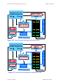
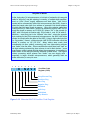
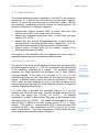
do when. As such, the IDMS can aptly be thought of as the “heart” of
the machine. The simple computer augmented with an IDMS is shown
in Figure 2-10.
Instruction Decoder
and Micro-Sequencer
Clock
Start
Opcode Address
Data Bus
Memory
Address
ALU
Data
Flags
Data
Instruction
Register
Address Bus
Program
Counter
Figure 2-10 Complete simple computer block diagram.
We now have a complete “floor plan” for our “house”, that we have
specified in a top-down fashion. Before actually building it, though, let’s
make sure we understand how the “rooms” work together.
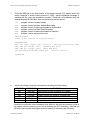
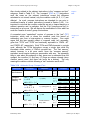
2.6 Instruction Execution Tracing
To get a better idea of how the various functional blocks of our simple
computer work in concert to process instructions, we will return to our
short program of Table 2-2 and use a technique called instruction
tracing to help us visualize the flow of information. On a cycle-by-cycle
basis, we will examine the address and data paths as well as the bit
patterns in each register for the first three instructions of this short
program. Recall that we used the term “micro-sequencer” because
there is a sequence of events associated with processing an
instruction: here, a fetch cycle followed by an execute cycle.
Preliminary Edition
instruction
tracing
©2001 by D. G. Meyer
Microcontroller-Based Digital System Design
Chapter 2 - Page 19
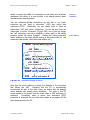
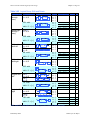
The instruction trace worksheet in Figure 2-11 sets the stage for this
exercise, which shows the initial state of the machine after START is
pressed. Note that there are several things we will keep track of as our
machine executes the program. In particular, we will be monitoring
what happens to the PC, IR, and “A” register as well as the contents of
memory. We will also practice naming each cycle as it occurs.
Instruction Decoder
and Micro-Sequencer
Clock
Opcode Address
?
?
Data
CF NF VF ZF
Data Bus
A register
ALU
START
Cycle: ________
Data
Data
Location
00000
00001
00010
00011
00100
00101
00110
00111
01000
01001
01010
01011
01100
01101
01110
01111
Contents
00001011
01001100
00101101
00001011
10001100
00101110
00001011
01101100
00101111
10100000
10101010
01010101
Address Bus
Address
IR
? ? ? ?
PC
Address
Start
00000
Memory
Figure 2-11 Instruction trace worksheet for machine state after START
is pressed, prior to first fetch cycle.
Recall that pressing the START pushbutton places the machine in a
known initial state: the PC is reset to “00000” and the state counter (in
the IDMS) is set to “fetch”. Note that the initial state of the IR and ALU
may be “random” and that memory is initialized to the values indicated
(although at this point we “don’t care” what is in the unused location
010102 or the locations where the results will be stored, 011012–
011112).
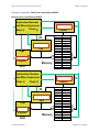
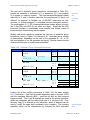
During the first fetch cycle, shown in Figure 2-12, the instruction at
memory location 000002 is read and placed in the IR. As the IR is
being loaded with the instruction, the PC is incremented by one (i.e.,
once the fetch of the current cycle is complete, the PC is pointing to
the next instruction to execute). Note that the values in each register
are those obtained after the “fetch LDA” cycle is complete.
Preliminary Edition
©2001 by D. G. Meyer
Microcontroller-Based Digital System Design
Instruction Decoder
and Micro-Sequencer
Chapter 2 - Page 20
00000 → 00001
Clock
IR
Opcode Address
000 01011
Data
CF NF VF ZF
?
A register
ALU
LDA
Cycle: Fetch
________
Contents
00001011
01001100
00101101
00001011
10001100
00101110
00001011
01101100
00101111
10100000
10101010
01010101
Memory
Instruction trace worksheet for first fetch cycle.
Instruction Decoder
and Micro-Sequencer
00001
Clock
Address
IR
Opcode Address
000 01011
10101010
A register
ALU
Data
CF NF VF ZF
Data Bus =
00001011
Cycle: ________
Exec LDA
Data
Data
? 1 ? 0
Location
00000
00001
00010
00011
00100
00101
00110
00111
01000
01001
01010
01011
01100
01101
01110
01111
Contents
00001011
01001100
00101101
00001011
10001100
00101110
00001011
01101100
00101111
10100000
10101010
01010101
Address Bus = 01011
Start
PC
Address
Figure 2-12
Data Bus =
00001011
Data
Data
? ? ? ?
Location
00000
00001
00010
00011
00100
00101
00110
00111
01000
01001
01010
01011
01100
01101
01110
01111
Address Bus = 00000
Address
Address
Start
PC
Memory
Figure 2-13 Instruction trace worksheet for first execute cycle.
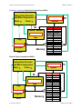
Preliminary Edition
©2001 by D. G. Meyer
Microcontroller-Based Digital System Design
Instruction Decoder
and Micro-Sequencer
Chapter 2 - Page 21
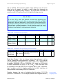
00001 → 00010 PC
Clock
IR
Opcode Address
010 01100
10101010
Data
CF NF VF ZF
Data Bus =
01001100
A register
ALU
Data
Data
? 1 ? 0
Location
00000
00001
00010
00011
00100
00101
00110
00111
01000
01001
01010
01011
01100
01101
01110
01111
Cycle: ________
Fetch ADD
Contents
00001011
01001100
00101101
00001011
10001100
00101110
00001011
01101100
00101111
10100000
10101010
01010101
Address Bus = 00001
Address
Address
Start
Memory
Figure 2-14 Instruction trace worksheet for second fetch cycle.
Instruction Decoder
and Micro-Sequencer
00010
Clock
IR
Opcode Address
010 01100
11111111
Data
CF NF VF ZF
A register
ALU
Data Bus =
01010101
Cycle: ________
Exec ADD
Data
Data
0 1 0 0
Location
00000
00001
00010
00011
00100
00101
00110
00111
01000
01001
01010
01011
01100
01101
01110
01111
Contents
00001011
01001100
00101101
00001011
10001100
00101110
00001011
01101100
00101111
10100000
10101010
01010101
Address Bus = 01100
Address
Address
Start
PC
Memory
Figure 2-15 Instruction trace worksheet for second execute cycle.
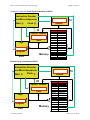
Preliminary Edition
©2001 by D. G. Meyer
Microcontroller-Based Digital System Design
Instruction Decoder
and Micro-Sequencer
Chapter 2 - Page 22
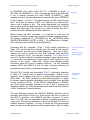
00010 → 00011
Clock
IR
Opcode Address
001 01101
11111111
Data
CF NF VF ZF
A register
ALU
Data Bus =
001 01101
Data
Data
0 1 0 0
Location
00000
00001
00010
00011
00100
00101
00110
00111
01000
01001
01010
01011
01100
01101
01110
01111
Cycle: ________
Fetch STA
Contents
00001011
01001100
00101101
00001011
10001100
00101110
00001011
01101100
00101111
10100000
10101010
01010101
Address Bus = 00010
Address
Address
Start
PC
Memory
Figure 2-16 Instruction trace worksheet for third fetch cycle.
Instruction Decoder
and Micro-Sequencer
00011
Clock
IR
Opcode Address
001 01101
11111111
A register
ALU
Data
CF NF VF ZF
Data Bus =
11111111
Cycle: ________
Exec STA
Data
Data
0 1 0 0
Location
00000
00001
00010
00011
00100
00101
00110
00111
01000
01001
01010
01011
01100
01101
01110
01111
Contents
00001011
01001100
00101101
00001011
10001100
00101110
00001011
01101100
00101111
10100000
10101010
01010101
11111111
Address Bus = 01101
Address
Address
Start
PC
Memory
Figure 2-17 Instruction trace worksheet for third execute cycle.
Preliminary Edition
©2001 by D. G. Meyer
Microcontroller-Based Digital System Design
Chapter 2 - Page 23
During the first execute cycle, shown in Figure 2-13, the “LDA 01011”
instruction in the IR is executed. When this cycle is complete, the “A”
register contains the contents of memory location 010112, i.e., the
value 101010102. Note also that the NF is set to “1” and ZF is cleared
to “0”. The “execute LDA” cycle does not, however, affect the contents
of any memory location, nor does it change the contents of IR or PC
(condition code bits CF and VF are also unaffected).
We are now ready for the second fetch cycle (“fetch ADD”), shown in
Figure 2-14. Here, the instruction at memory location 000012 is
fetched and placed into the IR, and as that occurs, the value in the PC
is incremented by one. The results of executing the ADD instruction
are shown in Figure 2-15. Here, the contents of memory location
011002 (i.e., the value 010101012) are added to the value previously
loaded into the “A” register. A result of 111111112 is obtained, along
with condition code bits CF = “0”, NF = “1”, ZF = “0”, and VF = “0”.
This brings us to the third fetch cycle (“fetch STA”) of our tracing
example, shown in Figure 2-16. Here, the instruction at memory
location 000102 is fetched and placed into the IR, and as that occurs,
the value in the PC is incremented by one. The results of executing
the STA instruction are shown in Figure 2-17. Here, the contents of
the “A” register are stored at the memory location indicated in the
instruction’s address field: 011012. When the “execute STA” cycle is
complete, then, memory location 011012 contains the value
111111112. Note, however, that the “A” register as well as the
condition code bits are unchanged.
Several observations are in order. First, all of our simple computer’s
fetch cycles are identical (i.e., they are independent of the instruction
opcode). In fact, this has to be the case, since our machine basically
knows nothing about the instruction being fetched until it is placed in
the IR. Second, it may appear “strange” that our simple computer is
incrementing the value in the PC on the same cycle that it is being
used as a pointer to memory. Another way to say this is that the
increment of PC is overlapped with the fetch of the instruction. The
reason this can happen will become apparent when we start
implementing each functional block in the next section. For now,
though, suffice it to say that because each register will be implemented
using edge-triggered flip-flops, the same clock edge that causes the IR
to load the instruction being fetched also causes the PC to increment.
The IR, though, will be loaded with the value on the data bus prior to
the clock edge, while the value output by the PC (driving the address
Preliminary Edition
overlapped
©2001 by D. G. Meyer
Microcontroller-Based Digital System Design
Chapter 2 - Page 24
bus) will change after the clock edge – thus facilitating the desired
overlap. This is an important point that we will revisit several times
before the end of this chapter.
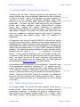
One final suggestion before we move to the “bottom-up” phase of our
simple computer design process. Practice the “instruction tracing”
process outlined in this section on other code segments to become
more familiar with “what happens when” as each instruction is fetched
and executed. As we say in the education industry, this is a “good test
question” (GTQ)!
good test
question
2.7 Bottom-Up Implementation of Simple Computer
Armed with a thorough understanding of how our simple computer
works, we are now ready to start building it from the bottom-up. In
practice, the preferred approach is to implement and test each block as
it is designed. Then, when we put the various functional blocks
together, we have a much better chance of the entire system working
“the first time”.
2.7.1 Memory
The block we will start with is memory. Although most of the time we
would simply choose a “memory chip” of appropriate size and speed, a
knowledge of “what’s under the hood” is essential to understanding
how the various functional blocks of our simple computer work
together.
First, some terminology. Normally, we think of memory as an entity
that, from the computer’s perspective, can be “read” or “written”. In
“read” mode, the memory unit simply outputs, on its data bus lines, the
contents of the location indicated on its address bus inputs. In “write”
mode, the memory unit stores the bit pattern present on its data bus
lines at the location indicated on its address bus inputs. The correct
acronym to describe such a “read/write memory” is RWM. Despite
valiant efforts, the name RWM never caught on. Instead, it is more
popular to refer to these devices as “random access memories” or
RAMs – so-named because any (random) location can be accessed in
the same amount of time (not because something random is read after
a given value is written).
The specific type of RAM we wish to concentrate on here is static
RAM, or SRAM. This is in contrast to dynamic RAM (DRAM), which
Preliminary Edition
static RAM (SRAM)
dynamic ram (DRAM)
©2001 by D. G. Meyer
Microcontroller-Based Digital System Design
Chapter 2 - Page 25
requires constant refreshing to retain information. (In DRAM, data is
stored as a charge on a capacitor – since the charge dissipates over
time, it must be periodically refreshed.) SRAM consists of a collection
of D latches that will retain data (without the need for refreshing) as
long as power is applied. Once power is turned off, however, all
information previously stored in the SRAM is lost (this is referred to as
a volatile memory).
In addition to address and data bus connections (where, for our simple
computer, the address bus is 5-bits wide and the data bus is 8-bits
wide), an SRAM needs three control signals. First, an SRAM needs an
overall enable, typically called a “chip select” (CS) or “chip enable”
(CE). This enable signal is needed to differentiate among multiple
SRAMs or, as we will see later in this chapter, between memory and
input/output devices. Second, an SRAM needs an output enable (OE)
signal which, provided the SRAM is selected, turns on a series of
three-state buffers that drive the data from the addressed location out
onto the data bus. Finally, an SRAM needs a write enable (WE) signal
which, if the SRAM is selected, opens the row of latches associated
with the addressed location and allows it to take on the value
presented to the SRAM on the data bus.
volatile
memory
chip select
(CS)
output enable
(OE)
write enable
(WE)
The basic building block of an SRAM is a memory cell, such as the one
depicted in Figure 2-18, consisting of a D-latch and a three-state
buffer. When the select (SEL) signal is asserted, the three-state buffer
is enabled, placing the data stored in the latch on the cell’s OUT line.
When both SEL and WR are asserted, the latch opens and accepts the
data present on the IN line (by virtue of asserting the latch enable or
“C” input of the D-latch). When WR is negated, the latch closes and
retains the new value.
Figure 2-18 SRAM cell (adapted from Wakerly).
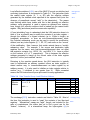
A complete SRAM can be constructed by combining an array of
memory cells with a (large) decoder plus some additional logic. The
internal structure of an eight location, 4-bit wide (or, “8x4”) SRAM is
shown in Figure 2-19. Note that the number of address lines needed is
log2(number_of_locations); here, log2(8) = 3. Stated another way, the
number of locations in an SRAM is 2n, where n is the number of
Preliminary Edition
©2001 by D. G. Meyer
Microcontroller-Based Digital System Design
Chapter 2 - Page 26
address lines. A “location” in the SRAM corresponds to a row of
memory cells; to select a particular row, an n-to-2n binary decoder is
needed.
Figure 2-19
memory
location
SRAM internal structure and symbol (adapted from Wakerly).
Preliminary Edition
©2001 by D. G. Meyer
Microcontroller-Based Digital System Design
Chapter 2 - Page 27
GigaBiga Dittos
The prefixes K (kilo-), M (mega-), G (giga-), and T (tera-), when referring to
memory sizes, mean 210 = 1024 (“about one thousand”), 220 = 1,048,576
(“about one million”), 230 = 1,073,741,824 (“about one billion”), and 240 =
1,099,511,627,776 (“about one trillion”), respectively. This brings up a very
important question: Does this means the feared “Y2K bug” is yet to occur
(in year 2048)? An even more important question, though, might be:
Instead of calling a billion bytes a “gigabyte”, wouldn’t a better name be
“bigabyte” (as in Biga (short for “Bigger”) Bytes of Digital Wisdom, the
subtitle for this text?
kilo-, mega-,
giga-, tera-
bigabyte
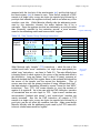
In addition to a decoder, some logic is needed to “qualify” the actions
associated with the OE and WE signals based on the assertion of CS
(the overall chip enable). When WE is asserted in conjunction with
CS, the data present on the DIN pins (DIN3 – DIN0) is written at the
location specified on the address lines (note that the operation
completes upon negation of the WE signal). When OE is asserted in
conjunction with CS, the data output by a given row is routed to the
three-state buffers that drive the external data lines.
Since the read and write operations are mutually exclusive, however,
there is usually no need for separate data input and output lines.
Instead, the data input and output lines are tied together and
connected to the rest of the system using a bi-directional data bus.
Such a configuration is shown in Figure 2-20. Note that an additional
buffer is used to receive the incoming data during a write operation, to
reduce the load seen by the entity driving the bus.
bi-directional
data bus
Figure 2-20 SRAM bi-directional data bus (adapted from Wakerly).
Preliminary Edition
©2001 by D. G. Meyer
Microcontroller-Based Digital System Design
Chapter 2 - Page 28
Before moving on, a few notes concerning memory timing are in order.
Because an SRAM read operation is a purely combinational function,
the order in which the address and control signals (CS and OE) are
asserted is of no consequence. As we will see in Chapter 5, though,
each of these signals represents a critical timing path with respect to
receiving valid data from memory on a read cycle: tA A is the address
access (propagation delay) time, tCS is the chip select access time, and
tOE is the output enable access time. When interfacing an SRAM to a
computer, all of these “read” paths need to be analyzed.
Since a “D” latch is used to store each bit of data in an SRAM, the
timing relationship between the information on the address and data
buses as well as the requisite control signals (CS and WE) is more
stringent than for a read cycle. In particular, the address information
needs to be stable, and the chip select (CS) needs to be asserted, for
some time (tCW) before WE is asserted (opening the set of latches
associated with the selected location). Also, the information supplied
to the SRAM on the data bus must be stable tSETUP prior to the
negation of the WE signal, and tHOLD following the negation of the WE
signal. (These setup and hold timing parameters will be given specific
names in Chapter 5.) The consequence of violating the data setup or
hold timing specifications of an SRAM, or of not asserting the WE
control signal for a sufficient period of time, is the possibility of
metastable behavior. All of these “write”-related timing parameters
need to be analyzed when interfacing an SRAM to a computer.
Returning to our simple computer, we note that by simply doubling the
“width” of the SRAM depicted in Figure 2-19 (from 4-bits to 8-bits) and
quadrupling the “length” (from 8 locations to 32 locations), as well as
adding the bi-directional data bus interface shown in Figure 2-20, we
will have the exact structure of SRAM needed. The only difference is
the “unique” names we will use for our simple computer’s memory
control signals: “MSL” for the memory select signal, “MOE” for the
memory output enable, and “MWE” for the memory write enable.
critical
timing path
t AA
t CS
t OE
t CW
t SETUP
t HOLD
metastable
behavior
MSL
MOE
MWE
2.7.2 Program Counter
The next functional block we wish to address is the program counter
(PC). Basically, this is nothing more than a (5-bit) binary “up” counter
with an asynchronous reset and three-state outputs.
The
asynchronous reset (ARS) will be connected to the START
pushbutton, so that the first instruction fetched is from location 000002.
There are two other control signals needed: one that enables the PC to
increment by one when a low-to-high (“positive edge”) of the system
Preliminary Edition
ARS
©2001 by D. G. Meyer
Microcontroller-Based Digital System Design
Chapter 2 - Page 29
CLOCK signal occurs, which we will call PCC; and one that turns on
the three-state buffers that “gate” the value in the PC onto the address
bus, which we will call POA. Note that if PCC is negated while a
positive CLOCK edge occurs, the program counter should simply
retain its current state.
PCC
POA
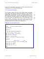
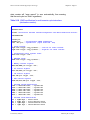
To document the design of each functional block, we will present an
ABEL (“Advanced Boolean Expression Language”) source file. Those
unfamiliar with the ABEL language and source file format should
review the material presented on this subject in Chapter 1. The ABEL
source file for the program counter module is shown in Table 2-3.
ABEL
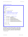
Table 2-3 Program counter module.
MODULE pc
TITLE
'Program Counter Module'
DECLARATIONS
CLOCK pin;
PC0..PC4 pin istype 'reg_D,buffer';
PCC pin; " PC count enable
POA pin; " PC output on address bus tri-state enable
ARS pin; " asynchronous reset (connected to START)
EQUATIONS
"
PC0.d
PC1.d
PC2.d
PC3.d
PC4.d
=
=
=
=
=
retain state
!PCC&PC0.q #
!PCC&PC1.q #
!PCC&PC2.q #
!PCC&PC3.q #
!PCC&PC4.q #
count up by 1
PCC&!PC0.q;
PCC&(PC1.q $ PC0.q);
PCC&(PC2.q $ (PC1.q&PC0.q));
PCC&(PC3.q $ (PC2.q&PC1.q&PC0.q));
PCC&(PC4.q $ (PC3.q&PC2.q&PC1.q&PC0.q));
[PC0..PC4].oe = POA;
[PC0..PC4].ar = ARS;
[PC0..PC4].clk = CLOCK;
END
Examining the source file, we see that when PCC is negated, the next
state is simply the current state. When PCC is asserted, the equations
for a synchronous 5-bit binary “up” counter determine the next state.
Assertion of POA causes the three-state buffers associated with each
Preliminary Edition
©2001 by D. G. Meyer
Microcontroller-Based Digital System Design
Chapter 2 - Page 30
register bit to be enabled, and assertion of ARS causes each flip-flop
comprising the PC to be asynchronously reset.
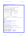
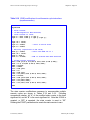
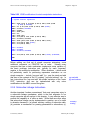
2.7.3 Instruction Register
The instruction register (IR) has a very simple mission: temporarily
hold (“stage”) the instruction fetched from memory so that it can be
“peeled apart” and executed. As such, it is simply a series of D flipflops with two control signals. The first control signal, which we will call
IRL, enables the instruction register to be loaded with the instruction
read from memory; the load should occur on the positive edge of the
system CLOCK. The second control signal, which we will call IRA,
turns on the three-state buffers of the lower 5-bits of the IR, to “gate”
the address field of the instruction onto the address bus.
IRL
IRA
Table 2-4 Instruction register module.
MODULE ir
TITLE
'Instruction Register Module'
DECLARATIONS
CLOCK pin;
" IR4..IR0 connected to address bus
" IR7..IR5 supply opcode to IDMS
IR0..IR7 pin istype 'reg_D,buffer';
DB0..DB7 pin; " data bus
IRL pin; " IR load enable
IRA pin; " IR output on address bus enable
EQUATIONS
"
retain state
load
[IR0..IR7].d = !IRL&[IR0..IR7].q # IRL&[DB0..DB7];
[IR0..IR7].clk = CLOCK;
[IR0..IR4].oe = IRA;
[IR5..IR7].oe = [1,1,1];
END
Preliminary Edition
©2001 by D. G. Meyer
Microcontroller-Based Digital System Design
Chapter 2 - Page 31
Several items in the IR module source file, shown in Table 2-4,
deserve explanation. First, when IRL is negated, note that the IR
simply retains its current state. Second, note that, unlike the PC, there
is no need to asynchronously reset the IR when the START
pushbutton is pressed, since its (random) initial value is of no
consequence. Finally, note that IRA only controls the three-state
outputs associated with the lower 5-bits of the IR, and that the threestate buffers of the upper 3-bits (i.e., the opcode bits) are always
enabled. The reason the three-state buffers associated with the upper
3-bits are always enabled is that they are connected directly to the
IDMS module (i.e., they do not drive a bus). Recall that the IDMS uses
the opcode bits to determine which system control signals are asserted
on the next cycle, when the instruction is executed.
2.7.4 Arithmetic Logic Unit
As mentioned earlier, the arithmetic logic unit (ALU) is so-named
because it performs the arithmetic (add, subtract, etc.) and logical
(“Boolean”) operations defined by the instruction set. A “real” ALU
performs a wide range of arithmetic and logical functions on operands
stored in either registers or in memory. Fortunately, our ALU is
relatively simple: it performs four different functions on a single register
(which we have called the accumulator, or “A” register) and sets four
condition code bits (or flags) based on the result obtained. As such,
only four control signals are needed: an overall enable, which we will
call ALE; two “function select” lines, which we will call ALX and ALY;
and a three-state output enable for “gating” the value in the “A” register
onto the data bus, which we will call AOE. The data bus interface must
be bi-directional, in order to input data supplied by memory on LDA,
ADD, SUB, and AND operations; and to output data to memory for
STA operations. The condition code bits (CF, NF, VF, ZF) are output
directly to the IDMS (we will see how these flags can be used to
implement conditional transfer of control instructions later).
The ABEL source file for the simple computer ALU is shown in Tables
2-5, 2-6, and 2-7. Referring first to the declaration section (Tables 2-5
and 2-6), we note that signals used for “internal” purposes are declared
as nodes. These include the carry bits and the combinational ALU
outputs. In the declarations that continue in Table 2-6, the least
significant bit carry-in (CIN) is defined as ALY. Noting that ALY is “0”
for ADD and “1” for SUB, we realize this is exactly what is needed to
add one to the diminished radix complement of the subtrahend (to
obtain the radix complement) when performing a SUB operation.
Preliminary Edition
arithmetic and
logical operations
ALE
ALX
ALY
condition
code bits
nodes
©2001 by D. G. Meyer
Microcontroller-Based Digital System Design
Chapter 2 - Page 32
Table 2-5 Declarations section of ALU module.
MODULE alu
TITLE 'ALU Module'
"
"
"
"
"
"
"
"
"
"
"
"
"
"
"
"
"
"
"
"
8-bit, 4-function ALU with bi-directional data bus
ADD:
SUB:
LDA:
AND:
OUT:
AOE
===
0
0
0
0
1
0
(Q7..Q0)
(Q7..Q0)
(Q7..Q0)
(Q7..Q0)
Value in
ALE
===
1
1
1
1
0
0
ALX
===
0
0
1
1
d
d
<- (Q7..Q0) +
<- (Q7..Q0) <- DB7..DB0
<- (Q7..Q0) &
Q7..Q0 output
ALY
===
0
1
0
1
d
d
X -> flag affected
Function
========
ADD
SUB
LDA
AND
OUT
<none>
DB7..DB0
DB7..DB0
DB7..DB0
on data bus DB7..DB0
CF
==
X
X
·
·
·
·
ZF
==
X
X
X
X
·
·
NF
==
X
X
X
X
·
·
VF
==
X
X
·
·
·
·
· -> flag not affected
Note: If ALE = 0, the state of all register bits should be retained
DECLARATIONS
CLOCK pin;
" ALU control lines (enable & function select)
ALE pin; " overall ALU enable
AOE pin; " data bus tri-state output enable
ALX pin; " function select
ALY pin;
" Carry equations (declare as internal nodes)
CY0..CY7 node istype 'com';
" Combinational ALU outputs (D flip-flop inputs)
" Used for flag generation (declare as internal nodes)
ALU0..ALU7 node istype 'com';
" Bi-directional 8-bit data bus (also, accumulator register bits)
DB0..DB7 pin istype 'reg_d,buffer';
" Condition code register bits
CF pin istype 'reg_d,buffer';
VF pin istype 'reg_d,buffer';
NF pin istype 'reg_d,buffer';
ZF pin istype 'reg_d,buffer';
Preliminary Edition
"
"
"
"
carry flag
overflow flag
negative flag
zero flag
©2001 by D. G. Meyer
Microcontroller-Based Digital System Design
Chapter 2 - Page 33
Table 2-6 Continuation of ALU source file declarations section.
" Declaration of intermediate equations
" Least significant bit carry-in (0 for ADD, 1 for SUB => ALY)
CIN = ALY;
" Intermediate equations for adder/subtractor SUM (S0..S7),
" selected when ALX = 0
S0
S1
S2
S3
S4
S5
S6
S7
=
=
=
=
=
=
=
=
DB0.q
DB1.q
DB2.q
DB3.q
DB4.q
DB5.q
DB6.q
DB7.q
$
$
$
$
$
$
$
$
(DB0.pin
(DB1.pin
(DB2.pin
(DB3.pin
(DB4.pin
(DB5.pin
(DB6.pin
(DB7.pin
$
$
$
$
$
$
$
$
ALY)
ALY)
ALY)
ALY)
ALY)
ALY)
ALY)
ALY)
$
$
$
$
$
$
$
$
CIN;
CY0;
CY1;
CY2;
CY3;
CY4;
CY5;
CY6;
" Intermediate equations for LOAD and AND,
" selected when ALX = 1
L0
L1
L2
L3
L4
L5
L6
L7
=
=
=
=
=
=
=
=
!ALY&DB0.pin
!ALY&DB1.pin
!ALY&DB2.pin
!ALY&DB3.pin
!ALY&DB4.pin
!ALY&DB5.pin
!ALY&DB6.pin
!ALY&DB7.pin
#
#
#
#
#
#
#
#
ALY&DB0.q&DB0.pin;
ALY&DB1.q&DB1.pin;
ALY&DB2.q&DB2.pin;
ALY&DB3.q&DB3.pin;
ALY&DB4.q&DB4.pin;
ALY&DB5.q&DB5.pin;
ALY&DB6.q&DB6.pin;
ALY&DB7.q&DB7.pin;
Intermediate equations for the full adder outputs (used for the ADD and
SUB) functions as well as the “logical” functions (here, LDA and AND)
are shown in Table 2-6. Note that the sole purpose of these
intermediate equations is to simplify the task of writing the ALU
equations. One can think of these as simply “definitions” (since they
are part of the declaration section) of “symbols” that will be used in
“higher level” equations.
intermediate
equations
The “real” equations start in Table 2-7. First are the carry equations
that implement a simple ripple adder/subtractor.
Next are the
combinational equations that generate the ALU outputs based on the
intermediate equations defined in Table 2-6. The data bus equations
appear next; note that if ALE is negated, the “A” register retains its
current state.
Preliminary Edition
©2001 by D. G. Meyer
Microcontroller-Based Digital System Design
Chapter 2 - Page 34
Table 2-7 Equations section of ALU source file.
EQUATIONS
" Ripple carry equations (CY7 is COUT)
CY0 = DB0.q&(ALY$DB0.pin) # DB0.q&CIN #
CY1 = DB1.q&(ALY$DB1.pin) # DB1.q&CY0 #
CY2 = DB2.q&(ALY$DB2.pin) # DB2.q&CY1 #
CY3 = DB3.q&(ALY$DB3.pin) # DB3.q&CY2 #
CY4 = DB4.q&(ALY$DB4.pin) # DB4.q&CY3 #
CY5 = DB5.q&(ALY$DB5.pin) # DB5.q&CY4 #
CY6 = DB6.q&(ALY$DB6.pin) # DB6.q&CY5 #
CY7 = DB7.q&(ALY$DB7.pin) # DB7.q&CY6 #
(ALY$DB0.pin)&CIN;
(ALY$DB1.pin)&CY0;
(ALY$DB2.pin)&CY1;
(ALY$DB3.pin)&CY2;
(ALY$DB4.pin)&CY3;
(ALY$DB5.pin)&CY4;
(ALY$DB6.pin)&CY5;
(ALY$DB7.pin)&CY6;
" Combinational ALU equations
ALU0 = !ALX&S0 # ALX&L0;
ALU1 = !ALX&S1 # ALX&L1;
ALU2 = !ALX&S2 # ALX&L2;
ALU3 = !ALX&S3 # ALX&L3;
ALU4 = !ALX&S4 # ALX&L4;
ALU5 = !ALX&S5 # ALX&L5;
ALU6 = !ALX&S6 # ALX&L6;
ALU7 = !ALX&S7 # ALX&L7;
" Register bit and data bus control equations
[DB0..DB7].d = !ALE&[DB0..DB7].q # ALE&[ALU0..ALU7];
[DB0..DB7].clk = CLOCK;
[DB0..DB7].oe = AOE;
" Flag register state equations
CF.d = !ALE&CF.q # ALE&(!ALX&(CY7 $ ALY) # ALX&CF.q);
CF.clk = CLOCK;
ZF.d = !ALE&ZF.q # ALE&(!ALU7&!ALU6&!ALU5&!ALU4&!ALU3&!ALU2&!ALU1&!ALU0);
ZF.clk = CLOCK;
NF.d = !ALE&NF.q # ALE&ALU7;
NF.clk = CLOCK;
VF.d = !ALE&VF.q # ALE&(!ALX&(CY7 $ CY6) # ALX&VF.q);
VF.clk = CLOCK;
END
Preliminary Edition
©2001 by D. G. Meyer
Microcontroller-Based Digital System Design
Chapter 2 - Page 35
Last, but not least, are the equations that govern the four condition
code bits. All of these flags retain their current state if ALE is negated.
The carry flag (CF) and overflow flag (VF) are only affected by the
ADD and SUB instructions. For ADD, the CF bit is set to the carry out
of the most significant position (here, CY7); for SUB, the CF bit is
interpreted as a borrow, and is therefore set to the complement of the
carry out of the sign position. The VF bit is simply the XOR of the carry
in to the sign bit (CY6) with the carry out of the sign bit (CY7).
The negative flag (NF) and zero flag (ZF) are affected by all four
functions implemented by our ALU. The NF bit is simply the sign bit
(ALU7) of the result generated by the ALU, while the ZF bit is set to “1”
if all the ALU result bits are zero.
Before moving on to the final block of our simple computer design,
there is an important practical point worth noting. All of the functional
blocks designed thus far – the memory, PC, IR, and ALU – can be
independently implemented (or simulated) and tested (as well as
debugged) before they are all “assembled together” into a completed
computer. Independent testing and debugging of each functional
block, in fact, is an important aspect of the “top-down, bottom-up”
strategy we have espoused in this chapter.
independent
testing and
debugging
2.7.5 Instruction Decoder and Micro-sequencer
As described previously, there are two basic steps involved with
“processing” each instruction, the combination of which is referred to
as a micro-sequence. During a fetch cycle, the instruction pointed to
by the PC is read from memory and loaded into the IR; the PC is
incremented by one as the instruction is loaded. During the ensuing
execute cycle, the instruction staged in the IR is “peeled” apart into an
opcode field and an operand address field; the opcode field indicates
the operation to be performed using data obtained from (or destined
for) the memory location specified by the address field. The functional
block that orchestrates the sequencing of these activities is called the
instruction decoder and micro-sequencer (IDMS).
Since, in this initial version of our simple computer, there are only two
different kinds of cycles (fetch and execute), a single flip-flop can be
used as a state counter (SQ). In reality, this state counter is simply a
single-bit binary counter (i.e., it simply toggles between “0” and “1”).
Note that the state counter must be placed in the “fetch” state when
START is pressed; therefore, it makes sense to assign the “reset” state
Preliminary Edition
state counter (SQ)
toggles
©2001 by D. G. Meyer
Microcontroller-Based Digital System Design
Chapter 2 - Page 36
of the SQ flip-flop (SQ=0) to the fetch cycle, and the “set” state of the
SQ flip-flop (SQ=1) to the execute cycle.
With the structure of the state counter established, the next step is to
determine which control signals (of the functional blocks designed
previously) need to be asserted when SQ=0 (fetch) and SQ=1
(execute). To accomplish this, we will need to refer back to each of the
previous sub-sections (on the design of the individual functional
blocks) as well as the instruction tracing worksheets completed
previously.
Referring again to Figure 2-12, we note that the following signals need
to be asserted to complete a fetch cycle. First, to “gate” the value in
the PC onto the address bus, the signal POA needs to be asserted by
the IDMS. To read the instruction, the memory needs to be selected
(MSL asserted) and its data bus output enabled (MOE asserted). To
load the instruction read from memory into the IR, the signal IRL needs
to be asserted. Finally, to increment the PC as the instruction is
loaded, the signal PCC needs to be asserted. A total of five system
control signals, therefore, needed to be asserted by the IDMS during a
fetch cycle (when SQ=0): POA, MSL, MOE, IRL, and PCC.
The control signals that need to be asserted during an “ALU function”
execute cycle (i.e., LDA, ADD, SUB, AND operation) can be inferred
from Figure 2-13. First, to “gate” the operand address staged in the IR
onto the address bus, the signal IRA needs to be asserted by the
IDMS. To read the operand, the memory needs to be selected (MSL
asserted) and its data bus output enabled (MOE asserted). To perform
the operation specified by the instruction opcode (supplied to the IDMS
from the upper 3-bits of the IR), ALE needs to be asserted along with
the prescribed combination of ALX and ALY (based on the ALU design
documented in Table 2-5).
The “store A” (STA) instruction execute cycle is similar, but notably
different, than an “ALU function” execute cycle. Here, the address
supplied to memory (from the IR, upon assertion of IRA) specifies the
destination for the data in the “A” register. To complete the write to
memory, it needs to be selected (MSL asserted) and write enabled
(MWE asserted). To “gate” the data in the “A” register onto the data
bus, AOE needs to be asserted. A total of four control signals need to
be asserted, then, to execute a “store A” (STA) instruction: IRA, MSL,
MWE, and AOE.
Preliminary Edition
©2001 by D. G. Meyer
Microcontroller-Based Digital System Design
Chapter 2 - Page 37
A succinct summary of all the system control signal assertions is
provided in Table 2-8. Note that, for the sake of clarity, signal
assertions are denoted using “H” (signals that are either negated or
“don’t care” are left blank). By way of contrast, the control signal
negations that are effected by execution of the HLT (halt) instruction
are denoted using “L”.
H
H
H
H
H
H
H
H
H
H
L
L
H
H
ALY
H
H
H
H
H
L
H
ALX
LDA
STA
ADD
SUB
AND
HLT
H
ALE
S1
S1
S1
S1
S1
S1
H
AOE
H
IRA
H
IRL
POA
MOE
S0
PCC
Instruction
Mnemonic
MWE
Decoded
State
MSL
Table 2-8 System control table.
H
H
H
H
L
H
H
H
The ABEL source file for the simple computer’s IDMS module is shown
in Tables 2-9 and 2-10. Referring first to the declarations listed in
Table 2-9, we find decoded opcode definitions (using the instruction
mnemonics as pseudonyms for the corresponding opcode bit patterns)
and decoded machine state definitions (S0 for fetch, S1 for execute).
The purpose of defining an intermediate equation for each opcode
combination is simply to make the job of writing the system control
equations (that appear in Table 2-10) easier. Perhaps if we were more
“clever”, we might have used the name “fetch” (instead of S0) and
“execute” (instead of S1) to help make the subsequent equations a bit
more clear (albeit more cumbersome to write).
Continuing with the IDMS equations in Table 2-10, we discover three
basic components: the state counter, the run/stop flip-flop, and the
system control equations. Looking first at the state counter, we note
that if the machine RUN enable is high (i.e., the machine is “running”),
the state counter flip-flop merely “toggles” each time a positive CLOCK
edge occurs. If RUN is negated, SQ is reset to “0” (i.e., the “fetch”
state). Pressing the START pushbutton also resets SQ to the “fetch”
state.
Preliminary Edition
run/stop
flip-flop
©2001 by D. G. Meyer
Microcontroller-Based Digital System Design
Chapter 2 - Page 38
Table 2-9 Declarations section of IDMS module.
MODULE idms
TITLE
'Instruction Decoder and Microsequencer'
DECLARATIONS
CLOCK pin;
START pin; " asynchronous START pushbutton
OP0..OP2 pin; " opcode bits (input from IR5..IR7)
" State counter
SQ node istype 'reg_D,buffer';
" RUN/HLT state
RUN node istype 'reg_D,buffer';
" Memory control signals
MSL,MOE,MWE pin istype 'com';
" PC control signals
PCC,POA,ARS pin istype 'com';
" IR control signals
IRL,IRA pin istype 'com';
" ALU control signals (not using flags yet)
ALE,ALX,ALY,AOE pin istype 'com';
" Decoded opcode definitions
LDA = !OP2&!OP1&!OP0; " LDA
STA = !OP2&!OP1& OP0; " STA
ADD = !OP2& OP1&!OP0; " ADD
SUB = !OP2& OP1& OP0; " SUB
AND = OP2&!OP1&!OP0; " AND
HLT = OP2&!OP1& OP0; " HLT
opcode
opcode
opcode
opcode
opcode
opcode
=
=
=
=
=
=
000
001
010
011
100
101
" Decoded state definitions
S0 = !SQ.q; " fetch
S1 = SQ.q; " execute
Preliminary Edition
©2001 by D. G. Meyer
Microcontroller-Based Digital System Design
Chapter 2 - Page 39
Table 2-10 Equations section of IDMS module.
EQUATIONS
" State counter
SQ.d = RUN.q&!SQ.q; " if RUN negated, resets SQ
SQ.clk = CLOCK;
SQ.ar = START;
" start in fetch state
" Run/stop (equivalent of SR latch)
RUN.ap = START; " start with RUN set to 1
RUN.clk = CLOCK;
RUN.d = RUN.q;
RUN.ar = S1&HLT; " RUN is cleared when HLT executed
" System control equations
MSL
MOE
MWE
ARS
PCC
POA
IRL
IRA
AOE
ALE
ALX
ALY
=
=
=
=
=
=
=
=
=
=
=
=
RUN.q&(S0 # S1&(LDA # STA # ADD # SUB # AND));
S0 # S1&(LDA # ADD # SUB # AND);
S1&STA;
START;
RUN.q&S0;
S0;
RUN.q&S0;
S1&(LDA # STA # ADD # SUB # AND);
S1&STA;
RUN.q&S1&(LDA # ADD # SUB # AND);
S1&(LDA # AND);
S1&(SUB # AND);
END
The run/stop flip-flop is defined next in Table 2-10. Here we note that
pressing the START pushbutton asynchronously sets the RUN flip-flop,
thereby enabling our simple computer to start executing instructions.
Once set, the RUN signal remains asserted until asynchronously reset
through execution of an HLT instruction.
We see how the RUN signal is used to enable/disable machine activity
in the system control equations that follow. Note that if RUN is high,
the system control signals are asserted according to the table in Table
2-8, as described previously. For example, MSL is asserted if a fetch
cycle is being performed (S0 high); or, an execute cycle is being
performed (S1 high) of an LDA instruction, an STA instruction, an ADD
instruction, a SUB instruction, or an AND instruction. If RUN is low,
Preliminary Edition
©2001 by D. G. Meyer
Microcontroller-Based Digital System Design
Chapter 2 - Page 40
however, all of the pertinent system control signals are negated. Note
that it is only necessary to negate the system control signals
responsible for causing the various functional blocks to change state
(i.e., it is not necessary to negate function select signals such as ALX
and ALY, nor is it necessary to negate three-state output enables).
This completes the “bottom-up” phase of the design process for the
initial version of our simple computer. All of the ABEL code described
in this section could be implemented using a single, modest-size PLD.
The addition of a conventional memory chip would yield a working
computer. Before augmenting the instruction set with some useful
extensions, though, let’s take a closer look at system timing.
2.8 System Timing Analysis
When we designed the program counter in Section 2.7.2, there was an
appearance of “cheating” – specifically, of using the current value in
the PC to access an instruction in memory while, at apparently the
same time, telling the PC to increment. This is an issue that deserves
further scrutiny.
To gain a better understanding of the timing relationship among
different activities within our computer, we need to understand two
basic hardware-imposed constraints. The first is that only one device
(functional block) can drive a bus on a given bus cycle, i.e., “bus
fighting” must be avoided. The second is that data can only “pass
through” one edge-triggered flip-flop per cycle. Thus, it is not possible
to load a value into a register and expect to “use it” (have the value
available on the register’s outputs) on the same cycle.
Given these constraints, we are now prepared to examine in detail the
sequence of activities that occur during a fetch cycle. A “qualitative”
timing diagram is provided in Figure 2-21 for this purpose (by
qualitative we mean that we’re not interested in the exact number of
nanoseconds between one signal assertion and another, just the fact
that there is a delay). Depicted in this diagram is the sequencing that
occurs as the machine finishes an execute cycle, performs a fetch of
the next instruction, and subsequently proceeds to execute the
instruction just fetched. Our focus here is on the events that constitute
a fetch cycle.
The first thing to note is that, since the functional blocks of the machine
were designed using positive-edge-triggered flip-flops, the clock edges
“drive” the machine from state-to-state. Thus, a “fetch cycle” is the
Preliminary Edition
bus fighting
qualitative
timing diagram
clock edges
©2001 by D. G. Meyer
Microcontroller-Based Digital System Design
Chapter 2 - Page 41
time between the clock edge that drives the machine from the previous
execute cycle to the current fetch cycle, and the subsequent clock
edge that transitions the machine from the fetch cycle to an execute
cycle. Shortly after the first clock edge in Figure 2-21, then, the control
signals MSL, MOE, POA, IRL, and PCC are asserted (the delay
relative to the clock edge in generating these signals is due to the
propagation delay of the state counter plus the delay associated with
the system control equations – see Table 2-10).
Previous S1 Execute
S0 Fetch
S1 Execute
IR loaded with
instruction on
data bus before
this point
PC incremented
after this point
PC
PC = PC+1
Instruction
Instruction
Loaded in IR
Figure 2-21 Fetch cycle event timing relationship.
The assertion of POA causes the three-state buffers of the PC to turn
on and drive its value onto the address bus. The value on the address
bus, in conjunction with the MSL and MOE signal assertions, causes
the memory to drive the addressed instruction onto the data bus (note
that, in most practical systems, this constitutes a substantial part of the
cycle time). Provided the instruction is on the data bus at least tSETUP
(of the D flip-flop) prior to the next clock edge, it is successfully loaded
into the IR (because the IRL signal is asserted) when that edge occurs.
Preliminary Edition
©2001 by D. G. Meyer
Microcontroller-Based Digital System Design
Chapter 2 - Page 42
While this may seem to be “enough” activity already, we realize that a
related “housekeeping” activity can be accomplished on this cycle as
well: incrementing the value in the PC, so it points to the next
instruction (in preparation for the next fetch). Again, based on the use
of edge-triggered flip-flops in our design, we note that the value on the
data bus just prior to the clock edge that loads the IR determines the
next state of the IR. It follows, then, that we can use that same clock
edge to drive the PC to its next state – this is why PCC is also asserted
during a fetch cycle. Note that the PC state change will occur after the
clock edge, i.e., after the instruction has been safely loaded into the IR.
This allows us to effectively overlap the load of the IR with the
increment of the PC on the same cycle. We will make use of this same
principle when we add some extensions to our machine later in this
chapter.
overlap
One might ask at this point, “Could we have delayed the increment of
the PC until the execute cycle?” In the initial version of our simple
computer, it would clearly be possible: here, the “new value” in the PC
would be available shortly after the commencement of the fetch cycle,
thus enabling the correct instruction to be loaded into the IR (the only
consequence might be a small amount of additional propagation delay
for the “new” value to become stable). When we add subroutine
linkage instructions to our computer, however, we will find it useful to
have the “new” value of the PC available during the first execute cycle
(to serve as the “return address” for a “subroutine call” instruction). In
anticipation of this extension, we will include the increment of the PC
as an integral part of the fetch cycle.
2.9 Simple Computer Extensions
When we originally designed our instruction set, we purposefully left
two opcode bit patterns “uncommitted”. The reason we did this was to
provide room for expansion. We will, then, add a “pair” of instructions
at a time to our “base” instruction set. The “pairs” we will add include
input/output (IN/OUT) instructions, transfer of control instructions
(JMP/JZF), stack manipulation instructions (PSH/POP), and subroutine
linkage instructions (JSR/RTS).
2.9.1 Input/Output Instructions
When we first drew the “big picture” of our simple computer (see
Figure 2-4), we included a switch “input port” and an LED “output port”.
As evident from the initial version of our instruction set, we included no
Preliminary Edition
input port
output port
©2001 by D. G. Meyer
Microcontroller-Based Digital System Design
Chapter 2 - Page 43
provision for using these. It makes sense, then, to add instructions for
providing our machine with the “modern convenience” of data input
and output (“I/O”).
First, we need to establish the destination that will be used for data
input (or read) from the “outside world”, as well as the source for data
that will be output (or written). Given that our machine has but one
register that participates in data transactions – namely, the “A” register
– it is the most likely candidate to serve as the destination/source of
data that is input/output, respectively. Thus, our new “IN” instruction
will function in a manner similar to an LDA instruction, except the
source of data will be the “outside world” and the address field will be
used as a pointer to an “input device” (instead of to memory). Similarly,
our new “OUT” instruction will function in a manner similar to an STA
instruction, except the destination of data will be the “outside world”
and the address field will be used as a pointer to an “output device”. A
name commonly used for this input/output strategy is accumulatormapped I/O.
Second, we need to establish how data will be communicated to/from
the ubiquitous “outside world”. Basically, a “gateway” is needed
between the system data bus and the external input and output
devices, along with some new system control signals that enable a
“read” (IOR) or a “write” (IOW) via this gateway. Also, a means of
decoding the I/O addresses (typically called port or device numbers)
into individual “device selects” (or enables) is needed. A diagram
illustrating the placement of the “I/O block” is provided in Figure 2-22;
an ABEL source file for a specific instance of this module is given in
Table 2-11.
Instruction Decoder
and Micro-Sequencer
Clock
Flags
Data
Data Bus
Memory
Address
Instruction
Register
Data
port numbers
device numbers
I/O block
Program
Counter
Opcode Address
ALU
IOW
Address Bus
Start
IOR
I/O
Figure 2-22 Block diagram of simple computer with I/O.
Preliminary Edition
©2001 by D. G. Meyer
Microcontroller-Based Digital System Design
Chapter 2 - Page 44
Table 2-11 Basic I/O module.
MODULE io
TITLE
'Input/Output Port 00000'
DECLARATIONS
DB0..DB7 pin istype 'com';
AD0..AD4 pin;
IN0..IN7 pin;
OUT0..OUT7 pin istype 'com';
"
"
"
"
data bus
address bus
input port
output port
IOR pin; " Input port read
IOW pin; " Output port write
" Port select equation for port address 00000
PS = !AD4&!AD3&!AD2&!AD1&!AD0;
EQUATIONS
[DB0..DB7] = [IN0..IN7];
[DB0..DB7].oe = IOR&PS;
[OUT0..OUT7] = [DB0..DB7];
[OUT0..OUT7].oe = IOW&PS;
END
Referring to the ABEL file, we see that it contains a specific port
address decoding equation, here for port address 000002. When the
pattern on the address bus matches this value, an I/O transaction via
this port address is enabled. If an IN instruction is being executed,
assertion of the IOR signal (by the IDMS) causes the value on the “IN
pins” (IN0...IN7) to be gated onto the system data bus, allowing it to be
loaded into the “A” register. If an OUT instruction is being executed,
assertion of the IOW signal causes the value on the data bus (supplied
by the “A” register) to be gated to the “OUT pins” (OUT0…OUT7).
There is a limitation, however, inherent in the I/O port design shown in
Table 2-11: the value output (when an OUT instruction is executed) is
only “active” for a very short time (specifically, the amount of time the
IOW signal is asserted by the IDMS). For devices such as light
Preliminary Edition
©2001 by D. G. Meyer
Microcontroller-Based Digital System Design
Chapter 2 - Page 45
emitting diodes (LEDs), the brief assertion of IOW will not provide a
satisfactory display. A better solution is to latch the value sent to the
output port, and retain it until execution of a subsequent OUT
instruction changes the value. An I/O module that provides a latched
output port is provided in Table 2-12. Here, assertion of IOW in
conjunction with the proper port address opens a transparent latch,
which then assumes the new value sent on the data bus. The latch
closes (retains its value) when IOW is negated.
latched
output port
Table 2-12 Latched I/O port.
MODULE iol
TITLE
'Input/Output Port 00000 - With Output Latch'
DECLARATIONS
DB0..DB7 pin istype 'com';
AD0..AD4 pin;
IN0..IN7 pin;
OUT0..OUT7 pin istype 'com';
"
"
"
"
data bus
address bus
input port
output port
IOR pin; " Input port read
IOW pin; " Output port write
" Port select equation for port address 00000
PS = !AD4&!AD3&!AD2&!AD1&!AD0;
EQUATIONS
[DB0..DB7] = [IN0..IN7];
[DB0..DB7].oe = IOR&PS;
" Transparent latch for output port
[OUT0..OUT7] = !(IOW&PS)&[OUT0..OUT7] # IOW&PS&[DB0..DB7];
END
The augmented system control table for our simple computer plus I/O
is given in Table 2-13. Note that there are two “new” equations (for
IOR and IOW), along with four equations that need to be updated (for
IRA, AOE, ALE, and ALX). The updated system control equations are
given in Table 2-14.
Preliminary Edition
©2001 by D. G. Meyer
Microcontroller-Based Digital System Design
Chapter 2 - Page 46
H
H
H
H
H
H
H
H
H
L
IOW
H
H
H
H
H
L
H
L
H
H
H
IOR
H
ALY
H
H
H
H
H
L
H
ALX
LDA
STA
ADD
SUB
AND
HLT
IN
OUT
H
ALE
S1
S1
S1
S1
S1
S1
S1
S1
H
AOE
H
IRA
H
IRL
POA
MOE
S0
PCC
Instruction
Mnemonic
MWE
Decoded
State
MSL
Table 2-13 System control table modified for I/O.
H
H
H
H
H
H
H
Table 2-14 System control equations modified for I/O.
" System control equations (IDMS)
MSL
MOE
MWE
ARS
PCC
POA
IRL
IRA
AOE
ALE
ALX
ALY
=
=
=
=
=
=
=
=
=
=
=
=
RUN.q&(S0 # S1&(LDA # STA # ADD # SUB # AND));
S0 # S1&(LDA # ADD # SUB # AND);
S1&STA;
START;
RUN.q&S0;
S0;
RUN.q&S0;
S1&(LDA # STA # ADD # SUB # AND # IN # OUT);
S1&(STA # OUT);
RUN.q&S1&(LDA # ADD # SUB # AND # IN);
S1&(LDA # AND # IN);
S1&(SUB # AND);
IOR = S1&IN;
IOW = S1&OUT;
END
Preliminary Edition
©2001 by D. G. Meyer
Microcontroller-Based Digital System Design
Chapter 2 - Page 47
2.9.2 Transfer-of-Control Instructions
Any program worth the silicon it runs on typically does more than
execute “straight line” code. Instead, execution transfers to different
parts of the program based on various conditions encountered.
Generically, we refer to the instructions that allow program execution to
“jump around” as transfer-of-control instructions.
There are two basic types of transfer-of-control instructions. If the
address field of the instruction contains the (absolute) address in
memory at which execution should continue, it is most often referred to
as a “jump” instruction. If the address field instead represents the
(signed) “distance” the next instruction is from the transfer-of-control
instruction, it is referred to as a “branch”. (There is not universal
agreement on this nomenclature, however – see sidebar.) Jumps (or
branches) that “always happen” are called unconditional; those that
happen only if a certain combination of condition codes exists are
called conditional.
straight line code
transfer-of-control
instructions
jump instruction
branch instruction
unconditional
conditional
A Branch by Any Other Name
Regrettably, there is no “universal agreement” among manufacturers of
microcontrollers concerning the names used for the basic transfer-of-control
instruction types. Since this is primarily a text dealing with Motorola products,
we will use the names they commonly use: “jump” for absolute transfer, and
“branch” for relative transfer. Be advised, though, that another “major
manufacturer” (Intel) uses just the opposite designation: “branch” for absolute
transfer, and “jump” for relative transfer. Although the author cut his “digital
teeth” on Intel processors, he prefers the Motorola adopted names.
The addition of transfer-of-control instructions to our simple computer
will require modifications to the PC (as well as to the IDMS).
Specifically, we will need to provide a mechanism for loading a new
value into the PC to implement “jump-style” instructions, or for adding a
signed offset to the value in the PC to implement “branch-style”
instructions. Here we will focus on the modifications necessary to
implement jump-style instructions. An ABEL source file for the modified
PC is provided in Table 2-15. Note that it is the same as the “original”
PC (see Table 2-3), except that a “load from address bus” function
(and associated control signal, PLA) has been added. Recall that the
“new value” with which the PC is to be loaded is staged in the IR, and
can therefore be conveniently “transported” to the PC via the address
bus.
Preliminary Edition
PLA
©2001 by D. G. Meyer
Microcontroller-Based Digital System Design
Chapter 2 - Page 48
Table 2-15 PC modifications to support transfer-of-control instructions.
MODULE pc
TITLE
'Program Counter'
DECLARATIONS
CLOCK pin;
PC0..PC4 pin istype 'reg_D,buffer';
PCC
PLA
POA
ARS
pin;
pin;
pin;
pin;
"
"
"
"
PC count enable
PC load from address bus enable
PC output on address bus tri-state enable
asynchronous reset (connected to START)
" Note: Assume PCC and PLA are mutually exclusive
EQUATIONS
"
retain state
PC0.d = !PCC&!PLA&PC0.q
"
count up by 1
# PCC&!PC0.q;
PC1.d = !PCC&!PLA&PC1.q
# PCC&(PC1.q $
PC2.d = !PCC&!PLA&PC2.q
# PCC&(PC2.q $
PC3.d = !PCC&!PLA&PC3.q
# PCC&(PC3.q $
PC4.d = !PCC&!PLA&PC4.q
# PCC&(PC4.q $
load
# PLA&PC0.pin
# PLA&PC1.pin
PC0.q);
# PLA&PC2.pin
(PC1.q&PC0.q));
# PLA&PC3.pin
(PC2.q&PC1.q&PC0.q));
# PLA&PC4.pin
(PC3.q&PC2.q&PC1.q&PC0.q));
[PC0..PC4].oe = POA;
[PC0..PC4].ar = ARS;
[PC0..PC4].clk = CLOCK;
END
The system control table, modified to include an “unconditional jump”
instruction (JMP) along with a “jump if zero flag set” (JZF) instruction,
is shown in Table 2-16. As its name implies, the JZF instruction
causes a transfer-of-control to the address following the opcode if the
zero flag (ZF) is set, i.e., the result of the most recent ALU operation
Preliminary Edition
JMP
JZF
©2001 by D. G. Meyer
Microcontroller-Based Digital System Design
Chapter 2 - Page 49
has generated a result of zero in the “A” register. (As it turns out, this
is a fairly “popular” condition to check in practical applications.) If the
condition specified by a “conditional jump” instruction (like JZF) is not
met, however, nothing happens (often called a no operation, or “NOP”)
– execution merely continues with the instruction that follows. In order
to effect the load of the jump address, the IDMS needs to know the
state of the various condition code bits generated by the ALU. The
equations for IRA and PLA, then, will be a function of ZF for the new
instructions added to the machine in Table 2-17.
no operation
NOP
H
H
H
H
H
H
H
H
H
L
L
H
H
PLA
H
ALY
H
H
H
H
H
L
H
ALX
LDA
STA
ADD
SUB
AND
HLT
JMP
JZF
H
ALE
S1
S1
S1
S1
S1
S1
S1
S1
H
AOE
H
IRA
H
IRL
POA
MOE
S0
PCC
Instruction
Mnemonic
MWE
Decoded
State
MSL
Table 2-16 System control table modified for transfer-of-control instructions.
H
H
H
H
L
H
H
ZF
H
H
H
ZF
Table 2-17 IDMS modifications to support transfer-of-control.
" System control equations (IDMS)
MSL
MOE
MWE
ARS
PCC
POA
IRL
IRA
AOE
ALE
ALX
ALY
=
=
=
=
=
=
=
=
=
=
=
=
RUN.q&(S0 # S1&(LDA # STA # ADD # SUB # AND));
S0 # S1&(LDA # ADD # SUB # AND);
S1&STA;
START;
RUN.q&S0;
S0;
RUN.q&S0;
S1&(LDA # STA # ADD # SUB # AND # JMP # JZF&ZF);
S1&I1;
RUN.q&S1&(LDA # ADD # SUB # AND);
S1&(LDA # AND);
S1&(SUB # AND);
PLA = S1&(JMP # JZF&ZF);
END
Preliminary Edition
©2001 by D. G. Meyer
Microcontroller-Based Digital System Design
Chapter 2 - Page 50
One could imagine, at this point, a number of other conditions that
would be useful for determining whether or not a jump or branch
should be “taken”. In addition to a separate “jump on condition”
instruction dedicated to each flag (CF, NF, VF, ZF), there are various
Boolean combinations of these flags that are of interest as well (e.g.,
testing for “greater than” or “less than or equal to”). All of these
variations will be explored when we tackle the instruction set of a “real”
microcontroller in the next chapter.
Boolean
combinations
of flags
2.9.3 Multiple Execute Cycle Instructions
To this point, all of the instructions we originally defined or added to
our simple computer required a single fetch cycle followed by a single
execute cycle. As the functions performed by an individual instruction
become more complex, however, additional execute cycles become
necessary. On the surface, this would appear to be a relatively
straightforward extension, accomplished by simply adding extra bits to
the state counter in the IDMS, along with a binary decoder to decode
the various states. Adding one additional bit to our original state
counter would provide us with four possible states: a fetch state (S0),
followed by three execute states (S1, S2, S3).
The “complication” that arises is that, despite this addition, we want our
original “single execute state” instructions to still execute in a single
state. Further, we want any new instructions that require two execute
states to consume only two execute states, and new instructions that
require all three execute states to consume exactly three execute
states. More succinctly, we want our state counter to be able to
accommodate variable-length execution cycles (here, from 1 to 3).
One way this can be accomplished is by adding a synchronous reset
capability to our (now 2-bit) state counter. For this purpose, we will
add a new signal (RST) to our system control table that, when
asserted, causes the state counter to reset to zero when the next clock
edge occurs. In the system control table, this signal will be asserted on
the final execute cycle of each instruction. For single execute cycle
instructions (such as LDA, STA, ADD, AND, SUB), the RST signal will
be asserted during S1 (the first execute cycle), ensuring that the next
cycle will be a “fetch”. For instructions requiring two execute cycles,
the RST signal will be asserted during S2 (the second execute cycle).
Finally, for three-execute-cycle instructions, the RST signal will be
asserted during S3 (note that, if RST is not asserted at this point, the
Preliminary Edition
S1
S2
S3
variable-length
execution cycles
synchronous reset
©2001 by D. G. Meyer
Microcontroller-Based Digital System Design
Chapter 2 - Page 51
state counter will “wrap around” to zero automatically, thus ensuring
that the next cycle is a “fetch” regardless).
Table 2-18 IDMS modifications for multi-execute-cycle instructions
(declarations section).
MODULE idmsr
TITLE 'Instruction Decoder and Microsequencer with Multi-Execution States'
DECLARATIONS
CLOCK pin;
START pin;
" asynchronous START pushbutton
OP0..OP2 pin; " opcode bits (input from IR5..IR7)
" State counter
SQA node istype 'reg_D,buffer'; " low bit of state counter
SQB node istype 'reg_D,buffer'; " high bit of state counter
" Synchronous state counter reset
RST node istype 'com';
" RUN/HLT state
RUN node istype 'reg_D,buffer';
" Memory control signals
MSL,MOE,MWE pin istype 'com';
" PC control signals
PCC,POA,ARS pin istype 'com';
" IR control signals
IRL,IRA pin istype 'com';
" ALU control signals
ALE,ALX,ALY,AOE pin istype 'com';
" Decoded opcode definitions
LDA = !OP2&!OP1&!OP0; " opcode
STA = !OP2&!OP1& OP0; " opcode
ADD = !OP2& OP1&!OP0; " opcode
SUB = !OP2& OP1& OP0; " opcode
AND = OP2&!OP1&!OP0; " opcode
HLT = OP2&!OP1& OP0; " opcode
" Decoded state
S0 = !SQB&!SQA;
S1 = !SQB& SQA;
S2 = SQB&!SQA;
S3 = SQB& SQA;
Preliminary Edition
000
001
010
011
100
101
definitions
" fetch state
" first execute state
" second execute state
" third execute state
©2001 by D. G. Meyer
Microcontroller-Based Digital System Design
Chapter 2 - Page 52
Table 2-19 IDMS modifications for multi-execute-cycle instructions
(equations section).
EQUATIONS
" State counter
" if RUN negated or RST asserted,
" state counter is reset
SQA.d = !RST & RUN.q & !SQA.q;
SQB.d = !RST & RUN.q & (SQB.q $ SQA.q);
SQA.clk = CLOCK;
SQB.clk = CLOCK;
SQA.ar = START;
SQB.ar = START;
" start in fetch state
" Run/stop (equivalent of SR latch)
RUN.ap = START;
" start with RUN set to 1
RUN.clk = CLOCK;
RUN.d = RUN.q;
RUN.ar = S1&HLT;
" RUN is cleared when HLT executed
" System control equations
MSL = RUN.q&(S0 # S1&(LDA # STA # ADD # SUB # AND));
MOE = S0 # S1&(LDA # ADD # SUB # AND);
MWE = S1&STA;
ARS = START;
PCC = RUN.q&S0;
POA = S0;
IRL = RUN.q&S0;
IRA = S1&(LDA # STA # ADD # SUB # AND);
AOE = S1&STA;
ALE = RUN.q&S1&(LDA # ADD # SUB # AND);
ALX = S1&(LDA # AND);
ALY = S1&(SUB # AND);
RST = S1&(LDA # STA # ADD # SUB # AND);
END
The state counter modifications necessary to accommodate multiple
execute cycles are shown in Tables 2-18 and 2-19. Following
conventional notation, bit “A” of the modified state counter is the least
significant bit, and bit “B” is the most significant bit. Note that if RUN is
negated, or RST is asserted, the state counter is reset to “00”.
Pressing the START pushbutton also resets the state counter to zero.
Preliminary Edition
©2001 by D. G. Meyer
Microcontroller-Based Digital System Design
Chapter 2 - Page 53
In the sections that follow, we will see examples of instructions that
require two or three execute states. The system control tables for
these “new” instruction sets will therefore include the RST signal.
2.9.4 Stack Manipulation Instructions
An important “modern convenience” that most “real” computers enjoy
is a stack mechanism. Stacks – also referred to as last-in, first-out
(LIFO) data structures – facilitate a number of capabilities, including
expression evaluation, subroutine linkage, and parameter passing.
While there are many variations on stack implementation, the most
common strategy is to place the stack contents in the uppermost
portion of (read/write) memory, and add a new register to the machine
that serves as a pointer to the top item on the stack. Not surprisingly,
this register is called the stack pointer (SP). An augmented system
block diagram illustrating the placement of the SP register in our
simple computer is given in Figure 2-23.
Instruction Decoder
and Micro-Sequencer
Memory
Address
Data Bus
SP
Data
ALU
Data
Flags
stack pointer
SP
Address Bus
Opcode Address
Instruction
Register
expression evaluation
subroutine linkage
parameter passing
Program
Counter
Clock
Start
last-in, first-out
LIFO
Figure 2-23 Block diagram of simple computer with stack.
Preliminary Edition
©2001 by D. G. Meyer
Microcontroller-Based Digital System Design
Chapter 2 - Page 54
Since program “growth” (or execution direction) is toward increasing
addresses (starting in “low” memory), it makes sense that stack growth
should be toward decreasing addresses (starting in “high” memory).
The stack grows as items are “pushed” onto it, which means the SP
register must decrement as it grows; conversely, as items are “popped”
off the stack and its size diminishes, the SP register must increment.
At this point, we realize there are two possible conventions that can be
used as a “stack pointer paradigm” – we can choose to have the SP
register point to the top stack item, or we can choose to have it point to
the next available location. The most commonly used convention (and
the one we will adopt here) is to have the SP register point to the top
stack item. Based on this choice, we realize that the initial value of the
SP register needs to be one greater than the address in which the first
stack item is placed. Because the SP register points to the top stack
item, it must be decremented in order to allocate space for a new item
during a “push” operation. If the stack starts in the uppermost location
of memory (for our simple computer, location 111112), the SP register
should be initialized to 000002 (i.e., one greater than 111112, modulo
25).
Stack growth and retraction based on this “conventional
convention” is illustrated in Figure 2-24. Note that items popped off the
stack are merely de-allocated from the stack area, not erased.
Based on an understanding of how the stack mechanism works, we
can now consider the design of the SP register module, documented in
Table 2-20. The first thing we note is that the SP register is simply an
“up/down” binary counter, with three-state output buffers and an
asynchronous reset. The IDMS, then, needs to supply the SP register
with four control signals: an asynchronous reset (ARS), an increment
enable (SPI), a decrement enable (SPD), and a three-state buffer
enable (SPA) that gates the value in the SP register onto the address
bus.
We now have all the “ingredients” available to create two new stack
manipulation instructions: push the contents of the “A” register onto the
stack (PSH), and pop the top stack item into the “A” register (POP).
One possible application for such a pair of instructions is expression
evaluation. Here, intermediate results of a calculation can be placed
on the stack and retrieved when needed. For example, to evaluate the
expression (W+X) – (Y–Z), we could first calculate the quantity (Y–Z)
and push it onto the stack, next calculate the quantity (W+X), and
finally pop the stack and subtract that value from our “running total”.
Formal methods exist for transforming an arbitrarily complex,
parenthesized expression into postfix form.
Preliminary Edition
execution
direction
stack growth
stack convention
top stack item
next available location
ARS
SPI
SPD
SPA
stack manipulation
instructions
PSH
POP
postfix
©2001 by D. G. Meyer
Microcontroller-Based Digital System Design
Chapter 2 - Page 55
11100
SP Register
11101
11110
00000
SP Register
Addr
11101
11111
“Top” of Memory
11101
11110
11111
<item #1>
SP Register
Addr
11110
11111
“Top” of Memory
11110
<item #2>
<item #1>
11101
11110
SP Register
Addr
11111
11111
“Top” of Memory
11101
<item #3>
<item #2>
<item #1>
11101
11110
SP Register
Addr
11111
“Top” of Memory
SP Register
11100
<item #4>
<item #3>
<item #2>
<item #1>
11101
11110
11111
<item #4>
<item #3>
<item #2>
<item #1>
11100
11101
11110
Addr
11111
<item #4>
<item #3>
<item #2>
<item #1>
11100
11101
11110
Addr
11111
00000
<item #4>
<item #3>
<item #2>
<item #1>
11100
11101
11110
11111
“Top” of Memory
11100
11101
11110
11111
Addr
Figure 2-24 Illustration of stack
growth: (a) pushing four items onto
the stack; (b) popping these four
items off the stack.
“Top” of Memory
Preliminary Edition
Addr
“Top” of Memory
11100
SP Register
11100
“Top” of Memory
11100
SP Register
#4>
#3>
#2>
#1>
“Top” of Memory
11100
SP Register
<item
<item
<item
<item
©2001 by D. G. Meyer
Addr
Microcontroller-Based Digital System Design
Chapter 2 - Page 56
Table 2-20 Stack pointer module.
MODULE sp
TITLE
'Stack Pointer'
DECLARATIONS
CLOCK pin;
SP0..SP4 pin istype 'reg_D,buffer';
SPI
SPD
SPA
ARS
pin;
pin;
pin;
pin;
"
"
"
"
SP increment
SP decrement
SP output on
asynchronous
enable
enable
address bus tri-state enable
reset (connected to START)
" Note: Assume SPI and SPD are mutually exclusive
EQUATIONS
"
retain state
SP0.d = !SPI&!SPD&SP0.q #
#
SP1.d = !SPI&!SPD&SP1.q #
#
SP2.d = !SPI&!SPD&SP2.q #
#
SP3.d = !SPI&!SPD&SP3.q #
#
SP4.d = !SPI&!SPD&SP4.q #
#
increment/decrement
SPI&!SP0.q
SPD&!SP0.q;
SPI&(SP1.q$SP0.q)
SPD&(SP1.q$!SP0.q);
SPI&(SP2.q$(SP1.q&SP0.q))
SPD&(SP1.q$(!SP1.q&!SP0.q));
SPI&(SP3.q$(SP2.q&SP1.q&SP0.q))
SPD&(SP3.q$(!SP2.q&!SP1.q&!SP0.q));
SPI&(SP4.q$(SP3.q&SP2.q&SP1.q&SP0.q))
SPD&(SP4.q$(!SP3.q&!SP2.q&!SP1.q&!SP0.q));
[SP0..SP4].oe = SPA;
[SP0..SP4].ar = ARS;
[SP0..SP4].clk = CLOCK;
END
Implementation of the PSH instruction requires two execute states.
Here, the SP register must first be decremented in order to allocate
space for the new item (given the convention we have adopted that SP
points to the top stack item). After the SP has been decremented, it
can be used as a pointer to indicate where in memory the contents of
“A” should be stored.
Preliminary Edition
©2001 by D. G. Meyer
Microcontroller-Based Digital System Design
Chapter 2 - Page 57
For POP, however, the SP register is already pointing to the “right
place”, enabling the “A” register to be loaded with the contents of that
location on the first execute cycle. The “bookkeeping” step of deallocating the item just popped off the stack (accomplished by
incrementing the SP register) needs to follow, which at first glance
appears to require a second execute cycle. Here, though, the same
clock edge that is used to load the “A” register (with the value pointed
to by the SP register) can be used to increment the SP register, since
its value will not change until after the load has safely completed. The
POP instruction, then, can be implemented using a single execute
cycle. (Note the similarity between the overlap employed here and the
overlap of the PC increment used previously in the fetch cycle.)
de-allocation
overlap
A modified system control table illustrating the addition of PSH and
POP to our simple computer’s instruction set is given in Table 2-21.
Here, only one of the instructions listed (PSH) requires a second
execute state (S2); the remaining instructions complete in a single
execute cycle. Note, therefore, that RST is not asserted until the S2
state of the PSH instruction, while for the other instructions RST is
asserted during the S1 state. A modified ABEL source file for the
IDMS that corresponds to this version of our instruction set is given in
Table 2-22.
PSH
H
Preliminary Edition
H
H
H
H
H
H
H
H
H
L
L
H
RST
S2
L
H
SPA
H
H
H
H
H
SPD
H
H
H
H
H
H
H
SPI
H
ALY
H
H
H
H
H
L
H
ALX
LDA
STA
ADD
SUB
AND
HLT
PSH
POP
H
ALE
S1
S1
S1
S1
S1
S1
S1
S1
H
AOE
H
IRA
H
IRL
POA
MOE
S0
PCC
Instruction
Mnemonic
MWE
Decoded
State
MSL
Table 2-21 System control table modifications for stack manipulation
instructions.
H
H
H
H
H
H
H
H
H
H
H
H
©2001 by D. G. Meyer
Microcontroller-Based Digital System Design
Chapter 2 - Page 58
Table 2-22 IDMS modifications for stack manipulation instructions.
" System control equations
MSL = RUN.q&(S0 # S1&(LDA # STA # ADD # SUB # AND
# POP) # S2&PSH);
MOE = S0 # S1&(LDA # ADD # SUB # AND # POP);
MWE = S1&STA # S2&PSH;
ARS = START;
PCC = RUN.q&S0;
POA = S0;
IRL = RUN.q&S0;
IRA = S1&(LDA # STA # ADD # SUB # AND);
AOE = S1&STA # S2&PSH;
ALE = RUN.q&S1&(LDA # ADD # SUB # AND # POP);
ALX = S1&(LDA # AND # POP);
ALY = S1&(SUB # AND);
SPI = S1&POP;
SPD = S1&PSH;
SPA = S1&POP # S2&PSH;
RST = S1&(LDA # STA # ADD # SUB # AND # POP) # S2&PSH;
END
Before adding our final set of simple computer extensions, some
additional comments on PSH/POP are in order.
Virtually every
computer that has a stack mechanism implements some variation of
the basic push/pop instruction pair, typically for each “important”
register in the machine’s architecture. Other variations – which would
be particularly useful for performing expression evaluation on our
simple computer – include “pop and add” (i.e., pop the stack and add
that item to the contents of the “A” register), “pop and subtract”, etc. In
fact, instructions like “pop and add” are simple variations of the “basic
POP” instruction, and can be implemented with only minor
modifications to the ABEL source files given.
pop and add
pop and subtract
2.9.5 Subroutine Linkage Instructions
Another important “modern convenience” that most computers enjoy is
a subroutine linkage mechanism, which is the final extension to our
simple computer we will explore in this chapter. A very effective way to
provide this capability is to utilize a stack. While there are other ways
that subroutine linkage can be implemented in practice, use of a stack
is attractive because it: (a) allows arbitrary nesting of subroutine calls;
(b) provides a mechanism for passing parameters to subroutines; (c)
Preliminary Edition
arbitrary
nesting
©2001 by D. G. Meyer
Microcontroller-Based Digital System Design
Chapter 2 - Page 59
allows recursion (the ability of a subroutine to call itself); and (d) allows
reentrancy (the ability of a code module to be shared among quasisimultaneously executing tasks).
The two subroutine-linkage instructions we will add to our “base”
instruction set are “jump to subroutine” (JSR) and “return from
subroutine (RTS). Generically, we can simply refer to these as
(subroutine) “call” and “return” instructions. As can be seen from the
“subroutine in action” illustration (Figure 2-25), one of the key things
the “call” instruction must do is establish a “return path” to the calling
program (hence the name “linkage”). Placing the calling program’s
return address on the stack affords nesting of subroutine calls (i.e., one
subroutine calls another, which then calls another, etc.).
recursion
reentrancy
return address
MAIN start of main program
JSR SUBA
(next instruction)
HLT
end of main program
SUBA start of subroutine A
JSR SUBB
(next instruction)
RTS end of subroutine A
SUBB start of subroutine B
RTS
end of subroutine B
Figure 2-25 Subroutine linkage in action.
Note that the return address is simply the address of the instruction
that follows the JSR.
Recalling that the PC is automatically
incremented as part of the fetch cycle, we realize that the desired
return address has already been calculated. The value in the PC
simply needs to be pushed onto the stack when a JSR instruction is
executed.
Conversely, when a return from subroutine (RTS)
instruction is executed, the top stack item needs to be popped off the
stack and placed into the PC.
Preliminary Edition
©2001 by D. G. Meyer
Microcontroller-Based Digital System Design
Chapter 2 - Page 60
These observations indicate that, in order to add JSR and RTS
instructions to our machine, the PC register needs to be modified.
Specifically, a bi-directional interface to the system data bus needs to
be added so that the value in the PC can be pushed/popped. Two new
control signals need to be added to the PC for this purpose: PLD, for
loading the PC with the value on the data bus (popped off the stack
when an RTS instruction is executed); and POD, for gating the value in
the PC onto the data bus (so that it can be pushed onto the stack when
a JSR instruction is executed). A block diagram depicting the modified
system is given in Figure 2-26. An ABEL file for the modified PC is
given in Table 2-23.
Instruction Decoder
and Micro-Sequencer
Clock
Opcode Address
ALU
Data
Flags
Data Bus
Memory
Data
Instruction
Register
SP
Address
Start
Address Bus
Program
Counter
Figure 2-26 Block diagram of simple computer with subroutine
linkage mechanism.
Upon examining the block diagram of the modified system, one might
initially be “disturbed” by the fact that the width (i.e., number of bits) of
the PC register does not match that of data bus and/or memory – here,
the PC register is only 5-bits wide, while the memory is 8-bits wide. In
practice, though, this is of no consequence – we will simply use the
lower 5-bits of the addressed memory location to store the value of the
PC when it is pushed onto the stack. In most “real” computers, there is
usually a better “match” between the PC and memory width (e.g., 32bit address space and 32-bit wide memory).
Preliminary Edition
©2001 by D. G. Meyer
Microcontroller-Based Digital System Design
Chapter 2 - Page 61
Table 2-23 Modified PC for subroutine linkage.
MODULE pcr
TITLE
'Program Counter with Data Bus Interface'
DECLARATIONS
CLOCK pin;
PC0..PC4 node istype 'reg_D,buffer'; " PC register bits
AB0..AB4 pin; " address bus (5-bits wide)
DB0..DB7 pin; " data bus (8-bits wide)
PCC
PLA
PLD
POA
POD
ARS
pin;
pin;
pin;
pin;
pin;
pin;
"
"
"
"
"
"
PC count enable
PC load from address bus enable
PC load from data bus enable
PC output on address bus tri-state enable
PC output on data bus tri-state enable
asynchronous reset (connected to START)
" Note: Assume PCC, PLA, and PLD are mutually exclusive
EQUATIONS
"
retain state
load from AB load from DB
PC0.d = !PCC&!PLA&!PLD&PC0.q # PLA&AB0.pin # PLD&DB0.pin
"
increment
# PCC&!PC0.q;
PC1.d = !PCC&!PLA&!PLD&PC1.q # PLA&AB1.pin # PLD&DB1.pin
# PCC&(PC1.q$PC0.q);
PC2.d = !PCC&!PLA&!PLD&PC2.q # PLA&AB2.pin # PLD&DB2.pin
# PCC&(PC2.q$(PC1.q&PC0.q));
PC3.d = !PCC&!PLA&!PLD&PC3.q # PLA&AB3.pin # PLD&DB3.pin
# PCC&(PC3.q$(PC2.q&PC1.q&PC0.q));
PC4.d = !PCC&!PLA&!PLD&PC4.q # PLA&AB4.pin # PLD&DB4.pin
# PCC&(PC4.q$(PC3.q&PC2.q&PC1.q&PC0.q));
[AB0..AB4] = [PC0..PC4].q;
[DB0..DB4] = [PC0..PC4].q;
" Output logic zero on upper 3-bits of data bus
[DB5..DB7] = 0;
[AB0..AB4].oe = POA;
[DB0..DB7].oe = POD;
[PC0..PC4].ar = ARS;
[PC0..PC4].clk = CLOCK;
END
Preliminary Edition
©2001 by D. G. Meyer
Microcontroller-Based Digital System Design
Chapter 2 - Page 62
We are now ready to outline the steps needed to execute the JSR and
RTS instructions. First, we realize there are two fundamental steps
associated with performing a JSR: (a) push the return address (the
value in the PC register) onto the stack, and (b) jump to the location
indicated by the instruction’s address field. Step (a) is accomplished in
a manner similar to the PSH instruction described in Section 2.9.4:
during the first execute cycle, the stack pointer is decremented; during
the second execute cycle, the new item (here, the PC) is written to the
location pointed to by the SP register. Step (b) is accomplished the
same way as the unconditional “jump” instruction (JMP) described in
Section 2.9.3: the location at which execution of the subroutine is to
commence is simply transferred from the IR to the PC via the address
bus. Adding it all up, we find that a total of three execute states are
needed to perform a JSR instruction.
By way of contrast, execution of an RTS instruction requires only a
single fundamental step: pop the return address off the stack and place
it into the PC register. This is really not much different than the “basic
pop” instruction (POP) described in Section 2.9.4, except here the
destination is the PC rather than the “A” register. Also, because RTS
is merely a “pop PC” operation, it can be performed in a single execute
cycle, just like the “pop A” (POP) instruction.
JSR
H
H
H
H
H
H
H
H
H
L
H
RST
S3
SPA
H
SPD
JSR
L
SPI
S2
L
H
PLD
H
H
H
H
H
POD
H
H
H
H
H
H
H
PLA
H
ALY
H
H
H
H
H
L
H
ALX
LDA
STA
ADD
SUB
AND
HLT
JSR
RTS
H
ALE
S1
S1
S1
S1
S1
S1
S1
S1
H
AOE
H
IRA
H
IRL
POA
MOE
S0
PCC
Instr.
Mnem.
MWE
Dec.
State
MSL
Table 2-24 System control table modifications for subroutine linkage
instructions.
H
H
H
Preliminary Edition
H
H
H
H
H
H
H
H
H
H
©2001 by D. G. Meyer
Microcontroller-Based Digital System Design
Chapter 2 - Page 63
Table 2-25 IDMS modifications for subroutine linkage instructions.
" System control equations
MSL = RUN.q&(S0 # S1&(LDA # STA # ADD # SUB # AND
# RTS) # S2&JSR);
MOE = S0 # S1&(LDA # ADD # SUB # AND # RTS);
MWE = S1&STA # S2&JSR;
ARS = START;
PCC = RUN.q&S0;
POA = S0;
PLA = S3&JSR;
POD = S2&JSR;
PLD = S1&RTS;
IRL
IRA
AOE
ALE
ALX
ALY
=
=
=
=
=
=
RUN.q&S0;
S1&(LDA # STA # ADD # SUB # AND);
S1&STA # S2&JSR;
RUN.q&S1&(LDA # ADD # SUB # AND # RTS);
S1&(LDA # AND # RTS);
S1&(SUB # AND);
SPI = S1&RTS;
SPD = S1&JSR;
SPA = S1&RTS # S2&JSR;
RST = S1&(LDA # STA # ADD # SUB # AND # RTS) # S3&JSR;
END
The system control table, modified to include the new JSR and RTS
instructions, is shown in Table 2-24. An ABEL file for the modified
IDMS is given in Table 2-25. Note that, since the JSR consumes all
three execute cycles available, it technically “doesn’t matter” whether
or not the RST signal is asserted during S3 (since the 2-bit state
counter will automatically “wrap around” to S0 when the next clock
edge occurs). It’s probably a good idea, though, to show RTS as being
asserted on S3, just in case future extensions to the instruction set
require a state counter with additional bits.
2.9.6 Other Possibilities
Having established the “basic modern conveniences” needed to
implement a very simple computer, our imaginations could “go wild”
thinking up new instructions and architectural extensions. We could
accommodate additional instructions (opcodes) by simply increasing
the number of opcode bits (an 8-bit opcode would give us 256
Preliminary Edition
©2001 by D. G. Meyer
Microcontroller-Based Digital System Design
Chapter 2 - Page 64
possibilities). And we could incorporate a more reasonably-sized
memory by simply increasing the number of address bits. We could
add new registers, such as an additional accumulator or an index
register, as well as new addressing modes. An index register could be
used as a pointer to memory, and facilitate implementation of a variety
of new addressing modes. The homework problems included at the
end of this chapter will allow us to explore some useful extensions.
2.10 Summary and References
In this chapter we have introduced the design and implementation of a
simple computer and progressively embellished it with a number of
extensions. In addition to reviewing a “top-down, bottom-up” strategy
for designing digital systems, we have also provided a “bridge”
between the basic digital logic design topics reviewed in Chapter 1 and
the microcontroller-oriented topics that commence in Chapter 3.
There are a number of texts that delve into the myriad of topics
associated with computer architecture and design, written at a variety
of levels. One of the best (and most widely used) introductory texts is
Patterson and Hennessey’s Computer Architecture: The HardwareSoftware Interface (Morgan Kaufmann). Their earlier text, Computer
Architecture: A Quantitative Approach (Morgan Kaufmann), is an
authoritative “advanced” text on the subject, used in numerous
graduate programs.
Other highly regarded texts on computer architecture include Mano’s
Computer Engineering Hardware Design (Prentice-Hall), Stalling’s
Computer Organization and Architecture (Macmillan), Haye’s
Computer Architecture and Organization, and Hamacher’s Computer
Organization.
One of the best sources for unbiased reviews of the “latest and
greatest” microprocessors is Microprocessor Report – a subscribersupported periodical published by Cahners Electronics Group.
Another excellent source of information on recent developments in
microprocessor architecture is IEEE Micro, a publication of the IEEE
Computer Society.
For information on embedded microcontrollers and applications, Circuit
Cellar Inc. magazine is the source of choice. Web sites of the major
manufacturers (Intel, Motorola, Texas Instruments, Hitatchi, etc.)
continue to be the best sources for detailed information concerning
specific microprocessors and microcontrollers.
Preliminary Edition
©2001 by D. G. Meyer
Microcontroller-Based Digital System Design
1.
Chapter 2 - Page 65
Modify the section of the IDMS source file, below, to provide up to 7 execute cycles (in
addition to a single fetch cycle). The original ABEL file is given in Tables 2-18 and 2-19.
MODULE idmsr
TITLE 'IDMS with 7 Execution States'
DECLARATIONS
" State counter
SQA node istype 'reg_D,buffer'; " low bit of state counter
SQB node istype 'reg_D,buffer';
SQC node istype 'reg_D,buffer'; " high bit of state counter
" Synchronous state counter reset
RST node istype 'com';
" RUN/HLT state
RUN node istype 'reg_D,buffer';
" Decoded state definitions
S0 =
S1 =
S2 =
S3 =
S4 =
S5 =
S6 =
S7 =
EQUATIONS
" State counter
" If RUN negated or RST asserted, state counter is reset
SQA.d =
SQB.d =
SQC.d =
Preliminary Edition
©2001 by D. G. Meyer
Microcontroller-Based Digital System Design
3.
L
L
RST
H
SPA
PSH
POP
H
H
H
H
SPD
S2
S2
H
H
H
H
H
H
SPI
H
ALY
H
H
H
H
H
L
H
ALX
LDA
STA
ADD
SUB
AND
HLT
PSH
POP
H
ALE
S1
S1
S1
S1
S1
S1
S1
S1
H
AOE
H
IRA
H
IRL
POA
S0
PCC
Instr.
Mnem.
MWE
Dec.
State
MOE
The possibility of an alternate stack convention (using the SP register as a pointer to the
next available location) was described in Section 2.9.4. Show how the system control
table for the PSH and POP instructions would change if this alternate convention were
used. Use the minimum number of execute states possible for each instruction.
MSL
2.
Chapter 2 - Page 66
H
H
H
H
L
H
H
H
Given that a practical program has a balanced set of PSH and POP instructions (i.e., each
PSH is “balanced” by a POP), are there any advantages or disadvantages inherent in the
alternate stack convention used in Problem 2-2?
_______________________________________________________________________
_______________________________________________________________________
_______________________________________________________________________
Preliminary Edition
©2001 by D. G. Meyer
Microcontroller-Based Digital System Design
4.
RST
SPA
SPD
SPI
JSR
RTS
L
PLD
S3
S3
L
H
POD
JSR
RTS
H
H
H
H
PLA
S2
S2
H
H
H
H
H
H
ALY
H
ALX
H
H
H
H
H
L
H
ALE
LDA
STA
ADD
SUB
AND
HLT
JSR
RTS
H
AOE
S1
S1
S1
S1
S1
S1
S1
S1
H
IRA
H
IRL
H
POA
PCC
MOE
S0
MWE
Instr.
Mnem.
MSL
The possibility of an alternate stack convention (using the SP register as a pointer to the
next available location) was described in Section 2.9.4. Show how the system control
table for the JSR and RTS instructions would change if this alternate convention were
used. Use the minimum number of execute states possible for each instruction.
Dec.
State
5.
Chapter 2 - Page 67
H
H
H
H
L
H
H
H
Given that a practical program has a balanced set of JSR and RTS instructions (i.e., each
JSR is “balanced” by a RTS), are there any advantages or disadvantages inherent in the
alternate stack convention used in Problem 2-4?
_______________________________________________________________________
_______________________________________________________________________
_______________________________________________________________________
Preliminary Edition
©2001 by D. G. Meyer
Microcontroller-Based Digital System Design
6.
Chapter 2 - Page 68
The 8-bit ALU designed in Section 2.7.4 employs a simple ripple-carry topology. Modify
the ABEL source file for the adder/subtractor based on the use of two 4-bit carry lookahead adder blocks employing a “group ripple”. The original ABEL file is listed in Tables
2-5, 2-6, and 2-7.
" Declaration of intermediate equations
" Generate functions
GA[0..3] = X[0..3]&Y[0..3];
GB[0..3] = X[4..7]&Y[4..7];
" Propagate functions
PA[0..3] = X[0..3]$Y[0..3];
PB[0..3] = X[4..7]$Y[4..7];
" Least significant bit carry-in (0 for ADD, 1 for SUB => ALY)
CIN = ALY;
EQUATIONS
S0
S1
S2
S3
S4
S5
S6
S7
=
=
=
=
=
=
=
=
PA0$CIN;
PA1$CA0;
PA2$CA1;
PA3$CA2;
PB0$CA3;
PB1$CB0;
PB2$CB1;
PB3$CB2;
" CLA equations (two 4-bit blocks, cascaded together)
CA0 =
CA1 =
CA2 =
CA3 =
CB0 =
CB1 =
CB2 =
CB3 =
Preliminary Edition
©2001 by D. G. Meyer
Microcontroller-Based Digital System Design
7.
Chapter 2 - Page 69
Part of the ABEL file for the “final version” of the program counter (PC) register used in the
simple computer is shown below (reduced to 4 bits). Add the equations necessary to
complete this file, given the declarations provided. Recall that it is interfaced to both the
Address Bus and the Data Bus, and uses the following control signals:
PCC
PLA
POA
PLD
POD
ARS
–
–
–
–
–
–
program counter increment enable
program counter load from Address Bus enable
program counter tri-state output enable for Address Bus
program counter load from Data Bus enable
program counter tri-state output enable for Data Bus
program counter asynchronous reset
MODULE pc4bit
TITLE '4-bit Version of Program Counter'
DECLARATIONS
PC0..PC3 node istype 'reg'; "PC bits – declared as internal nodes
AB0..AB3 pin istype 'com'; "Address Bus pins
DB0..DB3 pin istype 'com'; "Data Bus pins
PCC,PLA,POA,PLD,POD,ARS,CLOCK pin; "Control signals
EQUATIONS
8.
Assume the "simple computer" instruction set is changed to the following:
OPCODE
000
001
010
011
100
101
MNEMONIC
ADD addr
SUB addr
LDA addr
AND addr
STA addr
HLT
FUNCTION
Add contents of addr to contents of A register
Subtract contents of addr from contents of A register
Load A register with contents of location addr
AND contents of addr with contents of A register
Store contents of A register at location addr
(Halt) – Stop, discontinue execution
Complete the instruction trace worksheets that follow for the fetch and execute cycles of
the program stored in memory (up to, but not including, the HLT instruction). Note that you
will have to disassemble the program stored in memory to determine what it is doing.
Preliminary Edition
©2001 by D. G. Meyer
Microcontroller-Based Digital System Design
Chapter 2 - Page 70
(Problem 8, continued) Fetch Cycle, Instruction at 00000:
Execute Cycle, Instruction at 00000:
Instruction Decoder
and Micro-Sequencer
Clock
Address
IR
Opcode Address
Data
Data
Data
Flags
A register
Memory
ALU
Location
00000
00001
00010
00011
00100
00101
00110
00111
01000
01001
01010
01011
01100
01101
01110
01111
Contents
01001111
00001110
01101101
10001011
00101100
10001010
10100000
Address
Start
PC
11001100
00001111
00111100
00000111
Instruction Decoder
and Micro-Sequencer
Clock
Address
IR
Opcode Address
Data
Data
Data
Flags
A register
Memory
ALU
Preliminary Edition
Location
00000
00001
00010
00011
00100
00101
00110
00111
01000
01001
01010
01011
01100
01101
01110
01111
Contents
01001111
00001110
01101101
10001011
00101100
10001010
10100000
Address
Start
PC
11001100
00001111
00111100
00000111
©2001 by D. G. Meyer
Microcontroller-Based Digital System Design
Chapter 2 - Page 71
(Problem 8, continued) Fetch Cycle, Instruction at 00001:
Instruction Decoder
and Micro-Sequencer
PC
Clock
Address
IR
Opcode Address
Data
Data
Data
Flags
A register
Memory
ALU
Location
00000
00001
00010
00011
00100
00101
00110
00111
01000
01001
01010
01011
01100
01101
01110
01111
Contents
01001111
00001110
01101101
10001011
00101100
10001010
10100000
Address
Start
11001100
00001111
00111100
00000111
Execute Cycle, Instruction at 00001:
Instruction Decoder
and Micro-Sequencer
Clock
Address
IR
Opcode Address
Data
A register
ALU
Preliminary Edition
Data
Data
Flags
Memory
Location
00000
00001
00010
00011
00100
00101
00110
00111
01000
01001
01010
01011
01100
01101
01110
01111
Contents
01001111
00001110
01101101
10001011
00101100
10001010
10100000
Address
Start
PC
11001100
00001111
00111100
00000111
©2001 by D. G. Meyer
Microcontroller-Based Digital System Design
Chapter 2 - Page 72
(Problem 8, continued) Fetch Cycle, Instruction at 00010:
Instruction Decoder
and Micro-Sequencer
PC
Clock
Address
IR
Opcode Address
Data
Data
Data
Flags
A register
Memory
ALU
Location
00000
00001
00010
00011
00100
00101
00110
00111
01000
01001
01010
01011
01100
01101
01110
01111
Contents
01001111
00001110
01101101
10001011
00101100
10001010
10100000
Address
Start
11001100
00001111
00111100
00000111
Execute Cycle, Instruction at 00010:
Instruction Decoder
and Micro-Sequencer
Clock
Address
IR
Opcode Address
Data
A register
ALU
Preliminary Edition
Data
Data
Flags
Memory
Location
00000
00001
00010
00011
00100
00101
00110
00111
01000
01001
01010
01011
01100
01101
01110
01111
Contents
01001111
00001110
01101101
10001011
00101100
10001010
10100000
Address
Start
PC
11001100
00001111
00111100
00000111
©2001 by D. G. Meyer
Microcontroller-Based Digital System Design
Chapter 2 - Page 73
(Problem 8, continued) Fetch Cycle, Instruction at 00011:
Instruction Decoder
and Micro-Sequencer
PC
Clock
Address
IR
Opcode Address
Data
Data
Data
Flags
A register
Memory
ALU
Location
00000
00001
00010
00011
00100
00101
00110
00111
01000
01001
01010
01011
01100
01101
01110
01111
Contents
01001111
00001110
01101101
10001011
00101100
10001010
10100000
Address
Start
11001100
00001111
00111100
00000111
Execute Cycle, Instruction at 00011:
Instruction Decoder
and Micro-Sequencer
Clock
Address
IR
Opcode Address
Data
Data
Data
Flags
A register
Memory
ALU
Preliminary Edition
Location
00000
00001
00010
00011
00100
00101
00110
00111
01000
01001
01010
01011
01100
01101
01110
01111
Contents
01001111
00001110
01101101
10001011
00101100
10001010
10100000
Address
Start
PC
11001100
00001111
00111100
00000111
©2001 by D. G. Meyer
Microcontroller-Based Digital System Design
Chapter 2 - Page 74
(Problem 8, continued) Fetch Cycle, Instruction at 00100:
Instruction Decoder
and Micro-Sequencer
PC
Clock
Address
IR
Opcode Address
Data
Data
Data
Flags
A register
Memory
ALU
Location
00000
00001
00010
00011
00100
00101
00110
00111
01000
01001
01010
01011
01100
01101
01110
01111
Contents
01001111
00001110
01101101
10001011
00101100
10001010
10100000
Address
Start
11001100
00001111
00111100
00000111
Execute Cycle, Instruction at 00100:
Instruction Decoder
and Micro-Sequencer
Clock
Address
IR
Opcode Address
Data
A register
ALU
Preliminary Edition
Data
Data
Flags
Memory
Location
00000
00001
00010
00011
00100
00101
00110
00111
01000
01001
01010
01011
01100
01101
01110
01111
Contents
01001111
00001110
01101101
10001011
00101100
10001010
10100000
Address
Start
PC
11001100
00001111
00111100
00000111
©2001 by D. G. Meyer
Microcontroller-Based Digital System Design
Chapter 2 - Page 75
(Problem 8, continued) Fetch Cycle, Instruction at 00101:
Instruction Decoder
and Micro-Sequencer
PC
Clock
Address
IR
Opcode Address
Data
Data
Data
Flags
A register
Memory
ALU
Location
00000
00001
00010
00011
00100
00101
00110
00111
01000
01001
01010
01011
01100
01101
01110
01111
Contents
01001111
00001110
01101101
10001011
00101100
10001010
10100000
Address
Start
11001100
00001111
00111100
00000111
Execute Cycle, Instruction at 00101:
Instruction Decoder
and Micro-Sequencer
Clock
Address
IR
Opcode Address
Data
Data
Data
Flags
A register
Memory
ALU
Preliminary Edition
Location
00000
00001
00010
00011
00100
00101
00110
00111
01000
01001
01010
01011
01100
01101
01110
01111
Contents
01001111
00001110
01101101
10001011
00101100
10001010
10100000
Address
Start
PC
11001100
00001111
00111100
00000111
©2001 by D. G. Meyer
Microcontroller-Based Digital System Design
9.
Chapter 2 - Page 76
Assume the simple computer instruction set has been changed to the following:
Opcode
0 0 0
0 0 1
0 1 0
0 1 1
1 0 0
1 0 1
Mnemonic
ADD addr
SUB addr
LDA addr
AND addr
STA addr
HLT
Function Performed
Add contents of addr to contents of A
Subtract contents of addr from contents of A
Load A with contents of location addr
AND contents of addr with contents of A
Store contents of A at location addr
Halt – Stop, discontinue execution
On the instruction trace worksheet, below, show the final result of executing the program
stored in memory up to and including the HLT instruction.
Instruction Decoder
and Micro-Sequencer
Clock
Address
IR
Opcode Address
Data
Data
Data
Flags
A register
Memory
ALU
Preliminary Edition
Location
00000
00001
00010
00011
00100
00101
00110
00111
01000
01001
01010
01011
01100
01101
01110
01111
Contents
01001111
00001110
01101101
10001011
00101100
10001010
10100000
Address
Start
PC
11001100
00001111
00111100
00000111
©2001 by D. G. Meyer
Microcontroller-Based Digital System Design
Chapter 3 - Page 1
CHAPTER 3
INTRODUCTION TO MICROCONTROLLER
ARCHITECTURE AND PROGRAMMING MODEL
A good “working analogy” useful in the study of computer instruction sets
can be gleaned from a master carpenter, such as Norm Abram of This Old
House and New Yankee Workshop fame. Norm would never start a
construction project without first mastering the “tools in the toolbox” – an
apt description of a machine’s instruction set and programming model. He
would not only figure out how each tool works, but also practice using it
before starting a project that required use of that tool. Further, Norm would
not use any woodworking tool without careful adherance to safety rules,
e.g., wearing safety glasses and keeping protective blade guards in place.
We need to develop a similar posture as we write programs, protecting
ourselves from software errors that might cause “bits to fly all over the
place” – either figuratively or literally (as we will discuss in Chapter 10
when we consider ethical ramifications of product malfunctions induced by
software errors).
tools in the
toolbox
professional
skill
http://www.pbs.org
Norm would also tell us that before, say, using a compound mitre saw or a
biscuit joiner, we should practice (and become good at) making “straight
cuts” with a simple table saw. Stated another way, we should master an
instruction set and basic program structures before we “move up” to
programming in a high-level language. Programming, like carpentry, is a
profession skill – a skill that cannot be learned by merely reading about it
or watching someone else do it. The lab experiments and homework
exercises that accompany this chapter will provide an opportunity for
developing these skills.
Norm Abram
Figure 3-1 The author’s “hero” – master carpenter Norm Abram.
Preliminary Draft
©2001 by D. G. Meyer
Microcontroller-Based Digital System Design
Chapter 3 - Page 2
3.1 Differing World Views
A personal computer is perhaps the first thing that comes to mind when personal
the word “microprocessor” is mentioned.
Thanks to commercial computer
advertising on national television and the ubiquity of PCs, virtually
everyone knows what “Intel InsideTM” means. If there’s one thing the
much-ballyhooed “Y2K Crisis” accomplished, though, it was to make the
general populace aware that embedded microprocessors are literally
everywhere. The fundamental differences between microprocessors used
in personal computers and those used for embedded applications are not
universally appreciated, however.
In fact, two basic “world views”
regarding the role of microprocessors are applicable. What might be general-purpose
called the “general-purpose view” is that a microprocessor is an integral world view
part of a machine that runs “shrink-wrapped” software (or, on which
application programs can be written and run, most often using a high-level embedded
language or development tool). The “embedded view”, by way of contrast, world view
is that microprocessors (or microcontrollers) are a basic building block of
modern digital system design – in particular, of “intelligent” products.
Calling a computer “general-purpose” implies user programmability. It
also implies support for an operating environment that fosters such use.
Virtually all general-purpose application programs run under a timesharing operating system (e.g., variants of Unix or Windows TM), where the
“processor’s attention” is multiplexed among muliple tasks (which is why
these systems are sometimes referred to as multi-tasking or multiprogramming). The amount of time it takes an application to respond to
user input (response time or latency) is generally not considered “critical”
in nature. Stated another way, Windows TM “doesn’t care” if the mouse
pointer becomes “sluggish” in its response while the processor focuses on
a more “important” activity, such as WordTM’s insistence on “correcting” the
author’s colorful (and sometimes questionable) use of the English
language.
Embedded applications, on the other hand, are by definition non-userprogrammable; as such, they are often referred to as “turn-key” systems
(i.e., turn the key “on” and they run). Many (but not all) embedded
applications are real time in nature – meaning they must respond within
certain time constraints to external events (this is sometimes referred to as
mission critical timing). For example, when an automobile’s antilock brake
mechanism is activated, the microcontroller in charge must immediately
begin to pulse the brake cylinders at a periodic rate and continue to do so
until the vehicle stops. This task cannot be “rolled out” while the driver
surfs the wireless web for the best buy on snowshoes.
user programmability
time-sharing OS
multi-tasking
multi-programming
response time
latency
non-user-programmable
turn-key system
real time
mission critical
There are several reasons why the distinction between general-purpose
and embedded applications of microprocessors is important. First,
Preliminary Draft
©2001 by D. G. Meyer
Microcontroller-Based Digital System Design
Chapter 3 - Page 3
different
architectural
and/or
organizational
characteristics
of
microprocessors can make them more (or less) suited for the target
application. One of the most challenging tasks in embedded system
design is matching the requirements of a target application with the
computational and peripheral interface capabilities of a candidate
microcontroller. Unlike the “general-purpose” world, more (processing
power, clock speed, I/O pins, integrated peripherals, etc.) is not
necessarily better – rather, it is the closeness of the “match” between
processor capability and application requirements that is key. Jaded by
the impact of Moore’s Law on personal computing, this reality is hard for
“beginning students” to comprehend and appreciate.
more is not
necessarily better
Moore’s Law
Second, to come to the conclusion that, say, a 1.5 GHz Pentium IV is a
“better” processor than an 8 MHz 68HC12 – without specifying the application domain
intended application domain – is nonsensical. Simply stated, one would
never use a 68HC12 as the “brains” of a personal computer and never use
a Pentium III to control a microwave oven. Surprising as it may sound,
some of the 4-bit microcontrollers currently available are “plenty powerful”
for many consumer products that come to mind, such as appliance
controllers, garage door openers, ceiling fan controllers, answering
machines, feature phones, TV and radio tuners, etc. There are some
applications, however, where the distinction is a bit less clear. For
example, a point-of-sale terminal could be built around either a
microcontroller like the 68HC12 or a (low-end) Pentium microprocessor (or
one its “x86” predecessors targeted for embedded applications). The
“goodness” or “badness” of a particular processor can only be evaluated in
the context of a target application.
A Third World View?
A relatively new “world view” that is emerging (some would say being thrust
upon us) is that the personal computer is the “basic building block” of
modern embedded system design. Not a conventional desktop personal
computer, but a “stripped down” version running an operating system
geared toward embedded applications, like Windows CETM or variants of
Linux. For the point-of-sale terminal cited in the text, one could argue that
certain forms of them look “a lot like a PC” – they have a video display, a
keyboard, and perhaps a bar code scanner (instead of a mouse). So, the
argument goes, why not just use the “guts” of a PC as the basic building
block for this device and write the application code using PC-like tools that
run under a PC-like operating system? Great idea for this particular
application. But what if a simpler, higher volume unit is needed of the “may
I take your order” genre, where a keypad, LCD (liquid crystal display), and
cash drawer release solenoid are the only forms of I/O? Here it is much
harder to justify dedicating an entire PC to each terminal. As we say in the
industry, some “food for thought”…
Preliminary Draft
©2001 by D. G. Meyer
Microcontroller-Based Digital System Design
Chapter 3 - Page 4
What, then, are the characteristics that distinguish processors targeted for
general-purpose applications versus those targeted for embedded
applications? One reason we wish to address this question is to provide
rationale for choosing the “most appropriate” processor to “cut our digital
teeth” on. Another reason for addressing this question is to provide a
context for understanding why processors targeted for different
applications are necessarily different. The discussion which follows is
intended to provide a basis for this understanding. It is not, however,
intended as a detailed presentation on the characteristics of generalpurpose systems – complete treatment of this subject alone would fill an
entire textbook!
3.2 Characteristics That Distinguish Microprocessors
Processors that are primarily intended for embedded applications
generally possess the following characteristics. Most notably, perhaps, is bit width
they are often “smaller” (in terms of bit width and address space) than address space
their general-purpose counterparts. Since interrupts are a “way of life” in
event-driven systems, a flexible interrupt structure is a key characteristic flexible interrupt
of control-oriented microprocessors. And since interrupts occur frequently structure
in event-driven systems, the context switching overhead must necessarily context switching
be low – generally implying the need for relatively small register sets. overhead
Because embedded systems typically involve a wide variety of interfaces,
processors targeted for such applications typically provide a mixture of
both digital and analog I/O on-chip. A small amount of on-chip program
memory (ROM) and “scratchpad” RAM are usually sufficient, since many
embedded applications are relatively “simple” in nature. Finally, due to the
“real time” nature of many embedded applications, the amenability of
assembly-level “patching” of time-critical code segments is important.
General-purpose applications, run under a time-sharing operating system,
generally require processors with completely different characteristics and
built-in features than those used for embedded applications. Due to the
multi-tasking, multi-programming nature of general-purpose systems,
support for virtual memory is typically built into the processor and its virtual memory
instruction set. Simply put, virtual memory provides an address space for
each program or process that is not constrained by the physical (or actual) physical memory
memory installed in the system. For example, even though a personal
computer may only have 128 megabytes (MB) installed in it, a given
program can have as much as a terabyte (240 MB) of address space
available to it. Coupled with protection mechanisms, virtual memory is memory hierarchy
implemented using a hierarchy of memory subsystems, of varying size
and speed. Closest to the processor – usually on-chip – is a high-speed cache memory
cache memory (which itself may consist of more than one level). The next
level typically consists of comparatively slower dynamic RAM chips. The mass storage device
highest (and slowest) level is implemented with a mass storage device,
Preliminary Draft
©2001 by D. G. Meyer
Microcontroller-Based Digital System Design
Chapter 3 - Page 5
such as a hard disk drive. The “illusion” of a virtually limitless private
address space is accomplished by loading – on an “as needed” (or
demand) basis – portions of the application and its data set that are
needed at a particular instant. This demand paging process is managed demand paging
by the time-sharing operating system: when a block of code (or data)
needed is not present in memory, the task is “rolled out” while the
code/data is retrieved from the “next higher” level(s) of the memory page fault
hierarchy. While this page fault is being serviced, the next task in the
operating system’s process queue is started.
Another major difference between processors targeted for generalpurpose applications and embedded applications is I/O. For generalpupose systems, the main form of I/O is either memory-to-memory,
memory-to-disk, or memory-to-network. Further, the CPU rarely “directly”
participates in these I/O operations; instead, they are “delegated” to a direct memory access
special-purpose auxiliary processor called a direct memory access (DMA) (DMA) controller
controller. To perform a block transfer, the main processor simply tells the
DMA controller the starting addresses of the source and destination blocks
along with the size (byte count) of the transfer. For example, when the
operating system wishes to update the graphics display, the DMA
controller is told to copy the contents of the display buffer (in memory) to
the graphics controller. The main processor can continue to execute out
of its on-chip cache memory while the DMA controller uses the external
address and data buses to complete the data transfer.
Because high-level language compilation can be more effectively
optimized if a number of “general-purpose” registers are available in the
programming model, processors targeted for general-purpose applications
often sport large register sets (where “large” is at least eight, and in most
cases 16 or 32). The larger the register set, however, the greater the
context switching overhead – thus impacting system latency. For a timesharing operating system, though, the context switching overhead is of
little consequence, since a task switch typically occurs every 5
milliseconds (i.e., at a 200 Hz rate). Since context switches are relatively
infrequent (and the processing is typically not “mission critical” in nature),
the increased overhead of saving and restoring large register sets is
inconsequential.
Also, because compilers are much better than humans at optimizing code
targeted for large-register-set processors, assembly language patching of
general-purpose application code is a practice that has largely been
abandoned. Any remaining skeptics need look no further than optimized
MIPS code to verify this claim – trying to “patch” this kind of code usually
does more “harm” than good!
Preliminary Draft
large general-purpose
register set
assembly language
patching
©2001 by D. G. Meyer
Microcontroller-Based Digital System Design
Chapter 3 - Page 6
One last, but very important, distinction between processors targeted for
general-purpose versus embedded applications is the “world view” of
interrupts. In event-driven embedded systems, interrupts are a way of life;
in general-purpose applications, they are viewed as more of an “irritation”,
often (but not always) associated with something “bad” happening – e.g.,
“this program has performed an illegal operation and is being shut down”.
3.3 Taxonomy of Microprocessors
The taxonomy of processors depicted in Figure 3-2 helps put the variety of
microprocessors and microcontrollers currently available into perspective.
Within the major categories of “General Purpose” and “Embedded
Control”, microprocessors can be further subdivided based on instruction
set architecture and ALU bit-width. The “classic” classifications based on
instruction set architecture are: complex instruction set computer (CISC)
and reduced instruction set computer (RISC). To help understand this
distinction, a brief “history lesson” is in order.
CISC – complex
instruction set computer
RISC
RISC – reduced
instruction set computer
µP
General
Purpose
CISC
Embedded
Control
RISC
CISC
4
32
64
32
8
16
64
RISC
32
8
16 32
64
DSP
Integer
16
24
F.P.
32
Figure 3-2 Taxonomy of Microprocessors.
The burgeoning complexity of microprocessors in the early 1980’s gave
rise to the “less is best” RISC mentality. The underlying principle was that
a “less complex” microprocessor chip could run faster – so much so that it
could run a program several times faster than a comparable CISC
microprocessor, despite its lack of “powerful” instructions and addressing
modes. Instead of implementing complex, multi-cycle instructions in
hardware, the burden for this functionality was shifted to software. An
important key requisite to code optimization was restricting memory load-store
references to “load” and “store” instructions (hence the name load-store architecture
Preliminary Draft
©2001 by D. G. Meyer
Microcontroller-Based Digital System Design
Chapter 3 - Page 7
architecture) – all other instructions (add, subtract, AND, OR, etc.) were
restricted to operands contained in (and destined for) registers. The chip
real estate vacated by removing large microcode ROMs common in microcode ROM
CISCs was devoted to hardware resources that would help an optimizing
compiler, such as large register sets and “register windowing” techniques register windowing
to facilitate subroutine linkage. While less “compact” than a comparable
CISC program, the simplicity afforded by fixed-field decoding and simple
addressing modes made single-cycle execution of RISC instructions a
possibility.
To be a “true RISC” back then required adherence to some rather
Draconian architectural tenets: no more than 40 fixed-length, fixed-field
instructions; no more than 4 addressing modes; and strictly load-store.
Most so-called “RISC” machines today, however, can only be identified as
such based on the last characteristic. Other than being load-store
architectures, current RISC machines sport hundreds of instructions,
numerous addressing modes, variable-length instructions, and non-fixed
fields. Apparently concerned by this deviance from the tenets set in place
by the “founding fathers” of RISC, the designers of the IBM Power
architecture suggested that the acronym be changed to stand for “reduced
instruction set cycles”.
reduced instruction
set cycles
High Water Mark of Complexity
Microprocessors have become increasingly complex since their inception in
the early 1970s. Perhaps a “high water mark” of complexity was the ill-fated
Intel iAPX 432, that company’s attempt in 1981 to introduce the world’s first
“32-bit mainframe” microprocessor. Not only did the iAPX 432 sport a
sophisticated virtual memory management scheme, but it also had bitvariable length instruction opcode and operand fields. When Intel finally
produced a working chip set two years later, their competitors – which
included Motorola, National, and Zilog – had all produced viable 16-bit
microprocessors with an inkling of virtual memory support. The problem for
Intel was that the smaller competing processors were several times faster
than the iAPX 432. The fate of this ambitious device was unceremoniously
doomed.
While RISCs were gradually becoming more CISC-like during the late
1980’s and early 1990’s, the world’s “most popular” CISC architecture
(Intel x86) was adopting “RISC-like principles” in its design. Advances in
micro-architecture and process technology have since subsumed the
RISC-CISC performance debate.
In essence, most contemporary
microprocessors (including many microcontrollers) are in reality “CRISC”
machines – complex machines with reduced instruction set cycles.
Preliminary Draft
CRISC
©2001 by D. G. Meyer
Microcontroller-Based Digital System Design
Chapter 3 - Page 8
As one might guess, much has been written about RISC versus CISC
tradeoffs – a number of “classic” articles on this subject are listed at the
end of this chapter. The brief account provided here is intended only to
provide a context for understanding the taxonomy of microprocessors
depicted in Figure 3-2. Referring once again to this figure, we note that for
general-purpose applications, 32- and 64-bit machines are the basic
variants currently available (the earliest devices in this category were 16bit machines, but these are no longer considered viable for most of today’s
time-sharing operating systems).
In the embedded control domain, however, there is much greater variety,
including a new category: digital signal processor (DSP) devices. The
primary characteristic that distinguishes a DSP from a “generic”
microcontroller is the amount of hardware resources devoted to
performing the “multiply-and-accumulate” (MAC) operation – a staple of
most signal processing algorithms – as quickly as possible. Here there
are two basic categories: integer (also called fixed point), of which there
are 16- and 24-bit variants; and floating point, most of which are 32-bit
devices.
digital signal
processor (DSP)
multiply-andaccumulate (MAC)
24-bit Wonder
In the digital world where “powers of two” rule, a 24-bit processor may seem
a bit strange. What numeric-oriented applications might best be served by
24-bits of resolution? If 16-bits is insufficent for such an application, why not
move up to 32-bits of resolution as the next logical choice? It turns out that
the application – and it’s a big one – for which 24-bits “rule” is digital audio.
So-called “CD quality” audio requires 16-bits of resolution, providing a
theoretical dynamic range of 96 dB. To maintain this dynamic range in the
face of various “audio processing” algorithms (filtering, equalization,
reverberation, etc.), “extra bits” are required to represent intermediate
results – especially in a fixed point processor. The 24-bits of resolution
available in popular audio-oriented digital signal processors provide the
number of bits necessary for CD-quality sound.
CISC-style devices targeted for embedded applications range from 4- to
32-bits wide. Until recently, 4-bit devices of this genre were the highest
volume parts – of all microprocessors and microcontrollers on the market.
(Note, however, that highest volume does not imply highest profit –
competition and small margins yield relatively small profits compared with,
say, the “latest and greatest” microprocessors targeted for generalpurpose systems, which typically enjoy a much higher “markup”.) Larger
8- and 16-bit CISC microcontrollers are the current overall volume giants,
with 32-bit devices gaining ground. Many of the 16- and 32-bit CISC
microprocessors targeted for embedded applications are actually “re-
Preliminary Draft
highest volume
highest profit
©2001 by D. G. Meyer
Microcontroller-Based Digital System Design
Chapter 3 - Page 9
purposed” previous-generation devices formerly targeted for general- re-purposed
purpose systems (e.g., the Intel 386EC and 486EC as well as the
Motorola 68000EC and 68020EC devices). Together, this “bubble” of 4to 32-bit CISC devices on the taxonomy diagram represents a mammoth
sales volume of components.
RISC-style devices targeted for embedded applications range from 8- to
64-bits wide.
One of the newer players on the block, Microchip
Corporation, has become famous for its “PIC” line of 8-bit microcontrollers. PIC microcontrollers
This popular, wide-ranging series of devices is the closest thing to “true
RISC” currently available: they have small instruction sets, few addressing
modes, small on-chip memories, and simple on-chip peripherals. Further,
some of the PIC microcontrollers are housed in packages with as few as 8
pins. At the other end of the spectrum, a 64-bit MIPS RISC-style
processor is very popular as well – anyone who has never heard of Nintendo 64
Nintendo 64TM either lives in Palm Beach County, or doesn’t have small Palm Beach County
children! As was the case for “retired” 32-bit CISC processors, their RISCstyle counterparts have also been “re-purposed” for embedded
applications.
Low Water Mark of Complexity
Provided they “make it past” the editor, this chapter contains a number of
references to Palm Beach County (Florida), which readers may recall was
made famous for its use of the stupendously complex and utterly confusing
“butteryfly ballot” in the Election of 2000. One thing, however, that Palm
Beach County and the rest of Florida deserve “partial credit” for is making
the punch card ballot an artifact of the past…at least we hope!
3.4 Choosing an Education-Appropriate Microprocessor
At this juncture, we are equipped to choose the computing device that will
serve as the focus of our educational venture. Perhaps the only thing
clear, though, is that there are a lot of choices – each with its own
tradeoffs. And it is here where many educators choose to take different
paths. Bewildered by all the tradeoffs, some simply choose to simulate a
“synthetic” instruction set. This approach, however, lacks the “hands on” synthetic instruction set
feel of using a “real” device that “does something”. Siding with familiarity,
a significant number select the Intel “x86” architecture as the vehicle of Intel x86 architecture
choice. A wide array of texts along with some laboratory tools have been
developed for this purpose.
This approach, however, can unwittingly
“rob” students of the perspective that there are other, much less powerful
devices available that are not only less expensive, but also much better
suited for a wide range of embedded applications.
Preliminary Draft
©2001 by D. G. Meyer
Microcontroller-Based Digital System Design
Chapter 3 - Page 10
Many other educators, though – motivated by the need to equip students
for senior design projects in the digital systems area – choose
microcontrollers as the “introductory vehicle”. This approach not only has
the advantage of introducing (and reinforcing) basic concepts of computer
architecture and machine instruction sets, but also of applying the
hardware concepts learned in prerequisite courses to interfacing
microcontrollers with external devices. Further, the same microcontroller
covered in such an introductory course can be incorporated into senior
design projects – where students have an opportunity to further apply
what they have learned about programming and interfacing to the design
of a complete system. In short, focusing on microcontrollers gives
students a good opportunity to learn about and apply a “basic building
block” of modern digital system design – thus the rationale for the
approach embraced in this text.
We have a “slight” problem, though: microcontrollers are not designed
strictly with “education” in mind (and, even if one were, it would be
impossible to reach universal agreement on its instruction set,
programming model, and on-chip peripherals). Rather, most have been
designed under the influence of “marketing types” whose mission in life is marketing types
to maximum the company’s bottom line, accomplished by making a given
microcontroller as “universally applicable” as possible. The unfortunate universal applicability
consequence, from an educational standpoint, is an ever-increasing
escalation of features and operating modes one must wade through to
learn “the basics” – details that tend to confuse and confound the learning
process.
Accepting this dilemma (and recalling our basic mission, which is to
introduce students not only to microcontrollers, but also to computer
architecture and programming models), what considerations should be
made in choosing a specific device – in particular, one that is “education
appropriate” (and friendly)? Some key characteristics that come to mind
include the following:
• straight-forward, easy-to-learn instruction set
• relatively “powerful” (i.e., CISC-like) instruction set, since we are
learning to program at the “assembly level”
• enough addressing modes to make it interesting, but not so many that
they become overwhelming or confusing
• variety and size of on-chip memories
• relatively few “operating modes”
• not too many bits “wide” (8- or 16-bits ideal) – we want to be able to
perform reasonably powerful mathematic operations (multiply and
divide), but usually don’t need (or want) the precision (and overhead)
afforded by floating point
• a reasonable complement of bit manipulation instructions to facilitate
control-oriented applications
Preliminary Draft
©2001 by D. G. Meyer
Microcontroller-Based Digital System Design
•
•
•
•
•
•
•
•
•
Chapter 3 - Page 11
amenable to high level language compilation
a representative set of on-chip peripherals commonly used in controloriented applications
appropriate, in terms of complexity (ease of use) and capability, for
senior design projects
fairly widespread application (design-ins)
quality of documentation and support available
commercial availability of an evaluation board and other
hardware/software development tools (assemblers, debuggers,
compilers)
in-circuit debugging support
family history/heritage
low cost
The “bad news” is that no single commercial microcontroller possesses all
the characteristics listed above. The “good news” is that a number of
devices currently available satisfy many of these “education appropriate”
characteristics. Among the author’s “personal favorites” are Motorola, personal favorites
Hitachi, and PIC devices.
Forced to choose, the Motorola 68HC12 68HC12
emerges as a leading candidate, with the MC68HC912B32 as the MC68HC912B32
MC68HC912B32
particular variant of interest.
The Elusive Pedagogical Microprocessor
Unfortunately (for educators), microprocessors and microcontrollers are
created with markets in mind, not students or professors. The consequence
of being market-driven (and, in most instances, “designed by committee”) is
that a number of features and operating modes creep into the design of a
product line – and tend to proliferate – as the availability of chip real estate
increases. That plus the desire to maintain “legacy compatibility” makes it
virtually impossible to find a “clean, simple, yet reasonably powerful”
microcontroller ideal for education. The “hands on” appeal of using a “real”
device, however, still outweighs the resignation to simply simulate a
synthetic device – at least at this point in “digital history.” Hopefully, the
author will have retired before the “simplest” microcontroller available is far
too complex to cover in a single course!
Why the 68HC12? It has a powerful, yet reasonably straight-forward
instruction set; has a good complement of addressing modes; has multiple
on-chip memories of different types (SRAM, byte-erasable EEROM, and
Flash EEROM); is 16-bits wide, providing a good balance between
“powerful math” and interfacing complexity; has a good set of bit
manipulation instructions; has third-party “C” compilers available for it; has
a great set of on-chip peripherals that are fairly easy to use; has proven
itself in senior design projects the author has supervised; is gaining
widespread application as the “upgrade” for its predecessor, the popular
Preliminary Draft
©2001 by D. G. Meyer
Microcontroller-Based Digital System Design
Chapter 3 - Page 12
68HC11; has good, complete documentation; has an inexpensive
evaluation board available for the particular variant of interest; has incircuit debugging capability; has a rich family heritage dating to the
“humble beginnings” of microprocessors; and isn’t prohibitively expensive.
68HC11
The sound of whirring power tools is emanating from Norm’s New Yankee
Workshop, so let’s start learning how to use them!
Truth in Advertising
The primary focus of this text is to help students learn how to design
microcontroller-based systems. To accomplish this goal, it is most
expedient to use a “real” microcontroller as a “working example.” And it also
makes sense, along this same vein, to focus on a single representative
device (here, the MC68HC912B32) rather than attempt to explain the
differences (variations) among different microcontroller family members.
Further, there is no pretense of providing a complete technical reference or
usage guide on this particular microcontroller – these documents are readily
available from the manufacturer’s web site (http://mot-sps.com).
3.5 Tools of the Trade
The homework and lab exercises included with this text are based on use M68EVB912B32
of the M68EVB912B32 Evaluation Board, shown in Figure 3-3. The EVB Evaluation Board
is packaged with printed copies of all pertinent documentation, which are (EVB)
also included as PDF files on the CD-ROM that accompanies this text. A
disk that contains IASM12, an integrated editor and assembler program, is IASM12
provided as well. This program runs under DOS on any conventional
personal computer. The 68HC912B32 microcontroller on the EVB comes
pre-loaded with a “debug monitor” program, called D-Bug12. This rather D-Bug12
extensive debugging utility includes an in-line assembler, which will prove
useful as we experiment with different instructions. All that needs to be
added to get “up and running” are a personal computer capable of
supporting DOS, a standard 9-pin serial port extension cable, and a
regulated 5 VDC power supply.
Another “nice feature” of the M68EVB912B32 is a protyping area that can
be used to implement custom interfacing circuitry. We will make use of
this provision in Chapter 8 to complete an illustrative design project. On
the EVB illustrated in Figure 3-3, a standard power jack has been installed
in the prototyping area to provide a convenient means of connecting a
commercially available 5 VDC “wall wart” power supply.
Preliminary Draft
prototyping area
©2001 by D. G. Meyer
Microcontroller-Based Digital System Design
Chapter 3 - Page 13
Reset Button
COM Port
Connector
5 VDC Power
Connector
User-Installed DC
Power Jack
Prototyping Area
68HC912B32
Microcontroller
Figure 3-3 Motorola M68EVB912B32 Evaluation Board with
power supply jack installed in prototyping area.
Before we delve into the details of the 68HC12 architecture and
programming model, a few suggestions on how to make use of these
“tools of the trade” are in order. There are three primary tools we will be
using throughout our initial discussion of the 68HC12 instruction set: (1)
the integrated editor, assembler, and communication utility; (2) the EVB,
connected to the PC via a COM port; and (3) the D-Bug12 monitor
program, that runs on the EVB when it is powered up.
First, some “helpful hints” on installing IASM12.
After copying the installing
contents of the diskette supplied with M68EVB912B32 to an appropriate IASM12
directory on the PC’s hard drive, run the program iasminst.exe. For
most of the options it prompts the user for, the default is fine – with some
notable exceptions. Most users will want a “listing file” automatically
generated, an “object file” automatically generated, “cycle counts” shown
in the listing file, “macros expanded” in the listing file, and “include files
expanded” in the listing file. Simply re-run the iasminst.exe program to
verify or change any of these settings.
Once installed, typing iasm12 in a DOS window starts the program, which
initially comes up in “editor” mode.
To “talk” to the board, a COMM window
communication (“COMM”) window must be opened; this is accomplished
by pressing function key F7. Pressing F8 several times will expand this
window.
As its name implies, the COMM window allows us to
communicate directly with the EVB and the monitor program (D-Bug12) it
is running. Upon powering up (or resetting) the EVB, the display shown in
Figure 3-4 should be obtained. Note that “>” is the “monitor prompt”. monitor prompt
Pressing function key F10 closes the COMM window, returning IASM12 to
its “editor” mode. A good on-line “help” capability, replete with information on-line help
Preliminary Draft
©2001 by D. G. Meyer
Microcontroller-Based Digital System Design
Chapter 3 - Page 14
on how to use IASM12 as well as details about the 68HC12 instruction set
(including examples), can be accessed by pressing the F1 function key.
F1-Help F2-Save F3-Load F4-Assemble F5-Exit F7-Comm F9-DOS shell F10-Menu
+-------------------------------- COMM WINDOW ---------------------------------+
¦
¦
¦D-Bug12 v2.0.2
¦
¦Copyright 1996 - 1997 Motorola Semiconductor
¦
¦For Commands type "Help"
¦
¦
¦
¦>
¦
¦
¦
¦
¦
¦
¦
¦
¦
¦
¦
¦
¦
+------ F1-Help F6-Download F7-Edit F8,F9-Resize F10-Close window ----------
Figure 3-4 IASM12 Communication Window to EVB.
Once we have established communication with the EVB, we can execute
any of the D-Bug12 monitor commands, described in Chapter 3 of the
M68EVB912B32 Evaluation Board User’s Manual (packaged with the EVB
and included as a PDF on the CD-ROM that accompanies this text). This
would be a good time to look over the various commands D-Bug12 is
capable of executing, as well as the EVB setup and configuration
information provided in Chapters 1 and 2 of this manual.
Fortunately, we will only need to use a few of these commands to master
the basics of the 68HC12 instruction set. In particular, we will find the
assembler/disassembler command (asm) and the trace command (t)
useful in understanding the functions performed by various instructions.
To initialize the contents of various registers and memory locations, we
will use the register modify (rm) and memory modify (mm) commands.
Once we start creating assembly source files, we will use the load (l) and
go (g) commands to download and execute them on the EVB.
Evaluation Board
User’s Manual
asm
t
rm
mm
l
g
An assembly source file is a text file containing a series of 68HC12 assembly source file
assembly instructions, along with comments that describe the program’s
operation; a “.asm” extension is used to distinguish the “source” version of
the program file from the derivatives generated as a result of the
“assembly process”. Any text editor can be used to create an assembly
source file: either the one integrated into IASM12 (which is somewhat
cumbersome to use), or any of the standard Windows TM editors like
Notepad. (Former UNIX hacks, such as the author, might prefer to use UNIX hacks
the DOS versions of vi or emacs instead.) Once an assembly source file
has been created, it can be loaded into the IASM12 editor (by pressing
key F3) and assembled (by pressing key F4). Provided the assembly was S-record
successful, the object file created (also called an “S-record” file, hence the object file
Preliminary Draft
©2001 by D. G. Meyer
Microcontroller-Based Digital System Design
Chapter 3 - Page 15
“.s19” extension) can be downloaded to the EVB for execution. As a
byproduct of the assembly process, an assembled source listing file
(“.lst”) is also created. The listing file shows the address at which each
instruction is located in memory, along with the object code generated –
information that will prove invaluable when debugging a program.
assembled source
listing file
The first “barrier” students typically encounter is keeping track of which
tool does what (and which one they are currently “talking to”) – since
D-Bug12 commands to the EVB are entered through the PC’s keyboard,
and the EVB’s response is displayed on the PC’s monitor. This challenge
generally manifests itself the first time students attempt to create an
assembly source file, assemble it, view the assembled source listing,
download the object file generated to the EVB, and attempt to execute it.
To help us navigate through this barrier, we will “walk” our way through a
simple example based on the “simple computer” instructions we learned
about in Chapter 2. We will then be prepared to test any of the 68HC12
instructions covered in the sections of this chapter that follow.
Assume we have created the assembly source file depicted in Figure 3-5,
named test.asm, using the text editor of our choice. All that this
program does is load the “A” register (accumulator) with the contents of
location 90016 in memory, add the contents of location 90116 to it, and
stores the result back in memory location 90016. The code that does all
this “orginates” at location 80016 in memory – which is conveyed to the
assembler program using the ORG pseudo-op (a pseudo-op is an
assembler directive that provides information to the assembler program,
but does not produce any executable code for the microcontroller). The
label MAIN marks the beginning of the “main program” (and therefore
assigned the value 80016 by the assembler); it is used as a symbolic
reference by the JMP instruction to transfer control back to the beginning
of the instruction sequence once it completes – the astute digijock(ette)
will recognize this as an “infinite loop”. The END pseudo-op simply tells
the assembler program it has reached the end of the source file. Note that
comments are delineated by a semicolon, and that “white space” may be
added at will. Also note that the assembly instructions themselves are
case insensitive, and that the instruction fields are separated by tabs
(although spaces will work just as well).
Once this assembly source file has been created, start up IASM12 by
typing iasm12 in response to a DOS prompt. Press function key F3 and
enter the assembly source file name (test.asm) followed by the ENTER
key; the contents of the file should now be displayed on the screen. Next,
press function key F4 to assemble the source file; the result, indicating a
successful assembly, is shown in Figure 3-6. Two new files have just
been created as a result of the assembly process: test.lst (the
Preliminary Draft
pseudo-op
assembler directive
symbolic reference
comments
case insensitive
instruction fields
assembly process
©2001 by D. G. Meyer
Microcontroller-Based Digital System Design
assembled source listing) and
format).
MAIN
ORG
800h
LDAA
ADDA
STAA
JMP
900h
901h
900h
MAIN
END
;
;
;
;
;
;
Chapter 3 - Page 16
test.s19 (the object file in S-record
originate program at
location 800h
(A) = (900h)
(A) = (A) + (901h)
(900h) = (A)
repeat operation
; end of assembly
;
source file
Figure 3-5 Asssmbly source file for test.asm
Let’s take a moment to look at each of these files to understand what they
contain. Press function key F3 and replace the “.asm” extension with
“.lst” and press the ENTER key; the assembled source listing file should
now be displayed on the screen, as shown in Figure 3-7. The column on
the far left indicates the address in memory at which each instruction is
destined to be stored: LDAA at location 80016, ADDA at 80316, STAA at
80616, and JMP at 80916. The number in brackets, in the next column
over, indicates the number of cycles it takes each instruction to execute
(recall that this was one of the “options” we deliberately enabled when we
installed IASM12). The next column of hexadecimal numbers represent
the machine code generated by the assembler program for each assembly
instruction. For example, the assembly instruction LDAA 900h represents
the machine code consisting of opcode byte B616 followed by the two-byte
address 090016. The bytes B616, 0916, and 0016 are stored at locations
80016, 80116, and 80216, respectively; thus, the next instruction (ADDA)
starts at location 80316. The next column is the source file line number,
which can be used as an aid in finding and correcting source file errors.
The remaining columns are just an “echo” of the source file contents.
address in memory
number of cycles
Appended to the end of this file is a symbol table, which is simply a list of symbol table
each label or symbol the assembler encountered and the value that was
assigned to it. Note that, as the source file is being assembled, there may forward reference
be a forward reference to a symbol defined later in the source file;
therefore, assembly requires a two-pass process. On the first pass, all the two-pass assembly
symbols are placed in the symbol table as they are referenced and
assigned values as they are encountered; any forward references are left
unresolved. On the second pass, the forward references are resolved
(“filled in”) based on the values determined at the completion of the first
pass; if a symbol is missing or unresolved, an assembly error will occur.
Preliminary Draft
©2001 by D. G. Meyer
Microcontroller-Based Digital System Design
MAIN
ORG
800h
LDAA
ADDA
STAA
JMP
900h
901h
900h
MAIN
END
;
;
;
;
;
;
Chapter 3 - Page 17
originate program at
location 800h
(A) = (900h)
(A) = (A) + (901h)
(900h) = (A)
repeat operation
+-------------- ASSEMBLE ---------------+
¦
¦
¦
Assembling : (editor)
¦
¦
¦
¦
Labels : 1
¦
¦
Lines : Total Current
¦
¦
11
10
¦
¦
¦
¦
Pass 2 : assembling
¦
¦
Success : Hit any key
¦
+---------------------------------------+
Figure 3-6 Confirmation of assembly success.
0800
0800
0803
0806
0809
[03]
[03]
[03]
[03]
1
2
3
4
5
6
7
8
9
10
11
B60900
BB0901
7A0900
060800
080C
MAIN
ORG
800h
LDAA
ADDA
STAA
JMP
900h
901h
900h
MAIN
END
;
;
;
;
;
;
originate program at
location 800h
(A) = (900h)
(A) = (A) + (901h)
(900h) = (A)
repeat operation
; end of assembly
;
source file
Symbol Table
MAIN
0800
Figure 3-7 Assembled source listing file.
Let’s “force” an assembly error to occur so it’s not a surprise when it forced error
happens in real life. Press function key F3 and replace the “.lst” with
“.asm”, then press ENTER; the original source file should now be on the
screen. Just for the experience of doing something useful with the
IASM12 editor, use the cursor keys to move to (and subsequently change) IASM12 editor
the label MAIN to MAIN2; the source file should now look like Figure 3-8.
Next, press F4 to assemble the file; note the error that occurs (the “first
parameter” – i.e., the symbol MAIN – of the JMP instruction is “unknown”).
Preliminary Draft
©2001 by D. G. Meyer
Microcontroller-Based Digital System Design
Chapter 3 - Page 18
After pressing the ESC key, change the label MAIN2 back to MAIN and
reassemble the code; assembly should now be successful.
MAIN2
ORG
800h
LDAA
ADDA
STAA
JMP
900h
901h
900h
MAIN
END
;
;
;
;
;
;
originate program at
location 800h
(A) = (900h)
(A) = (A) + (901h)
(900h) = (A)
repeat operation
; end of assembly
;
source file
Figure 3-8 A “forced error” in an assembly source file:
the label MAIN is not defined.
Before we load and execute the S-record object file, let’s look at it. Press
F3 and replace the “.asm” extension with “.s19”, then press ENTER; the
screen shown in Figure 3-9 should appear. The information contained in
this file is used by a loader program, which is part of D-Bug12 that runs on
the EVB, to place the machine code in the 68HC12’s memory. It stands to
reason, then, that this file must necessarily contain both address
information as well as opcode and operand data. Note that the first line
starts with the characters “S1”, while the second starts with the characters
“S9” – hence the name “S” (for starts with) “19”. The “1” and “9” represent
two different kinds of records that can be contained in a Motorola “S19”
file: a “regular” one (S1) and an “ending” one (S9). The next pair of digits
indicates the byte count of the line, in hexadecimal: for the S1 record (the
first line), it is 0F16 (or 1510), meaning that 15 bytes of information are
contained in this record. The next four digits represent the two-byte
starting address at which this record will be loaded into the
microcontroller’s memory: 080016. The next 24 digits represent the 12
bytes of machine code the assembler generated for this program: B60900
corresponds to the LDAA 900h instruction, BB0901 corresponds to ADDA
901h, A00900 corresponds to STAA 900h, and 060800 corresponds to
JMP 800h (recall that the symbol MAIN was assigned the value 80016).
loader program
S19
S10F0800B60900BB09017A0900060800D3
S9030000FC
Figure 3-9 The S-record file test.s19, generated by the
assembler for the source file test.asm.
The value represented by the final pair of digits, D3, is called a checksum;
it can be used by the loader program to check the integrity of the record as
Preliminary Draft
checksum
©2001 by D. G. Meyer
Microcontroller-Based Digital System Design
Chapter 3 - Page 19
it is received. The checksum is then calculated by summing, modulo
25610, all of the bytes in the record except the start code (S1), and then
taking a bit-wise (or ones’) complement of the value. For the S1 record
here, then, the checksum is found by summing 0F16 + 0816 + … + 0816 +
0016 = 2C16; taking the bit-wise complement of 2C16 (001011002) yields
D316 (110100112). As the D-Bug12 loader program “digests” each Srecord, it sums the bytes received modulo 25610. When the checksum is
received, it is added to the sum of the bytes received; since, on a good
day, these two values should be ones’ complements of each other, their
sum should yield FF16. This test is performed by the loader program to
check the integrity of each record as it is received.
The second S-record (that starts with S9) simply indicates the “end of file”.
There are three bytes of information in an S9 record: the byte count
(which, not surprisingly, is 0316) followed by a two-byte address field.
Here the address field is 000016, but could be any value since S-record
loader programs typically ignore this field.
The checksum byte is
calculated the same way as described above for S1-type records. We’ll
have more “fun” with S-records in Chapter 4 when we write our own loader
program!
Now that we know what an S-record is and understand the information it
contains, we’re ready to actually load one into the 68HC12
download
microcontroller’s memory. To download an S-record file (on the PC) into
the microcontroller’s memory (on the EVB), two things must happen: (1)
D-Bug12 needs to perform a “load” command, and (2) the IASM12
program running on the PC needs to output the contents of the S-record
file via the COM port connected to the EVB. Step (1) is accomplished by
opening a communication window (by pressing function key F7) and, in
response to the monitor prompt, typing load. Step (2) is accomplished by
pressing function key F6 and typing the name of the S-reord file to be
loaded (here, test.s19) followed by ENTER. The contents of the Srecord file will be echoed to the IASM12 COMM window as it is sent to the
EVB. Pressing ENTER after the download has completed should yield a
monitor prompt (>); if the message “BAD COMMAND” appears instead, bad command
something went wrong while the S-record file was being loaded. Should
an error occur, check the S-record file and repeat the download process
outlined above.
A quick way to check to see if an S-record file has been loaded correctly is
to disassemble the code just loaded in the microcontroller’s memory. This
can be accomplished using the D-Bug12 asm (assemble/disassemble)
command. Since our code was loaded starting at location 80016 in
memory, type asm 800 in response to the monitor prompt; after pressing
the ENTER key four times in succession (once for each of the four
instructions contained in this program), the screen shown in Figure 3-10
Preliminary Draft
disassemble
©2001 by D. G. Meyer
Microcontroller-Based Digital System Design
Chapter 3 - Page 20
should appear. Here, note that the prompt (>) has moved to the right,
providing the opportunity to enter (and assemble in-line) a new instruction in-line assembly
in place of the one indicated. To exit the asm command, type a period (.)
– the prompt should then move back to its “normal” position.
F1-Help F2-Save F3-Load F4-Assemble F5-Exit F7-Comm F9-DOS shell F10-Menu
+-------------------------------- COMM WINDOW ---------------------------------+
¦
¦
¦>asm 800
¦
¦0800 B60900
LDAA $0900
>
¦
¦0803 BB0901
ADDA $0901
>
¦
¦0806 7A0900
STAA $0900
>
¦
¦0809 060800
JMP
$0800
>.
¦
¦>
¦
¦
¦
¦
¦
¦
¦
¦
¦
¦
¦
+------ F1-Help F6-Download F7-Edit F8,F9-Resize F10-Close window -----------+
Figure 3-10 Use of the D-Bug12 asm command.
An important limitation to note is that the asm command has no knowledge
of the symbols used by the assembler program; thus, labels and symbols
do not appear in the disassembled code. Another important limitation to
keep in mind is that, if the “wrong” starting address is used (i.e., one that
does not correspond to an instruction boundary), incomprehensible results
will be obtained. This can be illustrated by disassembling the code, say,
from location 80116 (instead of 80016) – try this to see what happens.
In the exercises and lab experiments provided for this chapter, we will
primarily be investigating the function of individual instructions – or, at
most, two or three instructions in succession. One way we can empirically
test the effects of the 68HC12 instructions is to use the D-Bug12 asm
command – here, entering the instructions we wish to test in response to
the asm command prompt. The other way we can test instructions or
instruction sequences is to place them in an assembly source file,
assemble that file, and download the object file created. Most students
seem to prefer the latter approach.
Regardless of how the machine code has been entered into the
microcontroller’s memory, we are now ready to initialize the contents of
registers and memory locations in order to trace the execution of our
program. Using the D-Bug12 register modify (rm) command will allow us
to intialize any of the 68HC12’s registers; the only one important here is
the program counter. In response to the monitor prompt, type rm followed
by ENTER; the current value of the PC will be shown, which can be
changed by typing a new value (here, 800). When ENTER is pressed, the
program counter will take on value entered and subsequently prompt the
Preliminary Draft
empirically test
trace
©2001 by D. G. Meyer
Microcontroller-Based Digital System Design
Chapter 3 - Page 21
user to update the next register in sequence (here, the stack pointer). If
no change is desired, simply press ENTER. Note that the list “recycles”
after the seven registers possible to change are displayed; this provides
an opportunity to verify that any registers changed indeed took on the
desired value. To exit the rm command, simply type a period followed by
ENTER. The register modify sequence described above is shown in Figure
3-11.
F1-Help F2-Save F3-Load F4-Assemble F5-Exit F7-Comm F9-DOS shell F10-Menu
+-------------------------------- COMM WINDOW ---------------------------------+
¦
¦
¦>rm
¦
¦
¦
¦PC=0000 800
¦
¦SP=0A00
¦
¦IX=0000
¦
¦IY=0000
¦
¦A=00
¦
¦B=00
¦
¦CCR=90
¦
¦PC=0800 .
¦
¦>
¦
+------ F1-Help F6-Download F7-Edit F8,F9-Resize F10-Close window -----------+
Figure 3-11 Register modify sequence using D-Bug12 rm command.
Our illustrative program also uses some memory locations, namely 90016
and 90116. Location 90016 is used to store the “running sum” of the value
calculated by this program, and location 90116 contains the amount to add
to the running sum each time it completes a “loop”. We can initialize
these locations to “suitable values” using the D-Bug12 memory modify
(mm) command. In response to the monitor prompt, type mm 900
followed by ENTER; the current contents of memory location 90016 should
be displayed. To clear this value to zero, type 00 followed by ENTER. The
mm command will then display the contents of the next consecutive
location, 90116. For the purpose of testing our program, we would like this
value to be one. To do this, type 01 followed by ENTER. For the moment,
these are the only two locations we “care about”, so we can now exit the
memory modify command by typing a period (.) followed by ENTER. The
memory modify sequence described above is illustrated in Figure 3-12.
Note that, depending on what has previously been loaded into or run on
the EVB, the original contents of memory will vary.
We are now ready to “single step” through the execution of our program,
one instruction at a time, using the trace (t) command. In response to the
monitor prompt, press t followed by ENTER; the result of executing the
instruction pointed to by the program counter (here, at location 80016) is
displayed, followed by a disassembly of the instruction which follows (at
location 80316). Referring to Figure 3-13, we note that execution of the
LDAA 900h instruction loaded the “A” register with the contents of
Preliminary Draft
single step
©2001 by D. G. Meyer
Microcontroller-Based Digital System Design
Chapter 3 - Page 22
memory location 90016 (which, using the mm command, we initialized to
0016). Because the LDAA 900h instruction occupies three bytes in
memory, the program counter is “bumped” to 80316 as a result of
executing this instruction.
F1-Help F2-Save F3-Load F4-Assemble F5-Exit F7-Comm F9-DOS shell F10-Menu
+-------------------------------- COMM WINDOW ---------------------------------+
¦>
¦
¦>
¦
¦>
¦
¦>mm 900
¦
¦0900 B7 00
¦
¦0901 56 01
¦
¦0902 20 .
¦
¦>mm 900
¦
¦0900 00
¦
¦0901 01 .
¦
¦>
¦
¦>
¦
+------ F1-Help F6-Download F7-Edit F8,F9-Resize F10-Close window -----------+
Figure 3-12 Memory modify sequence using D-Bug12 mm command.
Pressing t followed by ENTER again causes the next instruction in
sequence, ADDA 901h, to be executed. Referring to Figure 3-14, we note
that this instruction adds the contents of memory location 90116 (which,
using the mm command, we initialized to 0116) to the “A” register. Since
the ADDA 901h instruction occupies three bytes in memory, the program
counter is “bumped” to 80616 as a result of executing this instruction.
F1-Help F2-Save F3-Load F4-Assemble F5-Exit F7-Comm F9-DOS shell F10-Menu
+-------------------------------- COMM WINDOW ---------------------------------+
¦>
¦
¦>
¦
¦>
¦
¦>
¦
¦>
¦
¦>
¦
¦>t
¦
¦
¦
¦ PC
SP
X
Y
D = A:B
CCR = SXHI NZVC
¦
¦0803 0A00 0000 0000
00:00
1011 0100
¦
¦0803 BB0901
ADDA $0901
¦
¦>
¦
+------ F1-Help F6-Download F7-Edit F8,F9-Resize F10-Close window -----------+
Figure 3-13 Result of first instruction trace using D-Bug12 t command.
Preliminary Draft
©2001 by D. G. Meyer
Microcontroller-Based Digital System Design
Chapter 3 - Page 23
F1-Help F2-Save F3-Load F4-Assemble F5-Exit F7-Comm F9-DOS shell F10-Menu
+-------------------------------- COMM WINDOW ---------------------------------+
¦>
¦
¦>t
¦
¦
¦
¦ PC
SP
X
Y
D = A:B
CCR = SXHI NZVC
¦
¦0803 0A00 0000 0000
00:00
1011 0100
¦
¦0803 BB0901
ADDA $0901
¦
¦>t
¦
¦
¦
¦ PC
SP
X
Y
D = A:B
CCR = SXHI NZVC
¦
¦0806 0A00 0000 0000
01:00
1001 0000
¦
¦0806 7A0900
STAA $0900
¦
¦>
¦
+------ F1-Help F6-Download F7-Edit F8,F9-Resize F10-Close window -----------+
Figure 3-14 Result of second instruction trace.
F1-Help F2-Save F3-Load F4-Assemble F5-Exit F7-Comm F9-DOS shell F10-Menu
+-------------------------------- COMM WINDOW ---------------------------------+
¦0803 BB0901
ADDA $0901
¦
¦>t
¦
¦
¦
¦ PC
SP
X
Y
D = A:B
CCR = SXHI NZVC
¦
¦0806 0A00 0000 0000
01:00
1001 0000
¦
¦0806 7A0900
STAA $0900
¦
¦>t
¦
¦
¦
¦ PC
SP
X
Y
D = A:B
CCR = SXHI NZVC
¦
¦0809 0A00 0000 0000
01:00
1001 0000
¦
¦0809 060800
JMP
$0800
¦
¦>
¦
+------ F1-Help F6-Download F7-Edit F8,F9-Resize F10-Close window -----------+
Figure 3-15 Result of third instruction trace.
F1-Help F2-Save F3-Load F4-Assemble F5-Exit F7-Comm F9-DOS shell F10-Menu
+-------------------------------- COMM WINDOW ---------------------------------+
¦0806 7A0900
STAA $0900
¦
¦>t
¦
¦
¦
¦ PC
SP
X
Y
D = A:B
CCR = SXHI NZVC
¦
¦0809 0A00 0000 0000
01:00
1001 0000
¦
¦0809 060800
JMP
$0800
¦
¦>t
¦
¦
¦
¦ PC
SP
X
Y
D = A:B
CCR = SXHI NZVC
¦
¦0800 0A00 0000 0000
01:00
1001 0000
¦
¦0800 B60900
LDAA $0900
¦
¦>
¦
+------ F1-Help F6-Download F7-Edit F8,F9-Resize F10-Close window -----------+
Figure 3-16 Result of fourth instruction trace.
Preliminary Draft
©2001 by D. G. Meyer
Microcontroller-Based Digital System Design
Chapter 3 - Page 24
Pressing t followed by ENTER again causes the next instruction in
sequence, STAA 900h, to be executed. Referring to Figure 3-15, we note
that this instruction stores the “updated” value in the “A” register at our
“running sum” location, 90016. Since the STAA 900h instruction occupies
three bytes in memory, the program counter is “bumped” to 80916 as a
result of executing this instruction.
Pressing t followed by ENTER again causes the next instruction in
sequence, JMP 800h, to be executed. Referring to Figure 3-16, we note
that execution of this instruction moves us back to the “top” of the “loop”,
i.e., location 80016. Three more t-ENTER combinations will complete a
second iteration of the “loop”, updating the running sum to 0216.
If we have large sequence of instructions that we would like to trace,
pressing the t-ENTER combination multiple times can quickly become
annoying. Fortunately, the D-Bug12 trace command can be told the
number of instructions to execute in sequence. Say, for example, we wish
to determine the result of executing the loop in this program five times.
Since there are four instructions in the loop, we would need to execute a
total of 2010 instructions to determine the final result. This can be
accomplished by simply typing t 20 followed by ENTER, which causes the
trace count
trace command to automatically repeat 20 times. The maximum “trace
count” that can be specified this way is 25510.
To continuously execute our program, we could simply use the D-Bug12
“go” (g) command by typing g 800 after downloading the S-record file.
Try this to see what happens. Why is there “no further response” (or, why
does the monitor program “appear to hang”) at this point? Because, like
the infamous Election of 2000, there is no prescribed, “lawful” way for the
program to terminate – it is simply an “infinite loop”! The only way to stop
it is to press the (tiny) reset button on the EVB – note that doing so causes
the monitor program to restart.
This gives us an opportunity to clear up some common misconceptions
concerning what, exactly, pressing the reset button does (its location is
shown in Figure 3-3). To explore this, use the rm command to view the
register values after pressing the EVB reset button; note that they have all
been initialized to known values. Next, use the mm command to check the
contents of memory locations 90016 and 90116; here we find that the
contents of 90016 is some “random value” (since the loop executed literally
millions of iterations between the time we started it and the time we
stopped it), but the contents of location 90116 is still 0116. The conclusion?
Pressing the reset button (sometimes called performing a “hard reset”)
places the processor’s registers in a known state, but leaves memory
unaffected.
Preliminary Draft
continuously execute
reset button
©2001 by D. G. Meyer
Microcontroller-Based Digital System Design
Chapter 3 - Page 25
What if we would like to execute a series of instructions and then just
“stop” so we can use various monitor commands to determine what
happened? This can be accomplished by terminating the code sequence
we wish to test with a software interrupt (SWI) instruction. Here, we can software interrupt
SWI
replace the JMP 800h instruction at the end of our program with an SWI
instruction. To do this, we could either: (a) modify our assembly source
file, re-assemble it, and download the object file; or, (b) use the D-Bug12
asm command to replace the JMP instruction with an SWI instruction.
Approach (b) is probably more expedient here. Recalling that the JMP
instruction resides at location 80916, we can replace it by typing asm 809
and, in response to the prompt, type SWI; this is illustrated in Figure 3-17.
After pressing ENTER, the newly inserted SWI instruction appears at
location 80916; typing a period (.) followed by ENTER terminates the in-line
assembly process.
F1-Help F2-Save F3-Load F4-Assemble F5-Exit F7-Comm F9-DOS shell F10-Menu
+-------------------------------- COMM WINDOW ---------------------------------+
¦
¦
¦>asm 809
¦
¦0809 060800
JMP
$0800
>SWI
¦
¦
¦
¦
¦
¦
¦
¦
¦
¦
¦
¦
¦
¦
¦
¦
¦
¦
¦
+------ F1-Help F6-Download F7-Edit F8,F9-Resize F10-Close window -----------+
Figure 3-17 Insertion of SWI instruction using asm command.
Once we have inserted the SWI instruction in place of the JMP (and used
the mm command to initialize location 90016), we can execute the entire
program by typing g 800. When the SWI instruction is executed, the
contents of machine’s registers are displayed and control is returned to DBug12, allowing the user to execute any monitor command.
When debugging a larger program, though, what we often wish to do is
execute our code up to a certain “problematic point” and trace from there.
This can be accomplished either by setting a breakpoint (using the DBug12 br command), or by using the “go till” (gt) command (which sets a
temporay breakpoint). After tracing through the “questionable code”,
normal execution can be resumed by simply typing g in response to the
monitor prompt.
Preliminary Draft
breakpoint
questionable code
©2001 by D. G. Meyer
Microcontroller-Based Digital System Design
Chapter 3 - Page 26
We are now equipped with the “tools of the trade” that will help us test and
execute assembly language instructions as well as code segments. With
this as background, we are now prepared to learn the details of 68HC12
instruction set in the sections of this chapter that follow. From there, we
will go on in Chapter 4 to learn program structures and assembly
language programming techniques.
3.6 Motorola 68HC12 Architecture and Programming Model
In its basic form, the programming model of the Motorola 68HC12 is a
fairly straight forward extension of the simple computer we designed in
Chapter 2.
Like our simple computer, the 68HC12 has an 8-bit
accumulator register (A); a program counter register (PC), here extended
to 16-bits; and a stack pointer register (SP), also extended to 16-bits. The
two computers also share the same basic condition code bits: a
carry/borrow flag (C), a negative flag (N), an overflow flag (V), and a zero
flag (Z). These flags function in the exact same manner as those on our
simple computer.
Unlike our simple computer, the 68HC12 has a second accumulator
register (cleverly called “B”), which can be concatenated with the “A”
register to form a double-byte (or “D”) accumulator. Thus, one can view
the 68HC12’s accumulator as either a single 16-bit entity (referred to as
“D”), or as two 8-bit “halves”, where the A register is the high byte and the
B register is the low byte. There is also a “new” condition code bit, called
the “half carry” flag (H), which is simply the carry out of the “lower half”
(i.e., low-order 4-bits) following an ADD operation (the only time it is valid).
In addition to the “arithmetic status” bits (H, N, Z, V, C), the so-called
Condition Code Register (CCR) also contains three “machine control” bits:
I and X are interrupt mask bits, and S is the stop disable bit. An illustration
showing the position of each flag in the CCR is provided in Figure 3-18.
The 68HC12 also has two 16-bit index registers (called “X” and “Y”) that
primarily serve as pointers to operands. These “pointer registers” provide
a number of additional ways of generating an effective address. A
diagrammatic view of the 68HC12 programming model is provided in
Figure 3-19.
Another salient difference between our simple computer and the 68HC12
is that instructions can vary in length, from a single byte (8-bits) to as
many as six bytes (48-bits). Opcodes are either one or two bytes, which
can be followed by a “postbyte” that provides additional information about
the addressing mode used. Data types supported by the 68HC12 include
bit, byte, word (16-bit), double word (32-bit), packed BCD, and unsigned
fractions.
Preliminary Draft
double-byte
accumulator D
machine control bits
index registers
pointers
postbyte
©2001 by D. G. Meyer
Microcontroller-Based Digital System Design
Chapter 3 - Page 27
Holy War of Words
In the “early days” of microprocessors, a hot topic of contention (at one point
called a “holy war”) was the ordering, in memory, of multiple-byte quantities,
such as 16-bit (“word” length) addresses and data items. Intel, first to
market with a commercially viable 8-bit microprocessor (the 8080), chose to
place the lowest order byte of an address or operand in the lowest address
at which that field was stored in memory. Using this ordering, called loworder-byte-first (or “little endian”) format, an instruction such as “JMP $1234”
would be stored in memory as XX $34 $12 (where “XX” is the opcode for
JMP), with XX stored at location addr, $34 at addr+1, and $12 at addr+2.
Motorola – most likely just to be “different” than Intel – chose the opposite
byte ordering for their first commercial microprocessor, the 6800, that hit the
market six months after the debut of the 8080. Using a high-order-byte-first
(or “big endian”) format, a Motorola-style JMP $1234 instruction would be
stored in memory as XX $12 $34. Many claims were made (and
considerable ink was spilled) concerning why one byte-ordering scheme
was “better” than the other. Other manufacturers since them have “split” on
the byte-ordering scheme they have chosen to use for their devices – some
even have a control register bit that allows the programmer (or compiler) to
select either of the two byte-ordering schemes for data items. The original
claims concerning which scheme was “better” are now largely moot –
especially in larger bit-width microprocessors, which generally fetch an
entire instruction (or more) at once.
7
6
5
4
3
2
1
0
S X H I N Z V C
Condition Code
Register (CCR)
Carry/Borrow Flag
Overflow Flag
Zero Flag
Negative Flag
IRQ Mask
Half-Carry
XIRQ Mask
Stop Disable
Figure 3-18 Motorola 68HC12 Condition Code Register.
Preliminary Draft
©2001 by D. G. Meyer
Microcontroller-Based Digital System Design
Chapter 3 - Page 28
D
7
A
0 7
B
0
Accumulators
15
X
0
15
Y
0
15
SP
0
Stack Pointer
15
PC
0
Program Counter
Index Registers
Figure 3-19 Motorola 68HC12 Programming Model.
Besides sporting a large variety of instructions, the 68HC12 also provides
a number of ways of generating the effective address of the operands
used by each instruction. Unlike our simple computer that had but a
single (“absolute”) addressing mode, the 68HC12 can have as many as
ten addressing mode variations that can be applied to each instruction.
While there are on the order of 200 different instructions implemented by
the 68HC12, the total number of variations possible when all the
addressing modes are considered is well over 1000.
Another aspect of the 68HC12’s programming model that we need to
understand before we begin to write code is its memory map. The memory map
68HC912B32, the specific 68HC12 variant we will focus on here, has
three different types of on-chip memory: SRAM, byte-erasable EEPROM
(electronically erasable programmable read-only memory), and flash
EEPROM. The relative locations of these memory modules are illustrated
in Figure 3-20. A typical embedded application would most likely be
placed in the 32 KB flash EEPROM which, by default, occupies the upper flash EEPROM
half of the processor’s address space (locations 800016 – FFFF16). On the 8000 - FFFF
M68EVB912B32 Evaluation Board, this area of memory is preloaded with
the D-Bug12 (“debug monitor”) operating system. On the EVB, then,
execution begins at location 800016 out of reset. (In Chapter 7, we will
discuss how to create our own “turn key” embedded systems by loading
our application code into the flash EEPROM.)
By default, the byte-erasable EEPROM occupies locations 0D0016 –
0FFF16 in the processor’s address space (which translates into a total of ¾
KB). As its name implies, a unique feature of this non-volatile block of
memory is that individual locations (bytes) can be erased and rewritten,
without the need for an additional (higher) power supply voltage. (The
flash EEPROM, described previously, can only be “bulk” erased, and
requires a separate (higher) supply voltage to erase and reprogram.)
Applications that require data that is “read mostly”, such as calibration
Preliminary Draft
byte-erasable
EEPROM
0D00 – 0FFF
©2001 by D. G. Meyer
Microcontroller-Based Digital System Design
Chapter 3 - Page 29
parameters, can make particularly effective use of this memory block. (In
Chapter 7, we will see how we can dynamically change interrupt vectors
by re-mapping them into the 68HC12’s byte-erasable memory.)
The 68HC912B32’s SRAM is primarily intended for storage of temporary
variables as well as the system stack. This 1 KB block, that by default
occupies locations 080016 – 0BFF16, is the area of memory in which we
will place our “practice” code (as we progress, we will also begin to use
the byte-erasable EEPROM, and ultimately the flash EEPROM). On the
M68EVB912B32 Evaluation Board, the D-Bug12 monitor uses the upper
half of SRAM (0A0016 – 0BFF16) for temporary variables, leaving a
seemingly paltry ½ KB (080016 – 09FF16) for our “fun and enjoyment”. To
maximize the effectiveness of this area, the SP register is initialized by the
D-Bug12 monitor to 0A0016. (Note that the same stack convention utilized
by our simple computer is employed by the 68HC12, i.e., the SP register
points to the top stack item, and as such, the SP register needs to be
initialized to one greater than the location of the “bottom stack item”).
SRAM
0800 – 0BFF
stack convention
The questions of how to add additional (external) memory devices to a
68HC912B32 as well as how to re-map the internal memory resources will
be addressed in Chapter 5.
0000
Registers
01FF
0800
SRAM
0BFF
0D00
0FFF Byte -Erasable EEPROM
8000
Flash EEPROM
FFC0
FFFF
Vectors
Figure 3-20 Motorola MC68HC912B32 Memory Map.
Preliminary Draft
©2001 by D. G. Meyer
Microcontroller-Based Digital System Design
Chapter 3 - Page 30
3.7 Addressing Modes
At this point, we have what amounts to a “chicken and egg” problem: to
understand all the variations of instruction formats possible, we need a
firm grasp of the 68HC12 addressing modes; a good understanding of the
addressing modes, however, can only be attained in the context of the
68HC12’s instruction set. To solve this dilemma, we will introduce two
very basic data transfer group instructions as a “vehicle” for presenting the
addressing modes. Once the addressing modes are firmly established,
we will move forward with the 68HC12 instruction set details.
chicken and egg
problem
The two instructions we will introduce first are basic “load” and “store”
accumulator instructions, similar in form and function to those of our
simple computer. The 68HC12 equivalent of our simple computer’s LDA
instruction is LDAA, for load accumulator A; the equivalent of STA is
STAA, for store accumulator A. The “absolute” addressing mode version
of each of these instructions requires 3 bytes (or 24-bits): an 8-bit opcode
field followed by a 16-bit operand address field. This can simply be
thought of as an “expanded” version of the 3-bit opcode and 5-bit operand
address used by our simple computer.
load and store
accumulator
Recall from Chapter 2 that an addressing mode is used by a computer to addressing mode
determine the effective address at which an operand is stored in memory. effective address
For our purposes, the effective address can be thought of as the actual (or
absolute) location in memory at which the data is stored. Most processors
worth their silicon provide, at minimum, six basic addressing modes:
1. Absolute (or extended/direct), so called because the operand field of
the instruction indicates the absolute (or actual) location in memory at
which the operand is stored.
(This is the addressing mode
implemented on our simple computer of Chapter 2.)
2. Register (or inherent), so called because the operands (if any) are
contained in registers – stated another way, the “name” of the operand
register is included (or “inherent”) in the instruction mnemonic.
3. Immediate, so called because the operand data immediately follows
the opcode, i.e., the data is contained in the instruction itself rather
than some other area of memory.
4. Relative, so called because the desired location (of either data or a
branch target) is relative to the current value in the PC register – here
the operand field is viewed as a signed offset that, when added to the
current value in the PC, yields the effective address.
5. Indexed, so called because the desired location is found using an
index register. With indexed addressing mode comes a whole series
of variants that utilize different offsets (e.g., constants or registers) to
determine the effective address.
Preliminary Draft
extended/direct
inherent/register
immediate
relative
indexed
©2001 by D. G. Meyer
Microcontroller-Based Digital System Design
Chapter 3 - Page 31
6. Indirect, so called because the initial effective address calculation indirect
yields the address of a (two-byte) pointer in memory, which is then
read and used to determine the actual address in memory where the
desired data is stored.
Armed with two basic instructions (LDAA and STAA) along with an outline
of the fundamental addressing modes supported, we can now delve into
the details of the 68HC12 addressing mode variations. A word of caution
plus a suggestion, though, is in order before we start.
Technical
documentation that describes addressing modes is often cryptic and
couched in hard-to-follow notation.
Further, the sheer number of
addressing mode variants possible can cause one to quickly become
overwhelmed. To help make our study of 68HC12 addressing modes as
“painless” and effective as possible, we will develop a “simplified” notation
scheme and provide several examples of each variant. As one might
guess, the way to learn addressing modes and the corresponding
instruction variants is to write “real code” that uses them – a task we will
attend to in Chapter 4. Breaking the task of learning addressing modes
into palatable parts, however, will help make the task tractable. The
notation we will use in the context of describing the 68HC12 addressing
modes and instruction set is provided in Table 3-1.
simplified notation
scheme
3.7.1 Non-Indexed Modes
For the LDAA and STAA instructions, two basic “non-indexed” modes of
addressing are relevant: “absolute” and immediate. Motorola uses two
different names for what can generically be called “absolute” addressing
mode, depending on the area of memory space addressed. Extended
refers to use of a (full) 16-bit address, while direct refers to use of an 8-bit
address (to access the machine’s register block residing in the first 256byte block of the address space, locations 000016 – 00FF16). The
Motorola adopted names for these modes are not universally used,
however.
The name immediate is almost universally used for an addressing mode in
which the operand data “immediately follows” the opcode field. In
Motorola assembly code, a pound sign (#) is used to specify immediate
addressing mode. A common mistake is to accidentally “forget” the pound
sign, causing the assembler program to use direct or extended addressing
mode instead of the desired immediate mode.
extended
direct
immediate
Examples:
LDAA
LDAA
LDAA
LDAA
$FF
$100
#$FF
#1
Preliminary Draft
;(A)←(00FFh)
;(A)←(0100h)
;(A)← FFh
;(A)← 1
direct mode
extended mode
immediate mode
immediate mode
{2
{3
{2
{2
bytes,
bytes,
bytes,
bytes,
3
3
1
1
cycles}
cycles}
cycle}
cycle}
©2001 by D. G. Meyer
Microcontroller-Based Digital System Design
Chapter 3 - Page 32
Table 3-1 Notation used to describe instructions and addressing modes.
Notation
How Used
Examples
prefix of $
or suffix of h
or H
prefix of !
or suffix of t
or T
prefix of %
or suffix of b
or B
( )
;
:
addr
rb
rw, rwh, rwl
#
,
[ ]
←
→
↔
~
′
Preliminary Draft
denotes a hexadecimal (base
16) number
$1234 = 1234h = 1234H = 123416
denotes a decimal (base 10)
number
!1234 = 1234t = 1234T = 123410
denotes a binary (base 2)
number
%10101010 = 10101010b = 10101010B =
101010102
denotes the contents of a
register or memory location
denotes the beginning of a
comment
indicates the concatenation of
two quantities
shorthand for the effective
address in memory at which
an operand is stored
shorthand for a byte-length
register, e.g., A or B
shorthand for a word-length
register, e.g., X, Y, D, SP,
where rwh denotes the high
byte of that register and rwl
the low byte
indicates use of immediate
addressing mode when used
before a constant that
appears in an instructions
operand field
indicates use of indexed
addressing mode when
placed between two entities
in the operand field
indicates use of indirect
addressing mode when used
to bracket the operand field
denotes an assignment or
“copy” (the arrow points
toward the destination)
denotes the exchange (or
“swap”) of contents
shorthand for number of
instruction execution cycles
indicates a (bit-wise)
complement
(A)
(0800h)
LDAA 0800h ; (A) = (0800h)
16-bit result in (A):(B) ≡ (D)
32-bit result in (D):(X)
LDAA addr ; (A) = (addr)
STArb 0800h ; (0800h) = (rb)
LDrw 0800h ; (rw) = (0800h):(0801h)
; -or; (rwh) = (0800h)
; (rwl) = (0801h)
LDAA
LDAA
LDAA
LDAA
#80h ; (A) = 80h
#$12 ; (A) = 12h
#$A5 ; (A) = A5h
#10101010b ; (A) = AAh
LDAA 2,X ; (A) = ((X) + 2)
STAA D,Y ; ((D)+(Y)) = (A)
STAA [2,X] ; (((X)+2):((X)+3)) = (A)
LDAA [D,Y] ; (A) = (((D)+(Y)):((D)+(Y)+1))
(A) ← (B) means load the A register with the
contents of the B register (the contents of B
remains the same)
(D) ↔ (X) means exchange the contents of
the D and X registers
assuming an 8 MHz bus clock, each cycle is
125 ns (nanoseconds)
mask′′ means the bit-wise complement of
mask
©2001 by D. G. Meyer
Microcontroller-Based Digital System Design
Chapter 3 - Page 33
3.7.2 Indexed Modes
The indexed addressing modes supported by the 68HC12 are numerous
and diverse. X, Y, and SP are most commonly used as “index” registers,
while A, B, and D are commonly used as “accumulator” offsets. While at
first seemingly overwhelming (Motorola defines ten official variants), the
list can be condensed to a few basic categories:
1. Indexed with (signed) constant offset, of which there are three
variants: a 5-bit offset, a 9-bit offset, and a 16-bit offset.
2. Indexed with (unsigned) accumulator offset, of which there are three
variants: A, B, and D.
3. Indexed with auto pre/post increment/decrement, of which there are
four permutations (and eight possible values, ranging from 1 to 8, by
which the indexed register can be incremented or decremented).
4. Indexed indirect, of which there are two variants: constant (16-bit
offset) and accumulator (D) offset.
Encouraged by the realization that four categories are much easier to
remember than ten, we can now consider the details of each.
Indexed with Constant Offset
The variants of this mode are all specified the same way: the signed offset
and index register of choice (X, Y, SP, PC) are placed in the operand field
of the instruction, separated by a comma. The assembler program
examines the offset specified and generates one of three different
instruction formats. If the offset is in the range of –1610 to +1510, the
assembler will place the 5-bit offset within the post byte that follows the
opcode. A different format is used if the offset is in the range of –25610 to
+25510: here, the most significant bit (only) of the offset is placed in the
post byte while the lower eight bits of the offset are placed in a single-byte
extension that follows the post byte.
If a 16-bit offset is specified, the assembler places it in a two-byte
extension that follows the post byte. Normally we would construe this as
an offset that ranges from –32,76810 to +32,76710.
An alternate
interpretation, however, is also perfectly valid here: as an (unsigned) offset
that ranges from 0 to 65,53510. The reason this interpretation is valid is
that the offset is added to an index register modulo 216 (i.e., it “wraps
around”). Thus, adding –1 (represented as FFFF16) yields the same result
as adding 65,53510 (also represented as FFFF16), due to the “modulo
nature” of the addition. This “dual” interpretation of 16-bit offsets will prove
useful when we examine table lookup in Chapter 4.
Preliminary Draft
signed offset
5-bit offset, no
extension byte
8-bit offset, one
extension byte
16-bit offset, two
extension bytes
wrap around
dual interpretation
of offsets
©2001 by D. G. Meyer
Microcontroller-Based Digital System Design
Chapter 3 - Page 34
Instructions using indexed with constant offset addressing mode therefore
range in size from two or three bytes (one or two opcode bytes followed by
a post byte) up to four or five bytes (opcode byte(s), post byte, plus one or
two extension bytes). As one might guess, there are differences in the
number of execution cycles associated with each variant.
Examples:
LDAA
LDAA
LDAA
LDAA
STAA
STAA
STAA
0,X
2,X
255t,Y
1000t,X
-1,Y
1,SP
100t,PC
;(A)←((X)+0)
5-bit offset {2 bytes,
;(A)←((X)+2)
5-bit offset {2 bytes,
;(A)←((Y)+255)
9-bit offset {3 bytes,
;(A)←((X)+1000) 16-bit offset {4 bytes,
;((Y)-1)←(A)
5-bit offset {2 bytes,
;((SP)+1)←(A)
5-bit offset {2 bytes,
;((PC)+100)←(A) 9-bit offset (3 bytes,
3
3
3
4
2
2
3
cycles}
cycles}
cycles}
cycles}
cycles}
cycles}
cycles)
Note that the first example illustrates the assembly format used to specify
“zero offset” indexed addressing (i.e., indexed addressing with no offset). zero offset
The next-to-last example illustrates how the contents of the stack can be
modified “in place” without pushing/popping items or disturbing the SP
register – a “trick” we will find quite useful in passing parameters to/from
subroutines. The final example illustrates use of the PC as an index
register, which allows the creation of “position independent” code (i.e., position independent
code
code that is not statically bound to a given set of memory locations).
Indexed with Accumulator Offset
The variants of this mode are specified the same way: the accumulator accumulator offset
offset (A, B, or D) and index (X, Y, SP, PC) registers of choice are placed
in the operand field of the instruction, separated by a comma. The only
“tricky” part associated with this addressing mode is the interpretation of
the offset as an unsigned quantity, in contrast with the (signed) constant
offset mode described previously (except for the 16-bit case, where the
offset in the “D” register can be interpreted as either signed or unsigned,
as described previously). The first question that comes to mind is: Why
did the designers of the 68HC12 choose to have the (8-bit) accumulator
offset interpreted as unsigned (or, stated another way, as “zero-extended” zero extended
to 16-bits before being added to the index register)? It turns out that the
most common application of accumulator offset indexed addressing is
accessing elements in an array. Since a “negative index” is often not very negative index
meaningful in this context, interpreting the accumulator offset as unsigned
makes sense. Further, a rather unpleasant “side effect” would occur if the
offset were interpreted as being signed: incrementing a byte-length index
past 7F16 (to 8016 and beyond) would cause a discontinuity in the
accessing of array elements (recall that, interpreted as signed, the 8-bit
quantity 7F16 represents +12710, while 8016 represents –12810). Not only
would this cause difficulty in reserving storage for an array (since some
Preliminary Draft
©2001 by D. G. Meyer
Microcontroller-Based Digital System Design
Chapter 3 - Page 35
elements could potentially be stored at locations “behind” the starting
address label), but also might cause difficulty in debugging code.
Examples:
LDAA
LDAA
LDAA
STAA
STAA
A,X
B,X
D,Y
B,SP
A,PC
;(A)←((A)+(X))
;(A)←((B)+(X))
;(A)←((D)+(Y))
;((B)+(SP))←(A)
;((A)+(PC))←(A)
{2
{2
{2
{2
{2
bytes,
bytes,
bytes,
bytes,
bytes,
3
3
3
2
2
cycles}
cycles}
cycles}
cycles}
cycles}
Note, from the first example above, that the accumulator offset register
and the destination of the load may be the same. Here, the “old” value of
the accumulator offset is used in the effective address calculation before it
takes on its new value by virtue of being the destination of the load. Since
common practice is to use an accumulator offset as an array index, the
second example – using distinct accumulator offset and destination
registers – is often utilized.
A particularly insidious problem can occur in the third example. Recalling insidious problem
that “D” is merely a pseudonym for “A:B” (i.e., “D” is just shorthand for “A
concatenated with B”), note that the high byte of the offset (the A register)
is modified as a “byproduct” of the load operation. This is fine as long as
we don’t expect to use “D” as a 16-bit accumulator offset in a subsequent
instruction (and still expect it to be the same value!).
Indexed with Auto Pre/Post Increment/Decrement
When using an index register as a pointer to elements in an array or
characters in a string, a common operation is to “bump” that pointer either
forward or backward in order to access the next (or previous) element.
With this in mind, the designers of the 68HC12 endowed it with a powerful
set of “automatic” indexed increment/decrement modes. These modes
are called automatic (auto) because they occur as a “side-effect” of the
instruction being executed. An auto increment (or decrement) of an index
register is called a pre-increment (decrement) if the index register is
modified prior to its use as the effective address for the operand being
accessed. Conversely, an auto increment (or decrement) is called a postincrement (decrement) after its use as the effective address for the
operand being accessed. Four permutations are therefore possible: auto
pre-increment, auto pre-decrement, auto post-increment, and auto postdecrement.
automatic
increment/decrement
What makes this mode particularly powerful, though, is that the amount of
increment/decrement can range from 1 to 8. Thus, arrays consisting of
byte, word (16-bit), or long (32-bit) data elements can be handled with
equal ease.
Preliminary Draft
©2001 by D. G. Meyer
Microcontroller-Based Digital System Design
Chapter 3 - Page 36
Fortunately, the assembly language format for the “indexed auto” mode is
fairly intuitive. An integer, ranging from 1 to 8, specifies the amount of
increment/decrement to be performed, followed by a comma and the
desired index register with a prefix or suffix of “+” or “–”. If a pre-increment
or pre-decrement of the index register is to be performed, a “+” or “–” sign
is placed before the index register name, respectively (e.g., “+X” or “–X”).
Conversely, if a post-increment or post-decrement of the index register is
to be performed, a “+” or “–” is placed after the index register name,
respectively (e.g., “X+” or “X–”). Note that, due to potentially devastating
(and meaningless) side effects, the PC cannot be used as an index
register in this mode; only X, Y, and SP may be used.
Examples:
LDAA
STAA
LDAA
STAA
LDAA
STAA
1,X+
1,-X
2,+Y
2,Y1,SP+
1,-SP
;(A)←((X)),
;(X)←(X)-1,
;(Y)←(Y)+2,
;((Y))←(A),
;(A)←((SP)),
;(SP)←(SP)-1,
(X)←(X)+1
((X))←(A)
(A)←((Y))
(Y)←(Y)-2
(SP)←SP+1
((SP))←(A)
<2
<2
<2
<2
<2
<2
bytes,
bytes,
bytes,
bytes,
bytes,
bytes,
3
2
3
2
3
2
cycles>
cycles>
cycles>
cycles>
cycles>
cycles>
The first example illustrates the classic approach to “bumping” through an
array or string consisting of single-byte data elements or ASCII characters.
Taken together, the first two examples illustrate how an index register can
auxiliary stack pointer
be used as an “auxiliary” stack pointer (for a stack in which the pointer
addresses the top stack item, and growth is toward decreasing
addresses): “LDAA 1,X+” is equivalent to “popping A” off an auxiliary
stack, while “STAA 1,–X” is equivalent to “pushing A” onto an auxiliary
stack. If SP is used as the index register (as shown in the last two
examples), “LDAA 1,SP+” and “STAA 1,–SP” are equivalent to “popping
A” off the system stack and “pushing A” onto the system stack,
respectively.
Asking About ASCII
A topic virtually impossible to avoid in a beginning course on
microprocessors or microcontrollers is ASCII (pronounced “as-key”) code.
This acronym stands for American Standard Code for Information
Interchange, a 7-bit coding scheme for alphanumeric characters transmitted
from keyboards or to display devices. It was originally used in conjunction
with mechanical teletype machines (readers who know what an “ASR33” is
are “really old”). Included in the coding scheme are a number of “control”
characters, the most famous of which include: CTRL-A ($00), the ASCII null
character; CTRL-D ($04), the end-of-transmission character; line feed
($0A); carriage return ($0D); CTRL-H ($08), the backspace character; and
everyone’s favorite, CTRL-G ($07), the “bell” character.
Preliminary Draft
©2001 by D. G. Meyer
Microcontroller-Based Digital System Design
Chapter 3 - Page 37
Indexed Indirect
At first glance, indirection appears to be (at best) completely nonsensical,
and (at worst) hopelessly confusing. What purpose is served by an
addressing mode that first requires a memory access to obtain a (16-bit)
pointer, followed by a subsequent access using that pointer to obtain the
desired operand? After all, use of a similar kind of “indirection” in football
is primarily intended to confuse the opposition, not “help” it!
Fortunately, there are good uses for indirection that transcend football. A
key use is the implementation of what might generically be referred to as a
“jump table”, i.e., a table of pointers to different subroutines (also called a jump/vector table
“vector table”, since it points to “where to go”). The basic idea is to access
the address of the desired subroutine from a table of pointers as a function
of an index variable, and then “go to” that routine. Such a transfer of indirect jump
control is also referred to as an indirect jump.
The 68HC12 supports two variations of indirection, which Motorola
includes under the category of “indexed” (since they are merely “indirect”
versions of two “conventional” indexed modes described previously). indexed-indirect with
Indexed-indirect with constant offset is simply the indirect version of constant offset
indexed addressing with 16-bit constant offset, and indexed-indirect with
accumulator offset is the indirect version of indexed addressing with 16-bit
accumulator (D) offset. In both cases, brackets around the operand field indexed-indirect with
signify to the assembler program that the indirect version of these indexed accumulator offset
modes is specified.
Note that the pointer accessed from memory
occupies two successive bytes, with the high byte of that pointer stored in
the first location and the low byte stored in the next consecutive location.
These two bytes are concatenated together to form the 16-bit pointer that
serves as the effective address of the operand.
Examples:
LDAA
LDAA
LDAA
STAA
LDAA
STAA
[2,X]
[100t,X]
[1000t,X]
[0,X]
[D,Y]
[D,Y]
;(A)←(((X)+2):((X)+3))
{4
;(A)←(((X)+100):((X)+101)) {4
;(A)←(((X)+1000):((X)+1001)){4
;(((X)+0):((X)+1))←(A)
{4
;(A)←(((D)+(Y)))
{2
;(((D)+(Y)))←(A)
{2
bytes,
bytes,
bytes,
bytes,
bytes,
bytes,
6
6
6
5
6
5
cycles}
cycles}
cycles}
cycles}
cycles}
cycles}
Note from the examples above that all the constant offset modes are four
bytes in length (opcode bye, post byte, and two extension bytes for the 16bit offset), while the accumulator offset version occupies only two bytes
(opcode byte plus post byte). As was the case for the non-indirect
versions of these addressing modes, valid index registers include X, Y,
SP, and PC.
Preliminary Draft
©2001 by D. G. Meyer
Microcontroller-Based Digital System Design
Chapter 3 - Page 38
3.7.3 Addressing Mode Summary
We are now equipped with the background to understand all the
addressing mode variants possible for each 68HC12 instruction. We have
also begun to see the impact of the addressing mode utilized on both the
length of the instruction in memory (byte count) as well as the total
number of cycles needed for execution (cycle count). A summary of all
the 68HC12 addressing modes that generally apply to data manipulation
instructions is provided in Table 3-2.
In an effort to help our trek through the 68HC12 instruction set be a bit intuitive icons
less overwhelming and somewhat more intuitive, we will use some “icons”
to denote the addressing mode possibilities for each instruction type.
These icons will provide a “visual” way to remember the addressing mode
variations, in place of the somewhat obtuse “official abbreviations”
published by Motorola (here, highlighted in blue). We will use the “ring inherent/register
dot” symbol (ž) as an icon for inherent (INH) addressing, based on the INH ž
“self-contained” nature of this mode (a “better” name for this mode, in
some instances, is register addressing). For immediate (IMM) mode, we immediate
IMM #
will use a pound sign (#) as the icon, since it is the symbol used in
assembly language source statements to specify that mode. Direct (DIR) direct/extended
and extended (EXT) modes are lumped together because, from a DIR/EXT '
functional point of view, they work the same way: they allow the instruction
to “directly dial” the address of the operand in memory. What better icon,
then, to represent direct (“local”) or extended (“long distance”) addressing
modes than a telephone (').
While there is quite a bit of variety in the indexed modes, they are all
based on use of an index register as a pointer; given this commonality, we
will use an “index finger” (.) icon to represent it. In general, if a given
68HC12 instruction supports indexed addressing, all of the variants
(constant offset with one extension byte, constant offset with two
extension bytes, accumulator offset, auto pre/post increment/decrement,
etc.) are supported – with very few exceptions. Motorola distinguishes
among the indexed modes based on the number of extension bytes
(beyond the postbyte) used: IDX is shorthand for modes with no extension
bytes, IDX1 for modes with one extension byte, and IDX2 for modes with
two extension bytes.
indexed
.
no extension bytes IDX
one extension byte IDX1
two extension bytes IDX2
Finally, as a natural extension to use of an “index finger” as the icon for
indexed addressing, we will place brackets around it ([.]) to represent the indexed-indirect [.]
indexed-indirect modes.
Motorola distinguishes between the two
two extension bytes [IDX2]
possibilities here based on the number of extension bytes: the “indirect
form” of the two-extension-byte indexed mode is abbreviated [IDX2]; while accumulator offset [D,IDX]
the indirect form of the accumulator offset indexed mode (where the “D”
register is the only possibility) is abbreviated [D,IDX].
Preliminary Draft
©2001 by D. G. Meyer
Microcontroller-Based Digital System Design
Chapter 3 - Page 39
Table 3-2 Addressing Mode Summary for Data Manipulation Instructions.
Icon Abbrev.
ž INH
Name
Inherent/Register
#
IMM
Immediate
'
DIR/EXT
Direct/Extended
.
IDX
IDX1
IDX2
Indexed with
Constant Offset
IDX
Indexed with
Accumulator Offset
IDX
Indexed with Auto
Pre-/PostIncrement or
Decrement
[IDX2]
Indexed-Indirect
with Constant Offset
[D,IDX]
Indexed-Indirect
with Accumulator
Offset
[.]
Preliminary Draft
Description
Examples
Operand(s) is (are)
contained in registers;
“inherent” means name of
register part of instruction
mnemonic
Operand data “immediately
follows” opcode; pound
sign (#) denotes use of
immediate data
Effective address of
operand (“absolute”
location in memory) follows
opcode; called “direct” if
the address can be
contained in a single byte,
or “extended” if two bytes
are required
Effective address is
determined by adding a
(signed) constant offset (5bit, 8-bit, or 16-bit) to an
index register (which may
be X, Y, SP, or PC)
Effective address is
determined by adding an
(unsigned) accumulator (A,
B, or D) to an index
register (X, Y, SP, or PC)
Effective address is
determined by an index
register (X, Y, or SP) that
can be modified prior to its
use (pre-inc/dec) or
following its use (postinc/dec); the amount of
pre/post modification
possible ranges from 1 to 8
Indexed with constant
offset addressing mode is
used to access a 16-bit
pointer in memory, which is
then used as the effective
address of the operand;
brackets denote use of
indirection
Indexed with accumulator
(D) offset mode is used to
access a 16-bit pointer in
memory, which is then
used as the effective
address of the operand;
brackets denote use of
indirection
DAA
LDAA
LDAA
#$FF
#1
LDAA
STAA
$FF
900h
LDAA
STAA
LDAA
STAA
0,X
1,Y
5,SP
2,PC
LDAA
STAA
LDAA
B,X
B,Y
D,X
STAA
LDAA
STAA
LDAA
1,-X
1,X+
8,+X
8,X-
LDAA
STAA
[4,X]
[2,Y]
LDAA
STAA
[D,Y]
[D,X]
;direct
;extended
;pre-dec
;post-inc
;pre-inc
;post-dec
©2001 by D. G. Meyer
Microcontroller-Based Digital System Design
Chapter 3 - Page 40
3.8 Motorola 68HC12 Instruction Set Overview
Continuing with the “Norm” analogy introduced at the beginning of this
chapter, the best way to view a machine’s instruction set is as a collection
of “tools in a toolbox.” Just as there are basic “tool types” available to a
carpenter (e.g., saws, hammers, screwdrivers, wrenches, routers, biscuit
joiners, etc.), so too are there basic “instruction types” available to a
programmer. The basic instruction types supported by most computers
include: data transfer, arithmetic, logical, transfer-of-control, machine
control, and
“special” (i.e., atypical instructions for specialized
applications such as graphics or signal processing). And just as there is a
wide variety of different “saw group” tools (table saws, band saws, hack
saws, etc.) available to a carpenter, there is a wide variety of “arithmetic
group” instructions (add, subtract, multiply, divide, etc.) available to a
programmer.
tool types
instruction types
Our approach, then, will be to break the 68HC12’s instruction set into the
six major groups listed above. Because we are already familiar with the
addressing mode variants possible for data manipulation instructions, we
will describe the syntax of each instruction independent of the addressing
mode variants (the abbreviation addr will be used to denote the effective
address). The addressing mode possibilities for each instruction will be
indicated using the icons (ž, #, ', ., [.]) described in the previous
section. To help make the discussion a bit more tractable, we will focus
our attention on the variants of a given instruction that are most commonly
used – as always, the “rest of the story” (instruction cycle counts and
“weird” but legal variants) can be obtained from the official Motorola
documentation (see http://mot-sps.com for complete details).
One disclaimer before we embark on the classifications. Admittedly, some
of the classifications represent a “judgment call” – for example, the “sign
extend” instruction can be construed as either a “data transfer” instruction
or an “arithmetic” instruction. Remember, though, that our objective is to
develop a framework that will help us remember the instructions based on
function. Returning to the “Norm” analogy for a moment, if our objective is
to drive a nail, both a hammer and a socket wrench will “work” – the fact
that we have classified the latter as a “wrench group” tool has no bearing
on this utility.
3.8.1
judgment call
framework
Data Transfer Group Instructions
As its name implies, the function that links members of this group is
transfer of data – which includes load, store, move, exchange, and stack
manipulation operations. In general, this group of instructions has a
limited effect on the machine’s condition codes (“CC” or “flags”). Move
(also called “transfer”) and exchange instructions have no effect on the
Preliminary Draft
transfer of data
©2001 by D. G. Meyer
Microcontroller-Based Digital System Design
Chapter 3 - Page 41
condition code bits, while load and store instructions affect only the
negative (N), zero (Z), and overflow (V) flags. Note that the carry/borrow
(C) flag is purposefully not affected by load and store instructions, since a
common application of the “C” condition code bit is to propagate a carry
(or borrow) forward in an extended precision arithmetic routine.
Load (LD) and store (ST) instructions are listed in Table 3-3. Note that all
applicable variants of the addressing modes are supported, with the
exception of immediate mode for stores (which would be meaningless).
Also note that store instructions affect the condition code bits just like the
load instructions, even though this would appear to be “unnecessary” and
perhaps even counterintuitive (recall that the simple computer we
designed in Chapter 2 did not affect the flags when a store was executed).
In fact, the first time the author noted that the 68HC12 affects flags as a
“side effect” of store instructions, he thought it was a mistake (and didn’t
believe it until he tried it out on a “live” microcontroller)!
load register
LD
store register
ST
Table 3-3 Data Transfer Group: Load and Store Registers.
Description
Mnemonic
Load
LDArb addr
Register
rb = A, B
Operation
(rb) ← (addr)
CC
N← o
Z← o
V← 0
(rw) ← (addr)
N← o
Z← o
V← 0
(addr) ← (rb)
N← o
Z← o
V← 0
(addr) ← (rw)
N← o
Z← o
V← 0
addr = # ' . [.]
LDrw addr
rw = D, X, Y, S
addr = # ' . [.]
Store
Register
STArb addr
rb = A, B
addr = ' . [.]
STrw addr
rw = D, X, Y, S
addr = ' . [.]
Preliminary Draft
Examples
LDAA
LDAA
LDAB
LDAA
LDAA
LDAB
LDAA
LDAA
LDD
LDS
LDX
LDY
LDX
STAA
STAB
STAA
STAA
STAB
STAA
STAA
STD
STX
STY
STX
STS
#1
$FF
900h
1,X
B,Y
2,Y+
[0,Y]
[D,X]
#1
#$A00
900h
A,X
[D,Y]
$FF
900h
1,X
B,Y
2,Y+
[0,Y]
[D,X]
900h
2,Y
A,X
[2,Y]
[D,Y]
Mode
~
#
'
'
.
.
.
[.]
[.]
#
#
'
.
[.]
'
'
.
.
.
[.]
[.]
'
.
.
[.]
[.]
1
3
3
3
3
3
6
6
2
2
3
3
6
2
3
2
2
2
5
5
3
2
2
5
5
©2001 by D. G. Meyer
Microcontroller-Based Digital System Design
Chapter 3 - Page 42
Load effective address (LEA), one of the 68HC12’s most non-intuitive (and
confusing) instructions, is documented in Table 3-4. This instruction loads
the named index register (X, Y, or SP) with the effective address
generated by the indexed mode specified in the operand field (note the
absence of parenthesis around “addr” in the description). The reason
most thinking adults have trouble with this is that generally an effective
address, once generated, is used to access an operand from memory;
here, though, the effective address itself is loaded into the named index
register. Why (and where) would one use such a capability?
load effective
address
LEA
A “less intimidating” way to understand what the LEA instruction does is to
think of it as a powerful way to modify the contents of an index register –
through the addition of a signed constant (up to 16-bits in length), an
(unsigned) accumulator, or even an auto-increment/decrement mode.
Any indexed addressing mode can be used to specify the modification
desired, and any index register (X, Y, SP, PC) can serve as the “source”
of the modification. Note, however, that certain variants have no “socially
redeeming value”. For example, if the source and destination index
registers are the same, auto post-increment/decrement does not affect
that register’s contents (e.g., LEAX 1,X+ and LEAY 2,Y+ have no effect
on the contents of X or Y, respectively). This is because the effective
address generated is based on the current value of the index register
specified, not the “post-modified” version.
Returning to the question posed above, the LEA instruction is typically
used to add/subtract an arbitrary constant to/from an index register or,
stated another way, to increment/decrement an index register by an
arbitrary amount. It is also used to initialize an index register relative to
another (e.g., Y initialized to one greater than X). While somewhat
arcane, the LEA instruction will prove quite useful in many applications.
Table 3-4 Data Transfer Group: Load Effective Address.
Description
Mnemonic
Load
LEArw addr
Effective
rw = X, Y, S
Address
addr = .
Operation
(rw) ← addr
CC
–
Examples
LEAX
LEAY
LEAX
LEAS
LEAY
LEAS
LEAX
2,Y
B,X
D,SP
1,X+
2,-X
200t,SP
1000t,SP
Mode
.
.
.
.
.
.
.
~
2
2
2
2
2
2
2
The exchange (EXG) instruction variants are listed in Table 3-5. Most of exchange/swap
the time, this instruction is used to “swap” the contents of two like-sized
registers. “Mismatched” swaps are “legal”, though, and included for the EXG
sake of completeness (the author has yet to find a good use for this
“feature”, however). In a mismatched swap, the byte-register (rb) is
Preliminary Draft
©2001 by D. G. Meyer
Microcontroller-Based Digital System Design
Chapter 3 - Page 43
swapped with the low byte of the word-register (rwl), and the high byte of
the word-register (rwh) is cleared to zero. Note that all variations of EXG
execute in a single cycle, occupy two bytes (an opcode byte followed by a
post byte that indicates the registers involved), and do not affect any of the
condition code bits. While Motorola officially calls the addressing mode
used by this instruction inherent, the author believes this to be a
misnomer. Since the registers involved are indicated by a post byte rather
than “inherently” specified by the instruction opcode, a more accurate
name for the addressing mode used here would be “register”.
post byte
register addressing
Table 3-5 Data Transfer Group: Exchange Instructions.
Description
Mnemonic
Exchange
EXG rb1,rb2
Register
rb = A, B, CCR
Contents
EXG rw1,rw2
rw = D, X, Y, S
EXG rb,rw
rb = A, B, CCR
rw = D, X, Y, S
EXG rw,rb
rw = D, X, Y, S
rb = A, B, CCR
Operation
(rb1) ↔ (rb2)
CC
–
(rw1) ↔ (rw2)
–
$00 → (rwh)
(rb) ↔ (rwl)
–
(rwh) ← $00
(rwl) ↔ (rb)
–
EXG
EXG
EXG
EXG
EXG
EXG
EXG
EXG
EXG
EXG
Examples
Mode
~
A,B
A,CCR
D,X
X,Y
A,X
B,Y
CCR,D
X,A
Y,B
D,CCR
ž
ž
ž
ž
ž
ž
ž
ž
ž
ž
1
1
1
1
1
1
1
1
1
1
What Motorola calls “transfer” (TFR) instructions – which the rest of the
civilized world calls “move” instructions, but might more appropriately be
called “copy” instructions – are listed in Table 3-6. The main difficulty here
is keeping track of which register is the source of the transfer and which is
the destination. Long ago (where “long” is about 30 years), someone at
Motorola decided that the first register name in the operand field should be
the source of the transfer and the second the destination. (This, of
course, was done with the primary intention of being “different than Intel”,
that had adopted a “destination followed by source” format for their “MOV”
instructions.) Thus, “TFR A,B” means transfer (or copy) the contents of
register A to register B. As is the case with the EXG instruction, transfers
of mismatched size are also legal for TFR: “byte-to-word” transfers are
zero-extended (“padded with zeroes”), and “word-to-byte” transfers are
merely truncated. Also like the EXG instruction, all variants of TFR
execute in a single cycle, occupy two bytes (an opcode byte followed by a
post byte), and do not affect any condition code bits. Again, even though
Motorola officially calls the addressing mode used by the TFR instruction
inherent, a better name would be “register”.
Preliminary Draft
move/copy
registers
TFR
©2001 by D. G. Meyer
Microcontroller-Based Digital System Design
Chapter 3 - Page 44
Table 3-6 Data Transfer Group: Transfer (Move) Register Instructions.
Description
Mnemonic
Transfer
TFR rb1,rb2
(Move)
rb = A, B, CCR
Register
TFR rw1,rw2
rw = D, X, Y, S
TFR rw,rb
rw = D, X, Y, S
rb = A, B, CCR
TFR rb,rw
rb = A, B, CCR
rw = D, X, Y, S
Operation
(rb1) → (rb2)
CC
–
(rw1) → (rw2)
–
(rwl) → (rb)
–
$00:(rb) → (rw)
–
Examples
TFR
TFR
TFR
TFR
TFR
TFR
TFR
TFR
TFR
TFR
A,B
A,CCR
X,D
D,Y
X,A
Y,B
X,CCR
A,X
B,Y
CCR,D
The so-called “sign extend” (SEX) instruction, described in Table 3-7, can
be thought of as a specialized version of a “mismatched” (byte-to-word)
TFR. Instead of padding the upper byte of the destination word-register
with zeroes, the “sign extend” instruction pads it with the sign (most
significant bit) of the source byte-register (as such, a better mnemonic for
this operation might have been “TFRS”). The SEX instruction can
therefore be used to sign extend an 8-bit offset before adding it to a 16-bit
index register. Note that despite being a “legal” variant, sign extending the
condition code register (CCR) makes absolutely no sense.
Mode
~
ž
ž
ž
ž
ž
ž
ž
ž
ž
ž
1
1
1
1
1
1
1
1
1
1
sign extend
SEX
Table 3-7 Data Transfer Group: Sign Extend Instruction.
Description
Mnemonic
Sign
SEX rb,rw
Extend
rb = A, B, CCR
Byte
rw = D, X, Y, S
Register
Operation
(rb) → (rwl)
CC
–
Examples
SEX
B,Y
~
ž
1
rwh padded
with sign of rb
The next set of data transfer group instructions, “move memory” (MOV), is
listed in Table 3-8. These “new” instructions (not included in Motorola
68xx predecessor instruction sets) provide a convenient way to transfer a
byte or word of data from one memory location to another, replacing the
“LD-ST” sequence previously required with a single instruction. We will
find them particularly useful for initializing the peripheral device registers
(located in the first 256-byte block in the processor’s address space). Like
the TFR assembly mnemonic, the source operand address is listed first,
followed by the destination address. Source operands can be specified
using immediate, extended, or any “short form” indexed mode (i.e.,
indexed modes that do not utilize extension bytes); destination operands
are limited to extended and “short form” indexed modes. A total of six
source-destination addressing mode permutations are therefore possible;
an example of each is given in Table 3-8. MOV instructions can occupy
Preliminary Draft
Mode
move memory
MOV
©2001 by D. G. Meyer
Microcontroller-Based Digital System Design
Chapter 3 - Page 45
as many as six bytes, and take as long as six cycles to execute; they can
also be “tricky” to interpret, given there can be as many as four items
(separated by commas) in the operand field. Like the EXG and TFR
instructions, MOV instructions do not affect any of the condition code bits.
Table 3-8 Data Transfer Group: Move Memory Instructions.
Description
Move
Memory
Mnemonic
MOVB addr1,addr2
Operation
CC
(addr1) → (addr2)
–
(addr1) → (addr2)
(addr1+1) → (addr2+1)
–
addr1 = # ' .
addr2 = ' .
MOVW addr1,addr2
addr1 = # ' .
addr2 = ' .
Examples
MOVB
MOVB
MOVB
MOVB
MOVB
MOVB
MOVW
MOVW
MOVW
MOVW
MOVW
MOVW
#$FF,$900
#2,0,X
$900,$901
$900,1,X
1,X-,$900
1,X+,2,Y+
#$FFFF,$900
#1,0,X
$900,$902
$900,2,X
2,X-,$900
2,X+,4,Y+
Mode
~
#→'
#→.
'→'
'→.
.→'
.→.
#→'
#→.
'→'
'→.
.→'
.→.
4
4
6
5
5
5
5
4
6
5
5
5
Note: Only indexed modes (.) that employ no extension bytes (beyond the post
byte) can be used with the move memory instructions; this implies that only short
constant offsets (-15 to +16) are valid.
The final set of data transfer instructions, listed in Table 3-9, perform
stack-related data transfers. In our simple computer of Chapter 2, we
called these operations “push” and “pop” – the names for these operations
used by virtually every other manufacturer of microprocessors…except
Motorola. Again, just to be “different than Intel”, Motorola chose the
mnemonics “push” (PSH) and “pull” (PUL), respectively, for stack-related
data transfers.
push
PSH
pull (pop)
PUL
Push Pulling
Notable by their absence are instructions that allow the PC or SP to be
pushed onto or pulled off the stack. While pushing either of these registers
onto the stack is of no consequence, pulling either of them off the stack
would most likely cause “anomalous behavior” (i.e., cause “bits to fly all over
the place”). For example, if the PC could be pulled from the stack,
execution would continue at the location specified by the top stack item –
this only makes sense if a “return address” has been placed on the stack by
a calling program (recall the simple computer’s RTS instruction); otherwise,
a program could quickly arrive at an “unknown location”. A somewhat more
insidious problem might occur if the SP could be pulled from the stack.
Here, the location of the entire stack would change, effectively canceling all
bets as to the stack’s current contents! In summary, there are good reasons
why the PC and SP are not included in the list of registers that can be
pushed or pulled.
Preliminary Draft
©2001 by D. G. Meyer
Microcontroller-Based Digital System Design
Chapter 3 - Page 46
There are two basic variants of PSH and PUL: one for byte-registers (A, B,
CCR) and another for word-registers (D, X, Y). Note that neither SP nor
PC can be pushed or pulled. Note also that the same stack convention
used by our simple computer is used here: the stack pointer (SP) points to
the location in which the top stack item is stored (for word-length items,
SP points to the high byte of the top stack item). Generally, PSH and PUL
do not affect any of the condition code bits – with the obvious exception of
PULC, which affects all the condition code bits.
Table 3-9 Data Transfer Group: Stack Manipulation Instructions.
Description
Mnemonic
Push
PSHrb
register
rb = A, B, C
onto stack
PSHrw
rw = D, X, Y
Pull (pop)
register
from stack
PULrb
rb = A, B, C
Operation
(SP) ← (SP) – 1
((SP)) ← (rb)
(SP) ← (SP) – 1
((SP)) ← (rwl)
(SP) ← (SP) – 1
((SP)) ← (rwh)
(rb) ← ((SP))
(SP) ← (SP) + 1
CC
–
–
*
Mode
~
PSHA
Examples
ž
2
PSHB
ž
2
PSHC
ž
2
PSHD
ž
2
PSHX
ž
2
PSHY
ž
2
PULA
ž
3
PULB
ž
3
PULC
ž
3
ž
3
ž
3
ž
3
PULD
(rwh) ← ((SP))
–
(SP) ← (SP) + 1
PULX
(rwl) ← ((SP))
PULY
(SP) ← (SP) + 1
* PULC affects all the condition code bits, with the exception of X, which cannot
be set by a software instruction once it is cleared.
PULrw
rw = D, X, Y
3.8.2
Arithmetic Group Instructions
Instructions that perform an arithmetic operation (add, subtract, multiply,
divide) are broadly classified here as belonging to the arithmetic group.
As one might guess, most of these instructions affect all of the condition
code bits (with a few notable exceptions).
Table 3-10 lists the variations of add (ADD) and subtract (SUB) of which
the 68HC12 is capable. The “with carry” versions (ADC and SBC) are
provided for implementing extended (or “infinite”) precision add or subtract
routines; in Chapter 4, we will learn how to write such routines. For the
ADC instruction, the “C” bit of the condition code register is interpreted as
a carry propagated forward, and is therefore added to the result. For the
SBC instruction, the “C” bit is interpreted as a borrow propagated forward,
and is therefore subtracted from the result. The “astute digijock(ette)” will
Preliminary Draft
add
ADD
add with carry
ADC
subtract
SUB
subtract with carry
SBC
©2001 by D. G. Meyer
Microcontroller-Based Digital System Design
Chapter 3 - Page 47
realize this is equivalent to adding the complement of the “C” bit to the
result, i.e., the way we did it in hardware.
In addition to the “memory plus register” add instructions described above,
there are two register-to-register add instructions. As documented in
Table 3-11, the first of these adds the contents of the two byte
accumulators (A and B) and places the result in the A register (ABA),
while the second adds the (zero-extended) contents of the B register to
the X or Y register (ABX or ABY). The ABX and ABY instructions are
artifacts of the “original” 6800 instruction set (circa 1975). These
instructions have been supplanted by the “LEA” instruction (described
previously); 68HC12 assembler programs convert ABX and ABY
mnemonics into “LEAX B,X” and “LEAY B,Y” instructions, respectively.
add B to A
ABA
add B to X
ABX
add B to Y
ABY
Table 3-10 Arithmetic Group: Add/Subtract Instructions.
Description
Mnemonic
Add
ADDrb addr
contents of rb = A, B
memory
location to
addr = # ' . [.]
register
ADCrb addr
rb = A, B
Operation
(rb) ← (rb) + (addr)
N←o
Z←o
V← o
C←o
H←o
(rb) ← (rb) + (addr) + (C)
N←o
Z←o
V← o
C←o
H←o
(D) ← (D) + (addr):(addr+1)
N←o
Z←o
V← o
C←o
(rb) ← (rb) – (addr)
N←o
Z←o
V← o
C←o
(rb) ← (rb) – (addr) – (C)
N←o
Z←o
V← o
C←o
(D) ← (D) – (addr):(addr+1)
N←o
Z←o
V← o
C←o
addr = # ' . [.]
ADDD addr
addr = # ' . [.]
Subtract
contents of
memory
location
from
register
SUBrb addr
rb = A, B
addr = # ' . [.]
SBCrb addr
rb = A, B
addr = # ' . [.]
SUBD addr
addr = # ' . [.]
Preliminary Draft
CC
Examples
ADDA
ADDB
ADDA
ADDB
ADDA
ADCA
ADCB
ADCA
ADCB
ADCA
ADDD
ADDD
ADDD
ADDD
SUBA
SUBB
SUBA
SUBB
SUBA
SBCA
SBCB
SBCA
SBCB
SBCA
SUBD
SUBD
SUBD
SUBD
#1
$900
1,X
A,X
[2,Y]
#1
$900
1,X
A,X
[2,Y]
#1
$900
1,X
[2,Y]
#1
$900
1,X
A,X
[2,Y]
#1
$900
1,X
A,X
[2,Y]
#1
$900
1,X
[2,Y]
Mode
~
#
'
.
.
[.]
#
'
.
.
[.]
#
'
.
[.]
#
'
.
.
[.]
#
'
.
.
[.]
#
'
.
[.]
1
3
3
3
6
1
3
3
3
6
2
3
3
6
1
3
3
3
6
1
3
3
3
6
2
3
3
6
©2001 by D. G. Meyer
Microcontroller-Based Digital System Design
Chapter 3 - Page 48
Table 3-11 Arithmetic Group: Register-to-Register Adds.
Description
Mnemonic
Add
ABA
registers
ABrw
rw = X, Y
Operation
(A) ← (A) + (B)
(rw) ← $00:(B) + (rw)
Mode
~
N←o
Z←o
V← o
C←o
H←o
CC
ABA
Examples
ž
2
–
ABX
ABY
ž
ž
2
2
Note that ADD, ADC, and ABA are the only 68HC12 instructions that
(meaningfully) affect the so-called “half carry” (H) condition code bit.
That’s because the only instruction that uses the “H” bit is the “decimal
adjust A (after add)” (DAA) instruction, described in Table 3-12 (note that
an appropriate five-letter mnemonic would be “DAAAA”). The purpose of
this instruction is to “correct” the result of an add operation performed on
two (packed) binary-coded decimal (BCD) operands, to produce a BCD
result (plus a BCD carry, for extended precision applications). “Packed
BCD” means that two (4-bit) BCD digits are placed in a single (8-bit) byte.
decimal adjust A
DAA
Table 3-12 Arithmetic Group: Decimal Adjust “A” Register.
Description
Decimal Adjust A
Mnemonic
DAA
Operation
decimal adjust
the result of ADD,
ADC, or ABA
CC
N←o
Z←o
V← ?
C←o
Examples
DAA
When a pair of packed BCD operands is added together, the “H” condition
code bit represents the carry out of the “one’s position”, while the “C”
condition code bit represents the carry out of the “ten’s position”. Note
that this often-misunderstood instruction does not “convert” binary
operands to BCD format; instead, it simply applies a “correction” to the
result obtained from directly adding packed BCD operands (similar in
function to the BCD adder circuit reviewed in Chapter 1). The action
performed by DAA is illustrated in Figure 3-21. Note that DAA does not
produce a meaningful result following a subtract operation, and that the
68HC12 does not have an instruction dedicated to performing decimal
adjust after subtraction.
Closely associated with add/subtract are instructions that can be used to
complement the contents of a register or memory location. The 68HC12
provides two possibilities: a “ones’ complement” (COM) instruction and a
“two’s complement” (NEG) instruction, documented in Table 3-13. Both of
these instructions support all applicable addressing modes.
Preliminary Draft
Mode
~
ž
3
correction function
complement
COM
negate
NEG
©2001 by D. G. Meyer
Microcontroller-Based Digital System Design
47
+68
--115
DAA
0100 0111
+0110 1000
----------1010 1111
+0110
----------1011 0101
+0110
----------1 0001 0101
ten’s
Chapter 3 - Page 49
result of ADD
since L.N. > 9,
add 6 to adjust
since U.N. > 9,
add 6 to adjust
CF is hundred’s
position
one’s
Figure 3-21 Illustration of DAA.
Table 3-13 Arithmetic Group: Complement.
Description
Mnemonic
Ones’
COMrb
complement rb = A, B
COM addr
Operation
(rb) ← $FF – (rb)
(addr) ← $FF – (addr)
addr = ' . [.]
Two’s
NEGrb
complement rb = A, B
NEG addr
addr = ' . [.]
(rb) ← $00 – (rb)
(addr) ← $00 – (addr)
CC
N←o
Z←o
V← 0
C←1
N←o
Z←o
V← 0
C←1
N←o
Z←o
V← o
C←o
N←o
Z←o
V← o
C←o
Examples
COMA
Mode
~
ž
1
COM
COM
COM
COM
NEGB
$900
1,X
B,X
[D,Y]
'
.
.
[.]
ž
4
3
3
6
1
NEG
NEG
NEG
NEG
$900
1,X
B,X
[D,Y]
'
.
.
[.]
4
3
3
6
The manner in which these two instructions affect the condition code bits
deserves some explanation. For the COM instruction, the N and Z flags
are set according to the new contents of the affected register or memory
location.
The overflow (V) flag is cleared and, strictly for “legacy
compatibility” reasons, the carry/borrow (C) flag is set (there is no
compelling reason, however, for the COM instructions to affect the V and
C bits this way). For the NEG instruction, the two’s complement negation
of the operand is formed by subtracting it from $00; the condition code bits
are simply set or cleared based on the results of this subtraction.
Preliminary Draft
©2001 by D. G. Meyer
Microcontroller-Based Digital System Design
Chapter 3 - Page 50
Also closely related to the subtract instructions is the “compare and test”
subgroup, listed in Table 3-14. The “compare” (CMP or CP) instructions
work the same as the subtract instructions except the difference
calculated is not stored; instead, only the condition codes (N, Z, V, C) are
affected. As such, compare instructions are intended for use prior to
conditional transfer of control instructions (covered in Section 3.8.4). It is
important to note that the condition code bits are set or cleared based on a
subtract operation and, in particular, that the C bit (“carry/borrow flag”) is
interpreted as a borrow. We will discuss the ramifications of this when we
cover the “transfer of control” group of instructions.
A somewhat more “specialized” version of compare is the “test” (TST)
instruction, which sets or clears the condition code bits based on
subtracting zero from a byte-register or memory location. One might
argue that this less general variant of compare really isn’t necessary,
given that “TSTA” and “TSTB” are functionally equivalent to “CMPA #0”
and “CMPB #0”, respectively. Both TSTrb and CMPrb execute in a single
cycle, although the TSTrb instructions occupy a single byte while the
immediate mode version of CMPrb occupies two. The “test memory”
variant, however, is a bit more useful, since the “compare memory”
equivalent would require loading an accumulator with zero. An interesting
thing to note about this subgroup is that, since zero is subtracted from the
operand, the overflow (V) and carry (C) flags are always cleared (since
overflow cannot occur, and there can never be a borrow). The only
meaningful condition code bits following a “test” instruction are N and Z.
compare
CMP
test for zero
TST
Table 3-14 Arithmetic Group: Compare/Test.
Description
Compare
Accumulators
Mnemonic
CBA
Compare
Register with
Memory
CMPrb addr
rb = A, B
addr = # ' . [.]
CPrw addr
rw = D, X, Y, S
Test for Zero
addr = # ' . [.]
TSTrb
rb = A, B
TST addr
addr = ' . [.]
Preliminary Draft
Operation
set CCR based on
(A) – (B)
set CCR based on
(rb) – (addr)
set CCR based on
(rw) – (addr):(addr+1)
CC
N←o
Z←o
V← o
C←o
N←o
Z←o
V← o
C←o
N←o
Z←o
V← o
C←o
set CCR based on
(rb) – $00
N←o
Z←o
V← 0
C←0
set CCR based on
(addr) – $00
N←o
Z←o
V← 0
C←0
Examples
CBA
CMPA
CMPB
CMPA
CMPB
CPD
CPX
CPY
CPS
TSTA
TSTB
#2
$900
2,X
[2,Y]
#2
$900
2,X
[2,Y]
TST
TST
TST
$900
1,X
[2,Y]
Mode
~
ž
2
#
'
.
[.]
ž
ž
1
3
3
6
2
3
3
6
1
1
#
.
[.]
3
3
6
[.]
#
'
.
©2001 by D. G. Meyer
Microcontroller-Based Digital System Design
Chapter 3 - Page 51
The next set of arithmetic group instructions, documented in Table 3-15,
provide the capability to increment (INC) or decrement (DEC) the contents
of a register or memory location. The byte-increment/decrement subset
affect the N, Z, and V condition code bits; the carry/borrow (C) flag is not
affected “on purpose” to facilitate use of INC/DEC instructions as loop
counters (or “pointer bumpers”) in extended precision arithmetic routines.
The word-register (X, Y, SP) increment/decrement subset affects (at most)
the Z flag (INS and DES do not affect any flags). Recall that the LEA
instruction provides a considerably more powerful and flexible means of
incrementing or decrementing a word-register.
increment
INC
decrement
DEC
Multiply and divide operations comprise the next set of arithmetic group
instructions, listed in Tables 3-16 through 3-18. Here there are a number
of permutations, depending on the size of the operands (8-, 16-, or 32bits) and whether or not the operands are signed. Special variants include
a fractional divide plus a “multiply-and-accumulate”.
Table 3-15 Arithmetic Group: Increment/Decrement.
Description
Increment
Mnemonic
INCr
r = A, B
Operation
(r) ← (r) + 1
INrw
rw = X, Y, S
(rw) ← (rw) + 1
INC addr
(addr) ← (addr) + 1
addr = ' . [.]
Decrement
DECr
r = A, B
(r) ← (r) – 1
DErw
rw = X, Y, S
(rw) ← (rw) – 1
DEC addr
addr = ' . [.]
(addr) ← (addr) – 1
CC
N←o
Z←o
V← o
Z←o
–
N←o
Z←o
V← o
N←o
Z←o
V← o
Z←o
–
N←o
Z←o
V← o
Examples
Mode
~
INCA
ž
1
INX
INY
INS
INC
INC
INC
INC
DECB
ž
1
ž
'
.
.
[.]
ž
1
4
3
3
6
1
ž
1
ž
'
.
.
[.]
1
4
3
3
6
DCX
DCY
DCS
DEC
DEC
DEC
DEC
$900
1,X
B,X
[D,Y]
$900
1,X
B,X
[D,Y]
Looking first at the multiply instructions in Table 3-16, the basic multiply
(MUL) instruction – that had its humble beginnings back in the late 1970s
with the venerable Motorola 6809 – performs an 8-bit by 8-bit unsigned
integer multiply. The A and B registers are used as the source operands,
which are overwritten with the result (high byte in A, low byte in B). Only
the carry flag (C) is affected by this instruction, which (if desired) can be
used to “round” the upper byte (contained in the A register). This rounding
capability, which can be implemented by following the MUL instruction
Preliminary Draft
8x8-bit multiply
MUL
©2001 by D. G. Meyer
Microcontroller-Based Digital System Design
Chapter 3 - Page 52
with an “ADCA #0” instruction (which simply adds the carry bit to the
value in the A register), is useful in cases where the operands are
construed as (unsigned) binary fractions. We might wish to truncate or
round the result if it is destined for an 8-bit digital-to-analog converter.
Star
∗
Wars
In the late 1970’s, when both Motorola and Intel were introducing their
“second-and-a-half” generation 8-bit microprocessors (the 6809 and 8085,
respectively), Motorola attempted to “trump” the 8085 (which beat the 6809
to market) by adding a feature its fiercest competitor (and market dominator)
did not have: a multiply instruction. It’s not clear how much the muchvaunted MUL instruction affected the 6809’s market share, but it was
certainly a novel feature for a microprocessor of that era.
Table 3-16 Arithmetic Group: Multiply.
Description
8x8 unsigned
integer multiply
16x16 unsigned
integer multiply
Mnemonic
MUL
Operation
CC
(D) ← (A) x (B)
C←o
EMUL
(Y):(D) ← (D) x (Y)
16x16 signed
integer multiply
EMULS
(Y):(D) ← (D) x (Y)
N←o
Z←o
C←o
N←o
Z←o
C←o
Examples
Mode
~
MUL
ž
3
EMUL
ž
3
EMULS
ž
3
Table 3-17 Arithmetic Group: Multiply and Accumulate.
Description
16x16 integer
multiply and
accumulate
Mnemonic
EMACS addr
addr = special
Operation
CC
Examples
~
(addr):(addr+1):(addr+2):(addr+3) ←
(addr):(addr+1):(addr+2):(addr+3) +
( ((X)) x ((Y)) )
N←o
V← o
Z←o
C←o
EMACS $900
13
Recall from Chapter 1 that, for a binary fraction, the radix point is to the
“far left”, making the most significant bit of weight 2-1 (1/2 = 0.5 10), the next
most significant bit of weight 2-2 (1/4 = 0.2510), and so on. Multiplying the
bit pattern 10000000b (1/2) by 01000000b (1/4) yields the 16-bit result
00100000 00000000b in (A):(B), or 1/8 (0.12510). Here, the result could
be truncated to the 8-bit value in the A register with no loss of precision;
the C condition code bit is therefore cleared by the MUL instruction to
nullify the effect of an ensuing “ADCA #0” instruction.
Consider, however, the case of multiplying the bit pattern 11111111b
(255/256 = 0.9960937510, or “the largest possible 8-bit unsigned fraction”)
Preliminary Draft
largest possible
unsigned fraction
©2001 by D. G. Meyer
Microcontroller-Based Digital System Design
Chapter 3 - Page 53
by 01000000b (1/4), which yields 00111111 11000000b in (A):(B), or
255/1024 (0.249023437510). Here, truncating the result to the 8-bit value
in the A register produces the result 63/256 (0.2460937510), while
rounding the result (as described above) produces the result 01000000b
in the A register, or (0.2510). To enable rounding, the MUL instruction sets
the C bit so that an ensuing “ADCA #0” instruction can increment the
value in the A register by one. The “astute digijock(ette)” will recognize
that rounding should be performed when the most significant bit of the B
register (the lower byte of the result) is one, which is exactly how the C
condition code bit is affected by the MUL instruction.
truncating
rounding
Before leaving the MUL instruction, it is important to note that the
operands in A and B can also be construed as simply unsigned integers.
For example, multiplying 3210 (00010000b) by 6410 (00100000b) yields
00000010 00000000b in (A):(B), or 204810. For multiplication of integers,
the C condition code bit holds “no social significance”.
Continuing with the “extended” (16-bit x 16-bit) multiply instructions in
Table 3-16, we find that they basically work the same as the “original”
MUL instruction, but with some notable differences. Here, the D and Y
registers are used to contain the two 16-bit operands, while the 32-bit
result is placed in (Y):(D). Like the MUL instruction, EMUL and EMULS
use the C condition code bit to facilitate rounding of binary fractions: here,
C is set to the most significant bit of the result in the D register (i.e., the
low-word of the result). Unlike MUL, though, both extended multiply
instructions affect the N and Z condition code bits. The only difference
between EMUL and EMULS is that the latter instruction assumes the
operands are signed (two’s complement) integers or fractions.
The 68HC12’s “multiply and accumulate” (EMACS) instruction, described
in Table 3-17, is rarely found in “generic” micrcontrollers. Rather, it is an
instruction that is typically found only in so-called digital signal processor
(DSP) chips. The “MAC” (multiply and accumulate) operation is a staple
of common signal processing applications such as digital filters and Fast
Fourier Transforms (FFTs). In the 68HC12 implementation of EMACS,
two 16-bit signed operands (pointed to by the X and Y registers) are
multiplied together; the 32-bit intermediate result obtained is then added to
a 32-bit “running sum” stored in memory.
extended 16x16-bit
multiply
EMUL (unsigned)
EMULS (signed)
multiply and
accumulate
EMACS
The main difference between the 68HC12’s EMACS instruction and an
equivalent that might be found on a 16-bit integer DSP chip is speed: on
the 68HC12, execution of the EMACS instruction consumes 13 cycles;
while on a DSP chip, the equivalent operation is typically executed in a
single cycle. The primary impediment to speed on the 68HC12 is lack of a
sufficient number of registers – not only to contain the 32-bit accumulated
result, but also to provide pointers for the operand arrays. Short of adding
Preliminary Draft
©2001 by D. G. Meyer
Microcontroller-Based Digital System Design
Chapter 3 - Page 54
additional registers, the only solution was to use four consecutive memory
locations as the 32-bit “accumulator”. Given that the (starting) address of
this 32-bit accumulator is specified using extended addressing mode and
that the X and Y registers are used as pointers to the two operand arrays,
there is no “conventional” addressing mode name that is applicable
(hence the designation special).
The various possibilities for performing a “divide” operation on the 68HC12
are documented in Table 3-18. One important thing to note, in contrasting
this set of instructions to the “multiply” sub-group, is that integers and
fractions are handled differently. With that in mind, let’s examine the
integer divide (IDIV and IDIVS) instructions first. Here, the D register is
used to contain a 16-bit dividend (unsigned for IDIV, signed for IDIVS) and
the X register is used to contain a 16-bit (unsigned or signed) divisor. The
resulting 16-bit quotient is placed in the X register, while the 16-bit
remainder is placed in the D register. If a “divide-by-zero” is attempted,
the C condition code bit is set and the quotient is set to $FFFF (the
remainder is indeterminate). For both IDIV and IDIVS, the Z condition
code bit is set when a quotient of zero is generated. IDIV and IDIVS differ,
however, in how they affect the N and V bits. The N bit is not affected by
the unsigned divide (IDIV), but is affected as expected (set to the sign of
the quotient) by the signed divide (IDIVS). The V bit is simply cleared by
the IDIV instruction, but is set by IDIVS if two’s complement overflow
occurs. An example of where two’s complement overflow occurs is
attempting to divide the “largest negative16-bit signed integer” (-32,76810
= $8000) by minus one ($FFFF). Theoretically, the result +32,76810
should be produced, but since the “largest positive 16-bit signed integer” is
+32,76710 ($7FFF), overflow occurs.
The “extended” divides (EDIV and EDIVS) are so-called because the
dividend is extended to 32-bits; the divisor, quotient, and remainder,
however, are limited to 16-bits. The Y register concatenated with the D
register is used to contain the 32-bit dividend, while the X register is used
to contain the 16-bit divisor. The 16-bit quotient is placed in the Y register,
and the 16-bit remainder is placed in the D register. EDIVS (the “signed”
version) affects the condition code bits (N, Z, V, C) the same way IDIVS
does, but EDIV (the “unsigned” version) differs from IDIV – primarily due
to the disparity between the length of the dividend and quotient. Instead,
EDIV affects the condition code bits the same way EDIVS does, except for
the overflow (V) bit. Since the quotient is limited to 16-bits, an unsigned
result exceeding 65,53510 ($FFFF) can be generated (e.g., dividing
anything with a non-zero “upper-word” by one).
Preliminary Draft
integer 16x16-bit
divide
IDIV (unsigned)
IDIVS (signed)
extended 32x16-bit
integer divide
EDIV (unsigned)
EDIVS (signed)
©2001 by D. G. Meyer
Microcontroller-Based Digital System Design
Chapter 3 - Page 55
Table 3-18 Arithmetic Group: Divide.
Description
16÷16 unsigned
integer divide
Mnemonic
IDIV
Operation
16÷16 signed
integer divide
IDIVS
(X) ← (D) ÷ (X)
(D) ← remainder
32÷16 unsigned
integer divide
EDIV
(Y) ← (Y):(D) ÷ (X)
(D) ← remainder
32÷16 signed
integer divide
EDIVS
(Y) ← (Y):(D) ÷ (X)
(D) ← remainder
32÷16 unsigned
fraction divide
FDIV
(X) ← (D) ÷ (X)
(D) ← remainder
(X) ← (D) ÷ (X)
(D) ← remainder
CC
V← 0
Z←o
C←o
N←o
V← o
Z←o
C←o
N←o
V← o
Z←o
C←o
N←o
V← o
Z←o
C←o
V← o
Z←o
C←o
Mode
~
IDIV
Examples
ž
12
IDIVS
ž
12
EDIV
ž
11
EDIVS
ž
12
FDIV
ž
12
The final member of the “divide” sub-group, fractional divide (FDIV), is
also perhaps the most misunderstood. The key is to remember that the
two 16-bit operands are construed as unsigned binary fractions (i.e., with
the radix point to the “far left”): the dividend is contained in the D register,
and the divisor is contained in the X register. After execution, the quotient
is placed in the X register and the remainder is placed in D. The
remainder can be resolved into the next-most-significant 16 fractional
result bits through execution of another FDIV instruction.
fractional divide
FDIV
As an illustrative example, if the dividend is 1/8 ($2000) and the divisor is
1/2 ($8000), the result will be 1/4 ($4000). The Z condition code bit, as
expected, is set if the quotient is zero; and, like the other 68HC12 divides,
the C bit is set if a “divide-by-zero” is attempted. If the divisor is less than
or equal to the dividend, the V bit is set and the quotient is set to $FFFF
(the remainder is indeterminate). “Reversing” the example cited above –
i.e., using a dividend of 1/2 ($8000) and divisor of 1/8 ($2000) – will
produce a result of “overflow”.
One last note about the “divide” sub-group: they are all “cycle hogs”,
consuming 11-12 clock ticks to execute. This is in contrast to the 3 cycles
consumed by each of the various multiply instructions.
The “min/max” instructions (MIN/MAX, EMIN/EMAX), listed in Table 3-19,
constitute the final subset of arithmetic group instructions.
These
instructions compare two unsigned operands – one of which is an
accumulator (“A” for the 8-bit version, “D” for the 16-bit version) and the
other of which resides in memory – and places the larger/smaller of the
two in the named accumulator or in memory. These instructions only use
Preliminary Draft
8-bit unsigned
min/max
MIN
MAX
©2001 by D. G. Meyer
Microcontroller-Based Digital System Design
Chapter 3 - Page 56
the indexed and indexed-indirect addressing modes. There are eight
permutations, based on: the size of the operands (8- or 16-bits), whether
the destination is memory or the accumulator, and whether a “min” or
“max” is performed. The condition codes (N, Z, V, C) are affected based
on subtracting the value in memory from the named accumulator.
16-bit unsigned
min/max
EMIN
EMAX
Table 3-19 Arithmetic Group: Minimum/Maximum.
Description
Mnemonic
Unsigned
MINA addr
8-bit
Minimum
addr = . [.]
MINM addr
Operation
CC
Examples
Mode
~
(A) ← min {(A), (addr)}
N←o
Z←o
V← o
C←o
(addr) ← min {(A), (addr)}
N←o
Z←o
V← o
C←o
(A) ← max {(A), (addr)}
N←o
Z←o
V← o
C←o
(addr) ← max {(A), (addr)}
N←o
Z←o
V← o
C←o
(D) ←
min {(D), (addr):(addr+1)}
N←o
Z←o
V← o
C←o
(addr):(addr+1) ←
min {(D), (addr):(addr+1)}
N←o
Z←o
V← o
C←o
(D) ←
max {(D), (addr):(addr+1)}
N←o
Z←o
V← o
C←o
(addr):(addr+1) ←
max {(D), (addr):(addr+1)}
N←o
Z←o
V← o
C←o
MINA 0,X
MINA 2,X+
MINA 1000t,Y
MINA [D,X]
MINA [2,Y]
MINM 0,X
MINM 2,X+
MINM 1000t,Y
MINM [D,X]
MINM [2,Y]
MAXA 0,X
MAXA 2,X+
MAXA 1000t,Y
MAXA [D,X]
MAXA [2,Y]
MAXM 0,X
MAXM 2,X+
MAXM 1000t,Y
MAXM [D,X]
MAXM [2,Y]
EMIND 0,X
EMIND 2,X+
EMIND 1000t,Y
EMIND [D,X]
EMIND [2,Y]
EMINM 0,X
EMINM 2,X+
EMINM 1000t,Y
EMINM [D,X]
EMINM [2,Y]
EMAXD 0,X
EMAXD 2,X+
EMAXD 1000t,Y
EMAXD [D,X]
EMAXD [2,Y]
EMAXM 0,X
EMAXM 2,X+
EMAXM 1000t,Y
EMAXM [D,X]
EMAXM [2,Y]
.
.
.
[.]
[.]
.
.
.
[.]
[.]
.
.
.
[.]
[.]
.
.
.
[.]
[.]
.
.
.
[.]
[.]
.
.
.
[.]
[.]
.
.
.
[.]
[.]
.
.
.
[.]
[.]
4
4
5
7
7
4
4
5
7
7
4
4
5
7
7
4
4
5
7
7
4
4
5
7
7
4
4
5
7
7
4
4
5
7
7
4
4
5
7
7
addr = . [.]
Unsigned
8-bit
Maximum
MAXA addr
addr = . [.]
MAXM addr
addr = . [.]
Unsigned
16-bit
Minimum
EMIND addr
addr = . [.]
EMINM addr
addr = . [.]
Unsigned
16-bit
Maximum
EMAXD addr
addr = . [.]
EMAXM addr
addr = . [.]
Preliminary Draft
©2001 by D. G. Meyer
Microcontroller-Based Digital System Design
Chapter 3 - Page 57
In summary, the arithmetic group includes add/subtract, decimal adjust,
complement/negate, compare/test, increment/decrement, multiply/divide,
and min/max instructions. While there is no “direct” support for floating
point numbers, software libraries are available for this purpose.
3.8.3
Logical Group Instructions
Instructions that perform logical manipulation and testing of data –
including AND, OR, XOR, shifts, and rotates – are members of this group.
We will find this group of instructions particularly useful for interrogating or
manipulating individual bits (or sets of bits) contained in peripheral device
registers.
There is a variety of “arithmetic applications” of these
instructions as well.
Table 3-20 Logical Group: Boolean Operations.
Description
Mnemonic
AND
ANDrb addr
rb = A, B
Operation
(rb) ← (rb) ∩ (addr)
addr = # ' . [.]
ANDCC
ANDCC addr
(CC) ← (CC) ∩ data
OR
addr = #
ORrb addr
rb = A, B
(rb) ← (rb) ∪ (addr)
addr = # ' . [.]
ORCC
ORCC addr
(CC) ← (CC) ∪ data
XOR
addr = #
EORrb addr
rb = A, B
(rb) ← (rb) ⊕ (addr)
addr = # ' . [.]
CC
N← o
Z← o
V← 0
all*
N← o
Z← o
V← 0
all*
N← o
Z← o
V← 0
Examples
ANDA
ANDA
ANDB
ANDA
ANDA
ANDB
ANDA
ANDA
ANDCC
ORA
ORA
ORB
ORA
ORA
ORB
ORA
ORA
ORCC
EORA
EORA
EORB
EORA
EORA
EORB
EORA
EORA
#1
$FF
900h
1,X
B,Y
2,Y+
[0,Y]
[D,X]
#$FE
#1
$FF
900h
1,X
B,Y
2,Y+
[0,Y]
[D,X]
#1
#1
$FF
900h
1,X
B,Y
2,Y+
[0,Y]
[D,X]
Mode
~
#
'
'
.
.
.
[.]
[.]
#
1
3
3
3
3
3
6
6
1
#
'
'
.
.
.
[.]
[.]
#
1
3
3
3
3
3
6
6
1
#
'
'
.
.
.
[.]
[.]
1
3
3
3
3
3
6
6
* Any condition code bit can potentially be cleared by an ANDCC instruction or set by an
ORCC instruction, with the exception of the “X” bit (non-maskable interrupt mask bit),
which cannot be set by a software instruction – more on this in Chapter 5.
Preliminary Draft
©2001 by D. G. Meyer
Microcontroller-Based Digital System Design
Chapter 3 - Page 58
Perhaps the first subgroup of logical instructions that comes to mind is
Boolean. The 68HC12 implements the most useful and basic of these,
listed in Table 3-20: AND, OR, and XOR (EOR). These instructions
perform a bit-wise Boolean operation on the named byte-register and
operand in memory; the result is stored in the named register. The
overflow (V) flag is cleared while the negative (N) and zero (Z) flags are
affected based on the result obtained.
Boolean operations
AND
OR
EOR
There are two special variants contained in this subgroup: ANDCC and ANDCC
ORCC. These instructions provide a generic way to clear or set any of the ORCC
condition code bits (well, almost any – the “X” bit, the non-maskable
interrupt mask, can be cleared but cannot be set by a software instruction
– the “machine control” portion of the CCR will be discussed in Chapter 5).
Note that the only addressing mode available is immediate.
ANDCC and ORCC can be used in place of the “vintage” (legacy)
set/clear instructions dedicated to specific condition code register bits.
These instructions, listed in Table 3-21, provide a “direct” means for
setting or clearing the carry flag (C), the overflow flag (V), or the system
interrupt mask bit (I).
vintage CCR set/clear
instructions
Table 3-21 Logical Group: Condition Code Bit Set/Clear.
Description
Clear C bit
of CCR
Set C bit of
CCR
Clear V bit
of CCR
Set V bit of
CCR
Clear I bit
of CCR
Set I bit of
CCR
Mnemonic
CLC
Operation
(C) ← 0
CC
(C) ← 0
Mode
~
CLC
Examples
ž
1
SEC
(C) ← 1
(C) ← 1
SEC
ž
1
CLV
(V) ← 0
(V) ← 0
CLV
ž
1
SEV
(V) ← 1
(V) ← 1
SEV
ž
1
CLI
(I) ← 0
(I) ← 0
CLI
ž
1
SEI
(I) ← 1
(I) ← 1
SEI
ž
1
The “complement and clear” sub-group, documented in Table 3-22,
provides a means for clearing and setting byte-registers or memory
locations (CLRA followed by COMA will set (A) to $FF). The astute
digijock(ette) will realize that the COM instruction was also included as a
member of the arithmetic group. Like Florida in the 2000 election, this one
was “too close to call”. (Conversely, a case could be made for calling the
“CLR” instruction an arithmetic instruction – a “hand recount” might be
necessary to sort this one out, or maybe just a high-priced lawyer.)
Preliminary Draft
clear
CLR
complement
COM
©2001 by D. G. Meyer
Microcontroller-Based Digital System Design
Chapter 3 - Page 59
Table 3-22 Logical Group: Byte Clear and Complement.
Description
Clear
Mnemonic
CLRrb
rb = A, B
(rb) ← $00
Operation
CLR addr
(addr) ← $00
CC
N←0
Z←1
V← 0
C←0
N←0
Z←1
V← 0
C←0
addr = ' . [.]
Complement
COMrb
rb = A, B
(rb) ← $FF – (rb)
COM addr
(addr) ← $FF – (addr)
N←o
Z←o
V← 0
C←1
N←o
Z←o
V← 0
C←1
addr = ' . [.]
Examples
CLRA
Mode
~
ž
1
CLR
CLR
CLR
CLR
COMA
$900
1,X
B,X
[D,Y]
'
.
.
[.]
ž
3
2
2
5
1
COM
COM
COM
COM
$900
1,X
B,X
[D,Y]
'
.
.
[.]
4
3
3
6
Even more useful than the byte clears and sets are the bit clear and set
instructions (BCLR and BSET), listed in Table 3-23. These instructions
provide a convenient, powerful means for setting or clearing individual bits
or groups of bits within a byte. The bit positions to be set or cleared are
indicated by a mask pattern (that follows the address field): bits of the
mask pattern that are “1” indicate the bits to be cleared or set by BSET
and BCLR, respectively. For example, execution of a “BCLR addr,$01”
instruction clears the bit position corresponding to the mask pattern
00000001b, i.e., the least significant position (bit position 0). Execution of
a “BSET addr,$F0” instruction sets the bit positions corresponding to the
mask pattern 11110000b, i.e., the most significant four bits (bit positions 7
through 4).
bit clear
BCLR
bit set
BSET
mask pattern
Table 3-23 Logical Group: Bit Clear and Set.
Description
Mnemonic
Bit clear
BCLR addr,mask
Operation
CC
(addr) ←
(addr) ∩ mask8 ′
N←o
Z←o
V← 0
(addr) ←
(addr) ∪ mask8
N←o
Z←o
V← 0
addr = ' .
Bit set
BSET addr,mask
addr = ' .
Preliminary Draft
Examples
BCLR
BCLR
BCLR
BCLR
BCLR
BSET
BSET
BSET
BSET
BSET
$50,$FE
$900,$FE
1,X,$01
2,X+,$F0
1000t,Y,$02
$50,$FE
$900,$FE
1,X,$01
2,X+,$F0
1000t,Y,$02
Mode
~
'
'
.
.
.
'
'
.
.
.
4
4
4
4
6
4
4
4
4
6
©2001 by D. G. Meyer
Microcontroller-Based Digital System Design
Chapter 3 - Page 60
Another important tool for bit-oriented operations is the “bit test” (BIT)
instruction, documented in Table 3-24. This instruction is analogous to the
TST instruction, except here the bit test is performed by ANDing the
named byte-register with the contents of a memory location and setting
the condition code bits accordingly. Like the TST instruction, the result of
the AND operation is not stored; only the condition codes are affected.
Table 3-24
bit test
BIT
Logical Group: Bit Test.
Description
Mnemonic
Bit test
BITrb addr
rb = A, B
addr = # ' . [.]
Operation
set CCR based on
(rb) ∩ (addr)
CC
N← o
Z← o
V← 0
Examples
BITA
BITA
BITB
BITA
BITA
BITB
BITA
BITA
#1
$FF
900h
1,X
B,Y
2,Y+
[0,Y]
[D,X]
Mode
~
#
'
'
.
.
.
[.]
[.]
1
3
3
3
3
3
6
6
The final subgroup of logical instructions is the “shift and rotate” group.
The first question that comes to mind is: “What’s the difference between a sign-preserving
shift and a rotate?” Shifts are generally regarded as arithmetic operations: arithmetic shift
a (sign-preserving) multiply-by-two (shift left) or divide-by-two (shift right).
Rotates generally involve a “wrap-around” effect, i.e., the bit “rotated out”
at one end gets “rotated in” at the other end. Therefore, if an N-bit register
is rotated N times right or N times left, it will return to its “original state”. end-off shift
This is in contrast with their “shifty” cousins, which are classically “end-off”
shifts – i.e., bits shifted out wind up in the proverbial “bit bucket”. An N-bit bit bucket
register shifted left arithmetically N (or more) times will be filled with
zeroes, while that same register shifted right arithmetically N (or more)
times will be filled with the sign of the original operand (i.e., all zeroes if
the original value was positive, or all ones if the original value was
negative).
Starting with the rotates, the first thing to note is that these instructions
operate on a 9-bit value consisting of the C condition code bit
concatenated with the named register or memory location. (Including “C”
in the instruction mnemonics – what Intel did for similar instructions in their
microprocessors – would have perhaps made this fact a bit easier to
remember!) The “proper names” for these instructions, documented in
Table 3-25, are therefore “rotate left through carry” (ROL) and “rotate right
through carry” (ROR). Note that since the C-bit is construed as an integral
part of the value being rotated, it is usually important that this flag be
placed in a known initial state prior to a rotate; otherwise, “strange bits”
may appear in the rotated result.
Preliminary Draft
9-bit rotate
through C
ROL (left)
ROR (right)
©2001 by D. G. Meyer
Microcontroller-Based Digital System Design
Chapter 3 - Page 61
Table 3-25 Logical Group: Shift and Rotate.
Description
Rotate left
through
carry
Mnemonic
ROLrb
rb = A, B
Operation
r7 … r 0
C
ROL addr
C
CC
N←o
Z←o
V← o
C←o
N←o
Z←o
V← o
C←o
m7 … m 0
addr = ' . [.]
Rotate right
through
carry
RORrb
rb = A, B
C
N←o
Z←o
V← o
C←o
N←o
Z←o
V← o
C←o
r 7 … r0
ROR addr
C
m7 … m 0
addr = ' . [.]
Arithmetic
shift left*
ASLrb
rb = A, B
ASLrw
rw = D
ASL addr
addr = ' . [.]
Arithmetic
shift right
C
C
a7 … a0
C
ASRrb
rb = A, B
0
r7 … r 0
0
b7 … b0
r7 … r0
N←o
Z←o
V← o
C←o
0
m 7 … m0
N←o
Z←o
V← o
C←o
N←o
Z←o
V← o
C←o
C
ASR addr
m7 … m 0
addr = ' . [.]
Logical shift
left*
LSLrb
rb = A, B
LSLrw
rw = D
LSL addr
C
C
Logical shift
right
LSRrb
rb = A, B
LSRrw
rw = D
LSR addr
a7 … a0
C
addr = ' . [.]
0
0
addr = ' . [.]
0
0
b7 … b0
m7 … m 0
r7 … r0
a 7 … a0
0
C
r 7 … r0
0
C
b7 … b0
m7 … m 0
C
C
N←o
Z←o
V← o
C←o
N←o
Z←o
V← o
C←o
N←o
Z←o
V← o
C←o
N←o
Z←o
V← o
C←o
N←o
Z←o
V← o
C←o
Examples
ROLA
Mode
~
ž
1
ROL
ROL
ROL
ROL
RORA
$900
1,X
B,X
[D,Y]
'
.
.
[.]
ž
4
3
3
6
1
ROR
ROR
ROR
ROR
ASLA
$900
1,X
B,X
[D,Y]
'
.
.
[.]
ž
4
3
3
6
1
ž
1
ASLD
ASL
ASL
ASL
ASL
ASRA
$900
1,X
B,X
[D,Y]
'
.
.
[.]
ž
4
3
3
6
1
ASR
ASR
ASR
ASR
LSLA
$900
1,X
B,X
[D,Y]
'
.
.
[.]
ž
4
3
3
6
1
ž
1
'
.
.
[.]
ž
4
3
3
6
1
ž
1
'
.
.
[.]
4
3
3
6
LSLD
LSL
LSL
LSL
LSL
LSRA
$900
1,X
B,X
[D,Y]
LSRD
LSR
LSR
LSR
LSR
$900
1,X
B,X
[D,Y]
*ASL and LSL instruction mnemonics generate identical machine code.
Preliminary Draft
©2001 by D. G. Meyer
Microcontroller-Based Digital System Design
Chapter 3 - Page 62
For a rotate left through carry (ROL), the entire contents of the targeted 9-bit rotate left
register or memory location is translated left one position; the “vacated” through C
low-order bit is loaded with the value that was in the C bit just prior to the
ROL, and the C-bit is loaded with the value that rotated out of the high ROL
order bit. If a series of nine ROL instructions is executed, the original
state of the targeted register or memory location as well as the C bit will
be restored.
A rotate right through carry (ROR) works the same as ROL, except the 9-bit rotate right
contents of the targeted register or memory location is translated right one through C
position. Here, the vacated high-order bit is loaded with the value that
ROR
was in the C bit just prior to the ROR, and the C bit is loaded with the
value that rotated out of the low order bit. As was the case for ROL, a
series of nine ROR instructions yields the original state. Note that while
ROL and ROR affect all of the flags (N, Z, V, C), the only one of “social
significance” is the C bit.
At this point, one might properly ask: “Why was this strange ‘9-bit rotate
through the carry bit’ implemented instead of a more intuitive 8-bit rotate
within the targeted register or memory location?” It turns out that a classic
(and useful) application of the “rotate through carry” mechanism is to “pick
off bits” and subsequently make decisions (through execution of
conditional transfer-of-control instructions) based on the state of individual
bits as they are encountered.
Continuing with the shifts (also listed in Table 3-25), we find that an
arithmetic shift left (ASL) translates the entire contents of the targeted
register or memory location one position left. Here, the “vacated” low
order bit is filled with a zero, and the bit that shifts out of the most
significant position is preserved in the C flag (for the purpose of
determining whether or not “overflow” occurred). The original contents –
whether originally positive or negative – is thus multiplied by two, within
the precision afforded by the targeted register or memory location. For
example, if the original contents of the A register is $01 (110), the result will
be $02 (210) after one ASLA instruction is executed, $04 (410) after a
second ASLA instruction is executed, up to a (positive) maximum of $40
(6410) after six consecutive ASLA instructions are executed. Here, note
that execution of one additional ASLA instruction would produce the value
$80, or –12810, thus changing the sign and causing “overflow” to occur.
Conversely, if the original contents of the A register is $FF (–110), the
result will be $FE (–210) after one ASLA instruction is executed, $FC (–410)
after two ASLA instructions are executed, up to a maximum (in magnitude)
of $80 (–12810) after seven consecutive ASLA instructions are executed.
Note that the overflow (V) flag is set if there is a “disagreement” between
the sign bit (reflected by the N flag) and the carry (C) flag, i.e., V = N ⊕ C,
Preliminary Draft
arithmetic shift
ASL (left)
©2001 by D. G. Meyer
Microcontroller-Based Digital System Design
Chapter 3 - Page 63
which would occur here if one more ASLA instruction were executed
(producing a result of $00 with the C bit set).
An arithmetic shift right (ASR) translates the contents of the targeted
register or memory location one position right. Here, the vacated highorder bit is filled with a copy of its original value, i.e., the sign bit is
replicated. The bit that shifts out of the least significant position is
preserved in the C bit, to facilitate rounding the result – which is effectively
the original contents divided by two. For example, if the original contents
of the A register is $7F (+12710), the result will be $3F (+6310) after one
ASRA instruction is executed, $1F (3110) after two ASRA instructions are
executed, down to $01 (+110) after six ASRA instructions are executed,
and $00 after seven (or more) ASRA instructions are executed. (Note that
if the result after the first ASRA, $3F, had been rounded to $40, the
contents of the A register would not reach $00 until a total of eight or more
ASRA instructions had been executed.)
arithmetic shift
ASR (right)
Unlike ASL, though, the overflow (V) flag has no meaning for ASR since
the sign of the result cannot “flip” as a consequence of shifting “one too
many” times. For example, if the original contents of the A register is $80
(–12810), the result will be $C0 (–6410) after one ASRA instruction is
executed, $E0 (–3210) after two ASRA instructions are executed, down to
$FE (–210) after six ASRA instructions are executed, and $FF (–110) after
seven (or more) ASRA instructions are executed. Note that, after the
eighth ASRA instruction, the C bit is set, enabling the result to be rounded
to $00. In either case (i.e., rounded or not), execution of additional ASRA
instructions will not change the contents of the A register (i.e., it will
“freeze” at either $FF or $00).
In addition to arithmetic shifts, the 68HC12 provides “logical shifts” – logical (zero fill) shift
defined as “end-off” shifts with zero fill. Thus, an arithmetic shift left and
logical shift left (LSL) are identical – in fact, the ASL and LSL assembly LSL (left)
mnemonics generate the same object code (machine instruction). LSR (right)
Further, an arithmetic shift right produces the same result as a logical shift
right (LSR) for positive operands. Only for the case of negative operands
will an arithmetic shift right produce a different result than a logical shift
right. A logical shift, then, translates the contents of the targeted register
or memory location one position left or right; the vacated position is filled
with a zero and the position that “shifts out” is preserved in the C bit.
Therefore, if an N-bit register is logically shifted left or right N (or more)
times, the resulting value will be all zeroes. An interesting (and useful) 16-bit logical shift
variant provided for the logical shifts (and, by association, the arithmetic
shift left) is a 16-bit shift of the double-byte (D) accumulator: LSLD and LSLD (left)
LSRD (right)
LSRD.
Preliminary Draft
©2001 by D. G. Meyer
Microcontroller-Based Digital System Design
Chapter 3 - Page 64
In summary, the logical group includes Boolean, complement/clear, bit
set/clear, bit test, and shift/rotate instructions. Some of the instructions
included in this group – by virtue of their “bit-oriented” nature – are
ostensibly arithmetic, however.
3.8.4
Transfer-of-Control Group Instructions
As its name implies, this group includes all the 68HC12 instructions that
facilitate transfer of control from one location of a program to another. The
major variants available include an unconditional jump instruction,
conditional and unconditional branch instructions, compound test and
branch instructions, and subroutine linkage instructions.
In Chapter 2, we defined the difference between a “jump” and a “branch”
as follows. If the address field of the instruction contains the (absolute)
address in memory at which execution should continue, it is usually
referred to as a “jump” instruction. If the address field instead represents
the (signed) “distance” the next instruction to execute is from the transferof-control instruction, it is referred to as a “branch”. (There is not universal
agreement on this nomenclature, however – Intel typically uses the
opposite definitions for jump and branch.) Jumps (or branches) that
“always happen” are called unconditional; those that happen only if a
certain combination of condition codes exists are called conditional.
Beginning with the unconditional jump (JMP) instruction listed in Table 326, we find that the 68HC12, through the variety of addressing modes
supported, provides a very powerful transfer-of-control mechanism that
includes use of indexed modes (for “computing” the address of the next
instruction) and indirection (for “looking up” the address of the next
instruction). We will make extensive use of so-called “jump tables” in the
programming examples that follow in Chapter 4.
unconditional jump
JMP
Table 3-26 Transfer-of-Control Group: Unconditional Jump.
Description
Mnemonic
Jump
JMP addr
addr = ' . [.]
Operation
(PC) ← addr
CC
Examples
– JMP $900
JMP
JMP
JMP
JMP
JMP
0,X
100t,Y
1000t,S
[D,Y]
[1000t,S]
Branch instructions – including the unconditional branch (BRA) listed in
Table 3-27 as well as the plethora of conditional branches that follow – all
have two forms: “short”, for which the signed offset ranges from –12810 to
+12710; and “long”, for which the signed offset ranges from –32,76810 to
+32,76710. A prefix of “L” in the assembly mnemonic is used to specify the
“long version” of a particular branch. In general, the “short” branches
Preliminary Draft
Mode
~
'
.
.
.
[.]
[.]
3
3
3
4
6
6
short unconditional
branch
BRA
long unconditional
branch
LBRA
©2001 by D. G. Meyer
Microcontroller-Based Digital System Design
Chapter 3 - Page 65
(unconditional and conditional) are two bytes long (one opcode byte plus
one offset byte); the “long” branches are all four bytes in length (two
opcode bytes plus two offset bytes). Because the destination of the
branch is determined “in relation” to the current location (i.e., the location relative addressing
mode icon
pointed to by the PC), the addressing mode is called relative (for which we
€
will use the icon€).
Table 3-27 Transfer-of-Control Group: Unconditional Branch.
Description
Mnemonic
Operation
CC
Examples
Mode
(Short)
BRA rel8
(PC) ← (PC) + rel8*
– BRA label
€
Branch
Long
LBRA rel16
(PC) ← (PC) + rel16*
– LBRA label
€
Branch
*Calculation of the two’s complement relative offset must take into account the
byte-length of the branch instruction. The “short” branch (BRA) instruction
occupies two bytes while the “long” branch (LBRA) instruction occupies four
bytes. Because the program counter is automatically incremented as a byproduct of the instruction fetch, the offset calculation must compensate for this.
~
2
4
A “tricky” (and perhaps confusing) aspect of calculating the signed offset
for a branch instruction is compensating for the PC increment that occurs
as a byproduct of the instruction fetch. Just as was the case for our
simple computer in Chapter 2, the PC points to the next instruction once
the current instruction has been fetched (and is about to be executed).
For the “short” branches, this means that the PC has already been
incremented by two before the offset is added; for the “long” branches, the
value is four. To implement the equivalent of an “infinite loop” with a BRA
instruction (i.e., a “branch to itself”), then, an offset of –2 (or $FE) must be
used. For a LBRA instruction, an offset of –4 (or $FFFC) must be used to
obtain the same result.
0800
0800 [01] 20FE
0802 [04] 1820FFFC
0806
1
2
3
4
5
6
7
8
9
org
800h
short
bra
short
long
lbra
long
end
Symbol Table
LONG
SHORT
0802
0800
Figure 3-22 Comparison of short and long branch offsets.
Preliminary Draft
©2001 by D. G. Meyer
Microcontroller-Based Digital System Design
Chapter 3 - Page 66
Fortunately, the offset calculation usually does not need to be done “by
hand” – assembler programs use symbols for labels and calculate the
offset field of branch instructions automatically. So even though a “hard”
number (like $FE or $FFFC) could be placed in the address field of a
branch instruction, we will virtually never do this in practice. Instead, we
will use the symbol label to denote the destination of the branch, as shown
in Figure 3-22, based on the tacit assumption that an assembler program
can calculate the relative offset much more accurately than we could ever
do “by hand”. This will certainly come as good news for the poll workers in
Palm Beach County!
branch offset
calculation
label
The Long and Short of It
(Locality of Reference)
A question that is sure to come to mind when studying the 68HC12 instruction
set is: “Why are there both ‘short’ and ‘long’ branches?” Back in the early
1970’s when the “grandfather” of the MC68xx series was conceived, just
“short” (unconditional and conditional) branches plus a “long” (unconditional)
jump were included in the instruction set. Short branches work well for a large
percentage of applications due to the principle of locality of reference.
According to this principle, there is a high probability that the next instruction
will be fetched from a location relatively close to the current instruction. For
typical application code, the percentage of time this is true is greater than 95%.
But on occasions when a “short” branch isn’t quite “long enough”, there is not a
“pretty” solution. A complete set of long (unconditional and conditional)
branches was therefore one of the key features added when the MC6809 was
introduced in the late 1970’s.
Table 3-28 Transfer-of-Control Group: Subroutine Linkage.
Description
Mnemonic
Jump to
JSR addr
Subroutine
addr = ' . [.]
Operation
(SP) ← (SP) – 2
((SP)) ← (PCh)
((SP)+1) ← (PCl)
(PC) ← addr
CC
Examples
– JSR $20
JSR
JSR
JSR
JSR
JSR
JSR
BSR
$900
0,X
100t,Y
1000t,S
[D,Y]
[1000t,S]
label
(SP) ← (SP) – 2
–
((SP)) ← (PCh)
((SP)+1) ← (PCl)
(PC) ← (PC) + rel8*
Return
RTS
(PCh) ← ((SP))
– RTS
from
(PCl) ← ((SP)+1)
Subroutine
(SP) ← (SP) + 2
*Calculation of the two’s complement relative offset must take into account the
byte-length of the BSR instruction, which is two bytes.
Branch to
Subroutine
Preliminary Draft
BSR rel8
Mode
~
'
'
.
.
.
[.]
[.]
4
4
4
4
5
7
7
4
ž
4
€
©2001 by D. G. Meyer
Microcontroller-Based Digital System Design
Chapter 3 - Page 67
The subroutine linkage instructions provided by the 68HC12 are listed in
Table 3-28. In the spirit of the unconditional jump and branch described subroutine linkage
above, subroutines can be “called” using either a jump (JSR) or a branch call: JSR/BSR
(BSR). Both instructions push the return address – effectively the current
value in the PC after the JSR or BSR has been fetched – onto the stack in return: RTS
a similar fashion. One simply follows the “push PC” operation with a jump
to the subroutine address (JSR), while the other performs a branch using
an 8-bit signed offset (BSR). Like the JMP instruction, the JSR supports a
replete set of addressing modes. Note, however, that there is not a “long”
version of BSR (and other than “legacy compatibility”, there is not
compelling reason for even having the BSR itself). The return from
subroutine (RTS) instruction simply “pops” (uh, pulls) the return address
off the stack and loads it into the PC, enabling program execution to
continue at the location following the JSR or BSR that previously “called”
the subroutine.
Puddle Jumping
Imagine a world without long branches. Greater than 95% of the time, not a
problem. But when a single byte signed offset just won’t reach, there’s no
great solution. Similar to a frog attempting to cross a stream via a collection
of strategically-placed lilypads (or the author attempting to fly from his
adopted hometown of Lafayette, Indiana, to virtually anywhere else in the
civilized world), the only way to get from point A to point B is by “puddle
jumping”. For the 6800 (and, unfortunately, also the more recent 68HC11),
this is precisely the kind of technique that must be employed. This is “bad
enough” when attempting to program in assembly language, but even more
of a nightmare for a compiler!
We are now ready to consider the rather overwhelming collection of
conditional branch instructions implemented on the 68HC12. The first set
of instructions, listed in Table 3-29, are appropriately called “simple”
conditionals since each involves the testing of a single flag (C, Z, N, V).
The “carry condition” (BCC/BCS) is based on the state of the C flag:
“clear” (BCC) means that the branch is taken if the carry flag is zero, and
“set” (BCS) means that the branch is taken if the carry flag is one. The
“test for equality” (BNE/BEQ) is based on taking the difference of two
operands (using a previous CMP or TST instruction) and obtaining a result
of zero, thus setting the Z flag – a condition we will use quite often in the
code writing exercises ahead in Chapter 4.
The “plus/minus” test
(BPL/BMI) is based on the state of the N flag, while the “overflow” test
(BVC/BVS) is based on the state of the V flag. Referring to the cycle (~)
column, note that more cycles are required to execute a branch that is
“taken” compared with a branch that is “not taken”. The reason for this
disparity is the need to “flush” and “refill” the processor’s instruction queue
each time a transfer-of-control takes place.
Preliminary Draft
simple conditionals
C:
Z:
N:
V:
(clear/set)
BCC/BCS
BNE/BEQ
BPL/BMI
BVC/BVS
instruction queue
flush and refill
©2001 by D. G. Meyer
Microcontroller-Based Digital System Design
Chapter 3 - Page 68
Table 3-29 Transfer-of-Control Group: Simple Conditional Branches.
Description
Branch if
carry clear
C=0
Branch if
carry set
C=1
Branch if
not equal
Z=0
Branch if
equal
Z=1
Branch if
positive
N=0
Branch if
negative
N=1
Branch if
overflow clear
V=0
Branch if
overflow set
V=1
Branch never
(No-op)
Mnemonic
BCC rel8
Operation*
(PC) ← (PC) + rel8
CC
–
Examples
LBCC rel16
(PC) ← (PC) + rel16
–
LBCC label
BCS rel8
(PC) ← (PC) + rel8
–
BCS
LBCS rel16
(PC) ← (PC) + rel16
–
LBCS label
BNE rel8
(PC) ← (PC) + rel8
–
BNE
LBNE rel16
(PC) ← (PC) + rel16
–
LBNE label
BEQ rel8
(PC) ← (PC) + rel8
–
BEQ
LBEQ rel16
(PC) ← (PC) + rel16
–
LBEQ label
BPL rel8
(PC) ← (PC) + rel8
–
BPL
LBPL rel16
(PC) ← (PC) + rel16
–
LBPL label
BMI rel8
(PC) ← (PC) + rel8
–
BMI
LBMI rel16
(PC) ← (PC) + rel16
–
LBMI label
BVC rel8
(PC) ← (PC) + rel8
–
BVC
LBVC rel16
(PC) ← (PC) + rel16
–
LBVC label
BVS rel8
(PC) ← (PC) + rel8
–
BVS
LBVS rel16
(PC) ← (PC) + rel16
–
LBVS label
BRN rel8
–
–
BRN
LBRN rel16
–
–
LBRN label
BCC
Mode
€
€
€
€
€
€
€
€
€
€
€
€
€
€
€
€
€
€
label
label
label
label
label
label
label
label
label
~**
3/1
4/3
3/1
4/3
3/1
4/3
3/1
4/3
3/1
4/3
3/1
4/3
3/1
4/3
3/1
4/3
1
3
*Operation performed if branch is taken. If branch is not taken, the
instruction effectively becomes a “no operation” (NOP). Calculation of the
two’s complement relative offset must take into account the byte-length of the
branch instruction itself (2 for short, 4 for long).
**The first number indicates the number of cycles consumed if the branch
is taken; the second number indicates the number of cycles consumed if
the branch is not taken.
Preliminary Draft
©2001 by D. G. Meyer
Microcontroller-Based Digital System Design
Chapter 3 - Page 69
Table 3-30 Transfer-of-Control Group: Signed Conditional Branches.
Description
Branch if
greater than
Z + (N ⊕ V) = 0
Branch if less
than or equal to
Z + (N ⊕ V) = 1
Branch if greater
than or equal
N⊕ V=0
Branch if
less than
N⊕ V=1
Mnemonic
BGT rel8
Operation*
(PC) ← (PC) + rel8
CC
–
Examples
LBGT rel16
(PC) ← (PC) + rel16
–
LBGT label
BLE rel8
(PC) ← (PC) + rel8
–
BLT
LBLE rel16
(PC) ← (PC) + rel16
–
LBLT label
BGE rel8
(PC) ← (PC) + rel8
–
BGE
LBGE rel16
(PC) ← (PC) + rel16
–
LBGE label
BLT rel8
(PC) ← (PC) + rel8
–
BLT
LBLT rel16
(PC) ← (PC) + rel16
–
LBLT label
BGT
label
label
label
label
Mode
€
€
€
€
€
€
€
€
~**
3/1
4/3
3/1
4/3
3/1
4/3
3/1
4/3
Table 3-31 Transfer-of-Control Group: Unsigned Conditional Branches.
Description
Branch if
higher than
C+Z=0
Branch if lower
than or same
C+Z=1
Branch if higher
than or same
C=0
Branch if
lower than
C=1
Mnemonic
BHI rel8
Operation*
(PC) ← (PC) + rel8
CC
–
Examples
LBHI rel16
(PC) ← (PC) + rel16
–
LBHI label
BLS rel8
(PC) ← (PC) + rel8
–
BLS
LBLS rel16
(PC) ← (PC) + rel16
–
LBLS label
BHS rel8
(PC) ← (PC) + rel8
–
BHS
LBHS rel16
(PC) ← (PC) + rel16
–
LBHS label
BLO rel8
(PC) ← (PC) + rel8
–
BLO
LBLO rel16
(PC) ← (PC) + rel16
–
LBLO label
BHI
label
label
label
label
Mode
€
€
€
€
€
€
€
€
~**
3/1
4/3
3/1
4/3
3/1
4/3
3/1
4/3
*Operation performed if branch is taken. If branch is not taken, the
instruction effectively becomes a “no operation” (NOP). Calculation of the
two’s complement relative offset must take into account the byte-length of the
branch instruction itself (2 for short, 4 for long).
**The first number indicates the number of cycles consumed if the branch
is taken; the second number indicates the number of cycles consumed if
the branch is not taken.
Compound conditionals – so-called because they typically involve more
than one flag – are comprised of two subsets: one that construes the
operands as signed (listed in Table 3-30), and the other that construes
them as unsigned (listed in Table 3-31). Both the signed and unsigned
conditional branches must be preceded by either a CMP or SUB
instruction. Recall that these instructions set or clear the flags (C, Z, N, Z)
based on the subtraction of an operand (specified by the effective
Preliminary Draft
compound conditionals
signed - unsigned
BGT - BHI
BGE - BHS
BLT - BLO
BLE - BLS
©2001 by D. G. Meyer
Microcontroller-Based Digital System Design
Chapter 3 - Page 70
address) from the named register, i.e., (register) – (address). For
example, the sequence “CMPA #5” followed by “BGT label” would cause
a branch to the instruction at address label if (A) ≥ 510. Stated another
way, if the calculation (A) – 510 yields a result greater than zero, the
branch to address label will be “taken” by the BGT instruction.
Comparing identical bit patterns, however, can cause a “greater than” (the BGT
signed BGT or unsigned BHI) conditional branch to be taken or not taken, BHI
depending on the interpretation of the bit patterns as signed or unsigned.
Consider the case of (A) = $01 with a “CMPA $FF” instruction performed.
Note that $FF, when interpreted as signed, is the two’s complement
representation for –1; when interpreted as unsigned, however, $FF is the
representation for 25510. Because (A) is greater than –1, a subsequent
“BGT label” instruction would cause the branch to address label to be
taken. But because (A) is not greater than 25510, a subsequent “BHI
label” instruction would not cause a branch to address label.
For the compound conditional branches, it’s a bit challenging to remember
the variety of signed and unsigned instruction mnemonics as well as the
differences in how they work. The “naming convention” adopted by
Motorola is to use “greater/less than” to denote the signed conditionals,
and “higher/lower than” to denote the unsigned conditionals.
An
interesting aspect of how the conditionals are evaluated centers around
the Boolean expressions used (see Tables 3-32 and 3-33). This is a
subject that the author confesses to “glossing over” for many years, when
temporarily embarrassed by questions such as: “Why is Z + (N ⊕ V) = 0
used as the Boolean expression to determine the BGT conditional?”
conditional branch
naming convention
The best way to understand where these Boolean expressions “come
from” is to derive them based on the “2-bit” case (i.e., the simplest case
that enumerates all the possibilities of both signed and unsigned
comparisons). The derivations for the signed and unsigned cases are
given in Tables 3-32 and 3-33, respectively. The 2-bit operands loaded in
the named register are designated R1R0, and the 2-bit operands residing
at the effective address in memory are designated M1M0. The flag
settings (C, Z, N, V) are based on performing the operation (R) – (M).
Here’s a critical point: the SUB or CMP instruction that performs (R) – (M)
could care less if the operands being compared are construed as signed
or unsigned. In fact, note that Tables 3-32 and 3-33 are basically identical
except for interpretation of the bit patterns and resulting comparisons.
Preliminary Draft
©2001 by D. G. Meyer
Microcontroller-Based Digital System Design
Table 3-32 Derivation of Signed Comparisons.
R1 R0 (R) M1 M0 (M)
?
C Z
0
0
0
0
0
0 (R) = (M) 0 1
0
0
0
0
1 +1 (R) < (M) 1 0
0
0
0
1
0
-2 (R) > (M) 1 0
0
0
0
1
1
-1 (R) > (M) 1 0
0
1 +1 0
0
0 (R) > (M) 0 0
0
1 +1 0
1 +1 (R) = (M) 0 1
0
1 +1 1
0
-2 (R) > (M) 1 0
0
1 +1 1
1
-1 (R) > (M) 1 0
1
0 -2
0
0
0 (R) < (M) 0 0
1
0 -2
0
1 +1 (R) < (M) 0 0
1
0 -2
1
0
-2 (R) = (M) 0 1
1
0 -2
1
1
-1 (R) < (M) 1 0
1
1 -1
0
0
0 (R) < (M) 0 0
1
1 -1
0
1 +1 (R) < (M) 0 0
1
1 -1
1
0
-2 (R) > (M) 0 0
1
1 -1
1
1
-1 (R) = (M) 0 1
Chapter 3 - Page 71
N
0
1
1
0
0
0
1
1
1
0
0
1
1
1
0
0
V
0
0
1
0
0
0
1
1
0
1
0
0
0
0
0
0
Table 3-33 Derivation of Unsigned Comparisons.
R1 R0 (R) M1 M0 (M)
?
C Z N
0
0
0
0
0
0 (R) = (M) 0 1 0
0
0
0
0
1 +1 (R) < (M) 1 0 1
0
0
0
1
0 +2 (R) < (M) 1 0 1
0
0
0
1
1 +3 (R) < (M) 1 0 0
0
1 +1 0
0
0 (R) > (M) 0 0 0
0
1 +1 0
1 +1 (R) = (M) 0 1 0
0
1 +1 1
0 +2 (R) < (M) 1 0 1
0
1 +1 1
1 +3 (R) < (M) 1 0 1
1
0 +2 0
0
0 (R) > (M) 0 0 1
1
0 +2 0
1 +1 (R) > (M) 0 0 0
1
0 +2 1
0 +2 (R) = (M) 0 1 0
1
0 +2 1
1 +3 (R) < (M) 1 0 1
1
1 +3 0
0
0 (R) > (M) 0 0 1
1
1 +3 0
1 +1 (R) > (M) 0 0 1
1
1 +3 1
0 +2 (R) > (M) 0 0 0
1
1 +3 1
1 +3 (R) = (M) 0 1 0
V
0
0
1
0
0
0
1
1
0
1
0
0
0
0
0
0
Preliminary Draft
Z=1
(R) = (M)
Z + (N ⊕ V) = 0
(R) > (M)
N⊕V=1
(R) < (M)
Z=1
(R) = (M)
C+Z=0
(R) > (M)
C=1
(R) < (M)
©2001 by D. G. Meyer
Microcontroller-Based Digital System Design
Chapter 3 - Page 72
To derive the Boolean expression for a given conditional, the function
defined by the corresponding shaded area can be mapped and minimized.
For example, the BGT conditional corresponds to the dark blue portion of
Table 3-32. Realizing that only a subset of the 16 possible combinations
of C-Z-N-V can occur in practice (and marking the ones that can’t occur as
“don’t cares”), we obtain the K-map depicted in Figure 3-23. Grouping
zeroes provides the minimal solution for this function, which turns out to
be the expression for the “complement” of the BGT conditional, namely
BLE. Here, we find that the “BLE taken condition” can be expressed by
the function Z + N′⋅V + N⋅V′ = Z + (N ⊕ V), which is the same as saying
the BLE “is taken” when Z + (N ⊕ V) = 1. The “BGT taken condition”,
then, is just the complement of this, or (Z + (N ⊕ V))′, which is the same as
saying that the BGT “is taken” when Z + (N ⊕ V) = 0. Don’t feel bad if this
isn’t “instantly obvious” – it wasn’t to the author either!
C′
0
1
N′
1
12
0
3
11
d
6
0
d
15
d
Z′
V
1
14
d
V′
9
d
7
2
1
13
d
d
8
d
5
0
N
C
4
10
d
0
Z
V′
Z′
Figure 3-23 Derivation of BGT/BLE functions.
C′
0
1
N′
1
12
1
3
13
d
d
7
d
2
15
d
d
6
0
14
d
Z′
8
d
5
0
N
C
4
d
Z
1
V′
9
d
11
V
1
10
0
V′
Z′
Figure 3-24 Derivation of BGE/BLT functions.
Preliminary Draft
©2001 by D. G. Meyer
Microcontroller-Based Digital System Design
Chapter 3 - Page 73
We can do a similar derivation for the BGE/BLT “pair” of conditionals, as
shown in Figure 3-24. Grouping the ones, we find the “BGE taken
condition” to be N′⋅Z′ + N⋅Z = (N ⊕ Z)′, which is the same as saying the
BGE “is taken” when N ⊕ Z = 0. Conversely, we can say that the BLT “is
taken” when the opposite condition is true, i.e., N ⊕ Z = 1.
BGE
BLT
For the BHI/BLS pair – the “unsigned cousins” of the BGT/BLE pair – the BHI
K-map in Figure 3-25 (derived from Table 3-33) applies. Here, grouping BLS
zeroes leads to the minimal function, which is simply C + Z. Since this
corresponds to the “complement” function (BLS), the BLS “is taken” when
C + Z = 1; conversely, the BHI “is taken” when the function C + Z = 0.
C′
0
1
N′
1
12
0
3
11
d
6
1
d
15
d
Z′
V
0
14
d
V′
9
d
7
2
0
13
d
d
8
d
5
1
N
C
4
10
d
0
Z
V′
Z′
Figure 3-25 Derivation of BHI/BLS functions.
C′
0
1
N′
1
12
1
3
13
d
d
7
d
2
15
d
d
6
1
14
d
Z′
8
d
5
1
N
C
4
d
Z
0
V′
9
d
11
V
0
10
0
V′
Z′
Figure 3-26 Derivation of BHS/BLO functions.
Preliminary Draft
©2001 by D. G. Meyer
Microcontroller-Based Digital System Design
Chapter 3 - Page 74
Finally, for the BHS/BLO pair – the “unsigned cousins” of the BGE/BLT BHS
pair – the K-map in Figure 3-26 applies. Grouping ones yields the function BLO
for BHS, which is simply C′. Thus, the BHS “is taken” when C = 0, while
the BLT “is taken” when C = 1. As such, since BHS and BLO are merely
tests of the carry flag, they are synonyms for (and produce the same
opcodes as) BCC and BCS, respectively.
Fortunately, assembler
programs accept the mnemonics BHS/BLO to prevent any confusion
associated with trying to remember that BHS is the same as BCC, and
that BLO is the same as BCS.
The conditional branches covered thus far are primarily “legacy”
instructions, carried over from earlier MC68xx family members.
A
common “feature” of these legacy conditionals is that they must be
preceded by a CMP or SUB instruction. At some point, with more silicon
at their disposal, microcontroller design engineers realized that the
compare and branch operations could be combined into a single
instruction. The 68HC12 provides three basic types of so-called “compare
and branch” instructions: those that branch based on bit tests (listed in
Table 3-34), those that branch based on register tests (listed in Table 335), and those that increment/decrement a register and subsequently
branch based on a test of that register (listed in Table 3-36). Note that,
since all of these instructions are essentially “self-contained”, there is no
need for them to affect any of the condition code bits.
legacy instructions
Table 3-34 Transfer-of-Control Group: Bit Test and Branch.
Description
Mnemonic
BRCLR addr,mask8,rel8
Branch if
bits clear
addr = ' .
Operation
IF
(addr) ∩ mask8 = 0
CC
–
THEN
(PC) ← (PC) + rel8
Branch if
bits set
BRSET addr,mask8,rel8
IF
(addr)′ ∩ mask8 = 0
addr = ' .
THEN
(PC) ← (PC) + rel8
–
Examples
BRCLR
BRCLR
BRCLR
BRCLR
BRCLR
BRCLR
BRSET
BRSET
BRSET
BRSET
BRSET
BRSET
$50,01,label
$900,01,label
0,X,$FF,label
10t,X,01,label
100t,Y,02,label
1000t,S,03,label
$50,01,label
$900,01,label
0,X,$FF,label
10t,X,01,label
100t,Y,02,label
1000t,S,03,label
The first subset of these instructions, BRCLR and BRSET, test individual
bits (or sets of bits) of a memory location and, if the test is successful,
branch to a new location based on an 8-bit signed offset. The bits
participating in the test are specified by an 8-bit mask pattern, where a “1”
in the mask pattern means that the corresponding bit position in the
operand is tested. For the BRCLR (“branch if bits clear”) instruction, the
branch is taken if all the bit positions specified by the mask pattern are
zeroes. This is accomplished by ANDing the mask pattern with the
Preliminary Draft
BRCLR
BRSET
©2001 by D. G. Meyer
M ~
'
'
.
.
.
.
'
'
.
.
.
.
4
5
4
4
6
8
4
5
4
4
6
8
Microcontroller-Based Digital System Design
Chapter 3 - Page 75
contents of the memory location; if the result of the bit-wise AND is all
zeroes, the branch conditional is true. For the BRSET (“branch if bits set”)
instruction, the branch is taken if all the bit positions specified by the mask
pattern are ones. This is accomplished by ANDing the mask pattern with
the complement of the memory location contents; if the result of the bitwise “complement-and-AND” operation yields all zeroes, the branch is
taken.
Direct, extended, and indexed addressing modes can be used by BRSET
and BRCLR to access the desired location in memory. Instruction lengths
vary from four to six bytes, with execution times as high as eight cycles.
We will find these instructions extremely useful for performing conditional
branches based on the state of various bits in the 68HC12’s peripheral
device registers.
The next subset of what we have broadly called “compare and branch”
instructions combines the equivalent of a TST instruction with either a
BEQ or BNE. These instructions, listed in Table 3-35, are TBEQ (“test
register and branch if zero”) and TBNE (“test register and branch if not
zero”). These “compound” instructions are actually a bit more powerful
than the “simple” predecessors that inspired them: not only can they use
any of the machine’s registers (A, B, D, X, Y, SP), but also the relative
branch offset has been extended to 9-bits (effectively doubling the range
of the signed offset).
TBEQ
TBNE
Table 3-35 Transfer-of-Control Group: Register Test and Branch.
Description
Test Register
and Branch if
Zero
Test Register
and Branch if
Not Zero
Mnemonic
TBEQ r,rel9
r = A,B,D,X,Y,S
TBNE r,rel9
r = A,B,D,X,Y,S
Operation
IF (r) = 0 THEN
(PC) ← (PC) + rel9
CC
–
IF (r) ≠ 0 THEN
(PC) ← (PC) + rel9
–
Examples
TBEQ
A,label
TBEQ
Y,label
TBNE
X,label
TBNE SP,label
The final subset of “compare and branch” instructions allows the named
register to be incremented or decremented, and causes the branch to be
taken based on whether or not the register has reached zero. The four
variants – IBEQ (“increment register and branch if zero”), IBNE
(“increment register and branch if not zero”), DBEQ (‘decrement register
and branch if zero”), and DBNE (“decrement register and branch if not
zero”) – are listed in Table 3-36. These instructions are quite useful in
creating programs with simple, low overhead loop structures.
Preliminary Draft
Mode
€
€
€
€
~
3
3
3
3
IBEQ
IBNE
DBEQ
DBNE
©2001 by D. G. Meyer
Microcontroller-Based Digital System Design
Chapter 3 - Page 76
It’s probably safe to say that the 68HC12 has one of the most versatile
sets of conditional branch instructions out there – certainly more than a
typical Palm Beach County poll worker could accurately count…especially
the ones quoted as saying, “What should I do when I run out of hands?”
Table 3-36 Transfer-of-Control Group: Increment/Decrement Register,
Test, and Branch.
Description
Inc Register
and Branch if
Zero
Inc Register
and Branch if
Not Zero
Dec Register
and Branch if
Zero
Dec Register
and Branch if
Not Zero
3.8.5
Mnemonic
IBEQ r,rel9
r = A,B,D,X,Y,SP
IBNE r,rel9
r = A,B,D,X,Y,SP
DBEQ r,rel9
r = A,B,D,X,Y,SP
DBNE r,rel9
r = A,B,D,X,Y,SP
Operation
(r) ← (r) + 1
IF (r) = 0 THEN
(PC) ← (PC) + rel9
(r) ← (r) + 1
IF (r) ≠ 0 THEN
(PC) ← (PC) + rel9
(r) ← (r) – 1
IF (r) = 0 THEN
(PC) ← (PC) + rel9
(r) ← (r) – 1
IF (r) ≠ 0 THEN
(PC) ← (PC) + rel9
CC
–
–
Examples
IBEQ
A,label
IBEQ
Y,label
IBNE
X,label
IBNE SP,label
–
–
DBEQ
A,label
DBEQ
Y,label
DBNE
X,label
DBNE SP,label
Mode
€
€
€
€
€
€
€
€
~
3
3
3
3
3
3
3
3
Machine Control Group Instructions
This group, as it turns out, might be more palatable in Palm Beach County
than the one just completed since we can literally count its members “by
hand” (i.e., there are fewer than ten). The purpose and function of most of
these instructions will not become clear until we formally introduce the
topic of interrupts in Chapter 5. For the sake of discussion here, an
interrupt can be viewed as an asynchronous (or “unexpected”), hardwareinduced subroutine call. This is in contrast to what is sometimes called an
exception, which is also “unexpected” but typically not induced by a
“hardware signal”. Rather, an exception is induced by a run-time anomaly
encountered as the program executes.
(Unfortunately, the terms
“interrupt” and “exception” are sometimes used interchangeably – see
sidebar.)
Some examples may be helpful here. Pressing a key on a keypad,
requesting transmission of the next character, and signaling completion of
a data conversion are classic examples of asynchronous “events” that
might trigger the execution of an interrupt service routine. Here, assertion
of a hardware signal causes the processor to alter its fetch cycle. Instead
of processing the next instruction pointed to by the PC, it looks up the
address of the routine dedicated to servicing the interrupt request (from an
“interrupt vector table”), saves the machine state (or “context”), and
transfers control to that routine. In other words, the equivalent of a
“subroutine call” takes place, along with saving the machine state, in
Preliminary Draft
interrupt
exception
interrupt service
routine
context
interrupt vector
table
©2001 by D. G. Meyer
Microcontroller-Based Digital System Design
Chapter 3 - Page 77
response to a hardware signal. Note that the machine state, which
consists of all the program-visible registers except SP, must be saved on
the stack so that interrupt handling occurs transparently, i.e., the
“interrupted program” is oblivious to having been interrupted.
Table 3-37 Machine Control Group.
Description
Return from
Interrupt
Mnemonic
RTI
Unimplemented
Opcode Trap
TRAP
Software
Interrupt
SWI
Enter
Background
Debug Mode
Wait for
Interrupt
BGND
Stop
Processing
STOP
No-operation
NOP
WAI
Operation
(CCR) ← ((SP)), (SP) ← (SP) + 1,
(D) ← ((SP)), (SP) ← (SP) + 2,
(X) ← ((SP)), (SP) ← (SP) + 2,
(Y) ← ((SP)), (SP) ← (SP) + 2,
(PC) ← ((SP)), (SP) ← (SP) + 2
(SP) ← (SP) – 2, ((SP)) ← (PC),
(SP) ← (SP) – 2, ((SP)) ← (Y),
(SP) ← (SP) – 2, ((SP)) ← (X),
(SP) ← (SP) – 2, ((SP)) ← (D),
(SP) ← (SP) – 1, ((SP)) ← (CCR),
I bit of CCR ← 1,
(PC) ← (Trap Vector)
(SP) ← (SP) – 2, ((SP)) ← (PC),
(SP) ← (SP) – 2, ((SP)) ← (Y),
(SP) ← (SP) – 2, ((SP)) ← (X),
(SP) ← (SP) – 2, ((SP)) ← (D),
(SP) ← (SP) – 1, ((SP)) ← (CCR),
I bit of CCR ← 1,
(PC) ← (SWI Vector)
Like a software interrupt, but no
registers are stacked – routines in
the BDM ROM control operation
(SP) ← (SP) – 2, ((SP))
(SP) ← (SP) – 2, ((SP))
(SP) ← (SP) – 2, ((SP))
(SP) ← (SP) – 2, ((SP))
(SP) ← (SP) – 1, ((SP))
Stop CPU Clocks
(SP) ← (SP) – 2, ((SP))
(SP) ← (SP) – 2, ((SP))
(SP) ← (SP) – 2, ((SP))
(SP) ← (SP) – 2, ((SP))
(SP) ← (SP) – 1, ((SP))
Stop All Clocks
–
CC
all1
Examples
M
~
RTI
ž
8/102
–
$18 tn3
ž
11
–
SWI
ž
9
–
BGND
ž
5
←
←
←
←
←
(PC),
(Y),
(X),
(D),
(CCR),
–
WAI
ž
8/54
←
←
←
←
←
(PC),
(Y),
(X),
(D),
(CCR),
–
STOP
ž
9/54
–
NOP
ž
1
1
RTI affects all the condition code bits, with the exception of X, which cannot be
set by a software instruction once it is cleared.
2
Normal execution requires 8 cycles. If another interrupt is pending when the
RTI is executed, 10 cycles are consumed.
3
Unimplemented 2-byte opcodes are those where the first opcode byte is $18
and the second opcode byte ranges from $30 to $39 or $40 to $FF.
4
The cycles listed correspond to entering and exiting WAI or STOP.
Preliminary Draft
©2001 by D. G. Meyer
Microcontroller-Based Digital System Design
Chapter 3 - Page 78
At the conclusion of an interrupt service routine, a “special” version of the
“return” instruction is needed – one that restores the machine state in
addition to resuming the “main-line” program at the point it was
interrupted. This leads us to our first Machine Control Group instruction,
return from interrupt (RTI), listed in Table 3-37. This instruction simply
restores each register from the copy saved previously on the stack. Note
that restoring the PC causes the interrupted program to resume where it
left off.
RTI
Interrupts provide a convenient framework for constructing “real-time” (or
“event-driven”) embedded control systems. Stated another way, interrupts
are a “way of life” in the design of microcontroller-based products. This is
in contrast to exceptions, which are typically associated with “something
bad” happening. Overflow, dividing by zero, or attempting to execute an
invalid opcode are examples of exceptions.
On the 68HC12, attempting to execute an invalid opcode will cause a
“trap” to occur. As such, a trap can be construed as an exception. Similar
to an interrupt, a trap causes the processor to save its state on the stack
and transfer control to a “trap handling” routine. Note that the TRAP
mnemonic, listed in Table 3-37, is not recognized by assembler programs;
rather, it simply documents the processor’s response to an unrecognized
(“unimplemented”) opcode. Perhaps somewhat insidiously, TRAP can be
used to advantage, allowing a system designer to define “new”
instructions comprised of unused opcodes. Here the TRAP handling
routine would be used to emulate, in software, the processing of these
new instructions. An example of where this might be used is for “higherlevel” functions such as floating-point arithmetic.
Sometimes it is useful to “force” an exception to occur in the normal
software execution stream. This is particularly useful in debugging code,
where one might wish to temporarily “interrupt” a program (by virtue of
hitting a “breakpoint”) to check the state of registers and/or memory
locations. On the 68HC12, this can be accomplished using the “software
interrupt” (SWI) instruction, also listed in Table 3-37. Like a TRAP,
execution of an SWI instruction saves the machine state on the stack and
transfers control to an SWI handling routine. For program debugging, SWI
instructions can be “manually” inserted in code, or “automatically” inserted
by a “debug monitor” (e.g., Motorola’s D-Bug12).
TRAP
SWI
I Take Exception to Your Interrupt
The distinction between interrupts and exceptions is sometimes blurred.
While the name of the “software interrupt” (SWI) instruction aptly describes
what it does (i.e., interrupts the normal flow of software execution), it’s really
not an interrupt as defined earlier – rather, it is an exception.
Preliminary Draft
©2001 by D. G. Meyer
Microcontroller-Based Digital System Design
Chapter 3 - Page 79
In addition to the “software breakpoint” capability afforded by the SWI
instruction, the 68HC12 has an even more powerful debugging capability,
called background debug mode. Here, a target microcontroller system background
running an application can be interrogated by a “pod” (a second 68HC12) debug mode
via a single-wire serial interface. The “pod” 68HC12, operating in “BDM BDM
mode”, can start or stop the target application as well as retrieve the state
of registers or memory locations while the application is running.
Background debug mode is commenced through execution of the BGND BGND
instruction, listed in Table 3-37. Hardware-assisted debugging is now a
common feature in many modern microprocessors and microcontrollers.
The “wait” (WAI) instruction, listed next in Table 3-37, provides a means WAI
for allowing the processor to “pause” execution (effected by stopping the
CPU clock) until an interrupt occurs. When a WAI instruction is executed,
the machine state is saved on the stack and the CPU clock is stopped (the
clock signals provided to the on-chip peripherals continue to run,
however). The WAI instruction is useful in applications where the CPU, at
a given point in a program, doesn’t have anything meaningful to do until
an interrupt occurs.
The “stop” (STOP) instruction is similar to WAI, but a bit more “drastic”.
Like WAI, execution of a STOP instruction causes the machine state to be
saved on the stack. After that occurs, all the clocks are stopped (including
those supplied to the on-chip peripherals), effectively putting the 68HC12
in “standby” mode.
While in standby mode, the internal state is
maintained along with the states of I/O pins; power consumption, though,
is greatly reduced. Asserting RESET or an interrupt input ends standby
mode. For STOP to be executed, the “stop disable” (S) bit in the condition
code register must be cleared; if the S bit is set, execution of STOP simply
consumes two cycles. The STOP instruction is useful in battery-powered
applications where there is a benefit from putting the processor “to sleep”
for extended periods of inactivity to maximize battery life.
STOP
The final machine control instruction listed in Table 3-37 does nothing!
The only purpose in life for “no-operation” (NOP) is to consume an
execution cycle, sometimes useful in so-called “delay loops”. Examples of
no-ops by other names include “branch never” (BRN), that also consumes
one cycle; and “long branch never” (LBRN), that consumes three cycles.
Recall that some addressing mode variants of the LEA instruction also
accomplish nothing more than consuming cycles.
NOP
3.8.6
BRN
LBRN
Special Group Instructions
Special, as its name implies, is used to refer to instructions that are not
ordinarily included on “generic” microcontrollers.
Unfortunately, this
distinction is far from absolute, given the tendency of manufacturers to
Preliminary Draft
©2001 by D. G. Meyer
Microcontroller-Based Digital System Design
Chapter 3 - Page 80
continuously expand “features” based on the increasing availability of chip
“real estate”.
The 68HC12 sports several subsets of instructions that might be deemed
“special”. The MIN/MAX instructions and EMACS instruction, covered
previously as part of the arithmetic group, could be called “special” since
few “generic” microcontrollers have these capabilities. With a bit more
confidence, though, we could claim that the “lookup and interpolate” (TBL)
and “fuzzy logic” instructions are indeed “special” – they are not only
“more rare” among mainstream microcontrollers, but also fit “less nicely”
into the broad categories of instructions previously defined. Our special
group, then, will consist only of these latter two subsets.
The “lookup and interpolate” (TBL) instruction is documented in Table 338. This instruction, or its “extended cousin” (ETBL), can be used to
perform a linear interpolation on values that fall between a pair of data
entries in a lookup table stored in memory. A lookup table is simply an
array of values that can be used to perform data translations or
conversions. The TBL instruction facilitates very compact storage of
lookup tables that are piece-wise linear.
TBL
ETBL
Table 3-38 Special Group: Table Lookup and Interpolate.
Description Mnemonic
Table
TBL addr
Lookup
and
addr = .*
Interpolate
Operation
(A) ← (addr) +
{ (B) X {(addr+1) – (addr) } }
ETBL addr
(D) ← (addr):(addr+1) +
{ (B) X { (addr+2):(addr+3) –
(addr):(addr+1) } }
addr = .*
CC
Examples
Mode
~
N←o
Z←o
C←?
TBL
0,X
TBL
2,X+
TBL
2,YTBL –16t,PC
TBL
15t,SP
ETBL 0,X
ETBL 2,X+
ETBL 2,YETBL –16t,PC
ETBL 15t,SP
.
.
.
.
.
.
.
.
.
.
8
8
8
8
8
10
10
10
10
10
N←o
Z←o
C←?
*Only indexed modes with “short” constant offsets (requiring no extension bytes)
can be used.
Y
Y2
YL
Y1
X
X1 XL X2
Figure 3-27 Illustration of TBL Parameters.
Preliminary Draft
©2001 by D. G. Meyer
Microcontroller-Based Digital System Design
Chapter 3 - Page 81
Successful use of TBL involves a multi-step process – perhaps another
reason for calling it “special”. Referring to Figure 3-27, the desired “lookup
point” (XL) is in-between (the nearest) two table entries stored in memory:
X1 and X2. Given these points along the X-axis, the calculations XL–X1
and X2–X1 are then made. Using FDIV, a binary fraction is calculated
based on dividing XL–X1 by X2–X1; the resulting unsigned fraction is then
placed in the B register. The last step before executing TBL is to set an
index register (X, Y, SP, or PC) to point to the first table entry, X1.
Execution of TBL then produces the following result in the A register:
(A) ← (addr) + { (B) X { (addr+1) – (addr) } }.
As an example, consider the function represented by the (base 10) X-Y
data points (1,10), (2,20), (4,50), and (5,80). Assume the “Y” value
corresponding to XL = 2.5 is desired. Here, X1 = 2 and X2 = 4. Plugging
in the numbers, XL–X1 = 0.5 and X2–X1 = 2; therefore, (XL–X1)÷(X2–X1)
= 0.25. With an index register pointed to the “X1” table entry (i.e., the
value 20) and the binary fraction 01000000b (0.2510) in the B register, TBL
performs the following calculation: (A) = 20 + { 0.25 X { 50 – 20 } } = 20 + 7
= 27. Note that the intermediate value resulting from the fractional
multiplication is not rounded, and therefore truncated to 7, yielding an
interpolated value of 2710 in the A register as TBL’s “final answer”.
Table 3-39 Special Group: Fuzzy Logic.
Description
Determine Grade
of Membership
Mnemonic
MEM
Operation
((Y)) ← grade of membership
(Y) ← (Y) + 1
(X) ← (X) + 4
Fuzzy Logic Rule
Evaluation
REV
MIN – MAX rule evaluation
Fuzzy Logic Rule
Evaluation
(Weighted)
REVW
MIN – MAX rule evaluation with
optional rule weighting; C bit in
CCR selects weighted (1) or
unweighted (0) rule evaluation
Weighted
Average
WAV
Performs weighted average
calculations on values stored in
memory
CC
N←?
Z←?
V← ?
C←?
H←?
N←?
Z←?
V← 1
C←?
H←?
N←?
Z←?
V← 1
C←?
H←?
N←?
Z←1
V← ?
C←?
H←?
Examples
~
MEM
5
REV
*
REVW
*
WAV
*
*Number of cycles varies based on number of elements in rule list.
There are, at this point, only four 68HC12 instructions that remain: those
that support fuzzy logic. These instructions, listed in Table 3-39, are
MEM, which evaluates trapezoidal membership functions; REV and
REVW, which perform unweighted or weighted MIN-MAX rule evaluation;
Preliminary Draft
©2001 by D. G. Meyer
Microcontroller-Based Digital System Design
Chapter 3 - Page 82
and WAV, which performs weighted average defuzzification on singleton
output membership functions.
The actions associated with these
instructions are relatively involved and complex compared with other
68HC12 instructions. To fully understand them requires a background on
fuzzy logic. We will illustrate their use in a programming example in the
chapter that follows.
3.9
fuzzy logic
MEM
REV
REVW
WAV
Summary and References
We began this chapter with the “Norm analogy” – that machine
instructions available to a computer engineer are like the “tools in the
toolbox” available to a master carpenter. Our objective was to learn what
tools we had in our “instruction set” toolbox along with some basics on
how to use them. The lab experiments and homework problems included
with this chapter will help you learn this material. There is no substitute for
“hands on” practice!
The authoritative reference for the material covered in this chapter is
Motorola’s CPU12 Reference Manual. A “soft copy” of this manual is
included as a PDF on the CD-ROM that accompanies this text; a printed
copy can be obtained directly from Motorola’s Literature Distribution
Center (LDC). A printed copy is also bundled with the M68EVB912B32
Evaluation Board.
Students who purchase the EVB will also want to become familiar with the
material covered in the first three chapters of Motorola’s M68EVB912B32
Evaluation Board User’s Manual. A “soft copy” of this manual is included
as a PDF on the CD-ROM that accompanies this text; a printed copy can
be obtained directly from Motorola’s Literature Distribution Center (LDC).
A printed copy is also bundled with the M68EVB912B32 Evaluation Board.
Looking through the IASM12 User’s Guide, included as a “.doc” file on the
IASM12 diskette bundled with the EVB, will also prove helpful.
Readers interested in a more complete account of the “RISC-CISC”
debate, summarized at the beginning of this chapter, may want to review
several key papers written on the subject:
• Patterson, D., “Reduced Instruction Set Computers,” Communications
of the ACM, January 1985, pp. 8-21.
• Colwell, R., et. al., “Computers, Complexity, and Controversy,” IEEE
Computer, September 1985, pp. 8-19.
• Wallich, P., “Toward Simpler, Faster Computers,” IEEE Spectrum,
August 1985, pp. 38-45.
A thorough (as well as entertaining) summary and analysis of the “byteordering” debate can be found in the article, “On Holy Wars and a Plea for
Peace”, which can be found at http://www.op.net/docs/RFCs/ien-137.
Preliminary Draft
©2001 by D. G. Meyer
Microcontroller-Based Digital System Design
Chapter 3 - Page 83
Problems
The CD-ROM that accompanies this text includes a printable version of
the problems that follow in PDF format. Selected problems can be printed
from this file and completed on the “full size” sheets produced.
3-1.
Disassemble the 68HC12 machine code listed below and "single step"
through it by hand, completing the chart below. Write the disassembled
instructions under the Disassembled Instructions heading, clearly
indicating the instructions associated with the specific memory contents.
Each "step" refers to the execution of one instruction. Assume the first
opcode byte is at location 0800h.
Address
Contents
0800
0801
0802
0803
0804
0805
0806
0807
0808
0809
080A
080B
080C
080D
080E
080F
Disassembled Instructions
86
E2
C6
42
18
06
86
43
8B
71
18
07
36
E0
B0
3F
Execution Step
(PC)
(A)
(B)
(CC)
Initial Values
0800
00
00
90
After Single Step 1
After Single Step 2
After Single Step 3
After Single Step 4
After Single Step 5
After Single Step 6
After Single Step 7
After Single Step 8
After Single Step 9
After Single Step 10
Preliminary Draft
©2001 by D. G. Meyer
Microcontroller-Based Digital System Design
3-2.
Chapter 3 - Page 84
Disassemble the 68HC12 machine code listed below and "single step"
through it by hand, completing the chart below. Write the disassembled
instructions under the Disassembled Instruction heading, clearly
indicating the instructions associated with the specific memory contents.
Each "step" refers to the execution of one instruction. Assume the first
opcode byte is at location 0900h.
Address
Contents
0900
0901
0902
0903
0904
0905
0906
0907
0908
0909
090A
090B
090C
090D
090E
090F
0910
0911
0912
0913
86
53
8B
97
18
07
C6
87
37
AB
80
18
07
86
19
A0
B0
18
07
3F
Disassembled Instruction
Execution Step
(PC)
(A)
(B)
(CC)
Initial Values
0900
00
00
90
After Single Step 1
After Single Step 2
After Single Step 3
After Single Step 4
After Single Step 5
After Single Step 6
After Single Step 7
After Single Step 8
After Single Step 9
After Single Step 10
Preliminary Draft
©2001 by D. G. Meyer
Microcontroller-Based Digital System Design
3-3.
Chapter 3 - Page 85
Assemble the 68HC12 instructions listed below into machine code. Place
the assembled machine code (corresponding with the instructions) into
memory under the Contents heading. Assume an ORG 0802h precedes
the instructions listed below. Be sure to clearly indicate how the
instructions and memory contents correspond.
Address
0800
0801
0802
0803
0804
0805
0806
0807
Contents
Instructions
LDAB
ORAB
LDAA
ABA
STAA
PSHA
PULB
LDAA
STAB
SWI
#$8A
$0954
#$AB
$09DE
#$02
A,X
0808
0809
080A
080B
080C
080D
080E
080F
0810
0811
0812
0813
0814
Preliminary Draft
©2001 by D. G. Meyer
Microcontroller-Based Digital System Design
3-4.
Chapter 3 - Page 86
Write a specific example of 12 additional 68HC12 addressing mode
variations of an LDAB instruction. Write the name of each specific
addressing mode, the instruction byte count, and the instruction cycle
count.
Assembly
Source Form
LDAB $091E
Preliminary Draft
Formal (Complete)
Addressing Mode Name
Extended
Motorola
Abbreviation
Byte
Count
Cycle
Count
EXT
3
3
©2001 by D. G. Meyer
Microcontroller-Based Digital System Design
3-5.
Chapter 3 - Page 87
The following table shows the data initially stored in a 68HC12's memory,
starting at location 0900h. The initial value of the registers is also given.
Assume the five instructions listed in parts (a) − (e) are stored elsewhere
in memory, and executed in the order listed (i.e., execution of a given
instruction may affect the execution of a subsequent instruction).
Complete the blanks for each instruction.
ADDRESS
0900
0901
0902
0903
0904
0905
0906
0907
CONTENTS
08
01
FD
9D
09
0D
7E
F3
ADDRESS
0908
0909
090A
090B
090C
090D
090E
090F
CONTENTS
67
2E
BC
9E
43
24
09
02
Initial Values: (A) = 00, (B) = 00, (CC) = 91, (X) = 0906, (Y) = 0900
(a) LDAA
2,X
(A) = _____ h
NF = ____
Cycles = ____
Addressing Mode = _________________________________________
(b) ADCA
[4,Y]
(A) = _____ h
CF = ____
Cycles = ____
Addressing Mode = _________________________________________
(c) LDAB
3,X+
(B) = _____ h
ZF = ____
Cycles = ____
Addressing Mode = _________________________________________
(d) STAB
3,X
(B) = _____ h
VF = ____
Cycles = ____
Addressing Mode = _________________________________________
(e) EORA
2,X
(A) = _____ h
NF = ____
Cycles = ____
Addressing Mode = _________________________________________
Preliminary Draft
©2001 by D. G. Meyer
Microcontroller-Based Digital System Design
3-6.
Chapter 3 - Page 88
The following table shows the data initially stored in a 68HC12's memory,
starting at location 0800h. The initial value of the registers is also given.
Assume the five instructions listed in parts (a) − (e) are stored elsewhere
in memory, and executed in the order listed (i.e., execution of a given
instruction may affect the execution of a subsequent instruction).
Complete the blanks for each instruction.
ADDRESS
0800
0801
0802
0803
0804
0805
0806
0807
CONTENTS
11
22
33
44
55
66
77
88
ADDRESS
0808
0809
080A
080B
080C
080D
080E
080F
CONTENTS
08
01
08
02
08
03
08
04
Initial Values: (A) = 00, (CC) = 91, (X) = 0804, (Y) = 0808
(a) ADCA
-2,X
(A) = _____ h
CF = ____
Cycles = ____
Addressing Mode = _________________________________________
(b) SBCA
[6,Y]
(A) = _____ h
CF = ____
Cycles = ____
Addressing Mode = __________________________________________
(c) LDAA
3,X
(A) = _____ h
NF = ____
Cycles = ____
Addressing Mode = __________________________________________
(d) EORA
[0,Y]
(A) = _____ h
ZF = ____
Cycles = ____
Addressing Mode = _________________________________________
(e) ANDA
1,+X
(A) = _____ h
NF = ____
Cycles = ____
Addressing Mode = _________________________________________
Preliminary Draft
©2001 by D. G. Meyer
Microcontroller-Based Digital System Design
3-7.
Chapter 3 - Page 89
The following table shows the data initially stored in a 68HC12's memory,
starting at location 0800h. The initial value of the registers is also given.
Assume the five instructions listed in parts (a) − (e) are stored elsewhere
in memory, and executed in the order listed (i.e., execution of a given
instruction may affect the execution of a subsequent instruction).
Complete the blanks for each instruction.
ADDRESS
0800
0801
0802
0803
0804
0805
0806
0807
CONTENTS
11
22
33
44
55
66
77
88
ADDRESS
0808
0809
080A
080B
080C
080D
080E
080F
CONTENTS
08
01
08
02
08
03
08
04
Initial Values: (A) = 00, (CC) = 91, (X) = 0803, (Y) = 080E
(a) ADCA
$0805
(A) = _____ h
CF = ____
Cycles = ____
Addressing Mode = _________________________________________
(b) SBCA
#$99
(A) = _____ h
CF = ____
Cycles = ____
Addressing Mode = _________________________________________
(c) LDAA
-2,X
(A) = _____ h
NF = ____
Cycles = ____
Addressing Mode = _________________________________________
(d) ORAA
[-2,Y]
(A) = _____ h
ZF = ____
Cycles = ____
Addressing Mode = _________________________________________
(e) ANDA
2,X+
(A) = _____ h
NF = ____
Cycles = ____
Addressing Mode = _________________________________________
Preliminary Draft
©2001 by D. G. Meyer
Microcontroller-Based Digital System Design
3-8.
For the program listing shown below, show the contents of the PC, SP, D,
X, and Y registers as well as the contents of the memory locations
indicated (reserved for the stack area) after the execution of each marked
instruction. Initially, (CC) = 90. Any stack locations that are “don’t cares”
should be designated “XX”. The assembly source file for this problem is
available on the CD-ROM that accompanies this text.
0800
0800
0803
0804
0806
0807
0808
080A
080B
080C
080E
080F
0811
0812
Res
ults
of
Eac
h
“Mar
ked”
Instr
ucti
on
Chapter 3 - Page 90
[02]
[02]
[02]
[03]
[09]
CD09D7
35
0702
30
3F
[03]
[02]
[01]
[03]
[01]
[02]
[05]
EC82
36
46
EBB0
55
6C82
3D
Registers
Initial
(PC)
0800
(SP)
0A00
(D)
0000
(X)
0000
(Y)
0000
Stack
Initial
(09FA)
00
(09FB)
00
(09FC)
00
(09FD)
00
(09FE)
00
(09FF)
00
(0A00)
00
Preliminary Draft
1
2
3
4
5
6
7
8
9
10
11
12
13
14
15
SUBR
ORG
LDY
PSHY
BSR
PULX
SWI
$800
#$09D7
LDD
PSHA
RORA
ADDB
ROLB
STD
RTS
END
2,SP
SUBR
; *** 1 ***
; *** 5 ***
; *** 2 ***
1,SP+
; *** 3 ***
2,SP
; *** 4 ***
After *1*
After *2*
After *3*
After *4*
After *5*
After *1*
After *2*
After *3*
After *4*
After *5*
©2001 by D. G. Meyer
Microcontroller-Based Digital System Design
3-9.
Chapter 3 - Page 91
For the program listing shown below, show the contents of the PC, SP, D,
X, and Y registers as well as the contents of the memory locations
indicated (reserved for the stack area) after the execution of each marked
instruction. Initially, (CC) = 90. Any stack locations that are “don’t cares”
should be designated “XX”. The assembly source file for this problem is
available on the CD-ROM that accompanies this text.
0800
0800
0803
0804
0806
0807
0808
080A
080B
080D
080E
080F
0811
0812
[02]
[02]
[02]
[03]
[09]
CE9876
34
0702
31
3F
[03]
[01]
[03]
[01]
[01]
[02]
[05]
EC82
45
A682
55
45
6C82
3D
Registers
Initial
(PC)
0800
(SP)
0A00
(D)
0000
(X)
0000
(Y)
0000
Stack
Initial
(09FA)
00
(09FB)
00
(09FC)
00
(09FD)
00
(09FE)
00
(09FF)
00
(0A00)
00
1
2
3
4
5
6
7
8
9
10
11
12
13
14
15
SUBR
ORG
LDX
PSHX
BSR
PULY
SWI
$800
#$9876
LDD
ROLA
LDAA
ROLB
ROLA
STD
RTS
END
2,SP
SUBR
; *** 1 ***
; *** 5 ***
2,SP
; *** 2 ***
; *** 3 ***
2,SP
; *** 4 ***
After *1*
After *2*
After *3*
After *4*
After *5*
After *1*
After *2*
After *3*
After *4*
After *5*
Results h “Marked” Instruction
Preliminary Draft
©2001 by D. G. Meyer
Microcontroller-Based Digital System Design
Chapter 3 - Page 92
3-10. For the program listing shown below, show the contents of the PC, SP, D,
X, and Y registers as well as the contents of the memory locations
indicated (reserved for the stack area) after the execution of each marked
instruction. Initially, (CC) = 90. Any stack locations that are “don’t cares”
should be designated “XX”. The assembly source file for this problem is
available on the CD-ROM that accompanies this text.
0800
0800
0803
0806
0807
0808
080A
080B
080C
080D
080F
0810
0812
0814
0815
0817
0818
[02]
[02]
[02]
[02]
[02]
[03]
[03]
[09]
CEFEDC
CD1234
34
35
0703
31
30
3F
[03]
[01]
[02]
[03]
[01]
[02]
[05]
EC82
59
6C82
EC84
59
6C84
3D
1
2
3
4
5
6
7
8
9
10
11
12
13
14
15
16
17
18
SUBR
ORG
LDX
LDY
PSHX
PSHY
BSR
PULY
PULX
SWI
$800
#$FEDC
#$1234
LDD
LSLD
STD
LDD
ASLD
STD
RTS
END
2,SP
SUBR
; *** 1 ***
; *** 2 ***
; *** 5 ***
2,SP
4,SP
; *** 3 ***
4,SP
; *** 4 ***
i of Each “Marked” Instruction
Registers
Initial
(PC)
0800
(SP)
0A00
(D)
0000
(X)
0000
(Y)
0000
Stack
Initial
(09FA)
00
(09FB)
00
(09FC)
00
(09FD)
00
(09FE)
00
(09FF)
00
(0A00)
00
Preliminary Draft
After *1*
After *2*
After *3*
After *4*
After *5*
After *1*
After *2*
After *3*
After *4*
After *5*
©2001 by D. G. Meyer
Microcontroller-Based Digital System Design
Chapter 3 - Page 93
3-11. Describe the actions caused by the following lines of code, such that the
differences among them are clear.
•
•
•
STAA
STAA
STAA
-2,X
2,-X
2,X-
3-12. Describe the actions caused by the following lines of code, such that the
differences among them are clear.
•
•
•
LDAB
LDAB
LDAB
3,Y-3,Y
3,-Y
3-13. For each of the following lines of code, write an instruction that performs
the equivalent function.
•
•
•
LDAB
STAB
ASLB
1,SP+
1,-SP
3-14. Show how, using LDAA and STAA instructions in conjunction with the
68HC12’s auto increment/decrement addressing modes, the X index
register can be used as a “software” stack pointer for implementing the
equivalent of the “PSHA” and “PULA” instructions, here using the same
convention as the SP register (which points to the top stack item).
3-15. Show how, using LDD and STD instructions in conjunction with the
68HC12’s auto increment/decrement addressing modes, the Y index
register can be used as a “software” stack pointer for implementing the
equivalent of “PSHD” and “PULD”, here using the convention that the
software stack pointer (Y) points to the next available location.
3-16. Indicate the D-Bug12 monitor command that should be used to
accomplish each of the following operations:
- set the serial port baud rate
- load user program S-record object file
- reset the 68HC12
- modify the 68HC12 register contents
- modify memory (SRAM) contents
- begin execution of a user program
- execute a single instruction and display register contents
- set/display user breakpoints
- clear user breakpoints
- enter assembly instruction mnemonics line-by-line
- display contents of memory
- display contents of registers
- bulk erase byte-erasable EEPROM
- execute a user subroutine
- set a temporary breakpoint and begin execution of a user program
3-17. Provide a single-sentence explanation of the four modes in which the
M68EVB912B32 can begin operation: EVB mode, JUMP-EE mode, POD
mode, and BOOTLOAD mode.
Preliminary Draft
©2001 by D. G. Meyer
Notes
Bigger Bytes of Digital Wisdom
©2001 by D. G. Meyer