1
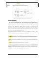
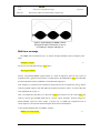
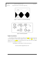
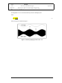
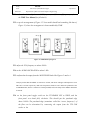
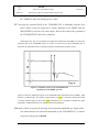
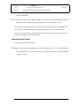
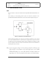
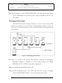
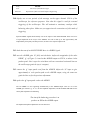
EE 460L Analog University of Nevada Las Vegas Linear Experiment 1 Department of Electrical and Computer Engineering Modulations PREPARATION 1- DSBSC GENERATION This experiment will be started by generating the double sideband suppressed carrier signal, or DSBSC. This modulated signal was probably not the first to appear in an historical context, but it is the easiest to generate. You will learn that all of these modulated signals are derived from low frequency signals, or ‘messages’. They reside in the frequency spectrum at some higher frequency, being placed there by being multiplied with a higher frequency signal, usually called ‘the carrier’. Definition of a DSBSC ( ) and Consider two sinusoids, or cosinusoids, ( ). A double sideband suppressed carrier signal, or DSBSC, is defined as their product, namely: ( ) ( ) .... 1 Generally, and in the context of this experiment, it is understood that: .... 2 Equation (1) can be expanded to give: ( ) ( ) ( ) ( ) .... 3 Equation 3 shows that the product is represented by two new signals, one on the sum frequency + ), and one on the difference frequency - ) - see Figure 1. Figure 1: Spectral components 1 EE 460L Analog University of Nevada Las Vegas Linear Modulations Experiment 1 Department of Electrical and Computer Engineering Remembering the inequality of eqn. (2) the two new components are located close to the frequency rad/s, one just below, and the other just above it. These are referred to as the lower and upper sidebands respectively. These two components were derived from a ‘carrier’ term on rad/s, and a message on rad/s. Because there is no term at carrier frequency in the product signal it is described as a double sideband suppressed carrier (DSBSC) signal. The term ‘carrier’ comes from the context of ‘double sideband amplitude modulation' (commonly abbreviated to just AM). AM is introduced later (although, historically, AM preceded DSBSC). The time domain appearance of a DSBSC , eqn. (1), in a text book is generally as shown in Figure 2. Figure 2: Eqn.(1) - a DSBSC - seen in the time domain Notice the waveform of the DSBSC in Figure 2, especially near the times when the message amplitude is zero. The fine detail differs from period to period of the message. This is because the ratio of the two frequencies and has been made non-integral. Although the message and the carrier are periodic waveforms (sinusoids), the DSBSC itself need not necessarily be periodic. Block diagram A block diagram, showing how eqn. (1) could be modeled with hardware, is shown in Figure 3 below. 2 EE 460L Analog Linear Modulations University of Nevada Las Vegas Experiment 1 Department of Electrical and Computer Engineering Figure 3: Block diagram to generate eqn. (1) with hardware. Viewing envelopes This is the first experiment dealing with a narrow band signal. Nearly all modulated signals in communications are narrow band. You will see pictures of DSB or DSBSC signals (and amplitude modulation -AM) in your text book, and will probably have a good idea of what is meant by their envelopes. You will only be able to reproduce the text book figures if the oscilloscope is set appropriately - especially with regard to the method of its synchronization. Any other methods of setting up will still be displaying the same signal, but not in the familiar form shown in text books. How is the 'correct method' of synchronization defined? With narrow-band signals, and particularly of the type to be examined in this and the other modulation experiments to follow, the following steps are recommended: 1) Use a single tone for the message, say 1 kHz. 2) Synchronize the oscilloscope to the message generator, which is of fixed amplitude, using the 'ext trig.' facility. 3) Set the sweep speed so as to display one or two periods of this message on one channel of the oscilloscope. 4) Display the modulated signal on another channel of the oscilloscope. With the recommended scheme the envelope will be stationary on the screen. In all but the most special cases the actual modulated waveform itself will not be stationary - since successive sweeps will show it in slightly different positions. So the display within the envelope - the modulated signal will be 'filled in', as in Figure 4, rather than showing the detail of Figure 2. 3 EE 460L Analog University of Nevada Las Vegas Linear Experiment 1 Department of Electrical and Computer Engineering Modulations Figure 4: Typical display of a DSBSC, with the message from which it was derived, as seen on an oscilloscope. Compare with Figure 2. Multi-tone message The DSBSC has been defined in eqn. (1), with the message identified as the low frequency term. Thus: ( ) .. . 4 For the case of a multi-tone message, ( ) ∑ ( ( ), where: ) then the corresponding DSBSC signal consists of a band of frequencies below frequencies above . Each of these bands is of width equal to the bandwidth of , and a band of ( ). The individual spectral components in these sidebands are often called side frequencies. If the frequency of each term in the expansion is expressed in terms of its difference from , and the terms are grouped in pairs of sum and difference frequencies, then there will be ‘n’ terms of the form of the right hand side of eqn. (3). Note it is assumed here that there is no DC term in result in a term at ( ). The presence of a DC term in ( ) will in the DSB signal; that is, a term at ‘carrier’ frequency. It will no longer be a double sideband suppressed carrier signal. A special case of a DSB with a significant term at carrier frequency is an amplitude modulated signal, which will be examined later. A more general definition still, of a DSBSC, would be: ( ) ( ) ... 6 4 EE 460L Analog University of Nevada Las Vegas Linear Department of Electrical and Computer Engineering Modulations where Experiment 1 ( ) is any (low frequency) message. By convention ( ) is generally understood to have a peak amplitude of unity (and typically no DC component). 2- AM GENERATION In the early days of wireless, communication was carried out by telegraphy, the radiated signal being an interrupted radio wave. Later, the amplitude of this wave was varied in sympathy with (modulated by) a speech message (rather than on/off by a telegraph key), and the message was recovered from the envelope of the received signal. The radio wave was called a ‘carrier’, since it was seen to carry the speech information with it. The process and the signal were called amplitude modulation, or ‘AM’ for short. In the context of radio communications, near the end of the 20th century, few modulated signals contain a significant component at ‘carrier’ frequency. However, despite the fact that a carrier is not radiated, the need for such a signal at the transmitter (where the modulated signal is generated), and also at the receiver, remains fundamental to the modulation and demodulation process respectively. The use of the term ‘carrier’ to describe this signal has continued to the present day. As distinct from radio communications, present day radio broadcasting transmissions do have a carrier. By transmitting this carrier the design of the demodulator, at the receiver, is greatly simplified, and this allows significant cost savings. The most common method of AM generation uses a ‘class C modulated amplifier’; such an amplifier is not available in the BASIC TIMS set of modules. It is well documented in text books. This is a ‘high level’ method of generation, in that the AM signal is generated at a power level ready for radiation. It is still in use in broadcasting stations around the world, ranging in powers from a few tens of watts to many megawatts. Unfortunately, text books which describe the operation of the class C modulated amplifier tend to associate properties of this particular method of generation with those of AM, and AM generators, in general. This gives rise to many misconceptions. The worst of these is the belief that it is impossible to generate an AM signal with a depth of modulation exceeding 100% without giving rise to serious RF distortion. You will see in this experiment that there is no problem in generating an AM signal with a depth of modulation exceeding 100%, and without any RF distortion whatsoever. But we are getting ahead of ourselves, as we have not yet even defined what AM is! 5 EE 460L Analog University of Nevada Las Vegas Linear Modulations Experiment 1 Department of Electrical and Computer Engineering Theory The amplitude modulated signal is defined as: ( ) ( ( ) ) ( ..... 7 ) ..... 8 ( ) ( ) ..... 9 Here: ‘E’ is the AM signal amplitude from eqn. (7). For modelling convenience eqn. (7) has been written into two parts in eqn. (8), where (A.B) = E. ‘m’ is a constant, which, as you will soon see, defines the ‘depth of modulation’. Typically m < 1. Depth of modulation, expressed as a percentage, is 100.m. There is no inherent restriction upon the size of ‘m’ in eqn. (7). This point will be discussed later. ‘’ and ’’ are angular frequencies in rad/s, where 300 Hz to 3000 Hz; and is a low, or message frequency, say in the range is a radio, or relatively high, ‘carrier’ frequency. In TIMS the carrier frequency is generally 100 kHz. Notice that the term ( ) in eqn. (9) contains both a DC component and an AC component. As will be seen, it is the DC component which gives rise to the term at - the ‘carrier’ - in the AM signal. The AC term ‘ ( )’ is generally thought of as the message, and is sometimes written as ( ). But strictly speaking, to be compatible with other mathematical derivations, the whole of the low frequency term ( ) should be considered the message. Thus: ( ) ( ) ... 10 Figure 5 below illustrates what the oscilloscope will show if displaying the AM signal. A block diagram representation of eqn. (8) is shown in Figure 6 below. In the experiment you will model eqn. (8) by the arrangement of Figure 6. The depth of modulation will be set to exactly 100% (m = 1). You will gain an appreciation of the meaning of ‘depth of modulation’, and you will learn how to set other values of ‘m’, including cases where m > 1. The signals in eqn. (8) are expressed as voltages in the time domain. You will model them in two parts, as written in eqn. (9). 6 EE 400L Analog Linear Modulations University of Nevada Las Vegas Experiment#1 Department of Electrical and Computer Engineering Figure 5 - AM, with m = 1, as seen on the oscilloscope Figure 6: Generation of equation 8 Depth of modulation 100% amplitude modulation is defined as the condition when soon become apparent. It requires that the amplitude of the DC ( amplitude of the AC part ( . Just what this means will ) part of ( ) is equal to the ). This means that their ratio is unity at the output of the ADDER, which forces ‘m’ to a magnitude of exactly unity. By aiming for a ratio of unity it is thus not necessary to know the absolute magnitude of A at all. 7 EE 400L Analog University of Nevada Las Vegas Linear Experiment#1 Department of Electrical and Computer Engineering Modulations Measurement of ‘m’ The magnitude of ‘m’ can be measured directly from the AM display itself. Thus: ( ) ( ) .... 11 where P and Q are as defined in Figure 7. Figure 7: Oscilloscope display for the case m = 0.5 8 EE 400L Analog University of Nevada Las Vegas Linear Modulations Experiment#1 Department of Electrical and Computer Engineering 3- SSB GENERATION There are three well known methods of SSB generation using analog techniques, namely the filter method, the phasing method, and Weaver’s method. This experiment will study the phasing method. Filter method We have already modeled a DSBSC signal. An SSB signal may be derived from this by the use of a suitable bandpass filter –commonly called, in this application, an SSB sideband filter. This, the filter method, is probably the most common method of SSB generation. Mass production has given rise to low cost, yet high performance, filters. But these filters are generally only available at ‘standard’ frequencies (for example 455 kHz, 10.7 MHz) and SSB generation by the filter method at other frequencies can be expensive. For this reason TIMS no longer has a 100 kHz SSB filter module, although a decade ago these were in mass production and relatively inexpensive. Phasing method The phasing method of SSB generation, which is the subject of this experiment, does not require an expensive filter, but instead an accurate phasing network, or quadrature phase splitter (QPS). It is capable of acceptable performance in many applications. The QPS operates at baseband, no matter what the carrier frequency (either intermediate or final), in contrast to the filter of the filter method. SSB signal ( ), a DSBSC signal is defined by: Recall that, for a single tone message ( ) ( ( ) ) ....12 ( ) .... 13 ....14 When, say, the lower sideband (LSB) is removed, by what ever method, then the upper sideband (USB) remains. ( ) .... 15 9 EE 400L Analog University of Nevada Las Vegas Linear Experiment#1 Department of Electrical and Computer Engineering Modulations This is a single frequency component at frequency ( ) ⁄( )Hz. It is a (co)sine wave. Viewed on an oscilloscope, with the time base set to a few periods of , it looks like any other sine wave. What is its envelope? The USB signal of eqn. (15) can be written in the following form: ( ) ( ) ( ) .... 16 The envelope has been defined as: ( ) .... 17 [from eqn. (15)] .... 18 Thus the envelope is a constant (ie., a straight line) and the oscilloscope, correctly set up, will show a rectangular band of color across the screen. This result may seem at first confusing. One tends to ask: ‘where is the message information’ ? Answer: the message amplitude information is contained in the amplitude of the SSB, and the message frequency information is contained in the frequency offset, from , of the SSB. An SSB derived from a single tone message is a very simple example. When the message contains more components the SSB envelope is no longer a straight line. Here is an important finding ! An ideal SSB generator, with a single tone message, should have a straight line for an envelope. Any deviation from this suggests extra components in the SSB itself. If there is only one extra component, say some ‘leaking’ carrier, or an unwanted sideband not completely suppressed, then the amplitude and frequency of the envelope will identify the amplitude and frequency of the unwanted component. A most important characteristic of any SSB generator is the amount of out-of-band energy it produces, relative to the wanted output. In most cases this is determined by the degree to which the 1 0 EE 400L Analog University of Nevada Las Vegas Linear Modulations Experiment#1 Department of Electrical and Computer Engineering unwanted sideband is suppressed. A ratio of wanted-to-unwanted output power of 40 dB was once considered acceptable commercial performance; but current practice is likely to call for a suppression of 60 dB or more, which is not a trivial result to achieve. Phasing generator The phasing method of SSB generation is based on the addition of two DSBSC signals, so phased that their upper sidebands (say) are identical in phase and amplitude, whilst their lower sidebands are of similar amplitude but opposite phase. The two out-of-phase sidebands will cancel if added; alternatively the in-phase sidebands will cancel if subtracted. The principle of the SSB phasing generator is illustrated in Figure 8. o Notice that there are two 90 phase changers. One operates at carrier frequency, the other at message frequencies. The carrier phase changer operates at a single, fixed frequency, rad/s. Figure 8: Principle of the SSB Phasing Generator The message is shown as a single tone at frequency rad/s. But this can lie anywhere within the o frequency range of speech, which covers several octaves. A network providing a constant 90 phase shift over this frequency range is very difficult to design. This would be a wideband phase shifter, or Hilbert transformer. In practice a wideband phase splitter is used. This is shown in the arrangement of Figure 9. 1 1 EE 400L Analog Linear Modulations University of Nevada Las Vegas Experiment#1 Department of Electrical and Computer Engineering Figure 9: Practical realization of the SSB phasing generator The wideband phase splitter consists of two complementary networks - say I (in-phase) and Q (quadrature). When each network is fed from the same input signal the phase difference between the o two outputs is maintained at 90 . Note that the phase difference between the common input and either of the outputs is not specified; it is not independent of frequency. Study Figures 8 and 9 to ensure that you appreciate the difference. At the single frequency rad/s the arrangements of Figure 8 and Figure 9 will generate two DSBSC. These are of such relative phases as to achieve the cancellation of one sideband, and the reinforcement of the other, at the summing output. You should be able to confirm this. You could use graphical methods (phasors) or trigonometrical analysis. The QPS may be realized as either an active or passive circuit, and depends for its performance on the accuracy of the components used. Over a wide band of audio frequencies, and for a common input, it maintains a phase difference between the two outputs of 90 degrees, with a small frequencydependent error (typically equiripple). Performance Criteria As stated earlier, one of the most important measures of performance of an SSB generator is its ability to eliminate (suppress) the unwanted sideband. To measure the ratio of wanted-to-unwanted sideband suppression directly requires a SPECTRUM ANALYSER. In commercial practice these instruments are very expensive, and their purchase cannot always be justified merely to measure an SSB generator performance. 1 2 EE 460L Analog University of Nevada Las Vegas Linear Modulations Experiment#1 Department of Electrical and Computer Engineering As always, there are indirect methods of measurement. One such method depends upon a measurement of the SSB envelope, as already hinted. Suppose that the output of an SSB generator, when the message is a single tone of frequency rad/s, consists only of the wanted sideband W and a small amount of the unwanted sideband U. It may be shown that, for U << W, the envelope is nearly sinusoidal and of a frequency equal to the frequency difference of the two components. Thus the envelope frequency is rad/s. Figure 10: Measuring sideband suppression via the envelope It is a simple matter to measure the peak-to-peak and the trough-to-trough amplitudes, giving twice P, and twice Q, respectively. Then: … 19 … 20 as seen from the phasor diagram. This leads directly to: (dB) …21 U is in fact the sum of several small components then an estimate of the wanted to unwanted power ratio can still be made. Note that it would be greater (better) than for the case where U is a single component. A third possibility, the most likely in a good design, is that the envelope becomes quite complex, with little or no stationary component at either or /2; in this case the unwanted component(s) are most likely system noise. 1 3 EE 460L Analog Linear Modulations University of Nevada Las Vegas Experiment#1 Department of Electrical and Computer Engineering Make a rough estimate of the envelope magnitude, complex in shape though it may well be, and from this can be estimated the wanted to unwanted suppression ratio, using eqn.(21). This should turn out to be better than 26 dB in TIMS, in which case the system is working within specification. The TIMS QPS module does not use precision components, nor is it aligned during manufacture. It gives only moderate sideband suppression, but it is ideal for demonstration purposes. Within the ‘working frequency range’ of the QPS the phase error from 90 between the two outputs will vary with frequency (theoretically in an equi-ripple manner). PRELAB DSBSC Generation Simulating the DSBSC Submit a PSPICE simulation of the block diagram shown in Figure 3. Use sinusoidal voltage sources for both the message and the carrier signal with amplitude of 5V and frequency of 1 kHz and 100 kHz respectively. Use transient analysis for the simulation. Submit your schematics and waveforms. 1 4 Analog Linear Modulations EE 460L University of Nevada Las Vegas Department of Electrical and Computer Engineering 1 5 Experiment#1 EE 460L Analog University of Nevada Las Vegas Linear Modulations Experiment#1 Department of Electrical and Computer Engineering EXPERIMENT 1- DSBSC Generation Preparing the model Figure 3 shows a block diagram of a system suitable for generating DSBSC derived from a single tone message. Figure 11 shows how to model this block diagram with TIMS. Figure 11: Pictorial of block diagram of Figure 3 The signal ( ), of fixed amplitude A, from the AUDIO OSCILLATOR, represents the single tone message. A signal of fixed amplitude from this oscillator is used to synchronize the oscilloscope. The signal ( ), of fixed amplitude B and frequency exactly 100 kHz, comes from the MASTER SIGNALS panel. This is the TIMS high frequency, or radiosignal. Text books will refer to it as the 'carrier signal'. The amplitudes A and B are nominally equal, being from TIMS signal sources. They are suitable as inputs to the MULTIPLIER, being at the TIMS ANALOG REFERENCE LEVEL. The output from the MULTIPLIER will also be, by design of the internal circuitry, at this nominal level. There is no need for any amplitude adjustment. It is a very simple model. 1 6 EE 460L Analog University of Nevada Las Vegas Linear Experiment#1 Department of Electrical and Computer Engineering Modulations T1 patch up the arrangement of Figure 11. Notice that the oscilloscope is triggered by the message, not the DSBSC itself (nor, for that matter, by the carrier). T2 use the FREQUENCY COUNTER to set the AUDIO OSCILLATOR to about 1 kHz Figure 2 shows the way most text books would illustrate a DSBSC signal of this type. But the display you have in front of you is more likely to be similar to that of Figure 4. Signal amplitude T3 measure and record the amplitudes A and B of the message and carrier signals at the inputs to the MULTIPLIER. The output of this arrangement is a DSBSC signal, and is given by: ( ) ( ) … 22 The peak-to-peak amplitude of the display is: peak-to-peak … 23 volts Here 'k' is a scaling factor, a property of the MULTIPLIER. One of the purposes of this experiment is to determine the magnitude of this parameter. Now: T4 measure the peak-to-peak amplitude of the DSBSC Since you have measured both A and B already, you have now obtained the magnitude of the MULTIPLIER scale factor 'k'; thus: ( ) ( ) … 24 Note that 'k' is not a dimensionless quantity. Fine detail in the time domain The oscilloscope display will not in general show the fine detail inside the DSBSC, yet many textbooks will do so, as in Figure 2. Figure 2 would be displayed by a single sweep across the screen. The normal laboratory oscilloscope cannot retain and display the picture from a single sweep. Subsequent sweeps will all be slightly different, and will not coincide when superimposed. 1 7 EE 460L Analog University of Nevada Las Vegas Linear Modulations Experiment#1 Department of Electrical and Computer Engineering To make consecutive sweeps identical, and thus to display the DSBSC as depicted in Figure 2, it is necessary that ‘µ’ be a sub-multiple of ‘’. This special condition can be arranged with TIMS by choosing the '2 kHz MESSAGE' sinusoid from the fixed MASTER SIGNALS module. The frequency of this signal is actually 100/48 kHz (approximately 2.08 kHz), an exact sub-multiple of the carrier frequency. Under these special conditions the fine detail of the DSBSC can be observed. T5 obtain a display of the DSBSC similar to that of Figure 2. A sweep speed of, say, 50ms/cm is a good starting point. Overload When designing an analog system, signal overload must be avoided at all times. Analog circuits are expected to operate in a linear manner, in order to reduce the chance of the generation of new frequencies. This would signify non-linear operation. A multiplier is intended to generate new frequencies. In this sense it is a non-linear device. Yet it should only produce those new frequencies which are wanted–any other frequencies are deemed unwanted. A quick test for unintended (non-linear) operation is to use it to generate a signal with a known shape -a DSBSC signal is just such a signal. Presumably so far your MULTIPLIER module has been behaving ‘linearly’. T6 insert a BUFFER AMPLIFIER in one or other of the paths to the MULTIPLIER, and increase the input amplitude of this signal until overload occurs. Sketch and describe what you see. Bandwidth Equation (3) shows that the DSBSC signal consists of two components in the frequency domain, spaced above and below by rad/s. With the TIMS BASIC SET of modules, and a DSBSC based on a 100 kHz carrier, you can make an indirect check on the truth of this statement. Attempting to pass the DSBSC through a 60 kHz LOWPASS FILTER will result in no output, evidence that the statement has some truth in it - all components must be above 60 kHz. 1 8 EE 460L Analog University of Nevada Las Vegas Linear Modulations Experiment#1 Department of Electrical and Computer Engineering A convincing proof can be made with the 100 kHz CHANNEL FILTERS module. Passage through any of these filters will result in no change to the display (see alternative spectrum check later in this experiment). Using only the resources of the TIMS BASIC SET of modules a convincing proof is available if the carrier frequency is changed to, say, 10 kHz. This signal is available from the analog output of the VCO, and the test setup is illustrated in Figure 12 below. Lowering the carrier frequency puts the DSBSC in the range of the TUNEABLE LPF. Figure 12: Checking the spectrum of a DSBSC signal T7 read about the VCO module in the TIMS User Manual. Before plugging the VCO in to the TIMS SYSTEM UNIT set the on-board switch to VCO. Set the front panel frequency range selection switch to ‘LO’. T8 read about the TUNEABLE LPF in the TIMS User Manual. T9 set up an arrangement to check out the TUNEABLE LPF module. Use the VCO as a source of sine wave input signal. Synchronize the oscilloscope to this signal. Observe input to, and output from, the TUNEABLE LPF. T10 set the front panel GAIN control of the TUNEABLE LPF so that the gain through the filter is unity. 1 9 EE 460L Analog University of Nevada Las Vegas Linear Modulations Experiment#1 Department of Electrical and Computer Engineering T11 confirm the relationship between VCO frequency and filter cutoff frequency (refer to the TIMS User Manual for full details). T12 set up the arrangement of Figure 12. Your model should look something like that of Figure 13, where the arrangement is shown modeled by TIMS. Figure 13: TIMS model of Figure 6 T13 adjust the VCO frequency to about 10 kHz T14 set the AUDIO OSCILLATOR to about 1 kHz. T15 confirm that the output from the MULTIPLIER looks like Figures 2 and/or 4. Analysis predicts that the DSBSC is centered on 10 kHz, with lower and upper sidefrequencies at 9.0 kHz and 11.0 kHz respectively. Both side frequencies should fit well within the passband of the TUNEABLE LPF, when it is tuned to its widest passband, and so the shape of the DSBSC should not be altered. T16 set the front panel toggle switch on the TUNEABLE LPF to WIDE, and the front panel TUNE knob fully clockwise. This should put the passband edge above 10 kHz. The passband edge (sometimes called the ‘corner frequency’) of the filter can be determined by connecting the output from the TTL CLK socket to the 2 0 Analog Linear Modulations EE 400L University of Nevada Las Vegas Experiment#1 Department of Electrical and Computer Engineering FREQUENCY COUNTER. It is given by dividing the counter readout by 100 (in the ‘NORMAL’ mode the dividing factor is 880). T17 note that the passband GAIN of the TUNEABLE LPF is adjustable from the front panel. Adjust it until the output has a similar amplitude to the DSBSC from the MULTIPLIER (it will have the same shape). Record the width of the passband of the TUNEABLE LPF under these conditions. Assuming the last Task was performed successfully this confirms that the DSBSC lies below the passband edge of the TUNEABLE LPF at its widest. You will now use the TUNEABLE LPF to determine the sideband locations. T should be possible to confirm this by Figure 14 below. Figure 14: Amplitude response of the TUNEABLE LPF superimposed on the DSBSC spectrum. Figure 14 shows the amplitude response of the TUNEABLE LPF superimposed on he DSBSC, when based on a 1 kHz message. The drawing is approximately to scale. It is clear that, with the filter tuned as shown (passband edge just above the l ower sidefrequency), it is possible to attenuate the upper sideband by 50 dB and etain the lower sideband effectively unchanged. T18 make a sketch to explain the meaning of the transition bandwidth of a lowpass filter. You should measure the transition bandwidth of your UNEABLE LPF, or instead accept the value given in manual. 2 1 EE 400L Analog Linear Modulations University of Nevada Las Vegas Experiment#1 Department of Electrical and Computer Engineering T19 lower the filter passband edge until there is a just-noticeable change to the DSBSC output. Record the filter passband edge as f A. You have located the upper edge of the DSBSC at ( + ) rad/s. T20 lower the filter passband edge further until there is only a sinewave output. You have isolated the component on ( - ) rad/s. Lower the filter passband edge still further until the amplitude of this sinewave just starts to reduce. Record the filter passband edge as fB . T21 again lower the filter passband edge, just enough so that there is no significant output. Record the filter passband edge as fC T22 from a knowledge of the filter transition band ratio, and the measurements fA and fB, estimate the location of the two sidebands and compare with expectations. You could use fC as a cross-check. 2 2 EE 400L Analog University of Nevada Las Vegas Linear Modulations Experiment#1 Department of Electrical and Computer Engineering 2- AM GENERATION Low frequency term a(t) To generate a voltage defined by eqn. (8) you need first to generate the term a(t). ( ) ( ) … 25 Note that this is the addition of two parts, a DC term and an AC term. Each part may be of any convenient amplitude at the input to an ADDER. The DC term comes from the VARIABLE DC module, and will be adjusted to the amplitude ‘A’ at the output of the ADDER. The AC term ( ) will come from an AUDIO OSCILLATOR, and will be adjusted to the amplitude ‘A.m’ at the output of the ADDER. Carrier supply c(t) The 100 kHz carrier c(t) comes from the MASTER SIGNALS module. ( ) ( ) … 26 The block diagram of Figure 6, which models the AM equation, is shown modelled by TIMS in Figure 15 below. To build the model: T23 first patch up according to Figure 15, but omit the input X and Y connections to the MULTIPLIER. Connect to the two oscilloscope channels using the SCOPE SELECTOR, as shown. T24 use the FREQUENCY COUNTER to set the AUDIO OSCILLATOR to about 1 kHz. T25 switch the SCOPE SELECTOR to CH1-B, and look at the message from the AUDIO OSCILLATOR. Adjust the oscilloscope to display two or three periods of the sine wave in the top half of the screen. 2 3 EE 400L Analog University of Nevada Las Vegas Linear Modulations Experiment#1 Department of Electrical and Computer Engineering Figure 15: TIMS model of the block diagram of Figure Now start adjustments by setting up a(t), as defined by eqn. (25), and with m = 1. T26 turn both g and G fully anti-clockwise. This removes both the DC and the AC parts of the message from the output of the ADDER. T27 switch the scope selector to CH1-A. This is the ADDER output. Switch the oscilloscope amplifier to respond to DC if not already so set, and the sensitivity to about 0.5 volt/cm. Locate the trace on a convenient grid line towards the bottom of the screen. Call this the zero reference grid line. T28 turn the front panel control on the VARIABLE DC module almost fully anticlockwise (not critical). This will provide an output voltage of about minus 2 volts. The ADDER will reverse its polarity, and adjust its amplitude using the ‘g’ gain control. 2 4 EE 400L Analog University of Nevada Las Vegas Linear Modulations Experiment#1 Department of Electrical and Computer Engineering T29 whilst noting the oscilloscope reading on CH1-A, rotate the gain ‘g’ of the ADDER clockwise to adjust the DC term at the output of the ADDER to exactly 2 cm above the previously set zero reference line. This is ‘A’ volts. You have now set the magnitude of the DC part of the message to a known amount. This is about 1 volt, but exactly 2 cm, on the oscilloscope screen. You must now make the AC part of the message equal to this, so that the ratio Am/A will be unity. This is easy: T30 whilst watching the oscilloscope trace of CH1-A rotate the ADDER gain control ‘G’ clockwise. Superimposed on the DC output from the ADDER will appear the message sine wave. Adjust the gain G until the lower crests of the sine wave are EXACTLY coincident with the previously selected zero reference grid line. The sine wave will be centered exactly A volts above the previously-chosen zero reference, and so its amplitude is A. Now the DC and AC, each at the ADDER output, are of exactly the same amplitude A. Thus: … 27 and so: … 28 You have now modeled MULTIPLIER, as required by eqn. (6). ( ) , with . This is connected to one input of the T31 connect the output of the ADDER to input X of the MULTIPLIER. Make sure the MULTIPLIER is switched to accept DC. Now prepare the carrier signal: ( ) ( ) … 29 2 5 EE 400L Analog Linear Modulations University of Nevada Las Vegas Experiment#1 Department of Electrical and Computer Engineering T32 connect a 100 kHz analog signal from the MASTER SIGNALS module to input Y of the MULTIPLIER. T33 connect the output of the MULTIPLIER to the CH2-A of the SCOPE SELECTOR. Adjust the oscilloscope to display the signal conveniently on the screen. Since each of the previous steps has been completed successfully, then at the MULTIPLIER output will be the 100% modulated AM signal. It will be displayed on CH2-A. It will look like Figure 5. Notice the systematic manner in which the required outcome was achieved. Failure to achieve the last step could only indicate a faulty MULTIPLIER? Agreement with theory It is now possible to check some theory. T34 measure the peak-to-peak amplitude of the AM signal, with m = 1, and confirm that this magnitude is as predicted, knowing the signal levels into the MULTIPLIER, and its ‘k’ factor. 2 6 Analog Linear Modulations EE 400L University of Nevada Las Vegas Experiment#1 Department of Electrical and Computer Engineering 3- SSB GENERATION QPS Refer to the TIMS User Manual for information about the QUADRATURE PHASE SPLITTER - the ‘QPS’. Before patching up an SSB phasing generator system, first examine the performance of the QUADRATURE PHASE SPLITTER module. This can be done with the arrangement of Figure 16. Figure 16: Arrangement to check QPS performance With the oscilloscope adjusted to give equal gain in each channel it should show a circle. This will give a quick confirmation that there is a phase difference of approximately 90 degrees between the two output sine waves at the measurement frequency. Phase or amplitude errors should be too small for this to degenerate visibly into an ellipse. The measurement will also show the bandwidth over which the QPS is likely to be useful. T35 set up the arrangement of Figure 16. The oscilloscope should be in X-Y mode, with equal sensitivity in each channel. For the input signal source use an AUDIO OSCILLATOR module. For correct QPS operation the display should be an approximate circle. We will not attempt to measure phase error from this display. 2 7 EE 400L Analog University of Nevada Las Vegas Linear Modulations Experiment#1 Department of Electrical and Computer Engineering T36 vary the frequency of the AUDIO OSCILLATOR, and check that the approximate circle is maintained over at least the speech range of frequencies. Record your observations. Phasing generator model When satisfied that the QPS is operating satisfactorily, you are now ready to model the SSB generator. Once patched up, it will be necessary to adjust amplitudes and phases to achieve the desired result. A hit-and-miss method can be used, but a systematic method is recommended, and will be described now. Figure 17: SSB phasing generator model T37 patch up a model of the phasing SSB generator, following the arrangement illustrated in Figure 17. Remember to set the on-board switch of the PHASE SHIFTER to the ‘HI’ (100 kHz) range before plugging it in. T38 set the AUDIO OSCILLATOR to about 1 kHz T39 switch the oscilloscope sweep to ‘auto’ mode, and connect the ‘ext trig’ to an output from the AUDIO OSCILLATOR. It is now synchronized to the message. 2 8 Analog Linear Modulations EE 400L University of Nevada Las Vegas Experiment#1 Department of Electrical and Computer Engineering T40 display one or two periods of the message on the upper channel CH1-A of the oscilloscope for reference purposes. Note that this signal is used for external triggering of the oscilloscope. This will maintain a stationary envelope while balancing takes place. Make sure you appreciate the convenience of this mode of triggering. Separate DSBSC signals should already exist at the output of each MULTIPLIER. These need to be of equal amplitudes at the output of the ADDER. You will set this up, at first approximately and independently, then jointly and with precision, to achieve the required output result. T41 check that out of each MULTIPLIER there is a DSBSC signal. T42 turn the ADDER gain ‘G’ fully anti-clockwise. Adjust the magnitude of the other DSBSC, ‘g’, of Figure 5, viewed at the ADDER output on CH2-A, to about 4 volts peak-to-peak. Line it up to be coincident with two convenient horizontal lines on the oscilloscope graticule (say 4 cm apart). T43 remove the ‘g’ input patch cord from the ADDER. Adjust the ‘G’ input to give approximately 4 volts peak-to-peak at the ADDER output, using the same two graticule lines as for the previous adjustment. T44 replace the ‘g’ input patch cord to the ADDER. The two DSBSC are now appearing simultaneously at the ADDER output. Now use one of the ADDER gain controls (‘g’ or ‘G’) for the amplitude adjustment, and the PHASE SHIFTER for the carrier phase adjustment for balancing. The aim of the balancing procedure is to produce an SSB at the ADDER output. The amplitude and phase adjustments are non-interactive. 2 9 EE 400L Analog University of Nevada Las Vegas Linear Experiment#1 Department of Electrical and Computer Engineering Modulations Performance measurement Since the message is a sine wave, the SSB will also be a sine wave when the system is correctly adjusted. Make sure you agree with this statement before proceeding. The oscilloscope sweep speed should be such as to display a few periods of the message across the full screen. This is so that, when looking at the SSB, a stationary envelope will be displayed. Until the system is adjusted the display will look more like a DSBSC, or even an AM, than an SSB. Remote from balance the envelope should be stationary, but perhaps not sinusoidal. As the balance condition is approached the envelope will become roughly sinusoidal, and its amplitude will reduce. Remember that the pure SSB is going to be a sinewave. As discussed earlier, if viewed with an appropriate time scale, which you have already set up, this should have a constant (‘flat’) envelope. This is what the balancing procedure is aiming to achieve. T45 balance the SSB generator so as to minimize the envelope amplitude. During the process it may be necessary to increase the oscilloscope sensitivity as appropriate, and to shift the display vertically so that the envelope remains on the screen. T46 when the best balance has been achieved, record results, using Figure 10 as a guide. Although you need the magnitudes P and Q, it is more accurate to measure a) 2P directly, which is the peak-to-peak of the SSB b) Q indirectly, by measuring (P-Q), which is the peak-to-peak of the envelope. As already stated, the TIMS QPS is not a precision device, and a sideband suppression of better than 26 dB is unlikely. You will not achieve a perfectly flat envelope. But its amplitude may be small or comparable with respect to the noise floor of the TIMS system. The presence of a residual envelope can be due to any one or more of: Leakage of a component at carrier frequency (a fault of one or other MULTIPLIER ) 3 0 EE 400L Analog Linear Modulations University of Nevada Las Vegas Experiment#1 Department of Electrical and Computer Engineering Incomplete cancellation of the unwanted sideband due to imperfections of the QPS. Distortion components generated by the MULTIPLIER modules. Other factors; can you suggest any? Any of the above will give an envelope ripple period comparable with the period of the message, rather than that of the carrier. Do you agree with this statement? If the envelope shape is sinusoidal, and the frequency is: Twice that of the message, then the largest unwanted component is due to incomplete cancellation of the unwanted sideband. The same as the message, then the largest unwanted component is at carrier frequency (‘carrier leak’). If it is difficult to identify the shape of the envelope, then it is probably a combination of these two; or just the inevitable system noise. An engineering estimate must then be made of the wanted-tounwanted power ratio (which could be a statement of the form ‘better than 45 dB’), and an attempt made to describe the nature of these residual signals. T47 if not already done so, use the FREQUENCY COUNTER to identify your sideband as either upper (USSB) or lower (LSSB). Record also the exact frequency of the message sine wave from the AUDIO OSCILLATOR. From a knowledge of carrier and message frequencies, confirm your sideband is on one or other of the expected frequencies. To enable the sideband identification to be confirmed analytically (see Question below) you will need to make a careful note of the model configuration, and in particular the sign and magnitude of the phase shift introduced by the PHASE SHIFTER, and the sign of the phase difference between the I and Q outputs of the QPS. Without these you cannot check results against theory. 3 1 EE 400L Analog University of Nevada Las Vegas Linear Experiment#1 Department of Electrical and Computer Engineering Modulations TUTORIAL QUESTIONS Q1 how would you answer the question ‘what is the frequency of the signal ( ) ( )’ ? Q2 what would the FREQUENCY COUNTER read if connected to the signal ( ) ( ( ) ( ) )? Q3 is a DSBSC signal periodic? Q4 carry out the trigonometry to obtain the spectrum of a DSBSC signal when the message consists of three tones, namely: ( ) ( ) ( ) Show that it is the linear sum of three DSBSC, one for each of the individual message components. Q5 derive eqn.(11), which relates the magnitude of the parameter ‘m’ to the peak-to-peak and trough-to-trough amplitudes of the AM signal. Q6 there is no difficulty in relating the formula of eqn. (11) to the waveform of Figure 7 for values of ‘m’ less than unity. But the formula is also valid for m > 1, provided the magnitudes P and Q are interpreted correctly. By varying ‘m’, and watching the waveform, can you see how P and Q are defined for m > 1? Q7 an AM signal, depth of modulation 100% from a single tone message, has a peak-topeak amplitude of 4 volts. What would an RMS voltmeter read if connected to this signal? Q8 what simple modification(s) to your model would change the output from the current to the opposite sideband? 3 2 Analog Linear Modulations EE 400L University of Nevada Las Vegas Experiment#1 Department of Electrical and Computer Engineering Q9 is the QPS an approximation to the Hilbert transformer? Explain. Q10 sketch the output of an SSB transmitter, as seen in the time domain, when the message is two audio tones of equal amplitude. Discuss. 3 3