1
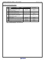
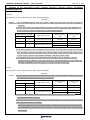
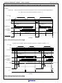
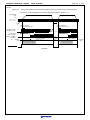
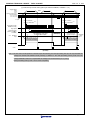
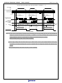
Date: Oct. 11, 2012 RENESAS TECHNICAL UPDATE 1753, Shimonumabe, Nakahara-ku, Kawasaki-shi, Kanagawa 211-8668 Japan Renesas Electronics Corporation Product Category Title MPU/MCU Document No. TN-RL*-A003A/E Correction for Incorrect Description Notice RL78/G13 Descriptions in the Hardware User’s Manual Rev. 2.00 Changed Information Category Technical Notification Reference Document RL78/G13 User’s Manual: Hardware Rev. 2.00 R01UH0146EJ0200 (February 2012) Rev. 1.00 Lot No. Applicable Product RL78/G13 Group R5F100xxx, R5F101xxx All lot This document describes misstatements found in the RL78/G13 User’s Manual: Hardware Rev. 2.00 (R01UH0146EJ0200). Corrections Applicable Item High-speed on-chip oscillator frequency selection register (HOCODIV) Applicable Page Page 289 A/D converter mode register 0 (ADM0) Page 474 Caution on A/D conversion time selection Pages 478 to 481 Figure 20-2. Timing of Generation of Internal Reset Signal by Power-on-reset Circuit and Voltage Detector 25.4 Overview of the data flash memory 25.7 Flash memory programming by self-programming 29.8 Flash memory programming characteristics Contents Cautions changed Incorrect descriptions revised Incorrect descriptions revised Pages 875, 876 Incorrect descriptions revised Page 933 Cautions added Page 942 Cautions added Page 1032 Specifications determined Document Improvement The above corrections will be made for the next revision of the User’s Manual: Hardware. (c) 2012. Renesas Electronics Corporation. All rights reserved. Page 1 of 13 Date: Oct. 11, 2012 RENESAS TECHNICAL UPDATE TN-RL*-A003A/E Corrections in the User’s Manual: Hardware No. 1 2 3 4 5 6 7 Corrections and Applicable Items Document No. English R01UH0146EJ0200 Cautions on the high-speed on-chip oscillator frequency selection register Page 289 (HOCODIV) changed Incorrect descriptions of A/D converter Page 474 mode register 0 (ADM0) revised Incorrect descriptions of caution on A/D Pages 478 to 481 conversion time selection revised Incorrect descriptions of Figure 20-2. Timing of Generation of Internal Reset Pages 875, 876 Signal by Power-on-reset Circuit and Voltage Detector revised Cautions on 25.4 overview of the data flash Page 933 memory added Cautions on 25.7 Flash Memory Page 942 Programming by Self-Programming added Specifications of 29.8 Flash Memory Page 1032 Programming Characteristics determined Pages in this document for corrections Page 3 Page 4 Page 5 Pages 6 to 9 Page 10 Page 11 Page 12 Incorrect: Bold with underline, Correct: Gray hatched Page 2 of 13 Date: Oct. 11, 2012 RENESAS TECHNICAL UPDATE TN-RL*-A003A/E 1. Cautions on the high-speed on-chip oscillator frequency selection register (HOCODIV) changed (page 289) Incorrect: (8) High-speed on-chip oscillator frequency select register (HOCODIV) (Omitted) Cautions 1. Set the HOCODIV register within the operable voltage range both before and after changing the frequency. 2. Use the device within the voltage of the flash operation mode set by the option byte (000C2H) even after the frequency has been changed by using the HOCODIV register. Option byte (000C2H) value Flash operation mode Operating frequency Operating voltage range range CMODE1 CMODE2 0 0 LV (low-voltage main) mode 1 to 4 MHz 1.6 to 5.5 V 1 0 LS (low-speed main) mode 1 to 8 MHz 1.8 to 5.5 V 1 1 HS (high-speed main) mode 1 to 16 MHz 2.4 to 5.5 V 1 to 32 MHz 2.7 to 5.5 V 3. The device operates at the old frequency for the duration of 3 clocks after the frequency value has been changed by using the HOCODIV register. When setting of high-speed on-chip oscillator clock as system clock, and the clock oscillation stabilization wait three minutes further. 4. To change the frequency of the high-speed on-chip oscillator when X1 oscillation, external oscillation input or subclock is set for the system clock, stop the high-speed on-chip oscillator by setting bit 0 (HIOSTOP) of the CSC register to 1 and then change the frequency. Correct: (8) High-speed on-chip oscillator frequency select register (HOCODIV) (Omitted) Cautions 1. Set the HOCODIV register within the operable voltage range of the flash operation mode set in the option byte (000C2H) both before and after changing the frequency. Option byte (000C2H) value Flash operation mode CMODE1 CMODE2 0 0 LV (low-voltage main) mode 1 0 LS (low-speed main) mode 1 1 HS (high-speed main) mode Operating frequency Operating voltage range range 1 to 4 MHz 1.6 to 5.5 V 1 to 8 MHz 1.8 to 5.5 V 1 to 16 MHz 2.4 to 5.5 V 1 to 32 MHz 2.7 to 5.5 V 2. Set the HOCODIV register while the high-speed on-chip oscillator clock (fIH) is selected as the CPU/peripheral hardware clock (fCLK). 3. After the frequency has been changed using the HOCODIV register and the following transition time has been elapsed, the frequency is switched. The device operates at the frequency for the duration of 3 clocks before the frequency has been changed. The CPU/peripheral hardware clock waits for maximum 3 clocks at the frequency after the frequency has been changed. Page 3 of 13 RENESAS TECHNICAL UPDATE TN-RL*-A003A/E Date: Oct. 11, 2012 2. Incorrect descriptions of A/D converter mode register 0 (ADM0) revised (page 474) Incorrect: (2) A/D converter mode register 0 (ADM0) (Omitted) Cautions 1. Change the ADMD, FR2 to FR0, LV1, LV0, and ADCE bits while conversion is stopped or on standby (ADCS = 0). 2. Do not change the ADCE and ADCS bits from 0 to 1 at the same time by using an 8-bit manipulation instruction. Be sure to set these bits in the order described in 11.7 A/D Converter Setup Flowchart. Correct: (2) A/D converter mode register 0 (ADM0) (Omitted) Cautions 1. Change the ADMD, FR2 to FR0, LV1, and LV0 bits while conversion is stopped (ADCS = 0, ADCE = 0). 2. Do not set ADCS = 1 and ADCE = 0. 3. Do not change the ADCS and ADCE bits from 0 to 1 at the same time by using an 8-bit manipulation instruction. Be sure to set these bits in the order described in 11.7 A/D Converter Setup Flowchart. Page 4 of 13 RENESAS TECHNICAL UPDATE TN-RL*-A003A/E Date: Oct. 11, 2012 3. Incorrect descriptions of caution on A/D conversion Time Selection revised (pages 478 to 481) Incorrect: Table 11-3. A/D Conversion Time Selection (Omitted) Cautions 1. When rewriting the FR2 to FR0, LV1, and LV0 bits to other than the same data, while in the conversion stopped/conversion standby status (ADCS = 0). Correct: Table 11-3. A/D Conversion Time Selection (Omitted) Cautions 1. Rewrite the FR2 to FR0, LV1, and LV0 bits to other than the same data while conversion is stopped (ADCS = 0, ADCE = 0). Page 5 of 13 Date: Oct. 11, 2012 RENESAS TECHNICAL UPDATE TN-RL*-A003A/E 4. Incorrect descriptions of the power-on reset circuit on Figure 20-2 revised (pages 875, 876) Incorrect: Figure 20-2. Timing of Generation of Internal Reset Signal by Power-on-reset Circuit and Voltage Detector (1) When LVD is OFF (option byte 000C1H: VPOC2 = 1) Supply voltage (VDD) 1.6 V VPOR = 1.51 V (TYP.) VPDR = 1.50 V (TYP.) 0V Wait for oscillation accuracy stabilizationNote 1 Wait for oscillation accuracy stabilizationNote 1 High-speed on-chip oscillator clock (fIH) CPU Starting oscillation is specified by software Starting oscillation is specified by software High-speed system clock (fMX) (when X1 oscillation is selected) Normal operation (high-speed on-chip oscillator clock)Note 2 Reset processing Note 3 Operation stops Reset Reset processingNote 2 period (oscillation stop) Normal operation (high-speed on-chip oscillator clock)Note 2 Operation stops Internal reset signal (Omitted) Notes 3. Reset processing time: 265 to 407 s (2) When LVD is interrupt & reset mode (option byte 000C1: LVIMDS1, LVIMDS0 = 1, 0) Supply voltage (VDD) Note 3 VLVDH VLVDL 1.6 V VPOR = 1.51 V (TYP.) VPDR = 1.50 V (TYP.) 0V Wait for oscillation accuracy stabilizationNote 2 Wait for oscillation accuracy stabilizationNote 2 High-speed on-chip oscillator clock (fIH) High-speed system clock (fMX) (when X1 oscillation is selected) CPU Operation stops Starting oscillation is specified by software Starting oscillation is specified by software Normal operation (high-speed on-chip oscillator clock)Note 1 Reset processing time Note 4 Reset period (oscillation stop) Normal operation (high-speed on-chip oscillator clock)Note 1 Reset processing timeNote 4 POR processing time Operation stops POR processing time Internal reset signal INTLVI (Omitted) Notes 4. Reset processing time: 497 to 720 s Page 6 of 13 Date: Oct. 11, 2012 RENESAS TECHNICAL UPDATE TN-RL*-A003A/E Correct: Figure 20-2. Timing of Generation of Internal Reset Signal by Power-on-reset Circuit and Voltage Detector (1) Power-on-reset circuit (When LVD is OFF) (option byte 000C1H: VPOC2 = 1).) Supply voltage (VDD) 1.6V VPOR = 1.51V ( TYP.) VPDR = 1.50V ( TYP.) 0V Wait for oscillation accuracy stabilizationNote 1 Wait for oscillation accuracy stabilizationNote 1 High-speed on-chip oscillator clock (fIH) High-speed system clock (fMX) (when X1 oscillation is selected) CPU Operation stops Normal operation (high-speed on-chip oscillator clock) Note 2 Voltage stabilization wait time and Reset processing timeby POR 1.37 ms(TYP.), 2.79 msMAX.) ( Reset period (oscillation stop) Normal operation (high-speed on-chip oscillator clock) Note 2 Voltage stabilization wait time and Reset processing timeby POR 1.37 ms(TYP.), 2.79 msMAX.) ( Operation stops Internal reset signal (Omitted) Page 7 of 13 Date: Oct. 11, 2012 RENESAS TECHNICAL UPDATE TN-RL*-A003A/E (2) LVD interrupt & reset mode (option byte 000C1H/LVIMDS1, LVIMDS0 = 1, 0) Supply voltage (VDD) Note 3 VLVDH VLVDL Operating voltage range lower limit setting VPOR = 1.51V ( TYP.) VPDR = 1.50V ( TYP.) 0V Wait for oscillation accuracy stabilizationNote 2 High-speed on-chip oscillator clock (fIH) High-speed system clock (fMX) (when X1 oscillation is selected) CPU Operation stops Wait for oscillation accuracy stabilizationNote 2 Starting oscillation is specified by software Starting oscillation is specified by software Normal operation (high-speed on-chip oscillator clock)Note 1 Reset processing timeby LVDNote 4 Reset period (oscillation stop) Normal operation (high-speed on-chip oscillator clock)Note 1 Operation stops Reset processing timeby LVDNote 4 Voltage stabilization wait time and Reset processing timeby POR 1.64 ms(TYP.), 3.10 msMAX.) ( Voltage stabilization wait time and Reset processing timeby POR 1.64 ms(TYP.), 3.10 msMAX.) ( Internal reset signal INTLVI (Omitted) Note 4. The time until normal operation is started require the following “the reset processing time by LVD” required after the voltage has reached LVD detection level (VLVDH), in addition to “the reset processing time by POR” and “the voltage stabilization wait time” required after the voltage has reached VPOR (1.51 V (TYP.)). Reset processing time by LVD: 0 ms to 0.0701 ms (MAX.) Page 8 of 13 Date: Oct. 11, 2012 RENESAS TECHNICAL UPDATE TN-RL*-A003A/E (3) LVD reset mode (option byte 000C1H/LVIMDS1, LVIMDS0 = 1, 1) Supply voltage (VDD) VLVD Operating voltage range lower limit setting VPOR = 1.51 V (TYP.) VPDR = 1.50 V (TYP.) 0V Wait for oscillation accuracy stabilizationNote 2 Wait for oscillation accuracy stabilizationNote 2 Wait for oscillation accuracy stabilizationNote 2 High-speed on-chip oscillator clock (fIH) High-speed system clock (fMX) (when X1 oscillation is selected) CPU Operation stops Normal operation (high-speed on-chip oscillator clock)Note 1 Reset period (oscillation stop) Normal operation (high-speed on-chip oscillator clock)Note 1 Reset period (oscillation stop) Reset processing timeby LVD Operation stops Reset processing timeby LVD Note 3 Voltage stabilization wait time and Reset processing timeby POR 1.64 ms(TYP.), 3.10 msMAX.) ( Normal operation (high-speed on-chip oscillator clock)Note 1 Note 3 Reset processing timeby LVDNote 4 Voltage stabilization wait time and Reset processing timeby POR 1.64 ms(TYP.), 3.10 msMAX.) ( Internal reset signal (Omitted) Note 3. The time until normal operation is started require the following “the reset processing time by LVD” required after the voltage has reached LVD detection level (VLVD), in addition to “the reset processing time by POR” and “the voltage stabilization wait time” required after the voltage has reached VPOR (1.51 V (TYP.)). Reset processing time by LVD: 0 ms to 0.0701 ms (MAX.) 4. When supply voltage falls and returns after only an internal reset occurs by the voltage detection circuit (LVD), the following “the reset processing time by LVD” is required after the voltage has reached LVD detection level (VLVD). Reset processing time by LVD: 0.0511 ms (TYP.), 0.0701 ms (MAX.) Page 9 of 13 RENESAS TECHNICAL UPDATE TN-RL*-A003A/E Date: Oct. 11, 2012 5. Cautions on overview of the data flash memory added (page 933) Incorrect: An overview of the data flash memory is provided below. The data flash memory can be written to by using the flash memory programmer or an external device Programming is performed in 8-bit units Blocks can be deleted in 1 KB units The only access by CPU instructions is byte reading (1 clock + wait 3 clock cycles) Because the data flash memory is an area exclusively used for data, it cannot be used to execute instructions (code fetching) Instructions can be executed from the code flash memory while rewriting the data flash memory (That is, Back Ground Operation (BGO) is supported) Accessing the data flash memory is not possible while rewriting the code flash memory (during self programming) Because the data flash memory is stopped after a reset ends, the data flash control register (DFLCTL) must be set up in order to use the data flash memory Manipulating the DFLCTL register is not possible while rewriting the data flash memory Transition the HALT, STOP mode is not possible while rewriting the data flash memory Correct: An overview of the data flash memory is provided below. For more details of rewriting the data flash memory, refer to the RL78 Family Data Flash Library User’s Manual. The data flash memory can be written to by using the flash memory programmer or an external device Programming is performed in 8-bit units Blocks can be deleted in 1 KB units The only access by CPU instructions is byte reading (1 clock + wait 3 clock cycles) Because the data flash memory is an area exclusively used for data, it cannot be used to execute instructions (code fetching) Instructions can be executed from the code flash memory while rewriting the data flash memory (That is, Back Ground Operation (BGO) is supported) Accessing the data flash memory is not possible while rewriting the code flash memory (during self programming) Because the data flash memory is stopped after a reset ends, the data flash control register (DFLCTL) must be set up in order to use the data flash memory Manipulating the DFLCTL register is not possible while rewriting the data flash memory Transition the HALT, STOP mode is not possible while rewriting the data flash memory Cautions 1. The high-speed on-chip oscillator needs to oscillate while the data flash is being rewritten. When stopping the high-speed on-chip oscillator, oscillate the high-speed on-chip oscillator clock (HIOSTOP = 0) and execute the data flash library after 30 s elapses. Page 10 of 13 Date: Oct. 11, 2012 RENESAS TECHNICAL UPDATE TN-RL*-A003A/E 6. Cautions on Flash Memory Programming by Self-Programming added (page 942) Incorrect: 25.7 Flash Memory Programming by Self-Programming The RL78/G13 supports a self-programming function that can be used to rewrite the flash memory via a user program. Because this function allows a user application to rewrite the flash memory by using the RL78/G13 self-programming library, it can be used to upgrade the program in the field. Cautions 1. 2. The self-programming function cannot be used when the CPU operates with the subsystem clock To prohibit an interrupt during self-programming, in the same way as in the normal operation mode, execute the self-programming library in the state where the IE flag is cleared (0) by the DI instruction. To enable an interrupt, clear (0) the interrupt mask flag to accept in the state where the IE flag is set (1) by the EI instruction, and then execute the self-programming library. (Omitted) Correct: 25.7 Flash Memory Programming by Self-Programming The RL78/G13 supports a self-programming function that can be used to rewrite the flash memory via a user program. Because this function allows a user application to rewrite the flash memory by using the RL78/G13 self-programming library, it can be used to upgrade the program in the field. Cautions 1. 2. The self-programming function cannot be used when the CPU operates with the subsystem clock To prohibit an interrupt during self-programming, in the same way as in the normal operation mode, execute the self-programming library in the state where the IE flag is cleared (0) by the DI instruction. To enable an interrupt, clear (0) the interrupt mask flag to accept in the state where the IE flag is set (1) by the EI instruction, and then execute the self-programming library. (Omitted) 4. The high-speed on-chip oscillator needs to oscillate during self-programming. When stopping the high-speed on-chip oscillator, oscillate the high-speed on-chip oscillator clock (HIOSTOP = 0) and execute the self-programming library after 30 s elapses. Page 11 of 13 Date: Oct. 11, 2012 RENESAS TECHNICAL UPDATE TN-RL*-A003A/E 7. Specifications of the Flash Memory Programming Characteristics determined (page 1032) Incorrect: 29.8 Flash Memory Programming Characteristics (TA = −40 to +85°C, 1.8 V ≤ EVDD0 = EVDD1 ≤ VDD ≤ 5.5 V, VSS = EVSS0 = EVSS1 = 0 V) Parameter Symbol Conditions MIN. System clock frequency fCLK 1.8 V VDD 5.5 V Code flash memory rewritable times Cerwr 1 erase + 1 write after Retained for 20 the erase is regarded years (Self/serial as 1 rewrite. programming) The retaining years Retained for 1 Note 1 Data flash memory rewritable times TYP. 1 MAX. Unit 32 MHz 1,000 Times Note 2 are until next rewrite after the rewrite. 1,000,000 years (Self/serial Note 2 programming) Retained for 5 100,000 years (Self/serial Note 2 programming) Notes 1. 128-pin products, and flash ROM: 384 to 512 KB of 44- to 100-pin products, these specifications show target values, which may change after device evaluation. 2. When using flash memory programmer and Renesas Electronics self programming library Correct: 29.8 Flash Memory Programming Characteristics (TA = −40 to +85°C, 1.8 V ≤ EVDD0 = EVDD1 ≤ VDD ≤ 5.5 V, VSS = EVSS0 = EVSS1 = 0 V) Parameter System clock frequency Code flash memory rewritable times Symbol fCLK Cerwr Conditions MIN. 1.8 V VDD 5.5 V TYP. 1 Retaining years: 20 years Ta = 85 C Note 3 Retaining year: 1 year Ta = 25 C Note 3 Retaining years: 5 years Ta = 85 C Note 3 100,000 Retaining years: 20 years Ta = 85 C Note 3 10,000 1,000 MAX. Unit 32 MHz Times Note 1,2,3 Data flash memory rewritable times 1,000,000 Note 1,2,3 Notes 1. 1 erase + 1 write after the erase is regarded as 1 rewrite. The retaining years are until next rewrite after the rewrite. 2. When using flash memory programmer and Renesas Electronics self programming library. 3. This characteristics is shown as the flash memory characteristics and based on Renesas Electronics reliability test. Page 12 of 13 RENESAS TECHNICAL UPDATE TN-RL*-A003A/E Date: Oct. 11, 2012 Issued Document History RL78/G13 User’s Manual: Hardware Rev 2.00, incorrect description notice, issued document history Document Number TN-RL*-A003A/E Issue Date Oct. 11, 2012 Description First edition issued Incorrect descriptions of No.1 to No.7 revised Page 13 of 13