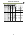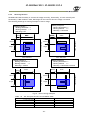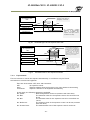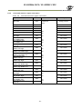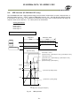
1
Spark Series User Manual SP-20000M-CXP2 SP-20000C-CXP2 20 MP CMOS Digital Progressive Scan Monochrome and Color Camera Document Version:Ver.1.2 SP-20000-CXP2_Ver.1.2_June2013 1049E-1312 SP-20000M-CXP2 / SP-20000C-CXP-2 Notice The material contained in this manual consists of information that is proprietary to JAI Ltd., Japan and may only be used by the purchasers of the product. JAI Ltd., Japan makes no warranty for the use of its product and assumes no responsibility for any errors which may appear or for damages resulting from the use of the information contained herein. JAI Ltd., Japan reserves the right to make changes without notice. Company and product names mentioned in this manual are trademarks or registered trademarks of their respective owners. Warranty For information about the warranty, please contact your factory representative. Certifications CE compliance As defined by the Directive 2004/108/EC of the European Parliament and of the Council, EMC (Electromagnetic compatibility), JAI Ltd., Japan declares that SP-20000M-CXP2 and SP-20000C-CXP2 comply with the following provisions applying to its standards. EN 61000-6-3 (Generic emission standard part 1) EN 61000-6-2 (Generic immunity standard part 1) FCC This equipment has been tested and found to comply with the limits for a Class B digital device, pursuant to Part 15 of the FCC Rules. These limits are designed to provide reasonable protection against harmful interference in a residential installation. This equipment generates, uses and can radiate radio frequency energy and, if not installed and used in accordance with the instructions, may cause harmful interference to radio communications. However, there is no guarantee that interference will not occur in a particular installation. If this equipment does cause harmful interference to radio or television reception, which can be determined by turning the equipment off and on, the user is encouraged to try to correct the interference by one or more of the following measures: - Reorient or relocate the receiving antenna. - Increase the separation between the equipment and receiver. - Connect the equipment into an outlet on a circuit different from that to which the receiver is connected. - Consult the dealer or an experienced radio/TV technician for help. Warning Changes or modifications to this unit not expressly approved by the party responsible for FCC compliance could void the user’s authority to operate the equipment. -2- SP-200000M-CXP2 Supplement The following statement is related to the regulation on “ Measures for the Administration of the control of Pollution by Electronic Information Products “ , known as “ China RoHS “. The table shows contained Hazardous Substances in this camera. mark shows that the environment-friendly use period of contained Hazardous Substances is 15 years. 嶷勣廣吭並㍻ 嗤蕎嗤墾麗嵎賜圷殆兆各式根楚燕 功象嶄鯖繁酎慌才忽佚連恢匍何〆窮徨佚連恢瞳麟半陣崙砿尖一隈〇云恢瞳ゞ 嗤蕎嗤 墾麗嵎賜圷殆兆各式根楚燕 〃泌和 桟隠聞喘豚㍉ 窮徨佚連恢瞳嶄根嗤議嗤蕎嗤墾麗嵎賜圷殆壓屎械聞喘議訳周和音氏窟伏翌 亶賜融延、窮徨佚連恢瞳喘薩聞喘乎窮徨佚連恢瞳音氏斤桟廠夛撹冢嶷麟半 賜斤児繁附、夏恢夛撹冢嶷鱒墾議豚㍉。 方忖仝15々葎豚㍉15定。 SP-20000C-CXP2 Supplement The following statement is related to the regulation on “ Measures for the Administration of the control of Pollution by Electronic Information Products “ , known as “ China RoHS “. The table shows contained Hazardous Substances in this camera. mark shows that the environment-friendly use period of contained Hazardous Substances is 15 years. 嶷勣廣吭並㍻ 嗤蕎嗤墾麗嵎賜圷殆兆各式根楚燕 功象嶄鯖繁酎慌才忽佚連恢匍何〆窮徨佚連恢瞳麟半陣崙砿尖一隈〇云恢瞳ゞ 嗤蕎嗤 墾麗嵎賜圷殆兆各式根楚燕 〃泌和 桟隠聞喘豚㍉ 窮徨佚連恢瞳嶄根嗤議嗤蕎嗤墾麗嵎賜圷殆壓屎械聞喘議訳周和音氏窟伏翌 亶賜融延、窮徨佚連恢瞳喘薩聞喘乎窮徨佚連恢瞳音氏斤桟廠夛撹冢嶷麟半 賜斤児繁附、夏恢夛撹冢嶷鱒墾議豚㍉。 方忖仝15々葎豚㍉15定。 SP-20000M-CXP2 / SP-20000C-CXP-2 - Contents - Introduction .....................................................................................1. General ....................................................................................2. Camera composition ....................................................................3. Key features ...............................................................................4. Parts locations and their functions ...................................................- 67789- 4.1 Parts locations and their functions ................................................................... - 9 4.2 Rear Panel ............................................................................................. - 10 - 5. Input and output.......................................................................... - 11 5.1 CoaXPress interface standard ....................................................................... 5.2 Connectors and pin assignment ..................................................................... 5.2.1 Digital Video Output (75Ω 1.0・2.3 DIN Receptacle) ...................................... 5.2.2 12-Pin connector ................................................................................. 5.2.2.1 Figure ........................................................................................ 5.2.2.2 Pin configuration............................................................................ 5.2.3 AUX Connector Hirose 10-Pin connector .................................................. 5.3 Digital In and out inteface ........................................................................... 5.3.1 Line Selector ..................................................................................... 5.3.2 Line Source ....................................................................................... 5.3.3 Line Mode ......................................................................................... 5.3.4 Line Inverter ..................................................................................... 5.3.5 Line Status ........................................................................................ 5.3.6 Line Format ...................................................................................... 5.3.7 GPIO ............................................................................................... 5.3.7.1 Basic block diagram ........................................................................ 5.3.7.2 Input and output matrix table ............................................................ 5.4 Pulse Generator ....................................................................................... 5.4.1 Clock Pre-scaler.................................................................................. 5.4.2 Pulse Generator Selector ....................................................................... 5.4.3 Pulse Generator Length ......................................................................... 5.4.4 Pulse Generator Start Point .................................................................... 5.4.5 Pulse Generator End Point ...................................................................... 5.4.6 Pulse Generator Repeat Count ................................................................. 5.4.7 Pulse Generator Clear Activation .............................................................. 5.4.8 Pulse Generator Clear Sync Mode .............................................................. 5.4.9 Pulse Generator Clear Source .................................................................. 5.4.10 Pulse Generator Inverter ...................................................................... 5.4.11 Pulse Generator setting parameters ......................................................... 5.4.12 Associated GenICam register information ................................................... - 11 12 12 12 12 12 13 13 13 14 15 15 15 15 16 16 17 18 18 18 19 19 19 19 19 19 21 22 22 23 - 6.1 Sensor layout .......................................................................................... 6.1.1 Monochrome sensor ............................................................................. 6.1.2 Bayer sensor ...................................................................................... 6.2 Camera output format (Tap Geometry) ............................................................ 6.2.1 1X–1Y .............................................................................................. 6.3 Output timing and output image.................................................................... 6.3.1 Horizontal timing ................................................................................ 6.3.2 Vertical timing ................................................................................... 6.3.3 ROI (Region Of Interest) ........................................................................ 6.3.4 Mirroring function ............................................................................... 6.3.5 Multi ROI function ............................................................................... 6.3.5.1 Multi ROI setting parameters .............................................................. 6.3.5.2 Associated GenICam register information ............................................... - 24 24 24 25 25 26 26 29 30 32 33 33 35 - 6. Sensor layout, output format and timing ........................................ - 24 - -3- SP-20000M-CXP2 / SP-20000C-CXP-2 6.4 7. Digital output bit allocation......................................................................... - 35 - Operating modes ...................................................................... - 36 - 7.1. Acquisition control (change the frame rate) ..................................................... 7.1.1 Acquisition control .............................................................................. 7.1.2 The relationship between Link Configuration and Acquisition Frame Rate............... 7.1.3 Calculation of frame rate(In Continuous Trigger mode) .................................. 7.1.4 Associated GenICam register information .................................................... 7.2. Exposure control ..................................................................................... 7.2.1 Exposure Mode ................................................................................... 7.2.2 ExposureTime .................................................................................... 7.2.3 Behavior if Trigger Overlap is set to Readout ................................................ 7.2.4 ExposureAuto .................................................................................... 7.3. Trigger operation .................................................................................... 7.3.1 Trigger Selector ................................................................................. 7.3.2 Trigger Mode ..................................................................................... 7.3.3 TriggerSource .................................................................................... 7.3.4 TriggerActivation ................................................................................ 7.3.5 Triggeroverlap ................................................................................... 7.3.6 Associated GenICam register information .................................................... 7.4. Normal continuous operation (Timed Exposure Mode/Trigger Mode OFF) .................... 7.5. Timed mode (EPS) ................................................................................... 7.5.1 If Overlap setting is OFF ........................................................................ 7.5.2 If Overlap setting is Readout ................................................................... 7.5.3 GPIO TTL output timing if Trigger Overlap is OFF ........................................... 7.5.4 GPIO TTL output timing if Trigger Overlap is Readout ...................................... 7.6 Trigger width mode (PWC) .......................................................................... 7.6.1 If Overlap setting is OFF ........................................................................ 7.6.2 If Overlap setting is Readout ................................................................... 7.6.3 Minimum trigger interval calculation formula (Trigger Overlap = OFF) ................... 7.6.4 Minimum trigger interval calculation formula (Trigger Overlap = Readout) .............. 7.7 PIV (Particle Image Velocimetry) ................................................................... 7.8 Sequence ROI Trigger ................................................................................ 7.8.1 Trigger Sequence ................................................................................ 7.8.2 Command Sequence ............................................................................. 7.8.3 Typical minimum trigger interval of Sequence ROI Trigger ................................ 7.8.4 Defaul Sequence Index Table .................................................................. 7.8.5 Sequence ROI setting parameters ............................................................. 7.8.6 Associated GenICam register information .................................................... 7.9. Operation and function matrix .................................................................... - 36 36 36 37 37 37 37 39 39 41 42 42 42 43 43 44 44 45 45 46 47 49 50 51 52 53 54 55 56 60 60 60 61 61 61 65 66 - 8.1 Black level control ................................................................................... 8.1.1 Black Level Selector............................................................................. 8.1.2 Black Level ....................................................................................... 8.1.3 Auto black control ............................................................................... 8.1.4 Associated GenICam register information .................................................... 8.2 Gain control ........................................................................................... 8.2.1 Gain Selector..................................................................................... 8.2.2 Gain ............................................................................................... 8.2.3 Gain Auto ......................................................................................... 8.2.4 Balance White Auto ............................................................................. 8.2.5 Associated GenICam register information .................................................... 8.3. LUT .................................................................................................... 8.3.1 LUT Enable ....................................................................................... 8.3.2 LUT Index ......................................................................................... 8.3.3 LUT Value ........................................................................................ 8.3.4 Associated GenICam register information .................................................... - 67 67 67 67 68 68 69 69 69 69 70 71 71 71 71 71 - 8. Other functions ........................................................................ - 67 - -4- SP-20000M-CXP2 / SP-20000C-CXP-2 8.4 8.5 8.6 8.7 8.8 Gamma ................................................................................................. Shading Correction ................................................................................... Blemish compensation ............................................................................... ALC ..................................................................................................... HDR function (SP-20000M-CXP2 only) .............................................................. - 72 72 73 74 76 - 9.1 9.2 Camera Control Tool ................................................................................. - 78 Camera Default Settings ............................................................................. - 78 - 9. Camera Settings......................................................................... - 78 10. 11. External appearance and dimensions .......................................... - 79 Specifications ........................................................................ - 80 - 11.1. 11.2. Camera spectral response ......................................................................... - 80 Specification table ................................................................................. - 81 - Appendix ...................................................................................... - 83 1. 2. 3. 4. 5. 6. Precautions............................................................................................... Typical Sensor Characteristics ......................................................................... Caution when mounting a lens on the camera ....................................................... Caution when mounting the camera .................................................................. Exportation............................................................................................... References ............................................................................................... - 83 83 83 83 84 84 - Manual change history ...................................................................... - 85 User's Record ................................................................................. - 86 - -5- SP-20000M-CXP2 / SP-20000C-CXP-2 Introduction EMVA 1288 With regard to signal to noise ratio in this manual, specifications measured by EMVA 1288 are used together with specifications by a traditional measurement method. EMVA 1288 is a more complete measurement that considers multiple noise sources, including random noise, pattern noise, and shading. Additionally, EMVA 1288 incorporates temporal variances in pixel output by capturing 100 frames of data and computing the RMS variations over the captured frames. Because of the comprehensive nature of the noise analysis and the additional consideration for RMS variances over time, EMVA 1288 SNR measurements are inherently lower than the traditional SNR measurements given by manufacturers. However, the comprehensive nature combined with rigid test parameters, means that all manufacturers’ are measuring their products equally and EMVA 1288 tested parameters can be compared among different manufacturers’ products. In order to learn more about EMVA 1288, please visit http://www.emva.org Interface The SP-20000-CXP2 employs CoaXPress as an interface system. In order to connect the camera to a PC, it requires the use of a Frame Graber board and the appropriate coaxial cable(s). The maximum video transfer rate per coaxial cable is 6.25 Gbps. In addition to video information, power and control signals can be transferred to the camera over this interface. For detailed specifications, please refer to “JIIA-NTF-001-2010” published by Japan Industrial Imaging Association, http://www.jiia.org. Computer used for SP-20000 series In order to get proper performance from this camera, it is necessary to use a PC equipped with a PCIe 2.0 slot with a size and capacity of 16 lanes or higher (x16 or x32). Frame grabber boards used with SP-20000 series As the SP-20000-CXP2 employ CoaXPress as an interface system, a CoaXPress-compliant frame grabber board is required. Both cameras have two CoaXPress interface connectors and it is recommended that a frame grabber board with more than two interface connectors be used in order to maximize camera performance. Cables used with SP-20000 series For the CoaXPress interface, coaxial cables are used. In the SP-20000-CXP2, they use 75Ω 1.0/2.3 DIN receptacles (Amphenol ACX1785-ND or equivalent). The coaxial cable used to connect the camera must have a 75Ω 1.0/2.3 DIN-type plug at the camera side. An ordinary BNC cable cannot be used. -6- SP-20000M-CXP2 / SP-20000C-CXP-2 1. General The SP-20000-CXP2 cameras are members of JAI’s new “Spark Series.” They provide both high resolution and a high frame rate with excellent image quality for machine vision applications. The SP-20000M-CXP2 is a monochrome progressive scan COMS camera and the SP-20000C-CXP2 is the equivalent Bayer mosaic progressive scan CMOS camera. Both are equipped with CMOS sensors offering a 35mm full size image format, a resolution of 20 million pixels, and a 4:3 aspect ratio. They provide 30 frames per second for continuous scanning with 5120 x 3480 full pixel resolution for both monochrome and raw Bayer output. 8-bit or 10-bit output can be selected for both monochrome and raw Bayer formats. 24-bit (3 x 8-bit) in-camera color interpolation is also selectable in the color model. The new cameras feature a CoaXPress interface with two coaxial cables which is capable of supporting a “Power over Coaxial Cable” capability. A full pixel readout or partial scan readout mode can be selected depending on applications. The readout format is available as an 8-tap output. The SP-20000-CXP2 have various comprehensive functions needed for automated optical inspection applications, such as solid state device inspection or material surface inspection. They incorporate video processing functions such as a look-up table, flat field shading compensation and blemish compensation in addition to fundamental functions such as trigger, exposure setting and video level control. The latest version of this manual can be downloaded from: www.jai.com The latest version of the JAI SDK for the SP-20000-CXP2 can be downloaded from: www.jai.com For camera revision history, please contact your local JAI distributor. 2. Camera composition The standard camera composition is as follows. Camera body 1 Sensor protection cap 1 Dear Customer (sheet) 1 The following optional accessories are available. Tripod base Power supply unit MP-42 PD-12 series -7- SP-20000M-CXP2 / SP-20000C-CXP-2 3. Key features New Spark Series, 35mm full size, CMOS 20-megapixel progressive scan camera with global shutter Utilizes CoaXPress interface with two cables configuration Aspect ratio 4:3, 5120(H) x 3480(V) - 20 million effective pixels 6.4 μm square pixels S/N 53 dB for monochrome and 51 dB for color 8-bit or 10-bit output for monochrome and Bayer color, plus 3 x 8-bit RGB for color with in-camera color interpolation 30 frames/second with full resolution in continuous operation for CXP6_X2 Link Configuration Supports ROI (Region Of Interest) modes for faster frame rate 0 dB to +24 dB gain control for both SP-20000-CXP2 models 299μs (1/100,000) to 8 seconds exposure control in 1 μs step Auto exposure control Timed and trigger width exposure control PIV and sequential trigger modes for specific applications ALC control with combined function of AGC and auto exposure HDR (High Dynamic Range) function is available (SP-20000M-CXP2 only) Various pre-processing circuits are provided Programmable LUT Gamma correction from 0.45 to 1.0 Flat field correction Bayer white balance with manual or one-push auto (SP-20000C-CXP2 only) Blemish compensation Color interpolation New Hirose 10P connector for TTL IN and OUT and LVDS IN interface F-mount for lens mount Accepts power over Coaxial cable Setup by Windows XP/Vista/7 via serial communication -8- SP-20000M-CXP2 / SP-20000C-CXP-2 4. Parts locations and their functions 4.1 Parts locations and their functions Lens mount AUX 10-pin connector LED 12-pin connector LINK 1 LINK 2 CXP#2 CXP#1 Mounting holes F-mount (Note *1) AUX Connector for TTL IN/OUT and LVDS IN Indication for power and trigger input DC and trigger input LINK Status indication for CXP#1 LINK Status indication for CXP#2 CoaXPress No.2 connector CoaXPress No.1 connector (Note*2) Holes for mounting tripod base or direct installation. Depth 5 mm (Note*3) *1) Note1: Rear protrusion on F-mount lens must be less than 14.0 mm. *2) Note2: When one coaxial cable is used, CXP#1 must be used. *3) Note3: The part number for the tripod adapter plate (with 1/4"-20 thread) is MP-42 (option). Fig. 1 Locations -9- SP-20000M-CXP2 / SP-20000C-CXP-2 4.2 Rear Panel The rear panel mounted LED provides the following information: Power connected – initiating This light goes OFF after initiating. In the process of changing Link Configuration Steady green: Camera is operating in Continuous mode Flashing green: The camera is receiving external triggering POWER/TRIG Amber: Note: The interval of flashing does not correspond with external trigger duration. DC IN /TRIG AUX LIN K-1 LINK-2 CXP-1 CXP-2 Fig. 2 LINK1, LINK 2 Steady green: Acquisition Active, Outputting video Flashing green: Acquistion Wait - 10 - Rear panel SP-20000M-CXP2 / SP-20000C-CXP-2 5. Input and output 5.1 CoaXPress interface standard The SP-20000-CXP2 use CoaXPress as their interface. CoaXPress is a PLUG-AND-PLAY interface and connects the camera and the frame grabber board by coaxial cable(s). Its maximum transfer rate is 6.25 Gbps per one coaxial cable. Additionally, CoaXPress interface supports power supplied through the coaxial cable as well as communication signals. In the CoaXPress interface, multiple coaxial cables can be used in order to achieve a faster transfer rate or a reduced transfer rate can be used to extend the cable length. In the SP-20000-CXP2, a 2 coaxial cable system is used. Master Link Data/Trigger/GPIO/Control Trigger/GPIO/Control Power Camera Frame Grabber Board Extension Link The distance between camera and frame grabber board depends on the bit rate of the video and the cable used. Among the unique features of CoaXPress is its ability to supply DC power and provide trigger timing accuracy. The maximum power supply per one cable is 13W with DC+24V voltage. If the system uses 2 cables, it will be 26W. The accuracy of the trigger is ±2 ns at 3.125 Gbps. The CoaXPress compliance labeling is assigned to the following five cable types and the maximum bit rate and transmission length is indicated in the table below. Compliance Labeling CXP-1 CXP-2 CXP-3 CXP-5 CXP-6 Maximum Operational Bit Rate per coax (Gbps) and transmission length 1.250 (up to 212 m) 2.500 (up to 185 m) 3.125 (up to 169 m) 5.000 (up to 102 m) 6.250 (up to 68 m) In the SP-20000-CXP2, the maximum bit rate is 6.25 Gbps per one cable and the power supply is available on the CXP#1 connector only. The following link configurations with the reference to pixel format are use in SP-20000-CXP2. Table – 1 SP-20000-CXP2 Link Confioguration Model Pixel format Link configuration SP-20000M-CXP2 SP-20000C-CXP2 Mono 8/10 Mono 8/10 Mono 8/10 Mono 8/10 Bayer 8/10/RGB Bayer 8/10/RGB Bayer 8/10/RGB Bayer 8/10/RGB CXP6_X2 CXP6_X1 CXP3_X2 CXP3_X1 CXP6_X2 CXP6_X1 CXP3_X2 CXP3_X1 Bit rate / cable 6.250 Gps 6.250 Gps 3.125 Gps 3.125 Gps 6.250 Gps 6.250 Gps 3.125 Gps 3.125 Gps Used BNC cable 2 1 2 1 2 1 2 1 For the details of the specifications, please refer to “JIIA-NTF-001-2010” published by Japan Industrial Imaging Association, http://www.jiia.org. - 11 - SP-20000M-CXP2 / SP-20000C-CXP-2 5.2 Connectors and pin assignment 5.2.1 Digital Video Output (75Ω 1.0・2.3 DIN Receptacle) Type: CoaXPress Connector (ACX1785-ND Amphenol Connector or equivalent) CXP#1 PoCXP compliant CXP#2 Maximum Bit Rate per one coax: 6.25 Gbps Maximum Bit Rate per two coax: 12.5 Gbps Note: If one coaxial cable is used, CXP#1 must be used. 5.2.2 12-Pin connector 5.2.2.1 Figure Type: HR-10A-10R-12PB(72) Hirose male or equivalent. Fig.3 Hirose 12-pin connector 5.2.2.2 Pin configuration Table – 2 12-pin configuration Pin no. Signal 1 GND 2 DC input 3 GND 4 NC 5 OPTO IN6 OPTO IN+ 7 OPTO OUT 8 OPTO OUT+ 9 TTL out 1 10 TTL In 1 11 DC input 12 GND Note 1) Note 2) Note 3) Remarks +12V ~ +24V (note 3) Line 5 Line 2 Line1 (note 1) Line4 (note 2) +12V ~ +24V (note 3) Factory default setting is Exposure Active and negative Factory default setting is trigger input. See page 6 for notes about power options for these cameras Note: If power is supplied from both the 12-pin connector and CoaXPress, the power from the 12-pin is active. If power from the 12-pin is interrupted, the operation depends on how power was initially connected. Please refer to the following: The order of power supply connections First 12-pin, then CoaXPress First CoaXPress, then 12-pin If the power supply from 12-pin is interrupted The power is supplied from CoaXPress The power is supplied from CoaXPress but the camera is not restarted. - 12 - SP-20000M-CXP2 / SP-20000C-CXP-2 5.2.3 AUX Connector Hirose 10-Pin connector Type: HIROSE 10-Pin Connector 3260-10S3(55) 8 1 Fig. 4 Hirose 10p connector Table-3 Pin configuration for Hirose 10P No I/O Name TTL OUT2 1 O TTL OUT3 2 O TTL IN2 3 I NC 4 GND 5 LVDS IN1+ 6 I LVDS IN17 I NC 8 GND 9 GND 10 5.3 Note Line8 Line9 Line10 Line11 Digital In and out inteface In the SP-20000-CXP2, the software control tool can assign the necessary signals used in the system to digital inputs and outputs. 5.3.1 Line Selector In the Line Selector, the following input and output signals can be assigned. Table – 4 Line Selector Line Selector item Description Line 1 TTL OUT 1 TTL output from #9 pin of DC In/Trigger HIROSE 12-Pin on the rear Line 2 OPTO OUT 1 Optical output from #7 and 8 pins of DC In/Trigger HIROSE 12-Pin on the rear Line 8 TTL OUT 2 TTL output from #1 pin “AUX” HIROSE 10-Pin on the rear Line 10 TTL OUT 3 t TTL output from #2 pin “AUX” HIROSE 10-Pin on the rear NAND 0 In 1 First input at first NAND gate in GPIO NAND 0 In 2 Second input at first NAND gate in GPIO NAND 1 In 1 First input at second NAND gate in GPIO NAND 1 in 2 Second input at second NAND gate in GPIO Note: In the line source, input interfaces besides those mentioned above will be shown but the line source setting is not available. The input interface can be configured in the trigger source and the pulse generator source. - 13 - SP-20000M-CXP2 / SP-20000C-CXP-2 5.3.2 Line Source Line source signal can be selected from the following table to connect it to the line item which is selected in the line selector. Table-5 Line Source Line Source item Description Low Connect Low Level signal to line item selected in Line Selector, Default setting High Connect High Level signal to line item selected in Line Selector Acquisition Trigger Wait Connect Acqusition Trigger Wait signal to line item selected in Line Selector Acqusition Active Connect Acqusition Active signal to line item selected in Line Selector Frame Trigger Wait Connect Frame Trigger Wait signal to line item selected in Line Selector Frame Active Connect Frame Active signal to line item selected in Line Selector Exposure Active Connect Exposure Active signal to line item selected in Line Selector FVAL Connect FVAL signal to line item selected in Line Selector LVAL Connect LVAL signal to line item selected in Line Selector PulseGenerator0 Out Connect Pulse Generator 0 signal to line item selected in Line Selector PulseGenerator1 Out Connect Pulse Generator 1 signal to line item selected in Line Selector PulseGenerator2 Out Connect Pulse Generator 2 signal to line item selected in Line Selector PulseGenerator3 Out Connect Pulse Generator 3 signal to line item selected in Line Selector Line 7 - CXP IN Connect CXP IN signal to line item selected in Line Selector (Trigger Packet) Line 4 – TTL IN 1 Connect TTL IN 1 signal to line item selected in Line Selector Line 5 – OPTO IN 1 Connect OPTO IN 1 signal to line item selected in Line Selector User output 0 Connect User output 0 signal to line item selected in Line Selector User output 1 Connect User output 1 signal to line item selected in Line Selector User output 2 Connect User output 2 signal to line item selected in Line Selector User output 3 Connect User output 3 signal to line item selected in Line Selector Nand0 Out Connect NAND 0 signal to line item selected in Line Selector Nand1 Out Connect NAND 1 signal to line item selected in Line Selector Line 10 TTL IN 2 Connect TTL IN 2 signal to Line 10 Line 11 LVDS IN Connect LVDS IN signal to Line 11 Note: (1) The user output is the trigger signal generated by software in PC for the camera. (2) As for LVAL, some line items cannot be connected. Refer to “5.3.6.2 GPIO matrix table” - 14 - SP-20000M-CXP2 / SP-20000C-CXP-2 5.3.3 Line Mode Indicates the status of the item selected in Line Selector. (INPUT or OUTPUT) Table – 6 Associated GenICam register information GenICam Name Line Selector Line Mode Line Inverter 5.3.4 Access R/W RO R/W Line Status RO Line Source R/W Line Format RO Values Line1,2,4,5,7~11 NAND 0 In1 to 2 NAND 1 In1 to 2 Output Input False True False True Low High Acquisition Trigger Wait Acquisition Active Frame Trigger Wait Frame Active Exposure Active FVAL PG0 to 3 User out0 to 3 TTL In1 Opt In CXP In (Trigger Packet) Nand0 to 1 TTL In2 LVDS In1 TTL LVDS Opto CXP Category Digital I/O Control Digital I/O Control Digital I/O Control Digital I/O Control Digital I/O Control Digital I/O Control Line Inverter Inverts the signal polarity for the item selected in Line Selector. False=Positive, True=Negative) 5.3.5 Line Status Indicates the status of the selected signal (input or output) (True=High, False=Low) 5.3.6 Line Format Indicates the interface category of input and output for the selected signal. Category: No connect, TTL, LVDS and OPTO coupled - 15 - SP-20000M-CXP2 / SP-20000C-CXP-2 5.3.7 GPIO GPIO is a general interface for input and output and controls the I/O for trigger signals and other valid signals and pulse generators. By using this interface you can control an external light source, make a delay function for an external trigger signal, or make a precise exposure setting together with a PWC trigger. 5.3.7.1 Basic block diagram The basic block diagram is as follows. In the SP-20000-CXP2, the pixel clock is fixed at 40 MHz, even though the sesor clock is selecteable in Link Configuration setting. Sel Bit (5,0) Sel Bit (7) Soft Trigger LVAL IN INV Trigger 2 (Frame Start) FVAL IN GPIO 1 (TTL OUT 1) Exposure Active GPIO 8 (TL OUT 2) GPIO 9 (TTL OUT 3) Acquisition Trigger Wait Sel Bit (7) Acquisition Active Frame Trigger Wait Frame Active INV INV N User output 0 User output 1 User output 2 Cross Pont Switch Gate 1 Gate 2 NAND User output 3 Sel Bit (7) INV Non INV GPIO 4 (TTL IN 1) Pulse Pulse Pulse Pulse GPIO 5 (OPTO IN 1) GPIO 7 (CXP IN) GPIO 10 (TTL IN2) Generator Generator Generator Generator 0 1 2 3 Clear IN Pulse Generator 20 bit counter x 4 CLR GPIO 11 (LVDS IN) Clock IN Pixel Clock 12 bit Counter Fig.5 GPIO interface - 16 - SP-20000M-CXP2 / SP-20000C-CXP-2 5.3.7.2 Input and output matrix table The relation between input and output is as follows. NAND 1 In 1 NAND 1 In 2 NAND 2 In 1 NAND 2 In 2 Pulse Generator 0 Pulse Generator 1 Pulse Generator 2 Pulse Generator 3 Acquisition End Line 8 - TTL OUT 2 Line 2 OPTO OUT 1 Line 9 - TTL OUT 3 NAND 0 Out NAND 1 Out 1 User Output 0 User Output 1 User Output 2 User Output 3 Line 10 - TTL IN 2 Line 11 - LVDS IN Line 1 - TTL OUT 1 Source signal (Cross point switch input) Low High Soft Trigger Acqusition Trigger Wait Acqusition Active Exposure Active Frame Trigger Wait Frame Active FVAL LVAL Pulse Generator 0 Pulse Generator 1 Pulse Generator 2 Pulse Generator 3 Line 4 - TTL In1 Line 5 - OPTO IN 1 Line 7 - CXP IN Trigger Packet Pulse Generator Selector Line Selector Acquisition Start point switch output) Trigger Selector Frame Start Table - 7 GPIO matrix table Selector (Cross Trigger Source Line Source - 17 - Pulse Generator Clear Source SP-20000M-CXP2 / SP-20000C-CXP-2 5.4 Pulse Generator The SP-20000-CXP2 has a frequency divider using the sensor clock as the basic clock and four pulse generators. In each Pulse Generator, various Clear settings are connected to GPIO. The following shows Pulse Generator default settings. Table - 8 Pulse Generator default settings Display Name Clock Pre-scaler Value 1 Pulse Generator Length Start Point End Repeat Clear Clear Clear Clear Pulse Generator Point Count Source Inverter Activation Sync Selector Mode 1 0 1 0 Off True Off Async Mode - Pulse Generator 0 - Pulse Generator 1 1 0 1 0 Off True Off Async Mode 1 0 1 0 Off True Off Async Mode - Pulse Generator 2 - Pulse Generator 3 1 0 1 0 Off True Off Async Mode Note: When Pulse Generator Repeat Count is set to “0”, the camera is operating in free-running mode. However, based on the above default settings, Length=1, Start Point=0 and End Point=1, Pulse Generator stops at High output. Therefore, if Start Point =0 and End Point=1 are configured, Length should be “2” as the minimum active width. 5.4.1 Clock Pre-scaler Clock pre-scaler (Divide Value) can set the dividing value of the frequency divider (12-bit length) and the sensor clock is used for this. Four built-in pulse generators work by the same clock. In the SP-20000-PMCL, the sensor pixel clock is 40 MHz . 5.4.2 Pulse Generator Selector This is where you select one of the 4 pulse generators in order to set or modify its parameters. Table - 9 Trigger item Pulse Generator setting Selector Pulse Generator 0 Pulse Generator 1 Pulse Generator 2 Pulse Generator 3 Description If Pulse Generator 0 is selected, Length, Start Point, End Point, Repeat Count, Clear Source, Clear Inverter, Clear Activation and Clear Sync Mode of Pulse Generator 0 are displayed under the selector. If Pulse Generator 1 is selected, Length, Start Point, End Point, Repeat Count, Clear Source, Clear Inverter, Clear Activation and Clear Sync Mode of Pulse Generator 1 are displayed under the selector. If Pulse Generator 2 is selected, Length, Start Point, End Point, Repeat Count, Clear Source, Clear Inverter, Clear Activation and Clear Sync Mode of Pulse Generator 2 are displayed under the selector. If Pulse Generator 3 is selected, Length, Start Point, End Point, Repeat Count, Clear Source, Clear Inverter, Clear Activation and Clear Sync Mode of Pulse Generator 3 are displayed under the selector. - 18 - SP-20000M-CXP2 / SP-20000C-CXP-2 Pulse generator Clear source IN (Clear activation = Rising edge Clear SYNC mode = Async) Pulse generator repeat count = N (Pulse generator length x N) Pulse generator length Pulse generator length Pulse generator length Pulse generator Output 0 0 0 Pulse generator End point Pulse generator Start point Fig.6 5.4.3 Pulse Generator pulse construction Pulse Generator Length Set the counter up value (number of clocks, refer to Table 12) for the selected pulse generator. If Repeat Count value is “0”, and if Pulse Generator Clear signal is not input, the pulse generator generates the pulse repeatedly until reaching this counter up value. 5.4.4 Pulse Generator Start Point Set the active output start count value for the selected pulse generator. However, please note that a maximum 1 clock jitter for the clock which is divided in the clock pre-scaler can occur. 5.4.5 Pulse Generator End Point Set the active output ending count value for the selected pulse generator. 5.4.6 Pulse Generator Repeat Count Set the repeating number of the pulse for the selected pulse generator. After Trigger Clear signal is input, the pulse generator starts the count set in Repeat Count. Accordingly, an active pulse which has a start point and end point can be output repeatedly. However, if Repeat Count is set to “0”, it works as free-running counter. 5.4.7 Pulse Generator Clear Activation Set the clear conditions of clear count pulse for the selected pulse generator. 5.4.8 Pulse Generator Clear Sync Mode Set the count clear method for the selected pulse generator. In case of Async Mode, if the clear signal is input during the length setting value, the counter will stop counting according to the clear signal input. In case of Sync Mode, if the clear signal is input during the length setting value, the counter will continue to count until the end of the length setting value and then clear the count. Both modes clear the repeat count when the counter is cleared. - 19 - SP-20000M-CXP2 / SP-20000C-CXP-2 (Example 1) Clear Activation = Rising Edge, Clear Sync Mode = Async Mode, Clear Inverter = False Pulse Generator Clear Source In Pulse Generator Output Clear ↓ 0 Fig.7 Counter clear in Async mode (Example 2) Clear Activation = Rising Edge, Clear Sync Mode = Sync Mode, Clear Inverter = False Pulse Generator Clear Source In Pulse Generator Output Clear ↓ 0 Pulse Generator Length 0 Fig.8 Note: Repeat Count is also reset. Counter clear in Sync mode - 20 - SP-20000M-CXP2 / SP-20000C-CXP-2 5.4.9 Pulse Generator Clear Source The following clear source can be selected as the pulse generator clear signal. Tabel - 10 Pulse generator clear source Pulse Generator Clear Source item Low High Acqusition Wait Trigger Acquisition Active Frame Trigger Wait Frame Active Exposure Active FVAL LVAL PulseGenerator0 Out PulseGenerator1 Out PulseGenerator2 Out PulseGenerator3 Out Line 7 – CXP IN (Trigger Packet) Line 4 - TTL IN 1 Description Connect Low level signal to Clear Source for the selected pulse generator. Default setting Connect High level signal to Clear Source for the selected pulse generator. Connect Acquisition Trigger Wait signal to Clear Source for the selected pulse generator. Connect Acquisition Active signal to Clear Source for the selected pulse generator. Connect Frame Trigger Wait signal to Clear Source for the selected pulse generator. Connect Frame Active signal to Clear Source for the selected pulse generator. Connect Exposure Active signal to Clear Source for the selected pulse generator. Connect FVAL signal to Clear Source for the selected pulse generator. Connect LVAL signal to Clear Source for the selected pulse generator. Connect Pulse Generator 0 output to Clear Source for the selected pulse generator. Connect Pulse Generator 1 output to Clear Source for the selected pulse generator. Connect Pulse Generator 2 output to Clear Source for the selected pulse generator. Connect Pulse Generator 3 output to Clear Source for the selected pulse generator. Connect CXP IN signal to Clear Source for the selected pulse generator. Connect TTL IN 1 signal to Clear Source for the selected pulse generator. Connect OPTO IN 1 signal to Clear Source for the selected pulse Line 5 – OPTO IN1 generator. Connect NAND 0 output signal to Clear Source for the selected pulse Nand0 Out generator. Connect NAND 1 output signal to Clear Source for the selected pulse Nand1 Out generator. Connect User Output 0 signal to Clear Source for the selected pulse User Output 0 generator. Connect User Output 1 signal to Clear Source for the selected pulse User Output 1 generator. Connect User Output 2 signal to Clear Source for the selected pulse User Output 2 generator. Connect User Output 3 signal to Clear Source for the selected pulse User Output 3 generator. Line 10 TTL IN 2 Connect TTL 2 IN signal to LINE 10. Line 11 LVDS IN Connect LVDS 1 IN signal to Line 11 Note: The pulse generator output cannot be used as the clear input to the same pulse generator. Refer to “5.4.7.2.GPIO matrix table”. - 21 - SP-20000M-CXP2 / SP-20000C-CXP-2 5.4.10 Pulse Generator Inverter Clear Source Signal can have polarity inverted. 5.4.11 Pulse Generator setting parameters Table - 11 Pulse Generator setting parameters Display Name Value Clock Pre-scaler Pulse Generator Clock (MHz) Pulse Generator Selector 1 to 4096 [Pixel Clock: 40 MHz ]÷[Clock Pre-scaler] - Pulse Generator 0 - Pulse Generator 1 - Pulse Generator 2 - Pulse Generator 3 1 to 1048575 ([Clock Source]÷[Clock Pre-scaler])-1 x [Pulse Generator Length] [ Pulse Generator Length (ms)]-1 0 to 1048574 ([Clock Source]÷[Clock Pre-scaler])-1 x [Pulse Generator Start Point] 1 to 1048575 ([Clock Source]÷[Clock Pre-scaler])-1 x [Pulse Generator End Point] [ Pulse Generator End Point (ms)]-[ Pulse Generator Start Point (ms)] 0 to 255 - Off - High Level - Low level - Rising Edge - Falling Edge - Async mode - Sync mode - Low - High - Acquisition Trigger Wait - Acquisition Active - Frame Trigger Wait - Frame Active - Exposure Active - FVAL - LVAL - PulseGenerator0 - PulseGenerator1 - PulseGenerator2 - PulseGenerator3 - Line 7 – CXP IN (Trigger Packet) - Line 4 – TTL IN 1 - Line 5 – OPTO IN 1 - Nand0 Out - Nand1 Out - User Output 0 - User Output 1 - User Output 2 - User Output 3 - Line 10 - TTL 2 In - Line 11 - LVDS 1 In - False - True - Pulse Generator Length Pulse Generator Length (ms) Pulse Generator Frequency (Hz) Pulse Generator Start Point Pulse Generator Start Point (ms) Pulse Generator End Point Pulse Generator End Point (ms) Pulse Generator pulse-width (ms) Pulse Generator Repeat Count Pulse Generator Clear Activation Clear Mode for the Pulse Generators - Pulse Generator Clear Sync Mode - Pulse Generator Clear Source - Pulse Generator Inverter(Polarity) Pulse Generator Clear Inverter Note: 1. If Pulse Generator Repeat Count is set to “0”, the pulse generator works in free-running mode. 2. The output of the same pulse generator cannot be connected to Clear input. - 22 - SP-20000M-CXP2 / SP-20000C-CXP-2 5.4.12 Associated GenICam register information Table – 12 Associated GenICam register information GenICam Name Pre-scaler Pulse Generator Selector Pulse Generator Length Pulse Generator Start Point Pulse Generator End Point Pulse Generator Repeat Count Access Category R/W 1 to 4096 Pulse Generators R/W PG0 to PG3 Pulse Generators R/W 0 to 1048575 Pulse Generators R/W 0 to 1048575 Pulse Generators R/W 0 to 1048575 Pulse Generators R/W 0 to 255 Pulse Generators Pulse Generator Clear Activation R/W Pulse Generator Clear Source R/W Pulse Generator Invertor Pulse Generator Sync Mode Values R/W R/W Free Run High Level Low Level Rising Edge Falling Edge Low High Soft Acquisition Trigger Wait Acquisition Active Frame Trigger Wait Frame Active Exposure Active FVAL PG0 to 3 User out0 to 3 TTL in Opto1 in CXP in (Trigger Packet) Nand0 to 1 True False Async Mode Sync Mode - 23 - Pulse Generators Pulse Generators Pulse Generators Pulse Generators SP-20000M-CXP2 / SP-20000C-CXP-2 6. Sensor layout, output format and timing 6.1 Sensor layout The CMOS sensors used in the SP-20000-CXP2 have the following pixel layout. 6.1.1 Monochrome sensor Pixel (0,0) 5120 Pixels Fig. 9 6.1.2 3840 Pixels F Monochrome sensorlayout Bayer sensor Pixel (0,0) 3840 Pixels F 5120 Pixels Fig. 10 Color sensor layout - 24 - SP-20000M-CXP2 / SP-20000C-CXP-2 6.2 Camera output format (Tap Geometry) Table - 13 Output format Camera output format Pixel format Refer to drawing 1X–1Y 8-bit, 10-bit, RGB 8-bit 6.2.1 Note: The camera output description is based on GenICam SFNC Ver.1.5.1. 6.2.1 1X–1Y 1X–1Y is 1-tap readout system specified in GenICam Tap Geometry and it outputs as the following. Step X = 1 Tap 1 X2 Y1 X3 Y1 X4 Y1 X5 Y1 X6 Y1 X7 Y1 X8 Y1 X5113 Y1 X5114 Y1 X5115 Y1 X5116 Y1 X5117 Y1 X5118 Y1 X5119 Y1 X5120 X5120 Y1 Y1 X1 Y2 X5120 Y2 X1 Y3839 X5120 Y3839 Height = 3840 Pixel Pixel(0,0) X1 Y1 Step Y = 1 X1 Y3840 X2 Y3840 X3 Y3840 X4 Y3840 X5 Y3840 X6 Y3840 X7 Y3840 X8 Y3840 X5113 Y3840 X5114 Y3840 X5115 Y3840 Width = 5120 Pixels Fig. 11 1X–1Y output system - 25 - X5116 Y3840 X5117 Y3840 X5118 Y3840 X5119 Y3840 X5120 X5120 Y3840 Y3840 SP-20000M-CXP2 / SP-20000C-CXP-2 6.3 6.3.1 Output timing and output image Horizontal timing The horizontal frequency depends on the link configuration. The following chart and tables explains the details. In the SP-20000M-CXP2, the horizontal frequency does not change when horizontal binning is effective, and therefore, the frame rate is not increased. FVAL Active Internal FVAL (a) LVAL Active (b) Internal LVAL (c) H-Offset DVAL Active Internal DVAL Internal DATA (d) Exposure Active Fig.12 Horizontal timing - 26 - SP-20000M-CXP2 / SP-20000C-CXP-2 Table – 14 Horizontal format in continuous trigger (1/2) Camera Settings Offset Y 0 3840 0 5120 0 1920 0 2560 0 3840 0 2560 0 1920 0 5120 0 3840 0 5120 0 1920 0 2560 0 3840 0 2560 0 1920 0 5120 0 3840 0 5120 0 1920 0 2560 0 3840 0 2560 0 1920 0 1X_1Y 1X_1Y 1X_1Y Vertical Height 5120 Horizontal Offset X CXP3 _X1 Binning Width CXP6 _X1 or CXP3 _X2 Tap Geometry Link Configuration CXP6 _X2 ROI 1 (Off) 1 (Off) 2 (On) 2 (On) 1 (Off) 1 (Off) 2 (On) 2 (On) 1 (Off) 1 (Off) 2 (On) 2 (On) 1 (Off) 2 (On) 1 (Off) 2 (On) 1 (Off) 2 (On) 1 (Off) 2 (On) 1 (Off) 2 (On) 1 (Off) 2 (On) (a) (b) (c) LVAL Active LVAL Non-Active H-Offset [Unit: Clock] [Unit: Clock] (d) Exposure Active Start to LVAL Active Start [Unit: Clock] 320 0.5 0 320 321 0 160 160.5 0 160 481 0 640 1 0 640 642 0 320 321 0 320 962 0 640 1 0 640 642 0 320 321 0 320 962 0 0.512 [Unit: us] LSB 0.512 8 or 8.523 0.512 0.512 or or 8.523 or 23.838 or 23.838 or 16 16 47.676 15.630 15.630 16 16 15.630 15.630 8 16 7.815 7.815 8 8 7.815 7.815 Step (Typ. ) 16 16 47.676 16 Note: (1) The horizontal frequency is not doubled if horizontal binning is ON. (2) If vertical binning is ON, the horizontal frequency becomes half. (3) H-Offset: The period from the LVAL Active start to DATA Active start (4) If the next frame is exposed while the image is read out in the vertical binning mode, the exposure control is controlled by 0.5 line. (5) “(d)Exposure Active Start to LVAL Active Start”has 1 clock difference due to the jitter in LVAL Non Active period. - 27 - SP-20000M-CXP2 / SP-20000C-CXP-2 Table – 15 Horizontal format in continuous trigger (2/2) Camera Settings Horizontal Frequency Horizontal Period [Unit: Clock] [Unit: kHz] [Unit: us] 0 3840 0 5120 0 1920 0 2560 0 3840 0 2560 0 1920 0 5120 0 3840 0 5120 0 1920 0 2560 0 3840 0 2560 0 1920 0 5120 0 3840 0 5120 0 1920 0 2560 0 3840 0 2560 0 1920 0 1 (Off ) 1 (Off ) 2 (On) 1 (Off) 320.5 124.805 8.013 2 (On) 641 62.402 16.025 1 (Off) 320.5 124.805 8.013 2 (On) 2 (On) 641 62.402 16.025 1 (Off ) 1 (Off ) 2 (On) 2 (On) 1 (Off ) 1 (Off ) 2 (On) 2 (On) 1 (Off) 641 62.402 16.025 2 (On) 1282 31.201 32.050 641 62.402 16.025 1282 31.201 32.050 1 (Off) 641. 31.201 32.050 2 (On) 1282 15.601 64.100 641 31.201 32.050 1282 15.601 64.100 Vertical 5120 Horizontal Offset Y 1X_1Y Height 1X_1Y 1Line Total Clock Binning Offset X CXP3 _X1 1X_1Y Width CXP6 _X1 or CXP3 _X2 Tap Geometry Link Configuration CXP6 _X2 ROI 1 (Off) 2 (On) 1 (Off) 2 (On) - 28 - SP-20000M-CXP2 / SP-20000C-CXP-2 6.3.2 Vertical timing In Continuous Trigger operation, the output timing relation is as follows. The SP-20000M-CXP2 supports H-Binning and V-Binning functions, but the frame rate is not increased. FVAL Active (A) FVAL Active (A) (B) (B) Internal FVAL Internal FVAL (C) V-Offset (C) V-Offset 0 Line 0 Line Internal LVAL Internal LVAL Internal DVAL Internal DVAL DVAL Active (A) DVAL Active (A) Internal DATA Internal DATA (F) Exposure End FVAL Active Start (F) to Exposure End to FVAL Active Start Exposure Active Exposure Active (E) Exposure time (Max) (E) Exposure time (Max) (D) (D) Exposure time Exposure (Min) time (Min) Fig. 13 Vertical timing relation Table – 16 Vertical format in Continuous Trigger (1/2) Camera Settings Offset Y Horizontal Vertical 7.5 Height 1X_1Y 15.0 0 3840 0 1 1 5120 0 1920 0 1 2 2560 0 3840 0 2 1 2560 0 1920 0 2 2 5120 0 3840 0 1 1 5120 0 1920 0 1 2 2560 0 3840 0 2 1 2560 0 1920 0 2 2 5120 0 3840 0 1 1 5120 0 1920 0 1 2 2560 0 3840 0 2 1 2560 0 1920 0 2 2 Offset X 1X_1Y 30.0 5120 Width CXP3 _X1 1X_1Y Acquisition Frame Rate CXP6 _X1 or CXP3 _X2 Tap Geometry Link Configuration CXP6 _X2 Binning 1:OFF, 2:ON ROI - 29 - (A) (B) (C) (D) FVAL Active FVAL Non -Active V -Offset Exposure Time (Min) [Unit: Line] [Unit: Line] [Unit: Line] [Unit: us] 3840 1920 3840 1920 321.1 160.6 321.1 160.6 0 10.0 3840 1920 3840 1920 320.6 160.3 320.6 160.3 0 10.0 3840 1920 3840 1920 320.6 160.3 320.6 160.3 0 10.0 SP-20000M-CXP2 / SP-20000C-CXP-2 Table – 17 Vertical format in Continuous Trigger (2/2) Camera Settings (2) (3) (4) (5) 6.3.3 Vertical Note: (1) 7.5 Horizontal 1X_1Y 3840 0 1 1 5120 0 1920 0 1 2 2560 0 3840 0 2 1 2560 0 1920 0 2 2 5120 0 3840 0 1 1 5120 0 1920 0 1 2 2560 0 3840 0 2 1 2560 0 1920 0 2 2 5120 0 3840 0 1 1 5120 0 1920 0 1 2 2560 0 3840 0 2 1 2560 0 1920 0 2 2 Offset Y CXP3 _X1 15.0 0 Height 1X_1Y 5120 Offset X CXP6 _X1 or CXP3 _X2 30.0 ROI Width 1X_1Y Acquisition Frame Rate Tap Geometry Link Configuration CXP6 _X2 (E) (F) Frame Rate Exposure Time (Max.) Exposure End to FVAL Active Start [Unit: Hz] [Unit: us] 30.000 [Acquisition Frame Rate Raw] - 250us = 33333-250 =33083 Binning 1:OFF, 2:ON 15.000 [Unit: Line] ROUNDDOWN( [Acquisition Frame Rate Raw] - 250us = 66667-250 =66417 7.500 [Acquisition Frame Rate Raw] - 500us = 133333-500 =132833 [Unit: us] 38.1 305.225 19.0 305.225 38.1 305.225 19.0 305.225 19.0 305.225 9.5 305.225 19.0 305.225 9.5 305.225 19.0 610.424 9.5 610.424 19.0 610.424 9.5 610.424 In the SP-20000-CXP2, the frame rate control is done in steps of 1 μs unit. Therefore, FVAL Non Active conversion has tolerance. Even if the horizontal binning is ON, the horizontal frequency is not doubled. Therefore, the vertical frequency is not increased. If the vertical binning is ON, the horizontal frequency becomes half. Therefore, if the height is half, the vertical frequency is not doubled. In the SP-20000-CXP2, the frame rate can be varied in steps of 1 μs. “(B) FVAL NON Active in the table XX will be varied. V-Offset: The period from FVAL Active Start to 1st LVAL Active Start ROI (Region Of Interest) In the SP-20000-CXP2, a subset of the image can be output by setting Width, Height, Offset-X, and Offset-Y. If the height is decreased, the number of lines read out is decreased and as the result, the frame rate is increased. However, in the horizontal directon, the horizontal frequency is not changed if the width is decreased. In the SP-20000-CXP2, the minimum width is “8” and minimum height is “2”. Readout area Setting example (1) Binning Horizontal = 1 Binning Vertical =1 Mirroring = Off OffsetX Width 3840 Height Max OffsetY Height 5120 Width Max Fig. 14 - 30 - Setting example (No binning) SP-20000M-CXP2 / SP-20000C-CXP-2 Setting example (2) Binning Horizontal = 2 Binning Vertical =2 Mirroring = Off Readout area Width 1920 Height Max OffsetX OffsetY Height 2560 Width Max Note: Binning is available only for SP-20000M-CXP2. Binning can be used in horizontal, vertical, or both directions. Fig.15 Setting example (Binning) Table – 18 Trigger / ROI setting examples (1/2) Camera Settings ROI Vertical Horizontal Offset Y 2/3 Screen - Center 1/2 Screen - Center 1/4 Screen - Center 1/8 Screen - Center Height 2/3 Screen - Center 1/2 Screen - Center 1/4 Screen - Center 1/8 Screen - Center Full Line Offset X Full Line Width 設定 参考 Binning Width Max Height Max Max Offset X Value Width and Offset X Step Max Offset Y Value CXP6 _X2 CXP6 _X1 or CXP3 _X2 Heigh t Step Offs et Y Step CXP3 _X2 5120 0 3840 0 1 (Off) 1 (Off) 5120 3840 0 8 8 8 0 2 1 3408 856 2560 640 1 (Off) 1 (Off) 5120 3840 1712 8 8 8 1280 2 1 1 (Off) 5120 3840 2560 8 8 8 1920 2 1 2560 1280 1920 960 1 (Off) 1280 1920 960 1440 1 (Off) 1 (Off) 5120 3840 3840 8 8 8 2880 2 1 640 2240 480 1680 1 (Off) 1 (Off) 5120 3840 4480 8 8 8 3360 2 1 2560 0 1920 0 2 (On) 2 (On) 2560 1920 0 8 8 8 0 1 1 1704 428 1280 320 2 (On) 2 (On) 2560 1920 856 8 8 8 640 1 1 480 2 (On) 2 (On) 2560 1920 1280 8 8 8 960 1 1 2 (On) 2560 1920 1920 8 8 8 1440 1 1 2 (On) 2560 1920 2240 8 8 8 1680 1 1 1280 640 960 640 960 480 720 2 (On) 320 1120 240 840 2 (On) Note: Setting restrictions 1. [Width Max] = 5120, [Height Max] = 3840 (H and V Binning Off) (If it is On, the value is 1/2) 2. [Max Offset X Value] = [Width Max] - [Width] :Maximum value which Offset X can be set 3. [Max Offset Y Value] = [Height Max] - [Height]:Maximum value which Offset Y can be set 4. [Width and Offset X Step]:The step number which Width and horizontal offset can be shifted 5. [Height and Offset Y Step]:The step number which Height and vertical offset can be shifted 。 - 31 - SP-20000M-CXP2 / SP-20000C-CXP-2 6.3.4 Mirroring function SP-20000-CXP2 has the ability to reverse the image vertically, horizontally, or both vertically and horizontally. If ROI readout is used, ROI image can be read out after the image is reversed. The following drawings are setting examples of mirror image. Setting example 2 Binning Horizontal = 1 Binning Vertical =1 Mirroring = Horizontal Setting example 1 Binning Horizontal = 1 Binning Vertical =1 Mirroring = Off OffsetX OffsetX Width Width 3840 Height Max Height 3840 Height Max OffsetY OffsetY Height 5120 Width Max 5120 Width Max Setting example 4 Binning Horizontal = 1 Binning Vertical =1 Mirroring = Horizontal & Vertical Setting example 3 Binning Horizontal = 1 Binning Vertical =1 Mirroring = Vertical Width OffsetX 3840 Height Max OffsetY Height Width OffsetY 3840 Height Max OffsetX Height 5120 Width Max 5120 Width Max Fig 16. Mirror setting examples Table – 19 The start pixel and line for SP-20000C-CXP2 Start Line OFF R&G Horizontal R&G Vertical B&G Horizontal & Vertical B&G - 32 - Start Pixel R G G B SP-20000M-CXP2 / SP-20000C-CXP-2 6.3.5 Multi ROI function This function divides one frame image into a maximum of 8 images vertically and reads out all areas in one frame. In this function, width is the same for all 8 images. The multi ROI function is enabled if [Video Sending Mode] is set to “Multi ROI”. Table – 20 Multi ROI Index table default values Multi ROI Index Max 1 Multi ROI Width 5120 Multi ROI Offset Multi ROI Index Selector - Index 0 - Index 1 - Index 2 - Index 3 - Index 4 - Index 5 - Index 6 - Index 7 6.3.5.1 Height 1 1 1 1 1 1 1 1 X Y 0 0 0 0 0 0 0 0 0 0 0 0 0 0 0 0 Multi ROI setting parameters (1) Multi ROI Index Max:Setting value 0 ~ 7 Maximum 8 ROI settings are possible in a frame. Set Index 1 through 8 in Multi ROI Index table as an application requires. (2) Multi ROI Width The setting range and Step number are the same as the normal ROI setting in which [Width] plus [Offset X] should be equal to [Width Max]. In Multi ROI operation, the maximum offset value in index 1 to index 8 is the object in this calculation. (3) Multi ROI Index Selector: Index 0 to 7 can be selected. [Height], [Offset X], and [Offset Y] of the selected Multi ROI Index are displayed and can be set. (4) Multi ROI Offset X: Offset X can be set for each ROI area of Multi ROI Index 0 to 7. The restriction for setting Step and other factors are the same as the normal ROI setting. As described before, in Multi ROI operation, Multi ROI Width is a common width setting for Multi ROI Index 0 to 7. (5) Multi ROI Height: Height can be set for each ROI area of Multi ROI Index 0 to 7. The restriction for setting Step and other factors are the same as the normal ROI setting. (6) Multi ROI Offset Y: Offset Y can be set for each ROI area of Multi ROI Index 0 to 7. The restriction for setting Step and other factors is the same as the normal ROI setting. The summary of Muliti ROI Height value of index 1 to 8 should be less than Height Max. - 33 - SP-20000M-CXP2 / SP-20000C-CXP-2 ROI setting explanation if Multi ROI Index Max is set to 4 Index 4 Offset Y Index 2 Offset Y Index 1 Offset X Index 3 Offset X Index 1 Offset X Index 1 Height Index 2 Offset X Index 3 Offset X Index 2 Height Index 3 Height Index 4 Offset X V-Binning Off Height Max = 3840 Index 4 Height H-Binning Off Width Max = 5120 Video output of Multi ROI [Width]= [Multi ROI Width] ] [Height]= [Index 1 Multi ROI Height]+ [Index 2 Multi ROI Height]+ [Index 3 Multi ROI Height]+ [Index 4 Multi ROI Height] Note: If Multi ROI function is used, the frame grabber board that is used should be set as follows. Horizontal pixel number is [Multi ROI Width]. Vertical pixel number is the aggregate of [Multi ROI Height] as configured. Fig. 17 Multi ROI output image - 34 - SP-20000M-CXP2 / SP-20000C-CXP-2 6.3.5.2 Associated GenICam register information Table – 21 Associated GenICam register information GenICam Name Video Send Mode Selector R/W Multi ROI Multi ROI Multi ROI Multi ROI Multi ROI Multi ROI R/W R/W R/W R/W R/W R/W Index Width Offset X Height Offset Y Index Max Values Normal Mode Trigger Sequence Command Sequence Multi Mode Index 0 to Index 7 8 to 5120 0 to 5120 – Multi ROI Width 2 to 3840 0 to 3840 – Multi ROI Height 1 to 8 Digital output bit allocation Tanble – 22 Digital output video level Sensor out Black Monochrome Color Monochrome Color 0% 100% 222LSB 890LSB 115% 255LSB 1023LSB 1023 White Clip Level 890 100% Level 32 0 Fig. 18 Black Level 25 Digital Out 10-bit 32LSB 8-bit 8LSB Digital Out [LSB] 6.4 Access Analog Out [mV] 700 800 Bit allocation (10-bit) - 35 - Category JAI-Custom JAI-Custom JAI-Custom JAI-Custom JAI-Custom JAI-Custom JAI-Custom SP-20000M-CXP2 / SP-20000C-CXP-2 7. Operating modes 7.1. Acquisition control (change the frame rate) 7.1.1 Acquisition control With Trigger OFF and in free-running mode, the default frame rate of the camera is based on the specified ROI. The smaller the ROI, the faster the default frame rate. However, it is possible to specify a free-running frame rate that is slower than the default rate. This can be useful when a longer exposure time is needed for a specific ROI. Modification of the frame rate is done by entering a value in the AcquisitionFrameRate control corresponding to the frequency to be allocated to each frame period. Allowed values range from the frequency required for the default frame rate to a maximum of 0.125Hz (8 seconds). The setting range is: The shortest Inverse number of time required to drive all pixels in the area set by ROI command or inverse number of time required to transmit one frame data to The longest to 0.125 Hz = 8 seconds Note: 1. If the trigger is set to ON, this function is not available. 2. The value for setting is the frequency (Hz). 3. The minimum interval of a frame depends on reading out time. If the setting value is less than time required for the minimum period, this setting is ignored and camera automatically operates at the minimum period (frequency). Self-running (Trigger OFF) works under the following conditions. Exposure Mode: OFF Exposure Mode: Timed and Frame start OFF Exposure mode: Trigger width and Frame start OFF. 7.1.2 The relationship between Link Configuration and Acquisition Frame Rate Table – 23 The relationship between Link Configuration and Acquisition Frame Rate Type Image Size Tap Geometry Pixel Format Acquisition Frame Rate (Max. Value) SP-20000M-CXP2 Mono 8/10 CXP6_X2 30 5210(H) Mono 8/10 CXP6_X1 15 x 1X_1Y Mono 8/10 CXP3_X2 15 3840(V) Mono 8/10 CXP3_X1 7.5 SP-20000C-CXP2 BayerRG 8/10 30 CXP6_X2 RGB8 15 5210(H) BayerRG 8/10 15 CXP6_X1 x 1X_1Y RGB8 7.5 3840(V) BayerRG 8/10 15 CXP3_X2 RGB8 7.5 BayerRG 8/10 CXP3_X1 7.5 Note: When the link configuration is changed, it will take a maximum of 10 seconds. While changing the link configuration, the camera LED lights in amber and after changed, it will turn to green. - 36 - Link Configuration SP-20000M-CXP2 / SP-20000C-CXP-2 7.1.3 Calculation of frame rate(In Continuous Trigger mode) Tanble – 24 Calculation of frame rate Camera Settings Link Configuration Sensor Clock CXP6_X2 40MHz Binning Vertical 1 (Off) 2 (On) CXP3_X2 or CXP6_X1 40MHz CXP3_X1 20MHz 1 (Off) 2 (On) 1 (Off) 2 (On) Note: (1) Acquisiton Frame Rate Minimum Value setting formula [Unit:us] ROUNDDOWN((([Height] x 320.5) + 102600 ) ÷ 40MHz x 10^6) ROUNDDOWN((([Height] x 641) + (102600÷2) ) ÷ 40MHz x 10^6) ROUNDDOWN((([Height] x 641) + 205240 ) ÷ 40MHz x 10^6) ROUNDDOWN((([Height] x 1282) + (205240÷2) ) ÷ 40MHz x 10^6) ROUNDDOWN((([Height] x 641) + 205220 ) ÷ 20MHz x 10^6) ROUNDDOWN((([Height] x 1282) + (205220÷2) ) ÷ 20MHz x 10^6) As the horizontal frequency is doubled with BinningVertical ON, even though the height becomes 1/2 , the frame rate is not changed. (2) If Binning Horizontal is set to ON, the horizontal frequency is not changed and therefore, the frame rate is not changed. 7.1.4 Associated GenICam register information Table - 25 Associated GenICam register information GenICam Name Acquisition Frame Rate Acquisition Frame Rate Raw Access Values Category R/W 0.125 to 30 Acquisition Control R/W 33333 to 8000000 Acquisition Control Note: faster frame rates than described in the above table cannot be set. 7.2. Exposure control This function sets how to expose the object. 7.2.1 Exposure Mode The exposure mode can be selected from the following three ways. Table – 26 Exposure Mode setting OFF Timed Trigger Width Exposure operation No exposure control (free-running operation) Exposure operation at the value set in Exposure Time. Setting value is usec unit. ・If Trigger Mode setting is OFF, the camera is in free-running operation. ・If Trigger Mode setting is ON, the exposure operation depends on the setting of Trigger Option. The exposure is controlled by the pulse width of the external trigger. ・Trigger Mode is forced to ON. - 37 - SP-20000M-CXP2 / SP-20000C-CXP-2 For trigger operation, Exposure Mode must be set to something other than OFF and Trigger Mode of Frame Start must be ON. If Exposure Mode is set at Timed, the exposure operation can be selected as follows by setting Trigger Option Table – 27 Trigger option Trigger Option setting OFF PIV Exposure operation Timed (EPS) mode PIV (Particle Image Velocimetry) mode The effect of the combination of Exposure Mode, Trigger Option and Trigger Mode is as follows. Table – 28 The combination of Exposure Mode, Trigger Option and Trigger Mode Exposure Mode OFF Trigger Option Trigger Mode (Frame Start) invalidity Invalidity OFF OFF Timed ON Trigger Width Table – 29 PIV Forced to ON invalidity Forced to ON Operation Self-running operaion Expsoure control by Exposure Time is not possible Self-running operaion Expsoure control by Exposure Time is not possible Timed (EPS) Operation Exposure can be controlled by Exposure Time PIV Operation Exposure can be controlled by Exposure Time Exposure is controlled by the pulse width of the external trigger Associated GenICam register information GenICam Name Access Exposure Mode R/W Trigger Mode R/W Trigger Option R/W Values Off Timed TriggerWidth Off On Off PIV - 38 - Category Acquisition Control Acquisition Control JAI-Custom SP-20000M-CXP2 / SP-20000C-CXP-2 7.2.2 ExposureTime This command is effective only when Exposure Mode is set to Timed. It is for setting exposure time. The setting step for exposure time is 1 μsec per step. Minimum: Maximum: 10 μsec (Note: The actual exposure time is 299µ 8 seconds (When Frame Start Trigger Mode is ON) Note: The actual exposure time is added the values listed in the following table against the setting exposure time due to the sensor characteristics. However, Exposure Active signal is not the actual exposure time, but the setting exposure time. Link Configuration CXP6_X2 CXP6_X1 CXP3_X2 CXP3_X1 Sensor actual exposure time Exposure Time + 289us Exposure Time + 577us Note: In free-running mode with the frame start trigger set to OFF, the maximum setting value of the exposure time is limited by the frame rate setting. Although 8 seconds is the maximum frame rate setting, the upper limit of the exposure time setting value (for all configurations except CXP3_X1) is 7,999,750 µsec., which is 250 µsec. shorter than the maximum. In the case of CXP_X3, it is 500 µsec. shorter. In EPS trigger operation, where Exposure Time is not influenced by the frame rate setting, the upper limit is 8 seconds. However, please note the following: As a characteristic of the senso used in SP-20000-CXP2, the black level tends to increase depending on the exposure time and the tenmperature of the sensor. SP-20000-CXP2 compensates black shift inside the camera but the following are the maximum ambient temperatures at which camera performance can be guaranteed for 8 secs of exposure time. SP-20000M-CXP2: Up to 15 ºC of ambient temperature SP-20000C-CXP2: Up to 5ºC of ambient temperature Table – 30 7.2.3 Associated GenICam register information GenICam Name Access Exposure Mode R/W Exposure Time Exposure Time Raw R/W R/W Values Off Timed TriggerWidth 10 to 8000000 [us] 10 to 8000000 [us] Category Acquisition Control Acquisition Control Acquisition Control Behavior if Trigger Overlap is set to Readout In the SP-20000-PMCL, if the accumulation of the next frame starts while the current image is read out, the varied value of accumulation time is changed to 1 Line period inside the camera. This is done so that the accumulation start signal will not affect the output signal while it is overlapped. However, the shutter noise at the exposure start period will appear on images. It is approximately 70LSB/10-bit as the maximum. - 39 - SP-20000M-CXP2 / SP-20000C-CXP-2 Table – 31 Modes where the exposure control becomes 1L if overlap occurs JAI Custom Naming Trigger Mode Trigger Overlap Continuous Trigger EPS Trigger / LVAL SYNC Reset HDR Off On Off / On (don't care) Readout Readout, if the trigger mode is ON. Table – 32 Formula of the exposure time maximum value at the continuous trigger Camera Settings Link Sensor Configuration Clock CXP6_X2 Binning Vertical 40MHz 1 (Off) 2 (On) CXP6_X1 or CXP3_X2 CXP3_X1 40MHz 1 (Off) 2 (On) 20MHz 1 (Off) 2 (On) At the continuous trigger operation, [Exposure Time Max] setting formula [Unit:us] = [Acquisition Frame Rate Raw ] - 250 = [Acquisition Frame Rate Raw ] - 250 = [Acquisition Frame Rate Raw ] - 250 = [Acquisition Frame Rate Raw ] - 250 = [Acquisition Frame Rate Raw ] - 500 = [Acquisition Frame Rate Raw ] - 500 Note: [Acquisiiton Frame Rate Raw] is the frame interval [Unit: us]. As an example, the following is for the continuous trigger operation. Exposure Time If Exposure start and Trigger readout are overlapped, the exposure start position is 1Line unit step.。 Exposure Timing Internal FVAL Exposure Active Frame Rate Time Acquisition Frame Rate Fig. 19 Behavior in the continuous trigger operation - 40 - SP-20000M-CXP2 / SP-20000C-CXP-2 Extended figure(1) At exposure start side In overlap condition, the exposure start timing is changed by 1 LVAL unit. Exposure Timing Internal LVAL Internal FVAL Fig.20 “Active” In Continuous Trigger operation, if the exposure time is increased, the exposure start point will be increased 1 line step. Extended figure at the exposure start side In continuous trigger, if the exposure time is increased by 1 µs, the exposure completion is delayed by 1 µs. This delay with 1 µs step is reset if the delay exceeds 1 line. This exposure time increase of 1 line is adjusted so that the exposure start timing is 1 line ealier. Extended figure(2) At exposure end side Exposure Timing Internal LVAL “Non-Active” Internal FVAL “Non-Active” Maximum 1 line is delayed. As the period between the exposure completion and the next FVAL active is a fixed value, the frame rate has a delay of this amount. Fig.21 7.2.4 Extended view for the exposure end side ExposureAuto This is a function to control the exposure automatically. It is effective only for Timed. ALC Reference controls the brightness. There are three modes: OFF, Once and Continuous. OFF: No exposure control Once: Exposure adjusts when the function is set, then remains at that setting Continuous: Exposure continues to be adjusted automatically In this mode, the following settings are available. ALC Speed: Rate of adjustment can be set (common with Gain Auto) ASC Max: The maximum value for the exposure time to be controlled can be set ASC Min: The minimum value for the exposure time to be controlled can be set ALC Reference: The reference level of the exposure control can be set (common with Gain Auto) ALC Channel area: The measurement area of the exposure control can be set - 41 - SP-20000M-CXP2 / SP-20000C-CXP-2 Table – 33 Associated GenICam register information GenICam Name 7.3. Access Values Category Exposure Auto R/W Off Continuous Once Exposure Auto Max R/W 100 to 8000000 JAI-Custom Exposure Auto Min R/W 100 to 8000000 JAI-Custom Acquisition Control Trigger operation Trigger Source can be selected in Trigger Selector. In the SP-20000-CXP2, the trigger source can be selected from Frame Start, Acquisition Start and Acquisition End. Table - 34 Trigger operation settings Camera Settings JAI Custom Trigger Trigger Trigger Mode Name Selector Trigger Exposure Option Mode Mode Frame Start 7.3.1 Off Off Off Continuous Trigger Off Timed Off Continuous Trigger On Timed Off EPS Trigger On Timed PIV PIV Trigger On Trigger Width Off PWC Trigger Description Self running operation with the maximum exposure time per the frame rate Self running operation with a user-set exposure time. Externally triggerred operation with a user-set exposure time Externally triggerred operation for PIV Externally triggerred operation with a pulse width exposure time Trigger Selector Selects the trigger operation. In the SP-20000-CXP2, the following trigger operation can be selected as the trigger. Table – 35 7.3.2 Trigger selector Trigger Selector Item Description Frame Start Frame Start Trigger operation Acquisition Start Acqusition Start Trigger operation Acqusition End Acqusition End Trigger operation Trigger Mode Select either free-running operation or external trigger operation. OFF: Free-running operation ON: External trigger operation - 42 - SP-20000M-CXP2 / SP-20000C-CXP-2 7.3.3 TriggerSource Select the trigger source to be used for trigger operation from the following table. Table – 36 Trigger Source Trigger Source Item Low High Soft Trigger PulseGenerator0 PulseGenerator1 PulseGenerator2 PulseGenerator3 Out Out Out Out Line 7 – CXP IN Line 4 - TTL 1 In Line -5 – OPTO IN 1 Nand 0 Out Nand1 Out User Output 0 User Output 1 User Output 2 User Output 3 Description Connect LOW level signal to the selected trigger operation Default setting Connect HIGH level signal to the selected trigger operation Connect Soft Trigger signal to the selected trigger operation Trigger can be input manually by the execution of the software trigger Trigger software is available on each trigger source. Connect Pulse generator 0 signal to the selected trigger operation Connect Pulse generator 1 signal to the selected trigger operation Connect Pulse generator 2 signal to the selected trigger operation Connect Pulse generator 3 signal to the selected trigger operation Connect the trigger up-linked from the frame grabber board to the selected trigger operation Connect TTL 1 IN signal to the selected trigger operation Connect OPTO IN 1 signal to the selected trigger operation Connect NAND 0 OUT signal to the selected trigger operation Connect NAND 1 OUT signal to the selected trigger operation Connect User Output 0 signal to the selected trigger operation. 0 or 1 status can be sent by User 0 command from PC(Host side). Connect User Output 1 signal to the selected trigger operation. 0 or 1 status can be sent by User 0 command from PC(Host side). Connect User Output 2 signal to the selected trigger operation. 0 or 1 status can be sent by User 0 command from PC(Host side). Connect User Output 3 signal to the selected trigger operation. 0 or 1 status can be sent by User 0 command from PC(Host side). Connect TTL 2 IN signal to Line 10 Connect LVDS 1 IN signal to Line 11 Line 10 TTL IN 2 Line 11 LVDS IN Note: In the SP-20000-CXP2, GPIO port is located on the AUX interface (Hirose 10P). In this GPIO. Line 10 and Line 11 are available. 7.3.4 TriggerActivation This command can select how to activate the trigger. Rising edge: Falling edge: Level High: Level Low: At the rising edge of the pulse, the trigger is activated. At the falling edge of the pulse, the trigger is activated. During the high level of trigger, the accumulation is activated During the low level of trigger, the accumulation is activated If Exposure Mode is set to Trigger Width, Level High or Level Low must be used. Table - 37 Trigger Activation Camera Settings Trigger Selector Trigger Mode Frame On Start On On Trigger Option JAI Custom Trigger Mode Name Off EPS Trigger Timed PIV PIV Trigger Trigger Width Off PWC Trigger × Exposure Mode Timed - 43 - Trigger Activation Setting Rising Falling Level Edge Edge High Level Low × × × × × SP-20000M-CXP2 / SP-20000C-CXP-2 7.3.5 Triggeroverlap This function defines whether or not a trigger pulse can be accepted while data is being read out. OFF: The trigger pulse is not accepted during CMOS readout. Read Out: The trigger pulse can be accepted during CMOS readout. 7.3.6 Associated GenICam register information Table – 38 Associated GenICam register information GenICam Name Access Trigger Selector R/W Trigger Mode R/W Trigger Software W Trigger Source R/W Trigger Activation R/W Trigger Over Lap R/W Values Acquisition Start Acquisition End Frame Start On Off Command Low High Soft Frame Trigger Wait Frame Active Exposure Active FVAL PG0 to PG3 User out0 to 3 TTL In1 Optp In CXP In (Trigger Packet) TTL In2 LVDS In1 Nand0 to 1 Rising Edge Falling Edge Level High Level Low Off Read out - 44 - Category Acquisition Control Acquisition Control Acquisition Control Acquisition Control Acquisition Control Acquisition Control SP-20000M-CXP2 / SP-20000C-CXP-2 7.4. Normal continuous operation (Timed Exposure Mode/Trigger Mode OFF) This is used for applications which do not require triggering. For the video timing, refer to chapter 6.3. Table – 39 Typical Minimum interval (Pixel format : 8-bit) Trigger Mode Timed Exposure Mode Trigger Mode OFF (Note1) Readout Mode Full AOI Center 2/3 AOI Center 1/2 AOI Center 1/4 AOI Center 1/8 V Binning ON (Full) (Note2) Time (Min. Trigger Period) CXP6_X1, CXP6_X2 CXP3_X2 CXP3_X1 33.333 ms 22.222 ms 16.667 ms 8.428 ms 4.500 ms 66.666 ms 44.444 ms 22.222 ms 16.826 ms 9.001 ms 133.333 ms 88.889 ms 66.667 ms 33.713 ms 18.002 ms 33.333 ms 66.666 ms 133.333 ms Note 1: Readout setting in Trigger Overlap is not available Note 2: SP-20000M-CXP2 only 7.5. Timed mode (EPS) This mode allows a single image frame to be captured with a preset exposure time by using the external trigger. An additional setting determines if the trigger pulse can be accepted during the exposure period. Basic settings to use this mode Trigger Mode = ON Exposure Mode = Timed Trigger Option = Off Trigger Overlapp = Off Table - 40 Typical Trigger minimum interval Trigger Mode Timed Exposure Mode Trigger Mode On Readout Mode Full AOI Center 2/3 AOI Center 1/2 AOI Center 1/4 AOI Center 1/8 V Binning ON (Full) (Note1) (Pixel format: 8-bit) Time (Min. Trigger Period) CXP6_X1, CXP6_X2 CXP3_X2 CXP3_X1 ≧31.761 ms ≧21.287 ms ≧16.050 ms ≧8.195 ms ≧4.267 ms ≧63.200 ms ≧42.252 ms ≧31.777 ms ≧16.066 ms ≧8.211 ms ≧126.389 ms ≧84.492 ms ≧63.544 ms ≧32.121 ms ≧16.410 ms ≧31.770 ms ≧63.216 ms ≧126.423 ms Note1: SP-20000M-CXP2 only Note2: The above table is if Trigger Overlap is set to Readout. - 45 - SP-20000M-CXP2 / SP-20000C-CXP-2 7.5.1 If Overlap setting is OFF t1 Frame Start Trigger Frame Trigger Wait Frame Active CMOS Exposure t2 Exposure Active Exposure Period FVAL t3 Note Note: The trigger pulse is accepted during Frame Trigger Wait being active if the trigger overlap is OFF. When the trigger is accepted, the trigger wait is inactive until the readout is completed. Fig. 22 Table – 41 Timed Overlap = OFF Timing values Camera Settings Tap Geometry t1 t2 t3 1X – 1Y 1X - 1Y 1X -1Y Vertical Binning Exposure Active Signal source 2L(mini) CXP6_X1 CXP3_X2 2L(mini) TTL Out 2.120 us 2.120 us 2.370 us Inside Camera TTL Out Inside Camera 450 ns ~480 ns 304.980 us 305.240 us 450 ns ~480 ns 304.980 us 305.240 us 700 ns ~750 ns 610.170 us 610.400 us TTL Out 305.240 us 305.240 us 610.170 us — — 1 (Off) Link Configuration 2 (On) CXP6_X2 CXP3_X1 2L(mini) Inside Camera 304.980 us 304.980 us 610.400 us Note: (1) Because jitter occurs during triggering, t2 has tolerance in time. (2) If the exposure signal is used as TTL OUT, the timing is delayed against the timing inside camera. Especially, the pahse delay is large at the rising edge. Table – 42 Minimum trigger interval calculation formula (Trigger Overlap: OFF) Camera Settings Link Tap Configuration Geometry CXP6_X2 1X – 1Y Binning Vertical 1 (Off) 2 (On) CXP6_X1 CXP3_X2 CXP3_X1 1X – 1Y 1X – 1Y Settings: Trigger Mode=“On”、Exposure Mode=“Timed”、Trigger Overlap=“Off” [Unit:us] ROUNDDOWN( ((([Height]+1) x 320.5) + 12205 ) ÷ 40MHz x 10^6) + 10us ROUNDDOWN( ((([Height]+1) x 641) + 12205 ) ÷ 40MHz x 10^6) + 10us 1 (Off) ROUNDDOWN( ((([Height]+1) x 641) + 12205 ) ÷ 40MHz x 10^6) + 10 us 2 (On) ROUNDDOWN( ((([Height]+1) x 1282) + 12205 ) ÷ 40MHz x 10^6) + 10us 1 (Off) ROUNDDOWN( ((([Height]+1) x 641) + 12205 ) ÷ 20MHz x 10^6) + 10us 2 (On) ROUNDDOWN( ((([Height]+1) x 1282) +12205 ) ÷ 20MHz x 10^6) + 10us Note: If Trigger Overlap is set at OFF and the trigger period is less than value described in the above table, the trigger mask becomes effective and the trigger might be ignored. - 46 - SP-20000M-CXP2 / SP-20000C-CXP-2 7.5.2 If Overlap setting is Readout t1 Frame Start Trigger Frame Trigger Wait Frame Active CMOS Exposure t2 Exposure Active Exposure Period FVAL Read out by previous trigger t3 Note Note: If the trigger overlap is Readout mode, Frame Trigger Wait is active on FVAL period of the previous trigger. In this period, the next trigger can be accepted. After receiving this trigger pulse, Frame Trigger Wait becomes inactive. Fig. 23 Overlap Readout Tabe – 43 Timing values Camera Settings Tap Geometry t1 1X – 1Y Vertical Binning Exposure Active Signal source — TTL Out t2 1X - 1Y — Inside Camera 1 (Off) t3 1X -1Y 2 (On) TTL Out Inside Camera TTL Out Inside Camera Link Configuration 2L(min) 1.680 us ~ 1.680 us + 1 Line 460 ns ~ 460 ns + 1 Line 305.240 us CXP6_X1 CXP3_X2 2L(min) 1.680 us ~ 1.680 us + 1 Line 460 ns ~ 460 ns + 1 Line 305.240 us 2L(min) 2.330 us ~ 2.330 us + 1 Line 710 ns ~ 710 ns + 1 Line 610.170 us 307.990 us 307.990 us 610.400 us 305.240 us 305.240 us 610.170 us 307.990 us 307.990 us 610.400 us CXP6_X2 - 47 - CXP3_X1 SP-20000M-CXP2 / SP-20000C-CXP-2 Table – 44 Minimum trigger interval calculation formula (Trigger Overlap: Readout) Camera Settings Link Tap Configurati Geometr on y CXP6_X2 1X – 1Y Binning Vertical Conditions: Trigger Mode=“On”,Exposure Mode=“Timed”,Trigger Overlap=“Readout” [Unit:us] 1 (Off) If ROUNDDOWN(((([Height]+1) x 320.5) + 12205 ) ÷ 40MHz x 10^6) + 10 - 260 ≧ [Exposure Time] Result= ROUNDDOWN(((([Height]+1) x 320.5) + 12205 ) ÷ 40MHz x 10^6 ) + 10 us If ROUNDDOWN(((([Height]+1) x 320.5) + 12205 ) ÷ 40MHz x 10^6) + 10 - 260 < [Exposure Time] Result = [Exposure Time] + 260 us 2 (On) If ROUNDDOWN(((([Height]+1) x 641) + 12205 ) ÷ 40MHz x 10^6) + 10 - 260 ≧ [Exposure Time] Result =ROUNDDOWN(((([Height]+1) x 641) + 12205 ) ÷ 40MHz x 10^6 ) + 10us If ROUNDDOWN(((([Height]+1) x 641) + 12205 ) ÷ 40MHz x 10^6) + 10 - 260 < [Exposure Time] CXP6_X1 CXP3_X2 1X – 1Y 1 (Off) Result = [Exposure Time] + 260 us If ROUNDDOWN(((([Height]+1) x 641) + 12205 ) ÷ 40MHz x 10^6) + 10 - 260 ≧ [Exposure Time] Result =ROUNDDOWN(((([Height]+1) x 641) + 12205 ) ÷ 40MHz x 10^6) +10us If ROUNDDOWN(((([Height]+1) x 641) + 12205 ) ÷ 40MHz x 10^6) + 10 - 260 < [Exposure Time] 2 (On) Result = [Exposure Time] + 260 us If ROUNDDOWN(((([Height]+1) x 1282) + 12205 ) ÷ 40MHz x 10^6) + 10 - 260 ≧ [Exposure Time] Result =ROUNDDOWN(((([Height]+1) x 1282) + 12205 ) ÷ 40MHz x 10^6) + 10us If ROUNDDOWN(((([Height]+1) x 1282) + 12205 ) ÷ 40MHz x 10^6) + 10 - 260 < [Exposure Time] CXP3_X1 1X – 1Y 1 (Off) Result = [Exposure Time] + 260 us If ROUNDDOWN(((([Height]+1) x 641) + 12205 ) ÷ 20MHz x 10^6) + 10 - 510 ≧ [Exposure Time] Result =ROUNDDOWN( ((([Height]+1) x 641) + 12205 ) ÷ 20MHz x 10^6 ) + 10us If ROUNDDOWN(((([Height]+1) x 641) + 12205 ) ÷ 20MHz x 10^6) + 10 - 510 < [Exposure Time] 2 (On) Result = [Exposure Time] + 510 us If ROUNDDOWN(((([Height]+1) x 1282) +12205 ) ÷ 20MHz x 10^6)+ 10 - 510 ≧ [Exposure Time] Result = ROUNDDOWN( ((([Height]+1) x 1282) +12205 ) ÷ 20MHz x 10^6 ) + 10us If ROUNDDOWN(((([Height]+1) x 1282) +12205 ) ÷ 20MHz x 10^6) + 10 - 510 < [Exposure Time] Result = [Exposure Time] + 510 us Note: (1) If Trigger Overlap is set at Readout and the trigger interval is set more than the value described in the above table, The exposure might not work properly and the proper image might not be output. (2) If the trigger overlap is set at “Readout” and the trigger period is set such that ( the trigger period (µs) – 260µs) is shorther than the exposure time, the exposure operation does not work properly and as a result, the proper image is not displayed. In this case, it is required either to shorten the exposure time or to prolong the trigger period. If the link configuration CXP3_X1 is used, the figure 520µs must be used instead of 260µs. - 48 - SP-20000M-CXP2 / SP-20000C-CXP-2 7.5.3 GPIO TTL output timing if Trigger Overlap is OFF Frame Start -Trigger Mode =“On” Exposure Mode =“Timed” Trigger Overlap =OFF Frame Start Trigger (a) (k) Frame Trigger Wait (i) (c) (f) Frame Active (j) Exposure Active (h) (d) (b) (e) FVAL Active Fig. 24 GPIO TTL OUT timing Table - 45 GPIO Out timing (Reference) (Trigger Overlap= OFF) Description (a) (b) (c) (d) Frame Start Trigger to Frame Trigger Wait Falling Edge Exposure Active Falling Edge to FVAL Rising Edge Frame Active Falling Edge to Frame Trigger Wait Rising Edge Exposure Active (e) FVAL Active (f) Frame Active (h) Tap Geometry:Geometry_1X_1Y Link Configuration Setting CXP6_X2 CXP6_X1 CXP3_X1 CXP3_X2 860 ns 860 ns 1.06 us (j) Frame Trigger wait Falling Edge to Frame Active Rising Edge Frame Active Rising Edge to Exposure Active Rising Edge (k) Frame Start Trigger to Exposure Active Rising Edge - If Frame Start Trigger is input from TTL IN 1 ( ) is the phase relation between the exposure time and FVAL inside camera 304.97 us (305.22 us) 304.97 us (305.22 us) 610.19 us (610.24 us) 990 ns 990 ns 1.83 us 8.61 us (10.03 us) 8.61 us (10.03 us) 8.68 us (10.05 us) If Exposure Time = 10. ( ) is the exposure time inside camera 30.74 ms (Intenal: 30.77 ms) 31.08 ms 61.53 ms (Internal: 61.54 ms ) 61.85 ms 123.07 ms ( Internal: 123.07 ms) 123.69 ms If Binning off and Height=3840 (Varies by the vertical ROI) 1.02 us 1.02 us 0.80 us This may vary by binning setting and ROI setting. The phase of Frame Active End Edge may vary by 1us against FVAL Active End. 1.28 us 1.28 us 1.27 us 0.00 us 0.00 us 0.00 us 2.13 us ~ 2.16 us (450 ns~ 480 ns) 1.67 us 2.129 us~ 2.156 us (450 ns~ 480 ns) 1.67 us 2.312 us~ 2.360 us (704.00 ns~ 754.00 ns) 1.61 us FVAL Falling Edge to Frame Active Falling Edge (i) Note If Exposure Mode = Timed Exposure Active at TTL I/F output ( ) is the exposure phase relation inside camera Exposure Active Start Edge : If the polarity is Active High Internal / TTL Out Phase 260 ns 260 ns 230 ns If the polarity is Active High Exposure Active End Edge: Internal / TTL Out Phase Note: The figure in ( ) is the comparison between the exposure time inside camea and Exposure Active - 49 - SP-20000M-CXP2 / SP-20000C-CXP-2 7.5.4 GPIO TTL output timing if Trigger Overlap is Readout Frame Start -Trigger Mode =“On” Exposure Mode =“Timed” Trigger Overlap =“Readout” Frame Start Trigger (a) (k) Starting position of Frame Trigger Active at EPS Trigger / [Trigger Overlap] = “Readout” setting. Frame Trigger Wait (i) (l) (g) (c) (f) Frame Active (j) Exposure Active (h) (d) The starting position will vary until [Exposure Time] value exceeds ([FVAL]+[Exposure Active End Edge ~ FVAL Active Start Edge]-158). [FVAL]+[Exposure Active End Edge ~ FVAL Active Start Edge] is a constant value. If [Exposure Time] is smaller than this constant value, the overlap period is shorter and if [Exposure Time] is larger than this constant value, the overlap period is longer. (b) FVAL Active (e) Fig. 25 GPIO timing (Overlap = Readout) Table - 46 GPIO output timing(Reference) (Trigger Overlap = Readout ) Description (a) Tap Geometry:Geometry_1X_1Y Link Configuration Setting CXP6_X2 CXP6_X1 CXP3_X1 CXP3_X2 860 ns 840.00 ns 1.063 us (±25ns) 304.97 us 304.97 us 610.19 us (305.22 us) (305.21 us) (610.42 us) 6.98 us 6.97 us 6.97 us Note 8.61 us (10.03 us) 8.56 us (10.03 us) 8.68 us (10.05 us) If Exposure Time=10 us ( ) is the exposure time inside camera 30.77 ms (Internal: 30.77 ms) 31.08 ms 61.53 ms (Internal: 61.54 ms) 61.85 ms 123.07 ms (Internal: 123.07 ms) 123.69 ms If Binning off and Height = 3840 (Varies by the vertical ROI setting) (d) Frame Start Trigger to Frame Trigger Wait Falling Edge Exposure Active Falling Edge to FVAL Raising Edge Frame Trigger Wait Rising Edge to Frame Active Falling Edge Exposure Active (e) FVAL Active (f) Frame Active (g) Exposure Active Falling Edge to Frame Trigger Wait Rising Edge FVAL Falling Edge to Frame Active Falling Edge 4.05 us 5.05 us 5.03 us 1.02 us 1.03 us 270 ns Frame Trigger Wait Falling Edge to Frame Active Rising Edge Frame Active Rising Edge to Exposure Active Rising Edge Frame Start Trigger to Exposure Active Rising Edge 1.32 us 1.33 us 1.29 us 0.00 us 0.00 us 0.00us 2.15 us ~ 2.17 us (450 ns~ 480 ns) 31.06 ms 2.16 ~ 2.17 us (450 ~ 480 ns) 61.83 ms 2.33 ~ 2.38 us (700 ~ 750 ns) 123.67 ms (b) (c) (h) (i) (j) (k) (l) This is changed by Link Configuration setting. Is Exposure Time=10 us If Exposure Mode = Timed This may vary by binning setting and ROI setting. The phase of Frame Active End Edge may vary by 1us against FVAL Active End. Exposure Active at TTL I/F output ( ) is the exposure phase relation inside camera Frame Trigger Wait Rising Edge Varies by Exposure Time setting Variableness Exposure Active Start Edge : 1.70 us 1.71 us 1.62 us Internal / TTL Out Phase 250 ns 250 ns 230 ns Exposure Active End Edge: Internal /TTL Out Phase Note: (1) In order to explain the phase relation of Frame Trigger Wait and Frame Active, the timing in this table reflects the condition that the trigger input is not overlapped in the previous video readout. (2) Figures in ( ) are the comparison between the exposure time inside camera and Exposure Active. - 50 - SP-20000M-CXP2 / SP-20000C-CXP2 7.6 Trigger width mode (PWC) In this mode, the exposure time is equal to the trigger pulse width. Accordingly, longer exposure times are supported. Additional settings determine if the trigger pulse can be accepted during the exposure period. Basic settings to use this mode Trigger Mode = ON Exposure Mode = Trigger Width Table - 47 Typical Minimum trigger interval (Pixel Format : 8-bit) Time (Min. Trigger Period) Trigger Mode Readout Mode CXP6_X1, CXP6_X2 CXP3_X2 Trigger Width Exposure Mode Full AOI Center 2/3 AOI Center 1/2 AOI Center 1/4 AOI Center 1/8 V Binning ON (Full) (Note1) CXP3_X1 ≧31.761 ms ≧21.287 ms ≧16.050 ms ≧8.195 ms ≧4.267 ms ≧63.200 ms ≧42.252 ms ≧31.777 ms ≧16.066 ms ≧8.211 ms ≧126.389 ms ≧84.492 ms ≧63.544 ms ≧32.121 ms ≧16.410 ms ≧31.770 ms ≧63.216 ms ≧126.423 ms Note1: SP-20000M-CXP2 only Note2: The above table is if Trigger Overlap is Readout. - 51 - SP-20000M-CXP2 / SP-20000C-CXP2 7.6.1 If Overlap setting is OFF t1 t4 Frame Start Trigger Frame Trigger Wait Frame Active CMOS Exposure t2 Exposure Active Exposure Period FVAL t3 Note Note: The trigger pulse is accepted during Frame Trigger Wait being active if the trigger overlap is OFF. When the trigger is accepted, the trigger wait is inactive until the readout is completed. Camera Settings Tap Geometry Vertical Binning Exposure Active Signal source Inside camera 10µs (min) 2.050 us ~ 2.080 us 380 ns ~ 410 ns CXP6_X1 CXP3_X2 10µs (min) 2.070 us ~ 2.090 us 380 ns ~ 400 ns 10µs (min) 2.120 us ~ 2.320 us 550 ns ~ 600 ns TTL Out 304.990 us 304.990 us 610.170 us Inside camera 305.240 us 305.240 us 610.400 us TTL Out 304.990 us 304.990 us 610.170 us Inside camera 305.240 us 305.240 us 610.400 us t1 TTL Out t2 1X – 1Y - 1 (Off) t3 1X – 1Y 2 (On) Link Configuration CXP6_X2 2.860 us ~ 2.840 us ~ 2.880 us 2.870 us Inside 2.600 us ~ 2.560 us ~ camera 2.630 us 2.620 us 0.780 us ~ 0.750 us ~ Real TTL Out 0.830 us 0.800 us Exposureti 1X – 1Y me Inside 2.190 us ~ 2.160 us ~ difference camera 2.250 us 2.240 us Note: 1. The jitter from the trigger occurs at both the exposure start edge and exposure end edge. 2. The real exposure time difference is an additional period of exposure time against TTL trigger input. (t4) - (t2) ≒ The real exposure time difference TTL Out t4 1X – 1Y - Fig. 26 Overlap = OFF - 52 - CXP3_X1 3.060 us ~ 3.010 us 2.840 us ~ 2.790 us 0.740 us ~ 0.800 us 2.240 us ~ 2.260 us SP-20000M-CXP2 / SP-20000C-CXP2 7.6.2 If Overlap setting is Readout t1 t4 Frame Start Trigger Frame Trigger Wait Frame Active CMOS Exposure t2 Exposure Active Exposure Period FVAL Read out by previous trigger t3 Note Note: If the trigger overlap is Readout mode, Frame Trigger Wait is active during FVAL period of the previous trigger. In this period, the next trigger can be accepted. After receiving this trigger pulse, Frame Trigger Wait becomes inactive. Camera Settings Tap Geometry Vertical Binning Exposure Active Signal source Link Configuration CXP6_X2 CXP6_X1 CXP3_X2 CXP3_X1 Inside camera 10µs (min) 2.090 us ~ 2.090 us + 1Line 380 ns ~ 380 ns + 1Line 10µs (min) 1.690 us ~ 1.690 us + 1Line 390 ns ~ 390 ns + 1Line 10µs (min) 2.230 us ~ 2.230 us + 1Line 550 ns ~ 550 ns + 1Line TTL Out 304.990 us 304.990 us 610.200 us Inside camera 305.240 us 305.240 us 610.420 us TTL Out 304.990 us 304.990 us 610.200 us Inside camera 305.240 us 305.240 us 610.420 us 2.900 us ~ 2.920 us 2.650 us ~ 2.670 us -7.180 us ~ 0.840 us -5.730 us ~ 2.290 us 2.880 us ~ 2.910 us 2.630 us ~ 2.660 us -15.210 us ~ 1.220 us -13.770 us ~ 2.270 us 3.050 us ~ 3.100 us 2.820 us ~ 2.870 us -31.240 us ~ 0.870 us -29.780 us ~ 2.320 us t1 t2 t3 Geometry _1X_1Y Geometry _1X_1Y TTL Out - 1 (Off) 2 (On) TTL Out t4 Geometry _1X_1Y - (t4)-(t2): Exposure Difference Geometry _1X_1Y - Inside camera TTL Out Inside camera Note:.1. The jitter from the trigger occurs at both the exposure start edge and exposure end edge. 2. The exposure start edge has 1 line jitter at receiving trigger in order not to influence the video signal. Fig. 27 Overlap: Readout - 53 - SP-20000M-CXP2 / SP-20000C-CXP2 7.6.3 Minimum trigger interval calculation formula (Trigger Overlap = OFF) Table – 48 Minimum trigger interval calculation formula (Trigger Overlap = OFF) Camera Settings Link Configuration Tap Geometry CXP6_X2 1X – 1Y CXP6_X1 CXP3_X2 1X – 1Y CXP3_X1 1X – 1Y Binning Vertical Conditions: PWC Trigger / Trigger Overlap = OFF [Unit:us] 1 (Off) 2 (On) 1 (Off) ROUNDDOWN (((([Height]+1) x 320.5) + 12205 ) ÷ 40MHz x 10^6) + [Trigger Pulse Width:10us~]) ROUNDDOWN ((((([Height]+1) x 641) + 12205 ) ÷ 40MHz x 10^6) + [Trigger Pulse Width:10us~] ) ROUNDDOWN ((((([Height]+1) x 641) + 12205 ) ÷ 40MHz x 10^6) + [Trigger Pulse Width:10us~] ) 2 (On) ROUNDDOWN ((((([Height]+1) x 1282) + 12205 ) ÷ 40MHz x 10^6) + [Trigger Pulse Width:10us~] ) 1 (Off) 2 (On) ROUNDDOWN ((((([Height]+1) x 641) + 12205 ) ÷ 20MHz x 10^6) + [Trigger Pulse Width:10us~] ) ROUNDDOWN ((((([Height]+1) x 1282) +12205 ) ÷ 20MHz x 10^6) + [Trigger Pulse Width:10us~] ) Note: If Trigger Overlap is set to OFF and the trigger period is less than value described in the above table, mask becomes effective and the trigger might be ignored. - 54 - the trigger SP-20000M-CXP2 / SP-20000C-CXP2 7.6.4 Minimum trigger interval calculation formula (Trigger Overlap = Readout) Table – 49 Minimum trigger interval calculation formula (Trigger Overlap = Readout) Camera Settings Link Tap Configuration Geometry CXP6_X2 1X – 1Y Binning Vertical 1 (Off) Conditions: PWC Trigger / Trigger Overlap = Readout [Unit:us] If ROUNDDOWN(((([Height]+1) x 320.5) + 12205 ) ÷ 40MHz x 10^6) +10 - 260 ≧ [Trigger Pulse Width] Result= ROUNDDOWN(((([Height]+1) x 320.5) + 12205 ) ÷ 40MHz x 10^6) + [Trigger Pulse Width:10us~] ) If ROUNDDOWN(((([Height]+1) x 320.5) + 12205 ) ÷ 40MHz x 10^6) +10 - 260 < [Trigger Pulse Width] 2 (On) Result=260us+[Trigger Pulse Width] If ROUNDDOWN(((([Height]+1) x 641) + 12205 ) ÷ 40MHz x 10^6) +10 - 260 ≧ [Trigger Pulse Width] Result= ROUNDDOWN((((([Height]+1) x 641) + 12205 ) ÷ 40MHz x 10^6) + [Trigger Pulse Width:10us~] ) If ROUNDDOWN(((([Height]+1) x 641) + 12205 ) ÷ 40MHz x 10^6) +10 - 260 < [Trigger Pulse Width] CXP6_X1 CXP3_X2 1X – 1Y 1 (Off) Result= 260us+[Trigger Pulse Width] If ROUNDDOWN(((([Height]+1) x 641) + 12205 ) ÷ 40MHz x 10^6) +10 - 260 ≧ [Trigger Pulse Width] Result= ROUNDDOWN((((([Height]+1) x 641) + 12205 ) ÷ 40MHz x 10^6) + [Trigger Pulse Width:10us~]) If ROUNDDOWN(((([Height]+1) x 641) + 12205 ) ÷ 40MHz x 10^6) +10 - 260 < [Trigger Pulse Width] 2 (On) Result=260us+[Trigger Pulse Width] If ROUNDDOWN(((([Height]+1) x 1282) + 12205 ) ÷ 40MHz x 10^6) +10 - 260 ≧ [Trigger Pulse Width] Result=ROUNDDOWN((((([Height]+1) x 320.5) + 12205 ) ÷ 40MHz x 10^6) + [Trigger Pulse Width:10us~]) If ROUNDDOWN(((([Height]+1) x 1282) + 12205 ) ÷ 40MHz x 10^6)+10 - 260 < [Trigger Pulse Width] Result=260us+[Trigger Pulse Width] CXP3_X1 1X 1Y 1 (Off) If ROUNDDOWN(((([Height]+1) x 641) + 12205 ) ÷ 20MHz x 10^6) +10 - 520 ≧ [Trigger Pulse Width] Result= ROUNDDOWN((((([Height]+1) x 641) + 12205 ) ÷ 20MHz x 10^6) + [Trigger Pulse Width:10us~]) If ROUNDDOWN(((([Height]+1) x 641) + 12205 ) ÷ 20MHz x 10^6) +10 - 520 < [Trigger Pulse Width] 2 (On) Result= 520us+[Trigger Pulse Width] If ROUNDDOWN(((([Height]+1) x 1282) + 12205 ) ÷ 20MHz x 10^6) +10 - 520 ≧ [Trigger Pulse Width] Result=ROUNDDOWN((((([Height]+1) x 1282) + 12205 ) ÷ 20MHz x 10^6) + [Trigger Pulse Width:10us~]) If ROUNDDOWN(((([Height]+1) x 1282) + 12205 ) ÷ 20MHz x 10^6) +10 - 520 < [Trigger Pulse Width] Result=520us+[Trigger Pulse Width] Note: For [Trigger Overlap]=Readout setting, if the trigger interval is set longer than the interval desctibed in this table or the same as the trigger width, the exposure operation might not work properly and as a result, the normal image might not be output. - 55 - SP-20000M-CXP2 / SP-20000C-CXP2 7.7 PIV (Particle Image Velocimetry) The Particle Image Velocimetry mode can be used in applications where 2 images need to be taken with a very short time interval. It can only be used with strobe flash as illumination. The first accumulation time is 10 sec to 33 msec. Then, the second exposure will be taken. The first strobe is activated during the first exposure duration and the second strobe is pulsed while the first frame is being read out. In this way, two strobe flashes generate two video outputs. Basic settings to use this mode Trigger Mode = ON Exposure Mode = Timed Trigger Option = PIV Table – 50 Typical Minimum trigger interval (Pixel Format: 8-bit) Time (Min. Trigger Period) Trigger Mode Readout Mode CXP6_X1, CXP6_X2 CXP3_X2 Full AOI Center 2/3 AOI Center 1/2 AOI Center 1/4 AOI Center 1/8 V Binning ON (Full) (Note2) PIV mode (Note1) Note 1. Note 2. CXP3_X1 ≧63.625 ms ≧42.677 ms ≧32.203 ms ≧16.492 ms ≧8.636 ms ≧126.489 ms ≧84.592 ms ≧63.644 ms ≧32.221 ms ≧16.510 ms ≧252.834 ms ≧169.041 ms ≧127.144 ms ≧64.299 ms ≧32.877 ms ≧63.635 ms ≧126.504 ms ≧252.868 ms This is Trigegr Overlap=OFF. Trigegr Overlap mode=Readout is not available SP-20000M-CXP2 only Trigger Period (Min.) Frame Start Trigger IN a Frame Trigger Wait Frame Active b Exposure Timing Exposure Active 1st Frame Readout Delay FVAL 2nd Frame Readout Delay tframe1 tframe2 DVAL td te1 ift te2 FVAL Non-Active Note 1. The exposure time for the first frame (te1) can be set by [Exposure Time]. Note 2. The second exposure time (te2) varies by ROI setting and Binning setting, but is not affected by [Exposure Time] setting. Fig. 28 PIV mode timing - 56 - SP-20000M-CXP2 / SP-20000C-CXP2 Table – 51 PIV trigger mode specifications (CXP-6_X2) time name Description td Exposure Beginning delay First exposure time period te1 itf Inter framing time te2 Second exposure time Exposure Active Signal Source TTL Out Internal - 8.62 us ~ 33.08 ms Internal TTL Out Internal TTL Out 10.05 us ~ 33.08 ms 307.01 us 305.58 us ≒1 frame (1) V-Binning Off =((([Height]×320.5) - 0.5) ÷ 40MHz) - 2.05 us + 128.77 us =((([Height]×320.5) - 0.5) ÷ 40MHz) - 0.35 us + 128.78 us TTL Out First Frame read out Intenal - - tframe2 Second Frame read out - 1st Frame Readout Delay Internal TTL Out Internal - 2nd Frame Readout Delay TTL Out Internal - FVAL Non-Active - - Trigger Period (Min.) - - - 2nd FVAL Active End ~ Frame Active End 2.11 us 400 ns~ 430 ns 10us ~ ≒1 Frame ([Height]=3840:33083us Max) = [Exposure Time Settings] TTL Out Intenal tframe1 Time Geometry_1X_1Y CXP6_X2 - (2) V-Binning On =((([Height]×641) - 1) ÷ 40MHz) - 2.05 us + 128.77 us =((([Height]×641) - 1) ÷ 40MHz) - 0.350 us + 128.78 us (1) V-Binning Off [FVAL Active] =((([Height]×320.5) - 0.5) ÷ 40MHz (2) V-Binning On [FVAL Active] =((([Height]×641) - 1) ÷ 40MHz [FVAL Active] (same as tframe1) Both V-Binning Off / V-Binning On = 304.97 us Both V-Binning Off / V-Binning On = 305.22 us Both V-Binning Off / V-Binning On = 304.97 us Both V-Binning Off / V-Binning On = 305.224 us Both V-Binning Off / V-Binning On = 434.00 us (1) V-Binning Off = 54.2 Line (2) V-Binning On = 27.1 Line (1) V-Binning Off =(((([Height]+0.5)×320.5)-0.5) x 2Frame ÷ 40MHz) +[Exposure Time] + 305.22 us + 434.00 us (2) V-Binning On =(((([Height]+0.5)×641)-0.5) x 2Frame ÷ 40MHz) +[Exposure Time] + 305.22 us + 434.00 us 0 Line - 57 - SP-20000M-CXP2 / SP-20000C-CXP2 Table - 52 PIV trigger mode specifications (CXP-6_X1, CXP3_X2) time name Description Exposure Active Signal Source td Exposure Beginning delay First exposure time period TTL Out Internal te1 itf Inter framing time te2 Second exposure time TTL Out 8.62 us ~ 66.42 ms Internal TTL Out Internal TTL Out 10.05 us ~ 66.42 ms 307.01 us 305.58 us ≒1 frame (1) V-Binning Off =((([Height]×641) - 1) ÷ 40MHz) - 2.05 us + 128.77 us =((([Height]×641) - 1) ÷ 40MHz) - 0.35 us + 128.78 us Intenal TTL Out tframe1 First Frame read out Intenal - - tframe2 Second Frame read out Internal - 1st Frame Readout Delay TTL Out Internal - 2nd Frame Readout Delay TTL Out Internal - FVAL Non-Active - - Trigger Period (Min.) - - - 2nd FVAL Active End ~ Frame Active End Time Geometry_1X_1Y CXP-6_X1 CXP-3_X2 2.11 us 400 ns~ 430 ns 10us ~ ≒1 Frame ([Height]=3840:66417us Max) = [Exposure Time Settings] - (2) V-Binning On =((([Height]×1282) - 2) ÷ 40MHz) - 2.05 us + 128.77 us =((([Height]×1282) - 2) ÷ 40MHz) - 0.35 us + 128.78 us (1) V-Binning Off [FVAL Active] =((([Height]×641) - 1) ÷ 40MHz (2) V-Binning On [FVAL Active] =((([Height]×1281) - 2) ÷ 40MHz [FVAL Active] (same as tframe1) Both V-Binning Off / V-Binning On = 304.97 us Both V-Binning Off / V-Binning On = 305.22 us Both V-Binning Off / V-Binning On = 304.97 us Both V-Binning Off / V-Binning On = 305.22 us Both V-Binning Off / V-Binning On = 434.00 us (1) V-Binning Off = 27.1 Line (2) V-Binning On = 13.5 Line (1) V-Binning Off =(((([Height]+0.5)×641)-0.5) x 2Frame ÷ 40MHz) +[Exposure Time] + 305.22 us + 434.00 us (2) V-Binning On =(((([Height]+0.5)×1282)-0.5) x 2Frame ÷ 40MHz) +[Exposure Time] + 305.22 us + 434.00 us 0 Line - 58 - SP-20000M-CXP2 / SP-20000C-CXP2 Table - 53 PIV trigger mode specifications (CXP3_X1) time name Description td Exposure Beginning delay First exposure time period te1 itf Inter framing time te2 Second exposure time Exposure Active Signal Source TTL Out Internal - 8.67 us ~ 123.68 ms Internal TTL Out Internal TTL Out 10.10 us ~ 123.68 ms 612.53 us 611.10 us ≒1 frame (1) V-Binning Off =((([Height]×641) - 1) ÷ 20MHz) - 2.35 us + 128.80 us =((([Height]×641) - 1) ÷ 20MHz) - 680 ns + 128.57 us TTL Out First Frame read out Internal - - tframe2 Second Frame read out Internal - 1st Frame Readout Delay TTL Out Internal - 2nd Frame Readout Delay TTL Out Internal - FVAL Non-Active - - Trigger Period (Min.) - - - 2nd FVAL Active End ~ Frame Active End 2.29 us 600 ns~ 650 ns 10us ~ ≒1 Frame ([Height]=3840:132833us Max) = [Exposure Time Settings] TTL Out Internal tframe1 Time Geometry_1X_1Y CXP3_X1 - (2) V-Binning On =((([Height]×1282) - 2) ÷ 20MHz) - 2.35 us + 128.80 us =((([Height]×1282) - 2) ÷ 20MHz) - 680 ns + 128.57 us (1) V-Binning Off [FVAL Active] =((([Height]×641) - 1) ÷ 20MHz (2) V-Binning On [FVAL Active] =((([Height]×1282) - 2) ÷ 20MHz [FVAL Active] (same as tframe1) Both V-Binning Off / V-Binning On = 610.19 us Both V-Binning Off / V-Binning On = 610.43 us Both V-Binning Off / V-Binning On = 610.19 us Both V-Binning Off / V-Binning On = 610.43 us Both V-Binning Off / V-Binning On = 739.00 us (1) V-Binning Off 時 = 23.1 Line (2) V-Binning On 時 = 11.5 Line (1) V-Binning Off =(((([Height]+0.5)×641) -1) x 2Frame ÷ 20MHz) +[Exposure Time] + 610.43 us + 739.00 us (2) V-Binning On =(((([Height]+0.5)×1282) -2) x 2Frame ÷ 20MHz) +[Exposure Time] + 610.43 us + 739.00 us 0 Line - 59 - SP-20000M-CXP2 / SP-20000C-CXP2 7.8 Sequence ROI Trigger This is a function to capture images in sequence based on preset ROI, Exposure Time, Gain and other parameters in the sequence index table. Basic settings to use this mode Acquisition mode : Continuous Trigger selector : Frame Start Trigger mode : ON Exposure mode : Timed Video send mode selector : Trigger Sequence or Command Sequence 7.8.1 Trigger Sequence In this mode, while the previous trigger operation (Index table) is activating, the next trigger cannot be overlapped. Sequence index table must complete index 0 and after index 0 is performed, the next index can be operated. Frame Start Trigger In Sequence behavior Index 0 Index 1 Index 2 Index 3 Index 4 Frame count =1 Next Index = Index 1 Frame count =1 Next Index = Index 2 Frame count =1 Next Index = Index 3 Frame count =1 Next Index = Index 4 Frame count =1 Next Index = Index 5 Fig. 29 Behavior of Sequence Mode 1 7.8.2 Command Sequence In this mode, after the acquisition starts, the index table is executed by the external trigger which sets the index according to the Next Sequence Index Command. In this case, Sequence ROI Frame Count and Sequence ROI Next Index commands in the index table are ignored. “TL Params Locked = 1” + “Acquisition Start” Next Sequence Index Command Set“Index 9” Set“Index 5” Frame Start Trigger In Sequence operation Index 0 Index 9 Next Index = Index 0 Next Index =Index 9 After Acquisition Start, the index is not changed by Next Sequence Index Command. So, Index 0 is executed. Fig. 30 Index 9 Next Index = Index 5 After Acquisition Start, the index is not changed by Next Sequence Index Command. So, the previous index is executed again. Behavior of Sequence Mode 2 - 60 - Index 5 SP-20000M-CXP2 / SP-20000C-CXP2 7.8.3 Typical minimum trigger interval of Sequence ROI Trigger Table - 54 Typical Minimum trigger interval (Pixel Format: 8-bit) Time (Min. Trigger Period) Trigger Mode Readout Mode CXP6_X1, CXP6_X2 CXP3_X2 Sequectial Timed Exposure Mode (Note1) Full AOI Center 2/3 AOI Center 1/2 AOI Center 1/4 AOI Center 1/8 V Binning ON (Full) (Note2) CXP3_X1 ≧31.761 ms ≧21.287 ms ≧16.050 ms ≧8.195 ms ≧4.267 ms ≧63.200 ms ≧42.252 ms ≧31.777 ms ≧16.066 ms ≧8.211 ms ≧126.389 ms ≧84.492 ms ≧63.544 ms ≧32.121 ms ≧16.410 ms ≧31.770 ms ≧63.216 ms ≧126.423 ms Note 1. Overlap mode=Readout is not available. Please set the exposure time not to be Readout mode. Note 2. SP-20000M-CXP2 only Note 3. The minimum interval calculation assumes that the exposure time for all sequences are equal. If there are differences, it is necessary to add the diference to the calculation. If the exposure times are different, it is recommended to organize the exposure times from the shortest exposure to the longest one in order to operate faster. Note 4. The above interval is if the exposure time is set to 10 µs. 7.8.4 Defaul Sequence Index Table Table – 55 Sequence Index table (Default) Trigger Sequence Offset Width Sequence AOI Index - Index 0 - Index 1 - Index 2 - Index 3 - Index 4 - Index 5 - Index 6 - Index 7 - Index 8 - Index 9 5120 5120 5120 5120 5120 5120 5120 5120 5120 5120 Gain Selector Height 3840 3840 3840 3840 3840 3840 3840 3840 3840 3840 X Y Gain (ALL) Red 0 0 0 0 0 0 0 0 0 0 0 0 0 0 0 0 0 0 0 0 100 100 100 100 100 100 100 100 100 100 0 0 0 0 0 0 0 0 0 0 Binning Blue Exposure Time Black Level 0 0 0 0 0 0 0 0 0 0 180000 180000 180000 180000 180000 180000 180000 180000 180000 180000 0 0 0 0 0 0 0 0 0 0 Horizontal Vertical LUT Enable Frame Count 1 (Off) 1 (Off) 1 (Off) 1 (Off) 1 (Off) 1 (Off) 1 (Off) 1 (Off) 1 (Off) 1 (Off) 1 (Off) 1 (Off) 1 (Off) 1 (Off) 1 (Off) 1 (Off) 1 (Off) 1 (Off) 1 (Off) 1 (Off) Off Off Off Off Off Off Off Off Off Off 1 1 1 1 1 1 1 1 1 1 Next Index Index 0 Index 0 Index 0 Index 0 Index 0 Index 0 Index 0 Index 0 Index 0 Index 0 7.8.5 Sequence ROI setting parameters Setting parameters for Sequence ROI are as follows. (1) Sequence ROI Index Selector In Sequence ROI Index Selector, Index 0 to 9 can be selected. Sequence ROI – Width, Height, Offset X, Offset Y, Gain Selector - Gain/Red/Blue, Exposure Time, Black Level, Binning Horizontal, Binning Vertical, LUT Enable, Frame Count, Next Index for the selected index are displayed. (2) Sequence ROI Width Set the width of sequence ROI. The setting range is 8 to 5120 Pixels. Rules for setting area and step number are the same as the normal ROI mode set by [Video Send Mode] =“Normal”. (3) Sequence ROI Height Set the height of sequence ROI. The setting range is 2 to 3840 lines. Rules for setting area and step number are the same as the normal ROI mode set by [Video Send Mode] =“Normal”. (4) Sequence ROI Offset X - 61 - SP-20000M-CXP2 / SP-20000C-CXP2 Set Offset X of sequence ROI. Sequence ROI Binning Horizontal =1 (Off): Setting range is 0 to (5120 - [Sequence ROI Width]) Sequence ROI Binning Horizontal =2 (On): Setting range is 0 to (2560 - [Sequence ROI Width]) The limitations of step number and other factors are the same as the normal ROI mode set by [Video Send Mode] =“Normal”. (5) Sequence ROI Offset Y Set Offset Y of sequence ROI. Sequence ROI Binning Vertical =1 (Off): Setting range is 0 to (3840 - [Sequence ROI Height]) Sequence ROI Binning Vertical =2 (On): Setting range is 0 to (1920 - [Sequence ROI Height]) The limitations of step number and other factors are the same as the normal ROI mode set by [Video Send Mode] =“Normal”. (6) Sequence ROI Gain Selector In Sequence ROI Gain Selector, the gain settings for each index are available. SP-20000C-CXP2: Gain (ALL), Red, and Blue can be set. SP-20000M-CXP2: Only Gain is displayed and can be set. (7) Sequence ROI Black Level Black Level setting is available for each index. (8) Sequence ROI Exposure Time Exposure Time setting is available for each index. (9) Sequence ROI Binning Horizontal ON or OFF of Horizontal Binning for each index can be set. (10) Sequence ROI Binning Vertical ON or OFF of Vertical Binning for each index can be set. (11) Sequence ROI LUT Enable Enable or disable of LUT function for each index 0 to 9 can be set. (12) Sequence ROI Frame Count This can set how many times the seleted index is repeated. This is applied to each index. Triggers are input according to numbers set in Frame Count and index is repeated and moves to the next index. Therefore, the same number of triggers as Frame Count must be input. (13) Sequence ROI Next Index Only when Trigger Sequence is configured, it is possible to set the next index to the currently executing index. In this case, after the aquisition starts and the external trigger is input, the index table always starts from index 0. Accordingly, after the repeated cycle of index 0 set by Frame Count is completed, the next index can be set as required. However, if Sequence ROI Next Index is set to OFF, it refers to the setting of Sequence Repetition. - 62 - SP-20000M-CXP2 / SP-20000C-CXP2 “TL Params Locked = 1” + “Acquisition Start” “Acquisition Stop” + “TL Params Locked = 0” “TL Params Locked = 1” + “Acquisition Start” “Acquisition Start” Acquisition Active “Non-Active” Sequence Index can be changed Sequence Index cannot be changed Sequence Index Execute from Index 0 Detect Sequence Next Index =Off setting “Active” “Non-Active” “Active” Sequence Index Can be changed Sequenc e Index Execute from Index 0 Sequence Index Pointer & Repetition Count Clear “Non-Active” “Active” Sequence Index cannot be changed Sequence Repetition Detect decrement value=0 Sequence Index Execute from Index 0 Sequence Index Execcute from Index 0 Frame Start Trigger In Frame Active Out Sequence Index Stop Sequence Index Executing Sequence Index Stop Sequence Index Executing Sequence Index Stop Sequence Index Executing Fig.31 Sequence ROI trigger timing chart (14) Sequence Repetition If Trigger Sequence is selected, and if there is an entry in the Index Table whose Sequence ROI Next Index is set to OFF, the value of Sequence Repetition is valid. Then, it becomes possible to repeat the Index Table as set in Sequence Repetition. After the acquisition sarts, the index table is executed from Index 0 by the external trigger. And when the index table whose Sequence ROI Next Index is set to OFF is finished, the value of Sequence Repetition is decremented internaly. In this case, if the result of decrement is not “0”, the index table starts from Index 0 again. If the result of decrement is 0, the status changes to Acquisition Stop and cannot accept the external trigger. The following chart shows the flow chart. - 63 - SP-20000M-CXP2 / SP-20000C-CXP2 Acquisition Start Set “Index 0” Trigger In No Input Input Execute Index Table [Sequence ROI Frame Count] Decrement value : -1 >≠ 0 [Sequence ROI Frame Count] Decrement value If Next Index does not have “Off” setting, the current index table is repeated. =0 ≠ Off Next Index Set the index number of the next index = Off [Sequence Repetition] Decrement value: -1 >≠ 0 [Sequence Repetition] Decrement value =0 Acquisition Stop Fig.32 Flow chart of Trigger Sequence - 64 - SP-20000M-CXP2 / SP-20000C-CXP2 (15) Next Sequence Index If Command Sequence is selected, Next Sequence Index can be used. When the index is changed in the Next Sequence Index selector, a Next Sequence Index command is sent to the camera manually. The index table which is indicated by the Next Sequence Index command is executed by the next trigger input. However, when Command Sequence is used, Sequence ROI Frame Count and Sequence ROI Next Index are disabled and ignored. In the case of Command Sequence, as Next Sequence Index command is not sent after the acquisition starts, Index 0 is executed if the external trigger is input. The index table indicated by the Next Sequence Index command exected by the external trigger. But, if the following Next Sequence Index command is not sent, and then the external trigger is input, the same index table is executed again. 7.8.6 Associated GenICam register information Table – 56 Associated GenICam register information GenICam Name Access Video Send Mode Selector R/W Sequence ROI Index R/W Sequence Repetition Sequence ROI Frame Count R/W R/W Sequence ROI Next Index R/W Sequence ROI Width Sequence ROI Height R/W R/W Sequence ROI OffsetX R/W Sequence ROI OffsetY R/W Sequence ROI Gain R/W Sequence Exposure Time R/W Sequence ROI H Binning Sequence ROI V Binning Sequence ROI LUT Enable Sequence ROI Black Level Sequence ROI Gain Red (for Color Model) Sequence ROI Gain Blue (for Color Model) Next Sequence Index Values Normal Mode Trigger Sequence Command Sequence Multi Mode Index 0 to Index 9 Category JAI-Custom JAI-Custom JAI-Custom JAI-Custom R/W R/W R/W R/W 1 to 255 1 to 255 Index 0 to Index 9 Off 8 to 5120 2 to 3840 0 to (5120 – Sequence ROI Width) 0 to (3840 – Sequence ROI Height) 100 to 1600 10 to Acquisition Frame rate Raw 1 or 2 1 or 2 0 or 1 -256 to 255 R/W -4533 to 17713 JAI-Custom R/W -4533 to 17713 JAI-Custom R/W Index 0 to Index 9 JAI-Custom - 65 - JAI-Custom JAI-Custom JAI-Custom JAI-Custom JAI-Custom JAI-Custom JAI-Custom JAI-Custom JAI-Custom JAI-Custom JAI-Custom SP-20000M-CXP2 / SP-20000C-CXP2 7.9. Operation and function matrix Table - 46 Exposuer Mode OFF (Note3) Timed (Note 3) Operation and function matrix Trigger mode OFF OFF Timed (Note 4) Trigger Width ON ON Trigger Option (Note4) (Note1) (Note2) (Note3) (Note4) ON HExposure control ROI Auto White Balance (Note2) Auto Gain Auto Exposure Trigger Overlap Video Send Mode Binning Binning (Note1) (Note1) 1 1 × ○ ○ ○ × 2 2 × ○ ○ ○ 1 1 ○ ○ ○ 2 2 ○ ○ 1 1 ○ 2 2 1 HDR Multi ROI Sequence ROI × ○ × × × × ○ × × ○ ○ × ○ × ○ ○ ○ ○ × ○ × ○ ○ ○ ○ ○ ○ ○ ○ ○ ○ ○ ○ ○ ○ ○ ○ ○ ○ 1 × ○ × × × ○ ○ × × 2 2 × ○ × × × ○ ○ × × 1 1 ○ ○ × × × × ○ × × 2 2 ○ ○ × × × × ○ × × OFF OFF OFF OFF (Note4) Timed V- PIV SP-20000M-CXP2 only SP-20000C-CXP2 only Continuous trigger operation External trigger operaion - 66 - SP-20000M-CXP2 / SP-20000C-CXP2 8. Other functions 8.1 Black level control This function adjusts the setup level. Variable range: -63 to 64 LSB (at 10-bit output) 8.1.1 Black Level Selector The following items can be adjusted. Monochrome: Black Level All Color: Black Level All/ Black Level Red/ Black Level Blue 8.1.2 Black Level The black level can be adjusted in the following range. Monochrome: Black Level All : -256 ~+255 Color: Black Level All : -256 ~+255 Black Level Red: -128 ~+127 Black Level Red: -128 ~+127 8.1.3 Auto black control The auto black control function is used to automatically adjust the black level of the sensor, which may vary due to temperature changes and/or the exposure time. It can adjust up to 30% of the video output level. It has three modes which have different compensation values and the user can choose an appropriate mode depending on the application. As the dynamic range of the sensor depends on the compensation value of the black level, for best results it is recommended that the camera be used under low temperature conditions, i.e., less than 30°C and with exposure times of less than 1 frame, in order to maintain an appropriate dynamic range. Auto: The compensation value can be automatically varied up to 30%. In this mode, the dynamic range is the smallest. Limit: In this mode, the limit of the black level compensation value can be set in the range of 0% to 30% by 1% steps. If the camera is used in an environment with little temperature change or short exposure time, this mode can automatically provide an appropriate balance between black level compensation and dynamic range by setting the upper limit of the black level compensation. Fix: In this mode, the camera automatically saves the temperature and the status of the exposure time just before this mode is set. Then, it sets the appropriate black level compensation value and the maximum dynamic range in accordance with the saved conditions. After this automatic adjustment, the compensation value, which is indicated by percentage, can be read out. In this mode, the black level compensation value is fixed. It is recommended to use this mode if the temperature and exposure time are stable. If the black level varies due to temperature change and/or exposure time variation, it is necessary to set this mode again in order to learn the new environmental conditions. If the environmental conditions are expected to be varied, it is recommended to use Auto or Limit mode. - 67 - SP-20000M-CXP2 / SP-20000C-CXP2 8.1.4 Associated GenICam register information Table – 57 Associated GenICam register information GenICam Name 8.2 Access Values Category Black Level Selector R/W Digital All Analog Control Black Level Raw R/W -256 to 255 Analog Control Gain control The SP-20000M-CXP2 can adjust the master gain level (DigitalGainAll) from x1 (0dB) to 16 times (+24dB) using x1 (0dB) as the reference (Factory default). In the SP-20000C-CXP2, the master gain level (DigitalGainAll) can be adjusted from x1 (0dB) to 16 times (+24dB) and R and B gains can be adjusted in the range of 0.45 times (-7dB) to 3.16 times (+ 10dB) using the master gain as the reference. Resolution: Master Gain: x0.01 /Step Blue/Red Gain: x0.00017 /Step In the SP-20000-CXP2, the digital gain is entirely used for adjusting the gain. Therefore, if a high gain setting is used, breaks in the histogram may occur. In the SP-20000C-CXP2, the color temperature adjusting range is specified in order to maintain the maximum dynamic range of the sensor. Therefore, if the white balance is adjusted out of the sepecified color temperature adjusting range and if the gain setting is less than the following conditions, the sensor output may clip before it is saturated. The guideline for settings at which the sensor output is clipped At Master Gain 0 dB : R/B Gain = -2995 ( approx. x 0.6) The guideline for R and B gain Color temperature R Gain setting B Gain setting 3000K -2110(approx. x 0.74) 16828(approx.. x 3) 9000K 18057(approx. x 3.2) -2993(approx.. x 0.6) Gain Setting Value Gain Amplitude Gain Control Range for Monochrome x16 34dB 24dB X16 X3.16 0 0dB x0.45 Red R&B Blue 10dB 0dB -7dB X7.15 x3.16 x1 (Magnification) 24dB 1600 Gain Setting Value Gain Control Range for Bayer Color Master X50.56 x7.15 100 Gain Magnification Master x50.56 1600 Gain Setting Value 10dB 10dB 0dB X1 0dB -7dB X0.45 17713 (X3.16) 0 (X1) -4533 (X0.45) 17713 (X3.16) 0 (X1) -4533 (X0.45) -7dB The above drawing shows the relation among gain setting value (command), gain amplitude and dB indication. For example, the gain amplitude “x 3.16” equals 10dB. Fig.33 Gain control - 68 - SP-20000M-CXP2 / SP-20000C-CXP2 8.2.1 Gain Selector The following parameters can be set. Monochrome: Digital All Color: Digital All / Digital Red/ Digital Blue 8.2.2 Gain The range for adjustment is as follows. Monochrome: Digital All : 100 ~ 1600 (0dB ~24dB) Color: Digital All : 100 ~ 1600 (0dB ~24dB) Digital Red: -4533 ~ +17713 (-7dB ~ +10dB) Digital Blue: -4533 ~ +17713 (-7dB ~ +10dB) 8.2.3 Gain Auto This provides automatic control of the gain level. This is controlled by the command ALC Reference. There are three modes. OFF: Adjust manually. Once: Operate only one time when this command is set Continuous: Operate the auto gain continuously The following detailed settings are also available. ALC Speed: The rate of adjustment of GainAuto can be set. (Common with Exposure Auto) Gain Auto Max: The maximum value of GainAuto control range can be set Gain Auto Min: The minimum value of GainAuto control range can be set ALC Reference: The reference level of Gain Auto control can be set (Common with Exposure Auto) ALC channel area: The measurement area of GainAuto control can be set, either entire area or individual section (Common with Exposure Auto) High Mid-left High Mid-right High Right Mid-High Left Mid-High Mid-left Mid-High Mid-right Mid-High Right Mid-Low Left Mid-Low Mid-left Mid-Low Mid-right MidLow Right Low Mid-left Low Mid-right Low Right High Left Low Left Fig.34 8.2.4 Detection area Balance White Auto This is a function to adjust white balance by controlling red and blue gain automatically. The operation can be selected from the following methods. OFF: Manual adjustment Once: Performs auto white balancing once when this function is called. Continuous: Continuously adjusts white balance. The controlled area can be set in AWB Channel Area. This is the same as ALC channel area. - 69 - SP-20000M-CXP2 / SP-20000C-CXP2 8.2.5 Associated GenICam register information Tanbe – 58 Associated GenICam register information GenICam Name Access Gain Auto R/W ALC Speed ALC Reference Gain Auto Max Gain Auto Min R/W R/W R/W R/W ALC Channel Area ALL R/W ALC Channel Area Low Right ALC Channel Area Low Middle Right ALC Channel Area Low Middle Left ALC Channel Area Low Left ALC Channel Area Middle Low Right ALC Channel Area Middle Low Middle Right ALC Channel Area Middle Low Middle Left ALC Channel Area Middle Low Left ALC Channel Area Middle High Right ALC Channel Area Middle High Middle Right ALC Channel Area Middle High Middle Left ALC Channel Area Middle High Left ALC Channel Area High Right ALC Channel Area High Middle Right ALC Channel Area High Middle Left ALC Channel Area High Left R/W R/W R/W R/W R/W R/W R/W R/W R/W R/W R/W R/W R/W R/W R/W R/W Values Off Continuous Once 1 to 8 1 to 100 100 to 1600 100 to 1599 Off On Off On Off On Off On Off On Off On Off On Off On Off On Off On Off On Off On Off On Off On Off On Off On Off On - 70 - Category Analog Control JAI-Custom JAI-Custom JAI-Custom JAI-Custom JAI-Custom JAI-Custom JAI-Custom JAI-Custom JAI-Custom JAI-Custom JAI-Custom JAI-Custom JAI-Custom JAI-Custom JAI-Custom JAI-Custom JAI-Custom JAI-Custom JAI-Custom JAI-Custom JAI-Custom SP-20000M-CXP2 / SP-20000C-CXP2 8.3. LUT This function can be used to convert the input to the desired output characteristics. The Look-Up Table (LUT) has 256 points for setup. The output level can be created by multiplying the gain data by the input level. 8.3.1 LUT Enable Can be selected from OFF, Gamma or LUT Table. 8.3.2 LUT Index This represents the “starting” or “input” pixel value to be modified by the Lookup Table. The SP-20000-CXP2 has a 256-point Lookup Table, meaning the index points are treated like an 8bit image with 0 representing a full black pixel and 255 representing a full white pixel. The index points are automatically scaled to fit the internal pixel format of the camera. This is common for all output configuration. 8.3.3 LUT Value This is the “adjusted” or “output” pixel value for a given LUT index. It has a range of 0 to 4095 (12-bit) and is automatically scaled to the bit depth of the current operating mode (8-bit or 10-bit). Note: linear interpolation is used if needed to calculate LUT values between index points. In the color mode, the LUT function works the same regardless of the color of the pixel. Output Data = Video IN x LUT data If there is no data, use adjacent data on both sides Average data compensation 画素欠陥が Fig.35 8.3.4 is used for LUT data processing method Associated GenICam register information Table – 59 Associated GenICam register information GenICam Name Access Gamma R/W JAI LUT Mode R/W LUT Selector R/W LUT Index LUT Value R/W R/W Values 0 to 15 Off Gamma LUT Mono (for mono) Red/Green/Blue (for Color) 0 to 255 0 to 4095 - 71 - Category Analog Control Analog Control LUT Control LUT Control LUT Control SP-20000M-CXP2 / SP-20000C-CXP2 8.4 Gamma This command is used set gamma between gamma 0.45 and gamma 1.0(OFF). 16 steps are provided. The gamma value is an approximate value. Fig.36 8.5 Gamma correction Shading Correction This function compensates for shading (non-uniformity) caused by the lens or the light source used. This compensation can be performed even if shading issues are not symmetrical in horizontal and/or vertical directions. There are two methods of correction. Flat shading correction: The method to compensate the shading is to measure the highest luminance level in the image and use that data as the reference. Luminance levels of other areas are then adjusted so that the level of the entire area is equal. Compensation is performed using a grid of 20 blocks (H) x 15 blocks (V). Each block has 256 pixels x 256 pixels. The complementary process is applied to produce the compensation data with less error. Adjustable range Less 30% Fig.37 Concept drawing of Flat shadingcorrection - 72 - SP-20000M-CXP2 / SP-20000C-CXP2 Color shading correction (For SP-20000C-CXP2 only): In this case, R channel and B channel are adjusted to match with G channel characteristics. The block grid for compensation is 20 blocks (H) x 15 blocks (V) and each block contains 256 x 256 pixels. The complementary process is applied to produce the compensation data with less error. Before adjustment After adjustment Fig. 38 Concept drawing of Color shadingcorrection Note: Under the following conditions, the shading correction circuit may not work properly. If there is some area in the image with a video level less than 70% If part of the image or the entire image is saturated If the highest video level in the image is less than 300LSB (at 10-bit output) Table – 60 Associated GenICam register information GenICam Name Access Shading Mode (Color Model Only) Perform Shading Correct R/W WO Shading Mode 8.6 R/W Values Flat Shading Color Shading True Off User1 User2 User3 Category JAI-Custom JAI-Custom JAI-Custom Blemish compensation The SP-20000-CXP2 has a blemish compensation circuit. This function compensates blemishes on the CMOS sensor (typically pixels with extremely high response or extremely low response). This applies to both monochrome and color versions. Pixels that fulfill the blemish criteria can be compensated by averaging the data from pixels in both adjacent columns and, in the case of the SP-20000C-CXP2, the defective pixels can be compensated by averaging the data from the same Bayer color pixels in adjacent columns. The number of pixels that can be compensated is up to 1000 pixels. Defective Pixel Blemish Compensation Principle B/W Color Fig. 39 Blemish compensation - 73 - SP-20000M-CXP2 / SP-20000C-CXP2 If several defective pixels occur in series, 3 pixels in monochrome and 2 same color pixels in color can be compensated. Avaraging Avaraging Defective pixels Defective pixels Fig. 40 Table – 61 Compensation if defective pixels are in series Associated GenICam register information GenICam Name 8.7 Access Blemish Reduction Enable R/W Blemish Reduction Calibration Blemish Detect Threshold Blemish Detect Position Index Blemish Detect Position X Blemish Detect Position Y WO R/W R/W R/W R/W Values Category False True True 0 to 100 0 to 1000 0 to 5119 0 to 3839 JAI-Custom JAI-Custom JAI-Custom JAI-Custom JAI-Custom JAI-Custom ALC In the SP-20000-CXP2, auto gain and auto exposure can be combined to provide a wide ranging automatic exposure control from dark to bright or vice versa. The functions are applied in the sequence shown below and if one function is disabled, the remaining function will work independently. If the lighting condition is changed from bright to dark If the lighting condition is changed from dark to bright Dark AGC works: Auto shutter works: AGC Max ASC ― AGC AGC ― ASC Light changes AGC operation Max ~ Min (User set) Gain is fixed at Min. Auto Shutter Max Auto shutter operation Max ~ Min (User set) Operation if light changes from dark to bright Fig.41 Bright ALC function - 74 - Auto Shutter fixed at Min Operation if light changes from bright to dark SP-20000M-CXP2 / SP-20000C-CXP2 ALCReference will determine the target video level for AGC and Auto Exposure. For instance, if ALCReference is set to 100% video level, AGC and/or Auto Exposure will function to maintain 100% video level. Table - -62 Associated GenICam register information GenICamName Access Exposure Auto R/W Gain Auto R/W ALC Speed ALC Reference ASC Max ASC Min AGC Max AGC Min R/W R/W R/W R/W R/W R/W ALC Area Enable ALL R/W ALC Channel Area Low Right ALC Channel Area Low Middle Right ALC Channel Area Low Middle Left ALC Channel Area Low Left ALC Channel Area Middle Low Right ALC Channel Area Middle Low Middle Right ALC Channel Area Middle Low Middle Left ALC Channel Area Middle Low Left ALC Channel Area Middle High Right ALC Channel Area Middle High Middle Right ALC Channel Area Middle High Middle Left ALC Channel Area Middle High Left ALC Channel Area High Right ALC Channel Area High Middle Right ALC Channel Area High Middle Left ALC Channel Area High Left R/W R/W R/W R/W R/W R/W R/W R/W R/W R/W R/W R/W R/W R/W R/W R/W - 75 - Values Off Continuous Once Off Continuous Once 1 to 8 1 to 100 101 to 8000000 100 to 999999 100 to 1600 100 to 1599 Off On Off On Off On Off On Off On Off On Off On Off On Off On Off On Off On Off On Off On Off On Off On Off On Off On Category Acquisition Control Analog Control JAI-Custom JAI-Custom JAI-Custom JAI-Custom JAI-Custom JAI-Custom JAI-Custom JAI-Custom JAI-Custom JAI-Custom JAI-Custom JAI-Custom JAI-Custom JAI-Custom JAI-Custom JAI-Custom JAI-Custom JAI-Custom JAI-Custom JAI-Custom JAI-Custom JAI-Custom JAI-Custom SP-20000M-CXP2 / SP-20000C-CXP2 8.8 HDR function (SP-20000M-CXP2 only) The SP-20000M-CXP2 has a High Dynamic Range function which utilizes built-in sensor characteristics. If [Exposure Mode] is set to“Timed”and then [HDR Mode] is set to “On”, the High Dynamic Range function is activated. In this mode, it is possible to determine the input level of knee point(s) by using the exposure time as the reference. 1 or 2 knee points can be defined. Setting parameters Knee Point 1 Knee Point 2 Knee Slope 2 Knee Slope 3 Concept drawing to set knee point(s) Read out Time time Exposure Time LVAL FVAL Exposure Active [Exposure Time] Knee Slope 1 Time = [Exposure Time]-[Knee Slope 2 Time]-[Knee Slope 3 Time ] Knee Slope 2 Time = ([Exposure Time] ÷ [Knee Slope 2]) - [Knee Slope 3 Time] Knee Slope 3 Time = [Exposure Time] ÷ [Knee Slope 3] Output 2nd Knee Point 1st Knee Point 120% 100% [Knee Point 2] Setting Range 50% [Knee Point 1] Setting Range Input 1/2 → Less [Exposure Time]÷[Knee Slope 2] Fig. 42 HDR operation - 76 - SP-20000M-CXP2 / SP-20000C-CXP2 Table – 63 HDR function Setting item Setting value Description HDR Mode On / Off Exposure Time 10 ~ 8000000 [Unit: us] Knee Point 1 10 ~ 120 (Step=1) [Unit: %] If [Exposure Mode] is set to “Timed”, On or OFF [HDR Mode] Determine the exposure time of HDR. The knee point on HDR operation can be determined using the exposure time as the reference Set the output level of Knee Point 1. The following relation must be kept. [Knee Point 1] ≦ [Knee Point 2] Knee Point 2 10 ~ 120 (Step=1) Knee Slope 2 2~ 16 (Step =1) [Unit: %] Determine the output level of Knee Point 2. Set the position of Knee Point 1 based on the exposure time. Knee slope 2 value means the dividing value of the exposure time. The position of Knee Point 1 has the following relation: [Exposure Time Value]-([Exposure Time Value] ÷[Knee Slope 2 Value]) Knee Slope 3 2 ~ 16 (Step =1) Set the position of Knee Point 2 based on the exposure time. Knee slope 3 value means the dividing value of the exposure time. The position of Knee Point 2 has the following relation: [Exposure Time Value]-([Exposure Time Value] ÷[Knee Slope 3 Value]) The following shows the relation between Knee Point 1 and Knee Slope 2 and 3. (1) 2 Knee Points and 3 Knee Slopes [Knee Slope 2] ≦ [Knee Slope 3] (2) 1 Knee Point and 2 Knee Slopes [Knee Slope 2] > [Knee Slope 3] and [Knee Point1] > [Knee Point 2] Read Slope Number Command - (3) No Knee Point and 1 Knee Slope [HDR Mode] =“Off” To read the number of Knee points generated by the setting of [Knee Point 1], [Knee Point 2], [Knee Slope 2] and [Knee Slope 3]. - 77 - SP-20000M-CXP2 / SP-20000C-CXP2 9. 9.1 Camera Settings Camera Control Tool In the SP-20000-CXP2, control of all camera functions is done by the JAI SDK and Control Tool software. All controllable camera functions are stored in an XML file inside of the camera. The JAI SDK and Control Tool software can be downloaded from www.jai.com. 9.2 Camera Default Settings When the camera is connected to PC and start up JAI_SDK, camera setting data (XML file) is downloaded to the camera. The following table shows default settings of basic functions. Image Format Bit allocation 8-bit Width 5120 Height 3840 Binning Horizontal 1(OFF) Binning Vertical 1(OFF) Link Configuration CXP3_X2 (Dual) Acquisition Control Acqusition Mode Continuous Acquisition Frame Rate 15Hz Trigger Selector Acqusition Start Trigger Mode OFF Trigger Activation Rising Edge Trigger Source Low Trigger Overlap OFF Exposure Control Exposure Mode Timed Gain Gain 1 Gain Auto OFF Gamma 0.45 Video Send Mode Normal - 78 - SP-20000M-CXP2 / SP-20000C-CXP2 10. External appearance and dimensions Dimensions tolerance : ±0.3mm Unit : mm Fig. 43 Appearance and Dimensions - 79 - SP-20000M-CXP2 / SP-20000C-CXP2 Camera spectral response SP-20000M 0.7 0.6 0.5 Sensitivity 11.1. Specifications 0.4 B&W 0.3 0.2 0.1 0 300 400 500 600 700 800 900 1000 1100 wavelength (nm) Fig.42 SP-20000M-CXP2 Spectral response SP-20000C 0.7 0.6 0.5 Sensitivity 11. 0.4 B G 0.3 R 0.2 0.1 0 300 400 500 600 700 800 900 wavelength (nm) Fig.43 SP-20000C-CXP2 Spectral response - 80 - 1000 1100 SP-20000M-CXP2 / SP-20000C-CXP2 11.2. Specification table Specifications SP-20000M-CXP2 Scanning system Synchronization Interface Image sensor (CMV-20000) Aspect ratio Effective image size Cell size Effective Image output pixel Pixel clock Link Configuration Tap Geometry CXP6_X2 CXP6_X1 Acquisition Frame rate CXP3_X2 CXP3_X1 EMVA 1288 Parameters Absolute sensitivity Maximum SNR SN ratio (Traditional Method) Full image Height ROI Image Output Format Digital Binni ng OFFSET Y Width OFFSET X H-1 H-2 V-1 V-2 Pixel format Video Send Mode SP-20000C-CXP2 Progressive scan, 1-tap output Internal CoaXPress (JIIA NIF-011-2010 CoaXPress Standard first edition) 6.25 Gbps, 2 Link PoCXP compliance 35mm Monochrome CMOS 35mm Bayer color CMOS 4:3 32.77 (h) x 24.58 (v) mm 41mm diagonal 6.4 (h) x 6.4 (v) m 5120 (h) x 3840 (v) 5120 (h) x 3840 (v) 40 MHz (CXP6_X2,CXP6_X1,CXP3_X2) and 20 MHz (CXP3_X1) CXP6_X2 Dual 6.25 Gbps CXP6_X1 Single 6.25 Gbps CXP3_X2 Dual 3.125 Gbps CXP3_X1 Singal 3.125 Gbps 1X–1Y 30 fps (Max) to 8 sec (Min) — 15 fps (Max) to 8 sec (Min) — 15 fps (Max) to 8 sec (Min) — 7.5 fps (Max) to 8 sec (Min) 10-bit output format 16.05 p (λ = 525 nm) 40.24dB 53 dB (Typical) (0dB gain, Black)) 5120 (h) x 3840 (v) 30 fps (Max) to 8 sec (Min) 15 fps (Max) to 8 sec (Min) : RGB 8-bit 15 fps (Max) to 8 sec (Min) 7.5 fps (Max) to 8 sec (Min) : RGB 8-bit 15 fps (Max) to 8 sec (Min) 7.5 fps (Max) to 8 sec (Min) : RGB 8-bit 7.5 fps (Max) to 8 sec (Min) 10-bit output format 18.14 p (λ = 530 nm) 38.32dB 51 dB (Typical) (0dB gain, Green Pixel Black) Bayer 5120 (h) x 3840 (v) 2 ~3840 lines, 2 line / step 2 ~3840 lines, 2 lines / step 0 ~3838 lines, 2 line / step 8 ~ 5120 pixels, 8 pixel/step 0 ~3838 lines , 2 lines / step 8 ~ 5120 pixels, 8 pixel/step 0 ~ 5112 pixels, 8 pixel/step 0 ~ 5112 pixels, 8 pixel/step 5120 pixels (H) 2560 pixels (H) * Frame rate is not changed 3840 lines (V) 1920 lines (V) * Frame rate is not changed 5120 pixels (H) 8-bit , 10-bit — 3840 lines (V) — Bayer 8-bit , 10-bit RGB 8-bit(Only for CXP6_X2/X1 & CXP3_X2) Normal mode,Trigger Sequence, Command Sequence, Multi ROI Acquisition Mode Acquisition Trigger selector Exposure Trigger option Continuous / Single frame / Multi frame Acqusition Start / Acquisition End Frame Start OFF (Timed), PIV(Timed PIV) Trigger Overlap OFF , Overlap ON (Only for Frame Start), - 81 - SP-20000M-CXP2 / SP-20000C-CXP2 Line4(TTL 1), Line 5 (Opt In 1), Line 7 (CXP IN), Pulse Generator 0/1/2/3 Soft Trigger, Line 10 (TTL 2), Line 11 (LVDS) 299 μs (Min) ~ 8 sec. (Max), Step: 1 μs Trigger input signal Exposure Mode Timed Trigger Width Auto exposure Exposure Auto response speed 1 ~ Digital I/O Auto Black Control Reference Adj. range Resolution Mode Gain Adjust -256 ~ 255LSB 10bit 1 STEP = 1LSB Auto, Limit, Fix Limit Manual range WB gain 0% to 30% adj. WB area Preset xcolor temp. WB range White balance Blemish comp. Detection Compensation Correct Numbers ALC Gamma LUT Shading compensation 0dB ~+24dB, 0.01dB/step — Power input Cuurent Power consumption Lens mount Flange back Optical filter Operating temperature / Humidity (Performance guaranteed) Operating temperature / Humidity Storage Temp. / Humidity Regulation Housing Dimensions 0dB ~+24dB、0.01dB/step R / B : -7dB to +10dB, 0.01dB/ step — 4x4 — 4600K, 5600K, 6500K — 3000K ~ 9000K — OFF, Once, continuous Detect white blemish above the threshold value (Black blemish is detected only by factory ) Complement by adjacent pixels Up to 1000 pixels AGC and Auto Exposure can be combined and automatically controlled 0.45 ~ 1.0 (8 steps are available) OFF: γ=1.0, ON= 256 points can be set Flat field Flat field, Color shading Block based (256 x 256 pixels) Block based (256 x 256 pixels) Color interpolation Power supply 8 Two slopes can be set. — Slope: Can be set 2 times to 16 times Line Selector (12-Pin and AUX 10-Pin): GPIO IN / GPIO OUT 33.5LSB 10-bit (Average of 100*100) HDR Black level adjust 299 μs (Min) ~ ∞ (Max) OFF / Once / Continuous - 100 μs (Min) ~ 8 sec. (Max) 3 x 3 matrix, Linear compensation DC+12V to +24V ± 10% (at the input terminal) 660mA ± 10% (12V input, Normal operation at CXP6_X2, 30 fps) 7.9W ± 10% (12V input, Normal operation at CXP6_X2, 30 fps) F mount, Rear protrusion of the lens is less than 40mm. F mount : 46.5 mm, Tolerance 0 to -0.05 mm Optical Low Pass filter + Protection glass : Not provided IR cut filter (Half value is 670nm) -5C to +45C / 20 – 80% (no-condensing) -45C to +70C / 20 – 80% (no-condensing) -45C to +70C / 20% - 80 % (no-condensing) CE (EN61000-6-2 and EN61000-6-3), FCC part 15 class B, RoHS, WEEE 62 x 62 x 84.5 mm (W x H x D) (excluding protrusion) Weight 350 g Note 1) Approximately 5 minutes pre-heating is required to achieve these specifications. Note 2) The above specifications are subject to change without notice. - 82 - SP-20000M-CXP2 / SP-20000C-CXP2 Appendix 1. Precautions Personnel not trained in dealing with similar electronic devices should not service this camera. The camera contains components sensitive to electrostatic discharge. The handling of these devices should follow the requirements of electrostatic sensitive components. Do not attempt to disassemble this camera. Do not expose this camera to rain or moisture. Do not face this camera towards the sun, extreme bright light or light reflecting objects. When this camera is not in use, put the supplied lens cap on the lens mount. Handle this camera with the maximum care. Operate this camera only from the type of power source indicated on the camera. Power off the camera during any modification such as changes of jumper and switch setting. 2. Typical Sensor Characteristics The following effects may be observed on the video monitor screen. They do not indicate any fault of the camera, but are associated with typical sensor characteristics. V. Aliasing When the CMOS camera captures stripes, straight lines or similar sharp patterns, jagged edges may appear on the monitor. Blemishes All cameras are shipped without visible image sensor blemishes. Over time some pixel defects can occur. This does not have a practical effect on the operation of the camera. These will show up as white spots (blemishes). Exposure to cosmic rays can cause blemishes to appear on the image sensor. Please take care to avoid exposure to cosmic rays during transportation and storage. It is recommended using sea shipment instead of air flight in order to limit the influence of cosmic rays on the camera. Pixel defects/blemishes also may emerge due to prolonged operation at elevated ambient temperature, due to high gain setting, or during long time exposure. It is therefore recommended to operate the camera within its specifications. Patterned Noise When the sensor captures a dark object at high temperature or is used for long time integration, fixed pattern noise may appear on the video monitor screen. 3. Caution when mounting a lens on the camera When mounting a lens on the camera dust particles in the air may settle on the surface of the lens or the image sensor of the camera. It is therefore important to keep the protective caps on the lens and on the camera until the lens is mounted. Point the lens mount of the camera downward to prevent dust particles from landing on the optical surfaces of the camera. This work should be done in a dust free environment. Do not touch any of the optical surfaces of the camera or the lens. 4. Caution when mounting the camera When you mount the camera on your system, please make sure to use screws of the recommended length described in the following drawing. Longer screws may cause serious damage to the PCB inside the camera. - 83 - SP-20000M-CXP2 / SP-20000C-CXP2 If you mount the tripod mounting plate, please use the provided screws. Camera chassis 5.0mm ± 0.2mm Tripod mount Attaching the tripod mount Camera chassis 5.0mm ± 0.2mm Fixing plate Mounting the camera to fixing plate 5. Exportation When exporting this product, please follow the export regulation of your own country. 6. References 1. This manual and a datasheet for SP-20000M-CXP2 / SP-20000C-CXP2 can be downloaded from www.jai.com 2. Camera control software can be downloaded from www.jai.com - 84 - SP-20000M-CXP2 / SP-20000C-CXP2 Manual change history Date Nov. 2013 Jan. 2014 Revision 1.0 1.1 June 2014 1.2 Changes New release Correct weight and power consumption in the specifications table, Change the description in Sequence ROI trigger mode, Add GenICam register information to relative chapter, Addcautions to sections, 5.2.2.2, 7.1.2 and 8.2, Correct typo Review totaly - 85 - SP-20000M-CXP2 / SP-20000C-CXP2 User's Record Camera type: SP-20000M-CXP2 / SP-20000C-CXP2 Revision: …………….. Serial No. …………….. Firmware version. …………….. For camera revision history, please contact your local JAI distributor. User's Mode Settings. User's Modifications. Company and product names mentioned in this manual are trademarks or registered trademarks of their respective owners. JAI A-S cannot be held responsible for any technical or typographical errors and reserves the right to make changes to products and documentation without prior notification. Europe, Middle East & Africa Asia Pacific Americas Phone +45 4457 8888 Fax +45 4491 3252 Phone +81 45 440 0154 Fax +81 45 440 0166 Phone (toll-free) +1 800 445 5444 Phone +1 408 383 0300 Visit our web site at www.jai.com - 86 -