1
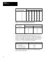
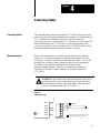
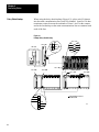
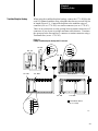
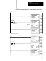
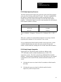
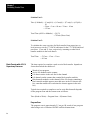
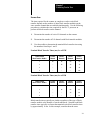
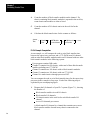
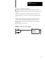
AllenBradley
Direct
Communication
Module
(Cat. No. 1771-DCM)
User
Manual
Table of Contents
To Our Customers . . . . . . . . . . . . . . . . . . . . . . . . . . . . . . .
11
To Our Customers . . . . . . . . . . . . . . . . . . . . . . . . . . . . . . . . . . .
Manual's Purpose . . . . . . . . . . . . . . . . . . . . . . . . . . . . . . . . . . .
Intended Audience . . . . . . . . . . . . . . . . . . . . . . . . . . . . . . . . . . .
Terminology . . . . . . . . . . . . . . . . . . . . . . . . . . . . . . . . . . . . . . . .
Related Publications . . . . . . . . . . . . . . . . . . . . . . . . . . . . . . . . . .
11
11
11
11
11
Overview of Direct Communication Module . . . . . . . . . . . .
21
Overview of Direct Communication Module . . . . . . . . . . . . . . . . . .
Describing the 1771DCM . . . . . . . . . . . . . . . . . . . . . . . . . . . . . .
Choosing 1771DCM or Data Highway . . . . . . . . . . . . . . . . . . . . .
Selecting Options . . . . . . . . . . . . . . . . . . . . . . . . . . . . . . . . . . . .
Example Applications . . . . . . . . . . . . . . . . . . . . . . . . . . . . . . . . .
Compatible Processors . . . . . . . . . . . . . . . . . . . . . . . . . . . . . . .
Keying . . . . . . . . . . . . . . . . . . . . . . . . . . . . . . . . . . . . . . . . . . .
21
21
22
22
23
23
23
Selecting Options . . . . . . . . . . . . . . . . . . . . . . . . . . . . . . .
31
Selecting Options . . . . . . . . . . . . . . . . . . . . . . . . . . . . . . . . . . . .
Switch Bank 0 . . . . . . . . . . . . . . . . . . . . . . . . . . . . . . . . . . . . . .
Switch Bank 1 . . . . . . . . . . . . . . . . . . . . . . . . . . . . . . . . . . . . . .
31
32
34
Connecting Cables . . . . . . . . . . . . . . . . . . . . . . . . . . . . . .
41
Connecting Cables . . . . . . . . . . . . . . . . . . . . . . . . . . . . . . . . . . .
Module Connector . . . . . . . . . . . . . . . . . . . . . . . . . . . . . . . . . . .
Daisy Chain Hookup . . . . . . . . . . . . . . . . . . . . . . . . . . . . . . . . . .
Trunkline/Dropline Hookup . . . . . . . . . . . . . . . . . . . . . . . . . . . . .
41
41
42
43
Using the Status Word . . . . . . . . . . . . . . . . . . . . . . . . . . . .
51
Using the Status Word . . . . . . . . . . . . . . . . . . . . . . . . . . . . . . . .
Examining Status Bits . . . . . . . . . . . . . . . . . . . . . . . . . . . . . . . . .
Status Bits Read by the Local Processor . . . . . . . . . . . . . . . . . . .
Status Bits Read by the Supervisory Processor . . . . . . . . . . . . . .
51
51
52
53
Programming the 1771-DCM . . . . . . . . . . . . . . . . . . . . . . .
61
Programming the 1771-DCM . . . . . . . . . . . . . . . . . . . . . . . . . . .
Local Processor Logic . . . . . . . . . . . . . . . . . . . . . . . . . . . . . . . .
1771-DCM Switch Settings . . . . . . . . . . . . . . . . . . . . . . . . . . . . .
Supervisory Processor Logic . . . . . . . . . . . . . . . . . . . . . . . . . . .
Processor/Module Compatibility . . . . . . . . . . . . . . . . . . . . . . . . .
61
61
63
63
613
ii
Table of Contents
Calculating Transfer Time . . . . . . . . . . . . . . . . . . . . . . . . .
71
Calculating Transfer Time . . . . . . . . . . . . . . . . . . . . . . . . . . . . . .
Discrete Transfer Time . . . . . . . . . . . . . . . . . . . . . . . . . . . . . . . .
Block Transfer Time . . . . . . . . . . . . . . . . . . . . . . . . . . . . . . . . . .
Block Transfer with a PLC3 Supervisory Processor . . . . . . . . . . .
71
71
74
76
Troubleshooting Your 1771-DCM . . . . . . . . . . . . . . . . . . . .
81
Troubleshooting Your 1771-DCM . . . . . . . . . . . . . . . . . . . . . . . .
LED Display for Normal Operation . . . . . . . . . . . . . . . . . . . . . . . .
LED Display for Fault Conditions . . . . . . . . . . . . . . . . . . . . . . . . .
Causes of Block Transfer Errors . . . . . . . . . . . . . . . . . . . . . . . . .
Errors Indicated by Status Bits . . . . . . . . . . . . . . . . . . . . . . . . . .
Specifications . . . . . . . . . . . . . . . . . . . . . . . . . . . . . . . . . . . . . .
81
81
81
82
83
84
Chapter
1
To Our Customers
To Our Customers
The following information may be helpful when using this manual:
Manual's Purpose
The purpose of this manual is to help you understand the intended
application of your Direct Communication Module (cat. no.
1771-DCM) and operate your 1771-DCM correctly in the shortest
possible time. We show you how to:
Select Module Options to Fit your Application
Install and Connect Your 1771-DCM
Use Status Bits to Detect Faults
Program the Transfer of Data between Processors
Compute the Transfer Time between Processors
Troubleshoot Module or System Malfunctions
Chapter 3
Chapter 4
Chapter 5
Chapter 6
Chapter 7
Chapter 8
Intended Audience
We assume you are familiar with installing and using Allen-Bradley
programmable controllers and that you have written ladder diagram
programs. If not, we suggest that you study the Programming and
Operations Manual of your processor(s) listed below under Related
Publications.
Terminology
We have written this manual using current programmable controller
terminology and have attempted to keep it free of jargon. If you
encounter terms that you do not understand, we suggest that you obtain
the current booklet, Programmable Controller Terms, listed below under
Related Publications.
Related Publications
You should be able to install and operate your 1771-DCM without the
need for additional publications. If not, the following publications may be
of interest to you:
11
Chapter 1
To Our Customers
12
Title
Publication
1771ASB Remote I/O Adapter
17716.5.37
Programmable Controller Terms
PCGI7.2
PLC2/05 Programming Manual
17726.8.6
PLC2/15 Programming Manual
17726.8.2
PLC2/02, 2/16, 2/17 User's Manual
17726.5.8
PLC2/30 Programming Manual
17726.8.3
PLC3 Programming Manual
17756.4.1
PLC5 Family Processor Manual
17856.8.2
PLC5/250 Programmer's Manual
50006.4.1
Chapter
2
Overview of Direct Communication Module
Overview of Direct
Communication Module
Allen-Bradley has introduced the Direct Communication Module (cat. no.
1771-DCM) to meet the growing need for communication between PC
processors.
Describing the 1771DCM
The 1771-DCM is a chassis-mounted single-slot I/O module that allows
communication between a supervisory processor and local processors
(Figure 2.1). The local processor can be chassis-mounted or configured
as a local or remote system.
Figure 2.1
Local and Remote Configurations
Local Configuration
S
C
A
N
N
E
R
Local
Proc.
Bidirectional
Block Transfer
PLC-2
PLC-5
D
C
M
Supervisory
Processor
PLC–2/30
PLC–3 Family
PLC–5/15
PLC–5/25
PLC–5/250
Remote I/O Link
1771–ASB Protocol
Remote Configuration
Local
Processor
PLC–2/30
PLC–3 Family
PLC–5/250
S
C
A
N
N
E
R
1
7
7
1
A
S
Remote I/O Link
1771–ASB Protocol
Bidirectional
Block Transfer
D
C
M
S
C
A
N
N
E
R
Supervisory
Processor
PLC–2/30
PLC–3 Family
PLC–5/15
PLC–5/25
PLC–5/250
Remote I/O Link
1771–ASB Protocol
12825
21
Chapter 2
Overview of Direct
Communication Module
The 1771-DCM passes data table values such as command bits, status
bits, and data blocks between supervisory and local processors. The
supervisory processor typically writes commands and/or data table values
to the local processor, and reads resulting status, diagnostic data, and data
values from the local processor (or vice versa).
The supervisory processor communicates serially with the 1771-DCM as
though it were a 1771-ASB Adapter Module, and addresses the
1771-DCM as though it were addressing a separate I/O chassis. You
select the mode of transfer between the supervisory processor and
1771-DCM: discrete transfer (up to eight words) or block transfer (up to
64 words). Either mode includes one status word.
The local processor communicates with the 1771-DCM over the
backplane using block transfers and addresses the 1771-DCM as an
intelligent I/O module. When the local processor is remotely configured,
it communicates with the 1771-DCM via block transfer through its
scanner-adapter link.
Choosing 1771DCM or Data
Highway
The 1771-DCM and data highway allow communication between PC
processors. Consider the following factors when determining the
appropriate choice. Use the 1771-DCM to:
Transfer data table words
Obtain predictable transfer times
Transfer up to eight words when transfer time over a remote I/O
channel is adequate, in addition to the transfer time of the local
processor and 1771-DCM
Transfer up to 64 words when transfer time for block transfers over a
remote I/O channel is adequate, in addition to the transfer time of the
local processor and 1771-DCM
Decrease data highway traffic
At least one processor must have a remote I/O scanner.
You cannot transfer ladder diagram programs nor messages stored in the
message area of memory using the 1771-DCM.
Selecting Options
22
You can select one or more of the following options depending on your
application requirements using switches on the module:
Chapter 2
Overview of Direct
Communication Module
Baud Rate/Distance
Select the communication rate and distance to the supervisory proces
sor as either 57.6K baud to a distance of 10,000 feet, or 115.2K baud
to a distance of 5,000 feet.
Transfer Method
Select block transfer or discrete data transfer between the 1771DCM
and the supervisory processor.
Rack Size
When using discrete data transfer, select the number of slots that de
termines how the 1771DCM appears to the scanner of the superviso
ry processor (the size of the I/O chassis simulated by the 1771DCM).
This also determines the number of words transferred.
Protected Data
Select protected data to prevent block transfers from the local proces
sor until the supervisory processor has received the previous block
transfer.
I/O Rack Address
Designate the I/O rack number, the number of the first module group
of the I/O chassis simulated by the 1771DCM, and whether it has the
highest starting module group address of two or more chassis as
signed to the same rack address.
These options are described in Chapter 3.
Example Applications
You can use the 1771-DCM in a variety of applications where the transfer
of data table values is required. For example, consider using it to:
Call messages stored in the data table of the supervisory processor and
outputted through an ASCII I/O module (cat. no. 1771-DA) or BASIC
module (cat. no. 1771-DB)
Download recipe data table values from supervisory to local
processor(s) where you want local processor(s) to execute different
versions of the same program
Download commands from the supervisory processor to execute
different sections of a ladder diagram program at the local processor
Compatible Processors
Use the 1771-DCM with any Allen-Bradley programmable controller that
uses block transfer and the 1771 I/O structure.
Keying
Reserve an I/O slot for this module by placing keying bands on the
backplane connector. Position keying bands between the following
numbers labeled on the backplane adjacent to the upper backplane
connector. The keying bands mate with corresponding slots in the module
connector:
Between 2 and 4
Between 16 and 18
23
Chapter
3
Selecting Options
Selecting Options
Select one or more of the following options depending on your
application requirements. Do this by setting switches in Switch Banks 0
and 1 on the left (metal cover) side of the 1771-DCM. To assist you, we
have printed a table of switch settings for each switch bank on the
module’s cover next to the switches (Figure 3.1).
Figure 3.1
Tables for Switch Settings
BANK 0
SW SW L A S T
1
2 RACK
BAUD
RATE
Not
Used
57.6
115.2
SW T R A N S SW SW D A T A
3 M THD 4
5 PTCT
NO
YES
BLOCK
DSCRT
Not
Used
SW R A C K
S IZ E
6
NO
YES
P
L
C
_
2
1
2
3
4
5
6
7
P
L
C
5
&
5
/
2
5
0
P
L
C
_
3
NOTE: DO
SWITCH
1
2
3
4
5
6
00
01
02
03
04
05
06
07
10
11
12
13
14
15
16
17
20
21
22
23
24
25
26
27
30
31
32
33
34
35
36
37
NOT USE OTHER SWITCH POSITIONS
7
8
1/4
1/2
3/4
FULL
BANK 1
I/O R A C K
NUMBER
SWITCH
F IR S T
SWITCH
M O D U LE
8
GROUP NO. 7
0
2
4
6
B
A
N
K
0
B
A
N
K
1
1
2
3
4
5
6
7
8
1
2
3
4
5
6
7
8
ON
CLOSED
OFF
OPEN
17906
31
Chapter 3
Selecting Options
Each switch bank has eight switches. Set each switch to the ON (closed)
position by depressing the right-hand side of the switch or to the OFF
(open) position by depressing the left-hand side of the switch (Figure 3.2).
Figure 3.2
Example Switch Bank
1
Switches 1 and 3 are OFF (open)
2
Shading represents the switch position
3
4
5
OPEN
6
7
8
12826
Switch Bank 0
The options that you select with Switch Bank 0 are as follows:
Switch 1 Baud Rate
ON (Closed) for 57.6K Baud
OFF (Open) for 115.2K Baud
Set the baud rate equal to that of the scanner of your supervisory
processor. You can transmit data up to 10,000 feet at a data rate of
57.6K baud or up to 5,000 feet at a data rate of 115.2K baud.
Switch 2 Not Used
32
Chapter 3
Selecting Options
Switch 3 Last Rack
ON (Closed) Not Last Rack
OFF (Open) Last Rack
If the 1771-DCM is assigned the same I/O rack number as other I/O
chassis, designate whether this I/O chassis is the last chassis (has the
highest starting module group number) of those assigned the same rack
number. (Refer to I/O Rack Number below.)
Switch 4 Transfer Method
ON (Closed) for Block Transfer
OFF (Open) for Discrete Data Transfer
Choose either discrete data transfer or block transfer between the
supervisory processor and 1771-DCM. With discrete transfer, the rack
size you select determines the number of words transferred as either 2, 4,
6, or 8 words including a status word. Data is transferred between the
1771-DCM and the supervisory processor as serial remote I/O data for
each slot of the simulated I/O chassis. The supervisory processor updates
the 1771-DCM as if it were an I/O chassis on a remote I/O link.
With block transfer, you can transfer up to 64 words including a status
word. The 1771-DCM appears to the supervisory processor as a remote
1/4 rack. Data is transferred between the first I/O slot simulated by the
1771-DCM and the supervisory processor when the supervisory
processor’s ladder program executes block transfers.
Communication between the 1771-DCM and local processor is always
block transfer regardless of the mode of communication between
1771-DCM and supervisory processor.
Switch 5 Not Used
Switch 6 Protected Data
ON (Closed) for Unprotected Data
OFF (Open) for Protected Data
This option maintains data integrity and maintains the order of data blocks
sent from the local processor to the supervisory processor only when you
select block transfer. The 1771-DCM does not recognize the start of a
33
Chapter 3
Selecting Options
new write block transfer from the local processor until the supervisory
processor has read the previous data from the 1771-DCM.
When you select unprotected data, the local processor updates the
1771-DCM continually, regardless of whether the supervisory processor
has read the data from the 1771-DCM.
Switches 7 and 8 Rack Size
Switch 7
Switch 8
Rack Size
ON
ON
1/4
ON
OFF
1/2
OFF
ON
3/4
OFF
OFF
Full
When your application requires the transmission of discrete data words,
the 1771-DCM appears to the scanner of the supervisory processor as a
4-, 8-, 12-, or 16-slot remote I/O chassis for the transfer of either 2, 4, 6,
or 8 words respectively. Select the equivalent rack size depending on the
number of words of discrete data you want to write or read. One slot is
equivalent to eight discrete data bits. One module group is equivalent to a
word. A full rack is equivalent to eight data words. The 1771-DCM
inserts one status word in the transfer regardless of the equivalent rack
size you select.
When you set the 1771-DCM for block transfer, the 1771-DCM appears
to the scanner of the supervisory processor as a block transfer module in
the first module group of a four-slot chassis (1/4 rack). You can read and
write up to 64 words including one status word. Slots 1 through 3 are not
used.
Switch Bank 1
The options that you select with Switch Bank 1 are as follows:
Switches 1 through 6 I/O Rack Number
34
PLC2 Family
PLC3 and PLC5/250
PLC5/15
PLC5/25
17
0 thru 37 octal
13
17
Chapter 3
Selecting Options
Designate the I/O rack number that you assign to the 1771-DCM with
Switches 1 - 6 of Switch Bank 1 (Table 3.A).
Table 3.A
I/O Rack Number Selection for PLC2, PLC3, and PLC5 Family Processors
Switch
I/O Rack Number (Octal)
1
2
3
4
5
6
1
0
ON
ON
ON
ON
ON
ON
P
2
1
ON
ON
ON
ON
ON
OFF
L
3
ON
ON
ON
ON
OFF
ON
C
4
ON
ON
ON
ON
OFF
OFF
ON
ON
ON
OFF
ON
ON
ON
ON
ON
OFF
ON
OFF
6
PLC2 5/15
3
PLC4
5/25
5
7
6
ON
ON
ON
OFF
OFF
ON
7
ON
ON
ON
OFF
OFF
OFF
10
ON
ON
OFF
ON
ON
ON
11
ON
ON
OFF
ON
ON
OFF
12
ON
ON
OFF
ON
OFF
ON
13
ON
ON
OFF
ON
OFF
OFF
14
ON
ON
OFF
OFF
ON
ON
15
ON
ON
OFF
OFF
ON
OFF
16
ON
ON
OFF
OFF
OFF
ON
17
ON
ON
OFF
OFF
OFF
OFF
20
ON
OFF
ON
ON
ON
ON
21
ON
OFF
ON
ON
ON
OFF
22
ON
OFF
ON
ON
OFF
ON
23
ON
OFF
ON
ON
OFF
OFF
24
ON
OFF
ON
OFF
ON
ON
25
ON
OFF
ON
OFF
ON
OFF
26
ON
OFF
ON
OFF
OFF
ON
27
ON
OFF
ON
OFF
OFF
OFF
5
2
PLC-3
&
PLC5/250
35
Chapter 3
Selecting Options
Switch
I/O Rack Number (Octal)
1
2
3
4
5
6
30
ON
OFF
OFF
ON
ON
ON
31
ON
OFF
OFF
ON
ON
OFF
32
ON
OFF
OFF
ON
OFF
ON
33
ON
OFF
OFF
ON
OFF
OFF
34
ON
OFF
OFF
OFF
ON
ON
35
ON
OFF
OFF
OFF
ON
OFF
36
ON
OFF
OFF
OFF
OFF
ON
37
ON
OFF
OFF
OFF
OFF
OFF
Switches 7 and 8 First (Starting) Module Group Number
First Module
Switch
Group Number
7
8
0
ON
ON
2
ON
OFF
4
ON
ON
6
OFF
OFF
Assign a unique stating module group number--such as 0, 2, 4, or 6--in
accordance with the number of chassis you assigned to the same I/O rack
number. You can assign from one to four 1771-DCMs and I/O adapters to
the same I/O rack number, provided that the combination does not exceed
a full rack. For example, assign starting module group numbers to each
I/O chassis or 1771-DCM in the following combinations:
Rack Configuration
Assign Module Group Numbers
• Four 1/4 Racks
0, 2, 4, and 6
• Two 1/2 Racks
0 and 4
• One 1/4 and One 3/4 Rack
0 and 2
• One 3/4 and One 1/4 Rack
0 and 6
You selected the equivalent rack size of your 1771-DCM with Switch
Bank 0, Switches 7 and 8, above.
36
4
Chapter
Connecting Cables
Connecting Cables
The communications channel between the 1771–DCM and a supervisory
processor is the same serial communications channel as used between the
1771–ASB Remote I/O Adapter (Series A) and the scanner of a
supervisory processor. You insert the 1771–DCM in a local or remote I/O
chassis and configure the 1771–DCM as an I/O chassis unique to the
supervisory processor. You can connect the 1771–DCM in a daisy chain
or trunkline/dropline hookup with other remote I/O chassis.
Module Connector
Make your connections to the connector at the bottom of the module
(Figure 4.1). Connector terminals are labeled at the bottom of the left
cover plate. Connector terminals accommodate two cables––one for the
incoming line of a daisy chain hookup, the other for the outgoing line.
Use either set of connector terminals for the dropline in the
trunkline/dropline hookup. Terminal 1 is connected to Terminal 4,
Terminal 2 to Terminal 5, and Terminal 3 to Terminal 6 inside the
1771–DCM.
WARNING: Do not disconnect this connector in a daisy chain
hookup when the system is operating because you disconnect
the remaining I/O chassis in the daisy chain. The connection
between terminals is inside the 1771–DCM.
Figure 4.1
Cable Connections
Line 2
(Clear)
1
Shield
Line 1
(Blue)
Line 2
(Clear)
I/O Cable
Shield
Line 1
Connector on 1771-DCM
(Blue)
1
Mating Connector
Install a 150 ohm 1/2 watt resistor when the 1771-DCM
is simulating the last I/O chassis in the daisy chain.
12827
41
Chapter 4
Connecting Cables
Daisy Chain Hookup
When using the daisy chain hookup (Figure 4.2), splice each I/O chassis
into the main communication line (serial I/O channel). Install a 150 ohm
terminator resistor between the terminals of Lines 1 and 2 at the scanner
and at the last hookup on the main communications line to terminate both
ends of the line.
Figure 4.2
Example Daisy Chain Hookup
1
1772 -SD2
PLC -2/30
2
Blue
Shield
Clear
Blue
Blue
1
Shield
Shield
2
Clear
Clear
3
1
1771 -ASB
1771 -DCM
1771 -ASB
1771 -ASB
Clear
2
Shield
Blue
1
2
1
42
Remote I/O Chassis
1771 -DCM
1 Install Terminator Resistor:
150ohm1/2 watt
Clear
Shield
Blue
12661
Chapter 4
Connecting Cables
Trunkline/Dropline Hookup
When using the trunkline/dropline hookup, connect the 1771–DCM to the
serial I/O channel trunkline using a dropline that does not exceed 100 feet
in length (Figure 4.3). Connect the dropline to the trunkline using a T
connector (cat. no. 1770–XG) or a station connector (cat. no. 1770–SC).
There are no restrictions as to the spacing between station connectors or T
connectors if you do not exceed the maximum cable distance. Terminate
the open port at the first and last T connector or station connector using a
Terminator Set (cat. no. 1770–XF).
Figure 4.3
Example Trunkline/Dropline Hookup with T Connectors
1
1772 -SD2
PLC -2/30
2
Blue
Shiel d
Clear
Bl ue
1
Shield
2
Clear
3
1771 -ASB
1
Remote I/O Chassis
1771 -DCM
1771 -ASB
1
1771 -ASB
Clear
Shield
1 Blue
2
1771 -DCM
1 Install Terminator Resistor
(cat. no. 1770XF)
2
1
12662
43
Chapter
5
Using the Status Word
Using the Status Word
The 1771-DCM sets status/alarm bits in the upper byte of the first word
transferred to either processor, regardless of whether you select block
transfer or discrete data transfer. In block transfer operation, the status
word is the first word of the read data block. In discrete data transfer, the
status word is found in the equivalent of the first module group of the I/O
chassis simulated by the 1771-DCM.
Important: Reserve the first transferred word for status data inserted by
the 1771-DCM. Be sure this word contains zeros when you initialize the
ladder program for either processor. The upper byte contains status data.
The lower byte is not available for transferring data under any
circumstances.
When you select discrete data transfer and set your rack size for the
number of words required for your application, keep in mind that the
number of words available for your data is one less than the number of
words transferred.
Examining Status Bits
Rack Size
Number of
Transfer Words
Words Available
For Your Data
1/4
2
1
1/2
4
3
3/4
6
5
Full
8
7
Examine bits in the upper byte of the status word using your ladder
program so it can take appropriate action when the 1771-DCM detects an
error or change in status. Upon detecting an error or change in status, the
1771-DCM sets an invalid data bit along with one or more bits that
indicate the nature of the error or change in status. These bits are
non-retentive.
51
Chapter 5
Using the Status Word
Bits in the status word read by the supervisory processor differ from those
read by the local processor. Some bits apply only when the 1771-DCM is
communicating with the supervisory processor by block transfer.
Status Bits Read by the Local
Processor
When the 1771-DCM detects an error in its communication with the
supervisory processor, it indicates this condition in the status word read by
the local processor as follows:
17
16
15
Insuf
Excess
Scanner
Data
Data
Comm
14
13
12
No
0
Data
0
11
10
Inhibit
Invalid
Outputs
Data
Error
Bit 17 Insufficient Data Available
Set by the 1771-DCM when data received from the supervisory processor
is less than that requested by the local processor. It appends zeroed data
words to provide the requested number of words.
Bit 16 Excessive Data Available
Set by the 1771-DCM when the data received from the supervisory
processor is more than that requested by the local processor. It truncates
the data and returns only the number of words requested.
Important: In block transfer mode, the 1771-DCM sets Bit 17 or 16
(defined above) when it detects that the length of a read block transfer
request from one processor differs from the number of words previously
written by the other processor. In discrete data transfer, the 1771-DCM
sets Bit 17 or 16 when it detects that the number of words read by one
processor differs from the number of words that the 1771-DCM
temporarily stored. This depends on the equivalent rack size that you set,
such as eight slots for four words.
Bit 15 Scanner Communications Error
Set by the 1771-DCM when it detects a loss in communications with the
scanner of the supervisory processor followed by a request for a read
block transfer from the local processor. The 1771-DCM returns the last
data received from the scanner, or zeroed data words if communications
had not been established. The 1771-DCM turns off the serial
communications LED until communications are restored.
52
Chapter 5
Using the Status Word
Bit 14 Not Used
Bit 13 No Data Available
Set by the 1771-DCM at power-up. The 1771-DCM rests this bit when it
receives data from the supervisory processor.
Bit 12 Not Used
Bit 11 Inhibit Outputs
Set by the 1771-DCM to inform the local processor that the supervisory
processor has been switched to program or test mode, has switched itself
to program mode because of a dependent I/O fault (PLC-2 family), or that
the 1771-DCM has lost communication with the supervisory processor.
Bit 10 Invalid Data
Set by the 1771-DCM whenever it sets any other status bit. As long as
this bit is reset, the 1771-DCM has detected no error condition or change
in status.
Status Bits Read by the
Supervisory Processor
When the 1771-DCM detects an error in its communication with the local
processor, it indicates this condition in the status word read by the
supervisory processor as follows:
17
16
15
14
13
12
11
10
Insuf
Excess
Backplane
Backplane
No
Old
0
Invalid
Data
Data
Reset
Error
Data
Data
Data
Bits 17, 16, 13, and 10 Same as Local Processor
Bit 15 Backplane Reset
Set by the 1771-DCM to inform the supervisory processor that the local
processor has reset the backplane. The local processor typically resets the
backplane when switched to program/test mode, or when it detects a fault
condition and turns off outputs. The 1771-DCM cannot detect a
backplane reset due to a fault condition resulting in outputs remaining in
last state. You determine the last state condition (hold last state or turn
off) by a DIP switch on the I/O chassis.
53
Chapter 5
Using the Status Word
Bit 14 Backplane Error
Set by the 1771-DCM whenever it detects that a block transfer operation
by the local processor was not completed on time, was out of sequence, or
contained a checksum error. The 1771-DCM returns the last valid data
received from the local processor. It returns zeroed data words if
communications had not been established. It inhibits block transfers to
the local processor until it detects a backplane reset or a scan from the
local processor.
Bit 12 Old Data
Set by the 1771-DCM whenever it detects that it has not received data
from the local processor after a delay of 14 read scans by the supervisory
processor (discrete data transfer), or since the last read block transfer by
the supervisory processor. The 1771-DCM passes old data to the
supervisory processor until it detects new data, passes it, and resets this
bit.
Bit 11 Not Used
54
Chapter
6
Programming the 1771-DCM
Programming the 1771-DCM
We assume that you are familiar with block transfer programming, that
you can allocate data table areas for read and write data blocks, and that
you can manipulate data to and from these data blocks. We will confine
this discussion to programming characteristics unique to the 1771–DCM.
Local Processor Logic
The local processor, typically a PLC–2 family mini–processor or PLC–5
family processor, reads and writes data to the 1771–DCM using block
transfers. Programming examples (Figure 6.1, Figure 6.2) assume that the
1771–DCM is set for six–word block transfers.
Figure 6.1
Local Processor Programming Example (PLC-2)
BLOCK XFER READ
Data Address:
0030
Module Address:
131
Block Length:
06
File:
0300-0305
BTR Done Bit
113
300
17
10
Data Valid Bit
Buffer File
FILE TO FILE MOVE
0040
Counter Address:
Position:
001
File Length:
006
File A:
0300-0305
File R:
0400-0405
Rate per Scan:
006
BLOCK XFER WRITE
0031
Data Address:
131
Module Address:
06
Block Length:
0200-0205
File:
013
EN
17
113
DN
17
0040
EN
17
0040
DN
15
013
EN
16
113
DN
16
61
Chapter 6
Programming the 1771-DCM
Block Transfer and File Move Instructions
Enter these instructions using the following information:
BTR/BTW Module Address
The module address of BTR and BTW instructions in the local
processor’s program is the physical location of the 1771–DCM. It is the
I/O rack, module group, and slot number (RGS) of the 1771–DCM:
In the same I/O chassis with the local processor
In an I/O chassis connected to a processor configured for local or
remote I/O operation
Block Length/File Length
Generally, set them to the number of words that you set for the
1771–DCM. If you have reason to set the read block length different
from the write block length (PLC–2 family processors), be sure that both
the BTR and BTW instructions cannot be enabled in the same scan.
When moving or transferring words into the BTW file for transfer to the
1771–DCM, be sure to avoid placing data in the first word because the
1771–DCM inserts status in this word.
File–to–File Move (FFM)
Use this instruction to store data received from the 1771–DCM. File A
address of the FFM is the same as the BTR file address. File R address is
a storage file for data received from the 1771–DCM.
Your ladder program must place data into the BTW file for transfer to the
1771–DCM. We leave this ladder logic to you because your application
and processor’s set of instructions determine how you would do this.
Examine the status word received from the 1771–DCM as a condition for
using the read block transfer data. Zero the status word at power–up and
be sure that your program does not use this word for any other purpose.
62
Chapter 6
Programming the 1771-DCM
Figure 6.2
Local Processor Programming Example (PLC-5)
Rung 2:0
PLC5 local write rung. The DCM is located in the same I/O chassis as the PLC5, and is set for block transfer. The local proces
sor's write length must match the supervisory processor's read length.
BTR
BTW
ENABLE BIT
ENABLE BIT
BTW
N12:5
N12:0
BLOCK TRNSFR WRITE
EN
15
15
Rack
0
DN
Group
3
Module
1
ER
Control Block
N12:5
Data file
N13:30
Length
17
Continuous
N
Rung 2:1
PLC5 local read rung. The DCM is located in the same I/O chassis as the PLC5, and is set for block transfer. The local proces
sor's read length must match the supervisory processor's write length.
BTR
ENABLE BIT
N12:0
BTW
ENABLE BIT
N12:5
15
15
1771-DCM Switch Settings
BTR
BLOCK TRNSFR READ
Rack
0
Group
3
Module
1
Control Block
N12:0
Data file
N13:30
Length
21
Continuous
N
EN
DN
ER
Select module operating conditions by setting switches on the module for
discrete data transfer or block transfer as follows:
Discrete Data Transfer
•
•
Transfer Method
Rack Size
Block Transfer
•
•
Transfer Method
Data Protect (If Applicable)
Set other switches as required by your application.
Supervisory Processor Logic
The addresses that you use for the 1771–DCM in the supervisory
processor’s ladder program are the addresses (RGS) to which you
configure your 1771–DCM using Switch Banks 0 and 1:
I/O Rack Number (Switch Bank 1, Switches 1 through 6).
63
Chapter 6
Programming the 1771-DCM
First (Starting) Module Group Number (Switch Bank 1, Switches 7 and
8)
The slot number will always be zero for block transfer only.
Equivalent rack size for discrete data transfer only (Switch Bank 0,
Switches 7 and 8). The equivalent rack size for block transfer mode is
fixed at 1/4 rack.
Discrete Data Transfer
The supervisory processor transfers discrete data to and from the
1771–DCM automatically via its I/O scan. You do not program these
transfers.
To transfer discrete data words to and from the 1771–DCM, you must use
I/O image table addresses in the supervisory processor’s ladder program
starting with the addresses (RGS) to which you configured your
1771–DCM. Use the number of image table words equal to the
equivalent I/O rack size that you set for the 1771–DCM.
The ladder program of your supervisory processor must move discrete
data, read from the 1771–DCM, from input image table words to a storage
location (Figure 6.3).
Figure 6.3
Supervisory Processor Programming Example for Discrete Data Transfer (PLC-2/30)
FFM Done Bit
041
120
15
Data Valid Bit
10
Buffer File
FILE TO FILE MOVE
Counter Address:
0041
Position:
001
File Length:
008
File A:
0120-0127
File R:
0700-0707
Rate per Scan:
008
0041
EN
17
0041
DN
15
Your ladder program must place data into output image table words for
transfer to the 1771–DCM. Avoid placing data in the first word because
the 1771–DCM inserts status in this word. We leave this ladder logic to
you because your application and processor’s set of instructions determine
how you would do this.
64
Chapter 6
Programming the 1771-DCM
Example 1:
Suppose you want to transfer six words, and you have configured the
1771–DCM to simulate a 3/4 I/O rack with the following address:
Rack Number = 2, First Module Group = 0. Also, suppose that the
1771–DCM is located in the same chassis with the local processor,
that the 1771–DCM’s actual location (RGS) is 131, that the local
processor’s block transfer read block is 300 through 305, and that the
block transfer write block is 200 through 205.
Data transfers would occur as follows:
Supervisory Processor
To
Local Processor
Output Image Table Words Match the I/O
Chassis Slots Simulated by the
1771-DCM
BTR Instruction Reads Data from the 1771-DCM
into Words 300 through 305
020 Status Word (Zeroed)
021 First Data Word
022 Second Data Word
:
:
025 Fifth Data Word
300 Status Word (Inserted by DCM)
301 First Data Word
302 Second Data Word
:
:
305 Fifth Data Word
Local Processor
To
Supervisory Processor
BTW Instruction Writes Data to the
1771-DCM from Words 200 through
205
Input Image Table Words Match the I/O Chassis
Slots Simulated by the 1771-DCM
200 Status Word (Zeroed)
201 First Data Word
202 Second Data Word
:
:
205 Fifth Data Word
120 Status Word (Inserted by DCM)
121 First Data Word
122 Second Data Word
:
:
125 Fifth Data Word
65
Chapter 6
Programming the 1771-DCM
Your ladder program for the supervisory processor must place data in
output image table word addresses for transfer to the 1771–DCM and
move data from input image table word addresses as needed by your
application. We leave this ladder logic to you because your application
and processor’s set of instructions determine how you would do this.
Block Transfer
We present block transfer rungs for the supervisory processor when the
1771–DCM is operating in block transfer mode (Figure 6.4 for a
PLC–2/30 supervisory processor, Figure 6.5 for PLC–3, and Figure 6.6
for a PLC–5 family processor).
66
Chapter 6
Programming the 1771-DCM
Figure 6.4
Block Transfer Programming Example for PLC-2 Family Local and Supervisory Processor
LOCAL PROCESSOR
BLOCK XFER READ
0030
Data Address:
131
Module Address:
00
Block Length:
0300-0377
File:
BTR Done Bit
113
300
17
10
Data Valid Bit
Buffer File
FILE TO FILE MOVE
Counter Address:
0040
Position:
001
File Length:
064
File A:
0300-0377
File R:
0400-0477
Rate per Scan:
064
BLOCK XFER WRITE
0031
Data Address:
Module Address:
131
Block Length:
00
File:
0200-0277
SUPERVISORY PROCESSOR
BLOCK XFER READ
Data Address:
0032
Module Address:
200
Block Length:
00
File:
0600-0677
BTR Done Bit
120
600
07
10
Data Valid Bit
Buffer File
FILE TO FILE MOVE
Counter Address:
0042
Position:
001
File Length:
064
File A:
0600-0677
File R:
0700-0777
Rate per Scan:
064
BLOCK XFER WRITE
0033
Data Address:
200
Module Address:
00
Block Length:
0500-0577
File:
013
EN
17
113
DN
17
0040
EN
17
0040
DN
15
013
EN
16
113
DN
16
020
EN
07
120
DN
07
0042
EN
17
0042
DN
15
020
EN
06
120
DN
06
67
Chapter 6
Programming the 1771-DCM
Figure 6.5
Block Transfer Programming Example for PLC-3 Supervisory Processor
BTR Done Bit
WB001:0000
BTR
15
Read Request
WB001:0000
17
BTR Done Bit
WB001:0000
15
68
MVF
BTW
BLOCK XFER WRITE
Rack:
002
Group:
0
Module:
0 = Low
Data:
FB003:0000
Length:
064
CNTL:
FB001:0000
MVF
WB002:0000
10
Data Valid Bit
BLOCK XFER READ
Rack:
002
Group:
0
Module:
0 = Low
Data:
FB002:0000
Length:
064
CNTL:
FB001:0000
FILES FROM A TO R
Buffer File
File A:
File R:
Counter:
Pos/Len:
Mode:
FB002:0000
FB004:0000
C0005
0/ 64
ALL/SCAN
CNTL
LE
12
CNTL
DN
15
CNTL
ER
13
CNTL
LE
02
CNTL
DN
05
CNTL
ER
03
C0005
EN
12
C0005
DN
15
C0005
ER
13
Chapter 6
Programming the 1771-DCM
Figure 6.6
Block Transfer Programming Example for PLC-5 Family Supervisory Processor
Rung 2:2
PLC5 supervisory write rung. The DCM is connected via remote I/O to the PLC5, and is set for 57.6K baud, block
transfer, and rack 3. The supervisory processor's write length must match the local processor's read length.
BTR
BTW
ENABLE BIT ENABLE BIT
N22:5
N22:0
15
15
BTW
BLOCK TRNSFR WRITE
Rack
3
Group
0
Module
0
Control Block
N22:0
Data file
N19:0
Length
31
Continuous
N
EN
DN
ER
Rung 2:3
PLC5 supervisory read rung. The DCM is connected via remote I/O to the PLC5, and is set for 57.6K baud, block
transfer, and rack 3. The supervisory processor's read length must match the local processor's write length.
BTR
BTW
ENABLE BIT ENABLE BIT
N22:5
N22:0
15
15
BTR
BLOCK TRNSFR READ
Rack
3
Group
0
Module
0
Control Block
N22:5
Data file
N19:40
Length
27
Continuous
N
EN
DN
ER
69
Chapter 6
Programming the 1771-DCM
Figure 6.7
Block Transfer Programming Example for PLC-5/250 Supervisory Processor
Rung 1STEP0:0
PLC5/250 supervisory write rung. The DCM is connected via remote I/O to the PLC5/250. The DCM baud rate switch
setting must match that of its scanner channel. The DCM rack switches are set for rack 7. The local processor's read
length must match the supervisory processor's write length.
BTR
BTW
ENABLE BIT ENABLE BIT
BR070:0
BW070:0
EN
EN
BTW
BLOCK TRNSFR WRITE
Rack
007
Group
0
Module
0
Control Block
BW070:0
Data file
1BTD2:1
Length
17
Continuous
NO
BT Timeout
4
Rung 1STEP0:1
PLC5/250 supervisory read rung. The DCM is connected via remote I/O to the PLC5/250. The DCM baud-rate switch
setting must match that of its scanner channel. The DCM rack switches are set for rack 7. The local processor's write
length must match the supervisory processor's read length.
BTR
BTW
ENABLE BIT ENABLE BIT
BTR
BR070:0
BW070:0
BLOCK TRNSFR READ
Rack
007
EN
EN
Group
0
Module
0
Control Block
BR070:0
Data file
1BTD3:1
Length
15
Continuous
NO
BT Timeout
4
610
EN
DN
ER
EN
DN
ER
Chapter 6
Programming the 1771-DCM
BTR/BTW Module Address
The module address of BTR and BTW instructions in the supervisory
processor’s program is the configured address of the 1771–DCM. It is the
I/O rack number and starting module group number (its slot number is
always zero for block transfer) that you set using Switch Banks 0 and 1).
Block Length/File Length
Generally, set them to the number of words that you set for the
1771–DCM. If you have reason to set the read block length different
from the write block length (PLC–2 family processors), be sure that both
the BTR and BTW instructions cannot be enabled in the same scan.
When moving or transferring words into the BTW file for transfer to the
1771–DCM, be sure to avoid placing data in the first word because the
1771–DCM inserts status in this word.
File–to–File Move (FFM) or (MVF)
Use this instruction to store data received from the 1771–DCM. File A
address of the FFM or MVF is the same as the BTR file address. File R
address of the FFM or MVF is a storage file for data from the
1771–DCM.
Your ladder program for the supervisory processor must place data into
the BTW file for transfer to the 1771–DCM. We leave this ladder logic to
you because your application and processor’s set of instructions determine
how you would do this.
Examine the status word received from the 1771–DCM as a condition for
using the read block transfer data. Zero the status word at power–up and
be sure that your ladder program does not use this word for any other
purpose.
611
Chapter 6
Programming the 1771-DCM
Example 2:
Suppose you want to transfer 64 words, and you have configured the
1771–DCM to simulate a block transfer module in Rack 2, First
Module Group = 0. Also suppose that the 1771–DCM is located in
the same chassis with the local processor, and that the 1771–DCM’s
actual location (RGS) is 131. In this example, you allocated data
blocks for block transfer as follows: (Refer to Figure 6.4 for
PLC–2/30, or Figure 6.5 for PLC–3 Programming)
Data Block
Supervisory Processor
Local Processor
Read
600 through 677
300 through 377
Write
500 through 577
200 through 277
Data transfers would occur as follows for PLC–2 family processors:
Supervisory Processor
Local Processor
BTW Instruction Writes Data to the
1771-DCM from Words 500 through
577
BTR Instruction Reads Data from the
1771-DCM into Words 300 through 377
500 Status Word (Zeroed)
501 First Data Word
502 Second Data Word
:
:
577 Last Data Word
300 Status Word (Inserted by DCM)
301 First Data Word
302 Second Data Word
:
:
377 Last Data Word
Local Processor
612
To
To
Supervisory Processor
BTW Instruction Writes Data to the
1771-DCM from Words 200 through
277
BTR Instruction Reads Data from the
1771-DCM into Words 600 through 677
200 Status Word (Zeroed)
201 First Data Word
202 Second Data Word
:
:
277 Last Data Word
600 Status Word (Inserted by DCM)
601 First Data Word
602 Second Data Word
:
:
677 Last Data Word
Chapter 6
Programming the 1771-DCM
Processor/Module Compatibility
Your 1771–DCM must have the following revision (or later) for
compatible block transfer operation with your processor.
Processor Family
1771-DCM Revision
PLC-3
F
PLC-5
E
PLC-5/250
E
Data transfers would occur as follows when the supervisory processor is a
PLC–3:
Supervisory Processor
To
Local Processor
BTW Instruction Writes Data to the
1771-DCM from Binary File 3, Words
0 through 63
BTR Instruction Reads Data from the 1771-DCM
into Words 300 through 377
FB003:0000 Status Word (Zeroed)
FB003:0001 First Data Word
FB003:0002 Second Data Word
:
:
FB003:0063 Last Data Word
300 Status Word (Inserted by DCM)
301 First Data Word
302 Second Data Word
:
:
377 Last Data Word
Local Processor
To
Supervisory Processor
BTW Instruction Writes Data to the
1771-DCM from Words
200 through 277
BTR Instruction Reads Data from the 1771-DCM
into Binary File 2, Words 0 through 63
200 Status Word (Zeroed)
201 First Data Word
202 Second Data Word
:
:
277 Last Data Word
FB002:0000 Status Word (Inserted by DCM)
FB002:0001 First Data Word
FB002:0002 Second Data Word
:
:
FB002:0063 Last Data Word
613
Chapter
7
Calculating Transfer Time
Calculating Transfer Time
The time required for the transfer of data from supervisory to local
processor (and vice versa) is the sum of three events:
Supervisory Processor and Remote I/O Scan Time
Transfer Time through the 1771-DCM
Local Processor Scan Time
The time required for the supervisory processor to communicate with the
1771-DCM depends on whether you select discrete data transfer (up to
eight words) or block transfer (up to 64 words), the number of other
remote I/O chassis, and the number of block transfer modules in the local
and remote I/O systems.
Discrete Transfer Time
You select the mode of transfer between the supervisory processor and the
1771-DCM as either discrete data transfer or block transfer. Discrete data
transfer is faster than block transfer.
Calculate the transfer time between processors when the 1771-DCM is
transferring discrete data by calculating the times associated with the
supervisory processor, 1771-DCM, and the local processor. Assume the
supervisory and local processor systems contain no other block transfer
modules.
Supervisory Processor
The supervisory processor reads discrete input data or writes discrete
output data to/from its I/O through its remote I/O scanner. Calculate the
total scan time of the supervisory processor as the sum of the program
scan, processor I/O scan if applicable, and the remote I/O scan using
values in the table as follows:
Scan
PLC2/30
PLC3
Program
5 ms/K Words
2.5 ms/K Words
Processor I/O
0.5 ms/Rack
N/A
Remote I/O
7 ms/Chassis
6 ms/Chassis
71
Chapter 7
Calculating Transfer Time
Total Scan (PLC-2) = Program + Processor I/O + Remote I/O
Total Scan (PLC-3) = Program + Remote I/O
1771DCM
The delay from the time the 1771-DCM receives data until it is ready for
data transfer is 15 ms. During this time, it detects errors and changes in
status and formats data.
Local Processor
The local processor reads data from or writes data to the 1771-DCM using
block transfer instructions, regardless of how data is transferred between
1771-DCM and supervisory processor. The time required is equal to the
program scan plus block transfer time which depends on the number of
words transferred.
Time for
PLC2/05
PLC2/15
PLC2/30 (Local)
Program Scan
15 ms/K
18 ms/K
5 ms/K
1 ms
4 ms
0.7 ms
0.08 ms/W
0.08 ms/W
0.08 ms/W
I/O Scan
Block Transfer
W = Number of Words Transferred
Total Scan = Program and I/O Scan + (Multiplier) x (Number of Words
Transferred)
See the appropriate processor manual for times for other processors.
Addition of Block Transfer Modules
Block transfer modules in the local I/O chassis can lengthen the I/O scan
time by the time required for each to perform a block transfer (worst
case). The delay depends on the number of block transfer modules
waiting to transfer and the number of words each will transfer. Calculate
the additional block transfer time for your processor as follows for each
block transfer module:
Time (Local) = Multiplier x (Number of Words Transferred)
72
Chapter 7
Calculating Transfer Time
Processor
Multiplier
PLC2/05, 2/15
0.08
PLC2/30 (Local)
0.08
PLC2 Family Example Computation
Suppose that a PLC-2/30 supervisory processor has a 6K program and
seven assigned rack numbers and the PLC-2/05 local processor has a 2K
program. There are no other block transfer modules in either the
supervisory or local systems.
1.
Calculate the time required to transfer eight words from supervisory
to local processor.
2.
Calculate the total time required if there are two additional block
transfer modules in the local chassis, transferring 64 words each.
Assume worst case.
Solution Part 1:
PLC-2/30 Supervisory Processor Scan Time:
Scan
PLC2/30
Program
5 ms/K Words
Processor I/O
0.5 ms/Rack
Remote I/O
7 ms/Chassis
Time (PLC-2/30)
= Program + Processor I/O + Remote I/O
= (5 ms)(6) + (0.5 ms)(7) + (7 ms)(7)
= 30 ms + 3.5 ms + 49 ms
= 82.5 ms
1771-DCM Delay: 15 ms
Local Processor Scan Time:
Time for
I/O Scan
PLC2/05
1 ms
Program Scan
15 ms/K
Block Transfer
0.08 ms/W
73
Chapter 7
Calculating Transfer Time
W = Number of Words Transferred
Scan = Program Scan + I/O Scan + (Multiplier) x (Number of Words
Transferred)
= (15 ms)(2) + 1 ms + (0.08)(8) ms
= 30 ms + 1 ms + 0.64 ms
= 31.6 ms
Transfer Time
= Supervisory + 1771-DCM + Local
= 82.5 ms + 15 ms + 31.6 ms
= 129 ms
Solution Part 2:
Additional time for two block transfer modules in the local chassis:
Time (PLC-2/05)
= 2(0.08 ms) x (Number of Words Transferred)
= 2(0.08 ms)(64) 1
= 10.2 ms
Total Transfer Time = Discrete Transfer + Block Transfer
= 129 ms + 10.2 ms
= 139 ms (Worst Case)
Block Transfer Time
When you select block transfer as the mode of transfer between the
supervisory processor and 1771-DCM, you can transfer up to 64 words
but the transfer time increases.
The time required for the transfer of data from supervisory to local
processor (and vice versa) is the sum of three events:
Supervisory Processor and Remote I/O Scan Time
Transfer Time through the 1771-DCM
Local Processor Scan Time
1771DCM and Local Processor
Refer to Discrete Data Transfer, above, for the time required by the
1771-DCM and the local processor. These times are the same for either
method of transfer between the supervisory processor and the 1771-DCM.
74
Chapter 7
Calculating Transfer Time
PLC2 Family Supervisory Processor
The time required by the supervisory processor is the sum of the program
scan, processor I/O scan, and remote I/O scan. The time is lengthened by
the number of enabled block transfer modules transferring data, one
module after the other, and on the number of words that each module
transfers. Calculate the time for a read or write operation for each enabled
block transfer module as follows:
Scan
PLC2/30
Program
5 ms/K Words
Processor I/O
0.5 ms/Rack
Remote I/O
7 ms/Chassis
Time (1 Module) = Program + Processor I/O + 2(Remote I/O) + 0.5W +
10
Where W = number of words transferred and 10 is an average constant
(typically, this constant is 4 for a read and 13 for a write).
If it is possible that all block transfer modules in the supervisory system
could be enabled at the same time, the worst case time for any one
transfer would include the waiting time for all other other block transfers.
PLC2 Family Example Computation
Suppose there are four block transfer modules in addition to the
1771-DCM that could be enabled simultaneously in a PLC-2/30
supervisory system. The local system has no additional block transfer
modules. Assume that the program has 4.8K words, there are six assigned
rack numbers in the remote I/O link, and that each block transfer is 64
words.
1.
Calculate the worst case time for the five modules to block transfer
their data.
2.
Calculate the worst case time for a block transfer from the
supervisory to the local processor.
75
Chapter 7
Calculating Transfer Time
Solution Part 1:
Time (1 Module) = (5 ms)(4.8) + (0.5 ms)(6) + 2(7 ms)(6) + (0.5)(64) +
10
= 24 ms + 3 ms + 84 ms + 32 ms + 10 ms
= 153 ms
Total Time (All Five Modules) = 5(153)
= 765 ms (Worst Case)
Solution Part 2:
To calculate the worst case time for block transfer from supervisory to
local processor via the 1771-DCM, add times for the 1771-DCM and local
processor: 15 ms and 31.6 ms, respectively, assuming no other block
transfer modules in the local chassis.
Total Time
Block Transfer with a PLC3
Supervisory Processor
= 765 ms + 15 ms + 31 ms
= 811 ms
The time required to complete a read or write block transfer depends on
factors that include the number of:
Words of user program
Active I/O channels on the scanner
I/O chassis entries in the rack list for the channel
I/O channels on the scanner that contain block transfer modules
Block transfer modules on the channel (if the I/O chassis containing a
block transfer module appears more than once in the I/O chassis rack
list, count the module once each time the chassis appears in the rack
list)
Typical time required to complete a read or write block transfer depends
on the program scan and the scanner scan as follows:
Time (Read or Write) = Program Scan + 2(Scanner Scan)
Program Scan
The program scan is approximately 2.5 ms per 1K words of user program
when using a mix of examine ON/OFF and block instructions.
76
Chapter 7
Calculating Transfer Time
Scanner Scan
The time required for the scanner to complete a read or write block
transfer depends on the number of other block transfer modules on the
same scanner channel that are enabled simultaneously. Use the following
procedure to calculate the time required for the PLC-3 processor to
perform all block transfers on the channel.
1.
Determine the number of active I/O channels on the scanner.
2.
Determine the number of I/O channels with block transfer modules.
3.
Use these tables to determine the nominal block transfer time using
the numbers from Steps 1 and 2.
Nominal Block Transfer Times (ms) for a BTW
Channels with
Block Transfer Modules
1 Active
Channel
2 Active
Channels
3 Active
Channels
4 Active
Channels
1
45
50
60
65
2
70
70
75
3
85
95
4
100
Nominal Block Transfer Times (ms) for a BTR
Channels with
Block Transfer Modules
1 Active
Channel
2 Active
Channels
3 Active
Channels
4 Active
Channels
1
35
50
50
60
2
60
60
65
3
70
80
4
90
Block transfer times typically are similar regardless of the type of block
transfer module or the number of words transferred. Nominal read block
transfer times typically are faster than nominal write block transfer times
by approximately 10 ms. In this example, consider them the same.
77
Chapter 7
Calculating Transfer Time
4.
Count the number of block transfer modules on the channel. If a
chassis containing block transfer modules is repeated in the rack list,
count chassis and modules as often as listed.
5.
Count the number of I/O chassis entries in the rack list for the
channel.
6.
Calculate the block transfer time for the scanner as follows:
Scanner
=
Time
Nominal
Time
x
# BT Modules
on the Channel
+
# I/O Chassis1
in Rack List
x 9 ms
PLC3 Example Computation
As an example, we will compute the read or write block transfer time
between the supervisory processor and a 1771-DCM in an I/O channel
with no other block transfer modules and in an I/O channel with two other
block transfer modules in the following system:
User program contains 20K words.
Channel 1 contains four I/O chassis, with a total of three block transfer
modules including one 1771-DCM.
Channel 2 contains two I/O chassis with no block transfer modules.
Channel 3 contains two I/O chassis with one 1771-DCM.
Channel 4 is made inactive through processor LIST.
You can compute the read or write block transfer times for the supervisory
processor in this example in four steps. Each of the following steps is
explained by an accompanying figure:
1.
Diagram the I/O channels of your PLC system (Figure 7.1), showing
the number of:
Block transfer modules in each I/O chassis
Block transfer I/O channels
I/O chassis entries in the rack list for each block transfer I/O
channel
Active I/O channels per scanner
A block transfer I/O channel is a channel that contains one or more
block transfer modules located in any chassis connected to the
channel.
78
Chapter 7
Calculating Transfer Time
An I/O chassis can appear more than once in a rack list of I/O
chassis. Count it and the block transfer module(s) that it contains as
often as it is listed.
Figure 7.1
Diagramming I/O Channels
Step 1 Diagram the chassis connected in series to each channel
(up to 4) of your scanner module. Then, fill in the information called fo below.
Example values have been added.
1
1
0
2
2
0
0
3
1
0
4
Make interactive thru processor LIST
0
= I/O chassis
n = number of block tranfer
modules in chassis
Description
Number
Ch 1
Ch 2
Ch 3
Ch 4
Active I/O channels
3
Block-transfer I/O channels
2
Block-transfer modules on each
I/O block transfer channel
3
0
1
0
I/O chassis on each block transfer
I/O channel
(I/O chassis in rack list)
4
0
2
0
12828
2.
Using information from the diagram of I/O channels (Figure 7.1),
look up the nominal time from the table in Figure 7.2.
79
Chapter 7
Calculating Transfer Time
Figure 7.2
Nominal Time Table
Step 2 Determine a time from the table. Example values have been added for a BTW instruction.
Number of Active I/O Channels
Active I/O channels
containing one or more
blocktransfer modules
1
1
2
3
4
Number of active I/O channels: 3
45
50
60
65
70
70
75
Number of active I/O channels containing one or
more blocktransfer module: 2
85
95
2
3
4
Time from table: 70 ms
100
Time (ms)
3.
12829
Compute the approximate transfer time for each block transfer I/O
channel. Use values from your channel diagram (Figure 7.1), a value
from the table (Figure 7.2), and the formula from Step 6 above. We
make these calculations for you in Figure 7.3.
Figure 7.3
Computing Channel Times
STEP 3:
710
Compute the scanner time for each block transfer channel.
Example values have been added.
Channel Time
CT
=
CT
=
CT1
=
[ 70 ms ] x [ 3 ] + [ 41 ] x 9 ms
210 ms + 3 x 9 ms
237 ms
CT2
=
Not a Block Transfer Channel
CT3
=
[ 70 ms ] x [ 1 ] + [ 21 ] x 9 ms
70 ms + 9 ms
79 ms
CT4
=
Not an Active Channel
Nominal
Time
x
# BT Modules
on BT Channel
+
I/O Chassis
-1 x 9 ms
on BT Channel
Chapter 7
Calculating Transfer Time
4.
Compute the approximate read or write block transfer time for
Channel 1 and Channel 3 (Figure 7.4).
Figure 7.4
Computing Block Transfer for Each Channel
STEP 4:
Compute the read or write block transfer time.
Example values have been added.
Program Scan
Time (Program)
=
=
=
2.5 ms/K Words x 20K Words
2.5 ms x 20
50 ms
Scanner Scan
Time (Read or Write)
=
237 ms for Channel 1 and 79 ms
for Channel 3 (from Step 3)
Block Transfer
Time Per Channel
Channel 1
=
Program Scan + 2 [Scanner Scan]
50 ms + 2 [ 237 ms ]
50 ms + 474 ms
524 ms
Channel 3
=
Program Scan + 2 [Scanner Scan]
50 ms + 2 [ 79 ms ]
50 ms + 158 ms
208 ms
Reducing PLC3 Scan Time
Due to the asynchronous scan relationship between program and scanner
and the serial operation of each channel in the scanner, we suggest that
you optimize the overall scan time. Although recommendations are
application dependent, we make the following recommendations as
general guidelines:
Whenever possible, control the manner in which block transfer
instructions are enabled. For example, if only a few block transfer
modules require frequent transfer of data, program them to run
continually. Inhibit block transfer instructions of those modules that
require less frequent transfer until enabled by a timer and/or some
application dependent condition.
Program the read and write block transfer instructions of your
1771-DCM in the same rung (Figure 6.5).
Distribute your block transfer modules equally between all four scanner
channels.
711
Chapter 7
Calculating Transfer Time
Distribute block transfer instructions equally throughout your program.
Place an equal number of non-block transfer rungs between block
transfer rungs.
For large numbers of block transfer instructions, distribute groups of
block transfer rungs equally throughout your program. Place no more
than four block transfer rungs consecutively in one group. Within each
group, condition the next rung using the done bit of the previous block
transfer instruction.
Consider an additional I/O scanner module (cat. no. 1775-S4A) if you
cannot otherwise reduce the block transfer times to meet your timing
requirements.
Special Timing Considerations
When using one 1775-S4A I/O scanner with thumbwheel switch set to 1,
only part of its data handling capacity is available for handling block
transfers. This scanner can store and transfer a maximum of 72 words at
any one time. This scanner can do four block transfer modules across any
of the active channels.
If a block transfer read instruction is enabled but the scanner’s buffer
cannot accept the instruction’s block length (the scanner is processing
other blocks of data), the block transfer instruction must wait for a
subsequent scan when the scanner’s buffer can accept all the words that
the module has to transfer. The same applies for a write block transfer
instruction. We suggest that you add an additional scanner if necessary.
Block Transfer Errors
Once enabled, a block transfer instruction in a PLC-3 ladder program will
set either a done bit or an error bit. The instruction indicates an error
when it illuminates the -(ER)- symbol. Typical block transfer errors occur
when:
You do not correctly enter the instruction:
- The rack, group, and module numbers do not match the location of
the installed module.
- You entered a file length greater than 64.
- You did not create the data file or the address that you entered does
not match the file you created.
Read and write error bits illuminate at the same time when the error
source is the module address entry or the file length entry in the
instruction block.
712
Chapter 7
Calculating Transfer Time
You have a communications problem.
You did not correctly connect the twin-axial cable to the scanner.
You did not connect a terminator resistor to each end of the twin-axial
cable.
When the scanner encounters a communication fault, it tries twice to
complete the transfer. It sets the error bit after the second unsuccessful
try.
When the scanner and/or processor detects a block transfer error, the
transfer is halted. Transfers from that module are prevented until:
Your program clears the instruction’s control word (clears the error,
Figure 7.5).
You locate and correct the error.
Figure 7.5
Resetting the Control Word after a Block Transfer Error
Control Word
03
13
MOV
Move from A to R
A : Storage Word
0000000000000000
R : Control Word
0000000000000000
713
Chapter
8
Troubleshooting Your 1771-DCM
Troubleshooting Your 1771-DCM When troubleshooting your 1771–DCM, check each of the following
sources in the order given for the cause of the fault:
LEDs on the 1771–DCM
Block transfer rungs in the ladder program of your local or supervisory
processor
Status bits in the status word read by the local or supervisory processor
LED Display for Normal
Operation
Under normal operating conditions, the LEDs are lit as follows:
Power (PWR)
ON
Serial Communication (SER COM)
ON
Backplane Communications
(BCKPLN COM)
ON
Module Fault (DCM FLT)
OFF
LED Display for Fault Conditions If a fault should occur, the LED display changes to indicate the source of
the fault which you diagnose as follows:
LED
Status
Diagnosis
PWR
OFF
The 1771-DCM is not getting +5V DC. Check the backplane
power supply.
SER COM
Blinking
Supervisory processor is in program or test mode. Check mode
selection.
Supervisory processor is not connected to the scanner. Check
the cable between processor and scanner (PLC-2/30 proces
sor).
Supervisory processor detected a fault and turned off outputs.
Check processor LEDs and status of outputs.
OFF
The supervisory processor is not communicating with the
1771-DCM. Check cable connections in the remote I/O link to
the 1771-DCM.
81
Chapter 8
Troubleshooting Your 1771-DCM
LED
BCKPLN
COM
Status
Blinking
Diagnosis
The 1771-DCM turns on this LED for half a second at the com
pletion of a read or write block transfer. This LED blinks when:
•
The local processor performs block transfers at a
rate slower than once every 1/2 second.
•
With the 1771-DCM in protected data mode, the
supervisory processor performs block transfers
at a rate slower than once every 1/2 second.
Reduce program scan and/or I/O scan time if possible in either
processor.
DCM FLT
OFF
No block transfers are occurring across the backplane between
the local processor and 1771-DCM. Refer to Block Transfer
Errors for the local processor, below.
ON
The 1771-DCM has detected an internal fault and is not operat
ing. Cycle power to the I/O chassis containing the 1771-DCM.
Replace it if the LED remains lit when you restore power.
If the 1771-DCM is the only thing connected to a supervisory
PLC-3, and the scanner baud is 115.2K, the DCM will stop
communicating and turn on the red fault light after approximate
ly 20 minutes of communication.
Causes of Block Transfer Errors
Observe block transfer rungs in the ladder diagram program of the
processor not performing block transfers. You have a block transfer error
when you observe one or both of the following:
The block transfer error bit is intensified (PLC–3 processor).
Enable and done bits of block transfer instructions either do not
intensify or remain intensified. They should alternately turn ON
(intensify) and turn OFF.
Block transfer errors are caused if one more more of the following are
incorrect:
The 1771–DCM’s location (RGS) in the local I/O chassis must match
the RGS of block transfer instructions in the local processor’s ladder
program.
The address of the I/O chassis simulated by the 1771–DCM (RGS)
must match the module address (RGS) of block transfer instructions in
the supervisory processor’s ladder program.
The block lengths of read and write block transfer instructions should
be equal (PLC–2 family processors); or if different, do not enable BTR
and BTW instructions in the same scan.
82
Chapter 8
Troubleshooting Your 1771-DCM
You assigned valid areas of data table for read and write blocks. For
example, if operating in discrete data transfer mode, I/O image table
addresses of the supervisory processor’s ladder program match the RGS
to which you configured the 1771–DCM.
Your conditioning instructions in block transfer rungs allow the rungs
to turn ON and OFF.
If using a PLC–2/30 supervisory processor, set the scanner for block
transfer operation.
If using a PLC–3 supervisory processor, create block transfer data files.
Errors Indicated by Status Bits
Display status bits in the status word read by either processor by
displaying the read block of the read block transfer instruction. Refer to
your processor’s manual for the procedure.
The first word in the data block is the status word. Hex codes of some
typical fault conditions are tabulated below:
Hex Code
Fault Condition
Read by Local Processor
0300
Supervisory processor is in program or test mode.
2300
No communication between the supervisory processor and its
scanner.
0900 or 2B00
1771-DCM has not received data from the supervisory proces
sor since power-up.
4100 or 8100
Number of words transferred between the supervisory proces
sor and 1771-DCM is not equal to the number read by the local
processor.
Read by Supervisory Processor
0500
1771-DCM has not received data from the local processor
since the last time it was read by the supervisory processor.
0900 or 0D00
1771-DCM has not received data from the local processor
since power-up.
1100
Local processor is not performing block transfers due to a time
out, out-of-sequence transfer, or checksum error.
2300
Local processor is not performing block transfers because it
reset the backplane.
4100 or 8100
Number of words transferred between the local processor and
1771-DCM is not equal to the number read by supervisory
processor.
83
Chapter 8
Troubleshooting Your 1771-DCM
Specifications
Function
• Provides Direct Communication
Between Supervisory and Local
Processors
Serial Communication
• Discrete Data Transfer: Up to
Seven Words Plus One Status Word
• Block Transfer: Up to 63 Words Plus
One Status Word
Transmission
• 10,000 Cable Feet at 57.6K Baud
• 5,000 Cable Feet at 115.2K Baud
Response Time
• Less than 15 ms
84
Interconnect Cable
• 1770-CD (Belden 9463 or Equivalent)
Backplane Current
• 1.2A
Keying
• Top Connector:
Between 2 and 4
Between 16 and 18
Environmental
• Operational Temperature:
0o to 60oC (32o to 140oF)
• Storage Temperature:
-40o to 85oC (-40o to 185oF)
• Relative Humidity:
5% to 95% (Without Condensation)
Index
A
Application Examples, 23
Audience, 11
Module Group Number, 36
O
Options, Selection of, 22, 31
B
Baud Rate, 32
Block Length, 62, 611
Block Transfer, 66
Errors, Causes of, 82
C
Connections to Module, 41
D
Data Highway, 22
Data Transfer
Block Transfer Example, 612
Discrete Data Example, 64
Data Words, Available, 51
Description of 1771-DCM, 21
Discrete Data Transfer, 71
E
Errors, Indicated by Status Bits, 83
I
Instructions
Block Transfer, 62
File Move, 62, 611
K
Keying, 23
L
LED Displays, 81
M
Module Address, 62, 611
Overview of 1771-DCM, 21
P
Processors, Compatible, 23
Programming, PLC-2 Family Processors
Local Processor, 61
Programming, PLC-3 Supervisory
Processor, 61, 63, 64, 67,
68, 69, 610
Supervisory Processor, 63
Protected Data, 33
Publications, Related, 11
Purpose of Manual, 11
R
Rack
Address, 23
Number, 34
Size, 34
Rack, Last, 33
S
Specifications, 84
Status Bits, 51
Status Word
Read by Local Processor, 52
Read by Supervisory Processor, 53
Switch Bank Settings on 1771-DCM, 32,
63
T
Terminator Resistor, 42, 43
Terminology, 11
Timing Considerations, PLC-3
Program Scan, 76
Reducing Scan Time, 711
Scanner Scan, 77
Special, 712
I–2
Index
Transfer Method, 33
Transfer Time, Block Transfer, 74
Example PLC-2/30 Supervisory
Processor, 75
Example PLC-3 Supervisory Processor,
78
Transfer Time, Discrete Data Transfer, 71
Example PLC-2 Family Processors, 73
Troubleshooting, 81
AllenBradley, a Rockwell Automation Business, has been helping its customers improve pro
ductivity and quality for more than 90 years. We design, manufacture and support a broad range
of automation products worldwide. They include logic processors, power and motion control
devices, operator interfaces, sensors and a variety of software. Rockwell is one of the worlds
leading technology companies.
Worldwide representation.
Argentina • Australia • Austria • Bahrain • Belgium • Brazil • Bulgaria • Canada • Chile • China, PRC • Colombia • Costa Rica • Croatia • Cyprus • Czech Republic •
Denmark • Ecuador • Egypt • El Salvador • Finland • France • Germany • Greece • Guatemala • Honduras • Hong Kong • Hungary • Iceland • India • Indonesia •
Ireland • Israel • Italy • Jamaica • Japan • Jordan • Korea • Kuwait • Lebanon • Malaysia • Mexico • Netherlands • New Zealand • Norway • Pakistan • Peru •
Philippines • Poland • Portugal • Puerto Rico • Qatar • Romania • RussiaCIS • Saudi Arabia • Singapore • Slovakia • Slovenia • South Africa, Republic • Spain •
Sweden • Switzerland • Taiwan • Thailand • Turkey • United Arab Emirates • United Kingdom • United States • Uruguay • Venezuela • Yugoslavia
AllenBradley Headquarters, 1201 South Second Street, Milwaukee, WI 53204 USA, Tel: (1) 414 3822000 Fax: (1) 414 3824444
Publication 1771-6.5.27 October, 1987
Supersedes 1771-6.5.27 - June 1985
PN 955102-95
Copyright 1987 AllenBradley Company, Inc. Printed in USA
Publication 1771-6.5.27 October, 1987