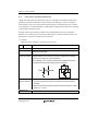
1
Section 6 Usage Precautions
Section 6 Usage Precautions
The quality and reliability of semiconductor devices is heavily influenced not only by the quality
inherent to the devices themselves, but also by the "use" conditions, environmental conditions and
how the selected circuits will be handled by the customer.
This section discusses all related precautions to be considered when deciding on parts for use
during system design, assembly, mounting and other component handling, during storage, or at
other times, including specific examples.
6.1
Device Selection
6.1.1
Maximum Ratings
Maximum ratings for semiconductor devices are defined as values which even momentarily must
not be exceeded. In this handbook, the concept of maximum ratings includes that of the absolute
maximum ratings. If a maximum rating is exceeded even for an instant, degradation or failure may
result. The subsequent lifetime of the device may be greatly shortened. In addition, differences in
the strength of individual products may mean that even though some products may withstand the
stress imposed when exceeding a maximum rating, others may abruptly fail.
In designing an electronic circuit with semiconductor devices, devices should be selected, or the
circuit designed, such that maximum ratings specified for devices are not exceeded, even given
fluctuations in external conditions during use.
In addition to DC maximum ratings, devices should be used with voltages, currents, power, and
times in the safe operating range at all points on the load locus curve. The power supply and
ground line serve as reference points for the semiconductor device operation. Special care should
be exercised to ensure that maximum ratings are not exceeded, including transient states.
Rev. 1.00 Aug. 31, 2006 Page 221 of 410
REJ27L0001-0100
Section 6 Usage Precautions
6.1.2
Derating
The quality and reliability of semiconductor devices are greatly influenced by the environment of
use. That is, products with the same quality may be less reliable in harsh environments, and more
reliable when the usage environment is less harsh. Even when used within the maximum ratings, if
a device is used under extremely stringent conditions equivalent to lifetime tests, wear-out-like
failures may result. Hence the concept of derating is extremely important.
Derating may be approached from two perspectives: derating with respect to design limits, and
derating with respect to manufacturing defects.
1. Derating with respect to design limits
When usage conditions become extremely harsh, the wear-out failure range may be entered
during the time of actual use, and if derating is not employed, it may become necessary to
schedule replacement of all devices as part of maintenance after operation for a certain length
of time in the application.
2. Derating with respect to manufacturing defects
Although the wear-out failure range is not entered while in the marketplace, if conditions of
use are harsh, the probability of occurrence of defects in the random failure range may no
longer be negligible.
Standard approaches to derating are described in table 6.1. In the "Temperature" row, junction part
temperatures assume intermittent use (for approximately three hours per day) over about 10 years.
Conditions for high-reliability applications, shown in parentheses, assume round-the-clock
operation over approx. 10 years.
Rev. 1.00 Aug. 31, 2006 Page 222 of 410
REJ27L0001-0100
Section 6 Usage Precautions
Table 6.1
Standard Examples of Derating Design*1
Derating Element*
Temperature
2
Diodes
Transistors
ICs
110°C or lower
Junction
3
temperature* (Tj = 60°C or lower)
HyICs
LDs
—
110°C or lower
(Tj = 60°C or
lower)
Topr min to Topr max
Device
(Ta = 0 to 45°C)
ambient
3
temperature*
Other
Humidity
Voltage
Current
Topr min to
Topr max
Ta = individual
specifications
—
Power consumption, ambient temperature,
heat-dissipation conditions Tj = Pd × θja + Ta
—
Rel. humidity
Relative humidity = 40 to 80%
Other
Normally, if there is condensation due to rapid changes in
temperature or for other reasons, the printed circuit board is
coated.
Breakdown
voltage
Maximum
Maximum
Conform to
rating × 0.8 or rating × 0.8 or catalog
less
less
recom(maximum
mended
rating × 0.5 or
conditions
less)
Overvoltage
Take measures to prevent overvoltage application, including electrostatic
discharge
Average
current
Ic × 0.5 or
less
(Ic × 0.25 or
less)
Ic × 0.5 or
less
Ic × 0.5 or
less
(especially
power ICs)
Conform to recommended
delivery specification conditions
Peak current
If (peak) × 0.8 Ic (peak) ×
or less
0.8 or less
Ic (peak) ×
0.8 or less
(especially
power ICs)
Conform to recommended
delivery specification conditions
Other
—
Take fanout, —
load
impedance
into
consideration
—
No
condensation
Conform to recommended
delivery specification conditions
Take optical
output Pomax
into
consideration
Rev. 1.00 Aug. 31, 2006 Page 223 of 410
REJ27L0001-0100
Section 6 Usage Precautions
Power
Pulse*
4
2
Diodes
Transistors
ICs
HyICs
Average
power
Maximum
rating × 0.5 or
less
(especially
Zener diodes)
Maximum
rating × 0.5 or
less
(especially
power
transistors)
Maximum rating
× 0.5 or less
(especially
power ICs,
high-frequency
ICs )
Conform to
Vf × If × Duty
recommended
delivery
conditions
ASO
Should not exceed individual catalog maximum ratings
Surge
If (surge) or
less
Derating Element*
Ic (peak) or
less
LDs
Ic (peak) or less Conform to recommended
delivery conditions
Notes: 1. Excludes special usage conditions, for example, extreme high temperatures.
2. These derating elements should be satisfied simultaneously wherever possible.
3. For applications requiring particularly high reliability, the values in parentheses ( )
should be used.
4. Generally where transient states are concerned, peak voltage including surges, current,
electric power, and junction temperature should be below maximum ratings, and
derating for reliability should be performed using the above average values. ASO (Area
of Safe Operation) will differ with the circuit used; please consult with one of our
engineers.
An example of derating for temperature is given in table 6.2. As the temperature rises, chemical
reactions in the materials constituting a semiconductor device are accelerated, and may result in a
failure. Generally reliability estimates are performed in terms of whether wear-out failure can be
guaranteed not to occur, based on the results of reliability tests and standard usage conditions in
the marketplace. Derating is performed after calculating the acceleration coefficient between the
lifetime test data, which has been confirmed by assuming the activation energy for the chemical
reactions for each failure mode, and the actual conditions of use. In general, temperature
acceleration alone does not result in a sufficient acceleration rate, but is ordinarily used together
with, for example, voltage and temperature difference. The acceleration limit for temperature must
be carefully analyzed. This is because a mistake in judgment may be made by other failure modes
governed by different reactions from that in the normal temperature range, such as the glass
transition temperature of plastic materials.
Rev. 1.00 Aug. 31, 2006 Page 224 of 410
REJ27L0001-0100
Section 6 Usage Precautions
Temperature Derating Characteristics (Example)
Example of Derating Application
Stress factor
Junction temperature
Failure judgment
criteria
Deterioration of electrical
characteristics
Failure mechanism Deterioration by chemical
reactions
Temperature Derating
10000
1000
Times
Table 6.2
0.5 eV
0.7 eV
0.9 eV
100
10
0.3 eV
1
Outline
The abscissa shows the reciprocal of absolute
temperature; the ordinate shows the time
required to reach the prescribed failure rate at
that temperature.
0.1
0
100
Temperature (°C)
200
How to calculate derating
Let us find the acceleration coefficients α in lifetime tests
It is believed that defects are caused by
with Tj values of 150°C and 65°C. For the activation energy,
chemical reactions of the material of which the
the general value of 0.5 eV for dielectric breakdown of the
devices are made. In general, in order for a
oxidation film is used.
reaction to take place energy has to be supplied
–5
α = exp [0.5/8.617 × 10 /(273 + 65)]
from outside.
–5
exp [0.5/8.617 × 10 /(273 + 150)]
Chemical reaction theory holds that this energy
comes from thermal kinetic energy. The
distribution of thermal kinetic energy follows the
Maxwell-Boltzmann law:
Lifetime = constant × exp (Ea/kT)
where
Ea = activation energy (eV)
T: absolute temperature (degrees K)
k: Boltzmann constant
(8.617 × 10⁻⁵eV/k)
An example of derating for humidity is shown in table 6.3. The primary purpose of this derating is
to prevent corrosive breaks of Al wiring and to reduce any changes in solderability accompanying
storage of package leads. Due to advances in plastic materials, corrosion and breakage of Al
wiring hardly ever occurs any more in the marketplace; but even today, use under extremely harsh
conditions may still result in wear-out failures within the expected period of useful life of a device.
Rev. 1.00 Aug. 31, 2006 Page 225 of 410
REJ27L0001-0100
Section 6 Usage Precautions
Table 6.3
Humidity Derating Characteristics (Example)
Example of Derating Application
Stress factor
Failure judgment
criterion
Temperature, relative
humidity
Deterioration of electrical
characteristics
Failure mechanism Metallization corrosion
Outline
Humidity Derating
Absolute humidity (mm Hg) (Source: Rikanenpyo)
Temperature/K
270
280
290
300
310
320
330
340
350
360
0
0.485
0.992
1.192
3.535
0.485
0.485
0.485
0.485
0.485
0.485
2
0.562
1.136
2.177
3.973
0.562
0.562
0.562
0.562
0.562
0.562
4
0.650
1.300
2.464
4.457
0.650
0.650
0.650
0.650
0.650
0.650
6
0.750
1.483
2.784
4.991
0.750
0.750
0.750
0.750
0.750
0.750
8
0.863
1.689
3.140
5.580
0.863
0.863
0.863
0.863
0.863
0.863
Since absolute humidity is proportional to the
number of water molecules contained in a unit
How to calculate derating
volume, in this example we approximate the
lifetime by the nth power of the stress that
We calculate the acceleration under typical conditions used in
governs the failure rate.
tests of ability to withstand humidity (65°C/95% RH) and
typical conditions in the marketplace (Ta = 25°C/65% RH).
Lifetime = constant × (absolute humidity) n
Taking the logarithms of both sides of this
equation, we obtain
log (lifetime) = n × log (absolute humidity) +
log (constant)
From the table, the saturation vapor pressure at 65°C is
calculated by the interpolation method to be 22.9 mmHg
and the saturation vapor pressure at 25°C is calculated to
be 2.8 mmHg.
The absolute humidity for value for each case is calculated by
Taking the logarithm of absolute humidity as
multiplying by 0.95 and 0.65, respectively.
the abscissa and the logarithm of the time
required to reach the prescribed failure rate at Taking the ratio and using the typical acceleration constant
2
n = 2 gives α = (21.7/1.8) = 145 times.
that absolute humidity as the ordinate, the
resulting graph is approximately a straight line.
Absolute humidity is a function of temperature
and relative humidity.
The absolute humidity can be obtained from
the following equation:
Absolute humidity = saturation absolute
humidity × relative humidity
An example of derating for temperature differences appears in table 6.4. The failure mechanism
assumes thermal fatigue failure of structural materials. This mode generally leads to wear-out
failure modes, and so adequate derating calculations are important for power devices and other
components. When designing thermal dissipation, the number of times heat stress is applied
during the lifetime of the semiconductor device and the temperature difference of the heat stress
must be taken into consideration.
Rev. 1.00 Aug. 31, 2006 Page 226 of 410
REJ27L0001-0100
Section 6 Usage Precautions
Voltage, current, and power derating is especially effective in preventing failure phenomena. In
particular, temperature-difference derating is strongly related to the occurrence of such failures,
that is, failures to which stress-strength models apply. In these cases, robustness against failure is
weakened by the development of structural defects, resulting in failure under stress which does not
initially lead to failure.
In the marketplace, conditions of actual use are not so simple that they can be described by a
single parameter. Moreover those conditions are not constant with time. Normally worst-case
conditions are assumed when performing the derating to determine whether or not it can be used;
but when conditions cannot be combined into a single parameter, conditions are converted into the
following standard conditions (compound stress temperature-difference acceleration, cf. table 6.5;
compound stress temperature acceleration, cf. table 6.6) and derating is performed.
Power Transistor Power Cycle Derating Characteristics (Example)
Example of Application of Derating
Stress factor
Junction temperature difference
Failure judgment
criterion
Deterioration of θch - c
Failure mechanism Solder fatigue
Outline
It is believed that the nth power of the temperature
difference is proportional to the power cycle limit.
Number of cycle lifetimes =
constant × (temperature difference) n
Taking logarithms of both sides of this equation
gives
log (number of cycle lifetimes) =
n × log (temperature difference) + log (constant)
Power Transistor Temperature Difference Derating
Example of a product having
the ability of 10,000 cycles at ∆Tch = 90°C
105
No. of available cycles
Table 6.4
104
103
n=6
102
10
n=5
n=4 n=3
n=2
100
1000
Junction temperature difference (∆Tch)
How derating data are used
If we take Tc to have an actual measured value of 85°C,
Pc to be 20 W and θch – c to be 1.0°C/W, Tjmax
becomes 85 + 20 × 1.0 = 105°C; the difference from Ta
= 25°C is ∆Tj = 80°C.
Taking the logarithm of the junction temperature
difference (∆Tch) at the time of power cycle ON or
OFF as the abscissa and the logarithm of the limiting The cycle lifetime at this time can be read from the
number of power cycles at that time as the ordinate, graph and the number of cycles for which the
the resulting graph is approximately a straight line.
component can be used obtained. In the case of a
TO3PFM, this becomes about 5, so the acceleration
This line of reasoning permits us to estimate the
number of years a device will last from the conditions rate between the conditions for reliability test datum =
85 and the conditions of actual use can be easily
under which the power transistor is used.
calculated.
Conversely, we can determine the power transistor
heat radiation conditions from the number of years
the device is required to last.
Rev. 1.00 Aug. 31, 2006 Page 227 of 410
REJ27L0001-0100
Section 6 Usage Precautions
Table 6.5
Compound Stress Temperature-Difference Derating Characteristics (Example)
Example of Application of Derating
Power Transistor Temperature Difference Derating
(Example)
Stress factor
Junction temperature
Temperature difference derating under multiple conditions
Failure judgment
criterion
Deterioration of θch - c
First, we find the acceleration coefficient between the
market conditions and lifetime test conditions.
Failure mechanism Solder fatigue
Outline
Environmental variations under actual use
conditions cannot necessarily be described in
terms of constant conditions.
For example, in the case of the temperature
difference in an automobile engine compartment,
the worst case would be immediately after the
engine has been turned off in a service area after
the car was driven on an expressway in summer.
Let us assume that, for example, Tch in this case
is 175°C, and that on average this situation
occurs 50 times in a year.
Let us assume further that in normal use Tch is
125°C, and that the engine is turned ON and
OFF 5 times per day on average.
When the reliability test condition is ∆T= 90°C,
we calculate how many cycles these correspond
to the reliability test condition.
Assuming that (lifetime) = (constant) ×
n
(temperature difference) , we solve for the case
n = 5.
Rev. 1.00 Aug. 31, 2006 Page 228 of 410
REJ27L0001-0100
α1 = [(175 – 25)/90]5 = 21.4 times
5
α2 = [(125 – 25)/90] = 1.88 times
Letting m be the necessary number of cycles at ∆T = 90°C,
m = 50 times/year × 10 years × 21.4 + 365 days × 10 years
× 5 times/day × 1.88.
In a lifetime test at ∆T = 90°C, this becomes about 45,000
cycles.
When the component is used under severe environmental
conditions, the acceleration limit becomes a problem. In
such a case, please consult with our company's Strategic
Marketing Dept.
Section 6 Usage Precautions
Table 6.6
Compound Stress Temperature Derating Characteristics (Example)
Example of Derating Application
Compound Stress Temperature Derating (Example)
Stress factor
Junction temperature
Temperature difference derating under multiple conditions
Failure judgment
criterion
Deterioration of θch - c
α1 = exp [0.6/8.517e /(273 + 165)]
–5
exp [0.6/8.517e /(273 + 175)]
= 0.71 times
Failure mechanism Solder fatigue
Outline
Environmental variations under actual use
conditions cannot necessarily be described in
terms of constant conditions.
For example, in the case of the temperature
difference in an automobile engine compartment,
the worst case would be immediately after the
engine has been turned off in a service area after
the car was driven on an expressway in summer.
Let us assume that, for example, Tj in this case is
165°C, and that on average this situation takes 10
hours in a year. Let us assume further that in
normal use Tj is 125°C, and 5 hours' driving per
day on average.
–5
α2 = exp [0.6/8.517e–5/(273 + 125)]
–5
exp [0.6/8.517e /(273 + 175)]
= 0.14 times
The market condition t that correspond to reliability test
times at 175°C:
t=
0.71 × 10 hours/year × 10 years + 0.14 ×
365 days/year × 10 years × 5 hours/day
= 2620 hours
In lifetime testing it is extremely important to limit the time
for testing up to 1,000 hours to guarantee the quality.
When the component is used under severe environmental
conditions, the acceleration limit becomes a problem. In
such a case, please consult with our company's Strategic
Marketing Dept.
If the reliability test condition is T = 175°C, we
calculate how many hours these correspond to the
reliability test condition.
Assuming that (lifetime) = (constant) ×
exp (Ea/kT), we solve for the case Ea = 0.6.
Assuming that the number of conditions that apply to practical use has been reduced to n,
ti = within the lifetime of a component, the cumulative time that the component has been used in
the market under the ith condition, and let
αi = the acceleration coefficient derived from the standard conditions and the ith condition. The
equivalent time that has elapsed under the standard conditions can be expressed as ti • αi. The
following equation can then be obtained by converting every condition into its equivalent under
the standard condition and obtaining the total.
t = ∑ti • αi
The lifetime under actual use conditions can be replaced with the test time in the accelerated
lifetime test by substituting the reliability test conditions for the standard conditions in this
formula.
Rev. 1.00 Aug. 31, 2006 Page 229 of 410
REJ27L0001-0100
Section 6 Usage Precautions
6.1.3
Using a Device with Equivalent Function
Among semiconductor device characteristics, there are some that are listed in the catalogue and
officially guaranteed, and others that, while not listed in the catalogue, are de facto conditions
under which the device can be used. Before taking advantage of characteristics that are not listed
in the catalogue, it is recommended that you thoroughly investigate those characteristics, including
variation among individual devices.
Examples of this kind of situation would be using a standard digital circuit as an operational
amplifier in an oscillator circuit, and using an output signal at a voltage at which operation is not
guaranteed in a transient state when power is turned ON.
• Example 1
Malfunction when a MOS IC is Used in an Analog Circuit
No. 1 Example
Malfunction when a MOS IC is used in an analog circuit
Type of device
MOS IC
Point
Caution is required as to the amount of margin in a circuit when the input
leakage current fluctuates.
Outline of example/ When a MOS IC was used as an oscillator circuit or analog switch, the
phenomenon/cause allowable leakage current was less than that for a digital circuit; a leakage
current that is too large can cause a malfunction.
Not only leakage current in the device itself, but also between terminals of
the printed circuit board (due to adhering dust) is a problem.
A
A
Countermeasures/
checking methods
B
B
1. Coat the printed circuit board so that dust will not adhere to it.
2. Improve the environment under which the device is used (reduce the
humidity).
3. Design the printed circuit board so that the resistance between A and B
will be 109 Ω or more.
Reference item
Rev. 1.00 Aug. 31, 2006 Page 230 of 410
REJ27L0001-0100
Section 6 Usage Precautions
• Example 2
Erroneous Output from a Schmitt Trigger IC when Power is Turned ON
No. 2 Example
Erroneous output from a Schmitt trigger IC when power is turned ON
Type of device
TTL IC
Point
Exercise caution with regard to transitional phenomena when power is turned
ON.
Outline of example/ If the power to a circuit using a Schmitt trigger IC is turned ON while the input
phenomenon/cause is at L level (0.8 V), even though the IC is an inverter the output became L.
This phenomenon occurred because of the IC's hysteresis characteristics; if
power is turned ON while the input is within the hysteresis range (about 0.7 V
to 1.6 V) the output becomes unstable and the circuit does not operate
normally.
Output voltate
5V
0.5 V input (outside hysteresis)
0.8 V input (within hysteresis)
0V
VCC
Countermeasures/
checking methods
5V
1. Keep the input outside of the hysteresis range until Vcc has reached a
steady state.
2. Use a type of device that does not have hysteresis characteristics.
Reference item
This applies also to recent microcontroller devices which include mask ROM versions, PROM
versions, ZTAT and F-ZTAT versions, which have exactly the same functions but differ in the
way of programming. Of course there are differences in the center values and dispersions of
characteristics which are guaranteed, but there are differences in characteristics that are not stated
explicitly in the specifications such as noise margin to prevent malfunction, noise generation, and
stability of the oscillator circuit.
Rev. 1.00 Aug. 31, 2006 Page 231 of 410
REJ27L0001-0100
Section 6 Usage Precautions
• Example 3
Difference between ZTAT Version and mask ROM Version in Electromagnetic Emission
(EME)
No. 3 Example
Deterioration when subjected to noise, caused by changing the mask
Type of device
Microcontroller
Point
It is necessary to ask, is there a problem with performance characteristics
which are not specified in the standards when a mask is changed?
Outline of example/ In a ZTAT microcontroller, prototyping and initial mass production were
phenomenon/
completed and then there was a switchover to a mask ROM version with the
cause
same pin layout in order to proceed to full-scale mass production.
When that was done, the level of noise generation increased, causing
malfunction of the scanning station selection function of an adjacent FM radio
(noise caused the radio to judge that there was a station at a frequency at
which there was not).
Adjustments were made in the printed circuit board ground wiring pattern
layout and in the location of the bypass capacitor, tentatively solving the
problem, but this caused delay in the timing of mass production, and in the
meantime it was necessary to continue using the expensive ZTAT
microcontroller.
Countermeasure/
checking method
The mask ROM version functional specifications have been adjusted to those
of the ZTAT microcontroller as much as possible, but depending on the
series used, there will be some products that differ somewhat in their
functions.
For example, even if the functions themselves are exactly the same, the
products can differ in some characteristics that do not show up in official
specifications (for example ability to withstand noise, latch-up, vulnerability to
electrostatic breakdown, etc.), and these things must be checked out in
advance using the actual device.
If there are characteristics that make the device difficult to use or if
improvements are necessary, please contact your Renesas sales office.
Reference item
Rev. 1.00 Aug. 31, 2006 Page 232 of 410
REJ27L0001-0100
Section 6 Usage Precautions
6.1.4
When a Device is Used in a Severe Environment
In particular, it is necessary to thoroughly consider the possibility that a failure may be caused by
wear out. Unless derating is done correctly in the wear out region, the failure rate will increase
rapidly with time when the device is actually used, causing serious trouble.
It is very important to provide for a long enough period of reliability testing by making sure that
the equivalent periods obtained with the acceleration coefficients produce a period longer than the
intended period of practical application. In the wear out failure period, once a failure starts to
occur the failure rate increases rapidly with time. Conversely, it is possible to confirm that the
failure rate in the practical use is very low even from a small number of samples, by using the data
of little longer time (for example, double the time) than the required lifetime.
6.1.5
When Using a Device in an Application that Requires High Reliability
In applications that require high reliability, e.g. in cases where the occurrence of a single failure
necessitates tracking down the reason and taking the required steps to improve quality, it is
necessary to estimate the failure rate not only caused by devices wearing out but also in the region
of randomly occurring failures. When failures occur randomly, it can be expected that if the
conditions of use become more severe then the failure rate will increase. For example, even in the
case of a product that has satisfied the quality requirement in the past, it is possible that if the
conditions of use become more severe it will no longer satisfy the quality requirement.
In many cases, the random failure region appears as a result of screening the initial failure mode
caused by manufacturing defects. Effective means of decreasing this failure rate include
decreasing the density of defects in the manufacturing step, and optimizing of the screening
method.
Of course the ultimate quality target is zero defects, but unfortunately this has not yet been
achieved. When using a product in which the effect of a failure occurring in a component would
be serious, preventive measures should be taken in the system.
Rev. 1.00 Aug. 31, 2006 Page 233 of 410
REJ27L0001-0100
Section 6 Usage Precautions
• Example 4
Quality Grade Selection
No. 4 Example
Quality grade selection
Type of device
All semiconductor devices
Point
It is necessary to ask whether the semiconductor device being used is
suitable for the application.
Outline of example/ In an application in which zero defect quality is required, a semiconductor
phenomenon/
device intended for use in ordinary household appliances was used, and
cause
considerable trouble was caused by the chronic occurrence of defects whose
probabilities are small.
When a complaint that the failure rate was high was lodged, it was
recommended that the user switch to a device intended for high reliability
applications.
Supplementary explanation: There are two types of differences in the quality
of an LSI intended for high reliability applications and an LSI intended for
ordinary applications. One is a case in which the design adds some
additional margin to the limiting value itself to meet the requirements of the
severe environmental conditions (temperature or environmental stress). The
other is better selection to reduce the failure rate resulting from
manufacturing fluctuations by using technology such as screening.
As we stated above the ultimate goal for devices to be used in applications
that require high reliability is zero defects, but at present this has not been
reached. We would like to have feedback from our customers whenever a
problem occurs so that we can work to improve quality.
Countermeasures/
checking methods
1. Please consult in advance with your Renesas sales office so that we can
help you select the product that is best suited for your application.
2. Please take the necessary precautions in your system for fail-safe
operation in case a failure occurs in a semiconductor product.
Reference item
Rev. 1.00 Aug. 31, 2006 Page 234 of 410
REJ27L0001-0100
Section 6 Usage Precautions
6.2
Preventing Electrostatic Discharge (ESD) Damage
Destructive defects are the most frequently occurring type of semiconductor device failure and it
is very difficult to trace the cause of destruction from its aftermath. When the incidence of
destruction is high, additional testing is conducted and specific measures are taken in an attempt to
find the conditions that reproduce the same form of destruction, but in reality, it is extremely
difficult to reproduce the forms of destruction that are exactly the same as those in the field.
This section, focusing on destruction mechanisms, summarizes the characteristics of destruction,
and the approach to prevention and countermeasures. Correct, careful handling of sensitive
semiconductor devices during production processes can be expected to have a large effect on the
reduction of defects during both the clients' production processes and the period of initial failures
in the field.
6.2.1
ESD Damage
Damage due to electrostatic discharge is the most frequently occurring mode of destruction
defects. Following, we summarize the mechanisms that charge devices, the mechanism of damage
and general precautions.
Damage of devices by electrostatic discharge is caused by sudden discharges resulting from
excessive electrical voltages and excessive currents. Except for devices with extremely high
frequencies, most devices have internal protective elements against static electricity. Damage of
devices due to electrostatic discharge will still, however, occur when static electricity that exceeds
the level of protection provided by the protective elements is applied to the device, or when a
high-frequency surge exceeds the speed of the protective elements.
After a device has been installed on a circuit board or apparatus, from the concept of distributedconstant circuits, applied static electricity concentrates at the point of lowest impedance to become
a stray current, and then causes destruction at the weakest point.
The semiconductor device itself is processed and manufactured at extremely high temperatures, so
destruction will not result in a short time if the temperature rises. However, when energy
consumed is intensely concentrated, the temperature rises locally and destruction occurs instantly.
When the static electricity itself causes the destruction, the voltage is high and the amount of
energy is comparatively low, so there is little sign of damage and, in many cases, it cannot be
observed. If static electricity is applied when the electric power is on, the resulting electrostatic
destruction will in some cases induce secondary thermal runaway and Area of Safe Operation
(ASO) destruction.
Rev. 1.00 Aug. 31, 2006 Page 235 of 410
REJ27L0001-0100
Section 6 Usage Precautions
(1)
Mechanisms for the Generation of Static Electricity
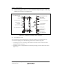
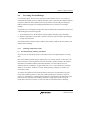
Static electricity is the charging of a material by either excess or a shortage of electrons. When a
material has an excess of electrons it is negatively charged, and when it has a shortage of electrons
it is positively charged.
Materials generally have an electrical quality of either acquiring electrons or of giving them up
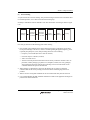
(the series of frictional electrification). For this reason, when two materials rub, make contact,
separate, or create friction, one material acquires electrons while the other gives them up (figure
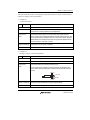
6.1). When a conductive material comes into proximity with a charged material, local charging
will occur because of electrostatic induction (figure 6.2). The amount of charge in the materials
depends on the material properties, the surrounding conditions (temperature and humidity), and
the conditions in terms of friction. However, large charges are generally generated in chemical
fibers and plastics (these materials are easily charged). Since static electricity charges the surface
of a material, the material's surface conductivity will also have a strong effect on charge transfer.
When the surface conductivity is high, the charge will diffuse quickly. Table 6.7 shows examples
of electrostatically generated voltages. Since surface conductivity increases with humidity, the
higher the relative humidity the lower the electrostatic voltage.
Insulator
Insulator
Figure 6.1 Frictional Electricity
Insulator
(Electrically)
charged body
Figure 6.2 Electrostatic Induction
Rev. 1.00 Aug. 31, 2006 Page 236 of 410
REJ27L0001-0100
Section 6 Usage Precautions
Table 6.7
Examples of Typical Electrostatic Voltages
Electrostatic Voltage Potential
Source
10 to 20%RH
65 to 90%RH
A person walking on a carpet
35000 V
1500 V
A person walking on a vinyl
floor
12000 V
250 V
A person working at a bench
6000 V
100 V
Vinyl covering
7000 V
600 V
Lifting a polythene bag from a
bench
20000 V
1200 V
Polyurethane packed chair
18000 V
1500 V
(From DOD-HDBK-263)
(2)
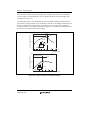
Charged-Device Model Mechanism
Recently the incidence of the ESD damage due to the charged-device model is increasing. This
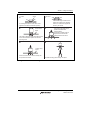
mode of destruction occurs when a charged device model discharges to a conductor. The devicecharging mechanisms that induce discharges are described below.
(a)
Frictional charging of package surfaces
Friction is often applied to a device in the manufacturing process or during assembly of devices
into electronic instruments. Examples are friction with the rubber roller of the device-stamping
machine, within the IC magazines, and device handling instruments. When friction is applied to
plastic packages, the surface of the package becomes charged. When the package is charged,
electric charge is electrostatically induced in the chip and its leads by electric fields within the
package, and the leads discharge when they make contact with a conductor (figure 6.3).
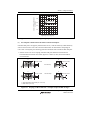
(b)
Device charging by electrostatic induction
In addition to description (a) above, figure 6.4 gives examples of charging that occurs even in the
absence of friction. When a device is placed on a charged plastic board, electrostatic induction
takes place in the chip and leads as shown in figure 6.4 (i). Then discharge occurs when tools or
human bodies make contact with the leads of figure 6.4 (ii). If the device is charged, there is a
further danger of discharge after it has been picked up from a board as shown in figure 6.4 (iii).
This shows that there is a danger of device discharge when charged materials are simply brought
into proximity with each other. The containers into which devices or completed boards are placed,
conveyor belts, and non-conductive gloves can all cause device discharge.
Rev. 1.00 Aug. 31, 2006 Page 237 of 410
REJ27L0001-0100
Section 6 Usage Precautions
Conductor
Discharge
Package charged surface
Figure 6.3 Internal Electrostatic Induction and Discharge when the Package Surface is
Charged
Conductor (e.g. pliers)
Discharge
Charged plastic board
(i)
(ii)
After removal from the plastic board
(iii)
Figure 6.4 Process of Device Charging by Electrostatic Induction
Rev. 1.00 Aug. 31, 2006 Page 238 of 410
REJ27L0001-0100
Section 6 Usage Precautions
(3)
General Precautions against ESD Damage
Caution is necessary in handling devices since they are generally susceptible to destruction due to
electrostatic discharge. The possibility of electrostatic discharge is especially high in the cases
listed below. Countermeasures, and confirmation of the conditions, are thus necessary to prevent
destruction.
(a)
Contact between devices and conductors
When conductors or devices are charged, discharge will occur between them. For the sake of
protection, human bodies must be grounded through a high resistance of 1 MΩ or greater. For
metals, the danger of destruction is greater because of the sharp discharges. Bringing devices into
contact with metals must be avoided as much as possible, but, when this is unavoidable, the metal
must be grounded and the charge must be removed from the devices.
(b)
Device subjected to friction
Packages become charged when they are subjected to friction, and when the lead pins are rubbed,
the chips and lead pins also become charged. It is necessary to reduce the amount of charge by
preventing friction or changing the material that may be subjected to friction.
(c)
When charged tools are brought into proximity with devices, the devices are charged
by electrostatic induction. The material of tools must therefore be exchanged for antistatic material.
(d)
Drops in the humidity of surroundings
When handling devices, if the humidity in the vicinity falls, devices or tools, once charged, do not
easily return to their original condition. Since static electricity is invisible, it is not easy to institute
perfect countermeasures to the above-mentioned factors (a)–(c). When executing these
countermeasures, greater effectiveness can be expected if the humidity is also controlled.
Rev. 1.00 Aug. 31, 2006 Page 239 of 410
REJ27L0001-0100
Section 6 Usage Precautions
(4)
Caution in Handling Devices
The most effective method of preventing sharp discharge of semiconductor elements is to use antistatic mats. First of all, devices will not become charged, but, if they become charged then, they
will not discharge sharply.
(a)
The working environment
The occurrence of static electricity is closely related to humidity, and static electricity occurs more
readily when the relative humidity drops. When there is a high-temperature area (in part of the
working environment), the local level of humidity in that area will be low, and this leads to the
possibility of large amounts of static electricity. Therefore, from the aspect of charge prevention,
during handling and the mounting process when the possibility of charge is high, it is important to
maintain a relative humidity of 45 to 55% by using humidifiers. When control of humidity is
difficult, an air-ionizing blower (called an ionizer) is also effective. However, over dependence on
the air-ionizing blower may lead to unexpected defects when failures do occur. It is more
important to take other measures to prevent charging and at the same time continuously confirm
the operation of the air-ionizing blower.
(b)
Work
In the work place, easily charged insulators (especially chemical fiber and plastic products) must
be avoided as much as possible, and conductive material should be used. For example, anti-static
materials such as anti-static work gowns and the use of air-ionizing blowers are recommended.
Also when handling semiconductor devices, it is necessary to use materials that prevent static
electricity or provide anti-static containers (for example, electrostatic-shielded bags, anti-static
mats, etc.) during storage or transportation.
1. Equipment and facilities
Measuring and test equipment, conveyors, work platforms, floor mats, tools, solder baths and
irons should all be thoroughly grounded to prevent electrostatic accumulation. Cover work
benches and floors with grounded anti-static matting (105 Ω/
to 109 Ω/
).
2. Human bodies
Ground human bodies during work. However, to prevent electric shock, always include a 1
MΩ resistor or higher connected in series, and be sure not to touch high voltage parts. Always
wear gloves and do not touch devices with bare hands. Gloves and work gowns must not be
made of such easily charged materials as nylon. Shoes or sandals with a resistance of 1 MΩ to
100 MΩ are regarded as adequate, but such values may vary due to dirt, wear, and humidity.
Rev. 1.00 Aug. 31, 2006 Page 240 of 410
REJ27L0001-0100
Section 6 Usage Precautions
3. Work methods
For manual soldering, use a soldering iron for semiconductors (12 V to 24 V, i.e., low-voltage
type), and ground the tip of the iron. In handling devices it is desirable to keep the frequency of
handling and the time of handling a given device to a bare minimum, as working quickly can
help to prevent destruction.
• Example 5
ESD Damage during Measurement
No. 5 Example
ESD during measurement
Type of device
MOS IC (plastic encapsulation)
Point
Measure the amount of charge after exposure to friction and take
countermeasures
Outline of example/ Because a plastic guide rail was used to feed the IC to an automatic
phenomenon/
measuring device, the IC's plastic materials became charged with static
cause
electricity as the IC slid along the guide rail. This charge was discharged at
the measuring head (metal), and caused destruction of the IC's input circuit.
This occurred at low levels of humidity, but not at high levels.
Countermeasures/
checking methods
1. Exchange the plastic guide rail for a metal one, to avoid the generation of
electrostatic charge.
2. GND the guide rail.
3. If these measures do not sufficiently reduce the amount of charge, use an
ionizing blower as well.
Reference item
Rev. 1.00 Aug. 31, 2006 Page 241 of 410
REJ27L0001-0100
Section 6 Usage Precautions
• Example 6
ESD Damage during Storage and Transportation
No. 6 Example
ESD during storage and transportation
Type of device
MOS IC (Plastic encapsulation)
Point
Substances adjacent to the device must not be allowed to charge to high
voltage.
Outline of example/ During the device production process the IC which was perfect after
phenomenon/
mounting onto the PCB and before assembly, becomes defective. When the
cause
PCBs were stacked for transportation or storage, charge in a capacitor facing
the IC was discharged and caused destruction of the IC.
Countermeasures/
checking methods
1. Place insulators between the PCBs during transport.
2. Discharge the capacitor.
3. Separate the PCBs keeping some distance between them.
Reference item
(5)
Excess Voltage Destruction
Other than static electricity another cause of destruction is the application of excess voltage,
commonly called excess voltage destruction. There are various causes and features of excess
voltage generation, but generally the form of destruction is determined by the amount of
discharged energy and the size of the energy consuming area. When the temperature of local areas
of silicon (Si) exceed 200°C the leakage current is extremely high and permanent destruction
results with a further increase in temperature. Physically, when the temperature rises above 500°C,
fusion of the Al metallization or damage to the Si substrate occur. The damaged area is obviously
related to the amount of surge energy involved in the destruction.
Excess voltage surge includes extraneous surges induced by the activity and the switching on/off
of other devices, unexpected lightening, and circuit-induced surges due to the activity of the
device itself. Surges also arise during measurement and testing, procedures which are unrelated to
the normal activity of devices.
Rev. 1.00 Aug. 31, 2006 Page 242 of 410
REJ27L0001-0100
Section 6 Usage Precautions
(6)
Destruction due to External Surges
External surges are the most troublesome because incidence is generally extremely low, and
investigating their causes or conducting simulation tests is difficult. To prevent the problem, it is
necessary to record in detail the conditions of operation and the surroundings at the time trouble
occurs.
• Example 7
Destruction due to Voltage Surge
No. 7 Example
Destruction due to voltage surge
Type of device
CMOS analogue switch IC
Point
Confirm the IC tolerance to input surge.
Outline of example/ In a customer's system that collect analogue data, as the source of analogue
phenomenon/
signal is far away from the analogue/digital converter, an external surge was
cause
induced on the connecting line. A CMOS analogue switch with an excess
voltage protection circuit was used on the analogue input, but the surge
exceeded the breakdown voltage causing destruction.
Several hundred meters
Countermeasures/
checking methods
CMOS analogue
switch IC
1. Isolation amplifier added to the input circuit.
−
+
2. Zener diode is added to the input circuit to absorb the surge.
Reference item
Rev. 1.00 Aug. 31, 2006 Page 243 of 410
REJ27L0001-0100
Section 6 Usage Precautions
(7)
Precautions against Destruction by Self-generated Excess Voltage
Surge sometimes generates high voltages within circuits. This is the case when inductive load
circuits are driven, such an applied surge is absorbed by the avalanche breakdown of transistors. In
such a case, incorporate protective elements. When they are already installed, control the surge
voltage and derate the energy to maintain reliability. Also by adding protective elements to the
circuit derating, characteristics are checked.
When a capacitor with a large capacitance as the load is driven, excess voltage sometimes arise
because of the inductive element of the load circuit.
• Example 8
A Driven Inductance Load
No. 8 Example
A driven inductance load
Type of device
TTL IC
Point
Confirm the voltage and current waveform when the load circuit L is switched
on and off.
Outline of example/ When an inductive load such as a relay is driven through a logical circuit, and
phenomenon/
when the current flowing into the coil in a relay is reversed, the resulting
cause
reverse voltage is not absorbed and the device will suffer electrical
destruction. The situation is the same when transistors are used.
Countermeasures/
checking methods
1. Introduce a clamping diode.
2. Introduce a dumping circuit.
Reference item
Rev. 1.00 Aug. 31, 2006 Page 244 of 410
REJ27L0001-0100
Section 6 Usage Precautions
• Example 9
Reactance Driven
No. 9 Example
Reactance driven
Type of device
TTL, CMOSIC
Point
Precautions against charging/discharging currents of capacitors
Outline of example/ If a capacitor is connected to an IC output, a charging current flows as its
phenomenon/cause level changes from low to high, and a discharging current flows as its level
changes from high to low. In the former case, a current corresponding to IOS
flows. In the latter case, a voltage corresponding VOH is applied to the VOL
level output current, causing destruction in the output transistor.
Charge
Discharge
C
Countermeasures/
checking methods
1. Use a capacitor with a capacitance that is lower than the value.
2. Insert a resistor in series with the capacitor.
3. Design systems that do not use capacitive load.
Reference item
Rev. 1.00 Aug. 31, 2006 Page 245 of 410
REJ27L0001-0100
Section 6 Usage Precautions
• Example 10
Destructive Defects due to Noise from the Power Supply to the LCD Driver
No. 10 Example
Destructive defects due to noise from the power supply to the LCD driver
Type of device
LCD-driver microcontroller
Points
1. Never reverse the voltage of the power supply to the LCD driver.
2. The voltage applied to the CMOS input must be between the value of the
power supply and GND.
Outline of example/ An LCD driver which was used trouble-free at company A repeatedly failed,
phenomenon/
for unknown reasons, in product tests at company B. There was a big
cause
discrepancy between the fraction defectives of device types even of the
same lot. The fraction defective also varied with the test pattern. By the
failure analysis, the destruction of the power supply section is confirmed.
Defect analysis confirmed that cause of destruction was a build-up of spiking
noise in the power supply to the liquid crystal display due to a capacitor load,
and the reversal of the potential difference across the power supply. A
bypass capacitor was placed across the power-supply connection providing
a reversed-voltage to synchronize with the noise. The destruction no longer
recurred.
Countermeasures/
checking methods
1. In order to avoid, for even a moment, the reversal of the voltage applied
to the power supply of a liquid-crystal display driver, use a capacitor with
the same phase to eliminate the noise as described above.
2. Widen and shorten the wiring runs of the power-supply pattern, and
under the most severe condition for the timing of changes in the column
signal, use a high-speed operation probe to check the waveform for the
presence of reversed voltages between the power-supply lines.
Reference item
Rev. 1.00 Aug. 31, 2006 Page 246 of 410
REJ27L0001-0100
Section 6 Usage Precautions
(8)
Precautions against Excess Voltage Destruction during Measurement
When measuring semiconductor devices, it is necessary to apply the same considerations as
applied to static electricity. In addition, particular care should also be taken with regard to the
points listed below.
(a)
Preventing destruction due to the power input sequence
If the power input sequence of semiconductor devices is faulty, device destruction may arise due
to such phenomena as latchup. For a power supply which has the negative features of the electric
current limitations, a voltage drop occurs due to a transient current, and as a result the device may
malfunction depending on the combination of the device and characteristics. Refer to individual
data books for details.
Even if the power input sequence for the test program is correct, the power input sequence may
not proceed correctly due to a faulty connection between the device and the socket of the
measuring instrument. The actual power input sequence may also be reversed due to a
combination of the startup speeds of the power voltage and those of the input/output signal.
Caution is needed.
• Example 11
Destruction due to Mistiming of Power Input
No. 11 Example
Destruction due to mistiming of power input
Type of device
Linear IC
Point
Confirm whether the power input sequence is the same as the specifications.
Outline of example/ When switching the mode, a malfunction of unknown cause occurred. The IC
phenomenon/
that malfunctioned operates on two power supplies. Only power supply 1 is
cause
used in normal operation, while power supply 2 is designed to turn on and
function when switching the mode.
The relevant IC was designed in such a way that unless the output signal is
muted (Mute) until power supply 2 rises to the high level (5 V), pulse noise
occurs and excessive current flows. It was confirmed that these precautions
for use had not been followed, and as a consequence the noise surrounding
the power supplies caused the device to malfunction.
Countermeasures/
checking methods
Confirm and follow the precautions for use given in the catalog or
specifications provided with the delivery documents. In the case that multiple
power supplies are used, be especially sure to control the timing of each
on/off event.
Reference item
Rev. 1.00 Aug. 31, 2006 Page 247 of 410
REJ27L0001-0100
Section 6 Usage Precautions
(b)
Protection against voltage and current surges
Take care to ensure that surging voltages are not applied from testers during characteristic
measurement, or use such countermeasures as adding clamping circuitry to the tester, or ensure
that abnormal voltages are not applied due to faulty connections during current driving
measurement.
• Example 12
Destruction during Measurement
No. 12 Example
Destruction during measurement
Type of device
TTL IC
Point
Beware of voltage surges when power is applied.
Outline of example/ 1. When measuring the bus-driver output voltage VOL, destruction occurred
phenomena/
because the input current IOL (100–300 mA) was kept constant.
cause
2. When measuring the breakdown voltage (for an IC of 70 V or greater)
with a current of 1 mA, the same destruction (as in (1) above) occurred.
3. When measuring the breakdown voltage (as in (2)), noise superimposed
on the constant current source, entered the negative range and caused
destruction.
Countermeasures/ 1. Use methods that apply voltages rather than currents.
checking methods
2. Apply voltages, within the breakdown voltage and measure the current.
3. When a method that includes the application of a current must be used, it
is effective to check the contacts in the previous sequence.
Reference item
When capacitors are installed to prevent noise on input/output terminals and are connected
carelessly, there is a chance that semiconductors will suffer electrical destruction because of peak
currents that result from charging and discharging of the capacitor. For example, during
intermediate inspections using board testers or in-circuit testers if the capacitor remains charged
when the next board is tested, destruction of semiconductor devices may result. In cases where the
capacitors on a board remain charged after a test, there is also a possibility of discharge later in the
storage case, so all capacitors in the tester and on the board must be completely discharged. In the
same manner, when a bypass capacitor with a large capacitance is inserted on the tester power
supply, care must be taken to ensure that an unnecessary charge does not remain after the power
supply is disconnected.
Rev. 1.00 Aug. 31, 2006 Page 248 of 410
REJ27L0001-0100
Section 6 Usage Precautions
(c)
Precautions against noise and oscillation
Normally, even in circuits that operate correctly, the load capacitance increases when devices are
connected to oscilloscope probes or instruments for measurement. Noise or oscillation are
generated and circuits malfunction, leading to the destruction of semiconductors. Therefore,
caution is necessary.
(d)
Prevention of conflict between semiconductor outputs and tester drivers
When measuring common I/O terminals, care is required so that the output of the semiconductor
and tester do not conflict.
(e)
Precautions against leakage from electrical equipment
Adequate control of electrical equipment is required so that leakage does not occur from AC
power supplies to terminals of curve tracers, oscilloscopes, pulse generators, or stabilized DC
power supply.
(f)
General precautions
When measuring, avoid the misconnection of terminals, reverse insertion, and shorting between
terminals. When checking board (substrate) operations, check that there are no solder bridges or
particle bridges before switching the power on.
• Example 13
Destruction during Measurement
No. 13 Example
Destruction during measurement
Type of device
Small Surface Mount IC
Point
Beware of contact defects when taking measurements
Outline of example/ When the semiconductor device to be measured was inserted into the tester
phenomenon/cause socket at an angle, a spike surge occurred due to contact defects between
the pins of the device and the tester socket, resulting in destruction of the IC.
Countermeasures/
checking methods
Place the contact check for the very beginning of the testing program. When
contact defects are detected, the inspection should be discontinued. In the
case of reverse insertion, the inspection should also be halted.
Reference item
Rev. 1.00 Aug. 31, 2006 Page 249 of 410
REJ27L0001-0100
Section 6 Usage Precautions
• Example 14
Destruction due to Faulty Connections
No. 14 Example
Destruction due to faulty connections
Type of device
Linear IC
Point
Ensure correct connection and clarify emergency measures against faulty
connections.
Outline of example/ When installing a set, the GND line was open and the VCC connected, an IC
phenomenon/
failed due to a contact between its output terminals and GND. The moment
cause
the output terminals made contact with GND, high currents were drawn
through an electrolytic capacitor between VCC and GND, causing destruction.
Countermeasure/
checking method
Place a clamping diode between the output terminals and GND.
Reference item
• Example 15
Destruction due to the Removal and Insertion of a Connector
No. 15 Example
Destruction defects due to the removal and insertion of a connector
Type of device
IC, LSI
Point
The removal and insertion of live connectors is strictly prohibited. If this
cannot be avoided, the design must allow for this possibility.
Outline of example/ In user processing, failures occurred frequently so that a motor did not run
phenomenon/
(average failure rate was 2 to 5%). Examination revealed that IC inputs had
cause
been destroyed. During board inspection, the customer erroneously removed
and inserted the connector while the DC supply was switched on. When this
procedure was discontinued, the defects did not recur.
Countermeasures/
checking methods
1. Always disconnect the power supply before connecting the board.
2. Protective resistors were inserted at the input terminals of the destroyed
IC.
Reference item
Rev. 1.00 Aug. 31, 2006 Page 250 of 410
REJ27L0001-0100
Section 6 Usage Precautions
6.2.2
Latchup
In devices in which the structures have a parasitic thyristor, such as CMOS circuitry, a failure
mode called latchup often occurs. Latchup is a phenomenon in which parasitic currents that flow
because of an external surge act as a trigger and switch the parasitic thyristor on. This leads to
heat-induced destruction. Such parasitic currents don't flow as long as the potential on each signal
line of the LSI is within the standard values. However, when the ground potential is floating, and
the potential between the input/output signal and the power supply is reversed, the current flows.
As the thyristor itself acts as a normal semiconductor element, if the power supply is cut before
the structure breaks down because of heat, this does not lead to destruction. Once the thyristor has
been turned on, unless the power is cut the problem can not be resolved, even if the input/output
voltage returns to normal.
Rev. 1.00 Aug. 31, 2006 Page 251 of 410
REJ27L0001-0100
Section 6 Usage Precautions
• Example 16
Destruction due to Latchup of LSI with Multiple Power Supplies
No. 16 Example
Destruction due to latchup of LSI with multiple power supplies
Type of device
CMOS LSI
Point
If the proper sequence for the application of power is not followed, latchup
will result.
Outline of example/ After an LSI that had passed the acceptance inspection had been mounted
phenomenon/
on a printed board, the LSI suffered destruction during examination by an incause
circuit tester.
Normally, connections are made first and tests are carried out after adjusting
the voltage in the –5 V generating circuit. In this case, however, the test was
erroneously performed without the connection being made first.
Consequently, –5 V was not being supplied to the LSI, latchup arose, an
abnormal current flowed to ground, and the LSI suffered destruction.
When using CMOS devices, assume the worst so that even if latchup does
occur, the circuit is made fail-safe in terms of prevention of secondary
damage, and protective resistors installed to limit self-generated heat.
−5 V is lost due to failure and the LSI
on the right causes latchup.
T
−5 V
generating
circuit
+5 V
LSI
−5 V
+5 V
+12 V
+12 V
GND
Power supply
Printed circuit board
Type of device
CMOS LSI
Countermeasures/
checking methods
1. Define the proper sequence for supplying and cutting power with multiple
power supplies LSI.
2. Insert protective elements in anticipation latchup occurring.
Reference item
Rev. 1.00 Aug. 31, 2006 Page 252 of 410
REJ27L0001-0100
Section 6 Usage Precautions
(1)
Destruction Induced by Excess Current
Destruction that occurs because of Al metallization meltdown is generically referred to as excess
current destruction. Al wiring has a positive temperature characteristic so its resistance is
increased by the application of large currents. As a result, more energy is consumed in the wiring
causing thermal runaway, the Al wiring exceeds Al-Si eutectic temperature and melts down.
Transistors suffer destruction from excess current, also there are cases of a large current flow and
generating excess current destruction. Alternatively, excess current causes the temperature to rise
and as a result a eutectic mixture of Al and Si breaks through a junction and transistors are
destroyed. It is difficult to determine the cause of the destruction from the resulting condition of
the device.
• Example 17
Destruction due to Large-Capacitance Capacitor
No. 17 Example
Destruction due to large-capacitance capacitor
Type of device
CMOS LSI
Point
If the GND does not function properly, the LSI will suffer destruction.
Outline of example/ During the debugging of programs, program development equipment was
phenomenon/
destroyed for unknown reasons. Regardless of how many times equipment
cause
was repeatedly replaced, several TTL and CMOS devices continued to be
destroyed at the same time. It was determined that latchup occurred
because a large-capacitance capacitor (2000 µF) was used and when the
power was turned on, the LSI's ground potential rose to half of the powersupply level.
Due to surge voltage, the wiring between the
GND and the power supply becomes a resistor,
and the GND voltage increases.
Destroyed
Potential of 1/2
the power supply
2000 µF
LSI
Input
GND
Low level
(0.4 V approx.)
LSI
Output
In the case of two power
supplies
Countermeasure/
checking method
GND: 2.5 V approx. Relative electrical
Input: 0.4 V approx. potential is reversed.
Exchange the large-capacitance capacitors on printed-circuit boards for
smaller-capacitance capacitors.
Reference item
Rev. 1.00 Aug. 31, 2006 Page 253 of 410
REJ27L0001-0100
Section 6 Usage Precautions
(2)
Thermal Runaway
Thermal runaway is a thermal characteristic of any circuit where the positive feedback of power
results in the temperature rising without limit until destruction occurs. It is no exaggeration to say
that thermal runaway is the most common form of destruction. In addition to those cases where
thermal runaway occurs because of local heating of a device, high-power devices have an
additional risk of thermal runaway because of their structurally inadequate thermal dissipation.
Caution must therefore be exercised in terms of heat-radiation (thermal management) design.
(3)
ASO Destruction
ASO stands for Area of Safe Operation, and this is a destruction mode that typically occurs in
bipolar devices. This is another kind of thermal runaway. In theory, due to the temperature
characteristic of the base emitter voltage, when the temperature increases, the voltage VBE falls,
and the consumption of energy at the emitter increases locally. Further, as VBE falls, local hot
spots occur which lead to destruction.
In the case of a MOS device, since the ON resistance rises with temperature, one characteristic is
the tendency to automatically equalize the generation of heat, this then greatly expands the area of
possible ASO destruction.
(4)
Destructive Avalanche
This is a failure mode which initiates an avalanche breakdown which in turn causes destruction
due to the applied voltage exceeding the junction breakdown voltage of a semiconductor device.
As with the time-dependent breakdown of dielectric film, when the yield energy is small,
immediate destruction does not occur. It can be considered that the destruction occurs when the
amount of energy passing through the junction exceeds a fixed value. Except in designs where it is
specifically intended, using avalanche breakdown is prohibited by maximum ratings and other
specifications, care is required.
Rev. 1.00 Aug. 31, 2006 Page 254 of 410
REJ27L0001-0100
Section 6 Usage Precautions
6.3
Preventing Mechanical Damage
Semiconductor devices are mainly made up of a silicon chip which forms its core to perform its
functions, bonding wires to carry electrical signals to and from the chip, lead wires, heat fins to
reliably radiate heat away, and mold resin to hold the whole package together mechanically and
protect it from external stresses. Since the constituent elements of the device differ considerably in
such properties as hardness and thermal expansion coefficient, the mechanical strength margin is
less than it would be for a device consisting of a single material. Consequently, all of the stages in
mounting components—bending the lead wires, attachment to the heat-sink plate, cleaning after
mounting to the printed circuit board, correcting the bending—harbor the potential for mechanical
breakage.
External mechanical forces can loosen the adhesive bonding of the resin to the leadframe, and
cause the subsequent deterioration of the margin for moisture resistance; transmission of the stress
to the bonding wires can cause deterioration of resistivity to temperature cycles; and in a severe
case wires can be disconnected. In addition, mechanical stresses applied to the heat-sink plate and
to the whole package can lead to chip cracks.
In the assembly process, caution should be exercised when mechanical stress is applied, and the
process should be designed so as not to permit defects caused by mechanical stresses. If it appears
that destruction will be caused by mechanical stress during the assembly process, it is possible that
some damage will be caused not only to the actual defective components but also to components
that do not qualify as defective. In this case the product might become defective in the market, so
caution is required.
In particular, in a type of product which is of hollow structure and bonding wires are not fixed in
place, there is danger of breakage caused by ultrasonic cleaning and vibration stress. There is
danger that narrow bonding wires will be disconnected by fatigue caused by resonance with
ultrasonic waves, and that wire disconnection will be caused by vibration and flow of gel resin.
6.3.1
Lead Forming and Cutting
When semiconductor devices are mounted on a printed circuit board, there are cases in which
outer leads are formed and/or cut in advance; if excessive force is applied to a lead during this
operation, the semiconductor device can be broken or the seal can be damaged.
Rev. 1.00 Aug. 31, 2006 Page 255 of 410
REJ27L0001-0100
Section 6 Usage Precautions
For example, if relative stress is applied between the package body and the leads of the device, an
internal connection could be loosen or a gap could be produced between the package body and the
lead, deteriorating airtightness and causing loss of reliability. In the worst case, the mold resin or
glass could break. For this reason, the following precautions should be observed when lead
forming or cutting lead wires.
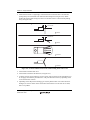
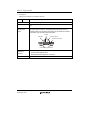
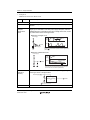
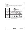
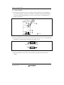
1. When a lead is bent, fix the lead in place between the bending point and the package body so
that relative stress will not be applied between the package body and the lead. Do not touch or
hold the package body when bending a lead (see figure 6.5). When a lead forming die is used
to perform lead forming for many devices, provide a mechanism of holding the outer lead in
place and make sure that this outer lead pressing mechanism itself does not apply stress to the
device body (see figure 6.6).
Further, if the package body pressing mechanism is used when bending the lead, this method
should support the package body around its periphery as shown in figure 6.7 to avoid
concentrating stress on the chip. t is the distance between the lead forming support point and
the chip.
Incorrect
Correct
Figure 6.5 How to Bent Package Leads with Handling
Rev. 1.00 Aug. 31, 2006 Page 256 of 410
REJ27L0001-0100
Section 6 Usage Precautions
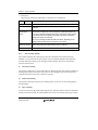
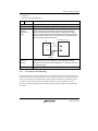
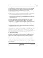
W1
W2
W3 Forming mechanism
t
Leave this
interval open.
W1
Presser
t is the distance over which the main
body, even if pulled by the force W3,
is retained and does not come in contact
with the presser.
Figure 6.6 Using the Lead Forming Die
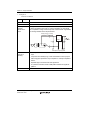
Incorrect
Correct
Chip
t
Main body presser
Lead presser
Figure 6.7 Example of the Lead Forming Die with the Package Body Presser
Rev. 1.00 Aug. 31, 2006 Page 257 of 410
REJ27L0001-0100
Section 6 Usage Precautions
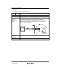
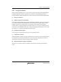
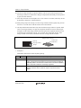
2. When the lead is bent to a right angle, it must be bent at a location at least 3 mm from the
package body. Do not bend the outer lead more than 90 degrees (see figure 6.8A). When
bending the lead less than 90 degrees, bend it at a location at least 1.5 mm from the package
body (see figure 6.8B).
A
3.0 mm min.
Correct
B
1.5 mm min.
Correct
C
Incorrect
D
Incorrect
Figure 6.8 Locations and Directions for the Lead Forming of the Outer Lead
3. Do not bend a lead more than once.
4. Do not bend a lead in the side direction (see figure 6.8C).
5. A lead of a device can be broken by excessive stress (such as tension) in the axial direction, so
do not apply more than the prescribed force. The prescribed stress will vary depending on the
cross-sectional area of a lead.
6. Depending on the shape of the bending jig or tool, the plated surface of an outer lead can be
damaged, so exercise caution. If the section that a lead contacts is on the order of 0.5 mmR,
there is no problem.
Rev. 1.00 Aug. 31, 2006 Page 258 of 410
REJ27L0001-0100
Section 6 Usage Precautions
Transistor and diode products can be supplied with preformed leads on request. If desired, please
contact our company's sales representative.
• Example 18
A Chip Crack Defect
No. 18 Example
A chip crack that formed during lead formation.
Type of device
Gate array
Point
When forming a lead on a surface-mounted package, check whether a
mechanical shock is being applied to the package body.
Outline of example/ In a user's process, the leads of a surface-mounted package device were
phenomenon/
corrected before being placed on a circuit board using a lead correction
cause
machine. At this time, the clearance between the forming die pressing on the
base of the lead and the package body was not left. For this reason, particles
entered between the package body and the forming die and applied a stress,
as a result of which a chip crack occurred.
Countermeasure/
Set the clearance between the package body and the forming die
Method of checking considering the size of specks of particles.
Reference item
• Example 19
Damage Caused by a Lead Forming Defect
No. 19 Example
Wire break caused by a lead formation defect
Type of device
Power transistor (Type TO-202)
Point
A lead must be held securely.
Outline of example/ When a transistor lead was formed, a lead presser was not used, so a
phenomenon/
disconnection defect was caused by loosening a pin.
cause
Since the pressing was insufficient, excessive tension was applied in the X
direction and an internal bonding wire was disconnected when the lead wire
was bent.
Presser
×
Lead wire
Bending
Transistor
Presser
Countermeasure/
When a lead forming, fix it in place between the main body of a transistor
Method of checking and the point where the lead wire is bent (see figure above).
Reference item
Precautions when bending (section 6.3.1)
Rev. 1.00 Aug. 31, 2006 Page 259 of 410
REJ27L0001-0100
Section 6 Usage Precautions
6.3.2
Mounting on a Printed Circuit Board
When a semiconductor device is mounted on a printed circuit board, be careful so that excessive
stress is not applied to the leads of the device.
The following are the principal precautions that need to be taken (see figure 6.9).
1. The intervals between device mounting holes on the printed circuit board should match the
distance between outer lead so that excessive stress is not applied while the device is being
inserted or after it is inserted.
2. When a device is inserted into a printed circuit board, do not pull on the leads with excessive
force from the backside, and prevent excessive stress from being applied between the leads and
the case.
3. Leave a suitable space between the semiconductor device and the circuit board. A good way to
do this is to use a spacer.
4. After fixing the device to the printed circuit board, avoid assembling the unit in such a way
that stress will be applied between the leads and the device package. For example, when a
device is connected to the heat-sink plate after soldering the leads to the printed circuit board,
fluctuations due to tolerances in lead length and printed circuit board dimensions can result in
stress being concentrated on the lead. This results in the lead being pulled out, package damage
or a lead becoming disconnected. For this situation, solder the lead after device is fixed in
place.
5. When using automatic insertion equipment, one should be especially careful so that
mechanical shock is not applied to the package body at the time of insertion. This will help
prevent cracks from forming in the package or the chip due to shock. Also, when automatic
forming equipment is used, one should observe the precautions given in section 6.3.1.
6. When the component is mounted in an IC socket and used under severe environmental
conditions, the contact between the IC pins and the IC socket may degrade. One should avoid
using an IC socket as much as possible. Also, when an IC socket is used to mount a multi-pin
grid array package device to a circuit board, the package can break or pins may bend when the
package is inserted or removed. Therefore it is strongly recommended that a commercially
available insertion/removal tool be used. One of the Orgat TX8136 series is a good choice for
an insertion and removal tool.
Rev. 1.00 Aug. 31, 2006 Page 260 of 410
REJ27L0001-0100
Section 6 Usage Precautions
Correct
Semiconductor
device
Incorrect
The lead are being inserted into the
printed circuit board in an awkward
manner, so stresses are applied as
shown by the arrows.
A mounting technique in which stress is not
applied to the bases of lead wires (arrows)
Incorrect
Correct
Printed circuit
board
Avoid forcing the leads into the
printed circuit board with
unformed leads.
The distance between holes in
the printed circuit board are
inappropriate for this device.
The distance between leads should be the same
as the interval between printed circuit board
mounting holes.
Incorrect
Correct
Printed circuit
board
Insert the semiconductor device carefully into
the printed circuit board.
The lead are being pulled through with pliers.
Figure 6.9 Methods of Mounting a Semiconductor Device on a Printed Circuit Board
Rev. 1.00 Aug. 31, 2006 Page 261 of 410
REJ27L0001-0100
Section 6 Usage Precautions
• Example 20
Damage of a Package by Automatic Insertion
No. 20 Example
Destruction of a package by automatic insertion
Type of device
Silicon diode (DHD type)
Point
Stress must not be applied to the main body of a device while a lead is being
bent.
Outline of example/ In automatic insertion of a DHD type diode into a printed circuit board by a
phenomenon/
high-speed insertion machine, the package glass was broken either by
cause
excessive pressure on the device main body or by excessive force used to
clinch leads on the rear side of the circuit board.
Presser
Lead wire
Package glass
Printed circuit board
Lead clinching mechanism
Countermeasures/
Methods of
checking
1. Adjust the position of the presser. Make the presser material that can
provide a buffer against shock.
2. Keep the lead clinching force to a minimum.
Reference item
Rev. 1.00 Aug. 31, 2006 Page 262 of 410
REJ27L0001-0100
Section 6 Usage Precautions
• Example 21
Solder Defect Caused by Warping of a Printed Circuit Board
No. 21 Example
Solder defect caused by warping of printed circuit board
Type of device
Microcontroller
Point
Be careful in correcting the warp of a circuit board by reflow.
Outline of example/ A defect involving the peeling off of solder under a surface-mounting reflow
phenomenon/
stress occurred. No matter how many times a solderability test was
cause
performed, no abnormality was detected, and the cause could not be
determined. In the course of discussions the subject of warping following
reflow was raised; examination of the circuit board involved showed that
asymmetry of the copper pattern that positions the components was the
cause and that the warping was abnormally large. It was judged that after
reflow, while the circuit board was still hot, mechanical stress was applied to
correct the warping.
In reflow, the assembly stress on surface mounted devices can be quite
large. These can develop into high stresses on the printed circuit board. If
the circuit board undergoes large warping at the assembly stage which it is
heated, even if the LSIs initially become bonded to the circuit board, they can
become loose later. The user must keep control over the allowed amount of
warping.
Countermeasures/
Methods of
checking
1. The circuit board pattern and the component layout are adjusted to
prevent warping.
2. The frame material is changed to increase the mechanical strength per
pin with respect to the circuit board.
Reference item
Rev. 1.00 Aug. 31, 2006 Page 263 of 410
REJ27L0001-0100
Section 6 Usage Precautions
• Example 22
Chip Cracking at the Time of Mounting a Component on a Circuit Board
No. 22 Example
Chip cracking at the time of mounting a component on a circuit board
Type of device
Power transistor (DPAK), Small-signal transistor (UPAK)
Point
It is necessary to determine if the exterior coating resin affects the stress on
the device.
Outline of example/ When an exterior-coating resin was used in mounting a component on a
phenomenon/
circuit board, the difference in thermal expansion coefficients between the
cause
epoxy resin in the device and the phenol resin used for the coating caused
an excessive stress to be applied to the inside of the element, ultimately
leading to formation of a chip crack.
Use of such a coating can adversely affect the device, depending on the
coating material and thickness. Use caution in such cases.
Countermeasure/
When using an exterior-coating resin, apply a stress-absorbing resin
Method of checking between the coating resin and the epoxy resin in the device.
Reference item
6.3.3
Flux Cleaning Methods
Flux residue remaining after soldering may affect the components and circuit board wiring
reliability, so as a general rule the flux must be removed. Cleaning methods include ultrasonic
cleaning, immersion cleaning, spray cleaning and steam cleaning. These have the following
respective characteristics.
(1)
Ultrasonic Cleaning
The product is immersed in a solvent and ultrasonic vibrations applied. This method is suitable for
cleaning inside minute cracks, but in some cases can cause damage to the connections between
components and the circuit board, so caution is necessary.
(2)
Immersion Cleaning
The product is cleaned by immersion in a cleaning fluid. It is necessary for the cleaning fluid to
have high purity.
(3)
Spray Cleaning
A solvent is sprayed on the product under high pressure. When the clearance between components
and the circuit board is small, the cleaning effectiveness can be increased by spraying at an angle.
Rev. 1.00 Aug. 31, 2006 Page 264 of 410
REJ27L0001-0100
Section 6 Usage Precautions
(4)
Steam Cleaning
A vaporized solvent is used for cleaning. This permits cleaning to be done with a solvent that does
not contain impurities, so it is often used in the final cleaning step.
Normally a combination of these methods is used. The normal flow of cleaning is shown in figure
6.10.
Ultrasonic
cleaning
Cleaning by
Immersion
in hot fluid
Cleaning by
Immersion
in cool fluid
Spray
cleaning
Steam
cleaning
Drying
Figure 6.10 Normal Flow of Cleaning
One must pay attention to the following points when cleaning.
1. One example of the conditions under which ultrasonic cleaning is performed is given below,
but to prevent damage to the device, caution is needed regarding the applied frequency, power
(especially the peak power), time, and preventing the device from resonating.
Frequency: 28 to 29 kHz (the device must not resonate).
Ultrasonic output: 15 W/liter (one time)
Time: 30 seconds or less
The device and the printed circuit board must not directly contact the vibration source. In
particular, ceramic package type QFNs (LCC) and QFPs (Ceramic) are cavity packages;
when subjected to ultrasonic cleaning the connecting wires can resonate under certain
conditions and become open or disconnected.
2. When cleaning is continued for a long time, the marking may be erased, so check the
conditions that will be used by running an actual test before committing large amount of
products.
3. When a solvent is used, public standards for the environment and safety must be observed.
4. It is recommended that the MIL standards summarized in table 6.8 be applied for the degree of
printed circuit board cleanliness.
Rev. 1.00 Aug. 31, 2006 Page 265 of 410
REJ27L0001-0100
Section 6 Usage Precautions
Table 6.8
Cleanliness Standards of a Printed Circuit Board
Item
Standard
Residual Amount of CI
1 µg/cm2 or less
Electrical Resistance of Extraction Solvent (after extraction)
2 × 10⁶ Ω • cm or more
Notes: 1. Circuit board area: Both sides of printed circuit board + mounted components
2. Extraction solvent: Isopropyl alcohol (75vol%) + H2O (25vol%) (before extraction)
(electrical resistance of extraction solvent must be 6 × 10⁶ Ω • cm or more).
3. Extraction method: Clean both surfaces of circuit board (for 1 minute or more) with at
2
least 10 ml/2.54 × 2.54 cm of solvent.
4. Measurement of electrical resistance of extraction solvent: With electrical conductivity
meter
For details of the MIL standards, see MIL-P-28809A.
• Example 23
Destruction by Ultrasonic Cleaning
No. 23 Example
Trouble in ultrasonic cleaning
Type of device
Ceramic package
Point
When cleaning a package with a cavity by ultrasonic, it is necessary to
carefully monitor the power.
Outline of example/ After a ceramic package device was assembled, it was cleaned
phenomenon/
ultrasonically; the bonding wires resonated with the ultrasonic vibrations. The
cause
bonding wires suffered fatigue and become disconnected in a short time.
Countermeasure/
Specify a frequency, output and time at which resonance will not occur.
Method of checking
Reference item
Rev. 1.00 Aug. 31, 2006 Page 266 of 410
REJ27L0001-0100
Section 6 Usage Precautions
• Example 24
Problem that Occurred when a Circuit Board was not Cleaned
No. 24 Example
Problem that occurred when a circuit board was not cleaned
Type of device
Linear IC
Point
Be careful of minute leaks.
Outline of example/ When components were soldered to a circuit board, flux adhered to the
phenomenon/
surface of the IC package; subsequently, flux that remained on the surface of
cause
the IC package absorbed moisture, the surface leakage current between IC
terminals increased, and the circuit board became defective.
Countermeasure/
After a circuit board is soldered, the flux should be cleaned off.
Method of checking
Reference item
6.3.4
Attachment of the Heat-Sink Plate
In a power device, a heat-sink plate can be used to radiate heat that is produced and thus lower the
junction temperature. Attaching a semiconductor device to a heat-sink plate is an effective method
of removing heat. To avoid loss of reliability, it is necessary to take the following precautions.
(1)
The Selection of Silicone Grease
To improve heat conduction between the device and the heat-sink plate and increase the heat-sink
effectiveness, silicone grease is uniformly applied in a thin uniform layer to the surface of the
device that contacts the heat-sink plate. Depending on the device, in some cases the device can
absorb oil from the silicone grease causing the chip coating material to swell. When selecting a
silicone grease, we recommend the use of G746 made by Shin-Etsu Chemical co. Ltd., or
equivalent. This grease has been formulated with an oil base that has low affinity for the package
resin so that it will not cause the coating material to swell. Of course, an equivalent product may
be used (however it is not necessary when using a metal can package).
If a different type of grease is used, it may not be possible to guarantee product quality. Use of a
hard grease can cause resin cracking when a screw is tightened, so use caution. One should avoid
applying more grease than necessary, since it can cause excessive stress.
Rev. 1.00 Aug. 31, 2006 Page 267 of 410
REJ27L0001-0100
Section 6 Usage Precautions
(2)
Use suitable torque when tightening.
If the applied torque is too low, the thermal resistance will increase, while if it is too high the
device can deform. This can cause chip damage and lead to breakage. Use only appropriate torque
to tighten within the limits given in table 6.9. The effect on thermal resistance between the
thickness of insulating material and tightening torque is given in figures 6.11 and 6.12.
Table 6.9
Optimum Tightening Torque for Representative Packages
Optimum Tightening Torque [kg • cm]
TO-3
6 to 10
TO-66
6 to 10
TO-3P
6 to 8
TO-3PFM
4 to 6
TO-220
4 to 6
TO-220FM
4 to 6
TO-126
4 to 6
TO-202
4 to 6
Power IC
4 to 8
Thermal resistance
(including contact thermal resistance)
of Insulating Material
θc + θ1 (°C/W)
Package
4.0
TO-3 type
(6 km • cm)
3.0
lar
My
Without silicon oil
a
Mic
2.0
r
Myla
Mica
1.0
With silicone oil applied
0
0.05
0.10
0.15
0.20
Thickness d (mm) of insulating material
Figure 6.11 Relations between Thickness and Thermal Resistance of Insulating Material
(Typical Examples)
Rev. 1.00 Aug. 31, 2006 Page 268 of 410
REJ27L0001-0100
Section 6 Usage Precautions
1.0
Contact thermal resistance
θc (°C/W)
TO-3 type example
0.8
Without silicon oil
0.6
With silicone oil applied
0.4
0.2
0
2
4
6
8
10
Tightening torque (kg • cm)
Figure 6.12 Relations between Tightening Torque and Contact Thermal Resistance
(3)
Give adequate consideration to the flatness of the heat-sink plate.
If the heat-sink plate is not properly attached to the device, it will not effectively radiate heat away
and can cause excessive stress. This can lead to deterioration of characteristics and package to
resin cracks. Consequently, the following precautions should be observed with the heat-sink plate.
1. Neither concave nor convex warping of the heat-sink plate should exceed 0.05 mm in a
horizontal distance between screw holes (figures 6.13 and 6.14). Also, the twist should not
exceed 0.05 mm.
L1
L2
0.05 mm or less
0.05 mm or less
Convex warp
L1
L2
0.05 mm or less
Concave warp
0.05 mm or less
L1: Interval between screw holes (24 ± 0.22 mm)
L2: Resin width (10.7 mm)
Figure 6.13 Warping of a Heat-Sink Plate—Examples of QIL and DIL Packages
Rev. 1.00 Aug. 31, 2006 Page 269 of 410
REJ27L0001-0100
Section 6 Usage Precautions
L1
L2
0.05 mm or less
L1
0.05 mm or less
L2
0.05 mm or less
0.05 mm or less
L1: Interval between screw holes (24 ± 0.3 mm)
L2: Header width (8.4 mm)
Figure 6.14 Warping of a Heat-Sink Plate—Example of an SIL Package
Rev. 1.00 Aug. 31, 2006 Page 270 of 410
REJ27L0001-0100
Section 6 Usage Precautions
2. For the case of aluminum, copper or iron plates, verify that there are no residual burrs, and
always chamfer the screw holes.
3. It is necessary to polish the surface that will contact the device until it is quite flat (
finishing).
4. Make certain there are no particles such as cutting filings caught in the space between the IC
header and the heat-sink plate.
5. Design the distance between screw holes to be the same as the interval between device screw
holes (for example in the case of a SP-10T type power IC, 24 ± 0.3 mm). An interval that is
either too wide or too narrow can cause resin cracking.
(4)
Do not solder anything directly to the device heat radiation plate.
If something were soldered directly to the device heat radiation plate, a great deal of thermal
energy would be applied causing the device junction temperature to greatly exceed the
temperature at which operation is guaranteed. This would seriously affect the device, shortening
its lifetime or even destroying it.
(5)
Do not apply mechanical stress to the package.
When tightening, if the tool used (screwdriver, jig, etc.) hits the plastic package directly, not only
can cracks be produced in the package but the mechanical stress can be transmitted to the inside,
accelerating fatigue of the device connection section and destroying the device or causing wire
damage. One must always use caution not to apply mechanical stress.
(6)
Do not attach any device to a heat-sink plate after lead wires are soldered.
If a device is attached to a heat-sink plate after leads are soldered to the printed circuit board,
dispersions in lead length and differences in the dimensions of printed circuit boards and heat-sink
plates can lead to excessive stress being concentrated in the leads. This can cause lead wires to be
pulled out, packages to be destroyed and wires to be disconnected. Consequently, the device
should be attached to the heat-sink plate first, and then the outer leads soldered.
(7)
Do not mechanically process or deform a device heat-sink plate or package.
If a device heat-sink plate is cut or deformed, or a package is mechanically processed or deformed,
the thermal resistance will be increased and abnormal stress applied to the interior of the device,
causing failures to occur.
Rev. 1.00 Aug. 31, 2006 Page 271 of 410
REJ27L0001-0100
Section 6 Usage Precautions
(8)
When attaching a power device, use the recommended components (spacer, washer, lug
terminal, screws, nuts, etc.) (see figure 6.15).
Type TO-3
Type TO-220
3-mm diameter screw
3-mm diameter screw
spacer
Metal washer
YZ033S washer
chassis
Insulating washer
3.6 +0.1
−0.08 mm hole diameter
Metal washer
3.3-mm diameter
SK16B spacer
Lug plate
Spring washer
3-mm diameter nut
2.2-mm
diameter
Heat radiating plate
Insulating washer
Metal washer
Spring washer
3-mm diameter nut
Figure 6.15 Example for Attaching a Power Transistor
(9)
Screws that are Used
The screws that are used to attach the device to the heat-sink plate can be classified into cap
screws and self tapping screws; the following precautions are needed in using these.
1. Use binding-cap screws conforming to the JIS-B1101 standard and screws that have heads
equivalent to truss cap screws.
2. Absolutely do not use any flat-head screws since they will apply excessive stress to the device
(figure 6.16).
Rev. 1.00 Aug. 31, 2006 Page 272 of 410
REJ27L0001-0100
Section 6 Usage Precautions
Binding cap screw
Truss head cap screw
Recommended screws
Flat head cap screw
Round flat head cap screw
Screw types that must not be used
(Use any of thread screws, pan head screws, truss head screws,
binding cap screws or flat head screws.)
Figure 6.16 Types of Screws to be Recommended and not be Used
3. When self tapping screws are used, adhere strictly to the tightening torque given above.
4. When using self tapping screws, do not use screws that are larger than the hole diameter in the
device attachment section. These screws tap not only the heat-sink plate but also the device
attachment holes, which can cause trouble.
(10) Heat-Sink Plate Screw Hole Diameter
1. If the hole is too large: Do not make the heat-sink plate hole diameter or chamfering larger
than the head diameter of the screws to be used. In particular, in a device that uses copper
plating as the flange material (TO-220, power IC, etc.), the tightening torque can cause
deformation of the copper plating and the plastic package.
2. If the hole is too small: In particular, if a self tapping screw is used, the tightening torque will
increase and exceed the recommended tightening torque that was discussed above, or else the
desired contact resistance will not be obtained.
Rev. 1.00 Aug. 31, 2006 Page 273 of 410
REJ27L0001-0100
Section 6 Usage Precautions
(11) Other Precautions and Recommendations in Attaching Components to the Heat-Sink
Plate
Junction temperature increase ∆Tj (˚C)
1. If two or more devices are attached to one heat-sink plate, the thermal resistance for each will
increase (see figure 6.17).
2. The heat-sink plate must be of suitable size and shape for radiating heat away. In addition,
forced air cooling must be provided as necessary. Measure the product case temperature under
actual use conditions, calculate the junction temperature using the published thermal resistance
value.
ed
120
e
ta
at
s
100
t
en
ar
n
po
om
ch
ta
nt
t
sa
ed
ch
i
ne
po
c
m
2
co
1
ch
i
h
wh hic
w
in
e e in
s
s
Ca Ca
80
60
40
20
0
5
10
15
20
25
Collector power consumption
per component (W)
30
Notes: 1. Heat radiating plate 300 × 200 × 1.5 mm aluminum plate
300
2. Attachment method
a. Position (figure at right)
Unit: mm
70 min
b. Tightening torque 9 kg • cm
c. Silicone oil is applied to the contact surface; mylar is not used.
d. Natural convection, horizontal position
200
Figure 6.17 A Case in which Two Components are Attached to One Heat-Sink Plate
Rev. 1.00 Aug. 31, 2006 Page 274 of 410
REJ27L0001-0100
Section 6 Usage Precautions
• Example 25
Package Destruction during Mounting
No. 25 Example
Package destruction at time of mounting
Type of device
Power transistor (type TO-220)
Point
The torque used to tighten must be checked.
Outline of example/ When a power transistor was mounted, the compressed air screwdriver
phenomenon/
torque rose above 10 kg • cm and the mounting holes in the heat-sink plate
cause
were too large, so the header and the plastic boundary surface peeled off.
Depending on the type of compressed air screwdriver, the dispersion in the
tightening torque can become large. If the torque rises above 8 kg • cm, the
heat-sink plate mounting holes are larger than the screw diameter, or if the
heat-sink plate mounting holes are not sufficiently flat, the header can be
deformed or separate from the plastic.
Countermeasure/
Use a torque within the recommended limits. For the type TO-220 the
Method of checking recommended limits are 4 to 6 kg • cm. Keep the flatness of the heat-sink
plate mounting holes within 50 µm, make sure that the mounting holes do not
open wider than the screw head diameter, and use the accessory metal
washers (YZ033S).
Reference item
Rev. 1.00 Aug. 31, 2006 Page 275 of 410
REJ27L0001-0100
Section 6 Usage Precautions
• Example 26
Chip Cracking at Time of Mounting to a Heat-Sink Plate
No. 26 Example
Chip cracking at time of mounting to a heat-sink plate
Type of device
Power transistor (type TO-3)
Point
Always check the tightening holes meet the recommended conditions.
Outline of example/ The heat-sink plate mounting holes were of large diameter and were
phenomenon/
excessively chamfered, so that when the transistor was mounted, one side of
cause
the heat-sink plate tightened around the screw hole dropped into the
chamfered section and the stem became inclined. When the other side was
tightened, the entire stem deformed. The result was that at least twice as
much of typical stress was applied to the chip inside, causing a chip crack.
Screw
Cap
Stem
Heat radiating plate
Nut
Countermeasures
and/Methods to
verify
1. Make the heat-sink plate hole diameter (including the beveled section)
smaller than the screw head diameter.
2. Use the appropriate torque to tighten.
Reference item
Rev. 1.00 Aug. 31, 2006 Page 276 of 410
REJ27L0001-0100
Section 6 Usage Precautions
6.4
Preventing Thermal Damage
As it was stated above, because of its construction a semiconductor device is very sensitive to
mechanical and thermal stresses. In addition, materials used in construction have different thermal
expansion coefficients. These differences have the potential to cause the adhesive holding the
different substances together to break. Repeated thermal stress on metals can cause fatigue
fractures.
In particular, the recent emphasis on light, thin, short and small surface mounted devices has led to
reduced margins for the following points.
1. As the temperature rises, the mechanical strength of plastic assembly drops considerably.
2. When the temperature exceeds 100°C, moisture in the resin vaporizes and the vapor fills gaps,
causing steam explosions.
One should carefully check the storage conditions and assembly conditions for each product, and
monitor them accordingly.
6.4.1
(1)
Soldering Temperature Profile
Precautions during Soldering Attachment
In general, it is not desirable to expose a semiconductor device to a high temperature for a long
time.
Also, when soldering, whether using a soldering iron or by a reflow method, it is necessary to do
the processing at as a low temperature and in as a short time as possible to achieve the required
attachment. The standard condition to determine the ability of a semiconductor device to
withstand the heat of soldering is, to apply 260°C heat at 1 to 1.5 mm from the device package,
260°C for 10 seconds or 350°C for 3 seconds. When performing soldering, be careful not to
exceed these values.
An example of temperature increase during soldering, the increase of temperature in the joint
section when soldering is done on a low power plastic-package power transistor, is shown in
figure 6.18. After heating in a soldering tank at 260°C for a specified time, the temperature of the
joint section was measured. If the soldering temperature is high and/or the time is long, the
temperature of the device increases; in some cases this can cause deterioration or breakage.
Rev. 1.00 Aug. 31, 2006 Page 277 of 410
REJ27L0001-0100
Section 6 Usage Precautions
If the flux that is used for soldering is strongly acidic or alkaline, the leads can be corroded, the
use of rosin flux is recommended, but in any case the flux should be removed thoroughly after
soldering (see section 6.3.3).
The soldering iron that is used should either have three terminals including a ground terminal or
the secondary voltage decreased using a transformer so that there is no leakage current at the tip of
the iron. If possible, the tip should always be grounded. In this case, one must be careful that
secondary damage is not caused by the ground (see figure 6.19). In addition, the soldering should
be done as far as possible from the device package.
200
Junction temperature (°C)
Solder tank at 260°C
Pull-up
In air
Transistor
100
1.5 mm
260°C
Solder
0 20 40 60 80 100
140
0
60
120
180
240
300
Time (seconds)
Junction temperature (°C)
200
Pull-up
Solder tank at 350°C
In air
100
Transistor
1.5 mm
350°C
0
Solder
10
20
0
10
20
30
30
40
50
60
Time (seconds)
Figure 6.18 Junction Temperature during Soldering
Rev. 1.00 Aug. 31, 2006 Page 278 of 410
REJ27L0001-0100
Section 6 Usage Precautions
AC
100 V
C
24 V
Tip of iron
1 MΩ
There must not be any leakage current at the tip of the
soldering iron and a potential must not be produced. The tip
should be grounded as far away as possible.
Figure 6.19 Grounding of the Tip of a Soldering Iron
(2)
Soldering a Lead Insertion Type Package in a Wave Solder Tank
In this method, the soldering is done by immersing the soldering sections of the package leads
below the liquid surface in the jet flow solder tank. If the solder jet comes into contact with the
device, the package can break, so be sure that the solder does not come into direct contact with the
device package.
In addition, when using a wave solder tank, the bottom surface of the board is heated by the hot
solder, and the temperature difference between the top and bottom surfaces can cause the board to
warp. If soldering is done while the board is warped, at the time of removal from the solder tank
the board will try to return to its original shape, causing excessive stress being applied to the leads
and the package. This in turn can cause the solder holding the joint together to crack and/or the
leads and the package to break. For this reason, when a wave solder tank is used, the board should
be held in place by brackets so that it will not be warped (see figure 6.20).
Stress
Stress
Stress
Stress
Heating by solder
(a) Warping of a board by wave
solder heating
(b) Residual stress applied to the package
when the board temperature drops
Figure 6.20 Warping of a Board in a Wave Solder Tank
Rev. 1.00 Aug. 31, 2006 Page 279 of 410
REJ27L0001-0100
Section 6 Usage Precautions
(3)
Soldering Surface-Mount Packages in a Wave Solder Bath
In this method, the products are first temporarily bonded to the board. The board is then turned
over so that the products are fully bonded in the flow solder process. This method requires special
measures because bridges will be formed due to excess solder between the leads and because hightemperature solder comes into direct contact with the samples, applying a severe thermal stress.
Also note that the method is applicable to only a limited number of packages available from
Renesas. Before using this method, therefore, you should consult Renesas to find out if it can be
used for a particular product.
You must also be careful when selecting the bonding agent used to temporarily bond samples to
the board. If, for example, the bonding performance is not strong enough, products that are being
mounted might fall off when the board is turned over. As mentioned in 6.4.1 (1), products may be
subject to unexpected stress from warping of the board caused by the heat from the solder jets and
product might fall off. This is something else you need to consider when you select a temporary
bonding agent.
6.4.2
Precautions in Handling a Surface-Mount Device
Here, we explain specific precautions and mounting conditions for surface-mount devices, the use
of these has recently been expanding quite rapidly. A surface-mount device must be soldered from
the side of the printed circuit board on which the parts are mounted. It is intrinsically easy for the
device to be subjected to thermal stress during mounting. In particular, if the mounting method
involves heating the whole package, the following precautions should be observed during
mounting. For details please refer to our company's publications "Renesas Surface Mount Package
User's Manual" and "Renesas Semiconductor Packages General Catalog."
(1)
Absorption of Moisture by the Package
If the epoxy resin used in a plastic package is stored in a humid location, moisture absorption
cannot be avoided. If the amount of moisture absorbed is sufficiently large, it can vaporize
suddenly during soldering causing the resin to separate from the leadframe surface. In a
particularly severe case, the package can crack (see section 4.4.1). Consequently, it is important to
store surface-mount packages in a dry atmosphere.
Moisture –absorption sensitive products should be stored in vapor barrier packaging. This prevents
moisture from being absorbed during transportation and storage. To prevent moisture absorption
after opening the storage bag the packages should be stored in the prescribed environment and
mounted by reflow soldering within the defined storage time limit.
Rev. 1.00 Aug. 31, 2006 Page 280 of 410
REJ27L0001-0100
Section 6 Usage Precautions
The required storage environment conditions and storage time limit are ranked according to the
ability of each product to withstand the storage temperature conditions. If a device is to be stored
again in vapor barrier packaging, active silica gel (the type with an indicator that turns blue if
moisture is absorbed) should be put inside with it. If the device has been out of vapor barrier
packaging and exposed to outside air for several days, it will return to its original condition after
being in the new vapor barrier packaging with the silica gel for three to five times the length of
time it was exposed to ambient. To remove moisture that was absorbed during transport, storage
and handling, it is recommended that the device be baked for 16 to 24 hours (4 to 24 hours in the
case of an ultra thin package such as a TQFP or TSOP).
In the following cases, it is necessary to bake the device at 125°C before mounting and soldering
it.
• The blue indicator in the silica gel desiccant cannot be seen at all through the desiccant bag.
• The permissible storage time after opening the package has been exceeded while the products
are being stored under the conditions stated above.
• The attached label states that it should be baked.
(There are some products attached to an ultra thin package or an extra large chip that need to
be baked in any case.)
The magazine, tray, or tape and reel normally used in shipping cannot withstand much
temperature, so the package typically cannot be baked as it is packed and received. Transfer the
package to a heat resistant container. A tray with the words HEAT PROOF inscribed on it can be
baked as is. However, avoid baking the package while it is inside vapor barrier packaging. Bake
gradually, with the tray placed on a flat board, so that the tray will not warp.
(2)
Dealing with Moisture Resistivity
Surface-mount products tend to have shorter distance from the outside lead to the inside IC chip
than plastic-sealed DIP products, so in some cases consideration needs to be given to moisture
resistivity. For example, in devices that are to be used outdoors or in which ability to withstand
moisture is particularly important, an appropriate measure such as resin coating is employed.
Coating materials include polyurethane and silicon resins. Stresses produced by hardening of the
resin, contraction stress and the difference in thermal expansion coefficients between the resin and
substrate can cause the element to crack, and the solder joint between the lead and the substrate to
crack or disconnect. Therefore the coating material should be selected and applied carefully.
Rev. 1.00 Aug. 31, 2006 Page 281 of 410
REJ27L0001-0100
Section 6 Usage Precautions
(3)
Precautions with Taped Items
In the case of a taped chip component or IC (MPAK, SOP, etc.), electrical charging caused by
separation of the cover tape or the carrier tape increases with the speed of the tape separation. To
prevent the component from being damaged by static electricity, avoid rapid separation and
friction as much as possible.
The recommended separation speed = 10 mm/s or less
(4)
Precautions in Mounting
When relative humidity decreases, it becomes easier for objects to become charged with static
electricity. Surface-mount products should be stored in a dry atmosphere to prevent moisture
absorption. Since the packages are not subject to friction, they will not become electrostatically
charged. During handling and mounting on a board, however, the relative humidity should be kept
between 45% and 75% to minimize the possibility of ESD damage.
6.4.3
Using Reflow to Attach Surface-Mount Devices
On a predetermined pattern that is required for solder joint for lead pins of a printed circuit board,
the specified amount of solder paste is applied to match the lead-pin pattern of the package. For
example when using screen printing, the package is placed on top of the solder pattern. The
package is temporarily held in place by the surface tension of the solder paste. Then, when the
solder is reflowed, the package leads are joined to the pattern of the printed circuit board by both
the surface tension of the melted solder and the self-aligning effect.
The design values of the pattern to which the leads are joined on the printed circuit board differ
depending on the solder paste material that is used and the reflow conditions. As a rule, the pattern
width should be 1.1 to 1.3 times that of the lead pins that will be soldered to it.
6.4.4
Recommended Conditions for Various Methods of Mounting Surface-Mount
Devices
The most widely used methods of mounting surface-mount devices are the infrared reflow, the
vapor phase reflow and the flow solder methods (wave soldering). These mounting methods all
involve heating the entire package. Strong thermal stress is applied to the package. From the point
of view of maintaining reliability, it is necessary to monitor the package surface temperature as
well as the temperature of the solder joint. Our company's recommended mounting conditions
include the package surface temperature in the case of the reflow method; the solder temperature
and immersion time in the case of flow solder.
Rev. 1.00 Aug. 31, 2006 Page 282 of 410
REJ27L0001-0100
Package surface temperature
Section 6 Usage Precautions
Peak temperature
and time
Temperature
gradient 2
Preheating
Actual set
condition
Temperature
gradient 1
Time
Figure 6.21 Example of Recommended Conditions
We will now present our thinking behind the recommended conditions, with reference to figure
6.21.
(1)
Temperature Gradient 1
When the temperature increases suddenly rapidly, the temperatures of the different parts of a
surface-mount device (such as the package surface, interior and rear) become different, so the
package warps due to the difference in thermal expansion coefficients among the different
materials, in some cases this leads to damaging the chip. Consequently, attention must be paid to
the upper limit of the rate of temperature increase. The lower limit is determined by the operating
efficiency of the reflow device.
(2)
Preheating
The temperatures of the components and the board are kept below the melting point of the solder
to stabilize the solder joint and lessen the thermal shock. In general, this is set near the rated
temperature of the surface-mount device.
(3)
Temperature Gradient 2
The upper limit of the rate of temperature increase is determined as in (1) above. The lower limit
is determined by the need to keep temperature and the time within limits specified in (4).
Rev. 1.00 Aug. 31, 2006 Page 283 of 410
REJ27L0001-0100
Section 6 Usage Precautions
(4)
Peak Temperature and Time
These are the most important factors requiring attention to keep any damage suffered by the
package to a minimum. The peak temperature directly affects the drop in strength of the package
(due to the temperature characteristics of the resin) and the water vapor pressure inside the
package, so as low a temperature as practical is desired. In addition, since the water vapor pressure
increases with time, it is necessary to keep the time as short as possible. Figure 4.60 shows the
heating conditions of the package thermal resistance evaluation that has been conducted at
Renesas. Soldering should be performed in a way that does not exceed these conditions. Observe
these conditions in determining permissible heating conditions in making of the solder joints,
taking into account the characteristics of the board, the components to be mounted, the solder
paste, and the reflow equipment.
• Example 27
Chip Cracks in a Surface-mount Package
No.
27
Example
Chip cracks in a surface-mount package
Type of device
QFP package
Point
Whether the package surface temperature satisfies the recommended
temperature
Outline of example/ When a semiconductor surface-mount package (QFP) is mounted on a
phenomenon/
board by hot air reflow soldering, the transient temperature difference
cause
(TS – Ti = 60°C) that occurs inside the package during the sudden heating
applied for reflow soldering causes the package to warp. This then produces
a stress that can crack the chip.
Hot air heating
Chip
TS
Ti
Lead
Location where temperature
is measured
Countermeasure/
Change the conditions so that the temperature increase during mounting
Method of checking becomes more gradual.
Reference item
Rev. 1.00 Aug. 31, 2006 Page 284 of 410
REJ27L0001-0100
Section 6 Usage Precautions
• Example 28
Reflow Mounting Defects
No. 28 Example
Reflow mounting defects
Type of device
Surface-mount package diode and transistor
Point
Poor mounting balance will cause problems such as product displacement
and float.
Outline of example/ If the mounting balance is poor when a surface mounted package (URP,
phenomena/
UFP, LLD, etc.) is mounted using reflow soldering, mounting problems can
causes
occur such as the package becoming displaced or not fixed on the surface.
Care is particularly required when lead-free materials or processes are being
handled.
1. The land pattern does not have left-right symmetry.
2. The amount of solder cream applied is not uniform.
3. The soldered parts are not all heated at the same time.
4. If some parts are in the shadow of neighboring components, the left-right
temperature difference of the soldered section can become large.
5. The ratio of flux contained fluctuates.
Countermeasure/
Check for the problems listed above.
Method of verifying
Reference item
Diode Package Data Book and Renesas Surface Mount Package User's
Manual
Rev. 1.00 Aug. 31, 2006 Page 285 of 410
REJ27L0001-0100
Section 6 Usage Precautions
6.5
Preventing Malfunction
There are several types of semiconductor malfunction. The semiconductor itself can become
damaged or degraded, making normal operation permanently impossible. In other cases, even
though a semiconductor has a slight defect, it will operate normally until a change in the
conditions of use and/or environmental conditions causes the latent defect to become critical. In
the former case, there is nothing to do except replace the damaged part, so quality is expressed in
terms of MTTF (Mean Time To Failure). In the latter case quality is expressed by a measure of the
frequency with which malfunction occurs, MTBF (Mean Time Between Failures).
MTBF expresses the frequency of malfunction in the environment in which the device is actually
used. If the mechanism of malfunction and the conditions in which it occurs become clear, it is
possible for the operation to become 100% defective under those conditions. In this section we
explain mainly the latter case.
6.5.1
Precautions with Respect to Hardware
In our company's 100% inspection procedure, a component's electrical characteristics are
efficiently and rigorously tested by a tester. However, for economic reasons there is a limit as to
how much time can be spent testing one component, so the test is conducted under what are
expected to be the worst case conditions. Because of the difference between the conditions of the
tester test and the conditions under which the component is used in practice, there are cases in
which malfunction occurs. Here we give specific examples of troubles that have been experienced
in the past, in the hope that this experience can be applied in the final evaluation of products.
6.5.2
Precautions in Circuit Design
Circuits are classified into two categories, analog circuits and digital circuits.
Analog circuits, typified by PLL circuits, sacrifice gain to obtain accurate amplification factor by
means of a feedback circuit between the input signal and the output signal. They can also generate
a variety of functions. They can also compare, detect, and integrate the phase difference between
input signals, and use a voltage-frequency conversion circuit to tune the phase difference. In all
cases small differences between input signals are greatly amplified for use, so it is easy for noise
that accompanies the input signal to have a considerable effect, and the output is very sensitive to
fluctuations in the electrical characteristics of constituent elements. Consequently, small changes
in leakage current and changes in gain can develop into a malfunctioning condition. Therefore it is
necessary to design the circuit while comprehending the worst case conditions among the
electrical characteristic specifications in sensitive parts of the circuit.
Rev. 1.00 Aug. 31, 2006 Page 286 of 410
REJ27L0001-0100
Section 6 Usage Precautions
In contrast, in a digital circuit, the levels of the input signal and the output signal are standardized,
and a noise margin between the two signals is set, which is advantageous with respect to
fluctuations in the characteristics of constituent elements. On the other hand, if a malfunction does
occur, it has the potential to grow into a very serious malfunction, depending on the meaning of
the signal that is affected. Recently, in devices which contain programs such as microcontrollers,
once the content of the program is changed, even if the immediate cause of the malfunction is
removed the original operation cannot be restored, so that the damage caused is greater than in the
case of an analog circuit. When malfunction occurs in a digital circuit, whether the input level,
output level and timing margin are being observed correctly are important points. In addition,
particularly during transient periods such as when the power is turned ON or OFF, one important
precaution is to design the circuit so that the effect of environmental conditions under which
correct operation is not guaranteed does not remain after regular operation starts.
• Example 29
TTL-CMOS Interface
No. 29 Example
TTL-CMOS interface
Type of device
TTL, CMOS IC
Point
Undershoot and overshoot must be within the specified range.
Summary of
example/
phenomenon/
cause
When CMOS LSIs are driven by TTL ICs, a malfunction may occur due to
undershoot noise or insufficient input level.
Undershoot is caused by reflection due to the imbalance between the low
output impedance of the TTL IC and the extremely high input impedance of
the CMOS LSI.
Insufficient input level is also caused by the significant difference in the input
level between TTL and CMOS. Particularly, the TTL level output does not
rise to Vcc level, which will cause a problem.
1. Insert a resistor at output pins of TTL IC to prevent undershoot.
2. Attach a pull-up resistor to input pins of CMOS IC.
3. Use a special interfacing IC.
Reference items
Rev. 1.00 Aug. 31, 2006 Page 287 of 410
REJ27L0001-0100
Section 6 Usage Precautions
• Example 30
Malfunction of Power-On Reset Circuit
No. 30 Example
Malfunction of power-on reset circuit
Type of device
IC, LSI
Point
An appropriate type of power-on reset circuit must be used for the power-up
waveform.
Summary of
example/
phenomenon/
cause
There are two types of power-on reset circuits, integral and differential. The
integral type is vulnerable to short-time power supply interruption, whereas
the differential type is vulnerable to slow rises in voltage. Due to this, circuits
may malfunction as shown in the figure below.
1. Malfunction of integral circuit
Power supply
t
Power
supply
Reset
A
Reset
Time
Schmitt trigger
If t is too short after power is turned off, the potential
at point A will not fall and a pulse will not be generated
(dotted line).
2. Malfunction of differential circuit
Power supply
Power
supply
Reset
Reset
Reset operation
voltage
Time
If the rise of the power supply is too slow, the
waveform will not reach the reset operation potential
and a reset will not be effected (dotted line).
Countermeasure/
measure of
checking
Replace the current power-on reset circuit with the power-supply-voltage
monitoring IC shown in the figure below.
Power supply
Power-supplyvoltage monitoring
IC
Reference items
Rev. 1.00 Aug. 31, 2006 Page 288 of 410
REJ27L0001-0100
Reset
Section 6 Usage Precautions
• Example 31
Malfunction during Measurement
No. 31 Example
Malfunction during measurement
Type of device
MOS LSI
Point
The impedance of measurement systems must be appropriate.
Summary of
example/
phenomenon/
cause
During measurement, resistors were connected to the measurement system
(see figure below) to prevent damage. This caused cross-talk between
adjacent input and output pins, thus resulting in a defective input voltage
margin. A single measurement system was shared for testing products with
different pin layouts, with a resistor connected not only to the output pin but
also to the input pin during measurement.
Measurement system
LSI
RΩ
Output
RΩ
Input
Input/output
crosstalk
Countermeasure/
measure of
checking
Modify the system so that the appropriate resistor for protecting the
measurement system can be selected by a relay depending on the pin
specifications (input/output) to allow selecting the 0-Ω resistor for input and
R-Ω resistor for output.
Reference items
6.5.3
Precautions for Board Mounting
Semiconductor devices are not used alone; they are mounted and used on various boards such as
printed-circuit boards, on which other devices are also mounted. Therefore, semiconductor devices
share a power-supply line with other devices and are subject to influence by extraneous signals
used for the circuits located near the semiconductor devices. Special consideration is thus
necessary regarding positioning of the signal lines that are likely to be affected by subtle signal
waveforms.
Rev. 1.00 Aug. 31, 2006 Page 289 of 410
REJ27L0001-0100
Section 6 Usage Precautions
• Example 32
Linear IC Oscillation
No. 32 Example
Linear IC oscillation
Type of device
Linear IC
Point
Oscillation must be checked.
Summary of
example/
phenomenon/
cause
If a long line is connected to an input pin of a linear IC, equivalent inductive
(L) load is generated on the input pin, causing oscillation. If a small signal
line runs parallel to a large-current output line, mutual induction is generated,
also causing oscillation of the output waveform.
Wiring is long ("L" load).
Input Output
GND
Ci
CL
Oscillates.
R
Example of 3-pin regulator
Countermeasures/
measure of
checking
1. Make input lines as short as possible to reduce inductive (L) load on the
input.
2. If input lines are inevitably long, monitor the waveform on the input pins
while varying the capacitance of input capacitor Ci and output capacitive
load CL.
3. Separate large-current lines from small signal lines.
4. In a printed-circuit board, insert a GND pattern between the signal line
patterns.
Reference items
Rev. 1.00 Aug. 31, 2006 Page 290 of 410
REJ27L0001-0100
Section 6 Usage Precautions
• Example 33
Malfunction due to Design Changes of Terminal Equipment
No. 33 Example
Malfunction due to design modification of terminal equipment
Type of device
MOS LSI
Point
LSIs must not be operated under high voltage.
Summary of
After the design of CRT display equipment had been changed, a nonexample/
repeatable runaway failure occurred abruptly. It recovered from the failure
phenomenon/cause after temporarily being left turned off. By reviewing the changes, it was found
that the cause was a shift in a threshold voltage due to a high electric field
(anode voltage was 20 kV).
High
voltage
circuit
CRT
LSI
Before design modification
(operates correctly.)
Countermeasures/
measure of
checking
High
voltage
circuit
CRT
High electric
field
LSI
After design modification
(mulfunction occurred.)
1. Modify the CRT connection manner to prevent high electric field
application.
2. Shield the LSI from electric charge.
Reference items
Rev. 1.00 Aug. 31, 2006 Page 291 of 410
REJ27L0001-0100
Section 6 Usage Precautions
• Example 34
Reset Malfunction due to Hazardous Noise
No. 34 Example
Reset malfunction due to hazardous noise
Type of device
IC, LSI
Point
Anti-noise measures must be taken for mechanical switches.
Summary of
example/
phenomenon/
cause
With set 1 connected to set 2, when the reset switch of the application circuit
was pressed, the application circuit was not reset, and instead
malfunctioned. Specifically, the reset signal of set 2 fell so slowly that
hazardous noise was generated in the reset-input circuit in set 1, thus
disabling correct reset function.
Set 1
A
CPU
reset pin
B
A
Set 2
B
Countermeasure/
measure of
checking
Modify set 1 to prevent generation of hazardous noise.
Reference items
Rev. 1.00 Aug. 31, 2006 Page 292 of 410
REJ27L0001-0100
Hazardous noise is
generated.
Section 6 Usage Precautions
• Example 35
Oscillation Circuit and Patterns on a Board
No. 35 Example
Oscillation circuit and patterns on a board
Type of device
Microcontroller
Point
Oscillation-start time must be constant.
Summary of
example/
phenomenon/
cause
An intermittent failure occurred in microcontrollers. The failure-occurrence
ratio depended on the product model despite the fact that the products were
assembled by the same manufacturer. By analyzing the oscillation
waveforms of the products presenting the high failure-occurrence ratio, it was
found that it sometimes took so long for oscillation to start that the reset
signal was cancelled before oscillation became stabilized, thus causing
malfunction.
It was also found that the difference in the failure-occurrence ratio between
product models was caused by the difference in oscillation circuit patterns.
That is, the products presenting the high malfunction ratio had no shield for
the input pattern of the oscillation pin, and a high-speed signal line crossed
the pattern. This signal line generated cross-talk, thus preventing stable
oscillation.
Countermeasures/
measure checking
1. Oscillation circuit patterns were modified to the standard patterns
recommended by the supplier.
2. Eliminating distortion of oscillation waveforms was confirmed by
monitoring the waveforms.
3. Series resistors were inserted into the input to stabilize the oscillation
circuit. Adequate margin was then confirmed.
Reference items
6.5.4
Precautions against Malfunction due to Noise
Accompanying the increased speed of semiconductor device operations, the devices now generate
more noise and have become more sensitive to noise that leads to malfunction. Extraneous noise,
for example, was eliminated by conventional low-speed devices acting as noise filters, thus
preventing malfunction of the subsequent devices, whereas the same noise is amplified by recent
high-speed devices, thus sometimes increasing the incidence of malfunction.
Rev. 1.00 Aug. 31, 2006 Page 293 of 410
REJ27L0001-0100
Section 6 Usage Precautions
Currently, CMOS devices capable of high-speed operation while at low power, have significantly
higher signal impedance and higher noise sensitivity. Furthermore, as CMOS circuits are
inevitably accompanied by large current changes synchronized with clock pulses on the power
supply line, this large current change coupled with print circuit patterns, may generate a lot of
noise. Specifically, sine-wave signals generate relevant frequency noise only, whereas squarewave signals generate various harmonics as noise.
Particular components of harmonic waves can be determined by performing Fourier analysis on
the square waves.
When the original oscillation frequency is f0 and a frequency that depends on the rise/fall gradient
of waveforms is f1, harmonic noise spectrum is attenuated at a rate of –10 dB/decade within the
frequency domain between f0–f1 and –20 dB/decade above f1. If harmonic signal waveforms are
further superposed on square waveforms, still more noise in the form of harmonics will be
generated.
• Example 36
Malfunction due to Cross-Talk Noise from NC Pins
No. 36 Example
Malfunction due to cross-talk noise from NC pins
Type of device
IC, LSI
Point
NC pins adjacent to noise-sensitive pins must be appropriately handled.
Summary of
example/
phenomenon/
cause
The user system malfunctioned in noise-tolerance testing during
development. The noise level was found to be high and several anti-noise
measures were tried. Grounding the NC pin was shown to be effective. After
investigation, it was found that the open NC pin was near the high-frequency
signal pattern on the printed circuit board, and the resulting cross-talk noise
was input to the adjacent pin through the stray capacitance, thus causing
malfunction.
Countermeasures/
measure of
checking
1. NC pins must be grounded with an appropriate value of impedance, or
connected to the power supply.
2. NC pins must be handled carefully because they may serve as internal
test pins.
Reference items
Rev. 1.00 Aug. 31, 2006 Page 294 of 410
REJ27L0001-0100
Section 6 Usage Precautions
• Example 37
Noise Generation
No. 37 Example
Noise generation (electrical)
Type of device
Microcontroller
Point
The capacitance and layout of the bypass capacitor must be appropriate.
The clock waveforms must be appropriately shaped.
Summary of
example/
phenomenon/
cause
Noise generated by digital circuits such as microcontrollers may cause
malfunction of peripheral devices. The noise depends on various factors
such as the clock waveforms and power supply current waveforms of the
LSI, and the positioning of the bypass capacitor and routing of both the
power and the GND lines on the printed circuit board.
Countermeasures/
measure of
checking
An LSI generates only a small electric waveform by itself. Power-supplyrelated electric waveforms can be eliminated using a bypass capacitor
effectively to suppress the power supply current loop, and clock-related
electric waveforms can be eliminated by shaping the rising and falling
waveforms. In other words, monitoring the clock waveforms and powersupply waveforms of the LSI mounted on the board using a spectrum
analyzer provides the means of preventing noise generation.
1. Shape the rising and falling waveforms of the clock (tr,tf) and reduce the
speed to accelerate attenuation of the harmonic waveforms. The
harmonic waveforms will be attenuated at a rate of 10 dB/decade within
the frequency range between the original oscillation frequency and tr (ff)
and at 20 dB/decade above this.
2. Absorb harmonic spectrum component using the bypass capacitor.
Selecting an appropriate capacitor that has excellent frequency
characteristics and is capable of absorbing the harmonic spectrum
component is important, and appropriate positioning of the bypass
capacitor, which determines magnitude of the power supply loop, is also
important.
Reference items
Rev. 1.00 Aug. 31, 2006 Page 295 of 410
REJ27L0001-0100
Section 6 Usage Precautions
6.5.5
Precautions on Signal Waveforms
Along with the speed-up of semiconductor device operations, noise and distorted waveforms,
which did not cause problems previously, have become likely to affect basic LSI operations. It
becomes increasingly difficult to test the stability of device operations. This is because not only
finding the conditions that most affect the operations is extremely difficult but also finding the
combination of good samples and samples that adversely affects the operations in an evaluation
and testing phase is also very difficult.
The best approach to effectively find and solve these issues is analyzing waveforms in detail.
Recently, advanced waveform monitors incorporating glitch-detection function are available, and
abnormal waveforms that were previously difficult to find can be quickly found today. However,
even when abnormal waveforms are found, it is often difficult to determine how much the
abnormal waveforms can affect the LSI. In such cases, please direct inquiries to the technical
support department of our company.
Rev. 1.00 Aug. 31, 2006 Page 296 of 410
REJ27L0001-0100
Section 6 Usage Precautions
• Example 38
Malfunction due to Distorted Input Waveforms
No. 38 Example
Malfunction due to distorted input waveforms
Type of device
IC, LSI
Point
Distortion of signals must be monitored.
Summary of
example/
phenomenon/
cause
When operating an IC, depending on the input waveform, distortion near the
threshold voltage may cause unstable IC operation leading to malfunction.
A certain logic product exhibited a significant propagation delay of the input
waveform shown below.
Output voltage
Specifically, the input waveform was distorted near the threshold voltage,
which changed the input level and disturbed multi-gate operation, thus
causing the delay.
A slight fluctuation
in the input voltage
causes a large
fluctuation in the
output voltage and
proneness to
voltage instability.
Input
waveform
Output
waveform
Long delay
Input voltage
Threshold voltage
Countermeasure/
measure of
checking
Add a buffer gate and shape the waveform to eliminate distorted input
waveforms.
Reference items
Rev. 1.00 Aug. 31, 2006 Page 297 of 410
REJ27L0001-0100
Section 6 Usage Precautions
• Example 39
DRAM Malfunction due to Noise in Address Signals
No. 39 Example
DRAM malfunction due to noise in address signals
Type of device
DRAM
Point
Signal waveform of DRAM must be appropriate.
Summary of
example/
phenomenon/
cause
DRAM internal circuits are designed to be triggered when the voltage level of
the address signals becomes stable. If a large noise above the specifications
is applied to these signals, access time starts at the time of noise generation,
thus causing malfunction. Particularly, special care for the waveforms of
these signals must be taken because they change depending on the retained
data, and the word line selected immediately before.
Countermeasure/
measure of
checking
1. Find a large noise in the waveforms of various signals using the glitchdetection function and determine the worst pattern based on the
characteristics.
2. Shape the waveform by improving the impedance matching with the
driver, power-supply patterns, positioning of bypass capacitors.
Reference items
In some cases, the operational margin for a circuit can be confirmed by analyzing signal
waveforms in detail. For analog circuits such as oscillation circuits and PLL circuits in particular,
waveform monitoring is one of the most effective means. If the phase difference between input
and output signals, amplitude, distortion, noise level, and other factors are strictly measured and
the waveforms are shaped to what it should be, malfunction frequency can be reduced and the
reliability can be improved greatly.
Rev. 1.00 Aug. 31, 2006 Page 298 of 410
REJ27L0001-0100
Section 6 Usage Precautions
• Example 40
Evaluation of Oscillation Circuit Stability
No. 40 Example
Evaluation of oscillation circuit stability
Type of device
Microcontroller
Point
Stability of oscillation circuits must be carefully confirmed.
Summary of
example/
phenomenon/
cause
Oscillation circuits are very difficult to handle and often cause intermittent
failures. This is particularly because they depend on the compatibility
between the LSI and the oscillator, the pattern routing on the printed circuit
board, and the combination of external capacitors, resistors, and other
elements. Therefore, the stability of oscillation circuits must be carefully
confirmed regarding temperature, power supply rising waveform, oscillation
stabilization time, phase difference between input and output, and
input/output waveforms.
Countermeasure/
measure of
checking
1. Confirm the temperature characteristics of the oscillation circuit because
the circuit gain may vary depending on the temperature.
2. Test the oscillation waveform while varying the power-supply rising
waveform and confirm that the waveform is perfect and that
extraordinarily slow rise of the power-supply waveform does not affect
the oscillation waveform.
3. Create the distribution of oscillation stabilization time and infer the
probability that oscillation will be stabilized after reset cancellation.
4. Find the limit regarding the stability of oscillation start by inserting series
resistors into the feedback circuit.
5. If oscillation is not obtained, check for distortion in the input/output
waveforms.
6. Oscillation stability can be predicted from the phase difference between
input and output waveforms.
Reference items
Rev. 1.00 Aug. 31, 2006 Page 299 of 410
REJ27L0001-0100
Section 6 Usage Precautions
6.5.6
Precautions with Regard to the Environmental Conditions in which the Device is
Used
There is a hidden danger lurking in the event of unexpected malfunction. If enough consideration
of the actual environmental conditions in which the device will be used in practice is not made,
trouble can occur as a result of differing perceptions between the party that supplies the device and
the party that uses it. It is difficult to detect this type of problem in advance. In particular, since
this kind of problem is difficult to classify, only a general discussion that applies to various cases
will be given here.
The case of illumination is an example of an environmental condition which can reduce the
temperature margin due to the generation of photoelectrons when the LSI is illuminated by intense
light, a process that becomes more active as the package becomes slimmer. The case of natural
rubber in close proximity to the LSI in a hot and humid environment is another. In this case,
leakage currents are increased if a buffer component has sulfur as its main component. The case of
a malfunction when the power is initially supplied, due to the system having been started up
without determining the conditions required by the device, provides a further example.
• Example 41
Decrease of the Operation Margin by Light Illumination
No. 41 Example
Decrease of the operation margin by light illumination
Type of device
Microcontroller
Point
For an application in which strong light is to be used, measure under the
actual conditions of use.
Summary of
example/
phenomenon/
cause
When strong light is applied on a semiconductor, photoelectrons are
produced. If there is a possibility that strong light will be incident on the LSI
during use, exercise caution. Caution is particularly necessary when the
package is thin and/or chips are purchased and assembled.
Countermeasure/
measure of
checking
1. When the electric characteristics of a bare chip are measured, shut off
the incoming light.
2. For an application in which strong light is to be applied to a packaged
product, measure the electric characteristics while applying light.
Reference items
Rev. 1.00 Aug. 31, 2006 Page 300 of 410
REJ27L0001-0100
Section 6 Usage Precautions
• Example 42
Leakage Defect Caused by Sulphide Gas Emitted by Natural Rubber
No. 42 Example
Leakage defect caused by sulphide gas emitted by natural rubber
Type of device
IC, LSI
Point
A substance of which sulphur is the main constituent, such as rubber, should
not be in close proximity to the IC.
Summary of
example/
phenomenon/
cause
Malfunction of unknown origin occurred in the market; as the result of an
investigation it was judged that a sulphide substance had crystallized
between LSI pins, amplifying the leakage current and causing malfunction.
Countermeasure/
measure of
checking
Do not place or mount any substance having sulphur as its principal
constituent, such as rubber, in close proximity to an IC.
The result of the investigation further revealed that there was a buffer
component made of a substance that had sulphur as its main constituent,
such as rubber, in close proximity to the LSI; sulphide gas emitted from that
substance cause dew in high humidity, causing the foreign chemical
substance to be formed between the LSI leads. In an experiment conducted
to reproduce the phenomenon in a high temperature, high humidity tank, it
could not be reproduced, but when an identical rubber component was
inserted into a desiccator and a test was conducted at high temperature and
high humidity, it was reproduced. (This defect does not occur in a wellventilated location.)
Reference items
• Example 43
Malfunction Caused by Surge Current when Power is Turned ON
No. 43 Example
Malfunction caused by surge current when power is turned ON
Type of device
Microcontroller
Point
The power-supply current is OK between the time the power is turned ON
and the start of oscillations.
Summary of
example/
phenomenon/
cause
After power is turned ON, until clock input, there was an indeterminate
section in the internal logic, and a current exceeding the current rating flowed
in the power supply. Part of the users system had internal circuits to detect
excess current flow; this current caused the device to malfunction.
Countermeasure/
measure of
checking
In an application in which it is necessary to detect excess current, the peak
power-supply current, as well as the average power-supply current, should
be specified.
Reference items
Rev. 1.00 Aug. 31, 2006 Page 301 of 410
REJ27L0001-0100
Section 6 Usage Precautions
6.6
Software Precautions
The number of products in which microcontrollers are used has increased considerably in recent
years. In most cases it has become possible for the user to customize the functions with software;
this is very convenient, but is also a source of problems. If a problem occurs infrequently in the
final product and is difficult to reproduce, it can be extremely difficult to determine whether the
problem is in the LSI or in the user's program.
Typical examples include malfunctions that sometimes occur and sometimes do not depending on
the internal RAM data pattern at power on.
From the viewpoint of security maintenance, many functions have come to be realized in software.
We are entering an age in which functions such as error logging and the load-and-go execution of
small programs in RAM are handled by combinations of hardware and software. When a failure
occurs, confirm that software programs written for the system do not include an error.
• Example 44
Program Malfunction in Referring to an Indeterminate RAM Area
No. 44 Example
Program malfunction in referring to an indeterminate RAM area
Type of device
Microcontroller
Point
Contents of indeterminate RAM must not be used in a program.
Summary of
example/
phenomenon/
cause
In a user's pre-production, small percentage of operation defects occurred
when power was turned ON.
When only a short time elapsed between turning power OFF and turning it
ON again, reproducibility of the defects was very poor. When the smoothing
capacitor was shorted and completely discharged after power was turned
OFF, the defect became easy to reproduce.
As a result of analyzing the user's program, it was found that uninitialized
RAM content at a certain address was used as a branch in the program; it
was judged that sometimes when power was turned ON this RAM data was
inverted, causing the malfunction.
Countermeasure/
measure of
checking
1. RAM contents that are not initialized must not be used as a branch
statement.
2. When developing a program, check operation after the RAM content is
initialized to set or reset state.
Reference items
Rev. 1.00 Aug. 31, 2006 Page 302 of 410
REJ27L0001-0100
Section 6 Usage Precautions
6.7
Being Prepared for Possible Malfunction
In order to achieve zero defects in LSI production, strenuous efforts have continued day and night,
but unfortunately this goal has not yet been achieved. Under conditions in which it is not possible
to obtain 100 % good products as the concept of yield represents, the failure to achieve a 100 %
testing rate means that the final product cannot be made fail-safe with respect to the possibility of
malfunction of the semiconductor components. Such product as a relay that has certain
characteristics as to how it behaves when it is destroyed. When the natural phenomenon of gravity
could be utilized, that characteristic could be used in system design, but unfortunately the
characteristics of semiconductor failure are not that simple. Types of failures include broken or
shorted wires, and open low stack or high stack. This fact can be used to judge that the output of a
high or low-level signal (not a fixed level) is evidence of normal operation. In addition, by using
this type of judgment together with the watchdog function, much higher fail-safe operation can be
obtained than with a relay circuit. Considering these, the end user should make the necessary
adjustments in the user system.
• Example 45
Watchdog and Fail Safe
No. 45 Example
Watchdog and fail safe
Type of device
Microcontroller
Point
The division of labor between hardware and software in the watchdog
function is important.
Summary of
example/
phenomenon/
cause
The watchdog function is effective in maintaining the safety of a system. The
watchdog function uses both hardware and software to reverse the output at
certain pins at regular intervals; if an interval deviates from the design value,
the problem can be detected from a separate monitoring circuit and the
system adjusted in the direction of safety to prevent the worst from
happening.
In this case, it is important that the reversal of output at regular intervals not
be achieved with hardware alone. If this were done, it would no longer be
possible to verify that software operation is normal.
Countermeasure/
measure of
checking
1. Let the program run away to test the cooperative protective functions.
2. Degenerate the hardware signal to test the cooperative protective
functions.
Reference items
Rev. 1.00 Aug. 31, 2006 Page 303 of 410
REJ27L0001-0100
Section 6 Usage Precautions
With the development of digital processing technology including microcontrollers, it has become
possible to let this technology perform very sophisticated judgments. At the same time, the
number of cases of completely unexpected types of malfunction has been increasing. Between the
hardware component manufacturer and the user who develops a system and software, great
difficulties occur when malfunction is intermittent. In systems in which a high degree of reliability
is required, it must be considered that not only in cases of frequent occurrence of a fault but also in
case of a fault that occurs infrequently and might be difficult to reproduce it in a test, an error
logging function should be built into the system. In the case of a microcontroller with a stored
program, electronic components such as the register and memory can change the flow of the
program. A function should be included in the system so that when abnormal operation is
detected, the data from these important parts will be stored and can be investigated later. This will
greatly contribute to finding leads that can be followed up to solve the problem. If possible, if, in
addition, there is also a Data Load and Go function to access the RAM area, greater analysis
power will be obtained.
• Example 46
Microcontroller Intermittent Failure Analysis
No. 46 Example
Analysis of intermittent failures in microcontrollers
Type of device
Microcontroller
Point
In analysis of intermittent defects, search for the cause starting from
differences in the contents of RAM and registers during normal and
erroneous operation.
Summary of
example/
phenomenon/
cause
In a product that used a microcontroller, the program ran away intermittently,
but the cause could not be determined and efforts to solve the problem took
a long time. Since the device was being used in single-chip mode, the history
of data changes on the address and data lines during the malfunction could
not be ascertained; it was not possible to determine the reason for the
microcontroller going into runaway execution from the data on the output
pins alone.
Countermeasure/
measure of
checking
If it is confirmed that a problem has occurred but the failure is an intermittent
one that occurs very infrequently, information regarding the problem will
always remain in variable data areas. These data can also be used
effectively as the information indicating that the logic of some parts operated
correctly by elimination method.
In applications that require high reliability, consideration should be given to
incorporating an error logging function from the beginning of development,
and the system designed so that the cause of malfunction can be determined
logically and appropriate action taken.
Reference items
Rev. 1.00 Aug. 31, 2006 Page 304 of 410
REJ27L0001-0100
Section 6 Usage Precautions
6.8
Failure-Detection Ratio during Test
As LSIs become faster and more complex, it becomes increasingly difficult to test the
performance of the LSI. Generally, as far as memory devices are concerned, 100% of failures can
be easily detected during test. However, it is difficult to prepare a perfect test pattern and test
conditions that accurately simulate all on-board memory device operations. The difficulty arises
from the fact that the test pattern and test conditions depend on various factors such as input signal
waveform, timing, data patterns, and address patterns.
Typical memory test patterns are as follows:
1. All-1 or all-0 pattern
2.
3.
4.
5.
6.
Checker or checker-bar pattern
Diagonal pattern
Address-decode pattern
Data retention test pattern
Marching pattern
7. Long-cycle test pattern
8. Walking pattern
9. Galloping pattern
10. Ping-pong pattern
Typical points to note are as follows:
1. Influence of adjacent bits
2. Interference between data lines
3. Interference between word lines
4.
5.
6.
7.
8.
Output noise
Sense-amplifier switching timing and timing of input signals
Stability of potentials of internal signal lines
Switching timings of the ATD circuit and other signals
Input-noise sensitivity
9. Input-signal undershoot
Rev. 1.00 Aug. 31, 2006 Page 305 of 410
REJ27L0001-0100
Section 6 Usage Precautions
Unlike memory devices, it is virtually impossible to test all the internal signals of microcontroller
ICs and application-specific digital-signal processor logic ICs because of their complex logic. In
particular, since memory circuits have pattern dependency as described above, and devices such as
microcontrollers are combinations of large-scale logic circuits, it is impossible to eliminate
manufacture-related failures effectively unless systematic measures for achieving satisfying
detection ratios are taken as early as possible in the phase of testing circuit design. When the logic
is highly complex, the device logic must be configured such that it allows the internal RAM to be
externally and directly tested in the test mode.
• Example 47
Testing Design of Devices with Internal RAM
No. 47 Example
Testing design of devices with internal RAM
Type of device
SoC
Point
RAM and registers must be able to be tested independently.
Summary of
example/
phenomenon/
cause
Malfunction occurred frequently in an SoC/LSI with incorporated memory
elements such as RAM due to an unknown cause. It was difficult to eliminate
failures using the test program.
Countermeasure/
measure of
checking
1. Internal RAM circuits must be externally and directly accessed.
By failure analysis, it was found that the malfunction was caused by an
internal RAM failure dependent on the data pattern. However, the RAM
module was difficult to test because the relevant SoC/LSI allowed the
internal RAM to be accessed only through logic paths. Although specific
measures were taken by adding patterns against each failure, effective RAM
testing was impossible and thus data-dependent manufacture-related failures
could not be eliminated completely using the test program. Therefore, an onboard RAM test had to be implemented.
2. Failures of the devices with the internal RAM that can only be internally
accessed can be eliminated during an on-board test.
Reference items
Rev. 1.00 Aug. 31, 2006 Page 306 of 410
REJ27L0001-0100
Section 6 Usage Precautions
Dielectric breakdown is one of the inevitable failure modes of MOS devices. This failure mode
requires burn-in, that is, a highly costly screening method, to obtain high-quality products. As a
100% failure-detection ratio can be easily achieved for memory devices, the burn-in saturation is
directly connected to the expectant product quality on the market. However, logic ICs, for which a
100% failure-detection ratio cannot be achieved due to the mechanisms involved and for economic
reasons, are shipped with some logic circuits remaining to be burnt in because of the low detection
ratio obtained by the burn-in pattern. In order to systematically eliminate from the market the
failures that were not detected by the test pattern, product quality must be controlled while
identifying and relating such conditions statistically and rationally.
• Example 48
Burn-in Saturation and Detection Ratio
No. 48 Example
Burn-in saturation and detection ratio
Type of device
Microcontroller
Point
The appropriate burn-in pattern must be used.
Summary of
example/
phenomenon/
cause
Appropriate burn-in has a positive affect on device lifetime in the future. In
the Weibull distribution approximation, the virtual shape parameter m
approaches 1 with the increasing numbers of burn-ins. If the user should
encounter any initial failure with exceptionally small m, the likely causes are
as follows:
1. The manufacturer did not perform burn-in.
2. The sections that were not subject to burn-in operation by the
manufacturer caused the failures.
3. Some novel causes of initial failures have been generated (causing
breakdown).
Countermeasure/
measure of
checking
1. Analyze failures and see whether or not the failed sections can be
detected by the test program.
2. Analyze failures and see whether or not the failed sections can be
operated by the burn-in pattern.
Reference items
Rev. 1.00 Aug. 31, 2006 Page 307 of 410
REJ27L0001-0100
Section 6 Usage Precautions
If the scale of logic complexity increases further despite the limited failure-detection ratio by
testing, the number of untested lines would also increase. As the undetected failure rate is
proportional to the number of untested lines, it seems that only unacceptably low quality products
will be manufactured in the near future. However, this is not the case. Specifically, if the yield in
production processes is maintained at the appropriate level, the current undetected failure rate can
be retained even if the logic scale increases. If the yield cannot be maintained at the appropriate
level and defect-repairing circuits or equivalents are not used to improve the yield, the untested
failure rate will be so high that it can no longer be ignored. In short, improving the yield is very
effective in maintaining product quality.
• Example 49
Logic Scale and Undetected Failures
No. 49 Example
Logic scale and undetected failures
Type of device
SoC
Point
The fraction defective in the untested sections by the test program must be
estimated.
Summary of
example/
phenomenon/
cause
It is anticipated that the increasing logic scale will lead to an increased failure
rate in the untested sections because the fraction defective in the untested
sections by the test program is simply proportional to the number of untested
patterns. However, the fraction defective in the untested sections will be the
same in spite of the increasing logic scale if the yield-related production
quality (production quality) and the test-detection-ratio-related design quality
(design quality) are maintained at the current level. This is because the
defect density itself decreases in spite of the increasing logic scale as long
as the yield is maintained at the same level.
It must be noted that this is true only when defects are random, and does not
hold for non-random defects such as specific layout, circuit function, and
performance faults, which are not tested.
Countermeasure/
measure of
checking
1. Estimate the fraction defective in the untested sections based on the
random-defect ratio.
2. Improve the production process to eliminate non-random defects.
Reference items
Rev. 1.00 Aug. 31, 2006 Page 308 of 410
REJ27L0001-0100
Section 6 Usage Precautions
The yield usually does not correspond well to the undetected failure rate. This may be because
many multiple defects are contained in yield-defective products. As multiple defects exhibit
multiple failures simultaneously, the detection ratio will be exceptionally high, thus allowing the
products to be screened out. The undetected failure rate can be controlled by effectively selecting
single defects from yield-defective products and exclusively controlling these single defects.
• Example 50
Single Defects, Multiple Defects, and Undetected Failures
No. 50 Example
Single defects, multiple defects, and undetected failures
Type of device
SoC
Point
Single defects must be separated from multiple defects.
Summary of
example/
phenomenon/
cause
It is anticipated that the increasing logic scale would lead to the increased
yield failure rate in the undetected sections. If the same ratio of single
defects and multiple defects are detected, fraction defectives are different if
they are missed by the test program. It must be noted that almost all
undetected failures are from single-defect products when the detection ratio
is high.
Countermeasure/
measure of
checking
1. A single-defect ratio is estimated by burn-in failure rate.
2. The undetected failure rate is estimated by the single-defect ratio.
Reference items
Rev. 1.00 Aug. 31, 2006 Page 309 of 410
REJ27L0001-0100
Section 6 Usage Precautions
6.9
Precautions in Packaging
General precautions in storage and transport of electronic components can be applied directly to
semiconductor devices, but there are additional points that require caution. An explanation of
some relevant general items is given below.
Recent semiconductor devices are of high quality and high reliability, but depending on such
factors as handling by the user, mounting and the conditions of use, there are many factors that can
lead to damage of the device (electrostatic discharge, mechanical destruction, moist gas, etc.).
First, let us discuss precautions with regard to possible damage of devices in the storage case and
during packaging.
(1)
The Storage Case
(a) Semiconductor manufacturers use storage cases of materials and construction that will
maintain the initial quality even under the worst environmental conditions, so use the storage
case specified by the manufacturer as much as possible.
(b) If the storage case specified by the manufacturer cannot be used, use a storage case that
satisfies the following conditions.
• The material will not trigger a chemical reaction or emit a harmful gas.
• The construction protects the device from damage by vibrations and shocks.
• The case material that leads of the device will contact is either electrically conductive or ESD
safe.
(c) When removing a device that is vulnerable to destruction by static electricity, such as a high
frequency device or an MOS device, from its storage case, discharge any electrical charge on
the body and clothing through electrostatic high-resistance (about 1 MΩ to the ground), then
remove it from the storage case using electrically conducting finger stole or gloves.
Rev. 1.00 Aug. 31, 2006 Page 310 of 410
REJ27L0001-0100
Section 6 Usage Precautions
(2)
Packaging
A semiconductor device in a storage case must be further packaged to protect it from outside
effects such as a shock, rain water and soiling. The packages used for some common products are
shown in figure 6.22.
1
Carton tape
(blue)
Exterior cardboard
carton
PP bands
Cardboard paper
Cardboard
Cardboard
Tape
2
Inner box
Magazine
Label
3
Stopper
Product
Tray
Product
Magazine or
tray, tape
Magazine
Product
Reel
Tape
Figure 6.22 Example of Packaging
Rev. 1.00 Aug. 31, 2006 Page 311 of 410
REJ27L0001-0100
Section 6 Usage Precautions
Opening the exterior cardboard carton reveals an inner box or boxes, inside of which is the storage
case (magazine, tray or tape and reel), inside which the ICs reside. In the case of plastic surfacemount packages which have large chips, there is also moisture-proof packaging to prevent
moisture absorption. Next, we give some precautions in packaging.
(a) To keep the shock, vibrations and moisture to which the semiconductor device is subjected to a
minimum, it is necessary to give serious consideration to using packaging that has sufficient
mechanical strength, ability to withstand vibrations and ability to block moisture to meet the
requirements of the transport method to be used. In general, the storage case is securely
wrapped in polyurethane foam or vinyl, which in turn is put into a cardboard carton with
sufficient packaging material to prevent vibrations, then the carton is closed with gummed
tape. Depending on the transport conditions, more secure packaging may become necessary.
(b) The outside of the cardboard carton should be labeled to indicate that the contents are fragile,
must not be allowed to become wet and which direction is up.
Right side up
Fragile
Do not permit
to become wet
Figure 6.23 Examples of Exterior Labeling
(c) If poor environmental conditions are anticipated, as in transport by sea, it is necessary to use
vacuum packaging and sealed packaging.
(d) The surfaces of transparent plastic magazines are treated to prevent them from becoming
electrically charged, but this surface treatment wears off over time, so these magazines should
not be used for storage for more than six months. Never reuse the magazines.
Rev. 1.00 Aug. 31, 2006 Page 312 of 410
REJ27L0001-0100
Section 6 Usage Precautions
6.10
Storage Precautions
When storing semiconductor devices, it is necessary to protect them from environmental dangers
including temperature, humidity, ultraviolet rays, poisonous or contaminating gases such as
hydrogen sulphide, radiation including X-rays, static electricity and strong electromagnetic fields.
(1)
Storage environment
(a)
Ambient temperature and humidity
The storage location should be kept at normal temperature and humidity, that is 25 to 35°C and 45
to 75% relative humidity (some products have special restrictions on storage conditions, which
should be observed). Care must be taken to avoid storage under temperature and humidity
conditions that are significantly different from these. When it is very dry, such as during winter, it
is necessary to use a humidifier. If tap water is used in the humidifier the chlorine in it can corrode
leads of devices, so purified or distilled water should be used.
(b)
Atmosphere and cleanliness
Avoid storage in a location with corrosive gas or a large amount of dust.
(c)
Temperature variations
Sudden temperature variations can cause condensation to form on devices and/or packing material,
so avoid such an environment, and store devices in a location where temperature variations are
small and slow (and away from direct sunlight or other strong light).
(d)
Electrical and electromagnetic environment
Store devices in a location with free of radiation, static electricity and strong electromagnetic
fields.
Rev. 1.00 Aug. 31, 2006 Page 313 of 410
REJ27L0001-0100
Section 6 Usage Precautions
(2)
Storage Conditions
(a) In storing semiconductor devices, it is necessary to make sure that they are not subjected to
heavy loads. In particular, when boxes are stacked, it is possible to subject the semiconductors
to excessive loads without realizing it. Of course it is also necessary to avoid placing heavy
objects on top of them.
Excessive weight
on top
Direct sunlight
Unstable
High humidity
Flame
Chemicals
: No good
Figure 6.24 Examples of Poor Storage Locations and Practices
(b) Store semiconductor devices without processing their external leads. This is to avoid degrading
the adherence of solder during mounting due, for example, to rust.
Example of lead processed by bending
Unprocessed lead
Figure 6.25 Storage Condition
(c) Place semiconductor devices only in containers that do not readily become electrostaticcharged.
Rev. 1.00 Aug. 31, 2006 Page 314 of 410
REJ27L0001-0100
Section 6 Usage Precautions
(3)
Long-term Storage
If a semiconductor device is stored for a long time (1 year or more), there is danger that the lead
terminals can become difficult to solder, perhaps even rust, and/or can suffer deterioration of
electrical characteristics. In particular, the following precautions are necessary.
(a) Storage environment: See (1) above.
(b) If long-term (1 year or more) storage is envisioned from the beginning, take such precautions
as using vacuum packaging or a sealed container into which silica gel is inserted.
(c) If a semiconductor device is stored under ordinary storage conditions and for a long time (1 to
8 years) has elapsed, before using the device it is necessary to determine if it can still be easily
soldered and if it has rusted.
(d) Storage in a poor environment, or long-term storage under ordinary storage conditions
Devices that have been placed in an extremely poor environment or stored under normal
conditions for one year or more must be examined for solderability, including rusting of the leads,
and electrical characteristics (packages for surface mounting are covered in section 6.4.2). Use
TAB products within three months of their manufacture.
(e) Although products in moisture-proof packaging can be stored for 10 or more years, this does
not guarantee the quality. If the package is opened and then resealed within this period, we
recommend the use of a fresh desiccant.
If a semiconductor device is stored in a very poor environment, or is stored under ordinary storage
conditions and 1 year or more has elapsed, it is necessary to determine whether it can still be
easily soldered, if it has rusted, and if there has been any change in its electrical characteristics (for
surface-mount packages, see section 6.4.2). Use TAB products within 3 months.
(4)
Storage of Chips and Wafers
Semiconductor chips and wafers must be stored under more strictly controlled conditions than
package products. Absolutely avoid storing chips and wafers in conditions in which they are
exposed to the outside air.
(a) Storage of chips and wafers
Store chips and wafers in the designated types of containers, and do not open and close the
containers any more than necessary. Normally, chip storage containers are airtight sealed to
protect chips and wafers from temperature, humidity and corrosive gases, and from vibrations and
shock during transport.
Rev. 1.00 Aug. 31, 2006 Page 315 of 410
REJ27L0001-0100
Section 6 Usage Precautions
(b) Do not store chips and wafers in opened containers. This is to prevent the chips and wafers
from being oxidized or corroded due to changes in temperature and humidity, and the presence
of gases, dust and chemicals.
(c) Store chips and wafers in an atmosphere at 5 to 30ºC and 45% to 75% RH, where they will not
be affected by chemicals or volatile substances.
(d) When putting a chip into or taking it out of a storage container, handle it gently using vacuum
tweezers or a vacuum collet so that the surface will not be scratched.
(e) The chip should be mounted within 5 days after the sealed storage container is opened. When
work is not being performed, as at night, the component should be stored in a dried nitrogen
atmosphere. If the sealed storage container has been opened, the component should be stored
in dried nitrogen (with the dew point of –30ºC or below) for not more than 20 days; if the
storage container is still sealed, it should be stored for no longer than three months.
Enlarged view of chip tray
Chip tray
1 chip in each
compartment
Vinyl bag (sealed)
Nitrogen
Figure 6.26 Examples of Chip Storage Containers
• Example 51
Solderability Defects that can Develop during Storage
No. 51 Example
Solderability defects that can develop during storage
Type of device
IC
Outline of example Magazines made of cardboard paper and black rubber were used for IC
storage, causing the device lead wires to become discolored and leading to
solderability defects. The lead surface material was converted to sulphide by
sulphur compounds contained in the storage magazines.
Countermeasure
Storage cases and magazines made of material that does not react with the
lead wires should be used. In particular, sulphur compounds must be
avoided.
Rev. 1.00 Aug. 31, 2006 Page 316 of 410
REJ27L0001-0100
Section 6 Usage Precautions
6.11
Precautions in Transport
In transport of semiconductor devices and of units and subsystems which incorporate
semiconductor devices, the same precautions must be observed that are necessary for other
electronic components; in addition, the points listed below must be considered.
1. Handle the cardboard cartons used as the exterior packaging carefully. In particular, be careful
not to subject them to shocks or drop them as this can damage the products inside.
2. Be particularly careful in handling the interior boxes.
If these are dropped, stoppers can fall out of the magazines inside allowing the products to fall
out and causing the leads to become deformed. Ceramic packages can be damaged, causing
leakage defects.
3. It is necessary to make sure that the products do not become wet. Be particularly careful when
transporting them through rain and/or snow (Do not permit products to become a wet).
4. Transport containers and jigs must not be easily charged and not generate electrostatic charge
when subjected to vibrations. One effective measure is to use conducting containers or
aluminum foil.
5. To prevent components from being destroyed by electrostatic charge on the body and/or
clothing, ground the body through a high resistance to discharge static electricity when
handling semiconductor devices. The resistance should be about 1 MΩ. It is necessary for the
resistor to be inserted into the connection between body and ground at a position relatively
close to the body to prevent danger of electrical shock.
6. In transporting a printed circuit board with semiconductor devices mounted on it, it is
necessary to take a measure, such as shorting the lead terminals to keep them at the same
potential, to prevent them from becoming charged with static electricity. If a printed circuit
board is transported on a belt conveyor, take an appropriate measure to prevent electrical
charging by the belt rubber.
7. When transporting a semiconductor device or printed circuit board, keep mechanical vibrations
and shocks to an absolute minimum.
8. Wafer shipments particularly must be handled very carefully to prevent vibration and shock
during transport and movement.
Rev. 1.00 Aug. 31, 2006 Page 317 of 410
REJ27L0001-0100
Section 6 Usage Precautions
6.12
(1)
Product Safety
Efforts to Ensure Product Safety
Since July 1995 the Product Liability (PL) Law has been in effect in Japan, but even before that
our company considered safety an integral element of product quality and has promoted safety of
semiconductor products as part of our efforts to improve them.
Our company's basic philosophy on product safety and efforts to improve it are as follows.
The product safety of our company's products is the normal level of safety required of the
semiconductor products themselves; the user must assume full responsibility for meeting safety
requirements connected with the way these products are used and the environment in which they
are used.
(a)
Product safety measures from the beginning
In the flow of, for example, the reliability program examples and quality certification flow,
requirements for product safety are specified; safety considerations form an integral part of the
decision to use a product, development and design. The principal safety measures that are taken in
the major steps from product development through shipment are listed in table 6.11.
Table 6.11 Principal Product Safety Measures
Principal Categories
Considerations (main points)
Product Development
On the way the user uses the product
Determination of Specifications
On the environment in which the product is used
Design
On destruction mode
On malfunction mode
Manufacture
Observance and clarification of manufacturing rules
Quality Assurance
Quality assurance and evaluation checks at each stage of
production
Sales
Issuance of documents
Rev. 1.00 Aug. 31, 2006 Page 318 of 410
REJ27L0001-0100
Section 6 Usage Precautions
(b)
Documentation
In order for semiconductor products to be used safely, there are a number of documents including
data sheets that indicate the product performance. We also issue a number of documents
specifically related to product safety so that the maximum utilization can be taken of the product
specifications.
Table 6.12 Documents Concerning Product Safety
Category
Examples of Specific Documents
Documents that give product specifications
Data sheets, Data books, Technical information,
Delivery specifications (Purchase specifications),
etc.
Documents that give precautions in use
Reliability hand Book, Renesas Surface Mount
Package User's Manual, etc.
Other documents (documents prepared for
individual users)
Sale agreements, Quality agreements, etc.
(c)
Consultations on specifications and quality
Quality consultations are held to assist the user in using the products under conditions that are
appropriate for the product specifications. As stated above, these conditions are announced in a
variety of documents, but discussion are held in order to give more detailed conditions for use and
help the user to select the most suitable product for each application.
Rev. 1.00 Aug. 31, 2006 Page 319 of 410
REJ27L0001-0100
Section 6 Usage Precautions
6.13
Examples of Other Categories of Problems
Finally, we introduce several examples that do not fit into any of the categories that have been
presented thus far.
• Example 52
Tape Peeling Off Caused by High-Speed Peeling in the Case of Tape and Reel Products
No. 52 Example
Tape peeling off caused by high-speed peeling in the case of tape and reel
products
Type of device
Embossed taping products
Point
The strength of embossed tape to being peeled off should be measured at
the actual speed to be used.
Outline of example/ Even though no problem occurred in the embossed taping certification test,
phenomenon/
the tape frequently peeled off during the users mounting process. An
cause
investigation revealed that, in the line in which the defect occurred, the most
recent model of high speed mounting machine was being used, and the tape
peel-off speed was faster than the previous speed in order to increase the
component mounting index time. In a test in which the tape peel-off speed
was increased, the defect was reproduced.
Countermeasures/
checking methods
1. In the embossed tape peel-off test, attention must be paid to the peel-off
speed.
2. In the embossed tape peel-off test, one must not forget to apply the
stress of storage as preprocessing.
Reference item
• Example 53
Changes in Characteristics Caused by X-ray Irradiation
No. 53 Example
Changes in characteristics caused by X-ray irradiation
Type of device
MOS IC (plastic sealed)
Outline of example In an X-ray penetration test, the device was irradiated with X-rays for a long
time, and the IC came to have defective characteristics. The IC's MOS
parameter (Vth) fluctuated, causing deterioration of characteristics.
Countermeasure
The X-rays with which the device is irradiated should be kept as weak as
possible.
Rev. 1.00 Aug. 31, 2006 Page 320 of 410
REJ27L0001-0100
Section 6 Usage Precautions
• Example 54
Lifetime Curve Using Cp and Cpk
No. 54 Example
Lifetime curve using Cp and Cpk
Type of device
All semiconductors
Point
The Cp and Cpk fraction defective is given and used effectively in predicting
the lifetime.
Outline of example/ Cp and Cpk provide an effective means not only for PQC but also for testing
phenomenon/
the product lifetime. When Cp and Cpk are used, it is possible to determine
cause
the fraction defective of products which do not meet the standards at that
time. That is interpreted as the defect rate at that time. If a Weibull plot of the
fraction defective is prepared together with the time duration of the lifetime
test, then the shape parameter m and the scale parameter η can be
determined even if the occurrence of defects is zero. If data are taken under
the diversified conditions, then it is even possible to find the acceleration
coefficient. Always select items to measure that are correlated with the
failure mode.
Countermeasures/
checking methods
1. Cp and Cpk indicate the fraction defectives.
2. The ability to approximate the distribution by a normal distribution is the
starting point for using Cp and Cpk.
Reference item
Rev. 1.00 Aug. 31, 2006 Page 321 of 410
REJ27L0001-0100
Section 6 Usage Precautions
• Example 55
Cp, Cpk and Screening
No. 55 Example
Cp, Cpk and screening
Type of device
All semiconductors
Point
Cp and Cpk provide a means of assuring quality without having to test every
single device.
Outline of example/ The concept of Cp and Cpk is convenient, but caution is particularly
phenomenon/
necessary when making a judgment on an item on which screening has been
cause
performed. Trying to predict the fraction defective from data after every
single device has been tested and defective devices removed is
meaningless.
If defective devices are removed, the devices that were removed contain
important elements. Between the values that are announced outside the
company and the values used in the final test, the following indeterminate
factors are included.
1. Measurement tolerances
2. Temperature corrections
3. Deterioration of reliability
Countermeasure/
checking method
When screening is performed, look carefully into the margin between the
external standards applied outside the company and the classification
standards.
Reference item
Rev. 1.00 Aug. 31, 2006 Page 322 of 410
REJ27L0001-0100
Section 6 Usage Precautions
• Example 56
Bonding Stress in Mounting Chips that Have Been Shipped
No. 56 Example
Bonding stress in mounting chips that have been shipped
Type of device
Power MOS FET
Point
The oxide film below the bonding pad is destroyed by the stress of bonding.
Outline of example/ When the characteristics of chips that had been shipped (power MOS FETs)
phenomenon/
were tested after mounting by the user, the breakdown voltage between
cause
source and gate was insufficient. As a result of analysis, it was judged that
the oxide film below the gate bonding was cracked, causing the breakdown
voltage to deteriorate. The cause was inadequate checking of the conditions
at the time of mounting.
Countermeasure/
checking method
After the bonding conditions are set, the characteristics need to be checked,
and, at the same time, the aluminum film below the bonded section should
be removed and the silicon oxide film should be checked for cracking.
Reference item
• Example 57
Leakage from Airtight Seal due to Electrolytic Corrosion
No. 57 Example
Leakage from airtight seal due to electrolytic corrosion
Type of device
Glass diode
Point
A voltage must not be applied to a product to which moisture is adhering.
Outline of example/ Copper oxide (Cu2O) that forms on the surface of the copper layer of a
phenomenon/
Dumet line diffuses into the glass, bonding to form an airtight construction.
cause
While a reverse bias is applied, water that adheres to the diode surface is
decomposed electrolytically by reverse bias, and hydrogen (H2) is generated
on the anode side.
This hydrogen reduces the cuprous oxide; water penetrates where the
reduction took place, producing a cavity and destroying the airtightness.
Destruction of the airtightness in turn permits more moisture to penetrate into
the cavity. Moisture penetration produces a leakage current on the surface of
the chip, increasing the reverse current (IR). If the reverse bias continues to
be applied while the reverse current is flowing, migration of the silver (Ag)
electrode of a chip occurs.
Countermeasure/
checking method
The IR becomes large due to fluctuations in the electrical characteristics.
View the inside from the glass package.
Reference item
Renesas Diode Data Book
Rev. 1.00 Aug. 31, 2006 Page 323 of 410
REJ27L0001-0100
Section 6 Usage Precautions
• Example 58
Signal Data Collision
No. 58 Example
Signal data collision
Type of device
IC, LSI
Outline of example For memory ICs having common input/output terminals, when data is at
output state and an input signal with the opposite direction is applied, data
collision will occur and generate excessive current flow. The resulting supply
voltage variation may cause malfunction or device destruction.
Countermeasures
1. Timing Design should be made to prevent data collision.
2. Timing should be changed using latch.
• Example 59
Destruction of Device due to Condensation
No.59 Example
Destruction of device due to condensation
Type of device
Power MOS FET
Outline of example Although we knew that products already on the market were regularly being
destroyed by condensation, we had difficulty determining the cause of the
defect from destroyed devices. In fact, however, the problem was occurring
only with the same model of a product purchased by particular customers.
Our investigation into seasonal occurrence revealed that the problem
worsened during the summer season. When we checked the customer's
operating environment, we found that the customer had installed a system
near the nozzle of an air conditioner. As a result, cold air from the air
conditioner caused condensation, leading to leakage between terminals and
destruction of the device. Once the system was relocated away from the air
conditioner nozzle, the products were no longer being destroyed.
Countermeasures
Check the environment where the product will be used to make sure that it is
not a particular kind of environment.
Rev. 1.00 Aug. 31, 2006 Page 324 of 410
REJ27L0001-0100