1
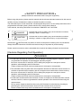
• SAFETY PRECAUTIONS •
(Always read these instructions before using this equipment.)
Before using this product, please read this manual and the relevant manuals introduced in this manual
carefully and pay full attention to safety to handle the product correctly.
The instructions given in this manual are concerned with this product. For the safety instructions of the
programmable controller system, please read the CPU module User's Manual.
In this manual, the safety instructions are ranked as "DANGER" and "CAUTION".
DANGER
Indicates that incorrect handling may cause hazardous conditions,
resulting in death or severe injury.
! CAUTION
Indicates that incorrect handling may cause hazardous conditions,
resulting in medium or slight personal injury or physical damage.
!
Note that the ! CAUTION level may lead to a serious consequence according to the circumstances.
Always follow the instructions of both levels because they are important to personal safety.
Please save this manual to make it accessible when required and always forward it to the end user.
[Cautions Regarding Test Operation]
!
DANGER
• GX Simulator simulates an actual PLC CPU to debug the created programs; however, it does
not guarantee the operation of the debugged sequence program.
Be sure to connect the PC with PLC CPU to debug the program as usual prior to actual
operation, after debugging with GX Simulator.
Failure to observe this may result in accidents due to misoutput or misoperation.
• The simulated result may differ from actual operation because GX Simulator cannot access I/O
modules or special function modules, and do not support some instructions or device memory.
Be sure to connect the PC with PLC CPU to debug the program as usual prior to actual
operation, after debugging with GX Simulator.
Failure to observe this may result in accidents due to misoutput or misoperation.
• GX Simulator includes serial communication function to respond to the demands from external
devices; however, it does not guarantee the actual operation of the external devices using the
response data.
Do not use the response data from the running GX Simulator for other than the checking by
performing the serial communication function for the external device such as PC.
Failure to observe this may result in accidents due to misoutput or misoperation.
A-1
A-1
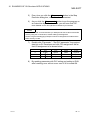
REVISIONS
* The manual number is given on the bottom left of the back cover.
Print Date
Sep., 2004
Nov., 2004
* Manual Number
SH (NA)-080468ENG-A
SH (NA)-080468ENG-B
Revision
First edition
Correction
Section 11.1
Feb., 2005
SH (NA)-080468ENG-C
Aug., 2005
SH (NA)-080468ENG-D
Correction
Section 1.2, Section 3.4.3, Section 3.4.6
Correction
Chapter 1, Section 1.1, Section 1.2, Section 2.2, Section 2.3,
Section 3.1, Section 3.2, Section 3.4.4, Section 3.4.6, Section 4.1,
Section 4.3, Chapter 7, Appendix 4
Nov., 2005
SH (NA)-080468ENG-E
Addition mode
FX3UCPU, FX3UCCPU
Correction
About the Generic Terms and Abbreviations, Section 1.1,
Section 1.2, Section 3.4.1, Section 3.4.4, Section 7.1.4, Section 9.2,
Section 11.1, Appendix 1.3, Appendix 1.5, Appendix 2.3,
Appendix 3.1, Appendix 3.2, Appendix 4
Apr., 2006
SH (NA)-080468ENG-F
Correction
Section 3.4.1, Section 3.4.3, Section 3.4.6, Section 4.3,
Appendix 3.1, Appendix 3.2
May., 2007
SH (NA)-080468ENG-G
Correction
Appendix 2.2, Appendix 2.5
Feb., 2008
SH (NA)-080468ENG-H
Correction
About the Generic Terms and Abbreviations, Section 2.3,
Section 3.4.6, Appendix 4
Apr., 2008
SH (NA)-080468ENG-I
Addition mode
Q02PHCPU, Q06PHCPU
Correction
About the Generic Terms and Abbreviations, Appendix 5
Jul., 2008
SH (NA)-080468ENG-J
Addition mode
FX3GCPU
Correction
About the Generic Terms and Abbreviations, Section 3.4.4,
Appendix 1.3, Appendix 1.5, Appendix 2.3, Appendix 5
Japanese Manual Version SH-080467-L
This manual confers no industrial property rights or any rights of any other kind, nor does it confer any patent licenses.
Mitsubishi Electric Corporation cannot be held responsible for any problems involving industrial property rights which
may occur as a result of using the contents noted in this manual.
© 2004 MITSUBISHI ELECTRIC CORPORATION
A-2
A-2
—— SOFTWARE USER REGISTRATION ——
After agreeing to the terms of the Software License Agreement included in the package, please access the
MELFANSweb Home Page (http://www.MitsubishiElectric.co.jp/melfansweb) and make a software user
registration. (User registration is free of charge.)
You can also make a registration by faxing or mailing the "Software Registration Card" packed with the
product.
1. Software Registration
You can make a software registration by accessing the MELFANSweb Home Page or faxing or mailing the
"Software Registration Card" packed with the product.
After you have made a software registration, we will register the user and send the "Software registration
confirmation" together with the user ID.
We will also provide the latest information, such as the new product release, version upgrade information
and event information, by direct mail.
2. Notes on Contact
Please ask questions concretely and clearly using terms listed in the manual.
When requesting us to solve a problem, provide us with detailed information for reproducing the problem.
In addition, contact the respective manufacturers when asking questions about the operating system (OS) or
the other vender's software products
User registration is valid only in Japan.
A-3
A-3
INTRODUCTION
Thank you for choosing the Mitsubishi MELSOFT Series Integrated FA software.
Read this manual and make sure you understand the functions and performance of MELSOFT series
thoroughly in advance to ensure correct use.
CONTENTS
SAFETY PRECAUTIONS..............................................................................................................................A- 1
REVISIONS ....................................................................................................................................................A- 2
SOFTWARE USER REGISTRATION...........................................................................................................A- 3
INTRODUCTION ...........................................................................................................................................A- 4
CONTENTS....................................................................................................................................................A- 4
About Manuals ...............................................................................................................................................A- 8
About the Generic Terms and Abbreviations ................................................................................................A- 9
Product Makeup .............................................................................................................................................A-11
1. OUTLINE OF GX Simulator
1- 1 to 1- 12
1.1 Features of the GX Simulator .................................................................................................................. 1- 2
1.2 Differences To Debugging with an Actual PLC Connected.................................................................... 1- 8
2. SYSTEM CONFIGURATION
2- 1 to 2- 2
2.1 System Configuration............................................................................................................................... 2- 1
2.2 Combination with MELSOFT Products ................................................................................................... 2- 1
2.3 Operating Environment ............................................................................................................................ 2- 2
3. SPECIFICATIONS
3- 1 to 3-26
3.1 Table of Functions.................................................................................................................................... 3- 1
3.2 Function List ............................................................................................................................................. 3- 3
3.3 Devices and Instructions Supported by the GX Simulator ..................................................................... 3- 8
3.4 GX Simulator Restrictions and Cautions................................................................................................. 3- 9
3.4.1 Restrictions and cautions common to each type of CPU ................................................................ 3- 9
3.4.2 Restrictions and cautions for the A series CPU functions ............................................................... 3-12
3.4.3 Restrictions and cautions for the QnA series CPU functions .......................................................... 3-14
3.4.4 Restrictions and cautions for the FX series CPU functions ............................................................. 3-17
3.4.5 Restrictions and cautions for the Motion controller functions .......................................................... 3-20
3.4.6 Restrictions and precautions for the Q series CPU functions ......................................................... 3-21
3.5 GX Simulator Safety and Handling Precautions ..................................................................................... 3-26
4. COMMON OPERATIONS FOR THE GX Simulator
4- 1 to 4- 7
4.1 Procedure from Installation to Debugging............................................................................................... 44.2 GX Developer Operations before Debugging ......................................................................................... 44.3 Description of the Initial Screen Display.................................................................................................. 44.4 Ending the GX Simulator ......................................................................................................................... 4A-4
A-4
1
3
5
7
5. SIMULATION OF EXTERNAL DEVICE OPERATION - I/O SYSTEM SETTING FUNCTIONS 5- 1 to 5-35
5.1 I/O System Setting Operation Procedure................................................................................................ 5- 4
5.2 Starting/Ending I/O System Setting......................................................................................................... 5- 5
5.3 Configuration of I/O System Settings Screen ......................................................................................... 5- 6
5.4 Setting by Using Timing Chart................................................................................................................. 5- 8
5.5 Operation of Timing Chart Format Input Screen..................................................................................... 5-10
5.5.1 Operation procedure of timing chart format input screen ................................................................ 5-10
5.5.2 Configuration of timing chart format input screen ............................................................................ 5-11
5.5.3 Entering/Deleting device ................................................................................................................... 5-13
5.5.4 Setting/Editing timing ........................................................................................................................ 5-15
5.5.5 Setting scan number of timing chart ................................................................................................. 5-21
5.5.6 Other operations................................................................................................................................ 5-22
5.6 Setting by Entering Device Value............................................................................................................ 5-25
5.7 Starting/Stopping the Simulation ............................................................................................................. 5-27
5.8 Other Operations...................................................................................................................................... 5-29
5.8.1 Operating the file ............................................................................................................................... 5-29
5.8.2 Cutting, copying and pasting all settings in the set No. ................................................................... 5-31
5.8.3 Batch-enabling/disabling settings ..................................................................................................... 5-32
5.8.4 Executing monitoring......................................................................................................................... 5-33
5.8.5 Reading I/O system setting file for SW5 or earlier versions ............................................................ 5-35
6. COMMUNICATION WITH EXTERNAL DEVICE - SERIAL COMMUNICATION FUNCTION
6- 1 to 6-12
6.1 Operation Procedures for Serial Communication Function .................................................................... 6- 2
6.2 Starting/Ending the Serial Communication Function .............................................................................. 6- 3
6.3 Layout of the Serial Communication Function Screen ........................................................................... 6- 4
6.4 Transmission Specifications .................................................................................................................... 6- 6
6.5 Usable Frames......................................................................................................................................... 6- 7
6.6 Command Lists ........................................................................................................................................ 6- 8
6.6.1 Usable A-compatible 1C frame commands ..................................................................................... 6- 8
6.6.2 Usable QnA-compatible 3C/4C frame commands........................................................................... 6- 9
6.7 Communication Status............................................................................................................................. 6-10
6.8 Error Code Lists ....................................................................................................................................... 6-11
6.8.1 When the A-compatible 1C frame is used........................................................................................ 6-11
6.8.2 When the QnA-compatible 3C/4C is used ....................................................................................... 6-12
7. MONITORING, TESTING DEVICE MEMORY - MONITOR FUNCTION
7- 1 to 7-29
7.1 Monitoring, Testing the Device Memory.................................................................................................. 7- 1
7.1.1 Operation Procedure of Monitoring Device Memory........................................................................ 7- 2
7.1.2 Starting/Ending Monitoring Device Memory..................................................................................... 7- 3
7.1.3 Specifying the station to be monitored ............................................................................................. 7- 4
7.1.4 Batch-monitoring the devices ........................................................................................................... 7- 5
7.1.5 Monitoring the buffer memory........................................................................................................... 7- 8
7.1.6 Monitoring the registered devices..................................................................................................... 7-11
7.1.7 Conducting a device test (Device write) ........................................................................................... 7-13
A-5
A-5
7.2 Using Timing Chart .................................................................................................................................. 7-15
7.2.1 Operation procedure of timing chart ................................................................................................. 7-15
7.2.2 Starting/Exiting timing chart .............................................................................................................. 7-16
7.2.3 Using timing chart.............................................................................................................................. 7-17
7.2.4 Entering/Deleting device to be monitored ........................................................................................ 7-20
7.2.5 Starting/Stopping monitoring ............................................................................................................ 7-23
7.2.6 Operating file ..................................................................................................................................... 7-24
7.2.7 Setting sampling period .................................................................................................................... 7-26
7.2.8 Other operations................................................................................................................................ 7-27
8 SETTING THE DEVICES FOR SIMULATION - DEVICE MANAGER FUNCTION
8- 1 to 8-26
8.1 Device Manager Operation Procedure.................................................................................................... 8- 3
8.2 Starting/Exiting Device Manager ............................................................................................................. 8- 4
8.3 Setting the Other Station Devices ........................................................................................................... 8- 5
8.3.1 Other station device setting .............................................................................................................. 8- 5
8.4 Setting the Device Values for Simulation ................................................................................................ 8- 7
8.4.1 Device control setting........................................................................................................................ 8- 7
8.4.2 Device value check setting ............................................................................................................... 8-12
8.5 Starting/Stopping Simulation ................................................................................................................... 8-14
8.6 Displaying the Results of Access to Devices (Log Display) ................................................................... 8-15
8.7 Other Operations...................................................................................................................................... 8-17
8.7.1 Performing the file operation of setting data .................................................................................... 8-17
8.7.2 Editing the settings ............................................................................................................................ 8-19
8.7.3 Printing the log information and setting information......................................................................... 8-22
8.7.4 Searching for log information............................................................................................................ 8-24
8.7.5 Saving the log information into file.................................................................................................... 8-25
8.7.6 Clearing the log information .............................................................................................................. 8-26
9. SAVING AND READING THE DEVICE AND BUFFER MEMORIES, OPTION SETTING
- TOOL FUNCTIONS
9- 1 to 9- 6
9.1 Saving the Device and Buffer Memories................................................................................................. 9- 1
9.2 Reading Saved Device Memory or Buffer Memory Data ....................................................................... 9- 3
9.3 Option Setting........................................................................................................................................... 9- 6
10. EXAMPLES OF GX Simulator APPLICATIONS
10- 1 to 10-15
10.1 Debugging Using GX Developer Step Execution Function ................................................................ 10- 4
10.2 Using Timing Chart Display for Debugging......................................................................................... 10- 6
10.3 Using I/O System Settings for Debugging .......................................................................................... 10-10
11. TROUBLESHOOTING
11- 1 to 11- 8
11.1 Error Messages Displayed on the LED Indicators .............................................................................. 11- 1
A-6
A-6
APPENDICES
App- 1 to App-67
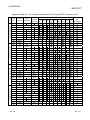
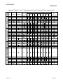
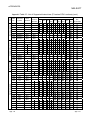
Appendix 1 List of Supported Devices ......................................................................................................App- 1
Appendix 1.1 The A series CPU function GX Simulator .......................................................................App- 1
Appendix 1.2 The QnA series CPU function GX Simulator ..................................................................App- 5
Appendix 1.3 FX series CPU function GX Simulator ............................................................................App-11
Appendix 1.4 GX Simulator for Q series CPU (A mode) functions.......................................................App-35
Appendix 1.5 GX Simulator for Q series CPU (Q mode) functions ......................................................App-35
Appendix 2 List of Supported Instruction...................................................................................................App-44
Appendix 2.1 A series CPU function GX Simulator ..............................................................................App-44
Appendix 2.2 QnA series function GX Simulator ..................................................................................App-46
Appendix 2.3 FX series function GX Simulator .....................................................................................App-48
Appendix 2.4 GX Simulator for Q series CPU (A mode) functions.......................................................App-55
Appendix 2.5 GX Simulator for Q series CPU (Q mode) functions ......................................................App-55
Appendix 3 List of Devices Usable with the I/O System Settings ............................................................App-57
Appendix 3.1 Condition area..................................................................................................................App-57
Appendix 3.2 Simulation device area ....................................................................................................App-59
Appendix 4 Method for Debugging the Universal Model QCPU Projects with the GX Simulator. ..........App-63
Appendix 4.1 Overview ..........................................................................................................................App-63
Appendix 4.2 Debugging procedure ......................................................................................................App-63
Appendix 4.3 Detailed operation............................................................................................................App-64
Appendix 5 Functions Added to Previous Versions..................................................................................App-65
INDEX
A-7
Index- 1 to Index- 3
A-7
About Manuals
The following manuals are related to this product.
Refer to the following table and request the necessary manuals.
Related Manuals
Manual Number
(Model Code)
Manual Name
GX Developer Version 8 Operating Manual
Describes the online functions of GX Developer including the programming procedure, printing out
procedure, monitoring procedure, and debugging procedure.
(Sold separately.)
SH-080373E
(13JU41)
REMARK
The GX Simulator Version 7 Operating Manual is contained in a single CD-ROM as
a set of the software package and manual.
For the user who wants the GX Simulator Version 7 Operating Manual as a single
item, it is available in a printed form as an option.
A-8
A-8
About the Generic Terms and Abbreviations
Unless otherwise specified, the following generic terms and abbreviations are
used in this manual.
Generic Term/Abbreviation
GX Simulator
GX Developer
MX Component
MX Sheet
Debug
Device memory
Monitor
Simulations
Timing chart
WDT error
Pseudo-sequence program
Basic model QCPU
Description
Generic product name of the products SWnD5C-LLT-E, SWnD5C-LLT-EA, SWnD5C-LLTEV and SWnD5C-LLT-EVA.
(n indicates any of versions 2 to 6.)
–EA indicates a multiple-license product, and -EV an updated product.
Generic product name of the products SWnD5C-GPPW-E, SWnD5C-GPPW-EA,
SWnD5C-GPPW-EV and SWnD5C-GPPW-EVA.
(n indicates any of versions 2 to 8.)
-EA indicates a multiple-license product, and –EV an updated product.
Generic product name of the products SWnD5C-ACT-E and SWnD5C-ACT-EA
(n means any of Versions 1 to 3)
-EA means a multiple-license product.
Generic product name of the products SWnD5C-SHEET-E and SWnD5C-SHEET-EA
(n means Version 1)
-EA means a multiple-license product.
Locating and correcting errors in a sequence program to create a correct program.
Areas to store device data in the GX Simulator, including inputs (X), outputs (Y), relays (M),
timers (T), data registers (D), etc.
Monitoring to determine the ON/OFF status of bit devices or the PV of word devices.
Test execution of a program on a personal computer with the GX Simulator installed,
instead of execution in an actual PLC.
Functions to visually confirm ON/OFF status of a bit device or the change in value of a word
device.
An error issued when a sequence program is written in such a way that it runs an infinite
loop.
Indicates a sequence program created by the GX Simulator to realize the settings of I/O
System Settings.
Generic term of the Q00JCPU, Q00CPU, and Q01CPU.
High Performance model
QCPU
Generic term of the Q02(H)CPU, Q06HCPU, Q12HCPU, and Q25HCPU.
Universal model QCPU
Generic term of the Q02UCPU, Q03UDCPU, Q04UDHCPU, Q06UDHCPU, Q13UDHCPU
and Q26UDHCPU.
Process CPU
Redundant CPU
Generic term of the Q02PHCPU, Q06PHCPU, Q12PHCPU and Q25PHCPU.
Generic term of the Q12PRHCPU and Q25PRHCPU.
QnA series CPU function
Function that simulates a project when the PLC series is the A series CPU or Q series CPU
(A mode).
Function that simulates a project when the PLC series is the QnA series CPU.
FX series CPU function
Motion controller function
Function that simulates a project when the PLC series is the FX series CPU.
Function that simulates a project when the PLC series is the motion controller (SCPU).
Q series CPU function
Function that simulates a project when the PLC series is the Q series CPU (Q mode).
Generic term of the A0J2HCPU, A1FXCPU, A1SCPU, A1SJCPU, A1SHCPU, A1SJHCPU,
A1NCPU, A2CCPU, A2CJCPU, A2NCPU, A2NCPU-S1, A2SCPU, A2SHCPU, A3NCPU,
A2ACPU, A2ACPU-S1, A3ACPU, A2UCPU, A2UCPU-S1, A2USCPU, A2USCPU-S1,
A2ASCPU, A2ASCPU-S1, A2ASCPU-S30, A2ASCPU-S60, A2USHCPU-S1, A3UCPU and
A4UCPU.
A series CPU function
A series CPU
QnA series CPU
A-9
Generic term of the Q2ACPU, Q2ASCPU, Q2ASCPU-S1, Q2ASHCPU, Q2ASHCPU-S1,
Q3ACPU, Q4ACPU and Q4ARCPU.
A-9
Generic Term/Abbreviation
FX series CPU
Motion controller
Q series CPU (A mode)
Q series CPU (Q mode)
Description
Generic term of the FX0CPU, FX0SCPU, FX0NCPU, FX1CPU, FX2CPU, FX2CCPU,
FX1SCPU, FX1NCPU, FX1NCCPU, FX2NCPU, FX2NCCPU, FX3GCPU, FX3UCPU and
FX3UCCPU.
Generic term of the A171SHCPU, A172SHCPU, A173UHCPU, A173UHCPU-S1,
A273UHCPU and A273UHCPU-S3.
Generic term of the Q02CPU-A, Q02HCPU-A and Q06HCPU-A.
Generic term of the Q00JCPU, Q00CPU, Q01CPU, Q02CPU, Q02HCPU, Q02PHCPU,
Q06HCPU, Q06PHCPU, Q12HCPU, Q12PHCPU, Q12PRHCPU, Q25HCPU, Q25PHCPU
and Q25PRHCPU.
R
Windows Vista
R
Windows XP
A - 10
R
R
Generic term of Microsoft Windows Vista Home Basic Operating System,
R
R
Microsoft Windows Vista Home Premium Operating System,
R
R
Microsoft Windows Vista Business Operating System,
R
R
Microsoft Windows Vista Ultimate Operating System
R
R
and Microsoft Windows Vista Enterprise Operating System.
R
R
Generic term of Microsoft Windows XP Professional Operating System and
R
R
Microsoft Windows XP Home Edition Operating System.
A - 10
Product Makeup
GX Simulator are made up of the following products.
Type
Product Name
GX Simulator (1 license product)
SW7D5C-LLT-E(V)
Quantity
(CD-ROM)
1
End-user softwere license agreement
1
Software registration Card
1
License agreement
GX Simulator (Multiple license product)
SW7D5C-LLT-E(V)A
1
(CD-ROM)
1
End-user softwere license agreement
1
Software registration Card
1
n
License agreement
1
1: The same number of software registration cards as that of licenses are packed with the product.
NOTICES
• We don't guarantee the commercially-available Microsoft Windows Operating
System-based software products that have been introduced in this manual.
• We hold the copyrights of this software package.
• No part of this manual may be transcribed or duplicated in any form without prior
permission by Mitsubishi Electric Corporation.
• We have attempted to cover all the revisions of software and hardware, but this
manual may not contain the latest revisions.
• The software of this product requires one license to be purchased per computer.
• We permit the user to use this software package (including this manual) based on
the Software License Agreement.
• We are not liable for consequences or influences due to this software package
(including this manual).
• The specifications of this software package and the descriptions in this manual
may be altered in future without prior notice.
R
A - 11
R
A - 11
MEMO
A - 12
A - 12
1 OUTLINE OF GX Simulator
MELSOFT
1. OUTLINE OF GX Simulator
1
This operating manual describes the functions and operation of the GX Simulator
Version 7.
The GX Simulator is a software package, which runs under Microsoft Windows
Operating System.
Offline debugging is possible by adding the GX Simulator to a computer in which the
GX Developer is installed. The offline debugging functions include the monitor and the
test of the host station/other station devices and simulated operation of external device
I/Os.
As the GX Simulator allows sequence programs to be developed and debugged on a
single computer, checking a modified program is quick and easy.
GX Developer must be installed before these functions can be used.
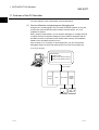
R
R
GX
GX
Developer Simulator
Device monitor and test, simulated operation
of machine side I/Os, etc. are possible.
Install
Connection of PLC
is not necessary.
A sequence program created with GX Developer can be debugged by writing it to the
GX Simulator.
The sequence program is automatically written to the GX Simulator when the GX
Simulator are started up.
Refer to GX Developer Operating Manual for information on operations not covered in
this manual:
1-1
1-1
1 OUTLINE OF GX Simulator
MELSOFT
1.1 Features of the GX Simulator
1
The main features of the GX Simulator are described below.
(1) Can be utilized as a single program debugging tool
Using the PLC for debugging in the conventional method required not only the
PLC but also I/O and special function modules, external device, etc. to be
prepared as needed.
When using the GX Simulator, you can perform debugging on a single personal
computer because I/O System Settings for external device simulation and the
simulation function for special function module buffer memory are available in
addition to the simulation function for PLC.
Also, because of no connection to actual equipment, you can proceed with
debugging safely if an abnormal output should occur due to a program bug.
Conventional debugging
GX Developer
Ladder monitor
Batch monitor (device memory)
Batch monitor (buffer memory)
Communication
Power
supply
1-2
CPU
I/O module
Special
function
module
1-2
1 OUTLINE OF GX Simulator
MELSOFT
Debugging using GX Simulator
User application
GX Developer
Ladder monitor
MX Sheet
Batch monitor (device memory)
MX Component
Batch monitor (buffer memory)
Communication
GX Simulator
1) Basic
screen
2) CPU
simulation
function
3) Device
memory
simulation
function
4) Buffer
memory
simulation
function
5)
6)
7)
8)
9)
10)
Device batch
monitor
Timing chart
I/O system
settings
Serial
communication
function
Device
manager
function
Tool function
1) ... Key switch, indicator display function
2) ... Function that simulates CPU operation
3) ... Function that simulates CPU device memory
4) ... Function that simulates the buffer memory area of a special function module
5) ... Function that monitors a batch of device memory values
6) ... Function that displays device memory changes in a chart form
7) ... Function that simulates I/O operation of external device
8) ... Function that simulates communication with an external device
9) ... Function that checks the operation of the user application using the MELSOFT product
10) ... Function that saves/reads device memory or buffer memory data to/from a file
1-3
1-3
1 OUTLINE OF GX Simulator
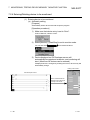
MELSOFT
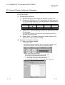
(2) Simulation of external device operation (I/O system setting function)
By setting the combination of bit device ON/OFF condition and word device value
interactively in the I/O system settings of GX Simulator, an external input
generated in response to a PLC output can be provided simulatively.
Devices need not be rewritten.
X0
X1
Start
Stop
GX Simulator: Only simple setting screen
Y0
To debug the
program shown
on the left
Run
Y0
Conventional debugging: Debugging program created
Y0
5s timer
5s timer setting
SET X1
(3) Checking of message format of frame sent by external device
(Serial communication function)
This function allows you to easily check whether the frame (A-compatible 1C
frame, QnA-compatible 3C/4C frame) used for access from an external device to
the PLC CPU via a serial communication module (computer link module) is in a
correct message format or not.
Since this function also enables devices to be accessed, you can check/change
device contents easily on an external device.
Conventionally, the serial communication module (computer link module) was
actually connected with the external device to check operation. Using this
function, however, you can easily check the message format and device contents
between GX Simulator and external device.
<Conventional debugging>
Debugging was performed with the external device connected with the serial
communication module (computer link module) actually.
PLC
Serial communication module
(computer link module)
Serially connectable
external device
Frame transmission
Response
1-4
1-4
1 OUTLINE OF GX Simulator
MELSOFT
<Debugging using GX Simulator>
Since GX Simulator responds to the frame sent from the external device, the
external device need not be connected to the serial communication module
(computer link module) actually.
Serially connectable
external device
Frame transmission
GX Simulator
Response
(4) Monitoring of device memory (monitor function)
You can monitor the states of the virtual CPU device memory and the buffer
memory.
Like the device batch monitor and buffer memory batch monitor functions of GX
Developer, you can not only monitor the ON/OFF states and values of devices
but also perform forced ON/OFF and change current values.
This function also allows you to display the ON/OFF states and values in a timing
chart format to grasp time series operation.
(5) Saving/reading of device/buffer memory data (tool function)
You can save the data of the device memory in the virtual CPU or the buffer
memory of the special function module temporarily, and when resuming
debugging, you can read and use the saved data.
1-5
1-5
1 OUTLINE OF GX Simulator
MELSOFT
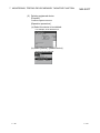
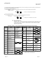
(6) Support for offline debugging of user application (Device Manager
function)
The operation of the user application using the MELSOFT product (e.g. MX
Component) can be checked easily without use of the actual PLC.
(a) Checking the read operation of the host station/other station
devices
Without creation of a program that will change device values for debugging,
the operation of the user application can be checked on the basis of the
device values that change with patterns.
Also, read operation from the host station/other station devices can be
checked without changing the user application.
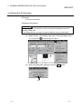
(Device change pattern setting screen)
Other station 2-1
D1 change pattern
Host station
X10 change pattern
Other station 1-2
D0 change pattern
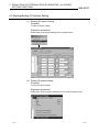
(b) Checking the written device values
Whether the values written from the user application to the host
station/other station devices are within the user-assumed ranges or not can
be checked.
This enables check for user application creation or setting mistakes.
~
MELSOFT product
Network No.
Station No.
User application
Public Sub Command 1 Click()
3
2
End Sub
Device read/write
GX Simulator
Host station
XY
D
Device memory
1-6
Other station
1-1
D
X
Other station
2-1
XY
Other station
3-2
M
D
Other station device setting
1-6
1 OUTLINE OF GX Simulator
MELSOFT
(7) Writing a edited program in RUN (Online change function)
The operation of transferring edited sequence program to GX Simulator is
unnecessary. Therefore, the transferred program operation can be momentarily
checked.
Furthermore, debug can be smoothly continued since the device value before
transfer operation has been retained.
• Brief operation procedure
1) Start GX Simulator.
2) Edit a sequence program in GX Developer.
3) Select [Convert] -[Convert (Online change)] from GX Developer menu and
write the edited program to GX Simulator in RUN.
(8) Can analyze the situation of trouble in a design room and quickly
identify incorrect places (Device memory write function)
The PLC status in the field can be recreated based on the device memory data at
the occurrence of trouble in a design room. The sequence program operation
that cannot be checked in the field (e.g. device test) can be confirmed.
Therefore, incorrect places of sequence program can be quickly identified and
the modification and the operation check are smoothly proceeded.
trouble
Taking PLC device memory
data into GX Simulator
GX Developer + GX Simulator
Analyzing PLC status and identifying incorrect places
on personal computer.
• Brief operation procedure
(Operation in the field)
1) Read device memory from PLC CPU in GX Developer.
2) Save project data.
(Operation in a design room)
3) Open the project data saved in the field.
4) Start GX Simulator.
5) Change GX Simulator status to STOP using "Remote operation" in PLC
write dialog box.
6) Write sequence program, parameter and device memory from GX
Developer to GX Simulator.
7) Monitor ladder and device in GX Developer.
1-7
1-7
1 OUTLINE OF GX Simulator
MELSOFT
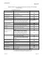
1.2 Differences To Debugging with an Actual PLC Connected
The specifications for debugging using the GX Simulator differ from those for
debugging with an actual PLC connected.
The main differences between debugging using the GX Simulator and debugging with
an actual PLC connected are shown below.
Refer to Section 3.4 for details.
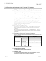
Item Name
Step execution,
skip execution,
partial
execution
Debugging with an Actual
PLC Connected
Debugging with GX Simulator
Debugging using step execution, skip execution, and
partial execution makes debugging operation more
efficient.
Not supported.
Step execution
"OPERATION ERROR" occurs when the device range
determined by CPU type or parameters is exceeded. 1
Device range
check
Operation continues even
if the indirect designation
by the index register
exceeds the device
range.
Applicable CPU
• FX series CPU
• Q series CPU (Q mode)
• A series CPU
• Q series CPU (A mode)
• A series CPU
• QnA series CPU
• FX series CPU
• Motion controller
• Q series CPU (Q mode)
• Q series CPU (A mode)
The device (@**) to be indirectly designated is also
checked within the device range of the device address.
However, file register is checked within ZR device range
instead of R device range.
(For the device range for a specific CPU type, refer to
Appendix 1.)
@DO checks the error in the ZR device range setting when
the following program is executed.
ADRSET R32767 D0
FMOV K1 @D0 K20
• QnA series CPU
• Q series CPU (Q mode)
R device
range
File
register
R32767
ZR device range
1: Indirectly designating file register checks the device range within the range of capacity set
on "PLC File" screen switched from "PLC Parameter" dialog box by tab.
1-8
1-8
1 OUTLINE OF GX Simulator
Item Name
MELSOFT
Debugging with an Actual
PLC Connected
Debugging with GX Simulator
Applicable CPU
Real number
range check
Dedicated instructions to
handle real numbers allow
operation to continue when
an illegal value occurs
which cannot be evaluated
as a real number.
Real number range checks are conducted rigorously.
"OPERATION ERROR" is displayed if a value cannot be
evaluated as a real number.
• A series CPU
• QnA series CPU
• Motion controller
• Q series CPU (Q mode)
• Q series CPU (A mode)
Number range
check
Value 0 is given as a result
of "0 divided by 0" by DIV
instruction, floating point
division, of the A series
PLC.
No error occurs.
The rigorous number range check can detect an illegal 0
denominator and "OPERATION ERROR" is generated if
0 ÷ 0 is executed.
• A series CPU
• Motion controller
• Q series CPU (A mode)
The illegal instruction is checked and "INSTRCT CODE
ERR." is displayed. Dedicated instructions must be
described as blocks.
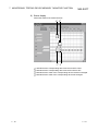
(Example of illegal ladder)
Illegal
instruction in a
dedicated
instruction
The illegal instruction is
ignored and operation
continues.
M9036
LEDA
RAD
LEDC
D200
DM0V
K120
LEDC
D210
Illegal
instruction
• A series CPU
• Motion controller
• Q series CPU (A mode)
D500
LEDR
END
Time concept
Supported
instructions
Operating CPU
type
Special function
module
(special function
block)
1-9
Actual time
As per constant scan setting.
• A series CPU
• QnA series CPU
• FX series CPU
• Motion controller
• Q series CPU (Q mode)
• Q series CPU (A mode)
All instructions can be
used.
Since data refresh instructions, PID control instructions
(QnA series, FX series CPUs), etc. cannot be used, they
are processed as NOPs.
(Refer to Appendix-2 for supported instructions.)
• A series CPU
• QnA series CPU
• FX series CPU
• Motion controller
• Q series CPU (Q mode)
• Q series CPU (A mode)
According to CPU type
used.
• Operates as A4UCPU when A series CPU, motion
controller or Q series CPU (A mode) is selected.
• Operates as Q4ACPU when QnA series CPU is
selected.
• Operates as FX series CPU when FX series CPU is
selected.
• Operates as Q25HCPU when Q series CPU (Q mode)
is selected.
• A series CPU
• QnA series CPU
• FX series CPU
• Motion controller
• Q series CPU (Q mode)
• Q series CPU (A mode)
Not supported.
Only the buffer memory area of a special function module
(special function block) is supported.
• A series CPU
• QnA series CPU
• FX series CPU
• Motion controller
• Q series CPU (Q mode)
• Q series CPU (A mode)
Supported
1-9
1 OUTLINE OF GX Simulator
Item Name
I/O module
Debugging with an Actual
PLC Connected
Supported
MELSOFT
Debugging with GX Simulator
Applicable CPU
Not supported
• A series CPU
• QnA series CPU
• FX series CPU
• Motion controller
• Q series CPU (Q mode)
• Q series CPU (A mode)
Network
Supported
Not supported
• A series CPU
• QnA series CPU
• FX series CPU
• Motion controller
• Q series CPU (Q mode)
• Q series CPU (A mode)
Memory cassette
capacity
An error occurs in GX
Developer if data exceeding
the memory cassette capacity
is written to the PLC.
No error occurs and normal operation continues
if data exceeding the memory cassette capacity
is written to the PLC.
• A series CPU
• QnA series CPU
• Motion controller
• Q series CPU (Q mode)
• Q series CPU (A mode)
Intelligent function
module (intelligent
parameters)
Supported
Only the initial setting, auto refresh setting and
buffer memory area are supported.
• Q series CPU (Q mode)
In case “Use the file
register” and “Use the
following file” are set,
but “Capacity” is not
set
Operates according to capacity
of the file register if the file
register specified on “Use the
following file” exists in the
specified drive.
Operates with the capacity of the file register set
as an 0K point, whether the file used on “Use the
following file” exist or not. Thus, “OPERATION
ERROR” occurs if the file register is used in the
program.
QnA series CPU
Q series CPU (Qmode)
(1) If the same name file
register as the program is in
the PLC CPU drive, the
PLC CPU debugs the file
register by the set capacity.
(1) If the same name file register as the program
is in the PC drive, GX Simulator debugs the
file register by the set capacity.
(2) If the same name file
register as the program is
not in the PLC CPU drive,
the PLC CPU will not
debug.
(2) If the same name file register as the program
is not in the PC drive, GX Simulator newly
creates a file register of 1018k steps and
debugs it.
When “Use the same file name
as the program” is selected for
a file register, the PLC CPU
monitors the file register within
the changed capacity.
When “Use the same file name as the program”
is selected for a file register, GX Simulator
monitors a file register of 1018k steps
(maximum).
When “Use the same
file name as the
program” is selected
for a file register.
When the capacity of
a file register is
changed during
program execution.
1 - 10
QnA series CPU
Q series CPU (Q mode)
QnA series CPU
Q series CPU (Q mode)
1 - 10
1 OUTLINE OF GX Simulator
Item Name
Debugging with an Actual
PLC Connected
MELSOFT
Debugging with GX Simulator
Applicable CPU
(1) When performed, execution
stops at each of the first
instruction, P/I pointer,
statement and note.
(1) When performed, execution stops at the
first instruction and P/I pointer but does
not stop at the first statement and note.
(2) When the start position is a
statement or note, execution
stops at the first statement or
note.
(2) When the start position is a statement or
note, execution stops at the first
instruction or P/I pointer immediately after
that statement or note.
(3) When the repetition count of the
option setup is set, each of the
instruction, P/I pointer,
statement and note is counted
once.
(3) When the repetition count of the option
setup is set, each of the instruction and P/I
pointer is counted once. The statement
and note are not counted.
(4) When a statement or note step
is set to the break point of the
option setup, execution stops at
the statement or note step.
(4) When a statement or note step is set to
the break point of the option setup,
execution does not stop at this break
point.
(1) When performed, execution
stops at each of the first
instruction, P/I pointer,
statement and note.
(1) When performed, execution stops at the
first instruction and P/I pointer but does
not stop at the first statement and note.
(2) When the start position is a
statement or note, execution
stops at the first statement or
note.
(2) When the start position is a statement or
note, execution stops at the first
instruction or P/I pointer immediately after
that statement or note.
(3) When a statement or note step
is set to the break point of the
break condition, execution stops
at the statement or note step.
(3) When a statement or note step is set to
the break point of the break condition,
execution does not stop at this break
point.
When -0 is specified
as floating-point real
number
An error occurs in some CPU
modules.
An error does not occur.
(Operated as 0)
• QnA series CPU
• Q series CPU (Q mode)
When dealing with a
Character string
constant
A maximum of 32 letters are
possible as a Character string
constant.
A maximum of 16 letters are possible as a
Character string constant.
• QnA series CPU
• Q series CPU (Q mode)
• FX series CPU
(1) Executable on ladder, ST, or
SFC.
(1) Executable on ladder, ST.
Error is displayed and online change is to
be terminated on SFC (The program
remains incomplete).
(2) Online change is executed
according to arbitrary setting
that is set in the following items
of Setting Options.
• Step No. specification used in
writing
• Instruction setting for online
change
(2) The following items of Setting Options
cannot be set arbitrarily. They are
performed based on the setting for GX
Simulator (The following items).
• Step No. specification used in writing
"Absolute step No." is selected.
• Instruction setting for online change
Selected the status that "Trailing edge
instructions are not executed" is
checked.
(When pre-setting exists before a startup
of GX Simulator, the setting recovers after
closing the GX Simulator).
When step
execution is
performed
When partial
execution is
performed
When online
change is performed
1 - 11
• QnA series CPU
• Q series CPU (Q mode)
• QnA series CPU
• Q series CPU (Q mode)
• A series CPU
• QnA series CPU
• Motion controller
• Q series CPU (Q mode)
• Q series CPU (A mode)
1 - 11
1 OUTLINE OF GX Simulator
Item Name
Debugging with an Actual
PLC Connected
MELSOFT
Debugging with GX Simulator
Applicable CPU
Supported
Not supported
However, only the buffer memory area in a special
function module (special function block) is
supported.
• FX series CPU
Positioning setting in
PLC parameter
Supported
Not supported
• FX series CPU
Extension file register
(ER)
Supported
Not supported
• FX series CPU
built-in high speed
counter
Supported
Not supported
• FX series CPU
Input interrupt
Counter interrupt
Timer interrupt
Supported
Not supported
• FX series CPU
Initialization of special
function block in PLC
parameter
1 - 12
1 - 12
2 SYSTEM CONFIGURATION
MELSOFT
2. SYSTEM CONFIGURATION
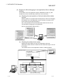
2.1 System Configuration
The following shows the system configuration.
GX Developer
or
GT Simulator
(option)
2
GX Simulator
(This product)
Parsonal computer
2.2 Combination with MELSOFT Products
The following describes combinations between GX Simulator Version 7 and MELSOFT
product versions.
(1) GX Simulator Version 7 operates on any version of GX Developer.
(2) To use the function added to GX Simulator Version 7 (Device
Manager function: Refer to Chapter 8), use the MELSOFT product
compatible with GX Simulator Version 7.
(3) Online change function is usable with GX Developer Version 8.27D
or later.
2-1
2-1
2 SYSTEM CONFIGURATION
MELSOFT
2.3 Operating Environment
The operating environment of GX Simulator is indicated below.
Item
2
Description
Installation (Add-in) destination
Added in to GX Developer (SW2D5C-GPPW-E or later, SW8D5C-GPPW-C).
Computer main unit
Personal computer on which Windows operates.
R
CPU
Refer to the following table "Used operating system and performance required for
Required memory
personal computer".
Hard disk free space
70MB or more
1
Disk drive
CD-ROM disk drive
Display
800
600 dot or more resolution. (1024
768 or higher for Windows Vista )
R
Microsoft Windows 95 Operating System
R
R
Microsoft Windows 98 Operating System
R
R
Microsoft Windows Millennium Edition Operating System
R
R
Microsoft Windows NT Workstation Operating System Version 4.0
R
R
Microsoft Windows 2000 Professional Operating System
R
Operating system
R
Microsoft Windows XP Professional Operating System
R
2
R
Microsoft Windows XP Home Edition Operating System
R
R
Microsoft Windows Vista
R
Home Basic Operating System
Microsoft Windows Vista
R
Home Premium Operating System
Microsoft Windows Vista
R
Business Operating System
Microsoft Windows Vista
R
Ultimate Operating System
Microsoft Windows Vista
R
Enterprise Operating System
R
R
R
R
R
1: 1MB is required to use a file register.
Make sure that the required space is secured within the driven in which this product has been installed, before using file
register.
2: For details on compatible operating systems, refer to the operating environment of GX Developer.
Used operating system and performance required for personal computer
Operating system
Performance Required for Personal Computer
CPU
Required memory
Windows 95
Pentium 133MHz or more
64MB or more
Windows 98
Pentium 133MHz or more
64MB or more
Windows Me
Pentium 150MHz or more
64MB or more
Windows NT Workstation 4.0 (Service Pack 3 or more)
Pentium 133MHz or more
64MB or more
Windows 2000 Professional
Pentium 133MHz or more
64MB or more
Windows XP
Pentium 300MHz or more
128MB or more
Pentium 1GHz or higher
1GB or more
R
R
R
R
R
R
R
R
R
Windows Vista
2-2
R
R
R
R
R
2-2
2 SYSTEM CONFIGURATION
MELSOFT
POINT
• Precaution for viewing PDF data/online manuals
Boost the personal computer memory for easier viewing.
• New functions of Windows
When Windows XP or Windows Vista is used, the following new functions
cannot be used.
If any of the following new functions is used, this product may not operate
normally.
Start of application in Windows compatible mode
Fast user switching
Remote desktop
Big fonts (Details setting of Screen properties)
64-bit operating system
R
R
R
R
2-3
2-3
3 SPECIFICATIONS
MELSOFT
3. SPECIFICATIONS
3.1 Table of Functions
The functions supported by the GX Simulator are shown below.
The functions supported by the GX Simulator include functions executed from the GX
Simulator menu and functions executed from the GX Developer menu.
The GX Simulator simulates the function of the CPU selected at the time of execution
of the GX Simulator from the GX Developer menu: it supports CPU's of type A, QnA,
and FX. Also, when the motion controller is selected, the corresponding function of the
A series CPU operates. (Refer to Section 3.4.5(1) for the A series CPU corresponding
to the motion controller.)
Also, when the Q series (Q mode) is selected, the Q series CPU functions operate, but
when the Q series (A mode) is selected, the A series CPU functions operate as
equivalent to those of the A4UCPU.
The functions supported by the GX Simulator are as indicated in Table 3.1.
3
Table 3.1 Functions Supported by GX Simulator
Function
Ladder monitor
Device monitor
Device test
Functions
executed from
the GX
Developer
menu
Description
• Monitors the processing status of the GX Simulator
• Forcibly write device values to the GX Simulator during
monitoring.
Write to PLC
• Writes parameter file and program file to GX Simulator.
PLC diagnostics
• Checks the GX Simulator status and errors.
Skip execution
Partial execution
Reference
• Skips program execution in the range between two
designated steps.
• Executes the part of the program in a designated step
or pointer range.
Step execution
• Executes the sequence program one step at a time.
Remote operation
• Operates the GX Simulator execution status.
GX Developer
Operating Manual
• Monitors the program execution status and number of
Program monitor list
executions as a table, starts and stops the program
execution in the table.
Online change
3-1
• Writes a program while a simulating CPU is in RUN
status (Writes at ladder or ST conversion).
3-1
3 SPECIFICATIONS
MELSOFT
Function
I/O system settings
Serial communication
function
Description
• Simulates the operation of external devices by simple
settings.
Reference
Chapter 5.
• Checks the operation of the frame that is sent from the
external device to the serial communication module
Chapter 6.
(computer link module).
• Conducts testing by monitoring the device memory
Monitor test
status.
• Displaying the ON/OFF chart of the devices.
Chapter 7.
• Forcing the devices ON/OFF, and changing present
• Function that allows the user application operation to be
executed from
the GX
Simulator
menu
3
values.
Functions
Device manager
function
checked by setting the external input-assumed device
value change patterns and write-enabled device ranges.
• Function that allows access from the user application
Chapter 8.
using the MELSOFT product to the other station devices.
Tools
Function equivalent to
WDT
Error detail display
function
Unsupported instruction
list display function
3-2
• Reads the saved device memory/buffer memory data and
makes option setting.
• Issues a WDT error if a sequence program is written in
such a way that it runs an infinite loop.
Chapter 9.
———
• Displays detailed error information at occurrence of an
error.
• Lists the instructions which are not supported by the GX
Chapter 4.
Simulator if they are included in a sequence program.
3-2
3 SPECIFICATIONS
MELSOFT
3.2 Function List
This section provides the function list of each screen.
(1) Initial screen function list
Reference
Start
Monitor Function
Monitors the device memory.
Device Memory Monitor...................................................
Section 7.1
Timing Chart Display ................................................
Displays the device change status.
Section 7.2
I/O System Settings............................................................
Simulates the external device operation. Chapter 5
Serial Communication Function
Device Manager
1
Simulates
............................
communication with the
external device.
1.......................................................Sets
the devices for simulation.
Chapter 6
Chapter 8
1: Unavailable when the PLC series is the FX series CPU.
Tools
Backup Device Memory.....................................
Writes device memory data to a file.
Section 9.1
Backup Buffer Memory...........................................
Writes buffer memory data to a file.
Section 9.1
Restore Device Memory.....................................
Reads the saved device memory data.
Section 9.2
Restore Buffer Memory...........................................
Reads the saved buffer memory data.
Section 9.2
Option
Selects how to display the initial screen
Display as minimized next time............................
at the start of GX Simulator.
Section 9.3
Help
Product information.........................................Shows the product information.
(2) Device Memory Monitor screen function list
Menu
Device Batch monitor................................................................
Batch-monitors the devices.
Section 7.1.4
Monitors the buffer memory.
Buffer memory monitor...........................................................
Section 7.1.5
Registers and monitors the devices.
Entry device monitor..........................................................
Section 7.1.6
Exits from Device Memory Monitor.
Exit..............................................................................................
Section 7.1.2
Online
Specifies the station to be monitored.
Transfer setup........................................................................
Section 7.1.3
Device write................................................................ Conducts a device test.
Section 7.1.7
3-3
3-3
3 SPECIFICATIONS
MELSOFT
(3) Timing Chart function list
Reference
File
Open File.........................................................................
Reads the saved monitor device data.
Writes the device data currently
Save File As.........................................................................
monitored.
Save Timing Data...........................................Saves as the timing chart data file.
Section 7.2.6
Section 7.2.6
Exit.........................................................................
Exits from Timing Chart.
Section 7.2.2
Section 7.2.6
Device
Enter Device......................................................................
Registers the devices to be monitored. Section 7.2.4
Deletes the selected devices.
Delete Device........................................................................
Section 7.2.4
Lists the devices being monitored.
List Device........................................................................
Section 7.2.8
Change the display format of the
Property.......................................................................
selected device.
Section 7.2.8
Monitor
Start/Stop......................................................................
Starts/stops monitor.
Section 7.2.5
Sampling period..............................................To change the Data accumulation
interval.
Section 7.2.7
3-4
3-4
3 SPECIFICATIONS
MELSOFT
(4) I/O system setting screen function list
Reference
File
New.........................................................................
Creates the new I/O system setting file. Section 5.8.1
Open.........................................................................
Opens current I/O system setting file.
Section 5.8.1
Save................................................................Overwrites and saves file being opened. Section 5.8.1
Save As.........................................................................
Gives the name to the file being opened Section 5.8.1
and saves it.
Execute I/O System Settings.........................................................................
Executes the I/O system setting.
Section 5.7
Cancel I/O system setting.........................................................................
Cancels the I/O system setting.
Import Earlier Version of I/O System File.......Reads I/O system setting files from
SW2 to SW5.
Exit I/O System Settings.................................Exits the I/O system setting.
Section 5.7
Section 5.8.5
Section 5.2
Edit
Cut......................................................................
Cuts the selected setting No..
Section 5.8.2
Copies the selected setting No..
Copy........................................................................
Section 5.8.2
Pastes the setting No. cut or copied.
Paste........................................................................
Section 5.8.2
Enable / Disable Settings
Enable All.................................................Enables all settings.
Section 5.8.3
Disable All.................................................Disables all settings.
Section 5.8.3
Online
Monitor Mode......................................................................
Starts monitor.
Section 5.8.4
Edit Mode........................................................Stops monitor.
Section 5.8.4
View
Tool Bar......................................................................
Set whether tool bar is displayed or not.
Set whether status bar is displayed or
Status Bar........................................................................
not.
Window
Cascade......................................................................
Cascades currently open screens.
Tiles currently open screens.
Tile.....................................................................
Arranges screens reduced to icons.
Arrange..................................................................
3-5
3-5
3 SPECIFICATIONS
MELSOFT
(5) Timing chart format input screen function list
Reference
File
Open File.........................................................................
Opens the timing chart data file.
Section 5.5.6
Exit.........................................................................
Exits from timing format input.
Section 5.5.2
Device
Enter Device......................................................................
Registers the devices to be setting.
Section 5.5.3
Deletes the registered devices.
Delete Device........................................................................
Section 5.5.3
Lists the registered devices.
List Device........................................................................
Section 5.5.6
Changes the display format of the
Property........................................................................
selected device.
Edit
Section 5.5.6
Undo......................................................................
Returns to previous status one step
before execution.
Sets status of bit device.
Bit Device........................................................................
Section 5.5.6
Sets status of word device.
Word Device........................................................................
Section 5.5.4
Activates setting of wizard screen.
Wizard........................................................................
Section 5.5.4
Inserts timing to selected section.
Insert........................................................................
Section 5.5.4
Deletes timing of selected section.
Delete........................................................................
Section 5.5.4
Section 5.5.4
Scan
Scan Setting......................................................................
Specifies scan number.
3-6
Section 5.5.5
3-6
3 SPECIFICATIONS
MELSOFT
(6) Device Manager screen function list
Reference
File
New...........................................................................................
Creates new setting information.
Section 8.7.1
Open..........................................................................................
Reads the saved setting information.
Section 8.7.1
Save......................................................................................
Saves the setting information.
Section 8.7.1
Save As......................................................................................
Saves the setting information with a name. Section 8.7.1
Print.....................................................................................Prints the setting information or gives
a print preview.
Section 8.7.3
Exit .....................................................................................Exits from Device Manager.
Section 8.2
Undo..........................................................................................
Undoes the last operation.
Section 8.7.2
Redo..........................................................................................
Redoes the undone operation.
Section 8.7.2
Cut.....................................................................................Cuts the specified line.
Section 8.7.2
Copy.....................................................................................
Copies the specified line.
Section 8.7.2
Paste.........................................................................................
Pastes the cut or copied line.
Section 8.7.2
Insert.......................................................................................
Inserts a line into the specified area.
Section 8.7.2
Delete......................................................................................
Deletes the specified line.
Section 8.7.2
Clear....................................................................................
Clears the specified line.
Section 8.7.2
Sort by Ascending...............................................................
Sorts the settings in ascending order.
Section 8.7.2
Sort by Descending................................................................
Sorts the settings in descending order.
Section 8.7.2
Find............................................................................................
Searches for the log information and/or
setting information.
Operation
Section 8.7.4
Edit
Start.....................................................................................
Starts each function of Device Manager.
Section 8.5
Stop.......................................................................................
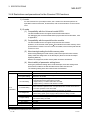
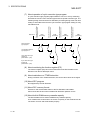
Stops the function being executed.
Section 8.5
Export Log......................................................................Saves the log result into the specified file. Section 8.7.5
Clear Log...................................................................................
Clears the log result.
3-7
Section 8.7.6
3-7
3 SPECIFICATIONS
MELSOFT
3.3 Devices and Instructions Supported by the GX Simulator
GX Simulator operates in the following device ranges and with the following
instructions.
CPU Type
Device
Instruction
A series CPU
Operates in the device range of the selected
CPU type. (Refer to Appendix 1.1)
Operates with the instructions supported by the A series
CPU. (Refer to Appendix 2.1)
QnA series CPU
Operates in the device range of the selected
CPU type. (Refer to Appendix 1.2)
Operates with the instructions supported by the QnA series
CPU. (Refer to Appendix 2.2)
FX series CPU
Operates in the device range of the selected
CPU type. (Refer to Appendix 1.3)
Operates with the instructions supported by the FX series
CPU. (Refer to Appendix 2.3)
Motion controller
Operates in the device range of the
corresponding ACPU. (Refer to Appendix 1.1)
Operates with the instructions supported by the A series
CPU. (Refer to Appendix 2.1) However, motion dedicated
instructions (SVST, CHGA, CHGV, CHGT, SFCS, ITP) are
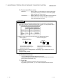
not supported. They are not processed.
Q series CPU (A mode)
Operates in the device range of the A4UCPU.
Operates with the instructions supported by the A4UCPU.
(Refer to Appendix 2.1)
Q series CPU (Q mode)
Operates in the device range of the selected
CPU type. (Refer to Appendix 1.5)
Operates with the instructions supported by the Q series
CPU (Q mode). (Refer to Appendix 2.5)
However, some devices and instructions are restricted or are not supported.
Unsupported devices and instructions are not processed (NOP). These NOP
instructions are shown on the initial screen of the GX Simulator as unsupported
information. (Refer to Section 4.3)
POINT
In this manual, the PLC portion of the motion controller is described as a function of
the motion controller.
In addition, the A171SH, A172SH, A173UH(S1), and A273UH(S3) are included in
the device/instruction support range of the A2SH, A2SH(S1), A3U, and A3U
respectively.
3-8
3-8
3 SPECIFICATIONS
MELSOFT
3.4 GX Simulator Restrictions and Cautions
The restrictions and cautions when debugging with the GX Simulator are described
below.
3.4.1 Restrictions and cautions common to each type of CPU
(1) GX Simulator Processing Time
The time set as constant scan is used to update the present value of the timer.
SM400
T0
Constant
scan
100ms
Scan1
Scan2
Scan3
Scan4
Scan5
Scan1
T0=1
Scan1
T0=2
Scan1
T0=3
Scan1
T0=4
Scan1
T0=5
300ms
Scan1
T0=3
Scan1
T0=6
Scan1
T0=9
T0=12
Scan1
T0=15
Scan1
K10
(To change the time, you can use D9020 for the A series CPU/Q series CPU (A
mode)/motion controller functions, parameter setting for the QnA series CPU/Q
series CPU (Q mode) functions, or D8039 for the FX series CPU functions.)
In the GX Simulator, the count made by the timer instruction during one scan
changes with the constant scan setting. At the constant scan setting of 100ms,
the 100ms timer counts +1 during one scan. At the constant scan setting of
300ms, the 100ms timer counts +3 during one scan.
(2) Restarting the GX Simulator
When restarting the GX Simulator immediately after ending it, it may take longer
than the usual restarting time.
(3) Device Range Checks using I/O System Settings
Appendix 3 shows a table of devices supported by I/O system settings.
The usable device ranges depend on the selected CPU model and parameter
setting range. (For details, refer to Appendix-1.)
(4) Interrupt Programs
Interrupt programs are not supported. Any sequence program created is not
executed.
(5) Floating Decimal Point
Rounding errors can occur in the results of instructions using the floating decimal
point. Therefore, the results may differ from calculations when a CPU is
connected.
(6) Read from PLC, Compare with PLC
Not supported by the GX Simulator.
3-9
3-9
3 SPECIFICATIONS
MELSOFT
(7) Comments
Not supported by the GX Simulator.
(8) LED Reset Button
The LED display is cleared when the LED reset button on the initial screen is
clicked. However, the display immediately reappears if the cause of the error has
not been removed, so it appears that the LED display is not reset when the
button is clicked.
(9) Automatic Writing of the GX Simulator
Parameters and sequence programs are written when the GX Simulator is
started up.
As the file register and device initial values are not automatically written, write
them to the GX Simulator using write to PLC.
(If you do not perform Write to PLC on GX Developer of SW0D5 -GPPW-E, the
file register/device initial values used are the values which were automatically
retained when the GX Simulator was ended last time.)
(10) About Restrictions on GX Simulator Installation
It is not possible to install an English version of the GX Simulator when a
Japanese version GX Developer is already installed.
(11) Using the I/O system setting file
To use the I/O system settings of SW5 or earlier, you need to choose [File] [Import Earlier Version of I/O System File] in the I/O system settings to read the
I/O system setting file.
Refer to Section 5.8.5 for operation details.
(12) Task Bar Settings
If Auto Hide is set in the Microsoft Windows Operating System task bar
settings, the task bar is hidden and not displayed at the bottom of the screen if
the GX Developer screen is displayed at its maximum size and the GX Simulator
initial screen is active.
The task bar is displayed when the GX Developer screen is reduced or the GX
Developer screen is set active.
R
R
(13) About device range check
If the device range is exceeded in indirect designation using the index register,
"OPERATION ERROR" occurs in the GX Simulator.
If "Continue" is selected for [PLC parameter] <PLC RAS> tab [Operating
mode when there is an error] on GX Developer, GX Simulator stops when this
error occurs.
(14) About real number range check
The GX Simulator checks the real number range strictly. If any value cannot be
evaluated as a real number, "OPERATION ERROR" occurs.
If "Continue" is selected for [PLC parameter] <PLC RAS> tab [Operating
mode when there is an error] on GX Developer, GX Simulator stops when this
error occurs.
3 - 10
3 - 10
3 SPECIFICATIONS
MELSOFT
(15) About supported instructions and devices
In the GX Simulator, some instructions and devices are unusable and processed
as NOPs.
(Refer to Appendix-1 and Appendix-2 for the supported instructions and devices.)
(16) About operating CPU types
When selected, the A series CPU/Q series CPU (A mode) operates as the
A4UCPU, the QnA series CPU as the Q4ACPU, the FX series CPU as the FX
series CPU, the motion controller as the A4UCPU, and the Q series CPU (Q
mode) as the Q25HCPU.
(17) About I/O modules
The GX Simulator does not support I/O modules.
(18) About networks
The GX Simulator does not support networks.
(19) I/O System setting
I/O System setting does not support the local devices. Set the device point that
can be executed(valid setting)at a time to 25000 point or less, for device value
input on I/O system setting dialog box.
Refer to Section 5.6. for details.
(20) Display of PLC CPU status
When the read SD device from PLC CPU is written to GX Simulator, the PLC
CPU status before the writing will be displayed in the monitor status dialog
box. 1
Therefore, the PLC CPU status display may differ from the execution status of
GX Simulator immediately after the SD device write to the GX Simulator.
(The display will not be modified until the execution status of the GX Simulator is
changed.)
When the SD device read from PLC CPU is written to GX Simulator in STOP
status, the display changes as the following.
GX Simulator the Initial Screen
GX Developer the monitor status dialog box
PLC CPU status (RUN)
Execution status (STOP)
1: The PLC CPU status in monitor status dialog box is displayed based on the
information of SD device.
3 - 11
3 - 11
3 SPECIFICATIONS
MELSOFT
3.4.2 Restrictions and cautions for the A series CPU functions
(1) Special function module Compatibility
The GX Simulator does not support the special function modules.
The special function module buffer memory area capacity is 16 k points 64
units. It is possible to save to and read from this area but any other access
results in an error.
(2) Saving To and Reading From Buffer Memory
Make I/O assignments with GX Developer before saving or reading the special
function module buffer memory. (Refer to the GX Developer Operating Manual)
It is not possible to save to and read from the buffer area unless I/O assignments
are made.
(3) Enabling and Disabling the Parameter Setting Items
Some GX Developer parameter settings are disabled by the GX Simulator even if
data is set for them.
The settings disabled by the GX Simulator are shown below.
Parameter
Setting
Memory capacity
PLC system
Disabled other than Sequence and "File register" of "program capacity".
"Output modes except for STOP RUN" are disabled.
• "Annunciator display mode" is disabled.
PLC parameter
PLC RAS
• Only "Operation error" and "Special function module access error" in
the "operating mode when there is an error" are enabled.
I/O assignment
Device
Network Parameter
All valid.
"Latch Start" is disabled.
All disabled.
(4) Microcomputer Programs
Not supported by the GX Simulator.
(5) PLC Memory Clear
Execute to clear all user data written to the GX Simulator and initialize.
Also execute this function when unstable GX Simulator operation occurs.
(6) A1FXCPU Built-in Functions
If the A1FXCPU type CPU is selected, the A1FXCPU I/O signals become
general I/O signals during debugging with the GX Simulator.
Consequently, the A1FX functions are identical to the I/O module functions.
(7) About numeric value range check
Checking the numeric value range strictly, the GX Simulator detects any illegal
operation whose divisor is 0.
Execution of 0 ÷ 0 will result in "OPERATION ERROR".
3 - 12
3 - 12
3 SPECIFICATIONS
MELSOFT
(8) About illegal instructions in dedicated instructions
The GX Simulator checks the dedicated instructions for illegal instructions and
displays "INSTRUCT CODE ERR.", if any.
(9) About special function module (special function block)
The GX Simulator supports only the buffer memory area of a special function
module (special function block).
(10) About memory cassette capacity
The GX Simulator has no memory cassette capacity. A lot of data which would
result in an excess of capacity on the actual device will not result in an error and
will be written properly.
(11) SFC Programs
Not supported by the GX Simulator.
3 - 13
3 - 13
3 SPECIFICATIONS
MELSOFT
3.4.3 Restrictions and cautions for the QnA series CPU functions
(1) Special Function Module Compatibility
The GX Simulator does not support the special function modules.
The special function module buffer memory area capacity is 16 k points 64
modules. It is possible to save to and read from this area but any other access
results in an error.
(2) Saving To and Reading From Buffer Memory
Make I/O assignments with GX Developer before saving or reading the special
function module buffer memory. (Refer to the GX Developer Operating Manual)
It is not possible to save to and read from the buffer area unless I/O assignments
are made.
(3) Enabling and Disabling the Parameter Setting Items
Some GX Developer parameter settings are disabled by the GX Simulator even if
data is set for them.
The settings disabled by the GX Simulator are shown below.
Parameter
Setting
PLC name
PLC system
PLC file
PLC
parameter
PLC RAS
I/O assignment
Device
All disabled.
Disabled, except for "Output mode at STOP to RUN" and "Common pointer No."
• The corresponding memory for the "file register" is disabled.
• The "comment file used in a command" is disabled.
• The "corresponding memory" for the "device initial value" is disabled.
• The "corresponding memory" for the "file for local device" is disabled.
• "Error Check" is disabled.
• Only "Operation error" and "Special function module access error" in the
"operating mode when there is an error" are enabled.
• "Annunciator display mode" is disabled.
• "Break down history" and "Lowspeed program execution time” are disabled.
"Standard settings" (base, Power supply unit, Increase cable) are all disabled.
"Latch Start" is disabled.
Program
All valid.
Boot file
All disabled.
SFC
Network Parameter
All disabled.
All disabled.
(4) Monitoring
• When the [Local device monitor non-execution] monitor status is selected in the
local device monitor of GX Developer, GX Simulator monitors the devices of
the program executed at the end of each scan.
However, when a low-speed execution type program is used, it is always
executed at the end of each scan. Therefore, GX Simulator monitors the
devices processed by the low-speed execution type program. Refer to (5) in
this section for details.
• When monitoring devices by specifying the program in the local device monitor
of GX Developer, GX Simulator monitors the local devices of the specified
program, regardless of whether a scan execution type program exists or not.
3 - 14
3 - 14
3 SPECIFICATIONS
MELSOFT
(5) About operation of Low-speed execution type Programs
Regardless of the constant scan setting or setting of the low-speed execution
type program execution time, the GX Simulator always executes the low-speed
execution type programs after the scan execution type programs.
The program execution sequence is show below. (This sequence is identical
during step operation.)
Initialization execution type
Scan execution type 1
Scan execution type 2
(Assume 1 scan uses 100 ms, then execution of 5 scans
500 ms. Changing of a reference time is possible by changing
the constant scan time (Refer to Section 3.4.1, (1)).
Scan execution type N
Low-speed type i
During each scan, all scan execution type programs are executed before one
low-speed execution type program is executed. Consequently, if N low-speed
execution type programs are set, N scans are required to execute them all.
1 scans
2 scans
3 scans
4 scans
Scan execution type
program
Low-speed execution type
program A
Low-speed execution type
program B
POINT
Since a low-speed execution type program is always completed within one scan,
the monitor value of SM510 is always OFF.
(6) Device Memory Monitor Device Range Check
T31744 to T32767, SB800 to SB7FFF, and SW800 to SW7FFF are used by the
system and are unavailable for monitoring or testing.
(7) Function register (FD) monitor
Monitor of function register (FD) cannot be executed from menu of GX Simulator:
Execute only from menu of GX Developer.
(8) TTMR Instruction Restrictions
A present value cannot be changed during TTMR instruction execution.
3 - 15
3 - 15
3 SPECIFICATIONS
MELSOFT
(9) I/O System Setting Device Range Check
SB800 to SB7FFF and SW800 to SW7FFFare used by the system and cannot
be assigned.
(10) SFC Programs
Not supported by the GX Simulator.
(11) PLC Memory Format
Execute to clear all user data written to the GX Simulator and initialize.
Also execute this function when unstable GX Simulator operation occurs.
(12) About special function module (special function block)
The GX Simulator supports only the buffer memory area of a special function
module (special function block).
(13) About built-in RAM/memory cassette capacity
The GX Simulator has no built-in RAM/memory cassette capacity.
A lot of data which would result in an excess of capacity on the actual device will
not result in an error and will be written properly.
(14) About Write to PLC of file register data
When performing Write to PLC of file register data to GX Simulator, always set
the execution status to STOP before starting execution.
(15) About forced input output registration/cancellation function
Not supported by the GX Simulator.
3 - 16
3 - 16
3 SPECIFICATIONS
MELSOFT
3.4.4 Restrictions and cautions for the FX series CPU functions
(1) CPU Type Selection and FX series CPU Operation
The GX Simulator for the FX series CPU functions operate according to the CPU
functions and device range of the selected CPU.
Application instructions not supported by the selected CPU operate with the GX
Simulator.
In cases where the sequence program may contain instructions not supported by
the actual PLC due to conversion of a program for a higher model to a program
for a lower model or due to input in the list mode, a program error occurs when
the sequence program is written to the actual PLC, even if the program runs with
the GX Simulator.
For example, the FX0, FX0S and FX0N PLCs do not support pulse-execution
application instructions, but these instructions run with the GX Simulator.
Even so, a program error occurs when this program is written to the actual PLC
because it contains non-supported instructions.
(2) STOP
RUN Program Check
A program error is detected by the STOP RUN program check only if MC/
MCR exists in the STL instruction or if no RET instruction is input for a STL
instruction.
No other items are detected by the STOP RUN program check. Therefore,
use the GX Developer program check functions in advance to check for these
other errors.
(3) Enabling and Disabling the Parameter Setting Items
Some GX Developer parameter settings are disabled by the GX Simulator even if
data is set for them.
Parameter
PLC parameter
Setting Items
Memory capacity
All valid
Device
All valid
PLC name
All invalid
I/O assignment
• Input/output settings are valid.
• Setting of special module 1 is invalid.
PLC system (1)
All invalid
PLC system (2)
All invalid
Positioning 1
All invalid
1: Parameters for FX3GCPU, FX3UCPU and FX3UCCPU.
(4) Program Memory Capacity
The maximum step capacity for each model is set.
(5) Watchdog Timer
The watchdog timer (D8000) operates every 200 ms for all CPUs. It can be
rewritten but the written value has no effect on its operation.
3 - 17
3 - 17
3 SPECIFICATIONS
MELSOFT
(6) Debugging
The step execution, skip execution and partial execution functions are only valid
when using the GX Simulator.
They cannot be used when an actual PLC is connected.
(7) Buffer Memory Monitor
The special extension device buffer memory in the GX Simulator operates as
general registers which allow reading and writing using FROM/TO instructions.
This memory does not posses any special functions from the special extension
devices.
(8) Analog Volume
The data registers (D8013, D8030 and D8031) storing the analog volume values
for the FX0, FX0S, FX0N, FX1S and FX1N PLCs operate as normal data registers.
Use the GX Developer device test functions to write values between 0 and 255 to
these registers for testing.
(9) High-speed counter
GX Simulator do not support high-speed counter.
(10) SORT, SORT2 Instruction
The SORT, SORT2 instruction is executed in the actual PLC over multiple scans.
However, it is executed completely in a single scan in the GX Simulator and
M8029 (complete flag) operates immediately.
(11) SFC Programs
Testing of SFC program for FX series CPU described as STL instructions is
possible with GX Simulator of SW2D5 -LLT-E or later version.
SFC programs for FX series CPU corresponding to GX Developer later than
SW5D5C-GPPW-E can also be tested with GX Simulator of SW2D5 -LLT-E or
later version.
However, when debugging is to be executed with step execution from SFC
display screen of GX Developer, GX Simulator of SW5D5C-LLT-E or later
version must be used.
(12) Handling Keep Devices
Contents are maintained at a GX Simulator STOP.
Contents are cleared when the GX Simulator is quit.
(13) Handling Non-Keep Devices
Contents are cleared at a GX Simulator STOP or when the GX Simulator are quit.
(14) Memory Clear
Execute to clear all user data written to the GX Simulator and initialize.
Also execute this function when unstable GX Simulator operation occurs.
3 - 18
3 - 18
3 SPECIFICATIONS
MELSOFT
(15) Quick startup of the GX Simulator with the FX series CPU
When the GX Simulator is used combining SW5D5C-LLT-E or later and
SW5D5C-GPPW-E or later, the GX Developer executes quick startup of the GX
Simulator. When other combinations are used, it starts up the GX Simulator at
normal speed.
(16) About step execution, skip execution and partial execution
Compatible with step execution, skip execution and partial execution, the GX
Simulator ensures more efficient debugging.
Refer to (9) for the step execution of SFC programs.
(17) About Character string constant
A maximum number of letters for a character string constant used in the program
is 16 digits.
Having 17 or more letters, the letters on and after 17 digits will be ignored.
(Example)
$+ "12345678901234567" "abcdefghijklmnopq" D0
When performing the above operations, the following data will be stored
after D0.
D0 to D15 = "1234567890123456abcdefghijklmnop"
(("7" and "q"), on and after 17 digits for each character string constant, will
be disregarded.)
(18) About PLC write of device memory
If the FX series CPU is used, the following items do not support PLC write
function of device memory.
• input (X)
• output (Y)
• Special relay (SM)
• Special register (SD)
(19) About special function module (special function block)
The GX Simulator supports only the buffer memory area of a special function
module (special function block).
(20) About online change
When the FX series CPU is used, online change function is not supported.
(21) About serial communication function
When the FX series CPU is used, serial communication function is not supported.
(22) About device manager function
When the FX series CPU is used, device manager function is not supported.
3 - 19
3 - 19
3 SPECIFICATIONS
MELSOFT
3.4.5 Restrictions and cautions for the Motion controller functions
(1) Motion controller Type Selection and Applicable CPU Type
The range of devices or instructions of a motion controller are those of the
applicable CPU.
The table below shows the types of CPU applicable to the motion controller.
Motion Controller
Applicable CPU
A171SH
A2SH
A172SH
A2SH (S1)
A173UH (S1)
A3U
A273UH (S3)
A3U
(2) Motion dedicated instructions
The GX Simulator does not support motion dedicated instructions. Thus, when
an attempt is made to use motion dedicated instructions on the GX Simulator,
nothing will be processed. (NOP)
Motion dedicated instructions are only the following six;
SVST, CHGA, CHGV, CHGT, SFCS, and ITP.
(3) SFC Programs
Not supported by the GX Simulator.
REMARK
Any restrictions and cautions other than the ones described above are the same as
those for the A series CPU functions. For the restrictions and cautions for the A
series CPU functions, refer to Section 3.4.2.
For details of the motion controller, refer to the Motion Controller User's Manual.
3 - 20
3 - 20
3 SPECIFICATIONS
MELSOFT
3.4.6 Restrictions and precautions for the Q series CPU functions
1) A mode
For the Q series CPU (A mode) functions, the A series CPU functions perform as
equivalent to those of the A4U, and therefore, refer to the restrictions on the A series
CPU.
2) Q mode
(1) Compatibility with the Universal model QCPU
The GX Simulator does not support the Universal model QCPU.
For debugging the Universal model QCPU projects with the GX Simulator, refer
to Appendix 4.
(2) Compatibility with the special function module
The GX Simulator does not support the special function module.
However, it has the area of 64k points 64 modules for the buffer memory of the
special function module. This area can be accessed, but access beyond that will
result in an error.
(3) About saving/reading the buffer memory data
When saving/reading the buffer memory data of the special function module,
always make I/O assignment on GX Developer. (Refer to the GX Developer
Operating Manual.)
Without I/O assignment, buffer memory data cannot be saved/read.
(4) About validity of parameter setting items
Among the parameter setting items of GX Developer, there are setting items
which will be invalid for the GX Simulator if their data have been set.
The following setting items are invalid for the GX Simulator.
Parameters
PLC name setting
PLC system setting
PLC file setting
PLC
parameter
PLC RAS setting
I/O assignment
Device setting
Program setting
Boot file setting
SFC setting
Multiple PLC setting
Network parameters
Redundant parameters 1
Setting Item
All invalid.
Items except "timer time limit setting", "STOP-RUN/output mode" and "common
pointer No." are invalid.
• "Target memory" of "file register" is invalid.
• "Comment file used for instructions" is invalid.
• "Target memory" of "device initial value" is invalid.
• "Target memory" of "file for local devices" is invalid.
• "Error check" is invalid.
• Items other than "operation error" and "special function module access error" in
"error-time operation mode" are invalid.
• "Fault history" and "low-speed program running time" are invalid.
• "Model", "switch setting" and "detail setting" of "I/O assignment" are invalid.
• "Basic setting" (base, power supply module, extension cable) is invalid.
"Latch range" is invalid.
• "Comment" of "file using method setting" is invalid.
• "I/O refresh setting" is invalid.
All invalid.
All invalid.
Invalid except "No. of PLC"
All invalid.
All invalid.
1: Parameters for Q12PRHCPU and Q25PRHCPU.
3 - 21
3 - 21
3 SPECIFICATIONS
MELSOFT
(5) Monitoring
• When the [Local device monitor non-execution] monitor status is selected in the
local device monitor of GX Developer, GX Simulator monitors the devices of
the program executed at the end of each scan.
However, when a low-speed execution type program or cyclic execution type
program is used, GX Simulator may monitor the devices processed by the lowspeed execution type program or cyclic execution type program at the end of
each scan. Refer to (6) or (7) in this section for details.
• When monitoring devices by specifying the program in the local device monitor
of GX Developer, GX Simulator monitors the local devices of the specified
program, regardless of whether a scan execution type program exists or not.
(6) About operation of Low-speed execution type Programs
Regardless of the constant scan setting or setting of the low-speed execution
type program execution time, the GX Simulator always executes the low-speed
execution type programs after the scan execution type programs.
The program execution sequence is show below. (This sequence is identical
during step operation.)
Initialization execution type
Scan execution type 1
Scan execution type 2
(Assume 1 scan uses 100 ms, then execution of 5 scans
500 ms. Changing of a reference time is possible by changing
the constant scan time (Refer to Section 3.4.1, (1)).
Scan execution type N
Low-speed type i
During each scan, all scan execution type programs are executed before one
low-speed execution type program is executed. Consequently, if N low-speed
execution type programs are set, N scans are required to execute them all.
1 scans
2 scans
3 scans
4 scans
Scan execution type
program
Low-speed execution type
program A
Low-speed execution type
program B
POINT
Since a low-speed execution type program is always completed within one scan,
the monitor value of SM510 is always OFF.
3 - 22
3 - 22
3 SPECIFICATIONS
MELSOFT
(7) About operation of cyclic execution type program
END
processing
Elapse of 400 millisec.
from reference time
END
processing
Elapse of 300 millisec.
from reference time
END
processing
Elapse of 200 millisec.
from reference time
Reference
Elapse of 100 millisec.
from reference time
A cyclic execution type program judges whether it can run or not by measuring
time after the end of a scan execution type and a low-speed execution type. The
following timing chart shows the GX Simulator processing timing at the scan time
setting of 100 milliseconds and the cyclic execution type program setting of every
200 milliseconds.
END
processing
Scan execution
type program
Low-speed execution
type program A
Cyclic execution type
program A
(200 millisec. cycle)
Cyclic execution type
program B
(200 millisec. cycle)
(8) About monitoring the function register (FD)
The function register (FD) cannot be monitored from the GX Simulator menu.
Monitor it from the GX Developer menu.
(9) About restrictions on TTMR instruction
During execution of the TTMR instruction, the current value cannot be changed.
(10) About SFC program
Not supported by the GX Simulator.
(11) About PLC memory format
Execute to clear all user data written to the GX Simulator and initialize.
Also execute this function when unstable GX Simulator operation occurs.
(12) About built-in RAM/memory cassette capacity
The GX Simulator has no built-in RAM/memory cassette capacity.
A lot of data which would result in an excess of capacity on the actual device will
not result in an error and will be written properly.
3 - 23
3 - 23
3 SPECIFICATIONS
MELSOFT
(13) About intelligent function module
The GX Simulator supports only the initial value setting, auto refresh setting and
buffer memory area of the intelligent function module.
(14) About Write to PLC of file register data
When performing Write to PLC of file register data to GX Simulator, always set
the execution status to STOP before starting execution.
(15) About forced input output registration/cancellation function
Not supported by the GX Simulator.
(16) About Character string constant
A maximum number of letters for a character string constant used in the program
is 16 digits.
Having 17 or more letters, the letters on and after 17 digits will be ignored.
(Example)
$+ "12345678901234567" "abcdefghijklmnopq"
When performing the above operations, the following data will be stored
after D0.
D0 to D15 = "1234567890123456abcdefghijklmnop"
(("7" and "q"), on and after 17 digits for each Character string constant, will
be disregarded.)
(17) About online change
When trailing edge instructions are included in a sequence program, the
operation performed immediately after online change may differ from the
debugging operation by connecting PLC CPU. For details, refer to QCPU User’s
Manual (Function Explanation, Program Fundamentals).
3 - 24
3 - 24
3 SPECIFICATIONS
MELSOFT
3) Q mode (multiple PLC system)
(1) About the GX Simulator Compatibility with multiple PLC system
The GX Simulator can’t be compatible with multiple PLC action itself.
There are reasons that the GX Simulator doesn’t support multiple starts and isn’t
conscious of the number of own machine which is necessary for multiple CPU
action. (Consciousness of what number the own machine is in some CPUs.)
It is only the part of the minimum requirements (it run as a single CPU sequence
program) to run sequence program (project) for applicable multiple CPU which
was written by the GX Developer.
(2) I/O assignment
I/O assignment parameter of the GX Developer appoints control CPU to each I/O
and intelligent function units.
Although it is able to read the control information to the GX Simulator, the
function isn’t compatible without consciousness of own machine. (If it is multiple
PLC applicable parameter, it isn’t the error for I/O assignment of the GX
Simulator original.)
(3) Difference between the GX Simulator and the practical machine
under the access instruction to the shared memory of multiple PLC
Although we use description of own machine/the other machine for expression of
difference between the GX Simulator and the practical machine, the GX
Simulator have no discrimination between own machine/the other machine.
The GX Simulator allows read from own machine with the FROM command.
3 - 25
3 - 25
3 SPECIFICATIONS
MELSOFT
3.5 GX Simulator Safety and Handling Precautions
The safety and handling precautions for the GX Simulator are described below.
(1) The GX Simulator simulates the actual PLC to debug sequence
programs. However, the correct operation of a debugged
sequence program cannot be guaranteed.
(2) The calculated results may differ from actual operation because the
GX Simulator does not access the I/O modules or special function
modules and do not support some instructions and devices.
POINT
After debugging has been performed by GX Simulator, it is necessary to execute
normal debugging by connecting the PLC CPU before starting actual operation.
3 - 26
3 - 26
4 COMMON OPERATIONS FOR THE GX Simulator
MELSOFT
4. COMMON OPERATIONS FOR THE GX Simulator
4.1 Procedure from Installation to Debugging
This section describes the procedures from installing the GX Simulator to debugging a
sequence program.
Procedure 1
Install GX Developer and the GX Simulator in the personal computer.
For the installation operation, refer to the "Method of installing the MELSOFT Series"
packed with the package.
GX
GX
Developer Simulator
4
Install
Procedure 2
Use GX Developer to create a sequence program.
Refer to the GX Developer Operating Manual.
Procedure 3
In GX Developer, set the parameters to assign the I/Os (for A/QnA/Q series CPU
functions) and make the program settings (for QnA series/ Q series (Q mode) CPU
functions).
Refer to the GX Developer Operating Manual.
POINTS
(1) Always do the program settings for the QnA series/Q series CPU function.
If you do not make the program settings and the GX Developer is of version
later than SW2D5 -GPPW-E the following will occur.
1) The ladder sequence (list) of the active screen of GX Developer will be
written.
2) The sequence program will not be written, if the active screen is not a ladder
(list) screen or if there are no active screens.
(2) Please set the I/O assignments (for A/QnA/Q series CPU function) before
reading/writing the buffer memory of special function module.
Refer to Section 4.2 (4).
(To next page)
4-1
4-1
4 COMMON OPERATIONS FOR THE GX Simulator
MELSOFT
(From previous page)
Procedure 4
Select the [Tools] [Start ladder logic test] GX Developer menu items to start the GX
Simulator. The sequence program and parameters created with GX Developer are
automatically written to the GX Simulator (equivalent to write to PLC).
Procedure 5
Set various devices that support the offline debugging of the user application.
Refer to "Chapter 8 Device Manager Function".
Procedure 6
Debug the sequence program using the GX Simulator and GX Developer functions.
Debugging is possible by using the device monitor, changing arbitrary device values,
or simulation of machine operation.
Refer to "Chapter 5 I/O SYSTEM SETTING FUNCTIONS"
and "Chapter 7 MONITOR FUNCTION".
Refer to the GX Developer Operating Manual.
Connection of actual
PLC is not necessary
When checking the operation of the frame sent from the external device, you can use
the serial communication function for debugging.
Refer to "Chapter 6 SERIAL COMMUNICATION FUNCTION".
Procedure 7
After debugging, modify the sequence program.
Refer to the GX Developer Operating Manual.
Procedure 8
Set the execution status in the initial screen to STOP.
If necessary, save the contents of the device memory and special function
module buffer memory.
Refer to "Chapter 9 TOOL FUNCTIONS".
Procedure 9
Select the [Online] [Write to PLC] GX Developer menu items to write the modified
program to the GX Simulator.
Refer to the GX Developer Operating Manual.
To debug the program again, repeat Procedures 5 to 9.
POINTS
After debugging has been performed by GX Simulator, it is necessary to execute
normal debugging by connecting the PLC CPU before starting actual operation.
4-2
4-2
4
4 COMMON OPERATIONS FOR THE GX Simulator
MELSOFT
4.2 GX Developer Operations before Debugging
This section describes the GX Developer operations required before debugging with
the GX Simulator.
Conduct the operations described below before debugging a program with the GX
Simulator.
(1) Make the Project to Create the Sequence Program.
To create a new project, select [Project] [New project] from the GX Developer
menus and make the required settings.
To read an existing project, select [Project] [Open project] from the GX
Developer menus and select the project.
(2) Create the Sequence Program.
(3) On the GX Developer side, make parameter settings for I/O
assignment (for A/QnA/Q series CPU functions), program setting
(for QnA series/Q series (Q mode) CPU functions), etc.
POINT
Always do the program settings for the QnA series CPU function.
If you do not make the program settings and the GX Developer is of version later
than SW2D5 -GPPW-E the following will occur.
(1) The ladder sequence (list) of the active screen of GX Developer will be written.
(2) The sequence program will not be written, if the active screen is not a ladder
(list) screen or if there are no active screens.
4-3
4-3
4 COMMON OPERATIONS FOR THE GX Simulator
MELSOFT
(4) When making I/O assignment on the <I/O assignment> tab screen
in the [PLC Parameters] dialog box of GX Developer, set the types
and the numbers of points of all modules.
"SP. UNIT LAY ERR." occurs if any of the following settings has been made.
1) Any of settings (a) to (c) on the following screen has been made.
(a) The type has been set but the number of points has not been set.
(b) With the settings made to slot 2 and later, the type and the number of
points of slot 1 have not been set.
(c) The number of points has been set but the type has not been set.
2) X/Y settings are overlapped.
Setting screen example (Q series CPU (Q mode))
(a)
(b)
(c)
(5) Select the [Tools] [Start ladder logic test] GX Developer menu
items to start the GX Simulator. An initial screen as shown below is
displayed.
The sequence program and parameters are automatically written to the GX
Simulator when the GX Simulator are started by GX Developer.
Offline debugging of the sequence program using the GX Simulator is now
possible.
4-4
4-4
4 COMMON OPERATIONS FOR THE GX Simulator
MELSOFT
4.3 Description of the Initial Screen Display
A GX Simulator initial screen as shown below is displayed when the GX Simulator is started.
This section describes the items displayed in the GX Simulator initial screen.
5)
13)
6)
4)
1)
2)
11)
3)
8)
7)
9)
Task bar
12)
10)
13)
Number
Name
1)
CPU type
2)
LED Indicators
3)
Operation Status LEDs
4)
Start
5)
Tools
6)
Help
7)
Switch Display and Settings
8)
INDICATOR RESET button
9)
RESET button
10)
Unsupported information
indicator lamp
11)
Error advance display button
12)
I/O system setting LED
13)
Icon
Description
Displays the currently selected CPU type.
Can display up to 16 characters.
The indicator display is equivalent to the display of CPU operation errors.
RUN/ERROR: Valid for all of the QnA, A, FX, Q series CPU and motion controller functions.
USER
: Appears only for the QnA series/Q series (Q mode) CPU functions.
Makes available the Monitor function, I/O System Settings, Serial Communication Function
and Device Manager.
Use the Tools menu to execute the tool functions.
Refer to Chapter 9 Tool Functions.
Displays the GX Simulator licensee name and software version.
Displays the execution status of the GX Simulator.
Click on the radio buttons to change the execution status.
Click to clear the LED display.
Click to reset the GX Simulator
Displayed only for the A, QnA, Q, and Motion controller series functions.
Displayed only when unsupported instructions or devices for the GX Simulator is found.
By double clicking, display the unsupported instructions that have been changed to NOP
instructions and their steps on another screen. (Refer to (1) in this Section.)
Clicking this button will display the descriptions of issued errors, error steps, and the name
of files in which the error is issued on another screen. (Refer to (2) in this Section.)
LED lights up during execution of I/O system setting.
Double clicking this will show the contents of current I/O system settings.
Displays the current status (normal or error occurrence).
(At error occurrence, the icon is enclosed by yellow.)
Icon
Current Status
Normal
Error occurrence
4-5
4-5
4 COMMON OPERATIONS FOR THE GX Simulator
MELSOFT
(1) Unsupported instruction list display function
Displays a list of program name and step No. when unsupported
instructions/devices are included in the program or I/O system setting.
To display the list display screen, double click unsupported information indicator
lamp (
). (The lamp is displayed only when unsupported
instructions/devices by GX Simulator exist in a sequence program.)
Note when unsupported devices are included in the I/O system setting, "iosys"
and "0" are displayed in the Program Name area and Step No. area respectively.
In case online change is processed during the display of unsupported instruction
list screen, the displayed information will not be renewed. For displaying the
latest information, close the screen and open the screen again.
(2) Error advance display function
Displays error detail on error advance screen by clicking error advance display
button when ERROR LED is in an ERROR status.
A series CPU/FX series CPU/Motion controller
/Q series CPU (A mode)
4-6
QnA series CPU/Q series CPU (Q mode)
(Displays a file name)
4-6
4 COMMON OPERATIONS FOR THE GX Simulator
MELSOFT
4.4 Ending the GX Simulator
[Purpose]
To end the GX Simulator.
[Operation procedure]
POINT
Before exiting from GX Simulator, save the I/O System setting data and Device
Manager setting data.
If the setting data are not saved, they will be deleted at exit from GX Simulator.
(1) Select [Tools] - [End ladder logic test] of GX Developer menu.
You can also click
of GX Developer for above.
(2) When the dialog box appears, click the OK button.
Click!
4-7
4-7
5 SIMULATION OF EXTERNAL DEVICE OPERATION - I/O SYSTEM
SETTING FUNCTIONS
MELSOFT
5. SIMULATION OF EXTERNAL DEVICE OPERATION I/O SYSTEM SETTING FUNCTIONS
The I/O system setting functions allow simulation of the operation of external devices.
In conventional debugging, a debugging sequence program was created to simulate
the operation of the external devices.
Using the I/O system setting functions, the operation of the external devices can be
automatically simulated without the requirement to create a special debugging
sequence program.
(1) Differences between Conventional Debugging and Debugging with
the I/O System Setting Functions
A comparison between conventional debugging with an actual PLC connected
and debugging using the I/O system setting functions is shown below.
(a) Conventional Debugging
The program must be modified as follows for debugging:
Add a debugging sequence program to simulate operation of the external
devices.
As an input (X) can be turned ON/OFF only with an external device
connected to the I/O unit, modify the program by changing X0 M0, X1
M1, etc. to conduct debugging with no external device connected.
(b) Debugging using the I/O System Settings
The I/O system setting function allows sequence program settings and
changes to be made for debugging from the setting screen.
It is unnecessary to add a sequence program. It is not necessary to rewrite
the devices (X0 M0) as the inputs (X) can be directly turned ON/OFF
from GX Developer.
<Program used in conventional debugging>
Problem 1: Devices must be rewritten
X0
M0 X1
Start
Y0
Y0
M1
Stop
<Program used for debugging using the GX Simulator>
Solution 1: Rewriting of devices is not necessary
X0
Y0
Run
X1
Y0
Start
Stop
Run
Y0
K50
T0
T0
M1
Y0
Solution 2: Pseudo-sequence program is
created in a separate file
5s timer
Problem 2: Sequence program for
debugging is necessary
SET X1
5s timer setting
5-1
5-1
5
5 SIMULATION OF EXTERNAL DEVICE OPERATION - I/O SYSTEM
SETTING FUNCTIONS
MELSOFT
(2) Conditions for simulation
With I/O system setting, optional operation will be performed after the condition is
fulfilled.
By combining conditions, conditions equivalent to the following circuits can be
set.
X0
X0
X1
X0
X2
X0
X1
X2
5
X0
X1
X2
X0
X1
X3
5-2
X0
X1
X2
X3
5-2
5 SIMULATION OF EXTERNAL DEVICE OPERATION - I/O SYSTEM
SETTING FUNCTIONS
MELSOFT
(3) Timing chart input and device value input
With I/O system setting, there are two inputs: one is timing chart input to execute
timing chart prepared by user after condition is fulfilled; the other is device value
input to set optional device value after specified time has elapsed.
Differences between the above two inputs are described below.
(a) Timing chart input
When condition set by user has been fulfilled, timing chart set by the user
can be operated.
With this input, complicated operations, such as "When Y0 is turned ON,
D0 is counted up, Y0 is turned OFF when X0 is turned ON", can be set.
However, the timer cannot be set: If timer is to be used, select device value
input.
<Timing chart format input screen>
(b) Device value input
When condition set by user has been fulfilled, specified device value can be
changed after an optional time has elapsed.
With this input, an operation such as "When Y0 is turned ON, 5 seconds
later X0 and X3 are turned ON" can be set.
5-3
5-3
5 SIMULATION OF EXTERNAL DEVICE OPERATION - I/O SYSTEM
SETTING FUNCTIONS
MELSOFT
5.1 I/O System Setting Operation Procedure
Operation procedure for I/O system setting is shown below.
Start
(Refer toSection 5.2)
Set I/O
system by inputting
device value?
NO
Set I/O system
by timing chart?
YES
Input device value to be set.
(Refer to Section 5.6)
YES
NO
Set using timing chart.
(Refer to Section 5.4)
Save file.
(Refer to Section 5.8.1)
Execute I/O system setting.
(Refer to Section 5.7)
Start monitoring with
I/O system setting?
NO
YES
Start monitoring.
(Refer to Section 5.8.3)
End
(Refer to Section 5.2)
5-4
5-4
5 SIMULATION OF EXTERNAL DEVICE OPERATION - I/O SYSTEM
SETTING FUNCTIONS
MELSOFT
5.2 Starting/Ending I/O System Setting
(1) Starting I/O system setting
[Purpose]
To start I/O system setting.
[Operation procedure]
Select [Start] - [I/O System Settings] from the initial screen.
(2) Ending I/O system setting
[Purpose]
To end I/O system settings.
[Operation procedure]
Select [File] - [Exit I/O System Settings] from I/O system settings screen.
5-5
5-5
5 SIMULATION OF EXTERNAL DEVICE OPERATION - I/O SYSTEM
SETTING FUNCTIONS
MELSOFT
5.3 Configuration of I/O System Settings Screen
I/O system settings screen is opened by clicking [Start] - [I/O System Settings] of initial
screen. Configuration of I/O system settings screen is shown below.
1)
2)
4)
3)
5)
6)
1) Menu bar
Name of menu that can be used in I/O system settings is displayed.
When menu has been selected, drop-down menu will be displayed and various
functions from this menu can be used.
2) Tool bar
From functions assigned by menu bar, those most frequently used are displayed
with buttons.
3) File under Editing
Displays name of file being edited.
4) File under Execution
Displays name of file registered as I/O system execution file.
5-6
5-6
5 SIMULATION OF EXTERNAL DEVICE OPERATION - I/O SYSTEM
SETTING FUNCTIONS
MELSOFT
5) I/O system settings tree
Selects setting method of I/O system settings.
• Timing chart input
Double-click column of number to be set: I/O system setting with timing chart
format can now be performed.
Ups to 40 settings (from No. 1 to No. 40) are possible.
• Device value input
Double-click column of number to be set: I/O system setting with device value set
can now be performed.
<When using the A/QnA/Q series CPU or motion controller>
You can make 500 settings, No. 1 to No. 500.
<When using the FX series CPU>
You can make 100 settings, No. 1 to No. 100.
6) Edit/monitor screen
Editing and monitoring of I/O system settings are performed using this screen.
• In timing chart input mode (Refer to Section 5.4)
• In device value input mode (Refer to Section 5.6)
5-7
5-7
5 SIMULATION OF EXTERNAL DEVICE OPERATION - I/O SYSTEM
SETTING FUNCTIONS
MELSOFT
5.4 Setting by Using Timing Chart
This section describes how to perform I/O system settings using timing chart.
[Operation procedure]
(1) Select [Start] - [I/O System Settings] from initial screen.
(2) Double-click column of number to set timing chart as shown below.
[Setting screen]
Make the setting below in I/O system setting dialog box.
1)
3)
2)
4)
[Description of items]
1) No.
The number of settings in the I/O system setting dialog box.
Up to 40 settings can be chosen.
When clicked, set No. is made object of Cut, Copy or Paste.
2) Condition
Designates the input condition from GX Simulator.
The input conditions can be designated as either a bit device or a word device.
For a bit device, designation condition is ON/OFF; for a word device, designation
condition is a comparison (=,<>,<,>,<=,>=) with a constant or another word
device.
In addition, relational conditions can be set by specifying AND/OR operation.
AND condition
OR condition
AND...... The condition will be fulfilled if both designated conditions on the left and
right are achieved. Otherwise, the condition will not be fulfilled.
OR ........ The condition will be fulfilled if either or both of designated conditions in
upper and lower columns are achieved.
5-8
5-8
5 SIMULATION OF EXTERNAL DEVICE OPERATION - I/O SYSTEM
SETTING FUNCTIONS
MELSOFT
• Input method (direct input)
Entering condition expression directly can perform setting.
<Example>
For a bit device: X0=OFF, M10=ON
For a word device: D5<20, D15<>5, D20=2, D25>=10, D0=D50
• Input method (entering by using dialog box)
Click
button and enter device name, device No., designated condition, etc.
Object of comparison is handled as a 16 bits hexadecimal integer.
When designated as K
, setting is done using decimal number, and designated
as H
, a hexadecimal number. If neither K nor H is designated, decimal number
setting will be selected.
Refer to Appendix 3.1 for devices that can be entered in the Condition area.
Selects ON or OFF condition.
Selects device name.
Enters device No.
When a bit device is selected:
Enter object device name and value.
Enters device No.
When a word device is selected:
Selects to use as Push button in monitor mode.
With Push button, you can make 500 settings, 0 to 499
(100 settings, 0 to 99, when using the FX series CPU).
User can fulfill conditions with optional timing by using the push button.
Selects comparison designation.
Selects when "Normally ON" is set.
POINT
Index representation (eg. D0Z0), representation of a word device in bits form (eg.
D0,0), and sets of bits device representation (eg. K4X0) are not allowed in the
Condition area.
3) Timing Chart Format
• Edit-Timimg Chart Format button
Click this button: The timing chart format input screen will appear.
Refer to Section 5.5 for operation of screen/
• Continuing
When timing set by timing chart input is to be executed continuously, apply
check mark
to check box.
4) Setting
Designates enable or disable for each setting.
Apply a check mark
to enable the setting.
5-9
5-9
5 SIMULATION OF EXTERNAL DEVICE OPERATION - I/O SYSTEM
SETTING FUNCTIONS
MELSOFT
5.5 Operation of Timing Chart Format Input Screen
This section describes operation of timing chart format input screen.
5.5.1 Operation procedure of timing chart format input screen
The operation procedure of timing chart format input screen is indicated below.
Start
Read timing chart
data file?
YES
NO
Read timing chart data file.
(Refer to Section 5.5.6)
Register device.
(Refer to Section 5.5.3)
Set/edit timing.
(Refer to Section 5.5.4)
Change scan number?
NO
YES
Set scan number.
(Refer to Section 5.5.5)
End
5 - 10
5 - 10
5 SIMULATION OF EXTERNAL DEVICE OPERATION - I/O SYSTEM
SETTING FUNCTIONS
MELSOFT
5.5.2 Configuration of timing chart format input screen
Configuration of timing chart format input screen is described below.
1)
2)
4)
3)
5)
6)
7)
1) Menu bar
Name of menu, which can be used in timing chart format input screen, is
displayed.
When menu has been selected, drop-down menu will be displayed and various
functions from this menu can be used.
2) Tool bar
From functions assigned by menu bar, those most frequently used will be
displayed with buttons.
3) Device name/device value
Bit device: When timing at cursor position is ON, device name lights (Yellow).
Word device: Device value, with the timing at cursor position, will be displayed in
the text box on the right of device name.
5 - 11
5 - 11
5 SIMULATION OF EXTERNAL DEVICE OPERATION - I/O SYSTEM
SETTING FUNCTIONS
MELSOFT
POINT
(1) Buffer register and extension file register are displayed as shown below.
<Buffer register >
<Extension file register>
The first I/O number of
a special function module
U
Block No.
ER
\G
Address
\R
Address
When first I/O No. is 4, and address
is K30, "U4\G30" will be displayed.
When block No. is 2, and address is
K30, "ER2\R30" will be displayed.
(2) When a word device is designated as a 32-bit integer, (D) is added to the device
name.
Example: D0(D), W6(D)
4) Scan number
Shows scan number of timing.
When scan number is set by selecting [Scan] - [Scan setting], disabled scans will
be displayed with shading.
When applying check mark to "Keep" on the right of Edit-Timimg Chart Format
button, the enabled scans can be repeated while the condition is being fulfilled.
Example: For continuation with 6 scans designated:
Only 6 scans from 0 to 5 are enabled.
Scans 0 to 5 will be executed repeatedly
while the condition is being fulfilled.
5)
OK button
Defines settings and exits from this screen.
6)
Cancel button
Cancels settings and exits from this screen.
7) Status
Displays state of timing chart being set.
1
4
5 - 12
2
3
1: Shows that object device was turned
ON from OFF.
2: Shows that object device was turned
OFF from ON.
3: Shows that object device remains
unchanged.
4: Shows that object device has
changed.
5 - 12
5 SIMULATION OF EXTERNAL DEVICE OPERATION - I/O SYSTEM
SETTING FUNCTIONS
MELSOFT
5.5.3 Entering/Deleting device
(1) Entering device to be simulated
[Purpose]
To enter device for setting timing.
[Operation procedure]
(a) Select [Device] - [Enter Device].
(b) Dialog shown below will appear. After setting each item, click
Enter button.
A maximum of 16 devices can be entered.
[Bit device selected]
Item
[Word device selected]
Contents
Device name
Selects name of device to be entered.
Device No.
Enters device No.
Displayed when "U" is selected with device name. Enter the higher two digits when
Unit initial address
initial I/O No. is expressed in three digits.
Example: In case of X/YIF0, enter "IF".
Sets initial value.
Initial value
For a bit device, select ON/OFF.
For a word device, enter value.
Sets display format of word device to be displayed.
Displayed format
Both decimal and hexadecimal numbers can be set.
Display can be selected from 16 Bit integers, 32 Bit integers and real numbers.
Enter button
Enters device.
Close button
Closes this screen.
5 - 13
5 - 13
5 SIMULATION OF EXTERNAL DEVICE OPERATION - I/O SYSTEM
SETTING FUNCTIONS
MELSOFT
(2) Deleting entered device
[Purpose]
To delete entered device.
[Operation procedure]
(a) Select device to be deleted.
Deleting Y1F is described here, as example.
(b) Select [Device] - [Delete Device].
Device has been deleted.
5 - 14
5 - 14
5 SIMULATION OF EXTERNAL DEVICE OPERATION - I/O SYSTEM
SETTING FUNCTIONS
MELSOFT
5.5.4 Setting/Editing timing
This section describes setting and editing method of timing.
(1) Setting the timing of bit device
Timing of bit device can be set following the procedure shown below.
Move cursor to the timing to be set and operate using any tool button, menu or
short-cut key.
Operation
To turn ON
designated timing
To turn OFF
designated timing
To turn OFF until
next ON timing
Tool
button
Menu
• [Edit] - [Bit Device] - [Device ON]
• Right-click, then [Device ON]
(Also can be done by double-clicking
cursor position.)
• [Edit] - [Bit Device] - [Device OFF]
• Right-click, then [Device OFF]
(Also possible to double-click cursor
position.)
Short-cut
key
Timing
F1
F2
• [Edit] - [Bit Device] - [Progressive OFF].
• Right-click, then [Progressive OFF].
F3
To turn ON until
next OFF timing
• [Edit] - [Bit Device] - [Progressive ON].
• Right-click, then [Progressive ON].
F4
To turn OFF
designated timing
and all later
• [Edit] - [Bit Device] - [All OFF].
• Right-click, then [All OFF].
To turn ON
designated timing
and all later
• [Edit] - [Bit Device] - [All ON].
• Right-click, then [All ON].
To insert timing
• [Edit] - [Insert]
• Right-click, then [Insert].
F5
F6
Insert
To delete timing
• [Edit] - [Delete]
• Right-click, then [Delete].
Delete
shows cursor position.
5 - 15
5 - 15
5 SIMULATION OF EXTERNAL DEVICE OPERATION - I/O SYSTEM
SETTING FUNCTIONS
MELSOFT
(a) Setting ON/OFF period
[Purpose]
To set ON/OFF continuously, with optional period after designated timing.
[Operation procedure]
1) Select initial bit device timing.
2) Operate either of operations shown below.
• Select [Edit] - [Wizard] menu.
• Right-click, select [Wizard] menu.
3) Bit device setting wizard screen will appear. Enter scan
number and click OK button.
4) Bit device ON/OFF has been set periodically.
5 - 16
5 - 16
5 SIMULATION OF EXTERNAL DEVICE OPERATION - I/O SYSTEM
SETTING FUNCTIONS
MELSOFT
(2) Setting the timing of word device
(a) Changing the designated timing value
[Purpose]
To change the timing value of designated word device.
[Operation procedure]
1) Select timing of word device to be changed.
2) Operate any one of the following operations:
• Select [Edit] - [Word Device] - [Change] menu.
• Right-click, then select [Change] menu.
• Click
.
• Enter "F7" key.
• Double-click designated timing.
3) Word device setting wizard screen will appear: Set each
item and click OK button.
5 - 17
5 - 17
5 SIMULATION OF EXTERNAL DEVICE OPERATION - I/O SYSTEM
SETTING FUNCTIONS
Item
MELSOFT
Contents
Value setting
Set value
Enter set value of word device.
Continuation
Apply check mark when setting is to be performed continuously.
(Example) Cursor position is scan No. 3, set value is 10, scan number is 4, changed value is 20
increased.
Value
70
50
30
10
0
3
4
5
6
Scan
Scan
Select number of scans to be continued.
Increase & decrease
Set to change set value when setting is to be performed continuously.
• Increase: Select when value is to be increased.
• Decrease: Select when value is to be decreased.
Changed value
Set increased/decreased value.
Trigonometric functions
SIN curve, COS curve
Set when device value is changed as shown below.
(Example) Maximum value is 50, periodical scans are 100.
COS curve
50
SIN curve
50
0
-50
50
100
Number of scans
0
-50
Maximum value
Enter maximum value.
Periodic scan
Select number of scans corresponding to 1 period of SIN/COS curve.
50
100
Number of scans
When maximum value is set, minimum value will be set as "-maximum value".
4) Word device value has been set.
5 - 18
5 - 18
5 SIMULATION OF EXTERNAL DEVICE OPERATION - I/O SYSTEM
SETTING FUNCTIONS
MELSOFT
(b) Fixing unchanged designated timing value
[Purpose]
To make certain word device value of designated timing is not changed.
[Operation procedure]
1) Select word device timing that is not to be changed.
2) Operate any one of following operations:
• Select [Edit] - [Word Device] - [No change] menu.
• Right-click, then select [No change] menu.
• Click
.
• Enter "F8" key.
Mark of scan No.2 has been changed.
(c) Inserting timing
[Purpose]
Insert the timing before designated timing.
Timing is inserted to the left side of cursor position.
[Operation procedure]
1) Select the timing at the right side of the position where
timing is to be inserted.
5 - 19
5 - 19
5 SIMULATION OF EXTERNAL DEVICE OPERATION - I/O SYSTEM
SETTING FUNCTIONS
MELSOFT
2) Operate any one of the following operations.
• Select [Edit] - [Insert] menu.
• Right-click, then select [Insert] menu.
• Click
.
• Enter "Insert" key.
After timing has been inserted, timing will shift to the right.
(d) Deleting the timing
[Purpose]
To delete designated timing.
[Operation procedure]
1) Select timing of the position to be deleted.
2) Operate any one of the following operations:
• Select [Edit] - [Delete] menu.
• Right-click, then select [Delete] menu.
• Click
.
• Enter "Delete" key.
After timing is deleted, timing will shift to the left.
5 - 20
5 - 20
5 SIMULATION OF EXTERNAL DEVICE OPERATION - I/O SYSTEM
SETTING FUNCTIONS
MELSOFT
5.5.5 Setting scan number of timing chart
[Purpose]
To set scan number of timing input from external device.
[Operation procedure]
(1) Select [Scan] - [Scan Setting].
(2) Scan number setting screen will appear: Enter scan number.
(Example)
When Scan number is set to 5, and timing chart is set to "Keep", scanning from 0
to 4 will be repeated as long as the condition is fulfilled.
Only 5 scans from 0 to 4 are effective.
Scanning from 0 to 4 will be repeated as long as the condition is fulfilled.
5 - 21
5 - 21
5 SIMULATION OF EXTERNAL DEVICE OPERATION - I/O SYSTEM
SETTING FUNCTIONS
MELSOFT
5.5.6 Other operations
(1) Reading data saved using timing chart of device memory monitor
[Purpose]
To read and use timing chart data file (*.DAT) saved with timing chart.
When the file is read, device and timing will be automatically registered. It is not
necessary to re-enter them.
[Operation procedure]
Select [File] - [Open File].
[Setting screen]
Designate optional file with "Look in", click file to be opened and click Open
button.
POINT
Devices for only 16 points from upper side of timings (maximum 64 points) set by
timing chart screen can be read.
It is necessary to move required timings to upper side before creating timing data
file.
(2) Returning to original state before operation
[Purpose]
To return to previous state before last operation performed.
Only the operation immediately before can be regained.
[Operation procedure]
Select [Edit] - [Undo].
5 - 22
5 - 22
5 SIMULATION OF EXTERNAL DEVICE OPERATION - I/O SYSTEM
SETTING FUNCTIONS
MELSOFT
(3) Displaying registered device list
Select [Device] - [List Device]. Registered device list will be displayed.
• Click Add button. Device registration dialog will be displayed. Refer to Section
5.5.3 (1) for details.
• By clicking Delete button, the device is deleted from object of monitoring.
Two or more devices can be deleted by using " Shift key + Select" or " Ctrl
key + Select".
• By clicking Jump To button, display of timing chart format input screen jumps
to device being selected.
• By clicking UP / Down button, device being selected moves up or down.
• Selecting Two or more devices
(Two or more devices cannot be selected and moved simultaneously.)
(4) Changing display format of word device
Select [Word Device]. Then select [Device] - [Property]. Dialog shown below will
appear: Display format can be changed.
• Value
Selects decimal or hexadecimal number display.
• View
Selects 16 Bit, 32 Bit or real number.
5 - 23
5 - 23
5 SIMULATION OF EXTERNAL DEVICE OPERATION - I/O SYSTEM
SETTING FUNCTIONS
MELSOFT
(5) Exchanging device display position
Display position of device can be exchanged by drag & Drop.
(a) Drag the device name in the timing chart format input screen.
Dotted line frame will appear during dragging.
Drag!
(b) Superimpose dotted line frame on the device name to be
exchanged. Device name can now be exchanged.
Stop dragging.
Superimpose dotted line frame.
5 - 24
5 - 24
5 SIMULATION OF EXTERNAL DEVICE OPERATION - I/O SYSTEM
SETTING FUNCTIONS
MELSOFT
5.6 Setting by Entering Device Value
This section describes I/O system setting by entering device value.
[Operation procedure]
(1) Select [Start] - [I/O System Settings] from initial screen.
(2) Double-click column of number to which device value is to be
set.
[Setting screen]
Perform setting in I/O system setting dialog box as shown below.
1)
2)
3)
4)
5)
[Description of items]
1) No.
Number of settings in I/O system setting dialog box.
Maximum 100 settings can be chosen.
Once the set No. has been clicked, it can be cut, copied or pasted.
2) Condition
Since the conditions are the same as those when timing chart is used, refer
to Section 5.4 2).
3) Timer
Sets the time from the point when designated condition is fulfilled until the
input is issued. Enter the time in 10 ms units. The setting range is 1 to 1000
(×10 ms).
4) Input No.
Designates the bit device which is turned ON/OFF once designated
condition has been fulfilled. Also designates word device whose value is to
be changed.
Sets bit device ON/OFF when
condition has been fulfilled.
Bit device designation
Word device designation
5 - 25
5 - 25
5 SIMULATION OF EXTERNAL DEVICE OPERATION - I/O SYSTEM
SETTING FUNCTIONS
MELSOFT
• Input method (Direct input)
Independent device designation ... Designates non-consecutive devices,
separated by commas (,).
(Example: D0=10,D2=20,D3=50)
Consecutive device designation ... Designates the first and last of a series of
(bit device only)
consecutive devices, separated by a hyphen
(-).
(Example: X0-100)
Mixed device designation.............. Designates a mixture of independent and
(bit device only)
consecutive devices.
(Example: X0, X2, M10-20)
• Input method (using dialog box)
Click
button and enter device name and device No., etc.
Refer to Appendix 3.2 for devices that can be entered in the input No. area.
Select device name.
Enter device number.
Enter value to be set
(also possible with word device)
Select device name.
Enter No. of first device
which is to be turned ON/OFF.
Enter No. of last device
which is to be turned ON/OFF.
Entered device
will be displayed.
When bit device is selected:
When word device is selected:
Device is registered by clicking here.
5) Setting
Designates whether each setting is to be enabled or disabled. Apply check mark
to check box for the setting to be enabled.
POINT
Set the device point that can be executed(valid setting)at a time to 25000 point or
less,for device value input on I/O system setting diaaalog box.
The following error message displays if “Execute I/O System Settings” is executed
when the device point exceeds 25001 points.
st
The cursor moves to 25001 point device setting area where “Enable” is set on
“Edit/monitor” screen.
5 - 26
5 - 26
5 SIMULATION OF EXTERNAL DEVICE OPERATION - I/O SYSTEM
SETTING FUNCTIONS
MELSOFT
5.7 Starting/Stopping the Simulation
Refer to "Section 10.3 Using I/O System Settings for Debugging" for example of
simulation.
(1) Starting the simulation
[Purpose]
To start simulation with contents in I/O system settings.
[Operation procedure]
(a) Select [File] - [Open] to open I/O system setting file (*.IOS).
Refer to Section 5.8.1 for details of operation.
(b) Select [File] - [Execute I/O System Settings].
(Yellow) can also be clicked instead of above.
(c) Dialog box for confirmation will appear: Click OK button.
POINT
After changing I/O system setting of a file being opened, the file can automatically
be saved by executing the I/O system settings.
If I/O system setting file is not to be saved, save the file under a different file name
and execute I/O system settings.
5 - 27
5 - 27
5 SIMULATION OF EXTERNAL DEVICE OPERATION - I/O SYSTEM
SETTING FUNCTIONS
MELSOFT
(d) When A series/QnA series/Q series CPU is used, execution
state will automatically change from STOP to RUN mode, and
simulation will start.
When FX series CPU is used, simulation is started by switching the setting
in the initial screen from STOP to RUN.
• When GX Developer is SW2D5 -GPPW-E or later
After the GX Simulator is started, the set I/O system settings will remain
enabled until they are deleted or the GX Simulator is quit.
To use the same I/O system settings when the GX Simulator is restarted,
read the I/O system setting data from the saved file, and then execute the
I/O system setting again.
POINT
For FX series CPU: If settings are made in RUN status, the status must be
switched to STOP once before returning to RUN, to enable the new settings.
(2) Stopping the simulation
[Purpose]
To stop the I/O system setting operation currently being executed.
[Operation procedure]
(a) Select [File] - [Cancel I/O System Settings].
Also
(White) can be clicked instead of above.
POINT
When I/O System Settings are not being executed, the I/O system setting LED on
the initial screen will turn off.
5 - 28
5 - 28
5 SIMULATION OF EXTERNAL DEVICE OPERATION - I/O SYSTEM
SETTING FUNCTIONS
MELSOFT
5.8 Other Operations
5.8.1 Operating the file
(1) Creating a new file
[Purpose]
To create a new file (*.IOS) to be used for I/O system settings.
[Operation procedure]
Select [File] - [New].
Also
can be clicked instead of above.
(2) Opening saved file
[Purpose]
To open an I/O system setting file (*.IOS) which has been saved.
[Operation procedure]
Select [File] - [Open].
Also
can be clicked instead of above.
[Setting screen]
Designate optional holder with "Look in", click the file to be opened, then click
Open button.
5 - 29
5 - 29
5 SIMULATION OF EXTERNAL DEVICE OPERATION - I/O SYSTEM
SETTING FUNCTIONS
MELSOFT
(3) Saving the file
[Purpose]
To over-write and save the I/O system setting file (*.IOS) being opened.
[Operation procedure]
Select [File] - [Save].
can also be clicked instead of above.
If file being opened has not been saved, "Save As" dialog will be displayed:
Save with optional name entered. Refer to (4) for details.
(4) Saving with new name
[Purpose]
To save I/O system setting file (*.IOS) that is being opened with new name
entered.
[Operation procedure]
Select [File] - [Save As].
[Setting screen]
Designate optional folder with "Save in", and enter file name to be saved in "File
name".
If setting is to be over-written on existing file, select the file to be saved by
clicking: Then click Save button.
5 - 30
5 - 30
5 SIMULATION OF EXTERNAL DEVICE OPERATION - I/O SYSTEM
SETTING FUNCTIONS
MELSOFT
5.8.2 Cutting, copying and pasting all settings in the set No.
(1) Cutting and copying the selected set No.
[Purpose]
To cut and copy selected set No. and save on clipboard.
[Operation procedure]
(a) Select the set No. to be cut/copied by clicking.
(b) For cutting, select [Edit] - [Cut].
can also be clicked instead of above.
For copying, select [Edit] - [Copy].
can also be clicked instead of above.
(2) Pasting the cut/copied set No.
[Purpose]
To paste cut/copied set No. to optional position
[Operation procedure]
(a) Select the set No. to be pasted by clicking.
(b) Select [Edit] - [Paste].
can also be clicked instead of above.
(c) Cut/copied set No. has been pasted.
POINT
The set No. copied or cut by device value input cannot be pasted by timing chart
input.
In addition, the set No. copied or cut by timing chart input cannot be pasted by
device value input, either.
5 - 31
5 - 31
5 SIMULATION OF EXTERNAL DEVICE OPERATION - I/O SYSTEM
SETTING FUNCTIONS
MELSOFT
5.8.3 Batch-enabling/disabling settings
(1) Batch-enabling settings
[Purpose]
To enable all set Nos. whose conditions and timing chart formats (or input Nos.)
have both been set.
1)
2)
[Operation procedure]
Choose [Edit] - [Enable/Disable Settings] - [Enable All].
(2) Batch-disabling settings
[Purpose]
To disable all settings.
[Operation procedure]
Choose [Edit] - [Enable/Disable Settings] - [Disable All].
5 - 32
5 - 32
5 SIMULATION OF EXTERNAL DEVICE OPERATION - I/O SYSTEM
SETTING FUNCTIONS
MELSOFT
5.8.4 Executing monitoring
(1) Starting monitoring
[Purpose]
To start monitoring a device on the I/O system settings screen.
[Operation procedure]
(a) Select [Online] - [Monitor mode].
can also be clicked instead of above.
(b) Monitoring will start.
Refer to (3) for details of operation on the screen during monitoring.
(2) Stopping monitoring
[Purpose]
To stop monitoring with I/O system setting screen.
[Operation procedure]
Select [Online] - [Edit mode].
can also be clicked instead of above.
5 - 33
5 - 33
5 SIMULATION OF EXTERNAL DEVICE OPERATION - I/O SYSTEM
SETTING FUNCTIONS
MELSOFT
(3) Screen during monitoring
When monitoring is started, I/O system settings screen will appear as shown
below:
Area displayed in yellow is effective.
3)
5)
1)
2)
4)
1)
Bit device
The status of displayed bit device can be inverted by clicking.
As shown on the screen, when "Y4=ON" is indicated, yellow display will
show ON status.
If "Y4=OFF" is indicated, yellow display will show OFF status.
2)
Word device
Following dialog box is displayed by clicking: Displayed value can be
changed.
3)
Normally ON
Since ON is normally set, nothing changes even if clicked.
4)
Push button
Push button state is inverted by clicking.
If there are push buttons with the same number, all buttons are linked for
operation.
5)
Timing chart preview button
Timing chart format input screen is displayed by clicking and the set
contents can be confirmed.
However, the contents of this displayed screen cannot be edited.
5 - 34
5 - 34
5 SIMULATION OF EXTERNAL DEVICE OPERATION - I/O SYSTEM
SETTING FUNCTIONS
MELSOFT
5.8.5 Reading I/O system setting file for SW5 or earlier versions
[Purpose]
To read I/O system setting file for SW2D5 -LLT-E to SW5D5C-LLT-E.
[Operation procedure]
Select [File] - [Import Earlier Version of I/O System File].
[Setting screen]
Specify any folder in "Look in", click the file to be opened (*.TXT, *.LIM), and then
click the Open button.
POINT
When reading a SW5D5 format file, specify a LIM file (*.LIM).
5 - 35
5 - 35
6 COMMUNICATION WITH EXTERNAL DEVICE - SERIAL
COMMUNICATION FUNCTION
MELSOFT
6. COMMUNICATION WITH EXTERNAL DEVICE - SERIAL
COMMUNICATION FUNCTION
The serial communication function allows you to easily check whether the frame (Acompatible 1C frame, QnA-compatible 3C/4C frame) used for access from an external
device to the PLC CPU via a serial communication module (computer link module) is in
a correct message format or not.
Since this function also enables devices to be accessed, you can check/change device
contents easily on an external device.
Conventionally, the serial communication module (computer link module) was actually
connected with the external device to check operation. Using this function, however,
you can easily check the message format and device contents between GX Simulator
and external device.
<Conventional debugging>
Debugging was performed with the external device connected with the serial
communication module (computer link module) actually.
PLC
Serial communication module
(computer link module)
Serially connectable
external device
6
Frame transmission
Response
<Debugging using GX Simulator>
Since GX Simulator responds to the frame sent from the external device, the
external device need not be connected to the serial communication module
(computer link module) actually.
Serially connectable
external device
Frame transmission
GX Simulator
Response
POINT
The serial communication function does not support the serial communication
module's no-procedure protocol created by sequence programming.
6-1
6-1
6 COMMUNICATION WITH EXTERNAL DEVICE - SERIAL
COMMUNICATION FUNCTION
MELSOFT
6.1 Operation Procedures for Serial Communication Function
The following are the operation procedures for the serial communication function.
<GX Simulator side>
<External device side>
Start
(Refer to Section 6.2)
Start
Make communication settings such
as the COM port, communication
speed and data length.
(Refer to Section 6.3)
With the exception of the
COM port, make all the
settings equal.
Make communication settings
such as the communication
speed and data length.
Click the Open button to open
the COM port.
(Refer to Section 6.3)
Open the COM port to
be used.
Open the COM port to be used.
Receive a frame.
Send a frame from the
external device to
GX Simulator.
(After that, a response
command is sent to the
external device.)
Send a frame.
Check the communication status
data and perform debugging.
(Refer to Section 6.3 and 6.7)
Check the response command
data and perform debugging.
6
NO
Has debugging ended?
Has debugging ended?
YES
Click the Close button to close
the COM port.
(Refer to Section 6.3)
End
(Refer to Section 6.2)
6-2
NO
YES
Close the COM port being
used.
Close the COM port.
End
6-2
6 COMMUNICATION WITH EXTERNAL DEVICE - SERIAL
COMMUNICATION FUNCTION
MELSOFT
6.2 Starting/Ending the Serial Communication Function
(1) Starting the serial communication function
[Purpose]
To start the serial communication function.
[Operation procedure]
Choose [Start] - [Serial Communication Function] on the initial screen.
(2) Ending the serial communication function
[Purpose]
To end the serial communication function.
[Operation procedure]
Click the End button on the Serial Communication Function screen.
6-3
6-3
6 COMMUNICATION WITH EXTERNAL DEVICE - SERIAL
COMMUNICATION FUNCTION
MELSOFT
6.3 Layout of the Serial Communication Function Screen
This section describes the layout of the Serial Communication Function screen that
opens when you click [Start] - [Serial Communication Function].
4)
1)
5)
6)
2)
1)
3)
Set the GX Simulator side environment for communication with the
external device.
With the exception of the COM port, make all settings equal to those of the
external device side.
Item
2)
Description
COM Port
Choose the COM port to be used.
Transfer Speed
Choose the transfer speed.
Data Length
Choose the data length.
Parity
Choose the parity.
Stop Bit
Choose the stop bit.
Format Selection
Choose the frame format.
GX Simulator supports only the following formats.
• A-compatible 1C frame format 3, format 4
• QnA-compatible 3C frame format 3, format 4
• QnA-compatible 4C frame format 3, format 4
Sum Check
Choose whether to make sum check or not.
Flow Control
Choose whether to exercise flow control or not.
The flow control exercised is RS/CS control.
Open button
Used to open the COM port as set in the communication settings.
Open the COM port first before starting communication with the external device.
3)
Close button
Used to close the opened COM port.
6-4
6-4
6 COMMUNICATION WITH EXTERNAL DEVICE - SERIAL
COMMUNICATION FUNCTION
4)
MELSOFT
Communication Status
Displays the communication result. Refer to Section 6.7 for details.
5)
Status Clear button
Used to clear the communication status.
6)
End button
Used to clear the communication status.
6-5
6-5
6 COMMUNICATION WITH EXTERNAL DEVICE - SERIAL
COMMUNICATION FUNCTION
MELSOFT
6.4 Transmission Specifications
The following are the transmission specifications of the serial communication function.
(1) Transmission specifications
PLC Series
Specifications
A series CPU/
Q series CPU (A mode)/
motion controller
Item
QnA series CPU/
Q series CPU (Q mode)
Communication system
Half duplex communication
Synchronization system
Asynchronous system
Transmission speed
9.6kbps
A-compatible 1C frame format 3
A-compatible 1C frame format 4
Compatible frames
Usable commands
Transmission
control
QnA-compatible 3C frame format 3
QnA-compatible 3C frame format 4
QnA-compatible 4C frame format 3
QnA-compatible 4C frame format 4
Refer to Section 6.6.
DTR/DSR (ER/DR) control
Compatible
RS/CS (RTS/CTS) control
Selectable
CD signal control
Disabled
DC1/DC3 (Xon/Xoff) control
Disabled
DC2/DC4 control
Disabled
Connection target
All handled as host
POINT
When the PLC series is the FX series CPU, the serial communication function is
unavailable.
(2) Cable wiring
Connect the external device and GX Simulator with the cable wired as shown
below.
GX Simulator Side
Wiring
External Device Side
FG
FG
TXD
TXD
RXD
RXD
RS(RTS)
RS(RTS) 1
CS(CTS)
CS(CTS) 1
DSR(DR)
DSR(DR)
DTR(ER)
DTR(ER)
1: Needed for flow control only
6-6
6-6
6 COMMUNICATION WITH EXTERNAL DEVICE - SERIAL
COMMUNICATION FUNCTION
MELSOFT
6.5 Usable Frames
This section describes the frames usable with the serial communication function.
(1) Usable frames
The following frames are usable.
The message format sent from the external device is analyzed to judge the frame
automatically.
(Example: When the PLC series is the A series CPU, the A-compatible 1C frame
format 3 and A-compatible 1C frame format 4 are judged automatically. However,
the QnA-compatible 3C/4C frame is unusable.)
PLC Series
A series CPU/
Q series CPU (A Mode)/
Frame
Motion Controller
QnA series/
FX series CPU
Q series CPU (Q Mode)
A-compatible 1C frame format 3
A-compatible 1C frame format 4
QnA-compatible 3C frame format 3
QnA-compatible 3C frame format 4
QnA-compatible 4C frame format 3
QnA-compatible 4C frame format 4
: Usable,
: Unusable
Refer to the following manuals for details of the frames.
• Computer Link Module (Com.link func./Print.func.) User's Manual ..SH-3511
• Serial Communication Module User's Manual....................................IB-66612
• Q Corresponding MELSEC Communication Protocol
Reference Manual...............................................................................SH-080008
(2) Devices usable with the frames
The following frames are usable.
Device Type
Bit devices
Remarks
Word devices
For extended registers, access can always be made
A-compatible
X, Y, M, L, S, B, F, M, TS, TN, CN, D, W, R,
to a maximum of 64 blocks regardless of the CPU.
1C frame
TC, C, S, CC, Special M
Note that the capacity depends on the parameter
D, Special D
setting.
QnA-compatible
3C frame
QnA-compatible
4C frame
6-7
X ,Y, M, L, F, V, B, TS,
TC, SS, SC, CS, CC, SB,
DX, DY
D, W, TN, SN,
CN, SW, Z, R, ZR
DX/DY is similar to X/Y.
6-7
6 COMMUNICATION WITH EXTERNAL DEVICE - SERIAL
COMMUNICATION FUNCTION
MELSOFT
6.6 Command Lists
This section explains the commands of the frames supported by GX Simulator.
Refer to the following manuals for details of the commands.
Refer to the following manuals for details of the frames.
• Computer Link Module (Com.link func./Print.func.) User's Manual ..SH-3511
• Serial Communication Module User's Manual....................................IB-66612
• Q Corresponding MELSEC Communication Protocol
Reference Manual...............................................................................SH-080008
6.6.1 Usable A-compatible 1C frame commands
The following are the A-compatible 1C frame commands usable with GX Simulator.
Command
Symbol
ASCII code
Function
BR
JR 2
WR
QR 2
BW
JW 2
WW
QW 2
Bit unit
Batch read
Word unit
Bit unit
Batch write
Word unit
Device memory
Test
(Random write)
Monitor data
registration
Word unit
Bit unit
1
Word unit
Bit unit
Monitor
Word unit
Extended file register
Intelligent function
module
Loopback test
Remote operation
Batch read
Batch write
Test (Random write)
Monitor data registration
Monitor
Word unit
Batch read
Batch write
Remote RUN
Remote STOP
BT
JT 2
WT
QT 2
BM
JM 2
Bit unit
1
WM
QM 2
MB
MJ 2
MN
MQ 2
ER
EW
ET
EM
ME
TR
TW
TT
RR
RS
42H, 52H
4AH, 52H
57H, 52H
51H, 52H
42H, 57H
4AH, 57H
57H, 57H
51H, 57H
42H, 54H
4AH, 54H
57H, 54H
51H, 54H
42H, 4DH
4AH, 4DH
57H, 4DH
51H, 4DH
4DH, 42H
4DH, 4AH
4DH, 4EH
4DH, 51H
45H, 52H
45H, 57H
45H, 54H
45H, 4DH
4DH, 45H
54H, 52H
54H, 57H
54H, 54H
52H, 52H
52H, 53H
Max. Number
of Points
256 bits
32 words
64 words
160 bits
10 words
64 words
20 bits
10 words
10 words
40 bits
20 words
20 words
———
64 words
64 words
10 words
20 words
———
128 bytes
128 bytes
———
———
———
1: When the AnNCPU is used, the number of used points is calculated as twice larger if
device X is used in bit unit monitor data registration (BM) or word unit monitor data
registration (WM).
For device X, therefore, the number of usable points is halved.
2: Not supported when the AnNCPU is used.
6-8
6-8
6 COMMUNICATION WITH EXTERNAL DEVICE - SERIAL
COMMUNICATION FUNCTION
MELSOFT
6.6.2 Usable QnA-compatible 3C/4C frame commands
The following are the QnA-compatible 3C/4C frame commands usable with GX
Simulator.
Command
(Sub command)
Function
Bit unit
Batch read
Batch write
0401(00
0)
Bit unit
1401(00
1)
0)
Word unit
0403(00
0)
Bit unit
1402(00
1)
(Random write)
Word unit
1402(00
0)
Monitor data registration
Word unit
0801(00
0)
Test
Monitor
Word unit
0802(0000)
Multiple block batch read
Word unit
0406(00
0)
Multiple block batch write
Word unit
1406(00
0)
3952 bits
7904 bits
480 words
960 words
480 words
960 words
3952 bits
7904 bits
480 words
960 words
480 words
960 words
96 words
192 words
96 words
192 words
94 bits
188 bits
96 words
192 words
96 words
192 words
96 words
192 words
96 words
192 words
——
——
480 words
960 words
Batch read
0601(0000)
960 words
1920 words
Batch write
1601(0000)
960 words
1920 words
Remote RUN
1001(0000)
——
——
1002(0000)
——
——
0101(0000)
——
——
0619(0000)
——
——
Remote STOP
CPU type read
Loopback test
Word unit
1401(00
Device memory
PLC CPU
1)
Word unit
Random read
Intelligent function
module
0401(00
Max. Number of Points
Q series CPU
QnA series CPU
(Q mode)
1
1: Unusable when the PLC series is the QnA series CPU
6-9
6-9
6 COMMUNICATION WITH EXTERNAL DEVICE - SERIAL
COMMUNICATION FUNCTION
MELSOFT
6.7 Communication Status
The following are the statuses displayed in Communication Status on the Serial
Communication Function screen.
Communication Status shows the latest status at top and can display up to 100
communication logs.
Displayed Status
Definition
A COM opening error occurred.
Can not connect
(ES
)
The status is displayed with the error code that indicates the definition of the error that occurred.
COM Open Completed!
COM opened as set in the communication settings.
COM Close completed!
COM closed normally.
Command Packet
A command was received from the connection target.
(command character)
1
Acknowledge Packet
(command character)
NAK Send
A command was sent from the serial communication function to the connection target.
1
NAK was returned in a response message.
The status is displayed with the error No.
Sum check error
In communication with sum check made, the sum check code was wrong.
No response is given since GX Simulator side cannot recognize the frame format.
Unsupported command
The command not supported was issued.
received
GX Simulator side returns NAK in a response message.
Can not distinguish frame The frame identification number cannot be recognized. No response is given.
Check whether the PLC series and used frame are correct.
Buffer full error
response is given.
Reduce the total number of data sent from the external device to less than 10000 bytes.
1: The communication command symbol is displayed.
6 - 10
6 - 10
6 COMMUNICATION WITH EXTERNAL DEVICE - SERIAL
COMMUNICATION FUNCTION
MELSOFT
6.8 Error Code Lists
This section explains the codes, definitions and corrective actions of errors that may
occur during communication.
6.8.1 When the A-compatible 1C frame is used
The following table indicates the error codes that may occur when the A-compatible 1C
frame is used.
Error Code
(Hexadecimal)
02H
Error Item
Sum check error
Error Definition
• The calculated sum check does not
match the sent sum check.
Corrective Action
• Reexamine the sum check on the
other end device.
• The frame format is incorrect.
(When the data length is shorter than
03H
Protocol error
the header length)
• Data does not exist in the character
• Restart communication after checking
and correcting the message sent by
the other end device.
part.
• A non-existing command was
specified.
• The requested number of points
exceeded the range permitted for the
command.
• A non-existing device was specified.
06H
Character part error
• The command of the
AnACPU/AnUCPU was sent to the
AnNCPU.
• The device unusable in the instruction
was specified.
• Restart communication after checking
and correcting the message sent by
the other end device.
• Monitor read was executed without
monitor registration.
• Unusable data was received.
1. The data outside the range usable
07H
Character error
with the instruction was received.
2. The bit device is not headed by a
multiple of 16.
12H
6 - 11
Special function module • The specified position is not I/Ospecifying error
assigned correctly.
• Make I/O assignment of the specified
position.
6 - 11
6 COMMUNICATION WITH EXTERNAL DEVICE - SERIAL
COMMUNICATION FUNCTION
MELSOFT
6.8.2 When the QnA-compatible 3C/4C is used
The following table indicates the error codes that may occur when the QnA-compatible
3C/4C frame is used.
Error Code
(Hexadecimal)
Error Item
7140H
Request data error
7142H
Device name error
7144H
Monitor registration error
7147H
Monitor registration point
count excess error
7E40H
Command error
7E43H
Device error
7E4FH
Device point count error
7F20H
ASCII-binary conversion
error
7F23H
MC protocol message
error
7F24H
Sum check error
6 - 12
Error Definition
Corrective Action
• The requested number of points exceeded
the range permitted for the command.
• A word device was specified for the bit unit
command.
• The last device number exceeded the
range.
• Last number of corresponding device ≥
• Restart communication after checking and
specified starting device number + specified
correcting the message sent by the other
number of points
end device.
• The command size is illegal.
• The device name is NULL.
• The number of device points exceeded the
maximum.
• The bit device is not headed by a multiple of
16 in the word unit random read command
or multiple block batch read command.
• Buffer memory read/write was executed
• Make I/O assignment and access the
with a non-existing module number
existing module number.
specified (without I/O assignment).
• Restart communication after checking and
• The device that could not be specified was
correcting the message sent by the other
specified in the corresponding command.
end device.
• A monitor request was made before monitor • Make a monitor request after registering the
registration.
device to be monitored.
• Restart communication after checking and
• The number of points for monitor
correcting the message sent by the other
registration exceeded the range.
end device.
• A non-existing command or sub command
was specified.
• F8 (QnA-compatible 4C frame) was
• Restart communication after checking and
specified as the frame identification number
correcting the message sent by the other
of the QnA-compatible 3C frame, or F9
end device.
(QnA-compatible 3C frame) was specified
as the frame identification number of the
QnA-compatible 4C frame.
• Restart communication after checking and
• A non-existing device was specified.
correcting the message sent by the other
end device.
• Restart communication after checking and
• The limit of the device point count was
correcting the message sent by the other
exceeded.
end device.
• A character unconvertible into binary was
• For communication in ASCII-binary
used in the command.
conversion, always send data in an even
• The sub command is illegal.
byte unit.
• After the character part, data (e.g. ETX, CR- • Restart communication after checking and
LF) does not exist or incorrect data was
correcting the message sent by the other
specified.
end device.
• The calculated sum check does not match • Reexamine the sum check on the other end
the received sum check.
device.
6 - 12
7 MONITORING, TESTING DEVICE MEMORY - MONITOR FUNCTION
MELSOFT
7. MONITORING, TESTING DEVICE MEMORY - MONITOR
FUNCTION
The device memory monitor function and timing chart display function are available as
the monitor functions.
• Device memory monitor function
This function monitors the device memory status stored in GX Simulator or tests a
device, e.g. forcibly turn a bit device ON/OFF or changes the current value of a word
device.
• Timing chart display function
This function samples the ON/OFF or values of the host station devices and displays
the device status per scan.
7.1 Monitoring, Testing the Device Memory
The operation method for monitoring, testing the device memory will be explained
below.
This section describes the device batch monitor, buffer memory monitor and entry
device monitor functions that are executed from the GX Simulator menu.
The following are the precautions for monitor execution.
POINT
(1) After changing the PLC parameter value or other station device setting during
monitor, perform the following operation.
• After changing the PLC parameter value during monitor of the host station,
perform PLC write and restart monitor.
7
• After changing the other station device setting during monitor of the other
station, restart monitor.
(2) When monitoring the other station devices, only the devices set in the "Other
station device setting" can be monitored. The monitor range is only the preset
number of consecutive points.
(3) Transfer Setup cannot be made during monitor.
7-1
7-1
7 MONITORING, TESTING DEVICE MEMORY - MONITOR FUNCTION
MELSOFT
7.1.1 Operation Procedure of Monitoring Device Memory
Operation procedure of monitoring device memory is shown below:
Start
(Refer to Section 7.1.2)
Specify the station to be
monitored.
(Refer to Section 7.1.3)
Batch-monitor the device
memory.
(Refer to Section 7.1.4)
Batch-monitor the buffer
memory.
(Refer to Section 7.1.5)
Is the device value
to be changed?
Monitor multiple devices
simultaneously.
(Refer to Section 7.1.6)
YES
Conduct a device test.
(Refer to Section 7.1.7)
NO
End
(Refer to Section 7.1.2)
7-2
7
7-2
7 MONITORING, TESTING DEVICE MEMORY - MONITOR FUNCTION
MELSOFT
7.1.2 Starting/Ending Monitoring Device Memory
(1) Starting monitoring device memory
[Purpose]
To start monitoring device memory.
[Operation procedure]
Select [Start] - [Monitor Function] - [Device Memory Monitor] from initial screen.
POINT
(1) When Device Memory Monitor starts, the Transfer Setup screen of GX
Simulator appears. Specify the station to be monitored. Refer to Section 7.1.3
for Transfer Setup.
(2) Up to eight Device Memory Monitor screens can be started.
(2) Ending monitoring device memory
[Purpose]
To end monitoring device memory.
[Operation procedure]
Select [Menu] - [Exit] from Device Memory Monitor screen.
7-3
7-3
7 MONITORING, TESTING DEVICE MEMORY - MONITOR FUNCTION
MELSOFT
7.1.3 Specifying the station to be monitored
[Purpose]
Specify the station of monitor target.
[Operation procedure]
Choose [Online] - [Transfer Setup] on the Device Memory Monitor screen.
[Setting screen]
1)
2)
[Explanation]
1) Host Station
Select here when reading/writing the devices of the host station.
2)
Other Station (Network No. - Station No.)
Select here when reading/writing the devices of the other station.
Specify the target station in the combo box.
To make selection, it is necessary to set the information on the other station
in the "Other station device setting" of Device Manager and start Device
Manager from the [Operation] - [Start] menu in advance.
Refer to Section 8.3.1 for the other station device setting.
7-4
7-4
7 MONITORING, TESTING DEVICE MEMORY - MONITOR FUNCTION
MELSOFT
7.1.4 Batch-monitoring the devices
[Purpose]
Specify and batch-monitor devices.
[Operation procedure]
Choose [Menu] - [Device batch monitor] on the Device Memory Monitor screen.
Alternatively, click the <<Device Batch>> Tab.
[Setting screen]
1)
3)
2)
4)
5)
6)
7)
8)
9)
11)
10)
[Explanation]
1) Device
Specify the device name and device number.
• Indexing, digit specification, word device bit specification and indirect
designation cannot be executed.
For the A series CPU, specify the extension file register in the ER \R
format.
Refer to Appendix 1 for the supported devices.
Take the following precautions when monitoring the bit devices of the other
station.
• If three or less devices are set, they cannot be batch-monitored.
• As the device number, enter a multiple of 16 into the Device field.
(Example) X0, X10, M0, M16, etc.
7-5
7-5
7 MONITORING, TESTING DEVICE MEMORY - MONITOR FUNCTION
2)
MELSOFT
Device batch display field
The specified devices are displayed.
• As the bit device status, 1 indicates an ON status and 0 an OFF status.
• The bit devices are displayed in units of 16 points.
• If the 16 points include the device not supported by the PLC CPU, its
value is displayed "0".
• For the C devices of the FX series CPU, C0 to C199 (16 bits) and C200
and later (32 bits) are separately displayed.
Set the display format to the Monitor format, Display and Data format items.
Double-clicking the Device batch display field during monitor displays the
Device write dialog box.
Refer to Section 7.1.7 for the Device write dialog box.
3)
Start monitor button
Starts monitor.
4)
Stop monitor button
Stops monitor being executed.
5)
Monitor format
Set the monitor format.
When the timer (T), counter (C) or retentive timer (ST) is specified, the
monitor format is automatically set to the Timer/Counter format.
Bit & Word .... Devices are monitored in both bit and word formats.
Bit ................. Devices are monitored in bit format.
Word ............. Devices are monitored in word format.
7-6
Bit & Word format
Bit format
Word format
Timer/Counter format
7-6
7 MONITORING, TESTING DEVICE MEMORY - MONITOR FUNCTION
6)
MELSOFT
Display
When the monitor format is "Bit & Word" or "Word", set the word device
(buffer memory) display format.
Make selection from among 16 bit integer, 32 bit integer, Real number and
ASCII character.
7)
Data format
When the display format is "16 bit integer" or "32 bit integer", set the value
display format.
Make selection from between "DEC" and "HEX".
8)
Bit order
Set the order of the bit devices being monitored.
F-0 The bit devices are arranged in order of F, E to 1, 0 from left to right.
0-F The bit devices are arranged in order of 0, 1 to E, F from left to right.
9)
Exit button
Ends Device Memory Monitor.
10) Monitor execution status
While monitor is being executed, " " flickers under the scroll button.
11) Connection target display field
Displays the CPU name and station number of the station currently
connected.
POINT
When specifying the timer (T), counter (C) or retentive timer (ST), enter T** (C**,
ST**).
7-7
7-7
7 MONITORING, TESTING DEVICE MEMORY - MONITOR FUNCTION
MELSOFT
7.1.5 Monitoring the buffer memory
[Purpose]
Batch-monitor the buffer memory.
[Operation procedure]
Choose [Menu] - [Buffer memory monitor] on the Device Memory Monitor screen.
Alternatively, click the <<Buffer Memory>> Tab.
[Setting screen]
1)
2)
4)
3)
5)
6)
7)
8)
9)
10)
12)
11)
[Explanation]
1) Module I/O
Enter the starting I/O number of the special function module to be
monitored.
When making access to the FX series CPU, enter the block No. of the
special expansion device into Module I/O.
2)
Memory address
Specify the buffer memory address.
Selection can be made between "DEC" and "HEX".
3)
Buffer memory display field
The specified devices are displayed according to the settings of the Monitor
format, Display and Data format.
As the bit device status, 1 indicates an ON status and 0 an OFF status.
Double-clicking the Buffer memory display field during monitor displays the
Device write dialog box.
Refer to Section 7.1.7 for the Device write dialog box.
4)
Start monitor button
Starts monitor.
5)
Stop monitor button
Stops monitor being executed.
7-8
7-8
7 MONITORING, TESTING DEVICE MEMORY - MONITOR FUNCTION
6)
MELSOFT
Monitor format
Set the monitor format.
Bit & Word .... Devices are monitored in both bit and word formats.
Bit ................. Devices are monitored in bit format.
Word ............. Devices are monitored in word format.
Bit & Word format
Bit format
Word format
7)
Display
When the monitor format is "Bit & Word" or "Word", set the word device
(buffer memory) display format.
Make selection from among 16 bit integer, 32 bit integer, Real number and
ASCII character.
8)
Data format
When the display format is "16 bit integer" or "32 bit integer", set the value
display format.
Make selection from between "DEC" and "HEX".
9)
Bit order
Set the order of the bit devices being monitored.
F-0 The bit devices are arranged in order of F, E to 1, 0 from left to right.
0-F The bit devices are arranged in order of 0, 1 to E, F from left to right.
10) Exit button
Ends Device Memory Monitor.
11) Monitor execution status
While monitor is being executed, " " flickers under the scroll button.
12) Connection target display field
Displays the CPU name and station number of the station currently
connected.
7-9
7-9
7 MONITORING, TESTING DEVICE MEMORY - MONITOR FUNCTION
MELSOFT
POINT
(1) When monitoring the buffer memory, make the following setting in advance.
• When monitoring the host station
Set the I/O assignment on the [PLC Parameters] - <<I/O assignment>> Tab
screen of GX Developer.
• When monitoring the other station
Set the buffer memory to be monitored in the other station device setting of
GX Simulator.
Refer to Section 8.3.1 for the other station device setting.
7 - 10
7 - 10
7 MONITORING, TESTING DEVICE MEMORY - MONITOR FUNCTION
MELSOFT
7.1.6 Monitoring the registered devices
[Purpose]
Monitor multiple devices simultaneously.
[Operation procedure]
Choose [Menu] - [Entry device monitor] on the Device Memory Monitor screen.
Alternatively, click the <<Entry Device>> Tab.
[Setting screen]
1)
2)
3)
6)
4)
5)
7)
9)
8)
[Explanation]
1) Register device button
Register the device to be monitored in the Register device dialog box.
a)
7 - 11
Device
Set the device to be registered.
• Word device bit specification and bit device digit specification can
also be executed.
Enter the device as described below.
Word bit specification:
[Word device].[Bit No.] Example: D0.5
Bit word specification:
[Number of digits] Bit device starting number Example: K1X0
For the A series CPU, specify the extension file register in the ER \R
format.
Refer to Appendix 1 for the entry method.
7 - 11
7 MONITORING, TESTING DEVICE MEMORY - MONITOR FUNCTION
b)
c)
d)
MELSOFT
Value
Set the input format when monitoring the word device.
Make selection from between "DEC" and "HEX".
Display
Set the display format when monitoring the word device.
• Devices T, C are displayed in only "16 bit integer" format. (For the
FXCPU, C200 and later are displayed in only "32 bit integer" format.)
• When "Real number" is selected, the value is "Decimal".
Make selection from among 16 bit integer, 32 bit integer, Real number
and ASCII character.
The set display format is displayed in the Device registration display
field as shown below.
16 bit integer → "Device" Example: D0
32 bit integer → "Device (D)" Example: D0(D)
Real number → "Device (E)" Example: D0(E)
ASCII character → "Device (S)" Example: D0(S)
Register button
Registers the set device.
2)
Delete device button
Deletes the selected device.
3)
Clear device button
Deletes all the registered devices.
4)
Start monitor button
Starts monitor.
5)
Stop monitor button
Stops monitor being executed.
6)
Device registration display field
The registered devices are displayed.
Up to 64 devices can be registered.
Click the scroll button to monitor the devices that are not displayed on the
screen.
Double-clicking the Device registration display field during monitor displays
the Device write dialog box.
Refer to Section 7.1.7 for the Device write dialog box.
7)
Exit button
Ends Device Memory Monitor.
8)
Monitor execution status
While monitor is being executed, " " flickers under the scroll button.
9)
Connection target display field
Displays the CPU name and station number of the station currently
connected.
POINT
When specifying the timer (T), counter (C) or retentive timer (ST), enter T** (C**,
ST**).
7 - 12
7 - 12
7 MONITORING, TESTING DEVICE MEMORY - MONITOR FUNCTION
MELSOFT
7.1.7 Conducting a device test (Device write)
[Purpose]
Change the ON/OFF status of a bit device or the current value of a word device
or buffer memory.
[Operation procedure]
Choose [Online] - [Device write] on the Device Memory Monitor screen.
Alternatively, double-click the device being displayed during monitor.
[Setting screen]
1)
2)
3)
4)
[Explanation]
1) Bit device
Enter the bit device.
Click Force ON , Force OFF or Toggle Force to change the status of
the specified device.
2)
Word device/Buffer memory
Device:
Specify the device name and device number.
The buffer register can also be specified in U \G format.
Buffer memory:
Specify the starting I/O number and buffer memory address of the special
function module.
3)
Setting value
Specify the value to be written to the specified word device or buffer
memory.
Any of the following values can be set.
16 bit integer ...... -32768 to 32767
32 bit integer ...... -2147483648 to 2147483647
Real number ...... Enter in decimal.
7 - 13
7 - 13
7 MONITORING, TESTING DEVICE MEMORY - MONITOR FUNCTION
4)
MELSOFT
Set button
When the word device or buffer memory is specified, write to device is
executed.
POINT
When specifying the timer (T), counter (C) or retentive timer (ST), enter T** (C**,
ST**).
7 - 14
7 - 14
7 MONITORING, TESTING DEVICE MEMORY - MONITOR FUNCTION
MELSOFT
7.2 Using Timing Chart
By using timing chart, timing of ON/OFF for bit device and change in word device value
can be confirmed easily.
7.2.1 Operation procedure of timing chart
Operation procedure of timing chart is shown below:
Start
(Refer to Section 7.2.2 (1))
Entry with auto mode.
Entry of device?
Enter device in auto mode.
(Refer to Section 7.2.4 (1)(a))
Entry device in
manual mode.
Enter device in manual mode.
(Refer to Section 7.2.4 (1)(b))
Start monitoring.
(Refer to Section 7.2.5)
Save entered
device in file?
NO
YES
Save in file.
(Refer to Section 7.2.6 (2))
End
(Refer to Section 7.2.2 (2))
REMARK
When sampling period is to be set, refer to Section 7.2.7.
Refer to Section 7.2.6 (3) if saved as timing chart data file.
7 - 15
7 - 15
7 MONITORING, TESTING DEVICE MEMORY - MONITOR FUNCTION
MELSOFT
7.2.2 Starting/Exiting timing chart
(1) Staring timing chart
[Purpose]
To start timing chart.
[Operation procedure]
Select [Monitor Function] - [Timing Chart Display] from the initial screen.
Maximum 4 timing charts can be started.
(2) Exit timing chart
[Purpose]
To exit timing chart.
[Operation procedure]
Select [File] - [Exit] from timing chart screen.
7 - 16
7 - 16
7 MONITORING, TESTING DEVICE MEMORY - MONITOR FUNCTION
MELSOFT
7.2.3 Using timing chart
(1) Screen display/operation
When you run Timing Chart, the following Timing Chart screen appears.
The following gives the explanations of the display data of the Timing Chart
screen.
3)
4)
1)
2)
6)
5)
8)
7)
1) Menu bar
Names of menu that can be used in timing chart are displayed.
When menu is selected, drop-down menu will be displayed and you can use
various functions from this menu.
2)
Status button
By clicking the "Status" button, you can start/stop monitoring.
For the details, refer to Section 7.2.5.
3) Device Entry
Selects auto or manual entry of device to be monitored.
For the details, refer to Section 7.2.4.
4) Range of Chart Display
When the sampling interval is set to per scan, the chart display range is
enlarged by 1, 2, 5, 10, and 20 times.
7 - 17
7 - 17
7 MONITORING, TESTING DEVICE MEMORY - MONITOR FUNCTION
MELSOFT
5) Device name/Device value
Bit device ................. When a device is in ON status, the device name lights
up (Yellow). Clicking on the device name will highlight
either ON and OFF of the device.
Word device ............ Displays the device value in an edit box at the right side
of the device name. Double clicking on the device
value will edit the device value.
POINTS
(1) The expressions in the timing chart are timer (T), counter (C), and retentive
timer (ST), and each of them has three types; contact, coil, and present value.
In the timing chart, they are expressed as follows.
Expressions used in the timing chart
Timer
Counter
Retentive timer
Contact
TS
CS
STS (SS)
Coil
TC
CC
STC (SC)
Present
value
TN
CN
STN (SN)
(2) Buffer register and extension file register are displayed as follows.
<Buffer register >
<Extension file register>
The first I/O number of
a special function module
U
\G
Address
When the first I/O number is 4
and the address is K30, they are
displayed as "U4\G30".
Block No.
ER
\R
Address
When the block No. is 2 and the
address is K30, they are displayed
as "ER2\R30".
(3) When word device is designated as 32 bit integer, (D) is added to the end of
device name.
Example: D0(D), W6(D)
6) Reference line/scale
The scale displayed indicates the past scan count.
Clicking the scale moves the reference line (vertical line) and shows the
device values at that scan in 5).
7) Scroll bar
Up to 1000 sampled past states of devices area saved.
By operating the scroll bar, you can confirm the past states of devices.
7 - 18
7 - 18
7 MONITORING, TESTING DEVICE MEMORY - MONITOR FUNCTION
MELSOFT
8) Status display
Shows the states of the monitor devices.
1
3
2
4
1 denotes that the corresponding device turned from OFF to ON.
2 denotes that the corresponding device turned from ON to OFF.
3 denotes that the value of the corresponding device remains unchanged.
4 denotes that the value of the corresponding device has changed.
7 - 19
7 - 19
7 MONITORING, TESTING DEVICE MEMORY - MONITOR FUNCTION
MELSOFT
7.2.4 Entering/Deleting device to be monitored
(1) Entering device to be monitored
(a) Automatic setting
[Purpose]
Automatically enters device used with sequence program.
[Operation procedure]
1) Make sure that device entry is set to "Auto":
If set to "Manual", switch to "Auto".
2) Select [Monitor] - [Start/Stop] to set to monitor mode.
You can also click Monitor Stop button instead of above.
3) Device displayed on GX Developer screen will
automatically be registered as device, and monitoring will
start. (Maximum 64 devices can be entered.)
If displayed device is changed by scrolling the screen, device entry will
automatically change.
<Timing chart screen>
<GX Developer screen>
Device monitored with GX
Developer will be displayed
on timing chart screen.
7 - 20
7 - 20
7 MONITORING, TESTING DEVICE MEMORY - MONITOR FUNCTION
MELSOFT
POINTS
(1) If devices registered using GX Developer do not appear in the timing chart
screen, switch the device entry setting from Auto to Manual , and execute
(2)
(3)
(4)
(5)
(6)
device entry.
For any instruction whose argument occupies double-word positions, two word
devices will be displayed on the timing chart screen.
(For DINC D0, D0 and D1 are entered.)
When batch monitor of GX Developer is used to monitor a bit device, this bit
device will not be entered.
When the A series/FX series /Q series (A mode) CPU/motion controller is
selected, the bit digit-specified/index-qualified device will not be entered.
When QnA series /Q series CPU (Q mode)is selected, directly designated
buffer memory will not be entered.
When FX series CPU is selected, the following instructions displayed on GX
Developer circuit monitor screen will not be entered.
RST T, RST C
PLS Y, PLS M
PLF Y, PLF M
(b) Manual entry
[Purpose]
Manually enters device to be monitored in timing chart.
[Operation procedure]
1) Select [Device] - [Enter Device].
2) The dialog shown below will appear: After setting each
item, click Enter button.
Maximum 64 devices can be entered.
<"Selection" selected>
Selects device name
to be entered.
<"Key input" selected>
Directly enters
device name.
Designates
device No.
Selects display format
of device to be displayed.
7 - 21
7 - 21
7 MONITORING, TESTING DEVICE MEMORY - MONITOR FUNCTION
MELSOFT
(2) Deleting registered device
[Purpose]
To delete registered devices.
[Operation procedure]
(a) Select the device to be deleted:
For example, X0 is deleted here.
(b) Select [Device] - [Delete Device].
Device has been deleted.
7 - 22
7 - 22
7 MONITORING, TESTING DEVICE MEMORY - MONITOR FUNCTION
MELSOFT
7.2.5 Starting/Stopping monitoring
(1) Starting monitoring
[Purpose]
To start monitoring the timing chart.
[Operation procedure]
After registering device, select [Monitor] - [Start/Stop] while monitor is stopped.
You can also click Monitor Stop button instead of above.
However, if device is registered in auto mode, monitoring will start when device is
registered.
(2) Stopping monitoring
[Purpose]
To stop monitoring timing chart.
[Operation procedure]
Select [Monitor] - [Start/Stop] during monitoring.
You can also click Monitoring button instead of above.
7 - 23
7 - 23
7 MONITORING, TESTING DEVICE MEMORY - MONITOR FUNCTION
MELSOFT
7.2.6 Operating file
(1) Opening saved file
[Purpose]
To open device registration file (*.mon) that have been saved.
[Operation procedure]
Select [File] - [Open file].
[Setting screen]
Designate optional folder with "Look in", click file to be opened, then click Open
button.
(2) Saving in file
[Purpose]
To save entered device as a device registration file (*.mon).
[Operation procedure]
Select [File] - [Save File As].
7 - 24
7 - 24
7 MONITORING, TESTING DEVICE MEMORY - MONITOR FUNCTION
MELSOFT
[Setting screen]
Designate optional folder with "Save in", and enter new file name in "File name".
If data is to be overwritten on existing file, select the file by clicking.
After setting, click Save button.
(3) Saving as timing chart data file
[Purpose]
To save as a timing chart data file.
Timing chart data file can be read using timing chart format input of I/O system
settings.
[Operation procedure]
Select [File] - [Save Timing data].
[Setting screen]
Designate optional folder with "Save in", and enter new file name in "File name".
If data is to be overwritten on existing file, select the file by clicking.
After setting, click Save button.
7 - 25
7 - 25
7 MONITORING, TESTING DEVICE MEMORY - MONITOR FUNCTION
MELSOFT
7.2.7 Setting sampling period
[Purpose]
To set collection interval of device value in the range between 1 and 20 scans.
[Operation procedure]
(1) Select [Monitor] - [Sampling Period].
(2) Sampling period setting screen will appear: Input data
collection interval.
<Example>
When Data Accumulation Interval is set to 5 scans, the device value will
be collected every 5 scans and displayed in the timing chart display
screen.
(The default value is 1 scan.)
REMARK
Every time you change the sampling period, the data displayed in the timing chart
will be cleared.
7 - 26
7 - 26
7 MONITORING, TESTING DEVICE MEMORY - MONITOR FUNCTION
MELSOFT
7.2.8 Other operations
(1) Displaying the list of registered devices
Select [Device] - [List Device]: The list of registered devices will be displayed.
• Click Enter button: Device entry dialog will appear.
Refer to Section 7.2.4 for details.
• Click Delete button: The device will be deleted from target of monitoring.
By using " Shift key + Select" or " Ctrl key + Select", two or more devices can
be deleted simultaneously.
• Click Jump To button: Timing chart being displayed will jump to selected
device.
• Click / button: Device being selected will move up/down.
• Selecting two or more devices
(You cannot select two or more devices for moving.)
(2) Changing word device display format
Select "Word Device" and select [Device] - [Property]. The dialog shown below
will appear: Display format can now be changed.
• Value
Changes between decimal and hexadecimal.
• View
Changes between 32 bit integer and Real number.
(Effective only when selected device is a double word)
7 - 27
7 - 27
7 MONITORING, TESTING DEVICE MEMORY - MONITOR FUNCTION
MELSOFT
(3) Exchanging device display position
Display position of device can be exchanged by drag & Drop.
(a) Drag the device name in the timing chart format input screen.
Dotted line frame will appear during dragging.
Drag!
(b) Superimpose dotted line frame on the device name to be
exchanged. Device name can now be exchanged.
Stop dragging.
Superimpose dotted line frame.
7 - 28
7 - 28
7 MONITORING, TESTING DEVICE MEMORY - MONITOR FUNCTION
MELSOFT
(4) Viewing the status changes of the devices monitored
The GX Simulator can save up to 1000 samples of past states of devices.
The following example shows how to confirm the device status of 260 scans
before.
(a) Set the monitoring state of timing chart to stop.
(b) Operate the scroll bar until -260 appears on the timing chart
screen.
Click "-260"on the screen.
Click!
Operate the scroll bar.
(c) By clicking "-260", the device status of 260 scans before will
appear in 1.
In
1, the bit device ON/OFF status and word device value are displayed.
1
This indicates that when both Y70 and
C0 turned OFF, TN2 started count.
7 - 29
7 - 29
8 SETTING THE DEVICES FOR SIMULATION - DEVICE MANAGER
FUNCTION
MELSOFT
8. SETTING THE DEVICES FOR SIMULATION - DEVICE
MANAGER FUNCTION
The Device Manager function is designed to facilitate the offline debugging of the user
application using the MELSOFT product.
This function enables the user application to be debugged without a network being
configured or program/setting being changed for the actual PLC.
~
Network No.
3
2
Station No.
MELSOFT product
User application
Public Sub Command 1 Click()
End Sub
Device read/write
GX Simulator
Device control setting
D10
Maximum value
Host station
X
YD
Other station
1-1
D
X
Other station
2-1
X
YM
Other station
Minimum value
3-2
D
D10
Device value check setting
D20
Device memory
Other station device setting
D20
Minimum
value 120
120
NG
8-1
Maximum
value 200
200
OK
NG
8-1
8
8 SETTING THE DEVICES FOR SIMULATION - DEVICE MANAGER
FUNCTION
MELSOFT
The Device Manager function can execute the following.
(1) Device control setting
Make this setting to select a pattern and change a device value.
With this setting, the device-changed operation of the user application can be
checked without creation of a device value changing program for debugging.
Sine wave
Trapezoidal wave
ON/OFF
(2) Device value check setting
Set a valid range/bit pattern to check for unexpected values written from the user
application to devices.
With this setting, illegal values written can be checked on the Log display screen
to check for user application creation or setting mistakes.
Device value check setting screen
Log display screen
8
(3) Other station device setting
Set the other station device memory to make access from the user application to
the other stations.
With this setting, the operation of the user application for accessing the other
station devices can be checked.
8-2
8-2
8 SETTING THE DEVICES FOR SIMULATION - DEVICE MANAGER
FUNCTION
MELSOFT
8.1 Device Manager Operation Procedure
The following shows a Device Manager operation procedure.
Start
(Refer to Section 8.2)
Is access made to
the other stations?
NO
YES
Other station device setting
Set the other station devices to be
used on the user application.
(Refer to Section 8.3.1)
Device control setting
Set the change of the device to be
used on the user application.
(Refer to Section 8.4.1)
Device value check setting
Set the valid range of the device to
be used on the user application.
(Refer to Section 8.4.2)
Start simulation.
(Refer to Section 8.5)
Log display
Display the result of access to the
host station/other station devices.
(Refer to Section 8.6)
Is an error displayed
in the log?
YES
Correct the user application.
NO
Start simulation.
(Refer to Section 8.5)
End
(Refer to Section 8.2)
8-3
8-3
8 SETTING THE DEVICES FOR SIMULATION - DEVICE MANAGER
FUNCTION
MELSOFT
8.2 Starting/Exiting Device Manager
(1) Starting Device Manager
[Purpose]
Start Device Manager.
[Operation procedure]
Choose [Start] - [Device Manager] on the initial screen.
(2) Exiting Device Manager
[Purpose]
Exit Device Manager.
[Operation procedure]
Choose [File] - [Exit] on the Device Manager screen.
8-4
8-4
8 SETTING THE DEVICES FOR SIMULATION - DEVICE MANAGER
FUNCTION
MELSOFT
8.3 Setting the Other Station Devices
Set the device memories of the other stations to be accessed by the user application.
8.3.1 Other station device setting
[Purpose]
Set the device memories of the other stations.
[Operation procedure]
Choose the <<Other station device setting>> Tab on the Device Manager
screen.
[Setting screen]
1)
2)
3)
4)
5)
[Explanation]
1) Network No.
Specify the network No. of the station to be accessed.
The input range is 1 to 255.
2)
Station No.
Specify the station No. of the station to be accessed.
The input range is 0 to 64.
3)
PLC series
Specify the PLC series of the station to be accessed.
8-5
8-5
8 SETTING THE DEVICES FOR SIMULATION - DEVICE MANAGER
FUNCTION
4)
MELSOFT
Device
Specify the starting device of the station to be accessed.
• When the T, C or ST device is set, the contact, coil and current value
device memories are batch-created.
• When the buffer register is set, it can be specified in the U \G format.
When the extension file register is set, it can be specified in the ER \R
format.
Refer to Appendix 1 for the input method.
5)
Number of points
Specify how many points will be secured from the starting device of the
specified device.
The input range is 1 to 32767.
POINT
(1) Make a registration in the other station device setting within the following range:
Number of stations:
1 to 1024
Number of device points: 1 to 1000k
Make sure that the total number of bit device
points and word device points is within 1000k.
Count one point of timer, retentive time or
counter as 3 points.
(2) Different ranges of the same device can be set separately.
Set the device range that the simulation target user application will access.
Example: Setting different ranges of data register
No.1: 100 points starting from D0 (D0 to D99),
No.2: 100 points starting from D200 (D200 to D299).
(3) Any cell that has wrong input data is displayed red.
8-6
8-6
8 SETTING THE DEVICES FOR SIMULATION - DEVICE MANAGER
FUNCTION
MELSOFT
8.4 Setting the Device Values for Simulation
Set the change pattern or device value range to the specified device.
A change pattern is to set the change of a word device value while a bit device is
ON/OFF within any predetermined time.
8.4.1 Device control setting
[Purpose]
The operation of the user application using the change pattern-set device can be
checked.
The following tables indicate whether setting can be input to each setting field or
not according to the change pattern and the range where setting can be input to
each setting field in the device control setting.
List of whether setting can be input to each setting field or not according to the change pattern
Change
pattern
Data type
32 bit 16 bit
Bit
int
int
Units of
Min.
time
Max.
Source
OFF Rising ON Falling
Constant
station
time time time time
Source
device
Cycle
Preview
Sine wave
Cosine wave
Trapezoidal
wave
Constant
Copy
ON/OFF
ON
OFF
: Can be input
: Cannot be input
Setting range according to units of time
Units of time
OFF time
Rising time
ON time
Falling time
Cycle
Seconds (sec.)
0 to 3600
1 to 3600
Minutes (min.)
0 to 60
1 to 60
Setting range according to data type
Data type
8-7
Min.
Max.
Bit
----
16 bit int
-32768 to 32767
32 bit int
-2147483648 to 2147483647
Constant
8-7
8 SETTING THE DEVICES FOR SIMULATION - DEVICE MANAGER
FUNCTION
MELSOFT
[Operation procedure]
Choose the <<Device control setting>> Tab on the Device Manager screen.
[Setting screen]
1)
2)
3)
4)
5)
6) to 17)
Items displayed by right scrolling
6)
7)
8)
9)
10)
11)
12)
13)
14)
15)
16)
17)
[Explanation]
1) Station (Nw. - St. No.)
Specify the station of the device whose change pattern will be set.
To set the other station, set the information on the other station in the
"Other station device setting" of Device Manager in advance.
Refer to Section 8.3.1 for the other station device setting.
2)
PLC series
Displays the PLC series of the PLC CPU on the specified station.
When the host station is selected:
Series of the station set on GX Developer
When the other station is selected:
Series of the station set in "Other station device setting"
3)
Device
Specify the device whose change pattern will be set.
Enter the device set in the other station device setting.
4)
Data type
Specify the data type of the device whose change pattern will be set.
Make selection from among Bit, 16 bit int and 32 bit int.
8-8
8-8
8 SETTING THE DEVICES FOR SIMULATION - DEVICE MANAGER
FUNCTION
5)
MELSOFT
Change
Specify the change pattern of the value of the specified device.
Make selection from among Sine wave, Cosine wave, Trapezoidal wave,
Constant, Copy, ON/OFF, ON and OFF.
Refer to 17) for details of each change pattern.
6)
Units of time
Specify the unit of the cycle, OFF time, rising time, ON time or falling time.
Make selection from between "sec." and "min.".
7)
Min.
Specify the minimum value of the change pattern of the specified device.
Set the minimum value to satisfy the following condition: minimum value <=
maximum value.
8)
Max.
Specify the maximum value of the change pattern of the specified device.
Set the maximum value to satisfy the following condition: minimum value
<= maximum value.
9)
OFF time
Specify the time when the minimum value continues.
10) Rising time
Specify the time when the device value changes from the minimum value to
the maximum value.
11) ON time
Specify the time when the maximum value continues.
12) Falling time
Specify the time when the device value changes from the maxmum value to
the minimum value.
13) Constant
Specify the data to be stored into the device.
14) Source station
Specify the station of the device that will be the source of copying the
change pattern.
15) Source device
Specify the device that will be the source of copying the change pattern.
16) Cycle
Specify the time of one cycle of the change pattern.
17) Preview
Clicking the Preview button displays the change pattern selected in 5) in
graph format.
The value of the item in the displayed dialog box can be changed.
Details of each change pattern will be provided on the next page.
8-9
8-9
8 SETTING THE DEVICES FOR SIMULATION - DEVICE MANAGER
FUNCTION
Change pattern
Description
Sine wave
Device update is repeated between the
specified minimum value and maximum value
in the specified cycle according to the sine
wave.
Cosine wave
Device update is repeated between the
specified minimum value and maximum value
in the specified cycle according to the cosine
wave.
MELSOFT
Preview
Trapezoidal wave Device update is repeated between the
specified minimum value and maximum value
at the OFF time, Rising time, ON time and
Falling time according to the trapezoidal wave.
8 - 10
8 - 10
8 SETTING THE DEVICES FOR SIMULATION - DEVICE MANAGER
FUNCTION
Change pattern
Constant
Copy
ON/OFF
Description
MELSOFT
Preview
The specified constant value is written when
device control starts.
None
The value of the copy source device is copied
to the corresponding device at the specified
cycle interval.
None
Device ON/OFF is repeated at the specified
OFF time/ON time.
ON
The device is turned ON (1) when device
control starts.
None
OFF
The device is turned OFF (0) when device
control starts.
None
POINT
• Any cell that has wrong input data is displayed red.
• An error will occur if "0" is entered into all of the OFF time, rising time, ON time
and falling time.
• In the device control setting, the update interval of the device value is 500ms.
8 - 11
8 - 11
8 SETTING THE DEVICES FOR SIMULATION - DEVICE MANAGER
FUNCTION
MELSOFT
8.4.2 Device value check setting
[Purpose]
Whether the value written from the user application is within the user-set range or
not can be checked.
The following table indicates the ranges where the minimum value, maximum
value, and pattern can be input according to the check method and data type in
the device value check setting.
Check method
Range
(Unsigned Dec)
Range
(Signed Dec)
Range
(Hex)
Pattern
Data type
Bit
16 bit int
32 bit int
Bit
16 bit int
32 bit int
Bit
16 bit int
32 bit int
Bit
16 bit int
32 bit int
Input range
0, 1
0 to 65535
0 to 4294967295
0, 1
-32768 to 32767
-2147483648 to 2147483647
0, 1
0 to FFFF
0 to FFFFFFFF
0, 1
0 to FFFF
0 to FFFFFFFF
[Operation procedure]
Choose the <<Device value check setting>> Tab on the Device Manager screen.
[Setting screen]
1)
2)
3)
4)
5)
6) to 8)
6)
7)
8)
[Explanation]
1) Station (Nw. – St. No.)
Specify the station of the device to be set.
When specifying the other station, set the information on the other station in
the "Other station device setting" of Device Manager in advance.
Refer to Section 8.3.1 for the other station device setting.
8 - 12
8 - 12
8 SETTING THE DEVICES FOR SIMULATION - DEVICE MANAGER
FUNCTION
2)
MELSOFT
PLC series
Displays the PLC series of the PLC CPU on the specified station.
When the host station is selected:
Series of the station set on GX Developer
When the other station is selected:
Series of the station set in "Other station device setting"
3)
Device
Specify the device on which a device value check will be made.
4)
Data type
Specify the data type when the set device value will be displayed.
Make selection from among Bit, 16 bit int and 32 bit int.
5)
Check method
Select how to specify the value to be set as the minimum value or
maximum value from Range (Unsigned Dec), Range (Signed Dec), Range
(Hex) and Pattern.
6)
Min.
Specify the minimum value of the valid range handled by the specified
device.
7)
Max.
Specify the maximum value of the valid range handled by the specified
device.
8)
Pattern
Specify as 0 the bit position that must not be turned ON when a value is
stored, and as 1 the bit position that may be turned ON/OFF.
Example: 16 bit integer
To cause an error when a negative value is stored, specify
7FFFH in Pattern.
Value set to Pattern
Bit position
15
14
Device status
0
1
to
1
1
1
1
7
1
1
1
1
F
1
1
1
1
F
1
0
1
1
1
0
0
1
1
0
0
1
F
Error does not occur if 0 or 1 is stored.
Error occurs when 1 is stored
Actually stored value (when error occurs)
Bit position
15
14
Device status
1
0
to
1
1
0
0
B
0
1
1
0
1
0
0
0
0
8
1
Actually stored value (when error does not occur)
Bit position
15
14
Device status
0
1
to
0
5
1
0
0
0
1
1
1
0
0
8
0
0
0
1
POINT
Any cell that has wrong input data is displayed red.
8 - 13
8 - 13
8 SETTING THE DEVICES FOR SIMULATION - DEVICE MANAGER
FUNCTION
MELSOFT
8.5 Starting/Stopping Simulation
(1) Starting simulation
[Purpose]
Start simulation using the Device Manager function.
[Operation procedure]
POINT
When a log result is being displayed on the log display screen, save the log result
before starting simulation.
The log result is deleted when simulation starts.
After setting the setting information of each function, choose [Operation] - [Start]
on the Device Manager screen.
After selection, start the user application.
When simulation starts, the operating status of the function is displayed on the
status bar of the Device Manager dialog box.
When an error occurs, an error message is displayed.
Operating status of function
Operating status
Stop
Start
Description
Status in which simulation has not started.
Status in which simulation is operating normally according to the set values.
Displayed error message
Error message
Excess Device control
cycle has occurred.
Error occurrence condition
Corrective action
• Exit the resident program.
The device could not change in the cycle
• Review the operating environment of
specified in the device control setting.
the personal computer.
(2) Stopping simulation
[Purpose]
Stop simulation using the Device Manager function.
[Operation procedure]
After stopping the user application, choose [Operation] - [Stop] on the Device
Manager screen that is executing the function.
8 - 14
8 - 14
8 SETTING THE DEVICES FOR SIMULATION - DEVICE MANAGER
FUNCTION
MELSOFT
8.6 Displaying the Results of Access to Devices (Log Display)
[Purpose]
Display the error details detected by GX Simulator in the setting device value
check.
This enables a check for an illegal value written to the set device.
[Operation procedure]
Select the <<Log display>> Tab on the Device Manager screen.
[Setting screen]
1)
2)
3)
4)
5)
6)
7)
8)
[Explanation]
1) Year/Month/Day
The year, month and day when an error occurred are displayed.
2)
Time
The time of day when the error occurred is displayed.
3)
Network No.
The network No. of the station being accessed when the error occurred is
displayed.
4)
Station No.
The station No. of the station being accessed when the error occurred is
displayed.
5)
PLC series
The series of the PLC CPU on the station where the error occurred is
displayed.
8 - 15
8 - 15
8 SETTING THE DEVICES FOR SIMULATION - DEVICE MANAGER
FUNCTION
6)
MELSOFT
Device
The device specified as the access destination is displayed.
7)
Device value
The device value at error occurrence is displayed.
8)
Error code
The code number for error classification is displayed.
Refer to 9) for the error code number.
9)
Message
The details of the error that occurred are displayed.
The error details are described below.
Error code
Message
0001
Range outside value
write
Error occurrence condition
The value was not written within the
range set in the device value check.
Corrective action
• Review the user application.
POINT
• Log display is not provided if an error occurs during a stop.
• A maximum of 100 pieces of information are displayed. However, when more
information is generated, older error information is deleted.
• At exit from Device Manager, the displayed log information is deleted.
When saving the log information, export the log (refer to Section 8.7.5).
8 - 16
8 - 16
8 SETTING THE DEVICES FOR SIMULATION - DEVICE MANAGER
FUNCTION
MELSOFT
8.7 Other Operations
8.7.1 Performing the file operation of setting data
(1) Creating a new file
[Purpose]
Create a new setting data file (other station device setting, device control setting,
device value check setting).
[Operation procedure]
Choose [File] - [New] on the Device Manager screen.
(2) Opening the existing file
[Purpose]
Open the saved setting data file.
[Operation procedure]
Choose [File] - [Open] on the Device Manager screen.
[Setting screen]
Specify any folder in "Look in", click the file to be opened, and then click the
Open button.
For "Files of type", only Device manager setting file (*.DMS) is available.
8 - 17
8 - 17
8 SETTING THE DEVICES FOR SIMULATION - DEVICE MANAGER
FUNCTION
MELSOFT
(3) Save
[Purpose]
Save the open setting data file.
[Operation procedure]
Choose [File] - [Save] on the Device Manager screen.
When the open file has not been saved, the "Save As" dialog box appears.
Attach a name and save the file.
Refer to (4) for details.
(4) Save As
[Purpose]
Save the open setting data file with a new name.
[Operation procedure]
Choose [File] - [Save As] on the Device Manager screen.
[Setting screen]
Specify the save destination folder in "Save in".
Enter the name of the file to be saved in "File name".
When overwriting the existing file, click the file to be saved to make selection.
After setting, click the Save button.
For "Files of type", only Device manager setting file (*.DMS) is available.
8 - 18
8 - 18
8 SETTING THE DEVICES FOR SIMULATION - DEVICE MANAGER
FUNCTION
MELSOFT
8.7.2 Editing the settings
Edit the settings in units of line or cell.
(1) Cutting or copying a line
[Purpose]
Cut or copy the line of the selected setting No. and save it into the clipboard.
[Operation procedure]
(a)
Click and select the line of the setting No. to be cut or copied.
(b)
When cutting, choose [Edit] - [Cut].
When copying, choose [Edit] - [Copy].
(2) Pasting the cut or copied line
[Purpose]
Paste the line of the cut or copied setting No. to any position.
[Operation procedure]
(a)
Click and select the No. of the paste destination line.
(b)
Choose [Edit] - [Paste].
(c)
The line of the cut or copied setting No. is pasted.
When data already exists on the paste destination line, it is overwritten.
8 - 19
8 - 19
8 SETTING THE DEVICES FOR SIMULATION - DEVICE MANAGER
FUNCTION
MELSOFT
(3) Inserting the cut or copied line
[Purpose]
Insert the line of the cut or copied setting No. into any position.
[Operation procedure]
(a)
Select the No. of the insertion destination line.
(b)
Choose [Edit] - [Insert Cut Cells] or [Insert Copied Cells].
(c)
The cut or copied setting No. is inserted into the position one line above the
selected line.
When the line of the setting No. has not been cut or copied before insertion,
a blank line is inserted into the selected line.
(4) Deleting or clearing the specified line
[Purpose]
Delete the line of the specified setting No.
[Operation procedure]
(a)
Select the line of the setting No. to be deleted.
(b)
When deleting, choose [Edit] - [Delete].
The data of the setting No. shifts up.
When clearing, choose [Edit] - [Clear].
The line of the specified setting No. is blanked.
8 - 20
8 - 20
8 SETTING THE DEVICES FOR SIMULATION - DEVICE MANAGER
FUNCTION
MELSOFT
(5) Sorting the lines
[Purpose]
Sort the lines of the setting No.
Sort the lines on the basis of the network No. and station No.
[Operation procedure]
When sorting the lines in ascending order, choose [Edit] - [Sort by Ascending].
When sorting the lines in descending order, choose [Edit] - [Sort by Descending].
(6) Undoing the last operation
[Purpose]
Undo the last operation.
Undo is valid for only the last operation.
[Operation procedure]
Choose [Edit] - [Undo].
(7) Redoing the undone operation
[Purpose]
Redo the undone operation.
Redo is valid for the last undone operation.
[Operation procedure]
Choose [Edit] - [Redo].
8 - 21
8 - 21
8 SETTING THE DEVICES FOR SIMULATION - DEVICE MANAGER
FUNCTION
MELSOFT
8.7.3 Printing the log information and setting information
[Purpose]
Print the log information generated by each function and/or the setting
information set for each function.
A print image can be checked on the print preview.
[Operation procedure]
Choose [Edit] - [Print] on the Device Manager screen.
[Setting screen]
1)
2)
3)
5)
6)
4)
[Explanation]
1) All items
Log information and/or setting information (other station device setting,
device control setting, device value check setting) is to be printed.
2)
Item selection
Only the selected item is to be printed.
3)
Item specification
Select the target of print.
• Log info.
The data displayed on the log screen are printed.
• Other station device setting
The settings on the other station device setting screen are printed.
• Device control setting
The settings on the device control setting screen are printed.
• Device value check setting
The settings on the device value check setting screen are printed.
8 - 22
8 - 22
8 SETTING THE DEVICES FOR SIMULATION - DEVICE MANAGER
FUNCTION
4)
MELSOFT
Printer setting
The Windows standard printer setting dialog box is displayed.
Set the printer used for printing.
R
5)
Print
Starts printing.
6)
Print preview
A print image is displayed.
•
Print button
Closes the print preview and prints the item specified in the print dialog.
•
Changes the preview display page to the first page.
•
Changes the preview display page to the previous page.
•
Changes the preview display page to the next page.
•
Changes the preview display page to the last page.
•
Changes the preview display format and display size.
8 - 23
8 - 23
8 SETTING THE DEVICES FOR SIMULATION - DEVICE MANAGER
FUNCTION
MELSOFT
8.7.4 Searching for log information
[Purpose]
From the error details output to the log, search for the character string entered in
the Search dialog box.
[Operation procedure]
Choose [Edit] - [Find] on the Device Manager screen.
[Setting screen]
[Explanation]
1) Find what
Enter the character string to be searched for.
2)
Match case
When the entered character string is searched for, the characters are
discriminated between uppercase and lowercase.
3)
Direction
Set the searching direction.
8 - 24
8 - 24
8 SETTING THE DEVICES FOR SIMULATION - DEVICE MANAGER
FUNCTION
MELSOFT
8.7.5 Saving the log information into file
[Purpose]
Save the log information into the specified place.
[Operation procedure]
Choose [Operation] - [Export Log] on the Device Manager screen.
[Setting screen]
Specify the save destination folder in "Save in".
Enter the name of the file to be exported in "File name".
When overwriting the existing file, click the file to be saved to make selection.
For "Save as type", only Text (Comma delimited) (*.csv) is available.
After setting, click the Save button.
8 - 25
8 - 25
8 SETTING THE DEVICES FOR SIMULATION - DEVICE MANAGER
FUNCTION
MELSOFT
8.7.6 Clearing the log information
[Purpose]
Clear the log information.
[Operation procedure]
Choose [Operation] - [Clear Log] on the Device Manager screen.
Immediately before clearing, the following message appears.
Yes : The log information is cleared after the log is exported.
No
8 - 26
: The log information is cleared without the log being exported.
8 - 26
9 SAVING AND READING THE DEVICE AND BUFFER MEMORIES,
OPTION SETTING - TOOL FUNCTIONS
MELSOFT
9. SAVING AND READING THE DEVICE AND BUFFER
MEMORIES, OPTION SETTING - TOOL FUNCTIONS
The following three functions are available as the tool functions.
Function to save device memory/buffer memory data
Function that saves the contents of the device memory or special function module
buffer memory temporarily at any timing.
Function to read the saved device memory/buffer memory data
Function that reads the saved data onto GX Simulator.
With these functions, the contents of the GX Simulator device memory or special
function module buffer memory can be saved midway through debugging and the
saved data can be read onto GX Simulator when debugging is restarted, allowing
debugging to be continued from the status when the data was saved.
Option setting function
Function to select how to display the initial window at the start of GX Simulator
With this function, whether the initial window displayed at the start of GX
Simulator is minimized or not can be selected.
9.1 Saving the Device and Buffer Memories
[Purpose]
To temporarily save the contents of the device memory and buffer memory to
allow debugging to continue after the personal computer is re-booted.
[Operation procedure]
1) Set the execution status in the initial window to STOP when
the device memory or buffer memory contents are to be
saved.
2)
Select [Tools]
memory].
[Backup device memory] or [Backup buffer
9
9-1
9-1
9 SAVING AND READING THE DEVICE AND BUFFER MEMORIES,
OPTION SETTING - TOOL FUNCTIONS
MELSOFT
[Setting screen]
Click on the Yes button, to save the entire device memory or the buffer memory
for the slots allocated to special function modules in the I/O assignment settings.
The buffer memory data is saved to the following directories:
A series CPU Functions
(Directory where the GX Simulator are installed) \Acpu\Devmem
QnA series CPU Functions
(Directory where the GX Simulator are installed) \QnAcpu\Devmem
FX series CPU Functions
(Directory where the GX Simulator are installed) \FXcpu\Devmem
Motion controller Functions
(Directories where the GX Simulator are installed)\Acpu\Devmem
Q series CPU Functions
(Directory where the GX Simulator are installed) \Qcpu\Devmem
[Example]
If C:\MELSEC is designated as the directory where the GX Simulator are
installed, then the buffer memory data is saved to the following directories:
A series CPU Functions
C:\Melsec\LLT\Acpu\Devmem
QnA series CPU Functions C:\Melsec\LLT\QnAcpu\Devmem
FX series CPU Functions
C:\Melsec\LLT\FXcpu\Devmem
Motion controller Functions C:\Melsec\LLT\Acpu\Devmem
Q series CPU Functions
C:\Melsec\LLT\Qcpu\Devmem
POINTS
(1) If the execution status is RUN, device memory/buffer memory cannot be
saved.
To save the device memory/buffer memory, change the status to STOP.
(2) The GX Simulator can save only one file.
If data already exists in the GX Simulator, the new file overwrites the existing
data (file).
9
9-2
9-2
9 SAVING AND READING THE DEVICE AND BUFFER MEMORIES,
OPTION SETTING - TOOL FUNCTIONS
MELSOFT
9.2 Reading Saved Device Memory or Buffer Memory Data
[Purpose]
To read the stored data of device memory and buffer memory.
[Operation procedure]
Set the execution status in the initial window to STOP. Select [Tools]
device memory] or [Restore buffer memory].
[Restore
[Setting screen]
Reading device memory
<A series CPU, Motion controller and Q series CPU (A Mode)>
<QnA series CPU and Q serise CPU (Q Mode )>
1)
3)
4)
5)
3)
4)
5)
<FX series CPU>
1)
3)
9-3
4)
5)
9-3
9 SAVING AND READING THE DEVICE AND BUFFER MEMORIES,
OPTION SETTING - TOOL FUNCTIONS
MELSOFT
Reading buffer memory
<A series CPU, QnA series CPU, Motion controller and Q serise CPU >
2)
4)
3)
5)
<FX series CPU>
2)
3)
9-4
4)
5)
9-4
9 SAVING AND READING THE DEVICE AND BUFFER MEMORIES,
OPTION SETTING - TOOL FUNCTIONS
MELSOFT
[Description]
1) Read Device Check Boxes
Click in the check boxes to select the devices read to GX Simulator.
Click on a check box again to cancel a selection.
All devices are selected by default.
2)
Read Special Function Module Check Boxes
For A series, QnA series, Q series CPU function or motion controller
function, the first I/O number to the special function module is displayed on
the screen.
The special function module block number or module block number is
displayed at the top of the FX series window.
Click the check box to select the special function module to be read to the
GX Simulator.
Click on a check box again to cancel a selection.
All special function modules are selected by default.
Only the special function module buffer memory can be read.
3)
Clear button
Click to clear all device or special function module selections.
4)
Select All button
Click to select all devices or special function modules.
5)
OK button
Click this button after completing all settings.
POINTS
(1) Device memory/buffer memory read is not allowed while the execution status
is RUN.
Change the execution status to STOP before reading device memory/buffer
memory.
(2) With the A series CPU function, QnA series CPU function, Q series CPU
function or Motion controller function, selection of a slot that is not assigned to
a special function module using the GX Developer I/O assignment setting is
not possible.
Before reading buffer memory, set the GX Developer I/O assignment.
9-5
9-5
9 SAVING AND READING THE DEVICE AND BUFFER MEMORIES,
OPTION SETTING - TOOL FUNCTIONS
MELSOFT
9.3 Option Setting
[Purpose]
Selects how to display the initial window at the start of GX Simulator.
[Operation procedure]
Choose [Tools] - [Option] - [Display as minimized next time].
Every time it is chosen, the check box on the left of the menu alternates between
ON and OFF.
When check box is ON
When check box is OFF
When you exit from GX Simulator with the check box ON, starting GX Simulator
next time displays the initial window on the task bar in the minimized status.
POINT
(1) The initial setting is a "check box OFF" status.
(2) Making selection merely turns the check box ON/OFF in the menu. At this
time, the initial window is not minimized.
9-6
9-6
10 EXAMPLES OF GX Simulator APPLICATIONS
MELSOFT
10. EXAMPLES OF GX Simulator APPLICATIONS
This chapter provides examples of debugging an actual program using the GX
Simulator.
In this manual, explanations are given using the system configuration shown below
and program shown on page 10-2.
[Simulation example]
The following shows the system where sheet is fed using roller and cut by cutter.
Rotation amount of roller is taken into high-speed counter unit (Channel 1 is
used), roller stops when the value reaches "1000" and sheet is cut by Y20 (cut
request).
Roller turns again by X10 (cut completion) from cutter to feed sheet.
[System configuration]
Cutter
Roller
Sheet
Y20 (cut request)
X10 (cut
completion)
Motor
D0
Q
D
6
2
Q
X
1
0
Q
Y
1
0
X10 to X1F
X20 to X2F
Q
C
P
U
X/Y0 to X/YF
Power supply
module
Encoder
POINT
Program, device registration file (*.mon), and I/O system setting file (*.IOS) are
stored in "Manual" folder of CD-ROM for the product.
When using them, copy them once onto the hard disk.
Since the sample files copied are read-only, cancel the read-only settings of all
files.
10 - 1
10 - 1
10
10 EXAMPLES OF GX Simulator APPLICATIONS
MELSOFT
[Sequence program]
10
10 - 2
10 - 2
10 EXAMPLES OF GX Simulator APPLICATIONS
MELSOFT
[Devices used]
Device No.
X0
High-speed
counter unit
signals
Cutter operation
control signals
Signals for
ON/OFF by user
Other devices
10 - 3
Signal name
Contents
Unit ready
Turns ON when high-speed counter unit is ready for start.
X2
Counter value matching
(point No.1)
Turns ON when present value matches the preset value of
matching output point. Turns ON when value reaches "1000"
in this example.
Y0
Matching signal No. 1
reset command
Turns ON to turn X2 OFF.
Y1
Preset command
Turns ON when executing preset functions.
In this example, present value is set to "0" when preset is
executed.
Y2
Matching signal enable
command
Turns ON when matching signal is output to external terminal.
In this example, it can be ignored.
Y4
Count enable command
Starts high-speed counter unit.
Count can be executed only when this signal is turned ON.
X10
cutting complete
Turns ON when cutting of sheet is completed.
Turns OFF when Y20 is turned OFF.
Y20
Cut request
Turns ON when sheet cutting is to be executed.
X15
Count operation start
Turns ON when executing count with high-speed counter unit.
X16
Present value reading
Turns ON when reading present value of high-speed counter
unit.
X17
Matching output data
setting
Turns ON when matching signal is externally output.
Normally turns ON when matching signal is used.
M10
Initial setting complete
Signal to inhibit initial setting at scan 2 or after.
D0 to D1
Present value storage
Device to store present value.
10 - 3
10 EXAMPLES OF GX Simulator APPLICATIONS
MELSOFT
10.1 Debugging Using GX Developer Step Execution Function
Using GX Developer independently, it is not possible to turn arbitrary devices ON/OFF
or to change device values during step execution. However, using the GX Simulator
allows the device values to be easily changed during step execution.
In this section, example of debugging with step execution jointly used with following
program is described.
Running the program on page 10-2 and turning on X0 causes "SP. UNIT ERROR" to
occur.
Carry out step execution to find out the step at which the error has taken place.
(1) Pre-debugging operation
1) Start GX Developer and create the program on page 10-2.
2)
Choose [Tools] [Start ladder logic test] on GX Developer to
start the GX Simulator.
(At a start, the parameters and program are automatically written and
SWITCH changes to RUN.)
(2) Step execution
1) Set SWITCH of the GX Simulator to STEP RUN.
2)
Turn on X0.
3)
Move the cursor to the position where step execution will be
started (step 0).
4)
Select [Online]
[Debug]
[Debug] on GX Developer.
In addition, select [Online] [Debug] [Step execution] on GX Developer.
The Step Execution dialog box then appears.
10 - 4
10 - 4
10 EXAMPLES OF GX Simulator APPLICATIONS
MELSOFT
5)
Every time you click the Step execute button in the Step
Execution dialog box, one instruction is executed.
6)
As you click the Step execute button to run the program on
an instruction-by-instruction basis, you will know that "SP.
UNIT ERROR" occurs when [DTOP H0 H0 K0 K1] is executed.
POINT
"SP. UNIT ERROR" occurred because you attempted to write a value to the buffer
memory using the TO instruction, without making I/O assignment.
Section 9.2 gives a debugging example in which I/O assignment is made and the
buffer memory is used.
7)
8)
10 - 5
Double-click "Parameter" - "Set PLC parameter" from project
data list on GX Developer and click "I/O assignment" tab so
that I/O assignment is as shown below.
Slot
Type
Model
Points
0
0 ( -0)
Special
QD62
16 points
1
0 ( -1)
Input
QX10
16 points
2
0 ( -2)
Output
QY10
16 points
By updating parameter with PLC writing and setting to RUN
after resetting, error will not occur even if X0 is turned ON.
10 - 5
10 EXAMPLES OF GX Simulator APPLICATIONS
MELSOFT
10.2 Using Timing Chart Display for Debugging
This section explains how to check device value changing timings with the timing chart
which displays the device chart using the GX Simulator.
(1) Pre-debugging operation
1) Start GX Developer and create the program on page 10-2.
2)
3)
Double-click "Parameter" - "PLC parameter" of project data list
on GX Developer, click the <<I/O assignment>> tab, and
make I/O assignment as indicated below.
Slot
Type
Model
Points
0
0 ( -0)
Special
QD62
16 points
1
0 ( -1)
Input
QX10
16 points
2
0 ( -2)
Output
QY10
16 points
Choose [Tools] [Start ladder logic test] on GX Developer to
start the GX Simulator.
(At a start, the parameters and program are automatically written and
SWITCH changes to RUN.)
4)
Select [Start] – [Monitor Function] - [Device Memory Monitor]
from initial window of GX Simulator, and start device memory
monitor.
(2) Displaying the timing chart
1) Running the timing chart
Select [Start] – [Monitor Function] - [Timing Chart Display] from initial
window, and start timing chart.
2)
Register device and start monitoring.
Register the following devices and click Monitor Stop button to start
monitoring.
• X0, X2, X10, X15, X16, X17, Y0, Y1, Y2, Y4, Y20, M10, D0 (Double word)
3)
Turning X0, X15 and X17 ON (initial setting)
X0, X15 and X17 are turned ON in sequence.
When X0 is turned ON, M10 is turned ON, in like manner X15: Y4, and
X17: Y2.
POINT
The timing chart retains data of up to 1000 scans.
10 - 6
10 - 6
10 EXAMPLES OF GX Simulator APPLICATIONS
Double-click here
to change between
ON and OFF.
MELSOFT
Turning on X15,
turns on Y4.
Turning on X0,
turns on M10.
Turning on X17,
turns on Y12.
<Actual machine state>
Cutter
Roller
Sheet
Motor
4)
Turning X2 ON (Sheet feeding complete
start cutting)
Assuming that present value of high-speed counter unit matches the
matching output point No. 1 (reaches 1000), turn X2 ON.
When X2 is turned ON, Y4 is turned OFF to stop roller operation, and cutter
executes cutting by turning Y20 ON.
Turnning on X2,
turns off Y4 and turns on Y20.
10 - 7
10 - 7
10 EXAMPLES OF GX Simulator APPLICATIONS
MELSOFT
<Actual machine state>
Cutter
Sheet
Roller
Motor
5)
Turn X10 ON (cutting complete)
Assuming that cutting is complete, signal X10 sent from cutter turns ON.
When X10 is turned on, Y20 is turned OFF and YO is turned ON.
When Y 20 is turned ON, cutter turns OFF X10. Turn X10 OFF manually.
Turn X10 OFF manually.
Turning X10 ON turns
Y0 ON and Y20 OFF.
<Actual machine state>
Cutter
Cut Sheet
Roller
Motor
10 - 8
10 - 8
10 EXAMPLES OF GX Simulator APPLICATIONS
6)
MELSOFT
Turn X2 OFF (Re-starting operation)
When Y0 is turned ON, high-speed counter unit turns X2 OFF. Turn X2
OFF manually.
When X2 is turned OFF, Y0 is turned OFF, Y1 ON and then OFF and Y4
ON.
By turning Y4 ON, roller re-starts operation.
General operation of program is now complete.
When X2 is turned OFF,
Y0 is turned OFF, Y1 is
turned ON for one scan
and Y4 is turned ON.
<Actual machine state>
Cutter
Roller
Sheet
Motor
10 - 9
10 - 9
10 EXAMPLES OF GX Simulator APPLICATIONS
MELSOFT
10.3 Using I/O System Settings for Debugging
This section describes the operation to perform simulation of external equipment using
the I/O system setting.
(1) Pre-debugging operation
1) Start GX Developer and create the program on page 10-2.
2) Double-click [Parameter] - [PLC parameter] of project data list
on GX Developer and click <<I/O assignment>> tab so that I/O
assignment is as shown below.
0
1
2
3)
Slot
0 ( -0)
0 ( -1)
0 ( -2)
Type
Special
Input
Output
Model
QD62
QX10
QY10
Points
16 points
16 points
16 points
Select [Tool] - [Start ladder logic test] on GX Developer to start
GX Simulator.
(Once started, parameter and program will be automatically written and
execution state is set to RUN.)
4)
Select [Start] - [I/O System Settings] on initial window of GX
Simulator to start I/O system setting.
(2) Operation of I/O system settings
1) Make the following settings.
• Timing chart input
The following setting is performed: D0 is counted up by turning Y4 ON,
and X2 turns ON when count reaches 1000 (matching output).
<Timing chart format input screen>
Count up D0 (32 bit integer) assuming present value.
Turn ON X2 at the moment D0 reaches 1000.
D0: Counted up in 20 count units from 0 to 49th scan.
20 (0 scan), 40, 60, 80 to 1000 (49th scan)
X2: Turned OFF 0 to 48th scan, turned ON only for 49th scan.
10 - 10
10 - 10
10 EXAMPLES OF GX Simulator APPLICATIONS
MELSOFT
• Device value input
Set No.
1
Contents
X0 (unit ready) is normally turned ON.
By clicking push button 0, X15 (count operation start) and X17 (matching data setting) which must
2
be turned ON by user, can be turned ON.
Operation will start by clicking push button 0.
3
When Y20 (cut request) is turned ON, X10 (cut complete) turns ON 3 seconds later.
This assumes the operation through cutting has been completed, after requesting cut.
When Y0 (matching signal No. 1 reset command) is turned ON, X2 (counter value matching (point
4
No. 1)) and X10 (cutting complete) are turned OFF.
Operation in which turning Y0 ON turns X2 OFF assumes the operation of high-speed counter unit.
Turing X10 OFF assumes the operation to return cutter signal to initial value.
5
When Y1 (preset command) is turned ON, D0 and D1 are set to "0".
This assumes the preset operation of high-speed counter unit.
2)
Save I/O system settings.
3)
Select [File] - [Execute I/O System Settings] to execute I/O
system setting.
Execution state of GX Simulator is set to RUN.
10 - 11
10 - 11
10 EXAMPLES OF GX Simulator APPLICATIONS
4)
MELSOFT
Select [Online] - [Monitor Mode] to set I/O system setting to
monitor mode.
When I/O system setting has been performed, the following pseudo
program is created.
When running program, the pseudo program will be executed after the
created program is executed.
10 - 12
10 - 12
10 EXAMPLES OF GX Simulator APPLICATIONS
MELSOFT
(3) Displaying timing chart
To confirm the device value, monitor using timing chart.
1)
Starting the timing chart
Select [Start] – [Monitor Function] - [Timing Chart Display] from initial
window to start timing chart.
2)
Registering device and starting monitoring
Register the devices shown below and click Monitor Stop button to start
monitoring.
• X0, X2, X10, X15, X16, X17, Y0, Y1, Y2, Y4, Y20, M10, D0 (Double word)
(4) Confirming the program operation
1) Click Push button 1. (Initial setting)
When Push button 0 of I/O system settings is clicked, operation will start.
By clicking Push button 0, X15 and X17 are turned ON.
Turning X15 ON turns Y4 ON, and turning X17 ON turns Y2 ON. In
addition, DO will be counted up in 20-count units by turning ON Y4.
By clicking Push
button 0, X15 and
X17 are turned ON.
Y2 is turned ON by
turning X17 ON.
Y4 is turned ON by
turning X15 ON.
By turning Y4 ON,
D0 is counted up.
10 - 13
10 - 13
10 EXAMPLES OF GX Simulator APPLICATIONS
MELSOFT
<Actual machine status>
Cutter
Roller
Sheet
Motor
2)
Turning X2 ON (Sheet feeding complete
Start cutting)
X2 is turned ON the moment D0 reaches 1000.
Y4 is turned OFF by turning X2 ON to stop roller operation, and cutting is
executed by cutter when Y20 is turned ON.
X2 is turned ON just the
moment D0 reaches 1000.
Y4 is turned OFF by turning X2 ON.
Y20 is turned ON by turning X2 ON.
<Actual machine status>
Cutter
Roller
Sheet
Motor
10 - 14
10 - 14
10 EXAMPLES OF GX Simulator APPLICATIONS
3)
MELSOFT
Turning X10 ON 3 seconds after Y20 is turned ON (Cutting
completed)
Assuming that 3 seconds is needed until cutting operation is complete, X10
should be turned ON 3 seconds after Y20 is turned ON.
When X10 is turned ON, Y20 is turned OFF and Y0 is turned ON.
Turning on X10,
turns on Y0 and turns off Y20.
<Actual machine status>
Cutter
Roller
Cut sheet
Motor
10 - 15
10 - 15
11 TROUBLESHOOTING
MELSOFT
11. TROUBLESHOOTING
11
If wrong sequence programs or parameters are used, GX Simulator displays the
relevant error messages on the initial window, in the following order, (1), (2).
(1) When an error occurs and the program is stopped, the error
message is displayed that indicates the cause of program stop.
(2) If errors occur when the operating mode is set to "Continue", the
error message for the first error is displayed.
11.1 Error Messages Displayed on the LED Indicators
This section describes error messages and error codes occurring in the GX Simulator,
gives a description and cause of the error, and suggests remedies.
(1) GX Simulator for A series CPU Functions
Error Message Table
Error Message
Error Code
(D9008) 1
Details Error Code
(D9091) ) 1
"INSTRCT CODE ERR."
101
The program contains an instruction
code which could not be decoded by
the GX Simulator.
102
Index qualification used for a 32-bit
constant.
103
The device specified in the dedicated
instruction is incorrect.
104
The program structure of the dedicated
instruction is incorrect.
105
The command name of the dedicated
instruction is incorrect.
10
107
Checked at RUN
STOP or at
the execution of
an instruction
"MISSING END INS."
Checked at RUN
STOP
11 - 1
Error Description and Cause
Remedy
Read the error step using GX
(1) The index qualification used for the Developer and modify the
device number and SV in timer or program step.
counter OUT instructions.
(2) The index qualification used for the
label number of the pointer (P)
added at the start of an instruction
jump destination or for the label
number of the interrupt pointer (I)
added at the start of an interrupt
program for the following
instructions.
lCJl lSCJl lCALLl lJMPl lLEDA/B
FCALLl lLEDA/Bll lBREAKll
121
There is no END (FEND) instruction in
the main program.
Write END in the end of main
program.
122
A sub program has been allocated in
the parameters and there is no END
(FEND) instruction.
Write END in the end of the subprogram.
12
11 - 1
11 TROUBLESHOOTING
MELSOFT
Error Message Table (cont.)
Error Message
Error Code
(D9008) 1
Details Error Code
(D9091) ) 1
"CAN'T EXECUTE(P)"
11
Remedy
Remove the duplicated number
of pointer (P) with the
destination head and correct so
that the number is not
duplicated.
131
The device number of the pointer (P)
or the interrupt pointer (I) used as a
label added to the destination head is
duplicating.
132
The label of the pointer (P) specified by
lCJl lSCJl lCALLl lCALLPl lJMPl
Read the error step using GX
lLEDA/B lFCALLl and lLEDA/B
Developer, check the step and
BREAKl instructions is not specified
insert the destination pointer (P).
prior to the END instruction.
133
(1) There is no lCALLl instruction for
the lRETl instruction in the
program.
(2) There is no lFORl instruction for
the lNEXTl, LEDA/B
BREAKlinstructions in the
program.
(3) The nesting level of lCALLl,
lCALLPl, or lFORl exceeds the
nesting limit six (6) and is
executing the sixth level.
(4) There is no lRETl or lNEXTl
instructions for the lCALLl or
lFORl instruction.
(1) Read the error step using
GX Developer. Check and
modify the program step.
(2) Nesting level for the lCALLl,
lCALLPl and lFORl
instructions must be five (5)
or less.
134
There is no parameter settings for the
sub program. Can not execute the
lCHGl instruction.
Read the error step using GX
Developer. Delete the line
containing the lCHGl instruction.
136
There is no parameter settings for sub
program 1. Can not execute the
lZCHG1l instruction.
Read the error step using GX
Developer. Delete the line
containing the lZCHG1l
instruction.
137
There is no parameter settings for sub
program 2. Can not execute the
lZCHG2l instruction.
Read the error step using GX
Developer. Delete the line
containing the lZCHG2l
instruction.
138
There is no parameter settings for sub
program 3. Can not execute the
lZCHG3l instruction.
Read the error step using GX
Developer. Delete the line
containing the lZCHG3l
instruction.
220
A program instruction is executed
infinitely in a single scan.
Read the error step and confirm
there is no occurrence of an
infinite loop.
241
The entire program has been executed
without executing the END instruction.
Please write the program to
(1) There is no END instruction.
PLC again.
(2) The END instruction is replaced
with some other instruction.
13
Checked at the
execution of the
instruction
Error Description and Cause
"WDT ERROR"
Checked at the
execution of the
sequence
program.
22
"END NOT EXECUTE"
Checked at the
execution of the
instruction.
11 - 2
24
11 - 2
11 TROUBLESHOOTING
MELSOFT
Error Message Table (cont.)
Error Message
Error Code
(D9008) 1
Details Error Code
(D9091) ) 1
Error Description and Cause
461
There is no special function module in
the area specified by the FROM/TO
instruction.
(1) Read the error step using
GX Developer. Check and
modify the FROM/TO
instruction in the program
step.
(2) Correct the I/O unit
allocation parameter
settings.
501
(1) Operations using the file register
(R), are executed with the device
number or block number
exceeding the range specified for
the file register (R).
(2) The file register is used in the
program without setting necessary
parameters for the file register (R).
(1) Read the error step using
GX Developer. Check and
modify the program step.
(2) Set the parameters for the
file register (R).
502
The combination of devices specified
by instruction is incorrect.
503
The storage data or constants are not
within the usable range.
504
The number of data handling settings
exceeds the usable range.
"SP.UNIT ERROR"
Checked at the
execution of the
FROM/TO
instruction or
special function
module dedicated
instruction.
46
"OPERATION ERROR"
50
Checked at the
execution of the
instruction
Remedy
Read the error step using GX
Developer.
Check and modify the program
step.
1 Characters in parentheses ( ) indicate the special register number where the information is saved.
11 - 3
11 - 3
11 TROUBLESHOOTING
MELSOFT
(2) GX Simulator for QnA series CPU
Error Message Table
Error Message
Error Code
(SD0) 1
Error Description and Cause
Remedy
SP.UNIT LAY ERR.
2107
(1) The starting X/Y setting in the I/O allocation (1) Reset the I/O allocation setting of
setting of parameter overlaps with the X/Y
parameter according to the actual status.
setting of some other module.
(2) Set the missing data in the Type or Points
in the I/O allocation setting of parameter.
(2) There is some data missing in the Type or
Points in the I/O allocation setting of
parameter.
SP.UNIT ERROR
2110
There is no special function module in the area
specified by the FROM/TO instruction.
(1) Read the error step and correct the
contents of the FROM/TO instruction.
(2) Correct the I/O unit parameter settings.
MISSING PARA.
2200
Parameter file is missing.
Please write the parameter again.
FILE SET ERROR
2400
The file specified in the parameter settings is
not available.
(1) Please delete the file name from the
parameter settings.
(2) Make a file as specified in the parameter
settings.
FILE OPE.ERROR
2410
The file specified in the sequence program is
not available.
(1) Check and modify the specified file name.
(2) Create the specified file.
2501
Multiple program files exist. But, the program
settings parameter is set to "None".
Change the parameter settings to "Present" or
delete unnecessary programs.
CAN'T EXE.PRG.
2503
No program files exist.
Please check the program configuration.
PARAMETER ERROR
3001
Parameter data is corrupted.
Please write the parameter again.
MISSING END INS.
4010
The program contains no "END (FEND)"
instruction.
Please check and correct the program.
4020
The total number of pointers used in the
program files exceeds the maximum allowable
number defined in the parameter settings.
4021
• The common pointer Nos. assigned to files
overlap.
• The local pointer Nos. assigned to files
overlap.
4100
An instruction contains data that cannot be
processed.
4101
The instruction data exceeds the allowable
number of data handled. Or the storage data
constants specified in the instruction exceeds
the usable range.
4200
A FOR instruction is executed without NEXT
instruction. Or the number of NEXT instructions
is lower than the number of FOR instruction.
4201
A NEXT instruction is executed without a FOR
instruction. Or the number of NEXT instructions
is greater than the number of FOR instructions.
4202
The nesting exceeds 16 loops.
Reduce nesting count to 16 or less loops.
4203
A BREAK instruction is executed when there is
no FOR instruction.
Check the error step and correct the program.
4210
A CALL instruction is executed without a
destination pointer.
4211
The executed subroutine program contains no
RET instruction.
4212
A RET instruction is existing before the FEND
instruction.
4213
The nesting exceeds 16 loops.
CAN'T SET(P)
OPERATION ERROR
FOR NEXT ERROR
CAN'T EXECUTE (P)
11 - 4
Check the error step and correct the program.
Check the error step and correct the program.
Check the error step and correct the program.
Check the error step and correct the program.
Reduce nesting count to 16 or less loops.
11 - 4
11 TROUBLESHOOTING
MELSOFT
Error Message Table (cont.)
Error Message
INST. FORMAT
ERROR
Error Code
(SD0) 1
Remedy
4231
Mismatch in the number of IX and IXEND
instructions.
Check the error step and correct the program.
5000
An instruction in a program of initial execution
type is infinitely executed in a single scan.
Read the error step and confirm there is no
occurrence of an infinite loop.
5001
An instruction in the program is infinitely
executed in a single scan.
Read the error step and confirm there is no
occurrence of an infinite loop.
9000
The program turns ON annunciator.
Check the user condition that turns On the
annunciator and make corrective action for that
condition.
WDT ERROR
F
Error Description and Cause
1 Characters in parentheses ( ) indicate the special register number where the information is saved.
11 - 5
11 - 5
11 TROUBLESHOOTING
MELSOFT
(3) GX Simulator for FX series CPU Functions
Error Message Table
Error Message
Error Code
(D8065, D8066)
1
Error Description and Cause
Remedy
WDT ERROR
6105
Occurrence of an infinite loop.
Check the program or contents of the
operands in the application instruction.
FILE NOT FOUND
6409
Illegal parameter settings.
Correct the parameter settings and write
parameters again.
INVALID CODE ERROR
6503
Data instruction code is corrupted.
Transfer the program from GX Developer
again.
EXIST SAME LABEL No.
6504
Overlapping label numbers.
Check the program and correct the
overlapping label numbers.
STL-MC INST.ERROR
6505
FOR NEXT ERROR
6607
Illegal occurrence of FOR to NEXT
instructions. FOR to NEXT nesting
exceeds the maximum nesting level of 6.
Check the program or contents of the
operands in the application instruction.
OPERATION ERROR
6701
No jump destination is specified for CJ or
CALL instruction.
Check the program or contents of the
operands in the application instruction.
CAN’T EXECUTE (P)
6702
The nestings of CALL instructions exceed
the maximum nesting level of 6.
Check the program or contents of the
operands in the application instruction.
FOR NEXT ERROR
6704
FOR - NEXT nestings exceed the
maximum nesting level of 6.
Check the program or contents of the
operands in the application instruction.
6705
An incompatible device is specified as an
operand of an application instruction.
6706
A device is specified outside the allowable Check the program or contents of the
range of an application instruction operand. operands in the application instruction.
6707
A file register which is not defined in the
parameter settings is accessed.
6708
FROM - TO instruction error.
Check the program or contents of the
operands in the application instruction.
6709
(1) Illegal nesting of FOR - NEXT
instructions.
(2) Illegal nesting of CALL - SRET
instructions.
Check the program or contents of the
operands in the application instruction.
(1) There is no lRETl instruction.
OPERATION ERROR
SP. UNIT ERROR
OPERATION ERROR
(2) MC and MCR instructions are
designated within an STL state.
Check the program and correct the
mutual instructions.
1 Characters in parentheses ( ) indicate the special register number where the information is saved.
Errors not displayed on the LED indicators are stored as operation error codes in
the special data register D8067.
For devices related to error displays, refer to Appendix 1.3.
11 - 6
11 - 6
11 TROUBLESHOOTING
MELSOFT
(4) GX Simulator for Q series CPU (A Mode) Functions
The error codes of the Q series CPU (A mode) are the same as those of the A
series CPU. Refer to the error message list of the GX Simulator for A series CPU
functions in Section 11.1(1).
(5) GX Simulator for Q series CPU (Q Mode) Functions
Refer to the QnA for the error message list.
Note that the following error message is specific to the Q mode.
SP PARA. ERROR
11 - 7
3301
There is an error in the intelligent function
utility settings.
(1) Check and correct the intelligent function unit
settings.
(2) Check and correct the parameter settings (I/O
allocation, Device settings).
11 - 7
11 TROUBLESHOOTING
MELSOFT
MEMO
11 - 8
11 - 8
APPENDICES
MELSOFT
APPENDICES
Appendix 1 List of Supported Devices
The GX Simulator supports the devices for an A series CPU, QnA series CPU, Q
series CPU, and FX series CPU.
For the motion controller, refer to the compatible devices of the A series CPU. For the
compatible CPU, refer to Section 3.3.
The devices supported by the GX Simulator are listed in Appendix Table 1.1 to
Appendix Table 1.15.
App
Appendix 1.1 The A series CPU function GX Simulator
(1) Device list
Appendix Table 1.1 List of Devices Supported by the GX Simulator
Device range (Number of points)
Device
Input (X)
1
2
Bit device
Output (Y)
2
Internal relay (L/M/S)
A0J2H
A1FX
A1N
A1S
A1SJ
A2C
A2CJ
A1S(S1)
Annunciator (F)
A3N
A1SH
A1SJH
A2SH
A2A(S1)
X0 to X7FF
(2048 points)
Y0 to Y7FF
(2048 points)
A3A
X00 to X3FF X00 to X7FF X00 to X1FFF
(1024 points) (2048 points) (8192 points)
Y00 to Y3FF Y00 to Y7FF Y00 to Y1FFF
(1024 points) (2048 points) (8192 points)
M0 to M8191 (8192 points)
(Usable as L/M/S by making setting)
M9000 to M9255 (256 points)
B0 to B1FFF
(8192 points)
F0 to F2047 (2048 points)
B0 to B3FF (1024 points)
B0 to BFFF (4096 points)
F0 to F255 (256 points)
Timer (T)
T0 to T255 (256 points)
T0 to T2047 (2048 points)
Counter (C)
C0 to C255 (256 points)
C0 to C1023 (1024 points)
D0 to D8191
D0 to D6143 (6144 points)
(8192 points)
Data register (D)
D0 to D1023 (1024 points)
Special register (D)
Word device
4
X0 to X1FF X0 to XFF X00 to X1FF X00 to X3FF
(512 points) (256 points) (512 points) (1024 points)
Y0 to Y1FF Y0 to YFF Y00 to Y1FF Y00 to Y3FF
(512 points) (256 points) (512 points) (1024 points)
M0 to M2047 (2048 points)
(Usable as L/M/S by making setting)
Special relay (M)
Link relay (B)
A2N(S1)
A2U(S1)
A2US(S1)
A2USH-S1
A2AS(S1)
A2AS-S30
A2AS-S60
A3U
A4U
Link register (W)
D9000 to D9255 (256 points)
W0 to W3FFF (1024 points)
W0 to WFFF (8192 points)
File register (R)
R0 to R8191 (8192 points)
Extension file
register 9
Block 1 to 64 (8k points)
Buffer register
(Um\Gn) 10
Pointer (P)
Decimal constant (K)
Hexadecimal constant (H)
App - 1
3
Module start address (Um)
When host station is specified, m = 0 to FC (16k points), when other station is specified, m = 0 to 3F (16k points)
Buffer register address (Gn) n = 0 to 16383 (16384 points)
Accumulator (A)
Index register
(Z, V)
Nesting (N)
W0 to W1FFF
(8192 points)
A0, A1 (2 points)
Z, V (2 points)
Z, Z1 to Z6, V, V1 to V6 (14 points)
N0 to N7 (8 points)
P0 to P255 (256 points)
K-2147483648 to K2147483647
H0 to HFFFFFFFF
App - 1
APPENDICES
MELSOFT
APP
App
The GX Simulator supports the devices for an A series CPU, QnA series CPU, Q
series CPU, and FX series CPU.
For the motion controller, refer to the compatible devices of the A series CPU. For the
compatible CPU, refer to Section 3.3.
The devices supported by the GX Simulator are listed in Appendix Table 1.1 to
Appendix Table 1.15.
APP
(1) Device list
: Compatible, ×: Incompatible, ---: Irrelevant
Compatibility with functions
Monitor
function 5
I/O system
settings
Serial
communication
function
Device
backup
Remarks
Device
manager
Actual input is invalid.
Actual input is invalid.
7
---Refer to (2) Special relay list for the supported special relays.
-------
6
6
6
8
6
6
6
8
No operation is performed in real time.
------Refer to (3) Special register list for the supported special registers.
---File register setting of parameter is required.
---I/O assignment setting of parameter is required.
-------------
----
----
----
----
----
----
----
----
----
----
---Up to 8 characters per instruction
1:
2:
3:
4:
5:
Device I is not supported.
Remote I/O included.
On GX Developer of SW2D5-GPPW or earlier, data can be written to the file registers of only block No. 1 to 48.
A2NCPU operates in the device range of the A2NCPU-S1.
Bit data digit specification, word data bit specification, and index qualification are available. In device memory monitor, however, they are limited to the
Entry Device tab and Timing Chart.
6: Contact/Coil/Current Value can be set. Representations are as follows. Timer: TS/TC/TN, Counter: CS/CC/CN.
7: Specify all internal relays (M, L, S) as M. (Example) Specify L1000 as M1000.
App - 2
App - 2
App
APPENDICES
MELSOFT
8: On the Other station device setting tab, only T/C can be represented. In the device control setting or device value check setting, only Contact/Coil/Current
Value (refer to *6 for representations) can be represented.
9: How to enter the extension file register data
Entry in ER \R format is applicable to only Device Batch monitor, Entry Device monitor, Timing Chart Display and Device Manager.
<Extension file register>
Block No.
ER
\R
For block No. 2 and address K30, enter "ER2\R30".
Address
10: How to enter buffer register data
Entry in U \G format is applicable to only Timing Chart Display, I/O System Settings and Device Manager.
<Buffer register>
Starting I/O No. of special function module
U
\G
For starting I/O No. 4 and address K30, enter "U4\G30".
Address
(2) Special Relay List
Appendix Table 1.2 lists the special relays supported by the GX Simulator for the
A series CPU functions. See the A series actual PLC User's Manual for details
about the special relays.
Appendix Table 1.2 List of Special Relays Supported by the GX Simulator
Number
Name
Description
Number
Name
Description
M9008
Self-diagnostic error
OFF :No error
ON :Error
M9032
M9009
Annunciator
detected
OFF :Not detected
ON :Detected
M9033
M9010
Operation error flag
OFF :No error
ON :Error
M9034
M9011
Operation error flag
OFF :No error
ON :Error
M9036
Normally ON
ON
OFF
M9012
Carry flag
OFF :Carry OFF
ON :Carry ON
M9037
Normally OFF
ON
OFF
M9020
User timing
clock No. 0
M9038
ON one scan only
after RUN
M9021
User timing
clock No. 1
M9039
RUN flag (OFF one
scan only after
RUN)
n2 scan
n2 scan
1
1
1
1-second clock
0.5s
0.5s
2-second clock
1s
1s
1-minute clock
30s
30s
ON
OFF
ON
OFF
1 scan
1 scan
M9022
User timing
clock No. 2
M9042
Stop status contact
M9023
User timing
clock No. 3
OFF :Not stop status
ON :Stop status
M9051
M9024
User timing
clock No. 4
CHG instruction
execution disabled
OFF :Enabled
ON :Disabled
M9054
STEP RUN flag
M9028
Clock data read
request
OFF :Not STEP RUN
ON :STEP RUN
M9091
Instruction error flag
OFF :No error
ON :Error
M9030
1
M9031
1
App - 3
0.1-second clock
n1 scan
OFF :No processing
ON :Read request
0.05s
0.05s
1: The values obtained are based on the set values and
0.2-second clock
0.1s
0.1s
number of scans of a constant scan.
App - 3
APPENDICES
MELSOFT
(3) Special Register List
Appendix Table 1.3 lists the special registers supported by the GX Simulator for
the A series CPU functions. See the A series actual PLC User's Manual for
details about the special registers.
Appendix Table 1.3 List of Special Registers Supported by the GX Simulator
Number
Name
Description
D9008
Self-diagnostic error
Self-diagnostic error
number
D9009
Annunciator
detected
F number from
external breakdown
D9010
Error step
Step number where
operation error
occurred
D9011
Error step
Step number where
operation error
occurred
D9015
CPU operation
status
CPU operation status
Program number
Saves the BIN value
of the executing
sequence program.
D9016
D9017
2
D9018
2
D9019
2
D9020
3
D9021
2
D9022
1
D9025
App - 4
Number
Minimum scan time
(10 ms units)
Scan time
Scan time
(10ms units)
Maximum scan time
Maximum scan time
(10ms units)
Constant scan
Constant scan time
(user settable in 10
ms units)
Description
D9026
Clock data
Clock data (day, hour)
D9027
Clock data
Clock data
(minute, second)
D9028
Clock data
Clock data
( , day of week)
D9035
Extension file
register
Block No. used
Designates device
number of
extension file
register.
Device number for
direct access of each
extension file registers
device.
D9091
Detailed error
number
Self-diagnosis
detailed error number
D9124
Quantity of
annunciators
detected
Quantity of
annunciators detected
Number of detected
annunciators
Number of detected
annunciators
D9036
D9037
Scan time
Name
D9125
D9126
D9127
D9128
D9129
D9130
D9131
D9132
Scan time
Scan time
(1 ms units)
1-second counter
Number of counts in
1-second intervals
2: Value equal to all constant scan set values. Default
Clock data
Clock data
(year, month)
3: The set constant time becomes the time for one scan.
1: Value derived from the constant scan set value.
value is 100 ms.
App - 4
APPENDICES
MELSOFT
Appendix 1.2 The QnA series CPU function GX Simulator
(1) Device list
Appendix Table 1.4 List of Devices Supported by the GX Simulator
Device
Host station device range
(Number of points)
1
Input (X)
Output (Y)
X0 to X1FFF (8192 points)
Y0 to Y1FFF (8192 points)
M0 to M8191 (8192 points)
L0 to L8191 (8192 points)
F0 to F2047 (2048 points)
V0 to V2047 (2048 points)
SB0 to SB7FF (2048 points)
B0 to B1FFF (8192 points)
Bit device
Internal relay (M) 4
Latch relay (L)
Annunciator (F)
Edge relay (V) 4
Link special relay (SB)
Link relay (B)
Special relay (SM)
SM0 to SM2047 (2048 points)
Function input (FX)
When program is used:
FX0 to FX4 (5 points)
Other than above:
FX0 to FXF (16 points)
When program is used:
FY0 to FY4 (5 points)
Other than above:
FY0 to FYF (16 points)
D0 to D12287 (12288 points)
9
Function output (FY) 9
Word device
Data register (D)
4
Setting range
Other station device range
(Number of points)
Fixed
Fixed
Changeable
Changeable
Changeable
Changeable
Fixed
Changeable
X0 to X1FFF (8192 points)
Y0 to Y1FFF (8192 points)
M0 to M32767 (32768 points)
L0 to L32767 (32768 points)
F0 to F32767 (32768 points)
V0 to V32767 (32768 points)
SB0 to SB7FFF (32768 points)
B0 to B7FFF (32768 points)
Fixed
SM0 to SM2047 (2048 points)
Fixed
Fixed
Changeable
When program is used:
FX0 to FX4 (5 points)
Other than above:
FX0 to FXF (16 points)
When program is used:
FY0 to FY4 (5 points)
Other than above:
FY0 to FYF (16 points)
D0 to D32767 (32768 points)
Special register (SD)
SD0 to SD2047 (2048 points)
Fixed
Link register (W)
Link special register (SW)
W0 to W1FFF (8192 points)
SW0 to SW7FF (2048 points)
Changeable
Fixed
W0 to W7FFF (32768 points)
SW0 to SW7FFF (32768 points)
Timer (T) 4
T0 to T2047 (2048 points)
Changeable
T0 to T32767 (32768 points)
Retentive timer (ST) 4
From ST0 on (none)
Changeable
ST0 to ST32767 (32768 points)
C0 to C1023 (1024 points)
FD0 to FD4 (5 points)
From R0 on (none)
From ZR0 on (none)
Module start address (Um) m = 0 to FE
Buffer register address (Gn)
n = 0 to 16383 (16384 points)
Z0 to Z15 (16 points)
N0 to N14 (15 points)
P0 to P4095 (4096 points)
K-2147483648 to K2147483647
H0 to HFFFFFFFF
E 1.17549-38 to E 3.40282+38
"ABC", "123"
Changeable
Fixed
C0 to C32767 (32768 points)
FD0 to FD4 (5 points)
Changeable
R0 to R32767 (32768 points)
ZR0 to ZR1042431 (1042432 points)
Counter (C) 4
Function register (FD)
2 9
File register (R)
Buffer register (Um\Gn) 3
Index register (Z)
Nesting (N)
Pointer (P)
Decimal constant (K)
Hexadecimal constant (H)
Real number constant
Character string constant
App - 5
Fixed
Fixed
Fixed
Fixed
Fixed
Fixed
Fixed
Fixed
SD0 to SD2047 (2048 points)
Module start address (Um) m = 0 to FE
Buffer register address (Gn)
n = 0 to 16383 (16384 points)
Z0 to Z15 (16 points)
N0 to N14 (15 points)
P0 to P4095 (4096 points)
K-2147483648 to K2147483647
H0 to HFFFFFFFF
E 1.17549-38 to E 3.40282+38
"ABC", "123"
App - 5
APPENDICES
MELSOFT
App
(1) Device list
: Compatible, ×: Incompatible, ---: Irrelevant
Monitor
function 7
I/O system
settings
Compatibility with functions
Serial communication
Device backup
function
Device Manager
Remarks
Actual input is invalid.
Actual input is invalid.
5
5
----------------
Refer to (2) Special relay list for the
supported special relays.
----
-------
Refer to (3) Special register list for the
supported special registers.
------6
6
8
8
6
6
8
8
6
6
8
8
No operation is performed in real time.
High-speed timer can be set in 0.1ms
units (by parameter).
No operation is performed in real time.
High-speed timer can be set in 0.1ms
units (by parameter).
-------
File register setting of parameter is
required.
I/O assignment setting of parameter is
required.
-------------
----
----
----
----
----
----
----
----
----
----
----
----
----
----
----
----
----
----
----
----
----
----
Up to 16 characters per instruction
1: Devices S, Jn\X, Jn\Y, Jn\B, Jn\SB, Jn\W, Jn\SW, I, BL and TR are not supported.
2: Cannot be monitored in Device Memory Monitor of GX Simulator. Execute the monitor/test function from GX Developer.
3: If index qualification is added to the module number, e.g. "U0Z0\G0", in the ladder, it is ignored and processed as U0\G0.
4: Device applicable as local device.
5: DX/DY can be specified.
6: Contact/Coil/Current Value can be set.
Representations are as follows. Timer: TS/TC/TN, Retentive timer: SS/SC/SN. However, STS/STC/STN can also be set.
Counter: CS/CC/CN
7: On the Entry Device monitor tab and timing chart, bit data digit specification, word data bit specification, and index qualification are
available. Indirect specification is unavailable.
8: On the Other station device setting tab, only T/C can be represented. In the device control setting or device value check setting, only
Contact/Coil/Current Value (refer to *6 for representations) can be represented.
9: The function input (FX), function output (FY) and function register (FD) of only the host station are supported.
App - 6
App - 6
APPENDICES
MELSOFT
(2) Special Relay List
Appendix Table 1.5 lists the special relays supported by the GX Simulator for the
QnA series CPU functions. See the QnA series actual PLC User's Manual for
details about the special relays.
Appendix Table 1.5 List of Special Relays Supported by the GX Simulator
Number
Name
Description
SM0
Diagnostic error
OFF :No error
ON :Error
SM1
Self-diagnostic
error
OFF :No self-diagnostic error
ON :Self-diagnostic
error
SM5
SM16
Error common
information
Error individual
information
OFF :No error
common
information
ON :Error common
information
OFF :No error
individual
information
ON :Error individual
information
Number
SM404
SM405
SM410
1
SM411
1
SM412
1
SM413
1
SM414
1
Name
ON one scan only
ON
after RUN
OFF
OFF one scan only
after RUN
ON
0.05s
0.2-second clock
0.1s
0.1s
1-second clock
0.5s
0.5s
2-second clock
1s
1s
2n-second clock
ns
ns
SM421
OFF :Normal
ON :Operation error
User timing
clock No.1
SM422
Annunciator
detected
OFF :Not detected
ON :Detected
User timing
clock No.2
SM423
SM203
STOP contacts
STOP status
User timing
clock No.3
SM205
STEP-RUN
contacts
STEP-RUN status
SM424
User timing
clock No.4
SM213
Clock data read
request
OFF :No processing
ON :Read request
SM430
User timing
clock No.5
SM250
Max. loaded I/O
read
OFF :No processing
ON :Read
SM431
User timing
clock No.6
SM400
Normally ON
ON
OFF
SM432
User timing
clock No.7
SM401
Normally OFF
ON
OFF
SM433
User timing
clock No.8
SM402
ON one scan only
after RUN
ON
OFF
SM434
User timing
clock No.9
SM403
OFF one scan only
after RUN
ON
SM510
Low-speed program execution flag
SM56
SM62
App - 7
Operation error
OFF
OFF
ON :Error
reset
1 scan
1 scan
1 scan
OFF
0.05s
User timing
clock No.0
Error reset
1 scan
0.1-second clock
SM420
SM50
Description
n2 scan
n2 scan
n1 scan
OFF :Complete or no
execution
ON :Executing
App - 7
APPENDICES
MELSOFT
Appendix Table 1.5 List of Special Relays Supported by the GX Simulator (cont.)
Number
Name
Description
Number
Name
Description
SM620
Memory card B
usability flag
OFF :Unusable
ON :Usable
SM1030
0.1-second clock
0.05s
0.05s
Memory card B
protection flag
OFF :Without protection
ON :With protection
SM1031
0.2-second clock
0.1s
0.1s
SM621
SM1032
1-second clock
0.5s
0.5s
SM622
Drive 3 flag
OFF :Without drive 3
ON :With drive 3
SM1033
2-second clock
1s
1s
SM623
Drive 4 flag
OFF :Without drive 4
ON :With drive 4
SM1034
2n-second clock
ns
ns
SM1036
Normally ON
ON
OFF
Use file register
OFF :File registers not
used
ON :File registers
used
SM1037
Normally OFF
ON
OFF
SM640
SM700
Carry flag
OFF :Carry OFF
ON :Carry ON
SM1038
ON one scan only
after RUN
ON
SM703
Sort order
OFF :Ascending
ON :Descending
SM1039
OFF one scan only
after RUN
ON
SM1042
Stop status contact
OFF :Not stop status
ON :Stop status
SM1054
STEP RUN flag
ON :STEP RUN
OFF :Not STEP RUN
SM704
Block comparison
OFF :Some do not
match
ON :All match
SM715
EI flag
OFF :DI
ON :EI
SM1008
Self-diagnostic error
OFF :No error
ON :Error
SM1009
Annunciator
detected
OFF :Not detected
ON :Detected
SM1011
Operation error flag
OFF :Normal
ON :Operation error
SM1020
User timing
clock No.0
SM1021
User timing
clock No.1
SM1022
User timing
clock No.2
SM1023
User timing
clock No.3
SM1024
User timing
clock No.4
App - 8
n2 scan
OFF
OFF
1 scan
1 scan
n2 scan
n1 scan
App - 8
APPENDICES
MELSOFT
(3) Special Register List
Appendix Table 1.6 lists the special registers supported by the GX Simulator for
the QnA series CPU functions. See the QnA series actual PLC User's Manual for
details about the special registers.
Appendix table 1.6 List of Special Registers Supported by the GX Simulator
Number
SD0
SD1
SD2
SD3
SD4
Name
Diagnostic error
Description
Diagnostic error
number
Time the diagnostic
error occurred
Time the diagnostic
error occurred
Error information
class
Error information class
code
Number
SD71
SD72
SD73
Annunciator
detected number
table
Annunciator detected
number
SD200
Switch status
CPU switch status
SD203
CPU operating
status
SD210
Clock data
SD211
Clock data
SD212
Clock data
SD213
Clock data
CPU operating status
3
Clock data
(year, month)
Clock data
(day, hour)
Clock data
(minute, second)
Clock data
( , day of week)
No. of X points
assigned
No. of Y points
assigned
No. of M points
assigned
No. of L points
assigned
No. of B points
assigned
No. of F points
assigned
No. of SB points
assigned
No. of V points
assigned
No. of S points
assigned
No. of T points
assigned
SD74
SD75
SD76
SD6
SD77
SD7
SD78
SD8
SD79
SD10
SD11
Error common
information
Error common
information
SD12
SD13
SD14
SD15
SD16
SD17
SD18
SD290
SD19
SD20
SD21
SD22
SD291
Error independent
information
Error independent
information
SD23
SD292
SD293
SD24
SD294
SD25
Device assignment
SD26
SD50
Error reset
Reset error number
SD62
Annunciator No.
Annunciator No.
SD63
Annunciator
quantity
Annunciator quantity
SD295
SD296
SD297
SD64
SD298
SD65
SD66
SD67
Annunciator
detected number
table
Annunciator detected
number
Description
SD70
SD5
SD9
Name
SD299
SD68
SD69
App - 9
App - 9
APPENDICES
MELSOFT
Appendix Table 1.6 List of Special Registers Supported by the GX Simulator (cont.)
Number
Name
Description
Number
Name
Description
Minimum low-speed
scan time
Minimum low-speed
scan time (1 ms units)
SD300
No. of ST points
assigned
SD532
2
SD301
No. of C points
assigned
SD533
2
No. of D points
assigned
SD534
2
SD303
No. of W points
assigned
SD535
2
SD304
No. of SW points
assigned
SD647
File register
capacity
File register capacity
SD302
Device assignment
Minimum scan time
(1 μs units)
Maximum lowspeed scan time
Maximum scan time
(1 ms units)
Maximum scan time
(1 μs units)
SD412
1
1-second counter
Number of counts in
1-second intervals
SD648
File register block
number
File register block
number
SD414
1
2n-second clock
setting
2n-second clock units
SD1008
Self-diagnostic error
Self-diagnostic error
number
SD420
Scan counter
Number of scans
counted
SD1009
Annunciator No.
Annunciator No.
SD1015
CPU operation
status
CPU operation status
SD1017
2
Scan time
Minimum scan time
(10 ms units)
SD1018
2
Scan time
Scan time
(10 ms units)
SD1019
2
Scan time
Maximum scan time
(10 ms units)
SD1021
2
Scan time
Scan time
(1 ms units)
SD1022
2
1-second counter
Number of counts of
1-second units
Initial scan time
(1 μs units)
SD1035
Extension file
register
Used block number
Minimum scan time
(1 ms units)
SD1124
Number of annunciators detected
Number of annunciators detected
Number of annunciators detected
Number of annunciators detected
SD430
Low-speed scan
counter
Number of scans
counted
SD500
Executed program
number
Program execution
type.
SD510
Low-speed program
number
Current low-speed
execution file name
SD520
2
SD521
2
SD522
2
SD523
2
SD524
2
SD525
2
SD526
2
SD527
2
SD528
2
SD529
2
Present scan time
(1 ms units)
Present scan time
Present scan time
(1 μs units)
Initial scan time
(1 ms units)
Initial scan time
Minimum scan time
Maximum scan time
Current low-speed
scan time
Minimum scan time
(1 μs units)
Maximum scan time
(1 ms units)
SD1125
SD1126
SD1127
SD1128
Maximum scan time
(1 μs units)
SD1129
Current scan time
(1 ms units)
SD1131
Current scan time
(1 μs units)
SD1130
SD1132
1: Value derived from the constant scan setting value and
number of scans.
2: Values equal to all constant scan setting values.
3: SD203 supports the CPU operation status only.
STOP/PAUSE cause is fixed at 0.
POINT
Special relays/registers that have contents different from those of Q4ACPU will
operate by the contents of special relays/registers of Q4ACPU.
App - 10
App - 10
APPENDICES
MELSOFT
Appendix 1.3 FX series CPU function GX Simulator
(1) Device list
Appendix Table 1.7 List of Devices Supported by the GX Simulator (CPU type: FX0/FX0S)
Device range
(Number of points)
Bit device
Device
Input (X)
X000 to X017 (16 points)
Output (Y)
Y000 to Y015 (14 points)
General
Auxiliary relay (M)
State (S)
Compatibility with functions
Monitor
function 2
I/O system
settings
M0 to M495 (496 points)
Latched 1
M496 to M511 (16 points)
Special
M8000 to M8255 (57 points)
Initial
S0 to S9 (10 points)
General
S10 to S63 (54 points)
100ms
T0 to T31 (32 points)
100ms/10ms
T32 to T55 (24 points)
16 bit up
C0 to C13 (14 points)
16 bit up 1
C14 to C15 (2 points)
16 bit general
D0 to D29 (30 points)
16 bit latched 1
D30 to D31 (2 points)
16 bit special
D8000 to D8255 (27 points)
16 bit index
V, Z (2 points)
Nesting (N)
For master control
N0 to N7 (8 points)
Pointer (P)
For CJ, CALL branch
P0 to P63 (64 points)
16 bit
-32768 to 32767
----
----
32 bit
-2147483648 to 2147483647
----
----
16 bit
H0 to HFFFF
----
----
32 bit
H0 to HFFFFFFFF
----
----
Word device
Timer (T)
Counter (C)
Data register (D)
(32 bits when used in pairs)
Decimal constant (K)
Hexadecimal constant (H)
App - 11
App - 11
APPENDICES
MELSOFT
App
(1) Device list
: Compatible, ×: Incompatible, ---: Irrelevant
Compatibility with functions
Serial communication
function
Device backup
Remarks
Device Manager
----
----
Octal number. Actual input
is invalid.
----
----
Octal number. Actual output
is invalid.
----
----
----
----
----
----
----
----
----
----
----
----
----
----
----
----
----
----
----
----
----
----
----
----
----
----
----
----
----
----
----
T32 to T55 are changed by
M8028 drive.
----
----
----
----
----
----
----
----
----
----
----
----
----
----
----
----
----
----
----
1: Area fixed to back up for interruption: This cannot be changed.
2: Bit data digit specification and word data bit specification are available.
In device memory monitor, however, they are limited to the Entry Device tab and Timing Chart.
App - 12
App - 12
APPENDICES
MELSOFT
Appendix Table 1.8 List of Devices Supported by the GX Simulator (CPU type: FX0N)
Device
Input (X)
Bit device
Output (Y)
Total number of points for
combined use with extension
Total number of points for
combined use with extension
Device range
(Number of points)
Compatibility with functions
Monitor
function 2
I/O system
settings
X000 to X177 (128 points)
Y000 to Y177 (128 points)
General
M0 to M383 (384 points)
Latched 1
M384 to M511 (128 points)
Special
M8000 to M8255 (67 points)
Initial 1
S0 to S9 (10 points)
Latched 1
S10 to S127 (118 points)
100ms
T0 to T31 (32 points)
100ms/10ms
T32 to T62 (31 points)
1ms
T63 (1 point)
16 bit up
C0 to C15 (16 points)
16 bit up 1
C16 to C31 (16 points)
16 bit general
D0 to D127 (128 points)
16 bit latched 1
D128 to D255 (128 points)
16 bit special
D8000 to D8255 (106 points)
File 1
D1000 to D2499 (1500 points)
16 bit index
V, Z (2 points)
Nesting (N)
For master control
N0 to N7 (8 points)
Pointer (P)
For CJ, CALL branch
P0 to P63 (64 points)
16 bit
-32768 to 32767
----
----
32 bit
-2147483648 to 2147483647
----
----
16 bit
H0 to HFFFF
----
----
32 bit
H0 to HFFFFFFFF
----
----
Auxiliary relay (M)
State (S)
Word device
Timer (T)
Counter (C)
Data register (D)
(32 bits when used in
pairs)
Decimal constant (K)
Hexadecimal constant (H)
App - 13
App - 13
APPENDICES
MELSOFT
: Compatible, ×: Incompatible, ---: Irrelevant
Compatibility with functions
Serial communication function
Device backup
Device Manager
Remarks
----
----
Octal number. Actual input is invalid.
----
----
Octal number. Actual output is invalid.
----
----
----
----
----
----
----
----
----
----
----
----
----
----
----
----
----
----
----
----
----
----
----
----
----
----
----
----
----
----
----
----
----
----
----
----
----
----
T32 to T62 are changed by M8028 drive.
-------
----
----
----
----
----
----
----
----
----
----
----
----
----
----
----
----
----
1: Area fixed to back up for interruption: This cannot be changed.
2: Bit data digit specification and word data bit specification are available.
In device memory monitor, however, they are limited to the Entry Device tab and Timing Chart.
App - 14
App - 14
APPENDICES
MELSOFT
Appendix Table 1.9 List of Devices Supported by the GX Simulator (CPU type: FX1)
Device
Input (X)
Output (Y)
Total number of points for
combined use with extension
Total number of points for
combined use with extension
Device range
(Number of points)
Compatibility with functions
Monitor
function 4
I/O system
settings
X000 to X177 (128 points)
Y000 to Y177 (128 points)
M0 to M499 (500 points)
Latched 1
M500 to M1023 (524 points)
Special
M8000 to M8255 (156 points)
Initial 1
S0 to S9 (10 points)
General 1
S10 to S499 (490 points)
Latched 2
S500 to S899 (400 points)
Annunciator 3
S900 to S999 (100 points)
100ms
T0 to T199 (200 points)
10ms
T200 to T245 (46 points)
16 bit up 1
C0 to C99 (100 points)
16 bit up 2
C100 to C125 (36 points)
16 bit general 1
D0 to D99 (100 points)
16 bit latched 2
D100 to D127 (28 points)
16 bit special
D8000 to D8255 (106 points)
16 bit index
V, Z (2 points)
Nesting (N)
For master control
N0 to N7 (8 points)
Pointer (P)
For CJ, CALL branch
P0 to P63 (64 points)
16 bit
-32768 to 32767
----
----
32 bit
-2147483648 to 2147483647
----
----
16 bit
H0 to HFFFF
----
----
32 bit
H0 to HFFFFFFFF
----
----
Bit device
General
Auxiliary relay (M)
State (S)
Word device
Timer (T)
Counter (C)
Data register (D)
(32 bits when used in
pairs)
Decimal constant (K)
Hexadecimal constant (H)
App - 15
App - 15
APPENDICES
MELSOFT
: Compatible, ×: Incompatible, ---: Irrelevant
Compatibility with functions
Serial communication function
Device backup
Device Manager
Remarks
----
----
Octal number. Actual input is invalid.
----
----
Octal number. Actual output is invalid.
----
----
----
----
----
----
----
----
----
----
----
----
----
----
----
----
----
----
----
----
----
----
----
----
----
----
----
----
----
----
----
----
----
----
----
----
----
----
----
----
----
----
----
----
----
----
----
----
----
----
----
----
----
----
----
----
----
1: Area not backed up for interruption. However, this area can be changed to area backed up for interruption by using
parameter settings.
2: Area backed up for interruption. This area can be changed to area not backed up for interruption by using parameter
settings.
3: Area fixed to back up for interruption: This area cannot be changed.
4: Bit data digit specification and word data bit specification are available.
In device memory monitor, however, they are limited to the Entry Device tab and Timing Chart.
App - 16
App - 16
APPENDICES
MELSOFT
Appendix Table 1.10 List of Devices Supported by the GX Simulator (CPU type: FX2/FX2C)
Device
Input (X)
Output (Y)
Total number of points for
combined use with extension
Total number of points for
combined use with extension
Device range
(Number of points)
Compatibility with functions
Monitor
function 4
I/O system
settings
X000 to X377 (256 points)
Y000 to Y377 (256 points)
M0 to M499 (500 points)
Latched 2
M500 to M1023 (524 points)
Latched 3
M1024 to M1535 (512 points)
Special
M8000 to M8255 (156 points)
Initial 1
S0 to S9 (10 points)
General 1
S10 to S499 (490 points)
Latched 2
S500 to S899 (400 points)
Annunciator 3
S900 to S999 (100 points)
100ms
T0 to T199 (200 points)
10ms
T200 to T245 (46 points)
1ms retentive type 3
T246 to T249 (4 points)
100ms retentive type 3
T250 to T255 (6 points)
16 bit up 1
C0 to C99 (100 points)
16 bit up 2
C100 to C199 (100 points)
32 bit bidirectional 1
C200 to C219 (20 points)
32 bit bidirectional 2
C220 to C234 (15 points)
16 bit general 1
D0 to D199 (200 points)
16 bit latched 2
D200 to D511 (312 points)
16 bit latched 3
D512 to D999 (488 points)
16 bit special
D8000 to D8255 (106 points)
File 3
D1000 to D2999 (2000 points)
RAM file
D6000 to D7999 (2000 points)
16 bit index
V, Z (2 points)
Nesting (N)
For master control
N0 to N7 (8 points)
Pointer (P)
For CJ, CALL branch
P0 to P127 (128 points)
16 bit
-32768 to 32767
----
----
32 bit
-2147483648 to 2147483647
----
----
16 bit
H0 to HFFFF
----
----
32 bit
H0 to HFFFFFFFF
----
----
Bit device
General 1
Auxiliary relay (M)
State (S)
Word device
Timer (T)
Counter (C)
Data register (D)
(32 bits when used in
pairs)
Decimal constant (K)
Hexadecimal constant (H)
App - 17
App - 17
APPENDICES
MELSOFT
: Compatible, ×: Incompatible, ---: Irrelevant
Compatibility with functions
Serial communication function
Device backup
Device Manager
Remarks
----
----
Octal number. Actual input is invalid.
----
----
Octal number. Actual output is invalid.
----
----
----
----
----
----
----
----
----
----
----
----
----
----
----
----
----
----
----
----
----
----
----
----
----
----
----
----
----
----
----
----
----
----
----
----
----
----
----
----
----
----
----
----
----
----
----
----
----
----
----
----
----
----
----
----
----
----
----
----
----
----
----
----
----
----
----
----
----
----
----
----
----
1: Area not backed up for interruption. However, this area can be changed to area backed up for interruption by using
parameter settings.
2: Area backed up for interruption. This area can be changed to area not backed up for interruption by using parameter
settings.
3: Area fixed to back up for interruption: This area cannot be changed.
4: Bit data digit specification and word data bit specification are available.
In device memory monitor, however, they are limited to the Entry Device tab and Timing Chart.
App - 18
App - 18
APPENDICES
MELSOFT
Appendix Table 1.11 List of Devices Supported by the GX Simulator (CPU type: FX1S)
Device
Input (X)
Bit device
Output (Y)
Total number of points for
combined use with extension
Total number of points for
combined use with extension
Device range
(Number of points)
Compatibility with functions
Monitor
function 2
I/O system
settings
X000 to X017 (16 points)
Y000 to Y015 (14 points)
General
M0 to M383 (384 points)
Latched 1
M384 to M511 (128 points)
Special
M8000 to M8255 (256 points)
Initial 1
S0 to S9 (10 points)
Latched 1
S0 to S127 (128 points)
100ms
T0 to T31 (32 points)
100ms/10ms
T32 to T62 (31 points)
1ms
T63 (1 point)
16 bit up
C0 to C15 (16 points)
16 bit up 1
C16 to C31 (16 points)
16 bit general
D0 to D127 (128 points)
16 bit latched 1
D128 to D255 (128 points)
16 bit special
D8000 to D8255 (256 points)
File 1
D1000 to D2499 (1500 points)
16 bit index
V0 to V7, Z0 to Z7 (16 points)
Nesting (N)
For master control
N0 to N7 (8 points)
Pointer (P)
For CJ, CALL branch
P0 to P63 (64 points)
16 bit
-32768 to 32767
----
----
32 bit
-2147483648 to 2147483647
----
----
16 bit
H0 to HFFFF
----
----
32 bit
H0 to HFFFFFFFF
----
----
Auxiliary relay (M)
State (S)
Word device
Timer (T)
Counter (C)
Data register (D)
(32 bits when used in
pairs)
Decimal constant (K)
Hexadecimal constant (H)
App - 19
App - 19
APPENDICES
MELSOFT
: Compatible, ×: Incompatible, ---: Irrelevant
Compatibility with functions
Serial communication function
Device backup
Device Manager
Remarks
----
----
Octal number. Actual input is invalid.
----
----
Octal number. Actual output is invalid.
----
----
----
----
----
----
----
----
----
----
----
----
----
----
----
----
----
----
----
----
----
----
----
----
----
----
----
----
----
----
----
----
----
----
----
----
----
----
T32 to T62 are changed by M8028 drive.
-------
----
----
----
----
----
----
----
----
----
----
----
----
----
----
----
----
----
1: Area fixed to back up for interruption: This cannot be changed.
2: Bit data digit specification and word data bit specification are available.
In device memory monitor, however, they are limited to the Entry Device tab and Timing Chart.
App - 20
App - 20
APPENDICES
MELSOFT
Appendix Table 1.12 List of Devices Supported by the GX Simulator (CPU type: FX1N / FX1NC)
Device
Input (X)
Output (Y)
Total number of points for
combined use with extension
Total number of points for
combined use with extension
Device range
(Number of points)
Compatibility with functions
Monitor
function 2
I/O system
settings
X000 to X177 (128 points)
Y000 to Y177 (128 points)
M0 to M383 (384 points)
Latched 1
M384 to M511 (128 points)
Latched 1
M512 to M1535 (1024 points)
Special
M8000 to M8255 (256 points)
Initial latched 1
S0 to S9 (10 points)
Latched 1
S10 to S127 (118 points)
Latched 1
S128 to S999 (872 points)
100ms
T0 to T199 (200 points)
10ms
T200 to T245 (46 points)
For 1ms retentive type latched
1
T246 to T249 (4 points)
For 100ms retentive type
latched 1
T250 to T255 (6 points)
16 bit up
C0 to C15 (16 points)
16 bit up 1
C16 to C31 (16 points)
16 bit up 1
C32 to C199 (168 points)
32 bit bidirectional
C200 to C219 (20 points)
32 bit bidirectional 1
C220 to C234 (15 points)
16 bit general
D0 to D127 (128 points)
16 bit latched 1
D128 to D255 (128 points)
16 bit latched 1
D256 to D7999 (7744 points)
16 bit special
D8000 to D8255 (256 points)
16 bit index
V0 to V7, Z0 to Z7 (16 points)
Nesting (N)
For master control
N0 to N7 (8 points)
Pointer (P)
For CJ, CALL branch
P0 to P127 (128 points)
16 bit
-32768 to 32767
----
----
32 bit
-2147483648 to 2147483647
----
----
16 bit
H0 to HFFFF
----
----
32 bit
H0 to HFFFFFFFF
----
----
Bit device
General
Auxiliary relay (M)
State (S)
Word device
Timer (T)
Counter (C)
Data register (D)
(32 bits when used in
pairs)
Decimal constant (K)
Hexadecimal constant (H)
App - 21
App - 21
APPENDICES
MELSOFT
: Compatible, ×: Incompatible, ---: Irrelevant
Compatibility with functions
Serial communication function
Device backup
Device Manager
Remarks
----
----
Octal number. Actual input is invalid.
----
----
Octal number. Actual output is invalid.
----
----
----
----
----
----
----
----
----
----
----
----
----
----
----
----
----
----
----
----
----
----
----
----
----
----
----
----
----
----
----
----
----
----
----
----
----
----
----
----
----
----
----
----
----
----
----
----
----
----
----
----
D1000 and later can be specified as file
registers.
----
----
----
----
----
----
----
----
----
----
----
----
----
----
----
----
1: Area fixed to back up for interruption: This cannot be changed.
2: Bit data digit specification and word data bit specification are available.
In device memory monitor, however, they are limited to the Entry Device tab and Timing Chart.
App - 22
App - 22
APPENDICES
MELSOFT
Appendix Table 1.13 List of Devices Supported by the GX Simulator
(CPU type: FX2N/FX22NC)
Device
Input (X)
Output (Y)
Total number of points for
combined use with extension
Total number of points for
combined use with extension
Device range
(Number of points)
Compatibility with functions
Monitor
function 4
I/O system
settings
X000 to X377 (256 points)
Y000 to Y377 (256 points)
M0 to M499 (500 points)
Latched 2
M500 to M1023 (524 points)
Latched 3
M1024 to M3071 (2048 points)
Special
M8000 to M8255 (156 points)
Initial 1
S0 to S9 (10 points)
General 1
S10 to S499 (490 points)
Latched 2
S500 to S899 (400 points)
Annunciator 3
S900 to S999 (100 points)
100ms
T0 to T199 (200 points)
10ms
T200 to T245 (46 points)
1ms retentive type 3
T246 to T249 (4 points)
100ms retentive type 3
T250 to T255 (6 points)
16 bit up 1
C0 to C99 (100 points)
16 bit up 2
C100 to C199 (100 points)
32 bit bidirectional 1
C200 to C219 (20 points)
32 bit bidirectional 2
C220 to C234 (15 points)
16 bit general 1
D0 to D199 (200 points)
16 bit latched 2
D200 to D511 (312 points)
16 bit latched 3
D512 to D7999 (7488 points)
16 bit special
D8000 to D8255 (106 points)
16 bit index
V0 to V7, Z0 to Z7 (16 points)
Nesting (N)
For master control
N0 to N7 (8 points)
Pointer (P)
For CJ, CALL branch
P0 to P127 (128 points)
16 bit
-32768 to 32767
----
----
32 bit
-2147483648 to 2147483647
----
----
16 bit
H0 to HFFFF
----
----
32 bit
H0 to HFFFFFFFF
----
----
Bit device
General 1
Auxiliary relay (M)
State (S)
Word device
Timer (T)
Counter (C)
Data register (D)
(32 bits when used in
pairs)
Decimal constant (K)
Hexadecimal constant (H)
App - 23
App - 23
APPENDICES
MELSOFT
: Compatible, ×: Incompatible, ---: Irrelevant
Compatibility with functions
Serial communication function
Device backup
Remarks
Device Manager
----
----
Octal number. Actual input is invalid.
----
----
Octal number. Actual output is invalid.
----
----
----
----
----
----
----
----
----
----
----
----
----
----
----
----
----
----
----
----
----
----
----
----
----
----
----
----
----
----
----
----
----
----
----
----
----
----
----
----
----
----
----
----
----
----
----
----
----
----
----
----
----
----
----
----
----
----
----
----
----
----
----
----
----
----
----
----
----
1: Area not backed up for interruption. However, this area can be changed to area backed up for interruption by using
parameter settings.
2: Area backed up for interruption. This area can be changed to area not backed up for interruption by using parameter
settings.
3: Area fixed to back up for interruption: This area cannot be changed.
4: Bit data digit specification and word data bit specification are available.
In device memory monitor, however, they are limited to the Entry Device tab and Timing Chart.
App - 24
App - 24
APPENDICES
MELSOFT
Appendix Table 1.14 List of Devices Supported by the GX Simulator
(CPU type: FX3G)
Device
Bit device
input (X)
output (Y)
combined use with extension
Total number of points for
combined use with extension
General
Auxiliary relay (M)
State (S)
Timer (T)
Word device
Total number of points for
Counter (C)
Device range
(Number of points)
Latched 3
M384 to M7679 (7296 points)
M8000 to M8511 (512 points)
Initial 1
S0 to S9 (10 points)
T0 to T199 (200 points)
10ms
T200 to T245 (46 points)
1ms retentive type 3
T246 to T249 (4 points)
100ms retentive type 3
T250 to T255 (6 points)
1ms 3
T256 to T319 (64 points)
16 bit up 1
C0 to C15 (16 points)
16 bit up 2
C16 to C199 (184 points)
32 bit bidirectional 1
C200 to C219 (20 points)
32 bit bidirectional 2
C220 to C234 (15 points)
D0 to D127 (128 points)
16 bit latched 2
D128 to D255 (128 points)
(32 bits when used
16 bit latched 3
D256 to D7999 (7744 points)
16 bit special
D8000 to D8511 (512 points)
16 bit index
V0 to V7, Z0 to Z7 (16 points)
16 bit latched
R0 to D23999 (24000 points)
For master control
Pointer (P)
For CJ, CALL branch
Decimal constant (K)
settings
S10 to S4095 (4086 points)
100ms
Nesting (N)
function 4
M0 to M383 (384 points)
16 bit general 1
Data register (R)
I/O system
Y000 to Y177 (128 points)
Data register (D)
in pairs)
Monitor
X000 to X177 (128 points)
Special
Latched 3
Compatibility with functions
N0 to N7 (8 points)
P0 to P2047 (2048 points)
16 bit
-32768 to 32767
----
----
32 bit
-2147483648 to 2147483647
----
----
Hexadecimal constant
16 bit
H0 to HFFFF
----
----
(H)
32 bit
H0 to HFFFFFFFF
----
----
App - 25
App - 25
APPENDICES
MELSOFT
: Compatible, ×: Incompatible, ---: Irrelevant
Compatibility with functions
Serial communication function
Device backup
Device Manager
Remarks
----
----
Octal number, Actual Input is invalid.
----
----
Octal number, Actual Output is invalid.
----
----
----
----
----
----
----
----
----
----
----
----
----
----
----
----
----
----
----
----
----
----
----
----
----
----
----
----
----
----
----
----
----
----
----
----
----
----
----
----
----
----
----
----
----
----
----
----
----
----
----
----
----
----
----
----
----
----
----
----
----
----
----
----
----
----
----
----
1: Area not backed up for interruption. However, this area can be changed to area backed up for interruption by using
parameter settings.
2: Area backed up for interruption. This area can be changed to area not backed up for interruption by using parameter
settings.
3: Area fixed to back up for interruption: This area cannot be changed.
4: Bit data digit specification and word data bit specification are available.
In device memory monitor, however, they are limited to the Entry Device tab and Timing Chart.
App - 26
App - 26
APPENDICES
MELSOFT
Appendix Table 1.15 List of Devices Supported by the GX Simulator
(CPU type: FX3U/FX3UC)
Bit device
Device
input (X)
Total number of points for
combined use with extension
X000 to X377 (256 points)
output (Y)
Total number of points for
combined use with extension
Y000 to Y377 (256 points)
Auxiliary relay (M)
State (S)
Timer (T)
Word device
Device range
(Number of points)
Counter (C)
Data register (D)
(32 bits when used
in pairs)
Data register (R)
Buffer register 4
Nesting (N)
Pointer (P)
Decimal constant (K)
Hexadecimal constant
(H)
Real number constant
Character string constant
App - 27
General 1
Latched 2
Latched 3
Special
Initial 1
General 1
Latched 2
Annunciator 3
Latched 3
100ms
10ms
1ms retentive type 3
100ms retentive type 3
1ms
16 bit up 1
16 bit up 2
32 bit bidirectional 1
32 bit bidirectional 2
16 bit general 1
16 bit latched 2
16 bit latched 3
16 bit special
16 bit index
16 bit latched 3
16 bit
For master control
For CJ, CALL branch
16 bit
32 bit
16 bit
32 bit
Compatibility with functions
I/O system
Monitor
settings
function 5
M0 to M499 (500 points)
M500 to M1023 (524 points)
M1024 to M7679 (6656 points)
M8000 to M8511 (512 points)
S0 to S9 (10 points)
S10 to S499 (490 points)
S500 to S899 (400 points)
S900 to S999 (100 points)
S1000 to S4095 (3096 points)
T0 to T199 (200 points)
T200 to T245 (46 points)
T246 to T249 (4 points)
T250 to T255 (6 points)
T256 to T511 (256 points)
C0 to C99 (100 points)
C100 to C199 (100 points)
C200 to C219 (20 points)
C220 to C234 (15 points)
D0 to D199 (200 points)
D200 to D511 (312 points)
D512 to D7999 (7488 points)
D8000 to D8255 (106 points)
V0 to V7, Z0 to Z7 (16 points)
R0 to D32767 (32768 points)
Un\G0 to Un\G32767 (32768 points)
N0 to N7 (8 points)
P0 to P127 (128 points)
-32768 to 32767
-2147483648 to 2147483647
H0 to HFFFF
H0 to HFFFFFFFF
E 1.17549-38 to E 3.40282+38
"ABC", "123"
----
----
----
----
----
----
----
----
----
----
----
----
App - 27
APPENDICES
MELSOFT
: Compatible, ×: Incompatible, ---: Irrelevant
Compatibility with functions
Serial communication function
Device backup
Device Manager
Remarks
----
----
Octal number, Actual Input is invalid.
----
----
Octal number, Actual Output is invalid.
----
----
----
----
----
----
----
----
----
----
----
----
----
----
----
----
----
----
----
----
----
----
----
----
----
----
----
----
----
----
----
----
----
----
----
----
----
----
----
----
----
----
----
----
----
----
----
----
----
----
----
----
----
----
----
----
----
----
----
----
----
----
----
----
----
----
----
----
----
----
----
----
----
----
----
----
----
----
----
----
----
----
----
---------Up to 16 characters per instruction
1: Area not backed up for interruption. However, this area can be changed to area backed up for interruption by using
parameter settings.
2: Area backed up for interruption. This area can be changed to area not backed up for interruption by using parameter
settings.
3: Area fixed to back up for interruption: This area cannot be changed.
4: How to enter buffer register data
I/O No.
<Buffer register>
For starting I/O No. 4 and address K30,
U \G
address enter "U4\G30".
5: Bit data digit specification and word data bit specification are available.
In device memory monitor, however, they are limited to the Entry Device tab and Timing Chart.
App - 28
App - 28
APPENDICES
MELSOFT
(2) Special Relay List
Appendix Table 1.16 lists the special relays supported by the GX Simulator for
the FX series CPU functions. See the FX series actual PLC Programming
Manual for details about the special relays.
Appendix Table 1.16 List of Special Relays Supported by the GX Simulator
No.
M8000
M8001
M8002
M8003
Name
RUN monitor
N/O contact
RUN monitor
N/C contact
Initial pulse
N/O contact
Initial pulse
N/C contact
Description
5 ms
M8012
100 ms clock
50 ms 50 ms
M8013
1 s clock
0.5 s
0.5 s
M8014
1 min clock
30 s
30 s
M8018
Internal realtime clock
detected
Normally ON
M8020
Zero
ON if counting result is 0
M8021
Borrow
M8022
Carry
M8028
M8029
M8031
App - 29
FX1S
FX1N, FX2N,
FX3U,
FX3G
FX3UC
FX1NC FX2NC
ON if any of M8060 to
M8067 operates.
10 ms clock
M8026
FX2,
FX2C
OFF one scan after RUN
M8011
M8024
FX1
ON one scan after RUN
Error occurred
Decimal-point
operation
instruction
Designate
BMOV direction
RAMP mode
designation
Switch timer
instruction
Instruction
execution
complete
Non-hold
memory all clear
instruction
FX0N
OFF: STOP
ON : RUN
OFF: RUN
ON : STOP
M8004
M8023
FX0,
FX0S
5 ms
ON if counting result is
less than maximum
minus value.
ON if counting result
increases a digit.
ON when floating
decimal-point instruction
is executed.
ON : Write
OFF: Read
ON : Hold output value
OFF: Reset output value
OFF: 100 ms base
ON : 10 ms base
OFF: Executing
ON : Execution complete
OFF: Hold
ON : Clear
App - 29
APPENDICES
MELSOFT
Appendix Table 1.16 List of Special Relays Supported by the GX Simulator (cont.)
No.
M8032
M8033
M8034
M8038
M8039
M8040
M8041
M8042
M8043
M8044
M8045
M8046
M8047
M8048
M8049
M8067
M8068
M8074
M8090
M8091
Name
Hold memory all
clear instruction
Memory hold
stop instruction
Disable all
outputs
instruction
RAM file clear
instruction
Constant scan
mode
designation
Disable transition
instruction
Transition start
instruction (for
IST command)
Start pulse
instruction (for
IST command)
Home position
return complete
instruction (for
IST command)
Home position
condition (for IST
command)
All output reset
disabled (for IST
command)
STL state
operation
STL monitor
enable
Annunciator
operation
Annunciator
enable instruction
Operation error
occurred
Operation error
latch
RAM file register
setting
BKCMP
instruction - block
comparison
signal
Output character
number selector
App - 30
Description
FX0,
FX0S
FX0N
FX1
FX2,
FX2C
FX1S
FX1N, FX2N,
FX3U,
FX3G
FX3UC
FX1NC FX2NC
OFF: Hold
ON : Clear
OFF: Clear
ON : Hold
OFF: Output enabled
ON : Output OFF
OFF: Hold
ON : Clear
OFF: Normal scan
ON : Constant scan
mode
OFF: Transition enabled
ON : Transition
disabled
OFF: Stop
ON : Transition start
ON : IST command
start instruction
ON : IST command
home position
return instruction
ON : Home position
OFF: Home position
return not
complete
ON : Reset disabled
OFF: Reset enabled
ON if any of S0 to S899
operates.
ON : D8040 to D8047
enabled
ON if any of S900 to
S999 operates.
ON : D8049 enabled
OFF: D8049 enabled
ON : Operation error
OFF: No operation error
Holds M8067 status
ON : Use
OFF: Do not use
ON : Comparison result
all matched
OFF: Comparison result
unmatched
ON : No change
OFF: Storing 00H
(NULL)
App - 30
APPENDICES
MELSOFT
Appendix Table 1.16 List of Special Relays Supported by the GX Simulator (cont.)
No.
Name
Description
M8160
XCH SWAP
function setting
ON : 8-bit conversion
OFF: Normal mode
M8161
8-bit processing
mode
ASC, ASCI, HEX
processing method
M8164
Change number
of FROM/TO
instruction transfer
points
Transfer points switch
instruction
M8168
SMOV HEX data
handling functions
Digit shift in 4-bit unit
M8200
Counting direction
of counter
ON : C200 down
OFF: C200 up
M8201
Counting direction
of counter
ON : C201 down
OFF: C201 up
M8202
Counting direction
of counter
ON : C202 down
OFF: C202 up
M8203
Counting direction
of counter
ON : C203 down
OFF: C203 up
M8204
Counting direction
of counter
ON : C204 down
OFF: C204 up
M8205
Counting direction
of counter
ON : C205 down
OFF: C205 up
M8206
Counting direction
of counter
ON : C206 down
OFF: C206 up
M8207
Counting direction
of counter
ON : C207 down
OFF: C207 up
M8208
Counting direction
of counter
ON : C208 down
OFF: C208 up
M8209
Counting direction
of counter
ON : C209 down
OFF: C209 up
M8210
Counting direction
of counter
ON : C210 down
OFF: C210 up
M8211
Counting direction
of counter
ON : C211 down
OFF: C211 up
M8212
Counting direction
of counter
ON : C212 down
OFF: C212 up
M8213
Counting direction
of counter
ON : C213 down
OFF: C213 up
M8214
Counting direction
of counter
ON : C214 down
OFF: C214 up
M8215
Counting direction
of counter
ON : C215 down
OFF: C215 up
App - 31
FX0,
FX0S
FX0N
FX1
FX2,
FX2C
FX1S
FX1N, FX2N,
FX3U,
FX3G
FX3UC
FX1NC FX2NC
App - 31
APPENDICES
MELSOFT
Appendix Table 1.16 List of Special Relays Supported by the GX Simulator (cont.)
No.
Name
Description
M8216
Counting direction
of counter
ON : C216 down
OFF: C216 up
M8217
Counting direction
of counter
ON : C217 down
OFF: C217 up
M8218
Counting direction
of counter
ON : C218 down
OFF: C218 up
M8219
Counting direction
of counter
ON : C219 down
OFF: C219 up
M8220
Counting direction
of counter
ON : C220 down
OFF: C220 up
M8221
Counting direction
of counter
ON : C221 down
OFF: C221 up
M8222
Counting direction
of counter
ON : C222 down
OFF: C222 up
M8223
Counting direction
of counter
ON : C223 down
OFF: C223 up
M8224
Counting direction
of counter
ON : C224 down
OFF: C224 up
M8225
Counting direction
of counter
ON : C225 down
OFF: C225 up
M8226
Counting direction
of counter
ON : C226 down
OFF: C226 up
M8227
Counting direction
of counter
ON : C227 down
OFF: C227 up
M8228
Counting direction
of counter
ON : C228 down
OFF: C228 up
M8229
Counting direction
of counter
ON : C229 down
OFF: C229 up
M8230
Counting direction
of counter
ON : C230 down
OFF: C230 up
M8231
Counting direction
of counter
ON : C231 down
OFF: C231 up
M8232
Counting direction
of counter
ON : C232 down
OFF: C232 up
M8233
Counting direction
of counter
ON : C233 down
OFF: C233 up
M8234
Counting direction
of counter
ON : C234 down
OFF: C234 up
M8316
Unconnected I/O
designation error
Turns ON when
designating an
unconnected I/O.
M8329
Instruction
execution
abnormal end
Turns ON when
instructions abnormally
ended.
FX0,
FX0S
FX0N
FX1
FX2,
FX2C
FX1S
FX1N, FX2N,
FX3U,
FX3G
FX3UC
FX1NC FX2NC
: This device or function is supported by the actual PLC.
: This device or function is not supported by the actual PLC.
: This device is supported by actual PLCs with a clock function.
For the GX Simulator, always ON regardless whether the actual PLC has a clock function.
App - 32
App - 32
APPENDICES
MELSOFT
(3) Special Register List
Appendix Table 1.17 lists the special registers supported by the GX Simulator for
the FX series CPU functions. See the FX series actual PLC Programming
Manual for details about the special registers.
Appendix Table 1.17 List of Special Registers Supported by the GX Simulator
No.
D8000
D8001
Name
Watchdog timer
PLC type and
system version
D8002
Memory capacity
D8004
Error M number
Low battery voltage
detection level
Scan present value
Minimum scan time
Maximum scan
time
D8006
D8010
D8011
D8012
D8013
Seconds
D8014
D8015
D8016
D8017
D8018
D8019
D8028
D8029
D8030
D8031
Minutes
Hours
Day
Month
Year
Day of week
Z register contents
V register contents
Analog volume 1
Analog volume 2
D8039
Constant scan time
D8040
D8041
D8042
D8043
D8044
D8045
D8046
D8047
ON state number 1
ON state number 2
ON state number 3
ON state number 4
ON state number 5
ON state number 6
ON state number 7
ON state number 8
ON state minimum
number
Operation error
code number
Operation error
occurred step
number latch
D8049
D8067
D8068
App - 33
Description
200 ms
FX0,
FX0S
FX0N
FX1
FX2,
FX2C
FX1S
FX1N, FX2N,
FX3U,
FX3G
FX3UC
FX1NC FX2NC
1
2
Maximum value for
model
M8060 to M8068
30 (0.1 V units)
0.1 ms units
0.1 ms units
3
3
0.1 ms units
3
Operates as 1-second
clock
Time data
Time data
Time data
Time data
Time data
Time data
Z register contents
V register contents
4
4
Initial value: 100 ms
(1 ms units) 5
STL monitor contents
STL monitor contents
STL monitor contents
STL monitor contents
STL monitor contents
STL monitor contents
STL monitor contents
STL monitor contents
STL monitor contents
Error code number
Saves step number
where error occurred
App - 33
APPENDICES
MELSOFT
Appendix Table 1.17 List of Special Registers Supported
by the GX Simulator (cont.)
No.
D8069
D8101
D8102
D8164
D8182
D8183
D8184
D8185
D8186
D8187
D8188
D8189
D8190
D8191
D8192
D8193
D8194
D8195
D8312
D8313
D8314
D8315
D8316
D8317
Name
Description
M8067 error occurred
step number
PLC type and system
version
Step number where
error occurred
Memory capacity
FX0,
FX0S
FX0N
FX1
FX2,
FX2C
FX1S
FX1N, FX2N,
FX3U,
FX3G
FX1NC FX2NC
FX3UC
6
Maximum value for
model
Designate number of
FROM/TO instruction Write transfer points
transfer points
Z1 register contents
Z1 register contents
V1 register contents
V1 register contents
Z2 register contents
Z2 register contents
V2 register contents
V2 register contents
Z3 register contents
Z3 register contents
V3 register contents
V3 register contents
Z4 register contents
Z4 register contents
V4 register contents
V4 register contents
Z5 register contents
Z5 register contents
V5 register contents
V5 register contents
Z6 register contents
Z6 register contents
V6 register contents
V6 register contents
Z7 register contents
Z7 register contents
V7 register contents
V7 register contents
Operation error step number latched (Lower)
Operation error step number latched (Upper)
Error step number of M8065 to M8067
(Lower)
Error step number of M8065 to M8067
(Upper)
Unconnected I/O designation error step
number latched (Lower)
Unconnected I/O designation error step
number latched (Upper)
: This device or function is supported by the actual PLC.
: This device or function is not supported by the actual PLC.
: This device is supported by actual PLCs with a clock function.
For the GX Simulator, stores internal clock data of PC (personal computer).
1: Initial value: 200 ms for all models. Can be changed but no watchdog timer check is
conducted.
2: FX0, FX0S ........ 20000
FX0N ................. 20000
FX1................... 21000
FX2, FX2C ......... 20000
FX1S ................. 22000
FX1N, FX1NC ..... 26000
FX2N, FX2NC ..... 24000
FX3G ................. 26000
FX3U, FX3UC ..... 24000
3: Values equal to all constant scan setting values. Default value is 100 ms.
4: Operates as a general data register. Test by writing values from 0 to 255 using the GX
Developer device test functions.
5: The set constant time becomes the time for one scan.
6: FX3U, FX3UC ..... 16000
App - 34
App - 34
APPENDICES
MELSOFT
Appendix 1.4 GX Simulator for Q series CPU (A mode) functions
(1) Device list
Since the devices of the Q series CPU (A mode) are the same as those of the
A4UCPU, refer to A4U in "Appendix Table 1.1 List of Devices Supported by the
GX Simulator".
(2) Special relay list
Since the special relays of the Q series CPU (A mode) are the same as those of
the A series CPU, refer to "Appendix Table 1.2 List of Special Relays Supported
by the GX Simulator".
(3) Special register list
Since the special registers of the Q series CPU (A mode) are the same as those
of the A series CPU, refer to "Appendix Table 1.3 List of Special Registers
Supported by the GX Simulator".
Appendix 1.5 GX Simulator for Q series CPU (Q mode) functions
(1) Device list
Appendix Table 1.18 List of Devices Supported by the GX Simulator
Device
Host station device range
(Number of points)
1
Word device
Bit device
Input (X)
Output (Y)
X0 to X1FFF (8192 points)
Y0 to Y1FFF (8192 points)
Internal relay (M) 4 M0 to M8191 (8192 points)
Latch relay (L)
L0 to L8191 (8192 points)
Annunciator (F)
F0 to F2047 (2048 points)
V0 to V2047 (2048 points)
Edge relay (V) 4
Link special relay (SB) SB0 to SB7FF (2048 points)
Link relay (B)
B0 to B1FFF (8192 points)
Special relay (SM)
SM0 to SM2047 (2048 points)
Function input
(FX) 9
Function output
(FY) 9
Data register (D)
When program is used:FX0 to FX4 (5 points)
Other than above:FX0 to FXF (16 points)
When program is used:FY0 to FY4 (5 points)
Other than above:FY0 to FYF (16 points)
D0 to D12287 (12288 points)
4
Special register (SD)
SD0 to SD2047 (2048 points)
Link register (W)
Link special register
(SW)
W0 to W1FFF (8192 points)
Timer (T) 4
App - 35
SW0 to SW7FF (2048 points)
T0 to T2047 (2048 points)
Setting range
Other station device range
(Number of points)
Fixed
Fixed
Changeable
Changeable
Changeable
Changeable
Fixed
Changeable
X0 to X1FFF (8192 points)
Y0 to Y1FFF (8192 points)
M0 to M32767 (32768 points)
L0 to L32767 (32768 points)
F0 to F32767 (32768 points)
V0 to V32767 (32768 points)
SB0 to SB7FFF (32768 points)
B0 to B7FFF (32768 points)
Fixed
SM0 to SM2047 (2048 points)
Fixed
Fixed
Changeable
Fixed
Changeable
Fixed
Changeable
When program is used:FX0 to FX4 (5 points)
Other than above:FX0 to FXF (16 points)
When program is used: FY0 to FY4 (5 points)
Other than above: FY0 to FYF (16 points)
D0 to D32767 (32768 points)
SD0 to SD2047 (2048 points)
W0 to W7FFF (8192 points)
SW0 to SW7FFF (2048 points)
T0 to T32767 (32768 points)
App - 35
APPENDICES
MELSOFT
App
(1) Device list
Since the devices of the Q series CPU (A mode) are the same as those of the
A4UCPU, refer to A4U in "Appendix Table 1.1 List of Devices Supported by the
GX Simulator".
(2) Special relay list
Since the special relays of the Q series CPU (A mode) are the same as those of
the A series CPU, refer to "Appendix Table 1.2 List of Special Relays Supported
by the GX Simulator".
(3) Special register list
Since the special registers of the Q series CPU (A mode) are the same as those
of the A series CPU, refer to "Appendix Table 1.3 List of Special Registers
Supported by the GX Simulator".
App
(1) Device list
: Compatible, ×: Incompatible, ---: Irrelevant
Monitor
function 7
I/O system
settings
Compatibility with functions
Serial communication
function
Device
backup
Device
Manager
Remarks
Actual input is invalid.
Actual output is invalid.
5
5
-------------------
Refer to (b) Special relay list for the
supported special relays.
----------
Refer to (c) Special register list for the
supported special registers.
-------
6
6
8
8
No operation is performed in real time.
High-speed timer can be set in 0.1ms units
(by parameter).
1ms units for conventional GX Simulator.
1:
4:
5:
6:
Devices S, Jn\X, Jn\Y, Jn\B, Jn\SB, Jn\W, Jn\SW, I, BL and TR are not supported.
Device applicable as local device.
DX/DY can be specified.
Contact/Coil/Current Value can be set.
Representations are as follows. Timer: TS/TC/TN, Retentive timer: SS/SC/SN. However, STS/STC/STN can also be set.
Counter: CS/CC/CN
7: On the Entry Device tab and timing chart, bit data digit specification, word data bit specification, and indexing are available. Indirect
designation is unavailable.
8: On the Other station device setting tab, only T/C can be represented. In the device control setting or device value check setting, only
Contact/Coil/Current Value (refer to *6 for representations) can be represented.
9: The function input (FX), function output (FY) and function register (FD) of only the host station are supported.
App - 36
App - 36
APPENDICES
MELSOFT
Appendix Table 1.18 List of Devices Supported by the GX Simulator (cont.)
Device
Setting range
Other station device range
(Number of points)
Retentive timer (ST) 4
From ST0 on (none)
Changeable
ST0 to ST32767 (32768 points)
Counter (C)
C0 to C1023 (1024 points)
Changeable
C0 to C32767 (32768 points)
FD0 to FD4 (5 points)
Fixed
FD0 to FD4 (5 points)
Changeable
R0 to R32767 (32768 points)
ZR0 to ZR1042431 (1042432 points)
4
Function register (FD)
Word device
Host station device range
(Number of points)
1
2 9
File register (R/ZR)
Buffer register (Um\Gn) 3
From R0 on (none)
From ZR0 on (none)
Module start address (Um)
m = 0 to FE (255 points)
Buffer register address (Gn)
n = 0 to 65535 (65536 points)
Fixed
Module start address (Um)
m = 0 to FE (255 points)
Buffer register address (Gn)
n = 0 to 65535 (65536 points)
Index register (Z)
Z0 to Z15 (16 points)
Fixed
Z0 to Z15 (16 points)
CPU shared memory (Um\Gn)
m = 3E0 to 3E3
n = 0 to 0FFF (4096 points)
Fixed
m = 3E0 to 3E3
n = 0 to 0FFF (4096 points)
Nesting (N)
N0 to N14 (15 points)
Fixed
N0 to N14 (15 points)
Pointer (P)
P0 to P4095 (4096 points)
Fixed
P0 to P4095 (4096 points)
Decimal constant (K)
K-2147483648 to K2147483647
Fixed
K-2147483648 to K2147483647
Hexadecimal constant (H)
H0 to HFFFFFFFF
Fixed
H0 to HFFFFFFFF
Real number constant
E 1.17549-38 to E 3.40282+38
Fixed
E 1.17549-38 to E 3.40282+38
Character string constant
"ABC", "123"
Fixed
"ABC", "123"
App - 37
App - 37
APPENDICES
MELSOFT
: Compatible, ×: Incompatible, ---: Irrelevant
Monitor
function 7
I/O system
settings
Compatibility with functions
Serial communication
function
Device
backup
Device
Manager
6
6
8
8
6
6
8
8
2
Remarks
No operation is performed in real time.
High-speed retentive timer can be set in
0.1ms units (by parameter).
1ms units for conventional GX Simulator
----------
I/O assignment setting of parameter is
required.
----
Valid for only multiple PLC setting.
----------
----
----
----
----
----
----
----
----
----
----
Up to 16 characters per instruction
1:
2:
3:
4:
5:
6:
Devices S, Jn\X, Jn\Y, Jn\B, Jn\SB, Jn\W, Jn\SW, I, BL and TR are not supported.
Can be monitored by the device memory monitor function. Cannot be monitored by the timing chart display function.
If indexing is added to the module number, e.g. "U0Z0\G0", in the ladder, it is ignored and processed as U0\G0.
Device applicable as local device.
DX/DY can be specified.
Contact/Coil/Current Value can be set.
Representations are as follows. Timer: TS/TC/TN, Retentive timer: SS/SC/SN. However, STS/STC/STN can also be set.
Counter: CS/CC/CN
7: On the Entry Device monitor tab and timing chart, bit data digit specification, word data bit specification, and index qualification are
available. Indirect specification is unavailable.
8: On the Other station device setting tab, only T/C can be represented. In the device control setting or device value check setting, only
Contact/Coil/Current Value (refer to *6 for representations) can be represented.
9: The function input (FX), function output (FY) and function register (FD) of only the host station are supported.
App - 38
App - 38
APPENDICES
MELSOFT
(2) Special Relay List
Appendix Table 1.19 lists the special relays supported by GX Simulator for the Q
series CPU (Q mode) functions. For details of the special relays, refer to the Q
Series CPU (Q Mode) PLC CPU User's Manual.
Appendix Table 1.19 List of Special Relays Supported by the GX Simulator
Number
Name
Description
SM0
Diagnostic error
OFF :No error
ON :Error
SM1
Self-diagnostic
error
OFF :No self-diagnostic error
ON :Self-diagnostic
error
SM5
SM16
Error common
information
Error individual
information
SM50
Error reset
SM56
Operation error
SM62
OFF :No error
common
information
ON :Error common
information
OFF :No error
individual
information
ON :Error individual
information
OFF
ON :Error
reset
Number
Name
SM405
OFF one scan only
after RUN
ON
SM409
0.01-second clock
0.005s 0.005s
SM410
1
SM411
1
SM412
1
SM413
1
SM414
1
SM415
1
0.05s
0.05s
0.2-second clock
0.1s
0.1s
1-second clock
0.5s
0.5s
2-second clock
1s
1s
2n-second clock
ns
ns
2n(ms)-clock
OFF :Normal
ON :Operation error
User timing
clock No.0
SM421
Annunciator
detected
OFF :Not detected
ON :Detected
User timing
clock No.1
SM422
SM203
STOP contacts
STOP status
User timing
clock No.2
SM205
STEP-RUN
contacts
STEP-RUN status
SM423
User timing
clock No.3
SM213
Clock data read
request
OFF :No processing
ON :Read request
SM424
User timing
clock No.4
SM250
Max. loaded I/O
read
OFF :No processing
ON :Read
SM430
User timing
clock No.5
OFF :Reached station
refresh
ON :All station refresh
SM431
SM254
All station refresh
command
User timing
clock No.6
SM432
SM400
Normally ON
ON
OFF
User timing
clock No.7
SM433
User timing
clock No.8
SM401
Normally OFF
ON
OFF
SM434
User timing
clock No.9
SM402
ON one scan only
after RUN
ON
OFF
SM510
SM403
OFF one scan only
after RUN
ON
Low-speed program execution flag
SM404
ON one scan only
after RUN
ON
App - 39
OFF
OFF
1 scan
1 scan
OFF
0.1-second clock
SM420
1 scan
Description
n(ms) n(ms)
n2 scan
n2 scan
n1 scan
OFF :Complete or no
execution
ON :Executing
1 scan
App - 39
APPENDICES
MELSOFT
Appendix Table 1.19 List of Special Relays Supported by the GX Simulator (cont.)
Number
SM620
SM621
Name
Description
Memory card B
OFF :Unusable
usability flag
ON :Usable
Memory card B
OFF :Without protection
protection flag
ON :With protection
SM622
Drive 3 flag
SM623
Drive 4 flag
OFF :Without drive 3
ON :With drive 3
OFF :Without drive 4
Use file register
0.1-second clock
0.05s
0.05s
SM1031
0.2-second clock
0.1s
0.1s
SM1032
1-second clock
0.5s
0.5s
SM1033
2-second clock
1s
1s
SM1034
2n-second clock
ns
ns
SM1036
Normally ON
ON
OFF
SM1037
Normally OFF
ON
OFF
ON one scan only
ON
after RUN
OFF
OFF one scan only
ON
after RUN
OFF
used
ON :File registers
SM703
Carry flag
Sort order
OFF :Carry OFF
Block comparison
EI flag
BIN/DBIN error
SM722
processing
switching
SM1008
SM1009
SM1011
SM1020
SM1021
SM1022
SM1023
SM1024
App - 40
Self-diagnostic error
OFF :DI
Stop status contact
SM1054
STEP RUN flag
1 scan
1 scan
OFF :Not stop status
ON :Stop status
ON :STEP RUN
OFF :Not STEP RUN
ON :EI
OFF :Error OK
ON :Error NG
OFF :No error
ON :Error
Annunciator
OFF :Not detected
detected
ON :Detected
Operation error flag
SM1042
match
ON :All match
SM715
SM1039
ON :Descending
OFF :Some do not
SM704
SM1038
ON :Carry ON
OFF :Ascending
Description
SM1030
used
SM700
Name
ON :With drive 4
OFF :File registers not
SM640
Number
OFF :Normal
ON :Operation error
User timing
clock No.0
User timing
clock No.1
User timing
clock No.2
n2 scan
n2 scan
n1 scan
User timing
clock No.3
User timing
clock No.4
App - 40
APPENDICES
MELSOFT
Appendix Table 1.19 List of special relays supported by GX Simulator (continued)
SM1510 to 1516 can be used only in operation of the Q12PRHCPU or Q25PRHCPU.
In GX Simulator, the values of SM1510 to 1516 are fixed to those enclosed by
parentheses in the following table.
Number
Name
SM1510
Operation mode
SM1511
System A
identification flag
SM1512
System B
identification flag
SM1513
Debug mode
status flag
Control/Standby
system status
App - 41
(Fixed to OFF)
OFF: Redundant system backup mode, debug mode
ON: Redundant system separate mode
(Fixed to System A, SM1511: ON, SM1512:OFF)
• Indicates System A/B of the redundant system.
At the time of TRK.CABLE ERR.(Error code:
6120) occurrence (System not determined.)
System A
System B
SM1511
ON
OFF
OFF
SM1512
OFF
ON
OFF
(Fixed to ON)
OFF: Not in debug mode
ON: Debug mode
(Fixed to Control system, SM1515: ON, SM1516: OFF)
• Indicates operation system status.
SM1515
SM1516
Meaning
Control
system
Standby
system
At the time of TRK.CABLE ERR.(Error code:
6120) occurrence (System not determined.)
SM1515
ON
OFF
OFF
SM1516
OFF
ON
OFF
App - 41
APPENDICES
MELSOFT
(3) Special Device List
Appendix Table 1.20 lists the special devices supported by GX Simulator for the
Q series CPU (Q mode) functions. For details of the special devices, refer to the
Q Series CPU (Q Mode) PLC CPU User's Manual.
Appendix table 1.20 List of Special Registers Supported by the GX Simulator
Number
SD0
SD1
SD2
SD3
SD4
Name
Diagnostic error
Description
Diagnostic error
number
Time the diagnostic
error occurred
Time the diagnostic
error occurred
Error information
class
Error information class
code
Number
SD72
SD73
SD74
SD75
SD76
SD6
SD77
SD7
SD78
SD8
SD79
SD10
SD11
Error common
information
Error common
information
SD200
SD201
SD203
SD12
SD220
SD13
SD221
SD14
SD222
SD15
SD223
SD224
SD225
SD226
SD227
SD16
SD17
SD18
SD19
SD20
SD21
SD22
Annunciator
detected number
table
Annunciator detected
number
Switch status
LED status
CPU operating
status
CPU switch status
CPU LED status
CPU operating status
3
Display device data
Display device data
Device assignment
No. of X points
assigned
No. of Y points
assigned
No. of M points
assigned
No. of L points
assigned
No. of B points
assigned
No. of F points
assigned
No. of SB points
assigned
No. of V points
assigned
No. of S points
assigned
No. of T points
assigned
SD290
Error independent
information
Error independent
information
SD23
SD291
SD292
SD24
SD293
SD25
SD26
SD50
Error reset
Reset error number
SD62
Annunciator No.
Annunciator No.
SD63
Annunciator
quantity
Annunciator quantity
SD64
SD66
SD67
SD68
SD294
SD295
SD296
SD297
SD65
Annunciator
detected number
table
Annunciator detected
number
Description
SD71
SD5
SD9
Name
SD70
SD298
SD299
SD69
App - 42
App - 42
APPENDICES
MELSOFT
Appendix Table 1.20 List of Special Registers Supported by the GX Simulator (cont.)
Number
Name
Description
Number
Name
Description
Minimum low-speed
scan time
Minimum low-speed
scan time (1 ms units)
SD300
No. of ST points
assigned
SD532
2
SD301
No. of C points
assigned
SD533
2
Minimum scan time
(1 μs units)
No. of D points
assigned
SD534
2
Maximum scan time
(1 ms units)
SD303
No. of W points
assigned
SD535
2
SD304
No. of SW points
assigned
SD647
File register
capacity
File register capacity
SD302
Device assignment
Maximum lowspeed scan time
Maximum scan time
(1 μs units)
SD412
1
1-second counter
Number of counts in
1-second intervals
SD648
File register block
number
File register block
number
SD414
1
2n-second clock
setting
2n-second clock units
SD1008
Self-diagnostic error
Self-diagnostic error
number
SD415
1
2n(ms) clock
2n(ms) clock units
SD1009
Annunciator No.
Annunciator No.
SD420
Scan counter
Number of scans
counted
SD1015
CPU operation
status
CPU operation status
SD430
Low-speed scan
counter
Number of scans
counted
SD1017
2
Scan time
Minimum scan time
(10 ms units)
SD500
Executed program
number
Program execution
type.
SD1018
2
Scan time
Scan time
(10 ms units)
SD510
Low-speed program
number
Current low-speed
execution file name
SD1019
2
Scan time
Maximum scan time
(10 ms units)
SD1021
2
Scan time
Scan time
(1 ms units)
SD1022
2
1-second counter
Number of counts of
1-second units
Initial scan time
(1 ms units)
SD1035
Extension file
register
Used block number
Initial scan time
(1 μs units)
SD1124
Number of annunciators detected
Number of annunciators detected
Number of annunciators detected
Number of annunciators detected
SD520
2
SD521
2
SD522
2
SD523
2
SD524
2
SD525
2
SD526
2
SD527
2
SD528
2
SD529
2
App - 43
Present scan time
Initial scan time
Minimum scan time
Maximum scan time
Current low-speed
scan time
Present scan time
(1 ms units)
Present scan time
(1 μs units)
Minimum scan time
(1 ms units)
Minimum scan time
(1 μs units)
SD1125
SD1126
SD1127
SD1128
Maximum scan time
(1 ms units)
SD1129
Maximum scan time
(1 μs units)
SD1131
Current scan time
(1 ms units)
Current scan time
(1 μs units)
SD1130
SD1132
1: Value derived from the constant scan setting value and
number of scans.
2: Values equal to all constant scan setting values.
3: SD203 supports the CPU operation status only.
STOP/PAUSE cause is fixed at 0.
App - 43
APPENDICES
MELSOFT
Appendix 2 List of Supported Instruction
The GX Simulator supports the A series CPU/QnA series CPU/Q series CPU
instructions.
However, some instructions are subject to restrictions and some are not supported.
Unsupported instructions are not processed (NOP).
See Appendices Table 2.1 to 2.4 for the instructions supported by the GX Simulator.
POINT
Unsupported instructions are not processed (NOP), and the "Unsupported
information indicator lamp" lights up on the initial screen of the GX Simulator
functions. (Refer to the display contents in "Section 4.3 Description of the Initial
Window Display".)
Appendix 2.1 A series CPU function GX Simulator
Appendix Table 2.1 List of Supported Instructions (A Series CPU Function)
(1) Sequence Instructions
Class
Instruction Symbol
Contact instructions
LD, LDI, AND, ANI, OR, ORI
Coupling instructions
ANB, ORB, MPS, MRD, MPP
Output instructions
OUT, OUT T, OUT C, SET, RST, PLS, PLF
Shift instruction
SFT(P)
Master control instructions
MC, MCR
End instructions
FEND, END
Other instructions
STOP, NOP
Restriction
(2) Basic Instructions
Class
Comparative operation
instructions
Arithmetic operation
instructions
BCD
BIN conversion
instructions
Data transfer instruction
Program branching
instructions
Program switching
instructions
App - 44
Instruction Symbol
Restriction
=, <>, >, <=, <, >=, D=, D<>, D>, D<=, D<, D>=
+(P), -(P), D+(P), D-(P),
(P), /(P), D (P), D/(P), B+(P), B-(P),
DB+(P), DB-(P), B (P), B/(P), DB (P), DB/(P), INC(P),
DEC(P), DINC(P), DDEC(P)
BCD(P), DBCD(P), BIN(P), DBIN(P)
MOV(P), DMOV(P), CML(P), DCML(P), BMOV(P), FMOV(P),
XCH(P), DXCH(P)
CJ, SCJ, JMP, CALL(P), RET
CHG
App - 44
APPENDICES
MELSOFT
Appendix Table 2.1 List of Supported Instructions (A Series CPU Function) (cont.)
(3) Applied Instructions
Class
Logical arithmetic
instructions
Rotation instructions
Instruction Symbol
Restriction
WAND(P), DAND(P), WOR(P), DOR(P), WXOR(P),
DXOR(P), WXNR(P), DXNR(P), NEG(P)
ROR(P), RCR(P), ROL(P), RCL(P), DROR(P), DRCR(P),
DROL(P), DRCL(P)
Shift instruction
SFR(P), SFL(P), BSFR(P), BSFL(P), DSFR(P), DSFL(P),
Data processing
instructions
SER(P), SUM(P), DSUM(P), DECO(P), ENCO(P), SEG,
BSET(P), BRST(P), DIS(P), UNI(P), ASC
FIFO instruction
Buffer memory access
instructions
FIFW(P), FIFR(P)
FOR to NEXT instructions
Display instructions
FOR, NEXT
LED, LEDA, LEDB, LEDR
Other instructions
STC, CLC, DUTY
SEG conducts 7-segment
decoding regardless of M9052
ON/OFF status.
FROM(P), DFRO(P), TO(P), DTO(P)
STC converted to SET M9012
CLC converted to RST M9012
(4) Dedicated Instructions 1
Class
Instruction Symbol
Direct output instruction
DOUT, DSET(P), DRST(P)
Structural program
instructions
BREAK(P), FCALL(P)
Restriction
Data operation instructions DSER(P), SWAP(P), DIS(P), UNI(P), TEST(P), DTEST(P)
I/O operation instruction
FF
Real number processing
instructions
BSQR(P), BDSQR(P), BSIN(P), BCOS(P), BTAN(P),
BASIN(P), BACOS(P), BATAN(P), INT(P), DINT(P),
FLOAT(P), DFLOAT(P), ADD(P), SUB(P), MUL(P), DIV(P),
RAD(P), DEG(P), SIN(P), COS(P), TAN(P), ASIN(P),
ACOS(P), ATAN(P), SQR(P), EXP(P), LOG(P)
BINDA(P), DBINDA(P), BINHA(P), DBINHA(P), BCDDA(P),
DBCDDA(P), DABIN(P), DDABIN(P), HABIN(P),
Character string processing
DHABIN(P), DABCD(P), DDABCD(P), LEN(P), STR(P),
instructions
DSTR(P), VAL(P), DVAL(P), ASC(P), HEX(P), SMOV(P),
SADD(P), SCMP(P), WTOB(P), BTOW(P)
Data control instructions
LIMIT(P), DLIMIT(P), BAND(P), DBAND(P), ZONE(P),
DZONE(P)
Clock instructions
DATERD(P)
Extension file register
instructions
RSET(P), BMOVR(P), BXCHR(P), ZRRD(P), ZRWR(P),
ZRRDB(P), ZRWRB(P)
Program switching
instructions
ZCHG
1: Compatibility indicated applies when the PLC type of the project is the A0J2H, A1FX, A1N, A1SJ, A2C, A2CJ,
A2N(S1), A1SH, A1SJH, A2SH, A3N, A171SH or A172SH.
• The dedicated instructions in the table are not supported. They are processed as NOPs.
• The dedicated instruction that begins with the LEDA, LEDB or LEDR instruction operates as the display instruction of
the application instructions.
• The LEDC and SUB instructions are not supported. They are processed as NOPs.
App - 45
App - 45
APPENDICES
MELSOFT
Appendix 2.2 QnA series function GX Simulator
Appendix Table 2.2 List of Supported Instructions (QnA series CPU functions)
(1) Sequence Instructions
Class
Instruction Symbol
Restriction
LD, LDI, AND, ANI, OR, ORI, LDP, LDF, ANDP, ANDF,
Contact instructions
ORP, ORF
Coupling instructions
ANB, ORB, MPS, MRD, MPP, INV, MEP, MEF, EGP, EGF
Output instructions
OUT, OUT T, OUT C, OUTH T, SET, RST, PLS, PLF, FF
Shift instructions
SFT(P)
Master control instructions
MC, MCR
End instructions
FEND, END
Other instructions
STOP, NOP, NOPLF, PAGE
(2) Basic Instructions
Class
Instruction Symbol
Restriction
Comparative operation
=, <>, >, <=, <, >=, D=, D<>, D>, D<=, D<, D>=, E=, E<>,
instructions
E>, E<=, E<, E>=, $=, $<>, $>, $<=, $<, $>=, BKCMP
+(P), -(P), D+(P), D-(P),
(P)
(P), /(P), D (P), D/(P), B+(P), B-
Arithmetic operation
(P), DB+(P), DB-(P), B (P), B/(P), DB (P), DB/(P), E+(P),
instructions
E-(P), E (P), E/(P), BK+(P), BK-(P), $+(P), INC(P),
DEC(P), DINC(P), DDEC(P)
BCD(P), DBCD(P), BIN(P), DBIN(P), INT(P), DINT(P),
Data conversion instructions
FLT(P), DFLT(P), DBL(P), WORD(P), GRY(P), DGRY(P),
GBIN(P), DGBIN(P), NEG(P), DNEG(P), ENEG(P),
BKBCD(P), BKBIN(P)
MOV(P), DMOV(P), EMOV(P), $MOV(P), CML(P),
Data transfer instructions
DCML(P), BMOV(P), FMOV(P), XCH(P), DXCH(P),
BXCH(P), SWAP(P)
Program branching instructions CJ, SCJ, JMP, GOEND
Other convenient instructions
App - 46
TTMR, STMR, RAMP, MTR
App - 46
APPENDICES
MELSOFT
Appendix Table 2.2 List of supported instructions (QnA series CPU functions) (cont.)
(3) Applied Instructions
Class
Instruction Symbol
Restriction
WAND(P), DAND(P), BKAND(P), WOR(P), DOR(P),
Logical arithmetic instructions
BKOR(P), WXOR(P), DXOR(P), BKXOR(P),
WXNR(P), DXNR(P), BKNXR(P)
Rotation instructions
Shift instructions
Bit processing instructions
ROR(P), RCR(P), ROL(P), RCL(P), DROR(P),
DRCR(P), DROL(P), DRCL(P)
SFR(P), SFL(P), BSFR(P), BSFL(P), DSFR(P),
DSFL(P),
BSET(P), BRST(P), TEST(P), DTEST(P), BKRST(P)
SER(P), DSER(P), SUM(P), DSUM(P), DECO(P),
Data processing instructions
ENCO(P), SEG(P), DIS(P), UNI(P), NDIS(P), NUNI(P), SORT, DSORT are
WTOB(P) BTOW(P), MAX(P), MIN(P), DMAX(P),
executed one scan.
DMIN(P), SORT, DSORT, WSUM(P), DWSUM(P)
Structural instructions
FOR, NEXT, BREAK(P), CALL(P), RET, FCALL(P),
ECALL(P), EFCALL(P)
Data table operation instruction
FIFW(P), FIFR(P), FPOP(P), FINS(P), FDEL(P)
Buffer memory access instructions
FROM(P), DFRO(P), TO(P), DTO(P)
BINDA(P), DBINDA(P), BINHA(P), DBINHA(P),
BCDDA(P), DBCDDA(P), DABIN(P), DDABIN(P),
Character string processing
instructions
HABIN(P), DHABIN(P), DABCD(P), DDABCD(P)
LEN(P), STR(P), DSTR(P), VAL(P), DVAL(P),
ESTR(P), EVAL(P), ASC(P), HEX(P), RIGHT(P),
LEFT(P), MIDR(P), MIDW(P), INSTR(P), EMOD(P),
EREXP(P)
SIN(P), COS(P), TAN(P), ASIN(P), ACOS(P),
Special function instructions
ATAN(P), RAD(P), DEG(P), SQR(P), EXP(P), LOG(P),
BSQR(P), BDSQR(P), BSIN(P), BCOS(P), BTAN(P),
BASIN(P), BACOS(P), BATAN(P)
Data control instructions
Switching instructions
Clock instructions
LIMIT(P), DLIMIT(P), BAND(P), DBAND(P), ZONE(P),
DZONE(P)
RSET(P), QDRSET (P)
DATERD(P), DATE+(P), DATE-(P), SECOND(P),
DATERD(P) reads the
HOUR(P)
computer clock data.
Program control instructions
PSTOP(P), POFF(P), PSCAN(P), PLOW(P)
Display instructions
LED, LEDR
Other instructions
DUTY, ZRRDB(P), ZRWRB(P), ADRSET(P)
App - 47
App - 47
APPENDICES
MELSOFT
Appendix 2.3 FX series function GX Simulator
Appendix Table 2.3 List of Supported Instructions (FX series CPU functions)
(1) Sequence Instructions
Class
Instruction Symbol
LD, LDI, LDP, LDF, AND, ANI, ANDP, ANDF, OR,
Contact instructions
ORI, ORP, ORF
Coupling instructions
ANB, ORB, MPS, MRD, MPP, INV
Output instructions
OUT, SET, RST, PLS, PLF
Master control instructions
MC, MCR
Step ladder instructions
STL, RET
Other instructions
END, NOP
Restriction
1
1
1: The LDP, LDF, ANDP, ANDF, ORP, ORF, and INV instructions are only compatible with FX1S, FX1N, FX1NC, FX2N,
FX2NC, FX3U and FX3UC PLC.
Transition/Comparison
Program flowchart
Class
(2) Applied Instructions
FNC
No.
Instruction
32-bit
Symbol
Instruction
00
CJ
01
CALL
02
SRET
03
IRET
04
EI
05
DI
06
FEND
07
WDT
08
FOR
09
NEXT
10
CMP
Pulses
Execution FX0,
FX0N FX1
Instruction FX0S
YES
YES
11
ZCP
YES
12
MOV
YES
13
SMOV
YES
14
CML
15
BMOV
16
FMOV
YES
YES
17
XCH
YES
YES
18
BCD
YES
19
BIN
YES
App - 48
Compatibility
Applicable PLCs
with GX
FX
1N,
FX2,
FX3U,
FX2N,
FX3G
FX1S
FX2C
FX3UC
Simulator
FX1NC FX2NC
YES
YES
App - 48
APPENDICES
MELSOFT
High-speed processing
Data processing
Rotation shift
Arithmetic/logical operations
Class
Appendix Table 2.3 List of Supported Instructions (FX series CPU functions) (cont.)
FNC
No.
Instruction
32-bit
symbol
Instruction
20
ADD
YES
21
SUB
YES
22
MUL
YES
23
DIV
YES
24
INC
YES
25
DEC
YES
26
WAND
YES
Pulses
Execution FX0,
FX0N FX1
Instruction FX0S
27
WOR
YES
28
WXOR
YES
29
NEG
YES
30
ROR
YES
YES
31
ROL
YES
YES
32
RCR
YES
YES
33
RCL
YES
YES
34
SFTR
YES
35
SFTL
36
WSFR
YES
37
WSFL
YES
38
SFWR
YES
39
SFRD
YES
40
ZRST
41
DECO
42
ENCO
43
SUM
YES
YES
44
BON
YES
YES
45
MEAN
YES
YES
46
ANS
47
ANR
48
SOR
YES
YES
49
FLT
YES
YES
50
REF
51
REFF
52
MTR
53
HSCS
54
HSCR
YES
55
HSZ
YES
56
SPD
57
PLSY
58
PWM
59
PLSR
App - 49
Applicable PLCs
Compatibility
with
FX1N, FX2N,
FX2,
FX3U,
FX3G
FX1S
FX2C
FX3UC GX Simulator
FX1NC FX2NC
YES
YES
YES
YES
YES
App - 49
APPENDICES
MELSOFT
External devices, SER
External devices, I/O
Convenient instructions
Class
Appendix Table 2.3 List of Supported Instructions (FX series CPU functions) (cont.)
FNC
No.
Instruction
32-bit
symbol
Instruction
60
IST
61
SER
YES
62
ABSD
YES
63
INCD
64
TTMR
65
STMR
66
ALT
67
RAMP
68
ROTC
69
SORT
Pulses
Execution FX0,
FX0N FX1
Instruction FX0S
Applicable PLCs
Compatibility
with
FX1N, FX2N,
FX2,
FX3U,
FX3G
FX1S
FX2C
FX3UC GX Simulator
FX1NC FX2NC
YES
70
TKY
YES
71
HKY
YES
72
DSW
73
SEGD
74
SEGL
75
ARWS
76
ASC
77
PR
78
FROM
YES
YES
79
TO
YES
YES
80
RS
81
PRUN
82
ASCI
YES
83
HEX
YES
84
CCD
YES
85
VRRD
YES
86
VRSC
RS2
YES
87
88
PID
YES
YES
YES
89
External devices, F2
90
MNET
YES
91
ANRD
YES
92
ANWR
YES
93
RMST
94
RMWR
YES
YES
95
RMRD
YES
YES
96
RMMN
YES
97
BLK
YES
98
MCDE
YES
99
App - 50
App - 50
APPENDICES
MELSOFT
Data processing 2
Floating decimal-point
Data transfer 2
Class
Appendix Table 2.3 List of Supported Instructions (FX series CPU functions) (cont.)
FNC
No.
Instruction
32-bit
symbol
Instruction
Pulses
Execution FX0,
FX0N
Instruction FX0S
102
ZPUSH
YES
103
ZPOP
YES
110
ECMP
YES
YES
111
EZCP
YES
YES
112
EMOV
YES
YES
116
ESTR
YES
YES
117
EVAL
YES
YES
118
EBCD
YES
YES
119
EBIN
YES
YES
120
EADD
YES
YES
121
ESUB
YES
YES
122
EMUL
YES
YES
123
EDIV
YES
YES
124
EXP
YES
YES
125
LOGE
YES
YES
126
LOG10
YES
YES
127
ESQR
YES
YES
128
ENEG
YES
YES
129
INT
YES
YES
130
SIN
YES
YES
131
COS
YES
YES
132
TAN
YES
YES
133
ASIN
YES
YES
134
ACOS
YES
YES
135
ATAN
YES
YES
136
RAD
YES
YES
137
DEG
YES
YES
140
WSUM
YES
YES
141
WTOB
YES
142
BTOW
YES
143
UNI
YES
144
DIS
YES
147
SWAP
YES
149
SORT2
YES
App - 51
FX1
Applicable PLCs
Compatibility
with
FX1N, FX2N,
FX2,
FX3U,
FX3G
FX1S
FX2C
FX3UC GX Simulator
FX1NC FX2NC
YES
App - 51
APPENDICES
MELSOFT
Other
Extension function
External devices
Clock operations
Positioning
Class
Appendix Table 2.3 List of Supported Instructions (FX series CPU functions) (cont.)
Instruction
32-bit
No.
symbol
Instruction
150
DSZR
151
DVIT
YES
152
TBL
YES
155
ABS
YES
156
ZRN
YES
157
PLSV
YES
158
DRVI
YES
159
DRVA
YES
160
TCMP
YES
161
TZCP
YES
162
TADD
YES
Execution
TSUB
164
HTOS
YES
YES
165
STOH
YES
YES
FX0N
FX1
FX2,
FX2C
FX1S
FX1N, FX2N,
FX1NC FX2NC
FX3G
FX3U,
with
FX3UC GX Simulator
YES
166
TRD
YES
167
TWR
YES
169
HOUR
YES
170
GRY
YES
YES
171
GBIN
YES
YES
176
RD3A
YES
177
WR3A
YES
180
EXTR
YES
182
COMRD
YES
184
RND
YES
186
DUTY
188
CRC
189
HCMOV
App - 52
FX0,
Instruction FX0S
163
Compatibility
Applicable PLCs
Pulses
FNC
YES
YES
App - 52
APPENDICES
MELSOFT
Contact comparison
Data processing 3
Character string control
Block data operation
Class
Appendix Table 2.3 List of Supported Instructions (FX series CPU functions) (cont.)
FNC
No.
Instruction
32-bit
symbol
Instruction
Pulses
Execution FX0,
FX0N FX1
Instruction FX0S
192
BK+
YES
YES
193
BK-
YES
YES
194
BKCMP=
YES
YES
195
BKCMP>
YES
YES
196
BKCMP<
YES
YES
197
BKCMP<>
YES
YES
198
BKCMP<=
YES
YES
199
BKCMP>=
YES
YES
200
STR
YES
YES
201
VAL
YES
YES
202
$+
YES
203
LEN
YES
204
RIGHT
YES
205
LEFT
YES
206
MIDR
YES
207
MIDW
YES
208
INSTR
YES
209
$MOV
YES
210
FDEL
YES
211
FINS
YES
212
POP
YES
213
SFR
YES
214
SFL
224
LD=
YES
225
LD>
YES
226
LD<
YES
228
LD<>
YES
229
LD≤
YES
YES
230
LD≥
YES
232
AND=
YES
233
AND>
YES
234
AND<
YES
236
AND<>
YES
237
AND≤
YES
238
AND≥
YES
240
OR=
YES
241
OR>
YES
242
OR<
YES
244
OR<>
YES
245
OR≤
YES
246
OR≥
YES
App - 53
Applicable PLCs
Compatibility
with
FX1N, FX2N,
FX2,
FX3U,
FX3G
FX1S
FX2C
FX3UC GX Simulator
FX1NC FX2NC
App - 53
APPENDICES
MELSOFT
High-speed
Data
Extension file register processings 2 processing 3
External device
communication
Data table operation
Class
Appendix Table 2.3 List of Supported Instructions (FX series CPU functions) (cont.)
FNC
No.
Instruction
32-bit
symbol
Instruction
Pulses
Execution FX0,
FX0N FX1
Instruction FX0S
256
LIMIT
YES
YES
257
BAND
YES
YES
258
ZONE
YES
YES
259
SCL
YES
YES
261
DABIN
YES
YES
262
BINDA
YES
YES
269
SCL2
YES
YES
270
IVCK
271
IVDR
272
IVRD
273
IVWR
274
IVBWR
278
RBFM
279
WBFM
280
HSCT
290
LOADR
YES
291
SAVER
YES
292
INITR
YES
293
LOGR
YES
294
RWER
YES
295
INITER
YES
Applicable PLCs
Compatibility
with
FX1N, FX2N,
FX2,
FX3U,
FX3G
FX1S
FX2C
FX3UC GX Simulator
FX1NC FX2NC
YES
: Supported by GX Simulator.
: Not supported by GX Simulator.
: Instruction supported by the actual PLC.
: FX0, FX0S, and FX0N actual PLCs do not support pulse-executed instructions.
: Instruction not supported by the actual PLC.
App - 54
App - 54
APPENDICES
MELSOFT
Appendix 2.4 GX Simulator for Q series CPU (A mode) functions
Since the supported instructions of the Q series CPU (A mode) are the same as those
of the A series CPU, refer to "Appendix Table 2.1 List of Supported Instructions (A
series CPU Function)".
Appendix 2.5 GX Simulator for Q series CPU (Q mode) functions
Appendix Table 2.4 List of Supported Instructions (Q Series CPU (Q Mode) Function)
(1) Sequence Instructions
Class
Instruction Symbol
Restriction
LD, LDI, AND, ANI, OP, ORI, LDP, LDF, ANDP, ANDF, ORP,
Contact instructions
ORF
Coupling instructions
ANB, ORB, MPS, MRD, MPP, INV, MEP, MEF, EGP, EGF
Output instructions
OUT, OUT T, OUT C, OUTH T, SET, RST, PLS, PLF, FF
Shift instruction
SFT(P)
Master control instructions
MC, MCR
End instructions
FEND, END
Other instructions
STOP, NOP
(2) Basic Instructions
Class
Comparative operation
instructions
Instruction Symbol
=, <>, >, <=, <, >=, D=, D<>, D>, D<=, D<, D>=, E=, E<>, E>,
E<=, E<, E>=, BKCMP
instructions
(P)
1
$=, $<>, $>, $<=, $<, $>=
+(P), -(P), D+(P), D-(P),
Arithmetic operation
Restriction
(P), /(P), D
(P), D/(P), B+(P), B-
(P), DB+(P), DB-(P), B (P), B/(P), DB (P), DB/(P), E+(P), E(P), E
(P), E/(P), BK+(P), BK-(P), INC(P), DEC(P), DINC(P),
DDEC(P)
$+(P)
1
BCD(P), DBCD(P), BIN(P), DBIN(P) INT(P), DINT(P), FLT(P),
Data conversion instructions
DFLT(P), DBL(P), WORD(P), GRY(P), DGRY(P), GBIN(P),
DGBIN(P), NEG(P), DNEG(P), ENEG(P), BKBCD(P),
BKBIN(P)
Data transfer instructions
MOV(P), DMOV(P), EMOV(P), $MOV(P), CML(P), DCML(P),
BMOV(P), FMOV(P), XCH(P), DXCH(P), BXCH(P), SWAP(P)
Program branch instructions
CJ, SCJ, JMP, GOEND
Other convenient instructions
TTMR, STMR, RAMP, MTR
1, 2
1: Unusable when the Q00JCPU, Q00CPU or Q01CPU is used.
2: Unusable when the Q12PRHCPU or Q25PRHCPU is used.
App - 55
App - 55
APPENDICES
MELSOFT
Appendix Table 2.4 List of Supported Instructions (Q Series CPU (Q Mode)
Function) (cont.)
(3) Applied Instructions
Class
Instruction Symbol
Restriction
Logical arithmetic instructions
WAND(P), DAND(P), BKAND(P), WOR(P), DOR(P),
BKOR(P), WXOR(P), DXOR(P), BKXOR(P), WXNR(P),
DXNR(P), BKNXR(P)
Rotation instructions
ROR(P), RCR(P), ROL(P), RCL(P), DROR(P),
DRCR(P), DROL(P), DRCL(P)
Shift instructions
SFR(P), SFL(P), BSFR(P), BSFL(P), DSFR(P),
DSFL(P)
Bit processing instructions
BSET(P), BRST(P), TEST(P), DTEST(P), BKRST(P),
Data processing instructions
SER(P), DSER(P), SUM(P), DSUM(P), DECO(P),
ENCO(P), SEG(P), DIS(P), UNI(P), NDIS(P), NUNI(P),
WTOB(P), BTOW(P), MAX(P), MIN(P), DMAX(P),
DMIN(P), SORT, DSORT, WSUM(P), DWSUM(P)
Structured instructions
SORT and DSORT are
executed in 1 scan.
FOR, NEXT, BREAK(P), CALL(P), RET, FCALL(P)
ECALL(P), EFCALL(P)
1
Data table operation
instructions
FIFW(P), FIFR(P), FPOP(P), FINS(P), FDEL(P)
Buffer memory access
instructions
FROM(P), DFRO(P), TO(P), DTO(P)
STR(P), DSTR(P), VAL(P), DVAL(P), ESTR(P),
EVAL(P)
Character string processing
instructions
BINDA(P), DBINDA(P), BINHA(P), DBINHA(P),
BCDDA(P), DBCDDA(P), DABIN(P), DDABIN(P),
HABIN(P), DHABIN(P), DABCD(P), DDABCD(P),
LEN(P), ASC(P), HEX(P), RIGHT(P), LEFT(P),
MIDR(P), MIDW(P), INSTR(P), EMOD(P), EREXP(P)
1
SIN(P), COS(P), TAN(P), RAD(P), DEG(P), SQR(P),
EXP(P), LOG(P), RND(P), SRND(P)
Special function instructions
ASIN(P), ACOS(P), ATAN(P), BSQR(P), BDSQR(P),
BSIN(P), BCOS(P), BTAN(P), BASIN(P), BACOS(P),
BATAN(P)
Data control instructions
LIMIT(P), DLIMIT(P), BAND(P), DBAND(P), ZONE(P),
DZONE(P), RSET(P)
Switching instruction
RSET(P), QDRSET(P)
Clock instructions
DATERD(P), DATA+(P), DATA−(P), SECOND(P),
HOUR(P)
Program control instructions
PSTOP(P), POFF(P), PSCAN(P), PLOW(P)
Display instructions
LEDR
Other instructions
DUTY, ZRRDB(P), ZRWRB(P), ADRSET(P),
ZPUCH(P), ZPOP(P)
QCPU instructions
RBMOV, FROM(P)
1
1
DATERD(P) reads clock data of
personal computer.
2
1
RBMOV operates as BMOV
instruction.
1: Unusable when the Q00JCPU, Q00CPU or Q01CPU is used.
2: Unusable when the Q12PRHCPU or Q25PRHCPU is used.
App - 56
App - 56
APPENDICES
MELSOFT
Appendix 3 List of Devices Usable with the I/O System Settings
Some devices designated in the condition setting area and simulation device area by
the I/O system settings are subject to restrictions.
A list of the devices which can be used with the I/O system settings is shown below.
<Timing chart input>
Condition area
Simulation device area
<Device value input>
Appendix 3.1 Condition area
Devices which can be designated in condition area are the same for both timing chart
input and device value input.
Function
Device Name
A series
CPU
QnA series
CPU
Q series CPU
(A mode)
Q series CPU
(Q mode)
FX series
CPU
Input (X)
Output (Y)
Internal relay (M)
Latch relay (L)
Step relay (S)
Bit device
Step relay (S) (for SFC)
State (S)
Annunciator (F)
Edge relay (V)
Link special relay (SB)
Link relay (B)
Special relay
Timer (T)
App - 57
(M)
(SM)
Contacts
1
1
1
1
1
Coil
App - 57
APPENDICES
MELSOFT
Function
Device Name
Retentive timer (ST)
Bit device
Counter (C)
A series
CPU
QnA series
CPU
Q series CPU
(A mode)
1
Contacts
Q series CPU
(Q mode)
FX series
CPU
1
1 2
1
1
Coil
Contacts
1
1
1
Coil
Function input (FX)
Function output (FY)
Link input (Jn\X)
Link output (Jn\Y)
Link relay (Jn\B)
Link special relay (Jn\SB)
SFC block (BL)
SFC transition device(TR)
Data register (D)
Special register
(D)
(SD)
Link register (W)
Link special register (SW)
Timer (present value) (T)
Word device
Retentive timer (present value) (ST)
Counter (present value) (C)
Function register (FD)
3
File register (R or D)
Extension file register
(ER)
(ZR)
5
Buffer register (Un\G)
4
Link register (Jn\W)
Link direct device (Jn\SW)
Index register
(Z)
(V)
Accumulator (A)
…………...Can be used.
…………...Cannot be used.
…………...Is not supported.
1: Only T, ST, and C contacts can be designated.
2: In the FX series, the device name becomes "T".
3: Only compatible with FX3U, FX3UC PLCs.
In FX3U, FX3UC PLCs, device name R represents extension register.
4: Only compatible with FX3U, FX3UC PLCs.
5: When I/O assignment is not set, the buffer register is treated as an unsupported device.
App - 58
App - 58
APPENDICES
MELSOFT
Appendix 3.2 Simulation device area
(1) Timing chart input
Function
Device Name
A series
CPU
QnA series
CPU
Q series CPU
(A mode)
Q series CPU
(Q mode)
FX series
CPU
Input (X)
Output (Y)
Internal relay (M)
Latch relay (L)
Step relay (S)
Step relay (S) (for SFC)
State (S)
Annunciator (F)
Edge relay (V)
Link special relay (SB)
Bit device
Link relay (B)
Special relay
Timer (T)
Retentive timer (ST)
Counter (C)
(M)
(SM)
Contacts
Coil
Contacts
Coil
Contacts
Coil
Function input (FX)
Function output (FY)
Link input (Jn\X)
Link output (Jn\Y)
Link relay (Jn\B)
Link special relay (Jn\SB)
SFC block (BL)
SFC transition device(TR)
…………...Can be used.
…………...Cannot be used.
…………...Is not supported.
App - 59
App - 59
APPENDICES
MELSOFT
Function
Device Name
A series
CPU
QnA series
CPU
Q series CPU
(A mode)
Q series CPU
(Q mode)
FX series
CPU
Data register (D)
Special register
(D)
(SD)
Link register (W)
Link special register (SW)
Timer (present value) (T)
Word device
Retentive timer (present value) (ST)
Counter (present value) (C)
Function register (FD)
1
File register (R or D)
Extension file register
(ER)
(ZR)
3
Buffer register (Un\G)
2
Link register (Jn\W)
Link direct device (Jn\SW)
Index register
(Z)
(V)
Accumulator (A)
…………...Can be used.
…………...Cannot be used.
…………...Is not supported.
1: Only compatible with FX3U, FX3UC PLCs.
In FX3U, FX3UC PLCs, device name R represents extension register.
2: Only compatible with FX3U, FX3UC PLCs.
3: When I/O assignment is not set, the buffer register is treated as an unsupported device.
App - 60
App - 60
APPENDICES
MELSOFT
(2) Device value input
Function
Device Name
A series
CPU
QnA series
CPU
Q series CPU
(A mode)
Q series CPU
(Q mode)
FX series
CPU
Input (X)
Output (Y)
Internal relay (M)
Latch relay (L)
Step relay (S)
Step relay (S) (for SFC)
State (S)
Annunciator (F)
Edge relay (V)
Link special relay (SB)
Bit device
Link relay (B)
Special relay
Timer (T)
Retentive timer (ST)
Counter (C)
(M)
(SM)
Contacts
Coil
Contacts
Coil
Contacts
Coil
Function input (FX)
Function output (FY)
Link input (Jn\X)
Link output (Jn\Y)
Link relay (Jn\B)
Link special relay (Jn\SB)
SFC block (BL)
SFC transition device(TR)
…………...Can be used.
…………...Cannot be used.
…………...Is not supported.
App - 61
App - 61
APPENDICES
MELSOFT
Function
Device Name
A series
CPU
QnA series
CPU
Q series CPU
(A mode)
Q series CPU
(Q mode)
FX series
CPU
Data register (D)
Special register
(D)
(SD)
Link register (W)
Link special register (SW)
Timer (present value) (T)
Word device
Retentive timer (present value) (ST)
Counter (present value) (C)
Function register (FD)
1
File register (R or D)
Extension file register
(ER)
(ZR)
3
Buffer register (Un\G)
2
Link register (Jn\W)
Link direct device (Jn\SW)
Index register
(Z)
(V)
Accumulator (A)
…………...Can be used.
…………...Cannot be used.
…………...Is not supported.
1: Only compatible with FX3U, FX3UC PLCs.
In FX3U, FX3UC PLCs, device name R represents extension register.
2: Only compatible with FX3U, FX3UC PLCs.
3: When I/O assignment is not set, the buffer register is treated as an unsupported device.
App - 62
App - 62
APPENDICES
MELSOFT
Appendix 4 Method for Debugging the Universal Model QCPU Projects with
the GX Simulator
Appendix 4.1 Overview
Run two separate GX Developer programs. Debug the copied project on one of them
and apply that debug result to the other GX Developer.
Appendix 4.2 Debugging procedure
Start
1) Run two separate
GX Developer
programs
GX Developer for editing
GX Developer for debugging
(operation performed on
the copied project)
3) Change the PLC type
to High Performance
model QCPU
4) Start the GX Simulator
and debug the project
2) Copy the project
(operation performed on
the original project)
5) Start the editor of the
original project
6) Apply the debug
result
End
App - 63
App - 63
APPENDICES
MELSOFT
Appendix 4.3 Detailed operation
The following describes the detailed operation according to the debugging procedure
on the previous page.
1) Run two separate GX Developer programs
Run two separate GX Developer programs for debugging and editing.
2) Copy the project
Create a copy of the original Universal model QCPU project for debugging with the
GX Simulator.
- Open the project to be debugged created with the Universal model QCPU.
- Select [Project] - [Save as], and save it with a different file name.
3) Change the PLC type to High Performance model QCPU
Change the PLC type from Universal model QCPU to High Performance model
QCPU.
- Select [Project] - [Change PLC type].
- Set the PLC type to High Performance model QCPU and execute the
"Change PLC type" function.
4) Start the GX Simulator and debug the project
Select [Tools] - [Start ladder logic test], and start the GX Simulator for debugging.
5) Start the editor of the original project
6) Apply the debug result
Apply the debug result to the original project.
POINT
Instructions added to the program with the Universal model QCPU cannot be
debugged.
App - 64
App - 64
APPENDICES
MELSOFT
Appendix 5 Functions Added to Previous Versions
The following indicates a history of main functions added to the previous versions.
Version
Distribution
7.22Y
Jul., 2008
7.20W
Apr., 2008
7.19V
Feb., 2008
7.08J
Nov., 2005
Ver.7
7.07H
Description
Time
Sep., 2005
Compatible with FX3GCPU.
(Compatible with GX Developer Version 8.72A or later.)
Compatible with Q02PHCPU and Q06PHCPU.
(Compatible with GX Developer Version 8.68W or later.)
Compatible with Windows Vista .
R
Compatible with FX3UCPU and FX3UCCPU.
(Compatible with GX Developer Version 8.23Z or later.)
Sep., 2004
Section 2.3
Section 3.4.4
Appendix 1.3
Appendix 2.3
Compatible with online change function.
Section 1.1
(Compatible with GX Developer Version 8.27D or later.)
Section 3.1
Added function of writing X, Y, SM, SD to device memory from GX
7.00A
Reference
Developer.
(Compatible with GX Developer Version 8.29F or later.)
Added function of reading/writing other station device from MX series.
Section 1.1
Section 3.4.1
Section 8.3.1
Section 3.4.6
6.20W
Jun., 2004
Compatible with Redundant CPU.
Appendix 1.5
Appendix 2.5
Section 3.4.6
6.13P
Jan., 2003
Compatible with Basic model QCPU of function version B.
Appendix 2.5
Compatible with Windows XP.
Section 2.3
6.12N
Oct., 2002
Added initial window minimum function.
Section 9.3
6.10L
Mar., 2002
Compatible with Process CPU.
R
Ver.6
Appendix 1.5
Section 3.4.6
Appendix 1.5
Appendix 2.5
Added serial communication function.
Chapter 6
Compatible with Windows 2000/Me.
Section 2.3
R
6.02C
Jul., 2001
Section 3.4.6
Compatible with Basic model QCPU.
Appendix 1.5
Appendix 2.5
Section 3.4.4
Ver.5
5.01B
Feb., 2000
Compatible with FX1SCPU and FX1NCPU.
Appendix 1.3
Compatible with SFC program in FX series.
Section 3.4.4
Appendix 2.3
Compatible with Motion controller SCPU.
Section 3.4.5
Improved I/O system setting functions.
Chapter 5
Section 3.4.6
Ver.4
Aug., 1999
Compatible with High performance model QCPU.
Appendix 1.5
Appendix 2.5
Ver.3
App - 65
Apr., 1999
Added timing chart function.
Section 7.2
App - 65
APPENDICES
Version
MELSOFT
Distribution
Description
Time
Reference
Section 3.4.4
Compatible with FX series.
Ver.2
App - 66
Nov., 1998
Appendix 1.3
Appendix 2.3
Compatible with Windows NT 4.0.
Section 2.3
Improved device memory monitor functions.
Chapter 7
Improved I/O system setting functions.
Chapter 5
R
App - 66
APPENDICES
MELSOFT
MEMO
App - 67
App - 67
INDEX
Ind
[A]
A-compatible 1C frame commands .............. 6- 8
A series CPU
Device list...............................................App- 1
List of Supported instruction..................App-44
Restrictions and cautions .......................... 3-12
[B]
Batch-enabling/disabling setting .................. 5- 32
Buffer memory............................................... 7- 8
Buffer memory monitor ................................. 7- 8
[C]
Cautions......................................................... 3- 9
A series CPU ............................................. 3-12
Common .................................................... 3- 9
FX series CPU........................................... 3-17
Handling..................................................... 3-26
Motion controller ........................................ 3-20
Q series CPU............................................. 3-21
QnA series CPU ........................................ 3-14
Clear log ........................................................ 8-26
Combination with MELSOFT Products ........ 2- 1
Condition area ...........................................App-57
Conditions...................................................... 5- 2
Configuration of screen
I/O system settings .................................... 5- 6
Serial communication function .................. 6- 3
Timing chart format input screen .............. 5-11
Timing chart screen................................... 7-15
COS curve ..................................................... 5-18
Cutting, copying, pasting set No................... 5-31
[D]
Device batch.................................................. 7- 5
Device batch monitor .................................... 7- 5
Device control setting.................................... 8- 7
Device display position exchange .......5-24, 7-28
Device entering/deleting ......................5-13, 7-20
Device list .............................................5-23, 7-27
A series CPU .........................................App- 1
Condition area .......................................App-57
FX series CPU.......................................App-11
Index - 1
Q series CPU ........................................ App-35
QnA series CPU.................................... App- 5
Simulation device area.......................... App-59
Usable with the I/O system settings ..... App-57
Device manager.............................................8- 1
Clear log .....................................................8-26
Device control setting.................................8- 7
Device value check setting ........................8-12
Editing settings ...........................................8-19
Export log ...................................................8-25
Find.............................................................8-24
Log display .................................................8-15
Other station device setting .......................8- 5
Print ............................................................8-22
Setting data file operation ..........................8-17
Simulation starting/stopping.......................8-14
Device memory monitor
Buffer memory monitor ..............................7- 8
Device batch monitor .................................7- 5
Device write................................................7-13
Entry device monitor ..................................7-11
Operation procedure ..................................7- 2
Outline ........................................................7- 1
Starting/ending ...........................................7- 3
Transfer Setup ...........................................7- 4
Device memory/buffer memory
Reading ......................................................9- 3
Saving.........................................................9- 1
Device selection.............................................7- 4
Device test .....................................................7-13
Device value check setting ............................8-12
Device value input..........................................5-25
Devices and instructions................................3- 8
[E]
Ending
Device memory monitor.............................7- 3
GX Simulator ..............................................4- 7
I/O system settings.....................................5- 5
Serial communication function...................6- 3
Timing chart................................................7-15
Entry device ...................................................7-11
Entry device memory.....................................7-11
Index - 1
Error code lists............................................... 6-11
A-compatible 1C frame ............................. 6-11
QnA-compatible 3C/4C frame................... 6-12
Error message............................................. 11- 1
Export log....................................................... 8-25
Ind
[F]
Features......................................................... 1- 2
Function Added to Previous Version ........App-65
Function list ................................................... 3- 3
FX series CPU
Device list...............................................App-11
List of supported instruction ..................App-48
Restrictions and precautions..................... 3-17
[G]
GX Developer operations.............................. 4- 3
[H]
Handling precautions .................................... 3-26
[I]
I/O system settings
Condition area .......................................App-57
Configuration of screen ............................. 5- 6
Cutting, copying, pasting set No. .............. 5-31
List of Devices Usable with the I/O System
Settings ..................................................App-57
Operation procedure ................................. 5- 4
Outline........................................................ 5- 1
Reading setting files of SW5 or earlier ..... 5-35
Starting and Ending................................... 5- 1
Setting file operation.................................. 5-29
Using timing chart...................................... 5- 8
Initial window ................................................. 4- 5
Instruction list
A series CPU .........................................App-44
FX series CPU.......................................App-48
Q series CPU.........................................App-55
QnA series CPU ....................................App-46
[L]
Log display .................................................... 8-15
[M]
Monitor starting/stopping............................... 7-23
Motion controller
Restrictions and cautions .......................... 3-20
Index - 2
[O]
Online Change .................................... 1- 10, 3- 1
Operation procedure
Common.....................................................4- 1
Device memory monitor.............................7- 2
I/O system settings.....................................5- 4
Serial communication function...................6- 2
Timing chart................................................7-15
Timing chart format input screen ...............5-10
Option.............................................................9- 6
Other station device setting ...........................8- 5
Outline ............................................................1- 1
[Q]
Q series CPU
Device list .............................................. App-35
List of supported instruction.................. App-55
Restrictions and precautions .....................3-21
QnA-compatible 3C/4C frame commands....6- 9
QnA series CPU
Device list .............................................. App- 5
List of supported instruction.................. App-46
Restrictions and cautions...........................3-14
[R]
Restrictions ....................................................3- 9
A series CPU..............................................3-12
Common.....................................................3- 9
FX series CPU ...........................................3-17
Motion controller.........................................3-20
Q series CPU .............................................3-21
QnA series CPU.........................................3-14
[S]
Sampling period .............................................7-26
Scan number........................................ 5-12, 5-21
Serial communication function ......................6- 1
Configuration of screen..............................6- 4
Operation procedure ..................................6- 2
Outline ........................................................6- 1
Simulation device area ............................. App-59
Simulation example .....................................10- 1
SIN curve........................................................5-18
Specifications .................................................3- 1
Starting
Device memory monitor.............................7- 3
I/O system settings.....................................5- 5
Index - 2
Timing chart ............................................... 7-15
Supported devices and instructions.............. 3- 8
[T]
Timing chart
Configulation of screen.............................. 7-17
Device display position exchange............. 7-27
Device entering/deleting............................ 7-20
File operation ............................................. 7-24
Monitor starting/stopping........................... 7-23
Operation procedure ................................. 7-15
Sampling period......................................... 7-26
Starting and Exiting ................................... 7-16
Timing chart format input screen
Configulation of screen.............................. 5-11
Device display position exchange............. 5-24
Device entering/deleting............................ 5-13
Device value input ..................................... 5-25
File operation ............................................. 5-29
Operation procedure ................................. 5-10
Scan number ....................................5-12, 5-21
Simulation starting/stopping ...................... 5-27
Timing setting/editing ................................ 5-15
Timing chart input.......................................... 5- 8
Timing data saving ........................................ 7-25
Timing setting/editing
Bit device ................................................... 5-15
Word device............................................... 5-17
Transfer Setup............................................... 7- 4
Troubleshooting............................................ 11- 1
Index - 3
Index - 3
Microsoft, Windows, Windows NT, Windows Vista are registered trademarks of Microsoft Corporation in
the United States and other countries.
Pentium is a registered trademark of Intel Corporation in the United States and other countries.
Other company and product names herein are either trademarks or registered trademarks of their
respective owners.
SPREAD
Copyright (C) 1998 Farpoint Technologies, Inc.
SH (NA)-080468ENG-J