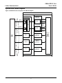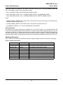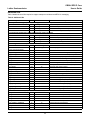
1
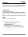
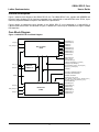
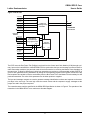
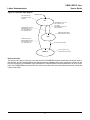
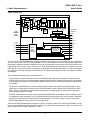
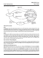
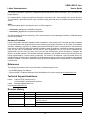
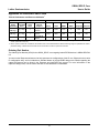
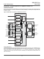
ispLever
CORE
TM
OBSAI RP3 IP Core
User’s Guide
June 2008
ipug55_01.3
OBSAI RP3 IP Core
User’s Guide
Lattice Semiconductor
Introduction
This document provides technical information about the Lattice Open Base Station Architecture Initiative Reference Point 3 Specification (OBSAI RP3) IP core. This IP core, together with SERDES and Physical Coding Sublayer (PCS) functionality integrated in the LatticeSC™, LatticeSCM™, and LatticeECP2M™ FPGAs, implements
the physical and data link layers of the OBSAI RP3 specification and can be used in applications connecting wireless baseband and RF modules.
The OBSAI RP3 IP core comes with the following documentation and files:
• Data sheet
• Netlist/database (.ngo format)
• Behavioral RTL simulation model
• Source files for instantiating and evaluating the core
The OBSAI RP3 IP core supports Lattice’s IP hardware evaluation capability, which makes it possible to create versions of the IP core that operate in hardware for a limited period of time (approximately one hour) without requiring
the purchase on an IP license. It may also be used to evaluate the core in hardware in user-defined designs.
Details for using the hardware evaluation capability are described in the Hardware Evaluation section of this document.
In the following text, the words transmit and receive refer to the direction of data flow with respect to the boundary
of the device on the external OBSAI RP3 interface.
Features
• Supports the physical link layer of the OBSAI RP3 specification
• Supports the data link layer of the OBSAI RP3 specification
• Supports the three standard bit rates of the OBSAI RP3 specification (768 Mbps, 1536 Mbps, and 3072 Mbps)
• Supports the optional 8-byte maximum for the receiver offset window.
• OBSAI data link parameter values specified at core generation time include:
– Number of bytes per frame (FRM_BYTES = (even values of 308 to 79686912)
– Number of Message Groups in Master Frame (RATE_INDEX*N_MG = 4 to 16383)
– Number of Messages in Message Group (M_MG = 4 to 255)
– Number of IDLE bytes at end of Message Group (K_MG = 1 to 19)
– Index that determines line rate (RATE_INDEX = 1, 2, 4)
– Number of bytes in code violation check block (0 < BLOCK_SIZE < 65536)
– Number of consecutive valid blocks to achieve byte synchronization (0 < SYNC_T < 65536)
– Number of consecutive invalid blocks to lose byte synchronization (0 < UNSYNC_T < 65536)
– Number of valid message groups to achieve frame synchronization (0 < FRAME_SYNC_T < 65536)
– Number of invalid message groups to lose frame synchronization (0 < FRAME_UNSYNC_T< 65536)
New in Version 3.0 (see Addendum for details):
• Support for Transport layer multiplexing/demultiplexing
• RP3-01 Messaging support: Clock Burst, RTT Measurement, Virtual Hardware Reset
• Ethernet messaging
2
OBSAI RP3 IP Core
User’s Guide
Lattice Semiconductor
General Description
Figure 1 shows a block diagram of the OBSAI RP3 IP core. The OBSAI RP3 IP core, together with SERDES and
Physical Coding Sublayer (PCS) functions integrated in the LatticeSC/M or LatticeECP2M series FPGA, implements the physical and data link layers of the OBSAI RP3 specification.
Figure 2 shows a system-level block diagram of the OBSAI RP3 IP core instantiated in a LatticeSC/M, or
LatticeECP2M series FPGA. As indicated in Figure 2, additional IP cores may be instantiated to support multiple
RP3 data links.
Core Block Diagram
Figure 1. OBSAI RP3 IP Core Block Diagram
OBSAI RP3 IP Core
TXDATAMSG[17:0]
TXCNTRLMSG[17:0]
TXDMSGVLD
TXCMSGVLD
TXDMSGRQST[1:0]
TXCMSGRQST[1:0]
TXDMSGCNT[21:0]
TXCMSGCNT[15:0]
TXD[15:0]
TXK_CNTRL[1:0]
RP3 Transmitter
(R3TX)
TXFRMSYNC[1:0]
TXDELTAREG[15:0],
TXDELTA_UDLB,
RXTXCNTRLREG[1:0]
M_MG[7:0], RIXN_MG[13:0], K_MG[4:0],
C_MG[4:0], RATE_INDEX[2:0],
FRM_BYTES[26:0], CNTRL_LOC[19:0][10:0],
TRM_CNT_LD_VALUE[28:0]
SYS_CLK
REFSYNC
REFSYNC
SAMPLE FF
RXLOSERR
RXSTATE[3:0], RXFRMOFFSET[7:0],
RXSCINTERR, RXFRMOORERR,
RXDNAERR, RXCVERR
RESET
RXPIREG[15:0], RXPI_UDLB,
BLOCK_SIZE[15:0], SYNC_T[15:0], UNSYNC_T[15:0],
FRM_SYNC_T[15:0], FRM_UNSYNC_T[15:0],
RXTXCNTRLREG[3:2]
RXDATAMSG[19:0]
RXCNTRLMSG[19:0]
RXD[15:0]
RXK_CNTRL[1:0]
RXDMSGVLD[1:0]
RXCMSGVLD[1:0]
RP3 Receiver
(R3RX)
RXDMSGCNT[21:0]
RXCMSGCNT[15:0]
RXFRMSYNC[1:0]
RXCV[1:0]
3
OBSAI RP3 IP Core
User’s Guide
Lattice Semiconductor
System-Level Block Diagram
Figure 2. OBSAI RP3 IP Core System-Level Block Diagram
FPGA in Base Station Module
ASB
Array
Core 0
Quad PCS/SERDES
OBSAI RP3
(Soft IP Core)
Lane 0
RP3 Tx
Data & Ctl
Data Msg
Cntrl Msg
R3TX
TX
SERDES
Control
Internal
User
Interface
PCS
Data Msg
RP3 Rx
Data & Ctl
Cntrl Msg
RX
R3RX
Data Msg
Control
RP3
Bus
Core 1
Base
Station
Module
Lane 1
OBSAI RP3
(Soft IP Core)
Lane 2
OBSAI RP3
(Soft IP Core)
Lane 3
OBSAI RP3
(Soft IP Core)
Core 2
Core 3
4
User Logic
(RP3
Transport
Layer
Function)
OBSAI RP3 IP Core
User’s Guide
Lattice Semiconductor
Core Signal Descriptions
Table 1. OBSAI RP3 I/O Signal List
Signal Name
Direction
Description
External RP3 Line Side Signals
RXD[15:0]
Input
Data byte received from PCS/SERDES block
RXK_CNTRL[1:0]
Input
Data code-group or special code-group indicator received from PCS/SERDES block
(0 = data code-group, 1 = special code-group)
RXCV[1:0]
Input
Code-group violation indicator received from PCS/SERDES block High-speed Data Output
Positive - Quad SERDES high speed outputs
TXD[15:0]
Output
Data word sent to PCS/SERDES block
TXK_CNTRL[1:0]
Output
Data code-group or special code-group indicator sent to PCS/SERDES block
(0 = data code-group, 1 = special code-group)
Internal User Interface Signals
R3RX Related Signals Unique to Each Receiver
RXPIREG[15:0]
Input
Receive PI – This is the amount of delay from the frame tick to the transmitted frame
boundary. Value of RXPI is given in byte-clock ticks.
RXPI_UDLB
Input
Receive PI Update Low Byte – A pulse on this lead indicates that input RXPIREG[3:0]
has been updated. This sends the receive state machine to the UNSYNC state.
RXDATAMSG[19:0]
Output
Receive Data Message – user-side data message received from RP3 link.[15:0] =
Receive Data Message data,[16], [18] = Receive K_Control - Indicates whether the current
data message byte is data or K-control.[17], [19] = Receive Code Violation - Indicates a
10B code violation on the associated data and control.
RXCNTRLMSG[19:0]
Output
Receive Control Message – user-side control message received from RP3 link.[15:0] =
Receive Control Message data,[16], [18] = Receive K_Control - Indicates whether the
current control message byte is data or K-control.[17], [19] = Receive Code Violation Indicates a 10B code violation on the associated data and control.
RXDMSGVLD[1:0]
Output
Receive Data Message Valid – Indicates that output RXDATAMSG[19:0] contains a valid
incoming data message identified by output RXDMSGCNT[19:0]. A ‘1’ on Bit 0 indicates
the message begins with the high byte (transmitted first), a ‘1’ on Bit 1 indicates a low byte
message start.
RXCMSGVLD[1:0]
Output
Receive Control Message Valid – Indicates that output RXCNTRLMSG[19:0] contains a
valid incoming data message identified by output RXCMSGCNT[31:0]. A ‘1’ on Bit 0
indicates the message begins with the high byte (transmitted first), a ‘1’ on Bit 1 indicates a
low byte message start.
RXDMSGCNT[21:0]
Output
Receive Data Message Count – Identifies the data message to which the data currently
being driven out on RXDATAMSG[31:0] belongs. Takes values from 0 up to ((M_MG - 1) *
RATE_INDEX * N_MG)-1.
RXCMSGCNT[15:0]
Output
Receive Control Message Count – Identifies the control message to which the data
currently being driven out on RXCNTRLMSG[31:0] belongs. Takes values from 0 up to
(RATE_INDEX * N_MG)-1.
RXFRMSYNC[1:0]
Output
Receive Frame Sync – Clock wide pulse that marks the received frame boundary (first
clock cycle of frame). A ‘1’ on Bit 0 indicates the frame begins with the high byte (transmitted first), a ‘1’ on Bit 1 indicates a low byte frame start.
RXSTATE[3:0]
Output
Receive State – Indicates which of its possible states the receive state machine is in. This
is a one-hot state machine with the following state values: UNSYNC = 0x8,
WAIT_FOR_K28.7_IDLES = 0x4, WAIT_FOR_FRAME_SYNC_T = 0x2, FRAME_SYNC =
0x1
RXSCINTERR
Output
Receive State Change Interrupt – Four clock wide pulse that indicates the receive state
machine has had a change of state.
RXFRMOORERR
Output
Receive Master Frame Out-Of-Range – This error is indicated when received Master
Frame is detected outside the allowed 5-byte wide window. Value ‘0’ indicates offset within
the allowed range while ‘1’ indicates out-of-range situation.
RXDNAERR
Output
Receive Data Not Aligned Error – This error indicates that the receiver cannot align data
in state WAIT_FOR_K28.7_ IDLES due to out of range K28.7 IDLE.
5
OBSAI RP3 IP Core
User’s Guide
Lattice Semiconductor
Table 1. OBSAI RP3 I/O Signal List (Continued)
Signal Name
Direction
Description
Output
Receive Code Violation Error – Indicates that one of the received 10B codes was invalid.
RXLOSERR
Output
Receive Loss-of-Signal Error – Indicates that the receive state machine is in the
UNSYNC state.
RXFRMOFFSET[7:0]
Output
Receive Master Frame Offset – This output contains a count of how long after the frame
tick plus PI the receive frame boundary occurs. If the offset exceeds 255 a value of 255 is
returned.
RXCVERR
R3TX Related Signals Unique to Each Transmitter
TXDATAMSG[17:0]
Input
Transmit Data Message – user-side data message transmitted to RP3 link (2 bytes wide).
([15:0] = Transmit Data, [16,17] = Transmit k-cntrl)
TXCNTRLMSG[17:0]
Input
Transmit Control Message – user-side control message transmitted to RP3 link (2 bytes
wide). ([15:0] = Transmit Data, [16,17] = Transmit k-cntrl)
TXDMSGVLD
Input
Transmit Data Message Valid – Indicates that Input TXDATAMSG[15:0] contains a valid
outgoing data message.
TXCMSGVLD
Input
Transmit Control Message Valid – Indicates that Input TXCNTRLMSG[15:0] contains a
valid outgoing control message.
Receive Transmit Control Register – [0] Transmit Enable - This bit enables or disables
the transmitter (0=disable, 1=enable).
RXTXCNTRLREG[3:0]
Input
[1] Loss Of Signal Enable - This bit enables or disables the impact of receive signal LOS on
transmitter state machine (0=disable, 1=enable).
[2] Pass receive messages - This bit is used to allow messages to be passed to the transport layer regardless of the offset (0=pass if within max_offset window, 1= pass always).
[3] Receive max_offset window - This bit selects the max_offset value for the receiver (0=4
bytes, 1=8 bytes).
TXDELTAREG[15:0]
Input
Transmit DELTA – This parameter specifies the amount of delay from the frame tick to the
expected boundary of the received frame. Value of TXDELTA is given in byte-clock ticks.
TXDELTA_UDLB
Input
Transmit DELTA Update Low Byte – A pulse on this lead indicates that TXDELTAREG
has been updated. This sends the transmit state machine from the IDLE state to the
FRAME_TX state.
TXDMSGCNT[21:0]
Output
Transmit Data Message Count – Identifies the data message byte that is currently being
requested by TXDMSGRQST[3:0]. Takes values from 0 up to M_MG*N_MG-1.
TXCMSGCNT[15:0]
Output
Transmit Control Message Count – Identifies the control message byte that is currently
being requested by TXCMSGRQST[3:0]. Takes values from 0 up to (N_MG*4) - 1.
TXDMSGRQST[1:0]
Output
Transmit Data Message Request – Requests the data message (to be supplied on input
TXDATAMSG[15:0]) identified by output TXDMSGCNT[21:0]. A ‘1’ on Bit 0 requests the
message begin with the high byte (transmitted first), a ‘1’ on Bit 1 requests a low byte message start.
TXCMSGRQST[1:0]
Output
Transmit Control Message Request – Requests the control message (to be supplied on
input TXCNTRLMSG[15:0]) identified by output TXCMSGCNT[15:0]. A ‘1’ on Bit 0 requests
the message begin with the high byte (transmitted first), a ‘1’ on Bit 1 requests a low byte
message start.
TXFRMSYNC[1:0]
Output
Transmit Frame Sync – Clock wide pulse that marks the transmit frame boundary (first
clock cycle of frame). A ‘1’ on Bit 0 indicates the frame begins with the high byte, a ‘1’ on Bit
1 indicates a low byte frame start.
OBSAI RP3 Related Signals Common to all Receivers and Transmitters
SYS_CLK
Input
RSTN
Input
IP Core Reset (active low).
Input
Reference Sync – Sync signal distributed from the centralized BTS system.
REFSYNC
IP Core System Clock (38.4 MHz, 76.8 MHz, or 153.6 MHz)
6
OBSAI RP3 IP Core
User’s Guide
Lattice Semiconductor
Parameter Descriptions
The synthesis affecting parameters are shown in Table 2.
Table 2. OBSAI RP3 Core Configuration Parameters
Parameter
Value Range
Description
Determines whether
the optional receiver
MAX_OFFSET of 8
will be supported.
OFFSET_8
0 or 1
RATE_INDEX
Multiplier on base rate of 768 Mbps to set line rate
1,2, or 4
M_MG
Number of messages in message group
4 to 255
N_MG
Number of message groups in master frame for line rate 768 Mbps
K_MG
Number of idles at end of message group
4 to
16383/RATE_INDEX
1 to 19
BLOCK_SIZE
Number of bytes in code violation check block
1 to 65535
SYNC_T
Number of consecutive valid blocks to achieve byte synchronization
1 to 65535
UNSYNC_T
Number of consecutive invalid blocks to lose byte synchronization
1 to 65535
FRAME_SYNC_T
Number of consecutive valid message groups to achieve frame synchronization
1 to 65535
FRAME_UNSYNC_T Number of consecutive invalid message groups to lose frame synchronization
1 to 65535
Note: This design supports even numbers of frame bytes only. RATE_INDEX * N_MG_VALUE * ((M_MG_VALUE*19) + K_MG_VALUE) must
produce an even number.
Interface Timing and Electrical Specifications
Please see the LatticeSC/M or LatticeECP2M Family Data Sheet for detailed SERDES and FPGA interface timing
and electrical specifications.
Functional Description
The OBSAI RP3 IP core is made up of two different blocks referred to as the Transmitter (R3TX) and the Receiver
(R3RX). One side of these blocks interfaces to the PCS/SERDES module of the LatticeSC/M, or LatticeECP2M
FPGA ASB. The other side interfaces to the user logic that implements the transport layer of the RP3 protocol.
As indicated in Figure 2, the OBSAI RP3 IP core is expected to be used in conjunction with additional user-side
logic that interfaces to the IP core via a 16-bit data message bus, a 16-bit control message bus, and some miscellaneous control bits in both the transmit and the receive directions.
Data Flow
Transmit Direction
The transmit path, shown in Figure 3, is the path from internal user logic towards the PCS/SERDES interface. In
this direction, the RP3 Transmitter (R3TX) multiplexes the data messages and control messages received from the
Transport Layer in the user’s logic on a per-message basis onto the 16-bit wide data and 2-bit wide control interface
to the PCS/SERDES of the LatticeSC/M or LatticeECP2M FPGA. The PCS/SERDES converts this 16-bit wide data
and 2-bit wide control into 10-bit codes that are then sent out on the RP3 line.
7
OBSAI RP3 IP Core
User’s Guide
Lattice Semiconductor
Figure 3. R3TX Path
R3TX
TxCntrlMsg
TxDataMsg
txd
TxK_Cntrl
Frame and
Message Group
Formatter
TxDMsgRqst
TxDMsgVld
txk_cntrl
PCS/SERDES
Side Interface
TxCMsgRqst
TxCMsgVld
User Side
Interface
TxDMsgCnt
TxCMsgCnt
TxFrmSync
Data Message
Control Message
Message Byte Counters
Msg_Params
Delta
Transmit
State Machine
Rx_LOS
RefSync
Udlb
TxEn
Frm_Bytes,
Trm_Cnt
TxDeltaReg
RxCntrlReg
The R3TX uses the Bus Frame Tick (RefSync) received from the Control and Clock Module (CCM) through a primary input on the LatticeSC/M or LatticeECP2M FPGA to synchronize the byte and message counters to those in
other base station modules. At a particular node all receivers need to be receiving the Master Frame boundary at
the same time. To allow for differences in delay from transmitters to receivers, a programmable variable (DELTA) is
given to each transmitter during initialization by writing the corresponding register in the register module of the top
level template This variable is used to set the delay from the Bus Frame Tick to the Master Frame boundary for that
particular transmitter. The value of this parameter can be either positive or negative.
The byte and message counters are used to generate message identification numbers and requests to the transport layer in the user logic. The user logic uses the counter values and the requests to supply messages at the
proper time and in the proper sequence.
The transmitter state machine specified in the OBSAI RP3 Specification is shown in Figure 4. The operation of the
transmitter in the OBSAI RP3 IP core conforms to this state diagram.
8
OBSAI RP3 IP Core
User’s Guide
Lattice Semiconductor
Figure 4. Transmitter State Diagram
Hardware Reset
OFF State: Nothing is
Transmitted to the Bus
(Disabled)
OFF
(TRANSMITTER_EN=1 and
LOS_ENABLE =1 and
LOS=0) OR
(TRANSMITTER_EN=1 and
LOS_ENABLE=0)
TRANSMITTER_EN=0 OR
(TRANSMITTER_EN=1
and LOS_ENABLE=1 and
LOS=1) OR HW Reset
IDLE state: K28.5 IDLE
bytes are sent to the bus.
IDLE
TRANSMITTER_EN=0
OR (TRANSMITTER_EN=1
and LOS_ENABLE=1 and
LOS=1) OR HW Reset
Parameter DELTA updated.
FRAME_TX
Frame_TX state: Frame
formatted data is transmitted.
Receive Direction
The receive path, shown in Figure 5, is the path from the PCS/SERDES interface towards the internal user logic. In
this direction, the RP3 receiver (R3RX) demultiplexes the data messages and control messages received from the
RP3 line through the PCS/SERDES of the LatticeSC/M or LatticeECP2M FPGA and passes them on to the user’s
logic. The PCS/SERDES converts the RP3 line serial 10-bit code to the 16-bit wide data and 2-bit wide control that
is sent to the R3RX.
9
OBSAI RP3 IP Core
User’s Guide
Lattice Semiconductor
Figure 5. R3RX Path
R3RX
d
K30.7
(A)
(B)
k_cntrl
cv
(C)
Bad Msg
Group
Detect
Data Pipe
(D)
(E)
(F)
(G)
(H)
Bad Block
Detect
K28.7
Detect
Bad Frame
and Offset
Detect
PCS/
SERDES
Side
Interface
(J)
User-Side
Interface
RxDataMsg
RxFrmSync
RxCntrlMsg
RxDataMsgVld
Frm_Bytes,
Trm_Cnt
RxCntrlMsgVld
RxDMsgCnt
Msg_Params
Sync_Params
TxPiReg
RefSync
Data Message
Control Message
Message Byte
Counters
Receive
State
Machine
and Framer
RxCMsgCnt
RxLOS
RxState
RxErr
RxFrmOS
The inputs from the PCS/SERDES are latched and then the K28.7 detect circuit looks for a 0xFC on the data, a
0x1 on k_control, and a 0x0 on the Code Violation rail. This circuit passes a one to the next data pipe stage when
this pattern is detected, otherwise it passes a zero. At the next stage the Code Violation rail is used to select incoming data and control or K30.7 and k_control of one. If the Code Violation rail has a one on it the data is forced to
0xFE and the k_control is forced to one, otherwise it passes the incoming data and control. The result of this action
is to replace all incoming bytes that were derived from an invalid 10-bit code with a K30.7 as required by the RP3
Specification.
At the next data pipe stage there are three detectors:
• The first of these detectors looks for consecutive bad blocks and consecutive good blocks. A block consists of
BLOCK_SIZE (stored in one of the accessible registers) bytes. If a block contains any byte with a code violation
it is marked bad, otherwise it is marked good. Consecutive bad blocks are counted and consecutive good blocks
are counted.
• The second of these detectors looks for consecutive bad messages and consecutive good messages. A message group is marked good if the first (M_MG)*19 bytes are data or K30.7 and the last K_MG bytes are K28.5,
K28.7, or K30.7, otherwise it is marked bad. Consecutive bad message groups are counted and consecutive
good message groups are counted.
• The third of these detectors looks for consecutive frames with bad K28.7 at the Master Frame boundary. A frame
is considered to have good K28.7 if all K_MG bytes that are expected to have K28.7 correctly have it, otherwise
the frame is considered bad. Consecutive frames with bad K28.7 are counted. These counts are used by the
Receive State Machine to synchronize to the incoming bytes.
The Receive State Machine diagram is shown in Figure 6. This figure is taken from the RP3 Specification. A modification has been made that forces the state machine to re-acquire frame synchronization if K28.7 no longer occurs
in the proper place for FRAME_UNSYNC_T frames.
10
OBSAI RP3 IP Core
User’s Guide
Lattice Semiconductor
Figure 6. Receiver State Diagram
SYNC_T consecutive
valid blocks of bytes
received
SYNC
HW_Reset
UNSYNC_T consecutive invalid
blocks of bytes received or
HW_Reset
UNSYNC
UNSYNC_T consecutive invalid
blocks of bytes received or
HW_Reset
UNSYNC_T
consecutive invalid
blocks of bytes received
or HW_Reset
WAIT_FOR_K28.7_IDLES
FRAME_UNSYNC_T
consecutive invalid
message groups or
frames with bad K28.7
received
WAIT_FOR_FRAME_SYNC_T
FRAME_SYNC_T
consecutive valid
message groups
received
FRAME_SYNC
K_MG consecutive
K28.7 idles received
FRAME_UNSYNC_T
consecutive invalid
message groups or
frames with bad K28.7
received
Start-Up Procedures
R3TX
Following reset, the R3TX transmit state machine is in the OFF state where it sends continuous K30.7 to the
PCS/SERDES module. When the transmitter is turned on, by writing the transmit control register to enable the
transmitter and having the LOS signal active if the LOS_EN bit was written to active, the transmit state machine
goes to the IDLE state and K28.5 is sent to the PCS/SERDES. When the DELTA parameter register is updated the
transmit state machine goes to the FRAME_TX state and starts to transmit frame formatted data
R3RX
Following reset, the R3RX receive state machine is in the UNSYNC state where no data is passed to the user. The
incoming blocks of data are checked for validity. When SYNC_T consecutive blocks of bytes are valid, the receive
state machine goes to the WAIT_FOR_K28.7_IDLES state. When K_MG consecutive K28.7 idles have been
received, the receive state machine goes to the WAIT_FOR_FRAME_SYNC_T state. When FRAME_SYNC_T
consecutive valid message groups have been received, the receive state machine goes to the FRAME_SYNC
state. In this state, received messages are passed to the user.
User Interface Timing Diagrams
This section provides interface timing diagrams for the user-side interface, conveying general behavior as well as
the active edges for transfer and sampling. All messages are 19 bytes in length and contain the associated message counter contents. The frame used for these diagrams has the following parameters: M_MG =5, N_MG= 4,
K_MG = 5, and RATE_INDEX = 1.
R3RX Receive User Message Interface
Data messages are passed from the core to the user in data bus RXDATAMSG[19:0]. The high byte (RXDATAMSG[15:8]) contains the first byte received by the core on the line side interface and the low byte (RXDATAMSG[7:0]) contains the second byte received. RXDATAMSG[19:18] contains the control (code violation and
k_control) associated with the high byte and RXDATAMSG[17:16] contains the control (code violation and
k_control) associated with the low byte. The two bit control output RXDMSGVLD is used to indicate the validity and
starting byte of the message. RXDMSGVLD[0] lasts for one clock and indicates a valid message beginning with the
high byte. RXDMSGVLD[1] lasts for one clock and indicates a valid message beginning with the low byte. The 21-
11
OBSAI RP3 IP Core
User’s Guide
Lattice Semiconductor
bit output RXDMSGCNT indicates the number of the current data message. This output is updated when RXDMSGVLD[1:0] goes active.
Figure 7 shows the first data message in a frame. RXFRMSYNC[0] indicates a new frame beginning with on the
high byte. RXDMSGVLD[0] indicates a message starting with the high byte, followed by the remainder of the 19byte message. The subsequent message begins on the low byte.
Figure 7. R3RX User Data Message Interface (Message Starts in Low Byte)
Similarly, control messages are passed from the core to the user in data bus RXCNTRLMSG[19:0]. The high byte
(RXCNTRLMSG[15:8]) contains the first byte received by the core on the line side interface and the low byte
(RXCNTRLMSG[7:0]) contains the second byte received. RXCNTRLMSG[19:18] contains the control (code violation and k_control) associated with the high byte and RXCNTRLMSG[17:16] contains the control (code violation
and k_control) associated with the low byte. The 2-bit control output RXCMSGVLD is used to indicate the validity
and starting byte of the message.
R3TX Transmit User Message Interface
Data messages are passed from the user to the core in data bus TXDATAMSG[17:0]. The high byte (TXDATAMSG[15:8]) contains the first byte that will eventually be transmitted by the core on the line side interface and the
low byte (TXDATAMSG[7:0]) contains the second byte that will eventually be transmitted. TXDATAMSG[17] contains the control (k_control) associated with the high byte and TXDATAMSG[16] contains the control (k_control)
associated with the low byte. The two bit control core output TXDMSGRQST is used by the core to request a data
message from the user. TXDMSGRSQT[0] lasts for one clock and indicates the request of a data message that
begins with the high byte. TXDMSGRSQT[1] lasts for one clock and indicates the request of a data message that
begins with the low byte. The 21-bit core output TXDMSGCNT indicates the number of the current data message.
This core output is updated when TXDMSGRQST[1:0] goes active. The start of the data message must be provided by the user on the second clock after the request from the core. The user asserts the core input TXVALID to
indicate that a valid message is being provided. If no message is available this input is kept low.
Figure 8 shows the first data message in a frame. TXFRMSYNC[0] indicates a new frame beginning with on the
high byte. TXDMSGRQST[0] requests a message starting with a high byte. The user logic responds two clock
cycles later by asserting TXDATA with TXDATA_HI/LO, followed by the remainder of the 19-byte message. The subsequent message begins on the low byte.
12
OBSAI RP3 IP Core
User’s Guide
Lattice Semiconductor
Figure 8. R3TX User Data Message Interface (Message Starts in Low Byte)
Synchronization
A single common PLL (instantiated by the user) provides the system (38.4 MHz, 76.8 MHz, or 153.6 MHz) clock for
all the IP core modules that are implemented in a single LatticeSC/M or LatticeECP2M FPGA. This system clock is
used as the clock for all of the R3TX transmitters, all of the R3RX receivers, the transmit clock for each PCS lane,
the receive clock for each PCS lane, the reference clock for each SERDES transmit PLL, the reference clock for
each SERDES receive PLL, and any user logic that interfaces to the IP cores. A reference clock is distributed to
this device from the centralized BTS system clock. This reference clock is used as a reference for the common
PLL. The possible frequencies for the OBSAI RP3 IP system clock are shown in Table 3. This clocking arrangement
is shown in Figure 9.
Each lane of the PCS block provides a FIFO at the interface to the FPGA logic for each direction. These FIFOs are
used to transfer data from the external FPGA system clock to the PCS internal transmit clock in the transmit direction and from the PCS internal receive clock to the external FPGA system clock in the receive direction.
Table 3. OBSAI RP3 IP System Clock
Line Rate Index (i)
Line Rate
System Clock Frequency
1
768 Mbps
38.4
2
1.536 Gbps
76.8
4
3.072 Gbps
153.6
13
OBSAI RP3 IP Core
User’s Guide
Lattice Semiconductor
Figure 9. OBSAI RP3 Clocking Scheme
OBSAI_RP3 Module 0
BusClk
PLL
RxRef
RxClk
FrmTck
R3RX
RxClk
Primary I/O
Txref
TxClk
FrmTck
BusFrm Tck
R3TX
TxClk
OBSAI_RP3
Core 0
PCS/SDS
Lane 0
Other Modules
Core Generation
The OBSAI RP3 IP core is available for download from the Lattice website (www.latticesemi.com). The IP files are
automatically installed using ispUPDATE technology in any user-specified directory.
The ispLEVER® IPexpress™ GUI window for the OBSAI RP3 core is shown in Figure 10. To generate a specific IP
core configuration, the user must specify:
• Project Path – A path to the directory into which the generated IP files will be loaded.
• File Name – “username” designation given to the generated IP core and corresponding folders and files.
• Design Entry Type – Verilog HDL.
• Device Family – The device family to which the IP is to be targeted. Only families that support the particular core
are listed.
• Part Name – Specific targeted part within the selected device family.
Note: If IPexpress is called from within an existing project, Project Path, Design Entry, Device Family and Part
Name default to the specified project parameters. Please refer to the IPexpress software help for further information.
14
OBSAI RP3 IP Core
User’s Guide
Lattice Semiconductor
Figure 10. OBSAI RP3 IPexpress GUI Window
15
OBSAI RP3 IP Core
User’s Guide
Lattice Semiconductor
To create a custom configuration, click on the Customize button to display the OBSAI RP3 IP core Configuration
GUI, shown in Figure 11. From this window, the user may select the desired OBSAI RP3 configuration parameters.
Figure 11. OBSAI RP3 IPexpress GUI Window
16
OBSAI RP3 IP Core
User’s Guide
Lattice Semiconductor
When the user clicks the Generate button, the IP core and parameter-configured supporting files are generated in
the user’s project directory. The directory structure of the generated files is shown in Figure 12. Note that the
OBSAI RP3_eval directory and subtending directories are only generated if the “Evaluation Directory” generation
option is selected.
Figure 12. OBSAI RP3 IP Core Generated Directory Structure
The following files are generated in the user’s project directory (\obsai_rp3_v3_test in Figure 12):
• <username>.lpc – IP parameter file (may be directly modified by user).
• <username>.ngo – Synthesized IP core. Depending on the configuration of the core, additional supporting .ngo’s
may also be generated.
• <username>_bb.v – Black box module wrapper for synthesis.
• <username>_inst.v – Example of instantiation template to be included in a user’s design.
• <username>_beh.v – Behavioral simulation model for IP core configuration username.
The \<obsai_rp3_eval> directory and subtending directories provide files supporting OBSAI RP3 core evaluation.
The \<username> subfolder (\cfg0 in Figure 12) contains files/folders with content specific to the username configuration.
Implementation Evaluation
The generated OBSAI RP3 IP core package includes black-box (<username>_bb.v) and instance (<username>_inst.v) templates that can be used to instantiate the core in a top-level design.
The top-level file obsai_rp3_top.v allows the user to map, place and route a standalone core. The configurationspecific core, as specified by the user, is instantiated inside a ring of flip-flops to isolate I/O timing. This design is
intended only to provide an accurate indication of the device utilization associated with the OBSAI RP3 core. Implementation of this top level is supported via the project file <username>_eval.syn located in
<project_dir>\obsai_rp3_eval\<username>\impl.
To use this project file:
1. Open either Synplify® or Precision® RTL Synthesis
2. Execute the obsai_rp3_top.tcl script in the appropriate subdirectory under
\<project_dir>\obsai_rp3_eval\<username>\impl. This will create a obsai_rp3_top.edf in the impl directory.
3. Select Open Project under the File tab in ispLEVER.
4. Browse to \<project_dir>\obsai_rp3_eval\<username>\impl in the Open Project dialog box.
5. Select and open <username>_eval.syn.
17
OBSAI RP3 IP Core
User’s Guide
Lattice Semiconductor
At this point, all of the files needed to support top-level synthesis and implementation will be imported to the
project.
6. Set up the place and route options by right-clicking on Place & Route Design and select Properties.
7. Implement the complete design via the standard ispLEVER GUI flow.
Functional Simulation Evaluation
The functional simulation includes two behavioral models of the OBSAI RP3 IP core instantiated along with userside driver/monitor modules. The user-specified core parameters are automatically set in the testbench. The toplevel testbench supporting both ModelSim® and Aldec® Active-HDL® evaluation simulations is provided in
\<project_dir>\obsai_rp3_eval\<username>\testbench. Users may run the evaluation simulation by doing the
following:
1. Open ModelSim (or Active-HDL).
2. Change Directory to \<project_dir>\obsai_rp3_eval\<username>\sim\modelsim.
3. Execute the obsai_rp3_eval.do script. The simulation waveform results will be displayed in the Wave window.
(For Active-HDL, the script is named obsai_rp3_eval.tcl)
The test sequence resets the core, waits for both master and slave receivers to achieve frame synchronization,
then sends data messages, Ethernet messages, one clock burst message, one virtual hardware reset message,
and one RTT measurement message.
The Lattice default parameters support significantly reduced simulation times as compared to parameter settings
conforming to the OBSAI standard recommendations. The Lattice default parameters and typical parameters a
user would likely specify (e.g. conforming to WCMDA recommendations) are shown in Table 4.
Table 4. OBSAI RP3 Parameters for Simulation
OBSAI Data Link Parameters
Lattice Default Values
WCDMA Recommended Values
M_MG
5
21
N_MG
4
1920
K_MG
5
1
RATE_INDEX
1
1,2,4
BLOCK_SIZE
40
400
SYNC_T
25
255
UNSYNC_T
25
255
FRAME_SYNC_T
20
1920
FRAME_UNSYNC_T
12
128
The Lattice default parameter values result in a master frame length of 400 bytes, and the evaluation simulation
takes a few minutes. A typical OBSAI master frame is 768,000 bytes long; the evaluation simulation runs for several
hours. Running reduced master frame lengths result in much shorter simulation duration, which may be desirable
in evaluation mode.
Including the Core in a Top-Level Design
Verilog
The obsai_rp3_top.v file located in \<project_dir>\obsai_rp3_eval\<username>\src provides an example core
instantiation (this is the file used for implementation evaluation). The text for the instantiation comes from the <username>_inst.v file in the project directory. Note that the core instance is configuration-specific; all the parameters
have been resolved. Simply include the instantiation text verbatim in the parent module’s description, and edit the
connection list as required.
18
OBSAI RP3 IP Core
User’s Guide
Lattice Semiconductor
For functional simulation, compile the configuration-specific behavioral model <username>_beh.v provided in the
project directory.
For implementation, compile the black-box description <username>_bb.v, also provided in the project directory.
The <username>.ngo and submodule .ngo’s, required for map, place and route, are created in the project directory,
as well.
VHDL
The corresponding files for including the core in a VHDL design are:
• <username>_inst.vhd, the instantiation template
• <username>_pkg.vhd, the component specification
The Verilog behavioral model <username>_beh.v may be used in a mixed-language simulation. A VHDL behavioral
model is not provided.
Hardware Evaluation
Lattice’s IP hardware evaluation capability makes it possible to create versions of IP cores that operate in hardware
for a limited period of time (approximately one hour) without requiring the purchase on an IP license. The hardware
evaluation capability is turned on by enabling the Hardware Evaluation option in the properties of the Build Database process in ispLEVER. When the Hardware Evaluation option is enabled, it is possible to generate a programming file that may be downloaded into the device. After initialization, the IP core will be operational for
approximately one hour. After one hour, the IP core will stop working and it will be necessary to reprogram the
device to re-enable operation. This hardware evaluation capability is only enabled if the core has not been licensed.
During implementation, a license check is performed. If a license is not detected, a pop-up window will be displayed indicating a license failure. Click OK in the window and generation will proceed to completion with hardware
evaluation enabled. If a license is detected, no pop-up window is displayed and core generation is completed with
no restrictions.
References
The following documents provide more information on implementing this core:
• ispLEVER Software User Manual
• ispLeverCORE™ IP Module Evaluation Tutorial available on the Lattice website at www.latticesemi.com
Technical Support Assistance
Hotline: 1-800-LATTICE (North America)
+1-503-268-8001 (Outside North America)
e-mail: [email protected]
Internet:www.latticesemi.com
Revision History
Date
Version
April 2006
01.0
Change Summary
Initial release.
October 2006
01.1
Added appendix for LatticeECP2M device family.
June 2007
01.2
Enhancements to Synthesizing and Implementing the Core and Hardware
Evaluation sections.
Updated appendices.
June 2008
01.3
Included addendum describing transport layer mux and RP3-01 support.
19
OBSAI RP3 IP Core
User’s Guide
Lattice Semiconductor
Appendix for LatticeSC FPGAs
Table 5. Performance and Resource Utilization1
Configuration
Transport
Layer
Master Frame Line Rate
Parameters
Index
Ports
Utilization
RP3-01
Support
Frequency (MHz)
Slices
LUTs
REGs
EBRs
Required Achieves
WCDMA /
GSM Edge
2 (1.5G)
1
No options
selected
1047
1499
1162
0
76.8
191
WCDMA /
GSM Edge
2 (1.5G)
1
Master with all
options2
2630
4174
2310
3
76.8
160
4 (3G)
4
Slave with all
options2
4558
7516
3200
3
153.6
160
CDMA
1. Performance and utilization characteristics using ispLEVER 7.1 software. When a different density, speed, or grade or a different software
version, performance may vary.
2. RP3-01 options include: RP1 Clock Burst, RTT Measurement, Virtual Hardware Reset, Ethernet Message support capabilities with default
parameter settings. Master and slave modes are Don't Cares when no RP3-01 options are selected.
Ordering Part Number
The Ordering Part Number (OPN) for the OBSAI_RP3 IP core targeting LatticeSC devices is OBSAI-RP3-SC-U3.
You can use the IPexpress software tool to help generate new configurations of this IP core. IPexpress is the Lattice
IP configuration utility, and is included as a standard feature of the ispLEVER design tools. Details regarding the
usage of IPexpress can be found in the IPexpress and ispLEVER help system. For more information on the
ispLEVER design tools, visit the Lattice web site at: www.latticesemi.com/software.
20
OBSAI RP3 IP Core
User’s Guide
Lattice Semiconductor
Appendix for LatticeECP2M FPGAs
Table 6. Performance and Resource Utilization1
Configuration
Master
Frame
Line Rate
Parameters
Index
Transport
Layer
Ports
Utilization
RP3-01
Support
Frequency (MHz)
Slices
LUTs
REGs
EBRs
Required Achieves
WCDMA /
GSM Edge
2 (1.5G)
1
No options
selected
999
1364
1152
0
76.8
167
WCDMA /
GSM Edge
2 (1.5G)
1
Master with all
options2
2543
3907
2442
3
76.8
128
2 (3G)
2
Slave with all
options2
3523
5655
2580
3
76.8
106
CDMA
1. Performance and utilization characteristics using ispLEVER 7.1 software. When a different density, speed, or grade or a different software
version, performance may vary..
2. RP3-01 options include: RP1 Clock Burst, RTT Measurement, Virtual Hardware Reset, Ethernet Message support capabilities with default
parameter settings. Master and slave modes are Don't Cares when no RP3-01 options are selected.
Ordering Part Number
The Ordering Part Number (OPN) for the OBSAI_RP3 IP core targeting LatticeECP2M devices is OBSAI-RP3-PMU3.
You can use the IPexpress software tool to help generate new configurations of this IP core. IPexpress is the Lattice
IP configuration utility, and is included as a standard feature of the ispLEVER design tools. Details regarding the
usage of IPexpress can be found in the IPexpress and ispLEVER help system. For more information on the
ispLEVER design tools, visit the Lattice web site at: www.latticesemi.com/software.
21
OBSAI RP3 IP Core
User’s Guide
Lattice Semiconductor
Addendum - Transport Layer/RP3-01 Support in Version 3.0+
Functional Description
Beginning with version 3.0, the OBSAI RP3 core includes optional support for transport layer multiplexing/demultiplexing and RP3/RP3-01 Operation and Maintenance (O&M) messaging. The following block diagram shows the
new logic in context:
Figure 13. OBSAI RP3 Core Additions for Mux/Demux and RP3-01
Ethernet/RP3-01 Message Handler
INSERTION
CONTROL
REGS
VIRTUAL
HW RESET
TX
RP1 CLOCK
BURST
TX
RTT
MEASURE
TX
Transport
Mux/DeMux
txk_cntrl[1:0]
txd[15:0]
R3TX
.
ETHERNET
PORT
XTRACT
DEMUX
FIFO intf
rxport0
rxport1
rxport2
rxport3
INSERT
MUX
txport0
txport1
txport2
txport3
Existing OBSAI
RP3 IP Core
sys_clk
refsync
rxd[15:0]
R3RX
rxk_cntrl[1:0]
rxcv[1:0]
RTT
MEASURE
RX
RP1 CLOCK
BURST
RX
VIRTUAL
HARDWARE
RESET RX
Transport Mux/Demux
The Transport Mux module interleaves messages from two or four ports per section 4.3.4 of the OBSAI RP3 specification. The synthesis parameter RP3_PORTS determines the number of ports equipped (1, 2, or 4). The combination of RP3_PORTS and the RATE_INDEX input (1, 2, or 4, where the output data rate is RATE_INDEX*
768Mbps) determines the ports’ input data rate (768 or 1536 Mbps). The Transport Demux module performs message de-interleaving.
22
OBSAI RP3 IP Core
User’s Guide
Lattice Semiconductor
Each RP3 port presents the same R3RX and R3TX interfaces as the base OBSAI RP3 core. In the transmit direction, unoccupied message slots (logic low on TXD/CMSGVLD) are replaced by empty messages (all ones).
Message Insertion/Extraction
ETHERNET and RP3-01 O&M messages are inserted into the transmit message stream following the message
transmission rules described in section 4.4.3 of the OBSAI RP3 specification. Separate synthesis parameters
(described below) optionally implement RP1 Frame Clock Burst, RTT measurement, Virtual Hardware Reset, and
Ethernet message handling. The RP301_MASTER parameter determines whether the core is compiled as master
or slave.
There are three types of ETHERNET and RP3-01 message insertion opportunities: normal message group control
slots, modulo count slots, and dual-level bit-map specified slots (per OBSAI RP3 specification, section 4.4.3). For
modulo count slots, the index and modulo are set via the INDEX and MODULUS inputs to the core. Note: As of version 3.0 of the core, only control message and modulo count insertion have been implemented.
Each of the implemented TX units sends a ready signal to the core’s insertion unit, which looks at the ready signals
in a fixed priority order, and selects the next message to insert into the next available time slot in the transmit
stream. The priority order, from high to low, is as follows: Virtual Hardware Reset, Clock Burst, RTT Measurement,
and Ethernet messaging.
Virtual Hardware Reset
Virtual Hardware Reset messages, defined in section 6.2.7 of the OBSAI RP3 specification, provide a way to
request a reset of a remote unit. For cores configured as masters, asserting the HW_RESET_REQ input accompanied by a valid HW_RESET_ADDRESS value triggers the request message. In slave mode, a hardware reset message with the slave’s address results in a single-clock-cycle active-high HW_RESET output.
RTT Measurement
RTT measurement messages are exchanged by adjacent nodes, either LC<->RU1 or RUn<->RUn+1. The master
RTT Measure TX module is triggered by asserting the core’s RTT_REQ input accompanied by a valid
RTT_TARGET_ADDR value. The addressed slave node returns the message using the return address from the
message, after setting the delta (1, 2) field (as specified in 6.2.6 of the OBSAI RP3 specification).
On receiving the returned RTT message, the master RTT Measure RX module asserts RTT_DELAY_VALID
accompanied by RTT_RETURN_ADDR and RTT_DELAY. RTT_DELAY is computed by the master node by subtracting the buffering time field in the return message from the master’s total round trip delay counter (which begins
counting when the message is sent). Note: the master node counter counts system clock cycles, so the slave
nodes’ buffering times should be in system clock cycle units, as well. The OBSAI spec calls for delays to be
reported in increments of 614.4 MHz clock cycles, so a left-shift operation (by the user logic) is required to properly
interpret the round trip delay value (shift by 4 for RATE_INDEX equals 4, by 8 for RATE_INDEX equals 2, and by 16
for RATE_INDEX equals 1).
RP1 Clock Burst
The RP1 Clock Burst TX module accepts RP1 clock burst messages as defined in section 8.4 of the OBSAI RP1
specification, and creates RP3-01 clock burst messages per 6.2.3 of the RP3 specification.
The RP1 Clock Burst RX module receives the message and generates a RP1 clock burst message with a new system frame number at a time determined according to the specification. CB_MSG_IN is the input at the master,
CB_MSG_OUT the output at the slave.
Section 8.4 of the OBSAI RP1 specification calls for clock burst messages to be transferred using a 30.72 MHz
system clock, with each message bit being eight clock cycles in duration. The OBSAI RP3 core provides additional
flexibility by using a separate clock signal CB_CLK for the message transfer. Message bits are one clock in duration, and the transfer is synchronous. There is no requirement for synchrony between CB_CLK and the primary
core clock CLK.
23
OBSAI RP3 IP Core
User’s Guide
Lattice Semiconductor
Three input values are required for the slave’s clock burst receiver: CB_K, CB_K_SFN_MINUS_23US, and
CB_K_SFN_MINUS_10MS. They are calculated as follows:
• CB_K = MASTER_FRAME_LENGTH/SYSTEM_FRAME_LENGTH
• CB_K_SFN_MINUS_23US = CB_K * SYSTEM_FRAME_LENGTH - CB_MESSAGE_LENGTH
• CB_K_SFN_MINUS_10MS = CB_K * SYSTEM_FRAME_LENGTH - MASTER_FRAME_LENGTH
where:
• MASTER_FRAME_LENGTH is the number of SYS_CLK periods in a master frame (which is 10 milliseconds for
standards-compliant configurations),
• SYSTEM_FRAME_LENGTH is the number of SYS_CLK periods in a system frame, and
• CB_MESSAGE_LENGTH = 90 * CB_CLK_PERIOD/SYS_CLK_PERIOD.
Ethernet Messages
The Ethernet Port module sends/receives messages via a 16-bit FIFO interface. In the transmit direction, the
FIFO_FULL output flag indicates that the transmit FIFO is unable to accept another message. Input ETH_TX_EOP
is asserted by user logic to indicate end-of-packet in the transmit direction. Output ETH_RX_EOP identifies the
final byte of a packet in the receive direction. In both directions, complete messages are assembled before being
passed on. Ethernet data is transferred synchronously on the rising edge of the Ethernet interface clock ETH_CLK.
Additional Parameters
Table 7 details the new synthesis parameters required to support transport mux/demux and RP3-01 messaging.
Table 7. Additional Parameters
Parameter Name
Range
Description
RP3_PORTS
1,2 or 4
Number of ports equipped for transport mux/demux
MASTER
0 or 1
1 implements master behavior. otherwise slave (default is 0)
MODULUS_SIZE
1 and up
width of RP301 message insertion modulus
INDEX_SIZE
1 to MODULUS_SIZE width of RP301 message insertion index value
VIRTUAL_HW_RESET 0 or 1
1 implements virtual hardware reset module (default is 0)
RTT_MEASUREMENT 0 or 1
1 implements RTT measurement module (default is 0)
CLOCK_BURST
0 or 1
1 implements RP3-01 clock burst module (default is 0)
ETHERNET_PORT
0 or 1
1 implements Ethernet port module (default is 0)
ETH_XFIFO_SIZE
0 and up
Must be at least as large as maximum packet size
ETH_RFIFO_SIZE
0 and up
Must be at least as large as maximum packet size
24
OBSAI RP3 IP Core
User’s Guide
Lattice Semiconductor
Additional I/Os
Table 8 details the new I/Os required to support transport mux/demux and RP3-01 messaging.
Table 8. Additional I/Os
Signal Name
I/O
Size
Description
Demultiplexed R3RX Signals (all other R3RX signals remain the same)
RXDATAMSG
Out
RP3_PORTS*20
Receive data (concatenated sublinks)
RXCNTRLMSG
Out
RP3_PORTS*20
Receive control (concatenated sublinks)
RXDMSGVLD
Out
RP3_PORTS*2
Receive data valid (concatenated)
RXCMSGVLD
Out
RP3_PORTS*2
Receive control valid (concatenated)
Pre-multiplexed R3TX Signals (all other R3TX signals remain the same)
TXDATAMSG
In
RP3_PORTS*18
Transmit data (concatenated sublinks)
TXCNTRLMSG
In
RP3_PORTS*18
TXDMSGVLD
In
RP3_PORTS
Transmit data message valids
TXCMSGVLD
In
RP3_PORTS
Transmit control message valids
Transmit control (concatenated)
RP3 Message Insertion Bitmap Access
MODULUS
In
MODULUS_SIZE
INDEX
In
INDEX_SIZE
In
1
RP3 modulus value
RP3 bitmap register read address
RP3-01 Control Interfaces
HW_RESET_REQ
HW_RESET_ADDR
Initiates hardware reset message (master only)
In
13
Address of slave node to be reset (master)
HW_RESET
Out
1
Hardware reset output (slave)
VHW_ERR
Out
1
Virtual hardware reset message error (slave)
RTT_SEND
In
1
Initiates RTT measurement sequence (master)
RTT_TARGET_ADDR
In
13
Address of target node (master)
RTT_BUFTIME
In
16
Buffering time for RTT measurement (slave)
RTT_DELAY
Out
16
Round trip delay value (master)
RTT_DELAY_VALID
Out
1
RTT measurement acknowledge (master)
RTT_RETURN_ADDR
Out
13
RTT measurement return address from slave (master)
RTT_ERR
Out
16
RTT message error flag (slave)
CB_CLK
In
1
Clock burst interface clock
CB_MSG_IN
In
1
Clock burst message input (master)
CB_MSG_OUT
Out
1
Clock burst message out (slave)
CB_K
In
8
Clock burst k-value (slave)
CB_K_SFN_MINUS_23US
In
26
Clock burst RRU buffering time (long)
CB_K_SFN_MINUS_10MS
In
26
Clock burst RRU buffering time (short)
CB_MSG_LENGTH
In
12
Clock burst message length
ETH_CLK
In
1
Ethernet interface clock
ETH_RSTN
In
1
Ethernet interface reset (active low)
RP3-01 Ethernet Interface (MII)
ETH_TXD
In
8
Ethernet transmit data
ETH_TXDV
In
1
Ethernet transmit data valid
ETH_TXEOP
In
1
Ethernet transmit end-of-packet
ETH_TARGET_ADDRESS
In
13
Ethernet transmit target address
ETH_TXAF
Out
1
Ethernet transmit FIFO almost full
ETH_TXFULL
Out
1
Ethernet transmit FIFO full
25
OBSAI RP3 IP Core
User’s Guide
Lattice Semiconductor
Table 8. Additional I/Os (Continued)
I/O
Size
ETH_RXD
Signal Name
Out
8
Ethernet receive data
Description
ETH_RXDV
Out
1
Ethernet receive data valid
ETH_RXEOP
Out
1
Ethernet receive end-of-packet
Configuring RP3/RP3-01 Support
The configuration GUI now supports the transport mux and RP3/RP3-01 features of the core (Figure 11).
Number of Transport Layer Ports determines whether the mux/demux function is required, and, if so, how many
ports are equipped.
RP3-01 Port Mode selects between Master and Slave configurations.
Checking the RP1 Clock Burst box enables Frame Clock Burst messaging. Clock Burst fMAX sets the maximum
frequency (in MHz) for the Clock burst interface.
Checking the RTT Measurement box adds RTT Measurement support.
Checking the Virtual Hardware Reset box enables RP3-01 virtual hardware reset handling.
Broadcast Address sets the address used for broadcast messages (clock burst transmit messages, address
matching in the receive direction).
The Ethernet checkbox adds the Ethernet interface. Ethernet fMAX sets the maximum frequency (in MHz) for the
Ethernet interface. RCV and XMT FIFO sizes are in bytes.
The Message Insertion section provides an entry point for setting the sizes of the MODULUS and INDEX inputs.
26
Mouser Electronics
Authorized Distributor
Click to View Pricing, Inventory, Delivery & Lifecycle Information:
Lattice:
OBSAI-RP3-PM-UT3 OBSAI-RP3-SC-UT3