1
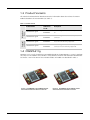
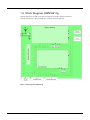
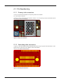
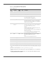
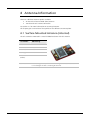
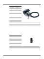
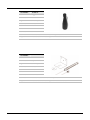
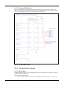
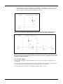
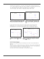
INDUSTRIAL WIRELESS™
OWSPA311g i/x ™
cB-0908
Electrical & Mechanical Datasheet
OWSPA311g i/x™
cB-0908
Electrical & Mechanical Datasheet
Copyright © 2006-2008 connectBlue AB
The contents of this document can be changed by connectBlue AB without prior notice
and do not constitute any binding undertakings from connectBlue AB. connectBlue AB
is not responsible under any circumstances for direct, indirect, unexpected damage or
consequent damage that is caused by this document.
All rights reserved.
Release: 2008-09
Document version: 1.13
Document number: cBProduct-0611-04 (1)
Printed in Sweden.
Trademarks
Registered trademarks from other companies are: Microsoft™, Windows™, Windows
NT™, Windows 2000™, Windows CE™, Windows ME™, are registered trademarks
from Microsoft Corporation.
Contents
1 General Information
1.1
1.2
1.3
1.4
1.5
Overview ............................................................................................5
Related Documents ...........................................................................5
Product Variants ................................................................................6
OWSPA311g......................................................................................6
Block Diagram OWSPA311g .............................................................7
2 Electrical Interface and Connectors
2.1
2.2
2.3
2.4
5
8
Pin Numbering ...................................................................................9
Characteristics .................................................................................15
Hardware Reset ...............................................................................16
Power Control ..................................................................................16
3 Operating Status
17
4 Antenna Information
18
4.1
4.2
Surface Mounted Antenna (internal)................................................18
External Antennas............................................................................19
5 Mounting Information
5.1
5.2
5.3
5.4
5.5
Module Dimensions .........................................................................26
Using the J2/J3 Board-to-Board Connectors ...................................28
Using Press-Fit Nuts for Mounting the Module ................................29
Using the J6 PCB Solder Pads ........................................................29
Antenna Issues ................................................................................30
6 WLAN Information
6.1
36
General ........................................................................................36
Product Care....................................................................................36
Radio Frequency Exposure .............................................................36
Electronic Equipment .......................................................................37
Potentially Explosive Atmospheres..................................................37
Safety Compliance...........................................................................37
Appendix A A.1
A.2
A.3
32
Declaration of Conformity ................................................................32
IC and FCC Compliance for OWSPA311g ......................................33
UL Listing Information ......................................................................35
Compliance with RoHS directive .....................................................35
8 Guidelines for Efficient and Safe Use
8.1
8.2
8.3
8.4
8.5
8.6
31
General Information .........................................................................31
7 Regulatory Information
7.1
7.2
7.3
7.4
26
Application Notes
38
Step-by-Step Guide .........................................................................38
Design Examples .............................................................................39
A Complete 5V Host System Interface ............................................46
Version 1.13 - 2008-09
4
1 General Information
1.1 Overview
The Serial Wireless LAN Module, OWSPA311g, from connectBlue has been developed for integration in industrial devices providing state of the art low power features. The module minimizes the work needed to implement WLAN (802.11b/g) in a device as it provides all software,
hardware, type approval, EMC certification etc. It is developed for reliable, high demanding industrial devices and applications and requires no host driver.
The Serial WLAN Module is a complete WLAN implementation. No external driver is needed.
The WLAN module has a small form factor and the interface layout is the same as the Bluetooth
modules from connectBlue, which enables customers to prepare their device for both Bluetooth
and/or WLAN.
•
Supports both 802.11b and 802.11g
•
No software driver needed.
•
Radio type approved for Europe
•
Unlicensed Modular Transmitter Approval for US and Canada
•
Compliant with EMC standards
•
Industrial temperature range -30 to +85 C
•
Support for low power modes
•
Compatible with connectBlue Bluetooth modules
•
Supports security features WEP64, WEP128, WPA, WPA2, LEAP
•
Ad-hoc and infrastructure mode
•
Internal or dual external antennas (diversity supported)
1.2 Related Documents
There are some documents related to the Serial Port Adapter:
-
The OWSPA AT Commands document contains a description of the AT commands supported in the OWSPA Serial Port Adapter.
-
The OWSPA Electrical & Mechanical Datasheet (this document) contains important information about the OWSPA Serial Port Adapter.
Version 1.13 - 2008-09
5
1.3 Product Variants
This Electrical and Mechanical datasheet contains information about the variants of OWSPA
modules based on the PCB cB-0908 (see Table 1).
Table 1: Product variants
External
antenna
Internal antenna
Product Name
Module ID /
FCC ID
Description
CB-OWSPA311gi-06
cB-0121-01 /
PVH090802
OWSPA311g with internal antenna, JST connector
CB-OWSPA311gi-04
cB-0120-01 /
PVH090802
OWSPA311g with internal antenna, no JST
connector
CB-OWSPA311gx-06
cB-0123-01 /
PVH090802
OWSPA311g with external antenna, JST connector. Receive diversity supported.
CB-OWSPA311gx-04
cB-0122-01 /
PVH090802
OWSPA311g with external antenna, no JST
connector. Receive diversity supported.
1.4 OWSPA311g
OWSPA311g is a small size Wireless LAN module based on the NXP BGW211 system in package
(SiP) chip-set. The modules are available in many different antenna and connector combinations.
See Picture 1 and 2 for some of the available models. All models are described in Table 1.
Picture 1: cB-OWSPA311gx-06 OWSPA module
with 2 external antennas and JST connector
Version 1.13 - 2008-09
Picture 2: cB-OWSPA311gi-06 OWSPA module
with internal antenna and JST connector
6
1.5 Block Diagram OWSPA311g
Coaxial connectors J4 and J5 are only available on x-versions (eXternal antenna).
Internal antenna A1 is only available on i-versions (Internal antenna).
Figure 1: Block diagram of OWSPA311g
Version 1.13 - 2008-09
7
2 Electrical Interface and Connectors
This section describes the signals available on the module interface connectors. There are three
ways of connecting to the OWSPA Module:
•
Via the PCB solder lands on the edge of the PCB, J6 (see Figure 5: Secondary side connectors). For more information see Section J6 Solder Lands Description.
•
Via the 2 x 20-pin 1mm pitch board-to-board (one piece part) connectors J2 and J3.
The J2 and J3 connectors exist on the OWSPA module only as compression pads (see
Figure 5: Secondary side connectors). These pads mates with the carrier board onepiece part connector. For more information see Section J2 Connector Description and
J3 Connector Description.
Optional:
•
Via the JST connector, J8 (see Figure 4: Primary side connectors).
The connector is a 6 poles pin header. The pitch is 1mm and the connector is from JST
with part number SM06B-SRSS-TB.
For more information see section J8 Connector Description.
Figure 2: Primary side of the PCB
Version 1.13 - 2008-09
Figure 3: Secondary side of the PCB
8
2.1 Pin Numbering
2.1.1 Primary side connectors
J8 is the JST connector located on the primary side of the module.
A1 is the internal antenna.
J4 and J5 are U.FL connectors for external antennas. J4 is the primary antenna connector and J5
the auxiliary antenna connector.
Figure 4: Primary side connectors
2.1.2 Secondary side connectors
J2 and J3 is the connectBlue board-to-board connector. The pin layout of the connector is compatible with all OEM Serial Port Adapters from connectBlue.
The J6 is the solder land connector.
Figure 5: Secondary side connectors
Version 1.13 - 2008-09
9
2.1.3
J2 Connector Description
Table 2: Signals on J2
J2
Pin Nr
Pin Name
Signal
Level
Type
Description
1, 2
VSS
Ground
Power
Ground (0 V)
3, 4
VDD
3.3V
Power
Supply voltage (3.3 – 5.5 VDC)
5 – 10
-
-
-
Reserved, do not connect.[ 1 ]
11
RED/Mode[1,2]
CMOS
Out/In
RED: Red LED control signal, low level = LED on (Output)
Not valid until 500ms after power up.
Mode: Not applicable to OWSPA311g
12
Switch-0[ 2 ]
CMOS
In
Switch-0 control signal, active low.
This signal activates the “Connect on external signal”
function. See the Serial Port Adapter AT command specification for more information.
13
GREEN/
[2]
Switch-1
CMOS
Out/In
GREEN:
Green LED control signal, low level = LED on (Output)
Not valid until 500ms after power up.
Switch-1:
[ 1, 4 ]
during power up the unit
If this pin is pulled-down
reverts to default serial settings.
The “Restore Default” input is only active during the first
500ms after power up.
See the Serial Port Adapter AT command Specification
for more information on the Restore switch.
14
BLUE[ 2 ]
CMOS
Out
Blue LED control signal, low level = LED on (Output)
Not valid until 500ms after power up.
Note:
Signal will flicker during data transmission.
15
UART-CTS[ 2 ]
CMOS
In
Hardware flow control (Clear To Send).
16
UART-TxD[ 2 ]
CMOS
Out
Transmit Data
17
UART-RTS[ 2 ]
CMOS
Out
Hardware flow control (Request To Send).
18
UART-RxD[ 2 ]
CMOS
In
Receive Data
19
UART-DTR[ 2 ]
CMOS
Out
Data Terminal Ready
20
UART-DSR[ 2 ]
CMOS
In
Data Set Ready
[1] To remain compatible, please check the datasheet for other connectBlue products using this
pin.
[2] Signals are CMOS logic level. (- 0.3 V < VIL < 0.8 V, 2 < VIH < 3.3 V)
[3] The ESD performance will be improved if this signal is decoupled with a 10 nF capacitor to
VSS.
[4] Choose a pull down resistor in the interval 1kΩ < R < 4.7kΩ, observe this is different to previous
product generations from connectBlue.
Version 1.13 - 2008-09
10
2.1.4 J3 Connector Description
Table 3: Signals on J3
J3
Pin Nr
Pin Name
1–8
Signal
Level
Type
Description
Reserved, do not connect[ 1 ]
-
9
SerialSelect-0
[2]
CMOS
Out
Control signal for external serial transceivers
10
SerialSelect-1
[2]
CMOS
Out
Control signal for external serial transceivers
11 – 14
Reserved, do not connect
-
15
PRI[ 2 ]
CMOS
In
Bluetooth co-existence interface: Bluetooth high priority
traffic indicator
16
BT[ 2 ]
CMOS
In
Bluetooth co-existence interface: Bluetooth arbitration
signal
17
WL[ 2 ]
CMOS
Out
Bluetooth co-existence interface: WLAN arbitration signal
18
RX-IND[ 2 ]
CMOS
Out
Bluetooth co-existence interface: WLAN receive indicator
19
RESETn[ 3 ]
CMOS
In
Active low. Must be driven by open drain collector.
20
-
Reserved, do not connect[ 1 ]
[1] To remain compatible, please check the datasheet for other connectBlue products using this
pin.
[2] Signals are CMOS logic level. (- 0.3 V < VIL < 0.8 V, 2 < VIH < 3.3 V)
[3] The ESD performance will be improved if this signal is decoupled with a 10 nF capacitor to
VSS.
Version 1.13 - 2008-09
11
2.1.5 J4 Primary External Antenna Connector
J4 is the primary external antenna connector. It is used for both transmit and receive.
The port impedance to match is 50Ω.
Table 4: Signals on J4
J4
Pin Nr
Pin Name
Signal
Level
Type
Description
1
AntMain
RF
I/O
Primary external antenna port (50Ω)
Note: this connector is only available on the CB-OWSPA311gx-02/04
2.1.6 J5 Auxiliary External Antenna Connector
J5 is the auxiliary external antenna connector. It is used only for receiving and if the unit is configured for diversity mode. The unit never transmits RF through this antenna connector.
The port impedance to match is 50Ω.
Table 5: Signals on J5
J5
Pin Nr
Pin Name
Signal
Level
Type
Description
1
AntAux
RF
I
Auxiliary external antenna port (50Ω)
Note: this connector is only available on the CB-OWSPA311gx-02/040
2.1.7 J8 Connector Description
Tabel 6: Signals on J8
J8
Pin Nr
Pin Name
Signal
Level
Type
Description
1
VSS
0V
Power
Ground (0 V)
2
VDD
3.3V
Power
Supply voltage (3.3 – 5.5 VDC)
3
UART-TxD[ 1 ]
CMOS
Out
Transmit Data
4
UART-RxD
[1]
CMOS
In
Receive Data
5
UART-CTS
[1]
CMOS
In
Hardware flow control (Clear To Send).
6
UART-RTS[ 1 ]
CMOS
Out
Hardware flow control (Request To Send).
[1] UART signals are CMOS logic level (- 0.3 V < VIL < 0.9 V, 2.1 V < VIH < 3.3 V)
Version 1.13 - 2008-09
12
2.1.8 J6 Solder Lands Description
Table 7: Signals on J6
J6
Pin Nr
Pin Name
Signal
Level
Type
Description
1
RESETn[ 3 ]
CMOS
In
Active low. Must be driven by open drain collector.
2
UART-DSR[ 2 ]
CMOS
In
Data Set Ready
3
VSS
Ground
Power
Ground (0 V)
4
VDD
3.3V
Power
Supply voltage (3.3 – 5.5 VDC)
5
UART-DTR[ 2 ]
CMOS
Out
Data Terminal Ready
6
RED/Mode[1,2]
CMOS
Out/In
RED:
Red LED control signal, low level = LED on (Output)
Not valid until 500ms after power up
Mode:
Not applicable to OWSPA311g
7
GREEN/
[2]
Switch-1
CMOS
Out/In
GREEN:
Green LED control signal, low level = LED on (Output)
Not valid until 500ms after power up.
Switch-1:
If this pin is pulled-down[ 1,4 ] during power up the unit
reverts to default serial settings.
The “Restore Default” input is only active during the first
500ms after power up.
See the Serial Port Adapter AT command Specification
for more information on the Restore switch.
8
BLUE[ 2 ]
CMOS
Out
Blue LED control signal, low level = LED on (Output)
Not valid until 500ms after power up.
Note:
Signal will flicker during data transmission.
9
UART-TxD[ 2 ]
CMOS
Out
Transmit Data
10
UART-RxD[ 2 ]
CMOS
In
Receive Data
11
UART-CTS[ 2 ]
CMOS
In
Hardware flow control (Clear To Send).
12
UART-RTS[ 2 ]
CMOS
Out
Hardware flow control (Request To Send).
13
PRI[ 2 ]
CMOS
In
Bluetooth co-existence interface: Bluetooth high priority
traffic indicator
14
BT[ 2 ]
CMOS
In
Bluetooth co-existence interface: Bluetooth arbitration
signal
15
WL[ 2 ]
CMOS
Out
Bluetooth co-existence interface: WLAN arbitration signal
Version 1.13 - 2008-09
13
J6
Pin Nr
Pin Name
Signal
Level
Type
Description
16
RX-IND[ 2 ]
CMOS
Out
Bluetooth co-existence interface: WLAN receive indicator
Reserved, do not connect[ 1 ]
17 – 28
29
Switch-0[ 2 ]
CMOS
In
30
Switch-0 control signal, active low.
This signal activates the “Connect on external signal”
function. See the Serial Port Adapter AT command specification for more information
Reserved, do not connect
31
SerialSelect-1
[2]
CMOS
Out
Control signal for external serial transceivers
32
SerialSelect-0
[2]
CMOS
Out
Control signal for external serial transceivers
[1] To remain compatible, please check the datasheet for other connectBlue products using this
pin.
[2] Signals are CMOS logic level. (- 0.3 V < VIL < 0.8 V, 2 < VIH < 3.3 V)
[3] The ESD performance will be improved if this signal is decoupled with a 10 nF capacitor to
VSS.
[4] Choose a pull down resistor in the interval 1k < R < 4.7k , observe this is different to previous product generations from connectBlue.
Version 1.13 - 2008-09
14
2.2 Characteristics
The OWSPA311g module is designed to be fully interchangeable with the connectBlue Bluetooth product range. If the host product has space for the board, it is possible to choose freely
between Bluetooth modules, e.g. cB-OEMSPA311i/x or cB-OEMSPA331i/x, or WLAN modules,
e.g. OWSPA311gi/x, without any change of the host product. If you design your power supply
for cB-OWSPA311gi/x the modules will be fully interchangeable.
2.2.1 Power supply
NOTE: Read the safety notes in section Guidelines for Efficient and Safe Use before using the
modules.
Table 8: Power supply
Symbol
Parameter
Value
VDD
Supply voltage (Unregulated*)
Unit
Min
3.3
V
Max
5.5
V
* The module is equipped with voltage regulators.
Table 9: Current consumption
Symbol
Power Mode
State
IDD @ VDD Reset pin low
= 5V
Sleep mode
Online mode
Stop mode
Value
Unit
Average
0.40
mA
Peak
400
mA
Idle
Average
4.0
mA
Connected (dtim=5)
Average
4.8
mA
Connected (dtim=1)
Average
7.4
mA
Transmitting
Average
130
mA
Idle
Average
4.0
mA
Connected
Average
143
mA
Transmitting
Average
143
mA
Idle
Average
0.57
mA
2.2.2 Input/Output signals
Table 10: Input/output signals
Symbol
Parameter
VIN Low
Logic LOW level input voltage on all logic
VIN High
VOUT Low
Value
Logic HIGH level input voltage
Logic LOW level output voltage
Version 1.13 - 2008-09
Unit
Min
-0.3
V
Max
0.8
V
Min
2.0
V
Max
3.3
V
Max
0.4
V
15
VOUT High
Logic HIGH level output voltage
Min
2.6
V
IGPIO
Sink and source current
Max
4
mA
CGPIO
Input capacitance
Typ
5
pF
Vthl(POR)
Lower Power-on reset threshold voltage
Typ
2.8
V
Vthu(POR)
Upper Power-on reset threshold voltage
Typ
3.1
V
2.2.3 Environmental
Table 11: Temperatures characteristics
Parameter
Product Variant
Storage temperature
Operating temperature
Value
Unit
Min
cB-OWSPA311g
-40
°C
Max
cB-OWSPA311g
+125
°C
Min
cB-OWSPA311g
-30
°C
Max
cB-OWSPA311g
+85
°C
2.3 Mechanical
Table 12: Mechanical characteristics
Parameter
Product Variant
Weight
Value
Unit
Typ
cB-OWSPA311gi-04
3.8
g
Typ
cB-OWSPA311gx-04
4.0
g
2.4 Hardware Reset
A hardware-reset input, RESETn, is available on connector J3 and J6 (see section 2.1). An external reset source must be open drain. The RESETn pin is internally pulled-up to 1.5V with a
resulting impedance of 5kΩ.
It is recommended to decouple the RESETn pin externally with a 10nF capacitor.
2.5 Power Control
The OWSPA Module can be put in one of three power modes.
•
Online mode – Minimum latency, maximum throughput.
•
Sleep mode – power saving. The adapter is held in low power mode and only listens
and responds to beacons.
•
Stop mode – Maximum power save. The device is incapable of transmitting data.
AT-commands are available for fine-tuning specific power consumption parameters.
Version 1.13 - 2008-09
16
3 Operating Status
The OWSPA311g module can be in different modes (see the Serial Port Adapter AT command
Specification for more information about the modes) and the RED, GREEN and BLUE signals can
be used to detect or indicating the status, see Table 13. The LED signals are active LOW.
Table 13: Signal states in different module modes
Serial Port Adapter Mode
Status
RGB LED
Color
GREEN
GPIO
BLUE
GPIO
RED
GPIO
Data mode
IDLE
Green
LOW
HIGH
HIGH
AT mode
IDLE
Orange
LOW
HIGH
LOW
Data mode, AT mode
CONNECTING*
Purple
HIGH
LOW
LOW
Data mode, AT mode
CONNECTED*
Blue
HIGH
LOW
HIGH
* On data activity the active LEDs flashes and will be HIGH for 50-100ms. For information on how to suppress the
flashes see section A.2.3.1.
DTR signal can be set to indicate an active WLAN link. For more information see Serial Port Adapter AT command Specification.
Version 1.13 - 2008-09
17
4 Antenna Information
There are 2 different antenna options available:
•
An internal surface mounted (SMD) antenna.
•
Two external U.FL antenna connectors.
See section 5.1 for more information on antenna placement.
This chapter gives an overview of the qualities of the different antenna options.
4.1 Surface Mounted Antenna (internal)
The unit cannot be mounted in a metal-shielded enclosure with this antenna.
Part Number
OWSPA311gi
Antenna name
FR05-01-N
Manufacture
Fractus
Polarization
Linear
Gain (Typ)
1.1 dBi
Antenna Size
(LxWxH)
6.7 x 6.7 x 1 mm
Comment
The antenna gain is dependent of the mounting of the module. See section 5.5
for mounting the module considering the antenna.
Version 1.13 - 2008-09
18
4.2 External Antennas
The external antennas are connected to the board via a U.FL connector. Some of the antennas
are connected directly to the U.FL connector of the board and some are connected using an
SMA connected through a short U.FL to SMA adapter cable.
Note: Antennas with SMA connectors are not approved for use in USA or Canada due to FCC
regulations.
4.2.1 Antenna Accessories
Part Number
cB-ACC-18
Name
U.FL to SMA
adapter cable
Connector
U.FL and
SMA female
Cable length
120 mm
Cable loss
Less than 0.5dBm
Comment
The SMA connector can be mounted in a panel.
Approval
Not to be used with modular approval in the US and Canada
4.2.2 Antennas
Part Number
Name
NanoBlue-IP04
Manufacture
CENTURION
Type
Patch antenna
Polarization
Vertical
Gain
+2 dBi
Size
48 x 13 x 1 mm
Connector
U.FL (IPEX)
Comment
To be connected to the PCB U.FL connector.
Approval
Approved for use in the US and Canada
Version 1.13 - 2008-09
19
Part Number
cB-ACC-27
Name
WCR-2400-IP04
Manufacture
Centurion
Type
½ wave dipole
Polarization
Vertical
Gain
+2.0dBi
Size
108 mm (Straight)
Connector
U.FL (IPEX)
Comment
To be connected to the PCB U.FL connector.
Approval
Approved for use in the US and Canada
Part Number
cB-ACC-16
Name
WCR-2400-SMA
Manufacture
Centurion
Type
½ wave dipole
Polarization
Vertical
Gain
+2dBi
Size
100 mm
Connector
SMA male
Comment
To be connected via the U.FL to SMA adapter cable.
Approval
Not to be used with modular approval in the US and Canada
Version 1.13 - 2008-09
20
Part Number
cB-ACC-17
Name
Reel planTec Bluetooth m70
Manufacture
Reel
Type
Patch
Polarization
Linear
Gain
+1dBi
Size (∅xH)
75 x 20 mm
Mounting
M16 x 13.6 mm
Cable length
3m
Connector
SMA male
Other info
Waterproof (IP67)
Comment
To be connected via the U.FL to SMA adapter cable.
Approval
Not to be used with modular approval in the US and Canada
Part Number
cB-ACC-23
Name
PSTG0-2400HS
Manufacture
Mobile Mark
Type
¼ wave dipole
Polarization
Vertical
Gain
0 dBi
Size
32 mm
Connector
SMA male
Comment
To be connected via the U.FL to SMA adapter cable.
Approval
Not to be used with modular approval in the US and Canada
Version 1.13 - 2008-09
21
Part Number
cB-ACC-21
Name
Rugged SMA
Manufacture
Radiall/Larsen
Type
½ wave dipole
Polarization
Vertical
Gain
2 dBi
Size
Connector
SMA male
Comment
To be connected via the U.FL to SMA adapter cable.
Approval
Not to be used with modular approval in the US and Canada
Part Number
Name
IHF-242
Manufacture
Joymax
Type
¼ wave dipole
Polarization
Vertical
Gain
+2 dBi
Size
82.5 mm
Connector
MCX male
Comment
To be connected via U.FL to MCX adapter cable
Approval
Not to be used with modular approval in the US and Canada
Version 1.13 - 2008-09
22
Part Number
Name
IH-151
Manufacture
Joymax
Type
½ wave dipole
Polarization
Vertical
Gain
5 dBi
Size
196 mm
Connector
SMA male
Comment
To be connected via the U.FL to SMA adapter cable
Approval
Not to be used with modular approval in the US and Canada
Version 1.13 - 2008-09
23
Part Number
Name
IG-103
Manufacture
Joymax
Type
dipole
Polarization
Vertical
Gain
+9 dBi
Size (∅xH)
24 x 621 mm
Connector
N-type
Comment
Approval
Not to be used with modular approval in the US and Canada
Part Number
Name
SPA 2400/75/8/0/V
Manufacture
HUBER+
SUHNER
Type
Patch
Polarization
Linear, Vertical
Gain
+7.5 dBi
Size
101 x 80 x 20 mm
Connector
SMA female
Comment
To be connected via the U.FL to SMA adapter cable
Approval
Not to be used with modular approval in the US and Canada
Version 1.13 - 2008-09
24
Part Number
Name
SOA
2400/360/6/0/V
Manufacture
HUBER+
SUHNER
Type
dipole
Polarization
Vertical
Gain
+6 dBi
Size (∅xH)
22 x 250 mm
Connector
N-type
Comment
Approval
Not to be used with modular approval in the US and Canada
Part Number
Name
SOA
2400/360/4/20/V
Manufacture
HUBER+
SUHNER
Type
¼ wave dipole
Polarization
Vertical
Gain
+4 dBi
Size (∅xH)
86 x 43 mm
Connector
SMA male
Comment
To be connected via the U.FL to SMA adapter cable
Approval
Not to be used with modular approval in the US and Canada
Version 1.13 - 2008-09
25
5 Mounting Information
5.1 Module Dimensions
Figure 6: OWSPA311g primary side dimensions [mm]
Figure 7 OWSPA311g profile dimensions [mm]
Version 1.13 - 2008-09
26
5.1.1 Solder Lands dimensions
Figure 8 OWSPA311g solder land dimensions [mm]
5.1.2 Mounting Holes
There are 2 x 2.3mm mounting holes on cB-0908. The reasons for the 2.3mm holes are that the
threaded M2 holes on the single and double row connectors (see section 5.2.1) are not aligned.
The outer tangents of the 2.3mm holes align the module if the single row connectors are used
and the inner if double row connectors are used (see Figure 9).
Choose the outer tangent (CC distance 27.24mm) if the module is aligned and mounted with
some other technique based on M2 screws (e.g. press-fit nuts), see Figure 10.
Figure 9: The 2.3mm mounting holes [mm]
Version 1.13 - 2008-09
27
5.2 Using the J2/J3 Board-to-Board Connectors
The board-to-board connector should be a 1mm pitch one-piece part connector. The recommended manufacture is Samtec with many connector options available; see section 5.2.1.1.
Chapter 2 contains more information about the connector and the electrical interface.
5.2.1 Suitable One-Piece Part Connectors
5.2.1.1 Double row ASP-118580-01 / ASP-118581-01 Connectors
This connector is a double row connector and connects both J2 and J3.
This connector has a height of 3.0mm and this has to be considered if components are to be
mounted on the motherboard under the OWSPA module. The connector is also available with a
height of 6.0mm and 10.0mm (The FSI-120 serie from Samtec).
There are alignment pins on the bottom side of the connector.
The connector is available with M2 threaded inserts ASP-118580-01) that fit the mounting holes
on the board. You may screw the OWSPA module directly into these inserts. If you want to have
a tighter and more secure mounting you may use longer screws and secure it using a nut on the
backside of the motherboard.
Another way to mount the module is to use press-fit nuts on the motherboard and skip the M2
threads on the connector (ASP-118581-01), see section 5.3 for more information about press-fit
nuts.
Table 14: Double row connectors from Samtec.
Samtec order
number
Quote
number
Equivalent part
Package
Remark
REF-120021-01
55392
FSI-120-03-G-D-AB
Tube
Align pin on bottom
side only
REF-120021-02
55392
FSI-120-03-G-D-AB-K-TR
Tape-n-Reel
Align pin on bottom
side only
REF-120018-01
55392
FSI-120-03-G-D-M-AB
Tube
With M2 threaded
inserts and align pin on
bottom side only
REF-120018-02
55392
FSI-120-03-G-D-M-AB-K-TR
Tape-n-Reel
With M2 threaded
inserts and align pin on
bottom side only
NOTE:
When ordering connectors from Samtec or an official Samtec distributor, please use the REF order number and refer to the connectBlue global quote number for best price. For technical
questions regarding the Samtec connectors please contact connectBlue or Samtec at
([email protected]).
See Figure 10 for more information about the connector and necessary measurements on the
motherboard. The large mounting holes on the motherboard are designed for press-fit nuts and
could be smaller if press-fit nuts are not used.
Version 1.13 - 2008-09
28
Figure 10: Host PCB layout [mm] for double row connector.
5.3 Using Press-Fit Nuts for Mounting the Module
A press-fit nut is pressed into the PCB from the bottom side with a special press tool. M2 sized
press-fit nuts are suitable for the modules (see Figure 10) and are manufactured by PEM Fastening Systems (www.pemnet.com), part no KFS2-M2 (see Figure 11). Be careful with the distance
between the nuts regarding alignment.
Figure 11: KFS2-M2 press-fit nut.
It is recommended to use spacers between the two PCB’s when press-fit nuts are used.
5.4 Using the J6 PCB Solder Pads
5.4.1 Host PCB
In order to avoid short circuit with traces/vias on the module the host PCB footprint should not
contain any traces or vias under the module except the pads interfacing the J6 pads. The host
pads which are soldered to the J6 pads should reach 0.5-1.0mm under the PCB and some mm
outside the module. No other pads than the J6 should be soldered to the host PCB. For detailed
information about the signals present on the solder lands
See section J6 Solder Lands Description.
Version 1.13 - 2008-09
29
5.4.2 Mounting process
•
We strongly recommend the modules not being soldered more than 1 time after shipping from connectBlue and that the modules are mounted just before the host product
is being soldered the last time. Although, connectBlue devices will withstand up to two
reflows to an absolute maximum temperature of 250°C.
•
The PCB in our modules is made of FR4-type with Chemical Gold Pads.
•
The modules are produced in a lead-free process with a lead-free soldering paste.
•
It is recommended that the customers make their own electrical, climate, stress and vibration tests on the final assembled product to secure that the manufacturing process
hasn't damaged or affected the OWSPA module in any way.
•
The modules can be delivered on trays or individually packed in ESD bags with label on
each module. The label will not withstand the heat of soldering and should be removed
before processed. The modules delivered in trays will not have individual label (only
batch labels on the tray).
•
Modules delivered on trays are classed with MSL-Class 3.
•
The device recommended maximum reflow temperature is 245°C for 10 sec.
•
The device absolute maximum reflow temperature is 250°C for 3 sec.
5.5 Antenna Issues
The unit cannot be mounted arbitrary, because of the radio communication. A unit with an internal surface mounted antenna, cB-OWSPA311gi, cannot be mounted in a metal enclosure.
No metal enclosure or plastics using metal flakes should be used, also avoid metallic based paint
or lacquer.
There must be a keep-out volume 10 mm in each direction around the antenna free from PCBtraces, PCB-vias, components or other conducting material.
If a metal enclosure is required, one of the external antenna options has to be used.
See section 4.2 for more information on the antenna options available.
Version 1.13 - 2008-09
30
6 WLAN Information
6.1 General Information
In the table below you can find information about module WLAN properties.
Table 15: WLAN information OWSPA311g
Parameter
Data
Radio
Phillips BGW211 (SA2459 + SA5253)
RF output power
802.11b mode: +17 dBm
802.11g mode:
+17 dBm (6 – 36 Mbit/s)
+15 dBm (48 – 54 Mbit/s)
Receiver sensitivity,
mode 802.11b
mode 802.11g
Data rate (PER< 10%)
1 Mbit/s -94 dBm
11 Mbit/s -87 dBm
6 Mbit/s - 89 dBm
9 Mbit/s - 88 dBm
12 Mbit/s - 86 dBm
18 Mbit/s - 85 dBm
24 Mbit/s - 82 dBm
36 Mbit/s - 78 dBm
48 Mbit/s - 74 dBm
54 Mbit/s - 72 dBm
Receive input level (max)
-10 dBm
Output frequency
2.412 –2.472 GHz
(channel 1 – 13, 5MHz separation)
WiFi Certified
Bluetooth coexistence
Version 1.13 - 2008-09
31
7 Regulatory Information
7.1 Declaration of Conformity
We, connectBlue AB, of
Norra Vallgatan 64 3V
SE-211 22 Malmö, Sweden
declare under our sole responsibility that our products:
cB-OWSPA311gi (cB-0120-01, cB-0121-01),
cB-OWSPA311gx (cB-0122-01, cB-0123-01)
to which this declaration relates, conforms to the following product specifications:
R&TTE Directive 1999/5/EC
EN 300 328
EMC Directive: 89/336/EEC
EN 301 489-1
EN 301 489-17
EN 61000-6-2
Safety Compliance
st
EN 60950-1:2001 and/or IEC 60950-1:2001 (1 Edition)
EN 60950-1/A11:2004 + Corrigendum:2004
23/03/2007 Malmö, Sweden
Mats Andersson
CTO of connectBlue AB
If a cB-OWSPA311g i/x is used within EU a notification may be necessary to be made to each of
the national authorities responsible for radio spectrum management of the intention to place
radio equipment that uses frequency bands whose use is not harmonized throughout the EU,
on its national market.
More information at: http://europa.eu.int/comm/enterprise/rtte/gener.htm
Version 1.13 - 2008-09
32
7.2 IC and FCC Compliance for OWSPA311g
See Table 1 for information about the different product variants.
7.2.1 IC Compliance
Operation is subject to the following two conditions:
(1) this device may not cause harmful interference,
and
(2) this device must accept any interference received, including interference that may cause undesired operation.
This device has been designed to operate with an antenna having a maximum gain of 9dBi.
Having a higher gain is strictly prohibited per regulations of Industry Canada. The required antenna impedance is 50 ohms.
To reduce potential radio interference to other users, the antenna type and its gain should be so
chosen that the equivalent isotropic radiated power (EIRP) is not more than that required for
successful communication.
The installer of this radio equipment must ensure that the antenna is located or pointed such
that it does not emit RF field in excess of Health Canada limits for the general population; consult Safety Code 6, obtainable from Health Canada’s website www.hc-sc.gc.ca/rpb.
7.2.2 FCC Statement for OWSPA311g
This device complies with Part 15 of the FCC Rules. Operation is subject to the following two
conditions: (1) this device may not cause harmful interference, and (2) this device must accept
any interference received, including interference that may cause undesired operation.
NOTE: This equipment has been tested and found to comply with the limits for a Class B digital
device, pursuant to Part 15 of the FCC Rules. These limits are designed to provide reasonable
protection against harmful interference in a residential installation. This equipment generates,
uses and can radiate radio frequency energy and, if not installed and used in accordance with
the instructions, may cause harmful interference to radio communications. However, there is no
guarantee that interference will not occur in a particular installation. If this equipment does
cause harmful interference to radio or television reception, which can be determined by turning
the equipment off and on, the user is encouraged to try to correct the interference by one or
more of the following measures:
•
Reorient or relocate the receiving antenna
•
Increase the separation between the equipment and receiver
•
Connect the equipment into an outlet on a circuit different from that to which the receiver is connected
Consult the dealer or an experienced radio/TV technician for help
7.2.3 Antenna
Our module type OWSPA311g is for OEM integrations only. In the end-user product the module
shall be professionally installed in such a manner that only the authorized antennas can be used.
Version 1.13 - 2008-09
33
7.2.4 Caution
Any changes or modifications NOT explicitly APPROVED by connectBlue AB could cause the
module to cease to comply with FCC rules part 15, and thus void the user’s authority to operate
the equipment.
7.2.4.1 Ad-hoc mode frequencies
Our module type OWSPA311g when operating under the definition of a client in 47 CFR
§15.202 is preconfigured to use the most restrictive regulatory domain. For this reason the
available operating frequency range is limited to channel 1 – 11 (2412 – 2462 MHz).
If the regulatory domain of the module for any reason is changed it may cause operation on illegal frequencies and as a result the module will cease to comply with FCC rules part 15, and
thus void the user’s authority to operate the equipment.
7.2.5 Labeling Requirements for End Product
For an end product using the product OWSPA311g there MUST be a label containing, at least,
the following information:
This device contains
FCC ID: PVH090802
IC: 5325A-090802
The label must be affixed on an exterior surface of the end product such that it will be visible
upon inspection in compliance with the modular approval guidelines developed by the FCC.
In accordance with 47 CFR § 15.19 the end product shall bear the following statement in a conspicuous location on the device:
“This device complies with Part 15 of the FCC Rules.
Operation is subject to the following two conditions:
(1) this device may not cause harmful interference, and
(2) this device must accept any interference received, including interference that may cause undesired operation.”
When the device is so small or for such use that it is not practicable to place the statement
above on it, the information shall be placed in a prominent location in the instruction manual or
pamphlet supplied to the user or, alternatively, shall be placed on the container in which the
device is marketed. However, the FCC ID label must be displayed on the device.
In case, where the final product will be installed in locations where the end-consumer
is not able to see the FCC ID and/or this statement, the FCC ID and the statement shall also be
included in the end-product manual.
7.2.6 RF-exposure Statement for OWSPA311g
This modular transmitter MUST have a separation distance of at least 20 cm between the antenna and the body of the user or nearby persons.
If the radio module is installed in a laptop display, transmission MUST be prevented if the lid is
closed to ensure that the minimum distance of 20 cm between the user and the transmitting
antenna is maintained.
Any notification to the end user of installation or removal instructions about the integrated radio module is NOT allowed.
Version 1.13 - 2008-09
34
7.3 UL Listing Information
If a customer intends to UL list a product including the OWSPA311g based on the PCB cB-090802 this information is useful:
The printed circuit board if produced according to the following specification:
•
UL recognized ZPMV2 min. 130 °C flame class V-0 or better.
7.4 Compliance with RoHS directive
The OWSPA311g are produced according to the RoHS (Restriction of the use of certain Hazardous Substances in electrical and electronic equipment) directive and complies with the directive.
Version 1.13 - 2008-09
35
8 Guidelines for Efficient and Safe Use
8.1 General
Read this information before using your OWSPA311g module.
For any exceptions, due to national requirements or limitations, when using your OWSPA311g
module, please contact connectBlue AB.
Note: Changes or modifications to the product not expressly approved by
connectBlue AB will void the user’s authority to operate the equipment.
8.2 Product Care
•
Do not expose your product to liquid or moisture.
•
Do not expose you product to extreme hot or cold temperature (see Section 2.2.3 for
further information)
•
Do not expose your product to lit candles, cigarettes, cigars, open flames, etc.
•
Do not drop, throw or try to bend your product since rough treatment could damage your
product.
•
Do not attempt to disassemble your product. Doing so will void warranty. The product does
not contain consumer serviceable or replaceable components. Service should only be
performed by connectBlue AB.
•
Do not paint your product as the paint could prevent normal use.
•
If you will not be using your product for a while, store it in a place that is dry, free from
damp, dust and extreme heat and cold.
•
The clearance and creepage distances required by the end product must be withheld when
the module is installed.
•
The cooling of the end product shall not negatively be influenced by the installation of the
module when the module is installed.
8.3 Radio Frequency Exposure
The OWSPA311g module contains a small radio transmitter and receiver. During
communication with other WLAN products the OWSPA311g module receives and transmits
radio frequency (RF) electromagnetic fields (microwaves) in the frequency range 2400 to 2480
MHz. The output power of the radio transmitter is very low.
When using the OWSPA311g module, you will be exposed to some of the transmitted RF
energy. This exposure is well below the prescribed limits in all national and international RF
safety standards and regulations.
Version 1.13 - 2008-09
36
8.4 Electronic Equipment
Most modern electronic equipment, for example, in hospitals and cars, is shielded from RF
energy. However, certain electronic equipment is not. Therefore:
Note: This equipment emits RF energy in the ISM (Industrial, Scientific, Medical) band. Please
insure that all medical devices used in proximity to this device meet appropriate susceptibility
specifications for this type of RF energy.
8.5 Potentially Explosive Atmospheres
Turn off your electronic device before entering an area with potentially explosive atmosphere. It
is rare, but your electronic device could generate sparks. Sparks in such areas could cause an
explosion or fire resulting in bodily injury or even death.
Areas with a potentially explosive atmosphere are often, but not always, clearly marked. They
include fuelling areas, such as petrol station, below deck on boats, fuel or chemical transfer or
storage facilities, and areas where the air contains chemicals or particles, such as grain, dust, or
metal powders.
8.6 Safety Compliance
In order to fulfill the safety standard EN 60950-1:2001 the OWSPA311g must be supplied by a
class-2 Limited Power Source.
8.6.1 Power Supply
•
Connect your power supply only to designated power-sources as marked on the product.
•
Make sure all cords and cable are positioned so that they will not be stepped on, tripped
over or otherwise subject to damage or stress.
•
To reduce risk of electric shock, unplug the unit from any power source before attempting
to clean it.
Version 1.13 - 2008-09
37
Appendix A -
Application Notes
Usually only a subset of the available functionality is of interest to the designer. In addition, depending on the host system, the electrical interface can be designed in many ways. The designer
can use the step-by-step guide in this chapter as an aid in the design process.
A.1 Step-by-Step Guide
Table 16: Step-by-step guide with Yes and No answers.
Question
Yes
No
Are you going to integrate the OWSPA The internal antenna models canSerial Port Adapter in a metal enclonot be used. Use the OWsure?
SPA311gx
You are free to choose
between the products. The
internal antenna models are
lower cost and are easier to
design-in. However, an
external antenna could give
better range.
Do you wish to use logic level when
communicating with the Serial Port
Adapter?
See section A.2.2.1 for electrical
design.
See section A.2.2.2 for
electrical design.
Do you want to use RS232 as the
physical serial interface?
See section A.2.2.2 for electrical
design.
Go on to next point.
Do you want to use RS485 or RS422
as the physical serial interface?
TDB
Go on to next point.
Is low power consumption important?
TBD
Go on to next point.
Do you wish to connect LEDs to the
Serial Port Adapter?
See section A.2.3 for design exam- Go on to next point.
ples for connecting the LEDs.
Do you want to detect the status of
the module with a controller?
See Chapter 3 for status detection
and section A.2.3 for electrical
design.
Go on to next point.
Do you wish to utilize the restore
switch?
See section A.2.3.2 for electrical
design.
Go on to next point.
Do you wish to utilize the Function
See section A.2.3.4 for electrical
switch (“Connect on external signal”)? design.
Go on to next point.
Do you want to manually reset the
module?
See section A.2.4 for electrical
design. Use a double row connector. See section 5.2.1.1.
Version 1.13 - 2008-09
38
A.2 Design Examples
This section contains design examples for all interfaces on connectors J2, J3, J6 and J8. The
connector type that suits a specific application depends on the needed signal and the preferred
interface type (wires, board-to-board or SMD).
A.2.1 Logic Levels
A 3.3V host system can be connected directly to the logic level pins (BLUE, UART-TxD / UARTRxD etc). A serial 100Ω resistor shall be used (see Figure 12) for protection, see Table 10 for
logic levels characteristics.
A 5V host system can easily be adjusted to the logic levels. A host system output signal can use
a resistive divider (18k/22k) to adjust the levels. This is applicable for speeds up to 115.2kBits/s.
The divider can be adjusted to 1.8k/2.2k and a logic buffer (74HCT08) for higher speeds (see
Figure 13). The host system input pins could require a buffer (see Figure 13) depending on the
logic level requirements (see Table 10).
The 74HCT08 gate is also available in a single gate package (74AHCT1G08).
Figure 12: Logic levels interface to a 3.3V
system. A protective 100Ω resistor is used.
Figure 13: Interface example with logic levels to a 5V system.
A 5V system with open collector outputs is designed in Figure 14.
Figure 14: Open collector outputs.
Version 1.13 - 2008-09
39
A.2.2 Serial Interface
The serial interface of the module use logic levels and the module can be connected to an external CPU (see section A.2.2.1).
An external driver is needed if the module should be on another physical interface like RS232
(see section A.2.2.2).
CTS (Clear To Send) and RTS (Request To Send) are used for hardware flow control.
DSR (Data Set Ready) can be used to make a connect attempt. See the Serial Port Adapter AT
commands specification.
DTR (Data Terminal Ready) can be used to detect if the module is up and running and ready to
receive data.
Note! The module must be configured to flow control none if hardware flow control is
not used, see the Serial Port Adapter AT Command Specification Manual.
A.2.2.1 Logic level Mode
The serial UART interface can be used in a host controller application with a UART interface. The
design of the interface depends on the power supply voltage of the host system; see Figure 15
for a 3.3V host system and Figure 16 for a 5V host system.
Figure 15: A complete UART interface with a
3.3V host system.
Figure 16: A complete UART interface with a 5V
host system.
Version 1.13 - 2008-09
40
A.2.2.2 External RS232 driver
An external RS232 driver is needed if the module should have a RS232 serial interface. See
Figure 17 for a complete design example that could be connected to the serial port of standard
PC. Pins providing functionality not used can be left unconnected.
Figure 17: A complete RS232 interface.
A.2.3 LED and Switch Design
A.2.3.1 BLUE Signal
The BLUE logic LED signal is not multiplexed with any other functionality. See Figure 18 for an
example on how to use the pin.
There are two important notes:
-
A blue LED requires about 3.5V forward voltage drop (cannot be used in a 3.3V system).
Version 1.13 - 2008-09
41
-
The BLUE signal can be used to detect if the module is connected or not. The BLUE signal
flashes when the module is sending and receiving data (see Chapter 3, Table 13). See
Figure 19 for an example on how to suppress the flashes.
Figure 18: A blue LED can be connected directly to the module if the LED current is below 4mA. A high
state (active low) makes the voltage drop over the LED to 2.2V. This is not enough to light the LED.
Figure 19: A Low pass filter and a 74HC08 suppress the flashes when the module is sending and receiving
data. The Blue LED can be removed if not required. The values are not suited in all applications and need to
be verified in a specific application.
A.2.3.2 RED Signal
The RED logic LED signal is not multiplexed with any other functionality. See Figure 20 for a
3.3V design.
In a 5V system the high state output (2.9V) from the module is not enough to turn off the LED
so a 74HCT08 buffer can be used to raise the high level to 5V (see Figure 21).
The 74HCT08 gate is available in a single gate package (74AHCT1G08).
Version 1.13 - 2008-09
42
Figure 20: A red LED in a 3.3V host system. The
status of the signal can also be used as input to a
host controller.
Figure 21: A red LED in a 5V host system. The
status of the signal can also be used as input
to a host controller.
For connectBlue products with internal RS232 driver, the RED signal pin is also used to select
Logic Level mode instead of RS232. The mode selection functionality is not applicable on OWSPA311g because there is no internal RS232 driver available. To be compatible with these products check the datasheet about this signal.
A.2.3.3 GREEN/Switch-1 signal
The GREEN/Switch-1 signal is a multiplexed signal:
-
GREEN - Logic green LED signal (see Chapter 3, Table 13). Becomes valid 500ms after start
up.
-
Switch-1 - The module reads the status of the signal at startup to decide if the serial interface settings shall be restored (LOW) (see the Serial Port Adapter User Manual for more details). The input signal must be stable for the first 500ms after startup (after reset/power on
reset).
The signal is internally pulled-up (15kΩ) to 3.0V for NOT restoring settings to default.
Note! The internal 15kΩ pull-up is smaller than on previous product generations from
connectBlue. This requires a smaller pull-down resistor (1kΩ) for a low state.
If a LED is used and a switch is required to be able to restore the settings, a high impendence
buffer need to prevent the signal from being pulled-up via the LED. A 74HC08 logic gate can be
used in a 3.3V system (see Figure 22) and a 74HCT08 logic gate in a 5V system (see Figure 23).
Both gates are available in a single gate package (74AHC1G08/74AHCT1G08).
Sometimes, over time, switch contacts can get an oxide layer. This may cause the closed switch
resistance to become too high to sink the signal to logic LOW (the signal is internally pulled-up
to 15kΩ). A design that prevents this can be found in Figure 27.
Figure 22: Switch-1 used together with a
green LED in a 3.3V host system. The status
of the signal can also be used as input to a
host controller. Notice the 1kΩ serial resistor.
Figure 23: Switch-1 used together with a green
LED in a 5V host system. The status of the
signal can also be used as input to a host
controller. Notice the 1kΩ serial resistor.
Version 1.13 - 2008-09
43
The buffer can be removed in a 3.3V system if no restore switch is required (see Figure 24).
In a 5V system the high state output (2.9V) from the module is not enough to turn off the LED,
so a 74HCT08 buffer can be used to raise the high level to 5V (see Figure 25).
The 74HCT08 gate is also available in a single gate package (74AHCT1G08).
Figure 24: No restore switch used but a green
LED in a 3.3V host system. The status of the signal
can also be used as input to a host controller.
Figure 25: No restore switch used but a green
LED in a 5V host system. The status of the
signal can also be used as input to a host controller.
A serial resistor to the restore switch must be used to prevent a short circuit when the
GREEN/Switch-1 pin is in output HIGH state and the switch is pressed (see Figure 26).
The GREEN/Switch-1 pin can be left unconnected if none of its functionality is required.
Figure 26: A low resistance restore
switch used. Notice the 1kΩ serial resistor.
Figure 27: If the resistance in the switch is not guaranteed to be low enough, a safer design can be used. Notice the 1kΩ serial resistor.
A.2.3.4 Switch-0 Signal
Switch-0 is not multiplexed with other functionality and a switch is easily implemented (see
Figure 28).
Sometimes, over time, switch contacts can get an oxide layer. This may cause the closed switch
resistance to become too high to sink the signal to logic LOW (the signal is internally pulled-up
to 15kΩ). A design that prevents this can be found in Figure 29.
The Switch-0 pin can be left unconnected if its functionality is not used.
Version 1.13 - 2008-09
44
Figure 28:
used.
A low resistance function switch
Figure 29: If the resistance in the switch is not
guaranteed to be low enough, a safer design can
be used.
A.2.4 Reset
The RESET pin can be connected to an external reset source, see Figure 30 for a switch example.
If the reset signal is connected to an output signal it must be an open drain, see Figure 31.
The RESET pin can be left unconnected if not used.
Figure 30: A reset switch.
Figure 31: Design of an open collector reset from an
active high output.
Version 1.13 - 2008-09
45
A.3 A Complete 5V Host System Interface
This is a complete 5V host system interface example with an RGB LED and two switches (except
the serial interface, see section A.2.2 for information). The design is based on the LM339 Quad
OP-amp instead of logic gates.
Figure 32: A complete 5V host interface with operational amplifier
Version 1.13 - 2008-09
46