1
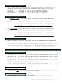
EEL Standard Procedure ---------- 002 DOCUMENT NUMBER -: DOCUMENT EDITOR -: AUTHOR ----------: DATE ------------: Esp002c.docx Office 2007 K.Bell 27 March 2012 PROTOMAT C100/HF (K045) – PCB PRODUCTION 1. INITIAL REQUIREMENTS a. Ensure the Compressor Log Sheet is up to date and all Moisture Traps are dry. The compressor shall be drained at regular intervals of no more than 7 days and the Compressor Log Sheet updated to provide a maintenance record. The Log Sheet is situated next to the compressor enclosure. b. Ensure the Protomat Maintenance Log Sheet is up to date. Depending upon the type of materials being milled, the Collet(1), Scanning Ring(2) and the Internal Thread(3) of the High Speed Spindle will require regular cleaning as per the following table:MATERIAL DUROID FR4 CLEANING REQUIREMENTS Upon Completion of Each Job Intervals of no more than 14 days (1) The Collet shall be immersed and thoroughly cleaned using SafeWash. Finally, degrease with Isopropyl Alcohol. (2) The Scanning Ring should be thoroughly cleaned using an Isowipe. Pay particular attention to the underside of this assembly! (3) The Internal Thread of the High Speed Spindle shall be thoroughly cleaned with Isopropyl Alcohol only. A brush is provided specifically for this purpose. Ensure all parts are thoroughly clean and dry then, align the keyway and carefully insert the Collet into the High Speed Spindle. The Log Sheet is situated next to the Protomat and shall be updated to provide a maintenance record. c. Switch on computer RPF00 ---------- SEE GPO’s MARKED PC, MONITOR and SPEAKERS d. Switch on Compressor and Vacuum --- SEE GPO’s MARKED COMPRESSOR and VACUUM e. Switch on Protomat and Enable Air - SEE GPO’s MARKED PROTOMAT and ENABLE AIR f. Switch on the Calibratiion Camera - SEE GPO MARKED CAMERA K081 g. Ensure Compressor regulator is set to not less than 8 Bars - See Indicator(PI-00) h. Ensure Protomat regulator is set to 7 Bars - See Indicator (PI-01) i. CAUTION! This manual has been written assuming Protel 99 SE to be the preferred CAD package. If working with Altium Designer files, please refer to the appropriate user manual for further information. j. CAUTION! This manual has been written assuming Boardmaster 4 to be the preferred software package for operating the Protomat. Boardmaster 5 has minor variations. EEL Standard Procedure 002 > Page 1 of 26 1.01 TOOL SETTINGS a. Until a much greater understanding of the milling process is acquired, it is suggested the following standard tool parameters shall apply to all tasks: UniCutter > MicroCutter > All End Mills > Set depth of cut for 08 Mil Insulation Channel Set depth of cut for 04 Mil Insulation Channel Set depth of cut to remove copper as required 1.02 FILE NAMING PROTOCOL a. All EXTERNAL CLIENT Protel Files shall be named to reflect their EEL Job#. EXAMPLES : 1. The DDB file shall have the following format : 63-499.DDB 2. PCB files shall have the following format : 63-49901a.pcb Where 63-499 is the Job#, 01 is the pcb# and a is the version b. All ETSG PROJECT Protel Files shall be named to reflect their EEL Project#. EXAMPLES : 1. The DDB file shall have the following format : A123a.DDB 2. PCB files shall have the following format : A12301a.pcb Where A123 is the Project#, 01 is the pcb# and a is the version 1.03 LOCATION OF WORKING FILES a. Before starting a job place the Protel File in [G:\RPFUser00\Protel DDB Files] It is assumed that files placed in this folder are correct and need no modification. If however, changes are required and these files are modified please ensure they transferred to your original Client Files Folder for archiving. Data files placed on RPF00 have temporary status and will eventually be deleted. 2. IMPORTANT DESIGN REQUIREMENTS 2.01 STANDARD PCB DIMENSIONS a. MAX SIZE (x,y) : A4 = 297 x 210 > Max Milling Area (Finished PCB) = 230 x 150 mm MID SIZE (x,y) : A5 = 210 x 148 > Max Milling Area (Finished PCB) = 143 x 88 mm MIN SIZE (x,y) : A6 = 148 x 105 > Max Milling Area (Finished PCB) = 45 mm 81 x The Maximum Milling Area is calculated by allowing -: X Axis > 25mm (Head Clearance) + 5.0mm (Fixing Tape) TOP & BOTTOM Y Axis > 25mm (Head Clearance) + 8.5mm (Registration Pin Clearance) LEFT & RIGHT 2.02 BORDERS a. PCB DESIGNS DO NOT REQUIRE ELECTRICAL LAYER BORDERS – May cause excessive milling 2.03 POLYGON PLANES a. POLYGON PLANES SHOULD BE FILLED NOT HATCHED – To avoid excessive milling EEL Standard Procedure 002 > Page 2 of 26 2.04 POWER PLANES a. PCB DESIGNS WHICH INCORPORATE POWER PLANES ARE NOT COMPATIBLE WITH THE CURRENT PROCESS AND SHOULD BE REPLACED WITH POLYGON PLANES – Edit Protel file as follow. Select > > [Design] ------------- Main Menu Bar [Layer Stack Manager] Select > > > [InternalPlane1] ----- Select Power Plane to be removed [InternalPlane2] [Properties] > > > > [Netname = No Net] --- Disconnects Power Plane from Net, this is [Delete] required before deletion can occur [Yes] [OK] ----------------- Removes Power Plane Select > > > [TopLayer] [BotLayer] [AddLayer] ----------- Mid Layer(n) should appear > Select > > [OK] ----------------- Escape Layer Stack Manager [Place] -------------------------- Main Menu Bar [Polygon Plane] > > > [Net Options = Select as reqd] --- Define net [Pour Over Same Net = ] ------- Required to connect vias to plane! [Remove Dead Copper = ] > > > > [Plane Settings] [Grid Size = 10mil] ---------- Nominal Selection [Track Size = 11mil] ---------- Nominal Selection [Layer = Select as reqd] > [OK]--- Place MidLayer(n) Polygon Plane on over entire PCB and connect to the appropriate net. > IMPORTANT! Ensure all pads and vias sharing the selected Net Label have been connected to the resulting Polygon Plane > Repeat until all Power Planes have been replaced with Polygon Planes 2.05 NON CONNECTED INT PADS a. DO NOT COMPLETELY REMOVE NON CONNECTED SOLDER PADS ON INNER LAYERS, CHOOSE ISOLATION MILLING, AS PRESSING WILL NOT BE EVEN AND SHORT CIRCUITS MAY OCCUR Short UNSUITABLE METHOD SATISFACTORY METHOD See K061A.MN1 Pages 29 and 30 for further information EEL Standard Procedure 002 > Page 3 of 26 3. CREATE GERBER FILES a. Start Protel and load the PCB file to be produced b. Select > > [File] [CAM Manager] --- Opens CAM Wizard c. Click [Next] ---------- To begin process > d. Select > > [Gerber] -------- Selects type of output (Gerber Selected) [Next] e. Click > [Next] ---------- Leave default name as “Gerber Output 1” f. Click > [Next] ---------- Leave embedded apertures “RS274X” g. Select > or > > [Units = Inches], [Format = 2:5] --- If PCB is in Imperial Units [Units = Millimeters], [Format = 4:4] --- If PCB is in Metric Units [Next] h. Select > > > > > > > > > > > [Top Layer = ] –-- Selection depends upon the PCB [Bot Layer = ] example in Bold Text assumes a [Mid Layer 1 = ] double sided PCB without Top & [Mid Layer 2 = ] Solder Mask. [Mid Layer 3 = ] [Mid Layer 4 = ] [Top Solder Mask = ] [Bot Solder Mask = ] [Keep Out Layer = ] –----- Always required for Cutting [Mid-layer pad option = ] –- Important! See note below [Next] design,the standard Bottom Outside For boards of 4 layers or more, checking this option ensures that non connected pads which may appear on any of the inner layers will be retained during manufacture. This requirement is critical with regard to the lamination process. It is suggested that this option remains checked for all boards unless technical requirements dictate otherwise. See Section 2c for graphical explanation. i. Select > > > [Generate Drill Drawing Plots [Generate Drill Guide Plots [Next] j. Select > > > > > [Plot used drill drawing pairs = UNCHECKED] - This menu only active [Mirror Plots = UNCHECKED] if [*] above is checked, [Graphics Symbols] indicated settings are nominal [Symbol Size = 50mils] [Next] k. Select > > > [Plot used drill guide layer pairs = UNCHECKED]- This menu only active [Mirror Plots = UNCHECKED] if [**] above is checked, [Next] indicated settings are nominal l. Select > > [Mechanicalx = UNCHECKED] --- Mechanical Layer Options [Next] m. Click [Finish] --- “Gerber Output 1” should now appear in window > = UNCHECKED] * – Nominal setting = UNCHECKED] ** – Nominal setting EEL Standard Procedure 002 > Page 4 of 26 4. CREATE NC DRILL FILE AND SET PROPERTIES a. R/Click > [Gerber Output 1] b. Select > [Insert NC Drill] c. Select > > or > [Options] [Units = Inches], [Format = 2:5] --- If PCB is in Imperial Units [Units = Millimetres], [Format = 4:4] --- If PCB is in Metric Units d. Select > > > > > [Advanced] [Keep leading and trailing zeroes] [Reference to relative origin] [Optimise change location commands = ] [OK] --- “NC Drill Output 1” should now appear in window 5. SET GERBER FILE PROPERTIES a. R/Click > [Gerber Output 1] b. Select > > > > > > > > > > > [Properties] [Advanced] [Keep leading and trailing zeroes] [Reference to relative origin] [Separate file per layer] [Sorted (vector)] [G54 on aperture change = ] [Use software arcs = ] [Optimise change location commands = ] [Leave Film Size and Aperture Matching Tolerances] [OK] c. Press [F9]--- Generates Protel CAM Files > 6. EXPORT GERBER FILES a. R/Click > > [CAM Outputs for 00-00000a.cam TAB] --- Top of Current Window [Close] a. R/Click > [CAM for 00-00000a FOLDER] --- In Protel Explorer under Document Folder c. Select > [Export] d. Path [D:\RPFUser00\Protel Output Files] --- Exported Protel CAM Files [OK] > > 7. CIRCUITCAM a. Start CircuitCAM program b. Select > [Graphic Mode Button] --- If not already in Graphic Mode c. SELECT THE APPROPRIATE TEMPLATE TO SUIT THE CURRENT PCB DESIGN > d. 2LAYER > GOTO SECTION 8 > e. 4LAYER > Select > > > > f. 6LAYER > Select > > > > ----------- CircuitCAM defaults to a 2 Layer Template [File] [New] [4Layer.cat] Configures CircuitCAM with the 4 Layer Template GOTO SECTION 8 > [File] [New] [6Layer.cat] Configures CircuitCAM with the 6 Layer Template GOTO SECTION 8 > EEL Standard Procedure 002 > Page 5 of 26 8. BOARDMASTER Always restart the Protomat between jobs or before starting new job** a. Start BoardMaster program** --- If present, ignore FIFO message 8.01 TOOL LIBRARY SELECTION a. > ENSURE THE CORRECT TOOL LIBRARY IS SELECTED FOR THE INITIAL PHASE Select fr4-100.tol for standard FR4 PCB Material Select SolderMask.tol for standard Solder Mask Material b. Select > > > > [Configuration] [Tool Library] [Mill/Drill] [Load] c. > Yes > IS THE CORRECT TOOL LIBRARY SELECTED? -- See Mill/Drill Tool Edit Menu for current library details. Select > [Cancel] Then > GOTO SECTION 8.02 > No > Select > > > 8.02 [fr4-100.tol] --- Example only, see Section 8.01a. [open] [OK] TEMPLATE SELECTION a. > SELECT THE APPROPRIATE TEMPLATE TO SUIT THE CURRENT PCB DESIGN b. 2LAYER > GOTO SECTION 9 > c. 4LAYER > Select > > > [Configuration] [Phases] [Load] Select > > > [PHASES4.PHS] -- Lookin [C:\LPKF40\BMaster\File type *.PHS] [Open] [OK] ----- Configures BoardMaster with the 4 Layer Template > d. 6LAYER > -------- BoardMaster defaults to a 2 Layer Template GOTO SECTION 9 > Select > > > [Configuration] [Phases] [Load] Select > > > [PHASES6.PHS] -- Lookin [C:\LPKF40\BMaster\File type *.PHS] [Open] [OK] ----- Configures BoardMaster with the 6 Layer Template > GOTO SECTION 9 > EEL Standard Procedure 002 > Page 6 of 26 9. IMPORT FILES – 1ST BUTTON a. Goto CircuitCAM b. ENSURE THE INSULATE SETTINGS COMPLY WITH THE FOLLOWING PARAMETERS Select > > > [Edit] [Insulate] [Main] Select > [Job] > Insulate Default Bottom --- Select Required Layer > [Tools] > > > > > [Width] > Base(All) = 0.2mm --- Auto set by Uni Cutter* IMPORTANT! > Special(Pads) = 0.2mm --- Recommended for INNER layers IMPORTANT! > Special(Pads) = 0.3mm --- Recommended for OUTER layer > [Save] > > REPEAT (9b) FOR ALL LAYERS CONTAINED IN THIS TEMPLATE [OK] Small Standard Big Bigger = = = = Micro Cutter 0.1mm (4mil) ------Universal Cutter 0.2mm (8mil)* -End Mill 1.00mm (39mil) --------End Mill 2.00mm (79mil) --------- Max Max Max Max size size size size c. Select > > [Import Button] Look in [D:\RPFUser00\Protel Output Files] d. Select > > [CAM for 6x-00000a] --- Sample Folder Only [Open] e. Select > [DRR,GKO,TXT,GBL or GTL,GBS or GTS Files] ------- For 1 Layer Board or > [DRR,GKO,TXT,GBL,GTL,GTS,GBS Files] ------------- For 2 Layer Board or > [DRR,GKO,TXT,GBL,GTL,G1,G2,GTS,GBS Files] ------- For 4 Layer Board or > [DRR,GKO,TXT,GBL,GTL,G1,G2,G3,G4,GTS,GBS Files -- For 6 Layer Board > [Open] ---- Only select GBS or GTS Files if Solder Mask is required IF A PROBLEM OCCURS AT THIS STAGE THEN ONE OF THE FOLLOWING SITUATIONS MAY APPLY: 1. THE FILE IMPORT ASSIGNMENTS ARE INCORRECTLY SET SEE DOC K045A.SM3 Page13 FOR FUTHER DETAILS 2. THE Aperture/Tool Template IS INCORRECT FOR THE JOB SEE BELOW FOR DETAILS. FOR IMPERIAL UNITS SELECT > Protel x drr Exc mil Inch 23AbsLead.txt(NCDrill) FOR METRIC UNITS SELECT > Protel 4.0 drr Exc mm Inch 43AbsLead.txt(NCDrill) (May indicate error – disregard this message!!!) 10. CONTOUR ROUTING – 2ND BUTTON a. Select > > > > > > > > [Contour Routing Button] Contour Routing = [Outside] Source = [Layer] & [Board Outline] Destination Layer = [Cutting Outside] List = [LpkfCuttingTools] Tool = [Contour Router 1.0mm (39mil) Gap Width = [1.0mm] [Run] --- Board Outline should appear around perimeter of PCB EEL Standard Procedure 002 > Page 7 of 26 11. BREAKOUT TABS – 3RD BUTTON a. > > Place cursor just outside top L/H corner of the Board Outline [Left Click Mouse] ------ Selects Board Outline b. Press > [+]/[-] to place cursor where 1st breakout tab is required Select > OR Press > Press [Breakout Tab Button] - Gap should now appear on Board Outline [Control]&[G] > Repeat this process for each breakout tab required. > [Escape] --- To Exit this process WARNING! Do not use the mouse to define breakout tabs. The board outline may be shifted by any movement of the mouse in “x” or “y” directions. 12. PLACE RUBOUT LAYER – 4TH BUTTON : OPTIONAL a. > DO YOU WISH TO PLACE RUBOUT LAYERS? No > GOTO SECTION 14 > Yes > CONTINUE > b. Select > [Rubout All Layers Button] --- Will default to All Layers c. > DO YOU WISH TO RUBOUT ALL LAYERS? Yes > GOTO 12e > No > CONTINUE > d. Select > [Rubout Layern] -- Select Active Layer from List Box e. > SELECT RUBOUT SHAPE FROM GRAPHICS TOOLBAR AS REQD - L/Hand of screen f. > > > > [Left Click Mouse] ------Define Rubout area ------[Left Click Mouse] ------[Escape][Escape] --------- > DO YOU WISH TO EDIT THE RUBOUT LAYER YOU HAVE JUST PLACED? No > GOTO SECTION 14 > Yes > CONTINUE > Press g. Start Block Define Define Area Fix Block Define Exit this process 13. EDIT RUBOUT LAYER : OPTIONAL a. > > Place cursor just outside top L/H corner of the Rubout to be edited [Left Click Mouse] ----------- Selects Defined Area b. > EDIT DEFINED AREA AS REQUIRED c. Press > [Escape][Escape] ------------- To Exit this process d. > DO YOU WISH TO PLACE ANOTHER RUBOUT LAYER? Yes > GOTO SECTION 12 > No > CONTINUE > EEL Standard Procedure 002 > Page 8 of 26 14. INSULATE MID LAYERS : OPTIONAL a. > DOES THIS PCB HAVE INTERNAL LAYERS? No > GOTO SECTION 15 > Yes > CONTINUE > b. Select > > > > [Edit] [Insulate] [InsulateLayerx] --- Select Inner Layer for insulation [Run] -------------- Calculate milling process for selected layer d. > ARE THERE MORE INTERNAL LAYERS TO INSULATE? Yes > GOTO SECTION 14b > No > CONTINUE > 15. INSULATE ALL LAYERS – 5TH BUTTON a. Select > [Insulate All Layers Button] --- Calculate milling process for Top & Bottom Layers only! 16. EXPORT FILES TO BOARDMASTER – 6TH BUTTON a. Select > SaveIn > > > [Export Button] [D:\RPFUser00\CircuitCam Output Files] [Open] [Save] --- Files saved EEL Standard Procedure 002 > Page 9 of 26 17. BOARDMASTER PROGRAM a. > Please be aware of operational differences between BM4 & BM5 Switch to BoardMaster, exported PCB should be displayed. 18. SECURING UNDERLAY AND PCB MATERIALS a. Select > > [Goto] [Pause] --- Positions Head allowing room to secure PCB and Underlay material b. Ensure bed is thoroughly clean before proceeding --- Use Isowipes > It is extremely important that the bed is dry and all traces of swarf and grease are removed before securing the Underlay and PCB materials in place. Failure to comply may result in inconsistent and poor quality results 18.01 a. UNDERLAY MATERIALS > IS THE MATERIAL TO BE MACHINED LESS THAN 1mm THICK No > GOTO 18.01b > Yes > > Clean the Underlay Support (EEL Part# K088) with an Isowipe Ensure the Underlay Support is dry then place in position This item was manufactured from Underlay Material 81-01-02 and is designed to raise the normal Underlay sheet by approx 0,6mm b. > > Clean the Underlay Material (EEL Part# 16-00-11) with an Isowipe Ensure the Underlay Material is dry then place in position ALWAYS USE NEW MATERIAL IF BOARD IS TO BE DRILLED PRIOR TO PLATING Fixing holes should be drilled in the Underlay Material using a 3,05mm dia drill in conjunction with the special Protomat Drilling Template (EEL Part# K075) provided. Open holes up to 3,10mm before fitting! NEVER ATTEMPT TO USE A 3,10mm DRILL WITH THE DRILLING TEMPLATE K075! 18.02 a. PCB MATERIALS > Select the appropriate PCB material for the project See EEL Data Sheet #7 for 2Layer PCB options See EEL Data Sheet #5 for 4Layer PCB options See EEL Data Sheet #6 for 6Layer PCB options Fixing holes should be drilled in the PCB Material using a 3,05mm dia drill in conjunction with the special Protomat Drilling Template (EEL Part# K075) provided. b. > Thoroughly clean the selected PCB material using an Isowipe. c. > Ensure PCB material is thoroughly dry then secure in position ready for machining. EEL Standard Procedure 002 > Page 10 of 26 19. POSITIONING THE PROJECT WITHIN THE WORK SPACE a. > In BoardMaster, move the project to the required position in the workspace, allowing for clearances required by the Protomat Tool Head and take into account available free space on the PCB material b. > Multiple copies of project may be placed if required 20. IMPORTANT MANUFACTURING INFORMATION a. IT HAS BEEN ESTABLISHED THAT DRILLING CAN CAUSE A BUILD UP OF DEBRIS BETWEEN THE PCB AND THE UNDERLAY MATERIAL. THIS IS ESPECIALLY NOTICEABLE IF LARGER HOLES, APPROX 3mm, ARE PRODUCED BY CONTOUR ROUTERS IN THIN OR FLEXIBLE PCB TYPES. FAILURE TO REMOVE THIS DEBRIS WILL RESULT IN UNEVEN MILLING AND POSSIBLE DAMAGE TO TOOLS. This situation is of no concern for boards which are to be plated through as they are removed from the Protomat after the drilling phase is completed. However, jobs which are to be immediately milled may need to be cleaned first. Note! The default order of the manufacturing process may be changed as a production easement (ie. Shift drilling to the final phase) if the situation permits. 21. MANUFACTURING PROCESS 21.01 TOOL CALIBRATION a. Micocutter > Calibration required upon each tool or material change. b. Unicutter > Calibration required upon each tool or material change. c. End Mill > Calibration required upon each tool or material change. d. Cont Router > Depth Setting as per Uni/Microcutter – Always Confirm Depth. e. Drill > Depth Setting as per Uni/Microcutter – Always Confirm Depth. SEE STAN PROC 001 FOR CALIBRATION PROCEDURES! EEL Standard Procedure 002 > Page 11 of 26 21.02 SELECT PCB TYPE a. 1 Layer > GOTO SECTION 22 (SINGLE LAYER MANUFACTURING PROCESS) b. 2 Layer > GOTO SECTION 23 (DOUBLE LAYER MANUFACTURING PROCESS) c. 4 Layer > GOTO SECTION 24 (FOUR LAYER MANUFACTURING PROCESS) d. 6 Layer > GOTO SECTION 25 (SIX LAYER MANUFACTURING PROCESS) EEL Standard Procedure 002 > Page 12 of 26 22. SINGLE LAYER PCB MANUFACTURING PROCESS 22.01 MARKING DRILLS a. > DO YOU WISH TO DRILL THE PCB AT THIS STAGE? No > GOTO SECTION 22.03 > Yes > CONTINUE > > Ensure Head Auto Control button is active b. c. Select > > > > [MarkingDrills] from List Box --- Selects first task [All+] [Start] Follow prompts 22.02 DRILLING a. Select > > > > [DrillingPlated] from List Box --- Selects next task [All+] [Start] Follow prompts b. REFER TO SECTION 20 > > 22.03 MILLING BOTTOM/TOP a. Select > > > > > [MillingBottom] or [MillingTop] from List Box – Depends on PCB design [All+] [Start] Follow prompts RECORD TOOL USAGE ON JOB SHEET 22.04 SOLDER MASK a. Yes No > DOES THIS PCB REQUIRE A SOLDER MASK? > GOTO SECTION 26 > > Prepare for machining as per requirements of Section 18. > GOTO SECTION 22.05 > > CONTINUE > 22.05 CUTTING OUTSIDE a. Select > > > > > [CuttingOutside] from List Box --- Selects next task [All+] [Start] Follow prompts RECORD TOOL USAGE ON JOB SHEET b. > Machining should now be complete and the PCB ready to break out. c. > GOTO SECTION 27 > EEL Standard Procedure 002 > Page 13 of 26 23. DOUBLE LAYER PCB MANUFACTURING PROCESS 23.01 a. MARKING DRILLS > DO YOU WISH TO DRILL THE PCB AT THIS STAGE? Answer “Yes” if this project requires plated thru holes or will be populated with conventional components No > GOTO SECTION 22.03 > Yes > CONTINUE > > Ensure Head Auto Control button is active b. c. Select > > > > [MarkingDrills] from List Box --- Selects first task [All+] [Start] Follow prompts 23.02 DRILLING a. Select > > > > [DrillingPlated] from List Box --- Selects next task [All+] [Start] Follow prompts b. > DOES THIS PCB REQUIRE PLATED THRU HOLES? > EXIT HERE AND PROCEED WITH PLATING PROCESS –--- See EEL Stan Proc 005 > Prepare for machining as per requirements of Section 18. > GOTO SECTION 22.03 > > REFER TO SECTION 20 AND CONTINUE > Yes No 23.03 MILLING BOTTOM a. Select > > > > > [MillingBottom] from List Box --- Selects first milling task [All+] [Start] Follow prompts RECORD TOOL USAGE ON JOB SHEET 23.04 MILLING TOP a. Select > > [Goto] [Pause] --- Positions Head allowing room to flip PCB material b. > REMOVE PCB, FLIP OVER AND SECURE AS PER REQUIREMENTS OF SECTION 18 c. > Thoroughly clean surface of PCB using Isowipe before proceeding d. Select > > > > > [MillingTop] from List Box --- Selects next milling task [All+] [Start] Follow prompts RECORD TOOL USAGE ON JOB SHEET EEL Standard Procedure 002 > Page 14 of 26 23.05 SOLDER MASK a. Yes No > DOES THIS PCB REQUIRE A SOLDER MASK? > GOTO SECTION 26 > > Prepare for machining as per requirements of Section 18. > GOTO SECTION 23.06 > > CONTINUE > 23.06 CUTTING OUTSIDE a. Select > > > > > [CuttingOutside] from List Box --- Selects next task [All+] [Start] Follow prompts RECORD TOOL USAGE ON JOB SHEET b. > Machining should now be complete and the PCB ready to break out. c. > GOTO SECTION 27 > EEL Standard Procedure 002 > Page 15 of 26 24. FOUR LAYER PCB MANUFACTURING PROCESS 24.01 INTERNAL PAIR LAYERS 2&3 a. > DO YOU WISH TO DRILL THE PCB AT THIS STAGE? Answer “Yes” if Layers 2 & 3 contain buried vias No > GOTO SECTION 24.04 > Yes > CONTINUE > 24.02 a. MARKING DRILLS > b. Select > > > > Ensure Head Auto Control button is active [MarkingDrills] from List Box --- Selects first drilling task [All+] [Start] Follow prompts 24.03 DRILLING a. Select > > > > [DrillingPlated] from List Box --- Selects next drilling task [All+] [Start] Follow prompts b. > EXIT HERE AND PROCEED WITH PLATING PROCESS –-- See EEL Stan Proc 005 c. > Prepare for machining as per requirements of Section 18. > CONTINUE > 24.04 MILLING LAYER 3 a. Select > > > > > [MillingLayer3Pos] from List Box --- Selects first milling task [All+] [Start] Follow prompts RECORD TOOL USAGE ON JOB SHEET 24.05 IDENT LAYER a. Select > > [Goto] [Pause] --- Positions Head allowing room to ident the PCB b. IDENT PCB WITH (3) CLOSE TO L/H LOCATION PIN - Use scriber or similar! > 24.06 MILLING LAYER 2 a. > REMOVE PCB, FLIP OVER AND SECURE AS PER REQUIREMENTS OF SECTION 18 b. > Thoroughly clean surface of PCB using Isowipe before proceeding c. Select > > > > > [MillingLayer2] from List Box --- Selects next milling task [All+] [Start] Follow prompts RECORD TOOL USAGE ON JOB SHEET EEL Standard Procedure 002 > Page 16 of 26 24.07 LAMINATION PROCESS a. > EXIT HERE AND PROCEED WITH LAMINATION PROCESS – See EEL Stan Proc 014 > CONTINUE > 24.08 EXTERNAL LAYERS TOP & BOT a. > Prepare for machining as per requirements of Section 18. NOTE! The PCB should be placed with the ident (3) facing up! 24.09 a. MARKING DRILLS > b. Select > > > > Ensure Head Auto Control button is active [MarkingDrills] from List Box --- Selects first drilling task [All+] [Start] Follow prompts 24.10 DRILLING a. Select > > > > [DrillingPlated] from List Box --- Selects next drilling task [All+] [Start] Follow prompts b. > DOES THIS PCB REQUIRE PLATED THRU HOLES? > EXIT HERE AND PROCEED WITH PLATING PROCESS –-- See EEL Stan Proc 005 > Prepare for machining as per requirements of Section 18. > GOTO SECTION 24.11 > > REFER TO SECTION 20 AND CONTINUE > Yes No 24.11 MILLING BOTTOM a. Select > > > > > [MillingBottom] from List Box --- Selects first milling task [All+] [Start] Follow prompts RECORD TOOL USAGE ON JOB SHEET 24.12 MILLING TOP a. Select > > [Goto] [Pause] --- Positions Head allowing room to flip PCB material b. > REMOVE PCB, FLIP OVER AND SECURE AS PER REQUIREMENTS OF SECTION 18 c. > Thoroughly clean surface of PCB using Isowipe before proceeding d. Select > > > > > [MillingTop] from List Box --- Selects next milling task [All+] [Start] Follow prompts RECORD TOOL USAGE ON JOB SHEET EEL Standard Procedure 002 > Page 17 of 26 24.13 SOLDER MASK a. Yes No > DOES THIS PCB REQUIRE A SOLDER MASK? > GOTO SECTION 26 > > Prepare for machining as per requirements of Section 18. > GOTO SECTION 24.14 > > CONTINUE > 24.14 CUTTING OUTSIDE a. Select > > > > > [CuttingOutside] from List Box --- Selects next task [All+] [Start] Follow prompts RECORD TOOL USAGE ON JOB SHEET b. > Machining should now be complete and the PCB ready to break out. c. > GOTO SECTION 27 > EEL Standard Procedure 002 > Page 18 of 26 25. SIX LAYER PCB MANUFACTURING PROCESS 25.01 INTERNAL PAIR LAYERS 3&4 a. > DO YOU WISH TO DRILL THE PCB AT THIS STAGE? Answer “Yes” if Layers 3 & 4 contain buried vias No > GOTO SECTION 25.04 > Yes > CONTINUE > 25.02 a. MARKING DRILLS > b. Select > > > > Ensure Head Auto Control button is active [MarkingDrills] from List Box --- Selects first drilling task [All+] [Start] Follow prompts 25.03 DRILLING a. Select > > > > [DrillingPlated] from List Box --- Selects next drilling task [All+] [Start] Follow prompts b. > EXIT HERE AND PROCEED WITH PLATING PROCESS –-- See EEL Stan Proc 005 c. > Prepare for machining as per requirements of Section 18. > CONTINUE > 25.04 MILLING LAYER 4 a. Select > Select > > > > > [MillingLayer4Pos] [for BM4 Only] from List Box --- First milling task [MillingLayer3Pos] [for BM5 Only] from List Box --- First milling task [All+] [Start] Follow prompts RECORD TOOL USAGE ON JOB SHEET 25.05 IDENT LAYER a. Select > > [Goto] [Pause] --- Positions Head allowing room to ident the PCB b. IDENT PCB WITH (4) CLOSE TO L/H LOCATION PIN - Use scriber or similar! > 25.06 MILLING LAYER 3 a. > REMOVE PCB, FLIP OVER AND SECURE AS PER REQUIREMENTS OF SECTION 18 b. > Thoroughly clean surface of PCB using Isowipe before proceeding c. Select > Select > > > > > [MillingLayer3Pos] [for BM4 Only] from List Box --- First milling task [MillingLayer4Pos] [for BM5 Only] from List Box --- First milling task [All+] [Start] Follow prompts RECORD TOOL USAGE ON JOB SHEET EEL Standard Procedure 002 > Page 19 of 26 25.07 LAMINATION PROCESS a. > EXIT HERE AND PROCEED WITH LAMINATION PROCESS – See EEL Stan Proc 014 > CONTINUE > 25.08 INTERNAL PAIR LAYERS 2&5 a. > Prepare for machining as per requirements of Section 18. b. > DO YOU WISH TO DRILL THE PCB AT THIS STAGE? Answer “Yes” if Layers 2 thru to 5 contain buried vias No > GOTO SECTION 25.11 > Yes > CONTINUE > 25.09 a. MARKING DRILLS > b. Select > > > > Ensure Head Auto Control button is active [MarkingDrills] from List Box --- Selects first drilling task [All+] [Start] Follow prompts 25.10 DRILLING a. Select > > > > [DrillingPlated] from List Box --- Selects next drilling task [All+] [Start] Follow prompts b. > EXIT HERE AND PROCEED WITH PLATING PROCESS –-- See EEL Stan Proc 005 c. > Prepare for machining as per requirements of Section 18. > CONTINUE > 25.11 MILLING LAYER 5 a. Select > > > > > [MillingLayer5Pos] from List Box --- Selects first milling task [All+] [Start] Follow prompts RECORD TOOL USAGE ON JOB SHEET 25.12 IDENT LAYER a. Select > > [Goto] [Pause] --- Positions Head allowing room to ident the PCB b. IDENT PCB WITH (5) NEAR L/H LOCATION PIN - Use scriber or similar! > 25.13 MILLING LAYER 2 a. > REMOVE PCB, FLIP OVER AND SECURE AS PER REQUIREMENTS OF SECTION 18 b. > Thoroughly clean surface of PCB using Isowipe before proceeding c. Select > > > > > [MillingLayer2] from List Box --- Selects next milling task [All+] [Start] Follow prompts RECORD TOOL USAGE ON JOB SHEET EEL Standard Procedure 002 > Page 20 of 26 25.14 LAMINATION PROCESS a. > EXIT HERE AND PROCEED WITH LAMINATION PROCESS – See EEL Stan Proc 014 > Wait 24Hrs before continuing! > CONTINUE > 25.15 EXTERNAL LAYERS TOP & BOT a. > Prepare for machining as per requirements of Section 18. NOTE! The PCB should be placed with the idents (3)&(5) facing up! 25.16 a. MARKING DRILLS > b. Select > > > > Ensure Head Auto Control button is active [MarkingDrills] from List Box --- Selects first drilling task [All+] [Start] Follow prompts 25.17 DRILLING a. Select > > > > [DrillingPlated] from List Box --- Selects next drilling task [All+] [Start] Follow prompts b. > DOES THIS PCB REQUIRE PLATED THRU HOLES? > EXIT HERE AND PROCEED WITH PLATING PROCESS –-- See EEL Stan Proc 005 > Prepare for machining as per requirements of Section 18. > GOTO SECTION 25.18 > > REFER TO SECTION 20 AND CONTINUE > Yes No 25.18 MILLING BOTTOM a. Select > > > > > [MillingBottom] from List Box --- Selects first milling task [All+] [Start] Follow prompts RECORD TOOL USAGE ON JOB SHEET 25.19 MILLING TOP a. Select > > [Goto] [Pause] --- Positions Head allowing room to flip PCB material b. > REMOVE PCB, FLIP OVER AND SECURE AS PER REQUIREMENTS OF SECTION 18 c. > Thoroughly clean surface of PCB using Isowipe before proceeding d. Select > > > > > [MillingTop] from List Box --- Selects next milling task [All+] [Start] Follow prompts RECORD TOOL USAGE ON JOB SHEET EEL Standard Procedure 002 > Page 21 of 26 25.20 SOLDER MASK a. Yes No > DOES THIS PCB REQUIRE A SOLDER MASK? > GOTO SECTION 26 > > Prepare for machining as per requirements of Section 18. > GOTO SECTION 25.21 > > CONTINUE > 25.21 CUTTING OUTSIDE a. Select > > > > > [CuttingOutside] from List Box --- Selects next task [All+] [Start] Follow prompts RECORD TOOL USAGE ON JOB SHEET b. > Machining should now be complete and the PCB ready to break out. c. > GOTO SECTION 27 > EEL Standard Procedure 002 > Page 22 of 26 26. SOLDER MASK PRODUCTION USING THE PROTOMAT a. Select > > [Goto] [Pause] --- Positions Head allowing room to remove PCB and fix Solder Mask material b. Carefully remove PCB from Protomat bed leaving Underlay Material in place c. Thoroughly clean bed and Underlay Material --- Use Isowipes d. Select > [SolderMask.tol] --- Solder Mask Tool Library, see Section 8.01 26.01 TOP SOLDER MASK a. Do you require a Top Solder Mask No > GOTO SECTION 26.05 > Yes > CONTINUE > 26.02 PREPARE UNDERLAY a. Place an extra sheet of Underlay Material (EEL Part# 16-00-11) on top of the original Underlay and clean with an isowipe. ALWAYS USE NEW MATERIAL IF SOLDER MASK FOIL IS TO BE MILLED If less than A4, cut the material to match the size of existing Underlay Fixing holes should be drilled in the Underlay Material using a 3,05mm dia drill in conjunction with the special Protomat Drilling Template (EEL Part# K075) provided. In order to maintain accurate registration do not increase holes to 3,10mm 26.03 PREPARE SOLDER MASK FOIL a. Carefully cut the Solder Mask Foil (EEL Part# 71-02-01) to size. The material should be cut at least 28mm larger than the PCB layout on all sides to allow for milling head clearance and fixing requirements. b. Gently warm the adhesive side of the Solder Mask material using a hot air gun. c. Carefully place the Solder Mask Foil, matt side down on the Underlay Material ensuring the material is flat and completely free from trapped air bubbles. Being careful not to scratch the Solder Mask, use a soft cloth or tissue to gently tease out trapped air. d. Secure the Solder Mask material on all sides using adhesive tape. In order to allow for sufficient milling head clearance, the adhesive tape should overlap the solder mask material by no more than 3mm. EEL Standard Procedure 002 > Page 23 of 26 26.04 MILLING TOP SOLDER MASK a. Select > > > > > [CuttingSoldStopTop] from List Box --- Selects first milling task [All+] [Start] Follow prompts RECORD TOOL USAGE ON JOB SHEET b. Select > > [Goto] [Pause] -- Positions Head allowing room to remove Solder Mask Foil c. Carefully remove Solder Mask Foil and place in safe location > 26.05 BOTTOM SOLDER MASK a. Do you require a Bottom Solder Mask No > GOTO SECTION 26.09 > Yes > CONTINUE > 26.06 PREPARE UNDERLAY a. Place an extra sheet of Underlay Material (EEL Part# 16-00-11) on top of the original Underlay and clean with an isowipe. ALWAYS USE NEW MATERIAL IF SOLDER MASK FOIL IS TO BE MILLED If less than A4, cut the material to match the size of existing Underlay Fixing holes should be drilled in the Underlay Material using a 3,05mm dia drill in conjunction with the special Protomat Drilling Template (EEL Part# K075) provided. In order to maintain accurate registration do not increase holes to 3,10mm 26.07 PREPARE SOLDER MASK FOIL a. Carefully cut the Solder Mask Foil (EEL Part# 71-02-01) to size. The material should be cut at least 28mm larger than the PCB layout on all sides to allow for milling head clearance and fixing requirements. b. Gently warm the adhesive side of the Solder Mask material using a hot air gun. c. Carefully place the Solder Mask Foil, matt side down on the Underlay Material ensuring the material is flat and completely free from trapped air bubbles. Being careful not to scratch the Solder Mask, use a soft cloth or tissue to gently tease out trapped air. d. Secure the Solder Mask material on all sides using adhesive tape. In order to allow for sufficient milling head clearance, the adhesive tape should overlap the solder mask material by no more than 3mm. EEL Standard Procedure 002 > Page 24 of 26 26.08 MILLING BOT SOLDER MASK a. Select > > > > > [CuttingSoldStopBottom] from List Box --- Selects first milling task [All+] [Start] Follow prompts RECORD TOOL USAGE ON JOB SHEET b. Select > > [Goto] [Pause] -- Positions Head allowing room to remove Solder Mask Foil c. Carefully remove Solder Mask Foil and place in safe location > 26.09 LAMINATION PROCESS a. > EXIT HERE AND PROCEED WITH LAMINATION PROCESS –-- See EEL Stan Proc 013 > CONTINUE > 26.10 CUTTING OUTSIDE a. > Prepare for machining as per requirements of Section 18. b. Select > [fr4-100.tol] --- FR4 PCB Tool Library, see Section 8.01 c. > Return to the appropriate PCB manufacturing process. > > > > GOTO GOTO GOTO GOTO 1 2 4 6 Lyr Lyr Lyr Lyr Section Section Section Section 22.05 23.06 24.14 25.21 > > > > 27. FINAL PROTOMAT REQUIREMENTS a. Remove remaining PCB material from the Protomat. If considered suitable for further PCB production, ident the material with it’s EEL Part# and place in the CURRENT MATERIAL storage area Ident remaining PCB using permanent marker or similar! c. THOROUGHLY CLEAN THE PROTOMAT AND SURROUNDING WORK AREA. d. RETURN ALL TOOLS TO THEIR STORAGE AREAS. 28. FINAL PCB REQUIREMENTS a. Does this PCB have a Solder Mask? Yes > GOTO SECTION 28.01 > No > GOTO SECTION 28.02 > 28.01 PCB WITH SOLDER MASK a. Either > Spray PCB using Clear Printed Circuit Lacquer (EEL Part# 30-06-01). Will protect exposed copper pads from oxidisation Or > Leave untreated. Depends upon Technical Instructions EEL Standard Procedure 002 > Page 25 of 26 28.02 PCB WITHOUT SOLDER MASK a. Carefully clean the PCB using Scotchbright (EEL Part# 21-03-01). b. Rinse with water. c. Thoroughly dry the PCB using clean compressed air. e. Using a magnifying glass, check for cleanliness. d. Finally, degrease using an isowipe. e. FROM NOW ON HANDLE THE PCB BY IT’S EDGES ONLY! f. Either > Or > Spray PCB using Clear Printed Circuit Lacquer (EEL Part# 30-06-01). Leave untreated. Depends upon Technical Instructions EEL Standard Procedure 002 > Page 26 of 26