1
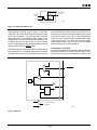
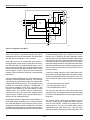
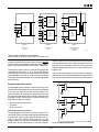
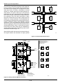
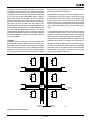
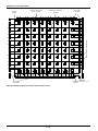
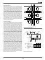
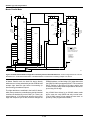
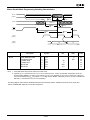
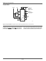
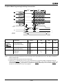
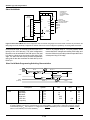
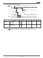
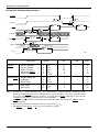
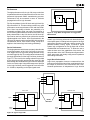
XC2000 Logic Cell Array Families Table of Contents Overview .............................................................. 2-186 XC2000 Logic Cell Array Families ........................ 2-187 Architecture ...................................................... 2-187 Programmable Interconnect ............................. 2-191 Crystal Oscillator .............................................. 2-195 Programming ................................................... 2-196 Special Configuration Functions ...................... 2-199 Master Serial Mode .......................................... 2-200 Master Serial Mode Programming Switching Characteristics ............................. 2-201 Master Parallel Mode ....................................... 2-202 Master Parallel Mode Programming Switching Characteristics ............................. 2-203 Peripheral Mode ............................................... 2-204 Peripheral Mode Programming Switching Characteristics ............................. 2-205 Slave Serial Mode ............................................ 2-206 Slave Serial Mode Programming Switching Characteristics ............................. 2-206 Program Readback Switching Characteristics ............................................. 2-207 General LCA Switching Characteristics ........... 2-208 Performance .................................................... 2-209 Power ............................................................... 2-210 Pin Descriptions ............................................... 2-212 Configuration Pin Assignments ........................ 2-214 Component Availability..................................... 2-216 Ordering Information ........................................ 2-216 XC2000 Logic Cell Array Family ........................... 2-217 Absolute Maximum Ratings ............................. 2-218 Operating Conditions ....................................... 2-218 DC Characteristics ........................................... 2-219 CLB Switching Characteristic Guidelines ......... 2-220 IOB Switching Characteristic Guidelines .......... 2-222 XC2000L Low-Voltage Logic Cell Array Family .... 2-223 Absolute Maximum Ratings ............................. 2-224 Operating Conditions ....................................... 2-224 DC Characteristics ........................................... 2-225 CLB Switching Characteristic Guidelines ......... 2-226 IOB Switching Characteristic Guidelines .......... 2-228 2-185 XC2000 Logic Cell Array Families Overview Introduced in 1985, the XC2000 family has seen continuously increasing sales for 8 years. In 1993, Xilinx introduced the ZERO+ Family of 3.3 V devices, intended for the fast growing market of battery-operated portable computers and instruments. While the XC3000/XC3100 families offer more speed, a wider range of device capacities and more packaging options, and the XC4000 family offers more advanced systems features, the XC2064 and XC2018 are the world’s lowest cost FPGAs, and they remain the most economical solution for all applications where the XC3020 or XC4002A features are not required. 2-186 XC2000 Logic Cell Array Families Product Description Features • Fully Field-Programmable: – I/O functions – Digital logic functions – Interconnections • General-purpose array architecture • Complete user control of design cycle • Compatible arrays with logic cell complexity equiva- Device VCC XC2064 XC2064L XC2018 XC2018L 5.0 V 3.3 V 5.0 V 3.3 V Typ. Logic Capacity (gates) 600 – 1,000 600 – 1,000 1,000 - 1,500 1,000 - 1,500 CLBs User I/O Max Config. bits 64 64 100 100 58 58 74 74 12,038 12,038 17,878 17,878 The XC2000 family operates with a nominal 5.0 V supply. The XC2000L family operates with nominal 3.3 V supply. lent from 600 to 1,500 gates • • • • • • • The LCA logic functions and interconnections are determined by data stored in internal static-memory cells. Onchip logic provides for automatic loading of configuration data at power-up. The program data can reside in an EEPROM, EPROM or ROM on the circuit board or on a floppy disk or hard disk. The program can be loaded in a number of modes to accommodate various system requirements. Available in 5-V and 3.3-V versions 100% factory tested Selectable configuration modes Low-power, CMOS, static-memory technology Performance equivalent to TTL SSI/MSI TTL or CMOS input thresholds Architecture Complete development system support – XACT Design Editor – Schematic Entry – Macro Library – Timing Calculator – Logic and Timing Simulator – Auto Place / Route Description The Logic Cell Array (LCA) is a high density CMOS integrated circuit. Its user-programmable array architecture is made up of three types of configurable elements: Input/Output Blocks, logic blocks and Interconnect. The designer can define individual I/O blocks for interface to external circuitry, define logic blocks to implement logic functions and define interconnection networks to compose larger scale logic functions. The XACT Development System provides interactive graphic design capture and automatic routing. Both logic simulation and in-circuit emulation are available for design verification. The Logic Cell Array is available in a variety of logic capacities, package styles, temperature ranges and speed grades. The general structure of a Logic Cell Array is shown in Figure 1. The elements of the array include three categories of user programmable elements: I/O Blocks (IOBs), Configurable Logic Blocks (CLBs) and Programmable Interconnections. The I/OBs provide an interface between the logic array and the device package pins. The CLBs perform user-specified logic functions, and the interconnect resources are programmed to form networks that carry logic signals among the blocks. LCA configuration is established through a distributed array of memory cells.The XACT development system generates the program used to configure the Logic Cell Array which includes logic to implement automatic configuration. Configuration Memory The configuration of the Logic Cell Array is established by programming memory cells which determine the logic functions and interconnections. The memory loading process is independent of the user logic functions. 2-187 XC2000 Logic Cell Array Families The static memory cell used for the configuration memory in the Logic Cell Array has been designed specifically for high reliability and noise immunity. Based on this design, which has been patented, integrity of the LCA configuration memory is assured even under adverse conditions. Compared with other programming alternatives, static memory provides the best combination of high density, high performance, high reliability and comprehensive testability. As shown in Figure 2, the basic memory cell consists of two CMOS inverters plus a pass transistor used for writing data to the cell. The cell is only written during configuration and only read during readback. During normal operation the pass transistor is off and does not affect the stability of the cell. This is quite different from the normal operation of conventional memory devices, in which the cells are continuously read and rewritten. affected by extreme power supply excursions or very high levels of alpha particle radiation. In reliability testing no soft errors have been observed, even in the presence of very high doses of alpha radiation. Input/Output Block Each user-configurable I/O block (IOB) provides an interface between the external package pin of the device and the internal logic. Each I/O block includes a programmable input path and a programmable output buffer. It also provides input clamping diodes to provide protection from electro-static damage, and circuits to protect the LCA from latch-up due to input currents. Figure 3 shows the general structure of the I/O block. The input buffer portion of each I/O block provides threshold detection to translate external signals applied to the package pin to internal logic levels. The input buffer threshold of the I/O blocks can be programmed to be compatible with either TTL (1.4 V) or CMOS (2.2 V) levels. The buffered input signal drives both the data input of an The outputs Q and Q control pass-transistor gates directly. The absence of sense amplifiers and the output capacitive load provide additional stability to the cell. Due to the structure of the configuration memory cells, they are not I/O Block Configurable Logic Block Interconnect Area X5418 Figure 1. Logic Cell Array Structure 2-188 Q Q Read or Write Configuration Control Data X5382 Figure 2. Configuration Memory Cell edge-triggered D flip-flop and one input of a two-input multiplexer. The output of the flip-flop provides the other input to the multiplexer. The user can select either the direct input path or the registered input, based on the content of the memory cell controlling the multiplexer. The I/O Blocks along each edge of the die share common clocks. The flip-flops are reset during configuration as well as by the active-low chip RESET input. block output buffer. Each I/O block output buffer is controlled by the contents of two configuration memory cells which turn the buffer ON or OFF or select 3-state buffer control. The user may also select the output buffer 3-state control (I/O block pin TS). When this I/O block output control signal is High (a logic one), the buffer is disabled and the package pin is high-impedance. Output buffers in the I/O blocks provide 4-mA drive for high fan-out CMOS or TTL-compatible signal levels. The output data (driving I/O block pin O) is the data source for the I/O Configurable Logic Block An array of Configurable Logic Blocks (CLBs) provides the functional elements from which the user’s logic is constructed. The logic blocks are arranged in a matrix in the Off TS (Output Enable) On Out Pin In D Q I/O Clock = Program-Controlled Multiplexer X5398 Figure 3. I/O Block 2-189 XC2000 Logic Cell Array Families X Outputs A G B Inputs C Y Comb. Logic D F S D Q K R K Clock X5399 Figure 4. Configurable Logic Block center of the device. The XC2064 has 64 such blocks arranged in an 8-row by 8-column matrix. The XC2018 has 100 logic blocks arranged in a 10 by 10 matrix. Each logic block has a combinatorial logic section, a storage element, and an internal routing and control section. Each CLB has four general-purpose inputs: A, B, C and D; and a special clock input (K), which may be driven from the interconnect adjacent to the block. Each CLB also has two outputs, X and Y, which may drive interconnect networks. Figure 4 shows the resources of a Configurable Logic Block. The logic block combinatorial logic uses a table look-up memory to implement Boolean functions. This technique can generate any logic function of up to four variables with a high speed sixteen-bit memory. The propagation delay through the combinatorial network is independent of the function generated. Each block can perform any function of four variables or any two functions of three variables each. The variables may be selected from among the four inputs and the block’s storage element output Q. Figure 5 shows various options which may be specified for the combinatorial logic. If the single 4-variable configuration is selected (Option 1), the F and G outputs are identical. If the 2-function alternative is selected (Option 2), logic functions F and G may be independent functions of three variables each. The three variables can be selected from among the four logic block inputs and the storage element output Q. A third form of the combinatorial logic (Option 3) is a special case of the 2function form in which the B input dynamically selects between the two function tables providing a single merged logic function output. This dynamic selection allows some 5-variable functions to be generated from the four block inputs and storage element Q. Combinatorial functions are restricted in that one may not use both its storage element output Q and the input variable of the logic block pin “D” in the same function. If used, the storage element in each Configurable Logic Block (Figure 6) can be programmed to be either an edgesensitive “D” type flip-flop or a level-sensitive “D” latch. The clock or enable for each storage element can be selected from: • The special-purpose clock input K • The general-purpose input C • The combinatorial function G The user may also select the clock active sense within each logic block. This programmable inversion eliminates the need to route both phases of a clock signal throughout the device. The storage element data input is supplied from the function F output of the combinatorial logic. Asynchronous SET and RESET controls are provided for each storage element. The user may enable these controls independently and select their source. They are active High inputs and the asynchronous reset is dominant. The 2-190 B A A B F A Any Function of 3 Variables C C D Any Function of 4 Variables B C M U X Q A A B G F D Q D Any Function of 3 Variables F Any Function of 3 Variables C Q Any Function of 3 Variables G C D G D Q Q Option 1 Option 2 Option 3 1 Function of 4 Variables 2 Functions of 3 Variables Dynamic Selection of 2 Functions of 3 Variables X5393 Figure 5. CLB Combinatorial Logic Options Note: Variables D and Q can not be used in the same function. storage elements are reset by the active-Low chip RESET pin as well as by the initialization phase preceding configuration. If the storage element is not used, it is disabled. The two block outputs, X and Y, can be driven by either the combinatorial functions, F or G, or the storage element output Q (Figure 4). Selection of the outputs is completely interchangeable and may be made to optimize routing efficiencies of the networks interconnecting the logic blocks and I/O blocks. switching matrices are provided to allow interconnections of metal segments from the adjoining rows and columns. Switches in the switch matrices and on block outputs are specially designed transistors, each controlled by a configuration bit. Logic-block output switches provide contacts to adjacent general interconnect segments and therefore to the switching matrix at each end of those segments. A switch matrix Programmable Interconnect A F Programmable interconnection resources in the Logic Cell Array provide routing paths to connect inputs and outputs of the I/O and logic blocks into desired networks. All interconnections are composed of metal segments, with programmable switching points provided to implement the necessary routing. Three types of resources accommodate different types of networks. F SET D Q K C • General purpose interconnect • Longlines • Direct connection G RES D General-Purpose Interconnect General-purpose interconnect, as shown in Figure 7a, is composed of four horizontal metal segments between the rows and five vertical metal segments between the columns of logic and I/O blocks. Each segment is only the height or width of a logic block. Where these segments would cross at the intersections of rows and columns, G Figure 6. CLB Storage Elememt 2-191 X5400 XC2000 Logic Cell Array Families can connect an interconnect segment to other segments to form a network. Figure 7a shows the general interconnect used to route a signal from one logic block to three other logic blocks. As shown, combinations of closed switches in a switch matrix allow multiple branches for each network. The inputs of the logic or I/O blocks are multiplexers that can be programmed with configuration bits to select an input network from the adjacent interconnect segments. Since the switch connections to block inputs are unidirectional (as are block outputs) they are usable only for input connection. The development system software provides automatic routing of these interconnections. Interactive routing is also available for design optimization. This is accomplished by selecting a network and then toggling the states of the interconnect points by selecting them with the “mouse”. In this mode, the connections through the switch matrix may be established by selecting pairs of matrix pins. The switching matrix combinations are indicated in Figure 7b. CLB CLB Switch Matrix See Fig. 7b A B CLB C K X CLB Y D Switch Matrix CLB CLB Special buffers within the interconnect area provide periodic signal isolation and restoration for higher general X5401 Figure 7a. General-Purpose Interconnect 2 Vertical Long Lines Available Programmable Switch Matrix Interconnections of General Interconnect Segments by Pin Global Net 8 1 2 7 Switch Matrices 8 6 5 1 2 7 a b c k X d Y a 8 d 6 5 1 2 6 5 1 2 6 5 7 4 Horizontal General Purpose Interconnect 8 7 Horizontal Long Line 5 Vertical General Purpose Interconnects Between Switch Matrics Programmable Interconnect Points (Do Not Use More Than One Per Input Pin) Figure 7b. Routing and Switch Matrix Connections 2-192 3 8 4 7 3 8 4 7 3 8 4 7 3 8 4 7 1 2 3 4 6 5 1 2 3 4 6 5 1 2 6 5 1 2 6 5 3 4 3 4 X3175 interconnect fan-out and better performance. The repowering buffers are bidirectional, since signals must be able to propagate in either direction on a general interconnect segment. Direction controls are automatically established by the Logic Cell Array development system software. Repowering buffers are provided only for the generalpurpose interconnect since the direct and Longline resources do not exhibit the same R-C delay accumulation. The Logic Cell Array is divided into nine sections with buffers automatically provided for general interconnect at the boundaries of these sections. These boundaries can be viewed with the development system. For routing within a section, no buffers are used. The delay calculator of the XACT development system automatically calculates and displays the block, interconnect and buffer delays for any selected paths. Longlines Longlines, shown in Figure 8a, run both vertically and horizontally the height or width of the interconnect area. Each vertical interconnection column has two Longlines; each horizontal row has one, with an additional Longline adjacent to each set of I/O blocks. The Longlines bypass the switch matrices and are intended primarily for signals that must travel a long distance or must have minimum skew among multiple destinations. A global buffer in the Logic Cell Array is available to drive a single signal to all B and K inputs of logic blocks. Using the global buffer for a clock provides a very low skew, high fan-out synchronized clock for use at any or all of the logic blocks. At each block, a configuration bit for the K input to the block can select this global line as the storage element clock signal. Alternatively, other clock sources can be used. A second buffer below the bottom row of the array drives a horizontal Longline which, in turn, can drive a vertical Longline in each interconnection column. This alternate buffer also has low skew and high fan-out capability. The network formed by this alternate buffer’s Longlines can be selected to drive the B, C or K inputs of the logic blocks. Alternatively, these Longlines can be driven by a logic or I/O block on a column by column basis. This capability provides a common, low-skew clock or control line within each column of logic blocks. Interconnections of these Longlines are shown in Figure 8b. CLB CLB Switch Matrix A B CLB C K X CLB Y D Switch Matrix Horizontal Long Lines CLB CLB Two Vertical Long Lines Global Long Lines Figure 8a. Longline Interconnect 2-193 X5402 XC2000 Logic Cell Array Families VERTICAL LONG LINES (2 PER COLUMN) GLOBAL BUFFER P9 P8 P7 P6 P5 P4 I/O CLOCKS (1 PER EDGE) HORIZONTAL LONG LINES (1 PER ROW) P3 P2 GND P68 P67 P66 P65 P64 P63 P62 P61 P W R AA AB AC AD AE AF AG AH P 5 9 P 1 1 P 1 2 BA BB BC BD BE BF BG P 5 8 BH P 5 7 P 1 3 P 1 4 CA CB CC CD CE CF CG P 5 6 CH P 1 6 DA DB DC DD DE DF DG P 5 4 DH P 5 3 P 1 7 V C C EA EB EC ED EE EF EG V C C EH P 5 1 P 1 9 P 2 0 FA FB FC FD FE FF FG P 5 0 FH P 4 9 P 2 1 P 2 2 GA GB GC GD GE GF GG GH I/O BLOCK DIRECT INTERCONNECT P 5 5 P 1 5 P 4 8 P 4 7 P 2 3 P 2 4 HA HB HC HD HE HF HG P 4 6 HH M 1 R M 0 R C C L O P P27 P28 P29 P30 P31 P32 P33 P34 GND P36 P37 P38 P39 P40 P41 P42 P43 R S T ALTERNATE OSCILLATOR AMPLIFIER BUFFER I/O CLOCKS (1 PER EDGE) Figure 8b. XC2064 Longlines, I/O Clocks, I/O Direct Interconnect 2-194 X1205 Direct Interconnect Direct interconnect, shown in Figure 9, provides the most efficient implementation of networks between adjacent logic or I/O blocks. Signals routed from block to block by means of direct interconnect exhibit minimum interconnect propagation and use minimum interconnect resources. For each Configurable Logic Block, the X output may be connected directly to the C or D inputs of the CLB above and to the A or B inputs of the CLB below it. The Y output can use direct interconnect to drive the B input of the block immediately to its right. Where logic blocks are adjacent to I/O blocks, direct connect is provided to the I/O block input (I) on the left edge of the die, the output (O) on the right edge, or both on I/O blocks at the top and bottom of the die. Direct interconnections of I/O blocks with CLBs are shown in Figure 8b. CLB CLB Switch Matrix A B CLB C K X CLB Y D Direct Interconnect Switch Matrix Crystal Oscillator CLB Figure 8b also shows the location of an internal high speed inverting amplifier which may be used to implement an onchip crystal oscillator. It is associated with the auxiliary buffer in the lower right corner of the die. When the oscillator is configured by MAKEBITS and connected as a signal source, two special user IOBs are also configured to connect the oscillator amplifier with external crystal oscillator components as shown in Figure10. The oscillator circuit becomes active early in the configuration process in order to allow the oscillator to stabilize. Actual internal connection is delayed until completion of configuration. In Figure 10, the feedback resistor R1, between the output and input, biases the amplifier at threshold. The inversion of the amplifier, together with the R-C networks and an ATcut series resonant crystal, produce the 360-degree phase shift of the Pierce oscillator. A series resistor R2 may be included to add to the amplifier output impedance when needed for phase-shift control, crystal resistance matching, or to limit the amplifier input swing to control clipping at large amplitudes. Excess feedback voltage may be corrected by the ratio of C2/C1. The amplifier is designed to be used from 1 MHz to about one-half the specified CLB toggle frequency. Use at frequencies below 1 MHz may require individual characterization with respect to a series resistance. Crystal oscillators above 20 MHz generally require a crystal which operates in a third overtone mode, where the fundamental frequency must be suppressed by an inductor across C2, turning this parallel resonant circuit to double the fundamental crystal frequency, i.e., 2/3 of the desired third harmonic frequency network. When the oscillator inverter is not used, these IOBs and their package pins are available for general user I/O. CLB X5403 Figure 9. Direct Interconnect On-Chip External Alternate Clock Buffer XTAL1 XTAL2 (IN) R1 R2 C1 Y1 Suggested Component Values R1 0.5 - 1 MΩ R2 0 - 1 kΩ (may be required for low frequency, phase shift and/or compensation level for crystal Q) C1, C2 10 - 40 pF Y1 1 - 20 MHz AT cut series resonant Figure 10. Crystal Oscillator 2-195 C2 48 DIP 68 PLCC 68 PGA 84 PLCC 84 PGA XTAL1 33 46 J10 56 K11 XTAL2 30 43 L10 53 L11 X5404 XC2000 Logic Cell Array Families Programming signalled by the release of the DONE / PROG pin of the device as the device begins operation. This open-drain output can be AND-tied with multiple Logic Cell Arrays and used as an active-High READY or active-Low , RESET, to other portions of the system. High during configuration (HDC) and low during configuration (LDC), are released one CCLK cycle before DONE is asserted. In master mode configurations, it is convenient to use LDC as an activeLow EPROM chip enable. Table 1. Configuration Mode Selection M0 M1 M2 CCLK 0 0 0 0 0 0 1 1 0 1 0 1 output output — output 1 1 1 1 0 0 1 1 0 1 0 1 — output — input Mode Data Master Master reserved Master Bit Serial Byte Wide Addr. = 0000 up — Byte Wide Addr. = FFFF down reserved — Peripheral Bit Serial reserved — Slave Bit Serial Configuration data to define the function and interconnection within a Logic Cell Array are loaded automatically at power-up or upon command. Several methods of automatically loading the required data are designed into the Logic Cell Array and are determined by logic levels applied to mode selection pins at configuration time. The form of the data may be either serial or parallel, depending on the configuration mode. The programming data are independent of the configuration mode selected. The state diagram of Figure 11 illustrates the configuration process. Input thresholds for user I/O pins can be selected to be either TTL-compatible or CMOS-compatible. At power-up, all inputs are TTL-compatible and remain in that state until the LCA begins operation. If the user has selected CMOS compatibility, the input thresholds are changed to CMOS levels during configuration. Figure 12 shows the specific data arrangement for the XC2064 device. Future products will use the same data format to maintain compatibility between different devices of the Xilinx product line, but they will have different sizes and numbers of data frames. For the XC2064, configuration requires 12,038 bits for each device. For the XC2018, the configuration of each device requires 17,878 bits. The XC2064 uses 160 configuration data frames and the XC2018 uses 197. The configuration bit stream begins with preamble bits, a preamble code and a length count. The length count is loaded into the control logic of the Logic Cell Array and is used to determine the completion of the configuration process. When configuration is initiated, a 24-bit length counter is set to 0 and begins to count the total number of configuration clock cycles applied to the device. When the current length count equals the loaded length count, the configuration process is complete. Two clocks before completion, the internal logic becomes active and is reset. On the next clock, the inputs and outputs become active as configured and consideration should be given to avoid configuration signal contention. (Attention must be paid to avoid contention on pins which are used as inputs during configuration and become outputs in operation.) On the last configuration clock, the completion of configuration is As each data bit is supplied to the LCA, it is internally assembled into a data word. As each data word is completely assembled, it is loaded in parallel into one word of the internal configuration memory array. The last word must be loaded before the current length count compare is true. If the configuration data are in error, e.g., PROM address lines swapped, the LCA will not be ready at the length count and the counter will cycle through an additional complete count prior to configuration being “done”. Table 1 shows the selection of the configuration mode based on the state of the mode pins M0 and M1. These package pins are sampled prior to the start of the configuration process to determine the mode to be used. Once configuration is DONE and subsequent operation has begun, the mode pins may be used to perform data readback, as discussed later. An additional mode pin, M2, must be defined at the start of configuration. This package pin is a user-configurable I/O after configuration is complete. Initialization Phase When power is applied, an internal power-on-reset circuit is triggered. When Vcc reaches the voltage at which the LCA device begins to operate (nominally 2.5 to 3 V), the chip is initialized, outputs are made high-impedance and a time-out is initiated to allow time for power to stabilize. This time-out (11 to 33 ms) is determined by a counter driven by a self-generated, internal sampling clock that drives the configuration clock (CCLK) in master configuration mode. This internal sampling clock will vary with process, temperature and power supply over the range of 0.5 to 1.5 MHz. LCA devices with mode lines set for master mode will time-out of their initialization using a longer counter (43 to 130 ms) to assure that all devices, which it may be driving in a daisy chain, will be ready. Configuration using peripheral or slave modes must be delayed long enough for this initialization to be completed. The initialization phase may be extended by asserting the active-Low external RESET. If a configuration has begun, an assertion of RESET will initiate an abort, including an orderly clearing of partially loaded configuration memory bits. After about three clock cycles for synchronization, initialization will require about 160 additional cycles of the internal sampling clock (197 for the XC2018) to clear the internal memory before another configuration may begin. 2-196 Power-On Delay is 214 Cycles for Non-Master Mode—11 to 33 ms 216 Cycles for Master Mode—43 to 130 ms User I/O Pins 3-Stated with High Impedance Pull-Up, HDC=High, LDC=Low PWRDWN Inactive Initialization Test M0 Power-On Delay Power Down No HDC, LDC or Pull-Up PWRDWN Active Active RESET Clear Configuration Memory RESET Active No Test Mode Pins Configuration Program Mode Start-Up Operational Mode Active RESET Operates on User Logic Yes Low on DONE/PROGRAM and RESET Clear Is ~ 160 Cycles for the XC2064—100 to 320 µs ~ 200 Cycles for the XC2018—125 to 390 µs X5307 Figure 11. A State Diagram of the Configuration Process for Power-up and Reprogram 11111111 0010 <24-Bit Length Count> 1111 0 <Data Frame # 001> 111 0 <Data Frame # 002> 111 0 <Data Frame # 003> 111 . . . . . . . . . . . . 0 <Data Frame # 159> 111 0 <Data Frame # 160> 111 1111 Dummy Bits (4 Bits Minimum), XACT 2.10 Generates 8 Bits Preamble Code Configuration Program Length Dummy Bits (4 Bits Minimum) Configuration Frames Data Bits Per Frame XC2018 XC2064 196 160 87 71 Header Program Data Repeated for Each Logic Cell Array in a Daisy Chain Postamble Code (4 Bits Minimum) Start-Up Requires Three Configuration Clocks Beyond Length Count X5405 Figure 12. XC2064 Internal Configuration Data Arrangement Reprogramming is initialized by a High-to-Low transition on RESET (after RESET has been High for at least 6 µs) followed by a Low level (for at least 6 µs) on both the RESET and the open-drain DONE/PROG pins. This returns the LCA device to the CLEAR state, as shown in Figure 11. Master Mode In Master mode, the Logic Cell Array automatically loads the configuration program from an external memory device. The Master Serial mode uses serial configuration data, synchronized by the rising edge of CCLK, as shown in Figure 13. In Master Parallel mode (Figure 14), the Logic Cell Array provides 16 address outputs and the control signals RCLK (Read Clock), HDC (High during configuration) and LDC (Low during configuration) to execute Read cycles from the external memory. Parallel 8-bit data words are read and internally serialized. As each data word is read, the least significant bit of each byte, normally D0, is the next bit in the serial stream. Addresses supplied by the Logic Cell Array can be selected by the mode lines to begin at address 0 and incremented to reach the memory (master Low mode), or they can begin at address FFFF Hex and be decremented 2-197 XC2000 Logic Cell Array Families (master High mode). This capability is provided to allow the Logic Cell Array to share external memory with another device, such as a microprocessor. For example, if the processor begins its execution from Low memory, the Logic Cell Array can load itself from High memory and enable the processor to begin execution once configuration is completed. The Done/PROG output pin can be used to hold the processor in a Reset state until the Logic Cell Array has completed the configuration process Daisy Chain The daisy-chain programming mode is supported by Logic Cell Arrays in all programming modes. In master mode and peripheral modes, the LCA device can act as a source of data and control for slave devices. For example, Figure 14 shows a single device in master mode, with two devices in slave mode. The master-mode device reads the external memory and begins the configuration loading process for all of the devices. Peripheral Mode (Bit Serial) Peripheral mode provides a simplified interface through which the device may be loaded as a processor peripheral. Figure 15 shows the peripheral mode connections. Processor Write cycles are decoded from the common assertion of the active-Low write strobe (IOWRT), and two active-Low and of the active-High chip selects (CS0 CS1 CS2). If all these signals are not available, the unused inputs should be driven to their respective active levels. The Logic Cell Array will accept one bit of the configuration program on the data input (DIN) pin for each processor Write cycle. Data is supplied in the serial sequence described earlier. The data begins with a preamble and a length count which are supplied to all devices at the beginning of the configuration. The length count represents the total number of cycles required to load all of the devices in the daisy chain. After loading the length count, the lead device will load its configuration data while providing a High DOUT to downstream devices. When the lead device has been loaded and the current length count has not reached the full value, memory access continues. Data bytes are read and serialized by the lead device. The data is passed through the lead device and appears on the data out (DOUT) pin in serial form. The lead device also generates the configuration clock (CCLK) to synchronize the serial output data. A master-mode device generates an internal CCLK of eight times the EPROM address rate, while a peripheral mode device produces CCLK from the chip select and write strobe timing. Since only a single bit from the processor data bus is loaded per cycle, the loading process involves the processor reading a byte or word of data, writing a bit of the data to the Logic cell Array, shifting the word and writing a bit until all bits of the word are written, then continuing in the same fashion with the next word, etc. After the configuration program has been loaded, an additional three clocks (a total of three more than the length count) must be supplied in order to complete the configuration process. When more than one device is being used in the system, each device can be assigned a different bit in the processor data bus, and multiple devices can be loaded on each processor write cycle. This broadside loading method provides a very easy and time-efficient method of loading several devices. Slave Mode Slave mode, Figure 16, provides the simplest interface for loading the Logic Cell Array configuration. Data is supplied in conjunction with a synchronizing clock. For each Lowto-High input transition of configuration clock (CCLK), the data present on the data input (DIN) pin is loaded into the internal shift register. Data may be supplied by a processor or by other special circuits. Slave mode is used for downstream devices in a daisy-chain configuration. The data for each slave LCA device are supplied by the preceding LCA device in the chain, and the clock is supplied by the lead device, which is configured in master or peripheral mode. After the configuration program has been loaded, an additional three clocks (a total of three more than the length count) must be supplied in order to complete the configuration process. Operation When all of the devices have been loaded and the length count is complete, a synchronous start-up of operation is performed. On the clock cycle following the end of loading, the internal logic begins functioning in the reset state. On the next CCLK, the configured output buffers become active to allow signals to stabilize. The next CCLK cycle produces the DONE condition. The length count control of operation allows a system of multiple Logic Cell Arrays to begin operation in a synchronized fashion. If the crystal oscillator is used, it will begin operation before configuration is complete to allow time for stabilization before it is connected to the internal circuitry. Reprogram The Logic Cell Array configuration memory may be rewritten while the device is operating in the user’s system. The LCA device returns to the Clear state where the configuration memory is cleared, I/O pins disabled, and mode lines re-sampled. Reprogram control is often implemented using an external open collector driver which pulls DONE/PROG LOW. Once it recognizes a stable request, the Logic Cell Array holds DONE/PROG LOW until the new configuration has been completed. Even if the DONE/ PROG pin is externally held LOW beyond the configuration period, the Logic Cell Array begins operation upon completion of configuration. To reduce sensitivity to noise, these re-program signals are filtered for 2–3 cycles of the 2-198 LCA internal timing generator (2 to 6 µs). Note that the Clear time-out for a master-mode reprogram or abort does not have the 4 times delay of the Initialization state. If a daisy chain is used, an external RESET is required, long enough to guarantee clearing all non-master mode devices. For XC2000-series LCA devices, this is accomplished with an external time delay. • Input thresholds • Readback disable • DONE pull-up resistor In some applications the system power supply might have momentary failures which can leave the LCA control logic in an invalid state. There are two methods to recover from this state. The first is to cycle the VCC supply to less than 0.1 V and re-apply valid VCC. The second is to provide the LCA device with simultaneous Low levels of at least 6 µs on RESET and DONE/PROG pins after the RESET pin has been High following a return to valid VCC. This guarantees that the LCA device will return to the Clear state. Either of these methods may be needed in the event of an incomplete voltage interruption. They are not needed for a normal application of power from an off condition. Input Thresholds During configuration, all input thresholds are TTL level. After configuration, input thresholds are established as specified, either TTL or CMOS. The PWRDWN input threshold is an exception; it is always a CMOS level input. The TTL threshold option requires additional power for threshold shifting. Battery Backup Because the control store of the Logic Cell Array is a CMOS static memory, its cells require only a very low standby current for data retention. In some systems, this low data-retention current characteristic facilitates preserving configurations in the event of a primary power loss. The Logic Cell Array has built in power-down logic which, when activated, clears all internal flip-flops and latches, but retains the configuration. All outputs are placed in the high-impedance state, and all input levels are ignored. The internal logic considers all inputs to be ones (High). Configuration is not possible during power down. Power-down data retention is possible with a simple battery-backup circuit because the power requirement is extremely low. For retention at 2.0 V, the required current is typically on the order of 500 nA. Screening to this parameter is available. To force the Logic Cell Array into the power-down state, the user must pull the PWRDWN pin Low and continue to supply a retention voltage to the VCC pins of the package. When normal power is restored, VCC is elevated to its normal operating voltage and PWRDWN is returned to a High. The Logic Cell Array resumes operation with the same internal sequence that occurs at the conclusion of configuration. Internal I/O and logic block storage elements will be reset, the outputs will become enabled and then the DONE/PROG pin will be released. No configuration programming is involved. Special Configuration Functions In addition to the normal user logic functions and interconnect, the configuration data include control for several special functions: Each of these functions is controlled by a portion of the configuration program generated by the XACT Development System. Readback After a Logic Cell Array has been programmed, the configuration program may be read back from the device. Readback may be used for verification of configuration, and as a method of determining the state of internal logic nodes during debugging. Three Readback options are provided: on command, only once, and never. An initiation of Readback is produced by a Low-to-High transition of the M0 / RTRIG (Read Trigger) pin. The CCLK input must then be driven by external logic to read back the configuration data. The first three Low-to-High CCLK transitions clock out dummy data. The subsequent Lowto-High CCLK transitions shift the data frame information out on the M1/RDATA (Read Data) pin. Note that the logic polarity is always inverted, a zero in Configuration becomes a one in Readback, and vice versa. Note also that each Readback frame has one Start bit (read back as a one) but, unlike in Configuration, each Readback frame has only one Stop bit (read back as a zero). The third leading dummy bit mentioned above can be considered the Start bit of the first frame. All data frames must be read back to complete the process and return the Mode Select and CCLK pins to their normal functions. Readback data includes the state of all internal storage elements. This information is used by the XACT development system In-Circuit Debugger to provide visibility into the internal operation of the logic while the system is operating. To read back a uniform time sample of all storage elements, it may be necessary to inhibit the system clock. DONE Pull-up The DONE / PROG pin is an open drain I/O that indicates programming status. As an input, it initiates a reprogram operation. An optional internal pull-up resistor may be enabled. The following seven pages describe the four configuration modes in detail. 2-199 XC2000 Logic Cell Array Families Master Serial Mode * IF READBACK IS ACTIVATED, A 5-kΩ RESISTOR IS REQUIRED IN SERIES WITH M1 +5 V * M0 DURING CONFIGURATION THE 5 kΩ M2 PULL-DOWN RESISTOR OVERCOMES THE INTERNAL PULL-UP, BUT IT ALLOWS M2 TO BE USER I/O. M1 PWRDWN OPTIONAL DAISY-CHAINED LCAs WITH DIFFERENT CONFIGURATIONS DOUT M2 HDC LDC GENERALPURPOSE USER I/O PINS ..... OTHER I/O PINS OPTIONAL SLAVE LCAs WITH IDENTICAL CONFIGURATIONS LCA +5 V RESET RESET VCC DIN CCLK CLK LDC DONE VPP DATA SCP CE CEO CASCADED SERIAL MEMORY OE D/P XC17XX (LOW RESETS THE XC17XX ADDRESS POINTER) X3033 Figure 13. Master Serial Mode In Master Serial mode, the CCLK output of the lead LCA device drives a Xilinx Serial PROM that feeds the LCA DIN input. Each rising edge of the CCLK output increments the Serial PROM internal address counter. This puts the next data bit on the SPROM data output, connected to the LCA DIN pin. The lead LCA device accepts this data on the subsequent rising CCLK edge. The lead LCA device then presents the preamble data (and all data that overflows the lead device) on its DOUT pin. There is an internal delay of 1.5 CCLK periods, which means that DOUT changes on the falling CCLK edge, and the next LCA device in the daisy-chain accepts data on the subsequent rising CCLK edge. The SPROM CE input should be driven from LDC . Using LDC avoids potential contention on the DIN pin, if this pin is configured as user-I/O, but LDC is then restricted to be a permanently High user output. Using DONE causes contention on DIN because there is no “early DONE” option on XC2000 devices. 2-200 Master Serial Mode Programming Switching Characteristics CCLK (Output) 2 TCKDS 1 TDSCK Serial Data In Serial DOUT (Output) X5406 Speed Grade -50 Description CCLK2 Data In setup Data In hold Symbol 1 2 TDSCK TCKDS Min 60 0 Max -70 -100 Min Max Min Max 60 0 60 0 Units ns ns Notes: 1. At power-up, VCC must rise from 2.0 V to VCC min in less than 25 ms. If this is not possible, configuration can be delayed by holding RESET Low until VCC has reached 4.0 V (2.5 V for XC2000L). A very long VCC rise time of >100 ms, or a non-monotonically rising VCC may require a >1-µs High level on RESET, followed by a >6-µs Low level on RESET and D/P after VCC has reached 4.0 V (2.5 V for XC2000L). 2. Master-serial-mode timing is based on slave-mode testing. 2-201 XC2000 Logic Cell Array Families Master Parallel Mode +5 V * +5 V M0 M1 PWRDWN 5 kΩ * +5 V CCLK CCLK DIN HDC RCLK GeneralPurpose User I/O Pins LCA Slave #n • • • M2 M2 A15 HDC HDC A14 A14 LDC A13 A13 A12 A12 A11 A10 A10 LDC GeneralPurpose User I/O Pins Other I/O Pins A9 A9 D/P D/P D7 A8 A8 RESET RESET D6 A7 A7 D7 D5 A6 A6 D6 D4 A5 A5 D5 D3 A4 A4 D4 D2 A3 A3 D3 D1 A2 A2 D2 D0 A1 A1 D1 A0 A0 D0 LDC OE D/P RESET • • • A11 Other I/O Pins • • • • • • • • LCA Master 5 kΩ DOUT DIN A15 EPROM Other I/O Pins CCLK 5 kΩ DOUT LCA Slave #1 M2 GeneralPurpose User I/O Pins NOTE: Reset of a master device should be asserted by an external timing circuit to allow for LCA CCLK variations in clear state time. * If readback is activated, a 5 kΩ resistor is required in series with M1 CE +5 V 5 kΩ 8 REPROGRAM M0 M1 PWRDWN M0 M1 PWRDWN DOUT * +5 V Open Collector SYSTEM RESET X5407 Figure 14. Master Parallel Mode Configuration with Daisy Chained Slave Mode Devices. All are configured from the common EPROM source. A well defined termination of SYSTEM RESET is needed when controlling multiple LCA devices. In Master Parallel mode, the lead LCA device directly addresses an industry-standard byte-wide EPROM and accepts eight data bits right before incrementing (or decrementing) the address outputs. The eight data bits are serialized in the lead LCA device, which then presents the preamble data (and all data that overflows the lead device) on the DOUT pin. There is an internal delay of 1.5 CCLK periods, after the rising CCLK edge that accepts a byte of data, and also changes the EPROM address, until the falling CCLK edge that makes the LSB (D0) of this byte appear at DOUT. This means that DOUT changes on the falling CCLK edge, and the next LCA device in the daisy-chain accepts data on the subsequent rising CCLK edge. Any XC3000 slave driven by an XC2000 master mode device must use early DONE and early internal reset. (The XC2000 master will not supply the extra clock required by a late programmed XC3000.) 2-202 Master Parallel Mode Programming Switching Characteristics A0-A15 (output) 1 TARC D0-D7 2 TRAC Byte n + 1 4 TRCD 3 TDRC RCLK (output) 6 TRCL 5 TRCH CCLK (output) DOUT (output) D6 D7 Byte n - 1 Description RCLK From address invalid To address valid To data setup To data hold RCLK high RCLK low Symbol 1 2 3 4 5 6 TARC TRAC TDRC TRCD TRCH TRCL X5408 Min Max Units 0 200 ns ns ns ns ns µs 60 0 600 4.0 Note: 1. CCLK and DOUT timing are the same as for slave mode. 2. At power-up, VCC must rise from 2.0 V to VCC min in less than 25 ms. If this is not possible, configuration can be delayed by holding RESET Low until VCC has reached 4.0 V (2.5 V for XC2000L). A very long VCC rise time of >100 ms, or a non-monotonically rising VCC may require a >1-µs High level on RESET, followed by a >6-µs Low level on RESET and D/P after VCC has reached 4.0 V (2.5 V for XC2000L). This timing diagram shows that the EPROM requirements are extremely relaxed: EPROM access time can be longer than 4000 ns, EPROM data output has no hold time requirement 2-203 XC2000 Logic Cell Array Families Peripheral Mode +5 V ADDRESS BUS DATA BUS * M0 D0 IOWRT 5 kΩ M1 PWR DWN DIN CCLK OPTIONAL DAISY-CHAINED LCAs WITH DIFFERENT CONFIGURATIONS WRT DOUT ... ADDRESS DECODE LOGIC M2 CS0 LCA HDC LDC CS1 DONE ... OTHER I/O PINS CS2 RESET * IF READBACK IS ACTIVATED, A 5-kΩ RESISTOR IS REQUIRED IN SERIES WITH M1 GENERALPURPOSE USER I/O PINS D/P RESET X5397 Figure 15. Peripheral Mode. Configuration data is loaded using serialized data from a microprocessor. Peripheral mode uses the trailing edge of the logic AND condition of the CS0, CS1, CS2, and WRT inputs to accept bit-serial data from a microprocessor bus. In the lead LCA device, this data is serially shifted into the internal logic. The lead LCA device presents the preamble data (and all data that overflows the lead device) on the DOUT pin. 2-204 Peripheral Mode Programming Switching Characteristics 1 TCA 2 TCI CSO CS1 WRT CS2 3 TCCC 3 TCCC CCLK OUTPUT 4 TDC 5 TCD DIN DOUT (2) (OUTPUT) X5384 Description Controls1 (CS0, CS1, CS2, WRT) Symbol Min Active (last active input to first inactive) 1 TCA 0.25 Inactive (first inactive input to last active) 2 TCI 0.25 CCLK2 DIN setup DIN hold 3 4 5 TCCC TDC TCD Max Units 5.0 µs µs 75 50 0 ns ns ns Notes: 1. Peripheral mode timing determined from last control signal of the logical AND of (CS0, CS1, CS2, WRT) to transition to active or inactive state. 2. CCLK and DOUT timing are the same as for slave mode. 3. At power-up, VCC must rise from 2.0 V to VCC min in less than 25 ms. If this is not possible, configuration can be delayed by holding RESET Low until VCC has reached 4.0 V (2.5 V for XC2000L). A very long VCC rise time of >100 ms, or a non-monotonically rising VCC may require a >1-µs High level on RESET, followed by a >6-µs Low level on RESET and D/P after VCC has reached 4.0 V (2.5 V for XC2000L). 2-205 XC2000 Logic Cell Array Families Slave Serial Mode +5 V M0 M1 PWRDWN 5 kΩ MICRO COMPUTER CCLK STRB I/O PORT OPTIONAL DAISY-CHANED LCAs WITH DIFFERENT CONFIGURATIONS M2 DIN D0 * IF READBACK IS ACTIVATED, A 5-kΩ RESISTOR IS REQUIRED IN SERIES WITH M1 * DOUT D1 HDC D2 LDC D3 GENERALPURPOSE USER I/O PINS LCA D4 ... OTHER I/O PINS D5 D/P D6 D7 RESET RESET X3034 Figure 16. Slave Serial Mode. Bit-serial configuration data are read at rising edge of the CCLK. Data on DOUT are provided on the falling edge of CCLK. Identically configured non-master mode LCAs can be configured in parallel by connecting DINs and CCLKs. In Slave Serial mode, an external signal drives the CCLK input(s) of the LCA device(s). The serial configuration bitstream must be available at the DIN input of the lead LCA device a short set-up time before each rising CCLK edge. The lead LCA device then presents the preamble data (and all data that overflows the lead device) on its DOUT pin. There is an internal delay of 1.5 CCLK periods, which means that DOUT changes on the falling CCLK edge, and the next LCA device in the daisy-chain accepts data on the subsequent rising CCLK edge. Slave Serial Mode Programming Switching Characteristics BIT N DIN 1 TDCC BIT N + 1 2 TCCD 5 TCCL CCLK 4 TCCH DOUT (OUTPUT) 3 TCCO BIT N – 1 BIT N X5385 Description CCLK To DOUT DIN setup DIN hold High time Low time Frequency Symbol 1 2 3 4 5 TCCO TDCC TCCD TCCH TCCL FCC Min 10 40 0.25 0.25 Max Unit 65 ns ns ns µs µs MHz 5.0 2 Note: At power-up, VCC must rise from 2.0 V to VCC min in less than 25 ms. If this is not possible, configuration can be delayed by holding RESET Low until VCC has reached (2.5 V for the XC2000L). A very long VCC rise time of >100 ms, or a nonmonotonically rising VCC may require a >1-µs High level on RESET, followed by a >6-µs Low level on RESET and D/P after VCC has reached (2.5 V for the XC2000L). 2-206 Program Readback Switching Characteristics DONE/PROG (Output) 11 12 TRTH TDRT RTRIG 13 TRTCC CCLK(1) 14 TCCRD RDATA (Output) Valid X3168 Description Symbol Min RTRIG PROG setup RTRIG high 11 12 TDRT TRTH 300 250 CCLK RTRIG setup RDATA delay 13 14 TRTCC TCCRD 100 Max ns ns 100 Notes: 1. CCLK and DOUT timing are the same as for slave mode, but TCCL for XC2000L is 0.5 µs min. 2. DONE/PROG output/input must be HIGH (device programmed) prior to a positive transition of RTRIG (M0). 2-207 Units ns ns XC2000 Logic Cell Array Families General LCA Switching Characteristics PWRDWN 12 TPS 13 TPH VCC (VALID) VPD 6 TDRRW RESET 4 TMRW 5 TRH 3 TRM 2 TMR VALID M0/M1/M2 7 TPGW 9 TDRDW DONE/PROG (I/O) 8 TPGI USER I/O User State Initialization State 10 TCLH 11 TCLL CLOCK X5386 Description Symbol Min Max Units RESET2 M2, M1, M0 setup M2, M1, M0 hold Width—FF Reset High before RESET4 Device Reset4 2 3 4 5 6 TMR TRM TMRW TRH TDRRW 60 60 150 6 6 DONE/PROG Progam width (Low) Initialization Device Reset 4 7 8 9 TPGW TPGI TDRDW 6 6 µs µs µs TCLH TCLL 8 8 ns ns CLOCK Clock (High) Clock (Low) 10 11 ns ns ns µs µs 7 Notes: 1. At power-up, VCC must rise from 2.0 V to VCC min in less than 25 ms. If this is not possible, configuration can be delayed by holding RESET Low until VCC has reached (2.5 V for the XC2000L). A very long VCC rise time of >100 ms, or a non-monotonically rising VCC may require a >1-µs High level on RESET, followed by a >6-µs Low level on RESET and D/P after VCC has reached (2.5 V for the XC2000L). 2. RESET timing relative to power-on and valid mode lines (M0, M1, M2) is relevant only when RESET is used to delay configuration. 3. Minimum CLOCK widths for the auxillary buffer are 1.25 times the TCLH, TCLL. 4. After RESET is High, RESET = D/P = Low for 6 µs will abort to CLEAR. 2-208 Performance The high performance of the Logic Cell Array results from its patented architectural features and from the use of an advanced high-speed CMOS manufacturing process. Performance may be measured in terms of minimum propagation times for logic elements. F=Q D Flip-flop loop delays for the I/O block and logic block flipflops are about 3 ns. This short delay provides very good performance under asynchronous clock and data conditions. Short loop delays minimize the probability of a metastable condition which can result from assertion of the clock during data transitions. Because of the short loop delay characteristic in the LCA device, the I/O block flipflops can be used very effectively to synchronize external signals applied to the device. Once synchronized in the I/O block, the signals can be used internally without further consideration of their clock relative timing, except as it applies to the internal logic and routing path delays. Device Performance The single parameter which most accurately describes the overall performance of the Logic Cell Array is the maximum toggle rate for a logic block storage element configured as a toggle flip-flop. The configuration for determining the toggle performance of the Logic Cell Array is shown in Figure 17. The clock for the storage element is provided by the global clock buffer and the flip-flop output Q is fed back through the combinatorial logic to form the data input for the next clock edge. Using this arrangement, flip-flops in the Logic Cell Array can be toggled at clock rates from 33–100 MHz, depending on the speed grade used. Q X,Y K X3166 Figure 17. Logic Block Configuration for Toggle Rate Measurement Actual Logic Cell Array performance is determined by the critical path speed, including both the speed of the logic and storage elements in that path, and the speed of the particular network routing. Figure 18 shows a typical system logic configuration of two flip-flops with an extra combinatorial level between them. To allow the user to make the best use of the capabilities of the device, the delay calculator in the XACT Development System determines worst-case path delays using actual impedance and loading information. Logic Block Performance Logic block propagation times are measured from the interconnect point at the input of the combinatorial logic to the output of the block in the interconnect area. Combinatorial performance is independent of logic function Combinatorial CLB Inputs F Source CLB Inputs F D Destination CLB Q F D Q General Interconnect Global Clock Global Clock X3167 Figure 18. Typical Logic Path 2-209 XC2000 Logic Cell Array Families because of the table look-up based implementation. Timing is different when the combinatorial logic is used in conjunction with the storage element. For the combinatorial logic function driving the data input of the storage element, the critical timing is data set-up relative to the clock edge provided to the storage element. The delay from the clock source to the output of the logic block is critical in the timing of signals produced by storage elements. The loading on a logic block output is limited only by the additional propagation delay of the interconnect network. Performance of the logic block is a function of supply voltage and temperature, as shown in Figure 19 . loading on the signal path at all points along the path. In calculating the worst-case delay for a general interconnect path, the delay calculator portion of the XACT development system accounts for all of these elements. As an approximation, interconnect delay is proportional to the summation of totals of local metal segments beyond each programmable switch. In effect, the delay is a sum of R-C delays each approximated by an R times the total C it drives. The R of the switch and the C of the interconnect are functions of the particular device performance grade. For a string of three local interconnects, the approximate delay at the first segment, after the first switch resistance, would be three units; an additional two delay units after the next switch plus an additional delay after the last switch in the chain. The interconnect R-C chain terminates at each repowering buffer. Nearly all of the capacitance is in the interconnect metal and switches; the capacitance of the block inputs is not significant. Interconnect Performance Interconnect performance depends on the routing resource used to implement the signal path. As discussed earlier, direct interconnect from block to block provides a minimum delay path for a signal. Power The single metal segment used for Longlines exhibits low resistance from end to end, but relatively high capacitance. Signals driven through a programmable switch will have the additional impedance of the switch added to their normal drive impedance. Power Distribution Power for the LCA is distributed through a grid to achieve high noise immunity and isolation between logic and I/O. For packages having more than 48 pins, two VCC pins and two ground pins are provided (see Figure 20). Inside the LCA device, a dedicated VCC and ground ring surrounding the logic array provides power to the I/O drivers. An General-purpose interconnect performance depends on the number of switches and segments used, the presence of the bidirectional repowering buffers and the overall SPECIFIED WORST-CASE VALUES 1.00 AL RCI 5 V) LITA X MI MA ME MAX COM ) 4.5 V RY ( (4.7 NORMALIZED DELAY 0.80 TYPICAL COMMERCIAL (+ 5.0 V, 25°C) 0.60 TYPICAL MILITARY 0.40 ARY (4.5 .5 V) ERCIAL (7 MIN COMM L (5.25 V) IA C R E M MIN COM MIN MILIT V) Y (5.5 V) MIN MILITAR 0.20 – 55 – 40 – 20 0 25 40 70 80 100 TEMPERATURE (°C) Figure 19. Relative Delay as a Function of Temperature, Supply Voltage and Processing Variations 2-210 125 X1045 1000 One device output with a 50 pF load (1.5 mW/MHz) XC2000 100 One global clock buffer and clock line (1.0 mW/MHz) One CLB driving three local interconnects (0.15 mW/MHz) (mW) 10 1.0 0.1 0.01 0.1 1 10 X5304 100 Frequency (MHz) One device output with a 50 pF load (0.7 mW/MHz) 100 One CLB driving three local interconnects (0.05 mW/MHz) XC2000L 10 One global clock buffer and clock line (0.4 mW/MHz) (mW) 1.0 0.1 0.01 0.001 0.1 1 10 100 X5305 Frequency (MHz) Figure 20. Typical Power Consumption by Element GND Ground and Vcc Ring for I/O Drivers independent matrix of VCC and ground lines supplies the interior logic of the device. This power distribution grid provides a stable supply and ground for all internal logic, providing the external package power pins are appropriately decoupled. Typically a 0.1 µF capacitor connected between the VCC and ground pins near the package will provide adequate decoupling. Vcc Vcc Logic Power Grid GND Figure 21. LCA Power Distribution X5422 Output buffers capable of driving the specified 4 mA loads under worst-case conditions may be capable of driving 25 to 30 times that current in a best case. Noise can be reduced by minimizing external load capacitance and reducing simultaneous output transitions in the same direction. It may also be beneficial to locate heavily loaded output buffers near the ground pads. Multiple VCC and ground pin connections are required for package types which provide them. 2-211 XC2000 Logic Cell Array Families Power Consumption The Logic Cell Array exhibits the low power consumption characteristic of CMOS ICs. Only quiescent power is required for the LCA configured for CMOS input levels. The TTL input level configuration option requires additional power for level shifting. The power required by the static memory cells which hold the configuration data is very low and may be maintained in a power-down mode. Typically most of power dissipation is produced by capacitive loads on the output buffers, where the incremental power consumption is 25 µW / pF / MHz . Another component of I/O power is the dc loading on each output pin. For any given system, the user can calculate the I/O power requirement based on the sum of capacitive and resistive loading of the devices driven by the Logic Cell Array. Internal power supply dissipation is a function of clock frequency and the number of nodes changing on each clock. In an LCA the fraction of nodes changing on a given clock is typically low (10–20%). For example, in a 16-bit binary counter, the average clock produces a change in slightly less than 2 of the 16 bits. In a 4-input AND gate there will be 2 transitions in 16 states. Typical global clock buffer power is about 2.5 mW / MHz for the XC2064 and 3.2 mW / MHz for the XC2018. With a typical load of three general interconnect segments, each Configurable Logic Block output requires about 0.22 mW / MHz of its output frequency. At 3.3 V, the dynamic power consumption is reduced by the square of the voltage ratio, i.e, about 56%. Pin Descriptions Permanently Dedicated Pins. VCC One or two (depending on package type) connections to the nominal +5 V supply voltage. All must be connected. GND One or two (depending on package type) connections to ground. All must be connected. PWRDWN A Low on this CMOS-compatible input stops all internal activity, but retains configuration. All flip-flops and latches are reset, all outputs are 3-stated, and all inputs are interpreted as High, independent of their actual level. While PWRDWN is Low, VCC may be reduced to any value >2.3 V. When PWDWN returns High, the LCA becomes operational with DONE Low for two cycles of the internal 1-MHz clock. During configuration, PWRDWN must be High. If not used, PWRDWN must be tied to VCC. RESET This is an active Low input which has three functions. Prior to the start of configuration, a Low input will delay the start of the configuration process. An internal circuit senses the application of power and begins a minimal time-out cycle. When the time-out and RESET are complete, the levels of the M lines are sampled and configuration begins. If RESET is asserted during a configuration, the LCA device is re-initialized and restarts the configuration at the termination of RESET. Dynamic Power Consumption XC2018 at 5.0V One CLB driving three local interconnects 0.22 mW/MHz One device output with a 50-pF load 2.0 mW/MHz One global clock buffer and line 3.2 mW/MHz If RESET is asserted after configuration is complete, it provides a global asynchronous reset of all IOB and CLB storage elements of the LCA device. RESET can also be used to recover from partial power failure. See section on Re-program under “Special Configuration Functions.” CCLK During configuration, Configuration Clock is an output of an LCA in Master mode or Peripheral mode, but an input in Slave mode. During a Readback, CCLK is a clock input for shifting configuration data out of the LCA. CCLK drives dynamic circuitry inside the LCA. The Low time may, therefore, not exceed a few microseconds. When used as an input, CCLK must be “parked High”. An internal pull-up resistor maintains High when the pin is not being driven. 2-212 DONE/PROG (D/P) DONE is an open-drain output, configurable with or without an internal pull-up resistor. At the completion of configuration, the LCA circuitry becomes active in a synchronous order; DONE goes active High one cycle after the IOB outputs go active. Once configuration is done, a High-to-Low transition of this pin will cause an initialization of the LCA and start a reconfiguration. M0/RTRIG As Mode 0, this input and M1, M2 are sampled before the start of configuration to establish the configuration mode to be used. A Low-to-High input transition, after configuration is complete, acts as a Read Trigger and initiates a Readback of configuration and storage-element data clocked by CCLK. By selecting the appropriate Readback option when generating the bitstream, this operation may be limited to a single Readback, or be inhibited altogether. M1/RDATA As Mode 1, this input and M0, M2 are sampled before the start of configuration to establish the configuration mode to be used. If Readback is never used, M1 can be tied directly to ground or VCC. If Readback is ever used, M1 must use a 5-kΩ resistor to ground or VCC, to accommodate the RDATA output. As an active Low Read Data, after configuration is complete, this pin is the output of the Readback data. User I/O Pins that can have special functions. M2 During configuration, this input has a weak pull-up resistor. Together with M0 and M1, it is sampled before the start of configuration to establish the configuration mode to be used. After configuration, this pin is a user-programmable I/O pin. XTL1 This user I/O pin can be used to operate as the output of an amplifier driving an external crystal and bias circuitry. XTL2 This user I/O pin can be used as the input of an amplifier connected to an external crystal and bias circuitry. The I/ O Block is left unconfigured. The oscillator configuration is activated by routing a net from the oscillator buffer symbol output and by the MakeBits program. CS0, CS1, CS2, WRT These four inputs represent a set of signals, three active Low and one active High, that are used to control configuration-data entry in the Peripheral mode. Simultaneous assertion of all four inputs generates a Write to the internal data buffer. The removal of any assertion clocks in the D0-D7 data. In Master mode,these pins become part of the parallel configuration byte, D4, D3, D2, D1. After configuration, these pins are userprogrammable I/O pins. RCLK During Master mode configuration RCLK represents a “read” of an external dynamic memory device (normally not used). After configuration, this is a user-programmable I/O pin. D0–D7 This set of eight pins represents the parallel configuration input for the parallel Master mode. After configuration is complete they are user programmed I/O pins. A0–A15 During Master Parallel mode, these 16 pins present an address output for a configuration EPROM. After configuration, they are user-programmable I/O pins. DIN During Slave or Master Serial configuration, this pin is used as a serial-data input. In the Master or Peripheral configuration, this is the Data 0 input. After configuration, this is a user-programmable I/O pin. HDC During configuration, this output is held at a High level to indicate that configuration is not yet complete. After configuration, this pin is a user-programmable I/O pin. DOUT During configuration this pin is used to output serialconfiguration data to the DIN pin of a daisy-chained slave. After configuration, this is a user-programmable I/O pin. LDC During Configuration, this output is held at a Low level to indicate that the configuration is not yet complete. After configuration, this pin is a user-programmable I/O pin. LDC is particularly useful in Master mode as a Low enable for an EPROM, but it must then be programmed as a High after configuration. Unrestricted User I/O Pins. I/O An I/O pin may be programmed by the user to be an Input or an Output pin following configuration. All unrestricted I/ O pins, plus the special pins mentioned on the following page, have a weak pull-up resistor of 40 to 100 kΩ that becomes active as soon as the device powers up, and stays active until the end of configuration. 2-213 XC2000 Logic Cell Array Families XC2064 Configuration Pin Assignments Configuration Mode: <M2:M1:M0> MASTER-SET <0:0:0> SLAVE <1:1:1> PERIPHERAL <1:0:1> GND MASTER-HIGH <1:1:0> MASTER-LOW <1:0:0> A13 A6 A12 A7 A11 A8 A10 A9 <<HIGH>> (O) (O) (O) (O) (O) (O) (O) (O) PWRDWN (I) <<HIGH>> VCC <<HIGH>> M1 (LOW) M0 (LOW) M2 (LOW) M1 (HIGH) M0 (HIGH) M1 (LOW) M0 (HIGH) M2 (HIGH) HDC (HIGH) <<HIGH>> LDC (LOW) M1 (HIGH) M0 (LOW) M1 (LOW) M0 (LOW) <<HIGH>> GND <<HIGH>> D7 (I) D6 (I) RESET (I) DONE (O) D5 (I) <<HIGH>> CS0 (I) CS1 (I) D4 (I) D3 (I) Vcc CS2 (I) D2 (I) WRT (I) D1 (I) RCLK D0 (I) <<HIGH>> RCLK DIN (I) CCLK (O) CCLK (I) <<HIGH>> DOUT (O) CCLK (O) A0 A1 A2 A3 A15 A4 A14 A5 (O) (O) (O) (O) (O) (O) (O) (O) 44 48 68 68 PLCC DIP PLCC PGA 1 B6 1 2 A6 3 B5 1 2 4 A5 5 B4 2 3 6 A4 3 4 7 B3 4 5 8 A3 5 6 9 A2 6 7 10 B2 7 8 11 B1 8 9 12 C2 10 13 C1 9 11 14 D2 15 D1 10 16 E2 17 E1 11 18 F2 12 12 19 F1 13 13 20 G2 14 21 G1 14 15 22 H2 23 H1 15 24 J2 16 25 J1 17 16 26 K1 18 17 27 K2 19 18 28 L2 20 19 29 K3 30 L3 21 20 31 K4 32 L4 22 21 33 K5 22 34 L5 23 35 K6 24 23 36 L6 37 K7 25 38 L7 39 K8 26 40 L8 27 41 K9 28 24 42 L9 29 25 43 L10 30 26 44 K10 31 27 45 K11 32 28 46 J10 33 29 47 J11 48 H10 34 30 49 H11 50 G10 35 31 51 G11 36 32 52 F10 33 53 F11 54 E10 37 34 55 E11 56 D10 38 35 57 D11 39 58 C10 40 36 59 C11 41 37 60 B11 42 38 61 B10 43 39 62 A10 44 40 63 B9 45 41 64 A9 46 42 65 D8 66 A8 47 43 67 B7 68 A7 48 44 <<HIGH>> is high impedance with a 20-50 kΩ internal pull-up during configuration Note: A PLCC in a “PGA-Footprint” socket has a different signal pinout than a PGA device. 2-214 User Operation GND I/O PWR DWN I/O VCC I/O RDATA (O) RTRIG (I) I/O GND I/O XTL2 OR I/O RESET PROG (I) XTL1 OR I/O I/O VCC I/O CCLK (I) I/O X6103 XC2018 Configuration Pin Assignments MASTER-SER <0:0:0> SLAVE <1:1:1> <<HIGH>> M1 (LOW) M0 (LOW) M2 (LOW) M1 (HIGH) M0 (HIGH) <<HIGH>> RCLK DIN (I) CCLK (0) CCLK (I) <<HIGH>> CONFIGURATION MODE: <M2:M1:M0> 44 68 84 64 PERIPHERAL MASTER-HIGH MASTER-LOW PLCC VQFP PLCC PLCC <1:0:1> <1:1:0> <1:0:0> 1 1 1 8 GND 2 2 9 A13 (O) 3 4 A6 (O) 5 3 2 10 A12 (O) 6 4 11 A7 (O) 7 5 12 3 A11 (O) 8 6 13 4 A8 (O) 9 7 14 5 A10 (O) 10 8 15 6 A9 (O) 11 9 16 7 12 10 17 8 PWRDWN (I) 13 11 18 9 14 12 19 15 13 20 10 16 14 17 15 21 11 <<HIGH>> 18 19 16 22 20 21 17 23 22 18 24 12 VCC 23 19 25 24 25 20 26 13 26 <<HIGH>> 27 21 27 14 28 22 28 29 23 29 15 30 24 30 31 25 31 16 M1 (HIGH) M1 (LOW) M1 (LOW ) 32 26 32 17 M0 (LOW) M0 (LOW) M0 (HIGH) 33 27 33 18 M2 (HIGH) 34 28 34 19 HDC (HIGH) 35 29 35 <<HIGH>> 36 30 36 20 LDC (LOW) 37 31 37 38 32 38 21 39 <<HIGH>> 40 33 39 41 34 40 42 22 43 35 41 23 GND 44 45 36 42 46 37 <<HIGH>> 47 38 43 48 49 39 44 50 40 51 41 45 24 D7 (I) 52 42 46 25 D6 (I) 53 43 47 26 54 44 48 27 RESET (I) 55 45 49 28 DONE (O) 56 46 50 29 <<HIGH>> 57 47 51 58 48 52 30 D5 (I) 59 60 49 53 61 62 50 54 31 D4 (I) CSO (I) 63 51 55 32 D3 (I) CS1 (I) 64 52 56 33 VCC 65 53 57 66 54 58 34 D2 (I) CS2 (I) 67 68 55 59 69 70 56 60 35 D1 (I) WRT (I) 71 57 61 RCLK 72 58 62 36 D0 (I) 73 59 63 37 DOUT (O) 74 60 64 38 CCLK (O) 75 61 1 39 A0 (O) 76 62 2 40 A1 (O) 77 63 3 41 A2 (O) 78 64 4 42 A3 (O) 79 65 A15 (O) 80 66 5 43 A4 (O) 81 67 6 A14 (O) 82 83 84 68 7 44 A5 (O) <<HIGH>> IS HIGH IMPEDANCE WITH A 20-50 kΩ INTERNAL PULL-UP DURING CONFIGURATION 2-215 84 100 PGA TQFP C6 A6 A5 B5 C5 A4 B4 A3 A2 B3 A1 B2 C2 B1 C1 D2 D1 E3 E2 E1 F2 F3 G3 G1 G2 F1 H1 H2 J1 K1 J2 L1 K2 K3 L2 L3 K4 L4 J5 K5 L5 K6 J6 J7 L7 K7 L6 L8 K8 L9 L10 K9 L11 K10 J10 K11 J11 H10 H11 F10 G10 G11 G9 F9 F11 E11 E10 E9 D11 D10 C11 B11 C10 A11 B10 B9 A10 A9 B8 A8 B6 B7 A7 C7 13 14 15 16 17 18 19 20 21 22 23 26 27 29 30 32 33 34 35 36 37 38 39 40 41 42 43 45 47 48 49 51 53 54 55 56 57 58 59 60 61 62 63 64 65 66 67 68 69 70 71 72 73 75 77 78 79 80 82 84 85 86 87 88 89 90 91 92 93 95 96 97 98 99 2 3 5 6 7 8 9 10 11 12 USER OPERATION GND I/O PWR DWN I/O VCC I/O RDATA (O) RTRIG (I) I/O GND I/O XTL2 OR I/O RESET PROG (I) XTL1 OR I/O I/O VCC I/O CCLK (I) I/O X3461 XC2000 Logic Cell Array Families For a detailed description of the device architecture, see pages 2-187 through 2-195. For a detailed description of the configuration modes and their timing, see pages 2-200 through 2-208. For package physical dimensions and thermal data, see Section 4. Ordering Information XC2064-70PC44C Example: Device Type Temperature Range Toggle Rate Number of Pins Package Type Component Availability 44 PINS PC44 CODE XC2018 68 64 84 100 PLAST. PLAST. PLAST. PLAST. CERAM. PLAST. CERAM. PLAST. DIP VQFP PLCC PGA PLCC PGA TQFP PLCC TYPE XC2064 48 -50 -70 -100 -130 -33 -50 -70 -100 -130 PD48 PC68 PG68 CI CI M CIM CI CI CI C C C VQ64 PC84 PG84 TQ100 PLAST. VQFP VQ100 MB MB CI CI CI CIMB CI CI CI CI CI CI C C C C C C C C XC2064L XC2018L C = Commercial = 0° to +85° C M = Mil Temp = -55° to +125° C C C I = Industrial = -40° to +100° C B = Mil-STD-883C Class B 2-216 C X6120