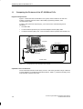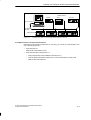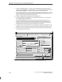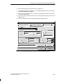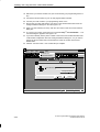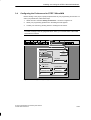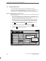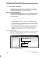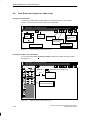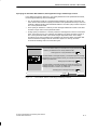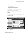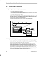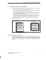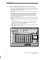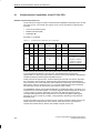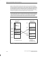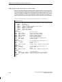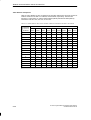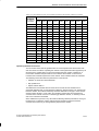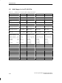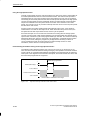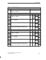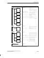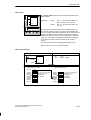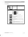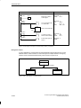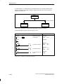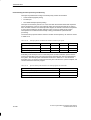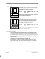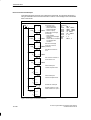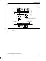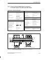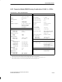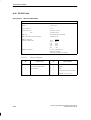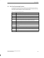
1
Preface, Contents
SIMATIC
S7-200 Programmable Controller
System Manual
This manual has the order number:
6ES7298-8FA01-8BH0
Introducing the
S7-200 Micro PLC
1
Installing an S7-200
Micro PLC
2
Installing and Using the
STEP 7-Micro/WIN Software
3
Getting Started with a
Sample Program
4
Additional Features of
STEP 7-Micro/WIN
Basic Concepts for
Programming an S7-200
CPU
5
CPU Memory: Data Types
and Addressing Modes
7
Input/Output Control
8
Network Communications
and the S7-200 CPU
9
Instruction Set
6
10
Appendix
S7-200 Data Sheets
A
Power Calculation Table
B
Error Codes
C
Special Memory (SM) Bits
D
How STEP 7-Micro/WIN
Works with Other STEP 7
Programming Products
E
Execution Times for STL
Instructions
F
S7-200 Order Numbers
G
S7-200 Troubleshooting
Guide
H
Index
ii
Safety Guidelines
!
!
!
Qualified Personnel
This manual contains notices which you should observe to ensure your own personal safety, as
well as to protect the product and connected equipment. These notices are highlighted in the
manual by a warning triangle and are marked as follows according to the level of danger:
Danger
indicates that death, severe personal injury or substantial property damage will result if proper
precautions are not taken.
Warning
indicates that death, severe personal injury or substantial property damage can result if proper
precautions are not taken.
Caution
indicates that minor personal injury or property damage can result if proper precautions are not taken.
The device/system may only be set up and operated in conjunction with this manual.
Only qualified personnel should be allowed to install and work on this equipment. Qualified
persons are defined as persons who are authorized to commission, to ground, and to tag circuits,
equipment, and systems in accordance with established safety practices and standards.
Correct Usage
!
Note the following:
Warning
This device and its components may only be used for the applications described in the catalog or the
technical description, and only in connection with devices or components from other manufacturers
which have been approved or recommended by Siemens.
This product can only function correctly and safely if it is transported, stored, set up, and installed
correctly, and operated and maintained as recommended.
Trademarks
SIMATIC, SIMATIC NET and SIMATIC HMI are registered trademarks of Siemens AG.
STEP7 and S7 are trademarks of Siemens AG.
Microsoft, Windows, Windows 95, and Windows NT are registered trademarks of Microsoft
Corporation.
Underwriters Laboratories is a trademark of Underwriters Laboratories, Inc.
Copyright Siemens AG 1998 All rights reserved.
Disclaimer of Liability
The reproduction, transmission or use of this document or its
contents is not permitted without express written authority.
Offenders will be liable for damages. All rights, including rights
created by patent grant or registration of a utility model or design, are
reserved.
We have checked the contents of this manual for agreement with the
hardware and software described. Since deviations cannot be precluded entirely, we cannot guarantee full agreement. However, the
data in this manual are reviewed regularly and any necessary corrections included in subsequent editions. Suggestions for improvement are welcomed.
Siemens AG
Bereich Automatisierungs- und Antriebstechnik
Geschaeftsgebiet Industrie-Automatisierungssysteme
Postfach 4848, D-90327 Nuernberg
Siemens Aktiengesellschaft
Technical data subject to change.
Siemens AG 1998
6ES7 298-8FA01-8BH0
ier tragen Sie Ihren Buchtitel ein --C79000 G7076 C230 02
Preface
Purpose
The S7-200 series is a line of micro-programmable logic controllers (Micro PLCs) that can
control a variety of automation applications. Compact design, low cost, and a powerful
instruction set make the S7-200 controllers a perfect solution for controlling small
applications. The wide variety of CPU sizes and voltages, and the multiple programming
options available, give you the flexibility you need to solve your automation problems.
This manual provides information about installing and programming the S7-200 Micro PLCs,
including the following topics:
Installing and wiring the S7-200 CPU and expansion I/O modules, and installing the
STEP 7-Micro/WIN software
Designing and entering a program
Understanding the CPU operations, such as data types and addressing modes, the CPU
scan cycle, password-protection, and network communication
This manual also includes descriptions and examples for the programming instructions,
typical execution times for the instructions, and the data sheets for the S7-200 equipment.
Audience
This manual is designed for engineers, programmers, installers, and electricians who have a
general knowledge of programmable logic controllers.
Scope of the Manual
The information contained in this manual pertains in particular to the following products:
S7-200 CPU models: CPU 212 Release 1.01, CPU 214 Release 1.01,
CPU 215 Release 1.02, and CPU 216 Release 1.02
Version 2.1 of STEP 7-Micro/WIN programming software packages:
–
STEP 7-Micro/WIN 16 for the 16-bit Windows 3.1x
–
STEP 7-Micro/WIN 32 for the 32-bit Windows 95 and Windows NT
Agency Approvals
The SIMATIC S7-200 series meets the standards and regulations of the following agencies:
European Community (CE) Low Voltage Directive 73/23/EEC
European Community (CE) EMC Directive 89/336/EEC
Underwriters Laboratories, Inc.: UL 508 Listed (Industrial Control Equipment)
Canadian Standards Association: CSA C22.2 Number 142 Certified (Process Control
Equipment)
Factory Mutual Research: FM Class I, Division 2, Groups A, B, C, & D Hazardous
Locations, T4A
VDE 0160: Electronic equipment for use in electrical power installations
Refer to Appendix A for compliance information.
S7-200 Programmable Controller System Manual
C79000-G7076-C230-02
iii
Preface
Related Information
Refer to the following documentation for more detailed information about selected topics:
ET 200 Distributed I/O System Manual: describes how to install and use the ET 200
products for distributed I/O.
Process Field Bus (PROFIBUS) standard (EN 50170): describes the standard protocol
for the S7-200 DP communication capability.
TD 200 Operator Interface User Manual: describes how to install and use the TD 200
with an S7-200 programmable logic controller.
How to Use This Manual
If you are a first-time (novice) user of S7-200 Micro PLCs, you should read the entire manual.
If you are an experienced user, refer to the table of contents or index to find specific
information.
The manual is organized according to the following topics:
“Introducing the S7-200 Micro PLC” (Chapter 1) provides an overview of some of the
features of the equipment.
“Installing an S7-200 Micro PLC” (Chapter 2) provides procedures, dimensions, and
basic guidelines for installing the S7-200 CPU modules and expansion I/O modules.
“Installing and Using the STEP 7-Micro/WIN Software” (Chapter 3) describes how to
install the programming software. It also provides a basic explanation about the features
of the software.
“Getting Started with a Sample Program” (Chapter 4) helps you enter a sample program,
using the STEP 7-Micro/WIN software.
“Additional Features of STEP 7-Micro/WIN” (Chapter 5) describes how to use the TD 200
Wizard and the S7-200 Instruction Wizard, and other new features of STEP 7-Micro/WIN.
“Basic Concepts for Programming an S7-200 CPU” (Chapter 6), “CPU Memory: Data
Types and Addressing Modes” (Chapter 7), and “Input/Output Control” (Chapter 8)
provide information about how the S7-200 CPU processes data and executes your
program.
“Network Communications and the S7-200 CPU” (Chapter 9) provides information about
how to connect the S7-200 CPU to different types of networks.
“Instruction Set” (Chapter 10) provides explanations and examples of the programming
instructions used by the S7-200 CPUs.
Additional information (such as the equipment data sheets, error code descriptions,
execution times, and troubleshooting) are provided in the appendices.
Additional Assistance
For assistance in answering technical questions, for training on this product, or for ordering,
contact your Siemens distributor or sales office.
For Internet information about Siemens products and services, technical support, or FAQs
(frequently asked questions) and application tips, use this Internet address:
http://www.ad.siemens.de
iv
S7-200 Programmable Controller System Manual
C79000-G7076-C230-02
Contents
1
2
3
4
5
Introducing the S7-200 Micro PLC . . . . . . . . . . . . . . . . . . . . . . . . . . . . . . . . . . . . . . . .
1-1
1.1
Comparing the Features of the S7-200 Micro PLCs . . . . . . . . . . . . . . . . . . . . . . . . . .
1-2
1.2
Major Components of the S7-200 Micro PLC . . . . . . . . . . . . . . . . . . . . . . . . . . . . . . .
1-4
Installing an S7-200 Micro PLC . . . . . . . . . . . . . . . . . . . . . . . . . . . . . . . . . . . . . . . . . . .
2-1
2.1
Panel Layout Considerations . . . . . . . . . . . . . . . . . . . . . . . . . . . . . . . . . . . . . . . . . . . . .
2-2
2.2
Installing and Removing an S7-200 Micro PLC . . . . . . . . . . . . . . . . . . . . . . . . . . . . . .
2-5
2.3
Installing the Field Wiring . . . . . . . . . . . . . . . . . . . . . . . . . . . . . . . . . . . . . . . . . . . . . . . .
2-8
2.4
Using Suppression Circuits . . . . . . . . . . . . . . . . . . . . . . . . . . . . . . . . . . . . . . . . . . . . . . .
2-13
2.5
Power Considerations . . . . . . . . . . . . . . . . . . . . . . . . . . . . . . . . . . . . . . . . . . . . . . . . . . .
2-15
Installing and Using the STEP 7-Micro/WIN Software . . . . . . . . . . . . . . . . . . . . . . .
3-1
3.1
Installing the STEP 7-Micro/WIN Software . . . . . . . . . . . . . . . . . . . . . . . . . . . . . . . . . .
3-2
3.2
Using STEP 7-Micro/WIN to Set Up the Communications Hardware . . . . . . . . . . .
3-4
3.3
Establishing Communication with the S7-200 CPU . . . . . . . . . . . . . . . . . . . . . . . . . .
3-7
3.4
Configuring the Preferences for STEP 7-Micro/WIN . . . . . . . . . . . . . . . . . . . . . . . . . .
3-25
3.5
Creating and Saving a Project . . . . . . . . . . . . . . . . . . . . . . . . . . . . . . . . . . . . . . . . . . . .
3-26
3.6
Creating a Program . . . . . . . . . . . . . . . . . . . . . . . . . . . . . . . . . . . . . . . . . . . . . . . . . . . . .
3-27
3.7
Creating a Data Block . . . . . . . . . . . . . . . . . . . . . . . . . . . . . . . . . . . . . . . . . . . . . . . . . . .
3-32
3.8
Using the Status Chart . . . . . . . . . . . . . . . . . . . . . . . . . . . . . . . . . . . . . . . . . . . . . . . . . .
3-34
3.9
Using Symbolic Addressing . . . . . . . . . . . . . . . . . . . . . . . . . . . . . . . . . . . . . . . . . . . . . .
3-36
Getting Started with a Sample Program . . . . . . . . . . . . . . . . . . . . . . . . . . . . . . . . . . .
4-1
4.1
Creating a Program for a Sample Application . . . . . . . . . . . . . . . . . . . . . . . . . . . . . . .
4-2
4.2
Task: Create a Project . . . . . . . . . . . . . . . . . . . . . . . . . . . . . . . . . . . . . . . . . . . . . . . . . . .
4-6
4.3
Task: Create a Symbol Table . . . . . . . . . . . . . . . . . . . . . . . . . . . . . . . . . . . . . . . . . . . . .
4-8
4.4
Task: Enter the Program in Ladder Logic . . . . . . . . . . . . . . . . . . . . . . . . . . . . . . . . . . .
4-10
4.5
Task: Create a Status Chart . . . . . . . . . . . . . . . . . . . . . . . . . . . . . . . . . . . . . . . . . . . . . .
4-14
4.6
Task: Download and Monitor the Sample Program . . . . . . . . . . . . . . . . . . . . . . . . . . .
4-15
Additional Features of STEP 7-Micro/WIN . . . . . . . . . . . . . . . . . . . . . . . . . . . . . . . . .
5-1
5.1
Using the TD 200 Wizard to Configure the TD 200 Operator Interface . . . . . . . . . .
5-2
5.2
Using the S7-200 Instruction Wizard . . . . . . . . . . . . . . . . . . . . . . . . . . . . . . . . . . . . . . .
5-12
5.3
Using the Analog Input Filtering Instruction Wizard . . . . . . . . . . . . . . . . . . . . . . . . . .
5-14
5.4
Using Cross Reference . . . . . . . . . . . . . . . . . . . . . . . . . . . . . . . . . . . . . . . . . . . . . . . . . .
5-17
5.5
Using Element Usage . . . . . . . . . . . . . . . . . . . . . . . . . . . . . . . . . . . . . . . . . . . . . . . . . . .
5-18
S7-200 Programmable Controller System Manual
C79000-G7076-C230-02
v
Contents
6
7
8
9
10
vi
5.6
Using Find/Replace . . . . . . . . . . . . . . . . . . . . . . . . . . . . . . . . . . . . . . . . . . . . . . . . . . . . .
5-19
5.7
Documenting Your Program . . . . . . . . . . . . . . . . . . . . . . . . . . . . . . . . . . . . . . . . . . . . . .
5-21
5.8
Printing Your Program . . . . . . . . . . . . . . . . . . . . . . . . . . . . . . . . . . . . . . . . . . . . . . . . . . .
5-23
Basic Concepts for Programming an S7-200 CPU . . . . . . . . . . . . . . . . . . . . . . . . . .
6-1
6.1
Guidelines for Designing a Micro PLC System . . . . . . . . . . . . . . . . . . . . . . . . . . . . . .
6-2
6.2
Concepts of an S7-200 Program . . . . . . . . . . . . . . . . . . . . . . . . . . . . . . . . . . . . . . . . . .
6-4
6.3
Concepts of the S7-200 Programming Languages . . . . . . . . . . . . . . . . . . . . . . . . . . .
6-5
6.4
Basic Elements for Constructing a Program . . . . . . . . . . . . . . . . . . . . . . . . . . . . . . . .
6-8
6.5
Understanding the Scan Cycle of the CPU . . . . . . . . . . . . . . . . . . . . . . . . . . . . . . . . .
6-10
6.6
Selecting the Mode of Operation for the CPU . . . . . . . . . . . . . . . . . . . . . . . . . . . . . . .
6-13
6.7
Creating a Password for the CPU . . . . . . . . . . . . . . . . . . . . . . . . . . . . . . . . . . . . . . . . .
6-14
6.8
Debugging and Monitoring Your Program . . . . . . . . . . . . . . . . . . . . . . . . . . . . . . . . . .
6-16
6.9
Error Handling for the S7-200 CPU . . . . . . . . . . . . . . . . . . . . . . . . . . . . . . . . . . . . . . . .
6-19
CPU Memory: Data Types and Addressing Modes . . . . . . . . . . . . . . . . . . . . . . . . .
7-1
7.1
Direct Addressing of the CPU Memory Areas . . . . . . . . . . . . . . . . . . . . . . . . . . . . . . .
7-2
7.2
Indirect Addressing of the CPU Memory Areas . . . . . . . . . . . . . . . . . . . . . . . . . . . . . .
7-9
7.3
Memory Retention for the S7-200 CPU . . . . . . . . . . . . . . . . . . . . . . . . . . . . . . . . . . . .
7-11
7.4
Using Your Program to Store Data Permanently . . . . . . . . . . . . . . . . . . . . . . . . . . . . .
7-16
7.5
Using a Memory Cartridge to Store Your Program . . . . . . . . . . . . . . . . . . . . . . . . . . .
7-17
Input/Output Control . . . . . . . . . . . . . . . . . . . . . . . . . . . . . . . . . . . . . . . . . . . . . . . . . . . . .
8-1
8.1
Local I/O and Expansion I/O . . . . . . . . . . . . . . . . . . . . . . . . . . . . . . . . . . . . . . . . . . . . . .
8-2
8.2
Using the Selectable Input Filter to Provide Noise Rejection . . . . . . . . . . . . . . . . . .
8-5
8.3
Using the Output Table to Configure the States of the Outputs . . . . . . . . . . . . . . . .
8-6
8.4
High-Speed I/O . . . . . . . . . . . . . . . . . . . . . . . . . . . . . . . . . . . . . . . . . . . . . . . . . . . . . . . . .
8-7
8.5
Analog Adjustments . . . . . . . . . . . . . . . . . . . . . . . . . . . . . . . . . . . . . . . . . . . . . . . . . . . . .
8-8
Network Communications and the S7-200 CPU . . . . . . . . . . . . . . . . . . . . . . . . . . . .
9-1
9.1
Communication Capabilities of the S7-200 CPU . . . . . . . . . . . . . . . . . . . . . . . . . . . . .
9-2
9.2
Communication Network Components . . . . . . . . . . . . . . . . . . . . . . . . . . . . . . . . . . . . .
9-6
9.3
Data Communications Using the PC/PPI Cable . . . . . . . . . . . . . . . . . . . . . . . . . . . . .
9-9
9.4
Data Communications Using the MPI or CP Card . . . . . . . . . . . . . . . . . . . . . . . . . . .
9-13
9.5
Distributed Peripheral (DP) Standard Communications . . . . . . . . . . . . . . . . . . . . . . .
9-15
9.6
Network Performance . . . . . . . . . . . . . . . . . . . . . . . . . . . . . . . . . . . . . . . . . . . . . . . . . . .
9-28
Instruction Set . . . . . . . . . . . . . . . . . . . . . . . . . . . . . . . . . . . . . . . . . . . . . . . . . . . . . . . . . .
10-1
10.1
Valid Ranges for the S7-200 CPUs . . . . . . . . . . . . . . . . . . . . . . . . . . . . . . . . . . . . . . . .
10-2
10.2
Contact Instructions . . . . . . . . . . . . . . . . . . . . . . . . . . . . . . . . . . . . . . . . . . . . . . . . . . . . .
10-4
10.3
Comparison Contact Instructions . . . . . . . . . . . . . . . . . . . . . . . . . . . . . . . . . . . . . . . . . .
10-7
10.4
Output Instructions . . . . . . . . . . . . . . . . . . . . . . . . . . . . . . . . . . . . . . . . . . . . . . . . . . . . . .
10-10
S7-200 Programmable Controller System Manual
C79000-G7076-C230-02
Contents
10.5
A
Timer, Counter, High-Speed Counter, High-Speed Output, Clock,
and Pulse Instructions . . . . . . . . . . . . . . . . . . . . . . . . . . . . . . . . . . . . . . . . . . . . . . . . . . .
10-13
10.6
Math and PID Loop Control Instructions . . . . . . . . . . . . . . . . . . . . . . . . . . . . . . . . . . . .
10-50
10.7
Increment and Decrement Instructions . . . . . . . . . . . . . . . . . . . . . . . . . . . . . . . . . . . . .
10-66
10.8
Move, Fill, and Table Instructions . . . . . . . . . . . . . . . . . . . . . . . . . . . . . . . . . . . . . . . . . .
10-68
10.9
Shift and Rotate Instructions . . . . . . . . . . . . . . . . . . . . . . . . . . . . . . . . . . . . . . . . . . . . .
10-78
10.10
Program Control Instructions . . . . . . . . . . . . . . . . . . . . . . . . . . . . . . . . . . . . . . . . . . . . .
10-84
10.11
Logic Stack Instructions . . . . . . . . . . . . . . . . . . . . . . . . . . . . . . . . . . . . . . . . . . . . . . . . .
10-99
10.12
Logic Operations . . . . . . . . . . . . . . . . . . . . . . . . . . . . . . . . . . . . . . . . . . . . . . . . . . . . . . . 10-102
10.13
Conversion Instructions . . . . . . . . . . . . . . . . . . . . . . . . . . . . . . . . . . . . . . . . . . . . . . . . . . 10-108
10.14
Interrupt and Communications Instructions . . . . . . . . . . . . . . . . . . . . . . . . . . . . . . . . . 10-114
S7-200 Data Sheets . . . . . . . . . . . . . . . . . . . . . . . . . . . . . . . . . . . . . . . . . . . . . . . . . . . . . .
A-1
A.1
General Technical Specifications . . . . . . . . . . . . . . . . . . . . . . . . . . . . . . . . . . . . . . . . . .
A-3
A.2
CPU 212 DC Power Supply, DC Inputs, DC Outputs . . . . . . . . . . . . . . . . . . . . . . . . .
A-6
A.3
CPU 212 AC Power Supply, DC Inputs, Relay Outputs . . . . . . . . . . . . . . . . . . . . . . .
A-8
A.4
CPU 212 24 VAC Power Supply, DC Inputs, Relay Outputs . . . . . . . . . . . . . . . . . . .
A-10
A.5
CPU 212 AC Power Supply, AC Inputs, AC Outputs . . . . . . . . . . . . . . . . . . . . . . . . .
A-12
A.6
CPU 212 AC Power Supply, Sourcing DC Inputs, Relay Outputs . . . . . . . . . . . . . .
A-14
A.7
CPU 212 AC Power Supply, 24 VAC Inputs, AC Outputs . . . . . . . . . . . . . . . . . . . . .
A-16
A.8
CPU 212 AC Power Supply, AC Inputs, Relay Outputs . . . . . . . . . . . . . . . . . . . . . . .
A-18
A.9
CPU 214 DC Power Supply, DC Inputs, DC Outputs . . . . . . . . . . . . . . . . . . . . . . . . .
A-20
A.10
CPU 214 AC Power Supply, DC Inputs, Relay Outputs . . . . . . . . . . . . . . . . . . . . . . .
A-22
A.11
CPU 214 AC Power Supply, AC Inputs, AC Outputs . . . . . . . . . . . . . . . . . . . . . . . . .
A-24
A.12
CPU 214 AC Power Supply, Sourcing DC Inputs, Relay Outputs . . . . . . . . . . . . . .
A-26
A.13
CPU 214 AC Power Supply, 24 VAC Inputs, AC Outputs . . . . . . . . . . . . . . . . . . . . .
A-28
A.14
CPU 214 AC Power Supply, AC Inputs, Relay Outputs . . . . . . . . . . . . . . . . . . . . . . .
A-30
A.15
CPU 215 DC Power Supply, DC Inputs, DC Outputs . . . . . . . . . . . . . . . . . . . . . . . . .
A-32
A.16
CPU 215 AC Power Supply, DC Inputs, Relay Outputs . . . . . . . . . . . . . . . . . . . . . . .
A-34
A.17
CPU 216 DC Power Supply, DC Inputs, DC Outputs . . . . . . . . . . . . . . . . . . . . . . . . .
A-36
A.18
CPU 216 AC Power Supply, DC Inputs, Relay Outputs . . . . . . . . . . . . . . . . . . . . . . .
A-38
A.19
Expansion Module EM221 Digital Input 8 x 24 VDC . . . . . . . . . . . . . . . . . . . . . . . . . .
A-40
A.20
Expansion Module EM221 Digital Input 8 x 120 VAC . . . . . . . . . . . . . . . . . . . . . . . . .
A-41
A.21
Expansion Module EM221 Digital Sourcing Input 8 x 24 VDC . . . . . . . . . . . . . . . . .
A-42
A.22
Expansion Module EM221 Digital Input 8 x 24 VAC . . . . . . . . . . . . . . . . . . . . . . . . . .
A-43
A.23
Expansion Module EM222 Digital Output 8 x 24 VDC . . . . . . . . . . . . . . . . . . . . . . . .
A-44
A.24
Expansion Module EM222 Digital Output 8 x Relay . . . . . . . . . . . . . . . . . . . . . . . . . .
A-45
A.25
Expansion Module EM222 Digital Output 8 x 120/230 VAC . . . . . . . . . . . . . . . . . . .
A-46
S7-200 Programmable Controller System Manual
C79000-G7076-C230-02
vii
Contents
A.26
Expansion Module EM223 Digital Combination
4 x 24 VDC Input/4 x 24 VDC Output . . . . . . . . . . . . . . . . . . . . . . . . . . . . . . . . . . . . . .
A-48
Expansion Module EM223 Digital Combination
8 x 24 VDC Input/8 x 24 VDC Output . . . . . . . . . . . . . . . . . . . . . . . . . . . . . . . . . . . . . .
A-50
Expansion Module EM223 Digital Combination
16 x 24 VDC Input/16 x 24 VDC Output . . . . . . . . . . . . . . . . . . . . . . . . . . . . . . . . . . . .
A-52
Expansion Module EM223 Digital Combination
4 x 24 VDC Input/4 x Relay Output . . . . . . . . . . . . . . . . . . . . . . . . . . . . . . . . . . . . . . . .
A-54
Expansion Module EM223 Digital Combination
4 x 120 VAC Input/4 x 120 VAC to 230 VAC Output . . . . . . . . . . . . . . . . . . . . . . . . . .
A-55
Expansion Module EM223 Digital Combination
8 x 24 VDC Input/8 x Relay Output . . . . . . . . . . . . . . . . . . . . . . . . . . . . . . . . . . . . . . . .
A-56
Expansion Module EM223 Digital Combination
16 x 24 VDC Input/16 x Relay Output . . . . . . . . . . . . . . . . . . . . . . . . . . . . . . . . . . . . . .
A-58
A.33
Expansion Module EM231 Analog Input AI 3 x 12 Bits . . . . . . . . . . . . . . . . . . . . . . .
A-60
A.34
Expansion Module EM232 Analog Output AQ 2 x 12 Bits . . . . . . . . . . . . . . . . . . . . .
A-66
A.35
Expansion Module EM235 Analog Combination AI 3/AQ 1 x 12 Bits . . . . . . . . . . . .
A-69
A.36
Memory Cartridge 8K x 8 . . . . . . . . . . . . . . . . . . . . . . . . . . . . . . . . . . . . . . . . . . . . . . . .
A-78
A.37
Memory Cartridge 16K x 8 . . . . . . . . . . . . . . . . . . . . . . . . . . . . . . . . . . . . . . . . . . . . . . .
A-79
A.38
Battery Cartridge . . . . . . . . . . . . . . . . . . . . . . . . . . . . . . . . . . . . . . . . . . . . . . . . . . . . . . .
A-80
A.39
I/O Expansion Cable . . . . . . . . . . . . . . . . . . . . . . . . . . . . . . . . . . . . . . . . . . . . . . . . . . . .
A-81
A.40
PC/PPI Cable . . . . . . . . . . . . . . . . . . . . . . . . . . . . . . . . . . . . . . . . . . . . . . . . . . . . . . . . . .
A-82
A.41
CPU 212 DC Input Simulator . . . . . . . . . . . . . . . . . . . . . . . . . . . . . . . . . . . . . . . . . . . . .
A-84
A.42
CPU 214 DC Input Simulator . . . . . . . . . . . . . . . . . . . . . . . . . . . . . . . . . . . . . . . . . . . . .
A-85
A.43
CPU 215/216 DC Input Simulator . . . . . . . . . . . . . . . . . . . . . . . . . . . . . . . . . . . . . . . . .
A-86
B
Power Calculation Table . . . . . . . . . . . . . . . . . . . . . . . . . . . . . . . . . . . . . . . . . . . . . . . . .
B-1
C
Error Codes . . . . . . . . . . . . . . . . . . . . . . . . . . . . . . . . . . . . . . . . . . . . . . . . . . . . . . . . . . . . .
C-1
C.1
Fatal Error Codes and Messages . . . . . . . . . . . . . . . . . . . . . . . . . . . . . . . . . . . . . . . . .
C-2
C.2
Run-Time Programming Problems . . . . . . . . . . . . . . . . . . . . . . . . . . . . . . . . . . . . . . . .
C-3
C.3
Compile Rule Violations . . . . . . . . . . . . . . . . . . . . . . . . . . . . . . . . . . . . . . . . . . . . . . . . .
C-4
D
Special Memory (SM) Bits . . . . . . . . . . . . . . . . . . . . . . . . . . . . . . . . . . . . . . . . . . . . . . . .
D-1
E
Using STEP 7-Micro/WIN with STEP 7 and STEP 7-Micro/DOS . . . . . . . . . . . . . .
E-1
E.1
Using STEP 7-Micro/WIN with STEP 7 . . . . . . . . . . . . . . . . . . . . . . . . . . . . . . . . . . . . .
E-2
E.2
Importing Files from STEP 7-Micro/DOS . . . . . . . . . . . . . . . . . . . . . . . . . . . . . . . . . . .
E-4
F
Execution Times for STL Instructions . . . . . . . . . . . . . . . . . . . . . . . . . . . . . . . . . . . . .
F-1
G
S7-200 Order Numbers . . . . . . . . . . . . . . . . . . . . . . . . . . . . . . . . . . . . . . . . . . . . . . . . . . .
G-1
H
S7-200 Troubleshooting Guide . . . . . . . . . . . . . . . . . . . . . . . . . . . . . . . . . . . . . . . . . . .
H-1
A.27
A.28
A.29
A.30
A.31
A.32
Index . . . . . . . . . . . . . . . . . . . . . . . . . . . . . . . . . . . . . . . . . . . . . . . . . . . . . . . . . . . . . . . . . Index-1
viii
S7-200 Programmable Controller System Manual
C79000-G7076-C230-02
Introducing the S7-200 Micro PLC
1
The S7-200 series is a line of micro-programmable logic controllers (Micro PLCs) that can
control a variety of automation applications. Figure 1-1 shows an S7-200 Micro PLC. The
compact design, expandability, low cost, and powerful instruction set of the S7-200 Micro
PLC make a perfect solution for controlling small applications. In addition, the wide variety of
CPU sizes and voltages provides you with the flexibility you need to solve your automation
problems.
SF
I0.0
Q0.0
RUN
I0.1
Q0.1
STOP
I0.2
Q0.2
I0.3
Q0.3
I0.4
Q0.4
I0.5
Q0.5
I0.6
SIMATIC
S7-200
Figure 1-1
I0.7
S7-200 Micro PLC
Chapter Overview
Section
Description
Page
1.1
Comparing the Features of the S7-200 Micro PLCs
1-2
1.2
Major Components of the S7-200 Micro PLC
1-4
S7-200 Programmable Controller System Manual
C79000-G7076-C230-02
1-1
Introducing the S7-200 Micro PLC
1.1
Comparing the Features of the S7-200 Micro PLCs
Equipment Requirements
Figure 1-2 shows the basic S7-200 Micro PLC system, which includes an S7-200 CPU
module, a personal computer, STEP 7-Micro/WIN programming software, and a
communications cable.
In order to use a personal computer (PC), you must have one of the following sets of
equipment:
S A PC/PPI cable
S A communications processor (CP) card and multipoint interface (MPI) cable
S A multipoint interface (MPI) card. A communications cable is provided with the MPI card.
Computer
S7-200 CPU
STEP 7-Micro/WIN
PC/PPI Cable
Figure 1-2
Components of an S7-200 Micro PLC System
Capabilities of the S7-200 CPUs
The S7-200 family includes a wide variety of CPUs. This variety provides a range of features
to aid in designing a cost-effective automation solution. Table 1-1 provides a summary of the
major features of each S7-200 CPU.
1-2
S7-200 Programmable Controller System Manual
C79000-G7076-C230-02
Introducing the S7-200 Micro PLC
Table 1-1
Summary of the S7-200 CPUs
CPU 212
Feature
CPU 214
CPU 215
CPU 216
ÁÁÁÁÁÁÁÁÁÁÁÁÁÁÁÁÁÁÁÁÁÁÁÁÁÁÁÁÁ
ÁÁÁÁÁÁÁÁÁ
ÁÁÁÁÁ
ÁÁÁÁÁÁ
ÁÁÁÁÁÁÁ
ÁÁÁÁÁÁ
ÁÁÁÁÁÁÁÁÁÁÁÁÁÁÁÁÁÁÁÁÁÁÁÁÁÁÁÁÁ
ÁÁÁÁÁÁÁÁÁ
ÁÁÁÁÁ
ÁÁÁÁÁÁ
ÁÁÁÁÁÁÁ
ÁÁÁÁÁÁ
ÁÁÁÁÁÁÁÁÁ
ÁÁÁÁÁ
ÁÁÁÁÁÁÁ
ÁÁÁÁÁÁ
ÁÁÁÁÁÁ
ÁÁÁÁÁÁ
ÁÁÁÁÁÁÁÁÁ
ÁÁÁÁÁ
ÁÁÁÁÁÁÁ
ÁÁÁÁÁÁ
ÁÁÁÁÁÁÁÁÁ
ÁÁÁÁÁ
ÁÁÁÁÁÁ
ÁÁÁÁÁÁÁ
ÁÁÁÁÁÁ
ÁÁÁÁÁÁÁÁÁ
ÁÁÁÁÁ
ÁÁÁÁÁÁ
ÁÁÁÁÁÁÁ
ÁÁÁÁÁÁ
ÁÁÁÁÁÁÁÁÁ
ÁÁÁÁÁ
ÁÁÁÁÁÁ
Á
ÁÁÁÁÁÁ
ÁÁÁÁÁÁ
ÁÁÁÁÁÁÁÁÁÁÁÁÁÁÁÁÁÁÁÁÁÁÁÁÁÁÁÁÁ
ÁÁÁÁÁÁÁÁÁ
ÁÁÁÁÁ
ÁÁÁÁÁÁ
ÁÁÁÁÁÁÁ
ÁÁÁÁÁÁ
ÁÁÁÁÁÁÁÁÁ
ÁÁÁÁÁ
ÁÁÁÁÁÁ
ÁÁÁÁÁÁÁ
ÁÁÁÁÁÁ
ÁÁÁÁÁÁÁÁÁÁÁÁÁÁÁÁÁÁÁÁÁÁÁÁÁÁÁÁÁ
ÁÁÁÁÁÁÁÁÁ
ÁÁÁÁÁ
ÁÁÁÁÁÁ
ÁÁÁÁÁÁÁ
ÁÁÁÁÁÁ
ÁÁÁÁÁÁÁÁÁ
ÁÁÁÁÁ
ÁÁÁÁÁÁ
ÁÁÁÁÁÁÁ
ÁÁÁÁÁÁ
ÁÁÁÁÁÁÁÁÁ
ÁÁÁÁÁ
ÁÁÁÁÁÁ
ÁÁÁÁÁÁÁ
ÁÁÁÁÁÁ
ÁÁÁÁÁÁÁÁÁ
ÁÁÁÁÁ
ÁÁÁÁÁÁ
ÁÁÁÁÁÁÁ
ÁÁÁÁÁÁ
ÁÁÁÁÁÁÁÁÁÁÁÁÁÁÁÁÁÁÁÁÁÁÁÁÁÁÁÁÁ
ÁÁÁÁÁÁÁÁÁ
ÁÁÁÁÁ
ÁÁÁÁÁÁ
ÁÁÁÁÁÁÁ
ÁÁÁÁÁÁ
ÁÁÁÁÁÁÁÁÁÁÁÁÁÁÁÁÁÁÁÁÁÁÁÁÁÁÁÁÁ
ÁÁÁÁÁ
ÁÁÁÁÁÁÁÁÁ
ÁÁÁÁÁÁ
ÁÁÁÁÁÁÁ
ÁÁÁÁÁÁ
ÁÁÁÁÁÁÁÁÁ
ÁÁÁÁÁ
ÁÁÁÁÁÁ
ÁÁÁÁÁÁÁ
ÁÁÁÁÁÁ
ÁÁÁÁÁÁÁÁÁ
ÁÁÁÁÁ
ÁÁÁÁÁÁÁ
ÁÁÁÁÁÁ
ÁÁÁÁÁÁ
ÁÁÁÁÁÁ
ÁÁÁÁÁÁÁÁÁ
ÁÁÁÁÁ
ÁÁÁÁÁÁÁ
ÁÁÁÁÁÁ
ÁÁÁÁÁÁÁÁÁ
ÁÁÁÁÁ
ÁÁÁÁÁÁ
ÁÁÁÁÁÁÁ
ÁÁÁÁÁÁ
ÁÁÁÁÁÁÁÁÁ
ÁÁÁÁÁ
ÁÁÁÁÁÁ
ÁÁÁÁÁÁÁ
ÁÁÁÁÁÁ
ÁÁÁÁÁÁÁÁÁÁÁÁÁÁÁÁÁÁÁÁÁÁÁÁÁÁÁÁÁ
ÁÁÁÁÁÁÁÁÁ
ÁÁÁÁÁ
ÁÁÁÁÁÁ
ÁÁÁÁÁÁÁ
ÁÁÁÁÁÁ
ÁÁÁÁÁÁÁÁÁÁÁÁÁÁÁÁÁÁÁÁÁÁÁÁÁÁÁÁÁ
ÁÁÁÁÁÁÁÁÁ
ÁÁÁÁÁ
ÁÁÁÁÁÁ
ÁÁÁÁÁÁÁ
ÁÁÁÁÁÁ
ÁÁÁÁÁÁÁÁÁ
ÁÁÁÁÁ
ÁÁÁÁÁÁ
ÁÁÁÁÁÁÁ
ÁÁÁÁÁÁ
ÁÁÁÁÁÁÁÁÁ
ÁÁÁÁÁ
ÁÁÁÁÁÁ
ÁÁÁÁÁÁÁ
ÁÁÁÁÁÁ
ÁÁÁÁÁÁÁÁÁÁÁ
ÁÁÁÁÁÁÁÁÁ
ÁÁÁÁÁÁÁ
ÁÁÁÁÁÁ
ÁÁÁÁÁÁ
ÁÁÁÁÁÁÁÁÁ
ÁÁÁÁÁ
ÁÁÁÁÁÁÁ
ÁÁÁÁÁÁ
ÁÁÁÁÁÁÁÁÁ
ÁÁÁÁÁ
ÁÁÁÁÁÁ
ÁÁÁÁÁÁÁ
ÁÁÁÁÁÁ
ÁÁÁÁÁÁÁÁÁ
ÁÁÁÁÁ
ÁÁÁÁÁÁ
ÁÁÁÁÁÁÁ
ÁÁÁÁÁÁ
ÁÁÁÁÁÁÁÁÁÁÁÁÁÁÁÁÁÁÁÁÁÁÁÁÁÁÁÁÁ
ÁÁÁÁÁÁÁÁÁ
ÁÁÁÁÁ
ÁÁÁÁÁÁ
ÁÁÁÁÁÁÁ
ÁÁÁÁÁÁ
ÁÁÁÁÁÁÁÁÁ
ÁÁÁÁÁ
ÁÁÁÁÁÁ
ÁÁÁÁÁÁÁ
ÁÁÁÁÁÁ
ÁÁÁÁÁÁÁÁÁÁÁÁÁÁÁÁÁÁÁÁÁÁÁÁÁÁÁÁÁ
ÁÁÁÁÁÁÁÁÁ
ÁÁÁÁÁ
ÁÁÁÁÁÁ
ÁÁÁÁÁÁÁ
ÁÁÁÁÁÁ
ÁÁÁÁÁÁÁÁÁÁÁÁÁÁ
ÁÁÁÁÁÁÁ
ÁÁÁÁÁÁ
ÁÁÁÁÁÁÁÁÁÁÁ
ÁÁÁÁÁÁ
ÁÁÁÁÁÁÁÁÁ
ÁÁÁÁÁÁÁ
ÁÁÁÁÁÁ
ÁÁÁÁÁÁÁÁÁ
ÁÁÁÁÁÁÁÁÁÁÁ
ÁÁÁÁÁÁÁ
ÁÁÁÁÁÁ
Physical Size of Unit
160 mm x 80 mm
x 62 mm
197 mm x 80 mm
x 62 mm
218 mm x 80 mm
x 62 mm
218 mm x 80 mm
x 62 mm
Program (EEPROM)
512 words
2 Kwords
4 Kwords
4 Kwords
User data
512 words
2 Kwords
2.5 Kwords
2.5 Kwords
Internal memory bits
128
256
256
256
Memory cartridge
None
Yes (EEPROM)
Yes (EEPROM)
Yes (EEPROM)
Optional battery cartridge
None
200 days typical
200 days typical
200 days typical
Backup(super capacitor)
50 hours typical
190 hours typical
190 hours typical
190 hours typical
Local I/O
8 DI / 6 DQ
14 DI / 10 DQ
14 DI / 10 DQ
24 DI / 16 DQ
Expansion modules (max.)
2 modules
7 modules
7 modules
7 modules
Process-image I/O register
64 DI / 64 DQ
64 DI / 64 DQ
64 DI / 64 DQ
64 DI / 64 DQ
Analog I/O (expansion)
16 AI / 16 AQ
16 AI / 16 AQ
16 AI / 16 AQ
16 AI / 16 AQ
Selectable input filters
No
Yes
Yes
Yes
Boolean execution speed
1.2 µs/instruction
0.8 µs/instruction
0.8 µs/instruction
0.8 µs/instruction
Counters / timers
64/64
128/128
256/256
256/256
For / next loops
No
Yes
Yes
Yes
Integer math
Yes
Yes
Yes
Yes
Real math
No
Yes
Yes
Yes
PID
No
No
Yes
Yes
High-speed counter
1 S/W
1 S/W, 2 H/W
1 S/W, 2 H/W
1 S/W, 2 H/W
Analog adjustments
1
2
2
2
Pulse outputs
None
2
2
2
Communication interrupt
events
1 transmit/
1 receive
1 transmit/1 receive 1 transmit/2 receive 2 transmit/4 receive
Timed interrupts
1
2
2
2
Hardware input interrupts
1
4
4
4
Real time clock
None
Yes
Yes
Yes
Number of comm ports:
1 (RS-485)
1 (RS-485)
2 (RS-485)
2 (RS-485)
Protocols supported Port 0:
PPI, Freeport
PPI, Freeport
PPI, Freeport, MPI
PPI, Freeport, MPI
N/A
N/A
DP, MPI
PPI, Freeport, MPI
Slave only
Yes
Yes
Yes
Memory
Inputs/Outputs (I/O)
Instructions
Additional Features
Communications
Port 1:
Peer-to-peer
S7-200 Programmable Controller System Manual
C79000-G7076-C230-02
1-3
Introducing the S7-200 Micro PLC
1.2
Major Components of the S7-200 Micro PLC
An S7-200 Micro PLC consists of an S7-200 CPU module alone or with a variety of optional
expansion modules.
S7-200 CPU Module
The S7-200 CPU module combines a central processing unit (CPU), power supply, and
discrete I/O points into a compact, stand-alone device.
S The CPU executes the program and stores the data for controlling the automation task or
process.
S The power supply provides electrical power for the base unit and for any expansion
module that is connected.
S The inputs and outputs are the system control points: the inputs monitor the signals from
the field devices (such as sensors and switches), and the outputs control pumps, motors,
or other devices in your process.
S The communications port allows you to connect the CPU to a programming device or to
other devices. Some S7-200 CPUs have two communications ports.
S Status lights provide visual information about the CPU mode (RUN or STOP), the current
state of the local I/O, and whether a system fault has been detected.
Figures 1-3, 1-4, and 1-5 show the different S7-200 CPU modules.
1-4
S7-200 Programmable Controller System Manual
C79000-G7076-C230-02
Introducing the S7-200 Micro PLC
SF
I0.0
Q0.0
RUN
I0.1
Q0.1
STOP
I0.2
Q0.2
I0.3
Q0.3
I0.4
Q0.4
I0.5
Q0.5
I0.6
SIMATIC
S7-200
Figure 1-3
I0.7
S7-212 CPU Module
SF
I0.0
I1.0
Q0.0
Q1.0
RUN
I0.1
I1.1
Q0.1
Q1.1
STOP
I0.2
I1.2
Q0.2
I0.3
I1.3
Q0.3
I0.4
I1.4
Q0.4
I0.5
I1.5
Q0.5
I0.6
I1.6
Q0.6
I0.7
I1.7
Q0.7
SIMATIC
S7-200
Figure 1-4
S7-214 CPU Module
SF
I0.0
I1.0
Q0.0
Q 1.0
RUN
I0.1
I1.1
Q0.1
Q 1.1
STOP
I0.2
I1.2
Q0.2
DP
I0.3
I1.3
Q0.3
I0.4
I1.4
Q0.4
I0.5
I1.5
Q0.5
I0.6
Q0.6
I0.7
IQ0.7
SIMATIC
S7-200
Figure 1-5
S7-215 and S7-216 CPU Module
S7-200 Programmable Controller System Manual
C79000-G7076-C230-02
1-5
Introducing the S7-200 Micro PLC
Expansion Modules
The S7-200 CPU module provides a certain number of local I/O. Adding an expansion
module provides additional input or output points. As shown in Figure 1-6, the expansion
module comes with a bus connector for connecting to the base unit.
S7-200 CPU Module
SIMATIC
S7-200
Expansion Module
SF
I0.0
Q0.0
I.0
RUN
I0.1
Q0.1
I.1
STOP
I0.2
Q0.2
I.2
I0.3
Q0.3
I.3
I0.4
Q0.4
I.4
I0.5
Q0.5
I.5
I0.6
I.6
I0.7
II.7
Bus Connector
Figure 1-6
1-6
CPU Module with an Expansion Module
S7-200 Programmable Controller System Manual
C79000-G7076-C230-02
Installing an S7-200 Micro PLC
2
The installation of the S7-200 family is designed to be easy. You can use the mounting holes
to attach the modules to a panel, or you can use the built-in clips to mount the modules onto
a standard (DIN) rail. The small size of the S7-200 allows you to make efficient use of space.
This chapter provides guidelines for installing and wiring your S7-200 system.
Chapter Overview
Description
Section
Page
2.1
Panel Layout Considerations
2-2
2.2
Installing and Removing an S7-200 Micro PLC
2-5
2.3
Installing the Field Wiring
2-8
2.4
Using Suppression Circuits
2-13
2.5
Power Considerations
2-15
S7-200 Programmable Controller System Manual
C79000-G7076-C230-02
2-1
Installing an S7-200 Micro PLC
2.1
Panel Layout Considerations
Installation Configuration
You can install an S7-200 either on a panel or on a standard rail. You can mount the S7-200
either horizontally or vertically. An I/O expansion cable is also available to add flexibility to
your mounting configuration. Figure 2-1 shows a typical configuration for these types of
installations.
Panel mounting
S7-200
I/O
Standard rail mounting
I/O
S7-200
I/O
I/O
I/O
Figure 2-1
I/O
Mounting Configurations
Clearance Requirements for Installing an S7-200 PLC
Use the following guidelines as you plan your installation:
S The S7-200 CPU and expansion modules are designed for natural convection cooling.
You must provide a clearance of at least 25 mm (1 in.), both above and below the units,
for proper cooling. See Figure 2-2. Continuous operation of all electronic products at
maximum ambient temperature and load reduces their life.
S For vertical mounting, the output loading may need to be derated because of thermal
constraints. Refer to Appendix A for the data sheet for your particular CPU. If you are
mounting the CPU and modules on a DIN Rail, the DIN rail stop is recommended.
S If you are installing an S7-200 horizontally or vertically on a panel, you must allow 75 mm
(2.9 in.) for the minimum panel depth. See Figure 2-2.
S If you plan to install additional modules horizontally or vertically, allow a clearance of at
least 25 mm (1 in.) on either side of the unit for installing and removing the module. This
extra space is required to engage and disengage the bus expansion connector.
S Be sure to allow enough space in your mounting design to accommodate the I/O wiring
and communication cable connections.
25 mm
(1 in.)
Clearance for cooling
25 mm
(1 in.)
ÂÂÂÂÂÂÂ
ÂÂÂÂÂÂÂ
ÂÂÂÂÂÂÂ
ÂÂÂÂÂÂÂ
ÂÂÂÂÂÂÂ
ÂÂÂÂÂÂÂ
S7-200
Clearance for removing
expansion I/O module
Front View
Figure 2-2
2-2
Front of the
enclosure
I/O
Mounting
surface
S7-200
75 mm
(2.9 in.)
25 mm
(1 in.)
Side View
Horizontal and Vertical Clearance Requirements for Installing an S7-200 PLC
S7-200 Programmable Controller System Manual
C79000-G7076-C230-02
Installing an S7-200 Micro PLC
Standard Rail Requirements
The S7-200 CPU and expansion modules can be installed on a standard (DIN) rail
(DIN EN 50 022). Figure 2-3 shows the dimensions for this rail.
1.0 mm
(0.039 in.)
35 mm
(1.38 in.)
7.5 mm
(0.29 in.)
Figure 2-3
Standard Rail Dimensions
Panel-Mounting Dimensions
S7-200 CPUs and expansion modules include mounting holes to facilitate installation on
panels. Figures 2-4 through 2-8 provide the mounting dimensions for the different S7-200
modules.
6.4 mm
(0.25 in.)
6.4 mm
(0.25 in.)
80 mm
(3.15 in.)
Figure 2-4
147.3 mm
(5.8 in.)
67.3 mm
(2.65 in.)
S7-212
Mounting holes
(M4 or no. 8)
Mounting Dimensions for an S7-212 CPU Module
6.4 mm
(0.25 in.)
197 mm
(7.76 in.)
184.3 mm
(7.25 in.)
6.4 mm
(0.25 in.)
80 mm
(3.15 in.)
160 mm
(6.3 in.)
67.3 mm
(2.65 in.)
S7-214
Mounting holes
(M4 or no. 8)
Figure 2-5
Mounting Dimensions for an S7-214 CPU Module
S7-200 Programmable Controller System Manual
C79000-G7076-C230-02
2-3
Installing an S7-200 Micro PLC
217.3 mm
(8.56 in.)
26.7 mm
(1.05 in.)
184.3 mm
(7.26 in.)
6.4 mm
(0.25 in.)
80 mm
(3.15 in.)
Figure 2-6
S7-215 or
S7-216
67.3 mm
(2.65 in.)
Mounting holes
(M4 or no. 8)
Mounting Dimensions for an S7-215 or S7-216 CPU Module
90 mm
(3.54 in.)
12.7 mm
(0.50 in.)
77.3 mm
(3.04 in.)
Existing
CPU or EM
8- or 16Point
Expansion
Module
6.4 mm
(0.25 in.)
Mounting holes
(M4 or no. 8)
Figure 2-7
80 mm
(3.15 in.)
67.3 mm
(2.65 in.)
Mounting Dimensions for an 8- or 16-Point Expansion Module
160 mm
(6.3 in.)
12.7 mm
(0.50 in.)
Existing
CPU or EM
147.3 mm
(5.8 in.)
32-Point
Expansion
Module
67.3 mm
(2.65 in.)
Mounting holes
(M4 or no. 8)
Figure 2-8
2-4
80 mm
(3.15 in.)
6.4 mm
(0.25 in.)
Mounting Dimensions for a 32-Point Expansion Module
S7-200 Programmable Controller System Manual
C79000-G7076-C230-02
Installing an S7-200 Micro PLC
2.2
Installing and Removing an S7-200 Micro PLC
Mounting an S7-200 Micro PLC on a Panel
!
Warning
Attempts to install or remove S7-200 modules or related equipment when they are
powered up could cause electric shock.
Failure to disable all power to the S7-200 modules and related equipment during
installation or removal procedures may result in death or serious personal injury, and/or
damage to equipment.
Always follow appropriate safety precautions and ensure that power to the S7-200
modules is disabled before installation.
Use the following procedure for installing an S7-200:
1.
Locate, drill, and tap the mounting holes for DIN M4 or American Standard number 8
screws. Refer to Section 2.1 for mounting dimensions and other considerations.
2.
Secure the S7-200 modules onto the panel, using DIN M4 or American
Standard number 8 screws.
If you are installing an expansion module, use the following steps:
1.
Remove the bus expansion port cover from the existing module housing by inserting a
screwdriver into the space between the bus expansion port cover and the housing, and
gently prying. Ensure that the plastic connecting joints are completely removed. Use
caution not to damage the module. Figure 2-9 shows proper screwdriver placement.
2.
Insert the bus connector into the bus expansion port of the existing module and ensure
that the connector snaps into place.
3.
Ensure that the expansion module is correctly oriented with respect to the CPU module.
If you are using an expansion cable, orient the cable up towards the front of the module.
4.
Connect the expansion module to the bus connector by sliding the module onto the bus
connector so that it snaps into place.
SIMATIC
S7-200
Bus expansion port cover
Figure 2-9
Removing the Bus Expansion Port Cover on an S7-200 CPU Module
S7-200 Programmable Controller System Manual
C79000-G7076-C230-02
2-5
Installing an S7-200 Micro PLC
Installing an S7-200 Micro PLC onto a Standard Rail
!
Warning
Attempts to install or remove S7-200 modules or related equipment when they are
powered up could cause electric shock.
Failure to disable all power to the S7-200 modules and related equipment during
installation or removal procedures may result in death or serious personal injury, and/or
damage to equipment.
Always follow appropriate safety precautions and ensure that power to the S7-200
modules is disabled before installation.
To install the S7-200 CPU module, follow these steps:
1.
Secure the rail every 75 mm (3.0 in.) to the mounting panel.
2.
Snap open the clip (located on the bottom of the module) and hook the back of the
module onto the rail.
3.
Snap the clip closed, carefully checking to ensure that the clip has fastened the module
securely onto the rail.
Note
Modules in an environment with high vibration potential or modules that have been
installed in a vertical position may require DIN rail stops.
If you are installing an expansion module, use the following steps:
2-6
1.
Remove the bus expansion port cover from the existing module housing by inserting a
screwdriver into the space between the bus expansion port cover and the housing, and
gently prying. Ensure that the plastic connecting joints are completely removed. Use
caution not to damage the module. Figure 2-9 shows proper screwdriver placement.
2.
Insert the bus connector into the bus expansion port of the existing module and ensure
that the connector snaps into place.
3.
Ensure that the expansion module is correctly oriented with respect to the CPU module.
If you are using an expansion cable, orient the cable up towards the front of the module.
4.
Snap open the clip and hook the back of the expansion module onto the rail. Slide the
expansion module onto the bus connector until it snaps into place.
5.
Snap the clip closed to secure the expansion module to the rail. Carefully check to
ensure that the clip has fastened the module securely onto the rail.
S7-200 Programmable Controller System Manual
C79000-G7076-C230-02
Installing an S7-200 Micro PLC
Removing the S7-200 Modules
!
Warning
Attempts to install or remove S7-200 modules or related equipment when they are
powered up could cause electric shock.
Failure to disable all power to the S7-200 modules and related equipment during
installation or removal procedures may result in death or serious personal injury, and/or
damage to equipment.
Always follow appropriate safety precautions and ensure that power to the S7-200
modules is disabled before you install or remove a CPU or expansion module.
To remove the S7-200 CPU module or expansion module, follow these steps:
!
1.
Disconnect all the wiring and cabling that is attached to the module that you are
removing. If this module is in the middle of a chain, the modules to the left or right must
be moved at least 25 mm (1 in.) to allow the bus connector to be disconnected. See
Figure 2-10.
2.
Unscrew the mounting screws or snap open the clip, and slide the module at least
25 mm (1 in.) to disengage the bus connector. The bus connector must be disconnected
on both sides of the module.
3.
Remove the module from the panel or rail, and install a new module.
Warning
If you install an incorrect module, the program in the micro PLC could function
unpredictably.
Failure to replace an expansion module and expansion cable with the same model or in
the proper orientation may result in death or serious personal injury, and/or damage to
equipment.
Replace an expansion module with the same model, and orient it correctly. If you are using
an expansion cable, orient the cable up towards the front of the module.
To remove this unit:
Move both units at least 25 mm,
and disconnect bus connector.
Figure 2-10
Or, move this unit at least 25 mm
and disconnect bus connector.
Removing the Expansion Module
S7-200 Programmable Controller System Manual
C79000-G7076-C230-02
2-7
Installing an S7-200 Micro PLC
2.3
Installing the Field Wiring
!
Warning
Attempts to install or remove S7-200 modules or related equipment when they are
powered up could cause electric shock.
Failure to disable all power to the S7-200 modules and related equipment during
installation or removal procedures may result in death or serious personal injury, and/or
damage to equipment.
Always follow appropriate safety precautions and ensure that power to the S7-200
modules is disabled before installing field wiring.
General Guidelines
The following items are general guidelines for designing the installation and wiring of your
S7-200 Micro PLC:
S Ensure that you follow all applicable electrical codes when wiring the S7-200 Micro PLC.
Install and operate all equipment according to all applicable national and local standards.
Contact your local authorities to determine which codes and standards apply to your
specific case.
S Always use the proper wire size to carry the required current. The S7-200 modules
accept wire sizes from 1.50 mm2 to 0.50 mm2 (14 AWG to 22 AWG).
S Ensure that you do not overtighten the connector screws. The maximum torque is
0.56 N-m (5 inches-pounds).
S Always use the shortest wire possible (maximum 500 m shielded, 300 m unshielded).
Wiring should be run in pairs, with a neutral or common wire paired with a hot or
signal-carrying wire.
S Separate AC wiring and high-energy, rapidly switched DC wiring from low-energy signal
wiring.
S Properly identify and route the wiring to the S7-200 module, using strain relief for the
wiring as required. For more information about identifying the terminals, see the data
sheets in Appendix A.
S Install appropriate surge suppression devices for any wiring that is subject to lightning
surges.
S External power should not be applied to an output load in parallel with a DC output point.
This may cause reverse current through the output, unless a diode or other barrier is
provided in the installation.
!
Warning
Control devices can fail in an unsafe condition, resulting in unexpected operation of
controlled equipment.
Such unexpected action could result in death or serious personal injury, and/or equipment
damage.
Consider using an emergency stop function, electromechanical overrides, or other
redundant safeguards that are independent of the programmable controller.
2-8
S7-200 Programmable Controller System Manual
C79000-G7076-C230-02
Installing an S7-200 Micro PLC
Grounding and Circuit Reference Point Guidelines for Using Isolated Circuits
The following items are grounding and circuit guidelines for using isolated circuits:
S You should identify the reference point (0 voltage reference) for each circuit in the
installation, and the points at which circuits with possible different references can connect
together. Such connections can result in unwanted current flows that can cause logic
errors or can damage circuits. A common cause of different reference potentials is
grounds which are physically separated by long distances. When devices with widely
separated grounds are connected with a communication or sensor cable, unexpected
currents can flow through the circuit created by the cable and the ground. Even over
short distances, load currents of heavy machinery can cause differences in ground
potential or can directly induce unwanted currents by electromagnetic induction. Power
supplies that are improperly referenced with respect to each other can cause damaging
currents to flow between their associated circuits.
S S7-200 products include isolation boundaries at certain points to help prevent unwanted
current flows in your installation. When you plan your installation, you should consider
where these isolation boundaries are, and where they are not provided. You should also
consider the isolation boundaries in associated power supplies and other equipment, and
where all associated power supplies have their reference points.
S You should choose your ground reference points and use the isolation boundaries
provided to interrupt unneeded circuit loops that could allow unwanted currents to flow.
Remember to consider temporary connections which may introduce a new circuit
reference, such as the connection of a programming device to the CPU.
S When locating grounds, you must also consider safety grounding requirements and the
proper operation of protective interrupting devices.
The following descriptions are an introduction to general isolation characteristics of the
S7-200 family, but some features may be different on specific products. Consult the data
sheet in Appendix A for your product for specifications of which circuits include isolation
boundaries and the ratings of the boundaries. Isolation boundaries rated less than1,500 VAC
are designed as functional isolation only, and should not be depended on as safety
boundaries.
S CPU logic reference is the same as DC sensor supply M.
S CPU logic reference is the same as the input power supply M on a CPU with DC power
supply.
S CPU communication ports have the same reference as CPU logic (except DP ports).
S Analog inputs and outputs are not isolated from CPU logic. Analog inputs are full
differential to provide low voltage common mode rejection.
S
S
S
S
S
S
CPU logic is isolated from ground to 100 VDC.
DC digital inputs and outputs are isolated from CPU logic to 500 VAC.
DC digital I/O groups are isolated from each other by 500 VAC.
Relay outputs, AC outputs, and AC inputs are isolated from CPU logic to 1,500 VAC.
AC and relay output groups are isolated from each other by 1,500 VAC.
AC power supply line and neutral are isolated from ground, the CPU logic, and all I/O to
1500 VAC.
S7-200 Programmable Controller System Manual
C79000-G7076-C230-02
2-9
Installing an S7-200 Micro PLC
Using the Optional Field Wiring Connector
The optional field wiring fan-out connector (Figure 2-11) allows for field wiring connections to
remain fixed when you remove and re-install the S7-200. Refer to Appendix G for the order
number.
Field Wiring
Fan-out Connector
AC
OUTPUTS
Figure 2-11
1L
0.0
0.1
0.2
2L
0.3
0.4
0.5
↓
N
L1
VAC
85–264
Optional Field Wiring Connector
Guidelines for AC Installation
The following items are general wiring guidelines for AC installations. Refer to Figure 2-12.
S Provide a single disconnect switch (1) that removes power from the CPU, all input
circuits, and all output (load) circuits.
S Provide overcurrent devices (2) to protect the CPU power supply, the output points, and
the input points. You can also fuse each output point individually for greater protection.
External overcurrent protection for input points is not required when you use the 24 VDC
sensor supply (3) from the Micro PLC. This sensor supply is short-circuit protected.
S Connect all S7-200 ground terminals to the closest available earth ground (4) to provide
the highest level of noise immunity. It is recommended that all ground terminals be
connected to a single electrical point. Use 14 AWG or 1.5 mm2 wire for this connection.
S DC sensor supply from the base unit may be used for base unit inputs (5), expansion DC
inputs (6), and expansion relay coils (7). This sensor supply is short-circuit protected.
L1
N
PE
(1) (2)
(4)
(6)
Fuse
DO
DI
(5)
Figure 2-12
2-10
(7)
PS
M L+
S7-200
AC/DC/Rly
DI
EM 221 DC
DO
EM 222 Rly
(3)
120/230 VAC Using a Single Overcurrent Switch to Protect the CPU and Load Wiring
S7-200 Programmable Controller System Manual
C79000-G7076-C230-02
Installing an S7-200 Micro PLC
Guidelines for DC Installation
The following items are general wiring guidelines for isolated DC installations. Refer to
Figure 2-13.
S Provide a single disconnect switch (1) that removes power from the CPU, all input
circuits, and all output (load) circuits.
S Provide overcurrent devices to protect the CPU power supply (2), the output points (3),
and the input points (4). You can also fuse each output point individually for greater
protection. External overcurrent protection for input points is not required when you use
the 24 VDC sensor supply from the Micro PLC. This sensor supply is current limited
internally.
S Ensure that the DC power supply has sufficient surge capacity to maintain voltage during
sudden load changes. External capacitance (5) may be required.
S Equip ungrounded DC power supplies with a resistor and a capacitor in parallel (6) from
the power source common to protective earth ground. The resistor provides a leakage
path to prevent static charge accumulations, and the capacitor provides a drain for high
frequency noise. Typical values are 1 MΩ and 4,700 pf. You can also create a grounded
DC system by connecting the DC power supply to ground (7).
S Connect all S7-200 ground terminals to the closest available earth ground (8) to provide
the highest level of noise immunity. It is recommended that all ground terminals be
connected to a single electrical point. Use 14 AWG or 1.5 mm2 wire for this connection.
S Always supply 24 VDC circuits from a source that provides safe electrical separation from
120/230 VAC power and similar hazards.
The following documents provide standard definitions of safe separation:
S PELV (protected extra low voltage) according to EN60204-1
S Class 2 or Limited Voltage/Current Circuit according to UL 508
Floating (6) or Grounded (7)
(1)
L1
N
PE
AC
(8)
(6)
DC
(7)
(5)
(2)
(3)
DO
DI
PS
S7-200
DC/DC/DC
DO
EM 222
DC
DI
EM 221
DC
(4)
24 VDC
Figure 2-13
L+
M
Isolated DC System Installation
S7-200 Programmable Controller System Manual
C79000-G7076-C230-02
2-11
Installing an S7-200 Micro PLC
Guidelines for North American Installation
The following items are general wiring guidelines for installations in North America where
multiple AC voltages are present. Refer to Figure 2-14 as you read these guidelines.
S Provide a single disconnect switch (1) that removes power from the CPU, all input
circuits, and all output (load) circuits.
S Provide overcurrent devices to protect the CPU power supply (2), the output points (3),
and the input points (4). You may also fuse each output point individually for greater
protection.
S Make AC power connections to the CPU power supply, AC output driven loads, and
relay-driven loads either line-to-grounded neutral (5) or line-to-line (6).
S Connect all S7-200 ground terminals to the closest available earth ground (7) to provide
the highest level of noise immunity. It is recommended that all ground terminals be
connected to a single electrical point. Use 14 AWG or 1.5 mm2 wire for this connection.
!
Caution
Line-to-line voltages in power systems with 230 VAC nominal line-neutral voltages will
exceed the voltage rating of the S7-200 power supply, inputs, and outputs.
Exceeding the voltage may cause failure of the S7-200 and connected equipment.
Do not use line-to-line connections where the voltage rating of your S7-200 module is
exceeded.
L1
L2
N
PE
(1)
120 VAC power to CPU and inputs
120 VAC and 220 VAC load outputs
(2)
(4)
(5)
(3)
(6)
(2)
(5)
(7)
DO
DI
Figure 2-14
2-12
P/S
S7-200
AC/AC/AC
DI
EM221AC
DO
EM 222AC
AC System Installation
S7-200 Programmable Controller System Manual
C79000-G7076-C230-02
Installing an S7-200 Micro PLC
2.4
Using Suppression Circuits
General Guidelines
Equip inductive loads with suppression circuits that limit voltage rise on loss of power. Use
the following guidelines to design adequate suppression. The effectiveness of a given design
depends on the application, and you must verify it for a particular use. Be sure all
components are rated for use in the application.
Protecting DC Transistors
The S7-200 DC transistor outputs contain zener diodes that are adequate for many
installations. Use external suppression diodes for either large or frequently switched
inductive loads to prevent overpowering the internal diodes. Figures 2-15 and 2-16 show
typical applications for DC transistor outputs.
(1)
+VDC
(1) IN4001 diode or
equivalent
Inductor
Figure 2-15
Diode Suppression
+VDC
(1)
(2)
(1) IN4001 diode or
equivalent
(2) 8.2 V zener, 5 W
Inductor
Figure 2-16
Zener Diode Suppression
S7-200 Programmable Controller System Manual
C79000-G7076-C230-02
2-13
Installing an S7-200 Micro PLC
Protecting Relays That Control DC Power
Resistor/capacitor networks, as shown in Figure 2-17, can be used for low voltage (30 V) DC
relay applications. Connect the network across the load.
R
R
C
where minimum R = 12 Ω
+VDC
Inductor
Figure 2-17
V DC
IL
IL
C I LK
where K is 0.5 µF/A to 1 µF/A
Resistor/Capacitor Network on Relay-Driven DC Load
You can also use diode suppression, as shown in Figures 2-15 and 2-16, for DC relay
applications. A threshold voltage of up to 36 V is allowed if you use a reverse zener diode.
Protecting Relays and AC Outputs That Control AC
When you use a relay or AC output to switch 115 V/230 VAC loads, place resistor/capacitor
networks across either the relay contacts or the AC outputs as shown in Figure 2-18. You
can also use a metal oxide varistor (MOV) to limit peak voltage. Ensure that the working
voltage of the MOV is at least 20% greater than the nominal line voltage.
R
MOV
C
R > 0.5 x Vrms for relay,
10 Ω minimum for AC outputs.
C = 0.002 µF to 0.005 µF for each
10 VA of steady-state load.
Inductor
Figure 2-18
AC Load with Network across Relay or AC Outputs
The capacitor allows leakage current to flow around the open switch. Be sure that the
leakage current, I (leakage) = 2 x 3.14 x f x C x Vrms, is acceptable for the application.
For example: A NEMA size 2 contactor lists 183 VA coil inrush and 17 VA sealed coil load. At
115 VAC, the inrush current is 183 VA/115 V = 1.59 A, which is within the 2A switching
capability of the relay contacts.
The resistor = 0.5 x 115 = 57.5 ; choose 68 as a standard value.
The capacitor = (17 VA/10) x 0.005 = 0.0085 µF; choose 0.01 µF as the value.
The leakage current = 2 x 3.14 x 60 x 0.01 x 10-6 x 115 = 0.43 mA rms.
2-14
S7-200 Programmable Controller System Manual
C79000-G7076-C230-02
Installing an S7-200 Micro PLC
2.5
Power Considerations
The S7-200 base units have an internal power supply that provides power for the base unit,
the expansion modules, and other 24 VDC user power requirements. Use the following
information as a guide for determining how much power (or current) the base unit can
provide for your configuration.
Power Requirements
Each S7-200 CPU module supplies both 5 VDC and 24 VDC power:
S Each CPU module has a 24 VDC sensor supply that can supply 24 VDC for local input
points or for relay coils on the expansion modules. If the power requirement for 24 VDC
exceeds the power budget of the CPU module, you can add an external 24 VDC power
supply to provide 24 VDC to the expansion modules.
S The CPU module also provides 5 VDC power for the expansion modules when an
expansion module is connected. If the 5 VDC power requirements for expansion modules
exceeds the power budget of the CPU module, you must remove expansion modules
until the requirement is within the power budget.
!
Warning
Connecting an external 24 VDC power supply in parallel with the S7-200 DC Sensor
Supply can result in a conflict between the two supplies as each seeks to establish its own
preferred output voltage level.
The result of this conflict can be shortened lifetime or immediate failure of one or both
power supplies, with consequent unpredictable operation of the PLC system.
Unpredictable operation could result in death or serious injury to personnel, and/or
damage to equipment and property.
The S7-200 DC Sensor Supply and any external power supply should provide power to
different points. A single connection of the commons is allowed.
The data sheets in Appendix A provide information about the power budgets of the CPU
modules and the power requirements of the expansion modules.
S7-200 Programmable Controller System Manual
C79000-G7076-C230-02
2-15
Installing an S7-200 Micro PLC
Calculating a Sample Power Requirement
Table 2-1 shows a sample calculation of the power requirements for an S7-200 Micro PLC
that includes the following modules:
S CPU 214 DC/DC/DC
S Three EM 221 Digital Input 8 x DC 24 V expansion modules
S Two EM 222 Digital Output 8 x Relay expansion modules
The CPU in this example provides sufficient 5 VDC current for the expansion modules;
however, it requires an additional power supply to provide the 24 VDC power requirement.
(The I/O requires 448 mA of 24 VDC power, but the CPU provides only 280 mA.) Appendix B
provides a blank power calculation table.
Table 2-1
Power Budget Calculations for a Sample Configuration
CPU Power Budget
CPU 214 DC/DC/DC
5 VDC
24 VDC
660 mA
280 mA
5 VDC
24 VDC
minus
System Requirements
CPU 214 DC/DC/DC
BASE UNIT
14 input x 7 mA =
98 mA
Three EM 221 expansion modules
3 x 60 mA =
180 mA
3 x 60 mA =
180 mA
Two EM 222 expansion modules
2 x 80 mA =
160 mA
2 x 85 mA =
170 mA
Total Requirement
340 mA
448 mA
5 VDC
24 VDC
320 mA
[168 mA]
equals
Current Balance
Current Balance Total
2-16
S7-200 Programmable Controller System Manual
C79000-G7076-C230-02
Installing and Using the STEP 7-Micro/WIN
Software
3
This manual describes Version 2.1 of STEP 7-Micro/WIN. Previous versions of the software
may operate differently.
STEP 7-Micro/WIN is a Windows-based software application that supports both the 16-bit
Windows 3.1 environment (STEP 7-Micro/WIN 16) and the 32-bit Windows 95 and
Windows NT environments (STEP 7-Micro/WIN 32). In order to use STEP 7-Micro/WIN, the
following equipment is recommended:
S Recommended: a personal computer (PC) with an 80586 or greater processor and
16 Mbytes of RAM, or a Siemens programming device (such as a PG 740); minimum
computer requirement: 80486 processor with 8 Mbytes
S One of the following sets of equipment:
–
A PC/PPI cable connected to your communications port (PC COM1 or COM2)
–
A communications processor (CP) card and multipoint interface (MPI) cable
–
A multipoint interface (MPI) card (A communications cable comes with the MPI card.)
S VGA monitor, or any monitor supported by Microsoft Windows
S At least 50 Mbytes of free hard disk space
S Microsoft Windows 3.1, Windows for Workgroups 3.11, Windows 95, or Windows NT 4.0
or greater
S Optional but recommended: any mouse supported by Microsoft Windows
STEP 7-Micro/WIN provides extensive online help. Use the Help menu command or press
F1 to obtain the most current information.
Chapter Overview
Section
Description
Page
3.1
Installing the STEP 7-Micro/WIN Software
3-2
3.2
Using STEP 7-Micro/WIN to Set Up the Communications Hardware
3-4
3.3
Establishing Communication with the S7-200 CPU
3-7
3.4
Configuring the Preferences for STEP 7-Micro/WIN
3-25
3.5
Creating and Saving a Project
3-26
3.6
Creating a Program
3-27
3.7
Creating a Data Block
3-32
3.8
Using the Status Chart
3-34
3.9
Using Symbolic Addressing
3-36
S7-200 Programmable Controller System Manual
C79000-G7076-C230-02
3-1
Installing and Using the STEP 7-Micro/WIN Software
3.1
Installing the STEP 7-Micro/WIN Software
Pre-Installation Instructions
Before running the setup procedure, do the following:
S If a previous version of STEP 7-Micro/WIN is installed, back up all STEP 7-Micro/WIN
projects to diskette.
S Make sure all applications are closed, including the Microsoft Office toolbar.
Installation may require that you restart your computer.
Installation Instructions for Windows 3.1
If you have Windows 3.1 (Windows for Workgroups 3.11) on your machine, use the following
procedure to install the STEP 7-Micro/WIN 16 software:
1.
Start by inserting Disk 1 in the disk drive of your computer (usually drive A or drive B).
2.
From the Program Manager, select the menu command File " Run...
3.
In the Run dialog box, type a:\setup and click “OK” or press ENTER. This starts the
setup procedure.
4.
Follow the online setup procedure to complete the installation.
Installation Instructions for Windows 95 or Windows NT 4.0
If you have Windows 95 or Windows NT 4.0 on your machine, use the following procedure to
install the STEP 7-Micro/WIN 32 software:
3-2
1.
Start by inserting Disk 1 in the disk drive of your computer (usually drive A or drive B).
2.
Click once on the “Start” button to open the Windows 95 menu.
3.
Click on the Run... menu item.
4.
In the Run dialog box, type a:\setup and click on “OK” or press ENTER. This starts the
setup procedure.
5.
Follow the online setup procedure to complete the installation.
6.
At the end of the installation, the Install/Remove Modules dialog box appears
automatically. See Figure 3-1. You can install the hardware for your machine to
communicate now (see Section 3.2), or you can wait until later (see Section 3.3).
S7-200 Programmable Controller System Manual
C79000-G7076-C230-02
Installing and Using the STEP 7-Micro/WIN Software
Install/Remove Modules
Selection:
Installed:
CPU5411
CPU5511 (Plug & Play)
CPU5611 (Plug & Play)
MPI-ISA on board
PC Adapter (PC/MPI-Cable)
Install -->
MPI-ISA Card
PC/PPI cable
<-- Remove
Resources...
MPI/PROFIBUS Card for PC
Close
Figure 3-1
This button appears
if you are using a
Windows NT
operating system.
Help
Install/Remove Modules Dialog Box
Troubleshooting the Installation
The following situations can cause the installation to fail:
S
S
S
S
Not enough memory: at least 50 Mbytes of free space are required on your hard disk.
Bad diskette: verify that the diskette is bad, then call your salesman or distributor.
Operator error: start over and read the instructions carefully.
Failure to close any open applications, including the Microsoft Office toolbar
Review the READMEx.TXT file included on your diskettes for the most recent information
about STEP 7-Micro/WIN. (In the x position, the letter A = German, B = English, C = French,
D = Spanish, E = Italian.)
S7-200 Programmable Controller System Manual
C79000-G7076-C230-02
3-3
Installing and Using the STEP 7-Micro/WIN Software
3.2
Using STEP 7-Micro/WIN to Set Up the Communications Hardware
General Information for Installing or Removing the Communications Hardware
If you are using Windows 95 or Windows NT 4.0, the Install/Remove Modules dialog box
appears automatically at the end of your software installation. See Figure 3-1. If you are
using Windows 3.1, follow these steps:
1.
Select the menu command Setup " Communications.... The Communications dialog
box appears.
2.
Click the “PG/PC Interface...” button. The Setting the PG/PC Interface dialog box
appears.
3.
Click the “Install...” button. The Install/Remove Modules dialog box appears. See
Figure 3-1.
You will need to base your installation of communications hardware on the following criteria:
S The operating system that you are using (Windows 3.1, Windows 95, or Windows NT 4.0)
S The type of hardware you are using, for example:
–
PC with PC/PPI cable
–
PC or SIMATIC programming device with multipoint interface (MPI) or
communications processor (CP) card
–
CPU 212, CPU 214, CPU 215, CPU 216
–
Modem
S The baud rate you are using
Table 3-1 shows the possible hardware configurations and baud rates that
STEP 7-Micro/WIN supports, depending on the type of CPU that you are using. For more
detailed information on communications setup, see Section 3.3.
Table 3-1
Hardware Configurations Supported by STEP 7-Micro/WIN
Type of CPU
CPU 212,
CPU 214,
CPU 216
STEP 7-Micro/
WIN Version
Hardware Supported
Baud Rates
Supported
Operating
System
Type of
Parameter Set
Micro/WIN 16
PC/PPI cable, MPI-ISA 9.6 kbaud or
card
19.2 kbaud
Windows 3.1
PPI,
PPI multi-master
Windows 95 or
Windows NT
PPI
Windows 95 or
Windows NT
PPI,
PPI multi-master
CPU 215 port 0
Micro/WIN 32
CPU 215 port 1 Micro/WIN 16
(DP port)
Micro/WIN 32
3-4
PC/PPI cable, MPI-ISA 9.6 kbaud or
card, MPI-ISA card on 19.2 kbaud
board, CP 5411,
CP 5511, CP 5611
Not supported
Not supported Windows 3.1
Not supported
Windows 95 or
Windows NT
MPI-ISA card,
MPI-ISA card on
board, CP 5411,
CP 5511, CP 5611
9.6 kbaud to
12 Mbaud
Windows 95 or
Windows NT
MPI
S7-200 Programmable Controller System Manual
C79000-G7076-C230-02
Installing and Using the STEP 7-Micro/WIN Software
Note
STEP 7-Micro/WIN 16 does not support the multi-master parameter set under the
Windows 95 or Windows NT 4.0 operating system.
The following hardware configurations are possible:
S CPU 212, CPU 214, CPU 216, CPU 215 (port 0)
–
PC/PPI Cable (PPI), 9.6 kbaud or 19.2 kbaud
–
MPI Card (PPI), 9.6 kbaud or 19.2 kbaud
S CPU 215 (port 1, that is, the DP port)
MPI Card (MPI), 9.6 kbaud to 12 Mbaud
Note
STEP 7-Micro/WIN 16 does not support communications on port 1 of the CPU 215.
The selections for MPI Card are different for STEP 7-Micro/WIN 16 and
STEP 7-Micro/WIN 32.
On the left side of the Install/Remove Modules dialog box is a list of hardware types that you
have not installed yet (see Figure 3-1). On the right side is a list of currently installed
hardware types. If you are using the Windows NT 4.0 operating system, there is a
“Resources” button under the Installed list box.
To install the hardware, follow these steps:
1.
From the Selection list box, select the hardware type that you have. A description of your
selection is shown in the lower window.
2.
Click the “Install -->” button.
To remove hardware, follow these steps:
1.
Select the hardware from the Installed list box on the right.
2.
Click the “<-- Remove” button.
When you are finished installing or removing hardware, click the “Close” button. This action
returns you to the Setting the PG/PC Interface dialog box. The selections that you made
appear now in the list box that contains the module parameter sets. See Figure 3-7.
For detailed information on the communications setup for your configuration, see
Section 3.3.
S7-200 Programmable Controller System Manual
C79000-G7076-C230-02
3-5
Installing and Using the STEP 7-Micro/WIN Software
Special Hardware Installation Information for Windows NT Users
Installing hardware modules under the Windows NT operating system is slightly different
from installing hardware modules under Windows 95. Although the hardware modules are
the same for either operating system, installation under Windows NT requires more
knowledge of the hardware that you want to install. Windows 95 tries automatically to set up
system resources for you; however, Windows NT does not. Windows NT provides you with
default values only. These values may or may not match the hardware configuration.
However, these parameters can be modified easily to match the required system settings.
When you have installed a piece of hardware, select it from the Installed list box and click the
“Resources” button. The Resources dialog box appears. See Figure 3-2. The Resources
dialog box allows you to modify the system settings for the actual piece of hardware that you
installed. If this button is unavailable (gray), you do not need to do anything more.
At this point you may need to refer to your hardware manual to determine the setting for each
of the parameters listed in the dialog box, depending on your hardware settings. You may
need to try several different interrupts in order to establish communication correctly.
For detailed information on the communications setup for your configuration, see
Section 3.3.
Resources - MPI-ISA Card<Board 1>
Memory Range:
#000CC000-000CC7FF
Input/Output Range:
Interrupt Request:
#15
Direct Memory Access:
# - Current hardware setting
* - Possible conflict with other hardware
OK
Figure 3-2
3-6
Cancel
Help
Resources Dialog Box for Windows NT
S7-200 Programmable Controller System Manual
C79000-G7076-C230-02
Installing and Using the STEP 7-Micro/WIN Software
3.3
Establishing Communication with the S7-200 CPU
You can arrange the S7-200 CPUs in a variety of configurations to support network
communications. You can install the STEP 7-Micro/WIN software on a personal computer
(PC) that has a Windows 3.1x, Windows 95, or Windows NT operating system, or you can
install it on a SIMATIC programming device (such as a PG 740). You can use the PC or the
programming device as a master device in any of the following communications
configurations:
S A single master device is connected to one or more slave devices. See Figure 3-3.
S A single master device is connected to one or more slave devices and one or more
master devices. See Figure 3-4 and Figure 3-5.
S A CPU 215 functions as a remote I/O module owned by an S7-300 or S7-400
programmable logic controller or by another PROFIBUS master. See Figure 3-13.
S A single master device is connected to one or more slave devices. This master device is
connected by means of 11-bit modems to either one S7-200 CPU functioning as a slave
device or else to a network of S7-200 CPUs functioning as slave devices. See
Figure 3-14.
Connecting Your Computer to the S7-200 CPU Using the PC/PPI Cable
Figure 3-3 shows a typical configuration for connecting your personal computer to your CPU
with the PC/PPI cable. To establish proper communications between the components, follow
these steps:
1.
Set the DIP switches on the PC/PPI cable for the baud rate.
2.
Connect the RS-232 end of the PC/PPI cable labeled PC to the communications port of
your computer, either COM1 or COM2, and tighten the connecting screws.
3.
Connect the other end (RS-485) of the PC/PPI cable to the communications port of the
CPU, and tighten the connecting screws.
For the technical specifications of the PC/PPI cable, see Section A.40; for its order number,
see Appendix G.
DIP switch settings (down = 0, up = 1):
0 1 0 0 = 9600 baud (shown)
0 0 1 0 = 19200 baud
Computer
1
RS-232
S7-200 CPU
0
PC/PPI cable
Figure 3-3
RS-485
Communicating with a CPU in PPI Mode
S7-200 Programmable Controller System Manual
C79000-G7076-C230-02
3-7
Installing and Using the STEP 7-Micro/WIN Software
Figure 3-4 shows a configuration with a personal computer connected to several S7-200
CPU modules. STEP 7-Micro/WIN is designed to communicate with one S7-200 CPU at a
time; however, you can access any CPU on the network. The CPU modules in Figure 3-4
could be either slave or master devices. The TD 200 is a master device. For detailed
information on network communications, see Chapter 9.
Note
Only STEP 7-Micro/WIN 16 with a Windows 3.1 operating system and
STEP 7-Micro/WIN 32 support multiple masters through the PC/PPI cable;
STEP 7-Micro/DOS does not.
S7-200 CPU
Station 2
Station 0
S7-200 CPU
Station 3
S7-200 CPU
Station 4
RS-232
TD 200
RS-485
PC/PPI Cable
Figure 3-4
Using a PC/PPI Cable for Communicating with Several S7-200 CPU Modules
Connecting Your Computer to the S7-200 CPU Using the MPI or CP Card
You can use STEP 7-Micro/WIN with a multipoint interface (MPI) or communications
processor (CP) card. Either card provides a single RS-485 port for connection to the network
using an MPI cable. STEP 7-Micro/WIN 32 (the 32-bit version) supports the MPI parameter
set for an MPI network; STEP 7-Micro/WIN 16 (the 16-bit version) does not. After
establishing MPI communications, you can connect STEP 7-Micro/WIN on a network that
contains other master devices. Each master must have a unique address. Figure 3-5 shows
a sample network with master and slave devices. For detailed information on network
communications, see Chapter 9. For information on the MPI card and the various CP cards
that are available, see Section 9.4. Appendix G lists their order numbers.
Note
If you are using the PPI parameter set, STEP 7-Micro/WIN does not support two different
applications running on the same MPI or CP card at the same time. Close the other
application before connecting STEP 7-Micro/WIN to the network through the MPI or CP
card.
3-8
S7-200 Programmable Controller System Manual
C79000-G7076-C230-02
Installing and Using the STEP 7-Micro/WIN Software
Master devices
TD 200
OP15
CPU 214
MPI or CP card
MPI cable
(RS-485)
CPU 212
CPU 214
CPU 212
CPU 214
Slave devices
Figure 3-5
Example of an MPI or CP Card with Master and Slave Devices
From What Point Do I Set Up Communications?
Depending on the operating system that you are using, you can set up communications from
any of the following points:
S Under Windows 3.1
Within STEP 7-Micro/WIN 16 only
S Under Windows 95 or Windows NT 4.0
–
During the final step of the installation (see Section 3.1)
–
From the Setting the PG/PC Interface icon, found in the Windows Control Panel
–
Within STEP 7-Micro/WIN 32
S7-200 Programmable Controller System Manual
C79000-G7076-C230-02
3-9
Installing and Using the STEP 7-Micro/WIN Software
Setting Up Communications within STEP 7-Micro/WIN
Within STEP 7-Micro/WIN there is a Communications dialog box that you can use to
configure your communications setup. See Figure 3-6. You can use one of the following
ways to find this dialog box:
S Select the menu command Setup " Communications....
S Create a new project and click the “Communications...” button in the CPU Type dialog
box.
S If you have a project open, select the menu command CPU " Type... and click the
“Communications...” button in the CPU Type dialog box.
STEP 7-Micro/WIN
View
CPU
Setup Help
✂
Project
Communications
Current Communication Settings
Module Parameter
PG/PC Interface...
PC/PPI cable (PPI)
Local Station Address
Transmission Rate
COM Port
Remote Station Address 2
0
Modem Setup...
9.6 kbps
2
Test Setup
Close
Figure 3-6
Setting Up the Communications between Programming Device or PC and the CPU
After you have called up the Communications dialog box, click the “PG/PC Interface...”
button. The Setting the PG/PC Interface dialog box appears. See Figure 3-7.
3-10
S7-200 Programmable Controller System Manual
C79000-G7076-C230-02
Installing and Using the STEP 7-Micro/WIN Software
STEP 7-Micro/WIN
View
CPU Setup Help
Setting the PG/PC Interface
✂
Project
Access Path
Access Point of Application:
Micro/WIN
(Standard for Micro/WIN)
Module Parameter Set Used:
Properties...
MPI-ISA Card(PPI)
<None>
MPI-ISA Card(MPI)
MPI-ISA Card(PPI)
MPI-ISA Card(PROFIBUS) PC/
PPI cable(PPI)
Copy...
Delete
(Assigning Parameters to an MPI-ISA Card
for a PPI Network)
Modules
Install...
OK
Figure 3-7
Cancel
Help
Setting the PG/PC Interface Dialog Box
Setting Up Communications from the Windows Control Panel
If you are using the Windows 95 or Windows NT 4.0 operating system, you can set up the
communications configuration by means of the Control Panel. From the Control Panel, select
the Setting the PG/PC Interface icon. See Figure 3-8.
Control Panel
File Edit View
Help
Setting the PG/PC
Interface
Figure 3-8
Control Panel with Setting the PG/PC Interface Icon
S7-200 Programmable Controller System Manual
C79000-G7076-C230-02
3-11
Installing and Using the STEP 7-Micro/WIN Software
Setting Up Communications during Installation
Under the Windows 95 or Windows NT 4.0 operating system, at the end of the
STEP 7-Micro/WIN installation, the Communications dialog box appears automatically. You
can set up your configuration at that time, or later.
Selecting the Correct Module Parameter Set and Setting It Up
When you have reached the Setting the PG/PC Interface dialog box (see Figure 3-7), you
must select “Micro/WIN” in the Access Point of Application list box in the Access Path tab.
This dialog box is common to several different applications, such as STEP 7 and WinCC, so
you must tell the program the application for which you are setting parameters.
When you have selected “Micro/WIN” and have installed your hardware, you need to set the
actual properties for communicating with your hardware. The first step is to determine the
protocol that you want to use on your network. See Table 3-1 or Chapter 9 to find out what
your CPU supports and what you should use for your configuration. In most cases, you will
use the PPI protocol for all of your CPU modules, except for the high-speed port (DP port) on
the CPU 215. This port uses the MPI protocol.
When you have decided what protocol you want to use, you can choose the correct setup
from the Module Parameter Set Used list box in the Setting the PG/PC Interface dialog box.
This box lists each hardware type that you have installed, along with the protocol type in
parentheses. For example, a simple setup might require you to use the PC/PPI cable to
communicate with a CPU 214. In this case, you select “PC/PPI cable(PPI).” Another example
is a setup that requires communicating with a CPU 215 through its high-speed port (DP port)
by means of a plain MPI-ISA card that you have installed in your computer. In this case, you
select “MPI-ISA Card(MPI).”
After you have selected the correct module parameter set, you must set up the individual
parameters for the current configuration. Click the “Properties...” button in the Setting the
PG/PC Interface dialog box. This action takes you to one of several possible dialog boxes,
depending on the parameter set that you selected. The sections that follow describe each of
these dialog boxes in detail.
In summary, to select a module parameter set, follow these steps:
1.
In the Setting the PG/PC Interface dialog box (see Figure 3-7), select “Micro/WIN” in the
Access Point of Application list box in the Access Path tab.
2.
Ensure that your hardware is installed. See Section 3.2.
3.
Determine the protocol that you want to use.
4.
Select the correct setup from the Module Parameter Set Used list box in the PG/PC
Interface dialog box.
5.
Click the “Properties...” button in the Setting the PG/PC Interface dialog box.
From this point, you make selections according to the parameter set that you chose.
Setting Up the PC/PPI Cable (PPI) Parameters
This section explains how to set up the PPI parameters for the following operating systems
and hardware:
S Windows 3.1: PC/PPI cable
S Windows 95 or Windows NT 4.0: PC/PPI cable
3-12
S7-200 Programmable Controller System Manual
C79000-G7076-C230-02
Installing and Using the STEP 7-Micro/WIN Software
From the Setting the PG/PC Interface dialog box, if you are using the PC/PPI cable and you
click the “Properties...” button, the properties sheet appears for PC/PPI cable (PPI). See
Figure 3-9.
Follow these steps:
1.
In the PPI Network tab, select a number in the Local Station Address box. This number
indicates where you want STEP 7-Micro/WIN to reside on the programmable controller
network.
2.
Select a value in the Timeout box. This value represents the length of time that you want
the communications drivers to spend to attempt to establish connections. The default
value should be sufficient.
3.
Determine whether you want STEP 7-Micro/WIN to participate on a network that has
multiple masters. See Chapter 9 for more information. You can leave the check mark in
the Multiple Master Network box, unless you are using a modem. In that case, the box
cannot be checked because STEP 7-Micro/WIN does not support that functionality.
4.
Set the transmission rate at which you want STEP 7-Micro/WIN to communicate over the
network. See Chapter 9, Table 9-1, for valid baud rates for your CPU module.
5.
Select the highest station address. This is the address where STEP 7-Micro/WIN stops
looking for other masters on the network.
STEP 7-Micro/WIN
View Setting
CPU the
Setup
PG/PCHelp
Interface
✂
Project
Access Path
Properties - PC/PPI Cable (PPI)
PPI Network
Local Connection
Station Parameters
Local Station Address:
0
Timeout:
1s
Network Parameters
Multiple Master Network
Transmission Rate:
9.6 kbps
Highest Station Address:
31
OK
OK
Figure 3-9
Cancel
Standard
Standard
Help
Help
PC/PPI Cable (PPI) Properties Sheet, PPI Network Tab
S7-200 Programmable Controller System Manual
C79000-G7076-C230-02
3-13
Installing and Using the STEP 7-Micro/WIN Software
6.
Click the Local Connection tab. See Figure 3-10.
7.
In the Local Connection tab, select the COM port to which your PC/PPI cable is
connected. If you are using a modem, select the COM port to which the modem is
connected and select the Use Modem check box.
8.
Click the “OK” button to exit the Setting the PG/PC Interface dialog.
STEP 7-Micro/WIN
View Setting
CPU the
Setup
PG/PCHelp
Interface
✂
Project
Access Path
Properties - PC/PPI Cable (PPI)
PPI Network
Local Connection
COM Port:
2
Use Modem
OK
OK
Cancel
Standard
Standard
Help
Help
Figure 3-10 PC/PPI Cable (PPI) Properties Sheet, Local Connection Tab
Setting Up the MPI Card (PPI) Parameters
This section explains how to set up the PPI parameters for the following operating systems
and hardware:
S Windows 3.1: MPI-ISA card (including those found in SIMATIC programming devices)
S Windows 95 or Windows NT 4.0:
3-14
–
MPI-ISA card
–
MPI-ISA card on board (MPI cards for SIMATIC programming devices)
–
CP 5411
–
CP 5511
–
CP 5611
S7-200 Programmable Controller System Manual
C79000-G7076-C230-02
Installing and Using the STEP 7-Micro/WIN Software
From the Setting the PG/PC Interface dialog box, if you are using any of the MPI or CP cards
listed above along with the PPI protocol, and you click the “Properties...” button, the
properties sheet appears for XXX Card(PPI), where “XXX” stands for the type of card you
installed, for example, MPI-ISA. See Figure 3-11.
Follow these steps:
1.
In the PPI Network tab, select a number in the Local Station Address box. This number
indicates where you want STEP 7-Micro/WIN to reside on the programmable controller
network.
2.
Select a value in the Timeout box. This value represents the length of time that you want
the communications drivers to spend to attempt to establish connections. The default
value should be sufficient.
3.
Determine whether you want STEP 7-Micro/WIN to participate on a network that has
multiple masters. See Chapter 9 for more information. You can leave the check mark in
the Multiple Master Network box.
4.
Set the transmission rate at which you want STEP 7-Micro/WIN to communicate over the
network. See Chapter 9, Table 9-1, for valid baud rates for your CPU module.
5.
Select the highest station address. This is the address where STEP 7-Micro/WIN stops
looking for other masters on the network.
6.
Click the “OK” button to exit the Setting the PG/PC Interface dialog box.
STEP 7-Micro/WIN
View
CPU Setup
Setup Help
Setting the PG/PC Interface
✂
Project
Access Path
Properties - MPI-ISA Card(PPI)
PPI Network
Station Parameters
Local Station Address:
0
Timeout:
1s
Network Parameters
Multiple Master Network
Transmission Rate:
9.6 kbps
Highest Station Address:
31
OK
Cancel
OK
Figure 3-11
Standard
Cancel
Help
Help
MPI-ISA Card (PPI) Properties Sheet
S7-200 Programmable Controller System Manual
C79000-G7076-C230-02
3-15
Installing and Using the STEP 7-Micro/WIN Software
Setting Up the MPI Card (MPI) Parameters
This section explains how to set up the MPI parameters for the following operating systems
and hardware:
S Windows 3.1: MPI-ISA card (including those found in SIMATIC programming devices)
S Windows 95 or Windows NT 4.0:
–
MPI-ISA card
–
MPI-ISA card on board (MPI cards for SIMATIC programming devices)
–
CP 5411
–
CP 5511
–
CP 5611
From the Setting the PG/PC Interface dialog box, if you are using any of the MPI or CP cards
listed above along with the MPI protocol, and you click the “Properties...” button, the
properties sheet appears for XXX Card(MPI), where “XXX” stands for the type of card you
installed, for example, MPI-ISA. See Figure 3-12.
STEP 7-Micro/WIN
View
CPU Setup Help
Setting the PG/PC Interface
✂
Project
Access Path
Properties - MPI-ISA Card(MPI)
MPI Network
Station Parameters
0
Local Station Address:
Not the Only Master Active
Make sure that
this check box is
empty.
1s
Timeout:
Network Parameters
Transmission Rate:
187.5 kbps
Highest Station Address:
31
OK
Cancel
OK
Figure 3-12
3-16
Standard
Cancel
Help
Help
MPI-ISA Card (MPI) Properties Sheet
S7-200 Programmable Controller System Manual
C79000-G7076-C230-02
Installing and Using the STEP 7-Micro/WIN Software
Follow these steps:
1.
In the MPI Network tab, select a number in the Local Station Address box. This number
indicates where you want STEP 7-Micro/WIN to reside on the programmable controller
network.
2.
Make sure that the Not the Only Master Active check box is cleared, regardless of the
number of masters you have on your network. If the check box contains a check mark,
click the box to clear it. Be sure to connect the communication cable between the
programming device and the CPU before initiating communications. If you start
communications before connecting the programming device to the existing CPU network
including one or more master devices, then communications are disrupted while the
network is being reinitialized.
3.
Select a value in the Timeout box. This value represents the length of time that you want
the communications drivers to spend to attempt to establish connections. The default
value should be sufficient.
4.
Set the transmission rate at which you want STEP 7-Micro/WIN to communicate over the
network. Because you are probably using the DP port on a CPU 215, you can select any
available transmission rate up to 12 Mbaud. See Chapter 9, Table 9-1, for valid baud
rates for your CPU module.
5.
Select the highest station address. This is the address where STEP 7-Micro/WIN stops
looking for other masters on the network.
6.
Click the “OK” button to exit the Setting the PG/PC Interface dialog box.
Troubleshooting the MPI Communications Setup for 16-Bit Applications
The MPI Card option activates the MPI drivers in the S7DPMPI.INI configuration file, which
was placed in the Windows directory during the STEP 7-Micro/WIN installation.
If you get an interrupt error, you must set the MPI card to a free hardware interrupt request
(IRQ) line. The default interrupt line is IRQ 5. The IRQ field is used to specify the interrupt
number used by the MPI card. An interrupt error indicates that IRQ 5 is already in use. To
specify a different IRQ line, follow these steps:
1.
Select the menu command Setup " Communications.... The communications dialog
box is displayed. Locate the hardware interrupt options and choose an alternate value.
2.
Accept your changes by clicking “OK” or pressing ENTER. The software automatically
modifies the S7DPMPI.INI file, and informs you if exiting the application is required.
3.
Restart the STEP 7-Micro/WIN application and select the MPI option again.
Note
The following are the default addresses for the S7-200 CPU modules with more than one
communication port:
S CPU 215
Port 0: 2
Port 1: 126
S CPU 216
Port 0: 2
Port 1: 2
S7-200 Programmable Controller System Manual
C79000-G7076-C230-02
3-17
Installing and Using the STEP 7-Micro/WIN Software
Troubleshooting the MPI Communications Setup for Windows NT 4.0
Setting up the MPI card correctly under Windows NT 4.0 is somewhat difficult. If you have
problems with your setup (assuming that you have the MPI card installed in the
communications setup screens), follow these steps:
1.
Make sure you have a working MPI card. There are several ways to do this: you can test
it on a Windows 95 machine or check it under STEP 7-Micro/WIN Version 2.0.
2.
Check the DIP switches on the side of your MPI card to determine how much memory to
reserve for the card. See Table 3-2.
3.
Check to see what resources Windows NT has reserved for the card to make sure that
the reserved resources match the switch configuration. Follow these steps:
a. Open the Setting the PG/PC Interface dialog box.
b. Click the “Install...” button.
c. Select the MPI Card from the Installed list.
d. Click the “Resources” button. This button is available only under Windows NT.
4.
If the resource allocation is correct and your card still does not work, try changing the
hardware interrupt request line to which the card is linked. There may be a conflict with
another piece of hardware. You can use the Resources dialog box to make this change.
5.
If you have gone through every interrupt and the card still does not work, you must
change the DIP switch settings on the card to a different address. Repeat step 3. Repeat
step 4.
6.
If you have tried all of the steps above and your card still does not work, all of your
resources are probably already taken by other pieces of hardware. You can try to
remove or disable some of these other hardware pieces (for example, sound cards) to
try to make some resources available. Then start again with step 2 above.
7.
If all else fails, use a different communications driver.
The documentation that comes with the MPI card explains in more detail the hardware
conflicts that may possibly occur.
Table 3-2
3-18
Amount of Memory Required for an MPI Card
SW1
SW2
SW3
Memory
ON
ON
ON
#000C8000-000C87FF
ON
ON
OFF
#000C9000-000C97FF
ON
OFF
ON
#000CC000-000CC7FF
ON
OFF
OFF
#000D0000-000D07FF
OFF
ON
ON
#000D1000-000D17FF
OFF
ON
OFF
#000DC000-000DC7FF
OFF
OFF
ON
#000E1000-000E17FF
S7-200 Programmable Controller System Manual
C79000-G7076-C230-02
Installing and Using the STEP 7-Micro/WIN Software
Connecting a CPU 215 as a Remote I/O Module
You can connect the CPU 215 to a PROFIBUS network, where it can function as a remote
I/O module owned by an S7-300 or S7-400 programmable logic controller or by another
PROFIBUS master. See Figure 3-13.
The CPU 215 has a port marked as DP on the CPU. Use the DP port to connect your
CPU 215 as a remote I/O module on a PROFIBUS network.
The only setting you must make on the CPU 215 to use it as a PROFIBUS slave is the
station address of the DP port of the CPU. This address must match the address in the
configuration of the master. The master device configures the CPU 215. For more
information about distributed peripheral (DP) standard communications, see Section 9.5.
S7-300 with CPU 315-2 DP as DP master
Programming Device (PG)
CPU 215
0
1
MPI
subnet
1
①
PROFIBUS
subnet
2
①
PC
① Terminating resistor on
0 to x MPI addresses of the nodes
0 to x PROFIBUS addresses of the nodes
Figure 3-13
0
CPU 215 on a PROFIBUS Subnetwork, with MPI Subnetwork
Using Modems to Connect an S7-200 CPU to a STEP 7-Micro/WIN Master
Using STEP 7-Micro/WIN on a PC with a Windows 3.1x, Windows 95, or Windows NT
operating system or on a SIMATIC programming device (such as a PG 740) as a
single-master device, you can make connections to the following S7-200 devices by means
of modems:
S A single S7-200 CPU as a slave device
S Multiple S7-200 CPUs as slaves on a network
S7-200 Programmable Controller System Manual
C79000-G7076-C230-02
3-19
Installing and Using the STEP 7-Micro/WIN Software
Depending on whether you want to connect to only one S7-200 CPU or to a network of them,
you need the following cables and adapter (see Figure 3-14):
S A cable with RS-232 capability at each end to connect the PC or SIMATIC programming
device to a full-duplex 11-bit modem at one end of the telephone line
S A null modem adapter to connect the modem at the other end of the telephone line to a
PC/PPI cable
S A PC/PPI cable to connect the null modem adapter to either of the following ports:
–
The communications port of the S7-200 CPU (see Figure 3-14)
–
A Siemens programming port connector on a PROFIBUS network (see Figure 9-3)
RS-232
COMx
Telephone line
Full-duplex
Full-duplex
PG/
PC
Figure 3-14
PC/PPI
cable
11-bit
modem
11-bit
modem
RS-232
Note: x = your port number
Null modem
adapter
Local
Remote
CPU 214
RS-232
S7-200 Data Communications Using an 11-Bit Modem
Because these configurations allow only one master device, there is no token passing.
These configurations support only the PPI protocol. In order to communicate through the PPI
interface, the S7-200 programmable logic controller requires that the modem use an 11-bit
data string. The S7-200 controller requires one start bit, eight data bits, one parity bit (even
parity), one stop bit, asynchronous communication, and a transmission speed of 9600 baud
for PPI. Many modems are not capable of supporting this data format. The modem requires
the settings listed in Table 3-3.
Figure 3-15 shows the pin assignments for a null modem adapter. For more information on
network communications using the PC/PPI cable, see Chapter 9.
Table 3-3
Modem Settings Required
Data Format in Bits
Transmission Speed
between Modem and PC
Transmission Speed on
the Line
8 data
1 start
1 stop
Other Features
Ignore DTR signal
9600 baud
9600 baud
No hardware flow
control
1 parity (even)
3-20
S7-200 Programmable Controller System Manual
C79000-G7076-C230-02
Installing and Using the STEP 7-Micro/WIN Software
Null Modem Adapter
25-Pin to 9-Pin Adapter
Modem
25-pin
25-pin
25-pin
2
3
4
5
6
7
8
20
2
3
2
3
7
5
2
3
4
5
6
7
8
20
Figure 3-15
PC/PPI cable
9-pin
Pin Assignments for a Null Modem Adapter
Setting Up the Communications Parameters When Using Modems
To set up communications parameters between your programming device or PC and the
CPU when using modems, you must use the module parameter set for the PC/PPI cable.
Otherwise, the Configure Modems function is not enabled. Ensure that the Configure
Modems function is enabled and then set up the configuration parameters by following these
steps:
Note
The communications setup described here applies to the Multi Tech
MultiModemZDX MT1932ZDX. If you are not using this type of modem, you must choose
“User-Defined” as the Selected Modem in the Configure Modems dialog box. Your modem
must be an 11-bit modem and must run at 9600 baud. Check the manual for your modem
to determine the parameters to enter in the Configuration tabs of the Configure Modems
dialog box.
1.
Select the menu command Setup " Communications....
In the Communications dialog box, if the Current Protocol area shows “PC/PPI
cable(PPI),” click the “PG/PC Interface...” button and go on to step 3.
If the Current Protocol area does not show “PC/PPI cable(PPI),” click the “PG/PC
Interface...” button and continue with step 2.
2.
In the Access Path tab, in the Module Parameter Set Used list box, select PC/PPC
cable(PPI). If this selection is not in the list box, you must install it. See Section 3.1.
3.
Click the “Properties” button. The PC/PPI cable(PPI) properties sheet appears.
4.
In the PC/PPI cable(PPI) properties sheet, click the Local Connection tab.
5.
In the COM Port area, ensure that the Use Modem box contains a check mark. If the box
is empty, select it to insert a check mark.
6.
Click the “OK” button. The Access Path tab appears again.
7.
Click the “OK” button. The Communications dialog box appears again.
S7-200 Programmable Controller System Manual
C79000-G7076-C230-02
3-21
Installing and Using the STEP 7-Micro/WIN Software
8.
Click the “Configure Modems...” button. The Configure Modems dialog box appears.
(You can also access the “Configure Modems...” button by selecting the menu command
Setup " Connect Modem.... The button appears in the Connect dialog box.)
The General Information tab of the Configure Modems dialog box provides the 11-bit data
string requirements for the modems and lists the hardware components that you need.
Figure 3-14 shows the same hardware components.
9.
Click the Local Modem Configuration tab. See Figure 3-16.
10. In the Local Modem Configuration tab, in the Selected Modem list box, choose Multi
Tech MultiModemZDX MT1932ZDX.
The only other fields that you can edit in this tab are Connect Phone Number and
Timeout. The time-out is the length of time that the local modem attempts to set up a
connection to the remote modem. If the time indicated in seconds in the Timeout field
elapses before the connection is set up, the attempt to connect fails.
11. If you want to test the configuration of your local modem, click the “Test Modem” button
while the modem is connected to your local machine (your programming device or PC).
12. Disconnect your local modem and connect your remote modem to your local machine
(your programming device or PC).
Configure Modems
Local Modem Configuration
Remote Modem Configuration
General Information
Connect Phone Number:
Selected Modem:
Multi Tech MultiModemZDX MT1932ZDX
5538
Dial Options
Disconnect
Disconnect
Use
Use DTP
DTP
Initialize: AT&F0%E5=1&E12M0X3
Prefix:
ATDT
Timeout: 30
Suffix:
Use
Use Command
Command
Command:
^M
seconds
Command Strings
ATH0
Flow Control
Set 11 Bit Mode:
$EB11
Transmitter
None
Set Baud Rate:
$SB
Receiver
None
Status:
Program Modem
OK
Test Modem
Cancel
Figure 3-16 Local Modem Configuration Tab of the Configure Modems Dialog Box
3-22
S7-200 Programmable Controller System Manual
C79000-G7076-C230-02
Installing and Using the STEP 7-Micro/WIN Software
13. Click the Remote Modem Configuration tab. See Figure 3-17.
14. In the Remote Modem Configuration tab, in the Selected Modem list box, choose Multi
Tech MultiModemZDX MT1932ZDX.
15. Click the “Program Modem” button. This action transfers the parameters into a memory
chip in the remote modem.
16. If you want to test your remote modem to see if it is programmed correctly, click the “Test
Modem” button.
17. Click the “OK” button. The Communications dialog box appears again.
Configure Modems
Local Modem Configuration
Remote Modem Configuration
General Information
Selected Modem:
Multi Tech MultiModemZDX MT1932ZDX
Dial Options
Disconnect
Disconnect
Use
Use DTP
DTP
Initialize: AT&F0%E5=1&E12M0X3
Prefix:
ATDT
Suffix:
Use
Use Command
Command
Command:
^M
ATH0
Command Strings
Set 11 Bit Mode:
Set Baud Rate:
Flow Control
$EB11
$SB
Transmitter
None
Receiver
None
Status:
Program Modem
OK
Test Modem
Cancel
Figure 3-17 Remote Modem Configuration Tab of the Configure Modems Dialog Box
S7-200 Programmable Controller System Manual
C79000-G7076-C230-02
3-23
Installing and Using the STEP 7-Micro/WIN Software
18. Disconnect your remote modem from your local machine (your programming device or
PC).
19. Connect the remote modem to your S7-200 programmable controller.
20. Connect your local modem to your programming device or PC.
21. Ensure that your setup matches the one shown in the General Information tab of the
Configure Modems dialog box. See also Figure 3-14.
22. When you have finished your setup, click the “OK” button to exit the Communications
dialog box.
23. To connect your modem, select the menu command Setup " Connect Modem.... The
Connect dialog box appears. See Figure 3-18.
24. If you did not already enter a phone number in the Connect Phone Number field of the
Local Modem Configuration tab of the Configure Modems dialog box, or if you want to
change the phone number that you entered there, enter the number in the Phone
Number field.
25. Click the “Connect” button. Your modem setup is complete.
STEP 7-Micro/WIN
View
CPU Setup Help
Preferences...
✂
Project
Communications...
Connect Modem...
Connect
Phone Number: xxx-xxxx
Configure Modems...
Connect
Cancel
Figure 3-18 Connect Dialog Box
3-24
S7-200 Programmable Controller System Manual
C79000-G7076-C230-02
Installing and Using the STEP 7-Micro/WIN Software
3.4
Configuring the Preferences for STEP 7-Micro/WIN
Before creating a new project, specify the preferences for your programming environment. To
select your preferences, follow these steps:
1.
Select the menu command Setup " Preferences... as shown in Figure 3-19.
2.
Select your programming preferences in the dialog box that appears.
3.
Confirm your choices by pressing ENTER or clicking the “OK” button.
Note
To enable a change in the Language field shown below, you must exit STEP 7-Micro/WIN
and restart the software.
Project Edit View CPU Debug Tools Setup Window Help
✂
Preferences...
Communications...
Connect Modem
Preferences
Default Editor
STL Editor
OK
Cancel
Ladder Editor
Mnemonic Set
International
SIMATIC
Language
English
Initial Window States
Maximize All
Figure 3-19
Program Editor
Normalized
Symbol Table
Minimized
Data Block Editor
Minimized
Status Chart
Minimized
Selecting Your Programming Preferences
S7-200 Programmable Controller System Manual
C79000-G7076-C230-02
3-25
Installing and Using the STEP 7-Micro/WIN Software
3.5
Creating and Saving a Project
Before you create a program, you must create or open a project. When you create a new
project, STEP 7-Micro/WIN opens the following editors:
S
S
S
S
Ladder Editor or Statement List Editor (depending on your selected preference)
Data Block Editor
Status Chart
Symbol Table
Creating a New Project
The Project menu command allows you to create a new project, as shown in Figure 3-20.
Select the menu command Project " New.... The CPU Type dialog box is displayed. If you
select the CPU type from the drop-down list box, the software displays only those options
which are available for your CPU; if you select “None,” no CPU-specific restrictions are
placed on your program. When you download the program, the CPU notifies you if you have
used options that are not available. For example, if your program uses an instruction that is
not supported by your CPU, the program is rejected.
Note
STEP 7-Micro/WIN does not check the range of parameters. For example, you can enter
VB9999 as a parameter to a ladder instruction even though it is an invalid parameter.
✂
Project View CPU Setup Help
New...
Ctrl+N
LAD
Open...
STL
DB1
SYM
STAT
Ctrl+O
CPU Type
1 c:\microwin\project1.prj
Select or read the CPU type from your PLC if you would like the software to
2 c:\microwin\project2.prj
limit the available options to only those supported by a specific CPU.
3 c:\microwin\project3.prj
Exit
CPU Type: CPU 214
Read CPU Type
Communications...
OK
Figure 3-20
Cancel
Creating a New Project
Saving a Project
You can save all of the components of your project by selecting the menu command
Project " Save All or by clicking the Save All button:
You can save a copy of the active project to a different name or location by selecting the
menu command Project " Save As....
3-26
S7-200 Programmable Controller System Manual
C79000-G7076-C230-02
Installing and Using the STEP 7-Micro/WIN Software
3.6
Creating a Program
STEP 7-Micro/WIN allows you to create the user program (OB1) with either the Ladder Editor
or the Statement List Editor.
Entering Your Program in Ladder Logic
The Ladder Editor window allows you to write a program using graphical symbols (see
Figure 3-21). The toolbar includes some of the more common ladder elements used to enter
your program. The first (left) drop-down list box contains instruction categories. You can
access these categories by clicking or pressing F2. After a category is selected, the second
drop-down list contains the instructions specific to that category. To display a list of all
instructions in alphabetical order, press F9 or select the All Instructions category. Or you can
select the View " Instruction Toolbar to display the Ladder Instruction Toolbar.
There are two comments associated with each network as described below.
S Single-line network title comments are always visible in the ladder display, and you can
access these by clicking anywhere in the network title region.
S Multi-line network comments are accessed by double-clicking on the network number
region. Multi-line network comments are only visible through a dialog box, but are printed
on all printouts.
To start entering your program, follow these steps:
1.
To enter a program title, select the menu command Edit " Program Title.... Type in your
new program title, then click the “OK” button.
2.
To enter ladder elements, select the type of element you want by clicking the
corresponding icon button or selecting it from the instruction list.
3.
Type the address or parameter in each text field and press ENTER.
S7-200 Programmable Controller System Manual
C79000-G7076-C230-02
3-27
Installing and Using the STEP 7-Micro/WIN Software
✂
Project Edit View CPU Debug Tools Setup Window Help
Ladder Editor - c:\microwin\project1.ob1
Contacts
F2
Normally Open
Network 1
I0.0
/
I
/I
F3
F4
F5
F6
F7
F8
F10
NETWORK TITLE (single line)
Double click here to access
the network title and
comment editor.
NOT
P
Select the instruction from
the drop down list or the
Instruction Toolbar, and
click to place the element.
N
Instruction Toolbar for
the Ladder Editor
Figure 3-21
3-28
Ladder Editor Window
S7-200 Programmable Controller System Manual
C79000-G7076-C230-02
Installing and Using the STEP 7-Micro/WIN Software
Entering Your Program in Statement List
The Statement List (STL) Editor is a free-form text editor which allows a certain degree of
flexibility in the way you choose to enter program instructions. Figure 3-22 shows an
example of a statement list program.
STL
STL Editor - project1.ob1
//Conveyor Line Program
NETWORK 1
//Start Motor:
LD
“Start1”
//When I0.0 is on
AN
“E-Stop1”
//and I0.1 is not on,
To allow viewing of the
=
Q0.0
//then turn on conveyor motor.
Network 2
//E-stop Conveyor:
LD
I0.1
//When E-stop 1 is on
O
I0.3
//or when E-stop 2 is on,
R
Q0.0, 1
//turn off conveyor motor.
NETWORK 3
MEND
Figure 3-22
program in Ladder,
divide segments of
code with the keyword
NETWORK.
//End of Program
STL Editor Window with Sample Program
To enter an STL program, follow these guidelines:
S To be able to view an STL program in ladder, you must divide segments of code into
separate networks by entering the keyword NETWORK. (Network numbers are
generated automatically after you compile or upload the program.) The Network
declarations must come at appropriate boundaries for ladder representation.
S Start each comment with a double slash (//). Each additional comment line must also
begin with a double slash.
S End each line with a carriage return.
S Separate each instruction from its address or parameter with a space or tab.
S Do not use a space between the operand type and the address (for example, enter I0.0,
not I 0.0).
S Separate each operand within an instruction with a comma, space, or tab.
S Use quotation marks when entering symbol names. For example, if your symbol table
contains the symbol name Start1 for the address I0.0, enter the instruction as follows:
LD “Start1”
Compiling the Program
After completing a network or series of networks, you can check the syntax of your code by
selecting the menu command CPU " Compile or by clicking the Compile button.
S7-200 Programmable Controller System Manual
C79000-G7076-C230-02
3-29
Installing and Using the STEP 7-Micro/WIN Software
Downloading Your Program
After completing your program, you can download the project to the CPU. To download your
program, select the menu command Project " Download... or click the Download button in
the main window.
The Download dialog box that appears allows you to specify the project components that
you want to download, as shown in Figure 3-23.
STEP 7-Micro/WIN - c:\microwin\project1.prj
Project Edit View CPU Debug Tools Setup Window Help
Ctrl+N
Ctrl+O
✂
New...
Open...
Close
Save All
Ctrl+S
Download
Save As...
All
OK
Import
Export
Program Code Block
Upload...
Ctrl+U
Download...
Ctrl+D
Cancel
Data Block
CPU Configuration
Page Setup...
Print Preview...
Print...
Ctrl+P
Print Setup...
Exit
Figure 3-23
Downloading Project Components to the CPU
S Program Code Block (OB1) contains your program logic to be executed by the CPU.
S Data Block (DB1) contains the initialization values to be used by your program.
S CPU Configuration (CFG) contains the system setup information, which includes
communication parameters, retentive ranges, input filter selections, password, and output
table definitions.
Click the “OK” button or press ENTER to confirm your choices and to execute the download
operation.
3-30
S7-200 Programmable Controller System Manual
C79000-G7076-C230-02
Installing and Using the STEP 7-Micro/WIN Software
Viewing a Program in Ladder Logic or Statement List
You can view a program in either ladder or STL by selecting the menu command View " STL
or View " Ladder, as shown in Figure 3-24.
When you change the view from STL to ladder and back again to STL, you may notice
changes in the presentation of the STL program, such as:
S Instructions and addresses are changed from lower case to upper case.
S Spaces between instructions and addresses are replaced with tabs.
You can accomplish the same formatting of the STL instructions by selecting the menu
command CPU " Compile while the STL Editor is active.
Note
Certain combinations of statement list instructions cannot be converted successfully to
ladder view. In that case, the message “Illegal Network” marks the section of code that
cannot be represented in ladder.
STEP 7-Micro/WIN - c:\microwin\project1.prj
STL
✂
Project Edit View CPU Debug Tools Setup Window Help
Ladder
Ladder EditorData
- untitled.ob1
Block
Symbol
F2 Table
Normally Open
Status Chart
Contacts
F3
STL
F4
F5
F6
F7
STL Editor - untitled.ob1
F8
F10
NETWORK 1
//Start/stop switch
Cross
Referenceswitch
Start/stop
LD
“Start1”
Element Usage
AN
“E-Stop1”
“Start1” “E-Stop1”
Q0.0
Q0.0
✓ Symbolic Addressing Ctrl+Y=
Network 1
✓ Toolbar
✓ Status Bar
NETWORK 2
MEND
//End
Instruction Toolbar
Zoom...
Figure 3-24
Changing the Program View from Ladder to Statement List
S7-200 Programmable Controller System Manual
C79000-G7076-C230-02
3-31
Installing and Using the STEP 7-Micro/WIN Software
3.7
Creating a Data Block
You can use the Data Block Editor to pre-define or initialize variables to be used in your
program. Usage of the data block is optional.
The Data Block Editor appears by default as a minimized window icon at the bottom of the
main window (if selected in Setup " Preferences... ). To access the data block, double-click
the icon, or click the Restore or Maximize button on the icon (in Windows 95).
Entering Data Block Values
The Data Block Editor is a free-form text editor that allows a certain degree of flexibility in the
format that you choose to enter the data values.
Use the following guidelines when creating a data block:
S Use the first column of each line to specify the data size and starting address of each
value to be stored in V memory.
S Separate the starting address from the data value(s) by a space or tab as shown below.
Figure 3-25 shows a sample data block with comments that describe each data element.
DB
Data Block Editor - untitled.db1
VB0
255
//stored as a byte, starting at VB0
VW2
256
//word value, starting at VW2
VD4
700.50
//double word real number, starting at VD4
VB8
-35
//byte value, stored starting at VB8
VW10 16#0A
//word value in HEX, stored starting at VW10
VD14 123456
//double word value, stored starting at VD14
VW20 2 4 8 16
//table of word values, starting at VW20
-2 64 12 56
//(note that data values in 2nd and
85 10 20 40
//3rd line cannot start in column 1)
VB45 ’Up’
//two-byte ASCII string, starting at VB45
V50
’This is a new message with 40 characters’
//ASCII string starting at VB50 (through VB89)
VW90 65535
//Word value starting at VW90
Address
column
Figure 3-25
3-32
Data values
Comments
Example of a Data Block
S7-200 Programmable Controller System Manual
C79000-G7076-C230-02
Installing and Using the STEP 7-Micro/WIN Software
!
Warning
STEP 7-Micro/WIN uses column 1 of every line in the Data Block Editor to determine the
starting address for the values to be stored in the data block. If you enter a number in
column 1, that number is interpreted as the starting address in V memory for any data that
follow. If you intended the number in column 1 to be a data value and not an address, this
could inadvertently cause data entered in the data block to be overwritten by the new data.
Referencing incorrect data could lead to unpredictable activity within the process when you
download the data block to a CPU. Unpredictable operations could cause death or serious
personal injury and/or damage to equipment.
To help ensure that data are stored in the correct locations in V memory, always specify a
size and address, such as VB100. Also, always proofread carefully to ensure that no data
value was inadvertently entered in column 1.
Table 3-4 gives examples of the notation to be used when entering values for a data block.
Table 3-4 Notation for Entering Values in a Data Block
Data Type
Example
Hexadecimal
16#AB
Integer (decimal)
10
Signed integer (decimal)
-10 or
Real (floating point): use a period (“.”) and not a comma (“,”)
10.57
or
20
+50
Text (ASCII): string text, contained within apostrophes
’Siemens’
(Note: “$” is a special character for designating that the following character is an ’That$’s it’
apostrophe or a dollar sign within a string.)
’Only $$25’
Table 3-5 shows the valid designators for entering the data size and starting address.
Table 3-5 Valid Size Designators
Size of Data
Example
Description
Byte
VB10
Stores the values that follow as bytes of data, starting at the
address specified.
Word
VW22
Stores the values that follow as words of data, starting at the
address specified.
Double Word
VD100
Stores the values that follow as double words of data, starting
at the address specified.
Auto-size
V10
Stores the data in the minimum size (byte, word, or double
word) required for storing the values. The values entered on
that line are stored starting at the specified V address.
Keep the
previous size
(Address column
is empty)
Stores data in byte, word, or double word, depending on the
size specified in the preceding line.
S7-200 Programmable Controller System Manual
C79000-G7076-C230-02
3-33
Installing and Using the STEP 7-Micro/WIN Software
3.8
Using the Status Chart
You can use the Status Chart to read, write, or force variables in your program.
The Status Chart editor appears by default as a minimized window icon at the bottom of the
main window (if selected in Setup " Preferences... ). To access the Status Chart,
double-click the icon, or click the Restore or Maximize button on the icon (in Windows 95).
Reading and Writing Variables with the Status Chart
Figure 3-26 shows an example of a Status Chart. To read or write variables using the Status
Chart, follow these steps:
1.
In the first cell in the Address column, enter the address or the symbol name of an
element from your program that you want to read or write, and press ENTER. Repeat this
step for all of the additional elements that you want in the chart.
2.
If the element is a bit (I, Q, or M, for example), the format is set as bit in the Format
column. If the element is a byte, word, or double word, select the cell in the Format
column and double-click or press the SPACEBAR to cycle through the valid formats.
3.
To view the current PLC value of the elements in your chart, click the Single Read
or the Continuous Read button
on the Status Chart.
button
4.
To stop the updating of status, click the Continuous Read button.
5.
To change a value, enter the new value in the “Change Value” column and click the
to write the value to the CPU.
Write button
Status Chart
Address
“Start_1”
I0.2
“Ready_Light_1”
Q1.2
VB0
VW2
VW4
VW6
VD10
VD14
VW20
VW24
Figure 3-26
3-34
Format
Bit
Bit
Bit
Bit
Signed
Unsigned
Bit
Hexadecimal
Floating Point
ASCII
Hexadecimal
ASCII
Change Value
Current Value
2#0
1
2#0
Press the SPACEBAR or
2#0
double-click
in the cell to
2#1
select valid format.
+84
4400
To change a value,
2#0000001000110010
enter the new value
16#0064
16#65 here and click the
Write button.
0.0000
10.0
‘TEMP’
16#28
16#0027
‘AB’
‘BA’
Example of a Status Chart
S7-200 Programmable Controller System Manual
C79000-G7076-C230-02
Installing and Using the STEP 7-Micro/WIN Software
Forcing Variables Using the Status Chart
To force a variable in the Status Chart to a specific value, follow these steps:
1.
For a cell in the Address column, enter the address or symbol name of the variable that
you want to force.
2.
If the element is a bit (I0.0, Q0.1), the format is always bit and cannot be changed. If the
element is a byte, word, or double word, select the format that you wish to use by
double-clicking or pressing the SPACEBAR to cycle through the valid formats.
3.
To force the variable to its current value, first read the current values in the PLC by
selecting the menu command Debug " Single Read or clicking the Single Read
.
button
Click or scroll to the cell that contains the current value you wish to force. Press the Force
while positioned on a current value to force the variable to that value.
button
4.
To force a new value for a variable, enter the desired value in the “Change Value”
column and press the Force button.
5.
To view all currently forced variables, click the Read Force button.
6.
To unforce all currently forced variables in the CPU, click the Unforce All button.
Editing Addresses
To edit an address cell, use the arrow keys or mouse to select the cell you want to edit.
S If you begin typing, the field clears and the new characters are entered.
S If you double-click the mouse or press F2, the field becomes highlighted and you can use
the arrow keys to move the editing cursor to the place that you want to edit.
S7-200 Programmable Controller System Manual
C79000-G7076-C230-02
3-35
Installing and Using the STEP 7-Micro/WIN Software
3.9
Using Symbolic Addressing
The Symbol Table allows you to give symbolic names to inputs, outputs, and internal
memory locations. See Figure 3-27. You can use the symbols that you have assigned to
these addresses in the Ladder Editor, STL Editor, and Status Chart of STEP 7-Micro/WIN.
The Data Block Editor does not support the use of symbolic names.
Guidelines for Entering Symbolic Addresses
The first column of the Symbol Table is used to select a row. The other columns are for the
symbol name, address, and comment. For each row, you assign a symbolic name to the
absolute address of a discrete input, output, memory location, special memory bit, or other
element. A comment for each assigned symbol is optional. Follow these guidelines when
creating a Symbol Table:
S
S
S
S
You can enter symbol names and absolute addresses in any order.
You can use up to 23 characters in the Symbol Name field.
You can define up to 1,000 symbols.
The Symbol Table is case-sensitive: for example, “Pump1” is considered a different
symbol from “pump1”.
S All leading and trailing spaces are removed from the symbol name by the Symbol Table
Editor. All adjacent internal spaces are converted to a single underscore. For example,
“Motor starter 2” changes to “Motor_starter_2”.
S If you have duplicate symbol names and/or addresses, they are marked with blue italics
by the Symbol Table Editor These duplicate names are not compiled, and they are not
recognized outside the symbol table. Overlapping addresses are not flagged as
duplicates; for example, VB0 and VW0 overlap in memory but are not flagged as
duplicates.
Starting the Symbol Table Editor
The Symbol Table Editor appears by default as a minimized window icon at the bottom of the
main window. To access the Symbol Table, double-click the icon, or click the Restore or
Maximize button on the icon (in Windows 95).
Symbol Table - untitled.sym
Symbol Name
Address
Start1
ReadyLight1
I0.0 To clear aStart
Switch
cell, press
the for assembly line 1
or SPACEBAR
Emergency
Stop for assembly line 1
I0.1 DELETE key
when cell is selected.
Assembly Line1 ready light (green)
Q1.0
MotorStarter1
Q1.1
Mixer1_Timer
T0
Mixer2_Timer
T37
E-Stop1
Line1_Counter
Relay_1
Relay_1
Figure 3-27
3-36
Comment
Assembly Line 1 motor
Duplicate symbols
are displayed in
M0.0 italics.
M0.1
C1
Example of a Symbol Table
S7-200 Programmable Controller System Manual
C79000-G7076-C230-02
Installing and Using the STEP 7-Micro/WIN Software
Editing Functions within the Symbol Table
The Symbol Table provides the following editing functions:
S Edit " Cut / Copy / Paste within a cell or from one cell to another.
S Edit " Cut / Copy / Paste one or several adjacent rows.
S Edit " Insert Row above the row containing the cursor. You can also use the INSERT or
INS key for this function.
S Edit " Delete Row for one or several highlighted adjacent rows. You can also use the
DELETE or DEL key for this function.
S To edit any cell containing data, use the arrow keys or mouse to select the cell that you
want to edit. If you begin typing, the field clears and the new characters are entered. If
you double-click the mouse or press F2, the field becomes highlighted, and you can use
the arrow keys to move the editing cursor to the place you want to edit.
Sorting Table Entries
After entering symbol names and their associated absolute addresses, you can sort the
Symbol Table alphabetically by symbol names or numerically by addresses in the following
ways:
S Select the menu command View " Sort Symbol Name to sort the symbol names in
alphabetical order.
S Select the menu command View " Sort Symbol Address to sort the absolute addresses
by memory types.
S7-200 Programmable Controller System Manual
C79000-G7076-C230-02
3-37
Installing and Using the STEP 7-Micro/WIN Software
3-38
S7-200 Programmable Controller System Manual
C79000-G7076-C230-02
Getting Started with a Sample Program
4
The examples and descriptions in this manual support Version 2.1 of STEP 7-Micro/WIN
programming software. Previous versions of the programming software may operate
differently.
This chapter describes how to use the STEP 7-Micro/WIN software to perform the following
tasks:
S Entering a sample program for a mixing tank with two supply pumps
S Creating a Symbol Table, Status Chart, and Data Block
S Monitoring the sample program
STEP 7-Micro/WIN provides extensive online help. Use the Help menu command or press
F1 to obtain the most current information.
Chapter Overview
Description
Section
Page
4.1
Creating a Program for a Sample Application
4-2
4.2
Task: Create a Project
4-6
4.3
Task: Create a Symbol Table
4-8
4.4
Task: Enter the Program in Ladder Logic
4-10
4.5
Task: Create a Status Chart
4-14
4.6
Task: Download and Monitor the Sample Program
4-15
S7-200 Programmable Controller System Manual
C79000-G7076-C230-02
4-1
Getting Started with a Sample Program
4.1
Creating a Program for a Sample Application
System Requirements for the Sample Program
After you create and download the sample program provided in this chapter, you can run this
program on an S7-200 CPU. Figure 4-1 shows the components that are required to run and
monitor the sample program:
S PC/PPI programming cable, or MPI card installed in your computer and RS-485 cable to
connect to the S7-200 CPU
S
S
S
S
S7-200 CPU
Input simulator
Power cord and power supply
STEP 7-Micro/WIN 32 Version 2.1 for the 32-bit Windows 95 and Windows NT, or
STEP 7-Micro/WIN 16 Version 2.1 for the 16-bit Windows 3.1x
Computer
S7-200 CPU
STEP 7-Micro/WIN
Input Simulator
PC/PPI Communications Cable
Figure 4-1
4-2
Requirements to Run the Sample Program
S7-200 Programmable Controller System Manual
C79000-G7076-C230-02
Getting Started with a Sample Program
Tasks for a Sample Mixing Tank Application
Figure 4-2 shows the diagram for a mixing tank. This mixing tank can be used for different
applications, such as for making different colors of paint. In this application, two pipelines
enter the top of the tank; these supply two different ingredients. A single pipeline at the
bottom of the tank transports the finished mixture. The sample program controls the filling
operation, monitors the tank level, and controls a mixing and heating cycle. The following
tasks describe the process:
Step 1:
Fill the tank with Ingredient 1.
Step 2:
Fill the tank with Ingredient 2.
Step 3:
Monitor the tank level for closure of the high-level switch.
Step 4:
Maintain the pump status if the start switch opens.
Step 5:
Start the mix-and-heat cycle.
Step 6:
Turn on the mixer motor and steam valve.
Step 7:
Drain the mixing tank.
Step 8:
Count each cycle.
Pump 1 Controls
Pump_1
Q0.0
Pump 2 Controls
Pump_2
Q0.1
Start_1
I0.0
Start_2
I0.1
Stop_1
I0.2
Stop_2
I0.3
High_Level
I0.4
Steam_Valve
Low_Level
I0.5
Mixer_Motor Q0.2
Drain_Valve
Q0.4
Figure 4-2
Q0.3
Drain_Pump
Q0.5
Program Example: Mixing Tank
S7-200 Programmable Controller System Manual
C79000-G7076-C230-02
4-3
Getting Started with a Sample Program
Sample Program in Statement List (STL) and Ladder Logic
You can enter the sample program in either statement list (STL) or ladder representation.
Table 4-1 provides the STL version of the sample program, and Figure 4-3 shows the same
sample program in ladder. Sections 4.2 to 4.4 guide you through the tasks required to enter
this program in ladder.
Table 4-1
4-4
Sample Program in Statement List
STL
Description
NETWORK 1
LD
“Start_1”
O
“Pump_1”
A
“Stop_1”
AN
“High_Level”
=
“Pump_1”
//Fill the tank with Ingredient 1.
NETWORK 2
LD
“Start_2”
O
“Pump_2”
A
“Stop_2”
AN
“High_Level”
=
“Pump_2”
//Fill the tank with Ingredient 2.
NETWORK 3
LD
“High_Level”
S
“Hi_Lev_Reached”, 1
//Set memory bit if high level is reached.
NETWORK 4
LD
“Hi_Lev_Reached”
TON
“Mix_Timer”, +100
//Start timer if high level is reached.
NETWORK 5
LDN
“Mix_Timer”
A
“Hi_Lev_Reached”
=
“Mixer_Motor”
=
“Steam_Valve”
//Turn on the mixer motor.
NETWORK 6
LD
“Mix_Timer”
AN
“Low_Level”
=
“Drain_Valve”
=
“Drain_Pump”
//Drain the mixing tank.
NETWORK 7
LD
“Low_Level”
A
“Mix_Timer”
LD
“Reset”
CTU
“Cycle_Counter”, +12
//Count each cycle.
NETWORK 8
LD
“Low_Level”
A
“Mix_Timer”
R
“Hi_Lev_Reached”, 1
//Reset memory bit if low level or time-out.
NETWORK 9
MEND
//End the main program.
S7-200 Programmable Controller System Manual
C79000-G7076-C230-02
Getting Started with a Sample Program
Network 1
Fill the tank with Ingredient 1.
“Start_1”
“Stop_1”
“High_Level”
“Pump_1”
“Pump_1”
Network 2
Fill the tank with Ingredient 2.
“Start_2”
“Stop_2”
“High_Level”
“Pump_2”
“Pump_2”
Network 3
Set memory bit if high level is reached.
“High_Level”
“Hi_Lev_Reached”
S
1
Network 4
Start timer if high level is reached.
“Hi_Lev_Reached”
“Mix_Timer”
TON
IN
+100
Network 5
“Mix_Timer”
PT
Turn on the mixer motor.
“Hi_Lev_Reached”
“Mixer_Motor”
“Steam_Valve”
Network 6
“Mix_Timer”
Drain the mixing tank.
“Low_Level”
“Drain_Valve”
“Drain_Pump”
Network 7
“Low_Level”
Count each cycle.
“Mix_Timer”
“Cycle_Counter”
CTU
CU
“Reset”
R
+12
Network 8
“Low_Level”
PV
Reset memory bit if low level or time-out.
“Mix_Timer”
“Hi_Lev_Reached”
R
1
Network 9
End the main program.
END
Figure 4-3
Sample Program in Ladder Logic
S7-200 Programmable Controller System Manual
C79000-G7076-C230-02
4-5
Getting Started with a Sample Program
4.2
Task: Create a Project
Creating a New Project
When you create or open a project, STEP 7-Micro/WIN starts the Ladder or STL Editor
(OB1), and depending on your selected preference, the Data Block Editor (DB1), the Status
Chart, and the Symbol Table.
To create a new project, select the menu command Project " New..., as shown in Figure 4-4,
or click the New Project toolbar button.
The CPU Type dialog box is displayed. Select your CPU type from the drop-down list box.
✂
Project
Project Edit View CPU Debug Tools Setup Window Help
New...
Ctrl+N
Open...
Ctrl+O
CPU Type
1 c:\microwin\project1.prj
Select or read the CPU type from your PLC if you would like the software to
2 c:\microwin\project2.prj
limit the available options to only those supported by a specific CPU.
3 c:\microwin\project3.prj
Exit
CPU Type: CPU 212
Read CPU Type
Communications...
OK
Figure 4-4
4-6
Cancel
Creating a New Project and Selecting the CPU Type
S7-200 Programmable Controller System Manual
C79000-G7076-C230-02
Getting Started with a Sample Program
Naming the Sample Project
You can name your project at any time; for this example, refer to Figure 4-5 and follow these
steps to name the project:
1.
Select the menu command Project " Save As... .
2.
In the File Name field, type the following: project1.prj
3.
Click the “Save” button.
✂
Project
Project Edit View CPU Debug Tools Setup Window Help
New...
Ctrl+N
Open...
Ctrl+O
Close
Save All
Ctrl+S
Save
As Project
Save As...
Save in:
Import
Export
Projects
sample.prj
Upload...
Ctrl+U
Download...
Ctrl+D
Enter project
name here.
Page Setup...
Print Preview...
project1.prj
Print...
File
name:
Ctrl+P
Print Setup...
Save as type: Project
Exit
Figure 4-5
Save
Cancel
Help
Naming the Sample Project
S7-200 Programmable Controller System Manual
C79000-G7076-C230-02
4-7
Getting Started with a Sample Program
4.3
Task: Create a Symbol Table
Opening the Symbol Table Editor
To define the set of symbol names used to represent absolute addresses in the sample
program, open the Symbol Table editor. Double-click the icon, or click the Restore or
Maximize button on the icon (in Windows 95). You can also select the menu command
View " Symbol Table.
Entering the Symbol Names
Figure 4-6 shows the list of symbol names and the corresponding addresses for the sample
program. To enter the symbol names, follow these steps:
1.
Select the first cell in the Symbol Name column, and type the following: Start_1
2.
Press ENTER to move the focus to the first cell in the Address column. Type the address
I0.0 and press ENTER. The focus moves to the cell in the Comment column.
(Comments are optional, but they are a useful way to document the elements in your
program.)
3.
Press ENTER to start the next symbol row, and repeat these steps for each of the
remaining symbol names and addresses.
4.
Use the menu command Project " Save All to save your Symbol Table.
Symbol Table - c:\microwin\project1.sym
Symbol Name
Address
Comment
Start_1
I0.0
Start switch for Paint Ingredient 1
Start_2
I0.1
Start switch for Paint Ingredient 2
Stop_1
I0.2
Stop switch for Paint Ingredient 1
Stop_2
I0.3
Stop switch for Paint Ingredient 2
High_Level
I0.4
Limit switch for maximum level in tank
Low_Level
I0.5
Limit switch for minimum level in tank
Reset
I0.7
Reset control for counter
Pump_1
Q0.0
Pump for Paint Ingredient 1
Pump_2
Q0.1
Pump for Paint Ingredient 2
Mixer_Motor
Q0.2
Motor for the tank mixer
Steam_Valve
Q0.3
Steam to heat mixture in tank
Drain_Valve
Q0.4
Valve to allow mixture to drain
Drain_Pump
Q0.5
Pump to drain mixture out of tank
Hi_Lev_Reached
M0.1
Memory bit
Mix_Timer
T37
Timer to control mixing/heating mixture
Cycle_Counter
C30
Counts total mix & heat cyles completed
Figure 4-6
4-8
Symbol Table for the Sample Program
S7-200 Programmable Controller System Manual
C79000-G7076-C230-02
Getting Started with a Sample Program
Programming with Symbolic Addresses
Before you start entering your program, make sure the ladder view is set for symbolic
addressing. Use the menu command View " Symbolic Addressing and look for a check
mark next to the menu item, which indicates that symbolic addressing is enabled.
Note
Symbol names are case-sensitive. The name you enter must match exactly the uppercase
and lowercase characters entered in the symbol table. If there is any mismatch, the cursor
stays on the element and the message “Invalid parameter” appears in the status bar at the
bottom of the main window.
S7-200 Programmable Controller System Manual
C79000-G7076-C230-02
4-9
Getting Started with a Sample Program
4.4
Task: Enter the Program in Ladder Logic
Opening the Ladder Editor
To access the Ladder Editor, double-click the icon at the bottom of the main window.
Figure 4-7 shows some of the basic tools in the Ladder Editor.
Ladder Editor - c:\microwin\project1.ob1
Contacts
Normally Open
F2
F3
F4
F5
F6
F7
F8
F10
Network 1
Family
listing
Instruction
listing
Vertical and
horizontal line
buttons
Normally open
contact button
Normally closed
contact button
Output coil button
Ladder Editor cursor
Figure 4-7
Some of the Basic Ladder Editor Tools
Instruction Toolbar in the Ladder Editor
You can also select View " Instruction Toolbar to display the Ladder Instruction Toolbar.
See Figure 4-8.
Ladder Editor - c:\microwin\project1.ob1
Contacts
F2
Normally Open
Network 1
/
I
/I
F3
F4
F5
F6
F7
F8
F10
NETWORK TITLE (single line)
I0.0
NOT
P
N
Figure 4-8
4-10
Instruction Toolbar
for the Ladder Editor
Some of the Basic Ladder Editor Tools
S7-200 Programmable Controller System Manual
C79000-G7076-C230-02
Getting Started with a Sample Program
Entering the First Network Element
Follow these steps to enter the first network of the sample program:
1.
Double click on or near the numbered network label to access the Title field in the
Comment Editor. Type the comment shown in Figure 4-9, and click “OK.”
2.
Press the down arrow key. The ladder cursor moves down to the first column position on
the left.
3.
Select the normally open by selecting “Contacts” from the family listing and then
selecting “Normally Open” from the instruction listing.
4.
Press ENTER, and a normally open contact appears with the name “Start_1” highlighted
above it.
(Every time you enter a contact, the software displays the default address of I0.0, which
in this example is defined as Start_1 in the Symbol Table.)
5.
“Start_1” is the first element required for Network 1. Press ENTER to confirm the first
element and its symbol name. The ladder cursor moves to the second column position.
Contacts
F2
Network 1
Normally Open
F3
F4
F5
F6
F7
F8
F10
Fill the tank with Paint Ingredient 1 and monitor tank.
“Start_1”
Enter the network
comment in the title
field. Click “OK.”
Press ENTER to
place element.
Figure 4-9
Entering the Network Comment and the First Ladder Element
Follow these steps to enter the remaining contacts of the first network:
1.
Press ENTER to enter the second element. A normally open contact appears with the
default symbol name “Start_1” highlighted above it.
2.
Type Stop_1 and press ENTER. The cursor moves to the next column.
3.
Click the normally closed contact button (“F5”). A closed contact appears with the default
symbol name “Start_1” highlighted above it.
4.
Type High_Level and press ENTER.
The ladder network should look like the one shown in Figure 4-10.
Contacts
F2
Network 1
“Start_1”
Figure 4-10
Normally Closed
F3
F4
F5
F6
F7
F8
F10
Fill the tank with Paint Ingredient 1 and monitor tank.
“Stop_1”
“High_Level”
Click normally closed
contact button.
Entering the Next Ladder Element
S7-200 Programmable Controller System Manual
C79000-G7076-C230-02
4-11
Getting Started with a Sample Program
The ladder cursor is now positioned to the right of the normally closed “High_Level” input.
Refer to Figure 4-11 and follow these steps to complete the first network:
1.
Click the coil button (“F6”) and move the mouse cursor inside the ladder cursor and click.
A coil appears with the name “Pump_1” highlighted above it. (Each coil that you enter is
given the default address of Q0.0, which in this case has been defined as Pump_1 in the
symbol table.)
2.
Press ENTER to confirm the coil and its symbol name.
3.
Use the mouse or press the left arrow key to move the cursor back to the first element of
the current network.
4.
Click the vertical line button (“F7”) to draw a vertical line between the first and second
contacts.
5.
Click the normally open contact button (“F4”) on the toolbar, and press ENTER. A contact
with the name “Start_1” appears.
6.
Type Pump_1 and press ENTER.
The first network is now complete.
Output Coils
Network 1
“Start_1”
F2
Output
F3
F4
F5
F6
F7
F8
F10
Fill the tank with Paint Ingredient 1 and monitor tank.
“Stop_1”
“High_Level”
“Pump_1”
Coil button
Vertical line
button
Pump_1
Type symbol
name here.
Figure 4-11
4-12
Completing the First Network
S7-200 Programmable Controller System Manual
C79000-G7076-C230-02
Getting Started with a Sample Program
Entering the Second Network
Follow these steps to enter the second network of the sample program:
1.
Use the mouse or press the down arrow key to move the cursor to Network 2.
2.
In the network comment field, type the comment shown in Figure 4-12. (Since the
comment for Network 2 is nearly identical to the one for Network 1, you can also select
and copy the text from Network 1 and paste it into the comment field for Network 2, then
change the paint ingredient number to 2.)
3.
Repeat the steps you used to enter the elements of Network 1, using the symbol names
shown in Figure 4-12.
4.
After you finish Network 2, move the cursor down to Network 3.
Contacts
F2
Network 2
Normally Open
F3
F4
F5
F6
F7
F8
F10
Fill the tank with Paint Ingredient 2 and monitor tank.
“Start_2”
“Stop_2”
“High_Level”
“Pump_2”
“Pump_2”
Figure 4-12
Entering the Second Network
Entering the Remaining Networks
From this point on, you can follow the same general procedures that you have used up to
now to enter the remaining networks. Refer to Figure 4-3 for the remaining networks.
Compiling the Program
After completing the sample program, check the syntax by selecting the menu command
CPU " Compile or by clicking the Compile button.
If you have entered all the networks correctly as shown in the sample program, you get a
“Compile Successful” message that also includes information on the number of networks and
the amount of memory used by the program. Otherwise, the Compile message indicates
which networks contain errors.
Saving the Sample Program
You can save your project by selecting the menu command Project " Save All or by clicking
This action saves all the components of your sample project.
the Save All button.
S7-200 Programmable Controller System Manual
C79000-G7076-C230-02
4-13
Getting Started with a Sample Program
4.5
Task: Create a Status Chart
Building Your Status Chart
To monitor the status of selected elements in the sample program, you create a Status Chart
that contains the elements that you want to monitor while running the program. To access the
Status Chart editor, double-click the icon at the bottom of the main window. Then enter the
elements for the sample program by following these steps:
1.
Select the first cell in the Address column, and type the following: Start_1
2.
Press ENTER to confirm your entry. This element type can only be displayed in bit format
(either 1 or 0), so you cannot change the format type.
3.
Select the next row, and repeat these steps for each of the remaining elements, as
shown in Figure 4-13.
When an Address cell is in focus and the row below is empty, pressing ENTER
automatically increments the address for each additional row. Refer to the online Help for
more information about using the Status Chart.
You can use the menu command Edit " Insert Row (or the INSERT or INS key) to insert a
blank row above the row containing the cursor.
4.
The timer T37 and the counter C30 can each be displayed in other formats. With the
focus in the Format column cell, press the SPACEBAR to cycle through the formats that
are valid for these element types. For this example, select Signed for the timer and
counter.
Save your Status Chart by selecting the menu command Project " Save All or by clicking
the Save All button.
Status Chart
Address
“Start_1”
“Start_2”
“Stop_1”
“Stop_2”
“High_Level”
“Low_Level”
“Reset”
“Pump_1”
“Pump_2”
“Mixer_Motor”
“Steam_Valve”
“Drain_Valve”
“Drain_Pump”
“Hi_Lev_Reached”
“Mix_Timer”
“Cycle_Counter”
Figure 4-13
4-14
Format
Bit
Bit
Bit
Bit
Bit
Bit
Bit
Bit
Bit
Bit
Bit
Bit
Bit
Bit
Signed
Signed
Current Value
2#0
2#0
2#0
2#0
2#0
2#0
2#0
2#0
2#0
2#0
2#0
2#0
2#0
2#0
+0
+0
Change Value
Status Chart for the Sample Program
S7-200 Programmable Controller System Manual
C79000-G7076-C230-02
Getting Started with a Sample Program
4.6
Task: Download and Monitor the Sample Program
Next you must download your program to the CPU and place the CPU in RUN mode. You
can then use the Debug features to monitor or debug the operation of your program.
Downloading the Project to the CPU
Before you can download the program to the CPU, the CPU must be in STOP mode. Follow
these steps to select STOP mode and to download the program:
1.
Set the CPU mode switch (which is located under the access cover of the CPU module)
to TERM or STOP.
2.
Select the menu command CPU " Stop or click the Stop button
in the main
window.
3.
Answer “Yes” to confirm the action.
4.
Select the menu command Project " Download... or click the Download button in the
main window:
5.
The Download dialog box allows you to specify the project components you want to
download. Press ENTER or click “OK.”
An information message tells you whether or not the download operation was successful.
Note
STEP 7-Micro/WIN does not verify that your program uses memory or I/O addresses that
are valid for the specific CPU. If you attempt to download a program that uses addresses
beyond the range of the CPU or program instructions that are not supported by the CPU,
the CPU rejects the attempt to download the program and displays an error message.
You must ensure that all memory locations, I/O addresses, and instructions used by your
program are valid for the CPU you are using.
Changing the CPU to RUN Mode
If the download was successful, you can now place the CPU in RUN mode.
1.
Select the menu command CPU " Run or click the Run button
2.
Answer “Yes” to confirm the action.
S7-200 Programmable Controller System Manual
C79000-G7076-C230-02
in the main window.
4-15
Getting Started with a Sample Program
Monitoring Ladder Status
Ladder status shows the current state of events in your program. Reopen the Ladder Editor
window, if necessary, and select the menu command Debug " Ladder Status On.
If you have an input simulator connected to the input terminals on your CPU, you can turn on
switches to see power flow and logic execution. For example, if you turn on switches I0.0
and I0.2, and the switch for I0.4 (“High_Level”) is off, the power flow for Network 1 is
complete. The network looks like the one shown in Figure 4-14.
STEP 7-Micro/WIN - c:\microwin\house.prj
✂
Project Edit View CPU Debug Tools Setup Window Help
Contacts
Execute Scans...
F2
Network 1
“Start_1”
Ladder Status On
Normally Open
F3
F4
F5
F6
F7
F8
F10
Fill the tank with Paint Ingredient 1 and monitor the tank.
“Stop_1”
“High_Level”
“Pump_1”
“Pump_1”
Figure 4-14
Monitoring Status of the First Network
If your STEP 7-Micro/WIN program does not match the CPU program, you are notified by the
warning screen shown in Figure 4-15. You are then asked to either compare the program to
the CPU, continue this operation, or cancel the operation.
STEP 7-Micro/WIN - c:\microwin\house.prj
✂
Project Edit View CPU Debug Tools Setup Window Help
Contacts
Timestamp Mismatch
F2
Normally Open
F3
F4
F5
F6
F7
F8
F10
The STEP 7-Micro/WIN project timestamps are not the same as the CPU
timestamps. This indicates that the project has been changed.
Network 1 ContinuingFill
tank with
1 and
monitor
the tank.
thisthe
operation
mayPaint
result Ingredient
in unpredictable
program
behavior.
!
“Start_1”
Created:
From Project
“Stop_1”
“High_Level”
10/31/97 - 11:59:36 AM
10/31/97 - 11:59:37 AM
From CPU
“Pump_1”
12/31/83 - 11:00:00 PM
12/31/83 - 11:00:00 PM
“Pump_1”Compare
Continue
Figure 4-15
4-16
Cancel
Timestamp Mismatch Warning Screen
S7-200 Programmable Controller System Manual
C79000-G7076-C230-02
Getting Started with a Sample Program
Viewing the Current Status of Program Elements
You can use the Status Chart to monitor or modify the current values of any I/O points or
memory locations. Reopen the Chart window, if necessary, and select the menu command
Debug " Chart Status On, as shown in Figure 4-16. As you switch inputs on or off with the
CPU in RUN mode, the Status Chart shows the current status of each element.
S To view the current PLC value of the elements in your program, click the Single Read
button
or the Continuous Read button
in the Status Chart window.
S To stop the reading of status, click the Continuous Read button
in the Status Chart
window.
STEP 7-Micro/WIN - c:\microwin\project1.prj
✂
Project Edit View CPU Debug Tools Setup Window Help
Execute Scans...
Single Read
Status Chart
Write
Chart Status On
Address
“Start_1”
“Start_2”
“Stop_1”
“Stop_2”
“High_Level”
“Low_Level”
“Reset”
“Pump_1”
“Pump_2”
“Mixer_Motor”
“Steam_Valve”
“Drain_Valve”
“Drain_Pump”
“Hi_Lev_Reached”
“Mix_Timer”
“Cycle_Counter”
Figure 4-16
Format
Mark Forced
Bit
Unmark Forced
Bit
Force Value
Bit
Bit
Unforce Value
Bit
Read All Forced
Bit
Unforce All
Bit
Bit
Bit
Bit
Bit
Bit
Bit
Bit
Signed
Signed
Current Value
2#1
2#0
2#1
2#0
2#0
2#0
2#0
2#1
2#0
2#0
2#0
2#0
2#0
2#0
+0
+0
Change Value
Monitoring the Status Chart of the Sample Program
S7-200 Programmable Controller System Manual
C79000-G7076-C230-02
4-17
Getting Started with a Sample Program
4-18
S7-200 Programmable Controller System Manual
C79000-G7076-C230-02
Additional Features of STEP 7-Micro/WIN
5
This chapter describes how to use the TD 200 Wizard to configure the TD 200 Operator
Interface. It also tells how to use the S7-200 Instruction Wizard to configure complex
operations, and describes other new features of version 2.1 of STEP 7-Micro/WIN.
Chapter Overview
Section
Description
Page
5.1
Using the TD 200 Wizard to Configure the TD 200 Operator Interface
5-2
5.2
Using the S7-200 Instruction Wizard
5-12
5.3
Using the Analog Input Filtering Instruction Wizard
5-14
5.4
Using Cross Reference
5-17
5.5
Using Element Usage
5-18
5.6
Using Find/Replace
5-19
5.7
Documenting Your Program
5-21
5.8
Printing Your Program
5-23
S7-200 Programmable Controller System Manual
C79000-G7076-C230-02
5-1
Additional Features of STEP 7-Micro/WIN
5.1
Using the TD 200 Wizard to Configure the TD 200 Operator Interface
The TD 200 Operator Interface is a text display device that displays messages enabled by
the S7-200 CPU. See Figure 5-1.You do not have to configure or program the TD 200. The
only operating parameters stored in the TD 200 are the addresses of the TD 200, the
address of the CPU, the baud rate, and the location of the parameter block. The
configuration of the TD 200 is stored in a TD 200 parameter block located in the V memory
(data memory) of the CPU. The operating parameters of the TD 200, such as language,
update rate, messages, and message-enabled bits, are stored in a program in the CPU.
SIEMENS
F5
F1
TD 200
F6
F2
F7
F3
F8
F4
SHIFT
Figure 5-1
ESC
ENTER
SIMATIC TD 200 Operator Interface
Defining the TD 200 Parameter Block
The parameter block consists of 10 or 12 bytes of memory which define the modes of
operation and point to the location in CPU memory where the actual messages are stored,
as shown in Figure 5-2. When you power up the TD 200, it looks for a parameter block
identifier in the CPU at the offset configured in the TD 200, either the ASCII characters “TD”
or an offset to the parameter block location, and it reads the data contained in the block.
CPU Memory
Byte 0 Byte 1 Byte 2 Byte 3 Byte 4 Byte 5 Byte 6 Byte 7 Byte 8 Byte 9 Byte 10 Byte 11
Parameter
Block ID
“T”
TD 200
Configuration
No. of M Area
Msgs. Address
Message
Address
“D”
7 6 5 4 3 2 1 0
A L L L U U U U
Language
7 6 5 4 3 2 1 0
0 P C F
D
Display
Update Rate
Message
Enable
Address
Password
(optional)
Points to messages
Display Mode:
20 or 40 characters per message
Disable/Enable Force Function
Disable/Enable Time-of-Day Clock Menu
Select Standard or
Alternate (Bar Graph)
Character Set
Figure 5-2
5-2
Disable/Enable Edit Password.
Note: If enabled, password is stored in bytes 10 and 11
of extended parameter block.
TD 200 Parameter Block
S7-200 Programmable Controller System Manual
C79000-G7076-C230-02
Additional Features of STEP 7-Micro/WIN
Using the TD 200 Wizard Configuration Tool
STEP 7-Micro/WIN provides a “wizard” that makes it easy to configure the parameter block
and the messages in the data memory area of the S7-200 CPU. The TD 200 Configuration
Wizard automatically writes the parameter block and the message text to the Data Block
Editor after you finish choosing the options and creating the messages. This data block can
then be downloaded to the CPU. For complete information on the TD 200, refer to the
SIMATIC TD 200 Operator Interface User Manual.
To create the parameter block and messages for the TD 200, follow these steps:
1.
Select the menu command Tools " TD 200 Wizard... as shown in Figure 5-3.
2.
Click on “Next>” or select an existing parameter block from the drop-down list, and follow
the step-by-step instructions to create or edit a TD 200 parameter block in V memory.
At any time in the procedure, you can click on the “<Prev” button to go back to a previous
dialog box if you need to change or review any of the parameters you have defined.
3.
At the end of the procedure, click on “Finish” to validate and save the parameter block.
You can view the configured parameter block by opening the data block editor.
When you download all blocks to the S7-200 CPU, the data block containing the TD 200
parameter block is stored in the CPU memory, where it can be read by the TD 200.
STEP 7-Micro/WIN - c:\microwin\project1.prj
Project Edit View CPU Debug Tools
Tools Setup Window Help
✂
Instruction Wizard..
TD 200 Configuration Wizard
TD 200 Wizard...
Project Services ...
Edit/Add Tools...
This wizard will help you configure TD 200 messages quickly and
easily. When you are finished, the wizard will generate the supporting
data block code for you.
To begin configuring TD 200 messages, click Next.
< Prev
Next >
Cancel
1, 1
Figure 5-3
Accessing the TD 200 Configuration Wizard
S7-200 Programmable Controller System Manual
C79000-G7076-C230-02
5-3
Additional Features of STEP 7-Micro/WIN
Selecting Language and Bar Graph Character Set
The first dialog box in the TD 200 Wizard allows you to select the menu language and
character set. Use the drop-down list box shown in Figure 5-4 to select the language in
which the TD 200 menus display. Use the option buttons to select the standard character set
or the alternative character set that allows you to display bar graph charts on the TD 200.
The TD 200 Wizard sets the corresponding bits in byte 2 of the parameter block.
TD 200 Configuration Wizard
You can configure the TD 200 to display menus and prompts in a specific
national language.
Which national language would you like your TD 200 to support?
English
Would you like to enable the Bar Graph character set?
Yes
No
< Prev
Figure 5-4
Next >
Cancel
TD 200 Language and Character Set
Enabling the Time of Day Menu, Force Function, and Password Protection
Use the option buttons to select the modes shown in Figure 5-5. If you select password
protection, a field appears for you to assign a password. Refer to the SIMATIC TD 200
Operator Interface User Manual for more information on these options. The TD 200 Wizard
sets the corresponding bits in byte 3 of the parameter block.
TD 200 Configuration Wizard
You can configure your TD 200 to allow the user to set the Time of Day
clock in the CPU, and to Force I/O in the CPU. You can also passwordprotect these options, so that a user may only access them after entering
the correct 4-digit password.
Would you like to enable the Time-of-Day (TOD) menu on your TD 200?
Yes
No
Would you like to enable the force menu on your TD 200?
Yes
No
Would you like to enable password protection?
Yes
Password (0000 - 9999): 0000
No
< Prev
Figure 5-5
5-4
Next >
Cancel
TD 200 Time-of-Day Clock, Force I/O, and Password Protection
S7-200 Programmable Controller System Manual
C79000-G7076-C230-02
Additional Features of STEP 7-Micro/WIN
Specifying Function Key Memory Bits and the Display Update Rate
You must specify a byte address in M memory to reserve eight bits that correspond to the
function keys on the TD 200. Valid address values are 0 to 15 in the CPU 212 and 0 to 31 in
the CPU 214, CPU 215, and CPU 216. The TD 200 Wizard writes the value to byte 5 of the
parameter block. Use the drop-down list box to select the display update rate, as described
in Figure 5-6. The TD 200 Wizard sets the corresponding bits in byte 2 of the parameter
block.
TD 200 Configuration Wizard
The TD 200 has 8 function keys (F1 through F4 and SHIFT F1 through SHIFT F4)
that are used to set memory bits in the CPU. You must reserve eight bits of memory
(M bits) for the TD 200 to set when a function key is pressed. One M bit is set by
the TD 200 each time the corresponding function key is pressed.
Which byte of M memory would you like to reserve for the TD 200?
0
The update rate determines how often the TD 200 polls the CPU for messages to
display. How often would you like the TD 200 to poll for messages?
As fast as possible
< Prev
Figure 5-6
!
Next >
Cancel
TD 200 Function Key Memory Bits and Update Rate
Warning
The TD 200 sets an M bit each time a function key is pressed. If you do not intend to use
function keys, and so do not assign an M byte address for function keys, the TD 200
defaults to byte M0 for the function keys. If your program uses bits in M0, and a user
presses any function key, the TD 200 sets the corresponding bit in M0, overwriting the
value assigned to that bit by your program.
Inadvertent changes to M bits could cause your program to behave unexpectedly.
Unpredictable controller operation could cause death or serious injury to personnel, and/or
damage to equipment.
Always reserve an M area address, even when your program does not utilize function
keys.
S7-200 Programmable Controller System Manual
C79000-G7076-C230-02
5-5
Additional Features of STEP 7-Micro/WIN
Selecting Message Size and Number of Messages
Use the option buttons to select the message size (bit 0 of byte 3 in the parameter block).
Enter a number from 1 to 80 in the text field to specify the number of messages you want to
create. The corresponding value is written to byte 4 in the parameter block. See Figure 5-7.
TD 200 Configuration Wizard
The TD 200 allows two message sizes, please select the message size
you wish to support.
20 character message mode - displays two messages at a time
40 character message mode - displays one message at a time
The TD 200 allows you to configure up to 80 messages. How many
messages do you wish to configure?
1
< Prev
Figure 5-7
5-6
Next >
Cancel
TD 200 Message Size and Number of Messages
S7-200 Programmable Controller System Manual
C79000-G7076-C230-02
Additional Features of STEP 7-Micro/WIN
Specifying the Parameter Block Address, Message Enable Flags, and Message Location
In the dialog box shown in Figure 5-8, you specify addresses for the parameter block itself,
the message enable flags, and the messages.
S The TD 200 always looks for a parameter block identifier at the offset configured in the
CPU. Use the first text field to specify the location of the parameter block if you want it to
reside at a different location than the default address. The value (TD) is written to bytes 0
and 1 of the parameter block.
S Then specify an address in V memory for the message-enable bits to reside. This value
is written to bytes 8 and 9 of the parameter block.
S Finally, specify an address in V memory where the messages are to start in consecutive
bytes. (The value of 32 is only a default.) The address you specify is written to bytes 6
and 7 of the parameter block. The number of bytes required is shown in the dialog
according to how many messages you specified in the previous dialog. Remember that
each 20-character message uses 20 consecutive bytes of V memory, and each
40-character message uses 40 consecutive bytes.
TD 200 Configuration Wizard
You must now define where you would like the 12 byte parameter definition
to reside in your data block. It is usually located at VB0.
Starting byte for 12 byte parameter block: 0
You have defined 1 messages requiring 1 consecutive bytes for message
enable flags. You must now define where you would like the enable flags to
reside in your data block.
Starting byte for enable flags: 12
You have defined 1 messages requiring 20 consecutive bytes for the
message information. You must now define where you would like the
message information to reside in your data block.
Starting byte for message information: 32
< Prev
Figure 5-8
Next >
Cancel
TD 200 Block Address, Enable Flags, and Message Location
S7-200 Programmable Controller System Manual
C79000-G7076-C230-02
5-7
Additional Features of STEP 7-Micro/WIN
Creating TD 200 Messages
The dialog box shown in Figure 5-9 allows you to create each of the 20- or 40-character
messages you specified in Figure 5-8. The messages are stored in V memory, beginning at
the address that you specified in Figure 5-8, as shown in Figure 5-9.
Type in your message, one character per text box. If you have specified more than one
message, click on the “Next Message >” button to enter text for each subsequent message.
TD 200 Configuration Wizard
You have asked to configure 1 message(s). Define your message by
placing your highest priority message first.
Message 1 of 1
5
10
T I M E
E L A P S E D
15
Message beginning address:
Message enabled bit:
Note: This field shows the INS
address of the particular
Embedded Data...
message. VB32 is the
address of MSG1, VB52
would be displayed for
MSG2, and so on.
Figure 5-9
<Previous Message
< Prev
20
VB32
VB12.7
Next Message >
Finish
Cancel
TD 200 Message Configuration Dialog
Embedding Data Values in a Text Message
You can place a data value within the message that displays on the TD 200. For example,
you can create a message that displays an elapsed time value as it is read by the CPU. In
order to display a data value, you must reserve space in the message.
To insert a place holder for a variable data value, place the cursor at the starting digit position
and click on the “Embedded Data...” button in the lower part of the dialog box. A dialog box
appears in which you define the format of the data value and other options, such as whether
or not the message requires acknowledgement, whether the data value can be edited, and
whether or not editing requires a password.
5-8
S7-200 Programmable Controller System Manual
C79000-G7076-C230-02
Additional Features of STEP 7-Micro/WIN
Typing International and Special Characters
When you enter certain international and special characters in the TD 200 Configuration
Wizard, they may not appear correctly on the TD 200 display. If the characters do not display
correctly, use the ALT key and number combinations shown in Table 5-1 to enter the
characters in the TD 200 Wizard.
Table 5-1
ALT Key Combinations for International and Special Characters
Character
ALT Key Combination
Character
ALT Key Combination
ü
ALT+0129
ñ
ALT+0164
ä
ALT+0132
Ω
ALT+0234
æ
ALT+0145
Σ
ALT+0228
Æ
ALT+0146
Π
ALT+0227
å
ALT+0134
O
ALT+0157
ö
ALT+0148
Ĉ
ALT+0195 (left arrow ←)
Å
ALT+0143
ĉ
ALT+0180 (right arrow →)
°
ALT+0248
ALT+0200 (single bar)
α
ALT+0224
ALT+0201 (double bar)
ß
ALT+0225
ALT+0202 (triple bar)
e
ALT+0238
ALT+0203 (four bars)
m
ALT+0230
ALT+0204 (five bars)
s
ALT+0229
¢
ALT+0155
S7-200 Programmable Controller System Manual
C79000-G7076-C230-02
↑
ALT+0194 (up arrow)
5-9
Additional Features of STEP 7-Micro/WIN
Formatting the Embedded Data Value
Figure 5-10 shows the dialog box where you define the parameters of the value to be
displayed. The format and options you specify are written to a format word (two bytes) that
precedes each embedded value. Select the size, display format, number of decimal places,
and other options for the embedded data variable.
Embedded Data
Data Format:
None
Display Format:
Signed
Digits to the right of the
decimal
Word
Unsigned
Double Word
Real (floating point)
2
User must acknowledge message
Is the user allowed to edit this data?
Should the user edit of data be Password-protected?
Note: Some fields
appear according
to options chosen.
Edit Notification Bit:
V45.2
Address of Data Value:
VD47
Delete
Figure 5-10
OK
Cancel
TD 200 Message Embedded Data Dialog
Figure 5-11 shows the message dialog box after you have selected the parameters for an
embedded data value. The grayed fields are the place holders for the data value. If you
specified that a user must acknowledge each message, then the acknowledgement
notification bit is displayed in the message dialog.
TD 200 Configuration Wizard
You have asked to configure 1 message(s). Define your message by
placing your highest priority message first.
Message 1 of 1
5
10
T I M E
E L A P S E D
15
Message beginning address:
Message enabled bit:
INS
Embedded Data...
Note: Gray fields are
place holders for
embedded data values.
Figure 5-11
5-10
Acknowledgement notification bit:
<Previous Message
< Prev
20
VB32
VB12.7
V45.1
Next Message >
Finish
Cancel
TD 200 Embedded Data Value Place Holder in Message
S7-200 Programmable Controller System Manual
C79000-G7076-C230-02
Additional Features of STEP 7-Micro/WIN
Finishing the TD 200 Parameter Block
Click on the “Next Message >” button to enter text for each subsequent message. After
entering all of your TD 200 messages, click on “Finish” to save your configured parameter
block and messages to the data block.
You can view the TD 200 parameter block as formatted by the TD 200 Wizard by opening
the data block editor. Figure 5-12 shows a sample parameter block for a 40-character
message as it appears in the data block editor.
DB
Data Block Editor
// BEGIN TD200_BLOCK 0
// (Comments within this block should not be edited or removed)
VB0
‘TD’
// TD 200 Identification
VB2
16#10
// Set Language to English, set Update to As fast as poss
VB3
16#31
// Set the display to 40 character mode; Up key V3.2; Dow
VB4
10
// Set the number of messages
VB5
0
// Set the Function Keys notification bits to M0.0 - M0.7
VW6
32
// Set the starting address for messages to VW32
VW8
12
// Set the starting address for message enable bits to V1
// MESSAGE 1
// Message Enable Bit V12.7
VB32 ‘TIME ELAPSED ’
VB45 16#11
// Edit Notification Bit V45.2; Acknowledgement Notificat
VB46 16#22
// Signed Double Word; 2 Digits to the right of the decim
VD47 16#0000
// Embedded Data Value: Move data for display here.
VB51 ‘ PUMP PRESSURE=’
VB66 16#10
// Edit Notification Bit V66.2; No Acknowledgement; No Pa
VB67 16#52
// Real Double Word; 2 Digits to the right of the decimal
Figure 5-12
Data Block Editor Showing a Sample TD 200 Parameter Block
S7-200 Programmable Controller System Manual
C79000-G7076-C230-02
5-11
Additional Features of STEP 7-Micro/WIN
5.2
Using the S7-200 Instruction Wizard
STEP 7-Micro/WIN provides the S7-200 Instruction Wizard, which lets you configure the
following complex operations quickly and easily.
S
S
S
S
Configure the operation of a PID instruction
Configure the operation of a Network Read or Network Write instruction
Configure a sampling and averaging algorithm (Analog Input Filtering)
Configure the operations of a High-Speed Counter
In Section 5.3, an example of the Analog Input Filtering Wizard is shown.
Selecting the S7-200 Instruction Wizard
To select the S7-200 Instruction Wizard, follow these steps:
1.
Select the menu command Tools " Instruction Wizard... as shown in Figure 5-13.
2.
Click on the instruction formula that you want to configure.
3.
Click on “Next>”. If you have not compiled your program since the last edit, you must do
so. Since a program compile may take some time (if your program is lengthy), you are
asked if you want to proceed. The message ‘‘Compile Needed. Your program must be
compiled in order to proceed. Compile Now?’’ appears. Click on “OK” to compile, or on
“Cancel” to cancel out of the wizard without compiling.
4.
Once you choose an instruction formula and your program has compiled, the specific
formula screens appear.
STEP 7-Micro/WIN - c:\microwin\project1.prj
✂
Project Edit View CPU Debug Tools
Tools Setup Window Help
Tools
Instruction Wizard..
S7-200 Instruction Wizard
TD 200 Wizard...
Project Services ...
Edit/Add Tools...
This S7-200 Instruction wizard will allow you to configure complex operations
quickly and easily. The Wizard will present you with a series of options for the
formula that you request. Upon completion, the wizard will generate the program
code for the configuration you have chosen.
The following is a list of the instruction formulae that the wizard supports. What
instruction formula would you like to configure?
PID
NETR/NETW
Analog Input Filtering
HSC
Configure the operation of a PID instruction.
To begin configuring the formula you have chosen, click Next.
< Prev
Figure 5-13
5-12
Next >
Cancel
Using the S7-200 Instruction Wizard
S7-200 Programmable Controller System Manual
C79000-G7076-C230-02
Additional Features of STEP 7-Micro/WIN
After you have answered all the queries for the chosen formula, you are shown the final
screen of the S7-200 Wizard, as shown in Figure 5-14. This screen explains the program
segments to be generated for the configuration you have chosen. It also allows you to
specify where the code should be placed within the main program.
S7-200 Instruction Wizard (Analog Input Filtering)
This S7-200 Instruction wizard will now generate code for the configuration you
have chosen, and insert that code in your program. The configuration you have
requested consists of:
One subroutine at SBR 1
Subroutines and Interrupt routines will be placed at the end of your program. Calls
to subroutines must be placed in your main program. To view where the call will be
inserted, choose a position, and press Browse. The program editor will then scroll
to the position you have chosen. When you are satisfied with the position, press
Finish.
After what Network should the code for the main program be inserted?
23
Browse
< Prev
Figure 5-14
Finish
Cancel
Program Segments Generated by the S7-200 Instruction Wizard
S7-200 Programmable Controller System Manual
C79000-G7076-C230-02
5-13
Additional Features of STEP 7-Micro/WIN
5.3
Using the Analog Input Filtering Instruction Wizard
You can use the Analog Input Filtering Wizard to add an averaging routine to your program.
The S7-200 analog module is a high-speed module. It can follow rapid changes in the analog
input signal (including internal and external noise). Reading-to-reading variations caused by
noise for a constant or slowly changing analog input signal can be minimized by averaging a
number of readings. As the number of readings used in computing the average value
increases, a correspondingly slower response time to changes in the input signal can be
observed. An average value computed from a large number of samples can stabilize the
reading while slowing down its response to changes in the input signal.
Basic Filtering
To accomplish basic filtering, you need to answer three questions:
1.
Which analog input do you wish to filter? (AIW0, AIW2, AIW4,...)
2.
To what address should the filtered value be written? (VWx, AQWx, ...)
3.
In what address do you want the scratchpad area for calculations to be placed? The
filtering code requires 12 bytes of data storage for calculations. (VBx, ...)
Additional Filtering Options
You can configure several options for more information about the analog input you are
monitoring,
S Configurable Sample Size
S Error Conditions
Specifying Input and Output
Specify which AIW is to be the input and where the output is to be written, as shown in
Figure 5-15. You can enter either an address or a symbol name for the output.
S7-200 Instruction Wizard (Analog Input Filtering)
This formula will implement a filtering algorithm for analog inputs. It works by
sampling the input on each scan, and then averaging the values over a given
number of scans to increase stability. This average is output as the filtered value.
The wizard will also allow you to attach error-checking code to the output, so that
module errors can be recognized and handled.
Which Analog Input would you like to filter? AIW0
The filtered output may be written to a word location in V-memory or to an Analog
Output. You may specify a direct address, or a symbol name.
Where would you like the output written?
‘‘Filtered Out’’
< Prev
Figure 5-15
5-14
Next>
Cancel
Specifying Input and Output in the Analog Input Filtering Wizard
S7-200 Programmable Controller System Manual
C79000-G7076-C230-02
Additional Features of STEP 7-Micro/WIN
Choosing the Address for the 12-Byte Scratchpad
Choose the area to begin the 12-byte scratchpad, as shown in Figure 5-16. You must also
choose the subroutine number for code generation and the sample size.
S7-200 Instruction Wizard (Analog Input Filtering)
12 bytes of V memory are required for calculations. You may specify any V memory
byte address.
Where should calculations area begin? VB 0
The code generated by this formula will be placed in a subroutine. You must
specify which subroutine to use. The wizard will suggest a subroutine number that
is not already in use by your program.
Which subroutine would you like to use:
10
You may adjust how many samples are used to determine an average. More
samples will provide better filtering, but will cause the value to respond slower to
changes in the input.
How many samples should be used to determine an average?
< Prev
Figure 5-16
Next>
256
Cancel
Choosing the Address for the 12-Byte Scratchpad
S7-200 Programmable Controller System Manual
C79000-G7076-C230-02
5-15
Additional Features of STEP 7-Micro/WIN
Module Error Checking
You can select the option of adding module error-checking code to your configuration.You
must specify the position of the analog module you are using in order to generate the code
that checks the correct SM locations.You must also specify a bit to contain the module error
status. In the event of a module error, this bit is set. If you choose to output a specific value
in the event of a module error, you must enter the value to output. See Figure 5-17.
S7-200 Instruction Wizard (Analog Input Filtering)
The wizard can include module error-checking code that will set the output to a
specified value in the event of a module error.
Include module error-checking code.
Module Error-Checking
At what position is the module attached to the CPU? 0
In the event of a module error, should the output be forced to a specific value,
or remain at the value of the last calculated average?
Output the last calculated average.
Value to output:
0
Output a specific value:
Module Error Bit:
< Prev
Figure 5-17
Next >
Cancel
Analog Input Filtering - Outputting a Specific Value in the Event of a Module Error
Alternatively, you can choose to ouptut the last calculated average value in the event of a
module error. See Figure 5-18.
S7-200 Instruction Wizard (Analog Input Filtering)
The wizard can include module error-checking code that will set the output to a
specified value in the event of a module error.
Include module error-checking code.
Module Error-Checking
At what position is the module attached to the CPU? 0
In the event of a module error, should the output be forced to a specific value,
or remain at the value of the last calculated average?
Output the last calculated average.
Output a specific value:
Module Error Bit:
< Prev
Figure 5-18
5-16
Next >
Cancel
Analog Input Filtering - Outputting the Last Calculated Average in the Event of a Module Error
S7-200 Programmable Controller System Manual
C79000-G7076-C230-02
Additional Features of STEP 7-Micro/WIN
5.4
Using Cross Reference
Use Cross Reference to generate a list of addresses used in your program. Cross Reference
lets you monitor the addresses as you write your program. When you select Cross
Reference, your program is compiled and the Cross Reference table is generated.
The Cross Reference table shows the element name, the network number, and the
instruction. See Figure 5-19. Indirect addresses in the Cross Reference table are shown with
the symbols (*) or (&).
To generate a Cross Reference table, follow these steps:
1.
Select View " Cross Reference.
2.
Your program is compiled and the Cross Reference table is generated.
3.
You can leave the Cross Reference table up while you are entering your program. If you
change the program and then click into the Cross Reference table, you must update the
table by selecting the Refresh option that appears at the top of the Cross Reference
screen.
4.
To view an element in your program, double-click on that element in the Cross
Reference table, and that element is highlighted in the Program Editor.
STEP 7-Micro/WIN - c:\microwin\project1.prj
✂
Project Edit View CPU Debug Tools Setup Window Help
STL
Ladder
Data-Block
Ladder Editor
untitled.ob1
Cross Reference (Compiled LAD View)
Symbol Table
NormallyOption
Open ViewF3
F4
F5
F6
F7
F8
F10
Element
Network Instruction
Cross Reference
Network 1Element Usage
Fill the tank with Paint Ingredient 1 and monitor the tank.
Contacts
F2
Status Chart
“Start_1”
1
✓ Symbolic Addressing Ctrl+Y
“Start_2”
2 “Pump_1”
“Stop_1”
“High_Level”
“Start_1”
✓ Toolbar
“Stop_1”
1
✓ Status Bar
“Pump_1”Instruction Toolbar
“Stop_2”
Zoom...
2
1
“High_Level”
2
3
1, 1
Figure 5-19
Viewing the Cross Reference List
S7-200 Programmable Controller System Manual
C79000-G7076-C230-02
5-17
Additional Features of STEP 7-Micro/WIN
5.5
Using Element Usage
You can use Element Usage to show the addresses and ranges that you have assigned in
your program. Element Usage shows this information in a more compact form than the
Cross Reference table. The range shown begins with the first used address, and ends with
the last used address. Unused addresses are shown as blank rows. See Figure 5-20.
There are two ways to view Element Usage:
S Bit Format shows I, Q, M, and S
S Byte Format shows V usage, AIW, AQW, MB, SMB, T, C, and HSC
Some considerations:
S Within the Byte view, the double word address shows up as four consecutive D’s. If there
are not four consecutive D’s you may have used this address twice, or it may be a
deliberate programming effort. (A word shows up as two consecutive W’s; a byte is one
B; and a bit is one b.)
S Elements marked in usage with dashes (--) indicate ranged references. A ranged
reference results from addresses that are used by an instruction without being explicitly
stated. For example, the NET READ (NETR) instruction uses an 8-byte table in V
memory; however the first byte is the only explicit reference.
To generate a Element Usage table, select View " Element Usage. Your program is
compiled and the Element Usage table appears. See Figure 5-20.You can leave the Element
Usage table up while you are entering your program. If you change the program, then click
into the Element Usage table, you must update the table by selecting the Refresh option that
appears at the top of the Element Usage screen.
Element Usage (Compiled LAD View)
Use View menu to
select Bit format
or Byte format.
Option View
Byte
9
8
VB00000000
7
6
5
4
3
2
1
0
--
--
D
D
W
W
D
D
D
D
b
VB00000010
VB00000020
VB00000030
Bit, Byte, Word, and
Double Word element
usage shown.
B
VB00000040
B
VB00000050
VB00000060
VB00000070
VB00000080
VB00000090
--
--
--
-- W
W
SMB000
SMB010
Figure 5-20
5-18
W
W
Viewing the Element Usage Table
S7-200 Programmable Controller System Manual
C79000-G7076-C230-02
Additional Features of STEP 7-Micro/WIN
5.6
Using Find/Replace
You can use Find to search for a specific parameter and Replace to replace that parameter
with another one. See Figure 5-21.
Using Find to Search for a Parameter
To use Find to search for a specific parameter, follow these steps:
1.
Select Edit " Find..... Figure 5-21 shows the Find dialog box.
2.
Select the parameters that you want to find.
3.
Select the Direction in which you want your program to be searched.
4.
Press the ‘‘Find Next’’ button to begin the search.
STEP 7-Micro/WIN - c:\microwin\project1.prj
Undo
✂
Project Edit View CPU Debug Tools Setup Window Help
Ctrl+Z
Cut
Ctrl+X
Ladder
Editor - untitled.ob1
Copy
Ctrl+C
Paste
Ctr;+V
Contacts
Normally Open
F2
F3
F4
F5
F6
F7
F8
F10
Cut Network
Copy Network
Network
1
Find
Fill the tank with Paint Ingredient 1 and monitor the tank.
Find What:
Paste Network
“Start_1”
Insert...
Find Next
“Stop_1”
Shift+Ins Text “High_Level”
Shift+Del
Find...
Ctrl+F
Instruction
Ctrl+H
Symbol
Replace...
Cancel
Network
Delete...
“Pump_1”
“Pump_1”
Replace
Program Title...
Match Case
Direction
All
Find
Find Whole
Whole Word
Word Only
Only
1, 1
Figure 5-21
Find Dialog Box
S7-200 Programmable Controller System Manual
C79000-G7076-C230-02
5-19
Additional Features of STEP 7-Micro/WIN
Replacing a Parameter
To replace a specific parameter, follow these steps:
1.
Select Edit " Replace.. Figure 5-22 shows the Replace dialog box.
2.
You must define the network to replace.
3.
Press the ‘‘Replace’’ button to replace an occurrence. When you press the ‘‘Replace’’
button, the first occurrence is found. You must press the ‘‘Replace’’ button again to
replace that occurrence, and to find the next occurrence.
4.
The ‘‘Replace All’’ button ignores any set ranges, and replaces all occurrences.
STEP 7-Micro/WIN - c:\microwin\project1.prj
Undo
✂
Project Edit View CPU Debug Tools Setup Window Help
Ctrl+Z
Cut
Ctrl+X
Ladder
Editor - untitled.ob1
Copy
Ctrl+C
Paste
Ctr;+V
Contacts
F2
Normally Open
Cut Network
F3
F4
F5
F6
F7
F8
F10
Use drop-down list
Replace
Copy Network
Network
1
Fill the tank with Paint
Ingredient
to select
symbol. 1 and monitor the tank.
Paste Network
“Start_1”
Insert...
Find What:
“Stop_1”
Shift+Ins
Text
“High_Level”
Delete...
Symbol
Shift+Del
Drain_Pump
Find...
Ctrl+F
Replace With:
Ctrl+H
Drain_Pump
“Pump_1”
Replace...
“Pump_1”
Cancel
Replace
Replace All
Program Title... Replacement Range
All
Network
Find Next
Match Case
to
Find
Find Whole
Whole Word
Word Only
Only
1, 1
Figure 5-22
5-20
Replace Dialog Box
S7-200 Programmable Controller System Manual
C79000-G7076-C230-02
Additional Features of STEP 7-Micro/WIN
5.7
Documenting Your Program
You can document your ladder program using program titles, network titles, and network
comments. You can document your STL program with descriptive comments.
Guidelines for Documenting LAD Programs
The ladder program title is used to provide a brief description of your project. To edit the
program title, select Edit " Program Title.... Enter your new program title, then click the
‘‘OK’’ button.
The ladder network title allows you to summarize the function of that network. The single-line
network title is always visible in the ladder display. To edit the network title, double-click on
the ‘‘Network Title’’ field in your program. Enter your summary in the ‘‘Title’’ field of the LAD
Network Title/Comment Editor. Click the ‘‘OK’’ button.
Ladder network comments allow you to describe the function of the network more
completely. To enter network comments, double-click on the ‘‘Network Title’’ field in your
program. Enter your comments in the ‘‘Comment’’ field, then click the ‘‘OK’’ button. Network
comments are not visible on the program screen, but you can view them by double-clicking
on a ‘‘Network Title’’ field.
To print your ladder network comments, select Project " Print.... Click on the ‘‘Page Setup...’’
button, then select the ‘‘Print Network Comments’’ option, and click the ‘‘OK’’ button.
Guidelines for Documenting STL Programs
Any text on a line in an STL program that is preceded by a double slash (//) is considered to
be an STL comment. You can use comments at the beginning of the program to describe it’s
overall purpose. You can also use comments on a line by themselves, or on the same line
as an instruction, to document the details of your program. See Figure 5-23.
STL
STL Editor - project1.ob1
// Program for a Home Security System
NETWORK 1
LD
I0.3
LDW>=
T0, +600
A
I0.2
OLD
S
M0.1, 1
S
Q0.3, 1
R
M0.2, 1
//Sound the alarm!
To allow
viewing of the
// If (the panic alarm has been turned
on)
in STL or Ladder,
// or (if the alert timer is >= 60 program
seconds
divide segments of code
//
and the system is armed)
with keyword NETWORK.
// then
// set the high-level alarm bit
// set the modem dialer bit
// reset the low-level alarm bit
NETWORK 2
LDN
I0.0
ON
I0.1
//Evaluate the system status.
// If zone 1 is open
// or if zone 2 is open
Figure 5-23
Documenting Your STL Program
S7-200 Programmable Controller System Manual
C79000-G7076-C230-02
5-21
Additional Features of STEP 7-Micro/WIN
Viewing an STL Program in Ladder
If you plan to view your STL program in ladder, you should follow these conventions when
writing your STL program. See Figure 5-23.
S You must divide the segments of STL code into separate networks by entering the
keyword, ‘‘Network’’. The network declarations must come at appropriate boundaries for
ladder representation. Network numbers are generated automatically after you compile or
upload your program.
S The STL comment lines that come before the first ‘‘Network’’ keyword become the ladder
program title.
S An STL comment placed on a network line after the ‘‘Network’’ keyword becomes a
ladder network title.
S STL comments that appear between the ‘‘Network’’ line and the first instruction of that
network become ladder network comments. An example is:
NETWORK
//NETWORK COMMENT LINE 1
//NETWORK COMMENT LINE 2
LD I0.0
5-22
// NETWORK TITLE
S7-200 Programmable Controller System Manual
C79000-G7076-C230-02
Additional Features of STEP 7-Micro/WIN
5.8
Printing Your Program
You can use the Print function to print your entire program or portions of the program.
S Select Project " Print... to print your program. Select what you want to print, then click
the ‘‘OK’’ button. See Figure 5-24.
S Use Page Setup to select additional printing options: margins, absolute/symbolic
addresses, network comments, and headers/footers.
S Use Setup to select your printer and paper options.
To print your program, follow these steps:
1.
Select Project " Print.... The Print dialog box shown in Figure 5-24 appears.
2.
Select the options to print from the ‘‘Print What:’’ field.
3.
Select the network range to print from the ‘‘LAD Network Range’’ field.
4.
If you need to change your printer setup, you can select either Page Setup or Setup.
5.
Click ‘‘OK’’.
Note
If you choose to print the Cross Reference table and/or the Element Usage table, you may
be required to compile your program. The time it takes for a program compile depends
upon the size of your program.
STEP 7-Micro/WIN - c:\microwin\project1.prj
Project Edit View CPU Debug Tools Setup Window Help
New...
Ctrl+N Print
Open...
Ctrl+O
Printer: HP LaserJet 4Si
Ladder Editor - untitled.ob1
Close
Print What:
Contacts
Save
All
Ctrl+S
Ladder
Save As...
Symbol Table
Network 1
Data Block
Import
Status Chart
Export
“Start1”
Cross Reference
Upload...
Ctrl+U
Element Usage
Download...
OK
Cancel
Page Setup...
Setup
Ctrl+D
LAD Network Range
Page Setup...
All
Print Preview...
Print...
Ctrl+P
Selection
to
Print Quality
High
Print Setup...
Exit
Figure 5-24
Print Dialog Box
S7-200 Programmable Controller System Manual
C79000-G7076-C230-02
5-23
Additional Features of STEP 7-Micro/WIN
5-24
S7-200 Programmable Controller System Manual
C79000-G7076-C230-02
Basic Concepts for Programming an
S7-200 CPU
6
Before you start to program your application using the S7-200 CPU, you should become
familiar with some of the basic operational features of the CPU.
Chapter Overview
Description
Section
Page
6.1
Guidelines for Designing a Micro PLC System
6-2
6.2
Concepts of an S7-200 Program
6-4
6.3
Concepts of the S7-200 Programming Languages
6-5
6.4
Basic Elements for Constructing a Program
6-8
6.5
Understanding the Scan Cycle of the CPU
6-10
6.6
Selecting the Mode of Operation for the CPU
6-13
6.7
Creating a Password for the CPU
6-14
6.8
Debugging and Monitoring Your Program
6-16
6.9
Error Handling for the S7-200 CPU
6-19
S7-200 Programmable Controller System Manual
C79000-G7076-C230-02
6-1
Basic Concepts for Programming an S7-200 CPU
6.1
Guidelines for Designing a Micro PLC System
There are many methods for designing a Micro PLC system. This section provides some
general guidelines that can apply to many design projects. Of course, you must follow the
directives of your own company’s procedures and of the accepted practices of your own
training and location. Figure 6-1 shows some of the basic steps in the design process.
Partition your process or machine.
Create the functional specifications of the units.
Design the hard-wired safety circuits.
Specify the operator stations.
Create the PLC configuration drawings.
Create a list of symbolic signal-naming conventions (optional).
Figure 6-1
Basic Steps for Planning a PLC System
Partitioning Your Process or Machine
Divide your process or machine into sections that have a level of independence from each
other. These partitions determine the boundaries between controllers and influence the
functional description specifications and the assignment of resources.
Creating the Functional Specifications
Write the descriptions of operation for each section of the process or machine. Include the
following topics:
S Input/output (I/O) points
S Functional description of the operation
S Permissives (states that must be achieved before allowing action) for each actuator
(solenoids, motors, drives, etc.)
S Description of the operator interface
S Interfaces with other sections of the process or machine
6-2
S7-200 Programmable Controller System Manual
C79000-G7076-C230-02
Basic Concepts for Programming an S7-200 CPU
Designing the Safety Circuits
Identify equipment requiring hard-wired logic for safety. Control devices can fail in an unsafe
manner, producing unexpected startup or change in the operation of machinery. Where
unexpected or incorrect operation of the machinery could result in physical injury to people or
significant property damage, consideration should be given to to the use of
electro-mechanical overrides which operate independently of the CPU to prevent unsafe
operations.
The following tasks should be included in the design of safety circuits:
S Identify improper or unexpected operation of actuators that could be hazardous.
S Identify the conditions that would assure the operation is not hazardous, and determine
how to detect these conditions independently of the CPU.
S Identify how the CPU and I/O affect the process when power is applied and removed,
and when errors are detected. This information should only be used for designing for the
normal and expected abnormal operation, and should not be relied on for safety
purposes.
S Design manual or electro-mechanical safety overrides that block the hazardous operation
independent of the CPU.
S Provide appropriate status information from the independent circuits to the CPU so that
the program and any operator interfaces have necessary information.
S Identify any other safety-related requirements for safe operation of the process.
Specifying the Operator Stations
Based on the requirements of the functional specifications, create drawings of the operator
station. Include the following items:
S Overview showing the location of each operator station in relation to the process or
machine
S Mechanical layout of the devices (display, switches, lights, etc.) for the operator station
S Electrical drawings with the associated I/O of the CPU or expansion module
Creating the PLC Configuration Drawings
Based on the requirements of the functional specification, create configuration drawings of
the control equipment. Include the following items:
S Overview showing the location of each CPU module in relation to the process or machine
S Mechanical layout of the CPU module and expansion I/O modules (including cabinets
and other equipment)
S Electrical drawings for each CPU module and expansion I/O module (including the device
model numbers, communication addresses, and I/O addresses)
Creating a List of Symbolic Names
If you choose to use symbolic names for addressing, create a list of symbolic names for the
absolute addresses. Include not only the physical I/O signals, but also the other elements to
be used in your program.
S7-200 Programmable Controller System Manual
C79000-G7076-C230-02
6-3
Basic Concepts for Programming an S7-200 CPU
6.2
Concepts of an S7-200 Program
Relating the Program to Inputs and Outputs
The basic operation of the S7-200 CPU is very simple:
S The CPU reads the status of the inputs.
S The program that is stored in the CPU uses these inputs to evaluate the control logic. As
the program runs, the CPU updates the data.
S The CPU writes the data to the outputs.
Figure 6-2 shows a simple diagram of how an electrical relay diagram relates to the S7-200
CPU. In this example, the state of the operator panel switch for opening the drain is added to
the states of other inputs. The calculations of these states then determine the state for the
output that goes to the solenoid that closes the drain.
The CPU continuously cycles through the program, reading and writing data.
Opn_Drn_PB
Cls_Drn_PB
A_Mtr_Fbk
E_Stop_On
Drain_Sol
Drain_Sol
S7-200 CPU
Output
Area
Input
Area
Output
Drain Solenoid
Input
Areas of Memory
in the CPU
Figure 6-2
S
Operator Station
Relating the Program to Inputs and Outputs
Accessing Data in the Memory Areas
The CPU stores the status of the inputs and outputs in specific areas of memory. Figure 6-2
shows a simplified flow of information: input ' memory area ' program ' memory area '
output. Each memory area is assigned an identifier (such as “I” for input and “Q” for output)
that is used for accessing the data stored in that area of memory.
STEP 7-Micro/WIN provides “absolute” addresses for all memory areas. You access a
specific location by entering an address (such as I0.0 for the first input point).
STEP 7-Micro/WIN also allows you to define symbolic names for absolute addresses. An
absolute address for a memory area includes not only the area identifier (such as “V”), but
also the size (up to 4 bytes or 32 bits) of data to be accessed: B (byte), W (word, or two
bytes), or D (double word, or 4 bytes). The absolute address also includes a numeric value:
either the number of bytes from the beginning of the memory area (offset) or the device
number. (This value depends on the area identifier. See Section 7.1.)
6-4
S7-200 Programmable Controller System Manual
C79000-G7076-C230-02
Basic Concepts for Programming an S7-200 CPU
6.3
Concepts of the S7-200 Programming Languages
The S7-200 CPU (and STEP 7-Micro/WIN) supports the following programming languages:
S Statement list (STL) is a set of mnemonic instructions that represent functions of the
CPU.
S Ladder logic (LAD) is a graphical language that resembles the electrical relay diagrams
for the equipment.
STEP 7-Micro/WIN also provides two representations for displaying the addresses and the
programming instructions in the program: international and SIMATIC. Both the international
and SIMATIC representations refer to the same S7-200 instruction set. There is a direct
correspondence between the international and the SIMATIC representation; both
representations have the same functionality.
Understanding the Basic Elements of Ladder Logic
When you write a program in ladder, you create and arrange the graphical components to
form a network of logic. As shown in Figure 6-3, the following types of elements are available
for creating your program:
S Contacts: each of these elements represents a switch through which power can flow
when a switch is closed.
S Coils: each of these elements represents a relay that is energized by power flowing to
that relay.
S Boxes: each of these elements represents a function that is executed when power flows
to the box.
S Networks: each of these elements forms a complete circuit. Power flows from the left
power rail through the closed contacts to energize the coils or boxes.
Output Coils
Output
F2
Network 1
F3
F4
F5
F6
F7
F8
F10
NETWORK TITLE (single line)
I0.1
I0.0
Q0.0
Network
Normally Open
Contact
Network 2
Coil
Normally Closed
Contact
NETWORK TITLE (single line)
I0.0
T32
IN
VW0
TON
Network
PT
Box
Left Power Rail
Figure 6-3
Basic Elements of Ladder Logic
S7-200 Programmable Controller System Manual
C79000-G7076-C230-02
6-5
Basic Concepts for Programming an S7-200 CPU
Understanding the Statement List Instructions
Statement list (STL) is a programming language in which each statement in your program
includes an instruction that uses a mnemonic abbreviation to represent a function of the
CPU. You combine these instructions into a program to produce the control logic for your
application.
Figure 6-4 shows the basic elements of a statement list program.
STL
STL Editor - project1.ob1
//Conveyor Line Program
Begin each comment with a
double slash (//).
NETWORK
//Start Motor:
LD
“Start1”
//When I0.0 is on
AN
“E-Stop1”
//and I0.1 is not on,
=
Q0.0
//then turn on conveyor motor.
NETWORK
//E-stop Conveyor:
LD
I0.1
//When E-stop 1 is on
O
I0.3
//or when E-stop 2 is on,
R
Q0.0, 1
//turn off conveyor motor.
NETWORK
MEND
Figure 6-4
//End of Program
Instruction
Operand
STL Editor Window with Sample Program
The STL instructions use a logic stack in the CPU for solving your control logic. As shown in
Figure 6-5, this logic stack is nine bits deep by one bit wide. Most of the STL instructions
work either with the first bit or with the first and the second bits of the logic stack. New values
can be “pushed” (or added) onto the stack; when the top two bits of the stack are combined,
the stack is “popped” (reduced by one bit).
While most STL instructions only read the values in the logic stack, many STL instructions
also modify the values stored in the logic stack. Figure 6-5 shows examples of how three
instructions use the logic stack.
6-6
S7-200 Programmable Controller System Manual
C79000-G7076-C230-02
Basic Concepts for Programming an S7-200 CPU
Bits of the Logic Stack
Load (LD)
Loads a new value (nv) onto the
stack.
Before Load
iv0
iv1
iv2
iv3
iv4
iv5
iv6
iv7
iv8
After Load
nv
iv0
iv1
iv2
iv3
iv4
iv5
iv6
iv7
iv8 is lost.
S0
S1
S2
S3
S4
S5
S6
S7
S8
Stack 0
Stack 1
Stack 2
Stack 3
Stack 4
Stack 5
Stack 6
Stack 7
Stack 8
-
First stack level, or top of the stack
Second stack level
Third stack level
Fourth stack level
Fifth stack level
Sixth stack level
Seventh stack level
Eighth stack level
Ninth stack level
And (A)
ANDs a new value (nv) with the
initial value (iv) at the top of the
stack.
Or (O)
ORs a new value (nv) with the initial
value (iv) at the top of the stack.
S0 = iv0 + nv
S0 = iv0 * nv
Before And
After And
Before Or
After Or
iv0
iv1
iv2
iv3
iv4
iv5
iv6
iv7
iv8
S0
iv1
iv2
iv3
iv4
iv5
iv6
iv7
iv8
iv0
iv1
iv2
iv3
iv4
iv5
iv6
iv7
iv8
S0
iv1
iv2
iv3
iv4
iv5
iv6
iv7
iv8
In these examples, “iv0” to “iv7” identify the initial values of the logic stack, “nv” identifies a new value provided by the instruction, and
“S0” identifies the calculated value that is stored in the logic stack.
Figure 6-5
Logic Stack of the S7-200 CPU
S7-200 Programmable Controller System Manual
C79000-G7076-C230-02
6-7
Basic Concepts for Programming an S7-200 CPU
6.4
Basic Elements for Constructing a Program
The S7-200 CPU continuously executes your program to control a task or process. You
create this program with STEP 7-Micro/WIN and download it to the CPU. From the main
program, you can call different subroutines or interrupt routines.
Organizing the Program
Programs for an S7-200 CPU are constructed from three basic elements: the main program,
subroutines (optional), and interrupt routines (optional). As shown in Figure 6-6, an S7-200
program is structured into the following organizational elements:
S Main program: The main body of the program is where you place the instructions that
control your application. The instructions in the main program are executed sequentially,
once per scan of the CPU. To terminate the main program, use an Unconditional End coil
in ladder or a Main Program End instruction (MEND) in STL. See (1) in Figure 6-6.
S Subroutines: These optional elements of your program are executed only when called
from the main program. Place the subroutines after the end of the main program
(following the Unconditional End coil in ladder logic or the MEND instruction in STL). Use
a Return (RET) instruction to terminate each subroutine. See (2) in Figure 6-6.
S Interrupt routines: These optional elements of your program are executed on each
occurrence of the interrupt event. Place the interrupt routines after the end of the main
program (following the Unconditional End coil in ladder logic or the MEND instruction in
STL). Use a Return From Interrupt (RETI) instruction to terminate each interrupt routine.
See (3) in Figure 6-6.
Subroutines and interrupt routines follow the Unconditional End coil or MEND instruction of
the main program; there is no other requirement for locating the subroutines and interrupt
routines within your program. You can mix subroutines and interrupt routines following the
main program; however, in order to provide a program structure that is easy to read and
understand, consider grouping all of the subroutines together after the main program, and
then group all of the interrupt routines together after the subroutines.
Main Program
(1)
MEND
Main Program:
Executed once per scan
SBR 0 Subroutine (optional)
RET
SBR 1 Subroutine (optional)
RET
User Program
Subroutine:
(2) Executed when called
from the main program
SBR n Subroutine (optional)
RET
INT 0 Interrupt Routine (optional)
RETI
INT 1 Interrupt Routine (optional)
RETI
Interrupt Routine:
Executed on each
(3) occurrence of the
interrupt event
INT n Interrupt Routine (optional)
RETI
Figure 6-6
6-8
Program Structure for an S7-200 CPU
S7-200 Programmable Controller System Manual
C79000-G7076-C230-02
Basic Concepts for Programming an S7-200 CPU
Example Program Using Subroutines and Interrupts
Figure 6-7 shows a sample program for a timed interrupt, which can be used for applications
such as reading the value of an analog input. In this example, the sample rate of the analog
input is set to 100 ms.
Ladder Logic
Statement List
Main Program
Network 1
SM0.1
0
CALL
Network 1
LD
SM0.1
CALL
0
//When first scan bit
//comes on
//Call subroutine 0.
Network 2
END
Network 2
MEND
Subroutines
Network 3
Network 3
SBR
0
0
//Begin subroutine 0
SBR
Network 4
LD
SM0.0
MOVB 100, SMB34
Network 4
SM0.0
MOV_B
EN
100
ENI
ATCH
0, 10
IN OUT SMB34
ENI
Network 5
RET
//Always on memory bit,
//set timed int. 0.
//interval to 100 ms
//Global Interrupt Enable
//Attach timed int. 0 to
//int. routine 0.
//Terminate subroutine.
ATCH
EN
0
10
Network 5
INT
EVENT
RET
Interrupt Routines
Network 6
0
INT
Network 6
INT
0
//Begin Int. routine 0.
Network 7
MOVW AIW4,VW100
//Sample Analog Input 4
Network 7
MOV_W
EN
AIW4
IN OUT
Network 8
RETI
//Terminate interrupt
routine
VW100
Network 8
RETI
Figure 6-7
Sample Program for Using a Subroutine and an Interrupt Routine
S7-200 Programmable Controller System Manual
C79000-G7076-C230-02
6-9
Basic Concepts for Programming an S7-200 CPU
6.5
Understanding the Scan Cycle of the CPU
The S7-200 CPU is designed to execute a series of tasks, including your program,
repetitively. This cyclical execution of tasks is called the scan cycle. During the scan cycle
shown in Figure 6-8, the CPU performs most or all of the following tasks:
S
S
S
S
S
Reading the inputs
Executing the program
Processing any communication requests
Executing the CPU self-test diagnostics
Writing to the outputs
One Scan Cycle
Writing to the outputs
Executing the CPU self-test diagnostics
Reading the inputs
Executing the program
Processing any communications requests
Figure 6-8
Scan Cycle of the S7-200 CPU
The series of tasks executed during the scan cycle is dependent upon the operating mode of
the CPU. The S7-200 CPU has two modes of operation, STOP mode and RUN mode. With
respect to the scan cycle, the main difference between STOP and RUN mode is that in RUN
mode your program is executed, and in STOP mode your program is not executed.
Reading the Digital Inputs
Each scan cycle begins by reading the current value of the digital inputs and then writing
these values to the process-image input register.
The CPU reserves the process-image input register in increments of eight bits (one byte). If
the CPU or expansion module does not provide a physical input point for each bit of the
reserved byte, you cannot reallocate these bits to subsequent modules in the I/O chain or
use them in your program. The CPU resets these unused inputs to zero in the image register
at the beginning of every scan. However, if your CPU module can accommodate several
expansion modules and you are not using this I/O capacity (have not installed the expansion
modules), you can use the unused expansion input bits as additional memory bits.
The CPU does not automatically update analog inputs as part of the scan cycle and does not
maintain an analog input image register. You must access the analog inputs directly from
your program.
6-10
S7-200 Programmable Controller System Manual
C79000-G7076-C230-02
Basic Concepts for Programming an S7-200 CPU
Executing the Program
During the execution phase of the scan cycle, the CPU executes your program, starting with
the first instruction and proceeding to the end instruction. The immediate I/O instructions give
you immediate access to inputs and outputs during the execution of either the program or an
interrupt routine.
If you use interrupts in your program, the interrupt routines that are associated with the
interrupt events are stored as part of the program. (See Section 6.4.) The interrupt routines
are not executed as part of the normal scan cycle, but are executed when the interrupt event
occurs (which may be at any point in the scan cycle).
Processing the Communication Requests
During the message-processing phase of the scan cycle, the CPU processes any messages
that were received from the communications port.
Executing the CPU Self-Diagnostic Test
During this phase of the scan cycle, the CPU checks its firmware and your program memory
(RUN mode only). It also checks the status of any I/O modules.
Writing to the Digital Outputs
At the end of every scan cycle, the CPU writes the values stored in the process-image output
register to the digital outputs.
The CPU reserves the process-image output register in increments of eight bits (one byte). If
the CPU or expansion module does not provide a physical output point for each bit of the
reserved byte, you cannot reallocate these bits to subsequent modules in the I/O chain.
However, you can use the unused bits of the process-image output register like the internal
memory (M) bits.
The CPU does not automatically update analog outputs as part of the scan cycle and does
not maintain an analog output image register. You must access the analog outputs directly
from your program.
When the CPU operating mode is changed from RUN to STOP, the digital outputs are set to
the values defined in the Output Table, or are left in their current state (see Section 8.3).
Analog outputs remain at the value last written.
Interrupting the Scan Cycle
If you use interrupts, the routines associated with each interrupt event are stored as part of
the program. The interrupt routines are not executed as part of the normal scan cycle, but
are executed when the interrupt event occurs (which may be at any point in the scan cycle).
Interrupts are serviced by the CPU on a first-come-first-served basis within their respective
priority assignments.
S7-200 Programmable Controller System Manual
C79000-G7076-C230-02
6-11
Basic Concepts for Programming an S7-200 CPU
Process-Image Input and Output Registers
It is usually advantageous to use the process-image register rather than to directly access
inputs or outputs during the execution of your program. There are three reasons for using the
image registers:
S The sampling of all inputs at the top of the scan synchronizes and freezes the values of
the inputs for the program execution phase of the scan cycle. The outputs are updated
from the image register after the execution of the program is complete. This provides a
stabilizing effect on the system.
S Your program can access the image register much quicker than it can access I/O points,
allowing faster execution of the program.
S I/O points are bit entities and must be accessed as bits, but you can access the image
register as bits, bytes, words, or double words. Thus, the image registers provide
additional flexibility.
An additional benefit is that the image registers are large enough to handle the maximum
number of input and output points. Since a real system consists of both inputs and outputs,
there is always some number of image register locations not used. You can use the unused
locations as extra internal memory bits. See Section 8.1.
Immediate I/O
Immediate I/O instructions allow direct access to the actual input or output point, even though
the image registers are normally used as either the source or the destination for I/O
accesses. The corresponding process-image input register location is not modified when you
use an immediate instruction to access an input point. The corresponding process-image
output register location is updated simultaneously when you use an immediate instruction to
access an output point.
6-12
S7-200 Programmable Controller System Manual
C79000-G7076-C230-02
Basic Concepts for Programming an S7-200 CPU
6.6
Selecting the Mode of Operation for the CPU
The S7-200 CPU has two modes of operation:
S STOP: The CPU is not executing the program. You can download a program or configure
the CPU when the CPU is in STOP mode.
S RUN: The CPU is running the program. When the CPU is in RUN mode, you cannot
download a program or configure the CPU.
The status LED on the front of the CPU indicates the current mode of operation. You must
place the CPU in the STOP mode to load the program into program memory.
Changing the Operating Mode with the Mode Switch
You can use the mode switch (located under the access door of the CPU module) to select
the operating mode for the CPU manually:
S Setting the mode switch to STOP mode stops the execution of the program.
S Setting the mode switch to RUN mode starts the execution of the program.
S Setting the mode switch to TERM (terminal) mode does not change the CPU operating
mode, but it does allow the programming software (STEP 7-Micro/WIN) to change the
CPU operating mode.
If a power cycle occurs when the mode switch is set to either STOP or TERM, the CPU goes
automatically to STOP mode when power is restored. If a power cycle occurs when the
mode switch is set to RUN, the CPU goes to RUN mode when power is restored.
Changing the Operating Mode with STEP 7-Micro/WIN
As shown in Figure 6-9, you can use STEP 7-Micro/WIN to change the operating mode of
the CPU. To enable the software to change the operating mode, you must set the mode
switch on the CPU to either TERM or RUN.
✂
Project Edit View CPU Debug Tools Setup Window Help
RUN mode
Figure 6-9
STOP mode
Using STEP 7-Micro/WIN to Change the Operating Mode of the CPU
Changing the Operating Mode from the Program
You can insert the STOP instruction in your program to change the CPU to STOP mode. This
allows you to halt the execution of your program based on the program logic. For more
information about the STOP instruction, see Chapter 10.
S7-200 Programmable Controller System Manual
C79000-G7076-C230-02
6-13
Basic Concepts for Programming an S7-200 CPU
6.7
Creating a Password for the CPU
All models of the S7-200 CPU provide password protection for restricting access to specific
CPU functions. A password authorizes access to the CPU functions and memory: without a
password, the CPU provides unrestricted access. When password protected, the CPU
prohibits all restricted operations according to the configuration provided when the password
was installed.
Restricting Access to the CPU
As shown in Table 6-1, S7-200 CPUs provide three levels of restricting access to CPU
functions. Each level allows certain functions to be accessible without a password. For all
three levels of access, entering the correct password provides access to all of the CPU
functions. The default condition for S7-200 CPUs is level 1 (no restriction).
Entering the password over a network does not compromise the password protection for the
CPU. Having one user authorized to access restricted CPU functions does not authorize
other users to access those functions. Only one user is allowed unrestricted access to the
CPU at a time.
Note
After you enter the password, the authorization level for that password remains effective for
up to one minute after the programming device has been disconnected from the CPU.
Table 6-1 Restricting Access to the S7-200 CPU
Task
Level 1
Level 2
Level 3
Not restricted Not restricted Not restricted
Read and write user data
Start, stop and restart the CPU
Read and write the time-of-day clock
Password
required
Read the forced data in the CPU
Upload the user program, data, and the configuration
Download to the CPU
Delete
the user program, data, and the configuration1
Password
required
Force data or single/multiple scan
Copy to the memory cartridge
1
The “Delete” protection can be overridden by the Clear password, ‘‘clearplc”.
Configuring the CPU Password
You use STEP 7-Micro/WIN to create the password for the CPU. Select the menu command
CPU " Configure and click the Password tab. See Figure 6-10. Enter the appropriate level
of access for the CPU, then enter and verify the password for the CPU.
6-14
S7-200 Programmable Controller System Manual
C79000-G7076-C230-02
Basic Concepts for Programming an S7-200 CPU
CPU Configure
Output Table
Port 0
Port 1
Input Filters
Retentive Ranges
Password
Full Privileges (Level 1)
Partial Privileges (Level 2)
Minimum Privileges (Level 3)
Password:
Verify:
Configuration parameters must be downloaded before they take effect.
OK
Figure 6-10
Cancel
Configuring a Password for the CPU
What to Do If You Forget the Password
If you forget the password, you must clear the CPU memory and reload your program.
Clearing the CPU memory puts the CPU in STOP mode and resets the CPU to the
factory-set defaults, except for the node address and the time-of-day clock.
To clear your program in the CPU, select the CPU " Clear... menu command to display the
Clear dialog box. Select the “All” option and confirm your action by clicking the “OK” button.
This displays a password-authorization dialog box. Entering the Clear password (clearplc)
allows you to continue the Clear All operation.
The Clear All operation does not remove the program from a memory cartridge. Since the
memory cartridge stores the password along with the program, you must also reprogram the
memory cartridge to remove the lost password.
!
Warning
Clearing the CPU memory causes the outputs to turn off (or in the case of an analog
output, to be frozen at a specific value).
If the S7-200 CPU module is connected to equipment when you clear the CPU memory,
changes in the state of the outputs can be transmitted to the equipment. If you had
configured the “safe state” for the outputs to be different from the factory settings, changes
in the outputs could cause unanticipated activity in the equipment, which could also cause
death or serious injury to personnel, and/or damage to equipment.
Always follow appropriate safety precautions and ensure that your process is in a safe
state before clearing the CPU memory.
S7-200 Programmable Controller System Manual
C79000-G7076-C230-02
6-15
Basic Concepts for Programming an S7-200 CPU
6.8
Debugging and Monitoring Your Program
STEP 7-Micro/WIN provides a variety of tools for debugging and monitoring your program.
Using Single/Multiple Scans to Monitor Your Program
You can specify that the CPU execute your program for a limited number of scans (from
1 scan to 65,535 scans). By selecting the number of scans for the CPU to run, you can
monitor the program as it changes the process variables. Use the menu command
Debug " Execute Scans to specify the number of scans to be executed. Figure 6-11 shows
the dialog box for entering the number of scans for the CPU to execute.
Execute Scan
Execute 1
program scan(s)
OK
Cancel
Figure 6-11
Executing Your Program for a Specific Number of Scans
Using a Status Chart to Monitor and Modify Your Program
As shown in Figure 6-12, you can use a Status Chart to read, write, force, and monitor
variables while the program is running. For more information about building a chart, see
Section 3.8.
Status Chart
Address
“Start_1”
“Start_2”
“Stop_1”
“Stop_2”
“High_Level”
“Low_Level”
“Reset”
“Pump_1”
“Pump_2”
“Mixer_Motor”
“Steam_Valve”
“Drain_Valve”
“Drain_Pump”
“Hi_Lev_Reached”
“Mix_Timer”
“Cycle_Counter”
Figure 6-12
6-16
Format
Bit
Bit
Bit
Bit
Bit
Bit
Bit
Bit
Bit
Bit
Bit
Bit
Bit
Bit
Signed
Signed
Current Value
2#0
2#0
2#0
2#0
2#0
2#0
2#0
2#0
2#0
2#0
2#0
2#0
2#0
2#0
+0
+0
Change Value
1
Monitoring and Modifying Variables with a Status Chart
S7-200 Programmable Controller System Manual
C79000-G7076-C230-02
Basic Concepts for Programming an S7-200 CPU
Displaying the Status of the Program in Ladder Logic
As shown in Figure 6-13, the program editor of STEP 7-Micro/WIN allows you to monitor the
status of the online program. (The program must be displaying ladder logic.) This allows you
to monitor the status of the instructions in the program as they are executed by the CPU.
Contacts
F2
Network 1
“Start_1”
Normally Open
F3
F4
F5
F6
F7
F8
F10
Fill the tank with Paint Ingredient 1 and monitor the tank.
“Stop_1”
“High_Level”
“Pump_1”
“Pump_1”
Figure 6-13
Displaying the Status of a Program in Ladder Logic
Using a Status Chart to Force Specific Values
The S7-200 CPU allows you to force any or all of the I/O points (I and Q bits) and variables to
specific values. In addition, you can also force up to 16 internal memory values (V or M) or
analog I/O values (AI or AQ). V memory or M memory values can be forced in bytes, words,
or double words. Analog values are forced as words only, on even-byte boundaries (such as
AIW6 or AQW14). All forced values are stored in the permanent EEPROM memory of the
CPU.
Because the forced data might be changed during the scan cycle (either by the program, by
the I/O update cycle, or by the communications-processing cycle), the CPU reapplies the
forced values at various times in the scan cycle. Figure 6-14 shows the scan cycle,
highlighting when the CPU updates the forced variables.
The Force function overrides an immediate-read or immediate-write instruction. The Force
function also overrides an output that was configured to go to a specified value on transition
to STOP mode: if the CPU goes to STOP mode, the output reflects the forced value and not
the configured value.
S7-200 Programmable Controller System Manual
C79000-G7076-C230-02
6-17
Basic Concepts for Programming an S7-200 CPU
Read the inputs
Write the outputs
Force values are applied to the inputs
as they are read.
Force values are applied to the
outputs as they are written.
Execute the program
One Scan Cycle
Execute the CPU self-test
diagnostics
Force values are applied to all
immediate I/O accesses.
Force values are applied for up to
16 memory values after the
program has been executed.
Process any communication requests
Force applied to all read/write communication accesses.
Figure 6-14
Scan Cycle of the S7-200 CPU
Figure 6-15 shows an example of the Status Chart. For more information on how to use the
Status Chart, see Section 3.8.
Status Chart
Address
“Start_1”
“Start_2”
“Stop_1”
“Stop_2”
“High_Level”
“Low_Level”
“Reset”
“Pump_1”
“Pump_2”
“Mixer_Motor”
“Steam_Valve”
“Drain_Valve”
“Drain_Pump”
“Hi_Lev_Reached”
“Mix_Timer”
“Cycle_Counter”
Figure 6-15
6-18
Format
Bit
Bit
Bit
Bit
Bit
Bit
Bit
Bit
Bit
Bit
Bit
Bit
Bit
Bit
Signed
Signed
Current Value
2#0
2#0
2#0
2#0
2#0
2#0
2#0
2#0
2#0
2#0
2#0
2#0
2#0
2#0
+0
+0
Change Value
1
Forcing Variables with the Status Chart
S7-200 Programmable Controller System Manual
C79000-G7076-C230-02
Basic Concepts for Programming an S7-200 CPU
6.9
Error Handling for the S7-200 CPU
The S7-200 CPU classifies errors as either fatal errors or non-fatal errors. You can use
STEP 7-Micro/WIN to view the error codes that were generated by the error. Figure 6-16
shows the dialog box that displays the error code and the description of the error. Refer to
Appendix C for a complete listing of the error codes.
CPU Information
General Information
Module Errors
Module 0:
Error Status
Module Configuration
Not present
Module 4:
Module 1:
Not present
Module 5:
Module 2:
Not present
Module 6:
Module 3:
Not present
CPU Errors
Fatal:
0
No fatal errors present.
NON-Fatal:
0
No non-fatal errors present.
DP Status
Not present
Not present
Use the description and the code
Not present the possible
for troubleshooting
cause of the error.
Close
Figure 6-16
CPU Information Dialog: Error Status Tab
Responding to Fatal Errors
Fatal errors cause the CPU to stop the execution of your program. Depending upon the
severity of the fatal error, it can render the CPU incapable of performing any or all functions.
The objective for handling fatal errors is to bring the CPU to a safe state from which the CPU
can respond to interrogations about the existing error conditions. When a fatal error is
detected by the CPU, the CPU changes to the STOP mode, turns on the System Fault LED
and the STOP LED, and turns off the outputs. The CPU remains in this condition until the
fatal error condition is corrected.
Once you have made the changes to correct the fatal error condition, you must restart the
CPU. You can restart the CPU either by turning the power off and then on, or by changing
the mode switch from RUN or TERM to STOP. Restarting the CPU clears the fatal error
condition and performs power-up diagnostic testing to verify that the fatal error has been
corrected. If another fatal error condition is found, the CPU again sets the fault LED
indicating that an error still exists. Otherwise, the CPU begins normal operation.
There are several possible error conditions that can render the CPU incapable of
communication. In these cases, you cannot view the error code from the CPU. These types
of errors indicate hardware failures that require the CPU module to be repaired; these
conditions cannot be fixed by changes to the program or clearing the CPU memory.
S7-200 Programmable Controller System Manual
C79000-G7076-C230-02
6-19
Basic Concepts for Programming an S7-200 CPU
Responding to Non-Fatal Errors
Non-fatal errors can degrade some aspect of the CPU performance, but they do not render
the CPU incapable of executing your program or from updating the I/O. As shown in
Figure 6-16, you can use STEP 7-Micro/WIN to view the error codes that were generated by
the non-fatal error. There are three basic categories of non-fatal errors:
S Run-time errors. All non-fatal errors detected in RUN mode are reflected in special
memory (SM) bits. Your program can monitor and evaluate these bits. Refer to
Appendix D for more information about the SM bits used for reporting non-fatal run-time
errors.
At startup, the CPU reads the I/O configuration and stores this information in the system
data memory and in the SM memory. During normal operation, the I/O status is
periodically updated and stored in the SM memory. If the CPU detects a difference in the
I/O configuration, the CPU sets the configuration-changed bit in the module-error byte;
the I/O module is not updated until this bit is reset. For the CPU to reset this bit, the
module I/O must again match the I/O configuration stored in the system data memory.
S Program-compile errors. The CPU compiles the program as it downloads. If the CPU
detects that the program violates a compilation rule, the download is aborted and an error
code is generated. (A program that was already downloaded to the CPU would still exist
in the EEPROM and would not be lost.) After you correct your program, you can
download it again.
S Run-time programming errors. You (or your program) can create error conditions while
the program is being executed. For example, an indirect-address pointer that was valid
when the program compiled may be modified during the execution of the program to point
to an out-of-range address. This is considered a run-time programming error. Use the
dialog box shown in Figure 6-16 to determine what type of error occurred.
The CPU does not change to STOP mode when it detects a non-fatal error. It only logs the
event in SM memory and continues with the execution of your program. However, you can
design your program to force the CPU to STOP mode when a non-fatal error is detected.
Figure 6-17 shows a network of a program that is monitoring an SM bit. This instruction
changes the CPU to STOP mode whenever an I/O error is detected.
Contacts
Normally Open
F2
Network 5
F3
F4
F5
F6
F7
F8
F10
When an I/O error occurs (SM5.0), go to STOP mode.
SM5.0
STOP
Figure 6-17
6-20
Designing Your Program to Detect Non-Fatal Error Conditions
S7-200 Programmable Controller System Manual
C79000-G7076-C230-02
CPU Memory: Data Types and Addressing
Modes
7
The S7-200 CPU provides specialized areas of memory to make the processing of the
control data faster and more efficient.
Chapter Overview
Description
Section
Page
7.1
Direct Addressing of the CPU Memory Areas
7-2
7.2
Indirect Addressing of the CPU Memory Areas
7-9
7.3
Memory Retention for the S7-200 CPU
7-11
7.4
Using Your Program to Store Data Permanently
7-16
7.5
Using a Memory Cartridge to Store Your Program
7-17
S7-200 Programmable Controller System Manual
C79000-G7076-C230-02
7-1
CPU Memory: Data Types and Addressing Modes
7.1
Direct Addressing of the CPU Memory Areas
The S7-200 CPU stores information in different memory locations that have unique
addresses. You can explicitly identify the memory address that you want to access. This
allows your program to have direct access to the information.
Using the Memory Address to Access Data
To access a bit in a memory area, you specify the address, which includes the memory area
identifier, the byte address, and the bit number. Figure 7-1 shows an example of accessing a
bit (which is also called “byte.bit” addressing). In this example, the memory area and byte
address (I=input, and 3=byte 3) are followed by a period (“.”) to separate the bit address
(bit 4).
MSB
I 3 . 4
LSB
7 6 5 4 3 2 1 0
Bit of byte, or bit number: bit 4 of 8 (0 to 7)
I
I
I
I
I
I
I
I
Period separates the byte address
from the bit number
Byte address: byte 3 (the fourth byte)
Area identifier (I = input)
MSB = most significant bit
LSB = least significant bit
Figure 7-1
0
1
2
3
4
5
6
7
Accessing a Bit of Data in the CPU Memory (Byte.bit Addressing)
By using the byte address format, you can access data in many CPU memory areas (V, I, Q,
M, and SM) as bytes, words, or double words. To access a byte, word, or double word of
data in the CPU memory, you must specify the address in a way similar to specifying the
address for a bit. This includes an area identifier, data size designation, and the starting byte
address of the byte, word, or double-word value, as shown in Figure 7-2. Data in other CPU
memory areas (such as T, C, HC, and the accumulators) are accessed by using an address
format that includes an area identifier and a device number.
V B 100
MSB
7
VB100
LSB
0
Byte address
Access to a byte size
VB100
Area identifier (V memory)
V W 100
Least significant byte
Most significant byte
MSB
15
VW100
8
VB100
Byte address
Access to a word size
LSB
0
7
VB101
Area identifier (V memory)
Most significant byte
MSB
31
VD100
24
VB100
Least significant byte
23
16
VB101
15
LSB
0
8 7
VB102
VB103
V D 100
MSB = most significant bit
LSB = least significant bit
Figure 7-2
7-2
Byte address
Access to a double word size
Area identifier (V memory)
Comparing Byte, Word, and Double-Word Access to the Same Address
S7-200 Programmable Controller System Manual
C79000-G7076-C230-02
CPU Memory: Data Types and Addressing Modes
Representation of Numbers
Table 7-1 shows the range of integer values that can be represented by the different sizes of
data.
Real (or floating-point) numbers are represented as 32-bit, single-precision numbers, whose
format is described in the ANSI/IEEE 754-1985 standard. Real number values are accessed
in double-word lengths.
Table 7-1 Data Size Designations and Associated Integer Ranges
Unsigned Integer Range
Data Size
Decimal
Hexadecimal
Signed Integer Range
Decimal
Hexadecimal
B (Byte): 8-bit value
0 to 255
0 to FF
-128 to 127
80 to 7F
W (Word): 16-bit value
0 to 65,535
0 to FFFF
-32,768 to 32,767
8000 to 7FFF
D (Double word, Dword):
32-bit value
0 to
4,294,967,295
0 to
FFFF FFFF
-2,147,483,648 to
2,147,483,647
8000 0000 to
7FFF FFFF
Addressing the Process-Image Input Register (I)
As described in Section 6.5, the CPU samples the physical input points at the beginning of
each scan cycle and writes these values to the process-image input register. You can access
the process-image input register in bits, bytes, words, or double words.
Format: Bit
Byte, Word, Double Word
I0.1
I[byte address].[bit address]
I[size][starting byte address] IB4
Addressing the Process-Image Output Register (Q)
At the end of the scan cycle, the CPU copies the values stored in the process-image output
register to the physical output points. You can access the process-image output register in
bits, bytes, words, or double words.
Format: Bit
Byte, Word, Double Word
Q1.1
Q[byte address].[bit address]
Q[size][starting byte address] QB5
Addressing the Variable (V) Memory Area
You can use V memory to store intermediate results of operations being performed by the
control logic in your program. You can also use V memory to store other data pertaining to
your process or task. You can access the V memory area in bits, bytes, words, or double
words.
Format: Bit
Byte, Word, Double Word
V10.2
V[byte address].[bit address]
V[size][starting byte address] VW100
Addressing the Bit Memory (M) Area
You can use the internal memory bits (M memory) as control relays to store the intermediate
status of an operation or other control information. While the name “bit memory area” implies
that this information is stored in bit-length units, you can access the bit memory area not only
in bits, but also in bytes, words, or double words.
Format: Bit
Byte, Word, Double Word
S7-200 Programmable Controller System Manual
C79000-G7076-C230-02
M26.7
M[byte address].[bit address]
M[size][starting byte address] MD20
7-3
CPU Memory: Data Types and Addressing Modes
Addressing the Sequence Control Relay (S) Memory Area
Sequence Control Relay bits (S) are used to organize machine operations or steps into
equivalent program segments. SCRs allow logical segmentation of the control program. You
can access the S bits as bits, bytes, words, or double words.
Format: Bit
Byte, Word, Double Word
S[byte address].[bit address]
S3.1
S[size][starting byte address] SB4
Addressing the Special Memory (SM) Bits
The SM bits provide a means for communicating information between the CPU and your
program. You can use these bits to select and control some of the special functions of the
S7-200 CPU, such as:
S A bit that turns on for the first scan
S Bits that toggle at fixed rates
S Bits that show the status of math or operational instructions
For more information about the SM bits, see Appendix D. While the SM area is based on
bits, you can access the data in this area as bits, bytes, words, or double words.
Format: Bit
Byte, Word, Double Word
SM[byte address].[bit address] SM0.1
SM[size][starting byte address] SMB86
Addressing the Timer (T) Memory Area
In the S7-200 CPU, timers are devices that count increments of time. The S7-200 timers
have resolutions (time-base increments) of 1 ms, 10 ms, or 100 ms. There are two variables
that are associated with a timer:
S Current value: this 16-bit signed integer stores the amount of time counted by the timer.
S Timer bit: this bit turns on (is set to 1) when the current value of the timer is greater than
or equal to the preset value. (The preset value is entered as part of the timer instruction.)
You access both of these variables by using the timer address (T + timer number). Access to
either the timer bit or the current value is dependent on the instruction used: instructions with
bit operands access the timer bit, while instructions with word operands access the current
value. As shown in Figure 7-3, the Normally Open Contact instruction accesses the timer bit,
while the Move Word (MOV_W) instruction accesses the current value of the timer. For more
information about the S7-200 instruction set, refer to Chapter 10.
Format:
7-4
T[timer number]
T24
S7-200 Programmable Controller System Manual
C79000-G7076-C230-02
CPU Memory: Data Types and Addressing Modes
Timer Bits (Read/Write)
Current Value
T3
Timer number (bit address)
Area identifier (timer)
MOV_W
EN
I2.1
T2
IN
OUT
T0
T1
T2
T3
T0
T1
T2
T3
MSB
15
Current Value of the Timer
(Read/Write)
LSB
0
Timer Bits
T0
T1
T2
T3
T0
T1
T2
T3
VW200
Timer number
(current value address)
Area identifier (timer)
Figure 7-3
Accessing the Timer Data
Addressing the Counter (C) Memory Area
In the S7-200 CPU, counters are devices that count each low-to-high transition event on the
counter input(s). The CPU provides two types of counters: one type counts up only, and the
other counts both up and down. There are two variables that are associated with a counter:
S Current value: this 16-bit signed integer stores the accumulated count.
S Counter bit: this bit turns on (is set to 1) when the current value of the counter is greater
than or equal to the preset value. (The preset value is entered as part of the counter
instruction.)
You access both of these variables by using the counter address (C + counter number).
Access to either the counter bit or the current value is dependent on the instruction used:
instructions with bit operands access the counter bit, while instructions with word operands
access the current value. As shown in Figure 7-4, the Normally Open Contact instruction
accesses the counter bit, while the Move Word (MOV_W) instruction accesses the current
value of the counter. For more information about the S7-200 instruction set, refer to
Chapter 10.
Format:
C[counter number]
C3
Current Value
MOV_W
EN
C2
IN
OUT
MSB
15
VW200
Counter number
(current value address)
Counter Bits
(Read/Write)
C0
C1
C2
C3
C0
C1
C2
C3
Counter number (bit address)
Area identifier (counter)
I2.1
C20
Current Value
(Read/Write)
C0
C1
C2
C3
LSB
0
Counter
Bits
C0
C1
C2
C3
Area identifier (counter)
Figure 7-4
Accessing the Counter Data
S7-200 Programmable Controller System Manual
C79000-G7076-C230-02
7-5
CPU Memory: Data Types and Addressing Modes
Addressing the Analog Inputs (AI)
The S7-200 converts a real-world, analog value (such as temperature or voltage) into a
word-length (16-bit) digital value. You access these values by the area identifier (AI), size of
the data (W), and the starting byte address. Since analog inputs are words and always start
on even-number bytes (such as 0, 2, or 4), you access them with even-number byte
addresses (such as AIW0, AIW2, or AIW4), as shown in Figure 7-5. Analog input values are
read-only values.
Format:
AIW[starting byte address]
MSB
LSB
15
8
AIW8
7
Figure 7-5
AI W 8
Byte address
Access to a word-size value
0
byte 9
byte 8
Most significant byte
AIW4
Area identifier (analog input)
Least significant byte
Accessing an Analog Input
Addressing the Analog Outputs (AQ)
The S7-200 converts a word-length (16-bit) digital value into a current or voltage,
proportional to the digital value (such as for a current or voltage). You write these values by
the area identifier (AQ), size of the data (W), and the starting byte address. Since analog
outputs are words and always start on even-number bytes (such as 0, 2, or 4), you write
them with even-number byte addresses (such as AQW0, AQW2, or AQW4), as shown in
Figure 7-6. Your program cannot read the values of the analog outputs.
Format:
AQW[starting byte address]
MSB
LSB
15
AQW10
Figure 7-6
8
7
0
byte 10
byte 11
Most significant byte
Least significant byte
AQW4
AQ W 10
Byte address
Access to a word-size value
Area identifier (analog output)
Accessing an Analog Output
Addressing the Accumulators (AC)
Accumulators are read/write devices that can be used like memory. For example, you can
use accumulators to pass parameters to and from subroutines and to store intermediate
values used in a calculation. The CPU provides four 32-bit accumulators (AC0, AC1, AC2,
and AC3). You can access the data in the accumulators as bytes, words, or double words.
As shown in Figure 7-7, to access the accumulator as bytes or words you use the least
significant 8 or 16 bits of the value that is stored in the accumulator. To access the
accumulator as a double word, you use all 32 bits. The size of the data being accessed is
determined by the instruction that is used to access the accumulator.
Format:
AC[accumulator number]
AC0
Note
See Section 10.14 for information about using the accumulators with interrupt routines.
7-6
S7-200 Programmable Controller System Manual
C79000-G7076-C230-02
CPU Memory: Data Types and Addressing Modes
MSB
7
MOV_B
EN
AC2
IN
OUT
LSB
0
AC2 (accessed as a byte)
VB200
Accumulator number
Area identifier (Accumulator)
MSB
15
DEC_W
EN
AC1
IN
OUT
VW100
8
LSB
0
7
Most significant
Least significant
Byte 1
Byte 0
AC1 (accessed as a word)
Accumulator number
Area identifier (Accumulator)
MSB
31
INV_D
EN
24 23
IN
OUT
LSB
0
7
Least significant
Byte 2
Byte 1
Byte 0
VD250
AC3 (accessed as a double word)
Accumulator number
Area identifier (Accumulator)
Figure 7-7
8
Most significant
Byte 3
AC3
16 15
Addressing the Accumulators
Addressing the High-Speed Counters (HC)
High-speed counters are designed to count events faster than the CPU can scan the events.
High-speed counters have a signed, 32-bit integer counting value (or current value). To
access the count value for the high-speed counter, you specify the address of the
high-speed counter, using the memory type (HC) and the counter number (such as HC0).
The current value of the high-speed counter is a read-only value and, as shown in
Figure 7-8, can be addressed only as a double word (32 bits).
Format:
HC[high-speed counter number]
MSB
31
HC1
LSB
0
HC2
Least significant
Most significant
Byte 3
Byte 2
Byte 1
Byte 0
HC 2
High-speed counter number
Area identifier (high-speed counter)
Figure 7-8
Accessing the High-Speed Counter Current Values
S7-200 Programmable Controller System Manual
C79000-G7076-C230-02
7-7
CPU Memory: Data Types and Addressing Modes
Using Constant Values
You can use a constant value in many of the S7-200 instructions. Constants can be bytes,
words, or double words. The CPU stores all constants as binary numbers, which can then be
represented in decimal, hexadecimal, or ASCII formats.
Decimal Format:
Hexadecimal Format:
ASCII Format:
[decimal value]
16#[hexadecimal value]
’[ASCII text]’
The S7-200 CPU does not support “data typing” or data checking (such as specifying that
the constant is stored as an integer, a signed integer, or a double integer). For example, an
Add instruction can use the value in VW100 as a signed integer value, while an Exclusive Or
instruction can use the same value in VW100 as an unsigned binary value.
The following examples show constants for decimal, hexadecimal, and ASCII format:
S Decimal constant:
20047
S Hexadecimal constant: 16#4E4F
S ASCII constant:
·Text goes between single quotes.·
7-8
S7-200 Programmable Controller System Manual
C79000-G7076-C230-02
CPU Memory: Data Types and Addressing Modes
7.2
Indirect Addressing of the CPU Memory Areas
Indirect addressing uses a pointer to access the data in memory. The S7-200 CPU allows
you to use pointers to address the following memory areas indirectly: I, Q, V, M, S, T (current
value only), and C (current value only). You cannot address individual bit or analog values
indirectly.
Creating a Pointer
To address a location in memory indirectly, you must first create a pointer to that location.
Pointers are double word memory locations that contain the address of another memory
location. You can only use V memory locations or accumulator registers (AC1, AC2, AC3) as
pointers. To create a pointer, you must use the Move Double Word (MOVD) instruction to
move the address of the indirectly addressed memory location to the pointer location. The
input operand of the instruction must be preceded with an ampersand (&) to signify that the
address of a memory location, instead of its contents, is to be moved into the location
identified in the output operand of the instruction (the pointer).
Example:
MOVD
MOVD
MOVD
&VB100, VD204
&MB4, AC2
&C4, VD6
Note
If you want to access a word or double word value in the I, Q, V, M, or S memory areas
indirectly, you must specify the address of the value’s initial byte as the input operand of
the MOVD instruction used to create the pointer. For example, VB100 is the address of the
initial byte of VW100, and MB4 is the address of the initial byte of MD4. If a symbol name
was assigned to the word or double word value, then you cannot use that symbol name in
the MOVD instruction used to create the pointer since the address of the value’s initial byte
must be specified in the instruction’s input operand. You must assign a different symbol
name to the address of the initial byte of the word or double word memory location for use
in pointer creation under these circumstances.
Example: ‘‘Pump_Speed’’ assigned as the symbol name for VW100
‘‘Pump_Speed_IB’’ assigned as the symbol name for VB100
(which is the initial byte of the word value stored in VW100)
MOVD &‘‘Pump_Speed’’, AC1
illegal (&VW100 is not allowed)
MOVD &‘‘Pump_Speed_IB’’, AC1 correct (&VB100 is OK)
Using a Pointer to Access Data
Entering an asterisk (*) in front of an operand for an instruction specifies that the operand is a
pointer. Using the example shown in Figure 7-9, *AC1 specifies that AC1 is a pointer to the
word-length value being referenced by the Move Word (MOVW) instruction. In this example,
the values stored in both V200 and V201 are moved to accumulator AC0.
S7-200 Programmable Controller System Manual
C79000-G7076-C230-02
7-9
CPU Memory: Data Types and Addressing Modes
AC1
V199
address of VW200
V200
12
V201
34
V202
56
V203
78
AC0
1234
Creates the pointer by
MOVD &VB200, AC1 moving the address of
VB200 (address of
VW200’s initial byte) to
AC1.
MOVW *AC1, AC0
V204
Figure 7-9
Moves the word
value pointed to by
AC1 to AC0.
Using a Pointer for Indirect Addressing
Modifying Pointers
You can change the value of a pointer. Since pointers are 32-bit values, use double-word
instructions to modify pointer values. Simple mathematical operations, such as adding or
incrementing, can be used to modify pointer values. Remember to adjust for the size of the
data that you are accessing:
S When accessing bytes, increment the pointer value by one.
S When accessing a word or a current value for a timer or counter, add or increment the
pointer value by two.
S When accessing a double word, add or increment the pointer value by four.
Figure 7-10 shows an example of how you can create an indirect address pointer, how data
is accessed indirectly, and how you can increment the pointer.
AC1
V199
address of VW200
V200
12
V201
34
V202
56
V203
78
MOVD &VB200, AC1
AC0
1234
MOVW *AC1, AC0
V204
AC1
address of VW202
V199
V200
12
V201
34
V202
56
V203
78
V204
AC0
7-10
Moves the word value
pointed to by AC1
(VW200) to AC0.
INCD
AC1
INCD
AC1
Increments the pointer
two times to point to
the next word location.
MOVW *AC1, AC0
Moves the word value
pointed to by AC1
(VW202) to AC0.
5678
Figure 7-10
Creates the pointer by
moving the address of
VB200 (address of
VW200’s initial byte)
to AC1.
Modifying a Pointer When Accessing a Word Value
S7-200 Programmable Controller System Manual
C79000-G7076-C230-02
CPU Memory: Data Types and Addressing Modes
7.3
Memory Retention for the S7-200 CPU
The S7-200 CPU provides several methods to ensure that your program, the program data,
and the configuration data for your CPU are properly retained:
S The CPU provides an EEPROM to store permanently all of your program, selected data
areas, and the configuration data for your CPU. See Figure 7-11.
S The CPU provides a super capacitor that maintains the integrity of the RAM after power
has been removed from the CPU. Depending on the CPU module, the super capacitor
can maintain the RAM for several days.
S Some CPU modules support an optional battery cartridge that extends the amount of
time that the RAM can be maintained after power has been removed from the CPU. The
battery cartridge provides power only after the super capacitor has been drained.
This section discusses the permanent storage and retention of the data in RAM under a
variety of circumstances.
RAM: maintained by the super capacitor and the
optional battery cartridge
EEPROM: provides
permanent storage
User program
User program
CPU configuration
CPU configuration
V memory
M memory
Timer and
Counter current
values
Figure 7-11
V memory
(permanent area)
M memory
(permanent area)
Storage Areas of an S7-200 CPU
Downloading and Uploading Your Program
Your program consists of three elements: the user program, the data block (optional), and
the CPU configuration (optional). As shown in Figure 7-12, downloading the program stores
these elements in the RAM area of the CPU memory. The CPU also automatically copies the
user program, data block (DB1), and the CPU configuration to the EEPROM for permanent
storage.
S7-200 Programmable Controller System Manual
C79000-G7076-C230-02
7-11
CPU Memory: Data Types and Addressing Modes
User program
CPU configuration
Data block (DB1): up to the
maximum V memory range
S7-200 CPU
User Program
CPU configuration
V memory
User Program
User program
CPU configuration
DB1 (up to the maximum size of the
permanent V memory area)
M memory
V memory
(permanent area)
M memory
(permanent area)
Timer and Counter
current values
Figure 7-12
CPU configuration
RAM
EEPROM
Downloading the Elements of the Program
When you upload a program from the CPU, as shown in Figure 7-13, the user program and
the CPU configuration are uploaded from the RAM to your computer. When you upload the
data block, the permanent area of the data block (stored in the EEPROM) is merged with the
remainder of the data block (if any) that is stored in RAM. The complete data block is then
transferred to your computer. The size of the permanent V memory area depends on your
CPU. See Section 10.1.
User program
CPU configuration
S7-200 CPU
User program
CPU configuration
User program
Remaining parts
of DB1
CPU configuration
Permanently stored
part of DB1
V memory
M memory
(permanent area)
M memory
Timer and Counter
current values
Figure 7-13
7-12
V memory
(permanent area)
RAM
EEPROM
Uploading the Elements of the Program
S7-200 Programmable Controller System Manual
C79000-G7076-C230-02
CPU Memory: Data Types and Addressing Modes
Automatically Saving the Data from the Bit Memory (M) Area When the CPU Loses Power
The first 14 bytes of M memory (MB0 to MB13), if configured to be retentive, are permanently
saved to the EEPROM when the CPU module loses power. As shown in Figure 7-14, the
CPU moves these retentive areas of M memory to the EEPROM.
RAM
EEPROM (Permanent)
User program
User program
CPU configuration
CPU configuration
V memory
M memory
Timer and Counter
current values
Figure 7-14
First 14 bytes of M memory
(MB0 to MB13), if configured to
be retentive, are copied to the
EEPROM when the CPU loses
power.
V memory
(permanent area)
M memory
(permanent area)
Saving Parts of Bit Memory (M) to EEPROM on Power Off
Retaining Memory on Power On
At power-up, the CPU restores the user program and the CPU configuration from the
EEPROM memory. See Figure 7-15.
RAM
User program
CPU configuration
EEPROM (Permanent)
User program
User program
CPU configuration
CPU configuration
V memory
V memory
(permanent area)
M memory
M memory
(permanent area)
Timer and Counter
current values
Figure 7-15
Restoring the User Program and CPU Configuration on Power On
S7-200 Programmable Controller System Manual
C79000-G7076-C230-02
7-13
CPU Memory: Data Types and Addressing Modes
At power on, the CPU checks the RAM to verify that the super capacitor successfully
maintained the data stored in RAM memory. If the RAM was successfully maintained, the
retentive areas of RAM are left unchanged. As shown in Figure 7-16, the non-retentive areas
of V memory are restored from the corresponding permanent area of V memory in the
EEPROM.
RAM
EEPROM (Permanent)
User program
User program
CPU configuration
V memory
The corresponding areas of
permanent V memory are copied
to the non-retentive areas of
V memory in RAM.
M memory
Timer and Counter
current values
Figure 7-16
CPU configuration
V memory
(permanent area)
M memory
(permanent area)
All other non-retentive
areas of memory are
set to 0.
Restoring Program Data on Power On (Data Was Successfully Maintained in RAM)
If the contents of the RAM were not maintained (such as after an extended power failure),
the CPU clears the RAM (including both the retentive and non-retentive ranges) and sets the
Retentive Data Lost memory bit (SM0.2) for the first scan following power on. As shown in
Figure 7-17, the data stored in the permanent EEPROM are then copied to the RAM.
RAM
EEPROM (Permanent)
User program
User program
CPU configuration
V memory (permanent area)
V memory
M memory
CPU configuration
V memory
(permanent area)
M memory (permanent area),
if defined as retentive
M memory
(permanent area)
Timer and Counter
current values
All other areas of memory
are set to 0.
Figure 7-17
7-14
Restoring Program Data on Power On (Data Not Maintained in RAM)
S7-200 Programmable Controller System Manual
C79000-G7076-C230-02
CPU Memory: Data Types and Addressing Modes
Defining Retentive Ranges of Memory
As shown in Figure 7-18, you can define up to six retentive ranges to select the areas of
memory you want to retain through power cycles. You can define ranges of addresses in the
following memory areas to be retentive: V, M, C, and T. For timers, only the retentive timers
(TONR) can be retained.
Note
Only the current values for timers and counters can be retained: the timer and counter bits
are not retentive.
To define the retentive ranges for the memory areas, select the CPU " Configure menu
command and click the Retentive Ranges tab. The dialog box for defining specific ranges to
be retentive is shown in Figure 7-18. To obtain the default retentive ranges for your CPU,
press the Defaults button.
CPU Configure
Output Table
Port 0
Port 1
Input Filters
Retentive Ranges
Data Area
Password
Offset
Number of
Elements
Defaults
Range 0:
Clear
Range 1:
Clear
Range 2:
Clear
Range 3:
Clear
Range 4:
Clear
Range 5:
Clear
Configuration parameters must be downloaded before they take effect.
OK
Figure 7-18
Cancel
Configuring the Retentive Ranges for the CPU Memory
S7-200 Programmable Controller System Manual
C79000-G7076-C230-02
7-15
CPU Memory: Data Types and Addressing Modes
7.4
Using Your Program to Store Data Permanently
You can save a value (byte, word, or double word) stored in V memory to EEPROM. This
feature can be used to store a value in any location of the permanent V memory area.
A save-to-EEPROM operation typically affects the scan time by 15 ms to 20 ms. The value
written by the save operation overwrites any previous value stored in the permanent
V memory area of the EEPROM.
Note
The save-to-EEPROM operation does not update the data in the memory cartridge.
Copying V Memory to the EEPROM
Special Memory Byte 31 (SMB31) and Special Memory Word 32 (SMW32) command the
CPU to copy a value in V memory to the permanent V memory area of the EEPROM.
Figure 7-19 shows the format of SMB31 and SMW32. Use the following steps to program the
CPU to save or write a specific value in V memory:
1.
Load the V memory address of the value to be saved in SMW32.
2.
Load the size of the data in SM31.0 and SM31.1. (See Figure 7-19.)
3.
Set SM31.7 to 1.
At the end of every scan, the CPU checks SM31.7; if the SM31.7 equals 1, the specified
value is saved to the EEPROM. The operation is complete when the CPU resets SM31.7
to 0. Do not change the value in V memory until the save operation is complete.
MSB
7
SMB31
sv
LSB
0
0 0
0
0
0 s1 s0
Save to EEPROM:
0 = No
1 = Yes
Size of value to be saved:
00 - byte
01 - byte
10 - word
11 - double word
The CPU resets SM31.7
after each save operation.
MSB
15
SMW32
LSB
0
V memory address
Specify the V memory address as an offset from V0.
Figure 7-19
Format of SMB31 and SMW32
Limiting the Number of Programmed Saves to EEPROM
Since the number of save operations to the EEPROM is limited (100,000 minimum, and
1,000,000 typical), ensure that only necessary values are saved. Otherwise, the EEPROM
can be worn out and the CPU can fail. Typically, you perform save operations at the
occurrence of specific events that occur rather infrequently.
For example, if the scan time of the S7-200 is 50 ms and a value was saved once per scan,
the EEPROM would last a minimum of 5,000 seconds, which is less than an hour and a half.
On the other hand, if a value were saved once an hour, the EEPROM would last a minimum
of 11 years.
7-16
S7-200 Programmable Controller System Manual
C79000-G7076-C230-02
CPU Memory: Data Types and Addressing Modes
7.5
Using a Memory Cartridge to Store Your Program
Some CPUs support an optional memory cartridge that provides a portable EEPROM
storage for your program.You can use the memory cartridge like a diskette. The CPU stores
the following elements on the memory cartridge:
S User program
S Data stored in the permanent V memory area of the EEPROM
S CPU configuration
For information about the memory cartridge that is appropriate for your CPU, see
Appendix A.
Copying to the Memory Cartridge
You can copy your program to the memory cartridge from the RAM only when the CPU is
powered on and the memory cartridge is installed.
!
Caution
Electrostatic discharge can damage the memory cartridge or the receptacle on the CPU.
Make contact with a grounded conductive pad and/or wear a grounded wrist strap when
you handle the cartridge. Store the cartridge in a conductive container.
You can install or remove the memory cartridge while the CPU is powered on. To install the
memory cartridge, remove the protective tape from the memory cartridge receptacle, and
insert the memory cartridge into the receptacle located under an access cover of the CPU
module. (The memory cartridge is keyed for proper installation.) After the memory cartridge is
installed, use the following procedure to copy the program.
1.
If the program has not already been downloaded to the CPU, download the program.
2.
Use the menu command CPU " Program Memory Cartridge to copy the program to the
memory cartridge. Figure 7-20 shows the elements of the CPU memory that are stored
on the memory cartridge.
3.
Remove the memory cartridge (optional).
RAM
User program
EEPROM (Permanent)
User program
User program
CPU configuration
CPU configuration
CPU configuration
V memory
V memory
(permanent area)
M memory
M memory
(permanent area)
Timer and counter
current values
Memory
Cartridge
V memory (permanent area)
Figure 7-20
Copying the CPU Memory to the Memory Cartridge
S7-200 Programmable Controller System Manual
C79000-G7076-C230-02
7-17
CPU Memory: Data Types and Addressing Modes
Restoring the Program and Memory with a Memory Cartridge
To transfer the program from a memory cartridge to the CPU, you must cycle the power to
the CPU with the memory cartridge installed. As shown in Figure 7-21, the CPU performs the
following tasks after a power cycle (when a memory cartridge is installed):
S The RAM is cleared.
S The contents of the memory cartridge are copied to the RAM.
S The user program, the CPU configuration, and the V memory area (up to the maximum
size of the permanent V memory area) are copied to the permanent EEPROM.
Note
Powering on a CPU with a blank memory cartridge, or a memory cartridge that was
programmed in a different model number CPU, causes an error. Remove the memory
cartridge and power on again. The memory cartridge can then be inserted and
programmed.
RAM
EEPROM (Permanent)
User program
CPU configuration
V memory
User program
CPU configuration
V memory (up to the maximum size of
the permanent V memory area)
M memory
User program
CPU configuration
V memory
(permanent area)
M memory
(permanent area)
Timer and counter
current values
All other areas of
memory are set to 0.
User program
CPU configuration
Memory
Cartridge
V memory (permanent area)
Figure 7-21
7-18
Restoring Memory on Power On (with Memory Cartridge Installed)
S7-200 Programmable Controller System Manual
C79000-G7076-C230-02
8
Input/Output Control
The inputs and outputs are the system control points: the inputs monitor the signals from the
field devices (such as sensors and switches), and the outputs control pumps, motors, or
other devices in your process. You can have local I/O (provided by the CPU module) or
expansion I/O (provided by an expansion I/O module). The S7-200 CPU modules also
provide high-speed I/O.
Chapter Overview
Description
Section
Page
8.1
Local I/O and Expansion I/O
8-2
8.2
Using the Selectable Input Filter to Provide Noise Rejection
8-5
8.3
Using the Output Table to Configure the States of the Outputs
8-6
8.4
High-Speed I/O
8-7
8.5
Analog Adjustments
8-8
S7-200 Programmable Controller System Manual
C79000-G7076-C230-02
8-1
Input/Output Control
8.1
Local I/O and Expansion I/O
The inputs and outputs are the system control points: the inputs monitor the signals from the
field devices (such as sensors and switches), and the outputs control pumps, motors, or
other devices in your process. You can have local I/O (provided by the CPU) or expansion
I/O (provided by an expansion I/O module):
S The S7-200 CPU module provides a certain number of digital local I/O points. For more
information about the amount of local I/O provided by your CPU module, refer to the data
sheets in Appendix A.
S The S7-200 CPU modules support the addition of both digital and analog expansion I/O.
For more information about the capabilities of the different expansion I/O modules, refer
to the data sheets in Appendix A.
Addressing the Local and Expansion I/O
The local I/O provided by the CPU module provides a fixed set of I/O addresses. You can
add I/O points to the CPU by connecting expansion I/O modules to the right side of the CPU,
forming an I/O chain. The addresses of the points of the module are determined by the type
of I/O and the position of the module in the chain, with respect to the preceding input or
output module of the same type. For example, an output module does not affect the
addresses of the points on an input module, and vice versa. Likewise, analog modules do
not affect the addressing of digital modules, and vice versa.
Discrete or digital expansion modules always reserve process-image register space in
increments of eight bits (one byte). If a module does not provide a physical point for each bit
of each reserved byte, these unused bits cannot be assigned to subsequent modules in the
I/O chain. For output modules, the unused bits in the reserved bytes can be used like internal
memory bits (M bits). For input modules, the unused bits in reserved bytes are set to zero
with each input update cycle, and therefore cannot be used as internal memory bits.
Analog expansion modules are always allocated in increments of two points. If a module
does not provide physical I/O for each of these points, these I/O points are lost and are not
available for assignment to subsequent modules in the I/O chain. Since there is no image
memory provided for analog I/O, there is no way to use these unused analog I/O points. All
analog I/O accesses are made immediately at the time of instruction execution.
Examples of Local and Expansion I/O
Figures 8-1, 8-2, and 8-3 provide examples that show how different hardware configurations
affect the I/O numbering. Notice that some of the configurations contain gaps in the
addressing that cannot be used by your program, while other I/O addresses can be used in
the same manner as the internal memory (M) bits.
8-2
S7-200 Programmable Controller System Manual
C79000-G7076-C230-02
Input/Output Control
Module 0
Module 1
8
In
8
Out
CPU 212
Process-image I/O register assigned to physical I/O:
I0.0
I0.1
I0.2
I0.3
I0.4
I0.5
I0.6
I0.7
I1.0
I1.1
I1.2
I1.3
I1.4
I1.5
I1.6
I1.7
Q0.0
Q0.1
Q0.2
Q0.3
Q0.4
Q0.5
Q1.0
Q1.1
Q1.2
Q1.3
Q1.4
Q1.5
Q1.6
Q1.7
Process-image I/O register that can be used as internal memory bits:
Q0.6
Q0.7
Figure 8-1
Q2.0
.
.
.
Q7.7
I2.0
.
.
.
I7.7
I/O Numbering Examples for a CPU 212
Module 0
Module 1
Module 2
Module 3
Module 4
4 In /
4 Out
8
In
3 AI /
1 AQ
8
Out
3 AI /
1 AQ
CPU 214
or
CPU 215
Process-image I/O register assigned to physical I/O:
I0.0
I0.1
I0.2
I0.3
I0.4
I0.5
I0.6
I0.7
I1.0
I1.1
I1.2
I1.3
I1.4
I1.5
Q0.0
Q0.1
Q0.2
Q0.3
Q0.4
Q0.5
Q0.6
Q0.7
Q1.0
Q1.1
I2.0
I2.1
I2.2
I2.3
Q2.0
Q2.1
Q2.2
Q2.3
I3.0
I3.1
I3.2
I3.3
I3.4
I3.5
I3.6
I3.7
AIW0
AIW2
AIW4
AQW0
Q3.0
Q3.1
Q3.2
Q3.3
Q3.4
Q3.5
Q3.6
Q3.7
AIW8 AQW4
AIW10
AIW12
Process-image I/O register that can be used as internal memory bits:
Q1.2
Q1.3
Q1.4
Q1.5
Q1.6
Q1.7
Q2.4
Q2.5
Q2.6
Q2.7
I4.0
.
.
.
I7.7
Q4.0
.
.
.
Q7.7
Process-image I/O register memory that cannot be used:
I1.6
I1.7
Figure 8-2
I2.4
I2.5
I2.6
I2.7
AIW6
AQW2
AIW14 AQW6
I/O Numbering Examples for a CPU 214 or CPU 215
S7-200 Programmable Controller System Manual
C79000-G7076-C230-02
8-3
Input/Output Control
Module 0
Module 1
Module 2
8 In /
8 Out
16 In /
16 Out
16 In /
16 Out
CPU 216
Process-image I/O register assigned to physical I/O:
I0.0
I0.1
I0.2
I0.3
I0.4
I0.5
I0.6
I0.7
Q0.0
Q0.1
Q0.2
Q0.3
Q0.4
Q0.5
Q0.6
Q0.7
I1.0
I1.1
I1.2
I1.3
I1.4
I1.5
I1.6
I1.7
Q1.0
Q1.1
Q1.2
Q1.3
Q1.4
Q1.5
Q1.6
Q1.7
I3.0
I3.1
I3.2
I3.3
I3.4
I3.5
I3.6
I3.7
Q2.0
Q2.1
Q2.2
Q2.3
Q2.4
Q2.5
Q2.6
Q2.7
I4.0
I4.1
I4.2
I4.3
I4.4
I4.5
I4.6
I4.7
Q3.0
Q3.1
Q3.2
Q3.3
Q3.4
Q3.5
Q3.6
Q3.7
I5.0
I5.1
I5.2
I5.3
I5.4
I5.5
I5.6
I5.7
Q4.0
Q4.1
Q4.2
Q4.3
Q4.4
Q4.5
Q4.6
Q4.7
I6.0
I6.1
I6.2
I6.3
I6.4
I6.5
I6.6
I6.7
Q5.0
Q5.1
Q5.2
Q5.3
Q5.4
Q5.5
Q5.6
Q5.7
I7.0
I7.1
I7.2
I7.3
I7.4
I7.5
I7.6
I7.7
Q6.0
Q6.1
Q6.2
Q6.3
Q6.4
Q6.5
Q6.6
Q6.7
I2.0
I2.1
I2.2
I2.3
I2.4
I2.5
I2.6
I2.7
Figure 8-3
8-4
I/O Numbering Examples for a CPU 216
S7-200 Programmable Controller System Manual
C79000-G7076-C230-02
Input/Output Control
8.2
Using the Selectable Input Filter to Provide Noise Rejection
Some S7-200 CPUs allow you to select an input filter that defines a delay time (selectable
from 0.2 ms to 8.7 ms) for some or all of the local digital input points.(See Appendix A for
information about your particular CPU.) As shown in Figure 8-4, this delay time is added to
the standard response time for groups of four input points. This delay helps to filter noise on
the input wiring that could cause inadvertent changes to the states of the inputs.
The input filter is part of the CPU configuration data that is downloaded and stored in the
CPU memory.
Use the menu command CPU " Configure... and click on the Input Filters tab to configure
the delay times for the input filter.
CPU Configure
Port 0
Output Table
Retentive Ranges
Port 1
Password
Input Filters
Defaults
I0.0 - I0.3 0.2
ms
I0.4 - I0.7 0.2
ms
I1.0 - I1.3 0.2
ms
I1.4 - I1.5 0.2
ms
Configuration parameters must be downloaded before they take effect.
OK
Figure 8-4
Cancel
Configuring the Input Filters for Rejecting Noise
S7-200 Programmable Controller System Manual
C79000-G7076-C230-02
8-5
Input/Output Control
8.3
Using the Output Table to Configure the States of the Outputs
The S7-200 CPU provides the capability either to set the state of the digital output points to
known values upon a transition to the STOP mode, or to leave the outputs in the state they
were in prior to the transition to the STOP mode.
The output table is part of the CPU configuration data that is downloaded and stored in the
CPU memory.
The configuration of output values applies only to the digital outputs. Analog output values
are effectively frozen upon a transition to the STOP mode. This occurs because your
program is responsible for updating the analog outputs as required. The CPU does not
update the analog inputs or outputs as a system function. No internal memory image is
maintained for these points by the CPU.
Select the menu command CPU " Configure... and click on the Output Table tab to access
the output table configuration dialog. See Figure 8-5. You have two options for configuring
the outputs:
S If you want to freeze the outputs in their last state, choose the Freeze Outputs box and
click on “OK.”
S If you want to copy the table values to the outputs, then enter the output table values.
Click the checkbox for each output bit you want to set to On (1) after a run-to-stop
transition, and click on “OK” to save your selections.
The default setting of the CPU is the mode of copying the output table values to the outputs.
The default values of the table are all zeroes.
CPU Configure
Port 0
Retentive Ranges
Output Table
Port 1
Password
Input Filters
Defaults
Freeze Outputs
Q0.x
Q1.x
Q2.x
Q3.x
Q4.x
Q5.x
Q6.x
Q7.x
7
7
7
7
7
7
7
7
6
6
6
6
6
6
6
6
5
5
5
5
5
5
5
5
4
4
4
4
4
4
4
4
3
3
3
3
3
3
3
3
2
2
2
2
2
2
2
2
1
1
1
1
1
1
1
1
0
0
0
0
0
0
0
0
These outputs
will be on after
a run-to-stop
transition.
Configuration parameters must be downloaded before they take effect.
OK
Figure 8-5
8-6
Cancel
Configuring the State of the Outputs
S7-200 Programmable Controller System Manual
C79000-G7076-C230-02
Input/Output Control
8.4
High-Speed I/O
Your S7-200 CPU module provides high-speed I/O for controlling high-speed events. For
more information about the high-speed I/O provided by each CPU module, refer to the data
sheets in Appendix A.
High-Speed Counters
High-speed counters count high-speed events that cannot be controlled at the scan rates of
the S7-200 CPU modules. Your S7-200 CPU module provides one software high-speed
counter and up to two hardware high-speed counters (depending on your CPU):
S HSC0 is an up/down software counter that accepts a single clock input. The counting
direction (up or down) is controlled by your program, using the direction control bit. The
maximum counting frequency of HSC0 is 2 KHz.
S HSC1 and HSC2 are versatile hardware counters that can be configured for one of
twelve different modes of operation. The counter modes are listed in Table 10-5. The
maximum counting frequency of HSC1 and HSC2 is dependent on your CPU. See
Appendix A.
Each counter has dedicated inputs for clocks, direction control, reset, and start, where these
functions are supported. In quadrature modes, an option is provided to select one or four
times the maximum counting rates. HSC1 and HSC2 are completely independent of each
other and do not affect other high-speed functions. Both counters run at maximum rates
without interfering with one another.
For more information about using the high-speed counters, see Section 10.5.
High-Speed Pulse Output
The S7-200 CPU supports high-speed pulse outputs. In these modules, Q0.0 and Q0.1 can
either generate high-speed pulse train outputs (PTO) or perform pulse width modulation
(PWM) control.
S The pulse train function provides a square wave (50% duty cycle) output for a specified
number of pulses and a specified cycle time. The number of pulses can be specified from
1 to 4,294,967,295 pulses. The cycle time can be specified in either microsecond or
millisecond increments either from 250 µs to 65,535 µs or from 2 ms to 65,535 ms.
Specifying any odd number of microseconds or milliseconds (such as 75 ms) causes
some duty cycle distortion.
S The pulse width modulation function provides a fixed cycle time with a variable duty cycle
output. The cycle time and the pulse width can be specified in either microsecond or
millisecond increments. The cycle time has a range either from 250 µs to 65,535 µs or
from 2 ms to 65,535 ms. The pulse width time has a range either from 0 µs to 65,535 µs
or from 0 ms to 65,535 ms. When the pulse width is equal to the cycle time, the duty
cycle is 100 percent and the output is turned on continuously. When the pulse width is
zero, the duty cycle is 0 percent and the output is turned off.
For more information about the high-speed outputs, see Section 10.5.
S7-200 Programmable Controller System Manual
C79000-G7076-C230-02
8-7
Input/Output Control
8.5
Analog Adjustments
Your S7-200 CPU module provides one or two analog adjustments (potentiometers located
under the access cover of the module). You can adjust these potentiometers to increase or
decrease values that are stored in bytes of Special Memory (SMB28 and SMB29). These
read-only values can be used by the program for a variety of functions, such as updating the
current value for a timer or a counter, entering or changing the preset values, or setting limits.
SMB28 holds the digital value that represents the position of analog adjustment 0. SMB29
holds the digital value that represents the position of analog adjustment 1. The analog
adjustment has a nominal range of 0 to 255 and a guaranteed range of 10 to 200.
You use a small screwdriver to make the adjustments: turn the potentiometer clockwise (to
the right) to increase the value, and counterclockwise (to the left) to decrease the value.
Figure 8-6 shows an example program using the analog adjustment.
STL
LAD
Clear AC0.
MOV_W
EN
I0.0
0
IN
OUT
IN
OUT
MOV_W
EN
AC0
OUT
T33
TON
Q0.0
/
IN
VW100
T33
Figure 8-6
8-8
IN
PT
I0.0
0, AC0
SMB28, AC0
AC0, VW100
LDN
TON
Q0.0
T33, VW100
LD
=
T33
Q0.0
AC0
Read analog
adjustment 0.
MOV_B
EN
SMB28
LD
MOVW
MOVB
MOVW
AC0
Save the word-based
value in VW100.
VW100
Use the word-based
value as a preset for a
timer. Turn on Q0.0
when T33 reaches
preset.
Q0.0
Example of Analog Adjustment
S7-200 Programmable Controller System Manual
C79000-G7076-C230-02
Network Communications and the
S7-200 CPU
9
The S7-200 CPUs support a variety of data communication methods, including the following:
S Communication from point to point (PPI)
S Communication over a multiple-master network
S Communication over a network of distributed peripherals (remote I/O)
Chapter Overview
Section
Description
Page
9.1
Communication Capabilities of the S7-200 CPU
9-2
9.2
Communication Network Components
9-6
9.3
Data Communications Using the PC/PPI Cable
9-9
9.4
Data Communications Using the MPI or CP Card
9-13
9.5
Distributed Peripheral (DP) Standard Communications
9-15
9.6
Network Performance
9-28
S7-200 Programmable Controller System Manual
C79000-G7076-C230-02
9-1
Network Communications and the S7-200 CPU
9.1
Communication Capabilities of the S7-200 CPU
Network Communication Protocols
The S7-200 CPUs support a variety of communication capabilities. Depending on the S7-200
CPU that you use, your network can support one or more of the following communication
protocols:
S Point-to-Point Interface (PPI)
S Multipoint Interface (MPI)
S PROFIBUS-DP
See Table 9-1 for details.
Table 9-1 Communication Capabilities for S7-200 CPUs
CPU
Port
PPI
PPI
PROFIBUS-DP
Slave Master
Slave
MPI Freeport
Slave
212
0
Yes
No
No
No
Yes
9.6 kbaud, 19.2 kbaud
214
0
Yes
Yes
No
No
Yes
9.6 kbaud, 19.2 kbaud
0
Yes
Yes
No
Yes
Yes
9.6 kbaud, 19.2 kbaud
DP
No
No
Yes
Yes
No
9.6 kbaud, 19.2 kbaud,
93.75 kbaud, 187.5 kbaud,
500 kbaud, 1 Mbaud,
1.5 Mbaud, 3 Mbaud,
6 Mbaud, 12 Mbaud
0
Yes
Yes
No
Yes
Yes
9.6 kbaud, 19.2 kbaud
1
Yes
Yes
No
Yes
Yes
9.6 kbaud, 19.2 kbaud
215
216
Baud Rate
These protocols are based upon the Open System Interconnection (OSI) seven-layer model
of communications architecture. The PPI, MPI, and PROFIBUS-DP protocols are
implemented on a token ring network which conforms to the Process Field Bus (PROFIBUS)
standard as defined in the European Standard EN 50170.
These protocols are asynchronous, character-based protocols with one start bit, eight data
bits, even parity, and one stop bit. Communication frames depend upon special start and
stop characters, source and destination station addresses, frame length, and a checksum for
data integrity. The three protocols can run on a network simultaneously without interfering
with each other as long as the baud rate is the same for each of them.
The PROFIBUS network uses the RS-485 standard on twisted pair cables. This allows up to
32 devices to be connected together on a network segment. Network segments can be up to
1,200 m (3,936 ft.) in length, depending on the baud rate. Network segments can be
connected with repeaters to allow more devices on a network and greater cable lengths.
Networks can be up to 9,600 m (31,488 ft.) using repeaters, depending on the baud rate.
See Section 9.2.
The protocols define two types of network devices: masters and slaves. Master devices can
initiate a request to another device on the network. Slave devices can only respond to
requests from master devices. Slaves never initiate a request on their own.
9-2
S7-200 Programmable Controller System Manual
C79000-G7076-C230-02
Network Communications and the S7-200 CPU
The protocols support 127 addresses (0 through 126) on a network. There can be up to 32
master devices on a network. All devices on a network must have different addresses in
order to be able to communicate. SIMATIC programming devices and PCs running
STEP 7-Micro/WIN have the default address of 0. Operator panels such as the TD 200, OP3,
and the OP7 default to address 1. The programmable controllers have the default address of
2. The DP port on the CPU 215 has the default address of 126.
PPI Protocol
PPI is a master/slave protocol. In this protocol the master devices (other CPUs, SIMATIC
programming devices, or TD 200s) send requests to the slave devices and the slave devices
respond. Slave devices do not initiate messages, but wait until a master sends them a
request or polls them for a response. All S7-200 CPUs act as slave devices on the network.
Some S7-200 CPUs can act as master devices while they are in RUN mode, if you enable
PPI master mode in the user program. (See the description of SMB30 in Appendix D.) Once
PPI master mode has been enabled, you can read from or write to other CPUs by using the
Network Read (NETR) and Network Write (NETW) instructions. See Chapter 10 for a
description of these instructions. While acting as a PPI master, the S7-200 CPU still
responds as a slave to requests from other masters.
PPI has no limit on how many masters can communicate to any one slave CPU, but there
can be no more than 32 masters on a network.
MPI Protocol
MPI may be either a Master/Master protocol or a Master/Slave protocol. Exactly how the
protocol operates is based on the type of device. If the destination device is an S7-300 CPU,
then a master/master connection is established because all S7-300 CPUs are network
masters. If the destination device is an S7-200 CPU, then a master/slave connection is
established because the S7-200 CPUs are slave devices.
MPI always establishes a connection between the two devices communicating with each
other. A connection is like a private link between the two devices. Another master cannot
interfere with a connection established between two devices. A master can establish a
connection to use for a short period of time, or the connection can remain open indefinitely.
Because the connections are private links between devices and require resources in the
CPU, each CPU can only support a finite number of connections. Table 9-2 lists the number
and type of MPI connections supported by each S7-200 CPU. Each CPU reserves some of
its connections for SIMATIC programming devices and operator panels. The reserved
connection for a SIMATIC programming device or PC running STEP 7-Micro/WIN ensures
that the user is always able to attach at least one SIMATIC programming device to the CPU
and gain access to the CPU. Some CPUs also reserve a connection for an operator panel.
These reserved connections cannot be used by other types of master devices (such as
CPUs).
S7-200 Programmable Controller System Manual
C79000-G7076-C230-02
9-3
Network Communications and the S7-200 CPU
Table 9-2
CPU
Number and Type of MPI Logical Connections for S7-200 CPUs
Port
Total Number of
Connections
Number and Type of Reserved Logical Connections
Two:
0
Four
One for programming device
One for operator panel
215
Two:
DP
Six
One for programming device
One for operator panel
Two:
0
Four
One for programming device
One for operator panel
216
Two:
1
Four
One for programming device
One for operator panel
The S7-300 and S7-400 CPUs can communicate with the S7-200 CPUs by establishing a
connection on the non-reserved connections of the S7-200 CPU. The S7-300s and S7-400s
can read and write data to the S7-200s using the XGET and XPUT instructions (refer to your
S7-300 or S7-400 programming manuals).
Note
The MPI protocol cannot be used to communicate with S7-200 CPUs in which the PPI
master function has been enabled. The MPI protocol classifies these devices as masters
and attempts to communicate with them by means of a master/master protocol which the
S7-200 CPUs do not support.
PROFIBUS-DP Protocol
The PROFIBUS-DP protocol is designed for high-speed communications with distributed I/O
devices (remote I/O). There are many PROFIBUS devices available from a variety of
manufacturers. These devices range from simple input or output modules to motor
controllers and programmable controllers.
PROFIBUS-DP networks usually have one master and several slave I/O devices. The
master device is configured to know what types of I/O slaves are connected and at what
addresses. The master initializes the network and verifies that the slave devices on the
network match the configuration. The master writes output data to the slaves and reads input
data from them continuously. When a DP master configures a slave device successfully, it
then owns that slave device. If there is a second master device on the network, it has very
limited access to the slaves owned by the first master.
The CPU 215 has one port which functions as a PROFIBUS-DP port. See Figure 9-1. See
Section 9.5 for complete information on the CPU 215 DP function.
9-4
S7-200 Programmable Controller System Manual
C79000-G7076-C230-02
Network Communications and the S7-200 CPU
User-Defined Protocols (Freeport)
Freeport communications is a mode of operation through which the user program can control
the communication port of the S7-200 CPU. Using Freeport mode, you can implement
user-defined communication protocols to interface to many types of intelligent devices.
The user program controls the operation of the communication port through the use of the
receive interrupts, transmit interrupts, the transmit instruction (XMT) and the receive
instruction (RCV). The communication protocol is controlled entirely by the user program
while in Freeport mode. Freeport mode is enabled by means of SMB30 (port 0) and SMB130
(port 1) and is only active when the CPU is in RUN mode. When the CPU returns to STOP
mode, Freeport communications are halted and the communication port reverts to normal
PPI protocol operation. See Section 10.14 for information about using the Freeport mode.
S7-300 with
CPU 315-2 DP
SIMATIC programming device
CPU 215
Figure 9-1
CPU 215 Connected to an S7-300 CPU and a Programming Device by Means of the
DP Port
S7-200 Programmable Controller System Manual
C79000-G7076-C230-02
9-5
Network Communications and the S7-200 CPU
9.2
Communication Network Components
The communication port on each S7-200 enables you to connect it to a network bus. The
information below describes this port, the connectors for the network bus, the network cable,
and repeaters used to extend the network.
Communication Port
The communication ports on the S7-200 CPUs are RS-485 compatible on a nine-pin
subminiature D connector in accordance with the PROFIBUS standard as defined in the
European Standard EN 50170. Figure 9-2 shows the connector that provides the physical
connection for the communication port, and Table 9-3 describes the signals.
Socket 1
Socket 9
Socket 6
Figure 9-2
Pin Assignment for the S7-200 CPU Communication Port
Table 9-3
S7-200 Communication Port Pin Assignments
Socket
1
2
PROFIBUS
Designation
Port 0 and Port 1
DP Port
1
Shield
Logic common
Logic common
2
24 V Return
Logic common
Logic common
3
RS-485 Signal B
RS-485 Signal B
RS-485 Signal B
4
Request-to-Send
No connection
Request-to-send 1
5
5 V Return
Logic common
Isolated +5 V Return2
6
+5 V
+5 V, 100 Ω series limit
Isolated +5 V, 90 mA
7
+24 V
+24 V
+24 V
8
RS-485 Signal A
RS-485 Signal A
RS-485 Signal A
9
Not applicable
No connection
No connection
Connector
shell
9-6
Socket 5
Shield
Logic common (CPU 212/214)
Chassis ground (CPU 215/216)
Chassis ground
VOH =3.5 V, 1.6 mA, VOL=0.6 V, 1.6 mA, Signal = VOH when the CPU is sending.
Signals A, B, and Request-to-Send on DP port are isolated from CPU logic and referenced to this isolated 5 V
return.
S7-200 Programmable Controller System Manual
C79000-G7076-C230-02
Network Communications and the S7-200 CPU
Network Connectors
Siemens offers two types of networking connectors that you can use to connect multiple
devices to a network easily. Both connectors have two sets of terminal screws to allow you to
attach the incoming and outgoing network cables. Both connectors also have switches to
bias and terminate the network selectively. One connector type provides only a connection to
the CPU. The other adds a programming port. See Figure 9-3. See Appendix G for ordering
information.
The connector with the programming port connection allows a SIMATIC programming device
or operator panel to be added to the network without disturbing any existing network
connections. The programming port connector passes all signals from the CPU through to
the programming port. This connector is useful for connecting devices (such as a TD 200 or
an OP3) which draw power from the CPU. The power pins on the communication port
connector of the CPU are passed through to the programming port.
!
Caution
Interconnecting equipment with different reference potentials can cause unwanted currents
to flow through the interconnecting cable.
These unwanted currents can cause communication errors or can damage equipment.
Be sure all equipment that you are about to connect with a communication cable either
shares a common circuit reference or is isolated to prevent unwanted current flows. See
“Grounding and Circuit Reference Point for Using Isolated Circuits” in Section 2.3.
Switch position = On
Terminated and biased
Network
connector with
programming
port
Switch position = Off
No termination or bias
On
Off
ABAB
Ä
TxD/RxD +
TxD/RxD -
390 Ω
A
220 Ω
Ä
Bare shielding
(~12 mm or 1/2 in.) must
contact the metal guides
of all locations.
Interconnecting cable
390 Ω
Cable shield
Switch position = On
Terminated and biased
Figure 9-3
ABAB
ÄÄ
Ä
TxD/RxD +
Pin #
6
3
8
5
1
Network
connector
Network
connector
On
ABAB
Cable must be
terminated and biased
at both ends.
B
Switch position = On
Terminated and biased
TxD/RxD Cable shield
TxD/RxD +
TxD/RxD -
B
A
Pin #
6
B
A
Cable shield
3
8
Network
connector
5
1
Switch position = Off
No termination or bias
Bias and Termination of Interconnecting Cable
S7-200 Programmable Controller System Manual
C79000-G7076-C230-02
9-7
Network Communications and the S7-200 CPU
Cable for a PROFIBUS Network
Table 9-4 lists the general specifications for a PROFIBUS network cable. See Appendix G for
the Siemens order number for PROFIBUS cable meeting these requirements.
Table 9-4
General Specifications for a PROFIBUS Network Cable
Specification
General Features
Type
Shielded, twisted pair
Conductor cross section
24 AWG (0.22 mm2) or larger
Cable capacitance
< 60 pF/m
Nominal impedance
100 Ω to 120 Ω
The maximum length of a PROFIBUS network segment depends on the baud rate and the
type of cable used. Table 9-5 lists the maximum segment lengths for cable matching the
specifications listed in Table 9-4.
Table 9-5
Maximum Cable Length of a Segment in a PROFIBUS Network
Transmission Rate
Maximum Cable Length of a Segment
9.6 kbaud to 93.75 kbaud
1,200 m (3,936 ft.)
187.5 kbaud
1,000 m (3,280 ft.)
500 kbaud
400 m (1,312 ft.)
1.5 Mbaud
200 m (656 ft.)
3 Mbaud to 12 Mbaud
100 m (328 ft.)
Network Repeaters
Siemens provides network repeaters to connect PROFIBUS network segments. See
Figure 9-4. The use of repeaters extends the overall network length and/or allows adding
devices to a network. PROFIBUS allows a maximum of 32 devices on a network segment of
up to 1,200 m (3,936 ft.) at 9600 baud. Each repeater allows you to add another 32 devices
to the network and extend the network another 1,200 m (3,936 ft.) at 9600 baud. Up to 9
repeaters may be used in a network. Each repeater provides bias and termination for the
network segment. See Appendix G for ordering information.
CPU
CPU
32 Devices/1,200 m (3,936 ft.)
Figure 9-4
9-8
Repeater
CPU
CPU
Repeater
32 Devices/1,200 m (3,936 ft.)
Network with Repeaters
S7-200 Programmable Controller System Manual
C79000-G7076-C230-02
Network Communications and the S7-200 CPU
9.3
Data Communications Using the PC/PPI Cable
PC/PPI Cable
The communication ports of a personal computer are generally ports that are compatible with
the RS-232 standard. The S7-200 CPU communication ports use RS-485 to allow multiple
devices to be attached to the same network. The PC/PPI cable allows you to connect the
RS-232 port of a personal computer to the RS-485 port of an S7-200 CPU. See Figure 9-5.
The PC/PPI cable can also be used to connect the communication port of an S7-200 CPU to
other RS-232 compatible devices.
S7-200 CPU
Station 2
RS-232
Station 0
PC/PPI Cable
Figure 9-5
RS-485
Using a PC/PPI Cable for Communicating with an S7-200 CPU
Using STEP 7-Micro/WIN with a PC/PPI Cable
STEP 7-Micro/WIN can use the PC/PPI cable to communicate with one or more S7-200
CPUs. See Figure 9-6. When using STEP 7-Micro/WIN, be sure that the baud rate selection
on the PC/PPI cable is set to the correct baud rate for your network. STEP 7-Micro/WIN
supports only 9600 baud and 19,200 baud.
S7-200 CPU
Station 2
Station 0
S7-200 CPU
Station 3
S7-200 CPU
Station 4
RS-232
RS-485
PC/PPI Cable
Apply termination and bias at stations 2 and 4. These stations are at the extreme ends of the
network.
The connector used at station 2 has a programming port connector. The connectors at all the other
stations do not have a programming port connector.
Figure 9-6
Using a PC/PPI Cable for Communicating with One CPU at a Time on a Network
S7-200 Programmable Controller System Manual
C79000-G7076-C230-02
9-9
Network Communications and the S7-200 CPU
STEP 7-Micro/WIN defaults to multiple-master PPI protocol when communicating to S7-200
CPUs. This protocol allows STEP 7-Micro/WIN to coexist with other master devices (TD 200s
and operator panels) on a network. This mode is enabled by checking the “Multiple Master
Network” check box on the PC/PPI Cable Properties dialog in the PG/PC Interface. See
Section 3.3.
STEP 7-Micro/WIN also supports a single-master PPI protocol. When using the
single-master protocol, STEP 7-Micro/WIN assumes that it is the only master on the network
and does not cooperate to share the network with other masters. Single-master protocol
should be used when transmitting over modems or over very noisy networks. The
single-master mode is selected by clearing the “Multiple Master Network” check box on the
PC/PPI Cable Properties dialog box in the PG/PC Interface. See Section 3.3.
For the technical specifications of the PC/PPI cable, see Appendix A.40; for its order number,
see Appendix G.
Using the PC/PPI Cable with Other Devices and Freeport
You can use the PC/PPI cable and the Freeport communication functions to connect the
S7-200 CPUs to many devices that are compatible with the RS-232 standard.
The PC/PPI cable supports baud rates between 600 baud and 38,400 baud. Use the DIP
switches on the housing of the PC/PPI cable to configure the cable for the correct baud rate.
Table 9-6 shows the baud rates and switch positions.
Table 9-6
Baud Rate Switch Selections on the PC/PPI Cable
Baud Rate
Switch (1 = Up)
38400
0000
19200
0010
9600
0100
4800
0110
2400
1000
1200
1010
600
1100
The RS-232 port of the PC/PPI cable is classified as Data Communications Equipment
(DCE). The only signals present on this port are transmit data, receive data, and ground.
Table 9-7 shows the pin numbers and functions for the RS-232 port of the PC/PPI cable. The
PC/PPI cable does not use or supply any of the RS-232 control signals such as Request to
Send (RTS) and Clear to Send (CTS).
Table 9-7
9-10
PC/PPI Cable: Pin Definitions for RS-232 Port
Pin Number
Function
2
Receive data (from DCE)
3
Transmit data (from DTE to DCE)
5
Ground
S7-200 Programmable Controller System Manual
C79000-G7076-C230-02
Network Communications and the S7-200 CPU
The PC/PPI cable is in the transmit mode when data is transmitted from the RS-232 port to
the RS-485 port. The cable is in receive mode when it is idle or is transmitting data from the
RS-485 port to the RS-232 port. The cable changes from receive to transmit mode
immediately when it detects characters on the RS-232 transmit line. The cable switches back
to receive mode when the RS-232 transmit line is in the idle state for a period of time defined
as the turnaround time of the cable. This time depends on the baud rate selection made on
the DIP switches of the cable. See Table 9-8.
If you are using the PC/PPI cable in a system where Freeport communication is also used,
the turnaround time must be comprehended by the user program in the S7-200 CPU for the
following situations:
S The S7-200 CPU responds to messages transmitted by the RS-232 device.
After receiving a request message from the RS-232 device, the transmission of a
response message by the S7-200 CPU must be delayed for a period of time greater
than or equal to the turnaround time of the cable.
S The RS-232 device responds to messages transmitted from the S7-200 CPU.
After receiving a response message from the RS-232 device, the transmission of the
next request message by the S7-200 CPU must be delayed for a period of time
greater than or equal to the turnaround time of the cable.
In both situations, the delay allows the PC/PPI cable sufficient time to switch from transmit
mode to receive mode so that data can be transmitted from the RS-485 port to the RS-232
port.
Table 9-8
PC/PPI Cable Turnaround Time (Transmit to Receive Mode)
Baud Rate
Turnaround Time (in Milliseconds)
38400
1
19200
1
9600
2
4800
4
2400
7
1200
14
600
28
S7-200 Programmable Controller System Manual
C79000-G7076-C230-02
9-11
Network Communications and the S7-200 CPU
Using a Modem with a PC/PPI Cable
You can use the PC/PPI cable to connect the RS-232 communication port of a modem to an
S7-200 CPU. Modems normally use the RS-232 control signals (such as RTS, CTS, and
DTR) to allow a PC to control the modem. The PC/PPI cable does not use any of these
signals, so when you use a modem with a PC/PPI cable, the modem must be configured to
operate without these signals. As a minimum, you must configure the modem to ignore RTS
and DTR. Consult the operator manual supplied with the modem to determine the
commands required to configure the modem.
When connecting a modem to a PC/PPI cable, you must use a null modem adapter between
the modem and the RS-232 port of the PC/PPI cable. Modems are classified as Data
Communications Equipment (DCE). The RS-232 port of the PC/PPI cable is also classified
as DCE. When you connect two devices of the same class (both DCE), the transmit data and
receive data pins must be swapped. A null modem adapter swaps the transmit and receive
lines. See Figure 9-7 for a typical setup and the pin assignment for a null modem adapter.
When using STEP 7-Micro/WIN with a modem, you must use a full-duplex modem which
supports 11 bit characters. See Section 3.3 for more information about using
STEP 7-Micro/WIN with a modem. When using a modem with a user-defined Freeport
protocol, you can use any modem which supports the character size of the protocol.
PC/PPI
cable
S7-200
RS-232
Modem
Null modem adapter
9 pin
25 pin
2
2 TD
3
3 RD
4 RTS
5 CTS
6 DSR
8 DCD
20 DTR
5
7 GND
Figure 9-7
9-12
Modem with Null Modem Adapter
S7-200 Programmable Controller System Manual
C79000-G7076-C230-02
Network Communications and the S7-200 CPU
9.4
Data Communications Using the MPI or CP Card
Siemens offers several network interface cards that you can put into a personal computer or
SIMATIC programming device. These cards allow the PC or SIMATIC programming device to
act as a network master. These cards contain dedicated hardware to assist the PC or
programming device in managing a multiple-master network, and can support different
protocols at several baud rates. See Table 9-9.
Table 9-9
Name
MPI
Cards for Connecting to a Multiple-Master Network
Type
Short AT ISA
or built into
programming
device
Operating
Systems
Supported
MS-DOS
Windows 3.1x
Windows 95
Windows NT
Short AT ISA
CP 5411
CP 5511
CP 5611
1
Windows 95
Windows NT
PCMCIA,
type II
Windows 95
Windows NT
Plug and Play
hardware
Short PCI
Windows 95
Plug and Play
hardware
Windows NT
Comments
Supports PPI protocol, 9600 baud and
19,200 baud
Supports PPI,1 MPI, and PROFIBUS-DP
protocols, 9600 baud to 1.5 Mbaud for PCs and
programming devices
Supports PPI,1 MPI, and PROFIBUS-DP
protocols, 9600 baud to 12 Mbaud for PCs and
programming devices
Supports PPI,1 MPI, and PROFIBUS-DP
protocols, 9600 baud to 12 Mbaud for notebook
PCs
Supports PPI,1 MPI, and PROFIBUS-DP
protocols, 9600 baud to 12 Mbaud for PCs
At 9600 baud or 19,200 baud only
The specific card and protocol are set up using the PG/PC Interface from within
STEP 7-Micro/WIN or from the Windows Control Panel. See Section 3.3.
When using Windows 95 or Windows NT, you can select any protocol (PPI, MPI, or
PROFIBUS) to be used with any of the network cards. As a general rule, you should select
PPI protocol at 9600 baud or 19200 baud when communicating to S7-200 CPUs. The only
exception is the CPU 215. When communicating to this CPU by means of the DP port, you
must select MPI protocol. The CPU 215 DP port supports baud rates from 9600 baud to
12 Mbaud. This port determines the baud rate of the master (CP or MPI card) automatically
and synchronizes itself to use that baud rate.
Each card provides a single RS-485 port for connection to the PROFIBUS network. The
CP 5511 PCMCIA card has an adapter that provides the 9-pin D port. You connect one end
of an MPI cable to the RS-485 port of the card and connect the other end to a programming
port connector on your network. See Figure 9-8. For more information on the
communications processor cards, see the SIMATIC Components for Totally Integrated
Automation Catalog ST 70.
S7-200 Programmable Controller System Manual
C79000-G7076-C230-02
9-13
Network Communications and the S7-200 CPU
Configurations Using a PC with an MPI or CP Card: Multiple-Master Network
Many configurations are possible when you use a multipoint interface card or
communications processor card. You can have a station running the STEP 7-Micro/WIN
programming software (PC with MPI or CP card, or a SIMATIC programming device)
connected to a network that includes several master devices. (This is also true of the PC/PPI
cable if you have enabled multiple masters.) These master devices include operator panels
and text displays (TD 200 units). Figure 9-8 shows a configuration with two TD 200 units
added to the network.
In this configuration, the communication possibilities are listed below:
S STEP 7-Micro/WIN (on station 0) can be monitoring the status on programming station 2,
while the TD 200 units (stations 5 and 1) communicate with the CPU 214 modules
(stations 3 and 4, respectively).
S Both CPU 214 modules can be enabled to send messages by using network instructions
(NETR and NETW).
S Station 3 can read data from and write data to station 2 (CPU 212) and station 4
(CPU 214).
S Station 4 can read data from and write data to station 2 (CPU 212) and station 3
(CPU 214).
It is possible to connect many master and slave stations to the same network. However, the
performance of the network can be adversely affected as more stations are added.
Station 0
CPU 212
Station 2
CPU 214
Station 3
CPU 214
Station 4
TD 200
Station 1
TD 200
Station 5
MPI cable
(RS-485)
Apply termination and bias at stations 2 and 4. These stations are at the extreme ends of the network.
The connectors used at stations 2, 3 and 4 have a programming port connector.
Figure 9-8
9-14
Using an MPI or CP Card to Communicate with S7-200 CPUs
S7-200 Programmable Controller System Manual
C79000-G7076-C230-02
Network Communications and the S7-200 CPU
9.5
Distributed Peripheral (DP) Standard Communications
The PROFIBUS-DP Standard
PROFIBUS-DP (or DP Standard) is a remote I/O communication protocol defined by the
European Standard EN 50170. Devices that adhere to this standard are compatible even
though they are manufactured by different companies. “DP” stands for “distributed
peripherals,” that is, remote I/O. “PROFIBUS” stands for “Process Field Bus.”
The CPU 215 has implemented the DP Standard protocol as defined for slave devices in the
following communication protocol standards:
S EN 50 170 (PROFIBUS) describes the bus access and transfer protocol and specifies
the properties of the data transfer medium.
S EN 50 170 (DP Standard) describes the high-speed cyclic exchange of data between DP
masters and DP slaves. This standard defines the procedures for configuration and
parameter assignment, explains how cyclic data exchange with distributed I/O functions,
and lists the diagnostic options which are supported.
A DP master is configured to know the addresses, slave device types, and any parameter
assignment information that the slaves require. The master is also told where to place data
that is read from the slaves (inputs) and where to get the data to write to the slaves (outputs).
The DP master establishes the network and then initializes its DP slave devices. The master
writes the parameter assignment information and I/O configuration to the slave. The master
then reads the diagnostics from the slave to verify that the DP slave accepted the
parameters and the I/O configuration. The master then begins to exchange I/O data with the
slave. Each transaction with the slave writes outputs and reads inputs. The data exchange
mode continues indefinitely. The slave devices can notify the master if there is an exception
condition and the master then reads the diagnostic information from the slave.
Once a DP master has written the parameters and I/O configuration to a DP slave, and the
slave has accepted the parameters and configuration from the master, the master now owns
that slave. The slave only accepts write requests from the master that owns it. Other masters
on the network can read the slave’s inputs and outputs, but they cannot write anything to the
slave.
Using the CPU 215 as a DP Slave
The CPU 215 can be connected to a PROFIBUS-DP network, where it functions as a DP
slave device. Port 1 of the CPU 215 (labeled DP on the unit) is the DP port. This port
operates at any baud rate between 9600 baud and 12 Mbaud. As a DP slave device, the
CPU 215 accepts several different I/O configurations from the master to transfer different
amounts of data to and from the master. This feature allows you to tailor the amount of data
transferred to meet the requirements of the application. Unlike many DP devices, the
CPU 215 does not transfer only I/O data. The CPU 215 uses a block of variable memory to
transfer to and from the master. This allows you to exchange any type of data with the
master. Inputs, counter values, timer values, or other calculated values can be transferred to
the master by first moving the data to the variable memory in the CPU 215. Likewise, data
from the master is stored in variable memory in the CPU 215 and can be moved to other
data areas.
S7-200 Programmable Controller System Manual
C79000-G7076-C230-02
9-15
Network Communications and the S7-200 CPU
The DP port of the CPU 215 can be attached to a DP master on the network and still
communicate as an MPI slave with other master devices such as SIMATIC programming
devices or S7-300/S7-400 CPUs on the same network.
Figure 9-9 shows a PROFIBUS network with a CPU 215. In this situation, the CPU 315-2 is
the DP master and has been configured by a SIMATIC programming device with STEP 7
programming software. The CPU 215 is a DP slave owned by the CPU 315-2. The ET 200
I/O module is also a slave owned by the CPU 315-2. The S7-400 CPU is attached to the
PROFIBUS network and is reading data from the CPU 215 by means of XGET instructions in
the S7-400 CPU user program.
SIMATIC
programming
device
S7-300 with
CPU 315-2 DP
ET 200B
CPU 215
CPU 400
Figure 9-9
9-16
CPU 215 on a PROFIBUS Network
S7-200 Programmable Controller System Manual
C79000-G7076-C230-02
Network Communications and the S7-200 CPU
Configuration
The only setting you must make on the CPU 215 to use it as a DP slave is the station
address of the DP port of the CPU. This address must match the address in the configuration
of the master. You can use STEP 7-Micro/WIN to modify the CPU configuration for the DP
port address and then download the new configuration to the CPU 215.
The address of the CPU 215 DP port can also be set with a DP configuration device
attached to the DP port. Setting the DP port address with one of these devices is only
possible if the DP port address shown in the STEP 7-Micro/WIN CPU configuration is the
default address of 126. The DP port address set by STEP 7-Micro/WIN overrides an address
that is set by means of a DP configuration device.
Note
To restore the default DP port address once the port address has been changed with a DP
configuration device, you must perform the following steps:
1.
Using STEP 7-Micro/WIN, modify the DP port address in the CPU
configuration to an unused value (not 126).
2.
Download the CPU configuration to the CPU 215.
3.
Again using STEP 7-Micro/WIN, modify the DP port address in the CPU
configuration to the default address (126).
4.
Download the CPU configuration to the CPU 215.
The master device exchanges data with each of its slaves by sending information from its
output area to the slave’s output buffer (called a “Receive mailbox”). The slave responds to
the message from the master by returning an input buffer (called a “Send mailbox”) which the
master stores in an input area. See Figure 9-10.
The CPU 215 can be configured by the DP master to accept output data from the master and
return input data to the master. The output and input data buffers reside in the variable
memory (V memory) of the CPU 215. When you configure the DP master, you define the
byte location in V memory where the output data buffer should start as part of the parameter
assignment information for the CPU 215. You also define the I/O configuration as the amount
of output data to be written to the CPU 215 and amount of input data to be returned from the
CPU 215. The CPU 215 determines the size of the input and output buffers from the I/O
configuration. The DP master writes the parameter assignment and I/O configuration
information to the CPU 215.
S7-200 Programmable Controller System Manual
C79000-G7076-C230-02
9-17
Network Communications and the S7-200 CPU
Figure 9-10 shows a memory model of the V memory in a CPU 215 and the I/O address
areas of a DP master CPU. In this example, the DP master has defined an I/O configuration
of 16 output bytes and 16 input bytes, and a V memory offset of 5000. The output buffer and
input buffer lengths in the CPU 215, determined from the I/O configuration, are both 16 bytes
long. The output data buffer starts at V5000 and the input buffer immediately follows the
output buffer and begins at V5016. The output data (from the master) is placed in V memory
at V5000. The input data (to the master) is taken from the V memory at V5016.
Note
If you are working with a data unit (consistent data) of three bytes or data units (consistent
data) greater than four bytes, you must use SFC14 to read the inputs of the DP slave and
SFC15 to address the outputs of the DP slave. For more information, see the System
Software for S7-300 and S7-400 System and Standard Functions Reference Manual.
CPU 215-2 DP
V memory
VB0
ÉÉÉÉÉÉÉ
ÉÉÉÉÉÉÉ
ÉÉÉÉÉÉÉ
ÉÉÉÉÉÉÉ
ÉÉÉÉÉÉÉ
ÉÉÉÉÉÉÉ
ÉÉÉÉÉÉÉ
CPU 315-2 DP
I/O address areas
P000
Offset:
5000 bytes
VB4999
VB5000
VB5015
VB5016
VB5031
VB5032
VB5119
Output buffer
(Receive mailbox):
16 bytes
Input buffer
(Send mailbox):
16 bytes
ÉÉÉÉÉÉÉ
ÉÉÉÉÉÉÉ
ÉÉÉÉÉÉÉ
ÉÉÉÉÉÉÉ
VB: variable memory byte
Figure 9-10
9-18
PI256
I/O input area:
16 bytes
PI271
PQ256
I/O output area:
16 bytes
PQ271
P: peripheral
PI: peripheral input
PQ: peripheral output
Example: CPU 215 V Memory and I/O Address Area of a PROFIBUS-DP Master
S7-200 Programmable Controller System Manual
C79000-G7076-C230-02
Network Communications and the S7-200 CPU
Table 9-10 lists the configurations that are supported by the CPU 215.
ÁÁÁÁÁ
ÁÁÁÁÁÁÁÁ
ÁÁÁÁÁÁÁ
ÁÁÁÁÁÁÁÁ
ÁÁÁÁÁ
ÁÁÁÁÁÁÁÁ
ÁÁÁÁÁÁÁ
ÁÁÁÁÁÁÁÁ
ÁÁÁÁÁ
ÁÁÁÁÁÁÁÁ
ÁÁÁÁÁÁÁ
ÁÁÁÁÁÁÁÁ
ÁÁÁÁÁ
ÁÁÁÁÁÁÁÁ
ÁÁÁÁÁÁÁ
ÁÁÁÁÁÁÁÁ
ÁÁÁÁÁ
ÁÁÁÁÁÁÁÁ
ÁÁÁÁÁÁÁ
ÁÁÁÁÁÁÁÁ
ÁÁÁÁÁ
ÁÁÁÁÁÁÁÁ
ÁÁÁÁÁÁÁ
ÁÁÁÁÁÁÁÁ
ÁÁÁÁÁ
ÁÁÁÁÁÁÁÁ
ÁÁÁÁÁÁÁ
ÁÁÁÁÁÁÁÁ
ÁÁÁÁÁ
ÁÁÁÁÁÁÁÁ
ÁÁÁÁÁÁÁ
ÁÁÁÁÁÁÁÁ
ÁÁÁÁÁ
ÁÁÁÁÁÁÁÁ
ÁÁÁÁÁÁÁ
ÁÁÁÁÁÁÁÁ
ÁÁÁÁÁ
ÁÁÁÁÁÁÁÁ
ÁÁÁÁÁÁÁ
ÁÁÁÁÁÁÁÁ
ÁÁÁÁÁ
ÁÁÁÁÁÁÁÁ
ÁÁÁÁÁÁÁ
ÁÁÁÁÁÁÁÁ
ÁÁÁÁÁ
ÁÁÁÁÁÁÁÁ
ÁÁÁÁÁÁÁ
ÁÁÁÁÁÁÁÁ
ÁÁÁÁÁ
ÁÁÁÁÁÁÁÁ
ÁÁÁÁÁÁÁ
ÁÁÁÁÁÁÁÁ
ÁÁÁÁÁ
ÁÁÁÁÁÁÁÁ
ÁÁÁÁÁÁÁ
ÁÁÁÁÁÁÁÁ
ÁÁÁÁÁ
ÁÁÁÁÁÁÁÁ
ÁÁÁÁÁÁÁ
ÁÁÁÁÁÁÁÁ
ÁÁÁÁÁ
ÁÁÁÁÁÁÁÁ
ÁÁÁÁÁÁÁ
ÁÁÁÁÁÁÁÁ
ÁÁÁÁÁ
ÁÁÁÁÁÁÁÁ
ÁÁÁÁÁÁÁ
ÁÁÁÁÁÁÁÁ
ÁÁÁÁÁ
ÁÁÁÁÁÁÁÁ
ÁÁÁÁÁÁÁ
ÁÁÁÁÁÁÁÁ
ÁÁÁÁÁ
ÁÁÁÁÁÁÁÁ
ÁÁÁÁÁÁÁ
ÁÁÁÁÁÁÁÁ
ÁÁÁÁÁ
ÁÁÁÁÁÁÁÁ
ÁÁÁÁÁÁÁ
ÁÁÁÁÁÁÁÁ
ÁÁÁÁÁ
ÁÁÁÁÁÁÁÁ
ÁÁÁÁÁÁÁ
ÁÁÁÁÁÁÁÁ
ÁÁÁÁÁ
ÁÁÁÁÁÁÁÁ
ÁÁÁÁÁÁÁ
ÁÁÁÁÁÁÁÁ
ÁÁÁÁÁ
ÁÁÁÁÁÁÁÁ
ÁÁÁÁÁÁÁ
ÁÁÁÁÁÁÁÁ
ÁÁÁÁÁ
ÁÁÁÁÁÁÁÁ
ÁÁÁÁÁÁÁ
ÁÁÁÁÁÁÁÁ
Table 9-10 I/O Configurations Supported by the CPU 215
Configuration
Input Buffer Size
(Data to the Master)
Output Buffer Size
(Data from the Master)
1
1 word
1 word
2 (default)
2 words
2 words
3
4 words
4 words
4
8 words
8 words
5
16 words
16 words
6
32 words
32 words
7
8 words
2 words
8
16 words
4 words
9
32 words
8 words
10
2 words
8 words
11
4 words
16 words
12
8 words
32 words
13
2 bytes
2 bytes
14
8 bytes
8 bytes
15
32 bytes
32 bytes
16
64 bytes
64 bytes
17
4 bytes
4 bytes
18
8 bytes
8 bytes
19
12 bytes
12 bytes
20
16 bytes
16 bytes
Data Consistency
Word consistency
Byte consistency
Buffer consistency
The location of the input and output buffers may be configured to be anywhere in the V
memory of the CPU 215. The default address for the input and output buffers is VB0. The
location of the input and output buffers is part of the parameter assignment information that
the master writes to the CPU 215. The master must be configured to recognize its slaves
and to write the required parameters and I/O configuration to each of its slaves.
Use the following tools to configure the DP master:
S For SIMATIC S5 masters, use COM ET 200 (COM PROFIBUS) Windows software
S For SIMATIC S7 masters, use STEP 7 programming software
S For SIMATIC 505 masters, use COM ET 200 (COM PROFIBUS) and TISOFT2
For detailed information about using these configuration and programming software
packages, refer to the manuals for these devices. For detailed information about the
PROFIBUS network and its components, refer to the ET 200 Distributed I/O System Manual.
(See Appendix G for the order number of this manual.)
S7-200 Programmable Controller System Manual
C79000-G7076-C230-02
9-19
Network Communications and the S7-200 CPU
Data Consistency
PROFIBUS supports three types of data consistency:
S Byte consistency ensures that bytes are transferred as whole units.
S Word consistency ensures that word transfers cannot be interrupted by other processes
in the CPU. This means that the two bytes composing the word are always moved
together and cannot be split.
S Buffer consistency ensures that the entire buffer of data is transferred as a single unit,
uninterrupted by any other process in the CPU.
Word and buffer consistency force the CPU to halt any other processes, such as user
interrupts, while manipulating or moving the DP I/O data within the CPU. Word consistency
should be used if the data values being transferred are integers. Buffer consistency should
be used if the data values are double words or floating point values. Buffer consistency
should also be used when a group of values all relate to one calculation or item.
You set the data consistency as part of the I/O configuration in the master. The data
consistency selection is written to the DP slave as part of the initialization of the slave. Both
the DP master and the DP slave use the data consistency selection to be sure that data
values (bytes, words, or buffers) are transferred uninterrupted within master and slave.
Figure 9-11 shows the different types of consistency.
Master
Byte 0
Byte 0
Byte 1
Byte 1
Byte 2
Byte 2
Byte 3
Byte 3
Byte 0
Byte 0
Byte 1
Byte 1
Byte 2
Byte 2
Byte 3
Byte 3
Byte 0
Byte 0
Byte 1
Byte 1
Byte 2
Byte 2
Byte 3
Byte 3
Byte 4
Byte 4
Byte 5
Byte 5
Byte 6
Byte 6
Byte 7
Byte 7
Figure 9-11
9-20
Slave
Byte consistency
Word consistency
Buffer consistency
Byte, Word, and Buffer Data Consistency
S7-200 Programmable Controller System Manual
C79000-G7076-C230-02
Network Communications and the S7-200 CPU
User Program Considerations
Once the CPU 215 has been successfully configured by a DP master, the CPU 215 and the
DP master enter data exchange mode. In data exchange mode, the master writes output
data to the CPU 215 and the CPU 215 responds with input data. The output data from the
master is placed into V memory (the output buffer) starting at the address that the DP master
supplied during initialization. The input data to the master is taken from the V memory
locations (the input buffer) immediately following the output data.
The starting address of the data buffers in V memory and the size of the buffers must be
known at the time the user program for the CPU 215 is created. The output data from the
master must be moved by the user program in the CPU 215 from the output buffer to the
data areas where it is to be used. Likewise, the input data to the master must be moved from
the various data areas to the input buffer for transfer to the master.
Output data from the DP master are placed into V memory immediately after the user
program portion of the scan has been executed. Input data (to the master) are copied from
V memory to an internal holding area for transfer to the master at this same time. Output data
from the master are only written into V memory when there is new data available from the
master. Input data to the master are transmitted to the master on the next data exchange
with the master.
SMB110 through SMB115 provide status information about the CPU 215 DP slave. These
SM locations show default values if DP communication has not been established with a
master. After a master has written parameters and I/O configuration to the CPU 215, these
SM locations show the configuration set by the DP master. You should check SMB110 to be
sure that the CPU 215 is currently in data exchange mode with the master before using the
information in SMB111 through SMB115. See Table 9-11.
Note
You cannot configure the CPU 215 I/O buffer sizes or buffer location by writing to memory
locations SMB112 through SMB115. Only the DP master can configure the CPU 215 for
DP operation.
Table 9-11
DP Status Information
SM Byte
SMB110
Description
MSB
7
0
ss:
LSB
0
0
0
0
0
0
s
s
Port 1: DP standard protocol status byte
DP standard status byte
00 = DP communications have not been initiated since power on
01 = Configuration/parameter assignment error detected
10 = Currently in data exchange mode
11 = Dropped out of data exchange mode
SM111 to SM115 are updated each time the CPU accepts configuration-parameter
assignment information. These locations are updated even if a configurationparameter assignment error is detected. These locations are cleared every time the
CPU is turned on.
SMB111
This byte defines the address of the slave’s master (0 to 126).
SMB112
SMB113
These bytes define the V memory address of the output buffer (offset from VB0).
SMB114
This byte defines the number of bytes for the output data.
SMB115
This byte defines the number of bytes for the input data.
SM112 is the most significant byte, and SM113 is the least significant byte.
S7-200 Programmable Controller System Manual
C79000-G7076-C230-02
9-21
Network Communications and the S7-200 CPU
DP LED Status Indicator
The CPU 215 has a status LED on the front panel to indicate the operational state of the DP
port:
S After the CPU is turned on, the DP LED remains off as long as DP communication is not
attempted.
S Once DP communication has been successfully initiated (the CPU 215 has entered data
exchange mode with the master), the DP LED turns green and remains on until data
exchange mode is exited.
S If communication is lost, which forces the CPU 215 to exit data exchange mode, the
DP LED turns red. This condition persists until the CPU 215 is powered off or data
exchange is resumed.
S If there is an error in the I/O configuration or parameter information that the DP master is
writing to the CPU 215, the DP LED flashes red.
Table 9-12 summarizes the status indications signified by the DP LED.
ÁÁÁÁÁ
ÁÁÁÁÁÁÁÁÁÁÁÁÁÁÁÁÁÁÁÁÁ
ÁÁÁÁÁ
ÁÁÁÁÁÁÁÁÁÁÁÁÁÁÁÁÁÁÁÁÁ
ÁÁÁÁÁ
ÁÁÁÁÁÁÁÁÁÁÁÁÁÁÁÁÁÁÁÁÁ
ÁÁÁÁÁ
ÁÁÁÁÁÁÁÁÁÁÁÁÁÁÁÁÁÁÁÁÁ
ÁÁÁÁÁ
ÁÁÁÁÁÁÁÁÁÁÁÁÁÁÁÁÁÁÁÁÁ
ÁÁÁÁÁ
ÁÁÁÁÁÁÁÁÁÁÁÁÁÁÁÁÁÁÁÁÁ
ÁÁÁÁÁ
ÁÁÁÁÁÁÁÁÁÁÁÁÁÁÁÁÁÁÁÁÁ
Table 9-12 DP LED Status Indicator
LED State
9-22
Status Indication Description
Off
No DP standard communication attempted since last power on
Flashing red
Error in parameter assignment or configuration, CPU not in data exchange mode
Green
Currently in data exchange mode
Red
Dropped out of data exchange mode
S7-200 Programmable Controller System Manual
C79000-G7076-C230-02
Network Communications and the S7-200 CPU
Device Database File: GSD
Different PROFIBUS devices have different performance characteristics. These
characteristics differ with respect to functionality (for example, the number of I/O signals and
diagnostic messages) or bus parameters such as transmission speed and time monitoring.
These parameters vary for each device type and vendor and are usually documented in a
technical manual. To help you achieve a simple configuration of PROFIBUS, the
performance characteristics of a particular device are specified in an electronic data sheet
called a device database file, or GSD file. Configuration tools based on GSD files allow
simple integration of devices from different vendors in a single network.
The device database file provides a comprehensive description of the characteristics of a
device in a precisely defined format. These GSD files are prepared by the vendor for each
type of device and made available to the PROFIBUS user. The GSD file allows the
configuration system to read in the characteristics of a PROFIBUS device and use this
information when configuring the network.
The latest versions of the COM ET 200 (now called COM PROFIBUS) or STEP 7 software
include configuration files for the CPU 215. If your version of software does not include a
configuration file for the CPU 215, you can use a modem to access the PROFIBUS Bulletin
Board Service (BBS) and copy the GSD file for the CPU 215. When accessing the bulletin
board, respond to the prompts from the BBS to access the CPU 215 database, and copy the
file. This is a self-extracting file that provides the files required for PROFIBUS. Use the
following telephone numbers to access the BBS:
S In North and South America: (423) 461-2751
File name to copy: S7215.EXE
S In Europe: (49) (911) 73 79 72
File name to copy: W32150AX.200
You can also use the Internet to get the latest GSD file (device database file). The address
is: www.profibus.com
If you are using a non-Siemens master device, refer to the documentation provided by the
manufacturer on how to configure the master device by using the GSD file.
S7-200 Programmable Controller System Manual
C79000-G7076-C230-02
9-23
Network Communications and the S7-200 CPU
Listing of the CPU 215 GSD File
Table 9-13 provides a listing of the current GSD file (the device database file) for the
CPU 215.
Table 9-13 Sample Device Database File for Non-SIMATIC Master Devices
;======================================================
; GSD-Data for the S7-215 DP slave with SPC3
; MLFB : 6ES7 215-2.D00-0XB0
; Date : 05-Oct-1996/release 14-March-97/09/29/97 (45,45)
; Version: 1.2 GSD
; Model-Name, Freeze_Mode_supp, Sync_mode_supp, 45,45k
; File
: SIE_2150
;======================================================
#Profibus_DP
; Unit-Definition-List:
GSD_Revision=1
Vendor_Name=”Siemens”
Model_Name=”CPU 215-2 DP”
Revision=”REV 1.00”
Ident_Number=0x2150
Protocol_Ident=0
Station_Type=0
Hardware_Release=”A1.0”
Software_Release=”Z1.0”
9.6_supp=1
19.2_supp=1
45.45_supp=1
93.75_supp=1
187.5_supp=1
500_supp=1
1.5M_supp=1
3M_supp=1
6M_supp=1
12M_supp=1
MaxTsdr_9.6=60
MaxTsdr_19.2=60
MaxTsdr_45.45=250
MaxTsdr_93.75=60
MaxTsdr_187.5=60
MaxTsdr_500=100
MaxTsdr_1.5M=150
MaxTsdr_3M=250
MaxTsdr_6M=450
MaxTsdr_12M=800
Redundancy = 0
Repeater_Ctrl_Sig = 2
24V_Pins = 2
Implementation_Type=”SPC3”
Bitmap_Device=”S7_2150”
;
; Slave-Specification:
OrderNumber=”6ES7 215-2.D00-0XB0”
Periphery=”SIMATIC S5”
;
Freeze_Mode_supp=1
Sync_Mode_supp=1
Set_Slave_Add_supp=1
Min_Slave_Intervall=1
9-24
S7-200 Programmable Controller System Manual
C79000-G7076-C230-02
Network Communications and the S7-200 CPU
Table 9-13 Sample Device Database File for Non-SIMATIC Master Devices, continued
Max_Diag_Data_Len=6
Slave_Family=3@TdF@SIMATIC
;
; UserPrmData-Definition
ExtUserPrmData=1 ”I/O Offset in the V-memory”
Unsigned16 0 0-5119
EndExtUserPrmData
; UserPrmData: Length and Preset:
User_Prm_Data_Len=3
User_Prm_Data= 0,0,0
Ext_User_Prm_Data_Ref(1)=1
;
Modular_Station=1
Max_Module=1
Max_Input_Len=64
Max_Output_Len=64
Max_Data_Len=128
;
; Module-Definitions:
;
Module=”2 Bytes Out/ 2 Bytes In
-” 0x31
EndModule
Module=”8 Bytes Out/ 8 Bytes In
-” 0x37
EndModule
Module=”32 Bytes Out/ 32 Bytes In
-” 0xC0,0x1F,0x1F
EndModule
Module=”64 Bytes Out/ 64 Bytes In
-” 0xC0,0x3F,0x3F
EndModule
Module=”1 Word Out/ 1 Word In
EndModule
Module=”2 Word Out/ 2 Word In
EndModule
Module=”4 Word Out/ 4 Word In
EndModule
Module=”8 Word Out/ 8 Word In
EndModule
Module=”16 Word Out/ 16 Word In
EndModule
Module=”32 Word Out/ 32 Word In
EndModule
-” 0x70
Module=”2 Word Out/ 8 Word In
EndModule
Module=”4 Word Out/ 16 Word In
EndModule
Module=”8 Word Out/ 32 Word In
EndModule
Module=”8 Word Out/ 2 Word In
EndModule
Module=”16 Word Out/ 4 Word In
EndModule
Module=”32 Word Out/ 8 Word In
EndModule
Module=”4 Byte buffer I/O
EndModule
Module=”8 Byte buffer I/O
EndModule
Module=”12 Byte buffer I/O
EndModule
Module=”16 Byte buffer I/O
EndModule
-” 0xC0,0x41,0x47
S7-200 Programmable Controller System Manual
C79000-G7076-C230-02
-” 0x71
-” 0x73
-” 0x77
-” 0x7F
-” 0xC0,0x5F,0x5F
-” 0xC0,0x43,0x4F
-” 0xC0,0x47,0x5F
-” 0xC0,0x47,0x41
-” 0xC0,0x4F,0x43
-” 0xC0,0x5F,0x47
-” 0xB3
-” 0xB7
-” 0xBB
-” 0xBF
9-25
Network Communications and the S7-200 CPU
Sample Program for DP Communication to a CPU 215 Slave
Table 9-14 provides a listing for a sample program in statement list for a CPU 215 that uses
the DP port information in SM memory. Figure 9-12 shows the same program in ladder logic.
This program determines the location of the DP buffers from SMW112 and the sizes of the
buffers from SMB114 and SMB115. This information is used in the program to copy the data
in the DP output buffer to the process-image output register of the CPU 215. Similarly, the
data in the process-image input register of the CPU 215 are copied into the DP input buffer.
Table 9-14 Sample Statement List Program for DP Communication to a CPU 215 Slave
Program Listing
//The DP configuration data in the SM memory area indicate how the
//master has configured the DP slave. The program uses the following data:
//
SMB110
DP status
//
SMB111
Master address
//
SMB112
V memory offset of outputs (word value)
//
SMB114
Number of output bytes
//
SMB115
Number of input bytes
//
VD1000
Output data pointer
//
VD1004
Input data pointer
NETWORK
LD
SM0.0
MOVD
&VB0, VD1000
MOVW
SMW112, VW1002
MOVD
&VB0, VD1004
MOVW
SMW112, VW1006
MOVW
+0, AC0
MOVB
SMB114, AC0
+I
AC0, VW1006
//On every scan:
//create an output pointer,
//add in the output offset,
//create an input pointer,
//add in output offset,
//clear the accumulator,
//load the number of output bytes.
//Offset pointer
NETWORK
LDB>= SMB114, 9
MOVB
8, VB1008
NOT
MOVB
SMB114, VB1008
//If the number of output bytes > 8,
//output count = 8
//Else
//output count = number of output bytes.
NETWORK
LDB>= SMB115, 9
MOVB
8, VB1009
NOT
MOVB
SMB115, VB1009
//If the number of input bytes > 8,
//input count = 8
//Else
//input count = number of input bytes.
NETWORK
LD
SM0.0
BMB
*VD1000, QB0, VB1008
BMB
IB0, *VD1004, VB1009
//On every scan:
//copy the DP outputs to the outputs,
//copy the inputs to the DP inputs.
NETWORK
MEND
9-26
S7-200 Programmable Controller System Manual
C79000-G7076-C230-02
Network Communications and the S7-200 CPU
LAD
Network 1
SM0.0
Network 3
SMB115
>=B
9
MOV_DW
EN
&VB0
IN
OUT
MOV_B
EN
8
VD1000
IN
OUT
VB1009
MOV_W
EN
MOV_B
EN
NOT
SMW112
IN
OUT
VW1002
SMB115
IN
OUT
VB1009
MOV_DW
EN
&VB0
IN
OUT
VD1004
Network 4
BLKMOV_B
SM0.0
EN
MOV_W
EN
SMW112
*VD1000
IN
OUT
VB1008
VW1006
MOV_W
N
OUT
QB0
BLKMOV_B
EN
+0
IN
EN
IN
OUT
IB0
AC0
VB1009
IN
N
OUT
*VD1004
MOV_B
EN
Network 5
SMB114
IN
OUT
AC0
END
ADD_I
EN
AC0
IN1
VW1006
IN2
VW1006
Network 2
SMB114
>=B
9
MOV_B
EN
8
IN
OUT
VB1008
MOV_B
EN
NOT
SMB114
IN
OUT
VB1008
ladder
continued
Figure 9-12
Sample Ladder Logic Program for DP Communication to a CPU 215 Slave
S7-200 Programmable Controller System Manual
C79000-G7076-C230-02
9-27
Network Communications and the S7-200 CPU
9.6
Network Performance
Limitations
Network performance is a function of many complex variables, but two basic factors
dominate the performance of any network: baud rate and the number of stations connected
to the network.
Example of a Token-Passing Network
In a token-passing network, the station that holds the token is the only station that has the
right to initiate communication. Therefore, an important performance figure for a
token-passing network is the token rotation time. This is the time required for the token to be
circulated to each of the masters (token holders) in the logical ring. In order to illustrate the
operation of a multiple-master network, consider the example shown in Figure 9-13.
The network in Figure 9-13 has four S7-200 CPU modules, and each has its own TD 200.
Two CPU 214 modules gather data from all the other CPU modules.
Note
The example provided here is based on a network such as the one shown in Figure 9-13.
The configuration includes TD 200 units. The CPU 214 modules are using the NETR and
NETW instructions. The formulas for token hold time and token rotation time shown in
Figure 9-14 are also based on such a configuration.
COM PROFIBUS provides an analyzer to determine network performance.
TD 200
Station 9
CPU 212
Station 2
Figure 9-13
CPU 212
Station 4
CPU 214
Station 6
TD 200
Station 7
TD 200
Station 5
TD 200
Station 3
CPU 214
Station 8
Example of a Token-Passing Network
In this configuration, the TD 200 (station 3) communicates with the CPU 212 (station 2),
TD 200 (station 5) communicates with CPU 212 (station 4), and so on. Also, CPU 214
(station 6) is sending messages to stations 2, 4, and 8, and CPU 214 (station 8) is sending
messages to stations 2, 4, and 6. In this network, there are six master stations (the four
TD 200 units and the two CPU 214 modules) and two slave stations (the two CPU 212
modules).
9-28
S7-200 Programmable Controller System Manual
C79000-G7076-C230-02
Network Communications and the S7-200 CPU
Sending Messages
In order for a master to send a message, it must hold the token. For example: When station 3
has the token, it initiates a request message to station 2 and then it passes the token to
station 5. Station 5 then initiates a request message to station 4 and then passes the token
to station 6. Station 6 then initiates a message to station 2, 4, or 8, and passes the token to
station 7. This process of initiating a message and passing the token continues around the
logical ring from station 3 to station 5, station 6, station 7, station 8, station 9, and finally back
to station 3. The token must rotate completely around the logical ring in order for a master to
be able to send a request for information. For a logical ring of six stations, sending one
request message per token hold to read or write one double-word value (four bytes of data),
the token rotation time is approximately 900 ms at 9600 baud. Increasing the number of
bytes of data accessed per message or increasing the number of stations increases the
token rotation time.
Token Rotation Time
The token rotation time is determined by how long each station holds the token. You can
determine the token rotation time for your S7-200 multiple-master network by adding the
times that each master holds the token. If the PPI master mode has been enabled (under the
PPI protocol on your network), you can send messages to other CPUs by using the Network
Read (NETR) and Network Write (NETW) instructions with CPU 214, CPU 215, or CPU 216.
(See the description of these instructions in Chapter 10.) If you send messages using these
instructions, you can use the formula shown in Figure 9-14 to calculate the approximate
token rotation time when the following assumptions are true:
S
S
S
S
Each station sends one request per token hold.
The request is either a read or write request for consecutive data locations.
There is no conflict for use of the one communication buffer in the CPU.
No CPU has a scan time longer than about 10 ms.
Token hold time (Thold) = (128 overhead + n data char) < 11 bits/char < 1/baud rate
Token rotation time (Trot) = Thold of master 1 + Thold of master 2 + . . . + Thold of master m
where n is the number of data characters (bytes)
and m is the number of masters
Solving for the token rotation time using the example shown above, where each of the six
masters has the same token hold time, yields:
T (token hold time)
= (128 + 4 char) < 11 bits/char < 1/9600 bit times/s
= 151.25 ms/master
T (token rotation time) = 151.25 ms/master < 6 masters
= 907.5 ms
(One “bit time” equals the duration of one signaling period.)
Figure 9-14
Formulas for Token Hold Time and Token Rotation Time, Using NETR and NETW
S7-200 Programmable Controller System Manual
C79000-G7076-C230-02
9-29
Network Communications and the S7-200 CPU
Token Rotation Comparison
Table 9-15 and Table 9-16 show comparisons of the token rotation time versus the number of
stations and amount of data at 19.2 kbaud, and 9.6 kbaud, respectively. The times are
figured for a case where you use the Network Read (NETR) and Network Write (NETW)
instructions with CPU 214, CPU 215, or CPU 216.
Table 9-15 Token Rotation Time versus Number of Stations and Amount of Data at 19.2 kbaud
9-30
Bytes
Transferred
per Station at
19.2 kbaud
2
stations
3
stations
4
stations
5
stations
6
stations
7
stations
8
stations
9
stations
10
stations
1
0.15
0.22
0.30
0.37
0.44
0.52
0.59
0.67
0.74
2
0.15
0.22
0.30
0.37
0.45
0.52
0.60
0.67
0.74
3
0.15
0.23
0.30
0.38
0.45
0.53
0.60
0.68
0.75
4
0.15
0.23
0.30
0.38
0.45
0.53
0.61
0.68
0.76
5
0.15
0.23
0.30
0.38
0.46
0.53
0.61
0.69
0.76
6
0.15
0.23
0.31
0.38
0.46
0.54
0.61
0.69
0.77
7
0.15
0.23
0.31
0.39
0.46
0.54
0.62
0.70
0.77
8
0.16
0.23
0.31
0.39
0.47
0.55
0.62
0.70
0.78
Number of Stations, with Time in Seconds
9
0.16
0.24
0.31
0.39
0.47
0.55
0.63
0.71
0.78
10
0.16
0.24
0.32
0.40
0.47
0.55
0.63
0.71
0.79
11
0.16
0.24
0.32
0.40
0.48
0.56
0.64
0.72
0.80
12
0.16
0.24
0.32
0.40
0.48
0.56
0.64
0.72
0.80
13
0.16
0.24
0.32
0.40
0.48
0.57
0.65
0.73
0.81
14
0.16
0.24
0.33
0.41
0.49
0.57
0.65
0.73
0.81
15
0.16
0.25
0.33
0.41
0.49
0.57
0.66
0.74
0.82
16
0.17
0.25
0.33
0.41
0.50
0.58
0.66
0.74
0.83
S7-200 Programmable Controller System Manual
C79000-G7076-C230-02
Network Communications and the S7-200 CPU
Table 9-16 Token Rotation Time versus Number of Stations and Amount of Data at 9.6 kbaud
Bytes
Transferred
per Station at
9.6 kbaud
2
stations
3
stations
4
stations
5
stations
6
stations
7
stations
8
stations
9
stations
10
stations
1
0.30
0.44
0.59
0.74
0.89
1.03
1.18
1.33
1.48
2
0.30
0.45
0.60
0.74
0.89
1.04
1.19
1.34
1.49
3
0.30
0.45
0.60
0.75
0.90
1.05
1.20
1.35
1.50
4
0.30
0.45
0.61
0.76
0.91
1.06
1.21
1.36
1.51
5
0.30
0.46
0.61
0.76
0.91
1.07
1.22
1.37
1.52
6
0.31
0.46
0.61
0.77
0.92
1.07
1.23
1.38
1.54
7
0.31
0.46
0.62
0.77
0.93
1.08
1.24
1.39
1.55
8
0.31
0.47
0.62
0.78
0.94
1.09
1.25
1.40
1.56
9
0.31
0.47
0.63
0.78
0.94
1.10
1.26
1.41
1.57
10
0.32
0.47
0.63
0.79
0.95
1.11
1.27
1.42
1.58
11
0.32
0.48
0.64
0.80
0.96
1.11
1.27
1.43
1.59
12
0.32
0.48
0.64
0.80
0.96
1.12
1.28
1.44
1.60
13
0.32
0.48
0.65
0.81
0.97
1.13
1.29
1.45
1.62
14
0.33
0.49
0.65
0.81
0.98
1.14
1.30
1.46
1.63
15
0.33
0.49
0.66
0.82
0.98
1.15
1.31
1.47
1.64
16
0.33
0.50
0.66
0.83
0.99
1.16
1.32
1.49
1.65
Number of Stations, with Time in Seconds
Optimizing Network Performance
The two factors which have the greatest effect on network performance are the baud rate
and the number of masters. Operating the network at the highest baud rate supported by all
devices has the greatest effect on the network. Minimizing the number of masters on a
network also increases the performance of the network. Each master on the network
increases the overhead requirements of the network. Fewer masters lessen the overhead.
The following factors also affect the performance of the network:
S Selection of master and slave addresses
S Gap update factor
S Highest station address
The addresses of the master devices should be set so that all of the masters are at
sequential addresses with no gaps between addresses. Whenever there is an address gap
between masters, the masters continually check the addresses in the gap to see if there is
another master wanting to come online. This checking requires time and increases the
overhead of the network. If there is no address gap between masters, no checking is done
and so the overhead is minimized.
Slave addresses may be set to any value without affecting network performance as long as
the slaves are not between masters. Slaves between masters increase the network
overhead in the same way as having address gaps between masters.
S7-200 Programmable Controller System Manual
C79000-G7076-C230-02
9-31
Network Communications and the S7-200 CPU
The S7-200 CPUs can be configured to check address gaps only on a periodic basis. This
checking is accomplished by setting the gap update factor (GUF) in the CPU configuration
for a CPU port with STEP 7-Micro/WIN. The GUF tells the CPU how often to check the
address gap for other masters. A GUF of one tells the CPU to check the address gap every
time it holds the token. A GUF of two tells the CPU to check the address gap once every two
times it holds the token. Setting a higher GUF reduces the network overhead if there are
address gaps between masters. If there are no address gaps between masters, the GUF has
no effect on performance. Setting a large number for the GUF causes long delays in bringing
masters online since addresses are checked less frequently. The GUF is only used when a
CPU is operating as a PPI master.
The highest station address (HSA) defines the highest address at which a master should
look for another master. Setting an HSA limits the address gap which must be checked by
the last master (highest address) in the network. Limiting the size of the address gap
minimizes the time required to find and bring online another master. The highest station
address has no effect on slave addresses. Masters can still communicate with slaves which
have addresses greater than the HSA. The HSA is only used when a CPU is operating as a
PPI master. The HSA can be set in the CPU configuration for a CPU port with
STEP 7-Micro/WIN.
As a general rule, you should set the highest station address on all masters to the same
value. This address should be greater than or equal to the highest master address. The
S7-200 CPUs default to a value of 126 for the highest station address.
9-32
S7-200 Programmable Controller System Manual
C79000-G7076-C230-02
10
Instruction Set
The following conventions are used in this chapter to illustrate the equivalent ladder logic and
statement list instructions and the CPUs in which the instructions are available:
L
A
D
n
Ladder logic
(LAD)
representation
S
T
L
=
Statement list
(STL)
representation
n
✓
✓
✓
✓
212
214
215
216
Conditional: executed
according to condition
of preceding logic
END
Unconditional: executed
without preceding logic
END
Available in
these CPUs
Chapter Overview
Section
Description
Page
10.1
Valid Ranges for the S7-200 CPUs
10-2
10.2
Contact Instructions
10-4
10.3
Comparison Contact Instructions
10-7
10.4
Output Instructions
10-10
10.5
Timer, Counter, High-Speed Counter, High-Speed Output, Clock,
and Pulse Instructions
10-13
10.6
Math and PID Loop Control Instructions
10-50
10.7
Increment and Decrement Instructions
10-66
10.8
Move, Fill, and Table Instructions
10-68
10.9
Shift and Rotate Instructions
10-78
10.10
Program Control Instructions
10-84
10.11
Logic Stack Instructions
10-99
10.12
Logic Operations
10-102
10.13
Conversion Instructions
10-108
10.14
Interrupt and Communications Instructions
10-114
S7-200 Programmable Controller System Manual
C79000-G7076-C230-02
10-1
Instruction Set
10.1 Valid Ranges for the S7-200 CPUs
ÁÁÁÁÁÁÁÁ
ÁÁÁÁÁ
ÁÁÁÁÁÁÁ
ÁÁÁÁÁÁ
ÁÁÁÁÁÁÁ
ÁÁÁÁÁÁÁÁ
ÁÁÁÁÁ
ÁÁÁÁÁÁÁ
ÁÁÁÁÁÁ
ÁÁÁÁÁÁÁ
ÁÁÁÁÁÁÁÁ
ÁÁÁÁÁ
ÁÁÁÁÁÁÁ
ÁÁÁÁÁÁ
ÁÁÁÁÁÁÁ
ÁÁÁÁÁÁÁÁ
ÁÁÁÁÁ
ÁÁÁÁÁÁÁ
ÁÁÁÁÁÁ
ÁÁÁÁÁÁÁ
ÁÁÁÁÁÁÁÁ
ÁÁÁÁÁ
ÁÁÁÁÁÁÁ
ÁÁÁÁÁÁ
ÁÁÁÁÁÁÁ
ÁÁÁÁÁÁÁÁ
ÁÁÁÁÁ
ÁÁÁÁÁÁÁ
ÁÁÁÁÁÁ
ÁÁÁÁÁÁÁ
ÁÁÁÁÁÁÁÁ
ÁÁÁÁÁ
ÁÁÁÁÁÁÁ
ÁÁÁÁÁÁ
ÁÁÁÁÁÁÁ
ÁÁÁÁÁÁÁÁ
ÁÁÁÁÁ
ÁÁÁÁÁÁÁ
ÁÁÁÁÁÁ
ÁÁÁÁÁÁÁ
ÁÁÁÁÁÁÁÁ
ÁÁÁÁÁ
ÁÁÁÁÁÁÁ
ÁÁÁÁÁÁ
ÁÁÁÁÁÁÁ
ÁÁÁÁÁÁÁÁ
ÁÁÁÁÁ
ÁÁÁÁÁÁÁ
ÁÁÁÁÁÁ
ÁÁÁÁÁÁÁ
ÁÁÁÁÁÁÁÁ
ÁÁÁÁÁ
ÁÁÁÁÁÁÁ
ÁÁÁÁÁÁ
ÁÁÁÁÁÁÁ
ÁÁÁÁÁÁÁÁ
ÁÁÁÁÁ
ÁÁÁÁÁÁÁ
ÁÁÁÁÁÁ
ÁÁÁÁÁÁÁ
ÁÁÁÁÁÁÁÁ
ÁÁÁÁÁ
ÁÁÁÁÁÁÁ
ÁÁÁÁÁÁ
ÁÁÁÁÁÁÁ
ÁÁÁÁÁÁÁÁ
ÁÁÁÁÁ
ÁÁÁÁÁÁÁ
ÁÁÁÁÁÁ
ÁÁÁÁÁÁÁ
ÁÁÁÁÁÁÁÁ
ÁÁÁÁÁ
ÁÁÁÁÁÁÁ
ÁÁÁÁÁÁ
ÁÁÁÁÁÁÁ
ÁÁÁÁÁÁÁÁ
ÁÁÁÁÁ
ÁÁÁÁÁÁÁ
ÁÁÁÁÁÁ
ÁÁÁÁÁÁÁ
ÁÁÁÁÁÁÁÁ
ÁÁÁÁÁ
ÁÁÁÁÁÁÁ
ÁÁÁÁÁÁ
ÁÁÁÁÁÁÁ
ÁÁÁÁÁÁÁÁ
ÁÁÁÁÁ
ÁÁÁÁÁÁÁ
ÁÁÁÁÁÁ
ÁÁÁÁÁÁÁ
ÁÁÁÁÁÁÁÁ
ÁÁÁÁÁ
ÁÁÁÁÁÁÁ
ÁÁÁÁÁÁ
ÁÁÁÁÁÁÁ
ÁÁÁÁÁÁÁÁ
ÁÁÁÁÁ
ÁÁÁÁÁÁÁ
ÁÁÁÁÁÁ
ÁÁÁÁÁÁÁ
ÁÁÁÁÁÁÁÁ
ÁÁÁÁÁ
ÁÁÁÁÁÁÁ
ÁÁÁÁÁÁ
ÁÁÁÁÁÁÁ
ÁÁÁÁÁÁÁÁ
ÁÁÁÁÁ
ÁÁÁÁÁÁÁ
ÁÁÁÁÁÁ
ÁÁÁÁÁÁÁ
ÁÁÁÁÁÁÁÁ
ÁÁÁÁÁ
ÁÁÁÁÁÁÁ
ÁÁÁÁÁÁ
ÁÁÁÁÁÁÁ
ÁÁÁÁÁÁÁÁ
ÁÁÁÁÁ
ÁÁÁÁÁÁÁ
ÁÁÁÁÁÁ
ÁÁÁÁÁÁÁ
ÁÁÁÁÁÁÁÁ
ÁÁÁÁÁ
ÁÁÁÁÁÁÁ
ÁÁÁÁÁÁ
ÁÁÁÁÁÁÁ
ÁÁÁÁÁÁÁÁ
ÁÁÁÁÁ
ÁÁÁÁÁÁÁ
ÁÁÁÁÁÁ
ÁÁÁÁÁÁÁ
ÁÁÁÁÁÁÁÁ
ÁÁÁÁÁ
ÁÁÁÁÁÁÁ
ÁÁÁÁÁÁ
ÁÁÁÁÁÁÁ
ÁÁÁÁÁÁÁÁ
ÁÁÁÁÁ
ÁÁÁÁÁÁÁ
ÁÁÁÁÁÁ
ÁÁÁÁÁÁÁ
ÁÁÁÁÁÁÁÁ
ÁÁÁÁÁ
ÁÁÁÁÁÁÁ
ÁÁÁÁÁÁ
ÁÁÁÁÁÁÁ
ÁÁÁÁÁÁÁÁ
ÁÁÁÁÁ
ÁÁÁÁÁÁÁ
ÁÁÁÁÁÁ
ÁÁÁÁÁÁÁ
ÁÁÁÁÁÁÁÁ
ÁÁÁÁÁ
ÁÁÁÁÁÁÁ
ÁÁÁÁÁÁ
ÁÁÁÁÁÁÁ
Table 10-1
Summary of S7-200 CPU Memory Ranges and Features
Description
CPU 212
CPU 214
CPU 215
CPU 216
User program size
512 words
2 Kwords
4 Kwords
4 Kwords
User data size
512 words
2 Kwords
2.5 Kwords
2.5 Kwords
Process-image input register
I0.0 to I7.7
I0.0 to I7.7
I0.0 to I7.7
I0.0 to I7.7
Process-image output
register
Q0.0 to Q7.7
Q0.0 to Q7.7
Q0.0 to Q7.7
Q0.0 to Q7.7
Analog inputs (read only)
AIW0 to AIW30
AIW0 to AIW30
AIW0 to AIW30
AIW0 to AIW30
Analog outputs (write only)
AQW0 to AQW30
AQW0 to AQW30
AQW0 to AQW30
AQW0 to AQW30
Variable memory (V)
V0.0 to V1023.7
V0.0 to V4095.7
V0.0 to V5119.7
V0.0 to V5119.7
V0.0 to V199.7
V0.0 to V1023.7
V0.0 to V5119.7
V0.0 to V5119.7
M0.0 to M15.7
M0.0 to M31.7
M0.0 to M31.7
M0.0 to M31.7
MB0 to MB13
MB0 to MB13
MB0 to MB13
MB0 to MB13
SM0.0 to SM45.7
SM0.0 to SM85.7
SM0.0 to SM194.7
SM0.0 to SM194.7
SM0.0 to SM29.7
SM0.0 to SM29.7
SM0.0 to SM29.7
SM0.0 to SM29.7
64 (T0 to T63)
128 (T0 to T127)
256 (T0 to T255)
256 (T0 to T255)
T0
T0, T64
T0, T64
T0, T64
Permanent area (max.)
Bit memory (M)
Permanent area (max.)
Special Memory (SM)
Read only
Timers
Retentive on-delay
1 ms
Retentive on-delay
10 ms
T1 to T4
T1 to T4, T65 to T68
T1 to T4, T65 to T68
T1 to T4, T65 to T68
Retentive on-delay 100 ms
T5 to T31
T5 to T31, T69 to T95
T5 to T31, T69 to T95
T5 to T31, T69 to T95
On-delay
1 ms
T32
T32, T96
T32, T96
T32, T96
On-delay
10 ms
T33 to T36
T33 to T36,
T97 to T100
T33 to T36,
T97 to T100
T33 to T36,
T97 to T100
On-delay
100 ms
T37 to T63
T37 to T63,
T101 to T127
T37 to T63,
T101 to T255
T37 to T63,
T101 to T255
Counters
C0 to C63
C0 to C127
C0 to C255
C0 to C255
High speed counter
HC0
HC0 to HC2
HC0 to HC2
HC0 to HC2
Sequential control relays
S0.0 to S7.7
S0.0 to S15.7
S0.0 to S31.7
S0.0 to S31.7
Accumulator registers
AC0 to AC3
AC0 to AC3
AC0 to AC3
AC0 to AC3
Jumps/Labels
0 to 63
0 to 255
0 to 255
0 to 255
Call/Subroutine
0 to 15
0 to 63
0 to 63
0 to 63
Interrupt routines
0 to 31
0 to 127
0 to 127
0 to 127
Interrupt events
0, 1, 8 to 10, 12
0 to 20
0 to 23
0 to 26
PID loops
Not supported
Not supported
0 to 7
0 to 7
Ports
0
0
0
0 and 1
10-2
S7-200 Programmable Controller System Manual
C79000-G7076-C230-02
Instruction Set
Table 10-2
S7-200 CPU Operand Ranges
CPU 212
Access Method
0.0 to 1023.7
0.0 to 7.7
0.0 to 7.7
0.0 to 15.7
0.0 to 45.7
0 to 63
0 to 63
0.0 to 7.7
CPU 214
V
I
Q
M
SM
T
C
S
V
I
Q
M
SM
T
C
S
0.0 to 5119.7
0.0 to 7.7
0.0 to 7.7
0.0 to 31.7
0.0 to 194.7
0 to 255
0 to 255
0.0 to 31.7
CPU 216
Bit access
(byte.bit)
V
I
Q
M
SM
T
C
S
Byte access
VB
0 to 1023
IB
0 to 7
QB
0 to 7
MB
0 to 15
SMB 0 to 45
AC
0 to 3
SB
0 to 7
Constant
VB
0 to 4095
IB
0 to 7
QB
0 to 7
MB
0 to 31
SMB 0 to 85
AC
0 to 3
SB
0 to 15
Constant
VB
0 to 5119
IB
0 to 7
QB
0 to 7
MB
0 to 31
SMB 0 to 194
AC
0 to 3
SB
0 to 31
Constant
VB
0 to 5119
IB
0 to 7
QB
0 to 7
MB
0 to 31
SMB 0 to 194
AC
0 to 3
SB
0 to 31
Constant
Word access
VW
0 to 1022
T
0 to 63
C
0 to 63
IW
0 to 6
QW
0 to 6
MW
0 to 14
SMW 0 to 44
AC
0 to 3
AIW 0 to 30
AQW 0 to 30
SW
0 to 6
Constant
VW
0 to 4094
T
0 to 127
C
0 to 127
IW
0 to 6
QW
0 to 6
MW
0 to 30
SMW 0 to 84
AC
0 to 3
AIW 0 to 30
AQW 0 to 30
SW
0 to 14
Constant
VW
0 to 5118
T
0 to 255
C
0 to 255
IW
0 to 6
QW
0 to 6
MW
0 to 30
SMW 0 to 193
AC
0 to 3
AIW 0 to 30
AQW 0 to 30
SW
0 to 30
Constant
VW
0 to 5118
T
0 to 255
C
0 to 255
IW
0 to 6
QW
0 to 6
MW
0 to 30
SMW 0 to 193
AC
0 to 3
AIW 0 to 30
AQW 0 to 30
SW
0 to 30
Constant
Double word
access
VD
0 to 1020
ID
0 to 4
QD
0 to 4
MD
0 to 12
SMD 0 to 42
AC
0 to 3
HC
0
SD
0 to 4
Constant
VD
0 to 4092
ID
0 to 4
QD
0 to 4
MD
0 to 28
SMD 0 to 82
AC
0 to 3
HC
0 to 2
SD
0 to 12
Constant
VD
0 to 5116
ID
0 to 4
QD
0 to 4
MD
0 to 28
SMD 0 to 191
AC
0 to 3
HC
0 to 2
SD
0 to 28
Constant
VD
0 to 5116
ID
0 to 4
QD
0 to 4
MD
0 to 28
SMD 0 to 191
AC
0 to 3
HC
0 to 2
SD
0 to 28
Constant
S7-200 Programmable Controller System Manual
C79000-G7076-C230-02
0.0 to 4095.7
0.0 to 7.7
0.0 to 7.7
0.0 to 31.7
0.0 to 85.7
0 to 127
0 to 127
0.0 to 15.7
CPU 215
V
I
Q
M
SM
T
C
S
0.0 to 5119.7
0.0 to 7.7
0.0 to 7.7
0.0 to 31.7
0.0 to 194.7
0 to 255
0 to 255
0.0 to 31.7
10-3
Instruction Set
10.2 Contact Instructions
Standard Contacts
L
A
D
n
The Normally Open contact is closed (on) when the bit value of
address n is equal to 1.
n
In STL, the normally open contact is represented by the Load,
And, and Or instructions. These instructions Load, AND, or OR
the bit value of address n to the top of the stack.
/
The Normally Closed contact is closed (on) when the bit value
of address n is equal to 0.
S
T
L
LD
A
O
n
n
n
LDN
AN
ON
n
n
n
In STL, the normally closed contact is represented by the Load
Not, And Not, and Or Not instructions. These instructions Load,
AND, or OR the logical Not of the bit value of address n to the
top of the stack.
Operands:
✓
✓
✓
✓
212
214
215
216
n:
I, Q, M, SM, T, C, V, S
These instructions obtain the referenced value from the
process-image register when it is updated at the beginning of
each CPU scan.
Immediate Contacts
L
A
D
The Normally Open Immediate contact is closed (on) when the
bit value of the referenced physical input point n is equal to 1.
n
I
In STL, the Normally Open Immediate contact is represented by
the Load Immediate, And Immediate, and Or Immediate
instructions. These instructions Load, AND, or OR the bit value
of the referenced physical input point n to the top of the stack
immediately.
n
/I
S
T
L
LDI
AI
OI
n
n
n
The Normally Closed Immediate contact is closed (on) when
the bit value of the referenced physical input point n is
equal to 0.
LDNI
ANI
ONI
n
n
n
In STL, the Normally Closed Immediate contact is represented
by the Load Not Immediate, And Not Immediate, and Or Not
Immediate instructions. These instructions Load, AND, or OR
the logical Not of the value of the referenced physical input point
n to the top of the stack immediately.
✓
✓
✓
✓
212
214
215
216
Operands:
n:
I
The immediate instruction obtains the referenced value from the
physical input point when the instruction is executed, but the
process-image register is not updated.
10-4
S7-200 Programmable Controller System Manual
C79000-G7076-C230-02
Instruction Set
Not
L
A
D
The Not contact changes the state of power flow. When power
flow reaches the Not contact, it stops. When power flow does
not reach the Not contact, it supplies power flow.
NOT
In STL, the Not instruction changes the value on the top of the
stack from 0 to 1, or from 1 to 0.
S
T
L
NOT
✓
✓
✓
✓
212
214
215
216
Operands:
none
Positive, Negative Transition
The Positive Transition contact allows power to flow for one
scan for each off-to-on transition.
L
A
D
P
In STL, the Positive Transition contact is represented by the
Edge Up instruction. Upon detection of a 0-to-1 transition in the
value on the top of the stack, the top of the stack value is set to
1; otherwise, it is set to 0.
N
S
T
L
The Negative Transition contact allows power to flow for one
scan, for each on-to-off transition.
EU
ED
✓
✓
✓
✓
212
214
215
216
In STL, the Negative Transition contact is represented by the
Edge Down instruction. Upon detection of a 1-to-0 transition in
the value on the top of the stack, the top of the stack value is set
to 1; otherwise, it is set to 0.
Operands:
S7-200 Programmable Controller System Manual
C79000-G7076-C230-02
none
10-5
Instruction Set
Contact Examples
LAD
Network 1
I0.0
I0.1
Network 2
I0.0
STL
NETWORK
LD
I0.0
A
I0.1
=
Q0.0
Q0.0
NETWORK
LD
I0.0
NOT
=
Q0.1
Q0.1
NOT
Network 3
I0.1
NETWORK
LD
I0.1
ED
=
Q0.2
Q0.2
N
Timing Diagram
I0.0
I0.1
Q0.0
Q0.1
On for one scan
Q0.2
Figure 10-1
10-6
Examples of Boolean Contact Instructions for LAD and STL
S7-200 Programmable Controller System Manual
C79000-G7076-C230-02
Instruction Set
10.3 Comparison Contact Instructions
Compare Byte
L
A
D
The Compare Byte instruction is used to compare two values:
n1 to n2. A comparison of n1 = n2, n1 >= n2, or n1 <= n2 can be
made.
n1
==B
n2
S
T
L
n1
>=B
n2
Operands:
n1
<=B
n2
In LAD, the contact is on when the comparison is true.
n1, n2:
VB, IB, QB, MB, SMB, AC, Constant,
*VD, *AC, SB
In STL, the instructions Load, AND, or OR a 1 with the top of
stack when the comparison is true.
LDB=
AB=
OB=
n1, n2
n1, n2
n1, n2
LDB>=
AB>=
OB>=
n1, n2
n1, n2
n1, n2
LDB<=
AB<=
OB<=
n1, n2
n1, n2
n1, n2
Byte comparisons are unsigned.
Note: You can create a <>, <, or > comparison by using the Not
instruction with the =, >=, or <= Compare instruction. The
following sequence is equivalent to a <> comparison of VB100
to 50:
LDB=
NOT
✓
✓
✓
✓
212
214
215
216
VB100, 50
Compare Word Integer
L
A
D
The Compare Word Integer instruction is used to compare two
values: n1 to n2. A comparison of n1 = n2, n1 >= n2, or
n1 <= n2 can be made.
n1
==I
n2
S
T
L
LDW=
AW=
OW=
n1
>=I
n2
Operands:
n1
<=I
n2
In LAD, the contact is on when the comparison is true.
n1, n2:
VW, T, C, IW, QW, MW, SMW, AC,
AIW, Constant, *VD, *AC, SW
In STL, the instructions Load, AND, or OR a 1 with the top of
stack when the comparison is true.
Word comparisons are signed (16#7FFF > 16#8000).
n1, n2
n1, n2
n1, n2
Note: You can create a <>, <, or > comparison by using the Not
instruction with the =, >=, or <= Compare instruction. The
following sequence is equivalent to a <> comparison of VW100
to 50:
LDW>= n1, n2
AW>=
n1, n2
OW>= n1, n2
LDW= VW100, 50
NOT
LDW<= n1, n2
AW<=
n1, n2
OW<= n1, n2
✓
✓
✓
✓
212
214
215
216
S7-200 Programmable Controller System Manual
C79000-G7076-C230-02
10-7
Instruction Set
Compare Double Word Integer
L
A
D
The Compare Double Word instruction is used to compare two
values: n1 to n2. A comparison of n1 = n2, n1 >= n2, or
n1 <= n2 can be made.
n1
==D
n2
S
T
L
n1
>=D
n2
Operands:
n1
<=D
n2
In LAD, the contact is on when the comparison is true.
n1, n2:
VD, ID, QD, MD, SMD, AC, HC,
Constant, *VD, *AC, SD
In STL, the instructions Load, AND, or OR a 1 with the top of
stack when the comparison is true.
LDD=
AD=
OD=
n1, n2
n1, n2
n1, n2
LDD>=
AD>=
OD>=
n1, n2
n1, n2
n1, n2
LDD<=
AD<=
OD<=
n1, n2
n1, n2
n1, n2
Double word comparisons are signed (16#7FFFFFFF >
16#80000000).
Note: You can create a <>, <, or > comparison by using the Not
instruction with the =, >=, or <= Compare instruction. The
following sequence is equivalent to a <> comparison of VD100
to 50:
LDD=
NOT
✓
✓
✓
✓
212
214
215
216
VD100, 50
Compare Real
L
A
D
S
T
L
212
10-8
The Compare Real instruction is used to compare two values:
n1 to n2. A comparison of n1 = n2, n1 >= n2, or n1 <= n2 can
be made.
n1
==R
n2
n1
>=R
n2
Operands:
n1
<=R
n2
In LAD, the contact is on when the comparison is true.
n1, n2:
VD, ID, QD, MD, SMD, AC, Constant,
*VD, *AC, SD
In STL, the instructions Load, AND, or OR a 1 with the top of
stack when the comparison is true.
LDR=
AR=
OR=
n1, n2
n1, n2
n1, n2
LDR>=
AR>=
OR>=
n1, n2
n1, n2
n1, n2
LDR<=
AR<=
OR<=
n1, n2
n1, n2
n1, n2
Real comparisons are signed.
Note: You can create a <>, <, or > comparison by using the Not
instruction with the =, >=, or <= Compare instruction. The
following sequence is equivalent to a <> comparison of VD100
to 50:
LDR=
NOT
✓
✓
✓
214
215
216
VD100, 50.0
S7-200 Programmable Controller System Manual
C79000-G7076-C230-02
Instruction Set
Comparison Contact Examples
LAD
Network 4
VW4
>=I
VW8
STL
Q0.3
NETWORK
LDW>=
VW4, VW8
=
Q0.3
Timing Diagram
VW4 >= VW8
VW4 < VW8
Q0.3
Figure 10-2
Examples of Comparison Contact Instructions for LAD and STL
S7-200 Programmable Controller System Manual
C79000-G7076-C230-02
10-9
Instruction Set
10.4 Output Instructions
Output
L
A
D
When the Output instruction is executed, the specified
parameter (n) is turned on.
n
In STL, the output instruction copies the top of the stack to the
specified parameter (n).
S
T
L
=
n
Operands:
✓
✓
✓
✓
212
214
215
216
n:
I, Q, M, SM, T, C, V, S
Output Immediate
L
A
D
When the Output Immediate instruction is executed, the
specified physical output point (n) is turned on immediately.
n
I
In STL, the output immediate instruction copies the top of the
stack to the specified physical output point (n) immediately.
S
T
L
=I
n
Operands:
✓
✓
✓
✓
212
214
215
216
n:
Q
The “I” indicates an immediate reference; the new value is
written to both the physical output and the corresponding
process-image register location when the instruction is
executed. This differs from the non-immediate references, which
write the new value to the process-image register only.
Set, Reset
L
A
D
When the Set and Reset instructions are executed, the
specified number of points (N) starting at the S_BIT are set
(turned on) or reset (turned off).
S_BIT
S
N
S_BIT
R
N
S
T
L
10-10
Operands:
S
S_BIT, N
R
S_BIT, N
✓
✓
✓
✓
212
214
215
216
S_BIT:
I, Q, M, SM, T, C, V, S
N:
IB, QB, MB, SMB, VB, AC, Constant,
*VD, *AC, SB
The range of points that can be set or reset is 1 to 255. When
using the Reset instruction, if the S_BIT is specified to be either
a T or C bit, then either the timer or counter bit is reset and the
timer/counter current value is cleared.
S7-200 Programmable Controller System Manual
C79000-G7076-C230-02
Instruction Set
Set, Reset Immediate
L
A
D
S
T
L
S_BIT
S_I
N
When the Set Immediate and Reset Immediate instructions
are executed, the specified number of physical output points (N)
starting at the S_BIT are immediately set (turned on) or
immediately reset (turned off).
S_BIT
R_I
N
Operands:
S_BIT:
Q
N:
IB, QB, MB, SMB, VB, AC, Constant,
*VD, *AC, SB
SI
S_BIT, N
RI
S_BIT, N
The range of points that can be set or reset is 1 to 64.
The “I” indicates an immediate reference; the new value is
written to both the physical output point and the corresponding
process-image register location when the instruction is
executed. This differs from the non-immediate references, which
write the new value to the process-image register only.
✓
✓
✓
✓
212
214
215
216
No Operation
L
A
D
The No Operation instruction has no effect on the user program
execution. The operand N is a number from 0 to 255.
N
NOP
Operands:
S
T
L
NOP
N
✓
✓
✓
✓
212
214
215
216
N:
0 to 255
If you use the NOP instruction, you must place it inside the main
program, a subroutine, or an interrupt routine.
S7-200 Programmable Controller System Manual
C79000-G7076-C230-02
10-11
Instruction Set
Output Examples
LAD
Network 1
I0.0
STL
NETWORK
LD
I0.0
=
Q0.0
S
Q0.1, 1
R
Q0.2, 2
Q0.0
Q0.1
S
1
Q0.2
R
2
Timing Diagram
I0.0
Q0.0
Q0.1
Q0.2
Figure 10-3
10-12
Examples of Output Instructions for LAD and STL
S7-200 Programmable Controller System Manual
C79000-G7076-C230-02
Instruction Set
10.5 Timer, Counter, High-Speed Counter, High-Speed Output, Clock,
and Pulse Instructions
On-Delay Timer, Retentive On-Delay Timer
L
A
D
The On-Delay Timer and Retentive On-Delay Timer
instructions time up to the maximum value when enabled. When
the current value (Txxx) is >= to the Preset Time (PT), the timer
bit turns on.
Txxx
IN TON
PT
The On-Delay timer is reset when disabled, while the Retentive
On-Delay timer stops timing when disabled. Both timers stop
timing when they reach the maximum value.
Txxx
IN TONR
Operands:
PT
S
T
L
TON
Txxx, PT
TONR
Txxx, PT
✓
✓
✓
✓
212
214
215
216
Txxx:
1 ms
TON
T32, T96
TONR
T0, T64
10 ms
T33 to T36
T97 to T100
T1 to T4
T65 to T68
100 ms
T37 to T63
T101 to T255
T5 to T31
T69 to T95
PT:
VW, T, C, IW, QW, MW, SMW, AC,
AIW, Constant, *VD, *AC, SW
TON and TONR timers are available in three resolutions. The resolution is determined by the
timer number and is shown in Table 10-3. Each count of the current value is a multiple of the
time base. For example, a count of 50 on a 10-millisecond (ms) timer represents 500 ms.
Table 10-3
Timer Numbers and Resolutions
Timer
Resolution
Maximum Value
TON
1 ms
32.767 seconds (s) T32
T32, T96
T32, T96
10 ms
327.67 s
T33 to T36
T33 to T36,
T97 to T100
T33 to T36,
T97 to T100
100 ms
3276.7 s
T37 to T63
T37 to T63,
T101 to T127
T37 to T63,
T101 to T255
1 ms
32.767 s
T0
T0, T64
T0, T64
10 ms
327.67 s
T1 to T4
T1 to T4,
T65 to T68
T1 to T4,
T65 to T68
100 ms
3276.7 s
T5 to T31
T5 to T31,
T69 to T95
T5 to T31,
T69 to T95
TONR
S7-200 Programmable Controller System Manual
C79000-G7076-C230-02
CPU 212
CPU 214
CPU 215/216
10-13
Instruction Set
Understanding the S7-200 Timer Instructions
You can use timers to implement time-based counting functions. The S7-200 provides two
different timer instructions: the On-Delay Timer (TON), and the Retentive On-Delay Timer
(TONR). The two types of timers (TON and TONR) differ in the ways that they react to the
state of the enabling input. Both TON and TONR timers time up while the enabling input is
on: the timers do not time up while the enabling input is off, but when the enabling input is off,
a TON timer is reset automatically and a TONR timer is not reset and holds its last value.
Therefore, the TON timer is best used when you are timing a single interval. The TONR timer
is appropriate when you need to accumulate a number of timed intervals.
S7-200 timers have the following characteristics:
Timers are controlled with a single enabling input, and have a current value that
maintains the elapsed time since the timer was enabled. The timers also have a preset
time value (PT) that is compared to the current value each time the current value is
updated and when the timer instruction is executed.
A timer bit is set or reset based upon the result of the comparison of current value to the
preset time value.
When the current value is greater than or equal to the preset time value, the timer bit
(T-bit), is turned on.
Note
Some timer current values can be made retentive. The timer bits are not retentive, and are
set only as a result of the comparison between the current value and the preset value.
When you reset a timer, its current value is set to zero and its T-bit is turned off. You can
reset any timer by using the Reset instruction, but using a Reset instruction is the only
method for resetting a TONR timer. Writing a zero to a timer’s current value does not reset its
timer bit. In the same way, writing a zero to the timer’s T-bit does not reset its current value.
Several 1-ms timers can also be used to generate an interrupt event. See Section 10.14 for
information about timed interrupts.
Updating Timers with 1-ms Resolution
The S7-200 CPU provides timers that are updated once per millisecond (1-ms timers) by the
system routine that maintains the system time base. These timers provide precise control of
an operation.
Since the current value of an active 1-ms timer is updated in a system routine, the update is
automatic. Once a 1-ms timer has been enabled, the execution of the timer’s controlling
TON/TONR instruction is required only to control the enabled/disabled state of the timer.
Since the current value and T-bit of a 1-ms timer are updated by a system routine
(independent from the programmable logic controller scan and the user program), the current
value and T-bits of these timers can be updated anywhere in the scan and are updated more
than once per scan if the scan time exceeds one millisecond. Therefore, these values are
not guaranteed to remain constant throughout a given execution of the main user program.
10-14
S7-200 Programmable Controller System Manual
C79000-G7076-C230-02
Instruction Set
Resetting an enabled 1-ms timer turns the timer off, resets the timer’s current value to zero,
and clears the timer T-bit.
Note
The system routine that maintains the 1-ms system time base is independent of the
enabling and disabling of timers. A 1-ms timer is enabled at a point somewhere within the
current 1-ms interval. Therefore, the timed interval for a given 1-ms timer can be up to 1 ms
short. You should program the preset time value to a value that is 1 greater than the
minimum desired timed interval. For example, to guarantee a timed interval of at least
56 ms using a 1-ms timer, you should set the preset time value to 57.
Updating Timers with 10-ms Resolution
The S7-200 CPU provides timers that count the number of 10-ms intervals that have elapsed
since the active 10-ms timer was enabled. These timers are updated at the beginning of
each scan by adding the accumulated number of 10-ms intervals (since the beginning of the
previous scan) to the current value for the timer.
Since the current value of an active 10-ms timer is updated at the beginning of the scan, the
update is automatic. Once a 10-ms timer is enabled, execution of the timer’s controlling
TON/TONR instruction is required only to control the enabled or disabled state of the timer.
Unlike the 1-ms timers, a 10-ms timer’s current value is updated only once per scan and
remains constant throughout a given execution of the main user program.
A reset of an enabled 10-ms timer turns it off, resets its current value to zero, and clears its
T-bit.
Note
The process of accumulating 10-ms intervals is performed independently of the enabling
and disabling of timers, so the enabling of 10-ms timers will fall within a given 10-ms
interval. This means that a timed interval for a given 10-ms timer can be up to 10 ms short.
You should program the preset time value to a value 1 greater than the minimum desired
timed interval. For example, to guarantee a timed interval of at least 140 ms using a 10-ms
timer, you should set the preset time value to 15.
S7-200 Programmable Controller System Manual
C79000-G7076-C230-02
10-15
Instruction Set
Updating Timers with 100-ms Resolution
Most of the timers provided by the S7-200 use a 100-ms resolution. These timers count the
number of 100-ms intervals that have elapsed since the 100-ms timer was last updated.
These timers are updated by adding the accumulated number of 100-ms intervals (since the
beginning of the previous scan) to the timer’s current value when the timer instruction is
executed.
The update of 100-ms timers is not automatic, since the current value of a 100-ms timer is
updated only if the timer instruction is executed. Consequently, if a 100-ms timer is enabled
but the timer instruction is not executed each scan, the current value for that timer is not
updated and it loses time. Likewise, if the same 100-ms timer instruction is executed multiple
times in a single scan, the number of 100-ms intervals are added to the timer’s current value
multiple times, and it gains time. Therefore, 100-ms timers should only be used where the
timer instruction is executed exactly once per scan. A reset of a 100-ms timer sets its current
value to zero and clears its T-bit.
Note
The process of accumulating 100-ms intervals is performed independently of the enabling
and disabling of timers, so a given 100-ms timer will be enabled at a point somewhere
within the current 100-ms interval. This means that a timed interval for a given 100-ms
timer can be up to 100 ms short. You should program the preset time value to a value 1
greater than the minimum desired timed interval. For example, to guarantee a timed
interval of at least 2100 ms using a 100-ms timer, the preset time value should be set to
22.
Updating the Timer Current Value
The effect of the various ways in which current time values are updated depends upon how
the timers are used. For example, consider the timer operation shown in Figure 10-4.
In the case where the 1-ms timer is used, Q0.0 is turned on for one scan whenever the
timer’s current value is updated after the normally closed contact T32 is executed and
before the normally open contact T32 is executed.
In the case where the 10-ms timer is used, Q0.0 is never turned on, because the timer bit
T33 is turned on from the top of the scan to the point where the timer box is executed.
Once the timer box has been executed, the timer’s current value and its T-bit is set to
zero. When the normally open contact T33 is executed, T33 is off and Q0.0 is turned off.
In the case where the 100-ms timer is used, Q0.0 is always turned on for one scan
whenever the timer’s current value reaches the preset value.
By using the normally closed contact Q0.0 instead of the timer bit as the enabling input to the
timer box, the output Q0.0 is guaranteed to be turned on for one scan each time the timer
reaches the preset value (see Figure 10-4). Figure 10-5 and Figure 10-6 show examples of
the Timer instructions for ladder logic and statement list.
10-16
S7-200 Programmable Controller System Manual
C79000-G7076-C230-02
Instruction Set
Wrong
T32
IN TON
T32
/
300
Corrected
Using a 1-ms Timer
Q0.0
T32
TON
300 PT
PT
T32
IN
/
T32
Q0.0
Q0.0
END
END
Wrong
T33
/
Q0.0
/
T33
IN TON
30
Corrected
Using a 10-ms Timer
T33
IN TON
PT
PT
30
Q0.0
T33
Q0.0
T33
END
END
Correct
T37
IN TON
T37
/
3
Better
Using a 100-ms Timer
T37
Q0.0
/
IN
3
PT
Q0.0
T37
PT
Q0.0
T37
END
Figure 10-4
TON
END
Example of Automatically Retriggered One Shot Timer
On-Delay Timer Example
LAD
I2.0
STL
T33
IN
3
LD
TON
TON
I2.0
T33, 3
PT
Timing Diagram
I2.0
T33 (current)
PT = 3
PT = 3
T33 (bit)
Figure 10-5
Example of On-Delay Timer Instruction for LAD and STL
S7-200 Programmable Controller System Manual
C79000-G7076-C230-02
10-17
Instruction Set
Retentive On-Delay Timer Example
LAD
STL
T2
I2.1
IN
10
LD
TONR
TONR
I2.1
T2, 10
PT
Timing Diagram
I2.1
PT = 10
T2 (current)
T2 (bit)
Figure 10-6
10-18
Example of Retentive On-Delay Timer Instruction for LAD and STL
S7-200 Programmable Controller System Manual
C79000-G7076-C230-02
Instruction Set
Count Up Counter, Count Up/Down Counter
L
A
D
The Count Up instruction counts up to the maximum value on
the rising edges of the Count Up (CU) input. When the current
value (Cxxx) greater than or equal to the Preset Value (PV), the
counter bit (Cxxx) turns on. The counter is reset when the Reset
(R) input turns on.
Cxxx
CU CTU
R
PV
In STL, the Reset input is the top of the stack value, while the
Count Up input is the value loaded in the second stack location.
Cxxx
CU CTUD
The Count Up/Down instruction counts up on rising edges of
the Count Up (CU) input. It counts down on the rising edges of
the Count Down (CD) input. When the current value (Cxxx) is
greater than or equal to the Preset Value (PV), the counter bit
(Cxxx) turns on. The counter is reset when the Reset (R) input
turns on.
CD
R
PV
S
T
L
CTU
Cxxx, PV
CTUD
Cxxx, PV
✓
✓
✓
✓
212
214
215
216
In STL, the Reset input is the top of the stack value, the Count
Down input is the value loaded in the second stack location, and
the Count Up input is the value loaded in the third stack
location.
Operands:
Cxxx:
0 to 255
PV:
VW, T, C, IW, QW, MW, SMW, AC,
AIW, Constant, *VD, *AC, SW
Understanding the S7-200 Counter Instructions
The Up Counter (CTU) counts up from the current value of that counter each time the
count-up input makes the transition from off to on. The counter is reset when the reset input
turns on, or when the Reset instruction is executed. The counter stops upon reaching the
maximum value (32,767).
The Up/Down Counter (CTUD) counts up each time the count-up input makes the transition
from off to on, and counts down each time the count-down input makes the transition from off
to on. The counter is reset when the reset input turns on, or when the Reset instruction is
executed. Upon reaching maximum value (32,767), the next rising edge at the count-up input
causes the current count to wrap around to the minimum value (-32,768). Likewise on
reaching the minimum value (-32,768), the next rising edge at the count-down input causes
the current count to wrap around to the maximum value (32,767).
When you reset a counter using the Reset instruction, both the counter bit and the counter
current value are reset.
The Up and Up/Down counters have a current value that maintains the current count. They
also have a preset value (PV) that is compared to the current value whenever the counter
instruction is executed. When the current value is greater than or equal to the preset value,
the counter bit (C-bit) turns on. Otherwise, the C-bit turns off.
Use the counter number to reference both the current value and the C-bit of that counter.
Note
Since there is one current value for each counter, do not assign the same number to more
than one counter. (Up Counters and Up/Down Counters access the same current value.)
S7-200 Programmable Controller System Manual
C79000-G7076-C230-02
10-19
Instruction Set
Counter Example
LAD
STL
C48
CU
CTUD
I4.0
LD
LD
LD
CTUD
I3.0
I4.0
//Count Up Clock
I3.0
//Count Down Clock
I2.0
//Reset
C48, 4
CD
I2.0
R
4
PV
Timing Diagram
I4.0
Up
I3.0
Down
I2.0
Reset
5
3
4
5
4
3
4
2
C48
(current)
1
0
0
C48
(bit)
Figure 10-7
10-20
Example of Counter Instruction for LAD and STL
S7-200 Programmable Controller System Manual
C79000-G7076-C230-02
Instruction Set
High-Speed Counter Definition, High-Speed Counter
L
A
D
The High-Speed Counter Definition instruction assigns a
MODE to the referenced high-speed counter (HSC). See
Table 10-5.
HDEF
EN
The High-Speed Counter instruction, when executed,
configures and controls the operational mode of the high-speed
counter, based on the state of the HSC special memory bits.
The parameter N specifies the high-speed counter number.
HSC
MODE
HSC
Only one HDEF box may be used per counter.
EN
N
S
T
L
Operands:
HSC:
0 to 2
MODE:
0 (HSC0)
0 to 11 (HSC1 or 2)
N:
0 to 2
HDEF HSC, MODE
HSC
N
✓
✓
✓
✓
212
214
215
216
Understanding the High-Speed Counter Instructions
High-speed counters count high-speed events that cannot be controlled at CPU scan rates.
HSC0 is an up/down software counter that accepts a single clock input. The counting
direction (up or down) is controlled by your program, using the direction control bit. The
maximum counting frequency of HSC0 is 2 KHz.
HSC1 and HSC2 are versatile hardware counters that can be configured for one of
twelve different modes of operation. The counter modes are listed in Table 10-5. The
maximum counting frequency of HSC1 and HSC2 is dependent on your CPU. See
Appendix A.
Each counter has dedicated inputs for clocks, direction control, reset, and start where these
functions are supported. For the two-phase counters, both clocks may run at their maximum
rates. In quadrature modes, an option is provided to select one time (1x) or four times (4x)
the maximum counting rates. HSC1 and HSC2 are completely independent of each other
and do not affect other high-speed functions. Both counters run at maximum rates without
interfering with one another.
Figure 10-16 shows an example of the initialization of HSC1.
S7-200 Programmable Controller System Manual
C79000-G7076-C230-02
10-21
Instruction Set
Using the High-Speed Counter
Typically, a high-speed counter is used as the drive for a drum timer, where a shaft rotating at
a constant speed is fitted with an incremental shaft encoder. The shaft encoder provides a
specified number of counts per revolution and a reset pulse that occurs once per revolution.
The clock(s) and the reset pulse from the shaft encoder provide the inputs to the high-speed
counter. The high-speed counter is loaded with the first of several presets, and the desired
outputs are activated for the time period where the current count is less than the current
preset. The counter is set up to provide an interrupt when the current count is equal to preset
and also when reset occurs.
As each current-count-value-equals-preset-value interrupt event occurs, a new preset is
loaded and the next state for the outputs is set. When the reset interrupt event occurs, the
first preset and the first output states are set, and the cycle is repeated.
Since the interrupts occur at a much lower rate than the counting rates of the high-speed
counters, precise control of high-speed operations can be implemented with relatively minor
impact to the overall scan cycle of the programmable logic controller. The method of interrupt
attachment allows each load of a new preset to be performed in a separate interrupt routine
for easy state control, making the program very straight forward and easy to follow. Of
course, all interrupt events can be processed in a single interrupt routine. For more
information, see the section on Interrupt Instructions.
Understanding the Detailed Timing for the High-Speed Counters
The following timing diagrams (Figure 10-8, Figure 10-9, Figure 10-10, and Figure 10-11)
show how each counter functions according to category. The operation of the reset and start
inputs is shown in a separate timing diagram and applies to all categories that use reset and
start inputs. In the diagrams for the reset and start inputs, both reset and start are shown with
the active state programmed to a high level.
Reset interrupt generated
1
Reset (Active High)
0
+2,147,483,647
Counter Current Value
0
-2,147,483,648
Counter value is somewhere in this range.
Figure 10-8
10-22
Operation Example with Reset and without Start
S7-200 Programmable Controller System Manual
C79000-G7076-C230-02
Instruction Set
Reset interrupt
generated
Counter
Disabled
Start (Active High)
1
0
Reset (Active High)
1
0
Counter
Enabled
Counter
Disabled
Reset interrupt
generated
Counter
Enabled
+2,147,483,647
Counter
Current Value
Current
value
frozen
0
Current
value
frozen
-2,147,483,648
Counter value is somewhere in this range.
Figure 10-9
Operation Example with Reset and Start
Current value loaded to 0, preset loaded to 4, counting direction set to Up.
Counter enable bit set to enabled.
Clock
Internal
Direction
Control
(1 = Up)
PV=CV interrupt generated
Direction changed within interrupt routine
1
0
1
0
4
3
2
Counter
Current
Value
Figure 10-10
1
0
3
2
1
0
-1
Operation Example of HSC0 Mode 0 and HSC1, or HSC2 Modes 0, 1, or 2
S7-200 Programmable Controller System Manual
C79000-G7076-C230-02
10-23
Instruction Set
Current value loaded to 0, preset loaded to 4, counting direction set to Up.
Counter enable bit set to enabled.
PV=CV interrupt generated
PV=CV interrupt generated and
Direction Changed interrupt generated
1
0
Clock
1
External
Direction
Control
(1 = Up)
0
5
4
4
3
3
2
Counter
Current
Value
2
1
1
0
Figure 10-11
Operation Example of HSC1 or HSC2 Modes 3, 4, or 5
When you use counting modes 6, 7, or 8 in HSC1 or HSC2, and a rising edge on both the up
clock and down clock inputs occurs within 0.3 microseconds of each other, the high-speed
counter may see these events as happening simultaneously to each other. If this happens,
the current value is unchanged and no change in counting direction is indicated. As long as
the separation between rising edges of the up and down clock inputs is greater than this time
period, the high-speed counter captures each event separately. In either case, no error is
generated and the counter maintains the correct count value. See Figure 10-12, Figure
10-13, and Figure 10-14.
Current value loaded to 0, preset loaded to 4, initial counting direction set to Up.
Counter enable bit set to enabled.
PV=CV interrupt generated
Count
Up
Clock
1
Count
Down
Clock
1
PV=CV interrupt generated and
Direction Changed interrupt generated
0
0
5
4
3
4
3
2
Counter
Current
Value
Figure 10-12
10-24
2
1
1
0
Operation Example of HSC1 or HSC2 Modes 6, 7, or 8
S7-200 Programmable Controller System Manual
C79000-G7076-C230-02
Instruction Set
Current value loaded to 0, preset loaded to 3, initial counting direction set to Up.
Counter enable bit set to enabled.
PV=CV interrupt generated and
Direction Changed interrupt
generated
PV=CV interrupt
generated
Phase A 1
Clock
0
Phase B 1
Clock
0
4
3
3
Counter
Current
Value
0
Figure 10-13
2
2
1
Operation Example of HSC1 or HSC2 Modes 9, 10, or 11 (Quadrature 1x Mode)
Current value loaded to 0, preset loaded to 9, initial counting direction set
to Up. Counter enable bit set to enabled.
PV=CV interrupt generated
Phase A
Clock
1
0
Phase B
Clock
1
PV=CV
interrupt generated
Direction Changed
interrupt generated
0
12
11
10
9
8
7
6
11
10
9
8
7
6
5
4
3
2
Counter Current
Value
0
Figure 10-14
1
Operation Example of HSC1 or HSC2 Modes 9, 10, or 11 (Quadrature 4x Mode)
S7-200 Programmable Controller System Manual
C79000-G7076-C230-02
10-25
Instruction Set
Connecting the Input Wiring for the High-Speed Counters
Table 10-4 shows the inputs used for the clock, direction control, reset, and start functions
associated with the high-speed counters. These input functions are described in Table 10-5.
Table 10-4
Dedicated Inputs for High-Speed Counters
Inputs Used
High-Speed Counter
HSC0
I0.0
HSC1
I0.6, I0.7, I1.0, I1.1
HSC2
I1.2, I1.3, I1.4, I1.5
Addressing the High-Speed Counters (HC)
To access the count value for the high-speed counter, you specify the address of the
high-speed counter, using the memory type (HC) and the counter number (such as HC0).
The current value of the high-speed counter is a read-only value and can be addressed only
as a double word (32 bits), as shown in Figure 10-15.
Format:
HC[high-speed counter number]
MSB
31
HC1
LSB
0
HC2
Least significant
Most significant
Byte 3
Byte 2
Byte 1
Byte 0
HC 2
High-speed counter number
Area identifier (high-speed counter)
Figure 10-15
10-26
Accessing the High-Speed Counter Current Values
S7-200 Programmable Controller System Manual
C79000-G7076-C230-02
Instruction Set
Table 10-5
HSC Modes of Operation
HSC0
Mode
0
Description
I0.0
Single phase up/down counter with internal direction control
SM37.3 = 0, count down
SM37.3 = 1, count up
Clock
HSC1
Mode
0
1
Description
I0.6
Single phase up/down counter with internal direction control
SM47 3 = 0,
SM47.3
0 count down
p
SM47.3 = 1,, count up
I0.7
Clock
I1.0
Reset
2
3
4
Start
Single phase up/down counter with external direction control
I0 7 = 0,
I0.7
0 count down
I0.7 = 1, count up
Dir.
Clock
Reset
5
6
Start
Two-phase counter with count up and count down clock inputs
Clock
(Up)
7
Clock
(Dn)
Reset
8
9
10
I1.1
Start
A/B phase quadrature counter,
phase A leads B by 90 degrees for clockwise rotation,
rotation
p
y 90 degrees
g
phase
B leads A by
for counterclockwise rotation
11
Clock
Phase
A
Clock
Phase
B
Reset
I1.2
I1.3
I1.4
Start
HSC2
Mode
0
1
Description
Single phase up/down counter with internal direction control
SM57 3 = 0,
SM57.3
0 count down
SM57.3 = 1, count up
Clock
Reset
2
3
4
Start
Single phase up/down counter with external direction control
I1 3 = 0,
I1.3
0 count down
I1.3 = 1, count up
Dir.
Clock
Reset
5
6
Start
Two phase counter with count up and count down clock inputs
Clock
(Up)
7
Clock
(Dn)
Reset
8
9
10
I1.5
Start
A/B phase quadrature counter,
phase A leads B by 90 degrees for clockwise rotation,
rotation
phase B leads A by 90 degrees for counterclockwise rotation
11
S7-200 Programmable Controller System Manual
C79000-G7076-C230-02
Clock
Phase
A
Clock
Phase
B
Reset
Start
10-27
Instruction Set
Understanding the Different High-Speed Counters (HSC0, HSC1, HSC2)
All counters (HSC0, HSC1, and HSC2) function the same way for the same counter mode of
operation. There are four basic types of counter modes for HSC1 and HSC2 as shown in
Table 10-5. You can use each type: without reset or start inputs, with reset and without start,
or with both start and reset inputs.
When you activate the reset input, it clears the current value and holds it cleared until you
de-activate reset. When you activate the start input, it allows the counter to count. While start
is de-activated, the current value of the counter is held constant and clocking events are
ignored. If reset is activated while start is inactive, the reset is ignored and the current value
is not changed, while the start input remains inactive. If the start input becomes active while
reset remains active, the current value is cleared.
You must select the counter mode before a high-speed counter can be used. You can do this
with the HDEF instruction (High-Speed Counter Definition). HDEF provides the association
between a High-speed Counter (HSC0, HSC1, or HSC2) and a counter mode. You can only
use one HDEF instruction for each high-speed counter. Define a high-speed counter by
using the first scan memory bit, SM0.1 (this bit is turned on for the first scan and is then
turned off), to call a subroutine that contains the HDEF instruction.
Selecting the Active State and 1x/4x Mode
HSC1 and HSC2 have three control bits used to configure the active state of the reset and
start inputs and to select 1x or 4x counting modes (quadrature counters only). These bits are
located in the control byte for the respective counter and are only used when the HDEF
instruction is executed. These bits are defined in Table 10-6.
You must set these control bits to the desired state before the HDEF instruction is executed.
Otherwise, the counter takes on the default configuration for the counter mode selected. The
default setting of reset input and the start input are active high, and the quadrature counting
rate is 4x (or four times the input clock frequency) for HSC1 and HSC2. Once the HDEF
instruction has been executed, you cannot change the counter setup unless you first go to
the STOP mode.
Table 10-6
Active Level Control for Reset and Start; 1x/4x Select Bits for HSC1 and HSC2
HSC1
HSC2
Description (used only when HDEF is executed)
SM47.0
SM57.0
Active level control bit for Reset:
0 = Reset is active high; 1 = Reset is active low
SM47.1
SM57.1
Active level control bit for Start:
0 = Start is active high; 1 = Start is active low
SM47.2
SM57.2
Counting rate selection for Quadrature counters:
0 = 4X counting rate; 1 = 1X counting rate
Control Byte
Once you have defined the counter and the counter mode, you can program the dynamic
parameters of the counter. Each high-speed counter has a control byte that allows the
counter to be enabled or disabled; the direction to be controlled (modes 0, 1, and 2 only), or
the initial counting direction for all other modes; the current value to be loaded; and the
preset value to be loaded. Examination of the control byte and associated current and preset
values is invoked by the execution of the HSC instruction. Table 10-7 describes each of
these control bits.
10-28
S7-200 Programmable Controller System Manual
C79000-G7076-C230-02
Instruction Set
Table 10-7
HSC0
Control Bits for HSC0, HSC1, and HSC2
HSC1
HSC2
Description
SM37.0 SM47.0 SM57.0 Not used after HDEF has been executed (Never used by HSC0)
SM37.1 SM47.1 SM57.1 Not used after HDEF has been executed (Never used by HSC0)
SM37.2 SM47.2 SM57.2 Not used after HDEF has been executed (Never used by HSC0)
SM37.3 SM47.3 SM57.3 Counting direction control bit:
0 = count down; 1 = count up
SM37.4 SM47.4 SM57.4 Write the counting direction to the HSC:
0 = no update; 1 = update direction
SM37.5 SM47.5 SM57.5 Write the new preset value to the HSC:
0 = no update; 1 = update preset
SM37.6 SM47.6 SM57.6 Write the new current value to the HSC:
0 = no update; 1 = update current value
SM37.7 SM47.7 SM57.7 Enable the HSC: 0 = disable the HSC; 1 = enable the HSC
Setting Current Values and Preset Values
Each high-speed counter has a 32-bit current value and a 32-bit preset value. Both the
current and the preset values are signed integer values. To load a new current or preset
value into the high-speed counter, you must set up the control byte and the special memory
bytes that hold the current and/or preset values. You must then execute the HSC instruction
to cause the new values to be transferred to the high-speed counter. Table 10-8 describes
the special memory bytes used to hold the new current and preset values.
In addition to the control bytes and the new preset and current holding bytes, the current
value of each high-speed counter can be read using the data type HC (High-Speed Counter
Current) followed by the number (0, 1, or 2) of the counter. Thus, the current value is directly
accessible for read operations, but can only be written with the HSC instruction described
above.
Table 10-8
Current and Preset Values of HSC0, HSC1, and HSC2
Current Value of HSC0, HSC1, and HSC2
HSC0
HSC1
HSC2
Description
SM38
SM48
SM58
Most significant byte of the new 32-bit current value
SM39
SM49
SM59
The next-to-most significant byte of the new 32-bit current value
SM40
SM50
SM60
The next-to-least significant byte of the new 32-bit current value
SM41
SM51
SM61
The least significant byte of the new 32-bit current value
Preset Value of HSC0, HSC1, and HSC2
HSC0
HSC1
HSC2
Description
SM42
SM52
SM62
Most significant byte of the new 32-bit preset value
SM43
SM53
SM63
The next-to-most significant byte of the new 32-bit preset value
SM44
SM54
SM64
The next-to-least significant byte of the new 32-bit preset value
SM45
SM55
SM65
The least significant byte of the new 32-bit preset value
S7-200 Programmable Controller System Manual
C79000-G7076-C230-02
10-29
Instruction Set
Status Byte
A status byte is provided for each high-speed counter that provides status memory bits that
indicate the current counting direction, if the current value equals preset value, and if the
current value is greater than preset. Table 10-9 defines each of these status bits for each
high-speed counter.
Table 10-9
HSC0
Status Bits for HSC0, HSC1, and HSC2
HSC1
HSC2
Description
SM36.0 SM46.0 SM56.0 Not used
SM36.1 SM46.1 SM56.1 Not used
SM36.2 SM46.2 SM56.2 Not used
SM36.3 SM46.3 SM56.3 Not used
SM36.4 SM46.4 SM56.4 Not used
SM36.5 SM46.5 SM56.5 Current counting direction status bit:
0 = counting down; 1 = counting up
SM36.6 SM46.6 SM56.6 Current value equals preset value status bit:
0 = not equal; 1 = equal
SM36.7 SM46.7 SM56.7 Current value greater than preset value status bit:
0 = less than or equal; 1 = greater than
Note
Status bits for HSC0, HSC1, and HSC2 are valid only while the high-speed counter
interrupt routine is being executed. The purpose of monitoring the state of the high-speed
counter is to enable interrupts for the events that are of consequence to the operation
being performed.
HSC Interrupts
HSC0 supports one interrupting condition: interrupt on current value equal to preset value.
HSC1 and HSC2 provide three interrupting conditions: interrupt on current value equal to
preset value, interrupt on external reset activated, and interrupt on a counting direction
change. Each of these interrupt conditions may be enabled or disabled separately. For a
complete discussion on the use of interrupts, see the Interrupt Instructions.
To help you understand the operation of high-speed counters, the following descriptions of
the initialization and operation sequences are provided. HSC1 is used as the model counter
throughout these sequence descriptions. The initialization descriptions make the assumption
that the S7-200 has just been placed in the RUN mode, and for that reason, the first scan
memory bit is true. If this is not the case, remember that the HDEF instruction can be
executed only one time for each high-speed counter after entering RUN mode. Executing
HDEF for a high-speed counter a second time generates a run-time error and does not
change the counter setup from the way it was set up on the first execution of HDEF for that
counter.
10-30
S7-200 Programmable Controller System Manual
C79000-G7076-C230-02
Instruction Set
Initialization Modes 0, 1, or 2
The following steps describe how to initialize HSC1 for Single Phase Up/Down Counter with
Internal Direction (Modes 0, 1, or 2):
1.
Use the first scan memory bit to call a subroutine in which the initialization operation is
performed. Since you use a subroutine call, subsequent scans do not make the call to
the subroutine, which reduces scan time execution and provides a more structured
program.
2.
In the initialization subroutine, load SM47 according to the desired control operation. For
example:
SM47 = 16#F8
produces the following results:
Enables the counter
Writes a new current value
Writes a new preset value
Sets the direction to count up
Sets the start and reset inputs to be active high
3.
Execute the HDEF instruction with the HSC input set to 1 and the MODE input set to 0
for no external reset or start to 1 for external reset and no start, or to 2 for both external
reset and start.
4.
Load SM48 (double word size value) with the desired current value (load with 0 to clear
it).
5.
Load SM52 (double word size value) with the desired preset value.
6.
In order to capture the event of current value equal to preset, program an interrupt by
attaching the CV = PV interrupt event (event 13) to an interrupt routine. See the section
on Interrupt Instructions in this chapter for complete details on interrupt processing.
7.
In order to capture an external reset event, program an interrupt by attaching the
external reset interrupt event (event 15) to an interrupt routine.
8.
Execute the global interrupt enable instruction (ENI) to enable HSC1 interrupts.
9.
Execute the HSC instruction to cause the S7-200 to program HSC1.
10. Exit the subroutine.
S7-200 Programmable Controller System Manual
C79000-G7076-C230-02
10-31
Instruction Set
Initialization Modes 3, 4, or 5
The following steps describe how to initialize HSC1 for Single Phase Up/Down Counter with
External Direction (Modes 3, 4, or 5):
1.
Use the first scan memory bit to call a subroutine in which the initialization operation is
performed. Since you use a subroutine call, subsequent scans do not make the call to
the subroutine, which reduces scan time execution and provides a more structured
program.
2.
In the initialization subroutine, load SM47 according to the desired control operation. For
example:
SM47 = 16#F8
produces the following results:
Enables the counter
Writes a new current value
Writes a new preset value
Sets the initial direction of the HSC to count up
Sets the start and reset inputs to be active high
3.
Execute the HDEF instruction with the HSC input set to 1 and the MODE input set to 3
for no external reset or start, 4 for external reset and no start, or 5 for both external reset
and start.
4.
Load SM48 (double word size value) with the desired current value (load with 0 to clear
it).
5.
Load SM52 (double word size value) with the desired preset value.
6.
In order to capture the event of current value equal to preset, program an interrupt by
attaching the CV = PV interrupt event (event 13) to an interrupt routine. See Interrupt
Instructions for complete details on interrupt processing.
7.
In order to capture direction changes, program an interrupt by attaching the direction
changed interrupt event (event 14) to an interrupt routine.
8.
In order to capture an external reset event, program an interrupt by attaching the
external reset interrupt event (event 15) to an interrupt routine.
9.
Execute the global interrupt enable instruction (ENI) to enable HSC1 interrupts.
10. Execute the HSC instruction to cause the S7-200 to program HSC1.
11. Exit the subroutine.
10-32
S7-200 Programmable Controller System Manual
C79000-G7076-C230-02
Instruction Set
Initialization Modes 6, 7, or 8
The following steps describe how to initialize HSC1 for Two Phase Up/Down Counter with
Up/Down Clocks (Modes 6, 7, or 8):
1.
Use the first scan memory bit to call a subroutine in which the initialization operations are
performed. Since you use a subroutine call, subsequent scans do not make the call to
the subroutine, which reduces scan time execution and provides a more structured
program.
2.
In the initialization subroutine, load SM47 according to the desired control operation. For
example:
SM47 = 16#F8
produces the following results:
Enables the counter
Writes a new current value
Writes a new preset value
Sets the initial direction of the HSC to count up
Sets the start and reset inputs to be active high
3.
Execute the HDEF instruction with the HSC input set to 1 and the MODE set to 6 for no
external reset or start, 7 for external reset and no start, or 8 for both external reset and
start.
4.
Load SM48 (double word size value) with the desired current value (load with 0 to clear
it).
5.
Load SM52 (double word size value) with the desired preset value.
6.
In order to capture the event of current value equal to preset, program an interrupt by
attaching the CV = PV interrupt event (event 13) to an interrupt routine. See Interrupt
Instructions for complete details on interrupt processing.
7.
In order to capture direction changes, program an interrupt by attaching the direction
changed interrupt event (event 14) to an interrupt routine.
8.
In order to capture an external reset event, program an interrupt by attaching the
external reset interrupt event (event 15) to an interrupt routine.
9.
Execute the global interrupt enable instruction (ENI) to enable HSC1 interrupts.
10. Execute the HSC instruction to cause the S7-200 to program HSC1.
11. Exit the subroutine.
S7-200 Programmable Controller System Manual
C79000-G7076-C230-02
10-33
Instruction Set
Initialization Modes 9, 10, or 11
The following steps describe how to initialize HSC1 for A/B Phase Quadrature Counter
(Modes 9, 10, or 11):
1.
Use the first scan memory bit to call a subroutine in which the initialization operations are
performed. Since you use a subroutine call, subsequent scans do not make the call to
the subroutine, which reduces scan time execution and provides a more structured
program.
2.
In the initialization subroutine, load SM47 according to the desired control operation.
For example (1x counting mode):
SM47 = 16#FC produces the following results:
Enables the counter
Writes a new current value
Writes a new preset value
Sets the initial direction of the HSC to count up
Sets the start and reset inputs to be active high
For example (4x counting mode):
SM47 = 16#F8 produces the following results:
Enables the counter
Writes a new current value
Writes a new preset value
Sets the initial direction of the HSC to count up
Sets the start and reset inputs to be active high
3.
Execute the HDEF instruction with the HSC input set to 1 and the MODE input set to 9
for no external reset or start, 10 for external reset and no start, or 11 for both external
reset and start.
4.
Load SM48 (double word size value) with the desired current value (load with 0 to clear
it).
5.
Load SM52 (double word size value) with the desired preset value.
6.
In order to capture the event of current value equal to preset, program an interrupt by
attaching the CV = PV interrupt event (event 13) to an interrupt routine. See Interrupt
Instructions for complete details on interrupt processing.
7.
In order to capture direction changes, program an interrupt by attaching the direction
changed interrupt event (event 14) to an interrupt routine.
8.
In order to capture an external reset event, program an interrupt by attaching the
external reset interrupt event (event 15) to an interrupt routine.
9.
Execute the global interrupt enable instruction (ENI) to enable HSC1 interrupts.
10. Execute the HSC instruction to cause the S7-200 to program HSC1.
11. Exit the subroutine.
10-34
S7-200 Programmable Controller System Manual
C79000-G7076-C230-02
Instruction Set
Change Direction Modes 0, 1, or 2
The following steps describe how to configure HSC1 for Change Direction for Single Phase
Counter with Internal Direction (Modes 0, 1, or 2):
1.
2.
Load SM47 to write the desired direction:
SM47 = 16#90
Enables the counter
Sets the direction of the HSC to count down
SM47 = 16#98
Enables the counter
Sets the direction of the HSC to count up
Execute the HSC instruction to cause the S7-200 to program HSC1.
Load a New Current Value (Any Mode)
The following steps describe how to change the counter current value of HSC1 (any mode):
Changing the current value forces the counter to be disabled while the change is made.
While the counter is disabled, it does not count or generate interrupts.
1.
Load SM47 to write the desired current value:
SM47 = 16#C0
Enables the counter
Writes the new current value
2.
Load SM48 (double word size) with the desired current value (load with 0 to clear it).
3.
Execute the HSC instruction to cause the S7-200 to program HSC1.
Load a New Preset Value (Any Mode)
The following steps describe how to change the preset value of HSC1 (any mode):
1.
Load SM47 to write the desired preset value:
SM47 = 16#A0
Enables the counter
Writes the new preset value
2.
Load SM52 (double word size value) with the desired preset value.
3.
Execute the HSC instruction to cause the S7-200 to program HSC1.
Disable a High-Speed Counter (Any Mode)
The following steps describe how to disable the HSC1 high-speed counter (any mode):
1.
Load SM47 to disable the counter:
SM47 = 16#00
2.
Disables the counter
Execute the HSC instruction to disable the counter.
Although the above sequences show how to change direction, current value, and preset
value individually, you may change all or any combination of them in the same sequence by
setting the value of SM47 appropriately and then executing the HSC instruction.
S7-200 Programmable Controller System Manual
C79000-G7076-C230-02
10-35
Instruction Set
High-Speed Counter Example
LAD
Network 1
SM0.1
STL
0
CALL
On the first scan, call
subroutine 0.
Network 1
LD
SM0.1
CALL
0
END
End of main program.
Network 2
MEND
Start of subroutine 0.
Network 3
SBR
0
Network 2
Network 3
0
SBR
Network 4
SM0.0
MOV_B
EN
16#F8
IN
OUT
HDEF
1
11
Enable the counter.
Write a new current value.
Write a new preset value.
Set initial direction to count
SMB47 up. Set start and reset
inputs to be active high.
Set 4x mode.
EN
HSC
MODE
MOV_DW
EN
0
IN
OUT
SMD48
MOV_DW
EN
50
IN
OUT
HSC1 configured for
quadrature mode with
reset and start inputs.
Network 4
LD
SM0.0
MOVB
16#F8, SMB47
HDEF
1, 11
MOVD
0, SMD48
MOVD
50, SMD52
ATCH
0, 13
ENI
HSC
1
Clear the current value of
HSC1.
Network 5
RET
Set HSC1 preset value to 50.
Network 6
INT
0
SMD52
ATCH
0
13
HSC 1 current value = preset
value (EVENT 13) attached
to interrupt routine 0.
EN
INT
EVENT
Global interrupt enable.
ENI
Network 7
LD
SM 0.0
MOVD
0, SMD48
MOVB
16#C0, SMB47
HSC
1
Network 8
RETI
HSC
1
Program HSC1.
EN
N
Network 5
Terminate subroutine.
RET
Network 6
0
INT
Network 7
SM0.0
Start of interrupt 0.
Clear the current value
of HSC1.
MOV_DW
EN
0
IN
OUT
SMD48
MOV_B
Write a new current value
and enable the counter.
EN
16#C0
IN
OUT
SMB47
HSC
Program HSC1.
EN
1
N
Network 8
RETI
Figure 10-16
10-36
Terminate interrupt routine.
Example of Initialization of HSC1
S7-200 Programmable Controller System Manual
C79000-G7076-C230-02
Instruction Set
Pulse
L
A
D
The Pulse instruction examines the special memory bits for the
pulse output (0.x). The pulse operation defined by the special
memory bits is then invoked.
PLS
EN
Q0.x
Operands:
S
T
L
PLS
212
x:
0 to 1
x
✓
✓
✓
214
215
216
Understanding the S7-200 High-Speed Output Instructions
Some CPUs allow Q0.0 and Q0.1 either to generate high-speed pulse train outputs (PTO) or
to perform pulse width modulation (PWM) control. The pulse train function provides a square
wave (50% duty cycle) output for a specified number of pulses and a specified cycle time.
The number of pulses can be specified from 1 to 4,294,967,295 pulses. The cycle time can
be specified in either microsecond or millisecond increments either from 250 microseconds
to 65,535 microseconds or from 2 milliseconds to 65,535 milliseconds. Specifying any odd
number of microseconds or milliseconds causes some duty cycle distortion.
The PWM function provides a fixed cycle time with a variable duty cycle output. The cycle
time and the pulse width can be specified in either microsecond or millisecond increments.
The cycle time has a range either from 250 microseconds to 65,535 microseconds or from 2
milliseconds to 65,535 milliseconds.The pulse width time has a range either from 0 to 65,535
microseconds or from 0 to 65,535 milliseconds. When the pulse width is equal to the cycle
time, the duty cycle is 100 percent and the output is turned on continuously. When the pulse
width is zero, the duty cycle is 0 percent and the output is turned off.
If a cycle time of less than two time units is specified, the cycle time defaults to two time
units.
Note
In the PTO and PWM functions, the switching times of the outputs from off to on and from
on to off are not the same. This difference in the switching times manifests itself as duty
cycle distortion. Refer to Appendix A for switching time specifications. The PTO/PWM
outputs must have a minimum load of at least 10 percent of rated load to provide crisp
transitions from off to on and from on to off.
S7-200 Programmable Controller System Manual
C79000-G7076-C230-02
10-37
Instruction Set
Changing the Pulse Width
PWM is a continuous function. Changing the pulse width causes the PWM function to be
disabled momentarily while the update is made. This is done asynchronously to the PWM
cycle, and could cause undesirable jitter in the controlled device. If synchronous updates to
the pulse width are required, the pulse output is fed back to one of the interrupt input points
(I0.0 to I0.4). By enabling the rising edge interrupt of that input when the pulse width needs to
be changed, you can synchronize the PWM cycle. See Figure 10-19 for an example.
The pulse width is actually changed in the interrupt routine and the interrupt event is
detached or disabled in the interrupt routine. This prevents interrupts from occurring except
when the pulse width is to be changed.
Invoking the PTO/PWM Operation
Each PTO/PWM generator has a control byte (8 bits); a cycle time value and a pulse width
value which are unsigned, 16-bit values; and a pulse count value which is an unsigned,
32-bit value. These values are all stored in designated areas of special memory bit memory.
Once these special memory bit memory locations have been set up to give the desired
operation, the operation is invoked by executing the Pulse instruction (PLS). This instruction
causes the S7-200 to read the special memory bit locations and program the PTO/PWM
generator accordingly.
PTO Pipeline
In addition to the control information, there are two status bits used with the PTO function that
either indicate that the specified number of pulses were generated, or that a pipeline overflow
condition has occurred.
The PTO function allows two pulse output specifications to be either chained together or to
be piped one after the other. By doing this, continuity between subsequent output pulse
trains can be supported. You load the pipeline by setting up the first PTO specification and
then executing the PLS instruction. Immediately after executing the PLS instruction, you can
set up the second specification, and execute another PLS instruction.
If a third specification is made before the first PTO function is completed (before the number
of output pulses of the first specification are generated), the PTO pipeline overflow bit
(SM66.6 or SM76.6) is set to one. This bit is set to zero on entry into RUN mode. It must be
set to zero by the program after an overflow is detected, if subsequent overflows are to be
detected.
The SM locations for pulse outputs 0 and 1 are shown in Table 10-10.
Note
Default values for all control bits, cycle time, pulse width, and pulse count values are zero.
10-38
S7-200 Programmable Controller System Manual
C79000-G7076-C230-02
Instruction Set
Table 10-10
Q0.0
PTO/PWM Locations for Piping Two Pulse Outputs
Q0.1
Status Bit for Pulse Outputs
SM66.6 SM76.6 PTO pipeline overflow
0 = no overflow; 1 = overflow
SM66.7 SM76.7 PTO idle
0 = in progress;
Q0.0
Q0.1
1 = PTO idle
Control Bits for PTO/PWM Outputs
SM67.0 SM77.0 PTO/PWM update cycle time value
0 = no update;
1 = update cycle time
SM67.1 SM77.1 PWM update pulse width time value
0 = no update;
1 = update pulse width
SM67.2 SM77.2 PTO update pulse count value
0 = no update;
1 = update pulse count
SM67.3 SM77.3 PTO/PWM time base select
0 = 1 µs/tick;
1 = 1ms/tick
SM67.4 SM77.4 Not used
SM67.5 SM77.5 Not used
SM67.6 SM77.6 PTO/PWM mode select
0 = selects PTO; 1 = selects PWM
SM67.7 SM77.7 PTO/PWM enable
0 = disables PTO/PWM; 1 = enables PTO/PWM
Q0.0
Q0.1
Cycle Time Values for PTO/PWM Outputs (Range: 2 to 65,535)
SM68
SM78
Most significant byte of the PTO/PWM cycle time value
SM69
SM79
Least significant byte of the PTO/PWM cycle time value
Q0.0
Q0.1
SM70
SM80
Most significant byte of the PWM pulse width value
SM71
SM81
Least significant byte of the PWM pulse width value
Q0.0
Q0.1
SM72
SM82
Most significant byte of the PTO pulse count value
SM73
SM83
Next-to-most significant byte of the PTO pulse count value
SM74
SM84
Next-to-least significant byte of the PTO pulse count value
SM75
SM85
Least significant byte of the PTO pulse count value
Pulse Width Values for PWM Outputs (Range: 0 to 65,535)
Pulse Count Values for Pulse Outputs (Range: 1 to 4,294,967,295)
S7-200 Programmable Controller System Manual
C79000-G7076-C230-02
10-39
Instruction Set
You can use Table 10-11 as a quick reference to determine the value to place in the
PTO/PWM control register to invoke the desired operation. Use SMB67 for PTO/PWM 0, and
SMB77 for PTO/PWM 1. If you are going to load the new pulse count (SMD72 or SMD82),
pulse width (SMW70 or SMW80), or cycle time (SMW68 or SMW78), you should load these
values as well as the control register before you execute the PLS instruction.
Table 10-11
PTO/PWM Hexadecimal Reference Table
Control
Register
(Hex Value)
Enable
Select Mode
Time Base
16#81
Yes
PTO
1 µs/tick
16#84
Yes
PTO
1 µs/tick
Load
16#85
Yes
PTO
1 µs/tick
Load
16#89
Yes
PTO
1 ms/tick
16#8C
Yes
PTO
1 ms/tick
Load
16#8D
Yes
PTO
1 ms/tick
Load
16#C1
Yes
PWM
1 µs/tick
16#C2
Yes
PWM
1 µs/tick
Load
16#C3
Yes
PWM
1 µs/tick
Load
16#C9
Yes
PWM
1 ms/tick
16#CA
Yes
PWM
1 ms/tick
Load
16#CB
Yes
PWM
1 ms/tick
Load
Result of executing the PLS instruction
Pulse Count
Pulse Width
Cycle Time
Load
Load
Load
Load
Load
Load
Load
Load
PTO/PWM Initialization and Operation Sequences
Descriptions of the initialization and operation sequences follow. They can help you better
understand the operation of PTO and PWM functions. The output Q0.0 is used throughout
these sequence descriptions. The initialization descriptions assume that the S7-200 has just
been placed in RUN mode, and for that reason the first scan memory bit is true. If this is not
the case, or if the PTO/PWM function must be re-initialized, you can call the initialization
routine using a condition other than the first scan memory bit.
10-40
S7-200 Programmable Controller System Manual
C79000-G7076-C230-02
Instruction Set
PWM Initialization
To initialize the PWM for Q0.0, follow these steps:
1.
Use the first scan memory bit to set the output to 1, and call the subroutine that you need
in order to perform the initialization operations. When you use the subroutine call,
subsequent scans do not make the call to the subroutine. This reduces scan time
execution and provides a more structured program.
2.
In the initialization subroutine, load SM67 with a value of 16#C3 for PWM using
microsecond increments (or 16#CB for PWM using millisecond increments). These
values set the control byte to enable the PTO/PWM function, select PWM operation,
select either microsecond or millisecond increments, and set the update pulse width and
cycle time values.
3.
Load SM68 (word size value) with the desired cycle time.
4.
Load SM70 (word size value) with the desired pulse width.
5.
Execute the PLS instruction so that the S7-200 programs the PTO/PWM generator.
6.
Load SM67 with a value of 16#C2 for microsecond increments (or 16#CA for millisecond
increments). This resets the update cycle time value in the control byte and allows the
pulse width to change. A new pulse width value is loaded, and the PLS instruction is
executed without modifying the control byte.
7.
Exit the subroutine.
Optional steps for synchronous updates. If synchronous updates are required, follow these
steps:
1.
Execute the global interrupt enable instruction (ENI).
2.
Using the condition you will use to update pulse width, enable (ATCH) a rising edge
event to an interrupt routine. The condition you use to attach the event should be active
for only one scan.
3.
Add an interrupt routine that updates the pulse width, and then disables the edge
interrupt.
Note
The optional steps for synchronous updates require that the PWM output is fed back to
one of the interrupt inputs.
Changing the Pulse Width for PWM Outputs
To change the pulse width for PWM outputs in a subroutine, follow these steps:
1.
Call a subroutine to load SM70 (word size value) with the desired pulse width.
2.
Execute the PLS instruction to cause the S7-200 to program the PTO/PWM generator.
3.
Exit the subroutine.
S7-200 Programmable Controller System Manual
C79000-G7076-C230-02
10-41
Instruction Set
PTO Initialization
To initialize the PTO, follow these steps:
1.
Use the first scan memory bit to reset the output to 0, and call the subroutine that you
need to perform the initialization operations. When you call a subroutine, subsequent
scans do not make the call to the subroutine. This reduces scan time execution and
provides a more structured program.
2.
In the initialization subroutine, load SM67 with a value of 16#85 for PTO using
microsecond increments (or 16#8D for PTO using millisecond increments). These
values set the control byte to enable the PTO/PWM function, select PTO operation,
select either microsecond or millisecond increments, and set the update pulse count and
cycle time values.
3.
Load SM68 (word size value) with the desired cycle time.
4.
Load SM72 (double word size value) with the desired pulse count.
5.
This is an optional step. If you want to perform a related function as soon as the pulse
train output is complete, you can program an interrupt by attaching the pulse train
complete event (Interrupt Category 19) to an interrupt subroutine, and execute the global
interrupt enable instruction. Refer to Section 10.14 Interrupt Instructions for complete
details on interrupt processing.
6.
Execute the PLS instruction to cause the S7-200 to program the PTO/PWM generator.
7.
Exit the subroutine.
Changing the PTO Cycle Time
To change the PTO Cycle Time in an interrupt routine or subroutine, follow these steps:
1.
Load SM67 with a value of 16#81 for PTO using microsecond increments (or 16#89 for
PTO using millisecond increments). These values set the control byte to enable the
PTO/PWM function, select PTO operation, select either microsecond or millisecond
increments, and set the update cycle time value.
2.
Load SM68 (word size value) with the desired cycle time.
3.
Execute the PLS instruction to cause the S7-200 to program the PTO/PWM generator.
4.
Exit the interrupt routine or the subroutine. (Subroutines cannot be called from interrupt
routines.)
Changing the PTO Count
To change the PTO Count in an interrupt routine or a subroutine, follow these steps:
10-42
1.
Load SM67 with a value of 16#84 for PTO using microsecond increments (or 16#8C for
PTO using millisecond increments). These values set the control byte to enable the
PTO/PWM function, select PTO operation, select either microsecond or millisecond
increments, and set the update pulse count value.
2.
Load SM72 (double word size value) with the desired pulse count.
3.
Execute the PLS instruction to cause the S7-200 to program the PTO/PWM generator.
4.
Exit the interrupt routine or the subroutine. (Subroutines cannot be called from interrupt
routines.)
S7-200 Programmable Controller System Manual
C79000-G7076-C230-02
Instruction Set
Changing the PTO Cycle Time and the Pulse Count
To change the PTO Cycle Time and Pulse Count in an interrupt routine or a subroutine,
follow these steps:
1.
Load SM67 with a value of 16#85 for PTO using microsecond increments (or 16#8D for
PTO using millisecond increments). These values set the control byte to enable the
PTO/PWM function, select PTO operation, select either microsecond or millisecond
increments, and set the update cycle time and pulse count values.
2.
Load SM68 (word size value) with the desired cycle time.
3.
Load SM72 (double word size value) with the desired pulse count.
4.
Execute the PLS instruction so that the S7-200 programs the PTO/PWM generator.
5.
Exit the interrupt routine or the subroutine. (Subroutines cannot be called from interrupt
routines.)
Active PTO/PWM
When a PTO or a PWM function is active on Q0.0 or Q0.1, the normal use of Q0.0 or Q0.1,
respectively, is inhibited. Neither the values stored in the process-image register nor any
forced values for these points are transferred to the output as long as either the PTO or PWM
function is active. A PTO is active when enabled and not complete. Immediate output
instructions, writing to these points while PTO or PWM outputs are active, do not cause
disruptions to either the PTO or PWM wave form.
Note
If a PTO function is disabled before completion, then the current pulse train is terminated,
and the output Q0.0 or Q0.1 reverts to normal image register control. Reenabling the PTO
function causes the pulse train to restart from the beginning using the last pulse output
specification loaded.
S7-200 Programmable Controller System Manual
C79000-G7076-C230-02
10-43
Instruction Set
Effects on Outputs
The PTO/PWM function and the process-image register share the use of the outputs Q0.0
and Q0.1. The initial and final states of the PTO and PWM waveforms are affected by the
value of the corresponding process-image register bit. When a pulse train is output on either
Q0.0 or Q0.1, the process-image register determines the initial and final states of the output,
and causes the pulse output to start from either a high or a low level.
Since both the PTO and PWM functions are disabled momentarily between PTO pipelined
changes and PWM pulse width changes, a small discontinuity in the output waveforms can
exist at the change points. To minimize any adverse effects of this discontinuity, always use
the PTO function with the process-image register bit set to a 0, and use the PWM function
with the process-image register bit set to a 1. The resulting waveforms of both the PTO and
PWM functions are shown in Figure 10-17. Notice that in the case of the PTO function at the
change point, the last half-cycle is shortened to a pulse width of about 120 µs. In the case of
the PWM function using the optional sequence for synchronous update, the first high time
pulse after the change is increased by about 120 µs.
Short low pulse at the change point (approximately 120 µs)
PTO waveform at the change
point for Q0.0 or Q0.1, when the
image register value is a 0.
1
0
Extended high pulse at the change point (approximately 120 µs)
PWM waveform at the change point
for Q0.0 or Q0.1 when the image
register is a 1.
Figure 10-17
10-44
1
0
Sample Pulse Train Shapes for Q0.0 or Q0.1
S7-200 Programmable Controller System Manual
C79000-G7076-C230-02
Instruction Set
Example of Pulse Train Output
LAD
Network 1
SM0.1
Q0.0
R
1
0
CALL
On the first scan, reset
image register bit low, and
call subroutine 0.
Network 1
LD
SM0.1
R
Q0.0, 1
CALL
0
Network 2
MEND
Network 2
END
STL
End of main ladder.
Network 3
SBR
0
Network 3
0
Start of subroutine 0.
SBR
Network 4
MOV_B
SM0.0
EN
16#8D
IN
OUT
MOV_W
Set up PTO 0 control byte:
- select PTO operation
- select ms
SMB67 increments
- set the pulse count and
cycle time values
- enable the PTO function
EN
500
Set cycle time to 500 ms.
IN
OUT
SMW68
MOV_DW
EN
4
IN
OUT
Set pulse count to
4 pulses.
SMD72
ATCH
EN
3
19
Network 4
LD
SM0.0
MOVB
16#8D, SMB67
MOVW
500, SMW68
MOVD
4, SMD72
ATCH
3, 19
ENI
PLS
0
INT
Define interrupt routine 3
to be the interrupt for
processing PTO 0
interrupts.
EVENT
ENI
Global interrupt enable.
PLS
Invoke PTO 0 operation.
PLS 0 => Q0.0
EN
0
Q0.x
Network 5
RET
Figure 10-18
Terminate subroutine.
Network 5
RET
Example of a Pulse Train Output
S7-200 Programmable Controller System Manual
C79000-G7076-C230-02
10-45
Instruction Set
LAD
STL
Network 18
Network 18
INT
3
3
INT
PTO 0 interrupt routine
Network 19
MOV_W
SMW68
==
500
EN
1000
IN
OUT
If current cycle time
is 500 ms, then set
cycle time of 1000 ms
SMW68 and output 4 pulses.
Network
LDW=
MOVW
PLS
CRETI
19
SMW68, 500
1000, SMW68
0
Network
LDW=
MOVW
PLS
20
SMW68, 1000
500, SMW68
0
PLS
EN
0
Q0.x
RETI
Network 20
SMW68
==
MOV_W
EN
1000
500
IN
OUT
If current cycle time
is 1000 ms, then set
cycle time of 500 ms
SMW68 and output 4 pulses.
PLS
EN
0
Q0.x
Network 21
Network 21
RETI
RETI
Timing Diagram
1 cycle
500 ms
1 cycle
1000 ms
Q0.0
4 cycles or 4 pulses
4 cycles or 4 pulses
Interrupt 3
occurs
Interrupt 3
occurs
Figure 10-18 Example of a Pulse Train Output (continued)
10-46
S7-200 Programmable Controller System Manual
C79000-G7076-C230-02
Instruction Set
Example of Pulse Width Modulation
Figure 10-19 shows an example of the Pulse Width Modulation. Changing the pulse width
causes the PWM function to be disabled momentarily while the update is made. This is done
asynchronously to the PWM cycle, and could cause undesirable jitter in the controlled
device. If synchronous updates to the pulse width are required, the pulse output is fed back
to the interrupt input point (I0.0). When the pulse width needs to be changed, the input
interrupt is enabled, and on the next rising edge of I0.0, the pulse width will be changed
synchronously to the PWM cycle.
The pulse width is actually changed in the interrupt routine and the interrupt event is
detached or disabled in the interrupt routine. This prevents interrupts from occurring except
when the pulse width is to be changed.
LAD
Network 1
SM0.1
Q0.1
S
1
0
CALL
Network 2
I0.1
ATCH
P
EN
.
.
1
INT
0
EVENT
On the first scan, set
image register bit high,
and call subroutine 0.
Feedback Q0.1 to I0.0, and
attach a rising edge event to
INT 1. This updates the pulse
width synchronous with the
pulse width cycle after I0.1
turns on.
Network 49
END
Network 50
Network 1
LD
SM0.1
S
Q0.1, 1
CALL
0
Network 2
LD
I0.1
EU
ATCH
1, 0
.
.
Network 49
MEND
End of main ladder.
Network 50
SBR
0
0
SBR
Start of subroutine 0.
Network 51
SM0.0
MOV_B
EN
16#CB
STL
IN
OUT
MOV_W
Set up PWM1 control byte:
- select PWM operation
- select ms increments
- set the pulse width and
SMB77
cycle time values
- enable the PWM function
Network 51
LD
SM0.0
MOVB
16#CB, SMB77
MOVW
10000, SMW78
MOVW
1000, SMW80
PLS
1
ENI
EN
10000
IN
OUT
SMW78
Set cycle time to
10,000 ms.
MOV_W
EN
1000
IN
OUT
PLS
Invoke PWM 1 operation.
PLS 1 => Q0.1
ENI
Enable all interrupts.
EN
1
.
.
Set pulse width to
SMW80 1,000 ms.
Q0.x
Network 59
RET
(Program continues on next page.)
Figure 10-19
.
.
.
Network 59
RET
Example of High-Speed Output Using Pulse Width Modulation
S7-200 Programmable Controller System Manual
C79000-G7076-C230-02
10-47
Instruction Set
LAD
STL
(Program continued from previous page.)
Network 60
1
INT
Network 60
INT
1
Begin interrupt routine when
I0.0 makes the transition from
off to on.
Network 61
SM0.0
Increase the pulse width by
the value in VW100.
ADD_I
EN
VW100
IN1
SMW80
IN2 OUT
Network 61
LD
SM0.0
+I
VW100, SMW80
PLS
1
DTCH
0
SMW80
PLS
Change pulse width.
EN
1
Q0.x
DTCH
Disable rising edge interrupt.
EN
0
EVENT
Network 62
RETI
Network 62
RETI
Timing Diagram
VW100 = 4000
Enable interrupt
VW100 = -2000
Enable interrupt
I0.1
I0.0
Q0.1
10% duty cycle
50% duty cycle
50% duty cycle
Interrupt 1 occurs
30% duty cycle
Interrupt 1 occurs
(cycle time = 10,000 ms)
Figure 10-19
10-48
Example of High-Speed Output Using Pulse Width Modulation (continued)
S7-200 Programmable Controller System Manual
C79000-G7076-C230-02
Instruction Set
Read Real-Time Clock, Set Real-Time Clock
L
A
D
The Read Real-Time Clock instruction reads the current time
and date from the clock and loads it in an 8-byte buffer (starting
at address T).
READ_RTC
EN
The Set Real-Time Clock instruction writes the current time and
date loaded in an 8-byte buffer (starting at address T) to the
clock.
T
SET_RTC
EN
In STL, the Read_RTC and Set_RTC instructions are
represented as Time of Day Read (TODR) and Time of Day
Write (TODW).
T
S
T
L
Operands:
TODR T
T:
VB, IB, QB, MB, SMB, *VD, *AC, SB
TODW T
212
✓
✓
✓
214
215
216
The time-of-day clock initializes the following date and time after
extended power outages or memory has been lost:
Date:
Time:
Day of Week
01-Jan-90
00:00:00
Sunday
The time-of-day clock in the S7-200 uses only the least significant two digits for the year, so
for the year 2000, the year will be represented as 00 (it will go from 99 to 00).
You must code all date and time values in BCD format (for example, 16#97 for the year
1997). Use the following data formats:
Year/Month
Day/Hour
Minute/Second
Day of week
yymm
ddhh
mmss
000d
yy dd mm d-
0 to 99
1 to 31
0 to 59
0 to 7
mm hh ss 1=
0=
1 to 12
0 to 23
0 to 59
Sunday
disables day of week (remains 0)
Note
The S7-200 CPU does not perform a check to verify that the day of week is correct based
upon the date. Invalid dates, such as February 30, may be accepted. You should ensure
that the date you enter is correct.
Do not use the TODR/TODW instruction in both the main program and in an interrupt
routine. A TODR/TODW instruction in an interrupt routine which attempts to execute while
another TODR/TODW instruction is in process will not be executed. SM4.3 is set indicating
that two simultaneous accesses to the clock were attempted.
The S7-200 PLC does not use the year information in any way and will not be affected by
the century rollover (year 2000). However, user programs that use arithmetic or compares
with the year’s value must take into account the two-digit representation and the change in
century.
S7-200 Programmable Controller System Manual
C79000-G7076-C230-02
10-49
Instruction Set
10.6 Math and PID Loop Control Instructions
Add, Subtract Integer
L
A
D
The Add and Subtract Integer instructions add or subtract two
16-bit integers and produce a 16-bit result (OUT).
ADD_I
EN
Operands:
IN1 OUT
IN2
OUT
OUT:
SUB_I
EN
IN1 OUT
IN2
S
T
L
IN1, IN2: VW, T, C, IW, QW, MW, SMW, AC,
AIW, Constant, *VD, *AC, SW
OUT
VW, T, C, IW, QW, MW, SMW, AC,
*VD, *AC, SW
In LAD:
IN1 + IN2 = OUT
IN1 - IN2 = OUT
In STL:
IN1 + OUT = OUT
OUT - IN1 = OUT
Note: When programming in LAD, if you specify IN1 to be the
same as OUT, you can reduce the amount of memory required.
+I
IN1, OUT
-I
IN1, OUT
These instructions affect the following Special Memory bits:
SM1.0 (zero); SM1.1 (overflow); SM1.2 (negative)
✓
✓
✓
✓
212
214
215
216
Add, Subtract Double Integer
L
A
D
The Add and Subtract Double Integer instructions add or
subtract two 32-bit integers, and produce a 32-bit result (OUT).
ADD_DI
EN
Operands:
IN1 OUT
IN2
EN
OUT
OUT:
SUB_DI
IN1 OUT
IN2
S
T
L
10-50
IN1, IN2: VD, ID, QD, MD, SMD, AC, HC,
Constant, *VD, *AC, SD
OUT
VD, ID, QD, MD, SMD, AC, *VD, *AC,
SD
In LAD:
IN1 + IN2 = OUT
IN1 - IN2 = OUT
In STL:
IN1 + OUT = OUT
OUT - IN1 = OUT
Note: When programming in LAD, if you specify IN1 to be the
same as OUT, you can reduce the amount of memory required.
+D
IN1, OUT
-D
IN1, OUT
These instructions affect the following Special Memory bits:
SM1.0 (zero); SM1.1 (overflow); SM1.2 (negative)
✓
✓
✓
✓
212
214
215
216
S7-200 Programmable Controller System Manual
C79000-G7076-C230-02
Instruction Set
Add, Subtract Real
L
A
D
The Add and Subtract Real instructions add or subtract two
32-bit real numbers and produce a 32-bit real number result
(OUT).
ADD_R
EN
IN1 OUT
Operands:
IN2
OUT
OUT:
SUB_R
EN
IN1 OUT
IN2
S
T
L
212
IN1, IN2: VD, ID, QD, MD, SMD, AC, Constant
*VD, *AC, SD
In LAD:
IN1 + IN2 = OUT
IN1 - IN2 = OUT
In STL:
IN1 + OUT = OUT
OUT - IN1 = OUT
OUT
+R
IN1, OUT
-R
IN1, OUT
✓
✓
✓
214
215
216
VD, ID, QD, MD, SMD, AC, *VD, *AC,
SD
Note: When programming in LAD, if you specify IN1 to be the
same as OUT, you can reduce the amount of memory required.
These instructions affect the following Special Memory bits:
SM1.0 (zero); SM1.1 (overflow/illegal value); SM1.2 (negative)
Note
Real or floating-point numbers are represented in the format described in the ANSI/IEEE
754-1985 standard (single-precision). Refer to the standard for more information.
S7-200 Programmable Controller System Manual
C79000-G7076-C230-02
10-51
Instruction Set
Multiply, Divide Integer
L
A
D
The Multiply instruction multiplies two 16-bit integers and
produces a 32-bit product (OUT).
MUL
EN
In STL, the least-significant word (16 bits) of the 32-bit OUT is
used as one of the factors.
IN1 OUT
IN2
The Divide instruction divides two 16-bit integers and produces
a 32-bit result (OUT). The 32-bit result (OUT) is comprised of a
16-bit quotient (least significant) and a 16-bit remainder (most
significant).
OUT
DIV
EN
In STL, the least-significant word (16 bits) of the 32-bit OUT is
used as the dividend.
IN1 OUT
IN2
OUT
Operands:
S
T
L
MUL
IN1, OUT
DIV
IN1, OUT
✓
✓
✓
✓
212
214
215
216
IN1, IN2: VW, T, C, IW, QW, MW, SMW, AC,
AIW, Constant, *VD, *AC, SW
OUT:
VD, ID, QD, MD, SMD, AC, *VD, *AC,
SD
In LAD:
IN1IN2 = OUT
IN1 / IN2 = OUT
In STL:
IN1OUT = OUT
OUT / IN1 = OUT
Note: When programming in LAD, if you specify IN1 to be the same as OUT, you can reduce
the amount of memory required.
These instructions affect the following Special Memory bits:
SM1.0 (zero); SM1.1 (overflow); SM1.2 (negative); SM1.3 (divide-by-zero)
10-52
S7-200 Programmable Controller System Manual
C79000-G7076-C230-02
Instruction Set
Multiply, Divide Real
L
A
D
The Multiply Real instruction multiplies two 32-bit real numbers,
and produces a 32-bit real number result (OUT).
MUL_R
EN
The Divide Real instruction divides two 32-bit real numbers,
and produces a 32-bit real number quotient.
IN1 OUT
IN2
OUT
Operands:
DIV_R
EN
IN1, IN2: VD, ID, QD, MD, SMD, AC, Constant,
*VD, *AC, SD
OUT:
IN1 OUT
IN2
S
T
L
212
OUT
VD, ID, QD, MD, SMD, AC, *VD, *AC,
SD
In LAD:
IN1IN2 = OUT
IN1/ IN2 = OUT
In STL:
IN1OUT = OUT
OUT / IN1 = OUT
*R
IN1, OUT
/R
IN1, OUT
Note: When programming in LAD, if you specify IN1 to be the
same as OUT, you can reduce the amount of memory required.
✓
✓
✓
These instructions affect the following Special Memory bits:
214
215
216
SM1.0 (zero); SM1.1 (overflow); SM1.2 (negative);
SM1.3 (divide-by-zero)
If SM1.1 or SM1.3 are set, then the other math status bits are
left unchanged and the original input operands are not altered.
Note
Real or floating-point numbers are represented in the format described in the ANSI/IEEE
754-1985 standard (single-precision). Refer to the standard for more information.
Square Root
L
A
D
EN
IN
S
T
L
SQRT
212
The Square Root of Real Numbers instruction takes the
square root of a 32-bit real number (IN) and produces a 32-bit
real number result (OUT) as shown in the equation:
SQRT
√ IN = OUT
OUT
IN, OUT
✓
✓
✓
214
215
216
Operands:
IN:
VD, ID, QD, MD, SMD, AC, Constant,
*VD, *AC, SD
OUT:
VD, ID, QD, MD, SMD AC, *VD, *AC,
SD
This instruction affects the following Special Memory bits:
SM1.0 (zero); SM1.1 (overflow); SM1.2 (negative)
S7-200 Programmable Controller System Manual
C79000-G7076-C230-02
10-53
Instruction Set
Math Examples
LAD
Network 1
I0.0
STL
NETWORK
LD
I0.0
+I
AC1, AC0
MUL
AC1, VD100
DIV
VW10, VD200
ADD_I
EN
AC1
IN1 OUT
AC0
IN2
OUT
AC0
MUL
EN
AC1
VW102
IN1 OUT
IN2
OUT
VD100
DIV
EN
VW202
VW10
IN1 OUT
IN2
OUT
VD200
Application
Add
AC1
4000
AC0
6000
Multiply
AC1
VD200
4000
VD100
200
VD100
800000
VW10
41
equals
equals
equals
4000
divided by
multiplied by
plus
AC0 10000
Divide
VD200
23
97
rem. quot.
VW200 VW202
Note: VD100 contains VW100 and VW102.
VD200 contains VW200 and VW202.
Figure 10-20
10-54
Examples of Math Instructions for LAD and STL
S7-200 Programmable Controller System Manual
C79000-G7076-C230-02
Instruction Set
PID Loop Control
L
A
D
The PID Loop instruction executes a PID loop calculation on
the referenced LOOP based on the input and configuration
information in TABLE.
PID
EN
TABLE
Operands:
LOOP
S
T
L
PID TABLE, LOOP
212
214
✓
✓
215
216
Table:
VB
Loop:
0 to 7
This instruction affects the following Special Memory bits:
SM1.1 (overflow)
The PID loop instruction (Proportional, Integral, Derivative Loop) is provided to perform the
PID calculation. The top of the logic stack (TOS) must be ON (power flow) to enable the PID
calculation. The instruction has two operands: a TABLE address which is the starting
address of the loop table and a LOOP number which is a constant from 0 to 7. Only eight
PID instructions can be used in a program. If two or more PID instructions are used with the
same loop number (even if they have different table addresses), the PID calculations will
interfere with one another and the output will be unpredictable.
The loop table stores nine parameters used for controlling and monitoring the loop operation
and includes the current and previous value of the process variable, the setpoint, output,
gain, sample time, integral time (reset), derivative time (rate), and the integral sum (bias).
To perform the PID calculation at the desired sample rate, the PID instruction must be
executed either from within a timed interrupt routine or from within the main program at a rate
controlled by a timer. The sample time must be supplied as an input to the PID instruction via
the loop table.
PID Algorithm
In steady state operation a PID controller regulates the value of the output so as to drive the
error (e) to zero. A measure of the error is given by the difference between the setpoint (SP)
(the desired operating point) and the process variable (PV) (the actual operating point). The
principle of PID control is based upon the following equation that expresses the output, M(t),
as a function of a proportional term, an integral term, and a differential term:
ÁÁÁÁ
ÁÁÁ
ÁÁÁÁÁÁ
ÁÁ
ÁÁÁÁÁÁÁ
ÁÁÁ
ÁÁÁÁÁÁ
ÁÁÁÁÁÁ
ÁÁÁÁ
ÁÁÁ
ÁÁ
ÁÁÁÁÁÁÁ
ÁÁÁ
ÁÁÁÁÁÁ
ŕ
ÁÁÁÁÁÁÁÁ
ÁÁÁÁ
ÁÁÁ
ÁÁÁÁÁÁÁ
ÁÁÁ
ÁÁÁÁÁÁ
ÁÁÁÁ
ÁÁÁ
ÁÁÁÁÁÁ
ÁÁÁÁÁÁÁ
ÁÁÁ
ÁÁÁÁÁÁ
ÁÁ
ÁÁÁÁ
ÁÁÁ
ÁÁÁÁÁÁ
ÁÁ
ÁÁÁÁÁÁÁ
ÁÁÁ
ÁÁÁÁÁÁ
t
M(t)
=
KC * e
+
K C e dt ) M initial
+
KC * de/dt
+
differential term
0
output
=
proportional term
+
integral term
where:
M(t)
KC
e
Minitial
is the loop output as a function of time
is the loop gain
is the loop error (the difference between setpoint and process variable)
is the initial value of the loop output
S7-200 Programmable Controller System Manual
C79000-G7076-C230-02
10-55
Instruction Set
In order to implement this control function in a digital computer, the continuous function must
be quantized into periodic samples of the error value with subsequent calculation of the
output. The corresponding equation that is the basis for the digital computer solution is:
ÁÁÁÁ
ÁÁ
ÁÁÁÁÁÁ
ÁÁÁ
ÁÁÁÁÁÁÁ
ÁÁ
ÁÁÁÁÁÁÁ
ȍ
ÁÁÁÁÁÁÁ
ÁÁÁÁ
ÁÁ
ÁÁÁÁÁÁ
ÁÁÁ
ÁÁ
ÁÁÁÁÁÁÁ
ÁÁ
ÁÁ
ÁÁÁÁ
ÁÁÁÁÁÁ
ÁÁÁ
ÁÁÁÁÁÁÁ
ÁÁÁÁÁÁÁ
ÁÁÁÁ
ÁÁ
ÁÁÁÁÁÁ
ÁÁÁ
ÁÁÁÁÁÁÁ
ÁÁ
ÁÁÁÁÁÁÁ
Mn
KC < en
=
KI <
+
n
) M initial
+
K D < (e n–e n–1)
1
output
=
proportional term
+
integral term
+
differential term
where:
Mn
KC
en
en - 1
KI
Minitial
KD
is the calculated value of the loop output at sample time n
is the loop gain
is the value of the loop error at sample time n
is the previous value of the loop error (at sample time n - 1)
is the proportional constant of the integral term
is the initial value of the loop output
is the proportional constant of the differential term
From this equation, the integral term is shown to be a function of all the error terms from the
first sample to the current sample. The differential term is a function of the current sample
and the previous sample, while the proportional term is only a function of the current sample.
In a digital computer it is not practical to store all samples of the error term, nor is it
necessary.
Since the digital computer must calculate the output value each time the error is sampled
beginning with the first sample, it is only necessary to store the previous value of the error
and the previous value of the integral term. As a result of the repetitive nature of the digital
computer solution, a simplification in the equation that must be solved at any sample time
can be made. The simplified equation is:
ÁÁÁÁ
ÁÁ
ÁÁÁÁÁÁ
ÁÁÁ
ÁÁÁÁÁÁÁ
ÁÁ
ÁÁÁÁÁÁÁ
ÁÁÁÁ
ÁÁ
ÁÁÁÁÁÁ
ÁÁÁ
ÁÁÁÁÁÁÁ
ÁÁ
ÁÁÁÁÁÁÁ
ÁÁÁÁÁÁÁÁÁ
ÁÁÁÁ
ÁÁ
ÁÁÁÁÁÁ
ÁÁÁ
ÁÁÁÁÁÁÁ
ÁÁÁÁÁÁ
ÁÁÁÁÁÁ
ÁÁÁ
ÁÁÁÁÁÁÁÁÁ
ÁÁÁÁÁÁÁ
Mn
=
KC < en
+
K I < e n ) MX
+
output
=
proportional term
+
integral term
+
K D < (e n–e n–1)
differential term
where:
Mn
KC
en
en - 1
KI
MX
KD
is the calculated value of the loop output at sample time n
is the loop gain
is the value of the loop error at sample time n
is the previous value of the loop error (at sample time n - 1)
is the proportional constant of the integral term
is the previous value of the integral term (at sample time n - 1)
is the proportional constant of the differential term
The CPU uses a modified form of the above simplified equation when calculating the loop
output value. This modified equation is:
ÁÁÁÁ
ÁÁÁ
ÁÁÁÁÁÁ
ÁÁ
ÁÁÁÁÁÁÁ
ÁÁ
ÁÁÁÁÁÁÁ
ÁÁÁÁÁÁÁÁ
ÁÁÁÁ
ÁÁÁ
ÁÁÁÁÁÁÁ
ÁÁ
ÁÁÁÁÁÁÁ
ÁÁ
ÁÁ
ÁÁÁÁ
ÁÁÁ
ÁÁÁÁÁÁ
ÁÁÁÁÁÁÁ
ÁÁÁÁÁÁÁ
ÁÁÁÁ
ÁÁÁ
ÁÁÁÁÁÁ
ÁÁ
ÁÁÁÁÁÁÁ
ÁÁ
ÁÁÁÁÁÁÁ
Mn
=
MPn
+
MIn
+
MDn
output
=
proportional term
+
integral term
+
differential term
where:
Mn
MPn
MIn
MDn
10-56
is the calculated value of the loop output at sample time n
is the value of the proportional term of the loop output at sample time n
is the value of the integral term of the loop output at sample time n
is the value of the differential term of the loop output at sample time n
S7-200 Programmable Controller System Manual
C79000-G7076-C230-02
Instruction Set
Proportional Term
The proportional term MP is the product of the gain (KC), which controls the sensitivity of the
output calculation, and the error (e), which is the difference between the setpoint (SP) and
the process variable (PV) at a given sample time. The equation for the proportional term as
solved by the CPU is:
MPn
=
KC * (SPn - PVn)
where:
is the value of the proportional term of the loop output at sample time n
is the loop gain
is the value of the setpoint at sample time n
is the value of the process variable at sample time n
MPn
KC
SPn
PVn
Integral Term
The integral term MI is proportional to the sum of the error over time. The equation for the
integral term as solved by the CPU is:
MIn
=
KC * TS / TI * (SPn - PVn) + MX
where:
MIn
KC
TS
TI
SPn
PVn
MX
is the value of the integral term of the loop output at sample time n
is the loop gain
is the loop sample time
is the integration period of the loop (also called the integral time or reset)
is the value of the setpoint at sample time n
is the value of the process variable at sample time n
is the value of the integral term at sample time n - 1 (also called the integral
sum or the bias)
The integral sum or bias (MX) is the running sum of all previous values of the integral term.
After each calculation of MIn, the bias is updated with the value of MIn which may be
adjusted or clamped (see the section “Variables and Ranges” for details). The initial value of
the bias is typically set to the output value (Minitial) just prior to the first loop output
calculation. Several constants are also part of the integral term, the gain (KC), the sample
time (TS), which is the cycle time at which the PID loop recalculates the output value, and the
integral time or reset (TI), which is a time used to control the influence of the integral term in
the output calculation.
S7-200 Programmable Controller System Manual
C79000-G7076-C230-02
10-57
Instruction Set
Differential Term
The differential term MD is proportional to the change in the error. The equation for the
differential term:
MDn
=
KC * TD / TS * ((SPn - PVn) - (SPn - 1 - PVn - 1))
To avoid step changes or bumps in the output due to derivative action on setpoint changes,
this equation is modified to assume that the setpoint is a constant (SPn = SPn - 1). This
results in the calculation of the change in the process variable instead of the change in the
error as shown:
MDn
=
KC * TD / TS * (SPn - PVn - SPn + PVn - 1)
=
KC * TD / TS * (PVn - 1 - PVn)
or just:
MDn
where:
MDn
KC
TS
TD
SPn
SPn - 1
PVn
PVn - 1
is the value of the differential term of the loop output at sample time n
is the loop gain
is the loop sample time
is the differentiation period of the loop (also called the derivative time or rate)
is the value of the setpoint at sample time n
is the value of the setpoint at sample time n - 1
is the value of the process variable at sample time n
is the value of the process variable at sample time n - 1
The process variable rather than the error must be saved for use in the next calculation of
the differential term. At the time of the first sample, the value of PVn - 1 is initialized to be
equal to PVn.
Selection of Loop Control
In many control systems it may be necessary to employ only one or two methods of loop
control. For example only proportional control or proportional and integral control may be
required. The selection of the type of loop control desired is made by setting the value of the
constant parameters.
If you do not want integral action (no “I” in the PID calculation), then a value of infinity should
be specified for the integral time (reset). Even with no integral action, the value of the integral
term may not be zero, due to the initial value of the integral sum MX.
If you do not want derivative action (no “D” in the PID calculation), then a value of 0.0 should
be specified for the derivative time (rate).
If you do not want proportional action (no “P” in the PID calculation) and you want I or ID
control, then a value of 0.0 should be specified for the gain. Since the loop gain is a factor in
the equations for calculating the integral and differential terms, setting a value of 0.0 for the
loop gain will result in a value of 1.0 being used for the loop gain in the calculation of the
integral and differential terms.
10-58
S7-200 Programmable Controller System Manual
C79000-G7076-C230-02
Instruction Set
Converting and Normalizing the Loop Inputs
A loop has two input variables, the setpoint and the process variable. The setpoint is
generally a fixed value such as the speed setting on the cruise control in your automobile.
The process variable is a value that is related to loop output and therefore measures the
effect that the loop output has on the controlled system. In the example of the cruise control,
the process variable would be a tachometer input that measures the rotational speed of the
tires.
Both the setpoint and the process variable are real world values whose magnitude, range,
and engineering units may be different. Before these real world values can be operated upon
by the PID instruction, the values must be converted to normalized, floating-point
representations.
The first step is to convert the real world value from a 16-bit integer value to a floating-point
or real number value. The following instruction sequence is provided to show how to convert
from an integer value to a real number.
XORD
MOVW
LDW>=
JMP
NOT
ORD
LBL
DTR
AC0, AC0
AIW0, AC0
AC0, 0
0
16#FFFF0000, AC0
0
AC0, AC0
// Clear the accumulator.
// Save the analog value in the accumulator.
// If the analog value is positive,
// then convert to a real number.
// Else,
// sign extend the value in AC0.
// Convert the 32-bit integer to a real number.
The next step is to convert the real number value representation of the real world value to a
normalized value between 0.0 and 1.0. The following equation is used to normalize either the
setpoint or process variable value:
RNorm = (RRaw / Span) + Offset)
where:
RNorm
RRaw
is the normalized, real number value representation of the real world value
is the un-normalized or raw, real number value representation of the real world
value
Offset
is 0.0 for unipolar values
is 0.5 for bipolar values
Span
is the maximum possible value minus the minimum possible value
= 32,000 for unipolar values (typical)
= 64,000 for bipolar values (typical)
The following instruction sequence shows how to normalize the bipolar value in AC0 (whose
span is 64,000) as a continuation of the previous instruction sequence:
/R
+R
MOVR
64000.0, AC0
0.5, AC0
AC0, VD100
S7-200 Programmable Controller System Manual
C79000-G7076-C230-02
// Normalize the value in the accumulator
// Offset the value to the range from 0.0 to 1.0
// Store the normalized value in the loop TABLE
10-59
Instruction Set
Converting the Loop Output to a Scaled Integer Value
The loop output is the control variable, such as the throttle setting in the example of the
cruise control on the automobile. The loop output is a normalized, real number value
between 0.0 and 1.0. Before the loop output can be used to drive an analog output, the loop
output must be converted to a 16-bit, scaled integer value. This process is the reverse of
converting the PV and SP to a normalized value. The first step is to convert the loop output
to a scaled, real number value using the formula given below:
RScal = (Mn - Offset) * Span
where:
RScal
Mn
is the scaled, real number value of the loop output
is the normalized, real number value of the loop output
Offset
is 0.0 for unipolar values
is 0.5 for bipolar values
Span
is the maximum possible value minus the minimum possible value
= 32,000 for unipolar values (typical)
= 64,000 for bipolar values (typical)
The following instruction sequence shows how to scale the loop output:
MOVR
-R
*R
VD108, AC0
0.5, AC0
64000.0, AC0
// Move the loop output to the accumulato.r
// Include this statement only if the value is bipolar.
// Scale the value in the accumulator.
Next, the scaled, real number value representing the loop output must be converted to a
16-bit integer. The following instruction sequence shows how to do this conversion:
TRUNC
MOVW
AC0, AC0
AC0, AQW0
// Convert the real number value to a 32-bit integer.
// Write the 16-bit integer value to the analog output.
Forward- or Reverse-Acting Loops
The loop is forward-acting if the gain is positive and reverse-acting if the gain is negative.
(For I or ID control, where the gain value is 0.0, specifying positive values for integral and
derivative time will result in a forward-acting loop, and specifying negative values will result in
a reverse-acting loop.)
Variables and Ranges
The process variable and setpoint are inputs to the PID calculation. Therefore the loop table
fields for these variables are read but not altered by the PID instruction.
The output value is generated by the PID calculation, so the output value field in the loop
table is updated at the completion of each PID calculation. The output value is clamped
between 0.0 and 1.0. The output value field can be used as an input by the user to specify
an initial output value when making the transition from manual control to PID instruction
(auto) control of the output (see discussion in the Modes section below).
10-60
S7-200 Programmable Controller System Manual
C79000-G7076-C230-02
Instruction Set
If integral control is being used, then the bias value is updated by the PID calculation and the
updated value is used as an input in the next PID calculation. When the calculated output
value goes out of range (output would be less than 0.0 or greater than 1.0), the bias is
adjusted according to the following formulas:
MX = 1.0 - (MPn + MDn)
when the calculated output, Mn > 1.0
MX = - (MPn + MDn)
when the calculated output, Mn < 0.0
or
where:
MX
MPn
MDn
Mn
is the value of the adjusted bias
is the value of the proportional term of the loop output at sample time n
is the value of the differential term of the loop output at sample time n
is the value of the loop output at sample time n
By adjusting the bias as described, an improvement in system responsiveness is achieved
once the calculated output comes back into the proper range. The calculated bias is also
clamped between 0.0 and 1.0 and then is written to the bias field of the loop table at the
completion of each PID calculation. The value stored in the loop table is used in the next PID
calculation.
The bias value in the loop table can be modified by the user prior to execution of the PID
instruction in order to address bias value problems in certain application situations. Care
must be taken when manually adjusting the bias, and any bias value written into the loop
table must be a real number between 0.0 and 1.0.
A comparison value of the process variable is maintained in the loop table for use in the
derivative action part of the PID calculation. You should not modify this value.
Modes
There is no built-in mode control for S7-200 PID loops. The PID calculation is performed only
when power flows to the PID box. Therefore, “automatic” or “auto” mode exists when the PID
calculation is performed cyclically. “Manual” mode exists when the PID calculation is not
performed.
The PID instruction has a power-flow history bit, similar to a counter instruction. The
instruction uses this history bit to detect a 0-to-1 power flow transition, which when detected
will cause the instruction to perform a series of actions to provide a bumpless change from
manual control to auto control. In order for change to auto mode control to be bumpless, the
value of the output as set by the manual control must be supplied as an input to the PID
instruction (written to the loop table entry for Mn) before switching to auto control. The PID
instruction performs the following actions to values in the loop table to ensure a bumpless
change from manual to auto control when a 0-to-1 power flow transition is detected:
Sets setpoint (SPn) = process variable (PVn)
Sets old process variable (PVn-1) = process variable (PVn)
Sets bias (MX) = output value (Mn)
The default state of the PID history bits is “set” and that state is established at CPU startup
and on every STOP-to-RUN mode transition of the controller. If power flows to the PID box
the first time that it is executed after entering RUN mode, then no power flow transition is
detected and the bumpless mode change actions will not be performed.
S7-200 Programmable Controller System Manual
C79000-G7076-C230-02
10-61
Instruction Set
Alarming and Special Operations
The PID instruction is a simple but powerful instruction that performs the PID calculation. If
other processing is required such as alarming or special calculations on loop variables, these
must be implemented using the basic instructions supported by the CPU.
Error Conditions
When it is time to compile, the CPU will generate a compile error (range error) and the
compilation will fail if the loop table start address or PID loop number operands specified in
the instruction are out of range.
Certain loop table input values are not range checked by the PID instruction. You must take
care to ensure that the process variable and setpoint (as well as the bias and previous
process variable if used as inputs) are real numbers between 0.0 and 1.0.
If any error is encountered while performing the mathematical operations of the PID
calculation, then SM1.1 (overflow or illegal value) will be set and execution of the PID
instruction will be terminated. (Update of the output values in the loop table may be
incomplete, so you should disregard these values and correct the input value causing the
mathematical error before the next execution of the loop’s PID instruction.)
Loop Table
The loop table is 36 bytes long and has the format shown in Table 10-12:
Table 10-12
Format of the Loop Table
Field
Format
0
Process variable
(PVn)
Double word - real
in
Contains the process variable, which
must be scaled between 0.0 and 1.0.
4
Setpoint
(SPn)
Double word - real
in
Contains the setpoint, which must be
scaled between 0.0 and 1.0.
8
Output
(Mn)
Double word - real
in/out
Contains the calculated output, scaled
between 0.0 and 1.0.
12
Gain
(KC)
Double word - real
in
Contains the gain, which is a
proportional constant. Can be a
positive or negative number.
16
Sample time
(TS)
Double word - real
in
Contains the sample time, in seconds.
Must be a positive number.
20
Integral time or
reset (TI)
Double word - real
in
Contains the integral time or reset, in
minutes. Must be a positive number.
24
Derivative time
or rate (TD)
Double word - real
in
Contains the derivative time or rate, in
minutes. Must be a positive number.
28
Bias
(MX)
Double word - real
in/out
Contains the bias or integral sum
value between 0.0 and 1.0.
32
Previous
process variable
(PVn-1)
Double word - real
in/out
Contains the previous value of the
process variable stored from the last
execution of the PID instruction.
Offset
10-62
Type
Description
S7-200 Programmable Controller System Manual
C79000-G7076-C230-02
Instruction Set
PID Program Example
In this example, a water tank is used to maintain a constant water pressure. Water is
continuously being taken from the water tank at a varying rate. A variable speed pump is
used to add water to the tank at a rate that will maintain adequate water pressure and also
keep the tank from being emptied.
The setpoint for this system is a water level setting that is equivalent to the tank being 75%
full. The process variable is supplied by a float gauge that provides an equivalent reading of
how full the tank is and which can vary from 0% or empty to 100% or completely full. The
output is a value of pump speed that allows the pump to run from 0% to 100% of maximum
speed.
The setpoint is predetermined and will be entered directly into the loop table. The process
variable will be supplied as a unipolar, analog value from the float gauge. The loop output will
be written to a unipolar, analog output which is used to control the pump speed. The span of
both the analog input and analog output is 32,000.
Only proportional and integral control will be employed in this example. The loop gain and
time constants have been determined from engineering calculations and may be adjusted as
required to achieve optimum control. The calculated values of the time constants are:
KC is 0.25
TS is 0.1 seconds
TI is 30 minutes
The pump speed will be controlled manually until the water tank is 75% full, then the valve
will be opened to allow water to be drained from the tank. At the same time, the pump will be
switched from manual to auto control mode. A digital input will be used to switch the control
from manual to auto. This input is described below:
I0.0 is Manual/Auto control; 0 is manual, 1 is auto
While in manual control mode, the pump speed will be written by the operator to VD108 as a
real number value from 0.0 to 1.0.
Figure 10-21 shows the control program for this application.
S7-200 Programmable Controller System Manual
C79000-G7076-C230-02
10-63
Instruction Set
LAD
STL
Network 1
SM0.1
Network 1
LD
SM0.1
CALL 0
0
CALL
Network 2
END
Network 2
MEND
Network 3
0
SBR
MOV_R
SM0.0
EN
IN
OUT
VD104
MOV_R
EN
0.25
IN
OUT
VD112
MOV_R
EN
0.10
OUT
IN
VD116
MOV_R
EN
30.0
//End of the main program
Network 3
SBR
0
Network 4
0.75
//On the first scan call
//the initialization
//subroutine.
OUT
IN
VD120
Network 4
LD
SM0.0
MOVR 0.75, VD104 //Load the loop setpoint.
// = 75% full.
MOVR 0.25, VD112 //Load the loop gain=0.25.
MOVR 0.10, VD116 //Load the loop sample
//time = 0.1 seconds.
MOVR 30.0, VD120 //Load the integral time
//= 30 minutes.
//
MOVR 0.0, VD124 //Set no derivative action.
MOVB 100, SMB34 //Set time interval
//(100 ms) for timed
//interrupt 0.
ATCH 0, 10
//Set up a timed
//interrupt to invoke
//PID execution.
ENI
//Enable interrupts.
MOV_R
EN
0.0
IN
OUT
VD124
MOV_B
EN
100
IN
OUT
SMB34
ATCH
EN
0
10
INT
EVENT
ENI
Network 5
RET
Network 6
0
INT
NETWORK 5
RET
NETWORK 6
INT
0
//PID Calculation
//Interrupt Routine
(This figure continues on the next page.)
Figure 10-21
10-64
Example of PID Loop Control
S7-200 Programmable Controller System Manual
C79000-G7076-C230-02
Instruction Set
LAD
Network 7
SM0.0
STL
NETWORK 7
WXOR_DW
EN
AC0
IN1
AC0
IN2 OUT
//Convert PV to a
//normalized real
//number value - PV is
//a unipolar input and
//cannot be negative.
AC0
MOV_W
LD
XORD
MOVW
EN
AIW0
IN
OUT
AC0
DI_REAL
EN
AC0
IN
OUT
DTR
/R
AC0
MOVR
DIV_R
EN
AC0
IN1
32000
IN2
OUT
SM0.0
AC0, AC0
AIW0, AC0
//Clear the accumulator.
//Save the unipolar
//analog value in
//the accumulator.
AC0, AC0
//Convert the 32-bit
//integer to a real
//number.
32000.0, AC0 //Normalize the value
//in the
//accumulator.
AC0, VD100 //Store the normalized
//PV in the loop TABLE.
AC0
MOV_R
EN
AC0
IN
OUT
VD100
NETWORK 8
Network 8
I0.0
PID
EN
VB100
TABLE
LD
I0.0
PID
VB100, 0
//Execute the loop when
//placed in auto mode.
//When auto mode is
//entered,
//invoke PID execution.
0 LOOP
Network 9
SM0.0
NETWORK 9
MUL_R
//Convert Mn to a scaled,
//sixteen-bit integer.
//Mn is a unipolar value
//and cannot be negative.
EN
VD108 IN1 OUT
32000
IN2 OUT
AC0
TRUNC
EN
AC0
IN
OUT
AC0
MOV_W
EN
AC0
IN
OUT
Network 10
RETI
LD
MOVR
SM0.0
VD108, AC0 //Move the loop output
//to the accumulator.
*R
32000.0, AC0 //Scale the value in
//the accumulator.
TRUNC AC0, AC0
//Convert the real
//number value to
//a 32-bit integer.
MOVW AC0, AQW0 //Write the 16-bit
//integer value to
//the analog output.
AQW0
NETWORK 10
RETI
Figure 10-21 Example of PID Loop Control (continued)
S7-200 Programmable Controller System Manual
C79000-G7076-C230-02
10-65
Instruction Set
10.7 Increment and Decrement Instructions
Increment Byte, Decrement Byte
L
A
D
The Increment Byte and Decrement Byte instructions add or
subtract 1 to or from the input byte.
INC_B
EN
IN
Operands:
OUT
DEC_B
IN:
VB, IB, QB, MB, SMB, AC,
Constant, *VD, *AC, SB
OUT:
VB, IB, QB, MB, SMB, AC,
*VD, *AC, SB
EN
IN
S
T
L
212
OUT
INCB
OUT
DECB
OUT
214
In LAD:
IN + 1 = OUT
IN - 1 = OUT
In STL:
OUT+ 1 = OUT
OUT - 1 = OUT
Increment and decrement byte operations are unsigned.
✓
✓
215
216
Note: When programming in LAD, if you specify IN to be the
same as OUT, you can reduce the amount of memory required.
These instructions affect the following Special Memory bits:
SM1.0 (zero); SM1.1 (overflow)
Increment Word, Decrement Word
L
A
D
The Increment Word and Decrement Word instructions add or
subtract 1 to or from the input word.
INC_W
EN
IN
Operands:
OUT
DEC_W
EN
IN
S
T
L
OUT
INCW
OUT
DECW
OUT
✓
✓
✓
✓
212
214
215
216
IN:
VW, T, C, IW, QW, MW, SMW, AC,
AIW, Constant, *VD, *AC, SW
OUT:
VW, T, C, IW, QW, MW, SMW, AC,
*VD, *AC, SW
In LAD:
IN + 1 = OUT
IN - 1 = OUT
In STL:
OUT + 1 = OUT
OUT - 1 = OUT
Increment and decrement word operations are signed
(16#7FFF > 16#8000).
Note: When programming in LAD, if you specify IN to be the
same as OUT, you can reduce the amount of memory required.
These instructions affect the following Special Memory bits:
SM1.0 (zero); SM1.1 (overflow); SM1.2 (negative)
10-66
S7-200 Programmable Controller System Manual
C79000-G7076-C230-02
Instruction Set
Increment Double Word, Decrement Double Word
L
A
D
The Increment Double Word and Decrement Double Word
instructions add or subtract 1 to or from the input double word.
INC_DW
EN
IN
Operands:
OUT
DEC_DW
EN
IN
S
T
L
OUT
INCD
OUT
DECD
OUT
✓
✓
✓
✓
212
214
215
216
IN:
VD, ID, QD, MD, SMD, AC, HC,
Constant, *VD, *AC, SD
OUT:
VD, ID, QD, MD, SMD, AC, *VD, *AC,
SD
In LAD:
IN + 1 = OUT
IN - 1 = OUT
In STL:
OUT + 1 = OUT
OUT - 1 = OUT
Increment and decrement double word operations are signed
(16#7FFFFFFF > 16#80000000).
Note: When programming in LAD, if you specify IN to be the
same as OUT, you can reduce the amount of memory required.
These instructions affect the following Special Memory bits:
SM1.0 (zero); SM1.1 (overflow); SM1.2 (negative)
Increment, Decrement Example
LAD
STL
INC_W
EN
I4.0
AC0
IN
OUT
LD
INCW
DECD
I4.0
AC0
VD100
AC0
DEC_DW
EN
VD100
IN
OUT
VD100
Application
Increment Word
AC0
125
Decrement Double Word
VD100
increment
AC0
Figure 10-22
126
128000
decrement
VD100
127999
Example of Increment/Decrement Instructions for LAD and STL
S7-200 Programmable Controller System Manual
C79000-G7076-C230-02
10-67
Instruction Set
10.8 Move, Fill, and Table Instructions
Move Byte
L
A
D
The Move Byte instruction moves the input byte (IN) to the
output byte (OUT). The input byte is not altered by the move.
MOV_B
EN
IN
OUT
Operands:
S
T
L
MOVB
IN, OUT
✓
✓
✓
✓
212
214
215
216
IN:
VB, IB, QB, MB, SMB, AC, Constant,
*VD, *AC, SB
OUT:
VB, IB, QB, MB, SMB, AC, *VD, *AC,
SB
Move Word
L
A
D
The Move Word instruction moves the input word (IN) to the
output word (OUT). The input word is not altered by the move.
MOV_W
EN
IN
OUT
Operands:
S
T
L
MOVW IN, OUT
✓
✓
✓
✓
212
214
215
216
IN:
VW, T, C, IW, QW, MW, SMW, AC,
AIW, Constant, *VD, *AC, SW
OUT:
VW, T, C, IW, QW, MW, SMW, AC,
AQW, *VD, *AC, SW
Move Double Word
L
A
D
The Move Double Word instruction moves the input double
word (IN) to the output double word (OUT). The input double
word is not altered by the move.
MOV_DW
EN
IN
OUT
Operands:
S
T
L
MOVD
IN:
VD, ID, QD, MD, SMD, AC, HC,
Constant, *VD, *AC, &VB, &IB, &QB,
&MB, &T, &C, &SB, SD
OUT:
VD, ID, QD, MD, SMD, AC, *VD, *AC,
SD
IN, OUT
✓
✓
✓
✓
212
214
215
216
Move Real
L
A
D
The Move Real instruction moves a 32-bit, real input double
word (IN) to the output double word (OUT). The input double
word is not altered by the move.
MOV_R
EN
IN
OUT
Operands:
S
T
L
MOVR
212
10-68
IN, OUT
✓
✓
✓
214
215
216
IN:
VD, ID, QD, MD, SMD, AC, Constant,
*VD, *AC, SD
OUT:
VD, ID, QD, MD, SMD, AC, *VD, *AC,
SD
S7-200 Programmable Controller System Manual
C79000-G7076-C230-02
Instruction Set
Block Move Byte
L
A
D
The Block Move Byte instruction moves the number of bytes
specified (N), from the input array starting at IN, to the output
array starting at OUT. N has a range of 1 to 255.
BLKMOV_B
EN
IN
Operands:
N
S
T
L
OUT
IN, OUT: VB, IB, QB, MB, SMB, *VD, *AC, SB
N:
VB, IB, QB, MB, SMB, AC, Constant,
*VD, *AC, SB
BMB IN, OUT, N
✓
✓
✓
✓
212
214
215
216
Block Move Word
L
A
D
The Block Move Word instruction moves the number of words
specified (N), from the input array starting at IN, to the output
array starting at OUT. N has a range of 1 to 255.
BLKMOV_W
EN
IN
Operands:
N
S
T
L
IN:
VW, T, C, IW, QW, MW, SMW, AIW,
*VD, *AC, SW
OUT:
VW, T, C, IW, QW, MW, SMW, AQW,
*VD, *AC, SW
N:
VB, IB, QB, MB, SMB, AC, Constant,
*VD, *AC, SB
OUT
BMW IN, OUT, N
✓
✓
✓
✓
212
214
215
216
Block Move Double Word
L
A
D
The Block Move Double Word instruction moves the number
of double words specified (N), from the input array starting at IN,
to the output array starting at OUT. N has a range of 1 to 255.
BLKMOV_D
EN
IN
N
Operands:
OUT
IN, OUT: VD, ID, QD, MD, SMD, *VD, *AC, SD
N:
S
T
L
VB, IB, QB, MB, SMB, AC, Constant,
*VD, *AC, SB
BMD IN, OUT, N
212
214
✓
✓
215
216
S7-200 Programmable Controller System Manual
C79000-G7076-C230-02
10-69
Instruction Set
Swap Bytes
L
A
D
The Swap Bytes instruction exchanges the most significant
byte with the least significant byte of the word (IN).
SWAP
EN
Operands:
IN
S
T
L
SWAP
IN:
VW, T, C, IW, QW, MW, SMW, AC,
*VD, *AC, SW
IN
✓
✓
✓
✓
212
214
215
216
Move and Swap Examples
LAD
STL
LD
MOVB
SWAP
MOV_B
I2.1
EN
VB50
IN
I2.1
VB50, AC0
AC0
OUT AC0
SWAP
EN
AC0
IN
Application
Move
VB50
AC0
Figure 10-23
10-70
Swap
AC0
D6 C3
move
swap
C3
AC0
C3 D6
C3
Example of Move and Swap Instructions for LAD and STL
S7-200 Programmable Controller System Manual
C79000-G7076-C230-02
Instruction Set
Block Move Example
LAD
I2.1
VB20
4
STL
Move
Array 1 (VB20 to VB23) to
Array 2 (VB100 to VB103)
BLKMOV_B
EN
LD
BMB
I2.1
VB20, VB100, 4
IN
N
OUT
VB100
Application
VB20
30
Array 1
VB21
31
VB22
32
VB23
33
block move
Array 2
Figure 10-24
VB100
30
VB101
31
VB102
32
VB103
33
Example of Block Move Instructions for LAD and STL
S7-200 Programmable Controller System Manual
C79000-G7076-C230-02
10-71
Instruction Set
Memory Fill
L
A
D
The Memory Fill instruction fills the memory starting at the
output word (OUT), with the word input pattern (IN) for the
number of words specified by N. N has a range of 1 to 255.
FILL_N
EN
IN
N
S
T
L
OUT
Operands:
IN:
VW, T, C, IW, QW, MW, SMW, AIW,
Constant, *VD, *AC, SW
OUT:
VW, T, C, IW, QW, MW, SMW, AQW,
*VD, *AC, SW
N:
VB, IB, QB, MB, SMB, AC, Constant,
*VD, *AC, SB
FILL IN, OUT, N
✓
✓
✓
✓
212
214
215
216
Fill Example
LAD
FILL_N
EN
I2.1
0
10
STL
Clear VW200 to VW218
LD
FILL
I2.1
0, VW200, 10
IN
N
OUT
VW200
Application
0
fill
VW200
0
Figure 10-25
10-72
VW202
...
0
VW218
0
Example of Fill Instructions for LAD and STL
S7-200 Programmable Controller System Manual
C79000-G7076-C230-02
Instruction Set
Add to Table
L
A
D
The Add To Table instruction adds word values (DATA) to the
table (TABLE).
AD_T_TBL
EN
Operands:
DATA
TABLE
S
T
L
DATA:
VW, T, C, IW, QW, MW, SMW, AC,
AIW, Constant, *VD, *AC, SW
TABLE:
VW, T, C, IW, QW, MW, SMW, *VD,
*AC, SW
ATT DATA, TABLE
212
✓
✓
✓
214
215
216
The first value of the table is the maximum table length (TL).
The second value is the entry count (EC), which specifies the
number of entries in the table. (See Figure 10-26.) New data are
added to the table after the last entry. Each time new data are
added to the table, the entry count is incremented. A table may
have up to 100 entries, excluding both parameters specifying
the maximum number of entries and the actual number of
entries.
This instruction affects the following Special Memory bits:
SM1.4 is set to 1 if you try to overfill the table.
Add to Table Example
LAD
STL
LD
ATT
AD_T_TBL
EN
I3.0
VW100
DATA
VW200
TABLE
I3.0
VW100, VW200
Application
Before execution of ATT
VW100
1234
VW200
VW202
VW204
VW206
VW208
VW210
VW212
VW214
0006
0002
5431
8942
xxxx
xxxx
xxxx
xxxx
Figure 10-26
TL (max. no. of entries)
EC (entry count)
d0 (data 0)
d1 (data 1)
After execution of ATT
VW200
VW202
VW204
VW206
VW208
VW210
VW212
VW214
0006
0003
5431
8942
1234
xxxx
xxxx
xxxx
TL (max. no. of entries)
EC (entry count)
d0 (data 0)
d1 (data 1)
d2 (data 2)
Example of Add To Table Instruction
S7-200 Programmable Controller System Manual
C79000-G7076-C230-02
10-73
Instruction Set
Last-In-First-Out
L
A
D
The Last-In-First-Out instruction removes the last entry in the
table (TABLE), and outputs the value to a specified location
(DATA). The entry count in the table is decremented for each
instruction execution.
LIFO
EN
TABLEOUT
DATA
S
T
L
Operands:
LIFO TABLE, DATA
212
✓
✓
✓
214
215
216
TABLE:
VW, T, C, IW, QW, MW, SMW, *VD,
*AC, SW
DATA:
VW, T, C, IW, QW, MW, SMW, AC,
AQW, *VD, *AC, SW
This instruction affects the following Special Memory bits:
SM1.5 is set to 1 if you try to remove an entry from an empty
table.
Last-In-First-Out Example
LAD
I4.0
STL
LIFO
LD
LIFO
EN
VW200
I4.0
VW200, VW300
TABLE
DATA
VW300
Application
Before execution of LIFO
VW200
VW202
VW204
VW206
VW208
VW210
VW212
VW214
Figure 10-27
10-74
0006
0003
5431
8942
1234
xxxx
xxxx
xxxx
TL (max. no. of entries)
EC (entry count)
d0 (data 0)
d1 (data 1)
d2 (data 2)
After execution of LIFO
VW300
1234
VW200
VW202
VW204
VW206
VW208
VW210
VW212
VW214
0006
0002
5431
8942
xxxx
xxxx
xxxx
xxxx
TL (max. no. of entries)
EC (entry count)
d0 (data 0)
d1 (data 1)
Example of Last-In-First-Out Instruction
S7-200 Programmable Controller System Manual
C79000-G7076-C230-02
Instruction Set
First-In-First-Out
L
A
D
The First-In-First-Out instruction removes the first entry in the
table (TABLE), and outputs the value to a specified location
(DATA). All other entries of the table are shifted up one location.
The entry count in the table is decremented for each instruction
execution.
FIFO
EN
TABLEOUT
DATA
Operands:
S
T
L
FIFO TABLE, DATA
212
✓
✓
✓
214
215
216
TABLE:
VW, T, C, IW, QW, MW, SMW, *VD,
*AC, SW
DATA:
VW, T, C, IW, QW, MW, SMW, AC,
AQW, *VD, *AC, SW
This instruction affects the following Special Memory bits:
SM1.5 is set to 1 if you try to remove an entry from an empty
table.
First-In-First-Out Example
LAD
I4.1
STL
FIFO
LD
FIFO
EN
VW200
I4.1
VW200, VW400
TABLE
DATA
VW400
Application
Before execution of FIFO
VW200
VW202
VW204
VW206
VW208
VW210
VW212
VW214
Figure 10-28
0006
0003
5431
8942
1234
xxxx
xxxx
xxxx
TL (max. no. of entries)
EC (entry count)
d0 (data 0)
d1 (data 1)
d2 (data 2)
After execution of FIFO
VW400
5431
VW200
VW202
VW204
VW206
VW208
VW210
VW212
VW214
0006
0002
8942
1234
xxxx
xxxx
xxxx
xxxx
TL (max. no. of entries)
EC (entry count)
d0 (data 0)
d1 (data 1)
Example of First-In-First-Out Instruction
S7-200 Programmable Controller System Manual
C79000-G7076-C230-02
10-75
Instruction Set
Table Find
L
A
D
The Table Find instruction searches the table (SRC), starting
with the table entry specified by INDX, for the data value
(PATRN) that matches the search criteria of =, <>, <, or >.
TBL_FIND
EN
In LAD, the command parameter (CMD) is given a numeric
value of 1 to 4 that corresponds to =, <>, <, and >, respectively.
SRC
PATRN
INDX
Operands:
CMD
S
T
L
FND=
VW, T, C, IW, QW, MW, SMW, *VD,
*AC, SW
PATRN:
VW, T, C, IW, QW, MW, SMW, AC,
AIW, Constant, *VD, *AC, SW
INDX:
VW, T, C, IW, QW, MW, SMW, AC,
*VD, *AC, SW
CMD:
1 (=)
SRC, PATRN,
INDX
FND<> SRC, PATRN,
INDX
212
SRC:
FND<
SRC, PATRN,
INDX
FND>
SRC, PATRN,
INDX
✓
✓
✓
214
215
216
2 (< >)
3 (<)
4 (>)
If a match is found, the INDX points to the matching entry in the
table. To find the next matching entry, the INDX must be
incremented before invoking the Table Find instruction again. If
a match is not found, the INDX has a value equal to the entry
count.
The data entries (area to be searched) are numbered from 0 to
a maximum value of 99. A table may have up to 100 entries,
excluding both the parameters specifying the allowed number of
entries and the actual number of entries.
Note
When you use the Find instructions with tables generated with ATT, LIFO, and FIFO
instructions, the entry count and the data entries correspond directly. The
maximum-number-of-entries word required for ATT, LIFO, and FIFO is not required by the
Find instructions. Consequently, the SRC operand of a Find instruction is one word
address (two bytes) higher than the TABLE operand of a corresponding ATT, LIFO, or
FIFO instruction, as shown in Figure 10-29.
Table format for ATT, LIFO, and FIFO
VW200
VW202
VW204
VW206
VW208
VW210
VW212
VW214
Figure 10-29
10-76
0006
0006
xxxx
xxxx
xxxx
xxxx
xxxx
xxxx
Table format for TBL_FIND
TL (max. no. of entries)
EC (entry count)
d0 (data 0)
d1 (data 1)
d2 (data 2)
d3 (data 3)
d4 (data 4)
d5 (data 5)
VW202
VW204
VW206
VW208
VW210
VW212
VW214
0006
xxxx
xxxx
xxxx
xxxx
xxxx
xxxx
EC (entry count)
d0 (data 0)
d1 (data 1)
d2 (data 2)
d3 (data 3)
d4 (data 4)
d5 (data 5)
Difference in Table Format between Find Instructions and ATT, LIFO, and FIFO
S7-200 Programmable Controller System Manual
C79000-G7076-C230-02
Instruction Set
Table Find Example
LAD
TBL_FIND
EN
I2.1
VW202
16#3130
AC1
1
SRC
PATRN
STL
When I2.1 is on, search
the table for a value equal
to 3130 HEX.
LD
FND=
I2.1
VW202, 16#3130, AC1
INDX
CMD
Application
This is the table you are searching. If the table was created using ATT, LIFO, and FIFO instructions,
VW200 contains the maximum number of allowed entries and is not required by the Find instructions.
VW202
VW204
VW206
VW208
VW210
VW212
VW214
AC1
0
0006
3133
4142
3130
3030
3130
4541
EC (entry count)
d0 (data 0)
d1 (data 1)
d2 (data 2)
d3 (data 3)
d4 (data 4)
d5 (data 5)
AC1 must be set to 0 to search from the top of table.
Execute table search
AC1 contains the data entry number corresponding to the first
AC1
2
match found in the table (d2).
AC1
3
Increment the INDX by one, before searching the remaining
entries of the table.
Execute table search
AC1 contains the data entry number corresponding to the second
AC1
4
match found in the table (d4).
AC1
5
Increment the INDX by one, before searching the remaining entries
of the table.
Execute table search
AC1 contains a value equal to the entry count. The entire table has
AC1
6
been searched without finding another match.
AC1
Figure 10-30
0
Before the table can be searched again, the INDX value must be
reset to 0.
Example of Find Instructions for LAD and STL
S7-200 Programmable Controller System Manual
C79000-G7076-C230-02
10-77
Instruction Set
10.9 Shift and Rotate Instructions
Shift Register Bit
L
A
D
The Shift Register Bit instruction shifts the value of DATA into
the Shift Register. S_BIT specifies the least significant bit of the
Shift Register. N specifies the length of the Shift Register and
the direction of the shift (Shift Plus = N, Shift Minus = -N).
SHRB
EN
DATA
S_BIT
Operands:
N
S
T
L
DATA, S_BIT: I, Q, M, SM, T, C, V, S
N:
VB, IB, QB, MB, SMB, AC,
Constant, *VD, *AC, SB
SHRB DATA, S_BIT, N
✓
✓
✓
✓
212
214
215
216
Understanding the Shift Register Bit Instruction
The Shift Register Bit instruction provides an easy method for the sequencing and controlling
of product flow or data. Use the Shift Register Bit instruction to shift the entire register one bit,
once per scan. The Shift Register Bit instruction is defined by both the least significant bit
(S_BIT) and the number of bits specified by the length (N). Figure 10-32 shows an example
of the Shift Register Bit instruction.
The address of the most significant bit of the Shift Register (MSB.b) can be computed by the
following equation:
MSB.b = [(Byte of S_BIT) + ([N] - 1 + (bit of S_BIT)) / 8] . [remainder of the division by 8]
You must subtract 1 bit because S_BIT is one of the bits of the Shift Register.
For example, if S_BIT is V33.4, and N is 14, then the MSB.b is V35.1, or:
MSB.b
= V33 + ([14] - 1 +4)/8
= V33 + 17/8
= V33 + 2 with a remainder of 1
= V35.1
On a Shift Minus, indicated by a negative value of length (N), the input data shifts into the
most significant bit of the Shift Register, and shifts out of the least significant bit (S_BIT).
On a Shift Plus, indicated by a positive value of length (N), the input data (DATA) shifts into
the least significant bit of the Shift Register, specified by the S_BIT, and out of the most
significant bit of the Shift Register.
The data shifted out is then placed in the overflow memory bit (SM1.1). The maximum length
of the shift register is 64 bits, positive or negative. Figure 10-31 shows bit shifting for negative
and positive values of N.
10-78
S7-200 Programmable Controller System Manual
C79000-G7076-C230-02
Instruction Set
Shift Minus, Length = -14
S_BIT
MSB
V33
7
V34
7
V35
7
Shift Plus, Length = 14
LSB
4
1
S_BIT
MSB
0
V33
7
0
V34
7
0
V35
7
0
0
1
MSB of Shift Register
Figure 10-31
LSB
4
0
MSB of Shift Register
Shift Register Entry and Exit for Plus and Minus Shifts
Shift Register Bit Example
LAD
I0.2
STL
LD
EU
SHRB
SHRB
P
EN
I0.3
DATA
V100.0
4
I0.2
I0.3, V100.0, 4
S_BIT
N
Timing Diagram
I0.2
Positive transition (P)
I0.3
First shift
Second shift
MSB
7
Before the first shift
V100
LSB
0
0 1
0
1
S_BIT
I0.3
1
1
S_BIT
I0.3
1
0
S_BIT
I0.3
Overflow (SM1.1) x
After the first shift
V100
1 0
Overflow (SM1.1) 0
After the second shift
V100
0 1
Overflow (SM1.1) 1
Figure 10-32
Example of Bit Shift Register Instruction for LAD and STL
S7-200 Programmable Controller System Manual
C79000-G7076-C230-02
10-79
Instruction Set
Shift Right Byte, Shift Left Byte
L
A
D
The Shift Right Byte and Shift Left Byte instructions shift the
input byte value right or left by the shift count (N), and load the
result in the output byte (OUT).
SHR_B
EN
IN
OUT
Operands:
N
IN:
VB, IB, QB, MB, SMB, SB, AC, *VD,
*AC
N:
VB, IB, QB, MB, SMB, SB, AC,
Constant, *VD, *AC
OUT:
VB, IB, QB, MB, SMB, SB, AC, *VD,
*AC
OUT
SHL_B
EN
IN
OUT
N
OUT
The shift instructions fill with zeros as each bit is shifted out.
S
T
L
212
SRB
OUT, N
SLB
OUT, N
214
✓
✓
215
216
If the shift count (N) is greater than or equal to 8, the value is
shifted a maximum of 8 times. If the shift count is greater than 0,
the overflow memory bit takes on the value of the last bit shifted
out.
Shift right and shift left byte operations are unsigned.
Note: When programming in LAD, if you specify IN to be the
same as OUT, you can reduce the amount of memory required.
These instructions affect the following Special Memory bits:
SM1.0 (zero); SM1.1 (overflow)
Shift Right Word, Shift Left Word
L
A
D
The Shift Right Word and Shift Left Word instructions shift the
input word value right or left by the shift count (N), and load the
result in the output word (OUT).
SHR_W
EN
IN
OUT
Operands:
N
IN:
VW, T, C, IW, MW, SMW, AC, QW,
AIW, Constant, *VD, *AC, SW
N:
VB, IB, QB, MB, SMB, AC, Constant,
*VD, *AC, SB
OUT:
VW, T, C, IW, QW, MW, SMW, AC,
*VD, *AC, SW
OUT
SHL_W
EN
IN
OUT
N
OUT
The shift instructions fill with zeros as each bit is shifted out.
S
T
L
SRW
OUT, N
SLW
OUT, N
✓
✓
✓
✓
212
214
215
216
If the shift count (N) is greater than or equal to 16, the value is
shifted a maximum of 16 times. If the shift count is greater than
zero, the overflow memory bit takes on the value of the last bit
shifted out.
Shift right and shift left word operations are unsigned.
Note: When programming in LAD, if you specify IN to be the
same as OUT, you can reduce the amount of memory required.
These instructions affect the following Special Memory bits:
SM1.0 (zero); SM1.1 (overflow)
10-80
S7-200 Programmable Controller System Manual
C79000-G7076-C230-02
Instruction Set
Shift Right Double Word, Shift Left Double Word
L
A
D
The Shift Right Double Word and Shift Left Double Word
instructions shift the input double word value right or left by the
shift count (N), and load the result in the output double word
(OUT).
SHR_DW
EN
IN
OUT
N
Operands:
OUT
SHL_DW
EN
IN
OUT
N
IN:
VD, ID, QD, MD, SMD, AC, HC,
Constant, *VD, *AC, SD
N:
VB, IB, QB, MB, SMB, AC, Constant,
*VD, *AC, SB
OUT:
VD, ID, QD, MD, SMD, AC, *VD, *AC,
SD
OUT
The shift instructions fill with zeros as each bit is shifted out.
S
T
L
SRD
OUT, N
SLD
OUT, N
✓
✓
✓
✓
212
214
215
216
If the shift count (N) is greater than or equal to 32, the value is
shifted a maximum of 32 times. If the shift count is greater than
0, the overflow memory bit takes on the value of the last bit
shifted out.
Shift right and shift left double word operations are unsigned.
Note: When programming in LAD, if you specify IN to be the
same as OUT, you can reduce the amount of memory required.
These instructions affect the following Special Memory bits:
SM1.0 (zero); SM1.1 (overflow)
Rotate Right Byte, Rotate Left Byte
L
A
D
The Rotate Right Byte and Rotate Left Byte instructions rotate
the input byte value right or left by the shift count (N), and load
the result in the output byte (OUT).
ROR_B
EN
IN
OUT
Operands:
N
IN:
VB, IB, QB, MB, SMB, SB, AC, *VD,
*AC, SB
N:
VB, IB, QB, MB, SMB, SB, AC,
Constant, *VD, *AC, SB
OUT:
VB, IB, QB, MB, SMB, SB, AC, *VD,
*AC, SB
OUT
ROL_B
EN
IN
OUT
N
S
T
L
212
OUT
RRB
OUT, N
RLB
OUT, N
214
✓
✓
215
216
If the shift count (N) is greater than or equal to 8, a modulo-8
operation is performed on the shift count (N) before the rotate is
executed. This results in a shift count of 0 to 7. If the shift count
is 0, a rotate is not performed. If the rotate is performed, the
value of the last bit rotated is copied to the overflow bit.
Rotate right and rotate left byte operations are unsigned.
Note: When programming in LAD, if you specify IN to be the
same as OUT, you can reduce the amount of memory required.
These instructions affect the following Special Memory bits:
SM1.0 (zero); SM1.1 (overflow)
S7-200 Programmable Controller System Manual
C79000-G7076-C230-02
10-81
Instruction Set
Rotate Right Word, Rotate Left Word
L
A
D
The Rotate Right Word and Rotate Left Word instructions
rotate the input word value right or left by the shift count (N), and
load the result in the output word (OUT).
ROR_W
EN
IN
OUT
Operands:
N
IN:
VW, T, C, IW, MW, SMW, AC, QW,
AIW, Constant, *VD, *AC, SW
N:
VB, IB, QB, MB, SMB, AC, Constant,
*VD, *AC, SB
OUT:
VW, T, C, IW, QW, MW, SMW, AC,
*VD, *AC, SW
OUT
ROL_W
EN
IN
OUT
N
S
T
L
OUT
RRW
OUT, N
RLW
OUT, N
✓
✓
✓
✓
212
214
215
216
If the shift count (N) is greater than or equal to 16, a modulo-16
operation is performed on the shift count (N) before the rotation
is executed. This results in a shift count of 0 to 15. If the shift
count is 0, a rotation is not performed. If the rotation is
performed, the value of the last bit rotated is copied to the
overflow bit.
Rotate Right and Rotate Left Word operations are unsigned.
Note: When programming in LAD, if you specify IN to be the
same as OUT, you can reduce the amount of memory required.
These instructions affect the following Special Memory bits:
SM1.0 (zero); SM1.1 (overflow)
Rotate Right Double Word, Rotate Left Double Word
L
A
D
The Rotate Right Double Word and Rotate Left Double Word
instructions rotate the input double word value right or left by the
shift count (N), and load the result in the output double word
(OUT).
ROR_DW
EN
IN
OUT
N
Operands:
OUT
ROL_DW
EN
IN
OUT
N
S
T
L
OUT
RRD
OUT, N
RLD
OUT, N
✓
✓
✓
✓
212
214
215
216
IN:
VD, ID, QD, MD, SMD, AC, HC,
Constant, *VD, *AC, SD
N:
VB, IB, QB, MB, SMB, AC, Constant,
*VD, *AC, SB
OUT:
VD, ID, QD, MD, SMD, AC, *VD, *AC,
SD
If the shift count (N) is greater than or equal to 32, a modulo-32
operation is performed on the shift count (N) before the rotation
is executed. This results in a shift count of 0 to 31. If the shift
count is 0, a rotation is not performed. If the rotation is
performed, the value of the last bit rotated is copied to the
overflow bit.
Rotate Right and Rotate Left Double-Word operations are
unsigned.
Note: When programming in LAD, if you specify IN to be the
same as OUT, you can reduce the amount of memory required.
These instructions affect the following Special Memory bits:
SM1.0 (zero); SM1.1 (overflow)
10-82
S7-200 Programmable Controller System Manual
C79000-G7076-C230-02
Instruction Set
Shift and Rotate Examples
LAD
I4.0
STL
LD
RRW
SLW
ROR_W
EN
AC0
2
IN
N
OUT
I4.0
AC0, 2
VW200, 3
AC0
SHL_W
EN
VW200
3
IN
N
OUT
VW200
Application
Rotate
Before Rotate
AC0
0100 0000 0000 0001
After First Rotate
AC0
1010 0000 0000 0000
After Second Rotate
AC0
0101 0000 0000 0000
Zero Memory Bit (SM1.0)
Overflow Memory Bit (SM1.1)
Shift
Overflow
x
Before Shift
VW200
Overflow
1
After First Shift
VW200
1100 0101 0101 1010
VW200
1000 1010 1011 0100
Overflow
0
After Second Shift
x
Overflow
1
Overflow
1
= 0
= 0
After Third Shift
VW200
Overflow
0001 0101 0110 1000
Zero Memory Bit (SM1.0)
=
Overflow Memory Bit (SM1.1) =
Figure 10-33
Overflow
1110 0010 1010 1101
1
0
1
Example of Shift and Rotate Instructions for LAD and STL
S7-200 Programmable Controller System Manual
C79000-G7076-C230-02
10-83
Instruction Set
10.10 Program Control Instructions
End
The Conditional END instruction terminates the main user
program based upon the condition of the preceding logic.
L
A
D
END
The Unconditional END coil must be used to terminate the
main user program.
END
In STL, the unconditional END operation is represented by the
MEND instruction.
S
T
L
END
Operands:
MEND
✓
✓
✓
✓
212
214
215
216
None
All user programs must terminate the main program with an
unconditional END instruction. The conditional END instruction
is used to terminate execution before encountering the
unconditional END instruction.
Note
You can use the Conditional END and Unconditional END instructions in the main
program, but you cannot use them in either subroutines or interrupt routines.
Stop
L
A
D
STOP
Operands:
S
T
L
10-84
The STOP instruction terminates the execution of your program
immediately by causing a transition of the CPU from RUN to
STOP mode.
None
STOP
✓
✓
✓
✓
212
214
215
216
If the STOP instruction is executed in an interrupt routine, the
interrupt routine is terminated immediately, and all pending
interrupts are ignored. The rest of the program is scanned and
the transition from RUN to STOP mode is made at the end of
the current scan.
S7-200 Programmable Controller System Manual
C79000-G7076-C230-02
Instruction Set
Watchdog Reset
L
A
D
The Watchdog Reset instruction allows the CPU system
watchdog timer to be retriggered. This extends the time that the
scan is allowed to take without getting a watchdog error.
WDR
S
T
L
Operands:
WDR
✓
✓
✓
✓
212
214
215
216
None
Considerations for Using the WDR Instruction to Reset the Watchdog Timer
You should use the Watchdog Reset instruction carefully. If you use looping instructions
either to prevent scan completion, or to delay excessively the completion of the scan, the
following processes are inhibited until the scan cycle is terminated:
Communication (except Freeport Mode)
I/O updating (except Immediate I/O)
Force updating
SM bit updating (SM0, SM5 to SM29 are not updated)
Run-time diagnostics
10-ms and 100-ms timers will not properly accumulate time for scans exceeding 25
seconds
STOP instruction, when used in an interrupt routine
Note
If you expect your scan time to exceed 300 ms, or if you expect a burst of interrupt activity
that may prevent returning to the main scan for more than 300 ms, you should use the
WDR instruction to re-trigger the watchdog timer.
Changing the switch to the STOP position will cause the CPU to assume the STOP mode
within 1.4 seconds.
S7-200 Programmable Controller System Manual
C79000-G7076-C230-02
10-85
Instruction Set
Stop, End, and WDR Example
LAD
Network 1
SM5.0
STOP
When an I/O error is detected,
force the transition to STOP mode.
WDR
When M5.6 is on, retrigger the
Watchdog Reset (WDR) to allow
the scan time to be extended.
END
Terminate the main program.
.
.
.
Network 15
M5.6
.
.
.
Network 78
Figure 10-34
10-86
STL
Network
LD
SM5.0
STOP
.
.
.
Network
LD
M5.6
WDR
.
.
.
Network
MEND
Example of Stop, End, and WDR Instructions for LAD and STL
S7-200 Programmable Controller System Manual
C79000-G7076-C230-02
Instruction Set
Jump to Label, and Label
L
A
D
n
JMP
The Jump to Label instruction performs a branch to the
specified label (n) within the program. When a jump is taken, the
top of stack value is always a logical 1.
n
LBL
The Label instruction marks the location of the jump destination
(n).
Operands:
S
T
L
JMP
n
LBL
n
✓
✓
✓
✓
212
214
215
216
n:
0 to 255
Both the Jump and corresponding Label must be in the main
program, a subroutine, or an interrupt routine. You cannot jump
from the main program to a label in either a subroutine or an
interrupt routine. Likewise, you cannot jump from a subroutine or
interrupt routine to a label outside that subroutine or interrupt
routine.
Figure 10-35 shows an example of the Jump to Label and Label instructions.
Jump to Label Example
STL
LAD
Network 14
SM0.2
/
4
JMP
.
.
.
You can use the JMP to LBL instruction
in the main program, in subroutines, or
in interrupt routines.The JMP and its
corresponding LBL must always be
located within the same segment of
code (either the main program, a
subroutine, or an interrupt routine).
Network 33
4
LBL
Figure 10-35
If the retentive data has not been lost,
jump to LBL 4.
Network
LDN
SM0.2
JMP
4
.
.
.
Network
LBL
4
Example of Jump to Label and Label Instructions for LAD and STL
S7-200 Programmable Controller System Manual
C79000-G7076-C230-02
10-87
Instruction Set
Call, Subroutine, and Return from Subroutine
The Call instruction transfers control to the subroutine (n).
L
A
D
S
T
L
n
CALL
The Subroutine instruction marks the beginning of the
subroutine (n).
n
SBR
The Conditional Return from Subroutine instruction is used to
terminate a subroutine based upon the preceding logic.
RET
The Unconditional Return from Subroutine instruction must
be used to terminate each subroutine.
RET
Operands:
CALL
n
Once the subroutine completes its execution, control returns to
the instruction that follows the CALL.
SBR
n
n:
0 to 63
You can nest subroutines (place a subroutine call within a
subroutine), to a depth of eight. Recursion (a subroutine that
calls itself) is not prohibited, but you should use caution when
using recursion with subroutines.
CRET
RET
✓
✓
✓
✓
212
214
215
216
When a subroutine is called, the entire logic stack is saved, the
top of stack is set to one, all other stack locations are set to
zero, and control is transferred to the called subroutine. When
this subroutine is completed, the stack is restored with the
values saved at the point of call, and control is returned to the
calling routine.
Also when a subroutine is called, the top of stack value is always a logical 1. Therefore, you
can connect outputs or boxes directly to the left power rail for the network following the SBR
instruction. In STL, the Load instruction can be omitted following the SBR instruction.
Accumulators are passed freely among the main program and subroutines. No save or
restore operation is performed on accumulators due to subroutine use.
Figure 10-36 shows an example of the Call, Subroutine, and Return from Subroutine
instructions.
Restrictions
Restrictions for using subroutines follow:
Put all subroutines after the end of the main ladder program.
You cannot use the LSCR, SCRE, SCRT, and END instructions in a subroutine.
You must terminate each interrupt routine by an unconditional return from subroutine
instruction (RET).
10-88
S7-200 Programmable Controller System Manual
C79000-G7076-C230-02
Instruction Set
Call to Subroutine Example
LAD
Network 1
SM0.1
10
CALL
On the first scan:
Call SBR 10 for initialization.
Network
LD
SM0.1
CALL
10
.
.
You must locate all subroutines
after the END instruction.
.
Network
MEND
.
.
.
.
.
.
Network 39
END
.
.
.
Network 50
10
Network
SBR
10
Start of Subroutine 10
SBR
.
.
.
Network 65
M14.3
RET
.
.
.
Network 68
RET
Figure 10-36
STL
A conditional return (RET) from
Subroutine 10 may be used.
Each subroutine must be terminated
by an unconditional return (RET).
This terminates Subroutine 10.
.
.
.
Network
LD
M14.3
CRET
.
.
.
Network
RET
Example of Subroutine Instructions for LAD and STL
S7-200 Programmable Controller System Manual
C79000-G7076-C230-02
10-89
Instruction Set
For, Next
L
A
D
The FOR instruction executes the instructions between the FOR
and the NEXT. You must specify the current loop count (INDEX),
the starting value (INITIAL), and the ending value (FINAL).
FOR
EN
The NEXT instruction marks the end of the FOR loop, and sets
the top of the stack to 1.
INDEX
INITIAL
Operands:
FINAL
NEXT
S
T
L
FOR
INDEX,
INITIAL,
FINAL
NEXT
212
✓
✓
✓
214
215
216
INDEX:
VW, T, C, IW, QW, MW, SMW, AC,
*VD, *AC, SW
INITIAL:
VW, T, C, IW, QW, MW, SMW, AC,
AIW, Constant, *VD, *AC, SW
FINAL:
VW, T, C, IW, QW, MW, SMW, AC,
AIW, Constant, *VD, *AC, SW
For example, given an INITIAL value of 1 and a FINAL value of
10, the instructions between the FOR and the NEXT are
executed 10 times with the INDEX value being incremented
1, 2, 3, ...10.
If the starting value is greater than the final value, the loop is not
executed. After each execution of the instructions between the
FOR and the NEXT instruction, the INDEX value is incremented
and the result is compared to the final value. If the INDEX is
greater than the final value, the loop is terminated.
Use the FOR/NEXT instructions to delineate a loop that is repeated for the specified count.
Each FOR instruction requires a NEXT instruction. You can nest FOR/NEXT loops (place a
FOR/NEXT loop within a FOR/NEXT loop) to a depth of eight.
Figure 10-37 shows an example of the FOR/NEXT instructions.
10-90
S7-200 Programmable Controller System Manual
C79000-G7076-C230-02
Instruction Set
For/Next Example
LAD
Network 1
I2.0
STL
When I2.0 comes on,
the outside loop
indicated by arrow 1 is
executed 100 times.
FOR
VW100
1
100
EN
INDEX
INITIAL
The inside loop
indicated by arrow 2 is
executed twice for each
execution of the outside
loop when I2.1 is on.
FINAL
Network 10
I2.1
FOR
EN
VW225
INDEX
1
1
INITIAL
2
FINAL
Network
LD
I2.0
FOR
VW100, 1, 100
.
.
.
Network
LD
I2.1
FOR
VW225, 1, 2
.
.
.
2
Network 15
NEXT
Network 20
NEXT
Figure 10-37
Network
NEXT
.
.
Network
NEXT
Example of For/Next Instructions for LAD and STL
S7-200 Programmable Controller System Manual
C79000-G7076-C230-02
10-91
Instruction Set
Sequence Control Relay Instructions
L
A
D
The Load Sequence Control Relay instruction marks the
beginning of an SCR segment. When n = 1, power flow is
enabled to the SCR segment. The SCR segment must be
terminated with an SCRE instruction.
n
SCR
n
SCRT
The Sequence Control Relay Transition instruction identifies
the SCR bit to be enabled (the next S bit to be set). When power
flows to the coil, the referenced S bit is turned on and the S bit
of the LSCR instruction (that enabled this SCR segment) is
turned off.
SCRE
S
T
L
LSCR
n
SCRT
n
The Sequence Control Relay End instruction marks the end of
an SCR segment.
Operands:
n:
S
SCRE
✓
✓
✓
✓
212
214
215
216
Understanding SCR Instructions
In ladder logic and statement list, Sequence Control Relays (SCRs) are used to organize
machine operations or steps into equivalent program segments. SCRs allow logical
segmentation of the control program.
The LSCR instruction loads the SCR and logic stacks with the value of the S-bit referenced
by the instruction. The SCR segment is energized or de-energized by the resulting value of
the SCR stack. The top of the logic stack is loaded to the value of the referenced S-bit so
that boxes or output coils can be tied directly to the left power rail without an intervening
contact. Figure 10-38 shows the S stack and the logic stack and the effect of executing the
LSCR instruction.
LSCR
Load the value of Sx.y onto the SCR and logic stacks.
BEFORE
AFTER
S stack
initial value
of s
Figure 10-38
10-92
ivs
Logic stack
iv0
S stack
S-bit
Sx.y
Logic stack
Sx.y
iv1
iv1
iv2
iv2
iv3
iv3
iv4
iv4
iv5
iv5
iv6
iv6
iv7
iv7
iv8
iv8
Effect of LSCR on the Logic Stack
S7-200 Programmable Controller System Manual
C79000-G7076-C230-02
Instruction Set
The following is true of Segmentation instructions:
All logic between the LSCR and the SCRE instructions make up the SCR segment and
are dependent upon the value of the S stack for its execution. Logic between the SCRE
and the next LSCR instruction have no dependency upon the value of the S stack.
The SCRT instruction sets an S bit to enable the next SCR and also resets the S bit that
was loaded to enable this section of the SCR segment.
Restrictions
Restrictions for using SCRs follow:
You can use SCRs in the main program, but you cannot use them in subroutines and
interrupt routines.
You cannot use the JMP and LBL instructions in an SCR segment. This means that
jumps into, within, or out of an SCR segment are not allowed. You can use jump and
label instructions to jump around SCR segments.
You cannot use the FOR, NEXT, and END instructions in an SCR segment.
SCR Example
Figure 10-39 shows an example of the operation of SCRs.
In this example, the first scan bit SM0.1 is used to set S0.1, which will be the active
State 1 on the first scan.
After a 2-second delay, T37 causes a transition to State 2. This transition deactivates the
State 1 SCR (S0.1) segment and activates the State 2 SCR (S0.2) segment.
LAD
Network 1
SM0.1
Network 2
S0.1
S
1
S0.1
SCR
Network 3
SM0.0
Q0.4
S
1
Q0.5
R
2
IN
T37
TON
STL
On the first scan,
enable State 1.
Network 1
LD
SM0.1
S
S0.1, 1
Beginning of State 1
control region
Network 2
LSCR
S0.1
Turn on the red light on
First Street.
Turn off the yellow and
green lights on First
Street.
Network 3
LD
SM0.0
S
Q0.4, 1
R
Q0.5, 2
TON
T37, 20
Start a 2-second timer.
20 PT
Network 4
T37
S0.2
SCRT
Transition to State 2
after a 2-second delay.
Network 5
SCRE
End of SCR region for
State 1
Network 4
LD
T37
SCRT
S0.2
Network 5
SCRE
(Program continued on next page)
Figure 10-39
Example of Sequence Control Relays (SCRs)
S7-200 Programmable Controller System Manual
C79000-G7076-C230-02
10-93
Instruction Set
LAD
STL
(Program continued from previous page)
Network 6
S0.2
SCR
Beginning of State 2
control region
Network 7
SM0.0
Q0.2
S
1
IN
250
Network 8
T38
T38
TON
Turn on the green light
on Third Street.
Network 6
LSCR
S0.2
Network 7
LD
SM0.0
S
Q0.2, 1
TON
T38, 250
Start a 25-second timer.
PT
S0.3
SCRT
Transition to State 3
after a 25-second delay.
Network 9
SCRE
.
.
.
End of SCR region for
State 2
Network 8
LD
T38
SCRT
S0.3
Network 9
SCRE
.
.
.
Figure 10-39 Example of Sequence Control Relays (SCRs), continued
Divergence Control
In many applications, a single stream of sequential states must be split into two or more
different streams. When a stream of control diverges into multiple streams, all outgoing
streams must be activated simultaneously. This is shown in Figure 10-40.
State L
Transition Condition
State M
Figure 10-40
10-94
State N
Divergence of Control Stream
S7-200 Programmable Controller System Manual
C79000-G7076-C230-02
Instruction Set
The divergence of control streams can be implemented in an SCR program by using multiple
SCRT instructions enabled by the same transition condition, as shown in Figure 10-41.
LAD
Network
S3.4
SCR
STL
Beginning of State L
control region
Network
...
Network
M2.3
Network
. . .
I2.1
S3.5
SCRT
Transition to State M
S6.5
SCRT
Transition to State N
SCRE
End of SCR region for
State L
Network
Figure 10-41
Network
LSCR
S3.4
Network
LD
M2.3
A
I2.1
SCRT
S3.5
SCRT
S6.5
Network
SCRE
Example of Divergence of Control Streams
S7-200 Programmable Controller System Manual
C79000-G7076-C230-02
10-95
Instruction Set
Convergence Control
A similar situation arises when two or more streams of sequential states must be merged into
a single stream. When multiple streams merge into a single stream, they are said to
converge. When streams converge, all incoming streams must be complete before the next
state is executed. Figure 10-42 depicts the convergence of two control streams.
State L
State M
Transition Condition
State N
Figure 10-42
10-96
Convergence of Control Streams
S7-200 Programmable Controller System Manual
C79000-G7076-C230-02
Instruction Set
The convergence of control streams can be implemented in an SCR program by making the
transition from state L to state L’ and by making the transition from state M to state M’. When
both SCR bits representing L’ and M’ are true, state N can the enabled as shown below.
LAD
Network
S3.4
SCR
STL
Beginning of State L
control region
Network
LSCR
S3.4
Network
. . .
Network
...
Network
V100.5
S3.5
SCRT
Transition to State L’
Network
LD
V100.5
SCRT
S3.5
SCRE
End of SCR region for
State L
Network
SCRE
Beginning of State M
control region
Network
LSCR
S6.4
Network
Network
S6.4
SCR
Network
. . .
Network
...
Network
C50
S6.5
SCRT
Transition to State M’
Network
LD
C50
SCRT
S6.5
SCRE
End of SCR region for
State M
Network
SCRE
Network
Network
S3.5
Figure 10-43
S6.5
S5.0
S
1
Enable State N
S3.5
R
1
Reset State L’
S6.5
R
1
Reset State M’
Network
LD
S3.5
A
S6.5
S
S5.0, 1
R
S3.5, 1
R
S6.5, 1
Example of Convergence of Control Streams
S7-200 Programmable Controller System Manual
C79000-G7076-C230-02
10-97
Instruction Set
In other situations, a control stream may be directed into one of several possible control
streams, depending upon which transition condition comes true first. Such a situation is
depicted in Figure 10-44.
State L
Transition Condition
Transition Condition
State M
Figure 10-44
State N
Divergence of Control Stream, Depending on Transition Condition
An equivalent SCR program is shown in Figure 10-45.
LAD
Network
S3.4
SCR
STL
Beginning of State L
control region
Network
Network
. . .
...
Network
M2.3
Network
I3.3
Transition to State M
Network
LD
M2.3
SCRT
S3.5
S6.5
SCRT
Transition to State N
Network
LD
I3.3
SCRT
S6.5
SCRE
End of SCR region for
State L
S3.5
SCRT
Network
Figure 10-45
10-98
Network
LSCR
S3.4
Network
SCRE
Example of Conditional Transitions
S7-200 Programmable Controller System Manual
C79000-G7076-C230-02
Instruction Set
10.11 Logic Stack Instructions
And Load
S
T
L
ALD
✓
✓
✓
✓
212
214
215
216
The And Load instruction combines the values in the first and
second levels of the stack using a logical And operation. The
result is loaded in the top of stack. After the ALD is executed,
the stack depth is decreased by one.
Operands:
none
Or Load
S
T
L
OLD
✓
✓
✓
✓
212
214
215
216
The Or Load instruction combines the values in the first and
second levels of the stack, using a logical Or operation. The
result is loaded in the top of stack. After the OLD is executed,
the stack depth is decreased by one.
Operands:
none
Logic Push
S
T
L
The Logic Push instruction duplicates the top value on the
stack and pushes this value onto the stack. The bottom of the
stack is pushed off and lost.
LPS
✓
✓
✓
✓
212
214
215
216
Operands:
none
Logic Read
S
T
L
The Logic Read instruction copies the second stack value to
the top of stack. The stack is not pushed or popped, but the old
top of stack value is destroyed by the copy.
LRD
✓
✓
✓
✓
212
214
215
216
Operands:
none
Logic Pop
S
T
L
The Logic Pop instruction pops one value off of the stack. The
second stack value becomes the new top of stack value.
LPP
✓
✓
✓
✓
212
214
215
216
Operands:
S7-200 Programmable Controller System Manual
C79000-G7076-C230-02
none
10-99
Instruction Set
Logic Stack Operations
Figure 10-46 illustrates the operation of the And Load and Or Load instructions.
ALD
AND the top two stack values
Before
After
iv0
S0
iv1
OLD
OR the top two stack values
Before
After
iv0
S0
iv2
iv1
iv2
iv2
iv3
iv2
iv3
iv3
iv4
iv3
iv4
iv4
iv5
iv4
iv5
iv5
iv6
iv5
iv6
iv6
iv7
iv6
iv7
iv7
iv8
iv7
iv8
iv8
x
iv8
x
S0 = iv0 AND iv1
S0 = iv0 OR iv1
Note: x means the value is unknown (it may be either a 0 or a 1).
Figure 10-46
And Load and Or Load Instructions
Figure 10-47 illustrates the operation of the Logic Push, Logic Read, and Logic Pop
instructions.
LRD
Logic Read
LPS
Logic Push
LPP
Logic Pop
Before
iv0
After
iv0
Before
iv0
After
iv1
Before
iv0
After
iv1
iv1
iv0
iv1
iv1
iv1
iv2
iv2
iv1
iv2
iv2
iv2
iv3
iv3
iv2
iv3
iv3
iv3
iv4
iv4
iv3
iv4
iv4
iv4
iv5
iv5
iv4
iv5
iv5
iv5
iv6
iv6
iv5
iv6
iv6
iv6
iv7
iv7
iv6
iv7
iv7
iv7
iv8
iv8
iv7
iv8
iv8
iv8
x
Note: x means the value is unknown (it may be either a 0 or a 1).
Upon the LPS execution, iv8 is lost.
Figure 10-47
10-100
Logic Push, Logic Read, and Logic Pop Instructions
S7-200 Programmable Controller System Manual
C79000-G7076-C230-02
Instruction Set
Logic Stack Example
LAD
STL
Network 1
I0.0
Q5.0
I0.1
I2.0
I2.1
Network 2
I0.0
I0.5
Q7.0
I0.6
I2.1
Q6.0
I1.3
I1.0
Figure 10-48
NETWORK
LD
I0.0
LD
I0.1
LD
I2.0
A
I2.1
OLD
ALD
=
Q5.0
NETWORK
LD
I0.0
LPS
LD
I0.5
O
I0.6
ALD
=
Q7.0
LRD
LD
I2.1
O
I1.3
ALD
=
Q6.0
LPP
A
I1.0
=
Q3.0
Q3.0
Example of Logic Stack Instructions for LAD and STL
S7-200 Programmable Controller System Manual
C79000-G7076-C230-02
10-101
Instruction Set
10.12 Logic Operations
And Byte, Or Byte, Exclusive Or Byte
L
A
D
The And Byte instruction ANDs the corresponding bits of two
input bytes and loads the result (OUT) in a byte.
WAND_B
EN
The Or Byte instruction ORs the corresponding bits of two input
bytes and loads the result (OUT) in a byte.
IN1
The Exclusive Or Byte instruction XORs the corresponding bits
of two input bytes and loads the result (OUT) in a byte.
IN2 OUT
WOR_B
EN
Operands:
IN1
IN1, IN2: VB, IB, QB, MB, SMB, AC, Constant,
*VD, *AC, SB
OUT:
IN2 OUT
WXOR_B
EN
VB, IB, QB, MB, SMB, AC,
*VD, *AC, SB
Note: When programming in LAD, if you specify IN1 to be the
same as OUT, you can reduce the amount of memory required.
IN1
These instructions affect the following Special Memory bits:
IN2 OUT
S
T
L
212
10-102
SM1.0 (zero)
ANDB
IN1, OUT
ORB
IN1, OUT
XORB
IN1, OUT
214
✓
✓
215
216
S7-200 Programmable Controller System Manual
C79000-G7076-C230-02
Instruction Set
And Word, Or Word, Exclusive Or Word
L
A
D
The And Word instruction ANDs the corresponding bits of two
input words and loads the result (OUT) in a word.
WAND_W
EN
The Or Word instruction ORs the corresponding bits of two
input words and loads the result (OUT) in a word.
IN1
The Exclusive Or Word instruction XORs the corresponding
bits of two input words and loads the result (OUT) in a word.
IN2 OUT
WOR_W
EN
Operands:
IN1
IN1, IN2: VW, T, C, IW, QW, MW, SMW, AC,
AIW, Constant, *VD, *AC, SW
OUT:
IN2 OUT
WXOR_W
EN
VW, T, C, IW, QW, MW, SMW, AC,
*VD, *AC, SW
Note: When programming in LAD, if you specify IN1 to be the
same as OUT, you can reduce the amount of memory required.
IN1
These instructions affect the following Special Memory bits:
IN2 OUT
S
T
L
SM1.0 (zero)
ANDW
IN1, OUT
ORW
IN1, OUT
XORW
IN1, OUT
✓
✓
✓
✓
212
214
215
216
S7-200 Programmable Controller System Manual
C79000-G7076-C230-02
10-103
Instruction Set
And Double Word, Or Double Word, Exclusive Or Double Word
L
A
D
The And Double Word instruction ANDs the corresponding bits
of two input double words and loads the result (OUT) in a
double word.
WAND_DW
EN
The Or Double Word instruction ORs the corresponding bits of
two input double words and loads the result (OUT) in a double
word.
IN1
IN2 OUT
The Exclusive Or Double Word instruction XORs the
corresponding bits of two input double words and loads the
result (OUT) in a double word.
WOR_DW
EN
IN1
Operands:
IN2 OUT
WXOR_DW
EN
IN1, IN2: VD, ID, QD, MD, SMD, AC, HC,
Constant, *VD, *AC, SD
OUT:
VD, ID, QD, MD, SMD, AC, *VD, *AC,
SD
IN1
Note: When programming in LAD, if you specify IN1 to be the
same as OUT, you can reduce the amount of memory required.
IN2 OUT
These instructions affect the following Special Memory bits:
S
T
L
10-104
ANDD
IN1, OUT
ORD
IN1, OUT
XORD
IN1, OUT
✓
✓
✓
✓
212
214
215
216
SM1.0 (zero)
S7-200 Programmable Controller System Manual
C79000-G7076-C230-02
Instruction Set
And, Or, and Exclusive Or Instructions Example
LAD
I4.0
STL
WAND_W
EN
AC1
IN1
AC0
IN2
OUT
LD
ANDW
ORW
XORW
AC0
I4.0
AC1, AC0
AC1, VW100
AC1, AC0
WOR_W
EN
AC1
IN1
VW100
IN2
OUT
VW100
WXOR_W
EN
AC1
IN1
AC0
IN2
OUT
AC0
Application
And Word
Or Word
AC1 0001 1111 0110 1101
AC1 0001 1111 0110 1101
AND
AC0 1101 0011 1110 0110
equals
AC0 0001 0011 0110 0100
Figure 10-49
OR
VW100 1101 0011 1010 0000
equals
VW100 1101 1111 1110 1101
Exclusive Or Word
AC1
0001 1111 0110 1101
XOR
AC0 0001 0011 0110 0100
equals
AC0 0000 1100 0000 1001
Example of the Logic Operation Instructions
S7-200 Programmable Controller System Manual
C79000-G7076-C230-02
10-105
Instruction Set
Invert Byte
L
A
D
The Invert Byte instruction forms the ones complement of the
input byte value, and loads the result in a byte value (OUT).
INV_B
EN
IN
S
T
L
INVB
212
214
Operands:
OUT
OUT
✓
✓
215
216
IN:
VB, IB, QB, MB, SMB, AC,
*VD, *AC, SB
OUT:
VB, IB, QB, MB, SMB, AC,
*VD, *AC, SB
Note: When programming in LAD, if you specify IN to be the
same as OUT, you can reduce the amount of memory required.
This instruction affects the following Special Memory bits:
SM1.0 (zero)
Invert Word
L
A
D
The Invert Word instruction forms the ones complement of the
input word value, and loads the result in a word value (OUT).
INV_W
EN
IN
S
T
L
INVW
Operands:
OUT
OUT
✓
✓
✓
✓
212
214
215
216
IN:
VW, T, C, IW, QW, MW, SMW, AC,
AIW, Constant, *VD, *AC, SW
OUT:
VW, T, C, IW, QW, MW, SMW, AC,
*VD, *AC, SW
Note: When programming in LAD, if you specify IN to be the
same as OUT, you can reduce the amount of memory required.
This instruction affects the following Special Memory bits:
SM1.0 (zero)
Invert Double Word
L
A
D
The Invert Double Word instruction forms the ones
complement of the input double word value, and loads the result
in a double word value (OUT).
INV_DW
EN
IN
OUT
Operands:
S
T
L
INVD
OUT
✓
✓
✓
✓
212
214
215
216
IN:
VD, ID, QD, MD, SMD, AC, HC,
Constant, *VD, *AC, SD
OUT:
VD, ID, QD, MD, SMD, AC, *VD, *AC,
SD
Note: When programming in LAD, if you specify IN to be the
same as OUT, you can reduce the amount of memory required.
This instruction affects the following Special Memory bits:
SM1.0 (zero)
10-106
S7-200 Programmable Controller System Manual
C79000-G7076-C230-02
Instruction Set
Invert Example
LAD
STL
I4.0
LD
INVW
INV_W
EN
AC0
IN
OUT
I4.0
AC0
AC0
Application
Invert Word
AC0
1101 0111 1001 0101
AC0
0010 1000 0110 1010
complement
Figure 10-50
Example of Invert Instruction for LAD and STL
S7-200 Programmable Controller System Manual
C79000-G7076-C230-02
10-107
Instruction Set
10.13 Conversion Instructions
BCD to Integer, Integer to BCD Conversion
L
A
D
The BCD to Integer instruction converts the input Binary-Coded
Decimal value and loads the result in OUT.
BCD_I
EN
IN
The Integer to BCD instruction converts the input integer value
to a Binary-Coded Decimal value and loads the result in OUT.
OUT
I_BCD
Operands:
EN
IN
S
T
L
OUT
BCDI
OUT
IBCD
OUT
IN:
VW, T, C, IW, QW, MW, SMW, AC,
AIW, Constant, *VD, *AC, SW
OUT:
VW, T, C, IW, QW, MW, SMW, AC,
*VD, *AC, SW
Note: When programming in ladder logic, if you specify IN to be
the same as OUT, you can reduce the amount of memory used.
✓
✓
✓
✓
212
214
215
216
These instructions affect the following Special Memory bits:
SM1.6 (invalid BCD)
Double Word Integer to Real
L
A
D
IN
S
T
L
DTR
212
The Double Word Integer to Real instruction converts a 32-bit,
signed integer (IN) into a 32-bit real number (OUT).
DI_REAL
EN
Operands:
OUT
IN, OUT
✓
✓
✓
214
215
216
IN:
VD, ID, QD, MD, SMD, AC, HC,
Constant, *VD, *AC, SD
OUT:
VD, ID, QD, MD, SMD, AC, *VD, *AC,
SD
Truncate
L
A
D
The Truncate instruction converts a 32-bit, real number (IN) into
a 32-bit signed integer (OUT). Only the whole number portion of
the real number is converted (round-to-zero).
TRUNC
EN
IN
OUT
Operands:
S
T
L
TRUNC IN, OUT
212
✓
✓
✓
214
215
216
IN:
VD, ID, QD, MD, SMD, AC, Constant,
*VD, *AC, SD
OUT:
VD, ID, QD, MD, SMD, AC, *VD, *AC,
SD
This instruction affects the following Special Memory bits:
SM1.1 (overflow)
10-108
S7-200 Programmable Controller System Manual
C79000-G7076-C230-02
Instruction Set
Convert and Truncate Example
LAD
I0.0
MOV_DW
EN
0
IN
OUT
STL
Clear accumulator 1.
AC1
MOV_W
IN
OUT
LD
BCDI
I3.0
AC0
AC1
DI_REAL
EN
AC1
I0.0
0, AC1
C10, AC1
AC1, VD0
VD0, VD8
VD4, VD8
VD8, VD12
Load counter value
(number of inches)
into AC1.
EN
C10
LD
MOVD
MOVW
DTR
MOVR
*R
TRUNC
IN
OUT
Convert to a real number.
VD0
MUL_R
Multiply by 2.54 to change
to centimeters.
EN
VD0
IN1
VD4
IN2 OUT
VD8
TRUNC
Convert back to an integer.
EN
VD8
IN
I3.0
OUT
VD12
BCD_I
EN
AC0
IN
OUT
AC0
Application
Double Word Integer to Real and Truncate
C10
101
Count = 101 inches
VD0
101.0
VD4
2.54
VD8
256.54
V12
256
Figure 10-51
BCD to Integer
AC0
1234
AC0
04D2
2.54 constant (inches to centimeters)
256.54 centimeters as real number
BCDI
256 centimeters as integer
Example of Real Number Conversion Instruction
S7-200 Programmable Controller System Manual
C79000-G7076-C230-02
10-109
Instruction Set
Decode
L
A
D
The Decode instruction sets the bit in the output word (OUT)
that corresponds to the bit number (Bit #), represented by the
least significant “nibble” (4 bits) of the input byte (IN). All other
bits of the output word are set to 0.
DECO
EN
IN
OUT
Operands:
S
T
L
DECO
IN:
VB, IB, QB, MB, SMB, AC, Constant,
*VD, *AC, SB
OUT:
VW, T, C, IW, QW, MW, SMW, AC,
AQW, *VD, *AC, SW
IN, OUT
✓
✓
✓
✓
212
214
215
216
Encode
L
A
D
The Encode instruction writes the bit number (bit #) of the least
significant bit set of the input word (IN) into the least significant
“nibble” (4 bits) of the output byte (OUT).
ENCO
EN
IN
OUT
Operands:
S
T
L
ENCO
IN, OUT
✓
✓
✓
✓
212
214
215
216
IN:
VW, T, C, IW, QW, MW, SMW, AC,
AIW, Constant, *VD, *AC, SW
OUT:
VB, IB, QB, MB, SMB, AC, *VD, *AC,
SB
Segment
L
A
D
The Segment instruction generates a bit pattern (OUT) that
illuminates the segments of a seven-segment display. The
illuminated segments represent the character in the least
significant digit of the input byte (IN).
SEG
EN
IN
OUT
Operands:
S
T
L
SEG
IN:
VB, IB, QB, MB, SMB, AC, Constant,
*VD, *AC, SB
OUT:
VB, IB, QB, MB, SMB, AC, *VD, *AC,
SB
IN, OUT
✓
✓
✓
✓
212
214
215
216
Figure 10-52 shows the seven segment display coding used by
the Segment instruction.
(IN)
LSD
Segment
Display
0
0011
1111
1
0000
0110
2
0101
1011
3
0100
1111
4
0110
0110
a
f
g
e
b
c
d
Segment
Display
(OUT)
-g f e dcba
8
0111
1111
9
0110
0111
A
0111
0111
B
0111
1100
C
0011
1001
5
0110
1101
D
0101
1110
6
0111
1101
E
0111
1001
7
0000
0111
F
0111
0001
Figure 10-52
10-110
(IN)
LSD
(OUT)
-g f e dcba
Seven Segment Display Coding
S7-200 Programmable Controller System Manual
C79000-G7076-C230-02
Instruction Set
Decode, Encode Examples
LAD
I3.1
DECO
EN
AC2 IN
OUT
STL
Set the bit that corresponds
to the error code in AC2.
LD
DECO
I3.1
AC2, VW40
VW40
Application
AC2 contains the error code 3. The DECO instruction
sets the bit in VW40 that corresponds to this error code.
AC2
3
DECO
15
3 0
VW40 0000 0000 0000 1000
Figure 10-53
Example of Setting an Error Bit Using Decode
LAD
I3.1
STL
ENCO
Convert the error bit in AC2
to the error code in VB40.
EN
AC2 IN
OUT
LD
ENCO
I3.1
AC2, VB40
VB40
Application
15
AC2 contains the error bit. The ENCO instruction converts the
least significant bit set to an error code that is stored in VB40.
AC2
0
ENCO
VB40
Figure 10-54
9
1000 0010 0000 0000
9
Example of Converting the Error Bit into an Error Code Using Encode
Segment Example
LAD
I3.3
STL
LD
SEG
SEG
EN
VB48
IN
OUT
I3.3
VB48, AC1
AC1
Application
VB48
05
SEG
AC1
Figure 10-55
6D
(display character)
Example of Segment Instruction
S7-200 Programmable Controller System Manual
C79000-G7076-C230-02
10-111
Instruction Set
ASCII to HEX, HEX to ASCII
L
A
D
The ASCII to HEX instruction converts the ASCII string of length
(LEN), starting with the character (IN), to hexadecimal digits
starting at a specified location (OUT). The maximum length of
the ASCII string is 255 characters.
ATH
EN
IN
LEN
The HEX to ASCII instruction converts the hexadecimal digits,
starting with the input byte (IN), to an ASCII string starting at a
specified location (OUT). The number of hexadecimal digits to
be converted is specified by length (LEN). The maximum
number of the hexadecimal digits that can be converted is 255.
OUT
HTA
EN
IN
LEN
Operands:
OUT
IN, OUT: VB, IB, QB, MB, SMB, *VD, *AC, SB
LEN:
S
T
L
10-112
VB, IB, QB, MB, SMB, AC, Constant,
*VD, *AC, SB
ATH IN, OUT, LEN
HTA
IN, OUT, LEN
✓
✓
✓
✓
212
214
215
216
Legal ASCII characters are the hexadecimal values 30 to 39,
and 41 to 46.
These instructions affect the following Special Memory bits:
SM1.7 (illegal ASCII)
S7-200 Programmable Controller System Manual
C79000-G7076-C230-02
Instruction Set
ASCII to HEX Example
LAD
I3.2
STL
ATH
LD
ATH
EN
I3.2
VB30, VB40, 3
VB30 IN
3 LEN
OUT
VB40
Application
VB30 33
45
41
ATH
VB40 3E AX
Note: The X indicates that the “nibble” (half of a byte) is unchanged.
Figure 10-56
Example of ASCII to HEX Instruction
S7-200 Programmable Controller System Manual
C79000-G7076-C230-02
10-113
Instruction Set
10.14 Interrupt and Communications Instructions
Interrupt Routine, Return from Interrupt Routine
L
A
D
The Interrupt Routine instruction marks the beginning of the
interrupt routine (n).
n
INT
RETI
The Conditional Return from Interrupt instruction may be
used to return from an interrupt, based upon the condition of the
preceding logic.
RETI
The Unconditional Return from Interrupt coil must be used to
terminate each interrupt routine.
Operands:
S
T
L
INT
n:
0 to 127
n
CRETI
RETI
✓
✓
✓
✓
212
214
215
216
Interrupt Routines
You can identify each interrupt routine by an interrupt routine label that marks the entry point
into the routine. The routine consists of all your instructions between the interrupt label and
the unconditional return from interrupt instruction. The interrupt routine is executed in
response to an associated internal or external event. You can exit the routine (thereby
returning control to the main program) by executing the unconditional return from interrupt
instruction (RETI), or by executing a conditional return from an interrupt instruction. The
unconditional return instruction is always required.
Interrupt Use Guidelines
Interrupt processing provides quick reaction to special internal or external events. You should
optimize interrupt routines to perform a specific task, and then return control to the main
routine. By keeping the interrupt routines short and to the point, execution is quick and other
processes are not deferred for long periods of time. If this is not done, unexpected conditions
can cause abnormal operation of equipment controlled by the main program. For interrupts,
the axiom, ‘‘the shorter, the better,’’ is definitely true.
Restrictions
Restrictions for using the interrupt routine follow:
Put all interrupt routines after the end of the main ladder program.
You cannot use the DISI, ENI, CALL, HDEF, FOR/NEXT, LSCR, SCRE, SCRT, and END
instructions in an interrupt routine.
You must terminate each interrupt routine by an unconditional return from interrupt
instruction (RETI).
System Support for Interrupt
Because contact, coil, and accumulator logic may be affected by interrupts, the system
saves and reloads the logic stack, accumulator registers, and the special memory bits (SM)
that indicate the status of accumulator and instruction operations. This avoids disruption to
the main user-program caused by branching to and from an interrupt routine.
10-114
S7-200 Programmable Controller System Manual
C79000-G7076-C230-02
Instruction Set
Sharing Data Between the Main Program and Interrupt Routines
You can share data between the main program and one or more interrupt routines. For
example, a part of your main program may provide data to be used by an interrupt routine, or
vice versa. If your program is sharing data, you must also consider the effect of the
asynchronous nature of interrupt events, which can occur at any point during the execution
of your main program. Problems with the consistency of shared data can result due to the
actions of interrupt routines when the execution of instructions in your main program is
interrupted by interrupt events.
There are a number of programming techniques you can use to ensure that data is correctly
shared between your main program and interrupt routines. These techniques either restrict
the way access is made to shared memory locations, or prevent interruption of instruction
sequences using shared memory locations.
For an STL program that is sharing a single variable: If the shared data is a single byte,
word, or double-word variable and your program is written in STL, then correct shared
access can be ensured by storing the intermediate values from operations on shared
data only in non-shared memory locations or accumulators.
For a LAD program that is sharing a single variable: If the shared data is a single byte,
word, or double-word variable and your program is written in ladder logic, then correct
shared access can be ensured by establishing the convention that access to shared
memory locations be made using only Move instructions (MOV_B, MOV_W, MOV_DW,
MOV_R). While many LAD instructions are composed of interruptible sequences of STL
instructions, these Move instructions are composed of a single STL instruction whose
execution cannot be affected by interrupt events.
For an STL or LAD program that is sharing multiple variables: If the shared data is
composed of a number of related bytes, words, or double-words, then the interrupt
disable/enable instructions (DISI and ENI) can be used to control interrupt routine
execution. At the point in your main program where operations on shared memory
locations are to begin, disable the interrupts. Once all actions affecting the shared
locations are complete, re-enable the interrupts. During the time that interrupts are
disabled, interrupt routines cannot be executed and therefore cannot access shared
memory locations; however, this approach can result in delayed response to interrupt
events.
S7-200 Programmable Controller System Manual
C79000-G7076-C230-02
10-115
Instruction Set
Enable Interrupt, Disable Interrupt
L
A
D
The Enable Interrupt instruction globally enables processing of
all attached interrupt events.
ENI
The Disable Interrupt instruction globally disables processing
of all interrupt events.
DISI
Operands:
S
T
L
None
ENI
DISI
✓
✓
✓
✓
212
214
215
216
When you make the transition to the RUN mode, you disable
the interrupts. Once in RUN mode, you can enable all interrupts
by executing the global Enable Interrupt instruction. The global
Disable Interrupt instruction allows interrupts to be queued, but
does not allow the interrupt routines to be invoked.
Attach Interrupt, Detach Interrupt
L
A
D
The Attach Interrupt instruction associates an interrupt event
(EVENT) with an interrupt routine number (INT), and enables
the interrupt event.
ATCH
EN
The Detach Interrupt instruction disassociates an interrupt
event (EVENT) from all interrupt routines, and disables the
interrupt event.
INT
EVENT
DTCH
Operands:
EN
EVENT
S
T
L
INT :
0 to 127
EVENT:
0 to 26
ATCH INT, EVENT
DTCH EVENT
✓
✓
✓
✓
212
214
215
216
Understanding Attach and Detach Interrupt Instructions
Before an interrupt routine can be invoked, an association must be established between the
interrupt event and the program segment that you want to execute when the event occurs.
Use the Attach Interrupt instruction (ATCH) to associate an interrupt event (specified by the
interrupt event number) and the program segment (specified by an interrupt routine number).
You can attach multiple interrupt events to one interrupt routine, but one event cannot be
concurrently attached to multiple interrupt routines. When an event occurs with interrupts
enabled, only the last interrupt routine attached to this event is executed.
When you attach an interrupt event to an interrupt routine, that interrupt is automatically
enabled. If you disable all interrupts using the global disable interrupt instruction, each
occurrence of the interrupt event is queued until interrupts are re-enabled, using the global
enable interrupt instruction.
You can disable individual interrupt events by breaking the association between the interrupt
event and the interrupt routine with the Detach Interrupt instruction (DTCH). The Detach
instruction returns the interrupt to an inactive or ignored state.
10-116
S7-200 Programmable Controller System Manual
C79000-G7076-C230-02
Instruction Set
Table 10-13 lists the different types of interrupt events.
Table 10-13
Descriptions of Interrupt Events
Interrupt Description
Event Number
*
212
214
215
216
0
Rising edge, I0.0*
Y
Y
Y
Y
1
Falling edge, I0.0*
Y
Y
Y
Y
2
Rising edge, I0.1
Y
Y
Y
3
Falling edge, I0.1
Y
Y
Y
4
Rising edge, I0.2
Y
Y
Y
5
Falling edge, I0.2
Y
Y
Y
6
Rising edge, I0.3
Y
Y
Y
7
Falling edge, I0.3
Y
Y
Y
8
Port 0: Receive character
Y
Y
Y
Y
9
Port 0: Transmit complete
Y
Y
Y
Y
10
Timed interrupt 0, SMB34
Y
Y
Y
Y
11
Timed interrupt 1, SMB35
Y
Y
Y
12
HSC0 CV=PV (current value = preset value)*
Y
Y
Y
13
HSC1 CV=PV (current value = preset value)
Y
Y
Y
14
HSC1 direction input changed
Y
Y
Y
15
HSC1 external reset
Y
Y
Y
16
HSC2 CV=PV (current value = preset value)
Y
Y
Y
17
HSC2 direction input changed
Y
Y
Y
18
HSC2 external reset
Y
Y
Y
19
PLS0 pulse count complete interrupt
Y
Y
Y
20
PLS1 pulse count complete interrupt
Y
Y
Y
21
Timer T32 CT=PT interrupt
Y
Y
22
Timer T96 CT=PT interrupt
Y
Y
23
Port 0: Receive message complete
Y
Y
24
Port 1: Receive message complete
Y
25
Port 1: Receive character
Y
26
Port 1: Transmit complete
Y
Y
If event 12 (HSC0, PV = CV) is attached to an interrupt, then neither event 0 nor 1 can be attached
to interrupts. Likewise, if either event 0 or 1 is attached to an interrupt, then event 12 cannot be
attached to an interrupt.
S7-200 Programmable Controller System Manual
C79000-G7076-C230-02
10-117
Instruction Set
Communication Port Interrupts
The serial communications port of the programmable logic controller can be controlled by the
ladder logic or statement list program. This mode of operating the communications port is
called Freeport mode. In Freeport mode, your program defines the baud rate, bits per
character, parity, and protocol. The receive and transmit interrupts are available to facilitate
your program-controlled communications. Refer to the transmit/receive instructions for more
information.
I/O Interrupts
I/O interrupts include rising/falling edge interrupts, high-speed counter interrupts, and pulse
train output interrupts. The CPU can generate an interrupt on rising and/or falling edges of an
input. See Table 10-14 for the inputs available for the interrupts. The rising edge and the
falling edge events can be captured for each of these input points. These rising/falling edge
events can be used to signify an error condition that must receive immediate attention when
the event happens.
Table 10-14
Rising/Falling Edge Interrupts Supported
I/O Interrupts
CPU 212
CPU 214
CPU 215
CPU 216
I/O Points
I0.0
I0.0 to I0.3
I0.0 to I0.3
I0.0 to I0.3
The high-speed counter interrupts allow you to respond to conditions such as the current
value reaching the preset value, a change in counting direction that might correspond to a
reversal in the direction in which a shaft is turning, or an external reset of the counter. Each
of these high-speed counter events allows action to be taken in real time in response to
high-speed events that cannot be controlled at programmable logic controller scan speeds.
The pulse train output interrupts provide immediate notification of completion of outputting
the prescribed number of pulses. A typical use of pulse train outputs is stepper motor control.
You can enable each of the above interrupts by attaching an interrupt routine to the related
I/O event.
10-118
S7-200 Programmable Controller System Manual
C79000-G7076-C230-02
Instruction Set
Time-Based Interrupts
Time-based interrupts include timed interrupts and the Timer T32/T96 interrupts. The CPU
can support one or more timed interrupts (see Table 10-15). You can specify actions to be
taken on a cyclic basis using a timed interrupt. The cycle time is set in 1-ms increments from
5 ms to 255 ms. You must write the cycle time in SMB34 for timed interrupt 0, and in SMB35
for timed interrupt 1.
Table 10-15
Timed Interrupts Supported
Timed Interrupts
Number of timed interrupts supported
CPU 212
CPU 214
CPU 215
CPU 216
1
2
2
2
The timed interrupt event transfers control to the appropriate interrupt routine each time the
timer expires. Typically, you use timed interrupts to control the sampling of analog inputs at
regular intervals.
A timed interrupt is enabled and timing begins when you attach an interrupt routine to a timed
interrupt event. During the attachment, the system captures the cycle time value, so
subsequent changes do not affect the cycle time. To change the cycle time, you must modify
the cycle time value, and then re-attach the interrupt routine to the timed interrupt event.
When the re-attachment occurs, the timed interrupt function clears any accumulated time
from the previous attachment, and begins timing with the new value.
Once enabled, the timed interrupt runs continuously, executing the attached interrupt routine
on each expiration of the specified time interval. If you exit the RUN mode or detach the
timed interrupt, the timed interrupt is disabled. If the global disable interrupt instruction is
executed, timed interrupts continue to occur. Each occurrence of the timed interrupt is
queued (until either interrupts are enabled, or the queue is full). See Figure 10-58 for an
example of using a timed interrupt.
The timer T32/T96 interrupts allow timely response to the completion of a specified time
interval. These interrupts are only supported for the 1-ms resolution on-delay timers (TON)
T32 and T96. The T32 and T96 timers otherwise behave normally. Once the interrupt is
enabled, the attached interrupt routine is executed when the active timer’s current value
becomes equal to the preset time value during the normal 1-ms timer update performed in
the CPU (refer to section 10.5). You enable these interrupts by attaching an interrupt routine
to the T32/T96 interrupt events.
S7-200 Programmable Controller System Manual
C79000-G7076-C230-02
10-119
Instruction Set
Understanding the Interrupt Priority and Queuing
Interrupts are prioritized according to the fixed priority scheme shown below:
Communication (highest priority)
I/O interrupts
Time-based interrupts (lowest priority)
Interrupts are serviced by the CPU on a first-come-first-served basis within their respective
priority assignments. Only one user-interrupt routine is ever being executed at any point in
time. Once the execution of an interrupt routine begins, the routine is executed to completion.
It cannot be pre-empted by another interrupt routine, even by a higher priority routine.
Interrupts that occur while another interrupt is being processed are queued for later
processing.
The three interrupt queues and the maximum number of interrupts they can store are shown
in Table 10-16.
Table 10-16
Interrupt Queues and Maximum Number of Entries per Queue
CPU 212
CPU 214
CPU 215
CPU 216
Communications queue
4
4
4
8
I/O Interrupt queue
4
16
16
16
Timed Interrupt queue
2
4
8
8
Queue
Potentially, more interrupts can occur than the queue can hold. Therefore, queue overflow
memory bits (identifying the type of interrupt events that have been lost) are maintained by
the system. The interrupt queue overflow bits are shown in Table 10-17. You should use
these bits only in an interrupt routine because they are reset when the queue is emptied, and
control is returned to the main program.
Table 10-17
Special Memory Bit Definitions for Interrupt Queue Overflow Bits
Description (0 = no overflow, 1 = overflow)
10-120
SM Bit
Communication interrupt queue overflow
SM4.0
I/O interrupt queue overflow
SM4.1
Timed interrupt queue overflow
SM4.2
S7-200 Programmable Controller System Manual
C79000-G7076-C230-02
Instruction Set
Table 10-18 shows the interrupt event, priority, and assigned event number.
Table 10-18
Descriptions of Interrupt Events
Interrupt Description
Event Number
Priority Group
Priority
in Group
Communications
(highest)
0
8
Port 0: Receive character
9
Port 0: Transmit complete
0*
23
Port 0: Receive message complete
0*
24
Port 1: Receive message complete
1
25
Port 1: Receive character
1*
26
Port 1: Transmit complete
1*
0
Rising edge, I0.0**
2
Rising edge, I0.1
1
4
Rising edge, I0.2
2
6
Rising edge, I0.3
3
1
Falling edge, I0.0**
4
3
Falling edge, I0.1
5
5
Falling edge, I0.2
6
7
Falling edge, I0.3
7
12
HSC0 CV=PV (current value = preset value)**
0
13
HSC1 CV=PV (current value = preset value)
8
14
HSC1 direction input changed
9
15
HSC1 external reset
10
16
HSC2 CV=PV (current value = preset value)
11
17
HSC2 direction input changed
12
18
HSC2 external reset
13
19
PLS0 pulse count complete interrupt
14
20
PLS1 pulse count complete interrupt
15
10
Timed interrupt 0
11
Timed interrupt 1
1
21
Timer T32 CT=PT interrupt
2
22
Timer T96 CT=PT interrupt
3
I/O (middle)
Timed (lowest)
0
0
* Since communication is inherently half-duplex, both transmit and receive are the same priority.
** If event 12 (HSC0, PV = CV) is attached to an interrupt, then neither event 0 nor 1 can be attached
to interrupts. Likewise, if either event 0 or 1 is attached to an interrupt, then event 12 cannot be
attached to an interrupt.
S7-200 Programmable Controller System Manual
C79000-G7076-C230-02
10-121
Instruction Set
Interrupt Examples
Figure 10-57 shows an example of the Interrupt Routine instructions.
LAD
STL
Network 1
ATCH
SM0.1
EN
4
INT
0
EVENT
ENI
On the first scan:
Define interrupt routine 4
to be a rising edge
interrupt routine for I0.0.
Globally enable
interrupts.
Network 2
DTCH
SM5.0
EN
0
EVENT
Network 3
M5.0
DISI
If an I/O error is detected,
disable the rising edge
interrupt for I0.0.
(This rung is optional.)
Disable all interrupts
when M5.0 is on.
Network 2
LD
SM5.0
DTCH
0
Network 3
LD
M5.0
DISI
.
.
.
.
.
.
Network 50
Network 50
MEND
END
End of main ladder.
.
.
.
.
.
.
Network 60
INT
4
Network 60
4
I/0 rising edge interrupt
subroutine.
INT
.
.
.
Network 65
SM5.0
RETI
Conditional return based
on I/O error
RETI
Figure 10-57
.
.
.
Network 65
LD
SM5.0
CRETI
Network 66
RETI
Network 66
10-122
Network 1
LD
SM0.1
ATCH
4, 0
ENI
End of I0.0 rising edge
interrupt routine.
Example of Interrupt Instructions
S7-200 Programmable Controller System Manual
C79000-G7076-C230-02
Instruction Set
Figure 10-58 shows how to set up a timed interrupt to read the value of an analog input.
LAD
STL
Main Program
Network 1
SM0.1
0
CALL
First scan memory bit:
Call Subroutine 0.
Network 2
Network 1
LD
SM0.1
CALL
0
Network 2
MEND
END
Subroutines
Network 3
0
SBR
Network 4
SM0.0
MOV_B
EN
100
IN OUT
ATCH
EN
10
Network 3
SBR
0
Always on memory bit:
Set timed interrupt 0
interval to 100 ms.
Network 4
LD
SM0.0
MOVB 100, SMB34
Global Interrupt Enable
ENI
Attach timed interrupt 0 to
Interrupt routine 0.
ATCH
SMB34
ENI
0
Begin Subroutine 0.
0, 10
INT
EVENT
Network 5
RET
Terminate Subroutine
Network 5
RET
Interrupt Routines
Network 6
0
INT
Network 7
MOV_W
EN
AIW4
IN OUT
Begin Interrupt routine 0.
Network 6
INT
0
Sample AIW4.
Network 7
MOVW
AIW4, VW100
Terminate Interrupt routine.
Network 8
RETI
VW100
Network 8
RETI
Figure 10-58
Example of How to Set Up a Timed Interrupt to Read the Value of an Analog Input
S7-200 Programmable Controller System Manual
C79000-G7076-C230-02
10-123
Instruction Set
Transmit, Receive
L
A
D
The Transmit instruction invokes the transmission of the data
buffer (TABLE). The first entry in the data buffer specifies the
number of bytes to be transmitted. PORT specifies the
communication port to be used for transmission.
XMT
EN
TABLE
PORT
S
T
L
Operands:
TABLE:
VB, IB, QB, MB, SMB, *VD, *AC, SB
PORT:
0 to 1
XMT TABLE, PORT
✓
✓
✓
✓
212
214
215
216
L
A
D
The XMT instruction is used in Freeport mode to transmit data
by means of the communication port(s).
The Receive instruction invokes setup changes that initiate or
terminate the Receive Message service. You must specify a
start and an end condition for the Receive box to operate.
Messages received through the specified port (PORT) are
stored in the data buffer (TABLE). The first entry in the data
buffer specifies the number of bytes received.
RCV
EN
TABLE
PORT
Operands:
S
T
L
RCV TABLE, PORT
212
214
✓
✓
215
216
TABLE:
VB, IB, QB, MB, SMB, *VD, *AC, SB
PORT:
0 to 1
The RCV instruction is used in Freeport mode to receive data by
means of the communication port(s).
Understanding Freeport Mode
You can select the Freeport mode to control the serial communication port of the CPU by
means of the user program. When you select Freeport mode, the ladder logic program
controls the operation of the communication port through the use of the receive interrupts,
the transmit interrupts, the transmit instruction (XMT), and the receive instruction (RCV). The
communication protocol is entirely controlled by the ladder program while in Freeport mode.
SMB30 (for port 0) and SMB130 (for port 1 if your CPU has two ports) are used to select the
baud rate and parity.
The Freeport mode is disabled and normal communication is re-established (for example,
programming device access) when the CPU is in the STOP mode.
In the simplest case, you can send a message to a printer or a display using only the
Transmit (XMT) instruction. Other examples include a connection to a bar code reader, a
weighing scale, and a welder. In each case, you must write your program to support the
protocol that is used by the device with which the CPU communicates while in Freeport
mode.
10-124
S7-200 Programmable Controller System Manual
C79000-G7076-C230-02
Instruction Set
Freeport communication is possible only when the CPU is in the RUN mode. Enable the
Freeport mode by setting a value of 01 in the protocol select field of SMB30 (Port 0) or
SMB130 (Port 1). While in Freeport mode, communication with the programming device is
not possible.
Note
Entering Freeport mode can be controlled using special memory bit SM0.7, which reflects
the current position of the mode switch. When SM0.7 is equal to 0, the switch is in TERM
position; when SM0.7 = 1, the switch is in RUN position. If you enable Freeport mode only
when the switch is in RUN position, you can use the programming device to monitor or
control the CPU operation by changing the switch to any other position.
S7-200 Programmable Controller System Manual
C79000-G7076-C230-02
10-125
Instruction Set
Freeport Initialization
SMB30 and SMB130 configure the communication ports, 0 and 1, respectively, for Freeport
operation and provide selection of baud rate, parity, and number of data bits. The Freeport
control byte(s) description is shown in Table 10-19.
Table 10-19
Special Memory Bytes SMB30 and SMB130
Port 0
Port 1
Format of
SMB30
Format of
SMB130
Description
MSB
7
p
LSB
0
p
d
b
b
b m m
Freeport mode control byte
SM30.6
and
SM30.7
SM130.6
and
SM130.7
pp Parity select
00 = no parity
01 = even parity
10 = no parity
11 = odd parity
SM30.5
SM130.5
d
SM30.2 to
SM30.4
SM130.2 to bbb Freeport Baud rate
SM130.4
000 = 38,400 baud (for CPU 212: = 19,200 baud)
001 = 19,200 baud
010 = 9,600 baud
011 = 4,800 baud
100 = 2,400 baud
101 = 1,200 baud
110 = 600 baud
111 = 300 baud
SM30.0
and
SM30.1
SM130.0
and
SM130.1
Data bits per character
0 = 8 bits per character
1 = 7 bits per character
mm Protocol selection
00 = Point-to-Point Interface protocol (PPI/slave mode)
01 = Freeport protocol
10 = PPI/master mode
11 = Reserved (defaults to PPI/slave mode)
Note: For Port 0 operation, one stop bit is generated for all configurations except for the 7 bits per
character, no parity case, where two stop bits are generated. For Port 1 operation, one stop bit is
generated for all configurations.
10-126
S7-200 Programmable Controller System Manual
C79000-G7076-C230-02
Instruction Set
Using the XMT Instruction to Transmit Data
You can use the XMT instruction to facilitate transmission. The XMT instruction lets you send
a buffer of one or more characters, up to a maximum of 255. An interrupt is generated
(interrupt event 9 for port 0 and interrupt event 26 for port 1) after the last character of the
buffer is sent, if an interrupt routine is attached to the transmit complete event. You can make
transmissions without using interrupts (for example, sending a message to a printer) by
monitoring SM4.5 or SM4.6 to signal when transmission is complete.
Using the RCV Instruction to Receive Data
You can use the RCV instruction to facilitate receiving messages. The RCV instruction lets
you receive a buffer of one or more characters, up to a maximum of 255. An interrupt is
generated (interrupt event 23 for port 0 and interrupt event 24 for port 1) after the last
character of the buffer is received, if an interrupt routine is attached to the receive message
complete event. You can receive messages without using interrupts by monitoring SM86.
SMB86 (or SMB186) will be non-zero when the RCV box is inactive. It will be zero when a
receive is in progress.
The RCV instruction allows you to select the message start and message end conditions.
See Table 10-20 (SM86 through SM94 for port 0, and SM186 through SM194 for port 1) for
descriptions of the start and end message conditions.
Note
The Receive Message function is automatically terminated by an overrun or a parity error.
You must define a start condition (x or z), and an end condition (y, t, or maximum character
count) for the Receive Message function to operate.
S7-200 Programmable Controller System Manual
C79000-G7076-C230-02
10-127
Instruction Set
Table 10-20
Port 0
SMB86
Special Memory Bytes SMB86 to SMB94, and SMB186 to SMB194
Port 1
Description
SMB186
MSB
7
n
LSB
0
r
e
0
0
t
c
p
Receive message status byte
n: 1 = Receive message terminated by user disable command
r: 1 = Receive message terminated: error in input parameters or
missing start or end condition
e: 1 = End character received
t:
1 = Receive message terminated: timer expired
c: 1 = Receive message terminated: maximum character count achieved
p
SMB87
1 = Receive message terminated because of a parity error
MSB
7
SMB187
n
LSB
0
x
y
z m
t
0
0
Receive message control byte
n: 0 = Receive Message function is disabled.
1 = Receive Message function is enabled .
The enable/disable receive message bit is checked each time the RCV
instruction is executed.
x: 0 = Ignore SMB88 or SMB188.
1 = Use the value of SMB88 or SMB188 to detect start of message.
y; 0 = Ignore SMB89 or SMB189.
1 = Use the value of SMB89 or SMB189 to detect end of message.
z: 0 = Ignore SMW90 or SMB190.
1 = Use the value of SMW90 to detect an idle line condition.
m: 0 = Timer is an inter-character timer.
1 = Timer is a message timer.
t:
0 = Ignore SMW92 or SMW192.
1 = Terminate receive if the time period in SMW92 or SMW192
is exceeded.
These bits define the criteria for identifying the message (including both the
start-of-message and end-of-message criteria). To determine the start of a
message, the enabled start of message criteria are logically ANDed, and must
occur in sequence (idle line followed by a start character). To determine the
end of a message, the enabled end of message criteria are logically ORed.
Equations for start and stop criteria:
Start of Message = z x
End of Message = y + t + maximum character count reached
Note: The Receive Message function is automatically terminated by an
overrun or a parity error. You must define a start condition (x or z), and an
end condition (y, t, or maximum character count) for the receive message
function to operate.
10-128
SMB88
SMB188
Start of message character
SMB89
SMB189
End of message character
SMB90
SMB91
SMB190
SMB191
Idle line time period given in milliseconds. The first character received after
idle line time has expired is the start of a new message. SM90 (or SM190) is
the most significant byte and SM91 (or SM191) is the least significant byte.
S7-200 Programmable Controller System Manual
C79000-G7076-C230-02
Instruction Set
Table 10-20
Port 0
Special Memory Bytes SMB86 to SMB94, and SMB186 to SMB194
Port 1
Description
SMB92
SMB93
SMB192
SMB193
Inter-character/message timer time-out value given in milliseconds. If the
time period is exceeded, the receive message is terminated. SM92 (or
SM192) is the most significant byte, and SM93 (or SM193) is the least
significant byte.
SMB94
SMB194
Maximum number of characters to be received (1 to 255 bytes).
Note: This range must be set to the expected maximum buffer size, even if
the character count message termination is not used.
Using Character Interrupt Control to Receive Data
To allow complete flexibility in protocol support, you can also receive data using character
interrupt control. Each character received generates an interrupt. The received character is
placed in SMB2, and the parity status (if enabled) is placed in SM3.0 just prior to execution of
the interrupt routine attached to the receive character event.
SMB2 is the Freeport receive character buffer. Each character received while in Freeport
mode is placed in this location for easy access from the user program.
SMB3 is used for Freeport mode and contains a parity error bit that is turned on when a
parity error is detected on a received character. All other bits of the byte are reserved.
Use this bit either to discard the message or to generate a negative acknowledge to the
message.
Note
SMB2 and SMB3 are shared between Port 0 and Port 1. When the reception of a
character on Port 0 results in the execution of the interrupt routine attached to that event
(interrupt event 8), SMB2 contains the character received on Port 0, and SMB3 contains
the parity status of that character. When the reception of a character on Port 1 results in
the execution of the interrupt routine attached to that event (interrupt event 25), SMB2
contains the character received on Port 1 and SMB3 contains the parity status of that
character.
S7-200 Programmable Controller System Manual
C79000-G7076-C230-02
10-129
Instruction Set
Receive and Transmit Example
This sample program shows the use of Receive and Transmit. This program will receive a
string of characters until a line feed character is received. The message is then transmitted
back to the sender.
LAD
Network 1
SM0.1
MOV_B
EN
16#9
IN
OUT
MOV_B
EN
16#B0
IN
OUT
MOV_B
EN
16#A
IN
OUT
On the first scan:
- Initialize freeport
- Select 9600 baud
- Select 8 data bits
SMB30 - Select no parity
Network 1
LD
SM0.1
MOVB
16#9, SMB30
MOVB
16#B0, SMB87
MOVB
16#0A, SMB89
MOVW
+5, SMW90
Initialize RCV message
MOVB
100, SMB94
control byte
ATCH
0, 23
- RCV enabled
1, 9
- Detect end of message ATCH
ENI
character
SMB87
VB100, 0
- Detect idle line condition RCV
as message start
condition
Set end of message
character to hex 0A
SMB89 (line feed)
Set idle line timeout to
5 ms
MOV_W
EN
+5
IN
OUT
SMW90
Set maximum number of
characters to 100
MOV_B
EN
100
IN
OUT
ATCH
EN
0
23
Attach interrupt to
receive complete event
EVENT
ATCH
1
INT
9
EVENT
ENI
RCV
EN
0
SMB94
INT
EN
VB100
STL
Attach interrupt to
transmit complete event
Enable user interrupts
Enable receive box with
buffer at VB100 for port 0
TABLE
PORT
Figure 10-59 Example of Transmit Instruction
10-130
S7-200 Programmable Controller System Manual
C79000-G7076-C230-02
Instruction Set
LAD
STL
Network 2
Network 2
MEND
END
Network 3
Receive complete interrupt
0
INT
If receive status shows
receive of end character,
then attach a 10 ms timer
to trigger a transmit, then
return.
Network 4
MOV_B
SMB86
==B
16#20
EN
10
IN OUT
SMB34
Network 3
INT 0
Network
LDB=
MOVB
ATCH
CRETI
NOT
RCV
4
SMB86, 16#20
10, SMB34
2, 10
VB100, 0
ATCH
EN
2
10
INT
EVENT
RETI
RCV
EN
NOT
VB100
0
If receive complete for
any other reason, then
start a new receive.
TABLE
PORT
Network 5
RETI
Network 5
RETI
Network 6
Network 6
INT
2
2
INT
Timer interrupt
Network 7
SM0.0
DTCH
Detach timer interrupt
EN
10
EVENT
XMT
EN
VB100
0
Figure 10-60
Network 7
LD
SM0.0
DTCH
10
XMT
VB100, 0
Transmit message back
to user on port 0
TABLE
PORT
Example of Transmit Instruction (continued)
S7-200 Programmable Controller System Manual
C79000-G7076-C230-02
10-131
Instruction Set
LAD
STL
Network 8
Network 8
RETI
RETI
Network 9
Network 9
INT
1
1
INT
Transmit complete
interrupt
Network 10
SM0.0
RCV
Enable another receive
EN
VB100
0
TABLE
PORT
Network 11
RETI
Network 11
RETI
Figure 10-60
10-132
Network 10
LD
SM0.0
RCV
VB100, 0
Example of Transmit Instruction (continued)
S7-200 Programmable Controller System Manual
C79000-G7076-C230-02
Instruction Set
Network Read, Network Write
L
A
D
The Network Read instruction initiates a communication
operation to gather data from a remote device through the
specified port (PORT), as defined by the table (TABLE).
NETR
EN
The Network Write instruction initiates a communication
operation to write data to a remote device through the specified
port (PORT), as defined by the table (TABLE).
TABLE
PORT
NETW
Operands:
EN
TABLE
Table:
VB, MB, *VD, *AC
Port:
0 to 1
PORT
S
T
L
NETR
Table, Port
NETW
Table, Port
212
Byte
Offset
0
✓
✓
✓
214
215
216
The NETR instruction can read up to 16 bytes of information
from a remote station, and the NETW instruction can write up to
16 bytes of information to a remote station. A maximum of eight
NETR and NETW instructions may be activated at any one time.
For example, you can have four NETRs and four NETWs, or
two NETRs and six NETWs in a given S7-200 programmable
logic controller.
Figure 10-60 defines the table that is referenced by the TABLE
parameter in the NETR and NETW instructions.
D Done (function has been completed):
A Active (function has been queued):
E Error (function returned an error):
7
0 = not done
0 = not active
0 = no error
1 = done
1 = active
1 = error
0
D
A
E
0
Error code
1
Remote station address
2
Pointer to the data
Remote station address: the address of the PLC whose data is
to be accessed.
Pointer to the data area in the remote station: an indirect
pointer to the data that is to be accessed.
3
area in the
4
remote station
5
(I, Q, M, S, or V)
6
Data length
7
Data byte 0
8
Data byte 1
For NETR, this data area is where the values that are read
from the remote station are stored after execution of the
NETR.
22
Data byte 15
For NETW, this data area is where the values to be sent to
the remote station are stored before execution of the NETW.
Error Code
0
1
2
3
4
5
6
7
8
9
A-F
Figure 10-60
Data length: the number of bytes of data that is to be accessed
in the remote station (1 to 16 bytes).
Receive or transmit data area: 1 to 16 bytes reserved for the
data, as described below:
Definition
No error
Time-out error; remote station not responding
Receive error; parity, framing or checksum error in the response
Offline error; collisions caused by duplicate station addresses or failed hardware
Queue overflow error; more than eight NETR/NETW boxes have been activated
Protocol violation; attempt execute NETR/NETW without enabling PPI+ in SMB30
Illegal parameter; the NETR/NETW table contains an illegal or invalid value
No resource; remote station is busy (upload or download sequence in process)
Layer 7 error; application protocol violation
Message error; wrong data address or incorrect data length
Not used; (reserved for future use)
Definition of TABLE for NETR and NETW
S7-200 Programmable Controller System Manual
C79000-G7076-C230-02
10-133
Instruction Set
Example of Network Read and Network Write
Figure 10-61 shows an example to illustrate the utility of the NETR and NETW instructions.
For this example, consider a production line where tubs of butter are being filled and sent to
one of four boxing machines (case packers). The case packer packs eight tubs of butter into
a single cardboard box. A diverter machine controls the flow of butter tubs to each of the
case packers. Four CPU 212 modules are used to control the case packers and a CPU 214
module equipped with a TD 200 operator interface is used to control the diverter.
Figure 10-61 shows the network setup.
TD 200
Station 1
Case
Packer #1
CPU 212
Station 2
Case
Packer #2
CPU 212
Station 3
Case
Packer #3
CPU 212
Station 4
Case
Packer #4
CPU 212
Station 5
VB100
Control
VB100
Control
VB100
Control
VB100
Control
VW101
Status
VW101
Status
VW101
Status
VW101
Status
VB100
f
Number of
VB102
cases packed
Status
MSB
VB200
Rcv
Buffers
VB300
Xmt
Buffers
VB200
Receive buffer
Station 2
VB300
Transmit buffer
Station 2
VB210
Receive buffer
Station 3
VB310
Transmit buffer
Station
VB220
Receive buffer
Station 4
VB320
Transmit buffer
Station 4
VB230
Receive buffer
Station 5
VB330
Transmit buffer
Station
e e e 0 g b t Control
VB101
Diverter
CPU 214
Station 6
LSB
f
fault indicator; f=1, the case packer has detected an error
g
glue supply is low; g=1, must add glue in the next 30 minutes
b
box supply is low; b=1, must add boxes in the next 30 minutes
t
out of butter tubs to pack; t=1, out of butter tubs
eee error code identifying the type of fault experienced
Figure 10-61
10-134
Example of NETR and NETW Instructions
S7-200 Programmable Controller System Manual
C79000-G7076-C230-02
Instruction Set
The receive and transmit buffers for accessing the data in station 2 (located at VB200 and
VB300, respectively) are shown in detail in Figure 10-62.
The CPU 214 uses a NETR instruction to read the control and status information on a
continuous basis from each of the case packers. Each time a case packer has packed 100
cases, the diverter notes this and sends a message to clear the status word using a NETW
instruction.
The program required to read the control byte, the number of cases packed and to reset the
number of cases packed for a single case packer (case packer #1 ) is shown in
Figure 10-63.
Diverter’s Receive Buffer
for reading from Case Packer #1
7
VB200
Diverter’s Transmit Buffer
for clearing the count of Case Packer #1
0
D
A
E
0
Error code
7
VB300
0
D
A
E
0
ErrorcCode
VB201
Remote station address
VB301
Remote station address
VB202
Pointer to the
VB302
Pointer to the
VB203
data area
VB303
data area
VB204
in the
VB304
in the
VB205
Remote station = (&VB100)
VB305
Remote station = (&VB101)
VB206
Data length = 3 bytes
VB306
Data length = 2 bytes
VB207
Control
VB307
0
VB208
Status (MSB)
VB308
0
VB209
Status (LSB)
Figure 10-62
Sample TABLE Data for NETR and NETW Example
S7-200 Programmable Controller System Manual
C79000-G7076-C230-02
10-135
Instruction Set
LAD
Network 1
SM0.1
STL
On the first scan,
enable the PPI+
protocol.
MOV_B
EN
2
0
68
Network 2
V200.7
IN
OUT
FILL_N
EN
IN
OUT
N
VW208
SMB30
Clear all receive and
transmit buffers.
EN
2
IN
OUT
VB301
IN
OUT
VD302
MOV_B
IN
OUT
MOV_W
IN
OUT
VW307
NETW
0
Reset the number of
cases packed by
case packer #1.
TABLE
PORT
Network 3
V200.7
MOV_B
VB400
When the Done bit is
set, save the control
data from case
packer #1.
VB201
When the NETR is
not active and there
is no error, load the
station address of
case packer #1.
VD202
Load a pointer to the
data in the remote
station.
EN
VB207
IN
OUT
Network 4
SM0.1 V200.6 V200.5
/
/
/
MOV_B
EN
2
2
V200.7
VW208, 100
2, VB301
&VB101, VD302
2, VB306
0, VW307
VB300, 0
Load the data to be
transmitted.
EN
VB300
Network
LD
AW=
MOVB
MOVD
MOVB
MOVW
NETW
VB306
EN
0
0, VW200, 68
Load the length of
the data to be
transmitted.
EN
2
When the NETR
Done bit is set and
100 cases have
been packed, load
the station address
of case packer #1.
Load a pointer to the
data in the remote
station.
MOV_D
EN
&VB101
FILL
VW200
MOV_B
==I
100
Network 1
LD
SM0.1
MOVB
2, SMB30
IN
OUT
Network 3
LD
V200.7
MOVB
VB207, VB400
Network
LDN
AN
AN
MOVB
4
SM0.1
V200.6
V200.5
2, VB201
MOVD
MOVB
NETR
&VB100, VD202
3, VB206
VB200, 0
MOV_D
EN
&VB100
IN
OUT
Load the length of
the data to be
received.
MOV_B
EN
3
VB200
0
Figure 10-63
10-136
IN
OUT
NETR
EN
TABLE
PORT
VB206
Read the control and
status data in case
packer #1.
Example of NETR and NETW Instructions
S7-200 Programmable Controller System Manual
C79000-G7076-C230-02
A
S7-200 Data Sheets
Chapter Overview
Description
Section
Page
A.1
General Technical Specifications
A-3
A.2
CPU 212 DC Power Supply, DC Inputs, DC Outputs
A-6
A.3
CPU 212 AC Power Supply, DC Inputs, Relay Outputs
A-8
A.4
CPU 212 24 VAC Power Supply, 24 DC Inputs, Relay Outputs
A-10
A.5
CPU 212 AC Power Supply, AC Inputs, AC Outputs
A-12
A.6
CPU 212 AC Power Supply, Sourcing DC Inputs, Relay Outputs
A-14
A.7
CPU 212 AC Power Supply, 24 VAC Inputs, AC Outputs
A-16
A.8
CPU 212 AC Power Supply, AC Inputs, Relay Outputs
A-18
A.9
CPU 214 DC Power Supply, DC Inputs, DC Outputs
A-20
A.10
CPU 214 AC Power Supply, DC Inputs, Relay Outputs
A-22
A.11
CPU 214 AC Power Supply, AC Inputs, AC Outputs
A-24
A.12
CPU 214 AC Power Supply, Sourcing DC Inputs, Relay Outputs
A-26
A.13
CPU 214 AC Power Supply, 24 VAC Inputs, AC Outputs
A-28
A.14
CPU 214 AC Power Supply, AC Inputs, Relay Outputs
A-30
A.15
CPU 215 DC Power Supply, DC Inputs, DC Outputs
A-32
A.16
CPU 215 AC Power Supply, DC Inputs, Relay Outputs
A-34
A.17
CPU 216 DC Power Supply, DC Inputs, DC Outputs
A-36
A.18
CPU 216 AC Power Supply, DC Inputs, Relay Outputs
A-38
A.19
EM221 Digital Input 8 x 24 VDC
A-40
A.20
EM221 Digital Input 8 x 120 VAC
A-41
A.21
EM221 Digital Sourcing Input 8 x 24 VDC
A-42
A.22
EM221 Digital Input 8 x 24 VAC
A-43
A.23
EM222 Digital Output 8 x 24 VDC
A-44
A.24
EM222 Digital Output 8 x Relay
A-45
A.25
EM222 Digital Output 8 x 120/230 VAC
A-46
A.26
EM223 Digital Combination 4 x 24 VDC Input / 4 x 24 VDC Output
A-48
A.27
EM223 Digital Combination 8 x 24 VDC Input / 8 x 24 VDC Output
A-50
A.28
EM223 Digital Combination 16 x 24 VDC Input / 16 x 24 VDC Output
A-52
A.29
EM223 Digital Combination 4 x 24 VDC Input / 4 x Relay Output
A-54
S7-200 Programmable Controller System Manual
C79000-G7076-C230-02
A-1
S7-200 Data Sheets
A-2
Section
Description
Page
A.30
EM223 Digital Combination 4 x 120 VAC Input / 4 x 120 to 230 VAC Output
A-55
A.31
EM223 Digital Combination 8 x 24 VDC Input / 8 x Relay Output
A-56
A.32
EM223 Digital Combination 16 x 24 VDC Input / 16 x Relay Output
A-58
A.33
EM231 Analog Input AI 3 x 12 Bits
A-60
A.34
EM232 Analog Output AQ 2 x 12 Bits
A-66
A.35
EM235 Analog Combination AI 3 / AQ 1 x 12 Bits
A-69
A.36
Memory Cartridge 8K x 8
A-78
A.37
Memory Cartridge 16K x 8
A-79
A.38
Battery Cartridge
A-80
A.39
I/O Expansion Cable
A-81
A.40
PC/PPI Cable
A-82
A.41
CPU 212 DC Input Simulator
A-84
A.42
CPU 214 DC Input Simulator
A-85
A.43
CPU 215/216 DC Input Simulator
A-86
S7-200 Programmable Controller System Manual
C79000-G7076-C230-02
S7-200 Data Sheets
A.1
General Technical Specifications
National and International Standards
The national and international standards listed below were used to determine appropriate
performance specifications and testing for the S7-200 family of products. Table A-1 defines
the specific adherence to these standards.
S Underwriters Laboratories, Inc.: UL 508 Listed (Industrial Control Equipment)
S Canadian Standards Association: CSA C22.2 Number 142 Certified (Process Control
Equipment)
S Factory Mutual Research: FM Class I, Division 2, Groups A, B, C, & D Hazardous
Locations, T4A
S VDE 0160: Electronic equipment for use in electrical power installations
S European Community (CE) Low Voltage Directive 73/23/EEC
EN 61131-2: Programmable controllers - Equipment requirements
S European Community (CE) EMC Directive 89/336/EEC
Electromagnetic emission standards:
EN 50081-1: residential, commercial, and light industry
EN 50081-2: industrial environment
Electromagnetic immunity standards:
EN 50082-2: industrial environment
S7-200 Programmable Controller System Manual
C79000-G7076-C230-02
A-3
S7-200 Data Sheets
Technical Specifications
The S7-200 CPUs and all S7-200 expansion modules conform to the technical specifications
listed in Table A-1.
Table A-1
Technical Specifications for the S7-200 Family
Environmental Conditions — Transport and Storage
IEC 68-2-2, Test Bb, Dry heat and
IEC 68-2-1, Test Ab, Cold
-40° C to +70° C
IEC 68-2-30, Test Db, Damp heat
25° C to 55° C, 95% humidity
IEC 68-2-31, Toppling
100 mm, 4 drops, unpacked
IEC 68-2-32, Free fall
1 m, 5 times, packed for shipment
Environmental Conditions — Operating
Functional range
0° C to 55° C, 95% maximum non-condensing humidity
IEC 68-2-14, Test Nb
5° C to 55° C, 3° C/minute
IEC 68-2-27 Mechanical shock
15 G, 11 ms pulse, 6 shocks in each of 3 axis
IEC 68-2-6 Sinusoidal vibration
0.35 mm peak-to-peak 10 to 57 Hz; 2 G panel mount, 1G DIN rail
mount, 57 Hz to 150 Hz; 10 sweeps each axis, 1 octave/minute
EN 60529, IP20 Mechanical protection
Protects against finger contact with high voltage as tested by standard
probes. External protection is required for dust, dirt, water, and foreign
objects of less than 12.5 mm in diameter.
Electromagnetic Compatibility — Immunity1 per EN50082-21
EN 61000-4-2 (IEC 801-2)
Electrostatic discharge
8 kV air discharge to all surfaces and communication port
EN 50140 (IEC 801-3)
Radiated electromagnetic field
EN50204
26 MHz to 1 GHz 10 V/m, 80% modulation with 1 kHz signal
EN 61000-4-4 (IEC 801-4)
Fast transient bursts
2 kV, 5 kHz with coupling network to AC and DC system power
2 kV, 5 kHz with coupling clamp to digital I/O and communications
EN 61000-4-5 (IEC 801-5)
Surge immunity
2 kV asymmetrical, 1 kV symmetrical
5 positive/5 negative pulses 0°, +90°, -90° phase angle
(24 VDC circuits require external surge protection)
VDE 0160 Non-periodic overvoltage
at 85 VAC line, 90° phase angle, apply 390 V peak, 1.3 ms pulse
at 180 VAC line, 90° phase angle, apply 750 V peak, 1.3 ms pulse
A-4
900 MHz ± 5 MHz, 10 V/m, 50% duty cycle, 200 Hz repetition
frequency
S7-200 Programmable Controller System Manual
C79000-G7076-C230-02
S7-200 Data Sheets
Table A-1
Technical Specifications for the S7-200 Family, continued
Electromagnetic Compatibility — Conducted and Radiated Emissions2 per EN50081 -1 and -22
EN 55011, Class A, Group 1, conducted1
0.15 MHz to 0.5 MHz
0.5 MHz to 5 MHz
5 MHz to 30 MHz
< 79 dB (µV) Quasi-peak; < 66 dB (µV) Average
< 73 dB (µV) Quasi-peak; < 60 dB (µV) Average
< 73 dB (µV) Quasi-peak; < 60 dB (µV) Average
EN 55011, Class A, Group 1, radiated1
30 MHz to 230 kHz
230 MHz to 1 GHz
30 dB (µV/m) Quasi-peak; measured at 30 m
37 dB (µV/m) Quasi-peak; measured at 30 m
EN 55011, Class B, Group 1, conducted3
0.15 to 0.5 MHz
< 66 dB (µV) Quasi-peak decreasing with log frequency to 56 dB (µV);
< 56 dB (µV) Average decreasing with log frequency to 46 dB (µV)
0.5 MHz to 5 MHz
5 MHz to 30 MHz
< 56 dB (µV) Quasi-peak; < 46 dB (µV) Average
< 60 dB (µV) Quasi-peak; < 50 dB (µV) Average
EN 55011, Class B, Group 1, radiated3
30 MHz to 230 kHz
230 MHz to 1 GHz
30 dB (µV/m) Quasi-peak; measured at 10 m
37 dB (µV/m) Quasi-peak; measured at 10 m
High Potential Isolation Test
24 V/5 V nominal circuits
115/230 V circuits to ground
115/230 V circuits to 115/230 V circuits
230 V circuits to 24 V/5 V circuits
115 V circuits to 24 V/5 V circuits
1
2
3
500 VAC (optical isolation boundaries)
1,500 VAC
1,500 VAC
1,500 VAC
1,500 VAC
Unit must be mounted on a grounded metallic frame with the S7-200 ground connection made directly to the mounting metal. Cables
are routed along metallic supports.
Applicable for all devices bearing the CE (European Community) mark.
Unit must be mounted in a grounded metal enclosure. AC input power line must be equipped with a Schaffner FN 680-2.5/06 filter
or equivalent, 25. cm max. wire length from filters to the S7-200. The 24 VDC supply and sensor supply wiring must be shielded.
Relay Electrical Service Life
Figure A-1 shows typical performance data supplied by relay vendors. Actual performance
may vary depending upon your specific application.
4000
250 VAC resistive load
30 VDC resistive load
1000
500
300
100
250 VAC inductive load (p.f.=0.4)
30 VDC inductive load (L/R=7msec)
0
Figure A-1
1 2 3 4 5 6 7
Rated Operating Current (A)
Electrical Service Life
S7-200 Programmable Controller System Manual
C79000-G7076-C230-02
A-5
S7-200 Data Sheets
A.2
CPU 212 DC Power Supply, DC Inputs, DC Outputs
Order Number: 6ES7 212-1AA01-0XB0
General Features
Output Points (continued)
Switching delay
25 µs ON, 120 µs OFF
Surge current
4 A, 100 ms
Voltage drop
1.8 V maximum at maximum
current
512 words/EEPROM
Optical isolation
500 VAC, 1 min
User data size/storage
Data retention
512 words/RAM
50 hr typical
(8 hr minimum at 40° C)
Short circuit protection
None
Local I/O1
8 inputs/6 outputs
Input type (IEC 1131-2)
Type 1 sinking
Maximum number of
expansion modules
2
ON state range
15-30 VDC, 4 mA minimum
35 VDC, 500 ms surge
Digital I/O supported
64 inputs/64 outputs
ON state nominal
24 VDC, 7 mA
Analog I/O supported
16 inputs/16 outputs
OFF state maximum
5 VDC, 1 mA
Boolean execution speed
1.2 µs/instruction
Response time
I0.0 to I0.7
0.3 ms maximum
Internal memory bits
128
Optical isolation
500 VAC, 1 min
Timers
64 timers
Counters
64 counters
High-speed counters
1 software (2 KHz max.)
Analog adjustments
1
Standards compliance
UL 508 CSA C22.2 142
FM Class I, Division 2
VDE 0160 compliant
CE compliant
Physical size (L x W x D)
160 x 80 x 62 mm
(6.3 x 3.15 x 2.44 in.)
Weight
0.3 kg (0.7 lbs.)
Power dissipation
5 W at 1.75 A load
User program size/storage
Power Supply
Output Points
20.4 to 28.8 VDC
Input current
60 mA typical, CPU only
500 mA maximum load
UL/CSA rating
50 VA
Holdup time
10 ms minimum from
24 VDC
Inrush current
10 A peak at 28.8 VDC
Sourcing transistor
Fusing (non-replaceable)
1 A, 125 V, slow blow
Voltage range
20.4 VDC to 28.8 VDC
5 VDC current
260 mA for CPU
340 mA for expansion I/O
Maximum load current
Per single point
Per 2 adjacent points
All points total
0 to 40° C
0.75 A
1.00 A
2.25 A
Isolated
No
Inductive load clamping
Single pulse
(per common)
2A L/R = 10 ms
1A L/R = 100 ms
1 W energy dissipation
(1/2 Li2 x switch rate t 1 W)
Leakage current
2
Voltage range
Output type
Repetitive
1
Input Points
100 µA
55° C2
0.50 A
0.75 A
1.75 A
DC Sensor Supply
Voltage range
16.4 to 28.8 VDC
Ripple/noise (<10MHz)
Same as supplied voltage
24 VDC available current
Short-circuit current limit
180 mA
< 600 mA
Isolated
No
The CPU reserves 8 process-image input and 8 process-image output image register points for local I/O.
Linear derate 40 to 55° C Vertical mount derate 10° C.
A-6
S7-200 Programmable Controller System Manual
C79000-G7076-C230-02
S7-200 Data Sheets
Power supply
Outputs (20.4 to 28.8 VDC)
+
DC 24V
OUTPUTS
M
L+
+
0.0
0.1
0.2
0.3
0.4
0.5
M
L+
DC
24V
36V
Note:
1. Actual component values may vary.
2. DC circuit grounds are optional.
36V
470 Ω
3.3K Ω
DC 24V
INPUTS
1M
0.0
0.1
0.2
+
0.3
2M
0.4
0.5
0.6
0.7
+
M
L+
DC
SENSOR
SUPPLY
24 VDC power for input
sensors or expansion
mdules (180 mA)
Inputs (15 VDC to 30 VDC)
Figure A-2
Connector Terminal Identification for CPU 212 DC/DC/DC
S7-200 Programmable Controller System Manual
C79000-G7076-C230-02
A-7
S7-200 Data Sheets
A.3
CPU 212 AC Power Supply, DC Inputs, Relay Outputs
Order Number: 6ES7 212-1BA01-0XB0
General Features
Input Points
Physical size (L x W x D)
160 x 80 x 62 mm
(6.3 x 3.15 x 2.44 in.)
Input type (IEC 1131-2)
Type 1 sinking
Weight
0.4 kg (0.9 lbs.)
ON state range
15-30 VDC, 4 mA minimum
35 VDC, 500 ms surge
Power dissipation
6W
ON state nominal
24 VDC, 7 mA
User program size/storage
512 words/EEPROM
OFF state maximum
5 VDC, 1 mA
User data size/storage
Data retention
512 words/RAM
50 hr typical
(8 hr minimum at 40° C)
Response time
I0.0 to I0.7
0.3 ms maximum
Optical isolation
500 VAC, 1 min
Local I/O1
8 inputs/6 outputs
Maximum number of
expansion modules
2
Digital I/O supported
64 inputs/64 outputs
Analog I/O supported
16 inputs/16 outputs
Boolean execution speed
1.2 µs/instruction
Internal memory bits
Power Supply
Voltage/frequency range
85 to 264 VAC at 47 to 63 Hz
Input current
4 VA typical, CPU only
50 VA maximum load
Holdup time
20 ms minimum from
110 VAC
128
Inrush current
20 A peak at 264 VAC
Timers
64 timers
Fusing (non-replaceable)
2 A, 250 V, slow blow
Counters
64 counters
5 VDC current
High-speed counters
1 software (2 KHz max.)
260 mA for CPU
340 mA for expansion I/O
Analog adjustments
1
Isolated
Yes. Transformer, 1500 VAC,
1 min
Standards compliance
UL 508 CSA C22.2 142
FM Class I, Division 2
VDE 0160 compliant
CE compliant
Output Points
DC Sensor Supply
Voltage range
20.4 to 28.8 VDC
Ripple/noise (<10MHz)
1 V peak-to-peak maximum
Output type
Relay, dry contact
24 VDC available current
Short circuit current limit
180 mA
< 600 mA
Voltage range
5 to 30 VDC/250 VAC
Isolated
No
Maximum load current
2 A/point, 6 A/common
Overcurrent surge
7 A with contacts closed
Isolation resistance
100 MW minimum (new)
Switching delay
10 ms maximum
Lifetime
10,000,000 mechanical
100,000 with rated load
Contact resistance
200 mW maximum (new)
Isolation
coil to contact
contact to contact
(between open contacts)
1500 VAC, 1 min
750 VAC, 1 min
Short circuit protection
None
1
The CPU reserves 8 process-image input and 8 process-image output image register points for local I/O.
A-8
S7-200 Programmable Controller System Manual
C79000-G7076-C230-02
S7-200 Data Sheets
Outputs (30 VDC/250 VAC)
N (-)
N (-)
L (+)
L (+)
RELAY
OUTPUTS
1L
0.0
0.1
0.2
2L
0.3
Power supply
0.4
N
0.5
L1
VAC
85–264
Note:
1. Actual component values may vary.
2. Connect AC line to the L terminal.
3. DC circuit grounds are optional.
470 Ω
3.3 KΩ
DC 24V
INPUTS
1M
0.0
0.1
0.2
0.3
2M
0.4
0.5
0.6
0.7
M
L+
DC
SENSOR
SUPPLY
24 VDC power for input sensors
or expansion modules (180 mA)
+
+
Inputs (15 VDC to 30 VDC)
Figure A-3
Connector Terminal Identification for CPU 212 AC/DC/Relay
S7-200 Programmable Controller System Manual
C79000-G7076-C230-02
A-9
S7-200 Data Sheets
A.4
CPU 212 24 VAC Power Supply, DC Inputs, Relay Outputs
Order Number: 6ES7 212-1FA01-0XB0
General Features
Input Points
Physical size (L x W x D)
160 x 80 x 62 mm
(6.3 x 3.15 x 2.44 in.)
Input type (IEC 1131-2)
Type 1 sinking
Weight
0.4 kg (0.9 lbs.)
ON state range
15-30 VDC, 4 mA minimum
35 VDC, 500 ms surge
Power dissipation
6W
ON state nominal
24 VDC, 7 mA
User program size/storage
512 words/EEPROM
OFF state maximum
5 VDC, 1 mA
User data size/storage
Data retention
512 words/RAM
50 hr typical
(8 hr minimum at 40° C)
Response time
I0.0 to I0.7
0.3 ms maximum
Optical isolation
500 VAC, 1 min
Local I/O1
8 inputs/6 outputs
Maximum number of
expansion modules
2
Digital I/O supported
64 inputs/64 outputs
Analog I/O supported
16 inputs/16 outputs
Boolean execution speed
1.2 µs/instruction
Internal memory bits
Power Supply
Voltage/frequency range
20 to 29 VAC at 47 to 63 Hz
Input current
4 VA typical, CPU only
50 VA maximum load
Holdup time
20 ms minimum from
24 VAC
128
Inrush current
20 A peak at 29 VAC
Timers
64 timers
Fusing (non-replaceable)
2 A, 250 V, slow blow
Counters
64 counters
5 VDC current
High-speed counters
1 software (2 KHz max.)
260 mA for CPU
340 mA for expansion I/O
Analog adjustments
1
Isolated
Yes. Transformer, 500 VAC,
1 min
Standards compliance
UL 508 CSA C22.2 142
FM Class I, Division 2
VDE 0160 compliant
CE compliant
Output Points
DC Sensor Supply
Voltage range
20.4 to 28.8 VDC
Ripple/noise (<10MHz)
1 V peak-to-peak maximum
Output type
Relay, dry contact
24 VDC available current
Short circuit current limit
180 mA
< 600 mA
Voltage range
5 to 30 VDC/250 VAC
Isolated
No
Maximum load current
2 A /point, 6 A /common
Overcurrent surge
7 A with contacts closed
Isolation resistance
100 MW minimum (new)
Switching delay
10 ms maximum
Lifetime
10,000,000 mechanical
100,000 with rated load
Contact resistance
200 mW maximum (new)
Isolation
coil to contact
contact to contact
(between open contacts)
1500 VAC, 1 min
750 VAC, 1 min
Short circuit protection
None
1
The CPU reserves 8 process-image input and 8 process-image output image register points for local I/O.
A-10
S7-200 Programmable Controller System Manual
C79000-G7076-C230-02
S7-200 Data Sheets
Outputs (30 VDC/250 VAC)
N (-)
N (-)
L (+)
L (+)
RELAY
OUTPUTS
1L
0.0
0.1
0.2
2L
0.3
Power supply
0.4
N
0.5
L1
VAC
20–29
Note:
1. Actual component values may vary.
2. Connect AC line to the L terminal.
3. DC circuit grounds are optional.
470 Ω
3.3 KΩ
DC 24V
INPUTS
1M
0.0
0.1
0.2
0.3
2M
0.4
0.5
0.6
0.7
M
L+
DC
SENSOR
SUPPLY
24 VDC power for input sensors
or expansion modules (180 mA)
+
+
Inputs (15 VDC to 30 VDC)
Figure A-4
Connector Terminal Identification for CPU 212 24 VAC/DC/Relay
S7-200 Programmable Controller System Manual
C79000-G7076-C230-02
A-11
S7-200 Data Sheets
A.5
CPU 212 AC Power Supply, AC Inputs, AC Outputs
Order Number: 6ES7 212-1CA01-0XB0
General Features
Output Points (continued)
Physical size (L x W x D)
160 x 80 x 62 mm
(6.3 x 3.15 x 2.44 in.)
Weight
0.4 kg (0.9 lbs.)
Power dissipation
7 W at 2.5 A load
User program size/storage
512 words/EEPROM
User data size/storage
Data retention
512 words/RAM
50 hr typical
(8 hr minimum at 40° C)
Local I/O1
8 inputs/6 outputs
Maximum number of
expansion modules
2
Digital I/O supported
64 inputs/64 outputs
Analog I/O supported
16 inputs/16 outputs
Boolean execution speed
1.2 µs/instruction
Internal memory bits
128
Timers
64 timers
Counters
64 counters
High-speed counters
1 software (50 Hz max.)
Analog adjustments
1
Standards compliance
UL 508 CSA C22.2 142
FM Class I, Division 2
CE compliant
Switching delay
1/2 cycle
Surge current
30 A peak, 1 cycle /
10 A peak, 5 cycle
Voltage drop
1.5 V maximum at maximum
current
Optical isolation
1500 VAC, 1 min
Short circuit protection
None
Input Points
Input type (IEC 1131-2)
Type 1 sinking
ON state range
79 to 135 VAC, 47 to 63 Hz,
4 mA minimum
ON state nominal
120 VAC, 60 Hz, 7 mA
OFF state maximum
20 VAC, 1 mA
Response time
10 ms typical, 15 ms max.
Optical isolation
1500 VAC, 1 min
Power Supply
Output Points
Output type
Triac, zero-crossing
Voltage/frequency range
20 to 264 VAC, 47 to 63 Hz
Load circuit power factor
0.3 to 1.0
Inductive load clamping
MOV 275 V working voltage
Maximum load current
per single point
per 2 adjacent points
all points total*
0 to 40° C
1.20 A
1.50 A
3.50 A
Minimum load current
Leakage current
55° C2
1.00 A
1.25 A
2.50 A
Voltage/frequency range
85 to 264 VAC at 47 to 63 Hz
Input current
4 VA typical, CPU only
50 VA maximum load
Holdup time
20 ms minimum from
110 VAC
Inrush current
20 A peak at 264 VAC
Fusing (non-replaceable)
2 A, 250 V, slow blow
5 VDC current
320 mA for CPU
280 mA for expansion I/O
Isolated
Yes. Transformer, 1500 VAC,
1 min
DC Sensor Supply
Voltage range
20.4 to 28.8 VDC
Ripple/noise (<10MHz)
1 V peak-to-peak maximum
30 mA
24 VDC available current
180 mA
1.5 mA, 120 VAC/2.0 mA,
240 VAC
Short circuit current limit
< 600 mA
Isolated
No
1
The CPU reserves 8 process-image input and 8 process-image output register points for local I/O.
2
Linear derate 40 to 55° C. Vertical mount derate 10° C.
A-12
S7-200 Programmable Controller System Manual
C79000-G7076-C230-02
S7-200 Data Sheets
Outputs (20 VAC to 264 VAC)
AC
OUTPUTS
1L
0.0
0.1
0.2
2L
0.3
0.4
Power supply
0.5
N
L1
VAC
85–264
275V MOV
10 Ω
0.0068 µF
390 Ω
Note:
Actual component values may vary.
3.3 KΩ
0.15 µF
AC 120V
INPUTS
N
0.0
0.1
470 KΩ
0.2
0.3
0.4
0.5
0.6
0.7
M
L+
DC
SENSOR
SUPPLY
24 VDC power for input sensors
or expansion modules (180 mA)
Inputs (79 VAC to 135 VAC)
Figure A-5
Connector Terminal Identification for CPU 212 AC/AC/AC
S7-200 Programmable Controller System Manual
C79000-G7076-C230-02
A-13
S7-200 Data Sheets
A.6
CPU 212 AC Power Supply, Sourcing DC Inputs, Relay Outputs
Order Number: 6ES7 212-1BA10-0XB0
General Features
Input Points
Physical size (L x W x D)
160 x 80 x 62 mm
(6.3 x 3.15 x 2.44 in.)
Type
Sourcing
Weight
0.4 kg (0.9 lbs.)
Input voltage range
15 to 30 VDC, 35 VDC
for 500 ms
Power dissipation
6W
User program size/storage
512 words/EEPROM
ON state
4 mA minimum
User data size/storage
Data retention
512 words/RAM
50 hr typical
(8 hr minimum at 40° C)
OFF state
1 mA maximum
Response time
I0.0 to I0.7
0.3 ms maximum
Local I/O1
8 inputs/6 outputs
Optical isolation
500 VAC, 1 min
Maximum number of
expansion modules
2
Digital I/O supported
64 inputs/64 outputs
Analog I/O supported
16 inputs/16 outputs
Boolean execution speed
1.2 µs/instruction
Internal memory bits
128
Timers
64 timers
Counters
64 counters
High-speed counters
1 software (2 KHz max.)
Analog adjustments
1
Standards compliance
UL 508 CSA C22.2 142
FM Class I, Division 2
VDE 0160 compliant
CE compliant
Power Supply
Voltage/frequency range
85 to 264 VAC at 47 to 63 Hz
Input current
4 VA typical, CPU only
50 VA maximum load
Holdup time
20 ms minimum from
110 VAC
Inrush current
20 A peak at 264 VAC
Fusing (non-replaceable)
2 A, 250 V, slow blow
5 VDC available current
260 mA for CPU
340 mA for expansion I/O
Isolated
Yes. Transformer, 1500 VAC,
1 min
Output Points
1
Output type
Relay, dry contact
DC Sensor Supply
Voltage range
5 to 30 VDC/250 VAC
Voltage range
20.4 to 28.8 VDC
Maximum load current
2 A /point, 6 A/common
Ripple/noise (<10MHz)
1 V peak-to-peak maximum
Overcurrent surge
7 A with contacts closed
Isolation resistance
100 MW minimum (new)
24 VDC available current
short circuit current limit
180 mA
< 600 mA
Switching delay
10 ms maximum
Isolated
No
Lifetime
10,000,000 mechanical
100,000 with rated load
Contact resistance
200 mW maximum (new)
Isolation
coil to contact
contact to contact
(between open contacts)
1500 VAC, 1 min
750 VAC, 1 min
Short circuit protection
None
The CPU reserves 8 process-image input and 8 process-image output register points for local I/O.
A-14
S7-200 Programmable Controller System Manual
C79000-G7076-C230-02
S7-200 Data Sheets
Outputs (30 VDC/250 VAC)
N (-)
N (-)
L (+)
L (+)
RELAY
OUTPUTS
1L
0.0
0.1
0.2
2L
0.3
Power supply
0.4
N
0.5
L1
VAC
85–264
Note:
1. Actual component values may vary.
2. Connect AC line to the L terminal.
3. Input circuit ground is optional.
470 Ω
3.3 KΩ
1L
0.0
0.1
0.2
0.3
0.4
2L
0.5
0.6
+
DC 24V
INPUTS
0.7
M
L+
DC
SENSOR
SUPPLY
24 VDC power for input sensors
or expansion modules (180 mA)
+
Inputs (15 VDC to 30 VDC)
Figure A-6
Connector Terminal Identification for CPU 212 AC/Sourcing DC/Relay
S7-200 Programmable Controller System Manual
C79000-G7076-C230-02
A-15
S7-200 Data Sheets
A.7
CPU 212 AC Power Supply, 24 VAC Inputs, AC Outputs
Order Number: 6ES7 212-1DA01-0XB0
General Features
Output Points (continued)
Physical size (L x W x D)
160 x 80 x 62 mm
(6.3 x 3.15 x 2.44 in.)
Weight
0.4 kg (0.9 lbs.)
Power dissipation
7 W at 2.5 A load
User program size/storage
512 words/EEPROM
User sata size/storage
Data retention
512 words/RAM
50 hr typical
(8 hr minimum at 40° C)
Local I/O1
8 inputs/6 outputs
Maximum number of
expansion modules
2
Digital I/O supported
64 inputs/64 outputs
Analog I/O supported
16 inputs/16 outputs
Boolean execution speed
1.2 µs/instruction
Internal memory bits
128
Timers
64 timers
Counters
64 counters
High-speed counters
1 software (50 Hz max.)
Analog adjustments
1
Standards compliance
UL 508 CSA C22.2 142
FM Class I, Division 2
CE compliant
2
1/2 cycle
Surge current
30 A peak, 1 cycle /
10 A peak, 5 cycle
Voltage drop
1.5 V maximum at maximum
current
Optical isolation
1500 VAC, 1 min
Short circuit protection
None
Input Points
Input type (IEC 1131-2)
Type 1 sinking
ON state range
15 to 30 VAC, 47 to 63 Hz,
4 mA minimum
ON state nominal
24 VAC, 60 Hz, 7 mA
OFF state maximum
5 VAC, 1 mA
Response time
10 ms typical, 15 ms max.
Optical isolation
1500 VAC, 1 min
Power Supply
Output Points
1
Switching delay
Output type
Triac, zero-crossing
Voltage/frequency range
20 to 264 VAC, 47 to 63 Hz
Load circuit power factor
0.3 to 1.0
Inductive load clamping
MOV 275 V working voltage
Maximum load current
per single point
per 2 adjacent points
all points total
0 to 40° C
1.20 A
1.50 A
3.50 A
Minimum load current
Leakage current
55° C 2
1.00 A
1.25 A
2.50 A
Voltage/frequency range
85 to 264 VAC at 47 to 63 Hz
Input current
4 VA typical, CPU only
50 VA maximum load
Holdup time
20 ms minimum from
110 VAC
Inrush current
20 A peak at 264 VAC
Fusing (non-replaceable)
2 A, 250 V, slow blow
5 VDC current
320 mA for CPU
280 mA for expansion I/O
Isolated
Yes. Transformer, 1500 VAC,
1 min
DC Sensor Supply
Voltage range
20.4 to 28.8 VDC
Ripple/noise (<10MHz)
1 V peak-to-peak maximum
30 mA
24 VDC available current
180 mA
1.5 mA, 120 VAC/2.0 mA,
240 VAC
Short circuit current limit
< 600 mA
Isolated
No
The CPU reserves 8 process-image input and 8 process-image output register points for local I/O.
Linear derate 40 to 55° C. Vertical mount derate 10° C
A-16
S7-200 Programmable Controller System Manual
C79000-G7076-C230-02
S7-200 Data Sheets
Outputs (20 VAC to 264 VAC)
AC
OUTPUTS
1L
0.0
0.1
0.2
2L
0.3
0.4
Power supply
0.5
N
L1
VAC
85–264
275V MOV
0.0068 µF
10 Ω
Note:
Actual component values may vary.
390 Ω
3.3 KΩ
AC 24V
INPUTS
N
0.0
0.1
0.2
0.3
0.4
0.5
0.6
0.7
M
L+
DC
SENSOR
SUPPLY
24 VDC power for input sensors
or expansion modules (180 mA)
Inputs (15 VAC to 30 VAC)
Figure A-7
Connector Terminal Identification for CPU 212 AC/AC/AC
S7-200 Programmable Controller System Manual
C79000-G7076-C230-02
A-17
S7-200 Data Sheets
A.8
CPU 212 AC Power Supply, AC Inputs, Relay Outputs
Order Number: 6ES7 212-1GA01-0XB0
General Features
Input Points
Physical Size (L x W x D)
160 x 80 x 62 mm
(6.3 x 3.15 x 2.44 in.)
Input Type (IEC 1131-2)
Type 1 Sinking
Weight
0.4 kg (0.9 lbs.)
ON State Range
79 to 135 VAC, 47 to 63 Hz.
4 mA minimum
Power Dissipation
6W
ON State Nominal
120 VAC, 60 Hz, 7mA
User program size/storage
512 Words / EEPROM
OFF State Maximum
20 VAC, 1 mA
User data size/storage
Data retention
512 Words / RAM
50 hr typical
(8 hr minimum at 40° C)
Response Time
10 ms typical, 15 ms max.
Optical Isolation
1500 VAC, 1 minute
Local I/O1
8 Inputs / 6 Outputs
Power Supply
Maximum Number of
Expansion Modules
2
Voltage/frequency Range
85 to 264 VAC at 47 to 63 Hz
Input Current
Digital I/O Supported
64 Inputs / 64 Outputs
4 VA typical, CPU only
50 VA maximum load
Analog I/O Supported
16 Inputs / 16 Outputs
Hold Up Time
Boolean Execution Speed
1.2 µs/instruction
20 ms minimum from
110 VAC
Inrush Current
20 A peak at 264 VAC
Internal Memory Bits
128
Fusing (non-replaceable)
2 A, 250 V, Slow Blow
Timers
64 Timers
5 VDC Current
Counters
64 Counters
260 mA for CPU
340 mA for expansion I/O
High-speed counters
1 Software (2 KHz max.)
Isolated
Analog Adjustments
1
Yes. Transformer, 1500 VAC,
1 minute
Standards Compliance
UL 508 CSA C22.2 142
FM Class I, Division 2
VDE 0160 compliant
CE compliant
Output Points
1
Output Type
Relay, dry contact
Voltage Range
5 to 30 VDC / 250 VAC
Maximum Load Current
2 A/point
Overcurrent Surge
7 A with contacts closed
Isolation Resistance
100 MW minimum (new)
Switching Delay
10 ms maximum
Lifetime
10,000,000 Mechanical
100,000 with Rated Load
Contact Resistance
200 mW maximum (new)
Isolation
Coil to Contact
Contact to Contact
1500 VAC, 1 minute
1000 VAC, 1 minute
Short Circuit Protection
None
DC Sensor Supply
Voltage Range
20.4 to 28.8 VDC
Ripple/noise (<10Mhz)
1 V peak-to-peak maximum
24 VDC Available Current
Short Circuit Current Limit
180 mA
< 600 mA
Isolated
No
The CPU reserves 8 input and 8 output image register points for local I/O.
A-18
S7-200 Programmable Controller System Manual
C79000-G7076-C230-02
S7-200 Data Sheets
Outputs (30 VDC / 250 VAC)
N (-)
N (-)
L (+)
L (+)
RELAY
OUTPUTS
1L
0.0
0.1
0.2
2L
0.3
Power Supply
0.4
N
0.5
L1
VAC
85–264
Note:
1. Actual component values may vary.
2. Connect AC line to the L terminal.
0.0068 µF
390 ohms
3.3K ohms
0.15 µF
AC 120V
INPUTS
N
0.0
0.1
470K ohms
0.2
0.3
0.4
0.5
0.6
0.7
M
L+
DC
SENSOR
SUPPLY
24 VDC Power for Input Sensors
or Expansion Modules (180 mA)
Inputs (79 to 135 VAC)
Figure A-8
Connector Terminal Identification for CPU 212 AC/AC/Relay
S7-200 Programmable Controller System Manual
C79000-G7076-C230-02
A-19
S7-200 Data Sheets
A.9
CPU 214 DC Power Supply, DC Inputs, DC Outputs
Order Number: 6ES7 214-1AC01-0XB0
General Features
Optical isolation
Physical size (L x W x D)
197 x 80 x 62 mm
(7.76 x 3.15 x 2.44 in.)
Weight
0.4 kg (0.9 lbs.)
Power dissipation
8 W at 3 A load
User program size/storage
2 Kwords/EEPROM
User data size/storage
2 Kwords/RAM
Data and TOD retention
Supercap
Optional battery
190 hr typ. (120 hr minimum
at 40° C)
200 days continuous usage
Local I/O1
14 inputs/10 outputs
Max. I/O expansion modules
7
Digital I/O supported
64 inputs/64 outputs
Analog I/O supported
16 inputs/16 outputs
Boolean execution speed
0.8 µs/instruction
Internal memory bits
256
Timers
Output Points
Output type
Sourcing Transistor
Voltage range
20.4 to 28.8 VDC
Maximum load current
per single point
per 2 adjacent points
all points total
0 to 40° C
0.75 A
1.00 A
4.00 A
Inductive load clamping
Single pulse
(per common)
2A L/R = 10 ms
1A L/R = 100 ms
1 W energy dissipation
(1/2 Li2 x switch rate t 1 W)
Repetitive
100 µA
Switching delay
25 µs ON, 120 µs OFF
Surge current
4 A, 100 ms
Voltage drop
1.8 V maximum at maximum
current
128 timers
Optical isolation
Short circuit protection
500 VAC, 1 min
None
Counters
128 counters
Power Supply
High-speed counters
1 software (2 KHz max.)
2 hardware (7 KHz max. ea.)
Voltage range
20.4 to 28.8 VDC
Input current
TOD clock tolerance
6 minutes per month
85 mA typical, CPU only
900 mA, maximum load
Pulse outputs
2 (4 KHz max. each)
UL/CSA rating
50VA
Analog adjustments
2
Holdup time
10 ms min. from 24 VDC
Standards compliance
UL 508 CSA C22.2 142
FM Class I, Division 2
VDE 0160 compliant
CE compliant
Inrush current
10 A peak at 28.8 VDC
Fusing (non-replaceable)
1 A, 125 V, slow blow
5 VDC current
340 mA for CPU
660 mA for expansion I/O
Isolated
No
Input type (IEC 1131-2)
Type 1 sinking
ON state range
15-30 VDC, 4 mA minimum
35 VDC, 500 ms surge
Voltage range
16.4 to 28.8 VDC
ON state nominal
24 VDC, 7 mA
Ripple/noise (<10MHz)
Same as supplied voltage
OFF state maximum
5 VDC, 1 mA
24 VDC available current
280 mA
Short circuit current limit
< 600 mA
Isolated
No
Maximum response time
I0.0 to I1.5
I0.6 to I1.5 as used by
HSC1 and HSC2
2
55° C2
0.50 A
0.75 A
3.00 A
Leakage current
Input Points
1
500 VAC, 1 min
0.2 ms to 8.7 ms selectable
0.2 ms default
30 µs typical / 70 µs max.
DC Sensor Supply
The CPU reserves 16 process-image input and 16 process-image output register points for local I/O.
Linear derate 40 to 55° C. Vertical mount derate 10° C
A-20
S7-200 Programmable Controller System Manual
C79000-G7076-C230-02
S7-200 Data Sheets
Outputs (20.4 VDC to 28.8 VDC)
+
DC 24V
OUTPUTS
1M
1L+
Power supply
+
0.0
0.1
0.2
0.3
0.4
2M
+
2L+
0.5
0.6
0.7
1.0
M
1.1
L+
DC
24V
Note:
1. Actual component values may vary.
2. DC circuit grounds are optional.
36V
36V
470 Ω
3.3 KΩ
DC 24V
INPUTS
1M
0.0
0.1
0.2
0.3
0.4
0.5
+
0.6
0.7
2M
1.0
1.1
1.2
+
Inputs (15 VDC to 30 VDC)
Figure A-9
1.3
1.4
1.5
M
L+
DC
SENSOR
SUPPLY
24 VDC power for input
sensors or expansion
modules (280 mA)
Connector Terminal Identification for CPU 214 DC/DC/DC
S7-200 Programmable Controller System Manual
C79000-G7076-C230-02
A-21
S7-200 Data Sheets
A.10 CPU 214 AC Power Supply, DC Inputs, Relay Outputs
Order Number: 6ES7 214-1BC01-0XB0
General Features
Output Points
Physical size (L x W x D)
197 x 80 x 62 mm
(7.76 x 3.15 x 2.44 in.)
Weight
0.5 kg (1.0 lbs.)
Power dissipation
9W
User program size/Storage
2 Kwords/EEPROM
User data size/storage
2 Kwords/RAM
Data and TOD retention
Supercap
Optional battery
190 hr typ. (120 hr minimum
at 40° C)
200 days continuous usage
Relay, dry contact
Voltage range
5 to 30 VDC/250 VAC
Maximum load current
2 A/point, 8 A/common
Overcurrent surge
7 A with contacts closed
Isolation resistance
100 M minimum (new)
Switching delay
10 ms maximum
Lifetime
10,000,000 mechanical
100,000 with rated load
Contact resistance
200 m maximum (new)
1500 VAC, 1 min
750 VAC, 1 min
none
Local I/O1
14 inputs/10 outputs
Max. I/O expansion modules
7
Digital I/O supported
64 inputs/64 outputs
Isolation
coil to contact
contact to contact
(between open contacts)
Analog I/O supported
16 inputs/16 outputs
Short circuit protection
Boolean execution speed
0.8 µs/instruction
Power Supply
Internal memory bits
256
Voltage/frequency range
85 to 264 VAC at 47 to 63 Hz
Timers
128 timers
Input current
Counters
128 counters
4.5 VA typical, CPU only
50 VA max. load
High-speed counters
1 software (2 KHz max.)
2 hardware (7 KHz max. ea.)
Holdup time
20 ms min. from 110 VAC
Inrush current
20 A peak at 264 VAC
TOD clock tolerance
6 minutes per month
Fusing (non-replaceable)
2 A, 250 V, slow blow
Pulse outputs
Not recommended
5 VDC current
Analog adjustments
2
340 mA for CPU
660 mA for expansion I/O
Standards compliance
UL 508 CSA C22.2 142
FM Class I, Division 2
VDE 0160 compliant
CE compliant
Isolated
Yes. Transformer, 1500 VAC,
1 min
Input Points
DC Sensor Supply
Voltage range
20.4 to 28.8 VDC
Ripple/noise (<10MHz)
1 V peak-to-peak maximum
Input type (IEC 1131-2)
Type 1 sinking
24 VDC available current
280 mA
ON state range
15-30 VDC, 4 mA minimum
35 VDC, 500 ms surge
Short circuit current limit
< 600 mA
ON state nominal
24 VDC, 7 mA
Isolated
No
OFF state maximum
5 VDC, 1 mA
Maximum response time
I0.0 to I1.5
I0.6 to I1.5 as used by
HSC1 and HSC2
Optical isolation
1
Output type
0.2 ms to 8.7 ms selectable
0.2 ms default
30 µs typical / 70 µs max.
500 VAC, 1 min
The CPU reserves 16 process-image input and 16 process-image output register points for local I/O.
A-22
S7-200 Programmable Controller System Manual
C79000-G7076-C230-02
S7-200 Data Sheets
Outputs (30 VDC/250 VAC)
N (-)
N (-)
N (-)
L (+)
L (+)
L (+)
RELAY
OUTPUTS
1L
0.0
0.1
0.2
0.3
2L
0.4
0.5
0.6
Power supply
3L
0.7
1.0
N
1.1
L1
VAC
85–264
Note:
1. Actual component values may vary.
2. Connect AC line to the L terminal.
3. DC circuit grounds are optional.
470 Ω
3.3 KΩ
DC 24V
INPUTS
1M
0.0
0.1
0.2
0.3
0.4
0.5
+
0.6
0.7
2M
1.0
1.1
1.2
+
1.3
1.4
1.5
M
L+
DC
SENSOR
SUPPLY
24 VDC power for input
sensors or expansion
modules (280 mA)
Inputs (15 VDC to 30 VDC)
Figure A-10
Connector Terminal Identification for CPU 214 AC/DC/Relay
S7-200 Programmable Controller System Manual
C79000-G7076-C230-02
A-23
S7-200 Data Sheets
A.11 CPU 214 AC Power Supply, AC Inputs, AC Outputs
Order Number: 6ES7 214-1CC01-0XB0
General Features
Output Points
Physical size (L x W x D)
197 x 80 x 62 mm
(7.76 x 3.15 x 2.44 in.)
Output type
Triac, zero-crossing
Voltage/frequency range
20 to 264 VAC, 47 to 63 Hz
Weight
0.5 kg (1.0 lbs.)
Load circuit power factor
0.3 to 1.0
Power dissipation
11 W at 4.25 A load
Inductive load clamping
MOV 275 V working voltage
User program size/storage
2 Kwords/EEPROM
User data size/storage
2 Kwords/RAM
Maximum Load Current
per single point
per 2 adjacent points
all points total
0 to 40° C
1.20 A
1.50 A
6.00 A
Minimum load current
30 mA
Leakage current
1.5 mA, 120 VAC/2.0 mA,
240 VAC
Switching delay
1/2 cycle
Surge current
30 A peak, 1 cycle /
10 A peak, 5 cycle
Voltage drop
1.5 V maximum at maximum
current
Optical isolation
1500 VAC, 1 min
Short circuit protection
None
Data and TOD retention
Supercap
Optional battery
Local
I/O1
190 hr typ. (120 hr minimum
at 40° C)
200 days continuous usage
55° C2
1.00 A
1.25 A
4.25 A
14 inputs/10 outputs
Max. I/O expansion modules
7
Digital I/O supported
64 inputs/64 outputs
Analog I/O supported
16 inputs/16 outputs
Boolean execution speed
0.8 µs/instruction
Internal memory bits
256
Timers
128 timers
Counters
128 counters
High-speed counters
1 software (50 Hz)
2 hardware (50 Hz each)
TOD Clock tolerance
6 minutes per month
Pulse outputs
2 (100 Hz each)
Analog adjustments
2
Standards compliance
UL 508 CSA C22.2 142
FM Class I, Division 2
CE compliant
Input Points
Power Supply
Voltage / Frequency Range
85 to 264 VAC at 47 to 63 Hz
Input Current
4.5 VA typical, CPU only
50 VA maximum load
Hold Up Time
20 ms min. from 110 VAC
Inrush Current
20 A peak at 264 VAC
Fusing (non-replaceable)
2 A, 250 V, slow blow
5 VDC Current
440 mA for CPU
560 mA for expansion I/O
Isolated
Yes. Transformer, 1500 VAC,
1 min
Input type (IEC 1131-2)
Type 1 sinking
ON state range
79 to 135 VAC, 47 to 63 Hz,
4 mA minimum
Voltage Range
20.4 to 28.8 VDC
ON state nominal
120 VAC, 60 Hz, 7 mA
Ripple/noise (<10MHz)
<1 V peak-to-peak maximum
OFF state maximum
20 VAC, 1 mA
24 VDC Available Current
280 mA
Maximum response time
0.2 ms to 8.7 ms selectable
plus 15.0 ms for fixed filter
15.2 ms default
Short Circuit Current Limit
< 600 mA
Isolated
No
Optical isolation
DC Sensor Supply
1500 VAC, 1 min
1
The CPU reserves 16 process-image input and 16 process-image output register points for local I/O.
2
Linear derate 40 to 55° C. Vertical mount derate 10° C
A-24
S7-200 Programmable Controller System Manual
C79000-G7076-C230-02
S7-200 Data Sheets
Outputs (20 VAC to 264 VAC)
AC
OUTPUTS
1L
0.0
0.1
2L
0.2
0.3
3L
0.4
0.5
0.6
4L
Power supply
0.7
1.0
N
1.1
L1
VAC
85–264
275V MOV
10 Ω
0.0068 µF
390 Ω
3.3 KΩ
0.15 µF
AC 120V
INPUTS
N
0.0
0.1
Note: Actual component values may vary.
470 KΩ
0.2
0.3
0.4
0.5
0.6
0.7
1.0
1.1
1.2
1.3
1.4
1.5
M
L+
DC
SENSOR
SUPPLY
24 VDC power for input
sensors or expansion
modules (280 mA)
Inputs (79 VAC to 135 VAC)
Figure A-11
Connector Terminal Identification for CPU 214 AC/AC/AC
S7-200 Programmable Controller System Manual
C79000-G7076-C230-02
A-25
S7-200 Data Sheets
A.12 CPU 214 AC Power Supply, Sourcing DC Inputs, Relay Outputs
Order Number: 6ES7 214-1BC10-0XB0
General Features
Physical size (L x W x D)
Output Points
197 x 80 x 62 mm
(7.76 x 3.15 x 2.44 in.)
Output type
Relay, dry contact
Voltage range
5 to 30 VDC/250 VAC
Weight
0.5 kg (1.0 lbs.)
Maximum load current
2 A /point, 8 A/common
Power dissipation
9W
Overcurrent surge
7 A with contacts closed
User program size/storage
2 Kwords/EEPROM
Isolation resistance
100 M minimum (new)
User data size/storage
2 Kwords/RAM
Switching delay
10 ms maximum
Lifetime
10,000,000 mechanical
100,000 with rated load
Contact resistance
200 m maximum (new)
Isolation
Coil to contact
Contact to contact
(Between open contacts)
1500 VAC, 1 min
750 VAC, 1 min
Short circuit protection
None
Data and TOD retention
Supercap
Optional battery
Local
I/O1
190 hr typ. (120 hr minimum
at 40° C)
200 days continuous usage
14 inputs/10 outputs
Max. I/O expansion modules
7
Digital I/O supported
64 inputs/64 outputs
Analog I/O supported
16 inputs/16 outputs
Boolean execution speed
0.8 µs/instruction
Power Supply
Internal memory bits
256
Voltage/frequency range
85 to 264 VAC at 47 to 63 Hz
Timers
128 timers
Input current
Counters
128 counters
4.5 VA typical, CPU only
50 VA max. load
High-speed counters
1 software (2 KHz max.)
2 hardware (7 KHz max. ea.)
Holdup time
20 ms min. from 110 VAC
TOD clock tolerance
6 minutes per month
Inrush current
20 A peak at 264 VAC
Pulse outputs
Not recommended
Fusing (non-replaceable)
2 A, 250 V, slow blow
Analog adjustments
2
5 VDC current
Standards compliance
UL 508 CSA C22.2 142
FM Class I, Division 2
VDE 0160 compliant
CE compliant
340 mA for CPU
660 mA for expansion I/O
Isolated
Yes. Transformer, 1500 VAC,
1 min
DC Sensor Supply
Input Points
Type
Sourcing
Voltage range
20.4 to 28.8 VDC
Input voltage range
15 to 30 VDC, 35 VDC
for 500 ms
Ripple/noise (<10MHz)
1 V peak-to-peak maximum
24 VDC available current
280 mA
ON state
4 mA minimum
Short circuit current limit
< 600 mA
OFF state
1 mA maximum
Isolated
No
Maximum response time
I0.0 to I1.5
I0.6 to I1.5 as used by
HSC1 and HSC2
Optical isolation
1
0.2 ms to 8.7 ms selectable
0.2 ms default
30 µs typical/70 µs max.
500 VAC, 1 min
The CPU reserves 16 process-image input and 16 process-image output register points for local I/O.
A-26
S7-200 Programmable Controller System Manual
C79000-G7076-C230-02
S7-200 Data Sheets
Outputs (30 VDC/250 VAC)
N (-)
N (-)
N (-)
L (+)
L (+)
L (+)
RELAY
OUTPUTS
1L
0.0
0.1
0.2
0.3
2L
0.4
0.5
0.6
Power supply
3L
0.7
1.0
N
1.1
L1
VAC
85–264
Note:
1. Actual component values may vary.
2. Connect AC line to the L terminal.
3. Input circuit ground is optional.
470 Ω
3.3 KΩ
1L
0.0
0.1
0.2
0.3
0.4
0.5
0.6
0.7
2L
1.0
1.1
1.2
1.3
1.4
1.5
+
DC 24V
INPUTS
M
L+
DC
SENSOR
SUPPLY
24 VDC power for input
sensors or expansion
modules (280 mA)
+
Inputs (15 VDC to 30 VDC)
Figure A-12
Connector Terminal Identification for CPU 214 AC/Sourcing DC/Relay
S7-200 Programmable Controller System Manual
C79000-G7076-C230-02
A-27
S7-200 Data Sheets
A.13 CPU 214 AC Power Supply, 24 VAC Inputs, AC Outputs
Order Number: 6ES7 214-1DC01-0XB0
General Features
Output Points
Physical size (L x W x D)
197 x 80 x 62 mm
(7.76 x 3.15 x 2.44 in.)
Output type
Triac, zero-crossing
Voltage/frequency range
20 to 264 VAC, 47 to 63 Hz
Weight
0.5 kg (1.0 lbs.)
Load circuit power factor
0.3 to 1.0
Power dissipation
11 W at 4.25 A load
Inductive load clamping
MOV 275 V working voltage
User program size/storage
2 Kwords/EEPROM
User data size/storage
2 Kwords/RAM
Maximum load current
per single point
per 2 adjacent points
all points total
0 to 40° C
1.20 A
1.50 A
6.00 A
Minimum load current
30 mA
Leakage current
1.5 mA, 120 VAC/2.0 mA,
240 VAC
Switching delay
1/2 cycle
Surge current
30 A peak, 1 cycle /
10 A peak, 5 cycle
Voltage drop
1.5 V maximum at maximum
current
Optical isolation
1500 VAC, 1 min
Short circuit protection
None
Data and TOD retention
Supercap
Optional battery
Local
I/O1
190 hr typ. (120 hr minimum
at 40° C)
200 days continuous usage
55° C2
1.00 A
1.25 A
4.25 A
14 inputs/10 outputs
Max. I/O expansion modules
7
Digital I/O supported
64 inputs/64 outputs
Analog I/O supported
16 inputs/16 outputs
Boolean execution speed
0.8 µs/instruction
Internal memory bits
256
Timers
128 timers
Counters
128 counters
High-speed counters
1 software (50 Hz)
2 hardware (50 Hz each)
TOD clock tolerance
6 minutes per month
Pulse outputs
2 (100 Hz each)
Analog adjustments
2
Standards compliance
UL 508 CSA C22.2 142
FM Class I, Division 2
CE compliant
Input Points
Power Supply
Voltage/frequency range
85 to 264 VAC at 47 to 63 Hz
Input current
4.5 VA typical, CPU only
50 VA maximum load
Holdup time
20 ms min. from 110 VAC
Inrush current
20 A peak at 264 VAC
Fusing (non-replaceable)
2 A, 250 V, slow blow
5 VDC available current
440 mA for CPU
560 mA for expansion I/O
Isolated
Yes. Transformer, 1500 VAC,
1 min
Input type (IEC 1131-2)
Type 1 sinking
ON state range
15 to 30 VAC, 47 to 63 Hz,
4 mA minimum
Voltage range
20.4 to 28.8 VDC
ON state nominal
24 VAC, 60 Hz, 7 mA
Ripple/noise (<10MHz)
<1 V peak-to-peak maximum
OFF state maximum
5 VAC, 1 mA
24 VDC available current
280 mA
Maximum response time
0.2 ms to 8.7 ms selectable
plus 15.0 ms for fixed filter
15.2 ms default
Short circuit current limit
< 600 mA
Isolated
No
Optical isolation
DC Sensor Supply
1500 VAC, 1 min
1
The CPU reserves 16 process-image input and 16 process-image output register points for local I/O.
2
Linear derate 40 to 55° C. Vertical mount derate 10° C
A-28
S7-200 Programmable Controller System Manual
C79000-G7076-C230-02
S7-200 Data Sheets
Outputs (20 VAC to 264 VAC)
AC
OUTPUTS
1L
0.0
0.1
2L
0.2
0.3
3L
0.4
0.5
0.6
4L
Power supply
0.7
1.0
N
1.1
L1
VAC
85–264
275V MOV
10 Ω
0.0068 µF
390 Ω
Note:
Actual component values may vary.
3.3 KΩ
AC 24V
INPUTS
N
0.0
0.1
0.2
0.3
0.4
0.5
0.6
0.7
1.0
1.1
1.2
1.3
1.4
1.5
M
L+
DC
SENSOR
SUPPLY
24 VDC power for input
sensors or expansion
modules (280 mA)
Inputs (15 VAC to 30 VAC)
Figure A-13
Connector Terminal Identification for CPU 214 AC/AC/AC
S7-200 Programmable Controller System Manual
C79000-G7076-C230-02
A-29
S7-200 Data Sheets
A.14 CPU 214 AC Power Supply, AC Inputs, Relay Outputs
Model Number: 6ES7 214-1GC01-0XB0
General Features
Output Points
Physical Size (L x W x D)
197 x 80 x 62 mm
(7.75 x 3.15 x 2.44 in.)
Weight
0.5 kg (1.0 lbs.)
Power Dissipation
9W
User program size/storage
2K Words / EEPROM
User data size/storage
2K Words / RAM
Data and TOD Retention
Supercap
Optional Battery
190 hr typ. (120 hr minimum
at 40° C)
200 days continuous usage
Local I/O1
14 Inputs / 10 Outputs
Max. I/O Expansion Modules
7
Digital I/O Supported
64 Inputs / 64 Outputs
Analog I/O Supported
16 Inputs / 16 Outputs
Boolean Execution Speed
0.8 µs/instruction
Internal Memory Bits
256
Timers
128 Timers
Counters
Relay, dry contact
Voltage Range
5 to 30 VDC / 250 VAC
Maximum Load Current
2 A/point
Overcurrent Surge
7 A with contacts closed
Isolation Resistance
100 M minimum (new)
Switching Delay
10 ms maximum
Lifetime
10,000,000 Mechanical
100,000 with Rated Load
Contact Resistance
200 m maximum (new)
Isolation
Coil to Contact
Contact to Contact
1500 VAC, 1 minute
1000 VAC, 1 minute
Short Circuit Protection
None
Power Supply
Voltage / Frequency Range
85 to 264 VAC at 47 to 63 Hz
Input Current
4.5 VA typical, CPU only
50 VA max. load
128 Counters
Hold Up Time
20 ms min. from 110VAC
High-speed counters
1 Software (2 KHz max.)
2 Hardware (7 KHz max. ea.)
Inrush Current
20 A peak at 264 VAC
Fusing (non-replaceable)
2 A, 250 V, Slow Blow
TOD Clock Tolerance
6 minutes per month
5 VDC Current
Pulse Outputs
Not recommended
340 mA for CPU
660 mA for expansion I/O
Analog Adjustments
2
Isolated
Standards Compliance
UL 508 CSA C22.2 142
FM Class I, Division 2
VDE 0160 compliant
CE compliant
Yes. Transformer, 1500 VAC,
1 minute
Input Points
1
Output Type
DC Sensor Supply
Voltage Range
20.4 to 28.8 VDC
Ripple/noise (<10Mhz)
1 V peak-to-peak maximum
Input Type (IEC 1131-2)
Type 1 Sinking
24 VDC Available Current
280 mA
ON State Range
79 to 135 VAC, 47 to 63 Hz
4 mA minimum
Short Circuit Current Limit
< 600 mA
Isolated
No
ON State Nominal
120 VAC, 60 Hz. 7mA
OFF State Maximum
20 VAC, 1 mA
Maximum Response Time
0.2 ms to 8.7 ms selectable
plus 15.0 ms for fixed filter
15.2 ms default
Optical Isolation
1500 VAC, 1 minute
The CPU reserves 16 input and 16 output image register points for local I/O.
A-30
S7-200 Programmable Controller System Manual
C79000-G7076-C230-02
S7-200 Data Sheets
Outputs (30 VDC / 250 VAC)
N (-)
N (-)
N (-)
L (+)
L (+)
L (+)
RELAY
OUTPUTS
1L
0.0
0.1
0.2
0.3
2L
0.4
0.5
0.6
Power Supply
3L
0.7
1.0
1.1
N
L1
VAC
85–264
390 ohms
3.3K ohms
0.15 µF
AC 120V
INPUTS
N
0.0
0.1
Note: Actual component values may vary.
470K ohms
0.2
0.3
0.4
0.5
0.6
0.7
1.0
1.1
1.2
1.3
1.4
1.5
M
L+
DC
SENSOR
SUPPLY
24 VDC Power for Input
Sensors or Expansion
Modules (280 mA)
Inputs (79 to 135 VAC)
Figure A-14
Connector Terminal Identification for CPU 214 AC/AC/Relay
S7-200 Programmable Controller System Manual
C79000-G7076-C230-02
A-31
S7-200 Data Sheets
A.15 CPU 215 DC Power Supply, DC Inputs, DC Outputs
Order Number: 6ES7 215-2AD00-0XB0
General Features
Output Points
Physical size (L x W x D)
217.3 x 80 x 62 mm
(8.56 x 3.15 x 2.44 in.)
Weight
0.5 kg (1.1 lbs.)
Power dissipation
8W
User program size/storage
4 Kwords/EEPROM
User sata size/storage
2.5 Kwords/RAM
Data and TOD retention
Supercap
Optional battery
190 hr typ. (120 hr minimum
at 40° C)
200 days continuous usage
Local I/O1
14 inputs/10 outputs
Max. I/O expansion modules
7
Digital I/O supported
64 inputs/64 outputs
Analog I/O supported
16 inputs/16 outputs
Boolean execution speed
0.8 µs/instruction
Internal memory bits
256
Timers
256 timers
Counters
256 counters
High-speed counters
Sourcing MOSFET
Voltage range
20.4 to 28.8 VDC
Maximum load current
Q0.0 to Q0.7
Q1.0, Q1.1
Outputs may be connected
parallel for higher current
0 to 55° C
0.5A/Point
1.0A/Point
Leakage current
Q0.0 to Q0.7
Q1.0, Q1.1
200 µA
400 µA
Switching delay
Q0.0, 0.1
All others
100 µs, ON/OFF
150 µs ON, 400 µs OFF
On resistance
400 mΩ max.
Short circuit protection
Q0.0 to Q0.7
Q1.0, Q1.1
0.7 to 1.5 A/channel
1.5 to 3A/channel
Optical isolation
500 VAC, 1 min
Power Supply
Voltage range
20.4 to 28.8 VDC
1 software (2 KHz max.)
2 hardware (20 KHz max. ea.)
Input current
120 mA typical, CPU only
1.3 A maximum load
TOD clock tolerance
6 minutes per month
UL/CSA rating
50VA
Pulse outputs
2 (4 KHz max. each)
Holdup time
10 ms min. from 24 VDC
Analog adjustments
2
Inrush current
10 A peak at 28.8 VDC
Standards compliance
UL 508 CSA C22.2 142
FM Class I, Division 2
VDE 0160 compliant
CE compliant
Fusing (non-replaceable)
2 A, slow blow
5 VDC current
1000 mA for expansion I/O
Isolated
No
Input Points
DC Sensor Supply
Input type
Sink/Source
IEC Type 1 in sink mode
ON state range
15 to 30 VDC, 4 mA min.
35 VDC, 500 ms surge
Voltage range
16.4 VDC to 28.8 VDC
Ripple/noise (<10MHz)
Same as supplied Voltage
24 VDC available current
400 mA
ON state nominal
24 VDC, 7 mA
Short circuit current limit
< 600 mA
OFF state maximum
5 VDC, 1 mA
Isolated
No
Maximum response time
I0.0 to I1.5
I0.6 to I1.5 as used by
HSC1 and HSC2
Optical isolation
1
Output type
5-V DP Communication Supply
0.2 ms to 8.7 ms selectable
0.2 ms default
6 µs ON, 30 µs OFF
500 VAC, 1 min
5 VDC current:
90 mA, available at DP Port,
pins 6-5, for DP Repeater
Isolation
Transformer, 500 VAC,
1 min
The CPU reserves 16 process-image input and 16 process-image output register points for local I/O.
A-32
S7-200 Programmable Controller System Manual
C79000-G7076-C230-02
S7-200 Data Sheets
Outputs (20.4 VDC to 28.8 VDC)
Power supply
+
DC 24V
OUTPUTS
1M 1L+ 0.0
+
0.1
0.2
0.3 0.4
0.5
0.6 0.7
+
2M 2L+
1.0
1.1
D
D
D
D
D
D
D
M
L+
DC
24V
Note:
1. Actual component values may vary.
2. Either polarity accepted.
3. DC circuit grounds are optional.
470 Ω
3.3 KΩ
DC 24V
INPUTS
1M 0.0 0.1 0.2 0.3 0.4 0.5 0.6 0.7
D
D
D
D
D
2M 1.0 1.1 1.2 1.3 1.4 1.5 D
D
D
D
D
M L+
24V
DC
OUT
+
+
Figure A-15
24 VDC power for
input sensors or
expansion modules
(400 mA)
Connector Terminal Identification for CPU 215 DC/DC/DC
S7-200 Programmable Controller System Manual
C79000-G7076-C230-02
A-33
S7-200 Data Sheets
A.16 CPU 215 AC Power Supply, DC Inputs, Relay Outputs
Order Number: 6ES7 215-2BD00-0XB0
General Features
Output Points
Physical size (L x W x D)
217.3 x 80 x 62 mm
(8.56 x 3.15 x 2.44 in.)
Weight
0.6 kg (1.3 lbs.)
Power dissipation
9W
User program size/storage
4 Kwords/EEPROM
User data size/storage
2.5 Kwords/RAM
Data and TOD retention
Supercap
Optional battery
190 hr typ (120 hr min. at
40°C)
200 days continuous usage
Relay, dry contact
Voltage range
5 VDC to 30 VDC/250 VAC
Maximum load current
2 A/point, 6 A/common
Overcurrent surge
7 A with contacts closed
Isolation resistance
100 M minimum (new)
Switching delay
10 ms maximum
Lifetime
10,000,000 mechanical
100,000 with rated load
Contact resistance
200 m maximum (new)
1500 VAC, 1 min
750 VAC, 1 min
None
Local I/O1
14 input/10 outputs
Max. I/O expansion modules
7
Digital I/O supported
64 input/64 outputs
Isolation
Coil to contact
Contact to contact
(Between open contacts)
Analog I/O supported
16 inputs/16 outputs
Short circuit protection
Boolean execution speed
0.8 µs/instruction
Power Supply
Internal memory bits
256
Voltage/frequency range
85 to 264 VAC at 47 to 63 Hz
Timers
256 Timers
Input current
Counters
256 Counters
6 VA typical, CPU only
50 VA max. load
High-speed counters
1 software (2 KHz max.)
2 hardware (20 KHz max. ea.)
Holdup time
20 ms min. from 110 VAC
Inrush current
20 A peak at 264 VAC
TOD clock tolerance
6 minutes per month
Fusing (non-replaceable)
2 A, 250 V, Slow Blow
Pulse outputs
Not recommended
5 VDC current
1000 mA for expansion I/O
Analog adjustments
2
Isolated
Standards compliance
UL 508 CSA C22.2 142
FM Class I, Division 2
VDE 0160 compliant
CE compliant
Yes. Transformer, 1500 VAC,
1 min
Input Points
Input type
Sink/Source
IEC 1131 Type 1 in sink mode
ON state range
15 to 30 VDC, 4 mA
minimum
35 VDC, 500 ms surge
ON state nominal
24 VDC, 7 mA
OFF state maximum
5 VDC, 1 mA
Maximum response time
I0.0 to I1.5
I0.6 to I1.5 as used by
HSC1 and HSC2
1
Output type
0.2 ms to 8.7 ms selectable
0.2 ms default
6 µs ON, 30 µs OFF
DC Sensor Supply
Voltage range
19.2 to 28.8 VDC
Ripple/noise (<10MHz)
1 V peak-to-peak maximum
24 VDC available current
400 mA
Short circuit current limit
< 600 mA
Isolated
No
5-V DP Communication Supply
5 VDC current:
90 mA, available at DP Port,
pins 6-5, for DP Repeater
Isolation
Transformer, 500 VAC,
1 min
The CPU reserves 16 process-image input and 16 process-image output register points for local I/O.
A-34
S7-200 Programmable Controller System Manual
C79000-G7076-C230-02
S7-200 Data Sheets
Outputs (30 VDC / 250 VAC)
RELAY
OUTPUTS
1L
0.0
0.1
0.2
D
2L
0.3
D
0.4
3L
0.5 0.6
4L
0.7
Power Supply
D
5L
D
1.0
1.1 D
6L
N
L1
VAC
85-264
Note:
1. Actual component values may vary.
2. Connect AC line to the L terminal.
3. Either polarity accepted.
4. DC circuit grounds are optional.
470 Ω
3.3 KΩ
DC 24V
INPUTS
1M 0.0 0.1 0.2 0.3 0.4 0.5 0.6 0.7
D
D
D
D
D
2M 1.0 1.1 1.2 1.3 1.4 1.5 D
D
D
D
D
M L+
24V
DC
OUT
+
+
Inputs (15 VDC to 30 VDC)
Figure A-16
24 VDC power for
input sensors or
expansion
modules (400 mA)
Connector Terminal Identification for CPU 215 AC/DC/Relay
S7-200 Programmable Controller System Manual
C79000-G7076-C230-02
A-35
S7-200 Data Sheets
A.17 CPU 216 DC Power Supply, DC Inputs, DC Outputs
Order Number: 6ES7 216-2AD00-0XB0
General Features
Output Points
Physical size (L x W x D)
217.3 x 80 x 62 mm
(8.56 x 3.15 x 2.44 in.)
Weight
0.5 kg (1.1 lbs.)
Power dissipation
8W
User program size/storage
4 Kwords/EEPROM
User data size/storage
2.5 Kwords/RAM
Data and TOD retention
Supercap
Optional battery
190 hr typ. (120 hr minimum
at 40° C)
200 days continuous usage
Sourcing MOSFET
Voltage range
20.4 VDC to 28.8 VDC
Maximum load current
Outputs may be connected
parallel for higher current
0 to 55° C
0.5A/Point
Leakage current
200 µA
Switching delay
Q0.0, 0.1
All others
100 µs, ON/OFF
150 µs ON, 400 µs OFF
On resistance
400 mΩ max.
Local I/O1
24 inputs/16 outputs
Short circuit protection
0.7 to 1.5 A/channel
Max. I/O expansion modules
7
Optical isolation
500 VAC, 1 min
Digital I/O supported
64 inputs/64 outputs
Power Supply
Analog I/O supported
16 inputs/16 outputs
Voltage range
20.4 VDC to 28.8 VDC
Boolean execution speed
0.8 µs/instruction
Input current
Internal memory bits
256
100 mA typical, CPU only
1.2A maximum load
Timers
256 timers
UL/CSA Rating
50VA
Counters
256 counters
Holdup time
10 ms min. from 24 VDC
High-speed counters
1 software (2 KHz max.)
2 hardware (20 KHz max. ea.)
Inrush current
10 A peak at 28.8 VDC
Fusing (non-replaceable)
2 A, slow blow
TOD clock tolerance
6 minutes per month
5 VDC current
1000 mA for expansion I/O
Pulse outputs
2 (4 KHz max. each)
Isolated
No
Analog adjustments
2
DC Sensor Supply
Standards compliance
UL 508 CSA C22.2 142
FM Class I, Division 2
VDE 0160 compliant
CE compliant
Voltage range
16.4 VDC to 28.8 VDC
Ripple/noise (<10MHz)
Same as supplied voltage
24 VDC available current
400 mA
Short circuit current limit
< 600 mA
Isolated
No
Input Points
Input type
Sink/Source
IEC 1131 Type 1 in sink mode
ON state range
15 to 30 VDC, 4 mA min.
35 VDC, 500 ms surge
ON state nominal
24 VDC, 7 mA
OFF state maximum
5 VDC, 1 mA
Maximum response time
I0.0 to I1.5
I0.6 to I1.5 as used by
HSC1 and HSC2
I1.6 to I2.7
Optical isolation
1
Output type
0.2 ms to 8.7 ms selectable
0.2 ms default
6 µs ON, 30 µs OFF
4 ms max
500 VAC, 1 min
The CPU reserves 24 process-image input and 16 process-image output register points for local I/O.
A-36
S7-200 Programmable Controller System Manual
C79000-G7076-C230-02
S7-200 Data Sheets
Outputs (20.4 VDC to 28.8 VDC)
+
DC 24V
OUTPUTS
Power supply
1M 1L+ 0.0
+
0.1
0.2
0.3 0.4
0.5
0.5
0.7
+
2M 2L+
1.0
1.1
1.2
1.3
1.4
1.5
1.6
1.7
D
M
L+
DC
24V
Note:
1. Actual component values may vary.
2. Either polarity accepted.
3. DC circuit grounds are optional.
470 Ω
3.3 KΩ
DC 24V
INPUTS
1M 0.0 0.1 0.2 0.3 0.4 0.5 0.6 0.7 1.0 1.1 1.2 1.3 1.4
2M 1.5 1.6 1.7 2.0 2.1 2.2 2.3 2.4 2.5 2.6 2.7
M L+
24V
DC
OUT
+
+
Figure A-17
Inputs (15 VDC to 30 VDC)
24 VDC power for
input sensors or
expansion
modules (400 mA)
Connector Terminal Identification for CPU 216 DC/DC/DC
S7-200 Programmable Controller System Manual
C79000-G7076-C230-02
A-37
S7-200 Data Sheets
A.18 CPU 216 AC Power Supply, DC Inputs, Relay Outputs
Order Number: 6ES7 216-2BD00-0XB0
General Features
Output Points
Physical size (L x W x D)
217.3 x 80 x 62 mm
(8.56 x 3.15 x 2.44 in.)
Weight
0.6 kg (1.3 lbs.)
Power dissipation
9W
User program size/storage
4 Kwords/EEPROM
User data size/storage
2.5 Kwords/RAM
Output type
Relay, dry contact
Voltage range
5 to 30 VDC/250 VAC
Maximum load current
2 A/point, 10 A/common
Overcurrent surge
7 A with contacts closed
Isolation resistance
100 M minimum (new)
Switching delay
10 ms maximum
Data and TOD retention
Supercap
Optional battery
190 hr typ. (120 hr min. at 40°C)
200 days continuous usage
Lifetime
10,000,000 mechanical
100,000 with rated load
Local I/O1
24 inputs/16 outputs
Contact resistance
200 m maximum (new)
Max. I/O expansion
modules
7
Digital I/O supported
64 inputs/64 outputs
Isolation
Coil to contact
Contact to contact
(Between open contacts)
1500 VAC, 1 min
750 VAC, 1 min
Analog I/O supported
16 inputs/16 outputs
Short circuit protection
None
Boolean execution speed
0.8 µs/instruction
Power Supply
Internal memory bits
256
Voltage/frequency range
85 to 264 VAC at 47 to 63 Hz
Timers
256 timers
Input current
Counters
256 counters
6 VA typical, CPU only
50 VA max. load
High-speed counters
1 software (2 KHz max.)
2 hardware (20 KHz max. ea.)
Holdup time
20 ms min. from 110 VAC
Inrush current
20 A peak at 264 VAC
TOD clock tolerance
6 minutes per month
Fusing (non-replaceable)
2 A, 250 V, Slow Blow
Pulse outputs
Not recommended
5 VDC current
1000 mA for expansion I/O
Analog adjustments
2
Isolated
Standards compliance
UL 508 CSA C22.2 142
FM Class I, Division 2
VDE 0160 compliant
CE compliant
Yes. Transformer, 1500 VAC,
1 min
Input Points
Input type
Sink/Source
IEC Type 1131 in sink mode
ON state range
15 to 30 VDC, 4 mA minimum
35 VDC, 500 ms surge
ON state nominal
24 VDC, 7 mA
OFF state maximum
5 VDC, 1 mA
Maximum response time
I0.0 to I1.5
I0.6 to I1.5 as used by
HSC1 and HSC2
I1.6 to I2.7
Optical isolation
1
DC Sensor Supply
Voltage range
19.2 VDC to 28.8 VDC
Ripple/noise (<10MHz)
1 V peak-to-peak maximum
24 VDC available current
400 mA
Short circuit current limit
< 600 mA
Isolated
No
0.2 ms to 8.7 ms selectable
0.2 ms default
6 µs ON, 30 µs OFF
4 ms maximum
500 VAC, 1 min
The CPU reserves 24 process-image input and 16 process-image output register points for local I/O.
A-38
S7-200 Programmable Controller System Manual
C79000-G7076-C230-02
S7-200 Data Sheets
Outputs (30 VDC/250 VAC)
Power supply
N (-)
L (+)
RELAY
OUTPUTS
1L
0.0
0.1
0.2
0.3
D
2L
0.4
0.5
0.6
0.7 1.0
3L
1.1
1.2
1.3
1.4
1.5
1.6
1.7 D
N
L1
VAC
85–264
Note:
1. Actual component values may vary.
2. Connect AC line to the L terminal.
3. Either polarity accepted.
4. DC circuit grounds are optional.
470 Ω
3.3 KΩ
DC 24V
INPUTS
1M 0.0 0.1 0.2 0.3 0.4 0.5 0.6 0.7 1.0 1.1 1.2 1.3 1.4
2M 1.5 1.6 1.7 2.0 2.1 2.2 2.3 2.4 2.5 2.6 2.7
M L+
24V
DC
OUT
+
+
Figure A-18
Inputs (15 VDC to 30 VDC)
24 VDC power for
input sensors or
expansion modules
(400 mA)
Connector Terminal Identification for CPU 216 AC/DC/Relay
S7-200 Programmable Controller System Manual
C79000-G7076-C230-02
A-39
S7-200 Data Sheets
A.19 Expansion Module EM221 Digital Input 8 x 24 VDC
Order Number: 6ES7 221-1BF00-0XA0
General Features
Input Points
Physical size (L x W x D)
90 x 80 x 62 mm
(3.54 x 3.15 x 2.44 in.)
Input type
Type 1 Sinking per
IEC 1131-2
Weight
0.2 kg (0.4 lbs.)
ON state range
Power dissipation
2W
15-30 VDC, 4 mA minimum
35 VDC, 500 ms surge
Points1
8 digital inputs
ON state nominal
24 VDC, 7 mA
Standards compliance
UL 508 CSA C22.2 142
FM Class I, Division 2
VDE 0160 compliant
CE compliant
OFF state maximum
5 VDC, 1 mA
Response time
3.5 ms typical/4.5 ms max.
Optical isolation
500 VAC, 1 min
Current Requirements
1
5 VDC logic current
60 mA from base unit
24 VDC sensor current
60 mA from base unit or
external power supply
The CPU reserves 8 process-image input register points for this module.
Inputs (15 VDC to 30 VDC)
+
+
DC 24V
INPUTS
1M
.0
.1
.2
.3
2M
.4
.5
.6
.7
3.3 KΩ
470 Ω
Figure A-19
A-40
Note:
1. Actual component values may vary.
2. DC circuit grounds are optional.
Connector Terminal Identification for EM221 Digital Input 8 x 24 VDC
S7-200 Programmable Controller System Manual
C79000-G7076-C230-02
S7-200 Data Sheets
A.20 Expansion Module EM221 Digital Input 8 x 120 VAC
Order Number: 6ES7 221-1EF00-0XA0
General Features
Input Points
Physical size (L x W x D)
90 x 80 x 62 mm
(3.54 x 3.15 x 2.44 in.)
Input type
Type 1 sinking per
IEC 1131-2
Weight
0.2 kg (0.4 lbs.)
ON state range
Power dissipation
2W
79 to 135 VAC, 47 to 63 Hz,
4 mA minimum
Points1
8 digital inputs
ON state nominal
120 VAC, 60 Hz, 7 mA
Standards compliance
UL 508 CSA C22.2 142
FM Class I, Division 2
CE compliant
OFF state maximum
20 VAC, 1 mA
Response time
15 ms maximum
Optical isolation
1500 VAC, 1 min
Current Requirements
5 VDC logic current
1
70 mA from base unit
The CPU reserves 8 process-image input register points for this module.
Inputs (79 VAC to 135 VAC)
AC 120V
INPUTS
N
.0
0.15 µF
.1
.2
.3
.5
.6
.7
470 KΩ
3.3 KΩ
390 Ω
Figure A-20
.4
Note:
Actual component values may vary.
Connector Terminal Identification for EM221 Digital Input 8 x 120 VAC
S7-200 Programmable Controller System Manual
C79000-G7076-C230-02
A-41
S7-200 Data Sheets
A.21 Expansion Module EM221 Digital Sourcing Input 8 x 24 VDC
Order Number: 6ES7 221-1BF10-0XA0
General Features
1
Input Points
Physical size (L x W x D)
90 x 80 x 62 mm
(3.54 x 3.15 x 2.44 in.)
Type
Sourcing
Weight
0.2 kg (0.4 lbs.)
Input voltage range
15 VDC to 30 VDC, 35 VDC
for 500 ms.
Power dissipation
Points1
2W
ON state
4 mA minimum
8 digital inputs
OFF state
1 mA maximum
Standards compliance
UL 508 CSA C22.2 142
FM Class I, Division 2
VDE 0160 compliant
CE compliant
Response time
3.5 ms typical/4.5 ms max.
Optical isolation
500 VAC, 1 min
Current Requirements
5 VDC logic current
60 mA from base unit
24 VDC sensor current
60 mA from base unit or
external power supply
The CPU reserves 8 process-image input register points for this module.
Inputs (15 VDC to 30 VDC)
+
DC 24V
INPUTS
+
1L
.0
.1
.2
.3
3.3 KΩ
470 Ω
Figure A-21
A-42
2L
.4
.5
.6
.7
Note:
1. Actual component values may vary.
2. Input circuit ground is optional.
Connector Terminal Identification for EM221 Digital Sourcing Input 8 x 24 VDC
S7-200 Programmable Controller System Manual
C79000-G7076-C230-02
S7-200 Data Sheets
A.22 Expansion Module EM221 Digital Input 8 x 24 VAC
Order Number: 6ES7 221-1JF00-0XA0
General Features
Input Points
Physical size (L x W x D)
90 x 80 x 62 mm
(3.54 x 3.15 x 2.44 in.)
Input type
Type 1 sinking per
IEC 1131-2
Weight
0.2 kg (0.4 lbs.)
ON state range
Power dissipation
2W
15 to 30 VAC, 47 to 63 Hz,
4 mA minimum
Points1
8 digital inputs
ON state nominal
24 VAC, 60 Hz, 7 mA
Standards compliance
(pending)
UL 508 CSA C22.2 142
FM Class I, Division 2
CE compliant
OFF state maximum
5 VAC, 1 mA
Response time
15 ms maximum
Optical isolation
1500 VAC, 1 min
Current Requirements
5 VDC logic current
1
70 mA from base unit
The CPU reserves 8 process-image input register points for this module.
Inputs (15 VDC to 30 VAC)
AC 24V
INPUTS
N
.0
.1
.2
.3
.4
.5
.6
.7
3.3 KΩ
390 Ω
Note:
Actual component values may vary.
Figure A-22
Connector Terminal Identification for EM221 Digital Input 8 x 24 VAC
S7-200 Programmable Controller System Manual
C79000-G7076-C230-02
A-43
S7-200 Data Sheets
A.23 Expansion Module EM222 Digital Output 8 x 24 VDC
Order Number: 6ES7 222-1BF00-0XA0
General Features
Output Points (continued)
Physical size (L x W x D)
90 x 80 x 62 mm
(3.54 x 3.15 x 2.44 in.)
Weight
0.2 kg (0.4 lbs.)
Power dissipation
4 W at 3 A load
Points1
8 digital outputs
Standards compliance
UL 508 CSA C22.2 142
FM Class I, Division 2
VDE 0160 compliant
CE compliant
Inductive load clamping
Single Pulse
(per common)
2A L/R = 10 ms
1A L/R = 100 ms
1 W energy dissipation
(1/2 Li2 x switch rate t 1 W)
Repetitive
Leakage current
100 µA
Switching delay
50 µs ON, 200 µs OFF
Surge current
4 A, 100 ms
Voltage drop
1.8 V maximum at maximum
current
Optical isolation
500 VAC, 1 min
Short circuit protection
None
Output Points
Output type
Sourcing transistor
Voltage range
20.4 VDC to 28.8 VDC
Maximum load current
per single point
per 2 adjacent points
all points total
0 to 40° C
0.75 A
1.00 A
4.00 A
Current Requirements
55° C2
0.50 A
0.75 A
3.00 A
5 VDC logic current
80 mA from base unit
Output point current
Supplied by user at module
common
1
The CPU reserves 8 process-image output register points for this module.
2
Linear derate 40 to 55° C. Vertical mount derate 10° C
Outputs (20.4 to 28.8 VDC)
+
DC 24V
OUTPUTS
36V
36V
Figure A-23
A-44
1M
+
1L+
.0
.1
.2
.3
2M
2L+
.4
.5
.6
.7
Note:
1. Actual component values may vary.
2. DC circuit grounds are optional.
Connector Terminal Identification for EM222 Digital Output 8 x 24 VDC
S7-200 Programmable Controller System Manual
C79000-G7076-C230-02
S7-200 Data Sheets
A.24 Expansion Module EM222 Digital Output 8 x Relay
Order Number: 6ES7 222-1HF00-0XA0
General Features
Output Points (continued)
Physical size (L x W x D)
90 x 80 x 62 mm
(3.54 x 3.15 x 2.44 in.)
Switching delay
10 ms maximum
Weight
0.2 kg (0.4 lbs.)
Lifetime
10,000,000 mechanical
100,000 with rated load
Power dissipation
Points1
3W
Contact resistance
200 mW maximum (new)
8 digital relay outputs
Isolation
Coil to contact
Contact to contact
(between open contacts)
Standards compliance
UL 508 CSA C22.2 142
FM Class I, Division 2
VDE 0160 compliant
CE compliant
1500 VAC, 1 min
750 VAC, 1 min
Short circuit protection
None
Output Points
1
Current Requirements
Output type
Relay, dry contact
5 VDC logic current
80 mA from base unit
Voltage range
5 to 30 VDC/250 VAC
24 VDC coil current
Maximum load current
2 A/point, 8 A/common
85 mA from base unit or
external power supply
Overcurrent surge
7 A with contacts closed
Output point current
Supplied by user at module
common
Isolation resistance
100 MW minimum (new)
The CPU reserves 8 process-image output register points for this module.
Outputs (30 VDC/250 VAC)
24-VDC
Relay coil
RELAY
OUTPUTS
+
M
L+
N (-)
N (-)
L (+)
L (+)
1L
.0
.1
.2
.3
2L
.4
.5
.6
.7
Note:
1. Actual component values may vary.
2. Connect AC line to the L terminal.
3. DC circuit grounds are optional.
Figure A-24
Connector Terminal Identification for EM222 Digital Output 8 x Relay
S7-200 Programmable Controller System Manual
C79000-G7076-C230-02
A-45
S7-200 Data Sheets
A.25 Expansion Module EM222 Digital Output 8 x 120/230 VAC
Order Number: 6ES7 222-1EF00-0XA0
General Features
Output Points (continued)
Physical size (L x W x D)
90 x 80 x 62 mm
(3.54 x 3.15 x 2.44 in.)
Minimum load current
30 mA
Weight
0.2 kg (0.4 lbs.)
Leakage current
1.5 mA, 120 VAC/2.0 mA,
240 VAC
Power dissipation
Points1
5 W at 3.5 A load
Switching delay
1/2 cycle
8 digital outputs
Surge current
UL 508 CSA C22.2 142
FM Class I, Division 2
CE compliant
30 A peak 1 cycle,
10 A peak 5 cycle
Standards compliance
Voltage drop
1.5 V maximum at maximum
current
Optical isolation
1500 VAC, 1 min
None
Output Points
Output type
Triac, zero-cross turn on
Short circuit protection
Voltage/frequency range
20 to 264 VAC, 47 to 63 Hz
Current Requirements
Load circuit power factor
0.3 to 1.0
5 VDC logic current
120 mA from base unit
Output point current
Supplied by user at module
common
Maximum load current
per single point
per 2 adjacent points
all points total
0 to 40° C
1.20 A
1.50 A
4.75 A
C2
55°
1.00 A
1.25 A
3.50 A
1
The CPU reserves 8 process-image output register points for this module.
2
Linear derate 40 to 55° C. Vertical mount derate 10° C
A-46
S7-200 Programmable Controller System Manual
C79000-G7076-C230-02
S7-200 Data Sheets
Outputs (20 to 264 VAC)
AC
OUTPUTS
1L
.0
.1
2L
.2
.3
3L
.4
.5
4L
.6
.7
275V MOV
0.0068 µF
Figure A-25
10 Ω
Note:
Actual component values may vary.
Connector Terminal Identification for EM222 Digital Output 8 x 120/230 VAC
S7-200 Programmable Controller System Manual
C79000-G7076-C230-02
A-47
S7-200 Data Sheets
A.26 Expansion Module EM223 Digital Combination
4 x 24 VDC Input/4 x 24 VDC Output
Order Number: 6ES7 223-1BF00-0XA0
General Features
Output Points (continued)
Physical size (L x W x D)
90 x 80 x 62 mm
(3.54 x 3.15 x 2.44 in.)
Weight
0.2 kg (0.4 lbs.)
Power dissipation
3.5 W at 3 A load
Points1
4 digital inputs
4 digital outputs
Standards compliance
UL 508 CSA C22.2 142
FM Class I, Division 2
VDE 0160 compliant
CE compliant
Leakage current
1 µA maximum
Switching delay
25 µs ON, 120 µs OFF max.
Surge current
7 A, 100 ms
Optical isolation
500 VAC, 1 min
Short circuit protection
None
Input Points
Input type
Type 1 Sinking per
IEC 1131-2
ON state range
15-30 VDC, 4 mA minimum
35 VDC, 500 ms surge
ON state nominal
24 VDC, 7 mA
OFF state maximum
5 VDC, 1 mA
Response time
3.5 ms typical/4.5 ms
maximum
Optical isolation
500 VAC, 1 min
Output Points
Output type
Sourcing transistor
(P-Channel MOSFET)
Voltage range
20.4 to 28.8 VDC
ON state resistance
400 mW maximum
Maximum load current
per single point
all points total
*Linear derate 40 to 55° C
Vertical mount derate 10° C
(Two points can be
connected in parallel to
serve a high current load.)
0 to 40° C
2.50 A
4.00 A
Inductive load clamping
Single Pulse
(per common)
2A L/R = 10 ms
1A L/R = 100 ms
1 W energy dissipation
(1/2 Li2 x switch rate t 1 W)
Repetitive
1
55° C*
2.00 A
3.00 A
Current Requirements
5 VDC logic current
80 mA from base unit
24 VDC sensor current
30 mA from base unit or
external power supply
Output point current
Supplied by user at module
common
The CPU reserves 8 process-image input and 8 process-image output register points for this module.
A-48
S7-200 Programmable Controller System Manual
C79000-G7076-C230-02
S7-200 Data Sheets
Inputs (15 to 30 VDC)
Outputs (20.4 to 28.8 VDC)
+
+
DC/DC
IN-OUT
1M
.0
.1
.2
.3
3.3 KΩ
470 Ω
2M
L+
.0
.1
.2
.3
36V
36V
Note:
1. Actual component values may vary
2. DC circuit grounds are optional.
Figure A-26
Connector Terminal Identification for EM223 Digital Combination 4 x 24 VDC Input/4 x 24 VDC
Output
S7-200 Programmable Controller System Manual
C79000-G7076-C230-02
A-49
S7-200 Data Sheets
A.27 Expansion Module EM223 Digital Combination
8 x 24 VDC Input/8 x 24 VDC Output
Order Number: 6ES7 223-1BH00-0XA0
General Features
Input Points
Physical size (L x W x D)
90 x 80 x 62 mm
(3.54 x 3.15 x 2.44 in.)
Weight
0.2 kg (0.44 lbs.)
Power dissipation
3.0 W
Points1
8 digital inputs
8 digital outputs
Standards compliance
UL 508 CSA C22.2 142
FM Class I, Division 2
VDE 0160 compliant
CE compliant
Output Points
1
Input Type
Sink/Source
IEC 1131 Type 1 in sink
mode
ON State Range
15 to 30 VDC, 4 mA
minimum
35 VDC, 500 ms surge
ON State Nominal
24 VDC, 7 mA
OFF State Maximum
5 VDC, 1 mA
Response Time
4.0 ms
maximum
Optical Isolation
500 VAC, 1 min
Output type
Sourcing MOSFET
Current Requirements
Voltage range
20.4 VDC to 28.8 VDC
5 VDC logic current
120 mA from base unit
Maximum load current
Outputs may be connected
parallel for higher current
0 to 55_ C
0.5 A/Point
24 VDC sensor current
60 mA from base unit or
external power supply
200 µΑ
Output point current
Leakage current
Supplied by user at module
common
Switching delay
150 µs ON, 400 µs OFF
On resistance
400 mΩ maximum
Short circuit protection
0.7 to 1.5 A/channel
Optical isolation
500 VAC, 1 min
The CPU reserves 8 process-image input and 8 process-image output register points for this module.
A-50
S7-200 Programmable Controller System Manual
C79000-G7076-C230-02
S7-200 Data Sheets
Outputs (20.4 - 28.8 VDC)
+
DC
OUTPUTS
1M 1L
+
.0
.1
.2
D
.3
2M 2L .4
3.3 KΩ
.1
.2
D
D
.7
2M .4
.5
.6
.7
D
DC
INPUTS
+
+
Inputs (15 - 30 VDC)
Figure A-27
.3
.6
Note:
1. Actual component values may vary.
2. Either polarity accepted
3. Optional ground.
470 Ω
D 1M .0
.5
Connector Terminal Identification for EM223 Digital Combination 8 x 24 VDC Inputs/8 x 24 VDC
Outputs
S7-200 Programmable Controller System Manual
C79000-G7076-C230-02
A-51
S7-200 Data Sheets
A.28 Expansion Module EM223 Digital Combination
16 x 24 VDC Input/16 x 24 VDC Output
Order Number: 6ES7 223-1BL00-0XA0
General Features
Input Points
Physical size (L x W x D)
160 x 80 x 62 mm
(6.30 x 3.15 x 2.44 in.)
Weight
0.4 kg (0.9 lbs.)
Power dissipation
5.5 W
Points1
16 Digital inputs
16 Digital outputs
Standards compliance
UL 508 CSA C22.2 142
FM Class I, Division 2
VDE 0160 compliant
CE compliant
Output Points
1
Input type
Sink/Source
IEC 1131 Type 1 in sink
mode
ON state range
15 to 30 VDC, 4 mA
minimum
35 VDC, 500 ms surge
ON state nominal
24 VDC, 7 mA
OFF state maximum
5 VDC, 1 mA
Response time
4.0 ms maximum
Optical isolation
500 VAC, 1 minute
Current Requirements
Output type
Sourcing MOSFET
Voltage range
20.4 VDC to 28.8 VDC
Maximum load current
Outputs may be connected
parallel for higher current
0 to 55_ C
0.5 A/Point
Leakage current
200 µΑ
Switching delay
150 µs ON, 400 µs OFF
On resistance
400 mΩ maximum
Short circuit protection
0.7 to 1.5 A/channel
Optical isolation
500 VAC, 1 minute
5 VDC logic current
210 mA from base unit
24 VDC sensor current
120 mA from base unit or
external power supply
Output point current
Supplied by user at module
common
The CPU reserves 16 process-image input and 16 process-image output register points for this module.
A-52
S7-200 Programmable Controller System Manual
C79000-G7076-C230-02
S7-200 Data Sheets
Outputs (20.4 - 28.8 VDC)
+
DC
OUTPUTS
+
1M 1L
.0
.1
.2
.3
D
2M
+
2L .4
.5
.6
.7
3M 3L x.0
x.1
D
x.2 x.3 x.4 x.5 x.6 x.7
D
Note:
1. Actual component values may
vary.
2. Either polarity accepted
3. Optional ground.
470 Ω
3.3K Ω
1M .0
.1
.2
.3
.4
.5
.6
.7
D
D
D
2M x.0 x.1 x.2
x.3
x.4 x.5 x.6 x.7
D
D
D
D
D
DC
INPUTS
+
+
Inputs (15 - 30 VDC)
Figure A-28
Connector Terminal Identification for EM223 Digital Combination 16 x 24 VDC Inputs/16 x 24 VDC
Outputs
S7-200 Programmable Controller System Manual
C79000-G7076-C230-02
A-53
S7-200 Data Sheets
A.29 Expansion Module EM223 Digital Combination
4 x 24 VDC Input/4 x Relay Output
Order Number: 6ES7 223-1HF00-0XA0
General Features
Output Points (continued)
Physical size (L x W x D)
90 x 80 x 62 mm
(3.54 x 3.15 x 2.44 in.)
Weight
0.2 kg (0.4 lbs.)
Power dissipation
2W
Points1
4 digital inputs
4 digital relay outputs
Standards compliance
UL 508 CSA C22.2 142
FM Class I, Division 2
VDE 0160 compliant
CE compliant
200 mW maximum (new)
Short circuit protection
None
Input Points
Output Points
Input type
Type 1 Sinking per
IEC 1131-2
ON state range
15 to 30 VDC, 4 mA min.
35 VDC, 500 ms surge
ON state nominal
24 VDC, 7 mA
OFF state maximum
5 VDC, 1 mA
Response time
3.5 ms typical / 4.5 ms
maximum
500 VAC, 1 min
Output type
Relay, dry contact
Voltage range
5 to 30 VDC/250 VAC
Optical isolation
Maximum load current
2 A/Point
Current Requirements
Isolation resistance
100 MW maximum (new)
5 VDC Logic current
80 mA from base unit
Switching delay
10 ms maximum
24 VDC Sensor current
Lifetime
10,000,000 mechanical
100,000 with rated load
30 mA from base unit or
external power supply
24 VDC Coil current
35 mA from base unit or
external power supply
Output point current
Supplied by user at module
common
Isolation
Coil to contact
Contact to contact
(between open contacts)
1
Contact resistance
1500 VAC, 1 min
750 VAC, 1 min
The CPU reserves 8 process-image input and 8 process-image output register points for this module.
Inputs (15 VDC to 30 VDC) 24 VDC Relay Coil
Outputs (5 to 30 VDC/250 VAC)
+
+
N (-)
L (+)
DC/RLY
IN - OUT
1M
.0
.1
.2
.3
2M
L+
L
.0
.1
.2
.3
3.3 KΩ
470 Ω
Note:
1. Actual component values may vary.
2. Connect AC line to the L terminal.
3. DC circuit grounds are optional.
Figure A-29
A-54
Connector Terminal Identification for EM223 Digital Combination 4 x 24 VDC Input/4 x Relay
Output
S7-200 Programmable Controller System Manual
C79000-G7076-C230-02
S7-200 Data Sheets
A.30 Expansion Module EM223 Digital Combination
4 x 120 VAC Input/4 x 120 VAC to 230 VAC Output
Order Number: 6ES7 223-1EF00-0XA0
General Features
Output Points (continued)
Physical size (L x W x D)
90 x 80 x 62 mm
(3.54 x 3.15 x 2.44 in.)
Surge current
50 A peak, 1 cycle
15 A peak, 5 cycle
Weight
0.2 kg (0.4 lbs.)
Voltage drop
Power dissipation
5.5 W at 3 A load
1.8 V maximum at maximum
current
Points1
4 digital inputs
4 digital outputs
Optical isolation
1500 VAC, 1 min
Short circuit protection
None
Standards compliance
UL 508 CSA C22.2 142
FM Class I, Division 2
CE compliant
Output Points
2
Input type
Type 1 Sinking per
IEC 1131-2
ON state range
79 to 135 VAC, 47 to 63 Hz
4 mA minimum
Output type
Triac, zero-cross turn on
Voltage/frequency range
70 to 264 VAC, 47 to 63 Hz
ON state nominal
120 VAC, 60 Hz, 7 mA
Load circuit power factor
0.3 to 1.0
OFF state maximum
20 VAC, 1 mA
Response time
15 ms maximum
Optical isolation
1500 VAC, 1 min
Maximum load current
per single point
all points total
1
Input Points
C2
0 to 40° C
2.40 A
4.00 A
55°
2.00 A
3.00 A
Minimum load current
10 mA
Current Requirements
Leakage current
2.5 mA, 120 V
4.0 mA, 230 V
5 VDC logic current
100 mA from base unit
Output point current
Switching delay
1/2 cycle
Supplied by user at module
common
The CPU reserves 8 process-image input and 8 output process-image register points for this module.
Linear derate 40 to 55° C. Vertical mount derate 10° C
Inputs (79 to 135 VAC)
AC/AC
IN - OUT
N
.0
.1
.2
0.15 µF
Outputs (70 to 264 VAC)
.3
L
470 KΩ
0.022 µF
3.3 KΩ
.0
.1
.2
.3
10 Ω
390 Ω
Note: Actual component values may vary.
Figure A-30
Connector Terminal Identification for EM223 Digital 4 x 120 VAC Input/
4 x 120 VAC to 230 VAC Output
S7-200 Programmable Controller System Manual
C79000-G7076-C230-02
A-55
S7-200 Data Sheets
A.31 Expansion Module EM223 Digital Combination
8 x 24 VDC Input/8 x Relay Output
Order Number: 6ES7 223-1PH00-0XA0
General Features
Input Points
Physical size (L x W x D)
90 x 80 x 62 mm
(3.54 x 3.15 x 2.44 in.)
Weight
0.3 kg (0.7 lbs.)
Power dissipation
2.5 W
Points1
8 digital inputs
8 digital outputs
Standards compliance
UL 508 CSA C22.2 142
FM Class I, Division 2
VDE 0160 compliant
CE compliant
Output Points
1
Input Type
Sink/Source
IEC 1131 Type 1 in sink
mode
ON State Range
15 to 30 VDC, 4 mA
minimum
35 VDC, 500 ms surge
ON State Nominal
24 VDC, 7 mA
OFF State Maximum
5 VDC, 1 mA
Response Time
4.0 ms
maximum
Optical Isolation
500 VAC, 1 min
Output type
Relay, dry contact
Current Requirements
Voltage range
5 to 30 VDC/250 VAC
5 VDC logic current
100 mA from base unit
Maximum load current
2 A /point, 8 A/common
24 VDC sensor current
Isolation resistance
100 MΩ maximum (new)
90 mA from base unit or
external power supply
Switching delay
10 ms maximum
Output point current
Supplied by user at module
common
Lifetime
10,000,000 mechanical
100,000 with rated load
Contact resistance
200 mΩ maximum (new)
Isolation
Coil to contact
Contact to contact
(Between open contacts)
1500 VAC, 1 min
750 VAC, 1 min
Short circuit protection
None
The CPU reserves 8 process-image input and 8 process-image output register points for this module.
A-56
S7-200 Programmable Controller System Manual
C79000-G7076-C230-02
S7-200 Data Sheets
Outputs (30 VDC/250 VAC)
+
24 VDC
RELAY
OUTPUTS
M
L+
1L .0
.1
.2
.3
D
2L .4
.5
.6
.7
Note:
1. Actual component values may vary.
2. Either polarity accepted
3. DC circuit grounds are optional.
4. Relay coil power M must connect to
sensor supply M of CPU.
470 Ω
3.3 KΩ
D 1M .0
.1
.2
.3
D
D
.5
.6
.7
D
DC
INPUTS
+
+
Inputs (15 to 30 VDC)
Figure A-31
2M .4
Connector Terminal Identification for EM223 Digital 8 x 24 VDC Input/8 x Relay Output
S7-200 Programmable Controller System Manual
C79000-G7076-C230-02
A-57
S7-200 Data Sheets
A.32 Expansion Module EM223 Digital Combination
16 x 24 VDC Input/16 x Relay Output
Order Number: 6ES7 223-1PL00-0XA0
General Features
Input Points
Physical size (L x W x D)
160 x 80 x 62 mm
(6.30 x 3.15 x 2.44 in.)
Weight
0.45 kg (1.0 lbs.)
Power dissipation
7W
Points1
16 Digital inputs
16 Digital relay outputs
Standards compliance
UL 508 CSA C22.2 142
FM Class I, Division 2
VDE 0160 compliant
CE compliant
Output Points
1
2
Input type
Sink/Source
IEC 1131 Type 1 in sink
mode
ON state range
15 to 30 VDC, 4 mA
minimum
35 VDC, 500 ms surge
ON state nominal
24 VDC, 7 mA
OFF state maximum
5 VDC, 1 mA
Response time
3.5 ms typical/4.5 ms
maximum
Optical isolation
500 VAC, 1 minute
Output type
Relay, dry contact
Current Requirements
Voltage range
5 to 30 VDC/250 VAC
5 VDC logic current
160 mA from base unit
Maximum load current
2 A/point, 8 A/common
24 VDC sensor current
Isolation resistance
100 MΩ maximum (new)
120 mA from base unit or
external power supply
Switching delay
10 ms maximum
24 VDC coil current2
130 mA from base unit or
external power supply
Lifetime
10,000,000 Mechanical
100,000 with rated load
Output point current
Supplied by user at module
common
Contact resistance
200 mΩ maximum (new)
Isolation
Coil to contact
Contact to contact
(between open contacts)
1500 VAC, 1 min
750 VAC, 1 min
Short circuit protection
None
The CPU reserves 16 process-image input and 16 process-image output register points for this module.
Coil power must connect to common sensor supply M on the CPU.
A-58
S7-200 Programmable Controller System Manual
C79000-G7076-C230-02
S7-200 Data Sheets
Outputs (30 VDC/250 VAC)
+
24 VDC
RELAY
OUTPUTS
M
1L .0
L+
.1
.2
.3
D
2L .4
.5
.6
.7
3L x.0
x.1 x.2 x.3
D
4L x.4
x.5 x.6 x.7 D
Note:
1. Actual component values may
vary.
2. Either polarity accepted
3. DC circuit grounds are optional.
4. Relay coil power M must connect
to sensor supply M of CPU.
To Coils
470 Ω
3.3K Ω
1M .0
.1
.2
.3
.4
.5
.6
.7
D
D
D
2M x.0 x.1 x.2
x.3
x.4 x.5 x.6 x.7
D
D
D
D
D
DC
INPUTS
+
+
Inputs (15 to 30 VDC)
Figure A-32
Connector Terminal Identification for
EM223 Digital Combination 16 x 24 VDC Input/16 x Relay Output
S7-200 Programmable Controller System Manual
C79000-G7076-C230-02
A-59
S7-200 Data Sheets
A.33 Expansion Module EM231 Analog Input AI 3 x 12 Bits
Order Number: 6ES7 231-0HC00-0XA0
General Features
Input Points (continued)
Physical size (L x W x D)
90 x 80 x 62 mm
(3.54 x 3.15 x 2.44 in)
Analog-to-digital
conversion time
< 250 µs
Weight
0.2 kg (0.4 lbs.)
Analog step response
1.5 ms to 95%
Power dissipation
2W
Common mode rejection
40 dB, DC to 60 Hz
Points1
3 Analog inputs
Common mode voltage
Standards compliance
UL 508 CSA C22.2 142
FM Class I, Division 2
VDE 0160 compliant
CE compliant
Signal voltage plus common
mode voltage, less than or
equal to 12 V
Data word format2
Unipolar, full-scale range
Input Points
1
2
0 to 32000
Current Requirements
Input type
Differential
5 VDC logic current
70 mA from base unit
Input impedance
w 10 MΩ
External power supply
Input filter attenuation
-3 db @ 3.1 kHz
Maximum input voltage
30 V
60 mA from base unit or
external power supply
(24 VDC nominal, Class 2
or DC sensor supply)
Maximum input current
32 mA
Indicator LED, EXTF
Resolution
12 bit A/D converter
Power Supply Fault
Isolation
Non-isolated
Low voltage, on external
24 VDC
The CPU reserves 4 analog input points for this module.
Data Word increments in 8 count steps, left justified values. See Figure A-35.
Current transmitter
24V
Voltage transmitter
ANALOG
IN - PS
RA
A+
+
Unused
input
+ -
A–
RB
B+
B–
RC
C+
EXTF
C–
L+
M
EM231
AI 3 x 12 Bit
Figure A-33
A-60
Connector Terminal Identification for Expansion Module EM231 Analog Input AI 3 x 12 Bits
S7-200 Programmable Controller System Manual
C79000-G7076-C230-02
S7-200 Data Sheets
Calibration and Configuration Location
The calibration potentiometer and configuration DIP switches are accessed through the
ventilation slots of the module, as shown in Figure A-34.
Expansion module
1
2
3
4
OFF
ON
Gain
Figure A-34
Calibration Potentiometer and Configuration DIP Switches
Configuration
Table A-2 shows how to configure the module using the configuration DIP switches.
Switches 1 and 3 select the analog input range. All inputs are set to the same analog input
range.
Table A-2
Configuration Switch Table for EM231 Analog Input
Configuration Switch
1
Full Scale Input
Full-Scale
Resolution
OFF
0 to 5 V
1.25 mV
OFF
0 to 20 mA1
5 µA
ON
0 to 10 V
2.5 mV
1
3
ON
ON
OFF
0 to 20 mA measurements were made using the internal 250-Ω current-sense resistor.
S7-200 Programmable Controller System Manual
C79000-G7076-C230-02
A-61
S7-200 Data Sheets
Input Calibration
The module calibration is used to correct the gain error at full scale. Offset error is not
compensated. The calibration affects all three input channels, and there may be a difference
in the readings between channels after calibration.
To calibrate the module accurately, you must use a program designed to average the values
read from the module. Use the Analog Input Filtering wizard provided in STEP 7-Micro/WIN
to create this program (see Section 5.3). Use 64 or more samples to calculate the average
value.
To calibrate the input, use the following steps.
1.
Turn off the power to the module. Select the desired input range.
2.
Turn on the power to the CPU and module. Allow the module to stabilize for 15 minutes.
3.
Using a transmitter, a voltage source, or a current source, apply a zero value signal to
one of the input terminals.
4.
Read the value reported to the CPU by the appropriate input channel. The reading with a
zero value input indicates the magnitude of the offset error. This error cannot be
corrected by calibration.
5.
Connect a full-scale value signal to one of the input terminals. Read the value reported
to the CPU.
6.
Adjust the GAIN potentiometer until the reading is 32,000, or the desired digital data
value.
Data Word Format
Figure A-35 shows where the 12-bit data value is placed within the analog input word of the
CPU.
A variance in repeatability of only ±0.45% of full scale can give a variance of ±144 counts in
the value read from the analog input.
MSB
15 14
AIW XX
0
LSB
0
3 2
Data value
12 Bits
0
0
0
Unipolar data
Figure A-35
Data Word Format
Note
The 12 bits of the analog-to-digital converter (ADC) readings are left-justified in the data
word format. The MSB is the sign bit: zero indicates a positive data word value. The three
trailing zeros cause the data word to change by a count of eight for each one count
change in the ADC value.
A-62
S7-200 Programmable Controller System Manual
C79000-G7076-C230-02
S7-200 Data Sheets
Input Block Diagram
Figure A-36 shows the EM231 input block diagram.
A+
R
RA
C
xGAIN
+
C
Rloop
C
Vref
A/D Converter
Buffer
A-
A=0
R
-
R
11
0
DATA
Analog-to-digital converter
B+
R
R
RB
C
C
Rloop
C
Gain
x1
R
B-
A=1
R
SW1
R
C+
R
RC
C
SW3
C
Rloop
CR
Input differential and
common-mode filter
Figure A-36
R
C
A=2
AGND
A=3
Input selector
Attenuation stage
Gain stage
EM231 Input Block Diagram
S7-200 Programmable Controller System Manual
C79000-G7076-C230-02
A-63
S7-200 Data Sheets
Installation Guidelines for EM231
Use the following guidelines to ensure accuracy and repeatability:
S
S
S
S
S
S
S
S
S
Ensure that the 24-VDC Sensor Supply is free of noise and is stable.
Calibrate the module.
Use the shortest possible sensor wires.
Use shielded twisted pair wiring for sensor wires.
Terminate the shield at the sensor location only.
Short the inputs for any unused channels, as shown in Figure A-33.
Avoid bending the wires into sharp angles.
Use wireways for wire routing.
Ensure that input signals are floating or referenced to the external 24V common of the
analog module.
Understanding and Using the Analog Input Module: Accuracy and Repeatability
The EM231 analog input module is a low-cost, high-speed 12 bit analog input module. The
module is capable of converting an analog input to its corresponding digital value in
171 µsec for the CPU 212 and 139 µsec for all other S7-200 CPUs. Conversion of the
analog signal input is performed each time the analog point is accessed by your program.
These times must be added to the basic execution time of the instruction used to access the
analog input.
The EM231 provides an unprocessed digital value (no linearization or filtering) that
corresponds to the analog voltage or current presented at the module’s input terminals.
Since the module is a high-speed module, it can follow rapid changes in the analog input
signal (including internal and external noise). Reading-to-reading variations caused by noise
for a constant or slowly changing analog input signal can be minimized by averaging a
number of readings. As the number of readings used in computing the average value
increases, a correspondingly slower response time to changes in the input signal can be
observed.
You can use the STEP 7-Micro/WIN Analog Input Filtering wizard (see Section 5.3). to add
an averaging routine to your program. Remember that an average value computed from a
large number of samples stabilizes the reading while slowing down its response to changes
in the input signal. For slowly changing analog input signals, a sample size of 64 or greater is
recommended for the averaging routine.
The specifications for repeatability describe the reading-to-reading variations of the module
for an input signal that is not changing. The repeatability specification defines the limits within
which 99% of the readings will fall. The mean accuracy specification describes the average
value of the error (the difference between the average value of individual readings and the
exact value of the actual analog input signal). The repeatability is described in the
Figure A-37 by the bell curve. This figure shows the 99% repeatability limits, the mean or
average value of the individual readings, and the mean accuracy in a graphical form.
Table A-3 gives the repeatability specifications and the mean accuracy as they relate to each
of the configurable ranges.
A-64
S7-200 Programmable Controller System Manual
C79000-G7076-C230-02
S7-200 Data Sheets
Average
Value
Signal
Input
Mean (average)
Accuracy
Repeatability limits
(99% of all readings fall within these limits)
Figure A-37
Table A-3
Accuracy Definitions
Specifications for DC and AC Powered S7-200 CPUs
Full Scale Input
Range
Repeatability1
% of Full Scale
Mean (average) Accuracy1, 2, 3, 4
Counts
% of Full Scale
Counts
Specifications for DC Powered S7-200 CPUs
0 to 5 V
0 to 20 mA
± 0.075%
± 24
± 0.1%
0 1%
± 32
± 0.1%
0 1%
± 64
0 to 10 V
Specifications for AC Powered S7-200 CPUs
0 to 5 V
0 to 20 mA
± 0.15%
0 15%
± 48
0 to 10 V
1
2
3
4
Measurements made after the selected input range has been calibrated.
The offset error in the signal near zero analog input is not corrected, and is not included in the accuracy specifications.
There is a channel-to-channel carryover conversion error, due to the finite settling time of the analog multiplexer. The
maximum carryover error is 0.1% of the difference between channels.
Mean accuracy includes effects of non-linearity and drift from 0 to 55 degrees C.
S7-200 Programmable Controller System Manual
C79000-G7076-C230-02
A-65
S7-200 Data Sheets
A.34 Expansion Module EM232 Analog Output AQ 2 x 12 Bits
Order Number: 6ES7 232-0HB00-0XA0
General Features
Physical size (L x W x D)
90 x 80 x 62 mm
(3.54 x 3.15 x 2.44 in.)
Weight
0.2 kg (0.4 lbs.)
Power dissipation
2W
Points1
2 analog outputs
Standards compliance
UL 508 CSA C22.2 142
FM Class I, Division 2
VDE 0160 compliant
CE compliant
Output Points
Signal range
Voltage output
Current output
± 10 V
0 to 20 mA
Resolution, full-range
Voltage
Current
12 bits
11 bits
Resolution, full-scale
Voltage, bipolar
Current, unipolar
Data word format
Full-range
Voltage, bipolar
Current, unipolar
Full-scale
Bipolar
Unipolar
1
1 in 2000 counts, 0.5% of
full-scale per count
1 in 2000 counts, 0.5% of
full-scale per count
Accuracy
Worst case, 0 to 55° C
Voltage output
Current output
Typical, 25° C
Voltage output
Current output
± 2% of full-scale
± 2% of full-scale
± 0.5% of full-scale
± 0.5% of full-scale
Settling time
Voltage output
Current output
100 µs
2 ms
Maximum drive
@ 24 V user supply
Voltage output
Current output
5000Ω minimum
500Ω maximum
Current Requirements
5 VDC logic current
70 mA from Base Unit
External power supply
60 mA, plus output current
of 40 mA from Base Unit or
External Supply
(24 VDC nominal, Class 2 or
DC Sensor Supply)
Indicator LED, EXTF
Power supply fault
Low voltage, out-of-range
-32768 to + 32752
0 to +32752
-32000 to +32000
0 to + 32000
The CPU reserves 2 analog output points for this module.
A-66
S7-200 Programmable Controller System Manual
C79000-G7076-C230-02
S7-200 Data Sheets
Figure A-38 shows the Connector Terminal Identification for EM232 Analog Output AQ 2 x 12
Bits.
VLoad
-
ILoad
24V
+
ANALOG
OUTPUT-PS
V0
I0
M
V1
I1
M
L+
M
EM232
EXTF
AQ 2 x 12 Bit
Figure A-38 Connector Terminal Identification for Expansion Module EM232 Analog Output
AQ 2 x 12 Bits
Output Data Word Format
Figure A-39 shows where the 12-bit data value is placed within the analog output word of the
CPU.
MSB
15 14
AQW XX
0
LSB
0
4 3
Data value
11 Bits
0
0
0
0
Bipolar
(voltage mode)
Current output data format
MSB
15
AQW XX
4
Data value
12 Bits
LSB
0
3
0
0
0
0
Bipolar
(current mode)
Voltage output data format
Figure A-39
Output Data Word Format
Note
The 12 bits of the digital-to-analog converter (DAC) readings are left-justified in the output
data word format. The MSB is the sign bit: zero indicates a positive data word value. The
four trailing zeros are truncated before being loaded into the DAC registers. These bits
have no effect on the output signal value.
S7-200 Programmable Controller System Manual
C79000-G7076-C230-02
A-67
S7-200 Data Sheets
Output Block Diagram
Figure A-40 shows the EM232 output block diagram.
+24 Volt
R
100
+
+
-
Voltage-to-current converter
R
Iout
0..20 mA
M
Vref
D/A converter
+
+/- 2V
DATA
11
Vout
-
0
-10.. +10 Volts
R
Digital-to-analog converter
Voltage output buffer
1/4 R
M
Figure A-40
EM232 Output Block Diagram
Installation Guidelines for EM232
Use the following guidelines to ensure accuracy:
S
S
S
S
S
S
S
Ensure that the 24-VDC Sensor Supply is free of noise and is stable.
Use the shortest possible sensor wires.
Use shielded twisted pair wiring for sensor wires.
Terminate the shield at the sensor location only.
Avoid bending the wires into sharp angles.
Use wireways for wire routing.
Avoid placing signal wires parallel to high-energy wires. If the two wires must meet, cross
them at right angles.
Definitions of the Analog Specifications
S Accuracy: deviation from the expected value on a given point.
S Resolution: the effect of an LSB change reflected on the output.
A-68
S7-200 Programmable Controller System Manual
C79000-G7076-C230-02
S7-200 Data Sheets
A.35 Expansion Module EM235 Analog Combination AI 3/AQ 1 x 12 Bits
Order Number: 6ES7 235-0KD00-0XA0
General Features
Input Points
Physical size (L x W x D)
90 x 80 x 62 mm
(3.54 x 3.15 x 2.44 in.)
Weight
0.2 kg (0.4 lbs.)
Power dissipation
2W
Points1
3 analog inputs
1 analog output
Standards compliance
UL 508 CSA C22.2 142
FM Class I, Division 2
VDE 0160 compliant
CE compliant
Output Points
Input type
Differential
Input impedance
w 10 MΩ
Input filter attenuation
-3db @ 3.1 kHz
Maximum input voltage
30 V
Maximum input current
32 mA
Resolution
12 bit A/D converter
Isolation
Non-isolated
Analog-to-digital
conversion time
< 250 µsec
Signal range
Voltage output
Current output
Analog step response
1.5 ms to 95%
± 10 V
0 to 20 mA
Common mode voltage
Resolution, full-range
Voltage
Current
Signal voltage plus common
mode voltage, less than or
equal to 12 V
12 bits
11 bits
Common mode rejection
40 dB, DC to 60 Hz
Data word format2
Bipolar range3
Unipolar range2
-32000 to +32000
0 to + 32000
Data word format2
Bipolar range3
Unipolar range2
-32000 to +32000
0 to + 32000
Current Requirements
Accuracy
Worst case, 0 to 60° c
Voltage output
Current output
Typical, 25° c
Voltage output
Current output
1
2
3
± 2% of full-scale
± 2% of full-scale
5 VDC logic current
70 mA from Base Unit
External power supply
60 mA, plus output current
of 20 mA, from Base Unit
or External Supply
(24 VDC nominal, Class 2 or
DC Sensor Supply)
± 0.5% of full-scale
± 0.5% of full-scale
Settling time
Voltage output
Current output
100 µs
2 ms
Maximum drive
@ 24 V user supply
Voltage output
Current output
5000Ω minimum
500Ω maximum
Indicator LED, EXTF
Power supply fault
Low voltage, on
external 24 VDC
The CPU reserves 4 analog input points and 2 analog output points for this module.
Data word increments in 16 count steps, left justified ADC values. See Figure A-43 and Figure A-45.
Data word increments in 8 count steps, left justified ADC values. See Figure A-43.
S7-200 Programmable Controller System Manual
C79000-G7076-C230-02
A-69
S7-200 Data Sheets
V load
Current transmitter
I load
-
Voltage transmitter
Unused
input
+ -
ANALOG
IN -OUT-PS
RA
A+
A–
RB
B+
B–
RC
C+
24V
+
C – Vo
Io
L+
M
EM235
EXTF
AI 3 x 12 Bit
AQ 1 x 12 Bit
Figure A-41 Connector Terminal Identification for Expansion Module EM235 Analog Combination
AI 3/AQ 1 x 12 Bits
Calibration and Configuration Location
The calibration potentiometers and configuration DIP switches are accessed through the
ventilation slots of the module, as shown in Figure A-42.
Expansion module
1
2
3
4
5
6
7
8
9
10
11
OFF
ON
Offset Gain
Figure A-42
A-70
Calibration Potentiometers and Configuration DIP Switches
S7-200 Programmable Controller System Manual
C79000-G7076-C230-02
S7-200 Data Sheets
Configuration
Table A-4 shows how to configure the module using the configuration DIP switches.
Switches 1, 3, 5, 7, 9, and 11 select the analog input range and data format. All inputs are set
to the same input range and format.
Table A-4
Configuration Switch Table for EM235 Analog Combination
Configuration Switch
1
2
Full-Scale Input
Resolution
OFF
0 to 50 mV
12.5 mV
ON
OFF
0 to 100 mV
25 mV
ON
OFF
OFF
0 to 500 mV
125 mV
ON
OFF
ON
OFF
0 to 1 V
250 mV
OFF
OFF
ON
OFF
OFF
0 to 5 V
1.25 mV
OFF
OFF
ON
OFF
OFF
0 to 20 mA2
5 mA
ON
OFF
OFF
OFF
ON
OFF
0 to 10 V
2.5 mV
OFF
ON
OFF
ON
OFF
OFF
+25 mV
12.5 mV
OFF
ON
OFF
OFF
ON
OFF
+50 mV
25 mV
OFF
ON
OFF
OFF
OFF
ON
+100 mV
50 mV
OFF
OFF
ON
ON
OFF
OFF
+250 mV
125 mV
OFF
OFF
ON
OFF
ON
OFF
+500 mV
250 mV
OFF
OFF
ON
OFF
OFF
ON
+1 V
500 mV
OFF
OFF
OFF
ON
OFF
OFF
+2.5 V
1.25 mV
OFF
OFF
OFF
OFF
ON
OFF
+5 V
2.5 mV
OFF
OFF
OFF
OFF
OFF
ON
+10 V
5 mV
11
3
5
7
9
11
ON
ON
OFF
ON
OFF
ON
ON
OFF
OFF
ON
OFF
ON
ON
OFF
ON
ON
Switch 1 selects the input polarity: ON for unipolar and OFF for bipolar. CPU power cycle
required when switching between unipolar and bipolar data formats. Switches 3, 5, 7, 9 and
11 select voltage range.
0 to 20 mA measurements were made using the internal 250 current-sense resistor.
S7-200 Programmable Controller System Manual
C79000-G7076-C230-02
A-71
S7-200 Data Sheets
Input Calibration
The calibration affects all three input channels, and there may be a difference in the readings
between the channels after calibration.
To calibrate the module accurately, you must use a program designed to average the values
read from the module. Use the Analog Input Filtering wizard provided in STEP 7-Micro/WIN
to create this program (see Section 5.3). Use 64 or more samples in calculating the average
value.
To calibrate the input, use the following steps.
1.
Turn off the power to the module. Select the desired input range.
2.
Turn on the power to the CPU and module. Allow the module to stabilize for 15 minutes.
3.
Using a transmitter, a voltage source, or a current source, apply a zero value signal to
one of the input terminals.
4.
Read the value reported to the CPU by the appropriate input channel.
5.
Adjust the OFFSET potentiometer until the reading is zero, or the desired digital data
value.
6.
Connect a full-scale value signal to one of the input terminals. Read the value reported
to the CPU.
7.
Adjust the GAIN potentiometer until the reading is 32000, or the desired digital data
value.
8.
Repeat OFFSET and GAIN calibration as required.
Input Data Word Format
Figure A-43 shows where the 12-bit data value is placed within the analog input word of the
CPU.
A variance in repeatability of only ±0.50% of full scale can give a variance of ±160 counts in
the value read from the analog input.
MSB
15 14
AIW XX
0
LSB
0
3 2
Data value
12 Bits
0
0
0
Unipolar data
MSB
15
AIW XX
4
Data value
12 Bits
LSB
0
3
0
0
0
0
Bipolar data
Figure A-43
Input Data Word Format
Note
The 12 bits of the analog-to-digital converter (ADC) readings are left-justified in the data
word format. The MSB is the sign bit: zero indicates a positive data word value. In the
unipolar format, the three trailing zeros cause the data word to change by a count of eight
for each one-count change in the ADC value. In the bipolar format, the four trailing zeros
cause the data word to change by a count of sixteen for each one count change in the
ADC value.
A-72
S7-200 Programmable Controller System Manual
C79000-G7076-C230-02
S7-200 Data Sheets
Input Block Diagram
Figure A-44 shows the EM235 input block diagram.
BIPOLAR
UNIPOLAR
A+
R
RA
SW1
C
xGAIN
+
C
Rloop
C
Vref
A/D Converter
Buffer
A-
A=0
R
-
R
11
SW7
B+
DATA
R
R
RB
0
Analog-to-digital converter
C
C
Rloop
C
R
B-
A=1
R
SW9
R
C+
R
RC
C
R
A=2
Input ifferential and
common-mode filter
Input selector
Figure A-44
GAIN
x1
x10
x100
Not Valid
R
C
C-
SW5
OFF
OFF
ON
ON
SW11
C
Rloop
SW3
OFF
ON
OFF
ON
AGND
A=3
Attenuation stage
Gain stage
EM235 Input Block Diagram
S7-200 Programmable Controller System Manual
C79000-G7076-C230-02
A-73
S7-200 Data Sheets
Output Data Word Format
Figure A-45 shows where the 12-bit data value is placed within the analog output word of the
CPU. Figure A-46 shows the EM235 output block diagram.
MSB
15 14
AQW XX
LSB
0
4 3
0
Data value
11 Bits
0
0
0
0
Current output data format
MSB
15
4
AQW XX
Data value
12 Bits
LSB
0
3
0
0
0
0
Voltage output data format
Figure A-45
Output Data Word Format
Note
The 12 bits of the digital-to-analog converter (DAC) readings are left-justified in the output
data word format. The MSB is the sign bit: zero indicates a positive data word value. The
four trailing zeros are truncated before being loaded into the DAC registers. These bits
have no effect on the output signal value.
Output Block Diagram
Figure A-46 shows the EM235 output block diagram.
+24 Volt
R
100
+
+
-
Voltage-to-current converter
R
Iout
0..20 mA
M
Vref
D/A converter
+
+/- 2V
DATA
11
Vout
-
0
-10.. +10 Volts
R
Digital-to-analog converter
Voltage output buffer
1/4 R
M
Figure A-46
A-74
EM235 Output Block Diagram
S7-200 Programmable Controller System Manual
C79000-G7076-C230-02
S7-200 Data Sheets
Installation Guidelines for EM235
Use the following guidelines to ensure good accuracy and repeatability:
S
S
S
S
S
S
S
S
S
Ensure that the 24-VDC Sensor Supply is free of noise and is stable.
Calibrate the module.
Use the shortest possible sensor wires.
Use shielded twisted pair wiring for sensor wires.
Terminate the shield at the Sensor location only.
Short the inputs for any unused channels, as shown in Figure A-41.
Avoid bending the wires into sharp angles.
Use wireways for wire routing.
Avoid placing signal wires parallel to high-energy wires. If the two wires must meet, cross
them at right angles.
S Ensure that the input signals are floating, or referenced to the external 24V common of
the analog module.
Note
This expansion module is not recommended for use with thermocouples.
S7-200 Programmable Controller System Manual
C79000-G7076-C230-02
A-75
S7-200 Data Sheets
Understanding and Using the Analog Inputs: Accuracy and Repeatability
The EM235 combination input/output module is a low-cost, high-speed 12 bit analog input
module. The module is capable of converting an analog input to its corresponding digital
value in 171 µsec for the CPU 212, and 139 µsec for all other S7-200 CPUs. Conversion of
the analog signal input is performed each time the analog point is accessed by the user
program. These times must be added to the basic execution time of the instruction used to
access the analog input.
The EM235 provides an unprocessed digital value (no linearization or filtering) that
corresponds to the analog voltage or current presented at the modules input terminals. Since
the module is a high-speed module, it can follow rapid changes in the analog input signal
(including internal and external noise). Reading-to-reading variations caused by noise for a
constant or slowly changing analog input signal can be minimized by averaging a number of
readings. As the number of readings used in computing the average value increases, a
correspondingly slower response time to changes in the input signal will be observed.
You may use the STEP 7-Micro/WIN Analog Input Filtering wizard to add an averaging
routine to your program. Remember that an average value computed from a large number of
samples will stabilize the reading while slowing down its response to changes in the input
signal. For slowly changing analog input signals, a sample size of 64 or greater is
recommended for the averaging routine.
The specifications for repeatability describe the reading-to-reading variations of the module
for an input signal that is not changing. The repeatability specification defines the limits within
which 99% of the readings will fall. The mean accuracy specification describes the average
value of the error (the difference between the average value of individual readings and the
exact value of the actual analog input signal). The repeatability is described in Figure A-47
by the bell curve. This figure shows the 99% repeatability limits, the mean or average value
of the individual readings and the mean accuracy in a graphical form. Table A-5 gives the
repeatability specifications and the mean accuracy as they relate to each of the configurable
ranges.
Average
Value
Signal
Input
Mean (average)
Accuracy
Repeatability limits
(99% of all readings fall within these limits)
Figure A-47
A-76
Accuracy Definitions
S7-200 Programmable Controller System Manual
C79000-G7076-C230-02
S7-200 Data Sheets
Table A-5
Specifications for DC and AC Powered S7-200 CPUs
Full Scale Input
Range
Repeatability1
% of Full Scale
Mean (average) Accuracy1, 2, 3, 4
Counts
% of Full Scale
Counts
Specifications for DC Powered S7-200 CPUs
0 to 50 mV
0 to 100 mV
± 0.25%
± 0.2%
± 80
± 64
± 0.05%
± 16
± 0.25%
± 0.2%
± 0.1%
± 160
± 128
± 64
± 0.05%
± 32
± 0.25%
± 0.2%
± 80
± 64
± 0.05%
± 16
± 0.25%
± 0.2%
± 0.1%
± 160
± 128
± 64
± 0.05%
± 32
0 to 500 mV
0 to 1 V
0 to 5 V
± 0.075%
0 075%
± 24
0 to 20 mA
0 to 10 V
± 25 mV
± 50 mV
± 100 mV
± 250 mV
± 500 mV
±1V
± 2.5 V
±5V
± 10 V
± 0.075%
± 48
Specifications for AC Powered S7-200 CPUs
0 to 50 mV
0 to 100 mV
0 to 500 mV
0 to 1 V
0 to 5 V
± 0.15%
0 15%
± 48
0 to 20 mA
0 to 10 V
± 25 mV
± 50 mV
± 100 mV
± 250 mV
± 500 mV
±1V
± 2.5 V
±5V
± 10 V
1
2
3
4
± 0.15%
± 96
Measurements made after the selected input range has been calibrated.
The offset error in the signal near zero analog input is not corrected, and is not included in the accuracy specifications.
There is a channel-to-channel carryover conversion error, due to the finite settling time of the analog multiplexer. The
maximum carryover error is 0.1% of the difference between channels.
Mean accuracy includes effects of non-linearity and drift from 0 to 55 degrees C.
S7-200 Programmable Controller System Manual
C79000-G7076-C230-02
A-77
S7-200 Data Sheets
A.36 Memory Cartridge 8K x 8
Order Number: 6ES7 291-8GC00-0XA0
General Features
Physical size (L x W x D)
28 x 10 x 16 mm (1.1 x 0.4 x 0.6 in.)
Weight
3.6 g (0.01 lbs.)
Power dissipation
0.5 mW
Memory type
EEPROM
User storage
4096 bytes program + 1024 bytes user data
+ internal system data
Standards compliance
UL 508 CSA C22.2 142
FM Class I, Division 2
VDE 0160 compliant
CE compliant
Note
The 8K memory cartridge is produced in 4-pin and 5-pin versions. These versions are
entirely compatible.
This memory cartridge can be used in any S7-200 CPU model, but the 8K memory
cartridge will not store the maximum size program that is found in the CPU 215 or the
CPU 216. To avoid problems with program size, it is recommended that you use the 8K
memory cartridge only with the CPU 214 or the PDS 210.
Memory cartridges can only be used to transport programs betwen CPUs of the same
CPU type. (For example, a memory cartridge programmed by a CPU 214 can be used only
on another CPU 214.)
Memory Cartridge Dimensions
28.5 mm
(1.12 in.)
16.5 mm
(0.65 in.)
Figure A-48
A-78
11 mm
(0.42 in.)
Memory Cartridge Dimensions - 8K x 8
S7-200 Programmable Controller System Manual
C79000-G7076-C230-02
S7-200 Data Sheets
A.37 Memory Cartridge 16K x 8
Order Number: 6ES7 291-8GD00-0XA0
General Features
Physical size (L x W x D)
28 x 10 x 16 mm (1.1 x 0.4 x 0.6 in.)
Weight
3.6 g (0.01 lbs.)
Power dissipation
0.5 mW
Memory type
EEPROM
User storage
8192 bytes program + 5120 bytes user data
+ internal system data
Standards compliance
UL 508 CSA C22.2 142
FM Class I, Division 2
VDE 0160 compliant
CE compliant
Note
The 16K memory cartridge can be used in the PDS 210, the CPU 214, CPU 215, or the
CPU 216.
Memory cartridges can only be used to transport programs betwen CPUs of the same
CPU type. (For example, a memory cartridge programmed by a CPU 214 can only be used
on another CPU 214).
Memory Cartridge Dimensions
28.5 mm
(1.12 in.)
16.5 mm
(0.65 in.)
Figure A-49
11 mm
(0.42 in.)
Memory Cartridge Dimensions - 16K x 8
S7-200 Programmable Controller System Manual
C79000-G7076-C230-02
A-79
S7-200 Data Sheets
A.38 Battery Cartridge
Order Number: 6ES7 291-8BA00-0XA0
General Features
Physical size (L x W x D)
28 x 10 x 16 mm (1.1 x 0.4 x 0.6 in.)
Weight
3.6 g (0.01 lbs.)
Battery
Size (dia. x ht.)
Type
Shelf life
Typical life
Replacement
9.9 x 2.5 mm (0.39 x 0.10 in.)
Lithium (< 0.6 grams)
10 years
200 days continuous usage*
3V 30 mA/hr.(Renata CR 1025)
1 year interval recommended
Standards compliance
UL 508 CSA C22.2 142
FM Class I, Division 2
VDE 0160 compliant
CE compliant
*The battery is operational only after the super capacitor in the CPU has discharged. Power outages that are
shorter than the super capacitor’s data retention time will not subtract from the useful battery life.
Battery Cartridge Dimensions
28.5 mm
(1.12 in.)
16.5 mm
(0.65 in.)
Figure A-50
A-80
11 mm
(0.42 in.)
Battery Cartridge Dimensions
S7-200 Programmable Controller System Manual
C79000-G7076-C230-02
S7-200 Data Sheets
A.39 I/O Expansion Cable
Order Number: 6ES7 290-6BC50-0XA0
General Features
Cable length
0.8 m (32 in.)
Weight
0.2 kg (0.5 lbs.)
Connector type
Edge card
Typical Installation of the I/O Expansion Cable
UP
Ground wire
0.8 m (32 in.)
UP
Figure A-51
!
Typical Installation of an I/O Expansion Cable
Caution
Incorrectly installing the I/O expansion cable can damage the equipment.
If you connect the I/O expansion cable incorrectly, the electrical current flowing through the
cable can damage the expansion module.
Always orient the expansion cable so that the word “UP” on the connector of the cable
faces the front of the module, as shown in Figure A-51.
S7-200 Programmable Controller System Manual
C79000-G7076-C230-02
A-81
S7-200 Data Sheets
A.40 PC/PPI Cable
Order Number: 6ES7 901-3BF00-0XA0
General Features
Cable length
5 m (197 in.)
Weight
0.3 kg (0.7 lbs.)
Power dissipation
0.5 W
Connector type PC
PLC
9 pin Sub D (socket)
9 pin Sub D (pins)
Cable type
RS-232 to RS-485 non-isolated
Cable receive/transmit turn-around time
2 character times
Baud rate supported
(selected by DIP switch)
Standards compliance
Table A-6
RS-232
Pin
A-82
Switch
0000
0010
0100
1000
1010
1100
38.4 k
19.2 k
9.6 k
2.4 k
1.2 k
600
UL 508 CSA C22.2 142
FM Class I, Division 2
VDE 0160 compliant; CE compliant
Cable Pin Assignment
Function
Computer End
RS-485
Pin
Function
CPU S7-200 End
2
Received data (PC listens)
8
Signal A
3
Transmitted data (PC sends)
3
Signal B
5
Signal common
7
+24 V
2
+24 V Return (PLC logic common)
1
Shield (PLC logic common)
S7-200 Programmable Controller System Manual
C79000-G7076-C230-02
S7-200 Data Sheets
!
Caution
Interconnecting equipment with different reference potentials can cause unwanted currents
to flow through the interconnecting cable.
These unwanted currents can cause communication errors or can damage equipment.
Be sure all equipment that you are about to connect with a communication cable either
shares a common circuit reference or is isolated to prevent unwanted current flows. See
“Grounding and Circuit Referencing Guidelines for Using Isolated Circuits” in Section 2.3.
PC/PPI Cable Dimensions
0.3 m
(12 in.)
0.1 m
(4 in.)
4.6 m
(181 in.)
40 mm
(1.6 in.)
RS-232 COMM
Figure A-52
RS-485 COMM
PC/PPI Cable Dimensions
S7-200 Programmable Controller System Manual
C79000-G7076-C230-02
A-83
S7-200 Data Sheets
A.41 CPU 212 DC Input Simulator
Order Number: 6ES7 274-1XF00-0XA0
General Features
Physical size (L x W x D)
61 x 36 x 22 mm (2.4 x 1.4 x 0.85 in.)
Weight
0.02 Kg (0.04 lb.)
Points
8
User Installation
DC 24V 1M
INPUTS
0.0
0.1 0.2 0.3
23 mm
(0.9 in.)
2M 0.4
0.5
0.6
0.7
M
L+
DC
SENSOR
SUPPLY
1
0
Figure A-53
A-84
Installation of the CPU 212 DC Input Simulator
S7-200 Programmable Controller System Manual
C79000-G7076-C230-02
S7-200 Data Sheets
A.42 CPU 214 DC Input Simulator
Order Number: 6ES7 274-1XH00-0XA0
General Features
Physical size (L x W x D)
91 x 36 x 22 mm (3.6 x 1.4 x 0.85 in.)
Weight
0.03 Kg (0.06 lb.)
Points
14
User Installation
DC 24V
INPUTS
1M
0.0
0.1 0.2
0.3
0.4
0.5
23 mm
(0.9 in.)
0.6
0.7
2M 1.0
1.1 1.2 1.3 1.4 1.5
M
L+
DC
SENSOR
SUPPLY
1
0
Figure A-54
Installation of the CPU 214 DC Input Simulator
S7-200 Programmable Controller System Manual
C79000-G7076-C230-02
A-85
S7-200 Data Sheets
A.43 CPU 215/216 DC Input Simulator
Order Number: 6ES7 274-1XK00-0XA0
General Features
Physical size (L x W x D)
147 x 36 x 25 mm (3.6 x 1.4 x 0.85 in.)
Weight
0.04 Kg (0.08 lb.)
Points
24
User Installation
DC 24V
INPUTS
1M 0.0 0.1 0.2 0.3 0.4 0.5 0.6 0.7 1.0 1.1 1.2 1.3 1.4
2M 1.5 1.6 1.7 2.0 2.1
2.2 2.3 2.4 2.5 2.6 2.7
M L+
DC 24V
0
23 mm
(0.9 in.)
1
1
0
Figure A-55
A-86
Installation of the CPU 215/216 DC Input Simulator
S7-200 Programmable Controller System Manual
C79000-G7076-C230-02
B
Power Calculation Table
Each S7-200 CPU module (base unit) supplies 5 VDC and 24 VDC power for the expansion
modules.
S The 5 VDC is automatically supplied to the expansion modules through the bus
expansion port.
S Each CPU module provides a 24-VDC Sensor Supply for input points or expansion
module relay coils. You must manually connect the 24-VDC supply to the input points or
relay coils.
Use this table to determine how much power (or current) the CPU module can provide for
your configuration. Refer to Appendix A for power budgets of the CPU module and the power
requirements of the expansion modules. Section 2.5 provides an example for calculating a
power budget.
Power Budget
5 VDC
24 VDC
Minus
System Requirements
5 VDC
24 VDC
Base Unit
Total Requirements
Equals
Current Balance
5 VDC
24 VDC
Current Balance Total
S7-200 Programmable Controller System Manual
C79000-G7076-C230-02
B-1
Power Calculation Table
B-2
S7-200 Programmable Controller System Manual
C79000-G7076-C230-02
C
Error Codes
The information about error codes is provided to help you identify problems with your S7-200
CPU module.
Chapter Overview
Description
Section
Page
C.1
Fatal Error Codes and Messages
C-2
C.2
Run-Time Programming Problems
C-3
C.3
Compile Rule Violations
C-4
S7-200 Programmable Controller System Manual
C79000-G7076-C230-02
C-1
Error Codes
C.1
Fatal Error Codes and Messages
Fatal errors cause the CPU to stop the execution of your program. Depending on the severity
of the error, a fatal error can render the CPU incapable of performing any or all functions. The
objective for handling fatal errors is to bring the CPU to a safe state from which the CPU can
respond to interrogations about the existing error conditions.
The CPU performs the following tasks when a fatal error is detected:
S Changes to STOP mode
S Turns on both the System Fault LED and the Stop LED
S Turns off the outputs
The CPU remains in this condition until the fatal error is corrected. Table C-1 provides a list
with descriptions for the fatal error codes that can be read from the CPU.
Table C-1 Fatal Error Codes and Messages Read from the CPU
Error Code
C-2
Description
0000
No fatal errors present
0001
User program checksum error
0002
Compiled ladder program checksum error
0003
Scan watchdog time-out error
0004
Internal EEPROM failed
0005
Internal EEPROM checksum error on user program
0006
Internal EEPROM checksum error on configuration parameters
0007
Internal EEPROM checksum error on force data
0008
Internal EEPROM checksum error on default output table values
0009
Internal EEPROM checksum error on user data, DB1
000A
Memory cartridge failed
000B
Memory cartridge checksum error on user program.
000C
Memory cartridge checksum error on configuration parameters
000D
Memory cartridge checksum error on force data
000E
Memory cartridge checksum error on default output table values
000F
Memory cartridge checksum error on user data, DB1
0010
Internal software error
0011
Compare contact indirect addressing error
0012
Compare contact illegal value error
0013
Memory cartridge is blank, or the program is not understood by this CPU
S7-200 Programmable Controller System Manual
C79000-G7076-C230-02
Error Codes
C.2
Run-Time Programming Problems
Your program can create non-fatal error conditions (such as addressing errors) during the
normal execution of the program. In this case, the CPU generates a non-fatal run-time error
code. Table C-2 lists the descriptions of the non-fatal error codes.
Table C-2 Run-Time Programming Problems
Error Code
Run-Time Programming Problem (Non-Fatal)
0000
No error
0001
HSC box enabled before executing HDEF box
0002
Conflicting assignment of input interrupt to a point already assigned to a HSC
0003
Conflicting assignment of inputs to a HSC already assigned to input interrupt
0004
Attempted execution of ENI, DISI, or HDEF instructions in an interrupt routine
0005
Attempted execution of a second HSC with the same number before completing the
first (HSC in an interrupt routine conflicts with HSC in main program)
0006
Indirect addressing error
0007
TODW (Time-of-Day Write) data error
0008
Maximum user subroutine nesting level exceeded
0009
Execution of a XMT or RCV instruction while a different XMT or RCV instruction
is in progress
000A
Attempt to redefine a HSC by executing another HDEF instruction for the same HSC
0091
Range error (with address information): check the operand ranges
0092
Error in count field of an instruction (with count information): verify the maximum
count size
0094
Range error writing to non-volatile memory with address information
S7-200 Programmable Controller System Manual
C79000-G7076-C230-02
C-3
Error Codes
C.3
Compile Rule Violations
When you download a program, the CPU compiles the program. If the CPU detects that the
program violates a compile rule (such as an illegal instruction), the CPU aborts the download
and generates a non-fatal, compile-rule error code. Table C-3 lists the descriptions of the
error codes that are generated by violations of the compile rules.
Table C-3 Compile Rule Violations
Error Code
C-4
Compile Errors (Non-Fatal)
0080
Program too big to compile; you must reduce the program size.
0081
Stack underflow; you must split network into multiple networks.
0082
Illegal instruction; check instruction mnemonics.
0083
Missing MEND or instruction not allowed in main program: add MEND instruction,
or remove incorrect instruction.
0084
Reserved
0085
Missing FOR; add FOR instruction or delete NEXT instruction.
0086
Missing NEXT; add NEXT instruction or delete FOR instruction.
0087
Missing label (LBL, INT, SBR); add the appropriate label.
0088
Missing RET or instruction not allowed in a subroutine: add RET to the end of the
subroutine or remove incorrect instruction.
0089
Missing RETI or instruction not allowed in an interrupt routine: add RETI to the end
of the interrupt routine or remove incorrect instruction.
008A
Reserved
008B
Reserved
008C
Duplicate label (LBL, INT, SBR); rename one of the labels.
008D
Illegal label (LBL, INT, SBR); ensure the number of labels allowed was not
exceeded.
0090
Illegal parameter; verify the allowed parameters for the instruction.
0091
Range error (with address information); check the operand ranges.
0092
Error in the count field of an instruction (with count information); verify the
maximum count size.
0093
FOR/NEXT nesting level exceeded.
0095
Missing LSCR instruction (load SCR)
0096
Missing SCRE instruction (SCR end) or disallowed instruction before the SCRE
instruction
S7-200 Programmable Controller System Manual
C79000-G7076-C230-02
D
Special Memory (SM) Bits
Special memory bits provide a variety of status and control functions, and also serve as a
means of communicating information between the CPU and your program. Special memory
bits can be used as bits, bytes, words, or double words.
SMB0: Status Bits
As described in Table D-1, SMB0 contains eight status bits that are updated by the S7-200
CPU at the end of each scan cycle.
Table D-1
Special Memory Byte SMB0 (SM0.0 to SM0.7)
Description
SM Bits
SM0.0
This bit is always on.
SM0.1
This bit is on for the first scan. One use is to call an initialization subroutine.
SM0.2
This bit is turned on for one scan if retentive data was lost. This bit can be used as
either an error memory bit or as a mechanism to invoke a special startup sequence.
SM0.3
This bit is turned on for one scan when RUN mode is entered from a power-up
condition. This bit can be used to provide machine warm-up time before starting an
operation.
SM0.4
This bit provides a clock pulse that is on for 30 seconds and off for 30 seconds, for a
cycle time of 1 minute. It provides an easy-to-use delay, or a 1-minute clock pulse.
SM0.5
This bit provides a clock pulse that is on for 0.5 seconds and then off for 0.5 seconds,
for a cycle time of 1 second. It provides an easy-to-use delay or a 1-second clock pulse.
SM0.6
This bit is a scan clock which is on for one scan and then off for the next scan. This bit
can be used as a scan counter input.
SM0.7
This bit reflects the position of the Mode switch (off is TERM position, and on is RUN
position). If you use this bit to enable Freeport mode when the switch is in the RUN
position, normal communication with the programming device can be enabled by
switching to the TERM position.
S7-200 Programmable Controller System Manual
C79000-G7076-C230-02
D-1
Special Memory (SM) Bits
SMB1: Status Bits
As described in Table D-2, SMB1 contains various potential error indicators. These bits are
set and reset by instructions at execution time.
Table D-2
Special Memory Byte SMB1 (SM1.0 to SM1.7)
Description
SM Bits
SM1.0
This bit is turned on by the execution of certain instructions when the result of the
operation is zero.
SM1.1
This bit is turned on by the execution of certain instructions either when an overflow
results or when an illegal numeric value is detected.
SM1.2
This bit is turned on when a negative result is produced by a math operation.
SM1.3
This bit is turned on when division by zero is attempted.
SM1.4
This bit is turned on when the Add to Table instruction attempts to overfill the table.
SM1.5
This bit is turned on when either LIFO or FIFO instructions attempt to read from an
empty table.
SM1.6
This bit is turned on when an attempt to convert a non-BCD value to binary is made.
SM1.7
This bit is turned on when an ASCII value cannot be converted to a valid hexadecimal
value.
SMB2: Freeport Receive Character
SMB2 is the Freeport receive character buffer. As described in Table D-3, each character
received while in Freeport mode is placed in this location for easy access from the ladder
logic program.
Table D-3
Special Memory Byte SMB2
Description
SM Byte
SMB2
This byte contains each character that is received from Port 0 or Port 1 during Freeport
communication.
SMB3: Freeport Parity Error
SMB3 is used for Freeport mode and contains a parity error bit that is set when a parity error
is detected on a received character. As shown in Table D-4, SM3.0 turns on when a parity
error is detected. Use this bit to discard the message.
Table D-4
Special Memory Byte SMB3 (SM3.0 to SM3.7)
Description
SM Bits
D-2
SM3.0
Parity error from Port 0 or Port 1 (0 = no error; 1 = error was detected)
SM3.1 to
SM3.7
Reserved
S7-200 Programmable Controller System Manual
C79000-G7076-C230-02
Special Memory (SM) Bits
SMB4: Queue Overflow
As described in Table D-5, SMB4 contains the interrupt queue overflow bits, a status
indicator showing whether interrupts are enabled or disabled, and a transmitter-idle memory
bit. The queue overflow bits indicate either that interrupts are happening at a rate greater
than can be processed, or that interrupts were disabled with the global interrupt disable
instruction.
Table D-5
Special Memory Byte SMB4 (SM4.0 to SM4.7)
Description
SM Bits
1
SM4.01
This bit is turned on when the communication interrupt queue has overflowed.
SM4.11
This bit is turned on when the input interrupt queue has overflowed.
SM4.21
This bit is turned on when the timed interrupt queue has overflowed.
SM4.3
This bit is turned on when a run-time programming problem is detected.
SM4.4
This bit reflects the global interrupt enable state. It is turned on when interrupts are
enabled.
SM4.5
This bit is turned on when the transmitter is idle (Port 0).
SM4.6
This bit is turned on when the transmitter is idle (Port 1).
SM4.7
Reserved.
Use status bits 4.0, 4.1, and 4.2 only in an interrupt routine. These status bits are reset when the queue
is emptied, and control is returned to the main program.
SMB5: I/O Status
As described in Table D-6, SMB5 contains status bits about error conditions that were
detected in the I/O system. These bits provide an overview of the I/O errors detected.
Table D-6
Special Memory Byte SMB5 (SM5.0 to SM5.7)
SM Bits
Description
SM5.0
This bit is turned on if any I/O errors are present.
SM5.1
This bit is turned on if too many digital I/O points have been connected to the I/O bus.
SM5.2
This bit is turned on if too many analog I/O points have been connected to the I/O bus.
SM5.3 to
SM5.7
Reserved.
S7-200 Programmable Controller System Manual
C79000-G7076-C230-02
D-3
Special Memory (SM) Bits
SMB6: CPU ID Register
As described in Table D-7, SMB6 is the CPU identification register. SM6.4 to SM6.7 identify
the type of CPU. SM6.0 to SM6.3 are reserved for future use.
Table D-7
Special Memory Byte SMB6
Description
SM Bits
Format
MSB
7
x
SM6.4 to
SM6.7
SM6.0 to
SM6.3
LSB
0
x
x
x
xxxx = 0000 =
0010 =
1000 =
1001 =
r
r
r
r
CPU ID register
CPU 212
CPU 214
CPU 215
CPU 216
Reserved
SMB7: Reserved
SMB7 is reserved for future use.
SMB8 to SMB21: I/O Module ID and Error Registers
SMB8 through SMB21 are organized in byte pairs for expansion modules 0 to 6. As
described in Table D-8, the even-numbered byte of each pair is the module-identification
register. These bytes identify the module type, the I/O type, and the number of inputs and
outputs. The odd-numbered byte of each pair is the module error register. These bytes
provide an indication of any errors detected in the I/O for that module.
Table D-8
Special Memory Bytes SMB8 to SMB21
Description
SM Byte
Format
Even-Number Byte: Module ID Register
MSB
7
M
D-4
LSB
0
t
t
A
i
i
Odd-Number Byte: Module Error
Register
MSB
LSB
7
Q Q
C
0
0
0
0 R P
r
M:
Module present 0 = Present
1 = Not present
C:
Configuration error
R:
Out-of-range error
tt:
00
01
10
11
P:
No user power
rr:
Reserved
I/O module
Reserved
Reserved
Reserved
A
I/O type
ii
00
01
10
11
r
0 = Discrete
1 = Analog
No inputs
2 AI or 8 DI
4 AI or 16 DI
8 AI or 32 DI
SMB8
SMB9
Module 0 ID register
Module 0 error register
SMB10
SMB11
Module 1 ID register
Module 1 error register
QQ 00
01
10
11
No outputs
2 AQ or 8 DQ
4 AQ or 16 DQ
8 AQ or 32 DQ
S7-200 Programmable Controller System Manual
C79000-G7076-C230-02
Special Memory (SM) Bits
Table D-8
Special Memory Bytes SMB8 to SMB21, continued
SM Byte
Description
SMB12
SMB13
Module 2 ID register
Module 2 error register
SMB14
SMB15
Module 3 ID register
Module 3 error register
SMB16
SMB17
Module 4 ID register
Module 4 error register
SMB18
SMB19
Module 5 ID register
Module 5 error register
SMB20
SMB21
Module 6 ID register
Module 6 error register
SMW22 to SMW26: Scan Times
As described in Table D-9, SMW22, SMW24, and SMW26 provide scan time information:
minimum scan time, maximum scan time, and last scan time in milliseconds.
Table D-9
Special Memory Words SMW22 to SMW26
SM Word
Description
SMW22
This word provides the scan time of the last scan.
SMW24
This word provides the minimum scan time recorded since entering the RUN mode.
SMW26
This word provides the maximum scan time recorded since entering the RUN mode.
SMB28 and SMB29: Analog Adjustment
As described in Table D-10, SMB28 holds the digital value that represents the position of
analog adjustment 0. SMB29 holds the digital value that represents the position of analog
adjustment 1.
Table D-10
Special Memory Bytes SMB28 and SMB29
Description
SM Byte
SMB28
This byte stores the value entered with analog adjustment 0. This value is updated
once per scan in STOP/RUN.
SMB29
This byte stores the value entered with analog adjustment 1. This value is updated
once per scan in STOP/RUN.
S7-200 Programmable Controller System Manual
C79000-G7076-C230-02
D-5
Special Memory (SM) Bits
SMB30 and SMB130: Freeport Control Registers
SMB30 controls the Freeport communication for port 0; SMB130 controls the Freeport
communication for port 1. You can read and write to SMB30 and SMB130. As described in
Table D-11, these bytes configure the respective communication port for Freeport operation
and provide selection of either Freeport or system protocol support.
Table D-11
Special Memory Byte SMB30
Port 0
Port 1
Format of
SMB30
Format of
SMB130
Description
MSB
7
p
LSB
0
p
d
b
b
b m m
Freeport mode control byte
SM30.6
and
SM30.7
SM130.6
and
SM130.7
pp Parity select
00 = no parity
01 = even parity
10 = no parity
11 = odd parity
SM30.5
SM130.5
d
SM30.2 to
SM30.4
SM130.2 to bbb Freeport Baud rate
SM130.4
000 = 38,400 baud (for CPU 212: = 19,200 baud)
001 = 19,200 baud
010 = 9,600 baud
011 = 4,800 baud
100 = 2,400 baud
101 = 1,200 baud
110 = 600 baud
111 = 300 baud
SM30.0
and
SM30.1
SM130.0
and
SM130.1
Data bits per character
0 = 8 bits per character
1 = 7 bits per character
mm Protocol selection
00 = Point-to-Point Interface protocol (PPI/slave mode)
01 = Freeport protocol
10 = PPI/master mode
11 = Reserved (defaults to PPI/slave mode)
SMB31 and SMW32: Permanent Memory (EEPROM) Write Control
You can save a value stored in V memory to permanent memory (EEPROM) under the
control of your program. To do this, load the address of the location to be saved in SMW32.
Then, load SMB31 with the command to save the value. Once you have loaded the
command to save the value, you do not change the value in V memory until the CPU resets
SM31.7, indicating that the save operation is complete.
At the end of each scan, the CPU checks to see if a command to save a value to permanent
memory was issued. If the command was issued, the specified value is saved to permanent
memory.
As described in Table D-12, SMB31 defines the size of the data to be saved to permanent
memory and also provides the command that initiates the execution of a save operation.
SMW32 stores the starting address in V memory for the data to be saved to permanent
memory.
D-6
S7-200 Programmable Controller System Manual
C79000-G7076-C230-02
Special Memory (SM) Bits
Table D-12
Special Memory Byte SMB31 and Special Memory Word SMW32
Description
SM Byte
Format
SMB31:
Software
command
MSB
7
SMW32:
V memory
address
MSB
15
c
LSB
0
0
0
0
SM31.0
and
SM31.1
ss: Size of the value to be saved
00 = byte
01 = byte
10 = word
11 = double word
SM30.7
c:
0
0
s
s
LSB
0
V memory address
Save to permanent memory (EEPROM)
0 = No request for a save operation to be performed
1 = User program requests that the CPU save data to permanent memory.
The CPU resets this bit after each save operation.
SMW32
The V memory address for the data to be saved is stored in SMW32. This value is
entered as an offset from V0. When a save operation is executed, the value in this
V memory address is saved to the corresponding V memory location in the permanent
memory (EEPROM).
SMB34 and SMB35: Time Interval Registers for Timed Interrupts
As described in Table D-13, SMB34 specifies the time interval for timed interrupt 0, and
SMB35 specifies the time interval for timed interrupt 1. You can specify the time interval (in
1-ms increments) from 5 ms to 255 ms. The time-interval value is captured by the CPU at the
time the corresponding timed interrupt event is attached to an interrupt routine. To change
the time interval, you must reattach the timed interrupt event to the same or to a different
interrupt routine. You can terminate the timed interrupt event by detaching the event.
Table D-13
Special Memory Bytes SMB34 and SMB35
Description
SM Byte
SMB34
This byte specifies the time interval (in 1-ms increments from 5 ms to 255 ms) for
timed interrupt 0.
SMB35
This byte specifies the time interval (in 1-ms increments from 5 ms to 255 ms) for
timed interrupt 1.
S7-200 Programmable Controller System Manual
C79000-G7076-C230-02
D-7
Special Memory (SM) Bits
SMB36 to SMB65: HSC Register
As described in Table D-14, SMB36 through SM65 are used to monitor and control the
operation of the high-speed counters.
Table D-14
Special Memory Bytes SMB36 to SMB65
Description
SM Byte
D-8
SM36.0 to
SM36.4
Reserved
SM36.5
HSC0 current counting direction status bit: 1 = counting up
SM36.6
HSC0 current value equals preset value status bit: 1 = equal
SM36.7
HSC0 current value is greater than preset value status bit: 1 = greater than
SM37.0 to
SM37.2
Reserved
SM37.3
HSC0 direction control bit: 1 = count up
SM37.4
HSC0 update direction: 1 = update direction
SM37.5
HSC0 update preset value: 1 = write new preset value to HSC0 preset
SM37.6
HSC0 update current value: 1 = write new current value to HSC0 current
SM37.7
HSC0 enable bit: 1 = enable
SMB38
SMB39
SMB40
SMB41
HSC0 new current value
SMB42
SMB43
SMB44
SMB45
HSC0 new preset value
SMB38 is most significant byte, and SMB41 is least significant byte.
SMB42 is most significant byte, and SMB45 is least significant byte.
SM46.0 to
SM46.4
Reserved
SM46.5
HSC1 current counting direction status bit: 1 = counting up
SM46.6
HSC1 current value equals preset value status bit: 1 = equal
SM46.7
HSC1 current value is greater than preset value status bit: 1 = greater than
SM47.0
HSC1 active level control bit for reset: 0 = active high, 1 = active low
SM47.1
HSC1 active level control bit for start: 0 = active high, 1 = active low
SM47.2
HSC1 quadrature counter rate selection: 0 = 4x rate, 1 = 1x rate
SM47.3
HSC1 direction control bit: 1 = count up
SM47.4
HSC1 update direction: 1 = update direction
SM47.5
HSC1 update preset value: 1 = write new preset value to HSC1 preset
SM47.6
HSC1 update current value: 1 = write new current value to HSC1 current
SM47.7
HSC1 enable bit: 1 = enable
SMB48
SMB49
SMB50
SMB51
HSC1 new current value
SMB48 is most significant byte, and SMB51 is least significant byte.
S7-200 Programmable Controller System Manual
C79000-G7076-C230-02
Special Memory (SM) Bits
Table D-14
Special Memory Bytes SMB36 to SMB65, continued
SM Byte
SMB52 to
SMB55
Description
HSC1 new preset value
SMB52 is most significant byte, and SMB55 is least significant byte.
SM56.0 to
SM56.4
Reserved
SM56.5
HSC2 current counting direction status bit: 1 = counting up
SM56.6
HSC2 current value equals preset value status bit: 1 = equal
SM56.7
HSC2 current value is greater than preset value status bit: 1 = greater than
SM57.0
HSC2 active level control bit for reset: 0 = active high, 1 = active low
SM57.1
HSC2 active level control bit for start: 0 = active high, 1 = active low
SM57.2
HSC2 quadrature counter rate selection: 0 = 4x rate, 1 = 1x rate
SM57.3
HSC2 direction control bit: 1 = count up
SM57.4
HSC2 update direction: 1 = update direction
SM57.5
HSC2 update preset value: 1 = write new preset value to HSC2 preset
SM57.6
HSC2 update current value: 1 = write new current value to HSC2 current
SM57.7
HSC2 enable bit: 1 = enable
SMB58
SMB59
SMB60
SMB61
HSC2 new current value
SMB62
SMB63
SMB64
SMB65
HSC2 new preset value
SMB58 is most significant byte, and SMB61 is least significant byte.
SMB62 is most significant byte, and SMB65 is least significant byte.
SMB66 to SMB85: PTO/PWM Registers
As described in Table D-15, SMB66 through SMB85 are used to monitor and control the
pulse output and pulse width modulation functions. See the information on high-speed output
instructions in Chapter 10 for a complete description of these bits.
Table D-15
Special Memory Bytes SMB66 to SMB85
SM Byte
Description
SM66.0 to
SM66.5
Reserved
SM66.6
PTO0 pipeline overflow: 0 = no overflow, 1 = overflow
SM66.7
PTO0 idle bit: 0 = PTO in progress, 1 = PTO idle
SM67.0
PTO0/PWM0 update cycle time value: 1 = write new cycle time
SM67.1
PWM0 update pulse width value: 1 = write new pulse width
SM67.2
PTO0 update pulse count value: 1 = write new pulse count
SM67.3
PTO0/PWM0 time base: 0 = 1 µs/tick, 1 = 1 ms/tick
S7-200 Programmable Controller System Manual
C79000-G7076-C230-02
D-9
Special Memory (SM) Bits
Table D-15
Special Memory Bytes SMB66 to SMB85, continued
SM Byte
Description
SM67.4 and
SM67.5
Reserved
SM67.6
PTO0/PWM0 mode select: 0 = PTO, 1 = PWM
SM67.7
PTO0/PWM0 enable bit: 1 = enable
SMB68
SMB69
PTO0/PWM0 cycle time value
SMB70
SMB71
PWM0 pulse width value
SMB72
SMB73
SMB74
SMB75
PTO0 pulse count value
SMB68 is most significant byte, and SMB69 is least significant byte.
SMB70 is most significant byte, and SMB71 is least significant byte.
SMB72 is most significant byte, and SMB75 is least significant byte.
SM76.0 to
SM76.5
Reserved
SM76.6
PTO1 pipeline overflow: 0 = no overflow, 1 = overflow
SM76.7
PTO1 idle bit: 0 = PTO in progress, 1 = PTO idle
SM77.0
PTO1/PWM1 update cycle time value: 1 = write new cycle time
SM77.1
PWM1 update pulse width value: 1 = write new pulse width
SM77.2
PTO1 update pulse count value: 1 = write new pulse count
SM77.3
PTO1/PWM1 time base: 0 = 1 µs/tick, 1 = 1 ms/tick
SM77.4 and
SM77.5
Reserved
SM77.6
PTO1/PWM1 mode select: 0 = PTO, 1 = PWM
SM77.7
PTO1/PWM1 enable bit: 1 = enable
SMB78
SMB79
PTO1/PWM1 cycle time value
SMB80
SMB81
PWM1 pulse width value
SMB82
SMB83
SMB84
SMB85
PTO1 pulse count value
SMB78 is most significant byte, and SMB79 is least significant byte.
SMB80 is most significant byte, and SMB81 is least significant byte.
SMB82 is most significant byte, and SMB85 is least significant byte.
SMB86 to SMB94, and SMB186 to SMB194: Receive Message Control
As described in Table D-16, SMB86 through SMB94 and SMB186 through SMB194 are used
to control and read the status of the Receive Message instruction.
D-10
S7-200 Programmable Controller System Manual
C79000-G7076-C230-02
Special Memory (SM) Bits
Table D-16
Port 0
SMB86
Special Memory Bytes SMB86 to SMB94, and SMB186 to SMB194
Port 1
Description
SMB186
MSB
7
n
LSB
0
r
e
0
0
t
c
p
Receive Message status byte
n: 1 = Receive message terminated by user disable command
r: 1 = Receive message terminated: error in input parameters or
missing start or end condition
e: 1 = End character received
t:
1 = Receive message terminated: timer expired
c: 1 = Receive message terminated: maximum character count achieved
p
SMB87
1 = Receive message terminated because of a parity error
MSB
7
SMB187
n
LSB
0
x
y
z m
t
0
0
Receive Message control byte
n: 0 = Receive Message function is disabled.
1 = Receive Message function is enabled.
The enable/disable receive message bit is checked each time the RCV
instruction is executed.
x: 0 = Ignore SMB88 or SMB188.
1 = Use the value of SMB88 or SMB188 to detect start of message.
y; 0 = Ignore SMB89 or SMB189.
1 = Use the value of SMB89 or SMB189 to detect end of message.
z: 0 = Ignore SMW90 or SMB190.
1 = Use the value of SMW90 to detect an idle line condition.
m: 0 = Timer is an inter-character timer.
1 = Timer is a message timer.
t:
0 = Ignore SMW92 or SMW192.
1 = Terminate receive if the time period in SMW92 or SMW192
is exceeded.
These bits define the criteria for identifying the message (including both the
start-of-message and end-of-message criteria). To determine the start of a
message, the enabled start-of-message criteria are logically ANDed, and must
occur in sequence (idle line followed by a start character). To determine the
end of a message, the enabled end-of-message criteria are logically ORed.
Equations for start and stop criteria:
Start of Message = z < x
End of Message = y + t + maximum character count reached
Note: The Receive Message function is automatically terminated by an overrun or a parity error. You must define a start condition (x or z), and an end
condition (y, t, or maximum character count) for the receive message function
to operate.
SMB88
SMB188
Start of message character
SMB89
SMB189
End of message character
SMB90
SMB91
SMB190
SMB191
Idle line time period given in milliseconds. The first character received after
idle line time has expired is the start of a new message. SM90 (or SM190) is
the most significant byte and SM91 (or SM191) is the least significant byte.
S7-200 Programmable Controller System Manual
C79000-G7076-C230-02
D-11
Special Memory (SM) Bits
SMB92
SMB93
SMB192
SMB193
Inter-character/message timer time-out value (in milliseconds). If the time
period is exceeded, the receive message is terminated.
SM92 (or SM192) is the most significant byte, and SM93 (or SM193) is the
least significant byte.
SMB94
SMB194
Maximum number of characters to be received (1 to 255 bytes).
Note: This range must be set to the expected maximum buffer size, even if
the character count message termination is not used.
SMB110 to SMB115: DP Standard Protocol Status
As described in Table D-17, SMB110 through SMB115 are used to monitor the status of the
DP standard portocol.
Note
These locations are for status only. Do not write to them. The locations show values set by
the DP master device during the configuration process.
Table D-17
Special Memory Bytes SMB110 to SMB115
SM Byte
SMB110
Description
MSB
7
0
ss:
LSB
0
0
0
0
0
0
s
s
Port 1: DP standard protocol status byte
DP standard status byte
00 = DP communications have not been initiated since power on
01 = Configuration/parameter assignment error detected
10 = Currently in data exchange mode
11 = Dropped out of data exchange mode
SM111 to SM115 are updated each time the CPU accepts configuration-parameter
assignment information. These locations are updated even if a configurationparameter assignment error is detected. These locations are cleared every time the
CPU is turned on.
D-12
SMB111
This byte defines the address of the slave’s master (0 to 126).
SMB112
SMB113
These bytes define the V memory address of the output buffer (offset from VB0).
SMB114
This byte defines the number of bytes for the output data.
SMB115
This byte defines the number of bytes for the input data.
SM112 is the most significant byte, and SM113 is the least significant byte.
S7-200 Programmable Controller System Manual
C79000-G7076-C230-02
Using STEP 7-Micro/WIN with STEP 7 and
STEP 7-Micro/DOS
E
STEP 7-Micro/WIN 32 works as an integrated product in conjunction with STEP 7. From
within the STEP 7 software, you can use STEP 7-Micro/WIN in the same manner as any of
the other STEP 7 applications (such as the symbol editor or the program editor). For more
information about the STEP 7 programming software, refer to either online help or the
SIMATIC STEP 7 User Manual.
You can also import program files which were created with STEP 7-Micro/DOS. These files
can be edited and downloaded by STEP 7-Micro/WIN. For more information about
STEP 7-Micro/DOS, refer to either the online help or the SIMATIC STEP 7-Micro/DOS User
Manual.
Chapter Overview
Description
Section
Page
E.1
Using STEP 7-Micro/WIN with STEP 7
E-2
E.2
Importing Files from STEP 7-Micro/DOS
E-4
S7-200 Programmable Controller System Manual
C79000-G7076-C230-02
E-1
Using STEP 7-Micro/WIN with STEP 7 and STEP 7-Micro/DOS
E.1
Using STEP 7-Micro/WIN with STEP 7
You can use STEP 7-Micro/WIN within the STEP 7 software to access your S7-200 program:
S Off-line: You can insert a SIMATIC 200 Station into a STEP 7 project.
S Online: You can access the S7-200 CPU in the online “life-list” of the active stations on
the network.
Running the STEP 7-Micro/WIN programming software from within the STEP 7 software can
cause slight differences in the appearance from when STEP 7-Micro/WIN is running as a
stand-alone application:
S Browsers: If STEP 7-Micro/WIN is running within the STEP 7 software, you use the
STEP 7 browsers to navigate to the S7-200 station objects in the STEP 7 hierarchy. You
can only navigate to the S7-200 objects within the STEP 7 hierarchy; you cannot open
any objects (projects, programs, data blocks, or status charts) which are stored under the
STEP 7-Micro/WIN project hierarchy.
S Language and mnemonics: If STEP 7-Micro/WIN is running within the STEP 7 software,
you use the language and mnemonics settings for STEP 7.
Creating an S7-200 CPU within a STEP 7 Project
To create an S7-200 CPU with the STEP 7 programming software, you insert a SIMATIC 200
Station into a STEP 7 project. STEP 7 creates the 200 station. Unlike the S7-300 and S7-400
stations, there are no other objects (such as CPUs or networks) associated with the S7-200
station. A single S7-200 station represents an entire STEP 7-Micro/WIN project, which
includes the program, data block, symbols table, and status chart.
You can use the STEP 7 programming software to copy, move, delete, or rename the S7-200
project.
Note
You can insert an S7-200 CPU (“SIMATIC 200 Station”) only in the root of the STEP 7
project; you cannot insert a SIMATIC 200 Station under any other object type. There is no
interaction between the SIMATIC 200 station and any of the other STEP 7 objects.
To create an S7-200 station, follow these steps:
1.
Use the menu command File " New to create a new project in the project window of the
SIMATIC Manager.
2.
Use the menu command Insert " Station " SIMATIC 200 Station to create an S7-200
object.
3.
To edit the S7-200 station, double-click on the S7-200 object to open the station. STEP 7
starts the STEP 7-Micro/WIN programming software.
Note
You can have only one window running the STEP 7-Micro/WIN programming software at
any time. If you already have another S7-200 project open, you must close the first project
before you can open the second S7-200 project.
E-2
S7-200 Programmable Controller System Manual
C79000-G7076-C230-02
Using STEP 7-Micro/WIN with STEP 7 and STEP 7-Micro/DOS
Using STEP 7 to Edit an Online S7-200 CPU
The SIMATIC Manager provides an online life-list of S7 nodes or stations on the network.
This life-list includes any S7-200 nodes (stations) which have been connected to the
network. When you select the S7-200 node from the life-list, STEP 7 starts the
STEP 7-Micro/WIN programming software. STEP 7-Micro/WIN opens an empty (untitled)
project and uploads the user program, the data block, and the CPU configuration from the
S7-200 CPU.
Note
You can have different networks which can be accessed only through STEP 7 or only
through STEP 7-Micro/WIN. When STEP 7-Micro/WIN is running within the STEP 7
software, the life-list of the network shows only those stations which are accessible
through STEP 7.
Opening a STEP 7 Project from STEP 7-Micro/WIN
You can access the user program for an S7-200 station stored in STEP 7 projects even
when STEP 7-Micro/WIN is not running within the STEP 7 software. To edit the user
program, follow these steps:
1.
From the STEP 7-Micro/WIN programming software, use the menu command
Project " New to create a new project.
2.
Use the menu command Project " Import " STEP 7 Project, as shown in Figure E-1.
3.
From the STEP 7 project browser, select the S7-200 station from the STEP 7 project and
click the “Open” button.
The user program and other elements (data block, status chart, and symbol table) open
under the STEP 7-Micro/WIN project. See FIgure E-1.
STEP 7-Micro/WIN -untitled.prj
Project Edit View CPU Debug Tools Setup Window Help
Project
✂
New...
Ctrl+N
Open...
Ctrl+O
Ladder Editor - c:\microwin\project1.ob1
Close
Contacts
Save
All
WAND_B
SaveWAND_W
As...
WAND_DW
Import
WOR_B
Export
WOR_W
WOR_DW
Upload...
WXOR_B
Download...
WXOR_W
Page
Setup...
WXOR_DW
Print Preview...
INV_B
Print...
F2
Normally Open
Ctrl+S
F3
F4
F5
F6
F7
F8
F10
Network
STEP 7 1Project... NETWORK TITLE (single line)
Micro/DOS Project...
I0.0
Program Code Block...
Ctrl+U
Data Block...
Ctrl+D
Symbol Table...
Status Chart...
Network 2
Ctrl+P
Print Setup...
Exit
Figure E-1
Opening a STEP 7 Project from STEP 7-Micro/WIN
S7-200 Programmable Controller System Manual
C79000-G7076-C230-02
E-3
Using STEP 7-Micro/WIN with STEP 7 and STEP 7-Micro/DOS
E.2
Importing Files from STEP 7-Micro/DOS
STEP 7-Micro/WIN allows you to import programs created in the STEP 7-Micro/DOS
programming software into STEP 7-Micro/WIN projects.
Importing a STEP 7-Micro/DOS Program
To import a STEP 7-Micro/DOS program into a STEP 7-Micro/WIN project, follow these
steps:
1.
Select the menu command Project " New to create an untitled project.
2.
Select the menu command Project " Import " Micro/DOS Project..., as shown in
Figure E-2.
STEP 7-Micro/WIN -untitled.prj
Project Edit View CPU Debug Tools Setup Window Help
Project
✂
New...
Ctrl+N
Open...
Ctrl+O
Ladder Editor - c:\microwin\project1.ob1
Close
Contacts
Save
All
F2
Normally Open
Ctrl+S
Save As...
E-4
F4
F5
F6
F7
F8
F10
Network
STEP 7 1Project... NETWORK TITLE (single line)
Import
WAND_B
Export
WAND_W
WAND_DW
Upload...
WOR_B
Download...
WOR_W
PageWOR_DW
Setup...
Print WXOR_B
Preview...
WXOR_W
Print...
PrintWXOR_DW
Setup...
INV_B
Exit
Figure E-2
F3
Micro/DOS Project...
I0.0
Program Code Block...
Ctrl+U
Data Block...
Ctrl+D
Symbol Table...
Status Chart...
Network 2
Ctrl+P
Importing a STEP 7-Micro/DOS File
3.
Respond to the message (which announces that importing the Micro/DOS program will
overwrite the entire program) by clicking the “Yes” button to continue. (The new project
contains an empty program.) Clicking the “No” button cancels the operation.
4.
Using the Import Micro/DOS Program dialog box (shown in Figure E-3), select the
directory that contains the STEP 7-Micro/DOS program you want to import.
S7-200 Programmable Controller System Manual
C79000-G7076-C230-02
Using STEP 7-Micro/WIN with STEP 7 and STEP 7-Micro/DOS
5.
Double-click on the STEP 7-Micro/DOS file (or enter the file name), as shown in
Figure E-3.
6.
Click the “Open” button. The imported program and associated files open as an untitled
project.
Import Micro/DOS Program
Look in:
c: microwin
File name:
Save as type: MicroDos Project (*.vpu)
Enter the Micro/DOS
file name here.
Open
Cancel
Help
Figure E-3
Selecting the STEP 7-Micro/DOS Program
Import Guidelines and Limitations
When you import a STEP 7-Micro/DOS .vpu program file, a copy of the following Micro/DOS
files are converted to the STEP 7-Micro/WIN format after you save them:
S
S
S
S
Program files
V memory and data
Synonyms and descriptors
Status chart that has the same name as the project
The following actions occur when you import a Micro/DOS program into a STEP 7-Micro/WIN
project:
S Constants that were defined in V memory are maintained.
S Micro/DOS synonyms are converted to STEP 7-Micro/WIN symbols, but truncated, if
necessary, to fit the 23-character limit. The synonym descriptors, which can be up to 144
characters, are truncated to the 79-character limit for symbol comments in
STEP 7-Micro/WIN.
S Micro/DOS network comments (up to 16 lines of 60 characters) are preserved in the STL
and LAD editors.
S A Micro/DOS status chart that has the same name as the Micro/DOS program is
converted to a STEP 7-Micro/WIN status chart. For example, if you have a program
named TEST.VPU that has status charts TEST.CH2 and TEST2.CH2, the status chart
named TEST is imported, but not the status chart named TEST2.
S The network address, password, privilege level, output table, and retentive ranges are
set based upon the Micro/DOS files. You can find these parameters with the menu
command CPU " Configure....
S7-200 Programmable Controller System Manual
C79000-G7076-C230-02
E-5
Using STEP 7-Micro/WIN with STEP 7 and STEP 7-Micro/DOS
Saving the Converted Program
To add the imported program to the same directory as your other current STEP 7-Micro/WIN
projects, follow these steps:
1.
Select the menu command Project " Save As... and use the directory browser to select
your current STEP 7-Micro/WIN directory.
2.
In the File Name box, type the name you want to assign to the imported program files,
using the .prj extension.
3.
Click the “OK” button.
Note
Once saved or modified, the program imported into STEP 7-Micro/WIN cannot be exported
back into the STEP 7-Micro/DOS format. The original Micro/DOS files, however, are not
changed. You can still use the original files within STEP 7-Micro/DOS.
E-6
S7-200 Programmable Controller System Manual
C79000-G7076-C230-02
F
Execution Times for STL Instructions
Effect of Power Flow on Execution Times
The calculation of the basic execution time for an STL instruction (Table F-4) shows the time
required for executing the logic, or function, of the instruction when power flow is present
(where the top-of-stack value is ON or 1). For some instructions, the execution of that
function is conditional upon the presence of power flow: the CPU performs the function only
when power flow is present to the instruction (when the top-of-stack value is ON or 1). If
power flow is not present to the instruction (the top-of-stack value is OFF or 0), use a “no
power-flow” execution time to calculate the execution time of your program. Table F-1
provides the execution time of an STL instruction with no power flow (when the top-of-stack
value is OFF or 0) for each S7-200 CPU module.
Table F-1 Execution Time for Instructions with No Power Flow
CPU 212
Instruction with No Power Flow
10 µs
All STL instructions
CPU 214/215/216
6 µs
Effect of Indirect Addressing on Execution Times
The calculation of the basic execution time for an STL instruction (Table F-4) shows the time
required for executing the instruction, using direct addressing of the operands or constants. If
your program uses indirect addressing, increase the execution time for each indirectly
addressed operand by the figure shown in Table F-2.
Table F-2 Additional Time to Add for Indirect Addressing
CPU 212
Instruction for Indirect Addressing
CPU 214/215/216
All instructions except R, RI, S, and SI
76 µs
47 µs
R, RI, S, and SI
185.3 µs
120.2 µs
Effect of Analog I/O on Execution Times
Accessing the analog inputs and outputs affects the execution time of an instruction.
Table F-3 provides a factor to be added to the basic execution time for each instruction that
accesses an analog value.
Table F-3 Impact of Analog Inputs and Analog Outputs on Execution Times
Model
CPU 212
CPU 214/215/216
Analog Inputs
EM231, EM235
171 µs
139 µs
Analog Outputs
EM232, EM235
99 µs
66 µs
S7-200 Programmable Controller System Manual
C79000-G7076-C230-02
F-1
Execution Times for STL Instructions
Basic Execution Times for STL Instructions
Table F-4 lists the basic execution times of the STL instructions for each of the S7-200 CPU
modules.
Table F-4
Instruction
Execution Times for the STL Instructions (in µs)
Description
=
Basic execution time:
+D
1.2
4.8
6.0
0.8
3.2
4.0
0.8
3.2
4.0
0.8
3.2
4.0
Basic execution time
143
95
95
95
-D
Basic execution time
144
96
96
96
+I
Basic execution time
110
73
73
73
-I
Basic execution time
111
74
74
74
=I
Basic execution time
63
42
42
42
+R
Basic execution time
Maximum execution time
-
220
350
220
350
220
350
-R
Basic execution time
Maximum execution time
-
225
355
225
355
225
355
*R
Basic execution time
Maximum execution time
-
255
320
255
320
255
320
/R
Basic execution time
Maximum execution time
-
810
870
810
870
810
870
A
Basic execution time:
I, Q
M
SM, T, C, V, S
1.2
3.0
4.8
0.8
2.0
3.2
0.8
2.0
3.2
0.8
2.0
3.2
AB < =
Execution time when comparison is true
Execution time when comparison is false
65
68
43
45
43
45
43
45
AB =
Execution time when comparison is true
Execution time when comparison is false
65
68
43
45
43
45
43
45
AB > =
Execution time when comparison is true
Execution time when comparison is false
65
68
43
45
43
45
43
45
AD < =
Execution time when comparison is true
Execution time when comparison is false
137
140
91
93
91
93
91
93
AD =
Execution time when comparison is true
Execution time when comparison is false
137
140
91
93
91
93
91
93
AD > =
Execution time when comparison is true
Execution time when comparison is false
137
140
91
93
91
93
91
93
AI
Basic execution time
54
36
36
36
ALD
Basic execution time
1.2
0.8
0.8
0.8
AN
Basic execution time:
1.2
3.0
4.8
0.8
2.0
3.2
0.8
2.0
3.2
0.8
2.0
3.2
ANDB
Basic execution time
-
-
49
49
ANDD
Basic execution time
137
91
91
91
F-2
I, Q
M
SM, T, C, V, S
CPU 212 CPU 214 CPU 215 CPU 216
(in µs)
(in µs)
(in µs)
(in µs)
I, Q
M
SM, T, C, V, S
S7-200 Programmable Controller System Manual
C79000-G7076-C230-02
Execution Times for STL Instructions
Table F-4
Instruction
Execution Times for the STL Instructions (in µs), continued
Description
CPU 212 CPU 214 CPU 215 CPU 216
(in µs)
(in µs)
(in µs)
(in µs)
ANDW
Basic execution time
110
73
73
73
ANI
Basic execution time
54
36
36
36
AR=
Basic execution time
-
98
98
98
AR<=
Basic execution time
-
98
98
98
AR>=
Basic execution time
-
98
98
98
ATCH
Basic execution time
48
32
32
32
ATH
Total = Basic time + (Length)< (Length multiplier)
729
Basic execution time
62
Length multiplier (LM)
486
41
486
41
486
41
ATT
Basic execution time
-
268
268
268
AW < =
Execution time when comparison is true
Execution time when comparison is false
110
113
73
75
73
75
73
75
AW=
Execution time when comparison is true
Execution time when comparison is false
110
113
73
75
73
75
73
75
AW > =
Execution time when comparison is true
Execution time when comparison is false
110
113
73
75
73
75
73
75
BCDI
Basic execution time
249
166
166
166
BMB
Total = Basic time + (Length)< (LM)
Basic execution time
Length multiplier (LM)
633
32
422
21
422
21
422
21
Total = Basic time + (Length)<(LM)
Basic execution time
Length multiplier (LM)
-
-
446
43
446
43
Total = Basic time + (Length)< (LM)
Basic execution time
Length multiplier (LM)
636
51
424
34
424
34
424
34
CALL
Basic execution time
35
23
23
23
CRET
Basic execution time
26
17
17
17
CRETI
Basic execution time
75
50
50
50
CTU
Basic execution time
78
52
52
52
CTUD
Basic execution time
105
70
70
70
DECB
Basic execution time
-
-
37
37
DECD
Basic execution time
98
65
65
65
DECO
Basic execution time
84
56
56
56
DECW
Basic execution time
83
55
55
55
DISI
Basic execution time
36
24
24
24
DIV
Basic execution time
410
273
273
273
DTCH
Basic execution time
39
26
26
26
BMD
BMW
S7-200 Programmable Controller System Manual
C79000-G7076-C230-02
F-3
Execution Times for STL Instructions
Table F-4
Instruction
Execution Times for the STL Instructions (in µs), continued
Description
CPU 212 CPU 214 CPU 215 CPU 216
(in µs)
(in µs)
(in µs)
(in µs)
DTR
Basic execution time
Maximum execution time
-
108
135
108
135
108
135
ED
Basic execution time
32
21
21
21
ENCO
Minimum execution time
Maximum execution time
75
93
50
62
50
62
50
62
END
Basic execution time
1.8
1.2
1.2
1.2
ENI
Basic execution time
36
24
24
24
EU
Basic execution time
32
21
21
21
FIFO
Total = Basic time + (LM)<(Length)
Basic execution time
Length multiplier (LM)
234
29
234
29
234
29
385
12
385
12
385
12
424
28
424
28
424
28
423
29
423
29
423
29
431
25
431
25
431
25
428
28
428
28
428
28
Total = Basic time + (LM)<(Number of repetitions) Basic execution time
Loop multiplier (LM)
135
129
135
129
135
129
HDEF
Basic execution time
80
53
53
53
HSC
Basic execution time
101
67
67
67
HTA
Total = Basic time + (LM)<(Length)
Basic execution time
Length multiplier (LM)
714
35
476
23
476
23
476
23
IBCD
Basic execution time
186
124
124
124
INCB
Basic execution time
-
-
34
34
INCD
Basic execution time
96
64
64
64
INCW
Basic execution time
81
54
54
54
INT
Typical execution time with 1 interrupt
180
120
120
120
INVB
Basic execution time
-
-
40
40
INVD
Basic execution time
99
66
66
66
INVW
Basic execution time
84
56
56
56
FILL
FND <
FND <>
FND =
FND >
FOR
F-4
Total = Basic time + (LM)<(Length)
Basic execution time
Length multiplier (LM)
578
18
Total = Basic time + (LM)<(Length)
Basic execution time
Length multiplier (LM)
-
Total = Basic time + (LM)<(Length)
Basic execution time
Length multiplier (LM)
-
Total = Basic time + (LM)<(Length)
Basic execution time
Length multiplier (LM)
-
Total = Basic time + (LM)<(Length)
Basic execution time
Length multiplier (LM)
-
S7-200 Programmable Controller System Manual
C79000-G7076-C230-02
Execution Times for STL Instructions
Table F-4
Instruction
Execution Times for the STL Instructions (in µs), continued
Description
CPU 212 CPU 214 CPU 215 CPU 216
(in µs)
(in µs)
(in µs)
(in µs)
JMP
Basic execution time
1.2
0.8
0.8
0.8
LBL
Basic execution time
0
0
0
0
LD
Basic execution time:
I, Q
M
SM, T, C, V, S
1.2
3.0
4.8
0.8
2.0
3.2
0.8
2.0
3.2
0.8
2.0
3.2
LDB <=
Execution time when comparison is true
Execution time when comparison is false
63
66
42
44
42
44
42
44
LDB =
Execution time when comparison is true
Execution time when comparison is false
63
66
42
44
42
44
42
44
LDB >=
Execution time when comparison is true
Execution time when comparison is false
63
66
42
44
42
44
42
44
LDD <=
Execution time when comparison is true
Execution time when comparison is false
135
138
90
92
90
92
90
92
LDD =
Execution time when comparison is true
Execution time when comparison is false
135
138
90
92
90
92
90
92
LDD > =
Execution time when comparison is true
Execution time when comparison is false
135
138
90
92
90
92
90
92
LDI
Basic execution time
50
33
33
33
LDN
Basic execution time:
1.8
3.6
5.4
1.2
2.4
3.6
1.2
2.4
3.6
1.2
2.4
3.6
LDNI
Basic execution time
50
33
33
33
LDR=
Basic execution time
-
98
98
98
LDR<=
Basic execution time
-
98
98
98
LDR>=
Basic execution time
-
98
98
98
LDW <=
Execution time when comparison is true
Execution time when comparison is false
108
111
72
74
72
74
72
74
LDW =
Execution time when comparison is true
Execution time when comparison is false
108
111
72
74
72
74
72
74
LDW >=
Execution time when comparison is true
Execution time when comparison is false
108
111
72
74
72
74
72
74
LIFO
Basic execution time
-
261
261
261
LPP
Basic execution time
0.6
0.4
0.4
0.4
LPS
Basic execution time
1.2
0.8
0.8
0.8
LRD
Basic execution time
0.6
0.4
0.4
0.4
LSCR
Basic execution time
18
12
12
12
MEND
Basic execution time
1.2
0.8
0.8
0.8
MOVB
Basic execution time
45
30
30
30
MOVD
Basic execution time
81
54
54
54
MOVR
Basic execution time
81
54
54
54
I, Q
M
SM, T, C, V, S
S7-200 Programmable Controller System Manual
C79000-G7076-C230-02
F-5
Execution Times for STL Instructions
Table F-4
Instruction
Execution Times for the STL Instructions (in µs), continued
Description
CPU 212 CPU 214 CPU 215 CPU 216
(in µs)
(in µs)
(in µs)
(in µs)
MOVW
Basic execution time
66
44
44
44
MUL
Basic execution time
210
140
140
140
NEXT
Basic execution time
-
0
0
0
NETR
Basic execution time
-
478
478
478
NETW
Total = Basic time + (LM)<(Length)
Basic execution time
Length multiplier (LM)
460
16.8
460
16.8
460
16.8
NOP
Basic execution time
0
0
0
0
NOT
Basic execution time
1.2
0.8
0.8
0.8
O
Basic execution time:
I, Q
M
SM, T, C, V, S
1.2
3.0
4.8
0.8
2.0
3.2
0.8
2.0
3.2
0.8
2.0
3.2
OB < =
Execution time when comparison is true
Execution time when comparison is false
65
68
43
45
43
45
43
45
OB =
Execution time when comparison is true
Execution time when comparison is false
65
68
43
45
43
45
43
45
OB > =
Execution time when comparison is true
Execution time when comparison is false
65
68
43
45
43
45
43
45
OD < =
Execution time when comparison is true
Execution time when comparison is false
138
140
92
93
92
93
92
93
OD =
Execution time when comparison is true
Execution time when comparison is false
138
140
92
93
92
93
92
93
OD > =
Execution time when comparison is true
Execution time when comparison is false
138
140
92
93
92
93
92
93
OI
Basic execution time
54
36
36
36
OLD
Basic execution time
1.2
0.8
0.8
0.8
ON
Basic execution time:
1.2
3.0
4.8
0.8
2.0
3.2
0.8
2.0
3.2
0.8
2.0
3.2
ONI
Basic execution time
54
36
36
36
OR=
Basic execution time
-
98
98
98
OR<=
Basic execution time
-
98
98
98
OR >=
Basic execution time
-
98
98
98
ORB
Basic execution time
-
-
49
49
ORD
Basic execution time
137
91
91
91
ORW
Basic execution time
110
73
73
73
OW < =
Execution time when comparison is true
Execution time when comparison is false
108
111
72
74
72
74
72
74
OW =
Execution time when comparison is true
Execution time when comparison is false
108
111
72
74
72
74
72
74
F-6
I, Q
M
SM, T, C, V, S
S7-200 Programmable Controller System Manual
C79000-G7076-C230-02
Execution Times for STL Instructions
Table F-4
Instruction
Execution Times for the STL Instructions (in µs), continued
Description
CPU 212 CPU 214 CPU 215 CPU 216
(in µs)
(in µs)
(in µs)
(in µs)
OW > =
Execution time when comparison is true
Execution time when comparison is false
108
111
72
74
72
74
72
74
PID
Basic execution time
-
-
2000
2000
Adder to recalculate (Kc<Ts/Ti) and (Kc<Td/Ts)
prior to the PID calculation. Recalculation occurs if
the value of Kc, Ts, Ti, or Ts has changed from the
previous execution of this instruction, or on a
transition to auto control.
-
-
2600
2600
PLS
Basic execution time
-
153
153
153
R
Total = Operand time + (LM)<(Length)
Counter execution time
Timer execution time
Other operand execution time
33.9
32.9
39.9
23
21
27
23
22
27
23
22
27
Counter length multiplier (LM)
Timer length multiplier (LM)
Other operand length multiplier (LM)
28.8
49.7
5.6
19.2
33.1
3.7
19.2
33.1
3.7
19.2
33.1
3.7
If the length is stored in a variable instead of being a
constant, increase the basic execution time by
adding:
109.8
73.2
73.2
73.2
RCV
Basic execution time
-
-
126
126
RET
Basic execution time
27
18
18
18
RETI
Basic execution time
75
50
50
50
RI
Total = Basic time + (LM)<(Length)
Basic execution time
Length multiplier (LM)
31.5
60
21
40
21
40
21
40
If the length is stored in a variable instead of being a
constant, increase the basic execution time by
110
adding:
73
73
73
Total = Basic time + (LM)<(Length)
Basic execution time
Length multiplier (LM)
-
-
62
1.2
62
1.2
Total = Basic time + (LM)<(Length)
Basic execution time
Length multiplier (LM)
129
10.7
86
7.1
86
7.1
86
7.1
Total = Basic time + (LM)<(Length)
Basic execution time
Length multiplier (LM)
116
6.9
77
4.6
77
4.6
77
4.6
Total = Basic time + (LM)<(Length)
Basic execution time
Length multiplier (LM)
-
-
62
1.2
62
1.2
Total = Basic time + (LM)<(Length)
Basic execution time
Length multiplier (LM)
135
10.4
90
6.9
90
6.9
90
6.9
RLB
RLD
RLW
RRB
RRD
S7-200 Programmable Controller System Manual
C79000-G7076-C230-02
F-7
Execution Times for STL Instructions
Table F-4
Instruction
RRW
Execution Times for the STL Instructions (in µs), continued
Description
CPU 212 CPU 214 CPU 215 CPU 216
(in µs)
(in µs)
(in µs)
(in µs)
Total = Basic time + (LM)<(Length)
Basic execution time
Length multiplier (LM)
117
6.6
78
4.4
78
4.4
78
4.4
Total = Basic time + (LM)<(Length)
Basic execution time
Length multiplier (LM)
38
5.6
25
3.7
25
3.7
25
3.7
If the length is stored in a variable instead of being a
constant, increase the basic execution time by
110
adding:
74
74
74
SBR
Basic execution time
0
0
0
0
SCRE
Basic execution time
0
0
0
0
SCRT
Basic execution time
31
21
21
21
SEG
Basic execution time
47
31
31
31
SHRB
Total = Basic time + (LM)<(Length)
Basic execution time
Length multiplier (LM)
449
2.3
299
1.5
299
1.5
299
1.5
Total = Basic time + (LM)<(Length)
Basic execution time
Length multiplier (LM)
32
58
21
38
21
38
21
38
If the length is stored in a variable instead of being a
constant, increase the basic execution time by
110
adding:
73
73
73
Total = Basic time + (LM)<(Length)
Basic execution time
Length multiplier (LM)
-
-
64
1.6
64
1.6
Total = Basic time + (LM)<(Length)
Basic execution time
Length multiplier (LM)
131
8.9
87
5.9
87
5.9
87
5.9
Total = Basic time + (LM)<(Length)
Basic execution time
Length multiplier (LM)
119
5.1
79
3.4
79
3.4
79
3.4
-
1830
2110
1830
2110
1830
2110
S
SI
SLB
SLD
SLW
SQRT
Basic execution time
Maximum execution time
SRB
Total = Basic time + (LM)<(Length)
Basic execution time
Length multiplier (LM)
-
-
64
1.6
64
1.6
Total = Basic time + (LM)<(Length)
Basic execution time
Length multiplier (LM)
137
8.6
91
5.7
91
5.7
91
5.7
Total = Basic time + (LM)<(Length)
Basic execution time
Length multiplier (LM)
120
5.0
80
3.3
80
3.3
80
3.3
STOP
Basic execution time
13
9
9
9
SWAP
Basic execution time
65
43
43
43
SRD
SRW
F-8
S7-200 Programmable Controller System Manual
C79000-G7076-C230-02
Execution Times for STL Instructions
Table F-4
Instruction
Execution Times for the STL Instructions (in µs), continued
Description
CPU 212 CPU 214 CPU 215 CPU 216
(in µs)
(in µs)
(in µs)
(in µs)
TODR
Basic execution time
-
282
282
282
TODW
Basic execution time
-
489
489
489
TON
Basic execution time
48
32
32
32
TONR
Basic execution time
74
49
49
49
TRUNC
Basic execution time
Maximum execution time
-
258
420
258
420
258
420
WDR
Basic execution time
21
14
14
14
XMT
Basic execution time
272
181
181
181
XORB
Basic execution time
-
-
49
49
XORD
Basic execution time
137
91
91
91
XORW
Basic execution time
110
73
73
73
S7-200 Programmable Controller System Manual
C79000-G7076-C230-02
F-9
Execution Times for STL Instructions
F-10
S7-200 Programmable Controller System Manual
C79000-G7076-C230-02
S7-200 Order Numbers
CPUs
G
Order Number
CPU 212 DC Power Supply, DC Inputs, DC Outputs
6ES7 212-1AA01-0XB0
CPU 212 AC Power Supply, DC Inputs, Relay Outputs
6ES7 212-1BA01-0XB0
CPU 212 AC Power Supply, AC Inputs, AC Outputs
6ES7 212-1CA01-0XB0
CPU 212 AC Power Supply, Sourcing DC Inputs, Relay Outputs
6ES7 212-1BA10-0XB0
CPU 212 AC Power Supply, 24 VAC Inputs, AC Outputs
6ES7 212-1DA01-0XB0
CPU 212 24 VAC Power Supply, DC Inputs, Relay Outputs
6ES7 212-1FA01-0XB0
CPU 212 AC Power Supply, AC Inputs, Relay Outputs
6ES7 212-1GA01-0XB0
CPU 214 DC Power Supply, DC Inputs, DC Outputs
6ES7 214-1AC01-0XB0
CPU 214 AC Power Supply, DC Inputs, Relay Outputs
6ES7 214-1BC01-0XB0
CPU 214 AC Power Supply, AC Inputs, AC Outputs
6ES7 214-1CC01-0XB0
CPU 214 AC Power Supply, Sourcing DC Inputs, Relay Outputs
6ES7 214-1BC10-0XB0
CPU 214 AC Power Supply, 24 VAC Inputs, AC Outputs
6ES7 214-1DC01-0XB0
CPU 214 AC Power Supply, AC Inputs, Relay Outputs
6ES7 214-1GC01-0XB0
CPU 215 DC Power Supply, DC Inputs, DC Outputs
6ES7 215-2AD00-0XB0
CPU 215 AC Power Supply, DC Inputs, Relay Outputs
6ES7 215-2BD00-0XB0
CPU 216 DC Power Supply, DC Inputs, DC Outputs
6ES7 216-2AD00-0XB0
CPU 216 AC Power Supply, DC Inputs, Relay Outputs
6ES7 216-2BD00-0XB0
Expansion Modules
Order Number
EM221 Digital Input 8 x 24 VDC
6ES7 221-1BF00-0XA0
EM221 Digital Input 8 x 120 VAC
6ES7 221-1EF00-0XA0
EM221 Digital Sourcing Input 8 x 24 VDC
6ES7 221-1BF10-0XA0
EM221 Digital Input 8 x 24 VAC
6ES7 221-1JF00-0XA0
EM222 Digital Output 8 x 24 VDC
6ES7 222-1BF00-0XA0
EM222 Digital Output 8 x Relay
6ES7 222-1HF00-0XA0
EM222 Digital Output 8 x 120/230 VAC
6ES7 222-1EF00-0XA0
EM223 Digital Combination 4 x 24 VDC Input / 4 x 24 VDC Output
6ES7 223-1BF00-0XA0
EM223 Digital Combination 4 x 24 VDC Input / 4 x Relay Output
6ES7 223-1HF00-0XA0
EM223 Digital Combination 4 x 120 VAC Input / 4 x 120-230 VAC Output
6ES7 223-1EF00-0XA0
EM223 Digital Combination 8 x 24 VDC Input / 8 x Relay Output
6ES7 223-1PH00-0XA0
EM223 Digital Combination 8 x 24 VDC Input / 8 x 24 VDC Output
6ES7 223-1BH00-0XA0
S7-200 Programmable Controller System Manual
C79000-G7076-C230-02
G-1
S7-200 Order Numbers
Expansion Modules
Order Number
EM223 Digital Combination 16 x 24 VDC Input / 16 x Relay Output
6ES7 223-1PL00-0XA0
EM 223 Digital Combination 16 x 24 VDC Input / 16 x 24 VDC Output
6ES7 223-1BL00-0XA0
EM231 Analog Input AI 3 x 12 Bits
6ES7 231-0HC00-0XA0
EM232 Analog Output AQ 2 x 12 Bits
6ES7 232-0HB00-0XA0
EM235 Analog Combination AI 3/AQ 1 x 12 Bits
6ES7 235-0KD00-0XA0
CP 242-2 AS-Interface Master Module for S7-200
6GK7 242-2AX00-0XA0
Cables, Network Connectors, and Repeaters
Order Number
I/O Expansion Cable
6ES7 290-6BC50-0XA0
MPI Cable
6ES7 901-0BF00-0AA0
PC/PPI Cable
6ES7 901-3BF00-0XA0
PROFIBUS Network Cable
6XV1 830-0AH10
Network Bus Connector with Programming Port Connector, Vertical Cable Outlet
6ES7 972-0BB10-0XA0
Network Bus Connector (No Programming Port Connector), Vertical Cable Outlet
6ES7 972-0BA10-0XA0
RS 485 Bus Connector with Axial Cable Outlet
6GK1 500-0EA00
RS 485 Bus Connector with 30° Cable Outlet
6ES7 972-0BA30-0XA0
RS 485 IP 20 Repeater
6ES7 972-0AA00-0XA0
Communications Cards
Order Number
MPI Card: Short AT ISA
6ES7 793-2AA01-0AA0
CP 5411: Short AT ISA
6GK1 541-1AA00
CP 5511: PCMCIA, Type II, Plug and Play Hardware
6GK1 551-1AA00
CP 5611: Short PCI, Plug and Play Hardware
6GK1 561-1AA00
Operator Interfaces
Order Number
TD 200 Operator Interface
6ES7 272-0AA00-0YA0
OP3 Operator Interface
6AV3 503-1DB10
OP7 Operator Interface
6AV3 607-IJC20-0AX0
OP17 Operator Interface
6AV3 617-IJC20-0AX0
G-2
S7-200 Programmable Controller System Manual
C79000-G7076-C230-02
S7-200 Order Numbers
General
Order Number
Memory Cartridge 8K x 8
6ES7 291-8GC00-0XA0
Memory Cartridge 16K x 8
6ES7 291-8GD00-0XA0
Battery Cartridge
6ES7 291-8BA00-0XA0
DIN Rail Stops
6ES5 728-8MAll
12-Position Fan Out Connector (CPU 212/215/216)
10-pack
6ES7 290-2AA00-0XA0
14-Position Fan Out Connector (CPU 215/216 and Expansion I/O)
10-pack
6ES7 290-2CA00-0XA0
18-Position Fan Out Connector (CPU 214)
10-pack
6ES7 290-2BA00-0XA0
CPU 212 DC Input Simulator
6ES7 274-1XF00-0XA0
CPU 214 DC Input Simulator
6ES7 274-1XH00-0XA0
CPU 215/216 DC Input Simulator
6ES7 274-1XK00-0XA0
Programming Software
Order Number
STEP 7-Micro/WIN 16 (V2.1) Individual License
6ES7 810-2AA01-0YX0
STEP 7-Micro/WIN 16 (V2.1) Copy License
6ES7 810-2AA01-0YX1
STEP 7-Micro/WIN 16 (V2.1) Update
6ES7 810-2AA01-0YX3
STEP 7-Micro/WIN 32 (V2.1) Individual License
6ES7 810-2AA11-0YX0
STEP 7-Micro/WIN 32 (V2.1) Copy License
6ES7 810-2AA11-0YX1
STEP 7-Micro/WIN 32 (V2.1) Update
6ES7 810-2AA11-0YX3
STEP 7-Micro/DOS Individual License
6ES7 810-2DA00-0YX0
Manuals
Order Number
ET 200 Distributed I/O System Manual
6ES5 998-3ES22
PG 702 Programming Device Manual
6ES7 702-0AA00-8BA0
TD 200 Operator Interface User Manual
6ES7 272 0AA00-8BA0
CP242-2 AS-Interface Master Module Handbook
6GK7 242-2AX00-8BA0
STEP 7-Micro/DOS User Manual
6ES7 810-2DA10-8BA0
S7-200 Programmable Controller System Manual
C79000-G7076-C230-02
G-3
S7-200 Order Numbers
G-4
S7-200 Programmable Controller System Manual
C79000-G7076-C230-02
H
S7-200 Troubleshooting Guide
Table H-1
S7-200 Troubleshooting Guide
Possible Causes
Problem
Solution
Outputs stop
working.
The device being controlled has
When connecting to an inductive load (such as a motor
caused an electrical surge that damaged or relay), a proper suppression circuit should be used.
the output.
Refer to Section 2.4.
CPU SF
(System Fault)
light comes on.
The following list describes the most
common causes:
Read the fatal error code number and refer to
Section C.1:
User programming error
For a programming error, check the usage of the
–
0003 Watchdog error
–
0011 Indirect addressing
–
0012 Illegal compare
FOR, NEXT, JMP, LBL, and CMP instructions.
For electrical noise:
–
Refer to the wiring guidelines in Section 2.3. It
is very important that the control panel is
connected to a good ground and that high
voltage wiring is not run in parallel with low
voltage wiring.
–
Connect the M terminal on the 24 VDC Sensor
Power Supply to ground.
Electrical noise
–
0001 through 0009
Component damage
–
0001 through 0010
Analog input
This can be caused by a number of
values vary
reasons:
from one sample Electrical noise from the power
to the next even
supply
though the input
Electrical noise on the input signal
signal is
Improper grounding
constant.
The value returned is formatted
differently than expected
The module is a high-speed
module that does not provide any
50/60 Hz filtering
S7-200 Programmable Controller System Manual
C79000-G7076-C230-02
The value returned by the module is an unfiltered
number. A simple filter routine can be added to the
user program. Refer to the Analog Input Filter
Wizard in Chapter 5.
Check the actual repeatability of the value from the
module versus the specification in Appendix A. The
S7-200 modules return an unfiltered left-justified
value. This means that each step variation of 1 count
will increase the value by a step of 8 from the
S7-200 module.
To determine the source of the electrical noise, try
shorting an unused analog input point. If the value
read from the shorted point varies the same as the
sensor input, then the noise is coming from the
power lines. Otherwise, the noise is coming from the
sensor or sensor wiring.
–
For noise on the sensor wiring, see the
installation guidelines for EM231
(Section A.33) or EM235 (Section A.35).
–
For noise from the power supply, refer to the
wiring guidelines in Section 2.3, or try
connecting the M terminals on the analog
module and the CPU Sensor Supply to ground.
H-1
S7-200 Troubleshooting Guide
Table H-1
S7-200 Troubleshooting Guide, continued
Problem
Power supply
damaged.
Possible Causes
Over-voltage on the power lines
coming to the unit.
Solution
Connect a line analyzer to the system to check the
magnitude and duration of the over-voltage spikes.
Based on this information, add the proper type arrestor
device to your system.
Refer to the wiring guidelines in Section 2.3 for
information about installing the field wiring.
Electrical noise
problems
Improper grounding
Routing on wiring within the
control cabinet.
Refer to the wiring guidelines in Section 2.3. It is very
important that the control panel is connected to a good
ground and that high voltage wiring is not run in parallel
with low voltage wiring.
Connect the M terminal on the 24 VDC Sensor Power
Supply to ground.
Intermittent
values from
expansion I/O
modules
Communication
network is
damaged when
connecting to an
external device.
Excess vibration
Refer to Section A.1 for the sinusoidal vibration limits.
Improper mounting of the standard
(DIN) rail
If the system is counted on a standard (DIN) rail, refer to
Section 2.2.
The plastic connecting joints were not
completely removed when the bus
expansion cover was snapped out.
Refer to Section 2.2 for information about installing
expansion modules.
Defective bus connector
Replace the I/O bus connector.
The RS-485 port on the S7-200 CPU
and the PC/PPI cable are not isolated
(unless otherwise noted on the product
data sheet).
Refer to the wiring guidelines in Section 2.3, and to
The communication cable can provide
(Either the port a path for unwanted currents if all
on the
non-isolated devices (such as PLCs,
computer, the
computers or other devices) that are
port on the PLC, connected to the network do not share
or the PC/PPI
the same circuit common reference.
cable is
The unwanted currents can cause
damaged.)
communication errors or damage to
the circuits.
the network guidelines in Chapter 9.
Purchase an isolated RS485-to-RS232 adapter (not
supplied by Siemens) to use in place of the PC/PPI
cable.
Purchase an isolated RS485-to-RS485 repeater
when connecting machines that do not have a
common electrical reference.
STEP 7-Micro/WIN Communication problems
Refer to Chapter 9 for information about network
comunications.
Error Handling
Refer to Appendix C for information about error codes.
H-2
S7-200 Programmable Controller System Manual
C79000-G7076-C230-02
Index
A
AC installation, guidelines, 2-10
AC outputs, 2-14
Access restriction. See Password
Accessing
direct addressing, 7-2
memory areas
& and *, 7-9
indirect addressing, 7-9–7-11
modifying a pointer, 7-10
operand ranges, 10-3
Accumulators, addressing, 7-6
Adapter, null modem, 3-19–3-20, 9-12
Add Double Integer instruction, 10-50
Add Integer instruction, 10-50
Add Real instruction, 10-51
Add to Table instruction, 10-73
Address, Status/Force Chart, 3-35
Addresses
absolute, 6-4
monitoring, 5-17, 5-18
MPI communications, 3-17
symbolic, 6-4
S7-200 Programmable Controller System Manual
C79000-G7076-C230-02
Addressing
accumulators, 7-6
analog inputs, 7-6
analog outputs, 7-6
bit memory area, 7-3
byte:bit addressing, 7-2
counter memory area, 7-5
Element Usage Table, 5-18
expansion I/O, 8-2
high-speed counter memory area, 7-7
indirect (pointers), 7-9–7-11
& and *, 7-9
modifying a pointer, 7-10
local I/O, 8-2
memory areas, 7-2
network devices, 9-2
process-image input register, 7-3
process-image output register, 7-3
range, viewing, 5-18
sequence control relay memory area, 7-4
special memory bits, 7-4
timer, 7-4
using symbolic, 3-36
variable memory, 7-3
Agency approvals, A-3
Algorithm for PID loop control, 10-55–10-59
ALT key combinations, 5-9
Analog adjustment, 8-8
SMB28, SMB29, D-5
Analog expansion module, addressing, 8-2
Analog I/O, effect on execution times, F-1
Analog Input Filtering Wizard, 5-14–5-16
Analog inputs
accessing, 6-10
addressing, 7-6
read value interrupt routine, 10-123
Analog outputs
accessing, 6-11
addressing, 7-6
And Byte instruction, 10-102
And Double Word instruction, 10-104
And Load instruction, 10-99–10-101
And Word instruction, 10-103
ASCII to HEX instruction, 10-112
Attach Interrupt instruction, 10-116
Index-1
Index
B
C
Bar graph character set, TD 200, 5-4
Battery cartridge, 7-11
dimensions, A-80
order number, G-3
specifications, A-80
Baud rates
communication ports, 9-2
CPUs, 9-2
PC/PPI cable, A-82
switch selections on the PC/PPI cable, 3-7,
9-10
BCD to Integer instruction, 10-108
Bias
adjustment, PID loop control, 10-61
PID algorithm, 10-57
Biasing, network, 9-7
Bit access, 7-2
CPU 212/214/215/216, 10-3
Bit memory, 7-2
addressing, 7-3
Bits, special memory, D-1–D-13
Block Move Byte instruction, 10-69
Block Move Double Word instruction, 10-69
Block Move Word instruction, 10-69
Boolean contact instructions, example, 10-6
Buffer consistency, 9-20
Bus connector, 2-5–2-7
removing expansion modules, 2-7
Bus expansion port, removing breakaway cover,
2-5–2-7
Byte, and integer range, 7-3
Byte access, 7-2
CPU 212/214/215/216, 10-3
using pointer, 7-10
Byte address format, 7-2
Byte consistency, 9-20
Byte memory, 7-2
Cables
I/O expansion cable, specifications, A-81
installing the expansion cable, 2-5–2-7
MPI, 3-8
order number, G-2
PC/PPI, 9-9–9-11
baud rates, A-82
pin assignment, A-82
setting parameters, 3-12
specifications, A-82
PROFIBUS network, 9-8
removing modules, 2-7
Calculating power requirements, 2-15
Calibration
EM231, A-61
EM235, A-70, A-72
Call instruction, 10-88
CE certification, A-3
Changing a pointer, 7-10
Character interrupt control, 10-129
Characters, TD 200 Wizard, 5-9
Clearance requirements, 2-2
Clock
enabling, 5-4
status bits, D-1
Clock instructions, 10-13
Clock, Real-Time, 10-49
Communication instructions, 10-124–10-136
Network Read, 10-133
Network Write, 10-133
Receive, 10-124
Transmit, 10-124
Communication port
interrupts, 10-118
pin assignment, 9-6
Index-2
S7-200 Programmable Controller System Manual
C79000-G7076-C230-02
Index
Communications
baud rates, 9-2
capabilities, 9-2
checking setup, 3-9
configuration of CPU 215 as DP slave,
9-17–9-19
configurations, 9-2
connecting computer for, 3-7
DP (distributed peripheral) standard,
9-15–9-26
using the CPU 215 as slave, 3-19, 9-15
Freeport mode, 10-124, D-6
hardware
installing with Windows NT, 3-6
installing/removing, 3-4–3-6
master/slave devices, 9-9
modem, 3-19–3-24
MPI, 3-8, 9-3
network components, 9-6
PPI, 3-7, 9-3
processing requests, 6-11
PROFIBUS-DP protocol, 9-4
protocols supported, 9-2
remote I/O, 3-19, 9-15
sample program for CPU 215 as DP slave,
9-26
selecting a module parameter set, 3-12–3-13
setting up during installation, 3-12
setting up from the Windows Control Panel,
3-11
setting up parameters, 3-9
setup, 3-7–3-24
troubleshooting, 3-17
using a CP card, 3-8, 9-13–9-14
using the MPI card, 3-8, 9-13–9-14
using the PC/PPI cable, 9-9–9-11
Communications processor (CP), order number,
G-2
S7-200 Programmable Controller System Manual
C79000-G7076-C230-02
Compare Byte instruction, 10-7
Compare contact instructions
Compare Double Word Integer, 10-8
Compare Word Integer, 10-7
Compare Double Word Integer instruction, 10-8
Compare Real instruction, 10-8
Compare Word instruction, 10-7
Comparison, S7-200 CPUs, 1-3
Comparison contact, example, 10-9
Comparison contact instructions
Compare Byte, 10-7
Compare Real, 10-8
example, 10-9
Compiling
errors
rule violations, C-4
system response, 6-20
STEP 7-Micro/WIN program, 3-29
Configuration
calculating power requirements, B-1
communications hardware, 3-4
creating drawings, 6-3
DP master, 9-19
EM231, A-61
EM235, A-71
messages (TD 200), 5-3, 5-6–5-10
of CPU 215 as DP slave, 9-17–9-19
of PC with CP card and programming device, 9-14
of PC with MPI card and programming device, 9-14
output states, 8-6
parameter block, 5-3
PROFIBUS device database (GSD) file,
9-23–9-25
programming preferences, 3-25
retentive ranges of memory, 7-15
Connections, MPI logical, 9-3, 9-4
Index-3
Index
Connector terminal identification
CPU 212 24VAC/DC/Relay, A-11
CPU 212 AC/AC/AC, A-13, A-17
CPU 212 AC/DC/Relay, A-9
CPU 212 AC/Sourcing DC/Relay, A-15
CPU 212 DC/DC/DC, A-7
CPU 214 AC/AC/AC, A-25, A-29
CPU 214 AC/DC/Relay, A-23
CPU 214 AC/Sourcing DC/Relay, A-27
CPU 214 DC/DC/DC, A-21
CPU 215 AC/DC/Relay, A-35
CPU 215 DC/DC/DC, A-33
CPU 216 AC/DC/Relay, A-39
CPU 216 DC/DC/DC, A-37
EM221 Digital Input 8 x 120 VAC, A-41
EM221 Digital Input 8 x 24 VAC, A-43
EM221 Digital Input 8 x 24VDC, A-40
EM221 Digital Sourcing Input 8 x 24 VDC,
A-42
EM222 Digital Output 8 x 120/230 VAC,
A-47
EM222 Digital Output 8 x 24 VDC, A-44
EM222 Digital Output 8 x Relay, A-45
EM223 Digital Combination 16 x 24
VDC/16 x Relay, A-59
EM223 Digital Combination 4 x 120VAC/4
x 120 to 230 VAC, A-55
EM223 Digital Combination 4 x 24 VDC/4
x 24 VDC, A-49
EM223 Digital Combination 4 x 24 VDC/4
x Relay, A-54
EM223 Digital Combination 4 x 24 VDC/8
x Relay, A-57
EM231 Analog Input AI 3 x 12 Bits, A-60
EM235 Analog Combination AI 3/AQ 1 x
12 Bits, A-70
Connectors
bus expansion port, 2-5–2-7
removing cover, 2-7
network, 9-7
order number, G-2
Considerations
hardware installation, 2-2–2-4
high-vibration environment, 2-6
using DIN rail stops, 2-6
using Watchdog Reset instruction, 10-85
vertical installations, 2-6
Consistency, data, 9-20
Index-4
Constants, 7-8
Contact instructions, 10-4–10-6
example, 10-6
immediate contacts, 10-4
Negative Transition, 10-5
Not, 10-5
Positive Transition, 10-5
standard contacts, 10-4
Control bits, High-Speed Counter, 10-28
Conversion instructions, 10-108–10-113
ASCII to HEX, 10-112
BCD to Integer, 10-108
Decode, 10-110
Double Word Integer to Real, 10-108
Encode, 10-110
HEX to ASCII, 10-112
Integer to BCD, 10-108
Segment, 10-110
Truncate, 10-108
Converting
integer to real number, 10-59
loop inputs, 10-59
real number to normalized value, 10-59
saving a converted program, E-6
STEP7-Micro/DOS files, E-4
Correct orientation of the module, 2-5–2-8
Count Up Counter instruction, 10-19
Count Up/Down Counter instruction, 10-19
Counter instructions, 10-13–10-49
Count Up, 10-19
Count Up/Down, 10-19
example, 10-20
operation, 10-19
Counters
addressing memory area, 7-5
CPU 212/214/215/216, 10-2
types, 7-5
variables, 7-5
CP (communications processor) card, 9-13
configuration with PC, 9-14
connection procedure, 3-8
CP 5411, 9-13
order number, G-2
setting up the MPI Card (MPI) parameters,
3-16–3-17
setting up the MPI Card (PPI) parameters,
3-14
S7-200 Programmable Controller System Manual
C79000-G7076-C230-02
Index
CP 5511, 9-13
order number, G-2
setting up the MPI Card (MPI) parameters,
3-16–3-17
setting up the MPI Card (PPI) parameters,
3-14
CP 5611, 9-13
order number, G-2
setting up the MPI Card (MPI) parameters,
3-16–3-17
setting up the MPI Card (PPI) parameters,
3-14
CPU
basic operation, 6-4
clearing memory, 6-15
communication capabilities, 9-2
downloading STEP 7-Micro/WIN program,
3-30
error handling, 6-19
fatal errors, C-2
general technical specifications, A-4
ID register (SMB6), D-4
logic stack, 6-6
memory areas, 7-2
modem connection, 3-19–3-24
operand ranges, 10-3
order numbers, G-1
password, 6-14
scan cycle, 6-10
selecting mode, 6-13
CPU 212
backup, 1-3
baud rates supported, 9-2
comm ports, 1-3
communication, 9-2
expansion modules, 1-3
features, 10-2
hardware supported for network communications, 3-4
I/O, 1-3
I/O numbering example, 8-3
input filters, 1-3
instructions, execution times, F-1–F-10
instructions supported, 1-3
Add Double Integer, 10-50
Add Integer, 10-50
And Double Word, 10-104
And Immediate/And Not Immediate,
10-4
And Load, 10-99
And Word, 10-103
And/And Not, 10-4
S7-200 Programmable Controller System Manual
C79000-G7076-C230-02
ASCII to HEX, 10-112
Attach Interrupt/Detach Interrupt, 10-116
BCD to Integer, 10-108
Block Move Byte, 10-69
Block Move Word, 10-69
Call, 10-88
Compare Byte, 10-7
Compare Double Word Integer, 10-8
Compare Word Integer, 10-7
Conditional End/Unconditional End,
10-84
Conditional/Unconditional Return from
Interrupt, 10-114
Conditional/Unconditional Return from
Subroutine, 10-88
Count Up, 10-19
Count Up/Down, 10-19
Decode, 10-110
Decrement Double Word, 10-67
Decrement Word, 10-66
Divide Integer, 10-52
Edge Up/Edge Down, 10-5
Enable Interrupt/Disable Interrupt,
10-116
Encode, 10-110
END/MEND, 10-84
Exclusive Or Double Word, 10-104
Exclusive Or Word, 10-103
HEX to ASCII, 10-112
High-Speed Counter Definition, 10-21
immediate contacts, 10-4
Increment Double Word, 10-67
Increment Word, 10-66
Integer to BCD, 10-108
Interrupt Routine, 10-114
Invert Double Word, 10-106
Invert Word, 10-106
Jump to Label/Label, 10-87
Load Immediate/Load Not Immediate,
10-4
Load Sequence Control Relay, 10-92
Load/Load Not, 10-4
Logic Pop, 10-99
Logic Push, 10-99
Logic Read, 10-99
Memory Fill, 10-72
Move Byte, 10-68
Move Double Word, 10-68
Move Word, 10-68
Multiply Integer, 10-52
No Operation, 10-11
Not, 10-5
Index-5
Index
On-Delay Timer, 10-13
Or Double Word, 10-104
Or Immediate/Or Not Immediate, 10-4
Or Load, 10-99
Or Word, 10-103
Or/Or Not, 10-4
Output, 10-10
Output Immediate, 10-10
Positive Transition/Negative Transition,
10-5
Retentive On-Delay Timer, 10-13
Rotate Right Double Word/Rotate Left
Double Word, 10-82
Rotate Right Word/Rotate Left Word,
10-82
Segment, 10-110
Sequence Control Relay End, 10-92
Sequence Control Relay Transition,
10-92
Set Immediate/Reset Immediate, 10-11
Set/Reset, 10-10
Shift Register Bit, 10-78
Shift Right Double Word/Shift Left
Double Word, 10-81
Shift Right Word/Shift Left Word, 10-80
standard contacts, 10-4
STOP, 10-84
Subroutine, 10-88
Subtract Double Integer, 10-50
Subtract Integer, 10-50
Swap Bytes, 10-70
transition, 10-5
Transmit, 10-124
Watchdog Reset, 10-85
interrupt events, 10-117
interrupts, maximum, 10-120
interrupts supported, 1-3, 10-118
memory, 1-3
ranges, 10-2
module, 1-5
operand ranges, 10-3
order number, G-1
protocols supported, 1-3
specifications, A-6–A-15
input simulator, A-84
summary, 1-3
Index-6
CPU 212 DC input simulator, installation, A-84
CPU 214
backup, 1-3
baud rates supported, 9-2
comm ports, 1-3
communication, 9-2
expansion modules, 1-3
features, 10-2
hardware supported for network communications, 3-4
I/O, 1-3
I/O numbering example, 8-3
input filters, 1-3
instructions, execution times, F-1–F-10
instructions supported, 1-3
Add Double Integer, 10-50
Add Integer, 10-50
Add Real, 10-51
Add To Table, 10-73
And Double Word, 10-104
And Immediate/And Not Immediate,
10-4
And Load, 10-99
And Word, 10-103
And/And Not, 10-4
ASCII to HEX, 10-112
Attach Interrupt/Detach Interrupt, 10-116
BCD to Integer, 10-108
Block Move Byte, 10-69
Block Move Word, 10-69
Call, 10-88
Compare Byte, 10-7
Compare Double Word Integer, 10-8
Compare Real, 10-8
Compare Word Integer, 10-7
Conditional End/Unconditional End,
10-84
Conditional/Unconditional Return from
Interrupt, 10-114
Conditional/Unconditional Return from
Subroutine, 10-88
Count Up, 10-19
Count Up/Down, 10-19
Decode, 10-110
Decrement Double Word, 10-67
Decrement Word, 10-66
Divide Integer, 10-52
Divide Real, 10-53
Double Word Integer to Real, 10-108
Edge Up/Edge Down, 10-5
Enable Interrupt/Disable Interrupt,
10-116
S7-200 Programmable Controller System Manual
C79000-G7076-C230-02
Index
Encode, 10-110
END/MEND, 10-84
Exclusive Or Double Word, 10-104
Exclusive Or Word, 10-103
First-In-First-Out, 10-75
For/Next, 10-90
HEX to ASCII, 10-112
High-Speed Counter Definition, 10-21
immediate contacts, 10-4
Increment Double Word, 10-67
Increment Word, 10-66
Integer to BCD, 10-108
Interrupt Routine, 10-114
Invert Double Word, 10-106
Invert Word, 10-106
Jump to Label/Label, 10-87
Last-In-First-Out, 10-74
Load Immediate/Load Not Immediate,
10-4
Load Sequence Control Relay, 10-92
Load/Load Not, 10-4
Logic Pop, 10-99
Logic Push, 10-99
Logic Read, 10-99
Memory Fill, 10-72
Move Byte, 10-68
Move Double Word, 10-68
Move Real, 10-68
Move Word, 10-68
Multiply Integer, 10-52
Multiply Real, 10-53
Network Read/Network Write, 10-133
Next, 10-90
No Operation, 10-11
Not, 10-5
On-Delay Timer, 10-13
Or Double Word, 10-104
Or Immediate/Or Not Immediate, 10-4
Or Load, 10-99
Or Word, 10-103
Or/Or Not, 10-4
Output, 10-10
Output Immediate, 10-10
Positive Transition/Negative Transition,
10-5
Pulse, 10-37
Read Real-Time Clock, 10-49
Retentive On-Delay Timer, 10-13
Rotate Right Double Word/Rotate Left
Double Word, 10-82
Rotate Right Word/Rotate Left Word,
10-82
S7-200 Programmable Controller System Manual
C79000-G7076-C230-02
Segment, 10-110
Sequence Control Relay End, 10-92
Sequence Control Relay Transition,
10-92
Set Immediate/Reset Immediate, 10-11
Set Real-Time Clock, 10-49
Set/Reset, 10-10
Shift Register Bit, 10-78
Shift Right Double Word/Shift Left
Double Word, 10-81
Shift Right Word/Shift Left Word, 10-80
Square Root, 10-53
standard contacts, 10-4
STOP, 10-84
Subroutine, 10-88
Subtract Double Integer, 10-50
Subtract Integer, 10-50
Subtract Real, 10-51
Swap Bytes, 10-70
Table Find, 10-76
transition, 10-5
Transmit, 10-124
Truncate, 10-108
Watchdog Reset, 10-85
interrupt events, 10-117
interrupts, maximum, 10-120
interrupts supported, 1-3, 10-118
memory, 1-3
ranges, 10-2
module, 1-5
operand ranges, 10-3
order number, G-1
protocols supported, 1-3
specifications, A-20–A-29
input simulator, A-85
summary, 1-3
CPU 214 DC input simulator, installation, A-85
CPU 215
as DP slave, 3-19, 9-15
as remote I/O module, 3-19
backup, 1-3
baud rates supported, 9-2
comm ports, 1-3
communication, 9-2
configuration guidelines, 9-19
configuring as DP slave, 9-17–9-19
data buffer size, 9-19
data consistency, 9-20
data exchange mode with DP master, 9-21
DP LED status, 9-22
DP port, 3-19
expansion modules, 1-3
Index-7
Index
features, 10-2
hardware supported for network communications, 3-4
I/O, 1-3
I/O configurations supported, 9-19
I/O numbering example, 8-3
input buffer, 9-18, 9-21
input filters, 1-3
instructions, execution times, F-1–F-10
instructions supported, 1-3
Add Double Integer, 10-50
Add Integer, 10-50
Add Real, 10-51
Add To Table, 10-73
And Byte, 10-102
And Double Word, 10-104
And Immediate/And Not Immediate,
10-4
And Load, 10-99
And Word, 10-103
And/And Not, 10-4
ASCII to HEX, 10-112
Attach Interrupt/Detach Interrupt, 10-116
BCD to Integer, 10-108
Block Move Byte, 10-69
Block Move Double Word, 10-69
Block Move Word, 10-69
Call, 10-88
Compare Byte, 10-7
Compare Double Word Integer, 10-8
Compare Real, 10-8
Compare Word Integer, 10-7
Conditional End/Unconditional End,
10-84
Conditional/Unconditional Return from
Interrupt, 10-114
Conditional/Unconditional Return from
Subroutine, 10-88
Count Up, 10-19
Count Up/Down, 10-19
Decode, 10-110
Decrement Byte, 10-66
Decrement Double Word, 10-67
Decrement Word, 10-66
Divide Integer, 10-52
Divide Real, 10-53
Double Word Integer to Real, 10-108
Edge Up/Edge Down, 10-5
Enable Interrupt/Disable Interrupt,
10-116
Encode, 10-110
END/MEND, 10-84
Index-8
Exclusive Or Byte, 10-102
Exclusive Or Double Word, 10-104
Exclusive Or Word, 10-103
First-In-First-Out, 10-75
For/Next, 10-90
HEX to ASCII, 10-112
High-Speed Counter, 10-21
immediate contacts, 10-4
Increment Byte, 10-66
Increment Double Word, 10-67
Increment Word, 10-66
Integer to BCD, 10-108
Interrupt Routine, 10-114
Invert Byte, 10-106
Invert Double Word, 10-106
Invert Word, 10-106
Jump to Label/Label, 10-87
Last-In-First-Out, 10-74
Load Immediate/Load Not Immediate,
10-4
Load Sequence Control Relay, 10-92
Load/Load Not, 10-4
Logic Pop, 10-99
Logic Push, 10-99
Logic Read, 10-99
Memory Fill, 10-72
Move Byte, 10-68
Move Double Word, 10-68
Move Real, 10-68
Move Word, 10-68
Multiply Integer, 10-52
Multiply Real, 10-53
Network Read/Network Write, 10-133
Next, 10-90
No Operation, 10-11
Not, 10-5
On-Delay Timer, 10-13
Or Byte, 10-102
Or Double Word, 10-104
Or Immediate/Or Not Immediate, 10-4
Or Load, 10-99
Or Word, 10-103
Or/Or Not, 10-4
Output, 10-10
Output Immediate, 10-10
PID Loop, 10-55
Positive Transition/Negative Transition,
10-5
Pulse, 10-37
Read Real-Time Clock, 10-49
Receive, 10-124
Retentive On-Delay Timer, 10-13
S7-200 Programmable Controller System Manual
C79000-G7076-C230-02
Index
Rotate Right Byte/Rotate Left Byte,
10-81
Rotate Right Double Word/Rotate Left
Double Word, 10-82
Rotate Right Word/Rotate Left Word,
10-82
Segment, 10-110
Sequence Control Relay End, 10-92
Sequence Control Relay Transition,
10-92
Set Immediate/Reset Immediate, 10-11
Set Real-Time Clock, 10-49
Set/Reset, 10-10
Shift Register Bit, 10-78
Shift Right Byte/Shift Left Byte, 10-80
Shift Right Double Word/Shift Left
Double Word, 10-81
Shift Right Word/Shift Left Word, 10-80
Square Root, 10-53
standard contacts, 10-4
STOP, 10-84
Subroutine, 10-88
Subtract Double Integer, 10-50
Subtract Integer, 10-50
Subtract Real, 10-51
Swap Bytes, 10-70
Table Find, 10-76
transition, 10-5
Transmit, 10-124
Truncate, 10-108
Watchdog Reset, 10-85
interrupt events, 10-117
interrupts, maximum, 10-120
interrupts supported, 1-3, 10-118
memory, 1-3
ranges, 10-2
module, 1-5
operand ranges, 10-3
order number, G-1
output buffer, 9-18, 9-21
protocols supported, 1-3
sample program for DP slave, 9-26
specifications, A-32–A-35
input simulator, A-86
status information as DP slave, 9-21
summary, 1-3
S7-200 Programmable Controller System Manual
C79000-G7076-C230-02
CPU 215/216 DC input simulator, installation,
A-86
CPU 216
backup, 1-3
baud rates supported, 9-2
comm ports, 1-3
communication, 9-2
expansion modules, 1-3
features, 10-2
hardware supported for network communications, 3-4
I/O, 1-3
I/O numbering example, 8-4
input filters, 1-3
instructions, execution times, F-1–F-10
instructions supported, 1-3
Add Double Integer, 10-50
Add Integer, 10-50
Add Real, 10-51
Add To Table, 10-73
And Byte, 10-102
And Double Word, 10-104
And Immediate/And Not Immediate,
10-4
And Load, 10-99
And Word, 10-103
And/And Not, 10-4
ASCII to HEX, 10-112
Attach Interrupt/Detach Interrupt, 10-116
BCD to Integer, 10-108
Block Move Byte, 10-69
Block Move Double Word, 10-69
Block Move Word, 10-69
Call, 10-88
Compare Byte, 10-7
Compare Double Word Integer, 10-8
Compare Real, 10-8
Compare Word Integer, 10-7
Conditional End/Unconditional End,
10-84
Conditional/Unconditional Return from
Interrupt, 10-114
Conditional/Unconditional Return from
Subroutine, 10-88
Count Up, 10-19
Count Up/Down, 10-19
Decode, 10-110
Decrement Byte, 10-66
Decrement Double Word, 10-67
Decrement Word, 10-66
Divide Integer, 10-52
Divide Real, 10-53
Index-9
Index
Double Word Integer to Real, 10-108
Edge Up/Edge Down, 10-5
Enable Interrupt/Disable Interrupt,
10-116
Encode, 10-110
END/MEND, 10-84
Exclusive Or Byte, 10-102
Exclusive Or Double Word, 10-104
Exclusive Or Word, 10-103
First-In-First-Out, 10-75
For/Next, 10-90
HEX to ASCII, 10-112
High-Speed Counter Definition, 10-21
immediate contacts, 10-4
Increment Byte, 10-66
Increment Double Word, 10-67
Increment Word, 10-66
Integer to BCD, 10-108
Interrupt Routine, 10-114
Invert Byte, 10-106
Invert Double Word, 10-106
Invert Word, 10-106
Jump to Label/Label, 10-87
Last-In-First-Out, 10-74
Load Immediate/Load Not Immediate,
10-4
Load Sequence Control Relay, 10-92
Load/Load Not, 10-4
Logic Pop, 10-99
Logic Push, 10-99
Logic Read, 10-99
Memory Fill, 10-72
Move Byte, 10-68
Move Double Word, 10-68
Move Real, 10-68
Move Word, 10-68
Multiply Integer, 10-52
Multiply Real, 10-53
Network Read/Network Write, 10-133
Next, 10-90
No Operation, 10-11
Not, 10-5
On-Delay Timer, 10-13
Or Byte, 10-102
Or Double Word, 10-104
Or Immediate/Or Not Immediate, 10-4
Or Load, 10-99
Or Word, 10-103
Or/Or Not, 10-4
Output, 10-10
Output Immediate, 10-10
PID Loop, 10-55
Index-10
Positive Transition/Negative Transition,
10-5
Pulse, 10-37
Read Real-Time Clock, 10-49
Receive, 10-124
Retentive On-Delay Timer, 10-13
Rotate Right Byte/Rotate Left Byte,
10-81
Rotate Right Double Word/Rotate Left
Double Word, 10-82
Rotate Right Word/Rotate Left Word,
10-82
Segment, 10-110
Sequence Control Relay End, 10-92
Sequence Control Relay Transition,
10-92
Set Immediate/Reset Immediate, 10-11
Set Real-Time Clock, 10-49
Set/Reset, 10-10
Shift Register Bit, 10-78
Shift Right Byte/Shift Left Byte, 10-80
Shift Right Double Word/Shift Left
Double Word, 10-81
Shift Right Word/Shift Left Word, 10-80
Square Root, 10-53
standard contacts, 10-4
STOP, 10-84
Subroutine, 10-88
Subtract Double Integer, 10-50
Subtract Integer, 10-50
Subtract Real, 10-51
Swap Bytes, 10-70
Table Find, 10-76
transition, 10-5
Transmit, 10-124
Truncate, 10-108
Watchdog Reset, 10-85
interrupt events, 10-117
interrupts, maximum, 10-120
interrupts supported, 1-3, 10-118
memory, 1-3
ranges, 10-2
module, 1-5
operand ranges, 10-3
order number, G-1
protocols supported, 1-3
specifications, A-36–A-39
input simulator, A-86
summary, 1-3
S7-200 Programmable Controller System Manual
C79000-G7076-C230-02
Index
CPU modules
clearance requirements, 2-2
dimensions
CPU 212, 2-3
CPU 214, 2-3
CPU 215, 2-4
CPU 216, 2-4
expansion I/O modules, 2-4
screw sizes for installation, 2-3–2-5
installation procedure
correct orientation of module, 2-5–2-8
expansion cable, 2-5–2-7
panel, 2-5
rail, 2-6
power requirements, 2-15
procedure, removing, 2-7
removal procedure, 2-7
screw sizes for installation, 2-3–2-5
Creating, STEP 7-Micro/WIN project, 3-26
Creating a program, example: set up timed interrupt, 6-9
Cross-Reference Table, 5-17
printing, 5-23
Current time values, updating, 10-16
Cycle time, Pulse train output (PTO) function,
10-42
D
Data block
creating in STEP 7-Micro/WIN, 3-32
data type, 3-33
examples, 3-32
valid size designators, 3-33
Data Block Editor, 3-32
Data checking, 7-8
Data consistency, CPU 215, 9-20
Data exchange mode, DP master and CPU 215,
9-21
Data sheets. See Specifications
Data typing, 7-8
Data word format
EM231, A-62
EM235, A-72, A-74
Date, setting, 10-49
DC input simulator, installation, A-84, A-85,
A-86
DC installation, guidelines, 2-11
DC relay, 2-14
DC transistor, protecting, 2-13
Debugging, program, 6-16–6-18
Decode instruction, 10-110
S7-200 Programmable Controller System Manual
C79000-G7076-C230-02
Decrement Byte instruction, 10-66
Decrement Double Word instruction, 10-67
Decrement instructions, 10-50–10-65
Decrement Byte, 10-66
Decrement Double Word, 10-67
Decrement Word, 10-66
example, 10-67
Subtract Double Integer, 10-50
Subtract Integer, 10-50
Subtract Real, 10-51
Decrement Word instruction, 10-66
Defining messages (TD 200), 5-8
Designing a Micro PLC system, 6-2
Detach Interrupt instruction, 10-116
Device database (GSD) file, 9-23–9-25
locating, 9-23
using for non-SIMATIC master devices, 9-24
Devices, using non-SIMATIC master, 9-24
Differential term, PID algorithm, 10-58
Digital expansion module, addressing, 8-2
Digital inputs, reading, 6-10
Digital outputs, writing to, 6-11
Dimensions
battery cartridge, A-80
CPU 212, 2-3
CPU 214, 2-3
CPU 215, 2-4
CPU 216, 2-4
expansion I/O modules, 2-4
memory cartridge, A-78
PC/PPI cable, A-83
screw sizes for installation, 2-3–2-5
DIN rail
clearance requirements, 2-2–2-4
dimensions, 2-3
high-vibration installations, 2-6
installation procedure, 2-6
order number, G-3
removal procedure, 2-7
using DIN rail stops, 2-6
vertical installations, 2-6
Diode suppression, 2-13
DIP switch settings, PC/PPI cable, 3-7
DIP switches
EM 231 configuration, A-61
EM235 configuration, A-70, A-71
Direct addressing, 7-2
Disable Interrupt instruction, 10-116
Display update rate, selecting, 5-5
Distributed peripheral (DP) standard communications, 9-15–9-26
Divide Integer instruction, 10-52
Index-11
Index
Divide Real instruction, 10-53
Double word, and integer range, 7-3
Double word access, CPU 212/214/215/216,
10-3
Double Word Integer to Real instruction, 10-108
Downloading
error message, 4-15
mode requirements, 6-13
program, 3-30, 7-11
requirements for, 4-15
sample program, 4-15
DP (distributed peripheral) communications,
9-15–9-26
See also Remote I/O
sample program, 9-26
using the CPU 215 as slave, 3-19, 9-15
DP LED status indicator, CPU 215 as DP slave,
9-22
DP master
configuration tools, 9-19
data exchange mode with CPU 215, 9-21
DP port, CPU 215, 3-19
DP Standard, monitoring status, D-12
DP status information, CPU 215 as DP slave,
9-21
E
EEPROM, 7-11, 7-13
copying V memory, 7-16
error codes, C-2
saving from V memory, D-6
Electromagnetic compatibility, S7-200, A-5
Element Usage Table, 5-18
printing, 5-23
EM221, specifications, A-40–A-43
EM222, specifications, A-44–A-46
EM223, specifications, A-48–A-54
Index-12
EM231
calibration, A-61
configuration, analog input range, A-61
data word format, A-62
DIP switches, A-61
location, A-61
input block diagram, A-63
installation guidelines, A-64
specifications, A-60–A-64
EM235
calibration, A-70
configuration, analog input range, A-71
data word format, A-72, A-74
DIP switches
location, A-70
setting, A-71
input block diagram, A-73
installation guidelines, A-75
output block diagram, A-74
specifications, A-69–A-75
Embedded data values (text messages), 5-8
formatting, 5-10
Enable Interrupt instruction, 10-116
Encode instruction, 10-110
End instruction, 10-84
Environmental specifications, A-4
Equipment requirements
S7-200, 1-2
STEP 7-Micro/WIN, 3-1
Error handling
fatal errors, 6-19
non-fatal errors, 6-20
responding to errors, 6-19
restarting the CPU after a fatal error, 6-19
S7-200 Programmable Controller System Manual
C79000-G7076-C230-02
Index
Errors
compile rule violations, C-4
fatal, C-2
Network Read/Network Write, 10-133
non-fatal, C-3, C-4
PID loop, 10-62
run-time programming, C-3
SMB1, execution errors, D-2
ET 200, manual, G-3
European Community (EC) certification, A-3
Examples
Add to Table, 10-73
analog adjustment, 8-8
And, Or, Exclusive Or, 10-105–10-107
ASCII to HEX, 10-113
block move, 10-71–10-73
calculating power requirements, 2-15
call to subroutine, 10-89–10-91
comparison contact instructions, 10-9
contact instructions, 10-6
Convert and Truncate, 10-109
counter, 10-20
data block, 3-32
Decode/Encode, 10-111
decrement, 10-67
First-In-First-Out, 10-75
For/Next, 10-91–10-93
GSD file, 9-24
High-Speed Counter, 10-36
high-speed counter
operation of HSC0 Mode 0 and HSC1 or
HSC2 Modes 0, 1, or 2, 10-23
operation of HSC1 or HSC2 Modes 3, 4,
or 5, 10-24
operation of HSC1 or HSC2, Modes 6, 7
or 8, 10-24
operation of HSC1 or HSC2, Modes 9,
10, or 11, 10-25
operation with Reset and Start, 10-23
operation with Reset and without Start,
10-22
I/O numbering, 8-2, 8-3
increment, 10-67
initialization of HSC1, 10-21
Interrupt Routine instructions, 10-122
Invert, 10-107–10-109
Jump to Label, 10-87–10-89
Last-In-First-Out, 10-74
logic stack, 10-101–10-103
loop control (PID), 10-63–10-65
math, 10-54
memory fill, 10-72–10-74
S7-200 Programmable Controller System Manual
C79000-G7076-C230-02
move and swap, 10-70–10-72
MPI card with master/slave, 3-9
Network Read/Network Write,
10-134–10-136
on-delay timer, 10-17
output instructions, 10-12
parameter block, 5-11
program for DP communications, 9-26
Pulse Train Output, 10-45
Pulse width modulation, 10-47
Real number conversion instruction, 10-109
retentive on-delay timer, 10-18
sample program, 4-2
Segment, 10-111
Sequence Control Relay, 10-93–10-98
conditional transitions, 10-98
convergence control, 10-96–10-99
divergence control, 10-94
set up timed interrupt, 6-9
shift and rotate, 10-83–10-85
shift register bit, 10-79–10-81
Status/Force Chart, 3-34
Stop, End, and Watchdog Reset,
10-86–10-88
Symbol Table, 3-36
Table Find, 10-77
TD 200s added to network, 9-14
token passing network, 9-28
transmit instructions, 10-130
Truncate, 10-109
Exclusive Or Byte instruction, 10-102
Exclusive Or Double Word instruction, 10-104
Exclusive Or Word instruction, 10-103
Execution times
effect of analog I/O, F-1
effect of indirect addressing, F-1
effect of power flow, F-1
statement list instructions, F-1–F-11
Expansion cable
See also I/O expansion cable
installation procedure, 2-5–2-7
Expansion module. See EM231, etc.
Index-13
Index
Expansion modules, 1-4
addressing I/O points, 8-2
clearance requirements, 2-2
dimensions
8-, 16-, and 32-point I/O modules, 2-4
CPU 212, 2-3
CPU 214, 2-3
CPU 215, 2-4
CPU 216, 2-4
screw sizes for installation, 2-3–2-5
expansion cable, installing, 2-5–2-7
ID and error register (SMB8 to SMB21), D-4
installation procedure
correct orientation of module, 2-5–2-8
expansion cable, 2-5–2-7
panel, 2-5
rail, 2-6
removing the bus expansion port connector, 2-5–2-7
order numbers, G-1
power requirements, 2-15
removal procedure, 2-7
screw sizes for installation, 2-3–2-5
F
Fatal errors, C-2
and CPU operation, 6-19
Field wiring
installation procedure, 2-8
optional connector, 2-10
wire sizes, 2-8
Fill instructions, 10-68–10-77
example, 10-72–10-74
Memory Fill, 10-72
Filtering analog input, 5-14–5-16
Find instructions, 10-73–10-77
Add to Table, 10-73
First-In-First-Out, 10-75
Last-In-First-Out, 10-74
Table Find, 10-76
Find/Replace tool, 5-19
First-In-First-Out instruction, 10-75
Floating-point values, loop control, 10-59
Floating-point values, representing, 7-3
For instruction, 10-90
Force function, 6-17
enabling, 5-4
Forcing variables, Status/Force Chart, 3-35
Formatting, data values in text, 5-10
Index-14
Freeport mode
and operation modes, 10-124
character interrupt control, 10-129
definition, 10-118
enabling, 10-125
initializing, 10-126
operation, 10-124
SMB2, freeport receive character, D-2
SMB3, freeport parity error, D-2
SMB30, SMB130 freeport control registers,
10-126, D-6
Freeport mode of communication
user-defined protocol, 9-5
using the PC/PPI cable, 9-10–9-11
Freeze outputs, 8-6
Function keys, enabling, 5-5
G
Gap update factor (GUF), 9-31
Grounding and circuit, wiring guidelines, 2-9
GSD file
See also Device database file
locating, 9-23
using for non-SIMATIC master devices, 9-24
GUF. See Gap update factor
Guidelines
AC installation, 2-10
DC installation, 2-11
designing a PLC system, 6-2–6-4
entering symbolic addresses, 3-36
grounding and circuit, 2-9
high-vibration environment, 2-6
installing EM235, A-75
modifying a pointer for indirect addressing,
7-10
North American installation, 2-12
suppression circuits, 2-13
AC output, 2-14
DC relay, 2-14
using DIN rail stops, 2-6
vertical installations, 2-6
wiring, 2-8
isolation, 2-9
H
Help. See Online help
HEX PTO/PWM Reference Table, 10-40
S7-200 Programmable Controller System Manual
C79000-G7076-C230-02
Index
HEX to ASCII instruction, 10-112
High potential isolation test, A-5
High-Speed Counter, SMB36 - SMB 65 HSC
register, D-8
High-Speed Counter Definition instruction,
10-21
counter mode, 10-28
High-Speed Output
changing pulse width, 8-7, 10-38
operation, 10-37
PTO/PWM operation, 10-38–10-44
SMB66-SMB85 special memory bytes,
D-9
High-Speed Output instructions, 10-37–10-49
See also PTO/PWM functions
Pulse, 10-37
High-vibration environment, using DIN rail
stops, 2-6
Highest station address (HSA), 9-31
High-Speed Counter, 8-7, 10-21–10-40
changing direction, 10-35
control byte, 10-28
disabling, 10-35
examples, 10-22–10-25, 10-36
HSC interrupts, 10-30
initialization modes, 10-31–10-34
input wiring, 10-26
loading new current/preset value, 10-35
modes of operation, 10-27
operation, 10-22
selecting active state, 10-28
setting current and preset values, 10-29
status byte, 10-30
timing diagrams, 10-22–10-25
High-Speed Counter (HSC) box, 10-21
High-Speed Counter Definition (HDEF) box,
10-21
High-Speed Counter instructions, 10-13,
10-21–10-49
High-Speed Counter Definition, 10-21
High-Speed Counter, 10-21
High-Speed Counter memory area, addressing
HC memory area, 7-7
High-speed I/O, 8-7
High-Speed Pulse Output, 8-7
HSA. See Highest station address
S7-200 Programmable Controller System Manual
C79000-G7076-C230-02
HSC register, D-8
I
I/O address, of a PROFIBUS-DP master, 9-18
I/O configurations supported by the CPU 215,
9-19
I/O expansion cable
installation, A-81
specifications, A-81
I/O status, SMB5, D-3
Immediate contact instructions, 10-4
Immediate I/O, 6-12
Importing
guidelines and limitations, E-5
STEP 7-Micro/DOS files, E-4
Increment Byte instruction, 10-66
Increment Double Word instruction, 10-67
Increment instructions, 10-50–10-65
Add Double Integer, 10-50
Add Integer, 10-50
Add Real, 10-51
example, 10-67
Increment Byte, 10-66
Increment Double Word, 10-67
Increment Word, 10-66
Increment Word instruction, 10-66
Incrementing a pointer, 7-10
Indirect addressing, 7-9–7-11
& and *, 7-9
effect on execution times, F-1
modifying a pointer, 7-10
Initialization
freeport mode, 10-126
High-Speed Counters, 10-31–10-34
PTO/PWM functions, 10-40
Pulse train output (PTO) function, 10-42
PWM function, 10-41
Input block diagram, EM231, A-63, A-73
Input buffer, CPU 215, 9-18, 9-21
Input calibration
EM231, A-62
EM235, A-72
Input data word format, EM235, A-72
Input filter, noise rejection, 8-5
Index-15
Index
Input image register, 6-12
Input simulator
CPU 212, A-84
CPU 214, A-85
CPU 215/216, A-86
order number, G-3
Inputs, basic operation, 6-4
Install/Remove dialog box, 3-3
Installation
clearance requirements, 2-2
communications hardware, 3-4–3-6
special instructions for Windows NT users, 3-6
configurations, 2-2
CPU 212 DC input simulator, A-84
CPU 214 DC input simulator, A-85
CPU 215/216 DC input simulator, A-86
dimensions
CPU 212, 2-3
CPU 214, 2-3
CPU 215, 2-4
CPU 216, 2-4
expansion I/O modules, 2-4
screw sizes for installation, 2-3–2-5
standard rail, 2-3
EM231, A-64
EM235, A-75
high-vibration environment, using DIN rail
stops, 2-6
I/O expansion cable, A-81
memory cartridge, 7-17
procedure
correct orientation of module, 2-5–2-8
expansion module, 2-5–2-7
panel, 2-5
rail, 2-6
removal procedure, 2-7
screw sizes for installation, 2-3–2-5
STEP 7-Micro/WIN
Windows 3.1, 3-2
Windows 95, 3-2
Windows NT, 3-2
vertical positioning, using DIN rail stops,
2-6
Index-16
Instruction Wizard, S7-200
accessing/using, 5-12–5-14
analog input filtering, 5-14–5-16
Instructions
Add Double Integer, 10-50
Add Integer, 10-50
Add Real, 10-51
Add to Table, 10-73
And Byte, 10-102
And Double word, 10-104
And Load, 10-99–10-101
And Word, 10-103
ASCII to HEX, 10-112
Attach Interrupt, 10-116
BCD to Integer, 10-108
Block Move Byte, 10-69
Block Move Double Word, 10-69
Block Move Word, 10-69
Call, 10-88
clock, 10-13
Communication, 10-124–10-136
Compare Byte, 10-7
Compare Double Word Integer, 10-8
Compare Real, 10-8
Compare Word Integer, 10-7
Contacts, 10-4–10-6
Conversion, 10-108–10-113
Count Up, 10-19
Count Up/Down, 10-19
Counter, 10-13–10-49
counter, 10-19
Decode, 10-110
Decrement, 10-50–10-65
Decrement Byte, 10-66
Decrement Double Word, 10-67
Decrement Word, 10-66
Detach Interrupt, 10-116
Disable Interrupt, 10-116
Divide Integer, 10-52
Divide Real, 10-53
Double Word Integer to Real, 10-108
Enable Interrupt, 10-116
Encode, 10-110
End, 10-84
Exclusive Or Byte, 10-102
Exclusive Or Double Word, 10-104
Exclusive Or Word, 10-103
execution times, F-1–F-9
Fill, 10-68–10-77
Find, 10-73–10-77
Find/Replace, 5-19
First-In-First-Out, 10-75
S7-200 Programmable Controller System Manual
C79000-G7076-C230-02
Index
For, 10-90
HEX to ASCII, 10-112
High-Speed Counter, 10-13, 10-21–10-49
High-Speed Counter Definition, 10-21
High-Speed Counter, 8-7
High-Speed Counter (HSC) box, 10-21
High-Speed Counter Definition (HDEF) box,
10-21
High-Speed Output, 8-7, 10-37–10-49
immediate contacts, 10-4
Increment, 10-50–10-65
Increment Byte, 10-66
Increment Double Word, 10-67
Increment Word, 10-66
incrementing a pointer, 7-10
Integer to BCD, 10-108
Interrupt, 10-114–10-136
Interrupt Routine, 10-114
Invert Byte, 10-106
Invert Double Word, 10-106
Invert Word, 10-106
Jump to Label, 10-87
Last-In-First-Out, 10-74
Logic Operations, 10-102–10-107
Logic Pop, 10-99–10-101
Logic Push, 10-99–10-101
Logic Read, 10-99–10-101
Logic stack, 10-99–10-101
Loop Control (PID), 10-55–10-65
Math, 10-50–10-65
Memory Fill, 10-72
modifying a pointer, 7-10
Move, 10-68–10-77
Move Byte, 10-68
Move Double Word, 10-68
Move Real, 10-68
Move Word, 10-68
Multiply Integer, 10-52
Multiply Real, 10-53
Negative Transition, 10-5
Network Read, 10-133
Network Write, 10-133
Next, 10-90
No Operation, 10-11
Not, 10-5
On-Delay Timer, 10-13
On-Delay Timer Retentive, 10-13
Or Byte, 10-102
Or Double Word, 10-104
Or Load, 10-99–10-101
Or Word, 10-103
Output (coil), 10-10
S7-200 Programmable Controller System Manual
C79000-G7076-C230-02
Output immediate, 10-10
Outputs, 10-10–10-12
PID, 10-55–10-65
Positive Transition, 10-5
Program Control, 10-84–10-98
Pulse, 10-37
Pulse (PLS), 8-7, 10-37
Pulse (PLS) box, 8-7, 10-37
Read Real-Time Clock, 10-49
Real-Time Clock, 10-49
Receive, 10-124
Reset, 10-10
Reset Immediate, 10-11
Return from Interrupt Routine, 10-114
Return from Subroutine, 10-88
Rotate, 10-68–10-77
Rotate Left Byte, 10-81
Rotate Left Double Word, 10-82
Rotate Left Word, 10-82
Rotate Right Byte, 10-81
Rotate Right Double Word, 10-82
Rotate Right Word, 10-82
Segment, 10-110
Sequence Control Relay, 10-92
Set, 10-10
Set Immediate, 10-11
Set Real-Time Clock, 10-49
Shift, 10-68–10-77
Shift Left Byte, 10-80
Shift Left Double Word, 10-81
Shift Left Word, 10-80
Shift Register Bit, 10-78
Shift Register Bit (SHRB), 10-78
Shift Register Bit (SHRB) box, 10-78
Shift Right Byte, 10-80
Shift Right Double Word, 10-81
Shift Right Word, 10-80
Square Root, 10-53
standard contacts, 10-4
Stop, 10-84
Subroutine, 10-88
Subtract Double Integer, 10-50
Subtract Integer, 10-50
Subtract Real, 10-51
Swap Bytes, 10-70
Table, 10-73–10-77
Table Find, 10-76
Timer, 10-13–10-49
Transmit, 10-124
Truncate, 10-108
Watchdog Reset, 10-85–10-87
Integer, converting to real number, 10-59
Index-17
Index
Integer to BCD instruction, 10-108
Integral term, PID algorithm, 10-57
International characters, TD 200 Wizard, 5-9
Interrupt instructions, 10-114–10-136
Attach Interrupt, 10-116
Detach Interrupt, 10-116
Disable Interrupt, 10-116
Enable Interrupt, 10-116
example, 10-122
Interrupt Routine, 10-114
operation, 10-116
Return from Interrupt Routine, 10-114
Interrupt Routine instruction, 10-114
Interrupt routines, guidelines, 6-8
Interrupts
and scan cycle, 6-11
bit definitions for queue overflow, 10-120
CPU 212/214/215/216, 10-2
data shared with main program, 10-115
enabling and disabling, 10-116
event types and numbers
CPU 212/214/215/216, 10-117
priority, 10-121
High-Speed Counters, 10-30
I/O, 10-118
priority, 10-120
queues, 10-120
restrictions for using, 10-114
rising/falling edge, 10-118
routines, 10-114
setting up, 10-116
system support, 10-114
timed, 10-119, D-7
set up to read analog input, 10-123
Invert Byte instruction, 10-106
Invert Double Word instruction, 10-106
Invert Word instruction, 10-106
Isolated DC wiring guidelines, 2-11
J
Jump to Label instruction, 10-87
L
Ladder logic
basic elements, 6-5
changing to statement list, 3-31
editor, 3-27
entering program, 5-21
printing program, 5-23
program, entering in STEP 7-Micro/WIN,
3-27
program status, 6-17
sample program, 4-5, 4-10
viewing STEP 7-Micro/WIN program, 3-31
Language, operator interface, 5-4
Last-In-First-Out instruction, 10-74
Local I/O, addressing, 8-2
Logic Operations instructions, 10-102–10-107
And Byte, 10-102
And Double Word, 10-104
And Word, 10-103
example
And, Or, Exclusive Or, 10-105–10-107
Invert, 10-107–10-109
Exclusive Or Byte, 10-102
Exclusive Or Double Word, 10-104
Exclusive Or Word, 10-103
Invert Byte, 10-106
Invert Double Word, 10-106
Invert Word, 10-106
Or Byte, 10-102
Or Double Word, 10-104
Or Word, 10-103
Logic Pop instruction, 10-99–10-101
Logic Push instruction, 10-99–10-101
Logic Read instruction, 10-99–10-101
Logic stack
operation, 6-6
Sequence Control Relays (SCRs), 10-92
Logic Stack instructions, 10-99–10-101
And Load, 10-99–10-101
example, 10-101–10-103
Logic Pop, 10-99–10-101
Logic Push, 10-99–10-101
Logic Read, 10-99–10-101
operation, 10-100
Or Load, 10-99–10-101
Logical connections, MPI, 9-3, 9-4
Label instruction, 10-87
Index-18
S7-200 Programmable Controller System Manual
C79000-G7076-C230-02
Index
Loop control
adjusting bias, 10-61
converting inputs, 10-59
converting outputs, 10-60
error conditions, 10-62
forward/reverse, 10-60
loop table, 10-62
modes, 10-61
program example, 10-63–10-65
ranges/variables, 10-60
selecting type, 10-58
Loop Control (PID) instructions, 10-55–10-65
example, 10-63–10-65
Loop table, 10-62
M
Manuals, order number, G-3
Master devices
GSD file, 9-24
in communications, 9-9
modem, 3-19
MPI protocol, 9-3, 9-13
PPI protocol, 9-3
PROFIBUS-DP protocol, 9-4
using non-SIMATIC, 9-24
Math instructions, 10-50–10-65
Add Double Integer, 10-50
Add Integer, 10-50
Add Real, 10-51
Divide Integer, 10-52
Divide Real, 10-53
example, 10-54
Multiply Integer, 10-52
Multiply Real, 10-53
Square Root, 10-53
Subtract Double Integer, 10-50
Subtract Integer, 10-50
Subtract Real, 10-51
Memory
clearing, 6-15
Element Usage Table, 5-18
Memory areas, 6-4
accessing data, 6-4, 7-2
bit memory, 7-2
byte memory, 7-2
CPU, 7-2
operand ranges, 10-3
S7-200 Programmable Controller System Manual
C79000-G7076-C230-02
Memory cartridge
copying to, 7-17
dimensions, A-78
error codes, C-2
installing, 7-17
order number, G-3
removing, 7-17
restoring the program, 7-18
specifications, A-78
using, 7-17
Memory Fill instruction, 10-72
Memory ranges, CPU 212/214/215/216, 10-2
Memory retention, 7-11–7-16
battery cartridge (optional), 7-11
EEPROM, 7-11, 7-13, 7-16
power-on, 7-13–7-17
ranges, 7-15
super capacitor, 7-11
Message enable flags (TD 200), 5-7
Messages
defining, 5-8
embedding values, 5-8
enable flags, TD 200, 5-7
formatting embedded data value, 5-10
location, 5-7
size/number, 5-6
token-passing network, 9-29
Mode control, PID loops, 10-61
Mode switch, operation, 6-13
Modem
cable requirements, 3-19
network communications, 3-19–3-24
null modem adapter, 9-12
PC/PG to CPU connection, 3-19–3-20
using with the PC/PPI cable, 9-12
Modes. See Operation modes
Modes of operation, High-Speed Counters,
10-27
Modifying a pointer (indirect addressing), 7-10
Monitoring
addresses, 5-17
addresses/range, 5-18
program, 6-16–6-18
program status, 6-17
sample program, 4-16
Index-19
Index
Moudule parameter set
MPI Card (MPI), 3-16–3-17
MPI Card (PPI), 3-14
PC/PPI Cable (PPI), 3-12–3-13
selecting, 3-12–3-13
Mounting
clearance requirements, 2-2
dimensions
CPU 212, 2-3
CPU 214, 2-3
CPU 215, 2-4
CPU 216, 2-4
expansion I/O modules, 2-4
screw sizes for installation, 2-3–2-5
standard rail, 2-3
high-vibration environment, using DIN rail
stops, 2-6
procedure
correct orientation of module, 2-5–2-8
expansion module, 2-5–2-7
panel, 2-5
rail, 2-6
removal procedure, 2-7
screw sizes for installation, 2-3–2-5
vertical positioning, using DIN rail stops,
2-6
Move Byte instruction, 10-68
Move Double Word instruction, 10-68
Move instructions, 10-68–10-77
Block Move Byte, 10-69
Block Move Double Word, 10-69
Block Move Word, 10-69
example of block move, 10-71–10-73
example of move and swap, 10-70–10-72
Move Byte, 10-68
Move Double Word, 10-68
Move Real, 10-68
Move Word, 10-68
Swap Bytes, 10-70
Move Real instruction, 10-68
Move Word instruction, 10-68
MPI (multipoint interface), protocol, 9-3
baud rate, 9-13
MPI (Multipoint Interface) card, order number,
G-2
MPI cable, 3-8
Index-20
MPI card, 3-8, 9-13
configuration with PC, 9-14
connection procedure, 3-8
MPI parameters, 3-16
PPI parameters, 3-14
setting up the MPI Card (MPI) parameters,
3-16–3-17
setting up the MPI Card (PPI) parameters,
3-14
MPI communications, 3-8, 9-3
CP cards, 9-13
default addresses, 3-17
troubleshooting, 3-17
MPI logical connections, 9-3, 9-4
Multi Master Network check box, 3-13
Multiple Master network
CP cards, 9-13
MPI card, 9-13
Multiple master network, 9-13
Multiply Integer instruction, 10-52
Multiply Real instruction, 10-53
N
Negative Transition instruction, 10-5
S7-200 Programmable Controller System Manual
C79000-G7076-C230-02
Index
Network
biasing, 9-7
cable connections, 9-9
cable specifications, 9-8
communication port, 9-6
communications setup, 3-7–3-24
components, 9-6
connectors, 9-7
device address, 9-2
find/replace, 5-19
gap update factor (GUF), 9-31
highest station address (HSA), 9-31
installing communications hardware,
3-4–3-6
limitations, 9-28
master devices, 9-2
multiple master, 9-13
optimizing performance, 9-31
performance, 9-28
repeaters, 9-8
segments, 9-2
selecting the parameter set, 3-12
sending messages, 9-29
slave devices, 9-2
terminating, 9-7
token rotation time, 9-29–9-32
using non-SIMATIC master devices, 9-24
Network Read instruction, 10-133
errors, 10-133
example, 10-134–10-136
Network Write instruction, 10-133
errors, 10-133
example, 10-134–10-136
Next instruction, 10-90
No Operation instruction, 10-11
Noise rejection, input filter, 8-5
Non-fatal errors
and CPU operation, 6-20
system response, 6-20
North American installation, guidelines, 2-12
Not instruction, 10-5
Not the Only Master Active check box, 3-17
Null modem adapter, 3-19–3-20, 9-12
Numbers
representation of, 7-3
using constant values, 7-8
O
OB1 (user program), 3-27
On-Delay Timer instruction, 10-13
S7-200 Programmable Controller System Manual
C79000-G7076-C230-02
On-Delay Timer Retentive instruction, 10-13
Online help, STEP 7-Micro/WIN, 3-1
Operand ranges, CPU 212/214/215/216, 10-3
Operation modes
and force function, 6-17
and Freeport communication, 10-124
changing, 6-13
changing CPU to RUN in sample program,
4-15
status bits, D-1
Operator interface, TD 200, 5-2
Operator stations, specifying, 6-3
Or Byte instruction, 10-102
Or Double Word instruction, 10-104
Or Load instruction, 10-99–10-101
Or Word instruction, 10-103
Order numbers, G-1
Orientation of the module, 2-5–2-8
Output (coil) instruction, 10-10
Output block diagram, EM235, A-74
Output buffer, CPU 215, 9-18, 9-21
Output data word format, EM235, A-74
Output image register, 6-12
Output immediate instruction, 10-10
Output instructions, 10-10–10-12
example, 10-12
No Operation, 10-11
Output (coil), 10-10
Output immediate, 10-10
Reset, 10-10
Reset Immediate, 10-11
Set, 10-10
Set immediate, 10-11
Output table, configure output states, 8-6
Outputs
basic operation, 6-4
freezing, 8-6
high-speed pulse, 8-7
P
Panel
dimensions
CPU 212, 2-3
CPU 214, 2-3
CPU 215, 2-4
CPU 216, 2-4
expansion modules, 2-4
installation procedure, 2-5
expansion cable, 2-5–2-7
removal procedure, 2-7
Index-21
Index
Parameter, find/replace, 5-19
Parameter block (TD 200), 5-2
address, 5-7
configuring, 5-3
sample, 5-11
saving/viewing, 5-11
Parameter set, module
MPI Card (MPI), 3-16–3-17
MPI Card (PPI), 3-14
PC/PPI Cable (PPI), 3-12–3-13
selecting, 3-12–3-13
Password
clearing, 6-15
configuring, 6-14
CPU, 6-14
enabling password protection (TD 200), 5-4
lost, 6-15
privilege level, 6-14
restricting access, 6-14
PC/PPI cable, 9-9–9-11
baud rate switch selections, 9-10
connection procedure, 3-7
dimensions, A-83
DIP switch settings, 3-7
pin definitions for RS-232 port, 9-10
setting up parameters, 3-12
specifications, A-82
using with a modem, 3-19–3-20, 9-12
using with the Freeport communication
mode, 9-10–9-11
PC/PPI network, 9-9
Peer-to-peer communications, 1-3
Permanent program storage, 7-16
PG/PC Interface dialog box, 3-10
Physical size
CPU 212, 2-3
CPU 214, 2-3
CPU 215, 2-4
CPU 216, 2-4
expansion I/O modules, 2-4
screw sizes for installation, 2-3–2-5
PID algorithm, 10-55–10-59
PID instructions, 10-55–10-65
example, 10-63–10-65
PID Loop instruction
history bits, 10-61
modes, 10-61
PID loop table, 10-62
Index-22
PID loops
adjusting bias, 10-61
converting inputs, 10-59
converting outputs, 10-60
CPU 212/214/215/216, 10-2
error conditions, 10-62
forward/reverse, 10-60
loop table, 10-62
modes, 10-61
program example, 10-63–10-65
ranges, variables, 10-60
selecting loop control type, 10-58
Pin assignment
communication port, 9-6
PC/PPI, A-82
Pointers, 7-9–7-11
& and *, 7-9
modifying a pointer, 7-10
Positive Transition instruction, 10-5
Potentiometer location
EM231, A-61
EM235, A-70
Potentiometers, and SMB28, SMB29, 8-8
Power flow, effect on execution times, F-1
Power requirements
calculating, 2-15
calculation table, B-1
CPU, 2-15
expansion module, 2-15
Power-on, memory retention, 7-13–7-17
PPI (point-to-point interface)
cable connections, 9-9
communications, 3-7
network connection, 9-9
protocol, 9-3
PPI communications, 9-3
Preferences, setting, 3-25
Printing, STL or LAD program, 5-23
Process variable, converting, 10-59
Process-image input register
addressing, 7-3
operation, 6-10
Process-image output register, 6-11
addressing, 7-3
and PTO/PWM function, 10-44
S7-200 Programmable Controller System Manual
C79000-G7076-C230-02
Index
PROFIBUS
data consistency, 9-20
device database (GSD) file, 9-23–9-25
network cable specifications, 9-8
network repeaters, 9-8
PROFIBUS standard, pin assignment, 9-6
PROFIBUS-DP, 9-17
See also DP (distributed peripheral) standard
protocol, 9-4
PROFIBUS-DP master, I/O address area, 9-18
PROFIBUS-DP standard, 9-15
PROFIBUS-DP communications, 9-4
Program
analog inputs, 6-10
basic elements, 6-8
compiling in STEP 7-Micro/WIN, 3-29
creating in STEP 7-Micro/WIN, 3-27–3-31
debugging, 6-16–6-18
downloading, 7-11
downloading in STEP 7-Micro/WIN, 3-30
entering, 5-21
entering comments, 5-21
executing, 6-11
importing a STEP 7-Micro/DOS, E-4
importing guidelines and limitations, E-5
inputs/outputs, 6-4
monitoring, 6-16–6-18
monitoring status, 6-17
printing, 5-23
restoring from memory cartridge, 7-18
sample program, 4-2–4-19
saving permanently, 7-16
STEP 7-Micro/WIN preferences, 3-25
storage, 7-11–7-14, 7-17
structure, 6-8
uploading, 7-11
using Status/Force Chart, 6-16
using subroutines, 10-88
viewing a STEP 7-Micro/WIN, 3-31
S7-200 Programmable Controller System Manual
C79000-G7076-C230-02
Program Control instructions, 10-84–10-98
Call, 10-88
example, 10-89–10-91
End, 10-84
example, 10-86–10-88
For, 10-90
For/Next, example, 10-91–10-93
Jump to Label, 10-87
example, 10-87–10-89
Next, 10-90
Return from Subroutine, 10-88
Sequence Control Relay, 10-92
Stop, 10-84
example, 10-86–10-88
Subroutine, 10-88
Watchdog Reset, 10-85–10-87
example, 10-86–10-88
Programming concepts, 6-4
Programming language, concepts, 6-5
Programming software, order numbers, G-3
Project
components, 3-30
creating, 4-6
creating in STEP 7-Micro/WIN, 3-26
download to CPU, 3-30
sample program, 4-6
saving in STEP 7-Micro/WIN, 3-26
Proportional term, PID algorithm, 10-57
Protocols. See Communications, protocols;
Module parameter set
Index-23
Index
PTO/PWM functions, 10-38–10-44
and process image register, 10-44
control bits, 10-39
control byte, 10-38
control register, 10-40
SMB66-SMB85, D-9
cycle time, 10-39
effects on outputs, 10-43
hexadecimal reference table, 10-40
initialization, 10-40
PTO pipeline, 10-38
pulse width/pulse count, 10-39
status bit, 10-39
PTO/PWM HEX Reference Table, 10-40
Pulse (PLS), 8-7, 10-37
Pulse (PLS) box, 8-7, 10-37
Pulse instruction, 10-37
Pulse outputs, 8-7
Pulse train output (PTO) function, 8-7, 10-37
changing cycle time, 10-42
changing cycle time and pulse count, 10-43
changing pulse count, 10-42
example, 10-45
initializing, 10-42
Pulse width modulation (PWM) function, 8-7,
10-37
changing pulse width, 10-38, 10-41
example, 10-47
initializing, 10-41
R
Rail
clearance requirements, 2-2–2-4
dimensions, 2-3
high-vibration installations, 2-6
installation procedure, 2-6
removal procedure, 2-7
using DIN rail stops, 2-6
vertical installations, 2-6
Read Real-Time Clock instruction, 10-49
Real-Time Clock instructions, 10-49
Read Real-Time Clock, 10-49
Set Real-Time Clock, 10-49
Receive instruction, 10-124, 10-127
SMB86-SMB94, SMB186-SMB194, D-10
Relays, resistor/capacitor networks, 2-14
Index-24
Remote I/O, communications, 3-19, 9-15
Remote I/O module, CPU 215, 3-19
Removal
bus connector port cover, 2-5–2-7
clearance requirements, 2-2
correct orientation of module, 2-7
CPU, 2-7
dimensions
CPU 212, 2-3
CPU 214, 2-3
CPU 215, 2-4
CPU 216, 2-4
expansion I/O modules, 2-4
screw sizes for installation, 2-3–2-5
expansion module, 2-7
memory cartridge, 7-17
screw sizes for installation, 2-3–2-5
Repeater, order number, G-2
Repeaters, PROFIBUS network, 9-8
Replace tool, 5-19
Reset Immediate instruction, 10-11
Reset instruction, 10-10
Resistor/capacitor networks, relay applications,
2-14
Resources dialog box for Windows NT, 3-6
Restarting the CPU, after a fatal error, 6-19
Retaining memory, 7-11–7-16
Retentive On-Delay Timer instruction, 10-13
Retentive ranges of memory, defining, 7-15
Return from Interrupt Routine instruction,
10-114
Return from Subroutine instruction, 10-88
Rotate instructions, 10-68–10-77
example of shift and rotate, 10-83–10-85
Rotate Left Byte, 10-81
Rotate Left Double Word, 10-82
Rotate Left Word, 10-82
Rotate Right Byte, 10-81
Rotate Right Double Word, 10-82
Rotate Right Word, 10-82
Rotate Left Byte instruction, 10-81
Rotate Left Double Word instruction, 10-82
Rotate Left Word instruction, 10-82
Rotate Right Byte instruction, 10-81
Rotate Right Double Word instruction, 10-82
Rotate Right Word instruction, 10-82
RUN mode, 6-13
S7-200 Programmable Controller System Manual
C79000-G7076-C230-02
Index
Run-time errors, C-3
system response, 6-20
S
S7-200
clearance requirements, 2-2
components, 1-4
CPU modules, removal procedure, 2-7
CPU summary, 1-3
dimensions
CPU 212, 2-3
CPU 214, 2-3
CPU 215, 2-4
CPU 216, 2-4
expansion I/O modules, 2-4
screw sizes for installation, 2-3–2-5
electromagnetic compatibility, A-5
environmental conditions, A-4
expansion modules, 1-4
removal procedure, 2-7
installation procedure
correct orientation of module, 2-5–2-8
expansion cable, 2-5–2-7
panel, 2-5
rail, 2-6
Instruction Wizard, 5-12–5-16
analog input filtering, 5-14–5-16
removal procedure, 2-7
screw sizes for installation, 2-3–2-5
system components, 1-2
technical specifications, A-4
Safety circuits, designing, 6-3
Sample program
changing modes, 4-15
compiling, 4-13
creating a project, 4-6
creating a Status Chart, 4-14
creating symbol table, 4-8
downloading, 4-15
how to enter ladder logic, 4-10–4-14
ladder logic, 4-5
monitoring, 4-16
saving, 4-13
statement list, 4-4
system requirements, 4-2
tasks, 4-3
Sampling analog input, 5-14–5-16
S7-200 Programmable Controller System Manual
C79000-G7076-C230-02
Saving
program permanently, 7-16
STEP 7-Micro/WIN project, 3-26
value to EEPROM, D-6
Scaling loop outputs, 10-60
Scan cycle
and force function, 6-18
and Status/Force Chart, 6-17
interrupting, 6-11
status bits, D-1
tasks, 6-10
Scan time, SMW22 to SMW26), D-5
Screw sizes (for installation), 2-3–2-5
Segment instruction (Conversion instructions),
10-110
Segmentation instructions (SCR instructions),
10-93
Segments, network, 9-2
Sequence Control Relay instructions, 10-92
examples, 10-93–10-97
Sequence control relays
addressing memory area, 7-4
CPU 212/214/215/216, 10-2
Set Immediate instruction, 10-11
Set instruction, 10-10
Set Real-Time Clock instruction, 10-49
Setpoint, converting, 10-59
Setting the PG/PC interface dialog box, 3-10
Setting up
communications, 3-7–3-24
communications during installation, 3-12
communications from the Windows Control
Panel, 3-11
communications parameters, 3-9
Shift instructions, 10-68–10-77
example of shift and rotate, 10-83–10-85
example of shift register bit, 10-79–10-81
Shift Left Byte, 10-80
Shift Left Double Word, 10-81
Shift Left Word, 10-80
Shift Register Bit, 10-78
Shift Right Byte, 10-80
Shift Right Double Word, 10-81
Shift Right Word, 10-80
Shift Left Byte instruction, 10-80
Shift Left Double Word instruction, 10-81
Shift Left Word instruction, 10-80
Shift register, 10-78
Index-25
Index
Shift Register Bit (SHRB), 10-78
Shift Register Bit (SHRB) box, 10-78
Shift Register Bit instruction, 10-78
Shift Right Byte instruction, 10-80
Shift Right Double Word instruction, 10-81
Shift Right Word instruction, 10-80
Simulator. See Input simulator
Single-phase wiring guidelines, 2-10
Size of the modules
CPU 212, 2-3
CPU 214, 2-3
CPU 215, 2-4
CPU 216, 2-4
expansion I/O modules, 2-4
screw sizes for installation, 2-3–2-5
Slave devices
communications, 9-9
CPU 215 as DP slave, 3-19, 9-15
SM0.2 retentive data lost memory bit, 7-14
SMB0 status bits, D-1
SMB1 status bits, D-2
SMB110-SMB115 standard protocol status,
D-12
SMB186-SMB194 receive message control,
D-10
SMB2 freeport receive character, D-2
character interrupt control, 10-129
SMB28, SMB29 analog adjustment, 8-8, D-5
SMB3 freeport parity error, D-2
character interrupt control, 10-129
SMB30, SMB130 freeport control registers,
10-126, D-6
SMB34/SMB35 time-interval registers, D-7
SMB36-SMB65 HSC register, D-8
SMB4 queue overflow, D-3
SMB5 I/O status, D-3
SMB6 CPU ID register, D-4
SMB66-SMB85 PTO/PWM registers, D-9
SMB7 reserved, D-4
SMB8-SMB21 I/O module ID and error registers, D-4
SMB86-SMB94 receive message control, D-10
SMW22-SMW26 scan times, D-5
Index-26
Special memory bits, D-1–D-13
addressing, 7-4
SMB0 status bits, D-1
SMB1 status bits, D-2
SMB110-SMB115 DP standard protocol status, D-12
SMB186-SMB194 receive message control,
D-10
SMB2 freeport receive character, D-2
SMB28, SMB29 analog adjustment, D-5
SMB3 freeport parity error, D-2
SMB30, SMB130 freeport control registers,
10-126, D-6
SMB31 permanent memory (EEPROM)
write control, D-6
SMB34/SMB35 time interval registers, D-7
SMB36-SMB65 HSC register, D-8
SMB4 queue overflow, D-3
SMB5 I/O status, D-3
SMB6 CPU ID register, D-4
SMB66-SMB85 PTO/PWM registers, D-9
SMB7 reserved, D-4
SMB8-SMB21 I/O module ID and error registers, D-4
SMB86-SMB94 receive message control,
D-10
SMW222-SMW26 scan times, D-5
SMW32 permanent memory (EEPROM)
write control, D-6
S7-200 Programmable Controller System Manual
C79000-G7076-C230-02
Index
Specifications
battery cartridge, A-80
CPU 212, A-6–A-15
CPU 214, A-20–A-29
CPU 215, A-32–A-35
CPU 216, A-36–A-39
creating functional, 6-2
EM221, A-40–A-43
EM222, A-44–A-46
EM223, A-48–A-54
EM231, A-60–A-64
EM235, A-69–A-75
I/O expansion cable, A-81
Input simulator
CPU 212, A-84
CPU 214, A-85
CPU 215/216, A-86
memory cartridge, A-78
PC/PPI cable, A-82
S7-200 family, A-4
Square Root instruction, 10-53
Standard contact instructions, 10-4
Standard rail
clearance requirements, 2-2–2-4
dimensions, 2-3
high-vibration installations, 2-6
installation procedure, 2-6
removal procedure, 2-7
using DIN rail stops, 2-6
vertical installations, 2-6
Standards, national and international, A-3
Statement list, 6-5
allow viewing in ladder logic, 3-29
basic elements, 6-6
changing to ladder logic, 3-31
editor, 3-29
entering program, 5-21
execution times, F-1–F-11
program
entering in STEP 7-Micro/WIN, 3-29
printing, 5-23
sample program, 4-4
viewing STEP 7-Micro/WIN program, 3-31
Status bits (SMB0), D-1
Status byte, High-Speed Counter, 10-30
Status Chart
building for sample program, 4-14
sample program, 4-14
Status information, CPU 215 as DP slave, 9-21
Status LED, CPU 215 as DP slave, 9-22
S7-200 Programmable Controller System Manual
C79000-G7076-C230-02
Status/Force Chart
and scan cycle, 6-17
editing addresses, 3-35
forcing variables, 3-35
modifying program, 6-16
monitor/modify values, 4-17
reading and writing variables, 3-34
STEP 7-Micro/WIN, 3-34
STEP 7-Micro/DOS
converting files, E-4
importing files, E-4
STEP 7-Micro/WIN
compiling a program, 3-29
converting STEP 7-Micro/DOS files to, E-4
copy license order number, G-3
creating a data block, 3-32
creating a program, 3-27–3-31
creating a project, 3-26
Data Block Editor, 3-32
downloading a program, 3-30
equipment requirements, 3-1
hardware for network communications, 3-4
installing, 3-2
installing communications hardware,
3-4–3-6
modem communications, 3-19–3-24
online help, 3-1
order number, G-3
programming preferences, 3-25
saving a project, 3-26
setting up communications within, 3-10
Status/Force Chart, 3-34
troubleshooting installation, 3-2
update order number, G-3
viewing a program, 3-31
Stop instruction, 10-84
STOP mode, 6-13
Subroutine
example, 6-9
guidelines, 6-8
Subroutine instruction, 10-88
Subtract Double Integer instruction, 10-50
Subtract Integer instruction, 10-50
Subtract Real instruction, 10-51
Summary of S7-200 CPU
features, 1-3
memory ranges, 10-2
operand ranges, 10-3
Super capacitor, 7-11
Index-27
Index
Suppression circuits, guidelines
AC output, 2-14
DC relay, 2-14
DC transistor, 2-13
Swap Bytes instruction, 10-70
Symbol, find/replace, 5-19
Symbol Table
creating, 4-8
edit functions, 3-37
sample program, 4-8
sort by name/address, 3-37
STEP 7-Micro/WIN, 3-36
Symbolic Addressing, 3-36
Symbolic names, creating, 6-3
Synchronous updates, PWM function, 10-41
System design, Micro PLC, 6-2
T
Table Find instruction, 10-76
Table instructions, 10-73–10-77
Add to Table, 10-73
First-In-First-Out, 10-75
Last-In-First-Out, 10-74
Table Find, 10-76
TD 200, 5-2–5-9
bar graph character set, 5-4
configuring parameter block, 5-3
creating messages, 5-8
display update rate, 5-5
force function, 5-4
function keys, 5-5
menu language, 5-4
messages, 5-6–5-10
parameter block, 5-2
password protection, 5-4
Wizard configuration tool, 5-3
TERM mode, 6-13
Terminating, network, 9-7
Three-phase wiring guidelines, 2-12
Time-based interrupts, 10-119
Time-of-Day (TOD) menu, enabling, 5-4
Time, setting, 10-49
Timed interrupt
example, 6-9, 10-123
SMB34, SMB35, D-7
Timer instructions, 10-13–10-49
example of on-delay timer, 10-17
example of retentive on-delay timer, 10-18
On-Delay Timer, 10-13
On-Delay Timer Retentive, 10-13
Index-28
Timer T32/T96, interrupts, 10-119
Timers
addressing memory area, 7-4
CPU 212/214/215/216, 10-2
number, 10-13
operation, 10-13
resolution, 10-13
updating, 10-14–10-18
Token rotation comparison, 9-30
Token rotation time, 9-29–9-32
Token-passing network, example, 9-28
Transmit instruction, 10-124, 10-127
example, 10-130
Troubleshooting
compile errors, C-4
error handling, 6-19
fatal errors, C-2
MPI communications, 3-17
network read/network write errors, 10-133
non-fatal errors, 6-20
password lost, 6-15
PID loop, 10-62
run-time programming errors, C-3
STEP 7-Micro/WIN installation, 3-2
Truncate instruction, 10-108
U
Updating, timers, 10-14
Uploading, program, 7-11
User program (OB1), 3-27
User-defined protocol, Freeport mode of communication, 9-5
Using pointers, 7-9
& and *, 7-9
modifying a pointer, 7-10
Using subroutines, 10-88
V
V memory, copying using EEPROM, 7-16
Valid ranges for CPUs, 10-2
Values
data block, 3-33
in text messages, 5-8
Variable memory area, addressing, 7-3
Variables, forcing, 3-35, 6-17
Vertical positioning, using DIN rail stops, 2-6
Vibration potential on installation, using DIN
rail stops, 2-6
S7-200 Programmable Controller System Manual
C79000-G7076-C230-02
Index
Viewing, program, 3-31
W
Watchdog Reset instruction, 10-85–10-87
Watchdog Timer instruction, considerations,
10-85
Windows 3.1
installing STEP 7-Micro/WIN, 3-2
troubleshooting the MPI communications
setup, 3-17
Windows 95, installing STEP 7-Micro/WIN, 3-2
Windows NT
installing hardware, 3-6
installing STEP 7-Micro/WIN, 3-2
troubleshooting the MPI communications
setup, 3-18
Wiring
guidelines, 2-8–2-13
AC installation, 2-10
DC installation, 2-11
North American installation, 2-12
inputs, High-Speed Counters, 10-26
optional field wiring connector, 2-10
removing modules, 2-7
suppression circuits, 2-13–2-14
S7-200 Programmable Controller System Manual
C79000-G7076-C230-02
Wiring diagram
CPU 212 24VAC/DC/Relay, A-11
CPU 212 AC/AC/AC, A-13, A-17
CPU 212 AC/DC/Relay, A-9
CPU 212 AC/Sourcing DC/Relay, A-15
CPU 212 DC/DC/DC, A-7
CPU 214 AC/AC/AC, A-25, A-29
CPU 214 AC/DC/Relay, A-23
CPU 214 AC/Sourcing DC/Relay, A-27
CPU 214 DC/DC/DC, A-21
CPU 215 AC/DC/Relay, A-35
CPU 215 DC/DC/DC, A-33
CPU 216 AC/DC/Relay, A-39
CPU 216 DC/DC/DC, A-37
EM221 Digital Input 8 x 120 VAC, A-41
EM221 Digital Input 8 x 24 VAC, A-43
EM221 Digital Input 8 x 24VDC, A-40
EM221 Digital Sourcing Input 8 x 24 VDC,
A-42
EM222 Digital Output 8 x 120/230 VAC,
A-47
EM222 Digital Output 8 x 24 VDC, A-44
EM222 Digital Output 8 x Relay, A-45
EM223 Digital Combination 16 x 24
VDC/16 x Relay, A-59
EM223 Digital Combination 4 x 120 VAC/4
x 120 to 230 VAC, A-55
EM223 Digital Combination 4 x 24 VDC/4
x 24 VDC, A-49
EM223 Digital Combination 4 x 24 VDC/4
x Relay, A-54
EM223 Digital Combination 4 x 24 VDC/8
x Relay, A-57
EM231 Analog Input AI 3 x 12 Bits, A-60
EM235 Analog Combination AI 3/AQ 1 x
12 Bits, A-70
Wizard, TD 200, 5-3
international and special characters, 5-9
Word, and integer range, 7-3
Word access, 7-2
CPU 212/214/215/216, 10-3
using pointer, 7-10
Word consistency, 9-20
Write control, D-6
Index-29
Index
Index-30
S7-200 Programmable Controller System Manual
C79000-G7076-C230-02
Siemens AG
A&D AS E 46
Östliche Rheinbrückenstr. 50
D-76181 Karlsruhe
Federal Republic of Germany
From:
Your Name: _ _ _ _
Your Title: _ _ _ _
Company Name:
_
Street:
_
City, Zip Code_
Country:
_
Phone:
_
_
_
_
_
_
_
_
_
_
_
_
_
_
_
_
_
_
_
_
_
_
_
_
_
_
_
_
_
_
_
_
_
_
_
_
_
_
_
_
_
_
_
_
_
_
_
_
_
_
_
_
_
_
_
_
_
_
_
_
_
_
_
_
_
_
_
_
_
_
_
_
_
_
_
_
_
_
_
_
_
_
_
_
_
_
_
_
_
_
_
_
_
_
_
_
_
_
_
_
_
_
_
_
_
_
_
_
_
_
_
_
_
_
_
_
_
_
_
_
_
_
_
_
_
_
_
_
_
_
_
_
_
_
_
_
_
_
_
_
_
_
_
_
_
_
_
_
_
_
_
_
_
_
_
_
_
_
_
_
_
_
_
_
_
_
_
_
_
_
_
_
_
_
_
_
✄
Please check any industry that applies to you:
❒
Automotive
❒
Pharmaceutical
❒
Chemical
❒
Plastic
❒
Electrical Machinery
❒
Pulp and Paper
❒
Food
❒
Textiles
❒
Instrument and Control
❒
Transportation
❒
Nonelectrical Machinery
❒
Other _ _ _ _ _ _ _ _ _ _ _
❒
Petrochemical
S7-200 Programmable Controller System Manual
6ES7298-8FA01-8BH0-02
1
Remarks Form
Your comments and recommendations will help us to improve the quality and usefulness
of our publications. Please take the first available opportunity to fill out this questionnaire
and return it to Siemens.
Please give each of the following questions your own personal mark within the range
from 1 (very good) to 5 (poor).
1.
Do the contents meet your requirements?
2.
Is the information you need easy to find?
3.
Is the text easy to understand?
4.
Does the level of technical detail meet your requirements?
5.
Please rate the quality of the graphics/tables:
Additional comments:
_ _ _ _ _ _ _ _ _ _
_ _ _ _ _ _ _ _ _ _
_ _ _ _ _ _ _ _ _ _
_ _ _ _ _ _ _ _ _ _
_ _ _ _ _ _ _ _ _ _
_ _ _ _ _ _ _ _ _ _
_ _ _ _ _ _ _ _ _ _
_ _ _ _ _ _ _ _ _ _
2
_
_
_
_
_
_
_
_
_
_
_
_
_
_
_
_
_
_
_
_
_
_
_
_
_
_
_
_
_
_
_
_
_
_
_
_
_
_
_
_
_
_
_
_
_
_
_
_
_
_
_
_
_
_
_
_
_
_
_
_
_
_
_
_
_
_
_
_
_
_
_
_
_
_
_
_
_
_
_
_
_
_
_
_
_
_
_
_
_
_
_
_
_
_
_
_
_
_
_
_
_
_
_
_
_
_
_
_
_
_
_
_
_
_
_
_
_
_
_
_
_
_
_
_
_
_
_
_
_
_
_
_
_
_
_
_
_
_
_
_
_
_
_
_
_
_
_
_
_
_
_
_
_
_
_
_
_
_
_
_
_
_
_
_
_
_
_
_
_
_
_
_
_
_
_
_
_
_
_
_
_
_
_
_
_
_
_
_
_
_
_
_
_
_
_
_
_
_
_
_
S7-200 Programmable Controller System Manual
6ES7298-8FA01-8BH0-02