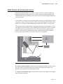
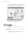
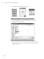
1
iii
PACIFIC NANOTECHNOLOGY PRODUCT WARRANTY
COVERAGE
Pacific Nanotechnology warrants that products manufactured by Pacific Nanotechnology will be free of defects in
materials and workmanship for one year from the date of shipment. The product warranty provides for all parts
(excluding consumables and maintenance items), labor, and software upgrades.
Instruments, parts, and accessories not manufactured by Pacific Nanotechnology may be warranted by Pacific Nanotechnology for the specific items and periods expressed in writing on published price lists or quotes. However, all
such warranties extended by Pacific Nanotechnology for those specific items and periods expressed in writing on
published price lists or quotes are limited in accordance with all the conditions, terms, and other requirements noted in this warranty. Pacific Nanotechnology makes no warranty whatsoever concerning products or accessories not
of its manufacture except as noted.
Customers outside the United States and Canada should contact their local Pacific Nanotechnology representative
for warranty information that applies to their locales.
CUSTOMER RESPONSIBILITIES
•
•
•
•
Complete ordinary maintenance and adjustments as stated in Pacific Nanotechnology manuals.
Use only Pacific Nanotechnology replacement parts.
Use only Pacific Nanotechnology-approved consumables such as filters, lamps, cantilevers, etc.
Provide safe and adequate working space for servicing of the products by Pacific Nanotechnology personnel.
REPLACEMENTS AND REPAIRS
•
Any product, part, or assembly returned to Pacific Nanotechnology for examination or repair must have prior
approval.
•
It must be identified by a Return Materials Authorization or RMA number obtained from Pacific Nanotechnology prior to shipment.
•
•
It must be returned freight prepaid to the designated address by the customer.
•
•
•
Pacific Nanotechnology will either replace or repair defective instruments or parts at its option.
Return freight costs will be prepaid by Pacific Nanotechnology if the product, part, or assembly is defective
and under warranty.
Repair and replacement of instruments or parts does not extend the time of the original warranty.
Replacement parts or products used on instruments out of warranty are themselves warranted free of defects
in materials and workmanship for 90 days with the exception of consumables such as filters, lamps, cantilevers, etc.
WARRANTY LIMITATIONS
This warranty does not cover:
1)
Any loss, damage, and or product malfunction caused by shipping or storage, accident, abuse alteration, misuse, or use of user-supplied software, hardware, replacement parts, or consumables other than those specified
by Pacific Nanotechnology.
2)
Parts and accessories that are expendable and replaceable in the course of normal operation.
3)
Products not properly placed and installed per Pacific Nanotechnology installation instructions.
Revision 1.1
iv
4)
Products not operated within the acceptable parameters noted per Pacific Nanotechnology installation instructions.
5)
Products that have been altered or customized without prior written authorization from Pacific Nanotechnology.
6)
Products that have had their serial number removed, altered or otherwise defaced.
7)
Improper or inadequate care, maintenance, adjustment, alteration, or calibration by the user.
Binary License Agreement
The use of the Pacific Nanotechnology instruments per the instructions in this manual includes executing a program. The Licensee assumes responsibility for the executed program chosen for your purposes, and for the use,
installation, and results received from it.
YOUR LICENSE WILL BE TERMINATED AUTOMATICALLY IF YOU COPY, MODIFY, USE OR TRANSFER THE
PROGRAM, OR ANY COPY, MODIFICATION, OR MERGED PORTION COMPLETELY OR PARTIALLY, EXCEPT AS SPECIFICALLY PROVIDED IN THIS LICENSE.
License:
The licensee may use the program on a single machine and copy the program into any machine-readable or printed
form for the support or the backup of the use of the program on the single machine.
The licensee may modify the program and or merge it into another program for your use on the single machine.
Any portion of the program that is merged into another program will continue to be subject to the terms of this
Agreement. The licensee must reproduce and include the copyright notice on any copy, modification, or portion
merged into another program.
If the licensee transfers the program and license to another party within your organization, said party must agree
to accept the terms and conditions of this Agreement. The licensee must, when transferring the program, either
transfer all copies, in any form (machine readable or printed), to the same party and destroy any copy (machine
readable or printed) or copies not transferred. The licensee may not transfer the program to anyone outside of the
licensee's organization without the written and express permission of Pacific Nanotechnology.
This license is effective from the date you take delivery of the software as purchased from Pacific Nanotechnology,
and remains in effect until terminated as indicated above or until the licensee terminates it. The licensee agrees to
destroy or return the program together with all copies, modifications, and merged programs in any form on their
termination of this license.
Revision 1.1
v
Copyright Notice — covers all attached documents
©Pacific Nanotechnology Incorporated 2004. All rights reserved.
Pacific Nanotechnology retains all ownership rights to this documentation and all revisions of the SPM Cockpit™
and NanoRule+ computer programs and other related software options.
Reproduction of any portion of this document or any image depicted in this publication without prior written authorization (with the exception of archival purposes or for the specific use of the program with Pacific Nanotechnology equipment) is prohibited by law and is a punishable violation of the law.
PACIFIC NANOTECHNOLOGY INCORPORATED PROVIDES THIS PUBLICATION “AS IS” WITHOUT WARRANTY OF ANY KIND, EITHER EXPRESS OR IMPLIED, INCLUDING BUT NOT LIMITED TO THE IMPLIED
WARRANTIES OR CONDITIONS OF MERCHANTABILITY OR FITNESS FOR A PARTICULAR PURPOSE. IN
NO WAY SHALL PACIFIC NANOTECHNOLOGY INCORPORATED BE LIABLE FOR ANY LOSS OF PROFITS,
LOSS OF BUSINESS, INTERRUPTION OF BUSINESS, LOSS OF DATA, LOSS OF USE, OR FOR SPECIAL, INCIDENTAL, INDIRECT, OR CONSEQUENTIAL DAMAGES OF ANY KIND EVEN IN THE EVENT OF SUCH DAMAGES ARISING FROM ANY DEFECT OR ERROR IN THIS PUBLICATIONS OR IN THE SPM COCKPIT™
SOFTWARE.
The trademarks or registered trademarks of Pacific Nanotechnology include the Pacific Nanotechnology logo,
Nano-R, SPM Cockpit, NanoRule+, X'Pert Mode, and EZ Mode.
Revision 1.1
vi
Safety Statement
LASER OPERATION: AFM SCANNING HEAD LASER
WARNING: NEVER LOOK DIRECTLY INTO THE LASER BEAM
IN ORDER TO AVOID THE POSSIBILITY OF THE USER INADVERTENTLY
LOOKING INTO THE LASER, ALWAYS USE THE SOFTWARE OR HARDWARE TO SWITCH THE LASER OFF BEFORE RAISING THE HEAD TO EYE
LEVEL.
The diode laser in the Nano-R™ scanning head complies with US 21 CFR 1040.10 and is certified as a Class IIIa laser. The laser wavelength is 670nm and the maximum power is 3 mW.
In addition to the above, please follow laser safety control measures in American National
Standards Institute Z136.1-1986.
HIGH VOLTAGE
Wherever high voltage is present on the system, extreme care should always be taken to
avoid direct contact while the instrument hardware is powered on. Always power off the
equipment before attempting to remove any panels or PC boards and before touching any
connectors by hand or with electrically conductive tools.
Pacific Nanotechnology, Inc. 2004
3350 Scott Blvd., Building #29 • Santa Clara, California 95054
Phone: (408) 982-9492 • Fax: (408) 982-9151
Revision 1.1
Nano-R AFM User’s Manual vii
Contents
Preface
Introduction . . . . . . . . . . . . . . . . . . . . . . . . . . . . . . . . . . . . . . . . . . . . . . . xi
AFM History . . . . . . . . . . . . . . . . . . . . . . . . . . . . . . . . . . . . . . . . . . . . . . . xi
Stylus Profilers . . . . . . . . . . . . . . . . . . . . . . . . . . . . . . . . . . . . . . . . . . xii
Scanning Tunneling Microscopes and Atomic Force Microscopes . .xiii
Nanoscience & Nanotechnology Overview . . . . . . . . . . . . . . . . . . . . . . . xv
AFM Tutorial
Introduction . . . . . . . . . . . . . . . . . . . . . . . . . . . . . . . . . . . . . . . . . . . . . . xxi
Concepts & Technologies. . . . . . . . . . . . . . . . . . . . . . . . . . . . . . . . . . . . xxi
Dimensions and Magnification . . . . . . . . . . . . . . . . . . . . . . . . . . . . . xxi
Piezoelectric Ceramic Transducer . . . . . . . . . . . . . . . . . . . . . . . . . . xxii
Force Sensors . . . . . . . . . . . . . . . . . . . . . . . . . . . . . . . . . . . . . . . . .xxiii
Feedback Control. . . . . . . . . . . . . . . . . . . . . . . . . . . . . . . . . . . . . . .xxiv
AFM Theory & Instrumentation . . . . . . . . . . . . . . . . . . . . . . . . . . . . . . . xxv
Taking Images . . . . . . . . . . . . . . . . . . . . . . . . . . . . . . . . . . . . . . . . . . . .xxvi
Resolution . . . . . . . . . . . . . . . . . . . . . . . . . . . . . . . . . . . . . . . . . . . xxvii
Probe Surface Interactions. . . . . . . . . . . . . . . . . . . . . . . . . . . . . . . xxvii
AFM Imaging Modes . . . . . . . . . . . . . . . . . . . . . . . . . . . . . . . . . . . xxviii
Chapter 1 Instrument Overview
Nano-R AFM Instrument System . . . . . . . . . . . . . . . . . . . . . . . . . . . . . . . .1
Hardware Components . . . . . . . . . . . . . . . . . . . . . . . . . . . . . . . . . . . . . . .2
Nano-R Stage. . . . . . . . . . . . . . . . . . . . . . . . . . . . . . . . . . . . . . . . . . . .2
AFM Scanner Head . . . . . . . . . . . . . . . . . . . . . . . . . . . . . . . . . . . . . . .3
AFM Probes . . . . . . . . . . . . . . . . . . . . . . . . . . . . . . . . . . . . . . . . . . . . .5
Sample Puck . . . . . . . . . . . . . . . . . . . . . . . . . . . . . . . . . . . . . . . . . . . .6
PNI Reference . . . . . . . . . . . . . . . . . . . . . . . . . . . . . . . . . . . . . . . . . . . . . .7
Software Modules . . . . . . . . . . . . . . . . . . . . . . . . . . . . . . . . . . . . . . . . . . .8
Acquisition . . . . . . . . . . . . . . . . . . . . . . . . . . . . . . . . . . . . . . . . . . . . . .9
Analysis . . . . . . . . . . . . . . . . . . . . . . . . . . . . . . . . . . . . . . . . . . . . . . .10
Basic Imaging Procedure . . . . . . . . . . . . . . . . . . . . . . . . . . . . . . . . . . . . .10
Revision 1.1
viii
Chapter 2 Tutorial: Contact EZMode
Before You Begin . . . . . . . . . . . . . . . . . . . . . . . . . . . . . . . . . . . . . . . . . . . 11
Powering Up the System . . . . . . . . . . . . . . . . . . . . . . . . . . . . . . . . . . . . . 11
Software Setup. . . . . . . . . . . . . . . . . . . . . . . . . . . . . . . . . . . . . . . . . . . . . 11
Load a Sample . . . . . . . . . . . . . . . . . . . . . . . . . . . . . . . . . . . . . . . . . . . . .14
Install a Probe . . . . . . . . . . . . . . . . . . . . . . . . . . . . . . . . . . . . . . . . . . . . .17
Align the Detector. . . . . . . . . . . . . . . . . . . . . . . . . . . . . . . . . . . . . . . . . . .23
Approaching the Sample . . . . . . . . . . . . . . . . . . . . . . . . . . . . . . . . . . . . .26
Scan the Sample . . . . . . . . . . . . . . . . . . . . . . . . . . . . . . . . . . . . . . . . . . .29
Image Processing . . . . . . . . . . . . . . . . . . . . . . . . . . . . . . . . . . . . . . . . . .34
Chapter 3 Tutorial: Close Contact EZMode
Before You Begin . . . . . . . . . . . . . . . . . . . . . . . . . . . . . . . . . . . . . . . . . . .39
Powering Up the System . . . . . . . . . . . . . . . . . . . . . . . . . . . . . . . . . . . . .39
Software Setup. . . . . . . . . . . . . . . . . . . . . . . . . . . . . . . . . . . . . . . . . . . . .39
Load a Sample . . . . . . . . . . . . . . . . . . . . . . . . . . . . . . . . . . . . . . . . . . . . .43
Install a Probe . . . . . . . . . . . . . . . . . . . . . . . . . . . . . . . . . . . . . . . . . . . . .45
Align the Detector. . . . . . . . . . . . . . . . . . . . . . . . . . . . . . . . . . . . . . . . . . .52
Frequency Sweep . . . . . . . . . . . . . . . . . . . . . . . . . . . . . . . . . . . . . . . . . .55
Approaching the Sample . . . . . . . . . . . . . . . . . . . . . . . . . . . . . . . . . . . . .58
Scan the Sample . . . . . . . . . . . . . . . . . . . . . . . . . . . . . . . . . . . . . . . . . . .61
Image Processing . . . . . . . . . . . . . . . . . . . . . . . . . . . . . . . . . . . . . . . . . .66
Chapter 4 Material Sensing Modes
Introduction . . . . . . . . . . . . . . . . . . . . . . . . . . . . . . . . . . . . . . . . . . . . . . .71
Lateral Force Microscopy (LFM) . . . . . . . . . . . . . . . . . . . . . . . . . . . . . . .71
Phase Imaging . . . . . . . . . . . . . . . . . . . . . . . . . . . . . . . . . . . . . . . . . . . . .73
Set Up . . . . . . . . . . . . . . . . . . . . . . . . . . . . . . . . . . . . . . . . . . . . . . . .73
Frequency Sweep . . . . . . . . . . . . . . . . . . . . . . . . . . . . . . . . . . . . . . .73
Scanning . . . . . . . . . . . . . . . . . . . . . . . . . . . . . . . . . . . . . . . . . . . . . .74
Force-Distance Curves . . . . . . . . . . . . . . . . . . . . . . . . . . . . . . . . . . . . . .76
Revision 1.1
Nano-R AFM User’s Manual
Chapter 5 X’Pert Mode & More
Introduction . . . . . . . . . . . . . . . . . . . . . . . . . . . . . . . . . . . . . . . . . . . . . . .81
X’Pert Mode . . . . . . . . . . . . . . . . . . . . . . . . . . . . . . . . . . . . . . . . . . . . . . .81
Config files . . . . . . . . . . . . . . . . . . . . . . . . . . . . . . . . . . . . . . . . . . . . . . . .83
Opening . . . . . . . . . . . . . . . . . . . . . . . . . . . . . . . . . . . . . . . . . . . . . . .83
Saving . . . . . . . . . . . . . . . . . . . . . . . . . . . . . . . . . . . . . . . . . . . . . . . .83
Stage Controls . . . . . . . . . . . . . . . . . . . . . . . . . . . . . . . . . . . . . . . . . . . . .84
Sample Mounting . . . . . . . . . . . . . . . . . . . . . . . . . . . . . . . . . . . . . . . . . . .85
Scanning . . . . . . . . . . . . . . . . . . . . . . . . . . . . . . . . . . . . . . . . . . . . . . . . .86
Feedback Controls . . . . . . . . . . . . . . . . . . . . . . . . . . . . . . . . . . . . . . .88
Saving Images . . . . . . . . . . . . . . . . . . . . . . . . . . . . . . . . . . . . . . . . . .89
Appendix: A Guide to AFM Image Artifacts
Introduction . . . . . . . . . . . . . . . . . . . . . . . . . . . . . . . . . . . . . . . . . . . . . . .91
Probe Artifacts . . . . . . . . . . . . . . . . . . . . . . . . . . . . . . . . . . . . . . . . . . . . .91
Surface Features Appear too Large . . . . . . . . . . . . . . . . . . . . . . . . . .92
Sub-surface Features Appear too Small . . . . . . . . . . . . . . . . . . . . . .93
Strangely Shaped Objects . . . . . . . . . . . . . . . . . . . . . . . . . . . . . . . . .94
Repeating Strange Patterns . . . . . . . . . . . . . . . . . . . . . . . . . . . . . . . .95
Scanner Artifacts . . . . . . . . . . . . . . . . . . . . . . . . . . . . . . . . . . . . . . . . . . .96
Probe-Sample Angle . . . . . . . . . . . . . . . . . . . . . . . . . . . . . . . . . . . . .96
X-Y Calibration/Linearity . . . . . . . . . . . . . . . . . . . . . . . . . . . . . . . . . .96
Z Calibration/Linearity . . . . . . . . . . . . . . . . . . . . . . . . . . . . . . . . . . . .98
Background Bow/Tilt . . . . . . . . . . . . . . . . . . . . . . . . . . . . . . . . . . . . .98
Z Edge Overshoot . . . . . . . . . . . . . . . . . . . . . . . . . . . . . . . . . . . . . .100
Scanner Drift . . . . . . . . . . . . . . . . . . . . . . . . . . . . . . . . . . . . . . . . . .101
X-Y Angle Measurements . . . . . . . . . . . . . . . . . . . . . . . . . . . . . . . .102
Z Angle Measurements . . . . . . . . . . . . . . . . . . . . . . . . . . . . . . . . . .102
Image Processing . . . . . . . . . . . . . . . . . . . . . . . . . . . . . . . . . . . . . . . . .103
Leveling . . . . . . . . . . . . . . . . . . . . . . . . . . . . . . . . . . . . . . . . . . . . . .103
High-Pass Filter . . . . . . . . . . . . . . . . . . . . . . . . . . . . . . . . . . . . . . . .104
Fourier Filtering . . . . . . . . . . . . . . . . . . . . . . . . . . . . . . . . . . . . . . . .104
Matrix-Filter Smoothing . . . . . . . . . . . . . . . . . . . . . . . . . . . . . . . . . .104
Image Looks Too Good . . . . . . . . . . . . . . . . . . . . . . . . . . . . . . . . . .105
Revision 1.1
ix
x
Vibrations . . . . . . . . . . . . . . . . . . . . . . . . . . . . . . . . . . . . . . . . . . . . . . . .106
Floor Vibrations . . . . . . . . . . . . . . . . . . . . . . . . . . . . . . . . . . . . . . . .106
Acoustic Vibrations. . . . . . . . . . . . . . . . . . . . . . . . . . . . . . . . . . . . . .106
Other Sources . . . . . . . . . . . . . . . . . . . . . . . . . . . . . . . . . . . . . . . . . . . .107
Electronics . . . . . . . . . . . . . . . . . . . . . . . . . . . . . . . . . . . . . . . . . . . .107
Surface Contamination. . . . . . . . . . . . . . . . . . . . . . . . . . . . . . . . . . .107
Vacuum Leaks . . . . . . . . . . . . . . . . . . . . . . . . . . . . . . . . . . . . . . . . .108
Revision 1.1
xi
Preface
INTRODUCTION
The Nano-R™ AFM is an easy-to-use, high-performance atomic force microscope
(AFM). While the Nano-R can be operated with little or no understanding of the
components of an AFM, Pacific Nanotechnology recommends that those who are
new to AFMs first take the time to read the AFM Tutorial on page xxi. Some understanding of the components and theory of an AFM system will greatly facilitate your ability to get optimal results from the Nano-R™ AFM.
AFM HISTORY
When we think of microscopes, we typically think of optical or electron microscopes. Such microscopes create a magnified image of an object by focusing electromagnetic radiation, such as photons or electrons, on its surface. Optical and
electron microscopes can easily generate two-dimensional magnified images of
an object's surface, with a magnification as great as 1000x for an optical microscope, and as large as 100,000x for an electron microscope. Although these are
powerful tools, the images obtained are typically in the plane horizontal to the
surface of the object. Such microscopes do not readily supply the vertical dimensions of an object's surface—the height and depth of the surface features.
The atomic force microscope (AFM), developed in the mid 1980's, uses a sharp
probe to magnify surface features. With an AFM, it is possible to image an object's
surface topography with extremely high magnifications, up to 1,000,000x. Furthermore, the magnification of an AFM is made in three dimensions: the horizontal X-Y plane and the vertical Z dimension. As acknowledged by Bennig and
Roher9, the inventors of the tunneling microscope, such a powerful technique has
its origins in the stylus profiler.
9. G. Bennig and H. Rohrer, Scanning Tunneling Microscopy-From Birth to Adolescence,
Rev. of Mod. Phys, Vol 59, No. 3, 1987, P 615
Revision 1.1
xii
Preface
STYLUS PROFILERS
Magnification of the vertical surface features of an object (those features leaving
the horizontal plane and extending in the vertical direction) have historically
been measured by a stylus profiler. Figure a illustrates an example of an early
profiler. This profiler, invented by Schmalz10 in 1929, utilized an optical lever
arm to monitor the motion of a sharp probe mounted at the end of a cantilever.
A magnified profile of the surface was generated by recording the motion of the
stylus on photographic paper. This type of “microscope” generated profile
“images” with a magnification of greater than 1000x.
photographic
film
mirror
light source
moving stage
flexure
Figure a. Example of a surface profiler made in 1929.
A common problem with stylus profilers was the possible bending of the probe
due to collisions with surface features. Such “probe bending” was a result of horizontal forces on the probe caused when it encountered large features on the
surface. This problem was first addressed by Becker11 in 1950 and later by Lee12.
Both Becker and Lee suggested oscillating the probe from a null position above
the surface to make contact with the surface. Becker remarked that the detail of
images measured using this vibrating profile method would depend on the
sharpness of the probe.
10. Uber Glatte und Ebenheit als physikalisches und physiologishes Problem, Gustev
Shmalz, Zeitchrift des Vereimes deutscher Ingenieurte, Oct 12, 1929, pp. 1461-1467
11. U.S. Patent 2,7288,222
12. UK Patent 2,009,409
Revision 1.1
Nano-R AFM User’s Manual
In 1971, Russell Young13 demonstrated a non-contact type of stylus profiler. In
his profiler, called the Topographiner, Young used the fact that, for electrically
conductive samples, the electron field emission current between a sharp metal
probe and a surface is very dependent on the probe-sample distance. In the Topographiner, the probe was mounted directly on a piezoelectric ceramic used to
move the probe in a vertical direction above the surface. An electronic feedback
circuit monitoring the electron emission was then used to drive the piezoceramic
and thus keep the probe-sample spacing fixed. Then, with piezoelectric ceramics,
the probe was used to scan the surface in the horizontal (X-Y) dimensions. By
monitoring the X-Y and Z position of the probe, a 3-D image of the surface was
constructed. The resolution of Young's instrument was controlled by the instrument’s vibrations.
SCANNING TUNNELING MICROSCOPES AND ATOMIC FORCE MICROSCOPES
In 1981, researchers at IBM were able to utilize the methods first demonstrated
by Young to create the scanning tunneling microscope14 (STM). Bennig and
Rohrer demonstrated that by controlling the vibrations of an instrument very
similar to Young's Topographiner, it was possible to monitor the electron
tunneling current between a sharp probe and a sample. Since electron tunneling
is much more sensitive than field emissions, the probe could be used to scan very
close to the surface. The results were astounding: Bennig and Rohrer were able
to see individual silicon atoms on a surface. Although the STM was considered a
fundamental advancement for scientific research, it had limited applications
because it only worked on electrically conductive samples.
A major advancement in profilers occurred in 1986 when Bennig and Quate15
demonstrated the AFM. Using an ultra-small probe tip at the end of a cantilever,
the AFM could achieve extremely high resolutions. Initially, the motion of the
cantilever was monitored with an STM tip. However, it was soon realized that a
light-lever, similar to the technique first used by Schmalz, could be used for
measuring the motion of the cantilever. In their paper, Bennig and Quate
proposed that the AFM could be improved by vibrating the cantilever above the
surface.
13. R. Young, J. Ward, F. Scire, The Topografiner: An Instrument for Measuring Surface
Microtopography, Rev. Sci. Inst., Vol 43, No 7, p 999
14. G. Bennig, H. Rohrer, Ch. Gerber, E. Weibel, Surface Studies by Scanning Tunneling
Microscopy, Vol. 49, No 1, 1982, p 57
15. G. Bennig, C.F. Quate, Ch. Geber, Atomic Force Microscope, Phys. Rev. Letters, Vol. 56,
No 9, p 930
Revision 1.1
xiii
xiv
Preface
The first practical demonstration of the vibrating cantilever technique in an AFM
was made in 1987 by Wickramsinghe16, using an optical interferometer to
measure the amplitude of a cantilever's vibration.
Oscillation amplitudes of between 0.3 nm and 100 nm were achieved with this
optical technique. Because the probe came into close contact with the surface
upon each oscillation, Wickramsinghe was able to sense the surface materials; the
differences between photo-resist and silicon were readily observed.
16. Y. Martin, C.C. Williams, H.K. Wickramasinghe, Atomic Force Microscope-Force Mapping and Profiling on a sub 100-Å scale. J. Appl. Phys. Vol 61, No 9, 1987, p 4723
Revision 1.1
Nano-R AFM User’s Manual
NANOSCIENCE & NANOTECHNOLOGY OVERVIEW
Approximately 15 years ago scientists and engineers began discussing a technological revolution that would be as dramatic and far-reaching to society as the industrial revolution: the nanotechnology revolution. At first, the primary
promoters of the nanotechnology revolution were considered eccentric at best,
and a little crazy at worst. However, their ideas and visions are now becoming
accepted by the mainstream intellectual, scientific, and engineering communities. Recently, governments and major corporations around the world have
committed several billion dollars per year for the advancement of nanotechnology and nanoscience research and development.
ATOMS AND MOLECULES
The systematic study, manipulation, and modification of atoms and molecules
having nanometer-sized dimensions began several hundred years ago. Society
has benefited greatly because chemists are able to use chemical reactions to
combine several types of atoms to create new types of molecules. With the advent
of quantum physics, physicists, chemists, and biologists can routinely study the
spectra of atoms and molecules. Several decades ago, biochemists began to
discover the usefulness of particular types of molecules such as proteins,
enzymes, and DNA.
Until recently, however, working with and controlling atoms and molecules was
limited to large quantities of these nanometer-sized objects. Realistically,
chemists would modify hundreds of trillions of molecules in a typical chemical
reaction. When chemists synthesize new molecules, they make them in large
quantities by using macroscopic methods such as heat to initiate chemical reactions. Biologists can identify and create new types of genetic material, but only
for a large number of molecules.
SO WHAT'S NEW?
All the revolutions in science and technology are facilitated by many driving
forces occurring simultaneously. The nanotechnology revolution, too, is being
driven by a number of developments, ideas, and technical advancements, the
primary ones being:
Revision 1.1
xv
xvi
Preface
Instruments that measure & manipulate atoms and molecules
The invention of the Scanning Tunneling Microscope (STM) permitted us to see
single atoms on a surface for the first time. Before this, it was possible to view and
create images of lattices of many molecules using techniques based on electromagnetic radiation. For example, x-ray techniques make it possible to recreate the
positions of atoms in a complex matrix or lattice. Tunneling electronic microscopes (TEM) make it possible to directly image atoms in a lattice. However,
these techniques cannot see single atoms, as they rely on the scattering of electromagnetic radiation from a collection of atoms.
Another important innovation is the laser “tweezer.” By using the momentum of
photons, it is possible to isolate collections of several hundred molecules or atoms
in a single location. Prior to this invention, the possibility of isolating a few
molecules or even a few hundred molecules was not considered possible.
The drive to make smaller computer chips & higher density information
storage
Moore's law, popularized in the late 20th century, dictates that there is a relationship between time and the size of electronic devices such as transistors. This relationship has been very effective in predicting advances in the world of
microelectronics for almost thirty years. However, physicists are predicting that
Moore's law will begin breaking down when the size of electronic devices
becomes less than 100 nanometers. There is a great effort, therefore, to discover
new methodologies for creating electronic devices of this size and smaller.
The storage of information is considered an essential advancement of modern
civilization. At first, recording information and ideas on written paper was a
great achievement; books and newspapers allowed the flow of knowledge and
information throughout the world. Today, information is stored digitally and
transmitted electronically. Digital bits with dimensions of less than a micron are
stored on magnetic disks and compact discs. There is an ever-increasing need to
store and transmit information on smaller spaces and transmit information with
faster methodologies.
Emerging belief that it is possible to mimic the mechanisms of biology
Researchers in the life sciences have discovered over the past few decades that
there are many fundamental mechanisms that facilitate the recreation and
support of all life forms. At a distance, these mechanisms can be characterized as
machines or engines. They absorb energy and, in a very efficient way, cause
events to occur. For example, a virus will permeate a cell and then integrate with
the genetic material of the cell.
Revision 1.1
Nano-R AFM User’s Manual
xvii
Presently, we can observe these activities on a macroscopic scale. In many cases,
we do not understand how they work or why they work. But there is a belief that
we can understand, emulate, and even use these fundamental activities or
machines that occur in biological systems.
Creation of mechanical devices having nanometer tolerances and motions
(MEMS)
To a great extent, the industrial revolution occurred because it became possible
to shape mechanical objects and thus create new types of machines. Before the industrial revolution, it was possible to routinely make objects that had dimensions
on the order of a few hundredths of an inch. An artist could paint pictures; a
potter could make dishes and pots. With the industrial revolution, it became
possible to routinely make machines with tolerances of a few thousandths of an
inch (25 to 100 microns), which gave way to the invention of the steam engine,
railroads, the car, and the airplane.
With MEMS technology, it is now possible to use machining technologies to
create machines smaller than the width of a human hair. This ability is presently
used in the sensors that activate airbags in cars, set the frequency of computers,
and allow digital projection.
NANOSCIENCE
Applying the scientific method to further understand the behavior of atoms and
molecules at the nanometer scale will push forward the frontiers of human
knowledge. Currently, our vision of the nano-world is based only on evidence we
collect from the macroscopic world in which we live. Presently, biologists,
chemists, physicists, and engineers have only a mental picture of what is
occurring on the nanometer scale. In fact, only very recently have they actually
seen or directly observed nano-events.
As an analogy, suppose you were presented with a gift in a box wrapped with
paper. In an effort to guess what is in the package, you could shake it or maybe
drop it. Based on how the package behaves under this “interrogation,” you may
get an idea of what is in it (i.e., is it heavy?, does it make a noise?). With the nano
revolution, scientists will be able to open the package—and really see what is
inside.
With new ideas and methods, scientists are beginning to further understand how
a single atom or molecule behaves. Even more interesting is the direct understanding of how collections of two or three or even a dozen atoms or molecules
behave.
Revision 1.1
xviii
Preface
NANOTECHNOLOGY
The fundamental knowledge gained through nanoscience and developments in
nanotechnology will certainly accelerate over the next several decades. With the
control of materials at the nanometer dimension, engineers are already able to
create new types of products and services. For example, the smallest transistors
we make in a factory today are about 130 nanometers wide. With future nanotechnology advancements, engineers will be able to make chips that have transistors 2-3 nanometers wide. Today, cosmetic manufacturers use liposomes with
diameters of a few tens of nanometers to reduce the dehydration of skin.
We expect that the nanotechnology revolution will result in the creation of new
types of products and services that will greatly benefit our lives.
What is Possible?
When the ideas and concepts discussed as part of the nanotechnology revolution
are fully implemented, what is possible? At this point, many of the possibilities
being discussed seem like science fiction.
We can only imagine what is possible…
Imagine:
Revision 1.1
•
All of recorded history will fit in a package small enough to carry in our
pockets. This includes all written documents, music, and movies.
•
Our world will be safer because the computers and sensing systems that
fit in a package the size of a pill will be able to warn us of dangers.
•
Life will be extended because we can create systems and modules that
replicate the functions and systems in our bodies.
•
New types of “quantum computers” will make calculations billions of
times faster than today's digital computers.
•
We can create new types of molecules with the mechanical assembly of
chemical systems instead of today's assembly by thermodynamic
chemical reactions.
Nano-R AFM User’s Manual
WHAT IS THE AFM’S CONTRIBUTION TO NANOTECHNOLOGY?
Measurement
An atomic force microscope (AFM) creates a highly magnified, three-dimensional image of a surface. The image is generated by monitoring the motion of an
atomically sharp probe as it is scanned across a surface. With an AFM, scientists
and engineers can directly view and measure surface features having dimensions
on the order of a few nanometers, including single atoms and molecules.
An AFM makes it possible to measure more than the physical dimensions of a
surface, as there is a “physical” interaction of the probe with the surface. For
example, by lightly pushing against the surface with the probe, it is possible to
measure surface hardness. Also, the degree of ease with which the probe glides
across the surface is a measure of the surface “friction.”
Modification
An AFM can be used to write on a surface, just as a pen is used to write on paper.
This new type of “lithography” is a completely new method for making surface
modifications at the nanometer scale. It is already possible to modify surfaces by
physically scratching the surface, directly depositing molecules on the surface,
and using electric fields to modify surfaces. Presently, this use of the AFM is in a
very exploratory phase, but it is showing tremendous promise. One of the
important technological issues that must be solved is the writing speed of AFM
lithography systems.
Manipulation
An AFM probe can be used to directly move objects across a surface. The objects
may be pushed, rolled around, or even picked up by the probe. With such
methods, it is possible to create nanometer-sized objects. One of the important
aspects of using an AFM for direct manipulation is the user interface for generating the motions of the probe. Some interfaces measure the locations of particles,
such as microspheres on a surface, and then automatically move the spheres to a
pre-established location. In another type of interface, called the nanomanipulator, the motion of the probe follows the motion of the user’s hand. When you
move your hand up and down, the probe moves up and down. This kind of
interface also allows the user to “feel” and “touch” a surface.
Revision 1.1
xix
xx
Preface
Revision 1.1
xxi
AFM Tutorial
INTRODUCTION
This section serves as an introduction to how an AFM works. With a basic understanding of the technologies employed in an AFM and how they are implemented in the design and operation of the instrument, you can obtain optimal results
from your Nano-R AFM.
CONCEPTS & TECHNOLOGIES
DIMENSIONS AND MAGNIFICATION
An AFM is optimized for measuring surface features that are extremely small,
therefore it is important to be familiar with the dimensions of the features being
measured. An AFM is capable of imaging features as small as a carbon atom
(~ 0.25 nanometers in diameter) and as large as the cross section of a human hair
(~ 80 microns in diameter).
The common unit of dimension used for making measurements in an AFM is the
nanometer (nm), one billionth of a meter:
1 meter = 1,000,000,000 nanometers
1 micron (µm) = 1,000 nanometers
Another common unit of measure is the Angstrom (Å), a tenth of a nanometer:
1 nanometer = 10 Angstroms
Magnification in an AFM is the ratio of the actual size of a feature to the size of
the feature when viewed on a computer screen. Thus, when an entire cross
section of a human hair is viewed on a 500 mm (20-inch) computer monitor, the
magnification can be expressed as:
Magnification = 500 mm/.08 mm = 6,250x
Revision 1.1
xxii
AFM Tutorial
In the case of extremely high resolution imaging, the entire field of view of the
image may be 100 nm. In this case, the magnification on a 500 mm computer
screen is:
Magnification = 500 mm/(100 nm*1 mm/1,000,000 nm) = 5,000,000x
PIEZOELECTRIC CERAMIC TRANSDUCER
Precise mechanical motion in an AFM is created from electrical energy using an
electromechanical transducer. The electrical motor used in a washing machine is
the most common example of an electromechanical transducer. The electromechanical transducer most commonly used in an AFM is the piezoelectric ceramic.
A piezoelectric material undergoes a change in geometry when it is placed in an
electric field. The amount and direction of motion depends on the type of piezoelectric material, the shape of the material, and the field strength. Figure b shows
the motion of a piezoelectric disk when exposed to an electric potential.
apply
voltage
Figure b. When a voltage is applied to the top and bottom surface of the
piezoelectric disc, the disc expands.
A typical piezoelectric material will expand by about 1 nm per applied volt.
Therefore, larger motions can be attained by making piezoelectric transducers
with hundreds of layers of piezoelectric materials, as illustrated in Figure c.
apply
voltage
Figure c.
Revision 1.1
When a voltage is applied to the top and bottom surface of a stack of
piezoelectric disks, the entire stack expands.
Nano-R AFM User’s Manual
xxiii
The amount of expansion of the whole stack depends on the applied voltage, the
piezo material, and the number of disks. By using one thousand layers of piezoelectric material, it is possible to get motions as large as 1000 nm per volt, or 0.1
mm of motion with 100 volts.
FORCE SENSORS
The construction of an AFM requires a force sensor to measure the forces
between a small probe and the surface being imaged. A common type of force
sensor utilizes the relationship between the motion of a cantilever and the
applied force. The relationship is given by Hook's law:
F=-K*D
where:
•
K is a constant which depends on the material and dimensions of the
cantilever
•
D is the motion of the cantilever.
For a cantilever made of silicon that has dimensions of:
L = 100 µm, W= 20 µm, T = 1 µm,
the force constant, K, is approximately 1 newton/meter. Therefore, a force of 1
nanonewton is required to move the cantilever 1 nm.
laser
photodetector
cantilever
Figure d. The light lever method for sensing the motion of the cantilever.
Revision 1.1
xxiv
AFM Tutorial
The motion of the cantilever can be measured with the “light lever” method, as
illustrated in Figure d. A laser beam is reflected off the back side of the cantilever
and onto a photo-detector. Deflection of the cantilever causes the laser beam to
move across the surface of the photo-detector.
The motion of the cantilever is then directly proportional to the output of the
photo-detector. Motions as small as 1 nm are routinely measured by AFMs using
this method.
FEEDBACK CONTROL
Feedback control is commonly used for keeping the motion of one object in a
fixed relationship to another object. A simple example of feedback control occurs
when you walk down a sidewalk. As you walk, you constantly control your
motion by viewing the edge of the sidewalk. If you begin to walk off the
sidewalk, you correct your motion so that you stay on the sidewalk. Feedback
control is used for many everyday applications, including the automatic controls
in airplanes and the thermostat controls in buildings. In an AFM, feedback
control is used to keep the probe in a “fixed” relationship with the surface while
a scan is measured.
Revision 1.1
Nano-R AFM User’s Manual
xxv
AFM THEORY & INSTRUMENTATION
The theory and operation of an AFM is similar to that of a stylus profiler. The
primary difference is that probe forces on the surface are much smaller in the
AFM. Because of this, smaller probes can be used, and a much higher resolution
can be achieved.
In an AFM, a constant force is maintained between the probe and sample while
the probe is raster scanned across the surface. By monitoring the Z motion of the
probe as it is scanned, a three dimensional image of the surface is constructed.
The constant force is maintained by measuring the force on the cantilever with
the light lever sensor and by using a feedback control electronic circuit to control
the position of the Z piezoelectric ceramic. The motion of the probe over the
surface is generated by piezoelectric ceramics that move the probe and force
sensor across the surface in the X and Y directions. See Figure e.
X-P
SG
CPU
Y-P
Z
Z-P
FC
FCU
T
F
Figure e.
Main components and subsystems of an AFM system.
Z - coarse Z motion translator: Moves the AFM head towards the surface so that
the force sensor can measure the force between the probe and sample. The
motion of the translator is usually about 10 mm.
T - coarse X-Y translation stage: Positions the section of the sample to be imaged
directly under the probe.
Revision 1.1
xxvi
AFM Tutorial
X-P & Y-P - X and Y piezoelectric transducers: Move the probe over the surface
in a raster motion when an image is measured.
FS - Force Sensor: Measures the force between the probe and the sample by
monitoring the deflection of the cantilever.
Z-P - Z piezoelectric ceramic: Moves the force sensor and probe in the vertical
direction in response to the measured deflection of the cantilever as the probe is
scanned across the surface.
FCU - Feedback control unit: Takes in the signal from the light lever force sensor
and outputs the voltage that drives the Z piezoelectric ceramic. This voltage
refers to the voltage required to maintain a constant deflection of the cantilever
while scanning.
SG - X-Y signal generator: Controls the raster motion of the probe in the X-Y
plane when an image is measured.
CPU - Computer: Used for setting the scanning parameters (such as scan size,
scan speed, and feedback control response) and for visualizing images captured
with the microscope.
F - Frame: A solid frame supports the entire AFM instrument. The frame must
be very rigid in order to prevent vibrations between the tip and the surface.
NOTE: Not shown in Figure e is an optical microscope, which is essential for
locating features on the sample surface and for monitoring the probe approach
process.
TAKING IMAGES
Taking an image of a sample with an AFM involves the following basic steps:
Revision 1.1
1
Install a probe in the microscope, and align the light lever sensing system.
2
Position the region of interest on the sample directly under the AFM probe,
using the X-Y translation stage and the optical microscope.
3
Engage the Z translation stage to bring the probe to the surface.
4
Start the scanning of the probe over the surface, and monitor the resulting
AFM image on the computer screen.
5
Save the image on a computer disk.
Nano-R AFM User’s Manual
xxvii
RESOLUTION
Traditional microscopes have only one measure of resolution: the resolution in
the plane of an image. An AFM has two measures of resolution: in the X-Y plane
of the measurement surface (in-plane resolution) and in the direction perpendicular to the surface (vertical resolution).
In-Plane Resolution: The in-plane resolution depends on the geometry of the
probe used for scanning. In general, the sharper the probe, the higher the resolution. The theoretical line scans in Figure f illustrate the difference between using a
sharp probe and a dull probe to measure two spherical features on a sample
surface. The sharper probe will result in a higher resolution image.
Figure f.
Using a dull probe vs. a sharp probe to measure spherical features.
Vertical Resolution: The vertical resolution in an AFM is established by relative
vibrations of the probe above the surface. Sources of vibrations include acoustic
noise, floor vibrations, and thermal vibrations. Getting the maximum vertical resolution requires minimizing these vibrations.
PROBE SURFACE INTERACTIONS
The strongest forces between the probe and surface are the mechanical forces that
occur when the atoms on the probe physically interact with the atoms on a
surface. However, other forces between the probe and surface can have an impact
on an AFM image. These include surface contamination, electrostatic forces, and
surface material properties.
Surface contamination: In ambient air, all surfaces are covered with a very thin
layer (< 50 nm) of contamination. This contamination, which can be comprised of
water and hydrocarbons, depends on the microscope’s operating environment.
Revision 1.1
xxviii AFM Tutorial
When the probe comes into contact with the surface contamination, capillary
forces can pull the probe towards the surface.
Electrostatic forces: Insulating surfaces can store charges on their surface, which
can interact with charges on the probe or cantilever. Such forces can be so strong
that they “bend” the cantilever when scanning a surface.
Surface material properties: Heterogeneous surfaces can have regions of
varying hardness and friction. As the probe is scanned across a surface, the
probe-surface interaction can change when moving from one region to another.
Such changes in forces can give a “contrast” that is useful for differentiating
between materials on a heterogeneous surface.
AFM IMAGING MODES
Topography Modes
As the probe at the end of the cantilever is scanned over the sample surface, a
constant force between the probe and the sample is maintained. There are two
methods for measuring the force on the cantilever as the probe encounters
changes in the sample topography. In deflection, or “contact,” mode, the deflection of the cantilever is measured directly. In vibrating mode, the cantilever is
vibrated, and changes in the vibration properties are measured.
Deflection Mode: Using the feedback control in the AFM, it is possible to scan a
sample with a fixed cantilever deflection. Because the deflection of the cantilever
is directly proportional to the force on the surface, a constant force is applied to
the surface during a scan. While this scanning mode is often called “contact”
mode, because the forces of the probe on the surface are often less than a nanonewton, the probe is minimally touching the surface.
Figure g. Contact mode AFM: the probe directly follows the topography of the
surface as it is scanned while a constant force is maintained.
Revision 1.1
Nano-R AFM User’s Manual
xxix
Vibrating Mode: The cantilever in an AFM can be vibrated using a piezoelectric
ceramic. When the vibrating cantilever comes close to the sample surface, the
amplitude and phase of the vibrating cantilever may change. The feedback unit
keeps either the vibration amplitude or phase constant. Changes in the vibration
amplitude or phase are easily measured, and the changes can be related to the
force on the surface. This technique has many names, including “non-contact”
and “intermittent contact” mode. It is important that the tip not “tap” the surface,
as this may break the probe or damage the sample.
Figure h. In vibrating methods, changes in probes vibrations are monitored to
establish the force of the probe onto the surface.
Material Sensing Modes
The interaction of the probe with the surface depends on the chemical and
physical properties of the surface. It is therefore possible to measure these interactions and thus “sense” the materials at a sample surface.
Vibrating Material Sensing Mode: The AFM cantilever may be vibrated to
measure the force between the probe and sample during a scan. The magnitude
of amplitude damping and the amount of phase change of the cantilever depends
on the surface chemical composition and the physical properties of the surface.
Thus, on a non-homogeneous sample, contrast can be observed between regions
of varying mechanical or chemical composition. Typically, in vibrating material
sensing mode, if the amplitude is fixed by the feedback unit, then the contrast of
the material is observed by measuring phase changes. This technique has many
names, including phase mode, phase detection, and force modulated microscopy.
Torsion Modes: In contact mode AFM, it is possible to monitor the torsion
motions of the cantilever as it is scanned across the surface. The amount of torsion
of the cantilever is affected by changes in topography as well as changes in
surface chemical properties. If a surface is perfectly flat but has an interface
between two different materials, it is often possible to image the change in
material properties. This technique is similar to lateral force microscopy (LFM).
Revision 1.1
xxx
AFM Tutorial
Figure i.
Revision 1.1
Torsion mode: changes in the torsion of the cantilever are an indication
of changes in the surface chemical composition.
1
Chapter 1
Instrument Overview
WARNING: Before operating the Nano-R AFM, make sure you are familiar with the safety information on page vi.
CAUTION: To prevent damage to your instrument, probe, and sample, observe all the caution
statements in the tutorial chapters (Chapter 2 and Chapter 3).
NANO-R AFM INSTRUMENT SYSTEM
computer
monitor
trackball
Master
Computer
video
microscope
monitor
Controller
(AFM control
electronics)
Nano-R
AFM stage
AFM scanner
& probe
sample
puck
Figure 1.1. Block diagram of Nano-R instrument system.
Revision 1.1
2
Chapter 1—Instrument Overview
Nano-R Stage - Includes the AFM scanner,
probe, sample puck, video optical microscope,
and the AFM scanner’s real-time calibration
sensors.
Master Computer - The IBM PC-type computer
is the virtual interface to the Nano-R AFM stage.
Pacific Nanotechnology software programs
resident on the computer’s hard disk are used for
measuring, visualization, and analysis of AFM
images.
Nano-R stage
Controller - Contains most of the electronics required
for operating the Nano-R stage. It is connected to the
Master Computer by a standard Ethernet cable, and
to the Nano-R stage by five cables.
Video Monitor - Displays the optical microscope
image of the probe-sample area. In some cases, the
computer monitor may be used as the video monitor.
Controller
Track ball - Provides an optional way to activate
many of the motorized features of the Nano-R stage,
including the X-Y stage positioning and the video microscope zoom and focus.
HARDWARE COMPONENTS
NANO-R STAGE
The AFM scanner head rests on three motorized posts, which are used to perform
a coarse Z approach of the probe tip to the sample surface. The sample puck rests
on a motorized X-Y stage for positioning the sample under the probe. The puck
can be easily removed for mounting a sample.
Revision 1.1
Nano-R AFM User’s Manual
video microscope
(with motorized
zoom & focus)
AFM scanner
head
motorized X-Y positioning
sample puck
Z approach motor
(1 of 3)
Figure 1.2. Stage components.
AFM SCANNER HEAD
The AFM scanner head contains the components that: 1) measure the force
between the probe and the sample, and 2) control the precise positioning of the
probe in X, Y, and Z.
The Z piezo component moves the probe vertically in response to changes sensed
in the sample surface. The X and Y piezos move the probe over the sample in a
raster pattern, which defines the scan region.
Revision 1.1
3
4
Chapter 1—Instrument Overview
laser
photodetector
cantilever
Figure 1.3. Light lever sensing system.
The Nano-R AFM scanner uses a light lever design. A red laser is focused on the
back of the cantilever and then projected onto a quad photodiode (photodetector). Two pairs of manual adjustment knobs on the scanner head are used to align
the sensing system. One pair controls the position of the laser light on the
backside of the cantilever; the other pair moves the photodetector into the light
path.
detector adjust knobs
laser adjust knobs
Figure 1.4. Adjustment knobs for laser and detector.
Revision 1.1
Nano-R AFM User’s Manual
AFM PROBES
CAUTION: Use care when handling AFM probes, as they can break very easily. Always handle
with tweezers, and never touch the cantilever.
The Nano-R AFM is shipped with
probes for the two basic imaging
modes: contact and close contact (vibrating cantilever). The probes come in
two marked boxes, 10 probes to a box.
AFM probes
cantilever
& probe
cantilever chip
metal substrate
Figure 1.5. PNI AFM probe (top view).
The probe tip extends from the end of a cantilever which is mounted to a chip.
The metal substrate that holds the cantilever chip is mounted in the AFM
scanner; it is magnetically coupled to the bottom of the scanner.
cantilever chip
metal substrate
cantilever
probe
Figure 1.6. PNI AFM probe (side view—not to scale).
Revision 1.1
5
6
Chapter 1—Instrument Overview
The two types of probes appear identical to the naked eye, but under the instrument’s optical microscope, you can see that contact cantilevers are significantly
longer than close contact cantilevers.
contact cantilever
close-contact cantilever
Figure 1.7. The two cantilever types, as seen on the video microscope monitor.
SAMPLE PUCK
The sample to be imaged is mounted on the sample puck. The puck is composed
of removable layers so the height of the puck can be adjusted to accommodate
different sample sizes (see page 85 for details). The protruding piece on the
bottom of the puck fits into the groove on the X-Y stage so it can be safely and
easily guided into position under the probe.
Figure 1.8. Sample puck.
Revision 1.1
Nano-R AFM User’s Manual
PNI REFERENCE
The Nano-R system is supplied with the PNI AFM reference, which is helpful for
establishing the performance of your instrument’s AFM scanners as well as the
optical microscope. The reference also serves as a useful test sample when
learning how to use your instrument (the tutorials in this manual are based on
this sample).
14 mm
1 mm
10 mm
A
B
1 mm
C
D
AFM Reference
A:
B:
C:
D:
Optical Reference
1 micron square/2 micron pitch
2.5 micron square/5 micron pitch
5 micron square/10 micron pitch
10 micron square/20 micron pitch
Notes:
- Feature height: nominal 75 nm
- Feature width: within +/- 0.3 microns
(15 lines in each: a, b, c, d)
a:
b:
c:
d:
a b
c
1 micron line/2 micron pitch
2.5 micron line/5 micron pitch
5 micron line/10 micron pitch
10 micron line/20 micron pitch
d
Figure 1.9. PNI reference.
Revision 1.1
7
8
Chapter 1—Instrument Overview
The patterns in the reference are made in a silicon nitride film deposited on a
silicon substrate. This combination gives optimal color contrast when viewed
with an optical microscope.
The pattern for AFM measurements is composed of four blocks of square
features. The features in each block have uniform size and pitch, with each block
containing features of a different size, as illustrated in Figure 1.9. This pattern is
repeated at 15 locations on the reference. The pattern for optical microscope
reference is composed of a series of four sets of parallel lines and a second series
perpendicular to the first.
SOFTWARE MODULES
The SPM Cockpit software modules serve three functions:
•
acquire AFM data
•
process and analyze the acquired data
•
display AFM images (contained in the analysis modules)
EZMode
Acquisition
X'Pert
SPM Cockpit
PNI Analysis
Analysis
NanoRule+
Figure 1.10. SPM Cockpit software modules.
The interfaces for the image acquisition and analysis modules feature tool bars
that provide convenient access to the most commonly-used software functions
for the given mode of operation. However, regardless of the module (acquisition
or analysis) or mode (EZ or X’Pert) you are in, all of the SPM Cockpit software
functions are always accessible via the menu items.
Note that the PNI Analysis software is included with all Nano-R AFM systems,
and NanoRule+, a more full-featured analysis software package, is available as
an option.
Revision 1.1
Nano-R AFM User’s Manual
ACQUISITION
When you launch the SPM Cockpit software, the acquisition module opens by
default. You will be in either EZMode or X’Pert Mode, depending on the mode
used in the last session. Use the Mode menu to switch between the two.
Figure 1.11. Acquisition module main screen, in EZMode.
EZMode is intended for new and occasional AFM users. A set of short-cut
buttons forms an easy-to-follow flow chart that takes you through the basic steps
for taking an AFM image. Each button opens a dialog offering the choices
necessary for accomplishing that step.
Figure 1.12. EZMode short cut buttons.
X’Pert Mode is oriented toward advanced AFM users who want to take
advantage of a wider range of choices and features for acquiring an image. The
X’Pert Mode short-cut buttons access the functions for accomplishing the same
required steps in EZMode, as well as other functions, but the buttons are not necessarily organized into sequential steps.
Figure 1.13. X’Pert mode short cut buttons.
Revision 1.1
9
10
Chapter 1—Instrument Overview
ANALYSIS
From the acquisition module, you can switch to the PNI Analysis module by
. A series of short-cut buttons is displayed for easy access to the most
clicking
commonly used image processing and analysis tools.
Figure 1.14. Analysis module short cut buttons.
To return to the acquisition module, click
.
BASIC IMAGING PROCEDURE
Acquiring an image with the Nano-R AFM requires the following basic steps,
whether you are a new, occasional, or advanced user:
Revision 1.1
1
Launch the SPM Cockpit software
2
Open a configuration file (contact or close-contact).
3
Retract the tip and raise the AFM scanner to provide safe clearance between
the probe tip and the sample puck.
4
Load a sample on the sample puck.
5
Install a probe on the AFM scanner.
6
Align the detector.
7
For close contact mode only, set the resonance frequency for the installed
cantilever.
8
Locate features for imaging.
9
Bring the probe into contact with the sample.
10
Scan the sample.
11
Perform image processing and analysis routines.
12
Retract the probe from the sample.
11
Chapter 2
Tutorial: Contact EZMode
BEFORE YOU BEGIN
This tutorial follows the steps for an taking a contact AFM image of the PNI AFM
reference in EZMode.
WARNING: Before operating the Nano-R AFM, make sure you are familiar with the safety information on page vi.
POWERING UP THE SYSTEM
1
Turn on the Master Computer.
2
Launch the SPM Cockpit software.
3
Turn on the Controller.
4
Turn on the video monitor.
SOFTWARE SETUP
1
Select Mode→EZMode.
2
Click the Start button from the EZMode toolbar.
3
Click Retract Tip, and click OK when complete.
Revision 1.1
12
Chapter 2—Tutorial: Contact EZMode
Figure 2.1. Retracting the tip.
4
Click Load Configuration, select the PNI-supplied contact mode configuration
file, and click Open.
Figure 2.2. Loading a configuration file.
This file should be located in the ConfigFiles folder in the SPM Cockpit
directory. It has the format sxxxx-con.cfg, where xxxx is the serial number of
your Nano-R system.
5
Click Linearize, check both boxes, and click OK.
Figure 2.3. Initiate connection confirm and calibration routines.
Revision 1.1
Nano-R AFM User’s Manual
6
Click OK when the communication between the Master Computer and the
Controller is confirmed.
Figure 2.4. Connection confirmed.
If there is no connection, you need to exit the SPM Cockpit software and
restart both the Master Computer and the Controller.
7
Click Yes to proceed with the calibration procedure.
Figure 2.5. Proceed with calibration routine.
8
Click OK when the last step of the calibration process is complete, and then
click OK to proceed.
Figure 2.6. Calibration routine complete.
Revision 1.1
13
14
Chapter 2—Tutorial: Contact EZMode
9
Click Select Mode on the toolbar, select Contact in the dialog, and click OK.
Figure 2.7. Select mode.
10
If the PNI AFM reference is already loaded on the sample puck, skip ahead
to page 17 to load a probe, or to page 23 if a contact probe is already loaded.
LOAD A SAMPLE
1
Click Tip Retract from the EZMode toolbar.
2
Click Stage from the EZMode toolbar.
3
Click
to raise the Z motor until there is at least a few millimeters of
clearance between the probe and the sample surface or puck, if no sample is
loaded (monitor by eye).
Figure 2.8. Raise the probe tip away from the sample.
Revision 1.1
Nano-R AFM User’s Manual
CAUTION: To prevent damage to your scanner, probe, and sample, be sure you have retracted
the tip and raised the Z scanner (as described in the preceding steps) before moving the puck.
4
Click
.
The motorized X-Y stage will move the puck towards you, to the limit of its
range.
5
Being careful not to touch the probe, slide the sample puck towards you, and
then lift it up out of the groove.
Figure 2.9. Remove puck.
6
Use tweezers to mount the PNI AFM reference on the center of the puck.
The sample disk is held in place magnetically.
Figure 2.10. Mounting the sample.
Revision 1.1
15
16
Chapter 2—Tutorial: Contact EZMode
7
Replace the puck on the stage by setting it down so the protruding piece on
the bottom fits into the wide part of the groove, and then slide it into position.
groove
Figure 2.11. Fit the sample puck into the groove on the X-Y stage.
8
9
Rotate the puck so that the PNI reference sample is square with the scanner
head.
Select Tools→NanoR Stage to open the AFM Stage Controls window.
Figure 2.12. Return sample puck to initial X-Y position.
10
Click
.
The motorized X-Y stage will return the puck to its original position
Revision 1.1
Nano-R AFM User’s Manual
INSTALL A PROBE
To operate in contact mode, you need to use a contact probe. Probes should be
stored in the supplied boxes marked “Contact” and “Close-contact,” as the difference between the two types of probes is not visible to the naked eye.
1
First, remove the sample puck as described in the section above.
2
Click Stage from the EZMode toolbar, and click
Stage Controls dialog.
in the AFM
Figure 2.13. Raise the probe tip away from the sample.
The Z motors will raise the scanner to the top of its range.
3
Click the
focus button to raise the video objective to the top of its range.
The upper indicator will turn from green to red when the objective reaches
the top of its range.
4
Click Align Laser from the tool bar.
5
Turn off the laser.
Revision 1.1
17
18
Chapter 2—Tutorial: Contact EZMode
Figure 2.14. Turning off the laser.
WARNING: To avoid potentially hazardous laser exposure, be sure to turn off the laser
before rotating the scanner into the probe exchange position.
6
Turn the probe exchange knobs on the side of the scanner head down (away
from you) 1/4 turn (Figure 2.15).
The scanner head will slide out about an inch.
Figure 2.15. Turn the knobs to disengage the scanner head.
Revision 1.1
Nano-R AFM User’s Manual
7
Grasp the handles on the front of the scanner head (Figure 2.16), and gently
slide the scanner head all the way towards you.
Figure 2.16. Slide the scanner head toward you.
8
Carefully rotate the scanner head up about 90 degrees, as shown in Figure
2.17.
Figure 2.17. Rotate the scanner head.
Revision 1.1
19
20
Chapter 2—Tutorial: Contact EZMode
probe
mount
Figure 2.18. Probe exchange position.
CAUTION: Handle AFM probes with care. The cantilever can break off easily if it touches anything or snaps down too forcefully on the magnetic mounting surface on either the scanner or in
the probe box.
Probe handling: When loading or removing a probe, pivot the substrate on
the edge opposite the cantilever, as shown in Figure 2.19. This will protect the
cantilever from striking the magnetic mounting surface, and it will prevent
the substrate from snapping down too forcefully, which may damage the
probe.
Figure 2.19. Probe handling.
Revision 1.1
Nano-R AFM User’s Manual
9
10
To remove a probe:
a)
Use tweezers to grasp the metal substrate as indicated in Figure 2.22.
b)
Carefully rotate the tweezers so the cantilever side of the substrate lifts
up off the magnetic mount first.
c)
Set the probe down onto the magnetic strip in the probe box so that the
side of the substrate opposite the cantilever makes contact first.
d)
Carefully rotate the tweezers so the cantilever side of the substrate comes
down onto the magnetic surface as gently as possible.
To install a new probe:
a)
Use tweezers to nudge a probe so that the substrate extends over the edge
of the magnetic strip in the probe box (Figure 2.20).
b)
Grasp the metal substrate, and carefully rotate the tweezers so the
cantilever side of the substrate lifts up off the magnetic strip first, as
shown in Figure 2.21.
Figure 2.20. Nudge the probe into position.
Revision 1.1
21
22
Chapter 2—Tutorial: Contact EZMode
Figure 2.21. Lift the probe, cantilever side first.
c)
Place the probe onto the magnetic mount so the side of the substrate
opposite the cantilever fits into the “L.”
“L”
mount
Figure 2.22. Mounting the probe.
Revision 1.1
Nano-R AFM User’s Manual
d)
Use the tweezers to push the substrate flush against the “L,” as shown in
Figure 2.23.
Figure 2.23. Push the probe substrate flush against the “L” mount.
11
Hold the scanner head by the handles, and rotate it back to the level position.
12
Gently slide the scanner back towards the stage until you feel some
resistance.
13
Turn the probe exchange knobs up (1/4 turn) to lock the scanner head into
place.
Now you can replace the sample puck, as described above (page 16).
ALIGN THE DETECTOR
1
Click Stage from the EZMode toolbar.
2
Use the focus controls to bring the probe tip into focus on the video monitor.
Focus controls: Click
to adjust the focus a single step, or hold it down
for continuous motion. Click
to initiate a large, continuous movement of
pre-set duration.
Revision 1.1
23
24
Chapter 2—Tutorial: Contact EZMode
Figure 2.24. Focus controls.
If you cannot find the probe on the monitor:
•
The probe may not have been
installed properly. Repeat the probe
installation procedure to make sure
the probe is seated squarely in the
“L” mount (page 17).
•
The objective’s field of view may
need to be adjusted in X-Y, using the
adjust screws. This is usually
necessary when switching between a
contact and close-contact probe, due
to the difference in size.
You can confirm that you have installed
a contact cantilever by noting the difference in length between contact and
close-contact cantilevers, as shown in
Figure 2.25.
Revision 1.1
adjust
screws
Nano-R AFM User’s Manual
close-contact cantilever
contact cantilever
Figure 2.25. Contact vs. close-contact probes.
3
Click
on the toolbar.
4
Turn on the laser.
The red dot alignment procedure has 3 goals:
5
•
position the laser spot on the back of the cantilever
•
position the photodetector in the center of the reflected laser beam
•
achieve a minimum overall measured signal strength
Watch the video monitor as you adjust the laser alignment knobs on the
scanner head to bring the laser spot onto the back of the cantilever.
The laser spot should be centered on the cantilever, not too close to the end,
as shown in Figure 2.26.
Figure 2.26. Centering the laser spot on the cantilever.
Revision 1.1
25
26
Chapter 2—Tutorial: Contact EZMode
6
Watch the red dot (in the Red Dot Alignment window) as you turn the
detector alignment knobs to bring the red dot into the top of the green box.
The red dot should be positioned just below the upper border of the box and
be centered along the vertical axis, as shown in Figure 2.27.
Figure 2.27. Aligning the detector.
7
Make sure the Z(SUM) value (signal intensity) is above the minimum.
If it is not, you need to re-seat or replace the probe.
APPROACHING THE SAMPLE
1
Click
from the EZMode toolbar.
2
Use the focus controls to bring the sample surface into focus on the video
monitor.
CAUTION: Whenever you engage the motorized X-Y stage, be sure the probe is a safe distance
above the sample/puck.
3
Revision 1.1
Use the X-Y stage controls to navigate to the largest of the four patterns on the
PNI AFM reference (10 µm squares/20 µm pitch).
Nano-R AFM User’s Manual
Increase or decrease the X-Y step size, as desired, to facilitate both coarse and
fine movements.
Figure 2.28. X-Y stage controls.
10 µm squares/20 µm pitch
Figure 2.29. Positioning the probe over the scan area.
If necessary, you can orient the sample by simply rotating the puck by hand.
Revision 1.1
27
28
Chapter 2—Tutorial: Contact EZMode
4
Focus on the cantilever.
CAUTION: Be careful not to drive the probe all the way into the sample surface.
5
While carefully monitoring the probe-sample distance by eye, use the
button to lower the Z scanner until the probe is about 1-2 mm above the
sample surface.
6
Focus on the sample surface, and make sure the probe is positioned
somewhere near the center of the pattern.
7
Click the Tip Approach button on the toolbar.
8
Click OK when the tip approach is complete.
CAUTION: Once the tip approach is complete, and the tip is in contact with the sample surface,
do not exit the SPM Cockpit software or turn off the Controller without first retracting the tip. Doing
so may cause damage to the tip, scanner, and sample.
Figure 2.30. Tip approach confirmation.
The PID indicator at the bottom of the window will turn green to indicate
that the probe tip is in contact with the sample surface, and the instrument is
now ready to perform a scan.
Revision 1.1
Nano-R AFM User’s Manual
SCAN THE SAMPLE
1
Click the Scan Sample button on the toolbar.
Figure 2.31. Scan image window.
2
Set the scanner controls as follows:
•
Scan Size: leave as is*
•
Scan Rage: 2 Hz
•
Resolution: 256
•
Scan Angle: 0
•
Acq. Channels: 4
•
Topography Gain: 1x
* The default scan size, which is entered by
the system when the calibration routine is
performed, is the maximum scan area for
your scanner.
Revision 1.1
29
30
Chapter 2—Tutorial: Contact EZMode
3
4
Set the feedback controls as follows:
•
Setpoint: 0
•
Gain: 2
•
Proportional: 5
•
Integral: 5
•
Derivative: 0
Select the Z(SEN) and Z(ERR) channels from the drop-down menus beneath
the two image displays, and for each display, select Forward, Histogramcorrection, and Auto-leveling.
Figure 2.32. Image display settings.
5
Select the Z(SEN) and Z(ERR) channels from the drop-down menus of the
two corresponding line scan displays.
Figure 2.33. Line scan settings.
Revision 1.1
Nano-R AFM User’s Manual
6
Click
to take a scan.
Figure 2.34. Taking a scan.
•
The images of the selected channels will build up line-by-line
in the displays. If no data is generated, the detector may be out
of alignment. In this case, click the
button, click Tip
Retract from the toolbar, re-align the red dot (page 23), and try
another scan.
•
To adjust the Z scale of the images, left-click and drag in the bar
to the left of each display to select a Z height range.
•
To view a single line scan, hold down the SHIFT key and leftclick in either image display to define a horizontal line across
the image; make sure the line includes the square features. The
line scan profile for the Z(SEN) channel should resemble the
shape and size of the 10 µm features.
Z
scale
adjust
Revision 1.1
31
32
Chapter 2—Tutorial: Contact EZMode
Figure 2.35. Viewing a single line scan.
When the feedback controls are properly set, the forward and reverse line
scan profiles for the Z(ERR) channel will roughly mirror each other.
Figure 2.36. Z(ERR) channel line profile.
Revision 1.1
7
To take additional scans, click
again, or check Repeat Scan to take
continuous scans of the same region.
8
To zoom to a new scan region:
a)
Left-click and drag in the image display to define a scan area.
b)
Left-click again to position the box within the scan region.
c)
Right-click to confirm the new scan region.
Nano-R AFM User’s Manual
d)
Click OK to zoom to the new
scan area.
The probe will move to the new
scan region, where you can start
a new scan. Additional zoom
features are accessible via the
Zoom and Extra Zoom buttons,
or by simply double-clicking in
the display.
Zoom confirm
zoom
region
Figure 2.37. Selecting a zoomed-in scan region.
9
To end your session now, click Tip Retract on the EZMode toolbar.
Once the tip is retracted, it is safe to turn off the Master Computer and the
Controller.
Revision 1.1
33
34
Chapter 2—Tutorial: Contact EZMode
IMAGE PROCESSING
1
Click Image Processing on the EZMode tool bar.
2
Click
to open an image for processing.
Figure 2.38. Image processing module.
3
Select the desired acquisition channel and
direction for the image to be processed.
The raw image data will not resemble the
image in the scan image window, as some
basic real-time image processing was
applied as it was being acquired.
4
Revision 1.1
Click
to apply a plane correction.
Nano-R AFM User’s Manual
excluded
areas
Figure 2.39. Plane leveling tool.
a)
b)
Under Select Correction Model, select:
•
Polynomial X-line leveling
•
Polynomial order: 1
Under Select Area to Analyze, select:
•
Exclude Area
•
Area marker: Rectangle.
Revision 1.1
35
36
Chapter 2—Tutorial: Contact EZMode
c)
To exclude the features on the PNI AFM reference, use the mouse to leftclick and drag in the image display so that every feature (both whole and
partial) is completely covered.
d)
Click Apply, and the leveled image appears in the right-hand display.
Figure 2.40. Leveled image (right).
Revision 1.1
Nano-R AFM User’s Manual
5
Click
to open the line profile tool.
left-click to select line
markers
Figure 2.41. Line profile tool.
a)
Under Profile Mode, select Horizontal.
b)
Under Display Mode:
•
Check Fit Vertical Scale
•
Uncheck Invert Data
c)
Left-click in the image display to select a line.
d)
Left-click in the line display to make measurement markers.
In the example above, measurements are made between the edges of two
consecutive features on the PNI AFM reference. The measurements
displayed to the right confirm a pitch of 20 µm and a Z-height of
approximately 70 nm.
NOTE: These measurements should not be used to calibrate your instrument!
Revision 1.1
37
38
Chapter 2—Tutorial: Contact EZMode
6
Click
to open the histogram tool, and use the slider bars to mark the
middle of the two ranges where the Z data points are clustered.
Figure 2.42. Histogram tool.
The Z Diff measurement on the vertical bar confirms the 70 nm height of the
PNI AFM reference features.
7
To save any of your processed images, select File→Save Image(s).
8
Click
to return to the acquisition module.
CAUTION: To prevent damage to your scanner, probe, and sample, be sure to retract the tip
before exiting the SPM Cockpit software or turning off the Controller.
9
Click Tip Retract.
It is now safe to exit the SPM Cockpit software.
Revision 1.1
39
Chapter 3
Tutorial: Close Contact EZMode
BEFORE YOU BEGIN
This tutorial follows the steps for an taking a contact AFM image of the PNI AFM
reference in EZMode.
WARNING: Before operating the Nano-R AFM, make sure you are familiar with the safety information on page vi.
POWERING UP THE SYSTEM
1
Turn on the Master Computer.
2
Launch the SPM Cockpit software.
3
Turn on the Controller.
4
Turn on the video monitor.
SOFTWARE SETUP
1
Select Mode→EZMode.
2
Click the Start button from the EZMode toolbar.
Revision 1.1
40
Chapter 3—Tutorial: Close Contact EZMode
3
Click Retract Tip, and click OK when complete.
Figure 3.1. Retracting the tip.
4
Click Load Configuration, select the PNI-supplied close-contact mode
configuration file, and click Open.
Figure 3.2. Loading a configuration file.
This file should be located in the ConfigFiles folder in the SPM Cockpit
directory. It has the format sxxxx-osc.cfg, where xxxx is the serial number of
your Nano-R system.
Revision 1.1
Nano-R AFM User’s Manual
5
Click Linearize, check both boxes, and click OK.
Figure 3.3. Initiate connection confirm and calibration routines.
6
Click OK when the communication between the Master Computer and the
Controller is confirmed.
Figure 3.4. Connection confirmed.
If there is no connection, you need to exit the SPM Cockpit software and
restart both the Master Computer and the Controller.
7
Click Yes to proceed with the calibration procedure.
Figure 3.5. Proceed with calibration routine.
Revision 1.1
41
42
Chapter 3—Tutorial: Close Contact EZMode
8
Click OK when the last step of the calibration process is complete, and then
click OK to proceed.
Figure 3.6. Calibration routine complete.
9
Click Select Mode on the toolbar, select Close Contact, and click OK.
Figure 3.7. Select mode.
10
Revision 1.1
If the PNI AFM reference is already loaded on the sample puck, skip ahead
to page 45 to load a probe, or to page 52 if a contact probe is already loaded.
Nano-R AFM User’s Manual
LOAD A SAMPLE
1
Click Tip Retract from the EZMode toolbar.
2
Click Stage from the EZMode toolbar.
3
Click
to raise the Z motor until there is at least a few millimeters of
clearance between the probe and the sample surface (monitor by eye).
Figure 3.8. Raise the probe tip away from the sample.
CAUTION: To prevent damage to your scanner, probe, and sample, be sure you have retracted
the tip and raised the Z scanner (as described in the preceding steps) before moving the puck.
4
Click
.
The motorized X-Y stage will move the puck towards you, to the limit of its
range.
5
Being careful not to touch the probe, slide the sample puck towards you, and
lift it up out of the groove.
Revision 1.1
43
44
Chapter 3—Tutorial: Close Contact EZMode
6
Use tweezers to mount the PNI AFM reference on the center of the puck.
The sample disk is held in place magnetically.
7
Replace the puck on the stage by setting it down so the protruding piece on
the bottom fits into the wide part of the groove, and then slide it into position.
groove
Figure 3.9. Fit the sample puck into the groove on the X-Y stage.
8
9
Rotate the puck so that the PNI reference sample is square with the scanner
head.
Select Tools→NanoR Stage to open the AFM Stage Controls window.
Figure 3.10. Return sample puck to initial X-Y position.
Revision 1.1
Nano-R AFM User’s Manual
10
Click
.
The motorized X-Y stage will return the puck to its original position
INSTALL A PROBE
To operate in close-contact mode, you need to use a close-contact probe. Probes
should be stored in the supplied boxes, which are marked “Contact” and “Closecontact,” as the differences between the two types of probes is not visible to the
naked eye.
1
First, remove the sample puck as described in the section above.
2
Click Stage from the EZMode toolbar, and click
Stage Controls dialog.
in the AFM
Figure 3.11. Raise the probe tip away from the sample.
The Z motors will raise the scanner to the top of its range.
3
Click the
focus button to raise the video objective to the top of its range.
The upper indicator will turn from green to red when the objective reaches
the top of its range.
Revision 1.1
45
46
Chapter 3—Tutorial: Close Contact EZMode
4
Click Align Laser from the tool bar.
5
Turn off the laser.
Figure 3.12. Turning off the laser.
WARNING: To avoid potentially hazardous laser exposure, be sure to turn off the laser
before rotating the scanner into the probe exchange position.
6
Turn the probe exchange knobs on the side of the scanner head down (away
from you) 1/4 turn (Figure 3.13).
The scanner head will slide out about an inch.
Revision 1.1
Nano-R AFM User’s Manual
Figure 3.13. Turn the knobs to disengage the scanner head.
7
Grasp the handles on the front of the scanner head (Figure 3.14), and gently
slide the scanner head all the way towards you.
Figure 3.14. Slide the scanner head toward you.
Revision 1.1
47
48
Chapter 3—Tutorial: Close Contact EZMode
8
Carefully rotate the scanner head up about 90 degrees, as shown in Figure
3.15.
Figure 3.15. Rotate the scanner head.
probe
mount
Figure 3.16. Probe exchange position.
Revision 1.1
Nano-R AFM User’s Manual
CAUTION: Handle AFM probes with care. The cantilever can break off easily if it touches anything or snaps down too forcefully on the magnetic mounting surface on either the scanner or in
the probe box.
Probe handling: When loading or removing a probe, pivot the substrate on
the edge opposite the cantilever, as shown in Figure 3.17. This will protect the
cantilever from striking the magnetic mounting surface, and it will prevent
the substrate from snapping down too forcefully, which may damage the
probe.
Figure 3.17. Probe handling.
9
10
To remove a probe:
a)
Use tweezers to grasp the metal substrate as indicated in Figure 3.20.
b)
Carefully rotate the tweezers so the cantilever side of the substrate lifts
up off the magnetic mount first.
c)
Set the probe down onto the magnetic strip in the probe box so that the
side of the substrate opposite the cantilever makes contact first.
d)
Carefully rotate the tweezers so the cantilever side of the substrate comes
down onto the magnetic surface as gently as possible.
Apply a small amount of glycerol to the probe mount.
This will ensure proper mechanical coupling between the probe and the
mount, which is essential for close-contact (vibrating cantilever) operation.
11
To install a new probe:
a)
Use tweezers to nudge a probe so that the substrate extends over the edge
of the magnetic strip in the probe box (Figure 3.18).
b)
Grasp the metal substrate, and carefully rotate the tweezers so the
cantilever side of the substrate lifts up off the magnetic strip first, as
shown in Figure 3.19.
Revision 1.1
49
50
Chapter 3—Tutorial: Close Contact EZMode
Figure 3.18. Nudge the probe into position.
Figure 3.19. Lift the probe, cantilever side first.
Revision 1.1
Nano-R AFM User’s Manual
c)
Place the probe onto the magnetic mount so the side of the substrate
opposite the cantilever fits into the “L.”
“L”
mount
Figure 3.20. Mounting the probe.
d)
Use the tweezers to push the substrate flush against the “L,” as shown in
Figure 3.21.
Figure 3.21. Push the probe substrate flush against the “L” mount.
12
Hold the scanner head by the handles, and rotate it back to the level position.
Revision 1.1
51
52
Chapter 3—Tutorial: Close Contact EZMode
13
Gently slide the scanner back towards the stage until you feel some
resistance.
14
Turn the probe exchange knobs up (1/4 turn) to lock the scanner head into
place.
Now you can replace the sample puck, as described above (page 44).
ALIGN THE DETECTOR
1
Click Stage from the EZMode toolbar.
2
Use the focus controls to bring the probe tip into focus on the video monitor.
Figure 3.22. Focus controls.
Focus controls: Click
to adjust the focus a single step, or hold it down
for continuous motion. Click
to initiate a large, continuous movement of
pre-set duration.
Revision 1.1
Nano-R AFM User’s Manual
If you cannot find the probe on the monitor:
•
The probe may not have been
installed properly. Repeat the probe
installation procedure to make sure
the probe is seated squarely in the
“L” mount (page 51).
•
The objective’s field of view may
need to be adjusted in X-Y, using the
adjust screws. This is usually
necessary when switching between a
contact and close-contact probe, due
to the difference in size.
adjust
screws
You can confirm that you have installed
a contact cantilever by noting the difference in length between contact and
close-contact cantilevers, as shown in
Figure 3.25.
close-contact cantilever
contact cantilever
Figure 3.23. Contact vs. close-contact probes.
3
Click Scan Sample from the toolbar, and make sure
the Setpoint value in the Feedback Controls box is 0.
4
Click
5
Turn on the laser.
on the EZMode toolbar.
The red dot alignment procedure has 3 goals:
•
position the laser spot on the back of the cantilever
•
position the photodetector in the center of the reflected laser beam
•
achieve a minimum overall measured signal strength
Revision 1.1
53
54
Chapter 3—Tutorial: Close Contact EZMode
6
Watch the video monitor as you adjust the laser alignment knobs on the
scanner head to bring the laser spot onto the back of the cantilever.
The laser spot should be centered on the cantilever, not too close to the end,
as shown in Figure 3.24.
Figure 3.24. Centering the laser spot on the cantilever.
7
Watch the red dot (in the Red Dot Alignment window) as you turn the
detector alignment knobs to bring the red dot into the center of the green box,
as shown in Figure 3.25.
Figure 3.25. Aligning the detector.
8
Make sure the Z(SUM) value (signal intensity) is above the minimum.
If it is not, you need to re-seat or replace the probe.
Revision 1.1
Nano-R AFM User’s Manual
FREQUENCY SWEEP
After aligning the detector, the resonant frequency for the installed cantilever
must be set.
1
Click Frequency Sweep on the EZMode tool bar to open the Frequency
sweep window.
Figure 3.26. Frequency sweep window.
2
Set the Drive Amplitude to 100.
3
Make sure the Z Setpoint is 0.
4
Make sure the Auto Set values are set as follows:
5
•
“Set Frequency mark...”: 5.0%
•
“Set Setpoint below mark...”: 20.0%
•
“Tune driving amplitude to...”: 1500 mV
Check the Auto option.
Revision 1.1
55
56
Chapter 3—Tutorial: Close Contact EZMode
6
Click Full Auto.
Figure 3.27. Initial frequency peak.
7
When the sweep is complete, click Tune Amplitude.
Figure 3.28. Tuned frequency peak.
Revision 1.1
Nano-R AFM User’s Manual
8
Check the quality of the peak, and repeat the frequency sweep if necessary.
The resulting peak should be clean and sharp, as shown in Figure 3.28. If the
line is noisy, or there are multiple peaks, it probably means the contact
between the probe and the scanner is faulty. To remedy this, repeat the procedure for installing a probe, making sure that the probe substrate is flush
with the “L” shaped mount. If you have not already done so, remove the
probe, apply a small droplet of glycerol to the probe mount, and then install
the probe.
9
Click
to accept the selected peak.
Figure 3.29. Confirm the frequency and drive amplitude.
10
Confirm that the frequency and amplitude values correspond to the values in
the Frequency sweep window, and click Yes.
11
Click Yes in the Auto Setpoint Value confirmation box.
The system will enter the new setpoint value in the Z Setpoint field as well
as in the Setpoint field in the Scan Image window.
Revision 1.1
57
58
Chapter 3—Tutorial: Close Contact EZMode
Figure 3.30. Confirm setpoint.
APPROACHING THE SAMPLE
1
Click
from the EZMode toolbar.
2
Use the focus controls to bring the sample surface into focus on the video
monitor.
CAUTION: Whenever you engage the motorized X-Y stage, be sure the probe is a safe distance
above the sample/puck.
3
Use the X-Y stage controls to navigate to the largest of the four patterns on the
PNI AFM reference (10 µm squares/20 µm pitch).
Increase or decrease the X-Y step size, as desired, to facilitate both coarse and
fine movements.
If necessary, you can orient the sample by simply rotating the puck by hand.
4
Revision 1.1
Focus on the cantilever.
Nano-R AFM User’s Manual
Figure 3.31. X-Y stage controls.
10 µm squares/20 µm pitch
Figure 3.32. Positioning the probe over the scan area.
Revision 1.1
59
60
Chapter 3—Tutorial: Close Contact EZMode
CAUTION: Be careful not to drive the probe all the way into the sample surface.
5
While carefully monitoring the probe-sample distance by eye, use the
button to lower the z scanner until the probe is about 1-2 mm above the
sample surface.
6
Focus on the sample surface, and make sure the probe is positioned
somewhere near the center of the pattern.
7
Click the Tip Approach button on the toolbar.
8
Click OK when the tip approach is complete.
CAUTION: Once the tip approach is complete, and the tip is in contact with the sample surface,
do not exit the SPM Cockpit software or turn off the Controller without first retracting the tip. Doing
so may cause damage to the tip, scanner, and sample.
Figure 3.33. Tip approach confirmation.
The PID indicator at the bottom of the window will turn green to indicate
that the probe tip is in contact with the sample surface, and the instrument is
now ready to perform a scan.
Revision 1.1
Nano-R AFM User’s Manual
SCAN THE SAMPLE
1
Click the Scan Sample button on the toolbar.
Figure 3.34. Scan image window.
2
Set the scanner controls as follows:
•
Scan Size: leave as is*
•
Scan Rage: 2 Hz
•
Resolution: 256
•
Scan Angle: 0
•
Acq. Channels: 4
•
Topography Gain: 1x
* The default scan size, which is entered by the
system when the calibration routine is performed,
is the maximum scan area for your scanner.
Revision 1.1
61
62
Chapter 3—Tutorial: Close Contact EZMode
3
4
Set the feedback controls as follows:
•
Setpoint: leave as is (set automatically when
the frequency sweep was performed)
•
Gain: 5
•
Proportional: 10
•
Integral: 10
•
Derivative: 5
Select the Z(SEN) and Z(ERR) channels from the drop-down menus beneath
the two image displays, and for each display, select Forward, Histogramcorrection, and Auto-leveling.
Figure 3.35. Image display settings.
5
Select the Z(SEN) and Z(ERR) channels from the drop-down menus of the
two corresponding line scan displays.
Figure 3.36. Line scan settings.
Revision 1.1
Nano-R AFM User’s Manual
6
Click
to take a scan.
Figure 3.37. Taking a scan.
•
The images of the selected channels will build up line-by-line in
the displays. If no data is generated, the detector may be out of
button, click Tip Retract
alignment. In this case, click the
from the toolbar, re-align the red dot (page 52), and try another
scan.
•
To adjust the Z scale of the images, left-click and drag in the bar
to the left of each display to select a Z height range.
•
To view a single line scan, hold down the SHIFT key and leftclick in either image display to define a horizontal line across
the image; make sure the line includes the square features. The
line scan profile for the Z(SEN) channel should resemble the
shape and size of the 10 µm features.
Z
scale
adjust
Revision 1.1
63
64
Chapter 3—Tutorial: Close Contact EZMode
Figure 3.38. Viewing a single line scan: Z(SEN) channel.
When the feedback controls are properly set, the forward and reverse line
scan profiles for the Z(ERR) channel will roughly mirror each other.
Figure 3.39. Z(ERR) channel line profile.
TROUBLESHOOTING: If you do not see any features, it may be due to one
of the following:
Revision 1.1
•
feedback controls improperly set (use the defaults)
•
setpoint is too low (increase slowly, a maximum of 2-4 clicks at a time,
and watch for a response in the display—increasing too much can
break the tip or damage your sample)
•
resonant frequency not properly set (open the Frequency sweep
window, and perform the frequency sweep procedure again)
•
dull probe tip (replace tip)
•
broken tip (replace tip)
•
poor mechanical coupling between the probe and scanner (reseat
probe)
Nano-R AFM User’s Manual
7
To take additional scans, click
again, or check Repeat Scan to take
continuous scans of the same region.
8
To zoom to a new scan region:
a)
Left-click and drag in the image display to define a scan area.
b)
Left-click again to position the box within the scan region.
c)
Right-click to confirm the new scan region.
The probe will move to the new scan region, where you can start a new
scan. Additional zoom features are accessible via the Zoom and Extra
Zoom buttons, or by simply double-clicking in the display.
zoom
region
Figure 3.40. Selecting a zoomed-in scan region.
9
To end your session now, click Tip Retract on the EZMode toolbar.
Once the tip is retracted, it is safe to turn off the Master Computer and the
Controller.
Revision 1.1
65
66
Chapter 3—Tutorial: Close Contact EZMode
IMAGE PROCESSING
1
Click Image Processing on the EZMode tool bar.
2
Click OK to load the Z(SEN) image into the image processing display.
Figure 3.41. Image processing module.
3
Select the desired acquisition channel and
direction for the image to be processed.
The raw image data will not closely resemble the image in the scan image window, as
some basic real-time image processing was
applied as it was being acquired.
4
Revision 1.1
Click
to apply a plane correction.
Nano-R AFM User’s Manual
excluded
areas
Figure 3.42. Plane leveling tool.
a)
b)
Under Select Correction Model, select:
•
Polynomial X-line leveling
•
Polynomial order: 1
Under Select Area to Analyze, select:
•
Exclude Area
•
Area marker: Rectangle.
Revision 1.1
67
68
Chapter 3—Tutorial: Close Contact EZMode
c)
To exclude the features on the PNI AFM reference, use the mouse to leftclick and drag in the image display so that every feature (both whole and
partial) is completely covered.
d)
Click Apply, and the leveled image appears in the right-hand display.
Figure 3.43. Leveled image (right).
Revision 1.1
Nano-R AFM User’s Manual
5
Click
to open the line profile tool.
left-click to select line
markers
Figure 3.44. Line profile tool.
a)
Under Profile Mode, select Horizontal.
b)
Under Display Mode:
•
Check Fit Vertical Scale
•
Uncheck Invert Data
c)
Left-click in the image display to select a line.
d)
Left-click in the line display to make measurement markers.
In the example above, measurements are made between the edges of two
consecutive features on the PNI AFM reference. The measurements
displayed to the right confirm a pitch of 20 µm and a Z-height of
approximately 70 nm.
NOTE: These measurements should not be used to calibrate your instrument!
Revision 1.1
69
70
Chapter 3—Tutorial: Close Contact EZMode
6
Click
to open the histogram tool, and use the slider bars to mark the
middle of the two ranges where the z data points are clustered.
Figure 3.45. Histogram tool.
The Z Diff measurement on the vertical bar confirms the 70 nm height of the
PNI AFM reference features.
7
To save any of your processed images, select File→Save Image(s).
8
Click
to return to the acquisition module.
CAUTION: To prevent damage to your scanner, probe, and sample, be sure to retract the tip
before exiting the SPM Cockpit software or turning off the Controller.
9
Click Tip Retract.
It is now safe to exit the SPM Cockpit software.
Revision 1.1
71
Chapter 4
Material Sensing Modes
INTRODUCTION
The Nano-R AFM is capable of providing much more than topographical information about your sample. By monitoring other signal channels which are
available when taking an AFM image, information about the properties of your
sample surface can be obtained.
Material sensing modes include, but are not limited to, lateral force microscopy
(LFM), phase imaging, and force vs. distance curves. Refer to the AFM Tutorial
(page xxix) for more information.
WARNING: Before operating the Nano-R AFM, make sure you are familiar with the safety information on page vi.
LATERAL FORCE MICROSCOPY (LFM)
LFM studies are done while operating in contact mode. The Z(L-R) channel, one
of the four channels available in contact mode, provides lateral force information.
The resulting LFM image can then be compared to the images generated by the
other channels.
CAUTION: To prevent damage to your instrument, probe, and sample, make sure you are familiar with the caution statements in Chapter 2.
1
Set up the Nano-R to take an image in contact mode, as described in
Chapter 2.
2
Set the scanner and feedback controls as described on page 29.
Revision 1.1
72
Chapter 4—Material Sensing Modes
3
4
Select the Z(SEN) and Z(L-R) channels from the drop-down menus beneath
the two image displays, and for each display, select Forward, Histogramcorrection, and Auto-leveling.
Select Settings→Input Selects to ADC.
Figure 4.1. LFM settings.
5
For Lateral Force Z(L-R), set the Gain to 1 and the Offset to 255.
6
Click
to take a scan.
While scanning, you can monitor the image and line scan of any of the four
channels.
Normally, the gain and offset values for
the Z(L-R) channel should be sufficient
for most lateral force imaging situations.
If a higher gain is needed, open the Red
Dot Alignment window and align the
photodetector so that the red dot is to the
left of the vertical mid-line, near the left
border of the green zone. The gain, offset,
and filter can then be adjusted while
scanning, for optimal image acquisition.
Revision 1.1
Nano-R AFM User’s Manual
Topography
LFM
Figure 4.2. 6x6 µm image of composite material.
PHASE IMAGING
Phase imaging is done in close-contact mode. The Z(DEM) channel, one of the
four channels available in close-contact mode, provides phase information. This
channel can be set to represent changes in either the phase or the amplitude of the
cantilever vibration, while holding the other constant.
CAUTION: To prevent damage to your instrument, probe, and sample, make sure you are familiar with the caution statements in Chapter 3.
SET UP
Set up the Nano-R to take an image in close-contact mode, as described in
Chapter 3.
FREQUENCY SWEEP
When setting the resonant frequency (in the Frequency Sweep
window), first set the Phase Shift to 270.
Revision 1.1
73
74
Chapter 4—Material Sensing Modes
SCANNING
1
Set the scanner and feedback controls as described on page 29.
2
Select the Z(SEN) and Z(DEM) channels from the drop-down menus beneath
the two image displays, and for each display, select Forward, Histogramcorrection, and Auto-leveling.
3
Select Settings→Demod Selects.
4
Set Demodulation to Amplitude.
When set to Amplitude (the default setting), the Z(DEM) channel represents
changes in the phase while a constant amplitude is maintained.
Figure 4.3. Z(DEM) channel settings.
5
Click
to take a scan.
The Z(SEN) and Z(DEM) channels were used to generate the images of the
PNI AFM reference shown below. While the surface of the PNI AFM reference is composed of a nominally homogeneous material, the phase image
(right) reveals surface contaminants.
Revision 1.1
Nano-R AFM User’s Manual
Figure 4.4. PNI AFM reference: Topography (left) and Phase (right).
The following images of a sample of SBS film compare the topography (Z(SEN)
channel) information with the phase (Z(DEM) channel) information.
Topography
Phase
Figure 4.5. 1.5x1.5 µm image of SBS film.
Revision 1.1
75
76
Chapter 4—Material Sensing Modes
Note that phase information is a convolution of several factors, with contributions from material properties as well as topography. Phase imaging typically
enhances fine feature contrast and provides some qualitative information about
visco-elasticity, hardness, adhesion, and contaminations.
FORCE-DISTANCE CURVES
Single-point measurements can be taken at selected locations on your sample
surface. The probe is moved toward the sample surface, to a pre-set voltagedefined position, and then retracted. The amount of cantilever deflection over the
course of this movement is expressed by the Z(ERR) signal, which is used to
generate a curve.
CAUTION: To prevent damage to your instrument, probe, and sample, make sure you are familiar with the caution statements in Chapter 2.
1
Take an image of your sample in contact mode, as described in Chapter 2.
2
To select a point on the sample to take a measurement, hold down the CTRL
key and left-click in the image display (in the Scan Image window). A black
dot marks the location.
Figure 4.6. Selecting a measurement location.
When you click OK, the tip will move to the selected location.
3
Click
to open the Force/Distance Curve window.
4
Check the Auto option.
5
Make sure Z(ERR) is the selected signal from the signal drop-down menu.
6
Make sure the correct spring constant value for the cantilever you are using
is entered in the Spring Constant field.
For PNI pre-mounted contact probes, this value is 0.2 N/m. When entering a
new value, you must click
to apply it.
Revision 1.1
Nano-R AFM User’s Manual
Figure 4.7. Force-distance curve settings.
7
Click Start to generate a force-distance curve.
The first curve (displayed in green) represents the deflection of the cantilever as it approaches the sample surface. The second curve (displayed in red)
represents the retraction of the cantilever.
8
Zoom in on a range of interest by left-clicking on the curve and dragging to
define the zoom region.
9
Right-click to define the
second limit of the range, and
then click Yes to apply it.
Confirm sweep range
Revision 1.1
77
78
Chapter 4—Material Sensing Modes
Figure 4.8. Zooming in on a voltage sweep range.
The force-distance curve window will re-scale to the new voltage range for
subsequent curves.
Measurements can be taken as follows:
Revision 1.1
•
Left-click anywhere on the curve to measure Z height.
•
Right-click anywhere on the curve to measure the signal level.
•
Left-click to grab and move the two measurement markers.
•
To take continuous measurements, check the
box next to the Start button.
Nano-R AFM User’s Manual
markers
Figure 4.9. Taking measurements.
Revision 1.1
79
80
Chapter 4—Material Sensing Modes
Revision 1.1
81
Chapter 5
X’Pert Mode & More
INTRODUCTION
The tutorials in Chapter 2 and Chapter 3 guide you through the minimal steps
required to take an AFM image. This chapter takes you a little further, exploring
some of the Nano-R features and functions that can help you take better images.
The contents are organized functionally, roughly following the basic steps for
taking an image outlined on page 10.
WARNING: Before operating the Nano-R AFM, make sure you are familiar with the safety information on page vi.
CAUTION: To prevent damage to your scanner, probe, and sample, make sure you are familiar
with the caution statements in Chapter 2 and Chapter 3.
X’PERT MODE
Once you are comfortable taking images in EZMode, you may find it more convenient to operate in X’Pert Mode. Select Mode→Expert to display the X’Pert
Mode short-cut buttons, which provide access to all the steps required for taking
an AFM image, as well as other functions and tools.
Figure 5.1. X’Pert Mode short-cut buttons.
Display the image processing toolbar.
Open the configuration file to be used for this session.
Revision 1.1
82
Chapter 5—X’Pert Mode & More
Save the current parameters and settings as a new configuration file.
Save image file.
Select the device directory.
Test the connection with the Controller.
Display the tabs for all the Settings menu items.
Open the Red Dot Alignment window.
Time mode oscilloscope.
Line mode oscilloscope.
Open Frequency sweep window.
Dual-trace storage scope.
Perform X-Y scanner calibration routine.
Automatic tip approach and retract.
Manual tip up/down control, with signal monitoring.
Advanced AFM stage controls.
Open Scan image window.
Open Force-distance curve window.
Revision 1.1
Nano-R AFM User’s Manual
CONFIG FILES
Two configuration files are supplied with the Nano-R, one for contact operation
and one for close-contact. These files contain information that is unique to your
particular instrument. Therefore, it is very important that back-up copies of these
files be kept in a safe place in the event that the ones on your Master Computer
are accidentally altered or deleted.
These files also contain the factory default values for all the software settings that
control your instrument.
OPENING
At the start of each session, you need to load a configuration file. The filenames
for the two supplied configuration files are in the following format (xxxx is the
serial number of your Nano-R instrument):
•
for contact mode: sxxxx-con.cfg
•
for close-contact mode: sxxxx-osc.cfg
You can use one of the supplied files or a user-created file containing the settings
from a previous session. However, the type of configuration file—contact or
close-contact—must match the imaging mode for your session (see below). Once
you have loaded a configuration file in X’Pert mode, there is no need to also select
the imaging mode, as in EZMode.
SAVING
In the course of taking images, you will invariably change many settings and parameters. At any point, the current settings, which may apply to a particular
sample and/or application, can be conveniently saved for future use by saving
them in a new configuration file.
When saving new configuration files, the filename should identify the file as
either contact or close-contact. If you load a contact configuration file and attempt
to operate in close-contact mode using a close-contact probe, for example, you
will not be able to do so.
Revision 1.1
83
84
Chapter 5—X’Pert Mode & More
STAGE CONTROLS
Figure 5.2. Advanced stage controls window.
Click
to access the advanced stage controls. Buttons in the Translate XY box
provide quick, automated ways to perform the stage translations for changing
the probe and sample.
The Load Sample button automatically moves the puck to the limit of the X-Y
stage range to facilitate changing the sample. Once a sample has been mounted
and the puck replaced, you can click the Center Position button to return the puck
to its original position.
The Change Tip button will run the Z motors to the top of their range (both the
scanner head and the video objective), to facilitate installing a new probe. The
Run to the TOP button in the Z Motors box does the same thing.
Revision 1.1
Nano-R AFM User’s Manual
Figure 5.3. X-Y Stage controls.
Trackball
A trackball is supplied with the Nano-R system as an alternative way of accessing the motorized stage controls.
The trackball can be activated from the stage controls
) or X’Pert Mode (
or Tools→NanoR
window in either EZMode (
Stage).
Trackball Stage Controls
Left button
Right button
X-Y Stage
off
off
Z Stage
off
on
Zoom
on
on
Focus
on
off
SAMPLE MOUNTING
The sample should be mounted so that it is stable and relatively flat. The magnet
at the center of the puck is a convenient way to stabilize the sample. Double-sided
tape is another method.
Revision 1.1
85
86
Chapter 5—X’Pert Mode & More
The height of the sample puck can be adjusted to accommodate samples of
varying heights. The puck is composed of 5 layers each measuring 1/4” in height.
Therefore, if your sample is taller than 1/4”, you should remove one layer for
each 1/4” of height in your sample.
screws
magnet
Figure 5.4. Sample puck.
Use a 1/16” Allen wrench to loosen one of the screws on the top of the puck.
Loosen it only until you feel some resistance, then loosen the other screw completely. Finally, finish loosening the first screw and remove the puck layer. To
add a layer, tighten the screws in the same way.
SCANNING
The
button on the X’Pert Mode toolbar opens the Scan image window.
While this is the same window used in EZMode, this section provides additional
details about the meaning of the various settings.
Scan Size
The maximum scan area that your instrument’s scanner can accurately scan is automatically entered in the Scan Size field each time the calibration routine is performed.
Revision 1.1
Nano-R AFM User’s Manual
Scan Rate
As a general rule, the slower the scan rate, the
better the feedback loop is able to track the
sample topography. Therefore, the scan rate
will largely depend on how rough or smooth
the sample is. For example, if the sample is very
flat, scanning at a slow rate is of no benefit; and
if a rough sample is scanned too quickly, information is likely to be lost.
Resolution
This value represents the number of pixels per
line in the image. The default setting, 256, will
result in a 256x256 pixel image (i.e., 256 line
scans, each consisting of 256 data points).
Scan Angle
The scan region is a square area that can be
rotated as desired, rather than having to physically rotate the sample. Note that the scan size may be automatically reduced in
the event that the rotation causes some of the scan area to extend beyond the
range of your scanner’s maximum range.
Zoom
The zoom windows provide tools for defining and fine-tuning your scan area.
These windows can also be accessed by double-clicking in the image display.
Simple zooms can be accomplished by clicking and dragging in the image
display to define a new scan area.
Topography Gain
Increasing the topography gain to 2x may be useful when imaging very small
features (< 5 nm). This is a way of increasing the gain without losing resolution.
The Z(HGT) channel should be monitored in this situation (instead of Z(SEN)),
as the z sensor will not be sensitive enough to resolve the small features.
Revision 1.1
87
88
Chapter 5—X’Pert Mode & More
Repeat Scan
When this option is checked, the system will take a continuous scan of the same
region. This allows you to keep adjusting the scanner and feedback controls until
they are optimized.
FEEDBACK CONTROLS
When you begin scanning, use the default
feedback control settings. These can then be
adjusted while scanning to optimize image acquisition. The parameters should be adjusted
one at a time, in small increments. Allow the
system to scan a few lines after each adjustment so you can see the result before adjusting
further.
Adjust these settings carefully, as it is possible
to damage your scanner, tip, and sample.
Setpoint
The setpoint represents the tip-sample distance that the feedback electronics
maintains as the tip is scanned over the sample surface. In contact mode, this is
expressed as a force (in nanonewtons); raising the value brings the tip closer to
the sample. In close-contact mode, the setpoint is expressed as a voltage, which
is related to the voltage required to oscillate the cantilever at (or near) its resonant
frequency. The setpoint in close-contact mode is set automatically when the
frequency sweep is performed. Increasing this value (making it less negative)
brings the tip closer to the sample.
Gain
The gain should be adjusted 1-2 steps at a time. Increasing the gain too quickly
can result in damage to the scanner.
PID
Use the following guidelines for tuning the proportional, integral, and derivative
gains (PID):
•
Revision 1.1
In contact mode, the derivative should be kept at 0, otherwise the scan will
be unstable.
Nano-R AFM User’s Manual
•
For relatively flat samples, use a relatively high proportional gain while
keeping the derivative low.
•
For relatively rough samples, use lower proportional values while
increasing the integral.
SAVING IMAGES
The
button on the X’Pert toolbar accesses the save options. By default,
images are saved in the ScanData folder.
Figure 5.5. Saving images.
To save every scan that is
taken, select the Auto-save
scanned images option.
Images will be saved in the
folder that was selected the
last time an image was
saved.
Revision 1.1
89
90
Chapter 5—X’Pert Mode & More
By default, four channels are selected (in the Scan
image window). So when an image is saved, a total of
eight files are saved, both the forward and reverse scan
data for each channel selected.
If some channels are not necessary for your application, you may want to reduce the number of
active acquisition channels in order to reduce the
number of files generated. To make sure the
channels you are interested in are active, select Settings→Input Selects to ADC, and make sure these
are listed as the primary channels. For example, if
the Acq. Channels setting (in the Scan image
window) is set to “2,” the signals designated as
Channel 1 and Channel 2 will be used.
Revision 1.1
91
Appendix:
A Guide to AFM Image Artifacts
INTRODUCTION
All measurement instrumentation used by scientists and engineers for research
development and quality control generates results that may have artifacts. This
appendix serves as a guide to identify common artifacts that occur in AFM
images. It is organized into the following sections, covering the four primary
sources of AFM artifacts:
•
Probes
•
Scanners
•
Image Processing
•
Vibrations
Figure 2
PROBE ARTIFACTS
Images measured with an atomic force microscope are always a convolution of
the probe geometry and the shape of the features being imaged. If the probe is
much smaller than the features of the images being measured, then the probegenerated artifacts will be minimal, and the dimensional measurements derived
from the images will be accurate.
Avoiding artifacts from probes is achieved by using the optimal probe for the application. For example, if the features of interest on the sample are in the 100
nanometer range, a probe with a diameter as large as 10 nanometers will be
adequate for getting good images with no artifacts. In some cases, even if the
probe is not as sharp as the object being imaged, it is still possible to get accurate
information from the image.
Following are some of the more common probe artifacts.
Revision 1.1
92
Appendix: A Guide to AFM Image Artifacts
SURFACE FEATURES APPEAR TOO LARGE
Figure A.1.
AFM probe scanning over a spherical surface feature.
Often the size of surface features, such as nanotubes and nanospheres, look larger
than expected. In the measurement illustrated in Figure A.1, the side of the probe
will cause a broadening of features in the image. However, the height of the
feature is correct when measured by a line profile.
In Figure A.2, the line profile of the image shows a diameter of 92 nm and a height
of 8 nm. The broadening in the image is caused by the shape of the probe.
Figure A.2.
Revision 1.1
AFM image and line profile of an 8 nm diameter sphere. Scan size:
400 X 400 nm.
Nano-R AFM User’s Manual
SUB-SURFACE FEATURES APPEAR TOO SMALL
When the probe measures a feature below the sample surface, the size of the
feature can appear too small. The line profile in these cases is established by the
geometry of the probe rather than the geometry of the sample. For example, in
the measurement illustrated in Figure A.3, the width of the probe prevents it from
reaching the bottom of the feature.
Figure A.3.
AFM probe scanning over a depression in the surface topography.
However, it is still possible to measure the opening of the hole from this type of
image. Also, the pitch of repeating patterns can be accurately measured with
probes that do not reach the bottom of the features.
In Figure A.4, the SEM image shows the sides of the squares in the test pattern to
be equal. In the AFM image, because the probe is not sharp, the squares appear
much smaller than they are, and as rectangles, not squares.
Figure A.4.
SEM (left) and AFM (right) images of a test pattern of squares (NTMDT TXO1).
Revision 1.1
93
94
Appendix: A Guide to AFM Image Artifacts
STRANGELY SHAPED OBJECTS
If the probe is broken or chipped, the resulting image may have strangely shaped
objects that are difficult to explain. The chipped probe in Figure A.5 follows the
surface geometry in a way which creates an image with a substantial artifact.
Revision 1.1
Figure A.5.
Chipped AFM probe scanning over a sample surface.
Figure A.6.
AFM image of a semiconductor test pattern and the line profile
showing an artifact. Scan size: 91 X 91µm.
Nano-R AFM User’s Manual
The dark right edges in the image in Figure A.6 would indicate that the tip was
scanned at a large angle to the surface, as described below (page 96). However,
the probe-sample angle would have to be extreme to explain this artifact. The
artifact can be easily seen in the line profile .
REPEATING STRANGE PATTERNS
If the surface features are much smaller than the probe, it is possible to see large
numbers of repeating patterns in the image. The patterns will often appear as triangles, especially if silicon probes are used.
Figure A.7 shows AFM images of colloidal gold particles that reflect the shape of
the tip rather than their own geometry. Compare the AFM images of the nanospheres, which should be perfect spheres, with the SEM images of the tips used
to take the AFM images. Because the chipped tips are much larger than the nanospheres, the geometry of the probes is reflected in the AFM images.
Figure A.7.
AFM images of nanospheres (top) and SEM images of the probes
used (bottom). Diameter of nanospheres: 5 nm (left) and 28 nm
(right). Scan size: 700 nm X 700 nm.
Revision 1.1
95
96
Appendix: A Guide to AFM Image Artifacts
SCANNER ARTIFACTS
The scanners in an atomic force microscope that move the probe in the X, Y, and
Z directions are typically made from piezoelectric ceramics. As electromechanical transducers, piezoelectric ceramics are capable of moving a probe very small
distances. However, when a linear voltage ramp is applied to piezoelectric
ceramics, the ceramics move in a nonlinear motion. Furthermore, the piezoelectric ceramics exhibit hysteresis effects caused by self-heating. Artifacts can also be
introduced into images due to the geometry of the scanner and the positioning of
the scanner relative to the sample.
PROBE-SAMPLE ANGLE
If the surface features are much smaller in profile than the probe, and the image
does not seem “correct,” the artifact may be caused by a non-perpendicular probe
surface angle. Ideally, the probe tip should be perpendicular to the surface.
Figure A.8.
A sharp probe scanning at an angle.
In the measurement illustrated in Figure A.8, the probe is much sharper than the
feature, so the image should be correct. However, because of the extreme probesample angle, the line profile will show an artifact at the left edge of the feature.
Solving this problem is achieved by adjusting the angle between the probe and
the sample so it is perpendicular. In some AFM microscopes, the probe is
designed to be at a 12 degree angle with respect to the sample. Some microscopes
do not have mechanical adjustments to control the probe-sample angle.
X-Y CALIBRATION/LINEARITY
All atomic force microscopes must be calibrated in the X-Y axis so that the images
presented on the computer screen are accurate. Also, the motion of the scanners
must be linear so that the distances measured from the images are accurate. With
no correction, the features on an image will typically appear smaller on one side
of the image than on the other.
Revision 1.1
Nano-R AFM User’s Manual
Figure A.9.
A test pattern of squares (left) will appear severely distorted (right)
if the piezoelectric scanner in the AFM is not linear.
The AFM image of the test pattern in Figure A.10is very linear. It appears as it
should, with consistent spacing of the squares on all sides.
Figure A.10.
Linear AFM image of a test pattern.
Once the scanner is properly linearized, it is also critical that it be calibrated. If it
is linear but not calibrated correctly, the X-Y values measured from line profiles
will be incorrect.
A common method for correcting the problems of X-Y non-linearity and calibration is to add calibration sensors to the X-Y piezoelectric scanners. These sensors
can be used to correct the linearity and the calibration in real time.
Revision 1.1
97
98
Appendix: A Guide to AFM Image Artifacts
Z CALIBRATION/LINEARITY
Accurate AFM height measurements depend on the piezoelectric ceramics in the
Z axis being both linear and calibrated. If the microscope is calibrated at only one
height, the height measurements will only be correct if the relationship between
the measured Z height and the actual Z height is linear.
Measured Z Height
Actual Z Height
Figure A.11.
Z calibration at only one point.
The graph in Figure A.11 shows the relationship between an actual Z height and a
measured Z height in an AFM. In cases where only one calibration point is
measured, as represented by the grey circle, the Z ceramic is assumed to be linear,
as shown by the straight line. However, as is often the case, the ceramic is nonlinear, as shown by the bowed line. When this is the case, the microscope will
measure incorrect Z heights unless the feature being measured is close to the calibration measurement.
BACKGROUND BOW/TILT
The piezoelectric scanners that move the probe in an atomic force microscope
typically move the probe in a curved motion over the surface. The curved motion
results in a “bow” in the AFM image. Also, a large planar background or “tilt”
can be observed if the probe-sample angle is not perpendicular.
In cases where a background bow and background tilt are larger than the features
of interest, the background must be subtracted from the image. This is often
called “leveling” or “flattening” the image. Typically, leveling the image should
make the desired features clearly visible.
The piezoelectric scanner is often supported at the top by a mechanical assembly,
as shown in Figure A.12, and the motion of the probe is therefore nonlinear in the
Z axis as it is scanned across a surface. The motion can be spherical or even parabolic, depending on the type of piezoelectric scanner.
Revision 1.1
Nano-R AFM User’s Manual
AFM scanner support
XYZ
scanner
curved motion of scanner
Figure A.12.
Nonlinear Z scanner motion.
In Figure A.13, the bow introduced into the image is seen at the edges. The line
profile across the image shows the magnitude of the bow.
Figure A.13.
Bow in AFM image and line profile of a flat piece of silicon. Scan
size: 85 X 85 µm.
Revision 1.1
99
100
Appendix: A Guide to AFM Image Artifacts
Z EDGE OVERSHOOT
Hysteresis in the piezoelectric ceramic that moves the probe in the Z direction can
cause what is known as “edge overshoot.” This problem is most often observed
when imaging micro-fabricated structures such as patterned Si wafers or
compact discs. The effect can visually improve the images by making the edges
appear sharper. However, a line profile of the structure shows errors.
Figure A.14.
Overshoot in scan (top) is apparent in the line profile (bottom).
Any overshoot that occurs as the probe is scanned over a surface feature would
be apparent in the line profile of the resulting image, at the leading and trailing
edges of the structure, as shown in Figure A.14 and Figure A.15.
Figure A.15.
Revision 1.1
This AFM image of a test pattern appears to have no artifacts, but
the line profile shows overshoot at the top of each line.
Nano-R AFM User’s Manual
101
SCANNER DRIFT
Drift in AFM images can be due to thermal drift in the piezoelectric scanner and
the susceptibility of AFMs to external temperature changes. In AFM imaging, it
is common to zoom in to a small area of a scanned region and take a new scan in
order to get a higher magnification. The most common type of drift shows up as
distortion at the beginning of such a scan, as shown in Figure A.16. Drift artifacts
are most easily observed when imaging test patterns: lines that should appear
straight have curvature.
Figure A.16.
Distortion due to drift in the initial part of a scan of a zoomed-in
area.
Figure A.17.
Zoomed image showing a distortion at the beginning of the scan
(scan angle: 45°).
Revision 1.1
102
Appendix: A Guide to AFM Image Artifacts
X-Y ANGLE MEASUREMENTS
Errors in the horizontal measurements in an image can result if the motion
generated by the X-Y scanner is not orthogonal. This error, or artifact, can best be
seen when imaging a test pattern with squares. The error in orthogonality can be
measured by using a straight edge to measure “orthogonal” lines in the image.
The lines drawn on the test pattern image in Figure A.18 show no measurable
cross-talk between the X and the Y axis.
Figure A.18.
AFM image of a test pattern with lines drawn to measure any error
in orthogonality.
Z ANGLE MEASUREMENTS
Mechanical coupling between the piezoelectric ceramics that move the probe in
the Z direction and those that move the probe in the X or Y directions can cause
substantial errors when trying to measure side wall angles. This error can best be
measured with a sample that has repeating triangular structures, as illustrated in
Figure A.19 and Figure A.20.
sample surface
line profile
Figure A.19.
Revision 1.1
Asymmetry caused by mechanical coupling between Z and X or Y
piezoelectric ceramics.
Nano-R AFM User’s Manual
Figure A.20.
103
AFM image of a sample with a repeating triangle pattern and the
extracted line profile.
IMAGE PROCESSING
This section presents some of the common artifacts that can be introduced into
AFM images by image processing software. Almost all AFM images require
some image processing before viewing or analysis, and most AFM products are
supplied with very powerful image display and analysis software. Properly
used, the image processing software will typically not introduce artifacts into an
image.
LEVELING
Most AFM images have some tilt and bow caused by the scanner or stage configuration (as described above on page 98). A number of background subtraction
options are possible. The two most common types are:
•
Line-by-line leveling: 0 to 4th order
•
Plane Leveling: 0 to 4th order
Image processing software typically allows you to exclude areas from the
leveling. When an area is excluded, it is not used for the calculation of the background in the image.
A typical leveling routine is illustrated in Figure A.21. In the original image (A),
before any image processing, tilt is easily recognized: the right side of the image
appears darker than the left side. The second image (B) is the result of line-by-line
leveling with a first-order background correction. The dark band is caused by the
image processing and is not a real structure. The third image (C) was derived by
excluding particles from the background subtraction process.
Revision 1.1
104
Appendix: A Guide to AFM Image Artifacts
B
A
Figure A.21.
C
Leveling of a 1.6 X 1.6 µm AFM image of nanospheres.
HIGH-PASS FILTER
A high-pass filter is often used to “smooth” data before it displays. In images
with substantial high-pass filtering, the dimensions like the step in Figure A.22 can
appear distorted. The amount of distortion depends on the amount of filtering
applied to the image. Other image artifacts can appear as a sharpness at the edge
of steps.
surface feature
Figure A.22.
resulting image
Image distortion due to high-pass filtering.
FOURIER FILTERING
Fourier filtering can easily introduce periodic structures into images. For
example, an image of “white noise” can be filtered to give periodic structure that
looks like atomic structure.
MATRIX-FILTER SMOOTHING
Matrix filtering is a very effective way of “smoothing” images and removing
noise. However, the filtering process often reduces the resolution. As a rule of
thumb, if the image has no noise in it, the data has probably been compromised.
The example in Figure A.23 shows how filtering can reduce the noise, as shown in
the line profiles, but also cause the shape of the nanospheres to be altered.
Revision 1.1
Nano-R AFM User’s Manual
Figure A.23.
105
AFM image of nanospheres before and after matrix smoothing.
IMAGE LOOKS TOO GOOD
If an AFM image looks too good to be true, it probably is. All measurement techniques have some noise associated with them. Because AFM data is completely
electronic, it is possible to take an image and alter it with image enhancement
techniques to create a beautiful picture that does not represent the structure of the
surface.
The image in Figure A.24 was derived from an image with substantial noise.
Filtering has added the “nodules,” which make it seem like a much higher resolution image.
Figure A.24.
AFM image of a nanotube showing “nodules” due to filtering. Scan
size: 850 X 850 nm.
Revision 1.1
106
Appendix: A Guide to AFM Image Artifacts
VIBRATIONS
Vibrations in an AFM’s operating environment can cause the probe to vibrate,
resulting in image artifacts. Typically, the artifacts appear as oscillations. Both
floor and acoustic vibrations can excite vibrational modes in an AFM and cause
artifacts.
FLOOR VIBRATIONS
Often, the floor in a building can vibrate up and down several microns at frequencies below 5 Hz. The floor vibrations, if not properly filtered, can cause
periodic structure in an image. This type of artifact is most often noticed when
imaging very flat samples. Sometimes the vibrations can be started by an external
event such as an elevator in motion, a train going by, or even people walking in
a hallway.
ACOUSTIC VIBRATIONS
Sound waves can cause artifacts in AFM images. The source of the sound may be
from an airplane going over the building or from the tones in a person’s voice.
The images and line profiles in Figure A.25 illustrate the effects of noise derived
from a person talking in the same room as the microscope.
Figure A.25.
Revision 1.1
High resolution images of a test grid with acoustic noise present in
the room (left) and without noise (right).
Nano-R AFM User’s Manual
107
OTHER SOURCES
ELECTRONICS
Faulty electronics can be a cause of artifacts in AFM images. Most often, these
appear as oscillations or unexplainable repeating patterns. Electronic ground
loops and broken components are usually the source of electronic noise. The electronic noise in the image in Figure A.26 was the result of not having a ground wire
attached to the stage. The artifact is identified by the oscillations.
Figure A.26.
Test pattern image with electronic noise at the top and bottom of
the scan.
SURFACE CONTAMINATION
Substantial contamination at the sample surface, such as a fingerprint or oil film,
can cause AFM image artifacts. Such artifacts appear as streaks on the image, as
seen in the top of the image in Figure A.27. Streaks tends to appear in areas of the
sample surface having “sharp” features and edges. Often the streaking can be
reduced or even eliminated by cleaning the sample with a high purity solvent.
Revision 1.1
108
Appendix: A Guide to AFM Image Artifacts
Figure A.27.
SEM image (left) and AFM image (right) of a contaminated test
pattern.
VACUUM LEAKS
Atomic force microscopes that are designed for imaging wafers and discs often
use a vacuum chuck to hold the wafer or disc while scanning images. A leak in
the vacuum between the specimen holder and the specimen can introduce image
artifacts which cause a loss of resolution. Cleaning the vacuum chuck and sample
often eliminates this problem.
part number 65-00614 Revision 1.1