1
16
0
15
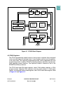
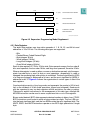
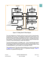
DATA FIELD
S/C
⇑
STATUS CONTROL BIT
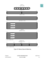
BDM SERIAL DATA WORD
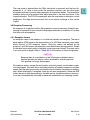
Figure 4-11 BDM Serial Data Word
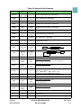
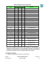
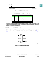
Table 4-7 CPU Generated Message Encoding
Bit 16
Data
0
XXXX
Valid data transfer
Message Type
0
FFFF
Command complete; Status OK
1
0000
Not ready with response; Come again
1
0001
BERR terminated bus cycle; Data invalid
1
FFFF
Illegal command
Command and data transfers initiated by the development system should clear bit 16.
The current implementation ignores this bit; however, Motorola reserves the right to
use this bit for future enhancements.
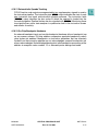
4.10.10 Recommended BDM Connection
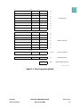
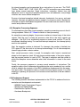
In order to provide for use of development tools when an MCU is installed in a system,
Motorola recommends that appropriate signal lines be routed to a male Berg connector or double-row header installed on the circuit board with the MCU. Refer to Figure
4-12.
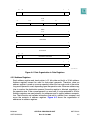
1
2
BERR
GND 3
4
BKPT/DSCLK
GND 5
6
FREEZE
RESET 7
8
IFETCH/DSI
VDD 9
10
IPIPE/DSO
DS
32 BERG
Figure 4-12 BDM Connector Pinout
MC68332
USER’S MANUAL
CENTRAL PROCESSOR UNIT
Rev. 15 Oct 2000
MOTOROLA
4-26

![CPU32 Reference Manual [330 pages!]](http://vs1.manualzilla.com/store/data/005686632_1-79fc9549061344d5fca8ab86e2038cb9-150x150.png)