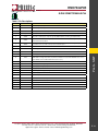
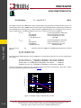
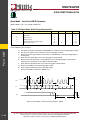
1
Analog Devices Welcomes Hittite Microwave Corporation www.analog.com www.hittite.com THIS PAGE INTENTIONALLY LEFT BLANK HMC704LP4E v04.0215 8 GHZ FRACTIONAL-N PLL Typical Applications Features The HMC704LP4E is ideal for: Wide band: DC - 8 GHz RF Input, 4 GHz 19-bit Prescaler • Microwave Point-to-Point Radios • Base Stations for Mobile Radio (GSM, PCS, DCS, CDMA, WCDMA) • Wireless LANs, WiMAX • Communications Test Equipment • CATV Equipment • Automotive Industry Leading Phase Noise & Spurious: -112 dBc/Hz @ 8 GHz Fractional, 50 kHz Offset Figure of Merit -230 dBc/Hz Fractional Mode -233 dBc/Hz Integer Mode 100 MHz PFD High PFD rate: 100 MHz PLLs - SMT 24 Lead 4x4 mm SMT Package: 16 mm2 Functional Diagram General Description The HMC704LP4E has been designed for the best phase noise and lowest spurious content possible in an integrated PLL. Fabricated in a SiGe BiCMOS process, this Fractional-N PLL consists of a very low noise digital phase detector, VCO divider, reference divider and a precision controlled charge pump. Ultra low in-close phase noise and low spurious allows wide loop bandwidths for faster frequency hopping and low micro-phonics. Exact frequency mode with 24-bit fractional modulator provides the ability to generate fractional frequencies with zero frequency error, an important feature for Digital Pre-Distortion systems. The serial interface offers read back capability and is compatible with a wide variety of protocols. 5-1 For price, delivery and to place orders: Analog Devices, Inc., One Technology Way, Norwood, MA 02062 978-250-3343 tel • 978-250-3373 fax • Order online at www.analog.com/hittitemw Application support: Phone: 978-250-3343 or [email protected] HMC704LP4E v04.0215 8 GHZ FRACTIONAL-N PLL Table 1. Electrical Specifications VDDCP, VPPCP = 5V+/-4%; RVDD, AVDD, DVDD, VDDPD, VCCPS = 3.3V +/-10%; AGND = DGND = 0V Parameter RF INPUT CHARACTERISTICS RF Input Frequency Range Conditions Min. Typ. Max. Units [6][7] [1] DC 8000 MHz [1] DC 4000 MHz Power Range [13] -15 Impedance 100 Ohms each leg||3pF Prescaler Input Freq Range -7 -3 100||3 dBm Ohms||pF REF INPUT CHARACTERISTICS Frequency Range (3.3V) [1][8] Power from 50Ohm Source [12] DC Impedance Ref Divider Range (14 bit) 350 MHz 6 dBm 100||3 Ohms||pF 1 16,383 [1][12] Integer Mode DC 50 115 MHz Fractional Mode A DC 50 80 MHz Fractional Mode B DC 50 100 MHz 2.5 mA CHARGE PUMP Output Current 20uA Steps 0.02 All should be equal 3.0 3.3 3.5 V POWER SUPPLIES RVDD, AVDD, VCCPS, VCCHF, VCCPD - Analog supply DVDD - Digital supply 3.0 3.3 3.5 V VDDLS, VPPCP Charge Pump VDDLS, VPPCP must be equal 3.0 5.0 5.2 V 3.3V - Current consumption [9] 38 52 58 mA 2 6 5V - Current consumption All Modes Power Down Current [10] BIAS Reference Voltage Pin 12. Measured with 10GOhm Meter 1.880 Floor Figure of Merit [11] Integer HiK Mode Integer Normal Mode Fractional HiK Mode [3] Fractional Normal Mode [3] -236 -232 -232 -228 Flicker Noise at foffset PNflick = Flicker FOM +20log(f vco) -10log(foffset) dBc/Hz Phase Noise Floor at f vco with fpd PNfloor = Floor FOM + 10log(fpd) +20log(f vco/fpd) dBc/Hz Total Phase Noise vs foffset, f vco, fpd PN = 10log(10(PNflick /10) + 10(PNfloor /10) ) 1.920 7 mA 100 uA 1.960 V -231 -228 -227 -225 dBc/Hz dBc/Hz dBc/Hz dBc/Hz PLLS - SMT PHASE DETECTOR RATE 50 PHASE NOISE Flicker Figure of Merit (FOM)[2] -266 Jitter SSB 100Hz to 50kHz SPURIOUS [4][5] Integer Boundary Spurs @~8GHz offsets less than loop bandwidth, fpd = 50MHz -233 -230 -230 -227 dBc/Hz dBc/Hz 50 -60 fs -52 dBc For price, delivery and to place orders: Analog Devices, Inc., One Technology Way, Norwood, MA 02062 978-250-3343 tel • 978-250-3373 fax • Order online at www.analog.com/hittitemw Application support: Phone: 978-250-3343 or [email protected] 5-2 HMC704LP4E v04.0215 8 GHZ FRACTIONAL-N PLL Table 1. Electrical Specifications (Continued) Parameter Conditions Min. Typ. Max. Units VIH/VIL within 50mV of Vsw 38 47 54 % DVDD VDD-0.4 V 0.5ns+0.2ns/pF 8.2ns+0.2ns/pF ns ns LOGIC INPUTS Switching Threshold (Vsw) LOGIC OUTPUTS VOH Output High Voltage VOL Output Low Voltage 0.4 PLLs - SMT Digital Output Driver Delay SCK to Digital Output Delay 5-3 32 V RF divider 8GHz Integer Mode 19 bit , Even values Only 1,048,574 RF divider 4GHz Integer Mode 19 bit , All values 16 524,287 RF divider 8GHz Fractional Mode 19 bit , Even values Only 40 1,048,566 RF divider 4GHz Fractional Mode 19 bit , All values 20 524,283 [1] Frequency is guaranteed across process, voltage and temperature from -400C to 850C. [2] With high charge-pump current, +12dBm 100MHz sine reference [3] Fractional FOM degrades about 3dB/octave for prescaler input frequencies below 2GHz [4] Using 50MHz reference with VCO tuned to within one loop bandwidth of an integer multiple of the PD frequency. Larger offsets produce better results. See the “Spurious Performance” section for more information. [5] Measured with the HMC704LP4E evaluation board. Board design and isolation will affect performance. [6] Internal divide-by-2 must be enabled for frequencies >4GHz [7] At low RF Frequency, Rise and fall times should be less than 1ns to maintain performance [8] Slew rate of greater or equal to 0.5ns/V [9] Current consumption depends upon operating mode and frequency of the VCO [10] Reference input disconnected [11] Min/Max versus temperature and supply, under typical reference & frequencies & RF power levels [12] Slew > 0.5V/ns is recommended , see Table 6 for more information [13] Operable with reduced spectral performance up to +7 dBm For price, delivery and to place orders: Analog Devices, Inc., One Technology Way, Norwood, MA 02062 978-250-3343 tel • 978-250-3373 fax • Order online at www.analog.com/hittitemw Application support: Phone: 978-250-3343 or [email protected] HMC704LP4E v04.0215 8 GHZ FRACTIONAL-N PLL TYPICAL PERFORMANCE CHARACTERISTICS Figure 1. Floor FOM vs. Mode and Temp Figure 2. Flicker FOM vs. Mode and Temp -226 -263 -264 -228 FLICKER FOM FLOOR FOM -265 -230 -232 -266 -267 -268 -234 int Frac Mode A Hik int Hik Frac Mode A -236 -40 0 40 TEMPERATURE (C) -270 -40 -20 0 20 40 60 80 TEMPERATURE (C) Figure 3. Floor FOM vs. Output Frequency and Mode Figure 4. Flicker FOM vs. Output Frequency and Mode -215 -263 HiK Frac Mode B int Frac Mode A Frac Mode B Hik int Hik Frac Mode A Hik Frac Mode B -220 Frac Mode A -264 FLICKER FOM Frac Mode B FLOOR FOM int Frac Mode A Hik int Hik Frac Mode A -269 80 PLLS - SMT Unless otherwise specified, plots are measured with a 50 MHz PD rate, VCO near 8 GHz. The operating modes in the following plots refer to Integer (int), Fractional Modes A and B, HiKcp (HiK) or Active (act) configurations. HiK Frac Mode A -225 Frac Mode A int Frac Mode A Frac Mode B Hik Frac Mode A Hik Frac Mode B Frac Mode B -265 -266 HiK Frac Mode B Int -230 -267 HiK Frac Mode A HiK Frac Int Int -235 -268 1 2 4 FREQUENCY (GHz) 8 1 2 4 8 FREQUENCY (GHz) For price, delivery and to place orders: Analog Devices, Inc., One Technology Way, Norwood, MA 02062 978-250-3343 tel • 978-250-3373 fax • Order online at www.analog.com/hittitemw Application support: Phone: 978-250-3343 or [email protected] 5-4 HMC704LP4E v04.0215 8 GHZ FRACTIONAL-N PLL Figure 5. Floor FOM vs. Reference Power and Mode Figure 6. Flicker FOM vs. Reference Power and Mode -226 -266 FLICKER FOM FLOOR FOM -267 int Mode A HiK int HiK Mode A -228 -230 -268 -269 -270 -232 int Frac Mode A Hik int Hik Frac Mode A -271 -234 -1 0 1 2 3 4 5 6 7 8 9 10 11 -272 -4 12 -2 0 2 4 6 8 10 12 REFERENCE POWER (dBm) Figure 7. Flicker FOM vs. Charge Pump Current Figure 8. Flicker FOM vs. CP Voltage, CP Current = 2.5mA -245 -256 -258 -250 FLICKER FOM -260 FLICKER FOM PLLs - SMT REFERENCE POWER (dBm) -255 -260 -262 -264 -266 -265 -268 -270 -270 0 0.5 1 1.5 2 2.5 3 0 1 CP CURRENT (mA) 2 3 4 5 CP VOLTAGE (V) Figure 9. Flicker FOM vs. CP Voltage, Hikcp + CP Current = 6mA Figure 10. Floor FOM vs. CP Voltage, CP Current = 2.5mA -264 -218 -266 FLOOR FOM FLICKER FOM -220 -268 -222 -224 -226 -228 -270 -230 0 1 2 3 CP VOLTAGE (V) 5-5 4 5 0 1 2 3 4 5 CP VOLTAGE (V) For price, delivery and to place orders: Analog Devices, Inc., One Technology Way, Norwood, MA 02062 978-250-3343 tel • 978-250-3373 fax • Order online at www.analog.com/hittitemw Application support: Phone: 978-250-3343 or [email protected] HMC704LP4E v04.0215 8 GHZ FRACTIONAL-N PLL Figure 11. Floor FOM vs. CP Voltage, Hikcp+CP Current = 6mA Figure 12. Floor FOM vs. CP Current -224 -200 -205 -226 -210 FLOOR FOM FLOOR FOM -228 -230 -215 -220 -232 -225 -234 -230 1 2 3 4 5 0 0.5 1 1.5 CP VOLTAGE (V) Figure 13. Spur Performance vs. Frequency Offset[1] 2.5 3 Figure 14. Spur Performance vs. Frequency Offset [2] -50 -55 -55 -60 -60 WORST SPUR (dBc) WORST SPUR (dBc) 2 CP CURRENT (mA) -65 -70 -75 -80 PLLS - SMT 0 -65 -70 -75 -80 -85 -85 -90 -90 1 10 100 1 1000 10 100 1000 FREQUENCY OFFSET (KHz) FREQUENCY OFFSET (kHz) Figure 16. Worst Case Integer Boundary Spur Near 4 GHz Figure 15. Worst Case Integer Boundary Spur Near 8 GHz -50 -50 Mode B Mode B HiK Mode B -55 WORST SPUR (dBc) WORST SPUR (dBc) -55 -60 -65 Mode A -70 Mode A Mode B HiK Mode A HiK Mode B -75 8450 8550 8650 HiK Mode B -60 -65 -70 Mode A -75 HiK Mode A -80 Mode A Mode B HiK Mode A HiK Mode B HiK Mode A 8750 8850 8950 FREQUENCY (MHz) -85 4150 4200 4250 4300 4350 4400 4450 4500 4550 4600 FREQUENCY (MHz) [1] CP Current = 2.5 mA, Loop Filter = 20 kHz, Phase Margin = 78° [2] Hi K, CP Current = 6 mA, Loop Filter BW = 45 kHz, Phase Margin = 78° For price, delivery and to place orders: Analog Devices, Inc., One Technology Way, Norwood, MA 02062 978-250-3343 tel • 978-250-3373 fax • Order online at www.analog.com/hittitemw Application support: Phone: 978-250-3343 or [email protected] 5-6 HMC704LP4E v04.0215 8 GHZ FRACTIONAL-N PLL Figure 17. Integer Boundary Spur vs. CP Offset [3] Figure 18. Modelled vs. Measured Phase Noise [4] -80 -25 WORST SPUR (dBc) -30 PHASE NOISE (dBc) Mode A Mode B HIK Mode A HiK Mode B -35 Recommended Operating Region -40 -45 -50 -100 -120 -140 HiK Mode B -55 -160 Mode B -60 HiK Int Predicted HiK Int Mode A -65 -600 HiK Mode A -400 -200 0 200 400 -180 100 600 1000 10 4 5 10 6 10 7 10 8 OFFSET (Hz) OFFSET CURRENT (uA) Figure 19. Modelled vs. Measured Phase Noise, Fractional Mode [3] Figure 20. Floor FOM Near 8 GHz vs. RF Power and Mode -80 -227 -228 -100 -229 -120 FLOOR FOM PHASE NOISE (dBc) PLLs - SMT 10 -140 -231 -232 Int ff fb act fb Int Hik Mode A act Predicted Hik Act Int Predicted Mode A -160 -230 HiK int HiK Mode A HiK Mode B -233 -180 100 1000 10 4 10 5 10 6 10 7 10 -234 -24 8 -21 -18 -15 OFFSET (Hz) -12 -9 -6 -3 0 3 RF POWER (dBm) Figure 21. Flicker FOM Near 8 GHz vs. RF Power and Mode Figure 22. Integer Boundary Spurious at 8 GHz + 10 kHz vs. RF Power [3] -266 -50 -55 SPUR (dBc) FLICKER FOM -266.5 -267 5KHz 10KHz -60 -65 -267.5 -70 HiK int HiK Mode A HiK Mode B -268 -24 -21 -18 -15 -12 -9 -6 -3 0 RF POWER (dBm) 3 -75 -15 -12 -9 -6 -3 0 3 RF POWER (dBm) [3] VCO Near 8.6 GHz, Prescalar = VCO/2 [4] Active Fractional A Mode (Prescalar @ 4 GHz + 5 kHz) 5-7 For price, delivery and to place orders: Analog Devices, Inc., One Technology Way, Norwood, MA 02062 978-250-3343 tel • 978-250-3373 fax • Order online at www.analog.com/hittitemw Application support: Phone: 978-250-3343 or [email protected] HMC704LP4E v04.0215 8 GHZ FRACTIONAL-N PLL Table 2. Pin Descriptions Pin Number Function 1 SDI Main Serial port data input Description 2 SCK Main Serial port clock input 3 ASEN 4 LD_SDO 5 VCOIN Complementary Input to the RF Prescaler. For Single Ended operation must be decoupled to the ground plane with a ceramic bypass capacitor, typically 100 pF. DC Bias of 2.0V is generated internally 6 VCOIP Input to the RF Prescaler. Small signal input from external VCO. DC Bias of 2.0V is generated internally. External AC Coupling required 7 VCCHF Power supply pin for the RF Section. Nominal +3.3 V. A decoupling capacitor to the ground plane should be placed as close as possible to this pin. See eval board layout. N/C VCCPS No Connect Power Supply Prescaler, Nominal +3.3V 10 N/C 11 VCCPD 12 BIAS External bypass decoupling for precision bias circuits, 1.920V +/-20 mV NOTE: BIAS ref voltage cannot drive an external load. Must be measured with 10 GOhm meter such as Agilent 34410A, normal 10 Mohm DVM will read erroneously. 13 N/C No Connect 14 AVDD 15 VPPCP 16 CP No Connect Power supply for the phase detector, Nominal +3.3V Power supply for analog bias generation, Nominal +3.3V Power supply for charge pump, Nominal +5V Charge pump output. 17 VDDLS Power Supply for charge pump digital section, Nominal +5V 18 RVDD Ref path supply, Nominal +3.3V 19 XREFP Reference input 20 ASCK PLLS - SMT 8 9 Auxiliary Serial Port Enable Output Lock Detect Output or Serial Data Output or GPO, Selectable Auxiliary Serial Port Clock Output 21 ASD 22 DVDD Auxiliary Serial Port Data Output 23 CEN Hardware Chip Enable 24 SEN Main Serial port latch enable input Digital supply, Nominal +3.3V For price, delivery and to place orders: Analog Devices, Inc., One Technology Way, Norwood, MA 02062 978-250-3343 tel • 978-250-3373 fax • Order online at www.analog.com/hittitemw Application support: Phone: 978-250-3343 or [email protected] 5-8 HMC704LP4E v04.0215 8 GHZ FRACTIONAL-N PLL Table 3. Absolute Maximum Ratings PLLs - SMT Parameter Rating AVDD or DVDD to GND -0.3V to +3.6V AVDD to DVDD -0.5V to +0.5V VDDLS, VPPCP -0.3V to +5.2V VCOIN, VCOIP Single Ended DC VCCHF-0.2V VCOIN, VCOIP Differential DC 5.2V VCOIN, VCOIP Single Ended AC 50Ohm +7 dBm VCOIN, VCOIP Differential AC 50Ohm +13 dBm XREFP reference input +18dBm, 5.6Vpeak Digital Load 1kOhm min Digital Input 1.4V to 1.7V min rise time 20nsec Digital Input Voltage Range -0.25 to DVDD+0,5V Thermal Resistance (Jxn to Gnd Paddle) 25 0C/W Operating Temperature Range -40 OC to +85 OC Storage Temperature Range -65 OC to + 125 OC Maximum Junction Temperature +125 OC Reflow Soldering Peak Temperature 260 OC Time at Peak Temperature 40sec ESD Sensitivity HBM Class 1B Stresses above those listed under Absolute Maximum Ratings may cause permanent damage to the device. This is a stress rating only; functional operation of the device at these or any other conditions above those indicated in the operational section of this specification is not implied. Exposure to absolute maximum rating conditions for extended periods may affect device reliability. 5-9 For price, delivery and to place orders: Analog Devices, Inc., One Technology Way, Norwood, MA 02062 978-250-3343 tel • 978-250-3373 fax • Order online at www.analog.com/hittitemw Application support: Phone: 978-250-3343 or [email protected] HMC704LP4E v04.0215 8 GHZ FRACTIONAL-N PLL NOTES: [1] PACKAGE BODY MATERIAL: LOW STRESS INJECTION MOLDED PLASTIC SILICA AND SILICON IMPREGNATED. [2] LEAD AND GROUND PADDLE MATERIAL: COPPER ALLOY. [3] LEAD AND GROUND PADDLE PLATING: 100% MATTE TIN. [4] DIMENSIONS ARE IN INCHES [MILLIMETERS]. [5] LEAD SPACING TOLERANCE IS NON-CUMULATIVE. [6] PAD BURR LENGTH SHALL BE 0.15 mm MAX. PAD BURR HEIGHT SHALL BE 0.05 mm MAX. [7] PACKAGE WARP SHALL NOT EXCEED 0.05 mm [8] ALL GROUND LEADS AND GROUND PADDLE MUST BE SOLDERED TO PCB RF GROUND. [9] REFER TO HITTITE APPLICATION NOTE FOR SUGGESTED PCB LAND PATTERN. PLLS - SMT Outline Drawing Table 4. Package Information Part Number Package Body Material Lead Finish MSL Rating Package Marking [1] HMC704LP4E RoHS-compliant Low Stress Injection Molded Plastic 100% matte Sn MSL1[2] H704 XXXX [1] 4-Digit lot number XXXX [2] Max peak reflow temperature of 260°C For price, delivery and to place orders: Analog Devices, Inc., One Technology Way, Norwood, MA 02062 978-250-3343 tel • 978-250-3373 fax • Order online at www.analog.com/hittitemw Application support: Phone: 978-250-3343 or [email protected] 5 - 10 HMC704LP4E v04.0215 8 GHZ FRACTIONAL-N PLL PLLs - SMT Evaluation PCB The circuit board used in the application should use RF circuit design techniques. Signal lines should have 50 Ohms impedance while the package ground leads and exposed paddle should be connected directly to the ground plane similar to that shown. A sufficient number of via holes should be used to connect the top and bottom ground planes. The evaluation circuit board shown is available from Hittite upon request. Table 5. Evaluation Order Information 5 - 11 Item Contents Part Number Evaluation Kit HMC704LP4E Evaluation PCB USB Interface Board 6’ USB A Male to USB B Female Cable CD ROM (Contains User Manual, Evaluation PCB Schematic, Evaluation Software, Hittite PLL Design Software) 129856-HMC704LP4E For price, delivery and to place orders: Analog Devices, Inc., One Technology Way, Norwood, MA 02062 978-250-3343 tel • 978-250-3373 fax • Order online at www.analog.com/hittitemw Application support: Phone: 978-250-3343 or [email protected] HMC704LP4E v04.0215 8 GHZ FRACTIONAL-N PLL PLLS - SMT Evaluation PCB Block Diagram Evaluation PCB Schematic To view Evaluation PCB Schematic please visit www.hittite.com and choose HMC704LP4E from “Search by Part Number” pull down menu to view the product splash page. For price, delivery and to place orders: Analog Devices, Inc., One Technology Way, Norwood, MA 02062 978-250-3343 tel • 978-250-3373 fax • Order online at www.analog.com/hittitemw Application support: Phone: 978-250-3343 or [email protected] 5 - 12 HMC704LP4E v04.0215 8 GHZ FRACTIONAL-N PLL Theory of Operation The PLL consists of the following functional blocks: 1. 2. 3. 4. 5. 6. 7. 8. Reference Path Input Buffer and ’R’ Divider VCO Path Input Buffer, RF Divide-by-2 and Multi-Modulus ’N’ Divider Δ Σ Fractional Modulator Phase Detector Charge Pump Main Serial Port Lock Detect and Register Control Auxiliary Output Serial Port 9. Power On Reset Circuit PLLs - SMT External VCO The PLL charge pump can operate with the charge pump supply as high as 5.2V. The charge pump output at the varactor tuning port, normally can maintain low noise performance to within 500 mV of ground or 800 mV of the upper supply voltage. Figure 23. Synthesizer with External VCO High Performance Low Spurious Operation The HMC704LP4E has been designed for the best phase noise and low spurious content possible in an integrated PLL. Spurious signals in a PLL can occur in any mode of operation and can come from a number of sources. Figure of Merit Noise Floor and Flicker Noise Models The phase noise of an ideal phase locked oscillator is dependent upon a number of factors: a. b. c. d. Frequency of the VCO, and the Phase detector VCO Sensitivity, kvco, VCO and Reference Oscillator phase noise profiles Charge Pump current, Loop Filter and Loop Bandwidth Mode of Operation: Integer, Fractional modulator style The contributions of the PLL to the output phase noise can be characterized in terms of a Figure of Merit (FOM) for both the PLL noise floor and the PLL flicker (1/f) noise regions, as follows: 5 - 13 For price, delivery and to place orders: Analog Devices, Inc., One Technology Way, Norwood, MA 02062 978-250-3343 tel • 978-250-3373 fax • Order online at www.analog.com/hittitemw Application support: Phone: 978-250-3343 or [email protected] HMC704LP4E v04.0215 8 GHZ FRACTIONAL-N PLL where: Φ p 2 Phase Noise Contribution of the PLL (rads2/Hz) Frequency of the VCO (Hz) Frequency of the Phase Detector (Hz) Frequency offset from the carrier (Hz) Figure of Merit (FOM) for the phase noise floor Figure of Merit (FOM) for the flicker noise region PLL Phase Noise Contribution PLL 1/f Flicker Noise PHASE NOISE (dBc/Hz) (EQ 1) Fp1 f02 Fp0 f02 Φ ( f0 , fm , fpd ) = + fm ffd 2 p VCO 1/f3 Noise VCO 1/f2 Noise PLL Noise Floor Typical Closed Loop Phase Noise Closed Loop Bandwidth PLLS - SMT fo fpd fm Fpo Fp1 LOG OFFSET FREQUENCY (fm) Figure 24. Figures of Merit Noise Models for the PLL If the free running phase noise of the VCO is known, it may also be represented by a figure of merit for both 1/f2 , Fv2, and the 1/f3, Fv3, regions. VCO Phase Noise Contribution Fν f02 F f2 Φν2 ( f0 , fm ) =ν 20 + 33 fm fm (EQ 2) The Figures of Merit are essentially normalized noise parameters for both the PLL and VCO that can allow quick estimates of the performance levels of the PLL at the required VCO, offset and phase detector frequency. Normally, the PLL IC noise dominates inside the closed loop bandwidth of the PLL, and the VCO dominates outside the loop bandwidth at offsets far from the carrier. Hence a quick estimate of the closed loop performance of the PLL can be made by setting the loop bandwidth equal to the frequency where the PLL and free running phase noise are equal. The Figure of Merit is also useful in estimating the noise parameters to be entered into a closed loop design tool such as Hittite PLL Design, which can give a much more accurate estimate of the closed loop phase noise and PLL loop filter component values. Given an optimum loop design, the approximate closed loop performance is simply given by the minimum of the PLL and VCO noise contributions. For price, delivery and to place orders: Analog Devices, Inc., One Technology Way, Norwood, MA 02062 978-250-3343 tel • 978-250-3373 fax • Order online at www.analog.com/hittitemw Application support: Phone: 978-250-3343 or [email protected] 5 - 14 HMC704LP4E v04.0215 8 GHZ FRACTIONAL-N PLL ( 2 Φ= min Φ 2p , Φν2 PLL-VCO Noise ) (EQ 3) PLLs - SMT An example of the use of the FOM values to make a quick estimate of PLL performance: Estimate the phase noise of an 8GHz closed loop PLL with a 100MHz reference operating in Fractional Mode B with the VCO operating at 8 GHz and the VCO divide by 2 port driving the PLL at 4GHz. Assume an HMC509 VCO has free running phase noise in the 1/f2 region at 1 MHz offset of -135 dBc/Hz and phase noise in the 1/f3 region at 1 kHz offset of -60 dBc/Hz. Fv1_dB = -135 Free Running VCO PN at 1MHz offset +20*log10(1e6) PNoise normalized to 1Hz offset -20*log10(8e9) Pnoise normalized to 1Hz carrier = -213.1 dBc/Hz at 1Hz VCO FOM Fv3_dB = -60 Free Running VCO PN at 1kHz offset +30*log10(1e3) PNoise normalized to 1 Hz offset -20*log10(8e9) Pnoise normalized to 1 Hz carrier = -168 dBc/Hz at 1Hz VCO Flicker FOM We can see from Figure 3 and Figure 4 respectively that the PLL FOM floor and FOM flicker parameters in fractional Mode A: Fpo_dB = -227 dBc/Hz at 1Hz Fp1_dB = -266 dBc/Hz at 1Hz Each of the Figure of Merit equations result in straight lines on a log-frequency plot. We can see in the example below the resulting PLL floor at 8 GHz = Fpo_dB +20log10(fvco) -10log10(fpd) = -227+198 -80 = -109 dBc/Hz PLL Flicker at 1 kHz = Fp1_dB+20log10(fvco)-10log10(fm) = -266 +198-30 = -98 dBc/Hz VCO at 1 MHz = Fv1_dB+20log10(fvco)-20log10(fm)= -213 +198-120 = -135dBc/Hz VCO flicker at 1 kHz = Fv3_dB+20log10(fvco)-30log10(fm)= -168 +198-90 = -60dBc/Hz These four values help to visualize the main contributors to phase noise in the closed loop PLL. Each falls on a linear line on the log-frequency phase noise plot shown in Figure 25. -20 PHASE NOISE (dBc/Hz) -40 VCO at 1 kHz -60 -80 -100 PLL Floor -120 PLL at 1 kHz -140 VCO at 1 MHz -160 -180 100 1000 4 5 6 10 10 10 FREQUENCY OFFSET (Hz) 10 7 10 8 Figure 25. Example of Figure of Merit models at 8 GHz 5 - 15 For price, delivery and to place orders: Analog Devices, Inc., One Technology Way, Norwood, MA 02062 978-250-3343 tel • 978-250-3373 fax • Order online at www.analog.com/hittitemw Application support: Phone: 978-250-3343 or [email protected] HMC704LP4E v04.0215 8 GHZ FRACTIONAL-N PLL It should be noted that actual phase noise near the corner frequency of the loop bandwidth is affected by loop parameters and one should use a more complete design tool such as Hittite PLL Design for better estimates of the phase noise performance. Noise models for each of the components in Hittite PLL Design can be derived from the FOM equations or can be provided by Hittite applications engineering. Spurious Performance Integer Operation The VCO always operates at an integer multiple of the PD frequency in an integer PLL. In general spurious signals originating from an integer PLL can only occur at multiples of the PD frequency. These unwanted outputs are often simply referred to as reference sidebands. The HMC704LP4E has been designed and tested for ultra-low spurious performance. Reference spurious levels are typically below -100 dBc with a well designed board layout. A regulator with low noise and high power supply rejection, such as the HMC860LP3E, is recommended to minimize external spurious sources. Reference spurious levels of below -100 dBc require superb board isolation of power supplies, isolation of the VCO from the digital switching of the PLL and isolation of the VCO load from the PLL. Typical board layout, regulator design, demo boards and application information are available for very low spurious operation. Operation with lower levels of isolation in the application circuit board, from those recommended by Hittite, can result in higher spurious levels. Of course, if the application environment contains other interfering frequencies unrelated to the PD frequency, and if the application isolation from the board layout and regulation are insufficient, then the unwanted interfering frequencies will mix with the desired PLL output and cause additional spurs. The level of these spurs is dependant upon isolation and supply regulation or rejection (PSRR). PLLS - SMT Spurs unrelated to the reference frequency must originate from outside sources. External spurious sources can modulate the VCO indirectly through power supplies, ground, or output ports, or bypass the loop filter due to poor isolation of the filter. It can also simply add to the output of the PLL. Fractional Operation Unlike an integer PLL, spurious signals in a fractional PLL can occur due to the fact that the VCO operates at frequencies unrelated to the PD frequency. Hence intermodulation of the VCO and the PD harmonics can cause spurious sidebands. Spurious emissions are largest when the VCO operates very close to an integer multiple of the PD. When the VCO operates exactly at a harmonic of the PD then, no in-close mixing products are present. Interference is always present at multiples of the PD frequency, fpd, and the VCO frequency, fvco. If the fractional mode of operation is used, the difference, Δ, between the VCO frequency and the nearest harmonic of the reference, will create what are referred to as integer boundary spurs. Depending upon the mode of operation of the PLL, higher order, lower power spurs may also occur at multiples of integer fractions (sub-harmonics) of the PD frequency. That is, fractional VCO frequencies which are near nfpd + fpdd/m, where n, d and m are all integers and d<m (mathematicians refer to d/m as a rational number). We will refer to fpdd/m as an integer fraction. The denominator, m, is the order of the spurious product. Higher values of m produce smaller amplitude spurious at offsets of mΔ and usually when m>4 spurs are very small or unmeasurable. The worst case, in fractional mode, is when d=0, and the VCO frequency is offset from nfpd by less than the loop bandwidth. This is the “in-band fractional boundary” case. For price, delivery and to place orders: Analog Devices, Inc., One Technology Way, Norwood, MA 02062 978-250-3343 tel • 978-250-3373 fax • Order online at www.analog.com/hittitemw Application support: Phone: 978-250-3343 or [email protected] 5 - 16 HMC704LP4E v04.0215 8 GHZ FRACTIONAL-N PLL Integer Boundary fVCO Δ n = integer d=0 m = 1 = 1st order Δ < Loop Bandwidth 1st Order Integer Boundary Spur Δ fVCO 2Δ PLLs - SMT (n+1)fpd (n+1/2)fpd nfpd Integer Boundary Integer Boundary nfpd d =1 n = integer m = 2 = 2nd order Δ < Loop Bandwidth Integer Boundary 2nd Order Spur 2Δ Δ (n+1/2)fpd (n+1)fpd Figure 26. Fractional Spurious Example Characterization of the levels and orders of these products is not unlike a mixer spur chart. Exact levels of the products are dependent upon isolation of the various PLL parts. Hittite can offer guidance about expected levels of spurious with our PLL and VCO application boards. Regulators with high power supply rejection ratios (PSRR) are recommended, especially in noisy applications. When operating in fractional mode, charge pump and phase detector linearity is of paramount importance. Any nonlinearity degrades phase noise and spurious performance. Phase detector linearity degrades when the phase error is very small and is operating back and forth between reference lead and VCO lead. To mitigate these non-linearities in fractional mode it is critical to operate the phase detector with some finite phase offset such that either the reference or VCO always leads. To provide a finite phase error, extra current sources can be enabled which provide a constant DC current path to VDD (VCO leads always) or ground (reference leads always). These current sources are called charge pump offset and they are controlled via “Reg 09h”. The time offset at the phase detector should be ~2.5 ns + 4Tps, where Tps is the RF period at the fractional prescaler input in nanoseconds (ie. after the optional fixed divide by 2). The specific level of charge pump offset current is determined by this time offset, the comparison frequency and the charge pump current and can be calculated from: ( ) Required CP Offset (µA) = 2.5 × 10 −9 + 4TPS (sec) × ( Fcomparison ) (Hz ) × ICP (µA) (EQ 4) CP Offset Current should never be more than 25% of the programmed CP current. Operation with charge pump offset influences the required configuration of the Lock Detect function. Refer to the description of “PD Window Based Lock Detect” later in this document. Note that this calculation can be performed for the center frequency of the VCO, and does not need refinement for small differences (<25%) in center frequencies. Another factor in the spectral performance in Fractional Mode is the choice of the Delta-Sigma Modulator mode. Mode A can offer better in-band spectral performance (inside the loop bandwidth) while Mode B offers better out of band performance. See “Reg 06h”[3:2] for DSM mode selection. Finally, all fractional PLLs create fractional spurs at some level. Hittite offers the lowest level fractional spurious in the industry in an integrated solution. 5 - 17 For price, delivery and to place orders: Analog Devices, Inc., One Technology Way, Norwood, MA 02062 978-250-3343 tel • 978-250-3373 fax • Order online at www.analog.com/hittitemw Application support: Phone: 978-250-3343 or [email protected] HMC704LP4E v04.0215 8 GHZ FRACTIONAL-N PLL Reference Input Stage The reference buffer provides the path from an external reference source (generally crystal based) to the R divider, and eventually to the phase detector. The buffer has two modes of operation. High Gain (recommended below 200 MHz), and High frequency, for 200 to 350 MHz operation. The buffer is internally DC biased, with 100 Ohm internal termination. For 50 Ohm match, an external 100 Ohm resistance to ground should be added, followed by an AC coupling capacitance (impedance < 1 Ohm), then to the XREFP pin of the part. At low frequencies, a relatively square reference is recommended to keep the input slew rate high. At higher frequencies, a square or sinusoid can be used. The following table shows the recommended operating regions for different reference frequencies. If operating outside these regions the part will normally still operate, but with degraded performance. PLLS - SMT Figure 27. Reference Path Input Stage Minimum pulse width at the reference buffer input is 2.5 ns. For best spur performance when R = 1, the pulse width should be (2 .5ns + 8 Tps), where Tps is the period of the VCO at the prescaler input. When R > 1 minimum pulse width is 2.5 ns. Table 6. Reference Sensitivity Table Square Input Sinusoidal Input Frequency Slew > 0.5 V/ns (MHz) Recommended Recommended Swing (Vpp) Min Max Recommended Recommended Power Range (dBm) Min Max < 10 YES 0.6 2.5 x x x 10 YES 0.6 2.5 x x x 25 YES 0.6 2.5 ok 8 15 50 YES 0.6 2.5 YES 6 15 100 YES 0.6 2.5 YES 5 15 12 150 ok 0.9 2.5 YES 4 200 ok 1.2 2.5 YES 3 8 200 to 350 x x x YES1 5 10 Note: For greater than 200 MHz operation, use buffer in High Frequency Mode. Reg[8] bit 21 = 1 Input referred phase noise of the PLL when operating at 50 MHz is between -150 and -156 dBc/Hz at 10 kHz offset depending upon the mode of operation. The input reference signal should be 10 dB better than this floor to avoid deg radation of the PLL noise contribution. It should be noted that such low levels are only necessary if the PLL is the dominant noise contributor and these levels are required for the system goals. For price, delivery and to place orders: Analog Devices, Inc., One Technology Way, Norwood, MA 02062 978-250-3343 tel • 978-250-3373 fax • Order online at www.analog.com/hittitemw Application support: Phone: 978-250-3343 or [email protected] 5 - 18 HMC704LP4E v04.0215 8 GHZ FRACTIONAL-N PLL Ref Path ’R’ Divider The reference path “R” divider is based on a 14 bit counter and can divide input signals of up to 350 MHz input by values from 1 to 16,383 and is controlled by “Reg 02h”[13:0]. The reference divider output may be viewed in test mode on the LD_SDO pin, by setting “Reg 0Fh”[4:0] = 9d. RF Path The RF path is shown in Figure 28. This path features a low noise 8 GHz RF input buffer followed by an 8GHz RF divideby-2 with a selectable bypass. If the VCO input is below 4 GHz the RF divide-by-2 should be by-passed for reduced power consumption and improved performance in fractional mode. The RF divide-by-2 is followed by the N divider, a 19 bit divider that can operate in either integer or fractional mode with up to 4 GHz inputs. Finally the N divider is followed by the Phase Detector (PD), which has two inputs, the RF path from the VCO (V) and the reference path (R) from the crystal. The PD can operate at speeds up to 80 MHz in fractional Mode A, 100 MHz in fractional Mode B and 115 MHz in integer mode. RF Buffer PLLs - SMT 8GHz VCOIN VCOIP RF Divide by 2 N Divider Phase Detector Charge Pump 80MHz/100MHz Fractional VPPCP 8GHz 4GHz 115MHz Integer /2 or CP UP 19 Bit /N V Bypass CP PD SEL CONTROL Ref Path R DN Figure 28. RF Path RF Input Stage The RF input stage provides the path from the external VCO to the phase detector via the RF or ’N’ divider. The RF input path is rated to operate up to 8 GHz across all conditions. The RF input stage is a differential common emitter stage with internal DC bias, and is protected by ESD diodes as shown in Figure 29. This input is not matched to 50 Ohms. A 50 Ohm resistor placed across the inputs can be used if desired. In most applications the input is used single-ended into either the VCOIP or VCOIN pin with the other input connected to ground through a DC blocking capacitor. The preferred input level for best spectral performance is -10 dBm nominally. Figure 29. RF Input Stage 5 - 19 For price, delivery and to place orders: Analog Devices, Inc., One Technology Way, Norwood, MA 02062 978-250-3343 tel • 978-250-3373 fax • Order online at www.analog.com/hittitemw Application support: Phone: 978-250-3343 or [email protected] HMC704LP4E v04.0215 8 GHZ FRACTIONAL-N PLL RF Path ’N’ Divider The main RF path ’N’ divider is capable of divide ratios anywhere between 219-1 (524,287) and 16 . This divider for example could divide a 4 GHz input to a PD frequency anywhere between its maximum output limit of 115 MHz to as low as 7.6 kHz. The ’N’ divider output may be viewed in test mode on LD_SDO by setting “Reg 0Fh”[4:0] = 10 d. When operating in fractional mode the N divider can change by up to +/-4 from the average value. Hence the selected divide ratio in fractional mode is restricted to values between 219-5 (524,283) and 20. If the VCO input is above 4 GHz then the 8 GHz fixed RF divide-by-2 should be used, “Reg 08h”[19] = 1. In this case the total division range is restricted to even numbers over the range 2*(219-5) (1,048,566) to 40. Charge Pump and Phase Detector The PD compares the phase of the RF path signal with that of the reference path signal and controls the charge pump output current as a linear function of the phase difference between the two signals. The output current varies in a linear fashion over nearly ±2π radians (±360) of input phase difference. Phase Detector and Charge Pump Functions Phase detector register “Reg 08h” allows manual access to control special phase detector features. PLLS - SMT The Phase Detector or PD has two inputs, one from the reference path divider and one from the RF path divider. When in lock these two inputs are at the same average frequency and are fixed at a constant average phase offset with respect to each other. We refer to the frequency of operation of the PD as fpd. Most formula related to step size, delta-sigma modulation, timers etc., are functions of the operating frequency of the PD, fpd is sometimes referred to as the comparison frequency of the PD. “Reg 0Bh”[2:0] allows fine tuning of the PD reset path delay. This adjustment can be used to improve performance at very high PD rates. Most often this register is set to the recommended value only. “Reg 06h”[5] and [6] enables the PD UP and DN outputs respectively. Disabling prevents the charge pump from pumping up or down respectively and effectively tri-states the charge pump while leaving all other functions operating internally. CP Force UP “Reg 08h”[9] and CP Force DN “Reg 00h”[10] allows the charge pump to be forced up or down respectively. This will force the VCO to the ends of the tuning range which can be useful for testing of the VCO. PD Force Mid “Reg 0Bh”[11] will disable the charge pump current sources and place a voltage source on the loop filter at approximately VPPCP/2. If a passive filter is used this will set the VCO to the mid-voltage tuning point which can be useful for testing of the VCO. “Reg 0Bh”[21:7] control other aspects of the phase detector operation and should be set to recommended values. PLL Jitter The standard deviation of the arrival time of the VCO signal, or the jitter, may be estimated with a simple approximation if we assume that the locked VCO has a constant phase noise, Φ 2 ( f0 ) , at offsets less than the loop 3 dB bandwidth and a 20 dB per decade roll off at greater offsets. The simple locked VCO phase noise approximation is shown on the left of Figure 30. For price, delivery and to place orders: Analog Devices, Inc., One Technology Way, Norwood, MA 02062 978-250-3343 tel • 978-250-3373 fax • Order online at www.analog.com/hittitemw Application support: Phone: 978-250-3343 or [email protected] 5 - 20 HMC704LP4E v04.0215 8 GHZ FRACTIONAL-N PLL фrms 2 2 φ ( f) φ ( f o) ф(t) r 2 ⁄ Hz B fo Figure 30. Synthesizer Phase Noise and Jitter With this simplification the total integrated VCO phase noise, Φν2 , in rads2 is given by PLLs - SMT Φν2 =Φ 2 ( f0 ) Bπ (EQ 5) where Φ 2 ( f0 ) is the single sideband phase noise in rads2/Hz inside the loop bandwidth, and B is the 3dB corner frequency of the closed loop PLL The integrated phase noise at the phase detector, Φ 2 pd , is just scaled by N 2 ie. Φ 2 pd Φν2 =2 N The rms phase jitter of the VCO ( Φ v ) in rads, is just the square root of the phase noise integral. Since the simple integral of (EQ 5) is just a product of constants, we can easily do the integral in the log domain. For example if the phase noise inside the loop is -110 dBc/Hz at 10 kHz offset and the loop bandwidth is 100 kHz, and the division ratio is 100, then the integrated phase noise at the phase detector, in dB, is given by; ( ) 2 Φ= 10log Φ 2 ( f0 ) βπ N 2 = -110 + 5 +50 - 40 = -95 dBrads , or equivalently Φ =10 pd dB rms. −95 20 = 18urads = 1 milli-degrees While the phase noise reduces by a factor of 20logN after division to the reference, due to the increased period of the PD reference signal, the jitter is constant. = Tpd Φ pd 2π The rms jitter from the phase noise is then given by Tjpn In this example if the PD reference was 50 MHz, Tpd = 20 nsec, and hence Tjpn = 56 femto-sec. PD Window Based Lock Detect Lock Detect Enable “Reg 07h”[3] = 1 is a global enable for all lock detect functions. The window based Lock Detect circuit effectively measures the difference between the arrival of the reference and the divided VCO signals at the PD. The arrival time difference must consistently be less than the Lock Detect window length, to declare lock. Either signal may arrive first, only the difference in arrival times is counted. 5 - 21 For price, delivery and to place orders: Analog Devices, Inc., One Technology Way, Norwood, MA 02062 978-250-3343 tel • 978-250-3373 fax • Order online at www.analog.com/hittitemw Application support: Phone: 978-250-3343 or [email protected] HMC704LP4E v04.0215 8 GHZ FRACTIONAL-N PLL Analog Window Lock Detect The lock detect window may be generated by either an analog circuit or a digital one-shot circuit. Clearing “Reg 07h”[6]=0 will result in a fixed, analog, nominal 10 nsec window, as shown in Figure 31. The analog window cannot be used if the PD rate is very high, for example near 100 MHz, or if the charge pump offset current results in an offset larger than 7 nsec. For example a 25 MHz PD rate with a 1mA charge pump setting (“Reg 09h”[6:0]=”Reg 09h”[13:7]= 50d) and a -400uA offset current “Reg 09h”[20:14]=80d), would have a phase offset of about 400/1000 = 40% of the PD period or about 16 nsec. In such an extreme case the divided VCO would arrive 16 ns after the PD reference, and would always arrive outside of the 10 nsec lock detect window. In such a case the lock detect circuit would always read unlocked, even though the VCO might be locked. The charge pump current, reference period, charge pump offset current, and lock detect window are related. Setting “Reg 07h”[6]=1 will result in a variable length lock detect window based upon the internal digital timer. The one shot timer period is controlled by “Reg 07h”[11:10]. The resulting lock detect window period is then generated by the number of timer periods defined in “Reg 07h”[9:7]. Declaration of Lock “Reg 07h”[2:0] defines the number of consecutive counts of the divided VCO that must land inside the lock detect window to declare lock. If for example we set “Reg 07h”[2:0] =5 then the VCO arrival would have to occur inside the widow 2048 times in a row to be declared locked, which would result in a Lock Detect Flag high. A single occurrence outside of the window will result in an out of lock, i.e. Lock Detect Flag low. Once low, the Lock Detect Flag will stay low until the lkd_wincnt_max = 2048 condition is met again. PLLS - SMT Digital Window Lock Detect The Lock Detect Flag status is always readable in “Reg 12h”[1]. Lock Detect status is also output to the LD_SDO pin if “Reg 0Fh”[4:0]=1, “Reg 0Fh”[6]=1 and “Reg 0Fh”[7]=1. Clearing”Reg 0Fh”[6]=0 will display the Lock Detect Flag on LD_SDO except when a serial port read is requested, in which case the pin reverts temporarily to the Serial Data Out pin and returns to the Lock Detect Flag after the read is completed. Timing of the Lock Detect function is shown in Figure 31 and Figure 32. Twindow = 10nsec LOCK WINDOW LOCK DETECT WINDOW 50MHz PD VCO with Jitter PHASE JITTER PHASE JITTER AVG PHASE OFFSET ~ 0 INTEGER MODE AVG PHASE OFFSET ~ 0 INTEGER MODE Figure 31. Normal Lock Detect Window - Integer Mode, Zero Offset For price, delivery and to place orders: Analog Devices, Inc., One Technology Way, Norwood, MA 02062 978-250-3343 tel • 978-250-3373 fax • Order online at www.analog.com/hittitemw Application support: Phone: 978-250-3343 or [email protected] 5 - 22 HMC704LP4E v04.0215 8 GHZ FRACTIONAL-N PLL Lock Detect Operation with Phase Offset When operating in fractional mode the linearity of the charge pump and phase detector are much more critical than in integer mode. The phase detector linearity degrades when operated with zero phase offset. Hence in fractional mode it is necessary to offset the phase of the reference and VCO at the phase detector. In such a case, for example with an offset delay, as shown in Figure 32, the VCO arrival may always occur after the reference. The lock detect circuit window may need to be adjusted to allow for the delay being used, if the delay is large. Twindow ~ +10nsec LOCK LOCK WINDOW AVG PHASE OFFSET AVG PHASE OFFSET DETECT WINDOW REFERENCE SIGNAL VCO AT PD with FRAC Jitter REF PHASE ARRIVAL PLLs - SMT REF PHASE ARRIVAL PHASE JITTER AT PD VCO ARRIVAL DISTRIBUTION AT PD AVG VCO PHASE OFFSET AVG VCO PHASE OFFSET FRACTIONAL MODE FRACTIONAL MODE Figure 32. Lock Detect Window - Fractional Mode with Offset In integer mode, 0 offset is recommended. In fractional mode, the time offset should be set to ~ 2.5 ns + 4 Tps, where Tps is the RF period at the fractional prescaler input (i.e. after the optional fixed divide by 2). Refer to the Fractional Operation section for further details about calculating charge pump offset currents Digital Lock Detect with Digital Window Example Typical Digital Lock detect window widths are shown in Table 7. Lock Detect windows typically vary +/-10% vs voltage and +/-15% over -40 C to +85 C. Table 7. Typical Digital Lock Detect Window Digital Lock Detect Window Nominal Value +/-25% (nsec) LD Timer Speed Reg07[11:10] Fastest 00 6.5 8.0 11.0 17 29 53 100 195 01 7.0 8.9 12.8 21 36 68 130 255 10 7.1 9.2 13.3 22 38 72 138 272 Slowest 11 7.6 10.2 15.4 26 47 88 172 338 0 1 2 3 4 5 6 7 0.5 1 2 4 8 16 32 64 LD Timer Divider Setting Reg07[9:7] LD Timer Divider Value As an example, if we operate in fractional mode at 2.7 GHz with a 50 MHz PD, charge pump gain of 2 mA and a down leakage of 400 uA. Then our average offset at the PD will be 0.4 mA/2 mA = 0.2 of the PD period or about 4 ns (0.2 x 1/50 MHz). However, the fractional modulation of the VCO divider will result in time excursions of the VCO divider output of +/-4Tvco (assuming the internal 8 GHz Divide-by-2 is not enabled. See Reg 8 Bit [19]) from this average value (+/-1.5ns in this example). Hence when in lock, the divided VCO will arrive at the PD about 4 +/-1.5 ns after the divided reference. The Lock Detect window always starts on the arrival of the first signal at the PD, in this case the reference. 5 - 23 For price, delivery and to place orders: Analog Devices, Inc., One Technology Way, Norwood, MA 02062 978-250-3343 tel • 978-250-3373 fax • Order online at www.analog.com/hittitemw Application support: Phone: 978-250-3343 or [email protected] HMC704LP4E v04.0215 8 GHZ FRACTIONAL-N PLL The Lock Detect window must be longer than 4 ns + 1.5 ns (5.5 ns) and shorter than the period of the PD, in this examp l e , 20 ns. A perfect Lock Detect window would be midway between these two values, or 12.75 ns. Tolerance on the window is +25% at +85 C, -25% at -40 C. Here 12.8 ns nominal window may extend by +25% at +85C to 16 ns, which is fine for a PD period of 20 ns. Also the minimum window may shrink by 25% to 9.6ns at -40C, which again works well for the DC offset of 5.5 ns. PD Period 20ns Ref at PD VCO at PD VCO Offset 4ns -Window Margin LD Window 12.8 ns+/-25% +Window Margin Figure 33. Lock Detect Window Example with 50MHz PD and 4ns VCO Offset There is always a good solution for the lock detect window for a given operating point. The user should understand however that one solution does not fit all operating points. If charge pump offset or PD frequency are changed significantly then the lock detect window may need to be adjusted. Cycle Slip Prevention (CSP) PLLS - SMT LD WINDOW When changing frequency and the VCO is not yet locked to the reference, the instantaneous frequencies of the two PD inputs are different, and the phase difference of the two inputs at the PD varies rapidly over a range much greater than +/-2π radians. Since the gain of the PD varies linearly with phase up to +/-2π, the gain of a conventional PD will cycle from high gain, when the phase difference approaches a multiple of 2π, to low gain, when the phase difference is slightly larger than 0 radians. The output current from the charge pump will cycle from maximum to minimum even though the VCO has not yet reached its final frequency. The charge on the loop filter small cap may actually discharge slightly during the low gain portion of the cycle. This can make the VCO frequency actually reverse temporarily during locking. This phenomenon is known as cycle slipping. Cycle slipping causes the pull-in rate during the locking phase to vary cyclically. Cycle Slipping increases the time to lock to a value much greater than that predicted by normal small signal Laplace analysis. The PLL PD features an ability to reduce cycle slipping during acquisition. The Cycle Slip Prevention (CSP) feature increases the PD gain during large phase errors. The specific phase error that triggers the momentary increase in PD gain is set via “Reg 0Bh”[8:7]. PD Polarity For price, delivery and to place orders: Analog Devices, Inc., One Technology Way, Norwood, MA 02062 978-250-3343 tel • 978-250-3373 fax • Order online at www.analog.com/hittitemw Application support: Phone: 978-250-3343 or [email protected] 5 - 24 HMC704LP4E v04.0215 8 GHZ FRACTIONAL-N PLL “Reg 0Bh”[4]=0 sets the phase detector polarity for use with a passive loop filter together with a VCO with a positive tuning slope (increasing tuning voltage increases VCO frequency). “Reg 0Bh”[4] = 1 inverts the phase detector polarity. This is most often used if an inverting op-amp is used in an active loop filter together with a VCO with a positive tuning slope. Charge Pump Tri-state “Reg 0Bh”[5]=”Reg 0Bh”[6]=0 tri-states the charge pump. This effectively freezes charge on the loop filter and allows the VCO to run open loop. Charge Pump Gain PLLs - SMT “Reg 09h”[6:0] and “Reg 09h”[13:7] program current gain settings for the charge pump. Pump ranges can be set from 0uA to 2.54 mA in 20uA steps. Charge pump gain affects the loop bandwidth. The product of VCO gain (Kvco) and charge pump gain (Kcp) can be held constant for VCO’s that have a wide ranging Kvco by adjusting the charge pump gain. This compensation helps to keep the loop bandwidth constant. In addition to the normal CP current as described above, there is also an extra output source of current that offers improved noise performance. HiKcp provides an output current that is proportional to the loop filter voltage. This being the case HiKcp should only be operated with active op-amp loop filters that define the voltage as seen by the charge pump pin. With 2.5V as observed at the charge pump pin, the HiKcp current is 3.5 mA. There are several configurations that could be used with the HiKcp feature. For lowest noise, HiKcp could be used without the normal charge pump current (the charge pump current would be set to 0). In this case, the loop filter would be designed with 3.5 mA as the effective charge pump current. Another possible configuration is to operate with both the HiKcp and normal charge pump current sources. In this case the effective charge pump current would be 3.5 mA + programmed normal charge pump current which could offer a maximum of 6 mA. With passive loop filters the voltage seen by the charge pump pin will vary which would cause the HiKcp current to vary widely. As such, HiKcp should not be used on passive loop filter implementations. A simplified diagram of the charge pump is shown in Figure 34. The current gain of the pump in Amps/radian is equal to the gain setting of this register divided by 2π. Charge Pump Offset “Reg 09h”[20:14] controls the charge pump current offsets. “Reg 09h”[21] and “Reg 09h”[22] enable the UP and DN offset currents respectively. Normally only one is used at a time. As mentioned earlier charge pump offsets affect fractional mode linearity and the Lock Detect window selection. 5 - 25 For price, delivery and to place orders: Analog Devices, Inc., One Technology Way, Norwood, MA 02062 978-250-3343 tel • 978-250-3373 fax • Order online at www.analog.com/hittitemw Application support: Phone: 978-250-3343 or [email protected] HMC704LP4E v04.0215 8 GHZ FRACTIONAL-N PLL 0-2.54mA 20uA Steps UP Pump Gain PD 7 UP Offset 7 0-635uA 5uAsteps UP Ref path Loop Filter VCO Path DN DN Pump Gain 7 0-2.54mA 20uA Steps DN Offset 7 0-635uA 5uAsteps Figure 34. Charge Pump Gain and Offset Control - Reg09h Frequency Tuning Integer Mode: Delta Sigma modulator is disabled., “Reg 06h”[11]=0, “Reg 06h”[7]=1 Fractional Modes: delta sigma modulator is enabled., “Reg 06h”11]=1, “Reg 06h”[7]=0 Mode A: provides better phase noise performance inside the loop bandwidth, worse outside; Mode B : higher phase noise inside the loop bandwidth, better outside; Exact Frequency Mode: Must be in Mode B. Provides zero frequency error; Frequency programming and mode control is described below. f ⋅N f fvco = 2d xtal Nint + xtal 24frac = 2d [ fint + ffrac ] R⋅2 R Frequency of VCO where Nint Nfrac d R fxtal fPD (EQ 6) PLLS - SMT The HMC704LP4E Fractional-N PLL can operate in either integer mode, or 3 different fractional modes. integer division ratio, “Reg 03h”, Integer Mode : an integer number between 16 and 219-1 Fractional Mode : an integer number between 20 and 219-5 fractional part, a number from 0 to 224-1, “Reg 04h” Divide by 2 for operation > 4GHz, “Reg 08h”[19] = 1, < 4GHz = 0 Reference path division ratio, a number from 1 to 214 , “Reg 02h” Frequency of the reference oscillator input PD operating frequency, fxtal /R As an example for fractional operation at 2.3GHz + 2.98Hz: fxtal = 50 MHz R =1 fref = 50 MHz Nint Nfrac d = 46 =1 =0 50 × 106 50 × 106 ⋅ 1 fvco = 20 46 + 2.3GHz + 2.98Hz = 1 1⋅ 224 (EQ 7) In this example the output frequency of 2,300,000,002.98Hz is achieved by programming the 16 bit binary value of 46d = 002Eh = 0000 0000 0010 1110 into dsm_intg. For price, delivery and to place orders: Analog Devices, Inc., One Technology Way, Norwood, MA 02062 978-250-3343 tel • 978-250-3373 fax • Order online at www.analog.com/hittitemw Application support: Phone: 978-250-3343 or [email protected] 5 - 26 HMC704LP4E v04.0215 8 GHZ FRACTIONAL-N PLL Similarly the 24 bit binary value of the fractional word is written into dsm_frac, 1d = 000 001h = 0000 0000 0000 0000 0000 0001 Example 2: Set the output to 7.650 025 GHz using a 100MHz reference, R=2. Here, output is greater than 4GHz, so we enable the internal divide by 2, d = 1. Find the nearest integer value Nint. Nint = 76, 2fint = 7.600 000GHz This leaves the fractional part to be 2ffrac =50.025MHz = Nfrac 224 ⋅ R ⋅ ffrac 224 ⋅ 2 ⋅ 50.025 × 106 = = 8392802.3 2d fxtal 2 ⋅ 100 × 106 (EQ 8) PLLs - SMT Since Nfrac must be an integer number, we round it to 8,392,802, and the actual VCO frequency will be 7,650,024,998.19 Hz, an error of -1.81Hz or about 2 parts in 2-10. Here we program the 16 bit Nint = “Reg 04h”= 76d = 4Ch = 0000 0000 0100 1100 and the 24 bit Nfrac = 8,392,802d = 801062h = 1000 0000 0001 0000 0110 0010 In addition to the above frequency programming words, the fractional mode must be enabled using the frac register. Other DSM configuration registers should be set to the recommended values supplied with the product evaluation board or available from applications support. Exact Frequency Mode The absolute frequency precision of a fractional frequency PLLs is normally limited by the number of bits in the fractional modulator. For example a 24 bit fractional modulator has frequency resolution set by the phase detector (PD ) comparison rate divided by 224. In the case of a 50MHz PD rate, this would be approximately 2.98 Hz, or 0.0596 ppm. In some applications it is necessary to have exact frequency steps, and even an error of 3Hz cannot be tolerated. In some fractional PLLs it is necessary to shorten the length of the accumulator (the denominator or the modulus) to accommodate the exact period of the step size. The shortened accumulator often leads to very high spurious levels at multiples of the channel spacing, fstep = fPD/Modulus. For example 200kHz channel steps with a 10MHz PD rate requires a modulus of just 50. The HMC method achieves the exact frequency step size while using the full 24 bit modulus, thus achieving exact frequency steps with very low spurious and a high comparison rate, which maintains excellent phase noise. Exact frequency steps can be achieved only when the PD rate and the desired frequency step size are related by an integer multiple. More precisely, the greatest common divisor, (GCD) of the PD rate and the desired frequency step size must be an integer, and that integer must be less than 214-1 or 16,383. As an example suppose that we want to achieve: a. b. c. d. Exact channel step size of fstep = 100kHz. Reference Crystal fxtal = 61.44MHz Phase Detector (PD) Rate fpd =61.44MHz Channel 1 Frequency, fvco(CH1) = 2000.200 MHz Proceed as follows: 5 - 27 For price, delivery and to place orders: Analog Devices, Inc., One Technology Way, Norwood, MA 02062 978-250-3343 tel • 978-250-3373 fax • Order online at www.analog.com/hittitemw Application support: Phone: 978-250-3343 or [email protected] HMC704LP4E v04.0215 8 GHZ FRACTIONAL-N PLL a. Calculate the GCD of the PD Rate, fpd , and the step size, fstep, GCD( 61.44MHz, 100kHz) = fgcd = 20kHz (same value for all channels) b. Set the Exact Frequency Register value, “Reg 0Ch” = fpd /fgcd = 61.44MHz/20kHz = 3072d = C00h (same value is used for all channels) c. Calculate the integer register setting for the channel, “Reg 03h” =Nint = fvco/fpd = floor (2000.2MHz/61.44MHz) = 32d =20h (Note: floor = round down to nearest integer). d. Calculate the equivalent integer boundary frequency, fint = Nint*fpd = 1966.080MHz. e. Calculate the fractional register setting for the channel, “Reg 04h” = Nfrac = 224(fvco -fint)/fpd = ceiling(224*(2000.2-1966.08)/61.44) = 9317035d=8E2AABh. It is important that this parameter be rounded up (hence the ‘ceiling’ function). The fractional value is programmed for each new channel. The integer value is only programmed initially and then only if the output crosses an integer boundary. Seed Register and AutoSeed Mode sible default values via the seed register “Reg 06h”[1:0]. If autoseed “Reg 06h”[8] is set, then the PLL will automatically reload the start phase from “Reg 06h”[1:0] into the DPA every time a new fractional frequency is selected. If autoseed is not set, then the PLL will start new fractional frequencies with the value left in the DPA from the last frequency. Hence the start phase will effectively be random. Certain zero or binary seed values may cause spurious energy correlation at specific frequencies. Correlated spurs are advantageous only in very special cases where the spurious are known to be far out of band and are removed in the loop filter. For most cases a pseudo-random seed setting (“Reg 06h”[1:0] =2 or 3) is recommended. Further, since the autoseed always starts the accumulators at the same place, performance is repeatable if autoseed is used. “Reg 06h”[1:0]=2 is recommended. PLLS - SMT The start phase of the fractional modulator digital phase accumulator (DPA) may be set to one of four pos Power on Reset The HMC704LP4E features a hardware Power on Reset (POR) on the digital supply DVDD. All chip registers will be reset to default states approximately 250 us after power up of DVDD. Once the supply is fully up, if the power supply then drops below 0.5V the digital portion will reset. Power Down Mode Hardware Power Down Chip enable may be controlled from the hardware CEN pin 23, or it may be controlled from the serial port. “Reg 01h”[0] =1 assigns control to the CEN pin. “Reg 01h”[0] =0 assigns control to the serial port “Reg 01h”[1]. For hardware test reasons or some special applications it is possible to force certain blocks to remain on inside the chip , even if the chip is disabled. See the register “Reg 01h” description for more details. Chip Identification Version information may be read from the PLL by reading the content of chip_ID in “Reg 00h”. For price, delivery and to place orders: Analog Devices, Inc., One Technology Way, Norwood, MA 02062 978-250-3343 tel • 978-250-3373 fax • Order online at www.analog.com/hittitemw Application support: Phone: 978-250-3343 or [email protected] 5 - 28 HMC704LP4E v04.0215 8 GHZ FRACTIONAL-N PLL General Purpose Output (GPO) Pin The PLL features a General Purpose Output (GPO) on the LD_SDO pin. GPO registers are described in “Reg 0Fh”. The GPO is a flexible interface that supports a number of different functions and real time test waveforms. The phase noise performance at this output is poor and uncharacterized. The GPO output should not be toggling during normal operation otherwise spectral performance may degrade. To use the GPO in HMC SPI mode, bit “Reg 0Fh” [7] must be set to 1. External VCO, 4.2V Tuning, Passive Filter The HMC704LP4E is targeted for high performance applications with an external VCO. The PLL charge pump has been designed to work directly with VCOs that can be tuned nominally over 1.0 to 4.0 Volts on the varactor tuning port with a +5V charge pump supply voltage. Slightly wider ranges are possible with a +5.2V charge pump supply or with slightly degraded performance. Hittite HITT-PLL design software is available to design passive loop filters driven directly from the PLL charge pump. PLLs - SMT External VCO, High Voltage Tuning, Active Filter Optionally an external op-amp may be used to support VCOs requiring higher voltage tuning ranges. Hittite’s HITT-PLL design software is available to design active loop filters with external op-amps. Various filter configurations are supported. Figure 35. Synthesizer with Active Loop Filter and Conventional External VCO MAIN SERIAL PORT Serial Port Modes of Operation The HMC PLL-VCO serial port interface can operate in two different modes of operation. a. HMC Mode (HMC Legacy Mode) - Single slave per HMCSPI Bus. b. Open Mode - Up to 8 slaves per HMCSPI Bus. The HMC5675ALP4E only uses 5 bits of address space. Both protocols support 5 bits of register address space. HMC Mode can support up to 6 bits of register address but, is restricted to 5 bits when compatibility with Open Mode is offered. 5 - 29 For price, delivery and to place orders: Analog Devices, Inc., One Technology Way, Norwood, MA 02062 978-250-3343 tel • 978-250-3373 fax • Order online at www.analog.com/hittitemw Application support: Phone: 978-250-3343 or [email protected] HMC704LP4E v04.0215 8 GHZ FRACTIONAL-N PLL Register 0 Modes Register 0 has a dedicated function in each mode. Open Mode allows wider compatibility with other manufacturers SPI protocols. Table 8. Register 0 Comparison - Single vs Multi-User Modes Single User HMC Mode READ WRITE Single Or Multi-User Open Mode Chip ID Chip ID 24 Bits 24 Bits Soft Reset, General Strobes Read Address [4:0] Soft reset [5] General Strobes [24:6] On power up, both types of modes are active and listening. All digital IO must be low at power-up. A decision to select the desired Serial Port mode (protocol) is made on the first occurrence of SEN or SCLK, after which the Serial Port mode is fixed and only changeable by a power down. a. If a rising edge on SEN is detected first HMC Mode is selected. b. If a rising edge on SCLK is detected first Open mode is selected. Serial Port HMC Mode - Single PLL PLLS - SMT Serial Port Mode Decision after Power-On Reset HMC Mode (Legacy Mode) serial port operation can only address and communicate with a single PLL, and is compat ible with most HMC PLLs and PLLs with integrated VCOs. The HMC Mode protocol for the serial port is designed for a 4 wire interface with a fixed protocol featuring a. 1 Read/Write bit b. 6 Address bits c. 24 data bits Serial Port Open Mode The Serial Port Open Mode features: a. Compatibility with general serial port protocols that use a shift and strobe approach to com munication. b. Compatible with HMC multi-Chip solutions, useful to address multiple chips of various types from a single serial port bus. The HMC Open Mode protocol has the following general features: a. b. c. d. e. 3 bit chip address, can address up to 8 devices connected to the serial bus Wide compatibility with multiple protocols from multiple vendors Simultaneous Write/Read during the SPI cycle 5 bit register address space 3 wire for Write Only capability, 4 wire for Read/Write capability. For price, delivery and to place orders: Analog Devices, Inc., One Technology Way, Norwood, MA 02062 978-250-3343 tel • 978-250-3373 fax • Order online at www.analog.com/hittitemw Application support: Phone: 978-250-3343 or [email protected] 5 - 30 HMC704LP4E v04.0215 8 GHZ FRACTIONAL-N PLL HMC RF PLLs with integrated VCOs also support HMC Open Mode. HMC700, HMC701, HMC702 and some generations of microwave PLLs with integrated VCOs do not support Open Mode. Typical HMC Open Mode serial port operation can be run with SCLK at speeds up to 50 MHz. Serial Port HMC Mode Typical serial port HMC Mode operation can be run with SCLK at speeds up to 50MHz. HMC Mode - Serial Port WRITE Operation AVDD = DVDD = 3.3V +/-10%, AGND = DGND = 0V Table 9. SPI HMC Mode - Write Timing Characteristics PLLs - SMT Parameter Conditions Min. Typ. Max. Units t1 SEN to SCLK setup time 8 nsec t2 SDI to SCLK setup time 3 nsec t3 SCLK to SDI hold time 3 nsec t4 SEN low duration 20 nsec MHz 50 Max SPI Clock Frequency A typical HMC Mode WRITE cycle is shown in Figure 36. a. The Master (host) both asserts SEN (Serial Port Enable) and clears SDI to indicate a WRITE cycle, followed by a rising edge of SCLK. b. The slave (PLL) reads SDI on the 1st rising edge of SCLK after SEN. SDI low indicates a Write cycle (/WR). c. Host places the six address bits on the next six falling edges of SCLK, MSB first. d. Slave registers the address bits in the next six rising edges of SCLK (2-7). e. Host places the 24 data bits on the next 24 falling edges of SCK, MSB first. f. Slave registers the data bits on the next 24 rising edges of SCK (8-31). g. SEN is cleared on the 32nd falling edge of SCLK. h. The 32nd falling edge of SCLK completes the cycle. 1 2 3 4 5 6 7 8 a2 a1 ao d23 28 29 30 31 32 SCLK t3 t2 SDI x /WR a4 a3 d22 d3 d2 d1 d0 x t1 SEN t4 Figure 36. Serial Port Timing Diagram - HMC Mode WRITE 5 - 31 For price, delivery and to place orders: Analog Devices, Inc., One Technology Way, Norwood, MA 02062 978-250-3343 tel • 978-250-3373 fax • Order online at www.analog.com/hittitemw Application support: Phone: 978-250-3343 or [email protected] HMC704LP4E v04.0215 8 GHZ FRACTIONAL-N PLL HMC Mode - Serial Port READ Operation A typical HMC Mode READ cycle is shown in Figure 37. i. The 32nd falling edge of SCLK completes the READ cycle. Table 10. SPI HMC Mode - Read Timing Characteristics Parameter Conditions Min. Typ. Max. Units t1 SEN to SCLK setup time 8 ns t2 SDI setup to SCLK time 3 ns t3 SCLK to SDI hold time 3 ns t4 SEN low duration 20 t5 SCLK to SDO delay 2 ns ns 8.2ns+0.2ns/pF 3 4 5 6 7 a3 a2 a1 ao PLLS - SMT a. The Master (host) asserts both SEN (Serial Port Enable) and SDI to indicate a READ cycle, followed by a rising edge SCLK. Note: The Lock Detect (LD) function is usually multiplexed onto the LD_SDO pin. It is suggested that LD only be considered valid when SEN is low. In fact LD will not toggle until the first active data bit toggles on LD_SDO, and will be restored immediately after the trailing edge of the LSB of serial data out as shown in Figure 37. b. The slave (PLL) reads SDI on the 1st rising edge of SCLK after SEN. SDI high initiates the READ cycle (RD) c. Host places the six address bits on the next six falling edges of SCLK, MSB first. d. Slave registers the address bits on the next six rising edges of SCLK (2-7). e. Slave switches from Lock Detect and places the requested 24 data bits on SD_LDO on the next 24 rising edges of SCK (8-31), MSB first . f. Host registers the data bits on the next 24 falling edges of SCK (8-31). g. Slave restores Lock Detect on the 32nd rising edge of SCK. h. SEN is de-asserted on the 32nd falling edge of SCLK. 8 28 29 30 31 32 SCLK t3 SDI x RD t2 a5 a4 x t1 SEN t5 LD_SDO LD (Lock Detect) d23 d22 d3 d2 t4 d1 d0 LD Figure 37. HMC Mode Serial Port Timing Diagram - READ For price, delivery and to place orders: Analog Devices, Inc., One Technology Way, Norwood, MA 02062 978-250-3343 tel • 978-250-3373 fax • Order online at www.analog.com/hittitemw Application support: Phone: 978-250-3343 or [email protected] 5 - 32 HMC704LP4E v04.0215 8 GHZ FRACTIONAL-N PLL Open Mode - Serial Port WRITE Operation AVDD = DVDD = 3.3V +/-10%, AGND = DGND = 0V Table 11. SPI Open Mode - Write Timing Characteristics Parameter Conditions Min. Typ. Max. Units t1 SDI setup time 3 ns t2 SDI hold time 1 ns t3 SEN low duration 10 ns t4 SEN high duration 10 ns t5 SCLK 32 Rising Edge to SEN Rising Edge 10 Serial port Clock Speed DC ns MHz 50 A typical WRITE cycle is shown in Figure 38. PLLs - SMT a. The Master (host) places 24 bit data, d23:d0, MSB first, on SDI on the first 24 falling edges of SCLK. b. the slave (PLL) shifts in data on SDI on the first 24 rising edges of SCLK c. Master places 5 bit register address to be written to, r4:r0, MSB first, on the next 5 falling edges of SCLK (25-29) d. Slave shifts the register bits on the next 5 rising edges of SCLK (25-29). e. Master places 3 bit chip address, a2:a0, MSB first, on the next 3 falling edges of SCLK (30-32). Hittite reserves chip address a2:a0 = 000 for all RF PLL-VCOs. f. Slave shifts the chip address bits on the next 3 rising edges of SCLK (30-32). g. Master asserts SEN after the 32nd rising edge of SCLK. h. Slave registers the SDI data on the rising edge of SEN. i. Master clears SEN to complete the WRITE cycle. t5 t2 t1 2 3 22 23 24 25 26 31 32 SCLK SDI x d22 d2 d1 d0 r4 r3 r0 a2 a0 a1 x SEN t4 t3 Figure 38. Open Mode - Serial Port Timing Diagram - WRITE 5 - 33 For price, delivery and to place orders: Analog Devices, Inc., One Technology Way, Norwood, MA 02062 978-250-3343 tel • 978-250-3373 fax • Order online at www.analog.com/hittitemw Application support: Phone: 978-250-3343 or [email protected] HMC704LP4E v04.0215 8 GHZ FRACTIONAL-N PLL Open Mode - Serial Port READ Operation A typical READ cycle is shown in Figure 39. In general, in Open Mode the LD_SDO line is always active during the WRITE cycle. During any Open Mode SPI cycle LD_SDO will contain the data from the current address written in “Reg 00h”[4:0]. If “Reg 00h”[4:0] is not changed then the same data will always be present on LD_SDO when an Open Mode cycle is in progress. If it is desired to READ from a specific address, it is necessary in the first SPI cycle to write the desired address to “Reg 00h”[4:0], then in the next SPI cycle the desired data will be available on LD_SDO. a. The Master (host), on the first 24 falling edges of SCLK places 24 bit data, d23:d0, MSB first, on SDI as shown in Figure 39. d23:d5 should be set to zero. d4:d0 = address of the register to be READ on the next cycle. b. the slave (PLL) shifts in data on SDI on the first 24 rising edges of SCLK c. Master places 5 bit register address , r4:r0, ( the address the READ ADDRESS register), MSB first, on the next 5 falling edges of SCLK (23-29). r4:r0=00000. d. Slave shifts the register bits on the next 5 rising edges of SCLK (23-29). e. Master places 3 bit chip address, a2:a0, MSB first, on the next 3 falling edges of SCLK (30-32).Chip address is always 000 for RF PLL-VCOs. f. Slave shifts the chip address bits on the next 3 rising edges of SCLK (30-32). g. Master asserts SEN after the 32nd rising edge of SCLK. h. Slave registers the SDI data on the rising edge of SEN. i. Master clears SEN to complete the address transfer of the two part READ cycle. j. If we do not wish to write data to the chip at the same time as we do the second cycle , then it is recommended to simply rewrite the same contents on SDI to Register zero on the READ back part of the cycle. k. Master places the same SDI data as the previous cycle on the next 32 falling edges of SCLK. l. Slave (PLL) shifts the SDI data on the next 32 rising edges of SCLK. m. Slave places the desired data (i.e. data from address in “Reg 00h”[4:0 ]) on LD_SDO on the next 32 rising edges of SCLK. Lock Detect is disabled. n. Master asserts SEN after the 32nd rising edge of SCLK to complete the cycle and revert back to Lock Detect on LD_SDO. PLLS - SMT An example of the Open Mode two cycle procedure to read from any random address is as follows: Note that if the chip address bits are unrecognized (a2:a0), the slave will tri-state the LD_SDO output to prevent a possible contention issue. Table 12. SPI Open Mode - Read Timing Characteristics Parameter Conditions Min. Typ. Max. Units t1 SDI setup time 3 ns t2 SDI hold time 3 ns t3 SEN low duration 10 ns t4 SEN high duration 10 t5 SCLK Rising Edge to SDO time ns 8.2+0.2ns/pF ns For price, delivery and to place orders: Analog Devices, Inc., One Technology Way, Norwood, MA 02062 978-250-3343 tel • 978-250-3373 fax • Order online at www.analog.com/hittitemw Application support: Phone: 978-250-3343 or [email protected] 5 - 34 HMC704LP4E v04.0215 8 GHZ FRACTIONAL-N PLL t1 FIRST CYCLE t2 2 19 20 21 24 25 26 29 31 30 32 SCLK SDI d4 d5 x READ Address t5 PLLs - SMT LD_SDO x LD d0 x x r4 a2 r0 Register Address = 00000 x x x a0 a1 x Chip Address = 000 x x x x x LD SEN t4 t6 SECOND CYCLE 2 19 20 21 24 25 26 30 31 32 SCLK SDI LD_SDO d23 x LD d5 d31 d30 d4 d0 d10 d9 r4 d8 a2 r0 d7 d6 d3 d2 x a0 a1 d1 d0 LD** SEN t3 **Note: Read-back on LD_SDO can function without SEN, however SEN rising edge is required to return the LD_SDO to the LD state Figure 39.Open Mode - Serial Port Timing Diagram - READ Operation 2-Cycles 5 - 35 For price, delivery and to place orders: Analog Devices, Inc., One Technology Way, Norwood, MA 02062 978-250-3343 tel • 978-250-3373 fax • Order online at www.analog.com/hittitemw Application support: Phone: 978-250-3343 or [email protected] HMC704LP4E v04.0215 8 GHZ FRACTIONAL-N PLL AUX SERIAL PORT The PLL also features a general purpose 16 bit Aux Serial Port (AuxSPI). The auxiliary serial port may be used to control other chips if available, via the Open mode protocol. The AuxSPI outputs the contents of “Reg 05h” upon receipt of a frequency change command. The AuxSPIdata is output at the AuxSPI clock rate which is fpd (“Reg 05h”[6]). A single AuxSPI transfer requires 16 AuxSPI cycles plus 4 overhead cycles. REGISTER MAP Table 13. Reg 00h ID Register (Read Only) BIT TYPE NAME W DEFLT [23:0] RO chip_ID 24 A7975h DESCRIPTION PLL Subsystem ID, 94075 (Continued) BIT [5] TYPE WO NAME rst_swrst W 1 DEFLT - DESCRIPTION Strobe (WRITE ONLY) generates soft reset. Resets all digital and registers to default states Table 13. Reg 00h Open Mode Read Address Register (Write Only) (Continued) BIT TYPE NAME W DEFLT [4:0] WO Open Mode Read Address 5 - DESCRIPTION PLLS - SMT Table 13. Reg 00h Open Mode and HMC Mode Reset Strobe Register (Write Only) Specifies address to read when in Open Mode 2 cycle read Table 14. Reg 01h POWERDN Register BIT TYPE NAME W DEFLT DESCRIPTION [0] R/W chipen_pin_select 1 0 1 = chip enable via CEN pin, Reg01[0]=1 and CEN pin low puts PLL in Power Down Mode, see Power Down Mode description 0 = PLL Subsystem chip enable via SPI (rst_chipen_from_spi) Reg01[1] [1] R/W chipen_from_spi 1 1 Controls PLL Subsystem Chip Enable (Power Down) if rst_chipen_ pin_select Reg01[0]=0 and Reg01[1]=1 = chip enabled, CEN don’t care Reg01[0]=0 and Reg01[1]=0 = chip disabled, CEN don’t care see Power Down Mode description and csp_enable [2] R/W Keep_Bias On 1 0 Keeps internal bias generators on, ignores Chip enable control [3] R/W Keep_PFD_on 1 0 Keeps PFD circuit on, ignores Chip enable control [4] R/W Keep_CP_On 1 0 Keeps Charge Pump on, ignores Chip enable control [5] R/W Keep_Ref_buf ON 1 0 Keeps Reference buffer block on, ignores Chip enable control [6] R/W Keep_VCO_on 1 0 Keeps VCO divider buffer on, ignores Chip enable control [7] R/W Keep_GPO_driver ON 1 0 Keeps GPO output Driver ON, ignores Chip enable control [8] R/W reserved 1 0 Reserved For price, delivery and to place orders: Analog Devices, Inc., One Technology Way, Norwood, MA 02062 978-250-3343 tel • 978-250-3373 fax • Order online at www.analog.com/hittitemw Application support: Phone: 978-250-3343 or [email protected] 5 - 36 HMC704LP4E v04.0215 8 GHZ FRACTIONAL-N PLL Table 15. Reg 02h REFDIV Register BIT TYPE NAME W DEFLT [13:0] R/W rdiv 14 1 DESCRIPTION Reference Divider ’R’ Value (EQ 8) Divider use also requires refBufEn Reg08[3]=1 min 0d max 16383d Table 16. Reg 03h Frequency Register - Integer Part BIT TYPE NAME W DEFLT DESCRIPTION VCO Divider Integer part, used in all modes, see (EQ 10) PLLs - SMT [18:0] R/W intg 19 200d C8h Fractional Mode min 20d max 219 -4 = 7FFFCh = 524,284d Integer Mode min 16d max 219 -1 = 7FFFFh = 524,287d Table 17. Reg 04h Frequency Register - Fractional Part BIT TYPE [23:0] R/W NAME frac W 24 DEFLT 0 DESCRIPTION VCO Divider Fractional part (24 bit unsigned) see Fractional Frequency Tuning Fractional Division Value = Reg4[23:0]/2^24 Used in Fractional Mode only min 0d max 2^24-1 = FFFFFFh = 16,777,215d Table 18. Reg 05h Aux SPI Register 5 - 37 BIT TYPE NAME W DEFLT [15:0] R/W Aux Data 16 0 DESCRIPTION Data to be output on ASD pin For price, delivery and to place orders: Analog Devices, Inc., One Technology Way, Norwood, MA 02062 978-250-3343 tel • 978-250-3373 fax • Order online at www.analog.com/hittitemw Application support: Phone: 978-250-3343 or [email protected] HMC704LP4E v04.0215 8 GHZ FRACTIONAL-N PLL Table 19. Reg 06h SD CFG Register [1:0] TYPE R/W NAME Seed select W 2 DEFLT DESCRIPTION 2 Selects the Seed in Fractional Mode 00: 0 seed 01: lsb seed 02: B29D08h seed 03: 50F1CDh seed Note: Writes to this register are stored in the PLL and are only loaded into the modulator when a frequency change is executed and if autoseed Reg06h[8] =1 [3:2] R/W Modulator order 2 2 Select the Delta Sigma Modulator Type 0: Reserved 1: Reserved 2: Mode B Offers better out of band spectral performance. Mode B Required for Exact Frequency Mode. 3: Mode A Offers better in band spectral performance [6:4] R/W Reserved 3 7 Program 100b 0 0: Use Modulator, Required for Fractional Mode, 1: Bypass Modulator, Required for Integer Mode Note: In bypass fractional modulator output is ignored, but fractional modulator continues to be clocked if frac_rstb =1, Can be used to test the isolation of the digital fractional modulator from the VCO output in integer mode [7] R/W frac_bypass 1 [8] R/W Autoseed 1 1 1: Loads the modulator seed (start phase) whenever the frac register is written 0: When frac register write changes frequency, modulator starts with previous contents [9] R/W clkrq_refdiv_sel 1 1 Selects the modulator core clock source- for Test Only 1: VCO divider clock (Recommended for normal operation) 0: Ref divider clock Ignored if bits [10] or [21] are set [10] R/W Modulator Core Clk Select 1 0 0: Modulator auxclk 1: Modulator VCO Clock delay (Recommended) [11] R/W frac_rstb 1 1 0: Disable Modulator, use for Integer Mode or Integer Mode with CSP 1: Enable Modulator Core, required for Fractional Mode, or Integer isolation testing [12] R/W Reserved 1 0 Program 0 [13] R/W Spare 1 0 Don’t care [15:14] R/W Reserved 2 0 Program 00b [17:16] R/W Reserved 2 0 Program 11b for PFD rates > = 50 MHz and 00b for <50 MHz when using Modulator Order Mode A (Reg06h[3:2]=11b). When using Modulator Order Mode B (Reg06h[3:2]=10b), bits [17:16] are don’t care bits [18] R/W BIST Enable 1 0 Enable Built in Self Test. Program 0 for normal operation [20:19] R/W RDIV BIST Cycles 2 0 Program 00b 0:1023 1:2047 2:3071 3:4095 [21] R/W Reserved 1 0 Program 0 [22] R/W Reserved 1 0 Program 0 For price, delivery and to place orders: Analog Devices, Inc., One Technology Way, Norwood, MA 02062 978-250-3343 tel • 978-250-3373 fax • Order online at www.analog.com/hittitemw Application support: Phone: 978-250-3343 or [email protected] PLLS - SMT BIT 5 - 38 HMC704LP4E v04.0215 8 GHZ FRACTIONAL-N PLL Table 20. Reg 07h Lock Detect Register PLLs - SMT BIT TYPE NAME W DEFLT DESCRIPTION [2:0] R/W lkd_wincnt_max 3 5 Lock Detect window sets the number of consecutive counts of divided VCO that must land inside the Lock Detect Window to declare LOCK 0: 5 1: 32 2: 96 3: 256 4: 512 5: 2048 6: 8192 7: 65535 [3] R/W Enable Internal Lock Detect 1 1 Enable Internal Lock Detect [5:4] R/W Reserved 2 0 Reserved [6] R/W Lock Detect Window type 1 0 Lock Detection Window Timer Selection 1: Digital programmable timer 0: Analog one shot, nominal +/-10nsec window [9:7] R/W LD Digital Window duration 3 0 Lock Detection - Digital Window Duration 0: 1/2 cycle 1: 1 cycle 2: 2 cycles 3: 4 cycles 4: 8 cycles 5: 16 cycles 6: 32 cycles 7: 64 cycles [11:10] R/W LD Digital Timer Freq Control 2 0 Lock Detect Digital Timer Frequency Control “00” fastest “11” slowest [12] R/W LD Timer Test Mode 1 0 1: Force Timer ON Continuously - For Test Only 0: Normal Timer operation - one shot [13] R/W Auto Relock - One Try 1 0 1: Attempts to relock if Lock Detect fails for any reason Only tries once. Table 21. Reg 08h Analog EN Register 5 - 39 BIT TYPE NAME W DEFLT 0 R/W bias_en 1 1 DESCRIPTION 1 R/W cp_en 1 1 Charge pump enable Program 1b 2 R/W pd_en 1 1 PD enable Program 1b 3 R/W refbuf_en 1 Reference path buffer enable Program 1b 4 R/W vcobuf_en 1 1 VCO path RF buffer enable Program 1b Enables main chip bias reference. Program 1b 5 R/W GPO/LDO/SDO_pad_en 1 1 0 - Pin LD_SDO disabled 1 - and Reg0Fh[7]=1, Pin LD_SDO is always on (required to output LD state or view GPO signals). 1 - and Reg0Fh[7]=0, Pin LD_SDO only outputs SDO data provided Reg0Fh[6]=0. 6 R/W Reserved 1 1 Program 1b 7 R/W VCO_Div_Clk_to_dig_en 1 1 VCO Divider Clock to Digital Enable Program 1b 8 R/W Reserved 1 0 Program 0 For price, delivery and to place orders: Analog Devices, Inc., One Technology Way, Norwood, MA 02062 978-250-3343 tel • 978-250-3373 fax • Order online at www.analog.com/hittitemw Application support: Phone: 978-250-3343 or [email protected] HMC704LP4E v04.0215 8 GHZ FRACTIONAL-N PLL Table 21. Reg 08h Analog EN Register BIT TYPE NAME W DEFLT 9 DESCRIPTION R/W Prescaler Clock enable 1 1 Prescaler clock enable Program 1b [10] R/W VCO Buffer and Prescaler Bias Enable 1 1 VCO Buffer and Prescaler Bias Enable Program 1b [11] R/W Charge Pump Internal Opamp enable 1 1 Charge Pump Internal Opamp enable Program 1b [14:12] R/W RF Buffer En/Bias 3 3 0: Disabled, 1: Low Bias,...7: High Bias Program 011b [17:15] R/W Div Resync En/Bias 3 3 0: Disabled, 1: Low Bias,...7: High Bias Program 011b R/W Reserved 1 0 Program 0 R/W 8 GHz Divide by 2 En 1 0 8 GHz Divide by 2 Enable [20] R/W Reserved 1 0 Program 0 [21] R/W Hi Frequency Reference 1 0 Program 1 for XTAL > 200 MHz [22] R/W Spare 1 1 Don’t care [23] R/W Spare 1 1 Don’t care PLLS - SMT [18] [19] For price, delivery and to place orders: Analog Devices, Inc., One Technology Way, Norwood, MA 02062 978-250-3343 tel • 978-250-3373 fax • Order online at www.analog.com/hittitemw Application support: Phone: 978-250-3343 or [email protected] 5 - 40 HMC704LP4E v04.0215 8 GHZ FRACTIONAL-N PLL Table 22. Reg 09h Charge Pump Register BIT [6:0] PLLs - SMT [13:7] [20:14] TYPE R/W R/W R/W NAME CP DN Gain CP UP Gain Offset Current W DEFLT 7 7 7 DESCRIPTION 10d Charge Pump DN Gain Control 20uA/step Affects fractional phase noise and lock detect settings 0d = 0uA 1d = 20uA 2d = 40uA ... 127d = 2.54mA 10d Charge Pump UP Gain Control 20uA/step Affects fractional phase noise and lock detect settings 0d = 0uA 1d = 20uA 2d = 40uA ... 127d = 2.54mA 0 Charge Pump Offset Control 5uA/step Affects fractional phase noise and spurs and lock detect settings 0d = 0uA 1d = 5uA 2d = 110uA ... 127d = 635uA [21] R/W Offset Current UP 1 0 1 - Sets Direction of Reg[20:14] Up, 0- UP Offset Off [22] R/W Offset Current DN 1 1 1 - Sets Direction of Reg[20:14] Down, 0- DN Offset Off [23] R/W HiK charge pump Mode 1 0 Hi Kcp Charge Pump - Very Low Noise, Narrow Compliance range, requires Opamp Table 23. Reg 0Ah AuxSPI Trigger Register 5 - 41 BIT TYPE NAME W DEFLT [23:0] R/W Reserved 24 2205h DESCRIPTION Program 1800h For price, delivery and to place orders: Analog Devices, Inc., One Technology Way, Norwood, MA 02062 978-250-3343 tel • 978-250-3373 fax • Order online at www.analog.com/hittitemw Application support: Phone: 978-250-3343 or [email protected] HMC704LP4E v04.0215 8 GHZ FRACTIONAL-N PLL Table 24. Reg 0Bh PD Register TYPE NAME W DEFLT DESCRIPTION [2:0] R/W pd_del_sel 3 1 Sets PD reset path delay [3] R/W Short PD Inputs 1 0 Shorts the inputs to the Phase Detector - Test Only [4] R/W pd_Invert 1 0 Inverts the PD polarity 0 - Use with a positive tuning slope VCO and passive loop filter (default). 1 - Use with a negative slope VCO or with an inverting active loop filter with a positive slope VCO. [5] R/W pd_up_en 1 1 Enables the PD UP output, see also Reg0B[9] [6] R/W pd_dn_en 1 1 enables the PD DN output, see also Reg0B[9] [8:7] R/W CSP Mode 2 0 Cycle Slip Prevention Mode Extra current (~8mA) is driven into the loop filter when the phase error is larger than: 0: CSP Disabled 1: CP Gain increased if Phase Error > 6 nsec 2: CP Gain increased if Phase Error > 14 nsec 3: CP Gain increased if Phase Error > 24 nsec This phase error delay varies +/-10% with temperature and +/-12% with process. CSP should only be used with comparison frequencies < = 50 MHz and disabled otherwise. Always confirm loop stability when using CSP [9] R/W Force CP UP 1 0 Forces CP UP output on - Use for Test only [10] R/W Force CP DN 1 0 Forces CP DN output on - Use for Test only [11] R/W Force CP MId Rail 1 0 Force CP MId Rail - Use for Test only [14:12] R/W PS Bias 3 0 Prescaler Bias 0: Nominal 1: +20% RF Buffer 2: +25% Rsync 3: +50% [16:15] R/W CP Internal OpAmp Bias 2 3 CP Internal OpAmp Bias [18:17] R/W MCounter Clock Gating 2 3 MCounter Clock Gating 0: MCounter Off for N < 32 1: N<128 2: N< 1023 3: All Clocks ON [19] R/W Spare 1 1 Don’t care [21:20] R/W Divider Pulse Width 2 0 0: shortest, ... 3: Longest [23:22] R/W Reserved 2 0 For price, delivery and to place orders: Analog Devices, Inc., One Technology Way, Norwood, MA 02062 978-250-3343 tel • 978-250-3373 fax • Order online at www.analog.com/hittitemw Application support: Phone: 978-250-3343 or [email protected] PLLS - SMT BIT 5 - 42 HMC704LP4E v04.0215 8 GHZ FRACTIONAL-N PLL Table 25. Reg 0Ch Exact Frequency Register BIT [13:0] TYPE R/W NAME Number of Channels per Fpd W 14 DEFLT DESCRIPTION 0 Comparison Frequency divided by the channel spacing. Must be an integer. Frequencies at multiples of the channel spacing will have zero frequency error. Only works in modulator Mode B. Must be 0 otherwise 0: Disabled 1: Disabled 2 to 16383d (3FFFh) allowed Table 26. Reg 0Fh GPO Register BIT TYPE NAME W DEFLT Signal selected here is output to SDO pin when enabled PLLs - SMT 5 - 43 DESCRIPTION [4:0] R/W [5] [6] 0. Data from Reg0F[5] 1. Lock Detect Output 2. Lock Detect Trigger 3: Lock Detect Window Output 4: Ring Osc Test 5. Pullup Hard from CSP 6. PullDN hard from CSP 7. Reserved 8: Reference Buffer Output 9: Ref Divider Output 10. VCO divider Output 11. Modulator Clock from VCO divider 12. Auxiliary Clock 13. Aux SPI Clock 14. Aux SPI Enable 15. Aux SPI Data Out 16. PD DN 17. PD UP 18. SD3 Clock Delay 19. SD3 Core Clock 20. AutoStrobe Integer Write 21. Autostrobe Frac Write 22. Autostrobe Aux SPI 23. SPI Latch Enable 24. VCO Divider Sync Reset 25. Seed Load Strobe 26.-29 Not Used 30. SPI Output Buffer En 31. Soft RSTB gpo_select 5 1 R/W GPO Test Data 1 0 1 - GPO Test Data when GPO_Select = 0 R/W Prevent Automux SDO 1 0 1- inhibits Automux of the SPI SDO line with Lock Detect [7] R/W Prevent Driver Disable 1 0 1- Prevents SPI from disabling SDO. Should be 1 if using HMC SPI mode. [8] R/W Disable PFET 1 0 Disable PFET [9] R/W Disable NFET 1 0 Disable NFET For price, delivery and to place orders: Analog Devices, Inc., One Technology Way, Norwood, MA 02062 978-250-3343 tel • 978-250-3373 fax • Order online at www.analog.com/hittitemw Application support: Phone: 978-250-3343 or [email protected] HMC704LP4E v04.0215 8 GHZ FRACTIONAL-N PLL Table 27. Reg 10h Reserve Register (Read Only) BIT TYPE NAME W DEFLT [8:0] RO Reserved 9 0 DESCRIPTION Reserved Table 28. Reg 11h Reserve Register (Read Only) BIT TYPE NAME W DEFLT [18:0] RO Reserved 19 0 DESCRIPTION Reserved Table 29. Reg 12h GPO2 Register (Read Only) TYPE NAME W DEFLT [0] RO GPO 1 0 GPO DESCRIPTION [1] RO Lock Detect 1 0 Lock Detect Table 30. Reg 13h BIST Register BIT TYPE NAME W DEFLT DESCRIPTION [15:0] RO BIST Signature 16 0 Digital Built-In Self Test Signature [16] RO BIST Busy 1 0 BIST Busy For price, delivery and to place orders: Analog Devices, Inc., One Technology Way, Norwood, MA 02062 978-250-3343 tel • 978-250-3373 fax • Order online at www.analog.com/hittitemw Application support: Phone: 978-250-3343 or [email protected] PLLS - SMT BIT 5 - 44