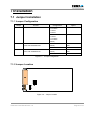
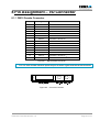
1
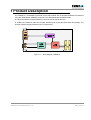
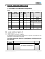
The Embedded I/O Company TPMC812 SERCOS PMC with 2 Encoder Interfaces Version 1.0 User Manual Issue 1.6 September 2006 D76812801 TEWS TECHNOLOGIES GmbH Am Bahnhof 7 Phone: +49-(0)4101-4058-0 25469 Halstenbek, Germany Fax: +49-(0)4101-4058-19 www.tews.com e-mail: [email protected] TEWS TECHNOLOGIES LLC 9190 Double Diamond Parkway, Suite 127, Reno, NV 89521, USA www.tews.com Phone: +1 (775) 850 5830 Fax: +1 (775) 201 0347 e-mail: [email protected] TPMC812-10 SERCOS PMC with 2 encoder interfaces TPMC812-11 SERCOS PMC with 2 encoder interfaces (optical isolated encoder interface) This document contains information, which is proprietary to TEWS TECHNOLOGIES GmbH. Any reproduction without written permission is forbidden. TEWS TECHNOLOGIES GmbH has made any effort to ensure that this manual is accurate and complete. However TEWS TECHNOLOGIES GmbH reserves the right to change the product described in this document at any time without notice. TEWS TECHNOLOGIES GmbH is not liable for any damage arising out of the application or use of the device described herein. Style Conventions Hexadecimal characters are specified with prefix 0x, i.e. 0x029E (that means hexadecimal value 029E). For signals on hardware products, an ‚Active Low’ is represented by the signal name with # following, i.e. IP_RESET#. 1999-2006 by TEWS TECHNOLOGIES GmbH TPMC812 User Manual Issue 1.6 Page 2 of 23 Issue Description Date 1.0 First Issue March 1999 1.1 Additions to User Manual, Board Revision changed to B May 1999 1.2 Add MTBF and weight value to Technical Specification March 2001 1.3 Jumper Configuration Description modified PCI Interface Data added to Technical Specification July 2002 1.4 General Revision May 2003 1.5 SERCON816 SERCOS Controller September 2004 1.6 New address TEWS LLC September 2006 TPMC812 User Manual Issue 1.6 Page 3 of 23 Table of Contents 1 2 3 PRODUCT DESCRIPTION ......................................................................................... 6 TECHNICAL SPECIFICATION................................................................................... 7 LOCAL SPACE ADDRESSING.................................................................................. 8 3.1 PCI9050 Local Space Configuration .............................................................................................8 3.2 Local Address Space 0...................................................................................................................8 3.2.1 SERCON816 Controller Register ........................................................................................8 3.2.2 Additional Local Register ...................................................................................................10 3.2.2.1 MSYNC Register (0x80).....................................................................................10 3.2.2.2 ENCx Register (0x82, 0x84) ..............................................................................11 3.3 Local Address Space 1.................................................................................................................12 3.3.1 SERCON816 Controller DPRAM.......................................................................................12 4 5 FUNCTIONAL DESCRIPTION ................................................................................. 13 PCI9050 TARGET CHIP........................................................................................... 14 5.1 PCI Configuration (CFG) Registers .............................................................................................14 5.1.1 PCI Header of the TPMC812.............................................................................................14 5.1.2 PCI Base Address Initialization .........................................................................................15 5.2 Local Configuration Register (LCR)............................................................................................16 5.3 Configuration EEPROM ................................................................................................................17 5.4 Local Software Reset....................................................................................................................18 5.5 Big / Little Endian..........................................................................................................................18 5.5.1 PCI Interrupt Control/Status Register ................................................................................20 6 7 PROGRAMMING HINTS .......................................................................................... 21 INSTALLATION........................................................................................................ 22 7.1 Jumper Installation .......................................................................................................................22 7.1.1 Jumper Configuration ........................................................................................................22 7.1.2 Jumper Location ................................................................................................................22 8 PIN ASSIGNMENT – I/O CONNECTOR .................................................................. 23 8.1.1 DB15 Female Connector ...................................................................................................23 TPMC812 User Manual Issue 1.6 Page 4 of 23 Table of Figures FIGURE 1-1 : BLOCK DIAGRAM TPMC812 ....................................................................................................6 FIGURE 2-1 : TECHNICAL SPECIFICATION...................................................................................................7 FIGURE 3-1 : PCI9050 LOCAL SPACE CONFIGURATION ............................................................................8 FIGURE 3-2 : SERCON816 CONTROLLER REGISTERS...............................................................................9 FIGURE 3-3 : ADDITIONAL LOCAL REGISTER............................................................................................10 FIGURE 3-4 : MSYNC REGISTER .................................................................................................................10 FIGURE 3-5 : ENCX REGISTER ....................................................................................................................11 FIGURE 3-6 : SERCON816 CONTROLLER DPRAM ....................................................................................12 FIGURE 5-1 : PCI CONFIGURATION REGISTER MAP ................................................................................14 FIGURE 5-2 : PCI9050 LOCAL CONFIGURATION REGISTER ....................................................................16 FIGURE 5-3 : CONFIGURATION EEPROM TPMC812-XX ...........................................................................17 FIGURE 5-4 : LOCAL BUS LITTLE/BIG ENDIAN...........................................................................................18 FIGURE 5-5 : INTERRUPT CONTROL/STATUS REGISTER (INTCSR; 0X4C)............................................20 FIGURE 7-1 : JUMPER CONFIGURATION....................................................................................................22 FIGURE 7-2 : JUMPER LOCATION ...............................................................................................................22 FIGURE 8-1 : DB15 FEMALE CONNECTOR .................................................................................................23 FIGURE 8-2 : CONNECTOR LOCATION .......................................................................................................23 TPMC812 User Manual Issue 1.6 Page 5 of 23 1 Product Description The TPMC812 is a standard single-width 32 bit PMC module with a complete SERCOS bus interface using the SERCON816 SERCOS Controller in the SERCON410B compatible mode. The physical interface supports RS485 on board as well as optical fiber ring. In addition the TPMC812 offers two encoder interface ports to provide hand wheel functionality. The encoder interface supports RS422 and TTL signal levels. Figure 1-1 : Block Diagram TPMC812 TPMC812 User Manual Issue 1.6 Page 6 of 23 2 Technical Specification LOGIC INTERFACE Mechanical Interface PCI Mezzanine Card (PMC) Interface Single Size Electrical Interface PCI Rev. 2.1 compliant 33 MHz / 32 bit PCI 5V PCI Signaling Voltage PCI Target Chip PCI9050-1 (PLX Technology) FUNCTIONALITY SERCOS Controller SERCON816 (SERCON410B Compatible Mode) Encoder Interface (2 Ports) X4 quadrature 8 bit Up/Down Counter with Overflow/Underflow Flags for incremental Encoders Physical SERCOS Interface (I/O) RS485 (DB15 Female Connector) Optical fiber (HFBR-1505A, HFBR-2505A) Physical Encoder Interface (I/O) RS422 or TTL (DB15 Female Connector) PHYSICAL DATA Power Requirements 220mA typical @ +5V Operating Temperature Range Operating -40°C to +85°C Storage -40°C to +85°C Humidity 5 – 95% non-condensing MTBF 196153 h Weight 78 g Figure 2-1 : Technical Specification TPMC812 User Manual Issue 1.6 Page 7 of 23 3 Local Space Addressing 3.1 PCI9050 Local Space Configuration The local on board addressable regions are accessed from the PCI side by using the PCI9050 local spaces. PCI9050 Local Space PCI9050 PCI Base Address (Offset in PCI Configuration Space) PCI Space Mapping Size (Byte) Port Width (Bit) Endian Mode Description 0 0 (0x10) MEM 128 32 LITTLE Local Configuration Registers 1 1(0x14) I/O 128 32 LITTLE Local Configuration Registers 2 2 (0x18) I/O 256 16 BIG (lower lane) Local Address Space 0 (Controller + Additional Registers) 3 3 (0x1C) MEM 2048 16 BIG (lower lane) Local Address Space 1 (Controller DPRAM) 4 4 (0x20) - - - - Local Address Space 2 5 5 (0x24) - - - - Local Address Space 3 6 6 (0x30) - - - - Local Expansion ROM Space Figure 3-1 : PCI9050 Local Space Configuration 3.2 Local Address Space 0 3.2.1 SERCON816 Controller Register The SERCON816 Controller Registers are mapped into PCI I/O Space and are accessible in the Local Address Space 0 of the PCI9050 PCI Target Chip. The PCI Base Address for the SERCON816 Controller Registers is the PCI Base Address for Local Address Space 0 of the PCI9050 PCI Target Chip (PCI9050 PCI Configuration Register Space Offset 0x18). Offset (to PCI Base Address) Name 0x00 VERSION 0x02 REG01 Function Size (bit) 16 16 See SERCON816 Reference Manual 0x04 REG02 0x06 REG03 16 0x08 REG04 16 0x0A REG05 16 TPMC812 User Manual Issue 1.6 16 Page 8 of 23 Offset (to PCI Base Address) Name Function Size (bit) 0x0C REG06 16 0x0E REG07 16 0x10 REG08 16 0x12 REG09 16 0x14 REG0A 16 0x16 REG0B 16 0x18 REG0C 16 0x1A REG0D 16 0x1C REG0E 16 0x1E TSCYC0 16 See SERCON816 Reference Manual 0x20 TSCYC1 0x22 TCYCDEL 16 16 0x24 TCNTLT 16 0x26 TCNTST 16 0x28 TCYCSTART 16 0x2A JTSCYC1 16 0x2C JTSCYC2 16 0x2E PROGERR_FL 16 0x30 JTRDEL1 16 0x32 JTRDEL2 16 0x34 TINT0 16 0x36 TINT1 16 0x38 TINT2 16 0x3A TINT3 16 0x3C TDIVCLK 16 0x3E DTDIVCLK 16 0x40 REG20 16 0x42 THTPT 16 0x44 THT 16 0x46 THWPT 16 0x48 THW 16 0x4A REG25 16 0x4C THR 16 0x4E FIFO 16 Figure 3-2 : SERCON816 Controller Registers For a detailed description of the functionality of these registers, please refer to the SERCON816 Reference Manual which is part of the TPMC812-ED Engineering Documentation. TPMC812 User Manual Issue 1.6 Page 9 of 23 3.2.2 Additional Local Register The Additional Local Registers are mapped into PCI I/O Space and are accessible in the Local Address Space 0 of the PCI9050 PCI Target Chip. The PCI Base Address for the Additional Local Registers is the PCI Base Address for Local Address Space 0 of the PCI9050 PCI Target Chip (PCI9050 PCI Configuration Register Space Offset 0x18). Offset (to PCI Base Address) Name Function Size (bit) Access 0x80 MSYNC Master Synchronization CLK Enable 16 R/W 0x82 ENC1 Encoder 1: Counter & Flags 16 R/C 0x84 ENC2 Encoder 2: Counter & Flags 16 R/C Figure 3-3 : Additional Local Register 3.2.2.1 MSYNC Register (0x80) Bit Symbol Description Access 15:1 Reserved Always read as ‘0’. Write as ‘0’. - Reset Value 0 0 MSYNC Transmission of the SERCON Master Synchronization CLK (SERCON816 CON_CLK signal) 1 = enabled 0 = disabled (Reset State) R/W 0 Figure 3-4 : MSYNC Register TPMC812 User Manual Issue 1.6 Page 10 of 23 3.2.2.2 ENCx Register (0x82, 0x84) Bit Symbol Description Access Reset Value 15:10 Reserved Always read as ‘0’ - 0 9 UF Underflow Flag for the 8 bit Counter If an underflow occurs while the Overflow Flag is set, the Overflow Flag will be cleared and the Underflow Flag will not be set. R/C 0 8 OF Overflow Flag for the 8 bit Counter If an overflow occurs while the Underflow Flag is set, the Underflow Flag will be cleared and the Overflow Flag will not be set. R/C 0 7:0 C7…C0 8 bit Encoder Counter Value of encoder x (x = 1,2) Since this is a X4 Quadrature Counter the signalchange of any Encoder Signal Phase (A or B) will be counted. In case of a leading Phase A Signal the counting-direction is up, otherwise down. R/C 0 Figure 3-5 : ENCx Register In case of read access, the Overflow and Underflow Flag are cleared automatically (after readout), while the encoder counter value remains unchanged. Any write access to an ENCx Register clears the 8 bit encoder counter value and the Overflow and Underflow Flags. TPMC812 User Manual Issue 1.6 Page 11 of 23 3.3 Local Address Space 1 3.3.1 SERCON816 Controller DPRAM The SERCON816 Controller DPRAM is mapped into PCI Memory Space and is accessible through the Local Address Space 1 of the PCI9050 PCI Target Chip. The PCI Base Address for the SERCON816 Controller DPRAM is the PCI Base Address for Local Address Space 1 of the PCI9050 PCI Target Chip (PCI9050 PCI Configuration Space Offset 0x1C). There are 1024 x 16 bit DPRAM words of storage. Only the lower 1024 16 bit words of the SERCON816 are accessible (SERCON410B compatible mode). Offset (to PCI Base Address) 0x000 0x002 ... 0x7FE Size (bit) Access 16 16 16 16 R/W R/W R/W R/W Figure 3-6 : SERCON816 Controller DPRAM For more information on the SERCON816 Dual Ported RAM please refer to the SERCON816 Reference Manual which is part of the TPMC812-ED Engineering Documentation. TPMC812 User Manual Issue 1.6 Page 12 of 23 4 Functional Description The TPMC812 SERCOS PMC implements a SERCOS communication interface by using the SERCON816 SERCOS controller in the SERCON410B compatible mode. The SERCOS interface is a digital interface for communication between systems which have to exchange information cyclically at short, fixed intervals (65µsec to 65msec). It is appropriate for the synchronous operation of distributed control or test equipment (e.g. connection between drives and numeric control). A SERCOS interface communication system consists of one master and several slaves. These units are connected by a optical fiber ring. This ring starts and ends at the master. The slaves regenerate and repeat their received data or send their own telegrams. By this method the telegrams sent by the master are received by all slaves while the master receives data telegrams from the slaves. The optical fiber assures a reliable high-speed data transmission with excellent noise immunity. The TPMC812 SERCOS PMC contains all the hardware related functions of the SERCOS interface and considerably reduces the hardware costs and the computing time requirements of the host CPU. It is the direct link between the electric-optical receiver and transmitter and the host CPU that executes the control algorithms. The TPMC812-20 SERCOS PMC can be used for both, SERCOS interface masters and slaves. The serial interface operates with data rates up to 4 Mbaud. A Dual Ported RAM (1024 * 16 Bit) is used for control and communication data exchange between the TPMC812 SERCOS PMC and the host CPU. The organization of the memory is flexible. The telegram processing of cyclic data is automatically controlled by the TPMC812 PMC. The transmission of service channel information over several communication cycles is executed automatically. The TPMC812 PMC also implements two 8 bit - X4 Quadrature Mode Counter for incremental encoder signals. Since this is a X4 Quadrature Counter the signal change of any Encoder Signal Phase (A or B) will be counted. In case of a leading Phase A signal the counting direction is up, otherwise down. Overflow and underflow conditions are signed by flags. TPMC812 User Manual Issue 1.6 Page 13 of 23 5 PCI9050 Target Chip 5.1 PCI Configuration (CFG) Registers 5.1.1 PCI Header of the TPMC812 PCI CFG Register Address Write ‘0’ to all unused (Reserved) bits 31 24 23 16 15 8 7 PCI write able Read after initialization write access (Hex Value) 0 0x00 Device ID ( Target Chip PCI9050-1 ) Vendor ID ( PLX – Technology ) N 9050 10B5 0x04 Status Command Y 0280 0000 0x08 0x0C Class Code BIST Header Type PCI Latency Timer Revision ID N 028000 XX Cache line Size Y[7:0] 00 00 00 00 0x10 PCI Base Address 0 for Memory Mapped Configuration Registers Y FFFFFF80 0x14 PCI Base Address 1 for I/O Mapped Configuration Registers Y FFFFFF81 0x18 PCI Base Address 2 for Local Address Space 0 Y FFFFFF01 0x1C PCI Base Address 3 for Local Address Space 1 Y FFFFF800 0x20 PCI Base Address 4 for Local Address Space 2 Y 00000000 0x24 PCI Base Address 5 for Local Address Space 3 Y 00000000 0x28 Cardbus CIS Pointer N 00000000 N 032C 1498 0x2C Subsystem ID ( TPMC812 ) 0x30 PCI Base Address for Local Expansion ROM Y 00000000 0x34 Reserved N 00000000 0x38 Reserved N 00000000 Y[7:0] 00 00 01 00 0x3C Max_Lat Subsystem Vendor ID ( TEWS TECHOLOGIES GmbH ) Min_Gnt Interrupt Pin Interrupt Line Figure 5-1 : PCI Configuration Register Map TPMC812 User Manual Issue 1.6 Page 14 of 23 5.1.2 PCI Base Address Initialization PCI Base Address Initialization is scope of the PCI host software. PCI9050 PCI Base Address Initialization: 1. Write 0xFFFF_FFFF to the PCI9050 PCI Base Address Register. 2. Read back the PCI9050 PCI Base Address Register. 3. For PCI Base Address Registers 0:5, check bit 0 for PCI Address Space. Bit 0 = '0' requires PCI Memory Space mapping Bit 0 = '1' requires PCI I/O Space mapping For the PCI Expansion ROM Base Address Register, check bit 0 for usage. Bit 0 = ‘0’: Expansion ROM not used Bit 0 = ‘1’: Expansion ROM used 4. For PCI I/O Space mapping, starting at bit location 2, the first bit set determines the size of the required PCI I/O Space size. For PCI Memory Space mapping, starting at bit location 4, the first bit set to '1' determines the size of the required PCI Memory Space size. For PCI Expansion ROM mapping, starting at bit location 11, the first bit set to '1' determines the required PCI Expansion ROM size. For example, if bit 5 of a PCI Base Address Register is detected as the first bit set to ‘1’, the PCI9050 is requesting a 32 byte space (address bits 4:0 are not part of base address decoding). 5. Determine the base address and write the base address to the PCI9050 PCI Base Address Register. For PCI Memory Space mapping the mapped address region must comply with the definition of bits 3:1 of the PCI9050 PCI Base Address Register. After programming the PCI9050 PCI Base Address Registers, the software must enable the PCI9050 for PCI I/O and/or PCI Memory Space access in the PCI9050 PCI Command Register (Offset 0x04). To enable PCI I/O Space access to the PCI9050, set bit 0 to '1'. To enable PCI Memory Space access to the PCI9050, set bit 1 to '1'. For more information please refer to the PCI9050-1 data sheet which is part of the TMPC812-ED Engineering Documentation. TPMC812 User Manual Issue 1.6 Page 15 of 23 5.2 Local Configuration Register (LCR) After reset, the PCI9050 Local Configuration Registers are loaded from the on board serial configuration EEPROM. The PCI base address for the PCI9050 Local Configuration Registers is: PCI9050 PCI Base Address 0 (PCI Memory Space) (Offset 0x10 in the PCI9050 PCI Configuration Register Space) or PCI9050 PCI Base Address 1 (PCI I/O Space) (Offset 0x14 in the PCI9050 PCI Configuration Register Space). Do not change hardware dependent bit settings in the PCI9050 Local Configuration Registers. Offset from PCI Base Address Register Value 0x00 Local Address Space 0 Range 0x0FFF_FF01 0x04 Local Address Space 1 Range 0x0FFF_F800 0x08 Local Address Space 2 Range 0x0000_0000 0x0C Local Address Space 3 Range 0x0000_0000 0x10 Local Exp. ROM Range 0x0000_0000 0x14 Local Re-map Register Space 0 0x0000_0001 0x18 Local Re-map Register Space 1 0x0000_1001 0x1C Local Re-map Register Space 2 0x0000_0000 0x20 Local Re-map Register Space 3 0x0000_0000 0x24 Local Re-map Register ROM 0x0000_0000 0x28 Local Address Space 0 Descriptor 0x5542_2100 0x2C Local Address Space 1 Descriptor 0x5542_2140 0x30 Local Address Space 2 Descriptor 0x0000_0000 0x34 Local Address Space 3 Descriptor 0x0000_0000 0x38 Local Exp. ROM Descriptor 0x0000_0000 0x3C Chip Select 0 Base Address 0x0000_0041 0x40 Chip Select 1 Base Address 0x0000_1401 0x44 Chip Select 2 Base Address 0x0000_0085 0x48 Chip Select 3 Base Address 0x0000_0000 0x4C Interrupt Control/Status 0x0000_005B 0x50 Miscellaneous Control Register 0x0078_0040 Figure 5-2 : PCI9050 Local Configuration Register TPMC812 User Manual Issue 1.6 Page 16 of 23 5.3 Configuration EEPROM After power-on or PCI reset, the PCI9050 loads initial configuration register data from the on board configuration EEPROM. The configuration EEPROM contains the following configuration data: • Address 0x00 to 0x0E : PCI9050 PCI Configuration Register Values • Address 0x10 to 0x62 : PCI9050 Local Configuration Register Values • Address 0x64 to 0x7C : Not used • Address 0x7E: TPMC variant See the PCI9050 Manual for more information. Address 0x00 0x02 0x04 0x06 0x08 0x0A 0x0C 0x0E 0x00 0x9050 0x10B5 0x1180 0x0000 0x029E 0x1498 0x0000 0x0100 0x10 0x0FFF 0xFF01 0x0FFF 0xF800 0x0000 0x0000 0x0000 0x0000 0x20 0x0000 0x000 0x0000 0x0001 0x0000 0x1001 0x0000 0x0000 0x30 0x0000 0x000 0x0000 0x0000 0x5542 0x2100 0x5542 0x2140 0x40 0x0000 0x000 0x0000 0x0000 0x0000 0x0000 0x0000 0x0041 0x50 0x0000 0x1401 0x0000 0x0085 0x0000 0x0000 0x0000 0x005B 0x60 0x0078 0x0040 0xFFFF 0xFFFF 0xFFFF 0xFFFF 0xFFFF 0xFFFF 0x70 0xFFFF 0xFFFF 0xFFFF 0xFFFF 0xFFFF 0xFFFF 0xFFFF s.b. Figure 5-3 : Configuration EEPROM TPMC812-xx Subsystem-ID Value (Offset 0x7E): TPMC812-10 0x000A TPMC812-11 0x000B For more information please refer to the PCI9050-1 data sheet which is part of the TPMC812-ED Engineering Documentation. TPMC812 User Manual Issue 1.6 Page 17 of 23 5.4 Local Software Reset The PCI9050 Local Reset Output LRESETo# is used to reset the on board local logic. The PCI9050 local reset is active during PCI reset or if the PCI Adapter Software Reset bit is set in the PCI9050 local configuration register CNTRL (offset 0x50). CNTRL[30] PCI Adapter Software Reset: Value of ‘1’ resets the PCI9050 and issues a reset to the Local Bus (LRESETo# asserted). The PCI9050 remains in this reset condition until the PCI Host clears this bit. The contents of the PCI9050 PCI and Local Configuration Registers are not reset. The PCI9050 PCI Interface is not reset. 5.5 Big / Little Endian • PCI – Bus (Little Endian) Byte 0 AD[7..0] Byte 1 AD[15..8] Byte 2 AD[23..16] Byte 3 AD[31..24] • Every Local Address Space (0...3) and the Expansion ROM Space can be programmed to operate in Big or Little Endian Mode. Big Endian Little Endian 32 Bit 32 Bit Byte 0 D[31..24] Byte 0 D[7..0] Byte 1 D[23..16] Byte 1 D[15..8] Byte 2 D[15..8] Byte 2 D[23..16] Byte 3 D[7..0] Byte 3 D[31..24] 16 Bit upper lane 16 Bit Byte 0 D[31..24] Byte 0 D[7..0] Byte 1 D[23..16] Byte 1 D[15..8] 16 Bit lower lane Byte 0 D[15..8] Byte 1 D[7..0] 8 Bit upper lane 8 Bit Byte 0 Byte 0 D[31..24] D[7..0] 8 Bit lower lane Byte 0 D[7..0] Figure 5-4 : Local Bus Little/Big Endian TPMC812 User Manual Issue 1.6 Page 18 of 23 Standard use of the TPMC812: Local Address Space 0 16 bit bus in Big Endian Mode (Lower Lane) Local Address Space 1 16 bit bus in Big Endian Mode (Lower Lane) Local Address Space 2 not used Local Address Space 3 not used Expansion ROM Space not used To change the Endian Mode use the Local Configuration Registers for the corresponding Space. Bit 24 of the according register sets the mode. A value of 1 indicates Big Endian and a value of 0 indicates Little Endian. For further information please refer to the PCI9050 manual which is also part of the TPMC812-ED Engineering Documentation. Use the PCI Base Address 0 + Offset or PCI Base Address 1 + Offset: Short cut Offset Name LAS0BRD 0x28 Local Address Space 0 Bus Region Description Register LAS1BRD 0x2C Local Address Space 0 Bus Region Description Register LAS2BRD 0x30 Local Address Space 0 Bus Region Description Register LAS3BRD 0x34 Local Address Space 0 Bus Region Description Register EROMBRD 0x38 Expansion ROM Bus Region Description Register You could also use the PCI - Base Address 1 I/O Mapped Configuration Registers. TPMC812 User Manual Issue 1.6 Page 19 of 23 5.5.1 PCI Interrupt Control/Status Register The INT0 output of the SERCON816 Controller is connected to the LINT1 input of the PCI9050 PCI Target Chip. The INT1 output of the SERCON816 Controller is connected to the LINT2 input of the PCI9050 PCI Target Chip. The PCI9050 PCI Target Chip can generate an interrupt at pin INTA# of the PCI bus. The interrupt status can be read at the Interrupt Status Register INTCSR of the PCI Controller PCI9050-1. For disabling / enabling PCI interrupts only set bit 6 of the PCI9050 Interrupt Control/Status Register (INTCSR; 0x4C) to ‘0’ / ‘1’. Do not change any other bits of this register. Bit 31:8 Description unused Access Reset Value R 0 7 Software Interrupt R/W 0 6 PCI Interrupt Enable R/W 1 5 Local Interrupt 2 Status R 0 4 Local Interrupt 2 Polarity R/W 1 3 Local Interrupt 2 Enable R/W 1 2 Local Interrupt 1Status R 0 1 Local Interrupt 1 Polarity R/W 1 0 Local Interrupt 1 Enable R/W 1 Figure 5-5 : Interrupt Control/Status Register (INTCSR; 0x4C) TPMC812 User Manual Issue 1.6 Page 20 of 23 6 Programming Hints For more information on programming the SERCON816 Controller please refer to the SERCON816 Reference Manual which is part of the TPMC812-ED Engineering Documentation. TPMC812 User Manual Issue 1.6 Page 21 of 23 7 Installation 7.1 Jumper Installation 7.1.1 Jumper Configuration Jumper J3 J2 J1 Function SERCOS I/O INTERFACE TYPE SERCOS RS485 INTERFACE SYNC LINE TERMINATION SERCOS RS485 INTERFACE DATA LINE TERMINATION Configuration Option 1-3 CLOSED 2-4 CLOSED 5-7 OPEN 6-8 OPEN RS485 1-3 OPEN 2-4 OPEN 5-7 CLOSED 6-8 CLOSED (Default) Optical Fiber 1-2 CLOSED (Default) Termination ON 120R 1-2 OPEN Termination OFF 1-2 CLOSED (Default) Termination ON 120R 1-2 OPEN Termination OFF Figure 7-1 : Jumper Configuration 7.1.2 Jumper Location Figure 7-2 : Jumper Location TPMC812 User Manual Issue 1.6 Page 22 of 23 8 Pin Assignment – I/O Connector 8.1.1 DB15 Female Connector Pin Signal Function 1 GND 2 SDATA+ SERCOS RS485 DATA LINE + 3 SSYNC+ SERCOS RS485 SYNC LINE + 4 ENC2A+ ENCODER 2 PHASE A + 5 ENC2B+ ENCODER 2 PHASE B + 6 GND 7 ENC1A+ ENCODER 1 PHASE A + 8 ENC1B+ ENCODER 1 PHASE B + 9 SDATA– SERCOS RS485 DATA LINE – 10 SSYNC– SERCOS RS485 SYNC LINE – 11 GND 12 ENC2A– ENCODER 2 PHASE A – 1) 13 ENC2B– ENCODER 2 PHASE B – 1) 14 ENC1A– ENCODER 1 PHASE A – 1) 15 ENC1B– ENCODER 1 PHASE B – 1) SIGNAL GROUND SIGNAL GROUND SIGNAL GROUND Figure 8-1 : DB15 Female Connector 1) For TTL level encoder interface inputs the pins for these signals must be left unconnected. Figure 8-2 : Connector Location TPMC812 User Manual Issue 1.6 Page 23 of 23