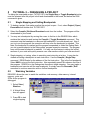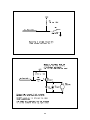
1
RMB-S / READS
User’s Guide
Version 1.2
July 1998
RIGEL CORPORATION
PO Box 90040
Gainesville, FL 32607
(352) 373-4629
FAX (352) 373-17106
www.rigelcorp.com
Copyright (C) 1998 by Rigel Corporation.
All rights reserved. No part of this document may be reproduced, stored in a retrieval system,
or transmitted in any form, or by any means, electronic, mechanical, photocopying, recording,
or otherwise, without the prior written permission of Rigel Corporation.
The abbreviation PC used throughout this guide refers to the IBM Personal Computer or its
compatibles. IBM PC is a trademark of International Business Machines, Inc.
Warranty
RIGEL CORPORATION - CUSTOMER AGREEMENT
1. Return Policy. If you are not satisfied with the items purchased, prior to usage, you may return them to Rigel
Corporation within thirty (30) days of your receipt of same and receive a full refund from Rigel Corporation. You will be
responsible for shipping costs. Please call (904) 373-4629 prior to shipping. A refund will not be given if the READS
package has been opened.
2.
READS License. The READS being purchased is hereby licensed to you on a non-exclusive basis for use in only one
computer system and shall remain the property of Rigel Corporation for purposes of utilization and resale. You
acknowledge you may not duplicate the READS for use in additional computers, nor may you modify, disassemble,
translate, sub-license, rent or transfer electronically the READS from one computer to another, or make it available
through a timesharing service or network of computers. Rigel Corporation maintains all proprietary rights in and to the
READS for purposes of sale and resale or license and re-license.
BY BREAKING THE SEAL AND OTHERWISE OPENING THE READS PACKAGE, YOU INDICATE YOUR
ACCEPTANCE OF THIS LICENSE AGREEMENT, AS WELL AS ALL OTHER PROVISIONS CONTAINED HEREIN.
3.
Limited Warranty. Rigel Corporation warrants, for a period of sixty (60) days from your receipt, that READS disks,
hardware assembled boards and hardware unassembled components shall be free of substantial errors or defects in
material and workmanship which will materially interfere with the proper operation of the items purchased. If you
believe such an error or defect exists, please call Rigel Corporation at (904) 373-4629 to see whether such error or
defect may be corrected, prior to returning items to Rigel Corporation. Rigel Corporation will repair or replace, at its
sole discretion, any defective items, at no cost to you, and the foregoing shall constitute your sole and exclusive remedy
in the event of any defects in material or workmanship.
THE LIMITED WARRANTIES SET FORTH HEREIN ARE IN LIEU OF ALL OTHER WARRANTIES, EXPRESSED OR
IMPLIED, INCLUDING, BUT NOT LIMITED TO, THE IMPLIED WARRANTIES OF MERCHANTABILITY AND FITNESS
FOR A PARTICULAR PURPOSE.
YOU ASSUME ALL RISKS AND LIABILITY FROM OPERATION OF ITEMS PURCHASED AND RIGEL CORPORATION
SHALL IN NO EVENT BE LIABLE FOR DAMAGES CAUSED BY USE OR PERFORMANCE, FOR LOSS PROFITS,
PERSONAL INJURY OR FOR ANY OTHER INCIDENTAL OR CONSEQUENTIAL DAMAGES. RIGEL
CORPORATION’S LIABILITY SHALL NOT EXCEED THE COST OF REPAIR OR REPLACEMENT OF DEFECTIVE
ITEMS.
IF THE FOREGOING LIMITATIONS ON LIABILITY ARE UNACCEPTABLE TO YOU, YOU SHOULD RETURN ALL
ITEMS PURCHASED TO RIGEL CORPORATION.
4.
Board Kit. If you are purchasing a board kit, you are assumed to have the skill and knowledge necessary to properly
assemble same. Please inspect all components and review accompanying instructions. If instructions are unclear,
please return the kit un-assembled for a full refund or, if you prefer, Rigel Corporation will assemble the kit for a fee of
$100.00. You shall be responsible for shipping costs. The foregoing shall apply only where the kit is un-assembled. In
the event the kit is partially assembled, a refund will not be available, however, Rigel Corporation can, upon request,
complete assembly for a fee based on an hourly rate of $50.00. Although Rigel Corporation will replace any defective
parts, it shall not be responsible for malfunctions due to errors in assembly. If you encounter problems with assembly,
please call Rigel Corporation at (904) 373-4629 for advice and instruction. In the event a problem cannot be resolved
by telephone, Rigel Corporation will perform repair work, upon request, at the foregoing rate of $50.00 per hour.
5.
Governing Law. This agreement and all rights of the respective parties shall be governed by the laws of the State of
Florida.
Table of Contents
1
INTRODUCTION............................................................................................................................................... 1
1.1
1.2
2
SOFTWARE SETUP ......................................................................................................................................... 3
2.1
2.2
2.3
2.4
2.6
3
OVERVIEW ...................................................................................................................................................... 1
PARTS LIST ..................................................................................................................................................... 2
SYSTEM REQUIREMENTS ................................................................................................................................. 3
SOFTWARE INSTALLATION, READS51 ............................................................................................................. 3
START UP ....................................................................................................................................................... 3
DAUGHTER BOARD JUMPERS ........................................................................................................................... 4
VERIFYING THAT THE MONITOR IS LOADED ....................................................................................................... 5
READS51 V 3.00 CONCEPTS.......................................................................................................................... 7
3.1 PROJECT ........................................................................................................................................................ 7
3.1.1 Executable Projects.............................................................................................................................. 7
3.1.2 Archive Projects ................................................................................................................................... 7
3.2 MODULE ......................................................................................................................................................... 7
4
TUTORIAL 1 -- EXECUTABLE PROJECTS .................................................................................................... 8
4.1
4.2
4.3
4.4
4.5
5
TUTORIAL 2 -- DEBUGGING A PROJECT ................................................................................................... 11
5.1
5.2
6
SINGLE-STEPPING AND SETTING BREAKPOINTS .............................................................................................. 11
W ATCHING VARIABLES .................................................................................................................................. 11
TUTORIAL 3 -- ARCHIVE PROJECTS .......................................................................................................... 13
6.1
6.2
7
CREATING AN EXECUTABLE PROJECT .............................................................................................................. 8
ADDING A MODULE .......................................................................................................................................... 8
BUILDING THE PROJECT................................................................................................................................... 9
DOWNLOADING THE PROJECT INTO MEMORY.................................................................................................. 10
RUNNING THE PROJECT ................................................................................................................................. 10
CREATING AN ARCHIVE PROJECT ................................................................................................................... 13
IMPORTING/EXPORTING MODULES ................................................................................................................. 13
THE RMB-S BOARD ...................................................................................................................................... 14
7.1 UIOD - USER INPUT/OUTPUT DEVICES .......................................................................................................... 14
7.2 MICROCONTROLLER PORTS ........................................................................................................................... 15
7.3 CHIP OPTIONS .............................................................................................................................................. 16
7.4 80515 / 80517 FAMILY OPTIONS .................................................................................................................. 17
7.4.1 Pin assignment................................................................................................................................... 17
7.4.2 Jumper Selection................................................................................................................................ 17
7.4.3 Analog-to-Digital Converter Reference Voltages ............................................................................... 18
7.5 MEMORY CONFIGURATION ............................................................................................................................. 19
7.5.1 8051 Memory Overview...................................................................................................................... 19
7.5.2 RMB-S Memory Options..................................................................................................................... 20
7.5.3 Memory Jumper Selection.................................................................................................................. 20
7.6 SYSTEM HEADER .......................................................................................................................................... 20
7.7 THE DAUGHTER BOARDS .............................................................................................................................. 21
7.7.1 The DA84 Daughter Board................................................................................................................. 21
7.7.2 The DA68 Daughter Board................................................................................................................. 21
7.7.3 The DA44 Daughter Board................................................................................................................. 21
7.7.4 The DA40 Daughter Board................................................................................................................. 22
8
THE READS51 ASSEMBLER ........................................................................................................................ 23
8.1 ASSEMBLY ERRORS ...................................................................................................................................... 23
8.1.1 Attempt to Redefine Symbol or Label................................................................................................. 23
8.1.2
8.1.3
8.1.4
8.1.5
8.1.6
8.1.7
8.1.8
8.1.9
8.1.10
8.1.11
8.1.12
9
Incorrect Symbol or Label................................................................................................................... 23
Incorrect Operand .............................................................................................................................. 23
Attempt to Branch Out of Bounds....................................................................................................... 23
Unresolved Operand(s) ...................................................................................................................... 23
Undecodable Line............................................................................................................................... 23
Operand(s) Out of Range................................................................................................................... 23
Incorrect Operand Types.................................................................................................................... 24
Incorrect Register Use........................................................................................................................ 24
Incorrect Constant .............................................................................................................................. 24
Odd or Out-of-Range Address ........................................................................................................... 24
Undefined Symbol .............................................................................................................................. 24
RROS - THE ROM-RESIDENT OPERATING SYSTEM ................................................................................ 25
9.1
9.2
9.3
9.4
THE INITIALIZATION ROUTINE ......................................................................................................................... 25
THE COMMAND PROCESSOR ......................................................................................................................... 25
DEBUG FUNCTIONS ....................................................................................................................................... 27
GENERAL PURPOSE ROUTINES (SYSTEM CALLS)............................................................................................ 28
9.5
9.6
SYSTEM VARIABLES ...................................................................................................................................... 29
THE INTERRUPT VECTOR TABLE .................................................................................................................... 31
Serial Communication
10
chkbrk ................................................................................................................................ 28
SAMPLE PROGRAMS ................................................................................................................................... 32
10.1
10.2
10.3
10.4
10.5
10.6
10.7
10.8
10.9
10.10
10.11
10.12
BASICS OF DIGITAL INPUTS AND OUTPUTS ................................................................................................. 32
A KEYLESS ENTRY (DIGITAL UNLOCK) SYSTEM.......................................................................................... 33
USING SUBROUTINES ................................................................................................................................ 34
USING THE SLR2016 INTELLIGENT DISPLAY .............................................................................................. 34
RUNNING LIGHTS ...................................................................................................................................... 34
USING INTERNAL TIMERS .......................................................................................................................... 34
USING INTERRUPTS................................................................................................................................... 34
A SIMPLE VOLTMETER .............................................................................................................................. 35
A 0-5 VOLT VOLTMETER ........................................................................................................................... 35
W ORKING WITH FRACTIONS - AN IMPROVED VOLTMETER .......................................................................... 35
MEASURING REACTION TIMES ................................................................................................................... 36
RUNNING IN THE USER MODE ................................................................................................................... 37
11
8051 FAMILY CHIP MANUFACTURERS....................................................................................................... 38
12
SOFTWARE VENDORS ................................................................................................................................. 39
13
BIBLIOGRAPHY ............................................................................................................................................. 40
JOURNALS ............................................................................................................................................................. 40
BOOKS .................................................................................................................................................................. 40
HARDWARE DESIGN ............................................................................................................................................... 40
APPENDICES ............................................................................................................................................................. I
APPENDIX A: READS51 MAIN MENU COMMANDS ............................................................................................. II
A.1 PROJECT .........................................................................................................................................................II
A.2 MODULE ..........................................................................................................................................................II
A.3 COMPILE ..........................................................................................................................................................II
A.4 VIEW .............................................................................................................................................................. III
A.5 TOOLS ............................................................................................................................................................ III
A.5.1 Editor ....................................................................................................................................................iii
A.5.2 TTY.......................................................................................................................................................iii
A.5.3 Assembler ............................................................................................................................................iii
A.5.4 Project ..................................................................................................................................................iii
A.5.5 Compile Errors .....................................................................................................................................iii
A.6 OPTIONS......................................................................................................................................................... III
A.7 W INDOW ......................................................................................................................................................... III
A.8 HELP .............................................................................................................................................................. III
APPENDIX B: READS EDITOR ..............................................................................................................................IV
B.1 READS51 EDITOR OVERVIEW ....................................................................................................................... IV
B.2 FILE MENU ..................................................................................................................................................... IV
B.2.1 Edit Menu .............................................................................................................................................iv
B.2.2 View...................................................................................................................................................... v
B.2.3 Window................................................................................................................................................. v
B.2.4 Navigate ............................................................................................................................................... v
B.3 MISCELLANEOUS EDIT AND NAVIGATION KEYS................................................................................................. VI
B.4 HIGHLIGHTING TEXT ....................................................................................................................................... VI
B.4.1 Highlighting the Current Word ..............................................................................................................vi
B.4.2 Highlighting a Block of Characters .......................................................................................................vi
B.4.3 Highlighting a Block of Lines ................................................................................................................vi
APPENDIX C: GENERAL PURPOSE ROUTINES (SYSTEM CALLS) ................................................................VIII
APPENDIX D: HOW BREAKPOINTS ARE HANDLED .........................................................................................XII
APPENDIX E: HOW TRACING IS HANDLED ..................................................................................................... XIV
APPENDIX F: DEBUGGING WITH AN ASCII TERMINAL................................................................................... XV
APPENDIX G: THE SOFTWARE DEVELOPMENT CYCLE ............................................................................... XVI
APPENDIX H: SAMPLE PROGRAM CIRCUIT DIAGRAMS ............................................................................ XVIII
APPENDIX I:
RMB-S BOARD HEADER PINS.................................................................................................. XXI
APPENDIX J:
BILL OF MATERIALS ................................................................................................................ XXII
APPENDIX K: BOARD LAYOUT ....................................................................................................................... XXV
APPENDIX L: SYSTEM AND CIRCUIT DIAGRAMS ....................................................................................... XXVI
1
1.1
INTRODUCTION
Overview
The RMB-S prototyping board and READS (Rigel’s Embedded Applications Development
System) constitute a complete system for developing embedded control applications. Efficient
software development and rapid hardware prototyping are combined in a single integrated development environment.
The prototyping board is designed to communicate with a PC (IBM PC or compatible) acting
as a host. The host-to-board communications are carried out through a serial port (COM1 or
COM2). The host-based development system READS is a menu-driven environment with an
editor, assembler, debugger, and PC-to-board communications software.
The ROM Resident Operating System (RROS) includes an operating system, a monitor
system and user-accessible system calls for control and communication support. The RROS
monitor may be used to communicate with an ASCII terminal when the PC (IBM PC or
compatible) host is unavailable.
RMB-S uses daughter boards to accommodate a wide variety of 8051 microcontrollers. The
daughter boards accommodate the following of pin configurations: DA84 for Siemens 80517
family in 84-pin PLCC format; DA68 for Siemens 80515 family in 68-pin PLCC format; and
DA44 for the 8052 family in 44-pin PLCC format including the new INTEL chip the 80C251;
and the DA40 for the 8052 family in the 40 pin dip package. The instruction set of these
microcontrollers are supersets of the MCS-51 instruction set. The RMB-S uses external RAM
during the development cycle. Once an application program is developed, it may be permanently placed in EPROM. With an application-specific program installed, the RMB-S may be
used to emulate an embedded controller.
Prototyping components consisting of push buttons, dip switches, light emitting diodes (LED),
numerical displays, potentiometers, and a speaker are used for emulating control application
inputs and outputs. These components are referred to as the User Input Output Devices
(UIOD). There are two solderless breadboard terminal strips, one connected to the
prototyping components and the other to the microcontroller ports and control lines, plus a
large solderless breadboard. These provide flexibility for connecting prototyping components
to the microcontroller lines, and for developing and debugging user-designed analog and
digital application circuits.
The source code of the user-accessible systems calls is provided. These routines as well as
all examples in the User’s Guide and in the distribution diskettes may be used or incorporated
into applications by the registered buyer without any royalties, fees, or limitations. Rigel
Corporation is not responsible for the suitability or correctness of the example software. Refer
to the warranty for additional information.
1.2
Parts List
Your RMB-S / READS package includes the following:
RMB-S Board
1. RMB-S motherboard.
2. RMB-S / READS User’s Guide.
3. A 32K EPROM with RROS (ROM Resident Operating System), 32K RAM.
4. Four daughter boards (DA40, DA44, DA68, and DA84), the DA68 populated with the
80C535.
5. Assembly Instructions (for unassembled kits only).
6. A serial modem cable and adapter.
7. 9 Volt 500mA power source (for US sales only).
READS Software
1. The Integrated Development System Package including an editor, a cross-assembler,
and PC to board communications software.
2. R-Host ASCII terminal emulator.
3. 8031 chip simulator
3. Sample software.
4. Source code for user-accessible system calls.
2
2
2.1
SOFTWARE SETUP
System Requirements
READS51 is designed to work with an IBM PC or compatible, 386 or better, running Windows
95 or Windows NT.
2.2
Software Installation, READS51
Place the CD-ROM in your drive. Go to the Rigel Products | 8051 Software | READS51 |
and select whether you wish to use the DOS or the WIN95/NT version of the software. Click
on the exe file and the program will begin to load in your system. Follow the standard install
directions answering the questions with the appropriate answers
This user’s manual is for the WIN95/NT version of the software. The DOS User’s Manual can
be found on the CD-ROM.
2.3
Start up
If you purchased a built RMB-S board, it is already set up to run the demo programs. The
following are the factory settings.
Memory
1. The RROS EPROM in U5. Jumper SEP removed.
2. A 32K RAM (62256) in U6. The two jumpers configured as RAM (right position).
3. U7 and U8 are not used by the demo programs. If populated, place jumpers to specify
either RAM or EPROM devices.
Slide switch S16 should be in the MON(ITOR) position.
USER
P2
P1
D10
D11
MON
TXD AUX
9VAC
RXD AUX
HWPD/
PE\ SWD
VCC
62256
VAREF
RAM
RAM
EPROM
VAGND
27C256
EPROM
SEP
RAM
EPROM
GND
RESET
Y1
U11
U5
U6
Vcc
Remove for VBB
Remove
for HWPD
EA
Figure 2.1 Default Jumper Settings with the 80C535 Processor
Jumpers in VAREF and VAGND populated. These are used for the analog-to-digital
converters.
The settings of jumpers PE\ SWD and HWPD\ depend on the processor used. For the demo
programs use the following settings.
3
Jumper
PE# / SWD
HWPD#
2.4
80C535
GND
Removed
Daughter Board Jumpers
The jumper on the daughter boards depend on the processor used. Always populate the EA\
jumper to enable fetching external code.
DA68
80C535, (CMOS): insert all jumpers.
1. Run the READS51 host driver by selecting Start | Programs | READS51. You may
also start READS51 by double clicking on the READS51 short cut icon if installed.
2.5 Configuring READS51 and Initiating Host-to-Board Communications
1. Press the Projects | New | Executable | a new project window will open where you can
select the board and processor you are using.
2. Select the communication port parameters using the Options | TTY Options menu
command. You will need to select the COM port you are using, and the baud rate.
3. Open the TTY window using the Tools | TTY menu command.
4
4. You can confirm the board is working by pushing the reset button on the board. The
appropriate processor should show in the TTY window. (8031/8032 will show 8052
5. monitor program, 80C535 will show 80515 monitor program)
80515 monitor program
2.6
Verifying that the Monitor is Loaded
Make sure the TTY window is active, clicking the mouse inside the TTY window to activate it if
necessary. Then type the letter ‘H’ (case insensitive) to verify that the monitor program is
responding. The ‘H’ command displays the available single-letter commands the monitor will
recognize.
The READS monitors use single-letter commands to execute basic functions. Port
configurations and data, as well as memory inspection and modifications may be
accomplished by the monitor. Most of the single-letter commands are followed by 4
hexadecimal digit addresses or 2 hexadecimal digit data bytes.
The list of monitor commands is displayed with the H command while the monitor program is
in effect. The H command displays the following table.
B
C
D
D
D
G
H
K
L
xxxx
xxxx-xxxx
xx-xx
xx=nn
xx-xx=nn
xxxx
sets Break point at address xxxx
displays Code memory
displays internal Data ram
modifies internal Data ram
fills a block of internal Data ram
Go - starts executing at address xxxx
Help - displays monitor commands
Kills (removes) break point
down Loads Intel hex file into memory
5
P
P
R
S
S
S
S
X
X
X
x
x=nn
xx-xx
xx=nn
xx-xx=nn
xxxx-xxxx
xxxx=nn
xxxx-xxxx=nn
displays data on Port x
modifies data on Port x to nn
displays the contents of the Registers
displays Special function register addresses
displays Special function registers
modifies Special function registers
fills Special function registers
displays eXternal memory
modifies eXternal memory
fills eXternal memory
A single-letter command may be followed by up to 3 parameters. The parameters must be
entered as hexadecimal numbers. Each ’x’ above represents a hexadecimal digit (characters
0..9, A..F). Intermediate spaces are ignored. Alphabetic characters are converted to upper
case. The length of the command string must be 16 characters or less. The command syntax
is:
Letter [address][-address][=data]<CR>.
6
3
READS51 V 3.00 CONCEPTS
READS51 introduces a project-oriented code development and management system. The
new concepts are defined below.
3.1
Project
A project is a collection of files managed together. Each file in a project corresponds to a code
module. All projects are kept in their individual subdirectories. You may copy or save projects
as a single entity. When saved under a different name, a new subdirectory is created and all
components of the project are duplicated in the new subdirectory.
By using the long names provided by the 32-bit Windows operating systems, you may use this
feature to keep different versions of your software in a controlled manner. For example, the
project “Motor Control 07-20-1997” may be saved under the name “Motor Control 07-25-1997”
as new features are added. This way, if needed, you may revert to an older version.
A project may either be an “executable project” or an “archive project.”
3.1.1 Executable Projects
Executable projects are meant to be compiled into code which is eventually run on the target
system. Components of an executable project are the code modules containing subroutines
or functions which make up the entire program.
3.1.2 Archive Projects
Archive projects are never compiled. They are intended to facilitate code reusability by
organizing and keeping code modules together. An archive project acts as a repository which
you may add modules to, or copy modules from. Executable projects can be quickly
constructed using already written and debugged modules from an archive project.
3.2
Module
A module is a single file which belongs to a project. Typically modules are assembly language
subroutines. You may copy modules from one project to another, or share modules in
different projects. For example, you may copy a previously developed module from an archive
project to an executable project by simply dragging its icon from one project window to the
other. By using existing or previously developed and debugged modules, you may
significantly improve code reusability, much in the same manner as libraries. Reusing modules
differs from using library functions of existing routines in that modules are kept in source form
rather than object form.
7
4
TUTORIAL 1 -- EXECUTABLE PROJECTS
A project is a collection of code modules which are grouped together. READS51 uses two
different kinds of projects, executable projects and archive projects. An executable project is a
collection of modules which are compiled together to form one executable program. An
archive project is a collection of modules that are grouped together to make retrieval from
storage easier.
We will first create an executable project. We will explain creating archive projects in a later
section.
4.1
Creating an Executable Project
1. Select Project | New | Executable
2. A New Project box will
open up.
3. In the Name/Dir box
type Tutor1. You may
also browse the
available selections by
clicking on the hand
icon and looking in the
work directory.
4. Select the processor and board you are using in the HW Configuration boxes.
5. Click OK
6. Click Yes to "A directory with that name exists. Do you want to use it ?"
7. A project window box will open which shows TUTOR1.RPJ represented as the root of a
tree. Next, we will add a module to it.
4.2
Adding a Module
A module is a block of code which is saved in a single source file. To add a module to the
executable project TUTOR1.RPJ, make sure that the project window is open. If the project
window is not open, select Project | Open | Executable and double click on TUTOR1.RPJ.
Now, you can add a module.
1. Select Module | Add
Module. A New Code
Module window will
appear.
2. Type Tutor.asm in the
Filename box, or click on
8
the hand icon and select Tutor.asm file from the list.
3. In the Name box type a short description for the module.
4. Select as the main module.
5. Click OK
Tutor.asm has been added. It appears as a branch of the project TUTOR1.RPJ.
The language box in the New Code Module window shows that the module will be in
Assembly. Currently READS51 only supports assembly language programming.
4.3
Building the Project
1. Double click on the Tutor.asm module. A READS Editor box with the program opens
up.
2. Click on the right
mouse button and
select Build from
the sub-menu
items displayed.
3. The READS
Status Bar says
Congratulations!
No assembly
errors found.
4. Now let’s add an
error. Add an "e"
at the end of the
first mov
statement so that
it reads move.
5. Right click and
select Build in the
READS editor box
again.
6. The READS Error Dialog box opens up and reports an Illegal Op Code in line 18 and
Line 18 in the READS Editor will be highlighted.
7. In the READS Editor correct line 18 by removing the "e", we added.
8. Right click and select Build in the READS editor box again. The project will build
without errors.
9
TUTOR1.HEX has just been created and it is ready to download and run.
4.4
Downloading the Project into Memory
The Compile | Download Hex (F4) command places the assembled instructions into the code
memory of the microcontroller model.
1. Select the Compile |
Download Hex command. A
small window will appear
asking the File name to be
downloaded.
2. Select the file and hit open
or, double click on the file you
want to download.
3. You may assemble and load
in a single step, provided that
there are no assembly errors,
using the Compile | Build
and Download (F9)
4.5
Running the
Project
Running the project TUTOR1.RPJ requires you to select the Compile | Run (Ctrl + F8) option.
Make sure that one of the serial ports on your computer is connected the board and correct
port parameters are entered in Options | TTY options.
A small box asking for the program start address appears. Enter 8000 and press OK. The
program will now be running on your board.
10
5
TUTORIAL 2 -- DEBUGGING A PROJECT
To debug the executable project TUTOR1.RPJ, the Single-Step or Toggle Breakpoint option
must be selected after the project is built and downloaded to the board, but before the RUN
command is given.
5.1
Single-Stepping and Setting Breakpoints
1. To debug a project, first make sure that the project is open. If not, select Project | Open |
Executable and double click TUTOR1.RPJ.
2. Select the Compile | Build and Download mode from the toolbar. The program will be
downloaded to your board.
3. You may set a breakpoint by moving the cursor to the line in the READS Editor which
contains the instruction and issuing the Compile | Toggle Breakpoint command. This
command sets the breakpoint or removes the breakpoint if one was already set. Now if
you try to run the program, the execution will stop once the breakpoint is reached. This
state, the breakpoint is reached and the program suspended, is called the Debug State. If
you set a new breakpoint in the Debug state, program execution resumes. The program
runs until the new breakpoint is reached. You may use this feature to debug the critical
sections of your code and quickly execute over other sections which you know work well.
4. Single stepping, or tracing, refers to executing one instruction at a time. It may also be
viewed as having a breakpoint at each instruction. Use the Compile | Single Step
command. READS asks for the address of the first instruction. This is the first breakpoint.
Select 8000 to stop at the first instruction. Now repeatedly press F8 to observe the flow of
the program. READS is in the Debug state throughout single stepping. You may toggle a
breakpoint and execute until the new breakpoint, or simply issue the Assemble | Run
command to continue execution with no further breakpoints.
5.2
Watching Variables
READS51 allows the user to watch the variables, code memory, data memory, internal
memory, ports and
SFRs as the program is
debugged.
1. Select View |
Watches
2. A Watch Setup
box will appear.
3. Press F8 to start
single-stepping.
11
4. You can watch the program single step through the code by looking at the READS
Editor window or you can select which variables to watch as the code runs.
12
6
TUTORIAL 3 -- ARCHIVE PROJECTS
Archive projects are intended to facilitate code reusability by organizing and keeping code
modules together. An archive project acts as a repository that you may add modules to, or
copy modules from. Executable projects can be quickly constructed using already written and
debugged modules from an archive project.
6.1
Creating an Archive Project
An archive project is used to store source code that may then be used for other projects. To
create an archive project:
1. Type Archive in the Name/Dir box
2. Select Project | New | Archive
3. Click OK
Now you will see the project window ARCHIVE.RAR represented as the root of a tree.
6.2
Importing/Exporting Modules
1. Open the executable project TUTOR1.RPJ by selecting Project | Open | Executable
and double clicking TUTOR1.RPJ
2. Open the archive project ARCHIVE.RAR by selecting Project | Open | Archive and
double clicking ARCHIVE.RAR
3. Click on the module Tutor.asm and hold the left mouse button down while you are
dragging toward ARCHIVE.RAR. When the archive project name is highlighted release
the mouse button
4. Click OK meaning that you want to make duplicate of Tutor.asm under the archive
directory.
You’ve created your own archive file containing the module Tutor.asm. You may add as many
modules to an archive project as you want. Usually the modules you will want to add are
tested and debugged modules that you may want to use for other projects. READS51
includes many of the more common modules in for the A/D routines, timers, counters and so
on.
13
7
THE RMB-S BOARD
7.1
UIOD - User Input/Output Devices
The development of application-specific microcontroller based prototype circuits is significantly
simplified with the RMB-S breadboard area, the two terminal strips, and the user input/output
devices (UIOD). UIODs include 14 light emitting diodes (LED), marked L0 to L5 and Bar
Display 0 to 7, 2 seven-segment numeric displays, marked DISPLAY LOW and DISPLAY
HIGH, and a speaker as output devices. The 54-post solderless terminal strip located just
above the UIODs contains 14 posts, marked LEDs 0 to 5 and Bar Display 0 to 7, for the LEDs.
Also, 14 posts, grouped into 2 sets marked HIGH DIGIT and LOW DIGIT, are connected to
the seven-segment displays. Each display has segments with the standard designations a to
g. The output devices are in a common anode configuration, meaning that their anodes are
connected to +5 Volts (Vcc) by current-limiting resistors. An output device, say segment d of
DISPLAY LOW, may be turned on by linking the corresponding post on the solderless terminal
strip to power ground (0 Volts). The power ground is available on the 54-post solderless
terminal strip placed above the breadboard, at two positions, both marked
GND.
BAR DISPLAY
LEDS
POTS
SPEAKER
7 6 5 4 3 210 7 6 54 3210 5 4 3 210 3 210 1
PUSHBUTTONS
7 6 5 43 210
HIGH DIGIT
CLR\
BL\
A1
A0
WR\
DIP SWITCH
6 543210
g fedcba
SPEAKER
LOW DIGIT
gfedcba
JP1
D3
76543210
R1
POT3 POT2 POT1 POT0
R2
SLR2016
U2
SS
76543210
L5
L2
L4
L1
L3
L0
D2
U1
HIGH
PB7
PB6
PB5
PB4
PB3
PB2
PB1
LOW
PB0
Figure 7.1 UIODs -- User Input/Output Devices
There are 16 switches, as part of the UIODs, to be used as digital input devices. Each switch
has one terminal connected to power ground, and the other available at the 54-post terminal
strip. The 8 push button switches, marked PB0 to PB7, terminate at the set of posts marked
PB. Similarly, the 8 toggle switches which are implemented by an 8 contact DIP switch
marked SW DIP-8, are terminated at the posts marked DIP-SW. Care should be taken not to
connect these output posts to the power posts VCC, V1, or V2, since closing (making contact)
the corresponding switch will short power to ground. Output devices sink current, and are
therefore appropriate to drive the microcontrollers input ports. No pull-up resistors are used
with the switches. If required by the application, pull-up resistors may be added using the
breadboard area.
In addition to the digital input devices, the UIODs contain 4 potentiometers, marked POT0 to
POT3. Each potentiometer has one fixed terminal connected to +5 Volts (VCC), the other
14
fixed terminal to 0 Volts (the power ground GND), and its wiper terminal available at the 54post terminal strip marked POTs. The RMB-S contains a socket (U1) to accommodate a
Siemens SLR2016 four-digit intelligent display. The intelligent display control inputs CL\, BL\,
A0, A1 and WR\ are available on the terminal. The data inputs to the intelligent display are
shared with the seven-segment display high digit. U1 is not normally populated.
As a simple demonstration, connect L0 to PB0. Observe that LED 0 lights when push button
PB 0 is pressed.
7.2
Microcontroller Ports
All microcontroller ports except those used to access external data and program memory are
available on the 54-post solderless terminal strip located above the breadboard. The posts in
the order they appear are listed below.
JP12
P8.3
P8.2
P8.1
P8.0
P7.0
P4.7
P4.6
P4.5
P4.4
P4.3
P4.2
P4.1
P4.0
P6.7
P6.6
P6.5
P6.4
P6.3
P6.2
P6.1
P6.0
P5.7
P5.6
P5.5
P5.4
P5.3
P5.2
P5.1
P5.0
VAREF
VAGND
GND
RO\
HWPO\
PE\
PSEN\
ALE
P3.5
P3.4
P3.3
P3.2
TXD
RXD
P1.7
P1.6
P1.5
P1.4
P1.3
P1.2
P1.1
P1.0
P7.7
P7.6
P7.5
P7.4
P7.3
P7.2
P7.1
JP13
VCC
V1
V2
GND
JP14
BREADBOARD
Figure 7.2 JP12, Microcontroller Ports
GND
is the power ground (0 Volts).
RO\
is the Reset Out line of the microcontroller.
HWPD\
is the Hardware Power Down line of the microcontroller.
PE\
is the PE\ SWD (Power saving modes Enable / Start WatchDog timer) line of the
microcontroller.
PSEN\
is connected to the PSEN\ (Program Segment Enable) pin of the microcontroller.
This is an output signal requesting external program memory during an instruction fetch cycle.
ALE
is connected to the microcontrollers ALE (Address Latch Enable) pin. This is an
output signal used while accessing external program or data memory. When set,
it indicates that Port 0 contains the lower 8 bits of a valid address.
P3.2-P3.5 are connected to the corresponding bits of Port 3. Notice that other bits of Port 3
are used as control lines to access external memory or as serial communication
lines. P3.0 and P3.1 are the receive and transmit lines for the RS-232 serial
communications port linking RMB-S to the host PC. P3.6 and P3.7 are the read
(RD\) and write (WR\) lines.
15
TXD
is connected to the transmit line of the RS-232 port connected to the host.
RXD
is connected to the receive line of the RS-232 port connected to the host.
P7.0-P7.7 are connected to the bits of Port 7.
P4.0-P4.7 are connected to the bits of Port 4.
P6.0-P6.7 are connected to the bits of Port 6.
P5.0-P5.7 are connected to the bits of Port 5.
P1.0-P1.7 are connected to the bits of Port 1.
VAGND
is connected to the microcontrollers VAGND pin. It provides the lower reference
voltage to the analog-to-digital converter. A jumper labeled VAGND, when installed, connects VAGND to the power ground (GND). If a reference voltage
other than 0 Volts is desired, the jumper should be removed and the new
reference voltage should be supplied at the VAGND post.
VAREF
is connected to the microcontrollers VAREF pin. It provides the higher reference
voltage to the analog-to-digital converter. A jumper labeled VAREF, when installed, connects VAREF to +5 Volts, regulated by a separate voltage regulator.
If a reference voltage other than +5 Volts is desired, the jumper should be
removed and the new reference voltage should be supplied at the VAREF post.
P8.0-P8.3 are connected to the bits of Port 8.
VCC
is the +5 Volt supply.
V1
is the unregulated voltage from the main power supply, about 12 Volts.
V2
is the unregulated negative supply from the MAX232 chip, about -10 Volts.
GND
is the power ground (0 Volts).
As a demonstration, connect the posts TXD and RXD to L0 and L1. Observe the state of L0
and L1 while RMB-S and the PC host communicate, for example, during issuing various
monitor commands. Recall that the LEDs will light when the TXD and RXD signals are low.
This arrangement is useful to verify that serial communications are operational.
7.3
Chip Options
The RMB-S prototyping and evaluation board accommodates the 8051 family of
microcontrollers. The microcontrollers are placed in daughter boards which are plugged in to
the RMB-S. This configuration allows the same motherboard to be used with a wide variety of
8051 family products. The following is a partial list of microcontrollers which may be used with
the RMB-S:
8031/ 80C31
8032/ 80C32
83C51/83C52
87C51/87C52
8052AH BASIC and 80C251 from INTEL
80C320 from Dallas Semiconductor
80535/80515, 80C535/80C515/80C515A from Siemens
80C537/80C517/80C517A also from Siemens
16
SAB C500 series from Siemens
7.4
80515 / 80517 Family Options
7.4.1 Pin assignment
The following tables summarize the pin assignment differences among the 80515 and 80517
families of microcontrollers. The # sign indicates that the associated signal is active low.
Pin
Number
4
37
68
Pin Number
4
60
69
80535
80C535 80C515A
VPD
VBB
VCC
PE#
VCC
VCC
80C537
PE# /SWD
GND
OWE
Available on Terminal?
PE# / SWD
VCC
HWPD#
80C517A
PE# / SWD
HWPD#
OWE
Yes
No
Yes
Available on Terminal ?
Yes
Yes
No
7.4.2 Jumper Selection
The RMB-S board contains 2 three-post jumpers labeled PE\ SWD and HWPD\ to
accommodate the different pin assignments of the processors. The center post of these
jumpers are connected to the PE# / SWD and HWPD# signals of the CPUs. The two extreme
posts are connected to VCC and GND, as marked. A single jumper from the center post to
the VCC side selects a logic high signal, and similarly, to a single jumper on the GND side
selects a logic low signal. The signal will float (high-impedance state) if the jumper is
removed.
9VAC
HWPD/
PE\ SWD
VCC
VAREF
VAGND
GND
RESET
Y1
U11
Vcc
Remove for VBB
Remove
for HWPD
EA
7.3 PE\SWD and HWPD jumpers
Note that these two signals are also available on the solderless terminal. The PE# / SWD
signal is internally set to logic 1 with a pull-up resistor. If the application circuit is to provide the
signals, the jumpers should be removed. The table below shows the jumper configurations for
various 535 and 537 microcontrollers.
17
Jumper
PE# /
SWD
HWPD#
80535
(PD input)
VCC or Float
VCC
80C535
(PE# input)
Select Signal
VCC
80C515A
(PE# / SWD)
Select Signal
(HWPD# input)
VCC or Float
80C537
(PE# / SWD)
Select Signal
GND
80C517A
(PE# / SWD)
Select Signal
(HWPD# input)
VCC or Float
HWPD/
PE\ SWD
VCC
VAREF
VAGND
GND
RESET
Jumper settings for the 80535
HWPD/
PE\ SWD
VCC
VAREF
VAGND
GND
RESET
Jumper settings for the 80C535 and the
80C515A
HWPD/
PE\ SWD
VCC
VAREF
VAGND
GND
RESET
Jumper settings for the 80C537
HWPD/
PE\ SWD
VCC
VAREF
VAGND
GND
RESET
Jumper settings for the 80C517A
The other pin assignment differences, namely the VBB/VCC pin 37 of the 80535 family and
the OWE input of the 80537 family of microcontrollers are addressed by jumpers on the
respective daughter boards.
7.4.3 Analog-to-Digital Converter Reference Voltages
The RMB-S board contains 4 two-post jumpers labeled VAREF, VAGND, TXD AUX, and RXD
AUX. Jumpers VAREF and VAGND, when installed, provide 5 volt and 0 volt reference
18
voltages to the microcontrollers’ analog-to-digital converters. When external reference
voltages are to be used, remove these jumpers and connect the reference voltages to the
posts on the solderless terminal strip.
USER
P2
P1
MON
TXD AUX
RXD AUX
PE\ SWD
VCC
HWPD/
VAREF
VAGND
RAM
EPROM
RAM
EPROM
RAM
SEP
EPROM
GND
7.4 A/D and AUX Jumpers
The jumpers TXD AUX and RXD AUX, when installed, connect the second serial port of the
80517 transmit and receive signals (P6.2 and P6.1) to the auxiliary serial port driver. If port
bits P6.1 and P6.2 are to be used as general purpose input/output ports, these jumpers should
be removed.
7.5
Memory Configuration
7.5.1 8051 Memory Overview
The 8051 family of microcontrollers address 64 kilobytes of program memory and 64 kilobytes
of external data memory. The microcontroller may read from both external data memory and
external code memory using the movx and movc instructions. The microcontroller may write
to external data memory but may not write to external code memory. It is possible, therefore,
to have up to 128 kilobytes of external memory.
The microcontroller pin Program Segment Enable (PSEN\) is activated (made logic 0) when a
byte is to be read from external program memory, and pin Read (RD\), when a byte is to be
read from external data memory. By combining these signals by an and gate (PSEN\ AND
RD\), the same physical 64-kilobyte memory block is made to appear as both external code
and data memory. The default RMB-S configuration overlaps external data and code memory
blocks by combining PSEN\ and RD\ in this manner. That is, code may be written to the single
overlapping 64 kilobytes of external memory as data, and then executed as code. This allows
down loading and running programs on the RMB-S.
19
7.5.2 RMB-S Memory Options
RMB-S has four 28-pin sockets U5, U6, U7, and U8, labeled P L, P H, XD L, and XD H,
respectively. Socket U5 accepts 27256 EPROMs. The other three sockets may hold either
27256 EPROMs or 62256 static RAMs. That is, each socket holds 32 kilobytes of memory.
Socket U5 labeled P L is mapped as the lower half of program memory, i.e., [0..7FFFh].
Socket U6 (P H)holds the higher half of program memory, [8000h..FFFFh]. Similarly, sockets
U7 (XD L) and U8 (XD H) hold the lower and higher halves of external data memory,
[0..7FFFh] and [8000h..FFFFh], respectively.
7.6
System header
All system signals are available on the 40-pin jumper header marked JP11. The pin
assignments are given below. Refer to the circuit diagram for additional information.
Signal
A15
A14
A13
Pin
1
3
5
Pin
2
4
6
Signal
VCC
GND
WR\
20
EPROM
RAM
EPROM
RAM
EPROM
7.5.3 Memory Jumper Selection
There are two jumpers next to each of the sockets U6, U7, and U8. These jumpers select
whether an EPROM or a static RAM is held. Note that these jumpers must be set together,
i.e., both jumpers must either be in the EPROM position or in the RAM position.
There is a single two-post jumper next to
U5, labeled SEP. Insert this jumper if
separate program memory and external
SE P
data memory is used. If the two memory
segments are to overlap, remove this
27C 256
62256
jumper. Sockets U5 and U6 hold the
64K of overlapped program and data
memory. When code is downloaded to
the RMB-S, the program and external
data memory segments must overlap so
U8
U5
U6
U7
that code is placed in memory as data
and read as instructions. Place a static
RAM in U6 and remove the jumper
Figure 7.5 Memory Jumper Selection
labeled SEP.
RAM
The low and high 32K memory blocks labeled as PL, PH, XDL, and XDH are valid when the
slide switch S16 is in the MONITOR position. In its USER position, the high and low 32K
memory blocks are swapped. That is, U5 is decoded to be the high code memory block, U6,
the low code memory block, U7, the high data memory block, and U8, the low data memory
block. The slide switch is used when downloaded programs need direct access to the
interrupt vectors located in low memory. Such a program, with its origin at 0, is first
downloaded a program into a RAM device placed in U6. During the download, U6 occupies
the high 32K memory block. While holding the RESET button down, S16 is moved to its
USER position. Now the program in U6 is in the low memory block, starting at address 0.
Releasing the RESET button executes the user program in U6. The user program may then
have direct access to all interrupt vectors.
A12
A11
A10
A9
A8
A7
A6
5
4
3
2
1
0
RO\
HWPD\
PE\ SWD
7.7
7
9
11
13
15
17
19
21
23
25
27
29
31
33
35
37
39
8
10
12
14
16
18
20
22
24
26
28
30
32
34
36
38
40
RD\
PSEN\
ALE
D7
D6
D5
D4
D3
D2
D1
D0
The Daughter Boards
7.7.1 The DA84 Daughter Board
The DA84 daughter board accommodates the 80517 family of microcontrollers in the 84 pin
PLCC format. It contains a reset button and 2 two-post jumpers labeled EA\ and OWE.
Jumper EA\ when installed connects the External Enable input to GND, thus allowing external
program memory to be fetched. This jumper must be removed when an 80517 with internal
ROM is used. The jumper OWE, when inserted, connects the Oscillator Watchdog Enable
input to ground, disabling the watchdog timer. This jumper may be removed, provided that the
software updates prevents the watchdog timer from overflowing.
7.7.2 The DA68 Daughter Board
The DA68 daughter board accommodates the 80515 family of microcontrollers in the 68 pin
PLCC format. It contains a reset button and 3 two-post jumpers labeled EA\ , VBB, and
HWPD. Jumper EA\ when installed connects the External Enable input to GND, thus allowing
external program memory to be fetched. This jumper must be removed when an 80515 with
internal ROM is used. The jumper VBB, when inserted, connects pin 37 to VCC. This is the
setting used with the CMOS devices. When the 80515/80535 is used, remove jumper VBB to
connect pin 37 to GND through a 47nF capacitor. The last jumper, labeled HWPD, when
installed, inserts a by-pass capacitor between pin 68 and GND. Insert this jumper if pin 68 is
used as a VCC input, i.e., with the 80515/80535/80C515/80C535, and remove if a 80C515A is
used and the HWPD# input is provided by external application circuitry.
7.7.3 The DA44 Daughter Board
The DA44 daughter board accommodates the 8052 family of microcontrollers in the 44 pin
PLCC format. It contains a reset button and a single two-post jumper labeled EA\. Jumper
EA\ when installed connects the External Enable input to GND, thus allowing external program
memory to be fetched. This jumper must be removed when an 8052 with internal ROM is
used.
21
The RST/VPD input to the microcontroller is connected to the HWPD\ line. Although the 8052
microcontrollers do not have the HWPD# input, this arrangement allows the RST/VPD input to
be selected by the 3-post jumper on the mother board, or by external application circuitry.
Note that the HWPD# input is available on the solderless terminal.
7.7.4 The DA40 Daughter Board
The DA40 daughter board accommodates the 8052 family of microcontrollers in the 40 pin
DIP format. It contains a reset button and a single two-post jumper labeled EA\. Jumper EA\
when installed connects the External Enable input to GND, thus allowing external program
memory to be fetched. This jumper must be removed when an 8052 with internal ROM such
as the 83C51 or the 8052AH BASIC from INTEL is used.
22
8
THE READS51 ASSEMBLER
When the assembly is successful, three files are automatically created or rewritten in the
default directory. They are the hex file with extension .HEX, the error file with extension .ERR,
and the map file with extension .MAP. All three files have the same file name as the source
file. These files are text files and can be viewed and modified in the editor. The hex file
contains the generated machine language code in the INTEL Hex format. This file, when
downloaded, will be converted into true machine language code by the RROS, the ROM
resident firmware.
READS calls ASSEMBLER to assemble source code in the editor. The assembler may also
be used off line. ASSEMBLER is a cross assembler for the Intel MCS-51 assembly language
used by the 8031/8051 family of microcontrollers. ASSEMBLER is a two-pass assembler.
Forward references are resolved during the second pass.
8.1
Assembly Errors
8.1.1 Attempt to Redefine Symbol or Label
A label or symbol of the same name was previously defined.
8.1.2 Incorrect Symbol or Label
Symbols and labels may only include letters [a-z], or [A-Z], digits [0-9], or the underscore
character ( _ ).
8.1.3 Incorrect Operand
The operand type is not permitted in the instruction. For example,
movb R0, R1
is a byte-oriented move, where the operands are word operands.
8.1.4 Attempt to Branch Out of Bounds
The jump point of a branching instruction is beyond reach. Relative jumps and calls are
limited to the range of [-127 to 128] words from the current address. The current address is
the address of the first byte of the following instruction.
8.1.5 Unresolved Operand(s)
Either a typographical error was made in naming the operand, or the operand is not defined. If
the operand is an expression, one or more of the terms is undefines.
8.1.6 Undecodable Line
This error is a "catch-all" error. Misspelled operation codes will generate this error. As in, for
example,
move R0, R1
Note that the assembler continues to read tokens until a valid operation code is detected.
Therefore, this error may be given after the instruction following the "MOVE" instruction. That
is, the assembler may assume that MOVE is a label or a symbol, for example.
8.1.7 Operand(s) Out of Range
This message is generated when the specified operand has a value too large or too small.
23
8.1.8 Incorrect Operand Types
Some instructions are limited to word, byte, or bit operands. Moreover, a word may be a
memory location, a Special Function Register address or a data byte of type #data16.
Sometimes this error is generated when a symbol is not properly defined.
8.1.9 Incorrect Register Use
An operand which is a constant or a memory type was expected, but a register was found.
8.1.10 Incorrect Constant
A constant or an expression contains an error. For example, hexadecimal numbers must start
with a numerical digit and end with the letter ’h’ or ’H’. Expressions involving incorrect
constants also generate this message.
8.1.11 Odd or Out-of-Range Address
The specified address is either odd or beyond the reach of a branching instruction. See the
error message "Operand(s) Out of Range."
8.1.12 Undefined Symbol
A symbol appears in the instruction, but no definition of the symbol is found. Sometimes this
message is generated if an include file containing the symbol definitions was not found, or
when a misspelled operation code is mistaken for a symbol.
24
9
RROS - THE ROM-RESIDENT OPERATING SYSTEM
RROS manages the prototyping board and cooperates with READS. RROS has a command
processor which can be accessed by an ASCII terminal or by the PC running a terminal
emulator. The READS is an intelligent interface with the board, which has hot keys that invoke
several RROS commands to accomplish higher level tasks. Many of the RROS routines are
available as user-accessible system calls.
The ROM-resident firmware consists of 6 major components:
1.
2.
3.
4.
5.
6.
An initialization routine
A command processor
Debug utilities
User-accessible system calls
System variables
Interrupt Vectors
Each of these components is explained below.
9.1
The Initialization Routine
This is a short routine that is invoked at power up or when the reset button on the board is pressed.
The following actions are taken:
disable interrupts
set stack pointer to 4Fh (stack will start at 50h)
initialize hardware:
select register bank 0
set the interrupt vector table at FF00h
initialize system software flags
initialize the serial port to run at 9600 Baud with parameters 8 bits, no parity, and
1 stop bit
9.2
The Command Processor
The system will branch to the command processor if no auto-exec routine is present. The
monitor commands are grouped under 12 single-letter commands. One or more of these
commands are issued by READS while interacting with the board. These commands may
also be given by an ASCII terminal. The monitor commands are grouped according to their
function and listed below.
Function
Read/Modify Data,
Read/Modify Special Function Registers
Load/Execute Program
Debug
Miscellaneous
25
Monitor Commands
X, C, D, R
P
L, G
B, K
H
The list of monitor commands is displayed with the H command while the monitor program is
in effect. The H command displays the following table.
B
C
D
D
D
G
H
K
L
P
P
R
S
S
S
S
X
X
X
xxxx
xxxx-xxxx
xx-xx
xx=nn
xx-xx=nn
xxxx
x
x=nn
xx-xx
xx=nn
xx-xx=nn
xxxx-xxxx
xxxx=nn
xxxx-xxxx=nn
sets Break point at address xxxx
displays Code memory
displays internal Data ram
modifies internal Data ram
fills a block of internal Data ram
Go - starts executing at address xxxx
Help - displays monitor commands
Kills (removes) break point
down Loads Intel hex file into memory
displays data on Port x
modifies data on Port x to nn
displays the contents of the Registers
displays Special function register addresses
displays Special function registers
modifies Special function registers
fills Special function registers
displays eXternal memory
modifies eXternal memory
fills eXternal memory
A single-letter command may be followed by up to 3 parameters. The parameters must be
entered as hexadecimal numbers. Each ’x’ above represents a hexadecimal digit (characters
0..9, A..F). Intermediate spaces are ignored. Alphabetic characters are converted to upper
case. The length of the command string must be 16 characters or less. The command syntax
is:
Letter [address][-address][=data]<CR>.
For example, the monitor command
X 92C1
will display the contents of external memory location 92C1h. The command
X 92C1 - 92CF
will display the contents of consecutive memory locations from 92C1h to 92CFh. Similarly, the
command
X 92C1-92CF=3F
will modify the contents of the memory locations from 92C1h to 92CFh, inclusively, to 3Fh.
The contents of these memory locations may be verified to be 3Fh by the command
X92C1-92CF.
26
The C command is identical to the X command except that code memory is displayed, not external data memory. Also, in the MCS-51 architecture, writing to code memory is not allowed.
If code and external data memory banks are overlapping, then code memory can effectively
be modified by the X command. Overlapping external data and code memory banks is the
default architecture of the development boards. The C command is only useful if the code and
external memory banks are jumper selected to be non-overlapping (see Section 4.3).
The D command is similar to the X command. It displays or modifies internal RAM memory.
The 8031 contains 128 internal RAM locations and the 8032, 256 internal RAM locations. Notice that, in this case, the memory addresses are limited to 2 hexadecimal digits.
The P command allows viewing or modifying the current state of the processor ports. Viewing
the state of a port is equivalent to reading the port as an input port. Modifying the port contents outputs a byte to the port. The 8031 and 8032 have 4 ports. Notice that ports 0 and 2
are used by the processor for memory address and data busses. In addition, 4 bits of Port 3
are used by the system. Bits of Port 3, P3.0 and P3.1 are used by the serial port as the receive data and transmit data lines. P3.6 and P3.7 are used in accessing memory as the write
and read control lines. Modifying bits P3.0 and P3.1 may affect the current data being transferred between the host and the board. Application programs should not write to ports 0 or 2,
or bits P3.6 or P3.7 of Port 3.
The G and L commands are used to down load a program into RAM and run this program.
The L command puts the board into a receive mode. The program should then be sent to the
board in the Intel Hex format. Once downloading is complete, the program may be run by the
G command. The parameter that follows the G command is the starting point of the program.
Notice that several programs may be loaded into RAM, each one run by a G command followed by its starting address. The details of the down load-and-run process are hidden from
the user when READS is used.
The R command displays the contents of the 4 register banks and the accumulator (a), the b
register (b), the program status word (psw), the data pointer (dptr), the stack pointer (sp), and
the program counter (pc).
The commands B and K are used in debugging. Their use is described in the following sections. Again, the details of their use are hidden from the user when READS is used.
The H command displays the help screen, summarizing the available monitor commands.
9.3
Debug Functions
Debugging a program which has been loaded in RAM may be accomplished by the monitor
functions B and K. However, the powerful debugging environment of READ is, in most cases,
the preferred way to debug programs. Debugging a program through the use of monitor
commands is initiated by selecting a break point in the program. The command B followed by
the address of the break point sets the break point. The break point should be placed at the
first byte of an instruction. The break point may only be placed at a RAM location. The K
command removes or "kills" the break point.
27
RROS provides minimal debugging utilities through a submenu when an ASCII terminal is being used. See Appendix A.4 for the RROS debugging submenu.
Debugging utilities constitute a major portion of RROS. There are two basic modes of
debugging: setting break points and tracing, sometimes referred to as single stepping. Each
of these modes have advantages and disadvantages. Debugging is geared more toward
software development. In terms of hardware debugging, although the debugger offers much
help, it cannot track real-time operation issues, such as external hardware interrupts. Such
situations call for an in-circuit emulator. See Appendices C and D for more information on how
debugging is performed by RROS.
9.4
General Purpose Routines (System Calls)
The ROM-resident firmware contains many general purpose subroutines that can be called by
user-written programs. Some of these subroutines are used by the system in carrying out the
monitor functions. The system calls are classified by their function below.
Function Subroutine Names
Serial Communication
chkbrk
beep
cret
crlf
getbyt
getchr
getchrx
inkey
print
prthex
prsphx
prtstr
sndchr
System
break
delay
mdelay
os_return
sdelay
setintvec
Miscellaneous
ascbin
binasc
display
percent
Access to these routines is provided through a jump table located in low ROM memory. The
application program can call these routines by name if the following header of equate pseudoops is included in the application program.
; ------------------------------------------------------28
; system calls
registers used
; ------------------------------------------------------ascbin
equ 0100h
;
a, r2, error flag
autoexec
equ 0103h
beep
equ 0106h
;
none
binasc
equ 0109h
;
a
break
equ 010Ch
;
a, (reads accumulator)
chkbrk
equ 010Fh
;
a, (reads serial port)
cret
equ 0112h
;
a
crlf
equ 0115h
;
a
delay
equ 0118h
;
a
display
equ 011Bh
;
a
getbyt
equ 011Eh
;
a, b
getchr
equ 0121h
;
a
getchrx
equ 0124h
;
a
init
equ 0127h
inkey
equ 012Ah
;
a
mdelay
equ 012Dh
;
a
os_return
equ 0130h
percent
equ 0133h
;
a
print
equ 0136h
;
a, dptr
prsphx
equ 0139h
;
a, r2
prtstr
equ 013Ch
;
a
prthex
equ 013Fh
;
a, r2
sdelay
equ 0142h
;
a
setintvec
equ 0145h
;
a, dptr
sndchr
equ 0148h
;
a
Then, the application program simply calls, say, subroutine getchr as follows.
.
.
lcall getchr
.
.
The registers used by these routines appear in the header as comments. If the application
program uses these registers, the registers should be pushed before the system call. The
source code of these general purpose routines are given on the distribution diskette. A short
description of the system calls is presented in Appendix A.1.
9.5
System Variables
The ROM-resident firmware uses several internal registers for the system. All of the monitor
commands use register bank 0. The stack is initialized to 4Fh, so that the first byte pushed is
placed in internal location 50h. Stack does not grow beyond 16 bytes (50h..5Fh) when the
monitor functions or the host mode debugging functions are used. The bottom of stack may
be set anywhere in internal ram by a user program.
The bit addressable internal RAM location 20h is used by the system to hold various software
flags. Notice that the individual bits of internal RAM 20h have addresses 0 to 7, 0 being the
least significant bit of 20h. The use of each software flag is shown below.
bit
0
flag name
dash
use
set if a dash was detected in the command line
29
1
2
3
4
5
6
7
equal
break
error
interrupt
host
trace
set if an equal sign was detected in the command line
set if a break point is in effect
set when an error is encountered
saves the status of EA (EAL) during debug
set when host mode debugging is selected
used internally by the trace routine during debugging
reserved for future use
Internal RAM locations 30h to 3Fh are used by the command line processor to save the command line. The parameters extracted from the command line are stored in binary in internal
RAM locations 42h to 47h. Internal RAM locations 48h to 4Ch are used by the debug routine.
Specifically, location 48h and 49h hold the break point address low and high bytes during
debugging. The debug routine returns command to the application program a long jump to the
address stored in [49h,49h].
Internal memory use is now summarized.
address
20h
30h..3Fh
42h..47h
48h..4Ch
50h..
use
software flags
command line buffer
buffer for command parameters
buffer for break parameters
stack (RROS does not place more than 16 bytes on stack)
Some important system information is placed at low addresses of ROM. The jump table
associated with user accessible system calls is located starting at 100h. ROM locations 400h
to 47Fh are reserved for system constants. For example, the ROM version and date is coded
as two words (2 bytes each) at locations 400h and 402h respectively. Below is the list of
system constants available to the user.
address
400h
402h
404h
use
ROM program version; e.g., 0103h refers to version 1.3
ROM program date; e.g., 1091h refers to October 1991
Contains the end of ROM-based program. Application
programs may be placed in EPROM above this address.
If the board is to emulate an (autonomous) embedded controller, rather than branching to the
monitor program at reset, control is given to an application program. In this case, the starting
address of the application program is placed at locations 480h and 481h, 481h containing the
high byte of the start address. If this address is FFFFh, the initialization routine branches to
the monitor. If this address is 0000h, the next word at locations 402h and 403h is checked.
Similarly, if this word contains an address other than FFFFh or 0000h, a long jump is made to
that address. This convention allows an auto-exec routine to be installed by placing its starting
address at [401h,400h] or removed by placing 0000 at [401h,400h]. Once zeros are burnt into
the EPROM, a new autoexec routine may be installed by placing its starting address at
[403h,402h]. This allows for up to 64 such installations, since ROM locations 480h to 4FFh
are set aside for autoexec routine addresses.
30
9.6
The Interrupt Vector Table
The 8032, 80535, and 80537 have 6, 12, and 14 interrupt sources, respectively. Each interrupt source, when acknowledged, causes a long jump to a fixed location in code memory. The
address of this location is referred to as an interrupt vector. The interrupt sources and the
corresponding vectors are listed below. The interrupt vectors point to low ROM addresses.
The RMB-S redirects these interrupts by placing long jump instructions at the interrupt vector
addresses in low ROM.
Source
Vector
IE0
0003h
TF0
000Bh
IE1
0013h
TF1
001Bh
RI(0)+TI(0) 0023h
TF2+EXF2 002Bh
IADC
0043h
IEX2
004Bh
IEX3
0053h
IEX4
005Bh
IEX5
0063h
IEX6
006Bh
RI1/TI1
0083h
CTF
009B
Redirected to
FF00h
FF04h
FF08h
FF0Ch
FF10h
FF14h
FF18h
FF1Ch
FF20h
FF24h
FF28h
FF2Ch
FF30h
FF34h
8052
x
x
x
x
x
x
80535
x
x
x
x
x
x
x
x
x
x
x
x
80537
x
x
x
x
x
x
x
x
x
x
x
x
x
x
The system ROM at location 0003h, for example, contains the instruction ljmp FF00h.
Similarly, the other interrupt vectors are redirected by long jump instructions.
RROS refers to the memory block FF00h to FF18h as the interrupt vector table. Notice that
with the default configuration, the interrupt vector table is in RAM. The initialization routine
(init) which is automatically invoked upon reset refreshes the interrupt vector table. This routine is available as a system call. Init also places long jump instructions at the interrupt
vector table. For example, at location FF00h, corresponding to external interrupt 0 (IE0), init
places the instruction ljmp 500h, where 500h is the address of the initialization routine
invoked at reset. All interrupt vector table entries are similarly initialized with ljmp 500h
instructions by the routine init. With the interrupt vector table so initialized, any acknowledged
interrupt jumps to start, effectively performing a reset.
Since the interrupt vector table is in RAM, its entries can be modified. Say the interrupt service routine isrIE0 is written and placed in memory. In order to direct IE0 to its service
routine, the instruction ljmp isrIE0 is placed in the interrupt vector table, starting at location
FF00h. Although the interrupt service routine address may be placed in the vector table by
move instructions, it is more convenient to use the system call setintvec. Setintvec is
invoked after placing the interrupt service routine address in dptr and the interrupt source,
from 0 to 11, in the accumulator.
31
10
SAMPLE PROGRAMS
10.1
Basics of Digital Inputs and Outputs
It was mentioned in Section 3.1 that LED 0 can be lit or turned off by connecting L0 to PB0
and pressing or releasing push button 0. Now consider the following experiment.
Connect L0 to P4.0 and PB0 to P4.1. Assemble the following very short program.
loop:
org 8100h
setb P4.1
; run using the monitor G8100 command
; prepare P4.1 for input
mov
;
;
;
;
C, P4.1
mov P4.0, C
sjmp loop
read the state of PB0 and store in the
Carry flag
transfer PB0 status to LED0
loop forever...
This program illustrates the Boolean (bit-oriented) capabilities of the MCS-51 family of processors. Notice that all bit transfers use the carry flag. The program also illustrates that digital
inputs are sensed only when the port bit is set and the input signal sinks or "pulls down" the
port bit (see the microcontroller manufacturer’s data book for details on internal port
hardware). This program will loop until the RESET button on the board is pressed.
The above program is superfluous since the same task can be accomplished by directly
connecting L0 and PB0. Now consider a simple addition to the program.
org 8100h
setb P4.1
loop: mov
C, P4.1
cpl C
mov P4.0, C
sjmp loop
; run using the monitor G8100 command
; prepare P4.1 for input
;
;
;
;
;
read the state of PB0 and store in the
Carry flag
complement the carry flag
transfer complemented PB0 status to L0
loop forever...
This program will light LED 0 when push button 0 is released and will turn LED 0 off when
push button 0 is pressed. Notice how trivial an addition this is to the software, while no
changes are made to the hardware (the beauty of programmable control!).
Moreover, several inputs can be monitored to make a decision whether to light the LED. Let
DIP switch 0 (DIP-SW0) be connected to Port 4 bit 2. The following program lights L0 when
PB0 is pressed, provided that DIP-SW0 is off. If DIP-SW0 is on, then P4.2 is pulled to ground,
and consequently, L0 is lit when PB0 is released.
org 8100h
setb P4.1
setb P4.2
loop: mov
C, P4.1
; run using the monitor G8100 command
; prepare P4.1 for input
; prepare P4.2 for input
; read the state of PB0,
; store in the Carry flag
; to invert or not to
32
; invert - ask P4.2
jb
cpl
P4.2, show
C
mov
P4.0, C
; complement the carry flag
show:
sjmp loop
; transfer complemented
; PB0 status to L0
; loop forever...
Suppose that, several input bits need to be considered to make a decision whether to light L0.
For example, let PB1 be connected to Port 4 bit 2 (P4.2). The following program will light L0 if
both PB0 and PB1 are pressed.
loop:
org 8100h
setb P4.1
setb P4.2
; run using the monitor G8100 command
; prepare P4.1 for input
; prepare P4.2 for input
mov
C, P4.1
orl
mov
C, P4.2
P4.0, C
;
;
;
;
;
;
;
sjmp loop
read the state of PB0,
store in the Carry
flag
the logic OR operator
transfer complemented
PB0 or PB1 to L0
loop forever...
Notice that in the above program both PB0 and PB1 need to be pressed so that both P4.1 and
P4.2 are at logic level 0. Only in this case will PB0 or PB1 will be 0, lighting the LED.
10.2
A Keyless Entry (Digital Unlock) System
Suppose you wanted to implement a keyless entry system. Let push buttons 0 to 3 be used.
If these buttons are pressed in the correct order, the unlocking mechanism is activated. If the
buttons are pressed in the incorrect order, an alarm is to be activated when 10 incorrect key
presses accumulate. Let LED 0 represent the unlocking mechanism and L1, the alarm.
Connect PB0, PB1, PB2, PB3 to P4.0, P4.1, P4.2, and P4.3, respectively. Connect L0 and L1
to P4.4 and P4.5 respectively. In addition, let PB4 be the reset input, connected to P4.6.
The program KEYLESS1.ASM, given on the distribution diskette, is a "brute force" implementation of the keyless entry system, designed to unlock if the buttons are pressed in the order 0-2-3-1. It uses 2 internal RAM locations: 7Eh stores the number of incorrect key presses
left before an alarm is activated and location 7Fh stores a count number used in a delay loop.
The delay loop is to prevent push button switch bouncing. (Bouncing refers to the rapid contact-disengage sequence while the button is being released.)
The program is in 4 segments, each checking for the next right button to be pressed. If the
right button is pressed, the next section follows, If not, the number of incorrect presses left is
decremented. If this count reaches 0 the alarm is activated.
33
10.3
Using Subroutines
The code making up program KEYLESS1.ASM can be reduced significantly by the use of
subroutines to undertake the repetitive procedures of waiting for a button to be pressed and
waiting for all buttons to be released. Consider next the program KEYLESS2.ASM. The
program uses the system call delay for the wait periods for debouncing, as well as the chkbrk routine to see if the user has become bored and hit the break key (Ctrl-C or Alt-F4).
The program KEYLESS3.ASM further implements a programmable key sequence. The
constants labeled first, second, third, and fourth hold the 4 keys of the sequence.
10.4
Using the SLR2016 Intelligent Display
Socket U1 accepts the Siemens SLR2016 Intelligent Display chip. This chip has 4 digits that
displays ASCII characters. The program SLR2016.ASM illustrates the intelligent display. The
SLR2016 has two address lines A0 and A1. One of the four digits is selected by A1-A0.
There are 7 data lines D0 to D6 that specifies the character to be displayed by its ASCII code.
The active low line WR\ executes a write command that displays the digit (character) specified
by D0-D7 at the location specified by A0-A1. The SLR2016 can be thought of a write only
memory of 4 locations that accept ASCII characters.
10.5
Running Lights
The example RunLgts0.ASM uses the 8 LEDs as output devices connected to Port 1.
Connect the 8 LEDs of the bar display to Port 1 bits. The program starts with the LED0
connected to P1.0 lit and all other LEDs off. After a short delay, this LED0 is turned off and
the LED1 connected to P1.1 is lit. The lit LED shifts to the left until LED7 is lit. The process
then reverses as the lit LED shifts to the right. The program RunLgts1.asm implements the
running lights. It also illustrates the use of system calls crlf, delay, inkey, print, prsphx, and
sndchr. The subroutine rlights performs rotating the lights.
10.6
Using Internal Timers
The programs RunLgts0.asm and RunLgts1.asm shifts the LEDs at a constant rate
determined by the delay routine. RunLghts1.asm is similar to RunLghts0.asm except it uses
Ports 4 and 5 together to control 16 LEDs. Besides the Bar Display, use LEDs marked L0 to
L5 and two segments from one of the seven-segment displays. While the delay routine is
running, the CPU is otherwise unproductive. It seems that spending the processors time on
simple timing is somewhat of a waste of resources. The program RunLgts2.asm introduces
interrupt driven timing operations. Timer 1 is initiated to operate as a free running timer, interrupting the processor each time it overflows. RunLgts2.asm also uses the subroutine rlights.
10.7
Using Interrupts
As seen in the above example, RunLgts2.asm, interrupt driven subroutines are especially
useful when hardware such as a timer or an analog-to-digital converter (ADC) runs
independently of the processor and requests the processor’s attention only after it has
completed its task. In such an arrangement, the timer or the ADC may be viewed as
undertaking a background process. In fact, since the timer or the ADC contains all necessary
hardware, the arrangement is really a simple form of parallel processing. The program
RunLgts3.asm implements the analog-to-digital converter to issue interrupts when the conversion is completed. The interrupt service routine places the digital output of the converter into
an internal ram location. This value is used to time the rotation of the lights. In order to run
RunLgts3.asm, connect the potentiometer POT0 to the port P6.0 of the 80535 or port P7.0 of
the 80537.
34
10.8
A Simple Voltmeter
This example implements a simple voltmeter using the 80535 or 80537 analog-to-digital
converter. TLet the voltmeter have a range 0-15 Volts. Analog-to-digital conversion with 8 bits
of resolution results in an accuracy of 0.0586 volts or 58.6 millivolts for the 0-15V range.
Since the voltage applied to the analog inputs of the 80535 or 80537 must be in the interval 05 Volts, a two-resistor voltage divider, along with two diodes for over and under voltage
protection, is used. The following simple circuit can be constructed on the breadboard. With
R1 = 10 Kilo Ohms and R2 = 5 Kilo Ohms, the analog-to-digital converter input is 5 volts,
producing a digital value of 256 (actually 255) when the input is at is 15 Volts. Thus, an input
of 12.5 Volts will produce the digital value of 213 decimal or D5h.
The output is displayed on the 7-segment displays. Connect DIGIT LOW to Port 4 (segment a
to P4.0, b to P4.1, ..., segment g to P4.6) and DIGIT HIGH to Port 5 (in the same manner as
DIGIT LOW).
10.9
A 0-5 Volt Voltmeter
The program Vmeter2.asm defines a global single-byte constant named range. Range is an
integer which is the value to be displayed when the analog-to-digital converter data register is
255. For example, using a voltage divider circuit given above with R1=10K and R2=5K, we
wish the display to read 12.5, rather than D5, when the input is at 12.5 volts. The program
Vmeter2.asm first shows the integral part of the voltage in decimal (12 for 12.5 Volts), followed
by the fractional part (50 for 0.5 Volts), also in decimal. The system call percent is used to
convert the binary fraction to its BCD (binary coded decimal) equivalent. If the above circuit is
to be used, set the constant range to 15 decimal (0Fh). The program Vmeter2.asm simply
multiplies the range with the digital value. The high byte of the 16-bit result is the integral part
of the voltage, and the low byte, the fractional part.
10.10
Working with Fractions - An Improved Voltmeter
The program Vmeter3.asm further elaborates the voltmeter to have a range which is not
necessarily an integer. For example, if in the voltage divider given above, R1 = 22 Kilo Ohms
and R2 = 6.8 Kilo Ohms, then the full range of the voltmeter is 5*(R1+R2)/R2 = 21.18. The
two single-byte constants Rint and Rfrc define the integral and fractional parts of the range.
For 21.18, Rint is 21 decimal or 15h, and Rfrc = 18 decimal or 2Eh (18/100 = 46/256, and 46
decimal = 2Eh).
The program Vmeter3.asm needs to multiply the 8-bit digital value with a 16-bit range. Let the
range R and the voltage being measures V be broken down to their integral and fractional
parts as,
R = Rint + Rfrc/256
V = Vint + Vfrc/256
where Rint, Rfrc, Vint, and Vfrc are 8-bit numbers. Let n be the 8-bit digital value of analog
signal. The voltage is then
V = R*(n/256) = n*(Rint + Rfrc/256) / 256.
35
Let N = n*(Rint + Rfrc/256), the numerator of the above expression, so that V = N/256.
Note that n*Rint and n*Rfrc are 16 bit numbers. Then,
256*N = 256*n*Rint + n*Rfrc
is a 24 bit number. Suppose 256*N is stored in 3 bytes, labeled B_0, B_1, and B_2, B_0
being the least significant byte. Bytes B_1 and B_2 give the integral part of N, and therefore,
byte B_2 is the integral part of V and byte B_1, the fractional. We will refer to B_2 and B_1 as
Vint and Vfrc. The following procedure is used to compute V, where HI(.) and LO(.) represent
the high and low bytes of the 16-bit arguments.
Vint = HI(n*Rint)
Vfrc = LO(n*Rint)
Vfrc = Vfrc + HI(n*Rfrc) and increment Vint if a carry results.
B_0 = LO(n*Rfrc)
The third step means increase the value of Vfrc by HI(n*Rfrc). If the result is more that 256,
then keep the lower 8 bits of the sum in Vfrc and increment Vint. The last step is not required,
since only one byte of the fraction will be displayed.
The program Vmeter3.asm first shows the integral part of the voltage in decimal (12 for 12.5
Volts), followed by the fractional part (50 for 0.5 Volts), also in decimal. The system call
percent is used to convert the binary fraction to its decimal equivalent.
10.11
Measuring Reaction Times
The time from the reception of a stimulus until a response is called the reaction time. The
program described here implements a reaction timer which measures the reaction time in milliseconds. The two digital displays and push button 0 (PB0) are used. The push button is
connected to bit 0 of Port 1. Ports 4 and 5 are connected to the LOW DIGIT and HIGH DIGIT,
respectively.
The push button PB0 is the only input to the system. When the program runs, it displays the
letters r and d (rd), indicating that the reaction timer is ready. Once PB0 is pressed, all
segments of the display are turned off. At a certain point in time all display segments are
turned on. This is the stimulus, also starting the timer. When PB0 is pressed again, the display shows the reaction time in milliseconds. If PB0 is pressed before the stimulus, or if PB0
is not pressed within 1000 milliseconds (1 second), the display shows ’- -’, indicating an error.
The three digits of the reaction time are displayed on two digits as the number "rolls" from left
to right. Program RTime1.asm gives the implementation.
RTime2.asm performs the same timer function using external interrupt 3, which is also
received through the same pin as bit 0 of Port 1. Using the interrupt reduces some repetitiveness in coding, but introduces additional complexity, since the interrupt must abort the
remaining count and return to the main program in subroutines count and showtime. The
return address of the subroutine is first placed in a designated internal ram location. The
interrupt service routine finds the return address, pushes it on stack and then returns. Notice
that stack is initialized before the return. This arrangement is only valid if the return address is
in the main program.
36
10.12
Running in the USER mode
Although RROS provides many useful facilities that complement user programs, it is
sometimes desirable to develop and run programs independent of RROS. The EPROM in U6
which holds the RROS occupies the low 32K block of memory when the slide switch S16 is in
the MON(ITOR) position. Upon reset, RROS executes and allows, downloading programs into
RAM.
The program USERmode.asm demonstrates how a program with its origin at 0 may be
downloaded to RAM and run. USERmode.asm uses the TIMER0 overflow interrupt to flash an
LED connected to port P1.0. Note that the Timer 0 interrupt branches to 0Bh.
USERmode.asm has an origin at 0, where a jump instruction is placed to branch to the main
body of the program. At origin 0Bh, a jump instruction redirects the program flow to the
interrupt service routine.
Connect P1.0 to an LED of the UIODs. Assemble the program. Download the program to
RAM. Note that although the program starts from 0, RROS stores the code starting at 8000h
where the RAM is decoded. (When downloading, RROS always sets the most significant bit
of the specified address.) Now, press and hold the RESET button. While the RESET button
is pressed, move the slide switch S16 to its USER position. Release the RESET button to
start the program and observe that the LED flashes.
37
11
8051 FAMILY CHIP MANUFACTURERS
The following is a list of chip manufacturers. There are over a 100 varieties of 8051
processors on the market today. The 8051 family has about a 45% share of the 8-bit
processor market. We recommend you call and ask for data books if you are interest in any
of the chips we’ve mentioned in this document.
Atmel Corporation, 2125 O’Nel Dr., San Jose, CA 95131, Telephone (800) 365-3375
www.atmel.com
Dallas Semiconductor, 4350 S. Beltwood Pkwy., Dallas, TX 75244-3292, Telephone (800)
336-6933 www.dalsemi.com
Intel Corporation, 2200 Mission College Blvd., Santa Clara, CA 95052-8119, Telephone
(800) 468-8118 www.intel.com
OKI Semiconductor, Inc., 785 N.Mary Ave., Sunnyvale, CA 94086, Telephone (800) 6546388 www.okisemi.com
Philips Semiconductors (Signetics), 811 E. Arques Ave., Box 3409, Sunnyvale, CA 940883409, Telephone (800) 447-1500, BBS: (800) 451-6644 www.philipsmcu.com
Siemens Components, Inc., Integrated Circuits Division, 10950 N. Tantau Ave., Cupertino,
CA 95014, Telephone (800) 777-4363 ext. 149 www.sci.siemens.com
Standard Microsystems Corporation, 80 Arkay Dr., Hauppauge, NY 11788, Telephone
(516) 435-6000
Silicon Systems, 14351 Myford Rd., Tustin, CA 92680-7022, Telephone (714) 573-6000
Silicon Systems offers one chip at present, the 73D2910. This is a 8052 compatible that
has been optimized for low power portable modem or communication applications.
Please check out our WEB site at www.rigelcorp.com for the latest software updates.
Other WEB sites you should check out are www.sci.siemens.com/, www.intel.com/,
www.tasking.com/, www.keil.com/, www.fsinc.com/. All of these sites provide free software,
Intel and Siemens provide app notes, and data sheets as well.
38
12
SOFTWARE VENDORS
We have a list with approximatly 40 - 50 software vendors on it. If you would like to receive
the complete list please call us and we will FAX it to you. We have worked with the following
companies and their software and found that it works well with our boards.
VENDOR
ASSEMBLE BASIC
C
FORTH
FUZZY
LOGIC
A.M. Research
X
BSO/Tasking
X
X
CMX Co.
E. S. P.
Franklin
X
X
Software Inc.
KEIL
X
X
M.C.C.
X
X
Rigel Corp.
X
X
Systronixs
X
(RTOS stands for Real-Time Operating System)
DEBUGGER SIMULATOR
X
RTOS
X
X
X
X
X
X
X
X
X
X
X
X
A. M. Research, 4600 Hidden Oaks Lane, Loomis, CA 95650-9479, Telephone (916) 6527472
www.amresearch.com
BSO/Tasking, 333 Elm St, Norfolk Pl., Dedham, MA 02026, Telephone (800) 458-8276,
www.tasking.com
CMX Co., 19 Indian Head Heights, Framingham, MA 01701, Telephone (508) 872-7675,
www.cmx.com
Embedded Systems Products, 11501 Chimney Rock, Houston, TX 77035, Telephone (800)
525-4302 www.rtxc.com
Franklin Software Inc., 888 Saratoga Ave., #2, San Jose, CA 95129, Telephone (408)
296-8051 www.fsinc.com
Keil Software., 214-735-8052
www.keil.com
Micro Computer Control, P.O. Box 275, 17 Model Ave., Hopewell, NJ 08525, Telephone
(609) 466-1751 www.mcc-us.com
Rigel Corporation, P.O. Box 90040, Gainesville, FL 32607, Telephone (352) 373-4629
BBS: (352) 377-4435 www.rigelcorp.com
Systronix Inc, 754 E. Roosevelt Ave., Salt Lake City, Utah 84105, Telephone (801) 4877412
www.systronix.com
39
13
BIBLIOGRAPHY
Journals
Circuit Cellar Ink, Circuit Cellar Incorporated, 4 Park Street, Suite 20, Vernon CT 06066
(telephone: 203/875-2751).
Elector Electronics USA, Audio Amateur Publications, Inc., 305 Union Street, Peterborough,
NH 03458.
Embedded Systems Programming, Miller Freeman Publications, 500 Howard Street, San
Francisco, CA 94105 (telephone: 415/397-1881).
Books
MCS-51 Macro Assembler, User’s Guide for DOS Systems, Intel Corp. 19106, Intel Corp.
Literature Sales, P.O. Box 7641, Mt. Prospect, IL 60056-7641 (Order No:122752-001).
8-Bit Embedded Controllers, Intel Corp. 1990, Intel Corp. Literature Sales, P.O. Box 7641, Mt.
Prospect, IL 60056-7641 (Order No:270645-002).
Embedded Applications, Intel Corp. 1990, Intel Corp. Literature Sales, P.O. Box 7641, Mt.
Prospect, IL 60056-7641 (Order No:2706410-002).
Microcontrollers 1988 Data Book / Handbook, Advance Micro Devices, Inc., 901 Thompson
Place, P.O. Box 3453, Sunnyvale, CA 9401010-3453.
8-Bit Single-Chip Microcontroller Handbook 1991/92, Siemens Components, Inc., Integrated
Circuit Division, 2191 Laurelwood Road, Santa Clara, CA 95054
Hardware Design
The Art of Electronics, by Paul Horowitz and Windfield Hill, Cambridge University Press,
19100.
40
APPENDICES
APPENDIX A: READS51 MAIN MENU COMMANDS
READS51 V3.X has a more modular look than the previous versions. Although the
functionality of the READS51 components remain fully integrated, the user interface has been
improved by placing many of the specific commands into sub-menus. The Main Menu
contains the higher-level options such as projects, modules, or tools.
The major tasks are delegated to the READS51 “Tools” which includes editors and host-toboard communications subsystems. Tools are distinguished by their own environments
including sub-menus and accelerator keys. Tools may be minimized when not used or simply
closed until needed again.
A.1
Project
Projects are collections of source code modules that are compiled as a whole. Use the project
menu to create “New” projects, “Open” existing projects, “Close” projects, select project
“Options”, and save projects. The “Exit” command is also under the menu “Project” option.
The use of projects is optional in READS51. It is meant to simplify the bookkeeping of the
various components of larger code. For short programs, it is often more practical to simply
write the code in the text editor and compile it without first creating a project.
The Project Window is the space just under the Main Menu. If a project is currently open, a
list of modules of the project is displayed. You may use the scroll bars to view the module list.
A.2
Module
A module is a single file which belongs to a project. Typically modules are assembly language
subroutines. You may copy modules from one project to another, or share modules in
different projects. For example, you may copy a previously developed module from an archive
project to an executable project by simply dragging its icon from one project window to the
other.
You may set “Module Properties”, “Add Module”, “Edit Module”, “Save”, “Save All”, or
“Delete” modules of the current project using the commands under the “Module” option. The
Add Module command allows you write and include new modules to a project, or lets you
select assembly programs which are already created. Edit Module opens the current module
in the editor. " saves the current module if it is open in the editor. Save All saves all modified
modules of the current project. Finally, Delete brings up a dialog box asking whether to
delete the module from the project or from the disk also. READS51 does not require the use
of modules.
A.3
Compile
The Compile menu commands include "Build", "Build and Download", "Download Hex",
"Toggle Breakpoint", "Program Reset", "Single Step", and "Run". Build compiles the
ii
current project. If no project is open and the editor contains a file, this current file is compiled.
Build and Download compiles the highlighted project and downloads it to the target board.
Toggle Breakpoints allow you to turn on or off breakpoints. The Single Step command
allows you to step through the program, statement by statement, after it has been downloaded
to the board. Download Hex, and Program Reset are basic features that implement the
stated command. The Run command runs the downloaded program on the target board.
A.4
View
The “View” menu commands allow the user to watch the variables and breakpoints as the
program is debugged.
The “Watches” menu command also allows you to select the variables that you wish to
watch. "Code Memory", "Data Memory", Internal Memory", "Ports", and "SFR" let you view/edit
stated parts of the memory.
A.5
Tools
Tools are the powerful subsystems that let you carry out complicated tasks. Tools usually
have their own menus and hot-key combinations. Currently the following tools are available
“Editor”, “TTY”, “Assembler”, “Project”, “Compile Errors”.
A.5.1 Editor
The Editor is a multi-document interface which holds small text files. The editor has its own
menu with the standard File, Edit, and Navigate commands. The user interface and hot-key
combinations are identical to the MS Windows Notepad program.
A.5.2 TTY
The TTY Window encapsulates all host-to-board communications. It has its own menu to set
the communications parameters, to bootstrap the board, and to download compiled programs
into the RAM of the board.
A.5.3 Assembler
Opens up the assembler, so that you can also assemble individual files.
A.5.4 Project
The Project selection toggles the Project window open or closed.
A.5.5 Compile Errors
Selecting the Compile Errors command toggles the READS Error Dialog window off and on.
A.6
Options
There are three commands in the “Options” menu. The “PC Timeout Options”, allows you
to select time-outs and whether to terminate the compiler after use. The “Compile Options”
allows you to select the processor you are working with. The “TTY options” allows you to
select the COM port and Baud rate.
A.7
Window
The Window command allows you to select how the READS51 windows will appear.
A.8
Help
This command invokes the READS51 Help system.
iii
APPENDIX B: READS EDITOR
B.1
READS51 Editor Overview
The Reads Editor implements a standard text editor with menus and controls familiar to most
Windows applications. The menu items and the actions taken by them are described below.
The Reads Editor is a stand-alone application. It is a part of the Integrated Development
Environment (IDE). In some cases, the IDE automatically opens the editor, for example, to
display a break point during a debug session.
The Reads Editor is more than just a text editor. Its behavior depends on the current state of
the IDE as listed below.
IDE State
Writing code
Compiling/assembling
Debugging
Reads Editor Tasks
Text editor, keyword help
Show errors
Show current step
In addition, the Reads Editor supports a local popup menu, activated by clicking the mouse
right button within the editor. All editor tasks and links, such as building the current project or
clearing all breakpoints during a debug session may be initiated by selecting the
corresponding popup menu item.
B.2
File Menu
This menu groups the operations which deal with storing, retrieving or printing files. It also
keeps a history list of the last few files opened, so that they may quickly be reopened.
New
Ctrl+N
Open
Ctrl+0
Close
Save
Ctrl+S
Save As
Print
Ctrl+P
Print Preview
Printer Setup
Exit
Opens a new file.
Opens an existing file.
Closes the current file.
Saves the current file to disk.
Saves the current file under a different file name.
Prints the current file.
Displays the page as it will be printed.
Selects printer options.
Terminates the editor.
B.2.1 Edit Menu
The editor uses the clipboard to facilitate copying segments of text from one place to another.
Such text is first tagged by highlighting it. You may highlight text by dragging the mouse while
keeping the left button down, or from the keyboard, by using the arrow keys while holding the
shift key down.
Cut
Ctrl+X
Copy
Ctrl+C
Paste
Ctrl+V
Removes the highlighted text from the file and places it into
the clipboard.
Copies the highlighted text into the clipboard without
removing it from the file.
Places the contents of the clipboard into the file at the
current caret position.
iv
Undo
Ctrl+Z
Select All
Ctrl+A
Restores the document to its state immediately before the
last edit command.
Selects the contents of the entire file.
B.2.2 View
You may change the appearance of the editor by the following commands.
Toolbar
Status Bar
Status Ribbon
Font 8 pt
Font 10 pt
Font 12 pt
Tab Size 2 chars
Tab Size 3 chars
Tab Size 4 chars
Tab Size 5 chars
Tab Size 6 chars
B.2.3 Window
Cascade
Tile
Arrange Icons
Displays a set of icons at the top of the editor window. These are
shortcuts to the more often used menu commands. Currently the
toolbar includes the following shortcuts: File New, File Open, File
Save, Cut, Copy, Paste, Print, and Help.
Displays a bar at the bottom of the editor window which shows the
current line and column. It also displays the status of the following
keys: Overwrite, CapsLock, and NumLock.
The status ribbon is an alternative form of the status bar.
Selects the smallest fonts.
Selects the medium size fonts.
Selects the largest size fonts.
Selects smallest tab size
Selects medium tab size
Selects medium tab size
Selects medium tab size
Selects largest tab size
Arranges all editor windows in a cascade fashion.
Tiles all editor windows. This is especially usefult to view two files
simultaneously.
You may arrange the minimized edit windows neatly by this
command.
Next Window
B.2.4 Navigate
Navigation commands move the caret within the text file. Although many of the navigation
commands are available from the menu, in most cases, the hot key combinations are more
convenient. For example, use Ctrl+Home to bring the caret to the beginning of the file.
In addition to the menu commands listed below, several keys (see Miscellaneous Edit and
Navigation Keys) move the caret, sometimes while performing another operation. For
example, the backspace key moves the caret backwards one character while erasing that
character.
Search
Ctrl+F
Search Forward
Search Backward
Replace
F3
Ctrl+F3
Ctrl+H
Beginning of Line
Home
Moves the caret to the next occurrence of the given
string.
Repeats the last search in the forward direction.
Repeats the last search in the backward direction.
Replaces the next occurrence of the search string
with another string.
Moves the caret to the beginning of the line.
v
End of Line
Beginning of File
End of File
Next Word
Previous Word
Jump
B.3
Moves the caret to the end of the line.
Moves the caret to the beginning of the file.
Moves the caret to the end of the file.
Moves the caret to the next word.
Moves the caret to the previous word.
Jumps to a given line number.
Miscellaneous Edit and Navigation Keys
Up Arrow
Down Arrow
Right Arrow
Left Arrow
PgUp
PgDn
Del
Backspace
B.4
End
Ctrl+Home
Ctrl+End
Ctrl+Right
Ctrl+Left
Moves caret to the previous line.
Moves caret to the next line.
Moves caret to the next character.
Moves caret to the previous character.
Moves caret to the previous page.
Moves caret to the next page.
Deletes the next character.
Deletes the previous character.
Highlighting Text
Highlighting text is the most fundamental operation in using the edit commands. There are
various shortcuts to highlighting text, also referred to as selecting text.
B.4.1 Highlighting the Current Word
Position the mouse cursor on the word to be highlighted and double click any mouse button.
B.4.2 Highlighting a Block of Characters
Using the mouse
Position the mouse cursor on the first character of the block and depress the left button.
While the left button is depressed, drag the mouse to the last character of the block and
release the mouse.
Using the Keyboard
Position the caret on the first character of the block and depress the shift key. Now, use the
arrow keys to position the caret on the last character of the block and release the shift key.
Normally, you can use any position key in combination with the shift key to advance or shrink
the highlighted area.
Normally a function that utilizes a character block also erases the highlighting. To explicitly
erase the highlighting click the mouse one more time or press any of the positioning keys.
B.4.3 Highlighting a Block of Lines
Using the mouse
Position the mouse cursor at any position on the first line of the block and depress the right
button. While the right button is depressed, drag the mouse to the last line of the block and
release the mouse.
vi
Using the Keyboard
Position the caret at any position on the first line of the block and hit the F8 function key. Use
the Up and Down arrow keys to position the caret on the last line and hit F8 again.
Normally a function that utilizes a line block also erases the highlighting. To explicitly erase
the highlighting, click the mouse one more time or press one of the arrow keys.
vii
APPENDIX C: GENERAL PURPOSE ROUTINES (SYSTEM CALLS)
A short description of user-accessible system calls is given below. The source code for the
system calls is given on diskette in the file syscalls.src.
ascbin - assumes that the contents of the accumulator is a hexadecimal digit, that is in the
interval ’0’..’9’, ’A’..’F’, or ’a’..’f’. Provided that the accumulator holds a valid hexadecimal
character, it is converted to binary and returned as the lower nibble of the accumulator. The
high nibble is cleared to 0000b. If the accumulator does not hold a valid hexadecimal
character, the system error flag (errorf) is set.
autoexec - checks the RROS system variable if a routine is to be executed after power up.
The presence of a start up routine is indicated by the routines start address (other than 0000h
or FFFFh) placed after location 480h. If an autoexec routine exists the message "hit any key
to abort" is sent out the serial port. If no characters are received from the serial port, a long
jump performed to the start up routine. If no such routine is present or if a character is received through the serial port within 2 seconds of the abort message, control is turned over to
the RROS command processor. The program status word (PSW) may be affected.
binasc - converts the low nibble of the accumulator to a hexadecimal character in the range
’0’..’9’ or ’A’..’F’. The high nibble is ignored. The program status word (PSW) may be affected.
beep - sends a bell character, ASCII 7, to the host through the serial port. No registers are
affected.
break - compares the contents of the accumulator to the break character, ASCII 3 (Ctrl-C). If
the accumulator holds the break character, control is passed back to the RROS command
processor. The program status word (PSW) may be affected.
chkbrk - reads a character from the serial port and compares it to the break character, ASCII
3. If equal, control is passed back to the monitor command processor. The program status
word (PSW) may be affected.
cret - outputs a carriage return, ASCII 0Dh, through the serial port. The accumulator (a) is
affected.
crlf - outputs a carriage return, ASCII 0Dh, followed by a line feed character, ASCII 0Ah
through the serial port. The accumulator (a) is affected.
delay - executes a dummy loop to suspend the execution nn milliseconds where nn is the
contents of the accumulator.
display - converts the low nibble of the accumulator to the corresponding seven-segmentdisplay pattern. Upon return, the accumulator holds the 7 bits, acc.0 corresponding to
segment a, and acc.6, segment g. The bits are cleared if the corresponding segment is to be
lit. Thus, the pattern will drive a common anode seven-segment-display which can be
connected to a port of the microcontroller.
viii
getbyt - waits to receive 2 characters (2 bytes) from the serial port. If the characters are valid
hexadecimal digits (0..9, A..F), then the ASCII-represented byte is converted to binary and
placed in the accumulator (a). The accumulator (a) and the b register (b) are affected.
getchr and getchrx - wait for a character to be received through the serial port. The character
is then returned in the accumulator (a). Routine getchr clears the most significant bit of the
character (byte), whereas getchrx returns all 8 bits.
init - invokes the initialization routine which initializes the interrupt vector table, sets the stack
to 4fh, clears software flags, and sets the serial communications to 9600 Baud, 8 data bits, 1
stop bit and no parity bits. It affects the accumulator, r0, and dptr.
inkey - peeks at the serial port to see if a character has been received. If so, the character is
returned in the accumulator (a). If not, a null (0) is returned in the accumulator (a). The
accumulator (a) is affected.
mdelay and sdelay - execute dummy loops for timing purposes. The period from when
mdelay is called to its return is exactly 1 millisecond. Routine sdelay takes exactly one second
from its call to its return. These delay routines are exact only when a 12Mhz system clock is
used, and when there are no interrupt routines in the background.
os_return - turns control over to the monitor. Since the monitor resets the stack (to 4fh), either a call or a jump instruction may be used to branch to the monitor.
percent - converts the binary fraction in the accumulator to the binary coded decimal (BCD)
fraction in the interval [0..99]. For example, the binary value 80h is converted to 50 BCD. The
BCD value is returned in the accumulator. This routine uses a look up table for speedy execution rather than computing the BCD value.
print and prtstr - send a string of characters out through the serial port. Print and prtstr use
the accumulator (a) and the data pointer (dptr). The string to be sent can be of arbitrary
length, provided that it terminates with the null character (0). Prtstr sends a null-terminated
string pointed to by dptr. Prtstr is useful if a string in a table of strings (such as error
messages) is to be printed.
The routine print assumes that the string immediately follows the call to print. It is appropriate
when the message is embedded in code. An example is given below.
.
.
lcall print
db
"Hello Everybody", 0Dh, 0Ah, 0
.
.
The define byte (db) pseudo-op allocates 18 bytes the code memory immediately following the
long call instruction. The first 15 bytes are filled with the ASCII codes of the letters of ’Hello
Everybody’. The following 3 bytes contain the ASCII codes for carriage return (0Dh), line feed
(0Ah), and the null character (0) which indicates the end of the string. The carriage return and
line feed will start a new line after the string ’Hello Everybody’ has been displayed.
ix
prthex and prsphx - convert the binary value of the accumulator into 2 hexadecimal digits.
Prsphx and prthex then send these two ASCII digits, high digit first, out through the serial port.
Before termination, prsphx sends a space (ASCII 20h) out through the serial port. These
routine use the accumulator (a) and register R2 during the binary to hexadecimal conversion.
setintvec - modifies the interrupt vector table so that interrupt source, from 0 to 5, indicated
by the value of the accumulator (a), is directed to the interrupt service routine whose starting
address is held in the data pointer (dptr). See Section 5.6 for a detailed description of the interrupt vector table. Except for the two registers (a) and (dptr), and the program status word
(psw), setintvec does not affect any registers. The 6 interrupt sources of the 8032 are listed
below.
source
0
1
2
3
4
5
number
int0
tint0
int1
tint1
sint
exint
description
external interrupt 0
timer 0 overflow interrupt
external interrupt 1
timer 1 overflow interrupt
serial port interrupt
timer 2 overflow interrupt
Notice that the source numbers follow the default priorities of the interrupts (see the microcontroller manufacturer’s data book for more information).
As an example, let t0isr be the interrupt service routine for the timer 0 overflow interrupt in an
application program. The interrupt is directed to t0isr by the following instructions.
.
.
mov
a, #1
; select interrupt
; source 1
move
dptr, #t0isr
; address of the
; service routine
lcall setintvec
.
.
.
.
t0isr:
.
.
.
.
.
reti
; the interrupt
; service routine
; starts here
;
;
;
;
various
applicationspecific
instructions
; the interrupt
x
; service routine
; ends here
sndchr - sends the contents of the accumulator out through the serial port. This routine waits
until the serial transmit operation has been completed. The accumulator (a) is affected.
xi
APPENDIX D: HOW BREAKPOINTS ARE HANDLED
A break point is set by replacing three bytes, the byte at the break point and the following two
bytes, by a long jump instruction to the break point handler routine in the system ROM. The
break point address is stored in internal RAM locations labeled pbuffr and pbuffr+1. The three
bytes removed from code are stored in pbuffr+2, pbuffr+3, and pbuffr+4.
Actually, there are two break point handlers, one to be used in conjunction with READS, and
the other, with an ASCII terminal. Host mode debugging, that is, using the break point handler
that works with READS, is more powerful than the ASCII terminal mode. Both modes let the
user view the internal data RAM. The host mode also allows viewing external memory and
modifying internal or external memory. The break point handler in either debugging mode
invokes submenus.
The following must be observed when setting a break point.
1.
2.
The break point must coincide with the first byte of an instruction in RAM.
The program should not make a jump to the byte BP+1 or BP+2 where BP is the
break point address.
Point 1 does not pose any restrictions. It is advisable to first obtain a list file from the
assembler and then pick appropriate break points.
Although very infrequently, point 2 may require some additional care in placing break points
just before labels. Consider the following example.
address
instruction
mnemonic
---------------------------------------------------------8100
16
dec r0
begin:
8101
7405
mov a, #5
.
.
.
.
.
.
8110
80EF
sjmp begin
if a break point is set at 8100, the three bytes at 8100, 8101, and 8102 will be modified to hold
a long jump to the break point handler routine, say at address xxxx. That is the byte 16h at
8100 will be modified to 02, and the word 7405 will hold xxxx. Once the break point is placed,
when the program execution comes to 8100, the program will branch to the break point
handler. However, when the short jump instruction at 8110 is processed, the address xxxx will
be fetched and interpreted as an instruction. The recommended way to avoid this is to place
nop (no operation) instructions after the dec r0 instruction.
xii
address
instruction
mnemonic
---------------------------------------------------------8100
16
dec r0
8101
00
nop
8102
00
nop
begin:
8103
7405
mov a, #5
.
.
.
.
.
.
8112
80EF
sjmp begin
Despite this inconvenience, implementing break points by placing long jump instructions in
code has the major advantage that it is not intrusive to the operation of the processor. That is,
until the break point is encountered, its presence has no effect on the rest of the program.
xiii
APPENDIX E: HOW TRACING IS HANDLED
Tracing is one of the options once a break point is encountered. It is implemented by
activating external interrupt 0 (IE0). First the interrupt is chosen to be level activated by
clearing TCON.0. Then bit 2 of Port 3 (P3.2), which receives the external signal for external
interrupt 0, is cleared. All interrupt priorities are set to the lowest priority by clearing interrupt
priority registers IP0 and IP1. By default, IE0 has the highest priority. An interrupt service
routine for IE0 is linked by placing its address into the interrupt vector table. Next the break
point is removed by restoring the 3 bytes occupied by the call to the break point handler, and
the execution resumes from the break point address. Since IE0 is already active, the program
jumps to its interrupt service routine after executing one instruction. The interrupt service
routine pops the return address, which points to the next instruction, and places a new break
point at the next instruction. It then deactivates IE0, restores the interrupt service routine and
returns. Of course, now the instruction upon return is a long jump to the break point handler.
Effectively, the processor has executed one instruction and has returned to the break point
handler.
The following must be observed when using the trace option.
1.
2.
IE0 and P3.2 must not be used by the program.
The interrupt service routine inspects the return address and inserts a break point only if
the return address is in RAM (8000h-FFFFh). Thus, tracing will not single step through
ROM.
Since at each trace instruction the system returns to the break point handler, the user interface
is identical to using break points.
xiv
APPENDIX F: DEBUGGING WITH AN ASCII TERMINAL
A break point is set from the monitor prompt (*) using the Bxxxx command and the program
run by the Gxxxx command, using an ASCII terminal. When the break point is encountered,
the registers followed by a submenu are displayed (sent to the terminal) by the ROM resident
firmware RROS. The submenu items are selected by single letter commands. The following
submenu items are available.
I
displays the contents of the 256 internal RAM locations
R
displays the 4 register banks, along with the accumulator, the b register, the stack pointer,
the data pointer, and the program counter.
F
displays the Special Function Registers. Notice that of the 128 special function
registers displayed, not all are used by the processor.
S
shows the stack pointer
C
removes the break point and continues the program
N
removes the break point and sets a new break point at the address which should follow
the N command. For example, N8200 sets the new break point at address 8200h.
T
branches to the trace utility. Trace places a break point at the next instruction.
Thus,
by repeatedly issuing the T command, one may single step through the program. At
each step, the programmer may examine the state of the processor. Only instructions
in RAM can be traced. Thus, T skips over any ROM resident subroutine or user
accessible system call which it encounters.
M
aborts the program and returns control to the monitor command processor.
xv
APPENDIX G: THE SOFTWARE DEVELOPMENT CYCLE
A successful embedded controller application requires a careful blend of hardware and
software. There is still a considerable amount of art involved in developing an embedded
controller system, especially in dividing the system functions between hardware and software,
and in designing the global structure of the software system. In this section, we focus our
attention on software development.
The objective of software engineering is to create software which meets the requirements,
minimizes cost, maximizes reliability, and maximizes the understandability and modifiability of
code. These objectives imply that a prerequisite to embedded system software development
is a set of specific system requirements. Cost should be minimized in the global sense. That
is, cost should include not only software development costs, but also hardware costs and
hardware/software maintenance costs. System reliability considerations, especially for real
time embedded systems, require writing code which is equipped to handle unexpected
operating circumstances. It is not uncommon that the majority of the code is concerned with
monitoring the health of the system and error recovery. Code understandability is enhanced
with a clear programming style combined with the liberal use of comments nested in the code.
Code modifiability is usually achieved by structured programming practices.
Structured programming refers to the organization of software in a hierarchy of modules and
subroutines. The lowest level subroutines should be small and general purpose. These subroutines will normally be used by higher level routines. Each higher echelon of routines becomes more specific to the application. The sample software and system calls constitute a
good starting point for structured programming.
The software development cycle can be broken down into the following steps:
Establish software requirements
There are two important questions to be answered in this step: what will software do, and how
will it do it? The answers provide the basis of subsequent software design.
Preliminary design
A good approach to preliminary design is to partition the problem into relatively independent
subproblems. Such modularization leads to a reduction in code complexity, to better code understandability, to easier code modifiability, to more efficient system testability. Moreover,
such modularization yields the key data structures to be used. A hierarchical chart should be
developed which shows the place of each module in the system, as well as the module calling
conventions. Such a hierarchical structure is the basis of modular programming and
structured programming. The interface between modules which communicate must be
specified. At the conclusion of the preliminary design step, each module is a black box with a
logical purpose.
Detailed design
Now that every module of the system is identified, the step of detailed design develops the
detailed description of the inputs and of the outputs for each module. The detailed design
step should also include a summary of all processes.
xvi
Coding
If a good detailed design was done, coding is the easiest step.
Debugging
Debugging is first concerned with producing an executable code. All syntax errors should be
resolved. Once executable code is developed, it should be run with realistic inputs to see if
each module produces the desired outputs. Single stepping, or tracing, through the code is a
good tool to microscopically evaluate the behavior of code.
Testing
Testing may be broken down to the following three activities.
Module testing: does each module perform as specified?
Integration testing: do modules interact with each other as specified?
System testing: does the system meet specifications?
Maintenance and Modification
Software maintenance refers to repairing the errors in code. Note that programs do not break
down! All errors were already in the program when it was created. These errors may be due
to coding errors, specification errors, or information passing misassumptions. Software
modification adds value to the software by introducing new features.
The above steps should be regarded as minimal guidelines. Depending on the specific
application, additional steps should be added as necessary.
xvii
APPENDIX H: Sample Program Circuit Diagrams
xviii
xix
xx
APPENDIX I: RMB-S BOARD HEADER PINS
All system signals are available on the 40-pin jumper header JP11. The pin assignments are
given below. Refer to the circuit diagram for additional information.
Signal
A15
A14
A13
A12
A11
A10
A9
A8
A7
A6
5
4
3
2
1
0
RO\
HWPD\
PE\ SWD
Pin
1
3
5
7
9
11
13
15
17
19
21
23
25
27
29
31
33
35
37
39
Pin
2
4
6
8
10
12
14
16
18
20
22
24
26
28
30
32
34
36
38
40
Signal
VCC
GND
WR\
RD\
PSEN\
ALE
D7
D6
D5
D4
D3
D2
D1
D0
xxi
APPENDIX J: BILL OF MATERIALS
The components used in the RMB-S are listed below. The bill of materials is organized in
terms of the part types. The cross reference list pertains to the component footprints as they
appear on the RMB-S board. The sheet number and the sheet name refer to the circuit
diagrams given in the previous section. The board location coordinates refer to the board
layout which follows the cross reference list in this section.
RMB-S System Block Diagram
Revision: 1.2
Reference Part
BB1
C1
C2
C3
C4
C5
C6
C7
C8
C9
C10
C11
C12
C13
C14
C15
D1
D2
D3
D4
D5
D6
D7
D8
D9
D10
D11
JP1
JP2
JP3
JP4
JP5
JP6
JP7
JP8
BREADBOARD
22uF
47uF
2200uf
100uf
10nF
10nF
10nF
10nF
10nF
100uf
470uF
22uF
22uF
22uF
22uF
ON
DISPLAY
DISPLAY
L5
L4
L3
L2
L1
L0
BRIDGE
1N4001
Input/Output
9VAC
9VAC
SEP
VAGND
VAREF
HWPD\
PE\SWD
Revised: October 27, 1993
Value
25Volts
25Volts
35Volts
25Volts
25Volts
25Volts
25Volts
25Volts
25Volts
25Volts
25Volts
25Volts
25Volts
25Volts
25Volts
LED
Seven-Segment
Seven-Segment
LED
LED
LED
LED
LED
LED
2-Header
2-Header
2-Header
3-Header
3-Header
xxii
Sheetname
Sheet #
ROOT
PAD
PAD
POWER
POWER
POWER
POWER
POWER
POWER
POWER
POWER
POWER
SERIAL
SERIAL
SERIAL
SERIAL
PAD
PAD
PAD
PAD
PAD
PAD
PAD
PAD
PAD
POWER
POWER
PAD
POWER
POWER
DECODE
CPU
CPU
CPU
CPU
1
2
2
3
3
3
3
3
3
3
3
3
9
9
9
9
2
2
2
2
2
2
2
2
2
3
3
2
3
3
5
6
6
6
6
JP9
JP10
JP11
JP12
JP13
JP14
JP15
JP16
LS1
P1
P2
R1
R2
R3
R4
R5
R6
R7
R8
R9
S1
S2
S3
S4
S5
S6
S7
S8
S9
S10
S11
S12
S13
S14
S15
S16
I/O
SYSTEM
SYSTEM BUS
Input / Output
BB4
BB4
DO2
DI2
SPEAKER
AUX RS232
HOST RS232
470
470
AN0
AN1
AN2
AN3
220
220
1K
PB0
PB1
PB2
PB3
PB4
PB5
PB6
PB7
SW DIP-8
E/R
E/R
E/R
E/R
E/R
E/R
MON/USER
U1
INTDSPY
U2
U3
U4
U5
U6
U7
U8
U9
U10
LED8
LM7805
LM7805
27256
27256
27256
27256
74LS00
74LS32
2-Header
2-Header
DB-9 Female
DB-9 Female
(9) Gang Resistor
(9) Gang Resistor
Potentiometer
Potentiometer
Potentiometer
Potentiometer
1/2 Watt
1/2 Watt
1/4 Watt
DIP Switch
3-Header
3-Header
3-Header
3-Header
3-Header
3-Header
Slide Switch
DPDT
Siemens SLR
2016
(8) Bar Display
Voltage Regulator
Voltage Regulator
SYSTEM EPROM
or 62256 RAM
or 62256 RAM
or 62256 RAM
xxiii
SOCKET
SOCKET
PIO
PIO
PIO
PIO
SERIAL
SERIAL
PAD
SERIAL
SERIAL
PAD
PAD
PAD
PAD
PAD
PAD
PAD
PAD
DECODE
PAD
PAD
PAD
PAD
PAD
PAD
PAD
PAD
PAD
MEMORY
MEMORY
MEMORY
MEMORY
MEMORY
MEMORY
MEMORY
7
7
8
8
8
8
9
9
2
9
9
2
2
2
2
2
2
2
2
5
2
2
2
2
2
2
2
2
2
4
4
4
4
4
4
4
PAD
2
PAD
POWER
POWER
MEMORY
MEMORY
MEMORY
MEMORY
MEMORY
DECODE
2
3
3
4
4
4
4
4
5
U11
U12
74HCT573
MAX232
CPU
SERIAL
RMB-S Board Layout
Revised: October 27, 1993
Revision: 1.2
DA40, DA44, DA68, DA84 Board Layouts
Revised: October 27, 1993
Revision: 1.2
xxiv
6
9
APPENDIX K: BOARD LAYOUT
xxv
APPENDIX L: SYSTEM AND CIRCUIT DIAGRAMS
xxvi