1
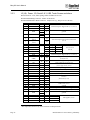
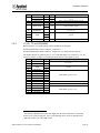
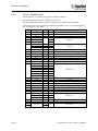
Bitsy G5
User’s Manual
ADS document # 110121-40011, preliminary
Applied Data Systems
10260 Old Columbia Road
Columbia MD 21046 USA
301-490-4007
www.applieddata.net
© 2007 ADS
Bitsy G5 User’s Manual
About the Cover Image
The cover image shows a revision 3 Bitsy G5.
Printing this Manual
This manual has been designed for printing on both sides of an 8.5x11 inch paper, but can be
printed single-sided as well. It has also been optimized for use in electronic form with active
cross-reference links for quick access to information.
Revision History
REV
1
DESCRIPTION
Preliminary release of Sections 1,2,3 and 7
ADS document # 110121-40011, preliminary
BY
08/09/2007
ch
Page i
Bitsy G5 User’s Manual
(This page intentionally blank)
Page ii
ADS document # 110121-40011, preliminary
Bitsy G5 User’s Manual
Table of Contents
About the Cover Image ......................................................................................................................................... i
Printing this Manual .............................................................................................................................................. i
Revision History.................................................................................................................................................... i
Table of Contents ................................................................................................................................................ iii
1
2
3
Introduction ...................................................................................................................................... 1
1.1
Overview............................................................................................................................... 1
1.2
Features ................................................................................................................................. 1
1.2.1
Processor..................................................................................................................... 1
1.2.2
Power Supply .............................................................................................................. 1
1.2.3
Memory....................................................................................................................... 1
1.2.4
Communications ......................................................................................................... 2
1.2.5
User Interface and Display.......................................................................................... 2
1.2.6
I/O ............................................................................................................................... 2
1.2.7
Audio Interface ........................................................................................................... 2
1.3
Block Diagram ...................................................................................................................... 3
Getting Started.................................................................................................................................. 5
2.1
Development Systems........................................................................................................... 5
2.1.1
System Components.................................................................................................... 5
2.1.2
Bitsy Personality Boards............................................................................................. 5
2.2
Frequently Asked Questions ................................................................................................. 5
2.3
Organization of this Manual ................................................................................................. 6
2.4
Errata, Addenda and Further Information ............................................................................. 7
Hardware Reference ......................................................................................................................... 9
3.1
Switches, Controls and Indicators......................................................................................... 9
3.1.1
S1: DIP Switch........................................................................................................... 9
3.1.2
D9: Green LED Indicator........................................................................................... 9
3.1.3
D7: Red LED Indicator .............................................................................................. 9
3.2
Jumper Settings..................................................................................................................... 9
3.2.1
JP2: LCD Display Power Select ................................................................................ 9
3.3
Signal Connectors ............................................................................................................... 10
3.3.1
J1 (J8): LCD Panel Interface Connector .................................................................. 10
3.3.2
J2 (J3): PCMCIA ..................................................................................................... 11
3.3.3
J3 (J9): Power, I/O, Serial 2 & 3, USB, Touch Screen and others........................... 12
3.3.4
J7 (J2): I2C and SDIO/MMC.................................................................................... 13
3.3.5
J9 (J4): Expansion Bus............................................................................................. 14
ADS document # 110121-40011, preliminary
Page iii
Bitsy G5 User’s Manual
3.3.6
3.3.7
3.3.8
J10 (J5): ADSmartIO, USB, Serial 1, Stereo Audio, I/Os ....................................... 15
J11 (J7): Supercapacitor Input ................................................................................. 16
J16 (J1): In-System Programming ........................................................................... 16
4
Feature Reference (tbd) .................................................................................................................. 19
5
Power and Power Management (tbd) ............................................................................................. 19
6
System Specifications (tbd) ............................................................................................................ 21
7
Board Revision History .................................................................................................................. 23
Page iv
7.1
Identifying the board revision ............................................................................................. 23
7.2
Revision History ................................................................................................................. 23
7.2.1
Revision 2 ................................................................................................................. 23
New Features
Changes
7.2.2
Revision 3 ................................................................................................................. 25
7.2.3
Revision A ................................................................................................................ 25
ADS document # 110121-40011, preliminary
1
Introduction
1.1
Overview
The Bitsy G5 is a full-featured single board computer using the i.MX31 Multimedia Applications
Processor. The Bitsy G5 is designed to meet the needs of embedded and graphical systems
developers.
This manual applies to the latest revision of the Bitsy G5, as listed in the revision history, section
7.2.
1.2
Features
1.2.1
Processor
1.2.2
1.2.3
•
Freescale i.MX31 32-bit ARM RISC processor
•
ARM1136JF-S core with Vector Floating Point coprocessor and multi-level cache system
•
Multimedia support including VGA MPEG-4 Hardware Encoder, Image Processing Unit
and Graphics Accelerator
•
Clock rates up to 532 MHz
•
Battery-backed real-time clock
Power Supply
•
6-15 V main power input
•
Freescale MC13783 Power Management and Audio Circuit
Memory
1
•
128 MiB DDR SRAM 1 2
•
32 MiB NOR Flash memory 3
•
PCMCIA, Type I and II, 3.3 and 5 V
The Bitsy G5 supports 32, 64 or 128 MiB DDR SRAM.
2
MiB is the IEC abbreviation for mebibyte = 220 byte = 1 048 576 byte. The kibi and mebi
prefixes are based on the 1998 IEC standard for binary multiples. For further reading, see the US
NIST web site, http://physics.nist.gov/cuu/Units/binary.html
3
The Bitsy G5 supports 8, 16, 32 or 64 MiB of NOR flash memory.
ADS document # 110121-40011, preliminary
Page 1
Bitsy G5 User’s Manual
1.2.4
1.2.5
1.2.6
1.2.7
Page 2
Communications
•
USB 2.0 Host Port and On-The-Go (OTG) Port supporting high (480 Mbit/s), full
(12 Mbit/s) and low (1.5 Mbit/s) speeds
•
Three Serial Ports
Serial 1: EIA-232, 3.3V logic level (9-wire)
Serial 2: 3.3V logic level (3-wire); IrDA and EIA-232 with optional personality board
Serial 3: EIA-232, 3.3V logic level (5-wire)
•
Four additional EIA-232 serial ports with optional personality board
•
I2C bus with I2C master device
•
Serial Peripheral Interface (SPI) port
•
Secure Digital (SD/SDIO) and Multimedia Card (MMC) support
•
10/100BT Ethernet, RJ45 with optional personality board
•
Expansion bus with optional personality board
User Interface and Display
•
Flat Panel Interface
•
Software-control of external VEE Generator for passive LCD contrast control
•
Analog Touch Panel Interface (four- or five-wire options)
•
External PS/2 Keyboard Support
•
Nine ADSmartIOTM ports configurable for digital I/O, A/D inputs (up to four) and/or up
to 4x5 keypad
•
Ten digital I/Os
•
Backlight Control Signals for Intensity and On/off
•
External Temperature Probe support
I/O
Audio Interface
•
Codec implemented by Freescale MC13783 Power Management and Audio Circuit
•
Stereo Microphone Input
•
Stereo 1W Speaker Outputs
•
Headphone Output
ADS document # 110121-40011, preliminary
Introduction
1.3
Block Diagram
The following diagram illustrates the system organization of the Bitsy G5. Arrows generally
indicate the direction of control and data flow.
Connector reference designators given are for the Bitsy family products. Connector reference
designators on the Bitsy G5 are labeled differently and are shown as (Jx).
The diagram also illustrates a composite of the three Bitsy Personality Boards4. Connectors not
found on all boards are drawn with dotted lines. See section 2.1.2 for additional details about the
personality boards.
Bitsy G5
Personality Board
Board Power
Power
supply
SPI2.2
RTC
BATTPOS
I2C
USB OTG
Audio I/F
Codec
Touch panel
controller
SPI2.0
xcvr
COM3
SPKR
MIC_IN
J7
Battery
(optional)
J16
Power input
J15
Touch panel
USB Function
J3
Touch Panel
Controller
Battery
charger
J3 (J9)
Power
Supplies
J18
COM3
buffers
COM2
JP4-7
PreAmp
buffers
IrDA
digital I/Os
Interfaces
SPI1.1
J22
COM2
J36
Wakeup
J12
Backlight
BATTPOS
J31
buffers
J13
LCD
J1 (J8)
MMC
J7 (J2)
+
LCD
i.MX31
J1
MC13783
P/S2 J5
Keyboard
I2C
I2C
I/Os
PS/2
COM1
buffers
SPKR
amp
J20
J6
J34
MIC_IN
J45
digital I/Os
SW1 Reset
USB host
buffers
buffers
digital I/Os
Quad
UART
J9
System
controller
logic
xcvr
J9 (J4)
DDR RAM and
Flash Memory
COM1
J44
J10
ADSmartIO
J10 (J5)
SPI1.0
System Bus
I2C
Ethernet
J39
USB Host port
J46
J47
COM4
COM5
J49
J50
COM6
COM7
PCMCIA
J2
J51
(J3)
4
Personality board connectors cited in the block diagram are from the rev A Ethernet/
CompactFlash Personality Board and the rev 3 Quad UART Personality Board.
ADS document # 110121-40011, preliminary
Page 3
Bitsy G5 User’s Manual
(This page intentionally blank)
Page 4
ADS document # 110121-40011, preliminary
2 Getting Started
2.1
Development Systems
Bitsy G5 boards are shipped as development systems designed to get the developer up and running
quickly.
To use the system, simply plug the power supply into the mini DIN-8 receptacle on the system.
If the screen does not display anything after five to ten seconds, check the Frequently Asked
Questions, below. Most operating systems cold boot within twenty seconds.
2.1.1
System Components
A typical development system is shown at right. It consists of the
following components:
•
Bitsy G5 single-board computer
•
Bitsy Personality Board
•
Flat panel display and cable
•
Backlight inverter and cable
•
Touch screen and cable
•
100-240 VAC power adapter
•
Plexiglas mounting
•
Developer's Cable Kit including
•
•
Serial Port DB9 adapter (ADS cable #610111-80001)
•
DB9F/F null modem cable
•
USB A-B cable
Operating system of your choice
• User's Guide (this document and operating system guide)
Please make sure you have received all the components before you begin your development.
2.1.2
Bitsy Personality Boards
The Bitsy G5 often works in tandem with another board to add functionality and customize the
system for its application. Personality boards can add custom circuits and locate connectors best
suited for the application design. At the time of writing, a new BitsyXb/G5 Personality Board is
under development. Details are tbd.
2.2
Frequently Asked Questions
The following are some of the most commonly asked questions for development systems:
Q: When I plug in power, my screen is white and nothing comes up on it.
A: Check the connector seating. The flat panel connector may have come loose in shipping.
Press it firmly into the panel and reapply power to your system.
ADS document # 110121-40011, preliminary
Page 5
Bitsy G5 User’s Manual
Q: Is there online support?
A: Yes. Information about the Bitsy G5 hardware and software is available on the ADS support
site at http://www.applieddata.net/support. See section 2.4 for further details.
Q: When I plug in power, my screen stays black.
A: If your system has supercapacitors installed (section 5.2.3), your system may be asleep. Try
waking up the system by shorting the wakeup signal (BitsyXb J3 pin 45 or Bitsy G5 J9 pin 45) to
ground. Development systems include a two-pin header on the personality board whose pins can
be shorted together to wake the system. You may also press the reset button to fully restart the
system.
Q: When I plug in power, the LED doesn't turn on.
A: Your system may still be booting. The LED is software controlled and is not necessarily
turned on at boot.
Q: Do I have to turn off the system before I insert a PCMCIA?
A: No. The Bitsy G5 supports hot-swapping of PCMCIA cards. Consult the operating system
documentation for details.
Q: Do I need to observe any ESD precautions when working with the system?
A: Yes. If possible, work on a grounded anti-static mat. At a minimum, touch an electrically
grounded object before handling the board or touching any components on the board.
Q: What do I need to start developing my application for the system?
A: You will need a flash ATA card (32 MiB or larger, 128 MiB recommended) and the cables
supplied with your system to interface your development station to the system. For further
direction, consult the ADS guide for the installed operating system.
Q: Who can I call if I need help developing my application?
A: ADS provides technical support to get your development system running. For customers who
establish a business relationship with ADS, we provide support to develop applications and
drivers.
Q: Can I upgrade the version of the operating system?
A: Yes. ADS provides regular operating system updates on its developers' web site. For
operating systems not maintained by ADS, contact the operating system vendor.
Q: I would like to interface to a different display panel. How can I do this?
A: ADS may have already interfaced to the panel you are interested in. Consult ADS for
availability.
2.3
Organization of this Manual
The manual organizes information in five key sections:
Page 6
Introduction
Provides an overview of the functionality and organization of the Bitsy
G5, as well as how to use this manual.
Hardware Reference
Describes the configuration settings and pinouts for all connectors and
jumpers on the Bitsy G5.
Feature Reference
Gives details about the various subsystems of the Bitsy G5.
Power Management
Provides key information about power management, tips for system
integration and electrical and mechanical interface specifications.
ADS document # 110121-40011, preliminary
Getting Started
Specifications
Electrical and mechanical interface specifications.
To locate the information you need, try the following:
2.4
1.
Browse the Table of Contents. Section titles include connector designators and their
function.
2.
Follow cross-references between sections.
3.
View and search this manual in PDF format
Errata, Addenda and Further Information
Errata and addenda to this manual are posted on the ADS support forums along with the latest
release of the manual. Consult the support forums any time you need further information or feel
information in this manual is in error. You may access the forums from the ADS support site,
http://www.AppliedData.net/Support
In addition to manuals, the support forums include downloads, troubleshooting guides, operating
system updates and answers to hundreds of questions about developing applications for ADS
products. You may also post questions you have about ADS products on the forums.
ADS document # 110121-40011, preliminary
Page 7
Bitsy G5 User’s Manual
(This page intentionally blank)
Page 8
ADS document # 110121-40011, preliminary
3 Hardware Reference
This section gives an overview of the hardware features of the Bitsy G5. This overview includes a
description of the switches, jumper settings, connectors and connector pinouts.
Many connectors and headers have a visible number or marking on the board that indicates pin 1.
If that pin is not clearly marked, there are two other ways to locate pin 1:
1.
For through-hole connectors, look at the underside of the board. The square pad is pin 1.
2.
Download the mechanical drawing of the Bitsy G5 available on the ADS Support site
(section 2.4). The square or indicated pad on each connector is pin 1.
3.1
Switches, Controls and Indicators
3.1.1
S1: DIP Switch
S1 is a two-position DIP switch located on the edge of the board at the opening of the PCMCIA
socket. When in the "ON" position, switches are closed and connect to ground. Otherwise they
are pulled up.
DIP switch positions "1" and "2" connect to the i.MX31. Most operating systems on the Bitsy G5
reserve these switches for their use. Consult the operating system manual for details.
3.1.2
D9: Green LED Indicator
The Bitsy G5 has one onboard green light-emitting diode (LED), located on the corner of the
board next to JP2, that is controlled by the processor. The LED is driven by the same buffers as
the display driver data lines. The LED will be off when the display buffers are disabled (see
power management section 5.2.2).
3.1.3
D7: Red LED Indicator
The Bitsy G5 has one onboard red LED that is connected to the MC13783 trickle LED driver
output. It is located at the edge of the board under the opening of the PCMCIA socket.
3.2
Jumper Settings
There is just one user-selectable jumper on the Bitsy G5. It uses a 2mm shorting block (shunt) to
select the setting. Turn off power to the Bitsy G5 before changing the position of a shunt.
3.2.1
JP2: LCD Display Power Select
Type: 3-post header, 2mm
This jumper selects the supply voltage for the LCD display. The three-pin header is located near
the PCMCIA ejector button.
Jumper setting
Voltage Selected
1-2
Vcc (5.0 V)
2-3
Vddx (3.3 V)
WARNING! The pin out of JP2 on the Bitsy G5 is not the same as the pin out for the BitsyXb.
Make sure you have selected the correct voltage before connecting the panel. Flat panels can be
irreparably damaged by incorrect voltages.
ADS document # 110121-40011, preliminary
Page 9
Bitsy G5 User’s Manual
3.3
Signal Connectors
The following tables describe the electrical signals available on the connectors of the Bitsy G5.
Each section provides relevant details about the connector including part numbers, mating
connectors, signal descriptions and references to related chapters.
To locate pin 1 of a connector, look for numbers silk screened on the
component side5 of the Bitsy G5, or look at the bottom side of a connector
for the square pad, which is pin 1. As seen from the component side, doublerow headers on the board are numbered as shown in the figure to the right.
2 4 6 8...
1 3 5 7...
For information about the location of the connectors on the Bitsy G5, refer to section 6.1.1.
Legend:
n/c
GND
(4.1)
Not connected
Bitsy G5 ground plane
Reference section(s) for signals
I
O
IO
P
A
OC
signal is an input to the system
signal is an output from the system
signal may be input or output
power and ground
analog signal
open collector output
Signal Types
The reference designators on the Bitsy G5 are labeled differently than the previous four
generations of the Bitsy family products or the mating personality board. The Bitsy family
products reference designators are listed in the following sections with the reference designators
on the Bitsy G5 shown as (Jx).
3.3.1
J1 (J8): LCD Panel Interface Connector
Board Connector: 2x17, 2mm spacing, Samtec STMM-117-02-G-D
Recommended Mating Cable: Samtec TCSD Series
Recommended Board-to-Board Connector: ESQT series (e.g. ESQT-117-02-F-D-500)
The following table describes the signals on the LCD interface connector. Signal names shown
are for TFT active matrix color LCDs at 16 bpp (bit-per-pixel). For other color depths and LCD
technologies, consult the table in section 4.6.4.
Signals from the i.MX31 are buffered and RFI filtered before reaching J1 (J8). The LCD panel
output buffers operate at a fixed 3.3 V. See section 4.6 for further details about displays.
Pin
1
2
3
4
5
6
5
Page 10
i.MX31
Signal Name
FPSHIFT
HSYNC
VSYNC3
Color Active TFT Display at 16bpp
ADS Signal Name
Description
n/c
GND
ground
PNL_PIXCLK
Pixel Clock
PNL_HSYNC
Horizontal Sync.
PNL_VSYNC
Vertical Sync.
GND
ground
The "component side" of the Bitsy G5 is the one on which the PCMCIA ejector is installed.
ADS document # 110121-40011, preliminary
Hardware Reference
7
8
9
10
11
12
13
14
15
16
17
18
19
20
21
22
23
24
25
26
27
28
29
30
LD12
LD13
LD14
LD15
LD16
LD17
LD6
LD7
LD8
LD9
LD10
LD11
LD0
LD1
LD2
LD3
LD4
LD5
Drdy0
Red Bit 0
Red Bit 1
Red Bit 2
Red Bit 3
Red Bit 4
Red Bit 5
ground
Green Bit 0
Green Bit 1
Green Bit 2
Green Bit 3
Green Bit 4
Green Bit 5
ground
Blue Bit 0
Blue Bit 1
Blue Bit 2
Blue Bit 3
Blue Bit 4
Blue Bit 5
ground
Data_Enable
PNL_PWR
Vcc (5 V) or 3.3 V (JP2)
31
PNL_RL
32
PNL_UD
33
ADSmartIO
PD0
34
3.3.2
PNL_RED0
PNL_RED1
PNL_RED2
PNL_RED3
PNL_RED4
PNL_RED5
GND
PNL_GREEN0
PNL_GREEN1
PNL_GREEN2
PNL_GREEN3
PNL_GREEN4
PNL_GREEN5
GND
PNL_BLUE0
PNL_BLUE1
PNL_BLUE2
PNL_BLUE3
PNL_BLUE4
PNL_BLUE5
GND
PNL_LBIAS
Horizontal Mode Select
(set by R247 or R246)
Vertical Mode Select
(set by R248 or R249)
PNL_ENA
Panel enable signal
VCON
low-voltage adjust for contrast
control of some displays (6.3.2)
(zero to PNL_PWR volts)
J2 (J3): PCMCIA
Integrated ejector: FCI 95620-050CA
The 68-pin PCMCIA socket conforms to the PCMCIA standard for 5V-tolerant Type II cards, and
can also be run at 3.3 V. The socket is normally de-energized; the operating system is responsible
for turning on the socket when a card is inserted and turning it off when the card is removed.
Ejector hardware is standard.
Vpp (pins 18 and 52), which is 12 V in older PCMCIA implementations, is left unconnected in
this implementation. See section 6.3.7 for electrical specifications.
ADS document # 110121-40011, preliminary
Page 11
Bitsy G5 User’s Manual
3.3.3
J3 (J9): Power, I/O, Serial 2 & 3, USB, Touch Screen and others
Board Connector: 2x25, 2mm spacing, Samtec STMM-125-02-G-D
Recommended Mating Connector: Samtec TCSD Series
Recommended Board-to-Board Connector: ESQT series (e.g. ESQT-125-02-F-D-500)
Pin
1
3
Name
EIO9
EIO8
EIO7
GND
VCC
5
7
9
11
13
15
17
19
21
23
25
27
29
31
33
6
Page 12
2
4
6
8
10
TEMP_SENSOR
_MINUS
TEMP_SENSOR
_PLUS
/IRDAON
TSPX
TSMY
TSMX
TSPY
EIO5
EIO6
BACKLIGHT
PWM
/BACKLIGHT
ON
RXD2T
TXD2T
WIPER
PB0
GND
PE2
CTS3
TXD3
RTS3
RXD3
USB+
USBGND
HP_IN
STXD
SRXD
SCLK2
SFRM2
Type
IO
IO
IO
PO
+5 V
AI
External Temperature Probe Connection
(4.3.5)
12
14
16
AO
18
OC
22
24
26
28
30
32
34
36
General Purpose Digital I/Os (4.7.1, 6.3.9)
ground
O
AIO
AIO
AIO
AIO
IO
IO
20
Description
P
PO
USB_RECONN
GND
35
37
39
43
Pin
I
O
AI
O
P
O
I
O
O
I
IO
IO
P
I
0
right
top
left
bottom
External IRDA control output
UL
Touch screen
LR
(6.3.3)
LL
UR
General Purpose Digital I/Os (4.7.1, 6.3.9)
Backlight Intensity (PWM)
(4.6.6, 6.3.2)
Backlight On/Off
(open-collector) (4.6.6, 6.3.2)
Serial 2
(3.3 V logic level) (4.5.1)
Touch screen wiper (optional 5-wire touch)
ADSmartIO 6 (5.2.7)
ground
Power Enable #2 for external devices (5.2.2)
Serial 3
(EIA-232) (4.5.1)
USB Client (4.5.2)
ground
Headphone connection (4.4.2, 6.3.8)
USB Client power management 6 (4.5.2)
P
O
I
O
O
ground
MOSI
MISO
SCLK
SS
SPI signals (4.5.3)
This output does not have any series resistance or ESD protection.
ADS document # 110121-40011, preliminary
Hardware Reference
Pin
Name
VBATT_POS
VBATT_NEG
41
POWERENABLE
/PE1
DCIN_POS
45
/RQONOFF
47
49
GND
Pin
38
40
42
44
48
Type
PI
P
O
O
Description
External Battery Input
(5.2.7)
Power Supply Control Output (5.2.2)
Power Enable #1 for external devices (5.2.2)
PI
External Power Input
I
"Request On/Off" Switch Input
(5.2.3, 6.3.1)
P
ground
PI
Real-time clock backup battery (4.2, 6.3.4)
46
BATPOS
3.3.4
50
J7 (J2): I2C and SDIO/MMC
Board Connector: 2x8, 2mm spacing, Samtec STMM-108-02-G-D-SM
Recommended Board-to-Cable Connector: TCSD series
Recommended Board-to-Board Connector: ESQT series (e.g. ESQT-108-02-F-D-450) 7
This header supplies the signals for the I2C (4.5.4) and SDIO/MMC (4.5.5) interfaces. See the
respective sections in Chapter 4 for additional details about how the signals are used.
Pin
1
2
3
4
5
6
7
8
9
10
11
12
13
14
15
16
Name
I2C_SDA
I2C_SCL
GND
SD_DAT2
SD_DAT3
SD_CMD
SD_DAT0
SD_CLK
/SD_CD
VDDX
VCC
/SD_WP
/SDIO_IRQ
/SD_PWREN
SD_DAT1
Type
IO
IO
P
P
IO
IO
IO
IO
O
I8
PO
PO
I
I
O
IO
Description
I2C (4.5.4)
ground
SDIO/MMC signals (4.5.5)
3.3 V
5V
SDIO/MMC signals (4.5.5)
7
Note that the STMM header is 0.050-inch higher than the other 2mm headers on the board
because it is a surface-mount part. Use a correspondingly shorter socket on mating boards.
8
Pulled-up on Bitsy G5 with 4.7kΩ resistor.
ADS document # 110121-40011, preliminary
Page 13
Bitsy G5 User’s Manual
3.3.5
J9 (J4): Expansion Bus
Board Connector: 2x5, 2mm spacing, Samtec STMM-125-02-G-D
Recommended Mating Connector: Samtec TCSD Series
Recommended Board-to-Board Connector: ESQT series (e.g. ESQT-125-02-F-D-500)
These signals can be used to expand the capabilities of the Bitsy G5 as a 3.3 V digital expansion
bus. See section 4.1.5 for details.
Pin
1
3
5
7
9
11
13
15
17
19
21
23
25
27
29
31
33
35
37
Page 14
Name
GND
n/c
n/c
PCBD10
PCBD9
PCBD8
PCBD2
PCBD1
PCBD0
n/c
n/c
n/c
PCBA11
VCC
/CARDBWAIT
CARDBRES
PCBA0
PCBA1
PCBA2
PCBA3
PCBA4
PCBA5
PCBA6
n/c
+3.3V
/CARDBON
n/c
CF_/INT
/CARDBMWR
n/c
BEB1_B
PCBA7
PCBA8
PCBA9
/CARDBMRD
n/c
CS_CF
Pin
Type
P
Description
ground
2
4
6
8
10
IO
IO
IO
IO
IO
IO
Data8-10
Data0-2
12
14
16
18
20
22
24
28
O
PO
I
O
O
O
O
O
O
O
O
Address 11
5V
Wait
Reset
Address0-6
P0
O
+3.3 V
5 V Power Control
I
O
O
O
O
O
O
O
Interrupt Signal
Memory Write
O
Chip Select
26
30
32
36
34
38
IO Read
Address7-9
Memory Read
ADS document # 110121-40011, preliminary
Hardware Reference
Pin
39
41
43
45
47
49
3.3.6
Name
PCBD15
PCBD14
PCBD13
PCBD12
PCBD11
PCBD7
PCBD6
PCBD5
PCBD4
PCBD3
n/c
Pin
Description
40
42
44
46
48
Type
IO
IO
IO
IO
IO
IO
IO
IO
IO
IO
/CARDBON_3P3V
50
O
3.3 V Power Control
Data11-15
Data3-7
J10 (J5): ADSmartIO, USB, Serial 1, Stereo Audio, I/Os
Board Connector: 2x25, 2mm spacing, Samtec STMM-125-02-G-D
Recommended Mating Connector: Samtec TCSD Series
Recommended Board-to-Board Connector: ESQT series (e.g. ESQT-125-02-F-D-500)
Pin
1
3
5
7
9
11
13
15
Name
/EXT_IRQ1
/EXT_IRQ2
EIO4
EIO3
EIO2
EIO1
EIO0
SIGPS2
CLKPS2
USB_PWR_
SENSE
USB_PWR_
CTRL
USB_UDCUSB_UDC+
I2C_SCL
SMTIO1
SMTIO0
SPKR_LSPKR_L+
SPKR_RSPKR_R+
Pin
2
4
6
8
Type
I
I
IO
IO
IO
IO
IO
IO
IO
10
I
12
O
14
16
IO
IO
IO
IO
IO
AO
AO
AO
AO
18
20
22
24
Description
External Interrupt 1 Input
External Interrupt 2 Input
General Purpose Digital I/Os (4.7.1, 6.3.9)
External PS/2 keyboard inputs
Sense Input from external USB
host power switch (4.5.2)
Discrete output to control external
USB host power switch (4.5.2)
USB Host (4.5.2)
PC6
PD1
PD0
I2C clock 9
Thermistor energize (4.3.5)
Passive panel enable (PNL_ENA)
Stereo Speaker, left channel (4.4.2)
Stereo Speaker, right channel (4.4.2)
9
PC6 and PC7 can be are used for the I2C bus master interface. Standard Bitsy G5 systems do not
connect the ADSmartIO controller to the I2C bus. See section 4.5.4 for details.
ADS document # 110121-40011, preliminary
Page 15
Bitsy G5 User’s Manual
Pin
17
19
21
23
25
27
29
31
33
35
37
39
41
43
45
47
Name
ROW0
ROW1
ROW2
ROW3
ROW4
COL0
COL1
COL2
COL3
RI1
DCD1
DSR1
DTR1
RXD1
TXD1
CTS1
RTS1
/EXT_IRQ3
VDDX
3.3.7
26
28
30
32
34
36
38
40
Type
IO
IO
IO
IO
IO
IO
IO
IO
IO
I
I
I
O
I
O
I
O
I
PO
MIC_GND
MIC_L
MIC_R
reserved
/RESET_IN
VDDX
VCC
49
Pin
I2C_SDA
GND
42
44
46
48
ADSmartIO
(see section 6.3.6)
Serial 1
(EIA-232 with 3.3 V logic level volume
production option)
(4.5.1)
External Interrupt 3 Input
3.3 V
P
Microphone ground
AI
AI
Stereo Microphone Input
I
PO
External Reset Input (6.3.1)
3.3 V
PO
5V
IO
P
50
Description
PC0
PC1
PC2
PC3
PC4
PA0
PA1
PA2
PA3
PC7
I2C data 9
ground
J11 (J7): Supercapacitor Input
Supercapacitors are not supported by the Bitsy G5. This socket may not be populated on all
boards.
3.3.8
J16 (J1): In-System Programming
Board Connector: 2x8, 2mm spacing, Samtec STMM-110-02-G-D-SM
Recommended Board-to-Board Connector: ESQT series (e.g. ESQT-110-02-F-D-450) [tbd]
This header is used during manufacturing for programming and test, but is not otherwise
supported for application use. Production customers may use this header to reprogram boot code.
Pin
1
2
3
4
5
6
Page 16
Name
PM_RSTMCU_B
TRSTB
TMS
GND
TCLK
GND
Type
I
I
I
P
I
P
Description
Power on reset
JTAG
ADS document # 110121-40011, preliminary
Hardware Reference
Pin
7
8
9
10
11
12
13
14
15
16
17
18
19
20
Name
TDI
GND
TDO
GND
RTCK
2.7V
PRG
VDDX
MISO
DE_B
MOSI
GND
SCK
GND
ADS document # 110121-40011, preliminary
Type
I
P
O
P
O
PO
I
PO
O
I
I
P
I
P
Description
2.75 V
ATMega/ADSmartIO
3.3 V
ATMega/ADSmartIO
JTAG
ATMega/ADSmartIO
Page 17
Bitsy G5 User’s Manual
(This page intentionally blank)
Page 18
ADS document # 110121-40011, preliminary
4 Feature Reference (tbd)
5 Power and Power Management (tbd)
ADS document # 110121-40011, preliminary
Page 19
6 System Specifications (tbd)
ADS document # 110121-40011, preliminary
Page 21
7 Board Revision History
7.1
Identifying the board revision
The product revision number of the Bitsy G5 is etched on the underside of the printed circuit
board. That number is 170121-4000x, where "x" is the board revision.
7.2
Revision History
This section describes the differences between the revisions of the Bitsy G5.
7.2.1
Revision 2
Pre-production.
If you are using a Bitsy G5 as a replacement for the BitsyXb, please note these differences from
revision A of the BitsyXb:
New Features
Freescale i.MX31 processor replaces XScale PXA270.
Freescale MC13783 Power Management and Audio Circuit:
•
Replaces discrete microphone preamp circuitry and Crystal CS4202 AC’97 stereo codec.
•
Replaces discrete switching regulator, linear voltage regulator and step down converters
providing supply voltages for processor, memories, CPLD, and IO.
•
Provides 4-wire analog touch panel capability.
• Replaces discrete RTC component.
DDR SRAM replaces SDRAM.
USB 2.0 Host port and USB 2.0 On-The-Go (OTG) port replaces USB 1.1 ports.
Changes
Pinout of JP2 swapped.
Voltage Setting
Vddx (3.3V)
Vcc (5.0V)
Jumper Setting
From
To
1-2
2-3
2-3
1-2
Connector reference designators labeled differently. In this manual, all Bitsy G5 reference
designators shown as (Jx).
LCD Panel Interface signals on J1 (J8) changed as follows:
Pin
1
From
PNL_VEE
To
n/c
Option to operate LCD panel buffers at either 3.3 V or 5 V removed. Supports LCD display data
at 3.3 V only.
Series resistor removed from USB_RECONN output, J3 (J9) pin 33.
ADS document # 110121-40011, preliminary
Page 23
Bitsy G5 User’s Manual
Input Power connector, J6, removed.
Secure Digital (SD/SDIO) and Multimedia Card (MMC) not supported.
Vee Adapter connector, J8, removed.
External CompactFlash not supported.
Connector J9 (J4) used for 3.3 V expansion bus only. Signals on J9 (J4) changed as follows:
Pin
2
4
9
11
12
13
14
16
18
20
21
22
24
26
27
28
30
31
32
33
35
36
37
38
49
From
/CARDBDET2
/CARDB16
CARDBSTSCHG
CARDBSPK
PCBA0
/CARDBREG
PCBA1
PCBA2
PCBA3
PCBA4
/CARDBVS2
PCBA5
PCBA6
CARDBVCC
CARDBIRQ
PCBA7
PCBA8
/CARDBIOWR
PCBA9
/CARDBIORD
/CARDB_VS1
PCBA10
/CARDBCE2
/CARDBCE1
/CARDBDET1
To
n/c
n/c
n/c
n/c
n/c
PCBA11
PCBA0
PCBA1
PCBA2
PCBA3
n/c
PCBA4
PCBA5
n/c
CF_/INT
PCBA6
PCBA7
n/c
PCBA8
BEB1_B
n/c
PCBA9
CS_CF
CS_CF
n/c
Battery trickle charger not supported.
Signals on J3 (J9) changed as follows:
Pin
22
From
CHARGE
To
ADSmartIO PB0
Signals on J10 (J5) changed as follows:
Pin
43
From
VREF
To
Reserved
Supercapacitor Input connector J11 (J7) not supported.
RTC Interface changed from I2C bus to SPI.
USB OTG transceiver added to I2C bus at address 010 1101.
Pull up resistor value on I2C bus changed from 1.2kΩ to 2.2kΩ.
Page 24
ADS document # 110121-40011, preliminary
Board Revision History
Crystal frequencies changed. Removed 24.576 MHz, 32.768 kHz and 13.000 MHz. Added 19.2
MHz and 26.000 MHz.
Red LED added to MC13783 trickle LED driver output.
ISP Port connector J16 (J1) changed from 16 pin STMM-108-02-G-D-SM to 20 pin STMM-11002-G-D-SM. Pinout changed as follows:
Name
/TRST
TMS
GND
TDI
TCLK
VDDX
GND
TDO
/FEW
FRDY
MISO
VCC
SCK
MOSI
PRG
GND
PM_RSTMCU_B
TRSTB
GND
GND
RTCK
2.7V
DE_B
GND
7.2.2
From
1
2
3
4
5
6
7
8
9
10
11
12
13
14
15
16
To
3
4
7
5
14
6
9
15
19
17
13
18
1
2
8
10
11
12
16
20
Revision 3
Initial release.
Secure Digital (SD/SDIO) and Multimedia Card (MMC) supported.
Pull up resistor value on /SD_CD signal, J7 (J2) pin 10, changed from 47kΩ to 4.7kΩ.
7.2.3
Revision A
Production release. Available Q4 2007.
ADS document # 110121-40011, preliminary
Page 25
Bitsy G5 User’s Manual
(This page intentionally blank)
Page 26
ADS document # 110121-40011, preliminary