1
Renesas Flash Programmer V2.05
APPENDIX B SUPPLEMENTARY INFORMATION
APPENDIX B SUPPLEMENTARY INFORMATION
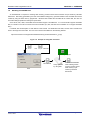
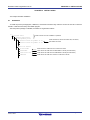
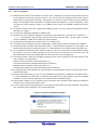
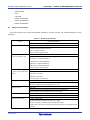
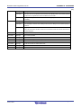
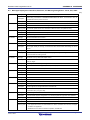
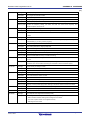
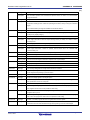
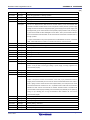
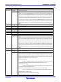
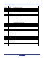
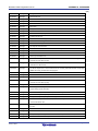
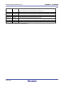
Figure B-1. E1 and E20 Pins - RX E1
Pin No.
E20
Pin Name
Pin Name (14-pin Compatible)
Pin Name (38-pin)
1
io4
io4
io1
2
GND
GND
io2
3
io5
io5
io0
4
io0
io0
5
SEND
SEND
−
UCONNECT (connected to GND of the
target board)
6
io1
io1
−
7
io3
io3
−
8
UVCC (whether 3.3V or 5.0V is
supplied or whether power is supplied
to the target can be detected)
UVCC
io3
RESET
9
UVCC2
UVCC2
10
io2
io2
11
RECEIVE
RECEIVE
12
GND
GND
−
13
RESET
RESET
−
14
UCONNECT (connected to GND of the
target board)
UCONNECT (connected to GND of the
target board)
15
−
SEND
UVCC
io4
−
16
17
UVCC2
−
18
19
RECEIVE
−
20
21
io5
22
−
23
−
24
−
25
−
26
−
27
−
28
−
29
−
30
−
31
−
32
−
33
−
34
−
35
−
36
−
37
−
38
−
“-” indicates an unused pin.
R20UT2906EJ0202 Rev. 2.02
Jul 01, 2015
Page 42 of 47