1
MB838 series
4-port (Rangeley SoC)
Networking Motherboard
USER’S MANUAL
Version A1
INSTALLATIONS
Acknowledgments
AMI is a registered trademark of American Megatrends, Inc.
PS/2 is a trademark of International Business Machines
Corporation.
Intel is a registered trademark of Intel Corporation.
Microsoft Windows is a registered trademark of Microsoft
Corporation.
Winbond is a registered trademark of Winbond Electronics
Corporation.
All other product names or trademarks are properties of their
respective owners.
2
MB838 User’s Manual
INSTALLATIONS
Table of Contents
Introduction .............................................................. 5
Product Description............................................................. 5
Specifications ...................................................................... 6
Checklist .............................................................................. 8
Board Dimensions ............................................................... 9
Block Diagram .................................................................. 10
Installations ............................................................ 11
Installing the Memory ....................................................... 12
Setting the Jumpers ........................................................... 13
Jumper Locations on MB838 ............................................. 14
JP2: Function reserved ....................................................... 15
JP3: DDR power selection ................................................. 15
JP4: AT / ATX mode selection .......................................... 15
JP7: Clear CMOS .............................................................. 15
JP8: LED5, LED6 Bypass or HDD LED selection ............ 15
JP12: Function reserved ..................................................... 15
Connectors on MB838 ...................................................... 16
J3: System Function Connector ......................................... 17
J8: Power connector for ATX power supply ..................... 18
J9: 2-pin Power connector for 12V DC power .................. 18
J11: USB pin header .......................................................... 18
J12: COM2 pin header ....................................................... 18
J28: Power Connector, Pitch 2.0mm.................................. 19
CN1: 22-pin right angle SATA connector ......................... 19
CN2, CN3: RJ-45 LAN port 3 and 4 ................................. 19
CN4: USB 2.0 connectors.................................................. 19
CN5: COM1 (Console Port) .............................................. 19
CN6, CN7: RJ-45 LAN port 1 and 2 ................................. 19
FAN1, FAN2, FAN3: System Fan Connectors .................. 19
LED1: LAN port 1 LED .................................................... 19
LED2: LAN port 2 LED .................................................... 19
LED3: LAN port 3 LED .................................................... 19
LED4: LAN port 4 LED .................................................... 19
LED5, 6: Status LED ......................................................... 20
SW2: Push button (GPI, porting by software) ................... 20
Digital I/O Sample Configuration .......................... 21
3
INSTALLATIONS
Watchdog Timer Configuration ............................ 25
BIOS Setup ............................................................. 29
BIOS Introduction.............................................................. 30
BIOS Setup ........................................................................ 30
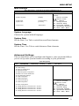
Advanced Settings.............................................................. 31
Security .............................................................................. 41
Drivers Installation ................................................. 44
LAN Drivers Installation................................................... 45
A. I/O Port Address Map .................................................. 48
B. Interrupt Request Lines (IRQ) ...................................... 48
C. Register of the LAN Bypass Controller ....................... 49
4
MB838 User’s Manual
INSTALLATIONS
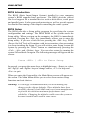
Introduction
Product Description
®
The MB838 networking motherboard is based on the latest Intel
AtomTM C2000 series SoC. Two DDR3 UDIMM sockets allows up to
32GB system memory.
The motherboard supports a total of eight Ethernet ports with the port 1
and port2 supporting Bypass function. It also has one fast SATA III
6Gbps ports, two USB 2.0 ports and one USB 2.0 for Mini PCI-e.
MB838 utilizes the dramatic increase in performance provided this
Intel’s latest cutting-edge technology. Measuring 203mm x 180mm.
MB838 Features
Supports Intel® AtomTM C2000 series processors
Two DDR3 UDIMM for maximum 32GB total, 1600MHz,
Unbuffered
Eth1~2: Intel® I347-AT4 GbE PHY, support Bypass
Eth3~4: Intel® I347-AT4 GbE PHY, No Bypass
One SATA III (6.0Gb/s)
One Mini PCI-E socket (mSATA compatible)
5
INSTALLATIONS
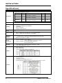
Specifications
Support Intel ® Rangeley processors:
Core#
SoC
TDP
QuickAssist
MB838-2C
2
Intel® Atom™ Processor C2358
(1M Cache, 1.70 GHz)
7W
Yes
MB838-4C
4
Intel® Atom™ Processor C2558
(2M Cache, 2.40 GHz)
15W
Yes
8
Intel® Atom™ Processor C2758
(4M Cache, 2.40 GHz)
20W
Yes
Processor
MB838-8C
BIOS
AMI BIOS
Memory
Video
NA
Network PHY
Eth1~2: Intel® I347-AT4 GbE PHY. One segment Bypass
Eth3~4: Intel® I347-AT4 GbE PHY. No Bypass
One segment hardware Bypass (Eth1 & 2)
Control by GPIO / Watchdog / Electrical Disconnect (Power Off)
Bypass mode selection ( BIOS)
Network
Bypass
Two DDR3/L UDIMM total for 32GB max memory
Dual channel DDR3 up to 1600 MHz
Unbuffered
ECC or non-ECC
Support 1.35V and 1.5V
SATA
Connector
SATA III (6.0Gb/s): One to mSATA
One to right angle 22-pin SATA connector
SATA II (3.0Gb/s): One to SATA, Black connector
One to golden finger 1
Storage
One onboard 22-pin SATA connector support 2.5” HDD
One mSATA (Mini PCI-e socket)
One to Mini PCI-e
Two to Front panel
One 2x4 pin header support one USB port
USB 2.0
Fintek F81866AD-I:
RJ-45 Console x1
Hardware monitors
4-pin Smart Fan (PWM) Connector x3
RS-232 [2x5] Box Header Onboard x1 (COM2, located close to LCM)
LPC I/O
6
MB838 User’s Manual
INSTALLATIONS
Fan
Connector
Three 4-pin smart fan connectors
Smart Fan
Control
The active temperature may be adjusted based on system thermal test result
Active
Default Smart Fan
Tolerance
Temperature
Enable or Disable
CPU Fan
50
+/- 3
Enable
System Fan
50
+/- 3
Enable
RTC
Rangeley built-in RTC with on-board lithium battery & holder
Expansion
Slot
(Golden
Finger)
Front Panel
Function LED
#1: PCI-e x8, for IP332
#2: PCI-e x4, for IP334
#1 LED: Power
(Green = Power On, Off= No Power)
#2 LED: Bypass or Status 2 (Pin header control)
Bypass: Green = LAN 1-2 or 3-4 Bypass,
Off = LAN Normal
#3 LED: Status 1 (GPIO control, Yellow / Red)
LCM
Optional, iIO 2x16 characters LCM (COM2)
Front Panel
Buttons &
Connector
Four RJ-45 connectors for Eth1~4 with LEDs
USB 2.0 x2
RJ-45 (for console, COM1)
Three LEDs for Power, Bypass & Status
Factory Mode Restore Reset Switch
Rear I/O
interface
PSU AC inlet
1x Slot Opening
AT or ATX mode selection jumper
ATX mode power on / off pin header
HDD active LED pin header
System Reset pin header
Clear CMOS
Power
Connector
24-pin ATX standard (connected to system power supply)
2-pin 12V DC-In (connected to external power adapter)
TPM
TPM 1.2 (INFINEON SLB9655TT1.2)
Watchdog
Timer
Yes (256 segments, 0, 1, 2…255 sec/min)
Operating
Temperature
0C ~ 60C
Storage
Temperature
-20C ~ 80C
Operational
Humidity
10% ~ 90% Relative Humidity (non-condensing)
RoHS
Compliant
Yes
Dimensions
203 mm x 180 mm
Jumper /
Pin Header /
Switch
Status 1
Bypass
Power
7
INSTALLATIONS
Checklist
Your MB838 package should include the items listed below.
MB838 motherboard
Driver DVD
8
MB838 User’s Manual
INSTALLATIONS
Board Dimensions
9
INSTALLATIONS
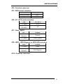
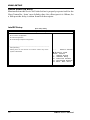
Block Diagram
DDR3-1600
UDIMM x2
PCI-e x8
Golden Finger #1
PCI-e
PCI-e x4
Golden Finger #2
PCI-e
Front x2
USB 2.0
Rangeley
KB/Mouse
USB 2.0
Pin header x1
USB 2.0
Mini PCI-e
SoC
COM
PCI-e x1
Fintek F81866AD-I
Super I/O
SATA III
LPC
RA 22-pin
SATA
SATA II
Console
Intel
I347-AT4
Eth3~4
7-pin
SATA x2
Smart Fan
Status LED 1
Bypass
Eth1~2
Golden Finger #1
Bypass LED
10
MB838 User’s Manual
INSTALLATIONS
Installations
This section provides information on how to use the jumpers and
connectors on the MB838 in order to set up a workable system. The
topics covered are:
Installing the Memory .......................................................................... 12
Setting the Jumpers .............................................................................. 13
Jumper Locations on MB838 ............................................................... 14
Connectors on MB838 ......................................................................... 16
11
INSTALLATIONS
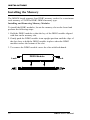
Installing the Memory
The MB838 board supports four DDR3 memory socket for a maximum
total memory of 32GB in DDR3 DIMM memory type.
Installing and Removing Memory Modules
To install the DDR3 modules, locate the memory slot on the board and
perform the following steps:
1. Hold the DDR3 module so that the key of the DDR3 module aligned
with that on the memory slot.
2. Gently push the DDR3 module in an upright position until the clips of
the slot close to hold the DDR3 module in place when the DDR3
module touches the bottom of the slot.
3. To remove the DDR3 module, press the clips with both hands.
DDR3 Module
12
Lock
Lock
Lock
Lock
MB838 User’s Manual
INSTALLATIONS
Setting the Jumpers
Jumpers are used on MB838 to select various settings and features
according to your needs and applications. Contact your supplier if you
have doubts about the best configuration for your needs. The following
lists the connectors on MB838 and their respective functions.
JP2: Function reserved ......................................................................... 14
JP3: DDR power selection ................................................................... 15
JP4: AT / ATX mode selection ............................................................ 15
JP7: Clear CMOS ................................................................................ 15
JP8: LED5, LED6 Bypass or HDD LED selection .............................. 15
JP12: Function reserved ....................................................................... 15
13
INSTALLATIONS
Jumper Locations on MB838
14
MB838 User’s Manual
INSTALLATIONS
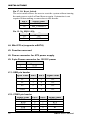
JP2: Function reserved
JP3: DDR power selection
JP3
DDR3 power
Short (Default)
1.5V
Open
1.35V
JP4: AT / ATX mode selection
JP4
AT/ATX
1-2 Short
ATX
2-3 Short
AT
(Default)
JP7: Clear CMOS
JP7
1-2 Short
(Default)
2-3 Short
CMOS
Normal
Clear CMOS
JP8: LED5, LED6 Bypass or HDD LED selection
JP8
CMOS
1-2 Short
HDD
2-3 Short
(Default)
LAN Bypass
JP12: Function reserved
15
INSTALLATIONS
Connectors on MB838
J1, J13: Power Connector, Pitch 2.54mm ............................................ 17
J2: 7-pin SATA connector ................................................................... 17
J3: System Function Connector............................................................ 17
J4: Mini PCI-e (supports mSATA) ...................................................... 18
J5: Function reserved .......................................................................... 18
J8: Power connector for ATX power supply ........................................ 18
J9: 2-pin Power connector for 12V DC power ..................................... 18
J11: USB pin header ............................................................................ 18
J12: COM2 pin header ......................................................................... 18
J28: Power Connector, Pitch 2.0mm .................................................... 19
CN1: 22-pin right angle SATA connector ........................................... 19
CN2, CN3: RJ-45 LAN port 3 and 4.................................................... 19
CN4: USB 2.0 connectors .................................................................... 19
CN5: COM1 (Console Port) ................................................................ 19
CN6, CN7: RJ-45 LAN port 1 and 2.................................................... 19
FAN1, FAN2, FAN3: System Fan Power Connector ........................... 19
LED1: LAN port 1 LED ...................................................................... 19
LED2: LAN port 2 LED ...................................................................... 19
LED3: LAN port 3 LED ...................................................................... 19
LED4: LAN port 4 LED ...................................................................... 19
LED5, 6: Status LED ........................................................................... 20
SW2: Push button (GPI, porting by software) .................................... 20
16
MB838 User’s Manual
INSTALLATIONS
J1, J13: Power Connector, Pitch 2.54mm
Pin #
Signal Name
1
+5V
2
GND
3
GND
4
+12V
J2: 7-pin SATA connector
J3: System Function Connector
J3 provides connectors for system indicators that provide light indication
of the computer activities and switches to change the computer status. J13
is a 20-pin header that provides interfaces for the following functions
Pin 1, 2: Speaker
This connector provides an interface to a speaker for audio tone
generation. An 8-ohm speaker is recommended.
Pin #
Signal Name
1
+5V
2
GND
Pin 13, 14: ATX Power ON Switch
This 2-pin connector is an “ATX Power Supply On/Off Switch” on
the system that connects to the power switch on the case. When
pressed, the power switch will force the system to power on. When
pressed again, it will force the system to power off.
Pin #
Signal Name
13
GND
14
Power_ON
Pin 15, 16: Power LED
The power LED indicates the status of the main power switch.
Pin #
Signal Name
15
+5V
16
GND
17
INSTALLATIONS
Pin 17, 18: Reset Switch
The reset switch allows the user to reset the system without turning
the main power switch off and then on again. Orientation is not
required when making a connection to this header.
Pin #
Signal Name
17
GND
18
PM_SYSRST#
Pin 19, 20: HDD LED:
Pin #
Signal Name
19
+5V
20
GND
J4: Mini PCI-e (supports mSATA)
J5: Function reserved
J8: Power connector for ATX power supply
J9: 2-pin Power connector for 12V DC power
Pin #
Signal Name
1
+12V
2
GND
J11: USB pin header
Signal Name Pin #
Signal Name
5V
1
2
NC
D-
3
4
NC
D+
5
6
NC
GND
7
8
NC
J12: COM2 pin header
Signal Name Pin #
DCD
1
RXD
2
TXD
3
DTR
4
GND
5
18
Pin #
Pin #
6
7
8
9
Signal Name
DSR
RTS
CTS
RI
MB838 User’s Manual
INSTALLATIONS
J28: Power Connector, Pitch 2.0mm
Pin #
Signal Name
1
+5V
2
Ground
3
Ground
4
+12V
CN1: 22-pin right angle SATA connector
CN2, CN3: RJ-45 LAN port 3 and 4
CN4: USB 2.0 connectors
CN5: COM1 (Console Port)
CN6, CN7: RJ-45 LAN port 1 and 2
FAN1, FAN2, FAN3: System Fan Connectors
FAN1, FAN2, FAN3 is a 4-pin header for system fans.
The fan must be 12V (Max. 1A).
Pin #
1
2
3
4
Signal Name
Ground
+12V
Rotation detection
Rotation control
LED1: LAN port 1 LED
LED2: LAN port 2 LED
LED3: LAN port 3 LED
LED4: LAN port 4 LED
19
INSTALLATIONS
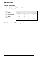
LED5, 6: Status LED
A1 & C1 : Status LED
A2 & C2 : Bypass or HDD status LED
A3 & C3 : Power LED
Status
Bypass or HDD
Power
Signal
Name
Pin #
Pin #
SIO_GPIO
33
A1
C1
+5 V
A2
C2
+3.3 V Signal A3 Pin # C3Pin #
Name
Signal
Name
SIO_GPIO
32
JP15
Selection
GNDSignal
Name
SIO_GPIO33
A1
+5 V
A2
SW2: Push button (GPI, porting+3.3
by V
software)
A3
Status
C1
C2
C3
SIO_GPIO32
JP15 Selection
GND
Bypass or HDD
Power
20
MB838 User’s Manual
INSTALLATIONS
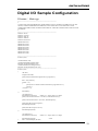
Digital I/O Sample Configuration
Filename:Main.cpp
//--------------------------------------------------------------------------//
// THIS CODE AND INFORMATION IS PROVIDED "AS IS" WITHOUT WARRANTY OF ANY
// KIND, EITHER EXPRESSED OR IMPLIED, INCLUDING BUT NOT LIMITED TO THE
// IMPLIED WARRANTIES OF MERCHANTABILITY AND/OR FITNESS FOR A PARTICULAR
// PURPOSE.
//
//--------------------------------------------------------------------------#include <dos.h>
#include <conio.h>
#include <stdio.h>
#include <stdlib.h>
#include "F81865.H"
#define BIT0 0x01
#define BIT1 0x02
#define BIT2 0x04
#define BIT3 0x08
#define BIT4 0x10
#define BIT5 0x20
#define BIT6 0x40
#define BIT7 0x80
//--------------------------------------------------------------------------int main (void);
void Dio5Initial(void);
void Dio5SetOutput(unsigned char);
unsigned char Dio5GetInput(void);
void Dio5SetDirection(unsigned char);
unsigned char Dio5GetDirection(void);
//--------------------------------------------------------------------------int main (void)
{
char SIO;
unsigned char DIO;
printf("Fintek 81865/81866 digital I/O test program\n");
SIO = Init_F81865();
if (SIO == 0)
{
printf("Can not detect Fintek 81865/81866, program abort.\n");
return(1);
}//if (SIO == 0)
Dio5Initial();
/*
//for GPIO50..57
Dio5SetDirection(0xF0);
//GP50..53 = input, GP54..57=output
printf("Current DIO direction = 0x%X\n", Dio5GetDirection());
printf("Current DIO status = 0x%X\n", Dio5GetInput());
printf("Set DIO output to high\n");
Dio5SetOutput(0x0F);
printf("Set DIO output to low\n");
Dio5SetOutput(0x00);
*/
//for GPIO50..57
Dio5SetDirection(0xF0);
//
//GP50..53 = input, GP54..57=output
Dio5SetOutput(0x00);
DIO = Dio5GetInput() & 0x0F;
//clear
21
INSTALLATIONS
Dio5SetOutput(0x00);
//clear
DIO = Dio5GetInput() & 0x0F;
if (DIO != 0x0A)
{
printf("The Fintek 81865 digital IO abnormal, abort.\n");
return(1);
}//if (DIO != 0x0A)
Dio5SetOutput(0xA0);
Dio5SetOutput(0xF0);
Dio5SetOutput(0xA0);
//clr# is high
//clk and clr# is high
//clr# is high
DIO = Dio5GetInput() & 0x0F;
if (DIO != 0x05)
{
printf("The Fintek 81865 digital IO abnormal, abort.\n");
return(1);
}
printf("!!! Pass !!!\n");
return 0;
}
//--------------------------------------------------------------------------void Dio5Initial(void)
{
unsigned char ucBuf;
//switch GPIO multi-function pin for gpio 50~57
//gpio53~57 UR5_FULL_EN(bit1), clear UR6_FULL_EN(bit3)
//set UR5_FULL_EN,should set UR_GP_PROG_EN = 1 (reg26,bit0) first
ucBuf = Get_F81865_Reg(0x26);
ucBuf |= BIT0;
Set_F81865_Reg(0x26, ucBuf);
//set UR5_FULL_EN(bit1), clear UR6_FULL_EN(bit3)
ucBuf = Get_F81865_Reg(0x2A);
ucBuf &= ~BIT3;//clear bit 3,
ucBuf |= BIT1;//set bit 1,
Set_F81865_Reg(0x2a, ucBuf);
//GPIO51 ~ GPIO52
//clear UR6_ALT_EN(bit5), IR_ALT_EN(bit4),set FDC_GP_EN(bit3)
//GPIO50
//set FDC_GP_EN(bit3), clear RTS6_ALT_EN(RTS6_2_ALT_EN)(bit6)
ucBuf = Get_F81865_Reg(0x2A);
ucBuf &= ~(BIT4+BIT5+BIT6);
//clear UR6_ALT_EN(bit5), IR_ALT_EN(bit4),
RTS6_ALT_EN(RTS6_2_ALT_EN)(bit6)
Set_F81865_Reg(0x2a, ucBuf);
//set FDC_GP_EN(bit3), should clear UR_GP_PROG_EN (reg26,bit0) first
ucBuf = Get_F81865_Reg(0x26);
ucBuf &= ~BIT0;
Set_F81865_Reg(0x26, ucBuf);//clear UR_GP_PROG_EN = 0 (reg26,bit0)
ucBuf = Get_F81865_Reg(0x2A);
ucBuf |= BIT3;
//set FDC_GP_EN(bit3),
Set_F81865_Reg(0x2a, ucBuf);
Set_F81865_LD(0x06);
//switch to logic device 6
//enable the GP5 group
ucBuf = Get_F81865_Reg(0x30);
ucBuf |= 0x01;
Set_F81865_Reg(0x30, ucBuf);
Set_F81865_Reg(0xA0, 0x00);
Set_F81865_Reg(0xA3, 0xFF);
//define as input mode
//push pull mode
}
//---------------------------------------------------------------------------
22
MB838 User’s Manual
INSTALLATIONS
void Dio5SetOutput(unsigned char NewData)
{
Set_F81865_LD(0x06);
Set_F81865_Reg(0xA1, NewData);
}
//--------------------------------------------------------------------------unsigned char Dio5GetInput(void)
{
unsigned char result;
Set_F81865_LD(0x06);
result = Get_F81865_Reg(0xA2);
return (result);
}
//--------------------------------------------------------------------------void Dio5SetDirection(unsigned char NewData)
{
//NewData : 1 for input, 0 for output
Set_F81865_LD(0x06);
Set_F81865_Reg(0xA0, NewData);
}
//--------------------------------------------------------------------------unsigned char Dio5GetDirection(void)
{
unsigned char result;
Set_F81865_LD(0x06);
result = Get_F81865_Reg(0xA0);
return (result);
//switch to logic device 6
//switch to logic device 6
//switch to logic device 6
//switch to logic device 6
}
//---------------------------------------------------------------------------
Filename:81865.cpp
//--------------------------------------------------------------------------//
// THIS CODE AND INFORMATION IS PROVIDED "AS IS" WITHOUT WARRANTY OF ANY
// KIND, EITHER EXPRESSED OR IMPLIED, INCLUDING BUT NOT LIMITED TO THE
// IMPLIED WARRANTIES OF MERCHANTABILITY AND/OR FITNESS FOR A PARTICULAR
// PURPOSE.
//
//--------------------------------------------------------------------------#include "F81865.H"
#include <dos.h>
//--------------------------------------------------------------------------unsigned int F81865_BASE;
void Unlock_F81865 (void);
void Lock_F81865 (void);
//--------------------------------------------------------------------------unsigned int Init_F81865(void)
{
unsigned int result;
unsigned char ucDid;
F81865_BASE = 0x4E;
result = F81865_BASE;
ucDid = Get_F81865_Reg(0x20);
if (ucDid == 0x07||ucDid == 0x10)
{
goto Init_Finish;
}
//Fintek 81865/66
F81865_BASE = 0x2E;
result = F81865_BASE;
ucDid = Get_F81865_Reg(0x20);
if (ucDid == 0x07||ucDid == 0x10)
{
goto Init_Finish;
}
//Fintek 81865/66
F81865_BASE = 0x00;
result = F81865_BASE;
23
INSTALLATIONS
Init_Finish:
return (result);
}
//--------------------------------------------------------------------------void Unlock_F81865 (void)
{
outportb(F81865_INDEX_PORT, F81865_UNLOCK);
outportb(F81865_INDEX_PORT, F81865_UNLOCK);
}
//--------------------------------------------------------------------------void Lock_F81865 (void)
{
outportb(F81865_INDEX_PORT, F81865_LOCK);
}
//--------------------------------------------------------------------------void Set_F81865_LD( unsigned char LD)
{
Unlock_F81865();
outportb(F81865_INDEX_PORT, F81865_REG_LD);
outportb(F81865_DATA_PORT, LD);
Lock_F81865();
}
//--------------------------------------------------------------------------void Set_F81865_Reg( unsigned char REG, unsigned char DATA)
{
Unlock_F81865();
outportb(F81865_INDEX_PORT, REG);
outportb(F81865_DATA_PORT, DATA);
Lock_F81865();
}
//--------------------------------------------------------------------------unsigned char Get_F81865_Reg(unsigned char REG)
{
unsigned char Result;
Unlock_F81865();
outportb(F81865_INDEX_PORT, REG);
Result = inportb(F81865_DATA_PORT);
Lock_F81865();
return Result;
}
//---------------------------------------------------------------------------
Filename:81865.h
//--------------------------------------------------------------------------//
// THIS CODE AND INFORMATION IS PROVIDED "AS IS" WITHOUT WARRANTY OF ANY
// KIND, EITHER EXPRESSED OR IMPLIED, INCLUDING BUT NOT LIMITED TO THE
// IMPLIED WARRANTIES OF MERCHANTABILITY AND/OR FITNESS FOR A PARTICULAR
// PURPOSE.
//
//--------------------------------------------------------------------------#ifndef __F81865_H
#define __F81865_H
1
//--------------------------------------------------------------------------#define F81865_INDEX_PORT
(F81865_BASE)
#define F81865_DATA_PORT
(F81865_BASE+1)
//--------------------------------------------------------------------------#define F81865_REG_LD
0x07
//--------------------------------------------------------------------------#define F81865_UNLOCK
0x87
#define F81865_LOCK
0xAA
//--------------------------------------------------------------------------unsigned int Init_F81865(void);
void Set_F81865_LD( unsigned char);
void Set_F81865_Reg( unsigned char, unsigned char);
unsigned char Get_F81865_Reg( unsigned char);
//--------------------------------------------------------------------------#endif //__F81865_H
24
MB838 User’s Manual
INSTALLATIONS
Watchdog Timer Configuration
The WDT is used to generate a variety of output signals after a user
programmable count. The WDT is suitable for use in the prevention of
system lock-up, such as when software becomes trapped in a deadlock.
Under these sorts of circumstances, the timer will count to zero and the
selected outputs will be driven. Under normal circumstance, the user will
restart the WDT at regular intervals before the timer counts to zero.
SAMPLE CODE:
This code and information is provided "as is" without warranty of any
kind, either expressed or implied, including but not limited to the implied
warranties of merchantability and/or fitness for a particular purpose.
//--------------------------------------------------------------------------//
// THIS CODE AND INFORMATION IS PROVIDED "AS IS" WITHOUT WARRANTY OF ANY
// KIND, EITHER EXPRESSED OR IMPLIED, INCLUDING BUT NOT LIMITED TO THE
// IMPLIED WARRANTIES OF MERCHANTABILITY AND/OR FITNESS FOR A PARTICULAR
// PURPOSE.
//
//--------------------------------------------------------------------------#include <dos.h>
#include <conio.h>
#include <stdio.h>
#include <stdlib.h>
#include "F81866.H"
//--------------------------------------------------------------------------int main (int argc, char *argv[]);
void EnableWDT(int);
void DisableWDT(void);
//--------------------------------------------------------------------------int main (int argc, char *argv[])
{
unsigned char bBuf;
unsigned char bTime;
char **endptr;
char SIO;
printf("Fintek 81866 watch dog program\n");
SIO = Init_F81866();
if (SIO == 0)
{
printf("Can not detect Fintek 81866, program abort.\n");
return(1);
}//if (SIO == 0)
if (argc != 2)
{
printf(" Parameter incorrect!!\n");
return (1);
}
bTime = strtol (argv[1], endptr, 10);
printf("System will reset after %d seconds\n", bTime);
if (bTime)
{
EnableWDT(bTime); }
else
{
DisableWDT();
}
25
INSTALLATIONS
return 0;
}
//--------------------------------------------------------------------------void EnableWDT(int interval)
{
unsigned char bBuf;
bBuf = Get_F81866_Reg(0x2B);
bBuf &= (~0x20);
Set_F81866_Reg(0x2B, bBuf);
//Enable WDTO
Set_F81866_LD(0x07);
Set_F81866_Reg(0x30, 0x01);
//switch to logic device 7
//enable timer
bBuf = Get_F81866_Reg(0xF5);
bBuf &= (~0x0F);
bBuf |= 0x52;
Set_F81866_Reg(0xF5, bBuf);
//count mode is second
Set_F81866_Reg(0xF6, interval);
//set timer
bBuf = Get_F81866_Reg(0xFA);
bBuf |= 0x01;
Set_F81866_Reg(0xFA, bBuf);
//enable WDTO output
bBuf = Get_F81866_Reg(0xF5);
bBuf |= 0x20;
Set_F81866_Reg(0xF5, bBuf);
//start counting
}
//--------------------------------------------------------------------------void DisableWDT(void)
{
unsigned char bBuf;
Set_F81866_LD(0x07);
//switch to logic device 7
bBuf = Get_F81866_Reg(0xFA);
bBuf &= ~0x01;
Set_F81866_Reg(0xFA, bBuf);
//disable WDTO output
bBuf = Get_F81866_Reg(0xF5);
bBuf &= ~0x20;
bBuf |= 0x40;
Set_F81866_Reg(0xF5, bBuf);
//disable WDT
}
//--------------------------------------------------------------------------//--------------------------------------------------------------------------//
// THIS CODE AND INFORMATION IS PROVIDED "AS IS" WITHOUT WARRANTY OF ANY
// KIND, EITHER EXPRESSED OR IMPLIED, INCLUDING BUT NOT LIMITED TO THE
// IMPLIED WARRANTIES OF MERCHANTABILITY AND/OR FITNESS FOR A PARTICULAR
// PURPOSE.
//
//--------------------------------------------------------------------------#include "F81866.H"
#include <dos.h>
//--------------------------------------------------------------------------unsigned int F81866_BASE;
void Unlock_F81866 (void);
void Lock_F81866 (void);
//--------------------------------------------------------------------------unsigned int Init_F81866(void)
{
unsigned int result;
unsigned char ucDid;
F81866_BASE = 0x4E;
result = F81866_BASE;
26
MB838 User’s Manual
INSTALLATIONS
ucDid = Get_F81866_Reg(0x20);
if (ucDid == 0x07)
{
goto Init_Finish;
}
F81866_BASE = 0x2E;
result = F81866_BASE;
ucDid = Get_F81866_Reg(0x20);
if (ucDid == 0x07)
{
goto Init_Finish;
}
//Fintek 81866
//Fintek 81866
F81866_BASE = 0x00;
result = F81866_BASE;
Init_Finish:
return (result);
}
//--------------------------------------------------------------------------void Unlock_F81866 (void)
{
outportb(F81866_INDEX_PORT, F81866_UNLOCK);
outportb(F81866_INDEX_PORT, F81866_UNLOCK);
}
//--------------------------------------------------------------------------void Lock_F81866 (void)
{
outportb(F81866_INDEX_PORT, F81866_LOCK);
}
//--------------------------------------------------------------------------void Set_F81866_LD( unsigned char LD)
{
Unlock_F81866();
outportb(F81866_INDEX_PORT, F81866_REG_LD);
outportb(F81866_DATA_PORT, LD);
Lock_F81866();
}
//--------------------------------------------------------------------------void Set_F81866_Reg( unsigned char REG, unsigned char DATA)
{
Unlock_F81866();
outportb(F81866_INDEX_PORT, REG);
outportb(F81866_DATA_PORT, DATA);
Lock_F81866();
}
//--------------------------------------------------------------------------unsigned char Get_F81866_Reg(unsigned char REG)
{
unsigned char Result;
Unlock_F81866();
outportb(F81866_INDEX_PORT, REG);
Result = inportb(F81866_DATA_PORT);
Lock_F81866();
return Result;
}
//--------------------------------------------------------------------------//--------------------------------------------------------------------------//
// THIS CODE AND INFORMATION IS PROVIDED "AS IS" WITHOUT WARRANTY OF ANY
// KIND, EITHER EXPRESSED OR IMPLIED, INCLUDING BUT NOT LIMITED TO THE
// IMPLIED WARRANTIES OF MERCHANTABILITY AND/OR FITNESS FOR A PARTICULAR
// PURPOSE.
//
//--------------------------------------------------------------------------#ifndef __F81866_H
#define __F81866_H
1
//--------------------------------------------------------------------------#define F81866_INDEX_PORT
(F81866_BASE)
#define F81866_DATA_PORT
(F81866_BASE+1)
//--------------------------------------------------------------------------#define F81866_REG_LD
0x07
//---------------------------------------------------------------------------
27
INSTALLATIONS
#define F81866_UNLOCK
0x87
#define F81866_LOCK
0xAA
//--------------------------------------------------------------------------unsigned int Init_F81866(void);
void Set_F81866_LD( unsigned char);
void Set_F81866_Reg( unsigned char, unsigned char);
unsigned char Get_F81866_Reg( unsigned char);
//--------------------------------------------------------------------------#endif //__F81866_H
28
MB838 User’s Manual
BIOS SETUP
BIOS Setup
This chapter describes the different settings available in the AMI BIOS
that comes with the board. The topics covered in this chapter are as
follows:
BIOS Introduction ............................................................................... 30
BIOS Setup .......................................................................................... 30
Advanced Settings ............................................................................... 31
IntelRCSetup Settings .......................................................................... 38
Security Settings .................................................................................. 41
Boot Settings........................................................................................ 42
Save & Exit Settings ............................................................................ 43
29
BIOS SETUP
BIOS Introduction
The BIOS (Basic Input/Output System) installed in your computer
system’s ROM supports Intel processors. The BIOS provides critical
low-level support for a standard device such as disk drives, serial ports
and parallel ports. It also password protection as well as special support
for detailed fine-tuning of the chipset controlling the entire system.
BIOS Setup
The BIOS provides a Setup utility program for specifying the system
configurations and settings. The BIOS ROM of the system stores the
Setup utility. When you turn on the computer, the BIOS is immediately
activated. Pressing the <Del> key immediately allows you to enter the
Setup utility. If you are a little bit late pressing the <Del> key, POST
(Power On Self Test) will continue with its test routines, thus preventing
you from invoking the Setup. If you still wish to enter Setup, restart the
system by pressing the ”Reset” button or simultaneously pressing the
<Ctrl>, <Alt> and <Delete> keys. You can also restart by turning the
system Off and back On again. The following message will appear on the
screen:
Press <DEL> / <F2> to Enter Setup
In general, you press the arrow keys to highlight items, <Enter> to select,
the <PgUp> and <PgDn> keys to change entries, <F1> for help and
<Esc> to quit.
When you enter the Setup utility, the Main Menu screen will appear on
the screen. The Main Menu allows you to select from various setup
functions and exit choices.
Warning: It is strongly recommended that you avoid making any
changes to the chipset defaults. These defaults have been
carefully chosen by both AMI and your system manufacturer
to provide the absolute maximum performance and
reliability. Changing the defaults could cause the system to
become unstable and crash in some cases.
30
MB838 User’s Manual
BIOS SETUP
Main Settings
Aptio Setup Utility – Copyright © 2012 American Megatrends, Inc.
Main
Advanced
IntelRCSetup
Security
Boot
BIOS Information
Save & Exit
Choose the system default
language
System Language
→ ← Select
[English]
System Date
System Time
[Fri 02/21/2014]
[10:30:55]
Access Level
Administrator
Screen
↑↓ Select Item
Enter: Select
+- Change Field
F1: General Help
F2: Previous Values
F3: Optimized Default
F4: Save ESC: Exit
System Language
Choose the system default language.
System Date
Set the Date. Use Tab to switch between Data elements.
System Time
Set the Time. Use Tab to switch between Data elements.
Advanced Settings
This section allows you to configure and improve your system and allows
you to set up some system features according to your preference.
Aptio Setup Utility
Main
Advanced
IntelRCSetup
Security
Boot
Save & Exit
► ACPI Settings
► Super IO Configuration
► Hardware Monitor
► Ethernet Bypass Configuration
►Serial Port Console Redirection
► PCI Subsystem Settings
► CSM Configuration
► USB Configuration
► Trusted Computing
► USB Configuration
► iSCSI Configuration
► Intel(R) Ethernet Connection I354
► Intel(R) Ethernet Connection I354
► Intel(R) Ethernet Connection I354
► Intel(R) Ethernet Connection I354
→ ← Select
– 00:03:2…
– 00:03:2…
– 00:03:2…
– 00:03:2…
Screen
↑↓ Select Item
Enter: Select
+- Change Field
F1: General Help
F2: Previous Values
F3: Optimized Default
F4: Save ESC: Exit
31
BIOS SETUP
ACPI Settings
Aptio Setup Utility
Main
Advanced
IntelRCSetup
Security
Boot
Save & Exit
ACPI Settings
→ ← Select
Enable ACPI Auto Conf
[Disabled]
Enable Hibernation
ACPI Sleep State
Lock Legacy Resources
[Enabled]
[S1 only (CPU Stop C…]
[Disabled]
Screen
↑↓ Select Item
Enter: Select
+- Change Field
F1: General Help
F2: Previous Values
F3: Optimized Default
F4: Save ESC: Exit
Enable Hibernation
Enables or Disables System ability to Hibernate (OS/S4 Sleep State).
This option may be not effective with some OS.
ACPI Sleep State
Select ACPI sleep state the system will enter, when the SUSPEND button
is pressed.
Lock Legacy Resources
Enabled or Disabled Lock of Legacy Resources.
Super IO Configuration
Aptio Setup Utility
Main
Advanced
IntelRCSetup
Security
Boot
Save & Exit
Super IO Configuration
→ ← Select
F81866 Super IO Chip
► Serial Port 0 Configuration
► Serial Port 1 Configuration
F81866
Screen
↑↓ Select Item
Enter: Select
+- Change Field
F1: General Help
F2: Previous Values
F3: Optimized Default
F4: Save ESC: Exit
Serial Port Configuration
Set Parameters of Serial Ports. User can Enable/Disable the serial port
and Select an optimal settings for the Super IO Device.
32
MB838 User’s Manual
BIOS SETUP
Hardware Monitor
Aptio Setup Utility
Main
Advanced
IntelRCSetup
Security
Boot
Save & Exit
PC Health Status
→ ← Select
Smart Fan 1 Function
Smart Fan 2 Function
Smart Fan 3 Function
CPU temperature
System temperature
Fan1 Speed
Fan2 Speed
Fan3 Speed
Vcore
[Disabled]
[Disabled]
[Disabled]
: +30 C
: +29 C
: 6382 RPM
: 6800 RPM
: 6800 RPM
: +0.944 V
+5V
+12V
+1.5V
VCC3V
:
:
:
:
Screen
↑↓ Select Item
Enter: Select
+- Change Field
F1: General Help
F2: Previous Values
F3: Optimized Default
F4: Save ESC: Exit
+5.171 V
+12.056 V
+1.552 V
+3.392 V
33
BIOS SETUP
Ethernet Bypass Configuration
Aptio Setup Utility
Main
Advanced
IntelRCSetup
Security
Boot
Save & Exit
Ethernet Bypass Configuration
Ethernet Bypass Quick Setting
[Normal]
All LAN ports in NORMAL. WDT monitor system hang & SW
initiates a reboot
Bypass Quick Setting
Set LAN Bypass to Normal, Bypass, Firewall or Custom Define Mode
Normal mode: All LAN ports in NORMAL. When Watchdog monitor system
hangs, software will initiates a system reboot.
Bypass mode: All LAN ports in BYPASS during power-off or watchdog initiates
Bypass. System will not reboot.
Firewall mode: All LAN ports in BYPASS until software change it to NORMAL
under OS. When watchdog monitors system hang, software will
initiates a system reboot.
Manual mode: Customer defines watchdog reset, watchdog Bypass and
power-off Bypass settings.
Aptio Setup Utility
Main
Advanced
IntelRCSetup
Security
Boot
Save & Exit
LAN Bypass Configuration
Ethernet Bypass Quick Setting
[Manual]
Watchdog Reset Signal
[Disabled]
Watchdog Bypass Setting
LAN1-2 Watchdog Bypass
Ext LAN1 LAN2 Bypass
Ext LAN3 LAN4 Bypass
System OFF Bypass Setting
LAN1-2 Watchdog Bypass
[Enable]
[Enable]
[Enable]
[Enable]
Ext LAN1 LAN2 Bypass
Ext LAN3 LAN4 Bypass
[Enable]
[Enable]
[Enable]
Note: “Ext LAN Bypass” items only appear when extended IBASE LAN
module card installed.
34
MB838 User’s Manual
BIOS SETUP
Serial Port Console Redirection
Aptio Setup Utility
Main
Advanced
IntelRCSetup
Security
Boot
Save & Exit
→ ← Select
COM0
Console Redirection
► Console Redirection Settings
[Enabled]
COM1
Console Redirection
► Console Redirection Settings
Screen
↑↓ Select Item
Enter: Select
+- Change Field
F1: General Help
F2: Previous Values
F3: Optimized Default
F4: Save ESC: Exit
[Disabled]
Serial Port for Out-of-Band Management /
Windows Emergency Management
Services (EMS)
Console Redirection
[Disabled]
► Console Redirection Settings
Aptio Setup Utility
Main
Advanced
IntelRCSetup
Security
Boot
Save & Exit
COM0
Console Redirection Settings
→ ← Select
Terminal Type
Bits per second
Data Bits
Parity
Stop Bits
Flow Control
[VT100]
[115200]
[8]
[None]
[1]
[None]
↑↓ Select Item
Enter: Select
+- Change Field
F1: General Help
F2: Previous Values
F3: Optimized Default
F4: Save ESC: Exit
VT-UTF8 Combo Key Support
Recorder Mode
Resolution 100x31
Legacy OS Redirection Resolution
Putty KeyPad
Redirection After BIOS POST
[Enabled]
[Disabled]
[Disabled]
[80x24]
[VT100]
[Always Enable]
Screen
35
BIOS SETUP
PCI Subsystem Settings
Aptio Setup Utility
Main
Advanced
IntelRCSetup
PCI Bus Driver Version
Security
Boot
Save & Exit
A5.0.1.04
→ ← Select
PCI Devices Common Settings:
PCI Latency Timer
PCI-X Latency Timer
VGA Palette Snoop
PERR# Generation
SERR# Generation
Above 4G Decoding
SR-IOV Support
[32 PCI Bus Clocks]
[64 PCI Bus Clocks]
[Disabled]
[Disabled]
[Disabled]
[Disabled]
[Disabled]
Screen
↑↓ Select Item
Enter: Select
+- Change Field
F1: General Help
F2: Previous Values
F3: Optimized Default
F4: Save ESC: Exit
► PCI Express Settings
► PCI Express Gen 2 Settings
PCI Latency Timer
Value to be programmed into PCI Latency Timer Register.
VGA Palette Snoop
Enables or disables VGA Palette Registers Snooping.
PERR# Generation
Enables or disables PCI device to generate PERR#.
SERR# Generation
Enables or disables PCI device to generate SERR#.
PCI Express Settings
Change PCI Express devices settings.
36
MB838 User’s Manual
BIOS SETUP
USB Configuration
Aptio Setup Utility
Main
Advanced
IntelRCSetup
Security
Boot
Save & Exit
USB Configuration
USB Module Version
8.10.27
USB Devices:
1 Keyboard, 1 Hub
Legacy USB Support
USB3.0 Support
XHCI Hand-off
EHCI Hand-off
[Enabled]
[Enabled]
[Enabled]
[Disabled]
USB Mass Storage Driv
[Enabled]
USB hardware delays and time-outs:
USB Transfer time-out
Device reset tine-out
Device power-up delay
[20 sec]
[20 sec]
[Auto]
→ ← Select
Screen
↑↓ Select Item
Enter: Select
+- Change Field
F1: General Help
F2: Previous Values
F3: Optimized Default
F4: Save ESC: Exit
Legacy USB Support
Enables Legacy USB support.
AUTO option disables legacy support if no USB devices are connected.
DISABLE option will keep USB devices available only for EFI
applications.
USB3.0 Support
Enable/Disable USB3.0 (XHCI) Controller support.
XHCI Hand-off
This is a workaround for OSes without XHCI hand-off support. The
XHCI ownership change should be claimed by XHCI driver.
EHCI Hand-off
Enabled/Disabled. This is a workaround for OSes without EHCI hand-off
support. The EHCI ownership change should be claimed by EHCI driver.
Port 64/60 Emulation
Enables I/O port 60h/64h emulation support. This should be enabled for
the complete USB keyboard legacy support for non-USB aware OSes.
USB Transfer time-out
The time-out value for Control, Bulk, and Interrupt transfers.
Device reset tine-out
USB mass Storage device start Unit command time-out.
37
BIOS SETUP
Device power-up delay
Maximum time the device will take before it properly reports itself to the
Host Controller. ‘Auto’ uses default value: for a Root port it is 100ms, for
a Hub port the delay is taken from Hub descriptor.
IntelRCSetup
Aptio Setup Utility
Main
Advanced
IntelRCSetup
Security
Boot
Save & Exit
► Processor Configuration
► USB Configuration
► South Bridge Chipset Configuration
--------------------------------------------------------------------------------------Setup Warning:
Setting items on this Screen to incorrect values may cause
system malfunction!
38
→ ←
Select Screen
↑↓ Select Item
Enter: Select
+- Change Field
F1: General Help
F2: Previous Values
F3: Optimized Default
F4: Save ESC: Exit
MB838 User’s Manual
BIOS SETUP
Processor Configuration
Main
Advanced
IntelRCSetup
Security
Boot
Save & Exit
Processor Configuration
------------------------------------------------------------------------------Processor ID
000406D8
Processor Frequency
2.400 GHz
Microcode Revision
00000121
L1 Cache RAM
224KB
L2 Cache RAM
2048KB
Processor Version
Geniune Intel(R) CPU
EIST (GV3)
Enhanced Halt State (C1E)
ACPI C2
[Auto]
[Disable]
[C6 NS]
Monitor/Mwait
Fast String
Max CPUID Value Limit
Execute Disable Bit
VMX
Extended APIC
AES-NI
Turbo
RAPL
Active Processor Core
CPU Flex Ratio Overri
CPU Core Ratio
[Enable]
[Enable]
[Disable]
[Enable]
[Enable]
[Enable]
[Enable]
[Enable]
[Enable]
[All]
[Disable]
24
----------------------------------------------
→ ←
Select Screen
↑↓ Select Item
Enter: Select
+- Change Field
F1: General Help
F2: Previous Values
F3: Optimized Default
F4: Save ESC: Exit
EIST (GV3)
Enable/Disable EIST. GV3 and TM1 must be enabled for TM2 to be
available. GV3 must be enabled for Turbo. Auto – Enable for B0 CPU
stepping, all others disabled, change setting to override.
Fast String
When enabled, enable fast string for REP MOVS/STOS.
MAX CPUID Value Limit
This should be enabled in order to boot legacy OSes that cannot support
CPUs with extended CPUID functions.
Execute Disable Bit
When disabled, force the XD feature flag to always return 0.
VMX
Enables the Vanderpool Technology, takes effect after reboot.
Extended APIC
Enable/Disable extended APIC support.
39
BIOS SETUP
AES-NI
Enable/Disable AES-NI support
Turbo
Enable or Disable CPU Turbo capability. This option only applies to ES2
and above.
Active Processor Core
Number of cores to enable in SoC package.
CPU Flex Ratio Override
Enable/Disable CPU Flex Ration Programming.
USB Configuration
Main
Advanced
IntelRCSetup
Security
Boot
Save & Exit
USB Configuration
USB Support
USB IO PM
[Enabled]
[Enable]
→ ←
Select Screen
↑↓ Select Item
Enter: Select
+- Change Field
F1: General Help
F2: Previous Values
F3: Optimized Default
F4: Save ESC: Exit
USB Support
USB Support Parameters.
USB IO PM
Enable/Disable IO PM.
40
MB838 User’s Manual
BIOS SETUP
Security
This section allows you to configure and improve your system and allows
you to set up some system features according to your preference.
Aptio Setup Utility
Main
Advanced
IntelRCSetup
Security
Boot
Save & Exit
Password Description
If ONLY the Administrator’s password is set, then
this only limit access to Setup and is only asked
for when entering Setup.
If ONLY the User’s password is set, then this is a
power on password and must be entered to boot
or enter Setup. In Setup the User will have
Administrator rights
The password length must be
in the following range:
Minimum length
Maximum length
→ ← Select
3
20
Screen
↑↓ Select Item
Enter: Select
+- Change Field
F1: General Help
F2: Previous Values
F3: Optimized Default
F4: Save ESC: Exit
Administrator Password
User Password
Administrator Password
Set Setup Administrator Password.
User Password
Set User Password.
41
BIOS SETUP
Boot Settings
Aptio Setup Utility
Main
Advanced
IntelRCSetup
Security
Boot Configuration
Setup Prompt Timeout
Bootup NumLock State
1
[On]
Quiet Boot
HDD BootSector Write
[Disabled]
[Normal]
Boot Option Priorities
Boot Option #1
Boot option #2
Network Device BBS Priorities
Boot
Save & Exit
→ ← Select
Screen
↑↓ Select Item
[IBA GE Slot 00A0]
Enter: Select
[UEFI: Build-in EFI…] +- Change Field
F1: General Help
F2: Previous Values
F3: Optimized Default
F4: Save
ESC: Exit
Setup Prompt Timeout
Number of seconds to wait for setup activation key.
65535(0xFFFF) means indefinite waiting.
Bootup NumLock State
Select the keyboard NumLock state.
Quiet Boot
Enables/Disables Quiet Boot option.
Boot Option Priorities
Sets the system boot order.
42
MB838 User’s Manual
BIOS SETUP
Save & Exit Settings
Aptio Setup Utility
Main
Advanced
IntelRCSetup
Security
Save & Exit
Boot
Save Changes and Exit
Discard Changes and Exit
Save Changes and Reset
Discard Changes and Reset
Save Options
Save Changes
Discard Changes
Restore Defaults
Save as User Defaults
Restore User Defaults
Boot Override
Launch EFI Shell from filesystem device
→ ← Select
Screen
↑↓ Select Item
Enter: Select
+- Change Field
F1: General Help
F2: Previous Values
F3: Optimized Default
F4: Save ESC: Exit
Save Changes and Exit
Exit system setup after saving the changes.
Discard Changes and Exit
Exit system setup without saving any changes.
Save Changes and Reset
Reset the system after saving the changes.
Discard Changes and Reset
Reset system setup without saving any changes.
Save Changes
Save Changes done so far to any of the setup options.
Discard Changes
Discard Changes done so far to any of the setup options.
Restore Defaults
Restore/Load Defaults values for all the setup options.
Save as User Defaults
Save the changes done so far as User Defaults.
Restore User Defaults
Restore the User Defaults to all the setup options.
43
APPENDIX
Drivers Installation
This section describes the installation procedures for software and
drivers. The software and drivers are included with the motherboard. If
you find the items missing, please contact the vendor where you made the
purchase. The contents of this section include the following:
LAN Drivers Installation...................................................................... 45
IMPORTANT NOTE:
After installing your Windows operating system, you must install first the
Intel Chipset Software Installation Utility before proceeding with the
drivers installation.
44
MB838 User’s Manual
BIOS SETUP
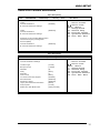
LAN Drivers Installation
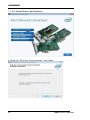
1. Insert the DVD that comes with the board. Click Intel and then
Intel(R) 8 Series Chipset Drivers.
2. Click Intel(R) PRO LAN Network Driver.
45
APPENDIX
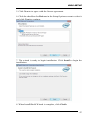
3. Click Install Drivers and Software.
4. When the Welcome screen appears, click Next.
46
MB838 User’s Manual
BIOS SETUP
5. Click Next to to agree with the license agreement.
6. Click the checkbox for Drivers in the Setup Options screen to select it
and click Next to continue.
7. The wizard is ready to begin installation. Click Install to begin the
installation.
8. When InstallShield Wizard is complete, click Finish.
47
APPENDIX
Appendix
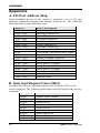
A. I/O Port Address Map
Each peripheral device in the system is assigned a set of I/O port
addresses which also becomes the identity of the device. The following
table lists the I/O port addresses used.
Address
000h - 01Fh
020h - 03Fh
040h - 05Fh
060h - 064h
070h - 07Fh
080h - 09Fh
0A0h - 0BFh
0C0h - 0DFh
0F0h
0F1h
3B0h- 3DFh
3F8h - 3FFh
2F8h - 2FFh
3E8h – 3EFh
2E8h – 2EFh
3E8h - 3EFh
2E8h - 2EFh
360h - 36Fh
Device Description
DMA Controller #1
Interrupt Controller #1
System Timer
Keyboard Controller
Real Time Clock
DMA Controller #2
Interrupt Controller #2
DMA Controller #3
Clear Math Coprocessor Busy Signal
Reset Math Coprocessor
Graphics adapter Controller
Serial Port #0 (COM1)
Serial Port #1 (COM2)
Serial Port #2 (COM3)
Serial Port #3 (COM4)
Serial Port #4 (COM5)
Serial Port #5 (COM6)
Network Ports
B. Interrupt Request Lines (IRQ)
Peripheral devices use interrupt request lines to notify CPU for the
service required. The following table shows the IRQ used by the devices
on board.
Level
Function
IRQ0
System Timer Output
IRQ1
Keyboard
IRQ4
Serial Port #1
IRQ3
Serial Port #2
IRQ5
Serial Port #3
IRQ11
Serial Port #4
IRQ8
Real Time Clock
IRQ14
Primary IDE
IRQ15
Secondary IDE
48
MB838 User’s Manual
BIOS SETUP
C. Register of the LAN Bypass Controller
To fulfill the varied requests on LAN Bypass controller, IBASE provide
the smart LAN Bypass controller. User can define the Bypass function
behavior when the system is power-on, power-off and WDT signal is
asserted.
The controller is behind the SMBus controller. The I2C address is listed
as below:
I2C Address (8bit)
Remark
1st Controller
0x68
2nd Controller
0x6A
CR 0x22 : System-On Bypass Register
Attribute : Read / Write
Reset default : 0x0000
LAN
Read /
Bit
Port#
Write
0
Eth1, 2
Read /
Write
Optional
Description
Enable / Disable LAN Bypass
function when the system is
power On.
1 = Enable LAN Bypass function
0 = Disable LAN Bypass function
CR 0x24 : System-Off Bypass Register
Attribute : Read / Write
Reset default : 0x0000
LAN
Read /
Bit
Port#
Write
0
Eth1, 2
Read /
Write
Description
Enable / Disable LAN Bypass
function when the system is power
Off.
1 = Enable LAN Bypass function
0 = Disable LAN Bypass function
49
APPENDIX
CR 0x26 : Watchdog (WDT) WDT_IN# Signal Control Register
Attribute : Read / Write
Reset default : 0x00
Read /
Bit
Description
Write
0
Read /
Write
WDT_OUT# Generator
The capacity use the WDT to reset the
system
1 = Generate 100ms pulse to reset signal
when WDT signal is asserted.
0 = Ignore the WDT signal.
WDT LAN Bypass Enable
The capacity use the WDT to set LAN
Bypass function
1
Read /
Write
2~7
1 = Enable LAN Bypass function when the
WDT signal is asserted.
CR 0x28 and CR 0x2A will be available if
this bit is set to "1".
0 = Disable WDT LAN Bypass function.
Reserved
CR 0x28 : Watchdog (WDT) Bypass Control Register
Attribute : Read / Write
Reset default : 0x0000
LAN
Read /
Bit
Description
Port#
Write
Enable / Disable WDT Bypass
function for each LAN port.
0
50
Eth1, 2
Read /
Write
1 = Follow the setting in "WDT
Bypass Register CR 0x2A"
when the WDT signal is
asserted.
0 = Ignore to control the bypass
when the WDT is asserted.
MB838 User’s Manual
BIOS SETUP
CR 0x2A : Watchdog (WDT) Bypass Register
Attribute : Read / Write
Reset default : 0x0000
LAN
Read /
Bit
Description
Port#
Write
The function works when the bit
in CR 0x28 is “1”. It controls
LAN Bypass function should be
Enabled / Disabled when the
WDT signal is asserted.
0
Eth1, 2
Read /
Write
If the bit is set to "1" in "WDT
Bypass Control Register
CR 0x28", it will follow below
setting:
1 = Enable LAN Bypass function
0 = Disable LAN Bypass
function
51