1
I-VC5
User Manual
2010 July V0
Copyright © 2008 IBASE Technology INC. All Rights Reserved.
No part of this manual, including the products and software described in it, may be
reproduced, transmitted, transcribed, stored in a retrieval system, or translated into
any language in any form or by any means, except documentation kept by the
purchaser for backup purposes, without the express written permission of IBASE
Technology INC. (“IBASE”).
Products and corporate names mentioned in this manual may or may not be
registered trademarks or copyrights of their respective companies, and are used for
identification purposes only. All trademarks are the property of their respective
owners.
Every effort has been made to ensure that the contents of this manual are correct and
up to date. However, the manufacturer makes no guarantee regarding the accuracy of
its contents, and reserves the right to make changes without prior notice.
2
Table of Contents
Accessories ........................................................................................................... 7
Components.......................................................................................................... 9
Front View ................................................................................................................... 9
Rear View .................................................................................................................. 11
Side View ................................................................................................................... 13
Specification ........................................................................................................14
Installation ..........................................................................................................15
Installing ground ring ................................................................................................. 15
Installing power cable................................................................................................. 16
Installing UPS cable .................................................................................................... 18
Installing the memory ................................................................................................ 19
Setting Jumper ........................................................................................................... 20
Connector pin definition .......................................................................................22
Rear Side.................................................................................................................... 22
Front Side .................................................................................................................. 24
Driver Installation ................................................................................................25
Intel Chipset Software Installation Utility .................................................................... 25
Intel Pineview Chipset Family Graphics Driver Installation ........................................... 28
Realtek High Definition Codec Audio Driver Installation ............................................... 31
Realtek GbE_FE Ethernet PCI-E NIC Drivers Installation ................................................ 32
PCI-E Serial Ports Driver Installation ............................................................................ 34
HC25 3G Wireless Module Driver Installation .............................................................. 39
BIOS Setup ...........................................................................................................40
BIOS Introduction ....................................................................................................... 40
BIOS Setup ................................................................................................................. 40
Advance Settings ........................................................................................................ 42
PCIPnP Settings .......................................................................................................... 50
3
Boot Settings.............................................................................................................. 51
Security Settings......................................................................................................... 53
Advanced Chipset Settings .......................................................................................... 54
Exit Setup................................................................................................................... 58
Appendix .............................................................................................................59
A-1 Watchdog Timer Configuration ............................................................................. 59
A-2 Digital I/O Sample Code........................................................................................ 65
4
Safety Information
Your I-VC5 is designed and tested to meet the latest standards of safety for
information technology equipment. However, to ensure your safety, it is important that
you read the following safety instructions.
Setting up your system
Read and follow all instructions in the documentation before you operate your
system.
Do not use this product near water.
Set up the system on a stable surface or secure on wall with the provided rail. Do
not secure the system on any unstable plane or without the rail.
Do not place this product on an unstable cart, stand, or table. The product may
fall, causing serious damage to the product.
Slots and openings on the chassis are for ventilation. Do not block or cover these
openings. Make sure you leave plenty of space around the system for ventilation.
Never insert objects of any kind into the ventilation openings.
This system should be operated from the type of power indicated on the marking
label. If you are not sure of the type of power available, consult your dealer or
local power company.
Use this product in environments with ambient temperatures between 0˚C and
60˚C.
If you use an extension cord, make sure that the total ampere rating of the
devices plugged into the extension cord does not exceed its ampere rating.
Care during use
Do not walk on the power cord or allow anything to rest on it.
Do not spill water or any other liquids on your system.
When the system is turned off, a small amount of electrical current still flows.
Always unplug all power, and network cables from the power outlets before
cleaning the system.
If you encounter the following technical problems with the product, unplug the
power cord and contact a qualified service technician or your retailer.
The power cord or plug is damaged.
Liquid has been spilled into the system.
The system does not function properly even if you follow the operating
instructions.
5
The system was dropped or the cabinet is damaged.
Lithium-Ion Battery Warning
CAUTION: Danger of explosion if battery is incorrectly replaced. Replace only with
the same or equivalent type recommended by the manufacturer. Dispose of used
batteries according to the manufacturer‟s instructions.
NO DISASSEMBLY
The warranty does not apply to the products that have been disassembled by users
6
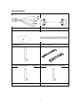
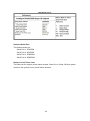
Accessories
a. Camera Extension Cable x 2 (Opt.)
b. Video Out Extension Cable x 1
c. Driver CD x 1
d. Power Cable x 3
e. Wireless LAN Antenna x 1 (optional)
f. Mounting Bracket Kit x 1 (Optional)
g. 3G Antenna x 1 (optional)
h. GPS Antenna x 1 (Optional)
7
i. Power Block x 1
8
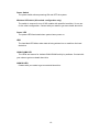
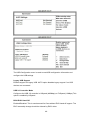
Components
Front View
Refer to the diagram below to identify the components on this side of the system.
Video Out
This is an integrated connector contains LVDS, USB and 12VDC. It intent for
connect with display which use LVDS signals.
USB
The USB (Universal Serial Bus) port is compatible with USB devices such as
keyboards, mouse devices, cameras, and hard disk drives. USB allows many
devices to run simultaneously on a single computer, with some peripheral acting
as additional plug-in sites or hubs.
Audio
Those three stereo headphone jacks (3.5mm) are used to be LINE IN, LINE OUT
and MIC audio connection. The upper stereo headphone jack (3.5mm) is used to
connect the audio signal into system to record or bypass it to storage or LINE
OUT. The middle stereo audio jack (3.5mm) is used to connect the system‟s
audio out signal to amplified speakers or headphones. The lower jack is designed
to connect the microphone used for video conferencing, voice narrations, or
simple audio recordings.
CAM1/CAM2 (DVR configuration only)
Connectors use with specified cable to record image from video camera.
9
Power Switch
The power switch allows powering ON and OFF the system.
Wireless Off Switch (3G module configuration only)
The switch is reserve for turn off 3G module with specified condition. It‟s no use
for the other configuration. Contact with your sales to get more detail about this.
Power LED
The power LED illuminated when system been power on.
HDD
The hard disk LED blinks when data is being written into or read from the hard
disk drive.
CAM1/CAM2 LED
The LEDs are reserve for indicate CAM1/CAM2 activity by software. Contact with
your sales to get more detail about this.
GSM/3G LED
Contact with your sales to get more detail about this.
10
Rear View
Refer to the diagram below to identify the components on this side of the system.
Chassis ground for ground ring attach usage. Connect ground-ring to vehicle
chassis to get better grounding performance.
6~36V
Vehicle power input for 12V/24V car battery system. Apply specified power
source with correct cable connection to source system.
UPS (Vehicle configuration only)
Connect to specified UPS power unit to get back-up power in vehicle application.
I-VC5 will charge UPS power unit automatically if the unit meet requirement. IT
MIGHT CAUSE DAMAGE IF NOT FOLLOW WITH SYSTEM REQUIREMENT.
Always contact with your sales before use this feature.
RS232
Communication or serial port is compatible with RS-232 interface.
RS232/422/485
Communication or serial port is compatible with RS-232 interface in normal
setting. Support RS422/485 signal/protocol with specified setting on mainboard.
VGA
Video Graphic Array (VGA) port supports a VGA-compatible device such as a
monitor or projector. The system default display output port.
11
LAN
The eight-pin RJ-45 LAN port supports a standard Ethernet cable for connection
to a local network.
USB
The USB (Universal Serial Bus) port is compatible with USB devices such as
keyboards, mouse devices, cameras, and hard disk drives. USB allows many
devices to run simultaneously on a single computer, with some peripheral acting
as additional plug-in sites or hubs.
DI/O
Numbers general purpose digital I/O connections.
WLAN (Wireless LAN configuration only)
Wireless LAN antenna connector.
GPRS (3G module configuration only)
3G/GPRS antenna connector.
GPS (GPS module configuration only)
GPS antenna connector.
12
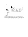
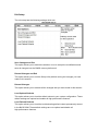
Side View
Refer to the diagram below to identify the components on this side of the system.
CF Card / SIM Card
Compact flash socket and SIM card socket cover. Access CF and SIM card with
remove this cover.
13
Specification
Construction
Aluminum/Steel
Chassis Color
Black
Storage
2.5” 40GB SATA HDD x 1 / removable 2.5” 80GB SATA HDD x 1
Mounting
Desktop or wall mount
Dimensions
207.8(W) x 70.0(H) x 224.7(D)mm
(8.18” x 2.76” x 8.85”)
Operating Temperature
0°C ~ 60°C (32°F ~ 140°F)
Storage Temperature
-20°C ~ 95°C
Relative Humidity
5~95% @60°C (non-condensing)
Vibration
Operating: MIL-STD-810F, Method 514.5, Category 20, Ground Vehicle –
Highway Truck (3 axes)
Non-operating: MIL-STD-810F, Method 514.5, Category 24, Minimum
Integrity Test (3 axes)
Shock
MIL-STD-810F, Method 516.5, Procedure I, sawtooth:
Operating: 20G / 11msec
Non-operating: 40G /11msec
Regulation
CE/FCC approval
Designed to meet ISO-7637-II
Designed to meet UL
RoHS
Available
‧This specification is subject to change without prior notice.
14
Installation
Before you start
Please take a moment and read this section before you install the system in your
vehicle. Often times, rushing into installing the system can result in serious damage
to I-VC5 and probably your vehicle electrical system. Always double check the
polarity of your wires with a voltmeter.
Avoid using the cigarette plug as a power source, often times the contacts are not
capable of delivering high current to I-VC5
Installing ground ring
To have good ground connection between I-VC5 and your vehicle, properly install
ground wire are important.
A
B
1. Disassembling M4 screw from point-A.
2. Chose adaptable wire (suggest at least 18AWG with 1050C ability wire)with O-ring
(accept M4 screw) and use original M4 screw secure the O-ring on point-A.
3. Secure point-B on your vehicle body with proper screw.
15
Installing power cable
A
B
C
D
D
1. Losing screws on power block on point-A.
2. Secure power cable (in accessary bag) on power block (in accessary bag),
point-B.
3. Tie screws on power block on point-A.
4. Plug power block to I-VC5 car battery connector, point-C, and use screwdriver to
secure power block.
5. Connecting power cable to car battery. Car battery + for positive polarity of car
battery, Car battery – for negative polarity of car battery.
6. Connecting Ignition (ACC) cable to corresponding connection of your vehicle.
16
Always double check the polarity of your wires with a voltmeter.
Power challenges in a Vehicle:
One of most difficult tasks of operating I-VC5 in a vehicle is power consumption while
the I-VC5 in OFF state. Even when I-VC5 is OFF, it will still consume about couple mA
from car battery to keep internal power scheme working.
No matter how big your battery is, you will eventually drain it if proper actions are not
taken.
Engine Cranks, under-voltage and over-voltage situations.
Another difficult task is car battery voltage level. While car batteries are rated at 12V,
they actually provide voltages in between 7-11V (engine cranks) or as high as 80 volts
(load dump).
Most of the times, your battery will stay at 13.5V (while car is running) but extra
precautions need to take place in order to prevent such situations. I-VC5 can operate
as low as 6V and as high as 36V with input voltage clamping and reverse protection.
17
Installing UPS cable
A
B
1. Plug UPS cable (UPS configuration), point-B, to I-VC5 UPS connector, point-A.
2. Connecting UPS cable to UPS battery then put battery into UPS box. Battery + for
positive polarity of car battery, Battery – for negative polarity of car battery.
18
Installing the memory
The IB808 board supports one DDR2 memory socket that can support up to 4GB
memory size, DDR2 533/667/800 (w/o ECC function).
Installing and Removing Memory Modules
To install the DDR2 modules, locate the memory slot on the board and perform the
following steps:
1.
Hold the DDR2 module so that the key of the DDR2 module aligns with that
on the memory slot. Insert the module into the socket at a slight angle
(approximately 30 degrees). Note that the socket and module are both
keyed, which means that the module can be installed only in one direction.
2.
To seat the memory module into the socket, apply firm and even pressure to
each end of the module until you feel it slip down into the socket.
3.
With the module properly seated in the socket, rotate the module downward.
Continue pressing downward until the clips at each end lock into position.
4.
To remove the DDR2 module, press the clips with both hands.
19
Setting Jumper
Jumpers are used on IB808 to select various settings and features according to your
needs and applications. Contact your supplier if you have doubts about the best
configuration for your needs. The following lists the connectors on IB808 and their
respective functions.
Jumper Locations on IB808
20
JP1, JP2, JP3: RS232/422/485 (COM3) Selection
COM3
RS-232
RS-422
RS-485
JP2:
JP2:
JP2:
1-2
3-4
5-6
JP1:
JP1:
JP1:
3-5 & 4-6
1-3 & 2-4
1-3 & 2-4
JP3:
JP3:
JP3:
3-5 & 4-6
1-3 & 2-4
1-3 & 2-4
Function
Jumper Setting
(pin closed)
JP4, JP5, JP6: RS232/422/485 (COM4) Selection
COM4
RS-232
RS-422
RS-485
JP5:
JP5:
JP5:
1-2
3-4
5-6
JP4:
JP4:
JP4:
3-5 & 4-6
1-3 & 2-4
1-3 & 2-4
JP6:
JP6:
JP6:
3-5 & 4-6
1-3 & 2-4
1-3 & 2-4
Function
Jumper Setting
(pin closed)
JP8: Clear CMOS Setting
JP8
Setting
OPEN
Normal
Closed
Clear CMOS
21
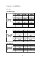
Connector pin definition
Rear Side
RS232/RS422/RS485:
Pin #
Signal Name
RS-232
R2-422
RS-485
1
DCD
TX-
DATA-
2
RX
TX+
DATA+
3
TX
RX+
NC
4
DTR
RX-
NC
5
Ground
Ground
Ground
6
DSR
NC
NC
7
RTS
NC
NC
8
CTS
NC
NC
9
RI
NC
NC
VGA
Pin #
Signal Name
Pin #
Signal Name
1
Red
2
Green
3
Blue
4
N.C.
5
GND
6
GND
7
GND
8
GND
9
N.C.
10
GND
11
N.C.
12
N.C.
13
HSYNC
14
VSYNC
15
NC
Pin #
Signal Name
Pin #
Signal Name
1
VCC
2
OUT1
3
OUT0
4
IN1
5
IN0
6
GND
7
OUT3
8
OUT2
9
IN3
10
IN2
DI/O (Digital I/O)
22
Car Battery Input (6~36V)
Pin #
Signal Name
Left
Ignition (ACC)
Right
Car Battery +
Pin #
Middle
Back Up Battery Input (UPS)
Pin #
Signal Name
Up
Battery +
Down
Battery -
23
Signal Name
Car Battery -
Front Side
Video Out
Pin #
Signal Name
Pin #
Signal Name
1
TXC-
2
LCD_GND
3
TX0+
4
TX1+
5
TX2+
6
ENABKL
7
USB_+5V
8
NC
9
USB_8P
10
TXC+
11
TX0-
12
TX1-
13
TX2-
14
+12V
15
5V/3.3V
16
NC
17
NC
18
USB_8N
19
Ground
20
Ground
21
Ground
22
Ground
23
+12V
24
NC
25
NC
USB_GND
CAM1/CAM2
Pin #
Signal Name
Pin #
Signal Name
1
TXC-
2
LCD_GND
3
TX0+
4
TX1+
5
TX2+
6
ENABKL
7
USB_+5V
8
NC
9
USB_8P
10
TXC+
11
TX0-
12
TX1-
13
TX2-
14
+12V
15
5V/3.3V
16
NC
17
NC
18
USB_8N
19
Ground
20
Ground
21
Ground
22
Ground
23
+12V
24
NC
25
NC
USB_GND
24
Driver Installation
This section describes the installation procedures for software and drivers under the
Windows XP, Windows Vista and Windows 7. The software and drivers are included
with the motherboard. If you find the items missing, please contact the vendor where
you made the purchase. The contents of this section include the following:
IMPORTANT NOTE:
After installing your Windows operating system (Windows XP/ Vista/ 7), you must
install first the Intel Chipset Software Installation Utility before proceeding with the
drivers installation.
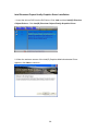
Intel Chipset Software Installation Utility
The Intel Chipset Drivers should be installed first before the software drivers to enable
Plug & Play INF support for Intel chipset components. Follow the instructions below to
complete the installation under Windows XP/Vista/7.
1. Insert the drivers DVD into the DVD drive. Click Intel and then Intel(R) Chipset
Software Installation Utility.
25
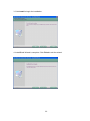
2. When the welcome screen to the Intel(R) Chipset Device Software appears, click
Next to continue.
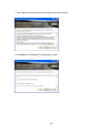
3.When the Setup Progress screen appears, click Next to continue.
26
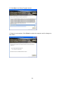
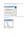
4. The Setup process is now complete. Click Finish to restart the computer and for
changes to take effect.
27
Intel Pineview Chipset Family Graphics Driver Installation
1. Insert the drivers DVD into the DVD drive. Click Intel and then Intel(R) Pineview
Chipset Drivers. Click Intel(R) Pineview Chipset Family Graphics Driver.
2. When the welcome screen of the Intel(R) Graphics Media Accelerator Driver
appears, click Next to continue.
28
3. Click Yes to to agree with the license agreement and continue.
4. Click Next in the Readme File Information screen.
29
5. Click Next in the Setup Progress screen.
6. Setup is now complete. Click Finish to restart the computer and for changes to
take effect.
30
Realtek High Definition Codec Audio Driver Installation
1. Insert the drivers DVD into the DVD drive. Click Intel and then Realtek High
Definition Codec Audio Driver.
2.When the welcome screen to InstallShield Wizard appears, click Next to start the
installation.
3.When the InstallShieldWizard has finished performing maintenance operations on
Realtek High Definition Codec Audio Driver, click Finish to restart the computer.
31
Realtek GbE_FE Ethernet PCI-E NIC Drivers Installation
Follow the steps below to install Realtek RTL8111DL LAN Drivers.
1. Insert the drivers DVD into the DVD drive. Click Intel and then Realtek GbE_FE
Ethernet PCI-E NIC Driver.
2. In the welcome screen of the InstallShield Wizard for REALTEK GbE & FE Ethernet
PCI-E NIC Driver, click Next.
32
3. Click Install to begin the installation.
4. InstallShield Wizard is complete. Click Finish to exit the wizard.
33
PCI-E Serial Ports Driver Installation
1. In the Windows OS, go to the Computer Management screen. In the
devices‟ as shown, right click the “PCI Serial Port Properties”.
2. In the PCI Serial Port Properties screen, click Reinstall Driver.
34
„Other
3. In the Hardware Update Wizard screen, select “No, not this time” and click Next to
continue.
4. Select “Install from a list or specific location (Advanced), and click Next to continue.
35
5. To choose the “search” and “installation” options, click the checkbox of “Include
this location in the search”, and click Browse to continue.
6. Choose the folder “XR17V354” under the “Intel” main folder of the driver disk, and
click OK to continue.
36
7. Click Continue Anyway.
37
8. Click Finish to close the wizard.
9. There are a total of four serial ports. Therefore, the Hardware Update Wizard
procedure has to be repeated for the rest of the serial ports.
38
HC25 3G Wireless Module Driver Installation
1. Insert the drivers DVD into the DVD drive. Click Intel and then HC25 3G Wirerless
Module Driver.
2. The InstallShield Wizard will install HC 25 Connection Manager on the computer.
To continue, click Install.
39
BIOS Setup
This chapter describes the different settings available in the Award BIOS that comes
with the board.
BIOS Introduction
The Award BIOS (Basic Input / Output System) installed in your computer system‟s
ROM supports various processors. The BIOS provides critical low-level support for a
standard device such as disk drives, serial ports and parallel ports. It also adds virus
and password protection as well as special support for detailed fine-tuning of the
chipset controlling the entire system.
BIOS Setup
The Award BIOS provides a Setup utility program for specifying the system
configurations and settings. The BIOS ROM of the system stores the Setup utility.
When you turn on the computer, the Award BIOS is immediately activated. Pressing
the <Del> key immediately allows you to enter the Setup utility. If you are a little bit
late pressing the <Del> key, POST (Power On Self Test) will continue with its test
routines, thus preventing you from invoking the Setup. If you still wish to enter Setup,
restart the system by pressing the ”Reset” button or simultaneously pressing the
<Ctrl>, <Alt> and <Delete> keys. You can also restart by turning the system Off and
back On again. The following message will appear on the screen:
Press <DEL> to Enter Setup
In general, you press the arrow keys to highlight items, <Enter> to select, the <PgUp>
and <PgDn> keys to change entries, <F1> for help and <Esc> to quit.
When you enter the Setup utility, the Main Menu screen will appear on the screen.
The Main Menu allows you to select from various setup functions and exit choices.
40
The section below the setup items of the Main Menu displays the control keys for this
menu. At the bottom of the Main Menu just below the control keys section, there is
another section, which displays information on the currently highlighted item in the list.
Note: If the system cannot boot after making and saving system changes with
Setup, the Award BIOS supports an override to the CMOS settings that resets your
system to its default.
Warning: It is strongly recommended that you avoid making any changes to the
chipset defaults. These defaults have been carefully chosen by both Award and
your system manufacturer to provide the absolute maximum performance and
reliability. Changing the defaults could cause the system to become unstable and
crash in some cases.
41
Advance Settings
This section allows you to configure and improve your system and allows you to set
up some system features according to your preference.
The Advanced BIOS Settings contains the following sections:
► CPU Configurations
► IDE Configuration
► Super IO Configuration
► Hardware Health Configuration
► ACPI Configuration
► AHCI Configuration
► USB Configuration
The fields in each section are shown in the following pages, as seen in the computer
screen. Please note that setting the wrong values may cause the system to
malfunction. If unsure, please contact technical support of your supplier.
42
The CPU Configuration menu shows the following CPU details:
Manufacturer: the name of the CPU manufacturer
Brand String: the brand name of the CPU being used
Frequency: the CPU processing speed
FSB Speed: the FSB speed
Cache L1: the CPU L1 cache size
Cache L2: the CPU L2 cache
Max CPUID Value Limit
Disabled for WindowsXP.
Execute-Disable Bit Capability
XD can prevent certain classes of malicious buffer overflow attacks when combined
with a supporting OS.
Hyper Threading Technology
Enabled for Windows XP and Linux (OS optimized for Hyper-Threading Technology)
and Disabled for other OS (OS not optimized for Hyper-Threading Technology). When
Disabled, only one thread per enabled core is enabled.
Intel SpeedStep(tm) tech (Pineview-M)
Disabled: Disable GV3
Enabled: Enable GV3
43
The IDE Configuration menu is used to change and/or set the configuration of the IDE
devices installed in the system.
ATA/IDE Configuration
(1) Disabled.
(2) Compatible.
(3) Enhanced.
Configure SATA as
(1) IDE Mode.
(2) AHCI Mode.
44
Onboard Serial Port
The default values are:
Serial Port 1: 3F8/IRQ4
Serial Port 2: 2F8/IRQ3
Serial Port 3: 3E8/IRQ11
Serial Port 4: 2E8/IRQ10
Restore on AC Power Loss
This field sets the system power status whether Power On or Power Off when power
returns to the system from a power failure situation.
45
The Hardware Health Configuration menu is used to show the operating temperature,
fan speeds and system voltages.
ACPI Shutdown Temperature
The system will shut down automatically under OS with ACPI mode, when the CPU
temperature reaches the configured temperature.
46
Suspend Mode
By default, the setting for this field is S1(POS) which is the only option supported.
47
The USB Configuration menu is used to read USB configuration information and
configure the USB settings.
Legacy USB Support
Enables support for legacy USB. AUTO option disables legacy support if no USB
devices are connected.
USB 2.0 Controller Mode
Configures the USB 2.0 controller in HiSpeed (480Mbps) or FullSpeed (12Mbps).This
option is enabled by HiSpeed.
BIOS EHCI Hand-Off
Enabled/Disabled. This is a workaround for Oses without EHCI hand-off support. The
EHCI ownership change should be claimed by EHCI driver.
48
Legacy USB1.1 HC Support
Support USB1.1 HC.
49
PCIPnP Settings
This option configures the PCI/PnP settings.
Plug & Play O/S
This lets BIOS configure all devices in the system or lets the OS configure PnP
devices not required for boot if your system has a Plug and Play OS.
Allocate IRQ to PCI VGA
This assigns IRQ to PCI VGA card if card requests IRQ or doesn't assign IRQ to PCI
VGA card even if card requests an IRQ.
IRQ#
Use the IRQ# address to specify what IRQs can be assigned to a particular peripheral
device.
50
Boot Settings
Quick Boot
This allows BIOS to skip certain tests while booting. This will decrease the time
needed to boot the system.
Quite Boot
When disabled, this displays normal POST messages. When enabled, this displays
OEM Logo instead of POST messages.
AddOn ROM Display Mode
This allows user to force BIOS/Option ROM of add-on cards to be displayed during
quiet boot.
51
Bootup Num-Lock
This select the power-on state for numlock.
PS/2 Mouse Support
This select support for PS/2 mouse.
Wait for ‘F1’ If Error
When set to Enabled, the system waits for the F1 key to be pressed when error
occurs. This allows option ROM to trap interrupt 19.
Hit <DEL> Message Display
This displays “Press <DEL> to run Setup” in POST.
Interrupt 19 Capture
This allows option ROMs to trap interrupt 19.
52
Security Settings
This setting comes with two options set the system password. Supervisor Password
sets a password that will be used to protect the system and Setup utility. User
Password sets a password that will be used exclusively on the system. To specify a
password, highlight the type you want and press <Enter>. The Enter Password:
message prompts on the screen. Type the password and press <Enter>. The system
confirms your password by asking you to type it again. After setting a password, the
screen automatically returns to the main screen.
To disable a password, just press the <Enter> key when you are prompted to enter
the password. A message will confirm the password to be disabled. Once the
password is disabled, the system will boot and you can enter Setup freely.
53
Advanced Chipset Settings
This setting configures the north bridge, south bridge and the ME subsystem.
WARNING! Setting the wrong values may cause the system to malfunction.
DRAM Frequency
This option supports only 667 MHz – which is the default setting.
54
Configure DRAM Timing by SPD
When this item is enabled, the DRAM timing parameters are set according to the
DRAM SPD (Serial Presence Detect). When disabled, you can manually set the
DRAM timing parameters through the DRAM sub-items.
Initiate Graphic Adapter
Select which graphics controller to use as the primary boot device. This option, by
default, is set to IGD.
Internal Graphics Mode Select
Use the feature to set the amount of system memory to be used by the Internal.
graphics device. expansion cards that require a specified area of memory to work
properly.
DVMT Mode Select
Select the control mode of memory built-in graphics capabilities. This option, by
default, is set to DVMT Mode.
DVMT/FIXED Memory
Sets the maximum memory size assigned to the integrated graphics capabilities. This
option, by default, is set to 256MB.
Boot Display Device
This option is used to select the display device used by the system when it boots.
55
Flat Panel Type
This option is used to select the type of flat panel connected to the system.
Options include: 640x480 / 800x600 / 1024x768 / 1280x768 / 1280x800 / 1280x600.
Spread Spectrum Clock
By default, this field is set to Disabled.
USB Function
This option enables the number of USB ports desired or disables the USB function.
USB 2.0 Controller
This option is enabled by default.
HDA Controller
This option is used to enable the Southbridge high definition audio controller.
56
SMBUS Controller
This option is enabled by default.
Enable Onboard PCI option ROM
This option is disabled by default.
57
Exit Setup
The exit setup has the following settings which are:
Save Changes and Exit
This option allows you to determine whether or not to accept the modifications and
save all changes into the CMOS memory before exit.
Discard Changes and Exit
This option allows you to exit the Setup utility without saving the changes you have
made in this session.
Discard Changes
This option allows you to discard all the changes that you have made in this session.
Load Optimal Defaults
This option allows you to load the default values to your system configuration. These
default settings are optimal and enable all high performance features.
Load Failsafe Defaults
This option allows you to load the troubleshooting default values permanently stored
in the BIOS ROM. These default settings are non-optimal and disable all
high-performance features.
58
Appendix
A-1 Watchdog Timer Configuration
The WDT is used to generate a variety of output signals after a user programmable
count. The WDT is suitable for use in the prevention of system lock-up, such as when
software becomes trapped in a deadlock. Under these sorts of circumstances, the
timer will count to zero and the selected outputs will be driven. Under normal
circumstance, the user will restart the WDT at regular intervals before the timer counts
to zero.
Sample Code:
File of the W627UHG.CPP
//--------------------------------------------------------------------------//
// THIS CODE AND INFORMATION IS PROVIDED "AS IS" WITHOUT WARRANTY OF ANY
// KIND, EITHER EXPRESSED OR IMPLIED, INCLUDING BUT NOT LIMITED TO THE
// IMPLIED WARRANTIES OF MERCHANTABILITY AND/OR FITNESS FOR A PARTICULAR
// PURPOSE.
//
//--------------------------------------------------------------------------#include "W627UHG.H"
#include <dos.h>
//--------------------------------------------------------------------------unsigned int W627UHG_BASE;
void Unlock_W627UHG (void);
void Lock_W627UHG (void);
//--------------------------------------------------------------------------unsigned int Init_W627UHG(void)
{
unsigned int result;
unsigned char ucDid;
W627UHG_BASE = 0x4E;
result = W627UHG_BASE;
ucDid = Get_W627UHG_Reg(0x20);
59
if (ucDid == 0xA2)
{
//W83627UHG??
goto Init_Finish;
}
W627UHG_BASE = 0x2E;
result = W627UHG_BASE;
ucDid = Get_W627UHG_Reg(0x20);
if (ucDid == 0xA2)
{
//W83627UHG??
goto Init_Finish;
}
W627UHG_BASE = 0x00;
result = W627UHG_BASE;
Init_Finish:
return (result);
}
//--------------------------------------------------------------------------void Unlock_W627UHG (void)
{
outportb(W627UHG_INDEX_PORT, W627UHG_UNLOCK);
outportb(W627UHG_INDEX_PORT, W627UHG_UNLOCK);
}
//--------------------------------------------------------------------------void Lock_W627UHG (void)
{
outportb(W627UHG_INDEX_PORT, W627UHG_LOCK);
}
//--------------------------------------------------------------------------void Set_W627UHG_LD( unsigned char LD)
{
Unlock_W627UHG();
outportb(W627UHG_INDEX_PORT, W627UHG_REG_LD);
outportb(W627UHG_DATA_PORT, LD);
Lock_W627UHG();
}
//---------------------------------------------------------------------------
60
void Set_W627UHG_Reg( unsigned char REG, unsigned char DATA)
{
Unlock_W627UHG();
outportb(W627UHG_INDEX_PORT, REG);
outportb(W627UHG_DATA_PORT, DATA);
Lock_W627UHG();
}
//--------------------------------------------------------------------------unsigned char Get_W627UHG_Reg(unsigned char REG)
{
unsigned char Result;
Unlock_W627UHG();
outportb(W627UHG_INDEX_PORT, REG);
Result = inportb(W627UHG_DATA_PORT);
Lock_W627UHG();
return Result;
}
//---------------------------------------------------------------------------
61
File of the W627UHG.H
//--------------------------------------------------------------------------//
// THIS CODE AND INFORMATION IS PROVIDED "AS IS" WITHOUT WARRANTY OF ANY
// KIND, EITHER EXPRESSED OR IMPLIED, INCLUDING BUT NOT LIMITED TO THE
// IMPLIED WARRANTIES OF MERCHANTABILITY AND/OR FITNESS FOR A PARTICULAR
// PURPOSE.
//
//--------------------------------------------------------------------------#ifndef __W627UHG_H
#define __W627UHG_H
1
//--------------------------------------------------------------------------#define
W627UHG_INDEX_PORT
(W627UHG_BASE)
#define
W627UHG_DATA_PORT
(W627UHG_BASE+1)
//--------------------------------------------------------------------------#define
W627UHG_REG_LD
0x07
//--------------------------------------------------------------------------#define W627UHG_UNLOCK
0x87
#define
0xAA
W627UHG_LOCK
//--------------------------------------------------------------------------unsigned int Init_W627UHG(void);
void Set_W627UHG_LD( unsigned char);
void Set_W627UHG_Reg( unsigned char, unsigned char);
unsigned char Get_W627UHG_Reg( unsigned char);
//--------------------------------------------------------------------------#endif
//__W627UHG_H
62
File of the MAIN.CPP
//--------------------------------------------------------------------------//
// THIS CODE AND INFORMATION IS PROVIDED "AS IS" WITHOUT WARRANTY OF ANY
// KIND, EITHER EXPRESSED OR IMPLIED, INCLUDING BUT NOT LIMITED TO THE
// IMPLIED WARRANTIES OF MERCHANTABILITY AND/OR FITNESS FOR A PARTICULAR
// PURPOSE.
//
//--------------------------------------------------------------------------#include <dos.h>
#include <conio.h>
#include <stdio.h>
#include <stdlib.h>
#include "W627UHG.H"
//--------------------------------------------------------------------------int main (void);
void WDTInitial(void);
void WDTEnable(unsigned char);
void WDTDisable(void);
//--------------------------------------------------------------------------int main (void)
{
char SIO;
SIO = Init_W627UHG();
if (SIO == 0)
{
. printf("Can not detect Winbond 83627UHG, program abort.\n");
......................................................................................... return(1);
}
WDTInitial();
WDTEnable(10);
WDTDisable();
return 0;
}
63
//--------------------------------------------------------------------------void WDTInitial(void)
{
unsigned char bBuf;
Set_W627UHG_LD(0x08); ...................... //switch to logic device 8
bBuf = Get_W627UHG_Reg(0x30);
bBuf &= (~0x01);
Set_W627UHG_Reg(0x30, bBuf); .......................... //Enable WDTO
}
//--------------------------------------------------------------------------void WDTEnable(unsigned char NewInterval)
{
unsigned char bBuf;
Set_W627UHG_LD(0x08); ...............................................................
.........................................................................................................
.........................................................................................................
//switch to logic device 8
Set_W627UHG_Reg(0x30, 0x01); ............................ //enable timer
bBuf = Get_W627UHG_Reg(0xF5);
bBuf &= (~0x08);
Set_W627UHG_Reg(0xF5, bBuf); ............. //count mode is second
Set_W627UHG_Reg(0xF6, NewInterval); ...................... //set timer
}
//--------------------------------------------------------------------------void WDTDisable(void)
{
Set_W627UHG_LD(0x08); ...............................................................
.........................................................................................................
.........................................................................................................
//switch to logic device 8
Set_W627UHG_Reg(0xF6, 0x00); .............. //clear watchdog timer
Set_W627UHG_Reg(0x30, 0x00); ....................................................
.........................................................................................................
//watchdog disabled
}
//---------------------------------------------------------------------------
64
A-2 Digital I/O Sample Code
File of the W627UHG.H
//--------------------------------------------------------------------------//
// THIS CODE AND INFORMATION IS PROVIDED "AS IS" WITHOUT WARRANTY OF ANY
// KIND, EITHER EXPRESSED OR IMPLIED, INCLUDING BUT NOT LIMITED TO THE
// IMPLIED WARRANTIES OF MERCHANTABILITY AND/OR FITNESS FOR A PARTICULAR
// PURPOSE.
//
//--------------------------------------------------------------------------#ifndef __W627UHG_H
#define __W627UHG_H
1
//--------------------------------------------------------------------------#define
W627UHG_INDEX_PORT
(W627UHG_BASE)
#define
W627UHG_DATA_PORT
(W627UHG_BASE+1)
//--------------------------------------------------------------------------#define
W627UHG_REG_LD
0x07
//--------------------------------------------------------------------------#define W627UHG_UNLOCK
0x87
#define
0xAA
W627UHG_LOCK
//--------------------------------------------------------------------------unsigned int Init_W627UHG(void);
void Set_W627UHG_LD( unsigned char);
void Set_W627UHG_Reg( unsigned char, unsigned char);
unsigned char Get_W627UHG_Reg( unsigned char);
//--------------------------------------------------------------------------#endif
//__W627UHG_H
65
File of the W627UHG.CPP
//--------------------------------------------------------------------------//
// THIS CODE AND INFORMATION IS PROVIDED "AS IS" WITHOUT WARRANTY OF ANY
// KIND, EITHER EXPRESSED OR IMPLIED, INCLUDING BUT NOT LIMITED TO THE
// IMPLIED WARRANTIES OF MERCHANTABILITY AND/OR FITNESS FOR A PARTICULAR
// PURPOSE.
//
//--------------------------------------------------------------------------#include "W627UHG.H"
#include <dos.h>
//--------------------------------------------------------------------------unsigned int W627UHG_BASE;
void Unlock_W627UHG (void);
void Lock_W627UHG (void);
//--------------------------------------------------------------------------unsigned int Init_W627UHG(void)
{
unsigned int result;
unsigned char ucDid;
W627UHG_BASE = 0x4E;
result = W627UHG_BASE;
ucDid = Get_W627UHG_Reg(0x20);
if (ucDid == 0xA2)
{
//W83627UHG??
goto Init_Finish;
}
W627UHG_BASE = 0x2E;
result = W627UHG_BASE;
ucDid = Get_W627UHG_Reg(0x20);
if (ucDid == 0xA2)
{
//W83627UHG??
goto Init_Finish;
}
W627UHG_BASE = 0x00;
result = W627UHG_BASE;
66
Init_Finish:
return (result);
}
//--------------------------------------------------------------------------void Unlock_W627UHG (void)
{
outportb(W627UHG_INDEX_PORT, W627UHG_UNLOCK);
outportb(W627UHG_INDEX_PORT, W627UHG_UNLOCK);
}
//--------------------------------------------------------------------------void Lock_W627UHG (void)
{
outportb(W627UHG_INDEX_PORT, W627UHG_LOCK);
}
//--------------------------------------------------------------------------void Set_W627UHG_LD( unsigned char LD)
{
Unlock_W627UHG();
outportb(W627UHG_INDEX_PORT, W627UHG_REG_LD);
outportb(W627UHG_DATA_PORT, LD);
Lock_W627UHG();
}
//--------------------------------------------------------------------------void Set_W627UHG_Reg( unsigned char REG, unsigned char DATA)
{
Unlock_W627UHG();
outportb(W627UHG_INDEX_PORT, REG);
outportb(W627UHG_DATA_PORT, DATA);
Lock_W627UHG();
}
//--------------------------------------------------------------------------unsigned char Get_W627UHG_Reg(unsigned char REG)
{
unsigned char Result;
Unlock_W627UHG();
outportb(W627UHG_INDEX_PORT, REG);
Result = inportb(W627UHG_DATA_PORT);
Lock_W627UHG();
67
return Result;
}
//---------------------------------------------------------------------------
68
File of the MAIN.CPP
//--------------------------------------------------------------------------//
// THIS CODE AND INFORMATION IS PROVIDED "AS IS" WITHOUT WARRANTY OF ANY
// KIND, EITHER EXPRESSED OR IMPLIED, INCLUDING BUT NOT LIMITED TO THE
// IMPLIED WARRANTIES OF MERCHANTABILITY AND/OR FITNESS FOR A PARTICULAR
// PURPOSE.
//
//--------------------------------------------------------------------------#include <dos.h>
#include <conio.h>
#include <stdio.h>
#include <stdlib.h>
#include "W627UHG.H"
//--------------------------------------------------------------------------int main (void);
void Dio5Initial(void);
void Dio5SetOutput(unsigned char);
unsigned char Dio5GetInput(void);
void Dio5SetDirection(unsigned char);
unsigned char Dio5GetDirection(void);
//--------------------------------------------------------------------------int main (void)
{
char SIO;
SIO = Init_W627UHG();
if (SIO == 0)
{
printf("Can not detect Winbond 83627UHG, program abort.\n");
return(1);
}
Dio5Initial();
Dio5SetDirection(0x0F);
//for GPIO50..57
//GP50..53 = input, GP54..57=output
printf("Current DIO direction = 0x%X\n", Dio5GetDirection());
printf("Current DIO status = 0x%X\n", Dio5GetInput());
69
printf("Set DIO output to high\n");
Dio5SetOutput(0x0F);
printf("Set DIO output to low\n");
Dio5SetOutput(0x00);
return 0;
}
//--------------------------------------------------------------------------void Dio5Initial(void)
{
unsigned char ucBuf;
Set_W627UHG_LD(0x08);
//switch to logic device 8
//enable the GP5 group
ucBuf = Get_W627UHG_Reg(0x30);
ucBuf |= 0x02;
Set_W627UHG_Reg(0x30, ucBuf);
}
//--------------------------------------------------------------------------void Dio5SetOutput(unsigned char NewData)
{
Set_W627UHG_LD(0x08);
//switch to logic device 8
Set_W627UHG_Reg(0xE1, NewData);
}
//--------------------------------------------------------------------------unsigned char Dio5GetInput(void)
{
unsigned char result;
Set_W627UHG_LD(0x08);
//switch to logic device 8
result = Get_W627UHG_Reg(0xE1);
return (result);
}
//---------------------------------------------------------------------------
70
void Dio5SetDirection(unsigned char NewData)
{
//NewData : 1 for input, 0 for output
Set_W627UHG_LD(0x08);
//switch to logic device 8
Set_W627UHG_Reg(0xE0, NewData);
}
//--------------------------------------------------------------------------unsigned char Dio5GetDirection(void)
{
unsigned char result;
Set_W627UHG_LD(0x08);
//switch to logic device 8
result = Get_W627UHG_Reg(0xE0);
return (result);
}
//---------------------------------------------------------------------------
71