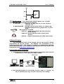
1
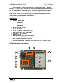
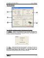
Micro Research Technology Ltd.,Part
801/121 M.8 Phaholyothin Rd., Kookod, Lumlukka, Pathumthani 12130
Tel : (662) 523-9453-4 Fax : (662) 523-9440 www.micro-research.co.th
AVR-SDK2/AVR-SDK2 PLUS
User’s Manual
The AVR-SDK 2 series microcontroller development board is design
base on an easy to use and low cost. This development board can support for
20 Pin MCU (ATTINY2313) and 40 pin MCU(ATMEGA 16/32/8535). The program
can be download into the MCU chip by in-system programming through the
MRT-ISP Loader module. The loader circuit are separate free from the microcontroller board. So you can use this tool to program the another microcontroller
board. Otherwise this development board come with the interface circuit that is
usually used for experiment and development.
Sepcification
•
•
•
•
•
•
•
•
•
•
•
•
•
•
Support device MCU
ATMEGA16
ATMEGA32
ATMEGA8535 (Standard Version)
AT90S2313
MCU X-TAL 8.0 MHz
8 bit LED logic monitor
4 bit PB switch
Piezo speaker
4 CH of voltage reference (0-5 V)
IDC-10 interface port (PORT A-D)
LCD port, 4 bit interface.
RS-232C port
MCU download port (MRT-ISP Loader)
RTC X-TAL 32.768 kHz
Real Time clock, DS1307 (Option)
EEPROM, 24C16 (Option)
For AVR-SDK2 PLUS come with the experiment 2" x 3" proto board
Identify the parts and function
3
4
2
1
12
9
8
10
11
5
6
13
7
1
AVR-SDK2/AVR-SDK2 PLUS
User’s Manual
1.) Power Supply : This development board were prepared two kind of
power supply connector. The first is DC-Jack for DC-Adaptor and the second
is 2 pin terminal block for connect to external power supply. With the bridge
diode circuit at the input part. So you can be supply voltage into the board
by regardless the polarity. In the board there is +5 regulator for system
working voltage. Otherwise this board also prepare 3 pin connector (+5V/
+Vin/Gnd) for easy to supply the extension interface board.
2.) 0-5 Vref : The four channel of adjustable voltage reference
3.)
LCD Port : The LCD port is connect to PORT-B of MCU. There is
configuration as 4-bit data interface as show below
GND
+5 V
Ve
RS
E
RD
D4
D6
D5
D7
The jumper JP16 use to select the RD/WR pin on LCD module. Select
connect to GND for keep the LCD operation in write mode only. Another selection
is PB1 to use as control direction of RD/WR by the microcontroller.
4.)
PORT-A : This port is direct connect from MCU pin to the IDC-10
connector. This pin alignment is an our standard so you can interface to
other interface module of our product.
PA0
PA4
PA1
PA3
PA5
PA6
+5 V
PA7
GND
PA2
2
AVR-SDK2/AVR-SDK2 PLUS
5.)
User’s Manual
PORT-B
: This port is direct connect from MCU pin to the IDC-10
connector. This pin alignment is an our standard so you can interface to
other interface module of our product.
PB0
PB4
PB1
PB3
PB5
PB6
+5 V
PB7
GND
PB2
6.) PORT-C : This port is direct connect from MCU pin to the IDC-10
connector. This pin alignment is an our standard so you can interface to other
interface module of our product.
PC0
PC4
PC1
PC3
PC5
PC6
+5 V
PC7
GND
PC2
7.) PORT-D : This port is direct connect from MCU pin to the IDC-10 connector.
This pin alignment is an our standard so you can interface to other interface
module of our product.
PD0
PD2
PD4
PD1
PD3
PD5
PD6
+5 V
PD7
GND
8.) ISP PORT : The ISP download port by the MRT-ISP Loader
3
AVR-SDK2/AVR-SDK2 PLUS
User’s Manual
9.) RS-232C : The serial communication port for RS-232
GND
Rx
Tx
10.) LED Logic Monitor : The independent circuit of 8 bits logic monitor. This
logic monitor are activate on high logic
Note : The WIP cable was recommented to be the interface cable
4
AVR-SDK2/AVR-SDK2 PLUS
User’s Manual
11.) PB Switch & Piezo Speaker : The 4 bits of PB switch are activate by
logic low. And one channel of piezo speaker
Note : The WIP cable was recommented to be the interface cable
12.) RTC and EEPROM (Option) : The optional RTC chip by DS1307.
Normally to operation with RTC chip the battery backup must be supply for
working during power off. Because this is an optional part so this board will
not have battery in standard version. But we provide the 2 resistor config
as voltage divider (2.75V) to supply the V-BATT of DS-1307. The resistor soldering
behind the board. So when you insert chip DS-1307 on the socket you can
working as well with out the external battery backup. But it is provide for testing
your software during development time. When the operation time of RTC must
going on during system power off. The battery backup must be reguirment and
remove the 2 resistor behind the board.
5
AVR-SDK2/AVR-SDK2 PLUS
User’s Manual
+5 V
8k2
DS 1307
V-BATT
10 k
GND
13.) Working Area : This development board separate into 2 model
depending the type of working area as list below.
◙ AVR-SDK2
: Soldering working area for do user circuit by
soldering iron.
◙ AVR-SDK2 PLUS : Working area by proto board. For testing and
learning interface circuit by jumper wire on proto
board.
We recomment the quick
● WIP-20 : Jumper wire between IDC-10 to the proto
board (20 pcs)
● WPP-20 : Jumper wire the circuit on proto board.
(20 pcs)
● WII-20 : Jumper wire between pin of IDC-10 connector.
Software Program
This development board con be program into the chip by the in-system
programming via the PC parallel.
The AVR-ISP was development by our
engineering team (MRT). The software is operation on windows base operating
system (95/98/2k/Xp). You can find more new upgrade version that may be have
in the future at the www.micro-research.co.th.
Preparation before Operating
1.) Connecting the AT-Download cable between development board and the
PC parallel port. Then apply the supply voltage.
Power Input
MRT-ISP LOADER
2.) The AVR-ISP software is an executing file that ready to running. For
easy to operation just copy into your hard drive and running.
6
AVR-SDK2/AVR-SDK2 PLUS
User’s Manual
AVR-ISP Software
2
1
3
4
5
The AVR-ISP software consist of 5 windows as list below.
1.) Setting : Select the PC parallel port that you connected. Normally the PC
has an LPT1 as standard. And the slide bar to adjust the download speed. The
setting of download speed is depend on the speed of you PC. Fast speed PC may
be need to reduce the download speed.
2.) Chip : Identify the MCU that will be download. Normally in the start up
program there will detect the board automatically. If the software found the
development board the MCU number will report on the windows. However you
can use the Read Signature Chip button to read t6he chip again when
development board was connect after the software execution.
7
AVR-SDK2/AVR-SDK2 PLUS
User’s Manual
3.) File : For open the program file (*.hex) to be download, when the √ Auto
Reload File was check the software will be reload this file automatically when
programming process.
4.) Option : The optional check box to setting the software operation
4.1) Auto Selection Device : This option will be enable the button of Read
Signature Chip for detecting the MCU chip on the development board. To disable
this option the user can be select device under program by your self at the dropdown list of Chip windows.
4.2) Auto Reload File : Option for convenient to download the some
programming file name during development time. This option will be reload the
programming process.
4.3) Bank After Erase : This option to verify the program memory were
bank (FFH) to make sure the chip is ready to program. After doing the process of
Erase operation.
4.4) Verify After Programming : The option to verify, the program-ming
data after programming process.
8
AVR-SDK2/AVR-SDK2 PLUS
User’s Manual
5.) Program : Programming command button consist of.
5.1) Erase
: Erase memory both Flash and EEPROM.
5.2) Program : Program code into Flash memory.
5.3) Fuse Bits : The AVR-ISP software can support to program
many chip. Some chip have the fuse bits function. The button will be enable to
setting the fuse bits function as show below.
After setting the fuse bits function. Then use the Program Fuse Bits button
to write the setting value into the chip. And the Read Fuse Bits button is use for
read back the setting of fuse bits function.
5.4) Lock Bits : To protection the code and data can be setting as show
below.
9
AVR-SDK2/AVR-SDK2 PLUS
User’s Manual
After setting the lock bit function. Then use the Program lock Bit button to
write the chip. And the Read Lock Bit button is use for read back the setting of
Lock bit protection.
5.5) AUTO : After setting all parameter of software. The AUTO button
is recomment to use for download program into chip. This function will be do
sequence for program automatically from Erase, Bank After Erase (if select),
Program then Verify After Programming (if select). The Fuse bit and Lock bit
setting did not effect by the AUTO operation.
Trouble Shooting
Q1) The AVR-ISP software can not reading the signature chip. And report
the message “Target board not found”
A1) This problem occurring when AVR-ISP software can not found
the development target board. Please checking the following.
1.) Make sure the download cable was tightly connected on
both side from PC and development board.
2.) Setting the parallel port mode in Bios Setup to EPP mode
for setting the bios detail please see on your computer
manual
Q2) The AVR-ISP software can be detect the MCU chip. But there is an
error message “Verify Error, Please decrease download speed”
A1) To solving this problem by reduce download speed value on the
setting windows.
10