1
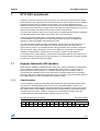
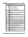
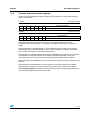
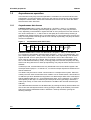
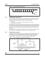
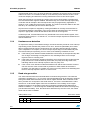
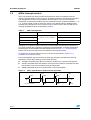
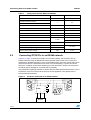
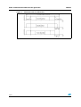
AN2354
Application note
ST10 UART recommendations
Introduction
This application note gives advice on using the ASC peripherals present in the ST10 and in
particular, the asynchronous operations will be considered. A brief guide in the configuration
of the peripheral and how to connect it to an RS232 interface or RS485 network is followed
by an analysis of the sources of timing problems and how to minimize them to allow correct
and error-free communications.
Please refer to the product user manual and datasheet for a full and detailed description of
the functionality.
April 2006
Rev 1
1/21
www.st.com
Contents
AN2354
Contents
1
ST10 ASC peripherals . . . . . . . . . . . . . . . . . . . . . . . . . . . . . . . . . . . . . . . . 3
1.1
1.2
1.3
2
3
4
5
2/21
Register linked with ASC modules . . . . . . . . . . . . . . . . . . . . . . . . . . . . . . . 3
1.1.1
Control register . . . . . . . . . . . . . . . . . . . . . . . . . . . . . . . . . . . . . . . . . . . . 3
1.1.2
Transmit and receive buffer registers . . . . . . . . . . . . . . . . . . . . . . . . . . . . 5
Asynchronous operation . . . . . . . . . . . . . . . . . . . . . . . . . . . . . . . . . . . . . . . 6
1.2.1
Asynchronous data frames . . . . . . . . . . . . . . . . . . . . . . . . . . . . . . . . . . . 6
1.2.2
Asynchronous transmission . . . . . . . . . . . . . . . . . . . . . . . . . . . . . . . . . . . 7
1.2.3
Asynchronous reception . . . . . . . . . . . . . . . . . . . . . . . . . . . . . . . . . . . . . 7
1.2.4
Hardware error detection . . . . . . . . . . . . . . . . . . . . . . . . . . . . . . . . . . . . . 8
1.2.5
Baud rate generation . . . . . . . . . . . . . . . . . . . . . . . . . . . . . . . . . . . . . . . . 8
ASCx interrupt control . . . . . . . . . . . . . . . . . . . . . . . . . . . . . . . . . . . . . . . 10
Connecting an ASC to an RS232 interface . . . . . . . . . . . . . . . . . . . . . . 11
2.1
Introduction . . . . . . . . . . . . . . . . . . . . . . . . . . . . . . . . . . . . . . . . . . . . . . . 11
2.2
Electrical characteristics . . . . . . . . . . . . . . . . . . . . . . . . . . . . . . . . . . . . . . 11
2.3
Connecting ST10F27x to a PC UART RS232 interface . . . . . . . . . . . . . . 12
Connecting ASC to an RS485 network . . . . . . . . . . . . . . . . . . . . . . . . . 13
3.1
Introduction . . . . . . . . . . . . . . . . . . . . . . . . . . . . . . . . . . . . . . . . . . . . . . . 13
3.2
RS485 versus RS232 . . . . . . . . . . . . . . . . . . . . . . . . . . . . . . . . . . . . . . . . 13
3.3
Connecting ST10F27x to an RS485 network . . . . . . . . . . . . . . . . . . . . . 14
UART communication and ST10 clock generation . . . . . . . . . . . . . . . . 15
4.1
Arithmetic error in baud rate setting . . . . . . . . . . . . . . . . . . . . . . . . . . . . . 15
4.2
Send/receive jitter problem . . . . . . . . . . . . . . . . . . . . . . . . . . . . . . . . . . . . 16
4.3
Clock issues . . . . . . . . . . . . . . . . . . . . . . . . . . . . . . . . . . . . . . . . . . . . . . . 16
4.4
Communication channel effects . . . . . . . . . . . . . . . . . . . . . . . . . . . . . . . . 17
4.5
Timing limit of UART communications . . . . . . . . . . . . . . . . . . . . . . . . . . . 17
4.6
Examples . . . . . . . . . . . . . . . . . . . . . . . . . . . . . . . . . . . . . . . . . . . . . . . . . 19
Revision history . . . . . . . . . . . . . . . . . . . . . . . . . . . . . . . . . . . . . . . . . . . 20
AN2354
1
ST10 ASC peripherals
ST10 ASC peripherals
Unlike the old microcontrollers of the ST10 family, two Asynchronous/Synchronous Serial
(ASC) Interfaces are implemented on the latest ST10F27x and ST1025x, one as a standard
peripheral and the other one mapped on the XBUS. The so-called standard module,
instead, is present on all the devices of the ST10 family. The main differences between the
two interfaces are limited to the programming model and interrupt management; in terms of
general functionality and performance the two modules are equivalent.
The rest of the document refers only to the ST10F27x, recalling that all discussion regarding
the standard module is still valid for all the other ST10 microcontrollers.
These peripherals provide serial communication between the ST10F27x and other
microcontrollers, microprocessors or external peripherals. We refer to standard ASC
interface as ASC0 and XBUS ASC interface as ASC1.
The ASC interfaces provide two kind of operations: Asynchronous and Synchronous. In
synchronous mode, data is transmitted or received synchronously to a shift clock. In
asynchronous mode, 8- or 9-bit data transfer, parity generation and a number of stop bits
can be selected. Parity, framing and overrun error detection is provided to increase the
reliability of data transfers. Transmission and reception of data is double-buffered.
For multiprocessor communication, a mechanism to distinguish address from data byte is
included. Testing is supported by a loop-back option. A 13-bit baud rate generator provides
the ASC with a separate serial clock signal.
1.1
Register linked with ASC modules
While ASC0 is enabled by default after the reset, ASC1 must be enabled by setting XPEN
(bit 2 of SYSCON register) and bit 8 of XPERCON register. ASC0 is connected as an
alternate function of bit 10 and bit 11 of PORT3 (P3.10/TXD0, P3.11/RXD0). ASC1 is
connected as an alternate function of bit 6 and bit 7 of PORT8 (P8.6/TXD1 P8.7/RXD1).
Obviously, RX pins must be set as input and TX pins as output, using the standard direction
port register (DP3) for ASC0 and XS1PORT register for ASC1.
1.1.1
Control register
A control register controls the operating mode: S0CON for ASC0 and XS1CON for ASC1.
The first one is bit addressable; the second one is not bit addressable. However, two
additional registers (XS1CONSET and XS1CONCLR) are provided to set and clear single
bits. Setting a bit in XS1CONSET register sets the corresponding bit in XS1CON register;
clearing a bit has no effect. Likewise, setting a bit in XS1CONCLR register clears the
corresponding bit in XS1CON register; clearing a bit has no effect.
SxCON (0 for ASC0 and 1 for ASC1)
15
14
13
12
SxR
SxLB SxBRS SxODD
RW
RW
RW
RW
Reset value: 0000h
11
10
9
8
7
-
SxOE
SxFE
SxPE SxOEN SxFEN SxPEN SxREN SxSTP
SxM
RW
RW
RW
RW
RW
6
RW
5
RW
4
RW
3
RW
2
1
0
3/21
ST10 ASC peripherals
Table 1.
AN2354
SxCON register description
Bit
4/21
Function
SxM
ASCx mode control
0 0 0:8-bit data - synchronous operation
0 0 1:8-bit data - synchronous operation
0 1 0:Reserved. Do not use this combination
0 1 1:7-bit data + parity - asynchronous operation
1 0 0:9-bit data - asynchronous operation
1 0 1:8-bit data + wake up bit - asynchronous operation
1 1 0:Reserved. Do not use this combination
1 1 1:8-bit data + parity - asynchronous operation
SxSTP
Number of stop bit selection asynchronous operation
0:One stop bit
1:Two stop bit
SxREN
Receiver enable bit
0:Receiver disabled
1:Receiver enabled
Reset by hardware after reception of byte in synchronous mode)
SxPEN
Parity check enable bit: asynchronous operation
0:Ignore parity
1:Check parity
SxFEN
Framing check enable bit - asynchronous operation
0:Ignore framing errors
1:Check framing errors
SxOEN
Overrun check enable bit
0:Ignore overrun errors
1:Check overrun errors
SxPE
Parity error flag
Set by hardware on a parity error (SxPEN=’1’). Must be reset by software.
SxFE
Framing error flag
Set by hardware on a framing error (SxFEN=’1’). Must be reset by software.
SxOE
Overrun error flag
Set by hardware on an overrun error (SxOEN=’1’). Must be reset by software.
SxODD
Parity selection bit
0:Even parity (parity bit set on odd number of ‘1’s in data)
1:Odd parity (parity bit set on even number of ‘1’s in data)
SxBRS
Baud rate selection bit
0:Divide clock by reload-value + constant (depending on mode)
1:Additionally reduce serial clock to 2/3rd
SxLB
Loopback mode enable bit
0:Standard transmit/receive mode
1:Loopback mode enabled
SxR
Baud rate generator run bit
0:Baud rate generator disabled (ASCx inactive)
1:Baud rate generator enabled
AN2354
1.1.2
ST10 ASC peripherals
Transmit and receive buffer registers
Writing to the Transmit buffer register SxTBUF (via an instruction or a PEC data transfer)
starts a transmission.
SxTBUF
Reset value: 0000h
15
14
13
12
11
10
9
8
7
6
5
4
3
-
-
-
-
-
-
-
Transmit Data Buffer
-
-
-
-
-
-
-
RW
SxRBUF
2
1
0
Reset value: 0xxxh
15
14
13
12
11
10
9
-
-
-
-
-
-
-
8
7
6
5
4
3
2
1
0
Received Data
R
Only the number of data bit which is determined by the selected operating mode is actually
transmitted. Bits written to positions 9 through 15 of register SxTBUF are always
insignificant. After a transmission is completed, the transmit buffer register is cleared to
0000h.
Data transmission is double-buffered, so a new character may be written to the transmit
buffer register before the transmission of the previous character is complete. This allows
back-to-back transmission of characters without gaps.
Data reception is enabled by the Receiver Enable bit SxREN. After reception of a character
is completed, the received data and, if provided by the selected operating mode, the
received parity bit can be read from the (read-only) Receive Buffer register SxRBUF.
Bits in the upper half of SxRBUF which are not valid in the selected operating mode are read
as zeros.
Data reception is double-buffered, so that reception of a second character may already
begin before the previously received character is read out of the receive buffer register.
The Loop-Back option (selected by bit SxLB) allows the data currently being transmitted to
be received simultaneously in the receive buffer.
5/21
ST10 ASC peripherals
1.2
AN2354
Asynchronous operation
In this document only Asynchronous Operation is considered; to use the ST10F27x ASC
peripherals in synchronous mode, refer to the user manual. Asynchronous mode supports
full-duplex communication, where both transmitter and receiver use the same data frame
format and the same baud rate.
1.2.1
Asynchronous data frames
8-bit data frames either consist of 8 data bits D7...D0 (SxM = ‘001b’) or of 7 data bits
D6...D0 plus an automatically generated parity bit (SxM = ‘011b’). Parity may be odd or
even, depending on bit SxODD in register SxCON. An even parity bit is set if the modulo-2sum of the 7 data bits is ‘1’, in which case an odd parity bit is cleared. Parity checking is
enabled via bit SxPEN (always OFF in 8-bit data mode). If a wrong parity bit is received, the
parity error flag SxPE is set along with the error interrupt request flag. The parity bit itself is
stored in bit SxRBUF.7.
Figure 1.
Asynchronous 8-bit data frames
Start D0
D1
(LSB)
bit
D2
D3
D4
D5
D6
(1st) 2nd
D7 /
Stop
Parity Stop
bIt
bit
9-bit data frames either consist of 9 data bits D8...D0 (SxM = ‘100b’), or of 8 data bits
D7...D0 plus an automatically generated parity bit (SxM = ‘111b’) or of 8 data bits D7...D0
plus a wake-up bit (SxM = ‘101b’). Parity may be odd or even, depending on bit SxODD in
register SxCON. An even parity bit is set, if the modulo-2-sum of the 8 data bits is ‘1’, in
which case an odd parity bit is cleared. Parity checking is enabled via bit SxPEN (always
OFF in 9-bit data and wake-up mode). If a wrong parity bit is received, the parity error flag
SxPE is set along with the error interrupt request flag. The parity bit itself is stored in bit 8 of
SxRBUF.
In wake-up mode, received frames are only transferred to the receive buffer register if the
9th bit (the wake-up bit) is ‘1’. If this bit is ‘0’, no receive interrupt request is activated and no
data is transferred.
This feature may be used to control communication in a multiprocessor system. When the
master processor wants to transmit a block of data to one of several slaves, it first sends out
an address byte which identifies the target slave. An address byte differs from a data byte in
that the additional 9th bit is a '1' for an address byte and a '0' for a data byte, so no slave is
interrupted by a data byte. An address byte interrupts all slaves (operating in 8-bit data +
wake-up bit mode), so each slave can examine the 8 LSBs of the received character (the
address).
The addressed slave switches to 9-bit data mode (by clearing bit SxM.0), which enables it to
also receive the data byte that will be coming (having the wake-up bit cleared). The slaves
that were not being addressed remain in 8-bit data + wake-up bit mode, ignoring the
following data byte.
6/21
AN2354
ST10 ASC peripherals
Figure 2.
Asynchronous 9-bit data frames
Start D0
D1
(LSB)
bit
D2
D3
D4
D5
D6
D7
(1st) 2nd
Stop Stop
bIt
bit
9th
bit
• Data bit D8
• Parity
• Wake-up bit
1.2.2
Asynchronous transmission
The ASCx module uses a modulo 16 counter clocked by fCPU / 2. A transmission begins at
the next overflow of this counter provided that SxR is set and data has been loaded into
SxTBUF. The transmitted data frame consists of three basic elements:
1.
the start bit
2.
the data field (8- or 9-bit, LSB first, including a parity bit, if selected)
3.
the delimiter (1- or 2-stop bit)
Data transmission is double-buffered. When the transmitter is idle, the transmit data loaded
into SxTBUF is immediately moved to the transmit shift register, thus freeing SxTBUF for the
next data to be sent.This is indicated by the transmit buffer interrupt request flag being set.
SxTBUF may now be loaded with the next data, while transmission of the previous one is
still going on.
The transmit interrupt request flag is set before the last bit of a frame is transmitted, that is,
before the first or the second stop bit is shifted out of the transmit shift register.
1.2.3
Asynchronous reception
A reception is initiated by a falling edge (1-to-0 transition) on pin RX, provided that bit SxR
and SxREN are set. The receive data input pin is sampled at 16 times the rate of the
selected baud rate. A majority decision of the 7th, 8th and 9th samples determines the
effective bit value. This avoids erroneous results that may be caused by noise.
Figure 3.
ASCx asynchronous mode interrupt generation
7/21
ST10 ASC peripherals
AN2354
If the detected value is not a '0' when the start bit is sampled, the receive circuit is reset and
waits for the next 1-to-0 transition at RX pin. If the start bit proves valid, the receive circuit
continues sampling and shifts the incoming data frame into the receive shift register.
When the last stop bit is received, the content of the receive shift register is transferred to
the receive data buffer register SxRBUF. Simultaneously, the receive interrupt request flag
is set after the 9th sample in the last stop bit time slot (as programmed), regardless of
whether or not a valid stop bit has been received. The receive circuit then waits for the next
start bit (1-to-0 transition) at the receive data input pin.
Asynchronous reception is stopped by clearing bit SxREN. A currently received frame is
completed including the generation of the receive interrupt request and an error interrupt
request, if appropriate. A start bit that follows this frame is not recognized.
In wake-up mode, received frames are only transferred to the receive buffer register, if the
9th bit (the wake-up bit) is ‘1’. If this bit is ‘0’, no receive interrupt request is activated and no
data is transferred.
1.2.4
Hardware error detection
To improve the safety of serial data exchange, the serial channels provide an error interrupt
request flag, which indicates the presence of an error, and three (selectable) error status
flags in register SxCON, which indicate which error has been detected during reception.
Upon completion of a reception, the error interrupt request flag is set simultaneously with
the receive interrupt request flag, if one or more of the following conditions are met:
1.2.5
●
If the framing error detection enable bit SxFEN is set and any of the expected stop bits
are not high, the framing error flag SxFE is set, indicating that the error interrupt
request is due to a framing error.
●
If the parity error detection enable bit SxPEN is set in parity bit receive modes and the
parity check on the received data bit proves false, the parity error flag SxPE is set,
indicating that the error interrupt request is due to a parity error.
●
If the overrun error detection enable bit SxOEN is set and the last character received
was not read out of the receive buffer by software or PEC transfer at the time the
reception of a new frame is complete, the overrun error flag SxOE is set indicating that
the error interrupt request is due to an overrun error.
Baud rate generation
The serial channels have their own dedicated 13-bit baud rate generator. The baud rate
generator is clocked by fCPU / 2. The timer counts downwards and can be started or stopped
through the Baud Rate Generator Run bit SxR in register SxCON. Each underflow of the
timer provides one clock pulse to the serial channel. The timer is reloaded with the value
stored in its 13-bit reload register each time it underflows. The resulting clock is again
divided according to the operating mode and controlled by the Baud Rate Selection bit
SxBRS. If SxBRS = ‘1’, the clock signal is additionally divided to two-thirds of its frequency
(see formulas and table). Thus, the baud rate is determined by the CPU clock, the reload
value and the value of SxBRS.
S0BG (FEB4h / 5Ah)
15
14
13
-
-
-
12
SFR
11
10
9
8
Reset value: 0000h
7
6
Baud Rate
RW
8/21
5
4
3
2
1
0
AN2354
ST10 ASC peripherals
For asynchronous operation, the baud rate generator provides a clock with 16 times the rate
of the established baud rate. Every received bit is sampled at the 7th, 8th and 9th cycle of
this clock. The baud rate for asynchronous operation of serial channels and the required
reload value for a given baud rate can be determined by the following formulas:
fCPU
BAsync =
16 x [2 + (SxBRS)] x [(SxBRL) + 1]
fCPU
SxBRL = (
)-1
16 x [2 + (SxBRS)] x BAsync
(SxBRL) represents the content of the reload register, taken as unsigned 13-bit integer and
(SxBRS) represents the value of bit SxBRS (‘0’ or ‘1’), taken as integer.
Using the above equation, the maximum baud rate can be calculated for any given clock
speed. It follows a table of values for baud rate versus reload register value for SxBRS = 0
and SxBRS = 1.
Table 2.
Common baud rate settings and deviation error
S1BRS = ‘0’, fCPU = 64 MHz
S1BRS = ‘1’, fCPU = 64 MHz
Baud rate
Deviation error
Reload value
Deviation error
Reload value
2 Mbaud
0%
0000H
-
-
500 Kbaud
0%
0003H
-
-
115.2 Kbaud
+2.12% / -3.55%
00010H / 0011H
+5.22% / -3.55%
000AH / 000BH
57.6 Kbaud
+2.12% / -0.79%
0021H / 0022H
+0.64% / -3.55%
0016H / 0017H
38.4 Kbaud
+0.16% / -1.73%
0033H / 0034H
+2.12% / -0.79%
0021H / 0022H
19.2 Kbaud
+0.16% / -0.79%
0067H / 0068H
+0.64% / -0.79%
0044H / 0045H
9600 baud
+0.16% / -0.32%
00CFH / 00D0H
+0.64% / -0.08%
0089H / 008AH
4800 baud
+0.16% / -0.08%
019FH / 01A0H
+0.28% / -0.08%
0114H / 0115H
2400 baud
+0.04% / -0.08%
00CFH / 00D0H
+0.10% / -0.08%
022AH / 022BH
1200 baud
+0.04% / -0.02%
0681H / 0682H
+0.01% / -0.08%
0456H / 0457H
600 baud
+0.01% / -0.02%
0D04H / 0D05H
+0.01% / -0.03%
08ADH / 08AEH
244 baud
-0.06%
1FFFH
+0.01% / -0.01%
1157H / 1158H
On the ST10 side, the baud rate is derived from the CPU frequency (fCPU). The fCPU is a
multiple (use of the internal PLL) of an external input clock which is generally different from
the ones used in a PC to generate the UART clock. Therefore, there is a deviation error
between the standard baud rate (reference being the PC) and the baud rate of the ST10
ASCx. This clock mismatch may lead to a reduction of tolerance as discussed in more detail
in Section 4.1: Arithmetic error in baud rate setting.
9/21
ST10 ASC peripherals
1.3
AN2354
ASCx interrupt control
ASCx can generate four kinds of interrupt request as a result of four different events:
Transmit, transmit buffer, receive and error. As already mentioned, the interrupt generation
and management of ASC1 is quite different from the ASC0. In the ST10F27x all the
peripherals connected on the XBUS share four IRQ lines and four registers (XIRxSEL, x = 0,
1, 2, 3) are provided in order to select the source of the XBUS interrupt. Whereas ASC1
provides four interrupt lines on the interrupt vectors, ASC0 uses its own four IRQ lines to
manage the different events as illustrated in Table 3:
Table 3.
ASCx interrupt lines
Interrupt vectors
ASC1 interrupt lines
ASC0 interrupt lines
Receive
S0RINT
Transmit
XP0INT, XP1INT, XP2INT
S0TINT
Transmit Buffer
S0TBINT
Error
XP3INT
S0EINT
In addition, the registers used by ASC0 are bit addressable whereas XBUS registers are
not. Other registers are provided to emulate the bit-addressability, as already explained in
the description of XS1CONSET and XS1CONCLR (see Section 1.1.1: Control register).
Please refer to the user manual for more details on interrupt generation.
An interrupt error request flag is set if one of the events described in Section 1.2.4:
Hardware error detection occurs.
For normal operation (other than the error interrupt), the ASCx provides three interrupt
requests to control data exchange via this serial channel:
●
SxTBIR is activated when data is moved from SxTBUF to the transmit shift register.
●
SxTIR is activated before the last bit of an asynchronous frame is transmitted or after
the last bit of a synchronous frame has been transmitted.
●
SxRIR is activated when the received frame is moved to SxRBUF.
ASCx asynchronous mode interrupt generation
Asynchronous mode
10/21
S0RIR
SxTIR
SxTBIR
S0RIR
Stop
Start
SxTBIR
Stop
Idle
Start
SxTBIR
SxTIR
Start
SxTIR
Stop
Figure 4.
Idle
S0RIR
AN2354
Connecting an ASC to an RS232 interface
2
Connecting an ASC to an RS232 interface
2.1
Introduction
The RS232 specification dates back to 1962, when it was first released by the EIA
(Electronic Industries Association). The specification has changed over time, incorporating
higher data rates and closing the compatibility gaps between TIA (Telecommunication
Industry Association) and international (ITU, ISO) standards. The current version of the
RS232RS232 specification is EIA/TIA-232-F, dated October 1997.
The RS232 link was initially intended to support modem and printer applications on IBM
PCs, however, it now enables a variety of peripherals to communicate with PCs. The RS232
standard was defined as a single-ended standard for increasing serial-communication
distances at low baud rates (< 20 Kbit/s).
2.2
Electrical characteristics
Table 4.
RS232 major electrical characteristics
Parameter
Conditions
Min.
Driver output voltage open circuit
Driver output voltage loaded
Slew rate
Unit
25
3kΩ < RL < 7kΩ
V
±5
±15
4
30
V/µs
2500
pF
7
kΩ
Maximum load capacitance
Receiver input resistance
Max.
3
Receiver input threshold
Output = Mark (Logic 1)
-3
V
Output = Space (Logic 0)
3
The major electrical characteristics of the RS232 standard are summarized in Table 4
above. Typical RS232 transmissions seldom exceed 30 meters (often only a few meters) for
two reasons. Firstly, the difference between transmitted levels (±5V) and receive levels
(±3V) allows only 2V of common-mode rejection. Secondly, the distributed capacitance of a
longer cable can degrade slew rates by exceeding the maximum specified load (2500pF).
Because the RS232 was designed as a point-to-point rather than a multidrop interface, its
drivers are specified for single loads from 3k to 7k ohm.
A typical RS232 signal fluctuates between positive and negative. Although the RS232 data
is inverted, an overall translation from TTL/CMOS levels of the ST10F27x to RS232 as well
as from RS232 to the TTL/CMOS levels of the ST10F27x is needed. A very common level
translator is the ST232A, a device which includes a charge pump to generate ±12V from a
single 5V supply, as well as two receivers and two transmitters in a single package. Please
refer to the product datasheet for the full device description.
11/21
Connecting an ASC to an RS232 interface
2.3
AN2354
Connecting ST10F27x to a PC UART RS232 interface
A typical application involves a connection between a microcontroller and a personal
computer. A PC UART interface uses a DB9 connector which contains more than only two
signals and the ground. A certain number of other signals (such as RTS, DTR) are
requested to set up a protocol between the PC and the peripheral (that is, modem). These
signals are not necessarily required and often the serial transfers are performed using only
Rx and Tx signals.
Figure 5 below shows an example of a connection between two ASCx peripherals and two
RS232 interfaces through an ST232A. The value of the capacitors needed for the charge
pump circuitry is 0.1µF.
PC RS232 interfaces typically use baud rates of 9600...115200 bit/s. Since the clock
sources are different, there is a deviation error between the standard baud rate and the
baud rate of ST10F27x ASCx. This clock mismatch may lead to a reduction of tolerance as
is discussed in more detail in Section 4.1: Arithmetic error in baud rate setting.
Figure 5.
ST10F27x connected to PC UART interfaces
+5V
+
+
+
TxD0
TxD1
ST10F27x
RxD0
RxD1
12/21
1
3
+
16
2
+
4
5
6
ST232A
11
14
10
7
12
9
13
8
15
DB9
DB9
AN2354
Connecting ASC to an RS485 network
3
Connecting ASC to an RS485 network
3.1
Introduction
An RS232 interface connects one DTE (data terminal equipment) to one DCE (data
communication equipment) at a maximum speed of 20 Kbit/s with a maximum cable length
of 30 meters. This was sufficient early on when almost all computer equipment was
connected by modems but, soon after, interfaces capable of one or more of the following
were in demand:
●
Connecting DTE's directly without the need for modems
●
Connecting several DTE's in a network structure
●
Communicating over longer distances
●
Communicating at faster speeds
RS485 is the most versatile communication standard in the standard series defined by the
EIA, as it performs well on all four points. Thus RS485 is currently a widely-used
communication interface in data acquisition and control applications where multiple nodes
communicate with each other.
3.2
RS485 versus RS232
One of the main problems with RS232 is the lack of immunity against noise on the signal
lines. The transmitter and receiver compare the voltages of the data and handshake lines
with one common zero line. Shifts in the ground level can have disastrous effects. Therefore,
the trigger level of the RS232 interface is set relatively high at ±3V (Table 3). Noise is easily
picked up and limits both the maximum distance and communication speed. On the
contrary, a common zero as a signal reference does not exist with RS485. A difference of
several volts in the ground level of the RS485 transmitter and receiver does not cause any
problems. The RS485 signals are floating and each signal is transmitted over a B line and
an A line. The RS485 receiver compares the voltage difference between both lines,
instead of the absolute voltage level on a signal line. This works well and prevents the
existence of ground loops, a common source of communication problems. The best results
are achieved if the B and A lines are twisted.
When the cable is twisted, we see that in some parts of the signal lines the direction of the
noise current is the opposite from the current in other parts of the cable. Consequently, the
resulting noise current is many factors lower than with an ordinary straight cable. Shielding
tries to isolate the signal lines from hostile magnetic fields. Twisted pairs in RS485
communication, however, add immunity, which is a much better way to fight noise.
Differential signals and twisting allow RS485 to communicate over much longer distances
than achievable with RS232. With RS485, communication distances of 1200 meters are
possible.
Differential signal lines also allow higher bit rates than possible with non-differential
connections. Therefore, RS485 can overcome the practical communication speed limit of
RS232. Currently, RS485 drivers are produced that can attain a bit rate of 35 Mbit/s.
13/21
Connecting ASC to an RS485 network
Table 5.
AN2354
Comparison between RS232 and RS485
Parameter
RS232
RS485
No
Yes
1
32
Full/Half Duplex
Half Duplex
Network topology
Point-to-Point
Multipoint
Maximum distance
30m
1200m
20 Kbit/s
35 Mbit/s
30V/µs
-
Differential
Maximum number of drivers
Maximum number of receivers
Modes of operation
Maximum speed
Maximum slew rate
Receiver input resistance
3..7kΩ
Driver load impedance
3.3
Receiver input sensitivity
±3V
Receiver input range
±15V
Maximum driver output voltage
±25V
Minimum driver output voltage
±5V
>12kΩ
54Ω
±200mV
-7V..+12V
±1.5V
Connecting ST10F27x to an RS485 network
Figure 6 on page 14 shows an example of connection between the ST10F27x and an
RS485 network through an RS485 transceiver (ST485). Please refer to the component
datasheet for detailed information. Since each RS485 system must have a driver that can be
disconnected from the transmission line when it is not transmitting, a generic ST10F27x
GPIO pin, in addition to the ASCx standard pins TxDx and RxDx, can be connected to the
ST485 DE (Driver Enable) pin to provide this functionality.
The problematic regarding data rate in relation with the cable characteristics and the correct
termination of the bus are beyond the purpose of this application note (please refer to
EIA/TIA-485 specifications).
Figure 6.
ST10F27x connected to an RS485 network
+5V
6
7
8
2
5
ST485
3
1
Rx
Tx
4
DE
ST10F27x
14/21
AN2354
4
UART communication and ST10 clock generation
UART communication and ST10 clock generation
The timing of a UART transmission is influenced by various factors. The baud rate of a
UART is usually configured by integer values – the arithmetic rounding error leads to baud
rate deviations (see Table 2: Common baud rate settings and deviation error). The
architecture of ST10F27x UARTs furthermore leads to intrinsic delays at the sending UART.
Moreover, the qualities of the clocks of the communication partners must be considered.
Clock drift and jitter influence the baud rate and the instant of communication start. The
network itself introduces some issues due to the finite channel bandwidth that reduces the
useful time interval to correctly sample the level of the bit. This section quantifies these
timing deviations separately, goes on to calculate the maximum baud rate deviation and
provides some examples at the end.
4.1
Arithmetic error in baud rate setting
The baud rate depends on the frequency of the CPU (fCPU). The baud rate is set by
choosing a value SxBRL (ASCx Baud Rate Setting) as follows:
f CPU
SxBRL = ----------------------------------------------------------------------–1
16 × [ 2 + SxBRS ] × baud
Since SxBRL must be an integer, the value that rounds up the desiderated baud rate is:
SxBRL up =
f CPU
---------------------------------------------------------------------- –1
16 × [ 2 + SxBRS ] × baud
while the value that rounds down the desiderated baud rate is:
SxBRL down =
f CPU
---------------------------------------------------------------------16 × [ 2 + SxBRS ] × baud
So the maximum error that is committed is:
1 ( SxBRL down – SxBRL up )
× [ 2 + SxBRS ] × baud
--- -------------------------------------------------------------------------- = 8
------------------------------------------------------------------2
SxBRL down
f CPU
Table 2: Common baud rate settings and deviation error on page 9 reports the arithmetic
error committed when one of the standard baud rates is set, assuming the CPU clock to be
64 MHz. The last formula clearly shows that:
●
the deviation error is directly proportional to the desiderated baud rate;
●
choosing appropriately SxBRS, the error is always less than 2.12%.
15/21
UART communication and ST10 clock generation
4.2
AN2354
Send/receive jitter problem
At initialization of the ASCx, the baud rate generator is started. Running at a frequency
corresponding to the configured baud rate, the baud rate generator periodically generates
ticks which are possible start events of a message bit. When the ASCx receives a transmit
signal, it starts the transmission at the next tick from the baud rate generator. Thus,
depending on the internal state of the baud rate generator, the transmission of a message
may be delayed up to the interval time of two subsequent baud rate generator ticks. The
state of the baud rate generator cannot be read, leading to an indeterministic send delay
jitter:
1
0 ≤t jitter ≤ -------------baud
Subsequent transmissions may not be affected by this send jitter, however if transmissions
can start at particular instants, the send jitter jeopardizes the achievable accuracy for this
send instant.
A similar situation exists for reception: A start condition is detected at the first tick from the
clock that feeds the module after the falling edge, leading to a indeterministic receive delay
jitter:
1
0 ≤t jitter ≤ ---------------------------16 ⋅ baud
4.3
Clock issues
Usually components performing a UART communication are set apart from each other and
are clocked by different clock sources. These clock sources are not absolutely free from
errors. Finite accuracy, drift and jitter are common problems of clock generation.
In general, a standard, low cost, ceramic resonator with ±0.5% accuracy and a further
±0.5% drift over temperature and life can be used for the clock source at both ends of the
link. On the other hand, a standard crystal oscillator usually provides 20ppm frequency
tolerance and 100ppm frequency stability.
Another issue related to the clock is the use of a PLL (Phase Locked Loop). PLL is used in
the ST10F27x to achieve higher internal clock frequencies but it introduces a small transient
phase shift called jitter. In the ST10F27x the single period jitter is, in the worst case, ±500ps
whereas the long term jitter can be maximum ±4.5ns. For more details regarding PLL jitter,
please refer to the product datasheet.
16/21
AN2354
4.4
UART communication and ST10 clock generation
Communication channel effects
In reception, the receiver must sample ideally in the middle of the bit; it is not desirable to
sample close to the bit transition point. The main reason for this is the finite (and typically
slow) transmission rise and fall times are made even slower if overly capacitive cabling is
used. A long bus incurs high attenuation, which reduces noise margin, making it more
important to sample when the bit level has settled. It is difficult to quantify a worst case
acceptable sampling range across a bit's period.
Usually, RS232 communications are performed over very short distances; regarding RS485
as an empirical law between baud rate and cable length may help:
1200
length ( m ) = -----------------------------------------------baudrate 2
1 + ⎛ --------------------------⎞
⎝ 250 ⎠
Baud rate is expressed in Kbit/s.
4.5
Timing limit of UART communications
This section investigates the maximum allowed deviation of the baud rates of sender and
receiver for correct communication.
The single bit cells of a UART frame are analyzed and the maximum admissible delay until
bits are detected incorrectly is calculated. Sender and receiver use baud rates that deviate
from the ideal baud rate. The worst case is a slow receiver trying to listen to a sender
transmitting too fast. The other extreme with a slow transmitter and a fast receiver is less
critical. For correct transmission, the instant of the detection point of the last bit cell of a
frame must be prior the instant of the end of the transmitted UART frame.
The condition for a successful communication is given in the following equation:
1
n – --2
n
------------------------------ – ---------------------------- ≤ 0
Baudrate s Baudrate f
n is the UART frame length in bit cells including start, parity and stop bits. By rewriting the
last equation it follows that the ratio between Baud Ratefast and Baud Rateslow must fulfil a
condition in order to guarantee correct communication:
Baudrate
n
-----------------------------f- ≤ -----------1
Baudrate s
n – --2
For example, considering an 8N1 (8 data bits, no parity, 1 stop bit) frame, it follows that the
Baud Ratefast can be up to 5.26% higher than Baud Rateslow in order to communicate
correctly.
17/21
UART communication and ST10 clock generation
Figure 7.
18/21
Maximum baud rate differences
AN2354
AN2354
4.6
UART communication and ST10 clock generation
Examples
As a first example, we consider a frame 8N1 received by an ST10F27x connected with a
PC, baud rate is 115200 bit/s, the connection is made through a simple straight cable 2
meters long, the connectors are standard DB9 and an ST232 is used as level translator.
In this case, reading Table 2 on page 9, if we choose a reload value of 0011h and
SxBRS = 0, the arithmetic error is -3.55%. In this condition, the PC UART is faster than the
ST10 UART. The transfers from the PC to the ST10 correspond to the worst case, being a
fast transmitter and a slow receiver. The maximum receive jitter is 1/(16 * 115200) seconds
or in terms of percentage of the frame about 0.6%. If the reference clock is obtained through
a standard ceramic resonator, we can assume a further 0.5% error whereas the PLL jitter is
negligible. Finally, supposing that the capacitive effect of the cable reduces the percentage
of the bit time available for sampling of about the 5% (very worst case), another 0.5% should
be added to our computation.
In Section 4.5 it has been shown that an 8N1 frame allows a difference of 5.26% between
the baud rate of the fast transmitter and the slow receiver in order to communicate correctly.
Even if all the factors described above sum up in a very unlucky case, a remaining safety
margin of 0.1% allows an error-free communication.
As another example, we consider an 8E1 frame (8 data bits, even parity, 1 stop bit) sent by
ST10F27x on an RS485 network 100 meters long (twisted pair cable), baud rate is 2 Mbit/s
and an ST485 is the transceiver.
In this case there is no arithmetic error but the effects of the cable and the clock issues like
the jitter have more impact. It’s difficult to quantify those effects; in any case, the clock
tolerance of 4.76% (see Section 4.5) also allows error-free communications with
significative capacitive cable effects and not very stable clock references.
Conclusion
Keeping in mind all the possible sources of problems and checking all the points described,
correct UART communications can be achieved in most cases.
19/21
Revision history
5
AN2354
Revision history
Table 6.
20/21
Document revision history
Date
Revision
27-Apr-2006
1
Changes
Initial release
AN2354
Please Read Carefully:
Information in this document is provided solely in connection with ST products. STMicroelectronics NV and its subsidiaries (“ST”) reserve the
right to make changes, corrections, modifications or improvements, to this document, and the products and services described herein at any
time, without notice.
All ST products are sold pursuant to ST’s terms and conditions of sale.
Purchasers are solely responsible for the choice, selection and use of the ST products and services described herein, and ST assumes no
liability whatsoever relating to the choice, selection or use of the ST products and services described herein.
No license, express or implied, by estoppel or otherwise, to any intellectual property rights is granted under this document. If any part of this
document refers to any third party products or services it shall not be deemed a license grant by ST for the use of such third party products
or services, or any intellectual property contained therein or considered as a warranty covering the use in any manner whatsoever of such
third party products or services or any intellectual property contained therein.
UNLESS OTHERWISE SET FORTH IN ST’S TERMS AND CONDITIONS OF SALE ST DISCLAIMS ANY EXPRESS OR IMPLIED
WARRANTY WITH RESPECT TO THE USE AND/OR SALE OF ST PRODUCTS INCLUDING WITHOUT LIMITATION IMPLIED
WARRANTIES OF MERCHANTABILITY, FITNESS FOR A PARTICULAR PURPOSE (AND THEIR EQUIVALENTS UNDER THE LAWS
OF ANY JURISDICTION), OR INFRINGEMENT OF ANY PATENT, COPYRIGHT OR OTHER INTELLECTUAL PROPERTY RIGHT.
UNLESS EXPRESSLY APPROVED IN WRITING BY AN AUTHORIZE REPRESENTATIVE OF ST, ST PRODUCTS ARE NOT DESIGNED,
AUTHORIZED OR WARRANTED FOR USE IN MILITARY, AIR CRAFT, SPACE, LIFE SAVING, OR LIFE SUSTAINING APPLICATIONS,
NOR IN PRODUCTS OR SYSTEMS, WHERE FAILURE OR MALFUNCTION MAY RESULT IN PERSONAL INJURY, DEATH, OR
SEVERE PROPERTY OR ENVIRONMENTAL DAMAGE.
Resale of ST products with provisions different from the statements and/or technical features set forth in this document shall immediately void
any warranty granted by ST for the ST product or service described herein and shall not create or extend in any manner whatsoever, any
liability of ST.
ST and the ST logo are trademarks or registered trademarks of ST in various countries.
Information in this document supersedes and replaces all information previously supplied.
The ST logo is a registered trademark of STMicroelectronics. All other names are the property of their respective owners.
© 2006 STMicroelectronics - All rights reserved
STMicroelectronics group of companies
Australia - Belgium - Brazil - Canada - China - Czech Republic - Finland - France - Germany - Hong Kong - India - Israel - Italy - Japan Malaysia - Malta - Morocco - Singapore - Spain - Sweden - Switzerland - United Kingdom - United States of America
www.st.com
21/21