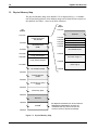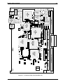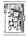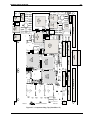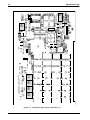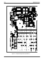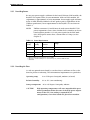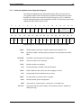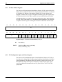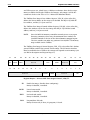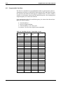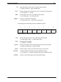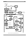
1
BajaPPC-750 PowerPC-Based, Single-Board Computer User’s Manual May 2002 Artesyn Communication Products 8310 Excelsior Dr. Madison, WI 53717 Web Site: Sales: Technical Support: BajaPPC-750 User’s Manual—Artesyn Part Number: www.artesyncp.com (800) 356-9602 (800) 327-1251 0002M621-15 BajaPPC-750 PowerPC-Based, Single-Board Computer User’s Manual May 2002 The information in this manual has been checked and is believed to be accurate and reliable. HOWEVER, NO RESPONSIBILITY IS ASSUMED BY ARTESYN COMMUNICATION PRODUCTS FOR ITS USE OR FOR ANY INACCURACIES. Specifications are subject to change without notice. ARTESYN COMMUNICATION PRODUCTS DOES NOT ASSUME ANY LIABILITY ARISING OUT OF USE OR OTHER APPLICATION OF ANY PRODUCT, CIRCUIT, OR PROGRAM DESCRIBED HEREIN. This document does not convey any license under Artesyn Communication Products patents or the rights of others. Artesyn and the Artesyn logo are registered trademarks of Artesyn Technologies and are used by Artesyn Communication Products under licence from Artesyn Technologies. All other trademarks are property of their respective owners. Revision History Revision Level Principal Changes Publication Date Board Rev. 0002M621-A First publication July 1999 1 0002M621-10 Update jumper settings October 1999 1 0002M621-11 Updated PCB artwork February 2000 21 0002M621-12 Update Fig. 2-5 and Section 4.4 July 2000 21 0002M621-13 Remove reference to software reset bit November 2000 21 0002M621-14 Update for board revision August 2001 22 0002M621-15 New board rev. & update Table 10-3 May 2002 23 Copyright © 1999–2002 Artesyn Communication Products All rights reserved. Regulatory Agency Warnings & Notices The Artesyn BajaPPC-750 is certified by the Federal Communications Commission (FCC) according to Title 47 of the Code of Federal Regulations, Part 15. The following information is provided as required by this agency. FCC Rules and Regulations – Part 15 This equipment has been tested and found to comply with the limits for a Class B digital device, pursuant to part 15 of the FCC Rules. These limits are designed to provide reasonable protection against harmful interference in a residential installation. This equipment generates, uses and can radiate radio frequency energy and, if not installed and used in accordance with the instructions, may cause harmful interference to radio communications. However, there is no guarantee that interference will not occur in a particular installation. If this equipment does cause harmful interference to radio or television reception, which can be determined by turning the equipment off and on, the user is encouraged to try to correct the interference by one or more of the following measures: • Reorient or relocate the receiving antenna • Increase the separation between the equipment and receiver • Connect the equipment into an outlet on a circuit different from that to which the receiver is connected • Consult the dealer or an experienced radio/TV technician for help CAUTION. Making changes or modifications to the BajaPPC-750 without the explicit consent of Artesyn Communication Products could invalidate the user’s authority to operate this equipment. Contents 1. Overview 1.1 Components and Features . . . . . . . . . . . . . . . . . . . . . . . . . . . . . . . . . . . . . . . . . . . . . . . . . . . . 1-1 1.2 Functional Description . . . . . . . . . . . . . . . . . . . . . . . . . . . . . . . . . . . . . . . . . . . . . . . . . . . . . . . 1-3 1.3 Physical Memory Map . . . . . . . . . . . . . . . . . . . . . . . . . . . . . . . . . . . . . . . . . . . . . . . . . . . . . . . 1-4 1.4 Additional Information . . . . . . . . . . . . . . . . . . . . . . . . . . . . . . . . . . . . . . . . . . . . . . . . . . . . . . . 1-6 1.4.1 Product Certifications . . . . . . . . . . . . . . . . . . . . . . . . . . . . . . . . . . . . . . . . . . . . . . . . 1-6 1.4.2 Terminology and Notation . . . . . . . . . . . . . . . . . . . . . . . . . . . . . . . . . . . . . . . . . . . . 1-7 1.4.3 Technical References . . . . . . . . . . . . . . . . . . . . . . . . . . . . . . . . . . . . . . . . . . . . . . . . . 1-7 2. Setup 2.1 Electrostatic Discharge . . . . . . . . . . . . . . . . . . . . . . . . . . . . . . . . . . . . . . . . . . . . . . . . . . . . . . . 2-1 2.2 BajaPPC-750 Circuit Board . . . . . . . . . . . . . . . . . . . . . . . . . . . . . . . . . . . . . . . . . . . . . . . . . . . . 2-2 2.2.1 Component Maps and Jumpers . . . . . . . . . . . . . . . . . . . . . . . . . . . . . . . . . . . . . . . . .2-2 2.2.2 Serial Numbers . . . . . . . . . . . . . . . . . . . . . . . . . . . . . . . . . . . . . . . . . . . . . . . . . . . . 2-12 2.2.3 Connectors . . . . . . . . . . . . . . . . . . . . . . . . . . . . . . . . . . . . . . . . . . . . . . . . . . . . . . .2-12 2.2.4 Reset/Interrupt Switch . . . . . . . . . . . . . . . . . . . . . . . . . . . . . . . . . . . . . . . . . . . . . . . 2-13 2.2.5 LED . . . . . . . . . . . . . . . . . . . . . . . . . . . . . . . . . . . . . . . . . . . . . . . . . . . . . . . . . . . . . 2-13 2.2.6 Optional VMEbus Configurations . . . . . . . . . . . . . . . . . . . . . . . . . . . . . . . . . . . . . . . 2-14 2.3 BajaPPC-750 Setup . . . . . . . . . . . . . . . . . . . . . . . . . . . . . . . . . . . . . . . . . . . . . . . . . . . . . . . . . 2-14 2.3.1 Providing Power . . . . . . . . . . . . . . . . . . . . . . . . . . . . . . . . . . . . . . . . . . . . . . . . . . . 2-15 2.3.2 Providing Air Flow . . . . . . . . . . . . . . . . . . . . . . . . . . . . . . . . . . . . . . . . . . . . . . . . . . 2-15 2.4 Operational Checks . . . . . . . . . . . . . . . . . . . . . . . . . . . . . . . . . . . . . . . . . . . . . . . . . . . . . . . . 2-16 2.5 Reset Methods . . . . . . . . . . . . . . . . . . . . . . . . . . . . . . . . . . . . . . . . . . . . . . . . . . . . . . . . . . . . 2-16 2.6 Troubleshooting . . . . . . . . . . . . . . . . . . . . . . . . . . . . . . . . . . . . . . . . . . . . . . . . . . . . . . . . . . . 2-17 2.6.1 Technical Support . . . . . . . . . . . . . . . . . . . . . . . . . . . . . . . . . . . . . . . . . . . . . . . . . .2-18 2.6.2 Service Information . . . . . . . . . . . . . . . . . . . . . . . . . . . . . . . . . . . . . . . . . . . . . . . . . 2-18 3. Central Processing Unit 3.1 Processor Reset . . . . . . . . . . . . . . . . . . . . . . . . . . . . . . . . . . . . . . . . . . . . . . . . . . . . . . . . . . . . . 3-2 3.2 Processor Initialization. . . . . . . . . . . . . . . . . . . . . . . . . . . . . . . . . . . . . . . . . . . . . . . . . . . . . . . . 3-2 3.2.1 Hardware Implementation Dependent Register . . . . . . . . . . . . . . . . . . . . . . . . . . . . . 3-3 3.2.2 Machine State Register . . . . . . . . . . . . . . . . . . . . . . . . . . . . . . . . . . . . . . . . . . . . . . . 3-4 3.3 Exception Handling . . . . . . . . . . . . . . . . . . . . . . . . . . . . . . . . . . . . . . . . . . . . . . . . . . . . . . . . . 3-6 3.4 Interrupt Handling . . . . . . . . . . . . . . . . . . . . . . . . . . . . . . . . . . . . . . . . . . . . . . . . . . . . . . . . . . 3-7 0002M621-15 i 3.5 Bus Speed . . . . . . . . . . . . . . . . . . . . . . . . . . . . . . . . . . . . . . . . . . . . . . . . . . . . . . . . . . . . . . . . .3-8 3.6 Cache Memory . . . . . . . . . . . . . . . . . . . . . . . . . . . . . . . . . . . . . . . . . . . . . . . . . . . . . . . . . . . . .3-8 3.6.1 Integrated Level 2 Cache . . . . . . . . . . . . . . . . . . . . . . . . . . . . . . . . . . . . . . . . . . . . . .3-9 3.7 JTAG/COP Interface. . . . . . . . . . . . . . . . . . . . . . . . . . . . . . . . . . . . . . . . . . . . . . . . . . . . . . . . .3-10 3.8 Debug Header . . . . . . . . . . . . . . . . . . . . . . . . . . . . . . . . . . . . . . . . . . . . . . . . . . . . . . . . . . . .3-11 4. On-Card Memory Configuration 4.1 MPC106 Memory Interface . . . . . . . . . . . . . . . . . . . . . . . . . . . . . . . . . . . . . . . . . . . . . . . . . . . .4-1 4.2 Boot Memory Configuration . . . . . . . . . . . . . . . . . . . . . . . . . . . . . . . . . . . . . . . . . . . . . . . . . . .4-2 4.3 User Flash . . . . . . . . . . . . . . . . . . . . . . . . . . . . . . . . . . . . . . . . . . . . . . . . . . . . . . . . . . . . . . . . .4-3 4.4 On-Card SDRAM. . . . . . . . . . . . . . . . . . . . . . . . . . . . . . . . . . . . . . . . . . . . . . . . . . . . . . . . . . . .4-3 4.4.1 SDRAM Configuration . . . . . . . . . . . . . . . . . . . . . . . . . . . . . . . . . . . . . . . . . . . . . . . .4-4 4.4.2 SDRAM Timing . . . . . . . . . . . . . . . . . . . . . . . . . . . . . . . . . . . . . . . . . . . . . . . . . . . . .4-4 4.5 Real-Time Clock . . . . . . . . . . . . . . . . . . . . . . . . . . . . . . . . . . . . . . . . . . . . . . . . . . . . . . . . . . . .4-6 4.6 Nonvolatile Memory Map . . . . . . . . . . . . . . . . . . . . . . . . . . . . . . . . . . . . . . . . . . . . . . . . . . . . .4-8 5. PMC/PCI Interface 5.1 Features . . . . . . . . . . . . . . . . . . . . . . . . . . . . . . . . . . . . . . . . . . . . . . . . . . . . . . . . . . . . . . . . . .5-1 5.2 PMC Module Installation. . . . . . . . . . . . . . . . . . . . . . . . . . . . . . . . . . . . . . . . . . . . . . . . . . . . . .5-2 5.3 PCI Bridge Configuration Registers . . . . . . . . . . . . . . . . . . . . . . . . . . . . . . . . . . . . . . . . . . . . . .5-3 5.3.1 PCI Command Register . . . . . . . . . . . . . . . . . . . . . . . . . . . . . . . . . . . . . . . . . . . . . . .5-4 5.3.2 PCI Status Register . . . . . . . . . . . . . . . . . . . . . . . . . . . . . . . . . . . . . . . . . . . . . . . . . . .5-5 5.4 PCI Interface . . . . . . . . . . . . . . . . . . . . . . . . . . . . . . . . . . . . . . . . . . . . . . . . . . . . . . . . . . . . . . .5-6 5.4.1 Device Mapping . . . . . . . . . . . . . . . . . . . . . . . . . . . . . . . . . . . . . . . . . . . . . . . . . . . .5-6 5.4.2 Timing . . . . . . . . . . . . . . . . . . . . . . . . . . . . . . . . . . . . . . . . . . . . . . . . . . . . . . . . . . . .5-7 5.4.3 Interrupts. . . . . . . . . . . . . . . . . . . . . . . . . . . . . . . . . . . . . . . . . . . . . . . . . . . . . . . . . .5-7 5.4.4 Arbitration . . . . . . . . . . . . . . . . . . . . . . . . . . . . . . . . . . . . . . . . . . . . . . . . . . . . . . . . .5-7 5.5 PCI Bus Control Signals . . . . . . . . . . . . . . . . . . . . . . . . . . . . . . . . . . . . . . . . . . . . . . . . . . . . . . .5-8 5.6 PMC Connector Pin Assignments . . . . . . . . . . . . . . . . . . . . . . . . . . . . . . . . . . . . . . . . . . . . . .5-10 6. VMEbus Interface 6.1 Features . . . . . . . . . . . . . . . . . . . . . . . . . . . . . . . . . . . . . . . . . . . . . . . . . . . . . . . . . . . . . . . . . .6-1 6.2 Universe Configuration Registers . . . . . . . . . . . . . . . . . . . . . . . . . . . . . . . . . . . . . . . . . . . . . . . .6-2 6.2.1 Initialization Values . . . . . . . . . . . . . . . . . . . . . . . . . . . . . . . . . . . . . . . . . . . . . . . . . .6-7 6.2.2 PCI Base Address Register. . . . . . . . . . . . . . . . . . . . . . . . . . . . . . . . . . . . . . . . . . . . . .6-8 6.2.3 PCI Configuration Space and Status Register . . . . . . . . . . . . . . . . . . . . . . . . . . . . . . .6-8 6.2.4 Master Control Register . . . . . . . . . . . . . . . . . . . . . . . . . . . . . . . . . . . . . . . . . . . . . .6-10 6.2.5 Miscellaneous Control Register. . . . . . . . . . . . . . . . . . . . . . . . . . . . . . . . . . . . . . . . .6-11 6.2.6 VMEbus Master Image Registers. . . . . . . . . . . . . . . . . . . . . . . . . . . . . . . . . . . . . . . .6-12 6.2.7 VMEbus Slave Image Registers . . . . . . . . . . . . . . . . . . . . . . . . . . . . . . . . . . . . . . . . .6-13 6.3 VMEbus Master Interface. . . . . . . . . . . . . . . . . . . . . . . . . . . . . . . . . . . . . . . . . . . . . . . . . . . . .6-15 6.3.1 Addressing . . . . . . . . . . . . . . . . . . . . . . . . . . . . . . . . . . . . . . . . . . . . . . . . . . . . . . . .6-16 6.3.2 Data Transfers . . . . . . . . . . . . . . . . . . . . . . . . . . . . . . . . . . . . . . . . . . . . . . . . . . . . .6-17 ii BajaPPC-750: Contents 6.4 VMEbus Slave Interface . . . . . . . . . . . . . . . . . . . . . . . . . . . . . . . . . . . . . . . . . . . . . . . . . . . . . . 6-17 6.4.1 Slave Mapping Example. . . . . . . . . . . . . . . . . . . . . . . . . . . . . . . . . . . . . . . . . . . . . . 6-18 6.5 VMEbus Interrupts . . . . . . . . . . . . . . . . . . . . . . . . . . . . . . . . . . . . . . . . . . . . . . . . . . . . . . . . . 6-20 6.5.1 Interrupter . . . . . . . . . . . . . . . . . . . . . . . . . . . . . . . . . . . . . . . . . . . . . . . . . . . . . . . . 6-21 6.5.2 Interrupt Handler. . . . . . . . . . . . . . . . . . . . . . . . . . . . . . . . . . . . . . . . . . . . . . . . . . . 6-21 6.6 VMEbus System Controller . . . . . . . . . . . . . . . . . . . . . . . . . . . . . . . . . . . . . . . . . . . . . . . . . . . 6-22 6.7 SYSFAIL Control . . . . . . . . . . . . . . . . . . . . . . . . . . . . . . . . . . . . . . . . . . . . . . . . . . . . . . . . . . . 6-22 6.8 Bus Timer . . . . . . . . . . . . . . . . . . . . . . . . . . . . . . . . . . . . . . . . . . . . . . . . . . . . . . . . . . . . . . . . 6-22 6.9 Mailboxes . . . . . . . . . . . . . . . . . . . . . . . . . . . . . . . . . . . . . . . . . . . . . . . . . . . . . . . . . . . . . . . . 6-22 6.10 Location Monitor . . . . . . . . . . . . . . . . . . . . . . . . . . . . . . . . . . . . . . . . . . . . . . . . . . . . . . . . . . 6-24 6.11 Semaphores . . . . . . . . . . . . . . . . . . . . . . . . . . . . . . . . . . . . . . . . . . . . . . . . . . . . . . . . . . . . . . 6-25 6.12 VMEbus Control Signals . . . . . . . . . . . . . . . . . . . . . . . . . . . . . . . . . . . . . . . . . . . . . . . . . . . . . 6-25 6.13 VMEbus Connector Pin Assignments. . . . . . . . . . . . . . . . . . . . . . . . . . . . . . . . . . . . . . . . . . . . 6-28 7. Ethernet Interface 7.1 21143 Registers . . . . . . . . . . . . . . . . . . . . . . . . . . . . . . . . . . . . . . . . . . . . . . . . . . . . . . . . . . . . 7-1 7.1.1 Configuration . . . . . . . . . . . . . . . . . . . . . . . . . . . . . . . . . . . . . . . . . . . . . . . . . . . . . . 7-2 7.1.2 Command/Status . . . . . . . . . . . . . . . . . . . . . . . . . . . . . . . . . . . . . . . . . . . . . . . . . . .7-2 7.2 Ethernet Address. . . . . . . . . . . . . . . . . . . . . . . . . . . . . . . . . . . . . . . . . . . . . . . . . . . . . . . . . . . . 7-3 7.3 Default Ethernet Boot Device . . . . . . . . . . . . . . . . . . . . . . . . . . . . . . . . . . . . . . . . . . . . . . . . . . 7-4 7.4 21143 Errata. . . . . . . . . . . . . . . . . . . . . . . . . . . . . . . . . . . . . . . . . . . . . . . . . . . . . . . . . . . . . . . 7-4 7.5 Ethernet Ports . . . . . . . . . . . . . . . . . . . . . . . . . . . . . . . . . . . . . . . . . . . . . . . . . . . . . . . . . . . . . .7-5 7.5.1 Fast Ethernet . . . . . . . . . . . . . . . . . . . . . . . . . . . . . . . . . . . . . . . . . . . . . . . . . . . . . . . 7-5 7.5.2 AUI Ethernet . . . . . . . . . . . . . . . . . . . . . . . . . . . . . . . . . . . . . . . . . . . . . . . . . . . . . . . 7-5 7.6 Cabling Considerations. . . . . . . . . . . . . . . . . . . . . . . . . . . . . . . . . . . . . . . . . . . . . . . . . . . . . . . 7-6 8. Serial and Parallel I/O 8.1 PCI to ISA Bridge . . . . . . . . . . . . . . . . . . . . . . . . . . . . . . . . . . . . . . . . . . . . . . . . . . . . . . . . . . . 8-1 8.1.1 Basic Operation . . . . . . . . . . . . . . . . . . . . . . . . . . . . . . . . . . . . . . . . . . . . . . . . . . . . . 8-2 8.1.2 Registers . . . . . . . . . . . . . . . . . . . . . . . . . . . . . . . . . . . . . . . . . . . . . . . . . . . . . . . . . . 8-2 8.2 I/O Controller . . . . . . . . . . . . . . . . . . . . . . . . . . . . . . . . . . . . . . . . . . . . . . . . . . . . . . . . . . . . . .8-4 8.2.1 Block Addressing . . . . . . . . . . . . . . . . . . . . . . . . . . . . . . . . . . . . . . . . . . . . . . . . . . . . 8-5 8.2.2 Configuration . . . . . . . . . . . . . . . . . . . . . . . . . . . . . . . . . . . . . . . . . . . . . . . . . . . . . . 8-5 8.3 Serial Ports . . . . . . . . . . . . . . . . . . . . . . . . . . . . . . . . . . . . . . . . . . . . . . . . . . . . . . . . . . . . . . . . 8-8 8.3.1 Serial Port Addressing . . . . . . . . . . . . . . . . . . . . . . . . . . . . . . . . . . . . . . . . . . . . . . . . 8-8 8.3.2 Serial Port Registers . . . . . . . . . . . . . . . . . . . . . . . . . . . . . . . . . . . . . . . . . . . . . . . . . . 8-8 8.3.3 Programmable Baud Rate . . . . . . . . . . . . . . . . . . . . . . . . . . . . . . . . . . . . . . . . . . . . 8-12 8.3.4 Connectors and Cabling . . . . . . . . . . . . . . . . . . . . . . . . . . . . . . . . . . . . . . . . . . . . .8-13 8.3.5 Handshaking Jumper . . . . . . . . . . . . . . . . . . . . . . . . . . . . . . . . . . . . . . . . . . . . . . . . 8-15 8.4 Parallel Port (Optional) . . . . . . . . . . . . . . . . . . . . . . . . . . . . . . . . . . . . . . . . . . . . . . . . . . . . . . 8-15 8.4.1 Parallel Port Addressing . . . . . . . . . . . . . . . . . . . . . . . . . . . . . . . . . . . . . . . . . . . . . . 8-16 8.4.2 Parallel Port Registers . . . . . . . . . . . . . . . . . . . . . . . . . . . . . . . . . . . . . . . . . . . . . . . . 8-16 0002M621-15 iii 9. Counter/Timers 9.1 Counter/Timers. . . . . . . . . . . . . . . . . . . . . . . . . . . . . . . . . . . . . . . . . . . . . . . . . . . . . . . . . . . . .9-1 9.2 Counter/Timer Registers . . . . . . . . . . . . . . . . . . . . . . . . . . . . . . . . . . . . . . . . . . . . . . . . . . . . . .9-1 9.2.1 Period Register . . . . . . . . . . . . . . . . . . . . . . . . . . . . . . . . . . . . . . . . . . . . . . . . . . . . . .9-2 9.2.2 Count Register . . . . . . . . . . . . . . . . . . . . . . . . . . . . . . . . . . . . . . . . . . . . . . . . . . . . . .9-2 9.2.3 Status Register . . . . . . . . . . . . . . . . . . . . . . . . . . . . . . . . . . . . . . . . . . . . . . . . . . . . . .9-2 9.2.4 Interrupt Acknowledge Register . . . . . . . . . . . . . . . . . . . . . . . . . . . . . . . . . . . . . . . . .9-3 9.2.5 Mode Register . . . . . . . . . . . . . . . . . . . . . . . . . . . . . . . . . . . . . . . . . . . . . . . . . . . . . .9-4 10. Monitor 10.1 Monitor Features. . . . . . . . . . . . . . . . . . . . . . . . . . . . . . . . . . . . . . . . . . . . . . . . . . . . . . . . . . .10-1 10.1.1 Start-Up Display. . . . . . . . . . . . . . . . . . . . . . . . . . . . . . . . . . . . . . . . . . . . . . . . . . . .10-1 10.1.2 Command-Line History . . . . . . . . . . . . . . . . . . . . . . . . . . . . . . . . . . . . . . . . . . . . . .10-3 10.1.3 Command-Line Editor . . . . . . . . . . . . . . . . . . . . . . . . . . . . . . . . . . . . . . . . . . . . . . .10-3 10.1.4 PowerPC Debugger . . . . . . . . . . . . . . . . . . . . . . . . . . . . . . . . . . . . . . . . . . . . . . . . .10-4 10.2 Basic Operation. . . . . . . . . . . . . . . . . . . . . . . . . . . . . . . . . . . . . . . . . . . . . . . . . . . . . . . . . . . .10-5 10.2.1 Power-Up/Reset Sequence . . . . . . . . . . . . . . . . . . . . . . . . . . . . . . . . . . . . . . . . . . . .10-5 10.2.2 Initializing Memory . . . . . . . . . . . . . . . . . . . . . . . . . . . . . . . . . . . . . . . . . . . . . . . .10-13 10.3 Monitor Command Reference . . . . . . . . . . . . . . . . . . . . . . . . . . . . . . . . . . . . . . . . . . . . . . . .10-13 10.3.1 Command Syntax . . . . . . . . . . . . . . . . . . . . . . . . . . . . . . . . . . . . . . . . . . . . . . . . .10-13 10.3.2 Typographic Conventions . . . . . . . . . . . . . . . . . . . . . . . . . . . . . . . . . . . . . . . . . . .10-14 10.4 Boot Commands . . . . . . . . . . . . . . . . . . . . . . . . . . . . . . . . . . . . . . . . . . . . . . . . . . . . . . . . . .10-14 10.4.1 bootbus . . . . . . . . . . . . . . . . . . . . . . . . . . . . . . . . . . . . . . . . . . . . . . . . . . . . . . . . .10-14 10.4.2 booteprom . . . . . . . . . . . . . . . . . . . . . . . . . . . . . . . . . . . . . . . . . . . . . . . . . . . . . .10-15 10.4.3 bootrom . . . . . . . . . . . . . . . . . . . . . . . . . . . . . . . . . . . . . . . . . . . . . . . . . . . . . . . .10-16 10.4.4 bootflash . . . . . . . . . . . . . . . . . . . . . . . . . . . . . . . . . . . . . . . . . . . . . . . . . . . . . . . .10-16 10.4.5 bootserial. . . . . . . . . . . . . . . . . . . . . . . . . . . . . . . . . . . . . . . . . . . . . . . . . . . . . . . .10-17 10.5 Memory Commands . . . . . . . . . . . . . . . . . . . . . . . . . . . . . . . . . . . . . . . . . . . . . . . . . . . . . . .10-18 10.5.1 checksummem. . . . . . . . . . . . . . . . . . . . . . . . . . . . . . . . . . . . . . . . . . . . . . . . . . . .10-18 10.5.2 clearmem. . . . . . . . . . . . . . . . . . . . . . . . . . . . . . . . . . . . . . . . . . . . . . . . . . . . . . . .10-18 10.5.3 cmpmem . . . . . . . . . . . . . . . . . . . . . . . . . . . . . . . . . . . . . . . . . . . . . . . . . . . . . . . .10-18 10.5.4 copymem . . . . . . . . . . . . . . . . . . . . . . . . . . . . . . . . . . . . . . . . . . . . . . . . . . . . . . .10-19 10.5.5 displaymem . . . . . . . . . . . . . . . . . . . . . . . . . . . . . . . . . . . . . . . . . . . . . . . . . . . . . .10-19 10.5.6 fillmem . . . . . . . . . . . . . . . . . . . . . . . . . . . . . . . . . . . . . . . . . . . . . . . . . . . . . . . . .10-19 10.5.7 findmem . . . . . . . . . . . . . . . . . . . . . . . . . . . . . . . . . . . . . . . . . . . . . . . . . . . . . . . .10-20 10.5.8 findnotmem. . . . . . . . . . . . . . . . . . . . . . . . . . . . . . . . . . . . . . . . . . . . . . . . . . . . . .10-20 10.5.9 findstr . . . . . . . . . . . . . . . . . . . . . . . . . . . . . . . . . . . . . . . . . . . . . . . . . . . . . . . . . .10-20 10.5.10 readmem . . . . . . . . . . . . . . . . . . . . . . . . . . . . . . . . . . . . . . . . . . . . . . . . . . . . . . . .10-20 10.5.11 setmem . . . . . . . . . . . . . . . . . . . . . . . . . . . . . . . . . . . . . . . . . . . . . . . . . . . . . . . . .10-21 10.5.12 swapmem . . . . . . . . . . . . . . . . . . . . . . . . . . . . . . . . . . . . . . . . . . . . . . . . . . . . . . .10-21 10.5.13 testmem . . . . . . . . . . . . . . . . . . . . . . . . . . . . . . . . . . . . . . . . . . . . . . . . . . . . . . . .10-21 10.5.14 um. . . . . . . . . . . . . . . . . . . . . . . . . . . . . . . . . . . . . . . . . . . . . . . . . . . . . . . . . . . . .10-22 iv BajaPPC-750: Contents 10.5.15 writemem . . . . . . . . . . . . . . . . . . . . . . . . . . . . . . . . . . . . . . . . . . . . . . . . . . . . . . . 10-22 10.5.16 writestr . . . . . . . . . . . . . . . . . . . . . . . . . . . . . . . . . . . . . . . . . . . . . . . . . . . . . . . . . 10-22 10.6 Flash Commands . . . . . . . . . . . . . . . . . . . . . . . . . . . . . . . . . . . . . . . . . . . . . . . . . . . . . . . . . 10-23 10.6.1 flashblkwr . . . . . . . . . . . . . . . . . . . . . . . . . . . . . . . . . . . . . . . . . . . . . . . . . . . . . . . 10-23 10.6.2 flashbytewrite . . . . . . . . . . . . . . . . . . . . . . . . . . . . . . . . . . . . . . . . . . . . . . . . . . . . 10-23 10.6.3 flashclrstat . . . . . . . . . . . . . . . . . . . . . . . . . . . . . . . . . . . . . . . . . . . . . . . . . . . . . . .10-23 10.6.4 flasheraseblk . . . . . . . . . . . . . . . . . . . . . . . . . . . . . . . . . . . . . . . . . . . . . . . . . . . . . 10-24 10.6.5 wideflashblkwr. . . . . . . . . . . . . . . . . . . . . . . . . . . . . . . . . . . . . . . . . . . . . . . . . . . . 10-24 10.6.6 wideflashclrstat . . . . . . . . . . . . . . . . . . . . . . . . . . . . . . . . . . . . . . . . . . . . . . . . . . . 10-24 10.6.7 wideflasheraseblk. . . . . . . . . . . . . . . . . . . . . . . . . . . . . . . . . . . . . . . . . . . . . . . . . . 10-24 10.6.8 rewritemonitor . . . . . . . . . . . . . . . . . . . . . . . . . . . . . . . . . . . . . . . . . . . . . . . . . . . 10-25 10.7 NVRAM Commands . . . . . . . . . . . . . . . . . . . . . . . . . . . . . . . . . . . . . . . . . . . . . . . . . . . . . . . 10-25 10.7.1 nvdisplay . . . . . . . . . . . . . . . . . . . . . . . . . . . . . . . . . . . . . . . . . . . . . . . . . . . . . . . . 10-25 10.7.2 nvinit . . . . . . . . . . . . . . . . . . . . . . . . . . . . . . . . . . . . . . . . . . . . . . . . . . . . . . . . . . . 10-30 10.7.3 nvopen . . . . . . . . . . . . . . . . . . . . . . . . . . . . . . . . . . . . . . . . . . . . . . . . . . . . . . . . . 10-30 10.7.4 nvset . . . . . . . . . . . . . . . . . . . . . . . . . . . . . . . . . . . . . . . . . . . . . . . . . . . . . . . . . . . 10-30 10.7.5 nvupdate . . . . . . . . . . . . . . . . . . . . . . . . . . . . . . . . . . . . . . . . . . . . . . . . . . . . . . . . 10-31 10.7.6 Default Boot Device Configuration Example . . . . . . . . . . . . . . . . . . . . . . . . . . . . . 10-31 10.7.7 Download Port Configuration Example . . . . . . . . . . . . . . . . . . . . . . . . . . . . . . . . .10-33 10.8 Test Commands . . . . . . . . . . . . . . . . . . . . . . . . . . . . . . . . . . . . . . . . . . . . . . . . . . . . . . . . . . 10-34 10.8.1 itctest . . . . . . . . . . . . . . . . . . . . . . . . . . . . . . . . . . . . . . . . . . . . . . . . . . . . . . . . . . 10-34 10.8.2 ethertest . . . . . . . . . . . . . . . . . . . . . . . . . . . . . . . . . . . . . . . . . . . . . . . . . . . . . . . . 10-34 10.8.3 serialtest . . . . . . . . . . . . . . . . . . . . . . . . . . . . . . . . . . . . . . . . . . . . . . . . . . . . . . . . 10-35 10.8.4 nvramtest . . . . . . . . . . . . . . . . . . . . . . . . . . . . . . . . . . . . . . . . . . . . . . . . . . . . . . . 10-35 10.8.5 cachetest . . . . . . . . . . . . . . . . . . . . . . . . . . . . . . . . . . . . . . . . . . . . . . . . . . . . . . . . 10-35 10.9 Remote Host Commands . . . . . . . . . . . . . . . . . . . . . . . . . . . . . . . . . . . . . . . . . . . . . . . . . . . 10-36 10.9.1 call . . . . . . . . . . . . . . . . . . . . . . . . . . . . . . . . . . . . . . . . . . . . . . . . . . . . . . . . . . . . 10-36 10.9.2 download . . . . . . . . . . . . . . . . . . . . . . . . . . . . . . . . . . . . . . . . . . . . . . . . . . . . . . . 10-37 10.9.3 Binary Download Format . . . . . . . . . . . . . . . . . . . . . . . . . . . . . . . . . . . . . . . . . . . .10-37 10.9.4 Hex-Intel Download Format. . . . . . . . . . . . . . . . . . . . . . . . . . . . . . . . . . . . . . . . . . 10-37 10.9.5 Motorola S-Record Download Format . . . . . . . . . . . . . . . . . . . . . . . . . . . . . . . . . . 10-40 10.10 Arithmetic Commands . . . . . . . . . . . . . . . . . . . . . . . . . . . . . . . . . . . . . . . . . . . . . . . . . . . . . 10-43 10.10.1 add . . . . . . . . . . . . . . . . . . . . . . . . . . . . . . . . . . . . . . . . . . . . . . . . . . . . . . . . . . . . 10-43 10.10.2 div . . . . . . . . . . . . . . . . . . . . . . . . . . . . . . . . . . . . . . . . . . . . . . . . . . . . . . . . . . . . . 10-43 10.10.3 mul . . . . . . . . . . . . . . . . . . . . . . . . . . . . . . . . . . . . . . . . . . . . . . . . . . . . . . . . . . . . 10-44 10.10.4 rand . . . . . . . . . . . . . . . . . . . . . . . . . . . . . . . . . . . . . . . . . . . . . . . . . . . . . . . . . . . 10-44 10.10.5 sub . . . . . . . . . . . . . . . . . . . . . . . . . . . . . . . . . . . . . . . . . . . . . . . . . . . . . . . . . . . . 10-44 10.11 Other Commands. . . . . . . . . . . . . . . . . . . . . . . . . . . . . . . . . . . . . . . . . . . . . . . . . . . . . . . . . 10-44 10.11.1 configboard. . . . . . . . . . . . . . . . . . . . . . . . . . . . . . . . . . . . . . . . . . . . . . . . . . . . . . 10-44 10.11.2 config_PCI . . . . . . . . . . . . . . . . . . . . . . . . . . . . . . . . . . . . . . . . . . . . . . . . . . . . . . .10-45 10.11.3 ethernetaddr . . . . . . . . . . . . . . . . . . . . . . . . . . . . . . . . . . . . . . . . . . . . . . . . . . . . . 10-45 10.11.4 getboardconfig . . . . . . . . . . . . . . . . . . . . . . . . . . . . . . . . . . . . . . . . . . . . . . . . . . . 10-45 10.11.5 help. . . . . . . . . . . . . . . . . . . . . . . . . . . . . . . . . . . . . . . . . . . . . . . . . . . . . . . . . . . .10-45 0002M621-15 v 10.12 Command Errors and Screen Messages . . . . . . . . . . . . . . . . . . . . . . . . . . . . . . . . . . . . . . . . .10-46 10.13 Monitor Function Reference . . . . . . . . . . . . . . . . . . . . . . . . . . . . . . . . . . . . . . . . . . . . . . . . .10-47 10.14 BajaPPC-750-Specific Functions. . . . . . . . . . . . . . . . . . . . . . . . . . . . . . . . . . . . . . . . . . . . . . .10-47 10.14.1 Grackle Read/Write . . . . . . . . . . . . . . . . . . . . . . . . . . . . . . . . . . . . . . . . . . . . . . . .10-47 10.14.2 Hardware Implementation Dependent Register . . . . . . . . . . . . . . . . . . . . . . . . . . .10-48 10.14.3 Miscellaneous . . . . . . . . . . . . . . . . . . . . . . . . . . . . . . . . . . . . . . . . . . . . . . . . . . . .10-48 10.14.4 Read/Write Configuration . . . . . . . . . . . . . . . . . . . . . . . . . . . . . . . . . . . . . . . . . . .10-49 10.14.5 Display Processor Temperature . . . . . . . . . . . . . . . . . . . . . . . . . . . . . . . . . . . . . . .10-49 10.15 Standard Artesyn Functions. . . . . . . . . . . . . . . . . . . . . . . . . . . . . . . . . . . . . . . . . . . . . . . . . .10-50 10.15.1 Conversions . . . . . . . . . . . . . . . . . . . . . . . . . . . . . . . . . . . . . . . . . . . . . . . . . . . . . .10-50 10.15.2 Booting . . . . . . . . . . . . . . . . . . . . . . . . . . . . . . . . . . . . . . . . . . . . . . . . . . . . . . . . .10-51 10.15.3 Cache Control . . . . . . . . . . . . . . . . . . . . . . . . . . . . . . . . . . . . . . . . . . . . . . . . . . . .10-51 10.15.4 MMU Control . . . . . . . . . . . . . . . . . . . . . . . . . . . . . . . . . . . . . . . . . . . . . . . . . . . .10-52 10.15.5 Baud Rate . . . . . . . . . . . . . . . . . . . . . . . . . . . . . . . . . . . . . . . . . . . . . . . . . . . . . . .10-52 10.15.6 Exceptions . . . . . . . . . . . . . . . . . . . . . . . . . . . . . . . . . . . . . . . . . . . . . . . . . . . . . . .10-53 10.15.7 Serial I/O . . . . . . . . . . . . . . . . . . . . . . . . . . . . . . . . . . . . . . . . . . . . . . . . . . . . . . . .10-54 10.15.8 Initialize Board . . . . . . . . . . . . . . . . . . . . . . . . . . . . . . . . . . . . . . . . . . . . . . . . . . . .10-55 10.15.9 Initialize FIFO . . . . . . . . . . . . . . . . . . . . . . . . . . . . . . . . . . . . . . . . . . . . . . . . . . . . .10-55 10.15.10 Initialize Ethernet Address . . . . . . . . . . . . . . . . . . . . . . . . . . . . . . . . . . . . . . . . . . .10-56 10.15.11 Interrupts. . . . . . . . . . . . . . . . . . . . . . . . . . . . . . . . . . . . . . . . . . . . . . . . . . . . . . . .10-56 10.15.12 Interrupt Error . . . . . . . . . . . . . . . . . . . . . . . . . . . . . . . . . . . . . . . . . . . . . . . . . . . .10-57 10.15.13 Legal Value Check . . . . . . . . . . . . . . . . . . . . . . . . . . . . . . . . . . . . . . . . . . . . . . . . .10-57 10.15.14 Memory Management . . . . . . . . . . . . . . . . . . . . . . . . . . . . . . . . . . . . . . . . . . . . . .10-58 10.15.15 Miscellaneous . . . . . . . . . . . . . . . . . . . . . . . . . . . . . . . . . . . . . . . . . . . . . . . . . . . .10-59 10.15.16 Artesyn Monitor. . . . . . . . . . . . . . . . . . . . . . . . . . . . . . . . . . . . . . . . . . . . . . . . . . .10-59 10.15.17 Support Functions . . . . . . . . . . . . . . . . . . . . . . . . . . . . . . . . . . . . . . . . . . . . . . . . .10-60 10.15.18 Seed . . . . . . . . . . . . . . . . . . . . . . . . . . . . . . . . . . . . . . . . . . . . . . . . . . . . . . . . . . .10-62 10.15.19 Serial Support . . . . . . . . . . . . . . . . . . . . . . . . . . . . . . . . . . . . . . . . . . . . . . . . . . . .10-63 10.15.20 Unexpected Interrupt Handler . . . . . . . . . . . . . . . . . . . . . . . . . . . . . . . . . . . . . . . .10-64 10.15.21 Strings . . . . . . . . . . . . . . . . . . . . . . . . . . . . . . . . . . . . . . . . . . . . . . . . . . . . . . . . . .10-64 10.15.22 Test Suite . . . . . . . . . . . . . . . . . . . . . . . . . . . . . . . . . . . . . . . . . . . . . . . . . . . . . . . .10-65 10.15.23 Timer . . . . . . . . . . . . . . . . . . . . . . . . . . . . . . . . . . . . . . . . . . . . . . . . . . . . . . . . . . .10-66 10.15.24 Printing . . . . . . . . . . . . . . . . . . . . . . . . . . . . . . . . . . . . . . . . . . . . . . . . . . . . . . . . .10-66 vi BajaPPC-750: Contents Figures Figure 1-1. General System Block Diagram . . . . . . . . . . . . . . . . . . . . . . . . . . . . . . . . . . . . . . . . . . . .1-3 Figure 1-2. Physical Memory Map . . . . . . . . . . . . . . . . . . . . . . . . . . . . . . . . . . . . . . . . . . . . . . . . . . .1-4 Figure 2-1. Component Map, Top (Board Rev. 23) . . . . . . . . . . . . . . . . . . . . . . . . . . . . . . . . . . . . . .2-3 Figure 2-2. Component Map, Bottom (Board Rev. 23) . . . . . . . . . . . . . . . . . . . . . . . . . . . . . . . . . . .2-4 Figure 2-3. Component Map, Top (Board Rev. 22) . . . . . . . . . . . . . . . . . . . . . . . . . . . . . . . . . . . . . .2-5 Figure 2-4. Component Map, Bottom (Board Rev. 22) . . . . . . . . . . . . . . . . . . . . . . . . . . . . . . . . . . .2-6 Figure 2-5. Component Map, Top (Board Rev. 21) . . . . . . . . . . . . . . . . . . . . . . . . . . . . . . . . . . . . . .2-7 Figure 2-6. Component Map, Bottom (Board Rev. 21) . . . . . . . . . . . . . . . . . . . . . . . . . . . . . . . . . . .2-8 Figure 2-7. Component Map, Top (Board Rev. 1) . . . . . . . . . . . . . . . . . . . . . . . . . . . . . . . . . . . . . . .2-9 Figure 2-8. Component Map, Bottom (Board Rev. 1) . . . . . . . . . . . . . . . . . . . . . . . . . . . . . . . . . . .2-10 Figure 2-9. Jumper and Fuse Locations . . . . . . . . . . . . . . . . . . . . . . . . . . . . . . . . . . . . . . . . . . . . . .2-11 Figure 5-1. Single-Width PMC Module Configuration . . . . . . . . . . . . . . . . . . . . . . . . . . . . . . . . . . . .5-2 Figure 5-2. Double-Width PMC Module Configuration . . . . . . . . . . . . . . . . . . . . . . . . . . . . . . . . . . .5-2 Figure 5-3. PCI Bridge Memory Space. . . . . . . . . . . . . . . . . . . . . . . . . . . . . . . . . . . . . . . . . . . . . . . .5-6 Figure 6-1. VMEbus Connectors (P0, P1, P2) . . . . . . . . . . . . . . . . . . . . . . . . . . . . . . . . . . . . . . . . . .6-28 Figure 7-1. Fast Ethernet Connector (P3, RJ45) . . . . . . . . . . . . . . . . . . . . . . . . . . . . . . . . . . . . . . . . .7-5 Figure 8-1. Serial Port-A Connector (P4, RJ45). . . . . . . . . . . . . . . . . . . . . . . . . . . . . . . . . . . . . . . . .8-13 Figure 8-2. Console Adapter #308A006-48 for Serial Port A . . . . . . . . . . . . . . . . . . . . . . . . . . . . . .8-14 Figure 8-3. Cable Assembly #314A002-12 for Serial Port B . . . . . . . . . . . . . . . . . . . . . . . . . . . . . . .8-15 Figure 10-1. Monitor Start-up Display . . . . . . . . . . . . . . . . . . . . . . . . . . . . . . . . . . . . . . . . . . . . . . . .10-2 Figure 10-2. Monitor Startup Flowchart (1 of 4) . . . . . . . . . . . . . . . . . . . . . . . . . . . . . . . . . . . . . . . .10-9 Figure 10-3. Monitor Startup Flowchart (2 of 4) . . . . . . . . . . . . . . . . . . . . . . . . . . . . . . . . . . . . . . .10-10 Figure 10-4. Monitor Startup Flowchart (3 of 4) . . . . . . . . . . . . . . . . . . . . . . . . . . . . . . . . . . . . . . .10-11 Figure 10-5. Monitor Startup Flowchart (4 of 4) . . . . . . . . . . . . . . . . . . . . . . . . . . . . . . . . . . . . . . .10-12 0002M621-15 vii Register Maps viii Register Map 2-1. BajaPPC-750 Board Configuration (P2 Configuration) . . . . . . . . . . . . . . . . . . . . 2-14 Register Map 3-1. BajaPPC-750 Board Configuration (Reset) . . . . . . . . . . . . . . . . . . . . . . . . . . . . . . 3-2 Register Map 3-2. PPC750 Hardware Implementation Dependent, HID0. . . . . . . . . . . . . . . . . . . . . 3-3 Register Map 3-3. CPU Machine State, MSR . . . . . . . . . . . . . . . . . . . . . . . . . . . . . . . . . . . . . . . . . . 3-4 Register Map 3-4. BajaPPC-750 Interrupt Status . . . . . . . . . . . . . . . . . . . . . . . . . . . . . . . . . . . . . . . 3-8 Register Map 3-5. BajaPPC-750 Board Configuration (Bus Speed) . . . . . . . . . . . . . . . . . . . . . . . . . . 3-8 Register Map 3-6. BajaPPC-750 L2 Cache/PMC Bus Mode . . . . . . . . . . . . . . . . . . . . . . . . . . . . . . . 3-9 Register Map 4-1. BajaPPC-750 Flash Bank Select . . . . . . . . . . . . . . . . . . . . . . . . . . . . . . . . . . . . . . 4-3 Register Map 4-2. BajaPPC-750 Board Configuration (Memory) . . . . . . . . . . . . . . . . . . . . . . . . . . . 4-4 Register Map 4-3. BajaPPC-750 Real-Time Clock . . . . . . . . . . . . . . . . . . . . . . . . . . . . . . . . . . . . . . . 4-6 Register Map 5-1. MPC106 PCI Command . . . . . . . . . . . . . . . . . . . . . . . . . . . . . . . . . . . . . . . . . . . 5-4 Register Map 5-2. MPC106 PCI Status. . . . . . . . . . . . . . . . . . . . . . . . . . . . . . . . . . . . . . . . . . . . . . . 5-5 Register Map 5-3. Winbond PCI Priority Control . . . . . . . . . . . . . . . . . . . . . . . . . . . . . . . . . . . . . . . 5-7 Register Map 6-1. Universe PCI Base Address, PCI_BS . . . . . . . . . . . . . . . . . . . . . . . . . . . . . . . . . . . 6-8 Register Map 6-2. Universe PCI Configuration Space and Status, PCI_CSR. . . . . . . . . . . . . . . . . . . . 6-9 Register Map 6-3. Universe Master Control, MAST_CTL . . . . . . . . . . . . . . . . . . . . . . . . . . . . . . . . 6-10 Register Map 6-4. Universe Miscellaneous Control, MISC_CTL . . . . . . . . . . . . . . . . . . . . . . . . . . . 6-11 Register Map 6-5. Universe PCI Slave Image 0 Control, LSI0_CTL . . . . . . . . . . . . . . . . . . . . . . . . . 6-13 Register Map 6-6. Universe VME Slave Image 0 Control, VSI0_CTL . . . . . . . . . . . . . . . . . . . . . . . . 6-14 Register Map 6-7. Universe PCI Miscellaneous, LMISC . . . . . . . . . . . . . . . . . . . . . . . . . . . . . . . . . . 6-15 Register Map 6-8. Universe VME Interrupt Enable, VINT_EN . . . . . . . . . . . . . . . . . . . . . . . . . . . . . 6-20 Register Map 6-9. Universe VMEbus Register Access Image Control, VRAI_CTL . . . . . . . . . . . . . . . 6-23 Register Map 6-10. Universe Location Monitor Control, LM_CTL. . . . . . . . . . . . . . . . . . . . . . . . . . . 6-24 Register Map 7-1. Intel 21143 General Purpose Command/Status, CSR9 . . . . . . . . . . . . . . . . . . . . 7-4 Register Map 8-1. Ultra I/O Serial Port Interrupt Enable, IER . . . . . . . . . . . . . . . . . . . . . . . . . . . . . . 8-8 Register Map 8-2. Ultra I/O Serial Port Interrupt Identification, IIR . . . . . . . . . . . . . . . . . . . . . . . . . . 8-9 Register Map 8-3. Ultra I/O Serial Port Line Control, LCR. . . . . . . . . . . . . . . . . . . . . . . . . . . . . . . . . 8-9 Register Map 8-4. Ultra I/O Serial Port Modem Control, MCR . . . . . . . . . . . . . . . . . . . . . . . . . . . . 8-10 Register Map 8-5. Ultra I/O Serial Port Line Status, LSR . . . . . . . . . . . . . . . . . . . . . . . . . . . . . . . . . 8-10 Register Map 8-6. Ultra I/O Serial Port Modem Status, MSR . . . . . . . . . . . . . . . . . . . . . . . . . . . . . 8-11 Register Map 8-7. Ultra I/O Parallel Port Data . . . . . . . . . . . . . . . . . . . . . . . . . . . . . . . . . . . . . . . . 8-16 Register Map 8-8. Ultra I/O Parallel Port Status . . . . . . . . . . . . . . . . . . . . . . . . . . . . . . . . . . . . . . . 8-16 Register Map 8-9. Ultra I/O Parallel Port Control . . . . . . . . . . . . . . . . . . . . . . . . . . . . . . . . . . . . . . 8-17 BajaPPC-750: Contents Register Map 9-1. Counter/Timer Status, CTSR . . . . . . . . . . . . . . . . . . . . . . . . . . . . . . . . . . . . . . . . .9-2 Register Map 9-2. Counter/Timer Mode, CTMR . . . . . . . . . . . . . . . . . . . . . . . . . . . . . . . . . . . . . . . .9-4 0002M621-15 ix Tables x Table 1-1. Address Summary . . . . . . . . . . . . . . . . . . . . . . . . . . . . . . . . . . . . . . . . . . . . . . . . . . . . . 1-5 Table 1-2. Regulatory Agency Compliance . . . . . . . . . . . . . . . . . . . . . . . . . . . . . . . . . . . . . . . . . . . 1-6 Table 1-3. Technical References . . . . . . . . . . . . . . . . . . . . . . . . . . . . . . . . . . . . . . . . . . . . . . . . . . . 1-7 Table 2-1. Mechanical Specifications . . . . . . . . . . . . . . . . . . . . . . . . . . . . . . . . . . . . . . . . . . . . . . . 2-2 Table 2-2. LED Segment Vector Assignments . . . . . . . . . . . . . . . . . . . . . . . . . . . . . . . . . . . . . . . . 2-13 Table 2-3. Power Requirements . . . . . . . . . . . . . . . . . . . . . . . . . . . . . . . . . . . . . . . . . . . . . . . . . . 2-15 Table 3-1. BajaPPC-750 CPU Features . . . . . . . . . . . . . . . . . . . . . . . . . . . . . . . . . . . . . . . . . . . . . . 3-1 Table 3-2. CPU Internal Register Initialization . . . . . . . . . . . . . . . . . . . . . . . . . . . . . . . . . . . . . . . . . 3-2 Table 3-3. IEEE Floating-Point Exception Modes . . . . . . . . . . . . . . . . . . . . . . . . . . . . . . . . . . . . . . . 3-5 Table 3-4. PPC750 Exception Priorities . . . . . . . . . . . . . . . . . . . . . . . . . . . . . . . . . . . . . . . . . . . . . . 3-6 Table 3-5. Interrupt Vector Assignments. . . . . . . . . . . . . . . . . . . . . . . . . . . . . . . . . . . . . . . . . . . . . 3-7 Table 3-6. JTAG/COP Interface Pin Assignments (HDR1). . . . . . . . . . . . . . . . . . . . . . . . . . . . . . . . 3-10 Table 3-7. Debug Header Pin Assignments (HDR4) . . . . . . . . . . . . . . . . . . . . . . . . . . . . . . . . . . . 3-11 Table 4-1. MPC106 Memory Interface Configuration Registers. . . . . . . . . . . . . . . . . . . . . . . . . . . . 4-1 Table 4-2. Memory Configuration Jumpers . . . . . . . . . . . . . . . . . . . . . . . . . . . . . . . . . . . . . . . . . . 4-2 Table 4-3. Memory Configuration Bit Values . . . . . . . . . . . . . . . . . . . . . . . . . . . . . . . . . . . . . . . . . 4-4 Table 4-4. SDRAM Access Time Required for the BajaPPC-750 . . . . . . . . . . . . . . . . . . . . . . . . . . . . 4-5 Table 4-5. Nonvolatile Memory Map . . . . . . . . . . . . . . . . . . . . . . . . . . . . . . . . . . . . . . . . . . . . . . . 4-8 Table 5-1. MPC106 PCI Interface Configuration Registers . . . . . . . . . . . . . . . . . . . . . . . . . . . . . . . 5-3 Table 5-2. PCI Device Identification Mapping. . . . . . . . . . . . . . . . . . . . . . . . . . . . . . . . . . . . . . . . . 5-6 Table 5-3. J1x PMC Connector Pin Assignments. . . . . . . . . . . . . . . . . . . . . . . . . . . . . . . . . . . . . . 5-10 Table 5-4. J2x PMC Connector Pin Assignments. . . . . . . . . . . . . . . . . . . . . . . . . . . . . . . . . . . . . . 5-11 Table 6-1. Universe Internal Register Summary. . . . . . . . . . . . . . . . . . . . . . . . . . . . . . . . . . . . . . . . 6-2 Table 6-2. Recommended Initialization Values for Universe . . . . . . . . . . . . . . . . . . . . . . . . . . . . . . 6-7 Table 6-3. VMEbus Default Memory Mapping . . . . . . . . . . . . . . . . . . . . . . . . . . . . . . . . . . . . . . . 6-16 Table 6-4. Universe VMEbus Interrupt Sources . . . . . . . . . . . . . . . . . . . . . . . . . . . . . . . . . . . . . . . 6-20 Table 6-5. Location Monitor Interrupt Mapping . . . . . . . . . . . . . . . . . . . . . . . . . . . . . . . . . . . . . . 6-24 Table 6-6. P0 Connector Pin Assignments . . . . . . . . . . . . . . . . . . . . . . . . . . . . . . . . . . . . . . . . . . 6-29 Table 6-7. P1 Connector Pin Assignments (Standard Configuration) . . . . . . . . . . . . . . . . . . . . . . 6-30 Table 6-8. P1 Connector Pin Assignments (Optional Configuration) . . . . . . . . . . . . . . . . . . . . . . . 6-31 Table 6-9. P2 Connector Pin Assignments (Standard Configuration) . . . . . . . . . . . . . . . . . . . . . . 6-32 Table 6-10. P2 Connector Pin Assignments (Optional Configuration) . . . . . . . . . . . . . . . . . . . . . . . 6-33 Table 7-1. 21143 Configuration Register Summary . . . . . . . . . . . . . . . . . . . . . . . . . . . . . . . . . . . . 7-2 Table 7-2. 21143 Command/Status Register Summary . . . . . . . . . . . . . . . . . . . . . . . . . . . . . . . . . 7-3 BajaPPC-750: Contents Table 7-3. Default Ethernet Boot Device Selection (JP1) . . . . . . . . . . . . . . . . . . . . . . . . . . . . . . . . . .7-4 Table 7-4. Fast Ethernet Pin Assignments (P3, RJ45) . . . . . . . . . . . . . . . . . . . . . . . . . . . . . . . . . . . . .7-5 Table 8-1. Serial/Parallel Port Connector Summary . . . . . . . . . . . . . . . . . . . . . . . . . . . . . . . . . . . . .8-1 Table 8-2. W83C553 Internal Register Summary . . . . . . . . . . . . . . . . . . . . . . . . . . . . . . . . . . . . . . .8-2 Table 8-3. Ultra I/O Block Addressing. . . . . . . . . . . . . . . . . . . . . . . . . . . . . . . . . . . . . . . . . . . . . . . .8-5 Table 8-4. Ultra I/O Configuration Registers. . . . . . . . . . . . . . . . . . . . . . . . . . . . . . . . . . . . . . . . . . .8-5 Table 8-5. Addresses for Ultra I/O Serial Port Registers . . . . . . . . . . . . . . . . . . . . . . . . . . . . . . . . . . .8-8 Table 8-6. Baud Rate Divisors (1.8462 MHz Crystal). . . . . . . . . . . . . . . . . . . . . . . . . . . . . . . . . . . .8-12 Table 8-7. Serial Port-A Pin Assignments (P4 RJ45 or Console Adapter) . . . . . . . . . . . . . . . . . . . . .8-13 Table 8-8. Serial Port-B Pin Assignments (HDR3 Header or Cable Assembly). . . . . . . . . . . . . . . . . .8-14 Table 8-9. EIA-232 Handshaking Configuration Jumper . . . . . . . . . . . . . . . . . . . . . . . . . . . . . . . . .8-15 Table 8-10. Addresses for Ultra I/O Parallel Port Registers. . . . . . . . . . . . . . . . . . . . . . . . . . . . . . . . .8-16 Table 9-1. Counter/Timer Registers . . . . . . . . . . . . . . . . . . . . . . . . . . . . . . . . . . . . . . . . . . . . . . . . .9-1 Table 10-1. Power-up Diagnostic PASS/FAIL Flags . . . . . . . . . . . . . . . . . . . . . . . . . . . . . . . . . . . . . .10-8 Table 10-2. Device Download Formats. . . . . . . . . . . . . . . . . . . . . . . . . . . . . . . . . . . . . . . . . . . . . .10-17 Table 10-3. NVRAM Configuration Groups . . . . . . . . . . . . . . . . . . . . . . . . . . . . . . . . . . . . . . . . . .10-26 Table 10-4. Test Command PASS/FAIL Flags . . . . . . . . . . . . . . . . . . . . . . . . . . . . . . . . . . . . . . . . .10-34 Table 10-5. Error and Screen Messages . . . . . . . . . . . . . . . . . . . . . . . . . . . . . . . . . . . . . . . . . . . . .10-46 Table 10-6. IsLegal Function Types . . . . . . . . . . . . . . . . . . . . . . . . . . . . . . . . . . . . . . . . . . . . . . .10-57 Table 10-7. NVOp Commands . . . . . . . . . . . . . . . . . . . . . . . . . . . . . . . . . . . . . . . . . . . . . . . . . . .10-61 Table 10-8. NVOp Error Codes . . . . . . . . . . . . . . . . . . . . . . . . . . . . . . . . . . . . . . . . . . . . . . . . . . .10-62 0002M621-15 xi xii BajaPPC-750: Contents 1 Overview The BajaPPC-750 is 64-bit single-board computer based on the IBM PowerPC™ PPC750 microprocessor. It can have up to 256 megabytes of synchronous DRAM and incorporate two PMC module sites. The PMC interfaces act as a base for plugover modules that provide additional functions. The BajaPPC-750 serves as a flexible and powerful platform for real-time communications applications, such as Advanced Intelligent Network (AIN) switches, telecommunications switches, and local/wide area network (LAN/WAN) bridges. The BajaPPC-750 has an optional configuration that allows for compatability with the Motorola MVME712M transition module. 1.1 Components and Features The following is a brief summary of the BajaPPC-750 components and features: CPU The CPU is an IBM PowerPC™ microprocessor running internally at 366 MHz or higher. The PPC750 has 32-kilobyte data and instruction caches, three instructions per clock cycle, and a 32/64-bit data bus mode. L2 Cache A 1-megabyte Level 2 cache is provided by two synchronous random access memory (SRAM) devices running at 122 MHz or higher. The cache has zero wait state performance (2-1-1-1 burst) with a two-way set associative cache design. SDRAM The BajaPPC-750 may be populated with 32, 64, 128, or 256 megabytes of 64-bit wide synchronous DRAM. Refresh and other control functions are provided by the Motorola MPC106 “Grackle” memory controller. EPROM The BajaPPC-750 has a 32-pin PLCC socket with a 512-kilobyte EPROM or flash memory capacity. ROM access and control functions are provided by the Motorola MPC106 memory controller. User Flash The BajaPPC-750 allows for 12 megabytes of user flash to support the PowerPC CPU. The MPC106 memory controller has four megabytes of paged flash (512 kilobytes per page) on its 8-bit ROM bus, as well as eight megabytes of flash on its 64-bit ROM bus. 0002M621-15 1-2 BajaPPC-750: Overview Ethernet™ The BajaPPC-750 employs the Intel (formerly DEC) 21143 PCI/CardBus 10/100-Mb/s Ethernet LAN Controller, which interfaces directly to the PCI local bus. The 21143 is fully compliant with the IEEE 802.3 100BASET draft for Fast Ethernet. Serial Interface The BajaPPC-750 provides two 16C550-compatible serial ports by means of the SMC FDC37C935 Ultra I/O chip. This device is a versatile I/O controller that resides on the ISA bus. A Winbond Systems Laboratory W83C553F chip bridges the PCI and ISA busses. Parallel Port The SMC FDC37C935 Ultra I/O chip also provides a parallel port for the BajaPPC-750 on row C of connector P2 (optional configuration only). VMEbus The PCI to VME interface for the BajaPPC-750 is provided by a Tundra Universe II (CA91C142) chip, which has built-in FIFOs and full VME64 master/slave capability with DMA. The VMEbus has a 32-bit address bus with 16-, 24-, or 32-bit address modes (4-gigabyte range) and a 32-bit data bus with 8-, 16-, 24-, 32-, or 64-bit board compatibility. The board supports all seven VMEbus interrupts. Mailbox Interrupts Mailbox interrupts allow the BajaPPC-750 to be controlled remotely from specific VMEbus addresses. This feature supports CPU interrupt and VMEbus lock functions. Counters/ Timers/ Interrupts The BajaPPC-750 uses a programmable logic device (PLD) to implement two general purpose 31-bit counter/timers and an interrupt controller. LED Reset/Interrupt Switch PMC Modules The BajaPPC-750 features a 7-segment LED display on the front panel that is oriented so it can be read when the board is vertically mounted. The BajaPPC-750 has a two-position momentary toggle switch. In the reset position, this switch resets the board (and the VMEbus when the board is the system controller). In the interrupt position, it provides a user-definable debug tool. PCI Mezzanine Card (PMC) interface is a 32-bit interface that allows you to customize the BajaPPC-750 by adding plugover modules. The plugover modules are based on the Peripheral Component Interconnect (PCI) standard. The BajaPPC-750 accepts two single-width or one doublewidth PMC modules with I/O on the front panel and connector P2. May 2002 Functional Description 1-3 1.2 Functional Description PPC750 PowerPC CPU 8 MB Flash 64 1MB L2 Cache 64-bit CPU Bus MPC106 PCI Bridge ROM Bus 32256 MB SDRAM 8 8 7-Segment LED PLD Interrupt Control Intel 21143 Fast Ethernet NVRAM, 4MB Flash, ROM/Flash ICS 1890 10Base-T 100BaseTX AUI Ethernet (P2) Ethernet RJ45 (P3) 32-bit Local PCI Bus Tundra Universe VME W83C553 ISA Bridge ISA Bus A32 D64 PCI Expansion Module J1x PCI Expansion Module J2x PMC1 I/O (P2) PMC2 I/O (optional P0) Serial A, RJ45 (P4) SMC 37C935 Ultra I/O Serial A (optional P2 config.) VME64 VMEbus Serial B (HDR3, P2) Parallel (optional P2 config.) VMEbus, Power (P1) Figure 1-1. General System Block Diagram 0002M621-15 1-4 BajaPPC-750: Overview 1.3 Physical Memory Map The physical memory map of the BajaPPC-750 is depicted in Fig. 1-2. Information on particular portions of the memory map can be found in later sections of this manual. See Table 1-1 for a list of these references. Hex Address Hex Address FFFF,FFFF Reserved FFFF,FFFF FFA0,0000 FF9E,0000 Flash/PLD Registers RTC/NVRAM FF9C,0000 FF80,0000 FF9A,0000 FF98,0000 64-bit Wide Flash (8 MB) Clear NMI RTC/NVRAM Interrupt Controller PLD Registers Boot EPROM Socket FF00,0000 PCI Interrupt Ack. FEF0,0000 FF90,0000 Config. Data Register User Flash, Pages 17 FEE0,0000 Config. Address Register FF88,0000 FEC0,0000 Flash, Page 0 PCI I/O Space (4 MB) FF80,0000 FE80,0000 PCI/ISA I/O Space (64 KB) FE00,0000 PCI/ISA Memory Space (16 MB) FD00,0000 PCI Memory Space 8000,0000 Reserved 4000,0000 SDRAM 0000,0000 Figure 1-2. Physical Memory Map May 2002 The BajaPPC-750 Monitor uses the area between 0000,0000 and 0003,0000 for the stack and uninitialized data. Any writes to this area can cause the monitor to operate unpredictably. Physical Memory Map 1-5 Table 1-1. Address Summary Hex Physical Address Access Mode Description See Section FFA0,0000 – Reserved – FF9E,0000 W Clear Non-maskable Interrupt Register 2.2.4, 3.1 FF9C,0000 R/W Real Time Clock/Nonvolatile RAM 4.5 FF9A,0070 R Interrupt Status Register (PLD) 3.4 FF9A,0060 R Interrupt Vector Register (PLD) 3.4 FF9A,0050 R/W Counter/Timer 2 - Timer Period Reg. (PLD) 9.2.1 FF9A,0040 R/W Counter/Timer 2 - Status/Mode Reg. (PLD) 9.2.3, 9.2.5 FF9A,0030 R/W Counter/Timer 2 - Count/Int. Ack. Reg. (PLD) 9.2.2, 9.2.4 FF9A,0020 R/W Counter/Timer 1 - Timer Period Reg. (PLD) 9.2.1 FF9A,0010 R/W Counter/Timer 1 - Status/Mode Reg. (PLD) 9.2.3, 9.2.5 FF9A,0000 R/W Counter/Timer 1 - Count/Int. Ack. Reg. (PLD) 9.2.2, 9.2.4 FF98,0030 R L2 Cache/PMC Bus Mode Register (PLD) 3.6.1, 5.2 FF98,0020 R Board Configuration Register (PLD) 4.4.1 FF98,0010 R/W Flash Bank Select Register (PLD) 4.3 FF98,0000 R/W LED (PLD) 2.2.5 FF90,0000 R Boot EPROM Socket (512K) with JP6 Out Boot User Flash Page 0 (512K) with JP6 In 4.2 FF88,0000 R/W User Flash Pages 1–7 (512K) 4.3 FF80,0000 R-R/W Flash Page 0 (512K) with JP6 Out EPROM Socket (512K) with JP6 In 4.2 FF00,0000 R/W Flash, 64-bit wide (8MB) 4.3 FEF0,0000 R PCI Interrupt Acknowledge 5.4.3 FEE0,0000 R/W Configuration Data Register (MPC106) 4.1 FEC0,0000 R/W Configuration Address Register (MPC106) 4.1 FE80,0000 R/W PCI I/O Space (4 MB), 0 Based 5 FE00,0000 R/W PCI/ISA I/O Space (64 KB), 0 Based 5 FD00,0000 R/W PCI/ISA Memory Space (16 MB), 0 Based 5, 8 8000,0000 R/W PCI Memory Space 5 4000,0000 – Reserved – 0000,0000 R/W SDRAM 4.4 0002M621-15 1-6 BajaPPC-750: Overview 1.4 Additional Information This section lists the BajaPPC-750’s regulatory certifications and briefly discusses the terminology and notation conventions used in this manual. It also lists general technical references for the BajaPPC-750. 1.4.1 Product Certifications The BajaPPC-750 has been tested and certified to comply with various safety, immunity, and emissions requirements as specified by the Federal Communication Commission (FCC), Industry Canada (IC), Underwriters Laboratories (UL), and the European Union Directives (CE mark). The following table summarizes this compliance: Table 1-2. Regulatory Agency Compliance Type Specification CE mark EMC Directive 89/336/EEC Emissions: EN55022: 1994-Class A Immunity: EN50082-1: 1997 FCC Title 47, Code of Federal Regulations, Part 15 (Class A) IC Industry Canada Standard ICES-003 (Class A) UL/CSA Safety of Information Technology Equipment, Including Electrical Business Equipment (Bi-National), UL 1950, Third Edition; CSA C22.2 No. 950-95, Third Edition Artesyn maintains test reports that provide specific information regarding the methods and equipment used in compliance testing. Unshielded external I/O cables, loose screws, or a poorly grounded chassis may adversely affect the BajaPPC-750’s ability to comply with any of the stated specifications. May 2002 Additional Information 1-7 1.4.2 Terminology and Notation Active low signals An active low signal is indicated with an asterisk * after the signal name. Byte, word, long word Throughout this manual byte refers to 8 bits, word refers to 16 bits, long word refers to 32 bits, and double long word refers to 64 bits. Radix 2 and 16 Hexadecimal numbers either end with a subscript 16 or begin with 0x. Binary numbers are shown with a subscript 2. 1.4.3 Technical References Further information on basic operation and programming of the intelligent components on the BajaPPC-750 can be found in the following documents: Table 1-3. Technical References Device or Interface Type Document† CPU PPC750 PowerPC™ 750 RISC Microprocessor User’s Manual IBM number GK21-0263-00. PowerPC™ Microprocessor Family: The Programming Environments IBM number G522-0290-00. http://www.chips.ibm.com Fast Ethernet 21143 DIGITAL Semiconductor 21143 PCI/CardBus 10/100-Mb/s Ethernet LAN Controller: Hardware Reference Manual (Intel Corporation, 1998) http://developer.intel.com/design/network I/O Controller FDC37C93x Ultra I/O Advance Information (Standard Microsystems Corporation, 1995) http://www.smc.com Memory Controller ISA Bridge W83C553F W83C553F System I/O Controller with PCI Arbiter, Data Book, Pub. #2565 (Winbond Systems Laboratory, 1995) Memory Controller PCI Bridge MPC106 MPC106 PCI Bridge/Memory Controller User’s Manual Motorola order number MPC106UM/AD 1/97. http://www.mot.com PCI Local Bus Specification (PCI Special Interest Group, Revision 2.1 1995). http://www.pcisig.com 0002M621-15 1-8 BajaPPC-750: Overview Table 1-3. Technical References — Continued Device or Interface Type Document† VMEbus Universe II (CA91C142) Universe II Users’ Guide (Tundra Semiconductor Corporation, 1997) http://www.tundra.com/unidex.html VME64 Draft Specification, Rev. 1.10, October 4, 1994 (VITA: Scottsdale, AZ) VME64 Extensions Draft Standard, Draft 1.6, February 7, 1997 (VITA: Scottsdale, AZ) http://www.vita.com Timekeeper SRAM M48T35 M48T35 CMOS 32K x 8 Timekeeper SRAM, Preliminary Data (SGS-Thomson Microelectronics, 1995) http://www.st.com † Frequently, the most current information regarding addenda/errata for specific documents may be found on the corresponding web site. If you have questions, please call an Artesyn Communication Products Technical Support representative at 1-800-327-1251, visit the web site at http://www.artesyncp.com, or send e-mail to [email protected]. May 2002 2 Setup This chapter describes the physical layout of the board, the setup process, and how to check for proper operation once the board has been installed. This chapter also includes troubleshooting, service, and warranty information. 2.1 Electrostatic Discharge Before you begin the setup process, please remember that electrostatic discharge (ESD) can easily damage the components on the BajaPPC-750. Electronic devices, especially those with programmable parts, are susceptible to ESD, which can result in operational failure. Unless you ground yourself properly, static charges can accumulate in your body and cause ESD damage when you touch the board. CAUTION. Use proper static protection and handle the BajaPPC-750 board only when absolutely necessary. Always wear a wriststrap to ground your body before touching the board. Keep your body grounded while handling the board. Hold the board by its edges—do not touch any components or circuits. When the board is not in an enclosure, store it in a staticshielding bag. To ground yourself, wear a grounding wriststrap. Simply placing the board on top of a static-shielding bag does not provide any protection—place it on a grounded dissipative mat. Do not place the board on metal or other conductive surfaces. 0002M621-15 2-2 BajaPPC-750: Setup 2.2 BajaPPC-750 Circuit Board The BajaPPC-750 is a 14-layer board. Standard board spacing is 0.800 inches. The dimensions of the BajaPPC-750 board are given in Table 2-1. Table 2-1. Mechanical Specifications Width Depth Height 9.187 in. 6.299 in. 0.535 in. 233.350 mm 160.000 mm 13.601 mm 2.2.1 Component Maps and Jumpers The figures on the following pages show the placement for various components on the BajaPPC-750 printed circuit board. Fig. 2-9 shows the jumper and fuse locations. May 2002 JP2 F1 R388 R389 R172 R173 C139 0002M621-15 C242 R158 R157 R156 R145 R144 R143 R142 R141 Y105 C111 C110 C109 R149 R148 R147 R146 R159 C276 Figure 2-1. Component Map, Top (Board Rev. 23) R168 P1 C378 U29 Flash/ EPROM U29 U29S C369 C107 C233 1 HDR3 C114 C130 P1 VMEbus BT1 U28 C134 C90 U24 3 5 7 9 11 13 JP5 JP6 JP4 HDR3 Serial Port B JP3 L6 C36 U24 L2 Cache C89 C129 P0 VMEbus P0 U503 U501 C133 U911 U23 C82 C128 J22 PMC C146 U500 U914 HDR2 C88 C311 U23 L2 Cache C87 U11H CR2 J22 U25 C145 C123 RN4 R135 C119 J24 PMC C144 C118 U21 R140 R150 R154 R166 R167 R165 R164 R163 R162 R161 R160 J21 PMC F5 C83 U11 C120 J12 PMC J24 J21 R151 U22 C117 JP1 Default JP1 Ethernet Select R852 R853 U810 R125 R119 R126 C901 L5 R28 J12 F4 Y4 R871 RN3 F3 Y104 R152 L4 C86 C30 C143 U802 CR700 R85 HDR1 HDR1 COP/JTAG CR1 CR1 7-Seg. LED U11 PowerPC CPU C113 C140 R132 R139 R26 C122 R843 R838 C98 U700 U22 Universe VME Y3 R58 R68 RN905 C135 R169 R174 RN1 R134 R133 Y5 R840 R841 U800 R31 C16 J11 PMC R128 C95 C33 P2 VMEbus & I/O P2 C236 R130 R129 R338 C115 J11 R117 C99 C116 R97 C7 C101 C324 R136 C66 R124 R321 R106 R115 R118 R122 R112 R105 C96 C106 C48 C94 R137 R138 U17 C65 R55 R71 R61 C102 C105 R63 R62 U20 R6 U17 W83C553 ISA Bridge C64 R54 R69 R59 RN2 C137 C204 R48 R42 R113 C121 J14 PMC C136 C51 C251 C112 C254 C73 RN900 RN901 U917 J14 F2 R9 R73 C63 R53 U13 MPC106 PCI U13 C124 C103 R175 R170 C47 R39 C57 U20 37C935 Ultra I/O R7 R72 C54 C72 R16 U83 R64 C74 R952 R955 RN911 R941 R954 R953 C56 R950 R951 R948 R35 R30 R32 R29 C59 R949 R22 R23 R21 R20 Y2 C44 C32 RN909 R947 Y102 L3 C49 Y101 C43 R295 R946 C199 R13 R18 Y1 U8 C126 R944 R943 U4 21143 Ethernet C269 U12 R8 C28 C29 R957 R956 C27 C307 R11 R963 C39 C8 R960 R959 R958 C182 C10 R3 R962 R961 L1 L2 S1 C15 C19 U4 P4 S1 Toggle Switch INT C3 C38 U7 C13 R877 U6 U5 C31 R885 R394 R395 P3 C12 R876 R874 C216 RESET C193 R872 C37 P4 Ethernet (RJ45) C5 C75 C125 C9 C6 C25 C127 C4 C147 C35 R120 C1 C97 C142 C2 C76 C11 C34 C382 C14 R176 P3 Ethernet (RJ45) BajaPPC-750 Circuit Board 2-3 R171 C141 R197 R196 R195 R194 R193 R192 R191 R190 HDR4 R233 C179 C232 C231 RN7 HDR4 Debug U42 R482 U108 R393 R399 C373 C301 U79 C306 C309 C312 C318 C323 R337 C327 C330 R343 C339 C343 C350 C356 C355 C354 C360 R364 C370 C377 C383 CR4 C374 C376 C198 C387 C202 C209 R483 CR8 U95 U915 U107 U52 R474 C294 C300 U92 C178 CR3 C305 CR5 U27 U84 U916 U910 C226 U55 C213 U95 4 Meg Flash U85 U78 C291 U920 C321 R336 C326 C328 R342 C337 C342 C348 C292 C188 C379 C222 C228 C258 C229 RN6 C249 C280 C220 C173 R398 R899 C174 C177 C175 R266 R476 R182 VR7 R181 VR6 R312 U39 C197 C221 U69 U91 U912 U81 R435 R217 C265 U82 R19 U80 U68 C225 C201 C219 U53 C167 C168 C205 C279 R319 R391 R320 RN11 U106 C316 U54 U66 U56 C263 C244 R863 R882 R44 R49 R306 R305 R884 R298 R293 R879 R875 R288 R283 R94 R93 R881 R304 R92 R91 R89 R90 R268 C217 C289 U41 R70 R60 R814 R96 R95 R829 C340 C346 C288 R811 R802 R804 R813 R809 R806 R800 R803 R805 R807 R41 R701 U103 C395 RN10 U102 C388 CR70 C203 C157 R939 R936 R933 R818 R817 R816 R827 R826 R825 R824 C372 C18 R842 R249 U10 U47 U49 R247 U45 R245 U104 C357 R837 C371 R33 R350 R241 U32 U3 U34 U36 R239 U99 R349 U98 R348 VR3 VR2 VR1 R180 R274 RN8 R341 C299 C394 R475 R179 R273 C341 R359 R358 R178 VR5 R177 VR4 R257 R256 C246 C266 R330 R851 C270 R315 R189 R188 R187 R186 R392 C234 R206 C238 C256 R236 R229 C171 R228 C185 R237 R317 R202 R270 C218 R65 R282 C163 R289 C170 R227 R309 R702 R883 R700 R819 R850 R820 R204 R123 C283 R324 R345 C352 C333 R235 C253 C20 R1 R2 R216 C344 R323 R929 R926 R923 R234 R262 C314 R910 R908 R254 R253 C393 R362 R361 C334 C26 U9 U46 U48 U44 R916 R921 R924 R930 R927 R925 R945 R938 R940 R905 C247 C392 R360 U40 R467 R942 R464 C156 C159 C391 R466 R900 R463 R199 R208 C277 U2 U33 U35 U31 C93 C132 U97 C215 U96 C150 R386 U88 2 Meg Flash C138 U89 2 Meg Flash C336 U90 2 Meg Flash C345 R421 U87 2 Meg Flash R433 R461 R200 R432 R460 C108 R431 R459 C252 R430 R458 C240 R429 R457 R907 C390 R462 R931 R928 R428 R456 C91 R422 U87 U90 U89 C272 C155 R420 C153 R427 R455 R375 R426 R454 R380 R425 R453 R374 R424 R452 R383 R384 R423 R451 C359 R397 R419 R450 R477 R418 R449 U1 R417 R448 R479 R416 R447 C353 R17 R415 R446 R478 U105 R414 R445 U94 R413 R444 U88 R400 C285 C281 C274 C271 C268 R308 R307 R302 R299 R296 R292 C214 Figure 2-2. Component Map, Bottom (Board Rev. 23) C381 U100 R412 R443 U86 R411 R442 U900 C386 R404 C293 C259 C260 R332 C317 R329 C322 C329 C338 C349 C375 R379 R703 RN915 R704 R346 R373 C366 R382 R372 R377 C365 C385 RN903 R366 C361 C362 R367 R368 C363 C364 R369 R370 R371 R376 C368 R410 R441 R351 R352 R353 R354 R831 R832 C389 RN906 RN907 RN9 R409 R440 R836 R387 R408 R439 U801 R363 R854 R839 R378 RN912 RN913 RN914 C84 U913 R210 R201 May 2002 C358 R230 R214 R209 C295 C296 C297 C347 R357 R347 R344 RN902 RN904 R339 R407 R438 C367 R873 R340 R316 R834 R835 R833 R356 R823 R822 R821 R830 R328 C304 C290 C267 RN916 RN917 RN918 RN919 R903 R403 R844 R322 R355 R333 R828 C261 C278 C257 C230 C176 C239 RN910 C273 RN908 C250 R812 R294 R810 RN5 R808 L900 C264 C245 R220 C235 C223 R219 CR6 R297 R815 R801 C210 R878 R901 R402 R880 R937 R904 C160 C23 C237 R935 R902 R385 C303 R906 C302 C85 C900 R258 R238 C224 R260 C227 R285 R261 R481 C196 C208 R281 R480 R279 R280 C195 C212 C207 U65 R40 C184 R862 R255 R278 R271 C194 C61 R934 R909 R259 R932 C21 R911 R267 C158 C186 R272 C206 C187 R244 C17 C172 C192 R218 R213 R211 C162 C183 R276 R277 C211 R265 C200 R207 R243 R870 R212 R203 R27 R205 R10 R4 C22 R250 R185 R183 R248 R922 C62 C166 R913 R246 R920 C78 C313 U93 R405 R406 R437 C52 C308 C24 R912 R242 R918 R240 R917 C335 R914 R915 C41 R184 R919 C189 R436 U101 2-4 BajaPPC-750: Setup R396 R401 U502 R434 C396 R468 R469 R470 R471 R472 R473 R465 R388 R389 R172 R173 0002M621-15 C242 R158 R157 R156 R145 R144 R143 R142 R141 Figure 2-3. Component Map, Top (Board Rev. 22) Y105 C111 C110 C109 R149 R148 R147 R168 R146 R159 C276 P0 J22 J22 PMC U503 U501 P1 C378 U29 Flash/ EPROM U29 U29S C369 U23 C82 C107 C233 1 HDR3 C114 C130 P1 VMEbus BT1 U28 C134 U911 C88 C311 U23 L2 Cache C87 U11H C90 HDR1 U24 U11 3 5 7 9 11 13 JP5 JP6 JP4 HDR3 Serial Port B JP3 L6 C36 U24 L2 Cache C89 U11 PowerPC CPU C129 P0 VMEbus J24 PMC U25 C146 U914 HDR2 C119 C145 C133 R140 R150 R154 R166 R167 R165 R164 R163 R162 R161 R160 U500 C83 C86 CR1 HDR1 COP/JTAG C128 J12 PMC J24 Y104 C144 C123 RN4 R28 J21 PMC C118 R135 R26 J12 J21 R871 F5 U21 C95 RN3 F4 R151 U22 C117 JP1 Default JP1 Ethernet Select R852 R853 U810 R125 R119 R126 C901 L5 R85 C30 C143 F3 Y4 L4 R31 C113 C140 R132 R139 R152 U16 U22 Universe VME Y3 R58 R68 R338 U802 C98 U800 U13 MPC106 PCI U13 C16 C122 R843 R838 R840 R841 R134 R133 Y5 C7 C66 Y2 RN905 C115 C135 R169 R174 R128 C99 J11 PMC RN1 R136 U17 C65 R55 Y102 C44 L2 S1 CR1 7-Seg. LED C120 P2 VMEbus & I/O P2 C236 C96 C116 R117 R130 R129 C106 R97 U917 CR2 J14 PMC R63 R62 U17 W83C553 ISA Bridge C64 R54 C101 C139 C51 R71 R61 C324 C137 C204 R124 R321 R106 R115 R118 R122 R112 R105 R137 R138 C48 RN2 C94 J11 C254 R69 R59 RN900 RN901 C112 C47 R48 R42 C102 C105 R9 R73 C54 C73 R113 U20 37C935 Ultra I/O R7 R72 R16 C72 R952 R955 R35 R30 R32 R29 U20 R6 C75 R954 R953 C251 C33 J14 F2 U83 R64 R950 R951 R948 R22 R23 R21 R20 RN911 C74 R949 R39 C57 R941 C63 R53 C199 R13 R18 Y101 L3 C13 C56 R8 C49 C59 R963 RN909 R947 C307 C43 C31 Y1 U8 C32 R946 U4 21143 Ethernet C269 U12 C28 R295 R944 R943 C27 C29 R957 R956 R11 C8 C39 C182 C10 R3 R960 R959 R958 C125 R962 R961 L1 C124 C121 C136 F1 JP2 U4 P4 C126 C103 R175 R170 C216 S1 Toggle Switch C15 C19 C9 INT C3 C38 U7 C127 R877 U6 U5 C12 R885 R394 R395 P3 C193 R876 R874 C25 RESET C5 R872 C37 P4 Ethernet (RJ45) C4 C147 C35 R120 C1 C97 C142 C2 C76 C6 C34 C382 C11 C14 R176 P3 Ethernet (RJ45) BajaPPC-750 Circuit Board 2-5 R171 C141 HDR4 C232 C231 RN7 HDR4 Debug C179 R482 U108 R393 R399 C373 C301 U79 C306 R326 C309 C312 C318 C323 R337 C327 C330 R343 C339 C343 C350 C356 C355 C354 C360 R364 C370 C377 C383 CR4 R483 CR8 U95 U915 U52 R474 C294 C300 U92 C178 CR3 C305 CR5 U27 U84 U916 U910 C226 U55 C213 U95 4 Meg Flash U85 U78 C291 U920 C321 R336 C326 C328 R342 C337 C342 C348 C292 C258 C222 C228 C229 C202 C209 U107 RN6 C249 C280 R233 C173 R266 C220 U42 C374 C376 C198 C387 R899 C174 C177 C175 R197 R196 R195 R194 R193 R192 R191 R190 R398 R325 R476 R182 VR7 R181 VR6 R312 R341 C188 C379 C197 C221 U69 U91 U912 U81 R435 R217 C265 U82 R19 U80 U68 C225 C201 C219 U53 C167 C168 C205 C279 R319 R391 R320 RN11 U106 C316 U54 U66 U56 C263 C244 R863 R44 R49 R306 R305 R884 R298 R293 R879 R875 R288 R283 R882 R94 R93 R202 R881 R304 R92 R91 R89 R90 R268 C217 C289 U41 R70 R60 R814 R96 R95 R829 C340 C346 C288 R811 R802 R804 R813 R809 R806 R800 R803 R805 R807 R41 U103 C395 RN10 U102 C388 C203 C157 R939 R936 R933 R818 R817 R816 R827 R826 R825 R824 C372 C18 R842 R249 U10 U47 U49 R247 U45 R245 U104 C357 R837 C371 R33 R350 R241 U32 U3 U34 U36 R239 U99 R349 U98 R348 VR3 VR2 VR1 R180 R274 RN8 U39 C394 R475 R178 VR5 R177 VR4 R257 R256 R179 R273 C341 R359 R358 C299 C270 R315 C246 C266 R330 R851 C234 R189 R188 R187 R186 C238 C256 R229 C171 R228 C185 R237 R317 R236 C170 R227 R309 R270 C218 R65 R282 C163 R289 R206 R392 C333 R204 R123 C283 R324 R345 C352 R883 R819 R850 R820 R235 R929 R926 R923 R930 R927 R925 C253 C20 R1 R2 R216 C344 R323 R254 R253 C393 R360 R234 R262 C314 R910 R908 C247 C392 R362 R361 C334 C26 U9 U46 U48 U44 R900 R945 R938 R940 R905 R916 R921 R924 R942 R464 U40 R467 R907 R463 C156 C159 C277 U2 U33 U35 U31 C93 C132 U97 C215 U96 C150 R386 U88 2 Meg Flash C138 U89 2 Meg Flash C336 U90 2 Meg Flash C345 R421 U87 2 Meg Flash R433 R461 R199 R208 R432 R460 R200 C391 R466 C108 R431 R459 C252 R430 R458 C240 R462 R931 R928 R429 R457 C91 R422 U87 U90 U89 C272 C155 R420 C153 R428 R456 R375 R427 R455 R380 R426 R454 R374 R425 R453 R383 R384 R424 R452 C359 R397 R423 R451 R477 R419 R450 Figure 2-4. Component Map, Bottom (Board Rev. 22) U1 R418 R449 R479 R417 R448 C353 R17 R416 R447 C285 C281 C274 C271 C268 R308 R307 R302 R299 R296 R292 C214 R478 U105 R415 R446 U94 R414 R445 U900 C381 U100 R413 R444 U88 R400 C293 C259 C260 R332 C317 R329 C322 C329 C338 C349 U86 R404 RN915 C386 R412 R443 R346 C375 R379 C385 RN903 R373 C366 R382 R372 R377 C365 C389 RN906 RN907 R366 C361 C362 R367 R368 C363 C364 R369 R370 R371 R376 C368 R378 RN912 RN913 RN914 R351 R352 R353 R354 R831 R832 R411 R442 R836 U913 R210 R201 May 2002 C358 R230 R214 R209 C295 C296 C297 C347 R357 R347 R344 RN902 RN904 R340 R316 U801 R363 R854 R839 R410 R441 C367 RN916 RN917 RN918 RN919 C84 R387 R409 R440 R834 R835 R833 R356 R823 R822 R821 R830 R328 C304 C290 C267 R322 R355 R333 R339 R408 R439 C390 R407 R438 R844 R903 RN9 R403 R901 R828 C261 C278 C257 C230 C176 C239 RN910 C273 RN908 R812 R294 C250 C264 C235 R810 RN5 R808 L900 R815 R801 C245 R220 R297 C223 R219 CR6 R878 R937 R904 C23 R880 R935 R902 C160 R402 C303 R906 R385 C237 R934 C302 C85 C900 R258 R238 C224 R260 C227 R285 R261 R481 C196 C208 R281 R480 R279 R280 C195 C212 C207 U65 R40 R873 R862 R255 R278 R271 C194 C61 C158 C184 R932 R909 R267 C21 R911 R259 C17 C186 R272 C206 C187 R244 C210 C172 C192 R218 R213 R211 C162 C183 R276 R277 C211 R265 C200 R207 R243 R870 R212 R203 R27 R205 R10 R4 C22 R250 R185 R183 R248 R922 C62 C166 R913 R246 R920 C78 C313 U93 R405 R406 R437 C52 C308 C24 R912 R242 R918 R240 R917 C335 R914 R915 C41 R184 R919 C189 R436 U101 2-6 BajaPPC-750: Setup R396 R401 U502 R434 C396 R468 R469 R470 R471 R472 R473 R465 C93 MADE IN U.S.A Figure 2-5. Component Map, Top (Board Rev. 21) C131 C100 C107 01439171-21 REV A JP2 Spare Jumpers JP2 F1 F2 * * * U18 C45 C46 R11 C39 C56 R137 R138 C116 R73 R170 R175 J11 J12 C142 C141 J12 PMC C140 J11 PMC R169 R174 C72 R72 U12 C28 U20 37C935 Ultra I/O R64 C71 C74 C75 C102 C106 C105 C59 * C27 R1 R2 C20 C22 R4 R10 R136 C143 Y5 U4 C64 R54 C65 R55 F3 J24 PMC C122 C98 F4 J21 P0 R57 R67 J22 C144 F5 U8 R21 R20 R25 R26 R29 R32 R33 R37 R40 R41 R46 R51 R23 R22 R28 R27 R30 R35 R34 R38 R42 R48 R47 R52 R61 R71 R79 R84 R96 R95 R104 R111 J22 PMC C145 J21 PMC C118 C123 C146 U22 Universe VME R44 R45 R49 R50 R58 R59 R60 R68 R69 R70 R74 R76 R78 R83 R75 R77 R90 R91 R94 R89 R92 R93 R101 R102 R103 R108 R109 R110 Y2 Y3 R98 R99 R100 R43 R56 R152 R153 U22 C117 Y4 C66 Y1 R5 R12 R14 R19 L4 L3 C44 U21 U16 R123 R124 JP1 Default Ethernet Select L5 U13 MPC106 PCI C43 U5 RN4 U503 U501 U500 U13 R126 C79 P1 C134 U23 L2 Cache C87 C88 U11H U29 Flash/ EPROM U23 C82 C114 R176 1 U11 C90 U24 L6 C36 U24 L2 Cache C89 JP4 5 7 9 11 HDR3 Serial Port B JP3 3 HDR1 CR1 * HDR1 COP/JTAG U11 PowerPC CPU L2 S1 CR1 7-Seg. LED C128 C147 R173 R172 P1 VMEbus BT1 U28 HDR2 C133 R85 C83 R125 R31 P4 INT S1 Toggle Switch RESET C129 P0 VMEbus J24 R156 R157 R158 RN3 C101 U17 W83C553 ISA Bridge C63 R53 U4 21143 Ethernet L1 P3 * P4 EIA-232 (RJ45) JP5 13 C120 P2 VMEbus & I/O P2 C112 R142 R141 C104 R155 J14 C138 U19 U15 U10 U3 U7 C19 R168 C139 C137 C132 R171 J14 PMC U14 U9 C136 * * * * * * * * U2 * * * * * * * * * * * * C108 * * * U6 R159 * U25 * 0002M621-15 * TECHNOLOGIES COPYRIGHT 2000 C130 * C84 * C67 R127 R131 C111 C110 C109 R149 R148 R147 R146 R145 R144 R143 R167 * * C76 * C81 R140 R150 R154 R166 R165 R164 R163 R162 R161 R160 * TM C70 C91 * C50 C78 R132 C119 CR2 * C37 C61 C85 C16 * C40 C55 R63 R62 C58 C69 R81 C68 R80 C62 R130 R134 R139 R151 R129 R133 C135 * C26 C52 R117 R120 R128 * R6 C92 R135 C30 * R8 R7 R97 * R9 C95 C115 C33 * * * R24 RN1 R114 C80 * C51 * C47 R116 R119 C86 R106 R115 R118 R122 R112 R105 C99 * C54 R88 R87 C94 C96 * C21 C24 C38 R15 C48 C53 RN2 * R86 R66 R65 R82 R121 * * C17 * C18 R17 C42 C41 R16 * C7 C25 * C9 R113 * * * C8 R13 R18 R107 * * C10 R3 C73 * C29 C60 * C13 R39 C57 * * C23 R36 * * C125 C49 * * * * C31 * * C32 C121 * * C127 C77 * C124 * C126 * C15 * C3 * C4 C103 * C35 * C1 * C2 C97 * C193 * * * BAJAPPC-750 C34 * * C5 * C14 * * * * C11 * * * C6 * C12 * * * P3 Ethernet (RJ45) BajaPPC-750 Circuit Board 2-7 JP6 C113 C179 R233 C176 U42 R230 C173 R213 R214 R208 R209 R210 R200 R201 R199 C159 C156 R481 CR3 U40 U107 U39 R218 C197 R217 C167 C168 R232 R203 C192 R252 R185 * C191 U36 C158 C152 U37 R215 R239 R240 R241 R242 R234 C154 * C164 U35 * U48 U61 R267 * C153 U38 R250 R245 R246 R247 R248 R249 U50 U49 U62 R243 *R244 C163 * C182 * C181 R221 * C180 C151 U65 U63 C199 C240 C272 * C203 * U57 Figure 2-6. Component Map, Bottom (Board Rev. 21) May 2002 C166 C150 * U32 C189 * * * U70 U33 U46 * C149 C252 * C165 C148 C282 C157 U31 U87 * U71 * U93 * U87 2 Meg Flash * U59 C303 R400 R395 R394 C269 C253 U44 C319 C310 C302* U45 * U88 2 Meg Flash C331 U58 U88 R385 R386 U96 C241 C233 * U72 U97 * * U101 C215 R262 * U89 U89 2 Meg Flash * C313 C332 R235 R216 R198 C155 U34 * * * C190 R389 R388 C390 U90 2 Meg Flash C275 R313 C254 C242 * C236 R286 U47 C391 * U73 * R467 R466 R465 R464 R463 R462 R461 R460 R433 R459 R432 R458 R431 R457 R430 R456 R429 R455 R428 R454 R427 R453 R426 R452 R425 R451 R424 R422R423 R421 R420 R450 R449 R419 R448 R418 R447 R417 R446 R416 R445 R415 R444 R414 R443 R413 R442 R412 R441 R411 R440 R410 R439 R409 R438 R408 R437 R407 R436 R406 R405 C314 C307 U75 R339 U90 R349 R348 C286 C276 U60 R381 * U74 C380 C335 * U98 R402 * C315 C308 R189 R188 R187 R186 C170 R227 R212 R226 C161 R225 R202 C169 R224 R223 * U41 R222 R251 R231 C160 R314 C255 C243 * C237 R287 C216 C204 R259 * U83 R361 R360 R387 R396 C333 R334 R362 R178 VR5 R177 VR4 R207 R206 R205 R204 U43 C217 C218 R268 R269 R270 C210 R263 * U99 RN9 * R229 C171 R228 U51 U64 * R363 R350 C336 * C371 U104 R403 R401 C178 R261 C221 R276 R277 R278 C219 R279 R280 R281 C211 R271 R272 R265 C205 C206 U53 C201 C200 C226 C225 C223 U54 U56 R304 U67 * R264 VR3 VR2 VR1 R179 C172 C185 R237 C184 R236 C183 RN5 * R303 R297 R289 R282 R323 R322 * C287 C277 U76 C234 * R309 U77 R356 R355 R354 R353 R352 R351 C334 R335 R333 C224 C244 C263 U66 R317 R255 R254 R253 C194 C186 C247 C261 * C289 R318 R320 C278 C279 R319 C273 C316 C358 C351 C344 C345 C346 C340 * C372 C357 C283 * C367 C238 C288 RN10 C368 R376 R371 R370 R369 C364 C363 R368 R367 C362 C361 R366 C245 C265 C264 U68 * RN11 R378 R382 * * C389 C257 C258 U69 R340 U80 * R324 C256 R180 * C388 * * R305 R306 R300 R301 R298 R293 R290 R291 R288 R283 R284 R275 C325 C320 R331 C311 R328 C304 C305 U81 C347 R357 R347 R344 U84 U82 R345 C365 R377 R372 * U502 C259 C260 R326 U78 U79 C301 C300 C294 C290 C291 C292 C293 U85 U92 U91 C384 R390 C385 R391 R292 C356 C350 C343 C339 R343 C330 C327 R337 C323 C318 C312 C309 C306 R482 CR8 CR4 C383 C377 C370 C359 C360 R365 R364 C353 C354 C355 C348 C342 C337 R342 C328 C326 R336 C321 U108 C373 R399 R393 U95 R435 R404 * U106 U103 U102 * C246 U27 R480 R274 R475 C208 CR5 CR6 R273 C207 C195 C212 R257 R256 C187 * C395 R338 C324 R330 R327 C298 R321 C284 C352 R379 C366 C375 R373 C386 * * R183 R182 VR7 R181 VR6 * C392 R316 C270 R315 R310 C248 R294 C266 * U86 U55 * * U100 RN8 C174 C177 C175 R476 C188 C379 * * R346 R295 R219 R220 R238 R258 R260 R474 * R434 * C393 R392 C381 * C220 R266 R312 C251 * C299 * C196 * C396 U94 U105 * R359 R341 R358 CR7 C341 C369 C394 * R473 R472 R471 R470 R469 R468 R325 * C249 C239 C280 C267 C250 * * C378 * C382 * * U95 4 Meg Flash C349 C338 C329 C322 R329 C317 R332 R483 R479 R197 R196 R195 R194 R193 R192 R191 R190 R184 * * U1 * * R398 R397 C297 C296 C295 C162 R211 HDR4 Debug * C374 C376 C198 R478 R374 R375 R380 R384 R383 R477 C235 C387 C227 C228 C229 C230 C231 C232 R285 C222 RN7 RN6 C213 C214 U52 C209 HDR4 C202 BajaPPC-750: Setup C285 C281 C274 C271 C268 C262 R311 R308 R307 R302 R299 R296 2-8 * JP2 Spare Jumpers Figure 2-7. Component Map, Top (Board Rev. 1) 0002M621-15 J14 PMC P2 VMEbus & I/O J12 PMC J11 PMC U20 37C935 Ultra I/O P0 VMEbus J24 PMC U17 W83C553 ISA Bridge U4 21143 Ethernet J22 PMC J21 PMC U22 Universe VME JP1 Default Ethernet Select U13 MPC106 PCI U29 Flash/ EPROM INT 1 3 5 7 9 11 HDR3 Serial Port B U24 L2 Cache 13 HDR1 COP/JTAG CR1 7-Seg. LED U11 PowerPC CPU S1 Toggle Switch RESET U23 L2 Cache P4 EIA-232 (RJ45) P1 VMEbus P3 Ethernet (RJ45) BajaPPC-750 Circuit Board 2-9 2-10 BajaPPC-750: Setup HDR4 Debug U95 4 Meg Flash U90 2 Meg Flash U89 2 Meg Flash U88 2 Meg Flash U87 2 Meg Flash Figure 2-8. Component Map, Bottom (Board Rev. 1) May 2002 Figure 2-9. Jumper and Fuse Locations 0002M621-15 JP2 SPARE JUMPERS 1-AMP SPARE FUSES P2 1 2 3 4 5 6 Jumper in, User Flash Bank 0, default Jumper out, Memory in PLCC socket JP6 MEMORY BOOT SELECT 12, False (12V), 23, True (+12V), default P0 Backplane 3.3V 3 1-AMP FUSE 2 On-Board 3.3V 1 1-AMP FUSE JP3 EIA-232 HANDSHAKING SELECT Jumper in, Flash, default when shipped with Flash in socket Jumper out, EPROM, default when shipped with EPROM in socket JP4 MEMORY TYPE IN PLCC SOCKET Jumper in, Enabled, default Jumper out, Disabled JP5 FLASH WRITE IN PLCC SOCKET (Other combinations are invalid.) 12, 34, 56, AUI 34, 56, MII/SYM with rate detect, default JP1 ETHERNET BOOT SELECT AUI Ethernet 1-AMP FUSE JP1 P3 P1 DEFAULT ETHERNET JUMPERS P4 LED BajaPPC-750 Circuit Board 2-11 2-12 BajaPPC-750: Setup 2.2.2 Serial Numbers Before you install the BajaPPC-750 in a card cage or system, you should record the following information: ❑ The board serial number: _____________________________________ . The board serial number appears on a bar code sticker located on the back of the board. ❑ The monitor version: _________________________________________ . The version number of the monitor is on the monitor start-up display. ❑ The operating system version and part number: ________________ . This information is labeled on the master media supplied by Artesyn or another vendor. ❑ The board revision number/date code: 621 _____________________ . A sticker on the board contains the board assembly part number (beginning with “621” for BajaPPC-750), ECO level (preceded by an asterisk *), date code, and configuration description. Be sure to include all the information that appears on the sticker. ❑ Any custom or user ROM installed, including version and serial number: ____________________________________________________________ . It is useful to have these numbers available when you contact Artesyn Communication Products. 2.2.3 Connectors The BajaPPC-750 has various connectors as follows: P0 P0 is an optional VME connector that allows for additional I/O and 3.3V power signals. It has six rows of 19 pins for a total of 114 extra signal paths. Pin assignments are shown in Section 6.13. P1, P2 P1 and P2 are the main VME connectors, which are compatible with both three-row and five-row DIN backplanes. P2 handles PMC I/O, AUI Ethernet, and serial I/O. P2 has an optional configuration that includes a Motorola-specific pinout, as well as a parallel port. Pin assignments are shown in Section 6.13. P3 P3 is an RJ45 connector for the front panel Fast Ethernet port. Refer to Section 7.5.1 for the pin assignments. May 2002 BajaPPC-750 Circuit Board 2-13 P4 P4 is an RJ45 connector for the front panel serial port A (standard configuration only). See Section 8.3.4 for pin assignments. J1x, J2x J1x (J11, J12, J14) and J2x (J21, J22, J24) are the two sets of PMC module connectors. Details and pin assignments are in Chapter 5. HDR1 HDR1 is a 16-pin JTAG\COP header that allows for boundaryscan testing of the PowerPC CPU and the BajaPPC-750. See Section 3.7 for pin assignments. HDR2 HDR2 allows for PLD programming (factory use only). HDR3 HDR3 is a 14-pin header located on the front of the circuit board to accommodate EIA-232 communications from serial port B. See Section 8.3.4 for pin assignments. HDR4 HDR4 is a 16-pin debug header that allows additional access to various PowerPC test signals. See Section 3.8 for pin assignments. 2.2.4 Reset/Interrupt Switch This momentary two-position toggle switch can reset the BajaPPC-750 or provide a level 6 interrupt to the CPU. It is located between serial port connector P4 and the LED on the front panel. The interrupt position on this switch may be used as a user-defined debugging tool. To determine the status of the interrupt switch, read bit zero of the 32-bit interrupt status register at FF9A,007016; a one indicates a switch interrupt. To clear the interrupt, write a one to the 8-bit register at FF9E,000016. 2.2.5 LED The BajaPPC-750 has a seven-segment LED on the front panel. The control register for this LED is located in a PLD at FF98,000016. Each bit of this register controls a particular segment of the seven-segment display. To turn a segment on, write a one to its control bit. At power-up or after a system reset, all segments are off. The segments are connected to data bits DH0–DH7 on the CPU as follows: Table 2-2. LED Segment Vector Assignments Data Bit Segment Data Bit Segment DH0 f DH4 c f DH1 g DH5 b e DH2 e DH6 a DH3 d DH7 decimal point 0002M621-15 a g b c d decimal point 2-14 BajaPPC-750: Setup 2.2.6 Optional VMEbus Configurations The BajaPPC-750 has an optional configuration that includes a six-row, 114-pin, VMEbus connector at P0 (see page 29 for pin assignments). It also has an optional configuration that includes a three-row, 96-pin, VMEbus connector at P2 (see page 33 for pin assignments). This optional P2 configuration provides compatability with the Motorola MVME712M transition module. Also, the software can read bit 6 of the Board Configuration Register at FF98,002016 to determine which P2 configuration is installed on the BajaPPC-750 (see Register Map 2-1). A value of zero in this field indicates the standard configuration, while a one indicates the optional configuration. 7 6 5 4 pwr_up P2_cfg bus_spd parity 3 2 bank_config 1 0 mem_size Register Map 2-1. BajaPPC-750 Board Configuration (P2 Configuration) 2.3 BajaPPC-750 Setup You need the following items to set up and check the operation of the Artesyn BajaPPC-750. ❑ Artesyn BajaPPC-750 microcomputer board ❑ Card cage and power supply ❑ Serial interface cable (EIA-232) ❑ CRT terminal When you unpack the board, save the antistatic bag and box for future shipping or storage. CAUTION. To avoid damaging the board, do not install or remove it while power is applied to the rack. CAUTION. The BajaPPC-750 board requires a relatively high insertion/ extraction force. Be careful not to flex the board while handling it. Use the mounting screws to apply pressure evenly during insertion. May 2002 BajaPPC-750 Setup 2-15 2.3.1 Providing Power Be sure your power supply is sufficient for the board. Without a PMC module, the BajaPPC-750 requires about 30 watts maximum. With two PMC modules, the requirement is approximately 45 watts maximum. Power supply ripple and noise below 10 MHz should be limited to 50 mV peak-to-peak (a requirement of the VMEbus specification). Power requirements for the BajaPPC-750 are shown in Table 2-3. NOTE. VMEbus connectors P1 and P2 must be used to meet BajaPPC-750’s power requirements. Fuses select whether the P1 connector or the onboard regulator provides +3.3-volt power signals for the PMC module(s). Both power sources have a current limit of 1 Amp (see also Chapter 5). Table 2-3. Power Requirements Voltage (volts) Range (volts) Maximum Current Usage +3.3 ±5% 1 ampa PMC module dependent +5 +12 -12 ±5% ±5% ±5% b All logic 4 amps c PMC module dependent c PMC module dependent 100 milliamps 100 milliamps a. Many modules do not require the +3.3V supply. b. Current is measured during an on-card memory test, without a PMC module. c. Estimated 2.3.2 Providing Air Flow As with any printed circuit board, be sure that there is sufficient air flow to the board to prevent overheating. The environmental requirements are specified as: Operating temp. 0 to +55 degrees Centigrade, ambient (at board) Relative humidity 0% to 95% (non-condensing) Storage temperature –40 to +85 degrees Centigrade, ambient CAUTION. High operating temperatures will cause unpredictable operation or permanent failure. Because of the high power requirements of the CPU, fan cooling is required for all configurations, even when boards are placed on extenders. 0002M621-15 2-16 BajaPPC-750: Setup 2.4 Operational Checks All products are tested before they are shipped from the factory. When you receive your BajaPPC-750, follow these steps to assure yourself that the system is operational: 1. Read “Monitor”, Chapter 10 and the operating system literature to become familiar with their features and available tools. 2. Visually inspect the board for components that could have loosened during shipment. Visually inspect the chassis and all cables. 3. Install the BajaPPC-750 in the VMEbus card cage. Be sure the board is seated firmly. 4. Connect a CRT terminal to serial port A via connector P4 or the transition module console port. Set the terminal as follows: ❑ 9600 baud, full duplex ❑ Eight data bits (no parity) ❑ Two stop bits for transmit data ❑ One stop bit for receive data. If your terminal does not have separate controls for transmit and receive stop bits, select one stop bit for both transmit and receive. Also, be sure the serial cable is securely connected. 5. Turn the system on. If you are using the BajaPPC-750 monitor, VxWorks, or pSOS, a sign-on message and prompt should appear on the screen. If the prompt does not appear, try using the toggle switch to Reset (R), then check your power supply voltages and CRT cabling. 6. Turn off the power before you remove boards from the card cage. 2.5 Reset Methods Any of the following actions reset the entire board: • Power-up • Input from the VMEbus SYSRESET* signal on P1 (row C, pin 12) May 2002 Troubleshooting 2-17 • Setting the toggle switch to Reset (R) on the BajaPPC-750 front panel • Writing a one to bit 23 (SW_LRST) of the Universe chip’s MISC_CTL register at offset 40416 resets the Universe and all devices on the local PCI bus (does not reset other VMEbus devices) 2.6 Troubleshooting In case of difficulty, use this checklist: ❑ Be sure the board is seated firmly in the card cage. ❑ Be sure the system is not overheating. ❑ Check the power cables and connectors to be certain they are secure. ❑ If you are using the BajaPPC-750 monitor, run the power-up diagnostics and check the results. “Monitor”, Chapter 10 describes the power-up diagnostics. ❑ Check your power supply for proper DC voltages. If possible, use an oscilloscope to look for excessive power supply ripple or noise (over 50 mVpp below 10 MHz). Note that the use of P2 is required to meet the power specifications. ❑ Check your terminal switches and cables. Be sure the serial cable is secure. ❑ Check that your terminal is connected to serial port A on the front panel. ❑ The BajaPPC-750 monitor uses values stored in on-card NVRAM (ROM) to configure and set the baud rates for its console port. The lack of a prompt might be caused by incorrect terminal settings, an incorrect configuration of the NVRAM, or a malfunctioning NVRAM. Try holding down the H character during a reset to abort autoboot using NVRAM parameters. If the prompt comes up, the NVRAM console parameters are probably configured incorrectly. Type nvopen then nvdisplay to check the console configuration. For more information about the way the NVRAM is used to configure the console port baud rates, refer to Chapter 10. 0002M621-15 2-18 BajaPPC-750: Setup 2.6.1 Technical Support After you have checked all of the above items, call 1-800-327-1251 and ask for technical support from our Customer Services Department (or send email to [email protected]). Please have the following information handy: • the BajaPPC-750 serial number, • the BajaPPC-750 monitor revision level (on the monitor start-up display and in the monitor command prompt in square brackets—see Chapter 10), • version and part number of the operating system, • revision/date code sticker on the front of the board, and • whether your board has been customized for options such as processor speed or configuration for networking and peripherals. 2.6.2 Service Information If you plan to return the board to Artesyn Communication Products for service, call 1-800-327-1251 and ask for our Test Services Department (or send e-mail to [email protected]) to obtain a Return Merchandise Authorization (RMA) number. We will ask you to list which items you are returning and the board serial number, plus your purchase order number and billing information if your BajaPPC-750 is out of warranty. Contact our Test Services Department for any warranty questions. If you return the board, be sure to enclose it in an antistatic bag, such as the one in which it was originally shipped. Send it prepaid to: Artesyn Communication Products Test Services Department 8310 Excelsior Drive Madison, WI 53717 RMA #____________ Please put the RMA number on the outside of the package so we can handle your problem efficiently. Our service department cannot accept material received without an RMA number. May 2002 3 Central Processing Unit This chapter is an overview of the processor logic on the BajaPPC-750. It includes information on the CPU, exception handling, and cache memory. The BajaPPC750 utilizes the IBM PPC750 PowerPC™ microprocessor, running at an internal clock speed of 366 MHz or higher. The following table outlines some of the key features for the PPC750 CPU: Table 3-1. BajaPPC-750 CPU Features Category PPC750 Key Features Instruction Set 32-bit CPU Speed (internal) 366 MHz (and faster) Data Bus 32/64-bit modes Address Bus 32-bit Instructions per Clock 3, (2 + Branch) Cache(s) 32K Instruction, 32K Data Execution Units 2 Integer, Float, Branch, Load/Store, System Voltages internal, 1.9 V or 2.5 V; input/output, 3.3 V Other general features for the PowerPC family of microprocessors include: • Superscalar microprocessor • Independent execution units and multiple register files • Independent, 8-way, set-associative, instruction and data caches • Low power design • JTAG/COP test interface 0002M621-15 3-2 BajaPPC-750: Central Processing Unit 3.1 Processor Reset The BajaPPC-750 has a momentary two-position reset switch on its front panel. Upon assertion of the SWRST* signal from this switch or the V_SYSRST* VME reset signal, the HRESET* signal is asserted at the CPU and power-on reset circuitry, ensuring the proper initialization value for the DRTRY* signal. When asserted, this signal prohibits data retrys, allowing operation of the fast L2 cache and data streaming. In addition, the front panel switch can issue a non-maskable interrupt to the interrupt controller programmable logic device (PLD). Software resets are initiated by asserting the SRESET* signal at the CPU. Bit 7 of the Board Configuration Register (see Register Map 3-1) at FF98,002016 indicates whether or not the reset was due to a power-up condition (0=power-up, 1=reset). After power-up, a write to the Clear NMI Register at FF9E,000016 sets this bit, which is cleared only at power-up. (After power-up, wait for at least 500 milliseconds before writing to the Clear NMI Register.) 7 6 5 4 pwr_up P2_cfg bus_spd parity 3 2 1 bank_config 0 mem_size Register Map 3-1. BajaPPC-750 Board Configuration (Reset) 3.2 Processor Initialization Initially, the BajaPPC-750 powers up with specific values stored in the CPU registers. The initial power-up state of the Hardware Implementation Dependent register (HID0) and the Machine State register (MSR) are given in Table 3-2. Table 3-2. CPU Internal Register Initialization Register Default After Initialization (Hex) HID0 8000,802C Hardware Implementation Dependent register. (See Section 3.2.1) MSR 3032 Machine State register. (See Section 3.2.2) May 2002 Notes Processor Initialization 3-3 3.2.1 Hardware Implementation Dependent Register The Hardware Implementation Dependent Register, HID0, contains bits for CPU-specific features. Most of these bits are cleared on initial power-up of the BajaPPC-750. Please refer to the PPC750 RISC Microprocessor User’s Manual for more detailed descriptions of the individual bit fields. The following register map summarizes HID0 for the PPC750 CPU: 0 1 2 3 4 5 6 7 8 9 10 11 12 13 14 15 EMCP DBP EBA EBD BCLK res. ECLK PAR DOZE NAP SLEEP DPM 16 17 18 19 20 21 22 23 24 25 26 27 28 29 30 31 ICE DCE ILOCK DLOCK ICFI DCFI SPD IFEM SGE DCFA BTIC res. ABE BHT res. NOOP TI reserved NHR Register Map 3-2. PPC750 Hardware Implementation Dependent, HID0 EMCP DBP EBA/EBD Enable machine check pin. Initially enabled on the BajaPPC-750. Enable bus address and data parity generation (in conjunction with EBA/ EBD). Bus address and data parity checking enables. BCLK Select bus clock for test clock pin. ECLK Enable external test clock pin. PAR DOZE NAP SLEEP Disable precharge of ARTRY* and shared signals. In doze mode the PLL, time base, and snooping are active. In nap mode the PLL and time base are active. In sleep mode no external clock is required. DPM Enable dynamic power management. NHR Not hard reset (software only). 0=hard reset, 1=no hard reset. ICE/DCE Instruction and data cache enables. The instruction cache is enabled on initial power-up. 0002M621-15 3-4 BajaPPC-750: Central Processing Unit I/DLOCK ICFI/DCFI SPD IFEM Instruction and data cache lock bits. Instruction and data cache flash invalidate bits. Speculative cache access disable. Instruction fetch enable M bit. SGE Store gathering enable. DCFA Data cache flush assist. BTIC Disable 64-entry branch instruction cache. ABE Address broadcast enable. Allows broadcast of dcbf, dcbi, and dcbst on the bus. BHT Enable branch history table. NOOPTI No-op touch instructions. 3.2.2 Machine State Register The Machine State Register, MSR, configures the state of the PPC750 CPU. On initial power-up of the BajaPPC-750, most of the MSR bits are cleared. The MSR may be read using the Move to Machine State Register (mtmsr) instruction. The mtmsr, System Call (sc), and Return from Exception (rfi) instructions may be used to modify the MSR. Please refer to the PPC750 RISC Microprocessor User’s Manual for detailed bit descriptions. 0 1 2 3 4 5 6 7 8 9 10 11 12 reserved 16 17 18 19 20 21 22 23 24 25 26 27 EE PR FP ME FE0 SE BE FE1 res. IP IR DR Register Map 3-3. CPU Machine State, MSR May 2002 28 13 14 15 POW res. ILE 29 30 31 RI LE reserved Processor Initialization POW ILE 3-5 Power management enable. Setting this bit enables the programmable power management modes: nap, doze, or sleep. These modes are selected in the HID0 register. This bit has no effect on dynamic power management. Exception little-endian mode. EE External interrupt enable. This bit allows the processor to take an external interrupt, system management interrupt, or decrementer interrupt. PR Privilege level. 0= user- and supervisor-level instructions are executed 1= only user-level instructions are executed FP Allows the execution of floating-point instructions. This bit is set on initial power-up. ME FE0/FE1 Machine check enable. Machine checking is enabled initially on the BajaPPC-750. These bits define the floating-point exception mode. Table 3-3. IEEE Floating-Point Exception Modes SE/BE IP IR/DR FE0 FE1 FP Exception Mode 0 0 Disabled 0 1 Imprecise nonrecoverable 1 0 Imprecise recoverable 1 1 Precise Single-step and branch trace enables. Exception prefix. Initially, this bit is cleared so that the exception vector table is placed at the base of RAM (0000,000016). When this bit is set, the vector table is placed at the base of ROM (FFF0,000016). Instruction and data address translation enables. RI Recoverable exception enable for system reset and machine check. This feature is enabled on initial power-up. LE Little-endian mode enable. On the BajaPPC-750, this bit must set to zero so that the processor always runs in big-endian mode. 0002M621-15 3-6 BajaPPC-750: Central Processing Unit 3.3 Exception Handling Each CPU exception type transfers control to a different address in the vector table. The vector table normally occupies the first 2000 bytes of RAM (with a base address of 0000,000016) or ROM (with a base address of FF80,000016). An unassigned vector position may be used to point to an error routine or for code or data storage. Table 3-4 lists the exceptions recognized by the processor from the lowest to highest priority. Table 3-4. PPC750 Exception Priorities Exception Vector Address Hex Offset Notes Trace 00D00 Lowest priority. DSI 00300 Refer to CPU user’s manual for specific causes. Alignment 00600 Any alignment exception condition. DSI 00300 Due to eciwx, ecowx. Program 00700 Due to a floating-point enabled exception. Floating-point unavailable 00800 Any floating-point unavailable exception. System call 00C00 System call exception. Program 00700 Due to an illegal instruction, a privileged instruction, or a trap. Instruction address breakpoint 01300 IABR ISI 00400 Instruction fetch exceptions. Thermal management 01700 Programmer-specified. Decrementer interrupt 00900 Decrementer passed through zero. Performance monitor interrupt 00F00 Programmer-specified. External interrupt 00500 Refer to Section 3.4 for description of interrupt sources and interrupt handling. System management interrupt 01400 SMI* System reset 00100 Soft reset. Machine check 00200 Assertion of TEA*. System reset 00100 Highest priority, hard reset. — 00000 Reserved. May 2002 Interrupt Handling 3-7 3.4 Interrupt Handling The interrupt controller on the BajaPPC-750 is a programmable logic device (PLD) that handles seven local interrupts and receives external interrupts from the counter/timers and PMC modules. (See Chapters 6 and 9 for additional information.) The interrupt controller drives the 750_INT* interrupt input on the CPU. The interrupt controller’s registers are accessible through the MPC106 ROM interface. When an interrupt is pending, the CPU may read a unique vector from the controller at location FF9A,006016 or the current state of the interrupts from the Interrupt Status Register at FF9A,007016. These 32-bit registers are connected to the most significant long word on the CPU bus. Table 3-5. Interrupt Vector Assignments Interrupt Source Mnemonic Priority Hex Vector Counter/Timer 2 CT2 Highest 0000,00B8 Counter/Timer 1 CT1 0000,00B0 Ethernet ETH 0000,00A8 PMC Site 2 INTD* J2x INTD 0000,00A0 PMC Site 2 INTC* J2x INTC 0000,0098 PMC Site 2 INTB* J2x INTB 0000,0090 PMC Site 2 INTA* J2x INTA 0000,0088 PMC Site 1INTD* J1x INTD 0000,0080 PMC Site 1 NTC* J1x INTC 0000,0078 PMC Site 1INTB* J1x INTB 0000,0070 PMC Site 1INTA* J1x INTA 0000,0068 Universe output LINT7 0000,0060 Universe output LINT6 0000,0058 Universe output LINT5 0000,0050 Universe output LINT4 0000,0048 Universe output LINT3 0000,0040 Universe output LINT2 0000,0038 Universe output LINT1 0000,0030 Universe output LINT0 0000,0028 ISA bridge chip ISA INT 0000,0010 Reset switch NMI 0000,0008 None pending – 0002M621-15 Lowest 0000,0000 3-8 0 BajaPPC-750: Central Processing Unit 1 2 3 4 5 6 7 8 9 10 11 12 13 14 15 CT2 CT1 ETH J2x INTD J2x INTC J2x INTB J2x INTA 28 29 30 31 ISA INT NMI 16 17 18 19 20 21 22 23 24 25 26 27 J1x INTD J1x INTC J1x INTB J1x INTA LINT 7 LINT 6 LINT 5 LINT 4 LINT 3 LINT 2 LINT 1 LINT 0 Register Map 3-4. BajaPPC-750 Interrupt Status The interrupt handler sends a command for the interrupting device to acknowledge the interrupt and deassert 750_INT*. 3.5 Bus Speed Bit 5 of the Board Configuration Register (see Register Map 3-5) at location FF98,002016 indicates the local bus speed. A configuration resistor determines the state of this bit (0 = 66 MHz, 1 = 83 MHz). 7 6 5 4 pwr_up P2_cfg bus_spd parity 3 2 1 bank_config 0 reserved Register Map 3-5. BajaPPC-750 Board Configuration (Bus Speed) 3.6 Cache Memory The PPC750 processor has separate, on-chip, 32-kilobyte instruction and data caches with eight-way, set-associative translation lookaside buffers (TLBs). The CPU supports the modified/exclusive/invalid (MEI) cache coherency protocol. Each cache has 128 entries and supports demand-paged virtual memory address translation and variable-sized block translation. The PPC750 also employs pseudo-least-recently used (PLRU) replacement algorithms for enhanced performance. May 2002 Cache Memory 3-9 3.6.1 Integrated Level 2 Cache In addition to the on-chip caches, the PPC750 CPU utilizes a 1-megabyte, integrated secondary cache provided by two synchronous random access memory (SRAM) chips. For the BajaPPC-750, the cache operates in Fast L2 mode and integrates data, tag, host interface, and LRU memory with a cache controller. At 122 MHz and above, it performs with zero wait states (2-1-1-1 burst). The cache design is two-way, set-associative and employs LRU logic. The software can read an 8-bit register at FF98,003016 to determine the L2 configuration settings (see Register Map 3-6). There are various configuration resistors that set the bit values for this register (0=installed, 1=not installed). Please refer to the IBM documentation for details on the L2 configuration parameters. 7 L2 6 5 4 DIVISOR 3 HLD 2 1 0 DLL J2X J1X Register Map 3-6. BajaPPC-750 L2 Cache/PMC Bus Mode L2 DIVISOR L2 cache enable/disable. 0=enabled, 1=disabled L2 clock divisor. 00=divide by 3, 01=divide by 2.5, 10=divide by 2, 11=divide by 1.5 HLD L2 hold time. 00=0.5 nanosecond, 01=1 nanosecond, 10=1.2 nanoseconds, 11=1.5 nanoseconds DLL L2 DLL speed. 0=fast, 1=slow J2X–J1X PMC bus mode. These bits do not affect the L2 cache. Refer to page 3 for details on the PMC bus mode. 0002M621-15 3-10 BajaPPC-750: Central Processing Unit 3.7 JTAG/COP Interface The JTAG/COP interface provides boundary-scan testing of the CPU and the BajaPPC-750. This interface is compliant with IEEE 1149.1 interface standard. JTAG interface signals are routed to header HDR1 (refer to the component map in Fig. 2-5). Table 3-6. JTAG/COP Interface Pin Assignments (HDR1) Pin Signal Pin Signal 1 TDO 2 no connection 3 TDI 4 TRST* 5 no connection 6 +3.3V 7 TCK 8 no connection 9 TMS 10 no connection 11 SRESET* 12 GND 13 HRESET* 14 used as a keying pin 15 CKSTP_OUT* 16 GND The signals for the JTAG/COP interface are defined as follows: CKSTP_OUT* Checkstop Output. When asserted, this output signal indicates that the CPU has detected a checkstop condition and has ceased operation. This signal also drives the HALT LED on the BajaPPC-750 circuit board. HRESET* Hard Reset. This input signal is used at power-up to reset the processor. SRESET* Soft Reset. This input signal may initiate a warm reset. TCK Test Clock Input. Scan data is latched at the rising edge of this signal. TDI Test Data Input. This signal acts at the input port for scan instructions and data. TDO Test Data Output. This signal acts as the output port for scan instructions and data. TMS Test Mode Select. This input signal is the test access port (TAP) controller mode signal. TRST* Test Reset. This input signal resets the test access port. May 2002 Debug Header 3-11 3.8 Debug Header In addition to the COP/JTAG interface, the BajaPPC-750 has a debug header at HDR4 on the back of the board to provide easy access to the following signals: Table 3-7. Debug Header Pin Assignments (HDR4) Pin Signal Pin Signal 1 ARTRY* 2 TA* 3 TS* 4 TEA* 5 AACK* 6 MCP* 7 TT0 8 TSIZ0 9 TT1 10 TSIZ1 11 TT2 12 TSIZ2 13 TT3 14 BG* 15 TT4 16 TBST* The signals for the debug header are defined as follows: ARTRY* Address Retry. Refer to the processor’s user manual for details. TA* Transfer Acknowledge. This signal acknowledges the successful completion of a data transfer. TS* Transfer Start. This signal indicates that a bus transaction is starting. TEA* AACK* MCP* TT0–TT4 TSIZ0–TSIZ2 BG* TBST* Transfer Error Acknowledge. This signal terminates a transfer error. Address Acknowledge. This signal terminates the address phase of transaction. Machine Check Interrupt. Refer to the processor’s user manual for details. Transfer Type. Refer to the processor’s user manual for details. Transfer Size. Refer to the processor’s user manual for details. Bus Grant. This is the processor bus grant signal. Transfer Burst. Refer to the processor’s user manual for details. 0002M621-15 3-12 BajaPPC-750: Central Processing Unit May 2002 4 On-Card Memory Configuration The BajaPPC-750 has a 32-pin, plastic-leaded chip carrier (PLCC) socket to support up to 512 kilobytes of EPROM or flash memory. The BajaPPC-750 also incorporates an 8-bit, 4-megabyte flash device and a 64-bit, 8-megabyte flash bank to provide an additional 12 megabytes of User Flash memory. The board supports on-card synchronous DRAM configurations of up to 256 megabytes. Off-card memory is accessible via the PMC/PCI and VMEbus interfaces. 4.1 MPC106 Memory Interface The Motorola MPC106 acts as the memory controller for the BajaPPC-750. Table 4-1 lists the control registers associated with the memory interface. Chapter 5 describes the PCI bridge. Please refer to the MPC106 PCI Bridge/Memory Controller User’s Manual for complete details on the memory interface registers. Table 4-1. MPC106 Memory Interface Configuration Registers MPC106 Size in Hex Address Bytes Access Mode Register Name 80-87 8 R/W Memory Starting Address 88-8F 8 R/W Extended Memory Starting Address 90-97 8 R/W Memory Ending Address 98-9F 8 R/W Extended Memory Ending Address A0 1 R/W Memory Enable A3 1 R/W Page Mode Counter/TImer F0 4 R/W Memory Control Configuration 1 F4 4 R/W Memory Control Configuration 2 F8 4 R/W Memory Control Configuration 3 FC 4 R/W Memory Control Configuration 4 0002M621-15 4-2 BajaPPC-750: On-Card Memory Configuration The BajaPPC-750 Configuration Address and Data Registers at FEC0,000016 and FEE0,000016 allow access to the MPC106 registers. To initiate an access, write the value 0x8000,00nn (where nn is the MPC106 address of the register you want to access) to the Configuration Address Register at FEC0,000016. The data for that register then may be read from or written to the Configuration Data Register at FEE0,000016. 4.2 Boot Memory Configuration The BajaPPC-750 has a 32-pin PLCC socket for either a byte-wide EPROM (up to 512 kilobytes) or a 512-kilobyte flash memory chip. This socketed memory occupies physical address space FF90,0000-FF97,FFFF16. CAUTION. When removing socketed PLCC devices, always use an extraction tool designed specifically for that task. Otherwise, you risk damaging the PLCC device. Jumpers on the BajaPPC-750 circuit board configure the memory as shown in Table 4-2. The on-board monitor (HKMON) is standard in the first 512K of this flash memory space. Table 4-2. Memory Configuration Jumpers Jumpera Function Options Default Configuration JP4 Selects type of memory in PLCC socket. JP4 in, Flash. JP4 out, EPROM. Varies JP5 Enables writing to Flash memory in PLCC socket JP5 in, JP5 in, Enable flash write. JP5 out, Disable flash write. Enable write JP6 Selects boot device JP6 in, User Flash Bank 0 JP6 out, PLCC socket. a. JP6 in, User Flash Bank 0t Spare jumpers are located at JP2 (board revs. 1 and 21 only). The MPC106 controls the access time for ROM. The default power-up timing allows boards of any speed to work with ROMs of speeds faster than 150 nanoseconds. We strongly suggest that you use the default timing because of the inherent risks of optimizing timing for a specific configuration and because the ROM is cached. May 2002 User Flash 4-3 4.3 User Flash The BajaPPC-750 provides 12 megabytes of User Flash. Four megabytes of 8-bit wide flash is paged 512 kilobytes at a time to the address space at FF88,000016. This memory is paged because the address window is limited to 512 kilobytes. If booting from User Flash, Bank 0 is addressed at FF80,000016. The byte-wide Flash Bank Select register (R/W) at FF98,001016 selects one of the eight User Flash pages at a time. All the Flash Bank Select Register bits are set to zeroes at power-up. 7 6 5 4 3 reserved 2 1 0 bank address 2 bank address 1 bank address 0 Register Map 4-1. BajaPPC-750 Flash Bank Select In addition to the four megabytes of paged User Flash, the BajaPPC-750 provides another eight megabytes of 64-bit wide flash, beginning at address FF00,000016. This memory must be accessed with 64-bit transfers from the PowerPC. 4.4 On-Card SDRAM The BajaPPC-750 supports 32-, 64-, 128-, and 256-megabyte configurations of 64bit wide synchronous DRAM (SDRAM). The memory chips are 4Mx16 or 8Mx16, 3.3-V, SDRAM devices arranged in up to eight banks of four devices. (Currently, no configurations utilize more than four banks. Revision 22 and higher boards do not support more than four banks.) On-card RAM occupies physical addresses from 0000,000016 to 0FFF,FFFF16. The SDRAM is controlled by the MPC106 DRAM controller, which may be programmed for most memory sizes and speeds, various block sizes, and write protection. In addition to the basic SDRAM control functions the MPC106 chip provides several additional DRAM-related functions and contains the following performance enhancing features: • Programmable delay insertion for controlling RAS precharge time, RAS low time, CAS setup before RAS time, CAS precharge time, CAS pulse width, CAS access time, and address access time. • Logic needed to control parity generation, and checking logic with functions to clear parity errors. 0002M621-15 4-4 BajaPPC-750: On-Card Memory Configuration 4.4.1 SDRAM Configuration Bits 0:3 of the Board Configuration Register (see Register Map 4-2) at FF98,002016 store the SDRAM bank configuration information. Bit 4 indicates whether or not the parity option is installed. Bits 5–7 do not affect the SDRAM configuration. 7 6 5 4 pwr_up P2_cfg bus_spd parity 3 2 1 0 bank_config mem_size Register Map 4-2. BajaPPC-750 Board Configuration (Memory) A programmable logic device (PLD) maintains these configuration values, which are determined by whether or not specific configuration resistors are physically installed on the BajaPPC-750 circuit board. The following table describes the configuration bit selections: Table 4-3. Memory Configuration Bit Values Bit Values Bit Field Description Bit 4 mem_size bank_config b. Bit 1 Bit0 0 32MB per bank 1 Bank 1 installed 0 0 0 Banks 1–2 installed 0 0 1 Banks 1–3 installed 0 1 0 0 1 1 Banks 1–5 installed a 1 0 0 Banks 1–6 installed a 1 0 1 Banks 1–7 installed a 1 1 0 Banks 1–8 installed a 1 1 1 Parity not installed Parity installed a. Bit 2 64MB per bank Banks 1–4 installed parity Bit 3 b 0 1 Currently, no configurations use more than four banks. Rev. 22 and higher boards do not support more than four banks. Currently, no configurations have parity installed. Rev. 22 and higher boards do not support parity. 4.4.2 SDRAM Timing One of the primary functions of the MPC106 is to allow flexible control of all important DRAM timing parameters. The correct SDRAM timing for any reasonable combination of board speed and SDRAM speed can be programmed. On the BajaPPC-750, the timing values programmed into the Memory Control Configu- May 2002 On-Card SDRAM 4-5 ration register 8 (F016) have been carefully tuned for optimum memory cycle times for 100-MHz SDRAMs (running at 83MHz in the current configuration) under a variety of conditions. The table below describes the wait states for the BajaPPC-750. Table 4-4. SDRAM Access Time Required for the BajaPPC-750 Cycle Total Clocks Wait States Reads 7 6 Writes 3 2 Burst Read (4 accesses) 7-1-1-1 6-0-0-0 Burst Write (4 accesses) 3-1-1-1 2-0-0-0 For non-burst cycles, the number in the “Total Clocks” column of Table 4-4 is the total number of CPU clock cycles required to complete the transfer, and the number in the “Wait States” column is the number of wait states per cycle. For burst cycles, the number in the “Total Clocks” column of Table 4-4 is the total number of CPU clocks for the first access of the four 8-word (64-bit) burst, plus the number of clocks for the second, third, and fourth cycles. The number in the “Wait States” column is the number of wait states for each of the four accesses. There are two other sources of wait states that SDRAM architectures can exhibit: • When a refresh must be performed and the SDRAM controller is unable to perform the refresh during non-RAM cycles. This happens so infrequently that any performance degradation is usually unnoticeable. • When the processor is required to perform back-to-back memory cycles with no delays. This is also rare because of the instruction cache. In the event of a back-to-back memory cycle, an additional two-clock-cycle wait is inserted between accesses. While the above information is important in comparing the relative performance of SDRAM designs, the performance of individual SDRAM designs has much less impact on overall system performance than one might expect. The reason for this is that the internal instruction and data cache built into the CPU helps to decouple the processor from slower speed memories such as SDRAMs. To summarize, the higher the cache hit rates, the less impact external memory has on system performance. 0002M621-15 4-6 BajaPPC-750: On-Card Memory Configuration 4.5 Real-Time Clock The real-time clock for the BajaPPC-750 is provided by an M48T35 Timekeeper SRAM device from SGS-Thomson Microelectronics. This is CMOS device with 32K x 8 of non-volatile RAM, integrated real-time clock, power-fail control circuitry, and lithium battery. CAUTION. There is a danger of explosion if the lithium battery is incorrectly replaced. Replace only with the same or equivalent type recommended by the manufacturer. Dispose of used batteries according to the manufacturer’s instructions. The BajaPPC-750 utilizes a SNAPHAT™ housing that allows the quartz crystal and lithium cell to be mounted in a socket on top of the SRAM array and supporting circuitry. The M48T35 is pin- and function-compatible with standard JEDEC 32K x 8 SRAMs. The real-time clock and NVRAM are mapped in the BajaPPC-750 memory space beginning at FF9C,000016. CAUTION. Since the RTC registers deal with 100-year values, the software must correctly set starting values to accommodate the year 2000 and beyond. Data Address (Hex) D7 7FFF D6 D5 D4 D3 10 Years D2 D1 Year D0 Function / Range (BCD Format) Year / 00-99 7FFE 0 0 7FFD 0 0 7FFC 0 FT 0 7FFB 0 0 10 Hours 7FFA 0 10 Minutes Minutes Minutes / 00-59 7FF9 ST 10 Seconds Seconds Seconds / 00-59 7FF8 W R 0 10 M. Month 10 Date Date 0 0 S Date / 01-31 Day Hours Calibration Register Map 4-3. BajaPPC-750 Real-Time Clock May 2002 Month / 01-12 Day / 01-07 Hour / 00-23 Control Real-Time Clock 4-7 The Real-Time Clock Configuration Registers contain all of the clock/calendar data and calibration information. Under normal operating conditions, the M48T35 operates as a conventional byte-wide static RAM. If the supply voltage drops below the VPFD (min) threshold, the device automatically protects itself by taking all outputs to high impedance and treating all inputs as “don’t care.” The control circuit switches power to the internal battery to preserve the data. The battery will operate for an accumulated period of at least 7 years. The following descriptions apply to the bits shown in Register Map 4-3: FT Frequency Test Bit - This bit is automatically reset to zero upon power-up and must be zero for normal clock operation. The FT bit is used in calibrating the clock (refer to M48T35 data sheet for calibration methods). ST Stop Bit - Writing a one to this bit turns off the oscillator. If the M48T35 will be stored for a significant amount of time, stopping the oscillator minimizes current drain on the battery. W Write Bit - Writing a one to this bit halts the register updating so that the day, date, and time BCD data may be written. When the write bit is set back to zero, the written data is transferred to the counters and the register updating resumes. Note: The FT bit and ‘0’ bits must be written to zero for normal clock and RAM operation. R Read Bit - Writing a one to this bit halts the register updating so that the day, date, and time information may be read. When the read bit is set back to zero, the register updating resumes. S Sign Bit - This bit is used in calibrating the clock. A one indicates positive calibration, while a zero indicates negative calibration (see M48T35 data sheet for details). 0 These bits must be set to zero for proper operation of the real-time clock. 0002M621-15 4-8 BajaPPC-750: On-Card Memory Configuration 4.6 Nonvolatile Memory Map A portion of ROM is reserved by Artesyn for data storage. The following memory map convention allows various operating systems to store their boot parameters without affecting each other. Table 4-5. Nonvolatile Memory Map Hex Address Range Description 500-7FF User nonvolatile data storage 400-4FF Reserved for pSOS 300-3FF Reserved for VxWorks 000-2FF Reserved for the BajaPPC-750 monitor Please refer to “NVRAM Commands”, Section 10.7 for details on programming the nonvolatile memory. May 2002 5 PMC/PCI Interface The PCI Mezzanine Card (PMC) interface supports the addition of modules that can provide other functions, such as SCSI, on the BajaPPC-750. The PMC/PCI interface complies with the Peripheral Component Interconnect (PCI) bus interface standard. 5.1 Features The BajaPPC-750 uses the Motorola MPC106 to implement the +3.3/5V PMC/PCI interface, which features: Expansion Sites The BajaPPC-750 has two PMC expansion sites to support two singlewidth PMC modules or one double-width PMC module. Both expansion sites support +3.3-volt or +5-volt PMC modules. NOTE. Address and Data Interrupts Initiator/Master Target/Slave The BajaPPC-750 circuit board selects +3.3-volt module power from either the VMEbus backplane or the onboard regulator, depending upon which fuse is installed. F4 selects the backplane; F3 selects the onboard regulator. Do not install both fuses at the same time. Power from either source has a 1-Amp current limit. (Spare fuses are located at F1 and F2.) Each PMC expansion site uses 32 multiplexed address/data lines to support 8-, 16-, and 32-bit transfers. Each PMC expansion site supports the four PCI interrupt lines. The MPC106 can allow the BajaPPC-750 CPU to act as a PCI bus cycle initiator. The MPC106 can act as a PCI bus target for other initiator devices, such as PMC modules, Ethernet devices, or VMEbus controllers. 0002M621-15 5-2 BajaPPC-750: PMC/PCI Interface 5.2 PMC Module Installation The BajaPPC-750 has two PMC expansion sites—J1x and J2x. A single-width PMC module may be installed at each of these sites, or a double-width module may be installed over both sites. Each site includes a cutout in the front panel for I/O. The possible PMC module configurations are shown in Fig. 5-1 and Fig. 5-2. PMC Module J1x PMC Module J2x J11 J12 J14 J21 J24 J22 P2 P1 Figure 5-1. Single-Width PMC Module Configuration Double-Width PMC Module J21 J11 J14 J12 J24 J22 P2 P1 Figure 5-2. Double-Width PMC Module Configuration May 2002 PCI Bridge Configuration Registers 5-3 When installing a PMC module, follow these guidelines: 1. Before adding modules to the BajaPPC-750, be sure that the combined power requirements of the BajaPPC-750 and the PMC modules do not exceed the system’s power supply rating. Without a PMC module, the BajaPPC-750 baseboard requires a maximum of about 30 W. With two PMC modules, the requirement is approximately 45 W maxiumum. 2. To prevent ESD damage to the BajaPPC-750 and the PMC modules, wear a grounding wriststrap and use a grounded work surface while handling the boards. 3. If the BajaPPC-750 is installed in a system, turn off power to the BajaPPC-750 before removing it from the system. 4. Set up the PMC module and install it on the BajaPPC-750 as specified in the module’s hardware manual. CAUTION. To avoid the risk of damaging boards, do not install or remove boards from a rack while power is applied. To check if a PMC module is installed, read the L2 Cache/PMC Bus Mode Register (Register Map 3-6) at FF98,003016. A value of one in Bit 0 indicates that PMC site J1x is occupied, and a one in Bit 1 indicates that site J2x is occupied. 5.3 PCI Bridge Configuration Registers The Motorola MPC106 is the PCI bridge for the BajaPPC-750. It interfaces directly with the CPU and supports synchronous DRAM. Table 5-1 summarizes the MPC106 configuration registers associated with the PCI interface. For complete details on these registers and bit definitions, please refer to the MPC106 PCI Bridge/Memory Controller User’s Manual. Table 5-1. MPC106 PCI Interface Configuration Registers MPC106 Hex Offset Size in Bytes Access Mode Register Name Hex Default 00 2 R Vendor ID (Motorola) 1057 02 2 R Device ID (MPC106) 0002 04 2 R/W PCI Command Register. Allow access to both memory and I/O space. Allow the MPC106 to act as PCI bus master. 0006 06 2 R/Bit-reset PCI Status Register 0080 08 1 R Revision ID nn 09 1 R Standard Programming Interface 00 0A 1 R Subclass Code 00 0B 1 R Class Code 06 0002M621-15 5-4 BajaPPC-750: PMC/PCI Interface Table 5-1. MPC106 PCI Interface Configuration Registers — Continued MPC106 Hex Offset Size in Bytes Access Mode Register Name Hex Default 0C 1 R Cache Line Size 08 0D 1 R Latency Timer 00 0E 1 R Header type 00 0F 1 R BIST Control (Built-in self test) 00 3C 1 R Interrupt Line 00 3D 1 R Interrupt Pin 00 3E 1 R MIN_GNT (Burst period length) 00 3F 1 R MAX_GNT (PCI bus access rate) 00 40 1 R MPC106 Bus Number Assignment 00 41 1 R/W Subordinate Bus Number 00 42 1 R Target Disconnect Timeout Counter 00 The MPC106 registers are accessed through the BajaPPC-750 Configuration Address and Data registers at FEC0,000016 and FEE0,000016. To initiate an access, write the value 0x8000,00nn (where nn is the MPC106 address of the register you want to access) to the Configuration Address register at FEC0,000016. Then the data for that register may be read from or written to the Configuration Data register at FEE0,000016. 5.3.1 PCI Command Register The PCI Command Register at hex offset 0416 controls the MPC106 bridge’s ability to generate and respond to PCI cycles. 15 14 Res. RL 13 12 11 Reserved 10 9 8 7 6 5 4 3 2 1 0 FBB SERR Res. PER Res. MWI SC BM MS IOS Register Map 5-1. MPC106 PCI Command RL FBB SERR PER MWI PCI force read lock (see MPC106 manual). 0=disable, 1=enable. Fast back-to-back. Hardwired to zero (no fast back-to-back transactions). SERR* driver enable. 0=disable, 1=enable. Parity error response enable. 0=disable, 1=enable. Memory-write-invalidate. Hardwired to zero (no MWI command). May 2002 PCI Bridge Configuration Registers SC 5-5 Special cycles. Hardwired to zero (ignore SC commands). BM Bus master. 0=PCI access disable, 1=bus master enable. MS Memory space access response. 0=disable, 1=enable. IOS I/O space. Hardwired to zero (no response to PCI I/O space accesses). 5.3.2 PCI Status Register The MPC106 PCI Status Register at hex offset 0616 records status information for PCI-related events. (See important note below regarding RMA master abort status bit.) 15 14 13 12 11 DPE SSE RMA RTA STA 10 9 DSEL 8 7 6 5 DPD FBB Res. 66M 4 3 2 1 Reserved Register Map 5-2. MPC106 PCI Status DPE SSE RMA Detected parity error. 1=parity error. Signalled system error. 1=SERR* asserted. Received master abort. 1=transaction terminated by master abort. CAUTION. You might need to clear the RMA bit more than once. After a master abort, always read the status of this bit to verify that it cleared successfully. RTA Received target abort. 1=transaction terminated by target abort. STA Signalled target abort. 1=target abort issued to a PCI master. DSEL DPD Device select timing. Hardwired to 0B0016 (fast select). Data parity detected. 1=parity error (while MPC106 is bus master and PCI Command Register, bit 6, is set). FBB Fast back-to-back capable. Hardwired to one (accept fast back-to-back transactions). 66M 66-MHz capable. Read only indicator that MPC106 cannot operate the PCI bus at 66 MHz. 0002M621-15 0 5-6 BajaPPC-750: PMC/PCI Interface 5.4 PCI Interface The MPC106 must be initialized to enable the functions on the chip and to set up the PCI bridge. The PCI bridge is used to decode portions of the local address bus and the PCI address bus. Fig. 5-3 illustrates how the PCI bridge works. Local Space PCI Memory Space PCI I/O Space Physical Hex Address FEC0,0000 FEC0,0000 Bridge PCI I/O Image FE80,0000 00C0,0000 PCI I/O 0080,0000 FD00,0000 FD00,0000 PCI Memory Image PCI Memory Bridge 8000,0000 8000,0000 0100,0000 0100,0000 Local RAM 0000,0000 Bridge 0000,0000 RAM Image 0000,0000 Figure 5-3. PCI Bridge Memory Space 5.4.1 Device Mapping Once the PCI bridge is initialized, PCI devices should be mapped so that they can be accessed locally. In addition to the MPC106, there are two PMC expansion slots and three PCI devices on the local PCI bus. Each PCI device requires its own IDSEL address line as indicated in the table below: Table 5-2. PCI Device Identification Mapping PCI Device IDSEL Address PMC Slot 1 AD11 PMC Slot 2 AD12 Ethernet AD15 VME bridge AD16 ISA bridge AD17 May 2002 PCI Interface 5-7 5.4.2 Timing The module interface transfers data between PCI and local memory at burst data rates. When two modules are installed, they both contend for ownership of a common bus, which may reduce the individual performance of each module. Specific transfer rates to the PCI bus are dependent on the module design. NOTE. A module may burst up to 32 long words to or from DRAM before a boundary crossing occurs, starting a new cycle. Many PMC modules also incorporate a bridge chip between their PCI and local busses, essentially creating two bridges that must be crossed to complete a cycle. Often, the second bridge is a source of long delays due to the associated bus acquisition latency. Initialization and time-out values should be set up to accommodate any additional latency. 5.4.3 Interrupts Each module has four interrupt lines which are routed through the interrupt controller programmable logic device (PLD) to the CPU’s interrupt input. Refer to Section 3.4 for details. 5.4.4 Arbitration PCI arbitration for the BajaPPC-750 is handled by the Winbond Systems Laboratory W83C553 ISA Bridge chip. This is a programmable arbiter that supports eight masters. Upon power-up in the default mode, the arbiter allows all PCI masters equal access to the local bus. However, the relative priority can be adjusted by manipulating the PCI Priority Control Register 1 starting at index 8016. See the W83C553 data book for complete details on this register. 7 6 5 BNK [3:1] Rotate Enable 4 3 BNK4 Fixed Mode Register Map 5-3. Winbond PCI Priority Control 0002M621-15 2 1 BNK [3:1] Fixed Mode 0 5-8 BajaPPC-750: PMC/PCI Interface BNK [3:1] Rotate Enable BNK4 Fixed Mode Priority BNK [3:1] Fixed Mode Priority These bits default to 1112 (rotation enabled). These bits select the priority as follows: 002 selects IDE ➔ bank1 ➔ bank2 ➔ bank3; 012 selects bank1 ➔ bank2 ➔ bank3 ➔ IDE; 102 selects bank2 ➔ bank3 ➔ IDE ➔ bank1; 112 selects bank3 ➔ IDE ➔ bank1 ➔ bank2 If no upper bits are chosen, IDEIRQ* priority is always higher than REQ4* 5.5 PCI Bus Control Signals The following signals for the PCI interface are available on connectors J1x and J2x. Refer to the PCI specification for detailed usage of these signals. All signals are bi-directional unless otherwise stated. NOTE. ACK64*, REQ64* A sustained three-state line is driven high for one clock cycle before float. These output signals are used to tell a 64-bit PCI device whether to use the 64-bit or the 32-bit data width. Since the BajaPPC-750 is a 32-bit board, these signals are tied off to indicate the 32-bit data width. AD00-AD31 ADDRESS and DATA bus (bits 0-31). These three-state lines are used for both address and data handling. A bus transaction consists of an address phase followed by one or more data phases. BUSMODE1*-4* On the BajaPPC-750, BUSMODE2* is tied high and BUSMODE3* and BUSMODE4* are tied low to indicate to the module that the BajaPPC-750 is a PMC baseboard. The module uses BUSMODE1* to indicate that it is present and compatible with the BajaPPC-750. C/BE0* -C/BE3* BUS COMMAND and BYTE ENABLES. These three-state lines have different functions depending on the phase of a transaction. During the address phase of a transaction these lines define the bus command. During a data phase the lines are used as byte enables. CLK DEVSEL* Clock. This input signal to PMC modules provides timing for PCI transactions. DEVICE SELECT. This sustained three-state signal indicates when a device on the bus has been selected as the target of the current access. May 2002 PCI Bus Control Signals FRAME* GNT* IDSEL 5-9 CYCLE FRAME. This sustained three-state line is driven by the current master to indicate the beginning of an access, and continues to be asserted until transaction reaches its final data phase. GRANT. This input signal indicates that access to the bus has been granted to a particular master. Each master has its own GNT*. INITIALIZATION DEVICE SELECT. This input signal acts as a chip select during configuration read and write transactions. INTA, B, C, D* PMC INTERRUPTS A, B, C, D. These input lines are used by the PMC module to interrupt the baseboard. The interrupts are routed through the interrupt controller to the CPU on BajaPPC-750. IRDY* INITIATOR READY. This sustained three-state signal indicates that the bus master is ready to complete the data phase of the transaction. LOCK* LOCK. This sustained three-state signal indicates that an atomic operation may require multiple transactions to complete. PAR PERR* PARITY. This is even parity across AD00-AD31 and C/BE0-C/BE3*. Parity generation is required by all PCI agents. This three-state signal is stable and valid one clock after the address phase, and one clock after the bus master indicates that it is ready to complete the data phase (either IRDY* or TRDY* is asserted). Once PAR is asserted, it remains valid until one clock after the completion of the current data phase. PARITY ERROR. This sustained three-state line is used to report parity errors during all PCI transactions. REQ* REQUEST. This output pin indicates to the arbiter that a particular master wants to use the bus. RST* RESET. The assertion of this input line brings PCI registers, sequencers, and signals to a consistent state. SERR* SYSTEMS ERROR. This open-collector output signal is used to report any system error with catastrophic results. STOP* STOP. A sustained three-state signal used by the current target to request that the bus master stop the current transaction. TRDY* TARGET READY. A sustained three-state signal that indicates the target’s ability to complete the current data phase of the transaction. 0002M621-15 5-10 BajaPPC-750: PMC/PCI Interface 5.6 PMC Connector Pin Assignments Each PMC expansion site has three 64-pin connectors. Pin assignments are shown in Table 5-3 and Table 5-4. Table 5-3. J1x PMC Connector Pin Assignments Pin J11 J12 J14 Pin J11 J12 J14 1 TCK +12V P2-C1 33 FRAME* Ground P2-C17 2 -12V TRST* P2-A1 34 Ground No Connection P2-A17 3 Ground TMS P2-C2 35 Ground TRDY* P2-C18 4 INTA* No Connection P2-A2 36 IRDY* +3.3V P2-A18 5 INTB* TDI P2-C3 37 DEVSEL* Ground P2-C19 6 INTC* Ground P2-A3 38 +5V STOP* P2-A19 7 BUSMODE1* Ground P2-C4 39 Ground PERR* P2-C20 8 +5V No Connection P2-A4 40 LOCK* Ground P2-A20 9 INTD* No Connection P2-C5 41 SDONE* +3.3V P2-C21 10 No Connection No Connection P2-A5 42 SBO* SERR* P2-A21 11 Ground P2-C6 43 PAR C/BE1* P2-C22 12 No Connection +3.3V P2-A6 44 Ground Ground P2-A22 13 CLK RST* P2-C7 45 +5V AD14 P2-C23 14 Ground BUSMODE3* P2-A7 46 AD15 AD13 P2-A23 15 Ground +3.3V P2-C8 47 AD12 Ground P2-C24 16 GNT* BUSMODE4* P2-A8 48 AD11 AD10 P2-A24 17 REQ* No Connection P2-C9 49 AD9 AD8 P2-C25 18 +5V Ground P2-A9 50 +5V +3.3V P2-A25 19 +5V AD30 P2-C10 51 Ground AD7 P2-C26 20 AD31 AD29 P2-A10 52 C/BE0* No Connection P2-A26 21 AD28 Ground P2-C11 53 AD6 +3.3V 22 AD27 AD26 P2-A11 54 AD5 No Connection P2-A27 23 AD25 AD24 P2-C12 55 AD4 No Connection P2-C28 24 Ground +3.3V P2-A12 56 Ground Ground 25 Ground IDSEL P2-C13 57 +5V No Connection P2-C29 26 C/BE3* AD23 P2-A13 58 AD3 No Connection P2-A29 27 AD22 +3.3V P2-C14 59 AD2 Ground 28 AD21 AD20 P2-A14 60 AD1 No Connection P2-A30 29 AD19 AD18 P2-C15 61 AD0 ACK64* P2-C31 30 +5V Ground P2-A15 62 +5V +3.3V P2-A31 31 +5V AD16 P2-C16 63 Ground Ground P2-C32 32 AD17 C/BE2* P2-A16 64 REQ64* No Connection P2-A32 BUSMODE2* P2-C27 P2-A28 P2-C30 NOTE: The shaded table cells represent +3.3V supplied from either the P1 VMEbus connector (if fuse F4 is present) or from the onboard regulator (if fuse F3 is present). These fuses have a 1-Amp current limit. May 2002 PMC Connector Pin Assignments 5-11 Table 5-4. J2x PMC Connector Pin Assignments Pin J21 J22 J24 Pin J21 J22 J24 1 TCK +12V P0-E4 33 FRAME* Ground P0-C13 2 -12V TRST* P0-D4 34 Ground No Connection P0-B13 3 Ground TMS P0-C4 35 Ground TRDY* P0-A13 4 INTA* No Connection P0-B4 36 IRDY* +3.3V P0-E14 5 INTB* TDI P0-A4 37 DEVSEL* Ground P0-D14 6 INTC* Ground P0-E5 38 +5V STOP* P0-C14 7 BUSMODE1* Ground P0-D5 39 Ground PERR* P0-B14 8 +5V No Connection P0-C5 40 LOCK* Ground P0-A14 9 INTD* No Connection P0-B5 41 SDONE* +3.3V P0-E15 10 No Connection No Connection P0-A5 42 SBO* SERR* P0-D15 11 Ground P0-E6 43 PAR C/BE1* P0-C15 12 No Connection +3.3V P0-D6 44 Ground Ground P0-B15 13 CLK RST* P0-C6 45 +5V AD14 P0-A15 14 Ground BUSMODE3* P0-B6 46 AD15 AD13 P0-E16 15 Ground +3.3V P0-A6 47 AD12 Ground P0-D16 16 GNT* BUSMODE4* P0-E7 48 AD11 AD10 P0-C16 17 REQ* No Connection P0-D7 49 AD9 AD8 P0-B16 18 +5V Ground P0-C7 50 +5V +3.3V P0-A16 19 +5V AD30 P0-B7 51 Ground AD7 P0-E17 20 AD31 AD29 P0-A7 52 C/BE0* No Connection P0-D17 21 AD28 Ground P0-E8 53 AD6 +3.3V 22 AD27 AD26 P0-D8 54 AD5 No Connection P0-B17 23 AD25 AD24 P0-C8 55 AD4 No Connection P0-A17 24 Ground +3.3V P0-B8 56 Ground Ground 25 Ground IDSEL P0-A8 57 +5V No Connection P0-D18 26 C/BE3* AD23 P0-E12 58 AD3 No Connection P0-C18 27 AD22 +3.3V P0-D12 59 AD2 Ground 28 AD21 AD20 P0-C12 60 AD1 No Connection P0-A18 29 AD19 AD18 P0-B12 61 AD0 ACK64* P0-E19 30 +5V Ground P0-A12 62 +5V +3.3V P0-D19 31 +5V AD16 P0-E13 63 Ground Ground P0-C19 32 AD17 C/BE2* P0-D13 64 REQ64* No Connection P0-B19 BUSMODE2* P0-C17 P0-E18 P0-B18 NOTE: The shaded table cells represent +3.3V supplied from either the P1 VMEbus connector (if fuse F4 is present) or from the onboard regulator (if fuse F3 is present). These fuses have a 1-Amp current limit. 0002M621-15 5-12 BajaPPC-750: PMC/PCI Interface May 2002 6 VMEbus Interface The Tundra Universe II CA91C142 provides a single-chip, 64-bit, VMEbus to PCI interface for the BajaPPC-750. The Universe is optimized to support high-speed processors and allows for numerous bus masters to share the resources on the bus. The VMEbus supports up to 21 boards. Artesyn tests all of its VMEbus boards in a fully-populated backplane. 6.1 Features The BajaPPC-750 VMEbus interface has the following features: Address The VMEbus interface uses 32 address lines for a total of 4 gigabytes of VMEbus address space. The VMEbus short, standard, and extended address modes are supported, and use 16, 24, and 32 address lines respectively. As VMEbus master, the BajaPPC-750 can access short, standard, and extended space addresses. As a VMEbus slave, the BajaPPC-750 can respond to the full 32-bit range of addresses on the VMEbus. The default master and slave images are programmable via parameters defined in the Artesyn monitor NVRAM configuration groups. Data Interrupts The VMEbus interface uses 32 data lines and 32 address lines to support 8-, 16-, 24-, 32-, or 64-bit data transfers. The Universe handles the seven VMEbus interrupts. Mailboxes / Location Monitor The Universe has four 32-bit mailboxes to facilitate interrupt routines for both the VMEbus and PCI bus. In addition, it supports a VMEbus location monitor to broadcast events across the VME backplane. System Controller The BajaPPC-750 may be configured as the VMEbus system controller to perform the necessary system controller functions: driving SYSCLK, BCLR, and SYSRESET, and providing bus watchdog and bus arbitration. 0002M621-15 6-2 BajaPPC-750: VMEbus Interface Slave Enables Slave enables are provided for each VMEbus space to which the BajaPPC750 responds—extended, standard, and short space. All three address spaces are initially disabled so that the CPU can control when slave accesses may first occur. The Artesyn monitor NVRAM configuration parameters (see Section 10.7) can program the slave interface to negate SYSFAIL* when ready. Also, the monitor can enable the slave image independently. 6.2 Universe Configuration Registers The Tundra Universe II CA91C142 provides a single-chip, VMEbus to PCI interface for the BajaPPC-750. Its registers are little-endian and occupy 4 kilobytes of internal memory. These registers are logically divided into three groups as follows: PCI configuration space, Universe device-specific, and VMEbus control and status. The method of access differs according to whether it is from the PCI bus or the VMEbus. From the PCI bus, the registers may be accessed through configuration space or the PCI-defined base address register (PCI_BS), which resides locally at FE80,00016. From the VMEbus, the registers may be accessed through the VMEbus Register Access Image (VRAI), which occupies 4 kilobytes in A16, A24, or A32 space. Alternatively, the registers may be accessed from the VMEbus as CR/CSR space according to the VME64 specification. The following table summarizes the Universe control registers. Please refer to the Universe User Manual for detailed descriptions of the control bits. Table 6-1. Universe Internal Register Summary Hex Offset Mnemonic Name 000 PCI_ID PCI Configuration Space ID Register 004 PCI_CSR PCI Configuration Space Control and Status Register 008 PCI_CLASS PCI Configuration Class Register 00C PCI_MISC0 PCI Configuration Miscellaneous 0 Register 010 PCI_BS PCI Configuration Base Address Register 014 PCI_BS1 PCI Configuration Base Address Register 1 018-024 PCI Unimplemented 028-2C PCI Reserved 030 PCI Unimplemented PCI Reserved 034-038 03C PCI_MISC1 PCI Configuration Miscellaneous 1 Register 040-0FF PCI Unimplemented 100 LSI0_CTL PCI Slave Image 0 Control 104 LSI0_BS PCI Slave Image 0 Base Address Register May 2002 Universe Configuration Registers 6-3 Table 6-1. Universe Internal Register Summary — Continued Hex Offset Mnemonic Name 108 LSI0_BD PCI Slave Image 0 Bound Address Register 10C LSI0_TO PCI Slave Image 0 Translation Offset 110 Universe Reserved 114 LSI1_CTL PCI Slave Image 1 Control 118 LSI1_BS PCI Slave Image 1 Base Address Register 11C LSI1_BD PCI Slave Image 1 Bound Address Register 120 LSI1_TO PCI Slave Image 1 Translation Offset 124 Universe Reserved 128 LSI2_CTL PCI Slave Image 2 Control 12C LSI2_BS PCI Slave Image 2 Base Address Register 130 LSI2_BD PCI Slave Image 2 Bound Address Register 134 LSI2_TO PCI Slave Image 2 Translation Offset 138 Universe Reserved 13C LSI3_CTL PCI Slave Image 3 Control 140 LSI3_BS PCI Slave Image 3 Base Address Register 144 LSI3_BD PCI Slave Image 3 Bound Address Register 148 LSI3_TO PCI Slave Image 3 Translation Offset 14C-16C Universe Reserved 170 SCYC_CTL Special Cycle Control Register 174 SCYC_ADDR Special Cycle PCI bus Address Register 178 SCYC_EN Special Cycle Swap/Compare Enable Register 17C SCYC_CMP Special Cycle Compare Data Register 180 SCYC_SWP Special Cycle Swap Data Register 184 LMISC PCI Miscellaneous Register 188 SLSI Special PCI Slave Image 18C L_CMDERR PCI Command Error Log Register 190 LAERR PCI Address Error Log 194-19C Universe Reserved 1A0 LSI4_CTL Local Slave Image 4 Control 1A4 LSI4_BS Local Slave Image 4 Base Address Register 1A8 LSI4_BD Local Slave Image 4 Bound Address Register 1AC LSI4_TO Local Slave Image 4 Translation Offset 1BD Universe Reserved 1B4 LSI5_CTL Local Slave Image 5 Control 1B8 LSI5_BS Local Slave Image 5 Base Address Register 1BC LSI5_BD Local Slave Image 5 Bound Address Register 1C0 LSI5_TO Local Slave Image 5 Translation Offset 1C4 Universe Reserved 0002M621-15 6-4 BajaPPC-750: VMEbus Interface Table 6-1. Universe Internal Register Summary — Continued Hex Offset Mnemonic Name 1C8 LSI6_CTL Local Slave Image 6 Control 1CC LSI6_BS Local Slave Image 6 Base Address Register 1D0 LSI6_BD Local Slave Image 6 Bound Address Register 1D4 LSI6_TO Local Slave Image 6 Translation Offset 1D8 Universe Reserved 1DC LSI7_CTL Local Slave Image 7 Control 1E0 LSI7_BS Local Slave Image 7 Base Address Register 1E4 LSI7_BD Local Slave Image 7 Bound Address Register 1E8 LSI7_TO Local Slave Image 7 Translation Offset 1EC-1FC Universe Reserved 200 DCTL DMA Transfer Control Register 204 DTBC DMA Transfer Byte Count Register 208 DLA DMA PCI bus Address Register 20C 210 Universe Reserved DVA DMA VMEbus Address Register Universe Reserved 214 218 DCPP DMA Command Packet Pointer 21C Universe Reserved 220 DGCS DMA General Control and Status Register 224 D_LLUE DMA Linked List Update Enable Register 228-2FC Universe Reserved 300 LINT_EN PCI Interrupt Enable 304 LINT_STAT PCI Interrupt Status 308 LINT_MAP0 PCI Interrupt Map 0 30C LINT_MAP1 PCI Interrupt Map 1 310 VINT_EN VMEbus Interrupt Enable 314 VINT_STAT VMEbus Interrupt Status 318 VINT_MAP0 VMEbus Interrupt Map 0 31C VINT_MAP1 VMEbus Interrupt Map 1 320 STATID Interrupt Status/ID Out 324 V1_STATID VIRQ1 STATUS/ID 328 V2_STATID VIRQ2 STATUS/ID 32C V3_STATID VIRQ3 STATUS/ID 330 V4_STATID VIRQ4 STATUS/ID 334 V5_STATID VIRQ5 STATUS/ID 338 V6_STATID VIRQ6 STATUS/ID 33C V7_STATID VIRQ7 STATUS/ID 340 LINT_MAP2 Local Interrupt Map 2 Register May 2002 Universe Configuration Registers 6-5 Table 6-1. Universe Internal Register Summary — Continued Hex Offset Mnemonic Name 344 VINT_MAP2 VME Interrupt Map 2 Register 348 MBOX0 Mailbox 0 34C MBOX1 Mailbox 1 350 MBOX2 Mailbox 2 354 MBOX3 Mailbox 3 358 SEMA0 Semaphore 0 Register 35C SEMA1 Semaphore 1 Register 360-3FC Universe Reserved 400 MAST_CTL Master Control 404 MISC_CTL Miscellaneous Control 408 MISC_STAT Miscellaneous Status 40C USER_AM User AM Codes Register 410-EFC Universe Reserved F00 VSI0_CTL VMEbus Slave Image 0 Control F04 VSI0_BS VMEbus Slave Image 0 Base Address Register F08 VSI0_BD VMEbus Slave Image 0 Bound Address Register F0C VSI0_TO VMEbus Slave Image 0 Translation Offset F10 Universe Reserved F14 VSI1_CTL VMEbus Slave Image 1 Control F18 VSI1_BS VMEbus Slave Image 1 Base Address Register F1C VSI1_BD VMEbus Slave Image 1 Bound Address Register F20 VSI1_TO VMEbus Slave Image 1 Translation Offset F24 Universe Reserved F28 VSI2_CTL VMEbus Slave Image 2 Control F2C VSI2_BS VMEbus Slave Image 2 Base Address Register F30 VSI2_BD VMEbus Slave Image 2 Bound Address Register F34 VSI2_TO VMEbus Slave Image 2 Translation Offset F38 Universe Reserved F3C VSI3_CTL VMEbus Slave Image 3 Control F40 VSI3_BS VMEbus Slave Image 3 Base Address Register F44 VSI3_BD VMEbus Slave Image 3 Bound Address Register F48 VSI3_TO VMEbus Slave Image 3 Translation Offset F4C-F60 Universe Reserved F64 LM_CTL Location Monitor Control F68 LM_BS Location Monitor Base Address Register F70 VRAI_CTL VMEbus Register Access Image Control Register F74 VRAI_BS VMEbus Register Access Image Base Address F78-F7C Universe Reserved 0002M621-15 6-6 BajaPPC-750: VMEbus Interface Table 6-1. Universe Internal Register Summary — Continued Hex Offset Mnemonic Name F80 VCSR_CTL VMEbus CSR Control Register F84 VCSR_TO VMEbus CSR Translation Offset F88 V_AMERR VMEbus AM Code Error Log F8C VAERR VMEbus Address Error Log F90 VSI4_CTL VMEbus Slave Image 4 Control F94 VSI4_BS VMEbus Slave Image 4 Base Address Register F98 VSI4_BD VMEbus Slave Image 4 Bound Address Register F9C VSI4_TO VMEbus Slave Image 4 Translation Offset FA0 Universe Reserved FA4 VSI5_CTL VMEbus Slave Image 5 Control FA8 VSI5_BS VMEbus Slave Image 5 Base Address Register FAC VSI5_BD VMEbus Slave Image 5 Bound Address Register FB0 VSI5_TO VMEbus Slave Image 5 Translation Offset FB4 Universe Reserved FB8 VSI6_CTL VMEbus Slave Image 6 Control FBC VSI6_BS VMEbus Slave Image 6 Base Address Register FC0 VSI6_BD VMEbus Slave Image 6 Bound Address Register FC4 VSI6_TO VMEbus Slave Image 6 Translation Offset FC8 Universe Reserved FCC VSI7_CTL VMEbus Slave Image 7 Control FD0 VSI7_BS VMEbus Slave Image 7 Base Address Register FD4 VSI7_BD VMEbus Slave Image 7 Bound Address Register FD8 VSI7_TO VMEbus Slave Image 7 Translation Offset FDC-FEC Universe Reserved FF0 Reserved VME CR/CSR FF4 VCSR_CLR VMEbus CSR Bit Clear Register FF8 VCSR_SET VMEbus CSR Bit Set Register FFC VCSR_BS VMEbus CSR Base Address Register May 2002 Universe Configuration Registers 6-7 6.2.1 Initialization Values Some of the Universe registers have recommended initialization values, as described in the table below. Please see the Universe User’s Manual for more information on the available power-up options. Table 6-2. Recommended Initialization Values for Universe Configure Register Hex Default Notes PCI space, control, and status PCI_BS 0080,0001 PCI base address, mapped to I/O space PCI_CSR 0000,0045 Parity error response, bus master, and target I/O enabled SYSFAIL* assertion VCSR_CLR 4000,0000 De-assert SYSFAIL on VMEbus (typically written at power-up/ init.) VMEbus transaction characteristics MAST_CTL 00D0,0000 Set maximum number of retries, posted write transfer count, request level and mode, release mode, and burst size VMEbus timeout and other misc. params. MISC_CTL 3000,0000 Set VMEbus timeout to 64µs Timer values LMISC Do not alter Additional PCI timing params. VME Master Image 0 (PCI Slave Image 0) LSI0_BS C000,0000 VME master base address LSI0_BD F800,0000 VME master window size LSI0_TO 0000,0000 VME master translation offset. (Default to zero—can be any address on 4K boundary) LSI0_CTL 8082,1000 Enable image and set A32 address space, max. 32-bit data width for VMEbus VSI0_BS C000,0000 VME slave base address VSI0_BD C800,000 VME slave window size VSI0_TO 4000,0000 VME slave translation offset VSI0_CTL 8062,0000 Enable image, set A32 address space, data AM code, and supervisor VRAI_BS 0000,1000 Mailbox base address VRAI_CTL 8060,0000 Enable and set for data AM code and supervisor VME Slave Image 0 VMEbus Register Access Image Control 0002M621-15 6-8 BajaPPC-750: VMEbus Interface 6.2.2 PCI Base Address Register The Universe PCI Configuration Base Address Register, PCI_BS, at hex offset 01016 defines the base address of the Universe register space on PCI and has a resolution of 4 kilobytes. In addition, it determines whether the Universe registers are mapped to memory or I/O space. If mapped to memory space, the registers may be located anywhere in the address space, but they should not be pre-fetched. For added flexibility, a second Universe PCI Configuration Base Address Register, PCI_BS1, exists at hex offset 01416 with identical bit assignments. The SPACE bit assignment for this register is the logical inversion of the SPACE bit for PCI_BS. 31 30 29 28 27 26 25 24 23 22 21 20 19 18 17 16 BS 15 14 13 12 BS 11 10 9 8 7 6 5 4 3 2 1 0 0 0 0 0 0 0 0 0 0 0 0 SPACE Register Map 6-1. Universe PCI Base Address, PCI_BS BS SPACE Base address. Local bus address space. (read only) Binary 0=memory, 1=I/O 6.2.3 PCI Configuration Space and Status Register The Universe PCI Configuration Space Control and Status Register, PCI_CSR, at hex offset 00416 defines the PCI space, parity handling characteristics, and other general parameters. The BM bit allows the Universe to master the PCI bus. The MS and IOS bits map the PCI space to memory or input/output space, respectively. For additional information about PCI, please refer to the PCI Local Bus Specification. May 2002 Universe Configuration Registers 6-9 31 30 29 28 27 D_PE S_ERR R_MA R_TA S_TA 15 14 13 12 11 10 Reserved 26 25 DEVSEL 24 23 DP_D TFBBC 22 21 20 19 18 17 16 Reserved 9 8 7 6 5 4 3 2 1 0 MF-BBC SERR_EN WAIT PERESP VGAPS MWI_EN SC BM MS IOS Register Map 6-2. Universe PCI Configuration Space and Status, PCI_CSR D_PE Detected parity error (write 1 to clear). Binary 0=no parity error, 1=parity error. S_ERR Signalled SERR# (write 1 to clear). Binary 0=SERR# not asserted, 1=SERR# asserted. R_MA Received master abort generated by master (write 1 to clear). Binary 0=no, 1=yes. R_TA Received target abort and master detected it (write 1 to clear). Binary 0=no, 1=yes. S_TA Signalled target abort, target terminated transaction (write 1 to clear). Binary 0=no, 1=yes. DEVSEL DP_D TFBBC MF-BBC SERR_EN WAIT PERESP Device select timing (read only). Binary 01=medium speed device. Data parity detected, master detected/generated data parity error. Binary 0=no, 1=yes. Target fast back-to-back capable (read only). The Universe can not accept back-to-back cycles from a different agent. Master fast back-to-back enable (read only). The Universe never generates fast back-to-back transactions. SERR# driver enable, in conjunction with PERESP to report address parity errors with SERR#. Binary 0=disable, 1=enable. Wait cycle control (read only). Binary 0=no address/data stepping. Parity error response, allow assertion of PERR# to report data parity errors. Binary 0=disable, 1=enable. 0002M621-15 6-10 BajaPPC-750: VMEbus Interface VGAPS MWI_EN SC VGA palette snoop (read only). Binary 0=disabled. Memory write and invalidate enable (read only). Binary 0=disabled. Special cycles (read only). Binary 0=disabled. BM Master enable. Binary 0=disable, 1=enable. MS Target memory enable. Binary 0=disable, 1=enable. IOS Target I/O enable. Binary 0=disable, 1=enable. 6.2.4 Master Control Register The Universe Master Control Register, MAST_CTL, at hex offset 40016 defines parameters to set up transactions between the VME and PCI interfaces. 31 30 29 28 27 MAXRTRY 15 14 25 24 PWON 13 Reserved 26 12 PABS 11 23 22 VRL 10 9 8 21 20 19 18 VRM VREL VOWN VOWN_ACK 7 6 Reserved 5 4 3 17 2 16 Reserved 1 0 BUS_NO Register Map 6-3. Universe Master Control, MAST_CTL MAXRTRY Maximum number of retries before the PCI master signals an error condition. Range=binary 0000 to 1111 (0000=retry forever). PWON Posted write transfer count. The PCI slave channel posted writes FIFO gives up the VME master interface according to this value. Binary 0000=128 bytes, 0001=256 bytes, 0010=512 bytes, 0011=1024 bytes, 0100=2048 bytes, 0101=4096 bytes, 1111=BBSY* release after each transaction, and all other values are reserved. VRL VMEbus request level. Binary 00=level 1, 01=level 2, 11=level 3 (reset value). May 2002 Universe Configuration Registers 6-11 VRM VMEbus request mode. Binary 0=demand, 1=fair. VREL VMEbus release mode. Binary 0=release when done, 1=release upon request. VOWN VME ownership bit. (VMEbus masters should not set this bit.) Binary 0=release VMEbus, 1=acquire and hold VMEbus. VOWN_ACK VME ownership bit acknowledge (synchronized to PCI clock). Binary 0=not owned, 1=acquired and held due to VOWN. (Read only.) PABS PCI aligned burst size. This determines the PCI address boundary where the Universe breaks up a PCI transaction. Binary 00=32 bytes, 01=64 bytes, 10=128 bytes, all others=reserved. BUS_NO PCI bus number. If the bus number of the PCI address equals this value, the configuration cycle is Type 0. Otherwise, it is Type 1. 6.2.5 Miscellaneous Control Register The Universe Miscellaneous Control Register, MISC_CTL, at hex offset 40416 defines VMEbus arbitration characteristics, software reset options, and other miscellaneous parameters. 31 30 29 28 VBTO 15 14 13 27 26 Rsv. VARB 12 11 10 25 24 VARBTO 9 23 22 21 20 19 18 17 16 SW_ LRST SW_ SRST Rsv. BI ENGBI RESCIND SYSCON V64AUTO 8 7 6 5 4 3 2 1 Reserved Register Map 6-4. Universe Miscellaneous Control, MISC_CTL VBTO VMEbus timeout in microseconds. (SYSCON support) Binary 0000=disabled, 0001=16µs, 0010=32µs, 0011=64µs (default), 0100=128µs, 0101=256µs, 0110=512µs, 0111=1024µs, all others=reserved. VARB VMEbus arbitration mode. (SYSCON support) Binary 0=round robin, 1=priority. 0002M621-15 0 6-12 BajaPPC-750: VMEbus Interface VARBTO VMEbus arbitration timeout in microseconds. (SYSCON support) Binary 00=disabled, 016µs, 10=256µs, all others=reserved. SW_LRST Software PCI reset characteristic. PCI masters should not write to this bit. Binary 0=no effect, 1=initiate LRST#. (Read always returns 0.) SW_SRST Software VMEbus SYSRESET characteristic. VMEbus masters should not write to this bit. Binary 0=no effect, 1=initiate SYSRST*. (Read always returns 0.) BI ENGBI RESCIND SYSCON V64AUTO BI Mode. (Also, this bit is affected by VIRQ1*, if enabled.) Binary 0=disabled, 1=enabled. Enable global BI-mode initiator. Binary 0=VIRQ1 assertion ignored, 1=VIRQ1 assertion activates BI mode. Rescinding DTACK Enable. This field is no longer used. The Universe always rescinds DTACK. Allow Universe to function as VMEbus system controller. Binary 0=disabled, 1=enabled. Initiate VME64 Auto ID slave participation by Universe. Binary 0=no effect, 1=initiate sequence. 6.2.6 VMEbus Master Image Registers The Universe allows up to eight VMEbus master (PCI slave) images. Each image has a control register, base address register, bound address register, and a translation offset register. All these registers have 64-kilobytes of resolution, except for the LSI0 and LSI4 register sets, which have a 4-kilobyte resolution. Since the bit assignments are similar for all eight VMEbus master (PCI slave) images, only image 0 will be discussed here. Refer to the Universe User’s Manual for additional details. The PCI Slave Image 0 Base Address Register, LSI0_BS, at hex offset 10416 defines the lowest address in the range to be decoded. Bits BS[31:12] hold the base address, and bits [11:0] are reserved. The PCI Slave Image 0 Bound Address Register, LSI0_BD, at hex offset 10816 defines the window size for the slave image. Bits BD[31:12] hold the bound address, and bits [11:0] are reserved. NOTE. Since the MPC106 memory controller currently issues a retry upon detecting a memory select error, the maximum slave window size should be limited to the size of the desired memory-mapped region. The slave window can make any portion of the BajaPPC-750 memory map available on the VMEbus. May 2002 Universe Configuration Registers 6-13 The PCI Slave Image 0 Control Register, LSI0_CTL, at hex offset 10016 defines the general VMEbus and PCI bus controls. 31 30 EN PWEN 15 14 PGM 29 28 27 26 25 24 23 Reserved 13 12 SUPER 11 10 Reserved 22 21 VDW 9 8 7 20 19 18 Reserved 6 VCT 5 4 17 16 VAS 3 2 Reserved 1 0 LAS Register Map 6-5. Universe PCI Slave Image 0 Control, LSI0_CTL EN PWEN VDW VAS PGM SUPER Enable the image. (power-up option, disable when configuring). Binary 0=disabled, 1=enabled. Posted write enable. Binary 0=disabled, 1=enabled. Maximum data width for VMEbus. Binary 00=8 bits, 01=16 bits, 10=32 bits, 11=64 bits. VMEbus address space. (power-up option) Binary 000=A16, 001=A24, 010=A32, 011=reserved, 100=reserved, 101=CR/CSR, 110=user1, 111=user2. Program/data AM code. Binary 00=data, 01=program, all others=reserved. Supervisor/user AM code. Binary 00=non-privileged, 01=supervisor, all others=reserved. VCT VMEbus cycle type. Binary 0= single cycles only, 1=single cycles and block transfers. LAS PCI bus memory space. (power-up option) Binary 0=memory space, 1=I/O space. 6.2.7 VMEbus Slave Image Registers The Universe also allows up to eight VMEbus slave images. Each image has a control register, base address register, bound address register, and a translation offset register. All these registers have 64-kilobytes of resolution, except for the VSI0 0002M621-15 6-14 BajaPPC-750: VMEbus Interface and VSI4 register sets, which have a 4-kilobyte resolution. Since the bit assignments are similar for all eight VMEbus slave images, only image 0 will be discussed here. Refer to the Universe User’s Manual for additional details. The VMEbus Slave Image 0 Base Address Register, VSI0_BS, at hex offset F0416 defines the lowest address in the range to be decoded. Bits BS[31:12] hold the base address, and bits [11:0] are reserved. The VMEbus Slave Image 0 Bound Address Register, VSI0_BD, at hex offset F0816 defines the window size for the slave image. Bits BD[31:12] hold the bound address, and bits [11:0] are reserved. NOTE. Since the MPC106 memory controller currently issues a retry upon detecting a memory select error, the maximum slave window size should be limited to the size of the desired memory-mapped region. The slave window can make any portion of the BajaPPC-750 memory map available on the VMEbus. The VMEbus Slave Image 0 Control Register, VSI0_CTL, at hex offset F0016 defines general VMEbus and PCI bus controls for this image. The PCI master interface must be enabled before a VMEbus slave image can respond to an incoming cycle (see BM bit description and Register Map 6-2). 31 30 29 EN PWEN PREN 15 14 13 28 27 26 25 24 23 Reserved 12 11 Reserved 10 9 22 21 PGM 8 20 19 SUPER 7 6 LD64EN LLRMW 5 18 Reserved 4 3 Reserved Register Map 6-6. Universe VME Slave Image 0 Control, VSI0_CTL EN Enable the image. (Disable when configuring). Binary 0=disabled, 1=enabled. PWEN Posted write enable. Binary 0=disabled, 1=enabled. PREN Pre-fetch read enable. Binary 0=disabled, 1=enabled. PGM Program/data AM code. Binary 00=reserved, 01=data, 10=program, 11=both. May 2002 17 16 VAS 2 1 0 LAS VMEbus Master Interface SUPER VAS 6-15 Supervisor/user AM code. Binary 00=reserved, 01=non-privileged, 10=supervisor, 11=both. VMEbus address space. Binary 000=A16, 001=A24, 010=A32, 011=reserved, 100=reserved, 101=CR/CSR, 110=user1, 111=user2. LD64EN Enable 64-bit PCI transactions. Binary 0=disabled, 1=enabled. LLRMW Allow VMEbus to lock PCI bus during RMW. For improved performance, disable this feature until it is needed. Binary 0=disabled, 1=enabled. LAS PCI bus memory space. (power-up option) Binary 00=memory space, 01=I/O space, 10=PCI configuration space, 11=reserved. 6.3 VMEbus Master Interface The architecture of the Universe can be described in terms of three channels: the PCI bus channel, the DMA channel, and the interrupt channel. The Universe functions as the VMEbus master interface upon the request of any of these channels, with the interrupt channel having the highest priority. The VMEbus master supports Read-Modify-Write (RMW) and Address-Only-with-Handshake (ADOH). A PCI master can lock VME resources via the VMEbus Lock command in the ADOH cycle. The Universe does not support RETRY* as a termination from the VMEbus slave. The VOWN bit in the Universe’s MAST_CLT register sets VMEbus ownership (see Register Map 6-3). The CWT bits in the Universe’s LMISC register at hex offset 18416 affect the performance of the PCI bus and, indirectly, the VMEbus. 31 30 29 28 27 Reserved Register Map 6-7. Universe PCI Miscellaneous, LMISC 0002M621-15 26 25 CWT (unused) 24 6-16 BajaPPC-750: VMEbus Interface CWT Coupled window timer in PCI clocks. This field no longer controls the Universe coupled window timer. Instead, the Universe waits for 215 PCI clocks before giving up the VMEbus. This timer restarts each time a PCI master tries a coupled request. Changing the CWT values during a coupled cycled will produce unpredictable results. The CWT value of 215 PCI clock cycles determines how long to hold the VMEbus after a coupled transaction (across the VMEbus) is made. 6.3.1 Addressing The Universe can generate A16, A24, A32, and CR/CSR address phases on the VMEbus in accordance with the VME64 specification (see control registers in Section 6.2). Programming of the VME master (PCI slave) image determines the address space, mode, and type. The Universe supports address pipelining, except during MBLT cycles. In addition, the USER_AM register allows for programming of two user-defined address modifier codes (default=same as VME64 user-defined AM code). The VMEbus decoding is such that the address must be in the window defined by the base and bound addresses. The address modifier has to match one of those specified by the address space, mode, and type fields. The eight VME slave images are bounded by A32 space. VME slave images 0 and 4 have a resolution of 4 kilobytes. The other six VME slave images have a resolution of 64 kilobytes. NOTE. The address space of a VMEbus slave image must not overlap the Universe control and status registers. Also, slave image spaces must not overlap each other, and master image spaces must not overlap each other. By default, the BajaPPC-750 NVRAM configuration parameters (see Chapter 10) map one VMEbus master and two VMEbus slave images as indicated in the table below: Table 6-3. VMEbus Default Memory Mapping Type Master Address Range (Hex) Slave Base Address (Hex) Extended C000,0000 – FCFF,FFFF 80000000 Standard BF00,0000 – BFFF,FFFF 200000 Short FEBF,0000 – FEBF,FFFF 1000 The user can reconfigure this mapping to include up to four VMEbus master and four VMEbus slave images. The mapping must be enabled via the nvdisplay and nvupdate monitor commands. Short VMEbus master space should be placed in upper PCI I/O space. May 2002 VMEbus Slave Interface 6-17 6.3.2 Data Transfers The Universe has a software-configurable, high-performance, internal DMA controller to facilitate data transfers between the PCI bus and VMEbus. It uses a single bidirectional FIFO to decouple DMA operations between the busses. The DMA controller supports a linked-list mode, where it can perform multiple block transfers by following pointers in the list. Please refer to Section 2.8 in the Universe User’s Manual for a thorough explanation of the DMA controller. Generally, if the width of the PCI bus data is less than that of the VMEbus, no packing or unpacking occurs between the two busses. However, for 32-bit PCI multi-data beat transactions to a PCI slave image with a 64-bit VMEbus data width, packing or unpacking does occur to maximize the full bandwidth on both busses. The Universe only generates aligned VMEbus transactions; so if the PCI data beat has non-contiguous byte enables, it is divided into multiple aligned VMEbus transactions. The initiating PCI image or PWON field of the MAST_CTL register (see Register Map 6-3) determines the length of BLT/MBLT cycles. The Universe will attempt block DMA transfers of up to 256 bytes for BLT and 2 kilobytes for MBLT as limited by the VMEbus specification (and VON counter). CAUTION. Do not perform any byte-, word-, or longword-wide reads/ writes on the VMEbus while a DMA transaction is pending on a BajaPPC-750 that utilizes revision Z1 of the Universe chip. If another VME master attempts a single-beat slave transaction (byte-, word-, or longword-wide read/write) under this condition, the slave transaction following the single-beat slave transaction will occur at a corrupted address. For the latest information regarding Universe errata, please visit the Tundra web site (see Section 1.4.3). 6.4 VMEbus Slave Interface When one of the eight programmed slave or register images is accessed by a VMEbus master, the Universe becomes a slave. It handles incoming write transactions from the VMEbus as either coupled-writes or posted-writes, as determined by the VMEbus slave image. (Refer to control registers in Section 6.2.) For posted-writes, a FIFO receives the data an acknowledgment is sent to the VMEbus master. For coupled-writes, the VMEbus master receives and acknowledgment only when the transaction is complete on the PCI bus. Similarly, read transactions may be either pre-fetched or coupled. 0002M621-15 6-18 BajaPPC-750: VMEbus Interface Although posted transactions do enhance performance, keep in mind that: • VMEbus errors will be reported via interrupt to the PCI master, rather than a target-abort. If the BajaPPC-750 processor is a PCI master (via the MPC106), VMEbus errors translate to an external interrupt (vector 50016) instead of the MCP/TEA. • Posted mode has less determinism than coupled mode. For example, a VMEbus error may not be reported as quickly in posted mode because the Universe must re-acquire the PCI channels to report the error. However, the PCI interrupt channel does have priority over the DMA and slave channels. 6.4.1 Slave Mapping Example The following code example maps an A32/D32 image to extended space. To compute the bound address (LSIx_BD) for the PCI slave window, simply add the memory size to the base address (LSIx_BS). The VME slave window bound address (VSIx_BD) may be determined in the same manner. (See control registers in Section 6.2.) /*****************************************************************************/ void universe_init() { volatile UNIVERSE_PORT *universeIO = (UNIVERSE_PORT *)UNIVERSE_MPC_IO_BASE; int noError = 0; /*map the Universe - via PCI configuration cycle - to PCI memory space at address UNIVERSE_PCI_MEM_BASE */ /*The CHRP_MAP definition has no bearing on the Universe chip - it simply tells the function where configuration space resides*/ noError = pci_dev_config_write((int)IDSEL_UNIVERSE, (int)UNIVERSE_VENDOR_ID, (int)UNIVERSE_PCI_BS, (int)(UNIVERSE_PCI_MEM_BASE), CHRP_MAP); if (noError < 0){ exit(); } /*enable the MEM space map, clear any previously asserted status bits*/ noError = pci_dev_config_write((int)IDSEL_UNIVERSE, (int)UNIVERSE_VENDOR_ID, (int)UNIVERSE_PCI_CSR, (int)(UNIV_PCI_CSR_D_PE UNIV_PCI_CSR_S_ERR UNIV_PCI_CSR_R_MA UNIV_PCI_CSR_R_TA UNIV_PCI_CSR_S_TA UNIV_PCI_CSR_BM UNIV_PCI_CSR_MS), (int)CHRP_MAP); May 2002 | | | | | | VMEbus Slave Interface 6-19 if (noError < 0){ exit(); } /*At this point the Universe should be mapped to its base address in PCI MEM space - i.e. it’s now available as a normal memory-mapped PCI device*/ /*Let’s first clean up the SYSFAIL line - it’s asserted after power up until otherwise noted*/ universeIO->VCSR_CLR |= ES((int)UNIV_VCSR_SYSFAIL); /*Configure the Universe VME arbitration parameters*/ universeIO->MAST_CTL = ES((int)(UNIV_MAST_CTL_MAXRTRY_FOREVER UNIV_MAST_CTL_PWON_128B UNIV_MAST_CTL_VRL_L3 UNIV_MAST_CTL_VRM_DEMAND UNIV_MAST_CTL_VREL_ROR UNIV_MAST_CTL_PABS_32B)); | | | | | /*We are going to define one massive window which consists purely of A32/D32 space: this is our PPC->PCI->VME path*/ /*First assure that the window is disabled before we make any modifications to its setup. Otherwise erratic behavior could result*/ universeIO->LSI0_CTL &= ES((int)(~UNIV_LSIX_CTL_EN)); /*LSI0_BS contains the base address of our window, as seen by the processor*/ universeIO->LSI0_BS = ES((int)CHRP_PCI_MEM_SPACE_START); /*LSI0_BD contains the end of our window as seen by the processor*/ universeIO->LSI0_BD = ES((int)CHRP_PCI_MEM_SPACE_END_VME); /*LSI0_TO contains the "translation offset" which is effectively added to the working window address, if necessary*/ universeIO->LSI0_TO = ES((int)CHRP_PCI_VME_LSI0_TO); /*now setup the attributes of this window using LSI0_CTL*/ universeIO->LSI0_CTL = ES((int)(UNIV_LSIX_CTL_VAS_A32 | UNIV_LSIX_CTL_PGM_DATA | UNIV_LSIX_CTL_SUPER | UNIV_LSIX_CTL_VDW_64 | UNIV_LSIX_CTL_LAS_MEM)); /*Enable the window*/ universeIO->LSI0_CTL |= ES((int)(UNIV_LSIX_CTL_EN)); /*Map the VME->PCI window - a32, into PCI mem space - note that this is a big uniform window. For now, no other modes are enabled (a24 etc)*/ /*VSI0_BS = base address of the window as seen on the VME bus*/ universeIO->VSI0_BS = ES((int)VME_SLAVE_ADDR_START & 0xFFFFF000); /*VSI0_BD = end of the VME window. BD-BS = size*/ universeIO->VSI0_BD = ES((int)VME_SLAVE_ADDR_END & 0xFFFFF000); 0002M621-15 6-20 BajaPPC-750: VMEbus Interface /*VSI0_TO = Translation offset into local PCI space*/ universeIO->VSI0_TO = ES((int)VME_PCI_MEM_TRANS_OFF & 0xFFFFF000); /*Window attributes*/ universeIO->VSI0_CTL = ES((int)(UNIV_VSIX_CTL_EN UNIV_VSIX_CTL_PGM_DATA UNIV_VSIX_CTL_SUPER_SUPER UNIV_VSIX_CTL_LD32EN | | | | /*local PCI is 32 bits wide*/ UNIV_VSIX_CTL_VAS_A32 | UNIV_VSIX_CTL_LAS_PCIMEM)); return; } 6.5 VMEbus Interrupts The Universe interrupt channel allows interrupts to be mapped either to the PCI bus or VMEbus interface. The VMEbus interrupts are generated on pins VIRQ#[71]. The following table identifies various interrupt sources and related Universe registers. Table 6-4. Universe VMEbus Interrupt Sources Interrupt Source Bit Enabled in VME software interrupt SW_INT VMEbus error VERR VINT_EN register PCI bus error LERR DMA event DMA PCI bus interrupt input LINT7-0 Mapped in VINT_MAP0 or VINT_MAP1 registers Status in VINT_STAT register The Universe also allows for each of the seven interrupt request levels to be generated simply by writing to the appropriate field in the VME Interrupt Enable Register, VINT_EN, at hex offset 31016. 31 30 29 28 27 26 25 VME_ SW7 VME_ SW6 VME_ SW5 VME_ SW4 VME_ SW3 VME_ SW2 VME_ SW1 15 14 Reserved 13 24 23 22 21 20 Reserved 19 18 17 16 MBOX 3 MBOX 2 MBOX 1 MBOX 0 12 11 10 9 8 7 6 5 4 3 2 1 0 VME_ SW_INT Rsvd. VME_ VERR VME_ LERR VME_ DMA LINT7 LINT6 LINT5 LINT4 LINT3 LINT2 LINT1 LINT0 Register Map 6-8. Universe VME Interrupt Enable, VINT_EN May 2002 VMEbus Interrupts 6-21 VME_SW7 VME_SW1 MBOX3 - MBOX0 VME_SW_INT VME software interrupt mask. Binary 0=masked, 1=enabled, transition from zero to one generates interrupt at the corresponding level. Mailbox interrupt mask. Binary 0=masked, 1=enabled. VME software interrupt mask. Binary 0=masked, 1=enabled. Transition from zero to one asserts the interrupt (power-up option). VME_VERR VMEbus error interrupt mask. Binary 0=masked, 1=enabled. VME_LERR PCI bus error interrupt mask. Binary 0=masked, 1=enabled. VME_DMA VME DMA interrupt mask. Binary 0=masked, 1=enabled. LINT7 - LINT0 LINTx interrupt mask. Binary 0=masked, 1=enabled. For the BajaPPC-750 application, the Universe is configured to send VME interrupts as LINT outputs to the interrupt controller programmable logic device (PLD), which interrupts the CPU via the 750_INT* line (see Section 3.4). 6.5.1 Interrupter The Universe interrupter provides an 8-bit status/ID to the interrupt handler. The upper seven bits are programmed from the STATID register. The lowest bit is cleared for software interrupts and set for all other interrupt sources. Software interrupts are given the highest priority. 6.5.2 Interrupt Handler In the event of a normal VMEbus interrupt, the Universe interrupt handler generates an acknowledge (IACK) cycle and output. Upon completion of the cycle, it releases the VMEbus, allowing the PCI resource to read the interrupt vector and service the output. Software interrupts are release-on-acknowledge (ROAK). Hardware and internal interrupts are release-on-register-access (RORA). 0002M621-15 6-22 BajaPPC-750: VMEbus Interface 6.6 VMEbus System Controller When the BajaPPC-750 circuit board is located in slot 1 of the VME system, the Universe acts as VMEbus system controller. In this capacity, the Universe provides a system clock driver, an arbitration module, an IACK Daisy Chain Driver (DCD), and a bus timer. To determine if the BajaPPC-750 is in slot 1, the Universe samples BG3IN* immediately after reset. If lines BG[3:0]* are sampled at logic low, then the the Universe becomes the VMEbus system controller. Otherwise, the SYSCON module is disabled. Software can override the automatic first slot detector by manipulating the SYSCON bit in the Universe’s MISC_CTL register (see Register Map 6-4). 6.7 SYSFAIL Control The Universe asserts SYSFAIL* after power-up or reset. It remains asserted until explicitly cleared, typically after self-tests and diagnostics are completed. To deassert the signal, write a one to the SYSFAIL bit at 1E16 of the VCSR_CLR register at offset FF416. Refer to the Universe specification for further information. At power-up all boards in the system assert SYSFAIL* until their diagnostics are complete. Once all boards are initialized, SYSFAIL* should not be asserted by any board, except to indicate a failure. (SYSFAIL* may be polled.) 6.8 Bus Timer The Universe has a programmable bus timer accessible through the VBTO field of the MISC_CTL register (see Register Map 6-4). The default time-out period for the VMEbus is 64 µs. The bus timer asserts VXBERR# when a VMEbus time-out occurs. 6.9 Mailboxes The Universe supports four 32-bit mailbox registers which can generate interrupts on either the VMEbus or PCI bus. The mailbox registers are in the existing register space beginning at hex offset 34816. Bits [19:16] of the Local Interrupt Enable Register, LINT_EN, at hex offset 30016 allow each mailbox interrupt to be enabled or masked by writing either a 1 or 0, respectively, to the corresponding MBOX field. May 2002 Mailboxes 6-23 Two interrupt mapping registers, LINT_MAP2 at offset 34016 and VINT_MAP2 at offset 34416, define the mailbox interrupt destinations. For example, writing a value of 0002 to LINT_MAP2, bits [2:0], maps the corresponding interrupt source for mailbox 0 to LINT[0]; writing a value of 0012 to the same location maps the source to LINT[1]; writing 0102 maps to LINT[2], and so on. Similarly, writing a value of 0012 to VINT_MAP2, bits [2:0], maps the corresponding interrupt source for mailbox 0 to VIRQ1; writing a value of 0102 to the same location maps the source to VIRQ2; writing 0112 maps to VIRQ3, and so on. Two status registers, LINT_STAT at offset 30416 and VINT_STAT at offset 31416, may be read to determine if a specific mailbox interrupt is active (1=active, 0=inactive). Writing a one clears the status bit. Two access registers, VRAI_BS at offset F7416 and VRAI_CTL at offset F8016, make the mailboxes available on the VMEbus. The VMEbus Register Access Image Base Address Register, VRAI_BS, specifies the base address in bits BS[31:12]. The VMEbus Register Access Image Control Register, VRAI_CTL, is described as follows: 31 30 29 28 EN 15 27 26 25 24 23 Reserved 14 13 12 11 22 21 PGM 10 9 8 7 20 SUPER 6 5 4 19 18 17 Reserved 3 2 16 VAS 1 0 Reserved Register Map 6-9. Universe VMEbus Register Access Image Control, VRAI_CTL EN PGM SUPER VAS Enable the image. Binary 0=disabled, 1=enabled. Program/data AM code. Binary 00=reserved, 01=data, 10=program, 11=both. Supervisor/user AM code. Binary 00=reserved, 01=non-privileged, 10=supervisor, 11=both. VMEbus address space. Binary 000=A16, 001=A24, 010=A32, all others=reserved. 0002M621-15 6-24 BajaPPC-750: VMEbus Interface 6.10 Location Monitor The Universe location monitor provides a mechanism for broadcasting events across the VME backplane. It is enabled and defined by the Location Monitor Control Register, LM_CTL, at hex offset F6416. The base address is set by the Location Monitor Base Address Register, LM_BS, in bits BS[31:12] at hex offset F6816. Bits [23:20] of the Local Interrupt Enable Register, LINT_EN, at hex offset 30016 allow each location monitor interrupt to be enabled or masked by writing either a 1 or 0, respectively, to the corresponding LM field. 31 30 29 28 EN 15 27 26 25 24 23 Reserved 14 13 12 11 22 21 PGM 10 9 8 7 20 19 18 SUPER 6 5 4 17 16 VAS 3 2 1 0 Reserved Register Map 6-10. Universe Location Monitor Control, LM_CTL EN Enable the image. Binary 0=disabled, 1=enabled. PGM Program/data AM code. Binary 00=reserved, 01=data, 10=program, 11=both. SUPER Supervisor/user AM code. Binary 00=reserved, 01=non-privileged, 10=supervisor, 11=both. VAS VMEbus address space. Binary 000=A16, 001=A24, 010=A32, 011=reserved, 100=reserved, 101=reserved, 110=user1, 111=user2. The location monitor generates one of four internal interrupts on the PCI bus. The interrupt level may be read on the VMEbus as follows: Table 6-5. Location Monitor Interrupt Mapping Binary value in VMEbus address lines AD[4:3] Defining field in LINT_MAP2 register 00 LM0 01 LM1 10 LM2 11 LM3 May 2002 Semaphores 6-25 The interrupt mapping register, LINT_MAP2 at offset 34016 defines the location monitor interrupt destinations. For example, writing a value of 0002 to LINT_MAP2, bits [18:16], maps the corresponding interrupt source for LM0 to LINT[0]; writing a value of 0012 to the same location maps the source to LINT[1]; writing 0102 maps to LINT[2], and so on. The status register, LINT_STAT at offset 30416 , may be read to determine if a specific location monitor interrupt is active (1=active, 0=inactive). Writing a one clears the status bit. NOTE. The Universe chip does not terminate the cycle with DTACK* unless initiated by another Universe. 6.11 Semaphores The Universe provides facilities for up to eight semaphores, which allow improved access to system resources. The semaphores each consist of a status bit and seven tag bits. Two semaphore registers, SEMA0 at hex offset 35816 and SEMA1 at hex offset 35C16, each contain status and tag bits for four semaphores. The status bits power-up with a logic 0. A process can write a one to the status bit and a unique pattern to the tag field of a specific semaphore. During subsequent byte-wide reads by the process, it will be granted ownership of the resource if the pattern matches the semaphore tag field. The owning process then can write a zero to the status bit to release the resource. 6.12 VMEbus Control Signals VMEbus pins are defined on P1 and P2. Refer to the ANSI/VITA 1-1994 VME64 Standard for detailed usage of these signals. All signals are bidirectional unless otherwise stated. Refer to Universe User Manual for a complete listing of the pins. The following signals on connectors P1 and P2 are used for the VMEbus interface. A01-A15 ADDRESS bus (bits 1-15). Three-state address lines that are used for short, standard, and extended addresses, and D64 block transfers. A16-A23 ADDRESS bus (bits 16-23). Three-state address lines that are used for standard and extended addresses, and D64 block transfers. A24-A31 ADDRESS bus (bits 24-31). Three-state address lines that are used for extended addresses and D64 block transfers. ACFAIL* AC FAILURE. An open-collector signal which is an input to the BajaPPC750 and may be used to generate an interrupt to the CPU by programming the Universe accordingly. 0002M621-15 6-26 BajaPPC-750: VMEbus Interface AM0-AM5 AS* ADDRESS MODIFIER (bits 0-5). Three-state lines that are used to broadcast information such as address size and cycle type. ADDRESS STROBE. A three-state signal that indicates when a valid address has been placed on the address bus. BBSY* BUS BUSY. An open-collector signal driven low by the current master to indicate that it is using the bus. When the master releases this line, the resultant rising edge causes the arbiter to sample the bus request lines and grant the bus to the highest priority requester. Early release mode is supported. BCLR* BUS CLEAR. A totem-pole signal generated by the arbiter to indicate when there is a higher priority request for the bus. This signal requests the current master to release the bus. BERR* BUS ERROR. An open-collector signal generated by a slave or bus timer. This signal indicates to the master that the data transfer was not completed in the time alloted (64 or 128µs). BG0IN*-BG3IN* BUS GRANT (0-3) IN. Totem-pole signals generated by the arbiter and requesters. Bus-grant-in and bus-grant-out signals form bus grant daisy chains. An input to the BajaPPC-750, the bus-grant-in signal indicates that it may use the bus if it wants. BG0OUT*-BG3OUT* BR0*-BR3* D00-D31 BUS GRANT (0-3) OUT. Totem-pole signals generated by requesters. An output from the BajaPPC-750 (driven by boards not requesting the bus, in response to the bus-grant-in signals), the bus-grant-out signal indicates to the next board in the daisy-chain that it may use the bus. BUS REQUEST (0-3). Open-collector signals generated by requesters. Assertion of one of these lines indicates that some master needs to use the bus. DATA BUS. Three-state bidirectional data lines used to transfer data between masters and slaves. DS0*, DS1* DATA STROBE ZERO, ONE. A three-state signal used in conjunction with LWORD* and A01 to indicate how many data bytes are being transferred (1, 2, 3, or 4). During a write cycle, the falling edge of the first data strobe indicates that valid data are available on the data bus. DTACK* DATA TRANSFER ACKNOWLEDGE. Either an open-collector or a threestate signal generated by a slave. The falling edge of this signal indicates that valid data are available on the data bus during a read cycle, or that data have been accepted from the data bus during a write cycle. The rising edge indicates when the slave has released the data bus at the end of a read cycle. May 2002 VMEbus Control Signals IACK* IACKIN* 6-27 INTERRUPT ACKNOWLEDGE. An open-collector or three-state signal used by an interrupt handler acknowledging an interrupt request. It is routed, via a backplane signal trace, to the IACKIN* pin of slot one, where it forms the beginning of the IACKIN*-IACKOUT* daisy-chain. INTERRUPT ACKNOWLEDGE IN. A totem-pole signal and an input to the BajaPPC-750. The IACKIN* indicates that the board may respond to the interrupt acknowledge cycle that is in progress. Address lines A3–A1 carry the associated interrupt request level. IACKOUT* INTERRUPT ACKNOWLEDGE OUT. A totem-pole signal and an output from the BajaPPC-750. The IACKIN* and IACKOUT* signals form a daisychain. The IACKOUT* signal indicates to the next board in the daisychain that it may respond to the interrupt acknowledge cycle in progress. IRQ1*-IRQ7* INTERRUPT REQUEST (1-7). Open-collector signals, generated by an interrupter, which carry interrupt requests. When several lines are monitored by a single interrupt handler, the line with the highest number is given the highest priority. LWORD* LONG WORD. A three-state signal used in conjunction with DS0*, DS1*, and A01 to select which byte location(s) within the 4-byte group are accessed during the data transfer. It is also used for D64 transfers. RETRY* RETRY. A line driven by a Slave to indicate to the Master that the cycle cannot be completed and the Master should try again later. This signal is not implemented on the BajaPPC-750. SERCLK SERIAL CLOCK. A totem-pole signal that is used to synchronize the data transmission on the VMEbus. This signal is not implemented on the BajaPPC-750. SERDAT* SYSCLK SYSFAIL* SYSRESET* SERIAL DATA. An open-collector signal that is used for VMEbus data transmission. This signal is not implemented on the BajaPPC-750. SYSTEM CLOCK. A totem-pole signal that provides a constant 16-MHz clock signal that is independent of any other bus timing. This signal is driven if the BajaPPC-750 is a system controller. SYSTEM FAIL. An open-collector signal that indicates a failure has occurred in the system. It is also used at power-up to indicate that at least one VMEbus board is still in its power-up initialization phase. This signal may be generated by any board on the VMEbus. The Universe drives this signal low at power-up. On the BajaPPC-750, SYSFAIL* may be driven by the board, and it is possible to read the state of the VMEbus SYSFAIL* signal. SYSTEM RESET. An open-collector signal that, when asserted, causes the system to be reset. 0002M621-15 6-28 BajaPPC-750: VMEbus Interface WRITE* +5V STDBY WRITE. A three-state signal generated by the master to indicate whether the data transfer cycle is a read or a write. A high level indicates a read operation; a low level indicates a write operation. +5 Vdc STANDBY. This line can act as a backup power source for the realtime clock. 6.13 VMEbus Connector Pin Assignments The main VMEbus connectors are P0, P1, and P2. Connector P0 is an optional six-row, 114-pin VME connector. In the standard configuration, connectors P1 and P2 are five-row, 160-pin DIN connectors. P2 has an optional configuration that provides Motorola compatability. In the optional P2 configuration, connectors P1 and P2 are three-row, 96-pin DIN connectors. The tables on the following pages show the pin assignments. NOTE. C32 D32 The P0 connector is optional and requires a mating J0 connector on the backplane. PMC connector J14 connects directly to P2. PMC connector J24 connects directly to P0. P2 D1 C1 B1 A1 P0 P1 B32 A32 Z32 Z1 A19 E1 D1 C1 B1 A1 Figure 6-1. VMEbus Connectors (P0, P1, P2) May 2002 VMEbus Connector Pin Assignments 6-29 Table 6-6. P0 Connector Pin Assignments Pin Row F Row E Row D Row C Row B Row A 1 GND Reserved Reserved Reserved Reserved Reserved 2 GND Reserved Reserved Reserved Reserved Reserved 3 GND +5V +5V +3.3V +3.3V +3.3V 4 GND PMC J24-1 PMC J24-2 PMC J24-3 PMC J24-4 PMC J24-5 5 GND PMC J24-6 PMC J24-7 PMC J24-8 PMC J24-9 PMC J24-10 6 GND PMC J24-11 PMC J24-12 PMC J24-13 PMC J24-14 PMC J24-15 7 GND PMC J24-16 PMC J24-17 PMC J24-18 PMC J24-19 PMC J24-20 8 GND PMC J24-21 PMC J24-22 PMC J24-23 PMC J24-24 PMC J24-25 9 GND Reserved Reserved Reserved Reserved Reserved 10 GND Reserved Reserved Reserved Reserved No Connection 11 GND No Connection No Connection No Connection No Connection No Connection 12 GND PMC J24-26 PMC J24-27 PMC J24-28 PMC J24-29 PMC J24-30 13 GND PMC J24-31 PMC J24-32 PMC J24-33 PMC J24-34 PMC J24-35 14 GND PMC J24-36 PMC J24-37 PMC J24-38 PMC J24-39 PMC J24-40 15 GND PMC J24-41 PMC J24-42 PMC J24-43 PMC J24-44 PMC J24-45 16 GND PMC J24-46 PMC J24-47 PMC J24-48 PMC J24-49 PMC J24-50 17 GND PMC J24-51 PMC J24-52 PMC J24-53 PMC J24-54 PMC J24-55 18 GND PMC J24-56 PMC J24-57 PMC J24-58 PMC J24-59 PMC J24-60 19 GND PMC J24-61 PMC J24-62 PMC J24-63 PMC J24-64 +5V 0002M621-15 6-30 BajaPPC-750: VMEbus Interface Table 6-7. P1 Connector Pin Assignments (Standard Configuration) Pin Row Z Row A Row B Row C Row D 1 No Connection D00 BBSY* D08 No Connection 2 GND D01 BCLR* D09 GND 3 No Connection D02 ACFAIL* D10 No Connection 4 GND D03 BG0IN* D11 No Connection 5 No Connection D04 BG0OUT* D12 No Connection 6 GND D05 BG1IN* D13 No Connection 7 No Connection D06 BG1OUT* D14 No Connection 8 GND D07 BG2IN* D15 No Connection 9 No Connection GND BG2OUT* GND GAP* 10 GND SYSCLK BG3IN* SYSFAIL* GA0* 11 No Connection GND BG3OUT* BERR* GA1* 12 GND DS1* BR0* SYSRESET* +3.3V to PMC 13 No Connection DS0* BR1* LWORD* GA2* 14 GND WRITE* BR2* AM5 +3.3V to PMC 15 No Connection GND BR3* A23 GA3* 16 GND DTACK* AM0* A22 +3.3V to PMC 17 No Connection GND AM1* A21 GA4* 18 GND AS* AM2* A20 +3.3V to PMC 19 No Connection GND AM3* A19 No Connection 20 GND IACK* GND A18 +3.3V to PMC 21 No Connection IACKIN* No Connection A17 No Connection 22 GND IACKOUT* No Connection A16 +3.3V to PMC 23 No Connection AM4 GND A15 No Connection 24 GND A07 IRQ7* A14 +3.3V to PMC 25 No Connection A06 IRQ6* A13 No Connection 26 GND A05 IRQ5* A12 +3.3V to PMC 27 No Connection A04 IRQ4* A11 No Connection 28 GND A03 IRQ3* A10 +3.3V to PMC 29 No Connection A02 IRQ2* A9 No Connection 30 GND A01 IRQ1* A8 +3.3V to PMC 31 No Connection -12V +5V STDBY +12V GND 32 GND +5V +5V +5V No Connection NOTE: The shaded table cells are No Connection when fuse F3 is present to select the onboard +3.3-volt regulator, which has a 1-Amp current limit. Rows Z and D are not present for the optional P2 configuration. May 2002 VMEbus Connector Pin Assignments 6-31 Table 6-8. P1 Connector Pin Assignments (Optional Configuration) Pin Row A Row B Row C 1 D00 BBSY* D08 2 D01 BCLR* D09 3 D02 ACFAIL* D10 4 D03 BG0IN* D11 5 D04 BG0OUT* D12 6 D05 BG1IN* D13 7 D06 BG1OUT* D14 8 D07 BG2IN* D15 9 GND BG2OUT* GND 10 SYSCLK BG3IN* SYSFAIL* 11 GND BG3OUT* BERR* 12 DS1* BR0* SYSRESET* 13 DS0* BR1* LWORD* 14 WRITE* BR2* AM5 15 GND BR3* A23 16 DTACK* AM0* A22 17 GND AM1* A21 18 AS* AM2* A20 19 GND AM3* A19 20 IACK* GND A18 21 IACKIN* No Connection A17 22 IACKOUT* No Connection A16 23 AM4 GND A15 24 A07 IRQ7* A14 25 A06 IRQ6* A13 26 A05 IRQ5* A12 27 A04 IRQ4* A11 28 A03 IRQ3* A10 29 A02 IRQ2* A9 30 A01 IRQ1* A8 31 -12V +5V STDBY +12V 32 +5V +5V +5V NOTE: Rows Z and D are not present for this configuration. 0002M621-15 6-32 BajaPPC-750: VMEbus Interface Table 6-9. P2 Connector Pin Assignments (Standard Configuration) Pin Row Z Row A Row B Row C Row D 1 TXD-B PMC J14-2 +5V PMC J14-1 RTS-B 2 GND PMC J14-4 GND PMC J14-3 CTS-B 3 RXD-B PMC J14-6 RETRY* PMC J14-5 DSR-B 4 GND PMC J14-8 A24 PMC J14-7 DTR-B 5 DCD-B PMC J14-10 A25 PMC J14-9 No Connection 6 GND PMC J14-12 A26 PMC J14-11 No Connection 7 No Connection PMC J14-14 A27 PMC J14-13 No Connection 8 GND PMC J14-16 A28 PMC J14-15 No Connection 9 No Connection PMC J14-18 A29 PMC J14-17 No Connection 10 GND PMC J14-20 A30 PMC J14-19 No Connection 11 No Connection PMC J14-22 A31 PMC J14-21 No Connection 12 GND PMC J14-24 GND PMC J14-23 No Connection 13 ETH_PWR PMC J14-26 +5V PMC J14-25 No Connection 14 GND PMC J14-28 D16 PMC J14-27 No Connection 15 No Connection PMC J14-30 D17 PMC J14-29 No Connection 16 GND PMC J14-32 D18 PMC J14-31 No Connection 17 ETH_DI* PMC J14-34 D19 PMC J14-33 No Connection 18 GND PMC J14-36 D20 PMC J14-35 No Connection 19 No Connection PMC J14-38 D21 PMC J14-37 No Connection 20 GND PMC J14-40 D22 PMC J14-39 No Connection 21 No Connection PMC J14-42 D23 PMC J14-41 No Connection 22 GND PMC J14-44 GND PMC J14-43 No Connection 23 No Connection PMC J14-46 D24 PMC J14-45 No Connection 24 GND PMC J14-48 D25 PMC J14-47 No Connection 25 No Connection PMC J14-50 D26 PMC J14-49 No Connection 26 GND PMC J14-52 D27 PMC J14-51 No Connection 27 No Connection PMC J14-54 D28 PMC J14-53 No Connection 28 GND PMC J14-56 D29 PMC J14-55 AUI_DO 29 AUI_CI PMC J14-58 D30 PMC J14-57 AUI_DO* 30 GND PMC J14-60 D31 PMC J14-59 AUI_DI 31 AUI_CI* PMC J14-62 GND PMC J14-61 GND 32 GND PMC J14-64 +5V PMC J14-63 No Connection May 2002 VMEbus Connector Pin Assignments 6-33 Table 6-10. P2 Connector Pin Assignments (Optional Configuration) Pin Row A Row B Row C 1 PMC J14-2 +5V AUI_CI* 2 PMC J14-4 GND AUI_CI 3 PMC J14-6 No Connection AUI_DO* 4 PMC J14-8 A24 AUI_DO 5 PMC J14-10 A25 AUI_DI* 6 PMC J14-12 A26 AUI_DI 7 PMC J14-14 A27 AUI_PWR 8 PMC J14-16 A28 P_STB* 9 PMC J14-18 A29 P_D0 10 PMC J14-20 A30 P_D1 11 PMC J14-22 A31 P_D2 12 PMC J14-24 GND P_D3 13 PMC J14-26 +5V P_D4 14 PMC J14-28 D16 P_D5 15 PMC J14-30 D17 P_D6 16 PMC J14-32 D18 P_D7 17 PMC J14-34 D19 P_ACK* 18 PMC J14-36 D20 P_BSY 19 PMC J14-38 D21 P_PE 20 PMC J14-40 D22 P_SEL 21 PMC J14-42 D23 P_INIT* 22 PMC J14-44 GND P_ERR 23 PMC J14-46 D24 TXD-A 24 PMC J14-48 D25 RXD-A 25 PMC J14-50 D26 RTS-A 26 PMC J14-52 D27 CTS-A 27 PMC J14-54 D28 TXD-B 28 PMC J14-56 D29 RXD-B 29 PMC J14-58 D30 RTS-B 30 PMC J14-60 D31 CTS-B 31 PMC J14-62 GND DTR-B 32 PMC J14-64 +5V DCD-B NOTE: Rows Z and D are not present for this configuration. 0002M621-15 6-34 BajaPPC-750: VMEbus Interface May 2002 7 Ethernet Interface The BajaPPC-750 provides a local area network (LAN) interface using the Intel (formerly DEC) 21143 PCI/CardBus 10/100-Mb/s Ethernet LAN Controller. The 21143 is a single-chip PCI bus master, supporting direct memory access (DMA) and full-duplex operation on either a 10Mb/s AUI port or 10/100Mb/s Fast Ethernet port with transceiver and clock recovery support from an ICS 1890 PHY device. The 21143 controller supports IEEE 802.3, ANSI 8802-3, and Ethernet standards. The 21143 is optimized for PCI-based systems. It includes a number of features which enhance its performance and versatility: • Large, independent receive and transmit FIFOs • Support for either media-independent interface (MII) for Fast Ethernet or serial interface for attachment unit interface (AUI) • On-chip DMA with programmable PCI burst size • Internal and external (PHY) loopback capability on MII or internal loopback on AUI • MicroWire interface for serial ROM 7.1 21143 Registers The Intel 21143 Fast Ethernet controller has a number of configuration and command/status registers (CSRs). The CSRs are mapped in host I/O or memory address space. Please see the 21143 technical documentation (referred to in Section 1.4.3) for complete details on the individual register bit assignments. 0002M621-15 7-2 BajaPPC-750: Ethernet Interface 7.1.1 Configuration The Intel 21143 allows for complete initialization and configuration from software. Write operations to reserved portions of the configuration registers complete normally, discarding any data. Read operations to these areas also complete normally, returning a value of zero. A hardware reset places the default values in the configuration registers, and a software reset (CSR0, bit 0) has no effect. The configuration registers accept byte-, word-, and longword-wide accesses. Table 7-1. 21143 Configuration Register Summary Hex Offset Mnemonic Function Hex Default 00 CFID Identification Register 00191011 04 CFCS Command and Status Register 02800000 08 CFRV Revision Register 02000041 0C CFLT Latency Timer Register 0 10 CBIO Base I/O Address Register undefined 14 CBMA Base Memory Address Register undefined 18-24 reserved 28 CCIS Card Information Structure Register read from serial ROM 2C SSID Subsystem ID Register read from serial ROM 30 CBER Expansion ROM Base Address Register XXXX0000 38 reserved 3C CFIT Interrupt 281401XX 40 CFDD Device and Driver Area Register 8000XX00 44 CWUA0 Configuration Wake-Up-LAN Address 0 undefined 48 CWUA0 Configuration Wake-Up-LAN Address 1 undefined 4C SOP0 SecureON Password (D,C,B,A) undefined 50 SOP1 SecureON Password (F,E) undefined 54 CWUC Configuration Wake-Up Command undefined 58-D8 reserved 7.1.2 Command/Status The Intel 21143 command/status registers (CSRs) are mapped in host I/O or memory space. The CSRs provide the host with pointers, commands, and status reports. These 32-bit registers are quadword aligned and require longword instructions. Also, the reserved bits should be written with zero to preserve compatibility with future releases. Reading the reserved bits will produce unpredictable results. May 2002 Ethernet Address 7-3 Table 7-2. 21143 Command/Status Register Summary Hex Offset Mnemonic Function Hex Default 00 CSR0 Bus Mode Register FE000000 08 CSR1 Transmit Poll Demand / Wake-Up Events Setup Register FFFFFFFF 10 CSR2 Receive Poll Demand / Wake-Up Events Control and Status Register FFFFFFFF 18 CSR3 Receive List Base Address Register variable 20 CSR4 Transmit List Base Address Register variable 28 CSR5 Status Register F0000000 30 CSR6 Operation Mode Register 32000040 38 CSR7 Interrupt Enable Register F3FE0000 40 CSR8 Missed Frames and Overflow Counter Register E0000000 48 CSR9 Boot ROM, Serial ROM, and MII Management Register FFFE83FF 50 CSR10 Boot ROM Programming Address Register variable 58 CSR11 General Purpose Timer Register FFFE0000 60 CSR12 SIA Status Register 000000C6 68 CSR13 SIA Connectivity Register FFFF0000 70 CSR14 SIA Transmit and Receive Register FFFFFFFF 78 CSR15 SIA and General-Purpose Port Register 8FFX0000 7.2 Ethernet Address The Ethernet address for your board is a unique identifier on a network and must not be altered. The address consists of 48 bits divided into two equal parts. The upper 24 bits define a unique identifier that has been assigned to Artesyn Communication Products, Inc. by IEEE. The lower 24 bits are defined by Artesyn for identification of each of our products. The Ethernet address for the BajaPPC-750 is a binary number referenced as 12 hexadecimal digits separated into pairs, with each pair representing eight bits. The address assigned to the BajaPPC-750 has the following form: 00 80 F9 51 XX XX 00 80 F9 is Artesyn’s identifier. 51 is the identifier for the BajaPPC-750 product group. The last two pairs of hex numbers correspond to the following formula: n – 1000, where n is the unique serial number assigned to each board. For example, if the serial number of a BajaPPC-750 is 2867, the calculated value is 1867 (74B16). Therefore, the board’s Ethernet address is 00:80:F9:51:07:4B. The complete Ethernet address is stored at byte offset 2016 in serial ROM. 0002M621-15 7-4 BajaPPC-750: Ethernet Interface 7.3 Default Ethernet Boot Device The Intel 21143 supports a variety of Ethernet modes. Since the hardware alone cannot determine the Ethernet configuration, the BajaPPC-750 provides a means for software to detect the mode via the jumper installations at JP1. These jumpers indicate the default Ethernet boot device as follows: Table 7-3. Default Ethernet Boot Device Selection (JP1) Jumpers1 installed at JP1 on: Ethernet mode selection: CSR9 DATA bits: pins 1–2 (Bit 2) pins 3–4 (Bit 1) pins 5–6 (Bit 0) yes yes yes AUI 11111000 no yes yes MII/SYM with rate detection (default) 11111100 – – – All other combinations are reserved – 1. Spare jumpers are located at JP2 (board revs. 1 and 21 only). In order to determine the Ethernet mode, the software can manipulate the CSR9 command/status register on the Intel 21143. This register is located at hex offset 4816 in PCI space. Please see the 21143 Hardware Reference Manual for complete details regarding the CSR9 register.) 31 : 20 19 18 17 16 reserved MDI MII MDO MDC 15 14 13 12 11 10 RD WR BR SR REG 9:8 7:0 DATA Register Map 7-1. Intel 21143 General Purpose Command/Status, CSR9 The BR bit selects the boot ROM port on the 21143 device. The jumpers at JP1 are tied to the first three boot ROM address/data lines on the 21143. When BR is set and the software sets the ROM read (RD) bit, the jumper status appears in bits 2:0 of the DATA field. If a jumper is present, it pulls the corresponding data line low. Bit 2 corresponds to the status of JP1 pins 1–2; bit 1 corresponds to pins 3–4, and bit 0 corresponds to pins 5–6. The remaining DATA bits are pulled high (reserved). 7.4 21143 Errata The Intel 21143 chip “Extraneous Word During Transmit” problem can cause trouble for low-level software, such as test routines. The 21143 can intermittently insert two extra bytes into the transmitted packet, causing the receiving station to calculate a CRC error. For additional information regarding this and other 21143 errata, please refer to the Errata Revision 4.0 (May 22, 1998) document, which is available from Intel technical support. (See Section 1.4.3.) May 2002 Ethernet Ports 7-5 7.5 Ethernet Ports The BajaPPC-750 has a versatile Ethernet interface. It supports full-duplex operation on either a 10/100Mb/s Fast Ethernet port or a 10Mb/s AUI port. The following sections describe these ports. 7.5.1 Fast Ethernet The Intel 21143 media-independent interface (MII) and ICS 1890 PHY device support 10/100Mb/s communications for the Fast Ethernet port, which is available at the P3 connector on the front panel. The pin assignments for P3 are given below: Table 7-4. Fast Ethernet Pin Assignments (P3, RJ45) Pin Signal Pin Signal 1 Tx+ 5 No Connection 2 Tx- 6 Rx- 3 Rx+ 7 No Connection 4 No Connection 8 No Connection 1 8 Figure 7-1. Fast Ethernet Connector (P3, RJ45) 7.5.2 AUI Ethernet The BajaPPC-750 provides for an additional Ethernet interface at VMEbus connector P2 (see Tables 6-9 and 6-10 for pinouts). This interface conforms to the IEEE 802.3 specification for an Attachment Unit Interface (AUI) and supplies all the required Ethernet signals. A standard 1-Amp fuse (Artesyn #2959001) guards the AUI supply voltage. This fuse (F5) is located near connector P2 on the BajaPPC-750 circuit board. Spare fuses are located at F1 and F2. 0002M621-15 7-6 BajaPPC-750: Ethernet Interface 7.6 Cabling Considerations The BajaPPC-750 Ethernet interface complies with the IEEE P802.3u/D3 and ANSI TP-PMD v2.0 UTP CAT 5 standards for Fast Ethernet. Since the 21143 LAN controller can operate at up to 100 Mb/s, UTP CAT 5 (unshielded twisted pair, category 5) cabling is highly recommended. May 2002 8 Serial and Parallel I/O The BajaPPC-750 has two 16C550-compatible serial ports and an optional parallel port. The following table summarizes the differences between the standard and optional configurations: Table 8-1. Serial/Parallel Port Connector Summary Port Standard Optional Serial A P4, front panel RJ45 P2, VMEbus row C Serial B P2, VMEbus rows Z & D; HDR3, 14-pin header P2, VMEbus row C; HDR3, 14-pin header Parallel none P2, VMEbus row C The serial and parallel interfaces are driven by an Ultra I/O controller chip that resides on an Industry Standard Architecture (ISA) bus. A Windbond PCI to ISA bridge chip links these interfaces with the rest of the system. 8.1 PCI to ISA Bridge The PCI to ISA bus interface for the BajaPPC-750 is provided by a Winbond Systems Laboratory W83C553 integrated circuit. The W83C553 ISA bridge features: • Compliance with revision 2.1 PCI specifications • PCI clock frequencies up to 33 MHz at 5 volts • Subtractive decoding for ISA bridge • 32-bit ISA direct memory access addressing • 4-byte line buffer • Fully-implemented standard ISA bus • Synchronous PCI-to-ISA interface 0002M621-15 8-2 BajaPPC-750: Serial and Parallel I/O 8.1.1 Basic Operation The W83C553 is an integrated device that bridges the PCI and ISA busses and performs PCI arbitration. In addition, it has other features (such as common ISA I/O functions) which are unimplemented for the BajaPPC-750. In its basic operation, the W83C553 translates cycles from the PCI bus onto the ISA bus, performing as a standard ISA bus controller with data buffering logic. The W83C553 generates ISA commands, controls I/O recovery, inserts wait-states, and supports up to five ISA slots without external buffering circuitry. An arbiter resolves any conflicts between PCI, refresh, and DMA cycles. The W83C553 handles both PCI master and slave bus bridging. 8.1.2 Registers The following table briefly summarizes the ISA bridge registers. Please refer to the Winbond Systems W83C553F System I/O Controller with PCI Arbiter Data Book for the bit assignments and other important details. Table 8-2. W83C553 Internal Register Summary Type Name Hex Default 01-00 — Vendor ID 10AD 03-02 — Device ID 0565 05-04 R/W Command 0007 07-06 R/W Status 0200 08 — Revision ID 00 0B-09 — Class Code 060100 0E — Header Type 80 Hex Offset Header Registers Control Registers (Function 0) 40 R/W PCI Control 20 41 R/W Scatter/Gather Relocation Base Address 04 42 R/W Line Buffer Control 00 43 R/W IDE Interrupt Routing Control EF 45-44 R/W PCI Interrupt Routing Control 0000 47-46 R/W BIOS Timer Base Address 0078 48 R/W ISA-to-PCI Address Decoder Control 01 49 R/W ISA ROM Address Decode 00 4A R/W ISA-to-PCI Memory Hole Start Address 00 4B R/W ISA-to-PCI Memory Hole Size 00 4C R/W Clock Divisor 00 4D R/W Chip Select Control 33 May 2002 PCI to ISA Bridge 8-3 Table 8-2. W83C553 Internal Register Summary — Continued Hex Offset Type Name Hex Default 4E R/W AT System Control 04 4F R/W AT Bus Control 00 80 R/W PCI Arbiter Priority Control E0 81 R/W PCI Arbiter Priority Extension Control 01 82 R/W PCI Arbiter Priority Enhanced Control 00 83 R/W PCI Arbiter Control 80 DMA Controller I/O Registers 00; 02; 04; 06; C0; C4; C8; CC R/W Base and Current Address1 — 01; 03; 05; 07; C2; C6; CA; CE R/W Base and Current Word Count1 — 08; D0 R DMA Command2 00 08 R DMA Controller 1 Status 00 D0 R DMA Controller 2 Status — 09; D2 0A; D4 0B; D6 0C; D8 0D; DA 0E; DC 0F; DE W W W W W W W 2 DMA Controller Request 2 DMA Controller Mask DMA Controller Mode 2 2 Clear Byte Pointer 2 Master Clear Clear Mask — — — — — 2 — 2 — 3 Write All Mask 87; 83; 81; n.a.; 82; 8B; 89; 8A R/W Memory Page 00 40B - DMAC1 4D6 - DMAC2 W Extended Mode Register 0x 40A R Scatter/Gather Interrupt Status 00 417-415; 413-410 W Scatter/Gather Command 000000 418; 419; 41A; n.a.; 41B; 41D; 41E; 41F R Scatter/Gather Status1 — 420-423; 424-427; 42842B; 42C-42F; n.a.; 434437; 438-43B; 43C-43F W Scatter/Gather Descriptor Table Pointer1 — 487; 483; 481; 482; n.a.; 48B; 489; 48A R/W DMA Page — Programmable Interrupt Controller (PIC) Registers 20 - PIC1; A0 - PIC2 W Initialization Command Word 1 19 20 - PIC1; A0 - PIC2 W Operational Control Word 2 — 20 - PIC1; A0 - PIC2 R/W Operational Control Word 3 — 21 - PIC1; A1 - PIC2 W Initialization Command Word 2 — 0002M621-15 8-4 BajaPPC-750: Serial and Parallel I/O Table 8-2. W83C553 Internal Register Summary — Continued Hex Offset Type Name Hex Default 21 W Initialization Command Word 3 - Master 04 A1 W Initialization Command Word 3 - Slave — 21 - PIC1; A1 - PIC2 W Initialization Command Word 4 — 21 - PIC1; A1 - PIC2 R/W Operational Control Word 1 — 4D0 - PIC1; 4D1 - PIC2 R/W Interrupt Edge/Level Control 00 R/W Counter4 — Counter/Timer I/O Registers 40; 41; 42 4 40; 41; 42 R Counter Status — 43 W Timer Control — 7B-78 — BIOS Timer 000000 Miscellaneous I/O Control Registers 61 R/W NMI Status and Control (Port B) 00 70 — NMI Enable and RTC Address 0xxx,xxxx 92 R/W Port 92 24 F0 W Co-processor Error — 810 W RTC CMOS RAM Protect 1 — 812 W RCT CMOS RAM Protect 2 — 1. Hex offset values are for Channels 0 through 7, respectively. 2. Hex offset values are for Controller 1 and Controller 2, respectively. 3. Hex offset values are for Pages 0 through 7, respectively. 4. Hex offset values are for Counter/Timer 0 through 2, respectively. 8.2 I/O Controller The SMC FDC37C935 Ultra I/O controller is a versatile single-chip device that provides support for keyboard, mouse, hard disk, floppy disk, parallel port, and serial port input/output. NOTE. Only the parallel port and high-speed serial channels are utilized in the BajaPPC-750 implementation of this chip. May 2002 I/O Controller 8-5 8.2.1 Block Addressing The CPU accesses the Ultra I/O controller through a series of read/write registers, which have configurable base addresses. All of the I/O registers are 8 bits wide with the exception of a 16-bit IDE data register at port 1F016.The following table summarizes the I/O port addressing scheme: Table 8-3. Ultra I/O Block Addressing Hex Base Address I/O Block Logical Device Base + (0-5) and + (7) Floppy Disk 0 FE00,0100 Base + (0-7) Serial Port Com 1 4 FE00,0108 Base + (0-7) Serial Port Com 2 5 Parallel Port SPP EPP ECP ECP+EPP+SPP 3 Base + (0-3) Base + (0-7) Base + (0-3), + (400-402) Base + (0-7), + (400-402) Base1 + (0-7), Base2 + (0) IDE1 1 Base1 + (0-7), Base2 + (0) IDE2 2 FE00,0110 8.2.2 Configuration Upon reset or power-up, the BIOS uses two configuration ports, INDEX and DATA, to initialize the logical devices at POST. These ports are only valid when the Ultra I/O controller is in Configuration mode, as set by the SYSOPT hardware pin. To enter the configuration state, write 55,5516 to the CONFIG PORT at 037016. To exit the configuration state, write AA16 to the same location. Table 8-4 summarizes the Ultra I/O configuration registers. For a complete description of all the control bits, please refer to the SMC Ultra FDC37C93x user’s documentation. Table 8-4. Ultra I/O Configuration Registers Hex Index Access Hard Reset Soft Reset Register Name Global Configuration Registers 02 W 00 00 Config. Control 03 R/W 03 n/a Index Address 07 R/W 00 00 Logical Device Number 20 R 02 02 Device ID - hard wired 21 R 01 01 Device Rev. - hard wired 22 R/W 00 00 Power Control 23 R/W 00 n/a Power Management 24 R/W 04 n/a OSC 2D R/W n/a n/a TEST 1 2E R/W n/a n/a TEST 2 0002M621-15 8-6 BajaPPC-750: Serial and Parallel I/O Table 8-4. Ultra I/O Configuration Registers — Continued Hex Index Access Hard Reset Soft Reset Register Name 2F R/W 00 n/a TEST 3 Logical Device 0 Configuration Registers (FDD) 30 R/W 00 00 Activate 60, 61 R/W 03, F0 03, F0 Primary Base I/O Address 70 R/W 06 06 Primary Interrupt Select 74 R/W 02 02 DMA Channel Select F0 R/W 0E n/a FDD Mode Register F1 R/W 00 n/a FDD Option Register F2 R/W FF n/a FDD Type Register F4 R/W 00 n/a FDD0 F5 R/W 00 n/a FDD1 Logical Device 1 Configuration Registers (IDE1) 30 R/W 00 00 Activate 60, 61 R/W 01, F0 01, F0 Primary Base I/O Address 70 R/W 03, F6 03, F6 Primary Interrupt Select Logical Device 2 Configuration Registers (IDE2) 30 R/W 00 00 Activate 60, 61 R/W 00, 00 00, 00 Primary Base I/O Address 62, 63 R/W 00, 00 00, 00 Second Base I/O Address 70 R/W 00 00 Primary Interrupt Select F0 R/W 00 n/a IDE2 Mode Register Logical Device 3 Configuration Registers (Parallel Port) 30 R/W 00 00 Activate 60, 61 R/W 00, 00 00,00 Primary Base I/O Address 70 R/W 00 00 Primary Interrupt Select 74 R/W 04 04 DMA Channel Select F0 R/W 3C n/a Parallel Port Mode Register Logical Device 4 Configuration Registers (Serial Port 1) 30 R/W 00 00 Activate 60, 61 R/W 00, 00 00, 00 Primary Base I/O Address 70 R/W 00 00 Primary Interrupt Select F0 R/W 00 n/a Serial Port 1 Mode Register Logical Device 5 Configuration Registers (Serial Port 2) 30 R/W 00 00 Activate 60, 61 R/W 00, 00 00, 00 Primary Base I/O Address 70 R/W 00 00 Primary Interrupt Select F0 R/W 00 n/a Serial Port 2 Mode Register May 2002 I/O Controller 8-7 Table 8-4. Ultra I/O Configuration Registers — Continued Hex Index Access Hard Reset Soft Reset Register Name F1 R/W 00 n/a IR Options Register Logical Device 6 Configuration Registers (RTC) 30 R/W 00 00 Activate 70 R/W 00 00 Primary Interrupt Select F0 R/W 00 n/a Real Time Clock Mode Register F1 R/W 00 n/a Serial EEPROM Mode Register F2 R/W 00 00 Serial EEPROM Pointer F3 W n/a n/a Write EEPROM Data F4 bits [6:0] R bit [7] W 03 03 Write Status F5 R n/a n/a Read EEPROM Data F6 R n/a n/a Read Status Logical Device 7 Configuration Registers (Keyboard) 30 R/W 00 00 Activate 70 R/W 00 00 Primary Interrupt Select 72 R/W 00 00 Second Interrupt Select Logical Device 8 Configuration Registers (AUX I/O) 30 R/W 00 00 Activate 60, 61 R/W 00, 00 00, 00 Primary Base I/O Address 62, 63 R/W 00, 00 00, 00 Second Base I/O Address E0-E7 R/W 01 n/a GP10-GP17 E8-ED R/W 01 n/a GP20-GP25 F0 R/W 00 n/a GP_INT F1 R/W 00 n/a GPR_GPW_EN F2 R/W 00 n/a WDT_VAL F3 R/W 00 n/a WDT_CFG 00 n/a WDT_CTRL F4 1 R/W 1. Register contains some read or read-only bits. 0002M621-15 8-8 BajaPPC-750: Serial and Parallel I/O 8.3 Serial Ports The Ultra I/O controller provides two high-speed Universal Asynchronous Receiver/Transmitter (UART) devices. Each UART channel is programmable for baud rate, start/stop bits, parity, and prioritized interrupts. Please refer to the Ultra I/O Controller User’s Manual for complete information on the serial ports. 8.3.1 Serial Port Addressing Each of the two serial ports has a register set located at sequentially increasing addresses above the base address. The configuration registers (see Table 8-4) determine the base address. Table 8-5. Addresses for Ultra I/O Serial Port Registers DLAB1 A2 A1 A0 Access Register Description 0 0 0 0 Read RBR Receive Buffer 0 0 0 0 Write THR Transmit Buffer 0 0 0 1 Read/Write IER Interrupt Enable X 0 1 0 Read Only IIR Interrupt Identification X 0 1 0 Write Only FCR FIFO Control X 0 1 1 Read/Write LCR Line Control X 1 0 0 Read/Write MCR Modem Control X 1 0 1 Read/Write LSR Line Status X 1 1 0 Read/Write MSR Modem Status X 1 1 1 Read/Write SCR Scratch Pad 1 0 0 0 Read/Write DLL Divisor Latch (least significant) 1 0 0 1 Read/Write DLM Divisor Latch (most significant) 1. DLAB = Bit 7 of LCR 8.3.2 Serial Port Registers Refer to Table 8-5 for a summary of the serial port registers. The Interrupt Enable Register, IER, enables specific interrupt sources for the serial ports. It is possible to disable all of the Ultra I/O serial port interrupts using this register. 0 1 2 3 4 5 6 7 ERDAI ETHREI ELSI EMSI 0 0 0 0 Register Map 8-1. Ultra I/O Serial Port Interrupt Enable, IER May 2002 Serial Ports 8-9 ERDAI ETHREI Enable received data available interrupt. 1 = enable Enable transmitter holding register empty interrupt. 1 = enable ELSI Enable receiver line status interrupt. Error sources are Overrun, Parity, Framing, and Break. 1 = enable EMSI Enable modem status interrupt. This bit is set when MSR bits change state. 1 = enable The Interrupt Identification Register, IIR, allows the host CPU to determine the priority and source of an interrupt on a serial port: 0 1 PEND 2 3 INT_ID 4 5 0 0 6 7 FIFO_EN Register Map 8-2. Ultra I/O Serial Port Interrupt Identification, IIR PEND Interrupt pending. 1 = none pending, 0 = pending INT_ID[1:3] Interrupt priority identification. Bit 3 is always zero in non-FIFO mode. 1 1 0 = receiver line status (highest priority) 0 1 0 = received data ready 1 0 0 = transmitter holding register empty 0 0 0 = modem status (lowest priority) FIFO_EN[6:7] Bits are set when FIFO control register bit 0 = 1. Bits 6 and 7 are always zero in non-FIFO mode (see Ultra I/O Controller User’s Manual). The Line Control Register, LCR, controls the format of the serial line: 0 1 WLS 2 3 4 5 6 7 STB PEN EPS STICK BREAK DLAB Register Map 8-3. Ultra I/O Serial Port Line Control, LCR WLS[0:1] Word length select bits. 00 = 5 bits, 10 = 6 bits, 01 = 7 bits, 11 = 8 bits STB Stop bits. 0 = 1 stop bit, 1 = 1.5 stop bits for 5-bit words or 2 stop bits for 6-,7-, and 8-bit words PEN Parity enable. 1 = enable 0002M621-15 8-10 BajaPPC-750: Serial and Parallel I/O EPS STICK BREAK DLAB Even parity select. With PEN enabled, 0 = odd parity and 1 = even parity Stick parity bit. With PEN enabled, 1 = parity bit transmitted and detected by receiver in opposite state from EPS bit Set break control bit. 1 = force TXD to spacing or logic “0” until reset Divisor latch access bit. 0 = allow access to RBR, THR, and IER; 1 = allow access to baud rate generator divisor latch The Modem Control Register, MCR, controls the interface with a serial port device: 0 1 2 3 4 5 6 7 DTR RTS OUT1 OUT2 LOOP 0 0 0 Register Map 8-4. Ultra I/O Serial Port Modem Control, MCR DTR Data terminal ready. 0 = nDTR output forced to logic “1”, 1 = nDTR output forced to logic “0” RTS Request to send. 0 = nRTS output forced to logic “1”, 1 = nRTS output forced to logic “0” OUT1 Output 1. Accessed only by the CPU, this bit has no corresponding pin. OUT2 Output 2. 0 = disable UART interrupts, 1 = enable UART interrupts LOOP Loopback. 1 = enable loopback diagnostic testing. The Line Status Register, LSR, tracks the status of the serial line: 0 1 2 3 4 5 6 7 DR OE PE FE BI THRE TEMT FIFO_ER Register Map 8-5. Ultra I/O Serial Port Line Status, LSR DR Data ready. 0 = all data has been read in RBR or FIFO, 1 = an incoming character has been received and transferred into the RBR or FIFO OE Overrun error. 1 = data in RBR was not read before being overwritten May 2002 Serial Ports 8-11 PE Parity error. 1 = parity error detected. This bit is reset when read. FE Framing error. 1 = framing error detected (no stop bit). This bit is reset when read. BI Break interrupt. 1 = received data was held at logic “0” for longer than a full word transmission time. This bit is reset when the CPU reads the LSR. THRE Transmitter holding register empty. 0 = serial port not ready, 1 = serial port ready for transmission TEMT Transmitter empty. 0 = THR or TSR contains a data character, 1 = THR and TSR are empty FIFO_ER FIFO error. This bit is always zero, except in FIFO mode, where 1 = FIFO error The Modem Status Register, MSR, tracks the status of the serial port device. These bits all are reset to zero whenever the MSR is read. 0 1 2 3 4 5 6 7 DCTS DDSR TERI DDCD CTS DSR RI DCD Register Map 8-6. Ultra I/O Serial Port Modem Status, MSR DCTS Delta clear to send. 1 = nCTS changed state DDSR Delta data set ready. 1 = nDSR changed state TERI DDCD Trailing edge of ring indicator. 1 = nRI changed state to logic “1” Delta data carrier detect. 1 = nDCD changed state CTS Complement of clear to send (nCTS) input. DSR Complement of data set ready (nDSR) input. RI DCD Complement of ring indicator (nRI) input. Complement of data carrier detect (nDCD) input. 0002M621-15 8-12 BajaPPC-750: Serial and Parallel I/O 8.3.3 Programmable Baud Rate The Ultra I/O controller has a programmable baud rate generator that works in conjunction with the two 8-bit Divisor Latch registers, DLL and DLM. The baud rate generator can divide the clock input by a number from 1 to 65535, which is stored as a 16-bit binary value in the DLL and DLM registers. The resulting clock output frequency is 16 times the baud rate. Upon initialization of the DLL and DLM registers, the value of the divisor determines the clock as follows: 0 = clock divided by 3 1 = inverse of input oscillator 2 = clock divided by 2, 50% duty cycle 3 or greater = low for 2 bits, high for count remainder Table 8-6. Baud Rate Divisors (1.8462 MHz Crystal) Desired Baud Rate Divisor for 16x Clock Clock Input (MHz) Percentage of Error 50 2304 1.8462 .001 75 1536 1.8462 .2 110 1047 1.8462 .2 134.5 857 1.8462 .004 150 768 1.8462 .2 300 384 1.8462 .2 600 192 1.8462 .2 1200 96 1.8462 .2 1800 64 1.8462 .2 2000 58 1.8462 .005 2400 48 1.8462 .2 3600 32 1.8462 .2 4800 24 1.8462 .2 7200 16 1.8462 .2 9600 12 1.8462 .2 19200 6 1.8462 .2 38400 3 1.8462 .030 57600 2 1.8462 .16 115200 1 1.8432 .16 230400 32770 3.6864 .16 460800 32769 7.3728 .16 May 2002 Serial Ports 8-13 NOTE. The EIA-232C specification defines a maximum rate of 20,000 bits per second over a typical 50-foot cable (2,500 picofarads maximum load capacitance). Higher baud rates are possible, but depend specifically upon the application, cable length, and overall signal quality. 8.3.4 Connectors and Cabling The Ultra I/O Controller provides two standard EIA-232 serial I/O ports. Serial Port A is available at the BajaPPC-750 front panel P4 connector (standard configuration only) and at the VMEbus P2 connector (optional configuration). Table 8-7 lists the pinouts for the front panel connector. A console adapter (Fig. 82) also is available for this connector, providing connectivity with a standard DB25 connector. Table 6-10 lists the pinouts for the VMEbus connector. Please refer to Table 8-1 for a summary of the port connector configurations. Table 8-7. Serial Port-A Pin Assignments (P4 RJ45 or Console Adapter) RJ45 Pin# (P4) DB25 Pin# (Adapter) Signal RJ45 Pin# (P4) DB25 Pin# (Adapter) Signal 1 8 no connection 5 7 GND 2 3 TXD_A* 6 6 RTS_A 3 2 RXD_A* 7 4 DCD_A 4 20 CTS_A 8 5 DTR_A NOTE. 1 This connector (P4) is not installed for the optional (Motorola-compatible) P2 configuration. 8 Figure 8-1. Serial Port-A Connector (P4, RJ45) 0002M621-15 8-14 BajaPPC-750: Serial and Parallel I/O Please Note: This adapter also includes a cable with male RJ45 connectors on both ends. RJ45 Female Connector DB25 Female Connector Figure 8-2. Console Adapter #308A006-48 for Serial Port A Serial Port B is available at header HDR3 (see Table 8-8 for pinouts) on the BajaPPC-750 circuit board and also at the VMEbus P2 connector (see Table 6-10 for pinouts). Fig. 8-3 shows the cable assembly for header HDR3. Table 8-8. Serial Port-B Pin Assignments (HDR3 Header or Cable Assembly) HDR3 Pin # (Header) DB25 Pin# (Cable) Signal HDR3 Pin # (Header) DB25 Pin# (Cable) Signal 1 1 No Connection 8 17 No Connection 2 14 No Connection 9 5 DTR_B 3 2 RXD_B* 10 18 No Connection 4 15 No Connection 11 6 RTS_B 5 3 TXD_B* 12 19 No Connection 6 16 No Connection 13 7 GND 7 4 DCD_B 14 20 CTS_B 8-13, 21-25 No Connection Please refer to the SMC Ultra FDC37C93x user’s documentation for a complete description of the serial port signals and associated control registers May 2002 Parallel Port (Optional) 8-15 Side View PIN 1 Keying Plug in Pin 1 AMP P/N 499712-1 CONDUCTOR 1 RS-232 Serial Port B CONDUCTOR 14 14-Pin Transition Connector (no strain relief, connector up) AMP P/N 188836-1 14-Conductor Ribbon Cable AMP P/N 1-57040-4 25-Pin Female "D" Connector (with strain relief, connector up) AMP P/N 747052-2 Figure 8-3. Cable Assembly #314A002-12 for Serial Port B 8.3.5 Handshaking Jumper A jumper on the BajaPPC-750 circuit board determines whether or not EIA-232 handshaking is enabled as follows: Table 8-9. EIA-232 Handshaking Configuration Jumper Jumper1 Function Options Default Configuration JP3 Selects whether EIA-232 handshaking is active JP3:1–2, False (–12V). JP3:2–3, True (+12V). JP3:2–3, True (+12V) 1. Spare jumpers are located at JP2 (board revs. 1 and 21 only). 8.4 Parallel Port (Optional) The Ultra I/O controller provides a standard parallel port, which is controlled by software. The parallel port signals are available at VMEbus connector P2, row C (see Table 6-10 for pinouts). NOTE. The standard BajaPPC-750 configuration does not provide parallel port signals. These signals are available only with the optional (Motorola-compatible) pinout configuration on P2. The following sections briefly describe eight addressable registers that determine the parallel port functions. Please refer to the Ultra I/O Controller User’s Manual for complete information on the parallel port features. 0002M621-15 8-16 BajaPPC-750: Serial and Parallel I/O 8.4.1 Parallel Port Addressing The base address for the BajaPPC-750 parallel port is FE00, 011016. The CPU can read/write the control and data registers. In Enhanced Parallel Port (EPP) mode, the status register also is read/write. (The EPP registers are available only in EPP mode. See the Ultra I/O Controller User’s Manual for details on the EPP registers.) Table 8-10. Addresses for Ultra I/O Parallel Port Registers Register Hex Address Register Hex Address Data Base + 0 EPP Data 0 Base + 4 Status Base + 1 EPP Data 1 Base + 5 Control Base + 2 EPP Data 2 Base + 6 EPP Address Base + 3 EPP Data 3 Base + 7 8.4.2 Parallel Port Registers The Data Register latches the contents of the data bus upon a write operation and outputs the results to the PD0–PD7 bits. A reset clears the Data Register. 7 6 5 4 3 2 1 0 PD7 PD6 PD5 PD4 PD3 PD2 PD1 PD0 Register Map 8-7. Ultra I/O Parallel Port Data The Status Register latches during the read cycle and contains the following information: 7 6 5 4 3 2 1 0 nBUSY nACK PE SLCT nERR 0 0 TMOUT Register Map 8-8. Ultra I/O Parallel Port Status nBUSY nACK Busy. Read by CPU as bit 7 of Printer Status Register. 0 = printer is busy, 1 = ready to accept next character Acknowledge. Read by CPU as bit 6 of Printer Status Register. 0 = character acknowledged, 1 = still processing or character not received May 2002 Parallel Port (Optional) 8-17 PE Paper End. Read by CPU as bit 5 of Printer Status Register. 0 = paper is loaded, 1 = paper end detected SLCT Printer Selected Status. Read by CPU as bit 4 of Printer Status Register. 0 = not selected, 1 = selected nERR Error. Read by CPU as bit 3 of Printer Status Register. 0 = error detected, 1 = no error detected TMOUT Time Out. Valid only in EPP mode. 0 = no time-out error, 1 = time-out error detected The parallel port Control Register bits are defined as follows: 7 6 5 4 3 2 1 0 0 0 PCD IRQE SLCTIN nINIT AUTOFD STROBE Register Map 8-9. Ultra I/O Parallel Port Control PCD IRQE SLCTIN nINIT AUTOFD STROBE Parallel Control Direction. Only valid in EPP or ECP mode. 0 = output mode (write), 1 = input mode (read) Interrupt Request Enable. 0 = enabled, 1 = disabled Printer Select Input. Inverted and output onto the nSLCTIN output. 0 = printer not selected, 1 = printer selected Initiate Output. Output onto the nINIT output (not inverted). Autofeed. Inverted and output onto the nAUTOFD output. 0 = no autofeed, 1 = generate automatic line feed after printing a line Strobe. Inverted and output onto the nSTROBE output. 0002M621-15 8-18 BajaPPC-750: Serial and Parallel I/O May 2002 9 Counter/Timers The interrupt control and counter/timer functions for the BajaPPC-750 are handled by a programmable logic device (PLD). Interrupts from the processor, reset facilities, Ethernet, VMEbus, PMC, and ISA subsystems are routed by this PLD. It is addressed by four lines from the boot ROM and has 32 DRAM data lines. NOTE. Please refer to Section 4.5 for information about the BajaPPC-750 realtime clock. 9.1 Counter/Timers The BajaPPC-750 has two programmable 32-bit counter/timers that provide both continuous and one-shot interrupts. Continuous interrupts may be generated with a period of 960 nanoseconds to approximately 4.3 minutes. Counter/timer interrupts are managed by the interrupt controller, which drives the interrupt input to the CPU. For details, see Section 3.4 on interrupt handling. 9.2 Counter/Timer Registers Each timer is programmed through three read registers and three write registers. These registers sit on data bus bits DH(0:7) and should be accessed as bytes. The registers are listed in the table below, followed by sections briefly describing each one. Table 9-1. Counter/Timer Registers Hex Address Read Function Write Function FF9A,0050 Timer 2 Period Register (CTPR) Timer 2 Period Register (CTPR) FF9A,0040 Timer 2 Status Register (CTSR) Timer 2 Mode Register (CTMR) FF9A,0030 Timer 2 Count Register (CTCR) Timer 2 Interrupt Acknowledge (CTIA) FF9A,0020 Timer 1 Period Register (CTPR) Timer 1 Period Register (CTPR) FF9A,0010 Timer 1 Status Register (CTSR) Timer 1 Mode Register (CTMR) FF9A,0000 Timer 1 Count Register (CTCR) Timer 1 Interrupt Acknowledge (CTIA) 0002M621-15 9-2 BajaPPC-750: Counter/Timers 9.2.1 Period Register The Period Register, CTPR, specifies the period to be used by the counter/timer. The value written indicates the number of 14.31818 MHz clocks between interrupts. This register can specify periods from 120 nanoseconds to 4.29 minutes. The formula for determining the correct value is: Value = ((desired period in nanoseconds)/69.8) – 1 or Value = (14,318,180/frequency in Hz) – 1 This register can be read at anytime, but it can only be written when the timer is disabled. At reset the period register is initialized to generate 10.00002-millisecond interrupts. 9.2.2 Count Register The Count Register, CTCR, returns the current contents of the counter. When the counter is activated, it is loaded with the contents of the period register and counts down from this value until zero is reached. Reading this register provides the time remaining until the timer generates an interrupt. 9.2.3 Status Register The Status Register, CTSR, is a read-only register that returns both the configuration, as specified by the mode register CTMR, and the status information for the timer. The format of this register is described in the following table. DH0 DH1 DH2 DH3 DH4 DH5 DH6 DH7 CInPrg Ovflow InPend StrStp IntrEn OvFlEn CTMode Enable Register Map 9-1. Counter/Timer Status, CTSR May 2002 Counter/Timer Registers 9-3 The bits (0:7) return the current state of the timer. These status bits are modified by the timer and can change at any time. The interrupt pending, overflow, and count-in-progress status bits are directly controlled by the state of the timer, and are used to determine the state of the timer. CInPrg The count-in-progress bit indicates that the timer has not reached a terminal count of zero. In timer mode this bit is set when the count is stopped. In counter mode this bit may only be cleared momentarily. Ovflow The overflow bit is set if the counter has reached a terminal count of zero and an interrupt is still present. This bit is also unaffected by the state of CTMR’s overflow enable bit. InPend The interrupt pending bit is set if the counter reaches a terminal count of zero, and is unaffected by the interrupt enable bit of CTMR. StrStp The start/stop timer bit is initially set and cleared through CTMR, but under several conditions can be cleared by the counter. These conditions occur when the timer is configured as a timer and has reached the terminal count, and when the timer is configured to stop on overflow and an overflow has occurred. The lowest four bits of this register return the contents of CTMR. These bits are static in that they are only affected by reset and writing to CTMR, and are unaffected by the current state of the counter/timer. IntrEn Interrupt enable. OvFlEn Overflow enable. CTMode Enable Counter/timer mode. Enable. 9.2.4 Interrupt Acknowledge Register The Interrupt Acknowledge Register, CTIA, clears the interrupt and overflow bits of CTSR. The interrupt pending and overflow status bits described above can be cleared either by clearing the enable bit in CTMR that resets the timer, or by writing to the register that clears the status bits without affecting the timer. 0002M621-15 9-4 BajaPPC-750: Counter/Timers 9.2.5 Mode Register The timer Mode Register, CTMR, is used to initialize and start the timer. The format of this register is described in the following table. DH3 DH4 DH5 DH6 DH7 StrStp IntrEn OvFlEn CTMode Enable Register Map 9-2. Counter/Timer Mode, CTMR StrStp The start/stop timer bit starts the timer when set and stops the timer when cleared. Use this feature when trying to read the current count from the CTCR. The start/stop timer bit is initially set and cleared through this register, however it may also be cleared by the counter. This is possible when the timer is configured as a timer and has reached terminal count, or when the timer is configured to stop on overflow and overflow has occurred. IntrEn When the interrupt enable bit is set, it allows the interrupt pending status to generate interrupt requests. OvFlEn When the overflow enable bit is set, the counter stops if a terminal count is reached and the previous interrupt has not been serviced. If this bit is cleared the counter continues regardless of the error condition. CTMode The counter/timer mode bit determines which of the modes the timer operates in. When cleared the counter/timer operates in timer mode, which counts down to zero once and then stops. When set the counter/ timer operates in counter mode, which continually counts down to zero and reloads. Enable The enable bit acts as a general purpose reset for the counter/timer. When set the timer can operate normally. When cleared the timer is stopped and reloaded, and the status is cleared. May 2002 10 Monitor The BajaPPC-750 monitor consists of about 150 C language functions. The monitor commands are a subset of these functions that provide easy-to-use tools for configuring the BajaPPC-750 at power-up or reset, as well as for communications, downloads, and other common tasks. This chapter describes the monitor’s features, basic operation, and configuration sequences. This chapter also serves as a reference for the monitor commands and functions. 10.1 Monitor Features The BajaPPC-750 monitor has a command-line editor and can recall previous command lines. This section describes these features, as well as the start-up display. 10.1.1 Start-Up Display At power-up or after a reset, the monitor runs diagnostics and reports the results in the start-up display. NOTE. The results of the power-up diagnostic tests are displayed at power-up or after a reset. A failed memory test could indicate a hardware malfunction that should be reported to our Test Services department at 1-800-327-1251 or [email protected]. At power-up and reset, the monitor configures the board according to the contents of nonvolatile configuration memory. If the configuration indicates that an autoboot device has been selected, the monitor attempts to load an application program from the specified device. You can prevent the board from booting the OS if any of the power-up tests fail by setting the NVRAM configuration parameter HaltOnFailure (see Table 10-3 and Section 10.7). 0002M621-15 10-2 BajaPPC-750: Monitor Baja750 Monitor, Ver 1.0 Enabling the L1 instruction cache... Print Hex Test, should = 89abcdef ? 0x89abcdef Memory Size is 0x08000000 Timebase Register Test PASSED Memory Test at 0x40000 PASSED Address Boundary Rotating Bit Test PASSED Monitor memory rotating bit test PASSED Monitor memory init PASSED Clearing BSS... Initializing ISA Bridge... Enabling external interrupts... Initializing PCI Device Base Addresses... Configuring the data and instruction MMU... Configuring the L2 cache timing... Enabling the L2 cache... Enabling the data cache... Testing memory addressing PASSED MPC750 L2 Cache Test ITC Counter/Timer Test DEC 21143A Test on Port A Serial Port 1 Test Serial Port 2 Test Clearing memory on powerup... PASSED PASSED PASSED PASSED PASSED Copyright Artesyn Technologies, 1999 Created: Mon Jun 7 11:51:11 1999 ======= Baja750(TM) Debug Monitor ========= Artesyn Technologies. === === Ver 1.0 === === ====== ============== =====(tm) ========= ========= ============== ======== ======== === === === === === === === === === === === === === === ========== === ========= === === ========== === === ========= === === === === === === === === ========= === === ========= === === ======== === === ======== === === Baja750[Ver 1.0] Figure 10-1. Monitor Start-up Display You can cancel the autoboot sequence by pressing the H key on the console keyboard before the countdown ends. The monitor is then in a “manual” mode from which you can execute commands and call functions. The monitor also enters manual mode if the autoboot fails. Instructions for downloading and executing remote programs are given in the command reference and function reference. The monitor provides a command-line interface that includes a command history and a vi-like line editor. The command-line interface has two modes: insert text mode and command mode. In insert text mode you can type text on the command line. In command mode you can move the cursor along the command line and modify commands. Each new line is brought up in insert text mode. May 2002 Monitor Features 10-3 10.1.2 Command-Line History The monitor maintains a history of up to 50 command lines for reuse. Press the <ESC> key from the command line to access the history. k or - Move backward in the command history to access a previous command. j or + Move forward in the command history to access a subsequent command. 10.1.3 Command-Line Editor The command-line editor uses typical UNIX® vi editing commands. help editor To access an on-line description of the editor, type help editor or h editor. <ESC> To exit Entry mode and start the editor, press <ESC>. You can use most common vi commands, such as x, i, a, A, $, w, cw, dw, r, and e. <cr> To execute the current command and exit the editor, press Enter or Return. <DEL> To discard an entire line and create a new command line, press <DEL> at any time. a or A Append text on the command line. i or I Insert text on the command line. x or X Delete a single character. r Replace a single character. w Move the cursor to the next word. c Change. Use additional commands with c to change words or groups of words, as shown below. cw or cW Change a word after the cursor (capital W ignores punctuation). ce or cE Change text to the end of a word (capital E ignores punctuation). cb or cB Change the word before the cursor (capital B ignores punctuation). 0002M621-15 10-4 BajaPPC-750: Monitor c$ Change text from the cursor to the end of the line. d Delete. Use additional commands with d to delete words or groups of words, as shown below. dw or dW Delete a word after the cursor (capital W ignores punctuation). de or dE Delete to the end of a word (capital E ignores punctuation). db or dB Delete the word before the cursor (capital B ignores punctuation). d$ Delete text from the cursor to the end of the line. 10.1.4 PowerPC Debugger The PowerPC debugger allows the operator to probe memory-mapped devices. It features simple commands that execute without requiring a stack or memory. The debugger starts automatically if the internal diagnostics discover an error. Also, the operator may force the debugger to start by pressing the ‘d’ key before resetting the board. The debugger may be called from the monitor command line by using the Debugger command (although the q command is not functional in this case). The following commands are available in the debugger: ? Display a list of available commands. r [b l] address Read a byte [b] or 32-bit long word [l] from an address. w [b l] address data Write a byte [b] or 32-bit long word [l] to an address. d address Display a 256-byte block of data beginning at address. After this command, additional blocks may be displayed by pressing return. f data address size Fill a block of size bytes with the byte data starting at address. t start end Perform a memory test from the start address to the end address. This is a rotating bit test on the block of memory. It writes 0x00000001 to the first 32-bit data value, 0x00000002 to the second, 0x00000004 to the third, and so on, until all addresses are written. It then reads the block of memory to verify that the data was written correctly. Next, it writes a second pattern starting with data values 0x00000002, 0x00000004, etc. and verifies the data in the same way. In all, the test writes 32 patterns to the block of memory. If errors are detected, only the first 18 are displayed. The pattern test repeats with a rotating zero this time, rather than a one. And May 2002 Basic Operation 10-5 finally, the test writes a unique address value to every 32-bit long word to check for address mirrors. i [0 1] Enable [1] or disable [0] the L1 instruction cache. m Attempt to initialize the stack and monitor data, and start the monitor without executing the powerup/reset diagnostics. 10.2 Basic Operation The BajaPPC-750 monitor performs various configuration tasks upon power-up or reset. This section describes the monitor operation as it relates to these specific tasks and the memory initialization. The flowcharts beginning on page 9 illustrate the power-up/reset sequence (bold texts in flowcharts indicate NVRAM parameters). 10.2.1 Power-Up/Reset Sequence At power-up or board reset, the monitor performs hardware initialization, diagnostics, autoboot procedures, free memory initialization, and if necessary, invokes the command-line editor. Power-up sequence: If an unexpected interrupt occurs before the console port is ready, the LED flashes “E”, followed by the exception number. If the exception number is “2”, then the LED displays: “A” for machine check detected, “B” for transfer error acknowledge detected, “C” for data parity error, or “D” for address parity error. 1. Initialize the MPC106 and turn off the LED display. 2. Read the Board Configuration Register to determine power-up or reset. 3. Write a “1” to the LED display. Check the decrementer function. The counter/ timer test flag (Table 10-1) reports failures. If this first step fails, the LED display flashes “1” continuously. 4. Write a “2” to the LED display. Test the PCI to ISA bridge connection with a rotating bit test of the DMA scatter/gather register at address FE00,042016. If an error is detected, the LED display will flash “A” (address), “B” (data read), and “C” (data written). 0002M621-15 10-6 BajaPPC-750: Monitor 5. Write a “3” to the LED display. Activiate serial port 1 on the Ultra I/O controller. 6. Write a “4” to the LED display. Perform a rotating bit test on the scratch register of the UART. If an error is detected, the LED display will flash “A” (address), “B” (data read), and “C” (data written). 7. Write a “5” to the LED display. Initialize the serial port for 9600 baud and check for a pressed key. If a “d” key is pressed, start the debugger. If an “s” key is pressed, skip the diagnostics, nvopen, and configboard, and use the default NVRAM parameters. If no key is pressed, or if any other key is pressed, then read NVRAM parameters to determine if diagnostics should be executed and if parity should be enabled. 8. Turn off the LED display and print the monitor version number. If memory parity was requested, set memory to read-modify-write mode. 9. Enable the L1 instruction cache. 10. Print a test hexadecimal number. Print the memory size (read from the Board Configuration Register). 11. Write a “7” to the LED display. Check timebase timer function. Counter/ timer test flag (Table 10-1) reports failures. If an error occurs, the debugger starts. 12. Write an “8” to the LED display. Write and read locations 0x40000 and 0x4000004 with the data pattern 0x05050a0a and its complement. DRAM data test flag (Table 10-1) reports failures. If a failure occurs, the monitor displays the failed address, followed by the incorrect data and the expected data; then the debugger starts. 13. Write a “9” to the LED display. Perform a rotating bit test on all address boundaries with parity disabled. Then initialize the address boundaries by writing each long word with its own address. DRAM data test flag (table) reports failures. If a failure occurs, the monitor displays the failed address, followed by the incorrect data and the expected data, and the debugger starts. 14. Write an “A” to the LED display. If the parity SDRAMs are installed and memory parity is requested, test the ability to detect bad parity. Write a value with even parity to address 0x4000. Then with parity generation turned off, change the data to odd parity. Reading the value at the address should cause a parity error. If an error occurs, the debugger starts. 15. Write a “B” to the LED display. If the parity SDRAMs are installed and memory parity is requested, enable parity checking; then write and read offset 0x40000 and 0x40004 in each memory bank with data patterns that have opposite byte parity (i.e., 0x01030103 and 0x03010301). The DRAM data and May 2002 Basic Operation 10-7 DRAM parity test flags (Table 10-1) report failures. If an error occurs, the test attempts to determine which byte lanes failed the parity test. Afterwards, the diagnostics continue with parity disabled. 16. Write a “C” to the LED display. Perform a rotating bit test on the first 0x40000 of memory required by the monitor. If a data error occurs, the debugger starts. If a parity error occurs, the test displays the error and continues the test with parity disabled. 17. If the parity SDRAMs are installed and memory parity is requested, enable parity checking; then initialize the lower 0x40000 of memory by writing each long word with its own address. Verify the data written. The DRAM data test flag (Table 10-1) reports failures. If a data error occurs, the monitor displays the failed address, followed by the incorrect data and the expected data, and the debugger starts. If a parity error occurs, the test displays the error and continues the test with parity disabled. Note: this test is performed if memory parity is enabled in the NVRAM parameters, even if the diagnostics are disabled. To avoid erasing memory, disable both diagnostics and parity in the NVRAM parameters. 18. Initialize at system level to set up for running compiled C code. Enable machine checks in the MPC106 and initialize BSS. Relocate the dynamic data section from ROM to its linked address space starting at 0x2000. Initialize the stack pointer to 0x1FFF8. 19. If an “s” key was not pressed on the serial port, load NVRAM data into memory and configure board according to the parameters in NVRAM. If NVRAM is invalid or the monitor detected a pressed key, load the default parameters into memory. (See Table 10-3 for default NVRAM parameters.) In either case, the actual NVRAM contents are left unchanged and may be edited with nvdisplay, followed by nvupdate. Finally, configure the serial port with the parameters that were loaded into memory. 20. Initialize the RAM-based interrupt vector table. Change the interrupt prefix to point to the RAM-based interrupt table at 0x00000000. Initialize the MPC106 error registers, interrupt handler table, and timebase register. 21. Store the results of the power-up diagnostics at an offset of 0x60 in NVRAM. To read the PASS/FAIL flags, do four byte reads from the NVRAM at 0x60, 0x61, 0x62, and 0x63. The byte at 0x60 should contain the magic number 0xa5 indicating that the device is functional and that PASS/FAIL reporting is supported. The values for the long word when a failure occurs are listed in Table 10-1. 0002M621-15 10-8 BajaPPC-750: Monitor Table 10-1. Power-up Diagnostic PASS/FAIL Flags Device Value Read on Failure Monitor Test Command Console Serial Port 0xa5000001 serialtest Counter/Timer 0xa5000002 itc_test Real Time Clock 0xa5000004 – FPU 0xa5000008 – Cache 0xa5000010 cachetest NVRAM 0xa5000020 nvramtest Flash 0xa5000040 flashtest Ethernet Port 0xa5000080 ethertest Download Serial Port 0xa5000100 serialtest DRAM Parity 0xa5000200 – DRAM Data 0xa5000400 – 22. Initialize the free memory pool. 23. Execute the configboard function if the “s” key was not pressed. If DoPCIConfig is set in NVRAM, configboard maps the base addresses of PCI devices. It then configures the MMU and caches. If diagnostics are enabled in NVRAM, configboard performs an address mirror test on system memory above address 0x40000. This test also executes (even when diagnostics are not enabled) if the board contains SDRAM parity and it is enabled with the MemParity NVRAM parameter. 24. If PowerUpDiags or ResetDiags is set in NVRAM, execute and display the results of the following power-up diagnostics on the console: cache, counter/ timer, Ethernet controller, and serial port tests. Display errors on the console. The NVRAM flag (Table 10-1) reports any failures. 25. Branch execution to StartMonitor, which checks the boot device. If a boot device (BootDev) is specified, begin the countdown to autoboot. After the countdown, boot from the selected device. If boot device is “none”, the user interrupts the countdown by pressing “H”, or any powerup tests fail and HaltOnFailure NVRAM boot parameter is set, skip the autoboot and start the line editor. May 2002 Basic Operation 10-9 LED 2 PCI Test Reset Parity Installed? Read Board Config Register Yes Error? Yes Display Error on LED Initialize MPC106 MemParity On? No No Read Board Config Register No Error Set Parity Flag Enable RMW Mode Light LED Display 1/4 Second Turn LED Display Off 1/4 Second LED 1 Decrementer Test LED 4 Test UART Scratch Reg Error? No Yes LED 3 Initialize UltraIO No or Any Other Key Yes Display Error on LED PowerUp or Reset? PowerUp Reset No LED 5 Initialize UART for 9600 baud Error? Yes Display Error on LED PowerUpDiags ResetDiags LED 6 On Off Set RunDiags Flag Key Press? Enable Instruction Cache 's' Set Flag SkipConfigBoard Print Hex 0x89abcdef Off 'd' Print Mem Size Enable Instruction Cache LED 7 Test TimeBase Register Error? Yes Skip Diagnostics No LED 8 Write Test at 0x40000 Display Error Set Error Flag Display Error Set Error Flag Yes Start Ramless Debugger Error? No Figure 10-2. Monitor Startup Flowchart (1 of 4) 0002M621-15 To LED 9 10-10 BajaPPC-750: Monitor From LED 8 LED 9 Address Boundary Test Error? Display Error Set Error Flag Yes No Parity Flag Set? No Yes LED A Generate Parity Error Test Leave Parity Disabled Error? Yes Display Error No LED B Write Test at Offset 0x40000 in each bank Error? Display Error Set Error Flag Yes No Error Type? Data Parity LED C First 0x40000 Rotating Bit Test Skip Diagnostics Error? Disable Parity Error Reporting Continue Test Yes Display Error Set Error Flag Parity Error Type? Data No Parity Flag Set? Yes LED D Monitor Memory Mirror Test Error? Disable Parity Error Reporting Continue Test Yes Display Error Set Error Flag Parity Error Type? No No Initialize Data Section Enter Ramless Debugger Enable Instruction Cache Exit Ramless Debugger Initialize Stack Start C Code Figure 10-3. Monitor Startup Flowchart (2 of 4) May 2002 Data Basic Operation 10-11 Start C Code Is SkipConfigBoard Set? No Is NVRAM valid? Yes Load NVRAM parameters into memory Yes Use default NVRAM parameters Configure Console to NVRAM params No ConfigSerDevs Copy Vector Table to Low Memory Is SkipConfigBoard Set? Initialize ISA Bridge Interrupt Controller Yes Skip NvOpen, Diagnostics, and Remainder of ConfigBoard Start Command Editor No ConfigBoard ThermProtect Enabled? Yes Configure Thermal Management Unit No L2State = On? Enable External Interrupts No Leave L2 Cache Disabled Yes Leave Instruction Cache Enabled Yes Enable Data Cache Yes Configure PCI Base Addresses config_pci Configure VME Bridge Enable the L2 cache InstCache? config_vme No Configure MMU L2 Installed? config_mmu Yes Disable Instruction Cache Configure L2 Cache Timing DataCache? No ConfigCaches No Leave Data Cache Disabled Continue ConfigBoard Figure 10-4. Monitor Startup Flowchart (3 of 4) 0002M621-15 10-12 BajaPPC-750: Monitor ConfigBoard (continued) MemParity Enabled? Disable Parity Error Reporting and RMW Mode No RunDiags Flag Set? Yes RunDiags Flag Set? No Parity Installed? Yes Initialize Memory With Each Address and Verify Yes Run L2 Cache, ITC, DEC21143, and UART Tests No Yes PowerUp PowerUp or Reset? No Reset ClrMemOnPowerUp ClrMemOnReset False True Clear Memory Above MemBase Start Countdown False No or Any Other Key Check boot device ROM Copy RomSize bytes from RomBase to LoadAddress EPROM Read long-word value at RomBase Start command editor Flash True Set Flash Bank to BankSelect Is long word a branch instruction? Yes disable_dcache CopyToLoadAdr Execute at LoadAddress 'h' Key Pressed? False disable_dcache disable_dcache Execute at Rombase Execute at Rombase Figure 10-5. Monitor Startup Flowchart (4 of 4) May 2002 No No Code in EPROM Monitor Command Reference 10-13 10.2.2 Initializing Memory The monitor uses the area between 0000,000016 and 0003,000016 for stack and uninitialized-data space. CAUTION. Any writes to that area can cause unpredictable operation of the monitor. The monitor initializes the on-board memory by writing each long word with its own address to prevent subsequent parity errors. If either of the NVRAM parameters “PowerUpMemClr” or “ClrMemOnReset” are set, the monitor will then clear the memory pool, depending upon the state of the board (powerup or reset). It is left up to the programmer to initialize any other accessible memory areas, such as off-card or module memory. 10.3 Monitor Command Reference This section describes the syntax and typographic conventions for the BajaPPC750 monitor commands. Subsequent sections in this chapter describe the individual commands, which fall into the following categories: boot, memory, flash, NVRAM, test, remote host, arithmetic, and other commands. NOTE. The BajaPPC-750 monitor performs argument checking for commands, but not for functions. (Please see Section 10.13 for function reference.) 10.3.1 Command Syntax Each command may be typed with the shortest number of characters that uniquely identify the command. For example, you can type nvd instead of nvdisplay. (There is no distinction between uppercase and lowercase.) Note, however, that abbreviated command names cannot be used with on-line help; you must type help and the full command name. Press Enter or Return (carriage return <cr>) to execute a command. • The command line accepts three argument formats: string, numeric, and symbolic. Arguments to commands must be separated by spaces. • Monitor commands that expect numeric arguments assume a default base for each argument. However, the base can be altered or specified by entering a colon (:) followed by the base. Several examples are provided below. 1234ABCD:16 hexadecimal 123456789:10 decimal 0002M621-15 10-14 BajaPPC-750: Monitor 1234567:8 octal 101010:2 binary • The default numeric base for functions is hexadecimal. Some commands use a different default base. • String arguments must start and end with double quotation marks (“). For example, typing the argument “Foo” would result in a string argument with the value Foo, which is passed to the command. • A character argument is a single character that begins and ends with a single quotation mark (‘). The argument ‘A’ would result in the character A being passed to the command. • A flag argument is a single character that begins with a hyphen (-). For example, the flag arguments -b, -w, or -l could be used for a byte, word, or long flag. There is a symbol entry for every function and command defined in the monitor. Each command must begin with a symbol. Commands are type-checked and argument-validated, but functions are not checked in any way. Commands that are not symbolic are assumed to be numeric, and the hexadecimal, decimal, octal, and binary value of the number is printed. 10.3.2 Typographic Conventions In the following command descriptions, italic type indicates that you must substitute your own selection for the italicized text. Square brackets [ ] enclose selections from which you must choose one item. 10.4 Boot Commands The boot commands provide facilities for booting application programs from various devices. They disable the data cache before calling the application. 10.4.1 bootbus bootbus is an autoboot device that allows you to boot an application program over a bus interface. This command is used for fast downloads to reduce development time. DEFINITION void BootBus(void) May 2002 Boot Commands 10-15 bootbus uses the “LoadAddress” field from the nonvolatile memory definitions group ‘BootParams’ (see Table 10-3) as the base address of a shared memory communications structure, described below: struct BusComStruct { unsigned long MagicLoc; unsigned long CallAddress; }; The structure consists of two unsigned long locations. The first is used for synchronization, and the second is the entry address of the application. The sequence of events used for loading an application is described below: 1. The host board waits for the target (this board) to write the value 0x496d4f6b (character string “ImOk”) to “MagicLoc” to show that the target is initialized and waiting for a download. 2. The host board downloads the application to the target board, writes the start address to “CallAddress,” and then writes 0x596f4f6b (character string “YoOk”) to “MagicLoc” to show that the application is ready for the target. 3. Target writes value 0x42796521 (character string “Bye!”) to “MagicLoc” to show that the application was found. The target then calls the application at “CallAddress.” When the application is called, four parameters are passed to the application from the nonvolatile memory boot configuration section. The parameters are seen by the application as shown below: Application(unsigned unsigned unsigned unsigned char char long long Device, Number, RomSize, RomBase) These parameters allow multiple boards using the same facility to receive configuration information from the monitor. Also refer to the function BootUp in Section 10.15.2. 10.4.2 booteprom booteprom is an autoboot device that allows you to boot an application program from EPROM. It starts execution of the application at “RomBase,” read from the non-volatile memory group ‘BootParams.’ DEFINITION void BootEPROM(void) 0002M621-15 10-16 BajaPPC-750: Monitor In order for the monitor to jump to the start of the program, the first long word of the EPROM image must contain a branch link (bl) instruction of the form 0100,10xx,xxxx,xxxx,xxxx,xxxx,xxxx,xx012. You can avoid jumping to an EPROM, even if a valid one is present, by changing the nonvolatile configuration parameter “BootDev” to something other than EPROM. Also refer to the function BootUp in Section 10.15.2. 10.4.3 bootrom bootrom is an autoboot device that allows you to boot an application program from ROM. It copies code from ROM into RAM and then jumps to the RAM address. The ROM source address “RomBase,” the RAM destination address “LoadAddress,” and the number of bytes to copy “RomSize” are read from the nonvolatile memory group ‘BootParams.’ DEFINITION void BootROM(void) When the application is called, two parameters are passed to the application from the nonvolatile memory group ‘BootParams.’ The parameters are seen by the application as shown below: Application(unsigned char Device, unsigned char Number) There are no arguments for this command. The nonvolatile configuration is modified with the NVRAM commands nvdisplay and nvupdate. Also refer to the function BootUp in Section 10.15.2. 10.4.4 bootflash bootflash is an autoboot device that allows you to boot an application program from any 512k flash page. The “BankSelect” parameter in the nonvolatile memory group ‘BootParams’ sets the Flash Bank Select Register to open the specified flash bank, which will be visible in the 512k window at address FF88,000016. If the “CopyToLoadAdr” parameter is true, the “RomSize” (number of bytes to copy) of the application code is copied from the “RomBase” (ROM source address) to the “LoadAddress” (RAM destination address). The application is called at “LoadAddress.” If the “CopyToLoadAdr” parameter is false, then the application code is called at “RomBase.” May 2002 Boot Commands 10-17 DEFINITION void BootFlash(void) When the application is called, two parameters are passed to the application from the nonvolatile memory group ‘BootParams.’ The parameters are seen by the application as shown below: Application(unsigned char Device, unsigned char Number) There are no arguments for this command. The nonvolatile configuration is modified with the NVRAM commands nvdisplay and nvupdate. Also refer to the function BootUp in Section 10.15.2. 10.4.5 bootserial bootserial is an autoboot device that allows you to boot an application program from a serial port. DEFINITION void BootSerial(void) It determines the format of the download and the entry execution address of the downloaded application from the “LoadAddress” and “DevType” fields in the nonvolatile memory group ‘BootParams.’ The “DevType” field selects one of the download formats specified below: Table 10-2. Device Download Formats Device Type Download Format INT_MCS86 0 Intel MCS-86 Hexadecimal Format MOT_EXORMAT 1 Motorola Exormax Format (S0-S3,S7-S9 Records) HK_BINARY 2 Artesyn Binary Format The nonvolatile configuration is modified with the NVRAM commands nvdisplay and nvupdate. When the application is called, three parameters are passed to the application from the nonvolatile memory boot configuration section. The parameters are seen by the application as shown below: Application(unsigned char Number, unsigned long RomSize, unsigned long RomBase) These parameters allow multiple boards using the same facility to receive different configuration information from the monitor. Also refer to the function BootUp in Section 10.15.2. 0002M621-15 10-18 BajaPPC-750: Monitor 10.5 Memory Commands The memory commands provide facilities for manipulating specific regions of the memory. For some memory commands, the data size is determined by the following flags: -b for data in 8-bit bytes -w for data in 16-bit words -l for data in 32-bit long words 10.5.1 checksummem checksummem source bytecount reads bytecount bytes starting at address source and computes the checksum for that region of memory. The checksum is the 16-bit sum of the bytes in the memory block. DEFINITION int CheckSumMem(unsigned char *Addr, unsigned long ByteCount) 10.5.2 clearmem clearmem destination bytecount clears bytecount bytes starting at address destination. DEFINITION int ClearMem(unsigned char *Dest, unsigned long ByteCount) 10.5.3 cmpmem cmpmem source destination bytecount compares bytecount bytes at the source address with those at the destination address. Any differences are displayed. DEFINITION int CmpMem(char *Src, char *Dest, int ByteCount) May 2002 Memory Commands 10-19 10.5.4 copymem copymem source destination bytecount copies bytecount bytes from the source address to the destination address. DEFINITION int CopyMem(unsigned char *Src, unsigned char *Dest, unsigned long ByteCount) 10.5.5 displaymem displaymem startaddr lines displays memory in 16-byte lines starting at address startaddr. The number of lines displayed is determined by lines. If the lines argument is not specified, sixteen lines of memory are shown. The data is displayed as hex character values on the left and printable ASCII equivalents on the right. Nonprintable ASCII characters are printed as a dot. Press any key to interrupt the display. If the previous command was displaymem, pressing <cr> displays the next block of memory. DEFINITION int DisplayMem(unsigned long Address, unsigned long Lines) 10.5.6 fillmem fillmem -[b,w,l] value startaddr endaddr fills memory with value starting at address startaddr to address endaddr. For example, to fill the second megabyte of memory with the data 0x12345678 type: fill -l 12345678 100000 200000 DEFINITION int FillMem(char Flag, unsigned long Value, unsigned long StartAddr, unsigned long EndAddr) 0002M621-15 10-20 BajaPPC-750: Monitor 10.5.7 findmem findmem -[b,w,l] searchval startaddr endaddr searches memory for a value from address startaddr to address endaddr for memory locations specified by the data searchval. DEFINITION int FindMem(char Flag, unsigned long unsigned long unsigned long unsigned long SearchVal, StartAddr, EndAddr, InvFlag) 10.5.8 findnotmem findnotmem -[b,w,l] searchval startaddr endaddr searches from address startaddr to address endaddr for memory locations that are different from the data specified by searchval. DEFINITION int FindNotMem(char Flag, unsigned long SearchVal, unsigned long StartAddr, unsigned long EndAddr) 10.5.9 findstr findstr searchstr startaddr endaddr searches from address startaddr to address endaddr for a string matching the data string searchstr. DEFINITION int FindStr(char *SearchStr, unsigned long StartAddr, unsigned long EndAddr) 10.5.10 readmem readmem -[b,w,l] address reads a memory location specified by address. This command displays the data in hexadecimal, decimal, octal, and binary format. DEFINITION int ReadMem(char Flag, unsigned long Address) May 2002 Memory Commands 10-21 10.5.11 setmem setmem -[b,w,l] address allows memory locations to be modified starting at address. setmem first displays the value that was read. Then you can type new data for the value or leave the data unchanged by entering an empty line. If you press <cr> after the data, the address counts up. If you press <ESC> after the data, the address counts down. To quit this command type any illegal hex character. DEFINITION int SetMem(int Flag, unsigned long Address) 10.5.12 swapmem swapmem source destination bytecount swaps bytecount bytes at the source address with those at the destination address. DEFINITION int SwapMem(char *Src, char *Dest, int ByteCount) 10.5.13 testmem testmem startaddr endaddr performs a nondestructive memory test from startaddr to endaddr. If endaddr is zero, the address range is obtained from the functions MemBase and MemTop. The memory test can be interrupted by pressing any character. This command can be used to verify memory (DRAM). It prints the progress of the test and summarizes the number of passes and failures. Also refer to the functions MemBase and MemTop in Section 10.15.15. DEFINITION int TestMem(unsigned long Base, unsigned long Top) 0002M621-15 10-22 BajaPPC-750: Monitor 10.5.14 um um -[b,w,l] base_addr top_addr performs a destructive memory test from base_addr to top_addr. This is done by first clearing all memory in the range specified, doing a rotating bit test at each location, and finally filling each data location with its own address. If top_addr is zero, the address range is obtained from the functions MemBase and MemTop. This command prints the progress of the test and summarizes the number of passes and failures. The memory test can be interrupted at the start of the next pass by pressing any character. Also refer to the functions MemBase and MemTop in Section 10.15.15. DEFINITION int UM(char flag, unsigned long l_limit, unsigned long u_limit) 10.5.15 writemem writemem -[b,w,l] address value writes value to a memory location specified by address. DEFINITION int WriteMem(char Flag, unsigned long Address, unsigned long Value) 10.5.16 writestr writestr “string” address writes the ASCII string specified by string to a memory location specified by address. The string must be enclosed in double quotes (“ “). DEFINITION int WriteStr(char *Str, unsigned long Address) May 2002 Flash Commands 10-23 10.6 Flash Commands The flash commands affect the User Flash devices on the BajaPPC-750 circuit board. They return zero upon successful completion of the operation, or –1 upon failure. The flash commands protect the monitor code after it is copied into the flash memory. If jumper J6 is installed, attempts to write to the 512-kilobyte range above FF90,000016 return an error. (The monitor boots from this address.) Similarly, writes to FF88,000016 are prohibited when Bank 0 is set by the Flash Bank Select register (refer to Register Map 4-1). If jumper J6 is not installed, the monitor code still can be installed in flash Bank 0 and addressed at FF80,000016. The commands described in sections 10.6.5 through 10.6.7 only affect the 32megabyte flash devices. 10.6.1 flashblkwr flashblkwr source destination bytecount writes bytecount from the source address to the destination address (flash memory). flashblkwr calls flasheraseblk to erase the block(s) it will write to. In the event of a write or erase error, it calls flashclrstat. DEFINITION int FlashBlkWr(unsigned char *Src, unsigned char *Dest, int ByteCnt) 10.6.2 flashbytewrite flashbytewrite destination value writes value to the byte at the destination address. DEFINITION int FlashByteWrite(unsigned char *FlashAddr, unsigned char Value) 10.6.3 flashclrstat flashclrstat destination resets the status register of the flash memory that contains the destination address. DEFINITION void FlashClrStat(unsigned char *FlashAddr) 0002M621-15 10-24 BajaPPC-750: Monitor 10.6.4 flasheraseblk flasheraseblk destination erases a 64-kilobyte block of flash memory that contains the destination address. DEFINITION int FlashEraseBlk(unsigned char *FlashAddr) 10.6.5 wideflashblkwr wideflashblkwr source destination bytecount writes bytecount from the source address to the destination address (64-bit wide flash memory). All accesses must be 64-bits wide, so bytecount must be a multiple of 8 bytes. wideflashblkwr calls wideflasheraseblk to erase the block(s) it will write to. In the event of a write or erase error, it calls wideflashclrstat. DEFINITION unsigned long WideFlashBlkWr(unsigned char *Src, void *Dest, unsigned long ByteCnt) 10.6.6 wideflashclrstat wideflashclrstat destination resets the status registers of the 64-bit wide flash memory that contains the destination address. DEFINITION void WideFlashClrStat(void *FlashAddr) 10.6.7 wideflasheraseblk wideflasheraseblk destination erases a 512-kilobyte block of wide flash memory that contains the destination address. DEFINITION int WideFlashEraseBlk(void *FlashAddr) May 2002 NVRAM Commands 10-25 10.6.8 rewritemonitor rewritemonitor overwrites the monitor software in the onboard soldered flash device with a new monitor image. It asks you for a source address and the size of the new monitor image. Once invoked, the function gives you two opportunities to exit without modifying the onboard flash. CAUTION. This function cannot recover from a failed write to the flash device. If a failure does occur, it cannot print an error and the monitor may no longer be able to boot the board. To recover, you would have to rewrite the monitor from a socketed flash device using the flashblkwr function. DEFINITION int ReWriteMonitor(void) 10.7 NVRAM Commands The monitor uses on-board NVRAM for nonvolatile memory. A memory map is given in Table 4-5, earlier in this manual. Portions of this nonvolatile memory are reserved for factory configuration and identification information and the monitor. The nonvolatile memory support commands deal only with the monitor- and Artesyn-defined sections of the nonvolatile memory. The monitor-defined sections are readable and writeable and can be modified by the monitor. 10.7.1 nvdisplay nvdisplay is used to display the Artesyn-defined and monitor-defined nonvolatile sections. The nonvolatile memory configuration information is used to completely configure the BajaPPC-750 at reset. The utility command configboard can also be used to reconfigure the board after modifications to the nonvolatile memory. DEFINITION void NVDisplay(void) The configuration values are displayed in groups. Each group has a number of fields. Each field is displayed as a hexadecimal or decimal number, or as a list of legal values. To display the next group, press <space> or <cr>. To edit fields within the displayed group, press E. 0002M621-15 10-26 BajaPPC-750: Monitor To quit the display, press <ESC> or Q. To save the changes, type the command nvupdate. To quit without saving the changes, type the command nvopen. Table 10-3 shows all the groups and fields you can edit with the nvdisplay command. Table 10-3. NVRAM Configuration Groups Group Fields Purpose Artesyn Default Optional Values Port Select communications port A (Console) (A, B) Baud Select baud rate 9600 (1200, 2400, 4800, 9600, 19200, 38400, 56000, 128000 bps) Parity Select parity type None (Even, Odd, None, Force) Data Select the number of data bits for transfer 8-Bits (5-Bits, 6-Bits, 7-Bits, 8-Bits) StopBits Select the number of stop bits for transfer 1-Bit (1-Bit, 2-Bits) ChBaudOnBreak Break character causes baud rate change False (True, False) RstOnBreak Break character causes reset False (True, False) Port Select communications port B (Download) (A, B) Baud Select baud rate 9600 (1200, 2400, 4800, 9600, 19200, 38400, 56000, 128000 bps) Parity Select parity type None (Even, Odd, None, Force) Data Select the number of data bits for transfer 8-Bits (5-Bits, 6-Bits, 7-Bits, 8-Bits) StopBits Select the number of stop bits for transfer 1-Bit (1-Bit, 2-Bits) ChBaudOnBreak Break character causes baud rate change False (True, False) RstOnBreak Break character causes reset False (True, False) ExtSlaveMap Provide VME extended base address for slave access 0x80000000 (See Universe Manual) ExtSlaveOffset Allow access to any region in the board’s memory map (address = zero + offset) 0x0 Console Download VMEBus May 2002 (memory range) NVRAM Commands 10-27 Table 10-3. NVRAM Configuration Groups — Continued Group Artesyn Default Optional Values Set offset for extended space master access (address = base + offset) 0x0 (memory range) ExtEnabled Enable extended slave map on the VMEbus False (True, False) StdSlaveMap Define A24 slave base address 0x200000 See Universe Manual StdSlaveOffset Allow access to any region in the board’s memory map (address = zero + offset) 0x0 (memory range) StdMastOffset Set offset for standard space master access (address = base + offset) 0x0 (memory range) StdEnabled Enable standard slave map on the VMEbus False (True, False) BusReqLev Define VMEbus request level (BR3 = lowest priority) BR3 (BR0, BR1, BR2, BR3) MastRelModes Define how the board terminates its bus tenure OnRequest (WhenDone, OnRequest, Never) VmeBusTimer Internal timer. DTACK must be received before this timer expires 64µs (4µs, 16µs, 32µs, 64µs, 128µs, 256µs, 512µs, Off) ArbiterMode Select the arbiter mode RoundRobin (RoundRobin, Priority) SlaveWrPost Enhance performance of PCI transfers to/from VMEbus (delayed error reporting when turned on) Off (Off, On) MasterWrPost Enhance performance of PCI transfers to/from VMEbus (delayed error reporting when turned on) Off (Off, On) Sysfail Allow SYSFAIL negation after power-up Off (Off, On) IndivRMC Allow all VME slave transactions to assert LOCK# on the PCI bus Off (Off, On) VRAIShtMap Define A16 VME slave address 0xf000 See Universe Manual VRAIEnabled Enable mailbox / register image False (True, False) Fields Purpose ExtMastOffset MailBox 0002M621-15 10-28 BajaPPC-750: Monitor Table 10-3. NVRAM Configuration Groups — Continued Group Artesyn Default Optional Values Turn instruction cache on or off On (On, Off) DataCache Turn data cache on or off On (On, Off) CacheMode Select the cache mode Copyback (Writethru, Copyback) L2State Enable or disable L2 Cache On (On, Off) SkipMMUConfig Enable or disable MMU configuration False (True, False) PowerUpMemClr Clear memory on power-up False (True, False) ClrMemOnReset Clear memory on reset False (True, False) PowerUpDiags Run diagnostics on powerup On (On, Off) ResetDiags Run diagnostics on reset Off (On, Off) MemParity Request memory parity (no effect if parity is not installed) On (On, Off) ThermProtect Put CPU in sleep mode when its temperature exceeds 100° C. Off (On, Off) CountValue Choose shortest (0) to long- 1 est (7) duration for autoboot countdown (0, 1, 2, 3, 4, 5, 6, 7) DoPCIConfig Configure module True (True, False) BoardIPAddr IP address of board 0.0.0.0 x.x.x.x; where 0 ≤ x ≤ 255 HostIPAddr IP address of host 0.0.0.0 x.x.x.x; where 0 ≤ x ≤ 255 GatewayIPAddr IP address of gateway 0.0.0.0 x.x.x.x; where 0 ≤ x ≤ 255 GatewayMask Gateway mask 0.0.0.0 x.x.x.x; where 0 ≤ x ≤ 255 DoEtherInit Initialize network interface upon boot False (True, False) BootDev Select boot device EPROM (None, Serial, ROM, Bus, Stos, EPROM) LoadAddress Define load address 0x40000 See User Manual RomBase Define ROM base 0xff800000 Used only when BootDev is defined as ROM or EPROM RomSize Define ROM size 0x80000 Used only when BootDev is defined as ROM DevType Define device type 0 Depends on the application Fields Purpose InstrCache Cache Misc Network (future use only) BootParams May 2002 NVRAM Commands 10-29 Table 10-3. NVRAM Configuration Groups — Continued Group Fields Purpose Artesyn Default DevNumber Define device number 0 Depends on the application ClrMemOnBoot Clear memory on boot False (True, False) HaltOnFailure Halt if a failure occurs True (True, False) CopyToLoadAddr Copies from RomBase to LoadAddr (BootFlash only) False (True, False) BankSelect Selects user flash bank containing the application (BootFlash only) 1 (0, 1, 2, 3, 4, 5, 6, 7) Optional Values HardwareConfig, Manufacturing, Service Reserved for use by Artesyn Communicaton Products manufacturing. EXAMPLE 1. At the monitor prompt, type: nvdisplay 2. Press <cr> until the group you want to modify is displayed. An example for the group “Console” is shown below. Group ‘Console’ Port Baud Parity Data StopBits ChBaudOnBreak RstOnBreak A 9600 None 8-bits 2-bits False False (A, B) (Even, Odd, None, Force) (5-Bits, 6-Bits, 7-Bits, 8-Bits) (1-Bit, 2-Bits) (False, True) (False, True) [SP, CR to continue] or [E, e to Edit] 3. Press E to edit the group. 4. Press <cr> until the field you want to change is displayed. 5. Type a new value. For most fields, legal options are displayed in parentheses. 6. Press <ESC> or Q to quit the display. 7. Type nvupdate to save the new value or nvopen to cancel the change by reading the old value. 0002M621-15 10-30 BajaPPC-750: Monitor 10.7.2 nvinit nvinit sernum “revlev” ecolev writes is used to initialize the nonvolatile memory to the default state defined by the monitor. First nvinit clears the memory and then writes the Artesyn and monitor data back to memory. It also saves the changes in NVRAM. CAUTION. nvinit clears any values you have changed from the default. Use nvinit only if the nonvolatile configuration data structures might be in an unknown state and you must return them to a known state. sernum serial number revlev revision level ecolev standard ECO level writes the number of writes to nonvolatile memory DEFINITION void NVInit(int SerNum, char *RevLev, int ECOLev, int Writes) 10.7.3 nvopen nvopen reads and checks the monitor and Artesyn-defined sections. If the nonvolatile sections are not valid, an error message is displayed. DEFINITION int NVOpen(void) 10.7.4 nvset nvset group field value is used to modify the Artesyn-defined and monitordefined nonvolatile sections. To modify the list with the nvset command, you must specify the group and field to be modified and the new value. The group, field, and value can be abbreviated, as in the following examples: nvset console port A nvset con dat 6 NOTE. The nonvolatile memory support commands provide the interface to the nonvolatile memory. The nonvolatile commands deal only with the monitor- and Artesyn-defined sections of the nonvolatile memory. May 2002 NVRAM Commands 10-31 The monitor-defined sections of nonvolatile memory are readable and writeable and can be modified by the monitor. The Artesyn-defined section of nonvolatile memory is also readable and writeable, but should not be modified. DEFINITION void NVSet(char *GroupName, char *FieldName, char *Value) 10.7.5 nvupdate nvupdate attempts to write the Artesyn- and monitor-defined nonvolatile sections back to the NVRAM device. First the data is verified, and then it is written to the device. The write is verified and all errors are reported. DEFINITION void NVUpdate(void) 10.7.6 Default Boot Device Configuration Example The default boot device is defined in the nonvolatile memory group ‘BootParams,’ in the field “BootDev.” When the BajaPPC-750 is reset or powered up, the monitor checks this field and attempts to boot from the specified device. Currently, the monitor supports Serial, ROM, Bus, EPROM, Flash, and Stos as standard. If you edit the “BootDev” field and define a device that is unsupported on your board, the monitor will display the message: Unknown boot device Defining “BootDev” as: “Serial” calls bootserial, “ROM” calls bootrom, “Bus” calls bootbus, “EPROM” calls booteprom, “Flash” calls bootflash, and “Stos” calls stos_boot. See the “Boot Commands”, Section 10.4 for details on these commands. EXAMPLE In this example, nvdisplay and nvupdate are used to change the default boot device from the bus to the ROM. The changes are made to the ‘BootParams’ group. NOTE. The fields in the ‘BootParams’ group have different meanings for each device. For example, “DevType” values are not used for Bus devices, but are used by Serial devices to select the format for downloading. 0002M621-15 10-32 BajaPPC-750: Monitor 1. At the monitor prompt, type: nvdisplay 2. Press <cr> until the ‘BootParams’ group is displayed. Group ‘BootParams’ BootDev Bus (None,Serial,ROM,Bus,EPROM,Stos) LoadAddress 0x40000 ROMBase 0xfff30000 ROMSize 0x40000 DevType 1 DevNumber 0 ClrMemOnBoot False(False, True) [SP, CR to continue] or [E, e to Edit] 3. Press E to edit the group. 4. Press <cr> until the “BootDev” field is displayed. 5. Type the new value “ROM.” 6. Press <cr> to display the “LoadAddress” field. 7. Type the address where execution begins. 8. Press <cr> to display the “ROMBase” field. 9. Type the ROM base address. 10. Press <cr> to display the “ROMSize” field. 11. Type the ROM size. 12. Press <ESC> or Q to quit the display. 13. Type nvupdate to save the new values. EXAMPLE In this example, nvdisplay and nvupdate are used to change the default boot device from the bus to the serial port. The changes are made to the ‘BootParams’ group. 1. At the monitor prompt, type: nvdisplay 2. Press <cr> until the ‘BootParams’ group is displayed. May 2002 NVRAM Commands 10-33 3. Press E to edit the group. 4. Press <cr> until the “BootDev” field is displayed. 5. Type the new value “Serial.” 6. Press <cr> until the “DevType” field is displayed. 7. Type the new value for “DevType”; for example, 2 selects downloads in Artesyn binary format. 8. Edit any other fields you want to modify. Whether you use the “DevType” and “DevNumber” fields depends on the application. 9. Press <ESC> or Q to quit the display. 10. Type nvupdate to save the new values. 10.7.7 Download Port Configuration Example In this example, the NVRAM command nvdisplay changes fields in the ‘Download’ group, which contains fields for port selection, baud rate, parity, number of data bits, and number of stop bits: 1. At the monitor prompt, type: nvdisplay 2. Press <cr> until the ‘Download’ group is displayed. 3. Press E to edit the group. 4. Press <cr> until the “Baud” field is displayed. 5. Type a new value. 6. Change other fields in the same way. 7. <cr> over all fields whether you edit them or not, until the monitor prompt reappears. 8. Type nvupdate to save the new value. NOTE. A cable reverser might be necessary for the connection. 0002M621-15 10-34 BajaPPC-750: Monitor 10.8 Test Commands The following on-card functional tests are available to be run any time you desire. The nonvolatile configuration memory can be used to enable or disable the execution of these tests on power-up and reset (see the nvdisplay monitor command’s Misc group in Table 10-3). The results of the tests are stored at an offset of 0x60 in NVRAM. To read the PASS/FAIL flags, do four byte reads from the ROM at 0x60, 0x61, 0x62, and 0x63. The byte at 0x60 should contain the magic number 0xa5 indicating that the device is functional and that PASS/FAIL reporting is supported. The values for the long word when a failure occurs are listed in Table 10-4. Table 10-4. Test Command PASS/FAIL Flags Test Value Read on Failure Monitor Command Console Serial Port 0xa5000001 serialtest Counter/Timer 0xa5000002 itctest Cache 0xa5000010 cachetest NVRAM 0xa5000020 nvramtest Ethernet Port 0xa5000080 ethertest Download Serial Port 0xa5000100 serialtest 10.8.1 itctest itctest tests the operation and accuracy of each of the two counter/timers in both modes. In timer mode, it sets the timer for 100 milliseconds and verifies that a single interrupt occurs 100 milliseconds later. In counter mode, the test counts 100 interrupts at 1-millisecond intervals. DEFINITION int ITCtest(void) 10.8.2 ethertest ethertest checks all the logic necessary to interface the Ethernet controller to the PCI bus in the following manner: • Assures that the Ethernet controller self test can be run without error. • Performs a data line test to ensure that all data line connectivity is intact. • Verifies that data can be transferred successfully with the 82C501 in loopback mode. May 2002 Test Commands 10-35 • Verifies that Ethernet controller interrupts can be generated, that the CPU responds to the interrupts, and that the interrupt condition can be cleared. • Assures that an Ethernet controller access to a non-responding local bus space results in an ABORT interrupt and that writing to the ABORT-clear address clears the interrupt. • Performs a continuous loopback test which causes the Ethernet controller to transmit a frame of data and then generate an interrupt. The interrupt handler verifies the transmitted data and kicks off another transmit command. The test stops after a number of data frames have been transmitted and verified. DEFINITION void ethertest(void) 10.8.3 serialtest serialtest verifies that data can be transmitted and received by the console and download ports. This test operates in internal loopback mode and simultaneously tests serial interrupts. DEFINITION void serialtest(void) 10.8.4 nvramtest nvramtest performs a non-destructive write test at offset 7FF16 in NVRAM. The NVRAM test command pass/fail flag (Table 10-4) reports any errors. DEFINITION void nvramtest(void) 10.8.5 cachetest cachetest verifies the connectivity of address and data lines to the CPU’s backside L2 cache. During the test, modified blocks are not cast out to system memory and instructions are not cached. The test fills the L2 cache with a one-megabyte block of addresses, then performs a rotating bit and address mirror test on all addresses in the test block. After invalidating the contents of the cache, it tests the L2 address tags stored on the PPC750 processor. For unique tag entries, it writes and verifies a series of rotating- 0002M621-15 10-36 BajaPPC-750: Monitor one addresses, rotating-zero addresses, and alternating one and zero addresses. The L2 synchronous RAM parity is disabled during the test, and the test restores the L2 cache to the original state when it is finished. DEFINITION int cachetest(void) 10.9 Remote Host Commands The monitor commands download and call are used for downloading applications and data in hex-Intel format, S-record format, or binary format. Hex-Intel and S-record are common formats for representing binary object code as ASCII for reliable and manageable file downloads. Both formats send data in blocks called records, which are ASCII strings. Records may be separated by any ASCII characters except for the start-of-record characters—“S” for S-records and “:” for hex-Intel records. In practice, records are usually separated by a convenient number of carriage returns, linefeeds, or nulls to separate the records in a file and make them easily distinguishable by humans. All records contain fields for the length of the record, the data in the record, and some kind of checksum. Some records also contain an address field. Most software requires the hexadecimal characters that make up a record to be in uppercase only. 10.9.1 call call address arg0 arg1 arg2 arg3 arg4 arg5 arg6 arg7 allows execution of a program after a download from one of the board’s interfaces. This command allows up to eight arguments to be passed to the called address from the command line. Arguments can be symbolic, numeric, characters, flags, or strings. The default numeric base is hexadecimal. The function disables and flushes the data cache before branching to the application. If the application wants to return to the monitor, it should save and restore the processor registers. Also, it is important that special-purpose registers remain unchanged. NOTE. The code at vector table locations 30016, 110016, and 120016 must remain intact, unless you wish to disable or reconfigure the data MMU for other user-defined purposes. DEFINITION int Call(int (*Funct) (), unsigned long Arg0, unsigned long Arg1... ) May 2002 Remote Host Commands 10-37 10.9.2 download download -[b,h,m] address provides a serial download from a host computer to the board. download uses binary, hex-Intel, or Motorola S-record format, as specified by the following flags: -b binary (address not used) -h hex-Intel (load address in memory = address + record address) -m Motorola S-record (load address in memory = address + record address) If no flag is specified, the default format is hex-Intel. Refer to Section 10.7.7 for an example of how to configure the download port using NVRAM commands. Sections 10.9.3, 10.9.4, and 10.9.5 describe the download formats in detail. DEFINITION int DownLoad(char Flag, unsigned long Address) 10.9.3 Binary Download Format The binary download format consists of two parts: • Magic number (which is 0x12345670) + number of sections • Information for each section including: the load address (unsigned long), the section size (unsigned long), a checksum (unsigned long) that is the longword sum of the memory bytes of the data section. NOTE. If you download from a UNIX host in binary format, be sure to disable the host from mapping carriage return <cr> to carriage return line feed <cr-lf>. The download port is specified in the nonvolatile memory configuration. 10.9.4 Hex-Intel Download Format Hex-Intel format supports addresses up to 20 bits (one megabyte). This format sends a 20-bit absolute address as two (possibly overlapping) 16-bit values. The least significant 16 bits of the address constitute the offset, and the most significant 16 bits constitute the segment. Segments can only indicate a paragraph, which is a 16-byte boundary. Stated in C, for example: address = (segment << 4) + offset; 0002M621-15 10-38 BajaPPC-750: Monitor or segment (ssss) + offset (oooo) = address (aaaaa) For addresses with fewer than 16 bits, the segment portion of the address is unnecessary. The hex-Intel checksum is a two’s complement checksum of all data in the record except for the initial colon (:). In other words, if you add all the data bytes in the record, including the checksum itself, the lower eight bits of the result will be zero if the record was received correctly. Four types of records are used for hex-Intel format: extended address record, data record, optional start address record, and end-of-file record. A file composed of hex-Intel records must end with a single end-of-file record. Extended Address Record :02000002sssscs : 02 0000 02 ssss cs is is is is is is the the the the the the record start character. record length. load address field, always 0000. record type. segment address field. checksum. The extended address record is the upper sixteen bits of the 20-bit address. The segment value is assumed to be zero unless one of these records sets it to something else. When such a record is encountered, the value it holds is added to the subsequent offsets until the next extended address record. Here, the first 02 is the byte count (only the data in the ssss field are counted). 0000 is the address field; in this record the address field is meaningless, so it is always 0000. The second 02 is the record type; in this case, an extended address record. cs is the checksum of all the fields except the initial colon. EXAMPLE :020000020020DC In this example, the segment address is 002016. This means that all subsequent data record addresses should have 20016 added to their addresses to determine the absolute load address. Data Record :11aaaa00d1d2d3...dncs : 11 aaaa first 00 d1...dn is the record start character. is the record length. is the load address. This is the load address of the data byte in the record (d1) relative to the current segment, if any. is the record type. are data bytes. May 2002 Remote Host Commands 10-39 cs is the checksum. EXAMPLE :0400100050D55ADF8E In this example, there are four data bytes in the record. They are loaded to address 1016; if any segment value was previously specified, it is added to the address. 5016 is loaded to address 1016, D516 to address 1116, 5A16 to address 1216, and DF16 to address 1316. The checksum is 8E16. Start Address Record :04000003ssssoooocs : 04 0000 03 ssss oooo cs is is is is is is is the the the the the the the record start character. record length. load address field, always 0000. record type. start address segment. start address offset. checksum. EXAMPLE :040000035162000541 In this example, the start address segment is 516216, and the start address offset is 000516, so the absolute start address is 5162516. End-of-File Record 00000001FF : 00 0000 01 FF is is is is is the the the the the record start character. record length. load address field, always 0000. record type. checksum. This is the end-of-file record, which must be the last record in the file. It is the same for all output files. EXAMPLE: Complete Hex-Intel File :080000002082E446A80A6CCE40 :020000020001FB :08000000D0ED0A2744617EFFE8 :0400000300010002F6 :04003000902BB4FD60 :00000001FF Here is a line-by-line explanation of the example file: :080000002082E446A80A6CCE40 0002M621-15 10-40 BajaPPC-750: Monitor loads loads loads loads loads loads loads loads byte byte byte byte byte byte byte byte 2016 8216 E416 4616 A816 0A16 6C16 CE16 to to to to to to to to address address address address address address address address 0016 0116 0216 0316 0416 0516 0616 0716 :020000020001FB sets the segment value to one, so 1016 must be added to all subsequent load addresses. :08000000D0ED0A2744617EFFE8 loads loads loads loads loads loads loads loads byte byte byte byte byte byte byte byte D016 ED16 0A16 2716 4416 6116 7E16 FF16 to to to to to to to to address address address address address address address address 1016 1116 1216 1316 1416 1516 1616 1716 :0400000300010002F6 indicates that the start address segment value is one, and the start address offset value is 2, so the absolute start address is 1216. :04003000902BB4FD60 loads byte 9016 to address 4016 loads byte 2B16 to address 4116 loads byte B416 to address 4216 loads byte FD16 to address 4316 :00000001FF terminates the file. 10.9.5 Motorola S-Record Download Format S-records are named for the ASCII character “S,” which is used for the first character in each record. After the “S” character is another character that indicates the record type. Valid types are 0, 1, 2, 3, 5, 7, 8, and 9. After the type character is a sequence of characters that represent the length of the record, and possibly the address. The rest of the record is filled out with data and a checksum. The checksum is the one’s complement of the 8-bit sum of the binary representation of all elements of the record except the S and the record type character. In other words, if you sum all the bytes of a record except for the S and the character immediately following it with the checksum itself, you should get FF16 for a proper record. User-Defined (S0) S0nnd1d2d3...dncs S0 indicates the record type. May 2002 Remote Host Commands 10-41 nn d1...dn cs is the count of data and checksum bytes. are the data bytes. is the checksum. S0 records are optional, and can contain any user-defined data. EXAMPLE S008763330627567736D In this example, the length of the field is 8, and the data characters are the ASCII representation of “v30bugs.” The checksum is 6D16. Data Records (S1, S2, S3) S1nnaaaad1d2d3...dncs S2nnaaaaaad1d2d3...dncs S3nnaaaaaaaad1d2d3...dncs S1 nn a...a d1...dn cs indicates the record type. is the count of address, data, and checksum bytes. is a 4-, 6-, or 8-digit address field. are the data bytes. is the checksum. These are data records. They differ only in that S1-records have 16-bit addresses, S2-records have 24-bit addresses, and S3-records have 32-bit addresses. EXAMPLES S10801A00030FFDC95B6 In this example, the bytes 0016, 3016, FF16, DC16, and 9516 are loaded into memory starting at address 01A016. S30B30000000FFFF5555AAAAD3 In this example, the bytes FF16, FF16, 5516, 5516, AA16, and AA16 are loaded into memory starting at address 3000,000016. Note that this address requires an S3record because the address is too big to fit into the address range of an S1-record or S2-record. Data Count Records (S5) S5nnd1d2d3...dncs S5 nn d1...dn cs indicates the record type. is the count of data and checksum bytes. are the data bytes. is the checksum. S5-records are optional. When they are used, there can be only one per file. If an S5-record is included, it is a count of the S1-, S2-, and S3-records in the file. Other types of records are not counted in the S5-record. 0002M621-15 10-42 BajaPPC-750: Monitor EXAMPLE S5030343B6 In this example, the number of bytes is 3, the checksum is B616, and the count of the S1-records, S2-records, and S3-records in the file is 34316. Termination and Start Address Records (S7, S8, S9) S705aaaaaaaacs S804aaaaaacs S903aaaacs S7, S8, or S9 indicates the record type. 05, 04, 03 count of address digits and the cs field. a...a is a 4-, 6-, or 8-digit address field. cs is the checksum. These are trailing records. There can be only one trailing record per file, and it must be the last record in the output file. Included in the data for this record is the initial start address for the downloaded code. EXAMPLES S903003CC0 In this example, the start address is 3C16. S8048000007B In this example, the start address is 80000016. EXAMPLE: Complete S-record File S0097A65726F6A756D707A S10F000000001000000000084EFAFFFE93 S5030001FB S9030008F4 Here is a line-by-line explanation of the example file: S0097A65726F6A756D707A contains the ASCII representation of the string “zerojump.” S10F000000001000000000084EFAFFFE93 loads the following data to the following addresses: byte byte byte byte byte byte byte byte 0016 0016 1016 0016 0016 0016 0016 0816 to to to to to to to to address address address address address address address address 0016 0116 0216 0316 0416 0516 0616 0716 May 2002 Arithmetic Commands 10-43 byte byte byte byte 4E16 FA16 FF16 FE16 to to to to address address address address 0816 0916 0A16 0B16 S5030001FB indicates that only one S1-record, S2-record, or S3-record was sent. S9030008F4 indicates that the start address is 0000000816. 10.10 Arithmetic Commands The commands in this group allow for basic arithmetic functions to be performed at the command line. 10.10.1 add add number1 number2 adds two integers in hexadecimal, binary, octal, or decimal (default). The default numeric base is decimal. Specify hexadecimal by typing “:16” at the end of the value, octal by typing “:8” or binary by typing “:2.” The result of the operation is displayed in hex, decimal, octal, and binary. DEFINITION int Add(unsigned long Arg1, unsigned long Arg2) 10.10.2 div div number1 number2 divides two integers in hexadecimal, binary, octal, or decimal (default). number1 is divided by number2. The command also checks the operation to avoid dividing by zero. The default numeric base is decimal. Specify hex by typing “:16” at the end of the value, octal by typing “:8” or binary by typing “:2.” The result of the operation is displayed in hex, decimal, octal, and binary. DEFINITION int Div(unsigned long Arg1, unsigned long Arg2) 0002M621-15 10-44 BajaPPC-750: Monitor 10.10.3 mul mul number1 number2 multiplies two integers in hexadecimal, binary, octal, or decimal (default) from the monitor. The default numeric base is decimal. Specify hex by typing “:16” at the end of the value, octal by typing “:8” or binary by typing “:2.” The result of the operation is displayed in hex, decimal, octal, and binary. DEFINITION int Mul(unsigned long Arg1, unsigned long Arg2) 10.10.4 rand rand is a linear congruent random number generator that uses a function Seed and a variable Value. The random number returned is an unsigned long. DEFINITION unsigned long Rand(void) 10.10.5 sub sub number1 number2 subtracts two integers in hexadecimal, binary, octal, or decimal (default). number2 is subtracted from number1. The default numeric base is decimal. Specify hexadecimal by typing “:16” at the end of the value, octal by typing “:8” or binary by typing “:2.” The result of the operation is displayed in hex, decimal, octal, and binary. DEFINITION int Sub(unsigned long Arg1, unsigned long Arg2) 10.11 Other Commands These commands provide basic configuration and help facilities. 10.11.1 configboard configboard configures the board to the state specified by the nonvolatile memory configuration. This includes the serial port, processor caches, VME interface, and the PMC modules, if necessary. May 2002 Other Commands 10-45 configboard can be used to reconfigure the board’s various interfaces after modification of the nonvolatile memory configuration (using nvdisplay or nvset). This command accepts no parameters. DEFINITION void ConfigBoard() 10.11.2 config_PCI config_PCI determines if any PMC modules or PCI devices are present and, if so, uses software polling to determine their type. The memory and I/O spaces of any installed modules are mapped to default locations—only the base addresses of the PCI devices are initialized. Subsequently, you can use the PCIshow command to display the PCI devices and their base addresses on the screen. DEFINITION void config_PCI(void) 10.11.3 ethernetaddr ethernetaddr returns the Ethernet address of the board in hexadecimal. For a description of the Ethernet address, please refer to Section 7.2. DEFINITION void EthernetAddr(void) 10.11.4 getboardconfig getboardconfig displays the contents of the two board configuration registers that specifiy the memory and L2 configurations. DEFINITION void GetBoardConfig(void) 10.11.5 help help name allows you to view the description of the monitor command specified by name. The full name of the command must be given. For instructions on editing command lines, type help editor. For a list of command-line functions, type help functions. 0002M621-15 10-46 BajaPPC-750: Monitor For a detailed memory map, type help memmap. DEFINITION int Help(char *Name) 10.12 Command Errors and Screen Messages Most commands return an explanatory message for misspelled or mistyped commands, missing arguments, or invalid values. Table 10-5 lists errors that can be attributed to other causes, especially errors that indicate a problem in the nonvolatile memory configuration. Table 10-5. Error and Screen Messages Message Source and Suggested Solution Error while clearing NV memory. NV memory has become corrupted. Use the nvinit command to restore defaults. If the problem persists, contact Customer Services1. Error while reading NV memory. Error while storing NV memory. Hit ‘H’ to skip auto-boot... Consult the introduction to this chapter for information about power-up conditions. No help for ___. The topic for help was misspelled or is not available. Check the spelling. If the topic was a command name, use the help command to check the spelling of the command. You must use the full command name, not an abbreviation. Power-up Test FAILED. A failed test could mean a hardware malfunction. Report the error to Test Services1. Unknown boot device. The boot device is invalid. Use nvdisplay to check and edit the ‘BootParams’ group, “BootDev” field. Save a new value with nvupdate. Warning – ISA bridge not initialized, PCI master abort detected The ISA bridge did not receive one or more initialization commands. Interrupts will be unstable. Report the error to Customer Services1. Unexpected _____ Exception at _____. There are many possible sources for this error. If the error is displayed during boot, it could mean that autoboot is enabled and invalid parameters are being used. If the error is displayed at reset or power-up and autoboot is not enabled, report the error to Customer Services1. If the error is displayed after a command has been executed, an attempt to perform an operation that causes an exception has probably been made. Warning NV memory is invalid using defaults. Consult the introduction to this chapter for information about reset conditions. 1. Artesyn Communications Products, 1-800-327-1251. Customer Services email [email protected], Test Services email [email protected]. May 2002 Monitor Function Reference 10-47 10.13 Monitor Function Reference The BajaPPC-750 monitor functions fall into two groups: BajaPPC-750-specific and standard Artesyn monitor functions. For convenience, related functions are combined in groups under a single name. If you can not find a particular function, please refer to the index for the appropriate page number. NOTE. Unlike the monitor commands, no argument checking takes place for functions that are called directly from the command line. The functions require spaces between the function name and its arguments. No parentheses or other punctuation is necessary. EXAMPLES AtomicAccess a0000000 ConnectHandler f8 1000 10.14 BajaPPC-750-Specific Functions This section describes functions which are specific to the BajaPPC monitor implementation. 10.14.1 Grackle Read/Write SYNOPSIS unsigned char ReadGrackleCfgb(unsigned char Offset) void WriteGrackleCfgb(unsigned char Offset, unsigned char 8-bit) unsigned short ReadGrackleCfghw(unsigned char Offset) void WriteGrackleCfghw(unsigned char Offset, unsigned short 16-bit) unsigned long ReadGrackleCfgw(unsigned char Offset) void WriteGrackleCfgw(unsigned char Offset, unsigned long 32-bit) DESCRIPTION ReadGrackleCfgb and WriteGrackleCfgb read and write a byte (8 bits) from the MPC106 register specified by Offset. ReadGrackleCfghw and WriteGrackleCfghw read and write a half word (16 bits) from the specified MPC106 register. ReadGrackleCfgw and WriteGrackleCfgw read and write a long word (32 bits) from the specified MPC106 register. Refer to Table 4-1 and Table 5-1 for lists of the MPC106 registers and their address offsets. 0002M621-15 10-48 BajaPPC-750: Monitor 10.14.2 Hardware Implementation Dependent Register SYNOPSIS unsigned long getHID0(void) void setHID0(unsigned long 32-bit) void clrHID0(unsigned long 32-bit) DESCRIPTION GetHID0 returns the value of the CPU’s Hardware Implementation Dependent register (HID0). Functions SetHID0 and ClrHID0 set and clear the bits in HID0. HID0 is described in Section 3.2.1. 10.14.3 Miscellaneous SYNOPSIS unsigned long getMSR(void) void setMSR(unsigned long 32-bit) void clrMSR(unsigned long 32-bit) unsigned long getTBU(void) unsigned long getTBL(void) unsigned long getDEC(void) void setDEC(unsigned long 32-bit) unsigned long getSRR0(void) unsigned long getPVR(void) unsigned long get_dbatu_entry(int batnum) unsigned long get_dbatl_entry(int batnum) DESCRIPTION The functions getMSR, setMSR, and clrMSR return the value of the Machine State register (MSR). setMSR and clrMSR either set or clear the bits in the MSR. getTBU and getTBL return the upper and lower 32-bit Time Base register values, respectively. Functions getDEC and getSRR0 return the value for the appropriate register. setDEC writes a value to the decrementer. getPVR gets the processor version number. get_dbatu_entry and get_dbatl_entry return the upper and lower MMU data block address translation register values, as indexed by 0, 1, 2, and 3. May 2002 BajaPPC-750-Specific Functions 10-49 10.14.4 Read/Write Configuration SYNOPSIS unsigned long readw_bus8(unsigned long source) void writew_bus8(unsigned long dest, unsigned long 32-bit) DESCRIPTION The MPC106 defines the address range FF80,000016 to FFFF,FFFF16 as 8-bit system ROM space. The monitor’s memory commands may not be used to write 32-bit values to the registers in this space because 8-bit access is required. Instead, the function writew_bus8 provides the necessary 8-bit access to the space. Functionality is undefined if Address is not long-word aligned. NOTE. The MPC106 supports 8-, 16-, and 32-bit reads in the ROM, so readw_bus8 is not necessary. However, it is included for compatibility with other Artesyn products. 10.14.5 Display Processor Temperature SYNOPSIS void DisplayTemp(void) DESCRIPTION DisplayTemp successively approximates the processor junction temperature from the Thermal Management Unit. It displays in real time the temperature in degrees Celsius. The resolution of the thermal sensor is 4° C. If the “ThermProtect” NVRAM parameter is enabled and MSR[EE] is not disabled, the monitor puts the processor into permanent sleep mode when the junction temperature exceeds 100° C. The application can change this behavior at 100° C by connecting a new interrupt handler to vector 170016. “ThermProtect” is disabled by default. 0002M621-15 10-50 BajaPPC-750: Monitor 10.15 Standard Artesyn Functions This section describes functions which are part of the standard Artesyn monitor implementation. 10.15.1 Conversions SYNOPSIS unsigned long atoh(char *p) unsigned long atod(char *p) unsigned long atoo(char *p) unsigned long atob(char *p) unsigned long atoX(char *p, int Base) void BitToHex(unsigned long Val) void HexToBin(unsigned long Val) void FindBitSet(unsigned long Number) DESCRIPTION These functions are a collection of numeric conversion programs used to convert character strings to numeric values, convert hexadecimal to BCD, BCD to hexadecimal, and to search for bit values. The atoh function converts an ASCII string to a hex number. The atod function converts an ASCII string to a decimal number. The atoo function converts an ASCII string to an octal number. The atob function converts an ASCII string to a binary number. The function atoX accepts both the character string p and the numeric base Base to be used in converting the string. This can be used for numeric bases other than the standard bases 16, 10, 8, and 2. The BinToHex function converts a binary value to packed nibbles (BCD). The HexToBin function converts packed nibbles (BCD) to binary. This function accepts the parameter Val, which is assumed to contain a single hex number of value 0-99. The FindBitSet function searches the Number for the first non-zero bit. The bit position of the least significant non-zero bit is returned. May 2002 Standard Artesyn Functions 10-51 10.15.2 Booting SYNOPSIS BootUp(int PowerUp) DESCRIPTION The BootUp function is called after the nonvolatile memory device has been opened and the board has been configured according to the nonvolatile configuration. This function also determines if memory is to be cleared according to the nonvolatile configuration and the flag PowerUp. The monitor provides an autoboot feature that allows an application to be loaded from a variety of devices and executed. This function uses the nonvolatile configuration to determine which device to boot from and calls the appropriate bootstrap program. The monitor supports the ROM, BUS, and SERIAL autoboot devices, which are not hardware-specific. The remainder of the devices may or may not be supported by board-specific functions described elsewhere. Currently, the board-specific devices are SCSI (floppy, disk, and tape) Ethernet, and Stos. ARGUMENTS The flag PowerUp indicates if this function is being called for the first time. If so, memory must be cleared. The BajaPPC-750 clears memory on reset, so PowerUp is always true. SEE ALSO StartMon.c, NvMonDefs.h, NVTable.c, “Boot Commands”, Section 10.4. 10.15.3 Cache Control SYNOPSIS void enable_icache(void) void disable_icache(void) void invalidate_icache(void) void enable_dcache(void) void disable_dcache(void) void flush_dcache(void) void invalidate_dcache(void) void flush_L2(void) void L2_on(void) 0002M621-15 10-52 BajaPPC-750: Monitor void L2_off(void) DESCRIPTION As the names indicate, these functions enable, disable, invalidate, and flush the instruction and data caches. The disable_dcache function calls flush_dcache before disabling the data cache. L2_off should not be called until disable_dcache and flush_L2 have been executed. 10.15.4 MMU Control SYNOPSIS void mmu_inst_enable(void) void mmu_inst_disable(void) void mmu_data_enable(void) void mmu_data_disable(void) DESCRIPTION The MMU functions enable or disable instruction and data address translation in the MSR register. 10.15.5 Baud Rate SYNOPSIS void baud_c(unsigned long baud) void baud_d(unsigned long baud) void ConfigSerDevs(void) DESCRIPTION The baud_c and baud_d functions set the baud rates for the console and download ports, respectively. The valid baud rate values are 1200, 2400,4800, 9600, 19200, 38400, 56000, and 128000 bps. The ConfigSerDevs function uses the current definitions in the nonvolatile memory configuration to configure the serial ports. It is important that the configuration be valid when this function is called, or unpredictable behavior may result. May 2002 Standard Artesyn Functions 10-53 Both serial ports can be configured to use 5 to 8 data bits, 1 or 2 stop bits, the handshake control lines, and odd, even, or no parity. 10.15.6 Exceptions SYNOPSIS vectinit(HANDLER default_handler HANDLERPARAM default_param, unsigned long vectmask) void connecthandler(unsigned long Vector, HANDLER handler) void disconnecthandler(unsigned long Vector) void Probe(char DirFlag, char SizeFlag, unsigned long Address, unsigned long DataPtr) DESCRIPTION These processor-specific functions provide interrupt and exception handling support. The lower 200016 bytes of memory contain routines, which the processor executes upon receiving an interrupt. These routines comprise the low memory interrupt table. For example, upon receiving a vector 20016 interrupt, the processor branches to address 20016 in memory and executes the corresponding interrupt routine. The function vectinit initializes these routines in the interrupt table so that they reference an unexpected-interrupt handler. vectinit expects a pointer to the default unexpected-interrupt handler and an optional fixed parameter for the handler. This ensures that the board will not hang upon receiving unexpected interrupts. The unexpected-interrupt handler saves the state of the processor at the point of detection and then calls IntrErr, which displays the error and restarts the monitor. For those applications requiring an interrupt vector to perform only a simple task, vectinit has a third parameter. This parameter, vectmask, specifies which vectors to initialize and which vectors to leave unmodified in low memory. The parameter is a 32-bit value, where each set bit indicates that the corresponding routine should be replaced. For example, if vectmask contains FFFF,FFFE16, all 32 vector routines will be overwritten except the routine at address 016. If vectmask contains FFFF,FFF316, all the routines will be overwritten except those at addresses 20016 and 30016. The function connecthandler initializes the entry in the vector table to point to the Handler address. The argument Vector indicates the vector number to be connected and the argument Handler is the address of the function that will handle the interrupts. With this structure, assembly language programming for interrupts is avoided. 0002M621-15 10-54 BajaPPC-750: Monitor The function disconnecthandler modifies the interrupt table entry associated with Vector to use the unexpected interrupt handler. It also de-allocates the memory used for the interrupt wrapper allocated by connecthandler. Because both connecthandler and disconnecthandler use the Malloc and Free facilities, it is necessary for memory management to be initialized. The function Probe accesses memory locations that may or may not result in a watchdog timeout or bus error. This function returns TRUE if the location was accessed and FALSE if the access resulted in a bus error. The argument DirFlag indicates whether a read (0) or a write (1) should be attempted. The argument SizeFlag selects either a byte access (1), a word access (2), or a long access (4). The argument Address indicates the address to be accessed, and the argument Data is a pointer to the read or write data. 10.15.7 Serial I/O SYNOPSIS unsigned char get_c (void) unsigned char get_d (void) void put_c (unsigned char c) void put_d (unsigned char c) int key_c (void) int key_d (void) int tx_empty (void) int tx_empty_d (void) DESCRIPTION These functions provide low-level input/output support to read, write, and configure the Ultra I/O controller. These functions interface with both the console and download devices. The get_c and get_d functions read a character from the console or download port, respectively. These functions also check for a break, allowing the monitor to perform a reset or change the baud rate when required. The put_c and put_d functions write the character c to the console or download port, respectively. If the character was sent, they return TRUE. If the function times out, they return FALSE. The key_c and key_d functions check for a character on the console or download port, respectively. If a character is available, they return TRUE. If no character is available, they return FALSE. May 2002 Standard Artesyn Functions 10-55 The tx_empty and tx_empty_d functions determine whether the transmitter is available for sending a character on the console or download port, respectively. If the transmitter is available, they return TRUE; otherwise, they return FALSE. 10.15.8 Initialize Board SYNOPSIS void config_MMU(void) void configSerDevs(void) void ConfigCaches(void) DESCRIPTION These functions provide initialization of the board’s interfaces at various points in the monitor. They use the nonvolatile memory configuration to determine how to configure an interface, so the data structures must contain valid data before the functions are called. The ConfigBoard command executes all of these functions. The config_MMU function sets the block address translation registers of the processor. ConfigSerDevs sets the console and download serial ports as specified by the NVRAM parameters. ConfigCaches initializes the processor caches to be On or Off as defined by the NVRAM parameters. 10.15.9 Initialize FIFO SYNOPSIS void InitFifo(struct Fifo *FPtr, unsigned char *StartAddr, int Length) void ToFifo(struct Fifo *FPtr, unsigned char c) void FromFifo(struct Fifo *FPtr, unsigned char *Ptr) DESCRIPTION These functions provide the necessary interface to initialize, read, and write a software FIFO. The FIFO is used for buffering serial I/O when using transparent mode, but could be used for a variety of applications. All three functions accept a pointer FPtr as the first argument to a FIFO management structure. This FIFO structure is described briefly below: 0002M621-15 10-56 BajaPPC-750: Monitor struct Fifo { unsigned char unsigned char int Length; unsigned char unsigned char int Count; } Fifo; *Top; *Bottom; *Front; *Rear; The function InitFifo initializes the FIFO control structure specified by FPtr to use the unsigned character buffer starting at StartAddr that is of size Length. The function ToFifo writes the byte c to the specified FIFO. This function returns TRUE if there is room in the FIFO (before adding c to the FIFO), or FALSE if the FIFO is full. The function FromFifo reads a byte from the specified FIFO. If a character is available, it is written to the address specified by the pointer Ptr and the function returns TRUE. If no character is available, the function returns FALSE. 10.15.10 Initialize Ethernet Address SYNOPSIS void ConfigEthernet(int serialnum) DESCRIPTION The function ConfigEthernet sets the Ethernet address of the board. It combines the decimal serial number with the company code and product ID to form the 6-byte address. When prompted, select the appropriate product name to configure the corresponding ID in the ethernet address. The EthernetAddr command displays the current address. 10.15.11 Interrupts SYNOPSIS void maskints(void) void unmaskints(void) DESCRIPTION The functions unmaskints and maskints are used to enable and disable external interrupts at the processor. May 2002 Standard Artesyn Functions 10-57 10.15.12 Interrupt Error SYNOPSIS void IntrErr(unsigned char Vector) DESCRIPTION When an unexpected interrupt is received, it is necessary to remove the error condition before returning to the monitor. This function is called from the low-level interrupt service routine, which parses the interrupt record for the address and the vector associated with the interrupt. The device is dealt with accordingly, and the monitor is resumed. Because the interrupt condition might be a program that continually generates exceptions, it is necessary to abort the program and return directly to the monitor level. This is done by calling the function RestartMon, which causes the processor to return to the line editor. 10.15.13 Legal Value Check SYNOPSIS void IsLegal(unsigned char Type, char *Str) DESCRIPTION This function is used to determine if the specified character string Str contains legal values to allow the string to be parsed as decimal, hex, uppercase, or lowercase. The function IsLegal traverses the character string until a NULL is reached. Each character is verified according to the Type argument. The effects of specifying each type are described below: Table 10-6. IsLegal Function Types Type Value Legal Characters DECIMAL 0x8 0-9 HEX 0x4 0 - 9, A - F, a - f UPPER 0x2 A-Z LOWER 0x1 a-z ALPHA 0x3 A - Z, a - z If the character string contains legal characters, this function returns TRUE; otherwise, it returns FALSE. The string equivalent of the character functions isalpha(), isupper(), islower(), and isdigit() can be constructed from this function, which deals with the entire string instead of a single character. 0002M621-15 10-58 BajaPPC-750: Monitor 10.15.14 Memory Management SYNOPSIS char *Malloc(unsigned long NumBytes) char *Calloc(unsigned long NumElements, unsigned long Size) void Free(unsigned long *MemLoc) void CFree(unsigned long *Block) char *ReAlloc(char *Block, unsigned long NumBytes) void MemReset(void) void MemAdd(unsigned long MemAddr, unsigned long MemSize) void MemStats(void) DESCRIPTION The memory management functions allocate and free memory from a memory pool. The monitor initializes the memory pool to use all on-card memory after the monitor’s bss section. If any of the autoboot features are used, the memory pool is not initialized and the application program is required to set up the memory pool for these functions. The functions Malloc, Calloc and ReAlloc allocate memory from the memory pool. Each of these functions returns a pointer to the memory requested if the request can be satisfied and NULL if there is not enough memory to satisfy the request. The function Malloc accepts one argument NumBytes indicating the number of bytes requested. The function Calloc accepts two arguments NumElements and Size indicating a request for a specified number of elements of the specified size. The function ReAlloc reallocates a memory block by either returning the block specified by Block to the free pool and allocating a new block of size NumBytes, or by determining that the memory block specified by Block is big enough and returning the same block to be reused. The functions Free and CFree return blocks of memory that were requested by Malloc, Calloc, or ReAlloc to the free memory pool. The address of the block to be returned is specified by the argument MemLoc, which must be the same value returned by one of the allocation functions. An attempt to return memory that was not acquired by the allocation functions is a fairly reliable way of blowing up a program and should be avoided. May 2002 Standard Artesyn Functions 10-59 The function MemReset sets the free memory pool to the empty state. This function must be called once for every reset operation and before the memory management facilities can be used. It is also necessary to call this function before every call to MemAdd. The function MemAdd initializes the free memory pool to use the memory starting at MemAddr of size specified by MemSize. This function currently allows for only one contiguous memory pool and must be preceded by a function call to MemReset. The function MemStats monitors memory usage. This function outputs a table showing how much memory is available and how much is used and lost as a result of overhead. SEE ALSO MemTop, MemBase. 10.15.15 Miscellaneous SYNOPSIS unsigned char *MemTop(void) unsigned char *MemBase(void) DESCRIPTION This is a collection of miscellaneous board support functions. The functions MemTop and MemBase are used to determine the addresses of the last and first long words in free memory. The size of DRAM is determined by bits DH(0:3) of the Board Configuration register (FF00,060016). The base of free memory is determined by the compiler-created variable End, which indicates the end of the monitor’s bss section. 10.15.16 Artesyn Monitor SYNOPSIS int NvHkOffset(void) int NvMonOffset(void) int NvMonSize(void) int NvMonAddr(void) 0002M621-15 10-60 BajaPPC-750: Monitor DESCRIPTION These functions allow the nonvolatile library functions to operate on the nonvolatile memory sections without actually compiling the board configuration files into the library. The NvHkOffset and NvMonOffset functions describe where in the nonvolatile memory device the Artesyn- and monitor-defined data sections begin. In general, the Artesyn-defined data section and the monitor data section reside in the user-writeable section of the nonvolatile memory device. The returned value is the offset in bytes from the beginning of the device in which the section is loaded. The functions NvMonSize and NvMonAddr return the size and location of the nonvolatile monitor configuration data structure. This again allows other monitor facilities and application programs to get at the monitor configuration structure without having to know too much about the monitor. 10.15.17 Support Functions SYNOPSIS void SetNvDefaults(NVGroupPtr Groups, int NumGroups) void DispGroup(NVGroupPtr Group, unsigned long EditFlag) int NVOp(unsigned unsigned unsigned unsigned long char long long NVOpCmd, *Base, Size, Offset) DESCRIPTION The support functions used for displaying, initializing, and modifying the nonvolatile memory data structures can also be used to manage other data structures that may or may not be stored in nonvolatile memory. The method used to create a display of a data structure is to create a second structure that contains a description of every field of the first structure. This description is done using the NVGroup structure. Each entry in the NVGroup structure describes a field name, pointer to the field, size of the field, indication of how the field is to be displayed, and the initial value of the field. An example data structure is shown below, as well as the NVGroup data structure necessary to describe the data structure. This example might describe the coordinates and depth of a window structure. struct NVExample { NV_Internal Internal; unsigned long XPos, YPos; unsigned short Mag; May 2002 Standard Artesyn Functions 10-61 } NVEx; NVField ExFields[] = { { “XPos”, (char *) &NVEx.XPos, sizeof(NVEx.XPos), NV_TYPE_DECIMAL, 0, 100, NULL}, { “YPos”, (char *) &NVEx.YPos, sizeof(NVEx.YPos), NV_TYPE_DECIMAL, 0, 200, NULL}, { “Depth” (char *) &NVEx.Mag, sizeof(NVEx.Mag), NV_TYPE_DECIMAL, 0, 4, NULL} } NVGroup ExGroups[] = { { “Window”, sizeof(ExFields)/sizeof(NVField), ExFields } }; If passed a pointer to the ExGroups structure, the function DispGroup generates the display shown below. The second parameter EditFlag indicates whether to allow changes to the data structure after it is displayed (same as in the nvdisplay command). Window Display Configuration XPos 100 YPos 200 Magnitude 4 The SetNvDefaults function, when called with a pointer to the ExGroup structure, initializes the data structure to those values specified in the NVGroup structure. The second parameter NumGroups indicates the number of groups to be initialized. The NVOp function stores and recovers data structures from nonvolatile memory. The only requirement of the data structure to be stored in nonvolatile memory is that the first field of the structure be NVInternal, which is where all the bookkeeping for the nonvolatile memory section is done. The first parameter NVOpCmd indicates the command to be performed. A summary of the commands is shown in the following table: Table 10-7. NVOp Commands Command Value Description NV_OP_FIX 0 Fix nonvolatile section checksum. NV_OP_CLEAR 1 Clear nonvolatile section. NV_OP_CK 2 Check if nonvolatile section is valid. NV_OP_OPEN 3 Open nonvolatile section. NV_OP_SAVE 4 Save nonvolatile section. NV_OP_CMP 5 Compare nonvolatile section data. The second parameter, Base, indicates the base address of the data structure to be operated on, and the Size parameter indicates the size of the data structure to be operated on. The Offset parameter specifies the byte offset in the nonvolatile memory device where the data structure is to be stored. An example of how to initialize, store, and recall the example data structure is shown below. 0002M621-15 10-62 BajaPPC-750: Monitor NVOp(NV_OP_CLEAR, NVOp(NV_OP_SAVE , NVOp(NV_OP_OPEN , NVOp(NV_OP_FIX, NVOp(NV_OP_SAVE , &NVEx, &NVEx, &NvEx, &NVEx, &NVEx, sizeof(NVEx), sizeof(NVEx), sizeof(NVEx), sizeof(NVEx), sizeof(NVEx), 0); 0); 0); 0); 0); The clear, save, and open operations cause the nonvolatile device to be cleared and filled with the NVEx data structure; then the data structure is filled from nonvolatile memory. The fix and save operation are used to modify the nonvolatile device, which updates the internal data structures and then writes them back to the nonvolatile memory device. If errors are encountered during the check, save, or compare operations, an error message is returned from the function NVOp. The error codes are listed below. Table 10-8. NVOp Error Codes Error Number Description NVE_NONE 0 No errors. NVE_OVERFLOW 1 Nonvolatile device write count exceeded. NVE_MAGIC 2 Bad magic number read from nonvolatile device. NVE_CKSUM 3 Bad checksum read from nonvolatile device. NVE_STORE 4 Write to nonvolatile device failed. NVE_CMD 5 Unknown operation requested. NVE_CMP 6 Data does not compare to nonvolatile device. SEE ALSO NVFields.h. 10.15.18 Seed SYNOPSIS void Seed(unsigned long Value) DESCRIPTION The Seed function sets the initial value for the random number generator command rand. May 2002 Standard Artesyn Functions 10-63 10.15.19 Serial Support SYNOPSIS unsigned char getchar (void) void putchar(char c) int KBHit(void) int TxMT(void) void ChBaud(int Baud) DESCRIPTION The serial support functions defined here provide the ability to read, write, and poll the monitor’s console device, which provides the user interface. The serial port is configured at reset according to the nonvolatile memory configuration. The function getchar reads characters from the console device. When called, this functions does not return until a character has been received from the serial port. The character read is returned to the function. The function putchar writes the character c from the console device. If the serial port does not accept the character, the function eventually times out. The function KBHit polls the console device for available characters. If the receiver indicates a character is available, this function returns TRUE; otherwise, it returns FALSE. The function TxMT polls the console device if the transmitter can accept more characters. If the transmitter indicates a character can be sent, this function returns TRUE; otherwise, it returns FALSE. The function ChBaud modifies the console’s baud rate. The argument Baud specifies the new baud rate to use for the port. Because this function accepts any baud rate, care must be taken to request only those baud rates supported by the terminal. SEE ALSO get_c, put_c, key_c, tx_empty, baud_c. 0002M621-15 10-64 BajaPPC-750: Monitor 10.15.20 Unexpected Interrupt Handler SYNOPSIS SetUnExpIntFunct(unsigned long Funct) DESCRIPTION If desired, a program can call the SetUnExpIntFunct function to attach its own interrupt handler to all unexpected interrupts. This function attaches the handler specified by Funct. The new interrupt handler must determine the source of the unexpected interrupt and remove it. 10.15.21 Strings SYNOPSIS int CmpStr(char *Str1, char *Str2) int StrCmp(char *Str1, char *Str2) void StrCpy(char *Dest, char *Source) int StrLen(char *Str) void StrCat(char *DestStr, char *SrcStr) DESCRIPTION These functions provide the basic string manipulation functions necessary to compare, copy, concatenate, and determine the length of strings. The function CmpStr compares the two null terminated strings pointed to by Str1 and Str2. If they are equal, it returns TRUE; otherwise, it returns FALSE. Note that this version does not act the same as the UNIX® strcmp function. CmpStr is not case-sensitive and only matches characters up to the length of Str1. This is useful for pattern matching and other functions. The function StrCmp compares the two null terminated strings pointed to by Str1 and Str2. If they are equal, it returns zero; otherwise, it returns the difference between the first two characters in the strings that fail to match (not case-sensitive). Note that this function is not the same as the UNIX strcmp function, which is case-sensitive. The function StrCpy copies the null terminated string Source into the string specified by Dest. There are no checks to verify that the string is large enough or is null terminated. The only limit is the monitor-defined constant MAXLN (80), which is the largest allowed string length the monitor supports. The length of the string is returned to the calling function. May 2002 Standard Artesyn Functions 10-65 The function StrLen determines the length of the null terminated string Str and returns the length. If the length exceeds the monitor defined limit MAXLN, the function returns MAXLN. The function StrCat concatenates the string SrcStr onto the end of the string DestStr. 10.15.22 Test Suite SYNOPSIS void TestSuite(unsigned long BaseAddr, unsigned long TopAddr, int TSPass) void ByteAddrTest(unsigned char *BaseAddr, unsigned char *TopAddr) void WordAddrTest(unsigned short *BaseAddr, unsigned short *TopAddr) void LongAddrTest(unsigned long *BaseAddr, unsigned long *TopAddr) void RotTest(unsigned long *BaseAddr, unsigned long *TopAddr) void PingPongAddrTest(unsigned long BaseAddr, unsigned long TopAddr) void Interact(int Mod, unsigned char *StartAddr, unsigned char *EndAddr) DESCRIPTION The function TestSuite and the memory tests which make up this function verify a memory interface. Each of these functions accepts two arguments BaseAddr and TopAddr which describe the memory region to be tested. The argument TSPass defines the number of passes to perform. Each test and the intended goals of the test are described briefly below. The function ByteAddrTest performs a byte-oriented test of the specified memory region. Each location is tested by writing the lowest byte of the location address through the entire memory region and verifying each location. The function WordAddrTest performs a word-oriented test of the specified memory region. Each location is tested by writing the lowest word of the location address through the entire memory region and verifying each location. 0002M621-15 10-66 BajaPPC-750: Monitor The function LongAddrTest performs a long-oriented test of the specified memory region. Each location is tested by writing the location address through the entire memory region and verifying each location. The function RotTest performs a long word-oriented test of the specified memory region. Each memory location is tested by rotating a single bit through the long-word location. The function PingPongAddrTest is used to test the reliability of memory accesses in an environment where the data addresses are varying widely. The intention is to cause the address buffers and multiplexors to change dramatically. The function Interact is used to test byte interaction in the memory region specified by StartAddr and EndAddr. The main goal of this test is to check for mirrors in memory. This is accomplished by testing the interaction between bytes at different points in memory. 10.15.23 Timer SYNOPSIS void time_delay(unsigned long duration) DESCRIPTION The time_delay function causes a delay of duration microseconds. This function makes use of the time base counter on the CPU to generate the delay. 10.15.24 Printing SYNOPSIS void xprintf(char *CtrlStr, unsigned long Arg0, unsigned long Arg1, ... unsigned long ArgN) void xsprintf(char *Buffer, char *CtrlStr, unsigned long Arg0, unsigned long Arg1, ... unsigned long ArgN) May 2002 Standard Artesyn Functions 10-67 DESCRIPTION This function serves as a System V UNIX®-compatible printf() without floating point. It implements all features of %d, %o, %u, %x, %X, %c, and %s. An additional control statement has been added to allow printing of binary values (%b). The xprintf and xsprintf functions format an argument list according to a control string CtrlStr. The function xprintf prints the parsed control string to the console, while the function xsprintf writes the characters to the Buffer. The control string format is a string that contains plain characters to be processed as is, and special characters that are used to indicate the format of the next argument in the argument list. There must be at least as many arguments as special characters, or the function may act unreliably. Special character sequences are started with the character %. The characters after the % can provide information about left or right adjustment, blank and zero padding, argument conversion type, precision, and more things too numerous to list. If detailed information on the argument formats and argument modifiers is required, see your local C programmer’s manual for details. Not all of the argument formats are supported. The supported formats are %d, %o, %u, %x, %X, %c, and %s. 0002M621-15 10-68 BajaPPC-750: Monitor May 2002 Index A C abbreviations for monitor commands 10-13 address modifier signal descriptions 6-26 space, VMEbus 6-1 summary 1-5 air flow requirements 2-15 ambiguous command, monitor error 10-46 arbitration, PCI 5-7 Artesyn identifier, Ethernet 7-3 AUI 7-5 autoboot 10-8 cancellation 10-46 cache CPU memory 3-8 level 2 3-9 certifications 1-6 character arguments for monitor commands 10-14 checksum, S-records 10-40 command reference 10-13 command-line editor 10-3 history 10-3 interface 10-2 component overview, BajaPPCM 1-1 configuration groups, NVRAM 10-26 connectors Ethernet 7-5 overview 2-12 PMC J1x 5-10 PMC J2x 5-11 serial port A 8-13 serial port B 8-14 convention in terminology and notation 1-7 counter/timer 9-1 count register 9-2 int ack register 9-3 mode register 9-4 overflow 9-3 period formula 9-2 period register 9-2 reset 9-4 status register 9-2 test command 10-34 CPU cache memory 3-8 exceptions 3-6 features 3-1 initialization 3-2 interrupt handling 3-7 B BERR 6-26 binary format records, downloading 10-37 block diagram, BajaPPCM 1-3 board configuration from the monitor 10-44 revision number 2-12 boot booting up 2-16, 10-51 commands 10-14 device configuration 10-31 booting applications from EPROM 10-15, 10-16, 10-17 from flash 10-16 from ROM 10-16 from serial port 10-17 over a bus interface 10-14 burst cycles 4-5 bus interface, VME 6-1 BUSMODE1*-4* 5-8 byte, terminology 1-7 0002M621-15 Index-1 reference manual 1-7 reset 3-2 CRT terminal setup 2-16 customer support service 2-18 D data transfer PCI 5-7 read/write cycle 6-28 VMEbus 6-1 debug header 3-11 defaults, monitor 10-60 diagnostics, power-up 10-1 double long word, terminology 1-7 double-width PMC module 5-2 download configuring the serial port 10-33 from monitor 10-36 DRAM 4-3 controller 4-3 timing 4-4 features BajaPPCM 1-1 CPU 3-1 Ethernet 7-1 ISA bridge 8-1 PMC 5-1 flags for memory monitor commands 10-18 for monitor commands 10-14 PASS/FAIL monitor tests 10-34 PASS/FAIL power-up diagnostics 10-7 flash memory commands 10-23 free memory 10-58 functional description 1-3 fuse Ethernet 7-5 locations 2-11 power route, J1x conn. 5-10 power route, J2x conn. 5-11 power route, P1 conn. 6-30 power source 2-15, 5-1 spare 2-11, 5-1 G E editor commands, monitor 10-3 EPROM, booting from 10-15, 10-16, 10-17 equipment for setup 2-14 error messages 10-46 ESC key 10-3 ESD prevention 2-1 Ethernet. See Fast Ethernet. examples default boot device 10-31 hex-Intel file 10-39 nvdisplay monitor command 10-29 S-record file 10-42 expansion site, PMC 5-2 extended address record in monitor 10-38 VME 6-25 F Fast Ethernet address 7-3, 10-45 AUI 7-5 cabling considerations 7-6 features 7-1 port 7-5 Index-2 grounding 2-1 H H key 10-2 hex-Intel file example 10-39 records 10-36, 10-37 history of commands, monitor 10-3 I I/O addresses 1-5 controller 8-4 initialization error, nonvolatile memory 10-46 of board to defaults 10-55 of counter/timer 9-4 of memory from the monitor 10-13 of nonvolatile memory, caution 10-30 installation BajaPPCM 2-14, 2-16 PMC module 5-3 INTA* 5-9 INTB* 5-9 BajaPPC-750: Index INTC* 5-9 INTD* 5-9 interrupt controller PLD 9-1 request, VMEbus 6-27 switch 2-13 vectors for CPU 3-7 interrupts PMC 5-7, 5-9 VMEbus 6-1 ISA bridge 8-1 basic operation 8-2 registers 8-2 ISA bus I/O controller 8-4 interface 8-1 J j key 10-3 J1x PMC pin assignments 5-10 signal descriptions 5-8 J2x PMC pin assignments 5-11 signal descriptions 5-8 JTAG/COP interface 3-10 K k key 10-3 keys ESC 10-3 H 10-2 j 10-3 k 10-3 L LED 2-13 long word, terminology 1-7 M mailboxes 6-22 master interface, VMEbus 6-15 mechanical specifications 2-2 memory boot ROM/flash 4-2 checksum 10-18 clearing 10-18 0002M621-15 compare addresses 10-18 controller 4-1 copy 10-19 destructive test 10-22 display 10-19 fill with specified value 10-19 flash block write 10-23 flash byte write 10-23 flash clear status 10-23 flash erase block 10-24 get configuration 10-45 initializing from the monitor 10-13 management 10-58 map, BajaPPCM 1-4 map, NVRAM 4-8 modify 10-21 monitor commands 10-18 nondestructive test 10-21 read 10-20 rewrite monitor image 10-25 search 10-20 search for string 10-20 swap 10-21 test failure 10-1 wide flash block write 10-24 wide flash clear status 10-24 wide flash erase block 10-24 write 10-22 write ASCII string 10-22 monitor autoboot 10-8 character arguments 10-14 command syntax 10-13 command-line editor 10-3 command-line history 10-3 command-line interface 10-2 commands. See monitor commands. flags 10-14 flash commands 10-23 functions. See monitor functions. NVRAM commands 10-25 power-up/reset sequence 10-5 typographic conventions 10-14 version number 2-12 monitor commands add 10-43 bootbus 10-14 booteprom 10-15, 10-16, 10-17 bootflash 10-16 bootrom 10-16 bootserial 10-17 cachetest 10-35 call 10-36 checksummem 10-18 Index-3 clearmem 10-18 cmpmem 10-18 cntrtest 10-34 config_PCI 10-45 configboard 10-25, 10-44 copymem 10-19 displaymem 10-19 div 10-43 download 10-37 ethernetaddr 10-45 ethertest 10-34 fillmem 10-19 findmem 10-20 findnotmem 10-20 findstr 10-20 flashblkwr 10-23 flashbytewrite 10-23 flashclrstat 10-23 flasheraseblk 10-24 getboardconfig 10-45 help 10-45 itctest 10-34 mul 10-44 nvdisplay 10-16, 10-17, 10-25, 10-34 nvinit 10-30 nvopen 10-30 nvramtest 10-35 nvset 10-30 nvupdate 10-16, 10-17, 10-31 rand 10-44 readmem 10-20 rewritemonitor 10-25 serialtest 10-35 setmem 10-21 sub 10-44 swapmem 10-21 testmem 10-21 um 10-22 wideflashblkwr 10-24 wideflashclrstat 10-24 wideflasheraseblk 10-24 writemem 10-22 writestr 10-22 monitor functions atob 10-50 atod 10-50 atoh 10-50 atoo 10-50 atoX 10-50 baud_c 10-52 baud_d 10-52 BitToHex 10-50 BootUp 10-51 ByteAddrTest 10-65 Index-4 Calloc 10-58 CFree 10-58 ChBaud 10-63 clrHID0 10-48 clrMSR 10-48 CmpStr 10-64 config_MMU 10-55 ConfigCaches 10-55 ConfigEthernet 10-56 ConfigSerDevs 10-52 configSerDevs 10-55 connecthandler 10-53 disable_dcache 10-51 disable_icache 10-51 disconnecthandler 10-53 DispGroup 10-60 DisplayTemp 10-49 enable_dcache 10-51 enable_icache 10-51 FindBitSet 10-50 flush_dcache 10-51 flush_L2 10-51 Free 10-58 FromFifo 10-55 get_c 10-54 get_d 10-54 get_dbatl_entry 10-48 get_dbatu_entry 10-48 getchar 10-63 getDEC 10-48 getHID0 10-48 getMSR 10-48 getPVR 10-48 getSRR0 10-48 getTBL 10-48 getTBU 10-48 HexToBin 10-50 InitFifo 10-55 Interact 10-65 IntrErr 10-57 invalidate_dcache 10-51 invalidate_icache 10-51 KBHit 10-63 key_c 10-54 L2_off 10-52 L2_on 10-51 LongAddrTest 10-65 Malloc 10-58 maskints 10-56 MemAdd 10-58 MemBase 10-59 MemReset 10-58 MemStats 10-58 MemTop 10-59 BajaPPC-750: Index mmu_data_disable 10-52 mmu_data_enable 10-52 mmu_inst_disable 10-52 mmu_inst_enable 10-52 NvHkOffset 10-59 NvMonAddr 10-59 NvMonOffset 10-59 NvMonSize 10-59 NVOp 10-60 PingPongAddrTest 10-65 Probe 10-53 put_c 10-54 put_d 10-54 putchar 10-63 ReadGrackleCfgb 10-47 ReadGrackleCfghw 10-47 ReadGrackleCfgw 10-47 readw_bus8 10-49 ReAlloc 10-58 RestartMon 10-57 RotTest 10-65 Seed 10-62 setDEC 10-48 setHID0 10-48 setMSR 10-48 SetNvDefaults 10-60 SetUnExpIntFunct 10-64 StrCat 10-64 StrCmp 10-64 StrCpy 10-64 StrLen 10-64 TestSuite 10-65 time_delay 10-66 ToFifo 10-55 tx_empty 10-54 tx_empty_d 10-54 TxMT 10-63 unmaskints 10-56 vectinit 10-53 WordAddrTest 10-65 WriteGrackleCfgb 10-47 WriteGrackleCfghw 10-47 WriteGrackleCfgw 10-47 writew_bus8 10-49 xprintf 10-66 xsprintf 10-66 monitor group BootParams 10-28, 10-31 Cache 10-28 Console 10-26 Download 10-26 HardwareConfig 10-29 MailBox 10-27 Manufacturing 10-29 0002M621-15 Misc 10-28, 10-34 Network 10-28 Service 10-29 VMEbus 10-26 MPC106 4-1 N non-burst cycles 4-5 nonvolatile memory checking 10-30 commands 10-25 modifying 10-30 notation conventions 1-7 number bases for monitor arguments 10-13 numeric format 10-13 NVRAM configuration groups 10-26 O operating temperature 2-15 overflow 9-3 P P1, P2 signal descriptions 6-25 parallel port 8-1 PASS/FAIL flags 10-7, 10-34 PCI bridge initialization 5-6 bridge to ISA 8-1 signal descriptions 5-8 slave images 6-12 pin assignments AUI port 6-33 Ethernet 7-5 J1x, PMC 5-10 J2x, PMC 5-11 parallel port 6-33 PMC connector 5-10 serial ports 6-33, 8-13 VMEbus connector 6-28 PMC arbitration 5-7 connector pin assignments 5-10 double-width module 5-2 expansion sites 5-2 interface features 5-1 interrupts 5-7, 5-9 module configurations 5-2 module initialization 10-45 Index-5 module installation 5-3, 10-45 overview 5-1 pin assignments, J1x 5-10 pin assignments, J2x 5-11 single-width module 5-2 power requirements 2-15 power-up errors 10-46 monitor sequence 10-5 power-up diagnostics 10-1 cache test 10-35 counter/timer test 10-34 Ethernet test 10-34 NVRAM test 10-35 PASS/FAIL flags 10-7 serial test 10-35 precautions 2-14 product code, Ethernet 7-3 programmable timers 9-1 R radix, terminology 1-7 real-time clock 4-6 configuration registers 4-7 records data 10-38, 10-41 data count 10-41 end-of-file 10-39 extended address 10-38 start address 10-39 termination and start address 10-42 user defined 10-40 references, manuals, and data books 1-7 register monitor commands 10-18 reset counter/timer 9-4 methods 2-16 monitor sequence 10-5 switch 2-13 return merchandise authorization (RMA) 2-18 returning the board to Artesyn 2-18 S screen messages 10-46 SDRAM. See DRAM. semaphores 6-25 serial I/O control from the monitor 10-63 Index-6 serial number circuit board 2-12 operating system 2-12 user ROM 2-12 serial ports 8-1 handshaking jumper 8-15 pin assignments 8-13 SERR* 5-9 service 2-18 setup CRT terminal 2-16 requirements 2-14 seven-segment display 2-13 short address, VME 6-25 signal descriptions, PCI bus command 5-8 BUSMODE1*-4* 5-8 byte enables 5-8 clock 5-8 cycle frame 5-9 device select 5-8 grant 5-9 initialization device select 5-9 initiator ready 5-9 interrupts 5-9 lock 5-9 parity 5-9 parity error 5-9 request 5-9 reset 5-9 stop 5-9 systems error 5-9 target ready 5-9 signal descriptions, VME +5V STDBY 6-28 AC failure 6-25 address modifier 6-26 address strobe 6-26 bus busy 6-26 bus clear 6-26 bus error 6-26 bus grant 6-26 bus request 6-26 data bus 6-26 data strobe 6-26 data transfer acknowledge 6-26 interrupt acknowledge 6-27 interrupt request 6-27 long word 6-27 read/write 6-28 system clock 6-27 system fail 6-27 system reset 6-27 BajaPPC-750: Index single-width PMC module 5-2 slave interface, VMEbus 6-17 specifications environmental 2-15 mechanical 2-2 S-records 10-36, 10-37, 10-40 file example 10-42 standard address, VME 6-25 standby power supply 6-28 static control 2-1 string format 10-13 switch, interrupt 2-13 symbol format 10-13, 10-14 synchronous 4-3 syntax for monitor commands 10-13 SYSCLK 6-27 SYSFAIL* 6-27 control 6-22 SYSRESET* 2-16, 6-27 system controller, driving SYSCLK 6-27 controller, VMEbus 6-1, 6-22 fail, VMEbus 6-27 reset, VMEbus 6-27 T technical references 1-7 terminology 1-7 test commands PASS/FAIL flags 10-34 timing, DRAM 4-4 toggle switch 2-13 troubleshooting 2-17 typographic conventions 10-14 U Ultra 8-4 configuration 8-5 Universe control registers 6-2 initialization values 6-7 interrupt channel 6-20 location monitor 6-24 mailboxes 6-22 master control register 6-10 miscellaneous control register 6-11 PCI base address 6-8 PCI configuration 6-8 PCI slave images 6-12 semaphores 6-25 VMEbus master 6-12 VMEbus slave images 6-13 unpacking 2-16 V vi editing commands 10-3 VMEbus +5V STDBY 6-28 address space 6-1 bus priorities 6-26 connector pin assignments 6-28 data transfers 6-1 features 6-1 interrupts 6-1 mailboxes 6-1 master images 6-12 master interface 6-15 signal descriptions 6-25 slave enables 6-2 slave images 6-13 slave interface 6-17 system controller 6-1, 6-22 W word, terminology 1-7 0002M621-15 Index-7