1
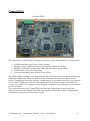
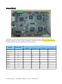
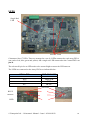
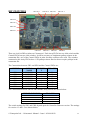
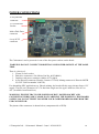
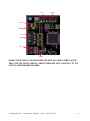
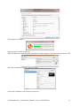
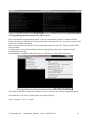
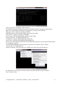
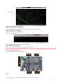
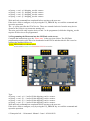
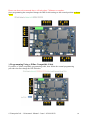
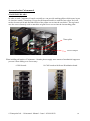
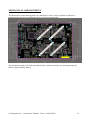
Cairnsmore1 Manual
Issue – 1.0
© Enterpoint Ltd. – Cairnsmore1 Manual – Issue 1.0 20/09/2012
1
Foreword
PLEASE TAKE SPECIAL NOTE OF ANY WARNINGS WITHIN
THIS MANUAL.
Trademarks
Spartan-3AN, Spartan6, ISE, Xilinx are the registered trademarks of Xilinx Inc, San Jose,
California, US.
© Enterpoint Ltd. – Cairnsmore1 Manual – Issue 1.0 20/09/2012
2
Contents
Cairnsmore1_board
Introduction
Getting Started
CONTROL FPGA
ARRAY FPGAS
SPI FLASH
LEDS
4
5
6
7
8
10
11
12
15
16
18
19
21
22
23
24
24
27
37
40
40
41
41
41
42
43
44
44
44
DIP SWITCHES
CLOCK GENERATOR
USB
TEMPERATURE SENSORS
POWER CONNECTIONS
POWER REGULATORS
THERMAL MANAGEMENT
BITCOIN MINING SOFTWARE FOR CM1
UPDATING CM1 FIRMWARE
UPDATING CONTROLLER FPGA FIRMWARE
UPDATING THE ARRAY FPGAS FIRMWARE
USING A XILINX COMPATIBLE CABLE
CAIRNSMORE1 ACCESSORIES
Stacking Pillars
Power Jumpers
Power Looms
Power Distribution Board
Up/Down Ribbon Cables
Mechanical Arrangement
Medical and Safety Critical Use
Warranty
Support
© Enterpoint Ltd. – Cairnsmore1 Manual – Issue 1.0 20/09/2012
3
Introduction
Welcome to your Cairnsmore1 board. This board is primarily intended for small scale HPC
applications such as Bitcoin mining.
The aim of this manual is to assist in using the main features of Cairnsmore1.
There are features that are beyond the scope of the manual. Should you need to use these features
then please email [email protected] for detailed instructions.
Cairnsmore1 currently comes with four Spartan6 LX150 FPGAs and one Spartan3 XC3S50AN
control FPGA. Custom variants can be produced for customers who require similar products, the
cost being dependent upon the design time involved, the quantity of boards required and the
timescales. Please contact us on [email protected] should you need further information.
Support materials and downloads are available from
http://www.enterpoint.co.uk/cairnsmore/cairnsmore1_support_materials.html
© Enterpoint Ltd. – Cairnsmore1 Manual – Issue 1.0 20/09/2012
4
Getting Started
6-way Phoenix connector
Controller
FPGAJTAG
connector
Controller FPGA
Array FPGAs
Jack socket
Disk Drive
Connector
PCIE connector
USB socket
Array JTAG
connector
UP/Down
Connectors
DIP Switches
For customers receiving their boards after 1st September your Cairnsmore1 will be supplied
programmed with Enterpoint’s approved bitstream. This should mean that updating the firmware is
not necessary. For customers receiving earlier boards you may need to update the firmware on
Cairnsmore1 See the section entitled 'Updating the firmware' below.
The Spartan-6 FPGAs on CM1 require the full ISE toolset to develop and build a design. The
Spartan3-AN Controller FPGA is supported by the free Webpack version of the ISE Toolset.
© Enterpoint Ltd. – Cairnsmore1 Manual – Issue 1.0 20/09/2012
5
Control FPGA
Controller FPGA
The Cairnsmore1 Control FPGA is a Spartan-3AN device in the TQ144 package. Its functions are:
1.
2.
3.
4.
5.
Configuration and control of the Clock Generator
Routing of Clock signals from the Clock Generator to the Array FPGAs
Routing of USB signals between the USB controller and the Array FPGAs
Control of the Array Power Regulators
Accessing temperature data from the Array FPGAs
The Control FPGA normally comes programmed with a core which allows the board to function in
a standard configuration. Firmware updates for the Controller may become available. See the
section “Updating the Controller firmware” in this manual. If you wish to write your own firmware
for the Control FPGA you will need to build and load your custom core using Xilinx ISE tools.
(version 11.1 or later). The Spartan3-AN is Webpack compatible but the Spartan6-LX150 requires
the full ISE toolset.
The connections between the Control FPGA and the other components are described in the
following sections of the manual. This FPGA has internal configuration memory. Programming
information is supplied at the end of this manual.
© Enterpoint Ltd. – Cairnsmore1 Manual – Issue 1.0 20/09/2012
6
Array FPGAS
2
1
3
4
Cairnsmore1 is fitted with four Spartan6 XC6SLX150 FPGAs in the FGG484 package. They are
connected together as 2 pairs in order to maintain compatibility with the Icarus bitcoin mining core.
The interconnections between the FPGAs are shown below:
SIGNAL
NAME
ARRAY
FPGA PIN
CONTROLLER PIN
TO ARRAY 1 TO ARRAY 2 TO ARRAY 3 TO ARRAY 4
CLOCKS_1
J1
78
93
32
64
CLOCKS_2
J3
76
91
31
63
USB_1
D1
83
99
48
55
USB_2
B1
87
101
50
57
USB_3
D2
84
105
47
58
USB_4
B2
88
103
51
59
USB_5
C3
90
102
54
70
USB_6
C1
85
98
49
69
USB_7
F2
82
96
42
68
USB_8
F1
79
92
46
60
© Enterpoint Ltd. – Cairnsmore1 Manual – Issue 1.0 20/09/2012
7
The connections between the pairs of FPGAs are shown below:
SIGNAL
NAME
LINK1
LINK2
LINK3
LINK4
FPGA 1
AND 3
B21
B22
D21
D22
FPGA 2
AND 4
D1
B1
D2
B2
© Enterpoint Ltd. – Cairnsmore1 Manual – Issue 1.0 20/09/2012
8
SPI FLASH MEMORY
128M FLASH
MEMORY
The four M25P128 SPI flash memory devices configure the Array FPGAs when the board is
powered and the Array voltage regulators are enabled, providing a suitable bitstream is programmed
into the device. The M25P128 has a capacity of 128Mbits with a single configuration bitstream for
each Cairnsmore1 array FPGA taking 4.1Mbits. The remaining space can be used by an advanced
user for alternative configuration bitstreams or for user data storage.
After configuration the SPI Flash can be accessed via the following pins of the FPGA:
M25P128 FUNCTION
CCLK
MOSI
DIN/
CSO_B
WRITE
HOLD
FPGA PIN
Y21
AB20
AA20
T5
U14
U13
The WRITE and HOLD pins of this memory device are pulled up to 3.3V using 1K resistors.
© Enterpoint Ltd. – Cairnsmore1 Manual – Issue 1.0 20/09/2012
9
LEDS
Single Red
LED
Sets of 4 LEDs
Cairnsmore1 has 17 LEDs. These are arranged as a set of 4 LEDs connected to each array FPGA
(one each of red, blue, green and yellow) and a single red LED connected to the Control FPGA on
pin 29 .
The relevant IO pin for an LED needs to be asserted high to ensure the LED turns on.
The LEDS are connected to the Array FPGAs as indicated below:
FPGA PIN
B18
A16
A18
A17
LED COLOUR
GREEN
YELLOW
RED
BLUE
YELLOW
BLUE
GREEN
RED
© Enterpoint Ltd. – Cairnsmore1 Manual – Issue 1.0 20/09/2012
10
DIP SWITCHES
SW2 bit 1
SW2 bit 4 SW3 bit 1
SW3 bit 4
SW1bit 4
SW1 Bit 1
SW6 bit 4
SW6 bit 1
SW5 bit 1
SW5 bit 4
SW4 bit 1
SW4 bit 4
There are six 4-bit DIP switches on Cairnsmore1. Each Array FPGA has one 4-bit switch and the
Control FPGA has two 4-bit switches. It will be necessary to implement pullup resistors in the
constraints file (.ucf) of the Control FPGA in order for those switches to be used. The switches
connected to the Array FPGAs have 1.5K pullup resistors fitted so do not require pullups in the
constraints file.
The Connections between SW1 and SW6 and the Control FPGA are:
SWITCH
SW1
SW1
SW1
SW1
SW6
SW6
SW6
SW6
SIGNAL
NAME
SWITCH1
SWITCH2
SWITCH3
SWITCH4
SWITCH5
SWITCH6
SWITCH7
SWITCH8
ELEMEN
T
1
2
3
4
1
2
3
4
FPGA PIN
33
35
140
53
80
97
125
123
The Connections between SW2 to SW5 and the Array FPGAs are shown below.
SWITCH ELEMENT
1
2
3
4
FPGA PIN
A4
D6
C6
C8
The switch settings for SW1 and SW6 depend upon the Controller firmware version. The settings
for version 1.3 and 1.5 are shown below:
© Enterpoint Ltd. – Cairnsmore1 Manual – Issue 1.0 20/09/2012
11
© Enterpoint Ltd. – Cairnsmore1 Manual – Issue 1.0 20/09/2012
12
© Enterpoint Ltd. – Cairnsmore1 Manual – Issue 1.0 20/09/2012
13
CLOCK GENERATOR
Clock Generator
Cairnsmore1 has an IDT5V19EE901NLGI clock generator capable of generating a variety of single
ended and differential clock signals of frequencies up to 500MHz. . The clock generator is
controlled by an SPI interface and is connected to the Control FPGA. Further information and a
datasheet concerning this Clock generator are available from www.idt.com.
The connections are shown below:
IDT5V19EE901 Function
CLK C
P-CLK (Differential Clock –ve)
P+ CLK (Differential Clock +ve)
CLKB
CLKA
SDAT
SCLK
EXP_CLK1_P
EXP_CLK1_N
EXP_CLK2
IDT5V19EE901 Pin
24
11
10
8
7
18
19
14
15
23
FPGA Pin
110
116
117
120
121
113
112
115
114
111
© Enterpoint Ltd. – Cairnsmore1 Manual – Issue 1.0 20/09/2012
Signal Name
CLKBUS3
CLKBUS5
CLKBUS4
CLKBUS2
CLKBUS1
CLKBUS9
CLKBUS10
CLKBUS6
CLKBUS7
CLKBUS8
14
USB
FT4232
device
USB
Mini-B
Socket
The USB interface on the Cairnsmore1 is achieved using an FT4232H USB 2.0 High
Speed (480Mb/s) to UART/FIFO device which can operate as a USB to quad serial /
parallel ports with a variety of configurations.
The datasheet and drivers for this device are available from http://www.ftdichip.com. When
appropriate drivers are installed the Drigmorn4 USB port should be detected as four serial ports.
Alternative data optimised drivers are also available from FTDI.
The USB connector on Cairnsmore1 is a mini-b socket.
The FT4232H is connected to the Spartan-3AN and is supported by an AT93C46E 1Kbit serial
EEPROM which is used for configuration data. It is envisaged that one USB channel will be routed
to each of the array FPGAs. The Spartan3-AN core supplied with the Cairnsmore1 implements the
following interconnections
SIGNAL
FT4232H PIN
ADBUS0
ADBUS1
ADBUS2
ADBUS3
ADBUS4
ADBUS5
ADBUS6
ADBUS7
ACBUS0
ACBUS1
ACBUS2
ACBUS3
16
17
18
19
21
22
23
24
26
27
28
29
CONTROL
FPGA PIN
28
27
25
24
21
20
19
18
16
15
13
12
© Enterpoint Ltd. – Cairnsmore1 Manual – Issue 1.0 20/09/2012
ARRAY FPGA
PIN
A1 PIN D1
A1 PIN B1
A1 PIN D2
A1 PIN B2
A1 PIN C3
A1 PIN C1
A1 PIN F2
A1 PIN F1
A2 PIN B21
A2 PIN B22
A2 PIN D21
A2 PIN D22
15
ACBUS4
ACBUS5
ACBUS6
ACBUS7
BDBUS0
BDBUS1
BDBUS2
BDBUS3
BDBUS4
BDBUS5
BDBUS6
BDBUS7
BCBUS0
BCBUS1
BCBUS2
BCBUS3
BCBUS4
BCBUS5
BCBUS6
BCBUS7
30
32
33
34
38
39
40
41
43
44
45
46
48
52
53
54
55
57
58
59
11
10
8
7
6
5
4
3
142
141
139
138
135
134
132
131
130
129
127
126
© Enterpoint Ltd. – Cairnsmore1 Manual – Issue 1.0 20/09/2012
A2 PIN C3
A2 PIN C1
A2 PIN F2
A2 PIN F1
A3 PIN D1
A3 PIN B1
A3 PIN D2
A3 PIN B2
A3 PIN C3
A3 PIN C1
A3 PIN F2
A3 PIN F1
A4 PIN B21
A4 PIN B22
A4 PIN D21
A4 PIN D22
A4 PIN C3
A4 PIN C1
A4 PIN F2
A4 PIN F1
16
TEMPERATURE SENSORS
Cairnsmore1 has 4 National Semiconductor LM75 temperature sensors fitted, one close to each of
the array FPGAs:
Sensor1
Sensor4
Sensor2
Sensor3
There are 3 connections between each temperature sensor and its nearest array FPGA: a 2-wire
serial interface and an output which behaves as an over-temperature warning.
The connections are shown below:
SIGNAL
SDA
SCL
OVER-TEMPERATURE
FPGA PIN
AB13
AB14
AB15
© Enterpoint Ltd. – Cairnsmore1 Manual – Issue 1.0 20/09/2012
17
POWER CONNECTIONS
6-way Phoenix
connector
5A 2.5mm Jack
Socket
Molex Disk Drive
connector
6-way PCIE
connector
The Cairnsmore1 can be powered via one of the four power sockets on the board.
WARNING: DO NOT CONNECT MORE THAN ONE POWER SOURCE AT THE SAME
TIME.
There is a choice of:
1. 2.5mm 5A Jack socket.
2. Disk drive connector 6.5A (Molex Part No. 0015244441)
3. Graphics card power connector (Molex 45732-0001)
4. 6-way Phoenix connector (Phoenix Contact 1757284). Mating connector is Phoenix MSTB
2,5/6-ST-5,08 Part number 1948750).
For demanding HPC applications e.g. Bitcoin mining, the board will take up to 6Amps from a 12V
supply. The fuse on Cairnsmore1 is a 7A fast blow single use fuse type LittelFuse series 451 or
453. (Available from Farnell etc).
WARNING: ENSURE THAT YOUR POWER SOURCE, POWER SOCKET AND
CONNECTING WIRES ARE CAPABLE OF CARRYING THE POWER TO THIS BOARD
SAFELY. DO NOT ATTEMPT TO POWER YOUR CAIRNSMORE1 BOARD FROM THE
USB CONNECTOR.
The pinout of the connectors is shown below (component side of PCB).
© Enterpoint Ltd. – Cairnsmore1 Manual – Issue 1.0 20/09/2012
18
12v
GND
12v
GND
12v
GND
12v
GND
MAKE SURE THAT YOUR POWER SOURCE IS COMPATIBLE WITH
THE CONNECTIONS SHOWN ABOVE BEFORE YOU CONNECT IT TO
YOUR CAIRNSMORE1 BOARD.
© Enterpoint Ltd. – Cairnsmore1 Manual – Issue 1.0 20/09/2012
19
POWER REGULATORS
4
5
8
2
1
9
7
3
6
WARNING – REGULATORS CAN BECOME HOT IN NORMAL
OPERATION ALONG WITH THE BOARDS THERMAL RELIEF AND THE
HEATSINKS. PLEASE DO NOT TOUCH OR PLACE HIGHLY FLAMABLE
MATERIALS NEAR THESE DEVICES WHILST THE CAIRNSMORE1
BOARD IS IN OPERATION.
There are 9 regulators on Cairnsmore1.
1. A Diodes Inc. AP7167 supplies 3.3v for the Spartan3-AN IO with a maximum current available
of 1A.
2. A Diodes Inc. AP7167 supplies 1.2v for the Spartan3-AN core with a maximum current available
of 1A.
3. A Linear Technology LT3480 supplies 3.3V for the Array FPGAs IO with a maximum current
available of 2A
4,5,6,7. Four Micrel MIC26950 Regulators supply the Array FPGAs with 1.2V with a maximum
current available of 12A each. These regulators can be switched on or off from the Control FPGA.
The enable signals must be asserted high for the regulator to turn on. The connections between
these regulators and the Control FPGA are shown below.
REGULATOR
1
2
3
4
CONTROL FPGA PIN
75
104
30
77
8 A Fairchild MC78M05 fixed 12v to 5v regulator provides the 5v control voltage for the four
MIC26950 regulators.
9 A Fairchild MC78M05 fixed 12v to 5v regulator provides the 5v supply for the USB device.
© Enterpoint Ltd. – Cairnsmore1 Manual – Issue 1.0 20/09/2012
20
Thermal Management
Cairnsmore1 is supplied with heatsinks and fan fitted. It is recommended that ambient air
temperature does not exceed 40 DegC and air conditioning is recommended for locations where 40
DegC might be exceeded.
Some bitstreams such as some current “220” bitstreams can use excessive power and hence
generate heat that is impossible to extract from the FPGA packaging. This may damage FPGAs and
our warranties will not support boards damaged by running “220” bitstreams or similar. The
maximum recommended bitstream is currently “200”. If in doubt email
[email protected] for a list of approved bitstreams.
ENTERPOINT LTD DOES NOT ACCEPT RESPONSIBILITY FOR
BOARD FAILURE IF INSUFFICIENT THERMAL
MANAGEMENT IS PROVIDED.
© Enterpoint Ltd. – Cairnsmore1 Manual – Issue 1.0 20/09/2012
21
BITCOIN MINING SOFTWARE FOR CAIRNSMORE1
Various bitcoin mining applications are available. A link to download CGminer is available on our
website http://www.enterpoint.co.uk/cairnsmore/cairnsmore1_support_materials.html. Enterpoint
Ltd. cannot be held responsible for the functionality of third party software such as CGminer.
© Enterpoint Ltd. – Cairnsmore1 Manual – Issue 1.0 20/09/2012
22
UPDATING THE FIRMWARE ON CAIRNSMORE1
From time to time, especially during the development phase of the Cairnsmore1 project, updated
versions of the Cairnsmore1 firmware will become available. These will be posted on
http://www.enterpoint.co.uk/cairnsmore/cairnsmore1_support_materials.html
1.
Updating the Controller FPGA firmware
1.1 Introduction
This procedure should be used to upgrade the Cairnsmore1 Controller to the latest revision.
1.2 DIP Switches
Make a note of your existing dip switch settings. You may need to set them back to these
settings after you program the version of the Controller. Now set DIP switches SW1 and SW6
as the following picture. SW2-5 can remain unchanged. They do not affect this process.
1.3. SPIProg.exe utility
Download the SPIProg utility from the Enterpoint website and extract to a suitable directory.
http://www.enterpoint.co.uk/cairnsmore/cairnsmore1_support_materials.html
The SPIProg.exe utility is a command line tool and therefore it is necessary to run this from a
command prompt.
© Enterpoint Ltd. – Cairnsmore1 Manual – Issue 1.0 20/09/2012
23
Select ‘Start’ ‘Run’ ‘cmd’ OK for Windows XP
Or ‘Start’ ‘Accessories’ ‘Command Prompt’ for Windows 7
Change directory to the location of the extracted file(s) , or change drive and directory as necessary.
E.g. Type: F: <return> (Choose you own drive)
Type: cd SPIProg <return> (Choose you own directory)
Check the SPIProg.exe and your upgrade bit file are present:
Type: dir <return>
© Enterpoint Ltd. – Cairnsmore1 Manual – Issue 1.0 20/09/2012
24
1.4. Before Programming
It is essential that the following procedure is read and understood before proceeding. If the program
process fails and the instructions are not followed correctly then it is possible to render the board
inoperable and a Xilinx Compatible cable will be required to recover the device.
Continue as follows:
a. Plug the USB Cable into the PC or Laptop being used, (if a laptop is being used, make sure that
the power cord is inserted to minimise the risk of the battery failing during this procedure).
b. Set the DIP Switches as indicated in section 1.2 above.
c. Verify that the Windows Cairnsmore driver has loaded.
Open Device Manager:
Windows XP (Right Click ‘My Computer’ Select ‘Properties’ Select ‘Hardware’ Select ‘Device
Manager’)
Windows 7 (‘Start’ Right Click ‘Computer’ Select ‘Properties’ Select ‘Device Manager’)
Expand the ‘Ports’ and ‘Universal Serial Bus Controllers’ Tree as shown:
Verify that the ‘USB Comms Port(COMnn)’ appears 4 times, and that ‘Cairnsmore JTAG,
Cairnsmore Port A, Cairnsmore Port B, and Cairnsmore SPI’ devices are listed as above.
1.5. Programming
The Ports are confirmed, the DIP Switch settings are correct, now we can program the new
version of firmware.
In your command box:
Type: spiprog XXXXXX.bit <return> (XXXXXX is filename of upgrade bit file)
© Enterpoint Ltd. – Cairnsmore1 Manual – Issue 1.0 20/09/2012
25
The bitfile will be verified, the device will be checked and then it will be Erased and reprogrammed
as shown above.
DO NOT SWITCH OFF OR UNPLUG YOUR USB CABLE IF THE VERIFY MESSAGE
INDICATES THAT THERE ARE ERRORS. (If errors are shown, repeat the process)
If 0 Errors are shown, then switch off the Cairnsmore1 and unplug your USB cable. The new
version will be loaded when the Cairnsmore Board is powered up or the USB cable is inserted. If
the Upgrade has been successful then the single RED LED will flash.
Return your DIP switches to the original settings or if specified by the upgrade documentation to
the settings specified there.
2.
Updating the Array FPGAs firmware.
Installation of software required to upgrade Cairnsmore1 firmware
.
2.1 Install Virtual Box Software
Download and Install Virtual Box Software from:
www.virtualbox.org
The following details are from Version 4.1.16; please get the latest version available.
Run the setup program, e.g. VirtualBox-4.1.16-78094-Win.exe
© Enterpoint Ltd. – Cairnsmore1 Manual – Issue 1.0 20/09/2012
26
Click Next to continue with the installation
Choose the installation location. (Defaults recommended).
Click Next to continue.
© Enterpoint Ltd. – Cairnsmore1 Manual – Issue 1.0 20/09/2012
27
Click Yes to continue
Click Install to continue.
During the Installation you will be prompted about Windows Logo Driver warning
© Enterpoint Ltd. – Cairnsmore1 Manual – Issue 1.0 20/09/2012
28
Click Continue Anyway for each occurrence of this message
After several minutes the installation will complete to the Finish Dialog;
Click finish to complete the installation and launch Virtual Box.
2.2 Import Debian VirtualBox Image.
Download the cairnsmore.ova Virtual Archive File from the Enterpoint Cairnsmore Support Page:
http://www.enterpoint.co.uk/cairnsmore/cairnsmore1_support_materials.html
Import this file into VirtualBox as follows:
Select ‘File’ ‘Import Appliance’
Select Choose and browse to the location where you have downloaded the Cairnsmore.ova file.
© Enterpoint Ltd. – Cairnsmore1 Manual – Issue 1.0 20/09/2012
29
Select the file and Click Open to continue
Click Next to continue
Keep the Appliance Import Setting at the defaults as below:
© Enterpoint Ltd. – Cairnsmore1 Manual – Issue 1.0 20/09/2012
30
Click Import to continue:
Import progress will be displayed.
After the Import has completed the Cairnsmore Virtual Machine will be present but powered Off.
Select the Cairnsmore machine and Click Start;
Login with Username: root Password: password
© Enterpoint Ltd. – Cairnsmore1 Manual – Issue 1.0 20/09/2012
31
2.3 Programming the Bitstream into the FPGA Array.
First verify that the programming software is able to communicate with the Cairnsmore Board.
Please note that you should have already installed the Cairnsmore Drivers, if you have not done this
yet then do so before continuing.
Make sure the Cairnsmore Board is powered and then connect to your PC/ Laptop with the USB
Lead provided.
It is important to wait until the Windows Driver plug and play process has completed before
performing the next step.
On the Running VirtualBox VM Select Devices, USB Devices and FTDI Cairnsmore1
This allows VirtualBox to grab the Cairnsmore Device ready for use with the programming tool.
Verify that the JTAG Device chain can be accessed as follows:
Type: xc3sprog –c cm1 –j <return>
© Enterpoint Ltd. – Cairnsmore1 Manual – Issue 1.0 20/09/2012
32
All 4 Array devices should be visible as above;
Download the appropriate Bitstream from the Enterpoint website Cairnsmore support page;
http://www.enterpoint.co.uk/cairnsmore/cairnsmore1_support_materials.html
shipping_test.bit - 4 FPGAs running @ 50MHz
shipping_test.pdf - DIP Switch Settings required for this bitfile
twin_test.bit - 2 FPGAs running @ 190MHz
twin_test.pdf - DIP Switch Settings required for this bitfile
board_control.bit - XC3S50AN upgrade file
xc3s50an.bit - Spartan3 SPI Flash programming file
xc6lx150.bit - Spartan6 SPI Flash bit programming file
Please look at the appropriate PDF file for the Bitstream required to ensure that the DIP Switches
are configured correctly.
The downloaded Bitstream files should be copied to the Cairnsmore VM as follows:
Copy the files to a USB Pen drive.
On the Cairnsmore VM, Select Devices, USB Devices and select your Pen Device.
In order that the correct device can be mounted, check the usb device type as follows:
Type: dmesg <return>
© Enterpoint Ltd. – Cairnsmore1 Manual – Issue 1.0 20/09/2012
33
Device 'sdb'
Mount the USB Device as follows:
Type: mount –t auto /dev/sdb /mnt
Copy the files from the Pen Drive to the current directory as follows:
Type: cp /mnt/*.bit . <return>
Check the files have been copied:
Type: ls *.bit <return>
Un-mount the device to make it safe to remove:
Type: umount /mnt <return>
Now we can program the bit file into the Array FPGAs.
Please note that this operation is temporary, removing power from the Cairnsmore Board will revert
back to the SPI Flash Loaded Bitstream. If you wish to maintain this Bitstream in the SPI flash then
move to the next section now.
Set the DIP Switches as shown below.
Type:
© Enterpoint Ltd. – Cairnsmore1 Manual – Issue 1.0 20/09/2012
34
xc3sprog –c cm1 –p 0 shipping_test.bit <return>
xc3sprog –c cm1 –p 1 shipping_test.bit <return>
xc3sprog –c cm1 –p 2 shipping_test.bit <return>
xc3sprog –c cm1 –p 3 shipping_test.bit <return>
Wait until each command has completed before moving to the next one.
If the device fails to configure, retry by using the UP_ARROW key to recall the command and
repeat the operation.
The ‘-p’ option specifies the JTAG device. These are counted clockwise from the array device
closest to the Green 6 way connector starting at 0.
The twin_test.bit file only requires device 0 and 3 to be programmed, whilst the shipping_test.bit
requires all 4 devices to be programmed.
2.4 Programming the Bitstream into the SPI Flash on the Array.
Complete the instructions up to the ‘Please note’ in the previous section. The SPI Flash
programming requires a bit file to be downloaded to the FPGA and then this bit file is used to
program the attached SPI device.
Set the DIP Switches as shown below.
Type:
xc3sprog –c cm1 –p 0 –I xc6lx150.bit shipping_test.bit <return>
xc3sprog –c cm1 –p 1 –I xc6lx150.bit shipping_test.bit <return>
xc3sprog –c cm1 –p 2 –I xc6lx150.bit shipping_test.bit <return>
xc3sprog –c cm1 –p 3 –I xc6lx150.bit shipping_test.bit <return>
Wait until each command has completed before moving to the next one.
If the device fails to configure, retry by using the UP_ARROW key to recall the command and
repeat the operation.
© Enterpoint Ltd. – Cairnsmore1 Manual – Issue 1.0 20/09/2012
35
Please note that each command above will take about 7 Minutes to complete.
Once programming has completed change the DIP Switch settings to the normal position as shown
below.
3. Programming Using a Xilinx Compatible Cable
If you have a Xilinx compatible programming cable, then follow the normal programming
procedure but first change the DIP Switches.
© Enterpoint Ltd. – Cairnsmore1 Manual – Issue 1.0 20/09/2012
36
DIP Switch Settings for shipping_test.bit PROGRAMMING OPERATION via Xilinx or
Compatible Programming Cable using JTAG Port
Pin 14
J3
Pin 1
Pin 14
J1
Pin 1
The programming of the FPGA and SPI Flash parts on Cairnsmore1 can be achieved using the
JTAG interface. There are two JTAG chains on Cairnsmore1.
The first JTAG chain allows the programming of the Spartan-3AN via the vertical JTAG connector
J3, which has a layout as follows:
13-3V3
14-GND
11-TMS
12-GND
9-TCK
10-GND
7-TDO
8-GND
5-TDI
6-GND
3-NC
4-GND
1-NC
2-GND
Using iMPACT Boundary Scan the JTAG chain appears like this
Use the appropriate .bit file to program the FPGA only or the FPGA and its internal flash. Rightclick the device to view the programming options.
The second JTAG connector, J1 is used to program the array of Spartan6 LX150 devices.
The JTAG connector J1 has a layout as follows :
14-3V3
13-GND
12-TMS
11-GND
10-TCK
9-GND
8-TDO
7-GND
6-TDI
5-GND
© Enterpoint Ltd. – Cairnsmore1 Manual – Issue 1.0 20/09/2012
4-NC
3-GND
2-NC
1-GND
37
Using IMPACT Boundary Scan the JTAG chain appears like this:
There are two alternative programming schemes:
1. Programming the FPGAs directly.
Direct JTAG programming of the FPGAs is volatile and the FPGAs will lose their configurations
every time the board power is cycled. For sustained use of an FPGA design programming the
design into the Flash memory is recommended (see 2 below).
Direct JTAG programming using .bit files is useful for fast, temporary programming during
development of FPGA programs. Right click the icon representing an FPGA and choose ‘Assign
New Configuration File’. Navigate to your .bit file and choose ‘OPEN’. The next dialogue box will
offer to add a flash memory and you should decline. Right click the icon representing the FPGA and
choose ‘Program’. On the next dialogue box ensure that the ‘Verify’ box is not checked (or greyed
out). (If it is you should uncheck it, failure to do this will result in error messages being displayed).
Click OK. The FPGA will program. This process is very quick (typically a few seconds). To
program more than one FPGA at a time hold down the 'Shift' key while selecting the FPGAs to be
programmed. Then choose 'Program' on the menu on the left of the iMPACT screen.
2. Programming the SPI flash memory devices.
Once the SPI Flash memory has been programmed, the FPGA will automatically load from the
Flash memory at power up. Generation of suitable Flash memory files (.mcs) can be achieved using
ISE iMPACT’s Prom File Formatter.
Right click on the icon representing the Spartan6 and choose ‘Add SPI/BPI Flash’ Navigate to your
programming file (.mcs) and click OPEN. Use the next dialogue box to select SPI flash and
M25P128. Data width should be set to 1. The flash memory should appear as shown below.
It will be necessary to repeat this for each FPGA to program all 4 SPI Flash devices.
Right click on the icon representing the flash memory and choose program to load your program
into the device. It is recommended that options to ‘Verify’ and ‘Erase before programming’ are
chosen. Otherwise all defaults can be accepted. The programming operation will take some time
(about 7 minutes per SPI flash device).
© Enterpoint Ltd. – Cairnsmore1 Manual – Issue 1.0 20/09/2012
38
Accessories for Cairnsmore1
STACKING PILLARS
In order to stack Cairnsmore1 boards vertically we can provide stacking pillars which come in sets
of 4 and are usually 75mm long. Except for the bottom board in a stack the four nylon 'feet' will
need to be unscrewed and discarded Each of the pillars screws into the one below. The top board
uses the screws formerly used to attach the original feet to secure into the last stacking pillar.
75mm pillar
Power Jumper
When building tall stacks of Cairnsmore 1 boards please supply some means of mechanical support to
prevent it from falling over if necessary.
6 CM1 boards
10 CM1 boards with Power Distribution board
© Enterpoint Ltd. – Cairnsmore1 Manual – Issue 1.0 20/09/2012
39
POWER JUMPERS.
To decrease the number of power cables used to supply power to a stack of 2 boards, we provide a
power jumper, which is used to connect the disk drive connectors of two Cairnsmore1 boards to
each other. One of the Cairnsmore1 boards must then be supplied with power via one of the
alternative power connectors since the disk drive connector is no longer available.
POWER LOOMS
For stack of more than two Cairnsmore1 boards we can provide power looms of different lengths,
each of which will power 3 boards from the Power Distribution board via the 6-pin Phoenix
connectors. The lengths of the medium and long power looms are designed so that the cables can be
routed up the corner of the stack by attaching them to the pillars as shown in the picture above.
a. Short loom
b. Medium loom
c. Long Loom
© Enterpoint Ltd. – Cairnsmore1 Manual – Issue 1.0 20/09/2012
40
POWER DISTRIBUTION BOARD
The Power distribution board is designed to distribute 12V supplies for a Cairnsmore1 stack. It uses
12V power from high efficiency, ATX power supplies using standard PCIe cabling from these
supplies. Depending on the quality and rating of the ATX PSU each PCIe input feed can support up
to 3-4 boards.
The Power Distribution Board also provides a switch to switch on/off the supplying ATX power
supply so that a motherboard is not needed for this function.
The power output to the Cairnsmore1 boards is via 4-pin Phoenix connectors (Part number MSTB
2,5/4-ST-5).
UP/DOWN RIBBON CABLES
UP/DOWN Ribbon Cables support the chaining of Cairnsmore1 boards though a single USB
interface. Currently the maximum number of boards on a single USB lead is 2 boards but it is
planned to extend this capability to more boards running off a single USB lead.
These cables are available in 4 lengths. The standard length is 10cm, but 20cm, 30cm and 40cm
cables are also available to suit your stacking arrangement.
© Enterpoint Ltd. – Cairnsmore1 Manual – Issue 1.0 20/09/2012
41
MECHANICAL ARRANGEMENT
The Dimensions on the drawing below are millimetres (mm). All sizes quoted are subject to
manufacturing tolerances and should only be used as a general guide.
The maximum height of the fully assembled board, (with its heatsinks, fan and supporting feet
fitted) is approximately 68mm.
© Enterpoint Ltd. – Cairnsmore1 Manual – Issue 1.0 20/09/2012
42
Medical and Safety Critical Use
Cairnsmore1 boards are not authorised for the use in, or use in the design of, medical or other safety
critical systems without the express written person of the Board of Enterpoint. If such use is
allowed the said use will be entirely the responsibility of the user. Enterpoint Ltd will accepts no
liability for any failure or defect of the Cairnsmore1 board, or its design, when it is used in any
medical or safety critical application.
Warranty
Cairnsmore1 comes with a 1 year return to bas warranty. “220” or similar bitstreams may damage
your Cairnsmore1 and use of such bitstreams will invalidate this warranty. If unsure which
bitstreams are permitted please email us on [email protected] for advice.
Support
Support for Cairnsmore1 is available from
http://www.enterpoint.co.uk/cairnsmore/cairnsmore1_support_materials.html and on email
[email protected].
© Enterpoint Ltd. – Cairnsmore1 Manual – Issue 1.0 20/09/2012
43