1
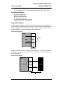
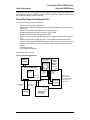
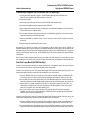
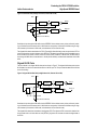
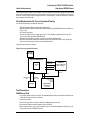
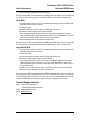
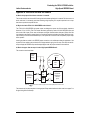
Evaluating the ORCA ORT42G5 with the
High-Speed SERDES Board
April 2004
Technical Note TN1069
Introduction
Contained in this package is information that will assist you in evaluating and verifying your ORCA® ORT42G5
designs using the Lattice High-Speed SERDES Board and the ORCAstra system bus control panel (available for
download from the Lattice web site at www.latticesemi.com/products/devtools/software/orcastra/index.cfm).
The Lattice High-Speed SERDES board supports a number of testing and evaluation setups for both the ORT42G5
and the ORSO42G5 . This document covers some common types of evaluation testing that can be performed on
the ORT42G5 device in raw (non-8b/10b) and 8b/10b modes. The tests include transmitter eye diagram measurement, 8b/10b near-end loop-back and SERDES-only (non 8b/10b), 8b/10b and aligned 8b/10b far-end loop-back.
All of the described evaluation setups will use the ort42g5v10ceval.bit bitstream. This bitstream should be included
with the package that you have downloaded from the Lattice web site at www.latticesemi.com/products/devtools/hardware/ort42g5-board/index.cfm. A unique ORCAstra macro is used to configure the device for each test.
PC and Evaluation Board Setup
This document assumes the ORCAstra application and bitstream programming software (ispVM®) are installed on
the user’s PC. It also assumes the baseline board configuration listed below. (The user is also encouraged to
experiment with other configurations.)
• All jumpers should be in their default position and default programming in the ispPAC®-POWR1208 as
described in the Evaluation Board User Manual. This will apply power in the recommended sequence and
provide 3.3V VDDIO to all banks.
• ispDOWNLOAD® cable (pDS4102-DL2A) connected to the parallel port of the PC and to the ispVM connector on the board (J30). The pDS4102-DL2A is included with the Lattice High Speed SERDES Board. Alternately, a HW-USB-1A ispDOWNLOAD cable can be used.)
• ORCAstra connected to the parallel or USB port on the PC and the ORCAstra Interface DB-25 or USB connector on the board (J108).
• External differential clock connected to the External System Clock SMA connectors (J87/J88 and J84/J85).
• External power should be provided from the Molex cable and power module.
In addition, the following design-specific jumpers must be added. Note that references to “up” or “down” positions
on switches SW14-Cx are made with the assumption that the Lattice logo is to the right side when looking at the
board:
• Jumper pins 13 and 14 on J100 – This connects the global FPGA design’s active low input reset to switch
SW14-C4. Make sure SW14-C4 remains in the “down” position to disable the reset for the duration of the
evaluation.
• Jumper pins 16 and 17 on J100 – This connects the input “clear_errors_n” signal to switch SW14-C3. Flipping SW14-C3 from the “down” to the “up” position clears the “prbserror”(D9-1) and “pkterror”(D12-1) LEDS
described below.
• Jumper pins 19 and 20 on J100 – This connects the “farendlbad” input signal to switch SW14-C2. When
SW14-C2 is in the “down” position, channel AD is in far end loop-back mode.
• Jumper pins 22 and 23 on J100 – This connects the “farendlbac” input signal to switch SW14-C1. When
SW14-C1 is in the “down” position, channel AC is in far end loop-back mode.
• Jumper pins 2 and 3 on J100 – This connects the 27-1 PRBS error checker signal to the D9-1 LED. The
design can be programmed to check 27-1 PRBS data on either of channels AC or AD in the FPGA. D9-1 will
glow and remain lit anytime PRBS errors are detected. To clear D9-1, SW14-C3 needs to be flipped from
the “down” to the “up” position.
• Jumper pins 26 and 27 on J100 – This connects the 8b/10 packet error checker signal to the D12-1 LED.
The design can be programmed to check a predefined 8b/10 packet data (generated on the transmit side of
www.latticesemi.com
1
tn1069_01
Evaluating the ORCA ORT42G5 with the
High-Speed SERDES Board
Lattice Semiconductor
AC and AD) on either of channels AC or AD in the FPGA. D12-1 will glow and remain lit anytime packet
errors are detected. To clear D12-1, SW14-C3 needs to be flipped from the “down” to the “up” position.
Recommended Reading
•
•
•
•
•
•
ORT42G5/ORT82G5 Data Sheet
ORCA Series 4 FPGA Data Sheet
ispVM System Software Data Sheet
ispDOWNLOAD Cable Data Sheet
High-Speed SERDES Briefcase Board User Manual
ORCAstra System Bus Control Panel User Manual
Loop-back Description
Two types of high-speed loop-back are discussed in this User’s Manual: Near-end Loop-back and Far-end Loopback. Near-end Loop-back (NELB) is defined as the data path from the FPGA Transmit into the SERDES and back
through the SERDES to the FPGA Receive as shown in Figure 1. The actual loop-back connection is made internally at the interfaces to transmit and receive CML buffers of the ORT42G5 device.
Figure 1. Near-end Loop-back
ORT42G5
Serial Data
FPGA
SERDES
32-bit Data
Reference Clock
Far-end Loop-back (FELB) is defined as the data path from the SERDES input, to the parallel data and back out
the SERDES as shown in Figure 2. Three different internal FELB path options are discussed, SERDES-only,
8b/10b and aligned 8b/10b.
Figure 2. Far-end Loop-back
ORT42G5
32-bit Data
FPGA
SERDES
Data Source
Serial Data
Reference Clock
2
Evaluating the ORCA ORT42G5 with the
High-Speed SERDES Board
Lattice Semiconductor
ORT42G5V10CEVAL Bitstream
The ort42g5v10ceval.bit design has been created as a base for all the described evaluation setups for the
ORT42G5 device. As shown in Figure 3, the design takes advantage of the four SERDES channels available on
the board. The ort42g5v10ceval bitstream and the ORCAstra macros used in the tests should be included in the
package you have downloaded from www.latticesemi.com/products/devtools/hardware/ort42g5-board/index.cfm.
Figure 3. ort42g5v10ceval Design
FPGA ASIC
ORT42G5
ORCAstra sysBUS USI
PKTERROR
8b/10b
PKT
CHK
CLEAR_ERRORS_N
REFCLK_A
PRBSERROR
27-1
PRBS
CHK
8b/10b
PKT
or
27-1
PRBS
Rx 8b/10b
FIFO
40-bit data,
MRWDAx
RWCKAx
1
Tx 8b/10b
Rx SERDES
HDIN_Ax
AC/AD
HDOUT_Ax
Tx SERDES
Data
Generator/
Analyzer
TSYSCLKAx
TCK78A
FARENDLBAx
REFCLK_B
Rx 8b/10b
40-bit data,
MRWDBx
Rx SERDES
HDIN_Bx
RWCKBx
BC/BD
RCK78
HDOUT_Bx
FIFO
TCK78
Tx 8b/10b
1
Tx SERDES
TSYSCLKBx
TCK78B
Either a PRBS 27-1 or predefined 8b/10b generator in the FPGA logic can supply the transmit data source for all
tests. Channels AC and AD can be used in a transmit-only mode to observe the transmit eye diagram, or can be
used for loop-back testing.
Channels AC and AD use the FIFO in the Embedded Core for clock domain crossing. Dual channel alignment can
be performed on these two channels. The FIFO can also be bypassed. In this case, the source of TCK78A needs to
be set in register 30A00 depending on whether channel AC or AD is being looked at.
In channels BC and BD, the clock domain crosses the FIFO in the FPGA logic. These channels can be used in the
SERDES-only mode or the 8b/10b mode.
Transmit Eye Diagram
One of the most fundamental evaluations that can be performed with the High-Speed SERDES Board is observation and measurement of the data eye generated by the device. The ORT42G5 device’s major mode will produce
an 8b/10b encoded or PRBS 27-1 data eye. The same experimental setup can be used for near-end loop-back
tests. Other data pattern eye diagrams can be measured using far-end loop-back setups discussed later in this
document.
3
Evaluating the ORCA ORT42G5 with the
High-Speed SERDES Board
Lattice Semiconductor
In this example, either channel AC or AD can be used to evaluate a data eye. In 8b/10b, both channels use the
8b/10b Transmit encoding block. IN PRBS 27-1 mode, the 8b/10b transmit encoder is by-passed. The data eye can
then be observed on the AC or AD HDOUT CML pins.
Transmit Eye Diagram Setup Requirements
You will need the following to complete this evaluation:
• ORT42G5 board configured as described earlier.
• ort42g5v10ceval.bit bitstream and bitstream programming devices (ispDOWNLOAD cable and ispVM running on a PC).
• ORCAstra GUI application in the ORT42G5 view (from the Options Menu)
• ORCAstra configuration file: 8b10b.fp1 for 8b/10b, raw_ac.fp1 for PRBS
• ORCAstra macro file: pktAC.fpm for 8b/10b, prbsAC for PRBS
• Scope to view data eye and high speed SMA cables (50Ω up to 3.0Gb/s) with bias tees at the input to the
scope.
• Clock source capable of driving a CML input clock (77.76-155.52MHz) and SMA cables from the clock
source to the Lattice High Speed SERDES Board and to the trigger input of the scope. (Note: The eye measurements could alternately be made using a Serial Data Analyzer. In that case no trigger connection is
required.)
• 5V DC wall power supply.
• 1.5V DC supply for the bias tees.
A typical setup is shown in Figure 4.
Figure 4. Transmit Eye Diagram Setup
Agilent 86100B DCA
(or equivalent)
5V DC 4A
Power Supply
Agilent 816112
20GHz
Electrical
Module
(or equivalent)
High-Speed SERDES Board
Trigger In
Picosecond
5575A
Bias Tee
ORT42G5
DUT
Picosecond
5575A
Bias Tee
HDOUTP_Bx
HDOUTN_Bx
ispDOWNLOAD
Cable
ORCAstra
Interface Cable
Computer
1.5V DC 0.5A
Power Supply
REFCLKN_B
REFCLKP_B
+
-
High = 500mV
Low = 0V
155MHz
Agilent 81130A
Clock Source
(or equivalent)
4
Note: Do not use
stand-alone bias tees
on channels (AA and BA).
Those channels have a
built-in bias tee.
Evaluating the ORCA ORT42G5 with the
High-Speed SERDES Board
Lattice Semiconductor
Transmit Eye Diagram Test Procedures (8b/10b Data Eye)
1. Connect the system as shown in Figure 4. The scope SMA cables should be connected to the
HDOUTP_Bx and HDOUTN_Bx SMA connectors on the board.
2. Power-up the system
3. Start the clock generator and provide a nominal 155.52 MHz CML reference clock.
4. Download the ort42g5v10ceval.bit bitstream into the ORT42G5.
5. Open Configuration 8b10b.fp1 using the pull-down menu in the ORCAstra application. This will setup the
AC and AD channels in an 8b/10b mode
6. Run the pktAC.fpm macro using the pull-down menu in the ORCAstra application. This macro will enable
channels AC and AD to transmit 8b/10b packets
7. Make sure that SW14-C1 and SW14-C2 are in the “up” position to prevent far end loop-back on channels
AC and AD
8. Observe the 8b/10b encoded data eye on the scope.
Now that the eye is present, the system can be manipulated to improve and/or distort the eye diagram. The
ORCAstra software can be used to change the pre-emphasis settings for the CML output buffer, change the halfamplitude setting for the CML output buffer, change the half-rate setting for the Tx SERDES channel, or change the
frequency of the incoming reference clock. The Tx SERDES channel can also be powered down using the ORCAstra application.
Note: To obtain a valid eye diagram measurement, both outputs of the CML buffer must be connected to the same
load. A difference in the loading of the P and the N outputs of the CML buffer will degrade the measured data eye.
Near End Loop-Back (8b/10b Data Eye)
In addition to the steps performed above to observe an 8b/10b eye, it is possible to perform an internal loop-back
on either channel AC or AD and verify the 8b/10b packet checker functionality.
In addition to the steps shown under the “Transmit Eye Diagram Test Procedures (8b/10b Data Eye)” section. The
following steps enable checking channel AC for 8b/10b packet in near end loop-back:
1. Check the TESTEN check box for channel AC (or write Data=41, address =30024) in the ORCAstra GUI.
This sets channel AC in internal loop-back while still enabling the data output to observe an eye on AC.
2. Run the pktAC.fpm macro using the pull-down menu in the ORCAstra application. This macro will enable
channels AC and AD to transmit 8b/10b packets and allows checking of 8b/10b packets using channel AC.
3. Observe LED D12-1 (packet errors LED). If this LED is on, then previous packet errors were seen. The
LED needs to be cleared to see if it latches any additional errors. Move SW14-C3 to the “down” position,
then to the “up” position. D12-1 should be cleared by now.
4. If D12-1 is not cleared, then a reset of the resync logic might be required. Check then uncheck the
GSWRST check box for Ax in the ORCAstra GUI. In addition, check then uncheck the FMPU_RESYNC1
check box for AC in the GUI. Repeat step 10.
In addition to the steps shown under the “Transmit Eye Diagram Test Procedures (8b/10b Data Eye)” section, the
following steps enable checking channel AD for 8b/10b packet in near end loop-back:
1. Check the TESTEN check box for channel AD (or write Data=41, address =30034) in the ORCAstra GUI.
This sets channel AD in internal loop-back while still enabling the data output to observe an eye on AD.
2. Run the pktAD.fpm macro using the pull-down menu in the ORCAstra application. This macro will enable
channels AC and AD to transmit 8b/10b packets and allows checking of 8b/10b packets using channel AD
5
Evaluating the ORCA ORT42G5 with the
High-Speed SERDES Board
Lattice Semiconductor
3. Observe LED D12-1 (packet errors LED). If this LED is on, previous packet errors were seen. The LED
needs to be cleared to see if it latches any additional errors. Move SW14-C3 to the “down” position, then to
the “up” position. D12-1 should be cleared by now.
4. If D12-1 is not cleared, then a reset of the resync logic might be required. Check then uncheck the
GSWRST check box for Ax in the ORCAstra GUI. In addition, check then uncheck the FMPU_RESYNC1
check box for AD in the GUI. Repeat step 10.
Transmit Eye Diagram Test Procedures (PRBS 27 Data Eye)
1. Connect the system as shown in Figure 4. The scope SMA cables should be connected to the
HDOUTP_Bx and HDOUTN_Bx SMA connectors on the board.
2. Power-up the system
3. Start the clock generator and provide a nominal 155.52MHz CML reference clock.
4. Download the ort42g5v10ceval.bit bitstream into the ORT42G5.
5. Open Configuration raw_ac.fp1 using the pull-down menu in the ORCAstra application. This will setup the
AC and AD channels in SERDES-only mode
6. Run the prbsAC.fpm macro using the pull-down menu in the ORCAstra application. This macro will setup
the AC and AD channels in SERDES-only mode and transmit PRBS 27 packets.
7. Make sure that SW14-C1 and SW14-C2 are in the “up” position to prevent far end loop-back on channels
AC and AD.
8. Observe the PRBS data eye on the scope.
Now that the eye is present, the system can be manipulated to improve and/or distort the eye diagram. The
ORCAstra software can be used to change the pre-emphasis settings for the CML output buffer, change the halfamplitude setting for the CML output buffer, change the half-rate setting for the Tx SERDES channel, or change the
frequency of the incoming reference clock. The Tx SERDES channel can also be powered down using the ORCAstra application.
Note: To obtain a valid eye diagram measurement, both outputs of the CML buffer must be connected to the same
load. A difference in the loading of the P and the N outputs of the CML buffer will degrade the measured data eye.
Near-end Loop-back (PRBS 27-1 Data Eye)
In addition to the steps performed above to observe an 27-1 eye, it is possible to perform an internal loop-back on
either channel AC or AD and verify the 27-1 PRBS checker functionality.
In addition to the steps shown under the “Transmit Eye Diagram Test Procedures (PRBS 27-1 Data Eye)” section,
the following steps enable checking channel AC for PRBS 27-1 PRBS in near end loop-back:
1. Open Configuration raw_ac.fp1 using the pull-down menu in the ORCAstra application. This will setup the
AC and AD channels in SERDES-only mode. This also sets channel AC are the source of TCK78A.
2. Check the TESTEN check box for channel AC (or write Data=41, address =30024) in the ORCAstra GUI.
This sets channel AC in internal loop-back while still enabling the data output to observe an eye on AC.
3. Run the prbsAC.fpm macro using the pull-down menu in the ORCAstra application. This macro will enable
channels AC and AD to transmit PRBS 27-1 and allows checking of PRBS 27-1 using channel AC. Observe
LED D9-1 (PRBS 27-1 errors LED). If this LED is on, then previous packet errors were seen. The LED
needs to be cleared to see if it latches any additional errors. Move SW14-C3 to the “down” position, then to
the “up” position. D9-1 should be cleared by now.
In addition to the steps shown under the “Transmit Eye Diagram Test Procedures -(PRBS 27-1 Data Eye)” section.
The following steps enable checking channel AD for PRBS 27-1 PRBS in near end loop-back:
1. Open Configuration raw_ad.fp1 using the pull-down menu in the ORCAstra application. This will setup the
AC and AD channels in SERDES-only mode. This also sets channel AD are the source of TCK78A.
6
Evaluating the ORCA ORT42G5 with the
High-Speed SERDES Board
Lattice Semiconductor
2. check the TESTEN check box for channel AD (or write Data=41, address =30034) in the ORCAstra GUI.
This sets channel AD in internal loop-back while still enabling the data output to observe an eye on AD.
3. Run the prbsAD.fpm macro using the pull-down menu in the ORCAstra application. This macro will enable
channels AC and AD to transmit PRBS 27-1 and allows checking of PRBS 27-1 using channel AD.
4. Observe LED D9-1 (PRBS 27-1 errors LED). If this LED is on, then previous packet errors were seen. The
LED needs to be cleared to see if it latches any additional errors. Move SW14-C3 to the “down” position,
then to the “up” position. D9-1 should be cleared by now.
Far-end Loop-back
For a Far-end Loop-back (FELB) test using the ORT42G5 device, the reference clock for the ORT42G5 and for the
data source must be frequency locked. This is a mandatory requirement since the ORT42G5 transmitter always
uses the local reference clock.
Three types of FELB can be performed with the ORT42G5 device. Each type uses a different data path for the
transmit and receive blocks of the embedded ASIC core. The three paths are SERDES-only, 8b/10b, and Aligned
8b/10b.
SERDES-only Tests
The active blocks in the SERDES-only data path are shown in Figure 5. Serial data is input through the CML buffer
into the SERDES. Clock and data recovery is then performed, producing an 10-bit data bus and recovered clock. A
MUX block then converts the 10-bit data to 40-bit data. This 40-bit data is transmitted into the FPGA. The
ort42g5v10ceval.bit design uses an asynchronous FIFO to cross clock domains to the local reference clock (REFCLK). The 40-bit data is then sent back into the embedded ASIC core, then through the MUX block to convert back
to 10-bits. Finally, it is re-serialized and transmitted via the CML buffer.
Figure 5. SERDES Only Data Path (ort42g5v10ceval.bit, Channel BC or BD)
FPGA
ASIC
Rx SERDES
32-bit
Data
HDIN_Bx
RWCKBx
HDOUT_Bx
Tx SERDES
FIFO
TSYSCLKBx
TCK78B (Derived from REFCLK)
The SERDES-only data path can be used to evaluate any type of data pattern. The data pattern must be guaranteed to provide an adequate density of 1’s for the ORT42G5 SERDES run length. For example, a Pseudo-Random
Bit Stream (PRBS) test can be performed using an external data source and checker and various types of PRBS
2n-1 sequences to test the ORT42G5 device. Different types of transmit data eyes can also be observed and measured using different data patterns in this mode.
8b/10b Tests
The active blocks in the 8b/10b data path are shown in Figure 6. The 8b/10b data path requires 8b/10b data to be
sent from an external data source to the Rx input. The Tx output then sends the data back to the data source for
checking.
7
Evaluating the ORCA ORT42G5 with the
High-Speed SERDES Board
Lattice Semiconductor
Figure 6. 8b/10b Data Path (ort42g5v10ceval.bit, Channel BC or BD)
FPGA
ASIC
Rx SERDES
Rx 8b/10b
32-Bit Data
DOUTBx_FP
HDIN_Bx
RWCKBx
HDOUT_Bx
Tx SERDES
Tx 8b/10b
FIFO
TSYSCLKBx
TCK78B (Derived from REFCLK)
Serial data is input through the CML buffer into the SERDES. Clock and data recovery is then performed, producing a 10-bit data bus and recovered clock. A MUX block then converts the 10-bit data to 40-bit data using an alignment character (/A/ character in XAUI mode, and ordered sets in Fibre Channel mode).
The aligned 40-bit data is transmitted to the FPGA. The ort42g5v10ceval.bit design uses an asynchronous FIFO to
cross clock domains to the local reference clock (REFCLK). The data is then sent back into the embedded core as
40 bits of data (32 bits of data, 4 bits of control, and 4 bits of TBIT9). Inside the Tx 8b/10b block, the 40-bit data is
sent through the MUX block, converted back to 10 bits (8b/10b decoder), serialized and transmitted via the CML
buffer.
Aligned 8b/10b Tests
The active blocks in the aligned 8b/10b data path are shown in Figure 7. The aligned 8b/10b data path requires
8b/10b data to be sent from an external data source to the Rx input. The Tx output sends the data back to the data
source for checking.
Figure 7. Aligned 8b/10b Data Path (ort42g5v10ceval.bit, Channel AC and AD)
FPGA
32-Bit Data
MRWDAx
ASIC
FIFO
Rx 8b/10b
Rx SERDES
HDIN_Ax
RWCKBx
HDOUT_Ax
Tx 8b/10b
Tx SERDES
TSYSCLKAx
TCK78A (Derived from REFCLK)
Serial data is input through the CML buffer into the SERDES. Clock and data recovery is then performed, producing a 10-bit data bus and recovered clock. A MUX block then converts the 10-bit data to 40-bit data using an alignment character (/A/ character in XAUI mode, and ordered sets in Fibre Channel mode).
The aligned 40-bit data is then transmitted to the alignment FIFO. The alignment FIFO crosses clock domains from
the recovered clock to the local reference clock (REFCLK), aligns the two channels and sends the aligned data to
the FPGA.
8
Evaluating the ORCA ORT42G5 with the
High-Speed SERDES Board
Lattice Semiconductor
The ort42g5v10ceval.bit design uses two registers to clock the data back to the transmit interface to the embedded
ASIC core as 40-bit data and frame pulse ((32 bits of data, 4 bits of control, and 4 bits of TBIT9) for each channel.
Inside the Tx block, the data is sent through the MUX block, converted back to 10 bits (8b/10b decoder), serialized
and transmitted via the CML buffer.
Setup Requirements for Far-end Loop-back Testing
You will need the following to complete this evaluation:
• ORT42G5 Evaluation Board configured as described earlier
• Ort42g5v10ceval.bit bitstream and bitstream programming devices (ispDOWNLOAD cable and ispVM running on a PC).
• 5V DC wall power supply.
• Clock source capable of driving a CML input clock (77.76-155.52MHz) and SMA cables from the clock
source to the Lattice High Speed SERDES Board.
• ORCAstra GUI application and serdes_only_felp.fpm and 8b/10b_felp.fpm macros.
• Data source with 8b/10b capability and frequency locked to the ORT42G5 reference clock. Typically this
data source will also perform checks on the received data stream.
A typical test setup is shown in Figure 8.
Figure 8. Far-end Loop-back Test Setup
5V DC 4A
Power Supply
High-Speed SERDES Board
HDINP_A/Bx
HDINN_A/Bx
ORT42G5
DUT
HDOUTP_A/Bx
Data Source
(Typically a BERT with
8b/10b capability)
HDOUTN_A/Bx
REFCLKN_B
REFCLKP_B
ispDOWNLOAD
Cable
ORCAstra
Interface Cable
Computer
+
-
Ext. Clock
High = 500mV
Low = 0V
155MHz
Agilent 81130A
Clock Source
(or equivalent)
Test Procedures
SERDES-only FELB
1. Connect the system as shown in Figure 8. The data SMA cables should be connected to the HDIN_Bx and
HDOUTN_Bx SMA connectors on the board.
2. Power-up the system.
3. Start the clock generator to provide a nominal 155.52MHz CML reference clock.
4. Download the ort42g5v10ceval.bit bitstream into the ORT42G5.
5. Open configuration raw_ac.fp1 using the pull-down menu in the ORCAstra application. This will set up the
BC and BD channels in SERDES-only mode
9
Evaluating the ORCA ORT42G5 with the
High-Speed SERDES Board
Lattice Semiconductor
6. Begin transmitting and analyzing data from the data source.
Note: If at any point the REFCLK or data is stopped, the SERDES channel may need to be reset to reacquire data
lock. This can be done by checking and then un-checking the GSWRT check box for Bx in the ORCAstra GUI.
8b/10b FELB
1. Connect the system as shown in Figure 8. The data SMA cables should be connected to the HDIN_Bx and
HDOUTN_Bx SMA connectors on the board.
2. Power-up the system.
3. Start the clock generator to provide a nominal 155.52MHz CML reference clock.
4. Download the ort42g5v10ceval.bit bitstream into the ORT42G5.
5. Open Configuration 8b10b.fp1 using the pull-down menu in the ORCAstra application. This macro will
enable channels BC and BD in 8b/10b mode and turn on the Fibre Channel Link State Machine. This setup
assumes that ordered sets (ex: K28.5 Dxx.x Dxx.x Dxx.x) would be received.
6. Begin transmitting and analyzing 8b/10b data from the data source.
Note: If at any point the REFCLK or data is stopped, the SERDES channel may need to be reset to reacquire data
lock. This can be done by checking and then un-checking the GSWRT check box for Bx in the ORCAstra GUI.
Aligned 8b/10b FELB
1. Connect the system as shown in Figure 8. The data SMA cables should be connected to the HDIN_Ax and
HDOUTN_Ax SMA connectors on the board.
2. Power-up the system.
3. Start the clock generator to provide a nominal 155.52 MHz CML reference clock.
4. Download the ort42g5v10ceval.bit bitstream into the ORT42G5.
5. Open Configuration 8b10b.fp1 using the pull-down menu in the ORCAstra application. This will enable
channels AC and AD in 8b/10b mode and turn on the Fibre Channel State Machine. In addition, it will
enable the Alignment FIFO on AC and AD. This setup assumes that ordered sets (e.g.: K28.5 Dxx.x Dxx.x
Dxx.x) would be received.
6. Set SW14-C1 and SW14-C2 in the “up” position. This sets both AC and AD in Far-end Loop-back Mode.
7. Begin transmitting and analyzing 8b/10b data from the data source.
Note: If at any point the REFCLK or data is stopped, the SERDES channel may need to be reset to reacquire data
lock. Check and then uncheck the GSWRST check box for Ax in the ORCAstra GUI. In addition, check and then
uncheck the FMPU_RESYNC1 check box for AC and AD in the GUI. As an indication that alignment is achieved,
verify that the DEMUX_WAS and CH248_SYNC LEDS in the GUI are on (bright green) for AC and AD.
Technical Support Assistance
Hotline: 1-800-LATTICE (North America)
+1-408-826-6002 (Outside North America)
e-mail: [email protected]
Internet: www.latticesemi.com
10
Evaluating the ORCA ORT42G5 with the
High-Speed SERDES Board
Lattice Semiconductor
Appendix A. Function of the Bias Tee Network
Q: What is the purpose of the bias tee and when is it needed?
The bias tee module is an enhanced DC blocking device that allows application of an external DC bias current to a
device under test. It is commonly used when interfacing a high frequency, DC coupled output device to an input
that does not provide the required DC bias.
Q: Why do the Lattice FPSC 2.5/3.125G SERDES need a bias tee?
The FPSC 2.5/3.125G SERDES high speed outputs are designed to operate into 50Ω termination impedance
biased at 1.5V or 1.8V DC. (This is the internal termination provided by Lattice 2.5/3.125G SERDES inputs and
other vendor CML inputs.) Since most oscilloscopes and Digital Communications Analyzers (DCAs) have 50Ω
input impedance terminated to ground, they do not provide the required termination bias voltage. When this equipment is directly connected to the SERDES output, it will provide an incorrect DC bias and prevents proper output
buffer operation.
Inserting the bias tee module in the SERDES output connection to the oscilloscope allows the application of the
required DC bias condition and provides the DC voltage translation going into the scope. This allows the oscilloscope to display the SERDES output waveform/eye diagram under the proper termination bias conditions.
Q: What is the proper bias tee setup for Lattice High Speed SERDES Board?
The connections are shown below:
External
Power
Supply
DC Biased
Port
50
Evaluation
Board SERDES
Tx Output
Note: The
50
Bias
Tee
AC
Biased
Port
Bias
Tee
AC
Unbiased
Port
High Speed
Oscilloscope
with 50Ω
Inputs
Bias
Tee
symbol above indicates a region where shielded (SMA) cable should be used.
The bias tees may be placed anywhere in the signal path. Delay matched cables should be used insure proper P to
N signal timing at the oscilloscope.
11
Evaluating the ORCA ORT42G5 with the
High-Speed SERDES Board
Lattice Semiconductor
Q: What is inside a bias tee module and how does it work?
The bias tee module is a passive device, consisting of a capacitor and inductor, as shown below.
DC-Biased
Port
AC-Unbiased
Port
AC-Biased
Port
Bias Tee
The capacitor blocks DC between the right and left signal ports. The inductor provides DC coupling/AC isolation
between the upper port and the left port. The inductor is the most critical element. In practice, this element consists
of several inductor and resistor components very carefully assembled to provide high impedance over multiple
decades of frequency. This is the key to providing low signal line reflection and low signal distortion.
Not all bias tees are the same. There are a variety of bias tees designed for specific frequency ranges and DC current levels from several different vendors. Lattice uses a Picosecond Pulse Lab bias tee. More detailed characterization and application documents are available from this vendor. See the references section at the end of this
document.
Q: Can the SERDES output be observed without a bias tee module?
Yes, in two different ways, as shown below.
1. For AC-coupled SERDES interface applications, external shunt resistors, tied to VDDOB, are suggested at
the Tx output. In this case the outputs may be connected to a high speed oscilloscope without using bias
tee elements. Simple coupling capacitors can be used as shown below.
VDDOB
120
High Speed
Oscilloscope
with 50Ω Inputs
120
Evaluation Board
SERDES
TX Output
50
50
Note: The
symbol above indicates a region where shielded (SMA) cable should be used.
In this interconnection the 120Ω external resistors provide the necessary DC bias to the Tx CML buffer outputs.
12
Evaluating the ORCA ORT42G5 with the
High-Speed SERDES Board
Lattice Semiconductor
2. Some newer test equipment provides adjustable bias voltage on the internal 50Ω input terminations. This
equipment may be directly connected to the SERDES Tx output, as shown below.
VDDOB
High Speed Equipment
with Adjustable Term
Input Voltage
Evaluation Board
SERDES TX Output
50
50
Vterm =
VDDOB
For this connection, the adjustable termination voltage should be set to the VDDOB supply voltage used on the Lattice High Speed SERDES Board (1.5V, if internal supply is being used). This is actually the best means of observing the Tx data output signals for DC coupled applications, since it eliminates any possible signal degradation
caused by bias tee and DC blocking elements.
References
Bias Tee Model 5575A, Picosecond Pulse Labs, Boulder CO, www.picosecond.com
13