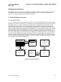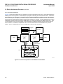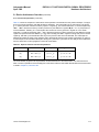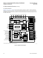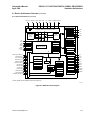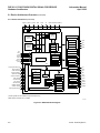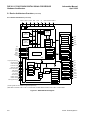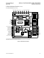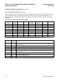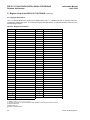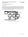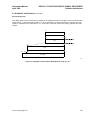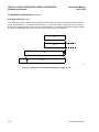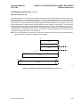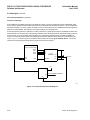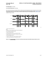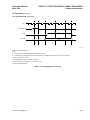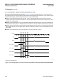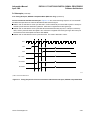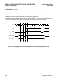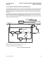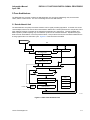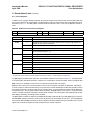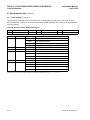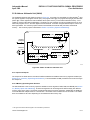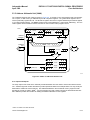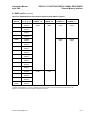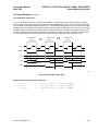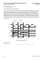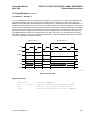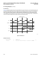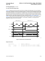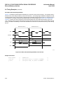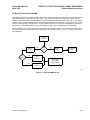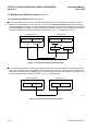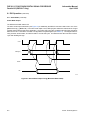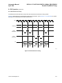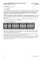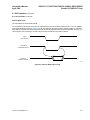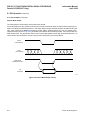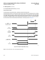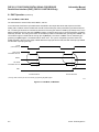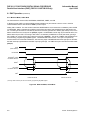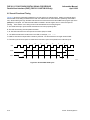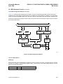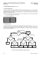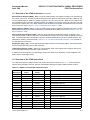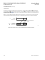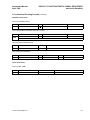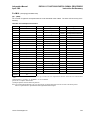
1
Information Manual January 1998 DSP1611/17/18/27/28/29 Digital Signal Processor For additional information, contact your Microelectronics Group Account Manager or the following: INTERNET: http://www.lucent.com/micro E-MAIL: [email protected] N. AMERICA: Microelectronics Group, Lucent Technologies Inc., 555 Union Boulevard, Room 30L-15P-BA, Allentown, PA 18103 1-800-372-2447, FAX 610-712-4106 (In CANADA: 1-800-553-2448, FAX 610-712-4106) ASIA PACIFIC: Microelectronics Group, Lucent Technologies Singapore Pte. Ltd., 77 Science Park Drive, #03-18 Cintech III, Singapore 118256 Tel. (65) 778 8833, FAX (65) 777 7495 CHINA: Microelectronics Group, Lucent Technologies (China) Co., Ltd., A-F2, 23/F, Zao Fong Universe Building, 1800 Zhong Shan Xi Road, Shanghai 200233 P. R. China Tel. (86) 21 6440 0468, ext. 316, FAX (86) 21 6440 0652 JAPAN: Microelectronics Group, Lucent Technologies Japan Ltd., 7-18, Higashi-Gotanda 2-chome, Shinagawa-ku, Tokyo 141, Japan Tel. (81) 3 5421 1600, FAX (81) 3 5421 1700 EUROPE: Data Requests: MICROELECTRONICS GROUP DATALINE: Tel. (44) 1189 324 299, FAX (44) 1189 328 148 Technical Inquiries: GERMANY: (49) 89 95086 0 (Munich), UNITED KINGDOM: (44) 1344 865 900 (Bracknell), FRANCE: (33) 1 41 45 77 00 (Paris), SWEDEN: (46) 8 600 7070 (Stockholm), FINLAND: (358) 9 4354 2800 (Helsinki), ITALY: (39) 2 6601 1800 (Milan), SPAIN: (34) 1 807 1441 (Madrid) Lucent Technologies Inc. reserves the right to make changes to the product(s) or information contained herein without notice. No liability is assumed as a result of their use or application. No rights under any patent accompany the sale of any such product(s) or information. Copyright © 1998 Lucent Technologies Inc. All Rights Reserved MN97-030WDSP DRAFT COPY A Word About Trademarks . . . The following Lucent Technologies Inc. trademarks are used in this manual: Tapdance® FlashDSP® The following trademarks, owned by entities other than Lucent Technologies Inc., are used in this manual: IEEE is a registered trademark of The Institute of Electrical and Electronics Engineers, Inc. Intel is a registered trademark of Intel Corporation. Motorola is a registered trademark of Motorola, Inc. MS-DOS and Windows are registered trademarks of Microsoft Corporation. TI is a registered trademark of Texas Instruments, Inc. UNIX is a registered trademark licensed exclusively through X/Open Company Ltd. X-Windows is a trademark of Massachusetts Institute of Technology. ii DRAFT COPY Lucent Technologies Inc. Foreword This manual contains detailed information on the design and application of the DSP1611/17/18/27/28/29 Digital Signal Processor family, which includes the FlashDSP ®1618, FlashDSP 1627, FlashDSP 1628, and FlashDSP 1629 development devices. The DSP1611-ST, DSP1618-ST, DSP1617-ST, DSP1627-ST, DSP1628-ST, and DSP1629-ST support software libraries, the FlashDSP1600-HDS Development System, and numerous DSP1611/17/18/27/28/29-specific hardware support tools are also available to aid in developing software and integrating the devices into systems. Additional information on the digital signal processor product line is available in the form of manuals, data sheets, and application notes. Conventions Used in this Manual In general, all registers writable or readable by DSP instructions are lower case. Device flags, I/O pins, and nonprogram-accessible registers are generally upper case. For clarity, register names and DSP instructions are printed in boldface when used in written descriptions. Variable names that are to be replaced by specific names are italicized, such as filename. Instruction set notation conventions are defined in Chapter 4. Lucent Technologies Inc. DRAFT COPY iii DSP1611/17/18/27/28/29 Digital Signal Processor INFORMATION MANUAL CONTENTS ➤1 ➤ ➤ ➤ ➤ ➤ ➤ ➤ ➤ ➤ ➤2 ➤ ➤ ➤ ➤ ➤ ➤ ➤ ➤ ➤ ➤ ➤ ➤ ➤ ➤ ➤ ➤ ➤ ➤ ➤ ➤ ➤ ➤ ➤ ➤ ➤3 ➤ ➤ ➤ ➤ ➤ ➤ ➤ iv Introduction.................................................................................................................................................. 1-1 1.1 General Description .......................................................................................................................... 1-2 1.1.1 Architecture ........................................................................................................................ 1-2 1.1.2 Instruction Set .................................................................................................................... 1-3 1.2 Typical Applications........................................................................................................................... 1-3 1.3 Application Support........................................................................................................................... 1-4 1.3.1 Support Software Library ................................................................................................... 1-4 1.3.2 Hardware Development System ......................................................................................... 1-4 1.4 Manual Organization ......................................................................................................................... 1-6 1.4.1 Applicable Documentation ................................................................................................. 1-7 Hardware Architecture................................................................................................................................. 2-1 2.1 Device Architecture Overview ........................................................................................................... 2-1 2.1.1 Harvard Architecture .......................................................................................................... 2-1 2.1.2 Concurrent Operations ....................................................................................................... 2-2 2.1.3 Device Architecture ............................................................................................................ 2-4 2.1.4 Memory Space and Bank Switching ................................................................................ 2-12 2.1.5 Internal Instruction Pipeline .............................................................................................. 2-13 2.2 Core Architecture Overview ............................................................................................................ 2-16 2.2.1 Data Arithmetic Unit ......................................................................................................... 2-16 2.2.2 Y Space Address Arithmetic Unit (YAAU) ........................................................................ 2-17 2.2.3 X Space Address Arithmetic Unit (XAAU) ........................................................................ 2-18 2.2.4 Cache ............................................................................................................................... 2-18 2.2.5 Control ............................................................................................................................. 2-18 2.3 Internal Memories ........................................................................................................................... 2-19 2.4 External Memory Interface (EMI) .................................................................................................... 2-19 2.5 Bit Manipulation Unit (BMU)............................................................................................................ 2-20 2.6 Serial Input/Output (SIO) Units ....................................................................................................... 2-20 2.7 Parallel Input/Output (PIO) (DSP1617 Only)................................................................................... 2-21 2.8 Parallel Host Interface (PHIF) (DSP1611/18/27/28/29 Only) .......................................................... 2-21 2.9 Bit Input/Output (BIO) ..................................................................................................................... 2-22 2.10 JTAG ............................................................................................................................................... 2-22 2.11 Timer ............................................................................................................................................... 2-22 2.12 Hardware Development System (HDS) Module.............................................................................. 2-23 2.13 Clock Synthesis (DSP1627/28/29 Only) ......................................................................................... 2-23 2.14 Power Management ........................................................................................................................ 2-23 Software Architecture .................................................................................................................................. 3-1 3.1 Register View of the DSP1611/17/18/27/28/29................................................................................. 3-1 3.1.1 Types of Registers .............................................................................................................. 3-1 3.1.2 Register Length Definition .................................................................................................. 3-5 3.1.3 Register Reset Values ........................................................................................................ 3-6 3.1.4 Flags .................................................................................................................................. 3-7 3.2 Memory Space and Addressing........................................................................................................ 3-8 3.2.1 Y-Memory Space ................................................................................................................ 3-8 Lucent Technologies Inc. ➤ ➤ ➤ ➤ ➤ ➤ ➤ ➤ ➤ ➤ ➤ ➤ ➤ ➤ ➤ ➤ ➤ ➤ ➤ ➤ ➤ ➤ ➤4 ➤ ➤ ➤ ➤ ➤ ➤ ➤ ➤ ➤ ➤ ➤ ➤ ➤ ➤ ➤ ➤ ➤5 ➤ ➤ ➤ ➤ ➤ ➤ ➤ ➤ ➤ ➤ v 3.2.2 X-Memory Space ............................................................................................................. 3-10 Arithmetic and Precision ................................................................................................................. 3-21 Interrupts......................................................................................................................................... 3-27 3.4.1 Introduction ...................................................................................................................... 3-27 3.4.2 Interrupt Sources ............................................................................................................. 3-29 3.4.3 Outputs of Interrupts ........................................................................................................ 3-31 3.4.4 Interrupt Operation ........................................................................................................... 3-32 3.4.5 Trap Description ............................................................................................................... 3-38 3.4.6 Powerdown with the AWAIT State .................................................................................... 3-40 3.4.7 Interrupts in DSP16A-Compatible Mode (DSP1617 Only) ............................................... 3-42 3.4.8 Timing Examples, DSP16A-Compatible Mode (DSP1617 Only) ..................................... 3-44 3.5 Clock Synthesis (DSP1627, DSP1628, and DSP1629 Only).......................................................... 3-47 3.5.1 PLL Control Signals ......................................................................................................... 3-48 3.5.2 PLL Programming Examples ........................................................................................... 3-50 3.5.3 Latency ............................................................................................................................ 3-50 3.6 Power Management ........................................................................................................................ 3-52 3.6.1 powerc Control Register Bits ........................................................................................... 3-52 3.6.2 STOP Pin ......................................................................................................................... 3-56 3.6.3 The pllc Register Bits (DSP1627/28/29 Only) ................................................................. 3-56 3.6.4 AWAIT Bit of the alf Register ........................................................................................... 3-56 3.6.5 Power Management Sequencing ..................................................................................... 3-57 3.6.6 Power Management Examples ........................................................................................ 3-58 Instruction Set ............................................................................................................................................. 4-1 4.1 Notation............................................................................................................................................. 4-2 4.2 Instruction Cycle Timing.................................................................................................................... 4-2 4.3 Addressing Modes ............................................................................................................................ 4-3 4.3.1 Register Indirect Addressing .............................................................................................. 4-3 4.3.2 Compound Addressing ...................................................................................................... 4-5 4.3.3 Direct Data Addressing ...................................................................................................... 4-7 4.4 Processor Flags ................................................................................................................................ 4-9 4.5 Instruction Set ................................................................................................................................. 4-11 4.5.1 Control Instructions .......................................................................................................... 4-12 4.5.2 Cache Instructions ........................................................................................................... 4-14 4.5.3 Data Move Instructions .................................................................................................... 4-15 4.5.4 Special Function Group ................................................................................................... 4-19 4.5.5 Multiply/ALU Group .......................................................................................................... 4-22 4.5.6 F3 ALU Instructions ......................................................................................................... 4-29 4.5.7 BMU Instructions .............................................................................................................. 4-30 4.5.8 Assembler Ambiguities ..................................................................................................... 4-35 Core Architecture ........................................................................................................................................ 5-1 5.1 Data Arithmetic Unit .......................................................................................................................... 5-1 5.1.1 Inputs and Outputs ............................................................................................................. 5-2 5.1.2 Multiplier Functions ............................................................................................................ 5-2 5.1.3 ALU .................................................................................................................................... 5-2 5.1.4 Accumulators ..................................................................................................................... 5-3 5.1.5 Counters ............................................................................................................................ 5-4 5.1.6 DAU Pseudorandom Sequence Generator (PSG) ............................................................. 5-7 5.1.7 Control Registers ............................................................................................................... 5-9 5.2 X Address Arithmetic Unit (XAAU) .................................................................................................. 5-11 5.2.1 Inputs and Outputs ........................................................................................................... 5-11 3.3 3.4 Lucent Technologies Inc. ➤ ➤ ➤ ➤ ➤ ➤ ➤ ➤ ➤ ➤ ➤6 ➤ ➤ ➤ ➤ ➤ ➤ ➤ ➤ ➤ ➤ ➤ ➤ ➤ ➤ ➤ ➤ ➤7 ➤ ➤ ➤ ➤ ➤ ➤ ➤ ➤ ➤ ➤ ➤ ➤ ➤ ➤ ➤ ➤ ➤ ➤ ➤ ➤ ➤ vi 5.2.2 X-Memory Space Segment Selection .............................................................................. 5-11 5.2.3 Register Descriptions ....................................................................................................... 5-12 5.3 Y Address Arithmetic Unit (YAAU) .................................................................................................. 5-13 5.3.1 Inputs and Outputs ........................................................................................................... 5-13 5.3.2 Y-Memory Space .............................................................................................................. 5-14 5.3.3 Register Descriptions ....................................................................................................... 5-14 5.3.4 Addressing Modes ........................................................................................................... 5-14 5.4 Cache and Control .......................................................................................................................... 5-17 5.4.1 Cache ............................................................................................................................... 5-17 5.4.2 Control ............................................................................................................................. 5-19 External Memory Interface .......................................................................................................................... 6-1 6.1 EMI Function ..................................................................................................................................... 6-1 6.2 Programmable Features.................................................................................................................. 6-13 6.3 Functional Timing............................................................................................................................ 6-14 6.3.1 Timing Action with Wait-States ........................................................................................ 6-15 6.4 Timing Examples ............................................................................................................................ 6-17 6.4.1 CKO Timing ...................................................................................................................... 6-17 6.4.2 Write, Read, Read, W = 0 ................................................................................................ 6-18 6.4.3 Read, Write, Write, W = 0 ................................................................................................ 6-19 6.4.4 Read, Write, W = 0, Compound Address ......................................................................... 6-20 6.4.5 Read W = 1, Read W = 2 ................................................................................................. 6-21 6.4.6 Write W = 1 ...................................................................................................................... 6-22 6.4.7 Read, Read with Delayed Enable .................................................................................... 6-23 6.4.8 Write, Read, with Delayed Enable .................................................................................... 6-24 6.5 Boot-Up from External ROM ........................................................................................................... 6-25 6.6 Memory Sequencer......................................................................................................................... 6-26 6.7 Downloading Code into External Program Memory ........................................................................ 6-28 Serial I/O ..................................................................................................................................................... 7-1 7.1 SIO Operation ................................................................................................................................... 7-2 7.1.1 Active Clock Generator ...................................................................................................... 7-2 7.1.2 Input Section ...................................................................................................................... 7-4 7.1.3 Output Section ................................................................................................................... 7-6 7.2 User-Controlled Features.................................................................................................................. 7-9 7.2.1 The sioc Register .............................................................................................................. 7-9 7.2.2 Loopback Control ............................................................................................................. 7-11 7.2.3 Power Management ......................................................................................................... 7-11 7.3 Serial I/O Pin Descriptions .............................................................................................................. 7-12 7.4 Codec Interface............................................................................................................................... 7-13 7.5 Serial I/O Programming Example ................................................................................................... 7-14 7.5.1 Program Segment ............................................................................................................ 7-14 7.6 Multiprocessor Mode Description.................................................................................................... 7-15 7.6.1 Multiprocessor Mode Overview ........................................................................................ 7-15 7.6.2 Detailed Multiprocessor Mode Description ...................................................................... 7-17 7.6.3 Suggested Multiprocessor Configuration ......................................................................... 7-24 7.6.4 Multiprocessor Mode Initialization .................................................................................... 7-25 7.7 Serial Interface #2 ........................................................................................................................... 7-26 7.7.1 SIO2 Features .................................................................................................................. 7-26 7.7.2 Programmable Features ................................................................................................... 7-27 7.7.3 Instructions Using the SIO2 ............................................................................................. 7-27 Lucent Technologies Inc. ➤8 ➤ ➤ ➤ ➤ ➤ ➤ ➤ ➤ ➤ ➤ ➤ ➤ ➤ ➤9 ➤ ➤ ➤ ➤ ➤ ➤ ➤ ➤ ➤ ➤ ➤ ➤ ➤ ➤ 10 ➤ ➤ ➤ ➤ ➤ ➤ ➤ ➤ ➤ ➤ ➤ 11 ➤ ➤ ➤ ➤ ➤ ➤ ➤ ➤ ➤ ➤ vii Parallel I/O (DSP1617 Only)........................................................................................................................ 8-1 8.1 PIO Operation ................................................................................................................................... 8-2 8.1.1 Active Mode ....................................................................................................................... 8-2 8.1.2 PIO Interaccess Timing ...................................................................................................... 8-5 8.1.3 Passive Mode ..................................................................................................................... 8-6 8.1.4 Peripheral Mode (Host Interface) ....................................................................................... 8-9 8.2 Programmer Interface ..................................................................................................................... 8-14 8.2.1 pioc Register Settings ..................................................................................................... 8-16 8.2.2 Latent Reads .................................................................................................................... 8-17 8.2.3 Power Management ......................................................................................................... 8-19 8.3 Interrupts and the PIO..................................................................................................................... 8-19 8.4 PIO Signals ..................................................................................................................................... 8-21 8.4.1 PIO Pin Multiplexing ......................................................................................................... 8-22 8.5 PIO Loopback Test Mode................................................................................................................ 8-22 Parallel Host Interface (PHIF) (DSP1611/18/27/28/29 Only)....................................................................... 9-1 9.1 PHIF Operation ................................................................................................................................. 9-2 9.1.1 Intel Mode, 16-Bit Read ..................................................................................................... 9-3 9.1.2 Intel Mode, 16-Bit Write ..................................................................................................... 9-4 9.1.3 Motorola Mode, 16-Bit Read .............................................................................................. 9-5 9.1.4 Motorola Mode, 16-Bit Write .............................................................................................. 9-6 9.1.5 8-Bit Transfers .................................................................................................................... 9-7 9.1.6 Accessing the PSTAT Register ........................................................................................... 9-7 9.2 Programmer Interface ....................................................................................................................... 9-8 9.2.1 phifc Register Settings ...................................................................................................... 9-8 9.2.2 Power Management ......................................................................................................... 9-10 9.3 Interrupts and the PHIF................................................................................................................... 9-10 9.4 PHIF Pin Multiplexing...................................................................................................................... 9-11 9.5 Overall Functional Timing ............................................................................................................... 9-12 Bit I/O Unit ................................................................................................................................................. 10-1 10.1 BIO Hardware Function................................................................................................................... 10-1 10.1.1 BIO Configured as Inputs ................................................................................................. 10-2 10.1.2 BIO Configured as Outputs .............................................................................................. 10-2 10.1.3 Pin Descriptions ............................................................................................................... 10-3 10.1.4 BIO Pin Multiplexing ......................................................................................................... 10-4 10.2 Software View ................................................................................................................................. 10-4 10.2.1 Registers .......................................................................................................................... 10-5 10.2.2 Flags ................................................................................................................................ 10-6 10.2.3 Instructions ....................................................................................................................... 10-6 10.2.4 Examples ......................................................................................................................... 10-6 The JTAG Test Access Port ....................................................................................................................... 11-1 11.1 Overview of the JTAG Architecture ................................................................................................. 11-1 11.2 Overview of the JTAG Instructions .................................................................................................. 11-3 11.3 Elements of the JTAG Test Logic .................................................................................................... 11-4 11.3.1 The Test Access Port (TAP) ............................................................................................. 11-4 11.3.2 The TAP Controller ........................................................................................................... 11-5 11.3.3 The Instruction Register—JIR .......................................................................................... 11-7 11.3.4 The Boundary-Scan Register—JBSR .............................................................................. 11-8 11.3.5 The Bypass Register—JBPR ......................................................................................... 11-16 11.3.6 The Device Identification Register—JIDR ...................................................................... 11-16 11.3.7 The JTAG Data Register—jtag ...................................................................................... 11-19 Lucent Technologies Inc. ➤ ➤ ➤ ➤ ➤ ➤ ➤ ➤ ➤ 12 ➤ ➤ ➤ ➤ ➤ ➤ ➤ ➤ ➤ 13 ➤ ➤ ➤ ➤ ➤ ➤ ➤ ➤ ➤ ➤ ➤ 14 ➤ ➤ ➤ ➤ ➤ ➤ ➤ ➤ ➤ ➤ ➤ ➤ ➤ ➤ ➤ ➤ ➤ ➤ ➤ ➤ ➤ viii 11.3.8 The JTAG Control Register—JCON ............................................................................... 11-19 11.3.9 The JTAG Output Stage—JOUT .................................................................................... 11-19 11.4 The JTAG Instruction Set .............................................................................................................. 11-19 11.4.1 The EXTEST Instruction ................................................................................................ 11-19 11.4.2 The INTEST Instruction ................................................................................................. 11-19 11.4.3 The SAMPLE Instruction ................................................................................................ 11-20 11.4.4 The BYPASS Instruction ................................................................................................ 11-20 11.4.5 The IDCODE Instruction ................................................................................................ 11-20 Timer ......................................................................................................................................................... 12-1 12.1 Hardware View................................................................................................................................ 12-1 12.2 Programmable Features and Operation.......................................................................................... 12-2 12.2.1 timerc Register Encoding ................................................................................................ 12-2 12.2.2 timer0 Register ................................................................................................................ 12-3 12.2.3 The inc Register .............................................................................................................. 12-3 12.2.4 Initialization Conditions .................................................................................................... 12-3 12.3 Program Example ........................................................................................................................... 12-4 12.4 Timing ............................................................................................................................................. 12-5 Bit Manipulation Unit (BMU) ...................................................................................................................... 13-1 13.1 Hardware View................................................................................................................................ 13-1 13.2 Software View ................................................................................................................................. 13-2 13.2.1 Instruction Set .................................................................................................................. 13-2 13.2.2 Shifting Operations ........................................................................................................... 13-2 13.2.3 Normalization ................................................................................................................... 13-4 13.2.4 Extraction ......................................................................................................................... 13-5 13.2.5 Insertion ........................................................................................................................... 13-6 13.2.6 Shuffle Accumulators ....................................................................................................... 13-8 13.2.7 Instruction Encoding ........................................................................................................ 13-9 13.2.8 Software Example .......................................................................................................... 13-10 Error Correction Coprocessor (DSP1618/28 Only) ................................................................................... 14-1 14.1 System Description ......................................................................................................................... 14-1 14.2 Hardware Architecture .................................................................................................................... 14-3 14.2.1 Branch Metric Unit ........................................................................................................... 14-3 14.2.2 Update Unit ...................................................................................................................... 14-4 14.2.3 Traceback Unit ................................................................................................................. 14-4 14.2.4 Interrupts and Flags ......................................................................................................... 14-5 14.2.5 Traceback RAM ................................................................................................................ 14-5 14.3 DSP Decoding Operation Sequence .............................................................................................. 14-6 14.4 Operation of the ECCP ................................................................................................................... 14-7 14.5 Software Architecture...................................................................................................................... 14-8 14.5.1 R-Field Registers ............................................................................................................. 14-8 14.5.2 ECCP Internal Memory-Mapped Registers .................................................................... 14-10 14.5.3 ECCP Interrupts and Flags ............................................................................................ 14-17 14.5.4 Traceback RAM .............................................................................................................. 14-17 14.6 ECCP Instruction Timing............................................................................................................... 14-19 14.6.1 ResetECCP Instruction .................................................................................................. 14-19 14.6.2 UpdateMLSE Instruction with Soft Decision .................................................................. 14-19 14.6.3 UpdateMLSE Instruction with Hard Decision ................................................................. 14-21 14.6.4 UpdateConv Instruction with Soft Decisions .................................................................. 14-22 14.6.5 UpdateConv Instruction with Hard Decision ................................................................... 14-23 14.6.6 TraceBack Instruction ..................................................................................................... 14-23 Lucent Technologies Inc. ➤ 15 ➤ ➤ ➤ ➤ ➤ ➤ ➤ ➤ ➤ ➤ ➤ ➤ ➤ ➤ ➤ ➤ ➤A ➤ ➤ ➤B ➤ ➤ ➤ ➤ ➤ ➤ ➤ ➤ ➤ ➤ ➤ ➤ ➤ ➤ ➤ ➤ ➤ ➤ ➤ ➤ ➤ ➤ ➤ ➤ ➤ ➤ ➤ ➤ ➤ ix Interface Guide .......................................................................................................................................... 15-1 15.1 Pin Information ................................................................................................................................ 15-1 15.2 Signal Descriptions ......................................................................................................................... 15-5 15.2.1 System Interface .............................................................................................................. 15-5 15.2.2 External Memory Interface ............................................................................................... 15-6 15.2.3 Serial Interface #1 ............................................................................................................ 15-7 15.2.4 PIO/PHIF or Serial Interface #2 and Control I/O Interface ............................................... 15-9 15.2.5 Control I/O Interface ....................................................................................................... 15-11 15.2.6 JTAG Test Interface ........................................................................................................ 15-11 15.3 Resetting DSP161X and DSP162X Devices................................................................................. 15-12 15.3.1 Powerup Reset ............................................................................................................... 15-12 15.3.2 Using the TAP to Reset the TAP Controller .................................................................... 15-12 15.3.3 RSTB Pin Reset ............................................................................................................. 15-13 15.4 Mask-Programmable Options ....................................................................................................... 15-14 15.4.1 Input Clock Options ........................................................................................................ 15-14 15.4.2 ROM Security Options (DSP1617/18/27/28/29 Only) .................................................... 15-14 15.5 Additional Electrical Characteristics and Requirements for Crystal .............................................. 15-15 Instruction Encoding.................................................................................................................................... A-1 A.1 Instruction Encoding Formats ........................................................................................................... A-1 A.2 Field Descriptions ............................................................................................................................. A-4 Instruction Set Summary ............................................................................................................................. B-1 goto JA ....................................................................................................................................................... B-1 goto B ......................................................................................................................................................... B-2 if CON goto/call/return................................................................................................................................ B-3 call JA ......................................................................................................................................................... B-4 icall ............................................................................................................................................................. B-5 do K { .......................................................................................................................................................... B-6 redo K ......................................................................................................................................................... B-7 R = IM16..................................................................................................................................................... B-8 SR = IM9 .................................................................................................................................................. B-10 R = aS[l].................................................................................................................................................... B-11 aT[l] = R.................................................................................................................................................... B-12 R = Y ........................................................................................................................................................ B-13 Y = R ........................................................................................................................................................ B-14 Z : R.......................................................................................................................................................... B-15 DR = *(OFFSET) ...................................................................................................................................... B-16 *(OFFSET) = DR ...................................................................................................................................... B-17 if CON F2 ................................................................................................................................................. B-18 ifc CON F2................................................................................................................................................ B-19 F1 Y ....................................................................................................................................................... B-20 F1 Y = a0[l] ............................................................................................................................................ B-22 F1 Y = a1[l] ............................................................................................................................................ B-22 F1 x = Y ................................................................................................................................................. B-24 F1 y[l] = Y............................................................................................................................................... B-26 F1 y = Y x = *pt++[i] ............................................................................................................................ B-28 F1 y = a0 x = *pt++[i] ........................................................................................................................... B-30 F1 y = a1 x = *pt++[i] ........................................................................................................................... B-30 F1 aT[l] = Y ............................................................................................................................................ B-32 F1 Y = y[l]............................................................................................................................................... B-34 F1 Z : y[l] ................................................................................................................................................ B-36 Lucent Technologies Inc. Information Manual April 1998 ➤ ➤ ➤ ➤ ➤ ➤ ➤ ➤ ➤ ➤ ➤ ➤ ➤ ➤ ➤ ➤ ➤ DSP160X DIGITAL SIGNAL PROCESSOR F1 Z : aT[l] ............................................................................................................................................. F1 Z : y x = *pt++[i].............................................................................................................................. aD = aS OP aT......................................................................................................................................... aD = aS OP p ........................................................................................................................................... aD = aS<h,l> OP IM16 ............................................................................................................................. aD = aS SHIFT aS ................................................................................................................................... aD = aS SHIFT arM.................................................................................................................................. aD = aS SHIFT IM16................................................................................................................................ aD = exp (aS) ........................................................................................................................................... aD = norm (aS, arM) ................................................................................................................................ aD = extracts (aS, arM) ............................................................................................................................ aD = extractz (aS, arM) ............................................................................................................................ aD = extracts (aS, IM16) .......................................................................................................................... aD = extractz (aS, IM16) .......................................................................................................................... aD = insert (aS, arM)................................................................................................................................ aD = insert (aS, IM16) .............................................................................................................................. aD = aS : aaT ........................................................................................................................................... Lucent Technologies Inc. B-38 B-40 B-42 B-43 B-44 B-46 B-47 B-48 B-49 B-50 B-51 B-51 B-52 B-52 B-53 B-54 B-55 x DSP1611/17/18/27/28/29 Digital Signal Processor INFORMATION MANUAL FIGURES ➤ Figure 1-1.In-Circuit Emulation with the FlashDSP 1600—JCS....................................................................... 1-5 ➤ Figure 2-1.Harvard Architecture ...................................................................................................................... 2-1 ➤ Figure 2-2.Concurrent Operations in the DSP1611/17/18/27/28/29 ................................................................ 2-2 ➤ Figure 2-3.DSP1611 Block Diagram................................................................................................................ 2-4 ➤ Figure 2-4.DSP1617 Block Diagram................................................................................................................ 2-5 ➤ Figure 2-5.DSP1618 Block Diagram................................................................................................................ 2-6 ➤ Figure 2-6.DSP1627 Block Diagram................................................................................................................ 2-7 ➤ Figure 2-7.DSP1628 Block Diagram................................................................................................................ 2-8 ➤ Figure 2-8.DSP1629 Block Diagram................................................................................................................ 2-9 ➤ Figure 2-9.Hardware Block Diagram for Internal Pipeline ............................................................................. 2-13 ➤ Figure 2-10.DSP1600 Core Functions........................................................................................................... 2-16 ➤ Figure 3-1.Program-Accessible Registers, DSP1611/17/18/27/28/29............................................................. 3-4 ➤ Figure 3-2.Data (Y) Memory Space ................................................................................................................. 3-8 ➤ Figure 3-3.Instruction/Coefficient (X) Memory Space .................................................................................... 3-10 ➤ Figure 3-4.p Register to Accumulator Bit Alignment, auc[1:0] = 00 ............................................................... 3-23 ➤ Figure 3-5.p Register to Accumulator Bit Alignment, auc[1:0] = 01 ............................................................... 3-24 ➤ Figure 3-6.p Register to Accumulator Bit Alignment, auc[1:0] = 10 ............................................................... 3-25 ➤ Figure 3-7.Register to Accumulator Bit Alignment, auc[1:0] = 11 .................................................................. 3-26 ➤ Figure 3-8.Interrupt Operation ....................................................................................................................... 3-28 ➤ Figure 3-9.DSP16A-Compatible Interrupts (DSP1617 Only) ......................................................................... 3-30 ➤ Figure 3-10.Timing Diagram of a Simple Interrupt ........................................................................................ 3-33 ➤ Figure 3-11.Interrupt Disable Latency ........................................................................................................... 3-35 ➤ Figure 3-12.Interrupt Request Circuit Diagram .............................................................................................. 3-36 ➤ Figure 3-13.Timing Diagram of Concurrent Interrupts .................................................................................. 3-37 ➤ Figure 3-14.Timing Diagram of User Trap ..................................................................................................... 3-39 ➤ Figure 3-15.Timing Diagram of Entering and Exiting Powerdown Mode ....................................................... 3-40 ➤ Figure 3-16.Timing Sequence of Concurrent Internal and External Interrupts, DSP16A-Compatible Mode . 3-44 ➤ Figure 3-17.Timing Sequences of Concurrent Internal and External Interrupts, DSP16A Compatible Mode 3-45 ➤ Figure 3-18.Timing Sequence of Concurrent External Interrupts, DSP16A Compatible Mode ..................... 3-46 ➤ Figure 3-19.Clock Source Block Diagram...................................................................................................... 3-47 ➤ Figure 3-20.Power Management Using the powerc Register (DSP1611/17/18 Only) .................................. 3-54 ➤ Figure 3-21.Power Management Using the powerc Register (DSP1627/28/29 Only) .................................. 3-55 ➤ Figure 4-1.Compound Addressing ................................................................................................................... 4-6 ➤ Figure 4-2.Direct Data Addressing .................................................................................................................. 4-8 ➤ Figure 4-3.Compound Addressing with Accumulators or y Register ............................................................. 4-28 ➤ Figure 4-4.BMU Shifting Operations .............................................................................................................. 4-31 ➤ Figure 4-5.Extraction ..................................................................................................................................... 4-32 ➤ Figure 4-6.Case 1. Source aS and Destination Accumulators Different ....................................................... 4-33 ➤ Figure 4-7.Case 2. Source aS and aD Destination Accumulators the Same................................................ 4-33 ➤ Figure 4-8.Shuffle Instruction......................................................................................................................... 4-34 ➤ Figure 5-1.DAU—Data Arithmetic Unit ............................................................................................................ 5-1 ➤ Figure 5-2.Conditional Instructions Using Counter Conditionals ..................................................................... 5-4 ➤ Figure 5-3.The ifc CON F2 Instruction ............................................................................................................. 5-6 xi Lucent Technologies Inc. ➤ Figure 5-4.DAU Pseudorandom Sequence Generator .................................................................................... 5-8 ➤ Figure 5-5.XAAU—X Address Arithmetic Unit ............................................................................................... 5-11 ➤ Figure 5-6.YAAU—Y Address Arithmetic Unit ............................................................................................... 5-13 ➤ Figure 5-7.Direct Data Addressing ................................................................................................................ 5-15 ➤ Figure 5-8.Use of the rb and re Registers ..................................................................................................... 5-16 ➤ Figure 6-1.External Memory Interface ............................................................................................................. 6-1 ➤ Figure 6-2.EMI Example ................................................................................................................................ 6-14 ➤ Figure 6-3.CKO Timing .................................................................................................................................. 6-17 ➤ Figure 6-4.Write, Read, Read, W = 0 ............................................................................................................ 6-18 ➤ Figure 6-5.Read, Write, Write, W = 0............................................................................................................. 6-19 ➤ Figure 6-6.Read, Write, W = 0 ....................................................................................................................... 6-20 ➤ Figure 6-7.Read, Read .................................................................................................................................. 6-21 ➤ Figure 6-8.Write W = 1 .................................................................................................................................. 6-22 ➤ Figure 6-9.Read, Read, with Delayed Enable ............................................................................................... 6-23 ➤ Figure 6-10.Write, Read, with Delayed Enable, No Hold Time...................................................................... 6-24 ➤ Figure 6-11.External ROM Boot-Up............................................................................................................... 6-25 ➤ Figure 7-1.Serial I/O Internal Data Path .......................................................................................................... 7-1 ➤ Figure 7-2.SIO Clocks ..................................................................................................................................... 7-2 ➤ Figure 7-3.SIO Active Mode Clock Timing....................................................................................................... 7-3 ➤ Figure 7-4.SIO Passive Mode Input Timing, 16-bit Words .............................................................................. 7-4 ➤ Figure 7-5.SIO Active Mode Input Timing, 16-bit Words ................................................................................. 7-5 ➤ Figure 7-6.SIO Passive Mode Output Timing, 16-bit Words............................................................................ 7-6 ➤ Figure 7-7.SIO Active Mode Output Timing, 16-bit Words .............................................................................. 7-7 ➤ Figure 7-8.SIO Passive Mode Output Timing, 8-bit Words.............................................................................. 7-8 ➤ Figure 7-9.DSP1611/17/18/27/28/29 to Lucent Technologies CSP1027 Codec Interface ............................ 7-13 ➤ Figure 7-10.DSP1611/17/18/27/28/29 to Lucent Technologies T7525 Codec Interface ............................... 7-13 ➤ Figure 7-11.Multiprocessor Connections ....................................................................................................... 7-15 ➤ Figure 7-12.Destination Address Communication ......................................................................................... 7-16 ➤ Figure 7-13.Protocol Channel Communication .............................................................................................. 7-16 ➤ Figure 7-14.DSP1611/17/18/27/28/29 Multiprocessor Connections.............................................................. 7-17 ➤ Figure 7-15.Multiprocessor Mode time slots .................................................................................................. 7-18 ➤ Figure 7-16.Multiprocessor Mode Output Timing .......................................................................................... 7-19 ➤ Figure 7-17.DSP1611/17/18/27/28/29 Multiprocessor Communications....................................................... 7-23 ➤ Figure 7-18.SIO2—PIO/PHIF Multiplexing .................................................................................................... 7-26 ➤ Figure 8-1.Parallel I/O Unit .............................................................................................................................. 8-1 ➤ Figure 8-2.Active Mode Input Timing (Minimum Width PIDS) ......................................................................... 8-3 ➤ Figure 8-3.Active Mode Output Timing (Minimum Width PODS)..................................................................... 8-4 ➤ Figure 8-4.PIO Interaccess Timing .................................................................................................................. 8-5 ➤ Figure 8-5.Passive Mode Input Timing ............................................................................................................ 8-7 ➤ Figure 8-6.Passive Mode Output Timing ......................................................................................................... 8-8 ➤ Figure 8-7.The DSP as a Microprocessor Peripheral ...................................................................................... 8-9 ➤ Figure 8-8.Peripheral Mode Input Timing ...................................................................................................... 8-11 ➤ Figure 8-9.Peripheral Output Mode Timing ................................................................................................... 8-12 ➤ Figure 8-10.Polling PSTAT Timing ................................................................................................................ 8-13 ➤ Figure 8-11.PIO Latent Reads Hardware ...................................................................................................... 8-18 ➤ Figure 8-12.PIO Latent Reads Timing ........................................................................................................... 8-18 ➤ Figure 9-1.Parallel Host Interface .................................................................................................................... 9-1 ➤ Figure 9-2.Intel Mode, 16-Bit Read.................................................................................................................. 9-3 ➤ Figure 9-3.Intel Mode, 16-Bit Write .................................................................................................................. 9-4 ➤ Figure 9-4.Motorola Mode, 16-Bit Read .......................................................................................................... 9-5 xii Lucent Technologies Inc. ➤ Figure 9-5.Motorola Mode, 16-Bit Write........................................................................................................... 9-6 ➤ Figure 9-6.Overall PHIF Read Cycle ............................................................................................................. 9-12 ➤ Figure 10-1.BIO Block Diagram ..................................................................................................................... 10-1 ➤ Figure 10-2.BIO Configured as Inputs ........................................................................................................... 10-2 ➤ Figure 10-3.BIO Configured as Outputs ........................................................................................................ 10-3 ➤ Figure 10-4.Logic Flow Diagram for BIO Configuration ................................................................................. 10-4 ➤ Figure 11-1.The JTAG Block Diagram........................................................................................................... 11-1 ➤ Figure 11-2.The TAP Controller State Diagram............................................................................................. 11-2 ➤ Figure 11-3.Timing Diagram Example ........................................................................................................... 11-6 ➤ Figure 11-4.The JTAG Instruction Register/Decoder Structure ..................................................................... 11-7 ➤ Figure 11-5.The Simplest Boundary-Scan Register Cell ............................................................................. 11-11 ➤ Figure 11-6.Cell Interconnections for a 3-State Pin ..................................................................................... 11-13 ➤ Figure 11-7.Bidirectional Cell....................................................................................................................... 11-14 ➤ Figure 11-8.Cell Interconnections for a Bidirectional Pin ............................................................................. 11-15 ➤ Figure 11-9.The Device Identification Register, JIDR.................................................................................. 11-16 ➤ Figure 12-1.Timer Block Diagram .................................................................................................................. 12-1 ➤ Figure 12-2.Timing Examples........................................................................................................................ 12-5 ➤ Figure 13-1.BMU Block Diagram ................................................................................................................... 13-1 ➤ Figure 13-2.Logical Right Shift ...................................................................................................................... 13-2 ➤ Figure 13-3.Left Shifts ................................................................................................................................... 13-3 ➤ Figure 13-4.Arithmetic Right Shift .................................................................................................................. 13-3 ➤ Figure 13-5.Extraction ................................................................................................................................... 13-5 ➤ Figure 13-6.Insertion, Case 1. Source and Destination Accumulators Different........................................... 13-6 ➤ Figure 13-7.Insertion, Case 2. Source and Destination Accumulators Are the Same .................................. 13-7 ➤ Figure 13-8.Shuffle Accumulators ................................................................................................................. 13-8 ➤ Figure 14-1.Error Correction Coprocessor Block Diagram/Programming Model........................................... 14-2 ➤ Figure 14-2.DSP Core Operation Sequence ................................................................................................. 14-6 ➤ Figure 14-3.ECCP Operation Sequence ....................................................................................................... 14-7 ➤ Figure 14-4.Register Block Diagram.............................................................................................................. 14-8 xiii Lucent Technologies Inc. DSP1611/17/18/27/28/29 Digital Signal Processor INFORMATION MANUAL TABLES ➤ Table 2-1. ➤ Table 2-2. ➤ Table 2-3. ➤ Table 2-4. ➤ Table 2-5. ➤ Table 3-1. ➤ Table 3-2. ➤ Table 3-3. ➤ Table 3-4. ➤ Table 3-5. ➤ Table 3-6. ➤ Table 3-7. ➤ Table 3-8. ➤ Table 3-9. ➤ Table 3-10. ➤ Table 3-11. ➤ Table 3-12. ➤ Table 3-13. ➤ Table 3-14. ➤ Table 3-15. ➤ Table 3-16. ➤ Table 3-17. ➤ Table 3-18. ➤ Table 3-19. ➤ Table 3-20. ➤ Table 3-21. ➤ Table 3-22. ➤ Table 3-23. ➤ Table 3-24. ➤ Table 3-25. ➤ Table 3-26. ➤ Table 3-27. ➤ Table 3-28. ➤ Table 3-29. ➤ Table 3-30. ➤ Table 3-31. ➤ Table 4-1. ➤ Table 4-2. ➤ Table 4-3. ➤ Table 4-4. ➤ Table 4-5. ➤ Table 4-6. ➤ Table 4-7. xiv Pipeline Flow for Concurrent Operations .................................................................................... 2-3 Symbols Used in the Block Diagrams ...................................................................................... 2-10 Memory Space .......................................................................................................................... 2-12 Single-Cycle Instruction Internal Pipeline.................................................................................. 2-14 Two-Cycle Fetch Internal Pipeline ............................................................................................ 2-15 Program-Accessible Registers by Function ............................................................................... 3-1 Program-Accessible Registers by Type, Listed Alphabetically .................................................. 3-2 Registers Nonaccessible by Program, Accessible Through Pins .............................................. 3-5 Register Length Definition .......................................................................................................... 3-5 Register Reset Values ............................................................................................................... 3-6 Flag Definitions .......................................................................................................................... 3-7 Data Memory Map (Y-Memory Space) ...................................................................................... 3-9 DSP1611 Instruction/Coefficient Memory Map (X-Memory Space) ......................................... 3-11 DSP1617 Instruction/Coefficient Memory Map (X-Memory Space) ......................................... 3-12 DSP1618 Instruction/Coefficient Memory Map (X-Memory Space) ......................................... 3-12 DSP1618x24 Instruction/Coefficient Memory Map (X-Memory Space) ................................... 3-13 DSP1627 Instruction/Coefficient Memory Map (X-Memory Space) ......................................... 3-14 DSP1627x32 Instruction/Coefficient Memory Map (X-Memory Space) ................................... 3-15 DSP1628x08 Instruction/Coefficient Memory Map (X-Memory Space) ................................... 3-16 DSP1628x16 Instruction/Coefficient Memory Map (X-Memory Space) ................................... 3-17 DSP1629x10 Instruction/Coefficient Memory Map (X-Memory Space) ................................... 3-18 DSP1629x16 Instruction/Coefficient Memory Map (X-Memory Space) ................................... 3-19 Interrupts in X-Memory Space ................................................................................................. 3-20 Arithmetic Unit Control (auc) Register ..................................................................................... 3-22 Vector Table ............................................................................................................................. 3-31 Interrupt Control (inc) Register (All Except DSP1618/28) ........................................................ 3-34 Interrupt Status (ins) Register (All Except DSP1618/28) ........................................................ 3-34 Interrupt Control (inc) Register (DSP1618/28) ......................................................................... 3-34 Interrupt Status (ins) Register (DSP1618/28)........................................................................... 3-35 Latency Times for Switching Between CKI and PLL-Based Clocks.......................................... 3-50 Phase-Locked Loop Control (pllc) Register.............................................................................. 3-51 PLL Electrical Specifications and pllc Register Settings .......................................................... 3-51 powerc Fields (DSP1617) ........................................................................................................ 3-53 powerc Fields (DSP1611, DSP1627, and DSP1629) .............................................................. 3-53 powerc Fields (DSP1618 and DSP1628) ................................................................................. 3-53 powerc Control Register Fields Description .............................................................................. 3-53 Compound Addressing Instructions ............................................................................................ 4-5 Direct Data Addressing ............................................................................................................... 4-7 Flags (Conditional Mnemonics)................................................................................................. 4-10 Control Instructions ................................................................................................................... 4-12 Replacement Table for Control Function Instructions ............................................................... 4-12 Example of Execution of Cache Instruction .............................................................................. 4-14 Replacement Table for Cache Instructions ............................................................................... 4-14 Lucent Technologies Inc. ➤ Table 4-8. ➤ Table 4-9. ➤ Table 4-10. ➤ Table 4-11. ➤ Table 4-12. ➤ Table 4-13. ➤ Table 4-14. ➤ Table 4-15. ➤ Table 4-16. ➤ Table 4-17. ➤ Table 4-18. ➤ Table 5-1. ➤ Table 5-2. ➤ Table 5-3. ➤ Table 5-4. ➤ Table 5-5. ➤ Table 5-6. ➤ Table 5-7. ➤ Table 5-8. ➤ Table 5-9. ➤ Table 5-10. ➤ Table 5-11. ➤ Table 6-1. ➤ Table 6-2. ➤ Table 6-3. ➤ Table 6-4. ➤ Table 6-5. ➤ Table 6-6. ➤ Table 6-7. ➤ Table 6-8. ➤ Table 6-9. ➤ Table 6-10. ➤ Table 6-11. ➤ Table 6-12. ➤ Table 6-13. ➤ Table 6-14. ➤ Table 6-15. ➤ Table 6-16. ➤ Table 7-1. ➤ Table 7-2. ➤ Table 7-3. ➤ Table 7-4. ➤ Table 7-5. ➤ Table 7-6. ➤ Table 7-7. ➤ Table 7-8. ➤ Table 7-9. ➤ Table 8-1. ➤ Table 8-2. ➤ Table 8-3. Data Move Instruction Summary............................................................................................... 4-15 Replacement Table for Data Move Instructions ....................................................................... 4-16 Special Function Statements .................................................................................................... 4-20 Replacement Table for Special Function Instructions............................................................... 4-20 Multiply/ALU Instructions .......................................................................................................... 4-23 Replacement Table for Multiply/ALU Instructions ..................................................................... 4-24 Instruction for Loading the x and y Registers into the Squaring Mode ..................................... 4-25 F3 ALU Instructions .................................................................................................................. 4-29 Replacement Table for ALU Instructions .................................................................................. 4-29 Replacement Table for BMU Instructions ................................................................................. 4-30 Summary of Ambiguous DSP1600 Commands Requiring a Mnemonic................................... 4-36 Counter Conditionals .................................................................................................................. 5-4 c0—c2 Register Functions ......................................................................................................... 5-6 Arithmetic Unit Control (auc) Register ........................................................................................ 5-9 Processor Status Word (psw) Register .................................................................................... 5-10 Replacement Table for Cache Instruction Encoding................................................................. 5-18 Control and Status Descriptions ............................................................................................... 5-19 Interrupt Control (inc) Register (DSP1611/17/27/29) ............................................................... 5-19 Interrupt Status (ins) Register (DSP1611/17/27/29)................................................................. 5-19 Interrupt Control (inc) Register (DSP1618/28) ......................................................................... 5-19 Interrupt Status (ins) Register (DSP1618/28)........................................................................... 5-19 alf Register ............................................................................................................................... 5-20 DSP1611 Instruction/Coefficient Memory Map (X-Memory Space) ........................................... 6-3 DSP1617 Instruction/Coefficient Memory Map (X-Memory Space) ........................................... 6-4 DSP1618 Instruction/Coefficient Memory Map (X-Memory Space) ........................................... 6-4 DSP1618x24 Instruction/Coefficient Memory Map (X-Memory Space) ..................................... 6-5 DSP1627 Instruction/Coefficient Memory Map (X-Memory Space) ........................................... 6-6 DSP1627x32 Instruction/Coefficient Memory Map (X-Memory Space) ..................................... 6-7 DSP1628x08 Instruction/Coefficient Memory Map (X-Memory Space) ..................................... 6-8 DSP1628x16 Instruction/Coefficient Memory Map (X-Memory Space) ..................................... 6-9 DSP1629x10 Instruction/Coefficient Memory Map (X-Memory Space) ................................... 6-10 DSP1629x16 Instruction/Coefficient Memory Map (X-Memory Space) ................................... 6-11 Data Memory Map (Y-Memory Space) .................................................................................... 6-12 mwait Register ......................................................................................................................... 6-13 ioc Register .............................................................................................................................. 6-13 CKO Options ............................................................................................................................. 6-14 Index of Timing Examples......................................................................................................... 6-17 Data Memory Map (DSP1617 Only) ......................................................................................... 6-28 Serial I/O Control (sioc) Register (DSP1611, DSP1617, and DSP1618 Only) ........................... 7-9 Serial I/O Control (sioc) Register (DSP1627/28/29 Only) ........................................................... 7-9 sioc Register Field Definitions .................................................................................................... 7-9 DSP1611/17/18/27/28/29 Serial I/O Pins ................................................................................. 7-12 Time-Division Multiplex Slot (tdms) Register ........................................................................... 7-20 Serial Receive/Transmit Address (srta) Register ..................................................................... 7-21 Description of the Multiprocessor Mode Operation Shown in Figure 7-17................................ 7-22 sioc2 Register (DSP1611, DSP1617, and DSP1618 Only) ..................................................... 7-27 sioc2 Register (DSP1627/28/29 Only) ..................................................................................... 7-27 PIO Strobe Widths ...................................................................................................................... 8-2 Function of the PSEL Pins .......................................................................................................... 8-6 The PIO Status Register, PSTAT ............................................................................................. 8-10 Lucent Technologies Inc. xv ➤ Table 8-4. ➤ Table 8-5. ➤ Table 8-6. ➤ Table 8-7. ➤ Table 8-8. ➤ Table 9-1. ➤ Table 9-2. ➤ Table 9-3. ➤ Table 9-4. ➤ Table 10-1. ➤ Table 10-2. ➤ Table 10-3. ➤ Table 10-4. ➤ Table 11-1. ➤ Table 11-2. ➤ Table 11-3. ➤ Table 11-4. ➤ Table 11-5. ➤ Table 11-6. ➤ Table 12-1. ➤ Table 13-1. ➤ Table 14-1. ➤ Table 14-2. ➤ Table 14-3. ➤ Table 14-4. ➤ Table 14-5. ➤ Table 14-6. ➤ Table 14-7. ➤ Table 14-8. ➤ Table 14-9. ➤ Table 15-1. ➤ Table 15-2. ➤ Table 15-3. ➤ Table 15-4. ➤ Table A-1. ➤ Table A-2. ➤ Table A-3. ➤ Table A-4. ➤ Table A-5. ➤ Table A-6. ➤ Table A-7. ➤ Table A-8. ➤ Table A-9. ➤ Table A-10. ➤ Table A-11. ➤ Table A-12. ➤ Table A-13. ➤ Table A-14. ➤ Table A-15. ➤ Table A-16. The PIO Buffer Flags ................................................................................................................ 8-10 Port Encoding pdx<0—7> ........................................................................................................ 8-14 PIO Control (pioc) Register ...................................................................................................... 8-15 PIO Signals ............................................................................................................................... 8-21 PIO Pin Multiplexing.................................................................................................................. 8-22 The PHIF Status Register, PSTAT ............................................................................................. 9-7 Parallel Host Interface Control (phifc) Register.......................................................................... 9-8 phifc Register PHIF Function (8-bit and 16-bit Modes) ............................................................... 9-9 PHIF Pin Multiplexing of Active Signals .................................................................................... 9-11 BIO Pin Multiplexing.................................................................................................................. 10-4 sbit Register Encoding ............................................................................................................. 10-5 cbit Register Encoding ............................................................................................................. 10-5 alf Flags .................................................................................................................................... 10-6 DSP1611/17/18/27/28/29 JTAG Instructions ............................................................................ 11-3 Boundary-Scan Register Cell Type Definitions ......................................................................... 11-8 JTAG Scan Register (DSP1611, 1617 and 1618 Only) ............................................................ 11-9 JTAG Scan Register (DSP1627/28/29 Only) .......................................................................... 11-10 JIDR Field Descriptions DSP1617/18/27/28/29 ...................................................................... 11-17 JIDR Field Descriptions DSP1611 .......................................................................................... 11-18 timerc Register ......................................................................................................................... 12-2 Format 3b: BMU Operations ..................................................................................................... 13-9 Incremental Branch Metrics ...................................................................................................... 14-4 ECCP Instruction Encoding ...................................................................................................... 14-9 Reset State of ECCP Registers ................................................................................................ 14-9 Memory-Mapped Registers .................................................................................................... 14-10 Control Fields of the Control Register ..................................................................................... 14-12 Representative UpdateMLSE Instruction Cycles (SH = 0)...................................................... 14-20 Representative UpdateMLSE Instruction Cycles (SH = 1)...................................................... 14-21 Representative UpdateConv Instruction Cycles (SH = 0) ....................................................... 14-22 Representative UpdateConv Instruction Cycles (SH = 1) ....................................................... 14-23 DSP1611/17/18 Pin Descriptions (See footnotes for any DSP1611/18 differences.) .............. 15-1 DSP1627/28/29 Pin Descriptions ............................................................................................. 15-3 DSP1617/18/27/28/29 ROM Options ...................................................................................... 15-14 DSP1611 Input Clock Options ................................................................................................ 15-14 (a ) Field ...................................................................................................................................... A-4 B Field ......................................................................................................................................... A-4 BMU Encodings .......................................................................................................................... A-4 CON Field ................................................................................................................................... A-5 D Field......................................................................................................................................... A-5 DR Field ...................................................................................................................................... A-5 F1 Field ....................................................................................................................................... A-6 F2 Field ....................................................................................................................................... A-6 F3 Field ....................................................................................................................................... A-7 I Field .......................................................................................................................................... A-7 R Field for DSP1617 ................................................................................................................... A-8 R Field for DSP1611/18/27/28/29 ............................................................................................... A-8 S Field ......................................................................................................................................... A-9 SI Field ........................................................................................................................................ A-9 SRC2 Field.................................................................................................................................. A-9 T-Field ......................................................................................................................................... A-9 Lucent Technologies Inc. xvi ➤ Table A-17. ➤ Table A-18. ➤ Table A-19. ➤ Table B-1. ➤ Table B-2. X Field ....................................................................................................................................... A-10 Y Field ....................................................................................................................................... A-10 Z Field ....................................................................................................................................... A-10 CON Field Encoding ................................................................................................................... B-3 R Field Replacement Values....................................................................................................... B-8 Lucent Technologies Inc. xvii Chapter 1 Introduction CHAPTER 1. INTRODUCTION CONTENTS ➤1 ➤ ➤ ➤ ➤ ➤ ➤ ➤ ➤ ➤ Introduction ..................................................................................................................................................1-1 1.1 General Description ...........................................................................................................................1-2 1.1.1 Architecture .........................................................................................................................1-2 1.1.2 Instruction Set .....................................................................................................................1-3 1.2 Typical Applications ...........................................................................................................................1-3 1.3 Application Support ...........................................................................................................................1-4 1.3.1 Support Software Library ....................................................................................................1-4 1.3.2 Hardware Development System .........................................................................................1-4 1.4 Manual Organization..........................................................................................................................1-6 1.4.1 Applicable Documentation ..................................................................................................1-7 Information Manual April 1998 DSP1611/17/18/27/28/29 DIGITAL SIGNAL PROCESSOR 1 Introduction Designed specifically for applications requiring low-power dissipation in digital cellular systems, the DSP1611, DSP1617, DSP1618, DSP1618x241, DSP1627, DSP1627x322, DSP1628x083, DSP1628x163, DSP1629x104, and DSP1629x164 are signal coding devices that can be programmed to perform a wide variety of fixed-point signal processing functions. The devices are based on the DSP1600 core with a bit manipulation unit for enhanced signal coding efficiency. The DSP1611/17/18/27/28/29 include a mix of peripherals specifically intended to support processing-intensive, but cost-sensitive, applications in the area of digital mobile communications. The features of the DSP1611/17/18/27/28/29 are as follows: Optimized for digital cellular applications with a bit manipulation unit for higher signal coding efficiency Multiple speed and operating voltage options Low power consumption Flexible power management modes — Standard sleep — Sleep with slow internal clock — Hardware STOP pin halts DSP Multiple packaging options available including low-profile TQFP and BQFP packaging Multiple mask-programmable clock options Single-cycle squaring 16 x 16-bit multiplication and 36-bit accumulation in one instruction cycle Instruction cache for high-speed, program-efficient, zero-overhead looping Memory sequencer for single-instruction access to both X and Y external memory space Two external vectored interrupts and trap Flexible internal ROM and internal dual-port RAM configurations Dual serial I/O ports with multiprocessor capability—16-bit data channel, 8-bit protocol channel 8-bit parallel interface 8-bit control I/O interface 256 memory-mapped I/O ports, one internally decoded for glueless device interfacing Interrupt timer CMOS I/O levels IEEE 5 P1149.1 test port (JTAG with boundary-scan) Full-speed in-circuit emulation hardware development system on-chip Supported by DSP1611/17/18/27/28/29 software and hardware development tools Each device also includes specific features for specialized applications — Error correction coprocessor (ECCP) in DSP1618/28 — On-chip phase-lock loop (PLL) in DSP1627/28/29 — Bootstrap ROM in DSP1611 This manual is a user's reference guide for the DSP1611/17/18/27/28/29. 1.The DSP1618x24 is basically the same as the DSP1618. They differ in the amount of internal ROM memory and X-memory mapping (see Table 3-11, Section 3.2.2, X-Memory Space). Discussion of the DSP1618 also refers to the DSP1618x24 except if noted otherwise. 2.The DSP1627x32 is basically the same as the DSP1627. They differ in the amount of internal ROM memory and X-memory mapping (see Table 3-12, Section 3.2.2, X-Memory Space). Discussion of the DSP1627 also refers to the DSP1627x32 except if noted otherwise. 3.The DSP1628x08 and DSP1628x16 differ only in the size of internal dual-port RAM. Discussion of the DSP1628 refers to both the DSP1628x08 and DSP1628x16 except if noted otherwise. 4.The DSP1629x10 and DSP1629x16 differ only in the size of internal dual-port RAM. Discussion of the DSP1629 refers to both the DSP1629x10 and DSP1629x16 except if noted otherwise. 5. IEEE is a registered trademark of The Institute of Electrical and Electronics Engineers, Inc. Lucent Technologies Inc. DRAFT COPY 1-1 DSP1611/17/18/27/28/29 DIGITAL SIGNAL PROCESSOR Introduction Information Manual April 1998 1.1 General Description 1.1.1 Architecture The DSP1611, DSP1617, DSP1618, DSP1627, DSP1628, and DSP1629 are made up of the DSP1600 core processor, a dual-port RAM, ROM, and several peripheral blocks. The core contains the data arithmetic unit, the memory addressing units, the cache, and the control section. The data arithmetic unit (DAU) is the main computational execution unit of the processor. It supports a 16-bit x 16-bit multiply, a 36-bit ALU operation, and two 16-bit data fetches from memory in a single instruction cycle. The DAU is made up of two input data registers, the multiplier, two accumulators, the ALU, and various control registers. The product from the multiplier can be accumulated in one of the two 36-bit accumulators. The data in these accumulators can be directly loaded from or stored to memory in 16-bit words. The ALU supports a full set of arithmetic and logic operations on either 16- or 32-bit data. Because a standard set of ALU conditions can be tested to perform conditional branches and subroutine calls, the processor functions as a powerful 16-bit or 32-bit microprocessor for logical and control applications. A bit manipulation unit (BMU) is provided to accelerate signal coding algorithms. It performs full 36-bit barrel shifting, normalization, and bit field extraction or insertion of data in the accumulators. Two alternate accumulators provide storage for 36-bit data. An on-chip cache memory can selectively store repetitive operations like those found in an FIR or IIR filter section. The code in the cache can repeat up to 127 times with no looping overhead. In addition, operations in the cache that require an X-memory data access (for example, reading fixed coefficients) execute at twice the normal rate. The cache greatly reduces the need for writing in-line repetitive code and, therefore, reduces program memory size requirements. In addition, power consumption is reduced because use of the cache eliminates a memory access for instruction fetches. Two addressing units support high-speed, register-indirect memory addressing with postincrementing of the register. Four address pointer registers can be used for either read or write addresses to the RAM. One address register is dedicated to the instruction/coefficient memory space for table look-up. Direct data addressing is supported for 16 key registers. A unique compound addressing mode that swaps data between a register and memory in only two instruction cycles is available. Immediate addressing can be done by using a 9-bit address in a one-cycle instruction or a 16-bit address in a two-cycle instruction. The DSP1611/17/18/27/28/29 on-chip memory includes both ROM and dual-port RAM. The RAM has separate ports to the instruction/coefficient bus and the data bus, and it can write either bus. A program can be downloaded from slow off-chip memory into the RAM and then executed at full-speed without wait-states. The RAM can also be downloaded through the JTAG interface for full-speed, remote, in-circuit emulation or for self-test. The external memory interface (EMI) connects either the instruction/coefficient buses or the data buses to the external memory buses. The bit input/output (BIO) unit has eight pins that can be individually selected as inputs or outputs. The timer provides programmable periodic interrupts. The JTAG interface is a four-wire standard test port defined by IEEE P1149.1. On-chip hardware development system (HDS) circuitry performs instruction breakpointing and branch tracing in support of full-speed, in-circuit emulation with only the low-speed serial JTAG interface required off-chip. The DSP1611/17/18/27/28/29 have both a parallel I/O port (PIO or PHIF) and two serial I/O ports (SIO). The serial I/O units are double-buffered and easily interface to other DSP1600 family devices, commercially available codecs, and time-division multiplexed (TDM) channels with few, if any, additional components. Both ports connect as many as eight DSPs in multiprocessor operation. The parallel I/O unit is capable of interfacing to an 8-bit bus containing other DSP1600 family devices, microprocessors, microprocessor peripherals, or other I/O devices. 1-2 DRAFT COPY Lucent Technologies Inc. Information Manual April 1998 DSP1611/17/18/27/28/29 DIGITAL SIGNAL PROCESSOR Introduction 1.1 General Description (continued) 1.1.1 Architecture (continued) Many applications, such as portable cellular terminals, require programmable sleep modes for power management. There are three different control mechanisms for achieving low-power operation: the powerc control register, the STOP pin, and the AWAIT bit in the alf register. The powerc register configures various power-saving modes by controlling internal clocks and peripheral I/O units. The STOP pin controls the internal processor clock. The AWAIT bit in the alf register allows the processor to go into a power-saving standby mode until an interrupt occurs. The external interrupts asynchronously restart the processor from a deep sleep power-saving mode, and program execution continues without any loss of state. The various power management options are chosen based on power consumption, wake-up latency, or both requirements. The DSP1611/17/18/27/28/29 are implemented in low-power CMOS technology and are offered in a variety of packaging options. For optimal matching to system requirements, several options for low-voltage power supply and clock speeds are available. See the latest data sheet for the current offerings. 1.1.2 Instruction Set The DSP1611/17/18/27/28/29 instructions fall into seven categories: multiply/ALU, special function, control, data move, F3 ALU, BMU, and cache. All instructions are 16 bits wide and have a C-like assembler syntax. Instructions typically execute in one or sometimes two cycles, and data-path latency effects have been eliminated. Very high performance is achieved by the use of concurrent instructions in the DAU. 1.2 Typical Applications The devices in the DSP16XX1 family of digital signal processors are used in many different application areas including telecommunications, speech processing, image processing, graphics, array processors, robotics, studio electronics, instrumentation, and military applications. Some of the possible applications follow: TELECOMMUNICATIONS Mobile Communications Speech coding, modulation/demodulation, channel coding/decoding Modems Echo cancellation, filtering, error correction and detection PBX Tone detection, tone generation, MF, DTMF Switches Tone detection, tone generation, line testing Transmission Multipulse LPC, ADPCM, transmultiplexing, encryption, DS0, DS1 1.XX denotes the last two digits of the device name, e.g., XX = 11 for the DSP1611. Lucent Technologies Inc. DRAFT COPY 1-3 DSP1611/17/18/27/28/29 DIGITAL SIGNAL PROCESSOR Introduction Information Manual April 1998 1.2 Typical Applications (continued) SPEECH Recognition Synthesis Coding Feature extraction, spectrum analysis, pattern matching LPC, format synthesis CELP, VSELP, ADPCM, LPC, multipulse LPC, vector quantization CONSUMER Studio Electronics Digital audio Answering Machines Speech coding/decoding, system control Entertainment Speech coding/decoding Educational — Many of these applications can use standard algorithms that have been designed to reduce computational and data transfer requirements for these DSPs. These algorithms have been coded in DSP1600 assembly language and are available to registered users via Lucent’s DSP tech support web page at http://www.lucent.com/micro/wam/tse. 1.3 Application Support The use of the DSP1611/17/18/27/28/29-ST Support Tools and the DSP1600-HDS Hardware Development System aids application development. 1.3.1 Support Software Library Software development tools to help create, test, and debug DSP1611/17/18/27/28/29 application programs are available from the Lucent Technologies’ appropriate support software library for the particular device. Each support software library consists of an assembler, linker, and software simulator that run on Sun-4 1, UNIX 2, or MSDOS 3 operating systems. The software includes a menu driven, Windows3 based, graphical user interface. The assembler transforms DSP1611/17/18/27/28/29 source code into object code in a standard format (COFF) that is then processed by the linker. The assembler contains a preprocessor similar to the C preprocessor and provides the features of a full macro assembler. The linker creates load modules for the simulator by combining object files, performing relocation, resolving external references, and supporting symbol table information for symbolic testing. The DSP1611/17/18/27/28/29 software simulator provides access to all registers and memory and allows program breakpointing. The simulator also provides the user interface to the DSP1600 Hardware Development System. 1.3.2 Hardware Development System The DSP1600 JTAG communication system (JCS) supports application system hardware development and software testing. 1. Sun, Sun Microsystems, the Sun logo, SunOS, and Solaris are trademarks or registered trademarks of Sun Microsystems, Inc. in the United States and other countries. 2. UNIX is a registered trademark licensed exclusively through X/Open Company Ltd. 3. MS-DOS and Windows are registered trademarks of the Microsoft Corporation. 1-4 DRAFT COPY Lucent Technologies Inc. Information Manual April 1998 DSP1611/17/18/27/28/29 DIGITAL SIGNAL PROCESSOR Introduction 1.3 Application Support (continued) 1.3.2 Hardware Development System (continued) Figure 1-1 shows the components of the DSP1600 hardware development system for in-circuit emulation. The PC is an MS-DOS 386, 486-based, or better machine. The enhanced system controller card (ESCC) plugs into an 8-bit slot on the PC ISA I/O bus and connects to the enhanced target interface box (ETIB). The ETIB provides a JTAG interface to the target DSP1611/17/18/27/28/29 device using a 9-pin connector cable. With this configuration, a program can be downloaded into the DSP on the user's board and executed at full speed. The emulation is performed with the actual DSP located on the user's board, and not one separated from it by a performancelimiting cable. Program development with breakpointing, single-stepping, and branch tracing is available with the simulator; it is aided by the hardware development system module on the DSP1611/17/18/27/28/29. 37-PIN CABLE ESCC POWER SUPPLY ac SUPPLY ETIB 9-PIN CABLE (JTAG INTERFACE) TARGET BOARD POWER CABLE (12.0 V—15.0 V) TARGET BOARD ESCC – ENHANCED SYSTEM CONTROLLER CARD ETIB – ENHANCED TARGET INTERFACE BOX Figure 1-1. In-Circuit Emulation with the FlashDSP 1600—JCS Another development tool available is the demonstration board (DSP1611/17/18/27/28/29-DEMO). The demonstration board replaces the customer board in Figure 1-1 and provides a development platform with external memory (static RAM or PROM), a DSP1611/17/18/27/28/29 device, and access many DSP signals. Lucent Technologies Inc. DRAFT COPY 1-5 DSP1611/17/18/27/28/29 DIGITAL SIGNAL PROCESSOR Introduction Information Manual April 1998 1.4 Manual Organization This document is a reference guide for the DSP1611, DSP1617, DSP1618, DSP1627, DSP1628, and DSP1629. It describes the architecture, instruction set, and interfacing requirements of the device. The remaining chapters of this manual are outlined below: Chapter 2. Hardware Architecture: An overall description of the device including separate sections describing the major elements of the architecture and how they function. Chapter 3. Software Architecture: A description of the topics associated with the software of the device. Included are a register view of the chip, arithmetic and precision of data, memory space description, and the interrupt structure. Chapter 4. Instruction Set: This section describes the general characteristics of the groups of instructions. Notation and addressing modes are also discussed in detail. Appendix B lists the complete instruction set and provides a description of each instruction including restrictions and normal uses. Chapter 5. Core Architecture: A detailed description of the DSP1600 core architecture. Chapter 6. External Memory Interface: A description of the EMI port including functional timing. Chapter 7. Serial I/O: A detailed analysis of the operation of the serial I/O ports including active and passive clocking, interrupts, and multiprocessor operation. Chapter 8. Parallel I/O (DSP1617 Only): A detailed analysis of the operation of this parallel I/O port including interrupt information. Chapter 9. Parallel Host Interface (PHIF) (DSP1611/18/27/28/29 Only): A functional description of the operation of this port, including interrupt information. Chapter 10. Bit I/O Unit: A functional description of the operation and programming of this port. Chapter 11. JTAG Test Access Port: Functional description of the JTAG port. Chapter 12. Timer: Operation and programming. Chapter 13. Bit Manipulation Unit: A detailed description of the bit manipulation unit. Chapter 14. Error Correction Coprocessor (DSP1618/28 Only): A detailed description of this coprocessor. Chapter 15. Interface Guide: A functional description of each category of pins with tables describing pins. Appendix A. Instruction Encoding: Lists the hardware-level encoding of the instruction set. Appendix B. Instruction Set Summary: Each instruction is described in detail. 1-6 DRAFT COPY Lucent Technologies Inc. Information Manual April 1998 DSP1611/17/18/27/28/29 DIGITAL SIGNAL PROCESSOR Introduction 1.4 Manual Organization (continued) 1.4.1 Applicable Documentation A variety of documents exists to provide specific information on various members of the DSP1600 product family. Contact your Lucent Technologies Account Manager for the latest issue of any of the following documents. The back cover lists contact numbers for customer assistance. DSP1611/17/18/27/28/29 Digital Signal Processor Information Manual (this manual) is a reference guide for the DSP1611/17/18/27/28/29. It describes the architecture, instruction set, and interfacing requirements. DSP1611, DSP1617, DSP1618, DSP1627, DSP1628, and DSP1629 Digital Signal Processor data sheets provide up-to-date timing requirements and specifications, electrical characteristics, and a summary of the instruction set and device architecture for each device. DSP1600 Support Tools Manual is an online document shipped with DSP1611/17/18/27/28/29 software tools. It includes the appropriate DSP1611/17/18/27/28/29 supplement that provides the information necessary to install and use the DSP1611/17/18/27/28/29 support software. The support tools manual is also required if working with the DSP1600 Hardware Development System because the support software provides an interface between the host computer and the development system. Each hardware development tool is packed with a user manual and schematics. Lucent Technologies Inc. DRAFT COPY 1-7 Chapter 2 Hardware Architecture CHAPTER 2. HARDWARE ARCHITECTURE CONTENTS ➤2 ➤ ➤ ➤ ➤ ➤ ➤ ➤ ➤ ➤ ➤ ➤ ➤ ➤ ➤ ➤ ➤ ➤ ➤ ➤ ➤ ➤ ➤ ➤ ➤ Hardware Architecture .................................................................................................................................2-1 2.1 Device Architecture Overview............................................................................................................2-1 2.1.1 Harvard Architecture ...........................................................................................................2-1 2.1.2 Concurrent Operations ........................................................................................................2-2 2.1.3 Device Architecture .............................................................................................................2-4 2.1.4 Memory Space and Bank Switching .................................................................................2-12 2.1.5 Internal Instruction Pipeline ..............................................................................................2-13 2.2 Core Architecture Overview .............................................................................................................2-16 2.2.1 Data Arithmetic Unit ..........................................................................................................2-16 2.2.2 Y Space Address Arithmetic Unit (YAAU) .........................................................................2-17 2.2.3 X Space Address Arithmetic Unit (XAAU) .........................................................................2-18 2.2.4 Cache ...............................................................................................................................2-18 2.2.5 Control ..............................................................................................................................2-18 2.3 Internal Memories ............................................................................................................................2-19 2.4 External Memory Interface (EMI).....................................................................................................2-19 2.5 Bit Manipulation Unit (BMU) ............................................................................................................2-20 2.6 Serial Input/Output (SIO) Units ........................................................................................................2-20 2.7 Parallel Input/Output (PIO) (DSP1617 Only) ...................................................................................2-21 2.8 Parallel Host Interface (PHIF) (DSP1611/18/27/28/29 Only) ...........................................................2-21 2.9 Bit Input/Output (BIO) ......................................................................................................................2-22 2.10 JTAG ................................................................................................................................................2-22 2.11 Timer................................................................................................................................................2-22 2.12 Hardware Development System (HDS) Module...............................................................................2-23 2.13 Clock Synthesis (DSP1627/28/29 Only) ..........................................................................................2-23 2.14 Power Management .........................................................................................................................2-23 Information Manual April 1998 DSP1611/17/18/27/28/29 DIGITAL SIGNAL PROCESSOR 2 Hardware Architecture This chapter presents an overview of the hardware in the DSP1611, DSP1617, DSP1618, DSP1627, DSP1628, and DSP1629. First, an overall view of the architecture is discussed; then, each major functional block is described. The following chapters give full details on each block. 2.1 Device Architecture Overview 2.1.1 Harvard Architecture Figure 2-1 shows a view of a simple operation in the DSP1611/17/18/27/28/29 architecture to demonstrate fundamentally how an instruction is processed. The architecture is a Harvard architecture defined as having two separate memory spaces. The first is the instruction/coefficient space or program space that is referred to in this manual as the X-memory space. The second is the data memory space that is referred to as the Y-memory space. Each memory space has a corresponding address arithmetic unit. In the instruction/coefficient memory space, the program addressing unit (XAAU) places addresses on the program address bus (XAB). In this example, these addresses go to the internal ROM that, then, places instructions on the program data bus (XDB). The instructions are decoded in the control block that, in turn, provides control signals to all of the processor sections. The control signals respond to instructions that, in this example, call for arithmetic operations on data residing in the RAM. The data addressing unit (YAAU) addresses the RAM over the data address bus (YAB), and data is transferred between the RAM and data arithmetic unit (DAU) over the data bus (YDB). The power of the architecture lies in the parallel operations that are possible. In this case, instruction processing, data transfer, and arithmetic operations can all be done simultaneously. ROM INSTRUCTIONS XAB PROG. COUNTER 16 PROGRAM ARITHMETIC ADDRESS UNIT DATA UNIT XDB 16 CONTROL YDB DATA YAB ADDRESS 16 16 RAM UNIT 5-4140 Figure 2-1. Harvard Architecture Lucent Technologies Inc. DRAFT COPY 2-1 DSP1611/17/18/27/28/29 DIGITAL SIGNAL PROCESSOR Hardware Architecture Information Manual April 1998 2.1 Device Architecture Overview (continued) 2.1.2 Concurrent Operations Figure 2-2 shows the hardware view of an example of concurrent operations in the device. It also demonstrates the flexibility of the memory spaces. In this example, the program is executing from the instruction cache. Instructions are fed directly to the control section freeing the XAB. The program addressing unit (XAAU) is now addressing one bank of the dual-port RAM (Bank 1) to transfer variable coefficients between the RAM and the DAU. It could alternatively have been addressing the ROM to transfer fixed coefficients to the DAU. The data addressing unit (YAAU) is addressing another bank of the dual-port RAM (Bank 4) to transfer data between the RAM and the DAU. Thus, in one instruction cycle, two words of data can be transferred to the DAU simultaneously during internal calculations in the DAU. In the DAU, a multiplication can occur at the same time as an accumulation of a previous product. In fact, a multiplication can occur in parallel with a variety of ALU operations. INTERNAL BUS CACHE CONTROL INSTRUCTIONS YAB YAAU DUAL-PORT DUAL-PORT RAM RAM BANK 1 BANK 4 DATA YDB y REGISTER XDB XAB XAAU VARIABLE COEFFICIENTS x REGISTER DAU MULTIPLIER ACCUMULATOR 5-4141.a Figure 2-2. Concurrent Operations in the DSP1611/17/18/27/28/29 2-2 DRAFT COPY Lucent Technologies Inc. Information Manual April 1998 DSP1611/17/18/27/28/29 DIGITAL SIGNAL PROCESSOR Hardware Architecture 2.1 Device Architecture Overview (continued) 2.1.2 Concurrent Operations (continued) Table 2-1 shows the sequence of instructions whose operations are described in the previous example. The pipelining of functional operations and data transfers is illustrated. The interpretation of the instructions is as follows: y = Y means place the contents of memory space Y in register y. In the actual instruction, Y could be replaced by *rM++. *rM++ denotes the memory location pointed to by the address in register rM (M = <0—3>) and postincrement the address. Similarly, x = X means place the contents of memory space X in register x. In the actual instruction, X could be replaced by *pt++. *pt++ denotes the memory location pointed to by the address in the pt register and postincrement the address. p = x*y means multiply the data in registers x and y and put the result in register p. a0 = a0 + p means add the value in p to the previous value in accumulator a0. The subscripts are attached to indicate the order of the operation and to demonstrate the flow of the results of operations on y and x. In this example, an accumulation takes place during every instruction cycle but there is a delay of three instructions from the data into the x and y registers to the final accumulation. Table 2-1. Pipeline Flow for Concurrent Operations Instruction # Accumulator Multiplier Registers (1) a00 = a0–1 + p0 y 2 = Y2 , x 2 = X2 (2) a01 = a00 + p1 p1 = x 1 * y 1 p2 = x 2 * y 2 (3) a02 = a01 + p2 p3 = x 3 * y 3 y 4 = Y4 , x 4 = X4 y 3 = Y3 , x 3 = X3 The most efficient programs use the parallelism as described above to the fullest extent. The instructions that allow concurrent operations are the multiply/ALU instructions with their associated data transfers and are described in detail in Chapter 4, Instruction Set. Lucent Technologies Inc. DRAFT COPY 2-3 DSP1611/17/18/27/28/29 DIGITAL SIGNAL PROCESSOR Hardware Architecture Information Manual April 1998 2.1 Device Architecture Overview (continued) 2.1.3 Device Architecture Figures 2-3, 2-4, 2-5, 2-6, 2-7, and 2-8 show the block diagrams for DSP1611, DSP1617, DSP1618, DSP1627, DSP1628, and DSP1629 processors. The major blocks are the DSP1600 processor core, the memories, the bit manipulation unit, the external memory interface, the serial input(s)/output(s), the parallel input/output, the bit I/O, the JTAG, and the timer. DB[15:0] AB[15:0] RWN EXM DSEL I/O EROM ERAMHI ERAMLO JTAG BOUNDARY-SCAN ioc EXTERNAL MEMORY INTERFACE & EMUX DUAL-PORT RAM 12K x 16 ROM 1K x 16 jtag TDO JCON † TDI ID† TCK BYPASS† TMS HDS CKI CKI2 CKO RSTB STOP TRAP INT[1:0] IACK YAB YDB XDB XAB BREAKPOINT† BMU aa0 TRACE † aa1 DSP1600 CORE ar0 TIMER ar1 timerc ar2 timer0 ar3 IDB SIO1 VEC[3:0] OR IOBIT[7:4] DO2 OR PSEL1 PHIF sdx(OUT) phifc srta OLD2 OR PODS OCK2 OR PSEL2 OBE2 OR POBE SYNC2 OR PSEL0 ICK2 OR PB0 ILD2 OR PIDS DI2 OR PB1 M U X PSTAT† pdx0(OUT) IBF2 OR PIBF ICK1 ILD1 SIO2 powerc sdx2(OUT) pdx0(IN) DI1 BIO srta2 sbit tdms2 cbit sioc2 SADD2 OR PB3 DO1 OCK1 sdx(IN) OLD1 OBE1 sioc sdx2(IN) DOEN2 OR PB2 IOBIT[3:0] OR PB[7:4] tdms IBF1 SYNC1 SADD1 saddx DOEN1 saddx2 † These registers are accessible through external pins only. 5-4142.a Figure 2-3. DSP1611 Block Diagram 2-4 DRAFT COPY Lucent Technologies Inc. Information Manual April 1998 DSP1611/17/18/27/28/29 DIGITAL SIGNAL PROCESSOR Hardware Architecture 2.1 Device Architecture Overview (continued) 2.1.3 Device Architecture (continued) DB[15:0] AB[15:0] RWN EXM DSEL I/O EROM ERAMHI ERAMLO JTAG BOUNDARY-SCAN ioc EXTERNAL MEMORY INTERFACE & EMUX DUAL-PORT RAM 4K x 16 ROM 24K x 16 jtag TDO JCON† TDI ID† TCK BYPASS † TMS HDS BREAKPOINT† CKI CKI2 CKO RSTB STOP TRAP INT[1:0] IACK YAB YDB XDB XAB BMU TRACE† aa0 aa1 ar0 DSP1600 CORE TIMER ar1 timerc ar2 IDB timer0 ar3 SIO1 VEC[3:0] OR IOBIT[7:4] DO2 OR PSEL1 PIO sdx(OUT) pioc srta OLD2 OR PODS OCK2 OR PSEL2 OBE2 OR POBE SYNC2 OR PSEL0 ICK2 OR PB0 ILD2 OR PIDS DI2 OR PB1 PSTAT† M U X ICK1 ILD1 SIO2 powerc sdx2(OUT) pdx<0—7>(IN) BIO srta2 pdx<0—7>(OUT) sbit tdms2 IBF2 OR PIBF DI1 cbit IOBIT[3:0] OR PB[7:4] sdx(IN) OLD1 OBE1 sdx2(IN) sioc2 DO1 OCK1 sioc DOEN2 OR PB2 SADD2 OR PB3 tdms IBF1 SYNC1 SADD1 saddx DOEN1 saddx2 † These registers are accessible through external pins only. 5-4142.b Figure 2-4. DSP1617 Block Diagram Lucent Technologies Inc. DRAFT COPY 2-5 DSP1611/17/18/27/28/29 DIGITAL SIGNAL PROCESSOR Hardware Architecture Information Manual April 1998 2.1 Device Architecture Overview (continued) 2.1.3 Device Architecture (continued) DB[15:0] AB[15:0] RWN ioc EXM DSEL I/O EROM ERAMHI ERAMLO EXTERNAL MEMORY INTERFACE & EMUX RAM4 1K x 16 ROM‡ 16K x 16 JTAG BOUNDARY-SCAN ECCP DUAL-PORT RAM[3:1] 3K x 16 eir ID† TCK BYPASS† TMS YAB YDB XDB XAB HDS BMU aa0 TRACE † aa1 ar0 DSP1600 CORE TIMER ar1 timerc ar2 timer0 ar3 IDB SIO1 VEC[3:0] OR IOBIT[7:4] DO2 OR PSEL1 OLD2 OR PODS OCK2 OR PSEL2 OBE2 OR POBE ILD2 OR PIDS DI2 OR PB1 TDI BREAKPOINT† CKI CKI2 CKO RSTB STOP TRAP INT[1:0] IACK ICK2 OR PB0 TDO JCON† ear edr SYNC2 OR PSEL0 jtag PHIF sdx(OUT) phifc srta PSTAT† M U X ICK1 ILD1 SIO2 powerc sdx2(OUT) pdx0(IN) BIO srta2 pdx0(OUT) sbit tdms2 IBF2 OR PIBF DI1 cbit DOEN2 OR PB2 DO1 OCK1 sdx(IN) OLD1 OBE1 sioc sdx2(IN) sioc2 SADD2 OR PB3 tdms IBF1 SYNC1 SADD1 saddx DOEN1 saddx2 IOBIT[3:0] OR PB[7:4] † These registers are accessible through external pins only. ‡ DSP1618x24 contains 24K x 16 ROM. 5-4142.c Figure 2-5. DSP1618 Block Diagram 2-6 DRAFT COPY Lucent Technologies Inc. Information Manual April 1998 DSP1611/17/18/27/28/29 DIGITAL SIGNAL PROCESSOR Hardware Architecture 2.1 Device Architecture Overview (continued) 2.1.3 Device Architecture (continued) DB[15:0] AB[15:0] RWN I/O EXM EROM ERAMHI ERAMLO JTAG BOUNDARY-SCAN EXTERNAL MEMORY INTERFACE & EMUX ioc DUAL-PORT RAM 6K x 16 ROM‡ 36K x 16 jtag TDO JCON† TDI ID† TCK BYPASS† TMS HDS BREAKPOINT† CKI CKI2 CKO RSTB STOP TRAP INT[1:0] IACK YAB YDB XDB XAB BMU aa0 TRACE† aa1 ar0 DSP1600 CORE TIMER ar1 timerc ar2 timer0 ar3 IDB SIO1 VEC[3:0] OR IOBIT[7:4] PHIF DO2 OR PSEL1 sdx(OUT) phifc OLD2 OR PODS PSTAT† OBE2 OR POBE SYNC2 OR PSEL0 ICK2 OR PB0 ILD2 OR PIDS M U X ICK1 ILD1 srta OCK2 OR PSEL2 DI1 powerc CLOCK SYNTHESIZER pdx0(IN) pdx0(OUT) DI2 OR PB1 pllc SIO2 sdx(IN) BIO srta2 cbit sioc sdx2(IN) saddx SADD2 OR PB3 OLD1 OBE1 tdms2 IBF2 OR PIBF DO1 OCK1 sdx2(OUT) sbit DOEN2 OR PB2 tdms IBF1 SYNC1 SADD1 DOEN1 sioc2 IOBIT[3:0] OR PB[7:4] saddx2 † These registers are accessible through external pins only. ‡ DSP1627x32 contains 32K x 16 internal ROM. 5-4142.d Figure 2-6. DSP1627 Block Diagram Lucent Technologies Inc. DRAFT COPY 2-7 DSP1611/17/18/27/28/29 DIGITAL SIGNAL PROCESSOR Hardware Architecture Information Manual April 1998 2.1 Device Architecture Overview (continued) 2.1.3 Device Architecture (continued) DB[15:0] AB[15:0] RWN ioc EXM DSEL I/O EROM ERAMHI ERAMLO EXTERNAL MEMORY INTERFACE & EMUX RAM4‡ 1K x 16 ROM 48K x 16 JTAG BOUNDARY-SCAN DUAL-PORT RAM ‡ 15/7K x 16 jtag TDO ECCP JCON† TDI eir ID† TCK ear BYPASS† TMS edr HDS TRST BREAKPOINT† CKI CKI2 CKO RSTB STOP TRAP INT[1:0] IACK XAB XDB YAB YDB BMU aa0 TRACE † aa1 ar0 DSP1600 CORE TIMER ar1 timerc ar2 timer0 ar3 IDB SIO1 VEC[3:0] OR IOBIT[7:4] DO2 OR PSTAT PHIF sdx(OUT) phifc srta OLD2 OR PODS OCK2 OR PCSN OBE2 OR POBE SYNC2 OR PBSEL ICK2 OR PB0 ILD2 OR PIDS DI2 OR PB1 IBF2 OR PIBF DOEN2 OR PB2 PSTAT† M U X ICK1 ILD1 powerc CLOCK SYNTHESIZER SIO2 tdms sdx(IN) pllc BIO srta2 DO1 OLD1 OBE1 sbit tdms2 sioc cbit sdx2(IN) saddx SADD2 OR PB3 IBF1 OCK1 sdx2(OUT) pdx0(IN) pdx0(OUT) DI1 SYNC1 SADD1 DOEN1 sioc2 IOBIT[3:0] OR PB[7:4] saddx2 † These registers are accessible through external pins only. ‡ DSP1628x16 contains a total of 16K x 16 internal RAM, and DSP1628x08 contains a total of 8K x 16 internal RAM. Figure 2-7. DSP1628 Block Diagram 2-8 DRAFT COPY Lucent Technologies Inc. Information Manual April 1998 DSP1611/17/18/27/28/29 DIGITAL SIGNAL PROCESSOR Hardware Architecture 2.1 Device Architecture Overview (continued) 2.1.3 Device Architecture (continued) DB[15:0] AB[15:0] RWN I/O EXM EROM ERAMHI ERAMLO JTAG BOUNDARY-SCAN EXTERNAL MEMORY INTERFACE & EMUX ioc DUAL-PORT RAM‡ 16K/10K x 16 ROM 48K x 16 YAB YDB XDB XAB ID† TCK BYPASS† TMS HDS TRST TRACE† aa0 aa1 DSP1600 CORE ar0 TIMER ar1 timerc ar2 timer0 ar3 SIO1 VEC[3:0] OR IOBIT[7:4] PHIF DO2 OR PSTAT sdx(OUT) phifc OLD2 OR PODS PSTAT† OBE2 OR POBE M U X DI2 OR PB1 powerc CLOCK SYNTHESIZER pdx0(IN) pdx0(OUT) pllc SIO2 ICK1 srta2 sbit DO1 OLD1 OBE1 tdms2 sioc sdx2(IN) saddx SADD2 OR PB3 IBF1 OCK1 sdx(IN) BIO cbit tdms sdx2(OUT) IBF2 OR PIBF DOEN2 OR PB2 DI1 ILD1 srta OCK2 OR PCSN ILD2 OR PIDS TDI BMU IDB ICK2 OR PB0 TDO JCON† BREAKPOINT† CKI CKI2 CKO RSTB STOP TRAP INT[1:0] IACK SYNC2 OR PBSEL jtag SYNC1 SADD1 DOEN1 sioc2 IOBIT[3:0] OR PB[7:4] saddx2 † These registers are accessible through external pins only. ‡ DSP1629x16 contains 16K x 16 internal RAM, and DSP1629x10 contains 16K x 10 internal RAM. Figure 2-8. DSP1629 Block Diagram Lucent Technologies Inc. DRAFT COPY 2-9 DSP1611/17/18/27/28/29 DIGITAL SIGNAL PROCESSOR Hardware Architecture Information Manual April 1998 2.1 Device Architecture Overview (continued) 2.1.3 Device Architecture (continued) Table 2-2. Symbols Used in the Block Diagrams Symbol aa0—aa1 ar0—ar3 Name/Description Alternate Accumulators Auxiliary BMU Registers BIO Bit Input/Output Unit BMU Bit Manipulation Unit BREAKPOINT BYPASS cbit ECCP Four Instruction Breakpoint Registers JTAG Bypass Register Control Register for BIO Error Correction Coprocessor (DSP1618 and DSP1628 only) ear ECCP Address Register (DSP1618 and DSP1628 only) edr ECCP Data Register (DSP1618 and DSP1628 only) eir ECCP Instruction Register (DSP1618 and DSP1628 only) EMUX HDS ID External Memory Multiplexor Hardware Development System JTAG Device Identification Register IDB Internal Data Bus ioc I/O Configuration Register JCON JTAG Configuration Register JTAG Standardized Test Port Defined in IEEE P1149.1 jtag pdx0—pdx7(IN) 16-bit Serial/Parallel Register Parallel I/O Data Transmit Input Registers <0—7> pdx0—pdx7(OUT) Parallel I/O Data Transmit Output Registers <0—7> PHIF Parallel Host Interface (DSP1611/18/27/28/29 only) phifc Parallel Host Interface Control Register (DSP1611/18/27/28/29 only) pllc Phase-lock Loop Control Register (DSP1627/28/29 only) PIO Parallel Input/Output Unit (DSP1617 only) pioc Parallel I/O Control Register (DSP1617 only) powerc Power Control Register PSTAT Parallel I/O Status Register ROM Internal ROM (1 Kword for DSP1611, 24 Kwords for DSP1617, 16 Kwords for DSP1618, 24 Kwords for DSP1618x24, 36 Kwords for DSP1627, 32 Kwords for DSP1627x32, 48 Kwords for DSP1628 and DSP1629) saddx Multiprocessor Protocol Register sbit Status Register for BIO sdx(IN) Serial Data Transmit Input Register sdx2(IN) Serial Data Transmit Input Register for SIO2 sdx(OUT) Serial Data Transmit Output Register sdx2(OUT) Serial Data Transmit Output Register for SIO2 2-10 SIO1 Serial Input/Output Unit #1 SIO2 Serial Input/Output Unit #2 DRAFT COPY Lucent Technologies Inc. Information Manual April 1998 DSP1611/17/18/27/28/29 DIGITAL SIGNAL PROCESSOR Hardware Architecture 2.1 Device Architecture Overview (continued) 2.1.3 Device Architecture (continued) Table 2-2. Symbols Used in the Block Diagrams (continued) Symbol Name/Description sioc Serial I/O Control Register sioc2 Serial I/O Control Register for SIO2 srta<1, 2> tdms<1, 2> Serial Receive/Transmit Address Registers Serial I/O Time-division Multiplex Signal Control Registers TIMER Programmable Timer timer0 Time Running Count Register timerc Timer Control Register TRACE Program Discontinuity XAB Program Space Address Bus XDB Program Space Data Bus YAB Data Space Address Bus YDB Data Space Data Bus DUAL-PORT RAM Internal dual-port RAM (12 Kwords for DSP1611, 4 Kwords for DSP1617 and DSP1618, 6 Kwords for DSP1627, 8 Kwords for DSP1628x08, 16 Kwords for DSP1628x16, 10 Kwords for DSP1629x10, and 16 Kwords for DSP1629x16) Lucent Technologies Inc. DRAFT COPY 2-11 DSP1611/17/18/27/28/29 DIGITAL SIGNAL PROCESSOR Hardware Architecture Information Manual April 1998 2.1 Device Architecture Overview (continued) 2.1.4 Memory Space and Bank Switching Table 2-3 describes the two memory spaces. Table 2-3. Memory Space Terminology Data (Y) memory space (see Section 3.2.1). Address Source Address Bus Memory Segments Accessed Data Bus YAAU YAB RAM[1:x]† YDB IO ERAMLO ERAMHI Program or instruction/coefficient (X) memory space (see Section 3.2.2). XAAU XAB [RAM1:x]† XDB IROM EROM †x= x= x= x= x= x= 4 for DSP1617 and DSP1618. 6 for DSP1627. 8 for DSP1628x08. 10 for DSP1629x10. 12 for DSP1611. 16 for DSP1628x16 and DSP1629x16. There are two memory spaces with separate addressing units, address buses, and data buses. The actual memories associated with the spaces are enabled automatically based on the address. For the data memory space, either internal dual-port RAM or external memory is used. The external memory is divided into three segments. The internal dual-port RAM is divided into multiple 1K word banks for DSP1611/17/18/27/28/29. For the program memory space, either internal ROM, internal dual-port RAM, or external ROM can be addressed. There are 16 2 = 65,536 addresses in each of the two memory spaces; the total address space for each is divided into segments, and each segment is associated with a physical memory. The arrangement of the segments is called the memory map. There is one map for the data memory space, and there are four possible memory maps for the program space. Memory maps are discussed in Section 3.2, Memory Space and Addressing and Section 6.1, EMI Function. 2-12 DRAFT COPY Lucent Technologies Inc. Information Manual April 1998 DSP1611/17/18/27/28/29 DIGITAL SIGNAL PROCESSOR Hardware Architecture 2.1 Device Architecture Overview (continued) 2.1.4 Memory Space and Bank Switching (continued) The internal dual-port RAM can be accessed in both the Y space and the X space. This RAM is arranged in multiple 1 Kword banks; and as long as the banks accessed are different, simultaneous data and instruction accesses can be made. If the same bank is accessed from both memory spaces simultaneously, an extra instruction cycle (one wait-state) is automatically initiated to carry out the transfer. The data transfer is performed first. It is important to note that the selection of physical memory within a memory space is automatic because it only depends on choice of address, and no extra time is involved to switch banks except in the case of accessing the same bank of internal RAM just described. 2.1.5 Internal Instruction Pipeline The internal pipeline of fetch, decode, and execute is hidden from the user. The latencies involved are automatically controlled without external intervention. The following is provided for information only. The relevant hardware is shown in Figure 2-9. X SPACE MEM. INSTRUCTIONS XAB PC DAU 16 XAAU XDB YDB 16 CONTROL AAU DECODE 16 YAB YAAU 16 RAM DAU DECODE 5-4143 Figure 2-9. Hardware Block Diagram for Internal Pipeline Lucent Technologies Inc. DRAFT COPY 2-13 DSP1611/17/18/27/28/29 DIGITAL SIGNAL PROCESSOR Hardware Architecture Information Manual April 1998 2.1 Device Architecture Overview (continued) 2.1.5 Internal Instruction Pipeline (continued) Table 2-4 illustrates the internal pipeline for single-cycle instructions such as a multiply-ALU instruction involving a read from RAM to the DAU. Each instruction cycle corresponds to one cycle of the non-wait-stated CKO. The instructions shown on the XAB bus will appear one phase (1⁄2 an instruction cycle) later on the external memory address bus. Table 2-4. Single-Cycle Instruction Internal Pipeline Instruction Cycle CKO Level XAB XDB AAU DECODE DAU DECODE YAB YDB 1 1 xaddr1 instr0 — instr–1 yaddr–1 — 1 0 — instr–1 — data–2 1 xaddr2 — instr1 instr0 2 — instr0 yaddr0 — 2 0 — — instr1 instr0 — data–1 3 1 xaddr3 instr2 — instr1 yaddr1 — 3 0 — — instr2 instr1 — data0 4 1 xaddr4 instr3 — instr2 yaddr2 — 4 0 — — instr3 instr2 — data1 The following describes the actions associated with each of the steps shown in bold in Table 2-4. Instruction CKO Level Process Description Cycle 1 1 The program counter (PC) places xaddr1 on the address bus XAB to program memory (X space memory). 1 0 The program memory is accessed. 2 1 The program memory responds by placing instr1 on the instruction data bus (XDB). 2 0 3 1 3 0 The AAU decoder decodes the instruction and sets up the YAAU to address the RAM. The YAAU places yaddr1 on the address bus YAB to the RAM. Also, the DAU decoder decodes instr1. The decoders direct a RAM read of data1 to the DAU. 4 1 The RAM is being accessed. 4 0 The RAM places the data on the YDB, and it is loaded into the DAU. 2-14 DRAFT COPY Lucent Technologies Inc. Information Manual April 1998 DSP1611/17/18/27/28/29 DIGITAL SIGNAL PROCESSOR Hardware Architecture 2.1 Device Architecture Overview (continued) 2.1.5 Internal Instruction Pipeline (continued) Table 2-5 illustrates the internal pipeline for a two-cycle fetch from X-memory space by using the pt register and a concurrent compound read/write of the Y-memory space by using the multiply/ALU instruction: Z : y x = *pt++. Table 2-5. Two-Cycle Fetch Internal Pipeline Instruction Cycle CKO Level XAB XDB AAU DECODE DAU DECODE YAB YDB 1 1 xaddr1 instr0 — instr–1 yaddr–1 — 1 0 — instr–1 — data–2 1 xaddr2 — instr1 instr0 2 — instr0 yaddr0 — — instr1 — instr1 instr0 instr1 — yaddr1r data–1 instr2 instr1 — data0 yaddr1w data1w 2 0 3 1 — ptaddr 3 0 — — — 4 1 xaddr3 coeff — instr1 4 0 — — instr2 instr1 — data1r 5 1 xaddr4 instr3 — instr2 yaddr2 — The following describes the actions associated with each of the steps shown in bold in Table 2-5. Instruction Cycle CKO Level Process Description 1 1 The program counter (PC) places xaddr1 on the address bus XAB to program memory (X space memory). 1 0 The program memory is accessed. 2 1 The program memory responds by placing instr1 on the instruction data bus (XDB). 2 0 3 1 3 0 The AAU decoder decodes the instruction, and sets up the YAAU to address the RAM and the XAAU to place the contents of the pt register on the XAB. The control section recognizes a two-cycle instruction. The YAAU places yaddr1r on the address bus YAB to the RAM. Also, the DAU decoder decodes instr1. The contents of the pt register (ptaddr) are placed on the XAB. The decoder directs a RAM read of data1r to the DAU. The RAM is accessed. 4 1 4 0 Lucent Technologies Inc. The data, coeff, from the X memory is transferred to the x register. The data1w is transferred to the RAM from the y register. The data1r is transferred from the RAM to the y register. The RAM is written with data1w. DRAFT COPY 2-15 DSP1611/17/18/27/28/29 DIGITAL SIGNAL PROCESSOR Hardware Architecture Information Manual April 1998 2.2 Core Architecture Overview 2.2.1 Data Arithmetic Unit The data arithmetic unit (DAU) is the main execution unit for signal processing algorithms. The DAU consists of a 16-bit by 16-bit multiplier, a 36-bit ALU, and two 36-bit accumulators: a0 and a1. The DAU performs two's complement, fixed-point arithmetic and is usable as a multiply/accumulate or ALU structure. The DAU multiplier and adder operate in parallel requiring, together, one instruction cycle for their execution. Microprocessor-like instructions are executed by the ALU. 1 i (16) SYS XDB XAAU MUX ADDER XAB CACHE CONTROL cloop (7) pr (16) pc (16) pi (16) pt (16) ins (16) alf (16) inc (16) mwait (16) IDB BRIDGE YAAU DAU yh (16) x (16) YDB yl (16) j (16) –1, 0, 1, 2 k (16) 16 x 16 MPY 32 p (32) MUX SHIFT (–2, 0, 1, 2) ADDER MUX YAB rb (16) 36 ALU/SHIFT c0 (8) c2 (8) auc (16) a0 (36) a1 (36) re (16) MUX c1 (8) CMP r0 (16) psw (16) r1 (16) r2 (16) 16 ybase (16) r3 (16) EXTRACT/SAT 5-1741.a Figure 2-10. DSP1600 Core Functions 2-16 DRAFT COPY Lucent Technologies Inc. Information Manual April 1998 DSP1611/17/18/27/28/29 DIGITAL SIGNAL PROCESSOR Hardware Architecture 2.2 Core Architecture Overview (continued) 2.2.1 Data Arithmetic Unit (continued) The multiplier executes a 16-bit by 16-bit multiply and stores the 32-bit product in the product register (p) in one instruction cycle. Data for the multiplier's inputs comes from the 16-bit x register and the upper 16 bits (high half) of the 32-bit y register. For multiply/ALU instructions, the x register can be loaded with coefficients from X-memory space or data from Ymemory space. The high half of the y register can be loaded from Y-memory space or the high or low half of an accumulator. If the single-cycle square mode is set in the auc register, an instruction that loads the y register also loads the x register with the same data. A multiply instruction then performs a squaring function. x, y, yl, p, pl, a0, a0l, a1, and a1l are also included in the general set of registers used for data move instructions. If the 32-bit registers are used in 16-bit instructions, the l suffix identifies the low half of the register and no suffix identifies the upper half. For example, a0 means bits 31—16 of a0 and a0l means bits 15—0. In addition to being used as an adder in the multiply/accumulate instructions, the 36-bit ALU provides the capability to implement functions and algorithms in the DSP1611/17/18/27/28/29 device that conventionally are executed in a microcomputer or a microprocessor. Operands to the ALU can be data in y, p, a0, or a1, or they can be immediates. The ALU sign-extends 32-bit operands from y or p to 36 bits, and it produces a 36-bit output (32 data bits and 4 guard bits) in one instruction cycle. Either accumulator can receive the 36-bit result. The ALU supports dyadic (two-operand) functions including addition, subtraction, and logical AND, OR, and XOR. It also supports monadic (single-operand) functions including rounding, two's complement negation, incrementing, and left and right shifts of 1, 4, 8, or 16 bits. More general shifting is available with the bit manipulation unit (see Section 2.5, Bit Manipulation Unit (BMU)). The auc (arithmetic unit control) register has five functions. It selects or deselects clearing of the lower 16-bit word of the y register and accumulators when the upper word is written. It selects or deselects saturation on overflow for the accumulators. It selects one of four alignments of data in the p register. It controls whether the pseudorandom sequence generator is reset if the pi register is written (see Section 5.1.6, DAU Pseudorandom Sequence Generator (PSG)). It selects the single-cycle squaring mode (See Section 5.1.2, Multiplier Functions). The auc register is reset to all zeros at chip reset. The psw (processor status word) register contains flags from ALU operations and provides access to the guard bits in the accumulators. The c<0—2> counters are 8 (signed) bits wide and can be used to count events such as the number of times the program has executed a sequence of code. They are controlled by the conditional instructions and provide a convenient method of program looping. 2.2.2 Y Space Address Arithmetic Unit (YAAU) The YAAU supports high-speed, register-indirect data memory addressing with postmodification of the address register. Four general-purpose 16-bit registers r<0—3> store read or write addresses for on-chip or off-chip RAM. Two 16-bit registers rb and re allow zero-overhead modulo addressing of data for efficient filter implementations. Two signed registers j and k are used to hold user-defined postincrements. Fixed increments of +1, –1, and +2 are also available, but the +2 increment is only available with compound addressing. Four compound-addressing modes are provided to make read/write operations more efficient. The YAAU allows direct addressing of data memory. During direct addressing, the base register (ybase) stores the 11 most significant bits of the address. The direct address instruction contains 5 bits that are concatenated with the 11 bits in ybase to form a complete 16-bit address. The instruction also specifies one register (DR) of 16 possible registers. A data move then takes place between the memory location specified by the 16-bit address and the register selected by the DR field. The YAAU decodes the 16-bit data memory address and provides individual enables for each 1 Kword bank of onchip dual-port RAM and three external data memory segments (ERAMHI, ERAMLO, and IO). One individual address in the IO memory segment also has an individually decoded output DSEL 1 facilitating glueless memorymapped I/O. 1.Not available in the DSP1627/28/29. Lucent Technologies Inc. DRAFT COPY 2-17 DSP1611/17/18/27/28/29 DIGITAL SIGNAL PROCESSOR Hardware Architecture Information Manual April 1998 2.2 Core Architecture Overview (continued) 2.2.3 X Space Address Arithmetic Unit (XAAU) The XAAU contains registers and an adder that control the sequencing of instructions in the processor. The program counter (PC) automatically increments through the instruction space and specifies addresses for instruction fetches. The interrupt return register (pi) and the subroutine return register (pr) are automatically loaded with return addresses that direct the return to main program execution from interrupt service routines and subroutines. High-speed, register-indirect instruction/coefficient memory addressing with postincrementing is done by using the pt register. The signed register i is used to hold a user-defined postincrement, or a fixed postincrement of +1 is available. The XAAU of the DSP1600 decodes the 16-bit instruction/coefficient address and produces enable signals for the appropriate X-memory segment. The possible X segments are internal ROM, each 1 Kword bank of dual-port RAM, and external ROM. The locations of these memory segments depend on which of the four memory maps is selected (see Section 3.2, Memory Space and Addressing). A core security mode can be selected by mask option1. This prevents reading out the contents of on-chip memories from off-chip. 2.2.4 Cache Under user control, the on-chip cache memory can store instructions for repetitive operations to increase the throughput and the coding efficiency of the device. The cache can store up to 15 instructions at a time and can repeatedly cycle through those instructions up to 127 times without using user defined loop, test, and conditional branch instructions. The set of instructions is executed as it is loaded into the cache, so zero-overhead looping is achieved. The cache iterative count can be specified either as an immediate value at assembly time or can be determined by the use of the cloop register. Instructions previously stored in the cache can be re-executed without reloading the cache. Note: Instructions in a cache loop are noninterruptible. Cache instructions eliminate the overhead if repeating a block of instructions. Therefore, the cache reduces the need to implement in-line coding in order to maximize the throughput. A routine using the cache uses fewer ROM locations than an in-line coding of the same routine. For two-operand multiply/arithmetic logic unit (ALU) instructions that do not require a write to memory, executing from the cache decreases the execution time from two instruction cycles to one instruction cycle resulting in an increase in throughput. 2.2.5 Control The control block provides overall DSP1611/17/18/27/28/29 system coordination. Inputs are provided to the control block over the program data bus (XDB). The instructions are decoded by hardware in the control block. The execution of the phases of an instruction is controlled by hardware throughout the DSP1611/17/18/27/28/29 device. The hardware sequences instructions through the pipeline and controls the I/O, the processing, the memory accesses, and the timing necessary to perform each operation. 1.The internal ROM memory of the DSP1611 is only available with a standard boot routine. DSP1611 devices do not offer the secure mask option. 2-18 DRAFT COPY Lucent Technologies Inc. Information Manual April 1998 DSP1611/17/18/27/28/29 DIGITAL SIGNAL PROCESSOR Hardware Architecture 2.3 Internal Memories All memory (internal and external) is 16 bits wide. The DSP1611 ROM contains 1K words and is preprogrammed with a variety of boot routines that make it easy for systems to download programs and data to the DSP1611’s large internal RAM space. The DSP1617, DSP1618, DSP1627, DSP1628, and DSP1629 all feature large, maskprogrammable internal ROM memories that can be encoded with programs, fixed data, or both. The DSP1617 ROM contains 24 Kwords, the DSP1618 ROM contains 16 Kwords, the DSP1618x24 ROM contains 24 Kwords, the DSP1627 ROM contains 36 Kwords, the DSP1627x32 ROM contains 32 Kwords, the DSP1628 contains 48 Kwords, and the DSP1629 contains 48 Kwords. The internal ROM of the code to support the hardware development system is included in ROMless devices supplied by Lucent Technologies and should be included in customer-created ROM programs. The internal dual-port RAM contains multiple banks of zero-wait-state memory. Each bank consists of 1K of 16-bit words and has separate ports to the instruction/coefficient buses and data buses. A program can reference the memory from either port at any time transparently and without restriction. The DSP1600 core automatically performs the multiplexing. In the event that references to both ports of a single bank are made simultaneously, the DSP1600 core automatically performs the data port access and then inserts a wait-state followed by the instruction/coefficient port access. A program can be downloaded from slow off-chip memory into the dual-port RAM and then executed without wait-states. Dual-port RAM is also useful for improving the performance of convolution in cases where the coefficients are adaptive. Full-speed, remote, in-circuit emulation is possible because the dual-port RAM can be downloaded through the JTAG port. This download capability is also useful for self-test. 2.4 External Memory Interface (EMI) The DSP1611/17/18/27/28/29 provides a 16-bit external address bus (AB[15:0]) and a 16-bit, external, bidirectional data bus (DB[15:0]). These buses are multiplexed between the internal instruction/coefficient memory buses (X space) and the data memory buses (Y space). The multiplexing is automatically controlled by the core that determines the memory space to be accessed from the instruction, the memory map, and the address. Because only Y space or X space can be accessed at one time through the EMI, a sequencer automatically handles the case when a program calls for simultaneous access of X space and Y space. For example, if a program is being executed from external ROM and an instruction calls for a read from external RAM, the sequencer first accesses the X space external ROM and then reads the data from external RAM. One extra instruction cycle is required, in addition to any external wait-states that are present if external memory is used, compared to internal operation. Four external memory enables (ERAMLO, IO, ERAMHI, and EROM) are outputs that control the selection of external memory segments. One of the IO addresses is individually decoded to provide an enable (DSEL1) for memorymapped I/O peripherals. Each of the five enables can be programmed individually to delay their assertion one-half of a free-running CKO period from the beginning of the external cycle. This allows a mix of high- and low-speed devices without bus conflicts or expensive glue logic. The DSEL1 enable is normally active-low, but it can be programmed to be activehigh. The ERAMLO, ERAMHI, EROM, and IO signals are active-low. Each of the memory segments can have a different number of wait-states associated with it where a wait-state is an extra instruction cycle inserted in the read or write cycle to allow for slower memories. The number of waitstates is programmable from 0 to 15 by setting bits in the mwait register. 1.Not available in the DSP1627/28/29. Lucent Technologies Inc. DRAFT COPY 2-19 DSP1611/17/18/27/28/29 DIGITAL SIGNAL PROCESSOR Hardware Architecture Information Manual April 1998 2.4 External Memory Interface (EMI) (continued) The DSP1611/17/18/27/28/29 allows writing to external program (X) memory. Bit 11 (WEROM) and bit 14 (EXTROM) of the ioc register enable the DSP to write the external X-memory space, which is normally read-only. If WEROM is set high, a write to or read from ERAMLO, IO, or ERAMHI memory space asserts the EROM strobe instead of the ERAM or IO strobes, thereby allowing access to X memory. If the EXTROM bit is set in conjunction with the WEROM bit, an entire 64K of EROM can be accessed. This feature is used by the hardware development software, and it can be used in system applications to download a program into the external program memory space. If external data (Y) memory is written, the RWN signal goes low for an external cycle. The CKO output pin can provide a reference for external I/O timing. Either a free-running CKO or a wait-stated CKO can be selected. The flexibility provided by the programmable options of the external memory interface allows the DSP1611/17/18/27/28/29 to interface gluelessly with a variety of commercial memory chips. A full description of the EMI is found in Chapter 6, External Memory Interface. 2.5 Bit Manipulation Unit (BMU) The BMU adds extensions to the DSP1600 core instruction set that execute in one or two cycles for more efficient bit operations on accumulators. The BMU contains logic for barrel shifting, normalization, and bit-field insertion or extraction. The unit also contains a set of 36-bit alternate accumulators that can be shuffled with the working set. Flags returned by the BMU mesh seamlessly with the conditional instructions. The BMU contains four 16-bit auxiliary registers ar<0—3> that contain input or output operands. The BMU is fully described in Chapter 13, Bit Manipulation Unit. The following barrel shift operations are available: arithmetic or logical shifts and left or right shifts. The shift amount is from immediate data in the second word of the instruction, from data in ar<0—3>, or from data in an accumulator. The normalization function is done on the accumulators by finding the exponent that is the number of redundant sign bits of a two's complement number. The calculated exponent is placed in one of the ar registers. The original accumulator value is shifted or normalized with respect to bit 31. In bit extraction, a contiguous field of bits is moved from the source accumulator to the lowest-order bits of the destination accumulator. In bit insertion, a contiguous field of bits in the lowest-order position of the source accumulator replaces bits at an offset position in the destination accumulator. The other bits in the destination accumulator are filled from the corresponding bits in the second source accumulator. The two alternate accumulators are used to shuffle data with one or two working accumulators. With the shuffle instruction, data is moved from a source accumulator to an alternate accumulator and the old data in the alternate accumulator is moved to a destination accumulator. Only one instruction cycle is required for swapping all 36 bits. 2.6 Serial Input/Output (SIO) Units SIO1 and SIO2 are asynchronous, full-duplex, double-buffered channels that easily interface with other DSP16XX1 devices in a multiple-processor environment. Commercially available codecs and time-division multiplex (TDM) channels can be interfaced to the SIO with few, if any, additional components. The SIO units are fully described in Chapter 7, Serial I/O. An 8-bit serial protocol channel is also available in the multiprocessor mode. This feature uses the SADD pin and saddx register to transmit an 8-bit software-definable field in addition to the address of the called processor. This feature is useful for transmitting the source address of the data, high-level framing information, or bits for error detection and correction. 1.XX denotes the last two digits of the device name, e.g., XX = 11 for the DSP1611. 2-20 DRAFT COPY Lucent Technologies Inc. Information Manual April 1998 DSP1611/17/18/27/28/29 DIGITAL SIGNAL PROCESSOR Hardware Architecture 2.6 Serial Input/Output (SIO) Units (continued) The following are some of the features of the SIO units: Strobes and clocks are either active or passive (driven by the DSP or from off-chip) to provide interface flexibility. Four selectable active clock speeds allow a variety of throughput rates. 8- or 16-bit data is supported. Input and output can be independently chosen to shift either MSB or LSB first. Input and output are independently configured. 2.7 Parallel Input/Output (PIO) (DSP1617 Only) The DSP1617 has an 8-bit parallel I/O interface for rapid transfer of data with external devices such as other DSPs, microprocessors, or peripheral I/O devices. Minimal or no additional logic is required to interface with peripheral devices, and data rates of up to 20 Mbytes/s are obtained at an instruction cycle of 25 ns. Two maskable interrupts are associated with the PIO unit. Although there is only one physical PIO port, there are eight logical PIO ports pdx<0—7>. One of the eight logical ports is signaled by the state of the peripheral select pins (PSEL[2:0]). The PIO is fully described in Chapter 8, Parallel I/O (DSP1617 Only). The data path of the PIO contains the 8-bit input buffer pdxin and the 8-bit output buffer pdxout. In passive mode, there are two pins that indicate the state of these buffers: the parallel input buffer full (PIBF) and the parallel output buffer empty (POBE). The pdxin register is shadowed in some modes to allow the PIO to accept data on an interrupt without disrupting its normal operation. In addition, there are two registers used to control and monitor the PIO's operation: the parallel I/O control (pioc) register and the PIO status (PSTAT) register. The PSTAT register can only be read by an external device, and it reflects the condition of the PIO. The pioc contains information about interrupts and can be used to set the PIO in a variety of modes. Strobe widths are programmable through the strobe field in the pioc. The PIO is accessed in two basic modes, active or passive. Input or output can be configured in either of these modes independently. In active mode, the DSP is in control and provides the strobes. In passive mode, the external device provides the strobes. 2.8 Parallel Host Interface (PHIF) (DSP1611/18/27/28/29 Only) The PHIF is a passive 8-bit parallel port that can interface to an 8-bit bus containing other Lucent DSPs, microprocessors, or peripheral I/O devices. The PHIF port supports Motorola1 or Intel 2 protocols and 8- or 16-bit transfers configured in software. The port data rate depends on the instruction cycle rate. A 25 ns instruction cycle allows the PHIF to support data rates up to 16 Mbytes/s assuming the external host device can transfer 1 byte of data in 25 ns. The PHIF is accessed in two basic modes, 8- and 16-bit modes. In 16-bit mode, the host determines an access of the high or low byte. In 8-bit mode, only the low byte is accessed. Software-programmable features provide a glueless host interface to microprocessors. The PHIF is fully described in Chapter 9, Parallel Host Interface (PHIF) (DSP1611/18/27/28/29 Only). 1. MC68000 is a trademark and Motorola is a registered trademark of Motorola, Inc. 2. Intel and Intellec are registered trademarks of Intel Corporation. Lucent Technologies Inc. DRAFT COPY 2-21 DSP1611/17/18/27/28/29 DIGITAL SIGNAL PROCESSOR Hardware Architecture Information Manual April 1998 2.9 Bit Input/Output (BIO) The BIO provides convenient and efficient monitor and control of eight individually configurable pins. A control register individually controls the directions of eight bidirectional control I/O pins (IOBIT[7:0]). If a pin is configured as an output, it can be individually set, cleared, or toggled. If a pin is configured as an input, it can be read, tested, or both. Flags returned by the BIO mesh seamlessly with the DSP1600 conditional instructions. The sbit and cbit registers are used to configure the BIO and transfer data to or from the DSP. The BIO pins are multiplexed with other device pins and are selected in the ioc register. The BIO is fully described in Chapter 10, Bit I/O Unit. 2.10 JTAG The DSP1611/17/18/27/28/29 incorporates extensive logic for a standard 4-pin test access port defined by the IEEE P1149.1 standard known as JTAG. The test port fully conforms to the standard's requirements and is further augmented by a number of custom features for self-test and on-chip emulation. The JTAG block contains instruction registers, data registers, and control logic and has its own set of instructions. It is controlled externally by a JTAG bus master. The 4-pin port is designed to provide board-level test capability in which all of the chips on a board would be connected in a serial path with test access to each chip. The following capabilities are provided by the JTAG block: 1. A set of instructions can be downloaded through the JTAG port into the DSP dual-port RAM and executed providing self-test capability. The results of a block of tests can be read out by scanning one of the data registers in the JTAG. 2. Boundary-scan can be done. All of the chip pins can be configured into a serial shift register that can be read or written serially through the JTAG. If data is serially shifted into the JTAG scan register, it can be used to replace the real chip inputs and outputs. Alternatively, the real chip data on the pins can be parallel-loaded into the scan register and shifted out. 3. The JTAG can be used to access and control the on-chip hardware development system. The JTAG block is fully described in Chapter 11, JTAG Test Access Port. 2.11 Timer The timer can interrupt after a programmed interval or can provide repetitive interrupts at a programmed interval. It provides more than nine orders of magnitude in the range interval selection. The interrupt timer is composed of these blocks: the prescaler, the timer itself, the timer control register, the timer0 register, and the period holding register. The prescaler divides the free-running CKO clock by one of 16 possible divisors from 2 to 65,536. This will provide a wide range of interrupt delay periods depending on the device instruction cycle and clock divisor chosen. The timer is a 16-bit down counter that can be loaded with an arbitrary number from software. It then counts down to 0 at the clock rate provided by the prescaler. Upon reaching 0 count, an interrupt is issued to the DSP through a vectored interrupt (bit 8 of inc and ins registers). At the discretion of the user, the timer will then either wait in a quiescent state for another command from software or will automatically repeat the last interrupting period. The timer control register (timerc) contains three fields affecting the timer. The RELOAD bit determines if the interrupt cycle will be repeated or if it is just a one-time event. The TOEN bit enables the clock to the timer so that it either counts or holds the old value. The PRESCALE field holds the value for the prescaler. The timer0 register provides the interface for reading or writing the timer. A write to timer0 is used to set an initial value in the timer and in the period holding register. The value in the timer can be read on-the-fly by a data move from timer0. The value written to timer0 is also stored in the period register and held as the count that the timer will return to if in the repeating mode. 2-22 DRAFT COPY Lucent Technologies Inc. Information Manual April 1998 DSP1611/17/18/27/28/29 DIGITAL SIGNAL PROCESSOR Hardware Architecture 2.11 Timer (continued) The timer interrupt can be individually enabled or disabled through the inc register. The timer can be stopped and started by software and can be reloaded with a new delay at any time. The timer is fully described in Chapter 12, Timer. 2.12 Hardware Development System (HDS) Module The on-chip HDS performs instruction breakpointing and branch tracing at full speed. Through the JTAG port, breakpointing is set up and the trace history is read back remotely. The JTAG port works in conjunction with HDS code in the on-chip ROM and software in a remote computer. Four hardware breakpoints can be set on instruction addresses. A counter can be preset with the number of breakpoints to be received before trapping the core. Breakpoints can be set in interrupt service routines. Alternately, the counter can be preset with the number of cache instructions to execute before trapping the core. Every time the program branches instead of executing the next sequential instruction, the pair of addresses from before and after the branch are caught in circular memory. The memory contains the last four pairs of program discontinuities for hardware tracing. A multiprocessor feature can be configured, so all processors are trapped if one processor gets a breakpoint. The Hardware Development System (HDS) is described in the DSP1600 Support Tools Manual and DSP1611/17/18/27/28/29 supplements. 2.13 Clock Synthesis (DSP1627/28/29 Only) The DSP1627/28/29 includes an on-chip clock synthesizer that can be used to generate the system clock for the DSP. The clock will run at a programmable frequency multiple of the input clock (CKI). The 1X CKI input clock, the output of the synthesizer, or a slow internal ring oscillator can be used as the source for the internal DSP clock. On powerup, CKI is selected as the clock source for the DSP. Setting the appropriate bits in the pllc control register will enable the clock synthesizer to become the clock source. The powerc register can override the selection to stop clocks or force the use of the slow ring oscillator clock for low-power operation. If not being used, the clock synthesizer can be powered down by clearing the PLLEN bit of the pllc register. Clock synthesis is fully described in Section 3.5, Clock Synthesis (DSP1627, DSP1628, and DSP1629 Only) 2.14 Power Management Many applications, such as portable cellular terminals, require programmable sleep modes for power management. There are three different control mechanisms for achieving low-power operation: the powerc control register, the STOP pin, and the AWAIT bit in the alf register. The AWAIT bit in the alf register allows the processor to go into a power-saving standby mode until an interrupt occurs. The powerc register configures various power-saving modes by controlling internal clocks and peripheral I/O units. The STOP pin controls the internal processor clock. The various power management options can be chosen based on power consumption, wake-up latency requirements, or both. Power management is fully described in Section 3.6, Power Management. Lucent Technologies Inc. DRAFT COPY 2-23 Chapter 3 Software Architecture CHAPTER 3. SOFTWARE ARCHITECTURE CONTENTS ➤3 ➤ ➤ ➤ ➤ ➤ ➤ ➤ ➤ ➤ ➤ ➤ ➤ ➤ ➤ ➤ ➤ ➤ ➤ ➤ ➤ ➤ ➤ ➤ ➤ ➤ ➤ ➤ ➤ ➤ Software Architecture ...................................................................................................................................3-1 3.1 Register View of the DSP1611/17/18/27/28/29 .................................................................................3-1 3.1.1 Types of Registers ..............................................................................................................3-1 3.1.2 Register Length Definition ..................................................................................................3-5 3.1.3 Register Reset Values ........................................................................................................3-6 3.1.4 Flags ...................................................................................................................................3-7 3.2 Memory Space and Addressing.........................................................................................................3-8 3.2.1 Y-Memory Space ................................................................................................................3-8 3.2.2 X-Memory Space ..............................................................................................................3-10 3.3 Arithmetic and Precision ..................................................................................................................3-21 3.4 Interrupts..........................................................................................................................................3-27 3.4.1 Introduction .......................................................................................................................3-27 3.4.2 Interrupt Sources ..............................................................................................................3-29 3.4.3 Outputs of Interrupts .........................................................................................................3-31 3.4.4 Interrupt Operation ............................................................................................................3-32 3.4.5 Trap Description ................................................................................................................3-38 3.4.6 Powerdown with the AWAIT State .....................................................................................3-40 3.4.7 Interrupts in DSP16A-Compatible Mode (DSP1617 Only) ................................................3-42 3.4.8 Timing Examples, DSP16A-Compatible Mode (DSP1617 Only) ......................................3-44 3.5 Clock Synthesis (DSP1627, DSP1628, and DSP1629 Only) ..........................................................3-47 3.5.1 PLL Control Signals ..........................................................................................................3-48 3.5.2 PLL Programming Examples ............................................................................................3-50 3.5.3 Latency .............................................................................................................................3-50 3.6 Power Management .........................................................................................................................3-52 powerc Control Register Bits ...........................................................................................3-52 3.6.1 3.6.2 STOP Pin ..........................................................................................................................3-56 3.6.3 The pllc Register Bits (DSP1627/28/29 Only) ..................................................................3-56 3.6.4 AWAIT Bit of the alf Register ............................................................................................3-56 3.6.5 Power Management Sequencing ......................................................................................3-57 3.6.6 Power Management Examples .........................................................................................3-58 Information Manual April 1998 DSP1611/17/18/27/28/29 DIGITAL SIGNAL PROCESSOR 3 Software Architecture This chapter contains a variety of topics on the software and programming of the device. First, the registers and their properties are listed in Section 3.1, Register View of the DSP1611/17/18/27/28/29. Next, the memory space and addressing modes are described Section 3.2, Memory Space and Addressing. Then, the arithmetic and precision for calculations in the DAU are described in Section 3.3, Arithmetic and Precision. Section 3.4, Interrupts, discusses both the vectored interrupts and the DSP16A compatible interrupts. (The DSP16A compatible interrupts are available on the DSP1617 only.) Section 3.5, Clock Synthesis (DSP1627, DSP1628, and DSP1629 Only), describes the DSP1627/28/29’s phase-lock loop based clock synthesizer. And finally, the flexible power management features are discussed in Section 3.6, Power Management. 3.1 Register View of the DSP1611/17/18/27/28/29 3.1.1 Types of Registers Registers are either accessible by the program or through the DSP1611/17/18/27/28/29 pins. Accessible by program means they can be selected in data move instructions. The program-accessible registers are denoted by lower-case names; the pin-accessible registers are denoted by upper-case names. The registers are generally of three types: Data—used for storing data that, in turn, become operands for the functional operators. Control and status—used for setting different configurations of the machine (control) or indicating the configuration of the machine (status). Addressing—used for storing information that points to a memory location. In some cases, addressing registers can be used as general-purpose data registers accessible by data move instructions. A very important register not directly accessible to the programmer or through external pins is the PC (program counter register). The machine automatically controls the PC to properly sequence the instructions. Table 3-1 lists the general set of program-accessible registers sorted by function. Table 3-2 sorts them alphabetically and includes their type and location. Table 3-3 lists the pin-accessible registers. Figure 3-1 depicts the program-accessible registers in a block diagram of the whole chip. Table 3-1. Program-Accessible Registers by Function Register Name Function r0, r1, r2, r3, j, k, rb, re, ybase YAAU addressing pt, pr, pi, i XAAU addressing p, pl, x, y, yl, a0, a0l, a1, a1l, aa0, aa1 DAU data auc, psw DAU control c0, c1, c2 Counters sdx, sdx2 SIO data srta, srta2, tdms, tdms2, saddx, saddx2, sioc, sioc2 SIO control pdx<0—7> (pdx0 only for DSP1611/18/27/28/29) PIO or PHIF data phifc (DSP1611/18/27/28/29 only) PHIF control pioc (DSP1617 only) PIO control eir, ear, edr (DSP1618/28 only) ECCP instruction, address, and data registers pllc (DSP1627/28/29 only) Control register for clock synthesizer cbit, sbit BIO data and control Note: Registers sioc, sioc2, srta, srta2, tdms, and tdms2 are not readable. Alternate accumulators aa0 and aa1 are only accessible with the BMU swap instruction. Lucent Technologies Inc. DRAFT COPY 3-1 DSP1611/17/18/27/28/29 DIGITAL SIGNAL PROCESSOR Software Architecture Information Manual April 1998 3.1 Register View of the DSP1611/17/18/27/28/29 (continued) 3.1.1 Types of Registers (continued) Table 3-1. Program-Accessible Registers by Function (continued) Register Name Function ioc SIO, CKO, PIO, EMI control timerc, timer0 Timer control and data ar0, ar1, ar2, ar3 BMU data inc, ins Interrupt control and status cloop Cache control mwait Wait-states control jtag Test interface data (reserved) powerc Power control alf Standby mode, memory map, flag status Note: Registers sioc, sioc2, srta, srta2, tdms, and tdms2 are not readable. Alternate accumulators aa0 and aa1 are only accessible with the BMU swap instruction. Notation for 32-bit registers: No suffix denotes the upper 16 bits; the l suffix denotes the lower 16 bits, e.g., a0, a0l (see Section 3.1.2, Register Length Definition for more details). Table 3-2. Program-Accessible Registers by Type, Listed Alphabetically Register Name aa0, aa1 a0, a0l, a1, a1l alf ar0, ar1, ar2, ar3 auc c0, c1, c2 cbit cloop i Description Alternate accumulators, 36-bit Type Section data BMU Accumulators 0 and 1, 36-bit data DAU Await, lowpr, flags c&s Control Auxiliary BMU registers data BMU Arithmetic unit control c&s DAU Counters Control register for BIO Cache loop count data DAU c & s/data BIO data Cache Pointer postincrement address XAAU inc Interrupt control control Control ins Interrupt status status Control ioc I/O configuration register c&s EMI, SIO, PIO address YAAU data JTAG Pointer postincrement address YAAU Wait-states for EMI control EMI 32-bit product, p is bits [31:16], pl is bits [15:0] data DAU PIO/PHIF I/O registers (pdx0 only for DSP1611/18/27/28/29) data PIO/PHIF PHIF control register (DSP1611/18/27/28/29) c&s PHIF address XAAU j jtag k mwait p, pl pdx<0—7> phifc pi Pointer postincrement 16-bit parallel/serial register Program interrupt return Note: Registers sioc, sioc2, srta, srta2, tdms, and tdms2 are not readable. Alternate accumulators aa0 and aa1 are only accessible with the BMU swap instruction. 3-2 DRAFT COPY Lucent Technologies Inc. Information Manual April 1998 DSP1611/17/18/27/28/29 DIGITAL SIGNAL PROCESSOR Software Architecture 3.1 Register View of the DSP1611/17/18/27/28/29 (continued) 3.1.1 Types of Registers (continued) Table 3-2. Program-Accessible Registers by Type, Listed Alphabetically (continued) Register Name Description Type Section c&s PIO Control registers for clock synthesizer (DSP1627/28/29 only) control Clock Synthesizer Power control control Chip pioc PIO control register (DSP1617 only) pllc powerc pr psw pt r0, r1, r2, r3 rb Program return address XAAU c & s, data DAU X address space table pointer address XAAU Y address space pointers address YAAU Modulo addressing, begin address address YAAU Program status word re Modulo addressing, end address address YAAU saddx<1, 2> Multiprocessor protocol register address/data SIO sbit Status register for BIO c & s/data BIO sdx<1, 2> SIO 16-bit I/O registers data SIO sioc<1, 2> SIO control registers c&s SIO srta<1, 2> Multiprocessing serial receive/transmit address registers address SIO tdms<1, 2> timer0 timerc x y, yl ybase Time-division multiplex signal control registers c&s SIO Timer running count register data Timer Timer control register c&s Timer Multiplier input data DAU Multiplier input, 32-bit, y is bits [31:16], yl is bits [15:0] data DAU address YAAU Direct addressing Note: Registers sioc, sioc2, srta, srta2, tdms, and tdms2 are not readable. Alternate accumulators aa0 and aa1 are only accessible with the BMU swap instruction. Lucent Technologies Inc. DRAFT COPY 3-3 DSP1611/17/18/27/28/29 DIGITAL SIGNAL PROCESSOR Software Architecture Information Manual April 1998 3.1 Register View of the DSP1611/17/18/27/28/29 (continued) 3.1.1 Types of Registers (continued) JTAG EMI BIO cbit ioc jtag sbit mwait CACHE & CONTROL XAAU YAAU inc ins cloop alf j r0 i k r1 pi rb r2 pr re r3 pt ybase PHIF x DAU BMU ar0 pdx0(IN) ar1 y ar2 pdx0(OUT) p phifc ar3 a0 a1 (DSP1611/18/27/28/29 ONLY) aa0 aa1 auc PIO pdx<0—7>(IN) c0 c1 c2 psw ECCP (DSP1618/28 ONLY) pdx<0—7>(OUT) eir CLOCK SYNTHESIZER pioc ear (DSP1617 ONLY) edr pllc powerc (DSP1627/28/29 ONLY) SIO2 SIO TIMER tdms tdm2 timerc saddx2 sioc2 saddx sioc srta2 sdx2 srta sdx CONTROL & STATUS ADDRESS timer0 DATA 5-4145.c Figure 3-1. Program-Accessible Registers, DSP1611/17/18/27/28/29 3-4 DRAFT COPY Lucent Technologies Inc. Information Manual April 1998 DSP1611/17/18/27/28/29 DIGITAL SIGNAL PROCESSOR Software Architecture 3.1 Register View of the DSP1611/17/18/27/28/29 (continued) 3.1.1 Types of Registers (continued) Registers not directly observable by the programmer (denoted by upper case), listed alphabetically: Table 3-3. Registers Nonaccessible by Program, Accessible Through Pins Name Type Section address HDS data JTAG Identification register, 32 bits data JTAG Input shift register data SIO JCON JTAG configuration register, 17 bits c&s JTAG OSR Output shift register data SIO c&s PHIF/PIO address HDS BREAKPOINT BYPASS ID ISR Description Four instruction breakpoint registers Bypass the boundary-scan register, 1 bit PSTAT PHIF/PIO status register TRACE Program discontinuity trace buffer Note: The program counter register (PC) is not directly accessible to be read or written by instruction or external pins. 3.1.2 Register Length Definition The accumulators are 36 bits long, and the y and p registers are 32 bits long. The letter name y (or p) can mean either the upper 16 bits of y (or p) or all 32 bits of y (or p) depending on the instruction. The table below defines when the upper 16 bits are meant and when the full 32 bits are meant. Table 3-4. Register Length Definition Register When Used in Transfers a0, a1, 16-bit, except 36-bit between accumulators and in aD = y aa0, aa1 In Functional Operators 36-bit, except 16-bit in aDh = aSh+1 and aD = aS<h, l> OP IM16 p 16-bit, except 32-bit to accumulators in multiply/ALU instruction y 16-bit, except 32-bit to accumulators in special function instruction 32-bit, except 16-bit in p = x * y 32-bit Note: The user must specify h or l in the ALU immediate, e.g., aD = aS<h,l> OP IM16. p or y is sign-extended to 36 bits for operations with accumulators. Lucent Technologies Inc. DRAFT COPY 3-5 DSP1611/17/18/27/28/29 DIGITAL SIGNAL PROCESSOR Software Architecture Information Manual April 1998 3.1 Register View of the DSP1611/17/18/27/28/29 (continued) 3.1.3 Register Reset Values Table 3-5 lists the values of the general set of registers after reset. A • indicates unknown on powerup reset and unaffected on subsequent reset. An S means the register shadows the PC. P indicates the value of the bit on the corresponding input pin. Table 3-5. Register Reset Values Register a0 a0l a1 a1l alf ar0 ar1 ar2 ar3 auc c0 c1 c2 cbit cloop i inc ins‡ ioc j jtag k mwait§ p pdx0 pdx1† pdx2† pdx3† pdx4† pdx5† pdx6† pdx7† phifc§§ pi Bits [15:0] •••••••••••••••• •••••••••••••••• •••••••••••••••• •••••••••••••••• 00000000•••••••• •••••••••••••••• •••••••••••••••• •••••••••••••••• •••••••••••••••• 0000000000000000 •••••••••••••••• •••••••••••••••• •••••••••••••••• •••••••••••••••• 000000000••••••• •••••••••••••••• 0000000000000000 0000010000000110 0000000000000000 •••••••••••••••• •••••••••••••••• •••••••••••••••• 0000000000000000 •••••••••••••••• 00000000•••••••• 00000000•••••••• 00000000•••••••• 00000000•••••••• 00000000•••••••• 00000000•••••••• 00000000•••••••• 00000000•••••••• 0000000000000000 SSSSSSSSSSSSSSSS Register pioc† pl powerc pr psw pt r0 r1 r2 r3 rb re saddx saddx2 sbit sdx sdx2 sioc sioc2 srta srta2 tdms tdms2 timer0 timerc x y ybase yl pllc†† ear‡‡ eir‡‡ edr‡‡ Bits [15:0] 0000000000001000 •••••••••••••••• 0000000000000000 •••••••••••••••• ••••00•••••••••• •••••••••••••••• •••••••••••••••• •••••••••••••••• •••••••••••••••• •••••••••••••••• 0000000000000000 0000000000000000 •••••••••••••••• •••••••••••••••• 00000000PPPPPPPP •••••••••••••••• •••••••••••••••• ••••••0000000000 ••••••0000000000 •••••••••••••••• •••••••••••••••• ••••••0000000000 ••••••0000000000 0000000000000000 ••••••••00000000 •••••••••••••••• •••••••••••••••• •••••••••••••••• •••••••••••••••• 0000000000000000 0000000000000000 0000000000001111 •••••••••••••••• † DSP1617 only. ‡ DSP1617 value is 0111010011000010. § If EXM is high and INT1 is low and RSTB goes high, mwait will contain all ones instead of all zeros. †† DSP1627/28/29 only. ‡‡ DSP1618/28 only. §§ DSP1611/18/27/28/29 only. 3-6 DRAFT COPY Lucent Technologies Inc. Information Manual April 1998 DSP1611/17/18/27/28/29 DIGITAL SIGNAL PROCESSOR Software Architecture 3.1 Register View of the DSP1611/17/18/27/28/29 (continued) 3.1.4 Flags For reference purposes, the definitions of the flags are included in Table 3-6 and Chapter 4, Instruction Set. Table 3-6. Flag Definitions Test Meaning Test pl Result is nonnegative (not LMI) (≥ 0). mi Result is negative (LMI) (< 0). eq Result is equal to 0 (LEQ) (= 0). ne Result is not equal to 0 (not LEQ) (≠ 0). gt Result is greater than 0 (not LMI and not LEQ) (> 0). le Result is less than or equal to 0 (LMI or LEQ) (≤ 0). lvs Logical overflow set (LLV). lvc Logical overflow clear (not LLV). mvs Meaning Mathematical overflow set (LMV). mvc Mathematical overflow clear (not LMV). Counter 0 greater than or equal to 0. c0lt† Counter 0 less than 0. c1ge† Counter 1 greater than or equal to 0. c1lt† Counter 1 less than 0. heads‡ Pseudorandom sequence bit set. tails‡ Pseudorandom sequence bit clear. true The condition is always satisfied in an if instruction. false The condition is never satisfied in an if instruction. allt§ All true—all BIO input bits tested compared successfully. allf§ All false—no BIO input bits tested compared successfully. c0ge† somet§ Some true—some BIO input bits tested compared successfully. somef§ Some false—some BIO input bits tested did not compare successfully. oddp Odd parity from BMU operation. evenp Even parity from BMU operation. mns1 Minus 1 result of BMU operation. nmns1 Not minus 1 result of BMU operation. npint Not PINT used by Hardware Development System. njint Not JINT used by Hardware Development System. lock The PLL has achieved lock and is stable (DSP1627/28/29 only). ebusy ECCP busy indicates error correction coprocessor activity (DSP1618/28 only). † Testing each of these conditions increments the respective counter being tested. ‡ The heads or tails condition is determined by a randomly set or a cleared bit. The bit is randomly set with probability of 0.5. The random bit is generated by a 10-stage pseudorandom sequence generator (PSG) that is updated after either a heads or tails test. (See Section 5.1.6, DAU Pseudorandom Sequence Generator (PSG) for more details.) § These flags are only set after an appropriate write to the BIO port (cbit register). Lucent Technologies Inc. DRAFT COPY 3-7 DSP1611/17/18/27/28/29 DIGITAL SIGNAL PROCESSOR Software Architecture Information Manual April 1998 3.2 Memory Space and Addressing The DSP1611/17/18/27/28/29 has two memory spaces: the X-memory space and the Y-memory space. They are differentiated by which addressing unit they use and not by the physical memory they use. The dual-port RAM is in the Y space and the X space, but it can be at different addresses. The Y addressing arithmetic unit (YAAU), unique to the Y-memory space, is particularly suited for addressing memory that contains data or operands for the processing units. The X addressing arithmetic unit (XAAU), unique to the X-memory space, is particularly suited for program control and addressing memory that contains the instructions and coefficients as operands. The internal dual-port RAM can be accessed in both the Y space and the X space. This RAM has multiple 1 Kword banks, and, as long as the banks accessed are different, simultaneous data and instruction accesses can be made. If the same bank is accessed from both memory spaces simultaneously, an extra instruction cycle (one wait-state) is added to carry out the transfer and the Y space transfer is performed before the X space transfer. 3.2.1 Y-Memory Space The Y-memory space is shown in Figure 3-2. Associated with the Y space are the Y addressing arithmetic unit (YAAU), the Y address bus (YAB), the Y data bus (YDB), and the external memory interface (EMI). The 64K memory space is divided into four segments (RAM, IO, ERAMLO, and ERAMHI), as shown in Table 3-7. The selection of a segment is automatic corresponding to the address in the YAAU. The segment for the internal RAM is further divided into multiple 1K banks. The addresses are decoded in the YAAU, and an enable wire is provided for each of the three external segments and for each of the internal RAM banks. OFF-CHIP EXTERNAL MEMORY ADDRESS BUS YAB ENABLES YAAU INTERNAL DUAL-PORT EXTERNAL EXTERNAL EXTERNAL ERAMHI ERAMLO IO RAM YDB DATA BUS EXTERNAL MEMORY DATA BUS 5-4110 Figure 3-2. Data (Y) Memory Space 3-8 DRAFT COPY Lucent Technologies Inc. Information Manual April 1998 DSP1611/17/18/27/28/29 DIGITAL SIGNAL PROCESSOR Software Architecture 3.2 Memory Space and Addressing (continued) 3.2.1 Y-Memory Space (continued) Table 3-7. Data Memory Map (Y-Memory Space) Decimal Hexadecimal Address DSP1611 DSP1617/1618 DSP1627 DSP1628 DSP1628 DSP1629 DSP1629 Address in r0, r1, r2, r3 x08 x16 x10 x16 0 0x0000 0x03FF RAM1 RAM1 RAM1 RAM1 RAM1 RAM1 RAM1 1024 0x0400 0x07FF RAM2 RAM2 RAM2 RAM2 RAM2 RAM2 RAM2 2048 0x0800 0x0BFF RAM3 RAM3 RAM3 RAM3 RAM3 RAM3 RAM3 3072 0x0C00 0x0FFF RAM4 RAM4 RAM4 RAM4 RAM4 RAM4 RAM4 4096 0x1000 0x13FF RAM5 Reserved RAM5 RAM5 RAM5 RAM5 RAM5 5120 0x1400 0x17FF RAM6 RAM6 RAM6 RAM6 RAM6 RAM6 6144 0x1800 0x1BFF RAM7 Reserved RAM7 RAM7 RAM7 RAM7 7168 0x1C00 0x1FFF RAM8 RAM8 RAM8 RAM8 RAM8 8192 0x2000 0x23FF RAM9 Reserved RAM9 RAM9 RAM9 9216 0x2400 0x27FF RAM10 RAM10 RAM10 RAM10 10240 0x2800 0x2BFF RAM11 RAM11 Reserved RAM11 11264 0x2C00 0x2FFF RAM12 RAM12 RAM12 12288 0x3000 0x33FF Reserved RAM13 RAM13 13312 0x3400 0x37FF RAM14 RAM14 14336 0x3800 0x3BFF RAM15 RAM15 15360 0x3C00 0x3FFF RAM16 RAM16 16384 0x4000 0x40FF IO IO 16640 0x4100 0x7FFF ERAMLO ERAMLO ERAMLO ERAMLO ERAMLO ERAMLO ERAMLO 32768 65535 0x8000 0xFFFF ERAMHI ERAMHI ERAMHI ERAMHI ERAMHI ERAMHI ERAMHI Lucent Technologies Inc. IO DRAFT COPY IO IO IO IO 3-9 DSP1611/17/18/27/28/29 DIGITAL SIGNAL PROCESSOR Software Architecture Information Manual April 1998 3.2 Memory Space and Addressing (continued) 3.2.2 X-Memory Space X-memory space (Figure 3-3) is instruction/coefficient or program memory. Associated with the X space are the X addressing arithmetic unit (XAAU), the X address bus (XAB), the X data bus (XDB), and three possible physical memories. The selection of the three memories is automatic corresponding to the address in the XAAU and the memory map selected. Each physical memory device has a corresponding address space, but, unlike the YAAU, the relationship between the memories and their corresponding address space can be changed. As shown in Tables 3-8 through 3-12, there are four different arrangements of the memories in the memory map. The selection of MAP 1—4 corresponds to the value of EXM and LOWPR. OFF-CHIP XAB ADDRESS BUS ENABLE XAAU INTERNAL ROM INTERNAL DUAL-PORT RAM EXTERNAL MEMORY ADDRESS BUS EXTERNAL EROM EXTERNAL MEMORY DATA BUS XDB DATA BUS 5-4111 Figure 3-3. Instruction/Coefficient (X) Memory Space 3-10 DRAFT COPY Lucent Technologies Inc. Information Manual April 1998 DSP1611/17/18/27/28/29 DIGITAL SIGNAL PROCESSOR Software Architecture 3.2 Memory Space and Addressing (continued) 3.2.2 X-Memory Space (continued) Table 3-8. DSP1611 Instruction/Coefficient Memory Map (X-Memory Space) MAP1† (EXM = 0 MAP2 (EXM = 1 MAP3 (EXM = 0 MAP4 (EXM = 1 LOWPR‡ = 0) LOWPR = 0) LOWPR = 1) LOWPR = 1) Decimal Address Address in pc, pt, pi, pr 0 0x0000 0x03FF IROM (1K) 1024 0x0400 0x2FFF Reserved (15K) 12288 0x3000 0x3FFF 16384 0x4000 0x43FF 17408 0x4400 0x7FFF Reserved (15K) 32768 0x8000 0xBFFF EROM (32K) 49152 0xC000 0xDFFF RAM<1—12> (12K) RAM<1—12> (12K) 61439 65535 0xF000 0xFFFF Reserved (4K) Reserved (4K) EROM (48K) EROM (32K) RAM<1—12> (12K) RAM<1—12> (12K) Reserved (4K) Reserved (4K) IROM (1K) EROM (48K) † MAP1 is set automatically during an HDS trap. The user-selected map is restored at the end of the HDS trap service routine. ‡ LOWPR is an alf register bit. The Lucent Technologies development system tools can independently set the memory map. Lucent Technologies Inc. DRAFT COPY 3-11 DSP1611/17/18/27/28/29 DIGITAL SIGNAL PROCESSOR Software Architecture Information Manual April 1998 3.2 Memory Space and Addressing (continued) 3.2.2 X-Memory Space (continued) Table 3-9. DSP1617 Instruction/Coefficient Memory Map (X-Memory Space) Decimal Address Address in pc, pt, pi, pr 0 0x0000 0x0FFF 4096 MAP1† (EXM = 0 MAP2 (EXM = 1 MAP3§ (EXM = 0 MAP4 (EXM = 1 LOWPR‡ = 0) LOWPR = 1) LOWPR = 0) LOWPR = 1) IROM (24K) EROM (48K) RAM<1—4> (4K) RAM<1—4> (4K) 0x1000 0x3FFF Reserved (12K) Reserved (12K) 16384 0x4000 0x5FFF IROM (24K) EROM (48K) 24576 0x6000 0x7FFF Reserved (8K) 32768 0x8000 0x9FFF EROM (16K) 40960 0xA000 0xBFFF 49152 0xC000 0xCFFF RAM<1—4> (4K) RAM<1—4> (4K) 53248 65535 0xD000 0xFFFF Reserved (12K) Reserved (12K) Reserved (8K) EROM (16K) † MAP1 is set automatically during an HDS trap. The user-selected map is restored at the end of the HDS trap service routine. ‡ LOWPR is an alf register bit. The Lucent Technologies development system tools can independently set the memory map. § MAP3 is not available if the secure mask-programmable option is selected. Table 3-10. DSP1618 Instruction/Coefficient Memory Map (X-Memory Space) MAP1† (EXM = 0 MAP2 (EXM = 1 MAP3§ (EXM = 0 MAP4 (EXM = 1 LOWPR‡ = 0) LOWPR = 1) LOWPR = 0) LOWPR = 1) Decimal Address Address in pc, pt, pi, pr 0 0x0000 0x0FFF 4096 0x1000 0x3FFF 16384 0x4000 0x7FFF 32768 0x8000 0xBFFF 49152 0xC000 0xCFFF RAM<1—4> (4K) RAM<1—4> (4K) 53248 65535 0xD000 0xFFFF Reserved (12K) Reserved (12K) IROM (16K) EROM (48K) EROM (32K) RAM<1—4> (4K) RAM<1—4> (4K) Reserved (12K) Reserved (12K) IROM (16K) EROM (48K) EROM (32K) † MAP1 is set automatically during an HDS trap. The user-selected map is restored at the end of the HDS trap service routine. ‡ LOWPR is an alf register bit. The Lucent Technologies development system tools can independently set the memory map. § MAP3 is not available if the secure mask-programmable option is selected. 3-12 DRAFT COPY Lucent Technologies Inc. Information Manual April 1998 DSP1611/17/18/27/28/29 DIGITAL SIGNAL PROCESSOR Software Architecture 3.2 Memory Space and Addressing (continued) 3.2.2 X-Memory Space (continued) Table 3-11. DSP1618x24 Instruction/Coefficient Memory Map (X-Memory Space) MAP1† (EXM = 0 MAP2 (EXM = 1 MAP3§ (EXM = 0 MAP4 (EXM = 1 LOWPR‡ = 0) LOWPR = 1) LOWPR = 0) LOWPR = 1) Decimal Address Address in pc, pt, pi, pr 0 0x0000 0x0FFF 4096 0x1000 0x1FFF 8192 0x2000 0x3FFF 16384 0x4000 0x5FFF 24576 0x6000 0x7FFF Reserved (8K) 32768 0x8000 0x9fff EROM (16K) 40960 0xA000 0xBFFF 49152 0xC000 0xCFFF RAM<1—4> (4K) RAM<1—4> (4K) 53248 0xD000 0xDFFF Reserved (12K) Reserved (12K) 57344 65535 0xE000 0xFFFF IROM (24K) EROM (48K) RAM<1—4> (4K) RAM<1—4> (4K) Reserved (12K) Reserved (12K) IROM (24K) EROM (48K) Reserved (8K) EROM (16K) † MAP1 is set automatically during an HDS trap. The user-selected map is restored at the end of the HDS trap service routine. ‡ LOWPR is an alf register bit. The Lucent Technologies development system tools can independently set the memory map. § MAP3 is not available if the secure mask-programmable option is selected. Lucent Technologies Inc. DRAFT COPY 3-13 DSP1611/17/18/27/28/29 DIGITAL SIGNAL PROCESSOR Software Architecture Information Manual April 1998 3.2 Memory Space and Addressing (continued) 3.2.2 X-Memory Space (continued) Table 3-12. DSP1627 Instruction/Coefficient Memory Map (X-Memory Space) Decimal Address Address in pc, pt, pi, pr 0 0x0000 0x0FFF 4096 0x1000 0x17FF 6144 0x1800 0x1FFF 8192 0x2000 0x2FFF 12288 0x3000 0x3FFF 16384 0x4000 0x4FFF 20480 0x5000 0x5FFF 24576 0x6000 0x6FFF 28672 0x7000 0x7FFF 32768 0x8000 0x8FFF 36864 0x9000 0x9FFF 40960 0xA000 0xAFFF 45056 0xB000 0xBFFF 49152 0xC000 0xCFFF 53248 0xD000 0xD7FF 55296 0xD800 0xDFFF 57344 0xE000 0xEFFF 61440 65535 0xF000 0xFFFF MAP1† (EXM = 0 MAP2 (EXM = 1 MAP3§ (EXM = 0 MAP4 (EXM = 1 LOWPR‡ = 0) LOWPR = 1) LOWPR = 0) LOWPR = 1) IROM (36K) EROM (48K) RAM<1—6> (6K) RAM<1—6> (6K) Reserved (10K) Reserved (10K) IROM (36K) EROM (48K) Reserved (12K) RAM<1—6> (6K) RAM<1—6> (6K) Reserved (12K) Reserved (10K) Reserved (10K) † MAP1 is set automatically during an HDS trap. The user-selected map is restored at the end of the HDS trap service routine. ‡ LOWPR is an alf register bit. The Lucent Technologies development system tools can independently set the memory map. § MAP3 is not available if secure mask-programmable option is selected. 3-14 DRAFT COPY Lucent Technologies Inc. Information Manual April 1998 DSP1611/17/18/27/28/29 DIGITAL SIGNAL PROCESSOR Software Architecture 3.2 Memory Space and Addressing (continued) 3.2.2 X-Memory Space (continued) Table 3-13. DSP1627x32 Instruction/Coefficient Memory Map (X-Memory Space) Decimal Address Address in pc, pt, pi, pr 0 0x0000 0x0FFF 4096 0x1000 0x17FF 6144 0x1800 0x2FFF 12288 0x3000 0x3FFF 16384 0x4000 0x4FFF 20480 0x5000 0x5FFF 24576 0x6000 0x6FFF 28672 0x7000 0x7FFF 32768 0x8000 0x8FFF 36864 0x9000 0x9FFF 40960 0xA000 0xAFFF 45056 0xB000 0xBFFF 49152 0xC000 0xCFFF 53248 0xD000 0xD7FF 55296 0xD800 0xDFFF 57344 0xE000 0xEFFF 61440 65535 0xF000 0xFFFF MAP1† (EXM = 0 MAP2 (EXM = 1 MAP3§ (EXM = 0 MAP4 (EXM = 1 LOWPR‡ = 0) LOWPR = 1) LOWPR = 0) LOWPR = 1) IROM (32K) EROM (48K) RAM<1—6> (6K) RAM<1—6> (6K) Reserved (10K) Reserved (10K) IROM (32K) EROM (48K) EROM (16K) RAM<1—6> (6K) RAM<1—6> (6K) Reserved (10K) Reserved (10K) EROM (16K) † MAP1 is set automatically during an HDS trap. The user-selected map is restored at the end of the HDS trap service routine. ‡ LOWPR is an alf register bit. The Lucent Technologies development system tools can independently set the memory map. § MAP3 is not available if secure mask-programmable option is selected. Lucent Technologies Inc. DRAFT COPY 3-15 DSP1611/17/18/27/28/29 DIGITAL SIGNAL PROCESSOR Software Architecture Information Manual April 1998 3.2 Memory Space and Addressing (continued) 3.2.2 X-Memory Space (continued) Table 3-14. DSP1628x08 Instruction/Coefficient Memory Map (X-Memory Space) Decimal Address Address in pc, pt, pi, pr 0 0x0000 0x0FFF 4096 0x1000 0x17FF 6144 0x1800 0x1FFF 8192 MAP1† (EXM = 0 MAP2 (EXM = 1 MAP3§ (EXM = 0 MAP4 (EXM = 1 LOWPR‡ = 0) LOWPR = 1) LOWPR = 0) LOWPR = 1) IROM (48K) EROM (48K) DPRAM (8K) DPRAM (8K) 0x2000 0x3FFF Reserved (8K) Reserved (8K) 16384 0x4000 0x4FFF IROM (48K) EROM (48K) 20480 0x5000 0x5FFF 24576 0x6000 0x6FFF 28672 0x7000 0x7FFF 32768 0x8000 0x8FFF 36864 0x9000 0x9FFF 40960 0xA000 0xAFFF 45056 0xB000 0xBFFF 49152 0xC000 0xCFFF 53248 0xD000 0xDFFF 57344 0xE000 0xEFFF 61440 65535 0xF000 0xFFFF DPRAM (8K) DPRAM (8K) Reserved (8K) Reserved (8K) † MAP1 is set automatically during an HDS trap. The user-selected map is restored at the end of the HDS trap service routine. ‡ LOWPR is an alf register bit. The Lucent Technologies development system tools can independently set the memory map. § MAP3 is not available if secure mask-programmable option is selected. 3-16 DRAFT COPY Lucent Technologies Inc. Information Manual April 1998 DSP1611/17/18/27/28/29 DIGITAL SIGNAL PROCESSOR Software Architecture 3.2 Memory Space and Addressing (continued) 3.2.2 X-Memory Space (continued) Table 3-15. DSP1628x16 Instruction/Coefficient Memory Map (X-Memory Space) Decimal Address Address in pc, pt, pi, pr 0 0x0000 0x0FFF 4096 0x1000 0x17FF 6144 0x1800 0x2FFF 12288 0x3000 0x3FFF 16384 0x4000 0x4FFF 20480 0x5000 0x5FFF 24576 0x6000 0x6FFF 28672 0x7000 0x7FFF 32768 0x8000 0x8FFF 36864 0x9000 0x9FFF 40960 0xA000 0xAFFF 45056 0xB000 0xBFFF 49152 0xC000 0xCFFF 53248 0xD000 0xDFFF 57344 0xE000 0xEFFF 61440 65535 0xF000 0xFFFF MAP1† (EXM = 0 MAP2 (EXM = 1 MAP3§ (EXM = 0 MAP4 (EXM = 1 LOWPR‡ = 0) LOWPR = 1) LOWPR = 0) LOWPR = 1) IROM (48K) DPRAM (16K) EROM (48K) DPRAM (16K) DPRAM (16K) IROM (48K) EROM (48K) DPRAM (16K) † MAP1 is set automatically during an HDS trap. The user-selected map is restored at the end of the HDS trap service routine. ‡ LOWPR is an alf register bit. The Lucent Technologies development system tools can independently set the memory map. § MAP3 is not available if secure mask-programmable option is selected. Lucent Technologies Inc. DRAFT COPY 3-17 DSP1611/17/18/27/28/29 DIGITAL SIGNAL PROCESSOR Software Architecture Information Manual April 1998 3.2 Memory Space and Addressing (continued) 3.2.2 X-Memory Space (continued) Table 3-16. DSP1629x10 Instruction/Coefficient Memory Map (X-Memory Space) Decimal Address Address in pc, pt, pi, pr 0 0x0000 0x0FFF 4096 0x1000 0x27FF 10240 0x2800 0x2FFF 12288 0x3000 0x3FFF 16384 0x4000 0x4FFF 20480 0x5000 0x5FFF 24576 0x6000 0x6FFF 28672 0x7000 0x7FFF 32768 0x8000 0x8FFF 36864 0x9000 0x9FFF 40960 0xA000 0xAFFF 45056 0xB000 0xBFFF 49152 0xC000 0xCFFF 53248 0xD000 0xDFFF 57344 0xE000 0xE7FF 59392 0xE800 0xEFFF 61440 65535 0xF000 0xFFFF MAP1† (EXM = 0 MAP2 (EXM = 1 MAP3§ (EXM = 0 MAP4 (EXM = 1 LOWPR‡ = 0) LOWPR = 1) LOWPR = 0) LOWPR = 1) IROM (48K) EROM (48K) DPRAM (10K) DPRAM (10K) Reserved (6K) Reserved (6K) DPRAM (10K) DPRAM (10K) Reserved (6K) Reserved (6K) IROM (48K) EROM (48K) † MAP1 is set automatically during an HDS trap. The user-selected map is restored at the end of the HDS trap service routine. ‡ LOWPR is an alf register bit. The Lucent Technologies development system tools can independently set the memory map. § MAP3 is not available if secure mask-programmable option is selected. 3-18 DRAFT COPY Lucent Technologies Inc. Information Manual April 1998 DSP1611/17/18/27/28/29 DIGITAL SIGNAL PROCESSOR Software Architecture 3.2 Memory Space and Addressing (continued) 3.2.2 X-Memory Space (continued) Table 3-17. DSP1629x16 Instruction/Coefficient Memory Map (X-Memory Space) Decimal Address Address in pc, pt, pi, pr 0 0x0000 0x0FFF 4096 0x1000 0x17FF 6144 0x1800 0x2FFF 12288 0x3000 0x3FFF 16384 0x4000 0x4FFF 20480 0x5000 0x5FFF 24576 0x6000 0x6FFF 28672 0x7000 0x7FFF 32768 0x8000 0x8FFF 36864 0x9000 0x9FFF 40960 0xA000 0xAFFF 45056 0xB000 0xBFFF 49152 0xC000 0xCFFF 53248 0xD000 0xDFFF 57344 0xE000 0xEFFF 61440 65535 0xF000 0xFFFF MAP1† (EXM = 0 MAP2 (EXM = 1 MAP3§ (EXM = 0 MAP4 (EXM = 1 LOWPR‡ = 0) LOWPR = 1) LOWPR = 0) LOWPR = 1) IROM (48K) DPRAM (16K) EROM (48K) DPRAM (16K) DPRAM (16K) IROM (48K) EROM (48K) DPRAM (16K) † MAP1 is set automatically during an HDS trap. The user-selected map is restored at the end of the HDS trap service routine. ‡ LOWPR is an alf register bit. The Lucent Technologies development system tools can independently set the memory map. § MAP3 is not available if secure mask-programmable option is selected. Lucent Technologies Inc. DRAFT COPY 3-19 DSP1611/17/18/27/28/29 DIGITAL SIGNAL PROCESSOR Software Architecture Information Manual April 1998 3.2 Memory Space and Addressing (continued) 3.2.2 X-Memory Space (continued) Interrupt Vectors in X Space If interrupts are being used, the lower addresses of the X-memory space must be reserved for the interrupt vectors. These addresses can be in IROM, EROM, or RAM depending on the memory map in force. Table 3-18 shows the vectors assigned to interrupts in the X-memory space. Table 3-18. Interrupts in X-Memory Space Vector Description Vector Address Reset vector IBF, OBE, PIDS, or PODS enabled from INT0 Software interrupt, from instruction icall‡ 0x0 pioc†; 0x1 0x2 TRAP from HDS 0x3 INT1 0x4 TIMEOUT 0x10 IBF2 0x14 OBE2 0x18 Reserved 0x1c EREADY§ 0x20 EOVF§ 0x24 Reserved 0x28 IBF 0x2c OBE 0x30 PIBF/PIDS 0x34 POBE/PODS 0x38 JINT 0x42 TRAP from user 0x46 † DSP1617 only. ‡ The icall instruction is reserved for use by the hardware development system. § DSP1618/28 only. 3-20 DRAFT COPY Lucent Technologies Inc. Information Manual April 1998 DSP1611/17/18/27/28/29 DIGITAL SIGNAL PROCESSOR Software Architecture 3.3 Arithmetic and Precision Fixed-point, two's complement arithmetic is used throughout the DSP1611/17/18/27/28/29 device. In the DAU, 16-bit data in the x register and in the high half of the y register can be multiplied together and the 32-bit result is stored in the p register. The data in the y or p registers or both accumulators can be operated on by the ALU; the result is stored in either of the 36-bit accumulators. The 32-bit data from the y or p register is sign-extended to 36 bits if operated on by the ALU. The four guard bits in the accumulators reduce the need for scaling data. Sometimes the 36-bit accumulators can be thought of as having an implied binary point to the right of bit 16, for example, if multiplying a fraction with 16 bits to the right of the decimal (Q16 format) times an integer. Bits 15—0 are then the fractional part (which is referred to as aMI, where aM = a0 or a1), and bits 35—16 are the integer part. The ALU operates on all 36 bits of the accumulators. The CLR field of the auc register (see Table 3-10) controls automatic clearing of the low half while loading a0, a1, or y registers. This makes it easy to perform 16-bit integer operations in the ALU by automatically clearing the low half of the register when the high half is loaded. The operands for the DAU can have many different formats. To make it easier to handle these different formats, the DSP has four options for scaling data as it is transferred from the p register to the accumulators: no shift, a 2-bit left shift, 1-bit left shift, or a 2-bit right shift. Table 3-10 illustrates how 2 bits in the auc register (auc[1, 0]) determine the bit alignment of the data in p with respect to the data in the accumulators. The connection of the data bus to the p register, the RAM, the accumulators, and the remaining registers in the DSP device is fixed, i.e., no other automatic shifts of data occur with data move or multiply/ALU instructions (although effectively a 16-bit right shift occurs in transferring the high half of a 32-bit register to a 16-bit register). The SAT field of the auc register (bits 3, 2) selects or deselects saturation mode. This is the manner in which data is transferred from the accumulators after an overflow has been detected. Overflow occurs whenever bit 31 of an accumulator is different from any of its guard bits. If saturation is enabled, the data transferred out of the accumulator is the largest positive or negative number (as defined by bit 35 of the accumulator) that can be represented with 32 bits. Note: The data in the accumulator does not change, only the value that is transferred changes. 231 – 1 = 0x7FFFFFFF largest positive number –231 = 0x80000000 largest negative number In nonsaturation mode, the actual value in the accumulator will be written. For further information about overflow, refer to the psw register in Section 5.1.7, Control Registers. The X=Y= field of the auc register (bit 7) controls the loading of the x register. If this bit is set to zero, there is no change in the loading of the x register; i.e., instructions that load the x register operate as expected, and instructions that do not load the x register do not affect the contents of the x register. If this bit is set to one, all instructions that load the high half of the y register cause the same data that is loaded into y to be loaded into x. The purpose of this bit is to allow a single-cycle squaring operation. For example: a0=0 auc=0x80 r1=table y=*r1++ do 100 { a0=a0+p p=x*y y=*r1++ auc=0 Lucent Technologies Inc. /* enable X=Y= */ /* square, and load both y and x */ /* /* /* accumulate, square, and load both y and x disable X=Y= */ */ */ DRAFT COPY 3-21 DSP1611/17/18/27/28/29 DIGITAL SIGNAL PROCESSOR Software Architecture Information Manual April 1998 3.3 Arithmetic and Precision (continued) The RAND field of the auc register (bit 8) selects or deselects inhibiting the on-chip pseudorandom sequence generator (PSG) whenever the pi register is written. If RAND is set to zero, the PSG is reset whenever the pi register is written with any value except during execution of an interrupt service routine (ISR). If RAND is set to one, resetting of the PSG is inhibited. For more details on the PSG, see Section 5.1.6, DAU Pseudorandom Sequence Generator (PSG). Table 3-19. Arithmetic Unit Control (auc) Register† Bit Field 8 7 6—4 3—2 1—0 RAND X=Y= CLR SAT ALIGN Field Value Description RAND 0 Pseudorandom sequence generator (PSG) is reset by writing the pi register only outside an interrupt service routine. PSG never reset by writing the pi register. 1 X=Y= 0 1 CLR 1xx Normal operation. y = Y transfer statements load both the x and the y registers allowing singlecycle squaring with p = x * y. Clearing yl is disabled (enabled if 0). x1x Clearing a1l is disabled (enabled if 0). xx1 Clearing a0l is disabled (enabled if 0). a1 saturation on overflow is disabled (enabled if 0). SAT 1x ALIGN 00 a0 saturation on overflow is disabled (enabled if 0). a0, a1 ← p. 01 a0, a1 ← p/4. 10 a0, a1 ← p x 4 (and zeros written to the two LSBs). 11 a0, a1 ← p x 2 (and zeros written to the LSB). x1 † The auc is a 16-bit register of which 9 bits [8:0] are used for control. The unused upper 7 bits [15:9] are always zero when read and should always be written with zeros to make the program compatible with future chip versions. The auc register is cleared at reset. 3-22 DRAFT COPY Lucent Technologies Inc. Information Manual April 1998 DSP1611/17/18/27/28/29 DIGITAL SIGNAL PROCESSOR Software Architecture 3.3 Arithmetic and Precision (continued) No Shift (Figure 3-4) If the auc[1:0] bits are 00, the data in the p register is not shifted with respect to the bits in the accumulator before product bits 31—0 are transferred into bits 31—0 of the accumulator. In the accumulator, the sign bit from the p register is extended into the guard bits 35—32. This mode is most often used if both x and y operands are 16-bit integers. 15 0 x(16) 31 16 15 y(32) 31 0 p(32) 35 32 31 0 a0, a1(36) 5-4112 Figure 3-4. p Register to Accumulator Bit Alignment, auc[1:0] = 00 Lucent Technologies Inc. DRAFT COPY 3-23 DSP1611/17/18/27/28/29 DIGITAL SIGNAL PROCESSOR Software Architecture Information Manual April 1998 3.3 Arithmetic and Precision (continued) Shift Right 2 Bits (Figure 3-5) If the auc[1:0] bits are 01, the data in the p register is shifted 2 bits to the right with respect to the bits in the accumulator as product bits 31—2 are transferred into bits 29—0 of the accumulator. Bits p[1:0] are lost. The sign of p (bit 31) is extended by 6 bits into bits 35—30 of the accumulator. This setting is most useful if avoiding overflow is a primary consideration and the loss of the two LSBs of the product can be tolerated. 15 0 x(16) 31 16 15 2 1 0 y(32) 31 p(32) 35 0 30 29 a0, a1(36) 5-4113 Figure 3-5. p Register to Accumulator Bit Alignment, auc[1:0] = 01 3-24 DRAFT COPY Lucent Technologies Inc. Information Manual April 1998 DSP1611/17/18/27/28/29 DIGITAL SIGNAL PROCESSOR Software Architecture 3.3 Arithmetic and Precision (continued) Shift Left 2 Bits (Figure 3-6) If the auc[1:0] bits are 10, the data in the p register is shifted 2 bits to the left with respect to the bits in the accumulator as product bits 31—0 are transferred into bits 33—2 of the accumulator. Bits 1 and 0 of the accumulator are cleared by the load of the accumulator with the data in p. The sign of p is extended by 2 bits into bits 35 and 34 of the accumulator. This mode is often used in filtering applications where coefficients in the x register are in Q14 format (2 magnitude bits, 14 fractional bits), and state variables in the y register are 16-bit integers. If the p register is not shifted prior to accumulation, the accumulated result would have 4 guard bits, 18 magnitude bits, and 14 fractional bits. Because it is often desirable to have the implied binary point to the right of bit 16 (16 fractional bits), the setting auc[1:0] = 10 automatically shifts the result 2 bit locations to the left generating an accumulated result with 4 guard bits, 16 magnitude bits, and 16 fractional bits. Note: The top 2 magnitude bits are shifted into overflow bits 33 and 32 that can only be read via the psw register, and saturation can be detected if enabled in the auc register. 15 0 x(16) 31 16 15 y(32) 31 0 p(32) 35 a0, a1(36) 33 2 1 0 5-4114 Figure 3-6. p Register to Accumulator Bit Alignment, auc[1:0] = 10 Lucent Technologies Inc. DRAFT COPY 3-25 DSP1611/17/18/27/28/29 DIGITAL SIGNAL PROCESSOR Software Architecture Information Manual April 1998 3.3 Arithmetic and Precision (continued) Shift Left 1 Bit (Figure 3-7) If the auc[1:0] bits are 11, the data in the p register is shifted 1 bit to the left with respect to the bits in the accumulator as product bits 31—0 are transferred into bits 32—1 of the accumulator. Bit 0 of the accumulator is cleared by the load of the accumulator with the data in p. The sign of p is extended by 3 bits into bits 35 through 33 of the accumulator. This mode is often used in filtering applications where coefficients in the x register are in Q15 format (1 magnitude bit, 15 fractional bits), and state variables in the y register are 16-bit integers. If the p register is not shifted prior to accumulation, the accumulated result would have 4 guard bits, 17 magnitude bits, and 15 fractional bits. Because it is often desirable to have the implied binary point to the right of bit 16 (16 fractional bits), the setting auc[1:0] = 11 automatically shifts the result 1 bit location to the left generating an accumulated result with 4 guard bits, 16 magnitude bits, and 16 fractional bits. Note: The top magnitude bit is shifted into overflow bit 32 that can only be read via the psw register, and saturation can be detected if enabled in the auc register. 15 0 x(16) 31 16 15 y(32) 31 0 p(32) 35 32 a0, a1(36) 1 0 5-4114.a Figure 3-7. Register to Accumulator Bit Alignment, auc[1:0] = 11 3-26 DRAFT COPY Lucent Technologies Inc. Information Manual April 1998 DSP1611/17/18/27/28/29 DIGITAL SIGNAL PROCESSOR Software Architecture 3.4 Interrupts 3.4.1 Introduction If an interrupt condition arises (e.g., an I/O request like assertion of PIDS), a sequence of actions is taken by the interrupt control logic to suspend normal program execution and branch to the interrupt service routine. The interrupt service routine is executed before returning to the normal instruction. Vectored interrupts allow multiple interrupt sources to be differentiated by assigning each to a unique interrupt branching location. If more than one interrupt is asserted at the same time, they will be serviced sequentially according to their assigned priorities. If an interrupt is being serviced and the same interrupt is requested again before service of the first is completed, the interrupt must remain asserted until the next rising edge of IACK. The interrupt structure of the DSP1611/17/27/29 provides a total of 11 interrupts and two traps, and the interrupt structure of the DSP1618/28 provides a total of 13 interrupts and two traps (see Table 3-20). Interrupt service routines cannot be interrupted. Branch instructions, conditional branch instructions, postdecrements of Y address registers, and cache loops are also not interruptible. A vectored interrupt that occurs during a noninterruptible instruction is not serviced until after the next interruptible instruction has been executed. A trap is similar to an interrupt except it gains control of the processor by branching to the trap service routine even if the current instruction is noninterruptible. However, it might not be possible to return to the normal instruction from the trap service routine because the state of the machine might not have been saved. The trap mechanism is intended for two purposes. It can be used by an application to gain control of the processor rapidly for asynchronous time-critical event handling (typically for catastrophic error recovery). It is also used by the hardware development system (HDS) to gain control of the processor. In the DSP1617, a set of interrupts have been retained to maintain compatibility with the DSP16A. Four I/O interrupts and the hardware interrupt pin (INT0) from DSP16A can be used in a DSP16A-compatible mode (see Section 3.4.7, Interrupts in DSP16A-Compatible Mode (DSP1617 Only)). Lucent Technologies Inc. DRAFT COPY 3-27 DSP1611/17/18/27/28/29 DIGITAL SIGNAL PROCESSOR Software Architecture Information Manual April 1998 3.4 Interrupts (continued) 3.4.1 Introduction (continued) IDB CLEAR BITS IBF OBE PODS/POBE PIDS/PIBF INT[1:0] OFF-CHIP TIME IBF2 OBE2 JINT Figure 3-8 is a functional block diagram of the interrupt hardware. 16 4—8,11 16 ONLY CLEARS INC REGISTER INS REGISTER 13 MASKS 13 13 13 PROCESSING TRAP IACK HDS trap VEC[3:0] OFF-CHIP INTERRUPT icall 5-4115b Figure 3-8. Interrupt Operation 3-28 DRAFT COPY Lucent Technologies Inc. Information Manual April 1998 DSP1611/17/18/27/28/29 DIGITAL SIGNAL PROCESSOR Software Architecture 3.4 Interrupts (continued) 3.4.2 Interrupt Sources There are 11 sources1 of interrupts and two sources of traps. The interrupt sources are described in the following list; Table 3-20 has more detail for each interrupt vector’s source, its vector address, its priority, its output encoding, and its cause. Software interrupt—An interrupt request issued by the instruction icall. The priority is 1 (lowest), and it is nonmaskable. The icall instruction is reserved for use by the hardware development system. IBF[2]2—Input buffer full indicates that an external device has written data into the SIO<1, 2> (serial input buffer). IBF can be enabled from either pioc3 or inc (IBF2 can only be enabled from inc). Interrupts enabled from pioc3 are compatible with DSP16A, and their priority is lower than the vectored interrupts enabled from inc. OBE[2]—Output buffer empty indicates that an external device has read data from the SIO<1, 2> (serial output buffer). OBE can be enabled from either pioc3 or inc (OBE2 can only be enabled from inc). PIDS—Parallel input data strobe indicates that an external device has written data into the parallel input register. PIDS can be enabled from either pioc3 or inc. PODS—Parallel output data strobe indicates that an external device has read the data from the parallel output register. PODS can be enabled from either pioc3 or inc. PIBF—Parallel input buffer full flag indicates that data has been written to the parallel input data register. PIBF can be enabled from inc. POBE—Parallel output buffer empty flag indicates that the parallel output data register has been read by an external device. POBE can be enabled from inc. INT[1:0]—Interrupt by an external device indicates an external device has requested service by asserting the INT[1:0] pin. INT0 can be enabled from either pioc3 or inc. JINT—JTAG interrupt request indicates that the jtag register has been written. JINT is reserved for the hardware development system. TIMEOUT—Interrupt request by timer indicates that the timer has reached zero count. EREADY4—Interrupt indicates ECCP is ready. EOVF4—Interrupt indicates an ECCP overflow condition. The interrupt sources can be classified in several different ways: On- or off-chip: The INT[1:0], PIDS (passive), PODS (passive), and trap signals are externally generated; the other interrupts are internally generated. Hardware or software: The icall instruction generates a software interrupt; the rest are generated by hardware. DSP16A—Compatible (DSP1617 only) or not: Four of the interrupt sources (PIDS, PODS, OBE, and IBF) have a different effect depending on whether they are enabled from the pioc3 (DSP16A compatibility mode) or enabled from the inc register. If they are enabled from the pioc3 register, program control will jump to location 0x1. If they are enabled from the inc register, program control jumps to a different vector location for each. If they are enabled from both the inc and the pioc3 registers, they are serviced as if enabled from the inc. Also, the INT0 is compatible with the INT of DSP16A because it vectors to location 0x1. Figure 3-9 shows the logical function of the DSP16A-compatible interrupts, and Table 3-20 describes them. 1.13 for DSP1618/28. 2.The label in [ ] is optional; IBF[2] means IBF or IBF2. 3.DSP1617 only. 4.DSP1618/28 only. Lucent Technologies Inc. DRAFT COPY 3-29 DSP1611/17/18/27/28/29 DIGITAL SIGNAL PROCESSOR Software Architecture Information Manual April 1998 3.4 Interrupts (continued) 3.4.2 Interrupt Sources (continued) 9 pioc INTERRUPTS ENABLED 5 4 INT0 PODS OBE IBF 16 PIDS IDB FROM CHIP PIN 0 MASKS 5 icall INTERRUPT PROCESSING 5 IACK TO CHIP PIN 5-4146 Figure 3-9. DSP16A-Compatible Interrupts (DSP1617 Only) 3-30 DRAFT COPY Lucent Technologies Inc. Information Manual April 1998 DSP1611/17/18/27/28/29 DIGITAL SIGNAL PROCESSOR Software Architecture 3.4 Interrupts (continued) 3.4.2 Interrupt Sources (continued) Table 3-20. Vector Table Source Vector Priority VEC[3:0]† Issued by Cleared By No interrupt — — 0x0 — — 0x1 icall ‡ ireturn Software interrupt 0x2 1 lowest pioc§ 0x1 1 0x1 SIO in read of sdx OBE enabled by pioc§ 0x1 1 0x1 SIO out write to sdx PIDS enabled by pioc§ 0x1 1 0x1 PIO in read of pdx<0—7> PODS enabled by pioc§ 0x1 1 0x1 PIO out write to pdx<0—7> IBF enabled by INT0 0x1 2 0x2 pin ireturn or write to ins JINT 0x42 3 0x8 jtag in read of jtag INT1 0x4 4 0x9 pin ireturn or write to ins TIMEOUT 0x10 7 0xc timer ireturn or write to ins IBF2 0x14 8 0xd SIO2 in read of sdx2 OBE2 0x18 9 0xe SIO2 out write to sdx2 Reserved 0x1c 10 — — — EREADY†† 0x20 11 0x1 ECCP ready ireturn or write to ins EOVF†† 0x24 12 0x2 ECCP overflow ireturn or write to ins Reserved 0x28 13 — — — IBF enabled by inc 0x2c 14 0x3 SIO in read of sdx OBE enabled by inc 0x30 15 0x4 SIO out write to sdx PIDS/PIBF enabled by inc 0x34 16 0x5 PHIF/PIO in read of pdx0 PODS/POBE enabled by inc 0x38 17 0x6 PHIF/PIO out write to pdx0 TRAP from HDS 0x3 18 — breakpoint, jtag, or pin ireturn TRAP from user 0x46 19 highest 0x7 pin ireturn † Pins VEC[3:0] are multiplexed with pins IOBIT[7:4]. Bit 12 of the ioc register must be cleared to enable VEC[3:0]. ‡ The icall instruction is reserved for use by the hardware development system. § Available on DSP1617 only. †† DSP1618/28 only. 3.4.3 Outputs of Interrupts The status bits in the ins register show if an interrupt has been recognized (defined as when the interrupt is latched into the register). An interrupt, however, might be recognized but not serviced (acted on by executing the associated service routine) depending on the state of the machine (i.e., other interrupt in progress, uninterruptible instruction, etc.). An interrupt will not be serviced if not enabled. The VEC[3:0] outputs show the interrupt being serviced (see the encoding in Table 3-20). If no interrupt or trap is being serviced, the VEC[3:0] output pins are all zero. Another output (IACK) goes high if any interrupt or trap is being serviced and goes low when the service routine ends (see the functional timing diagrams for IACK timing). Lucent Technologies Inc. DRAFT COPY 3-31 DSP1611/17/18/27/28/29 DIGITAL SIGNAL PROCESSOR Software Architecture Information Manual April 1998 3.4 Interrupts (continued) 3.4.4 Interrupt Operation Figure 3-10, on page 3-33 shows the timing of a simple interrupt. Also shown is the code segment that is being executed along with the interrupt service routine. In the timing diagram prior to time frame A, an external interrupt occurs on INT1. The DSP at this time is executing a sequence of single cycle interruptible instructions (nops). In time frame A, the interrupt is synchronized and latched in an interrupt-pending latch during the current instruction cycle (A). During time frame B, the interrupt decoder decodes the vector address of the pending interrupt. In the following cycle during time frame C, the interrupt is acknowledged on the VEC and IACK pins. The PC register is loaded with the next instruction address of the INT1 interrupt service routine. The return address of the interrupted instruction is saved in the pi register. At time frame D, the first instruction of the interrupt service routine (a0 = *r0) is executed causing the ERAMHI strobe to go low immediately. Three cycles later (E), the ireturn instruction executes, signaling the end of the interrupt service routine. The IACK and VEC pins are cleared and the contents of the pi register is loaded into the PC register. At time frame F, the next instruction begins. Code Fragment INT1 Interrupt Service Routine • • • int1_isr: a0=*r0 2*nop ireturn a0=0x0 mwait=0x0 r0=ERAM_HI inc=0x20 nop • • } Single //r0 points to ERAMHI cycle interruptible instructions • nop 3-32 DRAFT COPY Lucent Technologies Inc. Information Manual April 1998 DSP1611/17/18/27/28/29 DIGITAL SIGNAL PROCESSOR Software Architecture 3.4 Interrupts (continued) 3.4.4 Interrupt Operation (continued) CKO† INT1 IACK VEC[3:0] ERAMHI A B C D E F † CKO is a zero-wait-stated clock. Notes: A. INT1 pin is synchronized and latched in interrupt pending latch. B. Executing an interruptible instruction. C. Branch to interrupt routine. D. Start executing instructions in interrupt service routine. E. ireturn instruction is executed; end of interrupt service routine. F. Next instruction. Figure 3-10. Timing Diagram of a Simple Interrupt (Asserted During an Interruptible Instruction and No Other Pending Interrupts) Lucent Technologies Inc. DRAFT COPY 3-33 DSP1611/17/18/27/28/29 DIGITAL SIGNAL PROCESSOR Software Architecture Information Manual April 1998 3.4 Interrupts (continued) 3.4.4 Interrupt Operation (continued) In the following cases, extra delays (excluding wait-states) are required to service the interrupt: 1. The interrupt is always taken on instruction boundaries. If the instruction is a two-cycle instruction, the interrupt will allow it to complete execution. 2. The higher-priority interrupts are serviced before the lower-priority interrupts. Therefore, extra delay is more likely to occur to interrupts with low priority. 3. Interrupt service routines and trap service routines cannot be interrupted. 4. Branch instructions, conditional branch instructions and cache loops are not interruptible. 5. Postdecrement of the RAM address register (*rM--, M = one of 0, 1, 2, or 3) is not interruptible. (This is used by the pop instruction for control of stacks.) ins and inc Registers All of the vectored interrupts are maskable through the inc register. A one in any bit of inc enables the associated interrupt. If the bit is zero, the interrupt is masked. An interrupt that comes in while masked is latched (or recognized) and will cause an interrupt after being enabled. The status of the interrupt sources that have been recognized are readable in the ins register. Any of these interrupts that have been enabled in the inc register will cause a vectored interrupt, possibly with some delay, as described previously. Table 3-22 through Table 3-24 show the inc and ins registers. Clearing of Interrupts The PIO/PHIF and SIO<1, 2>interrupts are cleared by reading or writing pdx and sdx. Reading pdx clears PIDS/PIBF; writing to pdx clears PODS/POBE. Reading sdx clears IBF; writing to sdx clears OBE (see Section 8.3, Interrupts and the PIO, for more detail). The JTAG interrupt is cleared by reading the jtag register. If the vectored interrupts TIME and INT[1:0] are being serviced, they will be cleared when the ireturn instruction is issued. These vectored interrupts can also be cleared by writing to the ins register. If bits 8—4 in the ins register are written to with a one, the corresponding interrupt condition is cleared and the bit becomes a zero. Writing a zero to the ins register does nothing. Table 3-21. Interrupt Control (inc†) Register (All Except DSP1618/28) Bit Field 15 14—11 JINT‡ Rsvd 10 9 OBE2 IBF2 8 7—6 5—4 3 2 1 TIMEOUT Rsvd INT[1:0] PIDS/PIBF PODS/POBE 0 OBE IBF † A zero in any bit of the inc register disables the corresponding interrupt, and a one in any bit enables the corresponding interrupt. ‡ JINT is a JTAG interrupt and is controlled by the HDS. It can be made unmaskable by the Lucent Technologies development system tools. Table 3-22. Interrupt Status (ins†) Register (All Except DSP1618/28) Bit Field 15 14—11 JINT‡ Rsvd 10 9 OBE2 IBF2 8 7—6 5—4 3 2 1 TIMEOUT Rsvd INT[1:0] PIDS/PIBF PODS/POBE 0 OBE IBF † A zero in any bit of the ins register disables the corresponding interrupt, and a one in any bit enables the corresponding interrupt. ‡ JINT is a JTAG interrupt and is controlled by the HDS. It can be made unmaskable by the Lucent Technologies development system tools. Table 3-23. Interrupt Control (inc†) Register (DSP1618/28) Bit Field 15 JINT‡ 14 13 12 11 10 9 8 7—6 5—4 3 2 1 0 Rsvd EOVF EREADY Rsvd OBE2 IBF2 TIMEOUT Rsvd INT[1:0] PIBF POBE OBE IBF † A zero in any bit of the inc register disables the corresponding interrupt, and a one in any bit enables the corresponding interrupt. ‡ JINT is a JTAG interrupt and is controlled by the HDS. It can be made unmaskable by the Lucent Technologies development system tools. 3-34 DRAFT COPY Lucent Technologies Inc. Information Manual April 1998 DSP1611/17/18/27/28/29 DIGITAL SIGNAL PROCESSOR Software Architecture 3.4 Interrupts (continued) 3.4.4 Interrupt Operation (continued) Table 3-24. Interrupt Status (ins†) Register (DSP1618/28) Bit Field 15 JINT‡ 14 13 12 11 10 9 8 7—6 5—4 3 2 1 0 Rsvd EOVF EREADY Rsvd OBE2 IBF2 TIMEOUT Rsvd INT[1:0] PIBF POBE OBE IBF † A zero in any bit of the ins register disables the corresponding interrupt, and a one in any bit enables the corresponding interrupt. ‡ JINT is a JTAG interrupt and is controlled by the HDS. It can be made unmaskable by the Lucent Technologies development system tools. Interrupt Disable Latency Interrupts are latched on the falling edge of CKO and are taken at the end of the next interruptible instruction. Interrupts are enabled or disabled with a write to the inc register. The enabled/disabled condition becomes effective just prior to the fetch of the instruction following the write of the inc register. To illustrate this, the following code fragment demonstrates the interrupt disable latency. Interrupt disable latency is the delay from writing to the inc register for disabling certain interrupts to the time the interrupt is actually disabled. The number of nop instructions is not important; six nops were used in this example. inc=0x10 6*nop inc=0 6*nop /* /* /* /* enable the INT0 interrupt pin 6 nops disable the INT0 interrupt pin 6 nops */ */ */ */ Figure 3-11 shows the functional timing for this example with the INT0 interrupt applied at varying times to determine if the interrupt is taken or not taken. The reference is the time at which instruction words are fetched on the XDB (program data bus). 1 2 3 4 5 6 CKO XDB nop inc = 0 imm(0) nop goto 1 INT0 INTERRUPT IS TAKEN INTERRUPT IS NOT TAKEN 5-4117 Figure 3-11. Interrupt Disable Latency The interrupt pins are latched on the falling edge of CKO. The transition region from accepting the interrupt to not accepting it occurs at the falling edge of CKO during the fetch of the immediate word for the inc = 0 instruction. If the interrupt is taken, the program will branch to location 1 at time slot 6. If the interrupt is not taken, a nop occurs at time slot 6. One additional instruction, in this case a nop, will be executed before the interrupt service routine begins to be executed. If the user wishes to include a block of code that cannot be interrupted, the block of code could follow the nop after the imm(0) (immediate equal to zero) in Figure 3-11. Lucent Technologies Inc. DRAFT COPY 3-35 DSP1611/17/18/27/28/29 DIGITAL SIGNAL PROCESSOR Software Architecture Information Manual April 1998 3.4 Interrupts (continued) 3.4.4 Interrupt Operation (continued) Concurrent Interrupts If using DSP16A-compatible interrupts in the DSP1617 device, concurrent interrupts must be handled with extra care in order to guarantee that all interrupts will be serviced (details are described in Section 4.2.6 of the DSP16A Information Manual). It is much simpler to handle concurrent interrupts if they are enabled from the inc register in DSP1611/17/18/27/28/29. Interrupts are serviced according to the following rules: If interrupt requests (internal or external) occur at the same time or pending interrupts are enabled at the same time and the device is not servicing any of the pending requests, all the interrupts will be serviced sequentially according to their priority. The corresponding interrupt status bit is cleared after that interrupt is serviced and ireturn is issued. The interrupt service status pins (VEC[3:0]) and IACK pin indicate which interrupt is currently being serviced. Figure 3-12 shows a typical circuit that is used to assert an interrupt by an external device. This circuit removes the interrupt request signal when it begins to service that interrupt. DSP1611/17/18/27/28/29 VEC0 VEC1 VEC2 VEC3 INT1 INT0 A0 A1 A2 A3 Q0 1-OF-16 DECODER INT1ACK Q15 ENABLE IACK Q8 Q9 VDD D Q CK INT1 INTERRUPT REQUEST CL 5-4147 Figure 3-12. Interrupt Request Circuit Diagram 3-36 DRAFT COPY Lucent Technologies Inc. Information Manual April 1998 DSP1611/17/18/27/28/29 DIGITAL SIGNAL PROCESSOR Software Architecture 3.4 Interrupts (continued) 3.4.4 Interrupt Operation (continued) If the device is servicing a particular interrupt or that interrupt is already pending and it is desired to have the same interrupt requested again, the interrupt must remain asserted until the next rising edge of IACK. Figure 3-13 is the timing diagram of the concurrent interrupt in which the same interrupt is asserted again while the first interrupt request is being serviced. CKO† INT1 IACK VEC[3:0] A B C D E F G H 5-4118 † CKO is a zero-wait-stated clock. Notes: A. INT1 pin is synchronized and latched in interrupt pending latch. B. Executing an interruptible instruction. C. Branch to interrupt routine. D. Start executing instructions in interrupt service routine. E. ireturn instruction is executed; end of interrupt service routine. F. Next interruptible instruction. G. Branch to interrupt service routine caused by second INT1. H. Start executing instructions in interrupt service routine. Figure 3-13. Timing Diagram of Concurrent Interrupts (Interrupt Is Asserted During the Service of the Same Interrupt.) Lucent Technologies Inc. DRAFT COPY 3-37 DSP1611/17/18/27/28/29 DIGITAL SIGNAL PROCESSOR Software Architecture Information Manual April 1998 3.4 Interrupts (continued) 3.4.4 Interrupt Operation (continued) Polling for Interrupt The interrupts that are masked will not be serviced by an interrupt service routine. However, the interrupt conditions can be determined by polling the ins register. If the interrupt source is examined in a polling routine, certain action is taken to clear that status bit in the ins register. The SIO[2] and PIO/PHIF interrupt conditions can be cleared by reading or writing the I/O registers. JINT can be cleared by reading the jtag register. The interrupts TIME and INT[1:0] are cleared by an ireturn instruction or by writing the corresponding bits of the ins register with ones. Interrupts that can be cleared by an ireturn instruction are latched on the rising edge of the IACK signal. For this reason, these interrupts cannot be polled while programs are executing from the interrupt level. In the following example, the code continuously polls the ins register to determine if the condition TIMEOUT is true. When the timer reaches zero count, the serial input data is read into RAM and the TIMEOUT status of the ins register is cleared. sioc=0x0 inc=0x0 wait: a0=ins a0h&0x0100 if eq goto wait ins=0x0100 *r0=sdx /* /* /* /* /* /* /* passive SIO mask vectored interrupts check ins register for TIMEOUT look only at bit 8 if no TIMEOUT, wait. if TIMEOUT, clear interrupt by setting bit 8 to 1 move serial input data into RAM */ */ */ */ */ */ */ Note: pioc bits 9, 8 = 0 to disable ibf and obe interrupts in DSP16A-compatible mode (DSP1617 only). 3.4.5 Trap Description The maximum interrupt latency in a program can be as long as thousands of cycles if a cache loop uses a large repeat count. For some time-critical events, the long interrupt response time is too slow to gain control of the processor and remove the exception condition. Therefore, programming techniques such as breaking long cache loops into several short ones, using short interrupt service routines, etc. are often used to improve the response time. Alternatively, the trap mechanism causes the processor to branch to a trap service routine with less than four cycles of latency without restrictions from the current instruction. If in a trap service routine, another trap will be ignored. Also, the trap feature is used by the hardware development system for breakpointing and gaining control of the processor. Table 3-20 shows the vector address, priority, and trap status encoding (VEC[3:0]) of the user trap and HDS trap. The user trap (vector 0x46) is caused by asserting the TRAP pin of the DSP. Because a trap is not maskable and the user trap has the highest priority, at most two instructions (four cycles maximum) will execute from the time the trap is received at the pin to when it gains control (see Figure 3-14). An instruction that is executing when the trap occurs will be allowed to complete before the trap is taken (note that the instruction could be lengthened by waitstates). If the instruction is a two-cycle instruction (not counting wait-states), the pi register contains the address of the next instruction. If the instruction was a one-cycle instruction, the pi register will contain the address after the next instruction. If the program is in an interrupt service routine at the time the trap was taken, the return address in the pi register is overwritten if a user trap is taken. It is not possible to return to an interrupt service routine from a user trap service routine. Continuing program execution if a trap occurs during a cache loop is also not possible. A trap by the hardware development system does not affect the IACK or VEC[3:0] pins. Instead, they show the interrupt state or interrupt source of the DSP when the TRAP occurs. 3-38 DRAFT COPY Lucent Technologies Inc. Information Manual April 1998 DSP1611/17/18/27/28/29 DIGITAL SIGNAL PROCESSOR Software Architecture 3.4 Interrupts (continued) 3.4.5 Trap Description (continued) CKO† USER TRAP IACK VEC[3:0] A B C D E F 5-4119.a † CKO is a zero-wait-stated clock. Notes: A. TRAP pin is synchronized and latched in interrupt pending latch. B. A constant two-cycle delay to allow a two-cycle instruction to complete before entering into the trap service routine. C. Branch to trap service routine. D. Start executing instructions in trap service routine. E. ireturn instruction is executed; end of trap service routine. F. Next interruptible instruction. Figure 3-14. Timing Diagram of User Trap Lucent Technologies Inc. DRAFT COPY 3-39 DSP1611/17/18/27/28/29 DIGITAL SIGNAL PROCESSOR Software Architecture Information Manual April 1998 3.4 Interrupts (continued) 3.4.6 Powerdown with the AWAIT State These DSPs have a power-saving standby mode in which the internal clock is stretched indefinitely until an interrupt/trap request is received. A minimum amount of circuitry on the chip, including the PIO/PHIF and SIO, will continue to run in order to process the incoming interrupt. The processor enters the powerdown mode by the user setting the AWAIT bit (bit 15) of the alf register. After the AWAIT bit is set, one more instruction cycle is executed before entering the standby powerdown mode. After an interrupt request wakes up the processor, one more instruction cycle is executed before being interrupted. The timing of entering and exiting the sleep mode is illustrated in Figure 3-15. CKO† CKO‡ INT1 IACK VEC[3:0] A B D C E F 5-4120 † CKO is a free-running clock (ioc = 0x0000). ‡ CKO is a wait-stated clock (ioc = 0x0080). Notes: A. Setting AWAIT bit of the alf register. B. Executing one more instruction (nop) after AWAIT is set. C. Stretching the clock for powerdown mode. D. Executing one more instruction (nop) after coming out of sleep mode. E. Branching to interrupt service routine. F. Start executing instructions in interrupt service routine. Figure 3-15. Timing Diagram of Entering and Exiting Powerdown Mode 3-40 DRAFT COPY Lucent Technologies Inc. Information Manual April 1998 DSP1611/17/18/27/28/29 DIGITAL SIGNAL PROCESSOR Software Architecture 3.4 Interrupts (continued) 3.4.6 Powerdown with the AWAIT State (continued) Code Example for Sleep Mode (assuming execution from internal RAM) sleep: alf=0x8000 nop nop /* /* /* /* /* /* /* set bit 15 of alf register one more instruction executed sleep here external interrupt occurs one more instruction executed branch here return here */ */ */ */ */ */ */ main code: Lucent Technologies Inc. DRAFT COPY 3-41 DSP1611/17/18/27/28/29 DIGITAL SIGNAL PROCESSOR Software Architecture Information Manual April 1998 3.4 Interrupts (continued) 3.4.7 Interrupts in DSP16A-Compatible Mode (DSP1617 Only) One external interrupt (INT0) and four internal interrupts (IBF, OBE, PIDS, and PODS) can be compatible with the corresponding DSP16A interrupts in the DSP1617. If these interrupts are enabled in the pioc register, program control jumps to address 0x0001 upon receiving an interrupt just as in the DSP16A. If operating in DSP16A-compatible mode, no vectored interrupts should be enabled 1, i.e., inc = 0x0 for software compatibility with the DSP16A source code. However, detailed timing specifications and interrupt latency differ between the DSP16A and the DSP1617. The most important distinction is that, in DSP16A-compatible mode, ireturn does not clear the pending external interrupt if the interrupt is actually caused by an internal interrupt. The pending INT0 can be cleared by writing 0x10 to the ins register before issuing ireturn. One notable timing difference is the IACK signal that is asserted at the rising edge of the CKO clock in the DSP1617 instead of the falling edge of CKO as in DSP16A. However, ORing VEC0 and VEC1 in the DSP16A-compatible mode generates a signal equivalent to the DSP16A IACK signal. The software interrupt (icall, branching to location 0x2) in DSP1611/17/18/27/28/29 works the same way as in DSP16A. The icall instruction is reserved for use by the hardware development system. Concurrent Interrupts in DSP16A-Compatible Mode (DSP1617 Only) The complexity of servicing concurrent interrupts in the DSP16A-compatible interrupt mode is described below. The following discussion uses an example to illustrate the problem. For concurrent internal and external interrupts, any interrupts recognized more than one clock cycle before IACK are displayed by the status bits of the pioc register. They can be serviced in an interrupt handler as demonstrated in the example. EXAMPLE /******************************************************************/ /* Interrupts in DSP16A compatible mode (DSP1617). /* Concurrent internal (IBF) and external (INT0) interrupt /* enabled from the pioc register. /******************************************************************/ goto start intrpt: a0=pioc y=0x1 a0&y if eq goto sioint r0=0x11 a1=r0 pdx1=a1 ins=0x10 ireturn */ */ */ /* /* /* /* /* /* /* /* /* interrupt service routine move pioc register to a0 load mask 0x1 to y examine bit 0 (INT0) of pioc if no INT0, then service IBF service external interrupt DUMMY CODE DUMMY CODE DUMMY CODE */ */ */ */ */ */ */ */ */ /* clear INT0 before ireturn */ 1.If interrupts are enabled in the inc and pioc registers, the vectored interrupts are serviced. 3-42 DRAFT COPY Lucent Technologies Inc. Information Manual April 1998 DSP1611/17/18/27/28/29 DIGITAL SIGNAL PROCESSOR Software Architecture 3.4 Interrupts (continued) 3.4.7 Interrupts in DSP16A-Compatible Mode (DSP1617 Only) (continued) sioint: a1=sdx pdx0=a1 ireturn /* /* /* service internal (IBF) interrupt reading sdx clears IBF DUMMY CODE */ */ */ start: pioc=0x1a20 sioc=0x0 srta=0x0 auc=0x0 /* /* /* enable IBF and INT0 interrupts active pio passive sio port */ */ */ 40*nop stop: goto stop If the external interrupt is recognized while servicing an internal interrupt (less than one cycle between IACK and INT0 being latched), the INT0 interrupt is pending and is serviced at the next interruptible instruction after the current interrupt service routine has finished. In this case, unlike the DSP16A, there is no need to hold the INT0 signal until the next rising edge of IACK. If the IBF interrupt is recognized while servicing the external interrupt, it is serviced at the next interruptible instruction as in the previous case. Therefore, given the interrupt service routine in the EXAMPLE, asserting INT0 with a pulse width of two clock periods guarantees the service of the concurrent internal and external interrupts under all conditions. For concurrent external interrupts and if the external interrupt is being serviced as indicated by IACK and VEC1 high and if another external interrupt is requested again, the INT0 signal must be asserted until the next rising edge of IACK (or VEC1). For applications that need both concurrent internal and external interrupts, the INT0 pin can be asserted by a pulse of two CKO periods if no other INT0 is pending or in progress; otherwise, INT0 must remain asserted in order to be serviced again. Lucent Technologies Inc. DRAFT COPY 3-43 DSP1611/17/18/27/28/29 DIGITAL SIGNAL PROCESSOR Software Architecture Information Manual April 1998 3.4 Interrupts (continued) 3.4.8 Timing Examples, DSP16A-Compatible Mode (DSP1617 Only) Concurrent Internal and External Interrupts—Figure 3-16 shows the timing sequence of concurrent IBF and INT0 interrupts with both interrupt signals synchronized to the falling edge of the CKO clock. Four cases are given for different INT0 signals asserted at the same time as, or after, the IBF signal. Case 1—INT0 is asserted the same time as IBF. They are latched internally at point A, and an interrupt is caused by INT0 with both status bits in pioc set. INT0 in the pioc register is cleared when IACK goes low. IBF is cleared upon reading of sdx. Case 2—INT0 is asserted one clock cycle after IBF and latched internally at point B. Interrupt is caused by IBF with both status bits in pioc set. ireturn does not clear INT0. In DSP16A, ireturn does clear INT0 in this case. Case 3—INT0 is asserted two clock cycles after IBF and latched internally at point C. Interrupt is caused by IBF with only IBF status bit set in the pioc register. INT0 is pending and is taken at the next interruptible instruction after ireturn. Case 4—INT0 asserted three clock cycles after IBF. This case is identical to case 3. CKO† IBF IACK INT0 CASE 1 INT0 CASE 2 INT0 CASE 3 INT0 CASE 4 A B C D 5-4121 † CKO is a zero-wait-stated clock. Figure 3-16. Timing Sequence of Concurrent Internal and External Interrupts, DSP16A-Compatible Mode 3-44 DRAFT COPY Lucent Technologies Inc. Information Manual April 1998 DSP1611/17/18/27/28/29 DIGITAL SIGNAL PROCESSOR Software Architecture 3.4 Interrupts (continued) 3.4.8 Timing Examples, DSP16A-Compatible Mode (DSP1617 Only) (continued) Concurrent Internal and External Interrupts—Figure 3-17 also shows the timing sequence of concurrent IBF and INT0 interrupts with three cases of IBF asserted after the INT0 signal. Case 1—IBF is asserted one clock cycle after INT0. INT0 is latched at point A and IBF at point B. Interrupt is caused by INT0 with both status bits in pioc set. INT0 latch is negated when IACK goes high. Case 2—IBF is asserted two clock cycles after INT0 and latched internally at point C. Interrupt is caused by INT0, and only the INT0 status bit in pioc is set. INT0 latch is negated when IACK goes high. IBF interrupt is serviced at the next interruptible instruction after ireturn. Case 3—IBF is asserted three clock cycles after INT0. The result is identical to case 2. CKO† INT0 IACK IBF CASE 1 IBF CASE 2 IBF CASE 3 A B C D 5-4122 † CKO is a zero-wait-stated clock. Figure 3-17. Timing Sequences of Concurrent Internal and External Interrupts, DSP16A Compatible Mode Lucent Technologies Inc. DRAFT COPY 3-45 DSP1611/17/18/27/28/29 DIGITAL SIGNAL PROCESSOR Software Architecture Information Manual April 1998 3.4 Interrupts (continued) 3.4.8 Timing Examples, DSP16A-Compatible Mode (DSP1617 Only) (continued) Concurrent External Interrupts—Figure 3-18 shows the timing sequence of concurrent INT0 interrupts. Case 1—INT0 signal is negated at point B and asserted again at point C. Because the previous INT0 is still pending, the new INT0 must be asserted until the second rising edge of IACK. Case 2—INT0 signal is negated at point B and asserted again at point D. In this case, INT0 is asserted if servicing of the previous INT0 is in progress; it must remain asserted until the next rising edge of IACK. CKO† IACK VEC1 INT0 CASE 1 INT0 CASE 2 A B C D 5-4123 † CKO is a zero-wait-stated clock. Figure 3-18. Timing Sequence of Concurrent External Interrupts, DSP16A Compatible Mode 3-46 DRAFT COPY Lucent Technologies Inc. Information Manual April 1998 DSP1611/17/18/27/28/29 DIGITAL SIGNAL PROCESSOR Software Architecture 3.5 Clock Synthesis (DSP1627, DSP1628, and DSP1629 Only) The DSP1627/28/29 provides an on-chip programmable clock synthesizer that can be driven by an external clock at a fraction of the desired instruction rate. Figure 3-19 is the clock source diagram. The 1X CKI input clock, the output of the synthesizer, or a slow internal ring oscillator can be used as the source for the internal DSP clock. The clock synthesizer is based on a phase-lock loop (PLL). The terms clock synthesizer and PLL are used interchangeably. On powerup, CKI is used as the clock source for the DSP. This clock is used to generate the internal processor clocks and CKO. Setting the appropriate bits in the pllc control register (see Table 3-26) will enable the clock synthesizer to become the clock source. The powerc register, which is discussed in Section 3.6.1, powerc Control Register Bits, can be programmed to override the clock selection, to stop clocks, or to force the use of the slow ring oscillator clock for low-power operation. SLOWCKI powerc fSLOW CLOCK RING OSCILLATOR CKI INPUT CLOCK M fCKI U fCKI fINTERNAL CLOCK X VCO CLOCK fVCO INTERNAL PROCESSOR CLOCK ÷2 LOCK PLLSEL (FLAG TO INDICATE LOCK CONDITION OF PLL) ÷N PHASE DETECTOR CHARGE PUMP VCO PLLEN pllc LOOP FILTER Nbits[2:0] ÷M PLL/SYNTHESIZER Mbits[4:0] LF[3:0] Notes: Signals shown in bold are control bits from the pllc register or the powerc register. If PLLSEL = 0, DSP runs from the 1X version of CKI input clock. Other signals from the powerc register also control the clock source. Figure 3-19. Clock Source Block Diagram Lucent Technologies Inc. DRAFT COPY 3-47 DSP1611/17/18/27/28/29 DIGITAL SIGNAL PROCESSOR Software Architecture Information Manual April 1998 3.5 Clock Synthesis (DSP1627, DSP1628, and DSP1629 Only) (continued) 3.5.1 PLL Control Signals The input to the PLL comes from the input clock CKI. The PLL cannot operate without this external input clock. To use the PLL, the PLL must first be allowed to stabilize and lock to the programmed frequency. After the PLL has locked, the LOCK flag is set and the lock detect circuitry is disabled. The synthesizer can then be selected and used as the clock source. Setting the PLLSEL bit in the pllc register will switch sources from fCKI to fVCO/2 without glitching. It is important to note that the setting of the pllc register must be maintained and should not be changed unless the PLL is deselected as the clock source. Every time the pllc register is written, the LOCK flag is reset. The LOCK flag is not accessible through any register; its status is tested by the conditional control instruction if LOCK. (See Section 4.5.1, Control Instructions.) The frequency of the PLL output clock (fVCO) is determined by the values loaded into the 3-bit N divider and the 5-bit M divider. If the PLL is selected and locked, the frequency of the initial processor clock is related to the frequency of CKI by the following equations: fVCO = fCKI * M/N fINTERNAL CLOCK = fCKO = fVCO /2 The frequency of the VCO (fVCO) must fall within the range defined in the data sheet. Note: fVCO must be at least twice fCKI. The coding of the Mbits and Nbits is described as follows: Mbits=M-2 if (N==1) Nbits=0x7 else Nbits=N-2 where N ranges from 1 to 8 and M ranges from 2 to 20. Program the loop filter bits (LF[3:0]) according to Table 3-27. Two other bits in the pllc register (PLLEN and PLLSEL) provide control functions of the PLL. Clearing the PLLEN bit powers down the PLL. Setting the PLLEN bit powers up the PLL. Clearing the PLLSEL bit deselects the PLL causing the DSP to be clocked by the 1X CKI input. The PLL can be deselected and powered down in the same instruction by clearing bits PLLEN and PLLSEL of the pllc register; all remaining pllc bits must remain unchanged. Setting the PLLSEL bit selects the PLL-generated clock for the source of the DSP internal processor clock. The pllc register is cleared on reset and powerup; therefore, the DSP comes out of reset with the PLL deselected and powered down. M and N should be changed only if the PLL is deselected. The PLL provides a user flag (LOCK) to indicate if the loop has locked. If this flag is not asserted, the PLL output is unstable. The DSP should not be switched to the PLL-based clock without first checking that the LOCK flag is set. The LOCK flag is cleared by writing to the pllc register. If the PLL is deselected, it is necessary to wait for the PLL to relock before the DSP can be switched to the PLL-based clock. Before the input clock (CKI) is stopped, the PLL should be powered down. Otherwise, the LOCK flag is not reset, and there might be no way to determine if the PLL is stable when the input clock is applied again. The lock-in time depends on the operating frequency and the values programmed for M and N (see Table 3-27). 3-48 DRAFT COPY Lucent Technologies Inc. Information Manual April 1998 DSP1611/17/18/27/28/29 DIGITAL SIGNAL PROCESSOR Software Architecture 3.5 Clock Synthesis (DSP1627, DSP1628, and DSP1629 Only) (continued) 3.5.1 PLL Control Signals (continued) The following rules govern proper programming and use of the PLL: Choose the M and N counter values in the pllc register by selecting the lowest value for N and the appropriate value of M required to obtain the desired frequency of the internal clock. The values for M are in Table 3-27. The frequency of the PLL output clock (VCO) must fall within the range defined in the data sheet. The VCO frequency must also be at least 2x fCKI. Change the bits in the pllc register only if the PLL is not providing the internal clock source. To select the PLL as the internal clock: 1. Program all bits in the pllc register to the desired setting except for PLLSEL, which should be cleared. Setting the pllc register should be performed if the PLL is deselected. 2. Wait for the LOCK flag to be set. 3. Select the PLL by setting the PLLSEL bit. To deselect the PLL, clear only the PLLSEL without changing any other bits in the pllc register. The PLL is powered down by clearing the PLLEN bit in the pllc register. The PLL should not be powered down if it is selected. The PLL can be deselected and powered down in the same instruction by clearing bits PLLEN and PLLSEL of the pllc register; all remaining pllc bits must remain unchanged. Do not remove the input clock (CKI) before the PLL is powered down. Lucent Technologies Inc. DRAFT COPY 3-49 DSP1611/17/18/27/28/29 DIGITAL SIGNAL PROCESSOR Software Architecture Information Manual April 1998 3.5 Clock Synthesis (DSP1627, DSP1628, and DSP1629 Only) (continued) 3.5.2 PLL Programming Examples The following section of code illustrates how the PLL is initialized on powerup assuming the following operating conditions: VDD = 3 V CKI input frequency = 10 MHz Internal clock and CKO frequency = 50 MHz VCO frequency = 100 MHz Input divide down count N = 2 (Set Nbits[2:0] = 000 to get N = 2, as Table 3-26 describes.) Feedback down count M = 20 (Set Mbits[4:0] = 10010 to get M = 18 + 2 = 20, as Table 3-26 describes.) The device comes out of reset with the PLL powered down and deselected. pllinit: */ pllc=0xA912 /* Running CKI input clock at 10 MHz, set up counters /* in PLL, Power on PLL, but PLL remains deselected /* /* /* /* Loop to check for LOCK flag assertion Select high-speed, PLL clock Switch to PLL latency User’s code, now running at 50 MHz */ pllwait: call pllwait pllc=0xE912 2*nop goto start if lock return goto pllwait */ */ */ */ Section 3.6.6, Power Management Examples lists programming examples that illustrate how to use the PLL with the various power management modes. 3.5.3 Latency The switch between the CKI-based clock and the PLL-based clock is synchronous. This method results in the actual switch taking place several cycles after the PLLSEL bit is changed. During this time, actual code can be executed at the precedent clock rate. Table 3-25 shows the latency times for switching between CKI-based and PLL-based clocks. The PLL cannot be disabled until the switch back to CKI has been completed. In the example given, the delay to switch to the PLL source is 1—4 CKO cycles and to switch back is 11—31 CKO cycles. Table 3-25. Latency Times for Switching Between CKI and PLL-Based Clocks Switch to PLL-based clock Switch from PLL-based clock 3-50 Minimum Latency (cycles) Maximum Latency (cycles) 1 N+2 M/N + 1 M + M/N + 1 DRAFT COPY Lucent Technologies Inc. Information Manual April 1998 DSP1611/17/18/27/28/29 DIGITAL SIGNAL PROCESSOR Software Architecture 3.5 Clock Synthesis (DSP1627, DSP1628, and DSP1629 Only) (continued) 3.5.3 Latency (continued) Table 3-26. Phase-Locked Loop Control (pllc) Register Bit 15 14 13 Field PLLEN PLLSEL ICP Field PLLEN PLLSEL ICP SEL5V† LF[3:0] Nbits[2:0] Mbits[4:0] Value 0 1 0 1 — 0 1 — — — 12 11—8 7—5 4—0 SEL5V† LF[3:0] Nbits[2:0] Mbits[4:0] Description PLL powered down. PLL powered up. DSP internal clock taken directly from CKI. DSP internal clock taken from PLL. Charge Pump Current Selection (see Table 3-27 for proper value). 3 V operation (see Table 3-27 for proper value). 5 V operation (see Table 3-27 for proper value). Loop filter setting (see Table 3-27 for proper value). Encodes N, 1 ≤ N ≤ 8; where N = Nbits[2:0] + 2, unless Nbits[2:0] = 111 then N = 1. Encodes M, 2 ≤ M ≤ 24; where M = Mbits[4:0] + 2 & f INTERNAL CLOCK = fCKI x (M/(2N)). † Not available on the DSP1628 or DSP1629. Table 3-27. PLL Electrical Specifications and pllc Register Settings M VDD 23—24 21—22 19—20 16—18 12—15 8—11 2—7 19—20 17—18 16 14—15 12—13 10—11 8—9 7 5—6 2—4 2.7 V—3.6 V 2.7 V—3.6 V 2.7 V—3.6 V 2.7 V—3.6 V 2.7 V—3.6 V 2.7 V—3.6 V 2.7 V—3.6 V 5 V ± 5% 5 V ± 5% 5 V ± 5% 5 V ± 5% 5 V ± 5% 5 V ± 5% 5 V ± 5% 5 V ± 5% 5 V ± 5% 5 V ± 5% pllc13 (ICP) 1 1 1 1 1 1 1 1 1 1 1 1 1 1 1 1 1 pllc12 (SEL5V) 0 0 0 0 0 0 0 1 1 1 1 1 1 1 1 1 1 pllc[11:8] (LF[3:0]) 1011 1010 1001 1000 0111 0110 0100 1110 1101 1100 1011 1010 1001 1000 0111 0110 0101 Typical Lock-in Time (µs) (See Note 2) 30 30 30 30 30 30 30 30 30 30 30 30 30 30 30 30 30 Notes: The M and N counter values in the pllc register must be set so that the VCO operates in the appropriate range (see the data sheet). Choose the lowest value of N and then the appropriate value of M for fINTERNAL CLOCK = fCKI x (M/(2N)) = f VCO/2. Lock-in time represents the time following assertion of the PLLEN bit of the pllc register during which the PLL output clock is unstable. The DSP must operate from the 1X CKI input clock or from the slow ring oscillator while the PLL is locking. Completion of the lock-in interval is indicated by assertion of the LOCK flag. Lucent Technologies Inc. DRAFT COPY 3-51 DSP1611/17/18/27/28/29 DIGITAL SIGNAL PROCESSOR Software Architecture Information Manual April 1998 3.6 Power Management There are three different control mechanisms for putting the DSP1611/17/18/27/28/29 into low-power modes: the powerc control register, the STOP pin, and the AWAIT bit in the alf register. See the appropriate device’s data sheet for the typical power consumption in each mode. 3.6.1 powerc Control Register Bits The powerc register has 9 bits that power down various portions of the chip and select the clock source. The encoding for the powerc register is in Tables 3-28, 3-29, 3-30, and 3-31. The bits are described as follows: XTLOFF: Assertion of the XTLOFF bit powers down the crystal oscillator or the small-signal input circuit disabling the internal processor clock. Assertion of the XTLOFF bit also disables the crystal oscillator if it is used as a noninverting input buffer. Because the oscillator and the small-signal input circuits take many cycles to stabilize, care must be taken with the turn-on sequence as described in Section 3.6.5, Power Management Sequencing. SLOWCKI: Assertion of the SLOWCKI bit selects the ring oscillator as the clock source for the internal clock instead of CKI (or the clock synthesizer on the DSP1627/28/29). If CKI (or the clock synthesizer) is selected, the ring oscillator is powered down. Switching of the clocks is synchronized so that no partial or short clock pulses occur. Two nops should follow the instruction that sets or clears SLOWCKI. NOCK: Assertion of the NOCK bit synchronously turns off the internal processor clock whether its source is provided by CKI, the clock synthesizer, or the ring oscillator. The NOCK bit can be cleared by either resetting the chip with the RSTB pin or by asserting the INT0 or INT1 pins. Two nops should follow the instruction that sets NOCK. INT0EN: This bit allows the INT0 pin to asynchronously clear the NOCK bit, thereby, allowing the device to continue program execution from where it left off without any loss of state. No chip reset is required. It is recommended that, if INT0EN is to be used, the INT0 interrupt be disabled in the inc register so that an unintended interrupt does not occur. After the program resumes, the INT0 interrupt in the ins register should be cleared. INT1EN: This bit enables the INT1 pin to be used as the NOCK clear exactly like INT0EN previously described. The following control bits power down the peripheral I/O units of the DSP and can be used to further reduce the power consumption during standard sleep mode. SIO1DIS: This is a powerdown signal to the SIO1 I/O unit. It disables the clock input to the unit, thus eliminating any sleep power associated with the SIO1. Because the gating of the clocks might result in incomplete transactions, it is recommended that this option be used in applications where the SIO1 is not used or if reset might be used to reenable the SIO1 unit. Otherwise, the first transaction after reenabling the unit might be corrupted. SIO2DIS: This bit powers down the SIO2 in the same way SIO1DIS powers down the SIO1. PIODIS (DSP1617 only): This is a powerdown signal to the PIO I/O unit. It disables the clock input to the unit eliminating any sleep power associated with the PIO. Because the gating of the clocks can result in incomplete transactions, it is recommended that this option be used in applications where the PIO is not used or if reset can be used to reenable the PIO unit. Otherwise, the first transaction after reenabling the unit might be corrupted. If the DSP16A-compatible interrupts are being used, the PIO must remain powered up because the pioc register is needed. PHIFDIS (DSP1611/18/27/28/29 only): This is a powerdown signal to the PHIF I/O unit. It disables the clock input to the unit eliminating any sleep power associated with the PIO. Because the gating of the clocks can result in incomplete transactions, it is recommended that this option be used in applications where the PHIF is not used or if reset might be used to reenable the PHIF unit. Otherwise, the first transaction after reenabling the unit might be corrupted. TIMERDIS: This is a timer disable signal that disables the clock input to the timer unit. Its function is identical to the DISABLE field of the timerc control register. Writing a 0 to the TIMERDIS field continues the timer operation. 3-52 DRAFT COPY Lucent Technologies Inc. Information Manual April 1998 DSP1611/17/18/27/28/29 DIGITAL SIGNAL PROCESSOR Software Architecture 3.6 Power Management (continued) 3.6.1 powerc Control Register Bits (continued) ECCPDIS (DSP1618/28 only): This is a powerdown signal to the error correction coprocessor. It disables the clock input to the ECCP eliminating any sleep power associated with the coprocessor. Because the gating of the clocks can result in incomplete transactions, it is recommended that this option be used in applications where the ECCP is not used or if reset might be used to reenable the ECCP. Otherwise, the first transaction after reenabling the unit can be corrupted. Table 3-28. powerc Fields (DSP1617) Bit 15 14 13 12 11 10 9—8 7 6 5 4 3—0 Field XTLOFF SLOWCKI NOCK INTOEN rsvd INT1EN rsvd SIO1DIS SIO2DIS PIODIS TIMERDIS rsvd Table 3-29. powerc Fields (DSP1611, DSP1627, and DSP1629) Bit 15 14 13 12 11 10 9—8 7 6 5 4 3—0 Field XTLOFF SLOWCKI NOCK INTOEN rsvd INT1EN rsvd SIO1DIS SIO2DIS PHIFDIS TIMERDIS rsvd Table 3-30. powerc Fields (DSP1618 and DSP1628) Bit 15 14 13 12 11 10 9—8 7 6 5 4 3—1 0 Field XTLOFF SLOWCKI NOCK INTOEN rsvd INT1EN rsvd SIO1DIS SIO2DIS PHIFDIS TIMERDIS rsvd ECCPDIS Table 3-31. powerc Control Register Fields Description Field XTLOFF SLOWCKI NOCK Description 1 = power down crystal oscillator or small-signal clock input. 1 = select ring oscillator clock. 1 = disable internal processor clock. INT0EN 1 = INT0 clears NOCK field. INT1EN 1 = INT1 clears NOCK field. SIO1DIS 1 = disable SIO1. SIO2DIS 1 = disable SIO2. PIODIS 1 = disable PIO (DSP1617 only). PHIFDIS 1 = disable PHIF (DSP1611/18/27/28/29 only) TIMERDIS 1 = disable timer. ECCPDIS 1 = disable ECCP (DSP1618/28 only) Note: The reserved (rsrvd) bits should always be written with zeros to make the program compatible with future chip versions Figures 3-20 and 3-21 demonstrate a functional view of the effect of the bits of the powerc register on the clock circuitry. They illustrate only the high-level operation of each bit. Not shown are the bits that power down the peripheral units. Lucent Technologies Inc. DRAFT COPY 3-53 DSP1611/17/18/27/28/29 DIGITAL SIGNAL PROCESSOR Software Architecture Information Manual April 1998 3.6 Power Management (continued) 3.6.1 powerc Control Register Bits (continued) XTLOFF OFF CRYSTAL OSCILLATOR, OR SMALL SIGNAL CLOCK CKI2 RING OSCILLATOR DEEP SLEEP ON CKI TTL INPUT CLOCK MASK OPTION SELECTION SYNC. MUX CMOS INPUT CLOCK STOP SLOWCKI HW STOP DEEP SLEEP NOCK SW STOP DISABLE SYNC. GATE RSTB CLEAR NOCK INT0 INTERNAL PROCESSOR CLOCK INT0EN INT1 INT1EN 5-4124 Notes: The functions in the shaded ovals are bits in the powerc control register. Bits used to power down the peripheral units and the ECCP (DSP1618 only) are not shown. Deep sleep is the state arrived at by a hardware or software stop of the internal processor clock. The switching of the multiplexers and the synchronous gate is designed to be clean in the sense that no partial clocks occur. If the deep sleep state is entered with the ring oscillator selected, the internal processor clock is turned off before the ring oscillator is powered down. Figure 3-20. Power Management Using the powerc Register (DSP1611/17/18 Only) 3-54 DRAFT COPY Lucent Technologies Inc. Information Manual April 1998 DSP1611/17/18/27/28/29 DIGITAL SIGNAL PROCESSOR Software Architecture 3.6 Power Management (continued) 3.6.1 powerc Control Register Bits (continued) XTLOFF PLLEN OFF CRYSTAL OSCILLATOR, OR SMALL SIGNAL CLOCK CKI2 RING OSCILLATOR fslow clock MASK-PROGRAMMABLE OPTION CKI DEEP SLEEP ON PLL fVCO/2 fCKI CMOS INPUT CLOCK SYNC. MUX PLLSEL STOP SLOWCKI HW STOP DEEP SLEEP NOCK SW STOP CLEAR NOCK DISABLE SYNC. GATE RSTB finternal clock INT0 INTERNAL PROCESSOR CLOCK INT0EN INT1 INT1EN 5-4124.a Notes: The functions in the shaded ovals are bits in the powerc control register. The functions in the nonshaded ovals are bits in the pllc control register. Bits used to power down peripheral units and the ECCP (DSP1628) are not shown. Deep sleep is the state arrived at by a hardware or software stop of the internal processor clock. The switching of the multiplexers and the synchronous gate is designed to be clean in the sense that no partial clocks occur. If the deep sleep state is entered with the ring oscillator selected, the internal processor clock is turned off before the ring oscillator is powered down. PLL select is the PLLSEL bit of pllc; PLL powerdown is the PLLEN bit of pllc. Figure 3-21. Power Management Using the powerc Register (DSP1627/28/29 Only) Lucent Technologies Inc. DRAFT COPY 3-55 DSP1611/17/18/27/28/29 DIGITAL SIGNAL PROCESSOR Software Architecture Information Manual April 1998 3.6 Power Management (continued) 3.6.2 STOP Pin Assertion (active-low) of the STOP pin has the same effect as setting the NOCK bit in the powerc register. The internal processor clock is synchronously disabled until the STOP pin is returned high. If the STOP pin is returned high, program execution continues from where it left off without any loss of state. No chip reset is required. For the DSP1627/28/29, the PLL remains running, if enabled, during STOP assertion. 3.6.3 The pllc Register Bits (DSP1627/28/29 Only) The PLLEN bit of the pllc register can be used to power down the clock synthesizer circuitry. Before shutting down the clock synthesizer circuitry, the system clock should be switched to either CKI by using the PLLSEL bit of pllc or to the ring oscillator by using the SLOWCKI bit of powerc. 3.6.4 AWAIT Bit of the alf Register Setting the AWAIT bit of the alf register causes the processor to go into the standard sleep state or power-saving standby mode. Operation of the AWAIT bit is unchanged from the DSP1610. In this mode, only the minimum circuitry required to process an incoming interrupt remains active. An interrupt returns the processor to the previous state, and program execution continues. The action resulting from setting the AWAIT bit and the action resulting from setting bits in the powerc register are mostly independent. As long as the processor is receiving a clock, whether slow or fast, the DSP can be put into standard sleep mode with the AWAIT bit. If the AWAIT bit is set, the STOP pin can be used to stop and later restart the processor clock returning to the standard sleep state. If the processor clock is not running, however, the AWAIT bit cannot be set. If executing code with two or more wait-states, it is recommended that the alf register be set from within the cache to prevent any pending interrupt from being serviced until after the DSP enters the AWAIT state. 3-56 DRAFT COPY Lucent Technologies Inc. Information Manual April 1998 DSP1611/17/18/27/28/29 DIGITAL SIGNAL PROCESSOR Software Architecture 3.6 Power Management (continued) 3.6.5 Power Management Sequencing There are important considerations for sequencing the power management modes. Both the crystal oscillator and the small-signal clock input circuits have start-up delays that must be taken into account. Also, the chip might or might not need to be reset following a return from a low-power state. Devices with the crystal oscillator or small-signal input clocking option can use the XTLOFF bit in the powerc register to power down the on-chip oscillator or the small-signal circuitry, thereby, reducing the power dissipation. When reenabling the oscillator or the small-signal circuitry, it is important to bear in mind that a start-up interval exists during which time the clocks are not stable. Two scenarios exist here: 1. Immediate Turn-Off—Turn-On with RSTB: This scenario applies to situations where the target device is not required to execute any code while the crystal oscillator or small-signal input circuit is powered down and where restart from a reset state can be tolerated. In this case, the processor clock derived from either the oscillator or the small-signal input is running if XTLOFF is asserted. This effectively stops the internal processor clock. If the system chooses to reenable the oscillator or small-signal input, a reset of the device is required. The reset pulse must be of sufficient duration for the oscillator start-up interval to be satisfied. A similar interval is required for the small-signal input circuit to reach its dc operating point. A minimum reset pulse of 20 ms is adequate. The falling edge of the reset signal (RSTB) asynchronously clears the XTLOFF field, thus, reenabling the power to the oscillator or small-signal circuitry. The target DSP then starts execution from a reset state following the rising edge of RSTB. 2. Running from Slow Clock While XTLOFF Active: This second scenario applies to situations where the device needs to continue execution of its target code if the crystal oscillator or small-signal input is powered down. In this case, the device switches to the slow ring oscillator clock first by enabling the SLOWCKI field before writing a 1 to the XTLOFF field. Two nops are needed in between the two write operations to the powerc register. The target device then continues execution of its code at slow speed while the crystal oscillator or small-signal input clock is turned off. Switching from the slow clock back to the high-speed crystal oscillator clock is then accomplished in three user steps. First, XTLOFF is cleared. Then, a user-programmed routine sets the internal timer to a delay to wait for the crystal's oscillations to become stable. When the timer counts down to zero, the highspeed clock is selected by clearing the SLOWCKI field either in the timer's interrupt service routine or following a timer polling loop. For devices with the PLL and slow clock ring oscillator option, the use of the internal ring oscillator (slow clock) is required if entering the low-power state. For reliable operation in all environments, the ring oscillator must be selected as the clock source before the PLL is turned off. Lucent Technologies Inc. DRAFT COPY 3-57 DSP1611/17/18/27/28/29 DIGITAL SIGNAL PROCESSOR Software Architecture Information Manual April 1998 3.6 Power Management (continued) 3.6.6 Power Management Examples The following examples illustrate the more significant options for reducing the power dissipation. Standard Sleep Mode. This is the standard sleep mode. The alf register's AWAIT bit is set while the processor is clocked with a high-speed clock (CKI). Peripheral units can be turned off to further reduce the sleep power. powerc=0x00F0 sleep:a0=0x8000 do 1 { alf=a0 nop } nop next: . . . powerc=0x0 /* /* /* /* /* Turn off all peripheral units, core running with CKI*/ Preload a0 with alf setting */ Use cache to make instructions noninterruptible */ Stop internal DSP clock. Interrupt circuits active*/ Needed for bedtime execution */ /* /* /* /* Only sleep power consumed here until interrupt wakes up the device User code executes here Turn peripheral units back on */ */ */ */ Sleep with Slow Internal Clock 1. In this case, the ring oscillator is selected to clock the processor before the device is put to sleep. This will reduce the power dissipation while waiting for an interrupt to continue program execution. powerc=0x40F0 2*nop sleep:a0=0x8000 do 1 { alf=a0 nop } nop next: . . . powerc=0x00F0 2*nop powerc=0x0000 /* /* /* /* /* /* Turn off all peripheral units and select slow clock*/ Wait for it to take effect */ Preload a0 with alf setting */ Use cache to make instructions noninterruptible */ Stop internal DSP clock. Interrupt circuits active*/ Needed for bed-time execution */ /* /* /* /* /* /* Only sleep power consumed here until interrupt wakes up the device User code executes here Select high-speed clock Wait for it to take effect Turn peripheral units back on */ */ */ */ */ */ 1.In this case, the wake-up latency is determined by the period of the ring oscillator clock. 3-58 DRAFT COPY Lucent Technologies Inc. Information Manual April 1998 DSP1611/17/18/27/28/29 DIGITAL SIGNAL PROCESSOR Software Architecture 3.6 Power Management (continued) 3.6.6 Power Management Examples (continued) Sleep with Slow Internal Clock and Crystal Oscillator/Small-Signal Disabled 1. If the target device contains the crystal oscillator or the small-signal clock option, the clock input circuitry can be powered down to further reduce power. In this case, the slow clock must be selected first. powerc=0x40F0 2*nop powerc=0xC0F0 sleep:a0=0x8000 do 1 { alf=a0 nop } nop powerc=0x40F0 call xtlwait next: powerc=0x00F0 2*nop powerc=0x0000 /* /* /* /* /* /* /* Turn off all peripheral units and select slow clock*/ Wait for it to take effect */ Turn off the crystal oscillator */ Preload a0 with alf setting */ active */ Stop internal DSP clock. Interrupt circuits active*/ Needed for bedtime execution */ /* /* /* /* /* /* /* Only sleep power consumed here until interrupt wakes up the device Clear XTLOFF, reenable oscillator/small-signal Wait until oscillator/small-signal is stable Select high-speed clock Wait for it to take effect Turn peripheral units back on */ */ */ */ */ */ */ Software Stop. In this case, all internal clocking is disabled. INT0, INT1, or RSTB can be used to reenable the clocks. If the device uses the crystal oscillator or small-signal clock option, the power management must be done in correct sequence. powerc=0x4000 2*nop powerc=0xD000 inc=NOINT0 sopor:powerc=0xF000 3*nop next: powerc=0x4000 call xtlwait powerc=0x0 2*nop ins=0x0010 /* /* /* /* /* /* /* /* /* /* /* /* /* /* SLOWCKI asserted */ Wait for it to take effect */ XTLOFF asserted if applicable and INT0EN asserted*/ Disable the INT0 interrupt */ NOCK asserted, all clocks stop */ Minimum switching power consumed here */ Some nops will be needed */ INT0 pin clears the NOCK field, clocking resumes*/ INT0EN cleared and XTLOFF cleared, if applicable*/ Wait for the crystal oscillator/small-signal to */ stabilize, if applicable */ Clear SLOWCKI field, back to high speed */ Wait for it to take effect */ Clear the INT0 status bit */ 1.In this case, the wake-up latency is dominated by the crystal oscillator or small-signal start-up period. xltwait is a called subroutine that waits for stabilization. Lucent Technologies Inc. DRAFT COPY 3-59 DSP1611/17/18/27/28/29 DIGITAL SIGNAL PROCESSOR Software Architecture Information Manual April 1998 3.6 Power Management (continued) 3.6.6 Power Management Examples (continued) In this case also, the wake-up latency is dominated by the crystal oscillator or small-signal start-up period. The previous examples do not provide an exhaustive list of options available to the user. These options depend on: 1. The clock source to the processor. 2. Whether the user chooses to power down the peripheral units. 3. The operational state of the crystal oscillator/small-signal clock input either powered or unpowered. 4. Whether the internal processor clock is disabled through hardware or software. 5. The combination of power management modes the user chooses. 6. Whether or not the PLL is enabled. Power Management Examples with the PLL (DSP1627/28/29 Only) The following examples show the more significant options for reducing power dissipation if operation with the PLL clock synthesizer is desired. Standard Sleep Mode, PLL Running. This mode is entered in the same manner as without the PLL. While the input to the clock synthesizer (CKI) remains running, the alf register’s AWAIT bit is set. The PLL continues to run and dissipate power. Peripheral units can be turned off to further reduce the sleep power. powerc=0x00F0 sleep:a0=0x8000 do 1 { alf=a0 nop } nop */ nop */ next: . . . powerc=0x0000 3-60 /* /* /* /* /* Turn off peripherals, core running with PLL */ Set alf register in cache loop if running from */ external memory with >1 wait-state */ Stop internal processor clock, interrupt circuits*/ active */ /* Needed for bedtime execution. Only sleep power plus PLL /* power consumed here... Interrupt wakes up the device. /* /* User code executes here Turn peripheral units back on DRAFT COPY */ */ Lucent Technologies Inc. Information Manual April 1998 DSP1611/17/18/27/28/29 DIGITAL SIGNAL PROCESSOR Software Architecture 3.6 Power Management (continued) 3.6.6 Power Management Examples (continued) Sleep with Slow Internal Clock, PLL Running. In this case, the ring oscillator is selected to clock the processor before the device is put to sleep. This reduces power dissipation while waiting for an interrupt to continue program execution. powerc=0x40F0 2*nop sleep:a0=0x8000 do 1 { alf=a0 nop } nop */ nop */ next: . . . powerc=0x00F0 2*nop powerc=0x0000 /* /* /* /* /* /* Turn off peripherals and select slow clock */ Wait for slow clock to take effect */ Set alf register in cache loop if running from */ external memory with >1 wait-state */ Stop internal processor clock, interrupt circuits*/ active */ /* Needed for bedtime execution. Only sleep power plus PLL /* power consumed here... Interrupt wakes up the device. /* /* /* /* User code executes here Select high-speed PLL based clock Wait for it to take effect Turn the peripheral units back on */ */ */ */ Sleep with Slow Internal Clock and Crystal Oscillator/Small-Signal Disabled, PLL Disabled. If the target device contains the crystal oscillator or the small-signal clock option, the clock input circuitry can be powered down to further reduce power. In this case, the slow clock must be selected first and then the PLL must be disabled because the PLL cannot run without the clock input circuitry being active. powerc=0x40F0 2*nop pllc=0x29F2 powerc=0xC0F0 sleep:a0=0x8000 do 1 { alf=a0 nop } nop */ nop */ powerc=0X40F0 call xtlwait pllc=0xE9F2 call pllwait next: powerc=0x00F0 2*nop powerc=0x0000 Lucent Technologies Inc. /* /* /* /* /* /* /* /* Turn off peripherals and select slow clock */ Wait for slow clock to take effect */ Disable PLL (assume N=1, M=20, LF=1001) */ Disable crystal oscillator */ Set alf register in cache loop if running from */ external memory with >1 wait-state */ Stop internal processor clock, interrupt circuits*/ active */ /* Needed for bedtime execution. Only sleep power plus PLL /* power consumed here... Interrupt wakes up the device. /* /* /* /* /* /* /* Clear XTLOFF, leave PLL disabled */ Wait until crystal oscillator/small-signal is stable*/ Enable PLL, continue to run off slow clock */ Loop to check for LOCK flag assertion */ Select high-speed PLL based clock */ Wait for it to take effect */ Turn the peripheral units back on */ DRAFT COPY 3-61 DSP1611/17/18/27/28/29 DIGITAL SIGNAL PROCESSOR Software Architecture Information Manual April 1998 3.6 Power Management (continued) 3.6.6 Power Management Examples (continued) Software Stop, PLL Disabled. In this case, all internal clocking is disabled. INT0, INT1, or RSTB can be used to reenable the clocks. If the device uses the crystal oscillator or small-signal clock option, the power management must be done in the correct sequence with the PLL being disabled before shutting down the clock input buffer. powerc=0x40F0 2*nop pllc=0x29F2 powerc=0xD000 */ sopor:powerc=0xF000 3*nop cont: powerc=0x4000 */ call xtlwait pllc=0xE9F2 call pllwait powerc=0x0000 2*nop ins=0x0010 /* /* /* /* Turn off peripherals and select slow clock*/ Wait for slow clock to take effect */ Disable PLL (assume N=1, M=20, LF=1001) */ XTLOFF asserted, if applicable and INT0EN asserted /* /* /* /* /* NOCK asserted, all clocks stop */ Minimum switching power consumed here */ Some nops will be needed */ INT0 pin clears NOCK field, clocking resumes*/ INTOEN cleared and XTLOFF cleared, if applicable /* /* /* /* /* /* /* Wait until crystal oscillator/small-signal is*/ stable if applicable */ Enable PLL, continue to run off slow clock*/ Loop to check for LOCK flag assertion */ Select high-speed PLL based clock */ Wait for it to take effect */ Clear the INT0 status bit */ An example subroutine for xtlwait follows: xtlwait: timer0=0x2710 timerc=0x0010 inc=0x0000 loop1:a0=ins a0=a0 & 0x0100 if eq goto loop1 ins=0x0100 return /* /* /* /* /* /* /* /* Load a count of 10,000 into the timer Start the timer with a PRESCALE of two Disable the interrupts Poll the ins register Check bit 8 (TIME) of the ins register Loop if the bit is not set Clear the TIME interrupt bit Return to the main program */ */ */ */ */ */ */ */ /* */ An example subroutine for pllwait follows: pllwait: 3-62 if lock return goto pllwait wait for lock flag to be set DRAFT COPY Lucent Technologies Inc. Chapter 4 Instruction Set CHAPTER 4. INSTRUCTION SET CONTENTS ➤4 ➤ ➤ ➤ ➤ ➤ ➤ ➤ ➤ ➤ ➤ ➤ ➤ ➤ ➤ ➤ ➤ Instruction Set ..............................................................................................................................................4-1 4.1 Notation .............................................................................................................................................4-2 4.2 Instruction Cycle Timing ....................................................................................................................4-2 4.3 Addressing Modes .............................................................................................................................4-3 4.3.1 Register Indirect Addressing ...............................................................................................4-3 4.3.2 Compound Addressing .......................................................................................................4-5 4.3.3 Direct Data Addressing .......................................................................................................4-7 4.4 Processor Flags .................................................................................................................................4-9 4.5 Instruction Set..................................................................................................................................4-11 4.5.1 Control Instructions ...........................................................................................................4-12 4.5.2 Cache Instructions ............................................................................................................4-14 4.5.3 Data Move Instructions .....................................................................................................4-15 4.5.4 Special Function Group ....................................................................................................4-19 4.5.5 Multiply/ALU Group ...........................................................................................................4-22 4.5.6 F3 ALU Instructions ..........................................................................................................4-29 4.5.7 BMU Instructions ..............................................................................................................4-30 4.5.8 Assembler Ambiguities .....................................................................................................4-35 Information Manual April 1998 DSP1611/17/18/27/28/29 DIGITAL SIGNAL PROCESSOR 4 Instruction Set All DSP1611, DSP1617, DSP1618, DSP1627, DSP1628, and DSP1629 instructions are 16 bits wide and resemble C code. The instructions are grouped into seven categories: Control instructions direct program flow and can be conditionally executed on the basis of the state of internal flags. Cache instructions implement low-overhead loops by loading a set of instructions into a cache memory and repetitively executing them (up to 127 times). Data move instructions transfer data between registers, memory, and accumulators. Immediate loads of registers and accumulators are also possible. Special function instructions perform accumulator operations such as incrementing, rounding, negation, logical left shifts, and arithmetic right shifts. Special function instructions also permit a single-cycle 32-bit load of an accumulator from either the p or y register. These special function instructions can be conditionally executed on the basis of the state of internal flags. Multiply/ALU instructions are the primary instructions for signal-processing programs that perform multiply/accumulate, logical, and other ALU functions. They also transfer data between memory and registers in the data arithmetic unit. Flags are set based on accumulator results. ALU instructions perform operations between two accumulators, between an accumulator and the product register, or between an accumulator and an immediate data word. The operations are add, subtract, AND, OR, and exclusive OR. Flags are set based on accumulator results. BMU instructions perform full barrel shifting, extraction of an exponent, normalization, and extraction or insertion of an arbitrary field of bits on the accumulators. An instruction shuffles data between the accumulators and one of the alternate accumulators. Flags are set based on results. Note: The only instruction groups that set flags are the multiply/ALU, special function, ALU, and BMU groups. Also, certain flags are set by the BIO. The following sections describe the notation, the instruction cycle timing, the addressing modes, the internal flags used by conditional instructions, and the seven groups of instructions. Appendix B describes each instruction individually. Lucent Technologies Inc. DRAFT COPY 4-1 DSP1611/17/18/27/28/29 DIGITAL SIGNAL PROCESSOR Instruction Set Information Manual April 1998 4.1 Notation These operators are used to describe the instruction set: Operator Meaning * 16 x 16 32-bit multiplication (Denotes register-indirect addressing if used as a prefix to an address register.) + 36-bit addition† – 36-bit subtraction† ++ Register postincrement –– Register postdecrement >> Arithmetic right shift << Arithmetic left shift >>> Logical right shift <<< Logical left shift & 36-bit bitwise AND † | 36-bit bitwise OR† ^ 36-bit bitwise EXCLUSIVE OR† : Compound addressing ~ One's complement † The ALU performs 36-bit operations, but the operands can be 16, 32, or 36 bits. For all instructions listed in this chapter, the following are true: Brackets, [ ], are not part of the instruction syntax but indicate that the enclosed item is optional. Parentheses, ( ), and braces, { }, are part of the instruction syntax and must appear where shown in the instruction. Arrow brackets, < >, are not part of the instruction syntax but indicate that one of the enclosed items or a proper statement must be included to form a valid instruction. Upper-case characters in instructions denote a replacement character that is to be replaced by a specific value. For example, consider the pointer register rM, where M is replaced by 0, 1, 2, or 3. F Titles F1, F2, F3, and F4 are terms used to differentiate classes of instructions or statements. They are defined as follows: F1: Multiply/ALU operator statements F2: Operator statements for special function instructions (if CON F2) F3: ALU instructions F4: BMU instructions The valid instruction groups for the DSP device are represented in Tables 4-1 to 4-17. The items in these tables that are written in lower-case letters are proper statements and must appear where shown in the instruction. The items with capital letters are not proper statements and are replaced with immediate data, a register name, or a condition. For example, aD would be either a0 or a1. The valid replacement values for upper-case items are listed in the replacement tables. 4.2 Instruction Cycle Timing For the DSP1611/17/18/27/28/29, the instruction cycle is defined as the execution time of a single-cycle instruction in the absence of wait-states. For a 60 MHz 2x CKI or a 30 MHz 1x CKI, the instruction cycle is 33 ns. For the 4-2 DRAFT COPY Lucent Technologies Inc. Information Manual April 1998 DSP1611/17/18/27/28/29 DIGITAL SIGNAL PROCESSOR Instruction Set DSP1627/28/29, an instruction cycle is based on the frequency of the clock source that is selected (ring oscillator, CKI, or clock synthesizer). Instructions are all one or two 16-bit words and, typically, execute in one or two instruction cycles. 4.3 Addressing Modes There are three different locations for data in the DSP: in a register, in memory, or in an instruction. In this section, addressing refers to the way the location of the data is specified in an instruction. The DSP1611/17/18/27/28/29 instructions use the following modes of addressing: 1. Register-direct: Data is already in a register and can be used directly in a command (e.g., p = x * y). The register is specified in the instruction. 2. Register-indirect: Data is located in memory and is pointed to by an addressing register defined in the instruction. 3. Immediate: Data is located in part of a single-word instruction (short-immediate) or is the second word of a twoword instruction (long-immediate). For a short immediate instruction, 9 bits of data can only be transferred to one of the registers in the YAAU (except for ybase) and no other action occurs. For a long immediate instruction, two locations of program space are required so that 16 bits of data from the second word of the instruction can be transferred to one of the general set of registers. 4. Compound addressing: A combination of the above cases 1 and 2 in which the data is in both a register and in memory. A single instruction can call for a swap of the data. This is compound addressing; one addressing register points to a memory location (or locations) for a read followed by a write. The instruction also specifies a register for the swap, and the addressing register can be postmodified. 5. Direct-data addressing: A combination of case 1, 2, and 3 in which 5 bits from the instruction are concatenated with 11 bits previously stored in the ybase register to form an address to Y-memory space. The instruction also selects one of 16 registers to be the source or destination of data exchange with the Y memory. 6. Virtual-shift (modulo) addressing: A special case of register-indirect addressing in which an implicit circular shift register is established for zero-overhead virtual-shift addressing. This mode enables the creation of an arbitrarily sized portion of contiguous RAM locations to behave as if it were a physical delay or shift register without actually moving data within RAM. The virtual-shift buffer is implemented in memory by storing the data at fixed locations and incrementing the memory pointer in a modular fashion. Virtual-shift addressing is described in detail in Section 5.3.4, Addressing Modes. 4.3.1 Register Indirect Addressing Indirect addressing allows a register to be used as a pointer to a memory location. The following instructions are examples of register indirect addressing. x=*pt++ *r0=y The first instruction says to perform a memory read from the memory location pointed to by the pt register, put that data in the x register, and increment the address in pt by one. The second instruction says to look at the address in the r0 register and write the data from the y register (upper half) to the memory location in r0. In both cases, the register r0 or pt is said to point to the data in memory because the register contains a 16-bit address for a memory read or write. Lucent Technologies Inc. DRAFT COPY 4-3 DSP1611/17/18/27/28/29 DIGITAL SIGNAL PROCESSOR Instruction Set Information Manual April 1998 4.3 Addressing Modes (continued) 4.3.1 Register Indirect Addressing (continued) Mnemonics have been defined for indirect addressing. X represents data in the X-memory space, and Y represents data in the Y-memory space. They can have the following replacement values: X = *pt++ or *pt++i Y = one of *rM, *rM++, *rM– – , or *rM++j Note: M = one of 0, 1, 2, 3 i = postincrement or postdecrement register j = postincrement or postdecrement register The asterisk preceding the Y or X address register stands for the data pointed to by the address in the register. The mnemonics have the following meaning: *rM. This statement means the data pointed to by the address in the register rM. The contents of the register are not altered by the operation. *rM++, *pt++. The ++ following the address register indicates a postincrement of the address register. This example means the data pointed to by the address in the register; add 1 to the contents of the register after the operation is complete. *rM– –. The – – following the address register indicates a postdecrement of the address register. This example means the data pointed to by the address of the register: subtract 1 from the contents of the register after the operation is complete. *rM++j. The ++j following the address register indicates a postincrement of the address register. This example means the data pointed to by the address in the register and add the value of register j to the contents of the address register after the operation is complete. Negative values of j yield a postdecrement. *pt++i. The ++i following the address register indicates a postincrement of the address register. This example means the data pointed to by the address in the register and add the value of register i to the contents of the address register after the operation is complete. Negative values of i yield a postdecrement. Modulo (virtual shift) addressing uses indirect addressing to form the equivalent of a cyclic shift register within the RAM. Addresses loaded into registers rb and re define the first and last physical addresses of the cyclic shift register respectively. If a register is used as a memory pointer, its value is compared with re. If its value is equal to the contents of re and the postincrement is +1, the value in rb is copied into the register after the memory access is complete. Note: Whenever re contains a value not equal to zero, modulo addressing is active. On reset, the value of re is zero. Whenever modulo addressing is not used, this register should contain zero and should not be used to store any number other than the address of the end of a modulo. Modulo addressing works only with *rM++, *rMpz, and *rMzp. Section 5.3, Y Address Arithmetic Unit (YAAU) has more detail on modulo addressing. 4-4 DRAFT COPY Lucent Technologies Inc. Information Manual April 1998 DSP1611/17/18/27/28/29 DIGITAL SIGNAL PROCESSOR Instruction Set 4.3 Addressing Modes (continued) 4.3.2 Compound Addressing Compound addressing is a memory read/write operation using only one pointer register. The term Z specifies a source and a destination for a compound RAM read followed by a write sequence. The mnemonics for Z are a shorthand notation for the compound addressing functions explained below and shown in Table 4-1. The term temp used in the descriptions is a hypothetical register used for illustration only. Note that postincrementation can occur after either Step 2 or Step 3 in Table 4-1. Table 4-1. Compound Addressing Instructions Instruction Operations Z:R Step 1 *rMzp : R TEMP = R R = *rM Step 2 *rM++ = TEMP Step 3 *rMpz : R TEMP = R R = *rM++ *rM = TEMP *rMm2 : R TEMP = R R = *rM– – *rM++2 = TEMP *rMjk : R TEMP = R R = *rM++j *rM++k = TEMP Note: M can be 0, 1, 2, or 3. R can be one of the general set of registers in Table 4-9. R and rM must not be the same register (e.g., r1pz : r1). The two alphanumerics in mnemonics zp, pz, m2, and jk stand for the postincrements after Step 2 and Step 3. z is zero, p is plus 1, m is minus 1, 2 is plus 2, and j and k are increments from the j and k registers. Lucent Technologies Inc. DRAFT COPY 4-5 DSP1611/17/18/27/28/29 DIGITAL SIGNAL PROCESSOR Instruction Set Information Manual April 1998 4.3 Addressing Modes (continued) 4.3.2 Compound Addressing (continued) Figure 4-1 shows the four compound address instructions pictorially. Y MEMORY Y ADDRESSING REGISTER *rM INITIAL ADDRESS IN rM *(rM + 1) FINAL ADDRESS IN rM *rM INITIAL ADDRESS IN rM *(rM + 1) FINAL ADDRESS IN rM *(rM – 1) NEXT ADDRESS IN rM *rMzp : R 2 TEMP R 1 3 *rMpz : R 2 R TEMP 1 *rMm2 : R 3 1 3 TEMP R *rM INITIAL ADDRESS IN rM *((rM – 1) + 2) FINAL ADDRESS IN rM *rM INITIAL ADDRESS IN rM 2 2 … *rMjk : R 3 … 1 NEXT ADDRESS IN rM *(rM + j) TEMP R j† *((rM + j) + k) k† FINAL ADDRESS IN rM 5-4148 † j or k can be positive or negative. Figure 4-1. Compound Addressing 4-6 DRAFT COPY Lucent Technologies Inc. Information Manual April 1998 DSP1611/17/18/27/28/29 DIGITAL SIGNAL PROCESSOR Instruction Set 4.3 Addressing Modes (continued) 4.3.2 Compound Addressing (continued) As with other instructions that use the y, a0, and a1 registers, the following rules apply if using the compound addressing mode: If clearing of the low half of the register is enabled (according to the CLR field of the auc register), the low half of the register is cleared when the high half is loaded. If saturation on overflow is enabled (according to the SAT field of the auc register), the value of data transferred from the accumulator is limited. (See Section 5.1, Data Arithmetic Unit.) Virtual-shift addressing can be used with compound addressing. The contents of the address register are compared with the contents of register re during both the read and write cycles. If the contents of the address register are equal to the contents of re during the read cycle and the *rMpz mode is specified, rM is loaded with the contents of rb. If the contents of the address register are equal to the contents of re during the write cycle and the *rMzp mode is specified, rM is loaded with the contents of rb. Two of the compound addressing formats (*rMm2 and *rMjk) do not work with modulo addressing. 4.3.3 Direct Data Addressing Figure 4-2 shows the operation of direct data addressing used in two instructions: DR = *(OFFSET) and *(OFFSET) = DR. The contents of register DR are read from or written to the RAM memory location at the direct address. The ybase register holds the base address used for the direct address. It can be loaded with any 16-bit value, but only the upper 11 bits are used for the address. The ybase register can be thought of as specifying one of 2048 32-word pages. The OFFSET is a 5-bit address (OFFSET from the ybase register) and is specified in the opcode. The upper 11 bits of ybase are concatenated with the OFFSET to form the direct address. The register DR, specified in the opcode by bits 6—9, can be one of a set of 16. They are listed as follows. Table 4-2. Direct Data Addressing Register DR Field Register DR Field r0 0000 y 1000 r1 0001 yl 1001 r2 0010 p 1010 r3 0011 pl 1011 a0 0100 x 1100 a0l 0101 pt 1101 a1 0110 pr 1110 a1l 0111 psw 1111 Lucent Technologies Inc. DRAFT COPY 4-7 DSP1611/17/18/27/28/29 DIGITAL SIGNAL PROCESSOR Instruction Set Information Manual April 1998 4.3 Addressing Modes (continued) 4.3.3 Direct Data Addressing (continued) INSTRUCTION 15 IN X-MEMORY SPACE T-FIELD 11 10 9 6 R/W DR SPECIFIED 5 1 4 OFFSET 0 16 XDB DR = *(OFFSET) or *(OFFSET) = DR 5 16 CONTROL ybase REGISTER IN YAAU 5 15 5 4 OFFSET 0 BASE 11 5 YAB 16 YDB 16 REGISTER DR RAM 5-4149 Figure 4-2. Direct Data Addressing Example of *(OFFSET) = DR a0=0xface ybase=0x1232 *(0x15)=a0 4-8 /* /* /* /* /* /* /* /* /* Initialize value in accumulator. Store the upper 11 bits of 0x1232 into ybase as follows: Place (0001 0010 001) into the upper 11 bits of ybase Offset=0x15; Store (1 0101) into lower 5 bits of ybase Address in ybase is 0x1215, demonstrated below: 0001 0010 001 = upper 11 bits 1 0101 = lower 5 bits 0001 0010 0011 0101 = address=0x1235 Store 0xface (contents of a0) into location 0x1235. DRAFT COPY */ */ */ */ */ */ */ */ */ Lucent Technologies Inc. Information Manual April 1998 DSP1611/17/18/27/28/29 DIGITAL SIGNAL PROCESSOR Instruction Set 4.4 Processor Flags Control and special function instructions can be conditionally executed on the basis of internal flags set by the following conditions: A previous ALU operation A previous BMU operation A previous special function instruction The condition of one of the counters The value of a randomly set bit A test by the BIO port An interrupt from the JTAG port Functional operations on the accumulators set the flags as described above. Loading the accumulators with data move instructions or multiply/ALU transfer statements does not set flags. Four of the basic processor flags are defined below. They can be set by either ALU or BMU operations. These flags and their meanings are given below: LMI Logical Minus—A logical minus is determined by the state of bit 35 of the accumulator after the last DAU or BMU operation result. If bit 35 = 1, the result is a negative number and LMI is true. LEQ Logical Equal—A logical equal is determined by testing bits 35—0 of the last DAU or BMU operation result. If these bits are all zero, the result is zero and LEQ is true. LLV Logical Overflow (36-bit Overflow)—LLV is true if the sign of the result of an operation cannot be represented in a 36-bit accumulator. LMV Mathematical Overflow (32-bit Overflow)—LMV is true if bit 31 of the accumulator differs from any of the guard bits (32—35) after the last DAU or BMU operation. This indicates a number not representable in 32 bits. Lucent Technologies Inc. DRAFT COPY 4-9 DSP1611/17/18/27/28/29 DIGITAL SIGNAL PROCESSOR Instruction Set Information Manual April 1998 4.4 Processor Flags (continued) Table 4-3 shows the complete set of flags that can be used in conditional instructions and their meanings. The state of the four internal flags (defined above) that causes the condition to be true is enclosed in parentheses after the description. For example, if testing the condition le, the result is true if either the logical minus (LMI) or logical equal (LEQ) flags are true. Availability of flags: The BIO and four of the BMU flags (oddp, evenp, nmns1, and mns1) can be read from the alf register. The LMI, LEQ, LLV, and LMV can be read from the psw register. Table 4-3. Flags (Conditional Mnemonics) Test Meaning Test Meaning pl Result is nonnegative (not LMI) (≥ 0). mi Result is negative (LMI) (< 0). eq Result is equal to 0 (LEQ) (= 0). ne Result is not equal to 0 (not LEQ) (≠ 0). gt Result is greater than 0 (not LMI and not LEQ) (> 0). le Result is less than or equal to 0 (LMI or LEQ) (≤ 0). lvs Logical overflow set (LLV). lvc Logical overflow clear (not LLV). mvs Mathematical overflow set (LMV). mvc Mathematical overflow clear (not LMV). Counter 0 greater than or equal to 0. c0lt† Counter 0 less than 0. c1ge† Counter 1 greater than or equal to 0. c1lt† Counter 1 less than 0. heads‡ Pseudorandom sequence bit set. tails‡ Pseudorandom sequence bit clear. true The condition is always satisfied in an if instruction. false The condition is never satisfied in an if instruction. allt§ All true—all BIO input bits tested compared successfully. allf§ All false—no BIO input bits tested compared successfully. somet§ Some true—some BIO input bits tested compared successfully. somef§ Some false—some BIO input bits tested did not compare successfully. oddp Odd parity from BMU operation. evenp Even parity from BMU operation. mns1 Minus 1 result of BMU operation. nmns1 Not minus 1 result of BMU operation. npint Not PINT used by hardware development system. njint Not JINT used by hardware development system. lock†† The PLL has achieved lock and is stable. ebusy‡‡ ECCP busy indicates error correction coprocessor activity. c0ge† † Testing each of these conditions increments the respective counter being tested. ‡ The heads or tails condition is determined by a randomly set or cleared bit respectively. The bit is randomly set with probability of 0.5. The random bit is generated by a 10-stage pseudorandom sequence generator (PSG) that is updated after either a heads or tails test. The pseudorandom sequence can be reset by writing any value to the pi register except during an interrupt service routine. While in an interrupt service routine, writing to the pi register will update the register and not reset the PSG. If not in an interrupt service routine, writing to the pi register will reset the PSG. (The pi register will be updated but will be written with the contents of the PC on the next instruction.) Interrupts must be disabled when writing to the pi register. If an interrupt is taken after the pi write—before pi is updated with the PC value, the ireturn instruction will not return to the correct location. If the RAND bit in the auc register is set, however, writing the pi register will never reset the PSG. A random rounding function can be implemented with either heads or tails. (For further information, see Section 5.1.6, DAU Pseudorandom Sequence Generator (PSG).) § These flags are only set after an appropriate write to the BIO port (cbit register). †† DSP1627/28/29 only. ‡‡ DSP1618/28 only. 4-10 DRAFT COPY Lucent Technologies Inc. Information Manual April 1998 DSP1611/17/18/27/28/29 DIGITAL SIGNAL PROCESSOR Instruction Set 4.5 Instruction Set Control Multiply/ALU goto JA goto B if CON goto/call/return call JA icall F1 Y F1 Y = a0[l] F1 Y = a1[l] F1 x=Y F1 y[l] = Y F1 y=Y x = *pt++[i] F1 y = a0 x = *pt++[i] F1 y = a1 x = *pt++[i] do K { F1 aT[l] = Y instr1 F1 Y = y[l] . F1 Z : y[l] . F1 Z : aT[l] instrN F1 Z:y Cache } redo K Data Move x = *pt++[i] F3 ALU aD = aS OP aT aD = aS OP p R = IM16 aD = aS<h, l> OP IM16 SR = IM9 aS – aT R = aS[l] aS – p aT[l] = R aS <h, l> – IM16 R=Y aS –& aT Y=R aS & p Z:R aS < h, l> & IM16 DR = *(OFFSET) *(OFFSET) = DR BMU push(*rM) = R aD = aT SHIFT aS R = pop(*rM) aD = aS SHIFT arM Special Function aD = aS SHIFT IM16 aD = exp (aS) if CON F2 aD = norm (aS, arM) ifc CON F2 aD = extracts (aS, arM) aD = extractz (aS, arM) aD = extracts (aS, IM16) aD = extractz (aS, IM16) aD = insert (aS, arM) aD = insert (aS, IM16) aD = aS : aaT Lucent Technologies Inc. DRAFT COPY 4-11 DSP1611/17/18/27/28/29 DIGITAL SIGNAL PROCESSOR Instruction Set Information Manual April 1998 4.5 Instruction Set (continued) 4.5.1 Control Instructions Control instructions implement goto, call, and return commands. There is no latency when branching, i.e., the instruction executed following the control instruction has the address specified in the PC after execution of the control instruction. Control instructions are executed either conditionally or unconditionally. Both the condition and its complement are available for use in control instructions. Control instructions can not be executed in the cache. Control instructions can be conditioned on the basis of the DSP flags defined in Table 4-3. The result of the most recent accumulator operation prior to the control instruction establishes the state of the flags for the conditions associated with logical or mathematical functions. Table 4-4 lists the control instructions along with a description of how each instruction is encoded, the number of instruction cycles required to execute each instruction, and the number of memory locations (in words) required for the encoding of each instruction. Table 4-5 describes the replacements for the upper-case fields shown in Table 4-4. Table 4-4. Control Instructions† Control Instruction Equivalent Instruction (if applicable) goto JA‡ goto pt§ call JA‡ call pt§ return§ goto pr goto JA goto B call JA goto B goto B if CON goto JA‡ if CON goto pt§ if CON call JA‡ if CON call pt§ if CON return§ if CON goto pr if CON if CON if CON if CON if CON ireturn goto pi icall†† Encoded As Number of Cycles Number of Words 2 1 3 2 goto B 2 1 icall 3 1 goto JA goto B call JA goto B goto B † Control instructions cannot be used in the cache. Table 4-5 lists replacements for the upper-case fields shown in this table. ‡ The goto JA and call JA instructions should not be placed in the last or next-to-last instruction before the boundary of a 4 Kword page. If the goto or call is placed there, the program counter increments to the next page and the jump is to the next page rather than the desired current page. § If PC, pt, or pr point to external memory, add programmed wait-states to the number of cycles. †† The icall instruction is reserved for use by the hardware development system. Table 4-5. Replacement Table for Control Function Instructions Replace Value Meaning mi, pl, eq, ne, gt, le, lvs, mvs, mvc, c0ge, c0lt, c1ge, c1lt, heads, tails, true, false, npint, njint, lock†, ebusy‡ See Table 4-3 for definitions of processor flags. JA 12-bit value Least significant 12 bits of an absolute address within the same 4 Kword memory section. B 3-bit value in B-field instruction B selects one of return (same as goto pr) ireturn (same as goto pi) goto pt call pt CON † DSP1627/28/29 only. ‡ DSP1618/28 only. 4-12 DRAFT COPY Lucent Technologies Inc. Information Manual April 1998 DSP1611/17/18/27/28/29 DIGITAL SIGNAL PROCESSOR Instruction Set 4.5 Instruction Set (continued) 4.5.1 Control Instructions (continued) Control Statements goto JA. The goto JA instruction moves the immediate value JA into the lower 12 bits of the program counter (PC). The upper 4 bits of PC remain unchanged. The instruction at address JA is the next instruction executed. The goto JA instruction does not affect the program return (pr) register and can be used in a subroutine without losing the return address of the subroutine. The goto JA instruction should not be placed in the last or next-tolast instruction before the boundary of a 4 Kword page. If the goto is placed there, the program counter will have incremented to the next page and the jump will be to the next page rather than to the desired current page. call JA. The call JA instruction moves the contents of the PC into the pr register and the immediate data JA into the lower 12 bits of the PC. The upper 4 bits of PC remain unchanged. The pr register holds the return address of the subroutine, i.e., the address of the instruction following call JA; for example, if call JA is located at address N, the pr register is loaded with address N + 1. The instruction at address JA is the next instruction executed. The call JA instruction should not be placed in the last or next-to-last instruction before the boundary of a 4 Kword page. If the call is placed there, the program counter will have incremented to the next page and the jump will be to the next page rather than to the desired current page. goto pt. The goto pt instruction moves the contents of pt into the PC. The instruction with address equal to the contents of pt is the next instruction executed. Because pt is a 16-bit register, goto pt allows branches to any location in the 64 Kword program space. The goto pt instruction does not affect the program return register. call pt. The call pt instruction moves the contents of the PC into the pr register and the contents in pt into the PC. The pr register holds the return address of the subroutine, i.e., the address of the instruction following call pt; for example, if the call pt is located at address N, the pr register is loaded with the value N + 1. The instruction with address equal to the contents of pt is the next instruction executed. icall. The icall instruction moves the contents of the PC into the program interrupt (pi) register and interrupt vector address 0x0002 into the PC. The pi register holds the return address of the interrupt routine, i.e., the address following the icall instruction; for example, if the icall instruction is located at address N, the pi register is loaded with the value N + 1. The icall instruction is reserved for use by the hardware development system. return/goto pr. The return instruction moves the contents of the pr register into the PC. The pr register holds the return address of the subroutine. Execution of the instruction with address equal to the contents of pr follows the execution of the return instruction. The goto pr instruction works identically to the return instruction. ireturn/goto pi. The ireturn instruction moves the contents of the pi register into the PC. The pi register holds the interrupt return address. Outside of an interrupt service routine, the value of the PC is regularly written into the pi register. Execution of the instruction with address equal to the contents of pi follows the execution of the ireturn instruction. The goto pi instruction works identically to the ireturn instruction. If the goto pi or ireturn instructions are executed outside of an interrupt service routine, the instruction that immediately precedes the goto pi (or ireturn) must be a load of the pi register; otherwise, the goto pi (or ireturn) instruction will not execute properly. Lucent Technologies Inc. DRAFT COPY 4-13 DSP1611/17/18/27/28/29 DIGITAL SIGNAL PROCESSOR Instruction Set Information Manual April 1998 4.5 Instruction Set (continued) 4.5.2 Cache Instructions Cache instructions implement low-overhead loops. The use of cache loops conserves program memory, speeds execution time, and reduces power dissipation. The do instruction treats the specified N instructions as a loop to be executed K times. The redo instruction treats the previous N instructions as another loop to be executed K times. Both cache instructions use one program memory location. The do instruction executes in one instruction cycle, but the redo instruction executes in two instruction cycles. The value of K can also be written to the cloop register to specify the number of iterations at run time. The value in cloop is used if K is specified as zero in the instruction encoding. The value in cloop decrements every cache loop and is decremented to zero at the end of the do or redo instruction. (The cloop register will also contain the cache count from a do K or redo K instruction, K = 1 to 127). For multiply/ALU instructions that require two reads of dual-port RAM, executing from the cache decreases the execution time from two instruction cycles to one instruction cycle resulting in an additional increase in throughput. Table 4-6. Example of Execution of Cache Instruction Cache Instructions do K { redo K instruction1 instruction2 . . instructionN } Table 4-7. Replacement Table for Cache Instructions Replace Value K cloop† N Meaning Take the number of times the instructions are to be executed from bits 0 through 6 of the cloop register. 1 to 127 Number of times the instructions are to be executed, encoded in instruction. 1 to 15 1 to 15 instructions can be included. † The assembly-language statements (do cloop and redo cloop) are used to specify that the number of iterations is to be taken from the cloop register. K is set to 0 in the instruction encoding to select cloop. 4-14 DRAFT COPY Lucent Technologies Inc. Information Manual April 1998 DSP1611/17/18/27/28/29 DIGITAL SIGNAL PROCESSOR Instruction Set 4.5 Instruction Set (continued) 4.5.2 Cache Instructions (continued) Cache Statements When the cache is used to repeat a block of N instructions, the cycle timing of the instructions are as follows: 1. The first pass does not affect cycle timing except for the last instruction in the block of N instructions. This instruction always executes in two cycles, whether it is a one- or a two-cycle instruction. 2. During pass 2 through pass K – 1, each instruction is executed in the cache. 3. During the last (Kth) pass, the block of instructions executes inside the cache except for the last instruction that executes outside the cache. The instructions remain in the cache memory and can be reexecuted by using the redo command without the need to reload the cache. redo K. When the redo K instruction is used, the DSP executes the N instructions currently in the cache's memory K times. On the last iteration, the last instruction is executed outside the cache. Control group instructions and instructions with 16-bit immediates cannot be executed from within the cache. 16-bit immediates can be found in data move, F3, and F4 instruction groups. The instruction set summary (Appendix B) tells whether each instruction is cachable. Note: Instructions in a cache loop are noninterruptible. 4.5.3 Data Move Instructions Data move instructions perform three basic operations: moving immediate data to a register, moving data between a register and an accumulator, and moving data between a register and Y-memory space. All data move instructions use one program location except for the long immediate instructions that use a second program memory word for their immediate data. All execute in two instruction cycles except for the short immediate that executes in one instruction cycle. Table 4-8. Data Move Instruction Summary Statement Description Instruction Program Cycles Locations R = IM16 SR = IM9 Loads 16-bit immediate data (IM16) into a register (R). Loads 9-bit immediate data (IM9) into a YAAU register (SR). 2 1 2 2 R = aS[l] aT[l] = R Loads contents of half of accumulator (aS[l] into a register (R). Loads contents of register (R) into half of accumulator (aS[l]). 2 2 1 1 R=Y Y=R Z:R Loads contents of memory location (Y) into a register (R). Stores contents of register (R) into a memory location (Y). Loads contents of memory location (Z) into a register (R), and stores old contents of register (R) into memory location (Z). Loads contents of memory location (*(OFFSET)) into a register (DR). Stores contents of a register (DR) into a memory location (*(OFFSET)). 2 2 2 1 1 1 2 1 2 1 DR = *(OFFSET) *(OFFSET) = DR Note: If reading signed registers less than 16 bits wide, their contents are sign-extended to 16 bits. If reading unsigned registers less then 16 bits wide, their contents are zero-extended to 16 bits. If short immediate addressing is used to write to YAAU registers in the DSP, unsigned registers are zero-extended from 9 bits to 16 bits. Signed registers j and k are sign-extended from 9 bits to 16 bits. Lucent Technologies Inc. DRAFT COPY 4-15 DSP1611/17/18/27/28/29 DIGITAL SIGNAL PROCESSOR Instruction Set Information Manual April 1998 4.5 Instruction Set (continued) 4.5.3 Data Move Instructions (continued) Table 4-9. Replacement Table for Data Move Instructions (Registers are 16 bits unless otherwise stated.) Replace Value R x y yl p pl auc c0 c1 c2 r0 r1 r2 r3 rb re j k ybase pt pr pi i Meaning DAU register—signed. DAU register—signed†. DAU register—unsigned. DAU product register—signed. DAU product register, lower half—unsigned. DAU control register—unsigned, 7 bits. DAU counter 0—signed, 8 bits. DAU counter 1—signed, 8 bits. DAU counter 2—signed, 8 bits. YAAU YAAU YAAU YAAU YAAU YAAU YAAU YAAU YAAU pointer register—unsigned. pointer register—unsigned. pointer register—unsigned. pointer register—unsigned. modulo address register—unsigned. modulo address register—unsigned. incrementing register—signed. incrementing register—signed. direct data register—unsigned. XAAU pointer register—unsigned. XAAU program return register—unsigned. XAAU program interrupt register—unsigned‡. XAAU increment register—signed. psw Processor status word. sioc sdx tdms srta Serial I/O control register§. Serial I/O data register. Serial I/O tdms control register§. Serial receive/transmit address§. saddx sioc2 sdx2 tdms2 Serial protocol register. Serial I/O control register, port 2§. Serial I/O control register, port 2. Serial I/O tdms control register, port 2§. srta2 Serial receive/transmit address, port 2§. saddx2 pioc pdx<0—7> Serial protocol register, port 2. Parallel I/O control register (DSP1617 only). Parallel I/O data registers (pdx0 only in DSP1611/18/27/28/29). † Data moves to y, a0, or a1 load the high half (bits 31—16) of the register. If clearing of the destination is enabled according to the CLR field of the auc register, the low half of the destination register is cleared (0) when the high half is loaded. ‡ The pi register acts as a shadow of the PC. Each time the PC changes, its new value is loaded into pi. Shadowing is disabled when executing an interrupt service routine, and pi saves the contents of PC prior to the interrupt. Writes to pi do not alter its contents for less than one instruction cycle after shadowing resumes except during interrupt service routines. § sioc, sioc2, tdms, tdms2, srta, and srta2 registers are not readable. 4-16 DRAFT COPY Lucent Technologies Inc. Information Manual April 1998 DSP1611/17/18/27/28/29 DIGITAL SIGNAL PROCESSOR Instruction Set 4.5 Instruction Set (continued) 4.5.3 Data Move Instructions (continued) Table 4-9. Replacement Table for Data Move Instructions (continued) (Registers are 16 bits unless otherwise stated.) Replace Value R inc ins cloop cbit sbit ioc mwait jtag a0, a1, a0l, a1l ar<0—3> alf Meaning Interrupt control register. Interrupt status register. Cache loop count register. BIO control register. BIO status register. IO control register—EMI, CKO, PIO, and SIO control. wait-state control register. JTAG data register—unsigned. High and low halves of accumulators. Auxiliary BMU registers. Await, lowpr, flags status & control. timer0 timerc Timer initial count. Timer control register. powerc Power control register. eir ear edr ECCP instruction register (DSP1618/28 only). ECCP address register (DSP1618/28 only). ECCP data register (DSP1618/28 only). pllc Clock SYNTHESIZER control register (DSP1627/28/29 only). phifc PHIF control register (DSP1611/18/27/28/29 only). DR rM, a0[l], a1[l], y[l], Subset of registers accessible with direct addressing. p, pl, x, pt, pr, psw SR r<0—3>, rb, re, j, k Subset of registers for short immediate. aS, aT a0, a1 aSl, aTl a0l, a1l rM, * *rM++, *rM--,*rM++j Y Z High half of accumulator† (bits 31—16). Low half of accumulator (bits 15—0). Same as in multiply/ALU instructions. IM16 *rMzp,*rMpz, *rMm2,*rMjk 16-bit value Same as in multiply/ALU instructions. IM9 9-bit value Immediate data for YAAU registers. *(OFFSET) 5-bit value Immediate address for direct data addressing. Immediate data. † Data moves to y, a0, or a1 load the high half (bits 31—16) of the register. If clearing of the destination is enabled according to the CLR field of the auc register, the low half of the destination register is cleared (0) when the high half is loaded. ‡ The pi register acts as a shadow of the PC. Each time the PC changes, its new value is loaded into pi. Shadowing is disabled when executing an interrupt service routine, and pi saves the contents of PC prior to the interrupt. Writes to pi do not alter its contents for less than one instruction cycle after shadowing resumes except during interrupt service routines. § sioc, sioc2, tdms, tdms2, srta, and srta2 registers are not readable. Lucent Technologies Inc. DRAFT COPY 4-17 DSP1611/17/18/27/28/29 DIGITAL SIGNAL PROCESSOR Instruction Set Information Manual April 1998 4.5 Instruction Set (continued) 4.5.3 Data Move Instructions (continued) Data Move Instruction Examples Data move instructions must be written in the exact format shown. If the instructions are written in any other way (for example, R : Z instead of Z : R), the assembler produces an error message. All data move instructions can execute in the cache except for the long immediate (R = IM16). R = IM16 loads the 16-bit immediate data value (IM16) into the specified destination register (R). This data move instruction cannot be executed in the cache. SR = IM9 loads a 9-bit immediate data value (IM9) into one of the YAAU registers (j, k, rb, re, r0, r1, r2, or r3). The 9 bits are loaded into the LSBs of the register. All registers are then zero-extended except for j and k which are sign-extended. This special-case immediate instruction is often referred to as a short immediate or register set instruction. Short immediate instructions require one word of program memory, execute in one cycle, and can be executed inside the cache. The DSP1600 Assembler defaults to the long immediate if the value IM9 is greater than 9 bits or if a label is used. The short immediate can be forced with the set mnemonic (if the value IM9 is greater than 9 bits, it is truncated to 9 bits). For example, set r0 = 0xf00d will load r0 with 0x00d. R = Y loads the data contained in the specified Y source into the specified destination register (R). R = aS[l] loads the data contained in bits 31—16 (or 15—0 if aSl is specified) of the specified accumulator (aS) into the specified destination register (R). If saturation on overflow is enabled (according to the SAT field of the auc register), the transferred accumulator value is limited (see Section 5.1, Data Arithmetic Unit). Y = R loads the data contained in the specified source register (R) into the specified Y destination. aT[l] = R loads the data contained in the specified source register (R) into bits 31—16 (or 15—0 if aTl is specified) of the specified accumulator. If clearing of aTl is enabled (according to the CLR field of the auc register), then aTl is cleared (0) when the high half is loaded. The guard bits are loaded with the value of bit 31. Z : R loads contents of memory location (Z) into a register (R), and stores old contents of register (R) into memory location (Z). (See Section 4.3.2, Compound Addressing for an explanation of this data transfer mode). DR = *(OFFSET) loads from a direct address. Five bits in the instruction are concatenated with 11 bits in the ybase register to form a 16-bit address to Y memory. Data at that address is written to register DR. *(OFFSET) = DR stores to a direct address. Data from register DR is written to the Y memory location specified by the direct address. push(*rM) = R is an optional assembly-language form of the statement *rM++ = R and is used for stack operations. Data is written from register R to the memory location pointed to by the address in rM, and the address is incremented. R = pop(*rM) is an optional assembly-language statement that creates two DSP instructions: *rM-- followed by R = *rM. This combination is used for stack operations. The pointer register rM is decremented, and data is written from the new memory location to the register R. The decrement instruction is not interruptible, so interrupts cannot corrupt the two-instruction pop sequence. 4-18 DRAFT COPY Lucent Technologies Inc. Information Manual April 1998 DSP1611/17/18/27/28/29 DIGITAL SIGNAL PROCESSOR Instruction Set 4.5 Instruction Set (continued) 4.5.4 Special Function Group Instructions from the special function group are always executed in one instruction cycle. They require one word of program memory. The special function instructions are used to implement a number of algorithms that include the following nonlinear functions: absolute value, signum, minimum and maximum value finder, A-law and µ-law conversions, division, half-wave and full-wave rectification, and rounding. Special function instructions are executed either conditionally or unconditionally. Both the condition and its complement are available for use in special function instructions. Instructions from this group can be used in the cache. The special function instructions can be conditioned on the basis of the flags defined in Table 4-3. The result of the most recent accumulator or BMU operation prior to the special function instruction establishes the state of the flags for the conditions associated with logical or mathematical functions. To write a special function instruction unconditionally, write F2 by itself (see Table 4-10). To write the special function instructions conditionally, write the full form—if CON F2. To use the event counter, write ifc CON F2—meaning: if CON is true then c1=c1+1 F2 instruction c2=c1 } else { c1=c1+1 } { Note: If using the event counter (ifc instruction) and if the condition field CON is c0lt or c0ge, c0 is not incremented. Otherwise, if using the event counter (ifc instruction) and if CON is c1lt or c1ge, c1 is incremented once after the test. For example, ifc c0lt a0 = a1 first tests to see if c0 is less than zero, then increments c1. If c0 is less than zero, a0 = a1 is executed and c2 is set to the new value of c1. If c0 is ≥0, no further action occurs. Normally, a test of c0, such as if c0lt goto 0x400, increments c0. In the case of the ifc c0lt F2 instruction, c0 is not incremented. Special Function Instructions if CON F2 ifc CON F2 F2 Lucent Technologies Inc. DRAFT COPY 4-19 DSP1611/17/18/27/28/29 DIGITAL SIGNAL PROCESSOR Instruction Set Information Manual April 1998 4.5 Instruction Set (continued) 4.5.4 Special Function Group (continued) Table 4-10. Special Function Statements Statement F2 aD = aS >> 1 aD = aS >> 4 aD = aS >> 8 aD = aS >> 16 aD = aS aD = –aS aD = ~aS aD = rnd(aS) aDh = aSh + 1 aD = aS + 1 aD = y aD = p Description Arithmetic right shift (sign preserved) of 36-bit accumulators. 36-bit transfer. Two's complement. One's complement. Round upper 20 bits of accumulator. Increment high half of accumulator (lower half cleared). Increment accumulator. 32-bit transfer, sign extend into guard bits 35—32. aD = aS << 1 aD = aS << 4 aD = aS << 8 aD = aS << 16 Arithmetic left shift (sign-extended from new bit 31) of the least significant. 32 bits of the 36-bit accumulators. Table 4-11. Replacement Table for Special Function Instructions Replace aD, aS CON Value Meaning a0, a1 One of two DAU accumulators. mi, pl, eq, ne, gt, le, lvc, lvs, mvs, mvc, c0ge, c0lt, c1ge, c1lt, heads, tails, true, false, allt, allf, somet, somef, oddp, evenp, mns1, nmns1, npint, njint, lock†, ebusy‡ See Table 4-3 for definitions of processor flags. † DSP1627/28/29 only. ‡ DSP1618/28 only. 4-20 DRAFT COPY Lucent Technologies Inc. Information Manual April 1998 DSP1611/17/18/27/28/29 DIGITAL SIGNAL PROCESSOR Instruction Set 4.5 Instruction Set (continued) 4.5.4 Special Function Group (continued) Special Function Statements The statements must be written in the exact format shown. If the statements are written in any other way (for example, aD = 1 + aS instead of aD = aS + 1), the assembler produces an error message. aD = aS >> 1 The contents of the source accumulator (aS) are divided by 2, and the result is placed in the destination accumulator (aD). The sign bit is preserved. aD = aS >> 4 The contents of the source accumulator (aS) are divided by 2 , and the result is placed in the destination accumulator (aD). The sign bit is preserved. aD = aS >> 8 The contents of the source accumulator (aS) are divided by 2 , and the result is placed in the destination accumulator (aD). The sign bit is preserved. aD = aS >> 16 The contents of the source accumulator (aS) are divided by 2 the destination accumulator (aD). The sign bit is preserved. aD = aS << 1 The contents of the source accumulator (aS) are shifted 1 bit left, and the result is placed in the destination accumulator (aD). The sign bit is extended from the new bit 31. The least significant bit of aD is cleared to zero. aD = aS << 4 The contents of the source accumulator (aS) are shifted 4 bits left, and the result is placed in the destination accumulator (aD). The sign bit is extended from the new bit 31. The least significant 4 bits of aD are cleared to zero. aD = aS << 8 The contents of the source accumulator (aS) are shifted 8 bits left, and the result is placed in the destination accumulator (aD). The sign bit is extended from the new bit 31. The least significant 8 bits of aD are cleared to zero. aD = aS << 16 The contents of the source accumulator (aS) are shifted 16 bits left, and the result is placed in the destination accumulator (aD). The sign bit is extended from the new bit 31. The least significant 16 bits of aD are cleared to zero. aD = aS The contents of the source accumulator (aS) are placed in the destination accumulator (aD). aD = –aS The two's complement (or negative of the value) of the contents of the source accumulator (aS) are placed in the destination accumulator (aD). aD = rnd(aS) The 36-bit contents of the source accumulator (aS) are rounded to 20 bits, and the result is placed in aD[35—16] with zeros in aD[15—0]. aDh = aSh + 1 The value 0x00010000 is added to the contents of the source accumulator (aS), and the result is placed in the destination accumulator (aD). This statement increments the data in the high half of the source accumulator by one. The low half of aD is cleared. aD = aS + 1 The value 0x00000001 is added to the contents of the source accumulator (aS), and the result is placed in the destination accumulator (aD). This statement increments the data in the source accumulator by one. aD = y The contents of the y register are written to the destination accumulator (aD). aD = p The contents of the p register are written to the destination accumulator (aD). The bit alignment of the p register is a function of the ALIGN field of the auc register. aD = ~aS The contents of the source accumulator (aS) are inverted and placed in the destination accumulator—aD (one's complement). 4 8 Lucent Technologies Inc. DRAFT COPY 16 , and the result is placed in 4-21 DSP1611/17/18/27/28/29 DIGITAL SIGNAL PROCESSOR Instruction Set Information Manual April 1998 4.5 Instruction Set (continued) 4.5.5 Multiply/ALU Group The multiply/ALU instructions are the primary instructions used to implement signal-processing algorithms. Statements from this group can be combined to generate multiply/accumulate, logical, and other ALU functions and to simultaneously transfer data between memory and registers in the data arithmetic unit. In the examples presented, the statements should be read from right to left and top to bottom. Statements within a multiply/ALU instruction are executed essentially in parallel. The multiply/ALU instructions usually consist of more than one part. Each part of an instruction is called a statement. The general rule is that valid instructions can be formed by choosing one statement from each statement column in Table 4-12. If either statement is not required, a single statement from either column also constitutes a valid instruction. Conversely, valid instructions can be decomposed into separate statements with each coming from a different column in Table 4-12. The multiply/ALU instructions consist of two types of statements: a function and a transfer (see Table 4-12). The statements in the function column can be separated into two more types: those involving the multiplier and those involving only the ALU in the data arithmetic unit. The multiply/accumulate instructions typically used in signal-processing applications are assembled by using statements from the function column that include the multiplication of the data in x and y bits 31—16. In a full multiply/accumulate instruction, the x and y registers are loaded with the operands, the product of the previous operands is generated, and the previous product is accumulated in a0 or a1. The following example shows how a typical multiply/accumulate sequence is implemented. Example: Instruction # (1) y=Y (2) (3) x=X p=x*y aD = aS + p In the example presented, the data in the X source is copied into the x register and the data in the Y source into bits 31—16 of the y register in line 1. In line 2, the product of the data in x and y[31—16] is generated and stored in p. In line 3, the data in the source accumulator (aS) and the data in p are added and the result is loaded into the destination accumulator. Note that lines 2 and 3 could also have specified memory transfer operations for later instructions. Section 2.1.2, Concurrent Operations has more detail on the above pipeline. The ALU statements perform one of the following: The logical operations of AND, OR, or XOR between an accumulator and the data in the y register. The addition or subtraction of data in the y register or p register with accumulator data. The load of an accumulator with the data in the y register or p register. The y register or p register must be loaded prior to the ALU operation. The following example shows how a typical logical operation is implemented. (1) (2) y=Y aD = aS & y In this example, the data in the Y source is copied into the y register in line 1. In line 2, the logical AND of the data in the source accumulator (aS) and the data in y as a result of line 1 are calculated. The result is loaded into the destination accumulator. 4-22 DRAFT COPY Lucent Technologies Inc. Information Manual April 1998 DSP1611/17/18/27/28/29 DIGITAL SIGNAL PROCESSOR Instruction Set 4.5 Instruction Set (continued) 4.5.5 Multiply/ALU Group (continued) All multiply/ALU instructions require one word of memory. The number of instruction cycles required to execute an instruction in the multiply/ALU group is a function of the statement selected from the transfer column in Table 4-12. Instructions with statements in the transfer column involving a write to RAM are executed in two instruction cycles whether the instruction is in or out of the cache. Instructions with statements in the transfer column involving a read from the X space and the Y space simultaneously are executed in two instruction cycles if not in the cache and one instruction cycle if in the cache. An instruction with no transfer statement executes in one instruction cycle either in or out of the cache. The remaining instructions are executed in one instruction cycle either in or out of the cache. Table 4-12 gives the number of instruction cycles for each case. The no operation (nop) instruction is a special-case encoding of a multiply/ALU instruction and is executed in one instruction cycle. The assembly-language notation representation of a no operation instruction is either nop or a single semicolon (;) and is assembled as *r0. Note that the function statements and transfer statements in Table 4-12 are chosen independently. Any function statement can be combined with any transfer statement to form a valid multiply/ALU instruction. F1 function statements and transfer statements can also be used alone to form valid instructions. Table 4-12. Multiply/ALU Instructions F1 Function Statements aD = p aD = aS + p aD = aS – p p=x y * p=x y * p=x y * p=x y * Transfer Statements Cycles (Out/In Cache)† y=Y x=X 2/1‡ y = aT x=X 2/1 y[l] = Y§ aT[l] = 1/1 Y§ 1/1 aD = p x=Y 1/1 aD = aS + p Y 1/1 aD = aS – p Y = y[l]§ 2/2 aD = y Y = aT[l]§ 2/2 aD = aS + y Z:y aD = aS – y Z : y[l]§ aD = aS & y Z: x=X 2/2‡ 2/2 aT[l]§ 2/2 aD = a S | y aD = aS ^ y aS – y aS & y † With a 2X clock selection, an instruction cycle is 2 times the period of the input clock (CKI). With a 1X clock selection, an instruction cycle is 1 times the period of the input clock (CKI); or for the DSP1627/28/29, the instruction cycle is the frequency of the clock source that is selected. If an external memory access is made in X or Y space and wait-states are programmed, add the number of wait-states. ‡ Add one cycle if an X space access and a Y space access are made to the same bank of DPRAM in one instruction. § The l in [ ] is an optional argument that specifies the low 16 bits of aT or y. Note: For transfer statements when loading the upper half of an accumulator, the lower half is cleared if the corresponding CLR bit in the auc register is zero. auc is cleared by reset. Lucent Technologies Inc. DRAFT COPY 4-23 DSP1611/17/18/27/28/29 DIGITAL SIGNAL PROCESSOR Instruction Set Information Manual April 1998 4.5 Instruction Set (continued) 4.5.5 Multiply/ALU Group (continued) Table 4-13. Replacement Table for Multiply/ALU Instructions Replace Value Meaning aD, aS, aT a0, a1 One of two DAU accumulators. X *pt++ *pt++i X-space location pointed to by pt. pt is postmodified by +1 and i, respectively. Y *rM *rM++ *rM– – *rM++j Y-space location pointed to by rM (M = 0, 1, 2, 3). rM is postmodified by 0, +1, –1, and j, respectively. Z *rMzp, *rMpz, *rMm2, *rMjk Read/write compound addressing in Y space. rM (M = 0, 1, 2, 3) is used twice. First, postmodified by 0, +1, –1, and j, respectively; and second, postmodified by +1, 0, + 2, and k, respectively. Loads of a0, a1, and y clear the lower half of the selected register if the appropriate CLR field bits in the auc register are zeroed. Loads of a0l, a1l, and yl do not change the data in the high half of the selected register. The y and p operands are sign-extended through the guard bits[35:32] for operations with the accumulators. Single-Cycle Square By setting the X=Y= bit in the auc register, any instruction that loads the upper word of the y register also loads the x register with the same value. A subsequent instruction to multiply the x register and y register results in the square of the value being placed in the p register. The instruction a0 = a0+p p = x *y y = *r1++ is executed from the cache with the X=Y= bit set. It will read the value pointed to by r1, load it to both x and y, square the previously fetched value, and transfer the previous square to a0. A table of values pointed to by r1 can, thus, be squared in a pipeline with one instruction cycle per each value. The following sample program demonstrates the use of the single-cycle square. a0=a0^a0 auc=0x80 r1=table /* clear accumulator */ /* enable X=Y= */ /* initialize pointer */ y=*r1++/* load both x and y with first value*/ p=x y y=*r1++/* square, and load x and y with second*/ * /* value */ do 100 { /* set up cache loop of 100 repeats*/ a0=a0+pp=x yy=*r1++/* accumulate, square, and load both x*/ * /* and y */ } /* end of cache loop */ auc=0x0 /* turn off single-cycle square mode*/ If the X=Y= bit is set and the hardware development system is used, breakpoints or single-stepping will corrupt the x register. It is best to set the X=Y= bit just before the single-cycle routine is used and clear it just after. 4-24 DRAFT COPY Lucent Technologies Inc. Information Manual April 1998 DSP1611/17/18/27/28/29 DIGITAL SIGNAL PROCESSOR Instruction Set 4.5 Instruction Set (continued) 4.5.5 Multiply/ALU Group (continued) Table 4-14. Instruction for Loading the x and y Registers into the Squaring Mode y = IM16 Long immediate data move. y = aS[l] Data move from an accumulator [low word]. y = *rM Multiply/ALU transfer from Y memory. M = 0, 1, 2, or 3. y = *rM++ y = *rM– – y = *rM++j F1y = Yx = *pt++[i] F1y = aT[l]x = *pt++[i] In these, x is loaded with the same data as y but a dummy x access is also made. The use of these instructions for squaring is not recommended †. F1Z : yx = *pt++ Z:y Data move with compound addressing. † pt will be incremented, and the value pointed to by pt will be fetched but not loaded into x. Also, any restrictions from reading the same bank of internal memory or reading from external memory apply as if the x = *pt++[i] was actually implemented. Function Statements In the execution of these statements, the width of the operand is extended to 36 bits as appropriate. This is accomplished by sign-extending bit 31 in the p or y register to retain the correct two's complement value. The multiplier performs a two's complement multiply by using x and the high half of y (bits 31—16). The statements must be written in the exact format shown. If the statements are written in any other way (for example, aD = p + aS instead of aD = aS + p), the assembler produces an error message. p = x y The contents of the x and the y (bits 31—16) registers are multiplied, and the result is placed in the * p register. aD = p p = x y The contents of the p register are copied into the destination accumulator (aD), then the con* tents of the x and the y (bits 31—16) registers are multiplied, and the result is placed in the p register. The bit alignment between p and aD is a function of the ALIGN field of the auc register. aD = aS + p p = x y The contents of the source accumulator (aS) are added to the contents of the p register, * and the result is placed in the destination accumulator (aD). The bit alignment between p and aS is a function of the ALIGN field of the auc register. The contents of the x and the y (bits 31—16) registers are multiplied, and the result is placed in the p register. aD = aS – p p = x y The contents of the p register are subtracted from the contents of the source accumulator * (aS), and the result is placed in the destination accumulator (aD). The bit alignment between p and aS is a function of the ALIGN field of the auc register. The contents of the x and the y (bits 31—16) registers are multiplied, and the result is placed in the p register. aD = p The contents of the p register are copied into the destination accumulator (aD). The bit alignment between p and aD is a function of the ALIGN field of the auc register. aD = aS + p The contents of the source accumulator (aS) are added to the contents of the p register, and the result is placed in the destination accumulator (aD). The bit alignment between p and aS is a function of the ALIGN field of the auc register. aD = aS – p The contents of the p register are subtracted from the contents of the source accumulator (aS), and the result is placed in the destination accumulator (aD). The bit alignment between p and aS is a function of the ALIGN field of the auc register. aD = y The contents of the y register are copied into the destination accumulator (aD). Lucent Technologies Inc. DRAFT COPY 4-25 DSP1611/17/18/27/28/29 DIGITAL SIGNAL PROCESSOR Instruction Set Information Manual April 1998 4.5 Instruction Set (continued) 4.5.5 Multiply/ALU Group (continued) aD = aS + y The contents of the source accumulator (aS) are added to the contents of the y register, and the result is placed in the destination accumulator (aD). aD = aS – y The contents of the y register are subtracted from the contents of the source accumulator (aS), and the result is placed in the destination accumulator (aD). aD = aS & y The contents of the source accumulator (aS) are ANDed with the contents of the y register, and the result is placed in the destination accumulator (aD). aD = aS | y The contents of the source accumulator (aS) are ORed with the contents of the y register, and the result is placed in the destination accumulator (aD). aD = aS ^ y The contents of the source accumulator (aS) are XORed with the contents of the y register, and the result is placed in the destination accumulator (aD). aS – y The contents of the y register are subtracted from the contents of the source accumulator (aS). No result is saved, but the ALU flags are affected by the results of the subtraction. aS & y The contents of the source accumulator (aS) are ANDed to the contents of the y register. No result is saved, but the ALU flags are affected by the results of the AND function. Transfer Statements The transfer statements allow the user to transfer data from memory to the x and y registers and the accumulators, or from the y register and the accumulators to memory. y = Y x = X The data from the specified Y source is loaded into the high half (bits 31—16) of the y register. The data from the specified X source is loaded into the x register. If clearing of yl is enabled by using the CLR field of the auc register, yl is cleared (0) when the high half is loaded. y = aT x = X The data in the high half (bits 31—16) of the specified accumulator is loaded into the high half (bits 31—16) of the y register. The data from the specified X source is loaded into the x register. If clearing of yl is enabled by using the CLR field of the auc register, yl is cleared (0) when the high half is loaded. y = Y The data from the specified Y source is loaded into the high half of the y register (bits 31—16). If clearing of yl is enabled by using the CLR field of the auc register, yl is cleared (0) when the high half is loaded. yl = Y The data from the specified Y source is loaded into the low half of the y register (bits 15—0). The data in the high half of y is not altered. aT = Y The data from the specified Y source is loaded into the high half (bits 31—16) of the specified accumulator. The guard bits (35—32) are loaded with the value of bit 31. If clearing of aTl is enabled by using the CLR field of the auc register, the low half of the accumulator is cleared (0) when the high half is loaded. aTl = Y The data from the specified Y source is loaded into the low half (bits 15—0) of the specified accumulator. The data in the high half of the accumulator is not altered. x = Y The data from the specified Y source is loaded into the x register. Y No data is transferred. This transfer statement is used to modify the address register specified. If used without postmodification (i.e., *r0), this statement implements a nop. Y = y The data in the high half of the y register (bits 31—16) is loaded into the specified Y destination. Y = yl The data in the low half of the y register (bits 15—0) is loaded into the specified Y destination. Y = aT The data in the high half (bits 31—16) of the specified accumulator is written into the specified Y destination. If saturation on overflow is selected by using the SAT field of the auc register, the transferred accumulator value is limited. (See Section 5.1, Data Arithmetic Unit.) Y = aTl The data in the low half (bits 15—0) of the specified accumulator is written into the specified Y destination. If saturation on overflow is selected by using the SAT field of the auc register, the transferred accumulator value is limited. (See Section 5.1, Data Arithmetic Unit.) 4-26 DRAFT COPY Lucent Technologies Inc. Information Manual April 1998 DSP1611/17/18/27/28/29 DIGITAL SIGNAL PROCESSOR Instruction Set 4.5 Instruction Set (continued) 4.5.5 Multiply/ALU Group (continued) Z : y x = X The data from the specified X source is loaded into the x register. The data from the specified Z source is loaded into the high half (bits 31—16) of the y register, and the old data from the high half of the y register is loaded into the Z destination. If clearing of yl is enabled by using the CLR field of the auc register, yl is cleared (0) when the high half is loaded. Z : y The data from the specified Z source is loaded into the high half (bits 31—16) of the y register, and the old data from the high half of the y register is loaded into the Z destination. If clearing of yl is enabled by using the CLR field of the auc register, yl is cleared (0) when the high half is loaded. (See Figure 4-3, on page 4-28.) Z : yl The data from the specified Z source is loaded into the low half (bits 15—0) of the y register, and the old data of the low half of the y register is loaded into the Z destination. Data in the high half of the y register is not altered. (See Figure 4-3.) Z : aT The data from the specified Z source is loaded into the high half (bits 31—16) of the specified accumulator. If clearing of aTl is enabled by using the CLR field of the auc register, the low half of the accumulator is cleared (0) when the high half is loaded. The guard bits (35—32) are loaded with the value of bit 31. The old data from the high half of the accumulator is loaded into the Z destination. If saturation on overflow is enabled by using the SAT field of the auc register, the transferred accumulator value is limited. (See Section 5.1, Data Arithmetic Unit and Figure 4-3, on page 4-28.) Z : aTl The data from the specified Z source is loaded into the low half (bits 15—0) of the specified accumulator and the old data from the low half of the accumulator is loaded into the Z destination. The data in the high half of the accumulator is not altered. (See Figure 4-3, on page 4-28.) Lucent Technologies Inc. DRAFT COPY 4-27 DSP1611/17/18/27/28/29 DIGITAL SIGNAL PROCESSOR Instruction Set Information Manual April 1998 4.5 Instruction Set (continued) 4.5.5 Multiply/ALU Group (continued) Z : aTl *rMpz : aTl Y MEMORY 2 Y ADDRESSING REGISTER aT(h) *rM INITIAL ADDRESS IN rM *(rM + 1) FINAL ADDRESS IN rM *rM INITIAL ADDRESS IN rM *(rM + 1) FINAL ADDRESS IN rM aT(l) 1 TEMP 3 2 Z : aT *rMpz : aT 0 (IF auc[CLR] = 0) aT(h) aT(l) TEMP 1 3 2 Z:y *rMpz : y 0 (IF auc[CLR] = 0) *rM INITIAL ADDRESS IN rM *(rM + 1) FINAL ADDRESS IN rM y(l) y(h) TEMP 1 Z : yl 3 *rMpz : yl y(h) 2 *rM INITIAL ADDRESS IN rM *(rM + 1) FINAL ADDRESS IN rM y(l) 1 TEMP 3 5-4150 Figure 4-3. Compound Addressing with Accumulators or y Register Figure 4-3 shows pictorially the transfers associated with compound addressing with an accumulator or the y register. Only one of the four possible postmodification conditions is shown: *rMpz. The others are the same as in Section 4.3.2, Compound Addressing. 4-28 DRAFT COPY Lucent Technologies Inc. Information Manual April 1998 DSP1611/17/18/27/28/29 DIGITAL SIGNAL PROCESSOR Instruction Set 4.5 Instruction Set (continued) 4.5.6 F3 ALU Instructions The F3 ALU instructions perform accumulator two-operand operations with either another accumulator, the p register, or a 16-bit immediate operand. The result is placed in a destination accumulator that can be specified independently. Instructions that do not include a destination accumulator are used to set flags for conditional tests. The immediates can operate on either the low (aSl) or high (aSh) half of a source accumulator. When performing operations with 16-bit immediates, there is a question as to what to do with the other 16 bits. They are padded with zeros in all cases except the AND (&) function in which case they are padded with ones. In all cases, the sign bits are extended through the guard bits. This allows the user to program two consecutive immediate ALU instructions to perform a 32-bit immediate ALU operation. The accumulator and p instructions are cachable and execute in one-cycle. The immediate instructions are not cachable and are two-cycle. (If PC points to external memory, add programmed wait-states.) Table 4-15. F3 ALU Instructions Instruction Description aD = aS OP aT Perform an operation between two accumulators and place the result in the destination accumulator. D, S, and T can be specified independently in this instruction; they can all be the same or different. aD = aS OP p Perform an operation between a source accumulator aS and the p register and place the result in the destination accumulator (aD). p is sign-extended into bits 35—32 before the operation. Perform an operation between a source accumulator aS and a 16-bit immediate data and place the result in the destination register (aD). The h is not optional for specifying that IM16 be aligned with the high half of the accumulator. aD = aS<h, l> OP IM16 aS – aT These instructions are used to set flags. The operation is performed, but the result is not stored in an accumulator. Operations with immediate operands must specify the high (h) and low (l) half of the source accumulator. aS – p aS<h, l> – IM16 aS & aT aS & p aS<h, l> & IM16 Table 4-16. Replacement Table for ALU Instructions Replace Value aS, aT, aD a0 or a1 OP + 36-bit addition. – 36-bit subtract. & 36-bit bitwise AND. | 36-bit bitwise OR. ^ 36-bit bitwise exclusive OR. IM16 Lucent Technologies Inc. immediate Meaning one of the two accumulators. 16-bit data, sign-, zero-, or one-extended as appropriate. DRAFT COPY 4-29 DSP1611/17/18/27/28/29 DIGITAL SIGNAL PROCESSOR Instruction Set Information Manual April 1998 4.5 Instruction Set (continued) 4.5.7 BMU Instructions The bit manipulation unit (BMU) adds extensions that execute in one or two cycles and provide efficient bit operations on accumulators to the DSP1600 core instruction set. Instructions are provided for barrel shifting, normalization, and bit-field insertion/extraction. The unit also contains a set of alternate accumulators that can be shuffled with the working set. Flags returned by the BMU mesh seamlessly with the conditional instructions. The BMU contains four 16-bit auxiliary registers ar<0—3> that contain input or output operands. The BMU is fully described in Chapter 13, Bit Manipulation Unit. aD = aS SHIFT aS aD = aS SHIFT arM aD = aS SHIFT IM16 BMU Instructions aD = extracts (aS, arM) aS = extractz (aS, arM) aD = exp (aS) aD = norm (aS, arM) aD = extracts (aS, IM16) aD = extractz (aS, IM16) aD = insert (aS, arM) aD = insert (aS, IM16) aD = aS : aaT Table 4-17. Replacement Table for BMU Instructions Replace Value Meaning aD, aS, aS a0, a1 SHIFT >> << >>> <<< One of the two accumulators. (aS is the other accumulator, with respect to aS.) Arithmetic right shift (36-bit shift, sign filled in). Arithmetic left shift (36-bit shift, 0s filled in). Logical right shift (32-bit shift, 0s filled in). Logical left shift (36-bit shift, 0s filled in). arM ar<0—3> One of the four auxiliary BMU registers. IM16 16-bit value Immediate data. aaT aa0, aa1 One of the alternate accumulators. 4-30 DRAFT COPY Lucent Technologies Inc. Information Manual April 1998 DSP1611/17/18/27/28/29 DIGITAL SIGNAL PROCESSOR Instruction Set 4.5 Instruction Set (continued) 4.5.7 BMU Instructions (continued) The BMU instructions follow: Barrel Shifter aD = aS SHIFT aS The 36-bit value of aS is shifted by the number of bits specified in the high half of aS (bits 31—16), and the 36-bit result is written to aD. The values in aSl (low) and the aS guard bits are ignored. If the shift value is negative, the direction of the shift is reversed. aD = aS SHIFT arM The 36-bit value in aS is shifted by the shift value stored in arM, and the 36-bit result is written to aD. If the shift value is negative, the direction of the shift is reversed. aD = aS SHIFT IM16 The 36-bit value in aS is shifted by the shift value specified by the immediate number IM16, and the 36-bit result is written to aD. If the shift value is negative, the direction of the shift is reversed. For these instructions, flags are set based on the value written to aD. For left shifts, the LLV flag is set if any significant bits are lost from the value written to aD. For right shifts, the LLV flag is set if the shift amount is greater than 35 bits. Figure 4-4 defines the four types of shifts. In the logical right shift, bits 31—0 of the source are shifted to the right, and the empty upper bits are filled with zeros. In both types of left shift, bits 35—0 are shifted to the left, and the empty lower bits are filled with zeros. In the arithmetic right shift, bits 35—0 of the source accumulator are shifted to the right and the empty upper bits are sign-extended from the sign bit of the destination that came from bit 35 of the source. 35 32 31 16 15 0 BEFORE LOGICAL RIGHT SHIFT 35 AFTER 32 31 16 15 0 16 15 0 0--------------0 35 32 31 BEFORE LOGICAL LEFT SHIFT AND ARITHMETIC LEFT SHIFT 35 32 31 16 15 AFTER 0 0---------0 35 BEFORE 32 31 16 15 0 s ARITHMETIC RIGHT SHIFT 35 32 31 AFTER 16 15 0 s---------------s 5-4151 Figure 4-4. BMU Shifting Operations Lucent Technologies Inc. DRAFT COPY 4-31 DSP1611/17/18/27/28/29 DIGITAL SIGNAL PROCESSOR Instruction Set Information Manual April 1998 4.5 Instruction Set (continued) 4.5.7 BMU Instructions (continued) Note that the arithmetic left shift << for the BMU is defined differently than the arithmetic left shift for the special function instruction (see Table 4-10). In the case of the special function left shift, the guard bits (35—32) are signextended from the new bit 31 to be compatible with DSP16A. Normalization and Exponent Computation aD = exp (aS) The number of redundant sign bits present in the 36-bit value of aS is computed and placed in aDh (bits 35—16). The low half of aD (bits 15—0) is cleared. This exponent is generated with respect to bit 31 of aS. Flags are set based on the value written to aD. aD = norm (aS, arM) The exponent of aS is computed and placed in arM. The 36-bit value in aS is then normalized based on this exponent and placed in aD. Flags are set based on the value written to aD. Bit Field Extraction and Insertion aD = extracts (aS, arM) aD = extractz (aS, arM) aD = extracts (aS, IM16) aD = extractz (aS, IM16) An arbitrary selected sequence of contiguous bits in the 36-bit aS register is placed in the low-order bits of aD and either sign- or zero-extended. (Sign for extracts, zero for extractz.) This bit field is defined by the 16-bit value in arM. The upper 8 bits of arM hold the width of the field (in bits), and the lower 8 bits of arM hold the OFFSET from bit 0 of aS (in bits). Flags are set based on the value written to aD. An arbitrary selected sequence of contiguous bits in the 36-bit aS register is placed in the low-order bits of aD and either sign- or zero-extended. This bit field is defined by the 16-bit immediate value IM16. The upper 8 bits of IM16 hold the width of the field (in bits), and the lower 8 bits of IM16 hold the OFFSET from bit 0 of aS (in bits). Flags are set based on the value written to aD. WIDTH OFFSET SOURCE ACCUMULATOR DESTINATION ACCUMULATOR SPECIFIED IN IMMEDIATE OR arM ZERO EXTENDED OR SIGN EXTENDED LSB 5-4152 Figure 4-5. Extraction 4-32 DRAFT COPY Lucent Technologies Inc. Information Manual April 1998 DSP1611/17/18/27/28/29 DIGITAL SIGNAL PROCESSOR Instruction Set 4.5 Instruction Set (continued) 4.5.7 BMU Instructions (continued) aD = insert (aS, IM16) aD = insert (aS, arM) Case 1—source and destination are different: The low-order bit field of width W from the source accumulator is placed at a location in the destination accumulator determined by the OFFSET. The unaffected bits in the destination accumulator are unchanged. Flags are set based on the value written to aD. Case 2—the source and destination accumulators are the same: The insert field is moved from its original location to a new location determined by the OFFSET. The remaining bits are filled with the corresponding bits from the other accumulator. For example, the instruction a0 = insert(a0, ar1) moves a bit field in a0 to a new location in a0. The bits outside of the bit field are filled with the corresponding bits from a1. Flags are set based on the value written to aD, a0 in this case. The width and OFFSET are defined as in the extract instruction: either in an immediate IM16 or in an arM register. SOURCE aS ACCUMULATOR WIDTH OFFSET SOURCE 2 & aS, aD SPECIFIED IN IMMEDIATE OR arM DESTINATION ACCUMULATOR 5-4153 Figure 4-6. Case 1. Source aS and Destination Accumulators Different BEFORE aS = aD WIDTH SOURCE & DESTINATION ACCUMULATOR OFFSET AFTER SOURCE 2 aS 5-4154 Figure 4-7. Case 2. Source aS and aD Destination Accumulators the Same Lucent Technologies Inc. DRAFT COPY 4-33 DSP1611/17/18/27/28/29 DIGITAL SIGNAL PROCESSOR Instruction Set Information Manual April 1998 4.5 Instruction Set (continued) 4.5.7 BMU Instructions (continued) An alternate description of insertion covering both case 1 and 2 is the following: The bit field of width W comes from the source aS, the other bits come from the other accumulator, and the result is placed in the destination which is either of the accumulators. Alternate Accumulator Set aD = aS : aaT The contents of alternate accumulator aaT are replaced with the value in aS. The contents of aD are replaced with the (old) value in aaT. A temp register is used for the exchange to provide a true swap. All transfers are a full 36 bits. Flags are set based on the value written to aD. This is the only instruction that can access the alternate accumulators. 36 aS SOURCE ACCUMULATOR aaT 36 aD ALTERNATE ACCUMULATOR DESTINATION ACCUMULATOR 5-4155 Figure 4-8. Shuffle Instruction Flags: These flags are produced by the last operation in the BMU and can be used by the conditional instructions just like DAU flags. LMI Logical Minus—Bit 35 of the destination accumulator after the shift. If bit 35 = 1, sign is negative and LMI is true. LEQ Logical Equal—If all bits (35—0) of the destination accumulator after the shift are zero, LEQ is true. LLV Logical Overflow—For left shifts, LLV is true if any significant bits are lost after the shift into the destination accumulator. For right shifts, LLV is true if the shift amount is greater than 35 bits. (Note that a logical right shift of 32 bits or greater fills the destination accumulator with zeros.) LMV Mathematical Overflow—LMV is true if any of the bits 35—31 are different after the shift operation. Four BMU flags are also set from the last operation: evenp Even Parity—True if bits 35—0 have an even number of ones (zeros). oddp Odd Parity—True if bits 35—0 have an odd number of ones (zeros). mns1 Minus 1—True if all bits 35—0 are ones (minus 1 in two's complement). nmns1 Not Minus 1—True for all other patterns than all ones. 4-34 DRAFT COPY Lucent Technologies Inc. Information Manual April 1998 DSP1611/17/18/27/28/29 DIGITAL SIGNAL PROCESSOR Instruction Set 4.5 Instruction Set (continued) 4.5.8 Assembler Ambiguities There are several cases in the DSP16XX instruction set that present ambiguities to the assembler. The interpretation determines the number of words used to store the instruction, the number of cycles used to execute the instruction, and whether or not the flags are affected by the instruction. For example, the instruction a0 = y can be a multiply/ALU, a special function, or a data move instruction. If the instruction is interpreted as a multiply/ ALU or a special function instruction, it is a one-word instruction, executes in one cycle, and moves all 32 bits of y into a0. If it is interpreted as a data move instruction, it is a one-word instruction, executes in two cycles, and loads only the upper 16 bits of y into the upper half of a0 (the lower half of a0 is either cleared or remains unchanged based on the CLR field in the auc register). The type of instruction is critical if conditional testing based on the results of the instruction execution is performed. The DSP1600 flags are affected by multiply/ALU instructions and special functions but not by data moves. To allow the user to explicitly specify which type of instruction is to be used, several optional mnemonics are part of the DSP16XX instruction set. The table shows the mnemonics that can be used to specify the type of instruction. For example, the instruction move a0 = y forces the assembler to interpret a0 = y as a data move instruction. Prefix Word Type of Instruction Priority if true Special function 1 au Multiply/ALU 2 set Short immediate 3† move Data move 4 f3 f3 arithmetic 5 bmu Bit manipulation unit 6 † The short immediate encoding is an assembler default only if an immediate value of 9 bits or less is specified. Using a memory label as an immediate argument results in a move encoding because the assembler does not have a priori knowledge of any label’s physical address. If the user does not provide one of these key words for an instruction that is open to more than one interpretation, the assembler chooses the encoding based on the above priority. Lucent Technologies Inc. DRAFT COPY 4-35 DSP1611/17/18/27/28/29 DIGITAL SIGNAL PROCESSOR Instruction Set Information Manual April 1998 4.5 Instruction Set (continued) 4.5.8 Assembler Ambiguities (continued) Table 4-18 is a summary of DSP1600 ambiguous instructions that might need a mnemonic. Table 4-18. Summary of Ambiguous DSP1600 Commands Requiring a Mnemonic j = LABEL1 k = LABEL1 rb = LABEL1 re = LABEL1 rM = LABEL1 a1 = a0 a0 = a1 a0 = *rM a0l = *rM a1 = *rM a1l = *rM y = *rM x = *rM yl = *rM *rM = aT *rM = y *rM = yl Z : aT Z:y Z : yl a1 = p a0 = p a1 = y a0 = y aD = aS << 1 aD = aS << 4 aD = aS << 8 aD = aS << 16 aD = aS + p aD = aS – p Notes: LABEL1 = any valid DSP1600 label. aD, aS = a0 or a1. aT = a0, a1, a0l, or a1l. Z = *rMzp, *rMpz, *rMm2, or *rM++j (M = 0, 1, 2, or 3). rM = r0, r1, r2, or r3. 4-36 DRAFT COPY Lucent Technologies Inc. Chapter 5 Core Architecture CHAPTER 5. CORE ARCHITECTURE CONTENTS ➤5 ➤ ➤ ➤ ➤ ➤ ➤ ➤ ➤ ➤ ➤ ➤ ➤ ➤ ➤ ➤ ➤ ➤ ➤ ➤ ➤ Core Architecture .........................................................................................................................................5-1 5.1 Data Arithmetic Unit...........................................................................................................................5-1 5.1.1 Inputs and Outputs .............................................................................................................5-2 5.1.2 Multiplier Functions .............................................................................................................5-2 5.1.3 ALU .....................................................................................................................................5-2 5.1.4 Accumulators ......................................................................................................................5-3 5.1.5 Counters .............................................................................................................................5-4 5.1.6 DAU Pseudorandom Sequence Generator (PSG) ..............................................................5-7 5.1.7 Control Registers ................................................................................................................5-9 5.2 X Address Arithmetic Unit (XAAU) ...................................................................................................5-11 5.2.1 Inputs and Outputs ...........................................................................................................5-11 5.2.2 X-Memory Space Segment Selection ...............................................................................5-11 5.2.3 Register Descriptions ........................................................................................................5-12 5.3 Y Address Arithmetic Unit (YAAU) ...................................................................................................5-13 5.3.1 Inputs and Outputs ...........................................................................................................5-13 5.3.2 Y-Memory Space ..............................................................................................................5-14 5.3.3 Register Descriptions ........................................................................................................5-14 5.3.4 Addressing Modes ............................................................................................................5-14 5.4 Cache and Control ...........................................................................................................................5-17 5.4.1 Cache ...............................................................................................................................5-17 5.4.2 Control ..............................................................................................................................5-19 Information Manual April 1998 DSP1611/17/18/27/28/29 DIGITAL SIGNAL PROCESSOR 5 Core Architecture The DSP1600 core processor contains the data arithmetic unit, the memory addressing units, the instruction cache, and the control section. The core is a building block for new DSP devices. 5.1 Data Arithmetic Unit The data arithmetic unit (DAU) is the main execution unit for signal processing algorithms. It consists of a 16-bit x 16-bit multiplier, 36-bit ALU, and two 36-bit accumulators—a0 and a1. The DAU performs two's complement, fixedpoint arithmetic and has a complete set of multiply/accumulate and ALU instructions. The DAU multiplier and adder operate in parallel requiring only one instruction cycle for their combined execution. Operations are pipelined so that an accumulation of a current product is done, a new product is formed, and new data is loaded into the x and y registers all in one instruction cycle. Figure 5-1 is the block view of the DAU. X DATA BUS IDB yh (16) x (16) yl (16) 16 x 16 MULTIPLY p (32) SHIFT (–2, 0, 1, 2) MUX FLAGS ALU/SHIFT c0 (8) a0 (36) c1 (8) a1 (36) c2 (8) auc (16) FLAGS PSG EXTRACT/SAT. psw (16) 5-4156.a Figure 5-1. DAU—Data Arithmetic Unit Lucent Technologies Inc. DRAFT COPY 5-1 DSP1611/17/18/27/28/29 DIGITAL SIGNAL PROCESSOR Core Architecture Information Manual April 1998 5.1 Data Arithmetic Unit (continued) 5.1.1 Inputs and Outputs The XDB (instruction/coefficient data bus) provides coefficients to the x register and immediate data to the ALU. The IDB (internal data bus) provides access to all of the other registers in the DAU. Flags are important DAU outputs to the control section. 5.1.2 Multiplier Functions The multiplier executes a 16-bit × 16-bit multiply and stores the 32-bit result in the product register (p) in one instruction cycle. Data for the multiplier's inputs is stored in the 16-bit x register and the upper 16 bits (high half) of the 32-bit y register. A single-cycle squaring function is achieved by setting the X=Y= bit in the auc register. In this mode, any instruction that loads high half of the y register loads the x register with the same value. A subsequent multiply then results in a squaring operation. (See Section 4.5.5, Multiply/ALU Group for more details.) The x register can be directly loaded in one instruction cycle from X-memory space or Y-memory space with multiply/ALU instructions. The high half of the y register can be directly loaded from Y-memory space or the high or low half of an accumulator in one instruction cycle. The y register also provides 32-bit data for the dyadic (two-operand) ALU functions with an accumulator as the other input. For these, the y data is sign-extended to 36 bits. Use of the 32-bit Y register: y means high half, yl means low half, and y[l] means either. If auc bit 6 = 0, yl is cleared with a write to y. If auc bit 6 = 1, yl is not cleared with a write to y. Writing yl does not affect y. The 32-bit p register provides a 36-bit input for ALU functions by sign-extending bit 31. Unlike the a0, a1, or y registers, writing the high half of p does not change the data in the low half p regardless of the setting in the auc register. Registers x, y, yl, a0, a0l, a1, a1l, p, and pl are included in the general set of registers (see Table 4-9) available for use with the data move group of instructions. 5.1.3 ALU In addition to being used as an adder in the multiply/accumulate instructions, the 36-bit ALU implements functions and algorithms in the DSP1611/17/18/27/28/29 device that conventionally are executed in a microcomputer or a microprocessor. Operands to the ALU can be data in y, p, a0, a1, or immediates. The ALU sign-extends 32-bit operands from y or p to 36 bits and produces a 36-bit output (32 data bits and four guard bits) in one instruction cycle. Either accumulator can receive the 36-bit result. The ALU supports dyadic (two-operand) functions (addition, subtraction, logical AND, OR, and XOR) between an accumulator and another accumulator, y, p, or an immediate. The immediate is sign-extended up or zero-extended down depending on whether the low or high half of the accumulator is specified. Monadic functions of an accumulator include rounding, negation, incrementation, one's complement, and left and right shifts of 1, 4, 8, or 16 bits. The bit manipulation unit (BMU) (see Chapter 13, Bit Manipulation Unit) provides more complex accumulator functions. The instruction groups using the ALU are as follows: Special function instructions (F2); see Table 4-11. Multiply/ALU instructions; see Table 4-12. ALU instructions (F3); see Table 4-15. 5-2 DRAFT COPY Lucent Technologies Inc. Information Manual April 1998 DSP1611/17/18/27/28/29 DIGITAL SIGNAL PROCESSOR Core Architecture 5.1 Data Arithmetic Unit (continued) 5.1.4 Accumulators The accumulators a0 and a1 are 36 bits wide. The contents of either the high half of the accumulator (bits 31—16) or the low half of the accumulator (bits 15—0) can be transferred to the 16-bit data bus. Use of the 36-bit accumulators: aS means high half; aSl means low half (aS[l] means either aS or aSl can be selected; S is replaced by 0 or 1). For all types of instructions, writing aSl does not affect aS (high). For data move instructions only, writing aS (high) either does not affect aSl or clears aSl corresponding to the state of auc[5:4] as follows: — If auc[5] = 0, a1l is cleared with a write to a1 — If auc[5] = 1, a1l is not cleared with a write to a1 — If auc[4] = 0, a0l is cleared with a write to a0 — If auc[4] = 1, a0l is not cleared with a write to a0 For all types of instructions if aS is written (bits 31—16), bit 31 is sign-extended to bits 35—32. Bits 35—32 are calculated for addition and subtraction operations to the accumulators (including the special function operations: incrementing, two’s complement, and rounding), thereby indicating overflows. Access to the guard bits (35—32) for reading and writing is provided by the psw register. For data move instructions and for the transfer field of multiply ALU instructions (see Section 4.5, Instruction Set), the 36-bit value in an accumulator can be transferred to another register or to a memory location. In these cases, saturation on overflow can be enabled or disabled as follows: — If auc[3] = 0, saturation is enabled for a1 — If auc[3] = 1, saturation is disabled for a1 — If auc[2] = 0, saturation is enabled for a0 — If auc[2] = 1, saturation is disabled for a0 The overflow condition exists if the value in the 36-bit accumulator is too large to be represented as a 32-bit number, i.e., if bits 35—31 are not all zeros or all ones. If saturation is enabled and overflow occurs, the value that is transferred is the most positive or most negative number described below. The value in the accumulator remains unchanged. 31 Most Positive Number: 2 31 – 1 = 0x7FFF FFFF Most Negative Number: –2 = 0x8000 0000 Transfers of data from the p register to the accumulators have four options for scaling that are selected by encoding the ALIGN field of the auc register (see Section 3.3, Arithmetic and Precision). To write the contents of a 32-bit register (y, a0, or a1) to RAM requires two instructions: write the data in the high half of the register to RAM and write the data in the low half of the register to RAM. The order of the two writes to memory is left to the programmer. To read the contents of RAM to a 32-bit register also requires two instructions. If clearing the low half of the destination's 32-bit register is enabled by using the CLR field in the auc register, the read data in RAM to a 32-bit register must be done in the following order: load data to the high half of the register and then load data to the low half of the register. This order is necessary because a load to the low half of a register does not change the data in the high half, but a load to the high half of a register clears the data in the low half. If clearing of the low half of the register is disabled, the two register loads can be performed in either order. A write to the high half of the p register has no effect on the low half, there is no option that allows clearing the low half when the high half is written. Lucent Technologies Inc. DRAFT COPY 5-3 DSP1611/17/18/27/28/29 DIGITAL SIGNAL PROCESSOR Core Architecture Information Manual April 1998 5.1 Data Arithmetic Unit (continued) 5.1.5 Counters The signed c0 and c1 counter registers are 8 bits wide and under program control can count events such as the number of times the program executes a sequence of code. The c2 register is a holding register for counter c1. c0 and c1 conditional bits are based on the sign bits of each counter. If the counter value is negative, its associated conditional bit is set. Conditional instructions can test the state of the counter conditional bits (see also Section 3.1.4, Section 4.4, and Section 4.5.1) by referencing the conditional mnemonics described in Table 5-1: Table 5-1. Counter Conditionals Counter Register Conditional (CON) Description c0 c0ge Counter 0 greater than or equal to 0 c1 c1ge c0lt Counter 0 less than 0 Counter 1 greater than or equal to 0 c1lt Counter 1 less than 0 The DAU interprets 8-bit numbers stored in c0—c2 as two’s complement numbers. The most negative number (maximum count) stored is –27, –128, or 0x80. The most positive number stored is 27 – 1, 127 or 0x7F. Each time a conditional instruction tests one of these flags (if CON Instruction ), the counter increments following the test. See Figure 5-2. false cNge ? true (cN ≥ 0) true (cN < 0) Execute Instruction cN ← cN + 1 false (cN ≥ 0) cNlt ? (cN < 0) Execute Instruction cN ← cN + 1 cN ← cN + 1 if cNge Instruction N = 0 or 1 cN ← cN + 1 if cNlt Instruction N = 0 or 1 Figure 5-2. Conditional Instructions Using Counter Conditionals 5-4 DRAFT COPY Lucent Technologies Inc. Information Manual April 1998 DSP1611/17/18/27/28/29 DIGITAL SIGNAL PROCESSOR Core Architecture 5.1 Data Arithmetic Unit (continued) 5.1.5 Counters (continued) The following code segment example illustrates the use of c1 as a loop counter: /* Initialize counter to 1-4 = -3 */ … c1 = 1-4 loop: instruction instruction if c1lt goto loop /* /* /* /* If c1 < 0, condition lt (less than 0) is met..., c1 increments and control goes to loop. If c1 = 0, condition not met, and control goes on to next. The loop is executed four times. */ */ */ */ next: This following code example demonstrates nested loops that loop through the outer loop eight times and through the inner loop four times for each outer loop. c0 = 1-8 instruction innerloop: c1 = 1-4 instruction /* initialize c0 to 1-8 = -7 /* do operations in outerloop */ */ /* initialize c1 to 1-4 = -3 /* do operations in innerloop */ */ /* repeat innerloop, for c1; if c1 = 0, /* go on more outerloop ops */ */ /* repeat outerloop, for c0; if c0 = 0, /* go to next */ */ … … outerloop: … if c1lt goto innerloop instruction if c0lt goto outerloop next: Another way to use the counters is with the ifc CON F21 special function group instruction. This instruction automatically generates the following sequence: 1. Tests the condition CON2. Increments counter c1. 2. If true, performs operation F2 and loads c2 with the number in c1. 3. If false, goes onto next instruction. Figure 5-3, on page 5-6 illustrates using the counter with special function instructions. c2 is a holding register for c1. c1 continues to increment and c2 receives the count in c1 if a true condition occurs. No instructions increment c2 because its only use is as a holding register for c1. 1.See Section 4.5.4 for a description of the special function instruction group. 2.CON is any conditional (see Section 4.5.1). Lucent Technologies Inc. DRAFT COPY 5-5 DSP1611/17/18/27/28/29 DIGITAL SIGNAL PROCESSOR Core Architecture Information Manual April 1998 5.1 Data Arithmetic Unit (continued) 5.1.5 Counters (continued) false CON ? true Execute F2/F2E_function c1 ← c1 + 1 c1 ← c1 + 1 c2 ← c1 ifc CON F2_function Figure 5-3. The ifc CON F2 Instruction Note: The ifc CON F2 operates as described above even if the CON condition is a counter conditional. For example, the instruction ifc c0lt F2 does not increment counter c0. Table 5-2 summarizes the functions of c0, c1, and c2. Table 5-2. c0—c2 Register Functions Register Function c0 General-purpose incrementing counter Increments by one whenever an instruction of the form if c0ge Instruction or if c0lt Instruction executes. c1 General-purpose incrementing counter Increments by one whenever an instruction of the form if c1ge Instruction or if c1lt Instruction executes. Special function incrementing counter Increments by one whenever an instruction of the form ifc CON F2_Instruction executes†. Copies the value of c1 into c2 whenever an instruction of the form ifc CON F2_Instruction executes and the condition CON is true†. c2 Holding register for c1 Value Affected By † CON is any conditional (see Section 4.5.1). See Section 4.5.4 for a description of the special function (F2) instruction group. 5-6 DRAFT COPY Lucent Technologies Inc. Information Manual April 1998 DSP1611/17/18/27/28/29 DIGITAL SIGNAL PROCESSOR Core Architecture 5.1 Data Arithmetic Unit (continued) 5.1.6 DAU Pseudorandom Sequence Generator (PSG) The DAU includes a pseudorandom sequence generator (PSG) that can be used if a controlled amount of variability is desired while performing a calculation such as for random rounding. The PSG consists of a 9-bit linear feedback register and a 1-bit linear output stage (see Figure 5-4). The 1-bit output is randomly set or cleared with a probability of 0.5 whenever the heads or tails flag is tested. If the output is set, the heads flag is set; and if the output is clear, the tails flag is set (see Section 3.1.4, Flags). Control or special function instructions can be conditionally executed based on the state of the heads or tails flags. Prior to testing the heads or tails flags, the PSG must be reset once; otherwise, the states of these flags cannot be random. The PSG is reset by writing any value to the pi register outside of an interrupt service routine as long as the RAND bit of the auc register (see Section 3.3, Arithmetic and Precision) is cleared. If the RAND bit is set, resetting the PSG is inhibited. This is useful for software nested interrupts where the user wishes to vector by writing the pi register without the unwanted side effect of resetting the PSG. If the heads or tails flags are tested within a subroutine and different arrays of random sequences are desired each time the subroutine is called, the PSG should be reset only once in the main program. Although writing to the pi register can be used to reset the PSG, the main function of the pi register is as a PC shadow register for interrupt returns. Therefore, the user must take care when writing the pi register with a value if interrupts are enabled. If an interrupt is taken after the pi register is written with an arbitrary value and before pi is updated with the PC value, the ireturn instruction in the ISR will not return to the correct location. Consequently, if the pi register is written and any interrupts are enabled, precautions are necessary to ensure that an interrupt service routine is not executed with the incorrect return value in the pi register. This can be accomplished in one of two ways: either all interrupts must be disabled prior to writing the pi register (the interrupts can be subsequently reenabled following the pi write), or the pi register can be written with the address of the following instruction. The following example illustrates a case in which reset of the PSG is normally disabled (as is desired for software nested interrupts) but is enabled temporarily in order to reset the PSG: auc=0x100 . . . auc=0 pi=label label:nop auc=0x100 Lucent Technologies Inc. /* normally disable reset of PSG */ /* /* /* /* /* /* */ */ */ */ */ */ need to reset PSG here (not in ISR) enable reset of PSG reset PSG, write pi register with address of next instruction in case interrupt occurs here nop is needed here disable reset of PSG DRAFT COPY 5-7 DSP1611/17/18/27/28/29 DIGITAL SIGNAL PROCESSOR Core Architecture Information Manual April 1998 5.1 Data Arithmetic Unit (continued) 5.1.6 DAU Pseudorandom Sequence Generator (PSG) (continued) D 0 SET Q D 1 SET Q D 2 SET Q D 3 Q D SET 4 Q D SET 8 SET Q D 9 Q SET CLOCK† SET ‡ OUT 5-4157 † The PSG clock is pulsed whenever a heads or tails condition exists. ‡ The PSG is set to all ones whenever the pi register is written outside of an interrupt service routine unless the RAND bit of the auc register is set. Figure 5-4. DAU Pseudorandom Sequence Generator 5-8 DRAFT COPY Lucent Technologies Inc. Information Manual April 1998 DSP1611/17/18/27/28/29 DIGITAL SIGNAL PROCESSOR Core Architecture 5.1 Data Arithmetic Unit (continued) 5.1.7 Control Registers In addition to the registers already mentioned, the user has access to the arithmetic unit control register (auc) and the processor status word register (psw). The auc register configures some features of the data arithmetic unit as described in Table 5-3. The auc register is cleared to all zeros at reset. Bits 11 and 10 of the psw are cleared at reset. Table 5-3. Arithmetic Unit Control (auc) Register Bit 15—9 Field Field reserved 8 7 RAND X=Y= Value 6—4 3—2 1—0 CLR SAT ALIGN Description reserved — Reserved† RAND 0 Pseudorandom sequence generator (PSG) reset by writing the pi register only outside an interrupt service routine. PSG never reset by writing the pi register. X=Y= 0 1 1 CLR 1xx x1x xx1 Normal operation. y = Y transfer statements load both the x and the y registers, allowing single cycle squaring with p = x * y. Clearing yl is disabled (enabled if 0). Clearing a1l is disabled (enabled if 0). Clearing a0l is disabled (enabled if 0). a1 saturation on overflow is disabled (enabled if 0). SAT 1x ALIGN 00 a0 saturation on overflow is disabled (enabled if 0). a0, a1 ← p. 01 a0, a1 ← p/4. 10 a0, a1 ← p x 4 (and zeros written to the two LSBs). 11 a0, a1 ← p x 2 (and zeros written to the two LSBs). x1 † The auc is a 16 bit register of which 9 bits [8:0] are used for control. The unused upper 7 bits [15:9] are always zero if read and should always be written with zeros to make the program compatible with future chip versions. The auc register is cleared at reset. The psw register contains status information from the data arithmetic unit as shown in Table 5-4. The psw register is normally read to get status information. However, if it is overwritten, the new information will be considered valid. Note: There is no capability to write just one or a few bits; all 16 bits have to be written. psw bits 9 and 4 are ones if a 32-bit overflow occurs from an accumulator calculation for a0 and a1, respectively. A 32-bit overflow or mathematical overflow occurs if the result of a DAU add/subtract or BMU shift operation cannot be properly expressed in 32 bits (the sign bit rolls over into bit 33). The accumulator guard bits will then differ from the sign bit (bit 31). Also, a logical overflow can be detected in the psw register on bit 13 (LLV). A logical overflow occurs if a number cannot be expressed in 36 bits (36-bit overflow). This can happen if any significant bits are lost after adding, subtracting, or shifting overflow numbers. The psw register contains the status of two additional DAU flags: LEQ and LMI. The LEQ (psw[14]) bit is set if the last DAU/BMU operation produces a result of zero (all 36 bits in the accumulator can be zero). The LMI (psw[15]) bit is set if the last DAU/BMU operation produces a negative number as determined by accumulator bit 35. If bit 35 equals one, the result is negative; but if bit 35 equals zero, the result is positive. Lucent Technologies Inc. DRAFT COPY 5-9 DSP1611/17/18/27/28/29 DIGITAL SIGNAL PROCESSOR Core Architecture Information Manual April 1998 5.1 Data Arithmetic Unit (continued) 5.1.7 Control Registers (continued) The accumulator guard bits are sign extended from bit 31 during data move instructions and, therefore, do not affect the DAU flags. Writing the accumulator guard bits in the psw register will also change the corresponding bits in the accumulator. Table 5-4. Processor Status Word (psw) Register Bit Field 15—12 11—10 9 8—5 4 3—0 DAU Flags X a1[V] a1[35—32] a0[V] a0[35—32] Bit(s) Field Value† 15—12 DAU Flags‡ Wxxx LMI logical minus if set. xWxx LEQ logical equal if set. xxWx LLV logical overflow if set. xxxW LMV mathematical overflow if set. Result/Description 11—10 X — Reserved. 9 a1[V] W Accumulator 1 (a1) overflow if set. 8—5 a1[35—32] Wxxx Accumulator 1 (a1) bit 35. xWxx Accumulator 1 (a1) bit 34. xxWx Accumulator 1 (a1) bit 33. xxxW Accumulator 1 (a1) bit 32. 4 a0[V] W 3—0 a0[35—32] Wxxx Accumulator 0 (a0) bit 35. Accumulator 0 (a0) overflow if set. xWxx Accumulator 0 (a0) bit 34. xxWx Accumulator 0 (a0) bit 33. xxxW Accumulator 0 (a0) bit 32. † W indicates that the bit can be read or written. ‡ All DAU flags can be read from the psw register. The DAU flags are defined in section 3.1.4 , on page 3-7. 5-10 DRAFT COPY Lucent Technologies Inc. Information Manual April 1998 DSP1611/17/18/27/28/29 DIGITAL SIGNAL PROCESSOR Core Architecture 5.2 X Address Arithmetic Unit (XAAU) The X address arithmetic unit (XAAU) is shown in Figure 5-5. It consists of a 16-bit adder; an offset register (i); and four pointer registers: the program counter (PC1), the program return (pr), the program interrupt (pi), and the table pointer (pt). These registers are used to address the X space memory or instruction/coefficient memory. The i register is used to postmodify the pt register. The pt, pr, pi, and i registers are user-accessible and can be modified under program control. All of the registers are 16 bits wide. All contain unsigned data except for i which contains signed data. The X-memory space contains internal ROM, the internal dual-port RAM, and external memory. The X-memory space is described in Section 3.2, Memory Space and Addressing. XAAU 1 i (16) MEMORY SEGMENT MUX ENABLES ADDER ADDRESS BUS (16) 16 16 pi (16) XAB IDB PC (16) pr(16) pt (16) 5-4158 Figure 5-5. XAAU—X Address Arithmetic Unit 5.2.1 Inputs and Outputs The outputs of the XAAU are the instruction/coefficient address bus XAB and the memory segment enables (see Section 5.2.2, X-Memory Space Segment Selection). The internal data bus IDB provides access to all of the registers except PC. 5.2.2 X-Memory Space Segment Selection The 64K addresses in the X-memory space are divided into three segments: ROM, RAM, and EROM (see Section 3.2, Memory Space and Addressing). These three segments can be arranged four different ways (four different memory maps) in the space. The XAAU provides enable lines for the three segments. Additionally, the RAM segment is divided into multiple banks of 1 Kwords each. Each bank has an enable line from the XAAU. The enable lines are enabled one at a time depending on the address and the memory map. 1.The upper case denotes that this register is not accessible by instructions. Lucent Technologies Inc. DRAFT COPY 5-11 DSP1611/17/18/27/28/29 DIGITAL SIGNAL PROCESSOR Core Architecture Information Manual April 1998 5.2 X Address Arithmetic Unit (XAAU) (continued) 5.2.3 Register Descriptions The PC register is the program counter containing the address that points to the location of the current instruction in X-memory space. The PC can be loaded with an immediate address of a subroutine or a branch. The program return address from a subroutine invoked by using the call instruction is saved in the pr register. The program return address from an interrupt is saved in the pi register. The PC is loaded with the address in pr when returning from a subroutine or the address in pi when returning from an interrupt. The PC can also be loaded from the pt register with the goto pt instruction. The pt register is normally used to point to tables of data in X-memory space. The contents of the pt register can be postmodified by one or the value stored in the i register. The i register contains a 16-bit, two's complement signed number with a range of –32,768 to +32,767. The adder in the XAAU is used to postmodify the contents of the pt register. Because pt is a 16-bit unsigned register, it can be loaded with values to 64K. The pi register is a 16-bit shadow register. Each time the PC is modified, its new value is also loaded into the pi register. While in an interrupt service routine (ISR), this shadowing is disabled and pi holds the last value of PC (actually the address after the address of the last instruction executed) before the interrupt was taken. The return from interrupt instruction (ireturn) is simply a goto pi instruction. If not in an ISR, writing to pi generally has no permanent effect on the contents of pi because when the following instruction is fetched, pi is overwritten with the updated value of the PC. This holds true except if the write to pi is immediately followed by a goto pi instruction. Under this condition, the program will jump to the location identified in pi. Writing pi also resets the pseudorandom sequence generator (PSG) unless the RAND bit in the auc register is set. It is important to note that if an interrupt is taken after writing pi and before the next instruction executes, the ireturn in the ISR will not return to the correct location (See Section 5.1.6, DAU Pseudorandom Sequence Generator (PSG) for details on avoiding this problem.) Inside the ISR, the pi register can be read or written but writing affects the return address. A shadow register for the pi register allows traps generated by the hardware development system to be taken from inside an ISR. This allows hardware breakpoints to be set and single stepping to be performed inside an ISR. One restriction exists in the use of the pi register and its shadow register if using breakpoints. For the shadow register to be modified by a data move write to the pi register, the data move must occur prior to one instruction before the first breakpoint address in an ISR. 5-12 DRAFT COPY Lucent Technologies Inc. Information Manual April 1998 DSP1611/17/18/27/28/29 DIGITAL SIGNAL PROCESSOR Core Architecture 5.3 Y Address Arithmetic Unit (YAAU) The Y address arithmetic unit (YAAU) is shown in Figure 5-6. It consists of nine 16-bit registers and a 16-bit adder. The Y space, or data memory, is addressed by the r0—r3 pointer registers. The j and k offset registers can be used to postmodify registers r0—r3. The rb and re registers are used if a register addressing the RAM is applied in a cyclical (modulo) fashion. The ybase register stores a base address for Y space direct addressing. The nine YAAU registers are accessible to the user and can be read or written under program control. YAAU re (16) j (16) –1, 0 1, 2 k (16) MEMORY SEGMENT COMPARE MUX ENABLES ADDER ADDRESS BUS (16) 16 16 rb (16) YAB IDB MUX r0 (16) r1 (16) r2 (16) ybase (16) r3 (16) 5-4159 Figure 5-6. YAAU—Y Address Arithmetic Unit 5.3.1 Inputs and Outputs The major output of the YAAU is the YAB that provides addresses from the YAAU to internal and external memories. Address segments are also decoded to provide separate enables to the multiple banks of on-chip, dual-port RAM and the enables to external memory. One individual address in the IO external memory segment is also decoded to provide an enable—DSEL1. All of the registers are read or written through the bidirectional data bus IDB. IDB also provides the interface for loading immediate addresses into the registers. 1.DSEL not available in the DSP1627/28/29. Lucent Technologies Inc. DRAFT COPY 5-13 DSP1611/17/18/27/28/29 DIGITAL SIGNAL PROCESSOR Core Architecture Information Manual April 1998 5.3 Y Address Arithmetic Unit (YAAU) (continued) 5.3.2 Y-Memory Space The 64K memory space is divided into four segments: RAM, ERAMLO, ERAMHI, and IO as shown in Table 3-7 on page 9. The selection of a segment is automatic depending on the Y address in the YAAU. Unlike the X-memory space, there is only one memory map for the four segments. The segment for the internal RAM is further divided into multiple 1K banks. The addresses are decoded in the YAAU and an enable is provided for each of the external segments and each of the RAM banks. 5.3.3 Register Descriptions Registers r0—r3 provide register-indirect addressing. They are 16-bit unsigned registers that contain addresses pointing to RAM locations for reading or writing. Pointers r0—r3 can be automatically postmodified by 0, +1, –1, +2, the contents of the j register, or the contents of the k register. The j and k registers contain 16-bit, two's complement signed numbers with a range of –32,768 to +32,767. The k register and the +2 increment are only used by the compound addressing instructions. The adder in the YAAU postmodifies the contents of the r0—r3 registers. The registers, except for ybase, in the YAAU are the only ones that can be loaded with the short immediate instruction SR = IM9. Nine bits of data from the instruction are loaded into the lowest 9 bits of one of the YAAU registers as specified in the instruction. The upper 7 bits are filled with zeros except for the j and k registers that are signextended. The ybase register provides direct addressing of data memory (see Figure 5-7, on page 5-15). The upper 11 bits of the address are held in the upper portion of the ybase register (labelled BASE in Figure 5-7, on page 5-15). If a data move instruction using direct data addressing is executed, the instruction contains 4 bits selecting one of 16 registers (e.g., r0 or a0) as the source or destination for the data move and 5 bits that form the offset part of the address (see Section 4.3.2, Compound Addressing and Section 4.5.3, Data Move Instructions). The five offset bits are concatenated to the 11 base bits to form an address. The corresponding location becomes a source or destination for the data move. 5.3.4 Addressing Modes Four modes of addressing are supported by the YAAU (see also Section 4.3, Addressing Modes): 1. Register-indirect: The most frequently used mode in which one of the r0—r3 registers contains an address that points to a location in data memory. The address can be postmodified (see Section 5.3.3, Register Descriptions). 2. Direct data addressing: The lower 5 bits in the direct data instruction (see Section 4.5.3, Data Move Instructions) are concatenated with the upper 11 bits previously stored in the ybase register to form the address. 3. Compound addressing: Data contained in a memory location pointed to by one of the r0—r3 registers is swapped with the contents of a register specified directly in the compound addressing instruction (see Section 4.5.5, Multiply/ALU Group). Four choices of postmodification are available (see Section 4.3.2, Compound Addressing). 4. Virtual-shift (modulo) addressing: A special case of register-indirect addressing in which an implicit circular shift register is established for zero-overhead virtual-shift addressing. This mode enables the creation of an arbitrarily-sized portion of contiguous RAM locations to behave as if it were a physical delay or shift register without actually moving data within RAM. The virtual-shift buffer is implemented in memory by storing the data at fixed locations and incrementing the memory pointer in a modular fashion. The YAAU registers rb and re contain addresses that establish the lower and upper boundaries of the virtual-shift buffer. Virtual-shift addressing is normally disabled and is enabled by writing a nonzero value to re. re is cleared on reset. The following sections describe direct data addressing and virtual-shift addressing in further detail. 5-14 DRAFT COPY Lucent Technologies Inc. Information Manual April 1998 DSP1611/17/18/27/28/29 DIGITAL SIGNAL PROCESSOR Core Architecture 5.3 Y Address Arithmetic Unit (YAAU) (continued) 5.3.4 Addressing Modes (continued) Direct Data Addressing Figure 5-7 describes direct data addressing. The upper 11 bits of the address are held in the upper portion of the ybase register (labelled BASE in Figure 5-7). If a data move instruction using direct data addressing is executed (see Section 4.3.3, Direct Data Addressing), the instruction contains 4 bits selecting one of 16 registers (e.g., r0 or a0) as the source or destination for the data move and 5 bits that form the offset part of the address. The five offset bits are concatenated to the 11 base bits to form an address. The corresponding location becomes a source or destination for the data move. INSTRUCTION 15 iN X-MEMORY SPACE T-FIELD 11 10 9 6 R/W DR SPECIFIED 5 1 4 OFFSET 0 16 XDB DR = *(OFFSET) or *(OFFSET) = DR 5 16 CONTROL ybase REGISTER IN YAAU 5 15 5 4 OFFSET 0 BASE 11 5 YAB 16 YDB 16 REGISTER DR RAM 5-4160 Figure 5-7. Direct Data Addressing Lucent Technologies Inc. DRAFT COPY 5-15 DSP1611/17/18/27/28/29 DIGITAL SIGNAL PROCESSOR Core Architecture Information Manual April 1998 5.3 Y Address Arithmetic Unit (YAAU) (continued) 5.3.4 Addressing Modes (continued) Virtual-Shift Addressing Mode (Modulo Addressing) Figure 5-8 illustrates the use of the rb and re registers to establish an implicit delay line or circular shift register. A program stores one word (Xn) at a time in memory, and Xn – k through Xn can be read out. Then, a new value (Xn + 1) is stored, the oldest data (Xn – k) is lost, and the new sequence is read out. In a typical delay line or shift register, all of the bits are shifted physically in each clock cycle. But, in this implementation, the data remains stored at fixed memory locations and one pointer or addressing register is moved to generate the desired sequence of writing and reading. Two concepts are applied in this technique: the first describes how the circular register in memory is established, and the second describes the sequence of reading and writing data into and out of memory. 1. The rb and re registers contain addresses that define the boundaries of the cyclical (or circular) register. The rb register contains the address for the beginning data word in the figure, and the re register contains the address for the end data word. A single pointer register, such as r1, contains an address that increments as the pointer advances through the memory. If the pointer register address equals the address in re1 and the current instruction calls for a postincrement, the address in rb is placed in the pointer register instead of the next count increment. The pointer, thus, moves from the bottom location to the top and then continues on down. This forms a closed loop that will continually cycle. Program control of the pointer can generate different sequences from this closed loop as described in the second concept. 2. In sequence 1, the pointer starts at address 5 and new data (Xn + 1) is written over old data. The pointer increments and Xn – 5 is read out followed by sequential reads until Xn + 1 is read out. Sequence 2 then starts with the pointer moving to address 6, and new data (Xn + 2) is written over Xn – 5. The pointer increments, and data is read from locations 7, 1, . . . , 6. The sequences can continue indefinitely. Note: There are eight counts in a sequence and seven memory locations so the starting location is incremented each sequence. RAM RAM address address N data end start read read read read write read read Xn – 3 1 Xn – 2 2 Xn – 1 3 Xn 4 Xn + 1 5 Xn – 5 6 Xn – 4 7 data read pointer (rM) pointer (rM) read read read start SEQUENCE 1 Xn – 3 1 Xn – 2 2 Xn – 1 3 Xn 4 Xn + 1 5 Xn + 2 6 Xn – 4 7 rb pointer read read end N read write read addr N rb 1 re 7 re SEQUENCE 2 Xn – 5, Xn – 4, Xn – 3, . . . , Xn + 1 Xn – 4, Xn – 3, . . . , Xn + 2 5-4125 Figure 5-8. Use of the rb and re Registers 1.Modulo addressing works only with *rM++, *rMpz, or *rMzp. 5-16 DRAFT COPY Lucent Technologies Inc. Information Manual April 1998 DSP1611/17/18/27/28/29 DIGITAL SIGNAL PROCESSOR Core Architecture 5.3 Y Address Arithmetic Unit (YAAU) (continued) 5.3.4 Addressing Modes (continued) A code segment for controlling the previous sequence follows. It is assumed that new data is arriving in the SIO sdx input register at the proper time. r0=1 rb=1 re=7 loop: *r0++=sdx do 7 { y=*r0++ } goto loop /* Initialize register. /* Address 1 for beginning. /* Address 7 for end of shift register. /* /* Write to memory, increment address by 1. /* /* Initialize cache, 7 iterations. /* Do 7 reads from memory to y and increment address by /* 1 each time. /* /*Repeat, but now pointer has advanced one position /*past previous start. */ */ */ */ */ */ */ */ */ */ */ */ Other patterns are possible by changing the read/write patterns within the loop. For example, some other patterns are: write newer data word—read older data word (simple serial delay line) and write newer data word—read older data words from newest to oldest. The length of the virtual-shift register is limited only by the size of the selected memory up to the 64K addressing capability of the registers. Any nonzero value written to re will enable the virtualshift register mode for all of the pointer registers r0—r3. Register re is cleared on reset. 5.4 Cache and Control This portion of the core controls the instruction sequencing. It handles vectored interrupts and traps, contains a 15-word instruction cache memory, and provides decoding for registers outside of the DSP1600 core. It stretches the processor cycle if wait-states are required (wait-states can be programmed for external memory access via the mwait register). It also sequences downloading of self-test programs via JTAG to on-chip dual-port RAM. 5.4.1 Cache Under user control, the on-chip cache memory stores repetitive operations to increase the throughput and the coding efficiency of the device. Use of the cache also reduces power dissipation by eliminating program memory accesses. The cache can store up to 15 instructions at a time and then repeatedly cycle through those instructions up to 127 times without having to use loop, test, and conditional branch instructions. The set of instructions is executed as each instruction is loaded into the cache to achieve low overhead looping. The cache iterative count can be specified either as an immediate value at assembly time or can be set by writing the cloop register during program execution. Instructions previously stored in the cache can be re-executed without reloading the cache by using the redo instruction. Cache instructions eliminate the overhead when repeating a block of instructions. Therefore, the cache reduces the need to implement in-line coding in order to maximize the throughput. A routine utilizing the cache uses less ROM locations than in-line coding of the same routine. For multiply/ALU instructions that require two reads to dual-port RAM, executing from the cache decreases the execution time from two instruction cycles to one instruction cycle resulting in an increase in throughput. Lucent Technologies Inc. DRAFT COPY 5-17 DSP1611/17/18/27/28/29 DIGITAL SIGNAL PROCESSOR Core Architecture Information Manual April 1998 5.4 Cache and Control (continued) 5.4.1 Cache (continued) The instructions controlling the cache are given below: do K { instruction 1 instruction 2 | | instruction N } redo K Table 5-5. Replacement Table for Cache Instruction Encoding Bit 15—11 10—7 6—0 T N K Field Replace Value K cloop† Meaning Take the number of times the instructions are to be executed from bits 0 through 6 of the cloop register. 1 to 127 Number of times the instructions are to be executed, encoded in instruction. N 1 to 15 1 to 15 instructions can be included. T 01110 — † The assembly-language statements do cloop and redo cloop are used to specify that the number of iterations is to be taken from the cloop register. K is 0 in the instruction encoding to select cloop. If the cache is used to execute a block of instructions, the cycle timing of the instructions is as follows: In the first pass, the instructions are fetched from program memory and the cycle times are the normal out of cache values except the last instruction in the block of N instructions. This instruction executes in two cycles. During pass 2 through pass K – 1, each instruction is fetched from cache and the in-cache timing applies. During the last (Kth) pass, the block of instructions is fetched from cache and the in-cache timing applies except the timing of the last instruction is the same as if it were out of cache. If any of the instructions access external memory, programmed wait-states must be added to the cycle counts. The number of iterations (K) for a do or redo can be set at run time by first moving the number of iterations into the cloop register (7 bits unsigned) and then issuing the do cloop or redo cloop instruction. The cloop register will also store the K value if initiated from a do K (K = 1 to 127) instruction and will decrement at each cache loop. At the completion of the loops, the value of cloop is decremented to 0; hence, cloop needs to be written before each do cloop or redo cloop. Cache loops cannot be interrupted. Instructions that cannot be used in the cache are the control group instructions and any instructions that contain an immediate value as the second word of a two-word instruction. 5-18 DRAFT COPY Lucent Technologies Inc. Information Manual April 1998 DSP1611/17/18/27/28/29 DIGITAL SIGNAL PROCESSOR Core Architecture 5.4 Cache and Control (continued) 5.4.2 Control The control block provides overall DSP1611/17/18/27/28/29 system coordination and is mostly invisible to the user. Inputs (instructions) are provided to the control block over the program data bus (XDB). The instructions are decoded by hardware in the control block. Execution of the phases of an instruction is controlled by hardware throughout the device. The hardware sequences instructions through the pipeline and controls the I/O, the processing, the memory accesses, and the timing necessary to perform each operation. A three-level pipeline (fetch an instruction, decode the instruction, and execute the instruction) is hidden from the user. Control and status registers in the control section are the inc, ins, alf, and mwait registers (inc, ins, and alf are described in Tables 5-9 through 5-11). For further information, refer to the sections listed in Table 5-6. Table 5-6. Control and Status Descriptions Register Section ins, inc 3.4 alf 4.4 3.2 3.4.6 mwait 6.2 Subject Interrupts Processor Flags Memory Space and Addressing Powerdown with the AWAIT State Programmable Features Table 5-7. Interrupt Control (inc) Register (DSP1611/17/27/29) Bit 15 14—11 10 9 8 Field JINT Reserved OBE2 IBF2 TIMEOUT 7—6 5—4 Reserved INT[1:0] 3 2 PIDS/PIBF 1 0 PODS/POBE OBE IBF Table 5-8. Interrupt Status (ins) Register (DSP1611/17/27/29) Bit 15 14—11 10 9 8 7—6 Field JINT Reserved OBE2 IBF2 TIMEOUT 5—4 Reserved INT[1:0] 3 2 PIDS/PIBF 1 0 PODS/POBE OBE IBF Table 5-9. Interrupt Control (inc) Register (DSP1618/28) Bit 15 14 13 12 11 10 9 8 7—6 5—4 3 2 1 0 Field JINT rsrvd EOVF EREADY rsrvd OBE2 IBF2 TIMEOUT rsrvd INT[1:0] PIBF POBE OBE IBF Table 5-10. Interrupt Status (ins) Register (DSP1618/28) Bit 15 14 13 12 11 10 9 8 7—6 5—4 3 2 1 0 Field JINT rsrvd EOVF EREADY rsrvd OBE2 IBF2 TIMEOUT rsrvd INT[1:0] PIBF POBE OBE IBF Lucent Technologies Inc. DRAFT COPY 5-19 DSP1611/17/18/27/28/29 DIGITAL SIGNAL PROCESSOR Core Architecture Information Manual April 1998 5.4 Cache and Control (continued) 5.4.2 Control (continued) Table 5-11. alf Register Bit 15 14 Field AWAIT LOWPR 13—9 8 Reserved 7 5 4 3 2 1 ebusy nmns1 mns1 evenp oddp somef somet allf Bit Flag 15 AWAIT Set to enter power-saving standby mode or standard sleep mode. 14 LOWPR Memory map selection. 13—9 Reserved — 8 ebusy ECCP busy for DSP1618/28 (Reserved for DSP1611/17/27/29). 7 nmns1 NOT-MINUS-ONE from BMU. 6 mns1 MINUS-ONE from BMU. 5 evenp EVEN PARITY from BMU. 4 oddp ODD PARITY from BMU. 3 somef SOME FALSE from BIO. 2 somet SOME TRUE from BIO. 1 allf ALL FALSE from BIO. 0 allt ALL TRUE from BIO. 5-20 6 0 allt Use DRAFT COPY Lucent Technologies Inc. Chapter 6 External Memory Interface CHAPTER 6. EXTERNAL MEMORY INTERFACE CONTENTS ➤6 ➤ ➤ ➤ ➤ ➤ ➤ ➤ ➤ ➤ ➤ ➤ ➤ ➤ ➤ ➤ ➤ External Memory Interface ...........................................................................................................................6-1 6.1 EMI Function......................................................................................................................................6-1 6.2 Programmable Features ..................................................................................................................6-13 6.3 Functional Timing ............................................................................................................................6-14 6.3.1 Timing Action with Wait-States .........................................................................................6-15 6.4 Timing Examples .............................................................................................................................6-17 6.4.1 CKO Timing ......................................................................................................................6-17 6.4.2 Write, Read, Read, W = 0 .................................................................................................6-18 6.4.3 Read, Write, Write, W = 0 .................................................................................................6-19 6.4.4 Read, Write, W = 0, Compound Address ..........................................................................6-20 6.4.5 Read W = 1, Read W = 2 ..................................................................................................6-21 6.4.6 Write W = 1 .......................................................................................................................6-22 6.4.7 Read, Read with Delayed Enable .....................................................................................6-23 6.4.8 Write, Read, with Delayed Enable ....................................................................................6-24 6.5 Boot-Up from External ROM ............................................................................................................6-25 6.6 Memory Sequencer .........................................................................................................................6-26 6.7 Downloading Code into External Program Memory.........................................................................6-28 Information Manual April 1998 DSP1611/17/18/27/28/29 DIGITAL SIGNAL PROCESSOR 6 External Memory Interface The external memory interface (EMI) is used to connect the DSP1611/17/18/27/28/29 to external memory and I/O devices. It supports read operations from instruction/coefficient memory (also called program memory or Xmemory space) and read/write operations with data memory (Y-memory space) or memory-mapped I/O devices. Either the internal data bus or the internal instruction/coefficient bus is connected to the external data bus. External data memory is called ERAM, and external instruction/coefficient memory is called EROM. However, the actual memory devices can be ROMs, RAMs, PROMs, EPROMs, etc. The EMI supports four external memory segments each with a different software-programmable wait-state of value 0 to 15 cycles. One individual hardware address is decoded to drive DSEL1 for glueless I/O interfacing. Two features provide lower power dissipation. The external address bus is quiescent to eliminate switching currents when external memories are not accessed, and wait-states allow the use of slow, low-power memories. 6.1 EMI Function DSP1611/17/18/27/28/29 YDB 16 XDB 16 YAB 16 XAB IDB 16 16 CONTROL LOGIC MUX ioc MUX 16 DB[15:0] 4 16 AB[15:0] EXM RWN DSEL† MEMORY SEGMENT ENABLES CKO † DSEL not available in the DSP1627/28/29. 5-4126.b Figure 6-1. External Memory Interface Figure 6-1 shows the block diagram of the EMI function. Two multiplexers select either the internal instruction/coefficient (X) or data (Y) buses to be connected to the external interface. If the program references an external address, the appropriate internal bus is automatically connected to the external memory bus. Some instructions simultaneously access both external X and Y space. To avoid collisions, the DSP has a sequencer (see Section 6.6, Memory Sequencer) that accesses the X space first and then the Y space transparently to the user. The DSP allows writing into external instruction/coefficient memory. By setting bit 11 (WEROM) of the ioc register, writing to (or reading from) data memory or memory-mapped I/O asserts the EROM strobe instead of ERAMLO, IO, or ERAMHI strobes. Therefore, with WEROM set, EROM appears in both Y space (replacing ERAM) and X space (in its X address range). If WEROM is active, DSEL1 will not be asserted. 1.DSEL not available in the DSP1627/28/29. Lucent Technologies Inc. DRAFT COPY 6-1 DSP1611/17/18/27/28/29 DIGITAL SIGNAL PROCESSOR External Memory Interface Information Manual April 1998 6.1 EMI Function (continued) Bit 14 of the ioc register (EXTROM) can be used with WEROM to download a full 64K of memory (see Section 6.7, Downloading Code into External Program Memory). If WEROM and EXTROM are both asserted, address bit 15 (AB15) is held low aliasing the upper 32K of external memory in the lower 32K. The WEROM and EXTROM bits are used by the hardware development system to download a program to EROM space transparently to the user. The description of the function of each pin follows: AB[15:0]: This 16-bit external address bus outputs to external memory. The last valid external address is held on this bus, except if the JTAG has control of the pins or the pins are 3-stated during reset. DB[15:0]: The 16-bit bidirectional data bus to external data, external instruction/coefficient memory, or memorymapped I/O devices used alone or in any combination. RWN: Read/Write Not; it is an output from the DSP. It indicates a read if logic one and a write if logic zero. In this manual, the terms read and write are referenced to the DSP; i.e., it is the DSP doing the reading or writing. EXM: Selects internal or external instruction/coefficient memory space (see Tables 6-1 through 6-5). This input is latched into the DSP on the rising edge of RSTB. If EXM is latched in low, internal ROM is selected for a portion of the instruction/coefficient memory space as defined by the MAP selection. If EXM is latched in high, external memory called EROM is selected for that same portion of instruction/coefficient space. Memory Segment Enables: Outputs from the DSP. The four leads (EROM, ERAMHI, IO, and ERAMLO) are used to select one of the four external memory segments. If an enable is low, the segment associated with that enable is selected. Addresses corresponding to the segments are shown in Tables 6-1 through 6-11. The leading edge of each can be delayed one half a CKO period by programming the ioc register. This avoids bus contention and allows the mix of fast and slow external memory, I/O devices, or both. DSEL1: This output is used to select external I/O devices. It is predecoded from memory address 0x4000 in the IO external memory segment. By default, it is active if low but can be made active-high by programming the ioc register. CKO: This is the clock-out pin. Based on programming of the ioc register (see Table 6-13), CKO is one of the following (the term CKO by itself will refer to the free-running CKO): 1. The frequency of the 2x input clock CKI divided by two (called the free-running CKO) or the frequency of the 1x input clock CKI depending on the clock option of the DSP. Or, for the DSP1627/28/29 only, the frequency of the internal processor clock. 2. The frequency of the 2x input clock CKI divided by two times one plus the number (w) of wait-states (called the wait-stated CKO)—fCKI/(2(1 + w)); w is encoded in the control register mwait. Or, the frequency of the 1x input clock CKI divided by one plus the number (w) of wait-states—f CKI/(1 + w). It depends on the clock option of the DSP. For the DSP1627/28/29, the frequency of the internal processor clock selected divided by one plus the number of wait states. 3. Held high. 4. Held low. 5. CKO = CKI for crystal and small-signal options only. For the DSP1627/28/29, CKO = CKI even if PLL is selected as the internal clock source. 6. Sequenced wait-stated clock that completes two cycles during a sequenced external memory access. 1.DSEL not available in the DSP1627/28/29. 6-2 DRAFT COPY Lucent Technologies Inc. Information Manual April 1998 DSP1611/17/18/27/28/29 DIGITAL SIGNAL PROCESSOR External Memory Interface 6.1 EMI Function (continued) The external instruction/coefficient memory space has one segment (EROM) with four possible memory maps for the internal instruction/coefficient segments. The memory maps for instruction/coefficient and data space are shown in Tables 6-1 through 6-10. Section 3.2, Memory Space and Addressing describes how to select MAP1, 2, 3, or 4. Table 6-1. DSP1611 Instruction/Coefficient Memory Map (X-Memory Space) MAP1† (EXM = 0 MAP2 (EXM = 1 MAP3 (EXM = 0 MAP4 (EXM = 1 LOWPR‡ = 0) LOWPR = 0) LOWPR = 1) LOWPR = 1) Decimal Address Address in pc, pt, pi, pr 0 0x0000 0x03FF IROM (1K) 1024 0x0400 0x2FFF Reserved (15K) 12288 0x3000 0x3FFF 16384 0x4000 0x43FF 17408 0x4400 0x7FFF Reserved (15K) 32768 0x8000 0xBFFF EROM (32K) 49152 0xC000 0xDFFF RAM<1—12> (12K) RAM<1—12> (12K) 61439 65535 0xF000 0xFFFF Reserved (4K) Reserved (4K) EROM (48K) EROM (32K) RAM<1—12> (12K) RAM<1—12> (12K) Reserved (4K) Reserved (4K) IROM (1K) EROM (48K) † MAP1 is set automatically during an HDS trap. The user-selected map is restored at the end of the HDS trap service routine. ‡ LOWPR is an alf register bit. The Lucent Technologies development system tools can independently set the memory map. Lucent Technologies Inc. DRAFT COPY 6-3 DSP1611/17/18/27/28/29 DIGITAL SIGNAL PROCESSOR External Memory Interface Information Manual April 1998 6.1 EMI Function (continued) Table 6-2. DSP1617 Instruction/Coefficient Memory Map (X-Memory Space) Decimal Address Address in pc, pt, pi, pr 0 0x0000 0x0FFF 4096 MAP1† (EXM = 0 MAP2 (EXM = 1 MAP3§ (EXM = 0 MAP4 (EXM = 1 LOWPR‡ = 0) LOWPR = 1) LOWPR = 0) LOWPR = 1) IROM (24K) EROM (48K) RAM<1—4> (4K) RAM<1—4> (4K) 0x1000 0x3FFF Reserved (12K) Reserved (12K) 16384 0x4000 0x5FFF IROM (24K) EROM (48K) 24576 0x6000 0x7FFF Reserved (8K) 32768 0x8000 0x9FFF EROM (16K) 40960 0xA000 0xBFFF 49152 0xC000 0xCFFF RAM<1—4> (4K) RAM<1—4> (4K) 53248 65535 0xD000 0xFFFF Reserved (12K) Reserved (12K) Reserved (8K) EROM (16K) † MAP1 is set automatically during an HDS trap. The user-selected map is restored at the end of the HDS trap service routine. ‡ LOWPR is an alf register bit. The Lucent Technologies development system tools can independently set the memory map. § MAP3 is not available if the secure mask-programmable option is selected. Table 6-3. DSP1618 Instruction/Coefficient Memory Map (X-Memory Space) MAP1† (EXM = 0 MAP2 (EXM = 1 MAP3§ (EXM = 0 MAP4 (EXM = 1 LOWPR‡ = 0) LOWPR = 1) LOWPR = 0) LOWPR = 1) Decimal Address Address in pc, pt, pi, pr 0 0x0000 0x0FFF 4096 0x1000 0x3FFF 16384 0x4000 0x7FFF 32768 0x8000 0xBFFF 49152 0xC000 0xCFFF RAM<1—4> (4K) RAM<1—4> (4K) 53248 65535 0xD000 0xFFFF Reserved (12K) Reserved (12K) IROM (16K) EROM (48K) EROM (32K) RAM<1—4> (4K) RAM<1—4> (4K) Reserved (12K) Reserved (12K) IROM (16K) EROM (48K) EROM (32K) † MAP1 is set automatically during an HDS trap. The user-selected map is restored at the end of the HDS trap service routine. ‡ LOWPR is an alf register bit. The Lucent Technologies development system tools can independently set the memory map. § MAP3 is not available if the secure mask-programmable option is selected. 6-4 DRAFT COPY Lucent Technologies Inc. Information Manual April 1998 DSP1611/17/18/27/28/29 DIGITAL SIGNAL PROCESSOR External Memory Interface 6.1 EMI Function (continued) Table 6-4. DSP1618x24 Instruction/Coefficient Memory Map (X-Memory Space) MAP1† (EXM = 0 MAP2 (EXM = 1 MAP3§ (EXM = 0 MAP4 (EXM = 1 LOWPR‡ = 0) LOWPR = 1) LOWPR = 0) LOWPR = 1) Decimal Address Address in pc, pt, pi, pr 0 0x0000 0x0FFF 4096 0x1000 0x1FFF 8192 0x2000 0x3FFF 16384 0x4000 0x5FFF 24576 0x6000 0x7FFF Reserved (8K) 32768 0x8000 0x9fff EROM (16K) 40960 0xA000 0xBFFF 49152 0xC000 0xCFFF RAM<1—4> (4K) RAM<1—4> (4K) 53248 0xD000 0xDFFF Reserved (12K) Reserved (12K) 57344 65535 0xE000 0xFFFF IROM (24K) EROM (48K) RAM<1—4> (4K) RAM<1—4> (4K) Reserved (12K) Reserved (12K) IROM (24K) EROM (48K) Reserved (8K) EROM (16K) † MAP1 is set automatically during an HDS trap. The user-selected map is restored at the end of the HDS trap service routine. ‡ LOWPR is an alf register bit. The Lucent Technologies development system tools can independently set the memory map. § MAP3 is not available if the secure mask-programmable option is selected. Lucent Technologies Inc. DRAFT COPY 6-5 DSP1611/17/18/27/28/29 DIGITAL SIGNAL PROCESSOR External Memory Interface Information Manual April 1998 6.1 EMI Function (continued) Table 6-5. DSP1627 Instruction/Coefficient Memory Map (X-Memory Space) Decimal Address Address in pc, pt, pi, pr 0 0x0000 0x0FFF 4096 0x1000 0x17FF 6144 0x1800 0x1FFF 8192 0x2000 0x2FFF 12288 0x3000 0x3FFF 16384 0x4000 0x4FFF 20480 0x5000 0x5FFF 24576 0x6000 0x6FFF 28672 0x7000 0x7FFF 32768 0x8000 0x8FFF 36864 0x9000 0x9FFF 40960 0xA000 0xAFFF 45056 0xB000 0xBFFF 49152 0xC000 0xCFFF 53248 0xD000 0xD7FF 55296 0xD800 0xDFFF 57344 0xE000 0xEFFF 61440 65535 0xF000 0xFFFF MAP1† (EXM = 0 MAP2 (EXM = 1 MAP3§ (EXM = 0 MAP4 (EXM = 1 LOWPR‡ = 0) LOWPR = 1) LOWPR = 0) LOWPR = 1) IROM (36K) EROM (48K) RAM<1—6> (6K) RAM<1—6> (6K) Reserved (10K) Reserved (10K) IROM (36K) EROM (48K) Reserved (12K) RAM<1—6> (6K) RAM<1—6> (6K) Reserved (12K) Reserved (10K) Reserved (10K) † MAP1 is set automatically during an HDS trap. The user-selected map is restored at the end of the HDS trap service routine. ‡ LOWPR is an alf register bit. The Lucent Technologies development system tools can independently set the memory map. § MAP3 is not available if secure mask-programmable option is selected. 6-6 DRAFT COPY Lucent Technologies Inc. Information Manual April 1998 DSP1611/17/18/27/28/29 DIGITAL SIGNAL PROCESSOR External Memory Interface 6.1 EMI Function (continued) Table 6-6. DSP1627x32 Instruction/Coefficient Memory Map (X-Memory Space) Decimal Address Address in pc, pt, pi, pr 0 0x0000 0x0FFF 4096 0x1000 0x17FF 6144 0x1800 0x2FFF 12288 0x3000 0x3FFF 16384 0x4000 0x4FFF 20480 0x5000 0x5FFF 24576 0x6000 0x6FFF 28672 0x7000 0x7FFF 32768 0x8000 0x8FFF 36864 0x9000 0x9FFF 40960 0xA000 0xAFFF 45056 0xB000 0xBFFF 49152 0xC000 0xCFFF 53248 0xD000 0xD7FF 55296 0xD800 0xDFFF 57344 0xE000 0xEFFF 61440 65535 0xF000 0xFFFF MAP1† (EXM = 0 MAP2 (EXM = 1 MAP3§ (EXM = 0 MAP4 (EXM = 1 LOWPR‡ = 0) LOWPR = 1) LOWPR = 0) LOWPR = 1) IROM (32K) EROM (48K) RAM<1—6> (6K) RAM<1—6> (6K) Reserved (10K) Reserved (10K) IROM (32K) EROM (48K) EROM (16K) RAM<1—6> (6K) RAM<1—6> (6K) Reserved (10K) Reserved (10K) EROM (16K) † MAP1 is set automatically during an HDS trap. The user-selected map is restored at the end of the HDS trap service routine. ‡ LOWPR is an alf register bit. The Lucent Technologies development system tools can independently set the memory map. § MAP3 is not available if secure mask-programmable option is selected. Lucent Technologies Inc. DRAFT COPY 6-7 DSP1611/17/18/27/28/29 DIGITAL SIGNAL PROCESSOR External Memory Interface Information Manual April 1998 6.1 EMI Function (continued) Table 6-7. DSP1628x08 Instruction/Coefficient Memory Map (X-Memory Space) Decimal Address Address in pc, pt, pi, pr 0 0x0000 0x0FFF 4096 0x1000 0x17FF 6144 0x1800 0x1FFF 8192 MAP1† (EXM = 0 MAP2 (EXM = 1 MAP3§ (EXM = 0 MAP4 (EXM = 1 LOWPR‡ = 0) LOWPR = 1) LOWPR = 0) LOWPR = 1) IROM (48K) EROM (48K) DPRAM (8K) DPRAM (8K) 0x2000 0x3FFF Reserved (8K) Reserved (8K) 16384 0x4000 0x4FFF IROM (48K) EROM (48K) 20480 0x5000 0x5FFF 24576 0x6000 0x6FFF 28672 0x7000 0x7FFF 32768 0x8000 0x8FFF 36864 0x9000 0x9FFF 40960 0xA000 0xAFFF 45056 0xB000 0xBFFF 49152 0xC000 0xCFFF 53248 0xD000 0xDFFF 57344 0xE000 0xEFFF 61440 65535 0xF000 0xFFFF DPRAM (8K) DPRAM (8K) Reserved (8K) Reserved (8K) † MAP1 is set automatically during an HDS trap. The user-selected map is restored at the end of the HDS trap service routine. ‡ LOWPR is an alf register bit. The Lucent Technologies development system tools can independently set the memory map. § MAP3 is not available if secure mask-programmable option is selected. 6-8 DRAFT COPY Lucent Technologies Inc. Information Manual April 1998 DSP1611/17/18/27/28/29 DIGITAL SIGNAL PROCESSOR External Memory Interface 6.1 EMI Function (continued) Table 6-8. DSP1628x16 Instruction/Coefficient Memory Map (X-Memory Space) Decimal Address Address in pc, pt, pi, pr 0 0x0000 0x0FFF 4096 0x1000 0x17FF 6144 0x1800 0x2FFF 12288 0x3000 0x3FFF 16384 0x4000 0x4FFF 20480 0x5000 0x5FFF 24576 0x6000 0x6FFF 28672 0x7000 0x7FFF 32768 0x8000 0x8FFF 36864 0x9000 0x9FFF 40960 0xA000 0xAFFF 45056 0xB000 0xBFFF 49152 0xC000 0xCFFF 53248 0xD000 0xDFFF 57344 0xE000 0xEFFF 61440 65535 0xF000 0xFFFF MAP1† (EXM = 0 MAP2 (EXM = 1 MAP3§ (EXM = 0 MAP4 (EXM = 1 LOWPR‡ = 0) LOWPR = 1) LOWPR = 0) LOWPR = 1) IROM (48K) DPRAM (16K) EROM (48K) DPRAM (16K) DPRAM (16K) IROM (48K) EROM (48K) DPRAM (16K) † MAP1 is set automatically during an HDS trap. The user-selected map is restored at the end of the HDS trap service routine. ‡ LOWPR is an alf register bit. The Lucent Technologies development system tools can independently set the memory map. § MAP3 is not available if secure mask-programmable option is selected. Lucent Technologies Inc. DRAFT COPY 6-9 DSP1611/17/18/27/28/29 DIGITAL SIGNAL PROCESSOR External Memory Interface Information Manual April 1998 6.1 EMI Function (continued) Table 6-9. DSP1629x10 Instruction/Coefficient Memory Map (X-Memory Space) Decimal Address Address in pc, pt, pi, pr 0 0x0000 0x0FFF 4096 0x1000 0x27FF 10240 0x2800 0x2FFF 12288 0x3000 0x3FFF 16384 0x4000 0x4FFF 20480 0x5000 0x5FFF 24576 0x6000 0x6FFF 28672 0x7000 0x7FFF 32768 0x8000 0x8FFF 36864 0x9000 0x9FFF 40960 0xA000 0xAFFF 45056 0xB000 0xBFFF 49152 0xC000 0xCFFF 53248 0xD000 0xDFFF 57344 0xE000 0xE7FF 59392 0xE800 0xEFFF 61440 65535 0xF000 0xFFFF MAP1† (EXM = 0 MAP2 (EXM = 1 MAP3§ (EXM = 0 MAP4 (EXM = 1 LOWPR‡ = 0) LOWPR = 1) LOWPR = 0) LOWPR = 1) IROM (48K) EROM (48K) DPRAM (10K) DPRAM (10K) Reserved (6K) Reserved (6K) DPRAM (10K) DPRAM (10K) Reserved (6K) Reserved (6K) IROM (48K) EROM (48K) † MAP1 is set automatically during an HDS trap. The user-selected map is restored at the end of the HDS trap service routine. ‡ LOWPR is an alf register bit. The Lucent Technologies development system tools can independently set the memory map. § MAP3 is not available if secure mask-programmable option is selected. 6-10 DRAFT COPY Lucent Technologies Inc. Information Manual April 1998 DSP1611/17/18/27/28/29 DIGITAL SIGNAL PROCESSOR External Memory Interface 6.1 EMI Function (continued) Table 6-10. DSP1629x16 Instruction/Coefficient Memory Map (X-Memory Space) Decimal Address Address in pc, pt, pi, pr 0 0x0000 0x0FFF 4096 0x1000 0x17FF 6144 0x1800 0x2FFF 12288 0x3000 0x3FFF 16384 0x4000 0x4FFF 20480 0x5000 0x5FFF 24576 0x6000 0x6FFF 28672 0x7000 0x7FFF 32768 0x8000 0x8FFF 36864 0x9000 0x9FFF 40960 0xA000 0xAFFF 45056 0xB000 0xBFFF 49152 0xC000 0xCFFF 53248 0xD000 0xDFFF 57344 0xE000 0xEFFF 61440 65535 0xF000 0xFFFF MAP1† (EXM = 0 MAP2 (EXM = 1 MAP3§ (EXM = 0 MAP4 (EXM = 1 LOWPR‡ = 0) LOWPR = 1) LOWPR = 0) LOWPR = 1) IROM (48K) DPRAM (16K) EROM (48K) DPRAM (16K) DPRAM (16K) IROM (48K) EROM (48K) DPRAM (16K) † MAP1 is set automatically during an HDS trap. The user-selected map is restored at the end of the HDS trap service routine. ‡ LOWPR is an alf register bit. The Lucent Technologies development system tools can independently set the memory map. § MAP3 is not available if secure mask-programmable option is selected. Lucent Technologies Inc. DRAFT COPY 6-11 DSP1611/17/18/27/28/29 DIGITAL SIGNAL PROCESSOR External Memory Interface Information Manual April 1998 6.1 EMI Function (continued) The 16-bit address bus allows 65,536 words to be addressed in each of the two address spaces. The external data address space is divided into three segments: ERAMHI, ERAMLO, and IO. There is one memory map for the three segments and internal RAM. Table 6-11 shows the memory maps of the data address space for each device. Table 6-11. Data Memory Map (Y-Memory Space) Decimal Hexadecimal Address DSP1628 DSP1628 DSP1629 DSP1629 DSP1611 DSP1617/1618 DSP1627 Address in r0, r1, r2, r3 x08 x16 x10 x16 0 0x0000 0x03FF RAM1 RAM1 RAM1 RAM1 RAM1 RAM1 RAM1 1024 0x0400 0x07FF RAM2 RAM2 RAM2 RAM2 RAM2 RAM2 RAM2 2048 0x0800 0x0BFF RAM3 RAM3 RAM3 RAM3 RAM3 RAM3 RAM3 3072 0x0C00 0x0FFF RAM4 RAM4 RAM4 RAM4 RAM4 RAM4 RAM4 4096 0x1000 0x13FF RAM5 Reserved RAM5 RAM5 RAM5 RAM5 RAM5 5120 0x1400 0x17FF RAM6 RAM6 RAM6 RAM6 RAM6 RAM6 6144 0x1800 0x1BFF RAM7 Reserved RAM7 RAM7 RAM7 RAM7 7168 0x1C00 0x1FFF RAM8 RAM8 RAM8 RAM8 RAM8 8192 0x2000 0x23FF RAM9 Reserved RAM9 RAM9 RAM9 9216 0x2400 0x27FF RAM10 RAM10 RAM10 RAM10 10240 0x2800 0x2BFF RAM11 RAM11 Reserved RAM11 11264 0x2C00 0x2FFF RAM12 RAM12 RAM12 12288 0x3000 0x33FF Reserved RAM13 RAM13 13312 0x3400 0x37FF RAM14 RAM14 14336 0x3800 0x3BFF RAM15 RAM15 15360 0x3C00 0x3FFF RAM16 RAM16 16384 0x4000 0x40FF IO IO 16640 0x4100 0x7FFF ERAMLO ERAMLO ERAMLO ERAMLO ERAMLO ERAMLO ERAMLO 32768 65535 0x8000 0xFFFF ERAMHI ERAMHI ERAMHI ERAMHI ERAMHI ERAMHI ERAMHI IO IO IO IO IO Each of the four external segments has a corresponding enable line that is an output from the DSP. In addition, the lowest address in the IO segment is individually decoded and provided as an output for selecting external IO devices. This is the DSEL output (not available in the DSP1627/28/29). 6-12 DRAFT COPY Lucent Technologies Inc. Information Manual April 1998 DSP1611/17/18/27/28/29 DIGITAL SIGNAL PROCESSOR External Memory Interface 6.2 Programmable Features Two control registers are encoded by the user to change the operation of the EMI. All 16 bits of the mwait register and bits 14, 11, 8—6, and 4—0 of the ioc register apply to the EMI. Wait-states: For each of the four external memory segments, the number of wait-states from 0 to 15 can be selected in the mwait register. Table 6-12 shows the encoding. The duration of the external memory cycle is (1 + w) times the period of the CKO where w is the number of wait-states. If the EXM and INT1 pins are high at reset, the mwait register is initialized to all zeros (0 wait-states). If the EXM pin is high and INT1 is low at reset, the mwait register is initialized to all ones (15 wait-states). Table 6-12. mwait Register Bit Field 15—12 11—8 7—4 3—0 EROM[3:0] ERAMHI[3:0] IO[3:0] ERAMLO[3:0] Enable delays: Any one of the memory segment enables or the DSEL1 can be delayed by approximately one-half a CKO period by programming the ioc register as shown in Table 6-13. The leading edge of the enable can be delayed to avoid a situation in which two devices can drive the data bus simultaneously. Table 6-13. ioc Register Bit 15 14 13 12 11 10 9 8—7 6 5 4 3—0 Field Rsrvd EXTROM CKO2 EBIOH WEROM ESIO2 SIOLBC CKO[1:0] DSELH PIOLBC DDSEL0 DENB[3:0] ioc Field Description EXTROM If 1 and if bit 11 is 1, pulls AB15 low to download to lower 32K of EROM. CKO2 EBIOH WEROM ESIO2 CKO configuration—see below If 1, enables high half of BIO, IOBIT[7:4], and disables VEC[3:0] from pins. If 1, allows writing into external program (X) memory. If 1, enables SIO2 and low half of BIO, and disables PIO from pins. SIOLBC If 1, DO1 and DO2 looped back to DI1 and DI2. CKO[1:0] CKO configuration—see below. DSELH If 1, DSEL† active high. PIOLBC‡ If 1, PB[7:0] and PODS to PIDS internally looped back. DDSEL0 If 1, delay DSEL†. DENB3 If 1, delay EROM. DENB2 If 1, delay ERAMHI. DENB1 If 1, delay IO. DENB0 If 1, delay ERAMLO. † DSEL not available in the DSP1627/28/29. ‡ Not available in the DSP1627/28/29. Logic sense of DSEL: Bit 6 in the ioc register selects the logic sense of the DSEL1 output. If one, it is active-high; if zero, it is active-low. 1.DSEL not available in the DSP1627/28/29. Lucent Technologies Inc. DRAFT COPY 6-13 DSP1611/17/18/27/28/29 DIGITAL SIGNAL PROCESSOR External Memory Interface Information Manual April 1998 6.2 Programmable Features (continued) Selection of CKO: Bits 13, 8, and 7 in the ioc register are CKO2, CKO1, and CKO0. Table 6-14 shows the options for CKO. Table 6-14. CKO Options CKO2 CKO1 CKO0 CKO Output 1X CKI Description 2X CKI PLL 0 0 0 CKI CKI/2 CKI x M/(2N) Free-running internal chip clock. 0 0 1 CKI/(1+WX+WY) CKI/2(1+WX+W Y) CKI x (M/(2N))/[1+WY] Wait-stated internal clock. WX = X wait-states. WY = Y wait-states. 0 1 0 1 1 1 Held high. 0 1 1 0 0 0 Held low. Output of CKI buffer‡. 1 0 0 CKI CKI CKI† 1 0 1 X access: CKI/(1+WX) Y access: CKI/(1+WY) X access: CKI/2(1+WX) Y access: CKI/2(1+WY) X access: CKI x (M/(2N))/[1+WX] Y access: CKI x (M/(2N))/[1+WY] Wait-stated internal clock. WX = X wait-states. WY = Y wait-states. 1 1 0 Undefined Undefined Undefined Reserved 1 1 1 Undefined Undefined Undefined Reserved † CKO = CKI even if the PLL is selected as the internal clock source. ‡ For crystal and small-signal clock options only; otherwise, CKO is held low. Note: The phase of CKI is synchronized by the rising edge of RSTB. 6.3 Functional Timing Figure 6-2 is a typical application of the DSP1611/17/18/27/28/29 connected to an external instruction/coefficient memory and an external data memory. The two external memories share the address bus and data bus. The instruction/coefficient memory is a read-only memory for the DSP and is enabled by the EROM enable pin. The data memory is a read/write memory controlled by the ERAMLO enable and the RWN pin. The flexibility of the wait-states in the DSP allows a wide range of memory speeds to be used. 16 DB[15:0] AB[15:0] EROM 16 CS CS PROGRAM MEMORY DSP1611/17/18/27/28/29 OE DATA MEMORY OE W ERAMLO RWN 5-4161 Figure 6-2. EMI Example 6-14 DRAFT COPY Lucent Technologies Inc. Information Manual April 1998 DSP1611/17/18/27/28/29 DIGITAL SIGNAL PROCESSOR External Memory Interface 6.3 Functional Timing (continued) 6.3.1 Timing Action with Wait-States The timing of the EMI can be described by listing the actions that occur at the beginning, middle, and end of each memory cycle. Each memory cycle is defined by (w + 1) times one CKO period where w is the number of waitstates from 0 to 15. The following definitions apply throughout: Low—an electrical level near ground corresponding to logic zero. High—an electrical level near V DD corresponding to logic one. Assertion—the changing of a signal to its active value. Negation—the changing of a signal to its inactive value. CKO period—the time from negative edge to negative edge of the free-running CKO clock; the duration of one single instruction cycle. All EMI events occur on the falling edge of CKO. Read cycle, write cycle—the time when the external memory enable remains asserted (low). This definition is from the viewpoint of the external memory interface. From the viewpoint of the sequence of instructions in a program, a read and a write cycle definition can be different. For example, all write instructions take two instruction cycles but the corresponding enable low time is one instruction cycle. Each external memory write cycle is preceded by a one-instruction dead zone. Reads can be one or two instruction cycles depending on whether one or two operands are read. The dead zone for a two-cycle read can be before or after the external read cycle depending on whether the external read is from Y space or X space. An exception to the previous rules is the compound address instruction in which both a memory read and a memory write are done in a total of two instruction cycles. For a Read cycle: Beginning of memory cycle: CKO goes low. Data bus is 3-stated by the DSP. Either one of the external memory enables goes low, or the leading edge can be delayed one-half a CKO period by programming a bit in the ioc. Address bus becomes valid. RWN becomes valid (stays high for a read). End of cycle: occurring at (w + 1) times the CKO period. CKO goes low, latching data into the DSP. The selected enable goes high, but it can stay low if enabled on the next external memory cycle. The address bus changes if another external memory cycle starts next. Otherwise, the last valid external address is held. Lucent Technologies Inc. DRAFT COPY 6-15 DSP1611/17/18/27/28/29 DIGITAL SIGNAL PROCESSOR External Memory Interface Information Manual April 1998 6.3 Functional Timing (continued) 6.3.1 Timing Action with Wait-States (continued) For a Write cycle: A one instruction cycle dead zone always precedes the write cycle because all write instructions take a minimum of two instruction cycles. Beginning of memory cycle: CKO goes low. The data bus is 3-stated. Either one of the external memory enables goes low, or the leading edge can be delayed one-half a CKO period by programming a bit in the ioc. Address bus becomes valid. RWN goes low. Midcycle: CKO goes low for an odd number of wait-states, i.e., high for an even number of wait-states. The DSP places valid data on the data bus. End of cycle: CKO goes low. RWN goes high. The selected enable goes high, but can stay low if enabled for the next external memory cycle. The address bus changes if another external memory cycle starts next. Otherwise, the last valid external address is held. The data bus is held valid for one more CKO period unless an external read immediately follows in which case the bus will be 3-stated. 6-16 DRAFT COPY Lucent Technologies Inc. Information Manual April 1998 DSP1611/17/18/27/28/29 DIGITAL SIGNAL PROCESSOR External Memory Interface 6.4 Timing Examples Table 6-15 lists the different cases shown in the functional timing diagrams. These diagrams are intended to show function and not timing requirements to nanosecond accuracy. For timing requirements, see the appropriate DSP data sheet. Cause and effect arrows are shown for the interactions between the DSP and the external memory. Timing edges not labeled with cause and effect arrows can be assumed to be driven by the DSP and are coincident with CKO. Table 6-15. Index of Timing Examples Figure Condition Shown 6-3 CKO Timing, Free-Running and Wait-Stated 6-4 Write, Read, Read, (w = 0) 6-5 Read, Write, Write, (w = 0) 6-6 Read (w = 0), Write (w = 0) Compound Address 6-7 Read (w = 1), Read (w = 2) 6-8 Write (w = 1) 6-9 Read Followed Immediately by a Read, Delayed Enable 6-10 Write Followed Immediately by a Read, Delayed Enable, and no Write Hold Time 6.4.1 CKO Timing Figure 6-3 shows two of the six options available for the output clock (CKO). Either option appears on the output pin depending on the programming of 3 bits in the ioc register (see Section 6.2, Programmable Features). The free-running CKO is the frequency of CKI divided by two (2x input clock option). It will have a 50% duty cycle within the accuracy of the rise and fall times. If wait-states occur, the wait-stated CKO period is (w + 1) times the period of the free-running CKO. Wait-states occur during external memory cycles and when there is a simultaneous access to X space and Y space in the same bank of RAM. The duty cycle will also be 50%. The CKO continues to follow the options in Table 6-14 during the sleep state induced by setting the AWAIT bit in the alf register. CKI CKO (FREE-RUNNING) CKO (WAIT-STATED) EXTERNAL MEMORY CYCLE W=1 5-4162 Figure 6-3. CKO Timing Lucent Technologies Inc. DRAFT COPY 6-17 DSP1611/17/18/27/28/29 DIGITAL SIGNAL PROCESSOR External Memory Interface Information Manual April 1998 6.4 Timing Examples (continued) 6.4.2 Write, Read, Read, W = 0 Figure 6-4 illustrates a typical use of the EMI. The sequence shown is a write, read, read of the ERAMHI memory segment. The wait-state is set to 0. The ERAMHI enable goes low at the beginning of the write cycle and stays low throughout the read cycles. The address bus (AB) has a valid address placed on it for one period of CKO in each cycle. At the beginning of the write cycle, the data bus (DB) is 3-stated by the DSP. Halfway through the write cycle, DB is driven with data by the DSP. At the end of the write cycle, the DSP 3-states DB because a read cycle follows immediately. The external memory responds to the request for a read by placing data on the DB sometime before the end of the read cycle, and the data is latched into the DSP at the falling edge of CKO. In response to a new address, the external memory places new data on DB in the next read cycle. Because read instructions can be carried out in one instruction cycle, these cycles are back-to-back. If the external memory needs a clock edge from ERAMHI to initiate each cycle, the delay feature is used to delay the leading edge one half of a CKO period. WRITE CYCLE W=0 READ CYCLE W=0 READ CYCLE W=0 CKO ERAMHI AB DB WRITE ADDR VALID READ ADDR VALID WRITE DATA READ ADDR VALID READ DATA READ DATA RWN 5-4163 Figure 6-4. Write, Read, Read, W = 0 Sample Instructions for the Above Sequence: *r0++=a0 y=*r1++ x=*r1++ 6-18 /* /* /* Two-cycle write, r0 points to ERAMHI One-cycle read, r1 points to ERAMHI One-cycle read, r1 points to ERAMHI DRAFT COPY */ */ */ Lucent Technologies Inc. Information Manual April 1998 DSP1611/17/18/27/28/29 DIGITAL SIGNAL PROCESSOR External Memory Interface 6.4 Timing Examples (continued) 6.4.3 Read, Write, Write, W = 0 Figure 6-5 illustrates read, write, write with zero wait-states. This example shows that the instructions causing memory writes are two-cycle instructions (except if compound addressing is used). From the viewpoint of the EMI, one-cycle dead zones appear before each write cycle. The ERAMHI enable goes low for each cycle and goes high between cycles. The address bus is valid during each cycle and remains valid until the next cycle starts. The data bus (DB) is driven by data from the external memory during the read cycle. During the first half of the write cycle, the DSP 3-states the DB and writes the DB during the second half of the write cycle. Valid data is held on DB for one more CKO period to ensure hold time for the external memory. RWN is low during the write cycles. READ CYCLE W=0 WRITE CYCLE W=0 DEAD ZONE DEAD ZONE WRITE CYCLE W=0 CKO ERAMHI AB READ ADDRESS WRITE ADDRESS WRITE DATA DB WRITE ADDRESS WRITE DATA READ DATA RWN 5-4164 Figure 6-5. Read, Write, Write, W = 0 Sample Instructions for the Above Sequence: y=*r0++ *r1++=a0 *r1++=a0l Lucent Technologies Inc. /* /* /* One-cycle read, r0 points to ERAMHI Two-cycle write, r1 points to ERAMHI Two-cycle write, r1 points to ERAMHI DRAFT COPY */ */ */ 6-19 DSP1611/17/18/27/28/29 DIGITAL SIGNAL PROCESSOR External Memory Interface Information Manual April 1998 6.4 Timing Examples (continued) 6.4.4 Read, Write, W = 0, Compound Address Figure 6-6 illustrates a read followed by a write with zero wait-states. This example is generated by a compound address instruction. Because only one external memory segment (ERAMLO) is being addressed, the ERAMLO enable goes low at the beginning of the read cycle and stays low for the write cycle. The address bus (AB) becomes valid with the read address at the beginning of the read cycle and changes to the write address at the beginning of the write cycle. At some time in the read cycle, the data bus (DB) is driven by the external memory to valid data that is latched into the DSP at the end of the read cycle. The data bus is 3-stated by the DSP at the beginning of the write cycle and the external memory also 3-states. At the midpoint of the write cycle, the DSP places data on the data bus and holds it for one period of CKO after the end of the write cycle to guarantee hold time for the external memory unless immediately followed by a read cycle. The RWN signal is low for the duration of the write cycle. READ CYCLE W=0 WRITE CYCLE W=0 CKO ERAMLO AB READ ADDR. DB READ DATA WRITE ADDRESS WRITE DATA RWN 5-4165 Figure 6-6. Read, Write, W = 0 Sample Instruction: *r0pz:y 6-20 /* Compound read/write, r0 points to ERAMLO DRAFT COPY */ Lucent Technologies Inc. Information Manual April 1998 DSP1611/17/18/27/28/29 DIGITAL SIGNAL PROCESSOR External Memory Interface 6.4 Timing Examples (continued) 6.4.5 Read W = 1, Read W = 2 Figure 6-7 illustrates a read cycle of EROM with a wait-state of one followed one cycle later by an ERAMLO read cycle with a wait-state of two. All timing events are coincident with the falling edge of CKO. At the beginning, EROM goes low enabling the external instruction/coefficient memory. The address is placed on the address bus by the DSP, and the external memory can now come out of 3-state and later place data on the data bus. At the end of the first read cycle, EROM goes high and the external memory will respond by 3-stating the data bus. The EROM address remains valid until the next valid address is required. Sometime later, one CKO period in this example, the next read cycle starts. ERAMLO goes low selecting the external data memory that responds by starting its cycle. The ERAMLO address is placed on the address bus by the DSP. Later in the cycle, the external memory writes valid data to the data bus. The cycle ends three CKO periods (w = 2) later with ERAMLO going high, and the external memory responds by 3-stating the data bus. READ CYCLE W = 1 READ CYCLE W = 2 CKO EROM ERAMLO AB ERAMLO ADDRESS EROM ADDRESS DB EROM DATA ERAMLO DATA RWN 5-4166 Figure 6-7. Read, Read Sample Instructions: mwait=0x1002 y=a1 x=*pt++ a0=y y=*r0++ Lucent Technologies Inc. /*EROM W=1, /*One-cycle /*One-cycle /*One-cycle ERAMLO W=2 */ read with W=1, pt points to EROM*/ instruction, no action on EMI */ read with W=2, r0 points to ERAMLO*/ DRAFT COPY 6-21 DSP1611/17/18/27/28/29 DIGITAL SIGNAL PROCESSOR External Memory Interface Information Manual April 1998 6.4 Timing Examples (continued) 6.4.6 Write W = 1 Figure 6-8 illustrates a single write cycle to external data memory with a wait of one. At the beginning of the cycle (coincident with the falling edge of CKO), ERAMLO goes low enabling the external memory. Then, the address is placed on the address bus, the data bus is 3-stated by the DSP, and RWN goes low. Halfway through the write cycle, in this case one CKO period later, the data is placed on the data bus by the DSP. At the end of the write cycle, ERAMLO goes high allowing the external memory to latch the data. RWN also goes high. The data is left on the bus for another CKO period to maintain hold time for the external memory. WRITE CYCLE W = 1 CKO ERAMLO AB ERAMLO ADDRESS DB ERAMLO DATA RWN 5-4167 Figure 6-8. Write W = 1 Sample Instructions: mwait=0x0001 *r3++=a0 6-22 /* /* ERAMLO W=1 Two-cycle write with W=1, r3 points to ERAMLO DRAFT COPY */ */ Lucent Technologies Inc. Information Manual April 1998 DSP1611/17/18/27/28/29 DIGITAL SIGNAL PROCESSOR External Memory Interface 6.4 Timing Examples (continued) 6.4.7 Read, Read with Delayed Enable Figure 6-9 illustrates two back-to-back read cycles and use of delaying the leading edge of one of the enables to prevent the two external memories from both driving the data bus. The first read cycle is as before with a wait-state of one, reading the EROM. Two CKO periods after the beginning, the read cycle ends with EROM going high and the ERAMLO address placed on the address bus. If ERAMLO were to immediately go low selecting the external data memory and the instruction/coefficient memory had not yet released the bus, a problem could be caused by both driving the bus. At the least, high currents would result. To avoid this condition, a bit is programmed in the ioc register to delay the leading edge of ERAMLO by one half a CKO period (see Section 6.2, Programmable Features). During this period, the instruction/coefficient memory 3-states the data bus; and after ERAMLO goes low, the data memory can start to drive the data bus. The termination of ERAMLO is not delayed because ERAMLO goes high at the end of the read cycle. READ CYCLE W = 1 READ CYCLE W = 2 CKO EROM DELAYED EDGE ERAMLO AB EROM ADDRESS ERAMLO ADDRESS EROM DATA DB ERAMLO DATA RWN 5-4168 Figure 6-9. Read, Read, with Delayed Enable Sample Instructions: mwait=0x1002 y=a1 x=*pt++ p=x*y y=*r0++ Lucent Technologies Inc. /* /* /* EROM W=1, ERAMLO W=2 */ One-cycle read with W=1, pt points to EROM*/ Two-cycle read with W=2, r0 points to ERAMLO*/ DRAFT COPY 6-23 DSP1611/17/18/27/28/29 DIGITAL SIGNAL PROCESSOR External Memory Interface Information Manual April 1998 6.4 Timing Examples (continued) 6.4.8 Write, Read, with Delayed Enable Figure 6-10 illustrates a write followed immediately by a read of the same external memory. This example demonstrates the use of the delayed enable to prevent bus contention. The leading edge of ERAMLO is delayed one-half of a CKO period in both cycles to provide 3-state periods for the DSP and the external memory to exchange control of the data bus. The delay is selected by programming a bit in the ioc register (see Section 6.2, Programmable Features). Another point of this example is to show that the DSP does not provide extra hold time in the write cycle. Normally, there is an extra CKO period of hold time after the end of the write cycle; but if the DSP knows that a read cycle follows immediately, it must 3-state the data bus to allow time for the external memory to start driving the bus. WRITE CYCLE W = 1 READ CYCLE W = 1 CKO ERAMLO AB READ ADDRESS WRITE ADDRESS WRITE DATA DB READ DATA RWN 5-4169 Figure 6-10. Write, Read, with Delayed Enable, No Hold Time Sample Instructions: mwait=0x0001 *r0++=a0 y=*r1++ 6-24 /* /* /* ERAMLO W=2 Two-cycle write, r0 points to ERAMLO One-cycle read, r1 points to ERAMLO DRAFT COPY */ */ */ Lucent Technologies Inc. Information Manual April 1998 DSP1611/17/18/27/28/29 DIGITAL SIGNAL PROCESSOR External Memory Interface 6.5 Boot-Up from External ROM After RSTB goes from low to high, the DSP comes out of reset and fetches an instruction from location zero of the instruction/coefficient space memory map in effect. If the EXM pin is high at the rising edge of RSTB, MAP2 is selected. If MAP2 is selected, EROM enable goes low because MAP2 has EROM at location zero. If the external memory device is slow, the mwait register can be initialized with all the external memory segments having 15 waitstates by setting the INT1 external pin low. As the program executes, it can reset the wait-states to a more appropriate value. If both EXM and INT1 are high and RSTB goes high, DSP uses MAP2 with zero wait-states. When emerging from the reset sequence, the EROM enable goes low to fetch the first instruction at location zero. The first instruction is actually fetched twice, and only the second value is used. Figure 6-11 shows a flow chart of the initialization. RSTB GOES HIGH SELECT MAP 2 INT1 LOW ? YES NO YES EXM HIGH ? NO SELECT MAP 1 INTERNAL ROM WAITSTATES = 15 FETCH INSTR. TWICE FROM EROM, ADDR0 WAITSTATES = 0 5-4170 Figure 6-11. External ROM Boot-Up Lucent Technologies Inc. DRAFT COPY 6-25 DSP1611/17/18/27/28/29 DIGITAL SIGNAL PROCESSOR External Memory Interface Information Manual April 1998 6.6 Memory Sequencer The DSP1611/17/18/27/28/29 pin-multiplexes the external ROM and RAM buses. Because some instructions simultaneously access external ROM and RAM, a memory sequencer has been provided to eliminate any collisions that might otherwise occur. Upon receiving the instruction, the sequencer will perform the X access first and then the Y access transparently to the programmer. For example, let two instructions be executed: the first reads a coefficient from EROM and writes data to ERAM; the second reads a coefficient from EROM and reads data from ERAM. The sequencer carries out the following steps at the external memory interface: read EROM, write ERAM, read EROM, and read ERAM. Each step is done in sequential one-instruction cycle steps assuming zero waitstates are programmed. Note that the number of instruction cycles taken by the two instructions is four. In this case, the write hold time is zero. If there are programmed wait-states for either the X access external memory segment or the Y access external memory segment, they must be added to the instruction time. The following formula can be used to calculate the instruction cycles. Instruction cycles = number of cycles (normal operation) + XWS + YWS + 1 where: XWS = X programmed wait-states (mwait register) YWS = Y programmed wait-states (mwait register) The sample code segment illustrates the problem. rsect ".erom" auc=0 a0=0 r0=data loop: *r0++=a0 a0h=a0h+1 a0h–0xa if ne goto loop end: goto end // r0 points to external RAM // external RAM access .rsect".eram" data: 10*int The instruction at the label "loop" performs an access (write) to external RAM while the instruction itself is fetched from external ROM. If the extra cycles associated with the memory sequencer are not tolerated, there are two recommendations: 1. Place all read/write data (or all program and fixed data) in internal DPRAM, or 2. Use cache loops to perform the dual access. The first simply suggests avoiding a dual access to external memory altogether. The second requires some explanation. If instructions are executed in a cache loop as in the example that follows, the first pass through the loop loads the cache memory and the instructions are executed as if they were out-of-cache. Every iteration thereafter executes from within the cache. The first pass through the loop, however, uses the memory sequencer to fetch the instruction and then performs the ERAM access. Actually, after the instructions are loaded into cache, dual access disappears and the instruction fetch along with the additional cycles associated with the memory sequencer are avoided during the second through N iterations. Note: The reader is reminded that cache loops are noninterruptible. 6-26 DRAFT COPY Lucent Technologies Inc. Information Manual April 1998 DSP1611/17/18/27/28/29 DIGITAL SIGNAL PROCESSOR External Memory Interface 6.6 Memory Sequencer (continued) .rsect".erom" auc=0 a0=0 r0=data do 10 { *r0++=a0 a0h=a0h+1 } 2*nop end: goto end .rsect".eram" data: 10*int This program writes the values 0 through 9 to ERAM starting at the location called data. The cache memory is used to perform the dual access only once (*r0++ = a0) minimizing the additional instruction cycles used by the memory sequencer. DSP1610/DSP1616 Users If on the DSP1610 or the DSP1616 an X and Y access to external memory is specified in the same instruction, an interrupt called EMUXBOTH occurs. During this condition, the X access is performed and the Y access data is lost. Because, the EMUXBOTH interrupt does not occur on the DSP1611/17/18/27/28/29, the dual external access cannot be detected in code. A problem can occur if the code that purposely used an EMUXBOTH condition to cause an EMUXBOTH interrupt is ported from DSP1610/16 to DSP1611/17/18/27/28/29. Also, EMUXBOTH is missing from the DSP1611/17/18/27/28/29 interrupt vector table at 0x1C. Lucent Technologies Inc. DRAFT COPY 6-27 DSP1611/17/18/27/28/29 DIGITAL SIGNAL PROCESSOR External Memory Interface Information Manual April 1998 6.7 Downloading Code into External Program Memory The DSP1611/17/18/27/28/29 has 2 bits in the ioc register that enable writing of EROM. These are ioc bit 11 (WEROM) and ioc bit 14 (EXTROM). Table 6-16 shows the data memory map of the DSP1617 processor. Note: The data memory map for the DSP1611, DSP1618, DSP1627, DSP1628, and DSP1629 will be similarly affected. (See Table 6-11 for original Data Memory Maps.) Under normal conditions if both WEROM and EXTROM are zero and if the address in r0 is 16384 to 16639, the IO strobe is asserted. Similarly, if the address in r0 is 16640 to 32767 or 32768 to 65535, the ERAMLO or ERAMHI strobes are asserted respectively. Enabling the WEROM bit causes the processor to assert the EROM strobe in place of the IO, ERAMLO, and ERAMHI strobes for the addresses noted above. If RAM is used in place of ROM/ PROM/EPROM/EEPROM in a user’s system, instructions can be written into EROM space by simply setting the WEROM bit in the ioc. Only locations 16384 to 65535 can be modified in this manner. Locations 0 to 16383 in EROM space are still inaccessible. Setting the EXTROM bit in conjunction with the WEROM bit in the ioc causes the processor to force bit 15 of the address bus to ground. If a user were to set ioc = 0x4800 and r0 were to have the address 32768, EROM location 0 will be written. Table 6-16. Data Memory Map (DSP1617 Only) Decimal Address in Address r0, r1, r2, r3 WEROM = 0 EXTROM = 0 WEROM = 1 EXTROM = 1 WEROM = 1 EXTROM = 0 0 to 4095 0x0 to 0x0FFF DPRAM DPRAM DPRAM 4096 to 16383 0x1000 to 0x3FFF Reserved Reserved Reserved 16384 to 16639 0x4000 to 0x40FF IO 16640 to 32767 0x4100 to 0x7FFF ERAMLO EROM 0x4000 to 0x7FFF EROM 0x4000 to 0xFFFF 32768 to 65535 0x8000 to 0xFFFF ERAMHI EROM 0x0 to 0x7FFF CAUTION: The 16K of EROM space is writable by both WEROM alone and the combination of WEROM/ EXTROM (0x4000—0x7FFF). Care must be taken if these features are used. Programming Example The following example assumes the PIO1 port of the DSP1617 is used to download code to the processor. The PIO1 is in passive mode and is being driven by a host. Assume the processor is currently executing instructions in instruction map 4 (see Table 6-2). A minimal PIO1 interrupt service routine is required. Assume this is downloaded into DPRAM by DSP1617 software tools. 1.DSP1617 only. 6-28 DRAFT COPY Lucent Technologies Inc. Information Manual April 1998 DSP1611/17/18/27/28/29 DIGITAL SIGNAL PROCESSOR External Memory Interface 6.7 Downloading Code into External Program Memory (continued) /* Use WEROM and EXTROM */ #include "1617.h" #define ERAMHI 0x8000 .rsect ".ram" goto start /* PIDS interrupt vector */ .=0x34 pidsint: /* Test which byte */ if c1lt goto byte1 byte0: /* Read in lower byte */ word: /* Form the word */ a0=a0|a1 /* Write out to EROM */ *r0++=a01 /* Reset byte counter */ c1=-1 /* Read the pointer */ a1=r0 /* XOR with zero */ a1=a1^y /* If zero, goto page 2 */ if eq goto page2 /* If not, return */ ireturn page2: /* Read r1 */ a1=r1 /* XOR with zero */ a1=a1^y /* If zero, code has been downloaded, goto done */ if eq goto done /* If not, clear page counter */ r1=0x0 /* Reset memory pointer */ r0=ERAMHI /* Clear EXTROM bit, leave WEROM intact */ ioc=0x800 /* Return */ ireturn Lucent Technologies Inc. DRAFT COPY 6-29 DSP1611/17/18/27/28/29 DIGITAL SIGNAL PROCESSOR External Memory Interface Information Manual April 1998 6.7 Downloading Code into External Program Memory (continued) done: /* Clear interrupt control register */ inc=0x0 /* Goto stop */ goto stop byte1: /* Read in upper byte */ a0l=pdx0 /* Shift into proper place */ a0=a0<<8 /* Return */ ireturn start: /* Toss out the first word */ a0=pdx0 a0=pdx0 /* Clear accumulators & y */ a0=0x0 a1=a0 y=a0 /* Set the memory pointer */ r0=ERAMHI /* Enable PIDS interrupt */ inc=0x8 /* Set WEROM and EXTROM */ ioc=0x4800 /* Set the page counter */ r1=0x1 /* Set the byte counter */ c1=-1 /* Wait for 64 Kwords to be downloaded into EROM space */ wait: nop goto wait /* Stop if done */ stop: goto stop The counter c1 is used as a byte marker because only the DSP1617 has an 8-bit PIO. The r1 register is used as a marker to test whether 32K of code has been downloaded. The lower 32K of code is considered page 1, and the upper 32K is considered page 2. The speed of this code could increase considerably. The pointer register is checked after each word of program is downloaded. This check is a waste of computation if large blocks of code are being downloaded. An easy method of speeding it up is to use the c0 counter and perform the check every 128 words. Alternative methods can be used. 6-30 DRAFT COPY Lucent Technologies Inc. Chapter 7 Serial I/O CHAPTER 7. SERIAL I/O CONTENTS ➤7 ➤ ➤ ➤ ➤ ➤ ➤ ➤ ➤ ➤ ➤ ➤ ➤ ➤ ➤ ➤ ➤ ➤ ➤ ➤ ➤ ➤ Serial I/O ......................................................................................................................................................7-1 7.1 SIO Operation ....................................................................................................................................7-2 7.1.1 Active Clock Generator .......................................................................................................7-2 7.1.2 Input Section .......................................................................................................................7-4 7.1.3 Output Section ....................................................................................................................7-6 7.2 User-Controlled Features...................................................................................................................7-9 7.2.1 The sioc Register ...............................................................................................................7-9 7.2.2 Loopback Control ..............................................................................................................7-11 7.2.3 Power Management ..........................................................................................................7-11 7.3 Serial I/O Pin Descriptions...............................................................................................................7-12 7.4 Codec Interface................................................................................................................................7-13 7.5 Serial I/O Programming Example ....................................................................................................7-14 7.5.1 Program Segment .............................................................................................................7-14 7.6 Multiprocessor Mode Description ....................................................................................................7-15 7.6.1 Multiprocessor Mode Overview .........................................................................................7-15 7.6.2 Detailed Multiprocessor Mode Description .......................................................................7-17 7.6.3 Suggested Multiprocessor Configuration ..........................................................................7-24 7.6.4 Multiprocessor Mode Initialization .....................................................................................7-25 7.7 Serial Interface #2............................................................................................................................7-26 7.7.1 SIO2 Features ...................................................................................................................7-26 7.7.2 Programmable Features ...................................................................................................7-27 7.7.3 Instructions Using the SIO2 ..............................................................................................7-27 Information Manual April 1998 DSP1611/17/18/27/28/29 DIGITAL SIGNAL PROCESSOR 7 Serial I/O The two serial I/O ports (SIO1 and SIO2) on the DSP1611, DSP1617, DSP1618, DSP1627, DSP1628, and DSP1629 devices provide serial interfaces to multiple codecs and signal processors with little, if any, external hardware. The high-speed, double-buffered ports support back-to-back transmissions with data rates up to 25 Mbits/s for a 20 ns DSP if not in multiprocessor mode (check current data sheets for exact timing information). Each SIO has separate control and data registers. The output buffer empty (OBE) and input buffer full (IBF) flags facilitate the reading, writing, or both of each serial I/O port by program- or interrupt-driven I/O. There are four selectable active clock speeds. A bit-reversal mode provides compatibility with either most significant bit (MSB) first or least significant bit (LSB) first serial I/O formats. Up to eight DSPs can be connected in a multiprocessor configuration without any other external devices. The serial I/O control (sioc) register and time-division multiplexed slot (tdms) register allow various modes of operation to be selected. The serial data is read and written through the sdx registers. The serial receive/transmit address (srta) and serial input address or protocol (saddx) registers facilitate addressing other DSP devices in multiprocessor mode. The second SIO unit (SIO2) is functionally identical to SIO1. The SIO2 pins are multiplexed with the PIO pins for the DSP1617 and with the PHIF pins for the DSP1611/18/27/28/29. Figure 7-1 shows a simplified block-level representation of the serial I/O data path. The double-buffered inputs (ISR and sdx[IN]) and outputs (sdx[OUT] and OSR) connect to the internal data bus. Serial I/O uses a registerbased implementation. The input and output buffer registers (sdx[IN] and sdx[OUT], respectively) are used in the user program to input and output the data through the port. Both registers are referenced in the instruction set by the name sdx. Unlike other registers in the DSP device, writing and reading of sdx are performed on two distinct registers. The ICK, OCK, ILD, and OLD interfaces are represented by the clock generator block. The signals connected to this block are bidirectional and can be programmed via the sioc register. The IFSR block provides a flag signal for the input buffer full signal (IBF). The multiprocessor I/O is not represented in Figure 7-1 but is described in Section 7.6, Multiprocessor Mode Description. The signals shown on the lower portion of Figure 7-1 are described in Section 7.3, Serial I/O Pin Descriptions. DATA BUS INPUT FLAG SHIFT REGISTER (IFSR) INPUT BUFFER sdx[IN] OUTPUT BUFFER sdx[OUT] INPUT DATA SHIFT REGISTER (ISR) OUTPUT DATA SHIFT REGISTER (OSR) OUTPUT FLAG SHIFT REGISTER (OFSR) CLOCK GENERATOR IBF ILD DI ICK OCK DO OBE OLD 5-4171 Figure 7-1. Serial I/O Internal Data Path Lucent Technologies Inc. DRAFT COPY 7-1 DSP1611/17/18/27/28/29 DIGITAL SIGNAL PROCESSOR Serial I/O Information Manual April 1998 7.1 SIO Operation The DSP1611/17/18/27/28/29 devices contain two functionally identical SIO units. Throughout this chapter, the SIO pin names are referenced without the 1 or 2 designation to indicate that the description applies to either. For example, ICK refers to either ICK1 or ICK2. The following subsections describe the operation of the SIO active clock generator and the SIO input and output ports. 7.1.1 Active Clock Generator Active refers to generation by the DSP; passive refers to generation by external devices. The active clock signals for the SIO section are derived from CKO (free running non-wait-stated clock) with a maximum bit rate of CKO/2. A simplified representation of the SIO active clock and load generator is shown in Figure 7-2. In the figure, the open switches represent the user-programmable features. An open switch corresponds to the associated bit in the sioc or tdms register having a value of zero. Five signals can be individually programmed to be either inputs or outputs (passive or active): ICK, OCK, ILD, OLD, and SYNC. ICK and OCK are the input and output port bit clocks. ILD and OLD are the input and output port word strobes (word framing signals). SYNC is a framing signal used in multiprocessor mode (described in Section 7.6, Multiprocessor Mode Description) or in other applications. If using active clocks, the speed of the bit clocks can be selected from one of four speeds: CKO (free running) is divided by 2, 6, 8, or 10. This selection determines the speed of both ICK and OCK. The speed of ILD and OLD can be selected as either the ICK or OCK signals divided by 16. An active SYNC signal is generated from this same source (ICK or OCK ÷ 16) and is further divided by 8 or 16. The resulting SYNC signal is either the signal ICK or OCK divided by 128 or 256. The SYNC signal can be configured to generate an 8 kHz sampling signal for codec applications. DIV. BY 2, 6, 8, 10 sioc(7, 8) CKO† sioc(3) sioc(2) sioc(9) DIV. BY 16 sioc(5) sioc(4) DIV. BY 8, 16 tdms(9) OUTPUT SECTION INPUT SECTION tdms(0) OCK OLD SYNC ILD ICK 5-4172 † CKO is a free-running non-wait-stated clock. Figure 7-2. SIO Clocks 7-2 DRAFT COPY Lucent Technologies Inc. Information Manual April 1998 DSP1611/17/18/27/28/29 DIGITAL SIGNAL PROCESSOR Serial I/O 7.1 SIO Operation (continued) 7.1.1 Active Clock Generator (continued) Figure 7-3 shows the timing relationships for the various clocks in active mode on a 2X clock option device. The diagram shows ICK and OCK and assumes that the CKO/2 mode has been selected. All active mode transitions occur on the rising edge of CKO, and all active mode outputs are square waves (50% duty cycle). SYNC transitions always occur on the falling edge of active mode ILD/OLD transitions. CKI† CKO ICK/OCK ILD/OLD 8 ICK/OCK CYCLES 8 ICK/OCK CYCLES ICK/OCK shown with CKO/2 mode selected. ICK/OCK ILD/OLD SYNC 128/256 ICK/OCK CYCLES † For the DSP1627/28/29, this is the internal processor clock not CKI. 5-4173 Figure 7-3. SIO Active Mode Clock Timing Lucent Technologies Inc. DRAFT COPY 7-3 DSP1611/17/18/27/28/29 DIGITAL SIGNAL PROCESSOR Serial I/O Information Manual April 1998 7.1 SIO Operation (continued) 7.1.2 Input Section Figure 7-4 shows the timing relationships for the SIO input port signals in passive mode (passive mode is defined here as ILD being supplied by an external device). A typically free-running bit clock (ICK) synchronizes all events occurring within the input section of the SIO. A high-to-low transition of the input load (ILD) signal followed by the next rising edge of ICK initiates the start of an input transaction. The first serial data bit is read from DI on the next rising edge of ICK. Eight bits or 16 bits later (depending on the word size selected by the sioc ILEN field) if the input shift register (isr) fills, this data is transferred to the input buffer register (sdx[IN]). At this time, the input buffer full (IBF) flag and signal are also asserted indicating that the buffer is full. If enabled, the IBF interrupt will become pending. The DSP device can read the data at this time. The read command is of the type a0 = sdx, a1 = sdx, or Y = sdx (see Section 4.5.3, Data Move Instructions). The IBF flag and signal are negated when the input buffer is read synchronized with a rising edge of CKO. Another serial input can begin before the input buffer read takes place because the port is double-buffered. If the new transfer is completed before the previous input is read, the new data is transferred to the other input buffer overwriting the old data. Figure 7-4 also shows how back-to-back reads are pipelined. ILD ICK LATCH DI B0 B1 B2 B3 B15 B0 B1 IBF a0 = sdx CKO 5-4174 Figure 7-4. SIO Passive Mode Input Timing, 16-bit Words 7-4 DRAFT COPY Lucent Technologies Inc. Information Manual April 1998 DSP1611/17/18/27/28/29 DIGITAL SIGNAL PROCESSOR Serial I/O 7.1 SIO Operation (continued) 7.1.2 Input Section (continued) Figure 7-5 shows the same timing relationships in active mode (active mode is defined here as ILD being supplied by the DSP). The primary difference is that ICK now drives ILD and ILD is known to be a square wave. The first serial data bit will be read from DI exactly two ICK cycles after the falling edge of ILD. The IBF flag can be used as an interrupting condition by setting the IBF interrupt enable bit in the inc register (bit 0) for vectored interrupts. These bits are cleared when sdx is read. IBF is cleared on reset. For the DSP1617 only, the status of IBF can be read from either bit 4 or bit 15 of the pioc1 register or from bit 0 of the ins register (IBF interrupt status bit). The IBF bit is duplicated in bit 15 (the sign bit) of the pioc1 so that it can be tested without masking: /* DSP1617 only a0=pioc a0=a0 if pl goto loop loop: */ /* /* /* Put the value of pioc into accum. a0 */ Do ALU operation to set flags */ Loop until sign bit is negative (=1)*/ ICK ILD LATCH DI B15 B0 B1 B0 B1 B2 B3 IBF a0 = sdx CKO 5-4175 Figure 7-5. SIO Active Mode Input Timing, 16-bit Words 1.DSP1617 only. Lucent Technologies Inc. DRAFT COPY 7-5 DSP1611/17/18/27/28/29 DIGITAL SIGNAL PROCESSOR Serial I/O Information Manual April 1998 7.1 SIO Operation (continued) 7.1.3 Output Section If the DSP device is reset (powerup or RSTB), the output buffer empty (OBE) status flag and signal are set indicating the buffer is empty. If data is written to the output buffer by an instruction of the form sdx = a0, sdx = a1, sdx = Y, or sdx = VALUE, OBE is cleared and the serial output section is ready for a serial transmission. The status of the OBE flag can be read from either bit 3 of the pioc1 register or bit 1 of the ins register (OBE interrupt status bit). The OBE flag can be used as an interrupting condition by setting the OBE interrupt enable bit in either the inc register (bit 1) or the pioc1 register (bit 8) for vectored interrupts. Figure 7-6 shows the timing relationships for the SIO output port signals in passive mode (passive mode is defined here as OLD being supplied by an external device). A typically free-running clock (OCK) synchronizes all events taking place within the output section. A high-to-low transition of the output load (OLD) signal followed by the next rising edge of OCK initiates the start of an output transaction. This procedure causes the contents of the output buffer register (sdx[out]) to be transferred to the output shift (OSR) register, the OBE flag and signal to be set (indicating the need for more data), and the first serial data bit to be placed on the data output (DO) pin. One option available on the DSP1627/28/29 is to have the data placed on the DO pin on the falling edge of OCK rather than the rising edge. This is accomplished by setting bit 10 (DODLY) of the sioc (sioc2) register. Each data bit is then output on successive rising edges of OCK. Eight or 16 bits later (depending on the word size selected by the sioc OLEN field) when the serial output has been completed, an internal signal indicates that the last bit of the serial transmission has been sent. If the output buffer has been reloaded, another transfer begins immediately; otherwise, zeros are sent on the serial output until the buffer is reloaded prior to a high-to-low transition of OLD to begin another transmission. Double-buffering allows the output buffer to be reloaded while data is being shifted out of the output shift register. The OBE flag and signal are negated if the output buffer is reloaded via a write to the sdx register synchronized with a falling edge of CKO. OLD OCK DO B15 B0 B1 B0 B1 B2 B3 SADD AD0 AD7 AS0 AS7 AD0 AD7 OBE DOEN sdx = a0 sdx = a0 CKO 5-4176 Figure 7-6. SIO Passive Mode Output Timing, 16-bit Words 1.DSP1617 only. 7-6 DRAFT COPY Lucent Technologies Inc. Information Manual April 1998 DSP1611/17/18/27/28/29 DIGITAL SIGNAL PROCESSOR Serial I/O 7.1 SIO Operation (continued) 7.1.3 Output Section (continued) A serial address (SADD) transmits simultaneously with DO. The low-order 8 bits of this address are the transmit address field of the srta register (bits 7—0) (see Table 7-6). The high-order 8 bits of this address are obtained from the low byte of the saddx register (bits 7—0). The SADD output is primarily intended for use in multiprocessor mode and Section 7.6, Multiprocessor Mode Description should be consulted for its use in this application. The SADD output can also be used as a second serial output only port if not in multiprocessor mode because the SADD signal remains valid. (Do not confuse this with SIO2; SADD is a different port from the SIOs.) If SADD is to be used as a second data port, the LD bit of the sioc register (bit 9) must be set high to synchronize SADD with DO and the MODE bit of the tdms register (bit 8) must be set low to turn off multiprocessor mode. Under these conditions, arbitrary values can safely be written to the srta register (low byte) and saddx register (low byte) for 16-bit output transmissions. The high bytes of srta and saddx will be ignored in this application. Note: The SADD output is active-low (inverted data). SADD must be pulled high through a resistor for multiprocessor applications. The DOEN signal asynchronously enables the DO and SADD 3-state output buffers if active. Its operation is independent of any other SIO signals. Figure 7-7 shows the timing relationships for the SIO output port signals in active mode (active mode is defined here as OLD being supplied by the DSP). The primary difference from passive mode is that OCK now drives OLD and OLD is known to be a square wave. OCK OLD DRIVE 3-STATE DO B0 B1 B2 B3 B15 B1 B0 SADD AD0 AD7 AS0 AS7 AD0 AD7 OSE OBE DOEN 5-4177 Figure 7-7. SIO Active Mode Output Timing, 16-bit Words Lucent Technologies Inc. DRAFT COPY 7-7 DSP1611/17/18/27/28/29 DIGITAL SIGNAL PROCESSOR Serial I/O Information Manual April 1998 7.1 SIO Operation (continued) 7.1.3 Output Section (continued) Figure 7-8 shows an example of passive mode output with 8-bit word size selected via the sioc OLEN field (bit 1). The overall pipelining between successive words is the same as for 16-bit mode. Because the active mode ILD and OLD generators can only be set to ICK or OCK ÷ 16, active mode input and output in an 8-bit mode will probably not be used. OLD OCK DO 3-STATE DRIVE B0 B1 B2 B3 B7 B0 B7 B0 B1 B7 SADD AD0 AD7 AD0 AD7 AD0 AD7 OSE DOEN 5-4178 Figure 7-8. SIO Passive Mode Output Timing, 8-bit Words 7-8 DRAFT COPY Lucent Technologies Inc. Information Manual April 1998 DSP1611/17/18/27/28/29 DIGITAL SIGNAL PROCESSOR Serial I/O 7.2 User-Controlled Features Programmable modes are controlled by the serial I/O control (sioc) register, the ioc register, and the powerc register. The tdms and saddx registers are used to control the operation of the multiprocessor mode and are described in Section 7.6, Multiprocessor Mode Description. Flexibility in programming the functions of the serial I/O port allows the port to interface with a variety of devices with little or no glue logic. The SIOs can be powered down from the powerc register. 7.2.1 The sioc Register Tables 7-1 through 7-3 show and define the control bits of the sioc register. During device reset, the sioc register bits are cleared. Table 7-1. Serial I/O Control (sioc) Register (DSP1611, DSP1617, and DSP1618 Only) Bit Field 9 8—7 6 5 4 3 2 1 0 LD CLK MSB OLD ILD OCK ICK OLEN ILEN Table 7-2. Serial I/O Control (sioc) Register (DSP1627/28/29 Only) Bit 10 Field DODLY 9 8—7 6 5 4 3 2 1 0 LD CLK MSB OLD ILD OCK ICK OLEN ILEN Table 7-3. sioc Register Field Definitions DODLY LD CLK‡ MSB OLD ILD OCK 0 DO changes on the rising edge of OCK. 1 DO changes on the falling edge of OCK. The delay in driving DO increases the hold time on DO by half a cycle of OCK. 0 In active mode, ILD1 and/or OLD1 = ICK1 ÷ 16, active SYNC1 = ICK1 ÷ [128/256]†. 1 In active mode, ILD1 and/or OLD1 = OCK1 ÷ 16, active SYNC1 = OCK1 ÷ [128/256]†. 00 Active clock = CKO ÷ 2. 01 Active clock = CKO ÷ 6. 10 Active clock = CKO ÷ 8. 11 Active clock = CKO ÷ 10. 0 LSB first. 1 MSB first. 0 OLD1 is an input (passive mode). 1 OLD1 is an output (active mode). 0 ILD1 is an input (passive mode). 1 ILD1 is an output (active mode). 0 OCK1 is an input (passive mode). 1 OCK1 is an output (active mode). ICK 0 ICK1 is an input (passive mode). 1 ICK1 is an output (active mode). OLEN 0 16-bit output. 1 8-bit output. 0 16-bit input. 1 8-bit input. ILEN † See tdms register, SYNC field in Table 7-5. ‡ CKO is fINTERNAL CLOCK . Lucent Technologies Inc. DRAFT COPY 7-9 DSP1611/17/18/27/28/29 DIGITAL SIGNAL PROCESSOR Serial I/O Information Manual April 1998 7.2 User-Controlled Features (continued) 7.2.1 The sioc Register (continued) The following section describes the sioc bit fields in detail. DODLY (DSP1627/28/29 only)—The DODLY field (sioc bit 10) allows the data to be placed on the DO pin on the falling edge of OCK rather than the rising edge. This reduces the time available for DO to drive an external input but increases the hold time on DO by half an OCK cycle. LD—The LD field (sioc bit 9) allows the active, internally generated ILD and OLD signals to be derived from either ICK (LD = 0) or OCK (LD = 1). Active ILD and OLD are always derived from the same source. CLK—The CLK field (sioc bits 8, 7) allows one of four active I/O speeds to be selected: CKO/2, CKO/6, CKO/8, and CKO/10. Refer to Table 7-1 for the CLK field encoding. MSB—The MSB field (sioc bit 6) determines the bit order of the serial transmissions on DI and DO: most significant bit (MSB) first (MSB = 1) or least significant bit (LSB) first (MSB = 0). This mode switch allows compatibility with devices that perform either MSB first or LSB first serial transfers. This mode is also useful if performing µ-law or A-law conversions. A minimal amount of software is required to perform these conversions. Because this field allows the bit order to be switched when an sdx read or write occurs, the MSB field can be switched immediately before, after, or both before and after an sdx read or write. If this technique is used in other than an interrupt service routine, care should be taken to ensure that the proper mode is in effect in the event of an interrupt. OLD—The OLD field (sioc bit 5) allows OLD to be either an input (OLD = 0, passive mode) or an output (OLD = 1, active mode). ILD—The ILD field (sioc bit 4) allows ILD to be either an input (ILD = 0, passive mode) or an output (ILD = 1, active mode). OCK—The OCK field (sioc bit 3) allows OCK to be either an input (OCK = 0, passive mode) or an output (OCK = 1, active mode). ICK—The ICK field (sioc bit 2) allows ICK to be either an input (ICK = 0, passive mode) or an output (ICK = 1, active mode). OLEN—The OLEN field (sioc bit 1) controls the length of the serial output: either 16-bit (OLEN = 0) or 8-bit (OLEN = 1). If the data is sent in the 8-bit mode with the LSB first (MSB = 0), the eight data bits should be placed in the least significant half of sdx[out]; i.e., 0x00DD (D = data). If the data is sent in the 8-bit mode with the MSB first (MSB = 1), the eight data bits should be placed in the most significant half of sdx[out]; i.e., 0xDD00 (D = data). ILEN—The ILEN field (sioc bit 0) controls the length of the serial input: either 16-bit (ILEN = 0) or 8-bit (ILEN = 1). If the data is sent in the 8-bit mode with the LSB first (MSB = 0), the eight data bits are placed in the most significant half of sdx[in]; i.e., 0xDD00 (D = data). If the data is sent in the 8-bit mode with the MSB first (MSB = 1), the eight data bits are placed in the least significant half of sdx[in]; i.e., 0x00DD (D = data). 7-10 DRAFT COPY Lucent Technologies Inc. Information Manual April 1998 DSP1611/17/18/27/28/29 DIGITAL SIGNAL PROCESSOR Serial I/O 7.2 User-Controlled Features (continued) 7.2.2 Loopback Control For testing purposes, the DO output can be looped back to the DI input by encoding the ioc register. Bit 9 of ioc is the SIOLBC field. If set, the loopback is in effect. To exercise the loopback, the SIO clocks (ICK and OCK) should be in the active mode, 16-bit length, or the user should drive ICK and OCK with a clock as in passive mode. Similarly, ILD and OLD can be in active mode or can be tied together and driven from an external frame clock in passive mode. A typical test program sequence would be to initialize the control registers, write a word to sdx (the output buffer), poll to see when the output buffer empties, poll to see if the input buffer is full, and read from sdx. The input buffer full flag or the output buffer empty flag can also be used to check for the data transfer. Note: sdx has separate input and output buffers. During loopback in active mode, the output pins for DO, ICK, OCK, OLD, ILD, SYNC, SADD, and DOEN are 3-stated. 7.2.3 Power Management Bit 7 of the powerc register (SIO1DIS) is a powerdown signal to the SIO1 I/O unit. It disables the clock input to the unit eliminating any sleep power associated with the SIO1. Because the gating of the clocks can result in incomplete transactions, it is recommended that this option be used in applications where the SIO1 is not used or if reset can be used to re-enable the SIO1 unit. Otherwise, the first transaction after re-enabling the unit might be corrupted. Bit 6 of the powerc register (SIO2DIS) will power down the SIO2 unit. Lucent Technologies Inc. DRAFT COPY 7-11 DSP1611/17/18/27/28/29 DIGITAL SIGNAL PROCESSOR Serial I/O Information Manual April 1998 7.3 Serial I/O Pin Descriptions The physical serial I/O port consists of 12 signals: four are used for serial input, five are used for serial output, and three are used in multiprocessor applications, TDM applications, or both. Table 7-4 lists each signal with its type and description. Table 7-4. DSP1611/17/18/27/28/29 Serial I/O Pins Symbol Type Name/Description DI I ICK I/O† ILD I/O† IBF O† DO O† DOEN I/O† Data Input. Serial data latched on the rising edge of ICK, either LSB or MSB first corresponding to the sioc register MSB field. Input Clock. Clock for serial input data. Corresponding to the sioc register ICK field in active mode, ICK is an output; otherwise in passive mode, ICK is an input. Input Load. Falling edge of ILD indicates the beginning of a serial input word. Corresponding to the sioc register ICK field in active mode, ILD is an output; otherwise in passive mode, ILD is an input. Input Buffer Full. IBF is asserted if the input buffer is filled and negated by a read of the buffer. IBF is also negated by asserting RSTB. Data Output. Serial data output from the output shift register (osr), either LSB or MSB first, corresponding to the sioc register MSB field. DO changes on the rising edges of OCK for the DSP1611/17/18. For the DSP1627/28/29, DO changes on the rising or falling edge of OCK corresponding to the DODLY bit in the sioc register. DO is 3-stated if DOEN is high. Data Output Enable (Active-Low). An input if not in the multiprocessor mode. DO and SADD are enabled only if DOEN is low. In the multiprocessor mode (tdms register MODE field set), DOEN indicates a valid time slot for a serial output and is bidirectional. OCK I/O† OLD I/O† OBE O† SADD I/O† SYNC I/O† Output Clock. Clock for serial output data. Corresponding to the sioc register OCK field in active mode, OCK is an output; otherwise in passive mode, OCK is an input. Output Load. Clock for loading the output shift register (osr) from the output buffer (sdx[out]). A falling edge of OLD indicates the beginning of a serial output word. Corresponding to the sioc register OLD field in active mode, OLD is an output; otherwise in passive, OLD is an input. Output Buffer Empty. OBE is asserted if the output buffer is emptied (moved to the output shift register for transmission). It is cleared with a write to the buffer (sdx). OBE is also set by asserting RSTB. Serial Address (Active-Low). A 16-bit serial bit stream typically used for addressing during multiprocessor communication between multiple DSP devices. In multiprocessor mode, SADD is an output if the tdms time slot dictates a serial transmission; otherwise, it is an input. Both the source and destination DSP are identified in the transmission. SADD is always an output when not in multiprocessor mode and can be used as a second 16-bit serial output. SADD is 3-stated if DOEN is high and must be tied high through a resistor when used in multiprocessor applications. Multiprocessor Synchronization. Typically used in the multiprocessor mode. A falling edge of SYNC indicates the first word of a TDM I/O stream and causes the synchronization of the active ILD and OLD generators. SYNC is an output if the tdms register SYNC field is set; otherwise, it is an input. SYNC must be tied low if it is not used as an output. If used as an output, SYNC = ILD/OLD ÷ 8 or 16 corresponding to the setting of the SYNCSP field of the tdms register. This procedure can be used to generate a slow clock for SIO operation. † 3-stated. 7-12 DRAFT COPY Lucent Technologies Inc. Information Manual April 1998 DSP1611/17/18/27/28/29 DIGITAL SIGNAL PROCESSOR Serial I/O 7.4 Codec Interface Figure 7-9 is the schematic showing the connections required to interface the DSP1611/17/18/27/28/29 device to an Lucent Technologies CSP1027 linear codec. Figure 7-10 shows the connections necessary to interface the DSP device to an Lucent Technologies T7525 high-precision codec. In the first example, OCK of the DSP is active and ICK, ILD, and OLD are passive. The codec is in the nonmultiprocessor mode, although it can be used in the multiprocessor mode. In the second example, both input and output are passive. IOCK OCK ICK OLD CSP1027 SYNC ILD DI DO DO DI LINEAR CODEC SADD DSP1611/17/18/27/28/29 SADD SMODE2 VSS SMODE1 VSS SMODE0 VDD VSS DOEN 5-4179 Figure 7-9. DSP1611/17/18/27/28/29 to Lucent Technologies CSP1027 Codec Interface 2.048 MHz OCK MCLK T7525 XFS ICK TFS ILD RFS OLD PRECISION CODEC RPCM DO TPCM DI ATFS V DD VSS DSP1611/17/18/27/28/29 DOEN 5-4180 Figure 7-10. DSP1611/17/18/27/28/29 to Lucent Technologies T7525 Codec Interface Lucent Technologies Inc. DRAFT COPY 7-13 DSP1611/17/18/27/28/29 DIGITAL SIGNAL PROCESSOR Serial I/O Information Manual April 1998 7.5 Serial I/O Programming Example The program segment shown in this section demonstrates the use of the serial I/O port's interrupt facility. The advantage of using the interrupt on input buffer full (IBF) is that the input data is read in immediately making careful placement of the sdx read commands within the program unnecessary. This program allows 128 inputs to be read into a buffer while another buffer already loaded with data is used by the program. When the first buffer fills, the two buffers are switched and the process repeats. 7.5.1 Program Segment Programming Examples /* intrpt start: Ping pong I/O routine for DSP1617 goto start .=0x2c *r0++=sdx ireturn auc=0x0 pioc=0x200 /* interrupt on IBF sioc=0x0 /* passive I/O y=0x0 r1=0xfe *r1=y /* initialize flag r2=0xfd /* temp storage r0=0xff /* interrupt pointer r1=0xff /* program I/O pointer */ y=0x17f *r2=y goto loop */ */ /* /* */ */ */ */ */ */ address of last sample in 128-point buffer mainprg: loop: 7-14 /* Main program here; prog. must take less time than I/O! a0=*r1++ /* read in data from buffer */ */ a0=r0 y=*r2 a0-y if ne goto loop r1=0xfe a0=*r1 a0=a0 if eq goto buf y=0x00 *r1=y r0=0xff r1=0x17f y=0x17f *r2=y goto mainprg /* r0 is address of input ptr. */ /* /* check for 128 samples in buffer loop if not full */ */ /* /* /* get alternate buf flag set DAU flags alternate between buffers */ */ */ /* /* /* set flag for buf1 interrupt pointer to buf1 program I/O pointer to buf2 */ */ */ /* address of last sample in buf1 */ DRAFT COPY Lucent Technologies Inc. Information Manual April 1998 DSP1611/17/18/27/28/29 DIGITAL SIGNAL PROCESSOR Serial I/O 7.5 Serial I/O Programming Example (continued) 7.5.1 Program Segment (continued) buf: y=0x01 *r1=y r0=0x17f r1=0xff y=0x1ff *r2=y goto mainprg /* /* /* /* set flag for buf2 */ interrupt pointer to buf2 */ program I/O pointer to buf1 */ address of last sample in buf2*/ 7.6 Multiprocessor Mode Description 7.6.1 Multiprocessor Mode Overview The SIO multiprocessor mode allows up to eight DSP1611/17/18/27/28/29 devices (or DSP16A or DSP16XX devices that include multiprocessor capability) to be connected together to provide data transmission between any of the individual DSPs in the system. The SIO ports (SIO1 and SIO2) can be individually configured for multiprocessor mode. Figure 7-11 shows how the DSPs are connected together over a four-wire bus. All of the DSPs have access to the common data bus and the common address bus. The data rate while in multiprocessor mode is lower than the maximum nonmultiprocessor rate (refer to SIO multiprocessor timing information in data sheet). For successful multiprocessor communication with this bus configuration, the following requirements must be met: Only one DSP can drive the data and address buses at one time. This is satisfied by programming each DSP to be assigned its own time slot (or time slots) for its turn to transmit. There are eight serial time slots with 16 bits of serial data in each time slot. DSP 0 DSP 1 DATA CK ADD SYN DATA CK ADD SYN DSP 7 DATA CK ADD SYN 5-4181 Figure 7-11. Multiprocessor Connections Lucent Technologies Inc. DRAFT COPY 7-15 DSP1611/17/18/27/28/29 DIGITAL SIGNAL PROCESSOR Serial I/O Information Manual April 1998 7.6 Multiprocessor Mode Description (continued) 7.6.1 Multiprocessor Mode Overview (continued) The receiving DSP(s) need to know which data is intended for them. This information is contained in a serial address sent on the ADD line in each time slot. This is called the transmit address because it is stored in the transmitting DSP's srta register. The same number will be stored in the receiving DSP's srta register and called the receive address. The address is generally called the destination address. This 8-bit address is transmitted serially on ADD at the same time as the first 8 bits of the data. Figure 7-12 illustrates this concept. TRANSMITTING DSP RECEIVING DSP SRTA REG. SRTA REG RECEIVE ADDR. TRANS. ADDR. RECEIVE ADDR. 0010000 0010000 ADD DATA TRANS. ADDR. YES COMPARE ? READ DATA ADD DATA 5-4182 Figure 7-12. Destination Address Communication The receiving DSP might need to know which DSP the data came from and possibly other information about the data. This is contained in the second 8 bits of each time slot on the ADD bus. This information is called the protocol channel and is stored in the saddx register. The transmitting DSP can send its unique source address and possibly other information describing the data. Figure 7-13 shows this case. TRANSMITTING DSP saddx saddx 15 RECEIVING DSP 8 7 PROTOCOL INFO. 0 15 ADD ADD 8 7 0 5-4183 Figure 7-13. Protocol Channel Communication 7-16 DRAFT COPY Lucent Technologies Inc. Information Manual April 1998 DSP1611/17/18/27/28/29 DIGITAL SIGNAL PROCESSOR Serial I/O 7.6 Multiprocessor Mode Description (continued) 7.6.2 Detailed Multiprocessor Mode Description Three registers associated with multiprocessor mode are the time-division multiplexed slot (tdms) register (see Table 7-5), the serial receive and transmit address (srta) register (see Table 7-6), and the serial input address (saddx) register. Multiprocessor mode requires no external logic and uses a TDM interface with eight time slots per frame. A serial address on the SADD line is sent simultaneously with data on DO from any one device in a predetermined time slot, and the data is received only by other device(s) having the address specified. Each device has both a user-programmable receive address and transmit address associated with it. In multiprocessor mode, the following pins are connected together to form a four-wire bus as shown in Figure 7-14. The DI and DO pins form a single-wire data bus referred to as DATA. ICK and OCK form a clock line referred to as CK. SADD forms a single-wire address bus referred to as ADD. And, SYNC provides a synchronization line referred to as SYN. Typically, one particular device is specified statically to always drive CK and SYN, although CK can also be generated by an external clock. The signals are generated by the DSP device having active SYNC and OCK signals that occur if the tdms register SYNC field is set and the sioc register OCK field is set. DSP1611/17/18/27/28/29 DI DO ICK OCK ILD OLD IBF OBE SADD SYNC DOEN VDD VDD DATA CK NC NC NC NC ADD SYN NC 5-4184 Figure 7-14. DSP1611/17/18/27/28/29 Multiprocessor Connections The other devices use the SYNC and OCK signals in the passive mode to synchronize operations. All DSPs must have their ILD and OLD signals in active mode. Although these signals are not required externally for the operation of multiprocessor mode, they are used internally in the SIO and must be active for that reason. Lucent Technologies Inc. DRAFT COPY 7-17 DSP1611/17/18/27/28/29 DIGITAL SIGNAL PROCESSOR Serial I/O Information Manual April 1998 7.6 Multiprocessor Mode Description (continued) 7.6.2 Detailed Multiprocessor Mode Description (continued) Figure 7-15 shows the time slot allocation timing used when in multiprocessor mode. A high-to-low transition of SYNC (SYN) defines the beginning of time slot 0 and resynchronizes any DSP devices that are operating on the multiprocessor bus with SYN as an input. The DSP device that drives the multiprocessor bus during time slot 0 also drives the SYN line because of the way the tdms register is encoded. For this reason, one DSP device must always drive during time slot 0 unless SYN is externally generated. Eight words are exchanged within each SYN frame, so the tdms register should have the SYNCSP field set low if in multiprocessor mode. This provides 128 active ICK and/or OCK (CK) cycles per SYN frame (8 words × 16 bits/word). The DATA and ADD lines allow the serial transfer of 16 bits of data and 16 bits of address (eight destination and eight source bits) per time slot. Although the ILD and OLD signals need not be connected to anything while in multiprocessor mode, they must both be set in active mode and their behavior is shown in Figure 7-15. The ILD output clocks with every time slot to read in each word of address and data and the OLD output clocks only on those time slots during which the DSP in question actually drives the multiprocessor bus. In the example in Figure 7-15, OLD is shown assuming that the DSP drives during time slots 0, 2, and 5. Multiprocessor mode is turned on by setting the tdms MODE field (bit 9) to one. TIME SLOT 0 1 2 3 4 5 6 7 0 CK SYN ILD OLD† DATA D[0:15] D[0:15] D[0:15] D[0:15] D[0:15] D[0:15] D[0:15] D[0:15] D[0:15] ADD A[0:15] A[0:15] A[0:15] A[0:15] A[0:15] A[0:15] A[0:15] A[0:15] A[0:15] 5-4185 † OLD shown assuming DSP1611/17/18/27/28/29 drives bus in time slots 0, 2, and 5 (tdms = 0x125). Figure 7-15. Multiprocessor Mode time slots In multiprocessor mode, each device can send data in a unique time slot designated by the tdms register transmit slot field (bits 7—0). The tdms register has fully decoded fields to allow one DSP device to transmit in more than one time slot. This procedure is useful for multiprocessor systems with less than eight DSP devices if a higher bandwidth is necessary between certain devices in that system. Each device also has a fully decoded transmitting address specified by the srta register transmit address field (bits 7—0, see Table 7-6). This is used to transmit information regarding the destination(s) of the data. The fully decoded receive address specified by the srta register receive address field (bits 15—8) determines which data is received. 7-18 DRAFT COPY Lucent Technologies Inc. Information Manual April 1998 DSP1611/17/18/27/28/29 DIGITAL SIGNAL PROCESSOR Serial I/O 7.6 Multiprocessor Mode Description (continued) 7.6.2 Detailed Multiprocessor Mode Description (continued) Figure 7-16 shows the timing when a DSP drives the multiprocessor bus for any particular time slot. The timing is similar to active mode 16-bit output. The difference is ADD and DO are driven for only one-half cycle during the transmission of the first bit to prevent bus conflicts if the bus drive is switched from one DSP to another on time slot boundaries. The DOEN pin is bidirectional in multiprocessor mode and is driven low during each time slot in which the particular DSP is an output. This signal is not required externally for multiprocessor mode but is used internally by the DSP and can also be useful to the hardware designer in some applications. OCK OLD DO D0 D1 D15 D0 D1 SADD AD0 AD7 AS0 AS7 AD0 OSE DOEN 5-4127 Figure 7-16. Multiprocessor Mode Output Timing Whenever a DSP drives the bus in some time slot, the address of the destination DSP(s) is sent out on the ADD line concurrent with the transmission of the first 8 bits of the data. The bits of the address are inverted. This destination address (AD[7:0]) consists of the transmit address field of the srta register (bits 7—0) in the transmitting device. Following this transmission, protocol information (AS [7:0]) from the transmitting DSP is sent out on the ADD line concurrent with the transmission of the last 8 bits of the data. This protocol information is obtained from the low byte of the saddx register (bits 7—0) and can be written with any arbitrary value. The high byte of saddx is ignored on a write: Bit Write to saddx 15—8 7—0 X AS[7—0] (Transmitted AS) This 8-bit protocol information will be latched into the high byte of saddx by all receiving DSPs with matching address, and this information is made available to the software by reading the saddx register: Bit Read from saddx Lucent Technologies Inc. 15—8 7—0 AS[7—0] 0 DRAFT COPY (Received AS) 7-19 DSP1611/17/18/27/28/29 DIGITAL SIGNAL PROCESSOR Serial I/O Information Manual April 1998 7.6 Multiprocessor Mode Description (continued) 7.6.2 Detailed Multiprocessor Mode Description (continued) The protocol information is made available in the high byte of saddx to allow branching on the top bit without requiring any shift or compare operations. The low byte of saddx is always zero on a read. Two distinct registers are actually accessed if reading and writing the saddx register; writes go to the register holding the transmitted value, and reads get the received value from the receiving register. This is similar to the operation of the sdx register. This 8-bit protocol can be any value and constitutes an independent 8-bit serial channel while in multiprocessor mode. It is targeted to the destination DSP(s) along with the data and can be used for any desired purpose. For example, the top 3 bits of the saddx value is sufficient to encode a source ID for each source DSP (up to eight maximum on the TDM bus) leaving the remaining 5 bits free to convey other information about the associated data such as opcode/data bits, first/last word in transmission, or parity. Table 7-5. Time-Division Multiplex Slot (tdms) Register Bit 9 Field SYNCSP 8 7—1 0 MODE TRANSMIT SLOT SYNC Field Value SYNCSP 0 SYNC = ICK/OCK ÷ 128.‡ 1 SYNC = ICK/OCK† ÷ 256. 0 Multiprocessor mode off. DOEN is an input (passive mode). 1 Multiprocessor mode on. DOEN is an output (active mode). MODE TRANSMIT SLOT SYNC Result/Description † 1xxxxxxx Transmit slot 7. x1xxxxxx Transmit slot 6. xx1xxxxx Transmit slot 5. xxx1xxxx Transmit slot 4. xxxx1xxx Transmit slot 3. xxxxx1xx Transmit slot 2. xxxxxx1x Transmit slot 1. 1 Transmit slot 0. SYNC is an output (active mode). 0 SYNC is an input (passive mode). † See sioc register, LD field in Table 7-1. ‡ Select this mode if in multiprocessor mode. 7-20 DRAFT COPY Lucent Technologies Inc. Information Manual April 1998 DSP1611/17/18/27/28/29 DIGITAL SIGNAL PROCESSOR Serial I/O 7.6 Multiprocessor Mode Description (continued) 7.6.2 Detailed Multiprocessor Mode Description (continued) If the serial transmit address coming from the bidirectional ADD line of the transmitting device matches the receive address of one of the other devices, the data input is loaded into that device's input buffer and its IBF flag is set at the end of the transmission. The source ID or protocol information ( AS [7:0]) of the transmitting device is also loaded into the saddx register as described above. In order to read in the new data and source ID, an interrupt can take place based on the IBF flag. The transmit address is 8 bits wide with eight DSP devices (maximum) in the multiprocessor configuration. This means there is one address bit per DSP device. The srta register has one address bit per device in order to allow transmissions to more than one device at a time. A broadcast mode sending data from one device to all others is accomplished by setting all bits high in the transmission field of srta. Table 7-6. Serial Receive/Transmit Address (srta) Register Bit Field 15—8 7—0 RECEIVE ADDRESS TRANSMIT ADDRESS Field Value Result/Description RECEIVE ADDRESS 1xxxxxxx Receive address 7. x1xxxxxx Receive address 6. xx1xxxxx Receive address 5. xxx1xxxx Receive address 4. xxxx1xxx Receive address 3. TRANSMIT ADDRESS xxxxx1xx Receive address 2. xxxxxx1x Receive address 1. xxxxxxx1 Receive address 0. 1xxxxxxx Transmit address 7. x1xxxxxx Transmit address 6. xx1xxxxx Transmit address 5. xxx1xxxx Transmit address 4. xxxx1xxx Transmit address 3. xxxxx1xx Transmit address 2. xxxxxx1x Transmit address 1. xxxxxxx1 Transmit address 0. Typically, the time-division multiplex slot register (tdms) is set up at the beginning of a program and does not change for each of the devices in the multiprocessor system. If the time slot needs to be changed, it is imperative that each processor still have its own unique time slot. All new time slots are updated at the end of each time slot 0 (refer to Figure 7-15). During reset, the tdms register clears to all zeros disabling multiprocessor mode by default. The srta register is unaltered by reset. If a DSP has been set up to transmit in some particular time slot and the software running in that DSP fails to write the sdx register in preparation for that transmission, that DSP will drive the ADD line to all ones (inactive) for that entire time slot. This prevents spurious interrupts from occurring in what would have been the destination DSP(s) for that time slot if data had been available. In this way, the destination DSP(s) need only act on information sent by the source DSP if it actually has new data available. Once the data becomes available, the transmission will wait until the next available time slot. Lucent Technologies Inc. DRAFT COPY 7-21 DSP1611/17/18/27/28/29 DIGITAL SIGNAL PROCESSOR Serial I/O Information Manual April 1998 7.6 Multiprocessor Mode Description (continued) 7.6.2 Detailed Multiprocessor Mode Description (continued) In the following example, the srta register receive address is referred to as the device number. Note: It is possible to assign more than one receive address or a duplicate receive address to a DSP device, but the examples given assume a unique receive address which is the usual case. Figure 7-17 shows the operation of a system using eight DSP devices in a multiprocessor configuration. The settings used for the tdms and srta registers are shown in order to illustrate the current state of these registers during each I/O operation. The following describes the multiprocessor mode operation shown in Figure 7-17. Table 7-7. Description of the Multiprocessor Mode Operation Shown in Figure 7-17 time slot Actions 0 In preparation for time slot 0 (left-most column), the tdms register of device number 7 has been initialized so that it can transmit in time slot 0. Initialization also forces the device to generate the frame sync of the I/O stream (SYN). The srta register of device 7 has been set so that it can transmit to device 3 and receive address 7. The serial data register (sdx) of device 7 contains the data to be transmitted. During time slot 0, the data from device 7 is transmitted on the TDM channel. Device 3 recognizes its address on the serial address line (SADD) and accepts the data into its sdx register that is subsequently read by the command *r0 = sdx. All other devices ignore this transaction because the transmit address was not theirs. 1 No actions in time slot 1. 2 In preparation for time slot 2, the tdms register of device 2 has been initialized so that during time slot 2 device 2 will transmit to device 5. During time slot 2, the data from device 2 is transmitted on the TDM channel. Device 5 recognizes its address on the ADD and accepts the data into its sdx register that is then read by the command *r1++ = sdx. 3 No actions in time slot 3. 4 No actions in time slot 4. 5 In preparation for time slot 5, device 0 has been initialized so it will transmit in this time slot to all other devices. Devices 1, 4, and 6 (which have not been previously mentioned) are ready to receive data assigned to their respective addresses. Devices 2, 3, 5, and 7 (which were initialized earlier) are also ready to receive data. During time slot 5, the data in device 0 is transmitted on the TDM channel. Every device address is represented on the ADD line and all devices will accept the data. 7-22 6 No actions in time slot 6. 7 No actions in time slot 7. DRAFT COPY Lucent Technologies Inc. Information Manual April 1998 DSP1611/17/18/27/28/29 DIGITAL SIGNAL PROCESSOR Serial I/O 7.6 Multiprocessor Mode Description (continued) 7.6.2 Detailed Multiprocessor Mode Description (continued) TIME-SLOT NUMBER 3 4 5 0 2 tdms = 0x120 srta = 0x01FE sdx = *r1++ 1 1 srta = 0x0200 a0 = sdx srta = 0x0800 *r0 = sdx 7 srta = 0x0400 a0 = sdx srta = 0x1000 a0 = sdx srta = 0x2000 *r1++ = sdx 5 7 6 srta = 0x0800 a0 = sdx 4 3 2 tdms = 0x104 srta = 0x0420 sdx = a0 srta = 0x2000 a0 = sdx srta = 0x4000 a0 = sdx 6 DSP1611/17/18/27/28/29 NUMBER ACCORDING TO srta RECEIVE ADDRESS 0 tdms = 0x101 srta = 0x8008 sdx = *r0++ srta = 0x8008 a0 = sdx 5-4128 Figure 7-17. DSP1611/17/18/27/28/29 Multiprocessor Communications Lucent Technologies Inc. DRAFT COPY 7-23 DSP1611/17/18/27/28/29 DIGITAL SIGNAL PROCESSOR Serial I/O Information Manual April 1998 7.6 Multiprocessor Mode Description (continued) 7.6.3 Suggested Multiprocessor Configuration In the suggested configuration, the DSP device supplying the SYN signal also supplies the ICK and OCK signals. The remaining DSPs are configured for passive SYN, ICK, and OCK signals. All DSPs have active ILD and OLD signals. For the DSP device with the given transmit slot, the following parameters should be configured as shown: Parameter Transmit Slot 0 Transmit Slot 1—7 SYNC Active Passive ICK Passive Passive OCK Active Passive ILD Active Active OLD Active Active To achieve the configuration shown above, the following registers in the DSPs should be set as shown: Register Transmit Slot 0 Transmit Slot 1—7 sioc 0x238 0x230 tdms 0x101 0x1XX† srta 0xXXX† 0xXXX† † An X indicates that the number is dependent on the specific application. The interrupt on IBF must be enabled in the inc or pioc1 register of each device to allow the devices to detect and process an input. Note: Exactly one DSP device must normally be set up to drive time slot 0 because this device will also drive SYN. If SYN is to be externally generated, no DSP device should ever drive time slot 0 because this would cause a conflict on the SYN line. In order to prevent multiple bus drivers, any single time slot should not be allocated to more than one DSP. It is important that the ADD (device address) line is 3-stated (float) in any time slot that is not being driven by one of the DSP16XXs on the bus. To prevent spurious inputs, the line should either be pulled up to V DD with a resistor, or the software should guarantee that some DSP is always driving in every time slot. If SYN is externally generated, a pull-up resistor will be required. 1.DSP1617 only. 7-24 DRAFT COPY Lucent Technologies Inc. Information Manual April 1998 DSP1611/17/18/27/28/29 DIGITAL SIGNAL PROCESSOR Serial I/O 7.6 Multiprocessor Mode Description (continued) 7.6.4 Multiprocessor Mode Initialization The tdms register is cleared to 0 on device reset turning off multiprocessor mode. In order to get several DSPs synchronized and talking to each other on the multiprocessor bus after reset, each DSP device must set its tdms register to turn on multiprocessor mode and to drive its appropriate time slots. In addition, one DSP must drive time slot 0 unless SYN is driven from an external source as described in Section 7.6.3, Suggested Multiprocessor Configuration. The SYN line will not be driven until the DSP that drives time slot 0 is initialized in the software. The tdms information for all devices is updated at what each device thinks is the end of time slot 0. Even after all of the DSP devices have initialized their respective tdms registers, they are not yet synchronized with each other. In other words, the internal counters in each device that indicate the current time slot do not necessarily contain the same value. The DSPs are not guaranteed to be fully synchronized until the end of the first time slot following the first falling edge of the SYN signal that they all are certain to have recognized. Only at this point can reliable transactions begin. The following procedure guarantees reliable initialization of multiprocessor mode if executed soon after reset by every DSP on the bus: /* SIO Multiprocessor bus initialization procedure */ tdms=0x101 srta=0 N*nop a0=sdx inc=0x0003 srta=0xNNNN /* /* /* /* /* /* /* /* /* /* turn on multiprocessor mode; drive time slot 0 other DSPs will need to drive other time slots turn off all transmit and receive addresses to prevent spurious address matches insert N nops to wait until the end of the first time slot 0 after the first SYN falling edge read sdx register; clear out any spurious inputs set inc to enable SIO IBF and OBE interrupts set srta to desired transmit/receive values and continue with program */ */ */ */ */ */ */ */ */ */ Different DSPs need to drive different time slots. Each DSP can drive more than one if desired. The number of nops that are required depends on the clock period being used for the SYN signal and whether it is internally or externally generated. It is also assumed that all DSP devices are reset with the same signal. Enough time should be given to guarantee SYN has fallen and one time slot has subsequently gone by after all of the DSPs in the system have executed this code. For a free-running SYN signal, one and one-eighth times the SYN clock period is enough time to guarantee this. For example, in the case of an internally generated SYN signal running at the maximum clock rate allowed by the DSP internal clock generators, the SYN period is 1/256th of the CKO clock period and each nop requires one CKO clock period. Therefore, at least 256 x (9 / 8) = 288 nops are required to guarantee all of the DSPs are synchronized before the SIO interrupt enables are turned on. Any other instructions that don't require the use of the SIO can be executed instead of nops, as long as the total of the instructions (which can include nops) takes at least the same period as calculated to guarantee synchronization of all DSPs. Of course, in a real program segment, the nops are executed in a loop to save instruction space. Users who generate the SYN signal externally or who know more information about the initial state of the clocks in their system might be able to use a shorter delay in the above program segment. Before the DSPs are initialized, nothing is driving the DOEN signal that acts as an input before multiprocessor mode is turned on. For this reason, the DOEN pin should be pulled up to VDD through a resistor to prevent possible bus conflicts on the multiprocessor bus before the DSP devices have been initialized by their respective software routines (see Figure 7-12). Once successful synchronization is achieved, the SYNC pulse is no longer necessary to keep the DSPs in step. The eight time slots are maintained even if the SYNC pulse ceases or occurs every 16 time slots. Lucent Technologies Inc. DRAFT COPY 7-25 DSP1611/17/18/27/28/29 DIGITAL SIGNAL PROCESSOR Serial I/O Information Manual April 1998 7.7 Serial Interface #2 SIO2 is the second serial I/O port on the DSP1611/17/18/27/28/29. It is functionally the same as the first SIO. Because the SIO2 is multiplexed with the PIO/PHIF, one or the other is typically used at one time although limited use of the PIO/PHIF is possible with full use of the SIO2. This section will describe the features of the SIO2 that differentiate it from the SIO1 (the user should refer Section 7.1, SIO Operation for the features that are the same). 7.7.1 SIO2 Features The SIO2 block is identical to SIO1 from a functional standpoint, but the SIO2 I/O signals are multiplexed with the PIO/PHIF. Figure 7-18 shows the relationship between the pinouts of the PIO/PHIF and the SIO2. The functions of the SIO2 pins are identical to those of SIO1. SIO2 PIO/PHIF SELECTION BY ESIO2 IN ioc REGISTER MULTIPLEXER IBF2 ILD2 DI2 ICK2 PIBF PIDS PB1 PB0 OCK2 DO2 OLD2 SYNC2 SADD2 OBE2 DOEN2 PCSN PSTAT PODS PBSEL PB3 POBE PB2 PSEL2† PSEL1† PSEL0† † DSP1617 signal name. 5-4186.a Figure 7-18. SIO2—PIO/PHIF Multiplexing 7-26 DRAFT COPY Lucent Technologies Inc. Information Manual April 1998 DSP1611/17/18/27/28/29 DIGITAL SIGNAL PROCESSOR Serial I/O 7.7 Serial Interface #2 (continued) 7.7.2 Programmable Features Programmable modes of operation for the SIO2 are controlled by the serial I/O control (sioc2) register. This register, shown in Table 7-8, is used to set the port into various configurations. Both input and output operation can be configured as either active or passive. If active, the DSP generates load and clock signals. If passive, load and clock signals are provided as inputs to the device. Because input and output can be independently configured, the SIO2 has four different modes of operation. The sioc2 register also is used to select the frequency of active clocks and to configure the serial I/O data formats. The data can be 8 or 16 bits long and can be input/output MSB first or LSB first. Both input and output data formats can be independently configured. Table 7-8. sioc2 Register (DSP1611, DSP1617, and DSP1618 Only) Bit Field 9 8—7 6 5 4 3 2 1 0 LD2 CLK2 MSB2 OLD2 ILD2 OCK2 ICK2 OLEN2 ILEN2 Table 7-9. sioc2 Register (DSP1627/28/29 Only) Bit 10 Field DODLY2 9 8—7 6 5 4 3 2 1 0 LD2 CLK2 MSB2 OLD2 ILD2 OCK2 ICK2 OLEN2 ILEN2 (See Table 7-3 on page 9 for the values that are encoded in each field.) Additional programmable registers for the SIO2 are srta2, tdms2, and saddx2. They have the same bit configurations as SIO registers (srta, tdms, and saddx) discussed earlier in this chapter. The ESIO2 bit (10) of the ioc register selects the SIO2 pins instead of the PIO/PHIF if it is a one. A one in the SIOLBC bit (9) of the ioc register puts both SIO(1) and SIO2 into the loopback test mode. A zero is no loop. 7.7.3 Instructions Using the SIO2 Any data move or multiply/ALU transfer instructions referring to the sdx2 register will use the SIO2. The sioc2 register is generally set by immediate data move instructions. Lucent Technologies Inc. DRAFT COPY 7-27 Chapter 8 Parallel I/O (DSP1617 Only) CHAPTER 8. PARALLEL I/O CONTENTS ➤8 ➤ ➤ ➤ ➤ ➤ ➤ ➤ ➤ ➤ ➤ ➤ ➤ ➤ Parallel I/O (DSP1617 Only) ........................................................................................................................8-1 8.1 PIO Operation ....................................................................................................................................8-2 8.1.1 Active Mode ........................................................................................................................8-2 8.1.2 PIO Interaccess Timing .......................................................................................................8-5 8.1.3 Passive Mode .....................................................................................................................8-6 8.1.4 Peripheral Mode (Host Interface) ........................................................................................8-9 8.2 Programmer Interface ......................................................................................................................8-14 pioc Register Settings ......................................................................................................8-16 8.2.1 8.2.2 Latent Reads ....................................................................................................................8-17 8.2.3 Power Management ..........................................................................................................8-19 8.3 Interrupts and the PIO .....................................................................................................................8-19 8.4 PIO Signals ......................................................................................................................................8-21 8.4.1 PIO Pin Multiplexing ..........................................................................................................8-22 8.5 PIO Loopback Test Mode.................................................................................................................8-22 Information Manual April 1998 DSP1611/17/18/27/28/29 DIGITAL SIGNAL PROCESSOR 8 Parallel I/O (DSP1617 Only) The DSP1617 Parallel I/O (PIO) is an 8-bit interface for rapid transfer of data with external devices. Data rates up to 200 Mbits/s or 25 Mwords/s are supported by an instruction cycle of 20 ns. Minimal or no additional logic is required to interface with memory or other peripheral devices. Five maskable interrupts are included in the PIO unit. If not used, the PIO can be powered down via the powerc register. The PIO pins are multiplexed with BIO and SIO2 pins, and selection is controlled from the ioc register (see Table 8-8). The PIO can operate in the active mode (data strobes provided by the DSP) or in the passive mode (data strobes provided by an external device). As a passive port, the PIO acts as a flexible host interface requiring little or no glue logic to interface to a host microcontroller, microprocessor, or DSP. Although there is only one physical PIO port, there are eight logical PIO ports: pdx0 through pdx7. In active mode, the state of the peripheral select pins PSEL[2:0] shows which logical port is selected. The data path of the PIO is comprised of an 8-bit input buffer (pdx[IN]) and an 8-bit output buffer (pdx[OUT]). Zeros are always returned in bits 15—8 from a read of pdx. Two pins, PIBF (parallel input buffer full) and POBE (parallel output buffer empty), indicate the state of these buffers. The pdx[IN] register is shadowed in some modes to allow the PIO to accept data on an interrupt without disrupting its normal operation (see Section 8.3, Interrupts and the PIO). In addition, two registers control and monitor the PIO's operation: the PIO control (pioc) register and the PIO status (PSTAT) register. PSTAT can only be read by an external device and reflects the condition of the PIO. The pioc contains information about interrupts and can be used to set the PIO in a variety of modes. Access times are programmable via the strobe field in the pioc. Figure 8-1 shows the DSP PIO unit at the block level. PIO PIDS PB[7:0] pdx[IN] (8) 16 SHADOW pdx[OUT] (8) 16 IDB pstat (3) PODS PSEL[2:1] PSEL 0 pioc (16) 16 PIBF POBE 5-4187 Figure 8-1. Parallel I/O Unit Lucent Technologies Inc. DRAFT COPY 8-1 DSP1611/17/18/27/28/29 DIGITAL SIGNAL PROCESSOR Parallel I/O (DSP1617 Only) Information Manual April 1998 8.1 PIO Operation The PIO bus is an asynchronous interface. The PIO port characteristics are programmable and are controlled by the pioc. The PIO can be accessed in two basic modes: active or passive. In active mode, the DSP drives the data strobes (PIDS and PODS); and in passive mode, the external device drives these strobes. Input or output can be configured in either of these modes independently. In active mode, PIDS (parallel input data strobe) is an output that indicates if the PB bus is available during a read. Likewise, PODS (parallel output data strobe) is an output that indicates if data is available on the bus during a write. In passive mode, PIDS and PODS are inputs driven by an external device to latch data into and out of the PIO. If PODS and PIDS are configured in opposite modes (i.e., the DSP controlling one and the user controlling the other), the user must ensure that PODS and PIDS do not occur simultaneously. 8.1.1 Active Mode The PIO is configured for active mode by proper initialization of bits 12 and 11 of the pioc (see Section 8.2.1, pioc Register Settings). If both input and output are configured for active mode, the three pins PSEL[2:0] are outputs of the DSP that indicate which of the eight channels are being accessed. If either input or output is passive, some of these pins become inputs and serve different purposes (see Section 8.1.3, Passive Mode). The duration of active PIO strobe signals (PIDS and PODS) can be programmed by using bits 14 and 13 of the pioc register. Table 8-1 shows the possible configurations. Table 8-1. PIO Strobe Widths pioc Bits Strobe Width 14 13 PIDS† PODS† 0 0 T T 0 1 2T 2T 1 0 3T 3T 1 1 4T 4T † T = 1 CKO clock period. PIO transactions are executed with data move instructions to pdx[IN] or pdx[OUT]. Data move instructions are two cycles long, and the minimum strobe width is one cycle. Therefore, with consecutive PIO instructions, the strobes will have a 50% duty cycle. Note: If the strobe widths are not minimum (pioc[14:13] ≠ 00), consecutive PIO instructions are prohibited. Other non-PIO instructions must be placed between two PIO instructions. If pioc[14:13] = 01, an instruction or group of instructions taking one or more cycles must be placed between PIO instructions. If pioc[14:13] = 10, an instruction or group of instructions taking two or more cycles must be placed between PIO instructions. If pioc[14:13] = 11, a group of instructions taking three or more cycles must be placed between PIO instructions. Any interrupt service routine must guarantee these conditions are met. As a simple rule if pioc[14:13] = 11, the first instruction in an interrupt service routine cannot be a PIO instruction. 8-2 DRAFT COPY Lucent Technologies Inc. Information Manual April 1998 DSP1611/17/18/27/28/29 DIGITAL SIGNAL PROCESSOR Parallel I/O (DSP1617 Only) 8.1 PIO Operation (continued) 8.1.1 Active Mode (continued) Active Mode Input The DSP drives PIDS, and the external device drives the PB. The active mode input transaction (see Figure 8-2) is initiated by the DSP if it executes a data move from one of the pdx channels (e.g., *r2 = pdx0). If an active mode input occurs, PSEL[2:0] are asserted indicating which of eight external sources for the data has been selected. One-half a CKO cycle later, PIDS is pulled low signaling that an external device can place data on the parallel data bus (PB). The duration of PIDS is configurable in the pioc register, see Table 8-1. The diagram below is using minimum strobe widths, so PIDS is held low for one full CKO cycle. (For longer strobe widths, PIDS is held low for the corresponding number of CKO cycles.) The external device must place valid data on the PB before PIDS goes high. It can remove data from the PB after PIDS goes high. The value on the three PSEL pins is maintained one-half of a CKO cycle after PIDS is released. CKO PSEL[2:0] PIDS PB 5-4188 Figure 8-2. Active Mode Input Timing (Minimum Width PIDS) Lucent Technologies Inc. DRAFT COPY 8-3 DSP1611/17/18/27/28/29 DIGITAL SIGNAL PROCESSOR Parallel I/O (DSP1617 Only) Information Manual April 1998 8.1 PIO Operation (continued) 8.1.1 Active Mode (continued) Active Mode Output The DSP drives PODS and the PB. The active mode output transaction (see Figure 8-3) is initiated by the DSP if it executes a data move to one of the pdx channels (e.g., pdx0 = *r2). If an active mode output occurs, PSEL[2:0] are asserted to indicate which of eight possible external devices will be the destination. One-half a CKO cycle later, the DSP pulls PODS low and places data onto the PB. The duration of PODS is configurable in the pioc register (see Table 8-1). The diagram below is using minimum strobe widths, so PODS is held for one full CKO cycle. This data remains valid one-half of a CKO cycle after PODS goes high. CKO PSEL[2:0] PODS PB 5-4189 Figure 8-3. Active Mode Output Timing (Minimum Width PODS) 8-4 DRAFT COPY Lucent Technologies Inc. Information Manual April 1998 DSP1611/17/18/27/28/29 DIGITAL SIGNAL PROCESSOR Parallel I/O (DSP1617 Only) 8.1 PIO Operation (continued) 8.1.2 PIO Interaccess Timing The DSP drives PODS and PIDS, and the DSP and external device alternate in driving the PB. Figure 8-4 shows the timing of mixed active mode inputs and outputs. (See Section 8.1.1, Active Mode, for specific descriptions of individual input and output transactions.) CKO PSEL [2:0] PODS FROM DSP PIDS FROM DSP PB ACTIVE WRITE ACTIVE WRITE ACTIVE READ ACTIVE READ ACTIVE WRITE 5-4190 Figure 8-4. PIO Interaccess Timing Lucent Technologies Inc. DRAFT COPY 8-5 DSP1611/17/18/27/28/29 DIGITAL SIGNAL PROCESSOR Parallel I/O (DSP1617 Only) Information Manual April 1998 8.1 PIO Operation (continued) 8.1.3 Passive Mode In passive mode, the DSP can be used as a peripheral for other devices such as a microprocessor. Bits 12 and 11 of the pioc register configure the passive mode. If bit 12 of the pioc register is clear (0), the PODS signal becomes an input and the contents of the DSP's parallel output register (pdx[OUT]) can be read by the external device asserting PODS. If bit 11 of the pioc register is clear (0), PIDS is an input and the DSP's parallel input register (pdx[IN]) can be written by the external device asserting PIDS. Providing their respective interrupt mask bits are set (logic 1) in the pioc (or the inc register, see Section 3.4, Interrupts for more information), the assertion of PIDS (pioc bit 7) and PODS (pioc bit 6) by an external device causes an interrupt to the DSP to become pending. This achieves functional synchronization between the DSP and an external device. The function of the three PSEL pins changes whenever PIO input or output is placed in passive mode. Table 8-2 shows the effects of various modes on the PSEL[2:0] bits. Table 8-2. Function of the PSEL Pins PODS PIDS PSEL2 PSEL1 PSEL0 Active Active Output (PSEL2) Output (PSEL1) Output (PSEL0) Active Passive Input (enable bar) Output (PSEL1) Output (PSEL0) Passive Active Input (enable bar) Input (status/data) Output (PSEL0) Passive Passive Input (enable bar) Input (status/data) Output (PIBF | POBE) Table 8-5 shows the complete encoding for PSEL[2:0] as outputs (000 corresponding to port pdx0, etc.). If passive mode is used for either input or output, PSEL2 becomes an active-low enable or chip select. While PSEL2 is high, the DSP ignores any activity of a passive strobe. If a DSP using passive strobes is intended to be continuously enabled, PSEL2 should be grounded. Whenever PODS is passive, PSEL1 becomes an input that determines whether the PIO will drive PB with the contents of pdx[OUT] (i.e., the data) or the contents of PSTAT (i.e., the PIO status). If both PIDS and PODS are passive, PSEL0 takes on a special function. It is still an output, but it is now the logical OR of the two PIO buffer flags (PIBF and POBE). This feature is useful if the user wishes to have one signal that will tell an external device when the DSP is ready for a PIO access. (For further explanation, see Section 8.1.4, Peripheral Mode (Host Interface)). 8-6 DRAFT COPY Lucent Technologies Inc. Information Manual April 1998 DSP1611/17/18/27/28/29 DIGITAL SIGNAL PROCESSOR Parallel I/O (DSP1617 Only) 8.1 PIO Operation (continued) 8.1.3 Passive Mode (continued) Passive Mode Input The external device drives PIDS and PB. For any passive mode access to the PIO, an external device must first pull the PSEL2 pin low. Then, the passive mode input transaction (shown in Figure 8-5) can be initiated by the external device asserting PIDS. It must then place data onto the PB while PIDS is asserted and can remove the data from the bus after the PIDS goes high. No clock is shown here because the access is asynchronous and timed by the external device. PSEL2 (CHIP SELECT) PIDS FROM EXTERNAL DEVICE PB FROM EXTERNAL DEVICE 5-4191 Figure 8-5. Passive Mode Input Timing Lucent Technologies Inc. DRAFT COPY 8-7 DSP1611/17/18/27/28/29 DIGITAL SIGNAL PROCESSOR Parallel I/O (DSP1617 Only) Information Manual April 1998 8.1 PIO Operation (continued) 8.1.3 Passive Mode (continued) Passive Mode Output The external device drives PODS, and the DSP drives the PB. As mentioned above for any passive mode access to the PIO, an external device must first pull the PSEL2 pin low. PSEL1 should also be asserted at this time. If the PIO's status is sought, the external device should drive this input high. If the contents of the pdx[OUT] register are sought, PSEL1 should be driven low. Then, the passive mode output transaction (shown in Figure 8-6) is initiated by an external device asserting PODS. A short period later, the DSP drives the PB. The data remains valid for a short period after PODS is driven high by the external device. No clock is shown here because the access is asynchronous and timed by the external device. PSEL2 (CHIP SELECT) PSEL1 (DATA MODE) PODS FROM EXTERNAL DEVICE PB FROM DSP 5-4192 Figure 8-6. Passive Mode Output Timing 8-8 DRAFT COPY Lucent Technologies Inc. Information Manual April 1998 DSP1611/17/18/27/28/29 DIGITAL SIGNAL PROCESSOR Parallel I/O (DSP1617 Only) 8.1 PIO Operation (continued) 8.1.4 Peripheral Mode (Host Interface) If both PIDS and PODS are in passive mode, the PIO is operating in peripheral mode. The PIO unit is designed to allow the user to interface the DSP as a peripheral to another processor. A variety of techniques are available from using the PIBF and POBE flags as interrupts to an external device to polling the PSTAT register. For most applications, the PIO can be interfaced with no additional logic. Figure 8-7 is an example of a DSP to microprocessor connection. PSEL2 EN PB[7:0] D[7:0] 8 MICROPROCESSOR DSP1617 SYSTEM READ PODS WRITE PIDS PSEL0 INTREQ 5-4193 Figure 8-7. The DSP as a Microprocessor Peripheral Note: If PIO is configured in passive/passive (peripheral) mode, PSEL0 equals PIBF or POBE so that PSEL0 low indicates to the microprocessor that the DSP is ready for any access. The pins PIBF and POBE are flags that indicate parallel input buffer full and parallel output buffer empty. They are both active-high. The input flag works if PIDS is in passive mode and is cleared otherwise. The output flag works if PODS is in passive mode and is cleared otherwise. An external device can take PIBF going low as an interrupt meaning the pdx[IN] register is ready for another PIO input. Likewise, an external device can take POBE going low to mean the output buffer is loaded with data to be read. If both PIDS and PODS are passive signals, PSEL0 no longer selects between PIO channels. PSEL0 is now the logical OR of the two flags PIBF and POBE. This provides another way for an external device to determine whether the PIO is ready for an access. In peripheral mode and if PSEL0 is low, the other device is free to either read or write the PIO. Of course, this condition does not occur until the PIO is ready for either access but it requires the use of one less pin on the DSP and possibly fewer interrupt pins on the external device. Lucent Technologies Inc. DRAFT COPY 8-9 DSP1611/17/18/27/28/29 DIGITAL SIGNAL PROCESSOR Parallel I/O (DSP1617 Only) Information Manual April 1998 8.1 PIO Operation (continued) 8.1.4 Peripheral Mode (Host Interface) (continued) Polling the PSTAT register (performed by holding PSEL1 high during a passive read) provides PIO status externally without requiring any extra pins. This register cannot be read or written under program control and is read only over the PB. Its sole purpose is to be polled by an external device. The DSP itself is completely oblivious to the fact that PSTAT has been read. The state of pdx[IN], pdx[OUT], and the flags are unaffected and no internal interrupt is generated. Table 8-3 describes the PSTAT register. Figure 8-10 shows the functional timing for polling the PSTAT register. Table 8-3. The PIO Status Register, PSTAT Bit Field 7—3 2 1 0 Reserved LPIDS PIBF POBE Polling the PSTAT register yields the following information: LPIDS: If this bit is set, the PIO is configured for active mode input; otherwise, the input is in passive mode. (There is no need to present the same information about PODS because PSTAT can only be read during a passive mode output.) PIBF: If set, the parallel input buffer (pdx[IN]) is full. This bit has the same value as the pin by the same name. POBE: If set, the parallel output buffer (pdx[OUT]) is empty. This bit has the same value as the pin by the same name. Whenever PIDS is passive, PIBF is operative even if PODS is active. Likewise, POBE is operative if PODS is passive regardless of the mode of PIDS. The PSTAT register can be polled if PODS is passive even if PIDS is active. PSEL0 only indicates the state of the PIO buffers in peripheral mode. If either PIDS or PODS is active, PSEL0 indicates the channel to which a PIO output is directed. Table 8-4 summarizes the behavior of PIBF and POBE. Table 8-4. The PIO Buffer Flags PODS PIDS PIBF POBE Active Active Low Low Active Passive Operative Low Passive Active Low Operative Passive† Passive† Operative† Operative† † Peripheral mode. 8-10 DRAFT COPY Lucent Technologies Inc. Information Manual April 1998 DSP1611/17/18/27/28/29 DIGITAL SIGNAL PROCESSOR Parallel I/O (DSP1617 Only) 8.1 PIO Operation (continued) 8.1.4 Peripheral Mode (Host Interface) (continued) Peripheral Mode Input The external device drives PIDS, PSEL2, and the PB. As with all passive accesses, an external device must start off by driving PSEL2 low enabling the PIO. If the flags are being monitored, this can be in response to PIBF or PSEL0 going low. The external device then drives PIDS low. It must then place the data on the PB and leave it there until after PIDS is driven high. After the next full phase that CKO is high, PIBF and PSEL0 will be set indicating the input buffer is now full. As with any other passive mode access, the access is timed by the external device. CKO PSEL2 (CHIP SELECT) FROM EXTERNAL DEVICE OR PSEL0 (PIBF/POBE) FROM DSP PIBF FROM DSP PIDS FROM EXTERNAL DEVICE PB FROM EXTERNAL DEVICE 5-4129 Figure 8-8. Peripheral Mode Input Timing Lucent Technologies Inc. DRAFT COPY 8-11 DSP1611/17/18/27/28/29 DIGITAL SIGNAL PROCESSOR Parallel I/O (DSP1617 Only) Information Manual April 1998 8.1 PIO Operation (continued) 8.1.4 Peripheral Mode (Host Interface) (continued) Peripheral Mode Output The external device drives PODS, PSEL1, and PSEL2; and the DSP drives the PB. As with all passive accesses, an external device must start off by driving PSEL2 low enabling the PIO. If the flags are being monitored, this can be in response to PIBF or PSEL0 going low. The external device then drives PODS low. If data is being requested (as is the case below), PSEL1 must be driven low at this time. Shortly after PODS is asserted, the PIO drives data onto the PB. Shortly after PODS goes high, PB 3-states. After the next full phase that CKO is high, POBE and PSEL0 go high indicating that the output buffer is now empty. As with any other passive mode access, the access is timed by the external device. This timing is shown in Figure 8-9. CKO PSEL2 (CHIP SELECT) FROM EXTERNAL DEVICE PSEL1 (DATA MODE) PSEL0 (PIBF/POBE) FROM DSP POBE FROM DSP PODS FROM EXTERNAL DEVICE PB FROM DSP 5-4194 Figure 8-9. Peripheral Output Mode Timing Note: For timing information, refer to the appropriate data sheet. 8-12 DRAFT COPY Lucent Technologies Inc. Information Manual April 1998 DSP1611/17/18/27/28/29 DIGITAL SIGNAL PROCESSOR Parallel I/O (DSP1617 Only) 8.1 PIO Operation (continued) 8.1.4 Peripheral Mode (Host Interface) (continued) Polling the PSTAT Register Polling the PSTAT register (see Figure 8-10) is identical to a passive or peripheral mode output. The main difference is the PSEL1 pin must be held high while PODS is asserted. No flags are affected; PIBF, POBE, and PSEL0 do not change. PSEL2 FROM EXTERNAL DEVICE PSEL1 FROM EXTERNAL DEVICE PODS FROM EXTERNAL DEVICE PB FROM DSP PSTAT STATUS 5-4195 Figure 8-10. Polling PSTAT Timing Note: For timing information, refer to the appropriate data sheet. Lucent Technologies Inc. DRAFT COPY 8-13 DSP1611/17/18/27/28/29 DIGITAL SIGNAL PROCESSOR Parallel I/O (DSP1617 Only) Information Manual April 1998 8.2 Programmer Interface The PIO port can be accessed with the data move group of instructions. The eight logical ports (pdx0—pdx7) correspond to the encoding on the 3-bit field formed by the pins PSEL[2:0]. For example, an access to pdx3 will result in the 3-bit field 011 appearing on the three pins (PSEL[2:0]) in active-active mode. The complete encoding of the ports is shown in Table 8-5. Table 8-5. Port Encoding pdx<0—7> PODS PIDS PSEL2 PSEL1 PSEL0 Port pdx<0—7> Active Active 0 0 0 0 1 1 1 1 0 0 1 1 0 0 1 1 0 1 0 1 0 1 0 1 0 1 2 3 4 5 6 7 Active Passive x x x x 0 0 1 1 0 1 0 1 0, 4 1, 5 2, 6 3, 7 Passive Active x x x x 0 1 0, 2, 4, 6 1, 3, 5, 7 Passive Passive x x x 0—7 When programming the device, nine PIO registers can be referenced: pioc PIO control register. pdx0 Logical port 0. pdx1 Logical port 1. pdx2 Logical port 2. pdx3 Logical port 3. pdx4 Logical port 4. pdx5 Logical port 5. pdx6 Logical port 6. pdx7 Logical port 7. Note: pdx0—pdx7 all reference the same physical registers—pdx[IN] and pdx[OUT]. A read instruction accesses pdx[IN], and a write instruction accesses pdx[OUT]. For example: *r0=pdx1 pdx3=*r0 8-14 /* /* writes memory from pdx(in) reads memory to pdx(out) DRAFT COPY */ */ Lucent Technologies Inc. Information Manual April 1998 DSP1611/17/18/27/28/29 DIGITAL SIGNAL PROCESSOR Parallel I/O (DSP1617 Only) 8.2 Programmer Interface (continued) The PIO control (pioc) register (see Table 8-6) is a 16-bit, user-accessible register used to configure some features of the PIO: External device access time. Interrupt masks. Active/passive mode. Table 8-6. PIO Control (pioc) Register Bit 15 Field IBF 14—13 STROBE 12 11 10 PODS PIDS Reserved 9—5 4—0 INTERRUPTS STATUS Field Value IBF R IBF interrupt status bit (same as bit 4). 00 01 10 11 Strobe width of: PODS PIDS T T† 2T 2T 3T 3T 4T 4T PODS 0 1 PODS is an input (passive mode). PODS is an output (active mode). PIDS 0 1 PIDS is an input (passive mode). PIDS is an output (active mode). INTERRUPTS 1xxxx IBF interrupt enabled (disabled if 0)‡. x1xxx OBE interrupt enabled (disabled if 0)‡. xx1xx PIDS interrupt enabled (disabled if 0). STROBE STATUS Description xxx1x PODS interrupt enabled (disabled if 0). xxxx1 INT0 interrupt enabled (disabled if 0). Rxxxx IBF status bit‡. xRxxx OBE status bit‡. xxRxx PIDS status bit. xxxRx PODS status bit. xxxxR INT0 status bit. † T = 1 CKO clock period. ‡ The interrupt enables and the status bits in the pioc affect only SIO1, not SIO2. Lucent Technologies Inc. DRAFT COPY 8-15 DSP1611/17/18/27/28/29 DIGITAL SIGNAL PROCESSOR Parallel I/O (DSP1617 Only) Information Manual April 1998 8.2 Programmer Interface (continued) 8.2.1 pioc Register Settings Many of the bit fields in the pioc deal with interrupts. Before going any further the reader should be aware that in addition to the interrupt control provided by the pioc, interrupts in the DSP1617 can be controlled through the inc register in the CONTROL block. Because the PIO still supports interrupts to provide upward compatibility with the DSP16A, the DSP1617 has a super set of interrupt features including vectored interrupts. A new application should use the vectored interrupt features (see Section 3.4, Interrupts). pioc Register Bit Descriptions Bit 15 is the same as bit 4. See the description of bit 4 below. Bits 14 and 13 control the duration of assertion of the PIDS and PODS signals. (This is described in more detail in Section 8.1.1, Active Mode.) Bit 12, if equal to logic 1, makes the PODS pin an output; accordingly, the DSP can perform active mode write transactions to external devices. If bit 12 of the pioc register is equal to logic 0, the PODS pin is an input used by external devices to request the DSP to write. Bit 11, if equal to logic 1, makes the PIDS pin an output; accordingly, the DSP can perform active mode read transactions from external devices. If bit 11 of the pioc register is equal to logic 0, the PIDS pin is an input used by external devices to request the DSP to read the bus. Bits 9—5 are used to enable/disable interrupts. These bits will only disable interrupts if they are not enabled in the inc (see Section 3.4, Interrupts). Bits 4—0 indicate the status of the two SIO interrupts (IBF and OBE), the two PIO interrupts (PIDS and PODS), and the INT0 pin. This portion of the pioc register determines which of the interrupts are requesting service. These bits can be read by an interrupt service routine to determine which interrupt(s) have occurred and, therefore, how to proceed to service the interrupt request. These status bits are also used to perform programmed I/O by polling some condition if necessary. Section 8.3, Interrupts and the PIO, has more detail on PIO interrupts. Powerup and Reset: The contents of the pioc register are cleared, except bit 3 which is set if the RSTB signal is asserted. Accordingly, the DSP is in passive mode with all interrupts masked after a device reset. 8-16 DRAFT COPY Lucent Technologies Inc. Information Manual April 1998 DSP1611/17/18/27/28/29 DIGITAL SIGNAL PROCESSOR Parallel I/O (DSP1617 Only) 8.2 Programmer Interface (continued) 8.2.2 Latent Reads While in active mode, reading from a logical PIO port is accomplished by an actual read of the single physical port on the DSP. If a read of the parallel input register (physical port) is performed, a transaction to the external system is performed on the logical port. Reads from the logical port imply that: All reads take their data from the on-chip parallel input register. As data is read from the internal parallel input register, a read transaction to the external system is initiated. Upon completion of the external read transaction, data received from the external system (logical ports 0 through 7) is loaded into the parallel input register. Reads from the external system are latent because data is read from the internal parallel input register and then new data is accepted into the parallel input register from a logical port. For example, to read a string of four words of data (d0, d1, d2, d3) from the PIO port, the following actions are required: 1. The first instruction reads meaningless data from the parallel input register and initiates the transaction to bring the first word (d0) from the external device. 2. The second instruction reads the first word (d0) from the parallel input register and initiates the transaction to bring the second word (d1) from the external device. 3. The third instruction reads the second word (d1) from the parallel input register and initiates the transaction to bring the third word (d2) from the external device. 4. The fourth instruction reads the third word (d2) from the parallel input register and initiates the transaction to bring the fourth word (d3) from the external device. 5. The fifth and final instruction reads the fourth word (d3) from the parallel input register and initiates a transaction that reads another word of data from the external device and overwrites the last word (d3) in the parallel input register. To fetch a vector of data of length N requires N + 1 instructions and generates N + 1 read transactions to the external system. In order to fetch a single word that is not already present in the parallel input register, two instructions are required. Because all logical ports map into the same physical port, a fetch from any logical port takes data from the parallel input register; subsequently, the external access overwrites the contents of the parallel input register with the data from the logical port specified in the instruction. Figure 8-11, on page 8-18 and Figure 8-12, on page 8-18 show the hardware and functional timing for latent reads respectively. The parallel output register is distinct from the parallel input register. Writing to pdx0 through pdx7 does not alter the contents of the parallel input register. Lucent Technologies Inc. DRAFT COPY 8-17 DSP1611/17/18/27/28/29 DIGITAL SIGNAL PROCESSOR Parallel I/O (DSP1617 Only) Information Manual April 1998 8.2 Programmer Interface (continued) 8.2.2 Latent Reads (continued) PIDS PIO STROBES EXTERNAL DEVICE IDB 16 PB (8) pdx [IN] DSP1617 5-4196 Figure 8-11. PIO Latent Reads Hardware CKO VALID PSEL[2:0] PIDS VALID W1 PB *r0 = pdx0 VALID W2 *r0 = pdx0 2-CYCLE DATA MOVE RESULTS NEXT 2-CYCLE DATA MOVE IN MEANINGLESS DATA TO MEMORY, RESULTS IN TRANSFER OF W2 GENERATES EXTERNAL READ OF W1. TO MEMORY. 5-4197.a Figure 8-12. PIO Latent Reads Timing 8-18 DRAFT COPY Lucent Technologies Inc. Information Manual April 1998 DSP1611/17/18/27/28/29 DIGITAL SIGNAL PROCESSOR Parallel I/O (DSP1617 Only) 8.2 Programmer Interface (continued) 8.2.3 Power Management Bit 5 of the powerc register (PIO1DIS) is a powerdown signal to the PIO I/O unit. It disables the clock input to the unit, thus eliminating any sleep power associated with the PIO. Because the gating of the clocks can result in incomplete transactions, it is recommended that this option be used in applications where the PIO is not used or if reset can be used to reenable the PIO unit. Otherwise, the first transaction after reenabling the unit might be corrupted. 8.3 Interrupts and the PIO PIO events can generate two internal interrupts. An internal interrupt is generated (provided it is unmasked) if an external device performs a passive mode write. If the external device drives PIDS high, an internal interrupt request is generated. When the DSP accepts this interrupt request, the IACK signal is asserted. When the interrupt routine is completed, IACK is negated (becomes logic 0). Similarly, if an external device performs a passive read, an internal interrupt request is generated after PODS is driven high. When the DSP accepts this interrupt request, the IACK signal is asserted. When the interrupt routine has completed, IACK is negated (becomes logic 0). See Section 3.4, Interrupts, for more information on how the DSP reacts to interrupts. If the DSP is in the passive mode, the interrupt mechanism synchronizes a data source with the program being run by the DSP. A data source provides data to the DSP via passive writes. During the associated interrupt routine, the DSP program performs I/O functions. The receipt of data and the conclusion of the interrupt service routine by the DSP is indicated to the external data source by the falling edge (high-to-low) transition of the IACK signal. If the PIDS signal is active, the pdx[IN] register is shadowed during interrupts. This allows the parallel input to be used during interrupts without the possibility of destroying data previously fetched via a latent PIO read. When the interrupt service routine is exited, pdx[IN] is loaded with its previous value (prior to the interrupt). If the parallel input is changed from active to passive during the interrupt, the shadowing feature is disabled. Interrupts Controlled by the pioc: (also controlled by the inc register) Interrupts caused by an external device writing to the DSP's serial port. This type of interrupt is masked if bit 9 of the pioc register is set to logic 0. Interrupts caused by an external device reading from the DSP's serial port. This type of interrupt is masked if bit 8 of the pioc register is set to logic 0. Interrupts caused by an external device writing to the DSP's parallel port i the DSP is in passive mode. This type of interrupt is masked if bit 7 of the pioc register is set to logic 0. Interrupts caused by an external device reading from the DSP's parallel port if the DSP is in passive mode. This type of interrupt is masked if bit 6 of the pioc register is set to logic 0. Interrupts caused by an external device asserting the INT0 pin. This type of interrupt is masked if bit 5 of the pioc register is set to logic 0. If the five above interrupts are enabled in the pioc and not in the inc register, they will operate in a mode compatible with the DSP16A (i.e., all vectored to location 0x1). If enabled in the inc register, they vector to separate locations (see Section 3.4, Interrupts). Lucent Technologies Inc. DRAFT COPY 8-19 DSP1611/17/18/27/28/29 DIGITAL SIGNAL PROCESSOR Parallel I/O (DSP1617 Only) Information Manual April 1998 8.3 Interrupts and the PIO (continued) Bits 4—0 of the pioc indicate whether an interrupt was generated by IBF, OBE, PIDS, PODS, or INT0. These bits can be read by an interrupt service routine to determine which interrupt(s) have occurred and, hence, how to proceed to service the interrupt request. These status bits are also used to perform programmed I/O by polling some conditions when necessary. It is important to note that pending interrupt status bits are cleared under the following conditions: IBF (pioc[4]) indicates that the serial I/O input buffer is full. It is cleared by reading from the sdx (serial I/O) register. OBE (pioc[3]) indicates that the serial output buffer is empty. It is cleared when a write to the sdx (serial I/O) register is performed. PIDS (pioc[2]) indicates that an external device has written into the DSP's PIO register. Reading from the PIO register (pdx0 through pdx7), either inside or outside an interrupt routine, clears this bit. This interrupt can occur only if the DSP is in the passive mode; accordingly, the DSP reading from the PIO registers to clear pioc[2] does not cause an external read transaction to take place. PODS (pioc[1]) indicates that an external device has read from the DSP's PIO register. Writing to the PIO register (pdx0 through pdx7), either inside or outside an interrupt routine, clears this bit. This interrupt can occur only if the DSP is in the passive mode; accordingly, writing to the PIO registers (to clear pioc[1]) does not cause an external write transaction to take place. INT0 (pioc[0]) indicates that an external device has asserted the INT0 signal. It is cleared when the interrupt acknowledge (IACK) signal makes a high-to-low transition indicating that the interrupt service routine has completed. If external interrupts are masked, this bit will not be set if INT0 is asserted. This bit can be cleared only if an ireturn instruction causes the high-to-low transition of IACK. Note: There is a latency of one instruction cycle if altering the INTERRUPTS field of the pioc register. For example, if interrupts are disabled with the command pioc = 0x00, the DSP still responds to an interrupt during the next instruction. After this instruction is executed, the interrupts are disabled. Therefore, to protect an instruction sequence from interrupts, follow the command to mask the INTERRUPTS field of the pioc register with one instruction that can be safely interrupted. 8-20 DRAFT COPY Lucent Technologies Inc. Information Manual April 1998 DSP1611/17/18/27/28/29 DIGITAL SIGNAL PROCESSOR Parallel I/O (DSP1617 Only) 8.4 PIO Signals Table 8-7. PIO Signals Symbol Type† Name/Description PB[7:0] I/O‡ PSEL[2:0] I/O‡ PIO Data Bus. This 8-bit bidirectional bus is used to input data to or output data from the PIO. It is 3-stated by the DSP unless PODS is low. Peripheral Select 0—2. When both input and output are in active mode, this 3-bit field is an output that can be decoded to determine which of the eight logical channels (pdx<0—7>) data is to be conveyed to or from. If the PIO is set up to have passive input or output, PSEL2 becomes an input that acts as a chip select. In this capacity, the chip is selected if PSEL2 is low. PSEL1 I/O‡ When active output mode is used, PSEL1 and PSEL0 form a 2-bit field selecting between four channels (pdx<0—3>). When passive output mode is used, PSEL1 becomes an input. If driven high, the PIO will output the contents of the PSTAT register; otherwise, it will output the contents of pdx. PSEL0 is always an output. PSEL0 O‡ PIDS I/O‡ PODS I/O‡ As long as either input or output is configured for active mode, this pin indicates which channel is being written. When both input and output are in passive mode, PSEL0 becomes the logical OR of PIBF and POBE. Parallel Input Data Strobe. Negative assertion. In active mode, PIDS is an output. When PIDS is driven low, data can be placed onto the PB bus. When PIDS goes high, data should be removed from the PB bus. PIDS is asserted by the DSP during active mode read transaction. In passive mode, PIDS is an input. When asserted by an external device, this signal indicates that data is available on the PB bus. In both passive and active modes, the trailing edge (low-to-high transition) of PIDS is the sampling point. Parallel Output Data Strobe. Negative assertion. In active mode, PODS is an output. When PODS goes low, data is available on the PB bus. PODS is asserted by the DSP during an active mode write transaction. In passive mode, PODS is an input. When PODS is driven low by an external device, the DSP places the contents of its parallel output register (pdx<0—7>) onto the PB bus. PIBF O‡ POBE O‡ Parallel Input Buffer Full. Positive assertion. When PIDS is placed in active mode, this flag is cleared. It is also cleared after reset. It can only be set when PIDS is passive. It is set one cycle after the rising edge of PIDS indicating that data has been latched into the pdx [IN]. When the DSP reads the contents of this register emptying the buffer, the flag is cleared. Parallel Output Buffer Empty. Positive assertion. When PODS is placed in active mode, this flag is cleared. It is also cleared after reset. It can only be set when PODS is passive. In this case, it is set one cycle after the rising edge of PODS indicating that the data in pdx[OUT] has been driven onto the PB bus. When the DSP writes to this register filling the buffer, the flag is cleared. † I = input; O = output. ‡ 3-stated. Lucent Technologies Inc. DRAFT COPY 8-21 DSP1611/17/18/27/28/29 DIGITAL SIGNAL PROCESSOR Parallel I/O (DSP1617 Only) Information Manual April 1998 8.4 PIO Signals (continued) 8.4.1 PIO Pin Multiplexing The PIO pins are multiplexed with BIO and SIO pins. The PIO functions are selected at the pins by clearing bit 10, (ESIO2) in the ioc register. Table 8-8 lists the pins and the corresponding functions. (For more details, see Section 15.1, Pin Information.) Table 8-8. PIO Pin Multiplexing BQFP Pin TQFP Pin Symbol 65 52 IOBIT3/PB7 66 53 IOBIT2/PB6 67 54 IOBIT1/PB5 68 55 IOBIT0/PB4 70 57 SADD2/PB3 71 58 DOEN2/PB2 72 59 DI2/PB1 73 60 ICK2/PB0 74 61 OBE2/POBE 76 63 IBF2/PIBF 77 64 OLD2/PODS 78 65 ILD2/PIDS 8.5 PIO Loopback Test Mode The DSP provides a number of features that can test the device's operation. The PIO can be self-tested by using a loopback feature. This mode is selected in one of two ways: by setting the PIOLB bit in the jcon register (see Section 11.3.8, The JTAG Control Register—JCON, for information about the jcon register) or setting the PIOLBC bit in the ioc register. The ioc register can be modified by the user under program control, but jcon can only be written to through JTAG. For PIO loopback to operate properly, the user must set PODS in active mode and PIDS in passive mode by setting bit 12 and clearing bit 11 in the pioc. PIDS could be configured in active mode, but the data looping back would suffer from the latency inherent in active mode reads (see Section 8.2.2, Latent Reads). When the PIOLB bit is set—the PIO is configured for loopback, the PB pins are 3-stated, and an internal connection is made between pdx[OUT] and pdx[IN]. Both PODS and PIDS are 3-stated as well, and PODS now drives PIDS internally. Therefore, whenever the DSP performs a PIO write, a PIO read is automatically performed. For example, the following instructions pdx0=0xA34A *r1=pdx0 result in these actions: In the first instruction, the immediate hexadecimal value 0xA34A is moved into pdx[OUT] where it is transferred to pdx[IN]. When the PIO is read in the next instruction, the same data is transferred to the memory location pointed to by *r1. If the interrupt on PIDS is enabled and the PIO read is performed in an interrupt service routine, the program should have several nops between each PIO output to allow enough cycles for the interrupt to be taken. Later, when the PIO is released from loopback (again by modifying either the jcon or ioc register), the data could be verified by writing to the parallel port again. As an alternative while the PIO is still configured for loopback, the data could be written to the serial port or written to external RAM. 8-22 DRAFT COPY Lucent Technologies Inc. Chapter 9 Parallel Host Interface (PHIF) (DSP1611/18/27/28/29 Only) CHAPTER 9. PARALLEL HOST INTERFACE (PHIF) (DSP1611/18/27/28/29 ONLY) CONTENTS ➤9 ➤ ➤ ➤ ➤ ➤ ➤ ➤ ➤ ➤ ➤ ➤ ➤ ➤ Parallel Host Interface (PHIF) (DSP1611/18/27/28/29 Only) .......................................................................9-1 9.1 PHIF Operation ..................................................................................................................................9-2 9.1.1 Intel Mode, 16-Bit Read ......................................................................................................9-3 9.1.2 Intel Mode, 16-Bit Write ......................................................................................................9-4 9.1.3 Motorola Mode, 16-Bit Read ...............................................................................................9-5 9.1.4 Motorola Mode, 16-Bit Write ...............................................................................................9-6 9.1.5 8-Bit Transfers .....................................................................................................................9-7 9.1.6 Accessing the PSTAT Register ...........................................................................................9-7 9.2 Programmer Interface ........................................................................................................................9-8 phifc Register Settings .......................................................................................................9-8 9.2.1 9.2.2 Power Management ..........................................................................................................9-10 9.3 Interrupts and the PHIF ...................................................................................................................9-10 9.4 PHIF Pin Multiplexing.......................................................................................................................9-11 9.5 Overall Functional Timing ................................................................................................................9-12 Information Manual April 1998 DSP1611/17/18/27/28/29 DIGITAL SIGNAL PROCESSOR 9 Parallel Host Interface (PHIF) (DSP1611/18/27/28/29 Only) The PHIF is an 8-bit parallel port that can interface to an 8-bit bus containing other Lucent Technologies DSPs (e.g., DSP1611, DSP1616, DSP1628, . . . ), microprocessors, or peripheral I/O devices. The PHIF port supports either Motorola or Intel protocols as well as 8- or 16-bit transfers configured in software. The port data rate depends upon the instruction cycle rate. If not used, the PHIF can be powered down via the powerc register. The PHIF pins are multiplexed with BIO and SIO2 pins, and selection is controlled from the ioc register (see Section 3.1, Register View of the DSP1611/17/18/27/28/29). The PHIF is accessed in 8- or 16-bit mode. In 16-bit mode, the host determines access of the high or low byte. In 8-bit mode, only the low byte is accessed. In both modes, the host controller provides the strobes to control the transfer of data; hence, the PHIF is always in a passive mode. Software-programmable features allow for a glueless host interface to microprocessors. Figure 9-1 shows the DSP PHIF unit at the block level. The data path of the PHIF is comprised of a 16-bit input buffer (pdx0(IN)) and a 16-bit output buffer (pdx0(OUT)). Two DSP interrupts indicate the status of the two pdx0 buffers. PIBF (parallel input buffer full) is set when pdx0(IN) is written by an external device and is cleared when pdx0(IN) is read by the DSP. POBE (parallel output buffer empty) is set when the external device reads pdx0(OUT) and is cleared when the DSP writes pdx0(OUT). Two pins, PIBF (parallel input buffer full) and POBE (parallel output buffer empty), indicate the state of these interrupts; and the PSTAT register allows these interrupts to be read over the PB bus. The PIDS and PODS input pins are driven by an external controller to latch data into pdx0(IN) and pdx0(OUT) respectively. In Motorola mode, the PIDS pin becomes PRWN selecting read or write for the interface and PODS becomes PDS latching data for both read and write. The PHIF control register (phifc) is used to set the PHIF into a variety of modes. Input pin PCSN is a chip select pin, and input PBSEL selects the high byte or the low byte for 16-bit transfers. PB [7:0] 8 PHIF 8 8 pdx0(IN)[7:0] pdx0(IN)[15:8] PIDS/PRWN 16 PODS/PDS PCSN 8 PSTAT 16 PBSEL PIBF POBE pdx0(OUT) [15:8] pdx0(OUT)[7:0] 8 2 8 IDB PIBF, POBE PSTAT (8) 16 phifc (16) 5-4187.a Figure 9-1. Parallel Host Interface Lucent Technologies Inc. DRAFT COPY 9-1 DSP1611/17/18/27/28/29 DIGITAL SIGNAL PROCESSOR Parallel Host Interface (PHIF) (DSP1611/18/27/28/29 Only) Information Manual April 1998 9.1 PHIF Operation The PHIF is an asynchronous interface whose timing is controlled by an external host. The host initiates a read or write of the port and controls the timing with the PIDS and PODS data strobes. The DSP program reacts to the ensuing interrupt either by processing an interrupt service routine from an enabled interrupt or by polling the ins (interrupt status) register to see if an interrupt has occurred. The PHIF is compatible with two standard interfaces: one defined by Intel and one by Motorola. In the Intel mode, PIDS is the input data strobe and PODS is the output data strobe with respect to the DSP. In Motorola mode, PIDS is renamed PRWN (parallel read/write not) and selects between a read and a write. PODS is renamed PDS and becomes the data strobe for both input and output. Providing their respective interrupt mask bits are set (logic 1) in the inc register, the assertion of PIDS and PODS by an external device causes a PIBF or POBE interrupt to the DSP to become pending. (See Section 3.4, Interrupts, for more information.) PIBF and POBE are available at output pins and are used by the external host to achieve functional synchronization with the DSP. Pin Functions This interface pin-multiplexes the parallel host interface with the second serial I/O interface and the 4-bit I/O interface. The interface selection is made by writing the ESIO2 bit in the ioc register (see Section 9.4, PHIF Pin Multiplexing). A zero value for ESIO2 selects the PHIF pins and is the default setting after device reset. 9-2 DRAFT COPY Lucent Technologies Inc. Information Manual April 1998 DSP1611/17/18/27/28/29 DIGITAL SIGNAL PROCESSOR Parallel Host Interface (PHIF) (DSP1611/18/27/28/29 Only) 9.1 PHIF Operation (continued) 9.1.1 Intel Mode, 16-Bit Read The external device drives PCSN, PODS, and PBSEL. The DSP places data on PB for the external device to read. In the Intel mode, PIDS is the input data strobe and PODS is the output data strobe with respect to the DSP. Initially, PB is 3-stated. Valid data is placed on PB if both PCSN (chip select) and PODS (output data strobe) are low. The timing of this action is initiated by whichever of the two goes low last. PBSEL (byte-select) is low, so the low byte from the pdx0(OUT) register is placed on PB. If PODS is driven high by the external device, the data is latched externally and the DSP can again 3-state the PB. The timing of this action is controlled by PODS or PCSN, whichever goes high first. PBSEL can now be driven high to select the high byte of pdx0(OUT). The sense of PBSEL can be reversed by programming the phifc register. The default state is shown here. The cycle is completed by another strobe from PCSN and PODS. After the high byte is latched into the external device on the rising edge of PODS, the POBE interrupt is generated and the POBE output pin goes high. PCSN (CHIP SELECT) PODS, FROM EXTERNAL DEVICE PBSEL† PB, FROM DSP POBE† LOW BYTE READ HIGH BYTE READ † The logic levels of these pins can be inverted by programming the phifc register. 5-4495 Figure 9-2. Intel Mode, 16-Bit Read Lucent Technologies Inc. DRAFT COPY 9-3 DSP1611/17/18/27/28/29 DIGITAL SIGNAL PROCESSOR Parallel Host Interface (PHIF) (DSP1611/18/27/28/29 Only) Information Manual April 1998 9.1 PHIF Operation (continued) 9.1.2 Intel Mode, 16-Bit Write The external device drives PCSN, PIDS, PBSEL, and PB. In the Intel mode, PIDS is the input data strobe and PODS is the output data strobe with respect to the DSP. Initially, PB is 3-stated. Data is enabled into the DSP if both PCSN (chip select) and PIDS (input data strobe) are low. The timing of this action is controlled by whichever of the two goes low last. PBSEL (byte-select) is low, so the data is transferred to the low byte of the pdx0(IN) register. If PIDS is driven high by the external device, the data is latched by the DSP. The timing of this action is controlled by PIDS or PCSN whichever goes high first. PBSEL can now be driven high to transfer data to the high byte of pdx0 (IN). The sense of PBSEL can be reversed by programming the phifc register. The default state is shown here. The cycle is completed by another strobe from PCSN and PIDS. After the rising edge of PIDS latches the high byte into the DSP, the PIBF interrupt is generated and the PIBF output pin goes high. PCSN (CHIP SELECT) PIDS, FROM EXTERNAL DEVICE PBSEL† PB, FROM EXTERNAL DEVICE PIBF † LOW BYTE WRITE HIGH BYTE WRITE † The logic levels of these pins can be inverted by programming the phifc register. 5-4496 Figure 9-3. Intel Mode, 16-Bit Write 9-4 DRAFT COPY Lucent Technologies Inc. Information Manual April 1998 DSP1611/17/18/27/28/29 DIGITAL SIGNAL PROCESSOR Parallel Host Interface (PHIF) (DSP1611/18/27/28/29 Only) 9.1 PHIF Operation (continued) 9.1.3 Motorola Mode, 16-Bit Read The external device drives PCSN, PRWN, PODS/PDS, and PIDS/PBSEL. The DSP drives PB. In Motorola mode, PIDS is renamed PRWN (parallel read/write not) and selects a read or a write. PODS is renamed PDS and is the data strobe for both input and output. Initially, PB is 3-stated. The read operation is selected if PRWN is high during the transaction. Valid data is placed on PB if both PCSN (chip select) and PDS (input data strobe) are low. The timing of this action is controlled by whichever of the two goes low last. PBSEL (byte-select) is low, so the low byte from the pdx0(OUT) register is placed on PB. If PDS is driven high by the external device, the data is latched externally and the DSP can again 3state the PB. The timing of this action is controlled by PDS or PCSN, whichever goes high first. PBSEL can now be driven high to select the high byte of pdx0(OUT). The sense of PBSEL and PDS can be reversed by programming the phifc register. The default state is shown here. The cycle is completed by another strobe from PCSN and PDS. After the rising edge of PDS latches the high byte into the external device, the POBE interrupt is generated and the POBE output pin goes high. PCSN (CHIP SELECT) PIDS/PRWN PODS/PDS†, FROM EXTERNAL DEVICE PBSE PB, FROM DSP POBE† LOW BYTE READ HIGH BYTE READ † The logic levels of these pins can be inverted by programming the phifc register. 5-4497 Figure 9-4. Motorola Mode, 16-Bit Read Lucent Technologies Inc. DRAFT COPY 9-5 DSP1611/17/18/27/28/29 DIGITAL SIGNAL PROCESSOR Parallel Host Interface (PHIF) (DSP1611/18/27/28/29 Only) Information Manual April 1998 9.1 PHIF Operation (continued) 9.1.4 Motorola Mode, 16-Bit Write The external device drives PCSN, PIDS/PRWN, PODS/PDS, PBSEL, and PB. In Motorola mode, PIDS is renamed PRWN (parallel read/write not) and selects a read or a write. PODS is renamed PDS and is the data strobe for both input and output. Initially, PB is 3-stated. The write mode is selected if PIDS/PRWN is low, and the write is initiated by either PCSN or PODS/PDS. Data is enabled into the DSP if both PCSN (chip select) and PODS/PDS (input data strobe) are low. The timing of this action is controlled by whichever of the two goes low last. PBSEL (byte select) is low, so the data is transferred to the low byte of the pdx0(IN) register. If PODS/PDS is driven high by the external device, the data is latched by the DSP. The timing of this action is controlled by PODS/PDS or PCSN, whichever goes high first. PBSEL can now be driven high to select the high byte of pdx0(IN). The sense of PBSEL and PODS/PDS can be reversed by programming the phifc register. The default state is shown here. The cycle is completed by another strobe from PCSN and PODS/PDS. After the rising edge of PODS/PDS latches the high byte into the DSP, the PIBF interrupt is generated and the PIBF output pin goes high. The PIBF interrupt is reset when the DSP reads pdx0(IN). PCSN (CHIP SELECT) PIDS/PRWN PODS/PDS†, FROM EXTERNAL DEVICE PBSEL† PB, FROM EXTERNAL DEVICE PIBF† LOW BYTE WRITE HIGH BYTE WRITE † The logic levels of these pins can be inverted by programming the phifc register. 5-4498 Figure 9-5. Motorola Mode, 16-Bit Write 9-6 DRAFT COPY Lucent Technologies Inc. Information Manual April 1998 DSP1611/17/18/27/28/29 DIGITAL SIGNAL PROCESSOR Parallel Host Interface (PHIF) (DSP1611/18/27/28/29 Only) 9.1 PHIF Operation (continued) 9.1.5 8-Bit Transfers Eight-bit transfers are selected by setting the PMODE bit of the phifc. The timing figures for 8-bit mode look like one-half of the 16-bit timing figures with the exception that the interrupts PIBF and POBE are set after every instance of PIDS/PRWN or PODS/PDS in 8-bit mode. 9.1.6 Accessing the PSTAT Register Polling the PSTAT register (performed by holding the PSTAT high during a read) provides PHIF status externally without requiring any extra pins. This register cannot be read or written under program control and is read only over the PB. Its sole purpose is to be polled by an external device. The DSP itself is completely oblivious to the fact that PSTAT has been read. The state of pdx0(IN), pdx0(OUT), and the flags are unaffected, and no internal interrupt is generated. Table 9-1 describes the PSTAT register. The functional timing sequence for polling the PSTAT register is the same as for the pdx0(OUT) register shown previously. Table 9-1. The PHIF Status Register, PSTAT Bit 7—2 1 0 Field Zeros PIBF POBE Polling the PSTAT register yields the following information: PIBF: If 1, the parallel input buffer (pdx0(IN)) is full. This bit has the same value as the pin by the same name. In Intel mode, this bit is set if PIDS latches data into pdx0(IN). In Motorola mode, this bit is set if PDS latches data into pdx0(IN). In both cases, it is cleared when the DSP reads pdx0(IN). POBE: If 1, the parallel output buffer (pdx0(OUT)) is empty. The definition of this pin can be inverted to be active-low by writing a 1 to the PSOBEF field of the phifc register. This bit has the same value as the pin by the same name. In Intel mode, this bit is set if PODS latches data into pdx0(OUT). In Motorola mode, this bit is set if PDS latches data into pdx0(OUT). In both cases, it is cleared when the DSP writes pdx0(OUT). Lucent Technologies Inc. DRAFT COPY 9-7 DSP1611/17/18/27/28/29 DIGITAL SIGNAL PROCESSOR Parallel Host Interface (PHIF) (DSP1611/18/27/28/29 Only) Information Manual April 1998 9.2 Programmer Interface The PHIF port can be accessed with any DSP instruction that reads or writes to pdx0 in the general group of registers. The DSP reads the port by transferring data from the pdx0(IN) register and writes the port by transferring data to the pdx0(OUT) register. Although there are two separate physical registers (pdx0(IN) and pdx0(OUT)), DSP instructions use the single syntax (pdx0) for both. The register that is accessed depends on whether the register is read or written by the instruction: a1=pdx0 pdx0=a1 /* Transfers data to the accumulator a1 from pdx0(in) /* Transfers data from accumulator a1 to pdx0(out) */ */ 9.2.1 phifc Register Settings The PHIF control register (phifc) is a 16-bit user-accessible register used to configure some features of the PHIF (see Table 9-2 and Table 9-3 on page 9). On powerup or if the RSTB signal is asserted, the contents of the phifc register are cleared resulting in the following default configuration: PHIF always enabled (PBSEL internally tied to zero), Intel protocol, 8-bit transfers, pdx0 low byte selected (or PSTAT selected if PSTAT pin is asserted for a read operation) if PBSL = 0, and the POBE flag is read through the PSTAT register as active-high. Table 9-2. Parallel Host Interface Control (phifc) Register Bit 15—7 Field Reserved 6 5 4 3 2 1 PSOBEF PFLAGSEL PFLAG PBSELF PSTRB PSTROBE PMODE Field Value PSOBEF 0 1 Normal. POBE flag as read through PSTAT register is active-low. PFLAGSEL 0 1 Normal. PIBF flag ORed with POBE flag and output on PIBF pin; POBE pin unchanged. PFLAG 0 1 PIBF and POBE pins active-high. PIBF and POBE pins active-low. PBSELF 0 If PBSEL pin = 0, pdx0 low byte† (or PSTAT register if PSTAT pin is asserted for a read operation) is selected. (See Table 9-4 on page 11.) If PBSEL pin = 1, pdx0 low byte† (or PSTAT register if PSTAT pin is asserted for a read operation) is selected. (See Table 9-4 on page 11.) 1 0 Description PSTRB 0 1 If PSTROBE = 1, PODS pin (PDS) active-low. If PSTROBE = 1, PODS pin (PDS) active-high. PSTROBE 0 1 PMODE 0 1 Intel protocol: PIDS and PODS data strobes. Motorola protocol: PRWN and PDS data strobes. 8-bit data transfers. 16-bit data transfers. † See Table 9-3 on page 9 for selecting high byte. 9-8 DRAFT COPY Lucent Technologies Inc. Information Manual April 1998 DSP1611/17/18/27/28/29 DIGITAL SIGNAL PROCESSOR Parallel Host Interface (PHIF) (DSP1611/18/27/28/29 Only) 9.2 Programmer Interface (continued) 9.2.1 phifc Register Settings (continued) Table 9-3. phifc Register PHIF Function (8-bit and 16-bit Modes) PBSELF Field = 0† PBSELF Field = 1† POBF/PIBF Flag PMODE Field PSTAT Pin PBSEL Pin 0 (8-bit) 0 0 pdx0 low byte Reserved set 1 Reserved pdx0 low byte set 0 PSTAT register Reserved‡ — 1 PSTAT register pdx0 high byte — 0 Reserved‡ pdx0 low byte set 1 pdx0 high byte pdx0 low byte set 0 PSTAT register Reserved‡ — 1 Reserved‡ PSTAT register — 1 1 (16-bit) 0 1 † These columns indicates the conditions under which the POBE or PIBF flag is set following a read or write of the pdx0 register. ‡ If a reserved condition exists (e.g., PSTAT = PBSEL = 0 and PBSELF = 1) and a read or write operation occurs, no flag is set. PMODE PMODE selects 8-bit or 16-bit mode. In 16-bit mode, the DSP generates the PIBF and POBE interrupts after both bytes have been transferred where the order of the bytes is determined by the PBSELF field and the PBSEL pin. In 8-bit mode, the DSP generates the interrupts after each byte. PSTROBE PSTROBE selects either Intel mode or Motorola mode. In Intel mode, the data is strobed by two pins named PIDS (parallel input data strobe) and PODS (parallel output data strobe). In Motorola mode, the same two pins function differently and are named PRWN (parallel read/write not) and PDS (parallel data strobe). PRWN selects either a read or a write, and PDS strobes both reads and writes. PSTRB This field defines PDS (Motorola mode) as active-high or active-low. PBSELF PBSELF determines whether a one on the PBSEL byte-select pin corresponds to a high byte or to a low byte. PFLAG PFLAG inverts the definition of the PIBF and POBE pins. PFLAGSEL PFLAGSEL, if set to a one, causes both the PIBF and the POBE flags to appear on the PIBF pin by ORing PIBF and POBE together. The POBE pin is unchanged. This allows the single pin (PIBF) to be used to indicate the timing. Lucent Technologies Inc. DRAFT COPY 9-9 DSP1611/17/18/27/28/29 DIGITAL SIGNAL PROCESSOR Parallel Host Interface (PHIF) (DSP1611/18/27/28/29 Only) Information Manual April 1998 9.2 Programmer Interface (continued) 9.2.1 phifc Register Settings (continued) PSOBEF Setting PSOBEF to a one inverts the definition of the POBE flag in the PSTAT register to become active-low. Powerup and Reset: The contents of the phifc register are cleared if the RSTB signal is asserted. The state of the PHIF after powerup and reset is presented in Table 9-2 on page 8. Powerup and reset leave all zeros in the phifc register. 9.2.2 Power Management Bit 5 of the powerc register (PHIFDIS) is a power-down signal to the PHIF I/O unit. It disables the clock input to the unit eliminating any sleep power associated with the PHIF. Because gating of the clocks might result in incomplete transactions, it is recommended that this option be used in applications where the PHIF is not used or if reset can be used to re-enable the PHIF unit. Otherwise, the first transaction after re-enabling the unit might be corrupted. 9.3 Interrupts and the PHIF PHIF events can generate two internal interrupts. When PIDS/PRWN or PODS/PDS complete a data write or read, they generate the PIBF and POBE flags, respectively. Each of these flags is represented in three places in the DSP: in the ins register, as output pins, and in the PSTAT register. The occurrence of PIBF or POBE in the ins register indicates an interrupt pending to the DSP, but it is not acted on unless enabled in the inc (interrupt control) register. If enabled, the DSP accepts the interrupt request, the IACK (interrupt acknowledge) signal is asserted, and the interrupt service routine is started. When the interrupt routine is completed by reading or writing pdx0, IACK is negated (becomes logic 0). (See Section 3.4, Interrupts, for more information on how the DSP reacts to interrupts.) The interrupt mechanism synchronizes a data source with the program being run by the DSP. For example, a data source provides data to the DSP via writes. During the interrupt routine associated with PIBF, the DSP program performs I/O functions including reading pdx0. The receipt of data and the conclusion of the interrupt service routine by the DSP is indicated to the external data source by the falling edge (high-to-low) transition of the IACK signal. Typically, the end of the interrupt service routine is indicated to the external device directly with the falling edge of the PIBF flag either on the pin or in the PSTAT register. The external device can then initiate another transfer. Interrupts in the Status and Control Interrupt Registers Bit 3 (PIBF) and bit 4 (POBE) in the ins register indicate an interrupt was generated by PIDS/PRWN or PODS/PDS respectively. These are vectored interrupts: an interrupt generated from PIBF sets the program counter to location 0x34 and from POBE to 0x38. These status bits in ins can also be polled to perform programmed I/O. Pending interrupt status bits are cleared under the following conditions: PIBF (ins[3]) indicates that an external device has written into the DSP's pdx0(IN) register. PIBF is cleared when the DSP program reads pdx0 either inside or outside an interrupt routine. POBE (ins[2]) indicates that an external device has read from the DSP's pdx0(OUT) register. POBE is cleared when the DSP program writes pdx0 either inside or outside an interrupt routine. 9-10 DRAFT COPY Lucent Technologies Inc. Information Manual April 1998 DSP1611/17/18/27/28/29 DIGITAL SIGNAL PROCESSOR Parallel Host Interface (PHIF) (DSP1611/18/27/28/29 Only) 9.3 Interrupts and the PHIF (continued) The PHIF interrupts must be enabled in the inc register to be acted on. If set, bit 3 of inc enables PIBF and bit 2 enables POBE. If the interrupts are not enabled in the inc register, they will still appear in the ins register, on the output pins, and on PSTAT, but the vectored interrupt will not be generated. Note: There is a one instruction latency if altering the PIBF and POBE fields of the inc register. For example, if interrupts are disabled with the command inc = 0x0000, the DSP still responds to an interrupt during the next instruction. After this instruction has executed, the interrupts are disabled. Therefore, to protect an instruction sequence from interrupts, follow the command to mask the PIBF and POBE fields of the inc register with one instruction that can be safely interrupted. 9.4 PHIF Pin Multiplexing The PHIF pins are multiplexed with BIO and SIO pins. The PHIF functions are selected at the pins by writing bit 10 (ESIO2) to zero in the ioc register. This is the default value after reset. Table 9-4 lists the pins and the corresponding functions. (For more details, see Section 15.1, Pin Information.) Table 9-4. PHIF Pin Multiplexing of Active Signals Signal to Pin for (ioc Register bit 10) ESIO2 = 1 Signal to Pin for (ioc Register bit 10) ESIO2 = 0 IOBIT3 PB7 IOBIT2 PB6 IOBIT1 PB5 IOBIT0 PB4 SADD2 PB3 DOEN2 PB2 DI2 PB1 ICK2 PB0 OBE2 POBE IBF2 PIBF OLD2 PODS ILD2 PIDS SYNC2 PBSEL DO2 PSTAT OCK2 PCSN Lucent Technologies Inc. DRAFT COPY 9-11 DSP1611/17/18/27/28/29 DIGITAL SIGNAL PROCESSOR Parallel Host Interface (PHIF) (DSP1611/18/27/28/29 Only) Information Manual April 1998 9.5 Overall Functional Timing Figure 9-6 shows the overall timing diagram for an 8-bit read by an external device. Initially, the external device drives PODS low enabling the data from the DSP onto PB and into the external device (assuming that PCSN is low). When PODS goes high, the data is latched into the external device and the POBE interrupt goes high as the pdx0(OUT) is emptied. It is assumed that POBE is enabled in the inc register, and no other interrupts are pending. These actions occur during the time intervals labelled on the timing diagram: A: The POBE interrupt is synchronized and latched in an interrupt pending latch. B: The DSP is executing an interruptible instruction. C, D: The DSP branches to the interrupt service routine (ISR) for POBE. E. The DSP executes the first instruction in the ISR, for example, pdx0 = a0. F: POBE is reset as the output buffer is written by the DSP. The external device can again strobe PODS. G: The read cycle can then repeat. At least seven instruction cycles are required for the total read cycle. A B C D E F G CKO POBE PODS 5-4499 Figure 9-6. Overall PHIF Read Cycle 9-12 DRAFT COPY Lucent Technologies Inc. Chapter 10 Bit I/O Unit CHAPTER 10. BIT I/O UNIT CONTENTS ➤ 10 Bit I/O Unit..................................................................................................................................................10-1 ➤ 10.1 BIO Hardware Function ...................................................................................................................10-1 ➤ 10.1.1 BIO Configured as Inputs .................................................................................................10-2 ➤ 10.1.2 BIO Configured as Outputs ...............................................................................................10-2 ➤ 10.1.3 Pin Descriptions ................................................................................................................10-3 ➤ 10.1.4 BIO Pin Multiplexing ..........................................................................................................10-4 ➤ 10.2 Software View ..................................................................................................................................10-4 ➤ 10.2.1 Registers ...........................................................................................................................10-5 ➤ 10.2.2 Flags .................................................................................................................................10-6 ➤ 10.2.3 Instructions .......................................................................................................................10-6 ➤ 10.2.4 Examples ..........................................................................................................................10-6 Information Manual April 1998 DSP1611/17/18/27/28/29 DIGITAL SIGNAL PROCESSOR 10 Bit I/O Unit The Bit I/O (BIO) Unit for the DSP1611, DSP1617, DSP1618, DSP1627, DSP1628, and DSP1629 provides eight bidirectional pins for monitor or control functions. The pins are multiplexed with the PIO 1/PHIF2 and interrupt state pins. The BIO features include: Each pin can be an input or an output independent of the others and can be changed back and forth by the program. Data on inputs can be read directly into the DSP or can be compared with a stored pattern with or without masking. Flags are set based on the result. Data from the DSP can be placed directly on outputs, or the outputs can be toggled or left unchanged. The BIO is mainly intended for status and control but is also useful for general data purposes. This chapter describes the BIO hardware function and the software view including register encodings, sample programs, and pertinent instructions. 10.1 BIO Hardware Function Figure 10-1 is the block diagram for the BIO. Eight bidirectional pins (IOBIT[7:0]) go off-chip from the BIO. The interface to the internal part of the DSP is through the internal data bus (IDB) and the flags. Data move instructions transfer information to and from the BIO control registers over the IDB. The flags are set based on tests done on the data on the IOBIT input pins. ioc (10) PB[7:4] 16 BIO MU X PB[7:4]/IOBIT[3:0] MU X VE C[ 3:0] /I O BIT [7: 4] IOBIT[7:0] IDB 4 FLAGS VEC[3:0] ioc (12) DSP1611/17/18/27/28/29 5-4198 Figure 10-1. BIO Block Diagram Two registers (cbit and sbit) are the main components in the BIO. They are used for control of the unit and transfer of data. The upper byte of the sbit register controls the direction of each pin independently of the others. Section 10.1.1, BIO Configured as Inputs, and Section 10.1.2, BIO Configured as Outputs describe the BIO. 1.DSP1617 only. 2.DSP1611/18/27/28/29 only. Lucent Technologies Inc. DRAFT COPY 10-1 DSP1611/17/18/27/28/29 DIGITAL SIGNAL PROCESSOR Bit I/O Unit Information Manual April 1998 10.1 BIO Hardware Function (continued) 10.1.1 BIO Configured as Inputs Figure 10-2 is a block diagram for the BIO, and all pins are programmed by the sbit register to be inputs. Bits [15:8] of the sbit register (DIRection) select input or output for each IOBIT pin. Bits [7:0] of sbit hold the VALUE from the device pins and hold this VALUE whether the pin is an input or an output. The VALUE field can be read over IDB but not written. The cbit register in the input mode contains a MASK field and a PATTERN field that define a comparison with the input data from the pins. The MASK chooses bits to be ignored, and the PATTERN encoding is actually compared with the unmasked bits in VALUE if a write to cbit occurs. Four flags are set based on the comparisons. They are somef (some bits false), somet (some bits true), allf (all bits false), and allt (all bits true). IDB 8 16 15 8 MASK 7 15 0 8 8 8 DIR PATTERN cbit 8 7 0 VALUE sbit 8 8 INPUT BUFFERS COMPARE LOGIC FLAGS IOBIT[7:0] 5-4199 Figure 10-2. BIO Configured as Inputs 10.1.2 BIO Configured as Outputs If the DIR field of sbit has selected a pin or pins as outputs, the meaning of the fields in sbit stay the same; that is, they still contain the DIRection and the VALUE found on the device pins. The meaning of the bits in the cbit register, however, changes on a bit-by-bit basis. Each bit in the upper byte of cbit affects the meaning of the corresponding bit in the lower byte. The upper byte of cbit contains a MODE field in bits [15:8] and a DATA field in bits [7:0]. If a bit in the MODE field is a one, it selects the toggle mode for which a one in the DATA field means toggle the output and a zero in the DATA field means leave the output unchanged. If a bit in the MODE field is a zero, it selects the data mode for which a one in the DATA field becomes an output one and a zero becomes an output zero. 10-2 DRAFT COPY Lucent Technologies Inc. Information Manual April 1998 DSP1611/17/18/27/28/29 DIGITAL SIGNAL PROCESSOR Bit I/O Unit 10.1 BIO Hardware Function (continued) 10.1.2 BIO Configured as Outputs (continued) Figure 10-3 shows the BIO configured as all outputs. The bus from the DIR field of sbit controls the OUTPUT CONTROL logic and enables the output buffers (if not enabled, the output buffers are 3-stated). The input buffers remain connected to the sbit register and, in this case, store the value that the DSP has placed on the device pins. If a BIO pin is switched from being an output to being an input and then back to being an output, the pin remembers the previous output value. IDB 8 16 15 8 7 15 0 MODE 8 DIR DATA 8 7 0 VALUE sbit cbit 8 8 8 OUTPUT CONTROL INPUT BUFFERS DATA 8 8 ENABLE OUTPUT BUFFERS IOBIT[7:0] 5-4203 Figure 10-3. BIO Configured as Outputs 10.1.3 Pin Descriptions IOBIT[7:0] Each of these bits can be independently configured as either an output or an input. As outputs, they can be independently set, toggled, or cleared under program control. As inputs, they can be tested independently or in combinations for various data patterns. Symbol Type Name/Function IOBIT[7:0] I/O Status/Control Bits 0—7 Lucent Technologies Inc. DRAFT COPY 10-3 DSP1611/17/18/27/28/29 DIGITAL SIGNAL PROCESSOR Bit I/O Unit Information Manual April 1998 10.1 BIO Hardware Function (continued) 10.1.4 BIO Pin Multiplexing The pins for the BIO are shared with functions of the PIO and the VEC[3:0] functions. Table 10-1 shows the corresponding signal names. The bold font indicates the functions that are the default after RESET. The BIO functions IOBIT[7:4] are selected if bit 12 (EBIOH) of the ioc register is set. The BIO functions IOBIT[3:0] are selected if bit 10 (ESIO2) of the ioc register is set. Note: After reset, VEC[3:0] are the outputs and are driven low; and if IOBIT[7:4] are to be used as inputs, EBIOH must be set before the inputs are driven high. Table 10-1. BIO Pin Multiplexing Symbol Symbol IOBIT0/PB4 IOBIT4/VEC3 IOBIT1/PB5 IOBIT5/VEC2 IOBIT2/PB6 IOBIT6/VEC1 IOBIT3/PB7 IOBIT7/VEC0 10.2 Software View The cbit and sbit registers, the flags, and the pertinent instructions make up the software view. Figure 10-4 is a flow diagram showing the decisions made for each bit to determine the configuration of the BIO. Each decision is determined by a bit in the designated fields of the sbit or cbit registers. In all cases, the data on the device pins is stored in the VALUE field of sbit. sbit HIGH BYTE INPUT, 0 INPUT OR OUTPUT? ENABLE OUTPUT BUFFER OUTPUT, 1 cbit HIGH BYTE cbit HIGH BYTE TOGGLE,1 YES, 0 MASKED ? MODE? NO, 1 DATA,0 cbit LOW BYTE cbit LOW BYTE cbit LOW BYTE IGNORE INPUT NO PATTERN MATCH ? FLAG SETTING LOGIC YES 1 0 0 1 DATA = ? DATA = ? TOGGLE OUTPUT NO CHANGE ON OUTPUT 1 TO OUTPUT 0 TO OUTPUT 5-4204 Figure 10-4. Logic Flow Diagram for BIO Configuration 10-4 DRAFT COPY Lucent Technologies Inc. Information Manual April 1998 DSP1611/17/18/27/28/29 DIGITAL SIGNAL PROCESSOR Bit I/O Unit 10.2 Software View (continued) 10.2.1 Registers The encodings for the two registers (sbit and cbit) follow: Table 10-2. sbit Register Encoding Bit Field 15—8 7—0 DIR[7:0] VALUE[7:0] Field Value DIR 1xxxxxxx IOBIT7 is an output (input if 0). x1xxxxxx IOBIT6 is an output (input if 0). xx1xxxxx IOBIT5 is an output (input if 0). xxx1xxxx IOBIT4 is an output (input if 0). xxxx1xxx IOBIT3 is an output (input if 0). xxxxx1xx IOBIT2 is an output (input if 0). xxxxxx1x IOBIT1 is an output (input if 0). xxxxxxx1 IOBIT0 is an output (input if 0). VALUE Description Rxxxxxxx Reads the current value of IOBIT7. xRxxxxxx Reads the current value of IOBIT6. xxRxxxxx Reads the current value of IOBIT5. xxxRxxxx Reads the current value of IOBIT4. xxxxRxxx Reads the current value of IOBIT3. xxxxxRxx Reads the current value of IOBIT2. xxxxxxRx Reads the current value of IOBIT1. xxxxxxxR Reads the current value of IOBIT0. Table 10-3. cbit Register Encoding Bit Field Direction 15—8 7—0 MODE/MASK[7:0] DATA/PATTERN[7:0] Mode/Mask Data/PAT Action 1 (Output) 0 0 Clear 1 (Output) 0 1 Set 1 (Output) 1 0 No Change 1 (Output) 1 1 Toggle 0 (Input) 0 x No Test 0 (Input) 0 x No Test 0 (Input) 1 0 Test for Zero 0 (Input) 1 1 Test for One Reset Conditions The DIR field of sbit is set to all zeros on reset to select all pins as inputs. The VALUE field of sbit always reflects the values on the device pins. For a pin in the output mode, an internal register stores a value for the output from the most recent write of cbit. These internal registers are initialized to zero after reset. Lucent Technologies Inc. DRAFT COPY 10-5 DSP1611/17/18/27/28/29 DIGITAL SIGNAL PROCESSOR Bit I/O Unit Information Manual April 1998 10.2 Software View (continued) 10.2.2 Flags Those bits that have been configured as inputs can be individually tested for 1 or 0 (compared with PATTERN). For those inputs that are being tested, there are four flags produced: allt (all true, all the tested bits match PATTERN), allf (all false, none of the tested bits match the PATTERN), somet (some true, at least one of the tested bits matches the PATTERN), and somef (some false, at least one of the tested bits fails to match the PATTERN). The flags are updated each time the cbit register is written and can be tested by the conditional branch or special function instructions. The state of these flags can be saved and restored by reading and writing bits 0 to 3 of the alf register. Table 10-4. alf Flags Bit Flag Use 3 somef SOME FALSE from BIO 2 somet SOME TRUE from BIO 1 allf ALL FALSE from BIO 0 allt ALL TRUE from BIO 10.2.3 Instructions The data move group of instructions is used to read and write the sbit and cbit registers. These registers can be written from memory, from an accumulator, or with immediate data. They can be read to memory or to an accumulator. The flags that are set by the BIO are included in the general set of flags that are tested by the conditional branch and special function instruction. 10.2.4 Examples The following sections of code show how the BIO can be used. The first section uses the BIO as all outputs: sbit=0xff00 cbit=0x0000 cbit=0x00ab cbit=0xff0f cbit=0x0f0f /* /* /* /* /* set all direction bits to 1 (output) initialize BIO[7—0] to all 0s (data mode write) write 0xab out to BIO[7—0] (data mode write) toggle bits 3—0 of BIO; leave bits 7—4 unchanged write 0 to bits 7—4 in data mode; toggle bits 3—0 */ */ */ */ */ The following code segment uses the BIO as all inputs: sbit=0 a0=sbit a0=a0h&0x00ff /* /* /* /* cbit=0xffab /* if allt goto pass /* cbit=0x0302 /* if somet a0h=a0h+1/* 10-6 set all direction bits to 0 (input) read current value in sbit register mask off direction byte (if necessary) a0 now holds the current value on BIO pins test the entire BIO byte for 0xab if (BIO==0xab) branch to label pass test the bottom 2 bits for 0x2 if either bit matches, increment a0 DRAFT COPY */ */ */ */ */ */ */ */ Lucent Technologies Inc. Information Manual April 1998 DSP1611/17/18/27/28/29 DIGITAL SIGNAL PROCESSOR Bit I/O Unit 10.2 Software View (continued) 10.2.4 Examples (continued) The following code segment uses the top 4 bits of the BIO as outputs and the bottom 4 bits as inputs: sbit=0xf000 a0=sbit a0=a0h&0x000f cbit=0x0000 cbit=0xf0c0 cbit=0x0fab if allt goto pass /* /* /* /* /* /* /* /* /* bits 7—4 are outputs, bits 3—0 are inputs */ read current value in sbit register */ mask off all but the 4 inputs */ a0 now holds the current value on BIO[3—0] */ initialize BIO bits 7—4 to 0s */ toggle bits 7 and 6, leave bits 5 and 4 unchanged*/ write 0xa to bits 7—4 in data mode: */ also test bits 3—0 for 0xb */ if (BIO[3—0]==0xb) branch */ Note: In the last example, outputs can be set and inputs can be tested at the same time with one single write to the cbit register. Lucent Technologies Inc. DRAFT COPY 10-7 Chapter 11 JTAG Test Access Port CHAPTER 11. JTAG TEST ACCESS PORT CONTENTS ➤ 11 ➤ ➤ ➤ ➤ ➤ ➤ ➤ ➤ ➤ ➤ ➤ ➤ ➤ ➤ ➤ ➤ ➤ ➤ The JTAG Test Access Port........................................................................................................................11-1 11.1 Overview of the JTAG Architecture ..................................................................................................11-1 11.2 Overview of the JTAG Instructions...................................................................................................11-3 11.3 Elements of the JTAG Test Logic .....................................................................................................11-4 11.3.1 The Test Access Port (TAP) ..............................................................................................11-4 11.3.2 The TAP Controller ............................................................................................................11-5 11.3.3 The Instruction Register—JIR ........................................................................................... 11-7 11.3.4 The Boundary-Scan Register—JBSR ...............................................................................11-8 11.3.5 The Bypass Register—JBPR ..........................................................................................11-16 11.3.6 The Device Identification Register—JIDR .......................................................................11-16 11.3.7 The JTAG Data Register—jtag .......................................................................................11-19 11.3.8 The JTAG Control Register—JCON ................................................................................11-19 11.3.9 The JTAG Output Stage—JOUT .....................................................................................11-19 11.4 The JTAG Instruction Set ...............................................................................................................11-19 11.4.1 The EXTEST Instruction .................................................................................................11-19 11.4.2 The INTEST Instruction ..................................................................................................11-19 11.4.3 The SAMPLE Instruction ................................................................................................11-20 11.4.4 The BYPASS Instruction .................................................................................................11-20 11.4.5 The IDCODE Instruction .................................................................................................11-20 Information Manual April 1998 DSP1611/17/18/27/28/29 DIGITAL SIGNAL PROCESSOR 11 The JTAG Test Access Port The DSP1611, DSP1617, DSP1618, and DSP1627 have a standard four-pin test access port known as JTAG. The DSP1628, and DSP1629 have a five-pin test access port; the standard four-pin JTAG test access port plus an additional TRST pin. The test port fully conforms to the standards defined in IEEE P1149.11. In addition to the mandatory features of the standard, the JTAG block of the DSP has most of the optional and recommended features of the standard. The JTAG block also has custom test data registers and instructions that, with other features of the device, provide powerful added functions. These are downloading of test programs through the JTAG port (for self-test purposes) and on-chip support of the hardware development system (on-chip emulation). The full description of the custom features is beyond the scope of this manual. An overview of the JTAG architecture follows in Section 11.1. Section 11.2 is a brief overview of the JTAG instructions. A more detailed treatment of the material in Section 11.1 and Section 11.2 is found in Section 11.3, Elements of the JTAG Test Logic, and Section 11.4, The JTAG Instruction Set, respectively. 11.1 Overview of the JTAG Architecture TAP TEST DATA REGISTERS jtag TRST† JCON TDI TDI JTAG JBPR OUTPUT TDO STAGE JIDR (JOUT) TMS JBSR TCK TDO TCK TMS TRST† TAP CONTROLLER DR CONTROLS INSTRUCTION DECODER TDI JIR IR CONTROLS POWERUP RESET JSTATUS † Only available on the DSP1628/29. Figure 11-1. The JTAG Block Diagram 1.The JTAG port of the DSP has successfully passed the IEEE P1149.1 protocol certification test sequence generated by TAPDANCE, which is a rigorous, implementation independent test package developed and administered by Lucent Technologies. Lucent Technologies Inc. DRAFT COPY 11-1 DSP1611/17/18/27/28/29 DIGITAL SIGNAL PROCESSOR JTAG Test Access Port Information Manual April 1998 11.1 Overview of the JTAG Architecture (continued) The major subcircuits are as follows: TAP: For the DSP1611/17/18/27, a four-pin test access port (consisting of input pins—TCK, TMS, and TDI and the output pin—TDO) provides the standard interface to the test logic. No separate TRST (test logic reset) input pin exists, but a powerup reset circuit internal to the device resets the TAP Controller to its inactive state if the device is powered up. The DSP1628/29 provides a five-pin test access port consisting of the TCK, TMS, TDI, and TDO pins—as in the DSP1611/17/18/27—plus a TRST (test logic reset input) pin. TAP Controller: The TAP Controller implements the finite state machine that controls the operation of the test logic as defined by the standard. The TMS input value sampled on the rising edge of TCK controls the state transitions. The state diagram underlying the TAP Controller is shown in Figure 11-2. POWERUP 1 TEST LOGIC RESET 0 RUN-TEST/ IDLE 0 1 SELECTIR-SCAN 1 SELECTDR-SCAN 0 0 1 1 1 CAPTURE-DR CAPTURE-IR 0 0 0 SHIFT-DR SHIFT-IR 0 1 1 1 EXIT1-DR 1 EXIT1-IR 0 0 PAUSE-DR PAUSE-IR 0 0 1 1 0 0 EXIT2-DR EXIT2-IR 1 1 UPDATE-DR UPDATE-IR 1 1 0 0 5-4130 Note: State transitions are controlled by the value of TMS sampled on the rising edge of TCK. Figure 11-2. The TAP Controller State Diagram Instruction Register (JIR): A 4-bit scannable JTAG instruction register with parallel input and parallel output stages and holds 1 of 16 different instruction codes. The JTAG instructions and their detailed functions are presented in Section 11.4, The JTAG Instruction Set. The physical structure of the JIR is covered in Section 11.3.3, The Instruction Register—JIR. 11-2 DRAFT COPY Lucent Technologies Inc. Information Manual April 1998 DSP1611/17/18/27/28/29 DIGITAL SIGNAL PROCESSOR JTAG Test Access Port 11.1 Overview of the JTAG Architecture (continued) Boundary-Scan Register (JBSR): JBSR is a 106-bit JTAG boundary-scan register containing one scannable register cell for every I/O pin and every 3-state enable signal of the device as defined by the standard. JBSR can capture from parallel inputs or update into parallel outputs for every cell in the scan path. JBSR can be configured into three standard modes of operation (EXTEST, INTEST, and SAMPLE) by scanning the proper instruction code into the instruction register (JIR). An in-depth treatment of the boundary-scan register, its physical structure, and its different cell types is given in Section 11.3.4, The Boundary-Scan Register—JBSR. Bypass Register (JBPR): JBPR is a 1-bit long JTAG bypass register to bypass the boundary-scan path of nontargeted devices in board environments as defined by the standard. More detail can be found in Section 11.3.5, The Bypass Register—JBPR. Device Identification Register (JIDR): JIDR is a 32-bit JTAG device identification register containing Lucent Technologies company code, the DSP1611/17/18/27/28/29 part number, and version codes as defined by the standard. The JIDR captures the identification code from hardwired parallel inputs, but has no parallel outputs. The identification number is accessed serially. Section 11.3.6, The Device Identification Register—JIDR, expands on the JIDR structure and function. jtag Register (jtag): jtag is a 16-bit scannable data register used for communicating data or commands between the TAP and the DSP during test or HDS operations. JTAG Control Register (JCON): JCON is a 17-bit scannable JTAG control register that configures various selftest and hardware development system (HDS) operations. In addition to the above blocks, the JTAG design consists of a status block (JSTATUS), a clock multiplexer (JCKMUX), and an output stage (JOUT). 11.2 Overview of the JTAG Instructions The JTAG block supports 16 distinct public and private instructions as shown in Table 11-1. These instructions support various boundary-scan test, self-test, and hardware development system (HDS) interface functions. Table 11-1. DSP1611/17/18/27/28/29 JTAG Instructions Instruction Mnemonics Instruction Codes Public/ Private MODE EXTEST 0 Public 1 Description Select B-S register in EXTEST mode. INTEST 1 Public 1 Select B-S register in INTEST mode. SAMPLE 2 Public 0 Select B-S register in SAMPLE mode. JCONW1 3 Private 1 Reserved for HDS use. JSGCN2 4 Private 0 Reserved for HDS use. JCONW2 5 Private 0 Reserved for HDS use. JUSR0 6 Private 0 Reserved for HDS use. JTGW1 7 Private 1 Reserved for HDS use. JTGR1 8 Private 1 Reserved for HDS use. JTGW2 9 Private 0 Reserved for HDS use. JTGR2 10 Private 0 Reserved for HDS use. JTGW3 11 Private 0 Reserved for HDS use. JTGR3 12 Private 0 Reserved for HDS use. JUSR1 13 Private 0 Reserved for HDS use. IDCODE 14 Public 0 Select Device ID register. BYPASS 15 Public 0 Select BYPASS register. Lucent Technologies Inc. DRAFT COPY 11-3 DSP1611/17/18/27/28/29 DIGITAL SIGNAL PROCESSOR JTAG Test Access Port Information Manual April 1998 11.2 Overview of the JTAG Architecture (continued) The MODE column in Table 11-1 on page 3 refers to the value of the MODE control signal. The MODE control signal is obtained by merging the signals Input Mode Control and Output Mode Control, as defined in the standard, into one signal. If Mode is 0, input signals into the device are from the input pins of the device and device output signals are on the output pins. If Mode is 1, the device inputs and outputs are driven by the I/O scan path (the JBSR). The Mode signal is further described in Section 11.3.4, The Boundary-Scan Register—JBSR. All the mandatory instructions (BYPASS, SAMPLE, and EXTEST) and all optional instructions (IDCODE and INTEST), as described in the standard, are implemented as Table 11-1 on page 3 shows. In addition, various read/ write instructions for accessing custom registers jtag and JCON in different modes of operation are used for selftest and HDS. 11.3 Elements of the JTAG Test Logic 11.3.1 The Test Access Port (TAP) The Test Access Port consists of three dedicated input pins (TCK, TMS, and TDI) and one dedicated output pin (TDO). Additionally, the DSP1628/29 provides a TRST pin that can be used to reset the TAP controller. In a board environment, TCK and TMS are usually broadcast signals driving all devices with a JTAG port in the same scan path. TDI and TDO are usually daisy-chained among the devices by connecting the TDO of one device to the TDI of another. Other configurations are also possible, and examples can be found in the IEEE document. A description of the TAP pins follows: TCK is the common test clock input pin that synchronizes test operations among the devices on a board. Synchronization is essential for board interconnect tests and facilitates other test operations involving scanning various registers. The TAP Controller as well as all the registers (instruction and test data) are clocked with TCK. Because TCK is the common test clock in a board environment, the slowest JTAG design determines the common clock frequency. TMS is the test mode select input pin. It controls test operations by determining the current state of the TAP Controller, for example, capturing test results or shifting data. All devices in a given scan path receive the same TMS value and, thus, operate in the same state of the TAP Controller. The TMS value is sampled on the rising edge of TCK. Normally, TMS changes on the falling edge of TCK providing half a clock cycle of setup time. Otherwise, the external controller generating the TMS and TCK signals must allow enough setup time with respect to TCK. The TMS pin has an internal pull-up resistor, as required by the standard, to apply a logic 1 to open TMS inputs. TDI is the serial test data input pin. It provides the data for the instruction codes or test data register values needed in the test and, like TMS, is sampled on the rising edge of TCK. Normally, the TDI signal is generated by the TDO pin of the previous device on the chain (see TDO description below) and changes on the falling edge of TCK providing half a clock cycle of setup time. Otherwise, the source of TDI must allow enough setup time with respect to TCK. The TDI pin is also internally pulled up to apply a logic 1 in case of an external open fault. TDO is the 3-state serial test data output pin. It carries test results and other information out of the test logic while in the Shift-DR state or Shift-IR state. During all other TAP Controller states, the TDO output is 3-stated. TDO changes on the falling edge of TCK providing a convenient half clock cycle setup time for the TDI of the following device. The register driving TDO is determined by the current instruction as well as the current TAP Controller state. In the Shift-IR state, TDO is driven by the JIR register. During the Shift-DR state, one of the test data registers specified by the current instruction drives the TDO pin. TRST1 is the test logic reset input pin. If asserted low, TRST asynchronously resets the JTAG TAP controller. In an application environment, this pin must be asserted prior to or concurrent with RSTB. This pin is internally pulled up to avoid unwanted resetting of the TAP controller. 1.DSP1628/29 only. 11-4 DRAFT COPY Lucent Technologies Inc. Information Manual April 1998 DSP1611/17/18/27/28/29 DIGITAL SIGNAL PROCESSOR JTAG Test Access Port 11.3 Elements of the JTAG Test Logic (continued) 11.3.1 The Test Access Port (TAP) (continued) The timing diagram of Figure 11-3 illustrates some of the relationships among the TAP pins. The TAP for the DSP1611/17/18/27 does not include the optional TRST (test reset) input that is used to initialize the test logic to the inactive state. Instead, a built-in powerup reset circuit resets the test logic asynchronously to the Test Logic Reset state of the TAP Controller (see Figure 11-1 and Figure 11-2) upon powering the device. As mentioned before, the pull-up resistor on the TMS input drives a logic 1 to the unconnected TMS pin. The TAP Controller reaches the test logic reset state (normal device function resumes) after receiving a logic 1 on TMS for three to five TCK cycles. The pull-up resistor on TDI helps to isolate open-circuit faults of the scan path on a board. An open TDO-to-TDI connection shifts a 1 into the device selecting the bypass register (instruction code 1111). 11.3.2 The TAP Controller The TAP controller is a 16-state, finite-state machine implementing the state diagram of Figure 11-2. The value of TMS (at the rising edge of TCK) controls the state transitions. Various instruction register and data register control signals (such as shift, capture, and update), as well as boundary-scan control signals, are produced by the TAP controller. These signals are combined with the instruction decoder outputs to select the active register and to control the operation of that register synchronously. The instruction register (JIR) is selected solely through the TAP controller action, whereas test data registers (TDRs) are operated through the TAP controller and the instruction decoder. A brief description of the TAP controller states follows: Test Logic Reset: The test logic is disabled while the controller is in this state, so normal operation of the system logic can proceed. The IDCODE instruction is asynchronously selected in the instruction register (JIR) if this state is entered. RUN Test/Idle: In the DSP1611/17/18/27/28/29, tests downloaded into the dual-port RAM for the purpose of selftest should be executed in this state. Otherwise, this is an idle state and no changes in the state of the test logic occur. Select DR-Scan: This is a temporary state that is used to initiate the scanning of the test data register selected by the current instruction. Select IR-Scan: This is a temporary state that is used to initiate the scanning of the instruction register JIR. Capture xR: Load from parallel inputs (if any) to the shift register stage of the selected register (JIR or one of the TDRs). In this state, test results or control information is loaded into the shift register for subsequent scan operations. Shift xR: In this state, data is shifted in the selected register one stage towards TDO on every rising edge of TCK. Serial read and write of a register is performed in this state. Because the TDO output is enabled during the shift state, a serial write operation (shifting into a register) is always accompanied by a serial read operation (shifting out of a register) and vice versa. Exit1 xR: This is a temporary state to choose between termination of the scanning operation and the pause state. Pause xR: In this state, the shift operation is halted temporarily. Exit2 xR: This is a temporary state to choose between resumption of the shift operation (after pause) and termination of the scanning operation. Update xR: In this state, data from the shift register stage of the register is loaded into the latched parallel outputs (if any) that remain stable during shift operations. This is the terminal state in a scan operation. Lucent Technologies Inc. DRAFT COPY 11-5 DSP1611/17/18/27/28/29 DIGITAL SIGNAL PROCESSOR JTAG Test Access Port Information Manual April 1998 11.3 Elements of the JTAG Test Logic (continued) 11.3.2 The TAP Controller (continued) It is very important in generating TAP input test signals to note that the actions resulting from a given state (such as capture or shift) take place one clock cycle after the entry into that state. This requires one TCK cycle delay of the TDI input bits with respect to the TMS input bits corresponding to the shift state. The timing diagram of Figure 11-3 illustrates this point. TCK TMS TAP CONTROLLER STATE TDI 0 1 DR SCAN IDLE X 0 X 0 0 CAPTURE DR X 0 0 1 EXIT DR SHIFT DR X 0 1 1 0 1 PARALLEL OUTPUTS OF TDR TDO 0 UPDATE DR X IDLE X NEW DATA = 1010 LSB MSB TDR PARALLEL INPUTS 5-4131 Figure 11-3. Timing Diagram Example Timing Description The external controller drives TCK, TMS, and TDI (possibly through other devices). They all change state on the falling edge of TCK. TDO is driven from the DSP and also changes on the falling edge of TCK. TMS and TDI are strobed on the rising edge of TCK in the DSP, and the TAP Controller state changes just after the rising edge of TCK. Figure 11-3 shows two independent actions occurring: data parallel loaded into the test data register and shifted out on TDO, and new data being shifted into the DSP test data register and then enabled to the parallel outputs of TDR. In this example, the internal test data register is 4 bits long. The sequence on TMS moves the TAP Controller through the states shown in Figure 11-2. In this case, the sequence 010 . . . changes the controller from IDLE, to select DR SCAN, to capture DR, etc. At the end of the capture DR state, data is parallel loaded into the test data register. On the next falling edge of TCK now in the Shift-DR state, the LSB is shifted out of the DSP on TDO. On the next rising edge of TCK, the new data starts to shift into the DSP from TDI. (TDI changes on the falling edge of TCK and the DSP strobes TDI on the rising edge.) After four shifts, the new data is lined up in the DSP and is parallel loaded to the TDR output on the falling edge of TCK in the middle of the UPDATE DR state. 11-6 DRAFT COPY Lucent Technologies Inc. Information Manual April 1998 DSP1611/17/18/27/28/29 DIGITAL SIGNAL PROCESSOR JTAG Test Access Port 11.3 Elements of the JTAG Test Logic (continued) 11.3.3 The Instruction Register—JIR The JTAG instruction register (JIR) is a 4-bit scannable shift register with a parallel output stage. The parallel output stage is loaded from the shift register stage in the Update-IR state of the TAP Controller on the falling edge of TCK. The parallel outputs of JIR provide the currently active instruction to the decoder block that generates register enable signals. The serial input of JIR is tied to the TDI pin. The serial output feeds the JOUT block that chooses between the JIR and the selected TDR depending on whether the TAP Controller is in an IR-scan cycle or a DR-scan cycle. All four cells of JIR have the capability of loading the shift register stage from the parallel inputs. The standard requires cells 0 and 1 to capture constant logic values 1 and 0, respectively, as shown in Figure 11-4. REGISTER ENABLE AND CONTROL SIGNALS INSTRUCTION DECODER UPDATE-IR PARALLEL OUTPUT STAGE TDI CELL 3 CELL 2 CELL 1 CELL 0 TO JOUT BLOCK TCK CAPTURE-IR SHIFT-IR PINT JINT 0 1 PARALLEL INPUTS 5-4132 Note: The IEEE standard defines the most significant bit (MSB) of each register to be the one closest to the TDI pin and the least significant bit (LSB) to be the one closest to the TDO pin. According to this definition, the data should be shifted in LSB first if shifting data into a register through TDI. Figure 11-4. The JTAG Instruction Register/Decoder Structure Lucent Technologies Inc. DRAFT COPY 11-7 DSP1611/17/18/27/28/29 DIGITAL SIGNAL PROCESSOR JTAG Test Access Port Information Manual April 1998 11.3 Elements of the JTAG Test Logic (continued) 11.3.4 The Boundary-Scan Register—JBSR The JTAG boundary-scan register is a 106-bit scannable register containing a register cell for every digital I/O pin as well as for every 3-state enable signal of the device. The four JTAG TAP pins, ground pins, and power pins are excluded from the boundary-scan register as specified by the standard. All of the cells contain a parallel output stage that is updated on the falling edge of TCK. New data will appear only in the update DR state under full control of the test bus controller. Consequently, hazardous conditions, such as reset of the device or contention on external buses, can be prevented. Table 11-2 defines the register cell types. Table 11-2. Boundary-Scan Register Cell Type Definitions Cell Type I Meaning Input Cell. O 3-state Output Cell. B Bidirectional (I/O) Cell. OE 3-state Controller Cell. DC Bidirectional Controller Cell. Tables 11-3 and 11-4 show the configuration of the boundary-scan register. 11-8 DRAFT COPY Lucent Technologies Inc. Information Manual April 1998 DSP1611/17/18/27/28/29 DIGITAL SIGNAL PROCESSOR JTAG Test Access Port 11.3 Elements of the JTAG Test Logic (continued) 11.3.4 The Boundary-Scan Register—JBSR (continued) Table 11-3. JTAG Scan Register (DSP1611, 1617 and 1618 Only) Note: The direction of shifting is from TDI to cell 105, to cell 104, . . . , to cell 0, and to TDO. Cell 0—15 16 17 18—21 22 23—29 30 31—39 40 41 42 43 44 45 46 47 48 49 50 51 52 53 54 55 56 57 58 59 60 61 62 63 64 65 66 67 68 Type O I O O O B DC B O O I DC DC DC B B B B DC DC O B OE DC DC I B B DC DC B B B DC DC DC B Signal Name/Function AB[15:0] (cell #0 is AB0, etc.) EXM RWN EROM, ERAMLO, ERAMHI, IO DSEL DB[6:0] Controls cells 23—29, 31—39 DB[15:7] OBE1 IBF1 DI1 Controls cell 46 Controls cell 47 Controls cell 48 ILD1 ICK1 OCK1 OLD1 Controls cell 49 Controls cell 53 DO1 SYNC1 Controls cell 52 Controls cell 58 Controls cell 59 STOP† SADD1 DOEN1 Controls cell 63 Controls cell 62 OCK2/PSEL2/PCSN‡ DO2/PSEL1/PSTAT‡ SYNC2/PSEL0/PBSEL‡ Controls cell 64 Controls cell 69 Controls cell 68 ILD2/PIDS‡ Cell 69 70 71 72 73 74 75 76 77 78 79 80 81 82 83 84 85 86 87 88 89 90 91 92 93 94 95 96 97 98 99 100 101 102 103 104 105 Type Signal Name/Function B OLD2/PODS ‡ O IBF2/PIBF‡ DC Controls cell 75 DC Controls cell 74 O OBE2/POBE‡ B ICK2/PB0‡ B DI2/PB1‡ B DOEN2/PB2‡ B SADD2/PB3‡ DC Controls cell 77 DC Controls cell 76 DC Controls cell 82 DC Controls cell 85 B IOBIT0/PB4‡ DC Controls cell 87 DC Controls cell 86 B IOBIT1/PB5‡ B IOBIT2/PB6‡ B IOBIT3/PB7‡ B VEC3/IOBIT4‡ B VEC2/IOBIT5‡ DC Controls cell 88 DC Controls cell 89 B VEC1/IOBIT6‡ B VEC0/IOBIT7‡ I INT1 DC Controls cell 92 DC Controls cell 93 I INT0 DC Controls cell 101 OE Controls cells 0—15,40—41,70,73,100 O IACK B TRAP O CKO OE Controls cells 17—22,102 I RSTB Clock Generator § I † Shifting a zero into this cell in the mode to scan a zero into the device will disable the processor clocks the same as the STOP pin will. ‡ For descriptions of the pin multiplexing, see Section 10.1.4, BIO Pin Multiplexing, Section 9.4, PHIF Pin Multiplexing, Section 8.2.3, Power Management, and Section 7.7.1, SIO2 Features. § Indicates signal is internal and not necessarily observable at pins depending on how the JTAG is set up. Lucent Technologies Inc. DRAFT COPY 11-9 DSP1611/17/18/27/28/29 DIGITAL SIGNAL PROCESSOR JTAG Test Access Port Information Manual April 1998 11.3 Elements of the JTAG Test Logic (continued) 11.3.4 The Boundary-Scan Register—JBSR (continued) Table 11-4. JTAG Scan Register (DSP1627/28/29 Only) Note: The direction of shifting is from TDI to cell 104, to cell 103, . . . , to cell 0, and to TDO. Cell 0 1 2 3 4 5 6 7 8 9 10—25 26 27 28—31 32—36 37 38—48 49 50 51 52 53 54 55 56 57 58 59 60 61 62 63 64 65 66 67 68 Type Signal Name/Function OE Controls cells 1, 27—31 O CKO I RSTB DC Controls cell 4 B TRAP I STOP‡ O IACK I INT0 OE Controls cells 6, 10—25, 49, 50, 78, 79 I INT1 O AB[15:0] I EXM O RWN O EROM, ERAMLO, ERAMHI, IO B DB[4:0] DC Controls cells 32—36, 38—48 B DB[15:5] O OBE1 O IBF1 I DI1 DC Controls cell 53 B ILD1 DC Controls cell 55 B ICK1 DC Controls cell 57 B OCK1 DC Controls cell 59 B OLD1 OE Controls cell 61 O DO1 DC Controls cell 63 B SYNC1 DC Controls cell 65 B SADD1 DC Controls cell 67 B DOEN1 DC Controls cell 69 Cell 69 70 71 72 73 74 75 76 77 78 79 80 81 82 83 84 85 86 87 88 89 90 91 92 93 94 95 96 97 98 99 100 101 102 103 104 Type B DC B DC B DC B DC B O O DC B DC B DC B DC B DC B DC B DC B DC B DC B DC B DC B DC B I Signal Name/Function OCK2/PCSN† Controls cell 71 DO2/PSTAT† Controls cell 73 SYNC2/PDSEL† Controls cell 75 ILD2/PIDS† Controls cell 77 OLD2/PODS † IBF2/PIBF† OBE2/POBE† Controls cell 81 ICK2/PB0† Controls cell 83 DI2/PB1† Controls cell 85 DOEN2/PB2† Controls cell 87 SADD2/PB3† Controls cell 89 IOBIT0/PB4† Controls cell 91 IOBIT1/PB5† Controls cell 93 IOBIT2/PB6† Controls cell 95 IOBIT3/PB7† Controls cell 97 VEC3/IOBIT4† Controls cell 99 VEC2/IOBIT5† Controls cell 101 VEC1/IOBIT6† Controls cell 103 VEC0/IOBIT7† Clock Generator § † Please refer to pin multiplexing in Section 9.4, PHIF Pin Multiplexing, Section 10.1.4, BIO Pin Multiplexing, and Section 7.7.1, SIO2 Features, for a description of pin multiplexing of BIO, PHIF, VEC[3:0], and SIO2. ‡ Shifting a zero into this cell in the mode to scan a zero into the device will disable the processor clocks the same as the STOP pin will. § Indicates signal is internal and not necessarily observable at pins depending on how the JTAG is set up. If the JTAG SAMPLE instruction is used, this cell will have a logic one regardless of the state of the pin. 11-10 DRAFT COPY Lucent Technologies Inc. Information Manual April 1998 DSP1611/17/18/27/28/29 DIGITAL SIGNAL PROCESSOR JTAG Test Access Port 11.3 Elements of the JTAG Test Logic (continued) 11.3.4 The Boundary-Scan Register—JBSR (continued) In the preceding tables, the direction of shifting conforms to the definition of the MSB as the bit being closest to TDI as given in the standard. Before dealing with the details of the individual cells, attention should be paid to the common features of the different types of boundary-scan cells: All types of cells load or capture from their parallel inputs in the capture-DR state. In addition, they all contain parallel output stages into which new data is loaded or updated in the update-DR state. The MODE signal replaces both of the standard-defined signals Input Mode Control (which selects the source of input data into the device) and Output Mode Control (which selects the source of output data from the device). The MODE signal is derived from the instruction decoder and drives all of the cells in the JBSR register. The MODE signal is equal to one during EXTEST and INTEST and is equal to zero during SAMPLE and in the testlogic-reset state (i.e., during normal device functions). The CAPTURE, SHIFT, and UPDATE signals are derived from the TAP Controller and are gated with signals from the instruction decoder. If the current instruction selects the JBSR (i.e., with instructions EXTEST, INTEST, and SAMPLE being current), these signals are active. Otherwise, they are all inactive. SI and SO are the serial input and output of each register cell. The scan path is formed by tying the SO signal of one cell to the SI of the adjacent cell. The standard allows the cells to be assembled in any order with the MSB cell's SI tied to the TDI pin and the LSB cell's SO tied to the TDO pin. The JBSR cell clock is derived from TCK. In visualizing the boundary-scan register, it is useful to think of each cell as a four-terminal unit with the serial data flowing vertically and the parallel data flowing horizontally as shown in Figure 11-5. The JBSR is then formed by stacking such four-terminal units on top of each other. SERIAL OUTPUT CAPTURE-DR SHIFT-DR PARALLEL OUTPUT PARALLEL INPUT UPDATE-DR MODE SERIAL INPUT 5-4206 Figure 11-5. The Simplest Boundary-Scan Register Cell Lucent Technologies Inc. DRAFT COPY 11-11 DSP1611/17/18/27/28/29 DIGITAL SIGNAL PROCESSOR JTAG Test Access Port Information Manual April 1998 11.3 Elements of the JTAG Test Logic (continued) 11.3.4 The Boundary-Scan Register—JBSR (continued) With these features in mind, the five different types of cells used in the design of JBSR are described below. Boundary-Scan Input Cells: The I-type cells of JBSR consist of a shift register stage with the capture (i.e., load) capability from the parallel input and update (i.e., load) into the parallel output stage. Data from the parallel input pin is loaded into the shift-register in the capture-DR state and shifted out in the shiftDR state. The new values shifted in (i.e., the contents of the shift-register at the end of the shift cycle) are loaded into the parallel output stage during the update-DR state. The MODE signal that is decoded from the current instruction selects the source of input data into the device. If MODE equals zero, the device is doing its normal function and the input pin is driving the input signal. If MODE equals one, the scanned signal from the output of the parallel stage is driven into the device. The capture function takes place independent of the state of the MODE signal. Whether the device is doing its normal function (MODE = 0) or is in one of the boundary-scan test modes (MODE = 1), the activity on the input pin is captured during the capture-DR state. Boundary-Scan Output Cells: The O-type cells of JBSR are very similar to the I-type cells. They consist of a shift-register stage with parallel input load capability during the capture-DR state and parallel load into the output stage during the update-DR state. All output pins of the DSP are 3-statable, and the output of the O-type cells is always fed into a 3-state buffer with control coming from an OE-type cell (see Figure 11-6). If MODE equals zero, the output pin is selected to come from the corresponding device output signal. On the other hand, MODE equals one selects the scanned-in output to be applied to the pin. The O-type cell always captures from the device output signal independent of the value of the MODE signal. Boundary-Scan Output Enable Cells: (See Figure 11-6.) The OE-type cells of JBSR are similar to the I-type and O-type cells. The device output enable signal (OEI) is applied to the 3-state output buffer if MODE equals zero, and the scanned-in value is applied if MODE equals one. The OEI's value is captured into the shift register stage independent of the value of the MODE signal in the capture-DR state. An additional feature of the OE-type cells is that they are asynchronously initialized to zero upon entry into the testlogic-reset state (also on powerup). This ensures on powerup that all OE cells of different ICs have their parallel outputs initialized to the inactive state. On first entering the boundary-scan instructions EXTEST or INTEST, the 3state buses are all in the high-impedance state and no logic contention occurs. A single OE cell can drive multiple outputs as, for example, in buses. For example, Table 11-3 shows that the register cell number 99 controls the 3state buffer of many output cells. 11-12 DRAFT COPY Lucent Technologies Inc. Information Manual April 1998 DSP1611/17/18/27/28/29 DIGITAL SIGNAL PROCESSOR JTAG Test Access Port 11.3 Elements of the JTAG Test Logic (continued) 11.3.4 The Boundary-Scan Register—JBSR (continued) TO NEXT CELL O CELL SO CHIP OUTPUT PO DI PIN OUTPUT OUTPUT BUFFER OUTPUT PIN SI OE CELL SO CHIP OUTPUT ENABLE OEI POE PIN OUTPUT ENABLE SI FROM PREVIOUS CELL 5-4207 Figure 11-6. Cell Interconnections for a 3-State Pin Lucent Technologies Inc. DRAFT COPY 11-13 DSP1611/17/18/27/28/29 DIGITAL SIGNAL PROCESSOR JTAG Test Access Port Information Manual April 1998 11.3 Elements of the JTAG Test Logic (continued) 11.3.4 The Boundary-Scan Register—JBSR (continued) Boundary-Scan Bidirectional Cells: The B-type cells of the JBSR (see Figure 11-7) combine the I-type and O-type cells into one. Every bidirectional cell is associated with a direction control cell (a DC-type cell). This is not a one-to-one relationship, and, similar to 3-state outputs, a single DC cell can control several B cells. The combination of the B-cell and the corresponding DC cell fully controls the state of a bidirectional pin. The bidirectional cell contains one shift-register stage. It can be reconfigured into an output cell or an input cell depending on the value of the signal HOLI (high out, low in) obtained from the corresponding direction control cell. If HOLI equals one, the output stage captures the device output signal (DO) and the bidirectional cell acts like an O cell. If HOLI equals zero, the output stage captures the value of the input pin signal (PI) and the cell is configured as an I cell. The signal HOLI and its origin are further described in the description of the DC cell. SO SERIAL OUT DO HOLI DI FROM CHIP TO PIN PO FROM DC CELL FROM PIN TO CHIP PI SERIAL IN 5-4133 Figure 11-7. Bidirectional Cell The MODE signal, similar to the cells discussed before, determines whether the bidirectional pin is controlled by the normal device logic or by the test logic. If MODE equals zero, the bidirectional pin's function is defined by the device logic and the HOLI signal corresponds to the direction control signal from the device. In this case, the cell's output to the pin (PO) is tied to the corresponding signal from the device (DO) and the cell's input from the pin (PI) drives the device logic (DI). In the test mode (i.e., with MODE = 1), the bidirectional pin is under the control of the boundary-scan register and HOLI corresponds to the value scanned into the DC cell. In this case, both the pin output (PO) and the device logic input (DI) are tied to the scanned-in value of the update register. Direction Control Cells: The DC-type cells of the JBSR (see Figure 11-8) are similar to the OE-type cells and are used with the bidirectional cells discussed before. They consist of a shift-register cell with parallel load capability from input (during capture-DR state) and parallel load capability into the output stage (during update-DR state). The output stage is cleared when entering the test-logic-reset state that prevents bus contention upon the first entry into the EXTEST instruction (as discussed before in the description of the OE cells). The signal HOLI selects the source of captured data in the bidirectional cell. HOLI corresponds to the bidirectional enable signal from the device logic (OEI) if MODE equals zero or to the scanned-in signal if MODE equals one. Note that the 3-state buffer of the bidirectional pin is not driven by HOLI. Instead, it is driven by OE that is the same as HOLI except during INTEST when it is a zero. This will put the biputs in the high-impedance state during internal tests and, thus, prevent them from causing contention on external buses. 11-14 DRAFT COPY Lucent Technologies Inc. Information Manual April 1998 DSP1611/17/18/27/28/29 DIGITAL SIGNAL PROCESSOR JTAG Test Access Port 11.3 Elements of the JTAG Test Logic (continued) 11.3.4 The Boundary-Scan Register—JBSR (continued) With the different boundary-scan register cell types in mind, Figure 11-6 and Figure 11-8 show cell interconnections for a 3-state output pin and for a bidirectional pin. Note: In the DSP1611/17/18/27/28/29, all output pins are 3-statable. TO NEXT CELL B CELL PIN OUTPUT SO OUTPUT FROM PO DO CHIP BIDIRECTIONAL HOLI PIN INPUT INPUT TO DI PIN PI CHIP SI DC CELL SO HOLI BIDIRECTIONAL OEI POE ENABLE FROM CHIP PIN BIDIRECTIONAL ENABLE SI FROM PREVIOUS CELL 5-4208 Figure 11-8. Cell Interconnections for a Bidirectional Pin Lucent Technologies Inc. DRAFT COPY 11-15 DSP1611/17/18/27/28/29 DIGITAL SIGNAL PROCESSOR JTAG Test Access Port Information Manual April 1998 11.3 Elements of the JTAG Test Logic (continued) 11.3.5 The Bypass Register—JBPR The bypass register (JBPR) is a single shift register stage that is defined by the standard to bypass the boundaryscan register of devices not targeted for test in a board environment. This reduces the board serial path and, therefore, reduces test time—for example, if testing the targeted device by scanning vectors into its boundary-scan register. The BYPASS instruction selects the JBPR to be active. The BYPASS instruction is selected by default on powerup if no device ID register is implemented. The standard requires a zero to be loaded into the shift register during the capture-DR state if the bypass register is selected by the current instruction. This facility is used to distinguish the ICs on a board that do not implement a device identification register by performing a data register scan cycle after powerup. Those devices with an ID register will produce a 32-bit pattern starting with a one (see the JIDR description below), and those without an ID register will produce a single zero. The bypass register does not contain a parallel output stage because it is not required to drive any device or test logic. 11.3.6 The Device Identification Register—JIDR The JTAG device identification register (JIDR) is a 32-bit register containing the unique hardwired ID code for the DSP1611/17/18/27/28/29. The ID code is captured in the capture-DR state from hardwired parallel inputs and can be shifted out during the shift-DR state. Because the JIDR register does not drive any device or test logic in parallel, no parallel output stage exists in its implementation. 31 28 27 32-bit SHIFT REG. 12 11 0 TDI TDO VERSION PART NUMBER MANUFACTURER 0 0 0 1 1 TCK HARDWIRED PARALLEL INPUTS SHIFT-DR CAPTURE-DR TO ALL CELLS 5-4209 Figure 11-9. The Device Identification Register, JIDR The JTAG device identification register can be used to unambiguously determine the manufacturer of a component and to provide other descriptive information. As shown in Figure 11-9, the 32 bits of the JIDR are arranged into three fields. 11-16 DRAFT COPY Lucent Technologies Inc. Information Manual April 1998 DSP1611/17/18/27/28/29 DIGITAL SIGNAL PROCESSOR JTAG Test Access Port 11.3 Elements of the JTAG Test Logic (continued) 11.3.6 The Device Identification Register—JIDR (continued) A description of each field for the DSP1617/18/27/28/29 only follows: The Manufacturer Identity Field: Bits 11—0 of the JIDR make up the manufacturer identity field containing a compressed form of the JEDEC standard manufacturer's identification code. The assigned Lucent Technologies identification code is 0x03B. Part Number Field: Bits 18—12 contain the DSP1617/18/27/28/29 unique part number. The ROM code is contained in bits 27—19. The Version Field: Bits 31—28 contain the RESERVED, SECURE, and CLOCK fields as described in Table 11-5. A DR-scan cycle of the JIDR produces a 32-bit binary pattern with the LSB being shifted out first from the TDO during the shift-DR state. The following table summarizes the fields of JIDR for the DSP1617/18/27/28/29 only. Table 11-5. JIDR Field Descriptions DSP1617/18/27/28/29 Bit Field 31 30 29—28 27—19 18—12 11—0 RESERVED SECURE CLOCK ROMCODE PART ID 0x03B Field Value RESERVED 0 Mask-Programmable Features SECURE 0 1 Nonsecure ROM option. Secure ROM option. CLOCK 00 01 10 11 TTL level input clock option. Small-signal input clock option. Crystal oscillator input clock option. CMOS level input clock option. ROMCODE — Users ROMCODE ID: The ROMCODE ID is the 9-bit binary value of the following expression: (20 x value for first letter) + (value of second letter), where the values of the letters are in the following table. For example, ROMCODE GK is (20 x 6) + (9) = 129 or 0 1000 0001. ROMCODE LETTER A B C D E F G H J K L M N P R S T U W Y VALUE 0 1 2 3 4 5 6 7 8 9 10 11 12 13 14 15 16 17 18 19 PART ID DSP1617 DSP1618 DSP1618x24 DSP1627 DSP1627x32 DSP1628x08 DSP1628x16 DSP1629x10 DSP1629x16 Part ID (HEX) 0x18 0x19 0x1D 0x1C 0x2C 0x2A 0x2A 0x29 0x29 Lucent Technologies Inc. Part ID (Binary) 0011000 0011001 0011101 0011100 0101100 0101010 0101010 0101001 0101001 DRAFT COPY 11-17 DSP1611/17/18/27/28/29 DIGITAL SIGNAL PROCESSOR JTAG Test Access Port Information Manual April 1998 11.3 Elements of the JTAG Test Logic (continued) 11.3.6 The Device Identification Register—JIDR (continued) The IDCODE instruction selects JIDR to be the active register. IDCODE is the default instruction loaded into the JTAG instruction register (JIR) upon powerup if an ID register is implemented. Because the device identification register is declared optional by the standard, this feature can be used to identify the devices on a board without a JTAG device identification register by performing a DR-scan cycle after powering up the board. See the JBPR description (Section 11.3.5, The Bypass Register—JBPR) for more detail on this item. Note: The LSB of the JIDR is always a one by the standard. A description of each field for the DSP1611 only follows: The Manufacturer Identity Field: Bits 11—0 of the JIDR make up the manufacturer identity field containing a compressed form of the JEDEC standard manufacturer's identification code. The assigned Lucent Technologies identification code is 0x03B. Part Number Field: Bits 18—12 contain the DSP1611 unique part number 0010001. Bits 27—19 are reserved. The Version Field: Bits 31—28 contain the RESERVED, CLOCK RATE, and CLOCK fields as described in Table 11-5. A DR-scan cycle of the JIDR produces a 32-bit binary pattern with the LSB being shifted out first from the TDO during the shift-DR state. The following table summarizes the fields of JIDR for the DSP1611 only. Table 11-6. JIDR Field Descriptions DSP1611 Bit Field 31 30 29—28 27—19 18—12 11—0 RESERVED CLOCK RATE CLOCK RESERVED 0010001 0x03B Field Value RESERVED 0 — CLOCK RATE 0 1 Internal clock at CKI rate. Internal clock at CKI/2 rate. CLOCK 00 01 10 11 TTL level input clock option. Small signal input clock option. Crystal oscillator input clock option. CMOS level input clock option. 11-18 Mask-Programmable Features DRAFT COPY Lucent Technologies Inc. Information Manual April 1998 DSP1611/17/18/27/28/29 DIGITAL SIGNAL PROCESSOR JTAG Test Access Port 11.3 Elements of the JTAG Test Logic (continued) 11.3.7 The JTAG Data Register—jtag The jtag register is a 16-bit test data register that communicates data, test instructions, or both between the JTAG Controller and the DSP1600 core processor. jtag is serially readable or writable by the external controller through the TAP pins. 11.3.8 The JTAG Control Register—JCON JCON is a 17-bit control register that controls various self-test and hardware development system (HDS) functions of the DSP. Similar to the jtag register, JCON is accessible for serial read/write operations through the TAP pins by the JTAG Controller. 11.3.9 The JTAG Output Stage—JOUT JOUT consists of logic to select output of one of the test data registers or the instruction register. The selected output is latched with the falling edge of TCK before driving the TDO pin, as required by the standard. One of the test data registers is selected based on the current instruction in the JIR. The JIR output or the TDR output is selected through the TAP Controller action depending on whether an IR-scan cycle or a DR-scan cycle is in progress. In either case, the output pin TDO is only active during the shift state and is in 3-state otherwise. 11.4 The JTAG Instruction Set The JTAG instructions are 4-bit codes that select the test register and the test action to be taken when they are scanned into the instruction register (JIR). Some of these instructions and their functions are defined by the standard, and the rest are specific to the DSP1611/17/18/27/28/29 design. In this section, a description of the individual JTAG instructions covered briefly in Section 11.2, Overview of the JTAG Instructions, is presented. Because the description of a JTAG instruction is intimately tied to the functional details of the register selected by the instruction, register descriptions in Section 11.3, Elements of the JTAG Test Logic, should be referred to for more details on the instructions. 11.4.1 The EXTEST Instruction The EXTEST instruction is required by the standard. It connects the boundary-scan register JBSR between the TDI and TDO pins of the TAP and puts JBSR into external test mode, for example, to do board interconnect testing. As mentioned in the description of the JBSR (Section 11.3.4, The Boundary-Scan Register—JBSR), the MODE control signal is set to one during EXTEST. This allows the output pins to be driven by values scanned into the O cells of the JBSR. The signals present at the input pins are captured and shifted out for verification. This arrangement facilitates various kinds of external testing in a board environment. A pattern of 106 zeros can be scanned into the JBSR to 3-state all the outputs and to configure all bidirectional pins as inputs. Then during external tests, the output and biput pins can be driven safely by other devices. 11.4.2 The INTEST Instruction INTEST is an optional, though strongly recommended, instruction defined in the standard. It connects the boundary-scan register (JBSR) between the TDI and TDO and puts JBSR in the internal test mode. Similar to the EXTEST mode, the MODE control signal is set to one during INTEST. This allows the output pins to be driven by the values shifted into the JBSR register, and the inputs to the device are driven by the boundary-scan I-type cells. With MODE equals one and in the capture-DR state, the state of the outputs from the device logic is captured by the JBSR and can be shifted out for inspection. Lucent Technologies Inc. DRAFT COPY 11-19 DSP1611/17/18/27/28/29 DIGITAL SIGNAL PROCESSOR JTAG Test Access Port Information Manual April 1998 11.4 The JTAG Instruction Set (continued) 11.4.2 The INTEST Instruction (continued) The only feature distinguishing the INTEST instruction from the EXTEST instruction is all bidirectional cells are configured as inputs during INTEST to prevent any contention on bidirectional buses on the board while individual components are being tested. Any low-speed testing of the device, done by scanning input vectors through the JBSR, should be performed during the INTEST instruction. In this case, the test results are captured by the O-type cells of the JBSR and can be shifted out for verification. 11.4.3 The SAMPLE Instruction The SAMPLE instruction is required by the standard. It connects the boundary-scan register JBSR between TDI and TDO and configures it in the sample mode. Unlike the INTEST and EXTEST instructions, the SAMPLE instruction does not interfere with the normal functioning of the device and provides a passive function monitoring the activities on the device pins. This is achieved by setting the MODE signal to zero during the SAMPLE instruction that selects the normal flow of data across the JBSR cells (see Figure 11-5 through Figure 11-8). Because the capture function of the boundary-scan cells is not affected by the MODE signal whether in a test mode or not, the values of device signals on the input pins or destined for the output pins are always captured in the corresponding register cells of the JBSR. With the SAMPLE instruction present in the JIR, a snapshot of the normal activity of the device on its boundary can be obtained in the capture-DR state and shifted out for diagnostic purposes. This snapshot can also be updated into the boundary-scan register cells through the TAP Controller transitions (capture-DR, exit1-DR, and update-DR) while the SAMPLE instruction loads a safe pattern into the output stage of JBSR. This safe pattern can appear on the I/O pins in a later boundary-scan test instruction such as INTEST or EXTEST where the boundary of the device needs to be in a known state during the corresponding test operation. System maintenance and support functions, as well as functional test diagnosis of boards and systems, can also be achieved based on the SAMPLE mode of the boundary-scan register. 11.4.4 The BYPASS Instruction The instruction code 0xF corresponds to the BYPASS instruction in the DSP1611/17/18/27/28/29 JTAG design. Instruction code 0xF corresponds to the all ones instruction (1111) as required by the standard to select the BYPASS instruction. The BYPASS instruction selects the 1-bit long bypass register (JBPR) that is used to bypass the boundary-scan register if the device does not take part in a board test. As mentioned in Section 11.3.5, The Bypass Register—JBPR, JBPR loads a zero into the shift-register stage in the capture-DR state. Because JBPR does not contain an output stage, no value is loaded into the bypass register in the update-DR state. 11.4.5 The IDCODE Instruction The IDCODE instruction connects the device identification register (JIDR) across the TDI-TDO path. A DR-scan cycle while the IDCODE instruction is present can be used to shift the 32-bit hardwired device identification code (see Section 11.3.6, The Device Identification Register—JIDR) out of the TDO pin. This instruction is used to identify the device by its manufacturer, part number, and version number codes. Similar to the bypass register, JIDR does not contain a parallel output stage and no value can be loaded in the update-DR state. The instruction register is initialized to hold the IDCODE value (i.e., 0xE) when entering the test-logic-reset state (e.g., at powerup) as required by the standard. 11-20 DRAFT COPY Lucent Technologies Inc. Chapter 12 Timer CHAPTER 12. TIMER CONTENTS ➤ 12 ➤ ➤ ➤ ➤ ➤ ➤ ➤ ➤ Timer ..........................................................................................................................................................12-1 12.1 Hardware View.................................................................................................................................12-1 12.2 Programmable Features and Operation...........................................................................................12-2 12.2.1 timerc Register Encoding .................................................................................................12-2 12.2.2 timer0 Register .................................................................................................................12-3 12.2.3 The inc Register ...............................................................................................................12-3 12.2.4 Initialization Conditions .....................................................................................................12-3 12.3 Program Example ............................................................................................................................12-4 12.4 Timing ..............................................................................................................................................12-5 Information Manual April 1998 DSP1611/17/18/27/28/29 DIGITAL SIGNAL PROCESSOR 12 Timer The timer is an internal counter controlled by instructions that write to two control registers. The output of the timer is an interrupt to the core processor. The timer can be configured to count down once and interrupt or to interrupt regularly at a programmed interval. With a DSP instruction cycle of 20 ns, the interrupt interval can be set from 40 ns to over 85 seconds. 12.1 Hardware View timerc 0 N PRESCALE 4 3 8 T0EN 4 RELOAD 5 DISABLE 6 CKO PRESCALE DIV. BY 2 N + 1 2 to 65536 RESERVED 7 TCLK IDB PERIOD REGISTER CONTROL INITIAL COUNT timer0 16-bit TIMEOUT INTERRUPT COUNTER 16 5-4210 Figure 12-1. Timer Block Diagram Figure 12-1 is a block diagram of the timer. The interface to the DSP core is through the internal data bus (IDB) and through the interrupt (TIMEOUT). There are four main blocks in the timer (the timer control register timerc, the prescaler, the 16-bit down-counter, and the period register). The timer control register (timerc) is an 8-bit register written over the IDB. Bits 0—3 are the prescale number (N) that divides the CKO clock by 2 N + 1 before it goes to the timer0. Bit 4 (T0EN) enables the CKO to the prescaler. Bit 5 (RELOAD) selects the one-time or the repeated operation. Bit 6 (DISABLE) powers down the timer for reduced power in sleep mode. Bit 4 in the powerc register (TIMERDIS) performs the same function, i.e., powering down the timer. Bit 7 can be read and written, but it has no effect. Bits 8—15 are not implemented in the register but should be written with zeros to make the code compatible with future device versions. The prescaler divides the CKO frequency by the number 2 N + 1 where N is a binary number from 0 to 15. The timer, addressed as timer0, is a 16-bit down-counter that can be loaded from program memory over the IDB bus. It then counts down to zero at the clock rate provided by the prescaler. Upon reaching zero, the TIME interrupt is issued to the DSP core. The timer will then either wait in a quiescent state for another command or will automatically repeat the last interrupting period corresponding to RELOAD (bit 5 in timerc). The timer0 register can also be read over the IDB bus at any time transferring the current state of the counter. The period register stores the beginning count for the repeat mode and is loaded by a write to timer0. Lucent Technologies Inc. DRAFT COPY 12-1 DSP1611/17/18/27/28/29 DIGITAL SIGNAL PROCESSOR Timer Information Manual April 1998 12.2 Programmable Features and Operation Three control registers are involved in the operation of the timer. They are the timerc register, the timer0 register, and the inc register. 12.2.1 timerc Register Encoding Table 12-1. timerc Register Bit Field 15—7 6 5 4 3—0 Reserved DISABLE RELOAD T0EN PRESCALE Field and Value Action DISABLE = 0 Clocks enabled DISABLE = 1 Timer clocks of RELOAD = 0 Count down and stop RELOAD = 1 Repeat count cycle T0EN = 0 Hold current count T0EN = 1 Count toward zero Prescale Field Frequency of Interrupts† Period at CKI = 16.67 ns (60 MHz) (2x Clock) Period at CKI‡ = 25 ns (40 MHz) (1x Clock) 0000 CKO/2 66.7 ns 50 ns 0001 CKO/4 133.3 ns 100 ns 0010 CKO/8 266.7 ns 200 ns 0011 CKO/16 533.3 ns 400 ns 0100 CKO/32 1.067 µs 800 ns 0101 CKO/64 2.133 µs 1.6 µs 0110 CKO/128 4.267 µs 3.2 µs 0111 CKO/256 8.533 µs 6.4 µs 1000 CKO/512 17.07 µs 12.8 µs 1001 CKO/1024 34.13 µs 25.6 µs 1010 CKO/2048 68.27 µs 51.2 µs 1011 CKO/4096 136.5 µs 102.4 µs 1100 CKO/8192 273.1 µs 204.8 µs 1101 CKO/16384 546.1 µs 409.6 µs 1110 CKO/32768 1.092 ms 819.2 µs 1111 CKO/65536 2.185 ms 1.6384 ms † CKO = free-running non-wait-stated clock. ‡ The DSP1627/28/29 period is based on the internal clock selected (PLL, CKI, or ring oscillator). 12-2 DRAFT COPY Lucent Technologies Inc. Information Manual April 1998 DSP1611/17/18/27/28/29 DIGITAL SIGNAL PROCESSOR Timer 12.2 Programmable Features and Operation (continued) 12.2.1 timerc Register Encoding (continued) When the DSP is reset, the timer is guaranteed to be in a noncounting state with clocks powered up. The RELOAD bit of the timerc register selects one of two operating modes for the interrupt timer. If RELOAD is zero, the timer counts down from a specified value to zero, interrupts the DSP, and then stops, awaiting further commands from the software. If RELOAD is one, the timer counts down from a specified value to zero, interrupts the DSP, automatically reloads the specified value into the timer, and repeats indefinitely. This provides either a single timed interrupt event or a regular interrupt clock of arbitrary period. The T0EN bit enables the clock to the timer. If T0EN is a one, the timer counts down towards zero. If T0EN is a zero, the timer holds its current count. The PRESCALE field selects one of 16 possible clock speeds for the timer input clock. Setting the DISABLE bit of the timerc register to a logic one shuts down the timer and the prescaler for power savings. Setting the TIMERDIS (bit 4) in the powerc register has the same effect as shutting down the timer. The DISABLE bit and the TIMERDIS bit are cleared by writing a zero to their respective registers to restore the normal operating mode. 12.2.2 timer0 Register The second register in the interrupt timer block is named timer0. Upon writing to this register, both the timer itself and the optional reloadable period register are written with the specified 16-bit number. The timer, if enabled with T0EN, then starts counting down from this number to zero at the clock rate specified by the PRESCALE field. When the timer reaches zero, the DSP is interrupted vectoring to location 0x10. Upon reaching a count of zero, the timer either remains quiescent until another value is written to the timer0 register (RELOAD = 0) or automatically reloads the previous starting value from the period register into the timer register and recommences counting down (RELOAD = 1). At any time in the sequence, a new value can be written by the software into the timer and period registers. The timer then starts counting down from this new value. The timer0 register can also be read at any time. The timer is read on-the-fly, and its current value is returned to the software. 12.2.3 The inc Register The timer interrupt can be individually enabled or disabled through the inc register. A one in bit 8 of the inc register will enable the interrupt; a zero will disable or mask it. 12.2.4 Initialization Conditions if the DSP is reset, the bottom 8 bits of the timerc register and the timer itself are initialized to zero. This activity sets the prescaler to CKO/2, turns off the reload feature, disables timer counting, and initializes the timer value to its quiescent state. The act of resetting the device does not cause the timer to interrupt the DSP. The period register is not initialized on reset. Lucent Technologies Inc. DRAFT COPY 12-3 DSP1611/17/18/27/28/29 DIGITAL SIGNAL PROCESSOR Timer Information Manual April 1998 12.3 Program Example /*Assumes 2x input clock at 60 MHz*/ /*start at location 0*/ #include "1611.h" goto start /* goto start of main program .=0x10 /* skip past unused interrupt table entries goto tmrint /* go to timer interrupt handler at INT5 vector start:auc=0 /* perform initializations . . timer0=1250 /* interrupt every 1250 ticks of timer TCLK timerc=0x34 /* set input clock to CKO/32 (1.25 MHz) /* and enable RELOAD and timer0 counting inc=0x100 /* enable TIMEOUT (timer interrupt) . /* the DSP will now interrupt every 1.00 ms timerc=0x24 . timerc=0x34 . . tmrint:. timer0=NNNN ireturn 12-4 /* /* /* /* */ */ */ */ */ */ */ */ */ temporarily turn off timer clock to hold count*/ perform nontimed function */ restore clocking to timer */ continue with main routine */ /* Timer interrupt routine here /* optionally change timer period to new value DRAFT COPY */ */ Lucent Technologies Inc. Information Manual April 1998 DSP1611/17/18/27/28/29 DIGITAL SIGNAL PROCESSOR Timer 12.4 Timing Figure 12-2 shows the timing sequence for a short interval. The maximum interval for a DSP with a 33 ns instructions cycle is: 33 ns 65,536 65,536 – 1 = 142 seconds (TCKO, period of CKO) (PRESCALE value) (Max. count in timer0) (Max. delay) 1 2 3 4 5 6 7 8 9 10 11 12 13 14 15 16 17 2 2 2 2 2 2 1 1 0 0 2 2 1 1 0 0 2 CKO TCLK TIMER INTERRUPT TIMER COUNT 2 2 XAB, XDB FETCH FETCH FIRST TIMERC ON XAB, XDB WORD OF timer0 = 2 INTERRUPT inc = 0x100 HANDLER timerc = 0x30 nops executing 5-4211 Figure 12-2. Timing Examples The timing example in Figure 12-2 shows nearly the minimum delay possible. A starting count of one instead of two would give the minimum delay (a starting count of zero would not generate an interrupt). In the example, timer0 = 2 loads the initial count of two into the counter. The inc register is loaded with a one in bit 8 that enables the interrupt. Moving 0x30 (00110000) into timerc starts the counting and enables the repeat mode. In the simulation that generated this timing diagram, nops were the other instructions. The use of other instructions will produce variations in the time delay of one or two instruction cycles because of different instruction timings. The sequence shows first an instruction that writes a new value to timerc. Time slot 2 is if this instruction appears on the instruction data bus (XDB). Five instruction cycles (CKO) later, the first count occurs when the counter decrements to one. At time slot 9, it decrements to zero and the interrupt is issued. Assuming that an interruptible instruction is currently being executed, the interrupt will be serviced with the delay shown (see the interrupt service routine starting in time 13 in Figure 12-2). Meanwhile, back at the timer, the initial value of two has been transferred from the period register into the counter and the count resumes. At time slot 15, another interrupt is issued that will be ignored in this case. The same interrupt source is already being serviced and the interrupt routine will not have completed. If an interrupt is being serviced and the same interrupt is pending next, the interrupt must remain asserted into the next rising edge of IACK. (See Section 3.4.4, Interrupt Operation.) Lucent Technologies Inc. DRAFT COPY 12-5 Chapter 13 Bit Manipulation Unit CHAPTER 13. BIT MANIPULATION UNIT CONTENTS ➤ 13 Bit Manipulation Unit (BMU) .......................................................................................................................13-1 ➤ 13.1 Hardware View.................................................................................................................................13-1 ➤ 13.2 Software View ..................................................................................................................................13-2 ➤ 13.2.1 Instruction Set ...................................................................................................................13-2 ➤ 13.2.2 Shifting Operations ...........................................................................................................13-2 ➤ 13.2.3 Normalization ....................................................................................................................13-4 ➤ 13.2.4 Extraction ..........................................................................................................................13-5 ➤ 13.2.5 Insertion ............................................................................................................................13-6 ➤ 13.2.6 Shuffle Accumulators ........................................................................................................13-8 ➤ 13.2.7 Instruction Encoding .........................................................................................................13-9 ➤ 13.2.8 Software Example ...........................................................................................................13-10 Information Manual April 1998 DSP1611/17/18/27/28/29 DIGITAL SIGNAL PROCESSOR 13 Bit Manipulation Unit (BMU) The BMU has powerful bit manipulation capabilities. A general 36-bit barrel shifter interfaces directly to the main accumulators in the DAU providing the following features: Barrel shifting—logical and arithmetic, left and right shift Normalization and extraction of exponent Bit-field extraction and insertion These features increase the efficiency of the DSP in applications such as control or data encoding/decoding. For example, data packing and unpacking, in which short data words are packed into one 16-bit word for more efficient memory storage, are very easy. In addition, the BMU provides two auxiliary accumulators. In one instruction cycle, 36-bit data can be shuffled or swapped between one of the main accumulators and one of the alternate accumulators. 13.1 Hardware View Figure 13-1 is the block diagram of the BMU. The BMU components are shown shaded with the components in the DSP core (the main accumulators and the data bus (IDB)) shown to the left. The ar<0—3> registers are 16-bit registers that control the operations of the BMU. They store a value that determines the amount of shift or the width and offset fields for bit extraction or insertion. Alternately, an immediate data word transferred over the IDB can control the above operations. The third input to the MUX, the upper half of one of the main accumulators (bits 31—16), can determine the amount of shift but is not used as a control in the extraction/insertion instructions. The BMU operational unit performs not only full-barrel shift operations but the related operations of extraction, insertion, normalization, and extraction of exponent. The operational unit has a full 36-bit bidirectional data bus to the main accumulators (a0 and a1) in the DAU. Certain operations in the operational unit set flags that are returned to the DSP core. The final block in the BMU contains the 36-bit alternate accumulators aa0 and aa1. In one instruction cycle, data can be shuffled between one of the main accumulators and one of the alternate accumulators. The arM registers can be used as general-purpose registers that are read and written with data move instructions. ar0, ar1, ar2, ar3 REGISTERS IDB 16 16 16 36 aa0, aa1 ALTERNATE ACCUMULATORS 16 EXP MUX CONTROL 36 DATA a0, a1 MAIN ACCUMULATORS IN DAU FLAGS nmns1, mns1, oddp, evenp LMI, LEQ, LLV, LMV BMU SHIFT, EXTRACT, INSERT, NORMALIZE, FIND EXPONENT 4 4 5-4212 Figure 13-1. BMU Block Diagram Lucent Technologies Inc. DRAFT COPY 13-1 DSP1611/17/18/27/28/29 DIGITAL SIGNAL PROCESSOR Bit Manipulation Unit Information Manual April 1998 13.2 Software View 13.2.1 Instruction Set The following are the instructions for the BMU. Instruction set details are found in Section 4.5.7, BMU Instructions. BMU aD = aT SHIFT aS aD = aS SHIFT arM aD = aS SHIFT IM16 aD = exp (aS) aD = norm (aS, arM) aD = extracts (aS, arM) aS = extractz (aS, arM) aD = extracts (aS, IM16) aD = extractz (aS, IM16) aD = insert (aS, arM) aD = insert (aS, IM16) aD = aS : aaT 13.2.2 Shifting Operations In all of the shifting operations, the source accumulator and the destination accumulator can be the same or different. If the source and destination accumulators are different, the source remains the same after the shift. The amount of shift is defined by a value in one of the ar registers, in the high half of an accumulator, or from an immediate data word. The amount of shift is a signed value. If a negative shift is called for, the direction of shift is automatically reversed. The following describes the four types of shifts. In the logical right shift (>>> ) bits 31—0 of the source accumulator are shifted to the right into the destination accumulator. The open upper bits after the shift are filled in with zeros. BEFORE LOGICAL RIGHT SHIFT 35 AFTER 32 31 16 15 0 0----------------0 5-4213 Figure 13-2. Logical Right Shift 13-2 DRAFT COPY Lucent Technologies Inc. Information Manual April 1998 DSP1611/17/18/27/28/29 DIGITAL SIGNAL PROCESSOR Bit Manipulation Unit 13.2 Software View (continued) 13.2.2 Shifting Operations (continued) In the logical left shift (<<< ) and the arithmetic left shift ( <<), bits 35—0 of the source accumulator are shifted to the left. The open lower bits are filled in with zeros. The arithmetic left shift (<< ) for the BMU is defined differently from the arithmetic left shift for the special function instruction (see Table 4-10). In the case of special function shifts, the guard bits (35—32) are sign-extended from the new bit 31 (to be compatible with DSP16A). A common programming error occurs when attempting to perform a BMU arithmetic shift left by 1, 4, 8, or 16. The shift instruction (i.e. a0 = a0 << 8) will be encoded by the assembler as a special function instruction unless the shift instruction is preceded with the BMU mnemonic. For a more detailed discussion on the use of assembler mnemonics refer to Section 4.5.8, Assembler Ambiguities. 35 32 31 16 15 0 BEFORE LOGICAL LEFT SHIFT AND ARITHMETIC LEFT SHIFT 35 32 31 16 15 AFTER 0 0---------0 5-4214 Figure 13-3. Left Shifts In the arithmetic right shift ( >>), bits 35—0 in the source accumulator are shifted to the right into the destination accumulator. The open upper bits are filled in with the sign bit of the source accumulator. 35 32 31 16 15 0 BEFORE ARITHMETIC RIGHT SHIFT 35 32 31 16 15 0 AFTER s------------s 5-4134 Figure 13-4. Arithmetic Right Shift Flags in the Shifting Operation Four flags (see the following) are set as result of barrel shifter operations and can be tested with the conditional or special function instructions (see Table 4-3, Flags (Conditional Mnemonics), in Section 4.4, Processor Flags). LMI Logical Minus—bit 35 of the destination accumulator after the shift. If bit 35 = 1, the sign is negative and LMI is true. Stored in bit 15 of the psw register. LEQ Logical Equal—If all bits (35—0) of the destination accumulator after the shift are zero, LEQ is true. Stored in bit 14 of the psw register. LLV Logical Overflow—For left shifts, LLV is true if any significant bits are lost after the shift into the destination accumulator. For right shifts, LLV is true if the shift amount is greater than 35 bits. Note:A logical right shift of 32 bits or greater will fill the destination accumulator with zeros. Stored in bit 13 of the psw register. Lucent Technologies Inc. DRAFT COPY 13-3 DSP1611/17/18/27/28/29 DIGITAL SIGNAL PROCESSOR Bit Manipulation Unit Information Manual April 1998 13.2 Software View (continued) 13.2.2 Shifting Operations (continued) LMV Logical Mathematical Overflow—LMV is true if any of the accumulator bits 35—31 are different after the shift operation. Stored in bit 12 of the psw register. Four additional flags are also set from BMU operations: evenp Even Parity—True if all bits (35—0) have even parity. Stored in bit 5 of the alf register. oddp Odd Parity—True if all bits (35—0) have odd parity. Stored in bit 4 of the alf register. mns1 Minus 1—True if all bits (35—0) are 1s (minus one in two's complement). Stored in bit 6 of the alf register. nmns1 Not Minus 1—True for all other patterns other than all 1s. Stored in bit 7 of the alf register. 13.2.3 Normalization A two's complement number is normalized by detecting the number (E) of extra (or redundant) sign bits and then shifting the number to the left E times. For example: 11110011 10011000 There are three extra sign bits, so shift left three times in order that the last sign bit ends up in the MSB position. For the DSP, the number (E) of redundant sign bits is found with respect to sign bit 31. If an overflow has occurred, E will be negative and an arithmetic right shift will be done to normalize the number. E = K – 5 where K is the total number of bits that are the same starting from bit 35 and counting to the right. For example: Bit Positions Accumulator Contents 35—32 31—0 Normalization Action 0000 0110001 . . . 0 K = 5, E = 0, no shifting required. 0000 0001100 . . . 0 K = 7, E = 2, shift left twice. 0000 1000000 . . . 0 K = 4, E = –1, shift right once. 0110 1100010 . . . 0 K = 1, E = –4, shift right four times. 1111 1100101 . . . 0 K = 6, E = 1, shift left once. The instruction for exponentiation is aD = exp (aS) where the exponent (E) is placed in the high half of the destination accumulator (aD, bits 31—16). The lower half (bits 15—0) is cleared. The instruction for normalization is aD = norm (aS, arM) where the exponent (E) is calculated and placed in one of the arM (M = 0, 1, 2, or 3) registers. The number in aS is normalized and placed in aD with the sign bit in bit 31. aS is left unchanged. The flags (described Section 13.2.2, Shifting Operations) are set based on the value written into aD. 13-4 DRAFT COPY Lucent Technologies Inc. Information Manual April 1998 DSP1611/17/18/27/28/29 DIGITAL SIGNAL PROCESSOR Bit Manipulation Unit 13.2 Software View (continued) 13.2.4 Extraction In extraction, a sequence of contiguous bits from the aS accumulator is placed in the low-order bits of aD and then sign-extended or zero-extended. The bit field in aS is defined by a 16-bit word from an immediate data or from one of the arM registers. The upper 8 bits define the width of the field in bits, and the lower 8 bits define the location of the LSB of the field (which is the offset of the field). Pictorially: WIDTH OFFSET SOURCE ACCUMULATOR DESTINATION ACCUMULATOR SPECIFIED IN IMMEDIATE OR arM ZERO-EXTENDED OR SIGN-EXTENDED LSB 5-4215 Figure 13-5. Extraction The instructions are as follows: aD = extracts (aS, IM16) Get field from immediate IM16 and sign-extend. For example: a0 = extracts (a1, 0x0304). aD = extractz (aS, IM16) Get field from immediate IM16 and zero-extend. aD = extracts (aS, arM) Get field from arM register and sign-extend. aD = extractz (aS, arM) Get field from arM register and zero-extend. The eight flags (described Section 13.2.2, Shifting Operations) are set based on the value written into aD with their normal definitions, except LLV is true if WIDTH = 0 or if (WIDTH + OFFSET) > 36. Lucent Technologies Inc. DRAFT COPY 13-5 DSP1611/17/18/27/28/29 DIGITAL SIGNAL PROCESSOR Bit Manipulation Unit Information Manual April 1998 13.2 Software View (continued) 13.2.5 Insertion In insertion, both main accumulators can be used as sources. They are written as aS and aS, where aS means one accumulator and aS means the other accumulator. The term aS does not appear in the instruction; however, it is implied in Case 2 (see page 7). In both cases, the field width and offset are defined by an immediate data word or data in one of the arM registers. Case 1. The source aS and destination aD are different accumulators. The field from the low-order bits of aS is inserted into aD at a position defined by the offset. The original bits in aD not in the new field are unaffected. 35 aS 0 SOURCE ACCUMULATOR WIDTH SPECIFIED IN IMMEDIATE OR arM OFFSET SOURCE 2 & aS, aD DESTINATION ACCUMULATOR 5-4216 Figure 13-6. Insertion, Case 1. Source and Destination Accumulators Different 13-6 DRAFT COPY Lucent Technologies Inc. Information Manual April 1998 DSP1611/17/18/27/28/29 DIGITAL SIGNAL PROCESSOR Bit Manipulation Unit 13.2 Software View (continued) 13.2.5 Insertion (continued) Case 2. Case 2 is more complex. If aS is the same as aD in the instruction, aS is an implicit second source. The field from the aS accumulator is moved over by an amount defined by the offset. The other bits outside of the field come from the other accumulator aS. BEFORE aS = aD WIDTH SOURCE & DESTINATION ACCUMULATOR OFFSET AFTER SOURCE 2 aS 5-4135 Figure 13-7. Insertion, Case 2. Source and Destination Accumulators Are the Same The instructions are as follows: aD = insert (aS, IM16) Get field from immediate IM16 and insert. aD = insert (aS, arM) Get field from arM register and insert. For instance, for insertion instruction case 2, let a0 = aS = aD = 0x0000000F and a1 = aS = 0x00FAAABB then the instruction a0 = insert (a0, 0x0410) results in a0 = 0x00FFAABB The eight flags (described Section 13.2.2, Shifting Operations) are set based on the value written into aD with their normal definitions, except LLV is true if WIDTH = 0 or if (WIDTH + OFFSET) > 36. Lucent Technologies Inc. DRAFT COPY 13-7 DSP1611/17/18/27/28/29 DIGITAL SIGNAL PROCESSOR Bit Manipulation Unit Information Manual April 1998 13.2 Software View (continued) 13.2.6 Shuffle Accumulators The shuffle instruction exchanges data between one or both of the main accumulators and one of the two alternate accumulators. The contents of accumulator aD are replaced with the contents of alternate accumulator aaT, and the contents of aaT are replaced with the contents of accumulator aS. aD and aS can be the same or different. Figure 13-8 shows the shuffle instruction. Flags (described Section 13.2.2, Shifting Operations) are set based on the value written into aD. aS 36 SOURCE ACCUMULATOR aaT ALTERNATE ACCUMULATOR aD 36 DESTINATION ACCUMULATOR 5-4217 Figure 13-8. Shuffle Accumulators 13-8 DRAFT COPY Lucent Technologies Inc. Information Manual April 1998 DSP1611/17/18/27/28/29 DIGITAL SIGNAL PROCESSOR Bit Manipulation Unit 13.2 Software View (continued) 13.2.7 Instruction Encoding The following tables show the encoding for the BMU instructions. Table 13-1. Format 3b: BMU Operations Bit 15 Field 14 13 T 12 11 10 9 D S 8 7 6 F4[3—1] 5 4 0 F4[0] 3 2 1 0 ar[3—0] Immediate Operand (IM16) The T field is 11110; IM16 is made up of the field width in bits 15—8 and the field offset in bits 7—0. F4 ar 0000 00xx aD = aS >> arM 0001 00xx aD = aS << arM 0000 10xx aD = aS >>> arM 0001 10xx aD = aS <<< arM 1000 0000 aD = aS >> aS 1001 0000 aD = aS << aS 1000 1000 aD = aS >>> aS 1001 1000 aD = aS <<< aS 1100 0000 aD = aS >> IM16 1101 0000 aD = aS << IM16 1100 1000 aD = aS >>> IM16 1101 1000 aD = aS <<< IM16 0000 1100 aD = exp (aS) 0001 11xx aD = norm (aS, arM) 1110 0000 aD = extracts (aS, IM16) 0010 00xx aD = extracts (aS, arM) 1110 0100 aD = extractz (aS, IM16) 0010 01xx aD = extractz (aS, arM) 1110 1000 aD = insert (aS, IM16) 1010 10xx aD = insert (aS, arM) 0111 0000 aD = aS : aa0 0111 0001 aD = aS : aa1 Lucent Technologies Inc. Operation DRAFT COPY 13-9 DSP1611/17/18/27/28/29 DIGITAL SIGNAL PROCESSOR Bit Manipulation Unit Information Manual April 1998 13.2 Software View (continued) 13.2.8 Software Example The following program example demonstrates the use and power of the BMU. It is a routine to convert an 8-bit µ-law number to a 14-bit linear number. The routine calculates the function: 2Y = ( – 1 ) S × ( 33 + 2M ) × 2 N – 33 where S is the sign bit, M is the magnitude, and N is the exponent. The 8-bit µ-law value is passed to the routine in the high half of accumulator a0 in the form: 0 0 0 0 0 0 0 0 (S) (n2) (n1) (n0) (m3) (m2) (m1) (m0) A previous routine (_mulin) for the DSP16/16A is found in the application library. The comparison between the two routines is: DSP16A DSP1611/17/18/27/28/29 with BMU ROM Locations 24 17 Instruction Cycles 32 19 Routine Source Code 13-10 a0=~a0 a1=extractz(a0,0x0314) ar0=a1l a1=extractz(a0,0x0410) a1=a1<<17 y=33 a1=a1+y /* /* /* /* /* /* /* Inverts all bits in a0 Puts N into a1 Puts N into ar0 Puts M into a1l Puts 2M into a1h Puts 33 into high y Puts 2M+33 into a1h */ */ */ */ */ */ */ a1=a1<<ar0 /* /* Puts (2M+33) 2N into a1h by shifting left N times */ */ a1=a1-y a0=a0>>23 if mns1 a1=-a1 return /* /* /* Puts (2M+33) 2N–33 into a1h Puts sign bit in bit 0, 1s in 1—35 If negative, take two's complement */ */ */ DRAFT COPY Lucent Technologies Inc. Chapter 14 Error Correction Coprocessor (DSP1618/28 Only) CHAPTER 14. ERROR CORRECTION COPROCESSOR (DSP1618/28 ONLY) CONTENTS ➤ 14 ➤ ➤ ➤ ➤ ➤ ➤ ➤ ➤ ➤ ➤ ➤ ➤ ➤ ➤ ➤ ➤ ➤ ➤ ➤ ➤ ➤ Error Correction Coprocessor (DSP1618/28 Only) ....................................................................................14-1 14.1 System Description..........................................................................................................................14-1 14.2 Hardware Architecture .....................................................................................................................14-3 14.2.1 Branch Metric Unit ............................................................................................................14-3 14.2.2 Update Unit .......................................................................................................................14-4 14.2.3 Traceback Unit ..................................................................................................................14-4 14.2.4 Interrupts and Flags ..........................................................................................................14-5 14.2.5 Traceback RAM .................................................................................................................14-5 14.3 DSP Decoding Operation Sequence ...............................................................................................14-6 14.4 Operation of the ECCP ....................................................................................................................14-7 14.5 Software Architecture ......................................................................................................................14-8 14.5.1 R-Field Registers ..............................................................................................................14-8 14.5.2 ECCP Internal Memory-Mapped Registers ....................................................................14-10 14.5.3 ECCP Interrupts and Flags .............................................................................................14-17 14.5.4 Traceback RAM ...............................................................................................................14-17 14.6 ECCP Instruction Timing ...............................................................................................................14-19 14.6.1 ResetECCP Instruction ...................................................................................................14-19 14.6.2 UpdateMLSE Instruction with Soft Decision ...................................................................14-19 14.6.3 UpdateMLSE Instruction with Hard Decision ..................................................................14-21 14.6.4 UpdateConv Instruction with Soft Decisions ...................................................................14-22 14.6.5 UpdateConv Instruction with Hard Decision ...................................................................14-23 14.6.6 TraceBack Instruction ......................................................................................................14-23 Information Manual April 1998 DSP1611/17/18/27/28/29 DIGITAL SIGNAL PROCESSOR 14 Error Correction Coprocessor (DSP1618/28 Only) The error correction coprocessor (ECCP) performs full Viterbi decoding with single instructions for a wide range of maximum likelihood sequence estimation (MLSE) equalization and convolutional decoding. The ECCP operates in parallel with the DSP core increasing the throughput rate, and single-instruction Viterbi decoding provides significant code compression required for a single DSP solution for modern digital cellular applications. 14.1 System Description The ECCP is a loosely coupled, programmable internal coprocessor that operates in parallel with the DSP1600 core. Complete Viterbi decoding for MLSE equalization or convolutional decoding is performed with a single DSP instruction. The core communicates with the ECCP module via three interface registers. An address register (ear) is used to indirectly access the ECCP internal memory-mapped registers. A data register (edr) works in concert with the address register to indirectly read from or write to an ECCP internal memory-mapped register addressed by the contents of the address register. After each edr access, the contents of the address register is postincremented by one. Upon writing an ECCP opcode to instruction register eir, either MLSE equalization, convolutional decoding, a simple traceback operation, or ECCP reset is invoked. The mode of operation of the ECCP is set up by writing the appropriate fields of a memory-mapped control register. In MLSE equalization, the control register can be configured for 2-tap to 6-tap equalization. In convolutional decoding, the control register can be configured for constraint lengths 2 through 7 and code rates 1/1 through 1/6. One of two variants of the soft-decoded output can be programmed, or a hard-decoded output can be chosen. Usually, convolutional decoding is performed after MLSE equalization. For a receiver configuration with MLSE equalization followed by convolutional decoding, a Manhattan branch metric computation for convolutional decoding can be selected by setting a branch metric select bit in the control register. In wideband low data rate applications, additive white Gaussian noise (AWGN) is the principle channel impairment. Under these conditions, Euclidean branch metric computation for convolutional decoding is selected by resetting the branch metric select bit to zero. A traceback-length register is provided for programming the traceback decode length. Lucent Technologies Inc. DRAFT COPY 14-1 DSP1611/17/18/27/28/29 DIGITAL SIGNAL PROCESSOR Error Correction Coprocessor (DSP1618/28 Only) Information Manual April 1998 14.1 System Description (continued) A block diagram of the coprocessor and its interface to the DSP1600 core is shown in Figure 14-1. ECCP BRANCH METRIC UNIT EOVF SiHi, i = 0, . . . ,5 EREADY ZIG10 EBUSY ZQG32 G54 ear IDB edr UPDATE UNIT eir NS[63:0] CONTROL UNIT ECON PS[63:0] SYC MIDX MACH MACL TRACEBACK UNIT RAM4 TBLR DSR TBSR 5-4500 Figure 14-1. Error Correction Coprocessor Block Diagram/Programming Model The ECCP internal registers are accessed indirectly through the address and data registers (ear and edr). The control register (ECON) and the traceback length register (TBLR) are used to program the operating mode of the ECCP. The symbol registers (S0H0—S5H5, ZIG10, and ZQG32), the generating polynomial registers (ZIG10, ZQG32, and G54), and the channel impulse registers (S0H0—S5H5) are used as input to the ECCP for MLSE or convolutional decoding. Following a Viterbi decoding operation, the decoded symbol is read out of the decoded symbol register (DSR). All internal states of these memory-mapped registers are accessible and controllable by the DSP program. However, during periods of simultaneous DSP core and ECCP activity, ECCP internal registers and the shared bank RAM4 are not accessible to the user's DSP code. 14-2 DRAFT COPY Lucent Technologies Inc. Information Manual April 1998 DSP1611/17/18/27/28/29 DIGITAL SIGNAL PROCESSOR Error Correction Coprocessor (DSP1618/28 Only) 14.2 Hardware Architecture 14.2.1 Branch Metric Unit The branch metric unit of the ECCP performs full-precision real and complex arithmetic for computing 16-bit incremental branch metrics required for MLSE equalization and convolutional decoding. The branch metric unit performs either MLSE equalization or convolutional decoding depending on configuration. MLSE Equalization: To generate the estimated received complex signal at instance n E ( n , k ) = EI ( n , k ) + j EQ ( n, k ) at the receiver, all possible states k = 0 to 2 C–1 –1 taking part in the Viterbi state transition are convolved with the estimated channel impulse response H ( n ) = [ h ( n ), h ( n – 1 ), h ( n – 2 ), …h ( n – C + 1 ) ] T where the constraint length C = {2 to 6}. Each in-phase and quadrature-phase part of the channel tap h ( n ) = hI ( n ) + j hQ ( n ) is quantized to an 8-bit two's complement number. The channel estimates are normalized prior to loading into the ECCP; such that the worst-case summation of the hI(n) or hQ(n) are confined within a 10-bit two's complement number. The in-phase and quadrature-phase parts of the received complex signal Z ( n ) = ZI ( n ) + j ZQ ( n ) are also confined within a 10-bit two's complement number. The Euclidean branch metric associated with each of the 2C state transitions is calculated as: 2 BM ( n, k ) = XI ( n, k ) + XQ ( n, k ) 2 where XI ( n , k ) = abs { ZI ( n ) – EI ( n, k ) } and XQ ( n, k ) = abs { ZQ ( n ) – EQ ( n, k ) } The absolute values of the difference signal are saturated at the level 0xFF. The sixteen most significant bits of this 17-bit incremental branch metric are retained for the add-compare-select operation of the Viterbi algorithm. The in-phase and quadrature-phase parts of the received complex signal are stored in the ZIG10 and ZQG32 registers respectively. The complex estimated channel taps (H5 through H0) are stored in the S5H5 through S0H0 registers such that the in-phase part of the channel occupies the upper byte, and the quadrature-phase part of the channel occupies the lower byte. Convolutional Decoding: Two types of distance computation are implemented for convolutional decoding. Convolutional decoding over a Gaussian channel is supported with a Euclidean distance measure for rate 1⁄1 and 1⁄2 convolutional encoding. Convolutional decoding preceded by the MLSE equalization or other linear/nonlinear equalization is supported with Manhattan distance measure for rate 1⁄1 through 1⁄6 convolutional encoding. Generating polynomials G(0), . . . , G(5) (up to six-delays corresponding to a constraint length of seven) can take part in computing the estimated received signals E(0, k), . . . , E(5, k) associated with all possible state transitions k = 0, 1, 2C – 1. Lucent Technologies Inc. DRAFT COPY 14-3 DSP1611/17/18/27/28/29 DIGITAL SIGNAL PROCESSOR Error Correction Coprocessor (DSP1618/28 Only) Information Manual April 1998 14.2 Hardware Architecture (continued) 14.2.1 Branch Metric Unit (continued) Six 8-bit soft symbols S(0), . . . , S(5) are loaded into the ECCP. The incremental branch metrics associated with all 2C state transitions are calculated as indicated in Table 14-1. Table 14-1. Incremental Branch Metrics Distance Measure Code Rate 16-bit Incremental Branch Metric Euclidean 1/1 ( S (0 ) – E ( 0) ) Euclidean 1/2 Manhattan 1/1 [ Σ ( S ( i ) – E ( i ) ) ] >> 1, i = 0, 1 [ S ( i ) – E ( i ) ] << 8, i = 0 Manhattan 1/2 [ Σ ( S ( i ) – E ( i ) ) ] << 7, i = 0, 1 Manhattan 1/3 or 1/4 [ Σ ( S ( i ) – E ( i ) ) ] << 6, i = 0, 1, 2, or 3 Manhattan 1/5 or 1/6 [ Σ ( S ( i ) – E ( i ) ) ] << 5, i = 0, 1, …, 4, or 5 2 2 The received 8-bit signals S(5), . . . , S(0) are stored in the S5H5 through S0H0 registers. The generating polynomials G(1) and G(0) are stored in the upper and lower bytes of the ZIG10 register, respectively. The generating polynomials G(3) and G(2) are stored in the upper and lower bytes of the ZQG32 register, respectively. The generating polynomials G(5) and G(4) are stored in the upper and lower bytes of the G54 register, respectively. 14.2.2 Update Unit The add-compare-select operation of the Viterbi algorithm is performed in this unit. At every time instant, there are 2C state transitions of which 2C – 1 state transitions survive. The update unit selects and updates 2C – 1 surviving sequences in the traceback RAM that consists of the fourth bank of the internal RAM (RAM4). The accumulated cost of the path p at the Jth instant (ACC(J, p)) is the sum of the incremental branch metrics belonging to the path p up to the time instant J: ACC ( J, p ) = ΣBM ( j, p ), j = 1, …, J The update unit computes and stores full-precision 24-bit resolution path metrics of the bit sequence. To assist the detection of a near overflow in the accumulated path cost, an internal vectored interrupt (EOVF) is provided. 14.2.3 Traceback Unit The traceback unit selects a path with the smallest path metric among 2C – 1 survivor paths at every instant. The last signal of the path corresponding to the maximum likelihood sequence is delivered to the decoder output. The depth of this last signal is programmable at the symbol rate. The traceback decoding starts from the minimum cost index associated with the state with the minimum cost: 1 min { ACC ( j, p ), …, ACC ( j, p 2 C–1 )} If the end state is known, the traceback decoding can be forced in the direction of the right path by writing the desired end state into the minimum cost index register (MIDX). 14-4 DRAFT COPY Lucent Technologies Inc. Information Manual April 1998 DSP1611/17/18/27/28/29 DIGITAL SIGNAL PROCESSOR Error Correction Coprocessor (DSP1618/28 Only) 14.2 Hardware Architecture (continued) 14.2.4 Interrupts and Flags The ECCP generates the EREADY interrupt when the ECCP has completed an instruction, and it generates the EOVF interrupt if an overflow in the accumulated cost is imminent. The EBUSY flag indicates if the ECCP is in operation. 14.2.5 Traceback RAM As noted previously, the fourth 1 Kword bank of dual-port RAM is shared between the DSP1600 core and the ECCP. RAM4, located in the Y-memory space in the address range 0x0C00 to 0x0FFF, is used by the ECCP for storing traceback information. If the ECCP is active (i.e., the EBUSY flag is asserted), the DSP core cannot access this traceback RAM. Lucent Technologies Inc. DRAFT COPY 14-5 DSP1611/17/18/27/28/29 DIGITAL SIGNAL PROCESSOR Error Correction Coprocessor (DSP1618/28 Only) Information Manual April 1998 14.3 DSP Decoding Operation Sequence The DSP operation sequence for invoking the ECCP for an MLSE equalization or convolutional decoding operation is explained by using the operation flow diagram in Figure 14-2. Figure 14-2 shows the overall sequence for several DSP instructions, and Figure 14-3 shows the internal ECCP operation sequence for one ECCP operation. In Figure 14-2, the sequence of operations is row by row. In the first row, the ECCP is programmed and initialized. In the second row, symbol 1 is loaded, the first update MLSE or convolve operation is performed, and an invalid symbol is available. The subsequent rows follow as shown. EBUSY = FALSE ECCP OFF (LOAD ECCP) PROGRAM ECCP LOAD N SET OF RECEIVED SYMBOLS EBUSY = TRUE ECCP ON (EXEC ECCP) EBUSY = FALSE ECCP OFF (UNLOAD ECCP) LOAD SYMBOL 1 INTO ZI:ZQ/S[5:0] UPDATE MLSE/CONV INSTR 1 INVALID DECODED SYMBOL 1 LOAD SYMBOL TL INTO ZI:ZQ/S[5:0] UPDATE MLSE/CONV INSTR TL INVALID DECODED SYMBOL TL LOAD SYMBOL TL + 1 INTO ZI:ZQ/S[5:0] UPDATE MLSE/CONV INSTR TL + 1 VALID DECODED SYMBOL 1 LOAD SYMBOL N INTO ZI:ZQ/S[5:0] UPDATE MLSE/CONV INSTR N VALID DECODED SYMBOL N – TL PROGRAM ECCP {ECON = VALUE, TBLR = TL H, G = CHANNEL, GEN. POLY.} DISCARD TL INVALID DECODED SYMBOLS AND EXECUTE N UPDATE INSTRUCTIONS TRACEBACK INSTR 1 VALID DECODED SYMBOL N – TL + 1 TRACEBACK INSTR TL VALID DECODED SYMBOL N ACCEPT TL VALID DECODED SYMBOLS EXECUTE TL TRACEBACK INSTRUCTIONS 5-4501 Figure 14-2. DSP Core Operation Sequence 14-6 DRAFT COPY Lucent Technologies Inc. Information Manual April 1998 DSP1611/17/18/27/28/29 DIGITAL SIGNAL PROCESSOR Error Correction Coprocessor (DSP1618/28 Only) 14.4 Operation of the ECCP To operate the ECCP, the user first programs its mode of operation by setting the control register (ECON), setting the traceback length register (TBLR), and appropriately initializing the present state accumulated costs. The complete Viterbi decoding operation is achieved by the following steps: recursively loading the received symbols into the ECCP; executing the ECCP with an UpdateMLSE, an UpdateConv, or a TraceBack instruction; and, finally, unloading the decoded symbol from the ECCP. The operation of the ECCP is captured in the signal flow diagram in Figure 14-3. DSP PROGRAMS ECCP YES NEW ADAPTED CHANNEL ? DSP LOADS CHANNEL/GENERATING POLYNOMIALS INTO THE ECCP NO DSP LOADS RECEIVED SYMBOLS INTO THE ECCP DSP EXECUTES UPDATE INSTRUCTION TL = TBLR SET K = 0 FETCH MINIMUM COST INDEX CALCULATE BRANCH METRIC FOR BOTH STATE TRANSITIONS TO K CALCULATE REVERSED PATH CALCULATE ACCUMULATED COST FOR STATE TRANSITIONS TO K TL = TL – 1 SELECT MINIMUM ACCUMULATED COST AS SURVIVOR PATH NO IS TL = 0? UPDATE MINIMUM COST INDEX YES STORE SURVIVOR PATH YES DECREMENT TBLR BY ONE IS TRACEBACK INSTR. ? NO INCREMENT K BY ONE VITERBI DECODING COMPLETE YES OUTPUT DECODED SYMBOL NO ALL SYMBOLS DECODED ? IS K<2 (C – 1) –1 YES ? NO 5-4502 Figure 14-3. ECCP Operation Sequence Lucent Technologies Inc. DRAFT COPY 14-7 DSP1611/17/18/27/28/29 DIGITAL SIGNAL PROCESSOR Error Correction Coprocessor (DSP1618/28 Only) Information Manual April 1998 14.5 Software Architecture 14.5.1 R-Field Registers The ECCP registers are grouped into two categories: the R-field registers and the internal memory-mapped registers. Figure 14-4 is a functional block diagram of the R-field registers (edr, eir, and ear) and the internal memorymapped registers. The R-field registers are directly accessible from the DSP program. Through these registers, the memory-mapped registers are indirectly accessed for data transfer and control. As seen in Figure 14-4, the DSP can write an address to ear. A subsequent DSP write to edr will place data in the internal register addressed by ear and increment ear by one count. Similarly, a DSP read from edr will fetch data from the internal register addressed by ear and increment ear by one count. The DSP writes instructions directly to the eir register to start a particular operation of the ECCP. DSP CORE ECCP NS[63:0] PS[63:0] SYC IDB ECON edr TBLR … … S5H5 S0H0 MUX/ DEMUX eir DSR ZIG10 ZQG32 G54 MDX MACH MACL TSBR ear ADDRESSES 0x0000 TO 0x0410 +1 5-4503 Figure 14-4. Register Block Diagram The three R-field registers ear, edr, and eir are defined in the core instruction set as programmable registers for executing the ECCP and establishing the data interface between the ECCP and the core. Reserved bits are always zero when read and should be written with zeros to make the program compatible with future chip revisions. Address Register (ear): The address register holds the address of the ECCP internal memory-mapped registers. Each time the core accesses an internal ECCP register through edr, the content of the ear register is postincremented by one. During a DSP compound addressing instruction, the same edr register is accessed for both the read and the write operation. 14-8 DRAFT COPY Lucent Technologies Inc. Information Manual April 1998 DSP1611/17/18/27/28/29 DIGITAL SIGNAL PROCESSOR Error Correction Coprocessor (DSP1618/28 Only) 14.5 Software Architecture (continued) 14.5.1 R-Field Registers (continued) Data Register (edr): The contents of the ECCP internal memory-mapped registers are indirectly accessed by the DSP through this register. A write to the data register is directed to the ECCP internal register addressed by the contents of the ear register. A read from the data register fetches the contents of the ECCP internal register addressed by the ear register. Every access to the edr increments the ear register. Instruction Register (eir): Four instructions are defined for the ECCP operation. These instructions will be executed upon writing appropriate values in the eir register. Table 14-2 indicates the instruction encoding and their mnemonics. Table 14-2. ECCP Instruction Encoding eir Value in Hex Instruction 0000 UpdateMLSE 0001 UpdateConv 0002 TraceBack 0003 Reserved 0004 ResetECCP 0005—FFFF Reserved The UpdateMLSE instruction and the UpdateConv instruction each perform an appropriate branch metric calculation, a complete Viterbi add-compare-select operation, and a concurrent traceback decoding operation. The TraceBack instruction performs the traceback decoding alone. The ResetECCP instruction performs a proper reset operation to initialize various registers as described in Table 14-3. Table 14-3. Reset State of ECCP Registers Register Reset State eir 0x4 0xF (on pin reset) ear 0x0 SYC 0x0 ECON 0x0 MIDX 0x0 MACH 0xFF MACL 0xFFFF During periods of ECCP activity, write operations to the eir and edr registers and read operations from the edr register by the DSP code will be blocked. The eir register can be read during ECCP activity. The ECCP address register, ear, can be read or written during ECCP activity to set up the ECCP address for the next edr access after the completion of the ECCP instruction. Lucent Technologies Inc. DRAFT COPY 14-9 DSP1611/17/18/27/28/29 DIGITAL SIGNAL PROCESSOR Error Correction Coprocessor (DSP1618/28 Only) Information Manual April 1998 14.5 Software Architecture (continued) 14.5.2 ECCP Internal Memory-Mapped Registers Internal memory-mapped registers are defined in the ECCP address space for control and status purposes and to hold data. A summary of the contents of these registers is given in Table 14-4. Table 14-4. Memory-Mapped Registers Address Register Register Bit Field 0x0000—0x007F Next State Register NS[63:0]—24-bit words split across two address locations Bits 31:16 are addressed by even address. Bits 31:24 are zero. Bits 23:16 are most significant byte of path cost. 0x0080—0x01FF Reserved Bits 15: 0 are addressed by odd address. Bits 15:0 are lower 2 bytes of path cost. 0x0200—0x027F Present State Register PS[63:0]—24-bit words split across two address locations Bits 31:16 are addressed by even address. Bits 31:24 are zero. Bits 23:16 are most significant byte of path cost. 0x0280—0x03FF Reserved Bits 15:0 are addressed by odd address. Bits 15:0 are lower 2 bytes of path cost. 14-10 0x400 Current Symbol Pointer SYC Bits 5:0 are used. Bits 15:6 are reserved. 0x401 Control Register ECON Bit 0 is soft decision decode select. Bit 1 is Manhattan/Euclidean branch metric select. Bit 2 is soft/hard decision select. Bit 3 is reserved. Bits 7:4 are reserved. Bits 10:8 are code rate select. Bit 11 is reserved. Bits 14:12 are constraint length select. Bit 15 is reserved. 0x402 Traceback Length Register TBLR Bits 5:0 are used. Bits 15:6 are reserved. 0x403 Received Symbol/ Channel Tap Register S5H5 Convolutional decoding case: Bits 7:0 are reserved. Bits 15:8 are S5. MLSE equalization case: Bits 7:0 are HQ5. Bits 15:8 are HI5. 0x404 Received Symbol/ Channel Tap Register S4H4 Convolutional decoding case: Bits 7:0 are reserved. Bits 15:8 are S4. MLSE equalization case: Bits 7:0 are HQ4. Bits 15:8 are HI4. 0x405 Received Symbol/ Channel Tap Register S3H3 Convolutional decoding case: Bits 7:0 are reserved. Bits 15:8 are S3. MLSE equalization case: Bits 7:0 are HQ3. Bits 15:8 are HI3. DRAFT COPY Lucent Technologies Inc. Information Manual April 1998 DSP1611/17/18/27/28/29 DIGITAL SIGNAL PROCESSOR Error Correction Coprocessor (DSP1618/28 Only) 14.5 Software Architecture (continued) 14.5.2 ECCP Internal Memory-Mapped Registers (continued) Table 14-4. Memory-Mapped Registers (continued) Address Register Register Bit Field 0x406 Received Symbol/ Channel Tap Register S2H2 Convolutional decoding case: Bits 7:0 are reserved. Bits 15:8 are S2. MLSE equalization case: Bits 7:0 are HQ2 Bits 15:8 are HI2. 0x407 Received Symbol/ Channel Tap Register S1H1 Convolutional decoding case: Bits 7:0 are reserved. Bits 15:8 are S1. MLSE equalization case: Bits 7:0 are HQ1. Bits 15:8 are HI1. 0x408 Received Symbol/ Channel Tap Register S0H0 Convolutional decoding case: Bits 7:0 are reserved. Bits 15:8 are S0. MLSE equalization case: Bits 7:0 are HQ0. Bits 15:8 are HI0. 0x409 Decoded Symbol Register DSR Bits 7:0 are zero. Bits 15:8 are decoded symbol. 0x40A Received Real Signal/ Generating Polynomial ZIG10 Convolutional case: Bits 7:0 are G0. Bits 15:8 are G1. MLSE case: Bits 9:0 are in-phase part of received signal. Bits 15:10 are reserved. 0x40B Received Imaginary Signal/ Generating Polynomial ZQG32 Convolutional case: Bits 7:0 are G2. Bits 15:8 are G3. MLSE case: Bits 9:0 are quadrature-phase part of received signal. Bits 15:10 are reserved. 0x40C Generating Polynomial G54 Convolutional case: Bits 7:0 are G4. Bits 15:8 are G5. MLSE case: Bits 15:0 are reserved. 0x40D Minimum Cost Index Register MIDX Bits 7:0 are used. Bits 15:8 are reserved. Lucent Technologies Inc. DRAFT COPY 14-11 DSP1611/17/18/27/28/29 DIGITAL SIGNAL PROCESSOR Error Correction Coprocessor (DSP1618/28 Only) Information Manual April 1998 14.5 Software Architecture (continued) 14.5.2 ECCP Internal Memory-Mapped Registers (continued) Table 14-4. Memory-Mapped Registers (continued) Address Register 0x40E—F Minimum Accumulated Cost Register MACH MACL 0x040E Bits 15:8 are zero. Bits 7:0 are the upper byte of the minimum accumulated cost. 0x040F Bits 15:0 are the lower 2 bytes of the minimum accumulated cost. Traceback Shift Register TBSR Traceback shift register (TBSR) Bits 7:0 are TBSR. Bits 15:8 are reserved. Reserved Registers Reserved 0x410 0x411—0x7FF Register Bit Field Control Register (ECON) The constraint length, code rate, soft/hard decision mode, branch metric select, and soft decision data selection are set in the control register memory-mapped at address location 0x401. The bit allocation of the control register is the following. Table 14-5. Control Fields of the Control Register ECON Bits Function 15 14—12 11 Reserved Constraint Length Reserved 10—8 7—3 Code Rate Reserved 2 1 0 SH MAN SD Constraint Length: The constraint length (L) sets the number of states in the Viterbi decoding process to 2L – 1. The constraint length sets the number of bits in the generating polynomials for convolutional decoding and the number of complex channel estimate FIR taps for MLSE equalization. The constraint length also determines the effective length of the traceback shift register and the traceback RAM used to store the survivor paths. Three bits in the control register set the constraint length for convolutional decoding or MLSE equalization. For hard decision convolutional decoding, constraint lengths from 2 to 7 are supported. The hard decision MLSE equalization is possible for constraint lengths from 2 to 6. For soft decision convolutional decoding or MLSE equalization, constraint lengths from 2 to 6 are supported. This constraint length field is defined in the following table. Bits ECON(14—12) Constraint Length # of PS/NS Registers 000 001 010 011 100 101 2 3 4 5 6 7 2 4 8 16 32 64 14-12 110 Reserved 111 Reserved DRAFT COPY Lucent Technologies Inc. Information Manual April 1998 DSP1611/17/18/27/28/29 DIGITAL SIGNAL PROCESSOR Error Correction Coprocessor (DSP1618/28 Only) 14.5 Software Architecture (continued) 14.5.2 ECCP Internal Memory-Mapped Registers (continued) Control Register (ECON) (continued) Code Rate: Three bits in the control register set the code rate of the convolutional decoder. The ECCP supports six different code rates for convolutional decoding. The code rate field is defined in the following table. Bits ECON(10—8) Select Code Rate Generating Polynomials Symbols 000 001 010 011 100 101 1/1 1/2 1/3 1/4 1/5 1/6 G(0) G(0)—G(1) G(0)—G(2) G(0)—G(3) G(0)—G(4) G(0)—G(5) S(0) S(0)—S(1) S(0)—S(2) S(0)—S(3) S(0)—S(4) S(0)—S(5) 110 Reserved 111 Reserved Soft/Hard Decision: The SH field of the control register sets the data packing mode in the traceback unit. The two options are to pack soft decision data in a byte-packed form or hard decision bits in a bit-packed mode. Bit ECON(2) Function 0 Generate 8-bit soft decision as output 1 Generate hard decision bits as output Rate 1/1 & 1/2 Metric Select: For convolutional decoding of rate 1⁄1 and 1⁄2, the branch metric can be selected to be either the sum of squares or the Manhattan metric. The selection is set in bit 1 (MAN) of the ECON register. Bit ECON(1) Function 0 Select Euclidean Metric 1 Select Manhattan Metric Soft Decode: Soft decode (SD, bit 0 of the control register) selects one of two possible soft symbol definitions. The soft decision data can be set to the coded surviving branch metric or to the coded absolute value of the difference between the surviving and rejected accumulated path cost. Bit ECON(0) Function 0 Soft symbol is coded accumulated cost difference; symbol is the traceback bit. 1 Soft symbol is the coded survivor branch metric; symbol is the MSB of the traceback shift register. Soft Decoded Output Definition: Two types of 8-bit soft-decoded output are implemented. One is the coded survivor incremental branch metric, and the other is the coded accumulated path cost difference. Lucent Technologies Inc. DRAFT COPY 14-13 DSP1611/17/18/27/28/29 DIGITAL SIGNAL PROCESSOR Error Correction Coprocessor (DSP1618/28 Only) Information Manual April 1998 14.5 Software Architecture (continued) 14.5.2 ECCP Internal Memory-Mapped Registers (continued) Coded Path Cost Difference: An 8-bit quantized soft output is obtained from the accumulated cost difference of the two paths reaching a certain node in the trellis. The accumulated cost difference is a 24-bit binary number. The eight least significant bits of the absolute value of the difference (SD) are discarded. If the result is greater than 0x7F, it is saturated to 0x7F. The soft-decoded symbol (SS) is obtained from the hard decision bit (TB) defined as the LSB of the present state as follows: SS = ( 0x7F – SD >> 8 ) if TB = 0 else SS = ( 2 7 – SD >> 8 ) if TB = 1 Coded Survivor Branch Metric: Another 8-bit quantized confidence measure of the soft-decoded output is obtained from the branch metric (BM) of the survivor transition. The 16-bit branch metric is scaled down with a 9-bit right shift. If the decision bit (the most recent bit) is a zero, the soft-decoded output is SS = BM >> 9 else SS = 0xFF – BM >> 9 Current Symbol Register (SYC) The physical pointer to the traceback memory will be monitored and reported in the current symbol register at address location 0x400. This is the address pointer used to address a particular symbol section in the traceback memory that is shared with the fourth bank of the internal RAM (RAM4). This pointer will be incremented after each UpdateMLSE and UpdateConv instruction. It is a modulo 32 count for soft symbol decision and modulo 64 count pointer for hard symbol count. SYC Bits 15—6 5—0 Function Reserved Current symbol pointer Traceback Length Register (TBLR) The traceback decoding length is stored in the traceback length register at address location 0x402. The traceback length can be programmed by setting the TBLR field. If an UpdateMLSE or UpdateConv instruction is executed, a state update will be processed. Also, a parallel traceback will be processed by determining the last written symbol in the traceback memory addressed by minimum cost index register and going back through a number of symbols equal to the traceback length field. The user can change the traceback length from symbol to symbol. If a TraceBack instruction is executed, a simple traceback will be processed starting at the state pointed to by the minimum cost index register and going back through a number of symbols equal to the traceback length field. The programmed traceback length field will be automatically decremented by one. TBLR should not be written with a value of zero because this will result in incorrect traceback decoding operation. In the soft decision mode (ECON.SH = 0), only values in the range of 1 to 31 are legal. While in the hard decision mode (ECON.SH = 1), only values in the range of 1 to 63 are legal. TBLR Bits Function 14-14 15—6 5—0 Reserved Traceback length (0-63) DRAFT COPY Lucent Technologies Inc. Information Manual April 1998 DSP1611/17/18/27/28/29 DIGITAL SIGNAL PROCESSOR Error Correction Coprocessor (DSP1618/28 Only) 14.5 Software Architecture (continued) 14.5.2 ECCP Internal Memory-Mapped Registers (continued) Minimum Cost State Index Register (MIDX) The initial state number for traceback is stored in the minimum cost state index register at address location 0x40D. After an update instruction is completed, this register is automatically loaded with the state index corresponding to the minimum accumulated cost of the survivor paths determined in the update unit. Prior to a traceback instruction, the user can change the initial state index by writing to this register. MIDX Bits 15—8 7—0 Function Reserved Minimum state index Traceback Shift Register (TBSR) The Traceback Shift Register is located in the traceback unit and is used to address the traceback memory. It is located at address 0x410. The number of significant bits in this register is the constraint length minus one. The LSB of the traceback shift register is right aligned to bit 0 and contains the latest L – 1 decoded bits. TBSR Bits Function 15—8 7—0 Reserved Traceback decoded state right-aligned Update Cost Registers (NS[63:0], PS[63:0]) Two blocks, each having 64 registers, are allocated for storing the accumulated path costs. Each register is 24 bits wide. Functionally, one block is the next state accumulated cost register bank and the second block is the present state accumulated cost register bank. Next state registers (NS[63:0]) are located at 0x0—0x7F, and present state registers (PS[63:0]) are located at 0x200—0x27F. Two consecutive addresses are allocated to access each of these 24-bit registers. The even addresses starting with address zero will access bits 23 to 16 of an update field padded with eight zeros at the upper byte, and the odd addresses will access bits 15 to 0 of the same update field. Generating Polynomial Registers (ZIG10, ZQG32, and G54) For convolutional decoding, up to six generating polynomials are stored in three registers at address locations 0x40A to 0x40C. Odd-numbered generating polynomials are stored in the upper bytes of these three registers and the even-numbered generating polynomials are stored in the lower bytes of these three registers. (The names of these registers imply their shared functions for MLSE or convolutional decoding. For example, in ZIG10, the ZI stands for in-phase received symbol and G10 stands for generating polynomials G(1) and G(0).) Six generating polynomials will support up to rate 1/6 convolutional decoding. The 6 bits of the generating polyno1 6 1 mials (designated D to D ) will support convolutional decoding up to a constraint length of seven. D , the most 0 recent delay, is aligned with the MSB of the appropriate generating polynomial registers. D is assumed to always equal one. Depending on the code rate set in the control register, the appropriate number of generating polynomials will be used in the branch metric calculation. ZIG10 Bits Function 15 14 13 12 11 10 9—8 7 6 5 4 3 2 1—0 G1 (D1) G1 (D2) G1 (D3) G1 (D4) G1 (D5) G1 (D6) Reserved G0 (D1) G0 (D2) G0 (D3) G0 (D4) G0 (D5) G0 (D6) Reserved Lucent Technologies Inc. DRAFT COPY 14-15 DSP1611/17/18/27/28/29 DIGITAL SIGNAL PROCESSOR Error Correction Coprocessor (DSP1618/28 Only) Information Manual April 1998 14.5 Software Architecture (continued) 14.5.2 ECCP Internal Memory-Mapped Registers (continued) ZQG32 Bits 15 14 13 12 11 10 9—8 7 6 5 4 3 2 1—0 Function G3 (D1) G3 (D2) G3 (D3) G3 (D4) G3 (D5) G3 (D6) Reserved G2 (D1) G2 (D2) G2 (D3) G2 (D4) G2 (D5) G2 (D6) Reserved G54 Bits 15 14 13 12 11 10 9—8 7 6 5 4 3 2 1—0 Function G5 (D1) G5 (D2) G5 (D3) G5 (D4) G5 (D5) G5 (D6) Reserved G4 (D1) G4 (D2) G4 (D3) G4 (D4) G4 (D5) G4 (D6) Reserved Decoded Symbol Register (DSR) The decoded symbol register at address location 0x409 stores the symbol generated by the ECCP traceback unit. A decoded symbol is generated and saved in the upper byte of the decoded symbol register at the end of a TraceBack, an UpdateConv, or UpdateMLSE instruction. In hard-decoded symbol mode, bit 15 represents the decoded symbol; and in soft-decoded symbol mode, bits 15—8 represent the soft symbol. DSR Bits 15—8 7—0 Function Soft-Decoded Symbol 0 DSR Bits 15 14—0 Function Hard-Decoded Symbol 0 Binary Magnitude Symbol/Channel Model Registers (SiHi, i = 0, 1, . . . , 5) The symbol registers consist of six words at address locations 0x403 to 0x408, the contents of which are used for branch metric calculations. For convolutional decoding, the upper bytes of these six words contain received symbols (Si(n), i = 0, 1, . . . , 5) in 8-bit binary magnitude form. For MLSE equalization, the high byte stores in-phase channel estimate coefficients HI(n) in 8-bit two's complement form and the low byte stores the quadrature components HQ(n) in 8-bit two's complement form. SiHi Bits 15—8 7—0 MLSE Function HIi HQi Convolve Function Si Reserved 14-16 DRAFT COPY Lucent Technologies Inc. Information Manual April 1998 DSP1611/17/18/27/28/29 DIGITAL SIGNAL PROCESSOR Error Correction Coprocessor (DSP1618/28 Only) 14.5 Software Architecture (continued) 14.5.2 ECCP Internal Memory-Mapped Registers (continued) Complex Received Symbol Registers (ZIG10, ZQG32) The complex received symbol registers are used for MLSE equalization. The complex received symbol is stored in two registers in 10-bit two's complement form. The in-phase part of the received symbol is stored in the lower 10 bits of address location 0x40a, and the quadrature-phase part of the received symbol is stored in the lower 10 bits of address location 0x40B. ZIG10 Bits Function ZQG32 Bits Function 15—10 9—0 Reserved ZI 15—10 9—0 Reserved ZQ Reserved Registers Addresses above 0x410 are reserved and should not be accessed by the user code. Specifically, a write to edr with ear containing addresses higher than 0x410 can result in the incorrect operation of the ECCP. 14.5.3 ECCP Interrupts and Flags The ECCP interrupts the DSP core with two vectored interrupts, and ECCP status is indicated with a user flag. The ECCP user flag is named EBUSY and is used in conjunction with the if CON F2 or if CON goto/call/return instructions to monitor the ECCP status during ECCP operation. The flag is defined as: EBUSY: Asserted when the eir is written with an UpdateMLSE, UpdateConv, or TraceBack instruction and negated when the ECCP instruction is completed. If the EBUSY flag is asserted, read operations of the edr register and write operations to the eir and edr registers, including eir = ResetECCP, are ignored. Also, RAM4 cannot be accessed. Two vectored interrupts are EREADY and EOVF. These interrupts are maskable through the inc register, and their status can be read or changed by using the ins register utilizing the DSP1600 interrupt conventions. An ireturn from the vectored interrupt service routine will clear the interrupt status. (See Section 3.4, Interrupts, for further discussion.) The interrupts are defined as follows: EREADY: Asserted three cycles before the EBUSY flag is negated. Negated upon writing a one in the EREADY field of the ins register or upon executing an ireturn. EOVF: An overflow condition is detected if any one of the next state registers is loaded with 0xFF in the eight MSBs. This EOVF interrupt is then asserted to the DSP only after the current ECCP instruction is completed. EOVF is negated upon writing a one in the EOVF field of the ins register or upon executing an ireturn instruction. 14.5.4 Traceback RAM The fourth 1 Kword bank of dual-port RAM is shared by the ECCP for storing the traceback information. If the ECCP is active (i.e., the EBUSY flag is asserted), the DSP core cannot access this traceback RAM, DSP write operations to RAM4 are ignored, and read operations access corrupted data. As a rule, the DSP software must avoid accessing RAM4 from either the X-memory space or Y-memory space if the eir register is written with one of the UpdateMLSE, UpdateConv, or Traceback instructions. Following one of these instructions, the software can determine the end of ECCP activity either by polling the EBUSY flag and waiting for its negation or by waiting for the EREADY interrupt to be asserted. In the later case, RAM4 can be accessed by the EREADY interrupt service routine. Lucent Technologies Inc. DRAFT COPY 14-17 DSP1611/17/18/27/28/29 DIGITAL SIGNAL PROCESSOR Error Correction Coprocessor (DSP1618/28 Only) Information Manual April 1998 14.5 Software Architecture (continued) 14.5.4 Traceback RAM (continued) Programming Limitations: Although in general it is not recommended, user data as well as user code can reside in RAM4. Also, the user code that programs the ECCP and writes the instruction register (eir) can be executed from RAM4. However, the following programming restrictions are imposed on such blocks of code and data: 1. The location of the user code must not conflict with the addresses in RAM4 used for the storage of traceback information. The ECCP uses RAM4's address range 0x0C00 to 0x0C00 + 2(CL + 5) in the soft decision mode (i.e., if ECON.SH = 0) and the address range 0x0C00 to 0x0C00 + 2 (CL + 3) in the hard decision mode (i.e., if ECON.SH = 1) for the storage of traceback data where CL represents the value of the constraint length field of the ECON register. Any user data or code in RAM4 must reside outside these address ranges. 2. Access to RAM4 data and execution of code from RAM4 can be performed only during periods of ECCP inactivity. The only exception to this rule is the execution of ECCP instructions from RAM4. In this example, two instructions (pt=OutofRAM4 and goto pt) are executed from RAM4 after the ECCP is started with the eir update instruction. These two instructions cause the DSP program control (PC) register to jump outside RAM4 for the next program instructions. The jump to memory locations outside RAM4's address range must occur immediately after the loading of the eir instruction register, and the offset to the address places the ECCP instructions in RAM4 below the memory segment used by the ECCP itself. .rsect ".ram" /* ECCP code to reside in RAM */ OutofRAM4: if ebusy goto . ... /* This address is outside of RAM4 /* Wait for ECCP to finish /* Now can access ECCP and/or RAM4 */ */ */ .=0x0C00+offset program_eccp: ... eir=UpdateMLSE pt=OutofRAM4 goto pt /* Offset to avoid conflict with ECCP */ /* /* /* /* */ */ */ */ 14-18 Load various ECCP registers here Invoke ECCP instruction Address outside RAM4 Jump out of RAM4 DRAFT COPY Lucent Technologies Inc. Information Manual April 1998 DSP1611/17/18/27/28/29 DIGITAL SIGNAL PROCESSOR Error Correction Coprocessor (DSP1618/28 Only) 14.6 ECCP Instruction Timing ECCP Data Move Timing: Each ECCP data move instruction takes two cycles. Viterbi Instruction Timing: Following are formulas defining the number of instruction cycles for six different categories of ECCP processes. The number of instruction cycles is measured from the time when the eir register is written with the ECCP command to the time when the output data is ready in the edr register. 14.6.1 ResetECCP Instruction The ResetECCP instruction has no latency. 14.6.2 UpdateMLSE Instruction with Soft Decision The generic formula for the computation of the UpdateMLSE instruction cycles with soft decision (i.e., SH = 0) is as follows: UpdateMLSE ( SH = 0 )Cycles = 15 + 2 ( CL + 2 ) + Max [ 0 , TBLR – 2 ( CL + 2 ) +2 CL – 4] where CL represents the value of the constraint length field in the ECON register and TBLR is the traceback length value programmed into the TBLR register. Lucent Technologies Inc. DRAFT COPY 14-19 DSP1611/17/18/27/28/29 DIGITAL SIGNAL PROCESSOR Error Correction Coprocessor (DSP1618/28 Only) Information Manual April 1998 14.6 ECCP Instruction Timing (continued) 14.6.2 UpdateMLSE Instruction with Soft Decision (continued) Table 14-6 shows some representative values for the UpdateMLSE instruction cycles for different values of CL and TBLR. For the UpdateMLSE instruction, CL has a maximum value of four corresponding to constraint length 6. For the UpdateMLSE instruction with soft decision, the traceback length register can be programmed to a maximum value of 31. TBLR values greater than 31 are illegal and must not be used with the UpdateMLSE instruction if soft decision mode is selected. Table 14-6. Representative UpdateMLSE Instruction Cycles (SH = 0) CL TBLR Cycles 0 1—7 19 0 8 20 0 9 21 0 10 22 0 11 23 1 1—10 23 1 11 24 1 12 25 1 13 26 1 14 27 2 1—16 31 2 17 32 2 18 33 2 19 34 2 20 35 3 1—28 47 3 29 48 3 30 49 3 31 50 4 1—31 79 14-20 DRAFT COPY Lucent Technologies Inc. Information Manual April 1998 DSP1611/17/18/27/28/29 DIGITAL SIGNAL PROCESSOR Error Correction Coprocessor (DSP1618/28 Only) 14.6 ECCP Instruction Timing (continued) 14.6.3 UpdateMLSE Instruction with Hard Decision The generic formula for the computation of the UpdateMLSE instruction cycles with hard decision (i.e., SH = 1) is as follows: UpdateMLSE ( SH = 1 )Cycles = 15 + 2 ( CL + 2 ) + Max [ 0 , ( TBLR – 2 ( CL + 2 ) + Max [ 1 , 2 ( CL – 3 ) ] – 4 ) ] where CL represents the value of the constraint length field in the ECON register and TBLR is the traceback length value programmed into the TBLR register. Table 14-7 shows some representative values for the UpdateMLSE instruction cycles for different values of CL and TBLR. For the UpdateMLSE instruction, CL has a maximum value of four corresponding to constraint length 6. Table 14-7. Representative UpdateMLSE Instruction Cycles (SH = 1) CL TBLR Cycles 0 1—7 19 0 8 20 0 9 21 0 10 22 0 11 23 1 1—11 23 1 12 24 1 13 25 1 14 26 1 15 27 2 1—19 31 2 20 32 2 21 33 2 22 34 2 23 35 3 1—35 47 3 36 48 3 37 49 3 38 50 4 1—63 79 For the UpdateMLSE instruction with hard decision, the traceback length register can be programmed to a maximum value of 63. Lucent Technologies Inc. DRAFT COPY 14-21 DSP1611/17/18/27/28/29 DIGITAL SIGNAL PROCESSOR Error Correction Coprocessor (DSP1618/28 Only) Information Manual April 1998 14.6 ECCP Instruction Timing (continued) 14.6.4 UpdateConv Instruction with Soft Decisions With the ECON.SH field set to 0 (i.e., with soft decision mode selected), the following formula yields the number of instruction cycles for the UpdateConv instruction: UpdateConv ( SH = 0 )Cycles = 14 + 2 ( CL + 2 ) + Max [ 0 , TBLR – 2 ( CL + 2 ) + 2 CL – 3 ] where CL represents the value of the constraint length field in the ECON register and TBLR is the traceback length value programmed into the TBLR register. Table 14-8 shows some representative values for the UpdateConv instruction cycles with the soft decision mode selected for different values of CL and TBLR. Table 14-8. Representative UpdateConv Instruction Cycles (SH = 0) CL TBLR Cycles 0 1—6 18 0 7 19 0 8 20 0 9 21 0 10 22 1 1—9 22 1 10 23 1 11 24 1 12 25 1 13 26 2 1—15 30 2 16 31 2 17 32 2 18 33 2 19 34 3 1—27 46 3 28 47 3 29 48 3 30 49 3 31 50 4 1—31 78 Similar to the UpdateMLSE, the traceback length can attain a maximum value of 31 with the soft decision mode programmed (i.e., with ECON.SH = 0). 14-22 DRAFT COPY Lucent Technologies Inc. Information Manual April 1998 DSP1611/17/18/27/28/29 DIGITAL SIGNAL PROCESSOR Error Correction Coprocessor (DSP1618/28 Only) 14.6 ECCP Instruction Timing (continued) 14.6.5 UpdateConv Instruction with Hard Decision With the ECON.SH field set to 1 (i.e., with hard decision mode selected), the following formula yields the number of instruction cycles for the UpdateConv instruction: UpdateConv ( SH = 1 )Cycles = 14 + 2 ( CL + 2 ) + Max [ 0 , ( TBLR – 2 ( CL + 2 ) + Max [ 1, 2 ( CL – 3 ) ] – 3 ) ] where CL represents the value of the constraint length field in the ECON register and TBLR is the traceback length value programmed into the TBLR register. Table 14-9 shows some representative values for the UpdateConv instruction cycles with hard decision mode selected for different values of CL and TBLR. Table 14-9. Representative UpdateConv Instruction Cycles (SH = 1) CL TBLR Cycles 0 1—6 18 0 7 19 0 8 20 0 9 21 0 10 22 1 1—10 22 1 11 23 1 12 24 1 13 25 1 14 26 2 1—18 30 2 19 31 2 20 32 2 21 33 2 22 34 3 1—34 46 3 35 47 3 36 48 3 37 49 3 38 50 4 1—63 78 5 1—63 142 The traceback length register can reach a maximum value of 63 with the hard decision decoding mode selected. 14.6.6 TraceBack Instruction The length of the TraceBack instruction is only a function of the programmed traceback length and is equal to: TraceBack Cycles = TBLR + 14 The TBLR can be programmed to a maximum value of 31 if the TraceBack instruction is used after UpdateMLSE instructions or after UpdateConv instructions with soft decision symbols. A maximum value of 63 can be programmed for hard decision decoding after UpdateMLSE or UpdateConv instructions. The contents of the TBLR register are autodecremented after the TraceBack instruction is completed. Lucent Technologies Inc. DRAFT COPY 14-23 Chapter 15 Interface Guide CHAPTER 15. INTERFACE GUIDE CONTENTS ➤ 15 ➤ ➤ ➤ ➤ ➤ ➤ ➤ ➤ ➤ ➤ ➤ ➤ ➤ ➤ ➤ ➤ Interface Guide...........................................................................................................................................15-1 15.1 Pin Information.................................................................................................................................15-1 15.2 Signal Descriptions ..........................................................................................................................15-5 15.2.1 System Interface ...............................................................................................................15-5 15.2.2 External Memory Interface ................................................................................................15-6 15.2.3 Serial Interface #1 .............................................................................................................15-7 15.2.4 PIO/PHIF or Serial Interface #2 and Control I/O Interface ................................................15-9 15.2.5 Control I/O Interface ........................................................................................................15-11 15.2.6 JTAG Test Interface .........................................................................................................15-11 15.3 Resetting DSP161X and DSP162X Devices .................................................................................15-12 15.3.1 Powerup Reset ...............................................................................................................15-12 15.3.2 Using the TAP to Reset the TAP Controller .....................................................................15-12 15.3.3 RSTB Pin Reset ..............................................................................................................15-13 15.4 Mask-Programmable Options ........................................................................................................15-14 15.4.1 Input Clock Options .........................................................................................................15-14 15.4.2 ROM Security Options (DSP1617/18/27/28/29 Only) .....................................................15-14 15.5 Additional Electrical Characteristics and Requirements for Crystal...............................................15-15 Information Manual April 1998 DSP1611/17/18/27/28/29 DIGITAL SIGNAL PROCESSOR 15 Interface Guide Table 15-1 and Table 15-1 list the pin information including the symbol, the type, and the name or function. Functional descriptions of the pins, grouped by function, are found in Section 15.2, Signal Descriptions. Section 15.3, Resetting DSP161X and DSP162X Devices, describes the state of the chip at reset. Mask programmable options are described in Section 15.4. Electrical characteristics are described in the individual data sheets. 15.1 Pin Information Table 15-1. DSP1611/17/18 Pin Descriptions (See footnotes for any DSP1611/18 differences.) Symbol Type DB[15:0] I/O* External Memory Data Bus 15—0. Name/Function DSEL O† I/O Enable for Data Address 0x4000. IO O† Data Address 0x4000 to 0x40FF I/O Enable. ERAMHI O† Data Address 0x8000 to 0xFFFF External RAM Enable. ERAMLO O† Data Address 0x4100 to 0x7FFF External RAM Enable. EROM O† Program Address External ROM Enable. RWN O† Read/Write Not. EXM I AB[15:0] O* TCK I External ROM Enable. External Memory Address Bus 15—0. JTAG Test Clock. Mask-Programmable Input Clock Option TTL CMOS Small Signal Crystal Oscillator CMOS CKI‡ I CKI CKI VIN+ XLO, 10 pF capacitor to VSS CKI VDD/CKI2‡ P or I VDD open VIN– XHI, 10 pF capacitor to VSS open RSTB I CKO O§§ Processor Clock Output. Reset Bar. TRAP I/O* Nonmaskable Program Trap/Breakpoint Indication. IACK O* Interrupt Acknowledge. INT0 I Vectored Interrupt 0. INT1 I VEC0/IOBIT7 I/O* Vectored Interrupt Indication 0/Status/Control Bit 7. Vectored Interrupt 1. VEC1/IOBIT6 I/O* Vectored Interrupt Indication 1/Status/Control Bit 6. VEC2/IOBIT5 I/O* Vectored Interrupt Indication 2/Status/Control Bit 5. VEC3/IOBIT4 I/O* Vectored Interrupt Indication 3/Status/Control Bit 4. IOBIT3/PB7 I/O* Status/Control Bit 3/PIO/PHIF Data Bus Bit 7. IOBIT2/PB6 I/O* Status/Control Bit 2/PIO/PHIF Data Bus Bit 6. IOBIT1/PB5 I/O* Status/Control Bit 1/PIO/PHIF Data Bus Bit 5. * 3-stated if RSTB = 0 or by JTAG control. † 3-stated if RSTB = 0 and INT0 = 1. Output = 1 if RSTB = 0 and INT0 = 0. ‡ See Section 15.4, Mask-Programmable Options. § Pull-up devices on input. **3-stated by JTAG control. ††For SIO multiprocessor applications, add external pull-up resistors to SADD1 and/or SADD2 for proper initialization. ‡‡For DSP1611/18: PSEL0 is PBSEL, PSEL1 is PSTAT, and PSEL2 is PCSN. §§3-stated if RSTB = 0 and INT0 = 1. Output = CKI (1x) or CKI/2 (2x) if RSTB = 0 and INT0 = 0. Lucent Technologies Inc. DRAFT COPY 15-1 DSP1611/17/18/27/28/29 DIGITAL SIGNAL PROCESSOR Interface Guide Information Manual April 1998 15.1 Pin Information (continued) Table 15-1. DSP1611/17/18 Pin Descriptions (See footnotes for any DSP1611/18 differences.) (continued) Symbol Type IOBIT0/PB4 I/O* Status/Control Bit 0/PIO/PHIF Data Bus Bit 4. I/O* SIO2 Multiprocessor Address/PIO Data Bus Bit 3. DOEN2/PB2 I/O* SIO2 Data Output Enable/PIO/PHIF Data Bus Bit 2. DI2/PB1 I/O* SIO2 Data Input/PIO/PHIF Data Bus Bit 1. ICK2/PB0 I/O* SIO2 Input Clock/PIO/PHIF Data Bus Bit 0. OBE2/POBE O* SIO2 Output Buffer Empty/PIO/PHIF Output Buffer Empty. IBF2/PIBF O* SIO2 Input Buffer Full/PIO/PHIF Input Buffer Full. OLD2/PODS I/O* SIO2 Output Load/PIO/PHIF Output Data Strobe. ILD2/PIDS I/O* SIO2 Input Load/PIO/PHIF Input Data Strobe. SYNC2/PSEL0‡‡ I/O* SIO2 Multiprocessor Synchronization/Peripheral Select 0. DO2/PSEL1‡‡ I/O* SIO2 Data Output/Peripheral Select 1. OCK2/PSEL2‡‡ I/O* SIO2 Output Clock/Peripheral Select 2. TMS I§ JTAG Test Mode Select. TDI I§ JTAG Test Data Input. TDO O** JTAG Test Data Output. DOEN1 I/O* SIO1 Data Output Enable. I/O* SIO1 Multiprocessor Address. SADD2/PB3 SADD1 †† †† Name/Function STOP Input Clock. (This pin is VDD in the x11.) STOP I SYNC1 I/O* SIO1 Multiprocessor Synchronization. DO1 O* SIO1 Data Output. OLD1 I/O* SIO1 Output Load. OCK1 I/O* SIO1 Output Clock. ICK1 I/O* SIO1 Input Clock. ILD1 I/O* SIO1 Input Load. DI1 I IBF1 O* SIO1 Input Buffer Full. SIO1 Data Input. OBE1 O* SIO1 Output Buffer Empty. VSS P Ground. VDD P Voltage Supply. VPP P Flash device Voltage Supply. * 3-stated if RSTB = 0 or by JTAG control. † 3-stated if RSTB = 0 and INT0 = 1. Output = 1 if RSTB = 0 and INT0 = 0. ‡ See Section 15.4, Mask-Programmable Options. § Pull-up devices on input. **3-stated by JTAG control. ††For SIO multiprocessor applications, add external pull-up resistors to SADD1 and/or SADD2 for proper initialization. ‡‡For DSP1611/18: PSEL0 is PBSEL, PSEL1 is PSTAT, and PSEL2 is PCSN. §§3-stated if RSTB = 0 and INT0 = 1. Output = CKI (1x) or CKI/2 (2x) if RSTB = 0 and INT0 = 0. 15-2 DRAFT COPY Lucent Technologies Inc. Information Manual April 1998 DSP1611/17/18/27/28/29 DIGITAL SIGNAL PROCESSOR Interface Guide 15.1 Pin Information (continued) Table 15-2. DSP1627/28/29 Pin Descriptions Symbol Type DB[15:0] IO ERAMHI ERAMLO EROM RWN EXM AB[15:0] INT1 INT0 IACK STOP TRAP RTSB CKO TCK TMS TDO TDI I/O* CKI‡ CKI2‡ VEC0/IOBIT7 VEC0/IOBIT7 VEC2/IOBIT5 VEC3/IOBIT4 IOBIT3/PB7 IOBIT2/PB6 IOBIT1/PB5 IOBIT0/PB4 †† SADD2/PB3 DOEN2/PB2 DI2/PB1 ICK2/PB0 I I I/O* I/O* I/O* I/O* I/O* I/O * I/O * I/O * I/O* I/O* I/O* I/O* O† O† O† O† O† I O* I I O* I I/O* I O‡‡ I I O** I Name/Function External Memory Data Bus 15—0. Data Address 0x4000 to 0x40FF I/O Enable. Data Address 0x8000 to 0xFFFF External RAM Enable. Data Address 0x4100 to 0x7FFF External RAM Enable. Program Address External ROM Enable. Read/Write Not. External ROM Enable. External Memory Address Bus 15—0. Vectored Interrupt 1. Vectored Interrupt 0. Interrupt Acknowledge. STOP Input Clock. Nonmaskable Program Trap/Breakpoint Indication. Reset Bar. Processor Clock Output. JTAG Test Clock. JTAG Test Mode Select. JTAG Test Data Output. JTAG Test Data Input. Mask-Programmable Input Clock Option CMOS Small Crystal Signal Oscillator XLO, 10 pF capacitor to VSS CKI VAC XHI, 10 pF capacitor to VSS VSSA VCM Vectored Interrupt Indication 0/Status/Control Bit 7. Vectored Interrupt Indication 1/Status/Control Bit 6. Vectored Interrupt Indication 2/Status/Control Bit 5. Vectored Interrupt Indication 3/Status/Control Bit 4. Status/Control Bit 3/PHIF Data Bus Bit 7. Status/Control Bit 2/PHIF Data Bus Bit 6. Status/Control Bit 1/PHIF Data Bus Bit 5. Status/Control Bit 0/PHIF Data Bus Bit 4. SIO2 Multiprocessor Address/PHIF Data Bus Bit 3. SIO2 Data Output Enable/PHIF Data Bus Bit 2. SIO2 Data Input/PHIF Data Bus Bit 1. SIO2 Input Clock/PHIF Data Bus Bit 0. CMOS CKI open * 3-stated if RSTB = 0, or by JTAG control. † 3-stated if RSTB = 0 and INT0 = 1. Output = 1 if RSTB = 0 and INT0 = 0. ‡ See Section 15.4, Mask-Programmable Options. § Pull-up devices on input. **3-stated by JTAG control. ††For SIO multiprocessor applications, add external pull-up resistors to SADD1 and/or SADD2 for proper initialization. ‡‡3-stated if RSTB = 0 and INT0 = 1. Output = CKI (1x) or CKI/2 (2x) if RSTB = 0 and INT0 = 0. §§DSP1628/29 only. Lucent Technologies Inc. DRAFT COPY 15-3 DSP1611/17/18/27/28/29 DIGITAL SIGNAL PROCESSOR Interface Guide Information Manual April 1998 15.1 Pin Information (continued) Table 15-2. DSP1627/28/29 Pin Descriptions (continued) Symbol Type OBE2/POBE IBF2/PIBF OLD2/PODS ILD2/PIDS SYNC2/PBSEL DO2/PSTAT OCK2/PCSN DOEN1 †† SADD1 SYNC1 DO1 OLD1 OCK1 ICK1 ILD1 DI1 IBF1 OBE1 TRST§§ VSS VDD VPP O* O* I/O* I/O* I/O* I/O* I/O* I/O* I/O* I/O* O* I/O* I/O* I/O* I/O* I O* O* I P P P Name/Function SIO2 Output Buffer Empty/PHIF Output Buffer Empty. SIO2 Input Buffer Full/PHIF Input Buffer Full. SIO2 Output Load/PHIF Output Data Strobe. SIO2 Input Load/PHIF Input Data Strobe. SIO2 Multiprocessor Synchronization/PHIF Byte Select. SIO2 Data Output/PHIF Status Register Select. SIO2 Output Clock/PHIF Chip Select Not. SIO1 Data Output Enable. SIO1 Multiprocessor Address. SIO1 Multiprocessor Synchronization. SIO1 Data Output. SIO1 Output Load. SIO1 Output Clock. SIO1 Input Clock. SIO1 Input Load. SIO1 Data Input. SIO1 Input Buffer Full. SIO1 Output Buffer Empty. JTAG reset. Ground. Voltage Supply. Flash device Voltage Supply. * 3-stated if RSTB = 0, or by JTAG control. † 3-stated if RSTB = 0 and INT0 = 1. Output = 1 if RSTB = 0 and INT0 = 0. ‡ See Section 15.4, Mask-Programmable Options. § Pull-up devices on input. **3-stated by JTAG control. ††For SIO multiprocessor applications, add external pull-up resistors to SADD1 and/or SADD2 for proper initialization. ‡‡3-stated if RSTB = 0 and INT0 = 1. Output = CKI (1x) or CKI/2 (2x) if RSTB = 0 and INT0 = 0. §§DSP1628/29 only. 15-4 DRAFT COPY Lucent Technologies Inc. Information Manual April 1998 DSP1611/17/18/27/28/29 DIGITAL SIGNAL PROCESSOR Interface Guide 15.2 Signal Descriptions 15.2.1 System Interface The system interface consists of the clock, interrupt, and reset signals for the processor. RSTB Reset: Negative assertion. A high-to-low transition causes the processor to enter the reset state. The auc, powerc, sioc, sioc2, pioc (except OBE status bit set), pdx<0—7> (upper byte), tdms, tdms2, timerc, timer0, sbit (upper byte), inc, ins (except OBE and OBE2 status bits set), alf (upper 2 bits, AWAIT and LOWPR), ioc, rb, phifc, pllc, and re registers are cleared. The mwait register is initialized to all zeros (zero wait-states) unless the EXM pin is high and the INT1 pin is low. In that case, the mwait register is initialized to all ones (15 wait-states). Reset clears IACK, IBF, and IBF2. The DAU condition flags are not affected by reset. IOBIT[7:0] are initialized as inputs. If any of the IOBIT pins are switched to outputs (by writing sbit), their initial value will be logic zero (see Table 3-5). Upon negation of the signal, the processor begins execution at location 0x0000 in the active memory map (see Table 3-5). CKI Input Clock: A mask-programmable option selects the input clock to processor clock ratio (1X or 2X). For a 2X clock selection, the input clock (CKI) runs at twice the frequency of internal operation (see Section 15.4, Mask-Programmable Options, Tables 15-3, and 15-4). CKI2 Input Clock 2: Used with mask-programmable input clock options that require an external crystal or small signal differential across CKI and CKI2 (see Table 15-1 and Table 15-1 for Pin Descriptions). STOP Stop Input Clock: Negative assertion. A high-to-low transition synchronously stops all of the internal processor clocks leaving the processor in a defined state. Returning the pin high will synchronously restart the processor clocks to continue program execution from where it left off without any loss of state. This hardware feature has the same effect as setting the NOCK bit in the powerc register (see Table 3-5). CKO Clock Out: Buffered output clock with options programmable via the ioc register (see Table 6-13). The selectable CKO options (see Table 6-14) are as follows: A free-running output clock at the frequency of the internal processor clock; runs at the internal ring oscillator frequency if SLOWCKI is enabled. A wait-stated clock based on the internal instruction cycle; runs at the internal ring oscillator frequency if SLOWCKI is enabled. A sequenced, wait-stated clock based on the EMI sequencer cycle; runs at the internal ring oscillator frequency if SLOWCKI is enabled. A free running output clock that runs at the CKI rate independent of the powerc register setting. This option is only available with crystal and small-signal clock options. If the PLL is selected on the DSP1627/28/29, the CKO frequency equals the input CKI frequency regardless of how the PLL is programmed. A logic 0. A logic 1. Lucent Technologies Inc. DRAFT COPY 15-5 DSP1611/17/18/27/28/29 DIGITAL SIGNAL PROCESSOR Interface Guide Information Manual April 1998 15.2 Signal Descriptions (continued) 15.2.1 System Interface (continued) INT[1:0] Processor Interrupts 0 and 1: Positive assertion. Hardware interrupt inputs to the DSP1611/17/18/27/28/29. Each is enabled via the inc register. If enabled and asserted, each causes the processor to vector to the memory location described in Table 3-20. INT0 can be enabled in the pioc for DSP16A compatibility1. INT1 is used in conjunction with EXM to select the desired reset initialization of the mwait register (see Section 6.5). If INT0 is high and RSTB is low, all output and bidirectional pins are put in a 3-state condition except for TDO which 3-states by JTAG control. VEC[3:0] Interrupt Output Vector: These four pins indicate the interrupt currently being serviced by the device. Table 3-18 shows the code associated with each interrupt condition. Pins VEC[3:0] are multiplexed with pins IOBIT[7:4]. IACK Interrupt Acknowledge: Positive assertion. IACK signals if an interrupt is being serviced by the DSP1611/17/18/27/28/29. IACK remains asserted while in an interrupt service routine and is cleared when the ireturn instruction is executed. TRAP Trap Signal: Positive assertion. If asserted, the processor is put into the trap condition that normally causes a branch to the location 0x0046. The hardware development system (HDS) can configure the trap pin to cause an HDS trap that causes a branch to location 0x0003. Although normally an input, the pin can be configured as an output by the HDS. As an output, the pin can be used to signal a HDS breakpoint in a multiple processor environment. 15.2.2 External Memory Interface The external memory interface is used to interface the DSP1611/17/18/27/28/29 to external memory and I/O devices. It supports read/write operations from/to program and data memory spaces. The interface supports four external memory segments. Each external memory segment can have an independent number of software-programmable wait-states. One hardware address is decoded and an enable line is provided to allow glueless I/O interfacing. Because some instructions access X and Y memory simultaneously, a memory sequencer does the simultaneous access to both X- and Y-memory space to avoid collisions (see Section 6.6, Memory Sequencer). AB[15:0] External Memory Address Bus: Output only. This 16-bit bus supplies the address for read or write operations to the external memory or I/O. DB[15:0] External Memory Data Bus: This 16-bit bidirectional data bus is used for read or write operations to the external memory or I/O. 1.DSP1617 only. 15-6 DRAFT COPY Lucent Technologies Inc. Information Manual April 1998 DSP1611/17/18/27/28/29 DIGITAL SIGNAL PROCESSOR Interface Guide 15.2 Signal Descriptions (continued) 15.2.2 External Memory Interface (continued) RWN Read/Write Not: If a logic one, the pin indicates that the memory access is a read operation. If a logic zero, the memory access is a write operation. EXM External Memory Select: Input only. This signal is latched into the device on the rising edge of RSTB. The value of EXM latched-in determines if the internal ROM is addressable in the instruction/coefficient memory map. If EXM is low, internal ROM is addressable. If EXM is high, only external ROM is addressable in the instruction/coefficient memory map (see Section 3.2, Memory Space and Addressing). EXM chooses between MAP1, MAP2, MAP3, and MAP4. EROM External ROM Enable Signal: Negative assertion. If asserted, the signal indicates an access to external program memory (see Section 3.2, Memory Space and Addressing). This signal's leading edge can be delayed via the ioc register (see Table 6-13). ERAMHI External RAM High Enable Signal: Negative assertion. If asserted, the signal indicates an access to external data memory addresses 0x8000 through 0xFFFF (see Table 3-7). This signal's leading edge can be delayed via the ioc register (see Table 6-13). ERAMLO External RAM Low Enable Signal: Negative assertion. If asserted, the signal indicates an access to external data memory addresses 0x4100 through 0x7FFF (see Table 3-7). This signal's leading edge can be delayed via the ioc register (see Table 6-13). IO External I/O Enable Signal: Negative assertion. If asserted, the signal indicates an access to external data memory addresses 0x4000 through 0x40FF (see Table 3-7). This memory segment is intended for memory-mapped I/O. This signal's leading edge can be delayed via the ioc register (see Table 6-13). DSEL1 Device Select Line: Default negative assertion (positive assertion is selectable via the ioc register, see Table 6-13). This signal predecodes a specific memory address in the I/O external memory segment. Access to location 0x4000 asserts DSEL1 as well as the external I/O enable. 15.2.3 Serial Interface #1 The serial interface pins implement a full-featured synchronous/asynchronous serial I/O channel. In addition, several pins offer a glueless TDM interface for multiprocessing communication applications (see Figure 7-11). 1.DSEL not available in the DSP1627/28/29. Lucent Technologies Inc. DRAFT COPY 15-7 DSP1611/17/18/27/28/29 DIGITAL SIGNAL PROCESSOR Interface Guide Information Manual April 1998 15.2 Signal Descriptions (continued) 15.2.3 Serial Interface #1 (continued) DI1 Data Input: Serial data is latched on the riing edge of ICK1 either LSB or MSB first according to the sioc register MSB field (see Table 7-1). ICK1 Input Clock: The clock for serial input data. In active mode, ICK1 is an output according to the sioc register ICK field (see Table 7-1). In passive mode, ICK1 is an input according to the sioc register ICK field (see Table 7-1). ILD1 Input Load: The clock for loading the input buffer sdx(IN) from the input shift register (isr). A falling edge of ILD1 indicates the beginning of a serial input word. In active mode, ILD1 is an output according to the sioc register ILD field (see Table 7-1). In passive mode, ILD1 is an input according to the sioc register ILD field (see Table 7-1). IBF1 Input Buffer Full: Positive assertion. IBF1 is asserted when the input buffer sdx(IN) is filled. IBF1 is negated by a read of the buffer, e.g., a0 = sdx. IBF1 is also negated by asserting RSTB. DO1 Data Output: The serial data output from the output shift register (or) is either LSB or MSB first according to the sioc register MSB field. DO1 changes on the rising edges of OCK1. For the DSP1627/28/29, DO1 changes on the rising or falling edge of OCK1 corresponding to the DODLY bit in the sioc register. DO1 is 3-stated if DOEN1 is high. DOEN1 Data Output Enable: Negative assertion. An input if not in the multiprocessor mode. DO1 and SADD1 are enabled only if DOEN1 is low. DOEN1 is bidirectional if in the multiprocessor mode (tdms register MODE field set). In the multiprocessor mode, DOEN1 indicates a valid time slot for a serial output. OCK1 Output Clock: The clock for serial output data. In active mode, OCK1 is an output according to the sioc register OCK field (see Table 7-1). In passive mode, OCK1 is an input according to the sioc register OCK field (see Table 7-1). OLD1 Output Load: The clock for loading the output shift register (osr) from the output buffer (sdx(OUT)). A falling edge of OLD1 indicates the beginning of a serial output word. In active mode, OLD1 is an output according to the sioc register OLD field (see Table 7-1). In passive mode, OLD1 is an input according to the sioc register OLD field (see Table 7-1). OBE1 Output Buffer Empty: Positive assertion. OBE1 is asserted when the output buffer (sdx(OUT)) is emptied (moved to the output shift register for transmission). It is cleared with a write to the buffer, e.g., sdx = a0. OBE1 is also set by asserting RSTB. 15-8 DRAFT COPY Lucent Technologies Inc. Information Manual April 1998 DSP1611/17/18/27/28/29 DIGITAL SIGNAL PROCESSOR Interface Guide 15.2 Signal Descriptions (continued) 15.2.3 Serial Interface #1 (continued) SADD1 Serial Address: Negative assertion. A 16-bit serial bit stream typically used for addressing during multiprocessor communication between multiple DSP16XX devices. In multiprocessor mode, SADD1 is an output when the tdms time slot dictates a serial transmission; otherwise, it is an input. Both the source and destination DSP can be identified in the transmission. SADD1 is an output if not in multiprocessor mode and can be used as a second 16-bit serial output. (See Section 7.1.3, Output Section for additional information.) SADD1 is 3-stated if DOEN1 is high. If used as a bus, SADD1 should be pulled high through a resistor. SYNC1 Multiprocessor Synchronization: Typically used in the multiprocessor mode, a falling edge of SYNC1 indicates the first word of a TDM I/O stream and causes resynchronization of the active ILD1 and OLD1 generators. SYNC1 is an output if the tdms register SYNC field is set (i.e., selects the master DSP and uses time slot zero for transmit). As an input, SYNC1 must be tied low unless part of a TDM interface. If used as an output, SYNC1 = [ILD1/OLD1] / 8 or 16 according to the setting of the SYNCSP field of the tdms register. If configured as described above, SYNC1 can be used to generate a slow clock for SIO operations. 15.2.4 PIO/PHIF or Serial Interface #2 and Control I/O Interface This interface pin multiplexes a parallel I/O interface with a second serial I/O interface and a 4-bit I/O interface. The interface selection is made by writing the ESIO2 bit in the ioc register (see Section 6.2, Programmable Features for ioc register’s layout). The signals for the second SIO correspond exactly to those in SIO #1. Therefore, the pin descriptions below discuss only PHIF/PIO and BIO pin functionality. PB[7:0] Parallel I/O Data Bus: This 8-bit bidirectional bus is used to input data to or output data from the PHIF/PIO. Note that PB[3:0] are pin-multiplexed with SIO2 functionality, and PB[7:4] are pin-multiplexed with BIO unit pins IOBIT[3:0] (see Section 8.4.1). PSEL[2:0] (DSP1617 Only) Peripheral Select 2—0 (see Table 8-5): If the PIO configuration for both input and output are in active mode, this 3-bit field is an output. The 3-bit field can be decoded to determine which of the eight logical channels (pdx7—pdx0) is active. If the PIO is configured with either PIDS or PODS passive, PSEL2 becomes an input that acts as a chip select. In this capacity, the chip is selected if PSEL2 is low. If PODS is configured in active mode and PIDS is configured in passive mode, PSEL1 and PSEL0 form a 2-bit field selecting between four channels (pdx7—pdx4 alias into 3—0). If PODS is passive, PSEL1 becomes an input. If PSEL1 is high, the PIO will output the contents of the PSTAT register on PB[7:0]. If PSEL1 is low, PIO will output the contents of pdx(OUT). PSEL0 is always an output. As long as either PIDS or PODS is configured for active mode, PSEL0 indicates if the channel being written is odd or even (e.g., pdx7, 5, and 3 alias into 1, and pdx6, 4, and 2 alias into 0). If both PIDS and PODS are in passive mode, PSEL0 becomes the logical OR of PIBF and POBE. Lucent Technologies Inc. DRAFT COPY 15-9 DSP1611/17/18/27/28/29 DIGITAL SIGNAL PROCESSOR Interface Guide Information Manual April 1998 15.2 Signal Descriptions (continued) 15.2.4 PIO/PHIF or Serial Interface #2 and Control I/O Interface (continued) PCSN (DSP1611/18/27/28/29) Peripheral Chip Select Not: Negative assertion. PCSN is an input. While PCSN is low, the data strobes PIDS and PODS are enabled. While PCSN is high, the DSP1611/18/27/28/29 ignore any activity on PIDS and PODS. PBSEL (DSP1611/18/27/28/29) Peripheral Byte Select: An input pin, configurable in software. PBSEL selects the high or low byte of pdx0 available for host access. PSTAT (DSP1611/18/27/28/29) Peripheral Status Select: PSTAT is an input. If a logic zero, the PHIF will output the pdx0(OUT) register on the PB bus. If a logic one, the PHIF will output the contents of the PSTAT register on PB[7:0]. PIDS/PRWN Parallel Input Data Strobe: Negative assertion. PIDS is pulled low by an external device to indicate that data is available on the PB bus for the DSP to read. The DSP latches data from the PB bus on the rising edge (low-to-high transition) of PIDS. On the DSP1617 only, the PIO also supports an active mode, where PIDS is an output and is asserted by the DSP1617. If PIDS is low in active mode, data can be placed on the PB bus by an external device. In both active and passive modes, the DSP1617 reads the contents of the PB bus on the rising edge (low-to-high transition) of PIDS. PODS/PDS Parallel Output Data Strobe: Negative assertion. If PODS is pulled low by an external device, the DSP places the contents of the parallel output register onto the PB bus. On the DSP1617 only, the PIO also supports an active mode where PODS is an output and is asserted by the DSP1617. In active mode, the falling edge of PODS indicates that data is available on the PB bus. PIBF Parallel Input Buffer Full: Positive assertion. When PIDS/PRWN is placed in active mode, this flag is cleared. It is also cleared after reset. PIBF can only be set if PIDS is passive (always true in DSP1611/18/27/28/29). In this case, it is set one cycle after the rising edge of PIDS indicating that data has been latched into the pdx(IN) register. When the DSP1611/17/18/27/28/29 reads the contents of this register emptying the buffer, the flag is cleared. POBE Parallel Output Buffer Empty: Positive assertion. When PODS is placed in active mode, this flag is cleared. It is also cleared after reset. POBE can only be set if PODS is passive (always true in the DSP1611/18/27/28/29). In this case, it is set one cycle after the rising edge of PODS indicating that data in pdx(OUT) has been driven onto the bus. When the DSP1611/17/18/27/28/29 writes to pdx(OUT) filling the buffer, this flag is cleared. 15-10 DRAFT COPY Lucent Technologies Inc. Information Manual April 1998 DSP1611/17/18/27/28/29 DIGITAL SIGNAL PROCESSOR Interface Guide 15.2 Signal Descriptions (continued) 15.2.5 Control I/O Interface This interface is used for status and control operations provided by the bit I/O unit of the DSP1611/17/18/27/28/29. It is pin-multiplexed with the PIO and VEC[3:0] pins (see Section 8.4.1, PIO Pin Multiplexing). Setting the ESIO2 and EBIOH bits in the ioc register will provide a full 8-bit BIO interface at the pins. IOBIT[7:0] I/O Bits [7:0]: Each of these bits can be independently configured as either an input or an output. As outputs, they can be independently set, toggled, or cleared. As inputs, they can be tested independently or in combinations for various data patterns. 15.2.6 JTAG Test Interface The JTAG test interface has features that allow programs to be downloaded into the DSP via four pins. This provides extensive test and diagnostic capability. In addition, internal circuitry allows the device to be controlled through the JTAG port to provide on-chip in-circuit emulation. Lucent Technologies provides hardware and software tools to interface to the on-chip HDS via the JTAG port. Note: The DSP1611/17/18/27/28/29 provides all JTAG/IEEE 1149.1 standard test capabilities including boundaryscan. See Chapter 11, JTAG Test Access Port for additional information on the JTAG test interface. TDI Test Data Input: JTAG serial input signal. All serial-scanned data and instructions are input on this pin. This pin has an internal pull-up resistor. TDO Test Data Output: JTAG serial output signal. All serial-scanned data and status bits are output on this pin. TMS Test Mode Select: JTAG mode control signal that controls the scan operations when combined with TCK. This pin has an internal pull-up resistor. TCK Test Clock: JTAG serial shift clock. This signal clocks all data into the port through TDI and out of the port through TDO. It controls the port by latching the TMS signal inside the state-machine controller. TRST (DSP1628/29 only) Test Reset: Negative assertion. JTAG test reset. If asserted low, asynchronously resets JTAG TAP controller. Lucent Technologies Inc. DRAFT COPY 15-11 DSP1611/17/18/27/28/29 DIGITAL SIGNAL PROCESSOR Interface Guide Information Manual April 1998 15.3 Resetting DSP161X and DSP162X Devices DSP161X and DSP162X devices have several reset mechanisms. They include powerup reset initiated via an onchip powerup reset circuit (PUR), Test Access Port (TAP) Controller reset via the JTAG Test Access Port1, device reset via the RSTB pin of the device, and TAP reset via the TRST pin for the DSP1628/29 only. The proper use and operation of these reset mechanisms are discussed below. The two basic types of reset are the TAP Controller reset and the device reset. The TAP Controller reset is performed automatically by the PUR circuit on powerup or by clocking TCK with TMS held high for at least six cycles. For the DSP1628/29 only, the TAP controller can be reset by asserting the TRST pin low. Because the TAP Controller reset is necessary to ensure control of the device pins, it must be completed before the device reset sequence can begin. The device reset is performed by clocking CKI while asserting the external pin RSTB for at least six cycles (twelve cycles for devices with a 2X CKI rate). The device reset initializes the state of various user registers, synchronizes the internal clocks, and initiates code execution at location zero of the active memory map. The states of EXM, INT0, and INT1 during RSTB assertion are sampled by the DSP to determine the behavior of EMI pins and CKO during reset and the state of the mwait register following reset deassertion. The methods of asserting the reset mechanisms and their effect on the device are described in the following sections. 15.3.1 Powerup Reset All DSP161X and DSP162X devices contain an asynchronous powerup reset circuit that is activated if the device power supply V DD is ramped up according to the device data sheet specification t9. The primary function of the PUR is to place the device into a state where the DSP can be controlled by external pins. This is achieved by forcing the TAP Controller2 into the Test Logic Reset (TLR) state. In the TLR and device reset states, all bidirectional pins are 3-stated and all boundary-scan cells for unidirectional outputs are cleared. This ensures that on powerup all output enable cells of IC devices in the same JTAG scan chain have their parallel outputs initialized to an inactive state so that on first entering the boundary-scan instructions EXTEST or INTEST, the 3-state buses are in the high-impedance state. This prevents logic contention. To ensure there is no contention on the external memory bus, the external memory interface enable signals are forced to their inactive state in the TLR state. 15.3.2 Using the TAP to Reset the TAP Controller Failure to properly reset the device on powerup can lead to a loss of communication with the DSP pins. Because the TAP is always accessible regardless of the TAP Controller state, an alternate means for putting the TAP Controller into the TLR state and gaining control of the device pins is possible. As noted in the device data sheets, a power interruption requires that the TAP Controller be reset by the TAP pins TCK and TMS. Unless internal device nodes are fully discharged, a powerup reset does not properly initialize the TAP Controller. By clocking TCK through at least six cycles with TMS held high, the TAP Controller will ensure entry into the TLR state with all the effects described in Section 15.3.1. Additionally, the DSP1628/29 can reset the TAP controller by asserting the TRST pin low. Timing diagrams showing the TAP Controller reset using the TAP are shown in the respective device data sheets. These methods of resetting the TAP Controller ensure the user control of the device pins, but TAP Controller resets will not initialize user accessible portions of the device (i.e., data registers, program counters, etc.). This requires a device reset through the RSTB pin or a reset by using the Hardware Development System. 1.The JTAG Test Access Port fully conforms to the standards defined in IEEE P1149.1. 2.See Section 11.3.2, The TAP Controller for more information. 15-12 DRAFT COPY Lucent Technologies Inc. Information Manual April 1998 DSP1611/17/18/27/28/29 DIGITAL SIGNAL PROCESSOR Interface Guide 15.3 Resetting DSP161X and DSP162X Devices (continued) 15.3.3 RSTB Pin Reset The user accessible registers of the device are reset via the RSTB pin. Asserting RSTB by holding it low asynchronously while CKI is running asserts the primary chip reset signal 1. User registers are driven to their reset values2 on assertion of RSTB. The device is properly reset by asserting RSTB for at least six CKI cycles (twelve cycles for devices with a 2X CKI rate) to synchronize the internal processor clocks. In addition to resetting registers and synchronizing clocks, asserting INT0 while RSTB is asserted will 3-state all output and bidirectional pins except TDO which is controlled by only by the TAP Controller. If INT0 is not asserted while RSTB is asserted; EROM, ERAMHI, ERAMLO, IO, and RWN outputs are held high and CKO is a freerunning clock. Holding the EXM pin high and the INT0 pin low through the deassertion of RSTB causes the mwait register to be initialized to all ones for the maximum wait-states. Otherwise, mwait is initialized to all zeros during device reset. The primary chip reset is released synchronously several CKI cycles after the deassertion of RSTB, thus, causing the delay in clock synchronization described by the data sheet timing diagram on Reset Synchronization. The timing of RSTB deassertion is specified by t126 to ensure proper CKI—CKO phase relationship after reset. 1.An internal device signal not directly visible to the user. 2.See Section 3.1.3, Register Reset Values or the data sheet. Lucent Technologies Inc. DRAFT COPY 15-13 DSP1611/17/18/27/28/29 DIGITAL SIGNAL PROCESSOR Interface Guide Information Manual April 1998 15.4 Mask-Programmable Options The DSP1617/18/27/28/29 contains an internal ROM that is mask-programmable. The selection of several programmable features is made when a custom ROM is encoded. These features select the input clock options and hardware emulation or ROM security option as summarized in Table 15-3. Table 15-3. DSP1617/18/27/28/29 ROM Options Features Options Comments Input Clock to Processor Clock Ratio 1X 2X† See data sheets for specific maximum CKI frequencies. Input Clock TTL Level‡ CMOS Level Small Signal Crystal‡ 1X or 2X, 5 V only§ 1X or 2X 1X or 2X 1X only ROM Security Nonsecure Specify and link 16XXhds.v#††, allows emulation Secure Specify and link crc16.v#‡‡, no emulation capability † 2X clock option not available on the DSP1627/28/29. ‡ TTL and crystal options are not available on DSP1628/29. § The DSP1628/29 are available at 3 V ± 10% only. ††16XXhds.v# (# indicates the current version number) is the relocatable HDS object code. It must reside in the first 4 Kwords of ROM. ‡‡crc16.v# is the cyclic redundancy check object code. It must reside in the first 4 Kwords of ROM. 15.4.1 Input Clock Options Table 15-4. DSP1611 Input Clock Options Features Input Clock to Processor Clock Ratio Input Clock Options Comments 1x 2x CKI ≤ 40 MHz CKI ≤ 100 MHz TTL Level CMOS Level Small Signal Crystal 5 V only 2.7 V, 3 V, and 5 V 2.7 V, 3 V, and 5 V 2.7 V, 3 V, and 5 V For a 2X clock selection: the input clock CKI runs at twice the frequency of internal operation. If this option is selected, TTL or CMOS levels can be applied at the CKI pin or a small-signal differential voltage can be applied between pins CKI and CKI2. For a 1X clock selection: the TTL, CMOS, or small signal input buffer can be chosen, or the internal oscillator can be used with an external crystal. If the option for using an external crystal is chosen, the internal oscillator can be used as a noninverting input buffer simply by supplying a CMOS level input to the CKI pin and leaving the CKI2 pin open. 15.4.2 ROM Security Options (DSP1617/18/27/28/29 Only) The DSP1600 Hardware Development System (HDS) provides on-chip in-circuit emulation and requires that the relocatable HDS monitor routine be linked to the application code. This code's object file is called 1617hds.v#, 1618hds.v#, 1627hds.v#, 1628hds.v#, or 1629hds.v#; they must be contained entirely in the first 4 Kword page. If on-chip in-circuit emulation is desired, a nonsecure ROM must be chosen. 15-14 DRAFT COPY Lucent Technologies Inc. Information Manual April 1998 DSP1611/17/18/27/28/29 DIGITAL SIGNAL PROCESSOR Interface Guide 15.4 Mask-Programmable Options (continued) 15.4.2 ROM Security Options (DSP1617/18/27/28/29 Only) (continued) If ROM security is desired with the DSP1617/18/27/28/29, the HDS cannot be used. To provide testing of the internal ROM contents, a cyclic redundancy check (CRC) program is called by and linked to the user's source code. The CRC code (crc16.v#) must be entirely contained in the first 4 Kwords of ROM. Please refer to the DSP1611/17/18/27/28/29 Support Tools Manual for further discussion. 15.5 Additional Electrical Characteristics and Requirements for Crystal See the appropriate data sheet for application and specification information on the external crystal needed for use with the on-chip oscillator circuit. Lucent Technologies Inc. DRAFT COPY 15-15 Appendix A Instruction Encoding APPENDIX A. INSTRUCTION ENCODING CONTENTS ➤ A Instruction Encoding.................................................................................................................................... A-1 ➤ A.1 Instruction Encoding Formats ........................................................................................................... A-1 ➤ A.2 Field Descriptions ............................................................................................................................. A-4 Information Manual April 1998 DSP1611/17/18/27/28/29 DIGITAL SIGNAL PROCESSOR A Instruction Encoding This section defines the hardware-level encoding of the DSP1611, DSP1617, DSP1618, DSP1627, DSP1628, and DSP1629 device instructions. A.1 Instruction Encoding Formats Multiply/ALU Instructions Format 1: Multiply/ALU Read/Write Group Bit Field 15—11 10 9 8—5 4 3—0 T D S F1 X Y 15—11 10 9 8—5 4 3—0 T (aT ) S F1 X Y 15—11 10 9 8—5 4 3—0 T D S F1 X Y Format 1a: Multiply/ALU Read/Write Group Bit Field Format 2: Multiply/ALU Read/Write Group Bit Field Format 2a: Multiply/ALU Read/Write Group Bit Field 15—11 10 9 8—5 4 3—0 T (aT ) S F1 X Y 15—11 10 9 8—5 4—0 T D S F2 CON Special Function Instructions Format 3: F2 ALU Special Functions Bit Field Lucent Technologies Inc. A-1 DSP1611/17/18/27/28/29 DIGITAL SIGNAL PROCESSOR Instruction Encoding Information Manual April 1998 A.1 Instruction Encoding Formats (continued) F3 ALU Instructions Format 3a: F3 ALU Operations Bit 15—11 10 T D Field 9 8—5 4—3 2 1 0 S F3 SRC2 aT 0 1 Immediate Operand (IM16) BMU Instructions Format 3b: BMU Operations Bit 15—11 10 T D Field 9 8—6 5 4 3—0 S F4[3—1] 0 F4[0] AR[3—0] Immediate Operand (IM16) Control Instructions Format 4: Branch Direct Group Bit Field 15—12 11—0 T JA Format 5: Branch Indirect Group Bit Field 15—11 10—8 7—0 T B reserved Format 6: Conditional Branch Qualifier/Software Interrupt (icall) Note: A branch instruction immediately follows, except for a software interrupt (icall). Bit Field A-2 15—11 10 9—6 5—0 T SI reserved CON Lucent Technologies Inc. Information Manual April 1998 DSP1611/17/18/27/28/29 DIGITAL SIGNAL PROCESSOR Instruction Encoding A.1 Instruction Encoding Formats (continued) Data Move Instructions Format 7: Data Move Group Bit 15—11 10 9—4 3—0 T (aT ) R Y/Z Field Format 8: Data Move (immediate operand—2 words) Bit 15—11 10 9—4 3—0 T D R reserved Field Immediate Operand (IM16) Format 9: Short Immediate Group Bit 15—11 10—9 8—0 T I Short Immediate Operand (IM9) Field Format 9a: Direct Addressing Bit 15—11 10 9—6 5 4—0 T R/W DR[3:0] 1 OFFSET Field Cache Instructions Format 10: do—redo Bit Field 15—11 10—7 6—0 T N K Lucent Technologies Inc. A-3 DSP1611/17/18/27/28/29 DIGITAL SIGNAL PROCESSOR Instruction Encoding Information Manual April 1998 A.2 Field Descriptions (aT ) Field BMU Encodings (aT ) field specifies transfer accumulator. Table A-3. BMU Encodings F4 AR 0000 00nn aD = aS >> arM 0001 00nn aD = aS << arM 0000 10nn aD = aS >>> arM 0001 10nn aD = aS <<< arM 1000 0000 aD = aS >> aS 1001 0000 aD = aS << aS B field specifies the type of branch instruction (except software interrupt). 1000 1000 aD = aS >>> aS 1001 1000 aD = aS <<< aS Table A-2. B Field 1100 0000 aD = aS >> IM16 1101 0000 aD = aS << IM16 1100 1000 aD = aS >>> IM16 1101 1000 aD = aS <<< IM16 0000 1100 aD = exp(aS) Table A-1. ( aT ) Field (aT ) Register 0 Accumulator 1 1 Accumulator 0 B Field B Operation 000 return 001 ireturn 010 goto pt 011 call pt 1xx Reserved Operation 0001 11nn aD = norm(aS, arM) 1110 0000 aD = extracts(aS, IM16) 0010 00nn aD = extracts(aS, arM) 1110 0100 aD = extractz(aS, IM16) 0010 01nn aD = extractz(aS, arM) 1110 1000 aD = insert(aS, IM16) 1010 10nn aD = insert(aS, arM) 0111 0000 aD = aS : aa0 0111 0001 aD = aS : aa1 Note: nn encodes the auxiliary register to be used (00—ar0, 01—ar1, 10—ar2, or 11—ar3). A-4 Lucent Technologies Inc. Information Manual April 1998 DSP1611/17/18/27/28/29 DIGITAL SIGNAL PROCESSOR Instruction Encoding A.2 Field Descriptions (continued) CON Field D Field CON field specifies the condition for special functions and conditional control instructions. D field specifies a destination accumulator. Table A-5. D Field Table A-4. CON Field D Register CON Condition CON Condition 0 Accumulator 0 00000 mi 10000 gt 1 Accumulator 1 00001 pl 10001 le 00010 eq 10010 allt DR Field 00011 ne 10011 allf Table A-6. DR Field 00100 lvs 10100 somet 00101 lvc 10101 somef 00110 mvs 10110 oddp 00111 mvc 10111 evenp 01000 heads 11000 mns1 01001 tails 11001 nmns1 01010 c0ge 11010 npint DR Register 0000 r0 0001 r1 0010 r2 0011 r3 0100 a0 0101 a0l 01011 c0lt 11011 njint 01100 c1ge 11100 lock/ebusy† 0110 a1 01101 c1lt 11101 ebusy‡ 0111 a1l 1000 y 1001 yl 1010 p 1011 pl 1100 x 01110 true 11110 Reserved 01111 false 11111 Reserved † In DSP1627/28/29 only, lock. In DSP1618 only, ebusy. ‡ DSP1628 only. Lucent Technologies Inc. 1101 pt 1110 pr 1111 psw A-5 DSP1611/17/18/27/28/29 DIGITAL SIGNAL PROCESSOR Instruction Encoding Information Manual April 1998 A.2 Field Descriptions (continued) F1 Field F2 Field F1 field specifies the multiply/ALU function. F2 field specifies the special function to be performed. Table A-7. F1 Field Table A-8. F2 Field F1 Operation Operation aD = p p=x∗y 0000 aD = aS >> 1 0001 aD = aS + p p=x∗y 0001 aD = aS << 1 p=x∗y 0010 aD = aS >> 4 p=x∗y 0011 aD = aS << 4 0010 A-6 F2 0000 0011 aD = aS – p 0100 aD = p 0100 aD = aS >> 8 0101 aD = aS + p 0101 aD = aS << 8 0110 nop 0110 aD = aS >> 16 0111 aD = aS – p 0111 aD = aS << 16 1000 aD = aS | y 1000 aD = p 1001 aD = aS ^ y 1001 aDh = aSh + 1 1010 aS & y 1010 aD = ~aS 1011 aS – y 1011 aD = rnd(aS) 1100 aD = y 1100 aD = y 1101 aD = aS + y 1101 aD = aS + 1 1110 aD = aS & y 1110 aD = aS 1111 aD = aS – y 1111 aD = –aS Lucent Technologies Inc. Information Manual April 1998 DSP1611/17/18/27/28/29 DIGITAL SIGNAL PROCESSOR Instruction Encoding A.2 Field Descriptions (continued) F3 Field I Field F3 field specifies the operation in an F3 ALU instruction. I field specifies a register for short immediate data move instructions. Table A-9. F3 Field Table A-10. I Field Operation I Register 1000 aD = aS[h, l] | {aT, IM16, p} 00 r0 / j 1001 aD = aS[h, l] ^ {aT, IM16, p} 01 r1 / k r2 / rb r3 / re F3 1010 aS[h, l] & {aT, IM16, p} 10 1011 aS[h, l] – {aT, IM16, p} 11 1101 aD = aS[h, l] + {aT, IM16, p} 1110 aD = aS[h, l] & {aT, IM16, p} 1111 aD = aS[h, l] – {aT, IM16, p} Note: h and l are not optional if an immediate operand (IM16) is used. JA Field 12-bit jump address. K Field Number of times the N instructions in cache are to be executed. Zero specifies use of value in cloop register. N Field Number of instructions to be loaded into the cache. Zero implies redo operation. Lucent Technologies Inc. A-7 DSP1611/17/18/27/28/29 DIGITAL SIGNAL PROCESSOR Instruction Encoding Information Manual April 1998 A.2 Field Descriptions (continued) R Field R field specifies the register for data move instructions. Table A-12. R Field for DSP1611/18/27/28/29 Table A-11. R Field for DSP1617 R Register R Register R Register R Register 000000 r0 100000 inc 000000 r0 100000 inc 000001 r1 100001 ins 000001 r1 100001 ins 000010 r2 100010 sdx2 000010 r2 100010 sdx2 000011 r3 100011 saddx 000011 r3 100011 saddx 000100 j 100100 cloop 000100 j 100100 cloop 000101 k 100101 mwait 000101 k 100101 mwait 000110 rb 100110 saddx2 000110 rb 100110 saddx2 000111 re 100111 sioc2† 000111 re 100111 sioc2† 001000 pt 101000 cbit 001000 pt 101000 cbit 001001 pr 101001 sbit 001001 pr 101001 sbit 001010 pi 101010 ioc 001010 pi 101010 ioc 001011 i 101011 jtag 001011 i 101011 jtag 001100 p 101100 pdx4 001100 p 101100 Reserved 001101 pl 101101 pdx5 001101 pl 101101 Reserved 001110 pdx2 101110 pdx6 001110 pllc‡ 101110 Reserved 001111 pdx3 101111 pdx7 001111 Reserved 101111 eir§ 010000 x 110000 a0 010000 x 110000 a0 010001 y 110001 a0l 010001 y 110001 a0l 010010 yl 110010 a1 010010 yl 110010 a1 010011 auc 110011 a1l 010011 auc 110011 a1l 010100 psw 110100 timerc 010100 psw 110100 timerc 010101 c0 110101 timer0 010101 c0 110101 timer0 010110 c1 110110 tdms2† 010110 c1 110110 tdms2† 010111 c2 110111 srta2† 010111 c2 110111 srta2† 011000 sioc† 111000 powerc 011000 sioc† 111000 powerc 011001 srta† 111001 Reserved 011001 srta† 111001 edr§ 011010 sdx 111010 ar0 011010 sdx 111010 ar0 011011 tdms † 111011 ar1 011011 tdms† 111011 ar1 011100 pioc 111100 ar2 011100 phifc 111100 ar2 011101 pdx0 111101 ar3 011101 pdx0 111101 ar3 011110 pdx1 111110 Reserved 011110 Reserved 111110 ear § 011111 ybase 111111 alf 011111 ybase 111111 alf † Registers sioc[1, 2], srta[1, 2], and tdms[1, 2] are not readable. A-8 † Registers sioc[1, 2], srta[1, 2], and tdms[1, 2] are not readable. ‡ Not available in DSP1611 and DSP1618. § Not available in DSP1611, DSP1627, and DSP1629. Lucent Technologies Inc. Information Manual April 1998 DSP1611/17/18/27/28/29 DIGITAL SIGNAL PROCESSOR Instruction Encoding A.2 Field Descriptions (continued) S Field T Field S field specifies a source accumulator. T-field specifies the type of instruction. Table A-13. S Field Table A-16. T-Field S Register 0 Accumulator 0 1 Accumulator 1 SI Field SI field specifies when the conditional branch qualifier instruction should be interpreted as a software interrupt instruction. Table A-14. SI Field SI Operation 0 Not a software interrupt 1 Software interrupt SRC2 Field SRC2 field specifies operands in an F3 ALU instruction. Table A-15. SRC2 Field SRC2 Operands 00 aSl, IM16 10 aSh, IM16 01 aS, aT 11 aS, p T Operation Format 0000x 00010 00011 00100 00101 00110 00111 01000 01000 01001 01001 01010 01011 01011 01100 01101 01110 01111 1000x 10010 10011 10100 10101 10110 10111 11000 11000 11001 11010 11011 11100 11101 11110 11110 11111 goto JA short imm j, k, rb, re short imm r0, r1, r2, r3 Y = a1[l] Z : aT[l] Y aT[l] = Y bit0 = 0, aT = R bit0 = 1, aTl = R† bit10 = 0, R = a0 bit10 = 1, R = a0l† R = IM16 bit10 = 0, R = a1 bit10 = 1, R = a1l† Y=R Z:R do, redo R=Y call JA ifc CON if CON Y = y[l] Z : y[l] x=Y y[l] = Y bit0 = 0, branch indirect bit0 = 1, F3 ALU† y = a0 x = X Conditional branch qualifier y = a1 x = X Y = a0[l] Z:y x=X bit5 = 0, F4 ALU (BMU) † bit5 = 1, direct addressing y=Y x=X 4 9 9 1 2a 1 1a 7 7 7 7 8 7 7 7 7 10 7 4 3 3 1 2 1 1 5 3a 1 6 1 1 2 3b 9a 1 F1 F1 F1 F1 F2 F2 F1 F1 F1 F1 F1 F1 F1 F1 F1 † These instructions are not available in DSP16A. Lucent Technologies Inc. A-9 DSP1611/17/18/27/28/29 DIGITAL SIGNAL PROCESSOR Instruction Encoding Information Manual April 1998 A.2 Field Descriptions (continued) X Field Z Field X field specifies the addressing of ROM data in twooperand multiply/ALU instructions. Specifies the high or low half of an accumulator or the y register in oneoperand multiply/ALU instructions. Z field specifies the form of register indirect compound addressing with postmodification. Table A-17. X Field X Operation Two-Operand Multiply/ALU 0 *pt++ 1 *pt++i One-Operand Multiply/ALU 0 aTl, yl 1 aTh, yh Y Field Table A-19. Z Field Z Operation 0000 *r0zp 0001 *r0pz 0010 *r0m2 0011 *r0jk 0100 *r1zp 0101 *r1pz 0110 *r1m2 0111 *r1jk 1000 *r2zp 1001 *r2pz Y field specifies the form of register indirect addressing with postmodification. 1010 *r2m2 1011 *r2jk Table A-18. Y Field 1100 *r3zp 1101 *r3pz 1110 *r3m2 1111 *r3jk Y Operation 0000 *r0 0001 *r0++ 0010 *r0–– 0011 *r0++j 0100 *r1 0101 *r1++ 0110 *r1–– 0111 *r1++j 1000 *r2 1001 *r2++ 1010 *r2–– 1011 *r2++j 1100 *r3 1101 *r3++ 1110 *r3–– 1111 *r3++j A-10 Lucent Technologies Inc. Appendix B Instruction Set Summary APPENDIX B. INSTRUCTION SET SUMMARY CONTENTS ➤B ➤ ➤ ➤ ➤ ➤ ➤ ➤ ➤ ➤ ➤ ➤ ➤ ➤ ➤ ➤ ➤ ➤ ➤ ➤ ➤ ➤ ➤ ➤ ➤ ➤ ➤ ➤ ➤ ➤ ➤ ➤ ➤ ➤ ➤ ➤ ➤ ➤ ➤ ➤ ➤ ➤ ➤ Instruction Set Summary............................................................................................................................. B-1 goto JA ....................................................................................................................................................... B-1 goto B ......................................................................................................................................................... B-2 if CON goto/call/return................................................................................................................................ B-3 call JA......................................................................................................................................................... B-4 icall ............................................................................................................................................................. B-5 do K {.......................................................................................................................................................... B-6 redo K......................................................................................................................................................... B-7 R = IM16 .................................................................................................................................................... B-8 SR = IM9 .................................................................................................................................................. B-10 R = aS[l] ................................................................................................................................................... B-11 aT[l] = R ................................................................................................................................................... B-12 R = Y ........................................................................................................................................................ B-13 Y = R ........................................................................................................................................................ B-14 Z : R ......................................................................................................................................................... B-15 DR = *(OFFSET) ...................................................................................................................................... B-16 *(OFFSET) = DR ...................................................................................................................................... B-17 if CON F2 ................................................................................................................................................. B-18 ifc CON F2 ............................................................................................................................................... B-19 F1 Y ....................................................................................................................................................... B-20 F1 Y = a0[l] ............................................................................................................................................ B-22 F1 Y = a1[l] ............................................................................................................................................ B-22 F1 x = Y ................................................................................................................................................. B-24 F1 y[l] = Y .............................................................................................................................................. B-26 F1 y = Y x = *pt++[i] ............................................................................................................................ B-28 F1 y = a0 x = *pt++[i]........................................................................................................................... B-30 F1 y = a1 x = *pt++[i]........................................................................................................................... B-30 F1 aT[l] = Y ............................................................................................................................................ B-32 F1 Y = y[l] .............................................................................................................................................. B-34 F1 Z : y[l]................................................................................................................................................ B-36 F1 Z : aT[l] ............................................................................................................................................. B-38 F1 Z : y x = *pt++[i] ............................................................................................................................. B-40 aD = aS OP aT......................................................................................................................................... B-42 aD = aS OP p ........................................................................................................................................... B-43 aD = aS<h,l> OP IM16 ............................................................................................................................. B-44 aD = aS SHIFT aS ................................................................................................................................... B-46 aD = aS SHIFT arM ................................................................................................................................. B-47 aD = aS SHIFT IM16................................................................................................................................ B-48 aD = exp (aS) ........................................................................................................................................... B-49 aD = norm (aS, arM) ................................................................................................................................ B-50 aD = extracts (aS, arM) ............................................................................................................................ B-51 aD = extractz (aS, arM) ............................................................................................................................ B-51 aD = extracts (aS, IM16) .......................................................................................................................... B-52 ➤ ➤ ➤ ➤ aD aD aD aD = extractz (aS, IM16) .......................................................................................................................... = insert (aS, arM)................................................................................................................................ = insert (aS, IM16) .............................................................................................................................. = aS : aaT ........................................................................................................................................... B-52 B-53 B-54 B-55 DSP1611/17/18/27/28/29 DIGITAL SIGNAL PROCESSOR Instruction Set Summary Information Manual April 1998 B Instruction Set Summary This section explains in detail the instruction set for the DSP1611, DSP1617, DSP1618, DSP1627, DSP1628, and DSP1629. Refer to Appendix A for instruction set formats and field encodings. goto JA (branch direct) (PC) ← (PC bits 15—12)(JA) Program control jumps to location JA (within the same 4 Kword page). The lower 12 bits of the PC are written with the 12-bit immediate value of JA. The upper 4 bits of the PC remain unchanged (the goto pt instruction is used for branches outside the current 4 Kword page). Bit 15 14 13 12 11—0 Field 0 0 0 0 JA Note: The goto JA instruction should not be placed in the last or next-to-last instruction before the boundary of a 4 Kword page. If the goto is placed there, the program counter will have incremented to the next page and the jump will be to the next page, rather than to the desired current page. Words: 1 Cycles: 2 Group: Control Addressing: Immediate Flags affected: None Interruptible: No Cacheable: No Format: 4 B-1 DRAFT COPY Lucent Technologies Inc. Information Manual April 1998 DSP1611/17/18/27/28/29 DIGITAL SIGNAL PROCESSOR Instruction Set Summary goto B (branch direct) (PC) ← (B) Program control jumps to the location pointed to by the register encoded in the B field. The PC is written with the 16-bit value of the register. The following branch destinations are specified in the B field: B Field Action 000 return (same as goto pr) 001 ireturn (same as goto pi) 010 goto pt 011 call pt† 1xx Reserved † For this instruction, note that the current PC is also saved in the pr register before the jump. Bit 15 14 13 12 11 10—8 7 6 5 4 3 2 1 0 Field 1 1 0 0 0 B 0 0 0 0 0 0 0 0 Words: 1 Cycles: 2 Group: Control Addressing: Register Flags affected: None Interruptible: No Cacheable: No Format: 5 Lucent Technologies Inc. DRAFT COPY B-2 DSP1611/17/18/27/28/29 DIGITAL SIGNAL PROCESSOR Instruction Set Summary Information Manual April 1998 if CON goto/call/return (conditional branch qualifier) test CONdition; if true, execute the following control statement The condition CON is tested (encoded in the CON field). If the condition is true, the next instruction (which must be a control instruction) is executed. If false, the control instruction is not executed. Table B-1. CON Field Encoding CON 00000 Flag CON mi (negative result) Flag 10000 gt (result > 0) 00001 pl (positive result) 10001 le (result ≤ 0) 00010 eq (result = 0) 10010 allt (all BIO bits true) 00011 ne (result ≠ 0) 10011 allf (all BIO bits false) 00100 lvs (logical overflow set) 10100 somet (some BIO bits true) 00101 lvc (logical overflow clear) 10101 somef (some BIO bits false) 00110 mvs (math. overflow set) 10110 oddp (BMU odd parity result) 00111 mvc (math. overflow clear) 10111 evenp (BMU even parity result) 01000 heads (random bit set) 11000 mns1 (BMU minus 1 result) 01001 tails (random bit clear)† 11001 nmns1 (BMU not minus 1 result) 01010 c0ge (counter0 ≥ 11010 npint (JTAG handshake) 0)‡ 0)‡ 01011 c0lt (counter0 < 11011 njint 01100 c1ge (counter1 ≥ 0)‡ 11100 lock (DSP1627/28/29 only) ebusy (DSP1618 only) 01101 c1lt (counter1 < 0)‡ 11101 ebusy (DSP1628 only) 01110 true (always) 11110 Reserved 01111 false (never) 11111 Reserved † The random bit used is updated after each test of heads or tails. ‡ Using the c0ge or c0lt conditions causes the value of the c0 counter to be postincremented. Using the c1ge or c1lt conditions also causes the value of the c1 counter to be postincremented. The ensuing control opcode can be any of the following: goto JA goto pt call JA call pt return (goto pr) Note: ireturn and icall are the only control instructions that cannot be conditionally executed. Bit Field word 1 15 14 13 12 11 10 9 1 1 0 1 0 0 0 word 2 8 7 6 5 4—0 0 0 0 0 CON CONTROL OPCODE Words: 1 (not including the control statement) Cycles: 3 (including the branch/call/return) Group: Control Addressing: None Flags affected: None Interruptible: No Cacheable: No Format: 6 B-3 DRAFT COPY Lucent Technologies Inc. Information Manual April 1998 DSP1611/17/18/27/28/29 DIGITAL SIGNAL PROCESSOR Instruction Set Summary call JA (call subroutine direct) (pr) ← (PC + 1) (PC) ← (PC bits 15—12)(JA) The subroutine at address JA (within the same 4 Kword page) is called. The subroutine return register (pr) is set to PC + 1. The lower 12 bits of the PC are written with the 12-bit immediate value of JA. The upper 4 bits of the PC remain unchanged (the call pt instruction is used for subroutine calls outside the current 4 Kword page). Bit 15 14 13 12 11—0 Field 1 0 0 0 JA Note: The call JA instruction should not be placed in the last or next-to-last instruction before the boundary of a 4 Kword page. If the call is placed there, the program counter will have incremented to the next page and the jump will be to the next page rather than to the desired current page. Words: 1 Cycles: 2 Group: Control Addressing: Immediate Flags affected: None Interruptible: No Cacheable: No Format: 4 Lucent Technologies Inc. DRAFT COPY B-4 DSP1611/17/18/27/28/29 DIGITAL SIGNAL PROCESSOR Instruction Set Summary Information Manual April 1998 icall (software interrupt) (pi) ← (PC + 1) (PC) ← 2 IACK The icall instruction is reserved for use by the hardware development system. The interrupt handler is called just as it would be by an external interrupt. The interrupt return register is set to PC + 1, and the PC is set to two to start execution at the interrupt handler. Note that icall vectors to memory address two. The interrupt acknowledge pin (IACK) is set just as it would be by an external interrupt. Bit 15 14 13 12 11 10 9 8 7 6 5 4 3 2 1 0 Field 1 1 0 1 0 1 0 0 0 0 0 0 1 1 1 0 Words: 1 Cycles: 3 Group: Control Addressing: None Flags affected: None Interruptible: No Cacheable: No Format: 6 B-5 DRAFT COPY Lucent Technologies Inc. Information Manual April 1998 DSP1611/17/18/27/28/29 DIGITAL SIGNAL PROCESSOR Instruction Set Summary do K { instr1 . . (loop-in cache; cache loaded with new contents) . instrN } Execute the next N instructions K times. The next N instructions are loaded into the cache concurrent with their execution. They are then executed within the cache K – 1 more times at (potentially) higher speed. The iteration count K can be between 1 and 127 inclusive, and the number of instructions (N) must be between 1 and 15 inclusive. If K is equal to 0, the iteration count is taken from the value in the cloop register that must contain a value between 1 and 127 inclusive. The cloop register will be decremented to zero at the end of the do instruction. Notes on cache performance: The do instruction executes in one cycle. When the cache is used to repeat a block of N instructions, the cycle timing of the instructions are as follows: 1. The first pass does not affect cycle timing except for the last instruction in the block of N instructions. This instruction executes in two cycles. 2. During pass 2 through pass K – 1, each instruction is executed in the cache. 3. During the last (Kth) pass, the block of instructions executes inside the cache except for the last instruction that executes outside the cache. The instructions remain in the cache memory and may be re-executed using the redo instruction without the need to reload the cache. Bit 15 14 13 12 11 10—7 6—0 Field 0 1 1 1 0 N K Words: 1 Cycles: 1 Group: Cache Addressing: Immediate Flags affected: None Interruptible: No Cacheable: No Format: 10 Lucent Technologies Inc. DRAFT COPY B-6 DSP1611/17/18/27/28/29 DIGITAL SIGNAL PROCESSOR Instruction Set Summary Information Manual April 1998 redo K (loop in cache; cache contents unaffected) Execute the current contents of the cache K times. The current contents of the cache (loaded by a previous do instruction) are executed within the cache K additional times. The iteration count K can be between 1 and 127 inclusive. If K is equal to 0, the iteration count is taken from the value in the cloop register that must contain a value between 1 and 127 inclusive. The cloop register will be decremented to zero at the end of the redo instruction. Notes on cache performance: The redo instruction executes in two cycles. All instructions require the in-cache time to execute, except the last instruction of the last iteration that requires the out-of-cache time to execute. Thereafter, instructions fetched from X-space require their normal out-of-cache time to execute. Bit 15 14 13 12 11 10 9 8 7 6—0 Field 0 1 1 1 0 0 0 0 0 K Words: 1 Cycles: 2 Group: Cache Addressing: Immediate Flags affected: None Interruptible: No Cacheable: No Format: 10 B-7 DRAFT COPY Lucent Technologies Inc. Information Manual April 1998 DSP1611/17/18/27/28/29 DIGITAL SIGNAL PROCESSOR Instruction Set Summary R = IM16 (16-bit [long] immediate load) (R) ← (IM16) The contents of register R are replaced with the 16-bit immediate value of IM16. The value of R can be any of the following: Table B-2. R Field Replacement Values R Register R Register R Register 000000 r0 010110 c1† 101011 jtag 000001 r1 010111 c2† 101100 Rsrvd/pdx4/Rsrvd/Rsrvd 000010 r2 011000 sioc‡ 101101 Rsrvd/pdx5/Rsrvd/Rsrvd 000011 r3 011001 srta ‡ 101110 Rsrvd/pdx6/Rsrvd/Rsrvd 000100 j 011010 sdx 101111 Rsrvd/pdx7/eir/Rsrvd 000101 k 011011 tdms‡ 110000 a0 000110 rb 011100 phifc/pioc/phifc/phifc 110001 a0l 000111 re 011101 pdx0 110010 a1 001000 pt 011110 Rsrvd/pdx1/Rsrvd/Rsrvd 110011 a1l 001001 pr 011111 ybase 110100 timerc 001010 pi 100000 inc 110101 timer0 001011 i 100001 ins 110110 tdms2‡ 001100 p 100010 sdx2 110111 srta2‡ 001101 pl 100011 saddx 111000 powerc 001110 Rsrvd/pdx2/Rsrvd/pllc§ 100100 cloop 111001 Rsrvd/Rsrvd/edr/Rsrvd 001111 Rsrvd/pdx3/Rsrvd/Rsrvd 100101 mwait 111010 ar0 010000 x 100110 saddx2 111011 ar1 010001 y 100111 sioc2‡ 111100 ar2 010010 yl 101000 cbit 111101 ar3 010011 auc 101001 sbit 111110 Rsrvd/Rsrvd/ear/Rsrvd 010100 psw†† 101010 ioc 111111 alf 010101 c0† † Registers c0, c1, and c2 are less than 16 bits and are sign-extended when read. Register auc is less than 16 bits and is zero-extended when read. ‡ Registers sioc<1—2>, srta<1—2>, and tdms<1—2> are not readable. § R code 001110 is pllc for DSP1628 also. ††Writing the psw also writes the a0 and a1 guard bits. Note: If an R field is defined differently for any one of the devices, the register replacement is shown for all six in the following format: DSP1611-register/DSP1617-register/DSP1618&28-register/DSP1627&29-register. Lucent Technologies Inc. DRAFT COPY B-8 DSP1611/17/18/27/28/29 DIGITAL SIGNAL PROCESSOR Instruction Set Summary Information Manual April 1998 R = IM16 (16-bit [long] immediate load) (continued) Bit Field word 1 word 2 15 14 13 12 11 10 9—4 3 2 1 0 0 1 0 1 0 0 R 0 0 0 0 Immediate Value (IM16) Words: 2 Cycles: 2 Group: Data Move Addressing: Immediate Flags affected: None Interruptible: Yes Cacheable: No Format: 8 B-9 DRAFT COPY Lucent Technologies Inc. Information Manual April 1998 DSP1611/17/18/27/28/29 DIGITAL SIGNAL PROCESSOR Instruction Set Summary SR = IM9 (short immediate load) (SR) ← (IM9) The contents of register SR are replaced with the 9-bit immediate value of IM9. The value of SR can be any of the following: Register SR Register SR j 000 r0 100 k 001 r1 101 rb 010 r2 110 re 011 r3 111 These registers are 16 bits wide, and the j and k registers are sign-extended two's complement. The others are zero-extended. Bit 15 14 13 12 11—9 8—0 Field 0 0 0 1 SR IM9 Words: 1 Cycles: 1 Group: Data Move Addressing: Immediate Flags affected: None Interruptible: Yes Cacheable: Yes Format: 9 Notes: 1. In Appendix A, page A-3, this instruction is encoded using a 2-bit IM9 field that corresponds to the two LSBs of the SR field shown above. The most significant bit of SR is the least significant bit of the T field used in the instruction set encodings in Table A-16, page A-9. 2. When a DSP1611/17/18/27/28/29 program is encoded and if the immediate value IM9 is greater than 9 bits or a label is used for IM9, the assembler defaults to two-word, two-cycle data move encoding. The short immediate encoding can be forced by using the optional mnemonic set (if the value of IM9 is greater than 9 bits, it is truncated to 9 bits). For example, set r3 = var1 forces a short immediate encoding. Lucent Technologies Inc. DRAFT COPY B-10 DSP1611/17/18/27/28/29 DIGITAL SIGNAL PROCESSOR Instruction Set Summary Information Manual April 1998 R = aS[l] (load register from accumulator) (R) ← (aS[l]) The contents of register R are replaced with the current contents of accumulator aS (bits 31—16) or aSl (bits 15—0). Registers that are less than 16 bits load from the low-order bits of aS[l]. The value of S can be zero to select accumulator a0 or one to select accumulator a1. Register R is one of the general sets of registers shown for the long immediate load. The value of X can be zero to select aS or one to select aSl. Note: Writing the psw also writes the a0 and a1 guard bits. Bit 15 14 13 12 11 10 9—4 3 2 1 0 Field 0 1 0 S 1 X R 0 0 0 0 Words: 1 Cycles: 2 Group: Data Move Addressing: Register Flags affected: None Interruptible: Yes Cacheable: Yes Format: 7 B-11 DRAFT COPY Lucent Technologies Inc. Information Manual April 1998 DSP1611/17/18/27/28/29 DIGITAL SIGNAL PROCESSOR Instruction Set Summary aT[l] = R (load accumulator from register) (aT[l]) ← (R) The contents of accumulator aT (bits 31—16) or aTl (bits 15—0) are replaced with the current contents of register R, which are zero- or sign-extended to 16 bits if necessary. If clearing of aTl is enabled on a write to aT (with the CLR field of the auc register), bits 15—0 of accumulator aT will be cleared. Bits 35—32 (the guard bits) will be loaded with copies of bit 31. The value of X can be zero to select aT or one to select aTl. The value of aT can be zero to select a1 or one to select a0. aT is encoded as aT in the instruction encodings in Appendix A. Register R is one of the general sets of registers shown (in Table B-2 on page B-8) for the long immediate load, except that registers sioc, sioc2, srta, srta2, tdms, and tdms2 are not readable. Bit 15 14 13 12 11 10 9—4 3 2 1 0 Field 0 1 0 0 0 aT R 0 0 0 X Words: 1 Cycles: 2 Group: Data Move Addressing: Register Flags affected: None Interruptible: Yes Cacheable: Yes Format: 7a Note: If y or p is used as the register R, the assembler forces a special function encoding. The resulting instruction moves all 32 bits (sign-extended to 36 bits) of y into aT. All DAU flags are affected, and the execution requires only one cycle. If a two-cycle data move is desired, the optional mnemonic move may be used. Only the upper 16 bits of y are transferred and no flags are affected. For example: move a0 = y Lucent Technologies Inc. DRAFT COPY B-12 DSP1611/17/18/27/28/29 DIGITAL SIGNAL PROCESSOR Instruction Set Summary Information Manual April 1998 R = Y (load register from Y-space memory) perform (R) ← (*rM); then modify rM The contents of register R are replaced with the current contents of the Y-space memory location pointed to by rM where rM is specified by the two most significant bits of the Y field: 00 - r0 01- r1 10 - r2 11 - r3 The value of rM is then postmodified where the postmodification is specified by the two least significant bits of the Y field. 2 LSBs of Y Action Symbol 00 no action *rM 01 postincrement *rM++ 10 postdecrement *rM– – 11† postincrement by (j) *rM++j † Code 11, in this case, means add the current value of the j register to rM after accessing *rM. Register R is one of the general sets of registers listed under the long immediate load. Note: Writing the psw also writes the a0 and a1 guard bits. Bit 15 14 13 12 11 10 9—4 3—0 Field 0 1 1 1 1 0 R Y Words: 1 Cycles: 2 Group: Data Move Addressing: Register, Register Indirect Flags affected: None Interruptible: Yes Cacheable: Yes Format: 7 Notes: 1. If y, yl, or x are the destination registers (R), the assembler assembles this instruction as a single-cycle multiply/ ALU instruction. If a two-cycle move encoding is necessary, the optional mnemonic move may be used. For example: move y = *r1 forces a move encoding 2. R = pop(*rM) is a different assembly-language form for two statements: *rM– – followed by R = *rM and is used for stack operations. The pointer register rM is decremented, and data is written from the new memory location to the register R. The decrement instruction is not interruptible. B-13 DRAFT COPY Lucent Technologies Inc. Information Manual April 1998 DSP1611/17/18/27/28/29 DIGITAL SIGNAL PROCESSOR Instruction Set Summary Y = R (store register to Y-space memory) (*rM) ← (R); then modify rM The contents of the Y-space memory location pointed to by rM are replaced with the current contents of register R, which are zero- or sign-extended to 16 bits if necessary. rM is specified by the two most significant bits of the Y field: 00 - r0 01 - r1 10 - r2 11 - r3 The value of rM is then postmodified where the postmodification is specified by the two least significant bits of the Y field. push(*rM) = R is another assembly-language form for this instruction with a postincrement of one. This implements a write to a stack in memory. 2 LSBs of Y Action Symbol 00 no action *rM 01 postincrement *rM++ 10 postdecrement *rM– – 11† postincrement by (j) *rM++j † Code 11, in this case, means add the current value of the j register to rM after accessing *rM. Register R is one of the general set of registers listed (in Table B-2 on page B-8) under the long immediate load instruction, except that registers sioc, sioc2, srta, srta2, tdms, and tdms2 are not readable. Register sources c0, c1, and c2 are less than 16 bits and are sign-extended. Register source auc is less than 16 bits and is zero-extended. Bit 15 14 13 12 11 10 9—4 3—0 Field 0 1 1 0 0 0 R Y Words: 1 Cycles: 2 Group: Data Move Addressing: Register, Register Indirect Flags affected: None Interruptible: Yes Cacheable: Yes Format: 7 Lucent Technologies Inc. DRAFT COPY B-14 DSP1611/17/18/27/28/29 DIGITAL SIGNAL PROCESSOR Instruction Set Summary Information Manual April 1998 Z : R (exchange register with Y-space memory) temp ← (R); then (R) ← (*rM); then modify rM (first action); then (*rM) ← temp; then modify rM (second action) The contents of the Y-space memory location(s) pointed to by rM are exchanged with the current contents of register R, which are sign- or zero-extended to 16 bits if necessary. The pointer rM is modified after each of the two memory accesses according to bits zero and one of the Z field. rM is specified by bits two and three of the Z field: 00 - r0 01 - r1 10 - r2 11 - r3 The available options for the postmodification are specified by the two least significant bits of the Z field as follows: Symbol 2 LSBs of Z *rMzp 00 First Action no action (zero) Second Action postincrement (plus) *rMpz 01 postincrement (plus) no action (zero) *rMm2 10 postdecrement (minus) postincrement by two (+2) *rMjk 11† postincrement by (j) postincrement by (k) † Code 11, in this case, means add the current value of the j register to rM after reading *rM, and then add the current value of the k register to rM after writing *rM. Register R is one of the general sets of registers listed under the long immediate load instruction. Register sources c0, c1, and c2 are less than 16 bits and are sign-extended. Register source auc is less than 16 bits and is zeroextended. Note: Writing the psw also writes the a0 and a1 guard bits. Bit 15 14 13 12 11 10 9—4 3—0 Field 0 1 1 0 1 X R Z Words: 1 Cycles: 2 Group: Data Move Addressing: Register, Register Indirect Flags affected: None Interruptible: Yes Cacheable: Yes Format: 7 Note: R and rM must not be the same register (e.g., r2pz : r2). The eight logical PIO registers pdx0 through pdx7 cannot be used in compound data moves. B-15 DRAFT COPY Lucent Technologies Inc. Information Manual April 1998 DSP1611/17/18/27/28/29 DIGITAL SIGNAL PROCESSOR Instruction Set Summary DR = *(OFFSET) (load register from direct address in Y-space memory) (DR) ← (*(ybase + OFFSET)) The contents of register DR are replaced with the current contents of the Y-space memory location at address ybase + OFFSET. The ybase register holds the base address used for direct addressing. It can be loaded with any 16-bit value (see the R = IM16 instruction on page B-8). The OFFSET is a 5-bit direct address (OFFSET from the ybase register) and is specified in the opcode. The OFFSET can have any value from 0 to 31. Note: The upper 11 bits of ybase are concatenated with the OFFSET to form the direct address. The lower five bits of ybase are ignored. For direct addressing, register DR can be any of the following: Register DR Field Register DR Field r0 0000 y 1000 r1 0001 yl 1001 r2 0010 p 1010 r3 0011 pl 1011 a0 0100 x 1100 a0l 0101 pt 1101 a1 0110 pr 1110 a1l 0111 psw 1111 Writing the psw also writes the a0 and a1 guard bits. Writing to a0 or a1 will cause bits 35—32 (the guard bits) to be loaded with copies of bit 31. If clearing of a0l, a1l, or yl is enabled in the auc register, writes to a0, a1, or y will cause bits 15—0 of that register to be cleared. Bit 15 14 13 12 11 10 9—6 5 4—0 Field 1 1 1 1 0 1 DR 1 OFFSET Words: 1 Cycles: 2 Group: Data Move Addressing: Indirect, Register, Direct Flags affected: None Interruptible: Yes Cacheable: Yes Format: 9a Lucent Technologies Inc. DRAFT COPY B-16 DSP1611/17/18/27/28/29 DIGITAL SIGNAL PROCESSOR Instruction Set Summary Information Manual April 1998 *(OFFSET) = DR (store register to direct address in Y-space memory) (*(ybase + OFFSET)) ← (DR) The contents of the Y-space memory location at address ybase + OFFSET is replaced with the current contents of register DR. The ybase register holds the base address used for direct addressing in the DSP1611/17/18/27/28/29. It can be loaded with any 16-bit value (see the R = IM16 instruction on page B-8). The OFFSET is a 5-bit direct address (OFFSET from the ybase register) and is specified in the opcode. The OFFSET can have any value from 0 to 31. Note: The upper 11 bits of ybase are concatenated with the OFFSET to form the direct address. The lower five bits of ybase are ignored. For direct addressing, register DR can be any of the following: Register DR Field Register DR Field r0 0000 y 1000 r1 0001 yl 1001 r2 0010 p 1010 r3 0011 pl 1011 a0 0100 x 1100 a0l 0101 pt 1101 a1 0110 pr 1110 a1l 0111 psw 1111 Bit 15 14 13 12 11 10 9—6 5 4—0 Field 1 1 1 1 0 0 DR 1 OFFSET Words: 1 Cycles: 2 Group: Data Move Addressing: Indirect, Register, Direct Flags affected: None Interruptible: Yes Cacheable: Yes Format: 9a B-17 DRAFT COPY Lucent Technologies Inc. Information Manual April 1998 DSP1611/17/18/27/28/29 DIGITAL SIGNAL PROCESSOR Instruction Set Summary if CON F2 (if CONdition is true, then perform special function instruction) test CONdition; if true, then perform F2 The specified condition is tested. If it is true, the special function operation F2 is performed. (See Table B-1 on page B-3 for the conditions that can be tested, i.e., encoded in the CON field). The F2 functions can also be performed unconditionally, i.e., written by themselves and encoded as a condition of true. The F2 functions that can be conditionally performed, i.e., encoded in the F2 field, are as follows: F2 Operation F2 Operation 0000 aD = aS >> 1 1000 aD = p 0001 aD = aS << 1 1001 aDh = aSh + 1 0010 aD = aS >> 4 1010 aS = ~aS 0011 aD = aS << 4 1011 aD = rnd(aS) 0100 aD = aS >> 8 1100 aD = y 0101 aD = aS << 8 1101 aD = aS + 1 0110 aD = aS >> 16 1110 aD = aS 0111 aD = aS << 16 1111 aD = –aS Bit 15 14 13 12 11 10 9 8—5 4—0 Field 1 0 0 1 1 D S F2 CON Note: The D and S fields are used to specify aD and aS. Words: 1 Cycles: 1 Group: Special Function Addressing: Register Flags affected: LMI, LEQ, LLV, LMV Interruptible: Yes Cacheable: Yes Format: 3 Lucent Technologies Inc. DRAFT COPY B-18 DSP1611/17/18/27/28/29 DIGITAL SIGNAL PROCESSOR Instruction Set Summary Information Manual April 1998 ifc CON F2 (if CONdition is true, then perform special function instruction) (modify counter 1,2 accordingly) test CONdition; counter c1 = c1 + 1; if CON true, then {perform F2; c2 = c1} First, the specified condition is tested. Next, counter c1 is incremented. If the condition is true, the special function operation F2 is performed and counter c2 is set to the value of c1. The conditions that can be tested are encoded in the CON field (see Table B-1 on page B-3). The F2 functions can also be performed unconditionally, i.e., written by themselves and encoded as a condition of true. The possible F2 special functions that can be conditionally performed are as follows: F2 Operation F2 Operation 0000 aD = aS >> 1 1000 aD = p 0001 aD = aS << 1 1001 aDh = aSh + 1 0010 aD = aS >> 4 1010 aS = ~aS 0011 aD = aS << 4 1011 aD = rnd(aS) 0100 aD = aS >> 8 1100 aD = y 0101 aD = aS << 8 1101 aD = aS + 1 0110 aD = aS >> 16 1110 aD = aS 0111 aD = aS << 16 1111 aD = –aS Bit 15 14 13 12 11 10 9 8—5 4—0 Field 1 0 0 1 0 D S F2 CON Note: The D and S fields are used to specify aD and aS. Words: 1 Cycles: 1 Group: Special Function Addressing: Register Flags affected: LMI, LEQ, LLV, LMV Interruptible: Yes Cacheable: Yes Format: 3 B-19 DRAFT COPY Lucent Technologies Inc. Information Manual April 1998 F1 DSP1611/17/18/27/28/29 DIGITAL SIGNAL PROCESSOR Instruction Set Summary Y (multiply/ALU operation with postmodification of pointer register) perform operation F1 and access *rM; then postmodify rM (the contents of *rM are not written to a destination) This instruction performs the following three operations effectively in parallel: 1. The operation F1 is performed. The possible F1 operations are as follows: F1 Operation F1 Operation F1 Operation 0000 aD = pp = x * y 0110 nop 1011 aS – y 0001 aD = aS + pp = x * y 0111 aD = aS – p 1100 aD = y 0010 p=x*y 1000 aD = aS | y 1101 aD = aS + y 0011 aD = aS – pp = x * y 1001 aD = aS ^ y 1110 aD = aS & y 0100 aD = p 1010 aS & y 1111 aD = aS – y 0101 aD = aS + p The value of S can be zero to select a0 or one to select a1. The value of D can be zero to select a0 or one to select a1. Flags are modified based on the value computed by the DAU. Note: For all diadic operations involving the y register, y is sign-extended to 36 bits before performing the operation including logical operations. (See Section 3.3, Arithmetic and Precision, for the options of shifting the output of the p register into aS in the above operations.) 2. Access the Y-space location pointed to by rM where rM is specified by the two most significant bits of the Y field as follows (the accessed location is not written to a destination): 00 - r0 01 - r1 10 - r2 11 - r3 Postmodify the value of rM where the postmodification is specified by the two least significant bits of the Y field. 2 LSBs of Y 00 Action no action Symbol *rM 01 postincrement *rM++ 10 postdecrement *rM– – 11† postincrement by (j) *rM++j † Code 11, in this case, means add the current value of the j register to rM after accessing *rM. Note: When code 10 (postdecrement) is specified, this instruction is noninterruptible. It is used to implement the pop(*rM) instruction. Lucent Technologies Inc. DRAFT COPY B-20 DSP1611/17/18/27/28/29 DIGITAL SIGNAL PROCESSOR Instruction Set Summary F1 Information Manual April 1998 Y (multiply/ALU operation with postmodification of pointer register) (continued) Bit 15 14 13 12 11 10 9 8—5 4 3—0 Field 0 0 1 1 0 D S F1 0 Y Words: 1 Cycles: 1 Group: Multiply/ALU Addressing: Register Indirect, Register Flags affected: LMI, LEQ, LLV, LMV Interruptible: Yes (except for postdecrement) Cacheable: Yes Format: 1 B-21 DRAFT COPY Lucent Technologies Inc. Information Manual April 1998 DSP1611/17/18/27/28/29 DIGITAL SIGNAL PROCESSOR Instruction Set Summary F1 Y = a0[l] (multiply/ALU operation with parallel accumulator store) F1 Y = a1[l] perform operation F1 and write the value of aT[l] to *rM; then modify rM This instruction performs the following three operations effectively in parallel: 1. Write the (old) value of a0, a1, a0l, or a1l to the Y-space location pointed to by rM where rM is specified by the two most significant bits of the Y field. 00 - r0 01 - r1 10 - r2 11 - r3 The X field selects aT or aTl: X = 0 → aTl X = 1 → aT 2. Postmodify the value of rM where the postmodification is specified by the two least significant bits of the Y field. 2 LSBs of Y 00 Action no action Symbol *rM 01 postincrement *rM++ 10 postdecrement *rM– – 11† postincrement by (j) *rM++j † Code 11, in this case, means add the current value of the j register to rM after accessing *rM. Lucent Technologies Inc. DRAFT COPY B-22 DSP1611/17/18/27/28/29 DIGITAL SIGNAL PROCESSOR Instruction Set Summary Information Manual April 1998 F1 Y = a0[l] (multiply/ALU operation with parallel accumulator store) (continued) F1 Y = a1[l] (continued) 3. The operation F1 is performed. The possible operations for F1 are as follows: F1 Operation F1 Operation 0110 nop F1 1011 Operation 0000 aD = pp = x * y aS – y 0001 aD = aS + pp = x * y 0111 aD = aS – p 1100 aD = y 0010 p=x*y 1000 aD = aS | y 1101 aD = aS + y 0011 aD = aS – pp = x * y 1001 aD = aS ^ y 1110 aD = aS & y 0100 aD = p 1010 aS & y 1111 aD = aS – y 0101 aD = aS + p The value of S can be zero to select a0 or one to select a1. The value of D can be zero to select a0 or one to select a1. Flags are modified based on the value computed by the DAU. Note: For all diadic operations involving the y register, y is sign-extended to 36 bits before performing the operation (including logical operations). (See Section 3.3, Arithmetic and Precision, for the options available when shifting the output of the p register into aS in the above operations.) Bit Field 15 14 13 12 11 10 9 8—5 4 3—0 a0 1 1 1 0 0 D S F1 X Y a1 0 0 1 0 0 D S F1 X Y Words: 1 Cycles: 2 Group: Multiply/ALU Addressing: Register Indirect, Register Flags affected: LMI, LEQ, LLV, LMV Interruptible: Yes Cacheable: Yes Format: 1 B-23 DRAFT COPY Lucent Technologies Inc. Information Manual April 1998 F1 DSP1611/17/18/27/28/29 DIGITAL SIGNAL PROCESSOR Instruction Set Summary x = Y (multiply/ALU operation with parallel load of x register) perform operation F1 and copy *rM to x; then modify rM This instruction performs the following three operations (effectively in parallel): 1. The multiply/ALU operation F1 is performed. The possible operations for F1 are as follows: F1 Operation F1 Operation F1 Operation 0000 aD = pp = x * y 0110 nop 1011 aS – y 0001 aD = aS + pp = x * y 0111 aD = aS – p 1100 aD = y 0010 p=x*y 1000 aD = aS | y 1101 aD = aS + y 0011 aD = aS – pp = x * y 1001 aD = aS ^ y 1110 aD = aS & y 0100 aD = p 1010 aS & y 1111 aD = aS – y 0101 aD = aS + p The value of S can be zero to select a0 or one to select a1. The value of D can be zero to select a0 or one to select a1. Flags are modified based on the value computed by the DAU. Note: For all diadic operations involving the y register, y is sign-extended to 36 bits before performing the operation (including logical operations). (See Section 3.3, Arithmetic and Precision, for the options available when shifting the output of the p register into aS in the above operations.) 2. Access the Y-space location pointed to by rM, and write this value into the x register. rM is specified by the most significant bits of the Y field: 00 - r0 Lucent Technologies Inc. 01 - r1 10 - r2 DRAFT COPY 11 - r3 B-24 DSP1611/17/18/27/28/29 DIGITAL SIGNAL PROCESSOR Instruction Set Summary F1 Information Manual April 1998 x = Y (multiply/ALU operation with parallel load of x register) (continued) 3. Postmodify the value of rM where the postmodification is specified by the two least significant bits of the Y field. 2 LSBs of Y Action Symbol 00 no action *rM 01 postincrement *rM++ 10 postdecrement *rM– – 11† postincrement by (j) *rM++j † Code 11, in this case, means add the current value of the j register to rM after accessing *rM. Bit 15 14 13 12 11 10 9 8—5 4 3—0 Field 1 0 1 1 0 D S F1 0 Y Words: 1 Cycles: 1 Group: Multiply/ALU Addressing: Register Indirect, Register Flags affected: LMI, LEQ, LLV, LMV Interruptible: Yes Cacheable: Yes Format: 1 B-25 DRAFT COPY Lucent Technologies Inc. Information Manual April 1998 F1 DSP1611/17/18/27/28/29 DIGITAL SIGNAL PROCESSOR Instruction Set Summary y[l] = Y (multiply/ALU operation with parallel load of y register) perform operation F1 and copy *rM to y (or yl); then modify rM This instruction performs the following three operations effectively in parallel: 1. The multiply/ALU operation F1 is performed. The possible F1 operations are as follows: F1 Operation F1 Operation F1 Operation 0000 aD = pp = x * y 0110 nop 1011 aS – y 0001 aD = aS + pp = x * y 0111 aD = aS – p 1100 aD = y 0010 p=x*y 1000 aD = aS | y 1101 aD = aS + y 0011 aD = aS – pp = x * y 1001 aD = aS ^ y 1110 aD = aS & y 0100 aD = p 1010 aS & y 1111 aD = aS – y 0101 aD = aS + p The value of S can be zero to select a0 or one to select a1. The value of D can be zero to select a0 or one to select a1. Flags are modified based on the value computed by the DAU. Note: For all diadic operations involving the y register, y is sign-extended to 36 bits before performing the operation (including logical operations). (See Section 3.3, Arithmetic and Precision, for the options of shifting the output of the p register into aS in the above operations.) 2. Access the Y-space location pointed to by rM, and write this value into the y (or yl) register. rM is specified by the two most significant bits of the Y field: 00 - r0 01 - r1 10 - r2 11 - r3 The X field selects y or yl: X = 0 → yl Lucent Technologies Inc. X = 1 →y DRAFT COPY B-26 DSP1611/17/18/27/28/29 DIGITAL SIGNAL PROCESSOR Instruction Set Summary F1 Information Manual April 1998 y[l] = Y (multiply/ALU operation with parallel load of y register) (continued) 3. Postmodify the value of rM where the postmodification is specified by the two least significant bits of the Y field: 2 LSBs of Y Action Symbol 00 no action *rM 01 postincrement *rM++ 10 postdecrement *rM– – 11† postincrement by (j) *rM++j † Code 11, in this case, means add the current value of the j register to rM after accessing *rM. Bit 15 14 13 12 11 10 9 8—5 4 3—0 Field 1 0 1 1 1 D S F1 X Y Words: 1 Cycles: 1 Group: Multiply/ALU Addressing: Register Indirect, Register Flags affected: LMI, LEQ, LLV, LMV Interruptible: Yes Cacheable: Yes Format: 1 B-27 DRAFT COPY Lucent Technologies Inc. Information Manual April 1998 F1 y=Y DSP1611/17/18/27/28/29 DIGITAL SIGNAL PROCESSOR Instruction Set Summary x = *pt++[i] (multiply/ALU operation with parallel load of x and y registers) perform operation F1 and in parallel, perform the following data moves: (y) ← (*rM); then modify rM; then (x) ← (*pt); then (pt) = (pt)+ [1 or i] This instruction performs the following operations effectively in parallel: 1. The operation F1 is performed. The possible operations for F1 are as follows: F1 Operation F1 Operation F1 Operation 0000 aD = pp = x * y 0110 nop 1011 aS – y 0001 aD = aS + pp = x * y 0111 aD = aS – p 1100 aD = y 0010 p=x*y 1000 aD = aS | y 1101 aD = aS + y 0011 aD = aS – pp = x * y 1001 aD = aS ^ y 1110 aD = aS & y 0100 aD = p 1010 aS & y 1111 aD = aS – y 0101 aD = aS + p The value of S can be zero to select a0 or one to select a1. The value of D can be zero to select a0 or one to select a1. Flags are modified based on the value computed by the DAU. Note: For all diadic operations involving the y register, y is sign-extended to 36 bits before performing the operation (including logical operations). (See Section 3.3, Arithmetic and Precision, for the options of shifting the output of the p register into aS in the above operations.) 2. Access the Y-space location pointed to by rM, and write this value into the y register. rM is specified by the two most significant bits of the Y field: 00 - r0 Lucent Technologies Inc. 01 - r1 10 - r2 DRAFT COPY 11 - r3 B-28 DSP1611/17/18/27/28/29 DIGITAL SIGNAL PROCESSOR Instruction Set Summary F1 y=Y Information Manual April 1998 x = *pt++[i](multiply/ALU operation with parallel load of x and y registers) (continued) 3. Postmodify the value of rM where the postmodification is specified by the two least significant bits of the Y field: 2 LSBs of Y Action Symbol 00 no action *rM 01 postincrement *rM++ 10 postdecrement *rM– – 11† postincrement by (j) *rM++j † Code 11, in this case, means add the current value of the j register to rM after accessing *rM. 4. Access the X-space location pointed to by pt, and write this value into the x register. Either internal or external X-space may be accessed depending on the address and the state of the EXM pin. 5. Postmodify the value of the pt register by either one or i selected by the X field: X = 0 → *pt++ X = 1 → *pt++i Bit 15 14 13 12 11 10 9 8—5 4 3—0 Field 1 1 1 1 1 D S F1 X Y Words: 1 Cycles: 2 (1 cycle if in cache) Group: Multiply/ALU Addressing: Register Indirect, Register Flags affected: LMI, LEQ, LLV, LMV Interruptible: Yes Cacheable: Yes Format: 1 B-29 DRAFT COPY Lucent Technologies Inc. Information Manual April 1998 DSP1611/17/18/27/28/29 DIGITAL SIGNAL PROCESSOR Instruction Set Summary F1 y = a0 x = *pt++[i] (multiply/ALU operation with parallel load of x and y registers) F1 y = a1 x = *pt++[i] perform operation F1 and in parallel, perform the following data moves: (y) ← (a0) or (a1) and (x) ← (*pt); then (pt) = (pt)+ [1 or i] This instruction performs the following operations effectively in parallel: 1. The operation F1 is performed. The possible operations for F1 are as follows: F1 Operation F1 Operation F1 Operation 0000 aD = pp = x * y 0110 nop 1011 aS – y 0001 aD = aS + pp = x * y 0111 aD = aS – p 1100 aD = y 0010 p=x*y 1000 aD = aS | y 1101 aD = aS + y 0011 aD = aS – pp = x * y 1001 aD = aS ^ y 1110 aD = aS & y 0100 aD = p 1010 aS & y 1111 aD = aS – y 0101 aD = aS + p The value of S can be zero to select a0 or one to select a1. The value of D can be zero to select a0 or one to select a1. Flags are modified based on the value computed by the DAU. Note: For all diadic operations involving the y register, y is sign-extended to 36 bits before performing the operation (including logical operations). (See Section 3.3, Arithmetic and Precision, for the options of shifting the output of the p register into aS in the above operations.) 2. Copy the value in bits 31—16 of a0 or a1 to the y register. Note: Due to pipelining, the value copied from a0 or a1 is the value before executing the F1 operation. 3. Access the X-space location pointed to by pt, and write this value into the x register. Either internal or external X-space may be accessed depending on the address and the state of the EXM pin. Lucent Technologies Inc. DRAFT COPY B-30 DSP1611/17/18/27/28/29 DIGITAL SIGNAL PROCESSOR Instruction Set Summary Information Manual April 1998 F1 y = a0 x = *pt++[i] (multiply/ALU operation with parallel load of x and y registers) (continued) F1 y = a1 x = *pt++[i] (continued) 4. Postmodify the value of the pt register by either one or i selected by the X field: X = 0 → *pt++ Bit Field X = 1 → *pt++i 15 14 13 12 11 10 9 8—5 4 3 2 1 0 a0 1 1 0 0 1 D S F1 X 0 0 0 0 a1 1 1 0 1 1 D S F1 X 0 0 0 0 Words: 1 Cycles: 2 (1 cycle if in cache) Group: Multiply/ALU Addressing: Register Indirect, Register Flags affected: LMI, LEQ, LLV, LMV Interruptible: Yes Cacheable: Yes Format: 1 B-31 DRAFT COPY Lucent Technologies Inc. Information Manual April 1998 F1 DSP1611/17/18/27/28/29 DIGITAL SIGNAL PROCESSOR Instruction Set Summary aT[l] = Y (multiply/ALU operation with parallel load of accumulator register) perform operation F1 and copy *rM to aT (or aTl); then modify rM by M This instruction performs the following three operations effectively in parallel: 1. The operation F1 is performed. The possible operations for F1 are as follows: F1 Operation F1 Operation F1 Operation 0000 aD = pp = x * y 0110 nop 1011 aS – y 0001 aD = aS + pp = x * y 0111 aD = aS – p 1100 aD = y 0010 p=x*y 1000 aD = aS | y 1101 aD = aS + y 0011 aD = aS – pp = x * y 1001 aD = aS ^ y 1110 aD = aS & y 0100 aD = p 1010 aS & y 1111 aD = aS – y 0101 aD = aS + p The value of S is zero to select a0 or one to select a1. The value of D selects aD and aT as follows: aD and aT are opposites, and flags are modified based on the value computed by the DAU. Note: For all diadic operations involving the y register, y is sign-extended to 36 bits before performing the operation (including logical operations). (See Section 3.3, Arithmetic and Precision, for the options available when shifting the output of the p register into aS in the above operations.) 2. Access the Y-space location pointed to by rM, and write this value to the aT (or aTl) register. aT is defined as the opposite of aD for this instruction. rM is specified by the two most significant bits of the Y field: 00 - r0 01 - r1 10 - r2 11 - r3 The X field selects aT or aTl: X = 0 → aTl Lucent Technologies Inc. X = 1 → aT DRAFT COPY B-32 DSP1611/17/18/27/28/29 DIGITAL SIGNAL PROCESSOR Instruction Set Summary F1 Information Manual April 1998 aT[l] = Y (multiply/ALU operation with parallel load of accumulator register) (continued) 3. Postmodify the value of rM where the postmodification is specified by the two least significant bits of the Y field: 2 LSBs of Y Action Symbol 00 no action *rM 01 postincrement *rM++ 10 postdecrement *rM– – 11† postincrement by (j) *rM++j † Code 11, in this case, means add the current value of the j register to rM after accessing *rM. Bit 15 14 13 12 11 10 9 8—5 4 3—0 Field 0 0 1 1 1 D S F1 X Y Words: 1 Cycles: 1 Group: Multiply/ALU Addressing: Register Indirect, Register Flags affected: LMI, LEQ, LLV, LMV Interruptible: Yes Cacheable: Yes Format: 1 B-33 DRAFT COPY Lucent Technologies Inc. Information Manual April 1998 F1 DSP1611/17/18/27/28/29 DIGITAL SIGNAL PROCESSOR Instruction Set Summary Y = y[l] (multiply/ALU operation with parallel store of y register) perform operation F1 and (*rM) ← (y) or (yl); then modify rM This instruction performs the following operations (effectively in parallel): 1. The operation F1 is performed. The possible operations for F1 are as follows: F1 Operation F1 Operation F1 Operation 0000 aD = pp = x * y 0110 nop 1011 aS – y 0001 aD = aS + pp = x * y 0111 aD = aS – p 1100 aD = y 0010 p=x*y 1000 aD = aS | y 1101 aD = aS + y 0011 aD = aS – pp = x * y 1001 aD = aS ^ y 1110 aD = aS & y 0100 aD = p 1010 aS & y 1111 aD = aS – y 0101 aD = aS + p The value of S can be zero to select a0 or one to select a1. The value of D can be zero to select a0 or one to select a1. Flags are modified based on the value computed by the DAU. Note: For all diadic operations involving the y register, y is sign-extended to 36 bits before performing the operation (including logical operations). (See Section 3.3, Arithmetic and Precision, for the options available when shifting the output of the p register into aS in the above operations.) 2. Write the value of y or yl to the Y-space location pointed to by rM where rM is specified by the two most significant bits of the Y field: 00 - r0 01 - r1 10 - r2 11 - r3 The X field selects y or yl: X = 0 →y Lucent Technologies Inc. X = 1 →y DRAFT COPY B-34 DSP1611/17/18/27/28/29 DIGITAL SIGNAL PROCESSOR Instruction Set Summary F1 Information Manual April 1998 Y = y[l] (multiply/ALU operation with parallel store of y register) (continued) 3. Postmodify the value of rM where the postmodification is specified by the two least significant bits of the Y field: 2 LSBs of Y Action Symbol 00 no action *rM 01 postincrement *rM++ 10 postdecrement *rM– – 11† postincrement by (j) *rM++j † Code 11, in this case, means add the current value of the j register to rM after accessing *rM. Bit 15 14 13 12 11 10 9 8—5 4 3—0 Field 1 0 1 0 0 D S F1 X Y Words: 1 Cycles: 2 Group: Multiply/ALU Addressing: Register Indirect, Register Flags affected: LMI, LEQ, LLV, LMV Interruptible: Yes Cacheable: Yes Format: 1 B-35 DRAFT COPY Lucent Technologies Inc. Information Manual April 1998 F1 DSP1611/17/18/27/28/29 DIGITAL SIGNAL PROCESSOR Instruction Set Summary Z : y[l] (multiply/ALU operation with compound data move) perform operation F1 and in parallel, perform the following compound data move: temp ← (y) or (yl); then (y) or (yl) ← (*rM); then modify rM (first action); then (*rM) ← temp; then modify rM (second action) This instruction performs the following operations effectively in parallel: 1. The operation F1 is performed. The possible F1 operations are as follows: F1 Operation F1 Operation F1 Operation 0000 aD = pp = x * y 0110 nop 1011 aS – y 0001 aD = aS + pp = x * y 0111 aD = aS – p 1100 aD = y 0010 p=x*y 1000 aD = aS | y 1101 aD = aS + y 0011 aD = aS – pp = x * y 1001 aD = aS ^ y 1110 aD = aS & y 0100 aD = p 1010 aS & y 1111 aD = aS – y 0101 aD = aS + p The value of S can be zero to select a0 or one to select a1. The value of D can be zero to select a0 or one to select a1. Flags are modified based on the value computed by the DAU. Note: For all diadic operations involving the y register, y is sign-extended to 36 bits before performing the operation (including logical operations). (See Section 3.3, Arithmetic and Precision, for the options available when shifting the output of the p register into aS in the above operations.) 2. Save either the y or yl register into an internal temporary location (temp). The X field selects y or yl: X = 0 → yl X = 1 →y 3. Access the Y-space location pointed to by rM, and write this value into the y (or yl) register. rM is specified by the two most significant bits of the Z field: 00 - r0 01 - r1 10 - r2 11 - r3 4. Postmodify the value of rM using the first action described by the two least significant bits of the Z field described below. Lucent Technologies Inc. DRAFT COPY B-36 DSP1611/17/18/27/28/29 DIGITAL SIGNAL PROCESSOR Instruction Set Summary F1 Information Manual April 1998 Z : y[l] (multiply/ALU operation with compound data move) (continued) 5. Write the value saved in the temporary register (temp) to the memory location now pointed to by rM. 6. Postmodify the value of rM using the second action described by the two least significant bits of the Z field. The available options for the postmodification are specified as follows: Symbol 2 LSBs of Z *rMzp 00 no action (zero) First Action Second Action postincrement (plus) *rMpz 01 postincrement (plus) no action (zero) *rMm2 10 postdecrement (minus) postincrement by two (+2) *rMjk 11† postincrement by (j) postincrement by (k) † Code 11, in this case, means add the current value of the j or k register to rM after accessing *rM. Bit 15 14 13 12 11 10 9 8—5 4 3—0 Field 1 0 1 0 1 D S F1 X Z Words: 1 Cycles: 2 Group: Multiply/ALU Addressing: Register Indirect, Register Flags affected: LMI, LEQ, LLV, LMV Interruptible: Yes Cacheable: Yes Format: 2 B-37 DRAFT COPY Lucent Technologies Inc. Information Manual April 1998 F1 DSP1611/17/18/27/28/29 DIGITAL SIGNAL PROCESSOR Instruction Set Summary Z : aT[l] (multiply/ALU operation with parallel compound accumulator move) perform operation F1 and in parallel, perform the following compound accumulator move: temp ← (aT) or (aTl); then (aT) or (aTl) ← (*rM); then modify rM (first action); (*rM) ← temp; modify rM (second action) This instruction performs the following operations (effectively in parallel): 1. The operation F1 is performed. The possible operations for F1 are as follows: F1 Operation F1 Operation F1 Operation 0000 aD = pp = x * y 0110 nop 1011 aS – y 0001 aD = aS + pp = x * y 0111 aD = aS – p 1100 aD = y 0010 p=x*y 1000 aD = aS | y 1101 aD = aS + y 0011 aD = aS – pp = x * y 1001 aD = aS ^ y 1110 aD = aS & y 0100 aD = p 1010 aS & y 1111 aD = aS – y 0101 aD = aS + p The value of S is zero to select a0 or one to select a1. The value of D selects aD and aT as follows: D (bit 10) aD aT 0 a0 a1 1 a1 a0 aD and aT are opposites, and flags are modified based on the value computed by the DAU. Note: For all diadic operations involving the y register, y is sign-extended to 36 bits before performing the operation (including logical operations). (See Section 3.3, Arithmetic and Precision, for the options available when shifting the output of the p register into aS in the above operations.) 2. Save either the y or yl register into an internal temporary location (temp). aT is defined as the opposite of aD for this instruction. If aS in the F1 operation is the same as aT, the value used in the F1 operation will be the old value due to pipelining. The X field selects aT or aTl: X = 0 → aTl X = 1 → aT 3. Access the Y-space location pointed to by rM, and write this value to the aT (or aTl) register. rM is specified by the two most significant bits of the Z field: 00 - r0 01 - r1 10 - r2 11 - r3 4. Postmodify the value of rM using the first action described by the two least significant bits of the Z field described below. Lucent Technologies Inc. DRAFT COPY B-38 DSP1611/17/18/27/28/29 DIGITAL SIGNAL PROCESSOR Instruction Set Summary F1 Information Manual April 1998 Z : aT[l] (multiply/ALU operation with parallel compound accumulator move) (continued) 5. Write the value saved in the temporary register (temp) to the memory location now pointed to by rM. 6. Postmodify the value of rM using the second action described by the two least significant bits of the Z field. The available options for the postmodification are specified as follows: Symbol 2 LSBs of Z *rMzp 00 no action (zero) First Action Second Action postincrement (plus) *rMpz 01 postincrement (plus) no action (zero) *rMm2 10 postdecrement (minus) postincrement by two (+2) *rMjk 11† postincrement by (j) postincrement by (k) † Code 11, in this case, means add the current value of the j or k register to rM after accessing *rM. Bit 15 14 13 12 11 10 9 8—5 4 3—0 Field 0 0 1 0 1 D S F1 X Z Words: 1 Cycles: 2 Group: Multiply/ALU Addressing: Register Indirect, Register Flags affected: LMI, LEQ, LLV, LMV Interruptible: Yes Cacheable: Yes Format: 2a B-39 DRAFT COPY Lucent Technologies Inc. Information Manual April 1998 F1 Z:y DSP1611/17/18/27/28/29 DIGITAL SIGNAL PROCESSOR Instruction Set Summary x = *pt++[i] (multiply/ALU operation with compound data move and parallel load of x register) perform operation F1 and in parallel, perform both the following compound data move and x register load: temp ← (y); then (y) ← (*rM); then modify rM (first action); then (*rM) ← temp; then modify rM (second action); then (x) ← (*pt); then (pt) = (pt) + [1 or i] This instruction performs the following operations effectively in parallel: 1. The operation F1 is performed. The possible operations for F1 are as follows: F1 Operation F1 Operation F1 Operation 0000 aD = pp = x * y 0110 nop 1011 aS – y 0001 aD = aS + pp = x * y 0111 aD = aS – p 1100 aD = y 0010 p=x*y 1000 aD = aS | y 1101 aD = aS + y 0011 aD = aS – pp = x * y 1001 aD = aS ^ y 1110 aD = aS & y 0100 aD = p 1010 aS & y 1111 aD = aS – y 0101 aD = aS + p The value of S can be zero to select a0 or one to select a1. The value of D can be zero to select a0 or one to select a1. Flags are modified based on the value computed by the DAU. Note: For all diadic operations involving the y register, y is sign-extended to 36 bits before performing the operation (including logical operations). (See Section 3.3, Arithmetic and Precision, for the options available when shifting the output of the p register into aS in the above operations.) 2. Save the y register into an internal temporary location (temp). Lucent Technologies Inc. DRAFT COPY B-40 DSP1611/17/18/27/28/29 DIGITAL SIGNAL PROCESSOR Instruction Set Summary F1 Z:y Information Manual April 1998 x = *pt++[i] (multiply/ALU operation with compound data move and parallel load of the x register) (continued) 3. Access the Y-space location pointed to by rM, and write this value into the y register. rM is specified by the two most significant bits of the Z field: 00 - r0 01 - r1 10 - r2 11- r3 4. Postmodify the value of rM using the first action described by the two least significant bits of the Z field described below. 5. Write the value saved in the temporary register (temp) to the memory location now pointed to by rM. 6. Postmodify the value of rM by the second action described by the two least significant bits of the Z field. The available options for the postmodification are specified as follows: Symbol 2 LSBs of Z First Action Second Action *rMzp 00 no action (zero) postincrement (plus) *rMpz 01 postincrement (plus) no action (zero) *rMm2 10 postdecrement (minus) postincrement by two (+2) *rMjk 11† postincrement by (j) postincrement by (k) † Code 11, in this case, means add the current value of the j or k register to rM after accessing *rM. 7. Access the X-space location pointed to by pt, and write this value into the x register. Either internal or external X-space may be accessed depending on the memory map in effect. 8. Postmodify the value of the pt register by either one or i selected by the X field: X = 0 → *pt++ X = 1 → *pt++i Bit 15 14 13 12 11 10 9 8—5 4 3—0 Field 1 1 1 0 1 D S F1 X Z Words: 1 Cycles: 2 Group: Multiply/ALU Addressing: Register Indirect, Register Flags affected: LMI, LEQ, LLV, LMV Interruptible: Yes Cacheable: Yes Format: 2a B-41 DRAFT COPY Lucent Technologies Inc. Information Manual April 1998 DSP1611/17/18/27/28/29 DIGITAL SIGNAL PROCESSOR Instruction Set Summary aD = aS OP aT (diadic accumulator arithmetic) (aD) ← (aS) + (aT) (aD) ← (aS) – (aT) (aD) ← (aS) & (aT) (aD) ← (aS) | (aT) (aD) ← (aS) ^ (aT) (aS) – (aT) (aS) & (aT) The specified arithmetic/logical operation OP is performed on the two source accumulators (aS and aT), and the result is placed in aD. aD = aS + aT is a 36-bit add operation writing a 36-bit result. aD = aS – aT is a 36-bit subtract operation writing a 36-bit result. aD = aS & aT is 36-bit logical AND operation writing a 36-bit result. aD = aS | aT is 36-bit logical OR operation writing a 36-bit result. aD = aS ^ aT is 36-bit logical XOR operation writing a 36-bit result. aS – aT sets the flags on a 36-bit subtract. No result is written. aS & aT sets the flags on a 36-bit logical AND. No result is written. For these instructions, all three accumulator designators D, S, and T may be specified independently for complete flexibility. The F3 field specifies the operation to be performed. The following table provides the encoding for the F3 field: F3 Field Operation 1000 aD = aS | aT 1001 aD = aS ^ aT 1010 aS & aT 1011 aS – aT 1101 aD = aS + aT 1110 aD = aS & aT 1111 aD = aS – aT others Reserved Bit 15 14 13 12 11 10 9 8—5 4 3 2 1 0 Field 1 1 0 0 0 D S F3 0 1 T 0 1 Words: 1 Cycles: 1 Group: ALU Addressing: Register Flags affected: LMI, LEQ, LLV, LMV Interruptible: Yes Cacheable: Yes Format: 3a Lucent Technologies Inc. DRAFT COPY B-42 DSP1611/17/18/27/28/29 DIGITAL SIGNAL PROCESSOR Instruction Set Summary Information Manual April 1998 aD = aS OP p (accumulator arithmetic with p register) (aD) ← (aS) + (p) (aD) ← (aS) – (p) (aD) ← (aS) & (p) (aD) ← (aS) | (p) (aD) ← (aS) ^ (p) (aS) – (p) (aS) & (p) The specified arithmetic/logical operation OP is performed on the source accumulator aS and the p register (signextended to 36 bits), and the result is placed in aD. aD = aS + p is a 36-bit add operation writing a 36-bit result. aD = aS – p is a 36-bit subtract operation writing a 36-bit result. aD = aS & p is a 36-bit logical AND operation writing a 36-bit result. aD = aS | p is a 36-bit logical OR operation writing a 36-bit result. aD = aS ^ p is a 36-bit logical XOR operation writing a 36-bit result. aS – p sets the flags on a 36-bit subtract. No result is written. aS & p sets the flags on a 36-bit logical AND. No result is written. The F3 field specifies the operation to be performed. The following table provides the encoding for the F3 field: F3 Field Operation 1000 aD = aS | p 1001 aD = aS ^ p 1010 aS & p 1011 aS – p 1101 aD = aS + p 1110 aD = aS & p 1111 aD = aS – p others Reserved Bit 15 14 13 12 11 10 9 8—5 4 3 2 1 0 Field 1 1 0 0 0 D S F3 1 1 0 0 1 Words: 1 Cycles: 1 Group: ALU Addressing: Register Flags affected: LMI, LEQ, LLV, LMV Interruptible: Yes Cacheable: Yes Format: 3a Note: The instructions aD = aS + p and aD = aS – p are identical in function to the equivalent F1 operations. By default, the assembler will produce the F1 encodings for these instructions. To force the (F3) encoding, the optional mnemonic f3 may be used, as in: f3 a0 = a1 – p B-43 DRAFT COPY Lucent Technologies Inc. Information Manual April 1998 DSP1611/17/18/27/28/29 DIGITAL SIGNAL PROCESSOR Instruction Set Summary aD = aS<h,l> OP IM16 (accumulator arithmetic with immediate data) (aD) ← (aS<h,l>) + (IM16) (aD) ← (aS<h,l>) – (IM16) (aD) ← (aS<h,l>) & (IM16) (aD) ← (aS<h,l>) | (IM16) (aD) ← (aS<h,l>) ^ (IM16) (aS<h,l>) – (IM16) (aS<h,l>) & (IM16) The specified arithmetic/logical operation OP is performed on the source accumulator aS and a 16-bit immediate value IM16 extended as appropriate to 36 bits. The result is placed in aD. Note: These are 36-bit operations. The result and any affected flags depend upon the contents of all 36 accumulator bits. aD = aSh + IM16 and aD = aSh – IM16: The 16-bit value IM16 is aligned with bits 31—16 of aS. IM16 is signextended into the guard bits, and bits 15—0 are padded with zeros. The resulting 36-bit value is then added to or subtracted from aS writing a 36-bit result. aD = aSh & IM16 and aSh & IM16: The 16-bit value IM16 is aligned with bits 31—16 of aS. IM16 is sign-extended into the guard bits, and bits 15—0 are padded with ones. The resulting 36-bit value is then logically ANDed with aS. The first case writes a 36-bit result to aD. The second case sets the flags accordingly with no result written. aD = aSh | IM16 and aD = aSh ^ IM16: The 16-bit value IM16 is aligned with bits 31—16 of aS. IM16 is signextended into the guard bits, and bits 15—0 are padded with zeros. The resulting 36-bit value is then logically ORed or XORed with aS writing a 36-bit result. aSh – IM16: The 16-bit value IM16 is aligned with bits 31—16 of aS. IM16 is sign-extended into the guard bits, and bits 15—0 are padded with zeros. The resulting 36-bit value is then subtracted from aS setting the flags accordingly. No result is written. aD = aSl + IM16 and aD = aSl – IM16: The 16-bit value IM16 is aligned with bits 15—0 of aS. IM16 is zeroextended from bits 35—16. The resulting 36-bit value is then added to or subtracted from aS writing a 36-bit result. aD = aSl & IM16 and aSl & IM16: The 16-bit value IM16 is aligned with bits 15—0 of aS. IM16 is padded with ones from bits 35—16. The resulting 36-bit value is then logically ANDed with aS. The first case writes a 36-bit result to aD. The second case sets the flags accordingly with no result written. aD = aSl | IM16 and aD = aSl ^ IM16: The 16-bit value IM16 is aligned with bits 15—0 of aS. IM16 is zeroextended from bits 35—16. The resulting 36-bit value is then logically ORed or XORed with aS writing a 36-bit result. aSl – IM16: The 16-bit value IM16 is aligned with bits 15—0 of aS. IM16 is zero-extended from bits 35—16. The resulting 36-bit value is then subtracted from aS setting the flags accordingly. No result is written. The 16-bit immediate value IM16 is zero-, one-, or sign-padded. This allows the user to program two consecutive immediate instructions to achieve full 32-bit operations. This is why the AND operations are padded with ones. Note: To avoid confusion in understanding the operation of the instruction, the h is not optional in the <h, l> encoding. The X field selects aS or aSl: X = 0 → aSl Lucent Technologies Inc. X = 1 → aS DRAFT COPY B-44 DSP1611/17/18/27/28/29 DIGITAL SIGNAL PROCESSOR Instruction Set Summary Information Manual April 1998 aD = aS<h,l> OP IM16 (accumulator arithmetic with immediate data) (continued) The F3 field specifies the operation to be performed. The following table provides the encoding for the F3 field: F3 Field Operation 1000 aD = aS<h, l> | IM16 1001 aD = aS<h, l> ^ IM16 1010 aS<h, l> & IM16 1011 aS<h, l> – IM16 1101 aD = aS<h, l> + IM16 1110 aD = aS<h, l> & IM16 1111 aD = aS<h,l > – IM16 others Reserved Bit Field word1 word2 15 14 13 12 11 10 1 1 0 0 0 D 9 8—5 4 3 2 1 0 S F3 X 0 0 0 1 Immediate Value (IM16) Words: 2 Cycles: 2 Group: ALU Addressing: Immediate, Register Flags affected: LMI, LEQ, LLV, LMV Interruptible: Yes Cacheable: No Format: 3a B-45 DRAFT COPY Lucent Technologies Inc. Information Manual April 1998 DSP1611/17/18/27/28/29 DIGITAL SIGNAL PROCESSOR Instruction Set Summary aD = aS SHIFT aS (shift value in aS by aS bits) (aD) (aD) (aD) (aD) ← (aS) >> (aS) ← (aS) << (aS) ← (aS) >>> (aS) ← (aS) <<< (aS) These shift operations use the barrel switch in the BMU to perform shifts by a computed number of bits. The 36-bit value in aS is shifted by the number of bits specified by the value in the high half of aS (bits 31—16), and the 36-bit result is written to aD. The values in aSl and the aS guard bits are ignored. If the shift value is negative, the direction of the shift will automatically be reversed; i.e., a right shift will become a left shift of the same type and viceversa. aD = aS >> aS performs an arithmetic right shift. aD = aS << aS performs an arithmetic left shift. aD = aS >>> aS performs a logical right shift. (This instruction clears the guard bits [bits 35—32] before shifting.) aD = aS <<< aS performs a logical left shift. In the encoding, aS and aS must be different accumulators. Flags are set based on the value written into aD. For left shifts, the LLV flag is set if any significant bits are lost from the value written into aD. For right shifts, the LLV flag is set if the shift amount is greater than 35 bits. The SHIFT field selects the type of shift to perform: 00 - >> 01 - >>> 10 - << 11 - <<< Bit 15 14 13 12 11 10 9 8 7 6 5 4—3 2 1 0 Field 1 1 1 1 0 D S 1 0 0 0 SHIFT 0 0 0 Words: 1 Cycles: 2 Group: BMU Addressing: Register Flags affected: LMI, LEQ, LLV, LMV, ODDP, EVENP, MNS1, NMNS1 Interruptible: Yes Cacheable: Yes Format: 3b Lucent Technologies Inc. DRAFT COPY B-46 DSP1611/17/18/27/28/29 DIGITAL SIGNAL PROCESSOR Instruction Set Summary Information Manual April 1998 aD = aS SHIFT arM (shift value in aS by arM bits) (aD) (aD) (aD) (aD) ← (aS) >> (arM) ← (aS) << (arM) ← (aS) >>> (arM) ← (aS) <<< (arM) These shift operations use the barrel switch in the BMU to perform shifts by a number in arM. The 36-bit value in aS is shifted by the number of bits specified by the value in arM, and the 36-bit result is written to aD. If the shift value is negative, the direction of the shift will automatically be reversed; i.e., a right shift will become a left shift of the same type and vice versa. aD = aS >> arM performs an arithmetic right shift. aD = aS << arM performs an arithmetic left shift. aD = aS >>> arM performs a logical right shift. (This instruction clears the guard bits [bits 35—32] before shifting.) aD = aS <<< arM performs a logical left shift. Flags are set based on the value written into aD. For left shifts, the LLV flag is set if any significant bits are lost from the value written into aD. For right shifts, the LLV flag is set if the shift amount is greater than 35 bits. The SHIFT field selects the type of shift to perform: 00 - >> 01 - >>> 10 - << 11 - <<< 10 - ar2 11 - ar3 The M field selects one of the four ar registers: 00 - ar0 01 - ar1 Bit 15 14 13 12 11 10 9 8 7 6 5 4—3 2 1—0 Field 1 1 1 1 0 D S 0 0 0 0 SHIFT 0 M Words: 1 Cycles: 1 Group: BMU Addressing: Register Flags affected: LMI, LEQ, LLV, LMV, ODDP, EVENP, MNS1, NMNS1 Interruptible: Yes Cacheable: Yes Format: 3b B-47 DRAFT COPY Lucent Technologies Inc. Information Manual April 1998 DSP1611/17/18/27/28/29 DIGITAL SIGNAL PROCESSOR Instruction Set Summary aD = aS SHIFT IM16 (shift value in aS by IM16 bits) (aD) (aD) (aD) (aD) ← (aS) >> (IM16) ← (aS) << (IM16) ← (aS) >>> (IM16) ← (aS) <<< (IM16) These shift operations use the barrel switch in the BMU. The 36-bit value in aS is shifted by the number of bits specified by the 16-bit immediate value IM16, and the 36-bit result is written to aD. If the shift value is negative, the direction of the shift will automatically be reversed; i.e., a right shift will become a left shift of the same type and vice-versa. aD = aS >> IM16 performs an arithmetic right shift. aD = aS << IM16 performs an arithmetic left shift. aD = aS >>> IM16 performs a logical right shift. (This instruction clears the guard bits [bits 35—32] before shifting.) aD = aS <<< IM16 performs a logical left shift. Flags are set based on the value written into aD. For left shifts, the LLV flag is set if any significant bits are lost from the value written into aD. For right shifts, the LLV flag is set if the shift amount is greater than 35 bits. The SHIFT field selects the type of shift to perform: 00 - >> 01 - >>> 10 - << 11 - <<< Bit 15 14 13 12 11 10 9 8 7 6 5 4—3 2 1 0 Field word 1 1 1 1 1 0 D S 1 1 0 0 SHIFT 0 0 0 word 2 Immediate Value (IM16) Words: 2 Cycles: 2 Group: BMU Addressing: Immediate, Register Flags affected: LMI, LEQ, LLV, LMV, ODDP, EVENP, MNS1, NMNS1 Interruptible: Yes Cacheable: No Format: 3b Lucent Technologies Inc. DRAFT COPY B-48 DSP1611/17/18/27/28/29 DIGITAL SIGNAL PROCESSOR Instruction Set Summary Information Manual April 1998 aD = exp (aS) (get exponent of aS) (aDh) ← (# of redundant sign bits in aS) (aDl) ← 0 The number of redundant sign bits present in the 36-bit value in aS is computed and placed in the high half of aD (bits 35—16), and aDl (bits 15—0) is cleared. A two's complement number is normalized (see page B-50) by detecting the number (E) of extra (or redundant) sign bits and then shifting the number to the left E times (see Section 13.2.3, Normalization). For example: 11110011 10011000 There are three extra sign bits, so shift left three times in order that the last sign bit ends up in the MSB position. The number (E) of redundant sign bits is found with respect to sign bit 31. If an overflow has occurred, E will be negative and an arithmetic right shift will be done to normalize the number (see page B-50). E = K – 5 where K is the total number of bits that are the same starting from bit 35 and counting to the right. For example: Bit Positions 35—32 Accumulator Contents 31—0 Normalization Action 0000 0110001 . . . 0 K = 5, E = 0, no shifting required. 0000 0001100 . . . 0 K = 7, E = 2, shift left twice. 0000 1000000 . . . 0 K = 4, E = –1, shift right once. 0110 1100010 . . . 0 K = 1, E = –4, shift right four times. 1111 1100101 . . . 0 K = 6, E = 1, shift left once. The instruction for exponentiation is aD = exp (aS) where the exponent (E) is placed in the high half of the destination accumulator (aD, bits 31—16) and the lower half (bits 15—0) is cleared. The flags (described in Section 13.2.2, Shifting Operations) are set based on the value written into aD. Bit 15 14 13 12 11 10 9 8 7 6 5 4 3 2 1 0 Field 1 1 1 1 0 D S 0 0 0 0 0 1 1 0 0 Words: 1 Cycles: 1 Group: BMU Addressing: Register Flags affected: LMI, LEQ, LLV, LMV, ODDP, EVENP, MNS1, NMNS1 Interruptible: Yes Cacheable: Yes Format: 3b B-49 DRAFT COPY Lucent Technologies Inc. Information Manual April 1998 DSP1611/17/18/27/28/29 DIGITAL SIGNAL PROCESSOR Instruction Set Summary aD = norm (aS, arM) (normalize aS) (arM) ← (# of redundant sign bits in aS); then (aD) ← (aS) << (arM) The exponent (E) of aS is computed and placed in arM. The 36-bit value in aS is then normalized based on this exponent and placed in aD. More specifically, this instruction performs the following two operations in sequence: 1. The number (E) of redundant sign bits present in the 36-bit value in aS is computed, extended to 16 bits, and placed in arM. This exponent is generated with respect to bit 31 of aS. If an overflow has occurred, E will be negative and an arithmetic right shift will be done to normalize the number. E = K – 5 where K is the total number of bits that are the same starting from bit 35 and counting to the right. For example: Bit Positions Accumulator Contents 35—32 31—0 Normalization Action 0000 0110001 . . . 0 K = 5, E = 0, no shifting required. 0000 0001100 . . . 0 K = 7, E = 2, shift left twice. 0000 1000000 . . . 0 K = 4, E = –1, shift right once. 0110 1100010 . . . 0 K = 1, E = –4, shift right four times. 1111 1100101 . . . 0 K = 6, E = 1, shift left once. 2. The 36-bit value in aS is then arithmetically shifted left by E (the amount of this computed exponent), and the 36-bit shifted value is placed in aD. If aS has overflowed resulting in a negative exponent, the shift will be to the right producing the correct normalized value in aD for this case. The flags (described in Section 13.2.2, Shifting Operations) are set based on the value written into aD. The M field selects one of the four ar registers: 00 - ar0 01 - ar1 10 - ar2 11 - ar3 Bit 15 14 13 12 11 10 9 8 7 6 5 4 3 2 1—0 Field 1 1 1 1 0 D S 0 0 0 0 1 1 1 M Words: 1 Cycles: 1 Group: BMU Addressing: Register Flags affected: LMI, LEQ, LLV, LMV, ODDP, EVENP, MNS1, NMNS1 Interruptible: Yes Cacheable: Yes Format: 3b Lucent Technologies Inc. DRAFT COPY B-50 DSP1611/17/18/27/28/29 DIGITAL SIGNAL PROCESSOR Instruction Set Summary Information Manual April 1998 aD = extracts (aS, arM) (bit-field extract with control word in arM) aD = extractz (aS, arM) (low bits of aD) ← (bit field in aS selected by arM) An arbitrarily selected sequence of contiguous bits in the 36-bit aS register is placed in the low-order bits of the 36-bit aD register and either sign- or zero-extended. This bit field in aS is defined by the 16-bit value in arM. The upper eight bits of arM hold the WIDTH of the field (in bits), and the lower eight bits of arM hold the OFFSET from bit zero of aS (in bits): Bit 15—8 7—0 arM WIDTH OFFSET For example, arM = 0xe06 defines a 14-bit wide field, starting from bit six of aS. This copies bits 19—6 of aS to low-order aD (bits 13—0) and either sign- or zero-extends it through bit 35. Flags are set based on the value written into aD. The LLV flag is set if WIDTH = 0 or if (WIDTH + OFFSET) > 36. The X field selects either sign-extended (extracts) or zero-extended (extractz): extracts X = 0 X = 1 extractz The M field selects one of the four ar registers: 00 - ar0 01 - ar1 10 - ar2 11 - ar3 Bit 15 14 13 12 11 10 9 8 7 6 5 4 3 2 1—0 Field 1 1 1 1 0 D S 0 0 1 0 0 0 X M Words: 1 Cycles: 1 Group: BMU Addressing: Register Flags affected: LMI, LEQ, LLV, LMV, ODDP, EVENP, MNS1, NMNS1 Interruptible: Yes Cacheable: Yes Format: 3b B-51 DRAFT COPY Lucent Technologies Inc. Information Manual April 1998 DSP1611/17/18/27/28/29 DIGITAL SIGNAL PROCESSOR Instruction Set Summary aD = extracts (aS, IM16) (bit-field extract with immediate control word) aD = extractz (aS, IM16) (low bits of aD) ← (bit field in aS selected by 16-bit immediate value IM16) An arbitrarily selected sequence of contiguous bits in the 36-bit aS register is placed in the low-order bits of the 36-bit aD register and either sign- or zero-extended. This bit-field in aS is defined by the 16-bit immediate value IM16. The upper eight bits of IM16 hold the WIDTH of the field (in bits), and the lower eight bits of IM16 hold the OFFSET from bit zero of aS (in bits): Bit IM16 15—8 7—0 WIDTH OFFSET For example, IM16 = 0xe06 defines a 14-bit wide field starting from bit six of aS. This copies bits 19—6 of aS to low-order aD (bits 13—0) and either sign- or zero-extends it through bit 35. Flags are set based on the value written into aD. The LLV flag is set if WIDTH = 0 or if (WIDTH + OFFSET) > 36. The X field selects either sign-extended (extracts) or zero-extended (extractz): extracts X = 0 X = 1 extractz Bit 15 14 13 12 11 10 9 8 7 6 5 4 3 2 1 0 Field word1 1 1 1 1 0 D S 1 1 1 0 0 0 X 0 0 word2 Immediate Value (IM16) Words: 2 Cycles: 2 Group: BMU Addressing: Immediate, Register Flags affected: LMI, LEQ, LLV, LMV, ODDP, EVENP, MNS1, NMNS1 Interruptible: Yes Cacheable: No Format: 3b Lucent Technologies Inc. DRAFT COPY B-52 DSP1611/17/18/27/28/29 DIGITAL SIGNAL PROCESSOR Instruction Set Summary Information Manual April 1998 aD = insert (aS, arM) (bit-field insert with control word in arM) mask ← (1s in bits [OFFSET] thru [OFFSET + WIDTH]; other bits 0) (aD) ← (((aS) << OFFSET) & mask) | ((aS) & MASK) The low-order bits of the 36-bit aS register are inserted in an arbitrarily selected sequence of contiguous bits in aS (also 36-bit). Nonselected bits in aS are left unchanged. The merged result is then stored in aD. This bit-field in aS is defined by the 16-bit value in arM. The upper eight bits of arM hold the WIDTH of the field (in bits), and the lower eight bits of arM hold the OFFSET from bit zero of aS (in bits): Bit 15—8 7—0 arM WIDTH OFFSET For example, arM = 0xe06 defines a 14-bit wide field, starting from bit six of aS. This replaces bits 19—6 of aS with the low-order bits of aS (bits 13—0), and place the merged result into aD. Flags are set based on the value written into aD. The LLV flag is set if WIDTH = 0 or if (WIDTH + OFFSET) > 36. The M field selects one of the four ar registers: 00 - ar0 01 - ar1 10 - ar2 11 - ar3 Bit 15 14 13 12 11 10 9 8 7 6 5 4 3 2 1—0 Field 1 1 1 1 0 D S 1 0 1 0 0 1 0 M Words: 1 Cycles: 2 Group: BMU Addressing: Register Flags affected: LMI, LEQ, LLV, LMV, ODDP, EVENP, MNS1, NMNS1 Interruptible: Yes Cacheable: Yes Format: 3b B-53 DRAFT COPY Lucent Technologies Inc. Information Manual April 1998 DSP1611/17/18/27/28/29 DIGITAL SIGNAL PROCESSOR Instruction Set Summary aD = insert (aS, IM16) (bit field insert with immediate control word) mask ← (1s in bits [OFFSET] thru [OFFSET + WIDTH]; other bits 0) (aD) ← (((aS) << OFFSET) & mask) | ((aS) & MASK) The low-order bits of the 36-bit aS register are inserted in an arbitrarily selected sequence of contiguous bits in aS (also 36-bit). Nonselected bits in aS are left unchanged. The merged result is then stored in aD. This bit-field inaS is defined by the 16-bit immediate value IM16. The upper eight bits of IM16 hold the WIDTH of the field (in bits), and the lower eight bits of IM16 hold the OFFSET from bit zero of aS (in bits): Bit IM16 15—8 7—0 WIDTH OFFSET For example, IM16 = 0xe06 defines a 14-bit wide field, starting from bit six of aS. This replaces bits 19—6 of aS with the low-order bits of aS (bits 13—0) and places the merged result into aD. Flags are set based on the value written into aD. The LLV flag is set if WIDTH = 0 or if (WIDTH + OFFSET) > 36. Bit 15 14 13 12 11 10 9 8 7 6 5 4 3 2 1 0 Field word1 1 1 1 1 0 D S 1 1 1 0 0 1 0 0 0 word2 Immediate Value (IM16) Words: 2 Cycles: 2 Group: BMU Addressing: Immediate, Register Flags affected: LMI, LEQ, LLV, LMV, ODDP, EVENP, MNS1, NMNS1 Interruptible: Yes Cacheable: No Format: 3b Lucent Technologies Inc. DRAFT COPY B-54 aD = aS : aaT (swap accumulator with alternate accumulator) temp ← (aS); then (aD) ← (aaT); then (aaT) ← temp The contents of alternate accumulator aaT are replaced with the value in aS. The contents of aD are replaced with the old value in aaT. A temp register is used for the exchange to provide a true swap. All transfers are full 36-bit. Flags are set based on the value written into aD. Bit 15 14 13 12 11 10 9 8 7 6 5 4 3 2 1 0 Field 1 1 1 1 0 D S 0 1 1 0 1 0 0 0 T Words: 1 Cycles: 1 Group: BMU Addressing: Register Flags affected: LMI, LEQ, LLV, LMV, ODDP, EVENP, MNS1, NMNS1 Interruptible: Yes Cacheable: Yes Format: 3b Index Preliminary Data Sheet April 28, 1998 1:03 pm DSP1611/17/18/27/28/29 DIGITAL SIGNAL PROCESSOR A accumulators (see registers, accumulators) addressing (see memory, addressing) alternate accumulators (see register, aa0 and register, aa1) ALU 2-16, 2-17, 5-2 assembler ambiguities 4-35—4-36 B BIO 2-22 data mode 10-2 toggle mode 10-2 bit field extraction (see instructions, BMU, extraction) bit field insertion (see instructions, BMU, insertion) bit input/output (see BIO) bit manipulation unit (see BMU) BMU 2-20 flags 13-3 instruction set 13-2 instructions 13-9 operations 13-9 bus instruction/coefficient address (see XAB) instruction/coefficient data (see XDB) internal data (see IDB) X address (see XAB) X data (see XDB) Y address (see YAB) Y data (see YDB) C cache 5-17 cache instructions (see instructions, cache) cache loop 2-18 call JA 4-13 clock CKI 15-5 CKO 6-14, 12-1 computation exponent 4-32, 13-4 normalization 4-32, 13-4 conditional instructions (see instructions, conditional) control block 5-19 counter conditional mnemonics 5-4 counters (see register, c0; register, c1; and register, c2) D data address bus (see YAB) data addressing unit (see YAAU) Lucent Technologies Inc. data arithmetic unit (see DAU) data bus (see YDB) data memory space (see memory, Y space) data scaling (see register, auc, ALIGN field) DAU 2-16—2-17, 5-1—5-10 E ECCP Viterbi decoding 14-1, 14-7 EMI 6-1 timing 6-17—6-24 exp (see computation, exponent) exponent computation (see computation, exponent) external memory interface (see EMI) F FIR flag 14-12 BIO allf 10-6 allt 10-6 somef 10-6 somet 10-6 BMU evenp 4-34, 13-4 LEQ 4-34, 13-3 LLV 4-34, 13-3 LMI 4-34, 13-3 LMV 4-34, 13-4 mns1 4-34, 13-4 nmns1 4-34, 13-4 oddp 4-34, 13-4 DAU LEQ 5-10 LLV 5-10 LMI 5-10 LMV 5-10 ECCP EBUSY 14-5, 14-17 EOVF 14-5, 14-17 EREADY 14-5, 14-17 LOCK 3-48 PIO LPIDS 8-10 PIBF 8-10 POBE 8-10 processor LEQ 4-9 LLV 4-9 LMI 4-9 LMV 4-9 SIO 1 DSP1611/17/18/27/28/29 DIGITAL SIGNAL PROCESSOR IBF 7-1 OBE 7-1 flags 3-7 BMU 4-34 conditional mnemonics 4-10 counter (see flag, C0MI; flag, C1MI) processor 4-9—4-10 G guard bits 5-3 H hardware development system (see HDS) HDS 2-23 I IDB 5-2, 12-1 instruction call pt 4-13 do 4-14, 5-18 do K 4-14 goto JA 4-13 goto pi 4-13 goto pr 4-13 goto pt 4-13 icall 4-13 ireturn 4-13 notation 4-2 redo 4-14, 4-15, 5-17, 5-18 redo K 4-14, 4-15 return 4-13 TraceBack 14-23 instruction cycle timing 4-2 instructions 4-1 ALU F3 4-11, 4-29 multiply 4-22—4-28 function statements 4-25—4-26 transfer statements 4-26—4-28 BMU 4-11, 4-30—4-34 barrel shifter 4-31 extraction 4-32, 13-5 insertion 4-32, 13-6—13-7 shuffle 13-8 cache 4-11, 4-14—4-15, 5-18 conditional and counters 5-4—5-6 control 4-11, 4-12, 4-13 data move 4-11, 4-15—4-18 multiply/ALU 4-11 special function 4-11, 4-19—4-21 interrupt EMUXBOTH 6-27 EOVF 3-29 2 Preliminary Data Sheet April 28, 1998 1:03 pm EREADY 3-29 IBF 3-29 INT 3-29 JINT 3-29 OBE 3-29 PIBF 3-29, 9-2, 9-9 PIDS/PIBF 3-29 POBE 3-29, 9-2, 9-9 polling 3-38 software 3-29 TIME 12-1 TIMEOUT 3-29 vector table 3-31 interrupts 3-27—3-46 concurrent 3-36, 3-42, 3-44, 3-46 ECCP 14-17 PHIF 9-11 PIO 8-19 vectored 3-27 J JTA BYPASS instruction 11-20 JTAG 2-22 EXTEST instruction 11-19 IDCODE instruction 11-20 INTEST instruction 11-19 mode EXTEST 11-3 INTEST 11-3 SAMPLE 11-3 SAMPLE instruction 11-20 TAP 11-2, 11-4—11-5 TAP controller 11-5—11-6 TAP pin TCK 11-4 TDI 11-4 TDO 11-4 TMS 11-4 TRST 11-4 JTAG instruction set 11-19 JTAG test interface 15-11 L Logical Mathematical Overflow loops nested 5-5 using counters for 5-5 13-4 M MASK 10-2 memory addressing 3-8, 4-3 Lucent Technologies Inc. Preliminary Data Sheet April 28, 1998 1:03 pm DSP1611/17/18/27/28/29 DIGITAL SIGNAL PROCESSOR compound 4-3, 4-5—4-7, 4-28, 5-14 direct data 5-14, 5-15 direct-data 4-3, 4-7—4-8 immediate 4-3 long-immediate 4-3 register-direct 4-3 register-indirect 4-3—4-4, 5-14 short-immediate 4-3 virtual-shift (modulo) 4-3, 4-7, 5-14, 5-16—5-17 X space 5-11 Y space 5-14 cache 2-18, 5-17, 5-18 dual-port RAM 2-19 ERAM 6-1 EROM 6-1 external 2-12 internal RAM 2-19 internal ROM 2-19 map 6-3—6-12 space 3-8 X space 2-12, 2-13, 3-10—3-20, 6-1 EROM 5-11 RAM 5-11 ROM 5-11 Y space 2-12, 2-13, 3-8—3-9, 6-1 ERAMHI 5-14, 6-12 ERAMLO 5-14, 6-12 IO 5-14, 6-12 RAM 5-14 mode Intel 9-3—9-4 Motorola 9-5—9-6 powerdown 3-40 multiplex time-division (see TDM) multiplier 2-16, 2-17 mwait 15-12 N nested loops (see loops, nested) norm (see computation, normalization) normalization computation (see computation, normalization) O offset 14-18 operation interrupt 3-32—3-38 single-cycle squaring 3-21, 4-24 operations concurrent 2-2 overflow 5-3 Lucent Technologies Inc. P phase-lock loop (see PLL) pin-multiplex 6-26, 9-2, 9-11 pins IOBIT 10-3 SIO 7-12 PIO 2-21 active mode 8-1, 8-2 input 8-3 output 8-4 host interface mode 8-9—8-13 passive mode 8-1, 8-6 input 8-7 output 8-8 peripheral mode 8-9—8-13 input 8-11 output 8-12 powerup and reset 8-16 pipeline 2-3, 2-14—2-15 PLL 3-47—3-51 PODS/POBE 3-29 program address bus (see XAB) program addressing unit (see XAAU) program memory (see memory, X space) pseudorandom sequence generator (see PSG) PSG 3-22, 5-7 R register a0 5-3 a1 5-3 aa0 13-1 aa1 13-1 alf 5-19, 5-20 allf field 10-2, 10-6 allt field 10-2, 10-6 AWAIT field 3-40, 3-52, 3-56, 6-17 somef field 10-2, 10-6 somet field 10-2, 10-6 ar0 13-1 ar1 13-1 ar2 13-1 ar3 13-1 auc 2-17, 3-22, 5-9 ALIGN field 3-21, 5-3 CLR field 3-21, 5-2, 5-3 RAND field 3-22, 5-7 SAT field 3-21, 5-3 X=Y= field 3-21, 4-24, 5-2 c0 5-4—5-6 c1 5-4—5-6 c2 5-4—5-6 cbit 10-1, 10-2, 10-4, 10-5 3 DSP1611/17/18/27/28/29 DIGITAL SIGNAL PROCESSOR DATA field 10-2 MASK field 10-2 MODE field 10-2 PATTERN field 10-2, 10-6 cloop 2-18, 4-14, 5-17, 5-18 DSR 14-16 ear 14-1, 14-2, 14-8 ECON 14-2, 14-12 edr 14-2, 14-8, 14-9, 14-17 eir 14-8, 14-9, 14-17 i 2-18, 4-4, 5-11, 5-12 inc 3-34, 5-19, 12-3 ins 3-34, 3-35, 5-19 ioc 6-13 CKO0 field 6-14 CKO1 field 6-14 CKO2 field 6-14 EBIOH field 10-4 ESIO2 field 8-22, 9-2, 10-4 EXTROM field 2-20, 6-2, 6-28 SIOLBC field 7-11 WEROM field 2-20, 6-2, 6-28 isr 7-4 j 2-17, 4-4, 4-5, 5-13, 5-14 JBPR 11-3, 11-16 JBSR 11-3, 11-8—11-15 JCON 11-3, 11-19 JIDR 11-3, 11-16—11-18 CLOCK field 11-17, 11-18 CLOCK RATE field 11-18 PART ID field 11-17 ROMCODE field 11-17 SECURE field 11-17 JIR 11-2, 11-7 JOUT 11-19 jtag 11-3, 11-19 k 2-17, 4-5, 5-13, 5-14 mwait 2-19, 5-19, 6-13 p 2-17, 5-2 PC 5-11, 5-12 pdx[IN] 8-1 pdx[OUT] 8-1 pdx0(IN) 9-1 pdx0(OUT) 9-1 phifc 9-8—9-10 PBSELF field 9-9 PFLAG field 9-9 PFLAGSEL field 9-9 PMODE field 9-7, 9-9 PSOBEF field 9-10 PSTRB field 9-9 PSTROBE field 9-9 pi 2-18, 5-7, 5-11, 5-12 pioc 8-1, 8-2, 8-15—8-16 IBF field 8-20 4 Preliminary Data Sheet April 28, 1998 1:03 pm INT0 field 8-20 OBE field 8-20 PIDS field 8-20 PODS field 8-20 pllc 3-47, 3-48, 3-51 PLLEN field 3-48, 3-56 PLLSEL field 3-48, 3-56 powerc 3-47, 3-52—3-55 ECCPDIS field 3-53 INT0EN field 3-52 INT1EN field 3-52 NOCK field 3-52, 3-56 PHIFDIS field 3-52, 9-10 PIO1DIS field 8-19 PIODIS field 3-52 SIO1DIS field 3-52, 7-11 SIO2DIS field 3-52, 7-11 SLOWCKI field 3-52, 3-56, 3-57 TIMERDIS field 3-52 XTLOFF field 3-52, 3-57 pr 2-18, 5-11, 5-12 PSTAT 8-10, 8-13, 9-7 LPIDS field 8-10 PIBF field 8-10, 9-7 POBE field 8-10, 9-7 psw 2-17, 5-9, 5-10 pt 2-18, 5-11, 5-12 r0 2-17, 5-13, 5-14 r1 2-17, 5-13, 5-14 r2 2-17, 5-13, 5-14 r3 2-17, 5-13, 5-14 rb 2-17, 4-4, 5-13, 5-16 re 2-17, 4-4, 5-13, 5-16 saddx 7-1, 7-19 sbit 10-1, 10-2, 10-4, 10-5 DIR field 10-2, 10-3, 10-5 VALUE field 10-2, 10-5 sdx (see registers, sdx[IN] and sdx[OUT]) sdx[IN] 7-1 sdx[OUT] 7-1 sioc 7-1, 7-9, 7-10 CLK field 7-10 DODLY field 7-6, 7-10 ICK field 7-10 ILD field 7-10 ILEN field 7-4, 7-10 LD field 7-7, 7-10 MSB field 7-10 OCK field 7-10 OLD field 7-10 OLEN field 7-6, 7-8, 7-10 sioc2 7-27 DODLY field 7-6 srta 7-1, 7-21 SYC 14-14 Lucent Technologies Inc. Preliminary Data Sheet April 28, 1998 1:03 pm DSP1611/17/18/27/28/29 DIGITAL SIGNAL PROCESSOR DOEN 7-7, 7-12 DOEN1 15-8 DSEL 6-1, 6-2, 6-12, 6-13, 15-7 ERAMHI 2-19, 6-1, 15-7 ERAMLO 2-19, 6-1, 15-7 EROM 2-19, 6-1, 15-7 EXM 6-2, 15-7 IACK 15-6 IBF 7-12 IBF1 15-8 ICK 7-12 ICK1 15-8 ILD 7-12 ILD1 15-8 INT 15-6 INT1 6-25 IO 2-19, 6-1, 15-7 IOBIT 15-11 memory segment enables 6-2 OBE 7-12 OBE1 15-8 OCK 7-12 OCK1 15-8 OLD 7-12 OLD1 15-8 PB 15-9 PBSEL 9-1, 9-9, 15-10 PCSN 9-1, 15-10 PIBF 9-1, 15-10 PIDS 9-1, 9-2 PIDS/PRWN 15-10 POBE 9-1, 15-10 PODS 9-1, 9-2 PODS/PDS 15-10 PRWN 9-1 PSEL 15-9 PSTAT 15-10 RSTB 3-57, 6-25 RWN 6-2, 15-7 SADD 2-20, 7-12 SADD1 15-9 STOP 3-52, 3-56, 15-5 SYNC 7-12 SYNC1 15-9 TCK 15-11 TDI 15-11 TDO 15-11 TMS 15-11 TRAP 15-6 TRST 15-11 VEC 15-6 TBLR 14-7, 14-14, 14-19, 14-20 TBSR 14-15 tdms 7-1, 7-20 MODE field 7-7 timer0 12-3 timerc 12-2—12-3 DISABLE field 3-52, 12-3 PRESCALE field 12-3 RELOAD field 12-3 T0EN field 12-3 x 2-17, 5-2 y 2-17, 5-2 ybase 2-17, 5-13, 5-14 registers accumulators 2-16, 5-3 addressing 3-1 alternate accumulators 4-34 auxiliary (see registers:ar0, ar1, ar2, and ar3) control 5-19 control and status 3-1 counter 2-17 data 3-1 ECCP 14-8 ECCP internal memory-mapped 14-10 length 3-5 pointer 5-13 program-accessible 3-1 PSTAT 8-1 reset values 3-6 RELOAD 12-1 reset device 15-12 ECCP 14-1 powerup 7-6 RSTB (signal) 7-6 ResetECCP instruction 14-19 RSTB 15-5 S saturation (see register, auc, SAT field) shift arithmetic left (<<) 13-3 arithmetic right (>>) 13-3 logical left (<<<) 13-3 logical right (>>>) 13-2 signal AB 6-2, 15-6 CKI2 15-5 CKO 6-2, 15-5 DB 6-2, 15-6 DI 7-12 DI1 15-8 DO 7-12 DO1 15-8 Lucent Technologies Inc. SIO input section 7-4—7-5 loopback 7-11 multiprocessor mode 7-15—7-25 5 DSP1611/17/18/27/28/29 DIGITAL SIGNAL PROCESSOR Preliminary Data Sheet April 28, 1998 1:03 pm output section 7-6—7-8 SIO1 7-1 SIO2 7-1, 7-26—7-27 T T0EN 12-1 TBLR 14-22 test access port (see JTAG, TAP) timer 2-22, 12-1 prescaler 12-1 timer0 12-1, 12-2, 12-5 timerc 12-1 TIMERDIS 12-1, 12-3 trap 3-29, 3-38—3-39 V vectors interrupt X memory space 3-20 W wait-state 3-8, 6-1, 6-13, 6-17 X X addressing arithmetic unit (see XAAU) XAAU 2-1, 2-2, 2-18, 3-8, 3-10, 5-11—5-12 XAB 2-1, 2-2, 3-10, 5-11 XDB 3-10, 5-2 Y Y addressing arithmetic unit (see YAAU) YAAU 2-1, 2-2, 2-17, 3-8, 5-13 YAB 2-1, 3-8, 5-13 YDB 2-1, 3-8 6 Lucent Technologies Inc.