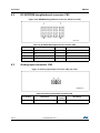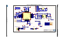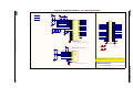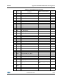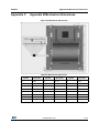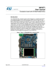
1
UM1903 User manual Evaluation board with STM32F756NG MCU Introduction The STM32756G-EVAL evaluation board is a complete demonstration and development platform for STMicroelectronics ARM® Cortex® -M7 core-based STM32F756NGH6 microcontroller. It features four I2C interfaces, six SPIs with three multiplexed simplex I2S interfaces, SDMMC, four USARTs, four UARTs, two CANs, three 12-bit ADCs, two 12-bit DACs, two SAIs, 8 to 14-bit digital camera module interface, internal 320+4 Kbytes SRAM and 1 Mbyte Flash memory, USB HS OTG and USB FS OTG, Ethernet MAC, FMC interface, Quad-SPI interface, cryptographic hardware accelerator, JTAG debugging support. This evaluation board can be used as a reference design for user application development but it is not considered as a final application. The full range of hardware features on the board helps the user to evaluate all peripherals (USB OTG HS, USB OTG FS, Ethernet, Motor control, CAN, microSD card, USART, Audio DAC and ADC, digital microphone, IrDA, RF-EEPROM, SRAM, Nor Flash memory, SDRAM, Quad-SPI Flash memory, 5.7" TFT LCD with a capacitive touch panel and others) and to develop his applications. Extension headers make it possible to easily connect a daughterboard for a specific application. The integrated ST-LINK/V2-1 provides an embedded in-circuit debugger and programmer for the STM32 MCU. Figure 1. STM32756G-EVAL evaluation board 1. Picture not contractual. June 2015 DocID027919 Rev 1 1/79 www.st.com 1 Contents UM1903 Contents 1 Features . . . . . . . . . . . . . . . . . . . . . . . . . . . . . . . . . . . . . . . . . . . . . . . . . . . 6 2 Demonstration software . . . . . . . . . . . . . . . . . . . . . . . . . . . . . . . . . . . . . . 7 3 Order code . . . . . . . . . . . . . . . . . . . . . . . . . . . . . . . . . . . . . . . . . . . . . . . . . 7 4 Delivery recommendations . . . . . . . . . . . . . . . . . . . . . . . . . . . . . . . . . . . 7 5 Hardware layout and configuration . . . . . . . . . . . . . . . . . . . . . . . . . . . . . 8 5.1 2/79 Embedded ST-LINK/V2-1 . . . . . . . . . . . . . . . . . . . . . . . . . . . . . . . . . . . . . 10 5.1.1 Drivers . . . . . . . . . . . . . . . . . . . . . . . . . . . . . . . . . . . . . . . . . . . . . . . . . . 11 5.1.2 ST-LINK/V2-1 firmware upgrade . . . . . . . . . . . . . . . . . . . . . . . . . . . . . . 11 5.2 Power supply . . . . . . . . . . . . . . . . . . . . . . . . . . . . . . . . . . . . . . . . . . . . . . 12 5.3 Clock source . . . . . . . . . . . . . . . . . . . . . . . . . . . . . . . . . . . . . . . . . . . . . . . 15 5.4 Reset source . . . . . . . . . . . . . . . . . . . . . . . . . . . . . . . . . . . . . . . . . . . . . . 16 5.5 Boot option . . . . . . . . . . . . . . . . . . . . . . . . . . . . . . . . . . . . . . . . . . . . . . . . 17 5.6 Audio . . . . . . . . . . . . . . . . . . . . . . . . . . . . . . . . . . . . . . . . . . . . . . . . . . . . 17 5.7 USB OTG FS1 . . . . . . . . . . . . . . . . . . . . . . . . . . . . . . . . . . . . . . . . . . . . . 20 5.8 USB OTG HS and USB OTG FS2 . . . . . . . . . . . . . . . . . . . . . . . . . . . . . . 20 5.9 RS232 and IrDA . . . . . . . . . . . . . . . . . . . . . . . . . . . . . . . . . . . . . . . . . . . . 21 5.10 microSD card . . . . . . . . . . . . . . . . . . . . . . . . . . . . . . . . . . . . . . . . . . . . . . 22 5.11 RF-EEPROM . . . . . . . . . . . . . . . . . . . . . . . . . . . . . . . . . . . . . . . . . . . . . . 22 5.12 CAN . . . . . . . . . . . . . . . . . . . . . . . . . . . . . . . . . . . . . . . . . . . . . . . . . . . . . 22 5.13 Ethernet . . . . . . . . . . . . . . . . . . . . . . . . . . . . . . . . . . . . . . . . . . . . . . . . . . 22 5.14 Memories . . . . . . . . . . . . . . . . . . . . . . . . . . . . . . . . . . . . . . . . . . . . . . . . . 23 5.15 Quad-SPI Nor Flash memory . . . . . . . . . . . . . . . . . . . . . . . . . . . . . . . . . . 24 5.16 Analog input . . . . . . . . . . . . . . . . . . . . . . . . . . . . . . . . . . . . . . . . . . . . . . . 24 5.17 Camera module . . . . . . . . . . . . . . . . . . . . . . . . . . . . . . . . . . . . . . . . . . . . 24 5.18 Display and input devices . . . . . . . . . . . . . . . . . . . . . . . . . . . . . . . . . . . . . 25 5.19 Motor control . . . . . . . . . . . . . . . . . . . . . . . . . . . . . . . . . . . . . . . . . . . . . . 27 5.20 MFX (Multi Function eXpander) . . . . . . . . . . . . . . . . . . . . . . . . . . . . . . . . 29 DocID027919 Rev 1 UM1903 6 Contents Connector . . . . . . . . . . . . . . . . . . . . . . . . . . . . . . . . . . . . . . . . . . . . . . . . 31 6.1 Motor control connector CN1 . . . . . . . . . . . . . . . . . . . . . . . . . . . . . . . . . . 31 6.2 RF-EEPROM daughterboard connector CN2 . . . . . . . . . . . . . . . . . . . . . 32 6.3 Analog input connector CN3 . . . . . . . . . . . . . . . . . . . . . . . . . . . . . . . . . . 32 6.4 Camera module connector CN4 . . . . . . . . . . . . . . . . . . . . . . . . . . . . . . . . 33 6.5 Daughterboard extension connector CN5 and CN6 . . . . . . . . . . . . . . . . . 34 6.6 RS232 connector CN7 . . . . . . . . . . . . . . . . . . . . . . . . . . . . . . . . . . . . . . . 38 6.7 USB OTG HS Micro-AB connector CN8 . . . . . . . . . . . . . . . . . . . . . . . . . 39 6.8 Ethernet RJ45 connector CN9 . . . . . . . . . . . . . . . . . . . . . . . . . . . . . . . . . 39 6.9 Memory connector CN10 and CN11 . . . . . . . . . . . . . . . . . . . . . . . . . . . . 40 6.10 ETM Trace debugging connector CN12 . . . . . . . . . . . . . . . . . . . . . . . . . . 43 6.11 USB OTG FS1 Micro-AB connector CN13 . . . . . . . . . . . . . . . . . . . . . . . . 43 6.12 USB OTG FS2 Micro-AB connector CN14 . . . . . . . . . . . . . . . . . . . . . . . . 44 6.13 JTAG/SWD connector CN15 . . . . . . . . . . . . . . . . . . . . . . . . . . . . . . . . . . 44 6.14 microSD connector CN16 . . . . . . . . . . . . . . . . . . . . . . . . . . . . . . . . . . . . . 45 6.15 Power connector CN17 . . . . . . . . . . . . . . . . . . . . . . . . . . . . . . . . . . . . . . 46 6.16 ST-LINK/V2-1 programming connector CN18 . . . . . . . . . . . . . . . . . . . . . 46 6.17 MFX programming connector CN19 . . . . . . . . . . . . . . . . . . . . . . . . . . . . . 46 6.18 TFT LCD connector CN20 . . . . . . . . . . . . . . . . . . . . . . . . . . . . . . . . . . . . 46 6.19 ST-LINK/V2-1 USB Type B connector CN21 . . . . . . . . . . . . . . . . . . . . . . 47 6.20 CAN D-type 9-pins male connector CN22 . . . . . . . . . . . . . . . . . . . . . . . . 47 6.21 MEMS microphone coupon connectors CN24 and CN27 . . . . . . . . . . . . 48 6.22 Audio jack (Speaker) CN25 . . . . . . . . . . . . . . . . . . . . . . . . . . . . . . . . . . . 48 6.23 Audio jack CN26 . . . . . . . . . . . . . . . . . . . . . . . . . . . . . . . . . . . . . . . . . . . . 48 6.24 SPDIF IN Connector CN28 . . . . . . . . . . . . . . . . . . . . . . . . . . . . . . . . . . . 49 Appendix A Electrical schematics . . . . . . . . . . . . . . . . . . . . . . . . . . . . . . . . . . . . 50 Appendix B Appendix A STM32756G-EVAL I/O assignment . . . . . . . . . . . . . . . 69 Appendix C Appendix B Mechanical dimensions . . . . . . . . . . . . . . . . . . . . . . . . 77 7 Revision History . . . . . . . . . . . . . . . . . . . . . . . . . . . . . . . . . . . . . . . . . . . 78 DocID027919 Rev 1 3/79 3 List of tables UM1903 List of tables Table 1. Table 2. Table 3. Table 4. Table 5. Table 6. Table 7. Table 8. Table 9. Table 10. Table 11. Table 12. Table 13. Table 14. Table 15. Table 16. Table 17. Table 18. Table 19. Table 20. Table 21. Table 22. Table 23. Table 24. Table 25. Table 26. Table 27. Table 28. Table 29. Table 30. Table 31. Table 32. Table 33. Table 34. Table 35. Table 36. Table 37. Table 38. Table 39. 4/79 Power related jumpers . . . . . . . . . . . . . . . . . . . . . . . . . . . . . . . . . . . . . . . . . . . . . . . . . . . . 13 25 MHz Crystal X1 related solder bridges . . . . . . . . . . . . . . . . . . . . . . . . . . . . . . . . . . . . . 16 32KHz Crystal X2 related solder bridges . . . . . . . . . . . . . . . . . . . . . . . . . . . . . . . . . . . . . . 16 Boot related Switch . . . . . . . . . . . . . . . . . . . . . . . . . . . . . . . . . . . . . . . . . . . . . . . . . . . . . . . 17 Boot related jumpers. . . . . . . . . . . . . . . . . . . . . . . . . . . . . . . . . . . . . . . . . . . . . . . . . . . . . . 17 Audio related jumpers . . . . . . . . . . . . . . . . . . . . . . . . . . . . . . . . . . . . . . . . . . . . . . . . . . . . . 18 USB OTG FS2 function configuration . . . . . . . . . . . . . . . . . . . . . . . . . . . . . . . . . . . . . . . . . 20 USART1 related jumpers . . . . . . . . . . . . . . . . . . . . . . . . . . . . . . . . . . . . . . . . . . . . . . . . . . 21 CAN related jumpers . . . . . . . . . . . . . . . . . . . . . . . . . . . . . . . . . . . . . . . . . . . . . . . . . . . . . 22 Ethernet related jumpers . . . . . . . . . . . . . . . . . . . . . . . . . . . . . . . . . . . . . . . . . . . . . . . . . . 23 Ethernet related solder bridges. . . . . . . . . . . . . . . . . . . . . . . . . . . . . . . . . . . . . . . . . . . . . . 23 NOR Flash memory related jumpers . . . . . . . . . . . . . . . . . . . . . . . . . . . . . . . . . . . . . . . . . 24 LED related jumpers . . . . . . . . . . . . . . . . . . . . . . . . . . . . . . . . . . . . . . . . . . . . . . . . . . . . . . 25 LCD modules connector (CN20). . . . . . . . . . . . . . . . . . . . . . . . . . . . . . . . . . . . . . . . . . . . . 25 Motor control related solder bridges . . . . . . . . . . . . . . . . . . . . . . . . . . . . . . . . . . . . . . . . . . 29 MFX signals . . . . . . . . . . . . . . . . . . . . . . . . . . . . . . . . . . . . . . . . . . . . . . . . . . . . . . . . . . . . 29 Motor control connector CN1 . . . . . . . . . . . . . . . . . . . . . . . . . . . . . . . . . . . . . . . . . . . . . . . 31 RF-EEPROM daughterboard connector CN2 . . . . . . . . . . . . . . . . . . . . . . . . . . . . . . . . . . . 32 Analog input-output connector CN3 . . . . . . . . . . . . . . . . . . . . . . . . . . . . . . . . . . . . . . . . . . 32 Camera module connector CN4 . . . . . . . . . . . . . . . . . . . . . . . . . . . . . . . . . . . . . . . . . . . . . 33 Daughterboard extension connector CN5 . . . . . . . . . . . . . . . . . . . . . . . . . . . . . . . . . . . . . 34 Daughterboard extension connector CN6 . . . . . . . . . . . . . . . . . . . . . . . . . . . . . . . . . . . . . 36 RS232 connector CN7 with ISP support. . . . . . . . . . . . . . . . . . . . . . . . . . . . . . . . . . . . . . . 38 USB OTG HS Micro-AB connector CN8 . . . . . . . . . . . . . . . . . . . . . . . . . . . . . . . . . . . . . . . 39 RJ45 connector CN9 . . . . . . . . . . . . . . . . . . . . . . . . . . . . . . . . . . . . . . . . . . . . . . . . . . . . . 39 Memory connector CN10 . . . . . . . . . . . . . . . . . . . . . . . . . . . . . . . . . . . . . . . . . . . . . . . . . . 40 Memory connector CN11 . . . . . . . . . . . . . . . . . . . . . . . . . . . . . . . . . . . . . . . . . . . . . . . . . . 41 ETM Trace debugging connector CN12 . . . . . . . . . . . . . . . . . . . . . . . . . . . . . . . . . . . . . . . 43 USB OTG FS1 Micro-AB connector CN13 . . . . . . . . . . . . . . . . . . . . . . . . . . . . . . . . . . . . . 44 USB OTG FS2 Micro-AB connector CN14 . . . . . . . . . . . . . . . . . . . . . . . . . . . . . . . . . . . . . 44 JTAG/SWD debugging connector CN15 . . . . . . . . . . . . . . . . . . . . . . . . . . . . . . . . . . . . . . 45 microSD connector CN16 . . . . . . . . . . . . . . . . . . . . . . . . . . . . . . . . . . . . . . . . . . . . . . . . . . 45 USB type B connector CN21 . . . . . . . . . . . . . . . . . . . . . . . . . . . . . . . . . . . . . . . . . . . . . . . 47 CAN D-type 9-pins male connector CN22 . . . . . . . . . . . . . . . . . . . . . . . . . . . . . . . . . . . . . 47 MEMS microphone coupon connectors CN24 and CN27. . . . . . . . . . . . . . . . . . . . . . . . . . 48 SPDIF IN connector CN28 . . . . . . . . . . . . . . . . . . . . . . . . . . . . . . . . . . . . . . . . . . . . . . . . . 49 I/O assignment . . . . . . . . . . . . . . . . . . . . . . . . . . . . . . . . . . . . . . . . . . . . . . . . . . . . . . . . . . 69 Mechanical dimensions . . . . . . . . . . . . . . . . . . . . . . . . . . . . . . . . . . . . . . . . . . . . . . . . . . . 77 Document Revision History . . . . . . . . . . . . . . . . . . . . . . . . . . . . . . . . . . . . . . . . . . . . . . . . 78 DocID027919 Rev 1 UM1903 List of figures List of figures Figure 1. Figure 2. Figure 3. Figure 4. Figure 5. Figure 6. Figure 7. Figure 8. Figure 9. Figure 10. Figure 11. Figure 12. Figure 13. Figure 14. Figure 15. Figure 16. Figure 17. Figure 18. Figure 19. Figure 20. Figure 21. Figure 22. Figure 23. Figure 24. Figure 25. Figure 26. Figure 27. Figure 28. Figure 29. Figure 30. Figure 31. Figure 32. Figure 33. Figure 34. Figure 35. Figure 36. Figure 37. Figure 38. Figure 39. Figure 40. Figure 41. Figure 42. Figure 43. Figure 44. STM32756G-EVAL evaluation board . . . . . . . . . . . . . . . . . . . . . . . . . . . . . . . . . . . . . . . . . . 1 Hardware Block Diagram . . . . . . . . . . . . . . . . . . . . . . . . . . . . . . . . . . . . . . . . . . . . . . . . . . . 9 STM32756G-EVAL evaluation board layout . . . . . . . . . . . . . . . . . . . . . . . . . . . . . . . . . . . . 10 USB composite device . . . . . . . . . . . . . . . . . . . . . . . . . . . . . . . . . . . . . . . . . . . . . . . . . . . . 11 Orientation setting of 5.7-inch LCD daughterboard . . . . . . . . . . . . . . . . . . . . . . . . . . . . . . 27 STM32756G-EVAL evaluation board motor control PCB reworks (bottom side) . . . . . . . . . . . . . . . . . . . . . . . . . . . . . . . . . . . . . . . . . . . . . . . . . . . . . 28 STM32756G-EVAL evaluation board motor control PCB reworks (top side) . . . . . . . . . . . . . . . . . . . . . . . . . . . . . . . . . . . . . . . . . . . . . . . . . . . . . . . . 28 Motor control connector CN1 (Top view) . . . . . . . . . . . . . . . . . . . . . . . . . . . . . . . . . . . . . . 31 RF-EEPROM daughterboard connector CN2 (Front view) . . . . . . . . . . . . . . . . . . . . . . . . . 32 Analog input-output connector CN3 (Top view) . . . . . . . . . . . . . . . . . . . . . . . . . . . . . . . . . 32 Camera module connector CN4 (Top view) . . . . . . . . . . . . . . . . . . . . . . . . . . . . . . . . . . . . 33 RS232 connector CN7(Front view) . . . . . . . . . . . . . . . . . . . . . . . . . . . . . . . . . . . . . . . . . . . 38 USB OTG HS Micro-AB connector CN8 (Front view) . . . . . . . . . . . . . . . . . . . . . . . . . . . . . 39 Ethernet RJ45 connector CN9 (Front view) . . . . . . . . . . . . . . . . . . . . . . . . . . . . . . . . . . . . 39 ETM Trace debugging connector CN12 (Top view) . . . . . . . . . . . . . . . . . . . . . . . . . . . . . . 43 USB OTG FS1 Micro-AB connector CN13 (Front view) . . . . . . . . . . . . . . . . . . . . . . . . . . . 43 USB OTG FS2 Micro-AB connector CN14 (Front view) . . . . . . . . . . . . . . . . . . . . . . . . . . . 44 JTAG/SWD debugging connector CN15 (Top view). . . . . . . . . . . . . . . . . . . . . . . . . . . . . . 44 microSD connector CN16 (Top view) . . . . . . . . . . . . . . . . . . . . . . . . . . . . . . . . . . . . . . . . . 45 Power supply connector CN17 (Front view) . . . . . . . . . . . . . . . . . . . . . . . . . . . . . . . . . . . 46 USB type B connector CN21 (Front view) . . . . . . . . . . . . . . . . . . . . . . . . . . . . . . . . . . . . . 47 CAN D-type 9-pins male connector CN22 (Front view) . . . . . . . . . . . . . . . . . . . . . . . . . . . 47 MEMS microphone coupon connectors CN24 and CN27(Top view) . . . . . . . . . . . . . . . . . 48 SPDIF IN connector CN28 (Front view) . . . . . . . . . . . . . . . . . . . . . . . . . . . . . . . . . . . . . . . 49 STM32756G-EVAL evaluation board . . . . . . . . . . . . . . . . . . . . . . . . . . . . . . . . . . . . . . . . . 50 STM32756G-EVAL MCU . . . . . . . . . . . . . . . . . . . . . . . . . . . . . . . . . . . . . . . . . . . . . . . . . . 51 STM32756G-EVAL Power . . . . . . . . . . . . . . . . . . . . . . . . . . . . . . . . . . . . . . . . . . . . . . . . . 52 STM32756G-EVAL SRAM, Flash memory and DRAM . . . . . . . . . . . . . . . . . . . . . . . . . . . 53 STM32756G-EVAL Audio . . . . . . . . . . . . . . . . . . . . . . . . . . . . . . . . . . . . . . . . . . . . . . . . . 54 STM32756G-EVAL LCD, Camera and RF connector. . . . . . . . . . . . . . . . . . . . . . . . . . . . . 55 STM32756G-EVAL Ethernet . . . . . . . . . . . . . . . . . . . . . . . . . . . . . . . . . . . . . . . . . . . . . . . 56 STM32756G-EVAL USB OTG HS and OTG FS2 . . . . . . . . . . . . . . . . . . . . . . . . . . . . . . . 57 STM32756G-EVAL USB OTG FS1 . . . . . . . . . . . . . . . . . . . . . . . . . . . . . . . . . . . . . . . . . . 58 STM32756G-EVAL RS232 and IrDA . . . . . . . . . . . . . . . . . . . . . . . . . . . . . . . . . . . . . . . . . 59 STM32756G-EVAL CAN and QSPI . . . . . . . . . . . . . . . . . . . . . . . . . . . . . . . . . . . . . . . . . . 60 STM32756G-EVAL Peripherals . . . . . . . . . . . . . . . . . . . . . . . . . . . . . . . . . . . . . . . . . . . . . 61 STM32756G-EVAL Motor control . . . . . . . . . . . . . . . . . . . . . . . . . . . . . . . . . . . . . . . . . . . . 62 STM32756G-EVAL Extension connector . . . . . . . . . . . . . . . . . . . . . . . . . . . . . . . . . . . . . . 63 STM32756G-EVAL ST-LINK/V2-1 . . . . . . . . . . . . . . . . . . . . . . . . . . . . . . . . . . . . . . . . . . . 64 STM32756G-EVAL MFX . . . . . . . . . . . . . . . . . . . . . . . . . . . . . . . . . . . . . . . . . . . . . . . . . . 65 STM32756G-EVAL JTAG and Trace . . . . . . . . . . . . . . . . . . . . . . . . . . . . . . . . . . . . . . . . . 66 STM32756G-EVAL Camera daughterboard . . . . . . . . . . . . . . . . . . . . . . . . . . . . . . . . . . . . 67 STM32756G-EVAL 5.7 TFT LCD daughterboard . . . . . . . . . . . . . . . . . . . . . . . . . . . . . . . . 68 Mechanical dimensions . . . . . . . . . . . . . . . . . . . . . . . . . . . . . . . . . . . . . . . . . . . . . . . . . . . 77 DocID027919 Rev 1 5/79 5 Features 1 6/79 UM1903 Features STM32F756NGH6 microcontroller with 1 Mbyte Flash memory and 320+4 Kbytes RAM Six 5 V power supply options: – Power jack – ST-LINK/V2-1 USB connector – User USB HS connector – User USB FS1 connector – User USB FS2 connector – Daughterboard SAI Audio DAC, stereo audio jack which supports headset with microphone Stereo digital microphone, audio jack connector used to connect external speakers 2 Gbytes (or more) SDMMC interface microSD card RF-EEPROM on I2C compatible serial interface RS232 communication IrDA transceiver JTAG/SWD and ETM trace debug support Embedded ST-LINK/V2-1 IEEE-802.3-2002 compliant Ethernet connector Camera module 8Mx32bit SDRAM, 1Mx16bit SRAM and 8Mx16bit Nor Flash memory 512-Mbit Quad-SPI Nor Flash memory 5.7 inches 640x480 pixels TFT color LCD with touch panel Joystick with 4-direction control and selector Reset, WakeUp/Tamper or key button 4 color user LEDs Extension connectors and memory connectors for daughterboard or wrapping board USB OTG HS and FS with Micro-AB connectors RTC with backup battery CAN2.0 A/B compliant connection Potentiometer Motor control connector DocID027919 Rev 1 UM1903 2 Demonstration software Demonstration software Demonstration software is preloaded in the Flash memory of the STM32F756NGH6 MCU for easy demonstration of the device peripherals in stand-alone mode. For more information and to download the latest version available, refer to the STM32756G-EVAL demonstration software available on www.st.com. 3 Order code To order the evaluation board for STM32F756NGH6 MCU, use the order code: STM32756G-EVAL2. 4 Delivery recommendations Some verifications are needed before using the evaluation board for the first time, to make sure that nothing was damaged during shipment and that no components are unplugged or lost. When the board is extracted from its plastic bag, check that no component remains in the bag. The main components to verify are: Caution: The 25MHz crystal (X1) and 25MHz crystal (X4), which may have been removed from its socket by a shock The microSD card, which may have been ejected from the connector CN16 (right side of the board) The dual-interface EEPROM board (ANT7-M24LR-A), which may have been unplugged from the connector CN2 (top left corner of the board) There is an explosion risk, if the battery is replaced by an incorrect one. DocID027919 Rev 1 7/79 78 Hardware layout and configuration 5 UM1903 Hardware layout and configuration STM32756G-EVAL evaluation board is designed around the STM32F756NGH6 (216-pin TFBGA package) MCU. The hardware block diagram Figure 2: Hardware Block Diagram illustrates the connection between STM32F756NGH6 MCU and peripherals (SDRAM, SRAM, Nor Flash memory, QSPI Flash memory, Camera module, Color LCD, USB OTG connectors, Motor control connector, USART, IrDA, Ethernet, Audio, CAN, RF-EEPROM, microSD card and embedded ST-LINK/V2-1). 8/79 DocID027919 Rev 1 UM1903 Hardware layout and configuration Figure 2. Hardware Block Diagram 93RZHU 6XSSO\ 9%DWWHU\ .+]&U\VWDO 9%$7 27* )6 86%FRQQHFWRU *3,2 .H\:DNHXS 7DPSHUEXWWRQV $'& 3RWHQWLRPHWHU 57& 6:7UDFH FRQQHFWRU 73,8 9*$/&' /&' 63',)B5; $XGLR,1 ,5'$ 56'% FRQQHFWRU 8$57 463, )ODVK 670)1*+ 67/,1.9 -7$*7UDFH FRQQHFWRU '$3 125)ODVK )0& ,2BH[SDQGHU -R\VWLFN7RXFK VFUHHQ ,& 5)(3520RU $&3RQ FRQQHFWRU 65$0 6$, 6'5$0 0LFUR6'FDUG 6'00& $XGLR'$& $PSOLILHU &$1 &$1FRQQHFWRU 27* +63+<86% FRQQHFWRU 06[[[[[9 3+<(WKHUQHW &RQQHFWRU 0,, 86%FRQQHFWRU '&0, &DPHUD FRQQHFWRU 0RWRUFRQWURO FRQQHFWRU 06Y9 1. The red circles show the I/O shared among the default functions and the camera or the motor control connectors. DocID027919 Rev 1 9/79 78 Hardware layout and configuration UM1903 Figure 3 will help the user to locate all these features on the actual evaluation board. Figure 3. STM32756G-EVAL evaluation board layout 5.1 Embedded ST-LINK/V2-1 The ST-LINK/V2-1 programming and debugging tool is embedded on the STM32756GEVAL evaluation board. Compared to ST-LINK/V2 the changes are listed below. The new features supported on ST-LINK/V2-1 are: USB software re-enumeration Virtual com port interface on USB Mass storage interface on USB USB power management request for more than 100 mA power on USB This feature is no more supported on ST-LINK/V2-1: SWIM interface For all general information concerning debugging and programming features common between ST-LINK/V2 and ST-LINK/V2-1 refer to ST-LINK/V2 User Manual UM1075. 10/79 DocID027919 Rev 1 UM1903 Hardware layout and configuration Note: ETM can only work at 50 MHz clock by default, because ETM signals are shared with other peripherals. If a better performance of ETM is required (84 MHz/98 MHz), R31, R34, R35, R37, R39, R247, SB4, SB16, SB18 must be removed, to reduce the stub on ETM signals. In this configuration SAI, Ethernet and Camera are not functional and Nor Flash memory and SRAM addresses are limited on A18. 5.1.1 Drivers The ST-LINK/V2-1 requires a dedicated USB driver, which can be found on www.st.com for Windows 7 and 8. On Windows XP the ST-LINK/V2-1 driver requires WinUsb to be installed before using the ST-LINK/V2-1 (either available from Microsoft website or included in the USB driver for ST-LINK/V2 for XP). In case the STM32756G-EVAL evaluation board is connected to the PC, before the driver is installed, some STM32756G-EVAL interfaces may be declared as “Unknown” in the PC device manager. In this case the user must install the driver files, and update the driver of the connected device from the device manager. Note: Prefer using the “USB Composite Device” handle for a full recovery. Figure 4. USB composite device 5.1.2 ST-LINK/V2-1 firmware upgrade The ST-LINK/V2-1 embeds a firmware upgrade mechanism for in-situ upgrade through the USB port. As the firmware may evolve during the life time of the ST-LINK/V2-1 product (for example new functionalities, bug fixes, support for new microcontroller families), it is recommended to visit www.st.com before starting to use the STM32756G-EVAL board and periodically, in order to stay up-to-date with the latest firmware version. DocID027919 Rev 1 11/79 78 Hardware layout and configuration 5.2 UM1903 Power supply STM32756G-EVAL evaluation board is designed to be powered by 5 V DC power supply and it is protected by PolyZen from wrong power plug-in event. It is possible to configure the evaluation board to use any of the following six sources for the power supply: 5 V DC power adapter connected on the board to the power jack CN17, the power jack on the board (Power Supply Unit on silk screen of JP13(PSU)). This is default setting of power supply source selection on STM32756G-EVAL evaluation board. 5 V DC power with 300 mA limitation from CN21, the USB type B connector of ST-LINK/V2-1 (USB 5 V power source on silkscreen of JP13(STlk)). If the USB enumeration succeeds (as explained below), the ST-LINK/V2-1 U5V power is enabled, by asserting the PWR_EN pin. This pin is connected to a power switch (ST890), which powers the board. This power switch features also a current limitation to protect the PC in case of short-circuit on board. If an overcurrent (more than 600 mA) happens on the board, the LED LD11 is lit. This setting cannot be used as default power source selection, because the whole board power consumption will be larger than the current limitation of DC power from CN21. 5V DC power with 500 mA limitation from CN8, the USB OTG HS Micro-AB connector (USB 5V power source on silkscreen of JP13 (HS)). 5V DC power with 500 mA limitation from CN13, the USB OTG FS1 Micro-AB connector (USB 5V power source on silkscreen of JP13 (FS1)). 5V DC power with 500 mA limitation from CN14, the USB OTG FS2 Micro-AB connector (USB 5V power source on silkscreen of JP13 (FS2)). 5V DC power from CN5 and CN6, the extension connectors for daughterboard (daughterboard power source on silkscreen of JP13 (D5V)). STM32756G-EVAL evaluation board can be powered from ST-LINK/V2-1 USB connector CN21 (U5V), only when the 5.7" LCD is disconnected, otherwise power consumption exceeds 300mA. When the board is connected to USB port only the ST-LINK/V2-1 is powered for the USB enumeration, because host PC only provides 100 mA max to the board at that time. During the USB enumeration, STM32756G-EVAL board requires 300 mA power from the host PC. If the host PC is able to provide the required power, the enumeration succeeds and the power transistor U17 (ST890) is switched ON, the red LED LD10 is turned ON, thus STM32756G-EVAL evaluation board can consume no more than 300 mA of current. If the host PC is not able to provide the requested current, the enumeration fails. Therefore the ST890 (U17) remains OFF so consequently 3.3 V domain of the board and MCU will not be powered. As a consequence, the red LED LD10 remains turned OFF. In this case it is mandatory to use an external power supply as extra power supply. E5V (from PSU) or D5V must be used as external power supply, in case current consumption of STM32756G-EVAL evaluation board exceeds the allowed current on USB. In this condition it is still possible to use USB for communication, for programming or debugging only, but it is mandatory to power the board, first using E5V or D5V, then connecting the USB cable to the PC. Proceeding this way ensures that the enumeration succeeds, thanks to the external power source. 12/79 DocID027919 Rev 1 UM1903 Hardware layout and configuration The following power sequence procedure must be respected: Connect jumper JP13 for PSU or D5V side Check that JP15 is removed Connect the external power source to PSU or D5V (daughterboard mounted) Check red LED LD10 is turned ON Connect the PC to USB connector CN21 If this order is not respected, the board may be powered by VBUS first then E5V or D5V, and the following risks may be encountered: Note: 1. If more than 300 mA current is needed by the board, the PC may be damaged or current can be limited by PC. As a consequence the board is not powered correctly. 2. 300 mA will be requested at enumeration (since JP15 must be OFF), so there is risk that request is rejected and enumeration does not succeed if the PC cannot provide such current. Consequently the board is not powered (the led LD10 remains OFF). In case the board is powered by an USB charger, there is no USB enumeration, so the led LD10 remains set to OFF permanently and the board is not powered. Only in this specific case the jumper JP15 needs to be set to ON, to allow the board to be powered anyway but in any cases the current will be limited to 600 mA by U17 (ST890). The power supply is configured by setting the related jumpers JP2, JP9 and JP13 as described in Table 1. Table 1. Power related jumpers Jumper JP2 Description JP2 is used to measure MCU current consumption manually by multimeter. Default setting: Fitted Vbat is connected to +3.3 V when JP9 is set as shown to the right (Default setting): 1 2 3 JP9 Vbat is connected to battery when JP9 is set as shown to the right: 1 2 3 JP13 is used to select one of the six possible power supply resources. For power supply jack (CN17) to the STM32756G-EVAL only, JP13 is set as shown to the right (Default setting): +6 )6 JP13 )6 '9 368 67ON 069 DocID027919 Rev 1 13/79 78 Hardware layout and configuration UM1903 Table 1. Power related jumpers (continued) Jumper Description For power supply from USB connector of ST-LINK/V2-1 (CN21) to STM32756GEVAL only, JP13 is set as shown to the right: +6 )6 )6 '9 368 67ON 069 For power supply from the daughterboard connectors (CN5 and CN6) to STM32756G-EVAL only, JP13 is set as shown to the right: +6 )6 )6 '9 368 67ON 069 JP13 For power supply from USB OTG FS2 (CN14) to STM32756G-EVAL only, JP13 is set as shown to the right: +6 )6 )6 '9 368 67ON 069 For power supply from USB OTG FS1 (CN13) to STM32756G-EVAL only, JP13 is set as shown to the right: +6 )6 )6 '9 368 67ON 069 14/79 DocID027919 Rev 1 UM1903 Hardware layout and configuration Table 1. Power related jumpers (continued) Jumper Description For power supply from USB OTG HS (CN8) to STM32756G-EVAL only, JP13 is set as shown to the right: +6 )6 )6 '9 368 67ON 069 JP13 For power supply from power supply jack(CN17) to both STM32756G-EVAL and daughterboard connected on CN5 and CN6, JP13 is set as shown to the right (daughterboard must not have its own power supply connected): +6 )6 )6 '9 368 67ON 069 The led LD10 is lit when the STM32756G-EVAL evaluation board is correctly powered by the 5 V . Note: In order to avoid the impact of USB PHY and Ethernet PHY and get precise results of current consumption on JP2, the following cautions need to be taken into account: 1) Configure Ethernet PHY into Power Down Mode by setting low level of IO_Expander (EXP_IO1) 2) Configure USB HS PHY into Low Power Mode (Register Address=04,bit 6 in USB PHY). 5.3 Clock source Two clock sources are available on STM32756G-EVAL evaluation board for STM32F756NGH6 MCU and RTC embedded. Three clock resources for camera, Ethernet PHY and USB OTG PHY: X1, 25 MHz Crystal with socket for STM32F756NGH6 Microcontroller, it can be removed from socket when internal RC clock is used. X2, 32 KHz Crystal for embedded RTC X3, 24 MHz oscillator for camera module (Default on camera daughterboard) X4, 25 MHz Crystal with socket for Ethernet PHY. X5, 24 MHz Crystal for USB OTG HS PHY. DocID027919 Rev 1 15/79 78 Hardware layout and configuration UM1903 Table 2. 25 MHz Crystal X1 related solder bridges Jumper SB27 SB28 T Description PH0 is connected to 25 MHz crystal when SB27 is open. (Default setting) PH0 is connected to extension connector CN5 when SB27 is closed. In such case R19 must be removed to avoid disturbance due to the 25 MHz quartz PH1 is connected to 25MHz crystal when SB28 is open. (Default setting) PH1 is connected to extension connector CN5 when SB28 is closed. In such case C23 and X1 must be removed to avoid disturbance due to the 25 MHz quartz Table 3. 32KHz Crystal X2 related solder bridges Solder Bridge SB25 SB26 Description PC14 is connected to 32 KHz crystal when SB25 is open. (Default setting) PC14 is connected to extension connector CN6 when SB25 is closed. In such case R18 must be removed to avoid disturbance due to the 32 Khz quartz PC15 is connected to 32 KHz crystal when SB26 is open. (Default setting) PC15 is connected to extension connector CN6 when SB26 is closed. In such case R17 must be removed to avoid disturbance due to the 32 Khz quartz Note: About the jumper JP6 for Ethernet clock, refer to Section 5.13: Ethernet. 5.4 Reset source The reset signal of STM32756G-EVAL evaluation board is low active and the reset sources include: Note: 16/79 Reset button B1 Debugging Tools from JTAG/SWD connector CN15 and ETM trace connector CN12 Daughterboard from CN5 Embedded ST-LINK/V2-1 RS232 connector CN7 for ISP The jumper JP3 has to be closed for RESET handled by the pin 8 of the RS232 connector CN7 (CTS signal). DocID027919 Rev 1 UM1903 5.5 Hardware layout and configuration Boot option STM32756G-EVAL evaluation board can boot from: Embedded User Flash memory System memory with boot loader for ISP Embedded SRAM for debugging The boot option is configured by setting switch SW1 (BOOT) and the boot base address is programmed in the BOOT_ADD0 and BOOT_ADD1 option bytes. The BOOT can be configured also via RS232 connector CN7. Table 4. Boot related Switch Boot address Switch configuration option bytes BOOT_ADD0 [15:0] STM32756G-EVAL boot from BOOT_ADD0[15:0] ST programmed value: Flash memory on ITCM at 0x0020 0000 (Default setting). BOOT_ADD1 [15:0] STM32756G-EVAL boot from BOOT_ADD1[15:0] ST programmed value: System bootloader at 0x0010 0000 0<->1 SW1 0<->1 SW1 Boot space Table 5. Boot related jumpers Jumper JP1 Description The Bootloader_BOOT is managed by pin 6 of connector CN7 (RS232 DSR signal) when JP1 is closed. This configuration is used for boot loader application only. Default setting: Not fitted 5.6 Audio An audio codec WM8994ECS/R, with 4 DACs and 2 ADCs inside, is connected to SAI interface of STM32F756NGH6 MCU to support TDM feature on SAI port. This feature is able to implement audio recording on digital microphone and analog microphone and audio playback of different audio stream on headphone and lineout at the same time. It communicates with STM32F756NGH6 MCU via I2C1 bus which is shared with LCD, camera module, RF-EEPROM and MFX (Multi Function eXpander). The analog microphone on the headset is connected to ADC of WM8994ECS/R through the audio jack connector CN26. External speakers can be connected to WM8994ECS/R via audio jack connector CN25. Two digital microphones (MEMs microphone) MP34DT01TR are on STM32756G-EVAL evaluation board. They are able to be connected to either audio codec or I2S port of DocID027919 Rev 1 17/79 78 Hardware layout and configuration UM1903 STM32F756NGH6 MCU, by setting the jumpers shown in Table 6. The coupon connectors CN24 and CN27 can be used to support MEMS microphone evaluation board STEVALMKI129V1 after removing SB20 and SB21. An optical connector CN28, compatible with SPDIF spec, is implemented on STM32756GEVAL, to receive external audio data. Table 6. Audio related jumpers Jumper Description Data signal on digital microphone is connected to audio codec when JP18 is set as shown to the right (Default setting): 1 2 3 JP18 Data signal on digital microphone is connected to I2S port of STM32F756NGH6 when JP18 is set as shown to the right (it is also needed to set JP5, according to this table): 1 2 3 Clock signal on digital microphone is connected to audio codec when JP19 is set as shown to the right (Default setting): 1 2 3 JP19 Clock signal on digital microphone is connected to timer output (PC7) of STM32F756NGH6, used to divide by two I2S clock, when JP19 is set as shown to the right (it is also needed to set JP4 according to this table): 1 2 3 PB3 is as TDO/SWO signal when JP4 is set as shown to the right (Default setting): 1 2 3 JP4 PB3 (I2S Clock) is connected to Timer input (PC6) of STM32F756NGH6, used as microphone clock divider, when JP4 is set as shown to the right (it is also needed to set JP19 according to this table): 1 2 3 18/79 DocID027919 Rev 1 UM1903 Hardware layout and configuration Table 6. Audio related jumpers (continued) Jumper Description PD6 is as FMC_NWAIT signal when JP5 is set as shown to the right (Default setting): 1 2 3 JP5 PD6 is connected to digital microphone as I2S data signal when JP5 is set as shown to the right (it is also needed to set JP18 together according to this table): 1 2 3 Digital microphone power source is connected to +3.3 V power when JP17 is set as shown to the right (Default setting): 1 2 3 JP17 Digital microphone power source is connected to MICBIAS1 from WM8994ECS/R when JP17 is set as shown to the right: 1 2 3 PA2 is connected to SAI2_SCKB when JP21 is set as shown to the right (Default setting): 1 2 3 JP21 PA2 is connected to MII_MDIO (Ethernet) when JP21 is set as shown to the right: 1 2 3 PC1 is connected to SAI1_SDA when JP22 is set as shown to the right (Default setting): 1 2 3 JP22 PC1 is connected to MII_MDC (Ethernet) when JP22 is set as shown to the right: 1 2 3 Note: The I2C address of WM8994ECS/R is 0b0011010. DocID027919 Rev 1 19/79 78 Hardware layout and configuration 5.7 UM1903 USB OTG FS1 STM32756G-EVAL evaluation board supports USB OTG full speed communication via a USB Micro-AB connector (CN13) and USB power switch (U11) connected to VBUS. The evaluation board can be powered by this USB connection at 5 V DC with 500 mA current limitation. A green led LD7 will be lit in one of these cases: Power switch (U11) is ON and STM32756G-EVAL works as a USB host VBUS is powered by another USB host when STM32756G-EVAL works as a USB device The red led LD8 will be lit when overcurrent occurs. Note: STM32756G-EVAL evaluation board should be powered by external power supply when using OTG function. Note: JP8 must be removed when using USB OTG FS as mentioned in Table 9. 5.8 USB OTG HS and USB OTG FS2 STM32756G-EVAL evaluation board supports USB OTG FS2: High speed communication via a USB Micro-AB connector (CN8), USB High speed PHY (U8) for high speed function. Full speed communication via another USB Micro-AB connector (CN14) The evaluation board can be powered by these USB connectors (CN8 or CN14) at 5 V DC with 500 mA current limitation. As several OTG FS2 signals are shared with OTG HS ULPI bus, some PCB reworks are needed, when using OTG FS2 (CN14), as shown in Table 7. Table 7. USB OTG FS2 function configuration Function Mount Remove OTG HS-CN8 (Default) R109,R115,SB12,SB15 R259,SB13,SB14,SB51 OTG FS2-CN14 R259,SB13,SB14,SB51 R109,R115,SB12,SB15 An USB power switch (U7) is also connected on VBUS and provides power to either CN8 (with SB12 and SB15 closed and SB13 and SB14 open), or CN14 (with SB13 and SB14 closed and SB12 and SB15 open). Green led LD5(for CN8) or LD9(for CN14) will be lit when either power switch (U7) is ON and STM32756G-EVAL works as a USB host, or VBUS is powered by another USB host when STM32756G-EVAL works as a USB device. The red led LD6 will be lit when over-current occurs. Note: 20/79 STM32756G-EVAL evaluation board should be powered, by an external power supply when using OTG function. DocID027919 Rev 1 UM1903 5.9 Hardware layout and configuration RS232 and IrDA RS232 and IrDA communication is supported by D-type 9-pins RS232 connector CN7, and IrDA transceiver U1, which is connected to USART1 of STM32F756NGH6 MCU on STM32756G-EVAL evaluation board. The signal Bootloader_RESET and Bootloader_BOOT are added on RS232 connector CN7 for ISP support. USART1 of STM32F756NGH6 MCU is shared with RS232/IrDA and ST-LINK/V2-1 controller. Its communication can be changed by setting JP14 and JP20. Table 8. USART1 related jumpers Jumper Description USART1_RX is connected to RS232/IrDA when JP14 is set as shown to the right (Default setting): 1 2 3 JP14 USART1_RX is connected to ST-LINK/V2-1 controller’s USART_TX when JP14 is set as shown to the right: 1 2 3 USART1_TX is connected to RS232/IrDA when JP20 is set as shown to the right (Default setting): 1 2 3 JP20 USART1_TX is connected to ST-LINK/V2-1 controller’s USART_RX when JP20 is set as shown to the right: 1 2 3 USART1_RX is connected to RS232 transceiver and RS232 communication is enabled when JP14 is set to pin1-2 and JP7 is set as shown to the right (Default setting): 1 2 3 JP7 USART1_RX is connected to IrDA transceiver and IrDA communication is enabled when JP14 is set to pin1-2 and JP7 is set as shown to the right: 1 2 3 DocID027919 Rev 1 21/79 78 Hardware layout and configuration 5.10 UM1903 microSD card The 2 Gbytes (or more) microSD card connected to SDMMC1 port of STM32F756NGH6 MCU, is available on the board. Detection of the microSD card is managed by MFX GPIO15. 5.11 RF-EEPROM RF-EEPROM daughterboard ANT7-M24LR-A is mounted on CN2 of STM32F756NGH6 MCU via I2C1 bus. The RF-EEPROM can be accessed by the microcontroller via the I2C1 bus or by Radio Frequency (RF), using a 13.56 MHz reader (for example, CR95HF). The I2C address of RF-EEPROM is 0b1010000. 5.12 CAN STM32756G-EVAL evaluation board supports one channel of CAN2.0 A/B compliant CAN bus communication based on 3.3 V CAN transceiver. High-speed mode, standby mode and slope control mode are available and can be selected by setting JP11. Table 9. CAN related jumpers Jumper Description CAN transceiver is working in standby mode when JP11 is set as shown to the right: 1 2 3 JP11 CAN transceiver is working in high-speed mode when JP11 is set as shown to the right (Default setting): 1 2 3 CAN transceiver is working in slope control mode when JP11 is open. 5.13 JP12 CAN terminal resistor is enabled when JP12 is fitted. Default setting: Not fitted JP8 PA11 is connected with CAN RX signal when JP8 is fitted. Default setting: Not fitted Ethernet STM32756G-EVAL evaluation board supports 10 M/100 M Ethernet communication by a PHY DP83848CVV(U6) and integrated RJ45 connector (CN9). Ethernet PHY is connected to STM32F756NGH6 MCU via MII interface. A 25 M clock can be generated by PHY or 22/79 DocID027919 Rev 1 UM1903 Hardware layout and configuration provided by MCO from STM32F756NGH6 MCU by setting the jumper JP6 as shown in Table 10: Ethernet related jumpers. MII Serial Management signals (MDIO and MDC) are simulated by GPIOs (PG6 and PG7) on STM32756G-EVAL evaluation board by default. The original MII serial management signals of the Ethernet IP in STM32F756NGH6 MCU, can be also used by setting JP21 and JP22. Refer to Table 6: Audio related jumpers for all the details. Table 10. Ethernet related jumpers Jumper Description 25 MHz clock is provided by external crystal X4 when JP6 is set as shown to the right (Default setting): 1 2 3 JP6 25 MHz clock for MII is provided by MCO at PA8 when JP6 is set as shown to the right: 1 2 3 Table 11. Ethernet related solder bridges Solder Bridges 5.14 Description SB36 MII CRS on DP83848CVV is connected to PA0 when SB36 is closed and SB32,SB34 are open Default setting: Open SB47 MII COL on DP83848CVV is connected to PH3 when SB47 is closed and R251 is unmounted Default setting: Open SB9 MII_RX_ER on DP83848CVV is connected to PI10 when SB9 is closed and R248 is unmounted Default setting: Open Memories 8 Mx32 bits SDRAM is connected to SDRAM Bank1 of FMC interface of STM32F756NGH6 MCU. 1 Mx16 bits SRAM is connected to bank1 NOR/PSRAM2 of FMC interface and both 8 bits and 16 bits access are allowed by BLN0 and BLN1, connected to BLE and BHE of SRAM respectively. A 128 Mbits Nor Flash memory is connected to bank1 NOR/PSRAM1 of FMC interface. The 16 bits operation mode is selected by pull-up resistor, connected to BYTE pin of NOR Flash DocID027919 Rev 1 23/79 78 Hardware layout and configuration UM1903 memory. The write protection can be enabled or disabled, depending on setting of jumper JP10, as showed inside Table 12. Table 12. NOR Flash memory related jumpers Jumper JP10 Description Write protection is enabled when JP10 is fitted while write protection is disabled when JP10 is not fitted. Default setting: Not fitted JP5 Description of JP5 is in Section 5.6: Audio All signals for memory are also connected on memory connectors CN10 and CN11 for memory daughterboards. Some limitation can happen when using other peripherals: 1. FMC addressing limitation depending number of Trace data bus used (A18 max for 4 bit ETM to A21 max for 1 bit ETM) 2. FMC addresses limited to A21 when SAI used 3. FMC addresses limited to A20 when Camera is used 4. FMC addresses limited to A22 when Ethernet is used In such cases, memory addresses A19 to A22 not connected to FMC, are pulled down, so that memories can be addressed within a limited address range. If A21 or A22 is required, the camera board should be removed on the board. 5.15 Quad-SPI Nor Flash memory 512-Mbit Quad-SPI Nor Flash memory is connected to Quad-SPI interface of STM32F756NGH6 MCU on STM32756G-EVAL evaluation board. 5.16 Analog input The two-pin header CN3 and 10K ohm potentiometer RV1 are connected to PF10 of STM32F756NGH6 MCU as analog input. A low pass filter can be implemented by replacing of R29 and C24 with right value of resistor and capacitor, as requested by the end user application. PF10 is shared with LED1 and can be set by jumper JP24. Refer to Section 5.18: Display and input devices for details. 5.17 Camera module A connector CN4 for DCMI signals is on STM32756G-EVAL evaluation board and camera module daughterboard MB1183. DCMI signals are duplicated with other peripherals (SAI, I2S, Nor Flash memory, microSD card, TRACE, MEMS Microphone and LED3). 24/79 DocID027919 Rev 1 UM1903 Hardware layout and configuration These peripherals may not function correctly if camera module is being used. VSYNC signal is shared with LED3 and can be set by jumper JP23. Refer to Section 5.18: Display and input devices for details. 5.18 Display and input devices 4 general purpose color leds (LD 1,2,3,4) are available for the display device and they are connected on MFX. Table 13. LED related jumpers Jumper Description PB7 is connected to LED3(red) when JP23 is set as shown to the right (Default setting): 1 2 3 JP23 PB7 is used as VSYNC signal of camera when JP23 is set as shown to the right : 1 2 3 PF10 is connected to LED1(green) when JP24 is set as shown to the right (Default setting): 1 2 3 JP24 PF10 is used as analog input from potentiometer when JP24 is set as shown to the right : 1 2 3 The 4-direction joystick (B3) with selection, Wakeup/Tamper button (B2) are available as input devices. 5.7 inch 640x480 TFT color LCD with capacitive touch panel are connected to RGB LCD interface of STM32F756NGH6 MCU. Table 14. LCD modules connector (CN20) Pin No. Description Pin connection Pin No. Description Pin connection 1 GND - 2 GND - 3 R0 PI15 4 G0 PJ7 5 R1 PJ0 6 G1 PJ8 7 R2 PJ1 8 G2 PJ9 9 R3 PJ2 10 G3 PJ10 DocID027919 Rev 1 25/79 78 Hardware layout and configuration UM1903 Table 14. LCD modules connector (CN20) (continued) Note: Pin No. Description Pin connection Pin No. Description Pin connection 11 R4 PJ3 12 G4 PJ11 13 R5 PJ4 14 G5 PK0 15 R6 PJ5 16 G6 PK1 17 R7 PJ6 18 G7 PK2 19 GND - 20 GND - 21 B0 PJ12 22 ENB PK7 23 B1 PJ13 24 - - 25 B2 PJ14 26 HSYNC PI12 27 B3 PJ15 28 VSYNC PI13 29 B4 PK3 30 GND - 31 B5 PK4 32 CLK PI14 33 B6 PK5 34 GND - 35 B7 PK6 36 RESET# - 37 GND - 38 I2C1_SDA PB9 39 INT MFX GPIO14 40 I2C1_SCL PB6 41 - - 42 - - 43 BL_CTRL PA8 44 - - 45 5V - 46 - - 47 BLGND - 48 - - 49 BLGND - 50 3.3V - On a 5.7-inch LCD daughterboard, BL_CTRL(PA8) signal adjusts brightness of backlight by mean of a pulse signal. Since BL_CTRL is shared with MII_MCO, which is in default setting, SB57 must be removed and SB60 must be closed. The orientation of the 5.7 inch LCD daughterboard can be changed by hinged standoffs and pillars. Refer to Figure 5 for details. 26/79 DocID027919 Rev 1 UM1903 Hardware layout and configuration Figure 5. Orientation setting of 5.7-inch LCD daughterboard ϰĐŵƉŝůůĂƌ ϮϬ͘ϱe ,ŽůĞ 5.19 Motor control STM32756G-EVAL evaluation board supports both asynchronous and synchronous threephases brushless motor control via a 34 pins connector CN1, which provides all required control and feedback signals to and from motor power-driving board. The available signals on this connector are emergency stop, motor speed, 3 phases motor current, bus voltage, heatsink temperature, coming from the motor driving board and 6 channels of PWM control signal, going to the motor driving circuit. Some PCB reworks are needed for motor control application, to disconnect those peripherals, which share I/Os with motor control connector and connect these I/Os to motor control connector: Open SB5, SB29, SB32, SB36, SB37, SB41, SB43, SB45, SB49, SB52, SB55, SB57, SB60, SB61, Remove R95, R100, R241, R252, keep no jumper on JP4(Pin2-3), keep no jumper on JP8/JP21/JP22, keep no jumper on JP19(Pin2-3), keep CN4 and CN13 unconnected. Close SB23, SB30, SB31, SB34, SB35, SB38, SB39, SB40, SB42, SB44, SB46, SB48, SB50, SB53, SB56, SB58, SB59, SB62. Mount R14 with 0 ohm resistor. PA4 and PA5 are DAC output; when using them for debugging purposes, keep CN4 unconnected and remove R126. Figure 6 and Figure 7 show that all the solder bridges and resistors to be removed, are marked in orange, while the solder bridges to be closed, are marked in green. DocID027919 Rev 1 27/79 78 Hardware layout and configuration UM1903 Figure 6. STM32756G-EVAL evaluation board motor control PCB reworks (bottom side) Figure 7. STM32756G-EVAL evaluation board motor control PCB reworks (top side) 1. To remove R95 and R100, open SB5 and mount R14 28/79 DocID027919 Rev 1 UM1903 Hardware layout and configuration Table 15. Motor control related solder bridges Solder Bridges Description The special motor current sampling operation is enabled when SB1 is closed (PA12 connected to PA8). The I/O pins PA12 and PA8 are disconnected and can be used by daughterboard when SB1 is not fitted. SB1 Default setting: Open SB2 should be kept open when encoder signal is from pin 31 of motor control connector CN1, while it should be kept closed when analog signal is from pin 31 of CN1 for special motor. SB2 Default setting: Open 5.20 MFX (Multi Function eXpander) There is a MFX circuit on STM32756G-EVAL evaluation board as IO-expander and driver for 2 LEDs.The communication interface between MFX and STM32F756NGH6 is I2C1 bus. The signals connected to MFX are listed in Table 16. Table 16. MFX signals Pin number of MFX Pin name of MFX 11 PA1 MFX_GPO1 LED2 Output LED 13 PA3 MFX_GPO3 LED4 Output LED 15 PA5 MFX_GPIO5 Audio_INT Input Codec 16 PA6 MFX_GPIO6 OTG_FS1_ OverCurrent Input USB_FS1 17 PA7 MFX_GPIO7 OTG_FS1_ PowerSwitchOn Output USB_FS1 18 PB0 MFX_GPIO0 JOY_SEL Input Joystick 19 PB1 MFX_GPIO1 JOY_DOWN Input Joystick 20 PB2 MFX_GPIO2 JOY_LEFT Input Joystick 26 PB13 MFX_GPIO13 MII_INT Input Ethernet PHY 27 PB14 MFX_GPIO14 LCD_INT Input LCD 28 PB15 MFX_GPIO15 microSDcard Detect Input microSD 29 PA8 MFX_GPIO8 OTG_FS2_ OverCurrent Input USB_FS2 30 PA9 MFX_GPIO9 OTG_FS2_ PowerSwitchOn Output USB_FS2 31 PA10 MFX_GPIO10 XSDN Output Camera MFX functions Functions of STM32756G-EVAL DocID027919 Rev 1 Direction (For MFX) Terminal device 29/79 78 Hardware layout and configuration UM1903 Table 16. MFX signals (continued) 30/79 Pin number of MFX Pin name of MFX 32 PA11 MFX_GPIO11 RSTI Output Camera 33 PA12 MFX_GPIO12 Camera_PLUG Input Camera 39 PB3 MFX_GPIO3 JOY_RIGHT Input Joystick 40 PB4 MFX_GPIO4 JOY_UP Input Joystick MFX functions Functions of STM32756G-EVAL DocID027919 Rev 1 Direction (For MFX) Terminal device UM1903 Connector 6 Connector 6.1 Motor control connector CN1 Figure 8. Motor control connector CN1 (Top view) 069 Table 17. Motor control connector CN1 Pin number of CN1 Pins of STM32F756NGH6 Description Pin number of CN1 Pins of STM32F756NGH6 Description Emergency STOP PA6 1 2 - GND MC_UH PC6 3 4 - GND MC_UL PA7 5 6 - GND MC_VH PC7 7 8 - GND MC_VL PB0 9 10 - GND MC_WH PC8 11 12 - GND MC_WL PB1 13 14 PC4 BUS VOLTAGE CURRENT A PC1 15 16 - GND CURRENT B PC2 17 18 - GND CURRENT C PC3 19 20 - GND NTC BYPASS RELAY PG11 21 22 - GND DISSIPATIVE BRAKE PWM PH6 23 24 - GND +5V power - 25 26 PC5 Heatsink temperature PFC SYNC PA12 and PA8 See Table 15 for details 27 28 - 3.3 V power PFC PWM PA11 29 30 - GND Encoder A PA0 31 32 - GND Encoder B PA1 33 34 PA2 Encoder Index DocID027919 Rev 1 31/79 78 Connector 6.2 UM1903 RF-EEPROM daughterboard connector CN2 Figure 9. RF-EEPROM daughterboard connector CN2 (Front view) 069 Table 18. RF-EEPROM daughterboard connector CN2 Pin number 6.3 Description Pin number Description 1 I2C1_SDA (PB9) 5 +3V3 2 NC 6 NC 3 I2C1_SCL (PB8) 7 GND 4 RESET(PC10) 8 NC Analog input connector CN3 Figure 10. Analog input-output connector CN3 (Top view) ϭ Ϯ 06Y9 Table 19. Analog input-output connector CN3 Pin number 1 32/79 Pin number Description analog input-output (PF10) DocID027919 Rev 1 2 Description GND UM1903 6.4 Connector Camera module connector CN4 Figure 11. Camera module connector CN4 (Top view) Table 20. Camera module connector CN4 Pin number Description Pin number Description 1 +1.8V 21 GND 2 +1.8V 22 GND 3 GND 23 D0(PC6) 4 GND 24 D1(PC7) 5 D10(PD6) 25 D2(PC8) 6 D11(PD2) 26 D3(PC9) 7 GND 27 D4(PC11) 8 GND 28 D5(PD3) 9 D8(PC10) 29 D6(PE5) 10 D9(PC12) 30 D7(PE6) 11 GND 31 HSYNC(PA4) 12 GND 32 VSYNC(PB7) 13 I2C1_SCL(PB8) 33 PCLK(PA6) 14 I2C1_SDA(PB9) 34 Test point8 15 Camera_PLUG (MFX GPIO12) 35 Test point11 16 GND 36 Test point10 17 RST IN (MFX GPIO11) 37 GND 18 Test point 7 38 GND 19 XSDN (MFX GPIO10) 39 +2.8V 20 Camera clock 40 +2.8V DocID027919 Rev 1 33/79 78 Connector 6.5 UM1903 Daughterboard extension connector CN5 and CN6 Two 60-pin male headers CN5 and CN6 can be used to connect with daughterboard or standard wrapping board to STM32756G-EVAL evaluation board. All GPIOs are dispatched on memory connectors (CN10 and CN11), and on connectors CN5 and CN6. The space between CN5 and CN6 connectors is defined as a standard, this allows developing common daughterboards for several ST evaluation boards. The standard width between CN5 pin1 and CN6 pin1 is 2700 mils (68.58 mm). Each pin on CN5 and on CN6 can be used by a daughterboard, after disconnecting it from the corresponding function block on STM32756G-EVAL evaluation board. Refer to Table 21 and Table 22 for details. Table 21. Daughterboard extension connector CN5 Pin 34/79 Description How to disconnect with function block on STM32756G-EVAL board Alternative Function 1 GND - - 3 PH0 OSC_IN Remove R19, Close SB27 5 RESET# - - 7 PF6 QSPI_BK1_IO3 Remove R237 9 PF10 LED1/Potentiometer Keep JP24 on open 11 PC0 ULPI_STP Remove R125 13 PA2 SAI2_SCKB/MII_MDIO/MC_EnIndex Open SB30, Keep JP21 on open 15 PA0 SAI2_SDB/ MII_CRS/MC_ENA Open SB32,SB34,SB36 17 PF8 QSPI_BK1_IO0 Remove R238 19 GND - - 21 PA4 PAR_HSYNC Disconnect CN4 23 PC2 MII_TXD2/MC_CurrentB Open SB38, Remove R241 25 PC4 MII_RXD0/ MC_BUSVOLTAGE Open SB40,SB43 27 PC3 MII_TX_CLK/ MC_CurrentC Open SB41,SB44 29 PB2 QSPI_CLK - 31 PJ3 LCD_R4 - 33 PB10 ULPI_D3 Remove R102 35 PB14 USB_FS2_DM Remove R288, Disconnect CN14 37 PH6 MII_RXD2/MC_DissipativeBrake Open SB42,SB45 39 GND - - 41 PB12 ULPI_D5/ USB_FS2_ID Open SB51, Remove R109 43 PB13 ULPI_D6/ USB_FS2_VBUS Remove R115,R259 45 PJ9 LCD_G2 - 47 PG7 MII_MDC_GPIO Open SB10 DocID027919 Rev 1 UM1903 Connector Table 21. Daughterboard extension connector CN5 (continued) Pin Description How to disconnect with function block on STM32756G-EVAL board Alternative Function 49 D5V - - 51 PG6 MII_MDIO_GPIO Open SB11 53 PJ7 LCD_G0 - 55 PJ10 LCD_G3 - 57 PJ8 LCD_G1 - 59 GND - - 2 PI11 ULPI_DIR Remove R124 4 PB5 ULPI_D7 Remove R119 6 PH1 OSC_OUT Remove C23,X1, Close SB28 8 PF7 QSPI_BK1_IO2 Remove R228 10 GND - - 12 PF9 QSPI_BK1_IO1 Remove R227 14 PA1 MII_RX_CLK/MC_ENB Open SB23,SB29 16 PC1 SAI1_SDA/MII_MDC/ MC_CurrentA Open SB31, Keep JP22 on open 18 PA3 ULPI_D0 Remove R88 20 PA6 MC_EmergencySTOP/PAR_PCLK Remove SB5,R14 22 PA7 MII_RX_DV/MC_UL Open SB35,SB37 24 PA5 ULPI_CK Remove R126 26 PB1 ULPI_D2/MC_WL Open SB39, Remove R100 28 PH4 ULPI_NXT Remove R123 30 GND - - 32 PI14 LCD_CLK - 34 PJ4 LCD_R5 - 36 PB11 ULPI_D4 Remove R106 38 PB15 USB_FS2_DP Remove R286, Disconnect CN14 40 PH7 MII_RXD3 Remove R45 42 PJ5 LCD_R6 - 44 PJ6 LCD_R7 - 46 PC5 MII_RXD1/MC_HEATSINK Open SB53,SB55 48 +3V3 - - 50 GND - - 52 PB0 ULPI_D1/MC_VL Open SB59,Remove R95 54 PJ0 LCD_R1 - 56 PJ2 LCD_R3 - DocID027919 Rev 1 35/79 78 Connector UM1903 Table 21. Daughterboard extension connector CN5 (continued) Pin Description How to disconnect with function block on STM32756G-EVAL board Alternative Function 58 PJ1 LCD_R2 - 60 +5V - - Table 22. Daughterboard extension connector CN6 Pin 36/79 Description Alternative Function How to disconnect with function block on STM32756G-EVAL board 1 GND - - 3 PC15 OSC32_OUT Remove R17, Close SB26 5 PI15 LCD_R0 - 7 PI12 LCD_HSYNC - 9 PI8 EXPANDER_INT Remove R295 11 PK6 LCD_B7 - 13 PK4 LCD_B5 - 15 PG12 SPDIF_RX1 Remove R215 17 PG9 SAI2_FSB Remove R193 19 GND - - 21 PB7 LED3/PAR_ VSYNC Keep JP23 on open 23 PD3 PAR_D5 Disconnect CN4 25 PG13 MII_TXD0 Remove R243 27 PJ12 LCD_B0 - 29 PG14 MII_TXD1 Remove R244 31 PB8 I2C1_SCL Remove R5,R195,R290, Disconnect CN4 33 PG11 MII_TX_EN/MC_NTC Open SB46, Remove R252 35 PJ11 LCD_G4 - 37 PK0 LCD_G5 - 39 GND - - 41 PA11 CAN1_RX/USB_FS1_DM /MC_PFCpwm Open SB50,Remove R284, Keep JP8 on open, Disconnect CN13 43 PA9 RS232_IRDA_TX/USB_FS1_ Open SB54,Remove R261 VBUS 45 PB3 JTDO- SWO/I2S3_CK Keep JP4 on open 47 PD6 NWAIT/I2S3_SD/PAR_D10 Keep JP5 on open, Disconnect CN4 49 D5V - - 51 PC8 SDCARD_D0/MC_WH/PAR_ Open SB58,SB61, Disconnect CN4 D2 DocID027919 Rev 1 UM1903 Connector Table 22. Daughterboard extension connector CN6 (continued) Pin Description Alternative Function How to disconnect with function block on STM32756G-EVAL board 53 PC11 SDCARD_D3 /PAR_D4 55 PC10 SDCARD_D2/EXT_RESET/P Remove R16,R281, Disconnect CN4 AR_D8 57 PD2 SDCARD_CMD/PAR_D11 Open SB63, Disconnect CN4 59 GND - - 2 PI13 LCD_VSYNC - 4 PC14 OSC32_IN Remove R18, Close SB25 6 PC13 TAMPER_WAKEUP_KEY Remove R216 8 PK7 LCD_ENB Remove R192 10 GND - - 12 PK5 LCD_B6 - 14 PB9 I2C1_SDA Remove R3, R189,R291, Disconnect CN4 16 PK3 LCD_B4 - 18 PB6 QSPI_BK1_NCS Remove R226 20 PJ14 LCD_B2 - 22 PJ15 LCD_B3 - 24 PB4 JTRST Remove R112 26 PJ13 LCD_B1 - 28 PC12 SDCARD_CK/ PAR_D9 Disconnect CN4,CN16 30 GND - - 32 PA15 JTDI Remove R101 34 PK1 LCD_G6 - 36 PA14 JTCK-SWCLK Remove R93 38 PK2 LCD_G7 - 40 PA13 JTMS-SWDIO Remove R86 42 PA12 CAN1_TX/USB_FS1_DP/MC Open SB48,SB49,SB52 _PFCsync2 44 PA10 RS232_IRDA_RX/USB_FS1 _ID Remove R117, Keep JP14 on open 46 PC9 SDCARD_D1/PAR_D3 Remove R260, Disconnect CN4 48 +3.3V - - 50 GND - - 52 PA8 LCD_BL_CTRL/MII_MCO/M C_PFCsync1 Open SB56,SB57,SB60 54 VBUS_FS1 - - DocID027919 Rev 1 Remove R275, Disconnect CN4 37/79 78 Connector UM1903 Table 22. Daughterboard extension connector CN6 (continued) Pin 6.6 Description Alternative Function How to disconnect with function block on STM32756G-EVAL board 56 PC7 MC_VH/PAR_D1/MIC_CK Disconnect CN1,CN4, Keep JP19 on open 58 PC6 MC_UH/PAR_D0/I2S3_CK Open SB62, Disconnect CN4, Keep JP4 on open 60 +5V - - RS232 connector CN7 Figure 12. RS232 connector CN7(Front view) 069 Table 23. RS232 connector CN7 with ISP support Pin number 38/79 Pin number Description Description 1 NC 6 Bootloader_BOOT 2 RS232_RX (PA10) 7 NC 3 RS232_TX (PA9) 8 Bootloader_RESET 4 NC 9 NC 5 GND - - DocID027919 Rev 1 UM1903 6.7 Connector USB OTG HS Micro-AB connector CN8 Figure 13. USB OTG HS Micro-AB connector CN8 (Front view) 069 Table 24. USB OTG HS Micro-AB connector CN8 Pin number 6.8 Description Pin number Description 1 VBUS 4 ID 2 D- 5 GND 3 D+ - - Ethernet RJ45 connector CN9 Figure 14. Ethernet RJ45 connector CN9 (Front view) Table 25. RJ45 connector CN9 Pin number Pin number Description Description 1 TxData+ 2 TxData- 3 RxData+ 4 Shield 5 Shield 6 RxData- 7 Shield 8 Shield DocID027919 Rev 1 39/79 78 Connector 6.9 UM1903 Memory connector CN10 and CN11 Two 40-pin male headers CN10 and CN11 are used to connect with memory daughterboard. GPIOs (which work as FMC memory signals) that are not present on CN5 and CN6, are available on these two connectors. The space between these two connectors is defined as a standard, which allows to develop common daughterboards. The standard width between CN10 pin1 and CN11 pin1 is 1914 mils (48.62 mm). For details on the signals assignment refer to Table 26 and Table 27. Table 26. Memory connector CN10 Pin 40/79 Description Alternative Function How to disconnect with function block on STM32756G-EVAL board 1 PH3 SDNE0/MII_COL Open SB47 3 PF13 A7 - 5 PF12 A6 - 7 PG1 A11 - 9 GND - - 11 PE7 D4 - 13 PE10 D7 - 15 PE12 D9 - 17 PE15 D12 - 19 PE13 D10 - 21 PD11 A16 - 23 PD12 A17 - 25 PG5 A15/BA1 - 27 PH11 D19 - 29 GND - - 31 PD13 A18 - 33 PG2 A12 - 35 PD8 D13 - 37 PD9 D14 - 39 PD14 D0 - 2 PH5 SDNWE - 4 PF14 A8 - 6 PG0 A10 - 8 PF11 SDNRAS - 10 GND - - 12 PE9 D6 - 14 PE8 D5 - DocID027919 Rev 1 UM1903 Connector Table 26. Memory connector CN10 (continued) Pin Description Alternative Function How to disconnect with function block on STM32756G-EVAL board 16 PE11 D8 - 18 PF15 A9 - 20 PE14 D11 - 22 PH8 D16 - 24 PH10 D18 - 26 PH9 D17 - 28 PG4 A14/BA0 - 30 GND - - 32 PH12 D20 - 34 PG3 A13 - 36 PD10 D15 - 38 PD15 D1 - 40 PG8 SDCLK/ MII_PPS_OUT - Table 27. Memory connector CN11 Pin Description Alternative Function How to disconnect with function block on STM32756G-EVAL board 1 PF5 A5 - 3 PF4 A4 - 5 PF3 A3 - 7 PE6 A22/SAI2_MCLK_B/TRACED Open SB16,SB17,SB18 3/PAR_D7 9 GND - - 11 PE4 A20/TRACED1 Open SB6 13 PE3 A19/TRACED0 Open SB8 15 PI5 NBL3 - 17 PI4 NBL2 - 19 PG15 SDNCAS - 21 PI10 D31/MII_RX_ER Open SB9 23 PE1 NBL1 - 25 PE0 NBL0 - 27 PG10 NE3 - 29 GND - - 31 PD0 D2 - 33 PI2 D26 - DocID027919 Rev 1 41/79 78 Connector UM1903 Table 27. Memory connector CN11 (continued) Pin 42/79 Description Alternative Function How to disconnect with function block on STM32756G-EVAL board 35 PI1 D25 - 37 PI0 D24 - 39 PH13 D21 - 2 PH2 SDCKE0 - 4 PE5 A21/TRACED2/PAR_D6 Open SB3,SB4 6 PD6 NWAIT /I2S3_SD/PAR_D10 Set JP5 on pin1-2, Disconnect CN4 8 PF2 A2 - 10 GND - - 12 PF1 A1 - 14 PF0 A0 - 16 PE2 A23/TRACECLK/ MII_TXD3 Open SB7, Remove R247 18 PI7 D29 - 20 PI9 D30 - 22 PI6 D28 - 24 PD7 NE1 - 26 PD5 NWE - 28 PD4 NOE - 30 GND - - 32 PD1 D3 - 34 PI3 D27 - 36 PH15 D23 - 38 PH14 D22 - 40 +3.3V - - DocID027919 Rev 1 UM1903 6.10 Connector ETM Trace debugging connector CN12 Figure 15. ETM Trace debugging connector CN12 (Top view) D^ϯϬϳϮϮsϮ Table 28. ETM Trace debugging connector CN12 Pin number 6.11 Pin number Description Description 1 +3.3V 2 TMS/PA13 3 GND 4 TCK/PA14 5 GND 6 TDO/PB3 7 KEY 8 TDI/PA15 9 GND 10 RESET# 11 GND 12 TraceCLK/PE2 13 GND 14 TraceD0/PE3 or SWO/PB3 15 GND 16 TraceD1/PE4 or nTRST/PB4 17 GND 18 TraceD2/PE5 19 GND 20 TraceD3/PE6 USB OTG FS1 Micro-AB connector CN13 Figure 16. USB OTG FS1 Micro-AB connector CN13 (Front view) 069 DocID027919 Rev 1 43/79 78 Connector UM1903 Table 29. USB OTG FS1 Micro-AB connector CN13 Pin number Description Pin number Description 1 VBUS (PA9) 4 ID (PA10) 2 D- (PA11) 5 GND 3 D+ (PA12) - - 6.12 USB OTG FS2 Micro-AB connector CN14 Figure 17. USB OTG FS2 Micro-AB connector CN14 (Front view) 069 Table 30. USB OTG FS2 Micro-AB connector CN14 Pin number 6.13 Description Pin number Description 1 VBUS (PB13) 4 ID (PB12) 2 D- (PB14) 5 GND 3 D+ (PB15) - - JTAG/SWD connector CN15 Figure 18. JTAG/SWD debugging connector CN15 (Top view) D^ϯϬϳϮϮsϮ 44/79 DocID027919 Rev 1 UM1903 Connector Table 31. JTAG/SWD debugging connector CN15 Pin number 6.14 Description Pin number Description 1 +3.3V 2 +3.3V 3 PB4 4 GND 5 PA15 6 GND 7 PA13 8 GND 9 PA14 10 GND 11 RTCK 12 GND 13 PB3 14 GND 15 RESET# 16 GND 17 DBGRQ 18 GND 19 DBGACK 20 GND microSD connector CN16 Figure 19. microSD connector CN16 (Top view) Table 32. microSD connector CN16 Pin number Description Pin number Description 1 SDMMC_D2(PC10) 6 VSS/GND 2 SDMMC_D3(PC11) 7 SDMMC_D0(PC8) 3 SDMMC_CMD(PD2) 8 SDMMC_D1(PC9) DocID027919 Rev 1 45/79 78 Connector UM1903 Table 32. microSD connector CN16 (continued) Pin number 6.15 Description Pin number Description 4 +3.3V 9 GND 5 SDMMC_CLK(PC12) 10 microSDcard_detect (MFX GPIO15) Power connector CN17 STM32756G-EVAL evaluation board can be powered from a DC 5 V power supply via the external power supply jack (CN17), shown in Figure 20. The central pin of CN17 must be positive. Figure 20. Power supply connector CN17 (Front view) '&9 *1' 069 6.16 ST-LINK/V2-1 programming connector CN18 The connector CN18 is used only for embedded ST-LINK/V2-1 programming during board manufacturing. It is not populated by default and not for end user. 6.17 MFX programming connector CN19 The connector CN19 is used only for MFX (Multi Function eXpander) programming during board manufacturing. It is not populated by default and not for end user. 6.18 TFT LCD connector CN20 A TFT color LCD board is mounted on CN20. Refer to Section 5.18: Display and input devices for details. 46/79 DocID027919 Rev 1 UM1903 6.19 Connector ST-LINK/V2-1 USB Type B connector CN21 The USB connector CN21 is used to connect the embedded ST-LINK/V2-1 to PC to debug the board. Figure 21. USB type B connector CN21 (Front view) Table 33. USB type B connector CN21 Pin number 6.20 Description Pin number Description 1 VBUS(power) 4 GND 2 DM 5,6 Shield 3 DP - - CAN D-type 9-pins male connector CN22 Figure 22. CAN D-type 9-pins male connector CN22 (Front view) 069 Table 34. CAN D-type 9-pins male connector CN22 Pin number Description Pin number Description 1,4,8,9 NC 7 CANH 2 CANL 3,5,6 GND DocID027919 Rev 1 47/79 78 Connector 6.21 UM1903 MEMS microphone coupon connectors CN24 and CN27 Figure 23. MEMS microphone coupon connectors CN24 and CN27(Top view) Table 35. MEMS microphone coupon connectors CN24 and CN27 Pin number 6.22 Description Pin number Description 1 DATA 4 VDD 2 GND 5 L/R 3 CLK 6 NC Audio jack (Speaker) CN25 A 3.5 mm stereo audio jack CN25 for speaker out is available on STM32756G-EVAL evaluation board to support external speaker. 6.23 Audio jack CN26 A 3.5 mm stereo audio jack CN26 is available on STM32756G-EVAL evaluation board to support headset (headphone and microphone integrated). 48/79 DocID027919 Rev 1 UM1903 6.24 Connector SPDIF IN Connector CN28 Figure 24. SPDIF IN connector CN28 (Front view) Table 36. SPDIF IN connector CN28 Pin number Description Pin number Description 1 SPDIF_RX1(PG12) 3 VCC 2 GND - - DocID027919 Rev 1 49/79 78 Electrical schematics UM1903 Appendix A Figure 25. STM32756G-EVAL evaluation board U_MCU MCU.SchDoc U_Audio Audio.SchDoc I2C1_SCL I2C1_SDA U_MFX MFX.SchDoc MFX_IO5 Audio_INT SAI2_SCKB SAI2_FSB SAI2_SDB SAI1_SDA SAI2_MCLKB MIC_CK I2S3_SD SPDIF_OUT SAI2_SCKB SAI2_FSB SAI2_SDB SAI1_SDA SAI2_MCLKB MIC_CK I2S3_SD SPDIF_RX1 U_LCD&Camera&Connectors LCD&Camera&Connectors.SchDoc I2C1_SCL I2C1_SDA I2C1_SCL I2C1_SDA MFX_IO10 MFX_IO11 MFX_IO12 MFX_IO14 XSDN RSTI Camera_PLUG LCD_INT RESET# LCD_R[0..7] LCD_G[0..7] LCD_B[0..7] LCD_CLK LCD_HSYNC LCD_VSYNC LCD_ENB LCD_BL_CTRL PAR_D[0..11] PAR_PCLK PAR_HSYNC PAR_VSYNC EXT_RESET 10MHz clock LCD_R[0..7] LCD_G[0..7] LCD_B[0..7] LCD_CLK LCD_HSYNC LCD_VSYNC LCD_ENB LCD_BL_CTRL PAR_D[0..11] PAR_PCLK PAR_HSYNC PAR_VSYNC EXT_RESET U_CAN&QSPI CAN&QSPI.SchDoc DocID027919 Rev 1 CAN1_RX CAN1_TX QSPI_CLK QSPI_BK1_NCS QSPI_BK1_IO0 QSPI_BK1_IO1 QSPI_BK1_IO2 QSPI_BK1_IO3 133MHz clock Same length CAN1_RX CAN1_TX QSPI_CLK QSPI_BK1_NCS QSPI_BK1_IO0 QSPI_BK1_IO1 QSPI_BK1_IO2 QSPI_BK1_IO3 U_Ethernet Ethernet.SchDoc MFX_IO13 MII_INT RESET# 25MHz clock MII_TX_CLK MII_TXD0 MII_TXD1 MII_TXD2 MII_TXD3 MII_TX_EN MII_RX_CLK MII_RXD0 MII_RXD1 MII_RXD2 MII_RXD3 MII_RX_DV MII_RX_ER MII_COL MII_CRS MII_MCO MII_MDIO MII_MDC MII_MDIO_GPIO MII_MDC_GPIO 25MHz clock 25MHz clock 25MHz clock MII_TX_CLK MII_TXD0 MII_TXD1 MII_TXD2 MII_TXD3 MII_TX_EN MII_RX_CLK MII_RXD0 MII_RXD1 MII_RXD2 MII_RXD3 MII_RX_DV MII_RX_ER MII_COL MII_CRS MII_MCO MII_MDIO MII_MDC MII_MDIO_GPIO MII_MDC_GPIO U_Peripherals Peripherals.SchDoc MFX_IO0 MFX_IO1 MFX_IO2 MFX_IO3 MFX_IO4 MFX_IO15 24MHz clock JOY_SEL JOY_DOWN JOY_LEFT JOY_RIGHT JOY_UP uSD_CLK uSD_CMD uSD_D0 uSD_D1 uSD_D2 uSD_D3 MicroSDCard_Detect Potentiometer TAMPER_WKUP_KEY uSD_CLK uSD_CMD uSD_D0 uSD_D1 uSD_D2 uSD_D3 Potentiometer TAMPER_WKUP_KEY Same length A[0..23] D[0..31] SDCLK SDNE0 SDNRAS SDNCAS SDNWE SDCKE0 FMC_NBL0 FMC_NBL1 FMC_NBL2 FMC_NBL3 FMC_NE1 FMC_NE3 FMC_NWE FMC_NOE FMC_NWAIT OTG_FS2_PowerSwitchOn OTG_FS2_OverCurrent U_ExtensionConnector ExtensionConnector.SchDoc PA[0..15] PB[0..15] PC[0..15] PD[0..15] PE[0..15] PF[0..15] PG[0..15] PH[0..15] PI[0..15] PJ[0..15] PK[0..7] U_JTAG&Trace JTAG&Trace.SchDoc TDI TRST TMS/SWDIO TCK/SWCLK TDO/SWO TRACE_CK TRACE_D0 TRACE_D1 TRACE_D2 TRACE_D3 ULPI_D[0..7] ULPI_CK ULPI_DIR ULPI_STP ULPI_NXT USB_FS2_DP USB_FS2_DM USB_FS2_ID 10MHz clock 84MHz clock TDI TRST TMS/SWDIO TCK/SWCLK TDO/SWO TRACE_CK TRACE_D0 TRACE_D1 TRACE_D2 TRACE_D3 RESET# U_Power Power.SchDoc U_ST_LINK_V2-1 ST_LINK_V2-1.SCHDOC TDI TRST TMS/SWDIO TCK/SWCLK TDO/SWO RESET# STLK_TX STLK_RX U_RS232&IrDA RS232&IrDA.SchDoc Bootloader_BOOT0 Bootloader_RESET Bootloader_BOOT0 Bootloader_RESET RS232/IrDA_RX RS232/IrDA_TX MFX_IO7 MFX_IO6 MFX_IRQOUT LED1 LED3 RESET# OTG_FS1_PowerSwitchOn OTG_FS1_OverCurrent 2 U_USB_OTG_FS USB_OTG_FS.SchDoc USB_FS1_DP USB_FS1_DM USB_FS1_ID USB_FS1_DP USB_FS1_DM USB_FS1_ID EXPANDER_INT LED1 LED3 JP20 JP14 RS232/IrDA_TX RS232/IrDA_RX 50/79 Note: 1.Text in italic placed on a wire doesn’ t correspond to net name. It just helps to identify rapidly MCU IO related to this wire. 2.T4 & T5 changed to BSN20, R183 changed to BAT60, C21 & C22 's value changed to 1.5pF, 32K crystal's part number changed to NX3215SA-32.768KHZ-EXS00A-MU00525 from A.1 to B.1 3.CN28 changed to DLR11H0 from A.1 to B.1 4.JP21 & JP22 are added to select MII_MDIO&MII_MDC and SAI on PA2/PC1 from A.1 to B.1 5. JP23 & JP24 are added to select LD1 & LD2 from A.1 to B.1 6. R188 10Kohm replaced by 4.7Kohm from A.1 to B.1 Title: MB1167 Project: STM327x6G-EVAL Size: A3 Reference: MB1167 Date: 3/25/2015 Revision: B.1 Sheet: 1 of 17 Electrical schematics RESET# 60MHz clock PA[0..15] PB[0..15] PC[0..15] PD[0..15] PE[0..15] PF[0..15] PG[0..15] PH[0..15] PI[0..15] PJ[0..15] PK[0..7] FMC_NWAIT RESET# RESET# Same length ULPI_D[0..7] ULPI_CK ULPI_DIR ULPI_STP ULPI_NXT USB_FS2_DP USB_FS2_DM USB_FS2_ID MC_PFCsync1 MC_PFCsync2 MC_WH MC_WL MC_VH MC_VL MC_UH MC_UL MC_CurrentA MC_CurrentB MC_CurrentC MC_EnA MC_EnB MC_NTC MC_DissipativeBrake MC_EmergencySTOP MC_PFCpwm MC_Heatsink MC_BusVoltage MC_EnIndex 1 MFX_IO9 MFX_IO8 A[0..23] D[0..31] SDCLK SDNE0 SDNRAS SDNCAS SDNWE SDCKE0 FMC_NBL0 FMC_NBL1 FMC_NBL2 FMC_NBL3 FMC_NE1 FMC_NE3 FMC_NWE FMC_NOE FMC_NWAIT U_MotorControl MotorControl.SchDoc MC_PFCsync1 MC_PFCsync2 MC_WH MC_WL MC_VH MC_VL MC_UH MC_UL MC_CurrentA MC_CurrentB MC_CurrentC MC_EnA MC_EnB MC_NTC MC_DissipativeBrake MC_EmergencySTOP MC_PFCpwm MC_Heatsink MC_BusVoltage MC_EnIndex MFX_WKUP U_USB_OTG USB_OTG.SchDoc 90MHz clock U_Memory Memory.SchDoc 3 I2C1_SCL I2C1_SDA 1 1K5 1K5 2 R190 R191 3 +3V3 SB34 SB36 SB32 SB23 SB29 SB30 MC_EnA MII_CRS SAI2_SDB MC_EnB MII_RX_CLK MC_EnIndex PA0 PA0 PA0 PA1 PA1 PA2 Open Open Closed Open Closed Open PC0 PC1 Open SB31 3 MII_MDIO SB24 PC1 PA2 Closed Closed SB22 1 JP21 PA4 PAR_HSYNC PA5 ULPI_CK PA6 MC_EmergencySTOP SB5 Closed PA6 PAR_PCLK SB35 Open PA7 MC_UL SB37 Closed PA7 MII_RX_DV SB56 Open PA0 PA8 MC_PFCsync1 SB60 Open PA1 PA8 LCD_BL_CTRL SB57 Closed PA2 PA8 MII_MCO SB54 Closed ULPI_D0 PA3 PA9 RS232/IrDA_TX R261 10K PA9 DAC_OUT1 PA4 VBUS_FS1 PA10 DAC_OUT2 PA5 RS232/IrDA_RX PA6 PA10 USB_FS1_ID SB50 Open PA7 PA11 MC_PFCpwm JP8 PA8 PA11 CAN1_RX PA9 PA11 USB_FS1_DM SB48 Open PA10 MC_PFCsync2 SB49 Closed PA11 CAN1_TX SB52 Closed PA12 USB_FS1_DP PA13 TMS/SWDIO PA14 TCK/SWCLK PA15 TDI SB59 SB39 Open Open PB2 QSPI_CLK 3 2 0 R19 20pF PB0 PB1 PB2 PB3 PB4 PB5 PB6 PB7 PB8 PB9 PB10 PB11 PB12 PB13 PB14 PB15 E1 F1 PH0 PH1 G1 H1 J1 E6 R4 10K 0 R5 R4 M5 A10 A9 A8 B6 B5 A7 B4 P12 R13 L13 K14 R14 R15 RESET# BOOT0 PC14-OSC32_IN PC15-OSC32_OUT PH0-OSC_IN PH1-OSC_OUT NRST BOOT E5 PK0 PK1 PK2 PK3 PK4 PK5 PK6 PK7 PJ0 PJ1 PJ2 PJ3 PJ4 PJ5 PJ6 PJ7 PJ8 PJ9 PJ10 PJ11 PJ12 PJ13 PJ14 PJ15 R6 R7 P7 N8 M9 M14 K12 J12 H12 J13 H13 G12 B10 B9 C9 D10 PK0 PK1 PK2 PK3 PK4 PK5 PK6 PK7 G13 F12 F13 D8 D7 C6 C5 C4 PAR_D0 PAR_D1 PAR_D2 PAR_D3 PAR_D8 PAR_D4 PAR_D9 2 SW1 09.03290.01 I2S3_CK PC7 R280 33 PC7 Open SB58 PC8 Closed SB61 PC8 PC9 R260 0 uSD_D1 EXT_RESET R281 0 uSD_D2 R275 0 uSD_D3 uSD_CLK TAMPER_WKUP_KEY LCD_R1 LCD_R2 LCD_R3 LCD_R4 LCD_R5 LCD_R6 LCD_R7 LCD_G0 LCD_G1 LCD_G2 LCD_G3 LCD_G4 LCD_B0 LCD_B1 LCD_B2 LCD_B3 R36 R38 R40 10K R21 [N/A] A19 A20 PAR_D6 TRACE_D2 A21 PAR_D7 TRACE_D3 SAI2_MCLKB A22 220K 220K Potentiometer Bootloader_BOOT0 1 D2 VDD_MCU JP3 Bootloader_RESET VDD_MCU VDD_MCU VDD_MCU C121 100nF C132 100nF C130 100nF C106 4.7uF L7 BEAD(FCM1608KF-601T03) TP9 VDDA VDDA VDDA C111 1uF C112 4.7uF C113 100nF R33 0 TP6 VREF VREF+ VDD_MCU +3V3 C114 100nF C122 100nF C123 100nF C124 100nF C133 100nF C118 100nF C131 100nF C105 1uF L10 F11 E7 K5 H5 L8 L9 J11 G11 E9 E8 J5 F4 K11 E10 F5 G5 L7 H11 R1 P1 C1 L5 VREF+ C126 100nF [N/A] 1 2 3 JP24 C110 100nF 1 2 3 BT1 CR1220 holder VDD1 VSS1 VDD2 VSS2 VDD3 VSS3 VDD4 VSS4 VDD5 VSS5 VDD6 VSS6 VDD7 VSS7 VDD8 VSS8 VDD_USB33 VSS9 VDD10 VSS10 VDD11 VSS11 VDD12 VSS12 VDD13 VSS13-VSS18 VDD14 VSS14 VDD15 VSS15 VDD17 VSS17 VDD18 VDD19 VSS19 VDD20 VSS20 VDDA VREF+ VBAT BYPASS-REG R249 STM32F7 10K VSSA VREFVCAP1 VCAP2 D2 PD0 D3 PD1 PAR_D11 PAR_D5 PAR_D10 D13 D14 D15 A16 A17 A18 D0 D1 PD8 PD9 PD10 PD11 PD12 PD13 PD14 PD15 R267 R276 33 33 PD2 PD3 PD4 PD5 PD6 PD7 R59 33 R70 33 R71 33 R265 33 R274 33 R263 33 R72 33 R60 33 PE0 PE1 D4 D5 D6 D7 D8 D9 D10 D11 D12 PE7 PE8 PE9 PE10 PE11 PE12 PE13 PE14 PE15 R63 R53 R52 R64 R54 R65 R67 R55 R66 33 33 33 33 33 33 33 33 33 A0 A1 A2 A3 A4 A5 PF0 PF1 PF2 PF3 PF4 PF5 PF6 PF7 PF8 PF9 PF10 PF11 PF12 PF13 PF14 PF15 R242 R240 R239 R236 R233 R232 R24 R22 R41 R26 33 33 33 33 33 33 33 33 33 33 R51 R255 R253 R256 R266 33 33 33 33 33 QSPI_BK1_IO3 QSPI_BK1_IO2 QSPI_BK1_IO0 QSPI_BK1_IO1 SDNRAS U4C BAT60JFILM C117 100nF PE6 PE6 PE6 PE6 D1 RESET# C125 100nF PE0 PE1 Closed SB7 R247 33 PE2 R39 33[N/A] Closed SB8 33 PE3 R37 Closed SB6 33 PE4 R35 Closed SB4 Closed SB3 33 PE5 R31 Closed SB16 Closed SB17 Closed SB18 33 PE6 R34 LCD_ENB 100nF C108 100nF A23 TRACE_D1 BAT60JFILM C128 100nF FMC_NE1 FMC_NBL0 FMC_NBL1 +3V3 JP1 3 C129 100nF 1 JP5 LED1 C109 100nF FMC_NOE FMC_NWE 2 220K 220K 220K R32 R23 Closed 3 I2S3_SD FMC_NWAIT TRACE_D0 LCD_G5 LCD_G6 LCD_G7 LCD_B4 LCD_B5 LCD_B6 LCD_B7 SB63 uSD_CMD TRACE_CK MII_TXD3 C99 C116 100nF U4B MC_VH MIC_CK MC_WH uSD_D0 PDR_ON R20 +3V3 C115 100nF MC_CurrentB MII_TXD2 MC_CurrentC MII_TX_CLK MC_BusVoltage MII_RXD0 MC_Heatsink MII_RXD1 MC_UH R302 C23 20pF B1 TD-0341 [RESET/Black] 1 2 4 PJ0 PJ1 PJ2 PJ3 PJ4 PJ5 PJ6 PJ7 PJ8 PJ9 PJ10 PJ11 PJ12 PJ13 PJ14 PJ15 PC0 PC1 PC2 PC3 PC4 PC5 PC6 PC7 PC8 PC9 PC10 PC11 PC12 PC13 M2 M3 M4 L4 N5 P5 H15 G15 G14 F14 B14 B13 A12 D1 SB38 33 SB44 SB41 SB40 SB43 SB53 SB55 SB62 STM32F7 X1 25MHz(with socket) 3 C20 PA0-WKUP PC0 PA1 PC1 PA2 PC2 PA3 PC3 PA4 PC4 PA5 PC5 PA6 PC6 PA7 PC7 PA8 PC8 PA9 PC9 PA10 PC10 PA11 PC11 PA12 PC12 PA13 PC13-ANTI_TAMP PA14 PA15 PC2 PC2 PC3 PC3 PC4 PC4 PC5 PC5 PC6 SAI1_SDA PE5 DocID027919 Rev 1 X2 NX3215SA-32.768KHZ-EXS00A-MU00525 R17 C21 1.5pF U4A N3 N2 P2 R2 N4 P4 P3 R3 F15 E15 D15 C15 B15 A15 A14 A13 JP22 Open R241 Open Closed Open Closed Open Closed Open PE2 ULPI_D1 PB0 ULPI_D2 PB1 R42 33 PB3 PB4 TRST ULPI_D7 PB5 1 TDO/SWO JP4 R43 33 PB6 QSPI_BK1_NCS R301 [N/A] PB7 PB8 I2C1_SCL 1 PB9 PAR_VSYNC I2C1_SDA ULPI_D3 PB10 2 ULPI_D4 PB11 3 LED3 ULPI_D5 PB12 JP23 ULPI_D6 PB13 SB51 Open USB_FS2_ID R259 [N/A] PB14 VBUS_FS2 USB_FS2_DM PB15 USB_FS2_DP R18 PC14 C22 1.5pF PC15 0 MC_VL MC_WL I2S3_CK MII_MDC 2 1 SAI2_SCKB ULPI_STP MC_CurrentA 3 2 Electrical schematics 51/79 Figure 26. STM32756G-EVAL MCU A6 A7 A8 A9 K9 F10 F6 K6 H6 K7 K8 J10 G10 F8 F7 J6 F2 K10 F9 G6 B12 C12 D12 C11 D11 C10 B11 A11 L15 L14 K15 N10 M10 M11 L12 K13 A6 A5 A3 A2 A1 B1 B2 R8 N9 P9 R9 P10 R10 R12 P11 R11 D2 E2 G2 H2 J2 K3 K2 K1 L3 L2 L1 P8 M6 N6 P6 M8 PD0 PD1 PD2 PD3 PD4 PD5 PD6 PD7 PD8 PD9 PD10 PD11 PD12 PD13 PD14 PD15 PG0 PG1 PG2 PG3 PG4 PG5 PG6 PG7 PG8 PG9 PG10 PG11 PG12 PG13 PG14 PG15 PE0 PE1 PE2 PE3 PE4 PE5 PE6 PE7 PE8 PE9 PE10 PE11 PE12 PE13 PE14 PE15 PH2 PH3 PH4 PH5 PH6 PH7 PH8 PH9 PH10 PH11 PH12 PH13 PH14 PH15 PF0 PF1 PF2 PF3 PF4 PF5 PF6 PF7 PF8 PF9 PF10 PF11 PF12 PF13 PF14 PF15 PI0 PI1 PI2 PI3 PI4 PI5 PI6 PI7 PI8-ANTI_TAMP2 PI9 PI10 PI11 PI12 PI13 PI14 PI15 N7 M7 M13 M12 N12 N11 J15 J14 H14 D9 C8 B8 C7 B3 A4 B7 K4 J4 H4 J3 P13 N13 P14 N14 P15 N15 M15 E12 E13 D13 E14 D14 C14 C13 C3 D3 D6 D4 C2 E4 D5 F3 E3 G3 H3 G4 A10 PG0 R258 33 A11 PG1 R257 33 A12 PG2 R272 33 A13 PG3 R262 33 A14 PG4 R273 33 MII_MDIO_GPIO A15 PG5 R264 33 MII_MDC_GPIO PG6 SB11 Closed PG7 SB10 Closed PG8 R61 33 MII_PPS_OUT SDCLK PG9 SAI2_FSB PG10 SB46 Open FMC_NE3 MC_NTC PG11 R252 33 MII_TX_EN PG12 SPDIF_RX1 PG13 R243 33 MII_TXD0 PG14 R244 33 MII_TXD1 PG15 R44 33 SDNCAS PH2 SDCKE0 PH4 R254 PH6 PH7 R56 R57 R68 R69 R58 R271 R279 R278 33 PH5 ULPI_NXT SDNWE SB45 R251 33 PH3 SB47 Open R270 R269 R268 R277 PI4 PI5 R250 R245 PI8 R246 PI11 PI12 PI13 R225 PI15 33 33 33 33 33 33 33 33 PH8 PH9 PH10 PH11 PH12 PH13 PH14 PH15 D16 D17 D18 D19 D20 D21 D22 D23 33 33 33 33 PI0 PI1 PI2 PI3 D24 D25 D26 D27 33 33 PI6 D28 PI7 D29 33 PI9 D30 0 PI14 LCD_R0 SDNE0 MII_COL MII_RXD2 Closed SB42 MC_DissipativeBrake Open MII_RXD3 FMC_NBL2 FMC_NBL3 EXPANDER_INT ULPI_DIR LCD_HSYNC LCD_VSYNC LCD_CLK R248 33 SB9 Open PI10 D31 MII_RX_ER STM32F7 PA[0..15] D[0..31] A[0..23] D[0..31] PB[0..15] A[0..23] PC[0..15] PD[0..15] LCD_R[0..7] LCD_G[0..7] L6 H10 LCD_B[0..7] LCD_R[0..7] PE[0..15] LCD_G[0..7] PF[0..15] PA[0..15] PB[0..15] PC[0..15] PD[0..15] PE[0..15] PG[0..15] PH[0..15] PI[0..15] PJ[0..15] PK[0..7] PH[0..15] PI[0..15] PJ[0..15] PK[0..7] PF[0..15] LCD_B[0..7] M1 N1 ULPI_D[0..7] L11 E11 PAR_D[0..11] C32 2.2uF PG[0..15] ULPI_D[0..7] PAR_D[0..11] C138 2.2uF JP9 Ceramic capacitor (Low ESR) Title: MCU Project: STM327x6G-EVAL Size: A3 Reference: MB1167 Revision: B.1 Sheet: 2 of 17 UM1903 Date: 3/31/2015 UM1903 Figure 27. STM32756G-EVAL Power D13 ZEN056V130A24LS CN17 L3 1 2 3 1 3 1 2 Z1 SMAJ5.0A-TR 2 DC-10B C60 100nF SV E5V CV SG CG1 CG2 CG3 3 4 5 6 C58 220uF +3V3 BNX002-01 VDD_MCU JP2 [N/A] C104 [N/A] C26 [N/A] C28 [N/A] JP13 1 2 3 4 5 6 7 8 9 10 11 12 TP14 5V +5V 3 Vin Vout Tab Vin +3V3 2 4 C56 10uF Vout Tab C61 10uF C57 100nF TP5 2V8 U2 LD1117STR +5V 3 Vin Vout Tab +2V8 2 4 R15 120 C19 10uF 1 C54 47uF 3 +1V8 2 4 1 TP4 +3V3 U18 LD1086D2M33 TP1 1V8 U19 LD1117S18TR +3V3 820 Header 6X2 +5V LD10 red 1 2 R142 TP13 TP2 TP16 TP3 Ground Ground Ground Ground 1 VBUS_HS VBUS_FS1 VBUS_FS2 D5V E5V U5V_ST_LINK GND DocID027919 Rev 1 C127 R6 150 C5 10uF Project: STM327x6G-EVAL Size: A4 Reference: MB1167 52/79 Date: 1/22/2015 Revision: B.1 Sheet: 3 of 17 Electrical schematics Title: Power D[0..31] D[0..31] A[0..23] A[0..23] U13 U14 +3V3 R146 10K 0 PE0 PE1 +3V3 CE2 VCC VCC VSS VSS G1 F1 F2 E2 D2 C2 C1 B1 G6 F6 F5 E5 D5 C6 C5 B6 D15 D14 D13 D12 D11 D10 D9 D8 D7 D6 D5 D4 D3 D2 D1 D0 A6 D6 E1 D1 E6 +3V3 +3V3 A5 B5 A4 G2 F2 F7 B4 IS61WV102416BLL-10MLI R92 10K R285 10K SRAM 0 0 A23 A22 A21 A20 A19 A18 A17 A16 A15 A14 A13 A12 A11 A10 A9 A8 A7 A6 A5 A4 A3 A2 A1 A0 W RP RB G E BYTE Vpp/WP DQ15A-1 DQ14 DQ13 DQ12 DQ11 DQ10 DQ9 DQ8 DQ7 DQ6 DQ5 DQ4 DQ3 DQ2 DQ1 DQ0 G7 F6 G6 F5 G4 F4 G3 F3 E6 H6 E5 H5 H4 E4 H3 E3 D15 D14 D13 D12 D11 D10 D9 D8 D7 D6 D5 D4 D3 D2 D1 D0 SDNWE SDNCAS SDNRAS SDNE0 SDCKE0 SDCLK FMC_NBL3 FMC_NBL2 VCC VCCQ VCCQ VSS VSS VSS G5 F1 D8 H2 H7 E8 PH5 PG15 PF11 PH3 PH2 R287 PG8 A11 A10 A9 A8 A7 A6 A5 A4 A3 A2 A1 A0 H9 G7 J3 H2 H1 G3 G2 G1 F3 F7 G9 G8 A15 A14 H8 J7 0 PI5 PI4 FMC_NBL1 FMC_NBL0 +3V3 A11 A10 A9 A8 A7 A6 A5 A4 A3 A2 A1 A0 BA1 BA0 K8 K7 J9 J8 J2 J1 WE# CAS# RAS# CS# CKE CLK F2 F8 K1 K9 DQM3 DQM2 DQM1 DQM0 E3 E7 H3 H7 K3 K2 NC NC NC NC NC NU PC28F128M29EWLA Nor Flash +3V3 B2 B7 C9 D9 E1 L1 M9 N9 P2 P7 +3V3 R85 10K R116 +3V3 10K C40 100nF Default setting: Open JP10 VDDQ VDDQ VDDQ VDDQ VDDQ VDDQ VDDQ VDDQ VDDQ VDDQ A7 F9 L7 R7 Place close SRAM +3V3 +3V3 Place close Nor Flash VDD VDD VDD VDD DQ31 DQ30 DQ29 DQ28 DQ27 DQ26 DQ25 DQ24 DQ23 DQ22 DQ21 DQ20 DQ19 DQ18 DQ17 DQ16 DQ15 DQ14 DQ13 DQ12 DQ11 DQ10 DQ9 DQ8 DQ7 DQ6 DQ5 DQ4 DQ3 DQ2 DQ1 DQ0 VSSQ VSSQ VSSQ VSSQ VSSQ VSSQ VSSQ VSSQ VSSQ VSSQ VSS VSS VSS VSS E2 D3 D2 B1 C2 A1 C3 A2 A8 C7 A9 C8 B9 D8 D7 E8 D31 D30 D29 D28 D27 D26 D25 D24 D23 D22 D21 D20 D19 D18 D17 D16 R2 N3 R1 N2 P1 M2 M3 L2 L8 M7 M8 P9 N8 R9 N7 R8 D15 D14 D13 D12 D11 D10 D9 D8 D7 D6 D5 D4 D3 D2 D1 D0 B3 B8 C1 D1 E9 L9 M1 N1 P3 P8 A3 F1 L3 R3 IS42S32800G-6BLI C149 C150 C151 C156 C157 C154 C148 C145 C161 C165 C164 C152 C159 C160 +3V3 100nF 100nF 100nF 100nF 100nF 100nF 100nF 100nF 100nF 100nF 100nF 100nF 100nF 100nF PD7 R91 PD5 R107 PD4 PD6 I/O15 I/O14 I/O13 I/O12 I/O11 I/O10 I/O9 I/O8 I/O7 I/O6 I/O5 I/O4 I/O3 I/O2 I/O1 I/O0 C8 B8 C5 D4 D5 C4 B3 E7 D7 C7 A7 B7 D6 C6 A6 B6 A3 C3 D3 B2 A2 C2 D2 E2 C163 C153 C158 FMC_NE1 FMC_NWE FMC_NOE FMC_NWAIT U9 A23 A22 A21 A20 A19 A18 A17 A16 A15 A14 A13 A12 A11 A10 A9 A8 A7 A6 A5 A4 A3 A2 A1 A0 100nF 100nF 100nF DocID027919 Rev 1 R90 10K +3V3 A20 A19 A18 A17 A16 A15 A14 A13 A12 A11 A10 A9 A8 A7 A6 A5 A4 A3 A2 A1 A0 CE WE OE BLE BHE C155 C162 FMC_NBL0 FMC_NBL1 PG10 R147 H6 G2 H1 D3 E4 F4 F3 G4 G3 H5 H4 H3 H2 D4 C4 C3 B4 B3 A5 A4 A3 B5 G5 A2 A1 B2 100nF 100nF FMC_NE3 A20 A19 A18 A17 A16 A15 A14 A13 A12 A11 A10 A9 A8 A7 A6 A5 A4 A3 A2 A1 A0 Electrical schematics 53/79 Figure 28. STM32756G-EVAL SRAM, Flash memory and DRAM Place close SDRAM SDRAM Title: SRAM & FLASH & SDRAM Project: STM327x6G-EVAL Size: A4 Reference: MB1167 Date: 3/31/2015 Revision: B.1 Sheet: 4 of 17 UM1903 U23 +1V8 +3V3 C87 C65 +3V3 SAI2_SCKB SAI2_FSB SAI2_SDB SAI1_SDA Audio_INT 1 PA2 PG9 R193 PA0 PC1 MFX_GPIO5 4K7 1uF 0 H2 F4 H3 E5 G4 JP19 DocID027919 Rev 1 C89 5 VDD LR CLK DOUT GND 2 3 4 SB20 Closed 100nF MP34DT01TR LEFT U25 C101 1 5 VDD LR CLK DOUT GND 2 3 4 3 MIC_DATA PD6 2 SB21 Closed MP34DT01TR 100nF MIC_VDD F6 H5 H4 F5 10K RIGHT U24 1 LDO1ENA LDO2ENA VREFC DMICCLK BCLK1 LRCLK1 DACDAT1 ADCDAT1 ADCLRCLK1/GPIO1 To MFX time slot0 of SAI R199 D4 D5 E6 C6 G1 E3 E4 F2 G3 MIC_CLK 2 3 PC7 R188 C69 1uF 4.7uF 100nF C86 C66 4.7uF C67 100nF C68 1uF C85 100nF C84 4.7uF 100nF C83 +1V8 1 C64 C8 D7 1uF B8 B9 C7 B7 I2S3_SD A8 A9 time slot1 of SAI GPIO3/BCLK2 GPIO4/LRCLK2 GPIO5/DACDAT2 GPIO7/ADCDAT2 GPIO6/ADCLRCLK2 GPIO11/BCLK3 GPIO10/LRCLK3 GPIO8/DACDAT3 GPIO9/ADCDAT3 IN1LP IN1LN AGND AGND AGND SPKGND1 SPKGND2 CPGND DGND HP2GND SDA SCLK CS/ADDR CIFMODE MCLK1 GPIO2/MCLK2 SPKMODE REFGND MICBIAS1 MICBIAS2 VMIDC HPOUT2N HPOUT2P HPOUT1FB HPOUT1R HPOUT1L LINEOUT1N LINEOUT1P LINEOUT2N LINEOUT2P LINEOUTFB IN2LP/VRXN IN2LN/DMICDAT1 IN1RP IN1RN IN2RP/VRXP IN2RN/DMICDAT2 F3 H1 G2 A4 Default I2C Address:0011010 R189 R195 R194 [N/A] 0 0 PB9 PB8 I2C1_SDA I2C1_SCL +3V3 PE6 D3 E1 A3 A5 A7 B6 C9 SAI2_MCLKB R177 C63 4.7uF F9 F8 C72 4.7uF 2K2 C74 4.7uF 3 CN26 6 G5 G6 H6 C5 B5 C4 B4 A6 4 2 R178 20 PJ3028B-3 GND SPKOUTLN SPKOUTLP SPKOUTRN SPKOUTRP CPVOUTN CPVOUTP C71 2.2uF C75 C73 2.2uF 2.2uF GND GND 3 CN25 6 180 4 2 R220 PJ3028B-3 180 4.7uF G8 H8 0 R196 4.7uF C98 C3 B3 [N/A] R221 R197 1K B1 A2 H7 G7 R223 R179 20 C88 CPCA CPCB JP18 D6 E7 E8 A1 C1 H9 E2 F7 100nF C77 +1V8 LDO1VDD AVDD1 SPKVDD1 SPKVDD2 AVDD2 CPVDD DCVDD DBVDD LDO2VDD 100nF C76 E9 D9 B2 C2 D8 G9 F1 D2 D1 +3V3 MIC_CK UM1903 Figure 29. STM32756G-EVAL Audio +3V3 R222 0 R219 1K GND GND 1 3 2 WM8994ECS/R JP17 MICBIAS1 +3V3 CN28 Coupon connectors RIGHT CN24 3 2 MIC_DATA 1 MIC_CLK CLK GND DATA SPDIF connector +3V3 LEFT CN27 NC LR VDD 6 5 R198 10K 4 MIC_VDD 3 2 MIC_DATA 1 MIC_CLK CLK GND DATA NC LR VDD 6 5 4 C96 Close to connector 100nF Less than 7mm 3 2 Vcc 1 Vout R215 0 PG12 SPDIF_OUT C97 30pF GND DLR11H0 MIC_VDD Coupon Connectors Project: STM327x6G-EVAL Size: A4 Reference: MB1167 Date: 3/25/2015 Revision: B.1 Sheet: 5 of 17 54/79 Electrical schematics Title: Audio Coupon Connectors RGB LCD Electrical schematics 55/79 Figure 30. STM32756G-EVAL LCD, Camera and RF connector Camera CN20 LCD_B[0..7] PI15 PJ0 PJ1 PJ2 PJ3 PJ4 PJ5 PJ6 LCD_R0 LCD_R1 LCD_R2 LCD_R3 LCD_R4 LCD_R5 LCD_R6 LCD_R7 PJ12 PJ13 PJ14 PJ15 PK3 PK4 PK5 PK6 LCD_B0 LCD_B1 LCD_B2 LCD_B3 LCD_B4 LCD_B5 LCD_B6 LCD_B7 1 3 5 7 9 11 13 15 17 19 21 23 25 27 29 31 33 35 37 39 41 43 45 47 49 To MFX LCD_INT LCD_BL_CTRL +5V L5 BEAD(FCM1608KF-601T03) MFX_GPIO14 PA8 C70 10uF C62 100nF 2 4 6 8 10 12 14 16 18 20 22 24 26 28 30 32 34 36 38 40 42 44 46 48 50 LCD_G0 LCD_G1 LCD_G2 LCD_G3 LCD_G4 LCD_G5 LCD_G6 LCD_G7 PJ7 PJ8 PJ9 PJ10 PJ11 PK0 PK1 PK2 R192 PK7 LCD_G[0..7] LCD_G[0..7] PI12 PI13 PI14 I2C1_SDA I2C1_SCL PB9 PB8 C102 CN4 100nF PD6 LCD_HSYNC LCD_VSYNC LCD_CLK RESET# I2C1_SDA I2C1_SCL R229 10K To MFX DocID027919 Rev 1 H2 PAR_D10 R231 R235 PC10 PAR_D8 [N/A] [N/A] PB8 I2C1_SCL_C MFX_GPIO12 MFX_GPIO11 MFX_GPIO10 Camera_PLUG RSTI From MFX XSDN From MFX Open Drains (RSTI & XSDN) PAR_HSYNC PAR_PCLK L4 BEAD(FCM1608KF-601T03) 1 3 5 7 9 11 13 15 17 19 21 23 25 27 29 31 33 35 37 39 +1V8 LCD_ENB +3V3 P127B-2*25MGF-079-1A FTSH-125-01-F-DV-K (Samtec) 41 C103 +1V8 +3V3 0 PAR_D[0..11] PAR_D[0..11] PC6 PC8 PC11 PE5 PA4 PA6 PAR_D0 PAR_D2 PAR_D4 PAR_D6 TP11 +2V8 C120 100nF 100nF 2 4 6 8 10 12 14 16 18 20 22 24 26 28 30 32 34 36 38 40 PAR_D11 PD2 PAR_D9 PC12 I2C1_SDA_CPB9 TP7 Camera_CLK PAR_VSYNC TP8 TP10 +2V8 F1000-2*20MGF-L0A CLM-120-02-L-D (Samtec) C119 100nF 42 H1 PC7 PC9 PD3 PE6 PB7 PAR_D1 PAR_D3 PAR_D5 PAR_D7 +1V8 R25 10K X3 4 1 VCC OUT EN GND 3 2 SM7745HEX-24.0M[N/A] +2V8 EXT/RF E2P Connector R234 4K7 T4 BSN20 I2C1_SCL 3 D R183 CN2 I2C1_SDA I2C1_SCL R3 R5 0 0 +3V3 PB9 PB8 1 3 5 7 2 4 6 8 R16 F206A-2*04MGF-A SSM-104-L-DH (Samtec) 0 PC10 T5 BSN20 EXT_RESET I2C1_SDA 3 D R298 R230 4K7 1 LCD_B[0..7] LCD_R[0..7] G 2 S [N/A] I2C1_SCL_C 1 LCD_R[0..7] G I2C1_SDA_C 2 S [N/A] Title: LCD & Camera & Connector Project: STM327x6G-EVAL Size: A4 Reference: MB1167 Date: 1/22/2015 Revision: B.1 Sheet: 6 of 17 UM1903 UM1903 Figure 31. STM32756G-EVAL Ethernet +3V3 C46 100nF R120 R114 R89 R97 50 50 50 50 C45 100nF R78 R131 240 240 U6 MII_TX_CLK MII_TX_EN MII_TXD0 MII_TXD1 MII_TXD2 MII_TXD3 MII_RXD0 MII_RXD1 MII_RXD2 MII_RXD3 MII_RX_ER MII_RX_DV MII_RX_CLK PC3 PG11 PG13 PG14 PC2 PE2 R62 PC4 PC5 PH6 PH7 PI10 PA7 PA1 R48 R47 R46 R45 33 33 33 33 R49 R50 33 33 PH3 PA0 PG7 PC1 PA2 PG6 DocID027919 Rev 1 MII_COL MII_CRS MII_MDC_GPIO MII_MDC MII_MDIO MII_MDIO_GPIO RESET# MII_INT 1 2 3 4 5 6 43 44 45 46 41 39 38 42 40 31 30 +3V3 R75 1K5 29 7 MFX_GPIO13 +3V3 To MFX R73 C31 22pF 33 R74 10K 33 34 25 0 X4 25MHz (with socket) TP12 25MHz R83 C30 22pF 4.87K 1 2 MII_MCO PA8 C140 100nF 3 C137 100nF C141 100nF 24 37 18 23 CN9 TX_CLK TX_EN TXD_0 TXD_1 TXD_2 TXD_3/SNI_MODE RXD_0/PHYAD1 RXD_1/PHYAD2 RXD_2/PHYAD3 RXD_3/PHYAD4 RX_ER/MDIX_EN RX_DV/MII_MODE RX_CLK TD+ TDRD+ RDNC NC NC NC NC 17 16 14 13 12 11 10 9 8 1 4 2 3 5 6 9 10 12 11 COL/PHYAD0 CRS/CRS_DV/LED_CFG MDC MDIO RESET_N PWR_DOWN/INT X2 X1 25MHz_OUT RBIAS PFBIN2 PFBIN1 PFBOUT C139 10uF 7 8 13 14 +3V3 LED_LINK/AN0 LED_SPEED/AN1 LED_ACT/COL/AN_EN NC NC AVDD33 IOVDD33 IOVDD33 AGND AGND IOGND IOGND DGND 28 27 26 21 R82 20 R81 22 48 32 R76 R77 R79 2K2 2K2 C29 100nF RD+ RCT RDLED(green)_A LED(green)_K LED(Yellow)_A LED(Yellow)_K NC CHS GND Shield Shield J0011D21B Second source: SI-60116-F 2K2 2K2 2K2 +3V3 TD+ TCT TD- +3V3 C33 100nF C37 100nF 19 15 47 35 36 DP83848CVV JP6 Title: Ethernet Project: STM327x6G-EVAL Size: A4 Reference: MB1167 Revision: B.1 Sheet: 7 of 17 56/79 Electrical schematics Date: 1/22/2015 Electrical schematics 57/79 Figure 32. STM32756G-EVAL USB OTG HS and OTG FS2 +3V3 R135 330 CN14 Vbus D+out D-out Dz Pup ID D+in D-in Pd1 Pd2 GND 6 7 8 9 10 Shield Shield Shield Shield EXP D2 1 R138 R139 22K 475900001 Open R122 3K3 LD6 2 R94 10K 1 SB14 1 SB15 R119 R115 R109 R106 R102 R100 R95 R88 0 0 0 0 0 0 0 0 17 18 19 20 21 22 23 24 27 28 R87 1M X5 C38 33pF RESET# R127 2 24MHz C39 33pF 9 R128 4K7 1 VBUS DM DP ID D7 D6 D5 D4 D3 D2 D1 D0 REG_EN VDD3.3 VDD3.3 VDD3.3 VDD3.3 XO XI VDD1.8 VDD1.8 VDDA1.8 RESET GND GND GNDPAD +3V3 Soldered if reset is controlled by hardware CPEN EXTVBUS RBIAS 3 Red STMPS2151STR 3 10 32 R98 12K[1%] 4 8 7 5 R103 C146 C144 C147 C143 100nF 100nF 100nF 100nF 15 26 29 T6 9013 1 47K R80 22K VBUS_HS CN8 1 VBUS 2 EXC-3BP121H[BEAD] DM 3 DP 4 ID 5 GND 820 D4 USBULC6-2F3 100nF 6 7 8 9 10 D3 ESDA14V2-2BF3 C35 C44 C34 C43 C41 2 1 33 C36 4.7uF L2 +3V3 31 16 6 25 30 R84 SB12 Closed A2 A1 ULPI_D7 ULPI_D6 ULPI_D5 ULPI_D4 ULPI_D3 ULPI_D2 ULPI_D1 ULPI_D0 NXT DIR STP CLKOUT 3 1 B2 B1 PB5 PB13 PB12 PB11 PB10 PB1 PB0 PA3 11 12 13 14 0 0 0 33 A2 A1 ULPI_D[0..7] ULPI_D[0..7] R123 R124 R125 R126 FAULT OUT B2 B1 PH4 PI11 PC0 PA5 ULPI_NXT ULPI_DIR ULPI_STP ULPI_CK GND IN EN Shield Shield Shield Shield EXP L1 475900001 EXC-3BP121H[BEAD] C42 C142 4.7uF 100nF C47 4.7uF 100nF100nF100nF100nF USB3300-EZK T1 9012 1K 3 DocID027919 Rev 1 Closed U8 LD5 Green R282 620 U7 2 5 4 +5V R96 330 OTG_FS2_OverCurrent To MFX 2 MFX_GPIO9 From MFX +3V3 +3V3 2 OTG_FS2_PowerSwitchOn SB13 Open MFX_GPIO8 0 T2 9013 1 47K EMIF02-USB03F2 R121 LD9 Green 2 A3 C1 D1 B1 C2 3 D6 B3 C3 D3 A2 B2 VBUS DM DP ID GND 2 22 22 USB_Micro-AB receptacle R288 R286 1 2 3 4 5 USB_Micro-AB receptacle VBUS_FS2 USB_FS2_DM USB_FS2_DP USB_FS2_ID PB13 PB14 PB15 PB12 R110 4K7 Title: USB_OTG_HS Project: STM327x6G-EVAL Size: A4 Reference: MB1167 Date: 1/22/2015 Revision: B.1 Sheet: 8 of 17 UM1903 UM1903 Figure 33. STM32756G-EVAL USB OTG FS1 +3V3 R133 620 MFX_GPIO6 1 OTG_FS1_PowerSwitchOn MFX_GPIO7 R130 0 +5V GND FAULT IN OUT EN STMPS2151STR From MFX R129 10K 3 1 LD8 Red R132 OTG_FS1_OverCurrent To MFX 0 CN13 1 2 3 4 5 C48 4.7uF VBUS DM DP ID GND 6 7 8 9 10 USB_Micro-AB receptacle U11 2 5 4 2 R134 47K Shield Shield Shield Shield EXP 475900001 +3V3 R284 R283 0 0 R118 330 1 0 ID D+in D-in Pd1 Pd2 GND EMIF02-USB03F2 LD7 Green 3 Vbus D+out D-out Dz Pup A3 C1 D1 B1 C2 2 D5 B3 C3 D3 A2 B2 R108 T7 9013 1 47K 2 DocID027919 Rev 1 VBUS_FS1 USB_FS1_DM USB_FS1_DP USB_FS1_ID PA9 PA11 PA12 PA10 R117 D2 R105 22K Title: USB_OTG_FS Size: A4 Reference: MB1167 Date: 1/22/2015 Revision: B.1 Sheet: 9 of 17 58/79 Electrical schematics Project: STM327x6G-EVAL Electrical schematics 59/79 Figure 34. STM32756G-EVAL RS232 and IrDA +3V3 U5 100nF 28 24 1 100nF 2 C136 C25 RS232/IrDA_TX 14 13 12 PA9 21 20 19 18 17 16 15 Bootloader_BOOT0 1 RS232/IrDA_RX PA10 2 Bootloader_RESET 3 23 JP7 C1+ C1C2+ C2T1IN T2IN T3IN R1OUTB R2OUTB R1OUT R2OUT R3OUT R4OUT R5OUT nEN 26 25 27 3 VCC GND V+ V- 9 10 11 T1OUT T2OUT T3OUT C135 100nF C134 100nF C27 100nF CN7 DB9-male USART1 DSR RXD TXD CTS 1 6 2 7 3 8 4 9 5 4 5 6 7 8 R1IN R2IN R3IN R4IN R5IN +3V3 22 nSHDN ST3241EBPR RS232 DocID027919 Rev 1 U1 5 3 4 +3V3 R1 R2 5.1 C4 4.7uF C2 100nF 47 1 2 6 7 8 SD TxD RxD Anode (VCC2) Cathode VCC1 NC GND TFDU6300 C3 4.7uF C1 100nF IrDA Title: RS232 & IrDA Project: STM327x6G-EVAL Size: A4 Reference: MB1167 Date: 1/22/2015 Revision: B.1 Sheet: 10 of 17 UM1903 UM1903 Figure 35. STM32756G-EVAL CAN and QSPI CAN +3V3 0 Default setting: 1<->2 3 R168 10K 1 R163 2 +3V3 C166 100nF CN22 DB9-male CAN connector Default setting: Open JP11 1 6 2 7 3 8 4 9 5 U20 1 2 3 4 PA11 D GND VCC R RS CANH CANL Vref 8 7 6 5 JP12 R164 120 SN65HVD230 2 CAN1_RX PA12 1 CAN1_TX 3 D14 ESDCAN24-2BLY Optional R170 [N/A] R174 0 +3V3 DocID027919 Rev 1 Quad SPI Flash U3 QSPI_BK1_IO3 PF6 R237 33 1 2 +3V3 +3V3 C107 3 100nF 4 5 R226 10K QSPI_BK1_NCS QSPI_BK1_IO1 6 PB6 PF9 7 R227 33 8 HOLD#/DQ3 CLK VCC DQ0 NC NC NC NC NC NC NC NC CS# Vss DQ1 W#/Vpp/DQ2 PB2 16 15 R238 33 R228 33 PF8 QSPI_CLK QSPI_BK1_IO0 14 13 12 11 10 9 PF7 QSPI_BK1_IO2 MT25QL512ABA8ESF-0SIT MICRON N25Q512A13GSF40E MICRON Project: STM327x6G-EVAL Size: A4 Reference: MB1167 Date: 1/22/2015 Revision: B.1 Sheet: 11 of 17 60/79 Electrical schematics Title: CAN & QSPI Wakeup Button Electrical schematics 61/79 Figure 36. STM32756G-EVAL Peripherals Potentiometer +3V3 R218 two pin header for external analog input 100 1 1 PF10 R30 R28 R216 R217 220K PC13 R157 47K R161 47K RV1 Joystick R160 47K +3V3 B3 5 7 8 MFX_GPIO15 10K[N/A] 10K[N/A] 10K[N/A] 10K[N/A] 10K[N/A] R210 R212 R214 R213 10nF[N/A] C94 10nF[N/A] C93 10nF[N/A] 10nF[N/A] C95 10nF[N/A] GND GND 9 10 Selection DWON LEFT RIGHT UP EVQQ7 9 10 R155 10K[N/A] 3 1 4 6 COMMON COMMON COMMON SW2 SW1 +3V3 2 MFX_GPIO0 MFX_GPIO1 MFX_GPIO2 MFX_GPIO3 MFX_GPIO4 C91 CN16 PJS008-2000 SMS064FF or SMS128FF JOY_SEL JOY_DOWN JOY_LEFT JOY_RIGHT JOY_UP R211 To MFX C92 PC9 PC8 PC11 PC10 PC12 PD2 1 2 3 4 5 6 7 8 DocID027919 Rev 1 R158 47K +3V3 To MFX (input with pull up) C90 100nF 2 Close to MCU on PCB R162 47K MicroSDCard_Detect 0 C24 [N/A] +3V3 MICRO SD (TF) Card R27 3386P-103(10K) TAMPER_WKUP_KEY 330 47 R29 0 0 2 3 Potentiometer 3 4 B2 WKUP/TAMPER C100 [N/A] uSD_D1 uSD_D0 uSD_D3 uSD_D2 uSD_CLK uSD_CMD +3V3 CN3 R154 0 Title: Peripherals Project: STM327x6G-EVAL Size: A4 Reference: MB1167 Date: 1/22/2015 Revision: B.1 Sheet: 12 of 17 UM1903 UM1903 Figure 37. STM32756G-EVAL Motor control +3V3 MC_EmergencySTOP MC_CurrentA PC1 R14 PA6 [N/A] R10 Motor control connector R13 3K3 CN1 MC_UH MC_UL MC_VH MC_VL MC_WH MC_WL C16 1nF 0 C14 [N/A] MC_CurrentB PC2 MC_NTC MC_DissipativeBrake R9 1 3 5 7 9 11 13 15 17 19 21 23 25 27 29 31 33 PC6 PA7 PC7 PB0 PC8 PB1 PG11 PH6 +5V 0 MC_PFCpwm MC_EnA MC_EnB C13 [N/A] PA11 PA0 PA1 EMERGENCY STOP MC-UH MC_UL MC_VH MC_VL MC_WH MC_WL CURRENT A CURRENT B CURRENT C NTC BYPASS RELAY DISSIPATIVE BRAKE +5V POWER PFC SYNC PFC PWM Encoder A Encoder B GND GND GND GND GND GND BUS VOLTAGE GND GND GND GND GND Heatsink Temperature Vdd_Micro GND GND Encoder Index 2 4 6 8 10 12 14 16 18 20 22 24 26 28 30 32 34 R11 0 PC4 C15 100nF R7 +3V3 0 MC_BusVoltage R12 100K PC5 MC_Heatsink C11 100nF MC_connector MC_CurrentC PC3 R8 PA2 0 C12 [N/A] MC_EnIndex C9 [N/A] MC_PFCsync2 DocID027919 Rev 1 MC_PFCsync1 Open SB2 PA12 PA8 SB1 Open C18 [N/A] C7 [N/A] C10 [N/A] C17 10nF C6 [N/A] C8 [N/A] Title: Motor Control Project: STM327x6G-EVAL Size: A4 Reference: MB1167 Date: 1/22/2015 Revision: B.1 Sheet: 13 of 17 Electrical schematics 62/79 Electrical schematics 63/79 Figure 38. STM32756G-EVAL Extension connector Place close Memory CN10 CN5 SB27 Open 1 3 5 7 9 11 13 15 17 19 21 23 25 27 29 31 33 35 37 39 41 43 45 47 49 51 53 55 57 59 PH0 RESET# R224 820 PF6 PF10 PC0 PA2 PA0 PF8 PA4 PC2 PC4 PC3 PB2 PJ3 PB10 PB14 PH6 PB12 PB13 PJ9 PG7 D5V DocID027919 Rev 1 PG6 PJ7 PJ10 PJ8 CN6 Left 2 4 6 8 10 12 14 16 18 20 22 24 26 28 30 32 34 36 38 40 42 44 46 48 50 52 54 56 58 60 PI11 PB5 PB[0..15] PC[0..15] PD[0..15] PE[0..15] PF[0..15] PA[0..15] PB[0..15] PC[0..15] PD[0..15] PE[0..15] PG[0..15] PH[0..15] PI[0..15] PJ[0..15] PK[0..7] PG[0..15] PC15 PH1 PF7 SB26 Open Open PF9 PA1 PC1 PA3 PA6 PA7 PA5 PB1 PH4 PI15 PI12 PI8 PK6 PK4 PG12 PG9 PB7 PD3 PG13 PJ12 PG14 PB8 PG11 PJ11 PK0 PI14 PJ4 PB11 PB15 PH7 PJ5 PJ6 PC5 PA11 PA9 PB3 PD6 +3V3 D5V PB0 PJ0 PJ2 PJ1 P1039-2*30MGF-089-1A FTR-130-03-L-D-LC (Samtec) PA[0..15] SB28 +5V PC8 PC11 PC10 PD2 1 3 5 7 9 11 13 15 17 19 21 23 25 27 29 31 33 35 37 39 41 43 45 47 49 51 53 55 57 59 SDNE0 A7 A6 A11 PH3 PF13 PF12 PG1 D4 D7 D9 D12 D10 A16 A17 A15 D19 PE7 PE10 PE12 PE15 PE13 PD11 PD12 PG5 PH11 A18 A12 D13 D14 D0 PD13 PG2 PD8 PD9 PD14 1 3 5 7 9 11 13 15 17 19 21 23 25 27 29 31 33 35 37 39 Right 2 4 6 8 10 12 14 16 18 20 22 24 26 28 30 32 34 36 38 40 42 44 46 48 50 52 54 56 58 60 PI13 PC13 PK7 SB25 PC14 Open PK5 PB9 PK3 PB6 PJ14 PJ15 PB4 PJ13 PC12 PA15 PK1 PA14 PK2 PA13 PA12 PA10 PC9 PE9 PE8 PE11 PF15 PE14 PH8 PH10 PH9 PG4 PH12 PG3 PD10 PD15 PG8 D6 D5 D8 A9 D11 D16 D18 D17 A14 D20 A13 D15 D1 SDCLK Place close Memory PA8 P1039-2*30MGF-089-1A FTR-130-03-L-D-LC (Samtec) PH5 SDNWE PF14 A8 PG0 A10 PF11 SDNRAS P1039-2*20MGF-089-1A FTR-120-03-L-D-LC (Samtec) +3V3 PC7 PC6 2 4 6 8 10 12 14 16 18 20 22 24 26 28 30 32 34 36 38 40 VBUS_FS1 +5V CN11 A5 A4 A3 A22 A20 A19 FMC_NBL3 FMC_NBL2 SDNCAS D31 FMC_NBL1 FMC_NBL0 FMC_NE3 D2 D26 D25 D24 D21 PF5 PF4 PF3 PE6 1 3 5 7 9 11 13 15 17 19 21 23 25 27 29 31 33 35 37 39 PE4 PE3 PI5 PI4 PG15 PI10 PE1 PE0 PG10 PD0 PI2 PI1 PI0 PH13 2 4 6 8 10 12 14 16 18 20 22 24 26 28 30 32 34 36 38 40 PH2 PE5 PD6 PF2 SDCKE0 A21 PF1 PF0 PE2 PI7 PI9 PI6 PD7 PD5 PD4 A1 A0 A23 D29 D30 D28 FMC_NE1 FMC_NWE FMC_NOE PD1 PI3 PH15 PH14 D3 D27 D23 D22 A2 FMC_NWAIT +3V3 P1039-2*20MGF-089-1A FTR-120-03-L-D-LC (Samtec) PH[0..15] PI[0..15] PJ[0..15] PK[0..7] PF[0..15] Title: Extension Connectors Project: STM327x6G-EVAL Size: A4 Reference: MB1167 Date: 1/22/2015 Revision: B.1 Sheet: 14 of 17 UM1903 D8 C169 100nF C174 100nF C172 100nF R208 2K7 BAT60JFILM JP15 PWR_EXT 100K +3V3_ST_LINK Board Ident: PC13=0 48 47 46 45 44 43 42 41 40 39 38 37 PA10 TX CN23 Not Fitted RX PA9 STLINK_RX VUSB_ST_LINK VDD_3 VSS_3 PB9 PB8 BOOT0 PB7 PB6 PB5 PB4/JNTRST PB3/JTDO PA15/JTDI JTCK/SWCLK +3V3_ST_LINK C52 100nF R200 3 2 LD11 8 Red 1K 1 R156 100K PWR_ENn 3 R159 10K IN IN OUT OUT FAULT SET ON GND 6 7 5 4 R152 2K2 R151 5K6 R153 0 R150 [N/A] ST890CDR Power Switch to supply +5V from STLINK USB CUR_SEL +3V3_ST_LINK LED_STLINK +3V3_ST_LINK R202 100 COM R289 [N/A] Not Fitted 4 1 Yellow LD12 HSMF-A201-A00J1 R203 0 +3V3_ST_LINK T_JTDO T_SWO T_SWDIO_IN T_JTMS T_NRST T_JRST T_JTDI T_JTCK TDO/SWO TMS/SWDIO RESET# TRST TDI TCK/SWCLK 10K 1 2 1K5 0 0 C55 100nF U17 1 2 T_JTMS T_JTCK T_SWDIO_IN Open STL_USB_DM STL_USB_DP SWD R294 100 USB_RENUMn R296 36K +3V3_ST_LINK CN18 STM_JTMS_SWDIO STM_JTCK_SWCLK 1 3 5 [N/A] 2 4 Title: ST-LINK/V2-1 Project: STM327x6G-EVAL Size: A4 Reference: MB1167 Date: 1/22/2015 Revision: B.1 Sheet: 15 of 17 64/79 Electrical schematics USB-typeB connector R171 R166 R169 C51 100nF U5V_ST_LINK C59 4.7uF STM_JTMS_SWDIO STL_USB_DP STL_USB_DM T_SWO LED_STLINK MCO VUSB_ST_LINK +3V3_ST_LINK R293 1 2 3 4 6 5 C49 10nF_X7R_0603 SB19 36 35 34 33 32 31 30 29 28 27 26 25 VDD_2 VSS_2 JTMS/SWDIO PA12 PA11 PA10 PA9 PA8 PB15 PB14 PB13 PB12 Red VCC DD+ GND SHELL SHELL C53 1uF_X5R_0603 BYPASS VUSB_ST_LINK JP16 [N/A] CN21 INH GND +3V3_ST_LINK 5 BAT60JFILM R292 100K T3 9013 Vout BAT60JFILM D12 R201 100 USB ST-LINK VUSB_ST_LINK Vin 3 STLK_RX C50 1uF_X5R_0603 2 DocID027919 Rev 1 STLK_TX 3 BAT60JFILM D7 D5V PA3 PA4 PA5 PA6 PA7 PB0 PB1 PB2/BOOT1 PB10 PB11 VSS_1 VDD_1 VBAT PC13 PC14 PC15 OSCIN OSCOUT NRST VSSA VDDA PA0 PA1 PA2 STLINK_TX Open R184 10K 1 2 +3V3_ST_LINK 1 2 3 R297 SWIM_PU_CTRL 4 8MHz(12pF) 100K 5 OSC_IN 6 OSC_OUT 7 STM_RST 8 +3V3_ST_LINK 9 10 SB64 C175 R186 4K7 AIN_1 +3V3 100nF 11 R187 4K7 12 X6 13 14 15 16 17 18 19 20 21 CUR_SEL 22 23 24 C80 20pF R185 [N/A] T_JTCK T_JTDO T_JTDI T_NRST T_JRST C81 20pF U16 LD3985M33R 1 BAT60JFILM D11 E5V U21 STM32F103CBT6 PWR BAT60JFILM D10 VBUS_FS2 +3V3_ST_LINK R173 VBUS_FS1 4K7 2 C167 100nF R209 USB_RENUMn STM_JTCK_SWCLK +5V BAT60JFILM D9 4 VBUS_HS D15 +3V3_ST_LINK UM1903 Figure 39. STM32756G-EVAL ST-LINK/V2-1 R207 [N/A] PB7 2 LD4 Blue 1 2 Ferrite LED3 C82 1uF [N/A] 680 Loop LEDs TP15 R182 10K[N/A] R172 MFX_IRQOUT PI8 R295 RESET# BAT60JFILM 0 R180 MFX_WKUP C79 100nF[N/A] 510 0 MFX_SWDIO MFX_SWCLK R181 47K[N/A] I2C1_SCL I2C1_SDA DocID027919 Rev 1 +3V3 R176 PB8 PB9 R290 R291 14 10 11 12 13 +3V3 D16 +3V3 C78 100nF C171 100nF 9 R204 +3V3 L6 24 36 48 1 680 R300 680 R205 0 0 44 46 7 2 34 37 42 43 45 [N/A] 21 22 R175 10K R167 [N/A] SPARE VDDA R206 LD3 Red 1 MFX Multi Function eXpander +3V3 VDD_1 VDD_2 VDD_3 VDD LD2 Orange 1 2 LED1 TSC_XP/GPO0 TSC_XN/GPO1 TSC_YP/GPO2 TSC_YN/GPO3 BOOT0 IRQOUT NRST WAKEUP SWDIO SWCLK MFX_V3 I2C_SCL I2C_SDA I2C_ADDR USART_TX USART_RX VSS_1 VSS_2 VSS_3 VSSA LD1 Green 1 2 U22 STM32L152CCT6 18 GPIO0 19 GPIO1 20 GPIO2 39 GPIO3 40 GPIO4 15 GPIO5 16 GPIO6 17 GPIO7 29 GPIO8 30 GPIO9 31 GPIO10 32 GPIO11 33 GPIO12 26 GPIO13 27 GPIO14 28 GPIO15 IDD_SH0 IDD_SH1/GPO5 IDD_SH2/GPO6 IDD_SH3/GPO7 IDD_CAL/GPO4 IDD_MEAS IDD_VDD_MCU one capacitor close to each MFX pins: VDD, VDD_1, VDD_2, VDD_3 C176 100nF C170 100nF MFX_IO0 MFX_IO1 MFX_IO2 MFX_IO3 MFX_IO4 MFX_IO5 MFX_IO6 MFX_IO7 MFX_IO8 MFX_IO9 MFX_IO10 MFX_IO11 MFX_IO12 MFX_IO13 MFX_IO14 MFX_IO15 C168 100nF C173 100nF +3V3 R165 0 CN19 MFX_SWDIO MFX_SWCLK 1 3 5 2 4 [N/A] 4 5 6 38 3 25 41 23 35 47 8 +3V3 PF10 Electrical schematics 65/79 Figure 40. STM32756G-EVAL MFX R299 510 Default I2C Address:1000010 Title: MFX Project: STM327x6G-EVAL Size: A4 Reference: MB1167 Date: 1/28/2015 Revision: B.1 Sheet: 16 of 17 UM1903 UM1903 Figure 41. STM32756G-EVAL JTAG and Trace +3V3 R141 R143 R136 R137 [N/A][N/A][N/A][N/A] TMS/SWDIO TCK/SWCLK TDO/SWO TDI TRST RESET# R86 R93 R99 R101 R112 R104 PA13 PA14 PB3 PA15 PB4 22 22 22 22 22 22 R140 [N/A] Trace connector JTAG connector CN15 JTAG +3V3 CN12 R111 [N/A] R113 [N/A] +3V3 1 2 3 4 5 6 7 8 9 10 11 12 13 14 15 16 17 18 19 20 KEY +3V3 R144 [N/A] R145 10K R148 10K R149 10K P127B-2*10MGF-079-1E7A FTSH-110-01-L-DV (Samtec) 5 4 3 1 U15 ESDALC6V1W5 2 5 4 3 1 U12 ESDALC6V1W5 2 2 U10 ESDALC6V1W5 5 4 PE6 PE5 PE4 PE3 PE2 1 TRACE_D3 TRACE_D2 TRACE_D1 TRACE_D0 TRACE_CK 3 DocID027919 Rev 1 1 2 3 4 5 6 7 8 9 10 11 12 13 14 15 16 17 18 19 20 Project: STM327x6G-EVAL Size: A4 Reference: MB1167 Date: 1/22/2015 Revision: B.1 Sheet: 17 of 17 66/79 Electrical schematics Title: JTAG & Trace C5 +1V8 Electrical schematics 67/79 Figure 42. STM32756G-EVAL Camera daughterboard C6 CN2 100nF +2V8 R9 22K SCL R12 STANDBY CN1 Camera_CLK PAR_PCLK PAR_VSYNC PAR_HSYNC PAR_D0 PAR_D1 PAR_D2 PAR_D3 PAR_D4 PAR_D5 PAR_D6 PAR_D7 PAR_D[0..7] +2V8 DocID027919 Rev 1 12 29 23 25 21 19 17 15 13 11 9 7 5 3 Camera_RST_S5K 22 24 STANDBY R2 [N/A] R3 [N/A] SCL SDA 18 20 +2V8 MCLK AVDD(2.8V) PCLK DVDD(1.8V) VSYNC DOVDD(2.8V) HSYNC D0 D1 D2 D3 SHUTTER D4 FLASH D5 D6 D7 NC D8 NC D9 NC NC RESET NC PWDN DGND SCL SDA AGND 4 6 8 +2V8 +2V8 +1V8 C2 100nF C1 100nF 0 R8 [N/A] +2V8 C3 100nF R10 [N/A] R11 [N/A] 26 SHUTTER 14 FLASH Camera_RST PAR_D0 PAR_D2 PAR_D4 PAR_D6 PAR_HSYNC PAR_PCLK SHUTTER R5 0 +2V8 C8 100nF 2 10 16 28 30 1 3 5 7 9 11 13 15 17 19 21 23 25 27 29 31 33 35 37 39 100nF 2 4 6 8 10 12 14 16 18 20 22 24 26 28 30 32 34 36 38 40 SDA EXTCLK PAR_D1 PAR_D3 PAR_D5 PAR_D7 PAR_VSYNC FLASH +2V8 FTMH-120-03-L-DV-ES C7 100nF PAR_D[0..7] 27 Camera Connector 1 +2V8 AXE530124 Camera Module :U866_3M_FF SENSOR: S5K5CAGA D1 BAT60JFILM EXTCLK +2V8 Camera_RST R6 10K[N/A] Camera_RST_S5K R13 2K when mounted on big manta board(MB10450), please soldered R6 10K and C9 470nF, removed R14 and changed R13 with 0 ohm R14 10K 4 1 R1 10K VCC OUT EN GND R7 Camera_CLK [N/A] U1 3 2 SM7745HEW-24.0M C4 100nF supply voltage: 2.5V+/-10% BAT60 VF: 0.28@10mA 0.35@100mA R4 0 default system clock using clock from mother board. C9 470nF[N/A] STMicroelectronics Title: MB1183 Camera Module Number:MB1183 Rev: C.1 Date: 1/27/2015 Sheet 1 of 1 UM1903 TP1 UM1903 Figure 43. STM32756G-EVAL 5.7 TFT LCD daughterboard VDD VDD GND TP2 BLGND TP3 VDD R1 [N/A] R2 4K7 R3 R4 R5 R6 R9 4K7 4K7 4K7 4K7 4K7 CN1 R7 4K7 CLK HSYNC VSYNC ENB R8 [N/A] 38 3 8 9 DCLK HSYNC VSYNC DE BL_CTRL 12 1 40 ADJ U/D L/R 4 5 6 BLVDD C1 C2 C6 C7 100nF 100nF 100nF 4.7uF G0 G1 G2 G3 G4 G5 VLED VLED VLED VDD 7 C3 C4 100nF 4.7uF B0 B1 B2 B3 B4 B5 VCC 10 11 16 20 24 28 32 36 37 39 R0 R1 R2 R3 R4 R5 VSS VSS VSS VSS VSS VSS VSS VSS VSS VSS NC 19 18 17 15 14 13 B2 B3 B4 B5 B6 B7 27 26 25 23 22 21 G2 G3 G4 G5 G6 G7 35 34 33 31 30 29 R2 R3 R4 R5 R6 R7 CN2 R2 R3 R4 R5 R6 R7 B2 B3 B4 B5 B6 B7 2 INT BL_CTRL BLVDD DocID027919 Rev 1 089H40-000000-G2-C AM640480G5TNQW-T00H BLGND 1 3 5 7 9 11 13 15 17 19 21 23 25 27 29 31 33 35 37 39 41 43 45 47 49 2 4 6 8 10 12 14 16 18 20 22 24 26 28 30 32 34 36 38 40 42 44 46 48 50 G2 G3 G4 G5 G6 G7 ENB HSYNC VSYNC CLK RST I2C_SDA I2C_SCL VDD Backlight driver & PFC connector for LCD panel P127B-2*25MGF-079-1A FTSH-125-01-F-DV-K (Samtec) VDD Connector for motherboard H1 R11 [N/A] VDD Default I2C Address:1000000 R12 [N/A] CN3 R13 [N/A] R14 [N/A] I2C_SCL I2C_SDA 5 2 6 3 R15 4K7 R16 4K7 RST 8 INT 7 VDD C5 100nF 1 4 H2 SCL SDA/MOSI GPIO10/CS GPIO11/MISO RES INT Note1: Text in italic placed on a wire doesn’ t correspond to net name. It just helps to identify rapidly MCU IO related to this wire. Note2: Pull up resistor R9 was added from Version A.1 to B.1 Note3: Backlight On/Off control circuit wass removed from Version A.1 to B.1 VCC GND CSF-2481-081R Touch panel connector for LCD panel STMicroelectronics Title: 5.7 inch LCD board Rev: B.1(PCB.SCH) Date: 6/7/2013 Sheet 1 of 1 68/79 Electrical schematics Number:MB1063 UM1903 Appendix A STM32756G-EVAL I/O assignment Appendix B Appendix A STM32756G-EVAL I/O assignment Table 37. I/O assignment Pin No. STM32756G-EVAL Pin Name Camera variant Motor control variant standard A1 PE4 A20/TRACED1 - - A2 PE3 A19/TRACED0 - - A3 PE2 A23/TRACECLK/MII_TXD3 - - A4 PG14 MII_TXD1 - - A5 PE1 NBL1 - - A6 PE0 NBL0 - - A7 PB8 Audio and EXPANDER and ACP and RF_I2C1_SCL - - A8 PB5 ULPI_D7 - - A9 PB4 NJTRST - - A10 PB3 JTDO/TRACESWO/ MICROPHONE2_I2S3_CK - - A11 PD7 NE1 - - A12 PC12 SDCARD_CK - D9 A13 PA15 JTDI - - A14 PA14 JTCK-SWCLK - - A15 PA13 JTMS-SWDIO - - B1 PE5 A21/TRACED2 - D6 B2 PE6 A22/SAI2_MCLK_B/TRACED3 - D7 B3 PG13 MII_TXD0 - - B4 PB9 Audio and EXPANDER and ACP and RF_I2C1_SDA - - B5 PB7 LED3 - VSYNC B6 PB6 QSPI_BK1_NCS - - B7 PG15 SDNCAS - - B8 PG11 MII_TX_EN NTC_BYPASS_IO - B9 PJ13 LCD_B1 - - B10 PJ12 LCD_B0 - - B11 PD6 NWAIT/MICROPHONE2_I2S3_SD - D10 B12 PD0 D2 - - B13 PC11 SDCARD_D3 - D4 DocID027919 Rev 1 69/79 78 Appendix A STM32756G-EVAL I/O assignment UM1903 Table 37. I/O assignment (continued) Pin No. 70/79 STM32756G-EVAL Pin Name Camera variant Motor control variant standard B14 PC10 SDCARD_D2/EXT_RESET - D8 B15 PA12 CAN1_TX/USB_FS1_DP PFC_SYNC2_TIM1_ETR - C1 Vbat Vbat - - C2 PI8ANTI TAMP2 EXPANDER_INT - - C3 PI4 NBL2 - - C4 PK7 LCD_DE - - C5 PK6 LCD_B7 - - C6 PK5 LCD_B6 - - C7 PG12 SPDIF_RX1 - - C8 PG10 NE3 - - C9 PJ14 LCD_B2 - - C10 PD5 NWE - - C11 PD3 - - D5 C12 PD1 D3 - - C13 PI3 D27 - - C14 PI2 D26 - - C15 PA11 CAN1_RX/USB_FS1_DM PFC_PWM_TIM1_1_CH4 - D1 PC13ANTI_TA KEY_ TAMP1_WKUP2 MP - - D2 PF0 A0 - - D3 PI5 NBL3 - - D4 PI7 D29 - - D5 PI10 D31/MII_RX_ER - - D6 PI6 D28 - - D7 PK4 LCD_B5 - - D8 PK3 LCD_B4 - - D9 PG9 SAI2_FS_B - - D10 PJ15 LCD_B3 - - D11 PD4 NOE - - DocID027919 Rev 1 UM1903 Appendix A STM32756G-EVAL I/O assignment Table 37. I/O assignment (continued) Pin No. STM32756G-EVAL Pin Name Camera variant Motor control variant standard D12 PD2 SDCARD_CMD - D11 D13 PH15 D23 - - D14 PI1 D25 - - D15 PA10 RS232_IRDA_USART1_RX/USB_FS1_ ID - E1 PC14OSC32_I OSC32_IN N - - E2 PF1 A1 - - E3 PI12 LCD_HSYNC - - E4 PI9 D30 - - E5 PDR_ON - - - E6 BOOT BOOT - - E7 VDD_3 - - - E8 VDD_11 - - - E9 VDD_10 - - - E10 VDD_15 - - - E11 VCAP2 - - - E12 PH13 D21 - - E13 PH14 D22 - - E14 PI0 D24 - - E15 PA9 RS232_IRDA_USART1_TX/ USB_FS1_VBUS - - F1 PC15OSC32_ OUT OSC32_OUT - - F2 VSS_18 - - - F2 VSS_13 - - - F3 PI11 ULPI_DIR - - F4 VDD_13 - - - F5 VDD_17 - - - F6 VSS_3 - - - F7 VSS_11 - - - F8 VSS_10 - - - F9 VSS_15 - - - DocID027919 Rev 1 71/79 78 Appendix A STM32756G-EVAL I/O assignment UM1903 Table 37. I/O assignment (continued) Pin No. 72/79 STM32756G-EVAL Pin Name Camera variant Motor control variant standard F10 VSS 2 - - - F11 VDD_2 - - - F12 PK1 LCD_G6 - - F13 PK2 LCD_G7 - - F14 PC9 SDCARD_D1 - D3 F15 PA8 Backlight_PWM_TIM1_CH1 /MII_MCO PFC_SYNC1_TIM1_1_CH 1 - G1 PH0 OSC_IN OSC_IN - - G2 PF2 A2 - - G3 PI13 LCD_VSYNC - - G4 PI15 LCD_R0 - - G5 VDD_18 - - - G6 VSS_17 - - - G10 VSS_9 - - - G11 VDDUSB - - - G12 PJ11 LCD_G4 - - G13 PK0 LCD_G5 - - G14 PC8 SDCARD_D0 WH_TIM8_CH3 D2 G15 PC7 MIC_CK_OUT_TIM8_CH2 VH_TIM8_CH2 D1 H1 PH1 OSC_OU OSC_OUT T - - H2 PF3 A3 - - H3 PI14 LCD_CLK - - H4 PH4 ULPI_NXT - - H5 VDD_5 - - - H6 VSS_5 - - - H10 VSS_20 - - - H11 VDD_20 - - - H12 PJ8 LCD_G1 - - H13 PJ10 LCD_G3 - - H14 PG8 SDCLK/MII_PPS_OUT - - H15 PC6 MIC_CK_IN_TIM8_CH1 UH_TIM8_CH1 D0 J1 NRST NRST - - DocID027919 Rev 1 UM1903 Appendix A STM32756G-EVAL I/O assignment Table 37. I/O assignment (continued) Pin No. STM32756G-EVAL Pin Name Camera variant Motor control variant standard J2 PF4 A4 - - J3 PH5 SDNWE - - J4 PH3 SDNE0/MII_COL - - J5 VDD_12 - - - J6 VSS_12 - - - J10 VSS_8 - - - J11 VDD_8 - - - J12 PJ7 LCD_G0 - - J13 PJ9 LCD_G2 - - J14 PG7 MII_MDC(GPIO) - - J15 PG6 MII_MDIO(GPIO) - - K1 PF7 QSPI_BK1_IO2 - - K2 PF6 QSPI_BK1_IO3 - - K3 PF5 A5 - - K4 PH2 SDCKE0 - - K5 VDD_4 - - - K6 VSS_4 - - - K7 VSS_6 - - - K8 VSS_7 - - - K9 VSS_1 - - - K10 VSS_14 - - - K11 VDD_14 - - - K12 PJ6 LCD_R7 - - K13 PD15 D1 - - K14 PB13 ULPI_D6/USB_FS2_VBUS - - K15 PD10 D15 - - L1 PF10 LED1/POT_ADC3_IN8 - - L2 PF9 QSPI_BK1_IO1 - - L3 PF8 QSPI_BK1_IO0 - - L4 PC3 MII_TX_CLK CURRENT_C_ADC3_123_ IN13 L5 BYPASS _REG - - - L6 VSS_19 - - - L7 VDD_19 - - - DocID027919 Rev 1 73/79 78 Appendix A STM32756G-EVAL I/O assignment UM1903 Table 37. I/O assignment (continued) Pin No. 74/79 STM32756G-EVAL Pin Name Camera variant Motor control variant standard L8 VDD_6 - - - L9 VDD_7 - - - L10 VDD_1 - - - L11 VCAP1 - - - L12 PD14 D0 - - L13 PB12 ULPI_D5/USB_FS2_ID - - L14 PD9 D14 - - L15 PD8 D13 - - M1 VSSA - - - M2 PC0 ULPI_STP - - M3 PC1 SAI1_SD_A/MII_MDC CURRENT_A_ADC1_123_ IN11 M4 PC2 MII_TXD2 CURRENT_B_ADC2_123_ IN12 M5 PB2 QSPI_CLK - - M6 PF12 A6 - - M7 PG1 A11 - - M8 PF15 A9 - - M9 PJ4 LCD_R5 - - M10 PD12 A17 - - M11 PD13 A18 - - M12 PG3 A13 - - M13 PG2 A12 - - M14 PJ5 LCD_R6 - - M15 PH12 D20 - - N1 VREF- - - - N2 PA1 MII_RX_CLK ENCODER_B_TIM5_5_CH 2 N3 PA0WKUP SAI2_SD_B/MII_CRS ENCODER_A_TIM5_5_CH 1 N4 PA4 - DAC_OUT1 N5 PC4 MII_RXD0 BUSVOLTAGE_ADC12_IN 14 N6 PF13 A7 - - N7 PG0 A10 - - DocID027919 Rev 1 HSYNC UM1903 Appendix A STM32756G-EVAL I/O assignment Table 37. I/O assignment (continued) Pin No. STM32756G-EVAL Pin Name Camera variant Motor control variant standard N8 PJ3 LCD_R4 - - N9 PE8 D5 - - N10 PD11 A16 - - N11 PG5 A15(BA1) - - N12 PG4 A14(BA0) - - N13 PH7 MII_RXD3 - - N14 PH9 D17 - - N15 PH11 D19 - - P1 VREF+ - - - P2 PA2 SAI2_SCK_B/MII_MDIO INDEX_TIM5_5_CH3 - P3 PA6 - STOP_TIM8_BKIN PIXCLK P4 PA5 ULPI_CK DAC_OUT2 - P5 PC5 MII_RXD1 HEATSINK_ADC12_IN15 - P6 PF14 A8 - - P7 PJ2 LCD_R3 - - P8 PF11 SDNRAS - - P9 PE9 D6 - - P10 PE11 D8 - - P11 PE14 D11 - - P12 PB10 ULPI_D3 - - P13 PH6 MII_RXD2 DISSIPATIVE_BRAKE_TI M2_12_CH1 - P14 PH8 D16 - - P15 PH10 D18 - - R1 VDDA - - - R2 PA3 ULPI_D0 - - R3 PA7 MII_RX_DV UL_TIM8_CH1N - R4 PB1 ULPI_D2 WL_TIM8_CH3N - R5 PB0 ULPI_D1 VL_TIM8_CH2N - R6 PJ0 LCD_R1 - - R7 PJ1 LCD_R2 - - R8 PE7 D4 - - R9 PE10 D7 - - R10 PE12 D9 - - DocID027919 Rev 1 75/79 78 Appendix A STM32756G-EVAL I/O assignment UM1903 Table 37. I/O assignment (continued) Pin No. 76/79 STM32756G-EVAL Pin Name Camera variant Motor control variant standard R11 PE15 D12 - - R12 PE13 D10 - - R13 PB11 ULPI_D4 - - R14 PB14 USB_FS2_DM - - R15 PB15 USB_FS2_DP - - DocID027919 Rev 1 UM1903 Appendix B Mechanical dimensions Appendix C Appendix B Mechanical dimensions Figure 44. Mechanical dimensions Table 38. Mechanical dimensions Symbol Size (mm) Symbol Size (mm) Symbol Size (mm) A1 68.58 E4 114.18 My 24.43 A2 48.62 e 116.5 P1 16.94 a 1.27 H 25 P2 55.37 D 4.5 Lx1 21.36 Q1 46.77 d 3.5 Lx2 32.64 Q2 9.98 E1 55 Ly1 5 X 157 E2 68 Ly2 6.4 Y 172.72 E3 107 Mx 20.1 - - DocID027919 Rev 1 77/79 78 Revision History 7 UM1903 Revision History Table 39. Document Revision History Date 10-Jun-2015 78/79 Version 1 Revision Details Initial release. DocID027919 Rev 1 UM1903 IMPORTANT NOTICE – PLEASE READ CAREFULLY STMicroelectronics NV and its subsidiaries (“ST”) reserve the right to make changes, corrections, enhancements, modifications, and improvements to ST products and/or to this document at any time without notice. Purchasers should obtain the latest relevant information on ST products before placing orders. ST products are sold pursuant to ST’s terms and conditions of sale in place at the time of order acknowledgement. Purchasers are solely responsible for the choice, selection, and use of ST products and ST assumes no liability for application assistance or the design of Purchasers’ products. No license, express or implied, to any intellectual property right is granted by ST herein. Resale of ST products with provisions different from the information set forth herein shall void any warranty granted by ST for such product. ST and the ST logo are trademarks of ST. All other product or service names are the property of their respective owners. Information in this document supersedes and replaces information previously supplied in any prior versions of this document. © 2015 STMicroelectronics – All rights reserved DocID027919 Rev 1 79/79 79