1
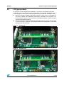
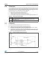
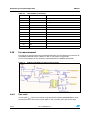
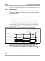
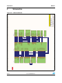
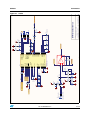
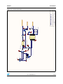
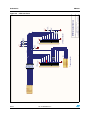
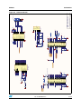
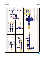
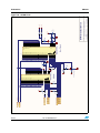
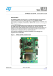
UM1521
User manual
STM32L152D-EVAL
evaluation board
Introduction
The STM32L152D-EVAL evaluation board is a complete demonstration and development
platform for the ARM Cortex-M3 core-based STM32L152ZDT6 microcontroller from
STMicroelectronics featuring two I2Cs, three SPIs, five USARTs, 12-bit ADC, 12-bit DAC,
LCD driver, internal 48 KB SRAM and 384 KB Flash, touch sensing, USB FS, LCD
controller, FSMC and JTAG debugging support.
This board can be used as reference design for user application development but it is not
considered as final application. The full range of hardware features on the board helps you
evaluate all peripherals (USB FS, USART, audio DAC, microphone ADC, dot-matrix LCD,
LCD glass, IrDA, LDR, SRAM, NOR Flash, MicroSD Card, temperature sensor and so on)
and develop your own applications. Extension headers make it possible to easily connect a
daughterboard or wrapping board for your specific application.
An ST-LINK/V2 is integrated on the board as embedded in-circuit debugger and
programmer for the STM32 MCU.
Figure 1.
STM32L152D-EVAL evaluation board
This user manual applies to the products listed in Table 1.
Table 1.
Applicable tools
Type
Evaluation tools
July 2012
Part numbers
STM32L152D-EVAL
Doc ID 022868 Rev 2
1/59
www.st.com
Contents
UM1521
Contents
1
2
3
2/59
Overview . . . . . . . . . . . . . . . . . . . . . . . . . . . . . . . . . . . . . . . . . . . . . . . . . . 4
1.1
Features . . . . . . . . . . . . . . . . . . . . . . . . . . . . . . . . . . . . . . . . . . . . . . . . . . . 4
1.2
Demonstration software . . . . . . . . . . . . . . . . . . . . . . . . . . . . . . . . . . . . . . . 4
1.3
Order code . . . . . . . . . . . . . . . . . . . . . . . . . . . . . . . . . . . . . . . . . . . . . . . . . 4
1.4
Delivery recommendations . . . . . . . . . . . . . . . . . . . . . . . . . . . . . . . . . . . . . 5
Hardware layout and configuration . . . . . . . . . . . . . . . . . . . . . . . . . . . . . 6
2.1
Development and debug support . . . . . . . . . . . . . . . . . . . . . . . . . . . . . . . . 8
2.2
Power supply . . . . . . . . . . . . . . . . . . . . . . . . . . . . . . . . . . . . . . . . . . . . . . . 9
2.3
Clock source . . . . . . . . . . . . . . . . . . . . . . . . . . . . . . . . . . . . . . . . . . . . . . . 11
2.4
Reset source . . . . . . . . . . . . . . . . . . . . . . . . . . . . . . . . . . . . . . . . . . . . . . 11
2.5
Boot option . . . . . . . . . . . . . . . . . . . . . . . . . . . . . . . . . . . . . . . . . . . . . . . . 12
2.6
LCD glass module . . . . . . . . . . . . . . . . . . . . . . . . . . . . . . . . . . . . . . . . . . 13
2.7
Audio . . . . . . . . . . . . . . . . . . . . . . . . . . . . . . . . . . . . . . . . . . . . . . . . . . . . 17
2.8
USB . . . . . . . . . . . . . . . . . . . . . . . . . . . . . . . . . . . . . . . . . . . . . . . . . . . . . 17
2.9
RS-232 and IrDA . . . . . . . . . . . . . . . . . . . . . . . . . . . . . . . . . . . . . . . . . . . 17
2.10
Touch sensing slider . . . . . . . . . . . . . . . . . . . . . . . . . . . . . . . . . . . . . . . . . 19
2.11
MicroSD Card . . . . . . . . . . . . . . . . . . . . . . . . . . . . . . . . . . . . . . . . . . . . . . 19
2.12
Serial EEPROM . . . . . . . . . . . . . . . . . . . . . . . . . . . . . . . . . . . . . . . . . . . . 20
2.13
RF EEPROM . . . . . . . . . . . . . . . . . . . . . . . . . . . . . . . . . . . . . . . . . . . . . . 20
2.14
SRAM . . . . . . . . . . . . . . . . . . . . . . . . . . . . . . . . . . . . . . . . . . . . . . . . . . . . 20
2.15
NOR Flash . . . . . . . . . . . . . . . . . . . . . . . . . . . . . . . . . . . . . . . . . . . . . . . . 20
2.16
Analog input . . . . . . . . . . . . . . . . . . . . . . . . . . . . . . . . . . . . . . . . . . . . . . . 21
2.17
Comparator . . . . . . . . . . . . . . . . . . . . . . . . . . . . . . . . . . . . . . . . . . . . . . . 21
2.18
Temperature sensor . . . . . . . . . . . . . . . . . . . . . . . . . . . . . . . . . . . . . . . . . 22
2.19
Display and input devices . . . . . . . . . . . . . . . . . . . . . . . . . . . . . . . . . . . . . 23
2.20
IDD measurement . . . . . . . . . . . . . . . . . . . . . . . . . . . . . . . . . . . . . . . . . . . 24
2.20.1
Run mode . . . . . . . . . . . . . . . . . . . . . . . . . . . . . . . . . . . . . . . . . . . . . . . 24
2.20.2
Low power mode . . . . . . . . . . . . . . . . . . . . . . . . . . . . . . . . . . . . . . . . . . 25
2.20.3
Ibias current measurement procedure . . . . . . . . . . . . . . . . . . . . . . . . . . 26
Connectors . . . . . . . . . . . . . . . . . . . . . . . . . . . . . . . . . . . . . . . . . . . . . . . 27
Doc ID 022868 Rev 2
UM1521
4
Contents
3.1
RS-232 connector CN1 . . . . . . . . . . . . . . . . . . . . . . . . . . . . . . . . . . . . . . 27
3.2
Power connector CN2 . . . . . . . . . . . . . . . . . . . . . . . . . . . . . . . . . . . . . . . 27
3.3
TFT LCD connector CN4 . . . . . . . . . . . . . . . . . . . . . . . . . . . . . . . . . . . . . 27
3.4
Daughterboard extension connector CN5 and CN10 . . . . . . . . . . . . . . . . 28
3.5
LCD glass daughterboard connectors CN6 and CN7 . . . . . . . . . . . . . . . 31
3.6
ST-LINK/V2 programming connector CN9 . . . . . . . . . . . . . . . . . . . . . . . . 32
3.7
ST-LINK/V2 USB type B connector CN14 . . . . . . . . . . . . . . . . . . . . . . . . 32
3.8
JTAG connector CN16 . . . . . . . . . . . . . . . . . . . . . . . . . . . . . . . . . . . . . . . 32
3.9
Trace debugging connector CN11 . . . . . . . . . . . . . . . . . . . . . . . . . . . . . . 33
3.10
Audio jack CN13 . . . . . . . . . . . . . . . . . . . . . . . . . . . . . . . . . . . . . . . . . . . . 33
3.11
MicroSD connector CN3 . . . . . . . . . . . . . . . . . . . . . . . . . . . . . . . . . . . . . . 34
3.12
Analog input-output 2-pin connector CN8 . . . . . . . . . . . . . . . . . . . . . . . . 34
3.13
User USB type B connector CN15 . . . . . . . . . . . . . . . . . . . . . . . . . . . . . . 35
3.14
RF EEPROM daughterboard connector CN12 . . . . . . . . . . . . . . . . . . . . . 35
Schematics . . . . . . . . . . . . . . . . . . . . . . . . . . . . . . . . . . . . . . . . . . . . . . . 36
Appendix A STM32L152D-EVAL I/O assignment . . . . . . . . . . . . . . . . . . . . . . . . . 52
Appendix B Mechanical dimensions. . . . . . . . . . . . . . . . . . . . . . . . . . . . . . . . . . . 57
Revision history . . . . . . . . . . . . . . . . . . . . . . . . . . . . . . . . . . . . . . . . . . . . . . . . . . . . 58
Doc ID 022868 Rev 2
3/59
Overview
UM1521
1
Overview
1.1
Features
1.2
●
Four 5 V power supply options: Power jack, ST-LINK/V2 USB connector, user USB
connector or daughterboard
●
Audio jack connected to I2S DAC, or STM32L152ZDT6 internal DAC
●
Microphone connected to ADC using integrated op amp as amplifier
●
2 GByte (or more) MicroSD Card on SDIO interface
●
Temperature sensor and RF EEPROM on I2C compatible serial interface
●
RS-232 interface configurable for communication or Flashloader
●
IrDA transceiver
●
JTAG and trace debug support, embedded ST-LINK/V2
●
4 Kbit serial Flash, 512K x16-bit SRAM and 128 Mbit NOR Flash
●
240x320 TFT color LCD connected to FSMC interface of STM32L152ZDT6
●
Joystick with 4-direction control and selector
●
Reset and Tamper or key button
●
4 color user LEDs and 3 LEDs as MCU power range indicator
●
MCU consumption measurement circuit
●
LCD glass 40 x 8 segments connected to LCD driver of STM32L152ZDT6
●
Extension connector for daughterboard or wrapping board
●
MCU voltage choice of 3.3 V or adjustable from 1.65 V to 3.6 V
●
USB FS connector
●
Touch slider
●
Light dependent resistor (LDR)
●
One MCU integrated op amp configured as Sallen-Key 2nd order low pass filter
●
One MCU integrated op amp configured as amplifier with adjustable gain
●
One ADC / DAC input signal connector
●
Potentiometer
Demonstration software
Demonstration software is preloaded in the board's Flash memory for easy demonstration of
the device peripherals in stand-alone mode. For more information and to download the
latest version available, please refer to the STM32L152D-EVAL demonstration software
available on www.st.com.
1.3
Order code
To order the STM32L152ZDT6 evaluation board, use the order code STM32L152D-EVAL.
4/59
Doc ID 022868 Rev 2
UM1521
1.4
Overview
Delivery recommendations
Some verifications are needed before using the board for the first time to make sure that
nothing was damaged during shipment and that no components are unplugged or lost.
When the board is extracted from its plastic bag, please check that no component remains
in the bag.
The main components to verify are:
1.
The 8 MHz crystal (X1) which may have been removed by a shock from its socket.
2.
The MicroSD Card which may have been ejected from the connector CN3 (left side of
the board).
3.
The dual-interface EEPROM board (ANT7-M24LR-A) which may have been unplugged
from the connector CN12 (top right corner of the board).
Doc ID 022868 Rev 2
5/59
Hardware layout and configuration
2
UM1521
Hardware layout and configuration
The STM32L152D-EVAL evaluation board is designed around the STM32L152ZDT6 (144pin TQFP package). The hardware block diagram Figure 2 illustrates the connection
between STM32L152D-EVAL and peripherals (LCD glass, Color LCD, Touch slider, USB FS
connector, Temperature Sensor, USART, IrDA, Audio, SRAM, Nor Flash, EEPROM,RF
EEPROM, MicroSD Card and embedded ST-LINK) and Figure 3 will help you locate these
features on the actual evaluation board.
Figure 2.
Hardware block diagram
*OYSTICK
,%$S
53!24
'0)/
7AKEUP
BUTTON
23
TRANSCEIVER
6OLTAGE
TRANSLATOR
)R$!
TRANSCEIVER
53!24
CONNECTOR
$OT-ATRIX
,#$
,$2
#OMPARATOR
&3-#
32!-./2&LASH
4OUCH
SLIDER
43
CONTROLLER
*4!'
PIN
CONNECTOR
$!#
!$#
53"
CONNECTOR
53"&3
%%02/
30)
-ICRO3$
#ARD
2&%%02/-
CONNECTOR
)#
3$)/
)3
/P!MP
!$#
4EMPERATURE
SENSOR
!UDIO
AMPLIFIER
6TO6
ADJUSTABLE
REGULATOR
6
REGULATOR
-#5
CONSUMPTION
MEASUREMENT
/P!MP
3%'
0OTENTIOMETER
53"4YPE"
CONNECTOR
*4!'4RACE
CONNECTOR
34-,:$4
/P!MP
-ICROPHONE
%XTENSION
CONNECTORFOR
'0)/S
,#$GLASS
= I/O shared with LCD glass
6/59
%MBEDDED
34 ,).+6
-36
Doc ID 022868 Rev 2
UM1521
Hardware layout and configuration
Figure 3.
Hardware block diagram
5-ICROPHONE
3
4OUCHSLIDER
#.#.
E XTENSION
CONNECTION
HEADER
#.
2&%%02/DAUGHTERBOARD
CONNECTOR
5
34-,:$4
#.#.
,#$GLASS
DAUGHTERBOARD
CONNECTOR
#.
53!24
#.
53"&3
2
,$2
5
)R$!
#.
TRACE
#.
*4!'
#.
-ICRO3$#ARD
,$
34,).+6
#/-,%$
#.
#OLOR,#$
#.
34,).+6
53"
#.
!UDIOJACK
#.
0OWERJACK
"
4AMPERKEY
BUTTON
26
6$$ADJUSTMENT
26POTENTIOMETER
5JOYSTICK
COLOR,%$S
6$$RANGE
,%$S
"RESETKEY
Doc ID 022868 Rev 2
-36
7/59
Hardware layout and configuration
2.1
UM1521
Development and debug support
Version 2 of the ST-LINK called ST-LINK/V2 is embedded on the board. This tool allows
program loading and debugging on the STM32L using a JTAG or SWD interface. Third-party
debug tools are also supported by JTAG connector CN16 and Trace connector CN11.
A specific driver must be installed on your PC for communication with embedded STLINK/V2. To download and install this driver, use the install shield called STLINK_V2_USBdriver.exe available on the Software and development tools page for ultra low
power STM32L family available on www.st.com.
Third-party toolchains support ST-LINK/V2 according to Table 2.
Table 2.
Third party support of ST-LINK/V2
Third party
Toolchain
Version
Atollic
TrueSTUDIO
2.1
IAR
EWARM
6.20.4
Keil
MDK-ARM
4.20
Tasking VX-Toolset
ARM Cortex-M
4.0.1
The embedded ST-LINK/V2 is connected to the PC via a standard USB cable connected to
connector CN14. The bicolor LED LD5 (COM) advises on the communication status as
follows:
Note:
8/59
●
Slow blinking Red LED/Off: At power on before USB initialization.
●
Fast blinking Red LED/Off: After the first correct communication between PC and STLINK/V2 (enumeration).
●
Red LED On: When initialization between PC and ST-LINK/V2 is successfully finished.
●
Green LED On: After successful target communication initialization.
●
Blinking Red/Green LED: During communication with target.
●
Red LED On: Communication finished and OK.
●
Orange LED On: Communication failure.
It is possible to power the board via CN14 (embedded ST/LINK/V2 USB connector) even if
an external tool is connected to CN11 (Trace connector) or CN16 (external JTAG & SWD
connector).
Doc ID 022868 Rev 2
UM1521
2.2
Hardware layout and configuration
Power supply
The STM32L152D-EVAL evaluation board is designed to be powered by a 5 V DC power
supply and to be protected by PolyZen from a wrong power plug-in event.
It is possible to configure the evaluation board to use any of following four sources for the
power supply.
●
5 V DC power adapter connected to CN2, the power jack on the board (power supply
unit (PSU) on silkscreen). The external power supply is not provided with the board.
●
5 V DC power with 500mA limitation from CN14, the USB type B connector of STLINK/V2 (USB 5 V power source on silkscreen (ST-LINK/V2)).
●
5 V DC power with 500mA limitation from CN15, the USB type B connector (USB 5V
power source on silkscreen (USB)).
●
5 V DC power from CN10, the extension connector for daughterboard (daughterboard
power source on silkscreen (D5V)).
The LEDs indicate the following:
●
LED LD9 is lit when the STM32L152D-EVAL board is powered by 5 V correctly.
●
Red LED LD8 is lit when the MCU is powered by low voltage (VDD < 1.8 V).
●
Yellow LED LD7 is lit when the MCU is powered by voltage (1.8 V < VDD < 2.2 V).
●
Green LED LD6 is lit when the MCU is powered by voltage (2.2 V < VDD).
The power supply is configured by setting the related jumpers JP1, JP5 and JP10 as
described in Table 3.
Table 3.
Jumper
Power supply jumper settings
Description
Setting
JP1 selects one of the four possible power supply sources.
STK
U5V
D5V
PSU
– For power supply jack(CN2) to the STM32L152D-EVAL only, JP1 is set
as shown to the right:
– For power supply from the daughterboard connectors (CN10) to
STM32L152D-EVAL only, JP1 is set as shown to the right:
JP1
– For power supply from USB (CN15) to STM32L152D-EVAL only, JP1
is set as shown to the right:
– For power supply from USB connector of ST-LINK/V2 (CN14) to
STM32L152D-EVAL only, JP1 is set as shown to the right:
(Default setting)
For power supply from power supply jack (CN2) to both STM32L152DEVAL and daughterboard connected on CN5 and CN10, JP1 is set as
shown to the right (daughterboard must not have its own power supply
connected)
Doc ID 022868 Rev 2
9/59
Hardware layout and configuration
Table 3.
UM1521
Power supply jumper settings (continued)
Jumper
Description
Setting
VDD is connected to fixed +3.3 V DC power when JP5 is set as shown to
the right: (Default setting)
JP5
VDD is connected to adjustable DC power from 1.65 V to 3.6 V when
JP5 is set as shown to the right:
JP10
VDD power is directly connected to MCU VDD when JP10 is set as
shown to the right (Default setting):
Note: For manual IDD measurement the jumper on JP10 must be
removed and replaced by an ammeter connected between pin 1 and 2 of
JP10.
Connect VDD power to MCU with current-sampling resister, 1 Ohm or
1 KOhm, in series for IDD current measurement when JP10 is set as
shown to the right:
Note:
Due to some peripheral component specifications, the low voltage limitations (component
will not work correctly when power level is under low voltage limitation) related to the
operating voltage of the peripherals are shown in Table 4.
Table 4.
Low voltage limitation
Peripheral
Component
I/O name
Low voltage limitation
USB
CN15
USB
3V
MicroSD Card
CN3
SDIO
2.7 V
SRAM
U5
FSMC
2.4 V
EEPROM
U25
SPI
1.8 V
CN12
I2C
1.8 V
RF EEPROM
Note:
10/59
The recommended AC220 V to DC5 V power adapter is the PSU-5V2A. It is not included
with the board but can be ordered from ST as a separate item. You can also use another
equivalent 5 V power adapter (polarity compatible with CN2) to power the STM32L152DEVAL board via the CN2 power jack on the board.
To order the recommended power supply, use the order code PSU-5V2A.
Doc ID 022868 Rev 2
UM1521
2.3
Hardware layout and configuration
Clock source
Two clock sources are available on the STM32L152D-EVAL evaluation board for the
STM32L152ZDT6 and RTC embedded.
●
X1, 8 MHz crystal with socket for the STM32L152ZDT6 microcontroller, it can be
removed from socket when internal RC clock is used.
●
X3, 32 kHz crystal for embedded RTC
Table 5.
8 MHz crystal X1 related solder bridges
Solder bridge
Description
PH1 is connected to 8 MHz crystal when SB1 is open. (Default setting)
SB1
PH1 is connected to extension connector CN10 when SB1 is closed. In such case
R51 must be removed to avoid disturbance due to the 8Mhz quartz
PH0 is connected to 8 MHz crystal when SB2 is open. (Default setting)
SB2
PH0 is connected to extension connector CN10 when SB2 is closed. In such case
C53 and X1 must be removed.
Table 6.
32 kHz crystal X3 related solder bridges
Solder bridge
Description
PC14 is connected to 32 kHz crystal when SB8 is open. (Default setting)
SB8
PC14 is connected to extension connector CN5 when SB8 is closed. In such case
R85 must be removed to avoid disturbance due to the 32kHz quartz
PC15 is connected to 32 kHz crystal when SB7 is open. (Default setting)
SB7
2.4
PC15 is connected to extension connector CN5 when SB7 is closed. In such case
R84 must be removed to avoid disturbance due to the 32 kHz quartz
Reset source
The reset signal of the STM32L152D-EVAL evaluation board is low active and the reset
sources include:
●
Reset button B1
●
Debug tools from JTAG connector CN16 and trace connector CN11
●
Daughterboard from CN10
●
Embedded ST-LINK/V2
●
RS-232 connector CN1 for ISP
Doc ID 022868 Rev 2
11/59
Hardware layout and configuration
2.5
UM1521
Boot option
The STM32L152D-EVAL evaluation board is able to boot from:
●
Embedded user Flash
●
System memory with boot loader for ISP
●
Embedded SRAM for debugging
The boot option is configured by setting switch SW1 (BOOT0) and SW2 (BOOT1). The
BOOT0 can be configured also via the RS-232 connector CN1.
Table 7.
Boot related switch
Switch
Boot from
STM32L152D-EVAL boots from user Flash when SW1 is set as
shown to the right. SW2 is don't care in this configuration.
(Default setting)
Switch
configuration
0 <----> 1
0 <----> 1
SW1
and
SW2
STM32L152D-EVAL boots from embedded SRAM when SW1 and
SW2 are set as shown to the right.
0 <----> 1
STM32L152D-EVAL boots from system memory when SW1 and
SW2 are set as shown to the right.
Table 8.
Jumper
JP11
12/59
Boot0 related jumpers
Description
The Bootloader_BOOT0 is managed by pin 6 of connector CN1 (RS-232 DSR signal)
when JP11 is closed. This configuration is used for boot loader application only.
Default setting: Not fitted
Doc ID 022868 Rev 2
UM1521
2.6
Hardware layout and configuration
LCD glass module
An LCD glass module daughterboard (MB979) is mounted on the STM32L152D-EVAL
evaluation board. It can be connected to the LCD driver of the STM32L152ZDT6 or work as
a set of jumpers by mounting it on two possible positions; position "IO" or position "LCD":
●
When the LCD glass module is mounted on position IO (see Figure 4), all peripherals
(memories, USART, audio, EEPROM, potentiometer, MicroSD Card, microphone, etc)
shared with the LCD glass are connected to the STM32L152ZDT6, and the LCD glass
is disconnected (default setting).
●
When the LCD glass module is mounted on position LCD (see Figure 5), the LCD glass
is connected to the LCD driver of the STM32L152ZDT6 and all peripherals shared with
LCD glass are disconnected.
Figure 4.
Position IO
Figure 5.
Position LCD
Doc ID 022868 Rev 2
13/59
Hardware layout and configuration
Table 9.
UM1521
LCD glass related jumpers
Jumper
Description
Setting
PA1 is connected to microphone (MIC_INP signal) when JP8 is set as shown to
the right: (Default setting)
JP8
PA1 is connected to LCD glass as SEG0 when JP8 is set as shown to the right:
PA2 is connected to microphone (MIC_INN signal) when JP6 is set as shown to
the right: (Default setting)
JP6
PA2 is connected to LCD glass as SEG1 when JP6 is set as shown to the right:
The custom LCD glass on MB979 is model XHO5002B. The signal mapping is shown in
Table 10, Table 11, Table 12 and Table 13 and segment names are given in Figure 6.
Table 10.
Pin
LCD glass segments mapping table pins 1-12
1
2
3
4
COM1 COM1
COM2
8
9
10
11
12
3g
4g
5g
6g
7g
8g
1h
2h
3h
4h
5h
6h
7h
8h
1i
2i
3i
4i
5i
6i
7i
8i
COM4 1j
2j
3j
4j
5j
6j
7j
8j
COM5
1d
2d
3d
4d
5d
6d
7d
8d
COM6
1c
2c
3c
4c
5c
6c
7c
8c
COM7
1e
2e
3e
4e
5e
6e
7e
8e
COM8
1f
2f
3f
4f
5f
6f
7f
8f
Table 11.
Pin
14/59
7
2g
COM3
COM4
6
1g
COM2
COM3
5
13
LCD glass segments mapping table pins 13-24
14
15
16
17
18
19
20
21
22
23
24
COM1 9g
10g
11g
12g
13g
14g
15g
16g
17g
18g
19g
5J
COM2 9h
10h
11h
12h
13h
14h
15h
16h
17h
18h
19h
5C
COM3 9i
10i
11i
12i
13i
14i
15i
16i
17i
18i
19i
5B
COM4 9j
10j
11j
12j
13j
14j
15j
16j
17j
18j
19j
5I
COM5 9d
10d
11d
12d
13d
14d
15d
16d
17d
18d
19d
13a
COM6 9c
10c
11c
12c
13c
14c
15c
16c
17c
18c
19c
13b
COM7 9e
10e
11e
12e
13e
14e
15e
16e
17e
18e
19e
O1
COM8 9f
10f
11f
12f
13f
14f
15f
16f
17f
18f
19f
O2
Doc ID 022868 Rev 2
UM1521
Hardware layout and configuration
Table 12.
Pin
LCD glass segments mapping table pins 25-36
25
26
27
28
29
30
31
32
33
34
35
36
COM1 7J
7N
7E
6J
6N
6E
5N
5E
4J
4N
4E
3J
COM2 7C
7M
P6
6C
6M
P5
5M
P4
4C
4M
P3
3C
COM3 7B
7H
7F
6B
6H
6F
5H
5F
4B
4H
4F
3B
COM4 7I
7A
7G
6I
6A
6G
5A
5G
4I
4A
4G
3I
COM5 19a
18a
17a
16a
15a
14a
12a
11a
10a
9a
8a
7a
COM6 19b
18b
17b
16b
15b
14b
12b
11b
10b
9b
8b
7b
COM7 S
7D
Q6
O4
6D
Q5
5D
Q4
µA
4D
Q3
C4
COM8 nA
7K
7L
O3
6K
6L
5K
5L
mA
4K
4L
C3
47
48
Table 13.
Pin
LCD glass segments mapping table pins 37-48
37
38
39
40
41
42
43
44
COM1 3N
3E
2J
2N
2E
1J
1N
1E
COM2 3M
P2
2C
2M
P1
1C
1M
+
COM3 3H
3F
2B
2H
2F
1B
1H
1F
COM4 3A
3G
2I
2A
2G
1I
1A
1G
COM5 6a
5a
4a
3a
2a
1a
S3
S1
COM6 6b
5b
4b
3b
2b
1b
S4
S2
COM7 3D
Q2
C1
2D
Q1
S5
1D
-
COM8 3K
3L
C2
2K
2L
S6
1K
1L
Doc ID 022868 Rev 2
45
46
COM5
COM6
COM7
COM8
15/59
Hardware layout and configuration
Figure 6.
16/59
UM1521
LCD segment names
Doc ID 022868 Rev 2
UM1521
2.7
Hardware layout and configuration
Audio
The STM32L152D-EVAL evaluation board supports stereo audio play by using an audio
DAC CS43L22 connected to both I2S2 port and one channel of DAC in the microcontroller
STM32L152ZDT6.
●
OpAmp3 of the STM32L152ZDT6 acts as a low pass filter of audio output for this DAC.
●
A headphone jack is connected to the output of CS43L22.
●
A microphone is connected to ADC through OpAmp1 of STM32L152ZDT6.
Table 14.
Audio related jumpers
Jumper
Description
Setting
PA4 is connected to analog input signal for ADC or output signal from DAC on
CN8 when JP7 is set as shown to the right:
JP7
PA4 output signal to OpAmp3 as low pass filter when JP7 is set as shown to the
right: (Default setting)
JP8
Description of JP8 is in Section 2.6: LCD glass module
JP6
Description of JP6 is in Section 2.6: LCD glass module
The I2C address of CS43L22 is 0b1001010.
The LCD glass module has to be mounted on "IO" position for Audio I2C usage. Refer to
Section 2.6: LCD glass module for detail.
2.8
USB
The STM32L152D-EVAL evaluation board supports USB2.0 compliant full speed
communication via a USB type B connector (CN15). The evaluation board can be powered
by this USB connection at 5 V DC with a 500 mA current limitation.
USB disconnection simulation can be implemented by controlling the internal 1.5 K pull-up
resistor on USB+ line and detection of 5 V power on USB connector CN15 by using a
resistor bridge connected to PE6.
USB will work properly when VDD > 3 V.
2.9
RS-232 and IrDA
RS-232 and IrDA communication is supported by D-type 9-pin RS-232 connector CN1, and
IrDA transceiver U2 which is connected to USART1 of the STM32L152ZDT6 on the
STM32L152D-EVAL evaluation board.
The signals Bootloader_RESET and Bootloader_BOOT0 can be added on RS-232
connector CN1 for ISP support. If Bootloader_RESET signal is used, mount R39 (Default:
Unmounted) with a 0 Ohm resistor as Figure 7 shows.
Doc ID 022868 Rev 2
17/59
Hardware layout and configuration
Figure 7.
Note:
UM1521
R39 resistor placement
If Bootloader_RESET signal is not used, remove R39 to avoid disturbance due to CTS
signal from pin8 of CN1, which could cause MCU reset with some software.
Table 15.
Jumper
RS-232 & IrDA related jumpers
Description
Setting
USART1_RX is connected to RS-232 transceiver and RS-232 communication is
enabled when JP4 is set as shown to the right (Default setting):
JP4
USART1_RX is connected to IrDA transceiver and IrDA communication is
enabled when JP4 is set as shown to the right:
The LCD glass module has to be mounted on IO position for USART1 usage. Refer to
Section 2.6: LCD glass module for detail.
18/59
Doc ID 022868 Rev 2
UM1521
2.10
Hardware layout and configuration
Touch sensing slider
The STM32L152D-EVAL evaluation board supports a touch sensing slider based on either
RC charging or charge transfer technology. The charge transfer technology is enabled by
default assembly.
PB6 and PB7 manage an active shield reducing sensitivity to other signals. The active
shield is placed on an internal layer immediately under the slider (layer 2) to cover
components related to the slider and the slider itself.
Table 16.
Touch sensing slider related solder bridges
Solder bridge
Description
PF9 is connected to sampling capacitor when SB3 is open. (Default setting)
SB3
PF9 is connected to extension connector CN10 when SB3 is closed. In this case
C54 must be removed to avoid disturbance due to the capacitor
PF8 is connected to touch slider when SB4 is open. (Default setting)
SB4
PF8 is connected to extension connector CN10 when SB4 is closed. In this case
R69 must be removed to avoid disturbance due to the touch slider
PF7 is connected to touch slider when SB5 is open. (Default setting)
SB5
PF7 is connected to extension connector CN10 when SB5 is closed. In this case
R73 must be removed to avoid disturbance due to the touch slider
PF6 is connected to touch slider when SB6 is open. (Default setting)
SB6
PF6 is connected to extension connector CN10 when SB6 is closed. In this case
R77 must be removed to avoid disturbance due to the touch slider
PB6 is connected to touch slider when SB10 is open. (Default setting)
SB10
PB6 is connected to extension connector CN10 when SB10 is closed. In this case
R92 must be removed to avoid disturbance due to the shield
PB7 is connected to touch slider when SB11 is open. (Default setting)
SB11
PB7 is connected to extension connector CN10 when SB11 is closed. In this case
R101 must be removed to avoid disturbance due to the capacitor
Note:
The slider is optimized when the board is powered at 3.3 V. It may be necessary to adjust
the capacitor value of C54 (47nF COG) and the firmware to adapt them to a low voltage.
2.11
MicroSD Card
The 2 GB (or more) MicroSD Card connected to the SDIO port of the STM32L152ZDT6 is
available on the board. MicroSD Card detection is managed by standard I/O port PC7.
The MicroSD Card will work properly when VDD > 2.7 V.
The LCD glass module has to be mounted on IO position for MicroSD Card usage. Refer to
Section 2.6: LCD glass module for detail.
Doc ID 022868 Rev 2
19/59
Hardware layout and configuration
2.12
UM1521
Serial EEPROM
A 4 Kbit (M95040-R) serial EEPROM is connected to SPI1 of the STM32L152ZDT6.
Serial Flash chip select is managed by I/O pin PB0.
The EEPROM will work properly when VDD > 1.8 V.
The LCD glass module has to be mounted on IO position for SPI EEPROM usage. Refer to
Section 2.6: LCD glass module for detail.
2.13
RF EEPROM
The RF EEPROM daughterboard (MB1020) implemented on the module is the M24LR64-R.
This EEPROM can be accessed by the MCU via the I2C bus or by RF using a 13.56 MHz
reader (for instance CR95HF).
The daughterboard can be connected to the STM32L152ZDT6 via the I2C bus on CN2.
The I2C address of RF EEPROM is 0b1010E2E1E0. E0-E2 values are determined by the
RF EEPROM daughterboard.
The RF EEPROM will work properly when VDD > 1.8 V.
The LCD glass module has to be mounted on IO position for RF EEPROM usage. Refer to
Section 2.6: LCD glass module for detail.
2.14
SRAM
512Kx16-bit SRAM is connected to bank2 of the FSMC interface and both 8-bit and 16-bit
accesses are allowed by BLN0 and BLN1 connected to BLE and BHE of SRAM respectively.
The SRAM will work properly when VDD > 2.4 V.
The LCD glass module has to be mounted on IO position for SRAM usage. Refer to
Section 2.6: LCD glass module for detail.
2.15
NOR Flash
128 Mbit NOR Flash is connected to bank1 of the FSMC interface. The 16-bit operation
mode is selected by pull-up resister connected to BYTE pin of NOR Flash. Write protection
is enabled or disabled by jumper JP9.
Table 17.
Jumper
JP9
NOR Flash related jumpers
Description
Write protection is enabled when JP9 is fitted while write protection is disabled when JP9 is
not fitted.
Default setting: Not fitted
The LCD glass module has to be mounted on IO position for NOR Flash usage. Refer to
Section 2.6: LCD glass module for detail.
20/59
Doc ID 022868 Rev 2
UM1521
2.16
Hardware layout and configuration
Analog input
A 2-pin connector, CN8, is connected to PA4 of the STM32L152ZDT6 as an external analog
input or DAC output. A low pass filter can be implemented for a 2-pin connector by replacing
R43 and C35 with ADC input or replacing R36 and C35 with DAC output, with correct values
of resistor and capacitor as requested by end user's application.
There are also three analog signals available on the board:
1.
10 KOhm potentiometer RV3 connected to PF10.
2.
10 KOhm potentiometer RV3 connected to OpAmp2 PA6.
3.
IDD measurement output signal connected to PF11 for MCU power consumption test.
Table 18.
Analog input related jumpers
Jumper
2.17
Description
JP12
10 KOhm potentiometer RV3 connected to OpAmp2 PA6 when JP12 is closed.
Default setting: Closed
JP7
Description of JP7 is in Section 2.7: Audio
Comparator
Three I/Os implement a comparator feature as shown in Figure 8:
●
Comparator non-inverting input PB4; connected to LDR (R157).
●
Comparator inverting input PB3; connected to potentiometer (RV3) used as variable
threshold input for comparison to luminosity measured on LDR.
●
Comparator non-inverting input PB5; connected to potentiometer (RV3) used as analog
voltage input for comparison with internal voltage reference (for instance Band gap) in
order to test analog Wakeup feature of the MCU.
Figure 8.
STM32L152D-EVAL comparator features
Doc ID 022868 Rev 2
21/59
Hardware layout and configuration
Table 19.
UM1521
Comparator, LDR and potentiometer related jumpers
Jumper
Description
Setting
PB4 is connected to LDR_OUT when JP2 is set as shown to the right:
JP2
PB4 is connected to TRST when JP2 is set as shown to the right:
(Default setting).
Potentiometer RV3 used as LDR variable threshold input is connected to
comparator inverting input GPCOMP_IN- (PB3) when JP13 is set as shown
to the right:
PF10
PB3
PB5
Potentiometer RV3 is connected to non inverting input
GPCOMP_IN+(PB5). The comparator inverting input can be connected to
¼ band gap, ½ band gap, band gap or DAC internally in order to test the
possibility to wakeup the MCU when an external voltage reaches a
programmable threshold when JP13 is set as shown to the right:
PF10
PB3
PB5
JP13
PF10
PB3
PB5
Potentiometer RV3 is connected to ADC input PF10 used as ADC input
when JP13 is set as shown to the right: (Default setting).
PB5 is connected to I2C_SMB, the interrupt output of temperature sensor
U24 when JP14 is closed (Default setting).
JP14
PB5 is disconnected from I2C_SMB but remains connected to COM_IN+
when JP14 is open for comparator application.
The LCD glass module has to be mounted in IO position for comparator usage. Refer to
Section 2.6: LCD glass module for detail.
2.18
Temperature sensor
Temperature sensor STLM75M2E is connected to the I2C bus of the STM32L152ZDT6
through two transistors to support a wide voltage range from 1.65 V to 3.6 V on the I2C bus.
I2C address of temperature sensor is 0b100100(A0), A0 can be 0 or 1 according to SB9.
Table 20.
Temperature sensor related solder bridge
Solder bridge
Description
I2C address A0 is 0 when SB3 is open. (Default setting)
SB9
I2C address A0 is 1 when SB3 is closed.
The LCD glass module has to be mounted on IO position for temperature sensor usage.
Refer to Section 2.6: LCD glass module for detail.
22/59
Doc ID 022868 Rev 2
UM1521
Hardware layout and configuration
Note:
Temperature result measured from STLM75M2E would be a little higher than ambient
temperature due to board heat.
2.19
Display and input devices
The display devices are 4 general purpose color LED's (LD 1,2,3,4) and a 240x320 TFT
color LCD connected to bank3 of the STM32L152ZDT6 FSMC interface port. The LCD
glass module must be mounted on IO position for color LCD usage. Refer to Section 2.6:
LCD glass module for detail.
Input devices are the 4-direction joystick (U23) with selection key and wakeup button (B2).
Three LCD references using different controllers can be mounted on LCD board MB895, as
shown in Table 21. The driver provided in the library is able to identify which LCD is used by
reading the controller ID, and then to adapt communication according to each controller
specificity. The LCD references and corresponding controllers used are summarized below:
Table 21.
LCD references
LCD reference
Controller
Controller manufacturer
AM-240320LDTNQW-02H
SPFD5408B
Orise Technology
AM-240320LDTNQW-05H
RM68050
Raydium
AM240320LGTNQW-01H
HX-8347D
Himax
Table 22.
LCD modules
Pin
Description
Pin connection
1
CS
CS of Bank3 of FSMC
2
RS
FSMC_A0
3
WR/SCL
FSMC_NWE
4
RD
FSMC_NOE
5
RESET
RESET#
6
PD1
FSMC_D0
7
PD2
FSMC_D1
8
PD3
FSMC_D2
9
PD4
FSMC_D3
10
PD5
FSMC_D4
11
PD6
FSMC_D5
12
PD7
FSMC_D6
13
PD8
FSMC_D7
14
PD10
FSMC_D8
15
PD11
FSMC_D9
16
PD12
FSMC_D10
17
PD13
FSMC_D11
Doc ID 022868 Rev 2
23/59
Hardware layout and configuration
Table 22.
LCD modules (continued)
Pin
2.20
UM1521
Description
Pin connection
18
PD14
FSMC_D12
19
PD15
FSMC_D13
20
PD16
FSMC_D14
21
PD17
FSMC_D15
22
BL_GND
GND
23
BL_control
5V
24
VDD
3.3V
25
VCI
3.3V
26
GND
GND
27
GND
GND
28
BL_VDD
5V
29
SDO
-
30
SDI
GND
IDD measurement
The built-in IDD measurement circuit implemented allows the consumption measurement of
the STM32L152ZDT6 while the MCU is in Run or Low power saving modes.
For IDD measurement the circuit below is implemented on the STM32L152D-EVAL.
Figure 9.
2.20.1
STM32L152D-EVAL IDD measurement circuit
Run mode
In Run mode, IDD current is measured using operational amplifier MAX9938FEUK+ (U19)
connected to the 1 Ohm shunt resistor (R62). In this case IDD_CNT_EN remains high
24/59
Doc ID 022868 Rev 2
UM1521
Hardware layout and configuration
during measurement, so R81 remains in short-circuit during measurement because of
transistor T1 which remains ON permanently. JP10 must be connected between pins 2 & 3.
2.20.2
Low power mode
In Low power modes (Stop or Standby), the operational amplifier MAX9938FEUK+ (U19) is
connected to the 1 KOhm shunt resistor (R81), controlled by the analog switch T1. In this
case the counter 74HC4060 (U15) enabled by IDD_CNT_EN manages the measurement
timing according to Figure 10.
The principle used to measure a current when the STM32L is in Low power mode is:
1.
Configure ADC to measure voltage on the IDD_Measurement pin (PF11).
2.
Configure PA0 to serve as wakeup pin.
3.
Enter Low power mode after setting IDD_CNT_EN (PC13) signal low.
4.
IDD_WAKEUP rising edge wakes up the MCU after around 300 ms.
5.
Start ADC conversion as soon as possible after wakeup in order to measure the
voltage corresponding to Low power mode on capacitor C82.
6.
Reset the counter by programming IDD_CNT_EN high (in less than 70 ms after the
wakeup) to avoid the R81 (1 KOhm) resistor being connected later in Run mode.
In Low power modes, the 1 K resistor is connected when T1 goes off after entering Low
power mode. Q12 output of the counter allows connection of the 1 K resistor when the
current IDD becomes very low.
Figure 10. STM32L152D-EVAL IDD Low power modes measurement timing diagram
Wake-up
period
IDD
measurement
Wake-up
event
MCU mode
Run
Clear CNT
event
Low power
5
IDD_CNT_EN (PC13)
3
6
Q12 = LOW_POWER_EN
(T1 pin 3)
4
Q13 = IDD_WAKEUP (PA0)
Q13n = disconnect filter
(U18 pin 4)
0 ms
150 ms
300 ms
Figure 10 shows how the counter and T1 ensure that, 150 ms after IDD_CNT_EN falling
edge, the shunt resistor R81 is connected between VDD_MCU and the power supply in
order to reduce the measurement range to 30 uA full scale when VDD = 1.8 V.
Then after another 150 ms for current stabilization, R81 is shorted, the IDD measurement is
stored in C82, and the MCU is woken up. After wakeup the MCU can measure the IDD
current corresponding to the Low power mode stored in C82.
Doc ID 022868 Rev 2
25/59
Hardware layout and configuration
2.20.3
UM1521
Ibias current measurement procedure
In Low power mode the bias current of operational amplifier input (U19 pin 4) is not
negligible compared to IDD current (typical Ibias is ~240 nA). To obtain a reliable MCU IDD
measurement it is possible to subtract the bias current from the IDD low power measurement
since this current is not sinked by the MCU. The procedure for accurate IDD measurement is:
1.
Set jumper JP10 on pin 1 and pin 2.
2.
Follow the Low power mode procedure to measure I1 = I bias.
3.
Remove jumper JP10 from pins 1 and 2 and place it on pins 2 and 3.
4.
Follow the Low power mode procedure to measure I2 = IDD + I bias.
5.
Calculate actual IDD: IDD = I2 - I1.
If JP10 jumper is in pins 2-3: STM32L is powered through IDD measurement circuit (default).
If JP10 jumper is in pins1-2: STM32L is powered directly by +3V3, IDD measurement circuit
is bypassed. Refer to Section 2.2: Power supply for detail.
Note:
26/59
1
When jumper JP10 is removed the current consumption of the STM32L can be measured by
connecting an ammeter between jumper JP10, pins 1 and 2.
2
RDS (on) typical value of analog switch T1= 50 MOhm, so to improve measurement
accuracy it is recommended to take into account the RDS in series with R62 (1 Ohm) in the
IDD Run mode current calculation.
3
To avoid current injection from MCU to components on the board during IDD measurement it
is strongly recommended to keep VDD_MCU ≤ 3.3 V. Some components on the board are
powered by 3.3 V (for instance the ST-LINK) so if VDD_MCU is higher than 3.3 V a current
can be in injected on signals like T_NRST (PB0 of U21) which disturbs the measurement in
low power mode.
Doc ID 022868 Rev 2
UM1521
Connectors
3
Connectors
3.1
RS-232 connector CN1
Figure 11. RS-232 connector (viewed from front)
Table 23.
RS-232 connector CN1 with HW flow control and ISP support
Pin
3.2
Description
Pin
Description
1
NC
6
Bootloader_BOOT0
2
RS-232_RX (PB11)
7
NC
3
RS-232_TX (PB10)
8
Bootloader_RESET
4
NC
9
NC
5
GND
Power connector CN2
The STM32L152D-EVAL evaluation board can be powered from a DC 5 V power supply via
the external power supply jack (CN2) shown in Figure 12. The central pin of CN2 must be
positive.
Figure 12. Power supply connector CN2 (viewed from front)
3.3
TFT LCD connector CN4
A TFT color LCD board (MB895) is mounted on CN4.
Doc ID 022868 Rev 2
27/59
Connectors
3.4
UM1521
Daughterboard extension connector CN5 and CN10
Two 42-pin male headers CN5 and CN10 can connect the daughterboard (or standard
wrapping board) to the STM32L152D-EVAL evaluation board. All GPIOs are available on
them and the LCD glass connectors (CN6, CN7).
The space between these two connectors and positions of POWER, GND and RESET pins
are defined as a standard which allows common daughterboards to be developed for
several evaluation boards. The standard width between CN5 pin1 and CN10 pin1 is
2700 mils (68.58 mm). This standard has been implemented on the majority of evaluation
boards.
Each pin on CN5 and CN10 can be used by a daughterboard after disconnecting it from the
corresponding function block on the STM32L152D-EVAL evaluation board. Refer to
Table 24 and Table 25 for detail.
Table 24.
Daughterboard extension connector CN5
Pin Description
28/59
How to disconnect with function block on
STM32L152D-EVAL board
Alternative function
1
GND
-
-
3
PF5
FSMC_A5
-
5
PF3
FSMC_A3
-
7
PF1
FSMC_A1
-
9
PE6
Tamper / Key / U5V_DET
Remove R150
11
PC14
32K OSC
Remove R85 and close SB8
13
PE5
FSMC_A21
/ TRACED2
-
15
PC15
32K OSC
Remove R84 and close SB7
17
PA4
CON_ADC4 -DAC1 /
Audio_DAC_OUT
JP7 open
19
GND
-
-
21
PB2
BOOT1
Remove R89
23
PF12
FSMC_A6
-
25
PF14
FSMC_A8
-
27
PG0
FSMC_A10
-
29
PE7
FSMC_D4
-
31
VLCD
-
-
33
PE9
FSMC_D6
-
35
PE11
FSMC_D8
-
37
PE13
FSMC_D10
-
39
GND
-
-
41
PG2
FSMC_A12
-
2
-
-
-
Doc ID 022868 Rev 2
UM1521
Connectors
Table 24.
Daughterboard extension connector CN5 (continued)
Pin Description
How to disconnect with function block on
STM32L152D-EVAL board
Alternative function
4
PF4
FSMC_A4
-
6
PF2
FSMC_A2
-
8
PF0
FSMC_A0
-
10
GND
-
-
12
PE4
FSMC_A20 / TRACED1
Remove R147
14
PF10
POTENTIOMETER
JP13 pin5,6 open
16
PA0
IDD_WAKEUP /
KEY_TAMPER2 /WKUP1
Remove R118
18
PA5
E2P_SCK
-
20
-
-
-
22
PF11
IDD_measurement
Remove R83,C82
24
PF13
FSMC_A7
-
26
PF15
FSMC_A9
-
28
PG1
FSMC_A11
-
30
GND
-
-
32
PE8
FSMC_D5
-
34
PE10
FSMC_D7
-
36
PE12
FSMC_D9
-
38
PE14
FSMC_D11 / E2P_ MISO
Remove R90
40
PE15
FSMC_D12 / E2P_ MOSI
Remove R120
42
+3.3
-
If use 3.3 V power, keep R24 mounting
Table 25.
Daughterboard extension connector CN10
Pin Description
How to disconnect with function block on
STM32L152D-EVAL board
Alternative function
1
GND
-
-
3
PB7
C_Shield_CT_6_4
Remove R101 and close SB11
5
PG15
LED4
Remove R60
7
PG13
JOYSTICK_SELECT
Remove R105
9
PC13
IDD_CNT_EN
-
11
RESET#
-
-
13
PG10
CS_RAM_EBAR2
Remove R40
15
PD7
LED2
Remove R71
17
PD5
FSMC_WEN
-
19
D5V
-
-
Doc ID 022868 Rev 2
29/59
Connectors
UM1521
Table 25.
Daughterboard extension connector CN10 (continued)
Pin Description
30/59
How to disconnect with function block on
STM32L152D-EVAL board
Alternative function
21
PD1
FSMC_D3
-
23
PH0
OSC_IN
Remove X1 from socket and close SB2
25
PA14
JTCK/SWCLK
-
27
PH2
FSMC_A22
-
29
PA12
USB_DP
Remove R136
31
PA11
USB_DM
Remove R149
33
PG7
JOYSTICK_RIGHT
Remove R117
35
PF6
SLIDER_CT_11_1
Remove R77 and close SB6
37
PF8
SLIDER_CT_11_3
Remove R69 and close SB4
39
GND
-
-
41
PG4
FSMC_A14
-
2
-
-
-
4
PB6
Shield_CT_6_3
Remove R92 and close SB10
6
PG14
LED3
Remove R67
8
PG12
LCD_EBAR3
-
10
GND
-
-
12
PG11
JOYSTICK_UP
Remove R119
14
PG9
CS_NOR_EBAR1
Remove R31
16
PD6
FSMC_WAITN
-
18
PD4
FSMC_OEN
-
20
PD3
LED1
Remove R74
22
PD0
FSMC_D2
-
24
VDD
-
-
26
PH1
OSC_OUT
Remove X1 from socket & close SB1
28
PA13
JTMS/SWDAT
-
30
GND
-
-
32
PG8
JOYSTICK_DOWN
Remove R110
34
PG6
JOYSTICK_LEFT
Remove R104
36
PF7
SLIDER_CT_11_2
Remove R73 and close SB5
38
PF9
SLIDER_CT_11_4
Remove C54 and close SB3
40
PG5
FSMC_A15
-
42
PG3
FSMC_A13
-
Doc ID 022868 Rev 2
UM1521
3.5
Connectors
LCD glass daughterboard connectors CN6 and CN7
Two 48-pin male headers CN6 and CN7 connect the LCD glass daughterboard (MB979).
GPIOs which act as LCD glass signals and are not on CN5 and CN10 are available on these
two connectors. The space between these two connectors and the position of every LCD
glass signal is defined as a standard which allows development of common daughterboards
for several evaluation boards. The standard width between the CN7 pin1 and CN6 pin1 is
700 mils (17.78 mm).
GPIO signals on these two connectors can be tested on odd pins when the LCD glass board
is absent. Signal assignments are detailed in Table 26.
Note:
If CN6 and CN7 are used as GPIO extension connector on a common daughterboard, do
not connect odd pins and even pins directly onto the daughterboard, and leave Trace
connector (CN11), JTAG connector (CN16) and JP2 open.
Table 26.
LCD glass daughterboard connectors CN6 and CN7
CN7
CN6
Odd pin
GPIO signal
Odd pin
GPIO signal
1
PA9
1
PD2
3
PA8
3
PC12
5
PA10
5
PC11
7
PB9
7
PC10
9
PB11
9
PC3
11
PB10
11
PC4
13
PB5
13
PC5
15
PB14
15
PC6
17
PB13
17
PC7
19
PB12
19
PC8
21
PA15
21
PC9
23
PB8
23
PD8
25
PB15
25
PD9
27
PC2
27
PD10
29
PC1
29
PD11
31
PC0
31
PD12
33
PA3
33
PD13
35
PA2
35
PD14
37
PB0
37
PD15
39
PA7
39
PE0
41
PA6
41
PE1
43
PB4
43
PE2
45
PB3
45
PE3
47
PB1
47
PA1
Doc ID 022868 Rev 2
31/59
Connectors
3.6
UM1521
ST-LINK/V2 programming connector CN9
Connector CN9 is used only for embedded ST-LINK/V2 programming during board
manufacture. It is not populated by default and is not for end-user use.
3.7
ST-LINK/V2 USB type B connector CN14
The USB connector CN14 is used to connect the embedded ST-LINK/V2 to a PC for
debugging the board.
Figure 13. USB type B connector CN14 (viewed from front)
Table 27.
USB type B connector CN14
Pin
3.8
Description
1
VBUS (power)
2
DM
3
DP
Pin
Description
4
GND
5,6
Shield
JTAG connector CN16
Figure 14. JTAG debugging connector CN16 (viewed from above PCB)
19 17 15 13 11 9
Table 28.
5
3
1
20 18 16 14 12 10 8
6
4
2
MS30918V1
JTAG debugging connector CN16
Pin
32/59
7
Description
Pin
Description
1
VDD power
2
VDD power
3
PB4
4
GND
5
PA15
6
GND
7
PA13
8
GND
9
PA14
10
GND
Doc ID 022868 Rev 2
UM1521
Connectors
Table 28.
JTAG debugging connector CN16 (continued)
Pin
3.9
Description
Pin
Description
11
RTCK
12
GND
13
PB3
14
GND
15
RESET#
16
GND
17
DBGRQ
18
GND
19
DBGACK
20
GND
Trace debugging connector CN11
Figure 15. Trace debugging connector CN11 (viewed from above PCB)
19 17 15 13 11 9
Table 29.
5
3
1
20 18 16 14 12 10 8
6
4
2
MS30918V1
Trace debugging connector CN11
Pin
3.10
7
Description
Pin
Description
1
VDD power
2
TMS/PA13
3
GND
4
TCK/PA14
5
GND
6
TDO/PB3
7
KEY
8
TDI/PA15
9
GND
10
RESET#
11
GND
12
TraceCLK/PE2
13
GND
14
TraceD0/PE3 or SWO/PB3
15
GND
16
TraceD1/PE4 or nTRST/PB4
17
GND
18
TraceD2/PE5
19
GND
20
TraceD3/PE6
Audio jack CN13
A 3.5 mm stereo audio jack CN13 connected to audio DAC is available on the
STM32L152D-EVAL board.
Doc ID 022868 Rev 2
33/59
Connectors
3.11
UM1521
MicroSD connector CN3
Figure 16. MicroSD connector CN3 (viewed from above PCB)
Table 30.
MicroSD connector CN3
Pin
3.12
Description
Pin
Description
1
SDIO_D2(PC10)
6
Vss/GND
2
SDIO_D3(PC11)
7
SDIO_D0(PC8)
3
SDIO_CMD(PD2)
8
SDIO_D1(PC9)
4
VDD
9
GND
5
SDIO_CLK(PC12)
10
MicroSDcard_detect (PC7)
Analog input-output 2-pin connector CN8
Figure 17. Analog input-output connector CN8 (viewed from top)
1
Table 31.
Analog input-output connector CN8
Pin
1
34/59
2
Description
GND
Pin
2
Doc ID 022868 Rev 2
Description
Analog input-output PA4
UM1521
3.13
Connectors
User USB type B connector CN15
Figure 18. USB type B connector CN15 (viewed from front)
Table 32.
USB type B connector CN15
Pin
3.14
Description
1
VBUS (power)
2
DM
3
DP
Pin
Description
4
GND
5,6
Shield
RF EEPROM daughterboard connector CN12
Figure 19. RF EEPROM daughterboard connector CN12 (viewed from front)
Table 33.
USB type B connector CN15
Pin
Description
Pin
Description
1
SDA(PB9)
3
VDD
2
SCL(PB8)
4
GND
Doc ID 022868 Rev 2
35/59
MP1
MP2
36/59
DB_PB7
DB_PB6
Doc ID 022868 Rev 2
2
U_Peripherals
Peripherals.SchDoc
DB_PB6
DB_PB7
ADC_DAC
LED1
LED2
LED3
LED4
USB_DM
USB_DP
Potentiometer
JOY_SEL
JOY_DOWN
JOY_LEFT
JOY_RIGHT
JOY_UP
LDR_OUT
COM_INCOM_IN+
WAKEUP
OA2_IN
DB_PF6
DB_PF7
DB_PF8
DB_PF9
CT11_1
CT11_2
CT11_3
CT11_4
SHIELD_CT6_3
CT6_4
U_Touch Slider
Touch Slider.SchDoc
PA[0..15]
PB[0..15]
PC[0..15]
PD[0..15]
PE[0..15]
PF[0..15]
PG[0..15]
PH[0..2]
RESET#
DB_PF9
DB_PF8
DB_PF7
DB_PF6
U_Extension connector
Extension connector.SCHDOC
Audio_Rf_Temp_SCL
Audio_Rf_Temp_SDA
Temp_SMB
E2P_SCK
E2P_CS
E2P_MISO
E2P_MOSI
U_TemSensor&RF_E2PROM&SPI_FLASH
TemSensor&RF_E2PROM&SPI_FLASH.SCHDOC
MIC_INP
MIC_INN
MIC_OUT
I2S_CMD
I2S_DIN
I2S_CK
I2S_MCK
Audio_Rf_Temp_SCL
Audio_Rf_Temp_SDA
Audio_RST
LPF_OA3_OUT
U_Audio
Audio.SchDoc
2
3
3
ADC_DAC
LED1
LED2
LED3
LED4
USB_DM
USB_DP
Potentiometer
JOY_SEL
JOY_DOWN
JOY_LEFT
JOY_RIGHT
JOY_UP
LDR_OUT
COM_INCOM_IN+
WAKEUP
OA2_IN
CT11_1
CT11_2
CT11_3
CT11_4
SHIELD_CT6_3
CT6_4
PA[0..15]
PB[0..15]
PC[0..15]
PD[0..15]
PE[0..15]
PF[0..15]
PG[0..15]
PH[0..2]
RESET#
I2C_SMB
E2P_SCK
E2P_CS
E2P_MISO
E2P_MOSI
MIC_INP
MIC_INN
MIC_OUT
I2S_CMD
I2S_DIN
I2S_CK
I2S_MCK
Audio_Rf_Temp_SCL
Audio_Rf_Temp_SDA
Audio_RST
LPF_OA3_OUT
U_MCU
MCU.SchDoc
4
4
IDD_CNT_EN
IDD_Measurement
TRACE_D0
TRACE_D1
TRACE_D2
TRACE_D3
TRACE_CK
TDO/SWO
TDI
TRST
TMS/SWDIO
TCK/SWCLK
FSMC_NBL0
FSMC_NBL1
FSMC_NWAIT
CS_NOR_EBAR1
CS_RAM_EBAR2
FSMC_NWE
FSMC_NOE
LCD_EBAR3
A[0..23]
D[0..15]
Bootloader_RESET
Bootloader_BOOT0
USART1/IrDA_RX
USART1/IrDA_TX
MicroSDCard_Detect
MicroSDCard_CLK
MicroSDCard_CMD
MicroSDCard_D0
MicroSDCard_D1
MicroSDCard_D2
MicroSDCard_D3
5
5
U_Power
Power.SchDoc
IDD_CNT_EN
IDD_Measurement
IDD_WAKEUP
U_IDD_measurement
IDD_measurement.SchDoc
TDO/SWO
TDI
TRST
TMS/SWDIO
TCK/SWCLK
RESET#
U_ST_LINK
ST_LINK.SCHDOC
RESET#
TRACE_D0
TRACE_D1
TRACE_D2
TRACE_D3
TRACE_CK
TDO/SWO
TDI
TRST
TMS/SWDIO
TCK/SWCLK
U_JTAG&Trace
JTAG&Trace.SchDoc
A[0..23]
D[0..15]
FSMC_NWE
FSMC_NOE
FSMC_NBL0
FSMC_NBL1
FSMC_NWAIT
CS_NOR_EBAR1
CS_RAM_EBAR2
U_SRAM&Flash
SRAM&Flash.SchDoc
RESET#
FSMC_NWE
FSMC_NOE
LCD_EBAR3
A[0..23]
D[0..15]
Bootloader_RESET
Bootloader_BOOT0
USART1/IrDA_RX
USART1/IrDA_TX
U_LCD_RS232_IrDA
LCD_RS232_IrDA.SchDoc
MicroSDCard_Detect
MicroSDCard_CLK
MicroSDCard_CMD
MicroSDCard_D0
MicroSDCard_D1
MicroSDCard_D2
MicroSDCard_D3
U_MicroSD
MicroSD.SchDoc
6
6
8
7
Rev: B.3
STM32L152D-EVAL
Number:MB964
Title:
Date: 2/3/2012
STMicroelectronics
8
Sheet 1
of
Note1: All text in the each sheet is in Italic format to be different with Net label.
Note2: Version upgrade from B.2 to B.3 due to USB external pull-up circuit(R164-R16
was removed.But these components' footprints are still on PCB.
7
4
1
1
Schematics
UM1521
Schematics
Figure 20. STM32L152D-EVAL
Doc ID 022868 Rev 2
1
Close to MCU on PCB
U3
KECG2740TBL
2
1
Audio_RST
100
R13
10uF
C10
C5
4.7uF
15K
R2
100K
R1
100K
R8
VDD
100nF
C11
C6
2.2uF
R9
18K
0
0
2
C2
4.7uF
2
2
RV2
[N/A]
C81
100nF
VDD
R6
680
C62
1uF
C68
1uF
PC6
PB13
PB15
PB12
R75
R76
TP2
MIC+
C75
100nF
I2S_MCK
I2S_CK
I2S_DIN
I2S_CMD
PB9
PB8
C71
100nF
C16
47pF
R12
2K2
R10
1K
VDD
C69
100nF
C61
1uF
10K
R97
0
+2V5
PB1
R95
Audio_Rf_Temp_SDA
Audio_Rf_Temp_SCL
1
3
1
PA2
PA3
STM32L
330pF
R7
82K
C9
OpAmp1
MIC_INN
-
+
MIC_INP
VQ
AFILTB
AFILTA
FILT+
AGND
AIN1B
AIN1A
AIN2B
AIN2A
AIN3B
AIN3A
AIN4B
AIN4A
SPKR_OUTA+
SPKR_OUTASPKR_OUTB+
SPKR_OUTBVP
VP
HP/LINE_OUTA
HP/LINE_OUTB
SPKR/HP
TSTO
TSTO
VL
DGND
GND/Thermal Pad
+VHP
VA
VD
FLYP
-VHPFILT
FLYN
MCLK
SCLK
SDIN
LRCK
RESET
SDA
SCL
A0
CS43L22
I2C address 0x94
PA1
20
36
33
35
0
13
16
34
12
10
11
37
38
39
40
32
1
2
3
U20
19
28
27
18
17
30
29
26
25
24
23
22
21
4
6
7
9
8
5
15
14
31
3
C17
10uF
+5V
1uF
C90
6
5
3
1
4
0
R27
PC3
Rev: B.3
STM32L152D-EVAL AUDIO
4
Date: 2/3/2012
LPF_OA3_OUT
4
Sheet 3
Figure 21. Audio
Number:MB964
Title:
STMicroelectronics
C89
150pF(COG)
R32
100K
ST-212-02V
2 CN13
C88
150pF(COG)
100
R102
R137
47K
+2V5
C93
1uF
C70
100nF
C83
0.022uF
R94
51
MIC_OUT
C87
1uF
C63
100nF
C80
0.022uF
R82
51
3
UM1521
Schematics
37/59
38/59
PC15
PC14
Doc ID 022868 Rev 2
1
Open by default
close to MCU
SB7
SB8
1
VLCD
PE5
PF5
PF3
PF1
PE6
PG2
PE9
PE11
PE13
PB2
PF12
PF14
PG0
PE7
PA4
Header 21X2 on the left
2
PE8
PE10
PE12
PE14
PE15
R24
0
PF11
PF13
PF15
PG1
PE4
PF10
PA0
PA5
+3V3
PH0
D5V
PH1
Open by default
close to MCU
SB1
SB2
DB_PF6
DB_PF8
PC13
RESET#
3
PG4
PA14
PH2
PA12
PA11
PG7
PD1
PG15
PG13
R123
R122
PG10
PD7
PD5
820
820
PG5
PG3
PG8
PG6
PA13
PG11
PG9
PD6
PD4
PD3
PD0
PG14
PG12
DB_PF7
DB_PF9
VDD
DB_PB6
Rev: B.3
4
4
Date: 2/3/2012
STM32L152D-EVAL Extension Connector
Number:MB964
Title:
STMicroelectronics
Header 21X2 on the right
2
4
6
8
10
12
14
16
18
20
22
24
26
28
30
32
34
36
38
40
42
1
3
5
7
9
11
13
15
17
19
21
23
25
27
29
31
33
35
37
39
41
DB_PB7
CN10
PF4
PF2
PF0
1
3
5
7
9
11
13
15
17
19
21
23
25
27
29
31
33
35
37
39
41
2
4
6
8
10
12
14
16
18
20
22
24
26
28
30
32
34
36
38
40
42
Right
CN5
3
Left
2
Sheet 6
PH[0..2]
RESET#
PG[0..15]
PF[0..15]
PE[0..15]
PD[0..15]
PC[0..15]
PB[0..15]
PA[0..15]
of
14
PH[0..2]
RESET#
PG[0..15]
PF[0..15]
PE[0..15]
PD[0..15]
PC[0..15]
PB[0..15]
PA[0..15]
Schematics
UM1521
Figure 22. Extension connector
1
VDD
3
1[1%]
R62
2
T1
FDC606P
S
4
R81
1K[1%]
4
5
1
VDD
2
JP10
5
3
2
3
1
4
3
5
2
SN74LVC1G66DCKT
I/O
O/I
C
GND VCC
U22
U18
SN74LVC1G04DCKT
U19
MAX9938FEUK+
1
2
3
4
5
6
7
8
10K
74LV4060PW
Q11 VCC
Q12
Q9
Q13
Q7
Q5
Q8
Q4
MR
Q6
RS
Q3
Rtc
GND
Ctc
U15
VDD
R83
16
15
14
13
12
11
10
9
Doc ID 022868 Rev 2
R63
15K
C43
100nF
3
PC13
PA0
VDD
PF11
R65
10K
VDD
5
1
2
6
4
R64
30K
FDC606P
3
T2
3
Oscillator frequency 30KHz
C58
1nF
VDD
C82
1uF
G
1
2
4
2
S
D
VDD_MCU
3
G
5
1
2
6
D
1
Rev: B.3
4
Date: 2/3/2012
STM32L152D-EVAL IDD_Measurement
Number:MB964
Title:
STMicroelectronics
IDD_CNT_EN
IDD_WAKEUP
IDD_Measurement
4
UM1521
Schematics
Figure 23. IDD measurement
39/59
40/59
1
1
TMS/SWDIO
TCK/SWCLK
TDO/SWO
TDI
TRST
RESET#
2
22
Doc ID 022868 Rev 2
PE6
PE5
PE4
PE3
PE2
R142 0
R133 [N/A]
R147 0
R135 [N/A]
KEY
Trace connector
TRACE_D3
TRACE_D2
TRACE_D1
TRACE_D0
TRACE_CK
CN11
FTSH-110-01-L-DV
VDD
1
2
3
4
5
6
7
8
9
10
11
12
13
14
15
16
17
18
19
20
RS1
2
PA13
PA14
PB3
PA15
PB4
R134
[N/A]
1
2
3
4
5
6
7
8
9
10
11
12
13
14
15
16
17
18
19
20
VDD
10K
10K
R138
3
R144
[N/A]
Rev: B.3
STM32L152D-EVAL JTAG&Trace
Number:MB964
Title:
4
4
Date: 2/3/2012
STMicroelectronics
R143
10K
VDD
R140
JTAG connector
CN16
JTAG
R145 R141 R154 R146
[N/A][N/A][N/A][N/A]
VDD
3
Schematics
UM1521
Figure 24. JTAG and Trace
Doc ID 022868 Rev 2
VDD
A[0..23]
D[0..15]
+5V
+3V3
C38
100nF
47
46
44
43
41
40
38
37
D7
D6
D5
D4
D3
D2
D1
D0
4
10
15
21
31
42
36
35
33
32
30
29
27
26
LCD_EBAR3 25
D15
D14
D13
D12
D11
D10
D9
D8
B1
B2
B3
B4
B5
B6
B7
B8
DIR
B1
B2
B3
B4
B5
B6
B7
B8
DIR
GND
GND
GND
GND
SN74LVC16T245
GND
GND
GND
GND
28
34
39
45
7
18
13
14
16
17
19
20
22
23
24
2
3
5
6
8
9
11
12
1
C94
100nF
VCCAVCCB
VCCAVCCB
A1
A2
A3
A4
A5
A6
A7
A8
OE
A1
A2
A3
A4
A5
A6
A7
A8
OE
U13
BEAD
L1
48
R34
10K
VDD
0
[N/A]
LCD_EBAR3
A[0..23]
D[0..15]
R15
R11
BEAD
L2
R68
10K
LCD_D7
LCD_D6
LCD_D5
LCD_D4
LCD_D3
LCD_D2
LCD_D1
LCD_D0
A1
LCD_D15
LCD_D14
LCD_D13
LCD_D12
LCD_D11
LCD_D10
LCD_D9
LCD_D8
A1
VDD
C101
10uF
22
23
24
25
26
27
28
29
30
1
2
3
4
5
C55
100nF
+3V3
PD10
PD11
PD12
PD13
PD14
PD15
PD16
PD17
PD1
PD2
PD3
PD4
PD5
PD6
PD7
PD8
LCD_D8
LCD_D9
LCD_D10
LCD_D11
LCD_D12
LCD_D13
LCD_D14
LCD_D15
14
15
16
17
18
19
20
21
VDD
PA9
R30
100K
LCD_D0
LCD_D1
LCD_D2
LCD_D3
LCD_D4
LCD_D5
LCD_D6
LCD_D7
6
7
8
9
10
11
12
13
USART1/IrDA_TX
TFT LCD
Connector to Mother board
BL_GND
BL_Control
VDD
VCI
GND
GND
BL_VDD
SDO
SDI
CS
RS
WR/SCL
RD
RESET
GPIO Control Direction
+3V3
LCD_CSN
LCD_RS
LCD_WRN
LCD_RDN
LCD_RSTN
CN4
VDD
USART1/IrDA_RX
Bootloader_RESET
LCD_EBAR3
FSMC_NWE
FSMC_NOE
RESET#
C39
100nF
PA10 R38
R39
FSMC_NOE
A0
LCD_EBAR3
25
47
46
44
43
41
40
38
37
48
4
10
15
21
31
42
B1
B2
B3
B4
B5
B6
B7
B8
DIR
B1
B2
B3
B4
B5
B6
B7
B8
DIR
GND
GND
GND
GND
SN74LVC16T245
GND
GND
GND
GND
28
34
39
45
7
18
13
14
16
17
19
20
22
23
24
2
3
5
6
8
9
11
12
1
C3
100nF
VCCAVCCB
VCCAVCCB
A1
A2
A3
A4
A5
A6
A7
A8
OE
A1
A2
A3
A4
A5
A6
A7
A8
OE
U14
C7
4.7uF
+3V3
USART1_RXD
BOOT_RESET
36
0
[N/A] 35
33
32
30
29
27
26
PF0
PG12
PD5
PD4
Bootloader_BOOT0
USART1_TXD
47
VDD
C8
4.7uF
C57
100nF
BOOT_RESET
USART1_TXD
5
VCC
GND
V+
V-
nSHDN
R1IN
R2IN
R3IN
R4IN
R5IN
T1OUT
T2OUT
T3OUT
JP4
1
3
+3V3
2
C4
100nF
R5
ST3241EBPR
nEN
R1OUTB
R2OUTB
R1OUT
R2OUT
R3OUT
R4OUT
R5OUT
T1IN
T2IN
T3IN
C1+
C1C2+
C2-
USART1_TXD
IrDA_RXD
23
21
20
19
18
17
16
15
14
13
12
28
24
1
2
U10
LCD_RS
LCD_CSN
LCD_WRN
LCD_RDN
LCD_RSTN
R4
C21
100nF
100nF
C29
+3V3
1
2
6
7
8
3
4
5
C27
100nF
C22
100nF
IrDA_RXD
USART1_RXD
22
4
5
6
7
8
9
10
11
26
25
27
3
+3V3
TXD
CTS
DSR
RXD
1
6
2
7
3
8
4
9
5
CN1
DB9-male USART1
Rev: B.3
STM32L152D-EVAL LCD&RS232
Number:MB964
Title:
Date: 2/3/2012
STMicroelectronics
TFDU6300
IrDA
Anode (VCC2)
Cathode
VCC1
NC
GND
TxD
RxD
SD
U2
C23
100nF
UM1521
Schematics
Figure 25. RS-232 and LCD
41/59
D
C
B
STM32L
1
-
TRST
LDR_OUT
6.8pF
C74
0
R84
20pF
C50
JP2
2
JP7
2
10K
R89
TDO/SWO
USB_DM
USB_DP
TMS/SWDIO
TCK/SWCLK
TDI
E2P_SCK
SHIELD_CT6_3
CT6_4
RESET#
100nF
C51
3
4
RESET
2
2
VDD
[N/A]
R52
0
R51
X1
8MHz (with socket)
1
B1
2
3
1
WAKEUP
D1
BAT60JFILM
VDD
3
26
27
28
29
44
45
96
97
98
99
111
112
113
7
8
9
23
24
PC0
PC1
PC2
PC3
PC4
PC5
PC6
PC7
PC8
PC9
PC10
PC11
PC12
PC13
PC14
PC15
PH0
PH1
3
150
R72
D2
BAT60JFILM
25
138
46
47
48
133
134
135
136
137
139
140
69
70
73
74
75
76
34
35
36
37
40
41
42
43
100
101
102
103
104
105
109
110
PB0
PB1
PB2
PB3
PB4
PB5
PB6
PB7
PB8
PB9
PB10
PB11
PB12
PB13
PB14
PB15
PA0
PA1
PA2
PA3
PA4
PA5
PA6
PA7
PA8
PA9
PA10
PA11
PA12
PA13
PA14
PA15
JP11
SEG18
SEG19
SEG20
SEG21
SEG22
SEG23
SEG24
SEG25
SEG26
SEG27
COM4
COM5
COM6
SEG16
COM3
SEG10
SEG11
SEG12
SEG13
SEG14
SEG15
SEG7
SEG8
SEG9
SEG5
SEG6
SEG17
SEG3
SEG4
COM0
COM1
COM2
SEG2
SW1
09.03290.01
R88
10K
IDD_CNT_EN
MC306-G-06Q-32.768 (manufacturer JFVNY)
X3
0
R85
3
1
2
2
LPF_OA3_OUT
09.03290.01
VDD
1 SW2
3
3
JP6
1
3
JP8
1
Close to MCU on PCB
SEG1
SEG0
Close to MCU on PCB
LPF_OA3_OUT
C25
5.6nF
R33
5.36K[1%]
C53
20pF
6.8pF
C67
2
PC3
MIC_INN
ADC_DAC
63.4K[1%]
R28
Sallen-Key LPF
+ LPF_OA3_INP
PC1
OpAmp3
C26
820pF
1
3
A
MIC_INP
2
4
2
1
Doc ID 022868 Rev 2
3
42/59
Bootloader_RESET
Bootloader_BOOT0
STM32L
NRST
BOOT0
PH0-OSC_IN
PH1-OSC_OUT
PC0
PC1
PC2
PC3
PC4
PC5
PC6
PC7
PC8
PC9
PC10
PC11
PC12
PC13-WKUP2
PC14-OSC32_IN
PC15-OSC32_OUT
PB0
PB1
PB2
PB3
PB4
PB5
PB6
PB7
PB8
PB9
PB10
PB11
PB12
PB13
PB14
PB15
PA0-WKUP1
PA1
PA2
PA3
PA4
PA5
PA6
PA7
PA8
PA9
PA10
PA11
PA12
PA13
PA14
PA15
U16A
PH2
PG0
PG1
PG2
PG3
PG4
PG5
PG6
PG7
PG8
PG9
PG10
PG11
PG12
PG13
PG14
PG15
PF0
PF1
PF2
PF3
PF4
PF5
PF6
PF7
PF8
PF9
PF10
PF11
PF12
PF13
PF14
PF15
PE0
PE1
PE2
PE3
PE4
PE5
PE6
PE7
PE8
PE9
PE10
PE11
PE12
PE13
PE14
PE15
PD0
PD1
PD2
PD3
PD4
PD5
PD6
PD7
PD8
PD9
PD10
PD11
PD12
PD13
PD14
PD15
4
PH2
PG0
PG1
PG2
PG3
PG4
PG5
PG6
PG7
PG8
PG9
PG10
PG11
PG12
PG13
PG14
PG15
56
57
87
88
89
90
91
92
93
124
125
126
127
128
129
132
106
PF0
PF1
PF2
PF3
PF4
PF5
PF6
PF7
PF8
PF9
PF10
PF11
PF12
PF13
PF14
PF15
PE0
PE1
PE2
PE3
PE4
PE5
PE6
PE7
PE8
PE9
PE10
PE11
PE12
PE13
PE14
PE15
PD0
PD1
PD2
PD3
PD4
PD5
PD6
PD7
PD8
PD9
PD10
PD11
PD12
PD13
PD14
PD15
10
11
12
13
14
15
18
19
20
21
22
49
50
53
54
55
141
142
1
2
3
4
5
58
59
60
63
64
65
66
67
68
114
115
116
117
118
119
122
123
77
78
79
80
81
82
85
86
4
A22
A10
A11
A12
A13
A14
A15
A6
A7
A8
A9
A0
A1
A2
A3
A4
A5
D4
D5
D6
D7
D8
D9
D10
SEG36
SEG37
SEG38
SEG39
SEG28
SEG29
SEG30
SEG31
SEG32
SEG33
SEG34
SEG35
D2
D3
COM7
JOY_LEFT
JOY_RIGHT
JOY_DOWN
CS_NOR_EBAR1
CS_RAM_EBAR2
JOY_UP
LCD_EBAR3
JOY_SEL
LED3
LED4
5
E2P_MOSI
E2P_MISO
TRACE_D3
CT11_1
CT11_2
CT11_3
CT11_4
Potentiometer
IDD_Measurement
D11
D12
TRACE_CK
TRACE_D0
LED1
FSMC_NOE
FSMC_NWE
FSMC_NWAIT
LED2
5
R150
0
A[0..23]
D[0..15]
PH[0..2]
PG[0..15]
PF[0..15]
PE[0..15]
PD[0..15]
PC[0..15]
PB[0..15]
PA[0..15]
A[0..23]
D[0..15]
PH[0..2]
PG[0..15]
PF[0..15]
PE[0..15]
PD[0..15]
PC[0..15]
PB[0..15]
PA[0..15]
R151
180K
R131
100K
U5V
TRACE_D2
A21
TRACE_D1
A20
6
PB0
PA9
PA8
PA10
PB9
PB11
PB10
PB5
PB14
PB13
PB12
PA15
PB8
PB15
PC2
PC1
PC0
PA3
PA2
PB0
PA7
PA6
PB4
PB3
PB1
COM7
COM6
COM5
COM4
SEG21
SEG22
SEG23
SEG24
SEG25
SEG26
SEG27
SEG28
SEG29
SEG30
SEG31
SEG32
SEG33
SEG34
SEG35
SEG36
SEG37
SEG38
SEG39
SEG0
TP7
OA2_OUT
OA2_OUT
COM1
COM0
COM2
COM3
SEG11
SEG10
SEG9
SEG14
SEG13
SEG12
SEG17
SEG16
SEG15
SEG20
SEG19
SEG18
SEG2
SEG1
SEG5
SEG4
SEG3
SEG8
SEG7
SEG6
6
2
4
6
8
10
12
14
16
18
20
22
24
26
28
30
32
34
36
38
40
42
44
46
48
OA2_OUT
OA2_INN
OA2_INP
COM_INAudio_RST
MIC_OUT
LPF_OA3_INP
2
4
6
8
10
12
14
16
18
20
22
24
26
28
30
32
34
36
38
40
42
44
46
48
Header 24X2
1
3
5
7
9
11
13
15
17
19
21
23
25
27
29
31
33
35
37
39
41
43
45
47
CN6
1
RV4
3314J-1-103
R107
A23
A19
D13
D14
D15
A16
A17
A18
D0
D1
1K
R87
[N/A]
OA2_IN
JP14
MicroSDCard_CMD
MicroSDCard_CLK
MicroSDCard_D3
MicroSDCard_D2
1K
FSMC_NBL0
FSMC_NBL1
E2P_CS
I2S_MCK
MicroSDCard_Detect
MicroSDCard_D0
MicroSDCard_D1
LPF_OA3_OUT
OA2_INN
OA2_INP
7
Rev: B.3
STM32L152D-EVAL MCU
Number:MB964
Title:
VDD
Date: 2/3/2012
STMicroelectronics
LCD Glass Connector
PD2
PC12
PC11
PC10
PC3
PC4
PC5
PC6
PC7
PC8
PC9
PD8
PD9
PD10
PD11
PD12
PD13
PD14
PD15
PE0
PE1
PE2
PE3
PA1
3
- PA7
+ PA6
OpAmp2
STM32L
R86
Audio_Rf_Temp_SCL
I2S_DIN
I2S_CK
I2S_CMD
USART1/IrDA_RX
Audio_Rf_Temp_SDA
USART1/IrDA_TX
7
LCD Glass Connector
Header 24X2
1
3
5
7
9
11
13
15
17
19
21
23
25
27
29
31
33
35
37
39
41
43
45
47
CN7
2
1
8
Sheet 2
I2C_SMB
COM_IN+
8
Schematics
UM1521
Figure 26. MCU
Doc ID 022868 Rev 2
1
2
MicroSDCard_D1
MicroSDCard_D0
MicroSDCard_D3
MicroSDCard_D2
MicroSDCard_CLK
MicroSDCard_CMD
2
PC9
PC8
PC11
PC10
PC12
PD2
R18
47K
SDC/2GB or more
CN3
PJS008-2000
R17
47K
PC7
R19
47K
R20
47K
VDD
VDD No Lower than 2.7V
0
R16
MicroSD card
MicroSDCard_Detect
R21
47K
VDD
3
3
1
2
3
4
5
6
7
8
SW2
SW1
9
10
1
Rev: B.3
STM32L152D-EVAL MicroSDcard
Number:MB964
Title:
4
Date: 2/3/2012
STMicroelectronics
4
UM1521
Schematics
Figure 27. MicroSD Card
43/59
PB4
U5V
1
R161
C106 1M
4.7nF
1
2
3
OA2_IN
8.2K
R157
VT9ON1
0
PF10
PB3
PB5
R43 0
5
3
1
USBLC6-2P6 (optional)
6
5
4
Header 3X2
6
4
2
JP13
JP12
I/O1
I/O1
GND Vbus
I/O2
I/O2
U27
VDD
Close to MCU on PCB
C35
[N/A]
0
R36
R155
PA4
R148
CN15
USB-typeB connector
1
VCC
2
D3
D+
4
GND
0
SHELL
0
SHELL
Potentiometer
COM_INCOM_IN+
LDR_OUT
ADC_DAC
VDD
U5V
R149
R136
C105
100nF
2
0 PA11
0 PA12
USB_DM
USB_DP
Potentiometer/Comparator
RV3
210K
ADC&DAC connector
USB
C104
[N/A]
100
JOY_SEL
JOY_DOWN
JOY_LEFT
JOY_RIGHT
JOY_UP
330
R118
PA0
R60
R67
R71
R74
B2
WKUP
680
R56
680
R59
680
R66
510
R70
R124
220K
VDD
2
LD4
Blue
1
R114
2
LD3
Red
1
4
3
1
3
LD2
Orange
1
2
1
2
CN8
+3V3
0
0
0
0
LED4
LED3
LED2
LED1
PG13
PG8
PG6
PG7
PG11
3
LEDs
R105
R110
R104
R117
R119
0
0
0
0
0
WKUP/TAMPER Button
WAKEUP
PG15
PG14
PD7
PD3
VDD
R61
2K[1%]
6
5
2
3
+3V3
3
1
4
6
2
5
Rev: B.3
STM32L152D-EVAL Peripherals
Number:MB964
Title:
7
1
4
MT008-A
DWON
LEFT
RIGHT
UP
Selection
COMMON
U23
TS3702IPT
U17B
4
Date: 2/3/2012
STMicroelectronics
100
R115
VDD
R54
1K2[1%]
1K[1%]
R55
+3V3
R49
VDD
1K[1%]
+3V3
100nF
C91
3
100nF
C96
LD1
Green
1
2
100nF
C84
2
100nF
C95
R103
10K
R109
10K
R96
10K
R108
10K
R116
10K
100nF
Doc ID 022868 Rev 2
C99
8
4
+3V3
1
LD8
Red
VDD>2.2V
Sheet 4
of
Joystick
14
Low Voltage LED
R53
510
LD6
Green
1.8V<VDD<2.2V
R58
510
LD7
Orange
U17A
R57 VDD<1.8V
TS3702IPT 510
2
1
2
1
44/59
2
1
Schematics
UM1521
Figure 28. Peripherals
VDD_MCU
DC-10B
1
1
BEAD
L3
U5V_ST_LINK
U5V
D5V
E5V
1
2
3
0
VDDA
R44
3
VLCD
8
6
4
2
33
32
VREF+
VLCD
C66 STM32L
1uF
6
VDD_1
VDD_2
VDD_3
VDD_4
VDD_5
VDD_6
VDD_7
VDD_8
VDD_9
VDD_10
VDD_11
VDDA
VREF+
1K
R3
VREF-
71
107
143
38
16
51
61
83
94
120
130
30
31
TP1
5V
C13
100nF
MCU Power
VSS_1
VSS_2
VSS_3
VSS_4
VSS_5
VSS_6
VSS_7
VSS_8
VSS_9
VSS_10
VSS_11
VSSA
VREF-
100nF
C49
+5V
Z1
SMAJ5.0A-TR
U16B
VREF
TP6
Header 4X2
7
5
3
1
JP1
C52
72
100nF 108
144
39
17
52
62
84
95
121
131
VDD_MCU
C30
1uF
2
U4
ZEN056V130A24LS
2
2
1
CV
VDD_MCU
R41
R37
TP9
Ground
+3V3
+3V6
+5V
+5V
C42
100nF
[N/A]
1K
C1
220uF
VDD_MCU
C78
C48
C59
C46
C77
100nF 100nF 100nF 100nF 100nF
2
4
5
6
3
E5V
C79
C56
C47
C65
C45
C60
100nF 100nF 100nF 100nF 100nF 100nF
LD9
red
1
BNX002-01
SG CG1
CG2
CG3
SV
U1
3
Vin
3
Vout
2
EN
VI
U11
ST1L05BPUR
U6
LD1117S25TR
1
6
C12
47uF
C31
4.7uF
+5V
GND
3
2
GND
ADJ
VO
PG
Vin
5
4
3
C18
10uF
+2V5
+5V
[N/A]
R45
11.8K[1%]
C36
3
C15
10uF
R14
232[1%]
Vout
Rev: B.3
STM32L152D-EVAL Power
Number:MB964
Title:
2
JP5
2
C20
[N/A]
R25
124[1%]
Vout=1.25*(1+232/124)=3.589V
Vin
U8
LD1117STR
1
3
VDD_ADJ
4
VDD
4
Date: 2/3/2012
Sheet 5
C19
10uF
+3V6
of
TP4
3V6
14
Power Supply VDD_ADJ [1.65V to 3.5V]
+3V3
C37
10uF[ESR<0.2ohm]
TP3
VDD_ADJ
C14
100nF
TP5
+3V3
STMicroelectronics
TP8
2V5
2
R42 22.1K[1%]
Vout
U9
LD1086D2M33
RV1 2
3386P-503H[5%]
EXP
GND
1
CN2
3
1
3
2
1
Doc ID 022868 Rev 2
1
1
UM1521
Schematics
Figure 29. Power
45/59
46/59
A[0..23]
D[0..15]
Doc ID 022868 Rev 2
1
CS_NOR_EBAR1
FSMC_NWE
FSMC_NOE
FSMC_NWAIT
FSMC_NBL0
FSMC_NBL1
CS_RAM_EBAR2
A[0..23]
D[0..15]
1
PG9
PD5
PD4
PD6
PE0
PE1
PG10
R31
R40
0
R26
10K
VDD
0
R35
10K
VDD
B5
G5
A2
A1
B2
G2
H6
H1
D3
E4
F4
F3
G4
G3
H5
H4
H3
H2
D4
C4
C3
B4
B3
A5
A4
A3
R47
10K
VDD
A20
A19
A18
A17
A16
A15
A14
A13
A12
A11
A10
A9
A8
A7
A6
A5
A4
A3
A2
A1
A0
VSS
VSS
CE2
VCC
VCC
I/O15
I/O14
I/O13
I/O12
I/O11
I/O10
I/O9
I/O8
I/O7
I/O6
I/O5
I/O4
I/O3
I/O2
I/O1
I/O0
D1
E6
A6
D6
E1
G1
F1
F2
E2
D2
C2
C1
B1
G6
F6
F5
E5
D5
C6
C5
B6
10K
R48
10K
R46
2
C33 100nF
JP9
C41
100nF
R50
10K
C44 100nF
VDD
VDD
D15
D14
D13
D12
D11
D10
D9
D8
D7
D6
D5
D4
D3
D2
D1
D0
Default setting: Open
VDD
VDD
SRAM
IS61WV51216BLL-10MLI
CY7C1071DV33-12BAXI
CE
WE
OE
BLE
BHE
A20
A19
A18
A17
A16
A15
A14
A13
A12
A11
A10
A9
A8
A7
A6
A5
A4
A3
A2
A1
A0
U5
2
A23
A22
A21
A20
A19
A18
A17
A16
A15
A14
A13
A12
A11
A10
A9
A8
A7
A6
A5
A4
A3
A2
A1
A0
A5
B5
A4
G2
F2
F7
B4
C8
B8
C5
D4
D5
C4
B3
E7
D7
C7
A7
B7
D6
C6
A6
B6
A3
C3
D3
B2
A2
C2
D2
E2
VCC
VCCQ
VCCQ
VSS
VSS
VSS
DQ15A-1
DQ14
DQ13
DQ12
DQ11
DQ10
DQ9
DQ8
DQ7
DQ6
DQ5
DQ4
DQ3
DQ2
DQ1
DQ0
G5
F1
D8
H2
H7
E8
G7
F6
G6
F5
G4
F4
G3
F3
E6
H6
E5
H5
H4
E4
H3
E3
3
Nor Flash
M29W128GL70ZA6E
M29W256GL70ZA6E
W
RP
RB
G
E
BYTE
Vpp/WP
A23
A22
A21
A20
A19
A18
A17
A16
A15
A14
A13
A12
A11
A10
A9
A8
A7
A6
A5
A4
A3
A2
A1
A0
U7
3
D15
D14
D13
D12
D11
D10
D9
D8
D7
D6
D5
D4
D3
D2
D1
D0
C28
100nF
C40
100nF
VDD
0
R22
+3V6
+3V3
Rev: B.3
4
Date: 2/3/2012
STM32L152D-EVAL SRAM&FLASH
Number:MB964
Title:
STMicroelectronics
C34
100nF
C24
100nF
[N/A]
R23
4
Schematics
UM1521
Figure 30. SRAM Flash
1
2
100K
R112
8MHz
X2
1
2
3
4
0
0
1
USB-typeB connector
VCC
DD+
GND
SHELL
SHELL
CN14
U5V_ST_LINK
JTAG
1
3
5
CN9
C72
20pF
C64
100nF
STM_JTMS_SWDIO
STM_JTCK_SWCLK
+3V3
C73
20pF
C76
100nF
+3V3
C100
100nF
2
4
R125
R126
+3V3
VBAT
PC13
PC14
PC15
OSC_IN
OSC_OUT
/RST
VSSA
VDDA
PA0
PA1
U2_TX
+3V3
1.5K
R127
22 STL_USB_DM
22 STL_USB_DP
1
2
3
SWIM_PU_CTRL 4
5
OSC_IN
OSC_OUT 6
STM_RST 7
8
C102
9
+3V3
100nF
AIN_1 10
11
12
R78 R79
[N/A]10K
C85
100nF
100K
R128
36K
2
R129
10K
U5V_ST_LINK
100K
R106
T3
9013
+3V3
2
+3V3
VDD_2
VSS_2
JTMS
PA12
PA11
PA10
PA9
PA8
S2_MOSI
S2_MISO
S2_CK
PB12
36
35
34
33
32
31
30
29
28
27
26
25
USB
MCU
T_JTMS
T_JTCK
T_SWDIO_IN
MCO
STM_JTMS_SWDIO
STL_USB_DP
STL_USB_DM
T_SWO
LED_STLINK
+3V3
U21
STM32F103C8T6
2
LED_STLINK
100nF
C97
Red
3
T_JTMS
T_NRST
T_JRST
T_JTDI
T_JTCK
T_SWDIO_IN
T_JTDO
T_SWO
3
R139
100
R130
0
1
2
3
4
+3V3
8
7
6
5
100nF
C103
TMS/SWDIO
RESET#
TRST
TDI
TCK/SWCLK
Rev: B.3
4
4
Date: 2/3/2012
STM32L152D-EVAL ST_LINK (JTAG only)
Number:MB964
Title:
4K7
R111
TDO/SWO
VDD
STMicroelectronics
SN74LVC2T45DCUT
VccA VccB
A1
B1
A2
B2
GND DIR
U26
VDD
LD5
HSMF-A201-A00J1
Yellow
R132
100
+3V3
2
1
R80
T_JTCK
T_JTDO
T_JTDI
T_NRST
T_JRST
3
4
+3V3
STM_JTCK_SWCLK
48
47
46
45
44
43
42
41
40
39
38
37
VDD_3
VSS_3
PB9
PB8
BOOT0
PB7
PB6
PB5
JNRST
JTDO
JTDI
JTCK
U2_RX
U2_CK
S1_CK
S1_MISO
S1_MOSI
PB0
PB1
PB2/BOOT1
PB10
PB11
VSS_1
VDD_1
13
14
15
16
17
18
19
20
21
22
23
24
3
Doc ID 022868 Rev 2
1
1
of
AIN_1
Sheet 8
4K7
R98
14
JTAG
UM1521
Schematics
Figure 31. ST_LINK
47/59
PB9
PB8
PB5
Doc ID 022868 Rev 2
E2P_SCK
E2P_MOSI
E2P_CS
E2P_MISO
Audio_Rf_Temp_SDA
Audio_Rf_Temp_SCL
Temp_SMB
0
PA5
PE15 R120
2
0
0
0
0
PC5 R91
PE14 R90
R160
R153
0
0
0
S
M95040-R
R113 100nF U25
7
10K
HOLD
C
8
VCC
D
1
S
VSS
2
Q
W
VDD
C92
VDD
D
1
3
S
G
VDD
D
3
TR2
FDN327N
6
5
4
3
R99
0
STLM75M2E
SDA VDD
SCL
A0
OS/INT A1
GND
A2
U24
8
7
6
5
C86
100nF
VDD
3
SB9
R121
10K
+3V3
4
Rev: B.3
4
Date: 2/3/2012
Sheet 9
of
STM32L152D-EVAL TemperatureSensor&RF E2PROM& SPI Flash
Number:MB964
Title:
STMicroelectronics
E2PROM RF CONNECTOR
Temperature sensor
1
2
3
4
R158 R163
4K7 4K7
+3V3
3
SPI EEPROM
CN12
SSM-104-L-SH
TR1
FDN327N
1
1
VDD
1
G
2
2
R93
R159
R152
3
3
R100 R156 R162
4K7 4K7 4K7
2
4
4
2
2
48/59
1
1
Schematics
UM1521
Figure 32. EEPROM and temperature sensor
DB_PB7
DB_PB6
1
SB11
SHIELD_CT6_3
CT6_4
SB10
CT11_3
CT11_2
CT11_1
DB_PF6
DB_PF7
DB_PF8
PB6
PB7
PF8
PF7
PF6
C98
220nF
R101
0
2.2k
R92
SB6
SB5
SB4
SB3
2
S1
Slider 3 pos
2
R77 R73 R69
10K 10K 10K
SLD_2
DB_PF9
SLD_3
3
SLD_1
1
1
2
2
Doc ID 022868 Rev 2
3
1
CT11_4
<----ESD resistor close to MCU pad
<----Active shield
C54
47nF(COG)GRM31M5C1H473JA01L
PF9
3
3
Rev: B.3
STM32L152D-EVAL Touch Slider
Number:MB964
Title:
4
Date: 2/3/2012
STMicroelectronics
4
Sheet 14 of
14
UM1521
Schematics
Figure 33. Touch slider
49/59
50/59
Doc ID 022868 Rev 2
D
C
B
A
1
1
2
1
2
3
4
5
6
7
8
9
10
11
12
13
14
15
16
17
18
19
20
21
22
23
24
CN2
Header 24
2
4
6
8
10
12
14
16
18
20
22
24
26
28
30
32
34
36
38
40
42
44
46
48
LCD_1
LCD_2
LCD_3
LCD_4
LCD_5
LCD_6
LCD_7
LCD_8
LCD_9
LCD_10
LCD_11
LCD_12
LCD_13
LCD_14
LCD_15
LCD_16
LCD_17
LCD_18
LCD_19
LCD_20
LCD_21
LCD_22
LCD_23
LCD_24
1
2
3
4
5
6
7
8
9
10
11
12
13
14
15
16
17
18
19
20
21
22
23
24
COM7
COM6
COM5
COM4
SEG21
SEG22
SEG23
SEG24
SEG25
SEG26
SEG27
SEG28
SEG29
SEG30
SEG31
SEG32
SEG33
SEG34
SEG35
SEG36
SEG37
SEG38
SEG39
SEG0
COM1
COM0
COM2
COM3
SEG11
SEG10
SEG9
SEG14
SEG13
SEG12
SEG17
SEG16
SEG15
SEG20
SEG19
SEG18
SEG2
SEG1
SEG5
SEG4
SEG3
SEG8
SEG7
SEG6
48
47
46
45
44
43
42
41
40
39
38
37
36
35
34
33
32
31
30
29
28
27
26
25
1
3
5
7
9
11
13
15
17
19
21
23
25
27
29
31
33
35
37
39
41
43
45
47
2
4
6
8
10
12
14
16
18
20
22
24
26
28
30
32
34
36
38
40
42
44
46
48
1
2
3
4
5
6
7
8
9
10
11
12
13
14
15
16
17
18
19
20
21
22
23
24
CN1
Header 24
1
3
5
7
9
11
13
15
17
19
21
23
25
27
29
31
33
35
37
39
41
43
45
47
2
LCD_1
LCD_2
LCD_3
LCD_4
LCD_5
LCD_6
LCD_7
LCD_8
LCD_9
LCD_10
LCD_11
LCD_12
LCD_13
LCD_14
LCD_15
LCD_16
LCD_17
LCD_18
LCD_19
LCD_20
LCD_21
LCD_22
LCD_23
LCD_24
CN4
Header 24X2
U1
XHO5002B
CN3
Header 24X2
3
3
Rev: A.1[PCB.SCH]
4
Date: 4/17/2012
STM32L152D-EVAL LCD Daughter board
Number:MB979
Title:
STMicroelectronics
4
Sheet 1
of
1
D
C
B
A
Figure 34. LCD glass daughter board MB979
Schematics
UM1521
D
C
C3
4.7uF/10V
C6
100nF
BLGND
C4
100nF
VL
L2
BEAD
1
VDD
BLVDD
L1
RP1
10K
R5
4K7
R6
4K7
8
1
7
3
9
STPS1L40M
STLD40DPMR
STLD40DPUR
SW
Vo
Vi
NC
EN
GND
FB
PGND Rset
U1
Z1
BLGND
[N/A]
[N/A]
R15
[N/A]
R14
[N/A]
R13
[N/A]
R12
R11
R7
4K7
R8
4K7
Mount only for
16-bit application
BLGND
4.7uH(1A)
R4
[N/A]
BL_Control R1
0
C5
10nF
C2
4.7uF/10V
VL
Enable
HSYNC
DotClk
VSYNC
B
BLVDD
TP5
VH
VDD
PD9
TP4
PD0
TP3
SDO
BLGND
SDI
GND
R9
4K7
4
2
6
5
RS
TP2
R3
10
R10
4K7
C7
10nF
VH
VDD
1
2
3
4
9
38
39
A
K
#RESET
SDO
SDI
2
RP2
10K
NC
NC
NC
NC
NC
NC
NC
NC
NC
NC
NC
NC
PD17
PD16
PD15
PD14
PD13
PD12
PD11
PD10
PD9
PD8
PD7
PD6
PD5
PD4
PD3
PD2
PD1
PD0
49
48
47
44
43
42
41
37
36
35
34
33
29
28
27
26
25
24
23
22
21
20
19
18
17
16
15
14
13
12
PD17
PD16
PD15
PD14
PD13
PD12
PD11
PD10
PD9
PD8
PD7
PD6
PD5
PD4
PD3
PD2
PD1
PD0
FH26-51S-0.3SHW(05)
AM-240320LDTNQW-00H (SPI)
AM-240320LDTNQW-02H (16bit parallel)
A
K
GND
GND
GND
GND
VDD
VCI
VCI
RESET
SDO
SDI
CS
WR/SCL
RD
RS
Enable
DotClk
HSYNC
VSYNC
NC
NC
NC
CN3
RP3
10K
RP4
10K
RP5
10K
Backlight driver & PFC connector for LCD panel
52
53
40
45
50
51
30
31
32
11
46
7
CS
5
WR_SCL 6
10
RD
8
RS
Enable
DotClk
HSYNC
VSYNC
mount only for SPI application
BLGND
R2
100K
BLGND
C1
4.7uF/35V
PD16
PD14
PD12
PD10
A
PD8
PD6
PD4
PD2
TP1
RD
2
PD17
PD15
PD13
PD11
Doc ID 022868 Rev 2
PD7
PD5
PD3
PD1
1
3
3
VDD
SDO
SDI
9
10
11
12
13
14
15
16
BLGND
BL_Control
SDO
#RESET
1
2
3
4
5
6
7
8
PD10
PD11
PD12
PD13
PD14
PD15
PD16
PD17
PD1
PD2
PD3
PD4
PD5
PD6
PD7
PD8
Rev: C.1(PCB.SCH)
4
Date: 1/21/2011
Sheet 1
of
2.4 inch LCD board support either SPI or 16-bit parallel
Number:MB895
Title:
14
15
16
17
18
19
20
21
6
7
8
9
10
11
12
13
Connector for SPI serial application
SPI connector
VDD
VCI
GND
GND
BL_VDD
BL_Control
BL_GND
BL_GND
CS
SCL
SDI
RS
WR
RD
SDO
RESET
CN1
PD10
PD11
PD12
PD13
PD14
PD15
PD16
PD17
PD1
PD2
PD3
PD4
PD5
PD6
PD7
PD8
1
Connector for 16-bit parallel application
16-bit connector
BL_GND
BL_Control
VDD
VCI
GND
GND
BL_VDD
SDO
SDI
CS
RS
WR/SCL
RD
RESET
CN2
CS
WR_SCL
SDI
22
23
24
25
26
27
28
29
30
1
2
3
4
5
STMicroelectronics
BLVDD
BLVDD
VDD
BL_Control
BLGND
CS
RS
WR_SCL
RD
#RESET
4
D
C
B
A
UM1521
Schematics
Figure 35. TFT LCD daughter board MB895
51/59
STM32L152D-EVAL I/O assignment
Appendix A
Table 34.
STM32L152D-EVAL I/O assignment
STM32L152D-EVAL I/O assignment
Pin No.
52/59
UM1521
Pin name
STM32L152D-EVAL I/O assignment
1
PE2
SEG 38 / A23 / TRACECK
2
PE3
SEG 39 / A19 / TRACED0
3
PE4
A20 / TRACED1
4
PE5
A21 / TRACED2
5
PE6
TAMPER3/TRACED3 / WKUP3/U5V_DET
6
VLCD
V_LCD
7
PC13ANTI_TAMP
IDD_CNT_EN
8
PC14OSC32_IN
OSC32_IN
9
PC15OSC32_OUT
OSC32_OUT
10
PF0
A0
11
PF1
A1
12
PF2
A2
13
PF3
A3
14
PF4
A4
15
PF5
A5
16
VSS_5
GND
17
VDD_5
VDD
18
PF6
SLIDER_CT_11_1
19
PF7
SLIDER_CT_11_2
20
PF8
SLIDER_CT_11_3
21
PF9
SLIDER_CT_11_4
22
PF10
POTENTIOMETER_ADC31
23
PH0OSC_IN
OSC_IN
24
PH1OSC_OUT
OSC_OUT
25
NRST
NRST
26
PC0
SEG18
27
PC1
SEG19 / LPF_OA3_INP
28
PC2
SEG20
29
PC3
SEG21 / LPF_OA3_OUT
30
VSSA
GND
31
VREF-
GND
32
VREF+
VDDA
Doc ID 022868 Rev 2
UM1521
STM32L152D-EVAL I/O assignment
Table 34.
STM32L152D-EVAL I/O assignment (continued)
Pin No.
Pin name
STM32L152D-EVAL I/O assignment
33
VDDA
VDDA
34
PA0WKUP
IDD_WAKEUP / KEY_TAMPER2/WKUP1
35
PA1
SEG0 / Micro_OA1_INP
36
PA2
SEG1 / Micro_OA1_INN
37
PA3
SEG2 / Micro_OA1_OUT
38
VSS_4
GND
39
VDD_4
VDD
40
PA4
CON_ADC4 -DAC1 / Audio_DAC_OUT
41
PA5
E2P_SCK
42
PA6
SEG3 / ADJ_G_OA2_INP
43
PA7
SEG4 / ADJ_G_OA2_INN
44
PC4
SEG22
45
PC5
SEG23 / E2P_CS
46
PB0
SEG5 / ADJ_G_OA2_OUT
47
PB1
SEG6 / Audio_DAC_RST
48
PB2
BOOT1
49
PF11
IDD_ADC_IN1b
50
PF12
A6
51
VSS_6
GND
52
VDD_6
VDD
53
PF13
A7
54
PF14
A8
55
PF15
A9
56
PG0
A10
57
PG1
A11
58
PE7
D4
59
PE8
D5
60
PE9
D6
61
VSS_7
GND
62
VDD_7
VDD
63
PE10
D7
64
PE11
D8
65
PE12
D9
66
PE13
D10
67
PE14
D11 / E2P_ MISO
Doc ID 022868 Rev 2
53/59
STM32L152D-EVAL I/O assignment
Table 34.
STM32L152D-EVAL I/O assignment (continued)
Pin No.
54/59
UM1521
Pin name
STM32L152D-EVAL I/O assignment
68
PE15
D12 / E2P_ MOSI
69
PB10
SEG10
70
PB11
SEG11
71
VSS_1
GND
72
VDD_1
VDD
73
PB12
SEG12 / I2S2_WS
74
PB13
SEG13 / I2S2_CK
75
PB14
SEG14
76
PB15
SEG15 / I2S2_SD
77
PD8
SEG28 / D13
78
PD9
SEG29 / D14
79
PD10
SEG30 / D15
80
PD11
SEG31 / A16
81
PD12
SEG32 / A17
82
PD13
SEG33 / A18
83
VSS_8
GND
84
VDD_8
VDD
85
PD14
SEG34 / D0
86
PD15
SEG35 / D1
87
PG2
A12
88
PG3
A13
89
PG4
A14
90
PG5
A15
91
PG6
JOYSTICK_LEFT
92
PG7
JOYSTICK_RIGHT
93
PG8
JOYSTICK_DOWN
94
VSS_9
GND
95
VDD_9
VDD
96
PC6
SEG24 / I2S2_MCK
97
PC7
SEG25 /uSD_DET
98
PC8
SEG26 / uSD_D0
99
PC9
SEG27 / uSD_D1
100
PA8
COM0
101
PA9
COM1 / USART1_TX
102
PA10
COM2 / USART1_RX
Doc ID 022868 Rev 2
UM1521
STM32L152D-EVAL I/O assignment
Table 34.
STM32L152D-EVAL I/O assignment (continued)
Pin No.
Pin name
STM32L152D-EVAL I/O assignment
103
PA11
USB_DM
104
PA12
USB_DP
105
PA13
JTMSSWDAT
106
PH2
A22
107
VSS_2
GND
108
VDD_2
VDD
109
PA14
JTCKSWCLK
110
PA15
SEG17 / JTDI
111
PC10
COM4 / SEG28/ SEG40 / uSD_D2
112
PC11
COM5 / SEG29 /SEG41 / uSD_D3
113
PC12
COM6 / SEG30 / SEG42 / uSD_CK
114
PD0
D2
115
PD1
D3
116
PD2
COM7 / SEG31 / SEG43 / uSD_CMD
117
PD3
LED1
118
PD4
OEN
119
PD5
WEN
120
VSS_10
GND
121
VDD_10
VDD
122
PD6
WAITN
123
PD7
LED2
124
PG9
CS_NOR_EBAR1
125
PG10
CS_RAM_EBAR2
126
PG11
JOYSTICK_UP
127
PG12
LCD_EBAR3
128
PG13
JOYSTICK_SELECT
129
PG14
LED3
130
VSS_11
GND
131
VDD_11
VDD
132
PG15
LED4
133
PB3
SEG7 / POT_COMP_INN / JTDO/SWO
134
PB4
SEG8 / LDR_COMP_INP / JTRST
135
PB5
SEG9 / POT_COMP_INP / Temp_SMBAl
136
PB6
Shield_CT_6_3
137
PB7
C_Shield_CT_6_4
Doc ID 022868 Rev 2
55/59
STM32L152D-EVAL I/O assignment
Table 34.
STM32L152D-EVAL I/O assignment (continued)
Pin No.
56/59
UM1521
Pin name
STM32L152D-EVAL I/O assignment
138
BOOT0
BOOT0
139
PB8
SEG16 / AUDIO_RF_Temp_SCL
140
PB9
COM3 / AUDIO_RF_Temp_SDA
141
PE0
SEG36 / BLN0
142
PE1
SEG37 / BLN1
143
VSS_3
GND
144
VDD_3
VDD
Doc ID 022868 Rev 2
UM1521
Mechanical dimensions
Appendix B
Mechanical dimensions
Figure 36. Mechanical dimension
Q1
A
D
P1
a1
P2
h
H
B
P3
Y
a2
C
Q2
a3
d
Mx
Q3
e
My
Ly
Lx
X
-36
Table 35.
Mechanical dimensions
Symbol
Size (mm)
Symbol
Size (mm)
Symbol
Size (mm)
A
68.58
e
72.363
P2
84.455
a1
2.54
H
11
P3
115.247
a2
2.54
h
12
Q1
24.13
a3
2.54
Lx
5.715
Q2
26.67
B
17.78
Ly
5.715
Q3
24.792
C
36
Mx
17.145
X
114.3
D
3.5
My
20.32
Y
172.72
d
3.2
P1
18.415
Doc ID 022868 Rev 2
57/59
Revision history
UM1521
Revision history
Table 36.
Document revision history
Date
Revision
30-Mar-2012
1
Initial release.
2
Updated Section 2.19: Display and input devices and added
Table 21.
Added Table 1: Applicable products, Figure 34: LCD glass daughter
board MB979 and Figure 35: TFT LCD daughter board MB895.
Added note in Section 2.18: Temperature sensor.
03-Jul-2012
58/59
Changes
Doc ID 022868 Rev 2
UM1521
Please Read Carefully:
Information in this document is provided solely in connection with ST products. STMicroelectronics NV and its subsidiaries (“ST”) reserve the
right to make changes, corrections, modifications or improvements, to this document, and the products and services described herein at any
time, without notice.
All ST products are sold pursuant to ST’s terms and conditions of sale.
Purchasers are solely responsible for the choice, selection and use of the ST products and services described herein, and ST assumes no
liability whatsoever relating to the choice, selection or use of the ST products and services described herein.
No license, express or implied, by estoppel or otherwise, to any intellectual property rights is granted under this document. If any part of this
document refers to any third party products or services it shall not be deemed a license grant by ST for the use of such third party products
or services, or any intellectual property contained therein or considered as a warranty covering the use in any manner whatsoever of such
third party products or services or any intellectual property contained therein.
UNLESS OTHERWISE SET FORTH IN ST’S TERMS AND CONDITIONS OF SALE ST DISCLAIMS ANY EXPRESS OR IMPLIED
WARRANTY WITH RESPECT TO THE USE AND/OR SALE OF ST PRODUCTS INCLUDING WITHOUT LIMITATION IMPLIED
WARRANTIES OF MERCHANTABILITY, FITNESS FOR A PARTICULAR PURPOSE (AND THEIR EQUIVALENTS UNDER THE LAWS
OF ANY JURISDICTION), OR INFRINGEMENT OF ANY PATENT, COPYRIGHT OR OTHER INTELLECTUAL PROPERTY RIGHT.
UNLESS EXPRESSLY APPROVED IN WRITING BY TWO AUTHORIZED ST REPRESENTATIVES, ST PRODUCTS ARE NOT
RECOMMENDED, AUTHORIZED OR WARRANTED FOR USE IN MILITARY, AIR CRAFT, SPACE, LIFE SAVING, OR LIFE SUSTAINING
APPLICATIONS, NOR IN PRODUCTS OR SYSTEMS WHERE FAILURE OR MALFUNCTION MAY RESULT IN PERSONAL INJURY,
DEATH, OR SEVERE PROPERTY OR ENVIRONMENTAL DAMAGE. ST PRODUCTS WHICH ARE NOT SPECIFIED AS "AUTOMOTIVE
GRADE" MAY ONLY BE USED IN AUTOMOTIVE APPLICATIONS AT USER’S OWN RISK.
Resale of ST products with provisions different from the statements and/or technical features set forth in this document shall immediately void
any warranty granted by ST for the ST product or service described herein and shall not create or extend in any manner whatsoever, any
liability of ST.
ST and the ST logo are trademarks or registered trademarks of ST in various countries.
Information in this document supersedes and replaces all information previously supplied.
The ST logo is a registered trademark of STMicroelectronics. All other names are the property of their respective owners.
© 2012 STMicroelectronics - All rights reserved
STMicroelectronics group of companies
Australia - Belgium - Brazil - Canada - China - Czech Republic - Finland - France - Germany - Hong Kong - India - Israel - Italy - Japan Malaysia - Malta - Morocco - Philippines - Singapore - Spain - Sweden - Switzerland - United Kingdom - United States of America
www.st.com
Doc ID 022868 Rev 2
59/59