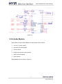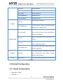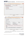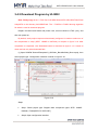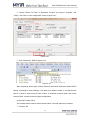
1
MYD-LPC435x/185x User Manual MYD-LPC435x/185x user manual Version V1.2 MYD-LPC435x/185x User Manual Version History Version Description Time Initial Version 2012.10.24 History V1.0 Add 7.0-inch screen support, modify the functional description V1.1 2013.02.22 of the sample program(Nvic_VectorTableRelocation) V1.2 modify the contact information 2013.03.28 MYD-LPC435x/185x User Manual DIRECTORY Chapter 1 Product Overview ............................................................................................ 1 1.1 Product Description ......................................................................................... 1 1.2 Product Preview............................................................................................... 2 1.3 Product Features ............................................................................................. 2 1.4 Product Configuration ...................................................................................... 5 Chapter 2 Hardware Introduction..................................................................................... 6 2.1 Hardware Resources Introduction .................................................................... 6 2.2 Main Module Introduction ................................................................................. 7 2.2.1 Main Processor LPC435x /185x ................................................................ 7 2.2.2 SDRAM Module......................................................................................... 8 2.2.3 NORFLASH Module .................................................................................. 9 2.2.4 SPI FLASH Module ................................................................................. 10 2.2.5 Ethernet Module ...................................................................................... 11 2.2.6 Audio Module .......................................................................................... 12 2.2.7 Touch Control Module ............................................................................. 13 2.2.8 User Button and Reset Circuit ................................................................. 14 2.2.9 LED ......................................................................................................... 15 2.2.10 EEProm Module .................................................................................... 15 2.2.11 Temperature sensor .............................................................................. 16 2.3 Peripheral Interface Introduction .................................................................... 17 2.3.1 UART Interface........................................................................................ 17 2.3.2 CAN and RS485 Interface ....................................................................... 18 2.3.3 SDCARD Interface .................................................................................. 19 2.3.4 USB OTG/HOST Interface ...................................................................... 19 2.3.5 JTAG Interface ........................................................................................ 20 2.3.6 LCD and Touch Screen Interface ............................................................ 20 2.3.7 User Interface .......................................................................................... 21 2.4 Jumper and BOOT Setting ............................................................................. 22 MYD-LPC435x/185x User Manual 2.4.1 Jumper Setting ........................................................................................ 22 2.4.2 BOOT Setting .......................................................................................... 22 Chapter 3 MDK Routine................................................................................................... 25 3.1 MDK Software Resources Introduction ........................................................... 25 3.2 Default Configuration ..................................................................................... 28 3.2.1 Serial Configuration ................................................................................. 28 3.2.2 Jumper Settings ...................................................................................... 29 3.3 MDK Configuration and Compilation .............................................................. 29 3.4 MDK Routine Debug and Download .............................................................. 33 3.4.1 MDK Routine Debug and Download ........................................................ 33 3.4.2 Download Program by ULINK2 .............................................................. 36 3.4.3 ISP Download ......................................................................................... 39 3.4.4 DFU Download ........................................................................................ 43 3.4.5 Internal Flash .......................................................................................... 43 3.5 ADC ............................................................................................................... 46 3.5.1 Adc_Burst................................................................................................ 46 3.5.2 Adc_Dma ................................................................................................ 47 3.5.3 Adc_Interrupt ........................................................................................... 47 3.5.4 Adc_Polling ............................................................................................. 48 3.6 ATIMER ......................................................................................................... 49 3.6.1 Atimer_Wic .............................................................................................. 49 3.7 BOOTFAST ................................................................................................... 50 3.7.1 Fast_Gpio_LedBlinky .............................................................................. 50 3.8 CCAN ............................................................................................................ 50 3.8.1 CCan_SimpleTxRx .................................................................................. 50 3.9 CGU .............................................................................................................. 51 3.9.1 CGU_measureFreq ................................................................................. 51 3.10 Cortex-M3/Cortex-M4 .................................................................................. 52 3.10.1 CortexM3_Bitband/CortexM4_Bitband .................................................. 52 3.10.2 CortexM3_Mpu/CortexM4_Mpu ............................................................. 53 MYD-LPC435x/185x User Manual 3.10.3 CortexM3_Privilege/CortexM4_Privilege ............................................... 54 3.11 DAC ............................................................................................................. 55 3.11.1 Dac_Dma .............................................................................................. 55 3.12 DUALCORE ................................................................................................. 55 3.12.1 Int_Demo............................................................................................... 55 3.12.2 Mbx_Demo ............................................................................................ 57 3.12.3 Queue_Demo ........................................................................................ 58 3.13 EMAC .......................................................................................................... 59 3.13.1 Emac_EasyWeb .................................................................................... 59 3.14 EMC ............................................................................................................ 60 3.14.1 Emc_NorFlash....................................................................................... 60 3.14.2 Emc_Sdram .......................................................................................... 61 3.15 GPDMA ....................................................................................................... 62 3.15.1 Gpdma_Flash2Ram .............................................................................. 62 3.15.2 Gpdma_LinkList .................................................................................... 62 3.15.3 Gpdma_Ram2Ram ............................................................................... 63 3.16 GPIO ........................................................................................................... 64 3.16.1 Gpio_LedBlinky ..................................................................................... 64 3.17 I2C ............................................................................................................... 64 3.17.1 I2c_EEProm .......................................................................................... 64 3.17.2 I2c_LM75B ............................................................................................ 65 3.17.3 I2c_Master ............................................................................................ 65 3.18 I2S ............................................................................................................... 66 3.18.1 I2s_Audio .............................................................................................. 66 3.19 LCD ............................................................................................................. 67 3.19.1 Lcd_Demo ............................................................................................. 67 3.20 NVIC ............................................................................................................ 67 3.20.1 Nvic_Priorities ....................................................................................... 67 3.20.2 Nvic_VectorTableRelocation ................................................................. 68 3.21 OTP ............................................................................................................. 69 MYD-LPC435x/185x User Manual 3.21.1 OTP_API ............................................................................................... 69 3.22 PWR ............................................................................................................ 69 3.22.1 Pwr_DeepPowerDown .......................................................................... 69 3.22.2 Pwr_DeepSleep .................................................................................... 70 3.22.3 Pwr_PowerDown ................................................................................... 71 3.22.4 Pwr_Sleep ............................................................................................. 72 3.23 RIT............................................................................................................... 72 3.23.1 Rit_Interrupt .......................................................................................... 72 3.24 RTC ............................................................................................................. 73 3.24.1 Rtc_Alarm ............................................................................................. 73 3.24.2 Rtc_Calibration ...................................................................................... 74 3.25 SDIO ............................................................................................................ 74 3.25.1 sdio_readwrite ....................................................................................... 74 3.26 SPIFI ........................................................................................................... 75 3.26.1 SPIFI_Test ............................................................................................ 75 3.27 SSP ............................................................................................................. 76 3.27.1 Ssp_Master ........................................................................................... 76 3.27.2 Ssp_Slave ............................................................................................. 77 3.28 TIMER ......................................................................................................... 78 3.28.1 Timer_Capture ...................................................................................... 78 3.28.2 Timer_FreqMeasure .............................................................................. 79 3.28.3 Timer_MatchInterrupt ............................................................................ 80 3.28.4 Timer_MatchPolling ............................................................................... 80 3.29 UART ........................................................................................................... 81 3.29.1 Uart_Autobaud ...................................................................................... 81 3.29.2 Uart_Dma .............................................................................................. 82 3.29.3 Uart_Interrupt ........................................................................................ 82 3.29.4 Uart_Polling ........................................................................................... 83 3.29.5 Uart_Rs485Master ................................................................................ 84 3.29.6 Uart_Rs485Slave .................................................................................. 84 MYD-LPC435x/185x User Manual 3.30 USBDEV ...................................................................................................... 85 3.30.1 Usb_Cdc ............................................................................................... 85 3.30.2 Usb_MassStorage ................................................................................. 86 3.31 USBDEV_ROM............................................................................................ 87 3.31.1 Usb_Composite ..................................................................................... 87 3.31.2 Usb_Dfu ................................................................................................ 88 3.31.3 Usb_Hid ................................................................................................ 89 3.31.4 Usb_MassStorage ................................................................................. 90 3.32 USBHOST ................................................................................................... 90 3.32.1 HID_Kbd................................................................................................ 90 3.33 WDT ............................................................................................................ 91 3.33.1 Wdt_Interrupt ........................................................................................ 91 Appendix 1 sales FAQ and technical support .............................................错误!未定义书签。 MYD-LPC435x/185x User Manual Chapter 1 Product Overview 1.1 Product Description MYD-LPC435x development boards are latest launched by MYIR, which based on Cortex-M4 kernel, are full-featured evaluation kit. The LPC435x, the world’s first asymmetrical dual-core digital signal controller architecture, featuring ARM® Cortex™-M4 and Cortex-M0 processors, brings the advantage of developing DSP and MCU applications within a single architecture and development environment. The Cortex-M4 processor combines the benefits of a microcontroller with high-performance digital signal processing features such as single-cycle MAC, Single Instruction Multiple Data (SIMD) techniques, saturating arithmetic, and a floating point unit. The Cortex-M0 coprocessor off-loads many of the data movement and I/O handling duties that can drain the bandwidth of the Cortex-M4 core. With its dual-core architecture and unique set of configurable peripheral, the LPC435x enables customers to develop a wide range of applications. MYD-LPC185x development boards are latest launched by MYIR, which based on Cortex-M3 kernel, are full-featured evaluation kit. Cortex-M3 is the kernel of the next generation, providing better performance than ARM7 at the same clock frequency and other system enhancements such as modern debug and a higher level of the block integration. The processor which contains 200KB SRAM and 64KB ROM has the function of system programming and application programming. MYD-LPC435x/185x both have 32 MB SDRAM, 2 MB NorFlash, 4 MB SPI Flash, 64 KB EEPROM, and also extend SD Card interface, USB Host/Device interface, CAN interface, RS485 interface, audio input/output interface, LCD interface, JTAG interface, function keys, etc. A wide range of applications are used in the field of motor control, power management, industrial automation, robotics, medical, automotive accessories and embedded audio. In software, it provides LPC435x/185x full-function MDK source, including all peripherals use routines, which greatly reduces the workload of secondary 1 MYD-LPC435x/185x User Manual development and shorten development cycle. 1.2 Product Preview Figure 1-1 1.3 Product Features Electrical parameters Operating Temperature: -40℃~85℃ Electrical Specifications: +5V power supply Mechanical Dimensions: 115 mm x 90 mm Processor (LPC435x) LPC435xFET256, Cortext-M4/M0 dual-core structure, frequency at up to 204MHz 32 bits ARM Cortex-M4 32 bits ARM Cortex-M0 asymmetric coprocessor Hardware floating-point unit 2 MYD-LPC435x/185x User Manual Up to 1 MB total dual bank flash memory with flash accelerator 264KB chip SRAM 64KB chip ROM containing boot code and on-chip software drivers 128 bit universal OTP Processor (LPC185x) LPC185xFET256(Cortex-M3 kernel), frequency at up to 180MHz Up to 1 MB total dual bank flash memory with flash accelerator 200KB chip SRAM 64KB chip ROM containing boot code and on-chip software drivers 128 bit universal OTP External memory 32 MB SDRAM 2 MB Nor Flash 4 MB SPI FLASH 64 KB EEPROM Audio Interface A 3.5mm Audio input interface A 3.5mm two-channel audio output interface LCD touch-screen interface 24 bit true color Resolution: maximum support 1024 x 768 Data transmission interface Three serials (UART0、UART2 and UART3. UART2 needs external MAX3232) One high-speed USB HOST interface One Mini USB OTG interface One Ethernet MAC Two CAN interface One RS485 interface Micro SD Card interface 3 MYD-LPC435x/185x User Manual Debug Interface Standard JTAG interface LED Indicator One system power indicator LED (red) Six user LEDs Other peripheral resources One temperature sensor MYD-LPC435x/185x development board which is stable and reliable has a strong expansibility. The mainly applicable field: Communicate Point of sale terminal, Web server, multiple protocol bridge Industrial/Medical automation controller, application control, robot control, HVAC, PLC, Converter, Circuit breakers, Medical scanning, Security monitoring, motor drive, as well as intercom, etc. Consumer/Appliances Audio, MP3 decoder, alarm systems, monitors, printers, scanners, small household appliances, as well as fitness equipment Car Parts, Car alarm, GPS/fleet Monitor 4 MYD-LPC435x/185x User Manual 1.4 Product Configuration No Name Number 1 MYD-LPC435x/185x Development Board 1 2 1.5 Meters Crossover Cable 1 3 1.5 Meters Mini USB 2.0 Cable 1 4 9Pin to 9Pin Serial 1 Note Include Schematic (PDF), 5 Product DVD 1 User Manual, Source Code, etc. Default configuration 4.3 6 4.3/7.0 Inch LCD Touch Screen 1 inch, or select 7.0 inch, or no configuration Table 1-1 5 MYD-LPC435x/185x User Manual Chapter 2 Hardware Resource Introduction 2.1 Hardware Resources Introduction MYD-LPC435x/185x hardware resources are shown in figure 2-1: Item Size Description Development board size: 115mm x 90mm MYD-LPC435x: LPC4350FET256/LPC4357FET256, CPU Cortex-M4 Core, with Context-M0 coprocessor, up to 204MHz MYD-LPC185x: LPC1850FET256/1857FET256, Up to 180MHz On-chip: MYD-LPC435x: 264KB SRAM, 64KB ROM, 128 bit OTP Memory MYD-LPC185x: 200KB SRAM, 64KB ROM, 128 bit OTP MYD-LPC1857/4357: 1 MB dual bank flash memory External: 32MB SDRAM, 2MB NOR FLASH, 4MB SPI FLASH Debug 20 Pin, 2.54mm JTAG debug interface Type Quantity RS485 1 Description Support RS485(shared with UART1) Peripheral Ethernet 1 100Mbps, DP83848 CAN 2 Support CAN USB 2 Support USB 6 MYD-LPC435x/185x User Manual HOST/Device 2.0 USB OTG 2.0 Audio 2 Audio in/out, UDA1380 SD interface 1 SD/MMC interface Extension interface 3 3 x 20 pin JTAG 1 Standard 20 pin JTAG interface Support 4.3 / 7.0 inch LCD interface 1 touch screen EEPROM 1 Temperature Sensor 1 External 64K EEPROM With range [-55, 127]℃ Precision 0.125℃ UART2(without UART 3 MAX3232), UART0 and UART3(DEBUG) User button 4 K1,K2,K3,K4 Reset 1 SW1 Button Power 5V/2A Power Supply Table 2-1 2.2 Main Module Introduction 2.2.1 Main Processor LPC435x/185x MYD-LPC435x boards are latest launched by MYIR, which based on Cortex-M4 kernel, are full-featured evaluation kit. LPC435x, the world’s first asymmetrical dual-core digital signal controller architecture, featuring ARM® Cortex™-M4 and Cortex-M0 processors, brings the advantage of developing DSP and MCU applications within a single architecture and development environment. The Cortex-M4 processor combines the benefits of a microcontroller with high-performance digital signal processing features 7 MYD-LPC435x/185x User Manual such as single-cycle MAC, Single Instruction Multiple Data (SIMD) techniques, saturating arithmetic, and a floating point unit. The Cortex-M0 coprocessor off-loads many of the data movement and I/O handling duties that can drain the bandwidth of the Cortex-M4 core. With its dual-core architecture and unique set of configurable peripherals, the LPC435x enables customers to develop a wide range of applications such as motor control, power management, industrial automation, robotics, medical, automotive accessories, and embedded audio. LPC185x operate at up to 180 MHz. The ARM Cortex-M3 CPU incorporates a 3-stage pipeline and uses Harvard architecture with separate local instruction and data buses as well as a third bus for peripherals. The ARM Cortex-M3 CPU also includes an internal prefetch unit that support speculative branching. Microcontroller contains an LCD controller, 10/100Mbps Ethernet controller, full-speed USB Device/Host/OTG controller, CAN bus controller, SPI, SSP, IIC, IIS, as well as external memory controller EMC and other resources, which is suitable for industrial control and medical system applications. 2.2.2 SDRAM Module SDRAM chooses K4S561632H. Its main characteristics are as follow: JEDEC standard 3.3V power supply LVTTL compatible with multiplexed address All inputs are sampled at the positive going edge of the system clock. Auto refresh 64ms refresh period (8K Cycle) SDRAM circuit is shown in figure 2-1: 8 MYD-LPC435x/185x User Manual Figure 2-1 2.2.3 NORFLASH Module NORFLASH chooses SST39VF1601 chip. Its characteristics are as follow: Single Voltage Read and Write Operations (2.7V to 3.6V) Superior Reliability Endurance: 100,000 Cycles (Typical) Greater than 100 years Data Retention Low Power Consumption (typical values at 5 MHz) Active Current: 9 mA (typical) 3µA Standby Current: 3μA (typical) Auto Low Power Mode: 3μA (typical) Support Sector-Erase Capability Block-Erase Capability Chip-Erase Capability Fast Read Access Time: 70ns,90ns 9 MYD-LPC435x/185x User Manual Automatic Write Timing NORFLASH circuit is shown in figure 2-2: Figure 2-2 2.2.4 SPI FLASH Module SPI FLASH Module chooses AT25DF321A. Its main characteristics are as follows: Serial Peripheral Interface (SPI) Compatible (module 0 and module 3) Operating Frequency at up to 85MHz (SPI interface) Fast Program and Erase Times 1ms Typical Page Program (256 Bytes) Time 50ms Typical 4-Kbyte Block Erase Time 25ms Typical 32-Kbyte Block Erase Time 400ms Typical 64-Kbyte Block Erase Time Endurance: 100,000 Program/Erase Cycles Data Retention: 20 Years 10 MYD-LPC435x/185x User Manual SPI FLASH circuit is shown in figure 2-3: Figure 2-3 2.2.5 Ethernet Module Ethernet Module chooses DP83848 chip. Its characteristics are as follows: Low-power 3.3V, 0.18μm CMOS technology 3.3V MAC Interface IEEE802.3u Auto-Negotiation and Parallel Detection IEEE802.3uENDEC, 10BASE-T transceivers and filters Ethernet circuit is shown in figure 2-4: 11 MYD-LPC435x/185x User Manual Figure 2-4 2.2.6 Audio Module Audio Module chooses UDA1380HN. Its characteristics are as follow: 2.4 to 3.6 V power supply Slave BCK and WS signals I2S-bus format Multiple format data output interface ADC front-end features DAC features UDA1380HN circuit is shown in figure2-5: 12 MYD-LPC435x/185x User Manual Figure 2-5 2.2.7 Touch Control Module TOUCH control module chooses TSC2046. Its characteristics are as follow: 2.2V to 5.25V operation 1.5V to 5.25V digital I/O Internal 2.5V reference On chip temperature measurement Touch-pressure measurement Auto power-down TSC2046 circuit is shown in figure 2-6: 13 MYD-LPC435x/185x User Manual Figure 2-6 2.2.8 User Button and Reset Circuit User button circuit and reset circuit is shown in figure 2-7, 2-8: Figure 2-7 14 MYD-LPC435x/185x User Manual Figure 2-8 2.2.9 LED LED circuit is shown in figure 2-9: Figure 2-9 2.2.10 EEProm Module EEProm chooses AT24C512. Its characteristics are as follow: Two-wire Serial Interface Bidirectional Data Transfer Protocol 15 MYD-LPC435x/185x User Manual Schmitt Triggers, Filtered Inputs for Noise Suppression 1 MHz, 400 kHz Compatibility High Reliability Endurance: 1,000,000 Write Cycles Data Retention: 40 Years Self-timed Write Cycle AT24C512 circuit is shown in figure 2-10: Figure 2-10 2.2.11 Temperature sensor Temperature sensor chooses STLM75M2E. Its characteristics are as follow: Power supply range from 2.8 V to 5.5 V Temperatures range from 55℃ to +125℃ Operating frequency: 20Hz to 400kHz Temperature accuracy of: ±2℃ from -25℃ to +100℃ ±3℃ from -55℃ to +125℃ Programmable temperature threshold and hysteresis set points STLM75M2E circuit is shown in figure 2-11: 16 MYD-LPC435x/185x User Manual Figure 2-11 2.3 Peripheral Interface Introduction 2.3.1 UART Interface UART circuit is shown in figure 2-12: Figure 2-12 17 MYD-LPC435x/185x User Manual 2.3.2 CAN and RS485 Interface CAN chooses TJA1040. Its characteristics are as follow: Fully compatible with the ISO 11898 standard High speed (up to 1 MBaud) Very low ElectroMagnetic Emission (EME) Differential receiver with high common-mode range for ElectroMagnetic Immunity (EMI) Input levels compatible with 3.3 V and 5 V devices At least 110 nodes can be connected Transmit Data (TXD) dominant time-out function Thermally protected CAN circuit is shown in figure 2-13: Figure 2-13 RS485 chooses SP3485. Its characteristics are as follows: RS-485 and RS-422 Transceivers Operates from a single +3.3V supply Interoperable with +5.0V logic Driver/Receiver Enable Low Power Shutdown Mode -7V to +12V Common-Mode Input Voltage Range Allows up to 32 transceivers on the serial bus Compatibility with the industry standard 75176 pinout 18 MYD-LPC435x/185x User Manual Driver Output Short-Circuit Protection RS485 circuit is shown in figure 2-14: Figure 2-14 2.3.3 SDCARD Interface SD circuit is shown in figure 2-15: Figure 2-15 2.3.4 USB OTG/HOST Interface USB OTG circuit is shown in figure 2-16: 19 MYD-LPC435x/185x User Manual Figure 2-16 USB HOST circuit is shown in figure 2-17: Figure 2-17 2.3.5 JTAG Interface JTAG circuit is shown in figure 2-18: Figure 2-18 2.3.6 LCD and Touch Screen Interface 20 MYD-LPC435x/185x User Manual LCD circuit is shown in figure 2-19: Figure 2-19 2.3.7 User Interface User interface circuit is shown in figure 2-20: 21 MYD-LPC435x/185x User Manual Figure 2-20 2.4 Jumper and BOOT Setting 2.4.1 Jumper Setting Name JP1 Description Note Connect 1 to 2 and use UART0 to output debugging information (The Default connect 2 to 3 and use compiler options of project must be UART3 to output debugging added to the DBG_UART0) Connect JP2 information 2 to 3 using UART3 to output debugging information. Default disconnection. It needs to Connection: ISP download mode JP3 connect in ISP download, while Disconnection: Normal mode others must be disconnected. Connect 2 to 3 by default. When JP5 Connect 1 to 2: enable CAN1 (then starting from NorFlash, 2 should be CAN1 can’t be used) connected to 3, otherwise JP6 NOrFlash can’t be used. Need to connect when using JTAG Connection: enable DEBUG JP7 debug Disconnection: disable DEBUG default) Table 2-2 2.4.2 BOOT Setting Dial switch circuit is shown in figure 2-21: 22 or download(connect by MYD-LPC435x/185x User Manual Figure 2-21 The functions are as follows: (It is effective that only when the startup mode select bit of chip OTP is not programmed. Meanwhile, if LPC1857/4357 has downloaded program, it will start from internal Flash program and have nothing to do with boot settings) Boot Mode 1(P2_9) 2(P2_8) 3(P1_2) 4(P1_1) Description Boot from device connected to USART0 0 0 0 0 USART0 using pins P2_0 and P2_1. Boot from Quad SPI flash SPIFI 0 0 0 1 connected to the SPIFI interface on P3_3 to P3_8 Boot from external static EMC 8-bit 0 0 1 0 memory (such as NORflash) using CS0 and an 8-bit data bus. Boot from external static EMC 16-bit 0 0 1 1 memory (such as NOR flash) using CS0 and a 16-bit data bus. Boot from external static EMC 32-bit 0 1 0 0 memory (such as NORflash) using CS0 and a 32-bit data bus. USB0 0 1 0 1 Boot from USB0 USB1 0 1 1 0 Boot from USB1 Boot from SPI flash connected to the SSP0 interface on P3_3 SPI (SSP) 0 1 1 1 (function SSP0_SCK), P3_6 (function SSP0_MISO), P3_7 (function SSP0_MOSI), and 23 MYD-LPC435x/185x User Manual P3_8 (function SSP0_SSEL Boot from device connected to USART3 1 0 0 0 USART3 using pins P2_3 and P2_4. Table 2-3 24 MYD-LPC435x/185x User Manual Chapter 3 MDK Routine 3.1 MDK Software Resources Introduction MYD-LPC435x/185x kit provides rich examples and users can learn how to use board resources, so as to shorten development cycle. All sample codes can be found in product CD-ROM. CD-ROM directory: \05-MDK_Source\Examples\. Software resources are shown in following table: Module Project Description Adc_Burst ADC test conversion t in Burst Mode Adc_Dma Use DMA to transfer ADC data conversion Adc_Interrup ADC data conversion in interrupt mode Adc_Polling ADC data conversion in polling mode Atimer_Wic Use Alarm Timer to wake up system ADC ATIMER Set BOOTFAST Fast_Gpio_LedBlinky System frequency up to 204MHz (LPC435x) or 180MHz (LPC185x), then drive LED blinks CAN communication Test (dock CAN0 and CCAN CCan_SimpleTxRx CAN1) CortexM4_Bitband/ Test bit segment of Context-M4/Context-M3 Cortex-M4 CortexM3_Bitband (MYD-LPC435x)/ CortexM4_Mpu/ Cortex-M3 CortexM3_Mpu Use MPU to Protect area test (MYD-LPC185x) CortexM4_Privilege/ Switch in privileged and non-privileged mode CortexM3_Privilege Demonstrates how to use DMA to transfer data DAC Dac_Dma to DAC 25 MYD-LPC435x/185x User Manual Demonstration of communication between M4 Int_Demo and M0 DUALCORE Demonstration of communication between M4 Mbx_Demo (MYD-LPC435x) and M0 Demonstration of communication between M4 Queue_Demo and M0 Demonstrate how to implement a simple web EMAC Emac_EasyWeb application Emc_NorFlash external Nor Flash literacy test Emc_Sdram external SDRAM read/write test Gpdma_Flash2Ram The GPDMA test of Flash to Ram EMC Demonstrate how to use the GPDMA Link-list GPDMA Gpdma_LinkList function GPIO Gpdma_Ram2Ram GPDMA test Gpio_LedBlinky Use GPIO driver LED lights (light water effect ) I2c_Master Use I2C to read and write UDA1380 register I2c_EEProm Read and write external EEPROM through I2C I2C Use an external temperature sensor through I2c_LM75B I2C I2S I2s_Audio LCD Lcd_Demo Output audio via I2S bus Color stripes displayed on the LCD panel is controlled by touch screen cursor Configure Nvic_Priorities NVIC priority and test tail-chaining/Late-arriving in interrupt mode in group NVIC Nvic_VectorTableRelocatio Describe how to relocate vector table n OTP Demonstrates how to use on chip OTP OTP_API 26 MYD-LPC435x/185x User Manual programming function. Attention! ! ! Start-up mode (the default is SPIFI) start after the running of this routine development board can only be specified in the code which has nothing to do with coding switch SW2 state. Carefully run! Test in deep low-power mode, as well as RTC Pwr_DeepPowerDown interrupt wake Test to enter Deep Sleep mode and interrupt Pwr_DeepSleep wake-up through the WIC PWR Test to enter power-down mode and interrupt Pwr_PowerDown wake-up through EVRT Test in sleep mode and interrupt wake-up Pwr_Sleep through the WIC Use RIT RIT as a timer to generate an Rit_Interrupt interrupt-driven LED. Test produced a one minute timer interrupt and Rtc_Alarm a 30s Alarm interrupt RTC Rtc_Calibration Real-time clock calibration SDIO sdio_readwrite SDCard test SPIFI SPIFI_Test Use SPIFI library To read and write external SPIFI Flash Ssp_Master SSP transfer data as host Ssp_Slave SSP transfer data as a slave Timer_Capture Capture timer function test Timer_FreqMeasure Measure signal frequency By timer Timer_MatchInterrupt Timer matches interrupt test Timer_MatchPolling Timer matches polling test Uart_Autobaud test UART baud rate function Automatic SSP TIMER UART 27 MYD-LPC435x/185x User Manual Uart_Dma UART DMA test Uart_Interrupt UART interrupt test Uart_Polling UART polling test Uart_Rs485Master RS485 host test Uart_Rs485Slave RS485 slave test USB simulates COM port Usb_Cdc USBDEV The test writes a simple USB mass storage Usb_MassStorage applications in LPC435x/185x Testing USB ROM in LPC435x/185x drive to Usb_Composite write a USB composite device (MassStroage, HID, DFU) application Driver is still lacking on PC and improve next Usb_Dfu version USBDEV_ROM Test on LPC435x/185x use USB ROM drive to Usb_Hid write a USB HID application Use LPC435x/185x write a simple USB mass Usb_MassStorage storage applications Test USB keyboard connected to the USB1 USBHOST as a terminal input and output HID_Kbd through UART3 HyperTerminal WDT Wdt_Interrupt Test WTD interrupt generated at a specific time Table 3-1 3.2 Default Configuration 3.2.1 Serial Configuration Baud Rate: 115200 Data Bits: 8 28 MYD-LPC435x/185x User Manual Parity Bit: None Stop Bit:1 No hardware control flow 3.2.2 Jumper Settings Jumper 1 2 JP1 3 Description Connect UART(J10) to UART3, UART3 output DEBUG information JP2 JP3 disconnect jumper to prohibit ISP Mode JP5 connect Nor Flash with A18、A19 to enable Nandflash. JP6 CAN1 is not available at this time Connect this jumper to open DEBUG function and JP7 debug online Table 3-2 3.3 MDK Configuration and Compilation Compile MDK routine, please keep subdirectory structure of 05-MDK Source \ LPC185x/435x in disc. Take Adc_Burst project for an example to illustrate how to configure MDK. Firstly find “05-MDK Source\LPC185x/435x\Examples\01_ADC\Adc_Burst\Keil” folder and double click project (Adc_Burst.uvproj), then configure project. (Noted, default project setting can made download successfully, please recheck if program compile or download failed): (1) Select project and click right button, then select “Options for Target ‘ XXX’”(XXX can be the components listed in Table 3-3, here take “SPIFI 128MB”for an example. Refer to figure 3-1. The Setting window is shown in figure 3-2: 29 MYD-LPC435x/185x User Manual Figure 3-1 Figure 3-2 Special Note: “Target” configuration is shown in a red box. The following list give three different projects address sat in the form. Refer to Table 3-3: on-chip IROM1 on-chip IRAM1 Project Name Start Size Start Size Internal SRAM 0x10000000 0x18000 0x10080000 0xA000 SPIFI 128MB 0x80000000 0x100000 0x10080000 0xA000 NorFlash 0x1C000000 0x400000 0x10080000 0xA000 IFlash 0x1A000000 0x80000 0x10000000 0x8000 30 MYD-LPC435x/185x User Manual Table 3-3 (2) Select corresponding chip models in “Device” table: Figure 3-3 (3) It is noted to select object file generated (include intermediate file) and execute name in “Output” table. Refer to figure 3-4: 31 MYD-LPC435x/185x User Manual Figure 3-4 (4) C/C++ configuration, user can add or delete compile files path. Refer to figure 3-5: Figure 3-5 (5) Choose project->Rebuild all target files project, or click shortcut icon to compile. The steps are shown in figure 3-6: 32 MYD-LPC435x/185x User Manual Figure 3-6 3.4 MDK Routine Debug and Download 3.4.1 MDK Routine Debug and Download The following is configuration of MDK program and it has a hardware emulator ULink2 in advance. (If need it, please contact us to purchase it) (1) After opening project, open setting dialog box and select Debug. Refer to figure 3-7: 33 MYD-LPC435x/185x User Manual Figure 3-7 Special Note: Different types of components correspond to initialization file, with tfollowing table demonstrates. Files of. Ini are in the \Project directory. Project Initialization file Internal SRAM Internal SRAM.ini SPIFI 128MB LPC18xx_43xx_SPIFI.ini LPC18xx_43xx_ExtFlash16.ini ( Debug) NorFlash LPC18xx_43xx_ExtFlash16Prog.ini (Programming) IFlash LPC43xx Internal Flash.ini Table 3-4 (2) Check hardware emulator ULink2 When connecting ULink2 to board, indicator lights of RUN and COM change blue and then turn off, while indicator lights change red and then remain the same. Thus, it indicates ULink2 has no problem. (3) Clicking Setting in figure 3-10, there will be connection status of ULink2 and board, as well as identification of kernel. Refer to figure 3-8: (Here take MYD-LPC435x for an 34 MYD-LPC435x/185x User Manual example. It displays two cores in figure 3-8, because LPC435x is M4/M0 dual-core processors.) Figure 3-8 (4) Click Ctrl+F5 or shortcut icon, or select Debug->Start/Stop Debug Session to start debugging. Refer to figure 3-9: Figure 3-9 35 MYD-LPC435x/185x User Manual 3.4.2 Download Program by ULINK2 Note: Firstly copy all the “*.FLM” files in 05-MDK Source\LPC185x/435x\Tools\Flash Utility\KEIL to the directory \keil\ARM\Flash. The “*.FLM”file is FLASH burning algorithm file which is used to download program. Prepare for board and Ulink2 and power cord, connect Ulink2 to JTAG (J13), and then turn power on. By default, each project component has already configured. It needs to select one of the components in step1 (SPIFI 128MB or NorFlash) to compile in figure 3-10. After compilation is completed, click Download button to download in figure 3-13. It needs to check and set only when download fails. (1) Open 05-MDK Source\Examples\01_ADC\Adc_Burst\Keil\Adc_Burst.uvproj, then select project type. Configuration interface is shown in figure 3-10: Figure 3-10 Steps: Step1: Select project type. Support there component types: SPIFI 128MB, Norflash, IFlash(MYD-LPC1857/4357) Step2: Open configuration interface 36 MYD-LPC435x/185x User Manual Step3: Select “Utilities” tab Step4: Select “se Target Driver For Flash Programming” Step5: Select”LINK2/ME Context Debugger” Step6: Select the corresponding initialization script file. See Table 3-4 in detail. Step7: Check "Update Target before Debuging" Step8: Enter Flash algorithm set interface The setting interface of entering Flash algorithm is shown in figure 3-11: Figure 3-11 Setting algorithm needs to pay attention to red box on map. Download Function area needs to check "Erase Sectors," Program ". RAM for Algorithm region need to fill in corresponding size. Start is “10000000”. Refer to table 3-5. Click “Add” to add Flash algorithm, refer to figure 3-12(“SPIFI 128MB”), then select Flash algorithm “SPI-Flash LPC18xx@0x8000, click “Add” on a return interface, lastly click “OK”: 37 MYD-LPC435x/185x User Manual Figure 3-12 Project Script Name Flash Algorithm Size Type SPIFI LPC18xx_43xx_SPIFI.ini SPI-Flash LPC18xx@0x8000 0x8000 128MB SST39VF1601@MYD-LPC4350 NorFlash LPC18xx_43xx_ExtFlash16Prog.ini 0x8000 /1850 LPC18xx/43xx IAP 512kB Flash Bank A IFlash LPC43xx Internal Flash.ini 0x0800 LPC18xx/43xx IAP 512kB Flash Bank B Table 3-5 Note: script file in each directory can be found in project Add Flash algorithm, then click “LOAD” to download. Refer to figure 3-13: 38 MYD-LPC435x/185x User Manual Figure 3-13 After download program, set start mode to run. Due to executable file of different project type downloaded to a different address, so its startup settings are also different. The following table illustrates boot settings of different project type. (Note: if it writes IFlash, board reset will run directly in IFIash program and is unrelated with boot settings. Use IFlash, please refer to chapter 3.4.2): BOOT(SW2) Project Component Type Pin1 Pin2 Pin3 Pin4 SPIFI 128MB L L L H NorFlash L L H H Table 3-6 3.4.3 ISP Download Note: ISP download only applies to MYD-LPC1857/4357 board. When using ISP software to download program, firstly install FLASH magic (download latest version from http://www.flashmagictool.com), then connect JP3, JP1 (PIN1), JP2 (PIN2) to enable UART0, lastly set dial switch to LOW position and restart development board. Steps: (1) Open FLASH magic and click “Options”, then choose “Advanced Options”. Refer to figure 3-14: 39 MYD-LPC435x/185x User Manual Figure 3-14 (2) Choose “Use DTR and RTS to control RST and ISP pin” in “Hardware Config” in “Advanced Options”, then click “OK”. Refer to figure 3-15: Figure 3-15 40 MYD-LPC435x/185x User Manual (3) Configure development environment and select LPC1857 or LPC4357. Flash Bank chooses Bank 0:0x1A000000. Refer to figure 3-16: Figure 3-16 COM Port communication port is based on computer (Here choose COM1). In order to ensure stability, baud rate is recommended to select 9600 at the first time. It can choose 57600 behind slowly improvement. Crystal oscillator selects 12M. Select Hex File in IFlash and select “Verify after programming”, “Active Flash Bank” “Erase blocks used by Hex File”. Refer to figure 3-17: 41 MYD-LPC435x/185x User Manual Figure 3-17 (4) Connect UART to COM (Note: ensure that the COM port used by ISP isn’t occupied by other applications) and click ISP->Read Device Signature, then Flash Magic will recognize LPC1857or LPC4357 ID. Refer to figure 3-18: 42 MYD-LPC435x/185x User Manual Figure 3-18 (5) Recognize board and click “Start” button, and program will be downloaded to board. Refer to figure 3-19: Figure 3-19 (6) After downloading program, disconnecting JP3 and resetting board, program starts running. 3.4.4 DFU Download The concrete steps of Using DFU to download program, please refer to lpc_dfusec.pdf (01-Documents/UserManual/Chinese/). 3.4.5 Internal Flash 43 MYD-LPC435x/185x User Manual Note: Internal Flash is the unique Flash of LPC4357and LPC1857 and only these two models can be chosen to download to Internal Flash. Configure MDK of IFIash and compile it, then download to Internal Flash. CPU will run program directly from Internal Flash without checking Boot settings. So it will not start form the other media. At this point, the following are two methods of booting from other media: (1) Erase Internal Flash. ① click IFlash and choose “Options for Target ‘ XXX’”(XXX may be the components listed in table 3-3), refer to figure 3-14. Choose “Utilities” and click “Settings”. Setting interface is shown in figure 3-20: Figure 3-14 Figure 3-20 44 MYD-LPC435x/185x User Manual ② choose “Erase Full Chip” in Download Function and remove “Program" and "Verify", click "OK" to save configuration. Refer to figure 3-21: Figure 3-21 ③ Click “Download”. Refer to figure 3-22: Figure 3-22 After completing above steps, Internal Flash will be erased and board checks BOOT setting. According to these settings, it will start from different media. It is noted that the above is used to erase Internal Flash routine. If download routines rather than erase Internal Flash, it needs to return original configuration. (2) Use ISP Jumper (JP3) The method doesn’t need to erase Internal Flash. Concrete steps are as follows: ① Connect JP3 45 MYD-LPC435x/185x User Manual ② Press the reset button ③ Release the reset button ④ Disconnect JP3 3.5 ADC 3.5.1 Adc_Burst Function description This example demonstrates ADC single/dual channel conversion inputs in burst mode, as well as show injecting a new ADC conversion channel on running channel. More details refer to project “abstract.txt”. Procedures Configure development and serial port by default configuration. Download program by chapter 3.4.2 and set start mode by table 3-6. After downloading program, pressing RESET to reset board. Adjust potential values of potentiometer VR1 to observe terminal information. Phenomenon Indicates ******************************************************************************** Hello MYIR ADC burst demo - MCU: lpc43xx - Core: ARM CORTEX-M4 - Communicate via: UART3 - 115200 bps Use ADC with 10-bit resolution rate of 200KHz, running burst mode (single or multiple input) Display ADC value via UART3 Turn the potentiometer to see how ADC value changes ******************************************************************************** ADC value on channel 1: 0000000940 ADC value on channel 3: 0000000616 ADC value on channel 1: 0000000877 ADC value on channel 3: 0000000616 ADC value on channel 1: 0000000855 46 MYD-LPC435x/185x User Manual 3.5.2 Adc_Dma Function description This example demonstrates ADC transfer data by DMA. ADC generates interrupt after conversion done and makes a request to DMA for transferring data. DMA resets up when previous transfer has been done. More details refer to project “abstract.txt”. Procedures Configure board and serial port by default configuration. Download program by chapter 3.4.2 and by set start mode table 3-6. After downloading program, pressing RESET to reset board. Adjust the potential values of potentiometer VR1 to observe terminal information. Phenomenon Indicates ******************************************************************************** Hello NXP Semiconductors ADC demo - MCU: LPC4300 - Core: ARM CORTEX-M4 - Communicate via: UART3 - 115200 bps Use ADC with 12-bit resolution rate of 200KHz, read in interrupt mode To get ADC channel value and display via UART3 Turn the potentiometer to see how ADC value changes ******************************************************************************** ADC value on channel 0: 0000000993 ADC value on channel 0: 0000000932 ADC value on channel 0: 0000000942 ADC value on channel 0: 0000000962 ADC value on channel 0: 0000000994 3.5.3 Adc_Interrupt Function description This example demonstrates ADC in interrupt mode. ADC generates interrupt after conversion done and checks DONE bit. ADC converted data is displayed via serial and then reset ADC. More details refer to project “abstract.txt”. Procedures 47 MYD-LPC435x/185x User Manual Configure board and serial port by default configuration. Download program by chapter 3.4.2 and set corresponding start mode by table 3-6. After downloading the program, pressing RESET to reset board. Adjust the potential values of potentiometer VR1 to observe terminal information. Phenomenon Indicates ******************************************************************************** Hello NXP Semiconductors ADC demo - MCU: lpc43xx - Core: ARM CORTEX-M4 - Communicate via: UART3 - 115200bps DMA testing : ADC peripheral to memory Use ADC with 10-bit resolution rate of 200KHz Value ADC channel is displayed by UART, this value is taken from destination memory value of DMA function Turn the potentiometer to see how ADC value changes ******************************************************************************** ADC value on channel 1: 0000000091 ADC value on channel 1: 0000000091 ADC value on channel 1: 0000000097 ADC value on channel 1: 0000000112 ADC value on channel 1: 0000000125 3.5.4 Adc_Polling Function description This example demonstrates ADC conversion in polling mode. After start ADC, check whether "DONE" bit is set and display ADC converted data via serial, then re-start ADC for next conversion. More details refer to project “abstract.txt”. Procedures Configure board and PC serial port by default configuration. Download program by chapter 3.4.2 and set corresponding start mode by table 3-6. After downloading program, pressing RESET to reset board. Adjust potential values of potentiometer VR1 and observe terminal information. Phenomenon Indicates ******************************************************************************** 48 MYD-LPC435x/185x User Manual Hello NXP Semiconductors ADC demo - MCU: LPC4300 - Core: ARM CORTEX-M4 - Communicate via: UART3 - 115200 bps Use ADC with 10-bit resolution rate of 200KHz, read in polling mode To get ADC value and display via UART3 Turn the potentiometer to see how ADC value changes ******************************************************************************** ADC value on channel 1: 0000000119 ADC value on channel 1: 0000000128 ADC value on channel 1: 0000000138 ADC value on channel 1: 0000000153 ADC value on channel 1: 0000000167 3.6 ATIMER 3.6.1 Atimer_Wic Function description This example demonstrates Alarm Timer generates interrupt and Wake Up System. After initialize Alarm Timer, system will enter sleep mode and weak up after 1 s in this cycle. More details refer to project “abstract.txt”. Procedures Configure board and serial port by default configuration. Download program by chapter 3.4.2 and set corresponding start mode by table 3-6. After downloading program, press RESET to reset board (This routine may need to press RESET twice). The terminal displays result. Phenomenon Indicates ******************************************************************************** Hello NXP Semiconductors Timer delay demo - MCU: lpc43xx - Core: ARM Cortex-M4 - Communicate via: UART3 - 115200 bps Using Alarm Timer to generate Interrupt and wake up system ******************************************************************************** 49 MYD-LPC435x/185x User Manual Waked Up by Alarm Timer Waked Up by Alarm Timer Waked Up by Alarm Timer Waked Up by Alarm Timer Waked Up by Alarm Timer 3.7 BOOTFAST 3.7.1 Fast_Gpio_LedBlinky Function description This example demonstrates how to use GPIO, and make CPU running at 204MHz, as well as start from other Flash and SPIFI. For details, please refer to project “abstract.txt” file. Procedures Configure board and serial port by default configuration. Download program by chapter 3.4.2 and set corresponding start mode by table 3-6. After downloading program, pressing RESET to reset board. D13 on board will begin to flash. Phenomenon Indicates LED (D13) flashes on board. 3.8 CCAN 3.8.1 CCan_SimpleTxRx Function description This routine demonstrates CCAN to send and receive data. It needs to connect CAN0 and CAN1 to the same bus. When CAN0 send data, CAN1 receive data and verify message. The results will be displayed in terminal. More details refer to project “abstract.txt”. Procedures Connect pin1 and pin2 (in J5 and J6) to enable Can1 and configure other jumper 50 MYD-LPC435x/185x User Manual according to default configuration. Connect pin2 in J8 (CAN0_H) to pin5 (CAN1_H), pin1 (CAN0_L) to pin4 (CAN1_L). Download program by chapter 3.4.2 and set start mode by table 3-6, press RESET button after downloading to start program. Pressing K1 key board triggers a single or multiple data transfer. Phenomenon Indicates ******************************************************************************** Hello NXP Semiconductors C_CAN demo - MCU: LPC43xx - Core: ARM CORTEX-M4 - Communicate via: UART3 - 115200 bps use C_CAN0 to transmit and C_CAN1 to receive. ******************************************************************************** CAN0 and CAN1 initialized. Press key K1(WAKEUP0) to start transmit/receive testing... [CAN0] Message object 17 TX complete [CAN1] Message object 1 RX STD Data verify OK. [CAN0] Message object 17 TX complete [CAN1] Message object 1 RX STD Data verify OK. 3.9 CGU 3.9.1 CGU_measureFreq Function description This example demonstrates CGU set and measure base clock frequency. Procedures Configure board and serial port by default configuration. Download program by chapter 3.4.2 and set start mode by table 3-6, press RESET button after downloading to start program (Press twice if system was in sleep or power-save mode). The terminal displays result. Phenomenon Indicates ******************************************************************************** Hello NXP Semiconductors 51 MYD-LPC435x/185x User Manual CGU demo - MCU: LPC43xx - Core: ARM CORTEX-M4 - Communicate via: UART3 - 115200 bps Use CGU to setup and show source base clock frequencies ******************************************************************************** Setting USB PLL... Setting Audio PLL... Setting All Divider's divisors to 4... All Settings Done! Continue to measure Clock Freq ... Measuring IRC Clock Freq ...=12047 kHz Measuring PLL0 Clock Freq ...=477673 kHz Measuring PLL0 Audio Clock Freq ...=24542 kHz Measuring Divider A Clock Freq ...=3011 kHz Measuring Divider B Clock Freq ...=3005 kHz Measuring Divider C Clock Freq ...=3005 kHz Measuring Divider D Clock Freq ...=3011 kHz Measuring Divider E Clock Freq ...=3017 kHz Measure finished! Demo End! 3.10 Cortex-M3/Cortex-M4 3.10.1 CortexM3_Bitband/CortexM4_Bitband Function description This example demonstrates Bit-banding feature of Cortex-M3/Cortex-M4 processor. More details refer to project “abstract.txt” file. Procedures Configure board and serial port by default configuration. Download program by chapter 3.4.2 and set start mode by table 3-6, press RESET button after downloading to start program. The terminal displays result. Phenomenon Indicates ******************************************************************************** Hello NXP Semiconductors Bit-banding demo - MCU: lpc43xx - Core: ARM CORTEX-M4 - Communicate via: UART3 - 115200 bps 52 MYD-LPC435x/185x User Manual This example used to test Bit-banding feature of Cortex-M4 processor ******************************************************************************** Test bit-band SRAM... The value at address 0x20000000: 0x55162B83 Use bit-band function to get value at bit 3: 0x00000000 Value after clear bit 3 value by using bit-band function: 0x55162B83 Value after set bit 3 value by using bit-band function: 0x55162B8B Test bit-band PERIPHERAL... The value of peripheral register at 0x40083000: 0x00000020 Use bit-band function to get value at bit 5: 0x00000001 Peripheral register after clear bit 5 value by using bit-band function: 0x00000000 Peripheral register after set bit 5 value by using bit-band function: 0x00000020 3.10.2 CortexM3_Mpu/CortexM4_Mpu Function description This example demonstrates MPU protects memory region. More details refer to project “abstract.txt” file. Procedures Configure board and PC serial port by default configuration. Download program by chapter 3.4.2 and set start mode by table 3-6, press RESET button after downloading to start program. Follow prompt and observe results in terminal. Phenomenon Indicates ******************************************************************************** Hello NXP Semiconductors MPU demo - MCU: lpc43xx - Core: ARM CORTEX-M4 - Communicate via: UART3 - 115200 bps Set up 8 region memory and try to access memory that don't allow to invoke Memory Management Handler 53 MYD-LPC435x/185x User Manual ******************************************************************************** Setup MPU: This provide 8 regions: Region 0 - Local SRAM: 0x10000000 (1MB) Region 1 - Static Memory: 0x1C000000 (64MB) Region 2 - AHB RAM: 0x20000000 (64MB) Region 3 - DYCS0: 0x28000000 (128MB) Region 4 - AHB Peripheral: 0x40000000 (64MB) Region 5 - DYCS2 DYCS3: 0x60000000 (512MB) Region 6 - SPIF Data: 0x80000000 (128MB) Region 7 - ARM BUS: 0xE0000000 (1MB) Region 2 can not access (just used for testing) Enable MPU! Press '1' to try to read memory from region 1 Read successful!!! Press '2' to try to read memory from region 5 Read memory at this region is not allow, LED D10 will blink... LED (D13) flashes on board. 3.10.3 CortexM3_Privilege/CortexM4_Privilege Function description This example demonstrates change privilege to unprivileged mode. More details refer to project “abstract.txt”. Procedures Configure board and PC serial port by default configuration. Download program by chapter 3.4.2 and set start mode by table 3-6, press RESET button after downloading to start program. Follow the instructions and observe the results in terminal. Phenomenon Indicates ******************************************************************************** Hello NXP Semiconductors Privileged demo - MCU: lpc43xx - Core: ARM CORTEX-M3 - Communicate via: UART0 - 115200 bps This example used to test Privileged feature of Cortex-M3 processor ******************************************************************************** Thread mode is privileged! Press '1' to change to unprivilege mode ... 54 MYD-LPC435x/185x User Manual Changed to unprivilege mode! Check: Thread mode change to unprivilege successful! Press '2' to change to privilege mode by calling system call exception... Called system call exception! Check: Thread mode change to privilege successful! Demo terminate! 3.11 DAC 3.11.1 Dac_Dma Function description This example demonstrates DMA transfer data to DAC peripheral. Procedures Configure board and serial port by default configuration. Download program by chapter 3.4.2 and set start mode by table 3-6, press RESET button after downloading to start program. The terminal displays result. Phenomenon Indicates ******************************************************************************** Hello NXP Semiconductors DAC demo - MCU: LPC43xx - Core: ARM Cortex-M4 - Communicate via: UART3 - 115200 kbps DMA testing : DAC memory to peripheral Value update for DAC is taken from one cell memory, using DMA function to transfer this value to DAC ******************************************************************************** Starting DAC demo....... 3.12 DUALCORE Note: All the routines in the directory only apply to MYD-LPC435x. 3.12.1 Int_Demo 55 MYD-LPC435x/185x User Manual Function description This example demonstrates inter-processor communication between the Cortex-M4 and Cortex-M0 kernel. More details refer to project “abstract.txt”. Procedures Configure board and PC serial port by default configuration. Double click “05-Examples\08_DUALCORE\Int_Demo\Keil\ M4_M0_ipc.uvmpw”. Specific operation is as follows (Note: compile M0 project firstly and then M4 project.): (1) Choose “M0” in “Set as Active Project” and “LPC43xx_M0_RAM”, and then recompile the program. Refer to figure 3-23: Figure 3-23 (2) Choose “M4” in “Set as Active Project” and “LPC43xx_M4_RAM”, and then recompile the program. Refer to figure 3-24: Figure 3-24 (3) Clicking “Start/Stop Debug” to enter Debug mode and RUN 56 button, D12 MYD-LPC435x/185x User Manual and D13 flash. Phenomenon Indicates D12 is controlled by M0 and D13 is controlled by M4. When Mo changes the state of D12, it will report M4 by interrupt and wait for signal of M4. When M4 receives the report and change the state of D13, it will report M0 by interrupt and wait for the next signal of M0. Then D12 and D13 flash. 3.12.2 Mbx_Demo Function description This example demonstrates inter-processor communication between the Cortex-M4 and Cortex-M0 kernel. M4 kernel sends command to the M0 kernel via MailBox, such as display string and calculation formula. When M0 receives MailBox, it will display results in terminal. More details refer to project “abstract.txt”. Procedures Configure board and serial port by default configuration. According to chapter 3.10.1 and then observe terminal information. Phenomenon Indicates --- M0 Started --************************************* ** LPC4300 = Cortex M4 + Cortex M0 ** ************************************* > M0 Sending: lpc4300 has two cores inside [ M4 :LPC4300 HAS TWO CORES INSIDE ] > M0 Sending: request for pow(0,3) [ M4: 0 ^ 3 = 0 ] > M0 Sending: heureka [ M4:akerueh ] > M0 Sending: lpc4300 has two cores inside [ M4 :LPC4300 HAS TWO CORES INSIDE ] > M0 Sending: request for pow(1,3) 57 MYD-LPC435x/185x User Manual [ M4: 1 ^ 3 = 1 ] 3.12.3 Queue_Demo Function description This example demonstrates inter-processor communication between the Cortex-M4 and Cortex-M0 kernel. More details refer to project “abstract.txt”. Procedures Configure board and serial port by default configuration, download the program by chapter 3.10.1 and then observe terminal information. Phenomenon Indicates --- M0 Started --************************************* ** LPC4300 = Cortex M4 + Cortex M0 ** ************************************* > M0 Sending: lpc4300 has two cores inside [ M4 :LPC4300 HAS TWO CORES INSIDE ] > M0 Sending: request for pow(0,3) [ M4: 0 ^ 3 = 0 ] > M0 Sending: heureka [ M4:akerueh ] > M0 Sending: lpc4300 has two cores inside [ M4 :LPC4300 HAS TWO CORES INSIDE ] > M0 Sending: request for pow(1,3) [ M4: 1 ^ 3 = 1 ] > M0 Sending: heureka [ M4:akerueh ] > M0 Sending: lpc4300 has two cores inside [ M4 :LPC4300 HAS TWO CORES INSIDE ] > M0 Sending: request for pow(2,3) [ M4: 2 ^ 3 = 8 ] 58 MYD-LPC435x/185x User Manual > M0 Sending: heureka [ M4:akerueh ] 3.13 EMAC 3.13.1 Emac_EasyWeb Function description This example demonstrates implement a simple web application. The web page shows two analog inputs (page refresh by each 5 seconds). More details refer to project “abstract.txt”. Procedures Connect PC and board by crosswire. Set board IP: 192.168.0.100, PC IP: 192.168.0.102. Configure board and serial port by default configuration. Download program by chapter 3.4.2 and set start mode by table 3-6, press RESET button after downloading to start program. Input the string http://192.168.0.100 to open page with ADC real-time sampling value. Phenomenon Indicates ADC real-time sampling value displayed on webpage, and changed follow potentiometer VR1's rolling. Refer to figure 3-25: 59 MYD-LPC435x/185x User Manual Figure 3-25 3.14 EMC 3.14.1 Emc_NorFlash Function description This example demonstrates EMC write/read external Nor Flash. More details refer to project “abstract.txt”. Procedures Configure board and serial port by default configuration. Download program by chapter 3.4.2 and set start mode by table 3-6, press RESET button after downloading 60 MYD-LPC435x/185x User Manual to start program. The terminal displays result. Phenomenon Indicates ******************************************************************************** Hello NXP Semiconductors NOR Flash demo - MCU: lpc43xx - Core: ARM Cortex-M4 - Communicate via: UART3 - 115200 bps This example will program the SST39VF1601 Nor Flash on MYD-LPC4300 Board ******************************************************************************** Initialize the Flash... Press 1 to Erase Sector 0... Press 2 to Program Menu data to Flash... Press 3 to Print menu data from exNOR... ******************************************************************************** Hello NXP Semiconductors NOR Flash demo - MCU: lpc43xx - Core: ARM Cortex-M4 - Communicate via: UART3 - 115200 bps This example will program the SST39VF1601 Nor Flash on MYD-LPC4300 Board ******************************************************************************** Test finished. 3.14.2 Emc_Sdram Function description This example demonstrates EMC excesses external SDRAM. More details refer to project “abstract.txt”. Procedures Configure board and serial port by default configuration. Download program by chapter 3.4.2 and set start mode by table 3-6, press RESET button after downloading to start program. The terminal displays result. Phenomenon Indicates ******************************************************************************** Hello NXP Semiconductors Ex SDRAM Demo - MCU: lpc43xx 61 MYD-LPC435x/185x User Manual - Core: ARM Cortex-M4 - Communicate via: UART3 - 115200 bps This example will fill then check the SDRAM content on LPC4300 Eval Board ******************************************************************************** Core M4 Clk = 0072000000 Initialize the SDRAM... Fill RAM... Check RAM... RAM Check Finish... Clear RAM content... 3.15 GPDMA 3.15.1 Gpdma_Flash2Ram Function description This example demonstrates GPDMA function by transferring data from Flash to Ram memory. More details refer to project “abstract.txt”. Procedures Configure board and PC serial port by default configuration. Download program by chapter 3.4.2 and set start mode by table 3-6, press RESET button after downloading to start program. The terminal displays result. Phenomenon Indicates ******************************************************************************** Hello NXP Semiconductors GPDMA demo - MCU: lpc43xx - Core: ARM CORTEX-M4 - Communicate via: UART3 - 115200 bps This example used to test GPDMA function by transfer data from Flash to RAM memory ******************************************************************************** Start transfer... Buffer Check success! 3.15.2 Gpdma_LinkList 62 MYD-LPC435x/185x User Manual Function description This example demonstrates GPDMA Link-list function. More details refer to project “abstract.txt”. Procedures Configure board and serial port by default configuration. Download program by chapter 3.4.2 and set start mode by table 3-6, press RESET button after downloading to start program. The terminal displays result. Phenomenon Indicates ******************************************************************************** Hello NXP Semiconductors GPDMA demo - MCU: lpc43xx - Core: ARM CORTEX-M4 - Communicate via: UART3 - 115200 bps This example used to test GPDMA link list function ******************************************************************************** Start transfer... Buffer Check success! 3.15.3 Gpdma_Ram2Ram Function description This example demonstrates GPDMA transfers data from RAM to RAM by interrupt mode. More details refer to project “abstract.txt”. Procedures Configure board and serial port by default configuration. Download program by chapter 3.4.2 and set start mode by table 3-6, press RESET button after downloading to start program. The terminal displays result. Phenomenon Indicates ******************************************************************************** Hello NXP Semiconductors GPDMA demo - MCU: lpc43xx - Core: ARM Cortex-M4 - Communicate via: UART3 - 115200bps 63 MYD-LPC435x/185x User Manual This example will transfer 2 blocks of data from memory boundary to the other memory boundary on RAM using GPDMA module with interrupt ******************************************************************************** Initialize Buffer... Start transfer... Buffer Check success! 3.16 GPIO 3.16.1 Gpio_LedBlinky Function description This example demonstrates GPIO controls LEDs. More details refer to project “abstract.txt”. Procedures Configure board and serial port by default configuration. Download program by chapter 3.4.2 and set start mode by table 3-6, press RESET button after downloading to start program. Then D9, D14, D12, D13 flash. Phenomenon Indicates LED flashes on board at flowing light effect. 3.17 I2C 3.17.1 I2c_EEProm Function description This example configures I2C as master and demonstrates operation of I2C and EEProm. More details refer to project “abstract.txt”. Procedures Configure board and serial port by default configuration. Download program by chapter 3.4.2 and set start mode by table 3-6, press RESET button after downloading to start program. The terminal displays result. Phenomenon Indicates 64 MYD-LPC435x/185x User Manual ******************************************************************************** Hello NXP Semiconductors EEProm demo - MCU: lpc43xx - Core: ARM Cortex-M4 - This example write the 64 Kbytes(device size) to EEProm then read back to verify ******************************************************************************** Init eeprom... Write data to EEProm... addr:65280 Done! Read and verify data from EEProm... addr:65280 Verify successfully! 3.17.2 I2c_LM75B Function description This example configures I2C as master and demonstrates operation I2C and LM75B. Procedures Configure the development and serial port by default configuration. Download program by chapter 3.4.2 and set start mode by table 3-6, press RESET button after downloading to start program. Chang tLM75B temperature and observe results in terminal. Phenomenon Indicates ******************************************************************************** Hello NXP Semiconductors I2C LM75B - MCU: lpc43xx - Core: ARM Cortex-M4 - This example configures I2C as master mode, configure LM75B'S threshold and hysteresis value, and get temperature from LM75B. ******************************************************************************** Current threshold: 30.250, hysteresis:-25.250 Cur temp: 28.125 3.17.3 I2c_Master 65 MYD-LPC435x/185x User Manual Function description This example configures I2C as master and demonstrates operation of UDA1380. More details refer to project “abstract.txt”. Procedures Configure board and serial port by default configuration. Download program by chapter 3.4.2 and set start mode by table 3-6, press RESET button after downloading to start program. The terminal displays result. Phenomenon Indicates ******************************************************************************** Hello NXP Semiconductors I2C demo - MCU: lpc43xx - Core: ARM Cortex-M4 - This example configures I2C as master mode, write 2 bytes to UDA1380's 0x00_register then read back to verify ******************************************************************************** Press '1' to transmit 2 bytes to UDA1380's 0x00_register... Press '2' to read UDA1380's 0x00_register... Verify successfully 3.18 I2S 3.18.1 I2s_Audio Function description This example demonstrates I2S transfer audio data to play a short music in a loop. More details refer to project “abstract.txt”. Procedures Configure board and serial port by default configuration. Download program by chapter 3.4.2 and set start mode by table 3-6, press RESET button after downloading to start program. Insert headphone to audio output port (J5) and check whether the audio output loop music. 66 MYD-LPC435x/185x User Manual Phenomenon Indicates Loop music can be heard in the headphone. 3.19 LCD 3.19.1 Lcd_Demo Function description This example demonstrates LCD use. More details refer to project “abstract.txt”. Procedures Configure board and serial port by default configuration. Download program by chapter 3.4.2 and set start mode by table 3-6, press RESET button after downloading to start program. Phenomenon Indicates The screen will display color stripes hand cursor and click on the LCD screen can manipulate hand cursor. 3.20 NVIC 3.20.1 Nvic_Priorities Function description This example demonstrates configure NVIC priority. DAC interrupt controls D14, and WIC interrupt generated by pressing key K1 controls D12. The priority of WIC interrupt is higher than DAC interrupt. More details refer to project “abstract.txt”. Procedures Configure board and serial port by default configuration and then modify the definition of "SAME_GROUP" in Nvic_Priorities.c project. If DAC and WIC are configured for two different vector group, then comment out the following line of code, otherwise test the two interrupt source by configuring the same vector group: #define SAME_GROUP 67 MYD-LPC435x/185x User Manual Recompile the project after editing it. Download program by chapter 3.4.2 and set start mode by table 3-6, press RESET button after downloading to start program. Phenomenon Indicates When two interrupt sources configured for different interrupt vector group support interrupt nesting. D14 stop blinking when pressing key K1, after D12 blinks 5 times, D14 will resume blink. When two interrupt sources configured for an interrupt vector group can’t support interrupt nesting. After press K1, WIC interrupt can’t respond immediately until exit DAC interrupt service. 3.20.2 Nvic_VectorTableRelocation Function description This example demonstrates the reposition of vector table. Vector Table will be remapped at the new address 0x20000000 after running the program. Each mode’s initial address in the interrupt vector is: (1) In Internal SRAM mode: Vector Table will be initialized at 0x10000000 (2) In SPIFI 128MB mode: Vector Table will be initialized at 0x80000000 (3) In NorFlash mode: Vector Table will be initialized at 0x1C000000 (4) In IFlash mode: Vector Table will be initialized at 0xEA000000 Timer interrupt printout a message by second. If VT remapping is successful, message is printed secondly. More details refer to project “abstract.txt”. Procedures Configure board and serial port by default configuration. Download program by chapter 3.4.2 and set start mode by table 3-6, press RESET button after downloading to start program. The terminal displays result. Phenomenon Indicates ******************************************************************************** Hello NXP Semiconductors Privileged demo - MCU: lpc43xx - Core: ARM CORTEX-M4 - Communicate via: UART3 - 115200 bps 68 MYD-LPC435x/185x User Manual This example used to test NVIC Vector Table Relocation function ******************************************************************************** Remapping Vector Table at address: 0x20000000 If Vector Table remapping is successful, a message will be printed every second... Match interrupt occur... Match interrupt occur... Match interrupt occur... 3.21 OTP 3.21.1 OTP_API Warning: this routine is only able to start from SPIFI Flash rather check BOOT DIP switch SW2 status, run cautiously!!! Please avoid misuse, take LPC435x for an example, put it in the 17_OTP_CAUTION file in 04-MDK_Source/LPC435x. If it is needed, please copy 17_OTP_CAUTION to 04-MDK_Source/LPC435x/Examples/ and then download it. Function description This program demonstrates operate OTP by solidified OTP API in ROM. Procedures Configure board and serial port by default configuration. Download program by chapter 3.4.2 and set start mode by table 3-6, press RESET button after downloading to start program. Phenomenon Indicates The development board will only start from SPIFI Flash, which is independent with Boot switch. 3.22 PWR 3.22.1 Pwr_DeepPowerDown Function description This example demonstrates system in deep sleep mode and wakeup by RTC 69 MYD-LPC435x/185x User Manual interrupt. More details refer to project “abstract.txt”. Procedures Configure board and serial port by default configuration. Download program by chapter 3.4.2 and set start mode by table 3-6, press RESET button after downloading to start program. (Press RESET twice If the system is in power saving or sleep mode.) The terminal displays result. Phenomenon Indicates ******************************************************************************** Hello NXP Semiconductors Power control demo - MCU: lpc43xx - Core: ARM CORTEX-M4 - Communicate via: UART3 - 115200 bps This example used to enter system in Deep PowerDown mode and wake up it by using RTC Interrupt ******************************************************************************** Configuring system, plz wait ... Press '1' to start demo: Enter Deep PowerDown mode... Wait 5s, RTC will wake-up system... ******************************************************************************** Hello NXP Semiconductors Power control demo - MCU: lpc43xx - Core: ARM CORTEX-M4 - Communicate via: UART3 - 115200 bps This example used to enter system in Deep PowerDown mode and wake up it by using RTC Interrupt ******************************************************************************** Configuring system, plz wait ... Press '1' to start demo: Enter Deep PowerDown mode... Wait 5s, RTC will wake-up system... 3.22.2 Pwr_DeepSleep Function description This example demonstrates system in deep sleep mode and wake up by WIC Interrupt. More details refer to project “abstract.txt”. Procedures 70 MYD-LPC435x/185x User Manual Configure board and serial port by default configuration. Download program by chapter 3.4.2 and set start mode by table 3-6, press RESET button after downloading to start program (Press RESET twice If the system is in power saving or hibernation mode.). Pressing K1 to wake up system, and the terminal displays result. Phenomenon Indicates ******************************************************************************** Hello NXP Semiconductors Power control demo - MCU: lpc43xx - Core: ARM CORTEX-M4 - Communicate via: UART3 - 115200 bps This example used to enter system in deep sleep mode and wake up it by using WAKEUP0 pin ******************************************************************************** Press '1' to start demo... Enter deep sleep! Press K1 key on the board to wakeup system... Waked up from deep sleep!!! 3.22.3 Pwr_PowerDown Function description This example demonstrates system in power down mode and wake up it by EVRT Interrupt. More details refer to project “abstract.txt”. Procedures Configure board and serial port by default configuration. Download program by chapter 3.4.2 and set start mode by table 3-6, press RESET button after downloading to start program (press RESET twice If the system is in power saving or sleep mode.). Pressing K1 to wake up system and observe D13 statues. Phenomenon Indicates Pressing K1 will trigger interrupt and LED light blinks twice. 71 MYD-LPC435x/185x User Manual 3.22.4 Pwr_Sleep Function description This example demonstrates system in sleep mode and wake up by WIC interrupt. More details refer to project “abstract.txt”. Procedures Configure board and serial port by default configuration. Download program by chapter 3.4.2 and set start mode by table 3-6, press RESET button after downloading to start program (press RESET twice If the system is in power saving or sleep mode.). Pressing K1 to wake up system, the terminal displays result. Phenomenon Indicates ******************************************************************************** Hello NXP Semiconductors Power control demo - MCU: lpc43xx - Core: ARM CORTEX-M4 - Communicate via: UART3 - 115200 bps This example used to enter system in sleep mode and wake up it by using WAKEUP0 pin(K1 key on the board) ******************************************************************************** Press '1' to start demo... Enter sleep!! Press K1 key on the board to exit sleep mode... Waked up from sleep!! 3.23 RIT 3.23.1 Rit_Interrupt Function description This example demonstrates configure RIT as a timer to generate interrupt. More details refer to project “abstract.txt”. 72 MYD-LPC435x/185x User Manual Procedures Configure board and serial port by default configuration. Download program by chapter 3.4.2 and set start mode by table 3-6, after downloading press RESET button to start program (press RESET twice If the system is in power saving or sleep mode.). Pressing K1 to wake up system and observe D13 status. Phenomenon Indicates D13 flashes at 0.5Hz. 3.24 RTC 3.24.1 Rtc_Alarm Function description This example demonstrates generate interrupt in Minute and Alarm interrupt at 30s. More details refer to project “abstract.txt”. Procedures Configure board and PC serial port by default configuration. Download program by chapter 3.4.2 and set start mode by table 3-6, press RESET button after downloading to start program (Press twice if system was in sleep or power-save mode). The terminal displays result. Phenomenon Indicates ******************************************************************************************* Hello NXP Semiconductors RTC demo - MCU: lpc43xx - Core: ARM CORTEX-M4 - Communicate via: UART3 - 115200 bps A simple RTC example. To generate interrupt in minute Counter Increment Interrupt (1min) and generate Alarm interrupt at 30s ******************************************************************************** Configuring system, plz wait ...Done. *****************************ALARM 30s matched! ******************************Minute: 001 73 MYD-LPC435x/185x User Manual ******************************ALARM 30s matched! 3.24.2 Rtc_Calibration Function description This example demonstrates calibrate real-time clock. More details refer to project “abstract.txt”. Procedures Configure board and serial port by default configuration. Download program by chapter 3.4.2 and set start mode by table 3-6, press RESET button after downloading to start program (Press twice if system was in sleep or power-save mode). The terminal displays result. Phenomenon Indicates ************************************************************************************** Hello NXP Semiconductors RTC Calibration demo - MCU: lpc43xx - Core: ARM CORTEX-M4 - Communicate via: UART3 - 115200 bps This example demonstrates how to calibrate RTC ******************************************************************************** Configuring system, plz wait... 003004005006007008 Calibrated! 010011012013014015016 Calibrated! 018019020021022 Calibrated! 3.25 SDIO 3.25.1 sdio_readwrite Function description This example demonstrates operation speed of SD Card. More details refer to project “abstract.txt”. 74 MYD-LPC435x/185x User Manual Procedures Configure board and serial port by default configuration. Download program by chapter 3.4.2 and set start mode by table 3-6, press RESET button after downloading to start program (Press twice if system was in sleep or power-save mode). Insert a Micro SD card (Note: Routine will write the SD card, so it needs backup data in an SD card before the test), follow prompts and observe results in terminal. Phenomenon Indicates ******************************************************************************** Hello NXP Semiconductors SD/MMC read/write demo - MCU: LPC43xx - Core: ARM CORTEX-M4 - Communicate via: UART3 - 115200 bps Use SDIO to perform read and write into from/to Card ******************************************************************************** Please insert a Micro SD card...Card inserted. WP pin is not used in Micro SD, just assume writable Press 1 to write data to sector 1 and verify: Verified! Press 2 to write data in Multitransfer mode and then verify: Verified! Press 3 to measure continuous read speed... Measuring, plz wait ... read speed = 7168 kB/s Press 4 to measure continuous write speed... Measuring, plz wait ... write speed = 2783 kB/s Test finished. 3.26 SPIFI 3.26.1 SPIFI_Test Function description This example demonstrates SPIFI library read/write an external QSPI serial flash. 75 MYD-LPC435x/185x User Manual More details refer to project “abstract.txt”. Procedures Configure board and serial port by default configuration. Download program by chapter 3.4.2 and set start mode by table 3-6, press RESET button after downloading to start program (Press twice if system was in sleep or power-save mode). Pressing K1 to wake up system and observe D13. Phenomenon Indicates ******************************************************************************** Hello NXP Semiconductors SPIFI demo - MCU: LPC4300 - Core: ARM CORTEX-M4 - Communicate via: UART3 - 115200 bps ******************************************************************************** Initializing SPIFI driver...OK! devSize: 0x400000, memSize:0x400000 Erasing QSPI device...OK Programming + verifying QSPI device...OK! The entire test procedure requires about 1 minute. If the test is successful, LED D13 will light. 3.27 SSP 3.27.1 Ssp_Master Function description This example demonstrates communication between SSP peripheral. It needs two MYD-LPC435x boards. One downloaded program is as host, the other downloaded program in chapter 3.25.2 is as slave. More details refer to project “abstract.txt”. Procedures Connect SCK、SSEL、MISO and MOSI between host and slave by four cables: Host Slave SCK(J17 pin 18) SCK(J17 pin 18) 76 MYD-LPC435x/185x User Manual SSEL(J17 pin 17) SSEL(J17 pin 17) MISO(J17 pin 16) MISO(J17 pin 16) MOSI(J17 pin 15) MOSI(J17 pin 15) Configure board and serial port by default configuration. Download program by chapter 3.4.2 and set start mode by table 3-6, press RESET button after downloading to start program (Press twice if system was in sleep or power-save mode). Connect serial to J10 in host, and the terminal displays result. Phenomenon Indicates ******************************************************************************** Hello NXP Semiconductors SSP demo - MCU: lpc43xx - Core: ARM Cortex-M4 - Communicate via: UART3 - 115200bps An example of SSP using polling mode to test the SSP driver This example uses SSP in SPI mode as master to communicate with an SSP slave device The master and slave transfer together a number of data byte ******************************************************************************** Press '1' to start transfer... Init buffer Start transfer... Verify complete! 3.27.2 Ssp_Slave Function description This example demonstrates communication between SSP peripheral. This program needs two MYD-LPC185x/435x boards. One downloaded this program is as host, the other download the program in chapter 3.25.1 is as slave. More details refer to project “abstract.txt”. Procedures Connect SCK、SSEL、MISO and MOSI between host and slave by four cables: Host Slave 77 MYD-LPC435x/185x User Manual SCK(J17 pin 18) SCK(J17 pin 18) SSEL(J17 pin 17) SSEL(J17 pin 17) MISO(J17 pin 16) MISO(J17 pin 16) MOSI(J17 pin 15) MOSI(J17 pin 15) Configure board and serial port by default configuration. Download program by chapter 3.4.2 and set start mode by table 3-6, press RESET button after downloading to start program (Press twice if system was in sleep or power-save mode). Connect the serial to J10 in host, and the terminal displays result. Phenomenon Indicates ******************************************************************************** Hello NXP Semiconductors SSP demo - MCU: lpc43xx - Core: ARM Cortex-M4 - Communicate via: UART3 - 115200bps An example of SSP using interrupt mode to test the SSP driver This example uses SSP in SPI mode as slave to communicate with an SSP master device The master and slave transfer together a number of data byte ******************************************************************************** Init buffer Wait for master transfer... 3.28 TIMER 3.28.1 Timer_Capture Function description This example demonstrates Capture Timer function. More details refer to project “abstract.txt”. Procedures Configure board and serial port by default configuration. Download program by chapter 3.4.2 and set start mode by table 3-6, press RESET button after downloading to start program (Press twice if system was in sleep or power-save mode). Connect 78 MYD-LPC435x/185x User Manual Pin6 in J16 and contact VCC or ground to generate capture time, the terminal displays result. Phenomenon Indicates ******************************************************************************** Hello NXP Semiconductors Timer Match interrupt demo - MCU: lpc43xx - Core: ARM Cortex-M4 - Communicate via: UART3 - 115200 bps Using Timer 1 to take a snapshot of the timer value when an input signal on CAP1.1(J16.6) transitions ******************************************************************************** Time capture: 0x00000003 Time capture: 0x00000003 Time capture: 0x00000006 Time capture: 0x00000006 3.28.2 Timer_FreqMeasure Function description This example demonstrates timer measure a signal's frequency. More details refer to project “abstract.txt”. Procedures Connect Pin16 in J16 to Pin4 in J17, and then configure board and serial port by default configuration. Download program by chapter 3.4.2 and set start mode by table 3-6, press RESET button after downloading to start program (Press twice if system was in sleep or power-save mode). The terminal displays result. Phenomenon Indicates ******************************************************************************** Hello NXP Semiconductors Timer measure frequency demo - MCU: lpc43xx - Core: ARM Cortex-M4 - Communicate via: UART3 - 115200 bps Use timer 0 to measure input signal frequency through its CAP0.2 Use timer 3 to generate different frequency signals ******************************************************************************** 79 MYD-LPC435x/185x User Manual Press c to continue measuring other signals... Please input frequency (from 1 to 999 hz):00678 Measuring......00678hz Press c to continue measuring other signals... Please input frequency (from 1 to 999 hz):00999 Measuring......01000hz Press c to continue measuring other signals... 3.28.3 Timer_MatchInterrupt Function description This example demonstrates timer Match generates specific time in interrupt mode. More details refer to project “abstract.txt”. Procedures Connect Pin16 in J16 to Pin4 in J17, and then configure the development and PC serial port by default configuration. Download program by chapter 3.4.2 and set start mode by table 3-6, press RESET button after downloading to start program (Press twice if system was in sleep or power-save mode). The terminal displays result. Phenomenon Indicates ******************************************************************************** Hello NXP Semiconductors Timer Match interrupt demo - MCU: lpc43xx - Core: ARM Cortex-M4 - Communicate via: UART3 - 115200 bps Using Timer 0 to generate interrupt at frequency 1Hz ******************************************************************************** Match interrupt occurred... Match interrupt occurred... Match interrupt occurred... Match interrupt occurred... Match interrupt occurred... 3.28.4 Timer_MatchPolling Function description 80 MYD-LPC435x/185x User Manual This example demonstrates Timer Match generates specific time in polling mode. More details refer to project “abstract.txt”. Procedures Connect Pin16 in J16 to Pin4 in J17, and then configure board and serial port by default configuration. Download program by chapter 3.4.2 and set start mode by table 3-6, press RESET button after downloading to start program (Press twice if system was in sleep or power-save mode). The terminal displays result. Phenomenon Indicates ******************************************************************************** Hello NXP Semiconductors Timer delay demo - MCU: lpc43xx - Core: ARM Cortex-M4 - Communicate via: UART3 - 115200 bps Using Timer 0 in polling mode Generate Interrupt at frequency 10Hz ******************************************************************************** Match interrupt occur.. Match interrupt occur.. Match interrupt occur.. Match interrupt occur.. Match interrupt occur.. 3.29 UART 3.29.1 Uart_Autobaud Function description This example demonstrates auto baud rate mode. More details refer to project “abstract.txt”. Procedures Configure the development and PC serial port by default configuration. Download program by chapter 3.4.2 and set start mode by table 3-6, press RESET button after downloading to start program (Press twice if system was in sleep or power-save mode). Inputting the letter "A" or "a" start detect the baud rate automatically, character 81 MYD-LPC435x/185x User Manual inputted to terminal will be back to manifest. Phenomenon Indicates Hello MYIR UART Auto Baudrate demo MCU LPC43xx - ARM Cortex-M4 UART3 - Auto Baud rate mode used RateMIN = 274 Hz <= UART_RATE <= RateMAX = 409090 Hz AutoBaudrate Status: Synchronous! Hello MYIR UART Auto Baudrate demo MCU LPC43xx - ARM Cortex-M4 UART3 - Auto Baud rate mode used RateMIN = 274 Hz <= UART_RATE <= RateMAX = 409090 Hz a test, i'm typing 3.29.2 Uart_Dma Function description This example demonstrates UART in DMA mode. More details refer to project “abstract.txt”. Procedures Configure board and serial port By default configuration (Baud Rate: 9600 bps,Data bit:8, Stop bit:1, Parity bit: 0, Hardware flow control: No). Download program by chapter 3.4.2 and set start mode by table 3-6, press RESET button after downloading to start program (Press twice if system was in sleep or power-save mode). Character inputted to terminal will be back to manifest. Phenomenon Indicates Hello NXP Semiconductors UART interrupt mode demo using ring buffer MCU lpc43xx - ARM Cortex-M4 UART3 - 9600bps This is a long string. It transferred in to DMA memory and transmit through Tx line on UART3 peripheral. To use UART with DMA mode, FIFO function must be enabled I'm typing here .... 3.29.3 Uart_Interrupt 82 MYD-LPC435x/185x User Manual Function description This example demonstrates UART in interrupt mode. More details refer to project “abstract.txt”. Procedures Configure board and serial port by default configuration. Download program by chapter 3.4.2 and set start mode by table 3-6, press RESET button after downloading to start program (Press twice if system was in sleep or power-save mode). Inputting letter "A" or "a" start detect the baud rate automatically, character inputted to terminal will be back to manifest. Phenomenon Indicates Hello NXP Semiconductors UART interrupt mode demo using ring buffer MCU lpc43xx - ARM Cortex-M4 UART3 - 9600bps I am typing .................... 3.29.4 Uart_Polling Function description This example demonstrates UART in polling mode. More details refer to project “abstract.txt”. Procedures Configure boards and serial port by default configuration. Download program by chapter 3.4.2 and set start mode by table 3-6, press RESET button after downloading to start program (Press twice if system was in sleep or power-save mode). Inputting letter "A" or "a" start detect the baud rate automatically, character inputted to terminal will be back to manifest. Phenomenon Indicates Hello NXP Semiconductors UART polling mode demo MCU lpc43xx - ARM Cortex-M4 UART3 - 9600bps I am typing... this is the polling mode of UART... 83 MYD-LPC435x/185x User Manual 3.29.5 Uart_Rs485Master Function description This example demonstrates communication between boards by RS485. It needs another MYD-LPC185x/435x development board which runs program in chapter 3.27.6. More details refer to project “abstract.txt”. Procedures Connect RS485_A and RS485_B by two cables, and then configure board and serial port by default configuration. Download program by chapter 3.4.2 and set start mode by table 3-6, press RESET button after downloading to start program (Press twice if system was in sleep or power-save mode). It needs to run slave device and then run master device, and the terminal displays result. Phenomenon Indicates Hello NXP Semiconductors RS485 demo in Master mode [A]Sending... [A]Receive: ACK [B]Sending... [B]Receive: [A]Sending... [A]Receive: ACK 3.29.6 Uart_Rs485Slave Function description This example demonstrates communication between boards by RS485. It needs another MYD-LPC185x/435x development board which runs program in chapter 3.27.6. More details refer to project “abstract.txt”. . Procedures Connect RS485_A and RS485_B by using two cables, and then configure board and serial port by default configuration (Note: Baud rate should be set to 115200). Download program by chapter 3.4.2 and set start mode by table 3-6, press RESET button after downloading to start program (Press twice if system was in sleep or 84 MYD-LPC435x/185x User Manual power-save mode). It needs to run slave device and then run master device, and the terminal displays result.. Phenomenon Indicates Hello NXP Semiconductors RS485 demo in Slave mode Slave's Receiver is not always enabled - Auto Address Detection is enabled Slave Addr detected! Msg A: Hello NXP Slave Addr detected! Msg A: Hello NXP Slave Addr detected! Msg A: Hello NXP Slave Addr detected! Msg A: Hello NXP 3.30 USBDEV 3.30.1 Usb_Cdc Function description This example demonstrates achieve virtual COM port by USBDEV. More details refer to project “abstract.txt”. Procedures Connect JP1’s Pin1 with JP2’s pin2 to select UART0, other jumpers stay in default configuration. Download program by chapter 3.4.2 and set start mode by table 3-6, press RESET button after downloading to start program (press twice if system was in sleep or power-save mode). Connect PC and J12 via mini USB cable, and then a virtual device will be detected in Windows’s device management. Please refer to figure 3-26. 85 MYD-LPC435x/185x User Manual Figure 3-26 It needs to install virtual serial driver at the first time (The name of driver: lpc18xx-vcom.inf). When finding the new device, choose to install it manually. After installing the driver, open the hardware serial which connect to UART0 (after setting JP1 and Jp2, ,UART0output from J10) and USB virtual serial (COM6) on PC. Setting serial port as follows: Baud Rate: 9600 bps,Data bit:8, Stop bit: 1, Parity bit: 0, Hardware flow control: No. When inputting any character in one terminal, it will display in the other serial. Phenomenon Indicates Opening two serial and inputting any character in one terminal, there will be character which is displayed in the other terminal. 3.30.2 Usb_MassStorage Function description This example demonstrates USB Mass Storage application on LPC43xx. More details refer to project “abstract.txt”. Procedures Configure board and serial port by default configuration. Download program by chapter 3.4.2 and set start mode by table 3-6, press RESET button after downloading to start program (Press twice if system was in sleep or power-save mode). Connecting PC and Mini USB J12 interface on board by USB, then opening “my 86 MYD-LPC435x/185x User Manual computer”, check that whether there is added removable storage device “LPC4300 USB” (in this case using LPC435x demo). Phenomenon Indicates After open “My computer”, there will be a removable storage device”LPC4300 USB”. Refer to figure 3-27: Figure 3-27 After opening it, there will be a “README.txt” which is only read. Refer to figure 3-28: Figure 3-28 At the same time, it can be created、copied、deleted、modified on the disk. 3.31 USBDEV_ROM 3.31.1 Usb_Composite Function description This example demonstrates achieve a USB Composite (MassStorage, HID and DFU) 87 MYD-LPC435x/185x User Manual application by USB ROM driver. More details refer to project “abstract.txt”. Procedures Configure board and serial port by default configuration. Download program by chapter 3.4.2 and set start mode by table 3-6, press RESET button after downloading to start program (Press twice if system was in sleep or power-save mode). Connecting PC and Mini USB J12 interface on board by USB, it can test on USB MassStorge、USB HID、USB DFU. Phenomenon Indicates (1) HID Interface Test Double click HIDClient.exe. The file location: “C:\Keil\ARM\Utilities\HID_Client\Release\HIDClient.exe”. After opening drop-down menu, choose the device “HID”, then click check box, and the device can receive the return PC status. There will be a check box next to Inputs which is chosen. Refer to figure 3-29: Figure 3-29 (2) USB MassStorage Test Open “My computer”, there will be a 32K unformatted removable disk. Format it, then can read, write, copy it. (3) DFU Test Run DFU download tools on PC. 3.31.2 Usb_Dfu 88 MYD-LPC435x/185x User Manual Function description This example demonstrates USB DFU (Device Firmware Upgrade) application by USB ROM driver. More details refer to project “abstract.txt”. Procedures Configure board and serial port by default configuration. Download program by chapter 3.4.2 and set start mode by table 3-6, press RESET button after downloading to start program (Press twice if system was in sleep or power-save mode). Connecting PC and Mini USB J12 interface on the development board by USB, and then test USB DFU. Phenomenon Indicates Run DFU download tools to test on PC. 3.31.3 Usb_Hid Function description This example demonstrates USB HID application by USB ROM driver. More details refer to project “abstract.txt”. Procedures Configure board and serial port by default configuration. Download program by chapter 3.4.2 and set start mode by table 3-6, press RESET button after downloading to start program (Press twice if system was in sleep or power-save mode). Connecting PC and Mini USB J12 interface on the development by USB, and then test USB DFU. Phenomenon Indicates Double click HIDClient.exe. The file location: “C:\Keil\ARM\Utilities\HID_Client\Release\HIDClient.exe”. After opening drop-down menu, choose the device “LPC18xx Demo”, then click check box, and the device can receive the return PC status. There will be a check box next to Inputs which is chosen. Refer to figure 3-30: 89 MYD-LPC435x/185x User Manual Figure 3-30 3.31.4 Usb_MassStorage Function description This example demonstrates a USB MassStorage application by USB ROM driver. More details refer to project “abstract.txt”. Procedures Configure board and serial port by default configuration. Download program by chapter 3.4.2 and set start mode by table 3-6, press RESET button after downloading to start program (Press twice if system was in sleep or power-save mode). Connecting PC and Mini USB J12 interface on the development by USB, and then test USB MassStorage. Phenomenon Indicates Open “My computer”, there will be a 32K unformatted removable disk. Format it, then can read, write, copy it. 3.32 USBHOST 3.32.1 HID_Kbd Function description This example demonstrates connect USB keyboard to USB1. More details refer to 90 MYD-LPC435x/185x User Manual project “abstract.txt”. Procedures Configure board and serial port by default configuration. Download program by chapter 3.4.2 and set start mode by table 3-6, press RESET button after downloading to start program (Press twice if system was in sleep or power-save mode). Open the serial and insert USB keyboard, follow prompt and observe results in terminal. Phenomenon Indicates +***** REMOTE MEASUREMENT RECORDER ****+ | This program is a simple Measurement | | Recorder. It is based on the LPC435x/185x | | and records the state of the voltage | | on the analog input AD0.2 . | + command -----------+ function ---------------------------+ | R [n] | read <n> records | |D | display measurement | | T hh:mm:ss | set time | | I mm:ss.ttt | set interval time | |C | clear records | |Q | quit recording | |S | start recording | +--------------------------+---------------------------------------+ Detecting the keyboard ... Command: 3.33 WDT 3.33.1 Wdt_Interrupt Function description This example demonstrates WDT generates interrupt after a specific time. More details refer to project “abstract.txt”. Procedures 91 MYD-LPC435x/185x User Manual Configure board and serial port by default configuration. Download program by chapter 3.4.2 and set start mode by table 3-6, press RESET button after downloading to start program (Press twice if system was in sleep or power-save mode). Open serial, follow prompt and observe results. Phenomenon Indicates ******************************************************************************* Hello NXP Semiconductors Watch dog timer interrupt (test or debug mode) demo - MCU: lpc43xx - Core: Cortex M4 - Communicate via: UART3 - 115200 bps ******************************************************************************** Watchdog is frequently fed by SysTick_Handler Press '1' to disable feeding Watchdog timer Press '2' to enable feeding Watchdog timer Enable feeding Disable feeding Warning...watchdog timeout! Warning...watchdog timeout! Warning...watchdog timeout! 92 MYD-LPC435x/185x User Manual Appendix 1 sales FAQ and technical support How to buy We accept paypal payment and bank wire transfer 1.Paypal payment Please select the products add into shopping cart, the checkout web page will redirect to paypal.com for you payment. Shipment fee will calculated automatically by your location region. 2.Bank wire transfer Please email or fax us with products list you want, we will send you a pro-invoice with order value total, shipping cost and bank information. Shipping details Please select the shipping area catalogue for you location. If you have carrier account to pay the shipment fee, please select “Freight collect” and email us the carrier account. Please visit http://www.myirtech.com/support.asp for more details Noted 1.The shipment will start in 3 biz days by Fedex Express, it usually take 7 days to reach regular cities or regions. 2.We will use DHL Express for West asia or middle east countries, it usually take 7 days to reach regular cities or regions. 3.The remote regions defined by Fedex/DHL may cause delay, 14 days in generally. 4.Some countries have strict import policy, we will help to make shipping invoice with you requirement, like invoice value, trade term, custom statements and H.S code etc. Please contact us with these shipment requirements if your country has strict custom affairs. Support and maintains MYIR provides 12 months warranty for hardware products if the defects or failures were not caused by wrong use. Return steps for defective products 1. Please email or call us get a Return Merchandise Authorization (RMA) by providing purchase details and reasons for return (defective, incorrect etc). 2. MYIR will make a shipping invoice (list value total, item description etc) for you return request. China have strict limit on return products, so please use MYIR’s shipping invoice to return items to avoid custom delay. Contact: Tel:+86-0755-25622735 Fax: +86-0755-2553 2724 Mail to: [email protected] [email protected] Website: www.myirtech.com 93