1
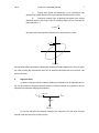
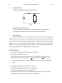
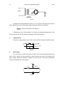
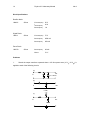
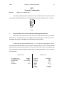
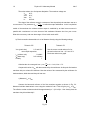
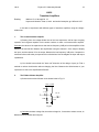
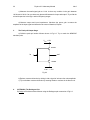
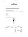
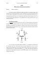
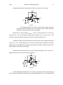
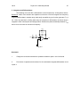
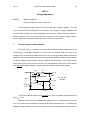
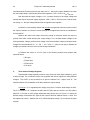
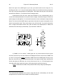
Physics 331 Electronics Laboratory Manual Simon Fraser University Physics Department Electronics Laboratory Table of Contents Introduction ................................................................................................................................iii Lab 1: Introduction to Equipment and DC Circuits .....................................................................1 1. Ohm's Law and its Disobedience ...................................................................... 1 2. Voltage Divider and Thévenin's Equivalent Circuit ........................................... 1 3. Oscilloscope and Function Generator............................................................... 2 Lab 2: RC and LR Circuits ..........................................................................................................5 1. Low-pass Filter .................................................................................................. 5 2. High-pass Filter ................................................................................................. 7 3. RC Differentiator/Integrator ............................................................................... 7 4. Cascaded Filters (optional) ............................................................................... 7 5. LR Filters (optional) ...........................................................................................7 Lab 3: LRC Resonant Circuits.....................................................................................................9 1. Series LRC Circuit............................................................................................. 9 2. Parallel LC Circuit ............................................................................................. 10 3. Fourier Analysis ................................................................................................10 Lab 4: Diode Circuits ...................................................................................................................11 1. Diode Characteristic and Half-wave Rectifier.................................................... 11 2. Full-wave Rectifier Bridge ................................................................................. 11 3. Voltage Doubler ................................................................................................12 4. Diode Clipper ....................................................................................................12 5. Diode Clamp .....................................................................................................13 6. Signal Rectifier (optional) ..................................................................................13 7. Zener Diode (optional).......................................................................................13 Lab 5: Transistor Fundamentals ................................................................................................. 15 1. Using Transistor Curve Tracers to Measure Operating Characteristics............ 15 2. Transistor Biasing ............................................................................................. 17 Lab 6: Transistor Amplifiers ........................................................................................................ 19 1. The Common-emitter Amplifier .........................................................................19 2. The Emitter-follower Amplifier ........................................................................... 19 3. The Push-pull Output Stage.............................................................................. 20 4. The Darlington Pair ...........................................................................................20 Lab 7: Field Effect Transistors ....................................................................................................23 1. Junction FET Characteristic Curves.................................................................. 23 2. FET Current Source .......................................................................................... 24 3. Source Follower ................................................................................................24 4. Using the JFET as a Variable Resistor ............................................................. 25 The World's Simplest AM Radio Transmitter .................................................... 25 5. The Common Source JFET Amplifier................................................................26 Lab 8: Differential and Operational Amplifiers............................................................................. 29 1. The Differential Amplifier ...................................................................................29 2. The Operational Amplifier..................................................................................30 i Physics 331 Lab 9: Operational Amplifiers II................................................................................................... 33 1. Non-inverting Voltage Feedback ....................................................................... 33 2. Inverting Voltage Feedback ..............................................................................33 3. Current to Voltage Converter ........................................................................... 33 3. The Active Rectifier ...........................................................................................34 4. Integrators and Differentiators........................................................................... 34 Lab 10: Positive Feedback and Oscillators ................................................................................. 37 1. Comparators .....................................................................................................37 2. The Schmitt Trigger ...........................................................................................38 3. R.C. Relaxation Oscillator ................................................................................. 38 4. The Wien Bridge Oscillator ............................................................................... 39 Lab 11: Voltage Regulators.........................................................................................................41 1. Discrete Transistor Voltage Regulator .............................................................. 41 2. Three-terminal Voltage Regulator .....................................................................42 3. Three Terminal Regulator as a Current Source ................................................ 43 Lab 12: TTL and CMOS Logic Gates.......................................................................................... 45 1. Mickey Mouse Logic and the Totem Pole Output..............................................45 2. CMOS Logic Gates ...........................................................................................46 3. CMOS Logic Chips............................................................................................47 4. The Latch Flip-Flop ...........................................................................................49 ii Electronics Laboratory Introduction The experiments in this lab manual are designed to introduce various aspects of analog electronics starting from the simplest concepts such as Ohm's law and leading to practical electronic circuits including amplifiers, integrated circuits, oscillators, voltage regulators and logic gates. Each lab script is intended for a four-hour lab period. Some students may need more time to complete the labs, especially at the beginning when the equipment is still unfamiliar. The time can be used more efficiently if the student prepares in advance by reading the script and planning the procedure before coming to the lab. The homework problems at the end of each lab script are intended to be done before the lab in order to prepare. Each workstation in the lab has the necessary equipment: an oscilloscope, a function (signal) generator, a multimeter and an experimental box. The multimeter can measure voltage, current, resistance and capacitance. The experimental box includes ±12 V power supplies for operational amplifiers and a +5 V supply for logic chips. The independent Anatek variable power supply includes a robust current limiting control. For those circuits built from independent components not using ic chips, it is better to use this power supply because it withstands abuse much better than the power supplies in the experimental box. Insert jumpers to create a continuous bus from one side to the other. Use the horizontal bus pins for the voltages shown here. +12 V +5 V ic These five holes are connected together. ic These are connected too, but not to the ones above. gnd –12 V These 25 holes are connected. These 25 holes are connected. But not to those on the left-hand side. Fig 0.1 The Breadboard Area The breadboarding area on the experimental box has holes for component leads, #22 solid wire and ic pins. Don't try to force larger wire into these hole because it will spring them too far and ruin the board. The horizontal rows of holes on the top and bottom of the breadboard are connected together horizontally. The left and right halves are independent. We suggest that you use these horizontal rows for power supply voltages and ground. You may wish to put a jumper wire between the left and right halves so that the voltages are the same across the board. The iii Physics 331 vertical columns of holes are connected electrically in groups of five along a vertical line. The top and bottom halves are independent. Typically one inserts an ic chip straddling the centre trough. There are then four empty holes for making connections to each ic pin. When you plug ic's into the breadboard, a common convention is to put pin 1 on the left. For other components, make sure the leads are not in the same column of five unless you want them connected together. The oscilloscope has many knobs and buttons which may be confusing at first. It helps if you read the introductory booklet and manual provided by Tektronix. If nothing seems to be happening press AUTOSTART. N. Alberding, November 1990 Revised, March 1994 Revised, July 1996 General Purpose knob Cursor control Miscellaneous controls Acquisition controls TDS 340 Menu controls Vertical Horizontal Trigger controls controls controls Menu controls Fig. 0.2 The Tektronix TDS 340 Oscilloscope Control Panel iv Lab 1 Physics 331 Laboratory Manual 1 LAB 1 Introduction to Equipment and DC Circuits If you have done the AC circuits labs in physics 234, Spring 1995 or later, you may skip Labs 1, 2 and 3 and add labs on additional topics after Lab 10. Make sure you are familiar with the equipment by doing section 3 of Lab 1 if necessary. Reading: Malvino: Ch. 1. Hayes and Horowitz: Class 1, Worked Examples and Lab 1. Note especially "A preliminary note on procedure." 1. Ohm's Law and its Disobedience a) Verify Ohm's law for a 22 kΩ resistor. Use an analog volt-ohm meter (VOM) for the current measurement and measure the voltage with a digital multimeter (DMM). Use the circuit of Fig. 1.1. When using the meters, start from the least sensitive scale and increase sensitivity until you get to the most sensitive scale appropriate for your reading. + VOM– + + 22 k DMM 0–20V 0–20 Vdc Variable Power Supply 0–1mA – – Fig 1.1 The DMM doesn't really measure the voltage you want. Find an alternative hookup that does measure the correct voltage. What happens to the current measurement? How do the internal resistances for the VOM and DMM affect the accuracy of the resistance determination? Which hookup is most accurate for a 20 k resistor? For a 20 MΩ resistor? b) Measure V vs. I for the #1869 incandescent lamp. Don't exceed 50 V. Get enough points to show how the lamp disobeys Ohm's law. Try to use the same graph paper by putting another scale on one of the axes if necessary. Why is the curve nonlinear? What is the resistance of the lamp? Does that question make any sense? 2. Voltage Divider and Thévenin's Equivalent Circuit a) Construct the voltage divider of Fig. 1.2. Use the 12 V dc power supply of the breadboard for Vin. Measure the open-circuit output voltage. Now connect a 10 kΩ resistor on the 2 Physics 331 Laboratory Manual Lab 1 output as a load and explain why the output voltage changes. What is its Thévenin equivalent resistance and voltage? Build the Thévenin equivalent circuit using the variable dc power supply and verify that it behaves the same as the original when the output is loaded with a 10 kΩ resistor. Vin 10 k V out 10 k Fig 1.2 b) Now build the circuit of Fig 1.3. Measure the open-circuit voltage and the short-circuit current and find the Thévenin equivalent resistance and voltage. Vin 33 k 10 k V out 22 k Fig. 1.3 Usually you don't want to short-circuit the output terminals of an unknown device because it might damage something inside. Find the load resistance which lowers the output voltage by one-half. How does this value compare with the Thévenin resistance? 3. Oscilloscope and function generator a) Show two signals on the oscilloscope display Adjust the function generator to produce a sine wave set the AMPLITUDE to 2 Vpp. Apply the sine wave signal from the function generator to Channel 1 of the oscilloscope. Simultaineously apply the SYNCH output signal of the function generator to Channel 2. Press, in sequence, the oscilloscope’s AUTOSET, CLEAR MENU and CH 1 buttons. AUTOSET should Lab 1 Physics 331 Laboratory Manual 3 configure the scope to measure the signals coming into the inputs. The CLEAR MENU and CH 1 buttons ensure that the display is clean and your next operations will affect the CH 1 display. The green light next to CH 1 should be lit. You should see a 2 Vpp signal displayed on the CH 1 trace and a square wave displayed on the CH 2 trace. What is the peak-to-peak voltage of the square wave? b) Change the scale and position of the waveforms Turn the SCALE knob under VERTICAL. Notice how the display changes. The V/DIV legend beneath the display reflects the scale changes. Adjust the CH 1 scale to 1 V/div. Press CH 2 and investigate the VERTICAL SCALE adjustment as before and leave CH 2 on 1 V/div. Press CH 1. Play with the VERTICAL POSITION knob. Turn the HORIZONTAL SCALE knob and note how the displayed waveform changes. The legend beneath the display reflects the change in sweep rate. Move the trance left and right with the HORIZONTAL POSITION control. After you have changed a few settings you should be able to return to the origional configuration by pressing AUTOSET. The result of AUTOSET depends on the signals which input to the oscilloscope, so if you have changed the function generator output in any way AUTOSET will result in a different configuration. Furthermore, not all of the oscilloscope’s function settings are reconfigured by AUTOSET. It is possible to save all settings of particular configuration for later recall from the oscilloscope's internal memory. See the User's Manual for how to do this. c) Investigate the difference between AC, DC, and GND input coupling. Press VERTICAL MENU. Observe the signals when you choose AC, DC and GND on the menu. Normally you use DC, even when you are measuring AC signals. The purpose of the AC coupled input is to subtract a DC offset from a signal so that you can magnify the alternating component. Add a DC offset to the signal by pulling the OFFSET button on the function generator. You should notice that AC coupling subtracts the offset from the displayed waveform. Avoid AC coupling unless you need to subtract an offset—at low frequencies AC coupling can distort the signal's display. AC coupling puts a high-pass filter on the input to remove the DC offset. So see this, put the coupling on AC and decrease the function generator's frequency until the signal starts to appear smaller in amplitude. After you finish put the frequency back to its original value. d) Learn the operation of the scope's sweep and trigger controls. Press TRIGGER MENU. Make sure trigger source is CH1. Vary the level control to observe the effect of changing the trigger level. There is a floating T on the screen to show you 4 Physics 331 Laboratory Manual Lab 1 where the triggered position of the input signal is displayed. There is also an arrow on the righthand side if the screen to indicate the trigger voltage level. If either of these indicators are not visible they may have been turned off. Consult the user's manual or an instructor to find out how to turn them on again. Change the trigger source to CH 2 which displays the SYNCH signal. What effect does changing the trigger level have now? Change the trigger slope from positive to negative. Note the difference. There's a button labelled "Set Level to 50%" which is handy to quickly stabilize a signal on the screen when you don't know where the trigger level should be set. Reconnect the SYNCH signal from the function generator to EXT TRIG. Select EXT TRIG for the trigger source. This frees CH 2 for observing another signal while still allowing the trigger signal to come from SYNCH of the function generator. e) Learn to measure frequency, assuming that the horizontal time base is accurately calibrated. Centre the displayed waveform about a horizontal line. Measure the period from zero zero crossing to zero crossing and calculate the frequency. Compare with the value obtained using the MEASURE menu and from the function generator readout. f) Generate Lissajous figures by applying two signals of different frequencies to CH 1 and CH 2 (Use the transformer for one signal.) Choose the DISPLAY menu and switch to the XY display instead of the YT display. If the HORIZONTAL SCALE setting is vastly inappropriate for the signal being displayed, the Lissajous figure may be incomplete. To see this, try varying HORIZ SCALE when displaying a Lissajous figure to make sure at least one full cycle is being displayed. g) Invert a signal using the VERTICAL menu and add, subtract, multiply and divide two signals applied to the two channels using the MATH functions. Use the function generator for one signal, and the PROB COMP signal for another. h) Printing You can print the scope display on a printer using the HARDCOPY function. This is useful for recording results to put in your lab book. Before using HARDCOPY you must ensure that the output port and printing options are correctly configured. Use the UTILITY — I/O menu to select the hardcopy port (e.g., Centronics), Layout (e.g., portrait) and Hard Copy format (e.g., Epson printer). Lab 2 Physics 331 Laboratory Manual 5 LAB 2 RC and LR Circuits Reading: Malvino: Ch. 16, sections 9, 10, 11,16, 17,18, 19, 20. Hayes and Horowitz: Class 2, Worked Examples and Lab 2. Read "A Note on Reading Capacitors values", p51, H&H In this experiment the concept of impedance is examined. The impedances of capacitors and inductors are investigated as a function of frequency. Special emphasis is given to the RC circuit as low-pass and high-pass filter, differentiator and integrator. 1. Low-pass Filter a) Construct the filter of Fig. 2.1. Drive it with a sine wave and measure the attenuation V out /V in as a function of frequency. Check to see if the filter attenuates 6dB/octave for frequencies well above the –3dB point (or simply the 3dB point). Measure the resistor's value and use the attenuation curve to calculate the capacitance and compare with its nominal value. 15 k V Vout in 0.01 µF Fig. 2.1 But be careful of grounding! Both ground clips of the scope probes are connected together within the scope. They both go to earth ground. Make sure that they are not connected to different points of your circuit. To speed-up the measurement, first find the 3dB point, then the 90% and 10% points. A few more frequencies should be enough to give you a good graph. b) Set up the frequency sweep of the signal generator to display the frequency response of the low pass filter and print it. Instead of changing the frequency manually, you can use the frequency sweep capability of the function generator. In frequency sweep mode, the function generator gradually changes the frequency output from f1 to f 2 passing through all intermediate frequencies. The sweep time, tsw, determines how long it takes to pass through the frequency range from f1 to f2 . After it reaches f2, it abruptly returns to f1 and repeats the sweep. If the sweep mode is linear then the frequency change from f1 is proportional to the time that has passed from the start of the sweep: f = f1 + (t / tsw) (f2 – f1) 6 Physics 331 Laboratory Manual Lab 2 If the sweep mode is logarithmic, then the frequency is proportional to the exponential of the time and the rate at which it sweeps is proportional to frequency: ln(f2/f1) f = f1 ekt where k = . tsw In logarithmic mode, for example, if the sweep is from 10 Hz to 1000 Hz it covers the range from 10 Hz to 100 Hz in the same amount of time that it covers the range from 100 Hz to 1000 Hz. In linear mode it covers the range from 10 Hz to 100 Hz in the same time that it covers the range from 100 Hz to 190 Hz and it would take 111 times longer to go from 100 Hz to 1000 Hz. To set the sweep mode on the function generator follow these steps: Press SHIFT MENU to enter the function generator menus. Using the > key select B: SWP MENU. Pressing ↓ gives 1:START F. You can now specify the beginning of the frequency shift using the knob. Use > to select other submenus such as 2:STOP F, 3:SWP TIME and 4: SWP MODE (LINEAR) OR (LOG). We suggest that START F should be near zero, and STOP F should be high enough to conveniently capture the frequency range of interest. • After you have entered in all the numbers depress SHIFT SWEEP to enter sweep mode. The output of the function generator should now be sweeping through the specified frequencies. • • • • • You can display a picture of the frequency response of a circuit on the oscilloscope in the following way: • Trigger on the SYNCH signal from the function generator . • Position the trigger point near the left-hand side the of the display. • Adjust the function generator’s sweep time and the scope’s HORIZ SCALE settings so that the end of the sweep is at the right-hand side of the display. You should choose the sweep time to be slow enough to allow for at least one cycle to take place before the frequency changes significantly. • Adjust the channel’s zero volts position to the bottom of the display. • Increase the amplitude of the function generator’s output so that a frequency response graph fills the display. • You can fill in the trace by using the “envelope mode.” Choose ENVELOPE from the ACQUIRE-MODE menu so that the screen will display the accumulation of several sweeps. The number of sweeps accumulated is controlled by the General Purpose Knob. c) Set the signal generator to a single square wave frequency and measure the risetime response of the low pass filter from 10% to 90% maximum. Compare with the theoretical relation trise = 0.35 . f3dB Hint: There is a special function on the MEASURE menu for measuring rise times. d) In previous courses you may have measured phase shift in the following ways: Lab 2 Physics 331 Laboratory Manual 7 1) Display both signals simultaneously on the oscilloscope and determine the phase difference from the time difference between the traces. 2) Produce a Lissajou figure by applying one signal to the vertical deflection plates of the scope. From the resulting ellipse you can calculate the phase difference, ϕ: ϕ = sin-1 B A where B is the y-intercept of the ellipse and A is the maximum y value. A B Fig. 2.2 One should be able to automate the phase shift measurement with a digital scope. Can you figure out a way of doing this automatically and use it to determine the phase shift curve and the 3 db point for the filter? 2. High-pass Filter a) Use the frequency-sweep method to display the attenuation of the high-pass filter in Fig. 2.3 as a function of frequency and take a picture. Carefully examine the response at very low frequencies by manually changing the frequency. 0.01 µF V Vout in 15 k Fig. 2.3 b) Find the 3dB point by manually sweeping the frequency. Use the most accurate method of the two used in the previous section 8 3. Physics 331 Laboratory Manual Lab 2 RC Differentiator/Integrator a) Apply a 100 kHz square wave signal to the low-pass filter of Fig. 2.1 and explain the output wave form. Apply a 100 Hz square wave to the high-pass filter of Fig 2.3 and explain the output. b) Repeat with a triangle wave. 4. Cascaded Filters a) Investigate the frequency response of a low-pass filter made by cascading two identical RC filters. b) Build a band pass filter by cascading a high pass and a low pass filter according the following design criterion: the output impedance of the first filter should be about 1/10 the input impedance of the second filter where only resistive impedances are considered. Measure its frequency response. 5. LR Filters (optional) Construct high pass and low pass LR filters and measure their frequency responses. Homework Problems 1. For a RC low-pass filter calculate |Vout| a) |Vin| b) The phase shift between Vout and Vin, c) The 3dB frequency. 2. Repeat for a LR low-pass filter. 3. Repeat for a RC high-pass filter. 4. For the circuit of Fig. 2.1 plot graphs of |Vout| vs. frequency |Vin| a) with linear axes b) with axes of log |Vout| vs. log f, (i.e., a log-log plot.) |Vin| Ensure that the high frequency (f >> 1/RC) behaviour is displayed. c) What is the filter attenuation in dB/octave at high frequencies? (An octave is a factor two in frequency.) Lab 3 Physics 331 Laboratory Manual 9 LAB 3 LRC Resonant Circuits Reading: Hayes and Horowitz: Class 2, p 44 , Class 3, sections A and B, Lab3, section 3- 1 Horowitz and Hill: section 1.22 In this experiment the resonance in LRC circuits will be investigated 1. Series LRC Circuit Connect the circuit of Fig. 3.1. Choose an inductor and calculate C to give a resonant frequency between 1 kHz and 100 kHz. The resistance R should be chosen so that Q > 2. L C Signal Generator R Fig. 3.1 a) Measure the resonant frequency. This can be done conveniently using the Lissajous figure obtained from the input voltage and VR. b) Measure the frequency dependence of the phase difference between Vin and VL or V C. c) Measure the magnitude of the voltages VL, VC and VR at the resonance frequency. d) Determine the bandwidth and Q of the circuit. e) Using the frequency sweep method, photograph the frequency dependence of VR and determine the bandwidth and Q from the photograph. f) Photograph the frequency dependence of VC. 10 2. Physics 331 Laboratory Manual Lab 3 Parallel LC Circuit Construct the parallel resonant (tank) circuit of Fig. 3.2. R L C Fig 3.2 a) Measure the resonant frequency. b) Print a display of the voltage frequency response and find the bandwidth and Q. c) Investigate what happens when you load the output with a load resistor. 3. Fourier Analysis Drive the circuit of Fig. 3.2 with a square wave and carefully observe the frequency response of the output voltage. You will get peaks in the output sine wave response at the circuit's resonant frequency and at certain lower frequencies that have harmonics at the resonant frequency. This is a sort of backward Fourier analysis. The first few terms of the Fourier expansion of a square wave should be roughly related to the peak frequencies and amplitudes. Try using the sweep generator to display a series of peaks at once. Homework Problems 1. a) Calculate the impedance of the series LRC circuit in Fig 3.1. b) Calculate the resonant frequency. c) Show that the voltage across R is maximum when the impedance is purely resistive. ω X d) Show that for large Q, the expression Q = 0 is equivalent to Q = 0 where X0 is the ∆ω R impedance of the capacitor or inductor at resonance and ∆ω is the full width at the 3dB points. 2. a) Calculate the impedance of the LRC circuit. of Fig. 3.2 b) Calculate the output voltage as a function of frequency c) What is the total current in the circuit at resonance? d) In practice, a real inductor has a finite resistance associated with it, RL, in series with L. Calculate the resonant frequency of the tank circuit including RL. Lab 4 Physics 331 Laboratory Manual 11 LAB 4 Diode Circuits Reading: Malvino: Ch. 3 and Ch. 4. Hayes and Horowitz: Class 3, Worked Example and Lab 3. This experiment will demonstrate the fundamentals of semiconductor diodes and some of their applications. 1. Diode Characteristic and Half-wave Rectifier a) Construct the circuit of Fig. 4.1. Display the I-V characteristic of the diode on the oscilloscope. Use dc coupling and set zero volts at the centre of the screen. Explain the I-V curve. 1N4001 Function Generator with floating output (AC voltage at least 10 V pp) R L Fig 4.1 An ohmmeter (VOM) can be used to measure the polarity of a diode. The band on the diode represents the cathode, i.e., the negative terminal when connected for forward conduction. C a u t i o n : Use the diode specifications at the end of the lab script to calculate the value and power rating of R needed to safeguard the diode. b) Display I vs time. Explain the dependence of the observed waveform on the applied voltage. c) Now replace the 1N4001 diode with an LED and record its characteristic curve. Keep this LED and its curve for future use. 2. Full-wave Rectifier Bridge a) Construct the full-wave bridge rectifier circuit of FIg. 4.2 using four 1N4001 rectifier diodes. Explain the output wave form. Remove one of the diodes and look at the symptoms. 12 Physics 331 Laboratory Manual Lab 4 120Vac R L 12.6Vac transformer Fig 4.2 b) Replace the missing diode and connect a 15 µF electrolytic filter capacitor across the output. Measure the peak-to-peak ripple voltage and compare with your calculations. C a u t i o n : Observe the polarity of the capacitor. c) Repeat with a 400 µF filter capacitor. You now have a respectable voltage source. How much current can the load draw without exceeding the diode specifications? 3. Voltage Doubler Connect the voltage doubler circuit of Fig 4.3 using 1N4001 diodes and explain its action. 0.01 µF in 0.01 µF out Fig 4.3 4. Diode Clipper The circuit of Fig. 4.4 limits the range of a signal. Use the 1N914 signal diode when you build it. Drive it with a sine wave (maximum output amplitude) and observe and measure the output voltage. Explain the operation. Suggest how you can clip a sine wave symmetrically around zero and draw the circuit diagram. 5 Vdc 1N914 1k in out Fig 4.4 Lab 4 5. Physics 331 Laboratory Manual 13 Diode Clamper The circuit of Fig. 4.5 is used to clamp the negative peak of a signal at about 4 V. Try it with sine, triangle and square waves. Explain the operation. 5 Vdc 0.1 µF 1N914 in out Fig. 4.5 6. Signal Rectifier (optional) The next circuit (Fig. 4.6) will pass one polarity only of a pulse-train. Apply a square wave, generate pulses at point A by differentiating and observe the rectified output. Note the forward drop of the diode. 1N914 A in C R1 R2 out Fig 4.6 7. Zener Diode (optional) Substitute a Zener diode (1N4733) for the ordinary diode in Fig. 4.1. Display the I-V characteristic of the Zener diode and explain. C a u t i o n : Incorporate the necessary current-limiting resistor R. Consult the specification in the data sheet. 14 Physics 331 Laboratory Manual Lab 4 Diode Specifications Rectifier diode 1N4001 Silicon V reverse(max) 50 V Iforward(max) 30 A Iforward(cont) 1A V reverse(max) 75 V Iforward(max) 2000 mA Iforward(cont) 200 mA Iforward(max) 49 mA V Zener 5.1 V Signal Diode 1N914 Silicon Zener Diode 1N4733 Silicon Problems 1. Sketch the output waveform expected when a 100 Hz square wave (10 Vp, 20 Vpp) is applied to each of the folllowing circuits. (a) out in 6.3 V Zener (b) in out 5 Vdc (c) in out 3 Vdc Lab 5 Physics 331 Laboratory Manual 15 LAB 5 Transistor Fundamentals Reading: Malvino: Ch. 6 through Ch. 9. You will study bipolar junction transistors (BJTs) in this lab. Most of the exercises will be done with the 2N3904 NPN transistor. The terminal connections are illustrated in Fig. 5.1 below. 4 90 3 N 2 E B C Fig 5.1 1. Using Transistor Curve Tracers to Measure Operating Characteristics There are several Tektronix 575 curve tracers in the lab. We also have a new model: Tektronix 571. The procedures will be slightly different depending on which one you use. Abreviated instructions are available on the bench near each curve tracer. a) Determine the collector characteristics, IC vs. VCE with I B as a parameter. The 571 curve tracer has a printer interface to let you make a hard copy of your curves. You must use the polaroid camera to get hard copy from the 575 curve tracer. Save the curves in your lab book and keep the particular transistor belonging to those curves. Suggested settings for the curve tracers are listed below. Tektronix 575 IC (collector mA) V CE (collector volts) IB (base step) polarity peak Volts Tektronix 571 5mA/div 2V/div 0.01 mA/step + 20 V Function Type Vce max Ic max Ib/step Steps R load P max Acquisition NPN 20 V 20 mA 10 µA 10 100 Ohm 2 Watt 16 Physics 331 Laboratory Manual Lab 5 The series resistor is to limit power dissipation. The maximum ratings are V CE V CB V EB IC 40 V, 60 V, 6 V, 200 mA. The slope of the collector curves is a measure of how imperfectly the transistor acts as a d IC current source. The parameter hoe = is called the output admittance. In the h-equivalent dVCE model of the transistor the collector-emitter output is modelled by an ideal current source in parallel with a resistance. h oe is the inverse of this resistance. Measure hoe from your curves. What is the accuracy and over what range of VCE is this result valid? b) Plot the transfer characteristics IC vs IB. Measure directly using the following settings: Tektronix 575 Tektronix 571 V CE (peak volts) 0, 5 and 15 V use multiple exposures Use the cursor to read values of IC for the ten IB values at VCE = 0, 5 and 15 V. Plot these values on a graph. IC (collector mA) IB (base step) Polarity 5 mA/div 0.01 mA/step + I Calculate the dc current gain h FE = βdc = C at I C = 1 mA, VCE = 5 V. IB Compare this value of β dc with that measured by the multimeter. At this point find another transistor with βdc at least 20% different. Note the values of h FE measured by the multimeter for both transistors, label them and keep for later use. c) Measure I C vs VBE Connect the base and collector of the first transistor together as shown in Fig. 5.2. Measure its diode characteristic curve using the method of Lab 4. This will give you IC vs VBE . The effective emitter resistance should be approximately re' = (25 mV)/IC . How closely does the transistor obey this relationship? Fig 5.2 Lab 5 2. Physics 331 Laboratory Manual 17 Transistor Biasing a) If V BB = 10 V in the circuit of Fig 5.3, calculate what values of RB to i) put V C at 7.5 V, ii) put VC within 10% of 12 V, iii) put VC within 10% of ground. Note: You can use the DC function of the signal generator to give 10V dc. V CC = 12V RC =1k V BB RB Fig 5.3 b) Find standard resistor values closest to those calculated in (a), build the circuit and measure VC for each case. (Use the external power supply for 12V.) Do the actual voltages agree within the precision of component values and the measurement accuracy? Now replace the transistor with the other one with a different βdc. Compare VC with that of the first transistor leaving RB the same in both cases. Does the change match your predictions based on the measured values of βdc? c) Investigate how well the transistor circuit acts as a current source. Measure the current flowing through the collector resistor for R C = 500 Ω and 2 kΩ. Model the response with a Norton equivalent circuit. d) Connect VBB to 12 V and find RB which puts VC at 5 V. e) Put an LED in the circuit and choose RB so it will light when VBB = 5V. f) Design and build an emitter-biased LED driver to switch off and on with 0 and 5V. g) Design a voltage divider biased circuit (Fig 5.4) with the following specifications: VCC = 12 V, IC= 2 mA, VC = 7.5 V and VE = 1 V. Build your circuit. Compare calculated and measured values VBB, VE and VC for both of your transistors. 18 Physics 331 Laboratory Manual Lab 5 V CC = 12V R2 RC VC R1 R E Fig 5.4 Homework Problems 1. Calculate the resistor values for part 2(a). 2. Design the voltage-divider bias circuit of part 2(g). 3. Write a computer program that calculates the resistor values for a voltage-divider bias circuit. Your input parameters are VCC, IC, VC and VCE. Use any high-level language such as C, Pascal, Modula 2, Fortran, APL or Basic. Run the program and turn a listing and sample output. 4. Do the algebra you will need for part 2(c) to obtain the Norton equivalent circuit from the currents obtained using the two values of Rc ; i.e., derive the equations for IN and RN in terms of the quantities you will measure. Lab 6 Physics 331 Laboratory Manual 19 LAB 6 Transistor Amplifiers Reading: Malvino: Ch.10 through Ch. 12. Hayes and Horowitz: Class 4, Lab 4 and worked examples, pp. 90ff and 115ff. In this lab we experiment with different types of transistor amplifiers using the voltagedivider bias. 1. The Common-emitter Amplifier a) Starting from the voltage-divider bias of the last experiment, add an input coupling capacitor and a bypass capacitor on the emitter resistor to make a common-emitter amplifier. Calculate the values of the capacitors so that the low-frequency 3 dB point of the ampllifier will be between 100 and 200 Hz. Measure the amplification using the channel 1 of the scope to display the input, and the channel 2 for the output. Measure the low-frequency 3dB point. Compare the measured values with what you expected from calculations. Now investigate the input and output impedances. b) You should have noticed the "barn roof" distortion of the design of part (a). Find a method to reduce the distortion without changing the bias. Measure the effectiveness of your improvement. How is the amplification affected? 2. The Emitter-follower Amplifier a) Construct the emitter follower circuit shown below in Fig 6.1. V CC = 12V 130k 1 µF 10 µF 150k 7.5k Fig 6.1 b) Calculate the base voltage VB, the emitter voltage VE, VCE and the emitter current, IE. Measure these quantities and compare. 20 Physics 331 Laboratory Manual Lab 6 c) Measure the small-signal gain at 1 kHz. Is there any variation in the gain between 100 Hz and 10 kHz? Can you detect any phase shift between the input and output? Try to find the critical frequencies in the high- and low-frequency ranges. d) Measure output and input impedances. Calculate the power gain. Increase the amplitude of the input signal and determine the onset of distortion, Explain. 3. The Push-pull Output Stage. a) Build the push-pull emitter follower shown in Fig 6.2. Try to match the NPN/PNP transistor pairs. V CC = 12V 2N3904 in out 2N3906 V DD = –12V Fig 6.2 b) Explore crossover distortion by driving it with a signal of at least a few volts amplitude. c) Try to eliminate crossover distortion by inserting diodes or resistors in the bias circuit. 4. (OPTIONAL) The Darlington Pair a) Design and build an emitter follower using the Darlington pair connection of Fig 6.3. Lab 6 Physics 331 Laboratory Manual 21 2N3904 2N3904 1k Fig 6.3 b) Measure current gain and input and output impedance. c) Can you explain the function of the 1 kΩ resistor? (Hint: See Horowitz and Hill.) Homework 1. Determine the capacitor values for use in part 1(a). 2. Calculate the voltages and currents asked for in the emitter follower of part 2(b). Also calculate the small-signal voltage gain and the input and output impedances of the emitter follower. If the emitter-follower is driving an external load, what load impedance yields maximum power transfer to the load? Calculate the ratio of the maximum power transferred to the load to the input power. This is the power gain. 3. (optional) Design an emitter follower using the Darlington Pair. Try to make the input impedance as high as practicable. Calculate current gain, input impedance and the output impedance. Hints: The critical frequency is the frequency at which the effect of the capacitor is to reduce the voltage by a factor of √ 2. If you choose the two capacitors so that this frequency is the same (e.g., 150 Hz) for both the input stage and the bypass, the output at this frequency will be reduced by a factor of (√ 2) 2 = 2. For the bypass capacitor it is not RE that you need to use. Draw the a.c. equivalent circuit and derive a formula for vE/vB. Without the capacitor this ratio will be about 1 at all frequencies. 1 Choose the capacitor so that the ratio is at the critical frequency. 2 √ Lab 7 Physics 331 Laboratory Manual 23 LAB 7 Field Effect Transistors Reading: Malvino, Ch. 13 and 14 Hayes and Horowitz, Class 7, worked example and Lab 7 This lab introduces Field Effect Transistors and their applications. 1. Junction FET Characteristic Curves Use a transistor curve tracer to determine the drain characteristics and transfer characteristics. The 2N5486 is an n-channel JFET having the following maximum ratings: V DS 25 V V DG 25 V V GS 25 V ID 30 mA The terminal pins are illustrated in Fig 7.1. 6 5 48 2N D S G Fig. 7.1 a) Measure the drain characeristics (ID vs. VDS) Tektronix 575 ID (collector mA) V DS (collector volts) V GS (base step generator) Polarity Tektronix 571 0.5 mA/div 2 V/div 0.2V/step + Function Acquisition Type N-FET Vds max 20 V I d max 20 mA Vg/step 0.5 V Offset varies withVgs(off), try –5V Steps 10 R load 0.25 Ohm P max 2 Watt 24 Physics 331 Laboratory Manual Lab 7 b) Measure the transfer characteristics (ID vs. VGS). Tektronix 575 Tektronix 571 ID (Collector mA) 0.5 mA/div V GS (base source volts) 0.2 V/step polarity both + and – V DS 5, 15 and 20 V Use the cursor to read ID for each of the drain curves of part (a) at V DS = 5, 15 and 20 V. Plot the values on graph paper. Determine I DSS , Vp and gm0. Compare with specifications. 2. FET Current Source The circuit of Fig. 7.2 allows you to explore the behaviour of a JFET current source. 12 V 100k VOM 2N5486 5.6k Fig 7.2 Vary the load resistance and watch V DS , and ID . Note the value of VDS which marks the departure from current-source behaviour. (Select your own criterion.) Repeat for different VGS, i.e., different source resistors, and explain your results in terms of the characteristics measured in Part 1. 3. Source Follower Drive the source follower of Fig. 7.3 with a small 1 kHz sine wave. Measure how much the gain differs from unity. Observe the phase shift and examine the onset of distortion. Lab 7 Physics 331 Laboratory Manual 25 12 V 0.01µF 2N5486 1M 4.7k Fig. 7.3 4. Using the JFET as a Variable Resistor In part 2 you found that the current source failed when V DS fell too low. Here you will deliberately bias the FET into the linear Ohmic region. a) Build the circuit of Fig. 7.4 without the shaded components. Drive it with a small sine wave of about 0.2V amplitude at 1 kHz. Notice what happens to the gain and the distortion when you adjust the potentiometer. The distortion is clearer if you drive the circuit with a triangle wave. Explain the distortion. v in (<1V) 0.01µF 10k 100k 1M 1M out 2N5486 330k –12V Fig. 7.4 b) Now try the compensation indicated by the shaded components. Check the improvement by driving this circuit with a triangle wave. Explain why there is some improvement. c) The World's Simplest AM Radio Transmitter: Amplitude modulation can be produced with a slight modification shown in Fig 7.5. Use two function generators. One supplies the carrier frequency of around 1 MHz. The other can be set to sweep through an audible frequency range, e.g., 400-2000 Hz. This provides the variable modulation voltage. Attach a long wire antenna (a meter or two) to the output and you're on the air. Try to pick up the signal on a radio some distance away. For fun you might connect the earphone output from a tape player or a microphone to vmod instead of the second signal generator. 26 Physics 331 Laboratory Manual v mod 1µF + Lab 7 v in (<1V) 10k 0.01µF 1M 1M 100k 2N5486 330k –12V Fig. 7.5 5. The Common Source JFET Amplifier (OPTIONAL, if there is time.) a) Build the common source JFET amplifier of Fig. 7.6. 12 V 5.6k v out 0.01µF v 2N5486 in 1M 2.2k 1 µF Fig. 7.6 b) Calculate the drain current and VGS. Measure ID, VGS and V DS and compare with the calculation. c) Calculate and measure the small signal voltage gain of the amplifier. d) Check the gain as a function of frequency and observe the phase shift. e) Drive the amplifier into distortion and explain its origin. f) Measure the input and output impedances. Lab 7 Physics 331 Laboratory Manual 27 Homework For all problems assume you have a JFET with IDSS = 9 mA and V gs(0ff) = –5 V. 1. Calculate the current through the load for the circuit of Fig.7.2 assuming the JFET is in the current-source region. What are the limits (maximum or minimum) for the load resistance that allow the JFET to operate as a current source? 2. Calculate the gain of the source follower in part 3. 3. Do the calculations indicated for the optional part 5. 28 [Blank page] Physics 331 Laboratory Manual Lab 7 Lab 8 Physics 331 Laboratory Manual 29 LAB 8 Differential and Operational Amplifiers Reading: Malvino, Chapter 18 First we will construct a differential amplifier and measure its properties. Many of the characteristics of the differential amplifier pertain to integrated circuit operational amplifiers. Next you will measure characteristics of the common 741C op amp and the better-performing LF411 op amp which has an FET input circuit. (Note: In this experiment you may use either ±12 V or ±15 V for the op-amp power depending on your breadboard box. Certain values will have to be adjusted accordingly.) 1. The Differential Amplifier a) Calculate the tail current of the circuit in Fig. 8.1 as well as the base currents in each transistor. The 22 Ω swamping resistors are used to improve the match between the discrete transistors. Use the h FE s of your transistors or assume a value of 200 if you haven't kept them. Build the differential amplifier shown in Fig. 8.1 and compare the measured tail and base currents with the calculated values. +12 V 1.5 k Q1 2N3904 Q2 2N3904 22Ω 4.7 k 22Ω 1.5 k 4.7 k –12 V Fig 8.1 b) In Fig. 8.2(a), if you ground the base of transistor Q 1 , the transistors are identical and the components have the values shown, then the output voltage will be +6.35 V. For this experiment, any deviation from +6.35 V will be called Vout(off). Connect the circuit of Fig 8.2(a). Jumper the base of Q1 to ground and measure Vout(off). Take off the jumper and connect the potentiometer voltage-divider and adjust it until the output voltage is +6.35 V. Record the base voltage of Q1 as Vin(off). 30 Physics 331 Laboratory Manual Lab 8 +12 V 10K 5% 1K 1.5 k Q1 2N3904 22Ω 10 k 5% +12 V Q2 2N3904 V 1.5 k Q1 2N3904 out Q2 2N3904 10 mV p-p 1 kHz 22Ω 22Ω Vout 22Ω 0.47µF 100 Ω 1.5 k 1.5 k –12 V 100 Ω –12 V (a) Fig 8.2 (b) c) Calculate the expected values of the differential and common-mode gains and the Common Mode Rejection Ratio. Measure the differential and common-mode gains, A and A cm, using the connection of Fig. 8.2(b). Use a frequency of 1 kHz and a signal level of around 10 mV p-p. 2. The Operational Amplifier a) Input offset and Bias Currents. The 741C has a typical Iin(bias) of 80 nA. Assuming that this is the current through each 220 k resistor in Fig. 8.3, calculate the dc voltages at both inputs. Now connect the circuit and measure the input voltages. Repeat this mesurement for the FET input, LF411 op amp. Calculate Iin(off) and Iin(bias) in both cases and compare the two op amps. +12 V 2 – 7 741C 3 220k + 4 220k –12 V Fig 8.3 6 Lab 8 Physics 331 Laboratory Manual 31 b) Output Offset Voltage. Connect the circuit of Fig. 8.4 using a 741C op amp. 100k +12 V 2 0.47 µF 7 – 6 741C 3 100 Ω + 4 0.47 µF Vout 10k 100k –12 V Fig. 8.4 The bypass capacitors are used on each supply voltage to prevent oscillations. This is discussed in Ch. 22 of Malvino, 5th ed. These capacitors should be connected as close to the IC as possible. Measure the dc output voltage Vout(off) . From the closed-loop gain of the circuit as connected, ACL, you can calculated the input offset voltage: Vin(off) = Vout(off) /AC L. Also measure Vout(off) and calculate Vin(off) for the LF411 op amp in the same circuit. c) Maximum Output Current. Disconnect the right end of the 100 k feedback resistor and connect it to +15 V. This will apply about 15 mV to the inverting input and saturate the op amp. Replace the 10 k load resistor by an ammeter and measure the maximum output current Imax. Do this for both the 741C and LF411 op amps. d) Slew Rate. Connect the circuit of Fig 8.5 choosing R2 between 100 kΩ and 1 MΩ. Measure the slew rate of the 741C and LF411 op amps. R2 +12 V R1 1K 2 3 0.47 µF 7 – 741C + 4 6 0.47 µF V out R3 10 K –12 V Fig 8.5 e) Power Bandwidth. Change R2 to 10 k. Set the ac generator at 1 kHz. Adjust the signal level to get 20 V p-p output from the op amp. Increase the frequency from 1 to 20 kHz and find 32 Physics 331 Laboratory Manual Lab 8 the approximate frequency where slew-rate distortion starts. Do for both 741C and LF411 op amps. f) Maximum Peak-to-Peak (MPP). Measure the MPP values for both op amps by increasing the signal level at 1 kHz until you start to see clipping on either peak. Homework 1. Calculate the values for Itail and the base currents of the differential amplifier. Use the currents to calculate Iin(bias) and Iin(off). Predict the differential gain, A, the common-mode gain, A CM, and the CMRR of the differential amp. Express the CMRR in dB. 2. Calculate the input voltages of the op amp circuit in part 2(a). Lab 9 Physics 331 Laboratory Manual 33 LAB 9 Operational Amplifiers II Reading: Malvino, Chapters 19 and 20 and section 21-1 Hayes and Horowitz, Class 8, Lab 8 and Ch. 4 Worked examples on pp175, 176. This week's experiment will use the ideal properties of operational amplifiers to build some commonly used practical circuits. [The diagrams in this lab don't explicitly show the power connections for the op amps. Refer to Lab 8 if you have forgotten the power pin numbers.] 1. Non-inverting Voltage Feedback Design a non-inverting voltage amplifier with a closed-loop gain of 10. Use the LF411 op amp and choose components with values closest to those specified in your design. Build the circuit and measure the gain. Calculate the theoretical input and output impedances, then measure the input and output impedances if they are within measurable ranges. 2. Inverting Voltage Feedback Now design an op amp circuit with a closed-loop gain of –10 using inverting voltage feedback. Calculate input and output impedances. Build the circuit and repeat the measurements specified in part 1. 3. Current to Voltage Converter The simplest current-to-voltage converter is just a resistor. An op amp in the circuit makes a much better device. The MRD-300 phototransistor can be hooked-up as either a photodiode (connect base and emitter leaving the collector unconnected) or as a phototransistor (base unconnected, emitter and collector connected). In either case it acts like a current source whose current depends on the amount of light that hits it. a) Connect the MRD-300 as a photodiode and use a 10 MΩ feedback resistor as in Fig 9.1. If the output voltage is too large, reduce the resistor to 1 MΩ. If you see fuzz on the output try a 0.001 µF capacitor across the feedback resistor. (How does this capacitor affect the feedback at high frequencies?) Connecting the output of the op amp to the scope, you should see the modulations from the lab's fluorescent lights. What is the photocurrent produced by the MRD300? Cover the phototransistor with you hand to make sure it's the lights you are seeing. Look at the summing junction, X, with the scope as Vout varies. Why is it better to use this op amp rather than just a 10 MΩ resistor? 34 Physics 331 Laboratory Manual Lab 9 10 M light x MRD300 (no collector connection) – 411 + V MRD-300 phototransistor out (Power connections and pin numbers are not shown.) C B E Fig. 9.1 b) [An analog oscilloscope must be used for this exercise to work.] Connect the MRD-300 as a phototransistor as shown in Fig 9.2. Now how much photocurrent is produced? Put the photodiode on the end of a twisted-pair wire so that you can put the diode up against the screen of the scope. This puts the scope in the feedback loop. Why is the diode so shy? +12 V 100 k or more light x – Vout 411 MRD300 (no base connection) + (Power connections and pin numbers are not shown.) Fig. 9.2 4. The Active Rectifier Build the active rectifier circuit shown in Fig. 9.3. Explain why it works better than the passive rectifier used in a previous lab. in + 411 – 1N914 out 10 k Fig. 9.3 Lab 9 Physics 331 Laboratory Manual 35 5. Integrators and Differentiators The following circuit acts like a differentiator at some frequencies, an integrator at others. Determine values of the resistors and capacitors so that the circuit will integrate one frequency range and differentiate in another range, both easily accessible by your function generator. Try it out. Verify its properties by finding what range of freqencies it differentiates and what range it integrates. Check it with square and triangle waves. Examine the phase relationship between vout and vin for a sine wave as a function of frequency. Rf C f Ci in Ri – 411 + out Fig. 9.4 Homework 1. Design the circuits and calculate the quantities needed for parts 1 and 2 of this lab. 2. Find values of capacitors and resistors for the combination integrator/differentiator circuit of part 4 36 [Blank page] Physics 331 Laboratory Manual Lab 9 Lab 10 Physics 331 Laboratory Manual 37 LAB 10 Positive Feedback and Oscillators Reading: Malvino, Sections 21-2, 21-3, 21-9, chapter 22 Hayes and Horowitz, Class 10, Lab 10 and Ch. 4 worked examples on pp 227ff. 1. Comparators a) Connect the LF411 op amp as a comparator. Drive the input with a sine wave and observe the output. You are just using the high open loop gain of the op amp and swinging between positive and negative saturation. One disadvantage of using the LF411 is its slow response time caused by the internal compensating capacitor used to avoid high frequency oscillations. See if you can measure this limited response time. + 12 V 10 k in 2 – 7 6 411 3 + out 4 – 12 V Fig 10.1 b) The LM311 is an op amp that is designed to be used as a comparator. Unlike most op amps, it has a faster response and you can change the voltage levels of the output. With this op amp you get –12 V if Vin < Vref and +12 V otherwise. The open collector output of the 311 allows you to change these output levels independently of the power supply that runs the op amp. Pin 1 comes from the emitter of the i.c.'s output transistor. It is not connected inside the chip. Whatever voltage level you connect this pin to becomes the output if V in > Vref. Often this pin is connected to ground. Similarly pin 7 goes to the output transistor's collector. This collector is not connected in the chip either—that's why it's call an open collector. You connect this pin to a voltage that you want when Vin < Vref, for example, 5 V. Open collector outputs are commonly used if logic voltage levels representing "true" or "false" are different in one part of the circuit from another part. Connect the LM311 as a comparator and observe its improved performance. Note that some of the pin numbers of the LM311 are different from the 411 or 741 op amps. 38 Physics 331 Laboratory Manual Lab 10 + 12 V 10 k 3 in – 1k 8 7 311 2 out + 1 4 – 12 V Fig 10.2 2. The Schmitt Trigger a) Because of its fast response, the 311 comparator can "chatter" if Vin hovers indecisively near the comparison point. In this case, the output will swing erratically between the positive and negative output levels as the input drifts up and down by very small amounts. The Schmitt trigger uses positive feedback to reinforce the comparitor's decision. Immediately after the input voltage crosses the trip point, the trip point (threshold level) changes so that the input must significantly retrace its path in order to reverse the decision. This means that there are two trip points: one for rising input signals, and another, lower one, for falling input signals. + 12 V in 3 – 4.7 k 8 7 311 2 + out 1 4 – 12 V 10 k 100 k Fig 10.3 Calculate the trip points of the circuit in Fig. 10.3 Build it and see if it operates like it should. Put a sine wave on the input and note the "hysteresis." Also note that the triggering stops for sine waves below certain amplitudes. 3. R.C. Relaxation Oscillator The next circuit in Fig. 10.4 shows how to build a square wave generator called a relaxation oscillator. What you do here is remove the input to the Schmitt trigger and reconnect it to one end of a capacitor. The other end of the capacitor is at ground and the capacitor is allowed to charge through a resistor coming from the output of the comparator. After the capacitor charges to the upper trip point, the comparator output goes low to ground. Now the capacitor will Lab 10 Physics 331 Laboratory Manual 39 discharge until it reaches the lower trip point. The comparator output goes high again and the charging cycle continues. The output oscillates between high and low with a frequency determined by the RC time constant of the resistor and capacitor. 100 k +12 V + 12 V x 3 – 4.7 k 8 7 311 2 + out 1 4 – 12 V – 12 V 0.01 µF 10 k 100 k Fig 10.4 Predict the frequency of the circuit. Build it and (a) measure the frequency, (b) measure the peak-to-peak voltage of the output and the voltage of the low level, (c) observe the inverting point x and explain its behaviour, and (d) try to change the frequency by changing the capacitor and resistor combination. 4. The Wien Bridge Oscillator Generating a sine wave is more difficult than a generating a square wave. The Wien bridge circuit uses the parallel-series, lead-lag, circuit to maximize positive feedback for its critical frequency, f c = 1/2πRC. The tungsten lamp in the negative feedback loop limits oscillations when they grow past a certain limit. As the current through the lamp increases at higher output voltages, then its resistance increases and cuts down the gain of the amplifier. Thus a stable frequency is maintained by the lead-lag circuit in the positive feedback loop, and a stable amplitude is established by the self-regulating effect of the tungsten lamp in the negative feedback. 40 Physics 331 Laboratory Manual Lab 10 #1869 lamp 560 Ω – 411 + R C 10 k 0.01 µF R 10 k out f= 1 2πRC C 0.01 µF Fig 10.5 Build the circuit in Fig 10.5 and check if its frequency is 1/2πRC. When you first turn it on you'll see the amplitude grow large until the negative feedback increases after the lamp warms up. When you poke the noninverting input with your finger the output will wobble. If you sweep the scope slowly and poke the noninverting input, you can see the envelope of the oscillation bob up and down. Can you explain this? You can use this oscillator for radio frequencies. Using R=470 Ω, C=220 pF in the lead-lag circuit will give 1/2πRC = 1.5 MHz. When I tried it, though, I got a frequency of about 500 kHz. The shift is probably because of stray capacitances and inductances in the circuit. You will probably have to experiment yourself to get a frequency in the AM radio band. We also found that increasing the 560 Ω feedback resistor to 1 kΩ improved the output amplitude. This way you can use the oscillator for the carrier frequency of the AM transmitter of the FET experiment. Homework 1. Find the trip points of the Schmitt trigger in Fig. 10.3. 2. Find the oscillation frequencies of the relaxation oscillator and Wien bridge oscillator shown in Figs. 10.4 and 10.5. Lab 11 Physics 331 Laboratory Manual 41 LAB 11 Voltage Regulators Reading: Malvino, Chapter 23 Hayes and Horowitz, Class 12 and Lab 12. These experiments will introduce the basic ideas about voltage regulators. The first circuit uses three discrete transistors to demonstrate the principles of voltage regulation and current limiting. Usually one uses prepackaged, three-terminal, voltage regulators instead of building a discrete circuit. The second experiment introduces a very practical voltage regulator whose voltage can be varied and which can also be used as a current source. 1. Discrete Transistor Voltage Regulator The circuit of Fig. 11.1 shows a circuit which will regulate the output voltage and limit the current output. It uses three transistors, Q1, Q2 and Q3, and a Zener diode. We use a Zener voltage of 6.2 V because Zener diodes around 5 V to 6 V are the most stable against temperature variations. One of the transistors acts as a common emitter amplifier so that the output voltage can be more than the Zener voltage. Another, called the "pass transistor," is an emitter follower which delivers most of the current to the load. The third transistor performs the current limiting task. Identify the amplifier transistor, the pass transistor and the current limiting transitor. 33 Ω Q2 Vin V out R2 680 Ω 2.2k 680 Ω Q3 Q1, Q2, Q3: 2N3904 Q1 1N5234 6.2 V 1 k trim 0.1 µF 2.2 k Fig 11.1 a) Find the feedback resistors and calculate the values of feedback resistors which will give Vout = 10 V. Build the circuit and use the variable power supply set at 15 V. Adjust the trim pot so that V out is 10 V with no load. Compare the voltages at the emitter and base of Q1, i.e., the Zener and feedback voltages. Measure the value of both arms of the trim resistance and compare with the 42 Physics 331 Laboratory Manual Lab 11 calculated values. Reconnect the trim pot and put a 1 kΩ load on the output. Measure how much the load voltage drops. Calculate the percent load regulation, %LR = 100% x ∆Vout/Vfull load. Now decrease the supply voltage to 12 V, measure the drop in the output voltage and express this drop as a percent supply regulation, %SR = 100% x ∆Vout/Vnominal. Find the dropout voltage, i.e., the input voltage below which the regulator won't regulate. b) Find the current-sensing resistor and calculate the expected maximum output current if the output is shorted, ISL. Does the current through the voltage divider need to be considered in this calculation? Measure the short-circuit output current by putting an ammeter across the output to ground. Now make a table showing the output voltage, Vout, the base-emitter voltage of the limiting transistor, VBE(lim), and the base voltage of the pass transistor, VB(pass). Measure these voltages for load resistances of 1 kΩ, 330 Ω, 100 Ω and 0 Ω (short circuit output). Explain the voltages you measure in terms of the current-limiting mechanism. c) Tabulate the values of Vout for each of the following troubles and compare with expected values: i) R 2 open. ii) Zener open iii) Zener short iv) Q1 open. 2. Three-terminal Voltage Regulator Prepackaged voltage regulators exist for many commonly used output voltages. If you're a hacker though, it is convenient to have one regulator that can be adjusted for many different voltages. The LM317 is one such device. Its pins are labelled "out," "adjust," and "in." Two external resistors form a feedback circuit that controls the output voltage. a) Design a +5 V regulated power supply using the 317 and the diode bridge of Lab 4. The 317 maintains 1.25 V between the ADJ and OUT pins and the current in the ADJ lead is about 50 µA. Provide a ±20% voltage adjustment range with a trim pot. Figure 11.2 shows the skeleton design. Allow about 20% ripple on the output of the filter capacitor with a 1 k load. Test the regulator as in part 1. Measure the %LR, %SR and dropout voltage. Try to measure the ripple rejection. Lab 11 Physics 331 Laboratory Manual 12.6Vac transformer 43 dc voltage with ripple LM317 Variac 0–120Vac in regulated output out adj R L 31 LM 7 ad j ou t in Fig. 11.2 3. Three Terminal Regulator as a Current Source The 317 maintains about 1.25 V between the ADJ and OUT pins. That's the basis of its use as a variable voltage regulator. This property can also be used to configure it as an adjustable current source. Fig. 11.3 shows the idea. The 220 Ω resistor establishes just over 4 mA. Most of this current goes through the load because the ADJ input passes very little current. Connect this circuit and check if the current varies as the load resistance is changed. What is the voltage compliance? What limits its performance at high and low currents? LM317 V 4.7 µF out in in + adj 220 Ω 0–10 mA 10 k Fig. 11.3 the load 44 Physics 331 Laboratory Manual Lab 11 Homework 1. Calculate the values of the feedback resistors for the three-transistor regulator of part 1 which gives a regulated output voltage of +10 V. Find the expected value of the short circuit output current limit. 2. Design the +5 V regulator of part 2 using the LM317 adjustable regulator. Find reasonable values for all unlabelled capacitors and resistors and provide for a ±20% adjustment. Lab 12 Physics 331 Laboratory Manual 45 LAB 12 TTL and CMOS Logic Gates Reading: Hayes and Horowitz, Class 13 and Lab 13. Today you will be introduced to the circuits of digital electronics. We will start with some circuits made with discrete electronics to perform logical AND, OR and NOT functions. Next, properties of the most commonly used integrated circuit series, the LS-TTL and HC CMOS, are studied. Finally you will use these basic chips to construct more complex circuits. 1. Mickey Mouse Logic and the Totem Pole Output These are among the simplest logic devices. They are useful in their own right from time to time. Also, they demonstrate the input circuitry to the most commonly used TTL chips, the lowpower Schottky (LS-TTL) family. Here we use standard 1N914 signal diodes instead of the faster Schottky diodes used in LS-TTL gates. OR in in AND +5V NOT +5V out in in in out out Fig 12.1 The AND circuit illustrated in Fig 12.1 is similar to the input of the 74LS00 NAND gates. Build it and confirm the logic function experimentally and record your results in a truth table. When you test this gate, use 0 V and 5 V for logical false and true. TTL expects at least 2.0 V input for a high (true) input and guarantees at least 2.4 V for a high output. CMOS requires at least 3.5 V for a high input and delivers at least 4.9 V for high output. In what ways do these circuits disobey these criteria? Try driving an LED. First connect an LED from the output to ground and observe what happens. Next connect the LED from the output to +5 V through a 2.2 k resistor. This will invert the output signal. Does it work better this way? Why or why not? 46 Physics 331 Laboratory Manual Lab 12 Build the NAND gate shown in Fig. 12.2 which is very similar to an LS-TTL circuit. Notice the totem pole output. Make a truth table of its operation showing the voltages on the bases of the totem pole transistors as well as the output voltage. Do the voltage levels conform to TTL criteria? What is the effect of leaving an input unconnected? +5V 22k 120Ω 7.5k in in out 2.7k Fig 12.2 2. CMOS Logic Gates Elementary logic gates are even more easily built from CMOS field effect transistors. Matched complementary pairs of MOSFET transistors are packaged in the CD4007 chip. Fig 12.3 shows its pin arrangement. For the following experiments always tie pin 14 to +5 V and pin 7 to ground. 6 14 2 13 3 8 1 10 5 7 4 11 12 9 CD4007 MOS Transistor Array Fig 12.3 Two inverters are shown in Fig 12.4. The first, using a passive pullup resistor, is like an "open drain" output. Try it and measure its output voltage as a function of time with a 1 kHz square wave input and a 100 kHz input. Now crank up the frequency as high as you can to see what happens. Lab 12 Physics 331 Laboratory Manual 47 If you have 1 kHz and 100 kHz outputs on you breadboard use them. Otherwise, use the F34 at 5 Vpp with a dc offset of 2.5 V to give 0 and 5 V logic levels. +5V +5V 14 10k 8 out 13 in out 6 8 in 6 7 7 Fig 12.4 Now connect the right-hand inverter circuit. It uses a complementary MOSFET as an "active" pullup. Also look at its output as high and low frequencies and compare with the passive pullup. The NAND gate shown in Fig 12.5 is simple. Make it. Test it. 14 in 2 +5 V 1 6 13 in 3 out 5 8 7 4 Fig. 12.5 3. CMOS Logic Chips a) "Connect all Inputs1." When you use CMOS chips like the 74HC00 NAND gates it is important to tie all inputs of all the gates on the chip to a definite logic level. Otherwise the input logic level will be indeterminant. In order to convince yourself of this, connect the 74HC00. Pins 7 and 14 should be ground and +5 V respectively. You are using only one NAND gate so ground the other six inputs of the unused NAND gates. Tie one input of a NAND to HIGH and connect about 6 inches of wire to the other input. Leave the other end of that long wire dangling in air. 1You can remember this rule by recalling the famous movie entitled "Destroy all Monsters." 48 Physics 331 Laboratory Manual Lab 12 Watch the output of the NAND gate as you wave your hand around near the long wire. Try touching your other to +5 V as you do this waving. What you see should convince you that you can't rely on the unconnected inputs of CMOS gates. Now replace the chip with a 74LS00 chip and notice the difference. (Turn power off before changing chips.) Indeterminate inputs can also cause both transistors of the complementary pair to conduct and consequently draw a lot of power from the supply. Intermittent surges of load to the power supply can make glitches. You can test this excessive current consumption using the setup below. First connect all the NAND inputs to ground and verify the low power consumption on the meter's most sensitive scale. Then put the meter on the 150 mA scale. As you drive the inputs with a voltage intermediate between the LOW and HIGH levels appropriate for CMOS, the measured current should go up abnormally. Try this with the 74LS00 too. +5 V mA +5V 14 13 12 11 10 9 8 14 +5 V 74HC00 10k 1 2 3 4 5 6 7 gnd 7 Fig 12.6 b) "NAND is All You Need2 ." NAND gates are very useful because all other logical functions can be built up from them. Because of DeMorgan's theorem we know that, "NAND is all you need." As an exercise design and build the AND function from NAND gates so that you can light one of the LEDs on you breadboard when both of the inputs are high. Next, build the OR function that lights an LED when one or both of the inputs is low. (I.e., OR with negative logic input and positive logic output–this is easy.) Verify they give the results you hope for. Design, build and test an XOR circuit (exclusive OR function) using only NAND gates. 2 It's rumoured that the Beatles once wrote a song with this title. Unfortunately, the title was changed at the last moment before release for marketing reasons. Lab 12 4. Physics 331 Laboratory Manual 49 The Latch Flip-Flop The flip-flop is an essential element in digital and computer circuits. Its ability to store information entered on its input after the input has been changed is useful for memories, registers and counters–almost every component of digital and microprocessor devices. The simplest flipflop is the NAND latch shown below. There are three useful states: set, reset and "no change." Fig 12.7 shows the "no change" state with both inputs high. This is its quiescent resting position and the output could be either high or low depending on whether the previous state was set or — — — — reset. The set state is when S is low and R high The reset state is when R is low and S high. The fourth state, both inputs low, results in an indeterminant output when the inputs return to their — — quiescent state. If both S and R are brought low and then raised, the output retained by Q depends on which input goes high first. This condition is not very useful and should be avoided. Build the NAND latch shown in Fig 12.7 and make its truth table. See if you can verify the indeterminancy of the fourth state. You can use either 74HC00 or 74LS00. +5 V S Q +5 V R Fig. 12.7 The little bars above S and R indicate that the set or reset condition occurs when the respective input is grounded instead of at 5 V. Homework Using only NAND gates, design the circuits for the logical operations (1) AND, (2) OR with inverse logic inputs, and (3) XOR for part 3(b). Congratulations, you made it to The End!