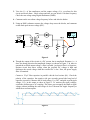
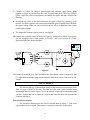
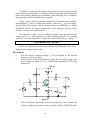
1
King Fahd University of Petroleum and Minerals Department of Electrical Engineering EE 203: Electronic Circuits I Laboratory Manual Feb. 2005 Table of Contents Exp No. Title Page 1..Introduction to Basic Laboratory equipments ............................................ 1 2..PSPICE Tutorial ....................................................................................... 10 3..Applications of Semiconductor Diodes .................................................... 23 4..Rectifier Circuits....................................................................................... 29 5..Bipolar Junction Transistor Characteristics.............................................. 36 6..BJT CE Amplifier..................................................................................... 41 7..The MOSFET Small Signal Amplifier ..................................................... 45 8..Differential Amplifier ............................................................................... 49 9..Transistor-Transistor Logic ...................................................................... 52 10.CMOS Inverter ........................................................................................ 57 INTRODUCTION This manual is your guide to the first electronics laboratory in the electrical engineering program. It is assumed that by completing the first electronics laboratory course you are familiar with basic electronic measurements and instrumentation, as well as with elements of data analysis, presentation of results, and reporting. Professional engineering practice requires using proper experimental methods and procedures. They include not only good measurement techniques, but also proper recording of all relevant information, preparing tables and graphs, etc. Almost as important as obtaining good data is their proper presentation which often determines success in this laboratory course as it does in engineering practice. Upon completion of the first laboratory course you should be very familiar with effective laboratory practices and professional style data presentation. They will be a great asset in your future. The experiments in this lab manual are designed to give the student practical experience in working with diodes and transistors (BJT, FETs and MOSFETs). The laboratory will complement and support the theory taught in the lectures, and should help the student to apply his knowledge of electronics. Laboratory Guidelines (Laboratory procedures) Every week before lab, each student should read over the laboratory experiment and work out the various calculations, etc. that are outlined in the prelab. The student should refer to Microelectronic Circuits, 4th edition by Sedra and Smith for the fundamental theory. Return parts and jumper wires to correct bins when you are finished with them. Do not put suspected defective parts back in the bins. Give them to the Lab Technician for testing or disposal. Report all equipment problems to Lab Instructor or Lab Technician. Most experiments have several parts; students must alternate in doing these parts as they are expected to work in group. Each student must have a laboratory notebook. The notebook should be a permanent document that is maintained and witnessed properly, and that contains accurate records of all lab sessions. Laboratory and equipment maintenance is the responsibility of not only the Lab Technician, but also the students. A concerted effort to keep the equipment in excellent condition and the working environment well-organized will result in a productive and safe laboratory. i Safety in the Laboratory To minimize electric shock hazard, the experiments are designed for low-voltage; however one should never assume that electric circuits are safe. Few milliamps of current through the body can be lethal. For your safety you must follow safety rules particularly: Turn off power before working on circuits. Know the location of emergency power-off switch. Make sure that the transformers and equipments are plugged into utility lines, have no exposed wiring. Check with the instructor if you are not certain about the procedure. Laboratory Notebook The laboratory notebook is a record of all work pertaining to the experiment. This record should be sufficiently complete so that you or anyone else of similar technical background can duplicate the experiment and data by simply following your laboratory notebook. Record everything directly into the notebook during the experiment. Do not use scratch paper for recording data. Do not trust your memory to fill in the details at a later time. GUIDELINES FOR LABORATORY NOTEBOOK • • • • • • • • • • • • • • • • State the objective of the experiment. Draw the ciruit digram and mention the values of resistances etc. which are used. Make a note of all the measuring instruments you have used. Mention the formulas used. Create a table and write down the readings, including the units. Show all your calculation neatly and SYSTEMATICALLY. Do this is an organized manner. Attach graph if any. Be concise. Complete sentences are not necessary as long as the context is clear. If mistakes are made, they should not be erased. Just bracket them and make a short note explaining the problem. Make entries as the lab progresses; don't assume you can fill it in later. The instructor will ask to see it during the lab. Date every page. All important results must be underlined. Attach simulation and hand calculation to your note book. Draw the figure using pencil before you come to the lab so that you can make corrections to it in case you need to do so by erasing and redrawing. This will ensure tidy and neat work. Prepare the READING TABLE using pencil and ruler and not just by sketching lines. Sketching gives rise to crooked lines and gives the lab notebook a haphazard look. Take a few short notes (2-3 lines), which explains some of the problems you encountered while doing the experiment. This will help you write better reports. ii General Lab Report Format Following the completion of each laboratory exercise in Electrical Engineering courses, a report must be written and submitted for grading. The purpose of the report is to completely document the activities of the design and demonstration in the laboratory. Reports should be complete in the sense that all information required to reproduce the experiment is contained within. Writing useful reports is a very essential part of becoming an engineer. In both academic and industrial environments, reports are the primary means of communication between engineers. There is no one best format for all technical reports but there are a few simple rules concerning technical presentations which should be followed. Adapted to this laboratory they may be summarized in the following recommended report format: • • • • • • • Title page Introduction Experimental Procedure Experimental Data Discussion Conclusions Detailed descriptions of these items are given below. Title Page: The title page should contain the following information • Your name • ID • Course number (including section) • Experiment number and title • Date submitted • Instructors Name • Introduction: It should contain a brief statement in which you state the objectives, or goals of the experiment. It should also help guide the reader through the report by stating, for example, that experiments were done with three different circuits or consisted of two parts etc. or that additional calculations or data sheets can be found in the appendix, or at the end of the report. • The Procedure It describes the experimental setup and how the measurements were made. Include here circuit schematics with the values of components. Mention instruments used and describe any special measurement procedure that was used. iii • Results/Questions: This section of the report should be used to answer any questions presented in the lab handout. Any tables and/or circuit diagrams representing results of the experiment should be referred to and discussed/explained with detail. All questions should be answered very clearly in paragraph form. Any unanswered questions from the lab handout will result in loss of points on the report. The best form of presentation of some of the data is graphical. In engineering presentations a figure is often worth more than a thousand words. There are some simple rules concerning graphs and figures which should always be followed. If there is more than one figure in the report, the figures should be numbered. Each figure must have a caption following the number. For example, “Figure 1.1: TTL Inverter” In addition, it will greatly help you to learn how to use headers and figures in MS Word. • The Discussion It is a critical part of the report which testifies to the student’s understanding of the experiments and its purpose. In this part of the report you should compare the expected outcome of the experiment, such as derived from theory or computer simulation, with the measured value. Before you can make such comparison you may have to do some data analysis or manipulation. When comparing experimental data with numbers obtained from theory or simulation, make very clear which is which. It does not necessarily mean that your experiment was a failure. The results will be accepted, provided that you can account for the discrepancy. Your ability to read the scales may be one limitation. The value of some circuit components may not be well known and a nominal value given by the manufacturer does not always correspond to reality. Very often, however, the reason for the difference between the expected and measured values lies in the experimental procedure or in not taking into account all factors that enter into analysis. • Conclusion: A brief conclusion summarizing the work done, theory applied, and the results of the completed work should be included here. Data and analyses are not appropriate for the conclusion. Notes Typed Reports are required. Any drawings done by hand must be done with neatness, using a straight edge and drawing guides wherever possible. Free hand drawings will not be accepted. Prelab results should be reported in the provided sheets at the end of the manual. It is your responsibility to obtain the instructor’s signature and to include the signed sheet with your final experiment report. Each student must submit an individual report based on an individual effort. iv KING FAHD UNIVERSITY OF PETROLEUM AND MINERALS DEPARTMENT OF ELECTRICAL ENGINEERING Electronic Circuits I - EE203 Experiment # 1 Introduction to Basic Laboratory equipments OBJECTIVE The objective of this experiment is to familiarize the students with the equipment in the electronics lab, specially 1. To learn the operational controls of function generator. 2. To learn the operational controls of Oscilloscope. INTRODUCTION Since students come from different backgrounds; therefore, this section may seem easy for some, while others may want to spend more time becoming familiar with the equipment. If you have not used the equipment before, spend some time with the equipment in this lab to insure you know how to correctly use it. OSCILLOSCOPE The oscilloscope is the most widely used general-purpose measuring instrument because it allows you see a graph of the voltage as a function of time in a circuit. Many circuits have specific timing requirements or phase relationships that can be measured with a two-channel oscilloscope. One can measure almost anything with the two-dimensional graph drawn by an oscilloscope. This general-purpose display presents far more information than is available from other test and measurement instruments like frequency counters or multimeters. There are two basic types of oscilloscope –analog and digital. Analog scopes are classic "real-time" instruments that show the waveform on a cathode-ray tube (CRT). Digital oscilloscope are rapidly replacing analog scopes because of their ability to store waveforms and because of measuring automation and many other features such as connections for computers. The TDS210 DSO is the standard laboratory oscilloscope in use for EE 203 Lab. This two channel, 100 MHz bandwidth, 1 GS/s (Giga Samples per Second) device provides a wide range of measurement capabilities in a compact package. It’s LCD display is a primary reason that this instrument comes in a much smaller physical size than the previous generation oscilloscopes. Through an easy-to-use push-button run menu system, it allows the user to quickly utilize all of its features. 1 Figure 1 Front Panel of TDS Built in automatic measurements and cursors make it possible to make many measurements quickly and accurately. In addition, a GPIB (IEEE 488) connection to a PC makes it possible to download waveform displays in formats that allow inclusion in other documents for writing labs reports, etc. This tutorial is intended to aid the student in getting an overview of the TDS210’s capabilities, either in a group setting with an instructor available, or as a self-study. Further details of operation can be explored by referring to the User Manual and the Programmer Manual. Taking automatic measurements using the Oscilloscope: The oscilloscope can take automatic measurements of most displayed signal. To measure signal frequency, period, and peak-to-peak amplitude, do the following steps: • Connect the output of the function generator to CH1 of the oscilloscope. • Turn on the power switch of the function generator. • Select the Sine wave button of the function generator and set the input to 1000 Hz, 200 mV P-P • Turn on the power switch of the oscilloscope. • After you turn on the power of the scope, push the autoset button. Both channels should be displayed. VERTICAL The Vertical Controls relate totally to the vertical movement of the scope trace. This oscilloscope has two vertical sections so that it can display two waveforms simultaneously. 2 CH1 and CURSOR1 Position CH2 and CURSOR2 Position MATH MENU CH 1 and CH 2 MENU VOLTS/DIV (CH 1and CH 2) Vertically adjust the channel 1 display or position cursor 1. Vertically adjust the channel 2 display or position cursor 2. Displays waveform math operations menu Displays the channel input menu selections and toggles the channel display on and off Selects calibrated scale factors Press CH1 MENU Button Note that this button will toggle the display of channel 1 on or off Using the buttons on the right side of the LCD screen, set CH1 for (see figure 2): Coupling: AC BW Limit: OFF Volts/Div: COARSE Probe: 1X Adjust VOLTS/DIV to 100mV o Press CH2 MENU Button Note that this button will toggle the display of channel 2 on or off Set CH2 the same as CH1 o Figure 2 o Display both channels (as show in Figure 2) 3 Adjust POSITION controls so that the 1=> is positioned in the top half of the LCD screen o Adjust POSITION controls so that the 2=> is positioned in the bottom half of the LCD screen o HORIZONTAL The Horizontal Controls relate to the horizontal movement of the scope trace. POSITION Horizontally adjust the position of all channels HORIZONTAL MENU Displays horizontal menu SEC/DIV Selects the horizontal time/div (scale factor) for the main timebase and the Window Zone Press HORIZONTAL MENU Button Using the buttons on the right side of the LCD screen, choose:(see figure 3) Main (not window zone or window) Trig knob = Level o Adjust SEC/DIV for 250 us (see Figure 3 ) o When the input frequency changes, adjust SEC/DIV for a meaningful waveform. o o Figure 3 4 TRIGGER Press TRIGGER MENU Button Using the buttons on the right side of the LCD screen, choose(see Figure 4): Edge Slope Rising Source CH1 Mode AUTO Coupling DC o Adjust trigger level (<= on right side of LCD screen) for a stable waveform o If the trigger level is greater than or less than the displayed waveform, the waveform will turn gray. o o Figure 4 DISPLAY Press DISPLAY Button Using the buttons on the right side of the LCD screen, choose: (see Figure 5) Type Vectors Persist Off Format YT o Note that using the buttons for Contrast Increase and Contrast Decrease may make the LCD screen more viewable. o o 5 Figure 5 CURSORS o o Press CURSOR Button Cursor types are VOLTAGE, TIME, and OFF Toggle top button, on right side of LCD screen, to change CURSOR type Figure 6 VOLTAGE cursor Adjust VERTICAL POSITION knobs to adjust voltage cursors to the top and bottom of CH1 waveform Note that the voltage values are displayed on the right side of the LCD screen o TIME cursor Adjust VERTICAL POSITION knobs to adjust time cursors to the top of two adjacent waveforms Note that the period and frequency are displayed on the right side of the LCD screen o 6 • • • • • • • • Figure 7 Push the Measure button to see the Measure menu. Push the top menu box button to select Source. Select CH1 for the first three measurements. Push the top menu box button to select Type. Push the first CH1 menu box button to select Freq. Push the second CH1 menu box button to select Period. Push the third CH1 menu box button to select Pk-Pk. Push the measure button. The frequency, period, and peak-to-peak measurements are shown in the menu and are updated periodically. Note the readings. FUNCTION GENERATOR Two types of function generators are available in our labs. They are: 1 2 Agilent 33120A 15MHz Function/Arbitrary Waveform generator SFG-830 30MHz Arbitrary/Function Generator 1. Agilent 33120A 15MHz Function/Arbitrary Waveform generator This function generator will output a variety of waveforms - including sine and cosine waves - at frequencies up to 15MHz The function generator controls • Take a look at the Agilent 33120A 15 MHz (see Figure 8) Function/Arbitrary Waveform generators. Just to the left of the terminals are four arrow buttons. These are used to select menu options and to make incremental changes in various numerical quantities (frequency, 7 amplitude, offset, etc.) The arrow buttons are multi-purpose in nature. They are used to Select peak-peak voltage setting, Select mega-Hertz frequency setting Select an RMS voltage setting • Just above the arrow button is a large dial knob. This dial knob can be used to set numerical quantities for frequency, amplitude, offset, etc. You can also use this dial knob to "fine tune" any quantity. • Locate the three buttons under the Function/Modulation heading on the left side of the front panel with the sine wave, square wave, and triangle wave shapes. These buttons allow you to select the wave shape. Just below these three buttons are buttons used to set the frequency, amplitude, and DC offset. The buttons described above are the features most frequently used for the experiments in this lab. Figure 8 Setting the frequency Press the frequency button labeled Freq Using the Enter Number button • Note that the twelve keys on the left and center of the panel have green numbers printed to the left of each key. Note key having the number 7. Note key having the +- symbol. Note key having the decimal point • You can use these keys for numerical input if you press the Enter Number key. Press the Enter Number key. Now enter the following key sequence: 3, . , 1, 5, 1 Now press the ENTER button. What is the frequency displayed? • You may change the units to MHz by pressing the MHz (up arrow button) instead of the ENTER button. Set the frequency to 2.701 MHz Setting the AC magnitude Let's set the amplitude to 2 volts peak-to-peak Press the Amplitude key Ampl 8 o Press Enter Number o Press 2 o Press Vpp (the up arrow button) Setting the DC offset Now let's set the DC offset to 1.2 volts. Press the offset button o Press Enter Number o Press 1.2 o Press ENTER Reset the DC offset to zero 2. SFG-830 30MHz Arbitrary/Function Generator Figure 9 The operation of SFG-830 30MHz Arbitrary/Function Generator (see Figure 9) is almost same as the Agilent 33120A function generator. Follow the same procedure to enter the frequency and amplitude. In this function generator we have 2 arrow keys above the freq & Ampl, which are used to change the wave shape and the changed shape is displayed on the bottom of the display. On the right side of panel we have buttons to enter frequency in Hz, KHz, and MHz. Other important function is the up-down arrow key which work like increment and decrement of the displayed quantity. 9 KING FAHD UNIVERSITY OF PETROLEUM AND MINERALS DEPARTMENT OF ELECTRICAL ENGINEERING Electronic Circuits I - EE203 Experiment # 2 PSPICE Tutorial I. Opening PSpice II. Drawing the circuit A. B. C. D. E. F. G. Getting the Parts Placing the Parts Connecting the Circuit Changing the Name of the Part Changing the Value of the Part Making Sure You Have a GND Voltage and Current Bubbles III. Voltage Sources A. B. C. D. VDC VAC VSIN VPULSE IV. Analysis Menu A. DC Sweep B. Bias Point Detail C. Transient V. Probe A. B. C. D. E. Before you do the Probe To Start the Probe Graphing Adding/Deleting Traces Finding Points VI. Measuring DC Analysis VII. Exercise 10 I. Opening PSpice • Find PSpice on the C-Drive. Open Schematics or you can go to PSpice A_D and then click on the schematic icon • . You will see the window as shown in Figure 1. Figure 1 II. Drawing the circuit A. Getting the Parts • The first thing that you have to do is get some or all of the parts you need. • This can be done by o Clicking on the 'get new parts' button , or o Pressing "Control+G", or o Going to "Draw" and selecting "Get New Part..." • Once this box is open, select a part that you want in your circuit. This can be done by typing in the name (part name) or scrolling down the list until you find it. 11 Figure 2 • An important prerequisite to building a schematic is the availability of the necessary parts (in the form of symbols) for assembly. Schematics have an extensive symbol libraries and a fully integrated symbol editor for creating your own symbols or modifying existing symbols. For the labs you will be using the existing symbols. • Some common parts are: o r - resistor o C - capacitor o L - inductor o d - diode o GND_ANALOG or GND_EARTH -- this is very important, you MUST have a ground in your circuit o VAC and VDC o Q2N – bipolar transistor o VSIN –Transient sine voltage source • Upon selecting your part (you will also see description of the part below part name and you can see the symbol of that part when you click on advanced in the above figure), click on the place button (you will see the part attached to the 12 mouse pointer) then click where you want it placed (somewhere on the white page with the blue dots), if you need multiple instances of this part click again, once you have selected that part right click your mouse the part will not be attached to the mouse pointer. Don't worry about putting it in exactly the right place, it can always be moved later. • If you want to take a part and close then you just select the part and click on place& close. • Once you have all the parts you think you need, close that box. You can always open it again later if you need more or different parts. (The parts you have selected will be listed on the menu bar for quick access) B. Placing the Parts • • You should have most of the parts that you need at this point. • To rotate parts so that they will fit in you circuit nicely, click on the part and press "Ctrl+R" (or Edit "Rotate"). To flip them, press "Ctrl+F" (or Edit "Flip"). • If you have any parts left over, just select them and press "Delete". Now, all you do is put them in the places that make the most sense (usually a rectangle works well for simple circuits). Just select the part (It will become Red) and drag it where you want it. C. Connecting the Circuit • • Now that your parts are arranged well, you'll have to attach them with wires. Go up to the tool bar and o select "Draw Wire" or o "Ctrl+W" or o go to "Draw" and select "Wire". • With the pencil looking pointer, click on one end of a part, when you move your mouse around, you should see dotted lines appear. Attach the other end of your wire to the next part in the circuit. • • Repeat this until your circuit is completely wired. • • To get rid of the pencil, right click. If you want to make a node (to make a wire go more then one place), click somewhere on the wire and then click to the part (or the other wire). Or you can go from the part to the wire. If you end up with extra dots near your parts, you probably have an extra wire, select this short wire (it will turn red), then press "Delete". 13 • If the wire doesn't go the way you want (it doesn't look the way you want), you can make extra bends in it by clicking in different places on the way (each click will form a corner). D. Changing the Name of the Part • You probably don't want to keep the names C1, C2 etc., especially if you didn't put the parts in the most logical order. To change the name, double click on the present name (C1, or R1 or whatever your part is), and then a box will pop up (Edit Reference Designator) see Figure 3. In the top window, you can type in the name you want the part to have. Figure 3 • Note that if you double click on the part or its value, a different box will appear. E. Changing the Value of the Part • If you only want to change the value of the part (if you don't want all your resistors to be 1K ohms), you can double click on the present value and a box called "Set Attribute Value" will appear see Figure 4. Type in the new value and press OK. Use u for micro as in uF = microFarad. Figure 4 14 F. Making Sure You Have a GND • This is very important. You cannot do any simulation on the circuit if you don't have a ground. If you aren't sure where to put it, place it near the negative side of your voltage source. G. Voltage and Current Bubbles • These are important if you want to measure the voltage at a point or the current going through that point. • To add voltage or current bubbles, go to the right side of the top tool bar and or "Current Marker" . To get select "Voltage/Level Marker" (Ctrl+M) either of these, go to "Markers" and either "Voltage/Level Marker" or "Current Marker". III. Voltage Sources A. VDC • This is your basic direct current voltage source that simulates a simple battery and allows you to specify the voltage value. B. VAC • A few things to note about the alternating current source, first PSpice takes it to be a sine source, so if you want to simulate a cosine wave you need to add (or subtract) a 90° phase shift. There are three values which PSpice will allow you to alter, these being: o ACMAG which is the RMS value of the voltage. o DC which is the DC offset voltage o ACPHASE which is the phase angle of the voltage • Note that the phase angle if left unspecified will be set by default to 0° C. VSIN • The SIN type of source is actually a damped sine with time delay, phase shift and a DC offset (see Figure 5). If you want to run a transient analysis you need to use the VSIN see how AC will effect your circuit over time. Do not use this type of source for a phasor or frequency sweep analysis, VAC would be appropriate for that. 15 Figure 5 o DC the DC component of the sine wave o AC the AC value of the sine wave o VOFF is the DC offset value. It should be set to zero if you need a pure sinusoid. o Vamplitude is the undamped amplitude of the sinusoid; i.e., the peak value measured from zero if there were no DC offset value. o FREQ is the frequency in Hz of the sinusoid. o TD is the time delay in seconds. Set this to zero for the normal sinusoid. o DF is the damping factor. Also set this to zero for the normal sinusoid. o PHASE is the phase advance in degrees. Set this to 90 if you need a cosine wave form. • Note that the normal usage of this source type is to set VOFF, TD and DF to zero as this will give you a 'nice' sine wave. D. VPULSE • The VPULSE is often used for a transient simulation of a circuit where we want to make it act like a square wave source. It should never be used in a frequency response study because PSpice assumes it is in the time domain, and therefore your probe plot will give you inaccurate results. Details of VPULSE are (see Figure 6): o DC the DC component of the wave. o AC the AC component of the wave. o V1 is the value when the pulse is not "on." So for a square wave, the value when the wave is 'low'. This can be zero or negative as required. For a pulsed current source, the units would be "amps" instead of "volts." o V2 is the value when the pulse is fully turned 'on'. This can also be zero or negative. (Obviously, V1 and V2 should not be equal.) Again, the units would be "amps" if this were a current pulse. o TD is the time delay. The default units are seconds. The time delay may be zero, but not negative. 16 o TR is the rise time of the pulse. PSpice allows this value to be zero, but zero rise time may cause convergence problems in some transient analysis simulations. The default units are seconds. o TF is the fall time in seconds of the pulse. o TW is the pulse width. This is the time in seconds that the pulse is fully on. o PER is the period and is the total time in seconds of the pulse. • This is a very important source for us because we do a lot of work on with the square wave on the wave generator to see how various components and circuits respond to it. Figure 6 IV. Analysis Menu Figure 7 To open the analysis menu click on the button. 17 A. DC Sweep • The DC sweep allows you to do various different sweeps of your circuit to see how it responds to various conditions. • For all the possible sweeps, o voltage, o current, o temperature, and o parameter and global • You need to specify a start value, an end value, and the number of points you wish to calculate. • For example you can sweep your circuit over a voltage range from 0 to 12 volts. The main two sweeps that will be most important to us at this stage are the voltage sweep and the current sweep. For these two, you need to indicate to PSpice what component you wish to sweep, for example V1 or V2. • Another excellent feature of the DC sweep in PSpice, is the ability to do a nested sweep. • A nested sweep allows you to run two simultaneous sweeps to see how changes in two different DC sources will affect your circuit. • Once you've filled in the main sweep menu, click on the nested sweep button and choose the second type of source to sweep and name it, also specifying the start and end values. (Note: In some versions of PSpice you need to click on enable nested sweep). Again you can choose Linear, Octave or Decade, but also you can indicate your own list of values, example: 1V 10V 20V. DO NOT separate the values with commas. B. Bias Point Detail • This is a simple, but incredibly useful sweep. It will not launch Probe and so give you nothing to plot. But by clicking on enable bias current display or enable bias voltage display, this will indicate the voltage and current at certain points within the circuit. C. Transient The transient analysis is probably the most important analysis you can run in PSpice, and it computes various values of your circuit over time • Choose Analysis…Setup from the menu bar, or click on the Setup Analysis button in the toolbar. The Analysis Setup dialog box opens. 18 • Click on the Transient button in the Analysis Setup dialog box. The Transient dialog box opens. • Two very important parameters in the transient analysis are (see Figure8): o print step o final time. Figure 8 • The ratio of final time: print step (Keep print step atleast 1/100th of the final time) determines how many calculations PSpice must make to plot a wave form. PSpice always defaults the start time to zero seconds and going until it reaches the user defined final time. It is incredibly important that you think about what print step you should use before running the simulation, if you make the print step too small the probe screen will be cluttered with unnecessary points making it hard to read, and taking extreme amounts of time for PSpice to calculate. However, at the opposite side of that coin is the problem that if you set the print step too high you might miss important phenomenon that are occurring over very short periods of time in the circuit. Therefore play with step time to see what works best for your circuit. • You can set a step ceiling which will limit the size of each interval, thus increasing calculation speed. Another handy feature is the Fourier analysis, which allows you to specify your fundamental frequency and the number of harmonics you wish to see on the plot. PSpice defaults to the 9th harmonic unless you 19 specify otherwise, but this still will allow you to decompose a square wave to see it's components with sufficient detail. V. Probe A. Before you do the Probe • • • • • • You have to have your circuit properly drawn and saved. There must not be any floating parts on your page (i.e. unattached devices). You should make sure that all parts have the values that you want. There are no extra wires. It is very important that you have a ground on your circuit. Make sure that you have done the Analysis Setup and that only the things you want are enabled. B. To Start the Probe: • • Click on the Simulate button on the tool bar • Then a new window will pop up. Here is where you can do your graphs. (or Analysis, Simulate, or F11). It will check to make sure you don't have any errors. If you do have errors, correct them. C. Graphing: • If you don't have any errors, you should get a window with a black background to pop up. • If you did have errors, in the bottom, left hand side, it will say what your errors were (these may be difficult to understand, so go To "View - Output File"). D. Adding/Deleting Traces: • PSpice will automatically put some traces in. You will probably want to change them. • • Go to Trace - Add Trace or on the toolbar. Then select all the traces you want. To delete traces, select them on the bottom of the graph and push Delete. E. Finding Points: • There are Cursor buttons that allow you to find the maximum or minimum or just a point on the line. These are located on the toolbar (to the right). 20 • • Select which curve you want to look at and then select "Toggle Cursor" . Then you can find the max, min, the slope, or the relative max or min ( relative max). is find VI. Measuring DC Analysis • If you want to measure DC levels you can use two parts to view these levels. These parts are placed on the schematic drawing the same way any other part is placed. VIEWPOINT is a voltage viewing point, which will show the value after the circuit is simulated. You place VIEWPOINT on a node. IPROBE is a current probe, which will show the value after the circuit is simulated. You need to put this part between two parts, so that current flowing in that branch can be measured. If you have measurements that are time-varying (i.e. a sinusoid) then you need to run Probe. VII. Exercise Read Pspice Tutorial before you start this Session: Parts to be used in the PSpice: Part Name Resister Diode Zener Diode DC source Electrical Ground Pspice Name R D1N4148 D1N750 VDC EGND Diode Characteristic: (TUTORIAL) 1. Click on Start Æ Program Æ MicroSim Eval 6.3 Æ Schematic 2. Open the Draw menu by clicking once on the Draw menu. Choose Get New Part, and then Browse. 3. Get part DC battery VDC from the source.slb library 4. Get part resistance R from the analog.slb library 5. Get part diode D1N4002 from the eval.slb library. 6. Get part earth ground AGND from the port.slb library. 7. To Rotate the part first select it, then press Ctrl-R. 8. Draw and complete the diode circuit shown in Figure 1 in which R = 200mΩ. You can click the left mouse on the device or element and choose Attributes from the Edit menu. Alternatively, you can change the attributes of any devices or elements by double clicking the left mouse and giving new values. 9. Analyze the circuit of Figure 1 by choosing Analysis from Schematic menu. • Click once on the Analysis menu and then choose Setup menu. 21 • Choose the analysis type – DC Sweep and give the sweep information: sweep name – VDD, start value – 0V, Sweep end value – 0.8V, and Sweep increment – 0.01. Figure 1 • • Run the simulation by choosing Simulate from the Analysis menu. • Repeat the same procedure for reverse bias by selecting diode D1N750, changing the polarity of the dc source, and changing the sweep values. Attach a copy of the probe output and schematic with this output. After successful simulation, PSPICE will automatically run Probe and move to Probe menu. Choose Add from the Trace menu of Probe and select the plot variable, the diode current. e.g. I(D1). 22 KING FAHD UNIVERSITY OF PETROLEUM AND MINERALS DEPARTMENT OF ELECTRICAL ENGINEERING Electronic Circuits I - EE203 Experiment # 3 Applications of Semiconductor Diodes OBJECTIVE To study the properties of semiconductor junction diodes and investigate some of their applications. COMPONENTS REQUIRED • • • Rectifier Diodes DIN4148 (2 No's) Zener Diodes D1N750 (Vz=3.6V, 5.1V) (2No's) Resistors 1KΩ, 4KΩ PRELAB WORK Students must perform the following calculations before coming to the lab. 1. For the logic gate circuit of Figure 1, generate the truth table by computing the output for all possible input combinations (0 or 5V). Assume diodes with a constant forward drop of 0.7 V. 2. For the circuit of Figure 2, assume a Zener diode with a forward drop of 0.7V and a Vz=5.1V. For a sinusoidal input of (5V, 5kHz) sketch the output and label the points. Does the output shape change if the input amplitude is increased to 10V (peak)? 3. For the limiter circuit of Figure 3. Sketch the output for 5kHz input sine wave with 10V (peak) amplitude. Does the output shape change if the input amplitude is decreased to 5V (peak)? Perform Pspice session, before coming to the Lab and save it in disk and bring it to the Lab. For details you can refer at the end of this Experiment. SUMMARY OF THEORY Diode is a semiconductor device that, only allow current flow in one direction. The schematic diagram is shown in Figure 1, where the line denotes cathode or the Nmaterial while the base is the anode or the P-material. Current flows from P toN or anode to cathode. There are many specifications for each type of diode, the most important two are: (1) PIV (Peak inverse Voltage) maximum voltages the diode can tolerate in 23 reverse direction. (2) IF (Forward Current) maximum forward current though diode when it is conducting. Diodes have small impedance to current flow in one direction (forward-biased) and large impedance in the reverse-biased mode. When diodes fail they either shortcircuit (pass current in both directions – i.e. low resistance in both directions) or open-circuit (do not pass current at all). Since the low impedance path is the one from anode to cathode, one needs to know which end is which. Diodes are widely used in applications such as mixers, detectors, protection circuits. In this experiment you will investigate few applications of diodes such as AND gate, halfwave rectfier and Zener limiter. Diode limiters are waveshaping circuits in that they are used to prevent signal voltage from going above or below certain levels. Because of this clipping capability, the limiter is also called clipper. EXPERIMENTAL WORK Before you connect the circuit test the diode using Digital multimeter (DMM) and Curve tracer; instructor will examine your procedure. 1. Connect the circuit of Figure 1 (See Diode Configuration); generate the truth table by computing the output for all possible input combinations (0 or 5V. Measure the output voltage using a voltmeter. What logic function does the circuit perform? +5V R1 V 4k A Vout V B Figure 1 2. Diode Configuration For the Circuit of Figure 2, set the signal generator with sinusoidal input of 5kHz with amplitude of approximately 5V. (Make sure the DC offset on your signal generator is zero.) Sketch the input versus the output as a function of time. Use the XY mode of Oscilloscope to plot transfer function. 24 Figure 2 3. Reverse the polarity of the diode (turn it around). Now repeat the above exercise. What's the difference in output versus input signals with the diode reversed? 4. Replace the Rectifier diode with Zener diode. Sketch the output signal as observed on the oscilloscope. Increase the input signal amplitude until you notice a change in the output signal. Write down the input peak amplitude at which the output changes. What is the effect of the diode breakdown voltage on the output? 5. Connect the circuit of Figure 3 with similar (Vz=3.6V) zener diodes, Apply a 5 KHz sine wave with 10V (peak) amplitude. Sketch the output and transfer function as observed on the oscilloscope and label the important points. Vary the input amplitude and notice the effect on the output. What is the function of this circuit? 6. Use two different zener diodes (Vz=3.6V, 5.1V) and repeat step 5. Figure 3 25 PSPICE WORK Parts to be used in the PSpice: Part Name Resister Diode Zener Diode DC source Electrical Ground Transient sine voltage source Voltage View Point Pulse voltage Source Pspice Name R D1N4148 D1N750 VDC EGND VSIN VIEWPOINT VPULSE DC Analysis Q1. Draw PSPICE for the circuit in Figure 1. Apply DC inputs of 0 or 5V (you can use ground and VDC for 0 and 5V respectively). Measure the output voltage for all input combination (Use VIEWPOINT to observe output).Record the result in the table. VA 0 0 5 5 VB 0 5 0 5 Vout Transient Analysis Q2. Draw the circuit in Figure 2, using PSPICE. Apply sinusoidal input voltage with 5V amplitudes and 5 kHz Frequency. (Double click the VSIN source and change only Vamp and Freq, and make all other values zero). Go to analysis Æset up choose transient analysis, choose print step—20ns, Final time----1ms (5cycles), save and choose Simulate from analysis, you will observe a Probe Window, Go to Trace Æto Add Trace, in that add the input and output traces. (Note: You can also use voltage Marker to plot the input & output directly). Repeat the same procedure for Zener diode with 5V and then 10V amplitude at 5 KHz Frequency. Q3. For the limiter circuit, draw the circuit in Figure 3, using PSPICE. Follow same procedure used in previous question. Find the voltage output using the probe (show 5-cycles). In your lab write-up make sure to include printouts of the simulation results. 26 DATA SHEET Table 1 A manufacturer's data sheet gives detailed information on a device so that it can be used properly in a given application. A typical data sheet provides maximum ratings, electrical characteristics, mechanical data and graphs of various parameters. Table 1, shows the maximum ratings for a D1N4148 rectifier diode. These are the absolute maximum values under which the diode can be operated without damage to device. For general reliability and longer life, the diode should always be operated well under these maximums. Generally, the maximum ratings are specified at 25oC and must be adjusted downward for higher temperatures. Explanation of the parameters from Table 1. • VRRM----The maximum reverse peak voltage that can be applied repetitively across the diode, Notice in this case, it is 100 V. This is same as PIV ratings. • IFSM-----The maximum peak value of nonrepetitive (one cycle) forward surge current. Other parameters are clear from Table1. Table 2 shows, typical and maximum values for certain electrical characteristics. These items differ from the maximum ratings in that they are not selected by design but are the results of operating the diode under specified conditions. A brief explanation of these parameters follows. 27 Table 2 • VF---- The instantaneous voltage across the forward-biased diode for different forward current at 250C. Figure below shows how forward voltage vary with forward current for a typical diode. • • IR--- The maximum current when the diode is reverse-biased with a dc voltage VR---The maximum reverse dc voltage that can be applied across the diode. Other parameters are clear from Table 2. 28 KING FAHD UNIVERSITY OF PETROLEUM AND MINERALS DEPARTMENT OF ELECTRICAL ENGINEERING Electronic Circuits I - EE203 Experiment # 4 Rectifier Circuits OBJECTIVE To Build and understand the operation of an AC to DC power supply. COMPONENTS REQUIRED • • • • • Rectifier Diodes GE1N5059(2 ) Zener Diodes D1N750 (Vz =10V) (1) Resistors 1KΩ, 2.2kKΩ Capacitor 22µF, 100µF, 1000µF Center-tap Transformer 12VAC (1) PRELAB For the regulated power supply circuit shown in Figure 6, assume regular diodes with 0.7V forward drop and a Zener diode with 0. 7V forward drop, Vz=10V at 20mA, Imin=5mA and rz=10Ω. Use a 15V (peak), 60Hz sine wave at the transformer secondary and assume a maximum ripple level of 1V. (a) Compute the unknown components needed to design 10V DC supply. Refer Figure 6. Hint: find R first, and then C assuming a discharge path through R and the Zener, rz, (Load RL is disconnected). What is the ripple level for C=22µF? Sketch the rectified, filtered, and regulated outputs. (b) Verify the experimental work with Pspice. Use two VSIN sources instead of center-tap transformer (as shown below). Note: rest of the circuit is same in experimental procedure, so follow experimental procedure to do Pspice work. Vsec VSIN CT VSIN 29 SUMMARY OF THEORY The objective of the lab is to reacquaint you with the fundamentals of AC (alternating current) and DC (direct current) voltages as well as introduce you to the basics of AC to DC conversion through the use of diode rectifiers. In Figure 1, RL simulates the load placed on the power supply, which can be a battery operated electronic device, a computer (though it would need a DC-DC step down converter), or any other circuit that requires a DC input. The first section of the power supply, after the AC voltage source, is the transformer. It is responsible for converting the AC signal from a standard wall outlet down to a 12 VAC signal. Most DC power supplies maintain a voltage much less than 120 volts, so the transformer stage is necessary to get the AC source amplitude down to a more reasonable level. Figure 1 The second stage, consisting of the two diodes D1 to D2, is referred to as a fullwave rectifier. The diodes only allow current to flow in one direction (the direction of the arrow on their symbol. D1 work to allow only positive AC voltages to pass through the rectifier unaffected. On the other hand, D2 flip the sign of the negative AC voltages to make the whole output of the rectifier to be positive as shown in Figure 1. This converts the AC voltage (a sine wave) to an always-positive DC voltage (a flat signal). Although the rectification stage makes the sine wave voltage to be positive, the rectifier’s result is not as “flat” a DC value as we would like to have from a reliable 30 voltage source, as you will measure in lab. The capacitor is included to help smooth out the ripples that result in the output from the rectification stage. Recall that the voltage across a capacitor cannot change instantaneously, but rather it requires a certain amount of time before it is fully charged. Large capacitance values help suppress the quickly changing voltage from the rectifier and result in a flatter DC value being supplied to the load. Typical power supply designs use relatively large capacitor values (greater than 1000 µF). EXPERIMENTAL WORK 1. Connect the full-wave rectfier shown in Figure 2. Observe the voltage across the secondry.Why is it necessary to use two channels to view the entire secondary voltage? Vsec 110 VAC 60Hz Oscilloscope CT CH1 CH2 Figure 2 2. Connect the full wave rectifier circuit shown in Figure 3. Use RL=2.2K. (Precaution: the ac line voltage must not be exposed; the transformer should be fused properly). Notice the polarity of diode. The line indicates the cathode side (the negative side). Connect the oscilloscope so that channel 1 is across the transformer secondary and channel 2 is across the output (load) resistor. The oscilloscope should be for “LINE Triggering” as the waveform to be viewed in this experiment is synchronized with the ac line voltage. Vsec 110 VAC 60Hz Oscilloscope CH1 CT Vout RL Figure 3 31 CH2 3. View the Vsec of the transformer and the output voltage (Vout), waveform for this circuit and sketch them . Label voltage and time on your sketch. Calculate frequency Check the rms voltage using Digital multimeter (DMM). 4. Comment on the waveform voltage frequency before and after the diodes. 5. Using an RMS voltmeter measure the voltage drop across the diodes; and comment on the diode peak inverse voltage (PIV). Figure 4 6. Though the output of the circuits is a DC current, but its amplitude fluctuates, i.e., it does not change direction but amplitude changes as shown in Figure 5. In order to smooth the rectified output voltage, a filter is needed. An electric filter is a CapacitorResistor circuit that stores voltage when the rectified DC voltage is high and discharges the stored voltage when the rectified DC is low. Now, the power supply filter is examined. Connect a 22 µ F filter capacitor in parallel with the load resistor (RL). Check the polarity of the capacitor- the negative side goes towards ground (the long lead of capacitor is positive). Measure the dc load voltage, Vout (DC), and peak to peak ripple voltage, Vr(pp), in the output as show in Figure 5. To measure the ripple voltages, switch the oscilloscope to AC coupling. This slows you to magnify the small ac ripple voltage without including the much larger dc level. Measure the ripple frequency at which the waveform repeats. Figure 5 32 7. Connect (a) 100µF (b) 1000µF, sketch ripple and calculate ripple factor. What happens to ripple as you increase the value of capacitance from 100µF to 1000µF? (Note: Larger the value of capacitance, the smaller the ripple and more effective the filtering) 8. Investigate the effect of the load resistor on the ripple voltage by connecting a 1K resister. The filter capacitor is not shown but should be place in parallel also. Measure the ripple voltage. What can you conclude about the effect of additional load current on the ripple voltage? 9. The output still contains ripples what do you suggest. 10. Connect the complete circuit as shown in Figure by adding the available Zener diode. Use the designed values (from prelab) for R and C and a load resistor RL=2.2kΩ. Sketch and label the observed output. Figure 6 11. Connect a smaller RL (e.g. 1kΩ) and notice the effect on the output. Compared to part (7), what function did the Zener diode perform? What is the effect of the load on DC output? DATA SHEET The amount and type of information found on data sheets for zener diodes varies from one type of diode to the next. The data sheet for some zeners contains more information than for others. Figure 7 gives an example of the type of information that you have studied that can be found on a typical data sheet but does not represent the complete data sheet. Electrical characteristics The Electrical characteristics are listed in tabular form in Figure 7, with zener type numbers in first column. This feature is common to most device data sheet. 33 • Zener voltage: For each zener type number, the nominal zener voltage, VZ, for a specified value of zener test current, IZT, is listed in the second column. The nominal value of VZ can vary depending on the tolerance. For example, the 1N750 has nominal VZ of 4.7 V. For 10% tolerance, this value can range from 4.23 V to 5.17 V. Figure 7 • • Zener impedence: ZZ is the value of dynamic impedence in ohms measured at the test current. The values of ZZ for each zener type are listed in the 3rd column. The term dynamic means that it is measured as an ac quantity; that is, the change in voltage for a specified change in current (ZZ= ∆ V Z / ∆ I Z ). You cannot get ZZ using VZ and IZT, which are dc values. Zener test current: The value of zener current, IZT, in mA at which the nominal zener voltage is specified is listed in the 4th column. 34 • Reverse leakage current: The values of leakage current are listed in the 5th and 7th column for different temperature and Reverse voltage (VR). The leakage current is current through reverse-biased zener diode for values of reverse voltage less than the value at the knee of the characteristics curve. Notice that the values are extremely small as was the case for rectifier diodes. • Maximum zener current: The maximum dc current, IZM, is listed in 10th column. The value of IZM is specified based on the power rating, the zener voltag at IZM, and the zener voltage tolerance. An approximate value for IZM can be calculated using the macimum power dissipitaion, PD(max) and VZ at IZM as follows: IZM= PD(max)/ V 35 KING FAHD UNIVERSITY OF PETROLEUM AND MINERALS DEPARTMENT OF ELECTRICAL ENGINEERING Electronic Circuits I - EE203 Experiment # 5 Bipolar Junction Transistor Characteristics OBJECTIVE The purpose of this experiment is to • • Measure and Graph the collector characteristis curves for a BJT. • Study data sheet of BJT Use the Characteristics curves to determine the βDC of the transistor at a given point. COMPONENTS REQUIRED • • Transistor 2N3904 Resistors 33KΩ, 100Ω Figure 1 2N3904 Pin configuration PRELAB Refer to the specifications for the 2N3904 and find the following information: a. transistor type b. maximum power it can dissipate at 250C c. maximum collector current rating d. maximum collector to emitter voltage rating e. operating temperature range f. minimum and maximum hFE g. the emitter to base breakdown voltage h. hFE @ IC = 10 mA SUMMARY OF THEORY A Bipolar junction transistor (BJT) is a three terminal device capable of amplifying an ac signal (see Figure 1). The three terminals are called base (B), emitter(E), collector(C), and come in two flavours NPN (On a NPN transistor arrow is not pointed IN (See Figure 1)) and PNP. The middle letter indicate the type of material used for the base, while outer letters indicate the emitter and collector 36 material. The sandwiched materials produce two pn junctions. These two junctions form two diodes-the emitter-base diode and base-collector diode. BJTs are current amplifiers. A small base current is amplfied to a larger current in the collector-emitter circuit. Consider first the NPN transistor shown at the top. If the base is at higher ( ≈ 0.6 volt) potential than the emitter then a current iB will flow into the base. The current into the collector is β times larger than the base current. The quantity β (usually called hFE in transistor data sheets) is a characteristic of the individual transistor and is typically in the range from 100-500 for the types of transistors we will be using. The transistor can be thought of as a current amplifier device -- the current at the output (collector or emitter) is β times large than the current at the input (base). Another useful characteristic is the dc alpha. For a transistor to amplify, power is required from dc sources. The dc voltages required for proper opertaion are referred to as bias voltages. The purpose of bias is to establish and maintain the requied operating conditions despite variations between transistors or changes in the circuit parameters. For normal operation, the baseemitter junction is forward-biased and base-collector junction reverse-biased. Since the base emitter junction is forward-biased, it has characteristics of a forward-biased diode. PSPICE A. BJT IC – VCE characteristic curves Use Schematics to connect the circuit shown in Figure 2. Select Analysis Æ Setup Æ DC Sweep. Select VCE from 0 to 8V. The Sweep type is linear. Set Nested Sweep for IB from 0.1mA to 0.5mA. Mark X in the Enable Nested Sweep. Generate three curves for IB = 0.1mA, 0.3mA and 0.5mA. Determine α and β from the curves for the following values of IB and VCE :IB = 0.1mA, 0.3mA and 0.5mA at VCE = 1V and VCE = 2.5V.Compare with experimental result. Figure 2 37 B. DC Current Gain β versus collector current IC and IB Use the same circuit shown in Figure 2. Set VCE = 5V. Select Analysis Æ Setup Æ DC Sweep. Sweep for IB from 100µA to 1mA in DECADES with 20 points per decade. Run the simulation. Plot the trace IC(Q1)/IB(Q1) versus IB. Also plot IC(Q1)/IB(Q1) versus IC. Find, from second plot, the maximum DC current gain. Find the corresponding IB and IC. Determine α at calculated IC. C. β versus Temperature Circuit for this analysis is shown in Figure 2. Consider VCE = 5V.You can generate β versus IC curves at different temperatures. This is a typical curve found in most data sheets for BJTs. Select Analysis Æ Setup Æ DC Sweep. Sweep for IB from 100µA to 1mA in DECADES with 20 points per decade. Click on the Nested Sweep button and set values -25, 25,125 Celsius. Mark ‘X’ in the Enable Nested Sweep box. Run the simulation. Generate a plot of β versus IC. At what IC the β is maximum? Note: If you find difficulty in identifying the curves, you should run each case separately and verify the identity of each curve. Put label on the plot to identify each curve. ATTACH ALL NECESSARY PRINT OUT OF YOUR PROBE WITH COMMENTS. DATA SHEET FOR TRANSISTOR A partial data sheet for the 2N3903 and 2N3904 npn transistors is shown in Figure 4. Notice that the maximum collector-emitter voltage (VCEO) is 40V. The CEO subscript indicates that the voltage is measured from collector (C) to emitter(E) with the base open (O). In the text we use VCE(max) for clarity. Also notice that the maximum collector current is 200mA. The collector-emitter saturation voltage, VCE(sat) is 0.2 V maximum for IC(sat)=10 mA and increases with the current. The βDC (DC current gain) is specified for several values of IC and it is worth discussing. About βDC The βDC is an important bipolar transistor parameter that we need to examine. βDC varies with both collector current and temperature. Keeping the junction temperature constant and increase in IC causes βDC to increase to a maximum. A further increase in IC beyond this point causes βDC to decrease. If IC is held constant and the temperature is varied, βDC changes directly with the temperature. If the temperature goes up, βDC goes up and vice versa. 38 Figure 4 Partial transistor data sheet Figure below shows the variation of βDC with IC and junction temperature (Tj) for a typical transistor. 39 A transistor data sheet usually specifies βDC (hFE) at specific IC values. Even at fixed values of IC and temperature, βDC varies from device to device for a given transistor due to inconsistencies in the manufacturing process that are unavoidable. The βDC specified at a certain values of IC is usually the minimum value, βDC(min), although the maximum and typical values are also sometimes specified. Maximum Transistor Ratings A transistor like any other electronic device has limitations on its operation. These limitations are stated in the form of maximum ratings and are normally specified on the manufacturer's data sheet as shown in Figure 4. Typical maximum ratings are given for collector-to-base voltage, collector-to-emitter voltage, collector current and power dissipation. The product of VCE and IC must not exceed the maximum power dissipation (Ptot(max)). Both VCE and IC cannot be maximum at the same time. Ptot(max) is usually specified at 250C. For Higher temperature, Ptot(max) is less. Data sheets often give derating factors for determining Ptot(max) at any temperature above 250C. For example, a derating factor of 2mW/0C indicates that the maximum power dissipation is reduced 2 mW for each centigrade degree increase in temperature DEMO: Transistor curve Tracer Your instructor will introduce you to the different functions of the transistor curve tracer for testing transistor’s characteristics. Instructors display both IC-VBE and IC-VCE. 40 KING FAHD UNIVERSITY OF PETROLEUM AND MINERALS DEPARTMENT OF ELECTRICAL ENGINEERING Electronic Circuits I - EE203 Experiment # 6 BJT CE Amplifier OBJECTIVE The purpose of this experiment is to: • Demonstrate the operation and characteristics of the small signal CE amplifier. • Determine the maximum output available from a basic common-emitter amplifier. • Calculate voltage gain, input, and output resistance experimentally. COMPONENTS REQUIRED • Transistor - 2N3904 • Capacitors - 22µF (2No's), 100 µ F • Resistors - 50kΩ, 22kΩ, 3.3kΩ (2No's),2.2k Figure 1 2N3904 Pin configuration PRELAB 1. For the circuit shown in Figure 2 consider β=75. Calculate the dc components IBQ and ICQ, VCEQ. 2. Draw the small signal equivalent circuit. 3. Calculate the voltage gain for the circuit (vo/vs). 4. Remove CE and calculate the voltage gain. 5. Connect a resistance of 2kΩ in series with the source in the presence of CE and calculate the new voltage gain. 6. From 3 and 5 calculate input resistance of the amplifier. 7. Remove the load resistance RL and calculate the voltage gain (in the presence of CE). 8. From 3 and 7 calculate the output resistance seen by the load SUMMARY OF THEORY In a common-emitter (CE) amplifier, the input signal is applied between the base and emitter and output signal is developed between the collector and emitter. The transistor's emitter is common to both the input and output circuits, hence the term common emitter. The input and out signal gives 180o phase shift. 41 To amplify ac signal, the base-emitter junction must be forward biased and the base-collector junction must be reverse-biased. The bias establishes and maintains the proper dc operating conditions for the transistor. After analyzing the dc conditions, the ac parameters for the amplifier can be evaluated. Figure 2, below shows the transistor configured as a common emitter amplifier. In this diagram, VS is the a.c. signal source, and RL is the load. VCC is a power supply, which provides the transistor with the necessary power to amplify the a.c. signal. Resistors R1 and R2 are used to establish the correct voltage at the base of the transistor. (See the text for more details.) The capacitors C1 and C2 serve to isolate the signal source and load from the voltage source VCC. (The capacitors are called “blocking capacitors” or “coupling capacitors”, since they block the d.c. voltage but act like a short to the a.c. signal.) EXPERIMENTAL WORK Before you connect the circuit test the transistor using DMM and curve Tracer, instructor will examine you procedure. DC analysis 1. 2. Wire the circuit as shown in Figure 2. The pin diagram for the 2N3904 transistor is shown in Figure 1. After you have checked all connections, apply the 10V supply voltage (you have to adjust the supply of 5-15V variable from beardboard to 10V using multimeter). Figure 2 3. With a multimeter, individually measure the transistor dc base, emitter and collector voltages and currents, record you results in table1. Findβ. Make sure 42 your transistor is biased in the active mode for amplifier application. Record your results in Table 1. Parameters VB VE VC IB IE IC Measured Value Theoritical Value Simulation Value Table1 Small Signal Analysis 4. 5. 6. 7. 8. 9. 10. 11. Apply a sine wave (10mV, 100 kHz) and measure the output voltage using the double beam oscilloscope. Display both input and output signals on the oscilloscope and observe the phase shift. Measure the output voltage and compute the voltage gain. (Avoid using Autoset of the oscilloscope, adjust manually, if the display is distorted due to the use of the 20dB attenuator) You must observe that the output signal level (Vout) is greater the input signal level (Vs). In addition, Vout is inverted or 180 degree out-of-phase, with respect to the input. Those points are two major characteristics of a commonemitter amplifier. Remove CE and calculate the voltage gain. Reconnect CE. Connect a 2kΩ resistance (RS) in series with the source and calculate the voltage gain in the presence of CE. Use the value obtained in step 2 with the one obtained here to calculate the input resistance. Remove the load resistance and calculate the voltage gain with CE connected. Summarize your results in Table 2. Compare results to the theoretical calculations and PSPICE simulation. Find the error percentages and discuss the factors that caused these errors. Attach theoretical and Pspice results with the report. Input and Output resistance can be calculated using. Ri / (Ri+Rs) =A3/A1 Ri---Input Resistance RL/ (RL+RO) =A1/A4 RO ---Output Resistance Record all your observations in table 2. CE Rs RL Vs(p-p) 100µF Without 100µF 100µF Without Without 2K Without 3.3K 3.3K 3.3K Without 20mV 20mV 20mV 20mV Vout(p-p) Table 2 43 Measured Gain Theoretical gain A1= A2= A3= A4= A1= A2= A3= A4= Simulation gain PSPICE WORK BIAS POINT DETAIL SIMULATION Use Schematics to connect the circuit shown in Figure 2. Analyze the circuit by choosing Analysis Æ Setup Æ Bias Point. Run the simulation by choosing Simulate from the Analysis menu (See the results from examine output choosing from file Menu). Write all the results in the following table. Vcc VB VE VC IB IE IC β α SMALL SIGNAL ANALYSIS Use Schematics to draw the amplifier circuit in Figure 2. For source Vs use VSIN from the Get New Part Menu. Double click the source and enter the values of peak voltage and frequency of 10mV and 1 kHz. Exactly follow the same procedure used in Lab. Write all the results in Table 2. 44 KING FAHD UNIVERSITY OF PETROLEUM AND MINERALS DEPARTMENT OF ELECTRICAL ENGINEERING Electronic Circuits I - EE203 Experiment # 7 The MOSFET Small Signal Amplifier OBJECTIVE To study the properties of the common source MOSFET amplifier. The voltage gain, input and output resistance will be calculated both theoretically and experimentally. COMPONENTS REQUIRED • N-channel MOSFET 2N4351 (1 ) • Resistors 5.6KΩ, 10kΩ, 100kΩ, 1Meg • Capacitor 22 µ F, (2) MOSFET pin Configuration PRELAB WORK 1. For the MOSFET CS amplifier circuit shown in Figure 1, assume Vt = 1.5V, K=0.5mA/V2 and calculate the drain current ID, and all DC voltages (VD, VG, VS). Check for saturation mode operation. 2. Draw the small signal equivalent circuit and drive expressions for the amplifier voltage gain, input and output resistances. SUMMARY OF THEORY The MOSFET structure has become the most important device structure in the electronics industry. It dominates the integrated circuit technology in Very Large Scale Integrated (VLSI) digital circuits based on n-channel MOSFETs and Complementary n-channel and p-channel MOSFETs (CMOS). The technical importance of the MOSFET results from its low power consumption, simple geometry, and small size, resulting in very high packing densities and compatibility with VLSI manufacturing technology. Two of the most popular configurations of small-signal MOSFET amplifiers are the common source and common drain configurations. The common source circuit is shown in Figure 1. The common sources, like all MOSFET amplifiers, have the characteristic of high input impedance. High input impedance is desirable to keep the amplifier from loading the signal source. This high input impedance is controlled by 45 the bias resistor RG (or bias resistors RG1 and RG2). Normally the value of the bias resistor(s) is chosen as high as possible. However too big a value can cause a significant voltage drop due to the gate leakage current. A large voltage drop is undesirable because it can disturb the bias point. For amplifier operation the MOSFET should be biased in the saturated region of the characteristics. The CS and CD MOSFET amplifiers can be compared to the CE and CC BJT amplifiers respectively. Like the CE amplifier, the CS amplifier has a negative voltage gain and an output impedance approximately equal to the drain resistor (collector resistor for the CE amplifier). The CD amplifier is comparable to the CC amplifier with the characteristics of high input impedance, low output impedance, and less than unity voltage gain. PSPICE 1. Verify all Prelab calculations using SPICE. Assume Vt = 1.5V, Kp = 0.05mA/V2, W = 30µm and L = 3µm. Note: To change Vt and Kp select the MOSFET (MbreaKN),. This is done by singleclicking on the transistor with the right mouse button. If it has been selected, it will turn red. Then, select "Model" from the Edit Menu. The Edit Model dialog box will appear. This box states the name of the part to be edited, along with three different methods to edit. We will select "Edit Model Instance (Model Editor)", since we want to use the Model Editor. Click that button, and you should get this error. This is just to inform us that if we change any of the parameters of the MOSFET, the model will behave differently. This is exactly what we want, so click "Okay". You should see the following: 2. Use SPICE TRAN analysis to find the maximum input voltage that can be amplified without distortion. Vary the value of RD and notice the effect on the output. Can you find the optimum value for RD that results in maximum symmetric output swing (clipping occurs on both sides). You must have your SPICE output file with your hand calculations ready before you come to the lab. 46 EXPERIMENTAL WORK Before you connect the circuit test the MOSFET using curve Tracer, instructor will examine you procedure 1. DC ANALYSIS: Connect the MOSFET CS amplifier circuit shown in Figure 1. Use a voltmeter to measure the transistor voltages (VD, VG, VS) and drain current (ID). Make sure your transistor is biased in the saturation mode for amplifier application. Compare all DC results to your prelab calculations. 2. AC ANALYSIS: Apply a sine wave (20mV, 10 kHz). Display both input and output signals on the oscilloscope and observe the phase shift. Measure the output voltage and compute the voltage gain. 3. Increase the input amplitude until you observe clipping in the output. Plot and label the clipped output. What is the maximum input that can be amplified without distortion (clipping)? 4. Connect a 100kΩ resistor between the voltage source and the coupling capacitor C1. Measure the voltage gain and use the results from step 2 to deduce the amplifier input resistance Rin. 5. Remove the load resistor RL, and measure the voltage gain, then deduce the amplifier output resistance Ro. At the end of this experiment: a) Compare all experimental results to the theoretical calculations and SPICE simulation. b) Discuss the differences between theory and experiment. c) Recall the BJT amplifier results and compare with the MOSFET. Which amplifier gives higher voltage gain (hint: compare gm) and higher input resistance? Figure 1 MOSFET Amplifier 47 DATA SHEET The 2N2351 MOSFET used in this Experiment is an 25 V (drain-source breakdown voltage), N-Channel enhancement mode MOSFET general purpose amplifier/switch MOSFET. For the enhancement-type MOSFET, the gate to source voltage must be positive and no drain current will flow until VGS exceeds the positive threshold voltage VT. VT is a parameter of each particular MOSFET and is temperature sensitive. This parameter sensitivity to temperature is one reason for establishing a stable dc bias. The 2N4351 MOSFET data sheet lists the minimum and maximum values of VT as 1 V and 5 V respectively (Refer Partial data sheet). yfs is gm which is a very important parameter to determine minimum and maximum voltage gain. Other parameters are very clear from the data sheet. 48 KING FAHD UNIVERSITY OF PETROLEUM AND MINERALS DEPARTMENT OF ELECTRICAL ENGINEERING Electronic Circuits I - EE203 Experiment # 8 Differential Amplifier OBJECTIVE To study the performance of BJT differential amplifier. The differential gain, the common mode gain, the input resistance, and the output resistance will be calculated both theoretically and experimentally. COMPONENTS REQUIRED • Transistor - 2N2222 • Resistors 1KΩ, (5 No's), 4.7KΩ, 0.47KΩ, 2.7KΩ • Capacitor 0.47µF PRELAB WORK Perform all of the experimental steps using PSPICE EXPERIMENTAL WORK 1. DC ANALYSIS: Connect the differential amplifier circuit shown in Figure1. With both inputs grounded (why?), measure the DC voltage at all possible nodes and the DC currents in all branches. Specifically I, VBE2, VCE2, VCE3 and IC2. Compare all DC results to your prelab calculations. 2. AC ANALYSIS: With input 2 grounded, connect a (30mV, 50kHz) sinusoidal signal to the input 1 and measure the small signal voltage gain using the oscilloscope. Notice the phase difference between the input and the output. Compare the value you obtain with the theoretical calculations of the differential gain. (The differential gain is the gain acquired by the difference voltage between the two inputs. This can be measured with both inputs receiving voltage or more easily with one of the inputs grounded and the other input receiving voltage. This is what we are doing). 3. With both inputs joined to each other repeat step (2). Now you are measuring the common mode gain. Compare the value you obtain with the corresponding theoretical value. (The common mode gain is the gain acquired by the sum of the two inputs. As you know from your lectures the output of the differential amplifier can be expressed as : vo = Gd(v1-v2) + Gc(v1+v2), thus when v1 = v2 49 the output voltage will be due only to the sum of the two inputs and gain will be the common mode gain). 4. Repeat step 2 after exchanging the inputs. Observe on the oscilloscope the phase difference between the input and the output in steps 2 and 4. 5. Disconnect RL and repeat step 2. From the result you obtain in this and step 2 calculate the output resistance. 6. Disconnect the resistances RS (from input 1) and repeat step 2. From the results of 2 and 6, calculate the input resistance. 7. For demonstration only : Apply a sinusoidal signal of (30mV, 50kHz) to one input and a triangular signal to the other input (15mV, 100kHz). Observe the output on your oscilloscope. Sketch the output and compare it with your expectations. Figure 1 Differential Amplifier DATA SHEET The 2N2222 is BJT, the data sheet of this can be analyzed same as 2N3904 except few facts which will be clarified below. 50 2N3904 and 2N2222 are intended for rather different purposes. The 2N2222 has an IC max of 800mA (metal case, the PN2222 has less current capabilities), while the 2N3904 has something like 300mA IC max. The 2N3904 is a higher speed and generally lower noise device. The 2N2222 is a medium-low power switch with higher input and output capacitances. The 2N3904 is a low power switch with lower noise .hFE is about the same for both. 51 KING FAHD UNIVERSITY OF PETROLEUM AND MINERALS DEPARTMENT OF ELECTRICAL ENGINEERING Electronic Circuits I - EE203 Experiment # 9 Transistor-Transistor Logic OBJECTIVE To study the circuit characteristics of Transistor-Transistor Logic (TTL) and to familiarize the student with the basic properties of logic circuits based on saturated bipolar junction transistors. COMPONENTS REQUIRED • Transistors • Resistors - D2N2222 (4 No's) 1KΩ, 4KΩ, 1.6KΩ, 0.13KΩ PRELAB WORK Using hand calculation, find the current in each branch and the voltage at each node in the circuit of Figure (1) when the input voltage is 5V. Assume βF=100, βR=0.01 VBE =0.7 V. Keep these results in your notebook, in the laboratory you will measure these currents and voltages and compare them with your calculations. Perform Pspice before coming to the Lab SUMMARY OF THEORY TTL has been the most popular circuit technology for implementing digital systems using SSI, MSI, LSI packages. At the present time, TTL continues to be used although it has certainly lost a lot of application grounds to its chief rival, CMOS. Figure 2, shows the complete TTL gate circuit. It consists of three stages: the first transistor Q1, operating in the inverse active mode—that is, in the active mode but with the roles of emitter and collector interchanged. The driver stage Q2, whose function is to generate the two complementary voltage signals required to drive the totem-pole circuit, which is the third (output) stage of the gate. The totem-pole circuit in the TTL gate has two additional components: the 130Ω, resistance in the collector circuit of Q4 and the diode D in the emitter circuit of Q4. The reason of including the 130Ω resistance is simply to limit the current that flows through Q4, especially in the event that the output terminal is accidentally short circuited to ground. This resistance also limits the supply current in another circumstances, namely, when Q4 turns on while Q3 is still in saturation. 52 Transfer characteristics Figure 1, below shows the sketch of voltage transfer characteristics drawn in a piecewise linear fashion. The actual characteristics, is offcourse is smooth curve. We shall now explain the transfer characteristics. Segment AB is obtained when transistor Q1 is saturated, Q2 and Q3 are off, and Q4 and D are on. The output voltage is approximately two diode drops below VCC. At point B the phase slitter (Q2) begins to turn on because the voltage at its base reaches 0.6V (0.5+VCEsat of Q1). Over segment BC, transistor Q1 remains saturated, but more and more of its base current get diverted to its base-collector junction and into the base of Q2, which operates as a linear amplifier. Transistor Q4 and diode D remain on, with Q4 acting as an emitter follower. Meanwhile the voltage at the base of Q3, although increasing remains insufficient to turn Q3 on (less than 0.6) Vo A B VOH C D VIL VIH VOL Vi Figure 1 Voltage Transfer Characteristics At breakpoint C Q3 start to conduct, Q2 & Q4 remains in active mode and Q1 remains saturated. The circuit behaves as an amplifier until Q2 and Q3 saturate and Q4 cuts off. This occurs at point D on the transfer characteristics, which corresponds to an input voltage VIH. From the transfer characteristics curve Figure 1, (refer also Figure 2) we can determine the critical points and the noise margin as follows VOH = 3.7V; VIL is somewhere in the range of 0.5 V to 1.2 V, and thus a conservative estimate would be 0.5 V; VOL =0.1 V; VIH =1.4 V; NMH = VOH –VIH =2.3 V; and NML =VIL – VOL =0.4 V. It should be noted that these values are computed assuming that the gate is not loaded and without taking into account power supply or temperature variations 53 PSPICE 1. Circuit specifications and setup Implement the circuit of a standard TTL inverter (shown in Figure 2) into a PSPICE circuit file or a Schematics file. The input signal to the inverter is a continuous symmetric square pulse of maximum amplitude of 5V and minimum amplitude of 0V. The period of the pulse is 500µs. (Note: to define such an input use the PULSE source definition; refer to PSPICE handout. For Schematics users, the source VPULSE can be used. In this case make sure to change the source attributes to match the given specifications). Use transistor type Q2N2222 for all transistors and diode type D1N4148. Record all your results in the table given. 2. Input/Output waveforms Perform transient analysis of the circuit and observe the input and output waveforms on the same plot. Convince yourself that the inverter action is established. In the analysis, allow a number of periods to be plotted by setting appropriate parameters relative to the period of the input signal. 3. Voltage levels and noise margins Remove the pulse source from the input terminal and connect a variable DC source. To study voltage levels and noise margins of the inverter, the input source is allowed to vary from 0 to 5V. At each input value the output voltage is recorded. A plot of output voltage versus input voltage is usually called the VTC (Voltage Transfer Characteristics). The above procedure is easily done using the DC Sweep analysis. (Note: The voltage increment of the input voltage should be fine enough to follow the sharp transition from HIGH to LOW in the output voltage). From the VTC, estimate the values VIL, VIH, VOL, VOH and calculate NML and NMH. Remember that VIL and VIH are defined at the “slope = -1” points on the VTC. Results VIL VIH VOL VOH NML NMH 54 EXPERIMENTAL WORK A. Transfer Characteristic 1. Connect the circuit shown in Figure 2. Apply a triangular wave of 10V peak-topeak to terminal A. Its frequency should be 1 kHz. 2. Use the oscilloscope to display the transfer characteristic with output V0 vertically and input A horizontally. Alternately, and briefly, connect input A to +5V and then to ground to establish axes conveniently near the lower left of your screen. Sketch the result, noting particularly the logic levels (VOH, VOL, VIH, VIL). Note to observe the transfer characteristics use the XY format or the dual trace format on the oscilloscope (put Channel 1 on the input and Channel 2 on the output). 3. Now connect a 330 ohms resistor from the output to ground and then from +5V supply to output. Note briefly the changes in output transition, particularly its position on the input axis and maximum level. Remove this load. 4. Now with no load, lower the supply voltage towards ground and note the effect on the display. What is the lowest useable power supply voltage? 5. Return to the standard supply voltage of +5V, apply 5V to the input and measure the current in each branch and the voltage at each node. You will compare these measurements with your hand calculations. Note: You may need to know β of the transistor used in the laboratory. This can be done by using the transistor curve tracer. Figure 2 TTL Inverter 55 B. Output Drive Capabilities 1. With the circuit supplied from the standard +5V supply voltage ground the input. Now apply resistors of 2k, 1k, 500 ohms to the output. Note the output in each case. Plot the output voltage versus load resistance. 2. Repeat step 1 but now with the load connected between the output and the +5V supply. Compare the results of steps 1 and 2 and comment. DATA SHEET The 2N2222 is BJT, the data sheet of this can be analyzed same as 2N3904 except few facts which will be clarified below. 2N3904 and 2N2222 are intended for rather different purposes. The 2N2222 has an IC max of 800mA (metal case, the PN2222 has less current capabilities), while the 2N3904 has something like 300mA IC max. The 2N3904 is a higher speed and generally lower noise device. The 2N2222 is a medium-low power switch with higher input and output capacitances. The 2N3904 is a low power switch with lower noise .hFE is about the same for both. 56 KING FAHD UNIVERSITY OF PETROLEUM AND MINERALS DEPARTMENT OF ELECTRICAL ENGINEERING Electronic Circuits I - EE203 Experiment # 10 CMOS Inverter OBJECTIVE To study the general characteristics of Complementary Metal Oxide Semiconductor (CMOS) Logic as a circuit element. COMPONENTS REQUIRED • Resisters • MOSFETS 1KΩ, 2KΩ, 5KΩ, 10KΩ, 2N4351, 2N4352 SUMMARY OF THEORY The inverter is truly the nucleus of all digital designs. Once its operation and properties are clearly understood, designing more intricate structures such as NAND gates, adders, multipliers, and microprocessors is greatly simplified. The electrical behavior of these complex circuits can be almost completely derived by extrapolating the results obtained for inverters. The analysis of inverters can be extended to explain the behavior of more complex gates such as NAND, NOR, or XOR, which in turn form the building blocks for modules such as multipliers and processors. The complementary MOSFET scheme (or CMOS) started the second revolution in computational machines. The limits of speed and density were conquered by moving to semiconductors and Very Large Scale Integration, but the power consumption and circuit cooling demands of bipolar transistors packed at extreme densities were formidable problems. The problem is that the transistor was always “on” (in other words drawing current and dissipating energy). CMOS circumvents this problem and allows bits to be stored without constant power consumption. A schematic of the CMOS inverter is given in the Figure 1 below. This device dissipates energy only when it is switched from high to low or back. Quiescent operation in either the high or the low state dissipates essentially no power. So cooling the circuit is much easier, and supplying power is much less of a problem. If you don’t believe me, just ask your calculator, digital watch or your laptop. 57 CMOS inverters are made of PMOS and NMOS transistors. PMOS and NMOS complement each other during regular operation of the inverter. The PMOS transistor conducts when logic zero is applied to its gate terminal and the NMOS transistor is off. The NMOS transistor conducts when logic one is applied to its gate terminal and the PMOS transistor is off. In CMOS one transistor acts as a large resistance when the other is on. The PMOS transistor pulls the output up and the NMOS transistor pulls it down. PSPICE 1. Circuit specifications and setup Implement the circuit of a standard TTL inverter (shown in Figure 1) into a PSPICE circuit file or a Schematics file. The input signal to the inverter is a continuous symmetric square pulse of maximum amplitude of 5V and minimum amplitude of 0V. The period of the pulse is 400ns. (Note: to define such an input uses the PULSE source definition; refer to PSPICE handout. For Schematics users, the source VPULSE can be used. In this case make sure to change the source attributes to: V1=0, V2=5V, TD=100ns, TR=0s, TF=0s and PW=800ns). Use p-channel enhancement MOS number MbreakP and n-channel enhancement MOS number MbreakN. In the attributes of both transistor define L=2µm and W=10µm. Record all your results in the table. 2. Input/Output waveforms Perform transient analysis of the circuit over 900ns interval with an increment of 10ns and observe the input and output waveforms on the same plot at the points marked V1, and Vout 3. Propagation delay Using the results of part 2, estimate the propagation delay of the inverter. The propagation delay is defined as the difference in time between the 50% marks of the input pulse and the corresponding (inverted) output pulse (Vout). 4. Switching time (Speed) Again using the results of part 2, focus on the output waveform and estimate the time that the output pulse takes to switch from the HIGH to LOW states and from the LOW to HIGH states. The switching time is defined as the difference in time between the 10% and the 90% marks on the output pulse for the LOW-HIGH case and the time between 90% and the 10% marks for the HIGH-LOW case (Vout). See Figure 2 for definitions 58 VDD = +5V MbreakP G2 M2 Vout V1 Vi G1 M1 MbreakN Figure 1. CMOS Inverter Figure 2 59 5. Voltage levels and noise margins Remove the pulse source from the input terminal and connect a variable DC source. To study voltage levels and noise margins of the inverter, the input source is allowed to vary from 0 to 5V. At each input value the output voltage is recorded. A plot of output voltage versus input voltage is usually called the VTC (Voltage Transfer Characteristics). The above procedure is easily done using the DC Sweep analysis. (Note: The voltage increment of the input voltage should be fine enough to follow the sharp transition from HIGH to LOW in the output voltage). From the VTC, estimate the values VIL, VIH, VOL, VOH and calculate NML and NMH. Remember that VIL and VIH are defined at the “slope = -1” points on the VTC. EXPERIMENTAL WORK A. Transfer Characteristic 1. Connect the circuit shown in Figure 3. Apply a triangular wave of frequency about 1000Hz and of 10V peak-to-peak to the circuit supplied from a dc supply of 5V. 2. Use the oscilloscope to display the transfer characteristic with output applied to the Y input and the input applied to the X input. Sketch the result, noting particularly the logic levels (VOH, VOL, VIH, VIL). Note to observe the transfer characteristics use the XY format or the dual trace format on the oscilloscope (put Channel 1 on the input and Channel 2 on the output). 3. Now lower the supply voltage and note the display. Note the effect of changing the dc supply voltage on the performance of the circuit. VDD = +5V M2 (p-channel) G2 S2 substrate2 D2 Vin Vout D1 G1 substrate1 S1 M1 (n-channel) Figure 3 CMOS Inverter 60 B. Output Drive Capabilities 1. With the circuit supplied from 5V dc, ground the input. Now apply (to ground) resistors of 1k, 2k, 5k and 10k. Measure the output voltage in each case. Plot the output voltage versus load current. 2. Repeat step 1 but now with input voltage = 5V and the load resistors connected between the output terminal and the dc supply. Plot the output voltage versus load current. COMPARE THE RESULTS OBTAINED IN STEPS 1 AND 2. COMMENT ON THE RESULTS. 61 62 Experiment # 3 Applications of Semiconductor Diodes Prelab Student ID: Name: Section: 1. Truth table: 0 0 5 5 VA (V) 0 5 0 5 VB (V) Vout (V) Circuit logic function is: ……………. 2. Zener circuit output waveform: Does the output shape change if the input amplitude is increased to 10V (peak)? 3. Limiter output waveform: Does the output shape change if the input amplitude is decreased to 5V (peak)? Instructor’s signature: 63 64 Experiment # 4 Rectifier Circuits Prelab Student ID: Name: Section: 1. Calculation Area (use back side if needed): R= Ripple level for C=22µF? C= Rectified waveform: Filtered waveform: Regulated waveform: Instructor’s signature: 65 66 Experiment # 5 Bipolar Junction Transistor Characteristics Prelab Student ID: Name: Section: Refer to the specifications for the 2N3904 and find the following information: Parameter Value Transistor type Maximum power it can dissipate at 250C Maximum collector current rating Maximum collector to emitter voltage rating Operating temperature range Minimum and maximum hFE The emitter to base breakdown voltage hFE @ IC = 10 mA Instructor’s signature: 67 68 Experiment # 6 BJT CE Amplifier Prelab Student ID: Name: Section: You can use the back side for calculations. Quantity Value IBQ ICQ. VCEQ The voltage gain for the circuit (vo/vs) The voltage gain with CE removed The voltage gain with a resistance of 2kΩ connected in series with the source in the presence of CE Input resistance of the amplifier The voltage gain with the load resistance RL removed (in the presence of CE) The output resistance seen by the load The small signal equivalent circuit: Instructor’s signature: 69 70 Experiment # 7 The MOSFET Small Signal Amplifier Prelab Student ID: Name: Section: You can use the back side for calculations. Quantity Value ID VG VD VS Saturation mode (True/False)? Amplifier voltage gain expression Input resistance expression Output resistance expression The small signal equivalent circuit: Instructor’s signature: 71 72 Experiment # 9 Transistor-Transistor-Logic Prelab Student ID: Name: Section: You can use the back side for calculations. Quantity Vin VBQ2 VBQ3 VBQ4 VEQ4 Vout Iin IBQ1 IBQ2 Value 5V Quantity IBQ3 IBQ4 ICQ2 ICQ3 ICQ4 IEQ2 IEQ3 I(R2) I(R3) Instructor’s signature: 73 Value 74