1
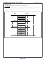
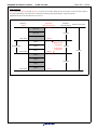
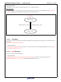
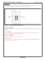
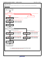
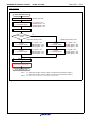
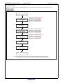
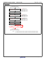
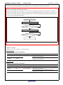
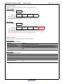
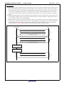
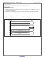
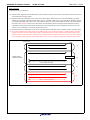
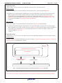
RENESAS TECHNICAL UPDATE TN-RX*-A113A/E Date: Dec. 1, 2014 RENESAS TECHNICAL UPDATE 1753, Shimonumabe, Nakahara-ku, Kawasaki-shi, Kanagawa 211-8668 Japan Renesas Electronics Corporation Product Category Title MPU & MCU Document No. Corrections to Descriptions for the Flash Memory in the RX110 Group User’s Manual Information Technical Notification Category Lot No. Applicable RX110 Group Product All Reference Document Rev. 1.00 TN-RX*-A113A/E RX110 Group User's Manual: Hardware Rev.1.00 (R01UH0421EJ0100) Specification Changes to the RX110 Group (TN-RX*-A112A/E) This document describes corrections to 31. Flash Memory in RX110 Group User's Manual: Hardware Rev.1.00. • Page 840 of 966 The Software commands column and On-board programming column in Table 31.1 Flash Memory Specifications are corrected, and Note 2 is deleted as follows: Before correction Table 31.1 Flash Memory Specifications Item Description Memory space Software commands • User area: Up to 128 Kbytes • The following commands can be executed in boot mode or during self-programming: blank check, block erase, program, read, set access window • Checksum can be also executed in boot mode. Suspend/resume can be also executed during self-programming. On-board programming omitted Self-programming in single-chip mode • The user area is rewritable using the self-programming library.*2 omitted Note 1. Note 2. omitted The library used for self-programming is provided. Refer to section 31.10, Rewriting by Self-Programming for details on the self-programming library. After correction Table 31.1 Flash Memory Specifications Item Description Memory space Software commands • User area: Up to 128 Kbytes • Extra area: Stores the start-up area information, access window information, and unique ID • The following commands are implemented: program, blank check, block erase, unique ID read • The following commands are implemented for programming the extra area: start-up area information program, access window information program On-board programming omitted Self-programming in single-chip mode • The user area is rewritable using the flash rewrite routine in the user program. omitted Note 1. omitted ©2014. Renesas Electronics Corporation, All rights reserved. Page 1 of 26 RENESAS TECHNICAL UPDATE TN-RX*-A113A/E Date: Dec. 1, 2014 • Page 842 of 966 Description in 31.3.1 Flash P/E Mode Entry Register (FENTRYR) is corrected as follows: Before correction To rewrite the ROM, either the FENTRYD or FENTRY0 bit must be set to 1 to place the ROM in P/E mode. After correction To rewrite the ROM, the FENTRY0 bit must be set to 1 to place the ROM in P/E mode. • Page 842 of 966 Descriptions of clearing conditions for the FENTRY0 bit in 31.3.1 Flash P/E Mode Entry Register (FENTRYR) are corrected as follows: Before correction • • • • Data is written by byte access. The FEKEY[7:0] bits are set to a value other than AAh and data is written to the FENTRYR register. AA00h is written to the FENTRYR register. Data is written to the FENTRYR register while the FENTRYR register is a value other than 0000h. After correction • AA00h is written to the FENTRYR register. • Page 848 of 966 Descriptions for block erase in 31.3.8 Flash Control Register (FCR) are corrected as follows: Before correction • Erase a block of the flash memory. Set the start address of the target erasure block in the FSARH and FSARL registers, and set the end address of the target erasure block in the FEARH and FEARL registers. If a setting other than the above is made, erasure may not be executed correctly. After correction • Erase a specified block in the flash memory. Set the beginning address of the block to be erased in registers FSARH and FSARL, and the last address in registers FEARH and FEARL. If a value other than the above is set, erasure may not be executed correctly. Page 2 of 26 RENESAS TECHNICAL UPDATE TN-RX*-A113A/E Date: Dec. 1, 2014 • Page 849, 850 of 966 Descriptions for the access window information program in 31.3.9 Flash Extra Area Control Register (FEXCR) are corrected as follows: Before correction This command is used to set the access window used for area protection. Set the access window in block units. Set bit 19 to bit 10 of the access window start address in the FWBH register, set bit 19 to bit 10 of the access window end address + 1, and execute this command. If the start address and end address are set to the same value, all areas can be accessed. Do not set the start address to a value larger than the value of the end address. After correction This command is used to set the access window used for area protection. Set the access window in block units. Specify the access window start address, which is the beginning address of the access window in the FWBL register, specify the access window end address, which is the next address of the last address of the access window in the FWBH register, and issue this command. Set bit 19 to bit 10 of the address for programming/erasure in each register. If the same value is set as the start address and end address, all areas can be accessed. Do not set the start address to a value larger than the value of the end address. • Pages 850, 851 of 966 Descriptions in 31.3.10 Flash Processing Start Address Register H (FSARH) and 31.3.12 Flash Processing End Address Register H (FEARH) are corrected as follows: Before correction – omitted – Set bit 19 to bit 16 of the flash memory address in this register. – omitted – After correction – omitted – Set bit 19 to bit 16 of the flash memory address for programming/erasure in this register. – omitted – • Page 851 of 966 Description in 31.3.11 Flash Processing Start Address Register L (FSARL) is corrected as follows: Before correction – omitted – Set bit 15 to bit 0 of the address in this register. – omitted – After correction – omitted – Set bit 15 to bit 0 of the flash memory address for programming/erasure in this register. – omitted – Page 3 of 26 RENESAS TECHNICAL UPDATE TN-RX*-A113A/E Date: Dec. 1, 2014 • Page 852 of 966 Description in 31.3.13 Flash Processing End Address Register L (FEARL) is corrected as follows: Before correction – omitted – Set bit 15 to bit 0 of the flash memory address in this register. – omitted – After correction – omitted – Set bit 15 to bit 0 of the flash memory address for programming/erasure in this register. – omitted – • Page 854 of 966 Descriptions for the reserved bits in 31.3.18 Flash Status Register 0 (FSTATR0) are corrected as follows: Before correction bit symbol Bit Name Description R/W b2 — Reserved This bit is read as 0. b7, b6 — Reserved These bits are read as 0. R Bit Name Description R/W omitted R omitted After correction bit symbol omitted b2 — Reserved The read value is undefined. R omitted b7, b6 — Reserved The read value is undefined. R • Page 854 of 966 The following description for the PRGERR flag in 31.3.18 Flash Status Register 0 (FSTATR0) is deleted: The value read from this flag is undefined when the FCR.STOP bit is set to 1 (processing is forcibly stopped) during erasure. • Page 854, 855 of 966 The following description is added to the BCERR flag in 31.3.18 Flash Status Register 0 (FSTATR0): The value read from this flag is undefined when setting the FCR.STOP bit to 1 (processing is forcibly stopped) during blank check. • Page 855 of 966 The following description in setting conditions for the ILGLERR flag in 31.3.18 Flash Status Register 0 (FSTATR0) is deleted: The ROM is set to P/E mode and a software command is executed. Page 4 of 26 RENESAS TECHNICAL UPDATE TN-RX*-A113A/E Date: Dec. 1, 2014 • Page 856 of 966 Description for the FRDY flag in 31.3.19 Flash Status Register 1 (FSTATR1) is corrected as follows: Before correction This flag is used to confirm whether a software command is executed. This flag is set to 1 when processing of the executed software command is completed, and 0 when the FCR.OPST bit is set to 0. After correction This flag is used to confirm whether a software command is executed. This flag becomes 1 when processing of the executed software command or the forced stop processing is completed, and this flag becomes 0 when setting the FCR.OPST bit to 0. • Page 857 of 966 Descriptions in 31.3.20 Flash Error Address Monitor Register H (FEAMH) are corrected as follows: Before correction This register stores the flash memory address where the error has occurred if an error occurs during execution of a software command (program, block erase, or verify). If a blank check error occurs when a blank check command is executed, this register stores the flash memory address where programming has been executed. – omitted – After correction This register is used to check the address where the error has occurred if an error occurs during processing of a software command. This register stores bit 19 to bit 16 of the address where the error has occurred for the program command or blank check command, or it stores bit 19 to bit 16 of the beginning address of the area where the error has occurred for the block erase command. Since this register value becomes undefined if setting the FRESETR.FRESET bit to 1, read the value before error processing. – omitted – • Page 857 of 966 Descriptions in 31.3.21 Flash Error Address Monitor Register L (FEAML) are corrected as follows: Before correction This register is used to confirm the address where the error has occurred if an error occurs during processing of a software command. This register stores bit 15 to bit 0 of the flash memory address where the error has occurred or bit 15 to bit 0 of the start address in the flash memory area where the error has occurred. When the software command terminates normally, this register stores bit 15 to bit 0 of the end address at execution of the command. To set the ROM area, set bit 1 and bit 0 to 00b. When a software command for the ROM is executed, lower-order 2 bits are set to 00b. Refer to Figure 35.1 and Figure 35.2 for details on the addresses of the flash memory. After correction This register is used to check the address where the error has occurred if an error occurs during processing of a software command. This register stores bit 15 to bit 0 of the address where the error has occurred for the program command or blank check command, or it stores bit 15 to bit 0 of the beginning address of the area where the error has occurred for the block erase command. Since this register value becomes undefined if setting the FRESETR.FRESET bit to 1, read the value before error processing. When the software command is normally completed, this register stores bit 15 to bit 0 of the last address at execution of the command. When executing a software command for the ROM or the unique ID read command, low-order 2 bits become 00b. Refer to Figure 35.1 and Figure 35.2 for details on the addresses of the flash memory. Page 5 of 26 RENESAS TECHNICAL UPDATE TN-RX*-A113A/E Date: Dec. 1, 2014 • Page 858 of 966 Note 1 in 31.3.23 Flash Access Window Start Address Monitor Register (FAWSMR) is corrected as follows: Before correction Note 1. The value of the blank product is 1. It is set to the same value set in bit 9 to bit 0 in the FWBH register after the access window information program command is executed. After correction Note 1. The value of the blank product is 1. It is set to the same value set in bit 9 to bit 0 in the FWBL register after the access window information program command is executed. • Page 859 of 966 Note 1 in 31.3.24 Flash Access Window End Address Monitor Register (FAWEMR) is corrected as follows: Before correction Note 1. The value of the blank product is 1. It is set to the same value set in bit 9 to bit 0 in the FWBL register after the access window information program command is executed. After correction Note 1. The value of the blank product is 1. It is set to the same value set in bit 9 to bit 0 in the FWBH register after the access window information program command is executed. • Page 860 of 966 (2) of Figure 31.2 in 31.4 Start-Up Program Protection is corrected as follows: Before correction (2) After the alternate area is successfully rewritten, the default area and the alternate area are switched using the self-programming library. After that, the program in the alternate area starts after a reset. After correction (2) After the alternate area is successfully rewritten, the default area and the alternate area are switched using the start-up area information program command. After that, the program in the alternate area starts after a reset. Page 6 of 26 RENESAS TECHNICAL UPDATE Date: Dec. 1, 2014 TN-RX*-A113A/E • Page 861 of 966 Description in 31.5 Area Protection and Figure 31.3 are changed as follows: Before correction Select the start block and end block to set the access window. While the access window can be set in boot mode or by self-programming, area protection is enabled only during self-programming in single-chip mode. Figure 31.3 shows the Area Protection Overview. Address FFFE 0000h Rewrite by self-programming Block 127 Block 126 FFFF E400h Access window FFFF EFFFh FFFF F000h Disabled ...... FFFF E3FFh Rewrite in boot mode Block 6 (end block) Block 5 Enabled Enabled Block 4 (start block) Block 3 Block 2 Disabled Block 1 FFFF FFFFh Figure 31.3 Block 0 Area Protection Overview Page 7 of 26 RENESAS TECHNICAL UPDATE Date: Dec. 1, 2014 TN-RX*-A113A/E After correction Specify the start address and end address to set the access window. While the access window can be set in boot mode or by self-programming, area protection is enabled only during self-programming in single-chip mode. Figure 31.3 shows the Area Protection Overview. Address for reading FFFE 0000h Address for programming/erasure Block 127 Rewrite by self-programming 6_0000h Block 126 FFFF E400h ...... FFFF E3FFh Block 6 Rewrite in boot mode Disabled 7_E3FFh 7_E400h Access window start address Block 5 Access window FFFF EFFFh FFFF F000h Block 4 Block 3 Enabled Access window end address Enabled 7_EFFFh 7_F000h Block 2 Disabled Block 1 FFFF FFFFh Figure 31.3 Block 0 7_FFFFh Area Protection Overview (Set Blocks 4 to 6 as the Access Window) Page 8 of 26 RENESAS TECHNICAL UPDATE Date: Dec. 1, 2014 TN-RX*-A113A/E • Page 862 of 966 Description in 31.6.1 Sequencer Modes and Figure 31.4 are changed as follows: Before correction The sequence has three modes. Transitions between modes are caused by writing to the FENTRYR register or issuing commands. Figure 31.4 is a diagram of mode transitions of the flash memory. Read mode ROM read mode FENTRYR register = AA00h FENTRYR register = AA01h ROM P/E mode Figure 31.4 31.6.1.1 Mode Transitions of the Flash Memory Read Mode Read mode is for high-speed reading of the ROM. Reading from a ROM address for reading can be accomplished in one ICLK clock. There is one read mode: ROM read mode. (1) ROM Read Mode This mode is for reading the ROM The sequencer enters this mode when the FENTRYR.FENTRY0 bit is set to 0 with the FENTRYR.FENTRYD bit set to 0. 31.6.1.2 ROM P/E Modes There is one P/E mode: ROM P/E mode. (1) ROM P/E Mode The ROM P/E mode is for programming and erasure of the ROM. The sequencer enters this mode when the FENTRYR.FENTRYD bit is set to 0 with the FENTRYR.FENTRY0 bit set to 1. Page 9 of 26 RENESAS TECHNICAL UPDATE TN-RX*-A113A/E Date: Dec. 1, 2014 After correction The sequencer has 2 modes. Transitions between modes are caused by writing to the FENTRYR register and setting the FPMCR register. Figure 31.4 is a diagram of mode transitions of the flash memory. Reset ROM read mode FRNTRYR register = AA00h FPMCR register 08h *1 FRNTRYR register = AA01h FPMCR register 82h/C2h *1 ROM P/E mode Note 1. See the corresponding flowchart for details on the procedure. Figure 31.4 31.6.1.1 Mode Transitions of the Flash Memory Read Mode Read mode is for high-speed reading of the ROM. Reading from a ROM address for reading can be accomplished in one ICLK clock. (1) ROM Read Mode In this mode, the ROM is in read mode. The sequencer enters this mode from P/E mode when setting the FPMCR register to 08h and setting the FENTRYR.FENTRY0 bit to 0. 31.6.1.2 P/E Modes The P/E mode is for programming and erasure of the ROM. (1) ROM P/E Mode In this mode, the ROM is in P/E mode. The sequencer enters this mode when setting the FENTRYR.FENTRY0 bit to 1 and setting the FPMCR register 82h or C2h. Page 10 of 26 RENESAS TECHNICAL UPDATE Date: Dec. 1, 2014 TN-RX*-A113A/E • Page 864 of 966 Figure 31.5 in (1) Switching to ROM P/E Mode of 31.6.3 Software Command Usage is corrected as follows: Before correction Start in ROM read mode SOPCCR.SOPCM bit =0 No Low-speed operating mode Yes End in ROM read mode*2 Write to FENTRYR register Write 12h to FPMCR register Set ROM P/E mode When setting the FENTRYR.FENTRY0 bit to 1: Write AA01h When setting the FPMCR register to 12h: Write A5h to the PROTR register Write 12h to the FPMCR register Write EDh to the FPMCR register Write 12h to the FPMCR register Wait for tDIS*1 OPCCR.OPCM[2:0] bits = 000b Yes No High-speed operating mode Middle-speed operating mode Write 92h to FPMCR register When setting the FPMCR register to 92h: Write A5h to the PROTR register Write 92h to the FPMCR register Write 6Dh to the FPMCR register Write 92h to the FPMCR register Write D2h to FPMCR register When setting the FPMCR register to D2h: Write A5h to the PROTR register Write D2h to the FPMCR register Write 2Dh to the FPMCR register Write D2h to the FPMCR register Write 82h to FPMCR register When setting the FPMCR register to 82h: Write A5h to the PROTR register Write 82h to the FPMCR register Write 7Dh to the FPMCR register Write 82h to the FPMCR register Write C2h to FPMCR register When setting the FPMCR register to C2h: Write A5h to the PROTR register Write C2h to the FPMCR register Write 3Dh to the FPMCR register Write C2h to the FPMCR register Wait for tMS*1 End in ROM P/E mode Note 1. tDIS: ROM mode transition wait time 1 (Refer to the Electrical Characteristics chapter.) tMS: ROM mode transition wait time 2 (Refer to the Electrical Characteristics chapter.) Note 2. Rewriting during low-speed operation is not possible. Figure 31.5 Procedure for Transition to ROM P/E Mode Page 11 of 26 RENESAS TECHNICAL UPDATE Date: Dec. 1, 2014 TN-RX*-A113A/E After correction Start in ROM read mode FENTRYR register = AA01h Set 12h in the FPMCR register Set ROM P/E mode. FPR register = A5h FPMCR register = 12h FPMCR register = EDh FPMCR register = 12h Wait for tDIS*1 OPCCR.OPCM[2:0] bits = 000b? No High-speed operating mode Yes Middle-speed operating mode Set 92h in the FPMCR register FPR register = A5h FPMCR register = 92h FPMCR register = 6Dh FPMCR register = 92h Set D2h in the FPMCR register FPR register = A5h FPMCR register = D2h FPMCR register = 2Dh FPMCR register = D2h Set 82h in the FPMCR register FPR register = A5h FPMCR register = 82h FPMCR register = 7Dh FPMCR register = 82h Set C2h in the FPMCR register FPR register = A5h FPMCR register = C2h FPMCR register = 3Dh FPMCR register = C2h Wait for tMS*1 Set the FCLK frequency in the FISR.PCKA[4:0] bits End in ROM P/E mode Note 1. Note 2. Figure 31.5 tDIS: ROM mode transition wait time 1 (Refer to the Electrical Characteristics chapter.) tMS: ROM mode transition wait time 2 (Refer to the Electrical Characteristics chapter.) The ROM cannot be rewritten in low-speed operating mode. Procedure for Transition from ROM Read Mode to ROM P/E Mode Page 12 of 26 RENESAS TECHNICAL UPDATE TN-RX*-A113A/E Date: Dec. 1, 2014 • Page 865 of 966 Figure 31.6 in (2) Switching to ROM Read Mode of 31.6.3 Software Command Usage is corrected as follows: Before correction Start in ROM P/E mode Write 92h to FPMCR register When setting the FPMCR register to 92h: Write A5h to the PROTR register Write 92h to the FPMCR register Write 6Dh to the FPMCR register Write 92h to the FPMCR register Wait for tDIS*1 Write 12h to FPMCR register When setting the FPMCR register to 12h: Write A5h to the PROTR register Write 12h to the FPMCR register Write EDh to the FPMCR register Write 12h to the FPMCR register Write 08h to FPMCR register When setting the FPMCR register to 08h: Write A5h to the PROTR register Write 08h to the FPMCR register Write F7h to the FPMCR register Write 08h to the FPMCR register Wait for tMS*1 Write AA00h to FENTRY register End in ROM read mode Note 1. tDIS: ROM mode transition wait time 1 (Refer to the Electrical Characteristics chapter.) tMS: ROM mode transition wait time 2 (Refer to the Electrical Characteristics chapter.) Figure 31.6 Procedure for Transition to ROM Read Mode Page 13 of 26 RENESAS TECHNICAL UPDATE TN-RX*-A113A/E Date: Dec. 1, 2014 After correction Start in ROM P/E mode Set 92h in the FPMCR register FPR register = A5h FPMCR register = 92h FPMCR register = 6Dh FPMCR register = 92h Wait for tDIS*1 Set 12h in the FPMCR register Set 08h in the FPMCR register FPR register = A5h FPMCR register = 12h FPMCR register = EDh FPMCR register = 12h FPR register = A5h FPMCR register = 08h FPMCR register = F7h FPMCR register = 08h Wait for tMS*1 FENTRYR register = AA00h FENTRYR register = 0000h? No Yes End in ROM read mode Note 1. Figure 31.6 tDIS: ROM mode transition wait time 1 (Refer to the Electrical Characteristics chapter.) tMS: ROM mode transition wait time 2 (Refer to the Electrical Characteristics chapter.) Procedure for Transition from ROM P/E Mode to ROM Read Mode Page 14 of 26 RENESAS TECHNICAL UPDATE TN-RX*-A113A/E Date: Dec. 1, 2014 • Page 862 to 870 of 966 The structure of sections in 31.6 Programming and Erasure are changed as follows: Before correction 31.6 31.6.1 31.6.1.1 31.6.1.2 31.6.2 31.6.3 (1) (2) (3) (4) (5) Programming and Erasure Sequencer Modes Read Mode ROM P/E Mode Software Commands Software Command Usage Switching to ROM P/E Mode Switching to ROM Read Mode Programming and Erasure Procedures Start-Up Area Information Program/Access Window Information Program Consecutive Read After correction 31.6 31.6.1 31.6.1.1 31.6.1.2 31.6.2 31.6.2.1 31.6.2.2 31.6.3 31.6.4 31.6.4.1 31.6.4.2 31.6.4.3 31.6.4.4 31.6.4.5 31.6.4.6 Programming and Erasure Sequencer Modes Read Mode P/E Mode Mode Transitions Transition from Read Mode to P/E Mode Transition from P/E Mode to Read Mode Software Commands Software Command Usage Program Block Erase Blank Check Start-Up Area Information Program/Access Window Information Program Unique ID Read Forced Stop of Software Commands Page 15 of 26 RENESAS TECHNICAL UPDATE Date: Dec. 1, 2014 TN-RX*-A113A/E The following descriptions and flowchart are added to 31.6.4.6 Forced Stop of Software Commands. 31.6.4.6 Forced Stop of Software Commands Perform the procedure shown in Figure 31.xx to forcibly stop the blank check command or block erase command. When the command processing is forcibly stopped, registers FEAMH and FEAML store the address at the time of the forced stop. For blank check, the stopped processing can be continued by copying the FEAMH and FEAML register values to registers FSARH and FSARL. Command is being executed FCR.STOP bit = 1 FSTATR1.FRDY flag = 1? No Yes FCR register = 00h FSTATR1.FRDY flag = 0? No Yes End Figure 31.xx Procedure for Forced Stop of Software Commands • Page 871 of 966 Table 31.5 in 31.7 Boot Mode is corrected as follows: Before correction Table 31.5 I/O Pins Used in Boot Mode Pin Name I/O Mode Description P15/RXD1 Input SCI Receive data through SCI1 for dedicated flash memory programmer communication*1 P16/RXD1 Output Transmit data through SCI1 for dedicated flash memory programmer communication*1 After correction Table 31.5 I/O Pins Used in Boot Mode Pin Name I/O Mode Description MD Input Boot mode Select operating mode (refer to section 3, Operating Modes). P15/RXD1 Input Boot mode (SCI) Receive data through SCI1 for dedicated flash memory programmer communication *1 P16/RXD1 Output Transmit data through SCI1 for dedicated flash memory programmer communication *1 Page 16 of 26 RENESAS TECHNICAL UPDATE Date: Dec. 1, 2014 TN-RX*-A113A/E • Page 880 of 966 Response in 31.9.3 Boot Mode Status Inquiry is corrected as follows: Before correction Command 4Fh Response 5Fh Size Status Error Size (1 byte): Total bytes of “Status” and “Error” (the value is always 2) Status (1 byte): MCU status (see Table 31.10) Error (1 byte): Information about the error occurred in the MCU (see Table 31.11) After correction Command 4Fh Response 5Fh Size State Error SUM Size (1 byte): Total bytes of “State” and “Error” (the value is always 2) State (1 byte): MCU state (see Table 31.10) Error (1 byte): Information about the error occurred in the MCU (see Table 31.11) SUM (1 byte): Value that is calculated so the sum of response data is 00h • Page 881 of 966 Table 31.12 in 31.9.4 Inquiry Commands is corrected as follows: Before correction Table 31.12 Inquiry Commands Command Description Supported device inquiry Inquiry for the device code and series name User area information inquiry Inquiry for the number of user areas, and the start and end addresses of the user area Block information inquiry Inquiry for the start and end addresses of the user areas, the block size, and the number of blocks After correction Table 31.12 Inquiry Commands Command Description Supported device inquiry Inquiry for the device code and series name Data area availability inquiry Inquiry for the availability of the data area User area information inquiry Inquiry for the number of user areas, and the start and end addresses of the user area Block information inquiry Inquiry for the start and end addresses of the user areas, the block size, and the number of blocks Page 17 of 26 RENESAS TECHNICAL UPDATE Date: Dec. 1, 2014 TN-RX*-A113A/E • Page 884 of 966 The section number of 31.9.6 Operating Frequency Select is corrected to 31.9.5.2. Accordingly, the subsequent section numbers are corrected as follows: Before correction 31.9.6 Operating Frequency Select 31.9.6.1 Program/Erase Status Transition 31.9.7 ID Code Authentication Command ... After correction 31.9.5.2 Operating Frequency Select 31.9.5.3 Program/Erase State Transition 31.9.6 ID Code Authentication Command ... • Page 889 of 966 Description in 31.9.8.3 Erase Preparation is corrected as follows: Before correction When the host sends this command, the MCU recognizes that an instruction to prepare for the erase command is issued from the host, enters the erase wait state, where only the block erase command to the user area or data area can be accepted, and sends a response. After correction When the host sends this command, the MCU recognizes that an instruction to prepare for the erase command is issued from the host, enters the erase wait state, where only the block erase command to the user area can be accepted, and sends a response. • Page 895 of 966 Figure 31.18 in 31.9.10.1 Bit Rate Automatic Adjustment Procedure is corrected as follows: Before correction START BIT D0 D1 D2 D3 D4 D5 D6 D7 STOP BIT At least 1 bit of high width Measure 9 bits of low width (data 00h) Figure 31.18 Data Format for Bit Rate Automatic Adjustment After correction At least 1 ms between commands Transmission to the MCU 00h 00h 00h (1) (2) (3) 00h ... 55h (see note 1) Reception from the MCU 00h Note 1. Maximum 30 times Figure 31.18 Transmit/Receive Data for Bit Rate Automatic Adjustment Page 18 of 26 RENESAS TECHNICAL UPDATE Date: Dec. 1, 2014 TN-RX*-A113A/E • Page 896 of 966 The procedure in 31.9.10.2 Procedure to Receive the MCU Information is corrected as follows: Before correction Send inquiry commands, and receive the information necessary to send setting commands, program/erase commands, and read-check commands. (1) Send a support device inquiry command (20h) to check which device to connect. The MCU returns the device code and series name. (2) Send a user area information inquiry command (25h) to check the start and end addresses of the user area. The MCU returns the start and end addresses of the user area. (3) Send a block information inquiry command (26h) to check the block configuration. The MCU returns the start address, the size of one block, and the number of blocks for the user area. MCU Programmer 20h (support device inquiry command) (1) Response to the support device inquiry command 25h (user area information inquiry command) (2) Response to the user area information inquiry command 26h (block information inquiry command) (3) Response to the block information inquiry command Figure 31.20 Procedure to Send Inquiry Commands Page 19 of 26 RENESAS TECHNICAL UPDATE Date: Dec. 1, 2014 TN-RX*-A113A/E After correction Send inquiry commands, and receive the information necessary to send setting commands, program/erase commands, and read-check commands. (1) Send a support device inquiry command (20h) to check which device to connect. The MCU returns the device code and series name. (2) Send a data area availability inquiry command (2Ah) to check the availability of data area and area protection. The MCU returns the availability of data area and area protection. (3) Send a user area information inquiry command (25h) to check the start and end addresses of the user area. The MCU returns the start and end addresses of the user area. (4) Send a block information inquiry command (26h) to check the block configuration. The MCU returns the start address, the size of one block, and the number of blocks for the user area. Programmer MCU 20h (support device inquiry command) (1) Response to the support device inquiry command 2Ah (data area availability inquiry command) (2) Response to the data area availability inquiry command 25h (user area information inquiry command) (3) Response to the user area information inquiry command 26h (block information inquiry command) (4) Response to the block information inquiry command Figure 31.20 Procedure to Send Inquiry Commands Page 20 of 26 RENESAS TECHNICAL UPDATE TN-RX*-A113A/E Date: Dec. 1, 2014 • Page 897 of 966 The procedure in 31.9.10.3 Procedure to Select the Device and Change the Bit Rate is corrected as follows: Before correction (1) Send the device select command (10h) to select the device to connect with the programmer and the endian of data that is programmed. When the program data is little endian, select the same device code as that for little endian in the response to the support device inquiry command. When the program data is big endian, select the same device code as that for big endian in the response to the support device inquiry command. When the device is selected successfully, the MCU sends a response (06h). When the MCU fails to receive, the MCU sends an error response (90h). (2) Send the operating frequency select command (3Fh) to change the bit rate for communication. When the bit rate is set successfully, the MCU sends a response (06h). When the bit rate cannot be changed, or when the MCU fails to receive, the MCU sends an error response (BFh). (3) When the MCU receives a response (06h), the MCU waits for 1-bit period at the bit rate for sending the operating frequency select command, and then set the bit rate of the programmer to the changed value. After that, the MCU sends communication confirmation data (06h) at the changed bit rate. When the MCU receives the command successfully, the MCU sends a response (06h) of the communication confirmation data. Programmer MCU 10h (device select command) 06h (ACK) (1) 90h, XXh (error code) 3Fh (operating frequency select command) (2) 06h (ACK) BFh, XXh (error code) Wait for 1-bit period Set the new bit rate 06h (check) 06h (ACK) (3) Figure 31.21 Procedure to Select the Device and Change the Bit Rate Page 21 of 26 RENESAS TECHNICAL UPDATE TN-RX*-A113A/E Date: Dec. 1, 2014 After correction (1) Send the device select command (10h) to select the device to connect with the programmer and the endian of data that is programmed. When the program data is little endian, select the same device code as that for little endian in the response to the support device inquiry command. When the program data is big endian, select the same device code as that for big endian in the response to the support device inquiry command. When the device is selected successfully, the MCU sends a response (46h). When the MCU fails to receive, the MCU sends an error response (90h). (2) Send the operating frequency select command (3Fh) to change the bit rate for communication. When the bit rate is set successfully, the MCU sends a response (06h). When the bit rate cannot be changed, or when the MCU fails to receive, the MCU sends an error response (BFh). (3) When the MCU receives a response (06h), the MCU waits for 1-bit period at the bit rate for sending the operating frequency select command, and then set the bit rate of the programmer to the changed value. After that, the MCU sends communication confirmation data (06h) at the changed bit rate. When the MCU receives the command successfully, the programmer sends a response (06h) of the communication confirmation data. Programmer MCU 10h (device select command) 46h (ACK) (1) 90h, XXh (error code) 3Fh (operating frequency select command) (2) 06h (ACK) BFh, XXh (error code) Wait 1-bit period Set the new bit rate 06h (check) 06h (ACK) (3) Figure 31.21 Procedure to Select the Device and Change the Bit Rate Page 22 of 26 RENESAS TECHNICAL UPDATE Date: Dec. 1, 2014 TN-RX*-A113A/E • Page 900 of 966 The procedure in 31.9.10.6 Erase Ready Operation and Change is corrected as follows: Before correction Erase the user area in the MCU. (1) Send the erase preparation command (48h) to place the MCU in the erase wait state. The MCU enters the erase wait state and sends a response (06h). (2) Send a block erase command (59h) to erase blocks in the MCU. When blocks are erased successfully, the MCU sends a response (06h). When the MCU fails to receive, the MCU sends an error response (D9h). Send block erase commands repeatedly until a block erase command has been sent for the total number of blocks. The total number of blocks is the sum of the user area blocks and data area blocks that are obtained in advance using the block information inquiry command. If the operation ends before all the block erase commands are sent, a command error may occur even when a correct command is sent in the program/erase state. (3) In order to place the MCU in the program/erase state, send a block erase command for end of erase (59h 04h FFh FFh FFh FFh A7h). The MCU enters the program/erase state and sends a response (06h). Programmer MCU 48h (erase preparation command) (1) 06h (ACK) 59h (block erase command) Erase (2) 06h (ACK) D9h, XXh (error code) 59h (block erase command for end of erase) (3) 06h (ACK) Figure 31.24 Procedure to Send Commands in Erase Ready Operation Page 23 of 26 RENESAS TECHNICAL UPDATE TN-RX*-A113A/E Date: Dec. 1, 2014 After correction Erase the user area in the MCU. (1) Send the erase preparation command (48h) to place the MCU in the erase wait state. The MCU enters the erase wait state and sends a response (06h). (2) Send a block erase command (59h) to erase blocks in the MCU. When blocks are erased successfully, the MCU sends a response (06h). When the MCU fails to receive, the MCU sends an error response (D9h). Send block erase commands repeatedly until a block erase command has been sent for the total number of blocks. The total number of blocks is the number of the user area blocks that are obtained in advance using the block information inquiry command. If the operation ends before all the block erase commands are sent, a command error may occur even when a correct command is sent in the program/erase state. (3) Send a block erase command for end of erase (59h 04h FFh FFh FFh FFh A7h). The MCU sends a response (06h). (4) To confirm whether erase ready operation has ended, send a boot mode status inquiry command (4Fh). The MCU sends a response to the boot mode status inquiry command when erase ready operation has ended. If erase ready operation has not ended, the MCU sends an error response (80h 4Fh). If the programmer receives an error response, restart the MCU in boot mode, and start again from section 31.9.10.1, Bit Rate Automatic Adjustment Procedure. Programmer MCU 48h (erase preparation command) (1) 06h (ACK) 59h (block erase command) Erase Repeat until all blocks are erased. (2) 06h (ACK) D9h, XXh (error code) 59h (block erase command for end of erase) (3) 06h (ACK) 4Fh (boot mode status inquiry command) (4) Response to the boot mode status inquiry command 80h, 4Fh (error response) Figure 31.24 Procedure to Send Commands in Erase Ready Operation Page 24 of 26 RENESAS TECHNICAL UPDATE Date: Dec. 1, 2014 TN-RX*-A113A/E • Page 904 of 966 The procedure in 31.9.10.10 Set the Access Window in the User Area is corrected as follows: Before correction Set the access window to avoid unintentionally rewriting the user area by the self-programming library. (1) Send the access window program command (74h) to set the access window or clear the access window settings. When setting the access window, set 00h in the access window, set the start address of the area that can be programmed by the self-programming library in the access window start address LH and access window start address HL, and set the end address of the area that can be programmed by the self-programming library in the access window end address LH and access window end address HL. - omitted After correction Set the access window to avoid unintentionally rewriting the user area during self-programming. (1) Send the access window program command (74h) to set the access window or clear the access window settings. When setting the access window, set 00h in the access window field, and set the start address and the end address of the area that can be programmed during self-programming in the access window start address and the access window end address, respectively. - omitted - • Page 905 of 966 Descriptions in 31.10.1 Overview of 31.10 Rewriting by Self-Programming and Figure 31.29 are corrected as follows: Before correction The MCU supports rewriting the flash memory by the user program. Using the self-programming library provided from Renesas Electronics, the ROM can be rewritten. RAM/ROM *1 Rewrite program for the user area Code flash library Execute flash functions Erase/program Flash information ROM Note 1: The ROM cannot be rewritten by executing the rewrite program on the ROM. Figure 31.29 Self-Programming Overview Refer to the user’s manual of “Code Flash Libraries” for comprehensive information about flash self-programming. Page 25 of 26 RENESAS TECHNICAL UPDATE Date: Dec. 1, 2014 TN-RX*-A113A/E After correction The MCU supports rewriting the flash memory by the user program. The ROM can be rewritten by preparing a routine to rewrite the flash memory (flash rewrite routine) in the user program. On-chip RAM *1 Flash rewrite routine Erase/program Flash information ROM Note 1: The ROM cannot be rewritten by executing the flash rewrite routine on the ROM. Figure 31.29 Self-Programming Overview • Page 906 of 966 Descriptions in (1) and (2) of 31.11 Usage Notes are corrected as follows: Before correction (1) Erase Suspended Area Data in areas where an erase operation is suspended is undefined. To avoid malfunctions caused by reading undefined data, do not execute commands and read data in the area where an erase operation is suspended. (2) Suspension by Erase Suspend Commands When suspending an erase operation by the erase suspend command, complete the operation by a resume command. After correction (1) Access the Block Where Erase Operation Is Forcibly Stopped When forcibly stopping an erase operation, data in the block where the erase operation is aborted is undefined. To avoid malfunctions caused by reading undefined data, do not execute instructions or read data in the block where an erase operation is forcibly stopped. (2) Processing After Forced Stop of Erase Operation After forcibly stopping an erase operation, issue the block erase command to the same block again. Page 26 of 26