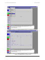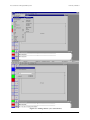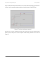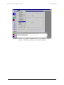
1
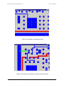
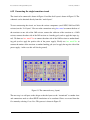
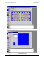
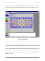
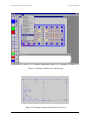
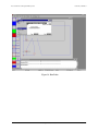
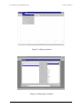
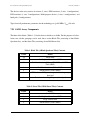
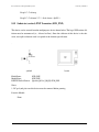
Research Centre for
Integrated Microsystems
University of Windsor
Using Electric Editor™ with the
Gennum GA911 Array
Submitted to Canadian Microelectronics Corporation
M.Shahkarami, R. Muscedere, G.A. Jullien
Acknowledgements
The authors would like to thank Russ Wright and Brian Gardiner at Electric Editor, Dr.
Ron Bolton University of Saskatchewan, Canadian Microelectronics Corporation and
Gennum Corporation in Burlington, Ontario for their assistance in the development of
this design environment.
Using Electric Editor™ with the Gennum GA911 Array
Research Centre for Integrated Microsystems
University of Windsor
Contents
1.
Features ...............................................................................................................................1
1.1
Nodes .......................................................................................................................1
1.2
Arcs ..........................................................................................................................1
1.3
Connectivity approach .............................................................................................2
1.4
Interaction with third party tools .............................................................................2
2.
Operation .............................................................................................................................2
2.5
Elements of producing a design...............................................................................2
2.6
Load a Technology.......................................................................................3
2.7
Load or Create a Library..............................................................................3
2.8
Edit or Create Facets....................................................................................3
2.9
Extract simulation files ................................................................................3
3.
A Typical Session ................................................................................................................4
3.10 Electric is initially loaded ........................................................................................4
3.11 The technology has a specific set of primitives .......................................................5
4.
The Menu of Primitives .......................................................................................................5
4.12 Pins...........................................................................................................................7
4.13 Metal Interconnect ...................................................................................................7
4.14 Active Devices .........................................................................................................8
4.15 Passive Devices ........................................................................................................9
5.
Load design library GennumFlat .......................................................................................10
5.16 GA911 Array Symmetry........................................................................................14
6.
A Single Transistor Circuit ................................................................................................15
6.17 Metal Interconnect Guidelines...............................................................................15
6.18 Making Connections ..............................................................................................16
6.19 Connecting the single transistor circuit .................................................................20
7.
Additional Information ......................................................................................................38
7.20 The GA911 Technology [3] ...................................................................................38
7.21 GA911 Array Components ....................................................................................39
7.22 GA911 Array Device Layouts ...............................................................................40
7.23 Resistor Lands........................................................................................................41
7.24 Notes on Performing Layout of Metal Interconnect ..................................42
7.25 Substrate Contacts......................................................................................43
7.26 Bond Pad Structures and ESD Protection Strategies .............................................44
7.27 The LF Bond Pad Structure .......................................................................44
8.
Device Details ....................................................................................................................45
iii
Research Centre for Integrated Microsystems
8.28
8.29
8.31
8.32
8.33
8.34
9.
University of Windsor
.Small NPN Transistor (SNPN) .............................................................................45
Large NPN Transistor (LNPN) ..............................................................................46
Large Emitter NPN Transistor or Junction Capacitor (CAP_NPN) ......................47
Substrate (vertical) PNP Transistor (SUB_PNP)..................................................49
P-channel JFET 90K Pinch Resistor (PNCHR90K)..............................................50
Diffused Resistors ..................................................................................................51
References..........................................................................................................................52
iv
Research Centre for Integrated Microsystems
University of Windsor
Using Electric EditorTM with the Gennum GA911 Array
1. Features
This package provides all of the tools associated with modern VLSI design software, but its strong
feature is the inclusion of connectivity information within mask layout designs. In this way mask
layouts are directly mappable to circuits since all of the polygons placed on the screen make sense
in terms of the normal elements of a circuit: nodes and arcs.
1.1 Nodes
A set of primitives are available to represent all of the possible nodes within a particular technology. Each of the primitives carry complete layer information associated with that node. In the
Gennum technology [2] the user is only concerned with placing a single layer of metal to connect
existing primitives “locked” into the GA911 array. The metal is placed using metal nodes or pins
and then making a connection between them. There is an on-line Design Rule Checker that
informs the design if the metal nodes or pins are too close to other metal lines or to the fixed primitives.
The connectivity information to the primitives is contained in pins that exist at the ends of all connectable layers forming the primitive. Ports are attached to these pins when connectivity information is to be passed up the hierarchy that is part of the VLSI design process.
1.2 Arcs
Nodes are connected by arcs. In the GA911 array, the only connection medium is a single layer of
metal (aluminum). The GA911 technology in Electric, however, provides 3 different types of arcs
which all map to the same metal layer when the array is fabricated [1]. These layers are: metal
(used for signal connections); metal-Vcc (used for positive power supply connections); metal-Vee
(used for negative power supply connections). Using different layers (which have different colors)
helps to “read” the circuit from the layout.
Features
1
Research Centre for Integrated Microsystems
University of Windsor
1.3 Connectivity approach
Rather than a pure polygon generator, Electric requires connections to be made between nodes
and arcs. The connections are made by identifying two pins of the same type of layer and executing the connection command. It is important to note that connections to the same type of layer
cannot be made by simply making the layers adjacent (this is often the case with other VLSI packages) but a connection has to be made, otherwise the design rule checker will generate an error.
This connectivity information can be used to directly extract schematics. The schematics use
nodes and arcs in the same orientation as the mask layout.
1.4 Interaction with third party tools
Electric is an open system and many tools have been added. For this course we will be using a
third party SPICE program (PSPICE) in conjunction with the schematic generator in Electric. We
will be able to simulate circuits directly from the connections made to the GA911 array.
2. Operation
Electric runs on most workstations. These notes briefly describe the use of Electric on a PC computer system, with special emphasis on the Gennum Corp. GA911 array.
2.5 Elements of producing a design
All designs are created using the following four major steps. The actual design process may take
hundreds of hours if it is a very complicated full custom design in a modern CMOS technology, or
just a few hours for a simple design in a more straightforward technology, such as the GA911 analog array.
Operation
2
Research Centre for Integrated Microsystems
University of Windsor
2.6 Load a Technology
The technology contains the primitives and design rules of the particular technology of fabrication. Many different technologies are available within the Electric libraries, and there is also the
capability of editing new technology files, though this is beyond the level required in this course.
2.7 Load or Create a Library
A design is created within a library. Several libraries can be resident within Electric at any one
time. The library contains a set of facets (different mask layouts of parts of the design) with the
facets usually forming a hierarchy, so that facets at the upper levels of the hierarchy use instances
of facets at the lower levels. Facets can be imported from other libraries resident within Electric.
New libraries can be loaded when required. Because of the many protocol translators within the
package, it is possible to import libraries in different protocols. It is important to note that these
external protocols may not provide Electric with connectivity information, and therefore will
cause design rule errors to be generated for each violation associated with lack of connectivity
information. For the GA911 array [2], we will be restricting ourselves to making connections on a
single facet called “2x1-layout”.
2.8 Edit or Create Facets
From an existing library of facets, new facets are created. The new facet consists of node primitives, instances of existing facets (with ports for connectivity) connected by arc primitives. This
new facet can be passed up the hierarchy by defining ports at appropriate pins and exporting the
ports to allow connections when the facet is instantiated. For the GA911 array, the only facet
instantiation will be for a SPICE simulation where the instantiated facet is connected to SPICE
sources and meters.
2.9 Extract simulation files
Once a design is complete (or parts of it complete) netlist files may be extracted for use in third
party simulators. For the GA911 array, a PSPICE file can be created that is an extraction from the
Operation
3
Research Centre for Integrated Microsystems
University of Windsor
geometry of the design using appropriate parameters from the technology files for the various
devices (nodes) in the circuit.
Electric allows the connection of sources and meters directly to the mask layout in order to define
the simulation required. This is possible because of the connectivity information stored within the
layout (the set of polygons on the screen are represented as a circuit within the Electric database).
3. A Typical Session
The following subsections show a typical design session with screen dumps from the PC package
[5]. It is expected that these notes will be used along with actual practice on the CAD package
running on a colour monitor.
3.10 Electric is initially loaded
In the PC, Electric is loaded (launched) from the “Start” menu. When loaded, an “About” window
appears. Simply click on Continue to continue with the program. The window shown in Figure 1
will appear. The default “gennum” technology is loaded (bipolar process GA911 array from Gennum Corp.), and an initial library (“noname”) created. There are no facets in the library, and the
screen indicates that it is not editing a facet.
A Typical Session
4
Research Centre for Integrated Microsystems
University of Windsor
Figure 1. Startup Window.
3.11 The technology has a specific set of primitives
When the technology loads, the node and arc primitives associated with the technology are shown
in a palette to the left of the working area in the window; see Figure 1.
4. The Menu of Primitives
The primitives are either nodes or arcs. The arcs reflect the different conducting layers available in
the technology. The nodes represent devices (transistors and resistors), interlayer connectors and
pins. Pins will also be present within arc and node primitives. When nodes are selected, the cursor
changes to a hand to indicate that the node can be placed. For arcs, the arc is only generated when
a pin is selected with the left mouse button, the cursor placed at the other end of the arc placeThe Menu of Primitives
5
Research Centre for Integrated Microsystems
University of Windsor
ment, and the right mouse button clicked. For the GA911 array, the only nodes that we will place
are the metal nodes; transistor and resistor array primitives are not to be placed since they are
already fixed in place in the “2x1-layout” facet. The menu reflects this since all of the nodes and
arcs that can be placed are on the left hand side of the menu, primitives on the right hand side are
all fixed in place primitives.
We will now briefly review the primitives associated with the Gennum technology (Figure 2).
NODE: Glass-mask-Node
NODE: small-PNP-transistor
NODE: Metal-Node
NODE: sub-PNP-transistor
NODE: DRC-Error-Node
NODE: large-NPN-transistor
NODE: Metal-Vee-Node
NODE: small-NPN-transistor
NODE: Metal-Vcc-Node
NODE: 10k-bent-resistor
NODE: Fixpin
NODE: 1k-5k-bent-resistor
NODE: Metal-Vee-Pin
NODE: land-xu
NODE: Metal-Vcc-Pin
NODE: 200-ohm-long-resistor
NODE: Metal-Pin
NODE: land
NODE: 1k-short-resistor
ARC: Fixarc
NODE: 90k-pinch-resistor
ARC: Metal-Vee
ARC: Metal-Vcc
NODE: 10k-long-resistor
ARC: Metal
NODE: 5k-long-resistor
Figure 2. Menu palette for the GA911 Array
The Menu of Primitives
6
Research Centre for Integrated Microsystems
University of Windsor
4.12 Pins
Pins are used to anchor the ends of arcs in automatic connection modes. They are also found in
node and arc primitives. They can be placed separately before an arc is drawn and used to define
the starting point for the arc. They are also used to define connection ports for allowing connections to instantiations of the facet in other facets. The pins are placed in Figure 3, and the three
different colours (red, green and blue) of the pins corresponds to the colours of the metal traces.In
this technology blue represents metal; red represents metal-Vcc; green represents metal-Vee. As
mentioned in Section 1.2, these three different connection media all map to a single layer of metal
in the final fabricated chip.
Figure 3. Primitives of Pins
4.13 Metal Interconnect
Circuit interconnect is performed using a single layer of metal. The minimum metal track width is
6µm and the minimum space between metal features is 4µm, except for metal to bond pad spacing
which is 14µm.
Figure 4 illustrates a placing of these nodes. Note that when a node is selected a “+” appears in the
center of the node.
The Menu of Primitives
7
Research Centre for Integrated Microsystems
University of Windsor
Figure 4. Nodes connecting to Metal
4.14 Active Devices
The Gennum technology contains five active device types. There are two NPN transistor types,
one large with dual emitters and one small; one PNP transistor type, with dual collectors; one
90kW pinch resistor type; and one three terminal multi-purpose device type that can be used as an
NPN transistor, a substrate PNP transistor or a junction capacitor. The NPN and PNP transistors
are three terminal devices, with the terminal labelled: B for base; C for collector; E for emitter.
Figure 5 shows the different active devices present in this technology.
Figure 5. Primitives of Active devices
The Menu of Primitives
8
Research Centre for Integrated Microsystems
University of Windsor
You will notice that these devices have multiple terminals with the same name. For example the
small NPN has four collector terminals, as shown in Figure 6 [3]; the collector terminals are internally connected. For more info see “Device Details” on page 45.
Figure 6. SNPN schematic and physical layout
4.15 Passive Devices
There are four discrete resistors available: 200Ω, 1kΩ, 5kΩ,and 10kΩ. The device outlines resistor
lands and land contacts are outlined in Figure 7.
Figure 7. Primitives of passive devices
The Menu of Primitives
9
Research Centre for Integrated Microsystems
University of Windsor
Diodes can be implemented by connecting to one end of a resistor and an associated resistor land
contact. The 90KΩ resistor is formed by pinching off a channel with a reverse-biased pn junction,
so it is somewhat more restricted in its use than the other four resistors. For more detail see
“Device Details” on page 45.
5. Load design library GennumFlat
We will begin by loading the design library, as shown in Figure 8; Open Library is selected from
the File menu and a window appears that asks for the name of the library; Figure 9 shows this process. The next step is to save this library as your working library, giving it an appropriate name.
Select SaveAs from the File menu. Type the path to where you wish to save the library in the window that appears.
Figure 8. Opening the design Library
Load design library GennumFlat
10
Research Centre for Integrated Microsystems
University of Windsor
Figure 9. Opening the GennumFlat Library
The screen can be regarded as a template for your design. What will appear on the screen is the
layout of an array named 2x1-layout, which consists of transistors, resistors and capacitors that
are unconnected. (Figure 10). If yours is different from Figure 10, then perhaps the wrong facet is
opened. Under the Facet menu, click on Edit New Facet. Then choose 2x1-layout from the list of
facets and click OK. This process is shown in Figure 11.
Load design library GennumFlat
11
Research Centre for Integrated Microsystems
University of Windsor
Figure 10. Layout of the 2x1 array
Load design library GennumFlat
12
Research Centre for Integrated Microsystems
University of Windsor
Figure 11. Edit New Facet
Load design library GennumFlat
13
Research Centre for Integrated Microsystems
University of Windsor
5.16 GA911 Array Symmetry
The contents of the 2x1 array can be seen in Figure 12 and Figure 13 [3]. The tiles form several
lines of symmetry. This symmetry of the Block (Quad) and Street (half) Tiles allows metal interconnect routes to be easily replicated using mirroring and rotation operations.
Figure 12. 2x1 Array
Figure 13. 2x1 Array Symmetry
Load design library GennumFlat
14
Research Centre for Integrated Microsystems
University of Windsor
6. A Single Transistor Circuit
We will illustrate the design process by constructing a single transistor circuit that will be used as
in the first laboratory of the course. The schematic of the circuitry that will be wired on the array
is shown in Figure 14.
Vcc
RC
10KΩ
RB
5KΩ
+
Vout
Q1
SNPN
+
10v
-
Vin
-
Vee
Figure 14. Single transistor circuit
The inverter is constructed by connecting an NPN transistor and resistors using arc primitives. In
order to do so we must first learn how to make connections.
6.17 Metal Interconnect Guidelines
As mentioned before, circuit interconnect is performed using a single metal layer, and before we
start there are a few points to make.
1. The most acceptable geometry is called Manhattan, where lines can only be at 90° angles to
each other. Acute angles can not be used.
2. Analog circuits often use symmetry (for example differential amplifiers), and it is useful to use
the inherent symmetry in the “mirrored” tiles to build each side of a symmetric circuit (by mirroring the connections). One component that might cause a problem if it is part of a mirrored
circuit is the pinch resistor. This device works by using a pn junction to “pinch-off” the conductive channel, and so the connections to it always have to be of the same polarity. Check the
operation of the circuit, in terms of polarity, carefully before making the connections to this
device.
A Single Transistor Circuit
15
Research Centre for Integrated Microsystems
University of Windsor
3. The pinch resistor can only tolerate a maximum of 6v between its terminals before it breaks
down, so again check the operation of the circuit carefully before using this resistor.
4. The isolation technique used in the GA911 array is by isolating components in reverse biased
pn junctions. In order to maintain the reverse bias it is important to connect the substrate to the
most negative chip supply voltage (see “Substrate Contacts” on page 43 for more details) and
the resistor land contacts to the most positive chip supply voltage or at least to a circuit node
that is always more positive than the potential applied to any resistor contained in that land (see
“Resistor Lands” on page 41 for more information).
6.18 Making Connections
To make a connection, we first select one of the metal arcs (depending on its use) from the primitive menu. You will notice that the arc name shows up at the bottom of your library menu. An
example of making a connection between two NPN transistor is shown in Figure 15-17.
Figure 15. Click on left mouse button to highlight start of connection
A Single Transistor Circuit
16
Research Centre for Integrated Microsystems
University of Windsor
Remember that there are three different metal arcs, metal-Vee (green), metal-Vcc (red) and metal
(blue). Use the first two only when connecting to the most negative or most positive nets of your
circuit, respectively; use metal for all other interconnections.
As shown in Figure 15, in order to make a connection between the two transistor nodes, first
select Arc: metal from the primitive menu, then click the left mouse button on the lower right
hand collector of the left transistor. Next, place the cursor where the next point of routing should
be and click the right mouse button (Figure 16). Finally place the cursor on the upper left collector
of the transistor on the right, and click the right mouse button to complete the connection
(Figure 17).
Figure 16. Click right mouse button on second point of connection
A Single Transistor Circuit
17
Research Centre for Integrated Microsystems
University of Windsor
Figure 17. Click right mouse button on final destination of metal interconnect
Here are some more example of connections.
Figure 18. Examples of connections to transistors
A Single Transistor Circuit
18
Research Centre for Integrated Microsystems
University of Windsor
Figure 19. Example of connection to pads
Figure 20. Example of connection to resistors and resistor land
A Single Transistor Circuit
19
Research Centre for Integrated Microsystems
University of Windsor
6.19 Connecting the single transistor circuit
The circuit to be connected is shown in Figure 14 and the final layout is shown in Figure 21. The
schematic can be obtained directly from this “mask layout”.
To start constructing the circuit, we locate the various components (small NPN, 10kΩ and 5kΩ
resistors) on the “2x1-layout”. Next we make connections using Arc: metal to connect the base of
the transistor to one side of the 5kΩ resistor, connect the collector of the transistor to a 10kΩ
resistor, connect the other side of the 5kΩ resistor to a bonding pad (used to apply the input signal). We then use Arc: metal-Vcc to connect the other side of the 10kΩ resistor to another bonding pad (used to apply the positive side of the power supply). Finally use Arc: metal-Vee to
connect the emitter of the transistor to another bonding pad (used to apply the negative side of the
power supply - in this case this will also be ground).
Figure 21. The connected array (layout)
The next step is to add ports to the design so that the layout can be “instantiated” to another facet
and connections made to allow SPICE simulations to be conducted. Ports are created from the
Port menu by selecting Create Port. This process is shown in Figure 22
A Single Transistor Circuit
20
Research Centre for Integrated Microsystems
University of Windsor
Figure 22. Adding ports
A Single Transistor Circuit
21
Research Centre for Integrated Microsystems
University of Windsor
In Figure 23, the power, ground, input and output ports are exported to be used for interconnection
at the next level of hierarchy. This is done from the Port menu, selecting Re-Export Everything.
Figure 23. Exporting Ports
In Figure 24 a schematic facet is created from the mask layout, by selecting Make Schematic from
the View menu. Note the exact matching of geometry between the mask layout and the schematic.
It is important to note that for normal design techniques, where nodes and arcs on a mask layout
have been oriented to provide as short connections as possible, we will not obtain standard geometries for normal schematic representation. The resulting schematic is shown in Figure 25. We
will now use the modified 2x1-layout array facet to create a facet, Test.(lay), at a higher level of
hierarchy. We start by creating the new facet, as shown in Figure 26, by selecting Edit New facet
from the Facet menu.
A Single Transistor Circuit
22
Research Centre for Integrated Microsystems
University of Windsor
Figure 24. Making a Schematic view from layout
Figure 25. Resulting schematic from layout of 2x1 array
A Single Transistor Circuit
23
Research Centre for Integrated Microsystems
University of Windsor
Figure 26. Edit new Facet Test
A Single Transistor Circuit
24
Research Centre for Integrated Microsystems
University of Windsor
An instance of the modified 2x1-layout facet can now be placed in the Test facet, by selecting New
Facet Instance from the Edit menu, see Figure 27. We note that the array does not appear with all
its masks, as originally laid out, but is simply a rectangle sized to exactly cover the largest mask
polygons in the original layout. We can check this out by peeking inside the instance, as in
Figure 28. This is done from the Facets menu by selecting Look Inside Highlighted.
We can also modify the instance so that it always displays the internal contents (though it will not
be possible to select any of the internal contents except exported ports). In order to be able to register the ports for the SPICE simulation that will follow, we now re-export the ports. Highlight the
entire array (unexpanded) and then use the re-export command, as shown in Figure 23.
We now set up for generating a SPICE simulation file by connecting a power supply, substrate
(ground) and meters to the mask layout using New SPICE Parts under the Edit menu and selecting
one of the options. Now place the Spice part in the Facet window. A window will open prompting
for a Spice card declaration. We set the SPICE declaration for the 10v power supply to dc 10v.
The supply is placed and connected using generic connection wire, since there is no concept of
different conducting media at the schematic level. This is shown in Figure 29. The type of analysis is chosen from the New SPICE Parts menu as well. It is important to note that for a dc or ac
analysis, the Spice part must be connected to the node being swept (similar to a voltage supply).
For transient analysis the Spice part can be place anywhere on the schematic (not connected to
anything).
A Single Transistor Circuit
25
Research Centre for Integrated Microsystems
University of Windsor
A Single Transistor Circuit
26
Research Centre for Integrated Microsystems
University of Windsor
Figure 27. Placing an instance of modified 2x1-layout in Test
A Single Transistor Circuit
27
Research Centre for Integrated Microsystems
University of Windsor
Figure 28. Peeking Inside 2x1-layout instance
A Single Transistor Circuit
28
Research Centre for Integrated Microsystems
University of Windsor
Figure 29. Adding sources (New SPICE Part)
A Single Transistor Circuit
29
Research Centre for Integrated Microsystems
University of Windsor
Figure 30 shows the full mask with all meters and a transient declaration placed (the transient declaration is used to control the printing resolution and simulation time for the SPICE run).
Figure 30. Test(layout) with sources connected
The next step is to create a schematic facet from “Test” layout facet. Go to View menu and select
Make Schematic. This process is shown in Figure 31 The resulting schematic facet is shown in
Figure 32.
A Single Transistor Circuit
30
Research Centre for Integrated Microsystems
University of Windsor
Figure 31. Making a schematic view from Test(layout)
A Single Transistor Circuit
31
Research Centre for Integrated Microsystems
University of Windsor
Figure 32. Resulting Test(sch)
We can now write the SPICE file; this done from the Tools menu. Click on Simulation Interface
then Write SPICE Deck. This process is shown in Figure 33. Any errors will be displayed on the
message board, and a window will open for saving the resulting netlist.
A Single Transistor Circuit
32
Research Centre for Integrated Microsystems
University of Windsor
Figure 33. Writing SPICE Deck
The complete SPICE listing is saved as shown in Figure 34 and the simulator PSpiceAD is
launched to run the netlist.
A Single Transistor Circuit
33
Research Centre for Integrated Microsystems
University of Windsor
Figure 34. Saving the SPICE Netlist
After a successful simulation your window should look like Figure 35. The output file generated
will be viewed with a graphing package (see Figure 36)
A Single Transistor Circuit
34
Research Centre for Integrated Microsystems
University of Windsor
Figure 35. Successful Simulation
The following figure shows how to start the graphing package MicroSim Probe and how to add
the waveforms for viewing. From the PSpiceAD window select File then RunProbe (Figure 36).
This will launch the graphing package and a display window will open (the background will be
black). To add waveforms to be displayed, select Trace and then Add from the MicroSim Probe
window (Figure 37). An “Add Trace” window will open that will list the waveform available for
graphing. Make your selection and click OK (Figure 38).The window will now show a graph of
your selected waveform (Figure 39).
A Single Transistor Circuit
35
Research Centre for Integrated Microsystems
University of Windsor
Figure 36. Run Probe
A Single Transistor Circuit
36
Research Centre for Integrated Microsystems
University of Windsor
Figure 37. Adding waveforms
Figure 38. Selecting the waveforms
A Single Transistor Circuit
37
Research Centre for Integrated Microsystems
University of Windsor
Figure 39. Output waveforms (reverse video)
7. Additional Information
7.20 The GA911 Technology [3]
Gennum's GA911 technology is a tile-based linear bipolar transistor array that allows designers to
create prototype IC layouts by simply connecting the array devices using a single layer of metal
interconnect. The layer of interconnect is used in fabrication as the programming layer for the
devices.
The arrays contain a selection of standard devices in fixed positions, usually mirrored and/or
rotated copies of other similar cells. This allows the use of mirroring and rotation to achieve layout symmetry. The designer routes the interconnect metal between individual device pins to lay
out the circuit. During this process the full hierarchy of the base arrays can be visually inspected
for design rule errors and electrical rule errors.
Additional Information
38
Research Centre for Integrated Microsystems
University of Windsor
The devices in the array consist of resistors (5 sizes), NPN transistors (2 sizes, 3 configurations),
PNP transistors (1 size, 2 configurations), Multi-purpose devices (3 sizes, 3 configurations), and
bond pads (2 configurations).
Typical overall performance parameters for the technology are ft=300 MHz, Vmax=20 volts.
7.21 GA911 Array Components
The three tables below (Tables 1-3) list the devices which are available. For the purposes of calculation, two sub-tile groupings can be used; these are the Block Tile (consisting of four BlockQuadrant tiles), and the Street Tile (consisting of two Half-Street tiles).
Table 1. Block Tile (4 Block-Quadrant Tiles) Contents
Count
28
12
28
8
4
4
8
Device
Small NPN
Small split-collector lateral PNP
P- diffused resistor (Values: 1KΩ, 5KΩ, and 10KΩ.
Total:88KΩ)
P+ diffused resistors (Value: 200Ω)
Pinch resistor (Value: 90KΩ)
NPN/substrate PNP/junction capacitor/low frequency
bond pad
P- resistor cluster/high frequency bond pad
Table 2. Street Tile (2 Half-Street Tiles) Contents
Count
8
4
2
2
Device
Small NPN
Small split-collector lateral PNP
Large vertical NPN
Pinch resistor (Value: 90KΩ)
Additional Information
39
Research Centre for Integrated Microsystems
University of Windsor
Table 3. 2x1 Array Contents
Count
64
28
2
56
16
10
8
16
Device
Small NPN
Small split-collector lateral PNP
Large NPN
P- diffused resistor (Values: 1KΩ, 5KΩ, and 10KΩ. Total:
176KΩ)
P+ diffused resistor (Value: 200Ω)
Pinch resistors (Value: 90KΩ)
NPN/substrate PNP/junction capacitor/low frequency
bond pad
P- resistor cluster/high frequency bond pad
7.22 GA911 Array Device Layouts
Figure 40 shows the layout outlines of each of the active device geometries. Note that the Small
PNP Transistor is a dual collector device while the Large NPN Transistor is a dual emitter device.
The 90KΩ Pinch Resistor is made using a P-type JFET device. The Multi-purpose device can be
configured as an NPN transistor, a substrate PNP transistor, or a junction capacitor.
Additional Information
40
Research Centre for Integrated Microsystems
University of Windsor
Figure 40a: Small NPN Transistor
Figure 40c: Small PNP Transistor
Figure 40b: Large NPN Transistor
Figure 40d: 90kΩ Pinch Resistor
Figure 40e: Multi-purpose Device
Figure 40. Active Device Layouts
7.23 Resistor Lands
Figure 41 shows the land areas containing the P-diffused resistors. Note that all four Block-Quadrant tiles share the common resistor land at the center of the block tile. There are four discrete
resistor values available: 200Ω, 1KΩ, 5KΩ, and 10KΩ. Each land area containing used resistors
should always be connected to the most positive chip supply voltage (Vcc) or at least be con-
Additional Information
41
Research Centre for Integrated Microsystems
University of Windsor
nected to circuit node which is more positive than the potential applied to any of the resistors contained in that land. Connections to a resistor land area can be made through the use of the land
contacts. In the case of multiple contacts, it is only necessary to connect one of the contacts to the
land bias voltage. Unused resistor lands need not be biased
Land contact
Land contact
Land contact
Land contact
Land contacts
Figure 41. Resistor Lands and Land Contacts
7.24 Notes on Performing Layout of Metal Interconnect
1. Non-Manhattan geometries are not recommended. Acute angles should be avoided, as should
traces or polygons which overlap back onto themselves.
2. Be careful to note the orientation of the 90KΩ pinch resistor in the Street Tiles when performing mirroring operations.
3. Be aware of the 6V breakdown of the 90KΩ pinch resistor when using this device.
4. The substrate should always be connected to the most negative chip supply voltage. In the
GA911 technology this is Vee.
5. Resistor land areas containing used resistors should always be connected to the most positive
chip supply voltage (Vcc) or at least to a circuit node which is always more positive than the
potential applied to any of the resistors. It is recommended that they be connected to Vcc.
Additional Information
42
Research Centre for Integrated Microsystems
University of Windsor
7.25 Substrate Contacts
The 2x1 array and other multi-tile arrays have substrate contacts running between Block Tile and
Street Tile formations (see Figure 42). In some situations where it may be convenient to use these
as a connection to the negative chip supply, some caution should be exercised. The resistance
from a substrate contact to the outer pickup ring is typically 70Ω or more. Any positive current
flowing into a substrate contact will raise the potential of the substrate in the vicinity of the entering current, and this may couple any fluctuations in the current to adjacent circuit blocks and
cause crosstalk or instability. In the case where the impressed voltage is greater than a few hundred millivolts, it will cause forward biasing of the epi-substrate junction which in turn will cause
injection of the electrons into the substrate, usually resulting in a critical circuit malfunction.
Similar caution should be employed in the use of the substrate PNP device (where the collector
current flows directly into the substrate), or an NPN device driven hard into saturation (in which
case a portion of the base current flows into the substrate). In these cases it is recommended that
the substrate contacts adjacent to the device should be connected directly to the outer substrate
pickup ring whenever possible. Alternatively, try to use a device which is adjacent to the pickup
ring.
Outer Substrate Pickup Ring
Substrate Contacts
Substrate Contacts
Additional Information
43
Research Centre for Integrated Microsystems
University of Windsor
Figure 42. Substrate Contacts
7.26 Bond Pad Structures and ESD Protection Strategies
GA911 bond pad structures are designed to be multi-purpose to avoid wasted space. There are two
types of bond pad structures, termed HF (for high frequency) and LF (low frequency) based on the
amount of parasitic capacitance associated with the pad.
7.26.1 The HF Bond Pad Structure
The HF bond pad structure can either be used as a resistor cluster or as a bond pad when it occurs
at the Edge of the array. It is not recommended to use the resistors which lie beneath a used
bond pad (i.e., all used HF bond pads on the Edge of the array) as they may be damaged
during the pad bonding process. In either case the land contact may be used as a cross-under. A
recommended use for this cross-under is to feed the positive supply (Vcc) rail into the BlockQuadrant since this provides bias for the resistor land at the same time. The bond pad metal is
electrically isolated from the underlying silicon by a layer of oxide. The resulting capacitance at
the interface is approximately 0.35pF.
HF bond pad structures which are not at the Edge of the array have the pad metal removed to
allow for more routing space.
7.27 The LF Bond Pad Structure
The LF bond pad structure can either be used as a multi-purpose device (a large NPN transistor, a
substrate PNP transistor, or a junction capacitor) or as a bond pad when it occurs at the edge of the
array. LF bond pad structures which are not at the edge of the array retain their metal cover since
it is a device contact. They cannot be bonded out. The parasitic capacitance of this pad is about 5
times higher (~1.75pF) than that of the HF bond pad due to the connections to the underlying diffusions.
Additional Information
44
Research Centre for Integrated Microsystems
University of Windsor
8. Device Details
8.28 .Small NPN Transistor (SNPN)
symbol
layout
BlockName:
SNPN
ModelName:
SNPN_911
PSPICE Netlist Format: Q[name] [C] [B] [E] [#Vee] SNPN_911
Notes:
1. This device actually appears as SNPN in the layout.
2. The Small NPN device model includes the collector to substrate capacitance CJS and the collector to substrate diode saturation current ISS. For this reason the substrate node must be specified.
3. If the PSPICE simulator is used and a name (not a number) is used for the substrate node, it
must be enclosed in square brackets. Otherwise it will be interpreted as the model name.
Parasitic models:
The diozen parasitic diode model can be added across the emitter-base of all NPN
devices for modeling the reverse emitter-base breakdown. These models will be
added if you request diode models during the parasitic extraction phase. The reverse
emitter-base breakdown voltage is approximately 6V.
Qzen N P N VEE snpn_911
Dzen P N diozen
Device Details
45
Research Centre for Integrated Microsystems
University of Windsor
The saturation current of the diode is purposely made very low so that there is negligible effect on
the transistor in the normal forward operating region. The anode of the diode is connected to the
base of the transistor and the cathode is connected to the emitter.
8.29 Large NPN Transistor (LNPN)
symbols
layout
BlockNames:
LNPN (single emitter), S2LNPN (dual emitter)
ModelName:
LNPN_911
PSPICE Netlist Format: Q[name] [C] [B] [E] [#Vee] LNPN_911 (x2 if both emitters)
Notes:
1. The Large NPN device model includes the collector to substrate capacitance
CJS and the collector to substrate diode saturation current ISS. For this reason
the substrate node must be specified.
2. If the simulator PSPICE is used and a name (not a number) is used for the substrate node, it must be enclosed in square brackets. Otherwise it will be interpreted as the model name.
Parasitic Models:
As for the small NPN device, the diozen model may be used to model reverse
emitter-base breakdown. However the diode model requires an area scaling factor
of 5.5 as shown in the example below.
Qzen N P N VEE lnpn_911
Dzen P N diozen 5.5
Device Details
46
Research Centre for Integrated Microsystems
University of Windsor
8.30 Small Split-Collector Lateral PNP Transistor (SPNP)
symbols
layout
BlockName:
SPNP (single collector), S2PNP (split collector)
ModelName:
SPNP_911
PSPICE Netlist Format: Q[name] [C] [B] [E] [#Vee] SPNP_911 0.5 (x2 if both collectors)
Notes:
1. An unused collector MUST be tied either to a used collector or Vee. Otherwise the open collector will cause the transistor to saturate.
2. The model includes base-substrate diode capacitance, therefore the substrate terminal must be
given.
3. In PSPICE this device should be modeled with the LPNP model type (see Appendix 3).
Parasitic Models:
None.
8.31 Large Emitter NPN Transistor or Junction Capacitor (CAP_NPN)
This device can be created from the multipurpose device shown below. It can be used as either a
very large emitter NPN transistor or a junction capacitor. The performance of this device, when
used as a NPN transistor, limits its use to medium speed, medium to high current output buffers.
As with the NPN transistor models, the substrate node is required.
Device Details
47
Research Centre for Integrated Microsystems
University of Windsor
symbol
layout
BlockName:
CAP_NPN
ModelName:
CAP_NPN
PSPICE Netlist Format: Q[name] [C] [B] [E] [#Vee] CAP_NPN
Notes:
1. Device configured as a 3pF capacitor (at zero reverse bias). Positive end of capacitor has
approximately 3.3pF parasitic capacitance to the substrate. It has a 5V reverse breakdown voltage.
Qcap3p C+ C- C- Vee CAP_NPN
2. Device configured as a 9pF capacitor (at zero reverse bias). Negative end of capacitor has
approximately 3.3pF parasitic capacitance to the substrate. It has a 5V reverse breakdown voltage.
Qcap9p C- C- C+ Vee CAP_NPN
3. Device configured as a 12pF capacitor (at zero reverse bias). Positive end of capacitor has
approximately 3.3pF parasitic capacitance to the substrate. It has 15V reverse breakdown voltage.
Qcap12p C+ C- C+ Vee CAP_NPN
Parasitic models:
The diocap parasitic diode model may be added for modeling the soft reverse
breakdown of the cap_npn device, which usually occurs at a slightly lower value
than the in the diozen model. Since this device also exhibits a hard breakdown, both
diocap and diozen models must be used together for accurate simulation of
breakdown. For example, given a 9pF capacitor:
Qcap C- C- C+ Vee CAP_NPN
Device Details
48
Research Centre for Integrated Microsystems
University of Windsor
Dcap1 C- C+ diocap
Dcap2 C- C+ diozen 2.7*** Scale factor = 9pF/3.3
8.32 Substrate (vertical) PNP Transistor (SUB_PNP)
This device can be created from the multipurpose device shown below. The large NPN emitter diffusion must be unconnected (i.e., allowed to float). Since the collector of this device is the substrate, no explicit substrate node is required in the element specification.
.
symbol
layout
BlockName:
SUB_PNP
ModelName:
SUB_PNP
PSPICE Netlist Format: Q[name] [#Vee] [B] [E] SUB_PNP
Notes:
1. LF pad (and pin) over this device must be removed before pruning.
Parasitic Models:
None.
Device Details
49
Research Centre for Integrated Microsystems
University of Windsor
8.33 P-channel JFET 90K Pinch Resistor (PNCHR90K)
symbol
layout
BlockName:
PNCHR90K
ModelName:
JP90K
PSPICE Netlist Format: J[name] [N] [P] [P] JP90K
Notes:
1. Terminal order is important for LVS.
Parasitic Models:
The diopin1 and diopin2 parasitic diode models can be used to model the voltage
breakdown and the epi-substrate diode respectively.
Example:
Jex N P P jp90k
Dpex1 N P diopin1
Dpex2 N P diopin2
These models are automatically added to all pinch resistors if diode models are requested during
layout extraction.
Device Details
50
Research Centre for Integrated Microsystems
University of Windsor
8.34 Diffused Resistors
symbol
BlockNames:
RES200R, res1k, res5k, res5ks, res10k, res10ks
ModelName:
RP1 (except for res200r which uses RP2)
PSPICE Netlist Format: R[name] [P] [N] RP1 <r>
Notes:
1. Resistor lands under used resistors must be biased (i.e., to Vcc).
2. HF pads over used resistor land areas must be removed. This is checked for at Post-Layout Pad
Check time.
Parasitic Models:
The parasitic capacitance between the diffusion and resistor land can be modeled one of two
ways: (1) using parasitic capacitor models or (2) with parasitic diode models.
1. Parasitic Capacitance Models - The capacitance between the resistor and its land can be represented by two capacitors (one connected to each end of the resistor) each with a value of one
half of the total capacitance. The common node should be the node which is connected to the
resistor land area. Different resistor sizes will have different amounts of parasitic capacitance.
These models will be automatically added to all resistors during layout extraction if capacitor
models have been selected. The list below gives typical worst-case capacitance values for each
resistor size:
Device Details
51
Research Centre for Integrated Microsystems
University of Windsor
Table 4. Resistor Capacitance Values
Resistor Size
200Ω
1KΩ
5KΩ
10KΩ
Capacitance (Worst Case)
0.1pF
0.2pF
0.4pF
0.35pF
Capacitance (Typical)
0.05pF
0.1pF
0.2pF
0.175pF
2. Parasitic Diode Models:- In place of the capacitors the dres family of parasitic diode models
can be used to improve simulation accuracy. These models accurately predict the variation in
capacitance with applied bias voltage. A voltage breakdown mechanism is included to catch
potential problems with undervoltage resistor land bias. The forward diode characteristic is left
at the default Spice settings; this is adequate for catching forward bias resistor land problems.
It should be noted that under normal circumstances this situation should never be allowed to
occur, as the isolation of one resistor to another in the same land will break down due to parasitic lateral PNP action (not modeled). These models will be automatically added to all resistors during layout extraction if diode models have been selected. Example: 5K resistor
R5 P N rp1 5k
Dr5p1 P [LAND] dres5k
Dr5p2 N [LAND] dres5k
9. References
[1]
Wright, R.L. and Penstone, S.R., Design Guidelines for Using the Gennum GA911 Bipolar
Semicustom Array Technology with the Electric Design System, Department of Electrical
Engineering, Queen's University [January 1991].
[2]
Gennum GA911 Bipolar Array Documentation, Gennum Corporation, Burlington Ontario.
[3]
Bolton, R.J., GA911 Design Kit V2.1 for Cadence Analog Artist: User Manual, Canadian
Microelectronics Corporation, March 26, 1997.
[4]
Rubin, S.M., Online Users Manual: Using the Electric VLSI Design System Version 5.4g2,
http://www.electriceditor.com/manual, September 16, 1998.
[5]
Jullien, G.A., VLSI Design course notes: Introduction to VLSI Computer Aided Design,
Chapter 7, 1993.
References
52