1
Freescale Semiconductor, Inc.
Freescale Semiconductor, Inc...
MPC8245UM
10/2003
Rev. 2
MPC8245 Integrated Processor
User’s Manual
For More Information On This Product,
Go to: www.freescale.com
Freescale Semiconductor, Inc.
HOW TO REACH US:
USA/EUROPE/LOCATIONS NOT LISTED:
Motorola Literature Distribution
P.O. Box 5405, Denver, Colorado 80217
1-480-768-2130
(800) 521-6274
JAPAN:
Freescale Semiconductor, Inc...
Motorola Japan Ltd.
SPS, Technical Information Center
3-20-1, Minami-Azabu Minato-ku
Tokyo 106-8573 Japan
81-3-3440-3569
Information in this document is provided solely to enable system and software implementers to use
Motorola products. There are no express or implied copyright licenses granted hereunder to design
ASIA/PACIFIC:
or fabricate any integrated circuits or integrated circuits based on the information in this document.
Motorola Semiconductors H.K. Ltd.
Silicon Harbour Centre, 2 Dai King Street
Tai Po Industrial Estate, Tai Po, N.T., Hong Kong
852-26668334
Motorola reserves the right to make changes without further notice to any products herein.
Motorola makes no warranty, representation or guarantee regarding the suitability of its products
for any particular purpose, nor does Motorola assume any liability arising out of the application or
use of any product or circuit, and specifically disclaims any and all liability, including without
TECHNICAL INFORMATION CENTER:
limitation consequential or incidental damages. “Typical” parameters which may be provided in
(800) 521-6274
Motorola data sheets and/or specifications can and do vary in different applications and actual
HOME PAGE:
performance may vary over time. All operating parameters, including “Typicals” must be validated
for each customer application by customer’s technical experts. Motorola does not convey any
www.motorola.com/semiconductors
license under its patent rights nor the rights of others. Motorola products are not designed,
intended, or authorized for use as components in systems intended for surgical implant into the
body, or other applications intended to support or sustain life, or for any other application in which
the failure of the Motorola product could create a situation where personal injury or death may
occur. Should Buyer purchase or use Motorola products for any such unintended or unauthorized
application, Buyer shall indemnify and hold Motorola and its officers, employees, subsidiaries,
affiliates, and distributors harmless against all claims, costs, damages, and expenses, and
reasonable attorney fees arising out of, directly or indirectly, any claim of personal injury or death
associated with such unintended or unauthorized use, even if such claim alleges that Motorola was
negligent regarding the design or manufacture of the part.
Motorola and the Stylized M Logo are registered in the U.S. Patent and Trademark Office. digital
dna is a trademark of Motorola, Inc. The described product is a PowerPC microprocessor. The
PowerPC name is a trademark of IBM Corp. and used under license. TUNDRA is a registered
trademark of Tundra Semiconductor Corporation (Canada, U.S., and U.K.). TUNDRA, the
Tundra logo, Tsi106, Tsi107, and Silicon Behind the Network are all trademarks of Tundra
Semiconductor Corporation. All other product or service names are the property of their
respective owners. Motorola, Inc. is an Equal Opportunity/Affirmative Action Employer.
© Motorola, Inc. 2003
For More Information On This Product,
Go to: www.freescale.com
Freescale Semiconductor, Inc...
Freescale Semiconductor, Inc.
Overview
1
Signal Descriptions and Clocking
2
Address Maps
3
Configuration Registers
4
Processor Core
5
Memory Interface
6
PCI Bus Interface
7
DMA Controller
8
Message Unit (I2O)
9
I2C Interface
10
PIC
11
DUART
12
Central Control Unit
13
Error Handling
14
Power Management
15
Performance Monitor
16
Debug Features
17
Programmable I/O and Watchpoint
18
Bit and Byte Ordering
A
Initialization Example
B
Instruction Set
C
Processor Core Register Summary
D
Revision History
E
Glossary of Terms and Abbreviations
For More Information On This Product,
Go to: www.freescale.com
Index
GLO
IND
Freescale Semiconductor, Inc...
Freescale Semiconductor, Inc.
1
Overview
2
Signal Descriptions and Clocking
3
Address Maps
4
Configuration Registers
5
Processor Core
6
Memory Interface
7
PCI Bus Interface
8
DMA Controller
9
Message Unit (I2O)
10
I2C Interface
11
PIC
12
DUART
13
Central Control Unit
14
Error Handling
15
Power Management
16
Performance Monitor
17
Debug Features
18
Programmable I/O and Watchpoint
A
Bit and Byte Ordering
B
Initialization Example
C
Instruction Set
D
Processor Core Register Summary
E
Revision History
GLO
Glossary of Terms and Abbreviations
IND
Index
For More Information On This Product,
Go to: www.freescale.com
Freescale Semiconductor, Inc.
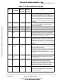
Contents
Paragraph
Section
Number
Title
Page
Number
Contents
Freescale Semiconductor, Inc...
About This Book
Audience ............................................................................................................. xliii
Organization........................................................................................................ xliv
Suggested Reading............................................................................................... xlv
General Information..................................................................................... xlv
Related Documentation .............................................................................. xlvi
Conventions ....................................................................................................... xlvii
Acronyms and Abbreviations ........................................................................... xlviii
Chapter 1
Overview
1.1
1.1.1
1.1.2
1.2
1.2.1
1.2.2
1.2.3
1.2.4
1.3
1.4
1.4.1
1.4.2
1.4.2.1
1.4.2.2
1.4.2.3
1.4.2.4
1.4.2.5
1.4.3
1.4.4
1.4.4.1
1.4.4.2
1.4.4.3
1.4.5
MOTOROLA
MPC8245 Integrated Processor Overview .......................................................... 1-1
MPC8245 Integrated Processor Features......................................................... 1-4
MPC8245 Integrated Processor Applications.................................................. 1-6
Processor Core Overview .................................................................................... 1-9
Execution Units.............................................................................................. 1-10
Data Types ..................................................................................................... 1-12
Caching .......................................................................................................... 1-12
Bus Operation ................................................................................................ 1-12
Peripheral Logic Bus ......................................................................................... 1-12
Peripheral Logic Overview ................................................................................ 1-14
Memory System Interface.............................................................................. 1-15
Peripheral Component Interconnect (PCI) Interface ..................................... 1-16
PCI Agent Capability................................................................................. 1-17
PCI Bus Arbitration Unit ........................................................................... 1-17
Address Maps and Translation .................................................................. 1-17
Byte Ordering ............................................................................................ 1-18
Bus Clock Buffers and Bus Ratios ............................................................ 1-18
DMA Controller............................................................................................. 1-18
Message Unit (MU) ....................................................................................... 1-18
Doorbell Registers ..................................................................................... 1-18
Inbound and Outbound Message Registers ............................................... 1-19
Intelligent Input/Output Controller (I2O) .................................................. 1-19
Inter-Integrated Circuit (I2C) Controller........................................................ 1-19
Contents
For More Information On This Product,
Go to: www.freescale.com
v
Freescale Semiconductor, Inc.
Contents
Freescale Semiconductor, Inc...
Paragraph
Number
1.4.6
1.4.7
1.4.8
1.4.9
1.5
1.5.1
1.5.2
1.6
1.7
1.7.1
1.7.2
1.7.3
1.7.4
1.7.5
1.8
Title
Page
Number
Programmable Interrupt Controller (PIC)...................................................... 1-20
Dual Universal Asynchronous Receiver/Transmitter (DUART) ................... 1-20
Integrated PCI Bus and SDRAM Clock Generation ..................................... 1-21
Performance Monitor..................................................................................... 1-21
Power Management ........................................................................................... 1-22
Programmable Processor Power Management Modes .................................. 1-22
Programmable Peripheral Logic Power Management Modes ....................... 1-23
Programmable I/O Signals with Watchpoint ..................................................... 1-24
Debug Features .................................................................................................. 1-24
Memory Attribute and PCI Attribute Signals ................................................ 1-24
Memory Debug Address................................................................................ 1-24
Memory Interface Valid (MIV)...................................................................... 1-25
Error Injection/Capture on Data Path ............................................................ 1-25
IEEE 1149.1 (JTAG)/Test Interface............................................................... 1-25
Differences Between the MPC8245 and the MPC8240 .................................... 1-25
Chapter 2
Signal Descriptions and Clocking
2.1
2.1.1
2.1.2
2.2
2.2.1
2.2.1.1
2.2.1.1.1
2.2.1.1.2
2.2.1.2
2.2.1.2.1
2.2.1.2.2
2.2.1.3
2.2.1.3.1
2.2.1.3.2
2.2.1.4
2.2.1.4.1
2.2.1.4.2
2.2.1.5
2.2.1.5.1
2.2.1.5.2
2.2.1.6
2.2.1.6.1
2.2.1.6.2
vi
Signal Overview .................................................................................................. 2-1
Signal Cross Reference.................................................................................... 2-4
Output Signal States During Reset .................................................................. 2-7
Detailed Signal Descriptions ............................................................................... 2-8
PCI Interface Signals ....................................................................................... 2-8
PCI Bus Request (REQ[4:0])—Input .......................................................... 2-9
PCI Bus Request (REQ[4:0])—Internal Arbiter Enabled ....................... 2-9
PCI Bus Request (REQ[4:0])—Internal Arbiter Disabled ...................... 2-9
PCI Bus Grant (GNT[4:0])—Output ........................................................... 2-9
PCI Bus Grant (GNT[4:0])—Internal Arbiter Enabled......................... 2-10
PCI Bus Grant (GNT[4:0])—Internal Arbiter Disabled........................ 2-10
PCI Address/Data Bus (AD[31:0])............................................................ 2-10
Address/Data (AD[31:0])—Output ....................................................... 2-10
Address/Data (AD[31:0])—Input.......................................................... 2-11
Parity (PAR)............................................................................................... 2-11
Parity (PAR)—Output ........................................................................... 2-11
Parity (PAR)—Input .............................................................................. 2-11
Command/Byte Enable (C/BE[3:0]).......................................................... 2-11
Command/Byte Enable (C/BE[3:0])—Output ...................................... 2-11
Command/Byte Enable (C/BE[3:0])—Input ......................................... 2-12
Device Select (DEVSEL) .......................................................................... 2-12
Device Select (DEVSEL)—Output ....................................................... 2-13
Device Select (DEVSEL)—Input.......................................................... 2-13
MPC8245 Integrated Processor User’s Manual
For More Information On This Product,
Go to: www.freescale.com
MOTOROLA
Freescale Semiconductor, Inc.
Contents
Freescale Semiconductor, Inc...
Paragraph
Number
2.2.1.7
2.2.1.7.1
2.2.1.7.2
2.2.1.8
2.2.1.8.1
2.2.1.8.2
2.2.1.9
2.2.1.10
2.2.1.10.1
2.2.1.10.2
2.2.1.11
2.2.1.11.1
2.2.1.11.2
2.2.1.12
2.2.1.12.1
2.2.1.12.2
2.2.1.13
2.2.1.13.1
2.2.1.13.2
2.2.1.14
2.2.1.15
2.2.2
2.2.2.1
2.2.2.2
2.2.2.3
2.2.2.4
2.2.2.5
2.2.2.6
2.2.2.7
2.2.2.8
2.2.2.9
2.2.2.9.1
2.2.2.9.2
2.2.2.10
2.2.2.10.1
2.2.2.10.2
2.2.2.11
2.2.2.12
2.2.2.13
2.2.2.14
2.2.2.15
MOTOROLA
Title
Page
Number
Frame (FRAME)........................................................................................ 2-13
Frame (FRAME)—Output .................................................................... 2-13
Frame (FRAME)—Input ....................................................................... 2-13
Initiator Ready (IRDY).............................................................................. 2-14
Initiator Ready (IRDY)—Output........................................................... 2-14
Initiator Ready (IRDY)—Input ............................................................. 2-14
Lock (LOCK)—Input ................................................................................ 2-14
Target Ready (TRDY) ............................................................................... 2-15
Target Ready (TRDY)—Output ............................................................ 2-15
Target Ready (TRDY)—Input ............................................................... 2-15
Parity Error (PERR)................................................................................... 2-15
Parity Error (PERR)—Output ............................................................... 2-16
Parity Error (PERR)—Input .................................................................. 2-16
System Error (SERR) ................................................................................ 2-16
System Error (SERR)—Output ............................................................. 2-16
System Error (SERR)—Input ................................................................ 2-16
Stop (STOP)............................................................................................... 2-17
Stop (STOP)—Output ........................................................................... 2-17
Stop (STOP)—Input .............................................................................. 2-17
Interrupt Request (INTA)—Output ........................................................... 2-17
ID Select (IDSEL)—Input ......................................................................... 2-17
Memory Interface Signals.............................................................................. 2-18
SDRAM Command Select (CS[0:7])—Output ......................................... 2-18
SDRAM Data Input/Output Mask (DQM[0:7])—Output ......................... 2-18
Write Enable (WE)—Output ..................................................................... 2-19
SDRAM Address (SDMA[11:0])—Output ............................................... 2-19
SDRAM Address 12 (SDMA12)—Output................................................ 2-19
SDRAM Address 13 (SDMA13)—Output................................................ 2-20
SDRAM Address 14 (SDMA14)—Output................................................ 2-20
SDRAM Internal Bank Select 0–1 (SDBA0, SDBA1)—Output .............. 2-20
Memory Data Bus (MDH[0:31], MDL[0:31]) .......................................... 2-21
Memory Data Bus (MDH[0:31], MDL[0:31])—Output ....................... 2-21
Memory Data Bus (MDH[0:31], MDL[0:31])—Input.......................... 2-22
Data Parity/ECC (PAR[0:7]) ..................................................................... 2-22
Data Parity (PAR[0:7])—Output ........................................................... 2-22
Data Parity (PAR[0:7])—Input.............................................................. 2-22
ROM Address 19:12 (AR[19:12])—Output.............................................. 2-22
SDRAM Clock Enable (CKE)—Output.................................................... 2-23
SDRAM Row Address Strobe (SDRAS)—Output ................................... 2-23
SDRAM Column Address Strobe (SDCAS)—Output .............................. 2-23
ROM Bank Selects (RCS[0:3])—Output .................................................. 2-24
Contents
For More Information On This Product,
Go to: www.freescale.com
vii
Freescale Semiconductor, Inc.
Contents
Freescale Semiconductor, Inc...
Paragraph
Number
2.2.2.16
2.2.2.17
2.2.2.18
2.2.3
2.2.3.1
2.2.3.2
2.2.3.2.1
2.2.3.2.2
2.2.3.2.3
2.2.3.2.4
2.2.3.3
2.2.4
2.2.4.1
2.2.4.1.1
2.2.4.1.2
2.2.4.2
2.2.4.2.1
2.2.4.2.2
2.2.5
2.2.5.1
2.2.5.2
2.2.5.3
2.2.5.4
2.2.6
2.2.6.1
2.2.6.1.1
2.2.6.1.2
2.2.6.2
2.2.6.3
2.2.6.4
2.2.6.5
2.2.6.6
2.2.6.7
2.2.6.8
2.2.6.9
2.2.6.9.1
2.2.6.9.2
2.2.6.10
2.2.6.10.1
2.2.6.10.2
2.2.6.10.3
viii
Title
Page
Number
Flash Output Enable (FOE)—Output ........................................................ 2-24
Address Strobe (AS)—Output ................................................................... 2-24
ROM/Port X Data Ready (DRDY)—Input ............................................... 2-25
PIC Control Signals ....................................................................................... 2-25
Discrete Interrupt 0–4 (IRQ[0:4])—Input ................................................. 2-25
Serial Interrupt Mode Signals .................................................................... 2-25
Serial Interrupt Stream (S_INT)—Input................................................ 2-26
Serial Interrupt Clock (S_CLK)—Output ............................................. 2-26
Serial Interrupt Reset (S_RST)—Output............................................... 2-26
Serial Interrupt Frame (S_FRAME)—Output ....................................... 2-26
Local Interrupt (L_INT)—Output ............................................................. 2-26
I2C Interface Control Signals......................................................................... 2-26
Serial Data (SDA)...................................................................................... 2-27
Serial Data (SDA)—Output................................................................... 2-27
Serial Data (SDA)—Input ..................................................................... 2-27
Serial Clock (SCL) .................................................................................... 2-27
Serial Clock (SCL)—Output ................................................................. 2-27
Serial Clock (SCL)—Input .................................................................... 2-27
DUART Signals ............................................................................................. 2-27
DUART Serial In Data (SIN1, SIN2)—Input............................................ 2-28
DUART Serial Out Data (SOUT1, SOUT2)—Output .............................. 2-28
Clear to Send (CTS1)—Input .................................................................... 2-28
Receive to Send (RTS1)—Output ............................................................. 2-28
System Control and Power Management Signals.......................................... 2-28
Hard Reset ................................................................................................. 2-29
Hard Reset (Processor) (HRST_CPU)—Input ...................................... 2-29
Hard Reset (Peripheral Logic) (HRST_CTRL)—Input ........................ 2-29
Soft Reset (SRESET)—Input .................................................................... 2-29
Machine Check (MCP)—Output ............................................................... 2-30
Nonmaskable Interrupt (NMI)—Input ...................................................... 2-31
System Management Interrupt (SMI)—Input ........................................... 2-31
Checkstop In (CHKSTOP_IN)—Input...................................................... 2-31
Time Base Enable (TBEN)—Input............................................................ 2-32
Quiesce Acknowledge (QACK)—Output ................................................. 2-32
Watchpoint Trigger Signals ....................................................................... 2-32
Watchpoint Trigger In (TRIG_IN)—Input ............................................ 2-32
Watchpoint Trigger Out (TRIG_OUT)—Output................................... 2-33
Debug Signals............................................................................................ 2-33
Memory Address Attributes (MAA[0:2])—Output .............................. 2-33
PCI Address Attributes (PMAA[0:2])—Output.................................... 2-34
Debug Address (DA[0:15])—Output .................................................... 2-34
MPC8245 Integrated Processor User’s Manual
For More Information On This Product,
Go to: www.freescale.com
MOTOROLA
Freescale Semiconductor, Inc.
Contents
Freescale Semiconductor, Inc...
Paragraph
Number
2.2.6.10.4
2.2.7
2.2.7.1
2.2.7.2
2.2.7.3
2.2.7.4
2.2.7.5
2.2.7.6
2.2.8
2.2.8.1
2.2.8.2
2.2.8.3
2.2.8.4
2.2.8.5
2.2.8.6
2.2.8.7
2.2.8.8
2.3
2.3.1
2.3.2
2.3.3
2.3.4
2.4
Title
Page
Number
Memory Interface Valid (MIV)—Output .............................................. 2-34
Test and Configuration Signals...................................................................... 2-35
PLL Configuration (PLL_CFG[0:4])—Input ............................................ 2-35
JTAG Test Clock (TCK)—Input................................................................ 2-35
JTAG Test Data Input (TDI)—Input ......................................................... 2-35
JTAG Test Data Output (TDO)—Output................................................... 2-36
JTAG Test Mode Select (TMS)—Input..................................................... 2-36
JTAG Test Reset (TRST)—Input .............................................................. 2-36
Clock Signals ................................................................................................. 2-36
System Clock Input (OSC_IN)—Input ..................................................... 2-37
PCI Clock (PCI_CLK[0:4])—Output........................................................ 2-37
PCI Clock Synchronize Out (PCI_SYNC_OUT)—Output....................... 2-37
PCI Feedback Clock (PCI_SYNC_IN)—Input ......................................... 2-37
SDRAM Clock Outputs (SDRAM_CLK[0:3])—Output .......................... 2-37
SDRAM Clock Synchronize Out (SDRAM_SYNC_OUT)—Output....... 2-37
SDRAM Feedback Clock (SDRAM_SYNC_IN)—Input ......................... 2-38
Debug Clock (CKO)—Output ................................................................... 2-38
Clocking ............................................................................................................ 2-38
Clocking Method ........................................................................................... 2-38
DLL Operation and Locking.......................................................................... 2-40
Clock Synchronization................................................................................... 2-41
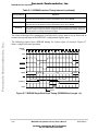
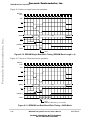
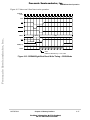
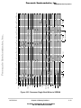
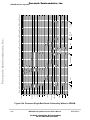
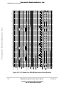
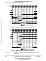
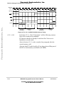
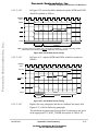
Clocking System Solution Examples............................................................. 2-42
Configuration Signals Sampled at Reset ........................................................... 2-43
Chapter 3
Address Maps
3.1
3.2
3.2.1
3.2.2
3.2.3
3.2.4
3.2.5
3.2.6
3.3
3.3.1
3.3.2
3.3.3
3.3.4
3.3.4.1
3.3.4.2
MOTOROLA
Address Map B .................................................................................................... 3-1
Address Map B Options....................................................................................... 3-6
Processor Compatibility Hole.......................................................................... 3-7
PCI Compatibility Hole ................................................................................... 3-7
Processor Alias Space...................................................................................... 3-7
PCI Alias Space ............................................................................................... 3-7
Processor Compatibility Hole and Alias Space ............................................... 3-8
PCI Compatibility Hole and Alias Space ...................................................... 3-10
Address Translation ........................................................................................... 3-11
Inbound PCI Address Translation.................................................................. 3-12
Outbound PCI Address Translation ............................................................... 3-16
Outbound PCI Address Translation Using Dual Address Cycles.................. 3-17
Address Translation Registers ....................................................................... 3-19
Local Memory Base Address Registers (LMBARn)................................. 3-20
Inbound Translation Window Registers (ITWRn)..................................... 3-21
Contents
For More Information On This Product,
Go to: www.freescale.com
ix
Freescale Semiconductor, Inc.
Contents
Paragraph
Number
Freescale Semiconductor, Inc...
3.3.4.3
3.3.4.4
3.3.4.5
3.4
3.4.1
3.4.2
Title
Page
Number
Outbound Translation High Base Address Registers (OTHBARn) .......... 3-23
Outbound Memory Base Address Registers (OMBARn) ......................... 3-23
Outbound Translation Window Register (OTWRn).................................. 3-24
Embedded Utilities Memory Block (EUMB) .................................................... 3-25
Processor Core Control and Status Registers ................................................ 3-27
Peripheral Control and Status Registers ........................................................ 3-29
Chapter 4
Configuration Registers
4.1
4.1.1
4.1.2
4.1.3
4.1.3.1
4.1.3.2
4.2
4.2.1
4.2.2
4.2.3
4.2.4
4.2.5
4.2.6
4.2.7
4.2.8
4.2.9
4.2.10
4.2.11
4.2.12
4.3
4.3.1
4.3.2
4.4
4.5
4.6
4.6.1
4.6.2
4.6.3
4.7
4.8
4.8.1
4.8.2
x
Configuration Register Access ............................................................................ 4-1
Configuration Register Access in Little-Endian Mode.................................... 4-2
Configuration Register Access in Big-Endian Mode ...................................... 4-3
Configuration Register Summary .................................................................... 4-3
Processor-Accessible Configuration Registers............................................ 4-4
PCI-Accessible Configuration Registers ..................................................... 4-8
PCI Interface Configuration Registers................................................................. 4-9
PCI Command Register—Offset 0x04 .......................................................... 4-10
PCI Status Register—Offset 0x06 ................................................................. 4-12
Programming Interface—Offset 0x09 ........................................................... 4-13
PCI Base Class Code—Offset 0x0B.............................................................. 4-14
PCI Cache Line Size—Offset 0x0C .............................................................. 4-14
Latency Timer—Offset 0x0D ........................................................................ 4-14
PCI Base Address Registers—LMBARn and PCSRBAR ............................ 4-14
Subsystem Vendor ID—Offset 0x2C............................................................. 4-15
Subsystem ID—Offset 0x2E ......................................................................... 4-16
PCI Interrupt Line—Offset 0x3C .................................................................. 4-16
PCI General Control Register (PGCR)—Offset 0x44 ................................... 4-16
PCI Arbiter Control Register (PACR)—Offset 0x46 .................................... 4-17
Peripheral Logic Power Management Configuration Registers (PMCRs) ........ 4-18
Power Management Configuration Register 1 (PMCR1)—Offset 0x70....... 4-18
Power Management Configuration Register 2 (PMCR2)—Offset 0x72....... 4-20
Output/Clock Driver and Miscellaneous I/O Control Registers ........................ 4-21
Embedded Utilities Memory Block Base Address Register—0x78 .................. 4-25
Memory Interface Configuration Registers ....................................................... 4-25
Memory Boundary Registers ......................................................................... 4-25
Memory Bank Enable Register—0xA0......................................................... 4-29
Memory Page Mode Register—0xA3 ........................................................... 4-30
Processor Interface Configuration Registers ..................................................... 4-31
Error Handling Registers ................................................................................... 4-35
ECC Single-Bit Error Registers..................................................................... 4-35
Error Enabling and Detection Registers ........................................................ 4-36
MPC8245 Integrated Processor User’s Manual
For More Information On This Product,
Go to: www.freescale.com
MOTOROLA
Freescale Semiconductor, Inc.
Contents
Paragraph
Number
Freescale Semiconductor, Inc...
4.9
4.10
4.11
4.12
4.13
4.14
Title
Page
Number
Extended ROM Configuration Registers—0xD0, 0xD4, 0xD8, 0xDC............. 4-42
Address Map B Options Register—0xE0.......................................................... 4-50
PCI/Memory Buffer Configuration Register—0xE1......................................... 4-51
PLL Configuration Register—0xE2 .................................................................. 4-52
Register—0xE3.................................................................................................. 4-53
Memory Control Configuration Registers ......................................................... 4-53
Chapter 5
G2 Processor Core
5.1
5.1.1
5.1.2
5.1.3
5.1.4
5.2
5.2.1
5.2.2
5.2.3
5.2.4
5.2.4.1
5.2.4.2
5.2.4.3
5.2.4.4
5.2.5
5.2.6
5.2.6.1
5.2.6.2
5.2.6.3
5.2.6.3.1
5.2.6.3.2
5.2.6.3.3
5.3
5.3.1
5.3.1.1
5.3.1.2
5.3.1.2.1
5.3.1.2.2
5.3.1.2.3
5.3.1.2.4
5.3.2
5.3.2.1
MOTOROLA
Overview.............................................................................................................. 5-1
Execution Units................................................................................................ 5-3
Data Types ....................................................................................................... 5-3
Memory Management...................................................................................... 5-3
Bus Operation .................................................................................................. 5-4
G2 Processor Core Features................................................................................. 5-4
Instruction Unit ................................................................................................ 5-5
Instruction Queue and Dispatch Unit............................................................... 5-6
Branch Processing Unit (BPU) ........................................................................ 5-6
Independent Execution Units........................................................................... 5-7
Integer Unit (IU) .......................................................................................... 5-7
Floating-Point Unit (FPU) ........................................................................... 5-7
Load/Store Unit (LSU) ................................................................................ 5-7
System Register Unit (SRU)........................................................................ 5-8
Completion Unit .............................................................................................. 5-8
Memory Subsystem Support............................................................................ 5-8
Memory Management Units (MMUs)......................................................... 5-9
Cache Units.................................................................................................. 5-9
Peripheral Logic Bus Interface .................................................................... 5-9
Peripheral Logic Bus Protocol............................................................... 5-10
Peripheral Logic Bus Data Transfers..................................................... 5-10
Peripheral Logic Bus Frequency ........................................................... 5-11
Programming Model .......................................................................................... 5-11
Register Set .................................................................................................... 5-11
PowerPC Register Set................................................................................ 5-12
MPC8245-Specific Registers..................................................................... 5-12
Hardware Implementation-Dependent Register 0 (HID0) .................... 5-14
Hardware Implementation-Dependent Register 1 (HID1) .................... 5-18
Hardware Implementation-Dependent Register 2 (HID2) .................... 5-18
Processor Version Register (PVR)......................................................... 5-19
PowerPC Instruction Set and Addressing Modes .......................................... 5-19
Calculating Effective Addresses................................................................ 5-19
Contents
For More Information On This Product,
Go to: www.freescale.com
xi
Freescale Semiconductor, Inc.
Contents
Freescale Semiconductor, Inc...
Paragraph
Number
5.3.2.2
5.3.2.3
5.4
5.4.1
5.4.2
5.4.2.1
5.4.2.2
5.4.2.3
5.4.2.3.1
5.4.2.3.2
5.4.3
5.4.3.1
5.4.3.2
5.5
5.5.1
5.5.1.1
5.5.2
5.5.3
5.6
5.6.1
5.6.2
5.7
5.7.1
5.7.1.1
5.7.1.2
5.7.1.3
5.7.1.4
5.8
Title
Page
Number
PowerPC Instruction Set............................................................................ 5-19
MPC8245 Implementation-Specific Instruction Set.................................. 5-21
Cache Implementation ....................................................................................... 5-22
PowerPC Cache Model.................................................................................. 5-22
MPC8245 Implementation-Specific Cache Implementation......................... 5-22
Data Cache................................................................................................. 5-23
Instruction Cache ....................................................................................... 5-24
Cache Locking ........................................................................................... 5-24
Entire Cache Locking ............................................................................ 5-25
Way Locking.......................................................................................... 5-25
Cache Coherency ........................................................................................... 5-25
CCU Responses to Processor Transactions ............................................... 5-26
Processor Responses to PCI-to-Memory Transactions.............................. 5-27
Exception Model................................................................................................ 5-28
PowerPC Exception Model............................................................................ 5-28
Exceptions and Exception Handlers .......................................................... 5-28
MPC8245 Implementation-Specific Exception Model.................................. 5-29
Exception Priorities........................................................................................ 5-32
Memory Management........................................................................................ 5-32
PowerPC MMU Model.................................................................................. 5-32
MPC8245 Implementation-Specific MMU Features..................................... 5-34
Instruction Timing.............................................................................................. 5-35
Stages of the Instruction Pipeline Processor.................................................. 5-35
Fetch Pipeline Stage .................................................................................. 5-35
Dispatch Pipeline Stage ............................................................................. 5-35
Execute Pipeline Stage .............................................................................. 5-35
Complete/Writeback Pipeline Stage .......................................................... 5-36
Differences Between the MPC8245 Core and the MPC603e Processor ........... 5-36
Chapter 6
Memory Interface
6.1
6.2
6.2.1
6.2.2
6.2.3
6.2.4
6.2.5
6.2.6
6.2.7
6.2.7.1
xii
Memory Interface Signal Summary..................................................................... 6-3
SDRAM Interface Operation ............................................................................... 6-6
Supported SDRAM Organizations .................................................................. 6-9
SDRAM Address Multiplexing ..................................................................... 6-11
SDRAM Memory Data Interface................................................................... 6-15
SDRAM Power-On Initialization .................................................................. 6-17
MPC8245 Interface Functionality for JEDEC SDRAMs .............................. 6-19
SDRAM Burst and Single-Beat Transactions................................................ 6-20
SDRAM Page Mode ...................................................................................... 6-21
SDRAM Paging in Sleep Mode................................................................. 6-23
MPC8245 Integrated Processor User’s Manual
For More Information On This Product,
Go to: www.freescale.com
MOTOROLA
Freescale Semiconductor, Inc.
Contents
Freescale Semiconductor, Inc...
Paragraph
Number
6.2.8
6.2.8.1
6.2.9
6.2.9.1
6.2.10
6.2.11
6.2.12
6.2.12.1
6.2.12.2
6.2.13
6.2.14
6.3
6.3.1
6.3.1.1
6.3.2
6.3.2.1
6.3.2.2
6.3.3
6.3.4
6.3.4.1
6.3.4.2
6.3.4.3
6.3.5
6.3.5.1
6.3.5.2
6.3.5.3
6.3.5.4
6.3.6
Title
Page
Number
SDRAM Interface Timing ............................................................................. 6-23
SDRAM Mode-Set Command Timing ...................................................... 6-28
SDRAM Parity and RMW Parity .................................................................. 6-28
RMW Parity Latency Considerations........................................................ 6-29
SDRAM In-Line ECC ................................................................................... 6-29
SDRAM Registered DIMM Mode ................................................................ 6-31
SDRAM Refresh............................................................................................ 6-33
SDRAM Refresh Timing ........................................................................... 6-35
SDRAM Refresh and Power-Saving Modes ............................................. 6-36
Processor-to-SDRAM Transaction Examples ............................................... 6-39
PCI-to-SDRAM Transaction Examples......................................................... 6-45
ROM/Flash Interface Operation ........................................................................ 6-49
Base ROM Interface Operation ..................................................................... 6-51
Base ROM Address Multiplexing ............................................................. 6-53
Extended ROM Interface ............................................................................... 6-55
Extended ROM Address Multiplexing ...................................................... 6-57
Extended ROM Interface Read Gathering................................................. 6-59
ROM/Flash Interface Write Operations......................................................... 6-60
ROM Interface Timing .................................................................................. 6-60
Read Timing—64-/32-Bit (Wide) Data Path ............................................. 6-62
Read Timing—8-Bit Data Path.................................................................. 6-64
ROM/Flash Interface Write Timing........................................................... 6-66
Port X Interface.............................................................................................. 6-66
Port X Operation........................................................................................ 6-68
Port X Timing ............................................................................................ 6-69
Port X Strobe Mode ................................................................................... 6-71
Port X Handshake Mode............................................................................ 6-71
PCI-to-ROM/Port X Transaction Example.................................................... 6-73
Chapter 7
PCI Bus Interface
7.1
7.1.1
7.1.2
7.1.3
7.1.4
7.2
7.2.1
7.2.1.1
7.2.1.2
MOTOROLA
PCI Interface Overview ....................................................................................... 7-1
MPC8245 as a PCI Initiator............................................................................. 7-2
MPC8245 as a PCI Target................................................................................ 7-3
PCI Signal Output Hold Timing ...................................................................... 7-3
PCI 2.2-Compatible Extensions to MPC8240 and the
Tundra Tsi107™ PowerPC Host Bridge...................................................... 7-4
PCI Bus Arbitration ............................................................................................. 7-4
Internal Arbitration for PCI Bus Access.......................................................... 7-5
Processor-Initiated Transactions to PCI Bus ............................................... 7-6
DMA-Initiated Transactions to the PCI Bus................................................ 7-6
Contents
For More Information On This Product,
Go to: www.freescale.com
xiii
Freescale Semiconductor, Inc.
Contents
Freescale Semiconductor, Inc...
Paragraph
Number
7.2.2
7.2.3
7.2.4
7.2.5
7.3
7.3.1
7.3.2
7.3.3
7.3.3.1
7.3.3.2
7.3.3.3
7.3.4
7.3.5
7.3.6
7.4
7.4.1
7.4.2
7.4.3
7.4.3.1
7.4.3.2
7.4.3.2.1
7.4.3.2.2
7.4.3.2.3
7.4.4
7.4.5
7.4.6
7.4.6.1
7.4.6.2
7.4.6.2.1
7.4.6.2.2
7.4.7
7.4.7.1
7.4.7.2
7.5
7.5.1
7.5.2
7.5.3
7.5.4
7.5.5
7.6
7.6.1
xiv
Title
Page
Number
PCI Bus Arbiter Operation .............................................................................. 7-6
PCI Bus Parking .............................................................................................. 7-8
Power-Saving Modes and the PCI Arbiter ...................................................... 7-8
Broken Master Lock-Out ................................................................................. 7-9
MPC8245 PCI Bus Protocol ................................................................................ 7-9
Basic Transfer Control..................................................................................... 7-9
PCI Bus Commands....................................................................................... 7-10
Addressing ..................................................................................................... 7-12
Memory Space Addressing........................................................................ 7-12
I/O Space Addressing ................................................................................ 7-13
Configuration Space Addressing ............................................................... 7-13
Device Selection ............................................................................................ 7-13
Byte Alignment.............................................................................................. 7-14
Bus Driving and Turnaround ......................................................................... 7-14
PCI Bus Transactions......................................................................................... 7-15
PCI Read Transactions................................................................................... 7-15
PCI Write Transactions .................................................................................. 7-17
Transaction Termination ................................................................................ 7-18
Master-Initiated Termination ..................................................................... 7-18
Target-Initiated Termination ...................................................................... 7-18
Target-Disconnect Termination ............................................................. 7-19
Retry Termination.................................................................................. 7-20
Target-Abort Termination ...................................................................... 7-20
Fast Back-to-Back Transactions .................................................................... 7-21
Dual Address Cycles (Master-Only).............................................................. 7-23
Configuration Cycles ..................................................................................... 7-25
PCI Configuration Space Header............................................................... 7-25
Accessing the PCI Configuration Space.................................................... 7-27
Type 0 Configuration Translation.......................................................... 7-28
Type 1 Configuration Translation.......................................................... 7-30
Other Bus Transactions.................................................................................. 7-30
Interrupt-Acknowledge Transactions ........................................................ 7-30
Special-Cycle Transactions........................................................................ 7-31
Exclusive Access ............................................................................................... 7-32
Starting an Exclusive Access ......................................................................... 7-32
Continuing an Exclusive Access.................................................................... 7-33
Completing an Exclusive Access................................................................... 7-33
Attempting to Access a Locked Target.......................................................... 7-33
Exclusive Access and the MPC8245 ............................................................. 7-33
PCI Error Functions ........................................................................................... 7-34
PCI Parity....................................................................................................... 7-34
MPC8245 Integrated Processor User’s Manual
For More Information On This Product,
Go to: www.freescale.com
MOTOROLA
Freescale Semiconductor, Inc.
Contents
Freescale Semiconductor, Inc...
Paragraph
Number
7.6.2
7.7
7.7.1
7.7.2
7.7.3
7.7.4
7.7.4.1
7.7.4.2
7.7.4.3
Title
Page
Number
Error Reporting .............................................................................................. 7-35
PCI Host and Agent Modes ............................................................................... 7-35
PCI Initialization Options .............................................................................. 7-36
Accessing the MPC8245 Configuration Space.............................................. 7-36
PCI Configuration Cycle Retry Capability in Agent Mode........................... 7-37
PCI Address Translation Support .................................................................. 7-37
Inbound PCI Address Translation.............................................................. 7-37
Outbound PCI Address Translation ........................................................... 7-38
Initialization Code Translation in Agent Mode ......................................... 7-38
Chapter 8
DMA Controller
8.1
8.2
8.3
8.3.1
8.3.2
8.3.2.1
8.3.2.2
8.3.3
8.3.4
8.3.5
8.4
8.4.1
8.4.2
8.4.3
8.4.4
8.5
8.5.1
8.5.2
8.5.2.1
8.5.2.2
8.5.2.3
8.5.2.4
8.5.2.5
8.5.3
8.5.3.1
8.5.3.2
8.5.3.3
8.5.3.4
MOTOROLA
DMA Overview ................................................................................................... 8-1
DMA Register Summary ..................................................................................... 8-2
DMA Operation ................................................................................................... 8-4
DMA Direct Mode........................................................................................... 8-5
DMA Chaining Mode ...................................................................................... 8-6
Basic Chaining Mode Initialization ............................................................. 8-6
Periodic DMA Feature................................................................................. 8-6
DMA Operation Flow...................................................................................... 8-8
DMA Coherency.............................................................................................. 8-9
DMA Performance........................................................................................... 8-9
DMA Transfer Types ......................................................................................... 8-10
PCI-to-PCI ..................................................................................................... 8-10
PCI-to-Local Memory.................................................................................... 8-10
Local Memory-to-PCI.................................................................................... 8-10
Local Memory to Local Memory................................................................... 8-11
Address Map Interactions .................................................................................. 8-11
Attempted Writes to Local ROM/Port X Space ............................................ 8-11
Host Mode Interactions.................................................................................. 8-11
PCI Master Abort When PCI Bus Specified for Lower 2-Gbyte Space.... 8-12
Address Alias to Lower 2-Gbyte Space..................................................... 8-12
Attempted Reads From ROM on the PCI Bus—Host Mode..................... 8-12
Attempted Reads From ROM on the Memory Bus ................................... 8-12
Address Translations for PCI Transactions ............................................... 8-12
Agent Mode Interactions ............................................................................... 8-12
Agent Mode DMA Transfers for PCI ........................................................ 8-13
Accesses to Outbound Memory Window that Overlaps
0xFE00_0000 – 0xFEEF_FFFF ............................................................ 8-13
Attempted Accesses to Local ROM When ROM is on PCI...................... 8-13
Attempted Access to ROM on the PCI Bus—Agent Mode ...................... 8-13
Contents
For More Information On This Product,
Go to: www.freescale.com
xv
Freescale Semiconductor, Inc.
Contents
Freescale Semiconductor, Inc...
Paragraph
Number
8.6
8.6.1
8.6.2
8.7
8.7.1
8.7.2
8.7.3
8.7.4
8.7.5
8.7.6
8.7.7
8.7.8
8.7.9
8.7.10
8.7.11
Title
Page
Number
DMA Descriptors for Chaining Mode ............................................................... 8-14
Descriptors in Big-Endian Mode ................................................................... 8-16
Descriptors in Little-Endian Mode ................................................................ 8-17
DMA Register Descriptions............................................................................... 8-18
DMA Mode Registers (DMRs)...................................................................... 8-18
DMA Status Registers (DSRs) ...................................................................... 8-21
Current Descriptor Address Registers (CDARs) ........................................... 8-23
High Current Descriptor Address Registers (HCDARs) ............................... 8-24
Source Address Registers (SARs) ................................................................. 8-25
High Source Address Registers (HSARs) ..................................................... 8-26
Destination Address Registers (DARs) ......................................................... 8-26
High Destination Address Registers (HDARs) ............................................. 8-27
Byte Count Registers (BCRs) ........................................................................ 8-27
Next Descriptor Address Registers (NDARs) ............................................... 8-28
High Next Descriptor Address Registers (HNDARs) ................................... 8-29
Chapter 9
Message Unit (with I2O)
9.1
9.2
9.2.1
9.2.2
9.2.3
9.3
9.3.1
9.3.2
9.3.3
9.3.3.1
9.3.3.1.1
9.3.3.1.2
9.3.3.2
9.3.3.2.1
9.3.3.2.2
9.3.4
9.3.4.1
9.3.4.1.1
9.3.4.1.2
9.3.4.1.3
9.3.4.1.4
9.3.4.2
9.3.4.2.1
xvi
Message Unit (MU) Overview ............................................................................ 9-1
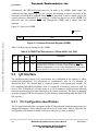
Message and Doorbell Register Programming Model......................................... 9-1
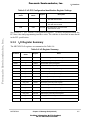
Message and Doorbell Register Summary....................................................... 9-2
Message Register Descriptions........................................................................ 9-2
Doorbell Register Descriptions........................................................................ 9-3
I2O Interface ........................................................................................................ 9-4
PCI Configuration Identification ..................................................................... 9-4
I2O Register Summary..................................................................................... 9-5
FIFO Descriptions............................................................................................ 9-6
Inbound FIFOs............................................................................................. 9-7
Inbound Free_List FIFO .......................................................................... 9-7
Inbound Post_List FIFO .......................................................................... 9-7
Outbound FIFOs .......................................................................................... 9-8
Outbound Free_List FIFO ....................................................................... 9-8
Outbound Post_List FIFO ....................................................................... 9-8
I2O Register Descriptions ................................................................................ 9-8
PCI-Accessible I2O Registers...................................................................... 9-9
Outbound Message Interrupt Status Register (OMISR).......................... 9-9
Outbound Message Interrupt Mask Register (OMIMR) ....................... 9-11
Inbound FIFO Queue Port Register (IFQPR)........................................ 9-12
Outbound FIFO Queue Port Register (OFQPR).................................... 9-13
Processor-Accessible I2O Registers .......................................................... 9-13
Inbound Message Interrupt Status Register (IMISR) ............................ 9-13
MPC8245 Integrated Processor User’s Manual
For More Information On This Product,
Go to: www.freescale.com
MOTOROLA
Freescale Semiconductor, Inc.
Contents
Freescale Semiconductor, Inc...
Paragraph
Number
9.3.4.2.2
9.3.4.2.3
9.3.4.2.4
9.3.4.2.5
9.3.4.2.6
9.3.4.2.7
9.3.4.2.8
9.3.4.2.9
9.3.4.2.10
9.3.4.2.11
9.3.4.2.12
Title
Page
Number
Inbound Message Interrupt Mask Register (IMIMR)............................ 9-16
Inbound Free_FIFO Head Pointer Register (IFHPR)............................ 9-17
Inbound Free_FIFO Tail Pointer Register (IFTPR)............................... 9-17
Inbound Post_FIFO Head Pointer Register (IPHPR) ............................ 9-18
Inbound Post_FIFO Tail Pointer Register (IPTPR) ............................... 9-19
Outbound Free_FIFO Head Pointer Register (OFHPR)........................ 9-19
Outbound Free_FIFO Tail Pointer Register (OFTPR) .......................... 9-20
Outbound Post_FIFO Head Pointer Register (OPHPR)........................ 9-21
Outbound Post_FIFO Tail Pointer Register (OPTPR)........................... 9-21
Messaging Unit Control Register (MUCR)........................................... 9-22
Queue Base Address Register (QBAR)................................................. 9-23
Chapter 10
Interface
I2C
10.1
10.1.1
10.1.2
10.1.3
10.1.4
10.2
10.2.1
10.2.2
10.2.3
10.2.4
10.2.5
10.2.6
10.2.7
10.2.8
10.3
10.3.1
10.3.2
10.3.3
10.3.4
10.3.5
10.4
10.4.1
10.4.2
10.4.3
10.4.4
10.4.5
10.4.6
MOTOROLA
I2C Interface Overview...................................................................................... 10-1
I2C Unit Features ........................................................................................... 10-1
I2C Interface Signal Summary....................................................................... 10-2
I2C Register Summary................................................................................... 10-2
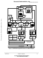
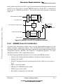
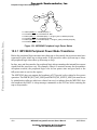
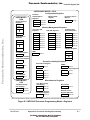
I2C Block Diagram ........................................................................................ 10-3
2
I C Protocol ....................................................................................................... 10-4
START Condition .......................................................................................... 10-4
Slave Address Transmission .......................................................................... 10-4
Repeated START Condition .......................................................................... 10-5
STOP Condition............................................................................................. 10-6
Arbitration Procedure .................................................................................... 10-6
Clock Synchronization................................................................................... 10-7
Handshaking .................................................................................................. 10-7
Clock Stretching ............................................................................................ 10-7
2
I C Register Descriptions .................................................................................. 10-7
I2C Address Register (I2CADR) ................................................................... 10-8
I2C Frequency Divider Register (I2CFDR)................................................... 10-8
I2C Control Register (I2CCR) ..................................................................... 10-11
I2C Status Register (I2CSR) ........................................................................ 10-13
I2C Data Register (I2CDR).......................................................................... 10-14
Programming Guidelines ................................................................................. 10-15
Initialization Sequence................................................................................. 10-15
Generation of START .................................................................................. 10-16
Post-Transfer Software Response ................................................................ 10-16
Generation of STOP..................................................................................... 10-17
Generation of Repeated START .................................................................. 10-17
Generation of SCK when SDA Low............................................................ 10-17
Contents
For More Information On This Product,
Go to: www.freescale.com
xvii
Freescale Semiconductor, Inc.
Contents
Paragraph
Number
10.4.7
10.4.7.1
10.4.7.2
10.4.8
Title
Page
Number
Slave Mode Interrupt Service Routine......................................................... 10-18
Slave Transmitter and Received Acknowledge ....................................... 10-18
Loss of Arbitration and Forcing of Slave Mode...................................... 10-18
Interrupt Service Routine Flowchart............................................................ 10-18
Freescale Semiconductor, Inc...
Chapter 11
Programmable Interrupt Controller (PIC) Unit
11.1
11.1.1
11.1.2
11.1.3
11.2
11.3
11.3.1
11.3.2
11.3.3
11.3.4
11.3.5
11.3.6
11.3.6.1
11.3.6.2
11.3.6.3
11.3.6.4
11.4
11.5
11.6
11.6.1
11.6.2
11.6.3
11.7
11.8
11.8.1
11.8.2
11.9
11.9.1
11.9.2
11.9.3
11.9.4
11.9.5
11.9.6
11.9.7
xviii
PIC Unit Overview ............................................................................................ 11-1
PIC Features Summary .................................................................................. 11-2
PIC Interface Signal Description ................................................................... 11-2
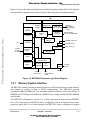
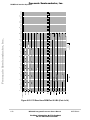
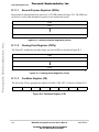
PIC Block Diagram........................................................................................ 11-3
PIC Register Summary ...................................................................................... 11-3
PIC Unit Interrupt Protocol................................................................................ 11-7
Interrupt Source Priority ................................................................................ 11-7
Processor Current Task Priority ..................................................................... 11-8
Interrupt Acknowledge .................................................................................. 11-8
Nesting of Interrupts ...................................................................................... 11-8
Spurious Vector Generation ........................................................................... 11-8
Internal Block Diagram Description.............................................................. 11-9
Interrupt Pending Register (IPR)—Nonprogrammable............................. 11-9
Interrupt Selector (IS) .............................................................................. 11-10
Interrupt Request Register (IRR)............................................................. 11-10
In-Service Register (ISR) ........................................................................ 11-10
PIC Pass-Through Mode.................................................................................. 11-10
PIC Direct Interrupt Mode ................................................................................11-11
PIC Serial Interrupt Interface............................................................................11-11
Sampling of Serial Interrupts........................................................................11-11
Serial Interrupt Timing Protocol .................................................................. 11-12
Edge/Level Sensitivity of Serial Interrupts.................................................. 11-12
PIC Timers ....................................................................................................... 11-12
Programming Guidelines ................................................................................. 11-13
Edge-Sensitive False Interrupts ................................................................... 11-15
Global Timer False Interrupts ...................................................................... 11-15
Register Definitions ......................................................................................... 11-15
Feature Reporting Register (FRR)............................................................... 11-15
Global Configuration Register (GCR)......................................................... 11-16
PIC Interrupt Configuration Register (ICR) ................................................ 11-17
PIC Vendor Identification Register (EVI) ................................................... 11-18
Processor Initialization Register (PI)........................................................... 11-19
Spurious Vector Register (SVR) .................................................................. 11-19
Global Timer Registers ................................................................................ 11-20
MPC8245 Integrated Processor User’s Manual
For More Information On This Product,
Go to: www.freescale.com
MOTOROLA
Freescale Semiconductor, Inc.
Contents
Paragraph
Number
Freescale Semiconductor, Inc...
11.9.7.1
11.9.7.2
11.9.7.3
11.9.7.4
11.9.7.5
11.9.7.6
11.9.8
11.9.8.1
11.9.8.2
11.9.8.3
11.9.8.4
11.9.9
11.9.9.1
11.9.9.2
11.9.10
Title
Page
Number
Timer Frequency Reporting Register (TFRR)......................................... 11-20
Timer Control Register (TCR)................................................................. 11-21
Global Timer Current Count Registers (GTCCRn) ................................. 11-22
Global Timer Base Count Registers (GTBCRn)...................................... 11-22
Global Timer Vector/Priority Registers (GTVPRs) ................................. 11-23
Global Timer Destination Registers (GTDRs)......................................... 11-24
External (Direct and Serial) and Internal Interrupt Registers ...................... 11-25
Direct and Serial Interrupt Vector/Priority Registers
(IVPRs, SVPRs) ................................................................................ 11-25
Direct and Serial Interrupt Destination Registers (IDRs and SIRs) ........ 11-26
Internal (I2C, DMA, MU, DUART) Interrupt Vector/Priority Registers
(IIVPRs)............................................................................................... 11-27
Internal (I2C, DMA, MU, or DUART) Interrupt Destination
Registers (IIDRs) ................................................................................. 11-28
Processor-Related Registers ........................................................................ 11-28
Processor Current Task Priority Register (PCTPR)................................. 11-28
Processor Interrupt Acknowledge Register (IACK)................................ 11-29
Processor End-of-Interrupt Register (EOI).................................................. 11-29
Chapter 12
DUART Unit
12.1
12.1.1
12.1.2
12.1.3
12.1.4
12.1.5
12.2
12.2.1
12.2.1.1
12.2.1.2
12.2.1.3
12.2.1.4
12.2.2
12.2.3
12.2.4
12.2.4.1
12.2.4.2
12.2.4.3
12.2.5
12.2.5.1
MOTOROLA
DUART Overview ............................................................................................. 12-1
DUART Unit Features ................................................................................... 12-1
DUART Block Diagram ................................................................................ 12-2
DUART Signal Description ........................................................................... 12-3
DUART Signal Mode Selection .................................................................... 12-4
DUART Register Summary ........................................................................... 12-5
DUART Operation ............................................................................................. 12-8
Serial Interface............................................................................................... 12-8
START Bit ................................................................................................. 12-9
Data Transfer ............................................................................................. 12-9
Parity Bit.................................................................................................. 12-10
STOP Bit.................................................................................................. 12-10
Baud-Rate Generator Logic ......................................................................... 12-10
Local Loop Back Mode ............................................................................... 12-10
Errors ........................................................................................................... 12-11
Framing Error .......................................................................................... 12-11
Parity Error .............................................................................................. 12-11
Overrun Error........................................................................................... 12-11
FIFO Mode .................................................................................................. 12-12
FIFO Interrupts ........................................................................................ 12-12
Contents
For More Information On This Product,
Go to: www.freescale.com
xix
Freescale Semiconductor, Inc.
Contents
Freescale Semiconductor, Inc...
Paragraph
Number
12.2.5.2
12.2.6
12.3
12.4
12.4.1
12.4.2
12.4.3
12.4.4
12.4.5
12.4.6
12.4.7
12.4.8
12.4.9
12.4.10
12.4.11
12.4.12
12.4.13
12.4.14
Title
Page
Number
DMA Mode Select................................................................................... 12-12
Interrupt Control Logic................................................................................ 12-13
DUART Initialization Sequence ...................................................................... 12-13
Programming Model ........................................................................................ 12-14
Receiver Buffer Register (URBR) ............................................................... 12-14
Divisor Most and Least Significant Byte Registers (UDMB and UDLB) .. 12-15
Transmitter Holding Register (UTHR)........................................................ 12-16
Interrupt Enable Register (UIER) ................................................................ 12-16
Interrupt ID Register (UIIR) ........................................................................ 12-17
FIFO Control Register (UFCR) ................................................................... 12-19
Line Control Register (ULCR) .................................................................... 12-20
MODEM Control Register (UMCR) ........................................................... 12-22
Line Status Register (ULSR) ....................................................................... 12-23
MODEM Status Register (UMSR) .............................................................. 12-24
Scratch Register (USCR) ............................................................................. 12-25
Alternate Function Register (UAFR)........................................................... 12-25
DMA Status Register (UDSR)..................................................................... 12-26
DUART Configuration Register (DCR) ...................................................... 12-28
Chapter 13
Central Control Unit
13.1
13.1.1
13.1.2
13.1.2.1
13.1.2.2
13.1.3
13.1.3.1
13.1.3.1.1
13.1.3.1.2
13.1.3.2
13.2
13.2.1
13.2.1.1
13.2.1.2
13.2.1.3
13.2.1.4
13.2.2
13.2.3
xx
Internal Buffers .................................................................................................. 13-1
Processor Core/Local Memory Buffers ......................................................... 13-2
Processor/PCI Buffers.................................................................................... 13-3
Processor-to-PCI-Read Buffer (PRPRB)................................................... 13-4
Processor-to-PCI-Write Buffers (PRPWBs).............................................. 13-5
PCI/Local Memory Buffers ........................................................................... 13-6
PCI-to-Local-Memory Read Buffering ..................................................... 13-7
PCI-to-Local-Memory Read Buffers (PCMRBs).................................. 13-7
Speculative PCI Reads from Local Memory ......................................... 13-8
PCI-to-Local-Memory-Write Buffers (PCMWBs).................................... 13-8
Internal Arbitration ............................................................................................ 13-9
Arbitration Between PCI and DMA Accesses to Local Memory.................. 13-9
DMA Transaction Boundaries for Memory/Memory Transfers.............. 13-10
DMA Transaction Boundaries for Memory-to-PCI Transfers................. 13-11
DMA Transaction Boundaries for PCI—Memory Transfers .................. 13-11
PCI and DMA Reads from Slow Memory/Port X................................... 13-11
Internal Arbitration Priorities....................................................................... 13-12
Guaranteeing Minimum PCI Access Latency to Local Memory ................ 13-13
MPC8245 Integrated Processor User’s Manual
For More Information On This Product,
Go to: www.freescale.com
MOTOROLA
Freescale Semiconductor, Inc.
Contents
Paragraph
Number
Title
Page
Number
Freescale Semiconductor, Inc...
Chapter 14
Error Handling
14.1
14.1.1
14.1.2
14.2
14.2.1
14.2.2
14.2.3
14.2.3.1
14.2.3.2
14.2.3.3
14.3
14.3.1
14.3.1.1
14.3.1.2
14.3.1.3
14.3.2
14.3.2.1
14.3.2.2
14.3.2.3
14.3.2.4
14.3.3
14.3.3.1
14.3.3.2
14.3.3.3
14.3.3.4
14.3.3.5
14.3.4
14.4
Overview............................................................................................................ 14-1
Error Handling Block Diagram...................................................................... 14-2
Priority of Externally Generated Errors and Exceptions ............................... 14-3
Exceptions and Error Signals............................................................................. 14-3
System Reset.................................................................................................. 14-3
Processor Core Error Signal (mcp) ............................................................... 14-4
PCI Bus Error Signals.................................................................................... 14-5
System Error (SERR) ................................................................................ 14-5
Parity Error (PERR)................................................................................... 14-5
Nonmaskable Interrupt (NMI)................................................................... 14-6
Error Reporting .................................................................................................. 14-6
Processor Interface Errors.............................................................................. 14-7
Processor Transaction Error....................................................................... 14-7
Flash Write Error ....................................................................................... 14-8
Processor Write Parity Error...................................................................... 14-8
Memory Interface Errors ............................................................................... 14-8
Memory Read Data Parity Error................................................................ 14-9
Memory ECC Error ................................................................................... 14-9
Memory Select Error ............................................................................... 14-10
Memory Refresh Overflow Error ............................................................ 14-10
PCI Interface Errors ..................................................................................... 14-10
PCI Address Parity Error ......................................................................... 14-10
PCI Data Parity Error............................................................................... 14-11
PCI Master-Abort Transaction Termination ............................................ 14-11
Received PCI Target-Abort Error ............................................................ 14-12
NMI (Nonmaskable Interrupt)................................................................. 14-12
Message Unit Error Events .......................................................................... 14-12
Exception Latencies ......................................................................................... 14-13
Chapter 15
Power Management
15.1
15.2
15.2.1
15.2.2
15.2.3
15.2.3.1
15.2.3.2
MOTOROLA
Overview............................................................................................................ 15-1
Processor Core Power Management .................................................................. 15-1
Dynamic Power Management........................................................................ 15-2
Programmable Power Modes on Processor Core .......................................... 15-2
Processor Power Management Modes—Details............................................ 15-4
Full-Power Mode with DPM Disabled ...................................................... 15-4
Full-Power Mode with DPM Enabled ....................................................... 15-4
Contents
For More Information On This Product,
Go to: www.freescale.com
xxi
Freescale Semiconductor, Inc.
Contents
Freescale Semiconductor, Inc...
Paragraph
Number
15.2.3.3
15.2.3.4
15.2.3.5
15.2.4
15.3
15.3.1
15.3.2
15.3.2.1
15.3.2.2
15.3.2.3
15.3.2.3.1
15.3.2.3.2
15.3.2.4
15.3.2.4.1
15.3.2.4.2
15.3.2.4.3
15.4
15.5
Title
Page
Number
Processor Doze Mode ................................................................................ 15-5
Processor Nap Mode.................................................................................. 15-5
Processor Sleep Mode................................................................................ 15-6
Power Management Software Considerations............................................... 15-7
Peripheral Logic Power Management................................................................ 15-7
MPC8245 Peripheral Power Mode Transitions ............................................. 15-8
Peripheral Power Management Modes .......................................................... 15-9
Peripheral Logic Full-Power Mode ........................................................... 15-9
Peripheral Logic Doze Mode..................................................................... 15-9
Peripheral Logic Nap Mode..................................................................... 15-10
PCI Transactions During Nap Mode ................................................... 15-11
PLL Operation During Nap Mode....................................................... 15-11
Peripheral Logic Sleep Mode .................................................................. 15-11
System Memory Refresh During Sleep Mode..................................... 15-12
Disabling the PLL During Sleep Mode ............................................... 15-12
SDRAM Paging During Sleep Mode .................................................. 15-12
Disabling Peripheral Clocks ............................................................................ 15-12
Example Code Sequence for Processor and Peripheral Logic Sleep Modes ... 15-13
Chapter 16
Performance Monitor
16.1
16.2
16.2.1
16.2.2
16.2.3
16.3
16.3.1
16.3.2
16.3.3
16.3.4
16.4
16.4.1
16.4.1.1
16.4.2
16.4.3
16.4.3.1
16.4.3.2
16.4.3.3
16.4.4
16.4.4.1
xxii
Overview............................................................................................................ 16-1
Performance Monitor Registers ......................................................................... 16-1
Command Registers (CMDR[0:3])................................................................ 16-2
Monitor Mode Control Register (MMCR) .................................................... 16-3
Performance Monitor Counter (PMC0–PMC3) ............................................ 16-4
Event Selection .................................................................................................. 16-5
Command Type 0 Events ............................................................................... 16-7
Command Type 1 Events ............................................................................... 16-8
Threshold Events ......................................................................................... 16-14
Burstiness..................................................................................................... 16-15
Performance Monitor Examples ...................................................................... 16-16
Determining UART Baud Rate.................................................................... 16-16
Measuring the UART Baud Rate Error ................................................... 16-17
Interrupt Latency.......................................................................................... 16-18
PCI Performance.......................................................................................... 16-20
PCI Utilization ......................................................................................... 16-20
PCI Efficiency ......................................................................................... 16-21
PCI Throughput ....................................................................................... 16-22
DMA Performance....................................................................................... 16-23
DMA Channel Busy ................................................................................ 16-23
MPC8245 Integrated Processor User’s Manual
For More Information On This Product,
Go to: www.freescale.com
MOTOROLA
Freescale Semiconductor, Inc.
Contents
Paragraph
Number
16.4.4.2
Title
Page
Number
DMA Segment Busy................................................................................ 16-24
Freescale Semiconductor, Inc...
Chapter 17
Debug Features
17.1
17.2
17.2.1
17.2.2
17.2.3
17.2.4
17.3
17.3.1
17.3.2
17.3.3
17.3.4
17.3.5
17.3.6
17.4
17.4.1
17.5
17.5.1
17.5.1.1
17.5.1.2
17.5.1.3
17.5.2
17.5.2.1
17.5.2.2
17.5.2.3
17.6
17.6.1
17.6.2
17.6.2.1
17.6.2.2
17.6.2.3
17.6.2.4
Debug Register Summary .................................................................................. 17-1
Address Attribute Signals .................................................................................. 17-2
Memory Address Attribute Signals (MAA[0:2])........................................... 17-2
Memory Address Attribute Signal Timing .................................................... 17-3
PCI Address Attribute Signals....................................................................... 17-3
PCI Address Attribute Signal Timing............................................................ 17-5
Memory Debug Address .................................................................................... 17-6
Enabling Debug Address ............................................................................... 17-6
Debug Address Signal Definitions ................................................................ 17-6
Physical Address Mappings........................................................................... 17-7
CS Encoding .................................................................................................. 17-8
Extended ROM Chip Select Encoding .......................................................... 17-9
Debug Address Timing ................................................................................ 17-10
Memory Interface Valid (MIV)........................................................................ 17-10
MIV Signal Timing...................................................................................... 17-11
Memory Datapath Error Injection/Capture...................................................... 17-15
Memory Data-Path Error Injection Mask Registers .................................... 17-16
Data High Error Injection Mask Register................................................ 17-16
Data Low Error Injection Mask Register................................................. 17-17
Parity Error Injection Mask Register....................................................... 17-17
Memory Data-Path Error Capture Monitor Registers.................................. 17-18
Data High Error Capture Monitor Register ............................................. 17-18
Data Low Error Capture Monitor Register.............................................. 17-18
Parity Error Capture Monitor Register .................................................... 17-19
JTAG/Testing Support...................................................................................... 17-19
JTAG Signals ............................................................................................... 17-20
JTAG Registers and Scan Chains ................................................................ 17-21
Bypass Register ....................................................................................... 17-21
Boundary-Scan Registers......................................................................... 17-21
Instruction Register.................................................................................. 17-21
TAP Controller......................................................................................... 17-21
Chapter 18
Programmable I/O and Watchpoint
18.1
18.2
MOTOROLA
Overview............................................................................................................ 18-1
Watchpoint Interface Signal Description ........................................................... 18-2
Contents
For More Information On This Product,
Go to: www.freescale.com
xxiii
Freescale Semiconductor, Inc.
Contents
Paragraph
Number
Freescale Semiconductor, Inc...
18.3
18.3.1
18.3.2
18.3.3
18.3.4
18.4
18.5
Title
Page
Number
Watchpoint Registers ......................................................................................... 18-3
Watchpoint Register Address Map ................................................................ 18-3
Watchpoint Trigger Registers ........................................................................ 18-4
Watchpoint Mask Registers ........................................................................... 18-7
Watchpoint Control Register (WP_CONTROL) ........................................... 18-9
State and Block Diagrams................................................................................ 18-14
Watchpoint Trigger Applications..................................................................... 18-15
Appendix A
Bit and Byte Ordering
A.1
A.2
A.3
A.4
A.4.1
A.5
Byte Ordering Overview..................................................................................... A-1
Byte Ordering Mechanisms ................................................................................ A-1
Big-Endian Mode................................................................................................ A-2
Little-Endian Mode............................................................................................. A-6
I/O Addressing in Little-Endian Mode ......................................................... A-15
Setting the Endian Mode of Operation ............................................................. A-15
Appendix B
Initialization Example
Appendix C
PowerPC Instruction Set Listings
C.1
C.2
C.3
C.4
C.5
Instructions Sorted by Mnemonic........................................................................C-1
Instructions Sorted by Opcode.............................................................................C-9
Instructions Grouped by Functional Categories ................................................C-17
Instructions Sorted by Form ..............................................................................C-27
Instruction Set Legend .......................................................................................C-39
Appendix D
Processor Core Register Summary
D.1
D.1.1
D.1.1.1
D.1.1.2
D.1.1.3
D.1.1.3.1
D.1.1.3.2
D.1.1.3.3
D.1.1.4
xxiv
PowerPC Register Set ......................................................................................... D-1
PowerPC Register Set—UISA........................................................................ D-2
General-Purpose Registers (GPRs)............................................................. D-4
Floating-Point Registers (FPRs) ................................................................. D-4
Condition Register (CR) ............................................................................. D-4
Condition Register CR0 Field Definition............................................... D-5
Condition Register CR1 Field Definition............................................... D-5
Condition Register CRn Field—Compare Instruction ........................... D-5
Floating-Point Status and Control Register (FPSCR) ................................ D-6
MPC8245 Integrated Processor User’s Manual
For More Information On This Product,
Go to: www.freescale.com
MOTOROLA
Freescale Semiconductor, Inc.
Contents
Freescale Semiconductor, Inc...
Paragraph
Number
D.1.1.5
D.1.1.6
D.1.1.7
D.1.2
D.1.2.1
D.1.2.2
D.1.3
D.1.3.1
D.1.3.2
D.1.3.3
D.1.3.4
D.1.3.5
D.1.3.6
D.1.3.7
D.1.3.8
D.1.3.9
D.1.3.10
D.1.3.11
D.2
D.2.1
D.2.2
D.2.3
D.2.4
D.2.5
D.3
D.3.1
D.3.2
D.3.3
Title
Page
Number
XER Register (XER) .................................................................................. D-8
Link Register (LR)...................................................................................... D-9
Count Register (CTR)................................................................................. D-9
PowerPC VEA Register Set—Time Base..................................................... D-10
Reading the Time Base ..............................................................................D-11
Computing Time of Day from the Time Base ...........................................D-11
PowerPC OEA Register Set.......................................................................... D-12
Machine State Register (MSR) ................................................................. D-14
Processor Version Register (PVR)............................................................ D-16
BAT Registers........................................................................................... D-16
SDR1......................................................................................................... D-18
Segment Registers .................................................................................... D-18
SPRG0–SPRG3 ........................................................................................ D-19
DSISR ....................................................................................................... D-19
Machine Status Save/Restore Register 0 (SRR0) ..................................... D-20
Time Base Facility (TB)—OEA; Writing to the Time Base..................... D-20
Decrementer Register (DEC).................................................................... D-20
External Access Register (EAR) .............................................................. D-21
Implementation-Specific Registers from MPC603e......................................... D-21
Data and Instruction TLB Miss Address Registers (DMISS and IMISS) .... D-22
Data and Instruction TLB Compare Registers (DCMP and ICMP) ............. D-22
Primary and Secondary Hash Address Registers (HASH1 and HASH2) .... D-23
Required Physical Address Register (RPA).................................................. D-23
Instruction Address Breakpoint Register (IABR)......................................... D-24
MPC8245-Specific Registers............................................................................ D-24
Hardware Implementation-Dependent Register 0 (HID0)............................ D-25
Hardware Implementation-Dependent Register 1 (HID1)............................ D-28
Hardware Implementation-Dependent Register 2 (HID2)............................ D-29
Appendix E
Revision History
E.1
Revision Changes From Revision 1 to Revision 2 ..............................................E-1
Glossary of Terms and Abbreviations
Index
MOTOROLA
Contents
For More Information On This Product,
Go to: www.freescale.com
xxv
Freescale Semiconductor, Inc.
Contents
Title
Page
Number
Freescale Semiconductor, Inc...
Paragraph
Number
xxvi
MPC8245 Integrated Processor User’s Manual
For More Information On This Product,
Go to: www.freescale.com
MOTOROLA
Freescale Semiconductor, Inc.
Figures
Figure
Number
Title
Page
Number
Freescale Semiconductor, Inc...
Figures
1-1
1-2
1-3
1-4
1-5
1-6
2-1
2-2
2-3
2-4
2-5
2-6
3-1
3-2
3-3
3-4
3-5
3-6
3-7
3-8
3-9
3-10
3-11
3-12
3-13
3-14
3-15
3-16
3-17
4-1
MPC8245 Integrated Processor Functional Block Diagram....................................... 1-2
System Using MPC8245 as a Host Processor............................................................. 1-7
Embedded System Using an MPC8245 as a Peripheral Processor ............................. 1-8
Embedded System Using an MPC8245 as a Distributed Processor ........................... 1-9
MPC8245 Integrated Processor Core Block Diagram .............................................. 1-11
MPC8245 Peripheral Logic Block Diagram ............................................................. 1-15
MPC8245 Signal Groups ............................................................................................ 2-3
Clock Subsystem Block Diagram ............................................................................. 2-39
Timing Diagram (1x, 1.5x, 2x, 2.5x, and 3x examples) ........................................... 2-39
System Clocking with External PLL ........................................................................ 2-42
Clocking Solution—Small Load Requirements........................................................ 2-43
Clocking Solution—High Clock Fanout Required ................................................... 2-43
Processor Address Map B in Host Mode .................................................................... 3-4
PCI Memory Master Address Map B in Host Mode .................................................. 3-5
PCI I/O Master Address Map B .................................................................................. 3-6
Address Map B Processor Options in Host Mode ...................................................... 3-9
Address Map B PCI Options in Host Mode.............................................................. 3-11
Inbound PCI Address Translation ............................................................................. 3-13
Many-to-One Mapping ............................................................................................. 3-14
One-to-Many Mapping ............................................................................................. 3-15
Outbound PCI Address Translation, OTHBAR = 0.................................................. 3-16
Outbound Dual Address Cycles, OTHBAR ≠ 0 ....................................................... 3-18
Local Memory Base Address Registers (LMBARn)—Offset 0x10
and 0x18 ............................................................................................................... 3-20
Inbound Translation Window Register (ITWRn)—Offset 0x0_2310
and 0x0_2330 ....................................................................................................... 3-21
Outbound Translation High Base Address Registers (OTHBARn)—
Offset 0x0_0230C and 0x0_232C........................................................................ 3-23
Outbound Memory Base Address Registers (OMBARn)—
Offset 0x0_2300 and 0x0_2320 ........................................................................... 3-24
Outbound Translation Window Registers (OTWRn)—
Offset 0x0_2308 and 0x0_2328 ........................................................................... 3-24
Embedded Utilities Memory Block Mapping to Local Memory.............................. 3-27
Embedded Utilities Memory Block Mapping to PCI Memory................................. 3-29
Processor Accessible Configuration Space................................................................. 4-7
MOTOROLA
Figures
For More Information On This Product,
Go to: www.freescale.com
xxvii
Freescale Semiconductor, Inc.
Figures
Freescale Semiconductor, Inc...
Figure
Number
4-2
4-3
4-4
4-5
4-6
4-7
4-8
4-9
4-10
4-11
4-12
4-13
4-14
4-15
4-16
4-17
4-18
4-19
4-20
4-21
4-22
4-23
4-24
4-25
4-26
4-27
4-28
4-29
4-30
4-31
4-32
4-33
4-34
4-35
4-36
5-1
5-2
5-3
5-4
5-5
5-6
xxviii
Title
Page
Number
PCI Accessible Configuration Space .......................................................................... 4-9
PCI Command Register—0x04 ................................................................................ 4-11
PCI Status Register—0x06 ....................................................................................... 4-12
Power Management Configuration Register 1 (PMCR1)—0x70 ............................. 4-18
Power Management Configuration Register 2 (PMCR2)—0x72 ............................. 4-20
Memory Starting Address Register 1—0x80............................................................ 4-26
Memory Starting Address Register 2—0x84............................................................ 4-26
Extended Memory Starting Address Register 1—0x88............................................ 4-26
Extended Memory Starting Address Register 2—0x8C ........................................... 4-27
Memory Ending Address Register 1—0x90............................................................. 4-27
Memory Ending Address Register 2—0x94............................................................. 4-28
Extended Memory Ending Address Register 1—0x98............................................. 4-28
Extended Memory Ending Address Register 2—0x9C ............................................ 4-28
Memory Bank Enable Register—0xA0 .................................................................... 4-29
Memory Page Mode Register—0xA3....................................................................... 4-30
Processor Interface Configuration Register 1 (PICR1)—0xA8................................ 4-31
Processor Interface Configuration Register 2 (PICR2)—0xAC ............................... 4-33
ECC Single-Bit Error Counter Register—0xB8 ....................................................... 4-35
ECC Single-Bit Error Trigger Register—0xB9 ........................................................ 4-35
Error Enabling Register 1 (ErrEnR1)—0xC0........................................................... 4-37
Error Detection Register 1 (ErrDR1)—0xC1 ........................................................... 4-38
Internal Processor Bus Error Status Register—0xC3 ............................................... 4-39
Error Enabling Register 2 (ErrEnR2)—0xC4........................................................... 4-39
Error Detection Register 2 (ErrDR2)—0xC5 ........................................................... 4-40
PCI Bus Error Status Register—0xC7 ...................................................................... 4-41
Processor/PCI Error Address Register—0xC8 ......................................................... 4-41
ERCR1 and ERCR2—0xD0, 0xD4 .......................................................................... 4-42
ERCR3 and ERCR4—0xD8, 0xDC.......................................................................... 4-49
Address Map B Options Register (AMBOR)—0xE0............................................... 4-50
PCI/Memory Buffer Configuration Register (PCMBCR)—0xE1............................ 4-51
PLL Configuration Register (PCR)—0xE2 .............................................................. 4-52
Memory Control Configuration Register 1 (MCCR1)—0xF0 ................................. 4-53
Memory Control Configuration Register 2 (MCCR2)—0xF4 ................................. 4-56
Memory Control Configuration Register 3 (MCCR3)—0xF8 ................................. 4-59
Memory Control Configuration Register 4 (MCCR4)—0xFC................................. 4-60
MPC8245 Integrated Processor Core Block Diagram ................................................ 5-2
MPC8245 Programming Model—Registers............................................................. 5-13
Hardware Implementation Register 0 (HID0) .......................................................... 5-14
Hardware Implementation Register 1 (HID1) .......................................................... 5-18
Hardware Implementation-Dependent Register 2 (HID2)........................................ 5-18
Data Cache Organization .......................................................................................... 5-23
MPC8245 Integrated Processor User’s Manual
For More Information On This Product,
Go to: www.freescale.com
MOTOROLA
Freescale Semiconductor, Inc.
Figures
Freescale Semiconductor, Inc...
Figure
Number
6-1
6-2
6-3
6-4
6-5
6-6
6-7
6-8
6-9
6-10
6-11
6-12
6-13
6-14
6-15
6-16
6-17
6-18
6-19
6-20
6-21
6-22
6-23
6-24
6-25
6-26
6-27
6-28
6-29
6-30
6-31
6-32
6-33
6-34
6-35
6-36
6-37
6-38
6-39
Title
Page
Number
Block Diagram for Memory Interface ........................................................................ 6-3
SDRAM Memory Interface Block Diagram ............................................................... 6-6
Example 512-MByte SDRAM Configuration With Parity ......................................... 6-8
SDRAM Registered Memory Interface .................................................................... 6-16
SDRAM In-Line ECC/Parity Memory Interface ...................................................... 6-17
PGMAX Parameter Setting for SDRAM Interface................................................... 6-22
SDRAM Single-Beat Read Timing (SDRAM Burst Length = 4)............................. 6-24
SDRAM Four-Beat Burst Read Timing Configuration—64-Bit Mode.................... 6-25
SDRAM Eight-Beat Burst Read Timing Configuration—32-Bit Mode................... 6-25
SDRAM Single-Beat Write Timing (SDRAM Burst Length = 4)............................ 6-26
SDRAM Four-Beat Burst Write Timing—64-Bit Mode........................................... 6-26
SDRAM Eight-Beat Burst Write Timing—32-Bit Mode ......................................... 6-27
SDRAM Mode Register Set Timing ......................................................................... 6-28
Registered SDRAM DIMM Single-Beat Write Timing............................................ 6-32
Registered SDRAM DIMM Burst-Write Timing ..................................................... 6-33
SDRAM Refresh Period............................................................................................ 6-33
SDRAM Bank Staggered CBR Refresh Timing ....................................................... 6-36
SDRAM Self-Refresh Entry ..................................................................................... 6-38
SDRAM Self-Refresh Exit........................................................................................ 6-38
Processor Burst Reads from SDRAM....................................................................... 6-40
Processor Single-Beat Reads from SDRAM ............................................................ 6-41
Processor Burst Writes to SDRAM........................................................................... 6-42
Processor Single-Beat Writes to SDRAM ................................................................ 6-43
Processor Single-Beat Reads Followed by Writes to SDRAM................................. 6-44
PCI Reads from SDRAM-Speculative Reads Enabled............................................. 6-46
PCI Reads from SDRAM-Speculative Reads Disabled............................................ 6-47
PCI Writes to SDRAM.............................................................................................. 6-48
ROM Memory Interface Block Diagram .................................................................. 6-49
16-Mbyte ROM System Including Parity Paths to DRAM—64-Bit Mode.............. 6-50
2-Mbyte Flash Memory System Including Parity Paths to DRAM—8-Bit Mode ... 6-51
Base ROM Address Multiplexing—8-Bit Data Path................................................ 6-54
Base ROM Address Multiplexing—32-Bit Data Path.............................................. 6-54
Base ROM Address Multiplexing—64-Bit Data Path.............................................. 6-55
Extended ROM Address Multiplexing—8-Bit Data Path......................................... 6-58
Extended ROM Address Multiplexing—16-Bit Data Path....................................... 6-58
Extended ROM Address Multiplexing—32-Bit Data Path....................................... 6-59
Extended ROM Address Multiplexing—64-Bit Data Path....................................... 6-59
Read Access Timing for Non-Burst ROM/Flash Devices—
64-/32-Bit (Wide) Data Path ................................................................................ 6-62
Read Access Timing (Cache Block) for Burst ROM/Flash Devices—
64-Bit (Wide) Data Path....................................................................................... 6-63
MOTOROLA
Figures
For More Information On This Product,
Go to: www.freescale.com
xxix
Freescale Semiconductor, Inc.
Figures
Figure
Number
Freescale Semiconductor, Inc...
6-40
6-41
6-42
6-43
6-44
6-45
6-46
6-47
6-48
6-49
6-50
6-51
6-52
7-1
7-2
7-3
7-4
7-5
7-6
7-7
7-8
7-9
7-10
7-11
7-12
7-13
7-14
7-15
8-1
8-2
8-3
8-4
8-5
8-6
8-7
8-8
8-9
8-10
8-11
8-12
xxx
Title
Page
Number
Read Access Timing (Cache Block) for Burst ROM/Flash Devices—
32-Bit (Wide) Data Path....................................................................................... 6-63
8-Bit ROM/Flash Interface—Single-Byte Read Timing .......................................... 6-64
8-Bit ROM/Flash Interface—Two-Byte Read Timing.............................................. 6-64
8-Bit ROM/Flash Interface—Cache-Line Read Timing........................................... 6-65
8-, 16-, 32-, or 64-Bit Flash Write Access Timing.................................................... 6-66
Port X Peripheral Interface Block Diagram .............................................................. 6-67
Example of Port X Peripheral Connected to the MPC8245...................................... 6-67
Port X Read Access Timing ...................................................................................... 6-70
Port X Write Access Timing ..................................................................................... 6-70
Port X Handshake Mode Read Timing ..................................................................... 6-71
Port X Handshake Mode Write Timing .................................................................... 6-72
PCI Read from ROM/Port X 64-Bit ......................................................................... 6-74
PCI Read from ROM/Port X 8-Bit ........................................................................... 6-75
Internal Processor DMA Arbitration for PCI Bus ...................................................... 7-5
PCI Arbitration Example ............................................................................................ 7-8
PCI Single-Beat Read Transaction............................................................................ 7-16
PCI Burst Read Transaction...................................................................................... 7-16
PCI Single-Beat Write Transaction........................................................................... 7-17
PCI Burst Write Transaction ..................................................................................... 7-17
PCI Target-Initiated Terminations............................................................................. 7-22
DAC Single-Beat Read Example .............................................................................. 7-23
DAC Burst Read Example ........................................................................................ 7-24
DAC Single-Beat Write Example ............................................................................. 7-24
DAC Burst Write Example ....................................................................................... 7-24
Standard PCI Configuration Header ......................................................................... 7-25
CONFIG_ADDR Register Format............................................................................ 7-27
Type 0 Configuration Translation ............................................................................. 7-28
PCI Parity Operation................................................................................................. 7-35
DMA Controller Block Diagram ................................................................................ 8-2
DMA Controller General Flow ................................................................................... 8-8
Chaining of DMA Descriptors in Memory ............................................................... 8-16
DMA Mode Register (DMR) .................................................................................... 8-18
DMA Status Register (DSR)..................................................................................... 8-22
Current Descriptor Address Register (CDAR) ......................................................... 8-24
High Current Descriptor Address Register (HCDAR) ............................................. 8-25
Source Address Register (SAR)................................................................................ 8-25
High Source Address Register (HSAR).................................................................... 8-26
Destination Address Register (DAR)........................................................................ 8-26
High Destination Address Register (HDAR)............................................................ 8-27
Byte Count Register (BCR) ...................................................................................... 8-28
MPC8245 Integrated Processor User’s Manual
For More Information On This Product,
Go to: www.freescale.com
MOTOROLA
Freescale Semiconductor, Inc.
Figures
Freescale Semiconductor, Inc...
Figure
Number
8-13
8-14
9-1
9-2
9-3
9-4
9-5
9-6
9-7
9-8
9-9
9-10
9-11
9-12
9-13
9-14
9-15
9-16
9-17
9-18
9-19
9-20
10-1
10-2
10-3
10-4
10-5
10-6
10-7
10-8
11-1
11-2
11-3
11-4
11-5
11-6
11-7
11-8
11-9
11-10
11-11
Title
Page
Number
Next Descriptor Address Register (NDAR).............................................................. 8-28
High Next Descriptor Address Register (HNDAR).................................................. 8-29
Message Registers (IMRs and OMRs)........................................................................ 9-3
Inbound Doorbell Register (IDBR)............................................................................. 9-3
Outbound Doorbell Register (ODBR) ........................................................................ 9-4
I2O Message Queue Example ..................................................................................... 9-6
Outbound Message Interrupt Status Register (OMISR) ........................................... 9-10
Outbound Message Interrupt Mask Register (OMIMR)........................................... 9-12
Inbound FIFO Queue Port Register (IFQPR) ........................................................... 9-12
Outbound FIFO Queue Port Register (OFQPR) ....................................................... 9-13
Inbound Message Interrupt Status Register (IMISR)................................................ 9-14
Inbound Message Interrupt Mask Register (IMIMR) ............................................... 9-16
Inbound Free_FIFO Head Pointer Register (IFHPR) ............................................... 9-17
Inbound Free_FIFO Tail Pointer Register (IFTPR) .................................................. 9-18
Inbound Post_FIFO Head Pointer Register (IPHPR) ............................................... 9-18
Inbound Post_FIFO Tail Pointer Register (IPTPR) .................................................. 9-19
Outbound Free_FIFO Head Pointer Register (OFHPR) ........................................... 9-19
Outbound Free_FIFO Tail Pointer Register (OFTPR).............................................. 9-20
Outbound Post_FIFO Head Pointer Register (OPHPR) ........................................... 9-21
Outbound Post_FIFO Tail Pointer Register (OPTPR) .............................................. 9-21
Messaging Unit Control Register (MUCR) .............................................................. 9-22
Queue Base Address Register (QBAR) .................................................................... 9-23
I2C Interface Block Diagram .................................................................................... 10-3
I2C Interface Transaction Protocol............................................................................ 10-4
I2C Address Register (I2CADR)............................................................................... 10-8
I2C Frequency Divider Register (I2CFDR) .............................................................. 10-8
I2C Control Register (I2CCR)................................................................................. 10-11
I2C Status Register (I2CSR) ................................................................................... 10-13
I2C Data Register (I2CDR) ..................................................................................... 10-14
Example I2C Interrupt Service Routine Flowchart ................................................. 10-19
PIC Unit Block Diagram........................................................................................... 11-3
PIC Interrupt Generation Block Diagram—Nonprogrammable Registers ............... 11-9
Serial Interrupt Interface Protocol........................................................................... 11-12
Feature Reporting Register (FRR) .......................................................................... 11-16
Global Configuration Register (GCR) .................................................................... 11-16
PIC Interrupt Configuration Register (ICR) ........................................................... 11-17
PIC Vendor Identification Register (EVI)............................................................... 11-18
Processor Initialization Register (PI) ...................................................................... 11-19
Spurious Vector Register (SVR) ............................................................................. 11-19
Timer Frequency Reporting Register (TFRR) ........................................................ 11-20
Timer Control Register ........................................................................................... 11-21
MOTOROLA
Figures
For More Information On This Product,
Go to: www.freescale.com
xxxi
Freescale Semiconductor, Inc.
Figures
Freescale Semiconductor, Inc...
Figure
Number
11-12
11-13
11-14
11-15
11-16
11-17
11-18
11-19
11-20
12-1
12-2
12-3
12-4
12-5
12-6
12-7
12-8
12-9
12-10
12-11
12-12
12-13
12-14
12-15
12-16
12-17
13-1
13-2
13-3
13-4
13-5
14-1
15-1
16-1
16-2
16-3
16-4
16-5
16-6
16-7
17-1
xxxii
Title
Page
Number
Global Timer Current Count Register (GTCCR) .................................................... 11-22
Global Timer Base Count Register (GTBCR)......................................................... 11-23
Global Timer Vector/Priority Registers (GTVPR) .................................................. 11-23
Global Timer Destination Register (GTDR) ........................................................... 11-24
Direct and Serial Interrupt Vector/Priority Registers (IVPRs and SVPRs) ............ 11-25
Direct and Serial Destination Registers (IDR and SIR).......................................... 11-27
Processor Current Task Priority Register (PCTPR) ................................................ 11-28
Processor Interrupt Acknowledge Register (IACK) ............................................... 11-29
Processor End of Interrupt Register (EOI).............................................................. 11-30
UART Block Diagram .............................................................................................. 12-3
Single UART/DUART Mode Signal Multiplexing................................................... 12-4
UART Bus Interface Transaction Protocol Example ................................................ 12-9
Receiver Register (URBR)...................................................................................... 12-14
Divisor Register (UDMB, UDLB).......................................................................... 12-15
Transmitter Holding Register (UTHR) ................................................................... 12-16
Interrupt Enable Register (UIER) ........................................................................... 12-16
Interrupt ID Register (UIIR) ................................................................................... 12-18
FIFO Control Register (UFCR) .............................................................................. 12-19
Line Control Register (ULCR) ............................................................................... 12-21
Modem Control Register (UMCR) ......................................................................... 12-22
Line Status Register (ULSR) .................................................................................. 12-23
Modem Status Register (UMSR) ............................................................................ 12-24
Scratch Register (USCR) ........................................................................................ 12-25
Alternate Function Register (UAFR) ...................................................................... 12-26
DMA Status Register (UDSR) ................................................................................ 12-26
DUART Configuration Register (DCR) ................................................................. 12-29
MPC8245 Internal Buffer Organization.................................................................... 13-2
Processor/Local Memory Buffers ............................................................................. 13-3
Processor/PCI Buffers............................................................................................... 13-4
PCI/Local Memory Buffers....................................................................................... 13-6
PCI/DMA Arbitration for Local Memory Accesses ............................................... 13-10
Internal Error Management Block Diagram ............................................................. 14-2
MPC8245 Peripheral Logic Power States................................................................. 15-8
Overflow Example .................................................................................................... 16-3
Performance Monitor Counter Registers (PMC0–PMC3)........................................ 16-5
Pipelined Processor Transaction and End-of-Data (EOD)........................................ 16-6
Processor Latency ..................................................................................................... 16-6
PCI Latency............................................................................................................... 16-7
Command Type 0 Threshold Example.................................................................... 16-15
Processor Burstiness Example ................................................................................ 16-16
Example PCI Address Attribute Signal Timing for Burst Read Operations............. 17-5
MPC8245 Integrated Processor User’s Manual
For More Information On This Product,
Go to: www.freescale.com
MOTOROLA
Freescale Semiconductor, Inc.
Figures
Freescale Semiconductor, Inc...
Figure
Number
17-2
17-3
17-4
17-5
17-6
17-7
17-8
17-9
17-10
17-11
17-12
17-13
17-14
17-15
17-16
17-17
17-18
17-19
17-20
17-21
18-1
18-2
18-3
18-4
18-5
18-6
18-7
18-8
18-9
18-10
18-11
18-12
Title
Page
Number
Example PCI Address Attribute Signal Timing for Burst Write Operations ............ 17-5
64-Bit SDRAM Physical Address for Debug ........................................................... 17-7
32-Bit SDRAM Physical Address for Debug ........................................................... 17-7
64-Bit ROM/Flash Physical Address for Debug....................................................... 17-8
32-Bit ROM/Flash Physical Address for Debug....................................................... 17-8
16-Bit ROM/Flash Physical Address for Debug....................................................... 17-8
8-Bit ROM/Flash Physical Address for Debug......................................................... 17-8
SDRAM Debug Address, MIV, and MAA Timings for Burst Read Operation...... 17-11
SDRAM Debug Address, MIV, and MAA Timings for Burst Write Operation..... 17-12
Example ROM Debug Address, MIV, and MAA Timings For Burst Read............ 17-13
Example Flash Debug Address, MIV, and MAA Timings For Single-Byte Read.. 17-14
Example Flash Debug Address, MIV, and MAA Timings for Write Operation..... 17-15
Functional Diagram of Memory Data-Path Error Injection.................................... 17-16
Data High Error Injection Mask—Offsets 0xF_F000, 0xF00 ................................ 17-16
Data Low Error Injection Mask—Offsets 0xF_F004, 0xF04 ................................. 17-17
Parity Error Injection Mask—Offsets 0xF_F008, 0xF08 ....................................... 17-17
Data High Error Capture Monitor—Offsets 0xF_F00C, 0xF0C ............................ 17-18
Data Low Error Capture Monitor—Offsets 0xF_F010, 0xF10 .............................. 17-18
Parity Error Capture Monitor—Offsets 0xF_F014, 0xF14..................................... 17-19
JTAG Interface Block Diagram .............................................................................. 17-20
Watchpoint Facility Signal Interface......................................................................... 18-1
Watchpoint #1 Control Trigger Register (WP1_CNTL_TRIG)—
Offsets 0xF_F018, 0xF18..................................................................................... 18-5
Watchpoint #2 Control Trigger Register (WP2_CNTL_TRIG)—
Offsets 0xF_F030, 0xF30..................................................................................... 18-5
Watchpoint #1 Address Trigger Register (WP1_ADDR_TRIG)—
Offsets 0xF_F01C, 0xF1C ................................................................................... 18-6
Watchpoint #2 Address Trigger Register (WP2_ADDR_TRIG)—
Offsets 0xF_F034, 0xF34..................................................................................... 18-6
Bit Match Generation for Watchpoint Trigger Bit Settings ...................................... 18-7
Watchpoint #1 Control Mask Register (WP1_CNTL_MASK)—
Offsets 0xF_F020, 0xF20..................................................................................... 18-7
Watchpoint #2 Control Mask Register (WP2_CNTL_MASK)—
Offsets 0xF_F038, 0xF38..................................................................................... 18-7
Watchpoint #1 Address Mask Register (WP1_ADDR_MASK)—
Offsets 0xF_F024, 0xF24..................................................................................... 18-9
Watchpoint #2 Address Mask Register (WP2_ADDR_MASK)—
Offsets 0xF_F03C, 0xF3C ................................................................................... 18-9
Watchpoint Control Register (WP_CONTROL)—
Offsets 0xF_F048, 0xF48................................................................................... 18-10
Watchpoint Facility State Diagram ......................................................................... 18-14
MOTOROLA
Figures
For More Information On This Product,
Go to: www.freescale.com
xxxiii
Freescale Semiconductor, Inc.
Figures
Freescale Semiconductor, Inc...
Figure
Number
18-13
A-1
A-2
A-3
A-4
A-5
A-6
A-7
A-8
A-9
A-10
A-11
D-1
D-2
D-3
D-4
D-5
D-6
D-7
D-8
D-9
D-10
D-11
D-12
D-13
D-15
D-14
D-16
D-17
D-18
D-19
D-20
D-21
D-22
D-23
D-24
D-25
D-26
D-27
D-28
D-29
xxxiv
Title
Page
Number
Watchpoint Facility Block Diagram........................................................................ 18-15
Four-Byte Transfer to PCI Memory Space—Big-Endian Mode ............................... A-3
Big-Endian Memory Image in Local Memory .......................................................... A-4
Big-Endian Memory Image in Big-Endian PCI Memory Space ............................... A-5
Munged Memory Image in Local Memory................................................................ A-7
Little-Endian Memory Image in Little-Endian PCI Memory Space.......................... A-8
One-Byte Transfer to PCI Memory Space—Little-Endian Mode ............................. A-9
Two-Byte Transfer to PCI Memory Space—Little-Endian Mode ........................... A-10
Four-Byte Transfer to PCI Memory Space—Little-Endian Mode............................A-11
One-Byte Transfer to PCI I/O Space—Little-Endian Mode.................................... A-12
Two-Byte Transfer to PCI I/O Space—Little-Endian Mode ................................... A-13
Four-Byte Transfer to PCI I/O Space—Little-Endian Mode ................................... A-14
MPC8245 Processor Programming Model—Registers ............................................. D-3
General-Purpose Registers (GPRs) ............................................................................ D-4
Floating-Point Registers (FPRs) ................................................................................ D-4
Condition Register (CR) ............................................................................................ D-4
Floating-Point Status and Control Register (FPSCR)................................................ D-6
XER Register ............................................................................................................. D-8
Link Register (LR) ..................................................................................................... D-9
Count Register (CTR) ................................................................................................ D-9
Time Base (TB)........................................................................................................ D-10
Machine State Register (MSR) ................................................................................ D-14
Processor Version Register (PVR) ........................................................................... D-16
Upper BAT Register................................................................................................. D-16
Lower BAT Register ................................................................................................ D-16
Segment Register Format (T = 0) ............................................................................ D-18
SDR1 Register Format ............................................................................................. D-18
SPRG0–SPRG3........................................................................................................ D-19
DSISR ...................................................................................................................... D-19
Machine Status Save/Restore Register 0 (SRR0) .................................................... D-20
Machine Status Save/Restore Register 1 (SRR1) .................................................... D-20
Decrementer Register (DEC) ................................................................................... D-20
External Access Register (EAR).............................................................................. D-21
DMISS and IMISS Registers ................................................................................... D-22
DCMP and ICMP Registers ..................................................................................... D-22
HASH1 and HASH2 Registers ................................................................................ D-23
Required Physical Address Register (RPA) ............................................................. D-23
Instruction Address Breakpoint Register (IABR).................................................... D-24
Hardware Implementation Register 0 (HID0) ......................................................... D-25
Hardware Implementation Register 1 (HID1) ......................................................... D-28
Hardware Implementation-Dependent Register 2 (HID2)....................................... D-29
MPC8245 Integrated Processor User’s Manual
For More Information On This Product,
Go to: www.freescale.com
MOTOROLA
Freescale Semiconductor, Inc.
Tables
Freescale Semiconductor, Inc...
Table
Number
i
1-1
1-2
1-3
2-1
2-2
2-3
2-4
2-5
3-1
3-2
3-3
3-4
3-5
3-6
3-7
3-8
3-9
3-10
3-11
3-12
3-13
3-14
4-1
4-2
4-3
4-4
4-5
4-6
4-7
4-8
4-9
4-10
4-11
4-12
Title
Page
Number
Tables
Acronyms and Abbreviated Terms .......................................................................... xlviii
Peripheral Logic Power Modes Summary ................................................................ 1-22
Programmable Peripheral Logic Power Modes Summary........................................ 1-23
Differences Between the MPC8245 and the MPC8240............................................ 1-25
MPC8245 Signal Cross Reference.............................................................................. 2-4
Output Signal States During System Reset................................................................. 2-8
PCI Command Encodings ......................................................................................... 2-12
Memory Data Bus Byte Lane Assignments .............................................................. 2-21
MPC8245 Reset Configuration Signals .................................................................... 2-44
Address Map B—Processor View in Host Mode........................................................ 3-2
Address Map B—PCI Memory Master View in Host Mode ...................................... 3-2
Address Map B—PCI Memory Master View in Agent Mode.................................... 3-3
Address Map B—PCI I/O Master View ..................................................................... 3-3
Address Map B—Processor View in Host Mode Options .......................................... 3-8
Address Map B—PCI Memory Master View in Host Mode Options ...................... 3-10
ATU Register Summary ............................................................................................ 3-19
Bit Settings for LMBARn—0x10 and 0x18 ............................................................. 3-20
Bit Settings for ITWRn—0x0_2310 and 0x0_2330 ................................................. 3-22
Bit Settings for OTHBARn—0x0_0230C and 0x0_232C........................................ 3-23
Bit Settings for OMBARn—0x0_2300 and 0x0_2320............................................. 3-24
Bit Settings for OTWRn—0x0_2308 and 0x0_2328................................................ 3-25
Embedded Utilities Local Memory Register Summary............................................ 3-27
Embedded Utilities Peripheral Control and Status Register Summary..................... 3-30
Configuration Registers Accessible from the Processor Core .................................... 4-4
Configuration Registers Accessible from the PCI Bus ............................................... 4-8
PCI Configuration Space Header Summary ............................................................... 4-9
Bit Settings for PCI Command Register—0x04 ....................................................... 4-11
Bit Settings for PCI Status Register—0x06 .............................................................. 4-12
Programming Interface—0x09 ................................................................................. 4-13
PCI Base Class Code—0x0B .................................................................................... 4-14
Cache Line Size Register—0x0C ............................................................................. 4-14
Latency Timer Register—0x0D ................................................................................ 4-14
Local Memory Base Address Register Bit Definitions—Offsets 0x10, 0x18 .......... 4-15
PCSR Base Address Register Bit Definitions—0x14............................................... 4-15
Subsystem Vendor ID—0x2C ................................................................................... 4-15
MOTOROLA
Tables
For More Information On This Product,
Go to: www.freescale.com
xxxv
Freescale Semiconductor, Inc.
Tables
Freescale Semiconductor, Inc...
Table
Number
4-13
4-14
4-15
4-16
4-17
4-18
4-19
4-20
4-21
4-22
4-23
4-24
4-25
4-26
4-27
4-28
4-29
4-30
4-31
4-32
4-33
4-34
4-35
4-36
4-37
4-38
4-39
4-40
4-41
4-42
4-44
4-43
4-45
4-46
4-47
4-48
4-49
4-50
4-51
4-52
5-1
xxxvi
Title
Page
Number
Subsystem ID—0x2E................................................................................................ 4-16
Interrupt Line Register—0x3C ................................................................................. 4-16
PCI General Control Register Bit Definitions—0x44 .............................................. 4-16
PCI Arbiter Control Register Bit Definitions—0x46 ............................................... 4-17
Bit Settings for Power Management Configuration Register 1—0x70 .................... 4-19
Power Management Configuration Register 2—0x72.............................................. 4-21
Output Driver Control Register Bit Definitions—0x73............................................ 4-22
CLK Driver Control Register Bit Definitions—0x74............................................... 4-23
Miscellaneous I/O Control Register 1 Bit Definitions—0x76.................................. 4-24
Miscellaneous I/O Control Register 2 Bit Definitions—0x77.................................. 4-24
Embedded Utilities Memory Base Address Register—0x78.................................... 4-25
Bit Settings for Memory Starting Address Registers 1 and 2 ................................... 4-26
Bit Settings for Extended Memory Starting Address Registers 1 and 2 ................... 4-27
Bit Settings for Memory Ending Address Registers 1 and 2 .................................... 4-28
Bit Settings for Extended Memory Ending Address Registers 1 and 2 .................... 4-29
Bit Settings for Memory Bank Enable Register—0xA0........................................... 4-30
Bit Settings for Memory Page Mode Register—0xA3 ............................................. 4-30
Bit Settings for PICR1—0xA8 ................................................................................. 4-31
Bit Settings for PICR2—0xAC................................................................................. 4-33
Bit Settings for ECC Single-Bit Error Counter Register—0xB8.............................. 4-35
Bit Settings for ECC Single-Bit Error Trigger Register—0xB9............................... 4-36
Bit Settings for Error Enabling Register 1 (ErrEnR1)—0xC0 ................................. 4-37
Bit Settings for Error Detection Register 1 (ErrDR1)—0xC1.................................. 4-38
Bit Settings for Internal Processor Bus Error Status Register—0xC3...................... 4-39
Bit Settings for Error Enabling Register 2 (ErrEnR2)—0xC4 ................................. 4-39
Bit Settings for Error Detection Register 2 (ErrDR2)—0xC5.................................. 4-40
Bit Settings for PCI Bus Error Status Register—0xC7............................................. 4-41
Bit Settings for Processor/PCI Error Address Register—0xC8................................ 4-42
Extended ROM Configuration Register 1—0xD0.................................................... 4-43
Extended ROM Configuration Register 2—0xD4.................................................... 4-46
Extended ROM Configuration Register 4—0xDC ................................................... 4-49
Extended ROM Configuration Register 3—0xD8.................................................... 4-49
Bit Settings for the AMBOR—0xE0 ........................................................................ 4-50
Bit Settings for this register—0xE1 .......................................................................... 4-52
Bit Settings for the PCR—0xE2 ............................................................................... 4-52
Bit Settings for this Register—0xE3......................................................................... 4-53
Bit Settings for MCCR1—0xF0 ............................................................................... 4-54
Bit Settings for MCCR2—0xF4 ............................................................................... 4-57
Bit Settings for MCCR3—0xF8 ............................................................................... 4-59
Bit Settings for MCCR4—0xFC............................................................................... 4-60
HID0 Field Descriptions ........................................................................................... 5-14
MPC8245 Integrated Processor User’s Manual
For More Information On This Product,
Go to: www.freescale.com
MOTOROLA
Freescale Semiconductor, Inc.
Tables
Freescale Semiconductor, Inc...
Table
Number
5-2
5-3
5-4
5-5
5-6
5-7
5-8
5-9
5-10
6-1
6-2
6-3
6-4
6-5
6-6
6-7
6-8
6-9
6-10
6-11
6-12
6-13
6-14
6-15
6-16
6-17
6-18
6-19
7-1
7-2
7-3
7-4
7-5
7-6
7-7
7-8
7-9
8-1
8-2
8-3
8-4
Title
Page
Number
HID0[BCLK] and HID0[ECLK] CKO Signal Configuration .................................. 5-17
HID1 Field Descriptions ........................................................................................... 5-18
HID2 Field Descriptions ........................................................................................... 5-18
CCU Responses to Processor Transactions............................................................... 5-26
Transactions Reflected to the Processor for Snooping ............................................. 5-27
Exception Classifications for the Processor Core ..................................................... 5-29
Exceptions and Conditions........................................................................................ 5-30
Integer Divide Latency.............................................................................................. 5-36
Major Differences Between the MPC8245 Core and the MPC603e ........................ 5-36
Memory Interface Signal Summary ............................................................................ 6-3
Memory Address Signal Mappings............................................................................. 6-4
SDRAM Data Bus Lane Assignments ........................................................................ 6-7
Unsupported Multiplexed Row and Column Address Bits......................................... 6-9
Supported SDRAM Device Configurations.............................................................. 6-10
SDRAM Address Multiplexing SDBA[1:0] and SDMA[12:0]—64-Bit Mode ....... 6-12
SDRAM Address Multiplexing SDBA[1:0] and SDMA[12:0]—32-Bit Mode ....... 6-14
Memory Data-Path Parameters ................................................................................. 6-15
SDRAM System Configurations............................................................................... 6-16
MPC8245 SDRAM Interface Commands................................................................. 6-19
SDRAM Interface Timing Intervals.......................................................................... 6-23
MPC8245 SDRAM ECC Syndrome Encoding (Data Bits 0-31) ............................. 6-30
The MPC8245 SDRAM ECC Syndrome Encoding (Data Bits 32-63) .................... 6-31
SDRAM Controller Power-Saving Configurations .................................................. 6-37
SDRAM Power-Saving Modes Refresh Configuration ............................................ 6-37
Base ROM Address and Data Bus Configurations ................................................... 6-52
Extended ROM Address and Data Bus Configurations............................................ 6-57
ROM Timing Configuration Parameters................................................................... 6-61
Port X AS Timing Parameters................................................................................... 6-69
PCI Arbiter Control Register Parking Mode Bits ....................................................... 7-8
PCI Bus Commands .................................................................................................. 7-10
Supported Combinations of AD[1:0] ........................................................................ 7-12
Disconnect Timing for PCI Write to Local/Extended ROM..................................... 7-20
PCI Configuration Space Header Summary ............................................................. 7-26
CONFIG_ADDR Register Fields ............................................................................. 7-27
Type 0 Configuration—Device Number to IDSEL Translation ............................... 7-29
Special-Cycle Message Encodings ........................................................................... 7-32
Initialization Options for PCI Controller .................................................................. 7-36
DMA Register Summary ............................................................................................ 8-2
DMA Descriptor Summary....................................................................................... 8-15
DMR Field Descriptions—Offsets 0x100, 0x200..................................................... 8-19
DSR Field Descriptions—Offsets 0x104, 0x204 ...................................................... 8-22
MOTOROLA
Tables
For More Information On This Product,
Go to: www.freescale.com
xxxvii
Freescale Semiconductor, Inc.
Tables
Freescale Semiconductor, Inc...
Table
Number
8-5
8-6
8-7
8-8
8-9
8-10
8-11
8-12
8-13
9-1
9-2
9-3
9-4
9-5
9-6
9-7
9-8
9-9
9-10
9-11
9-12
9-13
9-14
9-15
9-16
9-17
9-18
9-19
9-20
9-21
9-22
9-23
10-1
10-2
10-3
10-4
10-5
10-6
10-7
10-8
xxxviii
Title
Page
Number
CDAR Field Descriptions—Offsets 0x108, 0x208................................................... 8-24
HCDAR Field Description—Offsets 0x10C, 0x20C ................................................ 8-25
SAR Field Description—Offsets 0x110, 0x210........................................................ 8-25
HSAR Field Description—Offsets 0x114, 0x214..................................................... 8-26
DAR Field Description—Offsets 0x118, 0x218 ....................................................... 8-27
HDAR Field Description—Offsets 0x11C, 0x21C................................................... 8-27
BCR Field Descriptions—Offsets 0x120, 0x220...................................................... 8-28
NDAR Field Descriptions—Offsets 0x124, 0x224 .................................................. 8-29
HNDAR Field Description—Offsets 0x128, 0x228 ................................................. 8-29
Message Register Summary........................................................................................ 9-2
IMR and OMR Field Descriptions— Offsets 0x050–0x05C,
0x0_0050–0x0_005C ............................................................................................. 9-3
IDBR Field Descriptions—Offsets 0x068, 0x0_0068 ................................................ 9-3
ODBR Field Descriptions—Offsets 0x060, 0x0_0060............................................... 9-4
I2O PCI Configuration Identification Register Settings ............................................. 9-5
I2O Register Summary ................................................................................................ 9-5
Queue Starting Address............................................................................................... 9-7
OMISR Field Descriptions—Offset 0x030............................................................... 9-10
OMIMR Field Descriptions—Offset 0x034 ............................................................. 9-12
IFQPR Field Descriptions—Offset 0x040 ................................................................ 9-13
OFQPR Field Descriptions—Offset 0x044 .............................................................. 9-13
IMISR Field Descriptions—Offset 0x0_0100 .......................................................... 9-14
IMIMR Field Descriptions—Offset 0x0_0104......................................................... 9-16
IFHPR Field Descriptions—Offset 0x0_0120 .......................................................... 9-17
IFTPR Field Descriptions—Offset 0x0_0128 .......................................................... 9-18
IPHPR Field Descriptions—Offset 0x0_0130 .......................................................... 9-18
IPTPR Field Descriptions—Offset 0x0_0138........................................................... 9-19
OFHPR Field Descriptions—Offset 0x0_0140 ........................................................ 9-20
OFTPR Field Descriptions—Offset 0x0_0148......................................................... 9-20
OPHPR Field Descriptions—Offset 0x0_0150 ........................................................ 9-21
OPTPR Field Descriptions— Offset 0x0_0158 ........................................................ 9-22
MUCR Field Descriptions— Offset 0x0_0164......................................................... 9-22
QBAR Field Descriptions— Offset 0x0_0170 ......................................................... 9-23
I2C Interface Signal Description ............................................................................... 10-2
I2C Register Summary .............................................................................................. 10-3
I2CADR Field Descriptions—Offset 0x0_3000....................................................... 10-8
I2CFDR Field Descriptions—Offset 0x0_3004........................................................ 10-9
Serial Bit Clock Frequency Divider Selections ........................................................ 10-9
I2CCR Field Descriptions—Offset 0x0_3008 ........................................................ 10-11
I2CSR Field Descriptions—Offset 0x0_300C........................................................ 10-13
I2CDR Field Descriptions—Offset 0x0_3010........................................................ 10-15
MPC8245 Integrated Processor User’s Manual
For More Information On This Product,
Go to: www.freescale.com
MOTOROLA
Freescale Semiconductor, Inc.
Tables
Freescale Semiconductor, Inc...
Table
Number
11-1
11-2
11-3
11-4
11-5
11-6
11-7
11-8
11-9
11-10
11-11
11-12
11-13
11-14
11-15
11-16
11-17
11-18
11-19
11-20
11-21
11-22
11-23
11-24
11-25
11-26
11-27
11-28
11-29
12-1
12-2
12-3
12-4
12-5
12-6
12-7
12-8
12-9
12-10
12-11
Title
Page
Number
PIC Interface Signal Description .............................................................................. 11-2
PIC Register Address Map—Global and Timer Registers ....................................... 11-4
PIC Register Address Map—Interrupt Source Configuration Registers .................. 11-5
PIC Register Address Map—Processor-Related Registers....................................... 11-7
FRR Field Descriptions—Offset 0x4_1000............................................................ 11-16
GCR Field Descriptions—Offset 0x4_1020 ........................................................... 11-17
ICR Field Descriptions—Offset 0x4_1030............................................................. 11-17
EVI Register Field Descriptions—Offset 0x4_1080 .............................................. 11-18
PI Register Field Descriptions—Offset 0x4_1090 ................................................. 11-19
SVR Field Descriptions—Offset 0x4_10E0 ........................................................... 11-20
TFRR Field Descriptions—Offset 0x4_10F0 ......................................................... 11-20
TCR Field Descriptions—Offset 0x4_10F4 ........................................................... 11-21
EUMBBAR Offsets for GTCCRs ........................................................................... 11-22
GTCCR Field Descriptions ..................................................................................... 11-22
EUMBBAR Offsets for GTBCRs ........................................................................... 11-22
GTBCR Field Descriptions ..................................................................................... 11-23
EUMBBAR Offsets for GTVPRs ........................................................................... 11-23
GTVPRs Field Descriptions .................................................................................... 11-24
EUMBBAR Offsets for GTDRs.............................................................................. 11-24
GTDRs Field Descriptions ...................................................................................... 11-25
EUMBBAR Offsets for IVPRs and SVPRs............................................................ 11-25
IVPR and SVPR Field Descriptions ....................................................................... 11-26
EUMBBAR Offsets for IDRs and SIRs.................................................................. 11-26
IDRs and SIRs Field Descriptions .......................................................................... 11-27
EUMBBAR Offsets for IIVPRs.............................................................................. 11-27
EUMBBAR Offsets for IIDRs ................................................................................ 11-28
PCTPR Field Descriptions—Offset 0x6_0080 ....................................................... 11-29
IACK Field Descriptions—Offset 0x6_00A0......................................................... 11-29
EOI Field Descriptions—Offset 0x6_00B0 ............................................................ 11-30
DUART Signal Descriptions..................................................................................... 12-3
DUART Register Summary ...................................................................................... 12-5
Bit Settings for URBR—Offsets 0x500, 0x600...................................................... 12-14
Bit Settings for Divisor Register UDMB, UDLB—Offsets 0x501/0x601,
0x500/0x600....................................................................................................... 12-15
Baud Rate Examples ............................................................................................... 12-15
Bit Settings for UTHR—Offsets 0x500, 0x600...................................................... 12-16
Bit Settings for UIER—Offsets 0x501, 0x601 ....................................................... 12-17
Bit Settings for UIIR—Offsets 0x502, 0x602......................................................... 12-18
UIIR IID Bits Summary .......................................................................................... 12-18
Bit Settings for UFCR—Offsets 0x502, 0x602 ...................................................... 12-19
UFCR’s Receiver Trigger Level ............................................................................. 12-20
MOTOROLA
Tables
For More Information On This Product,
Go to: www.freescale.com
xxxix
Freescale Semiconductor, Inc.
Tables
Freescale Semiconductor, Inc...
Table
Number
12-12
12-13
12-14
12-15
12-16
12-17
12-18
12-19
12-20
13-1
13-2
14-1
14-2
15-1
15-2
16-1
16-2
16-3
16-4
16-5
16-6
16-7
16-8
16-9
16-10
16-11
16-12
17-1
17-2
17-3
17-4
17-5
17-6
17-7
17-8
17-9
17-10
17-11
17-12
17-13
18-1
xl
Title
Page
Number
Bit Settings for ULCR—Offsets 0x503, 0x603 ...................................................... 12-21
Parity Selection Using ULCR[PEN], ULCR[SP], and ULCR[EPS] ...................... 12-22
Bit Settings for UMCR—Offsets 0x504, 0x604 ..................................................... 12-22
Bit Settings for ULSR—Offsets 0x505, 0x605....................................................... 12-23
Bit Settings for UMSR—Offsets 0x506, 0x606 ..................................................... 12-25
Bit Settings for USCR—Offsets 0x507, 0x607 ...................................................... 12-25
Bit Settings for UAFR—Offsets 0x502, 0x602 ...................................................... 12-26
Bit Settings for UDSR—Offsets 0x510, 0x610 ...................................................... 12-26
Bit Settings for DCR—Offsets 0x511, 0x611......................................................... 12-29
Snooping Behavior Caused by a Hit in an Internal Buffer ....................................... 13-7
Internal Arbitration Priorities.................................................................................. 13-12
MPC8245 Error Priorities ......................................................................................... 14-3
Processor Write Parity Checking .............................................................................. 14-8
Programmable Processor Power Modes ................................................................... 15-3
Peripheral Logic Power Modes Summary ................................................................ 15-9
Performance Monitor Register Summary ................................................................. 16-1
Command Register (CMDR) .................................................................................... 16-2
Monitor Mode Control Register (MMCR)................................................................ 16-3
PMCn Field Descriptions.......................................................................................... 16-5
Command Type 0—Processor Transactions ............................................................. 16-8
Command Type 1—Event Encodings....................................................................... 16-8
DUART Baud Rate Error Example......................................................................... 16-17
Interrupt Latency Example...................................................................................... 16-19
PCI Utilization Example ......................................................................................... 16-21
PCI Efficiency Example.......................................................................................... 16-22
DMA Channel Busy Example................................................................................. 16-24
DMA Segment Busy Example ................................................................................ 16-24
Memory Data-Path Diagnostic Register Offsets....................................................... 17-2
Address Attribute Signal Summary .......................................................................... 17-2
Memory Address Attribute Signal Encodings .......................................................... 17-2
PCI Attribute Signal Encodings ................................................................................ 17-3
Memory Debug Address Signal Definitions ............................................................. 17-6
Example of CS Encoding for 568-Mbyte Memory System ...................................... 17-9
Memory Interface Valid Signal Definition.............................................................. 17-10
Data High Error Injection Mask Bit Field Definitions ........................................... 17-16
Data Low Error Injection Mask Bit Field Definitions ............................................ 17-17
Parity Error Injection Mask Bit Field Definitions .................................................. 17-17
Data High Error Capture Monitor Bit Field Definitions......................................... 17-18
Data Low Error Capture Monitor Bit Field Definitions ......................................... 17-19
Parity High Error Capture Monitor Bit Field Definitions....................................... 17-19
Watchpoint Signal Summary..................................................................................... 18-3
MPC8245 Integrated Processor User’s Manual
For More Information On This Product,
Go to: www.freescale.com
MOTOROLA
Freescale Semiconductor, Inc.
Tables
Freescale Semiconductor, Inc...
Table
Number
18-2
18-3
18-4
18-5
18-6
18-7
18-8
A-1
A-2
A-3
A-4
C-1
C-2
C-3
C-4
C-5
C-6
C-7
C-8
C-9
C-10
C-11
C-12
C-13
C-14
C-15
C-16
C-17
C-18
C-19
C-20
C-21
C-22
C-23
C-24
C-25
C-26
C-27
C-28
C-29
C-30
Title
Page
Number
Watchpoint Register Offsets...................................................................................... 18-4
Watchpoint Control Trigger Register Bit Field Definitions...................................... 18-5
Watchpoint Address Trigger Register Bit Field Definitions ..................................... 18-6
Watchpoint Control Mask Register Bit Field Definitions......................................... 18-8
Watchpoint Address Mask Register Bit Field Definitions ........................................ 18-9
Watchpoint Control Register Bit Field Definitions................................................. 18-10
Watchpoint Monitor Mode Select ........................................................................... 18-12
Byte Lane Translation in Big-Endian Mode .............................................................. A-2
Processor Address Modification for Individual Aligned Scalars............................... A-6
MPC8245 Address Modification for Individual Aligned Scalars.............................. A-6
Byte Lane Translation in Little-Endian Mode ........................................................... A-7
Complete Instruction List Sorted by Mnemonic.........................................................C-1
Complete Instruction List Sorted by Opcode..............................................................C-9
Integer Arithmetic Instructions .................................................................................C-17
Integer Compare Instructions....................................................................................C-18
Integer Logical Instructions ......................................................................................C-18
Integer Rotate Instructions ........................................................................................C-19
Integer Shift Instructions...........................................................................................C-19
Floating-Point Arithmetic Instructions .....................................................................C-19
Floating-Point Multiply-Add Instructions ................................................................C-20
Floating-Point Rounding and Conversion Instructions.............................................C-20
Floating-Point Compare Instructions ........................................................................C-20
Floating-Point Status and Control Register Instructions...........................................C-20
Integer Load Instructions ..........................................................................................C-21
Integer Store Instructions ..........................................................................................C-21
Integer Load and Store with Byte-Reverse Instructions ...........................................C-22
Integer Load and Store Multiple Instructions ...........................................................C-22
Integer Load and Store String Instructions ...............................................................C-22
Memory Synchronization Instructions......................................................................C-22
Floating-Point Load Instructions ..............................................................................C-23
Floating-Point Store Instructions ..............................................................................C-23
Floating-Point Move Instructions .............................................................................C-23
Branch Instructions ...................................................................................................C-24
Condition Register Logical Instructions ...................................................................C-24
System Linkage Instructions .....................................................................................C-24
Trap Instructions .......................................................................................................C-24
Processor Control Instructions ..................................................................................C-24
Cache Management Instructions ...............................................................................C-25
Segment Register Manipulation Instructions ............................................................C-25
Lookaside Buffer Management Instructions.............................................................C-25
External Control Instructions ....................................................................................C-26
MOTOROLA
Tables
For More Information On This Product,
Go to: www.freescale.com
xli
Freescale Semiconductor, Inc.
Tables
Freescale Semiconductor, Inc...
Table
Number
C-31
C-32
C-33
C-34
C-35
C-36
C-37
C-38
C-39
C-40
C-41
C-42
C-43
C-44
C-45
C-46
D-1
D-2
D-3
D-4
D-5
D-6
D-7
D-8
D-9
D-10
D-11
D-12
D-13
D-14
D-15
D-16
D-17
D-18
D-19
D-20
D-21
D-22
D-23
xlii
Title
Page
Number
I-Form .......................................................................................................................C-27
B-Form ......................................................................................................................C-27
SC-Form....................................................................................................................C-27
D-Form......................................................................................................................C-27
DS-Form....................................................................................................................C-29
X-Form......................................................................................................................C-29
XL-Form ...................................................................................................................C-33
XFX-Form.................................................................................................................C-34
XFL-Form .................................................................................................................C-34
XS-Form....................................................................................................................C-34
XO-Form ...................................................................................................................C-35
A-Form......................................................................................................................C-35
M-Form .....................................................................................................................C-36
MD-Form ..................................................................................................................C-37
MDS-Form ................................................................................................................C-37
PowerPC Instruction Set Legend ..............................................................................C-39
Bit Settings for CR0 Field of CR ............................................................................... D-5
Bit Settings for CR1 Field of CR ............................................................................... D-5
CRn Field Bit Settings for Compare Instructions ...................................................... D-5
FPSCR Bit Settings .................................................................................................... D-6
Floating-Point Result Flags in FPSCR....................................................................... D-8
XER Bit Definitions................................................................................................... D-9
BO Operand Encodings .......................................................................................... D-10
MSR Bit Settings ..................................................................................................... D-14
Floating-Point Exception Mode Bits........................................................................ D-15
BAT Registers—Field and Bit Descriptions ............................................................ D-17
BAT Area Lengths .................................................................................................. D-17
SDR1 Bit Settings .................................................................................................... D-18
Segment Register Bit Settings (T = 0) ..................................................................... D-18
Conventional Uses of SPRG0–SPRG3 .................................................................... D-19
External Access Register (EAR) Bit Settings .......................................................... D-21
DCMP and ICMP Bit Settings ................................................................................. D-22
HASH1 and HASH2 Bit Settings ............................................................................ D-23
RPA Bit Settings ...................................................................................................... D-24
Instruction Address Breakpoint Register Bit Settings ............................................. D-24
HID0 Field Descriptions .......................................................................................... D-25
HID0[BCLK] and HID0[ECLK] CKO Signal Configuration ................................. D-28
HID1 Field Descriptions .......................................................................................... D-29
HID2 Field Descriptions .......................................................................................... D-29
MPC8245 Integrated Processor User’s Manual
For More Information On This Product,
Go to: www.freescale.com
MOTOROLA
Freescale Semiconductor, Inc.
Freescale Semiconductor, Inc...
About This Book
The primary objective of this manual is to describe the functionality of the MPC8245 and
the MPC8241 PowerPC™ integrated processors. Unless noted otherwise, descriptions in
this manual that refer to the MPC8245 apply to the MPC8241. The MPC8245 processor
core is based on the MPC603e low-power microprocessor. It also performs many on-chip
peripheral functions.
The MPC603e implements the full 32-bit portion of the PowerPC architecture. Note that
this book is intended as a companion to the following publications:
•
•
MPC603e RISC Microprocessor User’s Manual
Programming Environments Manual for 32-Bit Implementations of the PowerPC
Architecture
Contact your local sales representative to obtain this Motorola documentation. Because the
PowerPC architecture supports a broad range of processors, the Programming
Environments Manual provides a general description of features that are common to these
processors and indicates features that are optional or may be implemented differently in the
design of each processor.
The information is subject to change without notice, as described in the disclaimers on the
title page of this book. As with any technical documentation, it is the reader’s responsibility
to use the most recent version of the documentation. For more information, contact your
sales representative.
Audience
This manual is intended for system software and hardware developers and applications
programmers who want to develop products using the MPC8245 integrated processor.
Readers should understand the following topics:
•
•
•
•
operating systems
microprocessor system design
basic principles of RISC processing
details of the PowerPC architecture
MOTOROLA
About This Book
For More Information On This Product,
Go to: www.freescale.com
xliii
Freescale Semiconductor, Inc.
Organization
The following list describing the major sections of this manual:
•
•
•
Freescale Semiconductor, Inc...
•
•
•
•
•
•
•
•
•
•
•
•
xliv
Chapter 1, “Overview,” provides a general understanding of the features and
functions of the MPC8245 device and its component parts.
Chapter 2, “Signal Descriptions and Clocking,” provides descriptions of the
MPC8245 external signals. It describes each signal’s behavior when the signal is
asserted and negated and when the signal is an input or an output.
Chapter 3, “Address Maps,” describes how the MPC8245 in host mode supports the
address map B configuration.
Chapter 4, “Configuration Registers,” describes the programmable configuration
registers of the MPC8245.
Chapter 5, “G2 Processor Core,” provides an overview of the basic functionality of
the G2 processor core.
Chapter 6, “Memory Interface,” describes the memory interface of the MPC8245
and how it controls the processor and PCI interactions to main memory.
Chapter 7, “PCI Bus Interface,” provides a rudimentary description of PCI bus
operations and the implementation of the PCI bus.
Chapter 8, “DMA Controller,” describes how the DMA controller operates on the
MPC8245.
Chapter 9, “Message Unit (with I2O),” describes a mechanism to facilitate
communications between host and peripheral processors.
Chapter 10, “I2C Interface,” describes the I2C (inter-integrated circuit) interface on
the MPC8245.
Chapter 11, “Programmable Interrupt Controller (PIC) Unit,” provides a description
of a general purpose interrupt controller solution using the PIC module of the
MPC8245.
Chapter 12, “DUART Unit,” describes the two (Dual) Universal Asynchronous
Receiver/Transmitters (UARTs) of the MPC8245, including
— operation of the two UARTs
— DUART initialization sequence
— programming details for the DUART registers and features
Chapter 13, “Central Control Unit,” describes the internal buffering and arbitration
logic of the MPC8245 central control unit (CCU).
Chapter 14, “Error Handling,” describes how the MPC8245 handles different error
conditions.
Chapter 15, “Power Management,” describes the many hardware support features
that the MPC8245 provides for power management.
MPC8245 Integrated Processor User’s Manual
For More Information On This Product,
Go to: www.freescale.com
MOTOROLA
Freescale Semiconductor, Inc.
•
•
•
•
Freescale Semiconductor, Inc...
•
•
•
•
Chapter 16, “Performance Monitor,” describes the MPC8245 performance monitor
facility that monitors bridge logic events such as SDRAM or PCI bus traffic, the
DUART, or the number of interrupts emanating from an interrupt controller.
Chapter 17, “Debug Features,” describes the MPC8245 features that aid in the
process of bringing the system up and debugging.
Chapter 18, “Programmable I/O and Watchpoint” describes the capabilities of the
TRIG_IN signal, and generating the TRIG_OUT signal based on programmable
watchpoints on the internal processor bus.
Appendix A, “Bit and Byte Ordering,” describes the big- and little-endian modes
and provides examples of each.
Appendix B, “Initialization Example,” describes an example of an assembly
language routine for initializing the configuration registers for the MPC8245 using
address map B.
Appendix C, “PowerPC Instruction Set Listings,” lists the MPC8245
microprocessor’s instruction set and the additional PowerPC instructions that the
MPC8245 does not implement.
Appendix D, “Processor Core Register Summary,” summarizes the register set in
the processor core of the MPC8245 as defined by the three programming
environments of the PowerPC architecture.
Appendix E, “Revision History,” contains information about changes made in this
document in various revisions.
Suggested Reading
This section lists additional reading that provides background for the information in this
manual as well as general information about the PowerPC architecture.
General Information
The following documentation provides useful information about PowerPC architecture and
computer architecture:
•
The following books are available from the PCI Special Interest Group, P.O. Box
14070, Portland, OR 97214; Tel. (800) 433-5177 (U.S.A.), (503) 797-4207
(International).
— Local Bus Specification, Rev 2.2
— PCI System Design Guide, Rev 1.0
•
The following books are available from Morgan-Kaufmann Publishers, 340 Pine
Street, Sixth Floor, San Francisco, CA:
— The PowerPC Architecture: A Specification for a New Family of RISC
Processors, Second Edition, by International Business Machines, Inc.
MOTOROLA
About This Book
For More Information On This Product,
Go to: www.freescale.com
xlv
Freescale Semiconductor, Inc.
For updates, see http://www.austin.ibm.com/tech/ppc-chg.html.
— PowerPC Microprocessor Common Hardware Reference Platform: A System
Architecture, by Apple Computer, Inc., International Business Machines, Inc.,
and Motorola, Inc.
— Computer Architecture: A Quantitative Approach, Second Edition, by
John L. Hennessy and David A. Patterson
— Computer Organization and Design: The Hardware/Software Interface, Second
Edition, David A. Patterson and John L. Hennessy
Freescale Semiconductor, Inc...
Related Documentation
Motorola documentation is available from the sources listed on the back cover of this
manual. The document order numbers are included in parentheses for ease in ordering:
•
•
•
•
•
•
•
•
•
xlvi
Programming Environments Manual for 32-Bit Implementations of the PowerPC
Architecture (MPEFPC32B/AD), which describes resources defined by the
PowerPC architecture.
The G2 PowerPC™ Core Reference Manual, which describes features for the
embedded G2 processor core, a derivative of the original MPC603e PowerPC
microprocessor design.
The Tsi107™ PowerPC Host Bridge User Manual, published by Tundra
Semiconductor Corporation (Tundra). See the Tundra website at www.tundra.com
for more information.
User’s manuals—These books provide details about individual implementations and
are intended for use with the Programming Environments Manual.
Addenda/errata to user’s manuals—Because some processors have follow-on parts,
an addendum describes the additional features and functionality changes. These
addenda are intended for use with the corresponding user’s manuals.
Hardware specifications—Hardware specifications provide specific data about bus
timing, signal behavior, and AC, DC, and thermal characteristics, as well as other
design considerations. Separate hardware specifications are provided for each part
described in this book.
Technical summaries—Each device has a technical summary that provides an
overview of its features. This document is roughly equivalent to the overview
(Chapter 1) of a user’s manual for implementation.
The Programmer’s Reference Guide for the PowerPC Architecture:
MPCPRG/D—This concise reference includes the register summary, memory
control model, exception vectors, and the PowerPC instruction set.
The Programmer’s Pocket Reference Guide for the PowerPC Architecture:
MPCPRGREF/D—This foldout card provides an overview of PowerPC registers,
instructions, and exceptions for 32-bit implementations.
MPC8245 Integrated Processor User’s Manual
For More Information On This Product,
Go to: www.freescale.com
MOTOROLA
Freescale Semiconductor, Inc.
•
Application notes—These useful short documents address specific design issues for
programmers and engineers who work with Motorola processors.
Additional literature is published as new processors become available. For a current list of
documentation, refer to http://www.motorola.com/semiconductors.
Conventions
Freescale Semiconductor, Inc...
This document uses the following notational conventions:
cleared/set
The words ‘set’ and ‘cleared’ are reserved for use with bits and
fields, but not signals. A bit or field is cleared when it contains the
value zero. A bit is set when it contains the value one. However, a
field can be set to a value that contains zeros and ones.
asserted/negated
The words ‘asserted’ and ‘negated’ are reserved for use with signals
and not bits.
mnemonics
Instruction mnemonics are shown in lowercase bold.
italics
Italics indicate variable command parameters, for example, bcctrx.
Book titles in text are set in italics.
Internal signals are set in italics, for example, qual BG.
0x0
Prefix to denote hexadecimal number
0b0
Prefix to denote binary number
rA, rB
Instruction syntax that identifies a source GPR
rD
Instruction syntax that identifies a destination GPR
frA, frB, frC
Instruction syntax that identifies a source FPR
frD
Instruction syntax that identifies a destination FPR
REG[FIELD]
Abbreviations for registers are shown in uppercase text. Specific bits,
fields, or ranges appear in brackets. For example, MSR[LE] refers to
the little-endian mode enable bit in the machine state register.
x
In some contexts, such as signal encodings, an unitalicized x
indicates a 'don’t care' logic.
x
An italicized x indicates an alphanumeric variable.
n
An italicized n indicates an numeric variable.
¬
NOT logical operator
&
AND logical operator
|
OR logical operator
0000
MOTOROLA
Indicates reserved bits or bit fields in a register. Although these bits
can be written to as ones or zeros, they are always read as zeros.
About This Book
For More Information On This Product,
Go to: www.freescale.com
xlvii
Freescale Semiconductor, Inc.
Acronyms and Abbreviations
Table i contains acronyms and abbreviations that appear in this document.
Table i. Acronyms and Abbreviated Terms
Freescale Semiconductor, Inc...
Term
Meaning
ALU
Arithmetic logic unit
BAT
Block address translation
BGA
Ball grid array package
BIST
Built-in self test
BIU
Bus interface unit
BPU
Branch processing unit
CAR
Cache address register
CAS
Column address strobe
CBR
CAS before RAS
CIA
Current instruction address
CMOS
Complementary metal-oxide semiconductor
CR
Condition register
CRTRY
Cache retry queue
CTR
Count register
DAC
Dual address cycle
DAR
Data address register
DBAT
Data BAT
DCMP
Data TLB compare
DEC
Decrementer register
DIMM
Dual inline memory module
DRAM
Dynamic random access memory
DMISS
Data TLB miss address
DSISR
Register for determining the source of a DSI exception
DTLB
Data translation lookaside buffer
DUART
Dual universal asynchronous receiver/transmitter
EA
Effective address
EAR
External access register
ECC
Error checking and correction
EDO
Extended data out DRAM
PIC
Programmable interrupt controller
ErrDR
Error detection register
xlviii
MPC8245 Integrated Processor User’s Manual
For More Information On This Product,
Go to: www.freescale.com
MOTOROLA
Freescale Semiconductor, Inc.
Table i. Acronyms and Abbreviated Terms (continued)
Freescale Semiconductor, Inc...
Term
Meaning
ErrEnR
Error enabling register
FIFO
First-in-first-out
FPR
Floating-point register
FPSCR
Floating-point status and control register
FPU
Floating-point unit
GPR
General-purpose register
HASH1
Primary hash address
HASH2
Secondary hash address
IABR
Instruction address breakpoint register
IBAT
Instruction BAT
ICMP
Instruction TLB compare
IEEE
Institute for Electrical and Electronics Engineers
Int Ack
Interrupt acknowledge
IMISS
Instruction TLB miss address
IQ
Instruction queue
ISA
Industry standard architecture
ITLB
Instruction translation lookaside buffer
IU
Integer unit
JTAG
Joint test action group interface
L2
Secondary cache
LIFO
Last-in-first-out
LR
Link register
LRU
Least recently
LSB
Least-significant byte
lsb
Least-significant bit
LSU
Load/store unit
MICR
Memory interface configuration register
MCCR
Memory control configuration register
MEI
Modified/exclusive/invalid
MESI
Modified/exclusive/shared/invalid—cache coherency protocol
MMU
Memory management unit
MSB
Most-significant byte
msb
Most-significant bit
MOTOROLA
About This Book
For More Information On This Product,
Go to: www.freescale.com
xlix
Freescale Semiconductor, Inc.
Table i. Acronyms and Abbreviated Terms (continued)
Freescale Semiconductor, Inc...
Term
l
Meaning
MSR
Machine state register
Mux
Multiplex
NaN
Not a number
No-op
No operation
OEA
Operating environment architecture
PCI
Peripheral component interconnect
PCIB/MC
PCI bridge/memory controller
PICR
Processor interface configuration register
PID
Processor identification tag
PIR
Processor identification register
PLL
Phase-locked loop
PMC
Power management controller
PMCR
Power management configuration register
PTE
Page table entry
PTEG
Page table entry group
PVR
Processor version register
RAS
Row address strobe
RAW
Read-after-write
RISC
Reduced instruction set computing
ROM
Read-only memory
RPA
Required physical address
RTL
Register transfer language
RWITM
Read with intent to modify
SDR1
Register that specifies the page table base address for virtual-to-physical address translation
SDRAM
Synchronous dynamic random access memory
SIMM
Single in-line memory module
SPR
Special-purpose register
SR
Segment register
SRR0
Machine status save/restore register 0
SRR1
Machine status save/restore register 1
SRU
System register unit
TAP
Test access port
TB
Time base facility
MPC8245 Integrated Processor User’s Manual
For More Information On This Product,
Go to: www.freescale.com
MOTOROLA
Freescale Semiconductor, Inc.
Table i. Acronyms and Abbreviated Terms (continued)
Freescale Semiconductor, Inc...
Term
Meaning
TBL
Time base lower register
TBU
Time base upper register
TLB
Translation lookaside buffer
TTL
Transistor-to-transistor logic
UIMM
Unsigned immediate value
UISA
User instruction set architecture
UUT
Unit under test
VCO
Voltage-controlled oscillator
VEA
Virtual environment architecture
WAR
Write-after-read
WAW
Write-after-write
WIMG
Write-through/caching-inhibited/memory-coherency enforced/guarded bits
XER
Register for indicating conditions such as carries and overflows for integer operations
MOTOROLA
About This Book
For More Information On This Product,
Go to: www.freescale.com
li
Freescale Semiconductor, Inc...
Freescale Semiconductor, Inc.
lii
MPC8245 Integrated Processor User’s Manual
For More Information On This Product,
Go to: www.freescale.com
MOTOROLA
Freescale Semiconductor, Inc.
Freescale Semiconductor, Inc...
Chapter 1
Overview
The primary objective of this manual is to describe the functionality of the MPC8245 and
the MPC8241 PowerPC™ integrated processors. This chapter provides an overview of the
MPC8245 PowerPC integrated processor for high-performance embedded systems. The
MPC8245 is a cost-effective, general-purpose integrated processor for applications using
PCI in networking infrastructure, telecommunications, and other embedded markets. It can
be used for control processing in applications such as network routers and switches, mass
storage subsystems, network appliances, and print and imaging systems.
To locate any published errata or updates for this document, refer to the web site at
http://www.motorola.com/semiconductors.
1.1
MPC8245 Integrated Processor Overview
The MPC8245 is comprised of a peripheral logic block and a 32-bit superscalar processor
core, as shown in Figure 1-1.
The peripheral logic integrates the following components:
•
•
•
•
•
•
•
PCI bridge
Dual universal asynchronous receiver/transmitter (DUART)
Memory controller
DMA controller
PIC unit
Message unit (and I2O interface)
I2C controller
MOTOROLA
Chapter 1. Overview
For More Information On This Product,
Go to: www.freescale.com
1-1
Freescale Semiconductor, Inc.
MPC8245 Integrated Processor Overview
MPC8245
Processor Core Block
Additional features:
• Prog I/O with Watchpoint
• JTAG/COP Interface
• Power Management
Processor
PLL
(64-Bit) Two-Instruction Fetch
Branch
Processing
Instruction Unit
Unit
(BPU)
(64-Bit) Two-Instruction Dispatch
System
Register
Unit
(SRU)
Integer
Unit
(IU)
FloatingPoint
Unit
(FPU)
Load/Store
Unit
(LSU)
64-Bit
Freescale Semiconductor, Inc...
Data
MMU
Instruction
MMU
16-Kbyte
Instruction
Cache
16-Kbyte
Data
Cache
Peripheral Logic
Bus
Peripheral Logic Block
Message
Unit
(with I2O)
DMA
Controller
Address
(32-Bit)
Data (64-Bit)
Data Path
ECC Controller
Central
Control
Unit
Memory
Controller
Performance
Monitor
I2C
5 IRQs/
16 Serial
Interrupts
I2C
Controller
DUART
Watchpoint
Facility
Memory/ROM/
Port X Control/Address
SDRAM_SYNC_IN
DLL
Peripheral Logic
PLL
PIC
Interrupt
Controller/
Timers
Data Bus
(32- or 64-Bit)
with 8-Bit Parity
or ECC
SDRAM Clocks
PCI_SYNC_IN
Configuration
Registers
PCI Bus
Interface Unit
Address
Translator
PCI
Arbiter
32-Bit
Five
PCI Interface Request/Grant
Pairs
Fanout
Buffers
PCI Bus
Clocks
OSC_IN
Figure 1-1. MPC8245 Integrated Processor Functional Block Diagram
1-2
MPC8245 Integrated Processor User’s Manual
For More Information On This Product,
Go to: www.freescale.com
MOTOROLA
Freescale Semiconductor, Inc.
MPC8245 Integrated Processor Overview
The processor core is a full-featured, high-performance processor with the following
features:
•
•
•
•
•
Floating-point support
Memory management
16-Kbyte instruction cache
16-Kbyte data cache
Power management features
Freescale Semiconductor, Inc...
The integration reduces the overall packaging requirements and the number of discrete
devices required for an embedded system.
The MPC8245 contains an internal peripheral logic bus that interfaces the processor core
to the peripheral logic. The core can operate at a variety of frequencies, allowing the
designer to trade off performance for power consumption. The processor core is clocked
from a separate PLL that is referenced to the peripheral logic PLL to allow the
microprocessor and peripheral logic block to operate at different frequencies while
maintaining a synchronous bus interface. The interface uses a 64- or 32-bit data bus
(depending on memory data bus width) and a 32-bit address bus along with control signals
that enable the interface between the processor and peripheral logic to be optimized for
performance. PCI accesses to the MPC8245 memory space are passed to the processor bus
for snooping when snoop mode is enabled.
The processor core and peripheral logic serve general purposes for a variety of embedded
applications. The MPC8245 can be used as either a PCI host or PCI agent controller.
MOTOROLA
Chapter 1. Overview
For More Information On This Product,
Go to: www.freescale.com
1-3
Freescale Semiconductor, Inc.
MPC8245 Integrated Processor Overview
1.1.1
MPC8245 Integrated Processor Features
This section summarizes the features of the MPC8245. Major features are as follows:
Freescale Semiconductor, Inc...
•
•
1-4
Processor core
— High-performance, superscalar processor core
— Integer unit (IU), floating-point unit (FPU) (software enabled or disabled),
load/store unit (LSU), system register unit (SRU), and a branch processing unit
(BPU)
— 16-Kbyte instruction cache
— 16-Kbyte data cache
— Lockable L1 caches—entire cache or on a per-way basis up to three of four ways
— Dynamic power management that supports 60x nap, doze, and sleep modes
Peripheral logic
— Peripheral logic bus
– Supports various operating frequencies and bus divider ratios
– 32-bit address bus, 64-bit data bus
– Supports full memory coherency
– Decoupled address and data buses for pipelining of peripheral logic bus
accesses
– Store gathering on peripheral logic bus-to-PCI writes
— Memory interface
– Supports up to 2 Gbytes of SDRAM memory
– High-bandwidth data bus (32- or 64-bit) to SDRAM
– Programmable timing supporting SDRAM
– Supports one to eight banks of 16-, 64-, 128-, 256-, or 512-Mbit memory
devices
– Write-buffering for PCI and processor accesses
– Supports normal parity, read-modify-write (RMW), or ECC
– Data-path buffering between memory interface and processor
– Low-voltage TTL logic (LVTTL) interfaces
– 272 Mbytes of base and extended ROM/Flash/Port X space
– Base ROM space supports 8-bit data path or same size as the SDRAM data
path (32- or 64-bit)
– Extended ROM space supports 8-, 16-, 32-bit gathering data path, 32- or
64-bit (wide) data path
MPC8245 Integrated Processor User’s Manual
For More Information On This Product,
Go to: www.freescale.com
MOTOROLA
Freescale Semiconductor, Inc.
MPC8245 Integrated Processor Overview
Freescale Semiconductor, Inc...
—
—
—
—
—
– Port X: 8-, 16-, 32-, or 64-bit general-purpose I/O port using ROM controller
interface with programmable address strobe timing, data-ready input signal
(DRDY), and four chip selects
32-bit PCI interface
– Operates up to 66 MHz
– PCI 2.2-compliant
– PCI 5.0-V tolerance
– Support for dual address cycle (DAC) for 64-bit PCI addressing (master only)
– Support for PCI locked accesses to memory
– Support for accesses to PCI memory, I/O, and configuration spaces
– Selectable big- or little-endian operation
– Store gathering of processor-to-PCI write and PCI-to-memory write accesses
– Memory prefetching of PCI read accesses
– Selectable hardware-enforced coherency
– PCI bus arbitration unit (five request or grant pairs)
– PCI agent mode capability
– Address translation with two inbound and outbound units (ATU)
– Some internal configuration registers accessible from PCI
Two-channel integrated DMA controller. (Writes to ROM/Port X are not
supported.)
– Supports direct mode or chaining mode (automatic linking of DMA transfers)
– Supports scatter gathering—read or write discontinuous memory
– 64 byte-per-channel transfer queue
– Interrupt on completed segment, chain, and error
– Local-to-local memory
– PCI-to-PCI memory
– Local-to-PCI memory
– PCI memory-to-local memory
Message unit
– Two doorbell registers
– Two inbound and two outbound messaging registers
– I2O message interface
I2C controller with full master/slave support that accepts broadcast messages
Programmable interrupt controller (PIC)
– Five hardware interrupts (IRQs) or 16 serial interrupts
MOTOROLA
Chapter 1. Overview
For More Information On This Product,
Go to: www.freescale.com
1-5
Freescale Semiconductor, Inc.
MPC8245 Integrated Processor Overview
Freescale Semiconductor, Inc...
•
•
1.1.2
– Four programmable timers with cascade
— Two (dual) universal asynchronous receiver/transmitters (UARTs)
— Integrated PCI bus and SDRAM clock generation
— Programmable PCI bus and memory interface output drivers
System-level performance monitor facility
Debug features
– Memory attribute and PCI attribute signals
– Debug address signals
– MIV signal marks valid address and data bus cycles on the memory bus.
– Programmable input and output signals with watchpoint capability
– Error injection/capture on data path
– IEEE 1149.1 (JTAG)/test interface
MPC8245 Integrated Processor Applications
The MPC8245 can be used for control processing in applications such as the following:
•
•
•
•
•
•
•
•
•
1-6
Routers
Switches
Multi-channel modems
Network storage
Image display systems
Enterprise I/O processor
Internet access device (IAD)
Disk controller for RAID systems
Copier or printer-board control
MPC8245 Integrated Processor User’s Manual
For More Information On This Product,
Go to: www.freescale.com
MOTOROLA
Freescale Semiconductor, Inc.
MPC8245 Integrated Processor Overview
Figure 1-2 shows the MPC8245 in the role of host processor.
MPC8245
CTRL
Processor Core
Data
DMA
MU(I2O)
I2 C
PIC
Local Memory:
SDRAM
ROM /
Port X
Peripheral
Logic
DUART
Perf Mon
Freescale Semiconductor, Inc...
Watchpoint
PCI Bus
Peripheral 1
Peripheral 2
Peripheral 3
PCI-to-PCI
Bridge
PCI Bus
Figure 1-2. System Using MPC8245 as a Host Processor
MOTOROLA
Chapter 1. Overview
For More Information On This Product,
Go to: www.freescale.com
1-7
Freescale Semiconductor, Inc.
MPC8245 Integrated Processor Overview
Figure 1-3 shows the MPC8245 in a peripheral processor application.
Host Processor
Host Bridge
Host Memory
PCI Bus
Freescale Semiconductor, Inc...
Peripheral
1
Peripheral
3
System
I/O
Controller
PCI-to-PCI
Bridge
PCI Bus
Peripheral 2
MPC8245
Processor Core
CTRL
Data
DMA
MU(I2O)
I2C
PIC
Peripheral
Logic
ROM /
Port X
Local Memory:
SDRAM
DUART
Perf Mon
Watchpoint
Figure 1-3. Embedded System Using an MPC8245 as a Peripheral Processor
1-8
MPC8245 Integrated Processor User’s Manual
For More Information On This Product,
Go to: www.freescale.com
MOTOROLA
Freescale Semiconductor, Inc.
Processor Core Overview
Figure 1-4 shows the MPC8245 as a distributed I/O processing device. In this figure, the
PCI-to-PCI bridge could be the PCI type 0 variety. The MPC8245 would not be part of the
system configuration map. This configuration is useful in applications such as RAID
controllers, where the I/O devices shown are SCSI controllers, or multi-port network
controllers where the devices shown are Ethernet controllers.
.
Host Processor
Host Bridge
Host Memory
Freescale Semiconductor, Inc...
PCI Bus
Peripheral
1
Peripheral 2
PCI-to-PCI
Bridge
I/O
Device
I/O
Device
Peripheral
3
System
I/O
Controller
Local PCI bus
MPC8245
CTRL
Processor Core
Data
DMA
ROM /
Port X
MU(I2O)
Local Memory:
SDRAM
I2C
Peripheral
PIC
Logic
DUART
PerfMon
Watchpoint
Figure 1-4. Embedded System Using an MPC8245 as a Distributed Processor
1.2
Processor Core Overview
The MPC8245 contains an embedded version of the MPC603e processor (G2 processor
core). For detailed information regarding the processor, refer to the following two manuals:
•
MPC603e RISC Microprocessor User’s Manual (those chapters that describe the
programming model, cache model, memory management model, exception model,
and instruction timing)
MOTOROLA
Chapter 1. Overview
For More Information On This Product,
Go to: www.freescale.com
1-9
Processor Core Overview
•
Freescale Semiconductor, Inc.
Programming Environments Manual for 32-Bit Implementations of the PowerPC
Architecture
This section presents an overview of the processor core, provides a block diagram showing
the major functional units, and describes briefly how those units interact. For more
information, refer to Chapter 5, “G2 Processor Core” and the G2 PowerPC™ Core
Reference Manual.
Freescale Semiconductor, Inc...
The processor core is a low-power implementation of the family of microprocessors that
implement the PowerPC architecture. The processor core implements the 32-bit portion of
the PowerPC architecture, which provides 32-bit effective addresses, integer data types of
8, 16, and 32 bits, and floating-point data types of 32 and 64 bits.
The processor core is a superscalar processor that can issue and retire as many as three
instructions per clock. Instructions can execute out of order for increased performance.
However, the processor core makes completion appear sequential.
1.2.1
Execution Units
The processor core integrates five execution units—an integer unit (IU), a floating-point
unit (FPU), a branch processing unit (BPU), a load/store unit (LSU), and a system register
unit (SRU). The ability to execute five instructions in parallel and the use of simple
instructions with rapid execution times yield high efficiency and throughput. Most integer
instructions execute in one clock cycle. On the processor core, the FPU is pipelined so a
single-precision multiply-add instruction can be issued and completed every clock cycle.
Figure 1-5 on page 1-11 provides a block diagram of the MPC8245 processor core that
shows how the execution units (IU, FPU, BPU, LSU, and SRU) operate independently and
in parallel.
NOTE
The conceptual diagram in Figure 1-5 does not attempt to show
the physical implementation of these features on the chip.
1-10
MPC8245 Integrated Processor User’s Manual
For More Information On This Product,
Go to: www.freescale.com
MOTOROLA
Freescale Semiconductor, Inc.
Processor Core Overview
64-Bit
Sequential
Fetcher
Branch
Processing
Unit
64-Bit
64-Bit
CTR
CR
LR
Freescale Semiconductor, Inc...
Instruction
Queue
System
Register
Unit
+
64-Bit
Dispatch Unit
Instruction Unit
64-Bit
32-Bit
Integer
Unit
/ * +
64-Bit
GPR File
Load/Store
Unit
GP Rename
Registers
+
XER
64-Bit
FPR File
FP Rename
Registers
FloatingPoint Unit
/ * +
FPSCR
32-Bit
Completion
Unit
D MMU
SRs
DTLB
Power
Dissipation
Control
Time Base
Counter/
Decrementer
JTAG/COP
Interface
Clock
Multiplier
Tags
DBAT
Array
I MMU
SRs
64-Bit
ITLB
16-Kbyte
D Cache
Touch Load Buffer
Copy-back Buffer
Tags
IBAT
Array
16-Kbyte
I Cache
Processor Logic
Bus Interface
32-Bit Address Bus
32-/64-Bit Data Bus
Figure 1-5. MPC8245 Integrated Processor Core Block Diagram
MOTOROLA
Chapter 1. Overview
For More Information On This Product,
Go to: www.freescale.com
1-11
Peripheral Logic Bus
1.2.2
Freescale Semiconductor, Inc.
Data Types
The processor core supports integer data types of 8, 16, and 32 bits, and floating-point data
types of 32 and 64 bits.
Freescale Semiconductor, Inc...
1.2.3
Caching
The processor core provides independent on-chip, 16-Kbyte, four-way set-associative,
physically-addressed instruction and data caches. The processor also features independent
on-chip instruction and data memory management units (MMUs). The MMUs contain
64-entry, two-way set-associative, data and instruction translation lookaside buffers (DTLB
and ITLB) that provide support for demand-paged virtual memory address translation and
variable-sized block translation. The TLBs and caches use a least recently used (LRU)
replacement algorithm. The processor also supports block address translation through the
use of two independent instruction and data block address translation (IBAT and DBAT)
arrays of four entries each. Effective addresses are compared simultaneously with all four
entries in the BAT array during block translation. In accordance with the PowerPC
architecture, if an effective address hits in both the TLB and BAT array, the BAT translation
takes priority.
As an added feature to the processor core, the MPC8245 can lock the contents of one to
three ways in the instruction and data cache (or an entire cache). For example, embedded
applications can lock interrupt routines or other important (time-sensitive) instruction
sequences into the instruction cache, and data can be locked into the data cache, which may
be important to code that must have deterministic execution.
1.2.4
Bus Operation
The processor core has a selectable 32- or 64-bit data bus and a 32-bit address bus. The
processor core supports single-beat and burst data transfers for memory accesses and also
supports memory-mapped I/O operations.
1.3
Peripheral Logic Bus
The MPC8245 contains an internal peripheral logic bus that interfaces the processor core
to the peripheral logic. The core can operate at a variety of frequencies, which allows the
designer to balance performance and power consumption. The processor core is clocked
from a separate PLL that is referenced to the peripheral logic PLL. This setup allows the
microprocessor and the peripheral logic to operate at different frequencies while
maintaining a synchronous bus interface.
The processor core-to-peripheral logic interface includes a 32-bit address bus, a 32- or
64-bit data bus and control and information signals. The peripheral logic bus allows for
1-12
MPC8245 Integrated Processor User’s Manual
For More Information On This Product,
Go to: www.freescale.com
MOTOROLA
Freescale Semiconductor, Inc.
Peripheral Logic Bus
internal address-only transactions as well as address and data transactions. The processor
core control and information signals include the following:
•
•
•
•
Address arbitration, start, transfer, and termination
Transfer attribute
Data arbitration, transfer, and termination
Processor state signals
Freescale Semiconductor, Inc...
Test and control signals provide diagnostics for selected internal circuits.
The peripheral logic interface supports bus pipelining, which allows the address tenure of
one transaction to overlap the data tenure of another. PCI accesses to the memory space are
monitored by the peripheral logic bus to allow the processor to snoop these accesses (when
snooping is not explicitly disabled).
As part of the peripheral logic bus interface, the processor core’s data bus is configured at
power-on to either a 32- or 64-bit width. When the processor is configured with a 32-bit
data bus, memory accesses on the peripheral logic bus interface allow transfer sizes of 8,
16, 24, or 32 bits in 1 bus clock cycle. Data transfers occur in either single-beat transactions,
or two- or eight-beat burst transactions, with a single-beat transaction transferring as many
as 32 bits. Single- or double-beat transactions are caused by noncached accesses that access
memory directly (that is, reading and writing when caching is disabled, caching-inhibited
accesses, and storing in write-through mode). Eight-beat burst transactions, which always
transfer an entire cache line (32 bytes), are initiated when a line is read from or written to
memory.
When the peripheral logic bus interface is configured with a 64-bit data bus, memory
accesses allow transfer sizes of 8, 16, 24, 32, or 64 bits in one bus clock cycle. Data transfers
occur in either single-beat transactions or four-beat burst transactions. Single-beat
transactions occur because noncached accesses access memory directly (that is, reads and
writes when caching is disabled, caching-inhibited accesses, and stores in write-through
mode). Four-beat burst transactions, which always transfer an entire cache line (32 bytes),
are initiated when a block is read from or written to memory.
MOTOROLA
Chapter 1. Overview
For More Information On This Product,
Go to: www.freescale.com
1-13
Freescale Semiconductor, Inc.
Peripheral Logic Overview
1.4
Peripheral Logic Overview
Freescale Semiconductor, Inc...
Integration reduces the overall packaging requirements and the number of discrete devices
that an embedded system requires.The peripheral logic block integrates the following
elements:
•
•
•
•
•
•
•
•
•
1-14
PCI bridge
Memory controller
DMA controller
PIC interrupt controller/timers
Message unit with an intelligent input/output (I2O) message interface
Inter-integrated circuit (I2C) controller
Dual universal asynchronous receiver/transmitter (DUART)
Performance monitor
Watchpoint facility
MPC8245 Integrated Processor User’s Manual
For More Information On This Product,
Go to: www.freescale.com
MOTOROLA
Freescale Semiconductor, Inc.
Peripheral Logic Overview
Figure 1-6 shows the major functional units within the peripheral logic block. Note that this
conceptual block diagram shows basic features rather than physical implementation.
Peripheral Logic
Bus
Peripheral Logic Block
Freescale Semiconductor, Inc...
Message
Unit
(with I2O)
DMA
Controller
Address
(32-Bit)
5 IRQs/
16 Serial
Interrupts
Data Path
ECC Controller
Central
Control
Unit
Memory
Controller
Performance
Monitor
I2C
I2 C
Data (64-Bit)
Controller
Memory/ROM/
Port X Control/Address
SDRAM_SYNC_IN
DLL
Peripheral Logic
PLL
PIC Interrupt
Controller/
Timers
Data Bus
(32- or 64-bit)
with 8-bit Parity
or ECC
SDRAM Clocks
PCI_SYNC_IN
Configuration
Registers
DUART
PCI Bus
Interface Unit
Watchpoint
Facility
Address
Translator
PCI
Arbiter
Fanout
Buffers
PCI Bus
Clocks
OSC_IN
32-Bit
PCI Interface
Five
Request/Grant
Pairs
Figure 1-6. MPC8245 Peripheral Logic Block Diagram
1.4.1
Memory System Interface
The MPC8245 memory interface controls processor and PCI interactions to main memory
and supports a variety of flash or ROM configurations. The MPC8245 supports
synchronous DRAM (SDRAM). The maximum supported memory size is two Gbytes of
SDRAM and 272 Mbytes of ROM/Flash. SDRAM must comply with the JEDEC SDRAM
specification.
The MPC8245 is designed to control a 32- or 64-bit data path to main memory SDRAM.
For a 32-bit data path, the MPC8245 can be configured to check and generate byte parity
using four parity bits. For a 64-bit data path, the MPC8245 can be configured to support
MOTOROLA
Chapter 1. Overview
For More Information On This Product,
Go to: www.freescale.com
1-15
Freescale Semiconductor, Inc.
Peripheral Logic Overview
parity or ECC checking and generation with eight parity/syndrome bits checked and
generated. Note that the data bus width (32- or 64-bit) chosen at reset for the 60x bus
interface is also used for the memory interface.
Freescale Semiconductor, Inc...
The MPC8245 supports SDRAM bank sizes from 1 to 512 Mbytes and provides bank start
address and end address configuration registers. Note that the MPC8245 does not support
DRAM. The MPC8245 can be configured so that appropriate row and column address
multiplexing occurs according to the accessed memory bank. Addresses are provided to
SDRAM through a 14-bit interface.
The ROM/Flash interface of the MPC8245 controls two areas of memory. These areas are
base ROM space, which is a 16-Mbyte area, and extended ROM space, which is a
256-Mbyte area. Four chip selects, one write enable, one output enable, and up to 25
address signals are provided for ROM/Flash systems.
The MPC8245 implements Port X, a memory bus interface that facilitates the connection
of general-purpose I/O devices. The Port X functionality allows the designer to connect
external registers, communication devices, and other such devices directly to the
MPC8245. Some devices may require a small amount of external logic to generate address
strobes, chip selects, and other signals properly.
1.4.2
Peripheral Component Interconnect (PCI) Interface
The PCI interface of the MPC8245 provides mode-selectable, big- to little-endian
conversion and can operate at speeds up to 66 MHz.
MPC8245 implements the following PCI bus commands:
•
•
•
•
•
Memory, I/O
Configuration reads and writes and special cycle
Interrupt acknowledge
Dual-address cycle
Other initiator-caused commands
The PCI interface for the MPC8245 is compliant with the Peripheral Component
Interconnect Specification, Rev. 2.2, and includes the following:
•
•
•
•
•
1-16
PCI agent capability
PCI bus arbitration unit
Address maps and translation
Big- and little-endian modes
PCI bus clock buffers and bus ratios
MPC8245 Integrated Processor User’s Manual
For More Information On This Product,
Go to: www.freescale.com
MOTOROLA
Freescale Semiconductor, Inc.
Peripheral Logic Overview
1.4.2.1
PCI Agent Capability
The MPC8245 PCI interface can be configured as host or agent. In host mode, the interface
acts as the main memory controller for the system and responds to all host memory
transactions.
Freescale Semiconductor, Inc...
In certain applications, the embedded system architecture mandates that the MPC8245
should act as a peripheral processor. In that case, the peripheral logic must not act like a
host bridge for the PCI bus. Instead, it functions as a configurable device that a host bridge
accesses. This capability allows multiple MPC8245 devices to coexist with other PCI
peripheral devices on a single PCI bus. The MPC8245 has PCI 2.2-compliant configuration
capabilities.
In agent mode, the MPC8245 can be configured to respond to a programmed window of
PCI memory space. A variety of initialization modes can boot the device.
1.4.2.2
PCI Bus Arbitration Unit
The MPC8245 contains a PCI bus arbitration unit that eliminates the need for an external
unit, which cuts system complexity and cost. This unit has the following features:
•
•
•
•
Five external arbitration signal pairs. The MPC8245 is the sixth member of the
arbitration pool.
The bus arbitration unit allows fairness as well as a priority mechanism.
A two-level round-robin scheme is used, in which each device can be programmed
within a pool of a high- or low-priority arbitration. One member of the low-priority
pool is promoted to the high-priority pool. As soon as it is granted the bus, it returns
to the low-priority pool.
The unit can be disabled to allow a remote arbitration unit to be used.
1.4.2.3
Address Maps and Translation
The MPC8245 processor bus supports memory-mapped accesses. The address space is
divided between memory and PCI according to address map B.
The MPC8245 allows remapping of PCI to local memory (inbound) transactions and
processor core to PCI (outbound) transactions. Agent mode supports both inbound and
outbound translation. Host mode supports only outbound translation. Note that address
translation is supported only in address map B because agent mode is supported for address
map B only.
When the MPC8245 is configured as a PCI agent, the amount of local memory that is
visible to the system is programmable. In addition, it may be necessary to map the local
memory to a different system memory address space. The address translation unit handles
the mapping of both inbound and outbound transactions for these cases.
MOTOROLA
Chapter 1. Overview
For More Information On This Product,
Go to: www.freescale.com
1-17
Freescale Semiconductor, Inc.
Peripheral Logic Overview
1.4.2.4
Byte Ordering
The MPC8245 allows the processor to run in either big- or little-endian mode (except for
the initial boot code, which must run in big-endian mode).
1.4.2.5
Bus Clock Buffers and Bus Ratios
Refer to Section 1.4.8, “Integrated PCI Bus and SDRAM Clock Generation” for
information on clock buffers and ratios in the MPC8245.
Freescale Semiconductor, Inc...
1.4.3
DMA Controller
The integrated DMA controller contains two independent units. Note that the DMA writing
capability for local memory is available for SDRAM, but writing is not available for the
ROM/Port X interface. Each DMA unit is capable of performing the following types of
transfers:
•
•
•
•
PCI-to-local memory
Local-to-PCI memory
PCI-to-PCI memory
Local-to-local memory
The DMA controller allows chaining through local memory-mapped chain descriptors.
Transfers can be scatter-gathered and misaligned. Interrupts are provided on completed
segment, chain, and error conditions. PCI dual address cycle (DAC) support is provided.
1.4.4
Message Unit (MU)
Many embedded applications require handshake algorithms to pass control, status, and data
information from one owner to another. The handshake algorithm is made easier through
the doorbell and message registers. The MPC8245 has a message unit (MU) that
implements doorbell and message registers as well as an I2O interface. The MU has many
conditions that can cause interrupts, and it routes external interrupts to the PCI interface and
internal interrupts through PIC to the processor core.
1.4.4.1
Doorbell Registers
The MPC8245 MU contains one 32-bit inbound doorbell register and one 32-bit outbound
doorbell register. The inbound doorbell register allows a remote processor to set a bit in the
register from the PCI bus, and an interrupt to the processor core is generated. Only the
processor core can clear the inbound doorbell register bits.
The processor core can write to the outbound register, causing the outbound interrupt signal
INTA to assert and interrupting the host processor. When INTA is generated, only the host
1-18
MPC8245 Integrated Processor User’s Manual
For More Information On This Product,
Go to: www.freescale.com
MOTOROLA
Freescale Semiconductor, Inc.
Peripheral Logic Overview
processor can clear it. The host processor writes ones to the bits that are set in the outbound
doorbell register.
1.4.4.2
Inbound and Outbound Message Registers
The MPC8245 contains two 32-bit inbound message registers and two 32-bit outbound
message registers. The inbound registers allow a remote host or PCI master to write a 32-bit
value, causing an interrupt to the processor core. The outbound registers allow the
processor core to write an outbound message that causes the outbound interrupt signal
INTA to assert.
Freescale Semiconductor, Inc...
1.4.4.3
Intelligent Input/Output Controller (I2O)
The intelligent I/O specification is an open standard that defines an abstraction layer
interface between the OS and subsystem drivers. Messages are passed between the message
abstraction layer from one device to another.
The I2O specification describes a system comprised of host processors and input/output
platforms (IOPs). The host processor is a single processor or a collection of processors
working together to execute a homogenous operating system. An IOP consists of a
processor, memory, and I/O interfaces. The IOP functions separately from other processors
within the system to handle system I/O functions.
The I2O controller of the MU enhances communication between hosts and IOPs within a
system. The two paths for messages are as follows:
•
•
An inbound queue transfers messages from a remote host or IOP to the processor
core.
An outbound queue transfers messages from the processor core to the remote host.
Each queue is implemented as a pair of FIFOs. The inbound and outbound message queues
each consist of a free_list FIFO and a post_list FIFO.
Messages are transferred between the host and the IOP using PCI memory-mapped
registers. The MPC8245 I2O controller facilitates moving the messages to and from the
inbound and outbound registers and local IOP memory. Interrupts signal the host and IOP
to indicate the arrival of new messages.
1.4.5
Inter-Integrated Circuit (I2C) Controller
The I2C serial interface has become an industry de facto standard for communicating with
low-speed peripherals, and is typically used for system management functions and
EEPROM support. The MPC8245 contains an I2C controller with full master and slave
functionality.
MOTOROLA
Chapter 1. Overview
For More Information On This Product,
Go to: www.freescale.com
1-19
Freescale Semiconductor, Inc.
Peripheral Logic Overview
1.4.6
Programmable Interrupt Controller (PIC)
The integrated programmable interrupt controller (PIC) of the MPC8245 reduces the
overall component count in embedded applications. The PIC unit collects external and
internal hardware interrupts, prioritizes them, and delivers them to the processor core.
The module operates in one of three modes:
•
Freescale Semiconductor, Inc...
•
•
In direct mode, five level- or edge-triggered interrupts can be connected directly to
an MPC8245.
In pass-through mode, interrupts detected at the IRQ0 input are passed directly to
the processor core. Also in this case, interrupts generated by the I2O, I2C, DMA,
controllers, watchpoint monitor, doorbell and message registers, and DUART are
passed to the L_INT output signal.
The MPC8245 provides a serial delivery mechanism when more than five external
interrupt sources are needed. The serial mechanism allows for up to 16 interrupts to
be serially scanned into the MPC8245. This mechanism increases the number of
interrupts without increasing the number of pins but with increasing the interrupt
latency.
The outbound interrupt request signal, L_INT, signals interrupts to the host processor when
the MPC8245 is configured for agent mode. The MPC8245 PIC includes four
programmable timers that can be used for system timing or for generating periodic
interrupts.
1.4.7
Dual Universal Asynchronous Receiver/Transmitter
(DUART)
The MPC8245 DUART controls the processor core interface to the serial devices attached
to the UART signals. Each UART is capable of converting the parallel data from the
processor core into a single serial bit stream for outbound transmission. On inbound
transmission, the UART converts the serial bit stream into the bytes for handling by the
processor core.
Some of the features of the MPC8245 DUART unit include:
•
•
•
•
•
•
1-20
Full-duplex operation
Program model compatible with the original 16450 UART and the PC16550D an
improved version of the 16450 that can be put into an alternate mode (FIFO mode)
16450 register reset values
FIFO mode for both transmitter and receiver provide 16-byte FIFOs
Serial data encapsulation and decapsulation with standard asynchronous
communication bits (START, STOP, and parity)
Maskable transmit, receive, line status, and MODEM status interrupts
MPC8245 Integrated Processor User’s Manual
For More Information On This Product,
Go to: www.freescale.com
MOTOROLA
Freescale Semiconductor, Inc.
Peripheral Logic Overview
•
•
•
Freescale Semiconductor, Inc...
1.4.8
Software-programmable baud generators divide SDRAM_CLKn by 1 to (216 – 1)
and generate a 16x clock
Clear to send (CTS) and ready to send (RTS) MODEM control functions
Software-selectable serial-interface data format (data length, parity, 1/1.5/2 STOP
bit, baud rate)
Integrated PCI Bus and SDRAM Clock Generation
Two PCI bus clocking solutions are directed towards a wide range of operating frequencies
with different system configurations and requirements. Trade-offs between operating
frequency (for performance) and power consumption are easily managed. For systems
where the MPC8245 is the host controller with a minimum number of clock loads, five
clock fanout buffers are provided on-chip.
For systems requiring more clock fanout or where the MPC8245 is an agent device,
external clock buffers may be used.
The MPC8245 provides an on-chip delay-locked loop (DLL) that supplies the external
memory bus clock signals to SDRAM banks. The memory bus clock signals are the same
frequency and are synchronous with the internal peripheral bus clock.
The internal DLL generates the four SDRAM clock outputs, and can account for the trace
length between the SDRAM_SYNC_OUT signal and SDRAM_SYNC_IN signal.
The MPC8245 requires a single clock input signal, PCI_SYNC_IN, which the PCI clock
fanout buffers can drive (specifically, the PCI_SYNC_OUT output). An external clock
driver can also drive PCI_SYNC_IN.
The PCI bus frequency drives PCI_SYNC_IN. An internal PLL, using PCI_SYNC_IN as
a reference, generates an internal sys-logic-clk signal that is used for the internal logic. The
peripheral bus clock frequency is configured at reset (by the MPC8245 PLL configuration
signals PLL_CFG[0:4]) to be a multiple of the PCI_SYNC_IN frequency.
The internal clocking of the processor core is generated from and synchronized to the
internal peripheral bus clock by means of a second PLL. The core’s PLL provides multiples
of the internal processor core clock rates as specified in the MPC8245 Integrated Processor
Hardware Specifications.
1.4.9
Performance Monitor
The MPC8245 core logic contains a performance facility that monitors bridge logic events
such as SDRAM or PCI bus traffic, DUART, or a number of interrupts emanating from an
interrupt controller. The performance monitor can be used for the following purposes:
•
To optimize overall system performance by monitoring bridge logic events
MOTOROLA
Chapter 1. Overview
For More Information On This Product,
Go to: www.freescale.com
1-21
Power Management
•
•
Freescale Semiconductor, Inc.
To understand the MPC8245 behavior in any system or software environment,
because some systems or software environments are not easily characterized by
signal traces or benchmarks
To help system developers bring up and debug their systems
The performance monitor uses the following run-time registers in the embedded utility
memory block:
•
Freescale Semiconductor, Inc...
•
•
Performance monitor counter registers (PMC0–PMC3) are 32-bit counters that
count occurrences of a software-selectable event.
Command registers (CMDR0–CMDR3) that select the counter, type of event, event
to be counted, and threshold for that event
Monitor mode control register (MMCR) that controls the operation of the
performance monitor counters
1.5
Power Management
The MPC8245 provides both automatic and program-controllable power reduction modes
for progressive reduction of power consumption.
The MPC8245 has independent power management functionality for both the processor
core and the peripheral logic. The MPC8245 provides hardware support for three levels of
programmable power reduction for both the processor and the peripheral logic. Register
programming invokes doze, nap, and sleep modes —HID0 in the case of the processor core
and configuration registers in the case of the peripheral logic block.
The processor and peripheral logic blocks are both fully static, allowing internal logic states
to be preserved during all power-saving modes. The following sections describe the
programmable power modes.
1.5.1
Programmable Processor Power Management Modes
Table 1-1 summarizes the programmable power-saving modes for the processor core.
These modes are very similar to those in the MPC603e device.
Table 1-1. Peripheral Logic Power Modes Summary
PM Mode
Functioning Units
Activation Method
Full-Power Wake Up Method
Full power
All units active
—
—
Full power
(with DPM)
Requested logic by
demand
By instruction dispatch
—
Doze
Bus snooping
Data cache as needed
Decrementer timer
Controlled by software (write to
HID0)
External asynchronous exceptions
(assertion of SMI or int)
Decrementer exception
Hard or soft reset
Machine check exception (mcp)
1-22
MPC8245 Integrated Processor User’s Manual
For More Information On This Product,
Go to: www.freescale.com
MOTOROLA
Freescale Semiconductor, Inc.
Power Management
Table 1-1. Peripheral Logic Power Modes Summary (continued)
Freescale Semiconductor, Inc...
PM Mode
Functioning Units
Activation Method
Full-Power Wake Up Method
Nap
Decrementer timer
Controlled by software (write to
HID0) and qualified with QACK
from peripheral logic
External asynchronous exceptions
(assertion of SMI or int)
Decrementer exception
Negation of QACK by peripheral logic
Hard or soft reset
Machine check exception (mcp)
Sleep
None
Controlled by software (write to
HID0) and qualified with QACK
from peripheral logic
External asynchronous exceptions
(assertion of SMI or int)
Negation of QACK by peripheral logic
Hard or soft reset
Machine check exception (mcp)
1.5.2
Programmable Peripheral Logic Power Management
Modes
The following sections describe the power management modes of the peripheral logic.
Table 1-2 summarizes the programmable power-saving modes for the peripheral logic
block.
.
Table 1-2. Programmable Peripheral Logic Power Modes Summary
PM Mode
Functioning Units
Full-Power Wake Up
Method
Activation Method
Full power
All units active
—
—
Doze
PCI address decoding and bus arbiter
System RAM refreshing
Processor bus request and NMI monitoring
PIC unit
I2C unit
PLL
Controlled by software
(write to PMCR1)
PCI access to memory
Processor bus request
Assertion of NMI 1
Interrupt to PIC
Hard reset
Nap
PCI address decoding and bus arbiter
System RAM refreshing
Processor bus request and NMI monitoring
PIC unit
I2C unit
PLL
Controlled by software
(write to PMCR1) and
processor core in nap or
sleep mode (QREQ
asserted)
PCI access to memory 2
Processor bus request
Assertion of NMInterrupt to
PIC
Hard reset
Sleep
PCI bus arbiter
System RAM refreshing (can be disabled)
Processor bus request and NMI monitoring
PIC unit
I2C unit
PLL (can be disabled)
Controlled by software
(write to PMCR1) and
processor core in nap or
sleep mode (QREQ
asserted)
Processor bus request
Assertion of NMI1
Interrupt to PIC
Hard reset
1
2
Programmable option based on value of PICR1[MCP_EN] = 1.
A PCI access to memory in nap mode does not cause QACK to negate. Consequently, it does not wake up the
processor core, and the processor core does not snoop this access. After servicing the PCI access, the peripheral
logic automatically returns to the nap mode.
MOTOROLA
Chapter 1. Overview
For More Information On This Product,
Go to: www.freescale.com
1-23
Freescale Semiconductor, Inc.
Programmable I/O Signals with Watchpoint
1.6
Programmable I/O Signals with Watchpoint
The MPC8245 programmable I/O facility allows the system designer to monitor the
peripheral logic bus. One or two watchpoints and their respective 4-bit countdown values
can be programmed. When the programmed threshold of the selected watchpoint is
reached, an external trigger signal is generated and the states of the peripheral logic address,
control, and data buses are latched into user-readable registers.
1.7
Debug Features
Freescale Semiconductor, Inc...
The MPC8245 includes the following debug features:
•
•
•
•
•
1.7.1
Memory attribute and PCI attribute signals
Debug address signals
MIV signal that marks valid address and data bus cycles on the memory bus
Error injection and capture on data path
IEEE 1149.1 (JTAG)/test interface
Memory Attribute and PCI Attribute Signals
The MPC8245 provides additional information corresponding to memory and PCI activity
on several signals to assist with system debugging. The two types of attribute signals are
described as follows:
•
•
1.7.2
Memory attribute signals are associated with the memory interface and provide
information about the source of the memory operation that MPC8245 is performing.
The PCI attribute signals are associated with the PCI interface and provide
information about the source of the PCI operation that MPC8245 is performing.
Memory Debug Address
When enabled, the debug address provides software disassemblers a simple way to
reconstruct the 30-bit physical address for a memory bus transaction to SDRAM and ROM,
Flash, or Port X. For SDRAM, these 16 debug address signals are sampled with the column
address and chip-selects. For ROMs, Flash, and Port X devices, the debug address pins are
sampled at the same time as the ROM address and can be used to recreate the 25-bit
physical address with ROM address. Bus width of the interface limits the granularity of the
reconstructed physical address (double words for 64-bit interfaces, words for 32-bit
interfaces, and bytes for 8-bit interfaces).
1-24
MPC8245 Integrated Processor User’s Manual
For More Information On This Product,
Go to: www.freescale.com
MOTOROLA
Freescale Semiconductor, Inc.
Differences Between the MPC8245 and the MPC8240
1.7.3
Memory Interface Valid (MIV)
The memory interface valid signal, MIV, is asserted whenever SDRAM, Flash, or ROM
addresses or data are present on the external memory bus. It is intended to help reduce the
number of bus cycles that logic analyzers must store in memory during a debug trace.
1.7.4
Error Injection/Capture on Data Path
Freescale Semiconductor, Inc...
The MPC8245 provides hardware to exercise and debug the ECC and parity logic by
allowing the user to inject multi-bit stuck-at faults onto the peripheral logic or memory
data/parity buses and to capture the data/parity output on receipt of an ECC or parity error.
1.7.5
IEEE 1149.1 (JTAG)/Test Interface
The processor core provides IEEE 1149.1 functions for facilitating testing and software
debugging. The IEEE 1149.1 test interface provides a means for boundary-scan testing the
MPC8245 and the board to which it is attached.
1.8
Differences Between the MPC8245 and the
MPC8240
The design philosophy of the MPC8245 is to maintain the MPC8240 base, but improve
some features and add a few others for enhanced capability in the embedded market. The
MPC8245 core is essentially the same as the MPC8240, but new features such as a DUART
were added to the peripheral logic block. Differences are summarized in Table 1-3.
Table 1-3. Differences Between the MPC8245 and the MPC8240
Supported
Feature
SDRAM
Additions to MPC8245
Supports register and inline buffer modes (flow-through no longer supported)
Support for up to 2-Gbyte, 133 MHz SDRAM memory
Supports up to 256-Mbit memory technology
ROM/Flash
Supports 272 Mbytes available ROM space (the added extended ROM mode supports
256 Mbytes of ROM or Port X)
Supports a 16-bit width ROM data bus in addition to 8-, 32-, and 64-bit widths (MPC8240)
Port X
Supports a 16-bit ROM I/O port in addition to 8-, 32-, and 64-bit ports (MPC8240)
Supports the DRDY signal and two additional chip selects (now four)
Allows PCI writes to Port X
PCI Interface
PCI 2.2-compliant
Adds a dual address cycle for 64-bit addressing
Address Translation Unit Has two ATUs
MOTOROLA
Chapter 1. Overview
For More Information On This Product,
Go to: www.freescale.com
1-25
Freescale Semiconductor, Inc.
Differences Between the MPC8245 and the MPC8240
Table 1-3. Differences Between the MPC8245 and the MPC8240 (continued)
Supported
Feature
PIC
I2C
Controller
Additions to MPC8245
Adds a cascade function for the four PIC timers and counters
Accepts broadcast messages
Performance Monitor
Adds a system level performance monitor with interrupts and PCI arbitration monitor
Core and I/O Voltages
The electrical characteristics of the MPC8245 are different from those of the MPC8240.
See the corresponding hardware specifications for each device.
DUART
Has dual 2-pin UARTs
Configurable to single 4-pin UART mode
Freescale Semiconductor, Inc...
Functionality selectable by reset configuration signal
1-26
MPC8245 Integrated Processor User’s Manual
For More Information On This Product,
Go to: www.freescale.com
MOTOROLA
Freescale Semiconductor, Inc.
Freescale Semiconductor, Inc...
Chapter 2
Signal Descriptions and Clocking
This chapter provides descriptions of the MPC8245 external signals. It describes each
signal’s behavior when the signal is asserted and negated when the signal is an input or an
output.
NOTE
A bar over a signal name indicates that the signal is active low,
such as AS (address strobe). Active-low signals are asserted
(active) when they are low and negated when they are high.
Signals that are not active low, such as nonmaskable interrupt
(NMI), are asserted when they are high and negated when they
are low.
Internal signals are depicted as lower case and in italics. For
example, sys_logic_clk is an internal signal. These signals are
referenced only as necessary for understanding the external
functionality of the device.
This chapter discusses the following topics:
•
•
•
•
2.1
The overview describes signals, contains a cross-reference of signals that serve
multiple functions, and includes a listing of output signal states at reset.
The signals sections describe each signal listed by functional block.
The clock signals sections describe operations of the input and output clock signals
on the MPC8245 and interactions between these signals.
The reset configuration signals sections list signals and modes they define.
Signal Overview
MPC8245 signals are organized into the following groups:
•
•
•
•
PCI interface signals
Memory interface signals
PIC control signals
I2C interface signals
MOTOROLA
Chapter 2. Signal Descriptions and Clocking
For More Information On This Product,
Go to: www.freescale.com
2-1
Signal Overview
•
•
•
Freescale Semiconductor, Inc.
System control, power management, and debug signals
Test/configuration signals
Clock signals
Freescale Semiconductor, Inc...
Figure 2-1 illustrates the grouping of MPC8245 external signals. The MPC8245 Integrated
Processor Hardware Specifications includes a pinout diagram and pin numbers as well as
a listing of all the electrical and mechanical specifications.
2-2
MPC8245 Integrated Processor User’s Manual
For More Information On This Product,
Go to: www.freescale.com
MOTOROLA
Freescale Semiconductor, Inc.
Signal Overview
.
Freescale Semiconductor, Inc...
PCI
Interface
Memory
Interface
REQ[3:0]
4
REQ4/DA4*
GNT[3:0]
1
4
GNT4/DA5*
AD[31:0]
1
32
1
1
1
SOUT1/PCI_CLK0
SIN1/PCI_CLK1
SOUT2/RTS1/PCI_CLK2
PAR
1
4
DEVSEL
1
1
FRAME
1
1
IRDY
1
1
LOCK
1
4
TRDY
PERR
SERR
1
1
1
1
1
STOP
INTA
1
1
1
OSC_IN
IDSEL
1
1
HRST_CTRL
CS[0:7]
8
1
HRST_CPU
DQM[0:7]
8
1
QACK/DA[0]*
WE, CKE
2
1
MCP
4
1
PCI_CLK[0:3]
PCI_CLK4/DA3*
PCI_SYNC_OUT
PCI_SYNC_IN
SDRAM_CLK[0:3]
SDRAM_SYNC_IN
CKO/DA1*
System
Control &
Power
Management
12
1
NMI
SDMA12/SRESET
1
1
1
SMI
SDMA13/TBEN
SDMA14/CHKSTOP_IN
SDBA[1:0]
1
SRESET
1
MDH[0:31]
PAR[0:7]/AR[19:12]
SDRAS, SDCAS
RCS0, RCS1
32
32
8
2
2
1
CHKSTOP_IN
1
TBEN
1
1
TRIG_IN
TRIG_OUT
3
MAA[0:2]
RCS2/TRIG_IN
3
PMAA[0:2]
1
DA[15:11], DA2
RCS3/TRIG_OUT
FOE
6
1
1
1
MIV
AS
1
5
PLL_CFG[0:4]/DA[10:6]*
4
1
TCK, TDI, TMS, TRST
TDO
DRDY
1
IRQ0/S_INT
IRQ1/S_CLK
IRQ2/S_RST
IRQ3/S_FRAME
IRQ4/L_INT
* Reference Table 17-5 Memory Debug
Address Signal Definitions
1
1
1
Clock
SDRAM_SYNC_OUT
SDMA[11:0]
2
DUART/
PCI Clock
SIN2/CTS1/PCI_CLK3
C/BE[3:0]
MDL[0:31]
PIC Control
1
1
SDA
1
SCL
Debug
Test/
Configuration
I2C Control
1
1
Multiplexed with signals also shown in this figure
in another functional group. Selected
function determined at reset.
Figure 2-1. MPC8245 Signal Groups
MOTOROLA
Chapter 2. Signal Descriptions and Clocking
For More Information On This Product,
Go to: www.freescale.com
2-3
Signal Overview
2.1.1
Freescale Semiconductor, Inc.
Signal Cross Reference
The following sections provide a quick summary of signal functions. Table 2-1 provides the
following information:
•
•
an alphabetical cross-reference to the signals of the MPC8245
signal names, interface, alternate functions, number of signals, and whether the
signal is an input, output, or bidirectional
direction of the multiplexed signal, which applies for the primary signal function
listed in the first column of the table for that row (and does not apply for the state of
the reset configuration signals)
a pointer to the section in this chapter where the signal function is described
•
Freescale Semiconductor, Inc...
•
Table 2-1. MPC8245 Signal Cross Reference
Signal Name
Interface
Alternate
Function(s)
AD[31:0]
Address/data
PCI
—
32
I/O
2.2.1.3
AR[19:12]
ROM address 19–12
Memory
PAR[0:7]
8
O
2.2.2.11
Address strobe
Memory
—
1
O
2.2.2.17
Command/byte enable
PCI
—
4
I/O
2.2.1.5
Signal
AS 1
C/BE[3:0]
CHKSTOP_IN
Pins I/O Section #
Checkstop in
System control
SDMA14
1
I
2.2.6.6
CKE1
SDRAM clock enable
Memory
—
1
O
2.2.2.12
CKO
Debug clock
Clock
DA1
1
O
2.2.8.8
SDRAM chip select
Memory
—
8
O
2.2.2.1
CTS1
Clear to send UART1
DUART
SIN2/
PCI_CLK3
1
I
2.2.5.3
DA[15:11], DA2
Debug addr [15:11, 2]
Debug
—
6
O
2.2.6.10.3
Debug addr [10:6]
Debug
PLL_CFG[0:4]
5
O
2.2.6.10.3
DA5
DA4
DA3
DA1
DA0
Debug addr 5
Debug addr 4
Debug addr 3
Debug addr 1
Debug addr 0
Debug
GNT4
REQ4
PCI_CLK4
CKO
QACK
5
O
2.2.6.10.3
DEVSEL
Device select
PCI
—
1
I/O
2.2.1.6
DQM[0:7]
SDRAM data qualifier
Memory
—
8
O
2.2.2.2
DRDY
ROM/Port X data ready
Memory
—
1
I
2.2.2.18
FOE1
Flash output enable
Memory
—
1
O
2.2.2.16
Frame
PCI
—
1
I/O
2.2.1.7
PCI bus grant
PCI
GNT0: PCI bus
request
GNT4: DA5
5
O
2.2.1.2
CS[0:7]
DA[10:6]
FRAME
GNT[4:0]
GNT4/DA51
2-4
MPC8245 Integrated Processor User’s Manual
For More Information On This Product,
Go to: www.freescale.com
MOTOROLA
Freescale Semiconductor, Inc.
Signal Overview
Table 2-1. MPC8245 Signal Cross Reference (continued)
Signal Name
Interface
Alternate
Function(s)
HRST_CPU
Hard reset (processor)
System control
—
1
I
2.2.6.1.1
HRST_CTRL
Hard reset (peripheral
logic)
System control
—
1
I
2.2.6.1.2
ID select
PCI
—
1
I
2.2.1.15
INTA
Interrupt request
PCI
—
1
O
2.2.1.14
IRDY
Initiator ready
PCI
—
1
I/O
2.2.1.8
IRQ0
Interrupt 0
PIC control
S_INT
1
I
2.2.3.1
IRQ1
Interrupt 1
PIC control
S_CLK
1
I
2.2.3.1
IRQ2
Interrupt 2
PIC control
S_RST
1
I
2.2.3.1
IRQ3
Interrupt 3
PIC control
S_FRAME
1
I
2.2.3.1
IRQ4
Interrupt 4
PIC control
L_INT
1
I
2.2.3.1
L_INT
Local interrupt
PIC control
IRQ4
1
O
2.2.3.3
LOCK
Lock
PCI
—
1
I
2.2.1.9
Memory addr attributes
Debug
—
3
O
2.2.6.10.1
MCP1
Machine check
System control
—
1
O
2.2.6.3
MDH[0:31]1
Data bus high
Memory
—
32
I/O
2.2.2.9
MDL[0:31]
MDL01
Data bus low
Memory
—
32
I/O
2.2.2.9
MIV
Memory interface valid
Debug
—
1
O
2.2.6.10.4
NMI
Nonmaskable interrupt
System control
—
1
I
2.2.6.4
System clock input
Clock
—
1
I
2.2.8.1
Parity
PCI
—
1
I/O
2.2.1.4
Data parity 0–7
Memory
AR[19:12]
8
I/O
2.2.2.10
PCI_CLK0
PCI clock output 0
Clock
SOUT1
1
O
2.2.8.2
PCI_CLK1
PCI clock output 1
Clock
SIN1
1
O
2.2.8.2
PCI_CLK2
PCI clock output 2
Clock
SOUT2/RTS1
1
O
2.2.8.2
PCI_CLK3
PCI clock output 3
Clock
SIN2/CTS1
1
O
2.2.8.2
PCI_CLK4
PCI clock output 4
Clock
DA3
1
O
2.2.8.2
PCI clock output
Clock
—
1
O
2.2.8.3
PCI clock input
Clock
—
1
I
2.2.8.4
Parity error
PCI
—
1
I/O
2.2.1.11
PLL configuration
Test/Configuration
DA[10:6]
5
I
2.2.7.1
PCI addr. attributes
Debug
—
3
O
2.2.6.10.2
Signal
Freescale Semiconductor, Inc...
IDSEL
MAA[0:2]1
OSC_IN
PAR
PAR[0:7]
PCI_SYNC_OUT
PCI_SYNC_IN
PERR
PLL_CFG[0:4]
PMAA[0:2]1
MOTOROLA
Chapter 2. Signal Descriptions and Clocking
For More Information On This Product,
Go to: www.freescale.com
Pins I/O Section #
2-5
Signal Overview
Freescale Semiconductor, Inc.
Table 2-1. MPC8245 Signal Cross Reference (continued)
Signal Name
Interface
Alternate
Function(s)
QACK1
Quiesce acknowledge
Power management
DA0
1
O
2.2.6.8
RCS01
ROM/bank 0 select
Memory
—
1
O
2.2.2.15
RCS1
ROM/bank 1 select
Memory
—
1
O
2.2.2.15
RCS2
ROM/bank 2 select
Memory
TRIG_IN
1
O
2.2.2.15
RCS3
ROM/bank 3 select
Memory
TRIG_OUT
1
O
2.2.2.15
PCI bus request
PCI
REQ0: PCI bus grant
REQ4: DA4
5
I
2.2.1.1
Signal
REQ[4:0]
REQ4/DA4
Pins I/O Section #
Freescale Semiconductor, Inc...
I/O
Request to send UART1
DUART
SOUT2/
PCI_CLK2
1
O
2.2.5.4
Serial interrupt clock
PIC control
IRQ1
1
O
2.2.3.2.2
SCL
Serial clock
I2C control
—
1
I/O
2.2.4.2
SDA
Serial data
I2C control
—
1
I/O
2.2.4.1
SDRAM bank select 0
Memory
1
O
2.2.2.8
1
O
2.2.2.8
1
O
2.2.2.14
2
O
2.2.2.4
10
O
2.2.2.4
1
O
2.2.2.5
1
O
2.2.2.6
O
2.2.2.7
RTS1
S_CLK
SDBA0
SDBA1
SDRAM bank select 1
Memory
SDCAS
SDRAM column access
strobe
Memory
SDMA[1:0]1
SDRAM address 1–0
Memory
SDMA[11:2]
SDRAM address 11–2
Memory
See Table 6-2
—
See Table 6-2
SDMA12
SDRAM address 12
Memory
SDMA13
SDRAM address 13
Memory
SDMA14
SDRAM address 14
Memory
SDRAM_CLK[0:3]
SDRAM clock outputs
Clock
—
4
O
2.2.8.5
SDRAM_SYNC_OUT
SDRAM clock output
Clock
—
1
O
2.2.8.6
SDRAM feedback clock
Clock
—
1
I
2.2.8.7
SDRAM row address
strobe
Memory
—
1
O
2.2.2.13
System error
PCI
—
1
I/O
2.2.1.12
S_FRAME
Serial interrupt frame
PIC control
IRQ3
1
O
2.2.3.2.4
SIN1
Serial data in UART1
DUART
PCI_CLK1
1
I
2.2.5.1
SIN2
Serial data in UART2
DUART
CTS1/PCI_CLK3
1
I
2.2.5.1
S_INT
Serial interrupt stream
PIC Control
IRQ0
1
I
2.2.3.2.1
SMI
System management
interrupt
System control
—
1
I
2.2.6.5
SOUT1
Serial data out UART1
DUART
PCI_CLK0
1
O
2.2.5.2
SDRAM_SYNC_IN
SDRAS
SERR
2-6
MPC8245 Integrated Processor User’s Manual
For More Information On This Product,
Go to: www.freescale.com
MOTOROLA
Freescale Semiconductor, Inc.
Signal Overview
Table 2-1. MPC8245 Signal Cross Reference (continued)
Signal Name
Interface
Alternate
Function(s)
SOUT2
Serial data out UART2
DUART
RTS1/PCI_CLK2
1
O
2.2.5.2
S_RST
Serial interrupt reset
PIC control
IRQ2
1
O
2.2.3.2.3
Soft reset
System control
SDMA12
1
I
2.2.6.2
STOP
Stop
PCI
—
1
I/O
2.2.1.13
TBEN
Time base enable
System control
SDMA13
1
I
2.2.6.7
TCK
JTAG test clock
Test
—
1
I
2.2.7.2
TDO
JTAG test data output
Test
—
1
O
2.2.7.4
TDI
JTAG test data Input
Test
—
1
I
2.2.7.3
TMS
JTAG test mode select
Test
—
1
I
2.2.7.5
Target ready
PCI
—
1
I/O
2.2.1.10
Watchpoint trigger in
System control
RCS2
1
I
2.2.6.9.1
Watchpoint trigger out
System control
RCS3
1
O
2.2.6.9.2
JTAG test reset
Test
—
1
I
2.2.7.6
Write enable
Memory
—
1
O
2.2.2.3
Signal
Freescale Semiconductor, Inc...
SRESET
TRDY
TRIG_IN
TRIG_OUT
TRST
WE
1
Pins I/O Section #
The MPC8245 samples these signals at the negation of reset to determine the reset configuration. After sampling,
they assume normal functions. See Section 2.4, “Configuration Signals Sampled at Reset,” for more information about
their function during reset.
2.1.2
Output Signal States During Reset
When a system reset is recognized (assertion of HRST_CPU and HRST_CTRL), the
MPC8245 ends all current internal and external transactions and releases all bidirectional
I/O signals to a high-impedance state. See Section 14.2.1, “System Reset,” for a complete
description of the reset functionality.
A number of signals serve alternate functions as configuration input signals during system
reset. Section 2.4, “Configuration Signals Sampled at Reset” describes their default values
and interpretation of their voltage levels during reset.
During reset, the MPC8245 ignores most input signals (except for PCI_SYNC_IN and the
reset configuration signals) and drives most of the output signals to an inactive state.
MOTOROLA
Chapter 2. Signal Descriptions and Clocking
For More Information On This Product,
Go to: www.freescale.com
2-7
Freescale Semiconductor, Inc.
Detailed Signal Descriptions
Table 2-2 shows the states of the output-only signals that are not used as reset configuration
signals during system reset.
Freescale Semiconductor, Inc...
Table 2-2. Output Signal States During System Reset
Interface
Signal
State During System Reset
PCI
GNT[3:0]
INTA
High impedance
Memory
DQM[0:7]
Driven high
CS[0:7]
RCS1
SDRAS
SDCAS
WE
Negated
SDMA[11:2],
SDBA0, SDBA1
Driven
SDMA12/SRESET
SDMA13/TBEN
SDMA14/CHKSTOP_IN
Driven if extended addressing enabled;
otherwise, high impedance
PAR[0:7]/AR[19:12]
High impedance
Clock
SOUT1/PCI_CLK0
SOUT2/PCI_CLK2
PCI_SYNC_OUT
SDRAM_CLK[0:3]
SDRAM_SYNC_OUT
CKO
Driven
System control
TRIG_OUT/RCS3
High impedance
Debug
DA[11:15], DA2
Driven
Test/Configuration
TDO
Negated
2.2
Detailed Signal Descriptions
The following subsections describe MPC8245 input and output signals, meanings of their
different states, and relative timing information for assertion and negation. In cases where
signals serve multiple functions (and have multiple names), they are described individually
for each function.
2.2.1
PCI Interface Signals
This section provides descriptions of the PCI interface signals on the MPC8245. Note that
throughout this manual, signals and bits of the PCI interface are referenced in little-endian
format. For more information about the operation of the MPC8245 PCI interface, see
Chapter 7, “PCI Bus Interface.” Refer to the PCI Local Bus Specification, Revision 2.1 for
a thorough description of the PCI local bus and specific signal-to-signal timing
relationships for the PCI bus.
2-8
MPC8245 Integrated Processor User’s Manual
For More Information On This Product,
Go to: www.freescale.com
MOTOROLA
Freescale Semiconductor, Inc.
Detailed Signal Descriptions
2.2.1.1
PCI Bus Request (REQ[4:0])—Input
The PCI bus request signals (REQ[4:0]) are inputs on the MPC8245, and have a different
meaning depending on whether the MPC8245 PCI arbiter is enabled or disabled. The PCI
REQn signals are point-to-point, and every master has its own REQn signal.
2.2.1.1.1
PCI Bus Request (REQ[4:0])—Internal Arbiter Enabled
Freescale Semiconductor, Inc...
The MPC8245 PCI arbiter is enabled by a low value on the reset configuration pin MAA2
or by the setting of bit 15 of the PCI arbitration control register. In this case, the REQ[4:0]
signals are used with the GNT[4:0] signals as the arbiter for up to five PCI masters. The
state meaning for the REQ[4:0] input signals in this case is the following:
State Meaning
Asserted: External devices are requesting control of the PCI bus. The
MPC8245 acts on the requests as described in Section 7.2, “PCI Bus
Arbitration.”
Negated: Indicates that no external devices want to use the PCI bus.
2.2.1.1.2
PCI Bus Request (REQ[4:0])—Internal Arbiter Disabled
The MPC8245 PCI arbiter is disabled by a high value on the reset configuration pin MAA2
or by the clearing of bit 15 of the PCI arbitration control register. In this case, the REQ0
becomes the PCI bus grant input for the MPC8245, and is asserted when the external arbiter
is granting the use of the PCI bus to the MPC8245. Note that if the REQ0 input signal is
asserted before running a PCI transaction is necessary, the MPC8245 GNT0 signal does not
assert (that is, the bus is parked) when a PCI transaction is to be run.
The REQ[4:1] input signals are ignored when the internal arbiter is disabled. The state
meaning of the REQ0 signal when the internal arbiter is disabled is the following:
State Meaning
Asserted: The REQ0 signal indicates that the MPC8245 is granted
control of the PCI bus. If REQ0 is asserted before the MPC8245 has
a transaction to perform (that is, the MPC8245 is parked), the
MPC8245 drives AD[31:0], C/BE[3:0], and PAR to stable (but
meaningless) states until they are needed for a legitimate transaction.
Negated: REQ0 is negated when the MPC8245 is not granted control
of the PCI bus.
2.2.1.2
PCI Bus Grant (GNT[4:0])—Output
The PCI bus grant (GNT[4:0]) signals are outputs on the MPC8245 and have different
meanings that depend on whether the MPC8245 PCI arbiter is enabled or disabled. The PCI
GNTn signals are point-to-point; every master has its own GNTn signal.
MOTOROLA
Chapter 2. Signal Descriptions and Clocking
For More Information On This Product,
Go to: www.freescale.com
2-9
Freescale Semiconductor, Inc.
Detailed Signal Descriptions
2.2.1.2.1
PCI Bus Grant (GNT[4:0])—Internal Arbiter Enabled
The MPC8245 PCI arbiter is enabled by a low value on the reset configuration pin MAA2
or by the setting of bit 15 of the PCI arbitration control register. In this case, the GNT[4:0]
signals are used with the REQ[4:0] signals as the arbiter for up to five PCI masters. The
state meaning for the GNT[4:0] input signals in this case is the following:
State Meaning
Asserted: The MPC8245 has granted control of the PCI bus to a
requesting master, using the priority scheme described in
Section 7.2, “PCI Bus Arbitration.” The MPC8245 asserts only one
GNTn signal during any clock cycle.
Freescale Semiconductor, Inc...
Negated: Indicates that the MPC8245 has not granted control of the
PCI bus and that external devices may not initiate a PCI transaction.
2.2.1.2.2
PCI Bus Grant (GNT[4:0])—Internal Arbiter Disabled
The MPC8245 PCI arbiter is disabled by a high value on the reset configuration pin MAA2
or by the clearing of bit 15 of the PCI arbitration control register. In this case, the GNT0
becomes the PCI bus request output for the MPC8245 and is asserted when the MPC8245
must run a PCI transaction. If the REQ0 input signal is asserted before the need to run a
PCI transaction, the GNT0 signal does not assert (the bus is parked) when a PCI transaction
is to be run. The state meaning for the GNT[4:0] input signals when the internal arbiter is
disabled is the following:
State Meaning
Asserted: The MPC8245 asserts the GNT0 signal as the PCI bus
request output signal. GNT[4:1] signals do not assert in this case.
Negated: The GNT[4:1] signals are driven high (negated) in this
mode. GNT0 is negated when the MPC8245 is not requesting control
of the PCI bus or the bus is parked on the MPC8245.
2.2.1.3
PCI Address/Data Bus (AD[31:0])
The PCI address/data bus (AD[31:0]) consists of 32 signals that are both input and output
signals on the MPC8245.
2.2.1.3.1
Address/Data (AD[31:0])—Output
The state meaning for AD[31:0] as outputs is the following:
State Meaning
Asserted/Negated: Represents the physical address during the
address phase of a PCI transaction initiated by the MPC8245. During
a data phase of a PCI transaction, AD[31:0] contain data being
driven.
The AD[7:0] signals define the least-significant byte and AD[31:24]
the most-significant byte.
2-10
MPC8245 Integrated Processor User’s Manual
For More Information On This Product,
Go to: www.freescale.com
MOTOROLA
Freescale Semiconductor, Inc.
Detailed Signal Descriptions
2.2.1.3.2
Address/Data (AD[31:0])—Input
The state meaning for AD[31:0] as inputs is the following:
State Meaning
2.2.1.4
Asserted/Negated: Represents the address to be decoded as a check
for device select during an address phase of a PCI transaction or data
being received during a data phase of a PCI transaction.
Parity (PAR)
Freescale Semiconductor, Inc...
The PCI parity (PAR) signal is both an input and output signal on the MPC8245. See
Section 7.6.1, “PCI Parity,” for more information about PCI parity.
2.2.1.4.1
Parity (PAR)—Output
The state meaning for PAR as an output signal is the following:
State Meaning
Asserted: This signal is driven by the MPC8245 to indicate odd
parity across the AD[31:0] and C/BE[3:0] signals (driven by the
MPC8245) during the address and data phases of a transaction.
Negated: Indicates even parity across the AD[31:0] and
C/BE[3:0] signals driven by the MPC8245 during address and data
phases.
2.2.1.4.2
Parity (PAR)—Input
The state meaning for PAR as an input signal is the following:
State Meaning
Asserted: Indicates odd parity that another PCI master or the PCI
target drives during read data phases.
Negated: Indicates even parity that another PCI master or the PCI
target drives during read data phases.
2.2.1.5
Command/Byte Enable (C/BE[3:0])
The four command/byte enable (C/BE[3:0]) signals are both input and output signals on the
MPC8245.
2.2.1.5.1
Command/Byte Enable (C/BE[3:0])—Output
The state meaning for C/BE[3:0] as output signals is the following:
State Meaning
MOTOROLA
Asserted/Negated: During the address phase, C/BE[3:0] define the
bus command of the transaction initiated by the MPC8245 as a PCI
master. Table 2-3 summarizes the PCI bus command encodings. See
Section 7.3.2, “PCI Bus Commands,” for more detailed information
about the bus commands.
Chapter 2. Signal Descriptions and Clocking
For More Information On This Product,
Go to: www.freescale.com
2-11
Freescale Semiconductor, Inc.
Detailed Signal Descriptions
During the data phase, C/BE[3:0] are used as byte enables, which
determine the byte lanes that carry meaningful data. The
C/BE0 signal applies to the least-significant byte.
Freescale Semiconductor, Inc...
Table 2-3. PCI Command Encodings
1
2.2.1.5.2
C/BE[3:0]
PCI Command
0000
Interrupt acknowledge
0001
Special cycle
0010
I/O read
0011
I/O write
0100
Reserved
0101
Reserved
0110
Memory read
0111
Memory write
1000
Reserved
1001
Reserved
1010
Configuration read
1011
Configuration write
1100
Memory read multiple
1101
Dual address cycle 1
1110
Memory read line
1111
Memory write and invalidate
The MPC8245 does not generate this command or the reserved
commands.
Command/Byte Enable (C/BE[3:0])—Input
The state meaning for C/BE[3:0] as input signals is the following:
State Meaning
Asserted/Negated: During the address phase, C/BE[3:0] indicate the
command that another master is sending. The MPC8245 uses the
value on these signals (in addition to the address) to determine
whether it is a target for a transaction. Table 2-3 summarizes the PCI
bus command encodings. See Section 7.3.3, “Addressing,” for more
information.
During the data phase, C/BE[3:0] indicate which byte lanes are valid.
2.2.1.6
Device Select (DEVSEL)
The device select (DEVSEL) signal is both an input and output on the MPC8245.
2-12
MPC8245 Integrated Processor User’s Manual
For More Information On This Product,
Go to: www.freescale.com
MOTOROLA
Freescale Semiconductor, Inc.
Detailed Signal Descriptions
2.2.1.6.1
Device Select (DEVSEL)—Output
The state meaning for DEVSEL as an output is the following:
State Meaning
Asserted: Indicates that the MPC8245 has decoded the address of a
PCI transaction and that it is the target of the current access.
Negated: Indicates that the MPC8245 has decoded the address and is
not the target of the current access.
2.2.1.6.2
Device Select (DEVSEL)—Input
The state meaning for DEVSEL as an input signal is the following:
Freescale Semiconductor, Inc...
State Meaning
Asserted: Indicates that some PCI target (other than the MPC8245)
has decoded its address as the target of the current access. This
operation is useful to the MPC8245 when it is the initiator of a PCI
transaction.
Negated: Indicates that no PCI target was selected.
2.2.1.7
Frame (FRAME)
The frame (FRAME) signal is both an input and output on the MPC8245.
2.2.1.7.1
Frame (FRAME)—Output
The state meaning for FRAME as an output is the following:
State Meaning
Asserted: Indicates that the MPC8245, acting as a PCI master, is
initiating a bus transaction. While FRAME is asserted, data transfers
may continue.
Negated: If IRDY is asserted, indicates that the PCI transaction is in
the final data phase. If IRDY is negated, it indicates that the PCI bus
is idle.
2.2.1.7.2
Frame (FRAME)—Input
The state meaning for FRAME as an input signal is the following:
State Meaning
Asserted: Indicates that another PCI master is initiating a bus
transaction and causes the MPC8245 to decode the address and the
command signals to see if it is the target of the transaction.
Negated: Indicates that the transaction is in the final data phase or
that the bus is idle.
MOTOROLA
Chapter 2. Signal Descriptions and Clocking
For More Information On This Product,
Go to: www.freescale.com
2-13
Freescale Semiconductor, Inc.
Detailed Signal Descriptions
2.2.1.8
Initiator Ready (IRDY)
The initiator ready (IRDY) signal is both an input and output on the MPC8245.
2.2.1.8.1
Initiator Ready (IRDY)—Output
The state meaning for IRDY as an output is the following:
Freescale Semiconductor, Inc...
State Meaning
Asserted: Indicates that the MPC8245, acting as a PCI master, can
complete the current data phase of a PCI transaction. During a write,
the MPC8245 asserts IRDY to indicate that valid data is present on
AD[31:0]. During a read, the MPC8245 asserts IRDY to indicate that
it is prepared to accept data.
Negated: Indicates that the PCI target must wait before the
MPC8245, acting as a PCI master, can complete the current data
phase. During a write, the MPC8245 negates IRDY to insert a wait
cycle when it cannot provide valid data to the target. During a read,
the MPC8245 negates IRDY to insert a wait cycle when it cannot
accept data from the target.
2.2.1.8.2
Initiator Ready (IRDY)—Input
The state meaning for IRDY as an input signal is the following:
State Meaning
Asserted: Indicates another PCI master is able to complete the
current data phase of a transaction.
Negated: If FRAME is asserted, it indicates a wait cycle from
another master. The MPC8245 uses this indication to insert wait
cycles when it is a target of a PCI transaction. If FRAME is negated,
it indicates the PCI bus is idle.
2.2.1.9
Lock (LOCK)—Input
The lock (LOCK) signal is an input on the MPC8245. See Section 7.5, “Exclusive Access,”
for more information. The state meaning for the LOCK input signal is the following:
State Meaning
Asserted: Indicates that a master is requesting exclusive access to
memory, which may require multiple transactions to complete.
Negated: Indicates that a normal operation is occurring on the bus, or
an access to a locked target is occurring.
2-14
MPC8245 Integrated Processor User’s Manual
For More Information On This Product,
Go to: www.freescale.com
MOTOROLA
Freescale Semiconductor, Inc.
Detailed Signal Descriptions
2.2.1.10 Target Ready (TRDY)
The target ready (TRDY) signal is both an input and output signal on the MPC8245.
2.2.1.10.1 Target Ready (TRDY)—Output
The state meaning for TRDY as an output signal.
Freescale Semiconductor, Inc...
State Meaning
Asserted: Indicates that the MPC8245, acting as a PCI target, can
complete the current data phase of a PCI transaction. During a read,
the MPC8245 asserts TRDY to indicate that valid data is present on
AD[31:0]. During a write, the MPC8245 asserts TRDY to indicate
that it is prepared to accept data.
Negated: Indicates that the PCI initiator must wait before the
MPC8245, acting as a PCI target, can complete the current data
phase. During a read, the MPC8245 negates TRDY to insert a wait
cycle when it cannot provide valid data to the initiator. During a
write, the MPC8245 negates TRDY to insert a wait cycle when it
cannot accept data from the initiator.
2.2.1.10.2 Target Ready (TRDY)—Input
The state meaning for TRDY as an input signal is the following:
State Meaning
Asserted: Indicates that another PCI target is able to complete the
current data phase of a transaction. If the MPC8245 is the initiator of
the transaction, it latches the data (on a read) or cycles the data on a
write.
Negated: Indicates a wait cycle that a target needs. If the MPC8245
is the initiator of the transaction, it waits to latch the data (on a read)
or continues to drive the data (on a write).
2.2.1.11 Parity Error (PERR)
The PCI parity error (PERR) signal is both an input and output signal on the MPC8245. See
Section 14.2.3.2, “Parity Error (PERR),” and Section 4.8.2, “Error Enabling and Detection
Registers,” for more information about setting up the MPC8245 to report parity errors. The
PCI initiator drives PERR on read operations; the PCI target drives PERR on write
operations.
MOTOROLA
Chapter 2. Signal Descriptions and Clocking
For More Information On This Product,
Go to: www.freescale.com
2-15
Freescale Semiconductor, Inc.
Detailed Signal Descriptions
2.2.1.11.1 Parity Error (PERR)—Output
The state meaning for PERR as an output signal is the following:
State Meaning
Asserted: Indicates that the MPC8245, acting as a PCI agent,
detected a data parity error.
Negated: Indicates no error.
2.2.1.11.2 Parity Error (PERR)—Input
The state meaning for PERR as an input signal is the following:
Freescale Semiconductor, Inc...
State Meaning
Asserted: Indicates that another PCI agent detected a data parity
error while the MPC8245 was sourcing data, The MPC8245 was
acting as the PCI initiator during a write or was acting as the PCI
target during a read.
Negated: Indicates no error.
2.2.1.12 System Error (SERR)
The PCI system error (SERR) signal is both an input and output signal on the MPC8245. It
is an open-drain signal, and multiple devices on the PCI bus can drive it. Refer to
Section 14.2.3.1, “System Error (SERR),” and Section 4.8.2, “Error Enabling and
Detection Registers,” for more information about system errors that the MPC8245 drives
and reports.
2.2.1.12.1 System Error (SERR)—Output
The state meaning for SERR as an output signal is the following:
State Meaning
Asserted: Indicates that an address parity error, a target-abort (when
the MPC8245 is acting as the target), or some other system error
(where the result is a catastrophic error) is detected.
Negated: Indicates no error.
2.2.1.12.2 System Error (SERR)—Input
The state meaning for SERR as an input signal is the following:
State Meaning
Asserted: Indicates that a PCI agent (other than the MPC8245) has
detected a catastrophic error.
Negated: Indicates no error.
2-16
MPC8245 Integrated Processor User’s Manual
For More Information On This Product,
Go to: www.freescale.com
MOTOROLA
Freescale Semiconductor, Inc.
Detailed Signal Descriptions
2.2.1.13 Stop (STOP)
The stop (STOP) signal is both an input and output signal on the MPC8245. Refer to
Section 7.4.3.2, “Target-Initiated Termination,” for more information about using the
STOP signal.
2.2.1.13.1 Stop (STOP)—Output
The state meaning for STOP as an output signal is the following:
State Meaning
Asserted: Indicates that the MPC8245, acting as a PCI target, is
requesting that the initiator stop the current transaction.
Freescale Semiconductor, Inc...
Negated: Indicates that the current transaction can continue.
2.2.1.13.2 Stop (STOP)—Input
The state meaning for STOP as an input signal is the following:
State Meaning
Asserted: Indicates that when the MPC8245 acts as a PCI initiator, it
receives a request from the target to stop the current transaction.
Negated: Indicates that the current transaction can continue.
2.2.1.14 Interrupt Request (INTA)—Output
The state meaning for INTA , which is primarily used when the MPC8245 is programmed
in agent mode, is the following:
State Meaning
Asserted: Indicates that the MPC8245 is requesting an interrupt on
the PCI bus. The on-chip DMA controller, DUART, I2C controller,
watchpoint facility, and message unit can cause these interrupts.
Negated: Indicates that the MPC8245 is not requesting an interrupt
on the PCI bus.
2.2.1.15 ID Select (IDSEL)—Input
The state meaning for IDSEL is the following. See Section 7.3.3.3, “Configuration Space
Addressing,” for more information about the role of the IDSEL signal in PCI configuration
transactions.
State Meaning
Asserted: When the C/BE[3:0] encoding is set to configuration
read/write, IDSEL indicates that the PCI configuration registers on
the MPC8245 are being accessed.
Negated: Indicates that this device in progress has no configuration
access.
MOTOROLA
Chapter 2. Signal Descriptions and Clocking
For More Information On This Product,
Go to: www.freescale.com
2-17
Freescale Semiconductor, Inc.
Detailed Signal Descriptions
Note that if the MPC8245 issues a PCI configuration transactions to itself (that is, a PCI
configuration transactions is initiated by the MPC8245 and IDSEL is asserted), the
MPC8245 performs a master-abort. The MPC8245 should use the method described in
Section 4.1, “Configuration Register Access,” to access its own configuration registers. If
the MPC8245 is in host mode and other PCI agents do not need to access the MPC8245
configuration space, Motorola recommends pulling down that signal.
Freescale Semiconductor, Inc...
2.2.2
Memory Interface Signals
The memory interface supports synchronous DRAMs (SDRAMs) and either standard
ROM or Flash devices. Some of the memory interface signals perform different functions
(and an alternate name describes them) depending on the RAM and ROM configurations.
This section provides a brief description of the memory interface signals on the MPC8245,
listed individually by both their primary and alternate names, describing the relevant
function in each section. For more information about the operation of the memory interface,
see Chapter 6, “Memory Interface.”
2.2.2.1
SDRAM Command Select (CS[0:7])—Output
The eight SDRAM command select (CS[0:7]) signals are output on the MPC8245. The
state meaning and timing comments for the CSn output signals are the following:
State Meaning
Asserted: Selects an SDRAM bank to perform a memory operation.
Negated: Indicates no SDRAM action during the current cycle.
Timing Comments Assertion: The MPC8245 asserts the CSn signal to begin a memory
cycle. See the MPC8245 Integrated Processor Hardware
Specifications for more timing information.
2.2.2.2
SDRAM Data Input/Output Mask (DQM[0:7])—Output
The eight SDRAM data input/output mask (DQM[0:7]) signals are outputs on the
MPC8245. The state meaning and timing comments for the DQMn output signals are
explained in this section. DQM0 connects to the most significant byte select, and DQM7
connects to the least significant byte select.
State Meaning
Asserted: Prevents writing to SDRAM. Note that the DQMn signals
are active-high for SDRAM. DQMn is part of the SDRAM command
encoding. See Section 6.2, “SDRAM Interface Operation,” for more
information.
Negated: Allows a read or write operation to SDRAM.
Timing Comments Assertion: See the MPC8245 Integrated Processor Hardware
Specifications for more timing information.
2-18
MPC8245 Integrated Processor User’s Manual
For More Information On This Product,
Go to: www.freescale.com
MOTOROLA
Freescale Semiconductor, Inc.
Detailed Signal Descriptions
2.2.2.3
Write Enable (WE)—Output
The write enable (WE) signal is an output on the MPC8245. For SDRAM, WE is part of
the SDRAM command encoding. See Section 6.2, “SDRAM Interface Operation,” for
more information. The state meaning and timing comments for the WE output signal for
Flash writes are the following:
State Meaning
Asserted: Enables writing to Flash.
Freescale Semiconductor, Inc...
Negated: No Flash write operation is pending.
Timing Comments Assertion: For SDRAM, the MPC8245 asserts WE concurrent with
SDCAS for write operations. For writes to base or extended ROM
space, the MPC8245 asserts WE one clock cycle after RCSn is
asserted.
Negation: For writes to base or extended ROM space, the MPC8245
negates WE one clock after RCSn is negated.
For Flash, the MPC8245 asserts WE one clock cycle after RCSn is
asserted and negates WE one clock cycle after RCSn is negated.
2.2.2.4
SDRAM Address (SDMA[11:0])—Output
The SDMA[11:0] signals carry 12 of the address bits for the memory interface. For
SDRAMs, they correspond to the row and column address bits.
State Meaning
Asserted/Negated: Contain different portions of the address
depending on the size of memory in use, the type of memory in use
(SDRAM, ROM or Flash) and the phase of the transaction. See
Section 6.2.2, “SDRAM Address Multiplexing,” Section 6.3.1.1,
“Base ROM Address Multiplexing,” and Section 6.3.2.1, “Extended
ROM Address Multiplexing,” for a complete description of the
mapping of these signals in all cases.
Timing Comments Assertion: See the MPC8245 Integrated Processor Hardware
Specifications for more timing information. For ROM and Flash, the
address is valid with the assertion of RCS0.
2.2.2.5
SDRAM Address 12 (SDMA12)—Output
The SDMA12 signal is similar to SDMA[11:0] in that it corresponds to different row or
column address bits, depending on the memory in use. SDMA12 is used in extended
address mode. See Section 6.2.2, “SDRAM Address Multiplexing” and Section 2.4,
“Configuration Signals Sampled at Reset,” for more information.
State Meaning
MOTOROLA
Asserted/Negated: See Section 6.2.2, “SDRAM Address
Multiplexing, Section 6.3.1.1, “Base ROM Address Multiplexing,”
Chapter 2. Signal Descriptions and Clocking
For More Information On This Product,
Go to: www.freescale.com
2-19
Freescale Semiconductor, Inc.
Detailed Signal Descriptions
and Section 6.3.2.1, “Extended ROM Address Multiplexing,” for a
complete description of the mapping of this signal in all cases.
Timing Comments Assertion/Negation: The same as SDMA[11:0]
2.2.2.6
SDRAM Address 13 (SDMA13)—Output
Freescale Semiconductor, Inc...
The SDMA13 signal is similar to SDMA[11:0] in that it corresponds to different row or
column address bits, depending on the memory in use. SDMA13 is multiplexed with TBEN
and is used in extended addressing mode. See 6.3.2, “Extended ROM Interface,” for more
information.
State MeaningAsserted/Negated: See Section 6.3.2.1, “Extended ROM Address
Multiplexing,” for a complete description of the mapping of this signal in all cases.
Timing Comments Assertion/Negation: The same as SDMA[11:0]
2.2.2.7
SDRAM Address 14 (SDMA14)—Output
The SDMA14 signal is similar to SDMA[11:0] in that it corresponds to different row or
column address bits, depending on the memory in use. SDMA14 is multiplexed with
CHKSTOP_IN and is used in extended addressing mode. See 6.3.2, “Extended ROM
Interface,” for more information.
State Meaning
Asserted/Negated: See Section 6.3.2.1, “Extended ROM Address
Multiplexing,” for a complete description of the mapping of this
signal in all cases.
Timing Comments Assertion/Negation: The same as SDMA[11:0]
2.2.2.8
SDRAM Internal Bank Select 0–1 (SDBA0, SDBA1)—Output
The SDBA[1:0] signals are similar to SDMA[11:0] in that they correspond to different row
or column address bits, depending on the memory in use. They are used only for the
SDRAM interface.
State Meaning
Asserted/Negated: Selects the SDRAM internal bank to be activated
during the row address phase and selects the SDRAM internal bank
for the read or write operation during the column address phase of
the memory access. See Section 6.2.2, “SDRAM Address
Multiplexing,” for a complete description of the mapping of these
signals in all cases.
Timing Comments Assertion/Negation: See the MPC8245 Integrated Processor
Hardware Specifications for more timing information.
2-20
MPC8245 Integrated Processor User’s Manual
For More Information On This Product,
Go to: www.freescale.com
MOTOROLA
Freescale Semiconductor, Inc.
Detailed Signal Descriptions
2.2.2.9
Memory Data Bus (MDH[0:31], MDL[0:31])
The memory data bus (MDH[0:31], MDL[0:31]) consists of 64 signals that are both input
and output signals on the MPC8245. The data bus is comprised of two halves: memory data
bus high (MDH[0:31]) and memory data bus low (MDL[0:31]).
Freescale Semiconductor, Inc...
The MPC8245 can also be configured to operate with a 32-bit data bus on the memory
interface by driving the reset configuration signal MDL0 low during reset. When the
MPC8245 is configured with a 32-bit data bus, the bus operates in the same way as when
configured with a 64-bit data bus, except that only MDH[0:31] is used and MDL[0:31] can
be left floating (except that it is driven by the MPC8245). For more information about other
data bus sizes available for the ROM/Flash/Port X interfaces, see Chapter 6, “Memory
Interface.”
Table 2-4 specifies the byte lane assignments (and data parity signal correspondence) for
the transfer of an aligned double-word in both 64- and 32-bit modes.
Table 2-4. Memory Data Bus Byte Lane Assignments
Byte Lane
Data Bus Signals
2.2.2.9.1
64-Bit Mode
32-Bit Mode
MDH[0:7]
0 (MSB)
0 (MSB), 4
MDH[8:15]
1
1, 5
MDH[16:23]
2
2, 6
MDH[24:31]
3
3, 7 (LSB)
MDL[0:7]
4
x
MDL[8:15]
5
x
MDL[16:23]
6
x
MDL[24:31]
7 (LSB)
x
Memory Data Bus (MDH[0:31], MDL[0:31])—Output
The state meaning and timing comments for the memory data bus as output signals are the
following:
State Meaning
Asserted/Negated: Represents the value of data that the MPC8245 is
driving.
Timing Comments Assertion/Negation: For SDRAM, the data bus signals are valid on
the next rising edge of sys-logic-clk after DQM[0:7] is asserted for a
write command. For ROM/Flash memory and Port X, the data bus
signals are valid on two cycles after the assertion of RCS0.
MOTOROLA
Chapter 2. Signal Descriptions and Clocking
For More Information On This Product,
Go to: www.freescale.com
2-21
Freescale Semiconductor, Inc.
Detailed Signal Descriptions
2.2.2.9.2
Memory Data Bus (MDH[0:31], MDL[0:31])—Input
The state meaning and timing comments for the data bus as input signals are the following.
Note that MDL0 is a reset configuration input signal.
State Meaning
Asserted/Negated: Represents the value of data that the memory
subsystem is driving on a read.
Freescale Semiconductor, Inc...
Timing Comments Assertion/Negation: For a memory read transaction, the data bus
signals are valid at a time, depending on the memory interface
configuration parameters. Refer to Chapter 4, “Configuration
Registers,” and Chapter 6, “Memory Interface,” for more
information.
2.2.2.10 Data Parity/ECC (PAR[0:7])
The eight data parity/ECC (PAR[0:7]) signals are both input and output signals on the
MPC8245.
2.2.2.10.1 Data Parity (PAR[0:7])—Output
The state meaning and timing comments for PAR[0:7] as output signals are the following:
State Meaning
Asserted/Negated: Represents the byte parity or ECC bits that are
being written to memory (PAR0 is the most-significant parity bit and
corresponds to byte lane 0, which is selected by DQM0). The data
parity signals are asserted or negated appropriately to provide odd
parity (including the parity bit) or ECC. Note that in 32-bit mode,
PAR[4:7] are driven low.
Timing Comments Assertion/Negation: PAR[0:7] are valid concurrent with MDH[0:31]
and MDL[0:31].
2.2.2.10.2 Data Parity (PAR[0:7])—Input
The state meaning and timing comments for PAR[0:7] as input signals are the following:
State Meaning
Asserted/Negated: Represents the byte parity or ECC bits being read
from memory (PAR0 is the most-significant parity bit and
corresponds to byte lane 0, which is selected by DQM0).
Timing Comments Assertion/Negation: PAR[0:7] are valid concurrent with MDH[0:31]
and MDL[0:31].
2.2.2.11 ROM Address 19:12 (AR[19:12])—Output
The ROM address 19–12 (AR[19:12]) signals are output signals only for the ROM address
function. Note that these signals are both input and output signals for the memory parity
2-22
MPC8245 Integrated Processor User’s Manual
For More Information On This Product,
Go to: www.freescale.com
MOTOROLA
Freescale Semiconductor, Inc.
Detailed Signal Descriptions
function (PAR[0:7]). The state meaning and timing comments for AR[19:12] as output
signals are the following:
State Meaning
Asserted/Negated: Represents bits 19–12 of the ROM/Flash address.
The other ROM address bits are provided by AR[10:0], as shown in
Section 6.3.1, “Base ROM Interface Operation.”
Timing Comments Assertion/Negation: The ROM address is valid on assertion of
RCS[0:3].
Freescale Semiconductor, Inc...
2.2.2.12 SDRAM Clock Enable (CKE)—Output
The SDRAM clock enable (CKE) signal is an output on the MPC8245 (and is also used as
a reset configuration input signal). CKE is part of the SDRAM command encoding. See
Section 6.2, “SDRAM Interface Operation,” for more information. The state meaning and
timing comments for the CKE output signal are the following:
State Meaning
Asserted: Enables the internal clock circuit of the SDRAM memory
device.
Negated: Disables the internal clock circuit of the SDRAM memory
device.
Timing Comments Assertion: See the MPC8245 Integrated Processor Hardware
Specifications for more timing information. Also, see Section 6.2,
“SDRAM Interface Operation,” for more information.
2.2.2.13 SDRAM Row Address Strobe (SDRAS)—Output
The SDRAM row address strobe (SDRAS) signal is an output on the MPC8245. The state
meaning and timing comments for the SDRAS output signal are the following:
State Meaning
Asserted/Negated: SDRAS is part of the SDRAM command
encoding and is used for SDRAM bank selection during read or write
operations. See Section 6.2, “SDRAM Interface Operation,” for
more information.
Timing Comments Assertion: See the MPC8245 Integrated Processor Hardware
Specifications for more timing information.
2.2.2.14 SDRAM Column Address Strobe (SDCAS)—Output
The SDRAM column address strobe (SDCAS) signal is an output on the MPC8245. The
state meaning and timing comments for the SDCAS output signal are the following:
State Meaning
MOTOROLA
Asserted: SDCAS is part of the SDRAM command encoding and is
used for SDRAM column selection during read or write operations.
See Section 6.2, “SDRAM Interface Operation,” for more
information.
Chapter 2. Signal Descriptions and Clocking
For More Information On This Product,
Go to: www.freescale.com
2-23
Freescale Semiconductor, Inc.
Detailed Signal Descriptions
Negated: SDCAS is part of SDRAM command encoding used for
SDRAM column selection during read or write operations.
Timing Comments Assertion: See the MPC8245 Integrated Processor Hardware
Specifications for more timing information.
2.2.2.15 ROM Bank Selects (RCS[0:3])—Output
Freescale Semiconductor, Inc...
The ROM bank select (RCS[0:3]) signals are output on the MPC8245 (and RCS0 is a reset
configuration input signal). Note that RCS2 and RCS3 are multiplexed with the TRIG_IN
and TRIG_OUT signals, respectively. The state meaning and timing comments for the
RCS[0:3] output signals are the following:
State Meaning
Asserted: Select ROM bank 0–3 for a read access or Flash bank 0–3
for a read or write access.
Negated: Deselect bank 0–3, indicating no pending memory access
to ROM/Flash.
Timing Comments Assertion: The MPC8245 asserts RCS[0:3] at the start of a
ROM/Flash access cycle.
Negation: Controlled by the many timing parameters in ERCR1–4
and MCCR1–2 registers.
2.2.2.16 Flash Output Enable (FOE)—Output
The Flash output enable (FOE) signal is an output on the MPC8245 (and a reset
configuration input signal). The state meaning and timing comments for the FOE output
signal are the following:
State Meaning
Asserted: Enables Flash output for the current read access.
Negated: Indicates no current read access to Flash.
Note that the FOE signal provides no indication of any write
operation(s) to Flash.
Timing Comments Assertion: The MPC8245 asserts FOE at the start of the Flash read
cycle.
Negation: Controlled by the many timing parameters in ERCR1–4
and MCCR1–2 registers.
2.2.2.17 Address Strobe (AS)—Output
The AS output signal functions as a user-defined timing signal for the Port X interface. The
assertion and pulse width are fully programmable with the ASFALL and ASRISE
parameters in the MCCR2 register and other timing parameters in the ERCR1–4 and
MCCR1–2 registers. AS is also a reset configuration input signal.
2-24
MPC8245 Integrated Processor User’s Manual
For More Information On This Product,
Go to: www.freescale.com
MOTOROLA
Freescale Semiconductor, Inc.
Detailed Signal Descriptions
State Meaning
Asserted: Programmable number of clocks (ASFALL) from the
assertion of RCS[0:3].
Negated: Programmable number of clocks (ASRISE) from the
assertion of AS.
2.2.2.18 ROM/Port X Data Ready (DRDY)—Input
The DRDY input signal is used as a handshake signal for the Port X interface in the Port X
strobe mode or handshake mode. In strobe mode, DRDY can terminate a Port X transaction
prematurely. In handshake mode, DRDY must be asserted to terminate a Port X transaction.
Freescale Semiconductor, Inc...
State Meaning
Asserted: The addressed Port X device has data ready and is
signalling that the transaction can be terminated.
Negated: No device is on the Port X interface (in strobe or handshake
mode) signalling the end of a transaction.
2.2.3
PIC Control Signals
Five PIC interrupt control signals have dual functions. The signals serve as five distinct
incoming interrupt requests (IRQ[0:4]) when the PIC unit is in discrete interrupt mode
(defined by GCR[M] = 1 and ICR[SIE] = 0). When the PIC unit is in the serial interrupt
mode (GCR[M] = 1 and ICR[SIE] = 1) or pass-through mode (GCR[M] = 0), each signal
takes on an alternate function. The protocol for the various modes of the PIC unit are
described in Chapter 11, “Programmable Interrupt Controller (PIC) Unit.”
2.2.3.1
Discrete Interrupt 0–4 (IRQ[0:4])—Input
The state meaning for the IRQ[0:4] signals (discrete interrupt mode) follows; the polarity
and sense of each of these signals is programmable. All of these inputs can be driven
completely asynchronously. In pass-through mode, interrupts from external source IRQ0
are passed directly to the processor.
State Meaning
2.2.3.2
Asserted/Negated: When the interrupt signal is asserted (according
to the programmed polarity), the PIC unit the priority checks the
priority and the interrupt is conditionally passed to the processor, as
Chapter 11, “Programmable Interrupt Controller (PIC) Unit”
describes.
Serial Interrupt Mode Signals
The serial interrupt mode provides for 1-16 interrupts to be clocked in serially through the
S_INT signal. The relative timing for these signals is described in Section 11.6.1,
“Sampling of Serial Interrupts.”
MOTOROLA
Chapter 2. Signal Descriptions and Clocking
For More Information On This Product,
Go to: www.freescale.com
2-25
Freescale Semiconductor, Inc.
Detailed Signal Descriptions
2.2.3.2.1
Serial Interrupt Stream (S_INT)—Input
This signal represents the incoming interrupt stream in serial interrupt mode.
State Meaning
2.2.3.2.2
Asserted/Negated: Represents the interrupts for up to 16 external
interrupt sources with individually programmable sense and polarity.
The S_CLK signal clocks these interrupts in to the MPC8245.
Serial Interrupt Clock (S_CLK)—Output
This output serves as the serial clock that the external interrupt source must use for driving
the 16 interrupts onto the S_INT signal.
Freescale Semiconductor, Inc...
State Meaning
2.2.3.2.3
Asserted/Negated: The frequency of this clock signal is programmed
in the serial interrupt configuration register.
Serial Interrupt Reset (S_RST)—Output
The state meaning of the S_RST signal is the following:
State Meaning
2.2.3.2.4
Asserted/Negated: S_RST is asserted only once for two S_CLK
cycles when the PIC is programmed to the serial interrupt mode.
Serial Interrupt Frame (S_FRAME)—Output
The state meaning of the S_FRAME signal is the following:
State Meaning
2.2.3.3
Asserted/Negated: Synchronizes the serial interrupt sampling to
interrupt source 00.
Local Interrupt (L_INT)—Output
The state meaning of the L_INT signal is the following:
State Meaning
2.2.4
Asserted/Negated: When the PIC is programmed in pass-through
mode, this output reflects the raw interrupts that the on-chip MU,
I2C, DUART, and DMA controllers and the PIC timers generate.
I2C Interface Control Signals
These two signals serve as a communication interconnect with other devices. All devices
connected to these two signals must have open-drain or open-collector outputs. The logic
AND function is performed on both of these signals with external pull-up resistors. Refer
to the MPC8245 Integrated Processor Hardware Specifications for the electrical
characteristics of these signals.
Chapter 10, “I2C Interface,” has a complete description of the I2C protocol and the relative
timings of the I2C signals.
2-26
MPC8245 Integrated Processor User’s Manual
For More Information On This Product,
Go to: www.freescale.com
MOTOROLA
Freescale Semiconductor, Inc.
Detailed Signal Descriptions
2.2.4.1
Serial Data (SDA)
This signal is an input when the MPC8245 is in a receiving mode and an output when it is
transmitting (as an I2C master or a slave).
2.2.4.1.1
Serial Data (SDA)—Output
The state meaning of the SDA output signal when the MPC8245 is transmitting (as an I2C
master or a slave) is the following:
State Meaning
Freescale Semiconductor, Inc...
2.2.4.1.2
Asserted/Negated: Drives the data.
Serial Data (SDA)—Input
The state meaning of the SDA input signal when the MPC8245 is receiving data is the
following:
State Meaning
2.2.4.2
Asserted/Negated: Used to receive data from other devices. The bus
is assumed to be busy when SDA is detected low.
Serial Clock (SCL)
This signal is an input when the MPC8245 is programmed as an I2C slave and an output
when programmed as an I2C master.
2.2.4.2.1
Serial Clock (SCL)—Output
The state meaning of the SCL output signal when the MPC8245 is an I2C master is the
following:
State Meaning
2.2.4.2.2
Asserted/Negated: Driven along with SDA as the clock for the data.
Serial Clock (SCL)—Input
The state meaning of the SCL output signal when the MPC8245 is an I2C slave is the
following:
State Meaning
2.2.5
Asserted/Negated: The I2C unit uses this signal to synchronize
incoming data on SDA. The bus is assumed to be busy when this
signal is detected low.
DUART Signals
The DUART unit can be used in either the four-signal UART mode or the special
four-signal DUART mode. In the four-signal UART mode, only UART1 is available and
the following signals are used: SOUT1, CTS1, SIN1, RTS1.
MOTOROLA
Chapter 2. Signal Descriptions and Clocking
For More Information On This Product,
Go to: www.freescale.com
2-27
Freescale Semiconductor, Inc.
Detailed Signal Descriptions
In the special four-signal DUART mode, only two signals (SINx and SOUTx) are used for
each UART. The signals SIN1, SOUT1, SIN2/CTS1, and SOUT2/RTS1 are multiplexed
with PCI_CLK0, PCI_CLK1, PCI_CLK2, and PCI_CLK3, respectively. Note that when
using DUART signals, PCI_CLK[0:3] signals cannot be used.
2.2.5.1
DUART Serial In Data (SIN1, SIN2)—Input
The state meaning of the SINx DUART input signals is the following:
State Meaning
Freescale Semiconductor, Inc...
2.2.5.2
Asserted/Negated: Represents data received on the UARTx receiver,
with the least significant bit received first.
DUART Serial Out Data (SOUT1, SOUT2)—Output
The state meaning of the SOUTx DUART output signals is the following:
State Meaning
2.2.5.3
Asserted/Negated: Represents data transmitted by UARTx. The
UARTx transmitter serial data output signals are high (mark
condition) when the transmitter is disabled, idle, or operating in the
local loop back mode. Data is shifted out on this signal, with the least
significant bit transmitted first.
Clear to Send (CTS1)—Input
The state meaning of the CTS1 input signal is the following:
State Meaning
2.2.5.4
Asserted/Negated: This active-low input is the clear-to-send input. It
is connected to the RTS output of the external UART device on the
bus. CTS1 can be programmed to generate an interrupt when the
signal changes state.
Receive to Send (RTS1)—Output
The state meaning of the RTS1 output signal is the following:
State Meaning
2.2.6
Asserted/Negated: This active-low output is the receive-to-send
output, and can be programmed to be negated or asserted. When
connected to the clear-to-send (CTS) input of an external device, this
signal can control data flow as a ready-to-send/receive data
indication.
System Control and Power Management Signals
The following sections describe the system control and power management signals of the
MPC8245.
2-28
MPC8245 Integrated Processor User’s Manual
For More Information On This Product,
Go to: www.freescale.com
MOTOROLA
Freescale Semiconductor, Inc.
Detailed Signal Descriptions
2.2.6.1
Hard Reset
The two hard reset signals on the MPC8245 (HRST_CPU and HRST_CTRL) must be
asserted and negated together to guarantee normal operation. Together, HRST_CPU and
HRST_CTRL cause the MPC8245 to end all current internal and external transactions, and
set all registers to their default values. Although HRST_CPU and HRST_CTRL must be
asserted together, they may be asserted completely asynchronously with respect to all other
signals. See Section 14.2.1, “System Reset,” for a complete description of the reset
functionality.
2.2.6.1.1
Hard Reset (Processor) (HRST_CPU)—Input
Freescale Semiconductor, Inc...
The following describes the state meaning and timing for the HRST_CPU input signal.
State Meaning
Asserted/Negated: See Section 2.1.2, “Output Signal States During
Reset,” and Section 2.4, “Configuration Signals Sampled at Reset,”
for more information about the interpretation of the other MPC8245
signals during reset.
Timing Comments Assertion/Negation: See the MPC8245 Integrated Processor
Hardware Specifications for specific timing information of these
signals and the reset configuration signals.
2.2.6.1.2
Hard Reset (Peripheral Logic) (HRST_CTRL)—Input
The following describes the state meaning and timing for the HRST_CTRL input signal.
Note that this signal corresponds to the RST# signal of the PCI specification.
State Meaning
Asserted/Negated: See Section 2.1.2, “Output Signal States During
Reset”, and Section 2.4, “Configuration Signals Sampled at Reset,”
for more information about the interpretation of the other MPC8245
signals during reset.
Timing Comments Assertion/Negation: See the MPC8245 Integrated Processor
Hardware Specifications for specific timing information of these
signals and the reset configuration signals.
2.2.6.2
Soft Reset (SRESET)—Input
The assertion of the soft reset input signal causes the same actions as the assertion of the
internal sreset signal by the PIC unit. A soft reset is recoverable, provided that in attempting
to reach a recoverable state, the processor does not encounter a machine check condition.
A soft reset exception is third in priority, following a hard reset and machine check. Note
that the SRESET signal is multiplexed with the SDMA12 signal. In extended addressing
mode, SDMA12 is used and SRESET is not available. See 6.3.2, “Extended ROM
Interface,” for more information.
MOTOROLA
Chapter 2. Signal Descriptions and Clocking
For More Information On This Product,
Go to: www.freescale.com
2-29
Freescale Semiconductor, Inc.
Detailed Signal Descriptions
State Meaning
Asserted/Negated: When SRESET is asserted, the processor core
attempts to reach a recoverable state by allowing the next instruction
to either complete or cause an exception, blocking the completion of
subsequent instructions, and allowing the completed store queue to
drain. Unlike a hard reset, no registers or latches are initialized;
however, the instruction cache is disabled (HID0[ICE] = 0].
Timing Comments Assertion: May occur at any time, asynchronous to any clock.
Negation: Must be asserted for at least 2 sys_logic_clk cycles. After
SRESET is negated, the processor vectors to the system reset vector.
Freescale Semiconductor, Inc...
2.2.6.3
Machine Check (MCP)—Output
The MPC8245 drives the MCP signal when any of the conditions described in Chapter 14,
“Error Handling,” generate a machine check error for generating the internal mcp signal.
The assertion of MCP depends upon whether the error handling registers of the MPC8245
are set to report the specific error. Additionally, the programmable parameter
PICR1[MCP_EN] enables or disables the assertion of MCP by the MPC8245 for all error
conditions. MCP is also used as a reset configuration input signal.
NOTE
Set the MIOCR[MCP_OD_MODE] parameter to designate the
output driver for MCP as open-drain.
State Meaning
Asserted: Reflects the state of the internal mcp signal. Indicates that
a reportable error condition, as defined in Chapter 14, “Error
Handling,” occurred. The current transaction may or may not have
ended, depending upon the software configuration. Assertion of mcp
causes the processor core to take a machine check exception
conditionally or enter the checkstop state based on the setting of the
MSR[ME] bit in the processor core.
Negated: No mcp is being reported to the processor core.
Timing Comments Assertion: mcp may be asserted to the processor core in any cycle.
The same timing applies to MCP.
Negation: The MPC8245 holds mcp asserted until the processor core
has taken the exception and all the error flags are cleared. The
MPC8245 decodes a machine check acknowledge cycle by detecting
processor reads from the two possible machine check exception
addresses at 0x0000_0200–0x0000_0207 and
0xFFF0_0200–0xFFF0_0207 and then negates mcp. This timing
also applies to MCP.
2-30
MPC8245 Integrated Processor User’s Manual
For More Information On This Product,
Go to: www.freescale.com
MOTOROLA
Freescale Semiconductor, Inc.
Detailed Signal Descriptions
High impedance: If the MIOCR[MCP_OD_MODE] bit is set, the
MCP signal is placed in high impedance when there is no error to
report.
2.2.6.4
Nonmaskable Interrupt (NMI)—Input
The nonmaskable interrupt (NMI) signal is an input on the MPC8245. The state meaning
and timing comments for the NMI input signal follow in this section. See Chapter 14,
“Error Handling,” for more information.
Freescale Semiconductor, Inc...
State Meaning
Asserted: Indicates that the MPC8245 should signal a machine check
interrupt (mcp) to the processor core.
Negated: No NMI reported.
Timing Comments Assertion: NMI may occur asynchronously at any time.
Negation: Should not occur until after the interrupt is taken. (The
interrupt source is assumed to be cleared by software in the interrupt
handler routine).
2.2.6.5
System Management Interrupt (SMI)—Input
The state meaning and timing comments for SMI are the following:
State Meaning
Asserted: The SMI input signal is level-sensitive and causes
exception processing for a system management interrupt when SMI
is asserted and MSR[EE] is set.
Negated: Indicates that normal operation should proceed.
Timing Comments Assertion: May occur at any time and may be asserted
asynchronously to the input clocks.
Negation: Should not occur until the interrupt is taken.
2.2.6.6
Checkstop In (CHKSTOP_IN)—Input
The state meaning and timing comments for the CHKSTOP_IN signal follow. Note that the
CHKSTOP_IN signal is multiplexed with the SDMA14 signal. In extended addressing
mode, SDMA14 is used and CHKSTOP_IN is not available. See 6.3.2, “Extended ROM
Interface,” for more information.
State Meaning
Asserted: Indicates that the MPC8245 processor core must internally
gate off all clocks and release all processor-related outputs to the
high-impedance state to terminate operation.
Negated: Indicates that normal operation should proceed.
Timing Comments Assertion: May occur at any time, and may be asserted
asynchronously to the input clocks.
MOTOROLA
Chapter 2. Signal Descriptions and Clocking
For More Information On This Product,
Go to: www.freescale.com
2-31
Freescale Semiconductor, Inc.
Detailed Signal Descriptions
Negation: Must remain asserted until the system is reset with a hard
reset.
2.2.6.7
Time Base Enable (TBEN)—Input
The state meaning and timing comments for TBEN follow. Note that the TBEN signal is
multiplexed with the SDMA13 signal. In extended addressing mode, SDMA13 is used and
TBEN is not available. In this case, PICR1[DEC] can be used to enable the processor core’s
decrementer. See Table 4-30 for a description of PICR1[DEC].
Freescale Semiconductor, Inc...
State Meaning
Asserted: Indicates that the time base and decrementer should
continue clocking. This input is essentially a count-enable control for
the time base counter and the decrementer.
Negated: Indicates that the time base and decrementer should stop
clocking.
Timing Comments Assertion/Negation: May occur on any cycle.
2.2.6.8
Quiesce Acknowledge (QACK)—Output
The quiesce acknowledge (QACK) signal is an output on the MPC8245 and is also a reset
configuration input signal. See Chapter 15, “Power Management,” for more information
about the power management signals. The state meaning and timing comments for the
QACK output signal are the following:
State Meaning
Asserted: Indicates that the processor core and peripheral logic are
in either nap or sleep mode.
Negated: Indicates that the processor core and peripheral logic are
not in nap or sleep mode.
2.2.6.9
Watchpoint Trigger Signals
One watchpoint trigger input and one watchpoint trigger output signal together provide a
programmable output signal and control of the watchpoint facility. See Chapter 18,
“Programmable I/O and Watchpoint,” for more information about the watchpoint facility.
2.2.6.9.1
Watchpoint Trigger In (TRIG_IN)—Input
The watchpoint trigger in (TRIG_IN) signal is an input on the MPC8245. The state
meaning and timing comments for the TRIG_IN signal follow in this section. Note that
TRIG_IN is an active-high (rising-edge triggered) signal that can be used alternately as the
RCS2 output signal.
State Meaning
2-32
Asserted: May cause the MPC8245 to exit the HOLD state or may
cause the value of the WP_RUN bit in the WP_CONTROL register
MPC8245 Integrated Processor User’s Manual
For More Information On This Product,
Go to: www.freescale.com
MOTOROLA
Freescale Semiconductor, Inc.
Detailed Signal Descriptions
to toggle (turning the watchpoint facility on or off). See Chapter 18,
“Programmable I/O and Watchpoint,” for more information.
Negated: No action taken.
Timing Comments Assertion/Negation: The MPC8245 interprets TRIG_IN as asserted
on detection of the rising edge of TRIG_IN. Required to be asserted
for a single clock cycle only.
Freescale Semiconductor, Inc...
2.2.6.9.2
Watchpoint Trigger Out (TRIG_OUT)—Output
The watchpoint trigger out (TRIG_OUT) signal is an output on the MPC8245. The state
meaning and timing comments for the TRIG_OUT signal follow in this section. Note that
the setting of WP_CONTROL[WP_TRIG] controls the active sense of TRIG_OUT. It can
be used alternately as the RCS2 output signal.
State Meaning
Asserted: Indicates that a final watchpoint match occurred, as
defined in the WP_MODE field of the WP_CONTROL register.
Negated: No final watchpoint match condition.
Timing Comments Assertion/Negation: Asserted until TRIG_IN is asserted unless the
WP_TRIG_HOLD parameter in the WP_CONTROL register is
cleared. Then TRIG_OUT is asserted for a single clock cycle.
2.2.6.10 Debug Signals
The following sections describe the debug signals that the MPC8245 uses in various debug
modes. See Chapter 17, “Debug Features,” for more details and timing information about
the debug signals.
2.2.6.10.1 Memory Address Attributes (MAA[0:2])—Output
The memory attribute signals are associated with the memory interface and provide
information about the source of the memory operation that the MPC8245 is performing.
They are also reset configuration input signals.
State Meaning
Asserted/Negated: These signals are encoded to provide more
detailed information about a memory transaction. See
Section 17.2.1, “Memory Address Attribute Signals (MAA[0:2]),”
for a table showing these encodings.
Timing Comments Assertion/Negation: Section 17.2.2, “Memory Address Attribute
Signal Timing,” refers to timing diagrams that show the relative
timing of these signals and the rest of the memory interface.
MOTOROLA
Chapter 2. Signal Descriptions and Clocking
For More Information On This Product,
Go to: www.freescale.com
2-33
Freescale Semiconductor, Inc.
Detailed Signal Descriptions
2.2.6.10.2 PCI Address Attributes (PMAA[0:2])—Output
The memory attribute signals are associated with the PCI interface and provide information
about the source of the PCI operation that the MPC8245 is performing. They are also reset
configuration input signals.
State Meaning
Asserted/Negated: These signals are encoded to provide more
detailed information about a PCI transaction. See Section 17.2.3,
“PCI Address Attribute Signals,” for a table showing these
encodings.
Freescale Semiconductor, Inc...
Timing Comments Assertion/Negation: Section 17.2.4, “PCI Address Attribute Signal
Timing,” contains timing diagrams showing the relative timing of
these signals and the rest of the PCI interface.
2.2.6.10.3 Debug Address (DA[0:15])—Output
When enabled, the debug address provides software disassemblers a simple way to
reconstruct the 30-bit physical address for a memory bus transaction to SDRAM, ROM,
Flash, or Port X. Note that most of these signals are multiplexed with other signals that may
be inputs in their alternate function.
State Meaning
Asserted/Negated: Section 17.3.1, “Enabling Debug Address,”
describes these signals in detail, and documents how they are
mapped to different address bits, depending on the type of memory
in use.
Timing Comments Assertion/Negation: For SDRAM, these 16 debug address signals
are sampled with the chip-selects. For ROM, Flash, and Port X
devices, the debug address pins are sampled at the same time as the
ROM address and can be used to recreate the 24-bit physical address
with ROM address.
2.2.6.10.4 Memory Interface Valid (MIV)—Output
Signalling when address and data signals should be sampled, the MIV signal can help
reduce the number of bus cycles that logic analyzers must store in memory during a debug
trace.
State Meaning
Asserted: The memory interface valid signal, MIV, is asserted
whenever SDRAM, Flash, or ROM addresses or data are present on
the external memory bus.
Timing Comments Assertion/Negation: Section 17.4.1, “MIV Signal Timing,”describes
the relative timing of MIV in detail.
2-34
MPC8245 Integrated Processor User’s Manual
For More Information On This Product,
Go to: www.freescale.com
MOTOROLA
Freescale Semiconductor, Inc.
Detailed Signal Descriptions
2.2.7
Test and Configuration Signals
The MPC8245 has several signals that are sampled during reset to determine the
configuration of the phase-locked loop clock mode and the ROM, Flash, and dynamic
memory.
To facilitate system testing, the MPC8245 provides a JTAG test access port (TAP) that
complies with the IEEE 1149.1 boundary-scan specification. This section also describes the
JTAG test access port signals.
Freescale Semiconductor, Inc...
2.2.7.1
PLL Configuration (PLL_CFG[0:4])—Input
PLL_CFG[0:4] determine the clock frequency relationships of the PCI clock, the processor
core frequency, and the sys_logic_clk signal that determines the frequency of the memory
interface clock. The value of PLL_CFG[0:4] at reset time is stored in the AMBOR register
and is readable from this register. See Section 4.10, “Address Map B Options
Register—0xE0,” for more information. Also, the multiplier factor that these signals
determine on reset is stored in HID1[PLLRATIO]. See Section 5.3.1.2.2, “Hardware
Implementation-Dependent Register 1 (HID1),” for more information about HID1.
State Meaning
Asserted: See the MPC8245 Integrated Processor Hardware
Specifications for the supported settings.
Timing Comments Assertion: These signals are sampled a few clocks after the negation
of HRST_CPU and HRST_CTRL. See the MPC8245 Integrated
Processor Hardware Specifications for timing information.
2.2.7.2
JTAG Test Clock (TCK)—Input
The JTAG test clock (TCK) signal is an input on the MPC8245. The state meaning for the
TCK input signal is the following:
State Meaning
Asserted/Negated: A free-running clock signal with a 30–70% duty
cycle should drive this input. Input signals to the test access port are
clocked in on the rising edge of TCK. Changes to the test access port
output signals occur on the falling edge of TCK. The test logic allows
TCK to be stopped.
Note that this input contains an internal pull-up resistor to ensure that
an unterminated input appears as a high signal level to the test logic.
2.2.7.3
JTAG Test Data Input (TDI)—Input
The state meaning for the TDI input signal is the following:
State Meaning
MOTOROLA
Asserted/Negated: The value presented on this signal on the rising
edge of TCK is clocked into the selected JTAG test instruction or
data register.
Chapter 2. Signal Descriptions and Clocking
For More Information On This Product,
Go to: www.freescale.com
2-35
Freescale Semiconductor, Inc.
Detailed Signal Descriptions
Note that this input contains an internal pull-up resistor to ensure that
an unterminated input appears as a high signal level to the test logic.
2.2.7.4
JTAG Test Data Output (TDO)—Output
The state meaning for the TDO output signal is the following:
State Meaning
Freescale Semiconductor, Inc...
2.2.7.5
Asserted/Negated: The contents of the selected internal instruction
or data register are shifted out onto this signal on the falling edge of
TCK. The TDO signal remains in a high-impedance state except
when data scanning is in progress.
JTAG Test Mode Select (TMS)—Input
The test mode select (TMS) signal is an input on the MPC8245. The state meaning for the
TMS input signal is the following:
State Meaning
Asserted/Negated: To distinguish the primary operation of the test
support circuitry, the internal JTAG TAP controller decodes this
signal.
Note that this input contains an internal pull-up resistor to ensure that
an unterminated input appears as a high signal level to the test logic.
2.2.7.6
JTAG Test Reset (TRST)—Input
The test reset (TRST) signal is an input on the MPC8245. The state meaning for the TRST
input signal is the following:
State Meaning
Asserted: This input causes asynchronous initialization of the
internal JTAG test access port controller. Note that the signal must be
asserted during power-up reset to initialize the JTAG test access port
properly and to support normal operation of the MPC8245.
Negated: Indicates normal operation.
NOTE
This input contains an internal pull-up resistor to ensure that an
unterminated input appears as a high signal level to the test
logic.
2.2.8
Clock Signals
The MPC8245 coordinates clocking across the memory bus and the PCI bus. This section
provides a brief description of the MPC8245 clock signals. See Section 2.3, “Clocking,” for
more detailed information about using the MPC8245 clock signals.
2-36
MPC8245 Integrated Processor User’s Manual
For More Information On This Product,
Go to: www.freescale.com
MOTOROLA
Freescale Semiconductor, Inc.
Detailed Signal Descriptions
2.2.8.1
System Clock Input (OSC_IN)—Input
Provides the input to the PCI clock fanout buffer. A clock can be connected to this input to
provide multiple low-skew copies on the PCI_CLK[0:4] and PCI SYNC_OUT signals. For
systems that do not use the fanout buffer feature, this signal should be tied to a fixed state.
2.2.8.2
PCI Clock (PCI_CLK[0:4])—Output
Freescale Semiconductor, Inc...
These signals provide multiple copies of OSC_IN as output signals when using the PCI
clock fanout buffer feature. If these outputs are not needed, they can be individually
disabled in the CDCR register to minimize power consumption. Note that PCI_CLK[0:3]
cannot be used when using DUART signals SIN1, SOUT1, SIN2/CTS1, and
SOUT2/RTS1.
2.2.8.3
PCI Clock Synchronize Out (PCI_SYNC_OUT)—Output
This output is an additional clock that the PCI clock fanout buffer provides. It is intended
to be fed into the PCI_SYNC_IN signal to allow the internal clock subsystem to
synchronize to the system PCI clocks.
2.2.8.4
PCI Feedback Clock (PCI_SYNC_IN)—Input
This signal provides the reference clock input to the peripheral logic PLL. The PLL
multiplies up and synchronizes to this reference clock. The frequency of the PLL outputs
is based on the PLL clock frequency configuration signal settings at reset. See the
MPC8245 Integrated Processor Hardware Specifications for a complete listing of
supported PLL_CFG[0:4] settings.
2.2.8.5
SDRAM Clock Outputs (SDRAM_CLK[0:3])—Output
The MPC8245 provides four low-skew copies of the SDRAM clock to use in small memory
subsystems. This clock is synchronized to the on-chip logic using a DLL. If these outputs
are not needed, they can be individually disabled in the CDCR register to minimize power
consumption.
2.2.8.6
SDRAM Clock Synchronize Out
(SDRAM_SYNC_OUT)—Output
SDRAM_SYNC_OUT is an additional SDRAM clock similar to SDRAM_CLK[0:3] and
can allow feedback into the DLL to allow proper compensation for the output and flight
time delay of the clock path.
MOTOROLA
Chapter 2. Signal Descriptions and Clocking
For More Information On This Product,
Go to: www.freescale.com
2-37
Freescale Semiconductor, Inc.
Clocking
2.2.8.7
SDRAM Feedback Clock (SDRAM_SYNC_IN)—Input
SDRAM_SYNC_IN is a feedback clock for the DLL to perform the phase comparison with
respect to sys_logic_clk, which adjusts the amount of delay for all the SDRAM_CLK[0:3]
signals.
Freescale Semiconductor, Inc...
The SDRAM_SYNC_OUT signal should be connected to the SDRAM_SYNC_IN signal
to allow the on -chip DLL to synchronize and compensate for routing delays and the output
buffer. When the DLL is locked, SDRAM_SYNC_IN is in phase with sys_logic_clk.
For systems that use an external PLL to provide the clock source to SDRAM, this signal
can be pulled high unless the SDRAM clock-to-PCI clock ratio is non-integer (3:2 or 5:2).
In that case, this signal can synchronize between the internal clock and the external
SDRAM clock.
2.2.8.8
Debug Clock (CKO)—Output
The debug clock (CKO) signal is an output on the MPC8245. The internal signal reflected
on CKO is determined by either the HID0[ECLK,SBCLK] bits (if PMCR1[CKO_SEL] =
0), or the two-bit PMCR1[CKO_MODE] field (if PMCR1[CKO_SEL] = 1). Both of these
options allow the CKO output driver to be disabled. See Section 5.3.1.2.1, “Hardware
Implementation-Dependent Register 0 (HID0),” and Section 4.3.1, “Power Management
Configuration Register 1 (PMCR1)—Offset 0x70,” for more information.
Note that as described in Section 5.3.1.2.1, “Hardware Implementation-Dependent
Register 0 (HID0)”, the processor core clock is driven on CKO while HRST_CPU and
HRST_CTRL are asserted.
The signal on this output is derived from a variety of internal signals after passing through
different numbers of internal buffers. This signal is intended for use during system debug,
rather than as a reference clock signal.
2.3
Clocking
The following sections describe the clocking on the MPC8245.
2.3.1
Clocking Method
The MPC8245 allows for multiple clock options to suit the needs of various system
configurations. Internally, the MPC8245 uses a phase-locked loop (PLL) circuit to generate
master clocks to the system logic and a second PLL to generate the processor clock. The
system logic PLL is synchronized to the PCI_SYNC_IN input signal.
Figure 2-2 shows a block diagram of the clocking signals in the MPC8245.
2-38
MPC8245 Integrated Processor User’s Manual
For More Information On This Product,
Go to: www.freescale.com
MOTOROLA
Freescale Semiconductor, Inc.
Clocking
MPC8245
Processor Core
PLL
Core Clk
SDRAM_SYNC_IN
SDRAM_SYNC_OUT
DLL
SDRAM_CLK[0:3]
PLL
sys_logic_clk
PCI_SYNC_IN
PCI_SYNC_OUT
OSC_IN
Freescale Semiconductor, Inc...
Peripheral Logic
PCI_CLK[0:4]
Figure 2-2. Clock Subsystem Block Diagram
The sys_logic_clk signal may be set to a multiple of the PCI bus frequency as defined in the
MPC8245 Integrated Processor Hardware Specifications. To help reduce the amount of
discrete logic required in a system, the MPC8245 provides PCI clock fanout buffers. The
MPC8245 also provides the memory clock (SDRAM_CLKn) signals through a delay
locked loop (DLL) that is running at the same frequency as the internal system logic
(sys_logic_clk).
Figure 2-3 shows the relationship of PCI_SYNC_IN and some multiplied clocks.
)
PCI_SYNC_IN
(1X)
(1.5X)
(2X)
(2.5X)
(3X)
Figure 2-3. Timing Diagram (1x, 1.5x, 2x, 2.5x, and 3x examples)
MOTOROLA
Chapter 2. Signal Descriptions and Clocking
For More Information On This Product,
Go to: www.freescale.com
2-39
Clocking
Freescale Semiconductor, Inc.
Freescale Semiconductor, Inc...
NOTE
PCI_SYNC_IN is not required to have a 50% duty cycle.
Furthermore, the PLL phase-locks the bus interface clocks,
internal clock and PCI_SYNC_IN edges.
T he PLL_CFG[0:4] signals configure the MPC8245 system logic PLL at reset. For a given
PCI frequency, these signals set the peripheral logic frequency and PLL (VCO) frequency
of operation and determine the available multiplier frequencies for the processor core. The
multiplier for the processor’s PLL is further defined by PLL_CFG[0:4] and represented by
the
value
in
HID1[PLLRATIO].
See
Section 5.3.1.2.2,
“Hardware
Implementation-Dependent Register 1 (HID1),” for more information about HID1. The
supported settings for the PLL configuration pins are defined in the MPC8245 Integrated
Processor Hardware Specifications.
2.3.2
DLL Operation and Locking
The DLL on the MPC8245 generates the SDRAM_CLK[0:3] and SDRAM_SYNC_OUT
signals. SDRAM_SYNC_OUT should be fed back through a delay loop into the
SDRAM_SYNC_IN input of the MPC8245. Adjusting the length of the delay loop can
remove the effects of trace delay to the system memory when the delay through the loop is
equivalent to the delay to the system memory.
The peripheral logic DLL is synchronized with SDRAM_SYNC_IN as follows:
1. PCI_CLK_SYNC_IN defines the phase.
2. The PLL generates sys_logic_clk, which eventually is in phase with
PCI_SYNC_IN.
3. The DLL causes SDRAM_SYNC_IN to be in phase eventually with sys_logic_clk.
Note that if the DLL is not yet locked, SDRAM_SYNC_IN probably shifts (sys_logic_clk
does not shift) as the DLL adds/subtracts delay from SDRAM_SYNC_OUT, until it locks.
Thus, when the DLL is locked, SDRAM_SYNC_IN is in phase with sys_logic_clk, which
in turn is in phase with PCI_SYNC_IN.
Figure 2-2 shows how the PCI_SYNC_IN and SDRAM_SYNC_IN signals are
independent of each other. These signals are supplied for synchronization of external
components on the system board. For minimum skew between PCI_SYNC_OUT and the
PCI_CLKn signals, design the trace length on PCI_SYNC_IN so that it is the same as the
trace lengths on the PCI_CLKn signals to their driven components. Similarly, for minimum
skew, design the loop length on SDRAM_SYNC_IN so that it is the same as the loop
lengths on the SDRAM_CLKn signals to their driven components. For example, for
minimum skew, if an SDRAM device has a 5-inch trace, the loop trace should be five inches
long.
2-40
MPC8245 Integrated Processor User’s Manual
For More Information On This Product,
Go to: www.freescale.com
MOTOROLA
Freescale Semiconductor, Inc.
Clocking
Freescale Semiconductor, Inc...
NOTE
Note that a system designer may deliberately vary the loop
lengths to introduce a distinct amount of skew between
SDRAM_SYNC_OUT
(PCI_SYNC_OUT)
and
the
SDRAM_CLKn (PCI_CLKn) signals.
To ensure proper operation and successful locking of the DLL, meet the requirements that
the MPC8245 Integrated Processor Hardware Specifications describes. In some cases
(depending on the board layout and the frequencies), the DLL lock range must be
lengthened by setting the MIOCR1[DLL_MAX_DELAY] bit described in Section 4.4,
“Output/Clock Driver and Miscellaneous I/O Control Registers.” Increase the time between
each of the 128 tap points in the delay line. Although this increased time makes it easier to
guarantee that the reference clock is within the DLL lock range, it can cause slightly more
jitter in the output clock of the DLL if the phase comparator shifts the clock between
adjacent tap points.
In some cases, such as systems that do not use the DLL_MAX_DELAY bit to lengthen the
DLL lock range and are unable to meet the timing requirements, particularly with a
low-speed memory bus, the DLL tap point may need to be altered explicitly. In that case,
write the DLL_EXTEND bit of PMCR2 to shift the lock range of the DLL by half of an
SDRAM clock cycle. Note that this bit should be written during system initialization only,
and should not be altered during normal operation. See MPC8245 Integrated Processor
Hardware Specifications for more information about using DLL_EXTEND and the locking
ranges that MPC8245 supplies.
A bit (DLL_RESET) in the AMBOR register controls the initial tap point of the DLL. Note
that although this bit is cleared after a hard reset, it must be explicitly set and then cleared
by software during initialization to guarantee correct operation of the DLL and the
SDRAM_CLK[0:3] signals (if they are used). See Section 4.10, “Address Map B Options
Register—0xE0,” for more information about the DLL_RESET bit.
2.3.3
Clock Synchronization
The MPC8245 can provide the entire system with various system clocks based on
PCI_SYNC_IN and the PLL_CFG[0:4] setting at reset. The internal logic of the MPC8245
synchronizes all of these clocks. In systems that use an external PLL to generate the
memory system clocks and do not depend on the SDRAM_CLK[0:3] signals (shown in
Figure 2-4), PCI_SYNC_IN must be phase-aligned with the input to the external PLL.
Also, the MPC8245 system logic PLL should be programmed to have the same bus ratio as
the external PLL to synchronize the internal processor bus and the internal peripheral logic
to the memory interface.
In situations where the setting of PLL_CFG[0:4] creates a half-clock ratio between the PCI
bus and processor bus and where an external PLL generates the memory system clocks,
SDRAM_SYNC_IN must be driven by the external PLL the same way as the SDRAM
MOTOROLA
Chapter 2. Signal Descriptions and Clocking
For More Information On This Product,
Go to: www.freescale.com
2-41
Freescale Semiconductor, Inc.
Clocking
devices. In addition, clock flipping logic must be enabled through the reset configuration
pin QACK. This flipping ensures that the processor bus and internal logic are synchronized
to the external memory system clocks in half-clock modes. Also, enabling the flipping
during half-clock modes delays the internal hard_reset to the processor core by
217(131,072) processor clock cycles. This delay is required to ensure that the clocking was
stabilized inside the MPC8245 after a reset.
MPC8245
Processor Core
Core Clk
PLL
*(only required if half-clock ratio)
SDRAM_SYNC_IN*
PLL
Freescale Semiconductor, Inc...
DLL
.
.
.
PLL
sys_logic_clk
Local Memory
Clocks
66.6, 83.3, 100 MHz
PCI_SYNC_IN
OSC_IN
PCI Clocks
20–66 MHz
Peripheral Logic
OSC
Low
Skew
Buffer
.
.
.
Figure 2-4. System Clocking with External PLL
2.3.4
Clocking System Solution Examples
This section describes two example clocking solutions for different system requirements.
For systems where the MPC8245 is the host controller with a minimum number of clock
loads, clock fanout buffers are provided on-chip (shown in Figure 2-5). For systems that
require more clock fanout or where the MPC8245 is an agent device, use external clock
buffers (see Figure 2-6).
2-42
MPC8245 Integrated Processor User’s Manual
For More Information On This Product,
Go to: www.freescale.com
MOTOROLA
Freescale Semiconductor, Inc.
Configuration Signals Sampled at Reset
MPC8245
Processor Core
Core Clk
PLL
Local Memory
Clocks
66–100 MHz
DLL
PLL
sys_logic_clk
PCI Clocks
20–66 MHz
OSC
Freescale Semiconductor, Inc...
Peripheral Logic
Figure 2-5. Clocking Solution—Small Load Requirements
MPC8245
Processor Core
Core Clk
PLL
0
Delay
Buffer
DLL
.
.
.
PLL
sys_logic_clk
Local Memory
Clocks
66.6, 75, 83.3, 100 MHz
PCI_SYNC_IN
OSC_IN
PCI Clocks
20–66 MHz
Peripheral Logic
OSC
Low
Skew
Buffer
.
.
.
Figure 2-6. Clocking Solution—High Clock Fanout Required
2.4
Configuration Signals Sampled at Reset
Table 2-5 contains a description of the signals sampled for configuration at the negation of
the HRST_CTRL and HRST_CPU signals. Note that throughout this manual, the reset
configuration signals are described as being sampled at the negation of reset. However, the
reset configuration signals are actually sampled three clock cycles before the negation of
the HRST_CTRL and HRST_CPU signals, as described in the MPC8245 Integrated
Processor Hardware Specifications. For more information about the timing requirements
of these configuration signals relative to the negation of the reset signals, refer to the
MPC8245 Integrated Processor Hardware Specifications.
MOTOROLA
Chapter 2. Signal Descriptions and Clocking
For More Information On This Product,
Go to: www.freescale.com
2-43
Freescale Semiconductor, Inc.
Configuration Signals Sampled at Reset
The reset configuration signals serve multiple purposes, and the signal names do not reflect
the functionality of the signals as they are used for reset configuration. The values on these
signals during reset are interpreted to be logic one or zero, regardless of whether the signal
name is defined as active-low. Most of the reset configuration signals have internal pull-up
resistors so that if the signals are not driven, the default value is high (a one), as shown in
the table. Some signals do not have pull-up resistors and must be driven high or low during
the reset period. Note that although the PLL_CFG[0:4] are sampled a few clocks after the
negation of HRST_CTRL and HRST_CPU, they are not considered reset configuration
signals.
Freescale Semiconductor, Inc...
Table 2-5. MPC8245 Reset Configuration Signals
Signal Name
Default
State Meaning
AS
1
Clock out select. Sets the initial value of PMCR1[CKO_SEL]:
0 Processor CKO; value on this signal determined by HID0[ECLK,SBCLK].
1 Peripheral logic CKO; value on this signal determined by PMCR1[CKO_MODE] field.
MDL[0], FOE
11
Sets the initial ROM bank 0 data path width, DBUS_SIZE[0:1], values in MCCR1.
DBUS_SIZE[0:1] = (MDL[0], FOE) at reset. MDL[0] also selects the size of the data
interface of the peripheral logic bus (between the processor core and the peripheral
logic) with the same settings and meaning as shown for RCS1 below.
For ROM/FLASH chip select #0 (RCS0)
(MDL[0] = 0, FOE = 0) = 32-bit data bus
(MDL[0] = x, FOE = 1) = 8-bit data bus
(MDL[0] = 1, FOE = 0) = 64-bit data bus
MAA0
1
Address map setting. This signal should always be pulled high since the MPC8245 only
supports address map B.
1 The MPC8245 is configured for address map B.
MAA1
1
MPC8245 host mode
0 MPC8245 is a PCI agent device
1 MPC8245 is a PCI master (host) device
MAA2
1
PCI arbiter disable. The value on this signal is inverted and then written as the initial
value of bit 15 in the PCI arbiter control register (PACR).
0 PCI arbiter enabled
1 PCI arbiter disabled
MCP, CKE
11
PCI output hold delay value (in nanoseconds) relative to PCI_SYNC_IN. The values on
these two signals determine the initial settings of PMCR2[5:4] as described in
Section 4.3.2, “Power Management Configuration Register 2 (PMCR2)—Offset 0x72,”
and the MPC8245 Integrated Processor Hardware Specifications. Note that the initial
value in PMCR2[5:4] is the inverse of the voltages on these signals at the negation of
reset (so the default for PMCR2[5:4] = 00).
PMAA0,
PMAA1
11
Driver capability for the memory signals (CS[0:7], DQM[0:7], WE, FOE, RCS0, RCS1,
SDBA[1:0], SDRAS, SDCAS, CKE, AS, and SDMA[11:0], CHKSTOP_IN, SRESET,
TBEN,TRIG_OUT, SDRAM_CLK[0:3], and SDRAM_SYNC_OUT signals). Sets the
initial value of the DRV_MEM _CTRL[1–2] bits in ODCR.
00 reserved
01 40-Ω drive capability
10 20-Ω drive capability
11 6-Ω drive capability
2-44
MPC8245 Integrated Processor User’s Manual
For More Information On This Product,
Go to: www.freescale.com
MOTOROLA
Freescale Semiconductor, Inc.
Configuration Signals Sampled at Reset
Freescale Semiconductor, Inc...
Table 2-5. MPC8245 Reset Configuration Signals (continued)
Signal Name
Default
State Meaning
PMAA2
1
Driver capability for the PCI and PIC controller output signals. The value of this signal
sets the initial value of ODCR[DRV_PCI].
0 20 Ω drive capability on AD[31:0], C/BE[3:0], DEVSEL, FRAME, GNT[4:0], PAR,
INTA, IRDY, PERR, SERR, STOP, TRDY, IRQ0/S_INT, IRQ1/S_CLK, and IRQ4/L_INT
signals and 6 Ω drive capability on IRQ2/S_RST and IRQ3/S_FRAME
1 40 Ω drive capability on PCI/PIC signals
QACK
0
Clock flip disable. When this signal is low on reset, it enables internal clock flipping logic,
which is necessary when the PLL[0:4] signals select a half-clock frequency ratio and an
external PLL is used to drive the SDRAM device. Note that clock flipping is not required
when the MPC8245 supplies the SDRAM clocks, even if half bus ratios are selected.
See Section 2.3.3, “Clock Synchronization” for more information about using clock
flipping.
0 Clock flip enabled
1 No clock flip
RCS0
1
Boot memory location. The setting of this signal during reset sets the initial RCS0 value
in the PICR1 register
0 Indicates that boot ROM is located on the PCI bus.
1 Indicates that boot ROM is located on local processor/memory data bus.
GNT4
1
Debug address disable. Sets the initial value of WP_CONTROL[DEBUG_ADDR_]. See
Section 17.3, “Memory Debug Address”, for more information about this function.
0 Debug address enabled; partial address of the transaction driven on DA[0:15].
1 Debug address disabled
SDMA1
1
Extended addressing mode. When this signal is low during reset, the extended
addressing mode is enabled. The value of this signal during reset determines the
function of the SRESET, TBEN, CHKSTOP_IN, TRIG_IN, and TRIG_OUT signals. See
6.3.2, “Extended ROM Interface,” for more information about the multiplexing of these
signals.
0 Extended addressing mode enabled. SDMA12, SDMA13, SDMA14, RCS2, and
RCS3 signals are available.
1 Extended addressing mode disabled. SRESET, TBEN, CHKSTOP_IN, TRIG_IN, and
TRIG_OUT are available.
SDMA0
1
DUART signals disabled. Controls the multiplexing between the DUART signals and the
PCI_CLK[0:3] signals. When this signal is low during reset, the SOUT1, SIN1,
SOUT2/RTS1, and SIN2/CTS1 signals are used instead of the PCI_CLK[0:3] signals.
0 DUART unit signals enabled
1 PCI_CLK[0:3] used instead of the DUART unit signals
MDH[16:31]
x1
Sets the initial value of the PCI Subsystem Vendor ID register (at offset 0x2C).
MDH[0:15]
x2
Sets the initial value of the PCI Subsystem ID register (at offset 0x2E).
1
The MDH[16:31] signal should be driven at reset to determine the initial value of the PCI Subsystem Vendor ID, but
alternatively 0x2C can be programmed during initialization.
2 The MDH[0:15] signal should be driven at reset to determine the initial value of the PCI Subsystem ID, but
alternatively 0x2E can be programmed during initialization.
MOTOROLA
Chapter 2. Signal Descriptions and Clocking
For More Information On This Product,
Go to: www.freescale.com
2-45
Freescale Semiconductor, Inc.
Freescale Semiconductor, Inc...
Configuration Signals Sampled at Reset
2-46
MPC8245 Integrated Processor User’s Manual
For More Information On This Product,
Go to: www.freescale.com
MOTOROLA
Freescale Semiconductor, Inc.
Freescale Semiconductor, Inc...
Chapter 3
Address Maps
The MPC8245 in PCI host mode supports an address mapping configuration that is
designated as address map B. In agent mode, the MPC8245 offers address translation
capability to allow address remapping for inbound and outbound PCI memory transactions.
Translation allows a certain address space to map to a window of physical memory.
The MAA1 reset configuration pin selects whether the MPC8245 is operating as a PCI host
or agent. For more information about the reset configuration signals, see Section 2.4,
“Configuration Signals Sampled at Reset.”
The MPC8245 also has a block of local memory and PCI memory space that is allocated to
the control and status registers for several embedded features. This block is called the
embedded utilities memory block (EUMB). The EUMB and its offsets are also described
in this chapter.
3.1
Address Map B
The address space of map B is divided into the following four areas:
•
•
•
•
local memory
PCI memory
PCI I/O
system ROM space
Throughout this chapter, the term local memory means that the MPC8245 memory
controller directly controls SDRAM.
Table 3-1, Table 3-2, Table 3-3, and Table 3-4 show separate views of address map B for
the processor core, a PCI memory device (host mode), a PCI memory device (agent mode),
and a PCI I/O device, respectively. When configured for map B, the MPC8245 translates
addresses across the internal peripheral logic bus and the external PCI bus, according to
Table 3-1 through Table 3-3.
MOTOROLA
Chapter 3. Address Maps
For More Information On This Product,
Go to: www.freescale.com
3-1
Address Map B
Freescale Semiconductor, Inc.
Table 3-1. Address Map B—Processor View in Host Mode
Processor Core Address Range
PCI Address Range
Freescale Semiconductor, Inc...
Hex
Definition
Decimal
0000_0000
6FFF_FFFF
0
2G - 256M - 1 No PCI cycle
7000_0000
7FFF_FFFF
2G - 256M
2G - 1
8000_0000
FDFF_FFFF
2G
FE00_0000
FE00_FFFF
FE01_0000
Local memory space1
No PCI cycle
Extended ROM/Flash
(256 Mbytes)11
4G - 32M - 1
8000_0000–FDFF_FFFF
PCI memory space2
4G - 32M
4G - 32M +
64K - 1
0000_0000–0000_FFFF
PCI I/O space (8 Mbytes),
0-based3
FE7F_FFFF
4G - 32M +
64K
4G - 24M - 1
Reserved3
Reserved3
FE80_0000
FEBF_FFFF
4G - 24M
4G - 20M - 1
0080_0000–00BF_FFFF
PCI I/O space (4 Mbytes),
0-based4
FEC0_0000
FEDF_FFFF
4G - 20M
4G - 18M - 1
CONFIG_ADDR
PCI configuration address
register5, 12
FEE0_0000
FEEF_FFFF
4G - 18M
4G - 17M - 1
CONFIG_DATA
PCI configuration data
register6, 12
FEF0_0000
FEFF_FFFF
4G - 17M
4G - 16M - 1
Interrupt acknowledge
broadcast
PCI interrupt
acknowledge
FF00_0000
FF7F_FFFF
4G - 16M
4G - 8M - 1
If ROM remote, then range 8-, 32- or 64-bit
FF00_0000–FF7F_FFFF; Flash/ROM space
if ROM local, then no PCI (8 Mbytes)7
cycle
FF80_0000
FFFF_FFFF
4G - 8M
4G - 1
If ROM remote, then range 8-, 32- or 64-bit
FF80_0000–FFFF_FFFF; Flash/ROM space
if ROM local, then no PCI (8 Mbytes)8
cycle
Table 3-2. Address Map B—PCI Memory Master View in Host Mode
PCI Memory Transaction Address Range
Hex
Decimal
0000_0000
6FFF_FFFF
0
7000_0000
7FFF_FFFF
2G - 256M
2G - 1
8000_0000
FEFF_FFFF
2G
FF00_0000
FF7F_FFFF
FF80_0000
FFFF_FFFF
3-2
Local Memory
Address Range
2G - 256M - 1 0000_0000–6FFF_FFFF
Definition
Local memory space1
7000_0000–7FFF_FFFF
Extended ROM/Flash (256
Mbytes)11
4G - 16M - 1
No local memory cycle
PCI memory space9, 10
4G - 16M
4G - 8M - 1
If ROM local, then
FF00_0000–FF7F_FFFF; if
ROM remote, then no local
memory cycle
8-, 32- or 64-bit
Flash/ROM space
(8 Mbytes).
4G - 8M
4G - 1
If ROM local, then
8-, 32- or 64-bit
FF80_0000–FFFF_FFFF; if Flash/ROM space
ROM remote, then no local (8 Mbytes).
memory cycle
MPC8245 Integrated Processor User’s Manual
For More Information On This Product,
Go to: www.freescale.com
MOTOROLA
Freescale Semiconductor, Inc.
Address Map B
Table 3-3. Address Map B—PCI Memory Master View in Agent Mode
PCI Memory Transaction Address Range
Processor Core
Address Range
(PCSRBAR) – (PCSRBAR + 4 Kbytes)
—
PCI control and status registers
(LMBAR0) – (LMBAR0 + window 0 size)
—
Local memory space 0 as defined by the
address translation unit (ATU). See Section 3.3,
“Address Translation,” for more information.
(LMBAR1) – (LMBAR1 + window 1 size)
—
Local memory space 1 as defined by the
address translation unit (ATU). See Section 3.3,
“Address Translation,” for more information.
Definition
Freescale Semiconductor, Inc...
Table 3-4. Address Map B—PCI I/O Master View
PCI I/O Transaction Address Range
Hex
Decimal
Processor Core
Address Range
Definition
0000_0000
0000_FFFF
0
64K - 1
No system memory cycle
Addressable
0001_0000
007F_FFFF
64K
8M - 1
No system memory cycle
Reserved3
0080_0000
00BF_FFFF
8M
12M - 1
No system memory cycle
Addressable
00C0_0000
FFFF_FFFF
12M
4G - 1
No system memory cycle
Not addressable by the
processor
Notes
1. Part of address range is separately programmable (see Table 4-45) for the processor interface and the PCI interface
to control whether accesses to this address range go to local memory or PCI memory.
2. If AMBOR[CPU_FD_ALIAS_EN] = 1 (see Table 4-45), the MPC8245 forwards processor transactions in the range
FD00_0000–FDFF_FFFF to the zero-based PCI memory space with the 8 most significant bits cleared (that is,
AD[31:0] = 0x00 || A[8:31] of the internal peripheral logic address bus).
3. Processor addresses are translated to PCI addresses as follows:
PCI address AD[31:0] = 0x00 || A[8:31] to generate the address range 0000_0000–007F_FFFF. Note that these
accesses always miss the outbound translation window. Also note that only 64 Kbytes has been defined
(0xFE00_0000–0xFE00–FFFF). The processor address range 0xFE01_0000–0xFE7F_FFFF and the PCI I/O
address range 0x0001_0000–0x007F_FFFF is reserved for future use.
4. The MPC8245 forwards processor transactions in this range to the PCI I/O space with the 8 most significant bits
cleared (that is, AD[31:0] = 0x00 || A[8:31]). Note that these accesses always miss the outbound translation window.
5. Each word in this address range is aliased to the PCI CONFIG_ADDR register. See Section 4.1, “Configuration
Register Access.”
6. Each word in this address range is aliased to the PCI CONFIG_DATA register. See Section 4.1, “Configuration
Register Access.”
7. The processor and PCI masters can access ROM/Flash on the local bus in the address range 0xFF00_0000–
0xFF7F_FFFF if the ROM/Flash is configured to be on the local bus at reset, see Section 2.4, “Configuration Signals
Sampled at Reset.” If PIRC2[CF_FF0_LOCAL] = 1, see Section 4.7, “Processor Interface Configuration Registers”;
otherwise, the address is sent to PCI. This address range is always treated as an access to an 8-, 32-, or 64-bit device
as configured at reset if it is configured to be on the local bus.
8. The processor and PCI masters can access ROM/Flash on the local bus in the address range 0xFF70_0000–
0xFFFF_FFFF if the ROM/Flash is configured to be on the local bus at reset (see Section 2.4, “Configuration Signals
Sampled at Reset”); otherwise, the address is sent to PCI. This address range is treated as an access to an 8-, 32-,
or 64-bit device as configured at reset if it is configured to be on the local bus.
9. If AMBOR[PCI_FD_ALIAS_EN] = 1 (see Table 4-45), the MPC8245 forwards PCI memory transactions in the range
FD00_0000–FDFF_FFFF to local memory with the 8 most significant bits cleared (that is, 0x00 || AD[23:0]).
MOTOROLA
Chapter 3. Address Maps
For More Information On This Product,
Go to: www.freescale.com
3-3
Freescale Semiconductor, Inc.
Address Map B
10. The MPC8245 responds to PCI memory cycles in the range PCSRBAR to PCSRBAR + 4 Kbytes (for run-time
registers). PCSRBAR can be programmed to be anywhere from 0x8000_0000 – 0xFCFF_FFFF or from
0xFE00_0000 – 0xFEFF_FFFF.
11. If extended ROM is not enabled (MCCR4[EXTROM] = 0), these addresses can be used for local memory
addressing.
12. These address regions appear as a hole in agent mode (and always miss the outbound translation window).
Figure 3-1, Figure 3-2, and Figure 3-3 provide graphical representations of the preceding
tables.
MPC8245
Memory Controller
Processor
Freescale Semiconductor, Inc...
0
Local
memory space
0 to 2GB - 256MB
Local
memory
cycles
Not forwarded
to PCI bus.
Memory controller
performs local
memory access
Reserved
PCI Memory Space
0
Not addressable by
processor
2GB - 256MB
Extended ROM
Extended ROM
2GB
Forwards to PCI
Memory Space
PCI memory space in
range
2 to 4GB - 32MB
Not addressable by
processor
2GB
4GB - 32MB
4GB - 16MB
If local ROM,
not addressable as
PCI memory.
If remote ROM,
PCI memory space
PCI Memory Space
4GB
PCI I/O Space
4GB - 32MB
PCI I/O Space
4GB - 32MB + 64KB Clears A[31:24] and
forwards to PCI I/O
space, except
0xFE01_0000–
4GB - 24MB
0xFE7F_FFFF,
which is reserved
PCI I/O Space
CONFIG_ADDR
CONFIG_DATA
PCI Int Ack
ROM or Flash
I/O addresses in
0 to 64KB range
4GB - 17MB
4GB - 16MB
4GB
64KB
8MB
I/O addresses in
8MB to 12MB range
4GB - 20MB
4GB - 18MB
0
12MB
PCI Configuration
Access
Int Ack Broadcast PCI
Not addressable by
processor
ROM Access
4GB
Figure 3-1. Processor Address Map B in Host Mode
3-4
MPC8245 Integrated Processor User’s Manual
For More Information On This Product,
Go to: www.freescale.com
MOTOROLA
Freescale Semiconductor, Inc.
PCI Master
Memory Space
MPC8245
Memory Controller
Address Map B
MPC8245
Memory Space
0
Forwarded to local
memory Interface
Freescale Semiconductor, Inc...
Local memory space
0 to 2G - 256M
Local memory in
0 to 2GB range.
Memory controller
performs memory
cycles
2GB - 256M
2GB - 256M
Extended ROM
Extended ROM
Extended ROM
2GB
PCI
memory addresses in
2GB to 4GB - 16MB
range
0
2GB
Ignored.
Not forwarded to
local memory.
MPC8245
ROM Space
4GB - 16M
ROM
4GB
If local ROM,
forwarded to ROM
4GB - 16M
Local ROM space
4GB
Figure 3-2. PCI Memory Master Address Map B in Host Mode
MOTOROLA
Chapter 3. Address Maps
For More Information On This Product,
Go to: www.freescale.com
3-5
Address Map B Options
Freescale Semiconductor, Inc.
PCI Master
I/O Space
MPC8245
Memory Controller
0
Addressable by
processor
64KB
Reserved
8MB
Addressable by
processor
Freescale Semiconductor, Inc...
12MB
MPC8245 does not
respond as a target
to PCI I/O accesses
Not addressable by
processor
4GB
Figure 3-3. PCI I/O Master Address Map B
3.2
Address Map B Options
When configured for address map B and host mode, the MPC8245 supports four optional
address mappings that are selectable by programming the AMBOR register (see
Table 4-45). The available options are explained in the following sections.
3-6
MPC8245 Integrated Processor User’s Manual
For More Information On This Product,
Go to: www.freescale.com
MOTOROLA
Freescale Semiconductor, Inc.
Address Map B Options
3.2.1
Processor Compatibility Hole
The processor compatibility hole optional mapping can create a hole in the local memory
space from 640 Kbytes to 768 Kbytes - 1. Processor core accesses to this range are
forwarded untranslated to PCI memory space. The processor compatibility hole is provided
for software compatibility with existing PC systems that may use the PCI memory space
region from 640 Kbytes to 768 Kbytes - 1 for drivers, firmware, or buffers. Setting the
PROC_COMPATIBILITY_HOLE bit in the address map B options register (AMBOR)
enables the processor compatibility hole.
Freescale Semiconductor, Inc...
3.2.2
PCI Compatibility Hole
The PCI compatibility hole optional mapping can create a hole in the local memory area of
PCI memory space from 640 Kbytes to 768 Kbytes - 1. PCI accesses to this range are not
claimed by the MPC8245. Thus, this range is available to PCI peripherals (such as video
controllers) that require it. The PCI compatibility hole is provided for software
compatibility with existing PC systems that may use the PCI memory space region from
640 Kbytes to 768 Kbytes - 1 for drivers, firmware, or buffers. Setting
AMBOR[PCI_COMPATIBILITY_HOLE] enables the PCI compatibility hole.
3.2.3
Processor Alias Space
The processor alias space optional mapping can translate processor accesses in the
16-Mbyte range, starting at 0xFD00_0000 to the first 16 Mbytes of PCI memory space. The
processor alias space can access devices that cannot be located above 16 Mbytes in PCI
memory
space
(for
example,
ISA-compatible
devices).
Setting
AMBOR[CPU_FD_ALIAS_EN] enables the processor alias space.
3.2.4
PCI Alias Space
The PCI alias space optional mapping can translate PCI memory space accesses in the
16-Mbyte range, starting at 0xFD00_0000 to the first 16 Mbytes of local memory. Software
may use the PCI alias space to access local memory in the 640 Kbyte to 1 Mbyte range
when the PCI compatibility hole is enabled. Setting AMBOR[PCI_FD_ALIAS_EN]
enables the PCI alias space.
MOTOROLA
Chapter 3. Address Maps
For More Information On This Product,
Go to: www.freescale.com
3-7
Address Map B Options
3.2.5
Freescale Semiconductor, Inc.
Processor Compatibility Hole and Alias Space
Table 3-5 defines the optional processor compatibility hole and processor alias space and
how they fit into map B.
Table 3-5. Address Map B—Processor View in Host Mode Options
Processor Core Address Range
PCI Address Range
Freescale Semiconductor, Inc...
Hex
Definition
Decimal
0000_0000
0009_FFFF
0
640K - 1
No PCI cycle
Local memory space
000A_0000
000F_FFFF
640K
768K - 1
000A_0000–000F_FFFF
0010_0000
6FFF_FFFF
768K
2G - 256M - 1
No PCI cycle
Local memory space
7000_0000
7FFF_FFFF
2G - 256M
2G - 1
No PCI cycle
Extended ROM space
8000_0000
FCFF_FFFF
2G
4G - 48M - 1
8000_0000–FCFF_FFFF
PCI memory space
FD00_0000
FDFF_FFFF
4G - 48M
4G - 32M - 1
0000_0000–00FF_FFFF
PCI memory space
(16 Mbytes), 0-based2
FE00_0000
FE7F_FFFF
4G - 32M
4G - 32M +
64K - 1
0000_0000–0000_FFFF
PCI I/O space (8 Mbytes),
0-based3
Compatibility hole1
1. This address range is separately programmable (see Table 4-45) for the processor interface and the PCI interface to
control whether accesses to this address range go to local memory or PCI memory.
2. If AMBOR[CPU_FD_ALIAS_EN] = 1 (see Table 4-45), the MPC8245 forwards processor transactions in this range
to the zero-based PCI memory space with the 8 most significant bits cleared (that is, AD[31:0] = 0x00 || A[8:31] of
the internal peripheral logic address bus).
3. Processor addresses are translated to PCI addresses as follows:
PCI address (AD[31:0]) = 0x00 || A[8:31] to generate the address range 0000_0000–007F_FFFF. Note that only 64
Kbytes has been defined (0xFE00_0000–0xFE00–FFFF). The processor address range
0xFE01_0000–0xFE7F_FFFF is reserved for future use.
3-8
MPC8245 Integrated Processor User’s Manual
For More Information On This Product,
Go to: www.freescale.com
MOTOROLA
Freescale Semiconductor, Inc.
Address Map B Options
Figure 3-4 shows the optional processor compatibility hole and processor alias space in
map B.
Processor
View
PCI Memory Space
0
640 KB
768 MB
Processor
Compatibility Hole
Transactions in the
processor compatibility
hole are forwarded
to PCI memory space.
0
Processor
Compatibility Hole
Freescale Semiconductor, Inc...
16 MB
640 KB
768 KB
TOM
Extended ROM space
2 GB - 256MB
2G
PCI Memory Space
Transactions
in the alias space
are translated to the
lowest 16 Mbytes of
PCI memory space.
4 GB - 48 MB
Processor Alias Space
4 GB - 32 MB
4G
4G
Figure 3-4. Address Map B Processor Options in Host Mode
MOTOROLA
Chapter 3. Address Maps
For More Information On This Product,
Go to: www.freescale.com
3-9
Address Map B Options
3.2.6
Freescale Semiconductor, Inc.
PCI Compatibility Hole and Alias Space
Table 3-6 defines the optional PCI compatibility hole and PCI alias space and how they fit
into map B.
Table 3-6. Address Map B—PCI Memory Master View in Host Mode Options
PCI Memory Transaction Address Range
Freescale Semiconductor, Inc...
Hex
Decimal
Local Memory
Address Range
Definition
0000_0000
0009_FFFF
0
640K- 1
0000_0000–0009_FFFF
Local memory space
000A_0000
000F_FFFF
640K
768K - 1
000A_0000–000F_FFFF
Compatibility hole1
0010_0000
6FFF_FFFF
768K
2G - 256M - 1
0010_0000–6FFF_FFFF
Local memory space
7000_0000
7FFF_FFFF
2G - 256M
2G - 1
No PCI cycle
Extended ROM space
8000_0000
FCFF_FFFF
2G
4G - 48M - 1
No local memory cycle
FD00_0000
FDFF_FFFF
4G - 48M
4G - 32M - 1
0000_0000–00FF_FFFF
FE00_0000
FEFF_FFFF
4G - 32M
4G - 16M - 1
No local memory cycle
PCI memory space3
Local memory space
(16 Mbytes), 0-based2
Reserved3
1. This address range is separately programmable (see Table 4-45) for the processor interface and the PCI interface to
control whether accesses to this address range go to local memory or PCI memory.
2. If AMBOR[PCI_FD_ALIAS_EN] = 1 (see Table 4-45), the MPC8245 forwards PCI memory transactions in this range
to local memory with the 8 most significant bits cleared (that is, 0x00 || AD[23:0]).
3. The MPC8245 responds to PCI memory cycles in the range PCSRBAR to PCSRBAR + 4 Kbytes (for run-time
registers). PCSRBAR can be programmed to be anywhere from 0x8000_0000 – 0xFCFF_FFFF or from
0xFE00_0000 – 0xFEFF_FFFF.
3-10
MPC8245 Integrated Processor User’s Manual
For More Information On This Product,
Go to: www.freescale.com
MOTOROLA
Freescale Semiconductor, Inc.
Address Translation
Figure 3-5 shows the optional PCI compatibility hole and PCI alias space in map B.
.
Processor Core
View
PCI Memory Space
0
640 KB
768 KB
0
PCI
Compatibility hole
PCI transactions
in the compatibility
hole are ignored by
the memory controller.
Not accessible from PCI
compatibility hole
16 MB
640 KB
768 KB
16 MB
Freescale Semiconductor, Inc...
TOM
Extended ROM space
4 GB - 48 MB
PCI alias space
4 GB - 32 MB
2 GB - 256MB
2G
PCI transactions
in the alias space
are translated to the
local memory space.
4G
4G
Figure 3-5. Address Map B PCI Options in Host Mode
3.3
Address Translation
The MPC8245 allows remapping of PCI to local memory (inbound) transactions and
processor core to PCI (outbound) transactions. Agent mode supports both inbound and
outbound translation. Host mode supports only outbound translation. The following
sections describe the address translation support of the MPC8245.
The MPC8245 has two outbound translation windows and two inbound translation
windows. Both outbound translation windows are capable of generating translated dual
address cycles (DACs) or translated single address cycles (SACs) to the PCI bus. Both
inbound windows receive only SAC transactions from the PCI bus.
All the configuration registers of the MPC8245 are intrinsically little-endian. In the register
descriptions of this chapter, bit 0 is the least significant bit of the register. This bit
numbering is based on the PCI standard for register bit order numbering and is opposite
from big endian bit ordering in the PowerPC architecture. For big endian bit ordering, bit 0
is the most significant bit of the register.
MOTOROLA
Chapter 3. Address Maps
For More Information On This Product,
Go to: www.freescale.com
3-11
Address Translation
3.3.1
Freescale Semiconductor, Inc.
Inbound PCI Address Translation
Freescale Semiconductor, Inc...
For inbound address translation, two inbound memory windows are specified in PCI
memory space and two inbound translation windows are specified in the MPC8245 local
memory space. PCI memory accesses in either of the inbound memory windows are
claimed by the MPC8245 and forwarded to local memory with the address translated to the
corresponding inbound translation window. PCI memory transactions outside of both
inbound memory windows are ignored (not claimed) by the MPC8245 unless they fall
within the embedded utilities memory block (EUMB). PCI memory accesses that fall
within the EUMB are handled as described in Section 3.4, “Embedded Utilities Memory
Block (EUMB),” regardless of address translation. The translated address should not fall
between two Gbytes to four Gbytes.
3-12
MPC8245 Integrated Processor User’s Manual
For More Information On This Product,
Go to: www.freescale.com
MOTOROLA
Freescale Semiconductor, Inc.
Address Translation
Figure 3-6 shows inbound PCI address translation from PCI memory space to the local
memory space.
PCI Memory Space
0
Freescale Semiconductor, Inc...
0
Processor Core
View
Local memory space
Inbound translation
window 1
Inbound translation
base address
Inbound window
size
Inbound translation
window 0
Inbound translation
base address
Inbound window
size
Inbound address
translation
Local memory
base address 0
Local memory
base address 1
4G
Inbound memory
window 0
2G
PCI memory space
Inbound memory
window 1
4G
Figure 3-6. Inbound PCI Address Translation
The local memory base address registers (LMBAR0 and LMBAR1) and the inbound
translation window registers (ITWR0 and ITWR1) specify the location and size of the
inbound memory windows and the inbound translation windows, respectively. These
registers are described in Section 3.3.4, “Address Translation Registers.” To disable
inbound address translation, program the inbound window size in both ITWRs to all zeros.
If inbound translation is disabled, the MPC8245 ignores all PCI memory transactions
except transactions to EUMB area.
Take care in system operation with multiple address translation windows. For translation
purposes, many-to-one mapping is supported, but one-to-many mapping is not supported.
In many-to-one mapping, shown in Figure 3-7, two inbound source addresses may be
MOTOROLA
Chapter 3. Address Maps
For More Information On This Product,
Go to: www.freescale.com
3-13
Address Translation
Freescale Semiconductor, Inc.
different, but the translation destination on the local memory can be the same or overlapped.
This factor can be used for shared memory systems.
PCI Memory Space
0
0
Processor Core
View
Local memory space
Freescale Semiconductor, Inc...
Overlap
Inbound translation
window 0
Inbound translation
window 1
Inbound address
translation
2G
Inbound Memory
Window 0
PCI Memory Space
Inbound Memory
Window 1
4G
4G
Figure 3-7. Many-to-One Mapping
3-14
MPC8245 Integrated Processor User’s Manual
For More Information On This Product,
Go to: www.freescale.com
MOTOROLA
Freescale Semiconductor, Inc.
Address Translation
In one-to-many mapping, shown in Figure 3-8, the source addresses are the same or
overlap, but the destination addresses are different. In this case, the MPC8245 cannot
determine the intended destination.
NOTE
One-to-many mapping is a programming error.
PCI Memory Space
0
0
Processor Core
View
Local Memory Space
Freescale Semiconductor, Inc...
Inbound Translation
Window 0
Inbound Translation
Window 1
Inbound address
translation
2G
Inbound Memory
Window 0
PCI Memory Space
Overlap
Inbound Memory
Window 1
4G
4G
Figure 3-8. One-to-Many Mapping
NOTE
Overlapping an inbound memory window with an outbound
translation window is not supported and can cause
unpredictable behavior, and that the inbound memory window
must not overlap the EUMB, effectively one-to-many
mapping, as specified by the PCSRBAR (PCI memory space
view). See Section 3.4, “Embedded Utilities Memory Block
(EUMB),” for more information.
MOTOROLA
Chapter 3. Address Maps
For More Information On This Product,
Go to: www.freescale.com
3-15
Address Translation
3.3.2
Freescale Semiconductor, Inc.
Outbound PCI Address Translation
Freescale Semiconductor, Inc...
Outbound memory translation can be enabled in either host or agent mode. Note that
outbound translation in host mode mainly supports 64-bit addressable PCI devices by using
DAC. For outbound translation, two outbound memory windows are specified in the upper
two Gbytes of the MPC8245 address space, and two outbound translation windows are
specified in the PCI memory space. Processor and DMA transactions that fall within either
of outbound memory windows are forwarded to the PCI bus with the address translated to
the corresponding outbound translation window. Outbound transaction addresses outside of
either outbound memory window are forwarded to the PCI bus untranslated. When the
MPC8245 is configured in PCI agent mode, outbound memory translation is required to
allow master access to host memory space.
Figure 3-9 shows outbound PCI address translation from the processor core address space
to PCI memory space.
Processor
View
PCI Memory Space
0
0
Host memory space
Outbound
window size
Outbound Translation
Window
Outbound translation
base address
Local Memory Space
TOM
Outbound address
translation
Outbound
window size
Outbound Translation
Window
PCI Memory Space
4G
Outbound translation
base address
Outbound address
translation
2G
PCI Memory Space
Outbound Memory
Window
Outbound Memory
Window
Transactions outside the
outbound memory
window are forwarded
without translation
Outbound memory
base address
Outbound memory
base address
4G - 20M
4G - 16M
4G
Figure 3-9. Outbound PCI Address Translation, OTHBAR = 0
Transactions to the MPC8245 address space marked as configuration address,
configuration data, and interrupt acknowledge (0xFEC0_0000–0xFEFF_FFFF) are
excluded from the outbound memory window. If an outbound memory base address is set
3-16
MPC8245 Integrated Processor User’s Manual
For More Information On This Product,
Go to: www.freescale.com
MOTOROLA
Freescale Semiconductor, Inc.
Address Translation
to include this range, the MPC8245 does not translate the accesses to the outbound
translation window. That is, the range appears as a hole in the outbound translation.
Freescale Semiconductor, Inc...
The outbound memory base address registers (OMBAR0 and OMBAR1) and the outbound
translation window registers (OTWR0 and OTWR1) specify the location and size of the
outbound memory windows and the outbound translation windows, respectively. These
registers are described in Section 3.3.4, “Address Translation Registers.” Program the
outbound window size to all zeros to disable outbound address translation.
NOTE
Overlapping an inbound memory window and an outbound
translation window is not supported and can cause
unpredictable behavior. This “mapping loop” is a programming
error. Also, an outbound memory window and its
corresponding outbound translation window must not overlap
with the EUMB, effectively one-to-many mapping, as specified
by the EUMBBAR (from the processor’s view) or the
PCSRBAR (from the PCI memory space view). Operation is
not guaranteed if the two are overlapping. However, the two
outbound translation windows can be overlapped, effectively
many-to-one mapping (which is useful in some shared memory
architectures).
For outbound SAC transactions to the PCI bus, both local processor and DMA addresses
that hit the outbound translation window are issued on the PCI bus as SAC transactions with
a translated address.
NOTE
Software can adjust the sizes and location of the outbound
translation windows during run-time.
3.3.3
Outbound PCI Address Translation Using Dual Address
Cycles
DAC cycles can also be performed on the PCI bus. If the OTHBARn registers are
programmed with non-zero values and a transaction from the processor core hits in one of
the outbound windows, a DAC transaction is generated on the PCI bus with the translated
lower 32-bit addresses. If the transaction misses the outbound windows, a SAC transaction
is generated.
NOTE
OTHBARn only applies for processor to PCI accesses and not
DMA. See Section 3.3.4.3, “Outbound Translation High Base
Address Registers (OTHBARn).”
MOTOROLA
Chapter 3. Address Maps
For More Information On This Product,
Go to: www.freescale.com
3-17
Address Translation
Freescale Semiconductor, Inc.
For a DMA transaction, if the corresponding high order address register is nonzero, a DAC
transaction is generated whether or not the transaction hits in the outbound windows. The
lower 32-bit address of the DMA DAC transaction is not translated. See Section 8.3, “DMA
Operation,” for more information.
Figure 3-10 shows outbound PCI address translation from the processor core address space
to PCI memory space using DACs.
Processor
View
PCI Memory Space
Freescale Semiconductor, Inc...
0
0
Transactions outside the
outbound memory
window are forwarded
without translation
2G
Outbound Memory
Window
Outbound address
translation
4G
OTHBAR || OTWR[31-12] || 0x000
4G
Outbound Translation
Window
264 - 1
Figure 3-10. Outbound Dual Address Cycles, OTHBAR ≠ 0
3-18
MPC8245 Integrated Processor User’s Manual
For More Information On This Product,
Go to: www.freescale.com
MOTOROLA
Freescale Semiconductor, Inc.
3.3.4
Address Translation
Address Translation Registers
This section describes the address translation registers in detail. The address translation
registers, summarized in Table 3-7 in register offset order, specify the windows for inbound
and outbound address translation. The detailed register descriptions in the rest of this
section are ordered as inbound registers (LMBARn and ITWRn) followed by outbound
registers (OTHBARn, OMBARn, and OTWRn).
Table 3-7. ATU Register Summary
Freescale Semiconductor, Inc...
Register Name
Location
Description
Local memory base
address register 0
(LMBAR0)
MPC8245 internal configuration registers.
See Chapter 4, “Configuration Registers”
Offset 0x10
Specifies the starting address of the first inbound
memory window. PCI memory transactions in
this inbound memory window are translated to
the first inbound translation window (specified by
ITWR0) in local memory.
Local memory base
address register 1
(LMBAR1)
MPC8245 internal configuration registers.
See Chapter 4, “Configuration Registers”
Offset 0x18
Specifies the starting address of the second
inbound memory window. PCI memory
transactions in this inbound memory window are
translated to the second inbound translation
window (specified by ITWR1) in local memory.
Outbound memory
base address
register 0
(OMBAR0)
EUMB. See Section 3.4, “Embedded
Utilities Memory Block (EUMB)”
Offset 0x0_2300 (local)
Offset 0x300 (PCI)
Specifies the starting address for the first
outbound memory window. Processor
transactions in this outbound memory window
are translated to the first outbound translation
window (specified by OTWR0) in PCI memory
space.
Outbound translation EUMB. See Section 3.4, “Embedded
window register 0
Utilities Memory Block (EUMB)”
(OTWR0)
Offset 0x0_2308 (local)
Offset 0x308 (PCI)
Specifies the starting address of the first
outbound translation window and the size of the
window.
Outbound translation
high base address
register 0
(OTHBAR0)
EUMB. See Section 3.4, “Embedded
Utilities Memory Block (EUMB)”
Offset 0x0_230C (local)
Offset 0x30C (PCI)
Specifies the 64-bit starting address of the region
in memory for the first outbound memory
window. DAC cycles are generated if this register
is nonzero. SAC cycles are generated if the
register is cleared to zero. This register only
applies to processor accesses to PCI.
Inbound translation
window register 0
(ITWR0)
EUMB. See Section 3.4, “Embedded
Utilities Memory Block (EUMB)”
Offset 0x0_2310 (local)
Offset 0x310 (PCI)
Specifies the starting address of the first inbound
translation window and the size of the window.
Outbound memory
base address
register 1
(OMBAR1)
EUMB. See Section 3.4, “Embedded
Utilities Memory Block (EUMB)”
Offset 0x0_2320 (local)
Offset 0x320 (PCI)
Specifies the starting address for the second
outbound memory window. Processor
transactions in this outbound memory window
are translated to the second outbound translation
window (specified by OTWR1) in PCI memory
space.
Outbound translation EUMB. See Section 3.4, “Embedded
window register 1
Utilities Memory Block (EUMB)”
(OTWR1)
Offset 0x0_2328 (local)
Offset 0x328 (PCI)
Specifies the starting address of the second
outbound translation window and the size of the
window.
MOTOROLA
Chapter 3. Address Maps
For More Information On This Product,
Go to: www.freescale.com
3-19
Address Translation
Freescale Semiconductor, Inc.
Table 3-7. ATU Register Summary (continued)
Freescale Semiconductor, Inc...
Register Name
Location
Description
Outbound translation
high base address
register 1
(OTHBAR1)
EUMB. See Section 3.4, “Embedded
Utilities Memory Block (EUMB)”
Offset 0x0_232C (local)
Offset 0x32C (PCI)
Specifies the 64-bit starting address of the region
in memory for the second outbound memory
window. DAC cycles are generated if this register
is nonzero. SAC cycles are generated if the
register is cleared to zero. This register only
applies to processor access to PCI.
Inbound translation
window register 1
(ITWR1)
EUMB. See Section 3.4, “Embedded
Utilities Memory Block (EUMB)”
Offset 0x0_2330 (local)
Offset 0x330 (PCI)
Specifies the starting address of the second
inbound translation window and the size of the
window.
3.3.4.1
Local Memory Base Address Registers (LMBARn)
The LMBARn, shown in Figure 3-11 and Table 3-8, define the two inbound memory
windows. LMBAR0 at offset 0x10 defines the first window and LMBAR1 at offset 0x18
defines the second window. Note that if the base address is not naturally aligned with
respect to the programmed translation window size in ITWRn, those low-order address bits
do not reconstruct the translated address. Instead, those address bits come from the PCI
address as part of the offset.
Reserved
Memory Space Indicator
Type
Prefetchable
Inbound Memory Base Address
31
0000_0000
12 11
1
4
3
00
2
1
0
0
Figure 3-11. Local Memory Base Address Registers (LMBARn)—Offset 0x10
and 0x18
Table 3-8. Bit Settings for LMBARn—0x10 and 0x18
Reset
Value
R/W
Description
Inbound
memory base
address
0x0000_0
R/W
Indicates the base address where the corresponding inbound memory
window resides. The inbound memory window should be aligned based
on the granularity specified by the inbound window size specified in the
ITWRn. Note that the EUMB area must be selected first. Then the
ITWRn is programmed, and subsequently these bits can be set.
11–4
—
All 0s
R
Reserved; the MPC8245 allows only a minimum of a 4 KByte window.
3
Prefetchable
1
R
Indicates that the space is prefetchable.
Bits
Name
31–12
3-20
MPC8245 Integrated Processor User’s Manual
For More Information On This Product,
Go to: www.freescale.com
MOTOROLA
Freescale Semiconductor, Inc.
Address Translation
Table 3-8. Bit Settings for LMBARn—0x10 and 0x18 (continued)
Bits
Name
Reset
Value
R/W
Description
2–1
Type
00
R
The inbound memory window may be located anywhere within the 32-bit
PCI address space.
0
Memory
space
indicator
0
R
Indicates PCI memory space.
Freescale Semiconductor, Inc...
3.3.4.2
Inbound Translation Window Registers (ITWRn)
The ITWRn registers, shown in Figure 3-12 and Table 3-9, define the two inbound
translation windows and the inbound window sizes. ITWR0 at offset 0x0_2310 defines the
first window and ITWR1 at offset 0x0_2330 defines the second window. The inbound
window size in the ITWRn sets the size of both the corresponding inbound translation
window in local memory and the inbound memory window in PCI memory space. Software
can alter the inbound translation base address in the ITWRn during run-time to access
different portions of local memory. Because the inbound memory base address in the
LMBARn should be aligned to the inbound window size in the ITWRn, the inbound
window size should not be changed without also updating the LMBARn. As a general rule,
the ITWRn should be programmed before first programming the LMBARn.
Reserved
No Snoop Enable
Inbound Window Size
Inbound Translation Base Address
31
0000_00
12 11 10
5
4
0
Figure 3-12. Inbound Translation Window Register (ITWRn)—Offset 0x0_2310
and 0x0_2330
MOTOROLA
Chapter 3. Address Maps
For More Information On This Product,
Go to: www.freescale.com
3-21
Address Translation
Freescale Semiconductor, Inc.
Table 3-9. Bit Settings for ITWRn—0x0_2310 and 0x0_2330
Bits
Name
Reset
Value
R/W
31–12 Inbound
Undefined
translation
base address
Freescale Semiconductor, Inc...
11
No snoop
enable
0
Description
R/W Local memory address that is the starting address for the inbound
translation window, which should be aligned based on the granularity
specified by the inbound window size.
Software should program the base address to target only the lower two
Gbytes of space.
R/W Disables snooping on the peripheral logic bus for PCI transactions to local
memory that hit the inbound translation window. By default, snooping on
the peripheral logic bus is allowed. Note this bit is only valid in agent
mode. In host mode, snooping is always allowed.
Whether snoop cycles actually occur further depends on the setting of the
NO_SNOOP_EN bit in PICR2. PICR2[NO_SNOOP_ENABLE] is the
master enable that controls snooping for on the peripheral logic bus for
any PCI or DMA transaction. ITWR[NO_SNOOP_EN] is the local enable
that controls snooping of the inbound translation window. Only
PICR2[NO_SNOOP_EN] needs to be set to disable snoop cycles.
0 Snooping is enabled
1 Snooping is disabled
10–5
—
All 0s
4–0
Inbound
window size
All 0s
R
Reserved
R/W Inbound window size. The inbound window size is encoded as N where
the window size is 2N+1 bytes. The minimum window size is 4 Kbytes; the
maximum window size is 1 Gbyte. Note that the inbound window size sets
the size of both the inbound memory window and the inbound translation
window.
0_0000 Inbound address translation disabled
0_0001 Reserved
...
0_1010 Reserved
0_1011 212 = 4-Kbyte window size
0_1100 213 = 8-Kbyte window size
0_1101 214 = 16-Kbyte window size
...
1_1101 230 = 1-Gbyte window size
1_1110 231 = 2-Gbyte window size
1_1111 Reserved
Note that the inbound memory window must not overlap with the EUMB.
The lower-order address bits of the base address field of ITWRn that are within the range
that the window size specified are ignored, and the MPC8245 ignores the incoming
lower-order address bits (within the range specified by the window size). However, to
accommodate future compatibility, Motorola recommends programming the base address
to be naturally aligned to the window size. For example, if the window size is programmed
as 1 Mbyte, the base address should be aligned to a 1-Mbyte boundary (as ITWRn[19–12]
do not determine if the inbound translation window is affected for a 1-Mbyte window).
3-22
MPC8245 Integrated Processor User’s Manual
For More Information On This Product,
Go to: www.freescale.com
MOTOROLA
Freescale Semiconductor, Inc.
3.3.4.3
Address Translation
Outbound Translation High Base Address Registers
(OTHBARn)
The OTHBARn registers, shown in Figure 3-13 and Table 3-10, define the upper 32 bits of
address for outbound DAC cycles (used in 64-bit PCI addressing) for the two outbound
memory windows. OTHBAR0 at offset 0x0_230C defines the high base address for the first
outbound memory window, and OTHBAR1 at offset 0x0_232C defines the high base
address for the second outbound memory window.
Freescale Semiconductor, Inc...
NOTE
OTHBARn registers apply only to processor-to-PCI accesses
and are irrelevant for DMA to PCI accesses.
If DMA issues a 32-bit transfer to PCI and the transfer hits an outbound window with
OTHBAR nonzero, a translated SAC is performed, rather than a DAC. For DMA DAC
transfers, software should program the appropriate high address registers in the DMA as
nonzero. In that case, the DMA DAC transfer always misses the outbound windows. See
Section 8.3, “DMA Operation,” for more information.
Outbound Translation High Base Address (DAC)
31
0
Figure 3-13. Outbound Translation High Base Address Registers (OTHBARn)—
Offset 0x0_0230C and 0x0_232C
Table 3-10. Bit Settings for OTHBARn—0x0_0230C and 0x0_232C
Bits
Name
31–0
Outbound
high base
address
3.3.4.4
Reset
Value
R/W
Description
All 0s
R/W
This field defines the upper 32-bit base address for an outbound
translation window generates DAC cycles on the PCI bus for local CPU
transactions that are directed to the PCI bus.
• A nonzero value enables the DAC functionality.
• A value of all zeros disables the DAC functionality and causes only
SAC cycles to be generated.
Outbound Memory Base Address Registers (OMBARn)
OMBARn registers, shown in Figure 3-14 and Table 3-11, define the outbound memory
windows. OMBAR0 at offset 0x0_2300 defines the first outbound memory window and
OMBAR1 at offset 0x0_2320 defines the second outbound memory window.
MOTOROLA
Chapter 3. Address Maps
For More Information On This Product,
Go to: www.freescale.com
3-23
Address Translation
Freescale Semiconductor, Inc.
Reserved
1
31
Outbound Memory Base Address
30
0000_0000_0000
12 11
0
Figure 3-14. Outbound Memory Base Address Registers (OMBARn)—
Offset 0x0_2300 and 0x0_2320
Freescale Semiconductor, Inc...
Table 3-11. Bit Settings for OMBARn—0x0_2300 and 0x0_2320
Bits
Name
Reset
Value
R/W
Description
31
—
1
R
Reserved. The outbound memory window must reside in the upper
two Gbytes of the MPC8245 address space.
30–12
Outbound
memory base
address
Undefined
R/W
11 – 0
—
All 0s
R
3.3.4.5
Processor address that is the starting address for the outbound
memory window. The outbound memory window must be aligned
based on the granularity specified by the outbound window size
specified in the corresponding OTWRn.
Reserved
Outbound Translation Window Register (OTWRn)
OTWRn registers, shown in Figure 3-15 and Table 3-12, define the outbound translation
window and outbound window sizes for the two outbound translation windows. OTWR0
defines the first outbound translation window and OTWR1 defines the second outbound
translation window. The outbound window size in OTWRn sets the size of both the
outbound translation window in PCI memory space and the outbound memory window in
the processor address space. Software can alter the outbound translation base address and
the outbound translation window size during run-time to allow software to scroll through
host memory or address alternate space as needed.
Reserved
Outbound Window Size
Outbound Translation Base Address
31
0000_000
12 11
5
4
0
Figure 3-15. Outbound Translation Window Registers (OTWRn)—
Offset 0x0_2308 and 0x0_2328
3-24
MPC8245 Integrated Processor User’s Manual
For More Information On This Product,
Go to: www.freescale.com
MOTOROLA
Freescale Semiconductor, Inc.
Embedded Utilities Memory Block (EUMB)
Table 3-12. Bit Settings for OTWRn—0x0_2308 and 0x0_2328
Bits
Name
Freescale Semiconductor, Inc...
31–12 Outbound
translation
base address
Reset
Value
R/W
Description
Undefined R/W PCI memory address: the starting address for the outbound translation
window. The outbound translation window should be aligned based on the
granularity that the outbound window size specifies.
11–5
—
All 0s
R
Reserved
4–0
Outbound
window size
All 0s
R/W
Outbound window size. The outbound window size is encoded as N where
the window size is 2N+1 bytes. The minimum window size is 4 Kbytes; the
maximum window size is 1 Gbyte. Note that the outbound window size
sets the size of both the outbound memory window and the outbound
translation window.
00000 Outbound address translation disabled
00001 Reserved
...
01010 Reserved
01011 212 = 4-Kbyte window size
01100 213 = 8-Kbyte window size
01101 214 = 16-Kbyte window size
...
11101 230 = 1-Gbyte window size
11110 231 = 2-Gbyte window size
11111 Reserved
Note that the outbound memory window must not overlap with the EUMB.
The MPC8245 ignores the outgoing lower-order address bits that are within the range that
the window size specifies. However, for future compatibility, Motorola recommends that
programming the base address to be naturally aligned to the window size.
3.4
Embedded Utilities Memory Block (EUMB)
The MPC8245 contains several embedded features that require control and status registers
that are accessible during normal operation. The features include the following:
•
•
•
•
•
•
•
DMA controller, message unit
DUART
PIC
I 2C
ATU
performance monitor
memory data path diagnostic logic (including watchpoint facility)
These registers in some cases are accessible by both the processor core and the PCI bus.
The collection of these units is called the embedded utilities. These registers comprise the
run-time registers, and a block of local memory and PCI memory space is allocated to them.
MOTOROLA
Chapter 3. Address Maps
For More Information On This Product,
Go to: www.freescale.com
3-25
Freescale Semiconductor, Inc.
Embedded Utilities Memory Block (EUMB)
The embedded utilities memory block (EUMB) is relocatable both in PCI memory space
(for PCI access) and local memory space (for processor access). The local memory map
location of this register block is controlled by the embedded utilities memory block base
address register (EUMBBAR). In the processor’s local memory map, the registers that
comprise the EUMB (specified by the EUMBBAR) are restricted to locations
0x8000_0000 to 0xFDFF_FFFF (see Section 3.1, “Address Map B”). The PCI bus memory
map location for this block is controlled by the peripheral control and status registers base
address register (PCSRBAR). In the PCI memory space, the registers of the EUMB
(specified by PCSRBAR) may reside in any unused portion of the PCI memory space. See
Section 4.2.7, “PCI Base Address Registers—LMBARn and PCSRBAR.”
Freescale Semiconductor, Inc...
NOTE
The EUMB should not reside inside either the outbound
memory window or the outbound translation window.
Operation is not guaranteed if the two are overlapping. The
processor must not run transactions to the PCI memory space
allocated for the EUMB by the PCSRBAR.
All registers in the EUMB except the DUART registers are
accessible with 32-bit accesses only. Transactions of sizes
other than 32-bit cause a programming error, and, if they are
used, operation is not guaranteed. The DUART registers are
byte addressable. Additionally, accesses to the EUMB must be
strictly ordered. Therefore, the EUMB should be marked
caching-inhibited and guarded using the WIMG memory/cache
access attributes in the processor’s BAT or page table entries.
The eieio instruction has no effect on the MPC603e and
MPC750 families of processors.
3-26
MPC8245 Integrated Processor User’s Manual
For More Information On This Product,
Go to: www.freescale.com
MOTOROLA
Freescale Semiconductor, Inc.
Embedded Utilities Memory Block (EUMB)
3.4.1
Processor Core Control and Status Registers
Figure 3-16 shows the location of the memory mapped registers of the EUMB that are
accessible by the processor for the DMA controller, message unit, DUART, PIC, I2C, ATU,
performance monitor, and memory data path diagnostic logic (including watchpoint
facility).
Local Memory Map
0
Freescale Semiconductor, Inc...
Embedded Utilities
Memory Block
0x0_0000
Message Unit
0x0_1000
0x0_2000
DMA
0x0_3000
0x0_4000
ATU
I2 C
DUART
0x0_5000
2G
0x4_0000
PIC
EUMBBAR
0x8_0000
EUMBBAR+1MB-1
0xF_ E000
Performance
monitor
0xF_ F000 Data path
diagnostics, WP
0xF_ F04C
0xF_ FFFF
4G-32M
Shaded area indicates locations not
allowed for the EUMB.
4G
Figure 3-16. Embedded Utilities Memory Block Mapping to Local Memory
Table 3-13 summarizes the embedded utilities’ local memory registers and their offsets.
Table 3-13. Embedded Utilities Local Memory Register Summary
Local Memory Offset
Register Set
Reference
0x0_0000 - 0x0_0FFF
Message registers,
doorbell interface, I2O
Section 9.2.1, “Message and Doorbell Register Summary” and
Section 9.3.2, “I2O Register Summary”
0x0_1000 – 0x0_1FFF
DMA controller
Section 8.2, “DMA Register Summary”
0x0_2000 – 0x0_2FFF
ATU
Section 3.3.4, “Address Translation Registers”
0x0_3000 – 0x0_3FFF
I2C controller
Section 10.3, “I2C Register Descriptions”
0x0_4000 – 0x0_4FFF
DUART
Section 12.1.5, “DUART Register Summary”
0x0_5000 – 0x3_FFFF
Reserved
MOTOROLA
—
Chapter 3. Address Maps
For More Information On This Product,
Go to: www.freescale.com
3-27
Freescale Semiconductor, Inc.
Embedded Utilities Memory Block (EUMB)
Table 3-13. Embedded Utilities Local Memory Register Summary (continued)
Local Memory Offset
Register Set
Reference
0x4_0000 – 0x7_FFFF
PIC controller
Section 11.2, “PIC Register Summary”
0x8_0000 – 0xF_DFFF
Reserved
0xF_E000 – 0xF_EFFF
Performance monitor
Section 16.2.3, “Performance Monitor Counter
(PMC0–PMC3)”
0xF_F000 – 0xF_F017
Data path diagnostics
Section 17.1, “Debug Register Summary”
0xF_F018 – 0xF_F04B
Data path diagnostics
and watchpoint registers
Chapter 18, “Programmable I/O and Watchpoint”
0xF_F04C – 0xF_FFFF
Reserved
—
Freescale Semiconductor, Inc...
—
3-28
MPC8245 Integrated Processor User’s Manual
For More Information On This Product,
Go to: www.freescale.com
MOTOROLA
Freescale Semiconductor, Inc.
Embedded Utilities Memory Block (EUMB)
3.4.2
Peripheral Control and Status Registers
The MPC8245 contains a set of memory mapped registers that are accessible from the PCI
bus in both host and agent mode. These registers allow external masters on the PCI bus to
access the MPC8245 on-chip embedded utilities such as the message unit, DMA controller,
ATU, I2C, DUART, performance monitor, and memory data path diagnostic logic as shown
in Figure 3-17. The region requires four Kbytes of PCI memory space. The base address for
this region is selectable through the PCI configuration register PCSRBAR (see
Section 4.2.7, “PCI Base Address Registers—LMBARn and PCSRBAR”).
PCI Memory Space
Freescale Semiconductor, Inc...
0
Embedded Utilities
Peripheral Control and Status Registers
0x000
Message Unit
0x100
0x300
0x400
DMA
0x500
ATU
I2C
DUART
0x700
PCSRBAR
PCSRBAR+4KB-1
0xE00
Performance
monitor
0xF00
Data path
diagnostics, WP
0xF4C
0xFFF
4G
Shaded area indicates locations not
allowed for the EUMB.
Figure 3-17. Embedded Utilities Memory Block Mapping to PCI Memory
MOTOROLA
Chapter 3. Address Maps
For More Information On This Product,
Go to: www.freescale.com
3-29
Freescale Semiconductor, Inc.
Embedded Utilities Memory Block (EUMB)
Table 3-14 summarizes the embedded utilities registers accessible by the PCI bus and their
offsets.
Table 3-14. Embedded Utilities Peripheral Control and Status Register Summary
Freescale Semiconductor, Inc...
PCI Memory Offset
Register Set
Reference
0x000 – 0x0FF
Message registers,
doorbell interface, I2O
Section 9.2.1, “Message and Doorbell Register Summary” and
Section 9.3.2, “I2O Register Summary”
0x100 – 0x2FF
DMA controller
Section 8.2, “DMA Register Summary”
0x300 – 0x3FF
ATU
Section 3.3.4, “Address Translation Registers”
0x400 – 0x4FF
I2C controller
Section 10.3, “I2C Register Descriptions”
0x500 – 0x6FF
DUART
Section 12.1.5, “DUART Register Summary”
0x700 – 0xDFF
Reserved
0xE00 – 0xEFF
Performance monitor
Section 16.2.3, “Performance Monitor Counter (PMC0–PMC3)”
0xF00 – 0xF17
Data path diagnostics
Section 17.1, “Debug Register Summary”
0xF18 – 0xF4B
Data path diagnostics
Chapter 18, “Programmable I/O and Watchpoint”
and watchpoint registers
0xF4C – 0xFFF
Reserved
3-30
—
—
MPC8245 Integrated Processor User’s Manual
For More Information On This Product,
Go to: www.freescale.com
MOTOROLA
Freescale Semiconductor, Inc.
Freescale Semiconductor, Inc...
Chapter 4
Configuration Registers
This chapter describes the programmable configuration registers of the MPC8245. These
registers are generally set up by initialization software after a power-on reset, hard reset, or
error handling routine. All the configuration registers of the MPC8245 are intrinsically
little-endian. In the register descriptions of this chapter, bit 0 is the least significant bit of
the register. This bit numbering is based on the PCI standard for register bit order
numbering and is opposite from big endian bit ordering in the PowerPC architecture. For
big endian bit ordering, bit 0 is the most significant bit of the register.
Reserved bits in the register descriptions are not guaranteed to have predictable values.
Software must preserve the values of reserved bits when writing to a configuration register.
Also, when reading from a configuration register, software should not rely on the value of
any reserved bit remaining consistent. Thus, the values of reserved bit positions must first
be read, merged with the new values for other bit positions, and then written back. Software
should use the transfer size shown in the register bit descriptions throughout this chapter.
4.1
Configuration Register Access
The MPC8245 configuration registers are accessible from the processor core through
memory-mapped configuration ports. The registers are accessed by an indirect method
similar to accessing PCI device configuration registers. A 32-bit register address
0x8000_00nn, where nn is the address offset of the desired configuration register (see
Table 4-1 and Figure 4-1), is written to the CONFIG_ADDR port at any word-aligned
address within the range 0xFEC0_0000–0xFEDF_FFFF. Then the data is accessed at the
CONFIG_DAT port at 0xFEE0_0000–0xFEEF_FFFF. Note that every word within this
range has an alias to the same location.
A subset of the configuration registers is accessible from the PCI bus through the use of PCI
configuration transactions. The MPC8245 responds to standard PCI configuration
transactions when its IDSEL signal is asserted. Table 4-2 provides a listing of configuration
registers accessible from the PCI bus.
Note that the address loaded into CONFIG_ADDR is used as a word address and does not
have byte granularity. Therefore, take care when accessing configuration registers that have
a 1-or 2-byte size when the address of that register is not word-aligned. In this case, the stb
MOTOROLA
Chapter 4. Configuration Registers
For More Information On This Product,
Go to: www.freescale.com
4-1
Freescale Semiconductor, Inc.
Configuration Register Access
or sth instructions must use an <ea> with the appropriate offset for that byte or word, as
shown in the following examples.
4.1.1
Configuration Register Access in Little-Endian Mode
Freescale Semiconductor, Inc...
When the processor and peripheral logic are in little-endian mode, the program should
access the configuration registers using the method described in Section 4.1,
“Configuration Register Access.” This section provides several examples of configuration
register access in little-endian mode.
The configuration register address (CONFIG_ADDR) in the processor register should
appear (as data appears) in descending byte order (MSB to LSB) when it is stored to the
peripheral logic. The configuration data (CONFIG_DATA) appears in the processor
register in descending significance byte order (MSB to LSB) at the time it is loaded or
stored to the peripheral logic.
Example: Map B address map configuration sequence, 4-byte data write to register at
address offset 0xA8
Initial values: r0 contains 0x8000_00A8
r1 contains 0xFEC0_0000
r2 contains 0xFEE0_0000
r3 contains 0xAABB_CCDD
Register at 0xA8 contains 0xFFFF_FFFF (AB to A8)
Code sequence:
stw
sync
stw
sync
r0,0(r1)
r3,0(r2)
Results:Address 0xFEC0_0000 contains 0x8000_00A8 (MSB to LSB)
Register at 0xA8 contains 0xAABB_CCDD (AB to A8)
Example: Map B address map configuration sequence, 1-byte data write to register at
address offset 0xAA
Initial values: r0 contains 0x8000_00A8
r1 contains 0xFEC0_0000
r2 contains 0xFEE0_0000
r3 contains 0xAABB_CCDD
Register at 0xA8 contains 0xFFFF_FFFF (AB to A8)
Code sequence:
stw
sync
r0,0(r1)
stb
sync
r3,2(r2)
Results:Address 0xFEC0_0000 contains 0x8000_00A8 (MSB to LSB)
Register at 0xA8 contains 0xFFDD_FFFF (AB to A8)
4-2
MPC8245 Integrated Processor User’s Manual
For More Information On This Product,
Go to: www.freescale.com
MOTOROLA
Freescale Semiconductor, Inc.
Configuration Register Access
4.1.2
Configuration Register Access in Big-Endian Mode
When the processor and peripheral logic are in big-endian mode, software must either use
the load/store with byte reversed instructions (lhbrx, lwbrx, sthbrx, and stwbrx) or
byte-swap the CONFIG_ADDR and CONFIG_DATA values before performing an access.
That is, software loads the configuration register address and the configuration register data
into the processor register in ascending byte order—LSB to MSB.
Note that in the following examples, the data in the configuration register (at 0xA8) is
shown in little-endian order because all the internal registers are intrinsically little-endian.
Freescale Semiconductor, Inc...
Example: Map B address map configuration sequence, 4-byte data write to register at
address offset 0xAA using store word with byte reversed instructions
Initial values:r0 contains 0x8000_00A8
r1 contains 0xFEC0_0000
r2 contains 0xFEE0_0000
r3 contains 0xAABB_CCDD
Register at 0xA8 contains 0xFFFF_FFFF (AB to A8)
Code sequence:
stwbrx
sync
stwbrx
sync
r0,0,r1
r3,0,r2
Results:Address 0xFEC0_0000 contains 0x8000_00A8 (MSB to LSB)
Register at 0xA8 contains 0xAABB_CCDD (AB to A8)
Example: Map B address map configuration sequence, 2-byte data write to register at
address offset 0xAA, using byte-swapped values in the processor registers
Initial values:r0 contains 0xA800_0080
r1 contains 0xFEC0_0000
r2 contains 0xFEE0_0000
r3 contains 0xDDCC_BBAA
Register at 0xA8 contains 0xFFFF_FFFF (AB to A8)
Code sequence:
stw
sync
sth
sync
r0,0(r1)
r3,2(r2)
Results:Address 0xFEC0_0000 contains 0x8000_00A8 (MSB to LSB)
Register at 0xA8 contains 0xAABB_FFFF (AB to A8)
4.1.3
Configuration Register Summary
The following sections summarize the addresses and attributes of the configuration
registers accessible by both the processor and the PCI interface.
MOTOROLA
Chapter 4. Configuration Registers
For More Information On This Product,
Go to: www.freescale.com
4-3
Freescale Semiconductor, Inc.
Configuration Register Access
4.1.3.1
Processor-Accessible Configuration Registers
Table 4-1 describes the configuration registers that are accessible by the processor core.
Not all registers are shown in this document. Note that any configuration addresses not
defined in Table 4-1 are reserved.
Table 4-1. Configuration Registers Accessible from the Processor Core
Freescale Semiconductor, Inc...
Address
Offset
Register
Program
Access
(Bytes)
Size
(Bytes)
Access
Reset Value
0x00
Vendor ID = 0x1057 (not shown)
2
2
Read
0x1057
0x02
Device ID = 0x0006(not shown)
2
2
Read
0x0006
0x04
PCI command register
2
2
Read/Write
mode-dependent
0x0004 host
0x0000 agent
0x06
PCI status register
2
2
Read/Bit Reset
0x00A0
0x08
Revision ID (not shown)
1
1
Read
0xnn
0x09
Standard programming interface
1
1
Read
mode-dependent
0x00 host
0x01 agent
0x0A
Subclass code (not shown)
1
1
Read
0x00
0x0B
Class code
1
1
Read
mode-dependent
0x06 host
0x0E agent
0x0C
Cache line size
1
1
Read/Write
0x00
0x0D
Latency timer
1
1
Read/Write
0x00
0x0E
Header type (not shown)
1
1
Read
0x00
0x0F
BIST control
1
1
Read
0x00
0x10
Local memory base address register 0
4
4
Read/Write
0x0000_0008
0x14
Peripheral control and status register
base address register
4
4
Read/Write
0x0000_0000
0x18
Local memory base address register 1
4
4
Read/Write
0x0000_0008
0x2C
Subsystem Vendor ID
2
2
Read/Write
config setting
0x2E
Subsystem ID
2
2
Read/Write
config setting
0x30
Expansion ROM base address
4
4
Read
0x0000_0000
0x3C
Interrupt line
1
1
Read/Write
0x00
0x3D
Interrupt pin (not shown)
1
1
Read
0x01
0x3E
MIN GNT (not shown)
1
1
Read
0x00
0x3F
MAX LAT (not shown)
1
1
Read
0x00
0x40
Bus number (not shown)
1
1
Read/Write
0x00
0x41
Subordinate bus number (not shown)
1
1
Read/Write
0x00
4-4
MPC8245 Integrated Processor User’s Manual
For More Information On This Product,
Go to: www.freescale.com
MOTOROLA
Freescale Semiconductor, Inc.
Configuration Register Access
Table 4-1. Configuration Registers Accessible from the Processor Core (continued)
Freescale Semiconductor, Inc...
Address
Offset
Register
Program
Access
(Bytes)
Size
(Bytes)
Access
Reset Value
0x44
PCI general control register
2
2
Read/Write
config setting
0x46
PCI arbiter control register
2
2
Read/Write
0x0000
0x70
Power management configuration
register 1 (PMCR1)
2
1 or 2
Read/Write
0x00
0x72
Power management configuration
register 2 (PMCR2)
1
1
Read/Write
0x00
0x73
Output driver control register
1
1
Read/Write
0xFF
0x74
CLK driver control register
2
1 or 2
Read/Write
0x0300
0x76
Miscellaneous driver control register 1
1
1
Read/Write
0x00
0x77
Miscellaneous driver control register 2
1
1
Read/Write
0x00
0x78
Embedded utilities memory block base
address register
4
4
Read/Write
0x0000_0000
0x80, 0x84
Memory starting address registers
4
1, 2, or 4
Read/Write
0x0000_0000
0x88,0x 8C
Extended memory starting address
registers
4
1, 2, or 4
Read/Write
0x0000_0000
0x90, 0x94
Memory ending address registers
4
1, 2, or 4
Read/Write
0x0000_0000
0x98, 0x9C
Extended memory ending address
registers
4
1, 2, or 4
Read/Write
0x0000_0000
0xA0
Memory bank enable register
1
1
Read/Write
0x00
0xA3
Page mode counter/timer
1
1
Read/Write
0x00
0xA8
Processor interface configuration 1
4
1, 2, or 4
Read/Write
0x00n4_0010
0xAC
Processor interface configuration 2
4
1, 2, or 4
Read/Write
0x000C_000C
0xB8
ECC single bit error counter
1
1
Read/Bit Reset
0x00
0xB9
ECC single bit error trigger register
1
1
Read/Write
0x00
0xC0
Error enabling register 1
1
1
Read/Write
0x01
0xC1
Error detection register 1
1
1
Read/Bit Reset
0x00
0xC3
Processor internal bus error status
register
1
1
Read/Bit Reset
0x00
0xC4
Error enabling register 2
1
1
Read/Write
0x00
0xC5
Error detection register 2
1
1
Read/Bit Reset
0x00
0xC7
PCI bus error status register
1
1
Read/Bit Reset
0x00
0xC8
Processor/PCI error address register
4
1, 2, or 4
Read
0x00
0xD0
Extended ROM configuration register 1 4
4
Read/Write
0xB5FF_8000
0xD4
Extended ROM configuration register 2 4
4
Read/Write
0xB5FF_8000
MOTOROLA
Chapter 4. Configuration Registers
For More Information On This Product,
Go to: www.freescale.com
4-5
Freescale Semiconductor, Inc.
Configuration Register Access
Table 4-1. Configuration Registers Accessible from the Processor Core (continued)
Freescale Semiconductor, Inc...
Address
Offset
Register
Program
Access
(Bytes)
Size
(Bytes)
Access
Reset Value
0xD8
Extended ROM configuration register 3 4
4
Read/Write
0x0C00_000E
0xDC
Extended ROM configuration register 4 4
4
Read/Write
0x0800_000E
0xE0
Address map B options register
1
1
Read/Write
0xC0
0xE2
PLL configuration register
1
1
Read
config setting
0xF0
MCCR1
4
1, 2, or 4
Read/Write
0xFFn2_0000
0xF4
MCCR2
4
1, 2, or 4
Read/Write
0x0000_0000
0xF8
MCCR3
4
1, 2, or 4
Read/Write
0x0000_0000
0xFC
MCCR4
4
1, 2, or 4
Read/Write
0x000_0000
others
Reserved
—
—
—
—
Note: Reset values marked mode-dependent are defined by whether the MPC8245 is operating in host or agent mode.
4-6
MPC8245 Integrated Processor User’s Manual
For More Information On This Product,
Go to: www.freescale.com
MOTOROLA
Freescale Semiconductor, Inc.
Configuration Register Access
Address
Reserved
Device ID
Vendor ID (0x1057)
00
PCI Status
PCI Command
04
Class Code
BIST Control
Subclass Code
Standard Programming
Revision ID
Header Type
Latency Timer
Cache Line Size
Local Memory Base Address Register
0C
10
Peripheral Control and Status Registers Base Address Register
14
Local Memory Base Address Register 1
18
Subsystem ID
Subsystem Vendor ID
Expansion ROM Base Address
MAX LAT
MIN GNT
Output Driver Control
30
Interrupt Line
3C
Subordinate Bus #
Bus Number
40
PMCR2
Misc Driver Cntrl Reg 2 Misc. Driver Cntrl Reg 1
2C
Interrupt Pin
PCI General Control
PCI Arbiter Control
Freescale Semiconductor, Inc...
08
44
PMCR1
70
Clock Driver Control Register
74
Embedded Utilities Memory Block Base Address Register
Memory Starting Address
78
Memory Starting Address
84
Extended Memory Starting Address
88
Extended Memory Starting Address
8C
Memory Ending Address
90
80
Memory Ending Address
94
Extended Memory Ending Address
98
Extended Memory Ending Address
9C
Memory Bank Enable
Memory Page Mode
A0
A4
Processor Interface Configuration Register 1
A8
Processor Interface Configuration Register 2
AC
ECC Single-Bit Trigger ECC Single-Bit Counter B8
BC
Proc. Bus Error Status
Error Detection 1
Error Enabling 1
C0
PCI Bus Error Status
Error Detection 2
Error Enabling 2
C4
Processor/PCI Error Address
C8
Extended ROM Configuration Register 1
D0
Extended ROM Configuration Register 2
D4
Extended ROM Configuration Register 3
D8
Extended ROM Configuration Register 4
PLL Configuration
DC
Addr. Map B Options
E0
Memory Control Configuration Register 1
F0
Memory Control Configuration Register 2
F4
Memory Control Configuration Register 3
F8
Memory Control Configuration Register 4
FC
Figure 4-1. Processor Accessible Configuration Space
MOTOROLA
Chapter 4. Configuration Registers
For More Information On This Product,
Go to: www.freescale.com
4-7
Freescale Semiconductor, Inc.
Configuration Register Access
4.1.3.2
PCI-Accessible Configuration Registers
Table 4-2 lists the subset of configuration registers that are accessible from the PCI bus.
Note that configuration addresses not defined in Table 4-2 are reserved.
Table 4-2. Configuration Registers Accessible from the PCI Bus
Freescale Semiconductor, Inc...
Address
Offset
Register
Program
Access
(Bytes)
Size
(Bytes)
Access
Reset Value
0x00
Vendor ID = 0x1057
2
2
Read
0x1057
0x02
Device ID = 0x0006
2
2
Read
0x0006
0x04
PCI command register
2
2
Read/Write
mode-dependent
0x0004 host
0x0000 agent
0x06
PCI status register
2
2
Read/Bit-Reset
0x00A0
0x08
Revision ID
1
1
Read
0xnn
0x09
Standard programming interface
1
1
Read
mode-dependent
0x00 host
0x01 agent
0x0A
Subclass code
1
1
Read
0x00
0x0B
Class code
1
1
Read
mode-dependent
0x06 host
0x0E agent
0x0C
Cache line size
1
1
Read/Write
0x00
0x0D
Latency timer
1
1
Read/Write
0x00
0x0E
Header type
1
1
Read
0x00
0x0F
BIST control
1
1
Read
0x00
0x10
Local memory base address register 0
4
4
Read/Write
0x0000_0008
0x14
Peripheral control and status register
base address register
4
4
Read/Write
0x0000_0000
0x18
Local memory base address register 1
4
4
Read/Write
0x0000_0008
0x2C
Subsystem Vendor ID
2
2
Read/Write
config setting
0x2E
Subsystem ID
2
2
Read/Write
config setting
0x30
Expansion ROM base address
4
4
Read
0x0000_0000
0x3C
Interrupt line
1
1
Read/Write
0x00
0x3D
Interrupt pin
1
1
Read
0x01
0x3E
MIN GNT
1
1
Read
0x00
0x3F
MAX LAT
1
1
Read
0x00
0x44
PCI general control register
2
2
Read/Write
config setting
0x46
PCI arbiter control register
2
2
Read/Write
0x0000
4-8
MPC8245 Integrated Processor User’s Manual
For More Information On This Product,
Go to: www.freescale.com
MOTOROLA
Freescale Semiconductor, Inc.
PCI Interface Configuration Registers
Table 4-2. Configuration Registers Accessible from the PCI Bus (continued)
Address
Offset
Others
Register
Reserved
Size
(Bytes)
Program
Access
(Bytes)
Access
Reset Value
—
—
—
—
Note: Reset values marked mode-dependent are defined by whether the MPC8245 is operating in host or agent
mode.
.
Address
Offset (Hex)
Reserved
Device ID (0x0006)
Freescale Semiconductor, Inc...
PCI Status
Class Code
BIST Control
Vendor ID (0x1057)
00
PCI Command
04
Subclass Code
Standard Programming
Revision ID
08
Header Type
Latency Timer
Cache Line Size
0C
Local Memory Base Address Register 0
10
Peripheral Control and Status Registers Base Address Register
18
Local Memory Base Address Register 1
Subsystem ID
Subsystem Vendor ID
Expansion ROM Base Address
MAX LAT
MIN GNT
2C
30
Interrupt Pin
Interrupt Line
////////
PCI Arbiter Control
14
3C
40
PCI General Control
44
Figure 4-2. PCI Accessible Configuration Space
4.2
PCI Interface Configuration Registers
The PCI Local Bus Specification defines the configuration registers from 0x00 through
0x3F. Table 4-3 summarizes the PCI configuration registers of the MPC8245. Detailed
descriptions of these registers are provided in the PCI Local Bus Specification.
Table 4-3. PCI Configuration Space Header Summary
Address
Offset
Register Name
0x00
Vendor ID
Identifies the manufacturer of the device (0x1057 = Motorola)
0x02
Device ID
Identifies the particular device (0x0006 = MPC8245).
0x04
PCI command
0x06
PCI status
Records status information for PCI bus-related events (see Section 4.2.2,
“PCI Status Register—Offset 0x06,” for more information)
0x08
Revision ID
Specifies a device-specific revision code (assigned by Motorola)
0x09
MOTOROLA
Description
Provides coarse control over a device’s ability to generate and respond to PCI
bus cycles (see Section 4.2.1, “PCI Command Register—Offset 0x04,” for
more information)
Standard programming Identifies the register-level programming interface
interface
of the MPC8245
Chapter 4. Configuration Registers
For More Information On This Product,
Go to: www.freescale.com
4-9
Freescale Semiconductor, Inc.
PCI Interface Configuration Registers
Freescale Semiconductor, Inc...
Table 4-3. PCI Configuration Space Header Summary (continued)
Address
Offset
Register Name
0x0A
Subclass code
0x0B
Base class code
Broadly classifies the type of function the MPC8245 performs
(Host mode = 0x06 bridge device, Agent mode = 0x0E intelligent I/O
controller)
0x0C
Cache line size
Specifies the system cache line size
0x0D
Latency timer
Specifies the value of the latency timer for this bus master in PCI bus clock
units
0x0E
Header type
Bits 0–6 identify the layout of bytes 10–3F; bit 7 indicates a multifunction
device. The MPC8245 uses the most common header type (0x00).
0x0F
BIST control
Optional register for control and status of built-in self test (BIST)
0x10–0x2F
—
0x30
Expansion ROM base
address
0x34–0x3B
—
0x3C
Interrupt line
Contains interrupt line routing information
0x3D
Interrupt pin
Indicates which interrupt pin the device (or function) uses
(0x00 = no interrupt pin)
0x3E
MIN GNT
Specifies the length of the device’s burst period
(0x00 indicates that the MPC8245 has no major requirements for the settings
of latency timers.)
0x3F
MAX LAT
Specifies how often the device needs to gain access to the PCI bus
(0x00 indicates that the MPC8245 has no major requirements for the settings
of latency timers)
0x43
—
Description
Identifies more specifically the function of the MPC8245
Reserved on the MPC8245
This register is read-only. The default value has 0b0 in bit 0, defining the
expansion ROM base address register as disabled in the MPC8245.
Reserved for future use by PCI
Reserved on the MPC8245
System software may need to scan the PCI bus to determine what devices are actually
present. To do this, the configuration software must read the vendor ID in each possible PCI
slot. If a read of an empty slot gets no response, the MPC8245 returns 0xFFFF (the invalid
vendor ID). Any configuration write cycle to a reserved register is completed normally and
the data is discarded.
4.2.1
PCI Command Register—Offset 0x04
The following subsections describe the MPC8245 PCI configuration registers in detail.
The 2-byte PCI command register, shown in Figure 4-3, provides control over the ability to
generate and respond to PCI cycles. Table 4-4 describes the bits of the PCI command
register.
4-10
MPC8245 Integrated Processor User’s Manual
For More Information On This Product,
Go to: www.freescale.com
MOTOROLA
Freescale Semiconductor, Inc.
PCI Interface Configuration Registers
Reserved
Memory-write-and-invalidate
Special cycles
Parity error response
Bus master
Memory space
I/O space
SERR
Fast back-to-back
0000_00
0
15
10
9
8
7
0
6
5
4
3
2
1
0
Freescale Semiconductor, Inc...
Figure 4-3. PCI Command Register—0x04
The 2-byte PCI status register, shown in Figure 4-4, is used to record status information for
PCI bus-related events. The definition of each bit is given in Table 4-5. Only 2-byte
accesses to address offset 0x06 are allowed.
Table 4-4. Bit Settings for PCI Command Register—0x04
Bits
Name
Reset
Value
15–10
—
All 0s
9
Fast back-to-back
0
This bit is hardwired to 0, indicating that the MPC8245 does not run fast
back-to-back transactions.
8
SERR
0
This bit controls the SERR driver of the MPC8245. This bit (and bit 6) must
be set to report address parity errors.
0 Disables the SERR driver
1 Enables the SERR driver
7
—
0
Reserved
6
Parity error response
0
This bit controls whether the MPC8245 responds to parity errors.
0 Parity errors are ignored and normal operation continues.
1 Action is taken on a parity error. See Chapter 14, “Error Handling,” for
more information.
5
—
0
Reserved
4
Memory-write-andinvalidate
0
This bit enables generation of the memory-write-and-invalidate command
by the MPC8245 as a master.
0 Memory-write command used by MPC8245.
1 Memory-write-and-invalidate command used by MPC8245.
3
Special cycles
0
This bit is hardwired to 0, indicating that the MPC8245 (as a target) ignores
all special-cycle commands.
2
Bus master
MOTOROLA
Description
Reserved
1 (host) This bit controls whether the MPC8245 can act as a master on the PCI bus.
0 (agent) Note that if this bit is cleared, processor-to-PCI writes cause the data to be
held until it is enabled. Processor to PCI reads with master disabled cause
a machine check exception (if enabled).
0 Disables the ability to generate PCI accesses
1 Enables the MPC8245 to behave as a PCI bus master
Chapter 4. Configuration Registers
For More Information On This Product,
Go to: www.freescale.com
4-11
Freescale Semiconductor, Inc.
PCI Interface Configuration Registers
Table 4-4. Bit Settings for PCI Command Register—0x04 (continued)
Bits
Name
Reset
Value
1
Memory space
0
This bit controls whether the MPC8245 (as a target) responds to memory
accesses.
0 The MPC8245 does not respond to PCI memory space accesses.
1 The MPC8245 responds to PCI memory space accesses.
0
I/O space
0
This bit is hardwired to 0, indicating that the MPC8245 (as a target) does
not respond to PCI I/O space accesses.
Freescale Semiconductor, Inc...
4.2.2
Description
PCI Status Register—Offset 0x06
The 2-byte PCI status register, shown in Figure 4-4, records status information for PCI
bus-related events. The definition of each bit is given in Table 4-5. Only 2-byte accesses to
address offset 0x06 are allowed.
Reads to this register behave normally. Writes are slightly different in that bits can be
cleared, but not set. A bit is cleared whenever the register is written and the data in the
corresponding bit location is a 1. For example, to clear bit 14 and not affect any other bits
in the register, write the value 0b0100_0000_0000_0000 to the register.
Reserved
Signaled Target-Abort
Received Target-Abort
DEVSEL Timing
Data Parity Detected
Fast Back-to-Back Capable
66-MHz Capable
Received Master-Abort
Signaled System Error
Detected Parity Error
0
15
14
13
12
11
10
9
8
7
6
0_0000
5
4
0
Figure 4-4. PCI Status Register—0x06
Table 4-5 describes the bit settings for the PCI status register.
Table 4-5. Bit Settings for PCI Status Register—0x06
Bits
Name
Reset
Value
15
Detected parity error
0
This bit is set whenever the MPC8245 detects an address or data parity
error, even if parity error handling is disabled (as controlled by bit 6 in the
PCI command register).
14
Signaled system error
0
This bit is set whenever the MPC8245 asserts SERR.
13
Received master-abort
0
This bit is set whenever the MPC8245, acting as the PCI master,
terminates a transaction (except for a special-cycle) using master-abort.
4-12
Description
MPC8245 Integrated Processor User’s Manual
For More Information On This Product,
Go to: www.freescale.com
MOTOROLA
Freescale Semiconductor, Inc.
PCI Interface Configuration Registers
Freescale Semiconductor, Inc...
Table 4-5. Bit Settings for PCI Status Register—0x06 (continued)
Bits
Name
Reset
Value
12
Received target-abort
0
This bit is set whenever an MPC8245-initiated transaction is terminated
by a target-abort.
11
Signaled target-abort
0
This bit is set whenever the MPC8245, acting as the PCI target, issues a
target-abort to a PCI master.
10–9
DEVSEL timing
00
These bits are hardwired to 0b00, indicating that the MPC8245 uses fast
device select timing.
8
Data parity detected
0
This bit is set upon detecting a data parity error. Three conditions must
be met for this bit to be set:
The MPC8245 detected a parity error.
MPC8245 was acting as the bus master for the operation in which the
error occurred.
Bit 6 (parity error response) in the PCI command register was set.
7
Fast back-to-back
capable
1
This bit is hardwired to 1, indicating that the MPC8245 (as a target) is
capable of accepting fast back-to-back transactions.
6
—
0
Reserved
5
66-MHz capable
1
This bit is read-only and indicates that the MPC8245 is capable of
66-MHz PCI bus operation.
4–0
—
0_0000
4.2.3
Description
Reserved
Programming Interface—Offset 0x09
Table 4-6 describes the PCI programming interface register (PIR).
Table 4-6. Programming Interface—0x09
Bits
Reset Value
Description
msb 7–0
Modedependent
0x00 When MPC8245 is configured as host bridge
0x01 When MPC8245 is configured as an agent device to indicate the programming model
supports the I2O interface
MOTOROLA
Chapter 4. Configuration Registers
For More Information On This Product,
Go to: www.freescale.com
4-13
Freescale Semiconductor, Inc.
PCI Interface Configuration Registers
4.2.4
PCI Base Class Code—Offset 0x0B
Table 4-7 describes the PCI base class code register (PBCCR).
Table 4-7. PCI Base Class Code—0x0B
Bits
Reset Value
Description
msb 7–0
Modedependent
0x06 When MPC8245 is configured as a host bridge to indicate ‘host bridge.’
0x0E When MPC8245 is configured as a target device to indicate the device is an agent
and is I2O capable.
Freescale Semiconductor, Inc...
4.2.5
PCI Cache Line Size—Offset 0x0C
Table 4-8 describes the processor cache line size register (PCLSR).
Table 4-8. Cache Line Size Register—0x0C
Bits
Reset Value
Description
msb 7–0
0x00
Represents the cache line size of the processor in terms of 32-bit words (eight 32-bit words
= 32 bytes). This register is read-write; however, an attempt to program this register to any
value other than 8 results in setting it to 0.
4.2.6
Latency Timer—Offset 0x0D
Table 4-9 describes the PCI latency timer register (PLTR).
Table 4-9. Latency Timer Register—0x0D
Bits
Reset Value
Description
msb 7–3
0000_0
The maximum number of PCI clocks for which the MPC8245 (while mastering a
transaction), will hold the bus after the PCI bus grant has been negated. The entire value in
this register represents the total latency in PCI clocks. Thus the total latency is the value in
bits 7–3 multiplied by 8 (because bits 2–0 are read-only as zeros). Refer to the PCI 2.2
specification for the rules by which the PCI bus interface unit completes transactions when
the timer has expired.
2–0
000
4.2.7
Read-only bits. Because these bits are read-only as zeros, the granularity of the latency
timer value is 8 PCI clocks.
PCI Base Address Registers—LMBARn and PCSRBAR
The following three base address registers are provided when the MPC8245 is used in the
PCI agent mode:
•
•
Two local memory base address registers (LMBAR0 and LMBAR1)
One peripheral control and status registers base address register (PCSRBAR)
These registers allow a host processor to configure the base addresses of the MPC8245
when the MPC8245 is being used as a PCI agent. The use of these memory spaces is
optional and selectable by the processor. The processor core configures the local memory
4-14
MPC8245 Integrated Processor User’s Manual
For More Information On This Product,
Go to: www.freescale.com
MOTOROLA
Freescale Semiconductor, Inc.
PCI Interface Configuration Registers
and enables the embedded utilities before the host software is allowed to complete PCI
configuration. See Chapter 3, “Address Maps,” for more information on the use of the
embedded utilities and the address translation functionality of the MPC8245.
Table 4-10 describes the bit settings for the LMBAR.
Freescale Semiconductor, Inc...
Table 4-10. Local Memory Base Address Register Bit Definitions—Offsets 0x10,
0x18
Reset
Value
R/W
Description
Inbound
memory base
address
0x0000_0
R/W
Indicates the base address where the inbound memory window
resides. The inbound memory window should be aligned based on the
granularity specified by the inbound window size specified in the
ITWRn. Note that the EUMB area must be selected first, then the
ITWRn programmed, and then the bits set. Refer to Chapter 3,
“Address Maps,” for more information on the EUMB and the ATU.
11–4
Reserved
All 0s
R
Reserved; the MPC8245 only allows a minimum of a 4-Kbyte window.
3
Prefetchable
1
R
Indicates that the space is prefetchable.
2–1
Type
00
R
The inbound memory window may be located anywhere within the
32-bit PCI address space.
0
Memory
space
indicator
0
R
Indicates PCI memory space
Bits
Name
31–12
Table 4-11 describes the PCSRBAR.
Table 4-11. PCSR Base Address Register Bit Definitions—0x14
Bits
Reset Value
R/W
msb 31–12
0x0000_0
R/W
11–0
0x000
R
4.2.8
Description
Indicates the PCI base address that is mapped to the runtime registers (for
example, DMA, I2O).
Reserved
Subsystem Vendor ID—Offset 0x2C
Table 4-12 describes the subsystem vendor ID register.
Table 4-12. Subsystem Vendor ID—0x2C
1
Bits
Reset Value
msb
15–0
x1
Description
Value is determined at startup through configuration pins MDH[16:31] but can be
programmed by software after reset.
Initial value depends on reset configuration signal. See Section 2.4, “Configuration Signals Sampled at Reset.”
MOTOROLA
Chapter 4. Configuration Registers
For More Information On This Product,
Go to: www.freescale.com
4-15
Freescale Semiconductor, Inc.
PCI Interface Configuration Registers
4.2.9
Subsystem ID—Offset 0x2E
Table 4-13 describes the subsystem ID register.
Table 4-13. Subsystem ID—0x2E
1
Bits
Reset Value
msb
15–0
x1
Description
Value is determined at startup through configuration pins MDH[0:15] but can be
programmed by software after reset.
Initial value depends on reset configuration signal. See Section 2.4, “Configuration Signals Sampled at Reset.”
Freescale Semiconductor, Inc...
4.2.10 PCI Interrupt Line—Offset 0x3C
Table 4-14 describes the PCI interrupt line register (ILR).
Table 4-14. Interrupt Line Register—0x3C
Bits
Reset Value
Description
msb 7–0
0x00
Contains the interrupt routing information. Software can use this register to hold information
regarding on which input of the system interrupt controller corresponds to the INTA signal.
Values in this register are system-architecture-specific.
4.2.11 PCI General Control Register (PGCR)—Offset 0x44
Table 4-15 describes the bit settings for the PCI general control register.
Table 4-15. PCI General Control Register Bit Definitions—0x44
Bits
Reset
Value
R/W
msb 15–6
All 0s
R
5
0
R/W
Controls ability to retry all incoming PCI read transactions to local memory while the
processor core is writing data to the PCI bus (for example, while internal buffers have
data to be written to the PCI bus).
0 Disables ability to retry all incoming PCI memory read transactions to local memory
while the processor core is writing data to the PCI bus
1 Enables ability to retry all incoming PCI memory read transactions to local memory
while the processor core is writing data to the PCI bus
4
x1
R/W
Controls LOCK support and is software programmable.
0 This bit is cleared by default when the MPC8245 is in host mode. Enables LOCK
support only if the MPC8245 is the target of a locked transaction.
1 This bit is set by default when the MPC8245 is in agent mode. Disables LOCK
support. All locked transactions are treated as non-locked transactions.
3
0
R
4-16
Description
Reserved
Reserved
MPC8245 Integrated Processor User’s Manual
For More Information On This Product,
Go to: www.freescale.com
MOTOROLA
Freescale Semiconductor, Inc.
PCI Interface Configuration Registers
Table 4-15. PCI General Control Register Bit Definitions—0x44 (continued)
Freescale Semiconductor, Inc...
1
Bits
Reset
Value
R/W
Description
2–1
00
R/W
Subsequent latency timer disconnect count. The MPC8245 will issue a disconnect if
the MPC8245, as a target, cannot provide data from PCI masters with in the clock
interval indicated below. The MPC8245 PCI is a 2.2 compatible device.
00 Disconnect issued after 8 PCI clocks
01 Disconnect issued after 16 PCI clocks
10 Disconnect issued after 32 PCI clocks
11 Disconnect issued after 64 PCI clocks
0
0
R
Reserved
Initial value depends on reset configuration signal. See Section 2.4, “Configuration Signals Sampled at Reset.”
4.2.12 PCI Arbiter Control Register (PACR)—Offset 0x46
This register controls the on-chip arbitration for external PCI masters. As many as five
external devices are supported.
Table 4-16 describes the bit settings for the PCI arbiter control register.
Table 4-16. PCI Arbiter Control Register Bit Definitions—0x46
Bits
Reset
Value
R/W
Description
msb 15
x1
R/W
Enable on-chip PCI arbitration.
0 If cleared, the on-chip arbiter for external PCI masters is disabled, and the MPC8245
presents its request on GNT0 to the external arbiter and receives its grant on REQ0.
1 If set, indicates the on-chip arbiter is enabled.
The state of this bit coming out of hard reset is determined by pin MAA2 but can be
programmed by software after reset.
14–13
00
R/W
Parking mode controls which device receives the bus grant when there are no outstanding
bus requests and the bus is idle.
00 The bus is parked with the last device to use the bus.
01 The bus is parked with the device using REQ0 and GNT0.
10 The bus is parked with MPC8245.
11 Reserved; do not use.
12
0
R/W
PCI broken master disable. This bit controls whether the PCI arbiter negates the bus grant
to a requesting master that does not assert FRAME within 16 PCI clock cycles from the
time the bus is idle.
0 PCI arbiter negates the PCI GNTx signal to a requesting master that does not begin
using the bus (by asserting FRAME) within 16 PCI clock cycles from the time the PCI
clock is idle.
1 A PCI master that has been granted the bus never loses its grant until (and unless) it
begins a transaction or negates the REQx signal.
It is recommended that this bit stay cleared.
11
0
R
10
0
R/W
MOTOROLA
Reserved
Retry PCI Configuration Cycle
1 PCI target logic retries all external PCI configuration transactions.
0 PCI target logic responds to external PCI configuration transactions.
Chapter 4. Configuration Registers
For More Information On This Product,
Go to: www.freescale.com
4-17
Freescale Semiconductor, Inc.
Peripheral Logic Power Management Configuration Registers (PMCRs)
Table 4-16. PCI Arbiter Control Register Bit Definitions—0x46 (continued)
Bits
Reset
Value
R/W
9–8
00
R
7
0
R/W
MPC8245 priority level, 1 = high, 0 = low
6–5
00
R
Reserved
4–0
Freescale Semiconductor, Inc...
1
0_0000 R/W
Description
Reserved
External device priority levels, 1 = high, 0 = low. Bit 0 corresponds to the device using
REQ0 and GNT0, bit 1 to REQ1 and GNT1, etc.
Initial value depends on reset configuration signal. See Section 2.4, “Configuration Signals Sampled at Reset.”
4.3
Peripheral Logic Power Management
Configuration Registers (PMCRs)
The power management configuration registers (PMCRs) control the power management
functions of the peripheral logic. For more information on the power management feature
of both the processor core and the peripheral logic, see Chapter 15, “Power Management.”
4.3.1
Power Management Configuration Register 1
(PMCR1)—Offset 0x70
Power management configuration register 1 (PMCR1), shown in Figure 4-5, is a 2-byte
register located at offset 0x70.
Reserved
PM
BR1_WAKE
DOZE
LP_REF_EN
NAP
SLEEP
NO_SLEEP_MSG
CKO_MODE
NO_NAP_MSG
0
15
14
13
0000
12
11
0
8
7
6
5
4
3
2
1
0
Figure 4-5. Power Management Configuration Register 1 (PMCR1)—0x70
4-18
MPC8245 Integrated Processor User’s Manual
For More Information On This Product,
Go to: www.freescale.com
MOTOROLA
Freescale Semiconductor, Inc.
Peripheral Logic Power Management Configuration Registers (PMCRs)
Table 4-17 describes the bits of PMCR1.
Freescale Semiconductor, Inc...
Table 4-17. Bit Settings for Power Management Configuration Register 1—0x70
Bits
Name
Reset
Value
15
NO_NAP_MSG
0
HALT command broadcast. Not supported on the MPC8245.
1 Initialization software must set this bit, indicating that the MPC8245 does not
broadcast a HALT command on the PCI bus before entering the nap mode.
14
NO_SLEEP_MSG
0
Sleep message broadcast. Not supported on the MPC8245.
1 Initialization software must set this bit, indicating that the MPC8245 does not
broadcast a sleep message command on the PCI bus before entering the
sleep mode.
13
—
0
Reserved
12
LP_REF_EN
0
Low-power refresh
0 Indicates that the MPC8245 does not perform memory refresh cycles when it
is in sleep mode
1 Indicates that the MPC8245 continues to perform memory refresh cycles
when in sleep mode
11–8
—
0
Reserved
7
PM
0
Power management enable
0 Disables the peripheral logic power management logic within the MPC8245
1 Enables the peripheral logic power management logic within the MPC8245
6
BR1_WAKE
0
BR1 wake. Enables power management wake-up from second processor on
peripheral bus.
0 BR1 is ignored during nap and sleep modes.
1 Assertion of BR1 causes the MPC8245 to wake up from nap or sleep mode
(used in multiprocessor systems).
5
DOZE
0
Enables/disables the doze mode capability of the MPC8245. Note that this bit is
only valid if MPC8245 power management is enabled.
(PMCR1[PM] = 1).
0 Disables the doze mode
1 Enables the doze mode
4
NAP
0
Enables/disables the nap mode capability of the MPC8245. Note that this bit is
only valid if MPC8245 power management is enabled.
(PMCR1[PM] = 1).
0 Disables the nap mode
1 Enables the nap mode
3
SLEEP
0
Enables/disables the sleep mode capability of the MPC8245. Note that this bit is
only valid if MPC8245 power management is enabled.
(PMCR1[PM] = 1).
0 Disables the sleep mode
1 Enables the sleep mode
MOTOROLA
Description
Chapter 4. Configuration Registers
For More Information On This Product,
Go to: www.freescale.com
4-19
Freescale Semiconductor, Inc.
Peripheral Logic Power Management Configuration Registers (PMCRs)
Freescale Semiconductor, Inc...
Table 4-17. Bit Settings for Power Management Configuration Register 1—0x70
1
Bits
Name
Reset
Value
2–1
CKO_MODE
00
Selects the clock source for the test clock output when CKO_SEL = 1.
00 Disables the test clock output driver
01 Selects the internal sys_logic_clk signal as the test clock output source
10 Selects one-half of the PCI rate clock as the test clock output source
11 Selects the internal PCI rate clock as the test clock output source
0
CKO_SEL
x1
The initial value of this bit is determined by the AS reset configuration bit, which
selects either the clock output of the processor core or the clock output of the
system logic to be driven out of the CKO signal.
0 Processor core clock selected. The signal driven by CKO is determined by
HID0[ECLK,SBCLK]. See Section 5.3.1.2.1, “Hardware
Implementation-Dependent Register 0 (HID0),” for the available choices.
1 System logic clock selected. The signal driven by CKO is determined by the
encoding of the CKO_MODE bits above. See CKO_MODE field description for
the available choices.
Description
Initial value depends on reset configuration signal. See Section 2.4, “Configuration Signals Sampled at Reset.”
4.3.2
Power Management Configuration Register 2
(PMCR2)—Offset 0x72
Power management configuration register 2 (PMCR2), shown in Figure 4-6, is a 1-byte
register located at offset 0x72.
Reserved
PLL_SLEEP
PCI_HOLD_DELAY[0–1]
DLL_EXTEND
0
7
6
0
5
4
3
00
2
1
0
Figure 4-6. Power Management Configuration Register 2 (PMCR2)—0x72
4-20
MPC8245 Integrated Processor User’s Manual
For More Information On This Product,
Go to: www.freescale.com
MOTOROLA
Freescale Semiconductor, Inc.
Output/Clock Driver and Miscellaneous I/O Control Registers
Table 4-18 describes the bits of PMCR2.
Freescale Semiconductor, Inc...
Table 4-18. Power Management Configuration Register 2—0x72
1
Bits
Name
Reset
Value
msb 7
DLL_EXTEND
0
This bit can be used to shift the lock-range of the DLL by half of a PCI clock
cycle. See the MPC8245 Integrated Processor Hardware Specifications for
more information on the use of the DLL extend feature.
0 Standard (non-extended) range
1 DLL extended range
6
—
0
Reserved
5–4
PCI_HOLD_DEL
xx 1
3
—
0
Reserved
2
PLL_SLEEP
0
PLL sampling when waking from sleep mode
0 The MPC8245 does not sample the PLL configuration pins
1 The MPC8245 samples the PLL configuration pins
1–0
—
0
Reserved
Description
PCI output hold delay value relative to the PCI_SYNC_IN signal. See the
MPC8245 Integrated Processor Hardware Specifications for the detailed
number of nanoseconds guaranteed for each setting. There are four sequential
settings for this value; each corresponds to a set increase in hold time:
00 Recommended for 66 MHz PCI bus (default)
01
10 Recommended for 33 MHz PCI bus
11
The initial values of bits 5 and 4 are determined by the inverse of MCP and CKE
reset configuration signals, respectively. See Section 2.4, “Configuration
Signals Sampled at Reset,” for more information. As these two pins have
internal pull-up resistors, the default value after reset is 0b00.
Initial value depends on reset configuration signal. See Section 2.4, “Configuration Signals Sampled at Reset.”
4.4
Output/Clock Driver and Miscellaneous I/O
Control Registers
Table 4-19 describes the general output driver control available with the MPC8245 through
the output driver control register (ODCR), and Table 4-20 describes the output
enable/disable capability available for the clock signals through the clock driver control
register (CDCR). Table 4-21 describes miscellaneous I/O control register 1 (MIOCR1),
which controls the type of output for the MCP, SRESET and QACK signals. Table 4-22
describes miscellaneous I/O control register 2 (MIOCR2), which controls the memory
interface input setup and hold times.
Note that the output drive of the RCS2 signal is hardwired to 6 ohms and the output drive
of the MIV signal is hardwired to 40 ohms.
MOTOROLA
Chapter 4. Configuration Registers
For More Information On This Product,
Go to: www.freescale.com
4-21
Freescale Semiconductor, Inc.
Output/Clock Driver and Miscellaneous I/O Control Registers
Output driver control allows for impedance matching of electrical signals. When driving a
capacitive load and the polarity of the driving signal is reversed, the maximum current
driven by the output driver of a pin occurs during the transition of the signal. The output
driver strength must be configured to match the load impedance. The matched impedance
limits the maximum current driven during signal transitions. The transition current and
mismatched impedance cause ringing on the signal. If the driver level is set too strong, the
ringing intensifies. For more information on the output driver type for each signal, refer to
the MPC8245 Integrated Processor Hardware Specifications.
Freescale Semiconductor, Inc...
.
Table 4-19. Output Driver Control Register Bit Definitions—0x73
Bits
Name
Reset
Value
msb 7
DRV_PCI
x1
6
—
1
5–4
DRV_MEM_CTRL[1–2]
xx1
4-22
Description
Driver capability for the PCI and PIC controller output signals.
0 20 Ω drive capability on AD[31:0], C/BE[3:0], DEVSEL, FRAME,
GNT[4:0], PAR, INTA, IRDY, PERR, SERR, STOP, TRDY,
IRQ0/S_INT, IRQ1/S_CLK, and IRQ4/L_IN signals and 6 Ω drive
capability on IRQ2/S_RST and IRQ3/S_FRAME
1 40 Ω drive capability on PCI/PIC signals
The initial value of this bit is determined by the PMAA2 reset
configuration pin.
Reserved 2
Driver capability for the standard and memory signals (CS[0:7],
DQM[0:7], WE, FOE, RCS0, RCS1, SDBA[1:0], SDRAS, SDCAS, CKE,
AS, SDMA[11:0], CHKSTOP_IN, SRESET, TBEN, RCS3/TRIG_OUT,
PMAA[0:2], SDA, SCL, CKO, QACK, DA[10:6], MCP, MDH[0:31],
MDL[0:31], PAR[0:7], and MAA[0:2]).
Controls drive strength of SDRAM_CLK[0:3] and SDRAM_SYNC_OUT
for silicon revisions 1.0 and 1.1.
DRV_MEM_CTRL[1–2]:
00 reserved
01 40-Ω drive capability for all standard and memory signals (including
the SDRAM_SYNC_OUT and SDRAM clocks of part revisions 1.0
and 1.1).
10 20-Ω drive capability for all standard and memory signals (including
the SDRAM_SYNC_OUT and SDRAM clocks of part revisions 1.0
and 1.1).
11 20-Ω drive capability for the following standard and memory signals:
PMAA[0:2], SDA, SCL, CKO, QACK, DA[10:6], MCP, MDH[0:31],
MDL[0:31], PAR[0:7], and MAA[0:2]; 6-Ω drive capability for all other
memory signals (including the SDRAM_SYNC_OUT and SDRAM
clocks of part revisions 1.0 and 1.1).
The initial value of DRV_MEM_CTRL[1–2] is determined by the PMAA0
and PMAA1 reset configuration pins, respectively.
MPC8245 Integrated Processor User’s Manual
For More Information On This Product,
Go to: www.freescale.com
MOTOROLA
Freescale Semiconductor, Inc.
Output/Clock Driver and Miscellaneous I/O Control Registers
Freescale Semiconductor, Inc...
Table 4-19. Output Driver Control Register Bit Definitions—0x73 (continued)
Bits
Name
Reset
Value
3–2
DRV_PCI_CLK[1–2]
1
Controls drive strength of PCI_CLK[0:4] and PCI_CLK_SYNC_OUT.
DRV_PCI_CLK[1–2]:
00 reserved
01 40-Ω drive capability
10 20-Ω drive capability
11 6-Ω drive capability
1–0
DRV_MEM_CLK_[1–2]
11
Controls drive strength of SDRAM_CLK[0:3] and SDRAM_SYNC_OUT
for silicon revision 1.2
Description
DRV_MEM_CLK_[1–2]:
00 reserved
01 40-Ω drive capability
10 20-Ω drive capability
11 6-Ω drive capability
1
2
See Initial value depends on reset configuration signal. See Section 2.4, “Configuration Signals Sampled at Reset.”
See chip errata #19.
Table 4-20. CLK Driver Control Register Bit Definitions—0x74
Bit
Name
Reset
Value
15
PCI_SYNC_OUT
0
This bit disables/enables the PCI_SYNC_OUT signal of the MPC8245. A
value of one (0b1) disables the output. A value of zero (0b0) enables the
output.
14
PCI_CLK0_DIS
0
This bit disables/enables the PCI_CLK0 output of MPC8245. A value of
one (0b1) disables the output. A value of zero (0b0) enables the output.
13
PCI_CLK1_DIS
0
This bit disables/enables the PCI_CLK1 output of MPC8245. A value of
one (0b1) disables the output. A value of zero (0b0) enables the output.
12
PCI_CLK2 _DIS
0
This bit disables/enables the PCI_CLK2 output of MPC8245. A value of
one (0b1) disables the output. A value of zero (0b0) enables the output.
11
PCI_CLK3_DIS
0
This bit disables/enables the PCI_CLK3 output of MPC8245. A value of
one (0b1) disables the output. A value of zero (0b0) enables the output.
10
PCI_CLK4_DIS
0
This bit disables/enables the PCI_CLK4 output of MPC8245. A value of
one (0b1) disables the output. A value of zero (0b0) enables the output.
9–8
—
00
Reserved
7
—
0
Reserved
6
SDRAM_CLK0_DIS
0
This bit disables/enables the SDRAM_CLK0 output of MPC8245. A value
of one (0b1) disables the output. A value of zero (0b0) enables the output.
5
SDRAM_CLK1_DIS
0
This bit disables/enables the SDRAM_CLK1 output of MPC8245. A value
of one (0b1) disables the output. A value of zero (0b0) enables the output.
4
SDRAM_CLK2_DIS
0
This bit disables/enables the SDRAM_CLK2 output of MPC8245. A value
of one (0b1) disables the output. A value of zero (0b0) enables the output.
MOTOROLA
Description
Chapter 4. Configuration Registers
For More Information On This Product,
Go to: www.freescale.com
4-23
Freescale Semiconductor, Inc.
Output/Clock Driver and Miscellaneous I/O Control Registers
Table 4-20. CLK Driver Control Register Bit Definitions—0x74 (continued)
Bit
Name
Reset
Value
3
SDRAM_CLK3_DIS
0
2–0
—
000
Description
This bit disables/enables the SDRAM_CLK3 output of MPC8245. A value
of one (0b1) disables the output. A value of zero (0b0) enables the output.
Reserved
Freescale Semiconductor, Inc...
Table 4-21. Miscellaneous I/O Control Register 1 Bit Definitions—0x76
1
Bits
Name
Reset
Value
7
MCP_OD_MODE
0
This bit can be used to internally configure the MCP output as
open-drain. Note that MCP is an output from peripheral to CPU block.
0 MCP is always driven
1 MCP is open-drain
6
—
0
Reserved
5–3
—
All 0s
Reserved
2
DLL_MAX_DELAY
0
1
CLK_FLIP
x1
Read only. This bit indicates the inverse of the clock-flip disable (QACK)
configuration signal during reset. See 2.3.3, “Clock Synchronization,” for
more information on the use of clock flipping.
0 Clock flipping is disabled, QACK is pulled high at reset
1 Clock flipping is enabled, QACK is pulled low at reset
—
00
Reserved
Description
This bit can be used to set the delay line length. Please see
Section 2.3.2, “DLL Operation and Locking,” for more information.
1 DLL_max_mode, longer DLL delay line length
0 shorter (or normal) DLL delay line length
Initial value depends on reset configuration signal. See Section 2.4, “Configuration Signals Sampled at Reset.”
Table 4-22. Miscellaneous I/O Control Register 2 Bit Definitions—0x77
Bits
Name
Reset
Value
7–6
—
00
Reserved
5–4
SDRAM_DSCD
10
SDRAM data in sample clock delay.
These bits are used to select the desired minimum SDRAM_SYNC_IN
input setup and hold times. The setup time increases as the field value
decreases and hold time decreases as the field decreases.
See the MPC8245 Integrated Processor Hardware Specifications for
more information on the setting of these bits.
3–0
—
000
Reserved
4-24
Description
MPC8245 Integrated Processor User’s Manual
For More Information On This Product,
Go to: www.freescale.com
MOTOROLA
Freescale Semiconductor, Inc.
Embedded Utilities Memory Block Base Address Register—0x78
4.5
Embedded Utilities Memory Block Base Address
Register—0x78
The embedded utilities memory block base address register (EUMBBAR), shown in
Table 4-23, controls the placement of the embedded utilities memory block (EUMB). See
Section 3.4, “Embedded Utilities Memory Block (EUMB).”
Freescale Semiconductor, Inc...
Table 4-23. Embedded Utilities Memory Base Address Register—0x78
Bits
Name
Reset
Value
msb
31–20
Base Address
0x000
19–0
—
4.6
Description
Base address of the embedded memory utilities block. The block size is 1 Mbyte,
and its base address is aligned naturally to a 1 Mbyte address boundary (so the
base address is 0xXXX0_0000). This block is used by processorinitiated transactions and should be located within PCI memory space.
Registers within the EUMB are located from 0x8000_0000 to 0xFDFF_FFFF.
Thus, valid values are 0x800–0xFDF. Otherwise, the EUMB is effectively
disabled.
0x0_0000 Reserved
Memory Interface Configuration Registers
The memory interface configuration registers (MICRs) control memory boundaries
(starting and ending addresses), memory bank enables, memory timing, and external
memory buffers. Initialization software must program the MICRs at reset and then enable
the memory interface on the MPC8245 by setting the MEMGO bit in memory control
configuration register 1 (MCCR1).
4.6.1
Memory Boundary Registers
The extended starting address and the starting address registers are used to define the lower
address boundary for each memory bank. The lower boundary is determined by the
following formula:
Lower boundary for bank n = 0b0 || <extended starting address n> || <starting
address n> || 0x0_0000.
The extended ending address and the ending address registers are used to define the upper
address boundary for each memory bank. The upper boundary is determined by the
following formula:
Upper boundary for bank n = 0b0 || <extended ending address n> || <ending address
n> || 0xF_FFFF.
MOTOROLA
Chapter 4. Configuration Registers
For More Information On This Product,
Go to: www.freescale.com
4-25
Freescale Semiconductor, Inc.
Memory Interface Configuration Registers
Figure 4-7, Figure 4-8, and Table 4-24 depict the memory starting address register 1 and 2
bit settings.
Starting Address Bank 3 Starting Address Bank 2 Starting Address Bank 1 Starting Address Bank 0
31
24 23
16 15
8
7
0
Figure 4-7. Memory Starting Address Register 1—0x80
Starting Address Bank 7 Starting Address Bank 6 Starting Address Bank 5 Starting Address Bank 4
31
24 23
16 15
8
7
0
Freescale Semiconductor, Inc...
Figure 4-8. Memory Starting Address Register 2—0x84
Table 4-24. Bit Settings for Memory Starting Address Registers 1 and 2
Bits
Name
Reset Value
Description
Word Address
31–24
Starting address bank 3
0x00
Starting address for bank 3
0x80
23–16
Starting address bank 2
0x00
Starting address for bank 2
15–8
Starting address bank 1
0x00
Starting address for bank 1
7–0
Starting address bank 0
0x00
Starting address for bank 0
31–24
Starting address bank 7
0x00
Starting address for bank 7
23–16
Starting address bank 6
0x00
Starting address for bank 6
15–8
Starting address bank 5
0x00
Starting address for bank 5
7–0
Starting address bank 4
0x00
Starting address for bank 4
0x84
Figure 4-9, Figure 4-10, and Table 4-25 depict the extended memory starting address
register 1 and 2 bit settings.
Reserved
Extended Starting Address 1
Extended Starting Address 2
Extended Starting Address 3
0000_0
31
Extended Starting Address 0
0000_0
27 26
24 23
0000_0
19 18
16 15
0000_0
11 10
8
7
3
2
0
Figure 4-9. Extended Memory Starting Address Register 1—0x88.
4-26
MPC8245 Integrated Processor User’s Manual
For More Information On This Product,
Go to: www.freescale.com
MOTOROLA
Freescale Semiconductor, Inc.
Memory Interface Configuration Registers
Reserved
Extended Starting Address 6
Extended Starting Address 5
Extended Starting Address 7
0000_0
31
Extended Starting Address 4
0000_0
27 26
24 23
0000_0
19 18
16 15
0000_0
11 10
8
7
3
2
0
Figure 4-10. Extended Memory Starting Address Register 2—0x8C
Freescale Semiconductor, Inc...
Table 4-25. Bit Settings for Extended Memory Starting Address Registers 1 and 2
Bits
Name
Reset Value
Description
Byte Address
31–27
—
All 0s
Reserved
26–24
Extended starting address 3
All 0s
Extended starting address for bank 3
23–19
—
All 0s
Reserved
18–16
Extended starting address 2
All 0s
Extended starting address for bank 2
15–11
—
All 0s
Reserved
10–8
Extended starting address 1
All 0s
Extended starting address for bank 1
7–3
—
All 0s
Reserved
2–0
Extended starting address 0
All 0s
Extended starting address for bank 0
31–27
—
All 0s
Reserved
26–24
Extended starting address 7
All 0s
Extended starting address for bank 7
23–19
—
All 0s
Reserved
18–16
Extended starting address 6
All 0s
Extended starting address for bank 6
15–11
—
All 0s
Reserved
10–8
Extended starting address 5
All 0s
Extended starting address for bank 5
7–3
—
All 0s
Reserved
2–0
Extended starting address 4
All 0s
Extended starting address for bank 4
0x88
0x8C
Figure 4-11, Figure 4-12, and Table 4-26 depict the memory ending address register 1 and
2 bit settings.
Ending Address Bank 3 Ending Address Bank 2 Ending Address Bank 1 Ending Address Bank 0
31
24 23
16 15
8
7
0
Figure 4-11. Memory Ending Address Register 1—0x90
MOTOROLA
Chapter 4. Configuration Registers
For More Information On This Product,
Go to: www.freescale.com
4-27
Freescale Semiconductor, Inc.
Memory Interface Configuration Registers
Ending Address Bank 7 Ending Address Bank 6 Ending Address Bank 5 Ending Address Bank 4
31
24 23
16 15
8
7
0
Figure 4-12. Memory Ending Address Register 2—0x94
Freescale Semiconductor, Inc...
Table 4-26. Bit Settings for Memory Ending Address Registers 1 and 2
Bits
Name
Reset Value
Description
Byte Address
31–24
Ending address bank 3
0x00
Ending address for bank 3
0x90
23–16
Ending address bank 2
0x00
Ending address for bank 2
15–8
Ending address bank 1
0x00
Ending address for bank 1
7–0
Ending address bank 0
0x00
Ending address for bank 0
31–24
Ending address bank 7
0x00
Ending address for bank 7
23–16
Ending address bank 6
0x00
Ending address for bank 6
15–8
Ending address bank 5
0x00
Ending address for bank 5
7–0
Ending address bank 4
0x00
Ending address for bank 4
0x94
Figure 4-13, Figure 4-14, and Table 4-27 depict the extended memory ending address
register 1 and 2 bit settings.
Reserved
Extended Ending Address 2
Extended Starting Address 1
Extended Ending Address 3
0000_0
31
Extended Ending Address 0
0000_0
27 26
24 23
0000_0
19 18
16 15
0000_0
11 10
8
7
3
2
0
Figure 4-13. Extended Memory Ending Address Register 1—0x98
Reserved
Extended Ending Address 6
Extended Starting Address 5
Extended Ending Address 7
Extended Ending Address 4
0000_0
31
0000_0
27 26
24 23
0000_0
19 18
16 15
0000_0
11 10
8
7
3
2
0
Figure 4-14. Extended Memory Ending Address Register 2—0x9C
4-28
MPC8245 Integrated Processor User’s Manual
For More Information On This Product,
Go to: www.freescale.com
MOTOROLA
Freescale Semiconductor, Inc.
Memory Interface Configuration Registers
Freescale Semiconductor, Inc...
Table 4-27. Bit Settings for Extended Memory Ending Address Registers 1 and 2
Bits
Name
Reset Value
31–27
—
All 0s
Reserved
26–24
Extended ending address 3
All 0s
Extended ending address for bank 3
23–19
—
All 0s
Reserved
18–16
Extended ending address 2
All 0s
Extended ending address for bank 2
15–11
—
All 0s
Reserved
10–8
Extended ending address 1
All 0s
Extended ending address for bank 1
7–3
—
All 0s
Reserved
2–0
Extended ending address 0
All 0s
Extended ending address for bank 0
31–27
—
All 0s
Reserved
26–24
Extended ending address 7
All 0s
Extended ending address for bank 7
23–19
—
All 0s
Reserved
18–16
Extended ending address 6
All 0s
Extended ending address for bank 6
15–11
—
All 0s
Reserved
10–8
Extended ending address 5
All 0s
Extended ending address for bank 5
7–3
—
All 0s
Reserved
2–0
Extended ending address 4
All 0s
Extended ending address for bank 4
4.6.2
Description
Byte Address
0x98
0x9C
Memory Bank Enable Register—0xA0
Individual banks of memory are enabled or disabled by using the 1-byte memory bank
enable register, shown in Figure 4-15 and Table 4-28. Each enabled memory bank
corresponds to a physical bank of memory enabled by one of the CS[0:7] signals for
SDRAM. If a bank is enabled, the ending address of that bank must be greater than or equal
to its starting address. If a bank is disabled, no memory transactions access that bank
regardless of its starting and ending addresses.
Bank 4
Bank 3
Bank 5
Bank 2
Bank 6
Bank 1
Bank 7
Bank 0
7
6
5
4
3
2
1
0
Figure 4-15. Memory Bank Enable Register—0xA0
MOTOROLA
Chapter 4. Configuration Registers
For More Information On This Product,
Go to: www.freescale.com
4-29
Freescale Semiconductor, Inc.
Memory Interface Configuration Registers
Freescale Semiconductor, Inc...
Table 4-28. Bit Settings for Memory Bank Enable Register—0xA0
4.6.3
Bits
Name
Reset Value
Description
7
Bank 7
0
Bank 7
0 Disabled
1 Enabled
6
Bank 6
0
Bank 6
0 Disabled
1 Enabled
5
Bank 5
0
Bank 5
0 Disabled
1 Enabled
4
Bank 4
0
Bank 4
0 Disabled
1 Enabled
3
Bank 3
0
Bank 3
0 Disabled
1 Enabled
2
Bank 2
0
Bank 2
0 Disabled
1 Enabled
1
Bank 1
0
Bank 1
0 Disabled
1 Enabled
0
Bank 0
0
Bank 0
0 Disabled
1 Enabled
Memory Page Mode Register—0xA3
The 1-byte memory page mode register, shown in Figure 4-16 and Table 4-29, contains the
PGMAX parameter which controls how long the MPC8245 retains the currently accessed
page (row) in memory. See Section 6.2.7, “SDRAM Page Mode,” for more information.
PGMAX
7
0
Figure 4-16. Memory Page Mode Register—0xA3
Table 4-29. Bit Settings for Memory Page Mode Register—0xA3
Bits
Name
7–0
PGMAX
4-30
Reset
Value
All 0s
Description
For SDRAM configurations, the value of PGMAX multiplied by 64 determines the
activate to precharge interval (sometimes called row active time or tRAS) for retained
page mode. When programmed to 0x00, page mode is disabled.
MPC8245 Integrated Processor User’s Manual
For More Information On This Product,
Go to: www.freescale.com
MOTOROLA
Freescale Semiconductor, Inc.
Processor Interface Configuration Registers
4.7
Processor Interface Configuration Registers
The processor interface configuration registers (PICRs) control the programmable
parameters of the peripheral bus interface to the processor core. There are two 32-bit
PICRs—PICR1 and PICR2. Figure 4-17 shows the bits of PICR1.
Reserved
Speculative PCI Reads
CF_APARK
0b1
LE_MODE
Freescale Semiconductor, Inc...
ST_GATH_EN
DEC
CF_DPARK
MCP_EN
FLASH_WR_EN
PROC_TYPE
RCS0
0b00
0000_0000
0
31
0
24 23 22 21 20 19 18 17 16 15
000
0
13 12 11 10 9
0
8
7
1
6
5
4
0
3
2
1
0
Figure 4-17. Processor Interface Configuration Register 1 (PICR1)—0xA8
Table 4-30 describes the PICR1 bit settings.
Table 4-30. Bit Settings for PICR1—0xA8
Bits
Name
Reset
Value
31–24
—
All 0s
23–22
—
00
00 Must be cleared to 0b00
21
—
0
Reserved
20
RCS0
x1
19
—
0
Reserved
18–17
PROC_TYPE
10
Processor type. These bits identify the type of processor used in the
system and determine the QREQ, QACK protocol used for power
management.
10 MPC603e
MOTOROLA
Description
Reserved
ROM location (read/write). This bit indicates the state of the ROM location
(RCS0) configuration signal during reset.
0 ROM is located on PCI bus.
1 ROM is located on processor/memory data bus.
Chapter 4. Configuration Registers
For More Information On This Product,
Go to: www.freescale.com
4-31
Freescale Semiconductor, Inc.
Processor Interface Configuration Registers
Freescale Semiconductor, Inc...
Table 4-30. Bit Settings for PICR1—0xA8 (continued)
Bits
Name
Reset
Value
16–13
addr <a9>
—
00
Reserved
12
FLASH_WR_EN
0
Flash write enable. This bit controls whether the MPC8245 allows write
operations to Flash ROM. Note that if writes to Flash are enabled (with
read-only devices in the banks), and a write transaction occurs, then bus
contention may occur because the write data is driven on the data bus,
and the read-only device starts driving the data bus. This can be avoided
by disabling write capability to the Flash/ROM address space through the
FLASH_WR_EN and/or FLASH_WR_LOCKOUT_EN configuration bits
or by connecting the FOE signal to the output enable of the read-only
device.
0 Flash write is disabled.
1 Flash write is enabled.
11
MCP_EN
0
Machine check enable. This bit controls whether the MPC8245 asserts
MCP (and takes the machine check exception) upon detecting an error.
See Chapter 14, “Error Handling,” for more information.
0 Machine check is disabled.
1 Machine check is enabled.
10
—
0
Reserved
9
CF_DPARK
0
Data bus park. This bit indicates whether the processor core is parked on
the peripheral logic data bus.
0 Processor core is not parked on the data bus.
1 Processor core is parked on the data bus. It is recommended that
software set this bit.
8
DEC
0
This bit can be used to enable the time base and decrementor of the
processor core. In extended addressing mode, the TBEN signal functions
as SDMA13. This bit can be used by software to enable the time base and
decrementor in the processor core.
0 Disable processor core decrementer in extended addressing mode
1 Enable processor core decrementer in extended addressing mode
7
NO_BUS_
WIDTH_CHECK
0
This bit controls whether the MPC8245 checks the data path size of
processor writes to local base ROM space. See14.3.1.2, “Flash Write
Error,” for more information.
0 Bus width check is enabled. An attempt to write to Flash with a transfer
size other than the base ROM data bus size (for example, a 32-bit write
to 8-bit Flash) may cause a Flash write error.
1 Bus width check is disabled. An attempt to write to Flash with a transfer
size other than the base ROM data bus size does not cause a Flash
write error.
6
ST_GATH_EN
0
This bit enables store gathering of writes from the processor to PCI
memory space. See Chapter 13, “Central Control Unit,” for more
information.
0 Store gathering is disabled.
1 Store gathering is enabled.
5
LE_MODE
0
This bit controls the endian mode of the MPC8245. See Appendix A, “Bit
and Byte Ordering,” for more information.
0 Big-endian mode
1 Little-endian mode
4-32
Description
MPC8245 Integrated Processor User’s Manual
For More Information On This Product,
Go to: www.freescale.com
MOTOROLA
Freescale Semiconductor, Inc.
Processor Interface Configuration Registers
Freescale Semiconductor, Inc...
Table 4-30. Bit Settings for PICR1—0xA8 (continued)
1
Bits
Name
Reset
Value
4
—
1
Reserved and must be set
3
CF_APARK
0
This bit indicates whether the processor address bus is parked.
0 Indicates that the processor core is not parked on the peripheral logic
address bus
1 Indicates that the processor core is parked on the peripheral logic
address bus
2
Speculative PCI
Reads
0
This bit controls speculative PCI reads from memory. Note that the
peripheral logic block performs a speculative read in response to a PCI
read-multiple command, even if this bit is cleared.
See Chapter 13, “Central Control Unit,” for more information.
0 Indicates that speculative reads are disabled.
1 Indicates that speculative reads are enabled.
1–0
—
00
Reserved
Description
Initial value depends on reset configuration signal. See Section 2.4, “Configuration Signals Sampled at Reset.”
Figure 4-18 shows the bits of the PICR2.
Reserved
NO_SNOOP_EN
CF_FF0_LOCAL
FLASH_WR_LOCKOUT
CF_SNOOP_WS
SERIALIZE_ON_CFG
00
0
0_ 0000
31 30 29 28 27 26 25 24
CF_APHASE_WS
00_0000_0000_0000
20 19 18 17
00
4
3
2
1
0
Figure 4-18. Processor Interface Configuration Register 2 (PICR2)—0xAC
Table 4-31 describes the bit settings for PICR2.
Table 4-31. Bit Settings for PICR2—0xAC
Bits
Name
Reset
Value
31–30
—
00
Reserved
29
SERIALIZE_ON_CFG
0
This bit controls whether the MPC8245 serializes configuration writes
to PCI devices from the processor. Note that the sense of this bit is the
opposite of that on the MPC8240.
0 Configuration writes to PCI devices from the processor do not cause
serialization. The internal buffers are not flushed.
1 Configuration writes to PCI devices from the processor cause the
MPC8245 to serialize and flush the internal buffers.
28
—
0
Reserved
MOTOROLA
Description
Chapter 4. Configuration Registers
For More Information On This Product,
Go to: www.freescale.com
4-33
Freescale Semiconductor, Inc.
Processor Interface Configuration Registers
Freescale Semiconductor, Inc...
Table 4-31. Bit Settings for PICR2—0xAC (continued)
Bits
Name
Reset
Value
27
NO_SNOOP_EN
0
This bit controls whether the MPC8245 generates snoop transactions
on the peripheral logic bus for PCI-to-system memory transactions.
This is provided as a performance enhancement for systems that do
not need to maintain coherency on system memory accesses by PCI.
0 Snooping is enabled.
1 Snooping is disabled.
26
CF_FF0_LOCAL
0
ROM remapping enable. This bit allows the lower 8 Mbytes of the
ROM/Flash address range to be remapped from the PCI bus to the
processor/memory bus. Note that this bit is meaningful only if the ROM
location parameter indicates that ROM is located on PCI bus
(PICR1[RCS0] = 0).
0 ROM/Flash remapping disabled. The lower 8 Mbytes of the
ROM/Flash address space are not remapped. All ROM/Flash
accesses are directed to the PCI bus.
1 ROM/Flash remapping enabled. The lower 8 Mbytes of the
ROM/Flash address space are remapped to the processor/memory
bus. ROM/Flash accesses in the range
0xFF00_0000–0xFF7F_FFFF are directed to the
processor/memory bus. ROM/Flash accesses in the range
0xFF80_0000–0xFFFF_FFFF are directed to the PCI bus.
25
FLASH_WR_LOCKOUT
0
Flash write lockout. This bit, once set, prevents writing to Flash. Once
set, this bit can only be cleared by a hard reset.
0 Write operations to Flash are enabled, provided
FLASH_WR_EN = 1.
1 Write operations to Flash are disabled until the MPC8245 is reset.
24–20
—
0_0000
19–18
CF_SNOOP_WS
11
17–4
—
All 0s
3–2
CF_APHASE_WS
11
Internal Address phase wait states. These bits control the minimum
number of address phase wait states (in clock cycles) for
processor-initiated operations.
For optimal performance, this parameter should be changed to 0b00
00 0 wait states
01 1 wait state; not recommended
10 2 wait states; not recommended
11 3 wait states; default, but not recommended
1–0
—
00
Reserved
4-34
Description
Reserved
Snoop wait states. These bits control the minimum number of wait
states for the address phase in a snoop cycle.
00 0 wait states (2-clock address phase); can be used for all other CPU
to memory clock ratios
01 1 wait state (3-clock address phase); should be used when 1:1 or
3:2 CPU to memory clock ratios are used
10 2 wait states (4-clock address phase); not recommended
11 3 wait states (5-clock address phase); default, but not
recommended
Reserved
MPC8245 Integrated Processor User’s Manual
For More Information On This Product,
Go to: www.freescale.com
MOTOROLA
Freescale Semiconductor, Inc.
Error Handling Registers
4.8
Error Handling Registers
Chapter 14, “Error Handling,” describes specific error conditions and how the MPC8245
responds to them. The registers at offsets 0xB8, 0xB9, and 0xC0 through 0xCB control the
error handling and reporting for the MPC8245. The following sections provide descriptions
of these registers.
Freescale Semiconductor, Inc...
4.8.1
ECC Single-Bit Error Registers
The ECC single-bit error registers are two 8-bit registers used to control the reporting of
ECC single-bit errors. See Chapter 14, “Error Handling,” for more information. The ECC
single-bit error counter, shown in Figure 4-19, maintains a count of the number of single-bit
errors that have been detected. It is a read/write register that is cleared to 0x00 whenever
any data is written to it.
ECC Single-Bit Error Counter
7
0
Figure 4-19. ECC Single-Bit Error Counter Register—0xB8
Table 4-32 describes the bits of the ECC single-bit error counter.
Table 4-32. Bit Settings for ECC Single-Bit Error Counter Register—0xB8
Bits
Name
7–0
ECC single-bit error
counter
Reset
Value
All 0s
Description
These bits maintain a count of the number of ECC single-bit errors that have
been detected and corrected. If this value equals the value contained in the
ECC single-bit error trigger register, then an error is reported (provided
ErrEnR1[2] = 1).
The ECC single-bit error trigger, shown in Figure 4-20, provides a threshold value that,
when equal to the single-bit error count, triggers the MPC8245 error reporting logic.
ECC Single-Bit Error Trigger
7
0
Figure 4-20. ECC Single-Bit Error Trigger Register—0xB9
MOTOROLA
Chapter 4. Configuration Registers
For More Information On This Product,
Go to: www.freescale.com
4-35
Error Handling Registers
Freescale Semiconductor, Inc.
Table 4-33 describes the bits of the ECC single-bit error trigger.
Table 4-33. Bit Settings for ECC Single-Bit Error Trigger Register—0xB9
Bits
Name
7–0
ECC single-bit
error trigger
Freescale Semiconductor, Inc...
4.8.2
Reset
Value
All 0s
Description
These bits provide the threshold value for the number of ECC single-bit errors
that are detected before reporting an error condition. If the value of the single bit
error counter register equals the value of this register, then an error is reported
(provided ErrEnR1[2] = 1).
If this register = 0x00, then no single bit error is ever generated.
Error Enabling and Detection Registers
The error enabling registers 1 and 2 (ErrEnR1 and ErrEnR2), shown in Figure 4-21 and
Figure 4-24, control whether the MPC8245 recognizes and reports specific error
conditions. Table 4-34 describes the bits of ErrEnR1, and Table 4-37 describes the bits of
ErrEnR2.
The error detection registers 1 and 2 (ErrDR1 and ErrDR2), shown in Figure 4-22 and
Figure 4-25, contain error flags that report when the MPC8245 detects a specific error
condition.
The error detection registers are bit-reset type registers. That is, reading from these registers
occurs normally; however, write operations are different in that bits (error flags) can be
cleared but not set. A bit is cleared whenever the register is written, and the data in the
corresponding bit location is a 1. For example, to clear bit 6 and not affect other bits in the
register, write 0b0100_0000 to the register. When the MPC8245 detects an error, the
appropriate error flag is set. Subsequent errors set the appropriate error flags in the error
detection registers, but the bus error status and error address are not recorded until the
previous error flags are cleared.
The processor bus error status register (BESR) is also described in this section, as its
address offset is 0xC3, which falls in between the ErrDR1 and ErrEnR2 in the memory
map. This register saves the value of the TT[0:4] and TSIZ[0:2] when a processor-initiated
bus error is detected.
The PCI bus error status register and processor/PCI error address register are described in
Figure 4-26 and Figure 4-27.
4-36
MPC8245 Integrated Processor User’s Manual
For More Information On This Product,
Go to: www.freescale.com
MOTOROLA
Freescale Semiconductor, Inc.
Error Handling Registers
Memory Refresh Overflow Enable
PCI Master PERR Enable
Memory Select Error Enable
Memory Parity/ECC Enable
PCI Target PERR Enable
PCI Master-Abort Error Enable
Processor Transaction Error Enable
RX_SERR_EN
7
6
5
4
3
2
1
0
Figure 4-21. Error Enabling Register 1 (ErrEnR1)—0xC0
Freescale Semiconductor, Inc...
Table 4-34. Bit Settings for Error Enabling Register 1 (ErrEnR1)—0xC0
Bits
Name
Reset
Value
7
RX_SERR_EN
0
This bit enables the reporting of SERR assertions that occur on the PCI bus
two clock cycles after the address phase of transactions where the
MPC8245 is the initiator.
0 Received PCI SERR disabled
1 Received PCI SERR enabled
6
PCI target PERR
enable
0
This bit enables the reporting of data parity errors on the PCI bus for
transactions involving the MPC8245 as a target.
0 Target PERR disabled
1 Target PERR enabled
5
Memory select error
enable
0
This bit enables the reporting of memory select errors that occur on
(attempted) accesses to system memory.
0 Memory select error disabled
1 Memory select error enabled
4
Memory refresh
overflow enable
0
This bit enables the reporting of memory refresh overflow errors.
0 Memory refresh overflow disabled
1 Memory refresh overflow enabled
3
PCI master PERR
enable
0
This bit enables the reporting of data parity errors on the PCI bus for
transactions involving the MPC8245 as a master.
0 Master PERR disabled
1 Master PERR enabled
2
Memory parity/ECC
enable
0
This bit enables the reporting of system memory read parity errors that occur
on accesses to system memory or those that equal the ECC single-bit error
threshold. [For SDRAM with in-line ECC/parity, this is the memory write
parity enable bit.]
0 Memory read parity/ECC single-bit threshold disabled
1 Memory read parity/ECC single-bit threshold enabled
1
PCI master-abort error
enable
0
This bit enables the reporting of master-abort errors that occur on the PCI
bus for transactions involving the MPC8245 as a master.
0 PCI master-abort error disabled
1 PCI master-abort error enabled
0
Processor transaction
error enable
1
This bit enables the reporting of processor transaction errors.
0 Processor transaction error disabled
1 Processor transaction bus error enabled
MOTOROLA
Description
Chapter 4. Configuration Registers
For More Information On This Product,
Go to: www.freescale.com
4-37
Error Handling Registers
Freescale Semiconductor, Inc.
Figure 4-22 shows the bits of error detection register 1.
Processor/PCI Cycle
Memory Refresh Overflow Error
Memory Read Parity Error/
ECC Single-Bit Error Exceeded
Memory Select Error
PCI Target PERR
Unsupported Processor
Transaction
PCI SERR
7
6
5
4
3
2
1Ž
0
Freescale Semiconductor, Inc...
Figure 4-22. Error Detection Register 1 (ErrDR1)—0xC1
Table 4-35 describes the bits of error detection register 1.
Table 4-35. Bit Settings for Error Detection Register 1 (ErrDR1)—0xC1
Bits
Name
Reset
Value
7
PCI SERR
0
MPC8245, as a PCI initiator, detected SERR asserted by an external PCI
agent two clock cycles after the address phase.
0 SERR not detected
1 SERR detected
6
PCI target PERR
0
PCI target PERR
0 The MPC8245, as a PCI target, has not detected a data parity error
1 The MPC8245, as a PCI target, detected a data parity error
5
Memory select error
0
Memory select error
0 No error detected
1 Memory select error detected
4
Memory refresh
overflow error
0
Memory refresh overflow error
0 No error detected
1 Memory refresh overflow has occurred
3
Processor/PCI cycle
0
Processor/PCI cycle
0 Error occurred on a processor-initiated cycle.
1 Error occurred on a PCI-initiated cycle.
2
Memory read parity
error/ECC single-bit
error trigger exceeded
0
Memory read parity error/ECC single-bit error trigger exceeded
0 No error detected
1 Parity error detected or ECC single-bit error trigger exceeded
1–0
Unsupported processor
transaction
00
Unsupported processor transaction
00 No error detected
01 Unsupported transfer attributes. Refer to Chapter 14, “Error Handling,”
for more details.
10 Reserved
11 Reserved
Description
The processor bus error status register (BESR) latches the state of the internal processor
address attributes when an internal bus error is detected. This information then can be used
by error handling software. Figure 4-23 shows the bits of the processor bus error status
register, and Table 4-36 provides a detailed description of the bit settings.
4-38
MPC8245 Integrated Processor User’s Manual
For More Information On This Product,
Go to: www.freescale.com
MOTOROLA
Freescale Semiconductor, Inc.
Error Handling Registers
TT[0:4]
TSIZ[0:2]
7
3
2
0
Figure 4-23. Internal Processor Bus Error Status Register—0xC3
U
Freescale Semiconductor, Inc...
Table 4-36. Bit Settings for Internal Processor Bus Error Status Register—0xC3
Bits
Name
Reset
Value
7–3
TT[0:4]
0000_0
These bits maintain a copy of TT[0:4]. When a processor bus error is detected, these
bits are latched until all error flags are cleared.
2–0
TSIZ[0:2]
000
These bits maintain a copy of TSIZ[0:2]. When a processor bus error is detected,
these bits are latched until all error flags are cleared.
Description
Figure 4-24 shows the enable bits for ErrEnR2.
Reserved
ECC Multibit Error Enable
Processor/Memory Write
Parity Error Enable
PCI Received Target Abort
Error Enable
PCI Address Parity Error Enable
Flash ROM Write Error
Enable
000
7
6
5
4
3
2
1
0
Figure 4-24. Error Enabling Register 2 (ErrEnR2)—0xC4
Table 4-37 describes the bits for ErrEnR2.
Table 4-37. Bit Settings for Error Enabling Register 2 (ErrEnR2)—0xC4
Name
Reset
Value
7
PCI address parity error
enable
0
6–4
—
000
3
ECC multi-bit error
enable
0
Bits
MOTOROLA
Description
This bit controls whether the MPC8245 asserts MCP (provided MCP is
enabled) if an address parity error is detected by the MPC8245 acting as a
PCI target.
0 PCI address parity errors disabled
1 PCI address parity errors enabled
Reserved
This bit enables the detection of ECC multibit errors.
0 ECC multi-bit error detection disabled
1 ECC multi-bit error detection enabled
Chapter 4. Configuration Registers
For More Information On This Product,
Go to: www.freescale.com
4-39
Error Handling Registers
Freescale Semiconductor, Inc.
Table 4-37. Bit Settings for Error Enabling Register 2 (ErrEnR2)—0xC4 (continued)
Name
Reset
Value
2
Processor memory
write parity error enable
0
This bit enables the detection of processor memory write parity errors. (note:
applies only for SDRAM with in-line parity checking).
0 Processor memory write error detection disabled
1 Processor memory write error detection enabled
1
PCI received target
abort error enable
0
This bit enables the detection of target abort errors received by the PCI
interface.
0 Target abort error detection disabled
1 Target abort error detection enabled
0
Flash ROM write error
enable
0
This bit controls whether the MPC8245 detects attempts to write to Flash
when either PICR1[FLASH_WR_EN] = 0 or
PICR2[FLASH_WR_LOCKOUT] = 0.
0 Disabled
1 Enabled
Freescale Semiconductor, Inc...
Bits
Description
Figure 4-25 shows the bits for error detection register 2.
Reserved
ECC Multibit Error
Processor Memory Write
Parity Error
Invalid Error Address
Flash ROM Write Error
000
7
6
5
0
4
3
2
1
0
Figure 4-25. Error Detection Register 2 (ErrDR2)—0xC5
Table 4-38 describes the bits of error detection register 2.
Table 4-38. Bit Settings for Error Detection Register 2 (ErrDR2)—0xC5
Bits
Name
Reset
Value
7
Invalid error address
0
6–4
—
000
3
ECC multi bit error
0
4-40
Description
This bit indicates whether the address stored in the processor/PCI error
address register is valid.
0 The address in the error address register is valid.
1 The address in the error address register is not valid.
Reserved
ECC multibit error
0 No ECC multi bit error detected
1 ECC multibit error detected
MPC8245 Integrated Processor User’s Manual
For More Information On This Product,
Go to: www.freescale.com
MOTOROLA
Freescale Semiconductor, Inc.
Error Handling Registers
Freescale Semiconductor, Inc...
Table 4-38. Bit Settings for Error Detection Register 2 (ErrDR2)—0xC5 (continued)
Reset
Value
Bits
Name
2
Processor memory
write parity error
0
Processor memory write parity error (SDRAM with in-line parity checking
only).
0 No error detected
1 Processor memory write parity error detected
1
—
0
Reserved
0
Flash ROM write error
0
Flash ROM write error
0 No error detected
1 The MPC8245 detected a write to Flash ROM when writes to
ROM/Flash are disabled.
Description
The PCI bus error status register latches the state of the PCI C/BE[3:0] signals when an
error is detected on the PCI bus, as defined in Section 14.3.3, “PCI Interface Errors.”
Figure 4-26 shows the PCI bus error status register.
MPC8245
Master/Target Status
Reserved
000
7
C/BE[3:0]
5
4
3
0
Figure 4-26. PCI Bus Error Status Register—0xC7
Table 4-39 describes the bits of the PCI bus error status register.
Table 4-39. Bit Settings for PCI Bus Error Status Register—0xC7
Bits
Name
7–5
—
4
MPC8245
master/target status
3–0
C/BE[3:0]
Reset
Value
Description
000
Reserved
0
MPC8245 master/target status
0 MPC8245 is the PCI master.
1 MPC8245 is the PCI target.
0000
These bits maintain a copy of C/BE[3:0]. When a PCI bus error is detected,
these bits are latched until all error flags are cleared.
The processor/PCI error address register maintains address bits for either the processor bus
or the PCI bus transaction that generated an error as shown in Figure 4-27.
Error Address
31
0
Figure 4-27. Processor/PCI Error Address Register—0xC8
MOTOROLA
Chapter 4. Configuration Registers
For More Information On This Product,
Go to: www.freescale.com
4-41
Freescale Semiconductor, Inc.
Extended ROM Configuration Registers—0xD0, 0xD4, 0xD8, 0xDC
Table 4-40 describes the bits of processor/PCI error address register.
Table 4-40. Bit Settings for Processor/PCI Error Address Register—0xC8
Freescale Semiconductor, Inc...
Bits
Name
Reset
Value
Description
31–24 Error address
0x00
A[24:31] or AD[7:0]—Dependent on whether the error is a processor bus error or a
PCI bus error. When an error is detected, these bits are latched until all error flags
are cleared.
23–16
0x00
A[16:23] or AD[15:8]—(Dependent on whether the error is a processor bus error or
a PCI bus error. When an error is detected, these bits are latched until all error flags
are cleared.
15–8
0x00
A[8:15] or AD[23:16]—Dependent on whether the error is a processor bus error or
a PCI bus error. When an error is detected, these bits are latched until all error flags
are cleared.
7–0
0x00
A[0:7] or AD[31:24]—Dependent on whether the error is a processor bus error or a
PCI bus error. When an error is detected, these bits are latched until all error flags
are cleared.
4.9
Extended ROM Configuration Registers—0xD0,
0xD4, 0xD8, 0xDC
The ERCRs control the programmable features of the extended ROM.
Figure 4-28 shows the bits for ERCR1 and ERCR2.
Reserved
RCSn_CTL
RCSn_ROMFAL
RCSn_ROMNAL
RCSn_DBW
RCSn_ASFALL
RCSn_ASRISE
RCSn_BURST
RCSn_TS_
WAIT_TIMER
RCSn_EN
0
31 30 29 28 27 26 25 24
20 19
15 14
10 9
5
4
0
Figure 4-28. ERCR1 and ERCR2—0xD0, 0xD4
4-42
MPC8245 Integrated Processor User’s Manual
For More Information On This Product,
Go to: www.freescale.com
MOTOROLA
Freescale Semiconductor, Inc.
Extended ROM Configuration Registers—0xD0, 0xD4, 0xD8, 0xDC
Table 4-41 describes the bit settings of ERCR1.
Freescale Semiconductor, Inc...
Table 4-41. Extended ROM Configuration Register 1—0xD0
Bits
Name
Reset
Value
msb 31
RCS2_EN
1
ROM chip-select 2 enable
0 RCS2 disabled
1 RCS2 enabled
30
RCS2_BURST
0
Burst mode ROM chip-select 2 timing enable
0 Indicates standard (nonburst) ROM access timing
1 Indicates burst-mode ROM access timing. When burst mode is enabled,
ROM reads use RCS2_ROMNAL for burst beats.
29–28
RCS2_DBW
11
These bits control the of the data bus width for RCS2.
00 8-bit data path with gathering
01 16-bit data path with gathering
10 32-bit data path with gathering. Gathering occurs if DBUS0 = 1.
11 wide data path; 64-bit if DBUS0 = 1, 32-bit if DBUS0 = 0
27–26
RCS2_CTL
01
This field determines the type of device and timing used for RCS2.
00 Independent RCS2 ROM/FLASH timing mode—RCS2 uses the timing
controls (RCS2_ROMFAL, RCS2_ROMNAL, RCS2_TS_WAIT_TIMER,
RCS2_ASFALL, and RCS2_ASRISE) set in this register.
01 Base ROM/FLASH timing mode—RCS2 uses the same timing controls
(ROMFAL, ROMNAL, TS_WAIT_TIMER, ASFAL, and ASRISE) as the
base ROM interface specified in the MCCRs.
10 RCS2 Port X strobe mode—See Section 6.3.5, “Port X Interface,” for more
information. Note that flash recovery time is disabled in this mode. Also
note that the relevant time parameters for this mode are RCS2_ROMFAL,
RCS2_TS_WAIT_TIMER, RCS2_ASRISE, and RCS2_ASFALL.
11 RCS2 Port X handshake mode—See Section 6.3.5, “Port X Interface,” for
more information.Note that flash recovery time is disabled in this mode.
Also note that the relevant time parameters for this mode are
RCS2_ROMFAL, RCS2_TS_WAIT_TIMER, RCS2_ASRISE, and
RCS2_ASFALL.
25
—
0
Description
Reserved
24–20
RCS2_ROMFAL All 1s
For nonburst ROM and Flash reads, RCS2_ROMFAL controls the access time.
For burst-mode ROMs, RCS2_ROMFAL controls the first access time. The
maximum value is 0b11111 (31). For the 64-bit and 32-bit configurations, the
actual cycle count is three cycles more than the binary value of
RCS2_ROMFAL. For the 8-bit configuration, the actual cycle count is two
cycles more than the binary value of RCS2_ROMFAL.
For Flash writes, RCS2_ROMFAL measures the write pulse low time. The
maximum value is 0b11111 (31). The actual cycle count is two cycles more
than the binary value of RCS2_ROMFAL.
Note that this timing is only in effect if ERCR1[RCS2_CTL] ≠ 01.
19–15
RCS2_ROMNAL All 1s
For burst-mode ROM and Flash reads, RCS2_ROMNAL controls the next
access time. The maximum value is 0b11111 (31). The actual cycle count is
three cycles more than the binary value of RCS2_ROMNAL.
For Flash writes, RCS2_ROMNAL measures the write pulse recovery (high)
time. The maximum value is 0b11111 (31) The actual cycle count is four cycles
more than the binary value of RCS2_ROMNAL.
Note that this timing is only in effect if ERCR1[RCS2_CTL] = 00.
MOTOROLA
Chapter 4. Configuration Registers
For More Information On This Product,
Go to: www.freescale.com
4-43
Freescale Semiconductor, Inc.
Extended ROM Configuration Registers—0xD0, 0xD4, 0xD8, 0xDC
Table 4-41. Extended ROM Configuration Register 1—0xD0 (continued)
Bits
14–10
Freescale Semiconductor, Inc...
9–5
4-44
Name
RCS2_ASFALL
RCS2_ASRISE
Reset
Value
Description
All 0s
RCS2 AS fall time. These bits control the falling edge timing of the AS signal
relative to the falling edge of RCS2 for the Port X interface. See Section 6.3.5,
“Port X Interface,” for more information.
00000 0 clocks (AS asserted coincident with the chip select)
00001 1 clock
00010 2 clocks
00011 3 clocks
...
11111 31 clocks
All 0s
RCS2 AS rise time. These bits control the rising edge timing of the AS signal
relative to the falling edge of RCS2 for the Port X interface. See Section 6.3.5,
“Port X Interface,” for more information.
00000 Disables AS signal generation
00001 1 clock
00010 2 clocks
00011 3 clocks
...
11111 31 clocks
MPC8245 Integrated Processor User’s Manual
For More Information On This Product,
Go to: www.freescale.com
MOTOROLA
Freescale Semiconductor, Inc.
Extended ROM Configuration Registers—0xD0, 0xD4, 0xD8, 0xDC
Table 4-41. Extended ROM Configuration Register 1—0xD0 (continued)
Bits
4–0
Name
RCS2_TS_
WAIT_TIMER
Reset
Value
All 0s
Description
RCS2 Transaction start wait states timer. The minimum time allowed for
ROM/Flash/Port X devices to enter high impedance is 2 memory system
clocks. RCS2_TS_WAIT_TIMER[0–2] adds wait states before the subsequent
transaction starts in order to account for longer disable times of a
ROM/Flash/Port X device. This delay is enforced after all ROM and Flash
accesses to ROM bank 2, delaying the next memory access from starting (for
example, SDRAM after ROM access, SDRAM after Flash access, ROM after
Flash access).
Freescale Semiconductor, Inc...
Wait States for ROM High Impedance
bits
All Flash
Reads with
writes1,2 and
Reads with
gather data
reads with
wide data
path in
gather data
path (32 or
registered
path in inline
64-bit)
buffer mode (8,
buffer mode (8,
16, 32-bit)
16, 32,-bit)
All Port X
writes 3
00000
2 clocks
5 clocks
6 clocks
3 clocks
00001
2 clocks
5 clocks
6 clocks
3 clocks
00010
3 clocks
5 clocks
6 clocks
3 clocks
00011
4 clocks
5 clocks
6 clocks
4 clocks
00100
5 clocks
5 clocks
6 clocks
5 clocks
00101
6 clocks
6 clocks
6 clocks
6 clocks
00110
7 clocks
7 clocks
7 clocks
7 clocks
00111
8 clocks
8 clocks
8 clocks
8 clocks
.....
.....
.....
.....
.....
11111
32 clocks
32 clocks
32 clocks
32 clocks
Note 1: In this context, Flash writes are defined as writes to RCS2 while in
Enhanced ROM/Flash control mode.
Note 2: For Flash writes only, add the write recovery time,
RCS2_ROMNAL, to the given minimum tri-state disable time.
Note 3: In this context, Port X writes are defined as writes to RCS2 while in
Port X Strobe or Port X handshake control mode.
MOTOROLA
Chapter 4. Configuration Registers
For More Information On This Product,
Go to: www.freescale.com
4-45
Freescale Semiconductor, Inc.
Extended ROM Configuration Registers—0xD0, 0xD4, 0xD8, 0xDC
Table 4-42 describes the bit settings for extended ROM configuration register 2.
Freescale Semiconductor, Inc...
Table 4-42. Extended ROM Configuration Register 2—0xD4
Reset
Value
Bits
Name
msb 31
RCS3_EN
1
ROM chip-select 3 enable
0 RCS3 disabled
1 RCS3 enabled
30
RCS3_BURST
0
Burst mode ROM chip-select 3 timing enable
0 Indicates standard (nonburst) ROM access timing
1 Indicates burst-mode ROM access timing. When burst mode is enabled,
ROM reads use RCS3_ROMNAL for burst beats.
29–28
RCS3_DBW
11
These bits control the of the data bus width for RCS3.
00 8-bit data path with gathering
01 16-bit data path with gathering
10 32-bit data path with gathering. Gathering occurs if DBUS0 = 1.
11 wide data path; 64-bit if DBUS0 = 1, 32-bit if DBUS0 = 0
27–26
RCS3_CTL
01
This field determines the type of device and timing used for RCS3.
00 Independent RCS3 ROM/FLASH timing mode—RCS3 uses the timing
controls (RCS3_ROMFAL, RCS3_ROMNAL, and
RCS3_TS_WAIT_TIMER, RCS3_ASFALL, and RCS3_ASRISE) set in
this register.
01 Base ROM/FLASH timing mode—RCS3 uses the same timing controls
(ROMFAL, ROMNAL, and TS_WAIT_TIMER, ASFALL, and ASRISE) as
the base ROM interface specified in the MCCRs.
10 RCS3 Port X strobe mode—See Section 6.3.5, “Port X Interface,” for more
information. Note that flash recovery time is disabled in this mode. Also
note that the relevant time parameters for this mode are RCS3_ROMFAL,
RCS3_TS_WAIT_TIMER, RCS3_ASRISE and RCS3_ASFALL.
11 RCS3 Port X handshake mode—See Section 6.3.5, “Port X Interface,” for
more information.Note that flash recovery time is disabled in this mode.
Also note that the relevant time parameters for this mode are
RCS3_ROMFAL, RCS3_TS_WAIT_TIMER, RCS3_ASRISE and
RCS3_ASFALL.
25
—
0
Reserved
24–20
RCS3_ROMFAL
All 1s
For nonburst ROM and Flash reads, RCS3_ROMFAL controls the access
time. For burst-mode ROMs, RCS3_ROMFAL controls the first access time.
The maximum value is 0b11111 (31). For the 64-bit and 32-bit configurations,
the actual cycle count is three cycles more than the binary value of
RCS3_ROMFAL. For the 8-bit configuration, the actual cycle count is two
cycles more than the binary value of RCS3_ROMFAL.
For Flash writes, RCS3_ROMFAL measures the write pulse low time. The
maximum value is 0b11111 (31). The actual cycle count is two cycles more
than the binary value of RCS3_ROMFAL.
Note that this timing is only in effect if ERCR2[RCS3_CTL] ≠ 01.
19–15
RCS3_ROMNAL
All 1s
For burst-mode ROM and Flash reads, RCS3_ROMNAL controls the next
access time. The maximum value is 0b11111 (31). The actual cycle count is
three cycles more than the binary value of RCS3_ROMNAL.
For Flash writes, RCS3_ROMNAL measures the write pulse recovery (high)
time. The maximum value is 0b11111 (31). The actual cycle count is four
cycles more than the binary value of RCS3_ROMNAL.
Note that this timing is only in effect if ERCR2[RCS3_CTL] = 00.
4-46
Description
MPC8245 Integrated Processor User’s Manual
For More Information On This Product,
Go to: www.freescale.com
MOTOROLA
Freescale Semiconductor, Inc.
Extended ROM Configuration Registers—0xD0, 0xD4, 0xD8, 0xDC
Table 4-42. Extended ROM Configuration Register 2—0xD4 (continued)
Reset
Value
Name
14–10
RCS3_ASFALL
All 0s
RCS3 AS fall time. These bits control the falling edge timing of the AS signal
relative to the falling edge of RCS3 for the Port X interface. See Section 6.3.5,
“Port X Interface,” for more information.
00000 0 clocks (AS asserted coincident with the chip select)
00001 1 clock
00010 2 clocks
00011 3 clocks
...
11111 31 clocks
9–5
RCS3_ASRISE
All 0s
RCS3 AS rise time. These bits control the rising edge timing of the AS signal
relative to the falling edge of RCS3 for the Port X interface. See Section 6.3.5,
“Port X Interface,” for more information.
00000 Disables AS signal generation
00001 1 clock
00010 2 clocks
00011 3 clocks
...
11111 31 clocks
Freescale Semiconductor, Inc...
Bits
MOTOROLA
Description
Chapter 4. Configuration Registers
For More Information On This Product,
Go to: www.freescale.com
4-47
Freescale Semiconductor, Inc.
Extended ROM Configuration Registers—0xD0, 0xD4, 0xD8, 0xDC
Table 4-42. Extended ROM Configuration Register 2—0xD4 (continued)
Bits
4–0
Name
Reset
Value
RCS3_TS_WAIT_ All 0s
TIMER
Description
RCS3 Transaction start wait states timer. The minimum time allowed for
ROM/Flash/Port X devices to enter high impedance is 2 memory system
clocks. RCS3_TS_WAIT_TIMER[0–2] adds wait states before the
subsequent transaction starts in order to account for longer disable times of
a ROM/Flash/Port X device. This delay is enforced after all ROM and Flash
accesses, delaying the next memory access from starting (for example,
SDRAM after ROM access, SDRAM after Flash access, ROM after Flash
access).
Freescale Semiconductor, Inc...
Wait States for ROM High Impedance
bits
All Flash
Reads with
writes1,2 and
Reads with
gather data
reads with
All Port X
wide data
path in
gather data
writes 3
path (32 or
registered
path in inline
64-bit)
buffer mode (8,
buffer mode (8,
16, 32-bit)
16, 32,-bit)
00000
2 clocks
5 clocks
6 clocks
3 clocks
00001
2 clocks
5 clocks
6 clocks
3 clocks
00010
3 clocks
5 clocks
6 clocks
3 clocks
00011
4 clocks
5 clocks
6 clocks
4 clocks
00100
5 clocks
5 clocks
6 clocks
5 clocks
00101
6 clocks
6 clocks
6 clocks
6 clocks
00110
7 clocks
7 clocks
7 clocks
7 clocks
00111
8 clocks
8 clocks
8 clocks
8 clocks
.....
.....
.....
.....
.....
11111
32 clocks
32 clocks
32 clocks
32 clocks
Note 1: In this context, Flash writes are defined as writes to RCS3 while
in Enhanced ROM/Flash control mode.
Note 2: For Flash writes only, add the write recovery time,
RCS3_ROMNAL, to the given minimum tri-state disable time.
Note 3: In this context, Port X writes are defined as writes to RCS3 while
in Port X Strobe or Port X handshake control mode.
4-48
MPC8245 Integrated Processor User’s Manual
For More Information On This Product,
Go to: www.freescale.com
MOTOROLA
Freescale Semiconductor, Inc.
Extended ROM Configuration Registers—0xD0, 0xD4, 0xD8, 0xDC
Table 4-43 describes the bit settings for extended ROM configuration register 3.
Figure 4-29 shows the bits for ERCR3 and ERCR4
Reserved
RCSn_SIZE
0000
31
RCSn_SADDR
28 27
0000_0000
12 11
4
3
0
Figure 4-29. ERCR3 and ERCR4—0xD8, 0xDC
Freescale Semiconductor, Inc...
Table 4-43. Extended ROM Configuration Register 3—0xD8
Name
Reset
Value
msb
31–28
—
0x0
27–12
RCS2_SADDR
0xC000
11–4
—
0x00
3–0
RCS2_SIZE
0b1110
Bits
Description
Reserved
Starting address for RCS2 in megabytes.
Physical starting address = 0x7 || RCS2_SADDR || 0x000
Reserved
Encoded size of RCS2 (see table below).
0000 = 4 Kbytes
0100 = 64 Kbytes
1000 = 1 Mbyte
1100 = 16 Mbytes
0001 = 8 Kbytes
0101 = 128 Kbytes
1001 = 2 Mbytes
1101 = 32 Mbytes
0010 = 16 Kbytes
0110 = 256 Kbytes
1010 = 4 Mbytes
1110 = 64 Mbytes
0011 = 32 Kbytes
0111 = 512 Kbyte
1011 = 8 Mbytes
1111 = 128 Mbytes
1110 is the default setting for RCS2_SIZE.
Table 4-44 describes the bit setting for extended ROM configuration register 4.
Table 4-44. Extended ROM Configuration Register 4—0xDC
Bits
Name
Reset
Value
msb
31–28
—
0x0
27–12
RCS3_SADDR
0xC000
MOTOROLA
Description
Reserved
Starting address for RCS3 in megabytes.
Physical starting address = 0x7 || RCS3_SADDR || 0x000
Chapter 4. Configuration Registers
For More Information On This Product,
Go to: www.freescale.com
4-49
Freescale Semiconductor, Inc.
Address Map B Options Register—0xE0
Name
Reset
Value
11–4
—
0x00
3–0
RCS3_SIZE
0b1110
Bits
Description
Reserved
Encoded size of RCS3 (see table below).
0000 = 4 Kbytes
0100 = 64 Kbytes
1000 = 1 Mbytes
1100 = 16 Mbytes
0001 = 8 Kbytes
0101 = 128 Kbytes
1001 = 2 Mbytes
1101 = 32 Mbytes
0010 = 16 Kbytes
0110 = 256 Kbytes
1010 = 4 Mbytes
1110 = 64 Mbytes
0011 = 32 Kbytes
0111 = 512 Kbytes
1011 = 8 Mbytes
1111 = 128 Mbytes
1110 is the default setting for RCS3_SIZE.
Freescale Semiconductor, Inc...
4.10 Address Map B Options Register—0xE0
The address map B options register (AMBOR) controls various configuration settings that
can be used to alias some addresses and to control accesses to holes in the address map.
Figure 4-30 shows the bits of the AMBOR.
Reserved
DLL_RESET
PCI_FD_ALIAS_EN
CPU_FD_ALIAS_EN
PCI_COMPATIBILITY_HOLE
PROC_COMPATIBILITY_HOLE
0
7
6
5
4
00
3
2
1
0
Figure 4-30. Address Map B Options Register (AMBOR)—0xE0
Table 4-45 shows the specific bit settings for the AMBOR.
Table 4-45. Bit Settings for the AMBOR—0xE0
Bits
Name
Reset
Value
7
CPU_FD_ALIAS_EN
1
Used to direct processor accesses to addresses that begin with
0xFDxx_xxxx. This bit is used only for address map B (and not supported
in agent mode).
0 Access are routed normally
1 Processor accesses with 0xFDxx_xxxx address are forwarded to the
PCI bus as PCI memory accesses to 0x00xx_xxxx.
6
PCI_FD_ALIAS_EN
1
Used to direct processor responses to addresses that begin with
0xFDxx_xxxx. This bit is used only for address map B (and not supported
in agent mode).
0 No response
1 The MPC8245, as a PCI target, responds to addresses in the range
0xFD00_0000–0xFDFF_FFFF (asserts DEVSEL), and forwards the
transaction to system memory as 0x0000_0000–0x00FF_FFFF.
4-50
Description
MPC8245 Integrated Processor User’s Manual
For More Information On This Product,
Go to: www.freescale.com
MOTOROLA
Freescale Semiconductor, Inc.
PCI/Memory Buffer Configuration Register—0xE1
Freescale Semiconductor, Inc...
Table 4-45. Bit Settings for the AMBOR—0xE0 (continued)
Bits
Name
Reset
Value
5
DLL_RESET
0
Used to reset the DLL tap point. See Section 2.3.2, “DLL Operation and
Locking.” This bit must be explicitly set and then cleared by software
during initialization in order to guarantee correct operation of the DLL and
the SDRAM_CLK[0:3] signals (if they are used). See the hardware
specification document for more details on the DLL locking modes and
their related graphs.
0 DLL tries to lock the phase between the SDRAM_SYNC_IN signal and
the internal sys_logic_clk signal.
1 The SDRAM_CLK signals are driven from tap point 0 of the internal
delay line.
4
—
0
Reserved
3
PCI_COMPATIBILITY
_HOLE
0
This bit is used only for address map B (not supported in agent mode).
0 The MPC8245, as a PCI target, responds to PCI addresses in the
range 0x000A_0000–0x000F_FFFF and forwards the transaction to
system memory.
1 The MPC8245, as a PCI target, does not respond to PCI addresses in
the range 0x000A_0000–0x000F_FFFF.
2
PROC_COMPATIBILITY
_HOLE
0
This bit is used only for address map B (not supported in agent mode).
0 The MPC8245 forwards processor-initiated transactions in the
address range 0x000A_0000–0x000B_FFFF to system memory.
1 The MPC8245 forwards processor-initiated transactions in the
address range 0x000A_0000–0x000B_FFFF to the PCI memory
space.
1–0
—
00
Reserved
Description
4.11 PCI/Memory Buffer Configuration Register—0xE1
The PCI/Memory buffer configuration register (PCMBCR) controls various configuration
settings. Figure 4-31 shows the bits of the PCMBCR.
Reserved
PCMWB_DISABLE
PCMWB_DISABLE
PCMRB_DISABLE
PCMRB_DISABLE
000000
7
6
5
4
3
2
1
0
Figure 4-31. PCI/Memory Buffer Configuration Register (PCMBCR)—0xE1
MOTOROLA
Chapter 4. Configuration Registers
For More Information On This Product,
Go to: www.freescale.com
4-51
Freescale Semiconductor, Inc.
PLL Configuration Register—0xE2
Table 4-46 shows the specific bit settings for this register.
Table 4-46. Bit Settings for this register—0xE1
Freescale Semiconductor, Inc...
Bits
Name
Reset
Value
Description
7–6
PCMRB_DISABLE
00
These bits control the number of PCMRB that the MPC8245 uses. This
parameter is primarily used for system debugging. For maximum
performance, all PCMRBs should be enabled.
00 All (4) PCMRBs enabled
01 1 PCMRB disabled; 3 PCMRBs available
10 2 PCMRBs disabled; 2 PCMRBs available
11 3 PCMRBs disabled; 1 PCMRBs available
5–4
PCMWB_DISABLE
00
These bits control the number of PCMWBs that the MPC8245. uses. This
parameter is primarily used for system debugging. For
maximum performance, all PCMWBs should be enabled.
00 All (4) PCMWBs enabled
01 1 PCMWB disabled; 3 PCMWBs available
10 2 PCMWBs disabled; 2 PCMWBs available
11 3 PCMWBs disabled; 1 PCMWB available
0
Reserved
3–0
—
4.12 PLL Configuration Register—0xE2
The PLL configuration register (PCR) indicates the values used to set the PLL mode. See
MPC8245 Integrated Processor Hardware Specifications for more information.
Figure 4-32 shows the bits of the PCR.
PLL_CFG
7
000
3
2
0
Figure 4-32. PLL Configuration Register (PCR)—0xE2
Table 4-47 shows the specific bit settings for the PLL Configuration Register.
Table 4-47. Bit Settings for the PCR—0xE2
1
Bits
Name
Reset
Value
7–3
PLL_CFG
x1
PLL Configuration. Indicates the values used to set the PLL mode.
2–0
—
000
Reserved
Description
Initial value depends on reset configuration signal. See Section 2.4, “Configuration Signals Sampled at Reset.”
4-52
MPC8245 Integrated Processor User’s Manual
For More Information On This Product,
Go to: www.freescale.com
MOTOROLA
Freescale Semiconductor, Inc.
Register—0xE3
4.13 Register—0xE3
Table 4-48 shows the specific bit settings for this register.
Table 4-48. Bit Settings for this Register—0xE3
Bits
7
Freescale Semiconductor, Inc...
6–0
1
Name
Reset
Value
Description
HOST_MODE
x1
Determines mode of MPC8245.This bit is read only.
1 MPC8245 is in host mode
0 MPC8245 is in agent mode
DLL_TAP_COUNT
xx
DLL_TAP_COUNT provides the value of the current DLL tap point. This
value can determine if the DLL has stabilized or if the DLL is advancing
or decrementing
Initial value depends on reset configuration signal. See Section 2.4, “Configuration Signals Sampled at Reset.”
4.14 Memory Control Configuration Registers
The four 32-bit memory control configuration registers (MCCRs) set all RAM and ROM
parameters. These registers are programmed by initialization software to adapt the
MPC8245 to the specific memory organization used in the system. After all the memory
configuration parameters have been properly configured, the initialization software turns on
the memory interface using the MEMGO bit in MCCR1.
Note that the RAM_TYPE bit in MCCR1 must be cleared (to select SDRAM mode) before
either the REGISTERED or buffer mode bits in MCCR4 are set to one. It is recommended
that the user should write MCCR1, 2, 3, and 4 first, in order, without setting the MEMGO
bit. Afterwards, the user should perform a read-modify-write operation to set the MEMGO
bit in MCCR1.
Figure 4-33 and Table 4-49 show the memory control configuration register 1 (MCCR1)
format and bit settings.
PCKEN
Bank 7 Row
SDRAM_EN
Bank 6 Row
SREN
Bank 5 Row
MEMGO
Bank 4 Row
BURST
Bank 3 Row
DBUS_SIZ[0–1]
Bank 2 Row
Bank 1 Row
ROMFAL
Bank 0
Row
ROMNAL
31
28 27
23 22 21 20 19 18 17 16 15 14 13 12 11 10 9
8
7
6
5
4
3
2
1
0
Figure 4-33. Memory Control Configuration Register 1 (MCCR1)—0xF0
MOTOROLA
Chapter 4. Configuration Registers
For More Information On This Product,
Go to: www.freescale.com
4-53
Freescale Semiconductor, Inc.
Memory Control Configuration Registers
Freescale Semiconductor, Inc...
Table 4-49. Bit Settings for MCCR1—0xF0
Bits
Name
Reset
Value
31–28
ROMNAL
All 1s
For burst-mode ROM and Flash reads, ROMNAL controls the next access time.
The maximum value is 0b1111 (15). The actual cycle count is three cycles more
than the binary value of ROMNAL.
For Flash writes, ROMNAL measures the write pulse recovery (high) time. The
maximum value is 0b1111 (15). The actual cycle count is four cycles more than
the binary value of ROMNAL.
27–23
ROMFAL
All 1s
For nonburst ROM and Flash reads, ROMFAL controls the access time. For
burst-mode ROMs, RCS2_ROMFAL controls the first access time. The maximum
value is 0b11111 (31). For the 64-bit and 32-bit configurations, the actual cycle
count is three cycles more than the binary value of ROMFAL. For the 8-bit
configuration, the actual cycle count is two cycles more than the binary value of
ROMFAL.
For Flash writes, ROMFAL measures the write pulse low time. The maximum
value is 0b11111 (31). The actual cycle count is two cycles more than the binary
value of ROMFAL.
xx
Read-only. This field indicates the state of the memory data path width. The value
of this field is determined by the reset configuration signals [DL[0], FOE]. Used
with DBUS_SIZ2 (stored in MCCR4[17]) as shown below.
DBUS_SIZ[0–2]:
For SDRAM:
0nn 32-bit data bus
1nn 64-bit data bus
22–21 DBUS_SIZ[0–1]
Description
For ROM/Flash chip select #0 (RCS0):
00n 32-bit data bus
n1n 8-bit data bus
10n 64-bit data bus
For ROM/Flash chip select #1 (RCS1):
0n0 32-bit data bus
nn1 8-bit data bus
1n0 64-bit data bus
For ROM/Flash chip select #2 (RCS2) and ROM/Flash chip select #3 (RCS3) data
bus width is set by ERCR1[RCS2_DBW] and ERCR2[RCS2_DBW], respectively.
20
BURST
0
Burst mode ROM timing enable
0 Indicates standard (nonburst) ROM access timing
1 Indicates burst-mode ROM access timing
19
MEMGO
0
RAM interface logic enable. Note that this bit must not be set until all other
memory configuration parameters have been appropriately configured by boot
code.
0 MPC8245 RAM interface logic disabled
1 MPC8245 RAM interface logic enabled
18
SREN
0
Self-refresh enable. Note that if self refresh is disabled, the system is responsible
for preserving the integrity of SDRAM during sleep mode.
0 Disables the SDRAM self refresh during sleep mode
1 Enables the SDRAM self refresh during sleep mode
4-54
MPC8245 Integrated Processor User’s Manual
For More Information On This Product,
Go to: www.freescale.com
MOTOROLA
Freescale Semiconductor, Inc.
Memory Control Configuration Registers
Freescale Semiconductor, Inc...
Table 4-49. Bit Settings for MCCR1—0xF0 (continued)
Bits
Name
Reset
Value
17
SDRAM_EN
1
SDRAM enable bit
0 Enables SDRAM
1 Disables SDRAM
Note that this bit must be set to 0 (SDRAM enabled) before transitioning to
registered or in-line buffer modes through the MCCR4[BUF_TYPE[0–1]] field and
before setting the MEMGO bit.
16
PCKEN
0
Memory interface parity checking/generation enable
0 Disables parity checking and parity generation for transactions to SDRAM
memory. Note that this bit must be cleared for SDRAM memory when operating
in inline buffer mode (MCCR4[BUF_TYPE[0–1]] = 0b10) and in-line parity/ECC is
enabled with MCCR2[INLINE_RD_EN] = 1.
1 Enables parity checking and generation for all registered mode memory
transactions to SDRAM memory.
15–14
Bank 7 row
00
RAM bank 7 row address bit count. These bits indicate the number of row address
bits that are required by the RAM devices in bank 7.
For SDRAM configurations (SDRAM_EN = 0), the encoding is as follows:
00 12 row bits by n column bits by 4 logical banks (12 × n × 4) or
11 row bits by n column bits by 4 logical banks (11 × n × 4)
01 Reserved
10 13 row bits by n column bits by 4 logical banks (13 × n × 4)
11 11 row bits by n column bits by 2 logical banks (11 × n × 2)
13–12
Bank 6 row
00
RAM bank 6 row address bit count. See the description for Bank 7 row
(bits 15–14).
11–10
Bank 5 row
00
RAM bank 5 row address bit count. See the description for Bank 7 row
(bits 15–14).
9–8
Bank 4 row
00
RAM bank 4 row address bit count. See the description for Bank 7 row
(bits 15–14).
7–6
Bank 3 row
00
RAM bank 3 row address bit count. See the description for Bank 7 row
(bits 15–14).
5–4
Bank 2 row
00
RAM bank 2 row address bit count. See the description for Bank 7 row
(bits 15–14).
3–2
Bank 1 row
00
RAM bank 1 row address bit count.See the description for Bank 7 row
(bits 15–14).
1–0
Bank 0 row
00
RAM bank 0 row address bit count. See the description for Bank 7 row
(bits 15–14).
MOTOROLA
Description
Chapter 4. Configuration Registers
For More Information On This Product,
Go to: www.freescale.com
4-55
Freescale Semiconductor, Inc.
Memory Control Configuration Registers
Figure 4-34 and Table 4-50 show the memory control configuration register 2 (MCCR2)
format and bit settings.
Reserved
INLINE_RD_EN
INLINE_WR_EN
REFINT
INLINE_PAR_NOT_ECC
RSV_PG
ASFALL[0–3]
ASRISE[0–3]
TS_WAIT_
TIMER[0–2]
RMW_
PAR
00
Freescale Semiconductor, Inc...
31 30 29 28
25 24
21 20 19 18 17 16 15
2
1
0
Figure 4-34. Memory Control Configuration Register 2 (MCCR2)—0xF4
4-56
MPC8245 Integrated Processor User’s Manual
For More Information On This Product,
Go to: www.freescale.com
MOTOROLA
Freescale Semiconductor, Inc.
Memory Control Configuration Registers
Table 4-50. Bit Settings for MCCR2—0xF4
Bits
Name
31–29
TS_WAIT_
TIMER[0–2]
Reset
Value
000
Description
Transaction start wait states timer. The minimum time allowed for ROM/Flash/Port
X devices to enter high impedance is 2 memory system clocks.
TS_WAIT_TIMER[0–2] adds wait states before the subsequent transaction starts
in order to account for longer disable times of a ROM/Flash/Port X device. This
delay is enforced after all ROM and Flash accesses, delaying the next memory
access from starting (for example, SDRAM after ROM access, SDRAM after
Flash access, ROM after Flash access).
Freescale Semiconductor, Inc...
Bits
Wait States for ROM High Impedance
Reads with
wide data path
(32 or 64-bit)
Reads with gather
data path in
flow-through or
registered buffer
mode (8, 16, 32,
64-bit)
All writes1, 2 and
reads with gather data
path in inline buffer
mode (8, 16, 32, 64-bit)
000
2 clocks
5 clocks
6 clocks
001
2 clocks
5 clocks
6 clocks
010
3 clocks
5 clocks
6 clocks
011
4 clocks
5 clocks
6 clocks
100
5 clocks
5 clocks
6 clocks
101
6 clocks
6 clocks
7 clocks
110
7 clocks
7 clocks
8 clocks
111
8 clocks
8 clocks
9 clocks
Note 1. In this context, Flash writes are defined as any write to RCS0 or
RCS1 or either RCS2 or RCS3 while in ROM/Flash control mode
respectively.
Note 2: For Flash writes, add the write recovery time, ROMNAL, to the
given wait states for ROM high-impedance time.
28–25
ASRISE[0–3]
MOTOROLA
0000
AS rise time. These bits control the rising edge timing of the AS signal for the Port
X interface. See Section 6.3.5, “Port X Interface,” for more information.
0000 Disables AS signal generation
0001 1 clock
0010 2 clocks
0011 3 clocks
...
1111 15 clocks
Chapter 4. Configuration Registers
For More Information On This Product,
Go to: www.freescale.com
4-57
Freescale Semiconductor, Inc.
Memory Control Configuration Registers
Freescale Semiconductor, Inc...
Table 4-50. Bit Settings for MCCR2—0xF4 (continued)
Bits
Name
Reset
Value
24–21
ASFALL[0–3]
0000
AS fall time. These bits control the falling edge timing of the AS signal for the Port
X interface. See Section 6.3.5, “Port X Interface,” for more information.
0000 0 clocks (AS asserted coincident with the chip select)
0001 1 clock
0010 2 clocks
0011 3 clocks
...
1111 15 clocks
20
INLINE_PAR_
NOT_ECC
0
In-line parity, not ECC. This bit selects between the ECC and parity
checking/correction mechanisms of the in-line data path when performing
memory reads. This bit is applicable for SDRAM systems running in inline buffer
mode (MCCR4[BUF_TYPE[0–1]] = 0b10) only, and when INLINE_RD_EN = 1.
0 MPC8245 uses ECC on the memory data bus.
1 MPC8245 uses parity on the memory data bus.
19
INLINE_WR_EN
0
In-line parity error reporting enable. This bit controls whether the MPC8245 uses
the in-line parity hardware to report peripheral bus parity errors on writes to
memory and to generate new parity for the data being written. Note that the buffer
type selector in MCCR4 must be set to in-line buffer mode
(MCCR4[BUF_TYPE[0–1]] = 0b10) to enable the in-line ECC/parity logic.
0 In-line bus parity error reporting disabled
1 In-line bus parity error reporting enabled
18
INLINE_RD_ EN
0
In-line read parity or ECC check/correction enable. This bit controls whether the
MPC8245 uses the ECC/parity checking and/or correction hardware in the in-line
data path to report ECC or parity errors on memory system read operations. This
bit activates different parity/ECC checking/correction hardware than that
controlled by PCKEN. Read parity/ECC checking can be enabled for SDRAM
systems running in inline buffer mode (MCCR4[BUF_TYPE[0–1]] = 0b10) only.
Also, note that the INLINE_PAR_NOT_ECC bit selects between parity or ECC on
the memory data bus when this bit is set.
0 In-line memory bus read parity/ECC error reporting disabled
1 In-line memory bus read parity/ECC error reporting enabled. Note that
MCCR1[PCKEN] must be cleared when this bit is set.
17–16
—
00
Reserved
15–2
REFINT
All 0s
Refresh interval. These bits directly represent the number of clock cycles between
CBR refresh cycles. One row is refreshed in each RAM bank during each CBR
refresh cycle. The value for REFINT depends on the specific RAMs used and the
operating frequency of the MPC8245. See Section 6.2.12, “SDRAM Refresh,” for
more information. Note that the period of the refresh interval must be greater than
the read/write access time to ensure that read/write operations complete
successfully.
4-58
Description
MPC8245 Integrated Processor User’s Manual
For More Information On This Product,
Go to: www.freescale.com
MOTOROLA
Freescale Semiconductor, Inc.
Memory Control Configuration Registers
Freescale Semiconductor, Inc...
Table 4-50. Bit Settings for MCCR2—0xF4 (continued)
Bits
Name
Reset
Value
1
RSV_PG
0
Reserve page register. If this bit is set, the MPC8245 reserves one of the four
page registers at all times. This is equivalent to only allowing three simultaneous
open pages.
0 Four open page mode (default)
1 Reserve one of the four page registers at all times
0
RMW_PAR
0
Read-modify-write (RMW) parity enable. This bit controls how the MPC8245
writes parity bits to SDRAM. Note that this bit does not enable parity checking and
generation. PCKEN must be set to enable parity checking. See Section 6.2.9,
“SDRAM Parity and RMW Parity,” for more information.
0 RMW parity disabled
1 RMW parity enabled. Note that this bit must be set for SDRAM systems that
use in-line ECC (MCCR4[BUF_TYPE[0–1]] = 0b10 and
MCCR2[INLINE_PAR_NOT_ECC]] = 0).
Description
Figure 4-35 and Table 4-51 show memory control configuration register 3 (MCCR3)
format and bit settings.
BSTOPRE[2–5]
REFREC
31
28 27
0000_0000_0000_0000_0000_0000
24 23
0
Figure 4-35. Memory Control Configuration Register 3 (MCCR3)—0xF8
Table 4-51. Bit Settings for MCCR3—0xF8
Bits
Name
Reset
Value
31–28
BSTOPRE[2–5]
0000
Burst to precharge—bits 2–5. These bits, together with BSTOPRE[0–1] (bits
19–18 of MCCR4), and BSTOPRE[6–9] (bits 3–0 of MCCR4), control the open
page interval. The page open duration counter is reloaded with BSTOPRE[0–9]
every time the page is accessed (including page hits). When the counter
expires, the open page is closed with a SDRAM-precharge bank command.
Section 6.2.7, “SDRAM Page Mode,” for more information.
27–24
REFREC
0000
Refresh to activate interval. These bits control the number of clock cycles from
an SDRAM-refresh command until an SDRAM-activate command is allowed.
See Section 6.2.12, “SDRAM Refresh,” for more information.
0001 1 clock
0010 2 clocks
0011 3 clocks
...
...
1111 15 clocks
0000 16 clocks
23–0
—
All 0s
Reserved
MOTOROLA
Description
Chapter 4. Configuration Registers
For More Information On This Product,
Go to: www.freescale.com
4-59
Freescale Semiconductor, Inc.
Memory Control Configuration Registers
Figure 4-36 and Table 4-52 show memory control configuration register 4 (MCCR4)
format and bit settings.
Figure 4-36. Memory Control Configuration Register 4 (MCCR4)—0xFC
EXTROM
BUF_TYPE[0]
BSTOPRE[0–1]
WMODE
DBUS_SIZE[2]
PRETOACT
Freescale Semiconductor, Inc...
BSTOPRE[6–9]
REGDIMM
ACTOPRE
31
Reserved
BUF_TYPE[1]
28 27
0
24 23 22 21 20 19 18 17 16 15 14
SDMODE
ACTORW
8
7
4
3
0
Table 4-52. Bit Settings for MCCR4—0xFC
Bits
Name
Reset
Value
31–28
PRETOACT
0000
Precharge to activate interval. These bits control the number of clock cycles from
an SDRAM-precharge command until an SDRAM-activate command is allowed.
See Section 6.2.4, “SDRAM Power-On Initialization,” for more information.
0001 1 clock
0010 2 clocks
0011 3 clocks
...
...
1111 15 clocks
0000 16 clocks
27–24
ACTOPRE
0000
Activate to precharge interval. These bits control the number of clock cycles from
an SDRAM-activate command until an SDRAM-precharge command is allowed.
See Section 6.2.4, “SDRAM Power-On Initialization,” for more information.
0001 1 clock
0010 2 clocks
0011 3 clocks
...
...
1111 15 clocks
0000 16 clocks
23
WMODE
0
Length of burst for 32-bit data. Applies to 32-bit data path mode only. Determines
whether the burst ROMs can accept eight beats in a burst or only four. In 32-bit
data path mode, burst transactions require data beats. If the burst ROM can only
accept four beats per burst, the memory controller must perform two transactions
to the ROM.
0 Four beats per burst (default)
1 Eight beats per burst
4-60
Description
MPC8245 Integrated Processor User’s Manual
For More Information On This Product,
Go to: www.freescale.com
MOTOROLA
Freescale Semiconductor, Inc.
Memory Control Configuration Registers
Freescale Semiconductor, Inc...
Table 4-52. Bit Settings for MCCR4—0xFC (continued)
Bits
Name
Reset
Value
22
BUF_TYPE[0]
0
Most significant bit of the memory data bus buffer type field. BUF_TYPE[0] is
used with bit 20 below (BUF_TYPE[1]) to configure the internal memory data path
buffering scheme as follows:
BUF_TYPE[0–1]:
00 Reserved
01 Registered buffer mode (default)
10 In-line buffer mode; SDRAM only
11 Reserved
The MPC8245 must be configured for in-line buffer mode in order to use the
in-line ECC/parity logic for SDRAM. The in-line ECC and parity hardware allow
the MPC8245 to check/generate parity on the internal peripheral logic bus and
check/correct/generate ECC or parity on the external SDRAM memory bus. See
Section 6.2.3, “SDRAM Memory Data Interface,” for more information.
21
EXTROM
0
Extended ROM space enable
0 Extended ROM disabled
1 Extended 256 Mbytes of local ROM memory space enabled
20
BUF_TYPE[1]
1
Least significant bit of the memory data bus buffer type field. BUF_TYPE[1] is
used with bit 22 above (BUF_TYPE[0]) to configure the internal memory data path
buffering scheme as described for bit 22.
19–18
BSTOPRE[0–1]
00
Burst to precharge—bits 0–1. These bits, together with BSTOPRE[2–5] (bits
31–28 of MCCR3), and BSTOPRE[6–9] (bits 3–0 of MCCR4), control the open
page interval. The page open duration counter is reloaded with BSTOPRE[0–9]
every time the page is accessed (including page hits). When the counter expires,
the open page is closed with a SDRAM-precharge bank command. See
Chapter 6, “Memory Interface,” for more information.
DBUS_SIZE[2]
0
See description for bits 22–21 of MCCR1.
17
Description
16
—
0
Reserved
15
REGDIMM
0
Registered DIMMs. Memory data and parity data path buses configured for
registered DIMMs. When enabled (REGDIMM = 1), SDRAM write data and parity
are delayed by one cycle on the memory bus with respect to the SDRAM control
signals (for example, SDRAS, SDCAS, WE).
0 Normal DIMMs
1 Registered DIMMs selected
MOTOROLA
Chapter 4. Configuration Registers
For More Information On This Product,
Go to: www.freescale.com
4-61
Freescale Semiconductor, Inc.
Memory Control Configuration Registers
Freescale Semiconductor, Inc...
Table 4-52. Bit Settings for MCCR4—0xFC (continued)
Bits
Name
Reset
Value
14–8
SDMODE
All 0s
Description
SDRAM mode register. These bits specify the SDRAM mode register data to be
written to the SDRAM array during power-up configuration. Note that the SDRAM
mode register ‘opcode’ field is not specified and is forced to 0 by the MPC8245
when the mode registers are written.
Bits 14–12 CAS latency
000 Reserved
001 1
010 2
011 3
100 Reserved
101 Reserved
110 Reserved
111 Reserved
Bit 11 Wrap type
0
Sequential. Default for MPC8245
1
Interleaved - Reserved
Bits 10–8 Burst length
000 Reserved
001 Reserved
010 4
011 8
100 Reserved
101 Reserved
110 Reserved
111 Reserved
7–4
ACTORW
0000
Activate to read/write interval. These bits control the number of clock cycles from
an SDRAM-activate command until an SDRAM-read or SDRAM-write command
is allowed. See Section 6.2.4, “SDRAM Power-On Initialization,” for more
information.
0001 Reserved
0010 2 clocks (minimum for registered data interfaces)
0011 3 clocks (minimum for in-line ECC/parity data interfaces)
...
...
1111 15 clocks
0000 16 clocks
3–0
BSTOPRE[6–9]
0000
Burst to precharge—bits 6–9. These bits, together with BSTOPRE[0–1] (bits
19–18 of MCCR4), and BSTOPRE[2–5] (bits 31–28 of MCCR3), control the open
page interval. The page open duration counter is reloaded with BSTOPRE[0–9]
every time the page is accessed (including page hits). When the counter expires,
the open page is closed with a SDRAM-precharge bank command. See
Chapter 6, “Memory Interface,” for more information.
4-62
MPC8245 Integrated Processor User’s Manual
For More Information On This Product,
Go to: www.freescale.com
MOTOROLA
Freescale Semiconductor, Inc.
Freescale Semiconductor, Inc...
Chapter 5
G2 Processor Core
The MPC8245 contains an embedded version of the MPC603e processor called the G2
processor core. This chapter provides an overview of the basic functionality of the
processor core. For detailed information regarding the processor refer to the following:
•
•
MPC603e RISC Microprocessor User’s Manual ( chapters that include the
following topics):
— Programming mode
— Cache model
— Memory management model
— Exception model
— Instruction timing
Programming Environments Manual for 32-Bit Implementations of the PowerPC
Architecture
The following section describes the details of the processor core, provides a block diagram
showing the major functional units, and describes briefly how those units interact. At the
end of this chapter, a section outlines detailed differences between the processor core and
the MPC8245 processor.
The signals associated with the processor core are described in Chapter 2, “Signal
Descriptions and Clocking.”
5.1
Overview
The processor core is a low-power implementation of the family of microprocessors that
implement the PowerPC architecture. The processor core implements the 32-bit portion of
the PowerPC architecture, which supports 32-bit effective addresses.
MOTOROLA
Chapter 5. G2 Processor Core
For More Information On This Product,
Go to: www.freescale.com
5-1
Freescale Semiconductor, Inc.
Overview
Figure 5-1 is a block diagram of the processor core.
64-Bit
Sequential
Fetcher
Branch
Processing
Unit
64-Bit
64-Bit
CTR
CR
LR
Instruction
Queue
Freescale Semiconductor, Inc...
System
Register
Unit
+
64-Bit
Dispatch Unit
Instruction Unit
64-Bit
32-Bit
Integer
Unit
/ * +
64-Bit
GPR File
Load/Store
Unit
GP Rename
Registers
+
XER
64-Bit
FPR File
FP Rename
Registers
FloatingPoint Unit
/ * +
FPSCR
32-Bit
Completion
Unit
D MMU
SRs
DTLB
Power
Dissipation
Control
Time Base
Counter/
Decrementer
JTAG/COP
Interface
Clock
Multiplier
Tags
DBAT
Array
I MMU
SRs
64-Bit
ITLB
16-Kbyte
D Cache
Touch Load Buffer
Copyback Buffer
Tags
IBAT
Array
16-Kbyte
I Cache
Processor Logic
Bus Interface
32-Bit Address Bus
32-/64-Bit Data Bus
Figure 5-1. MPC8245 Integrated Processor Core Block Diagram
5-2
MPC8245 Integrated Processor User’s Manual
For More Information On This Product,
Go to: www.freescale.com
MOTOROLA
Freescale Semiconductor, Inc.
Overview
The processor core is a superscalar processor that can issue and retire as many as three
instructions per clock. Instructions can execute out of order for increased performance;
however, the processor core makes completion appear sequential.
5.1.1
Execution Units
Freescale Semiconductor, Inc...
The processor core integrates the following five execution units:
•
•
•
•
•
Integer unit (IU)
Floating-point unit (FPU)
Branch processing unit (BPU)
Load/store unit (LSU)
System register unit (SRU)
The ability to execute five instructions in parallel and use simple instructions with rapid
execution times yields high efficiency and throughput. Most integer instructions execute in
one clock cycle. On the processor core, the FPU is pipelined so that a single-precision
multiply-add instruction can be issued and completed every clock cycle.
5.1.2
Data Types
The processor core supports integer data types of 8, 16, and 32 bits, and floating-point data
types of 32 and 64 bits.
5.1.3
Memory Management
The processor core provides separate on-chip, 16-Kbyte, four-way set-associative,
physically-addressed instruction and data caches. The processor also features independent
on-chip instruction and data memory management units (MMUs). The MMUs contain
64-entry, two-way set-associative, data and instruction translation lookaside buffers (DTLB
and ITLB) that provide support for demand-paged virtual memory address translation and
variable-sized block translation. The TLBs and caches use a least recently used (LRU)
replacement algorithm. The processor core also supports block address translation through
the use of two independent instruction and data block address translation (IBAT and DBAT)
arrays of four entries each. Effective addresses are compared simultaneously with all four
entries in the BAT array during block translation. In accordance with the PowerPC
architecture, if an effective address hits in both the TLB and BAT array, the BAT translation
takes priority.
As an added feature to the MPC603e core, the MPC8245 can lock the contents of 1–3 ways
in the instruction and data cache (or an entire cache), allowing embedded applications to
lock interrupt routines or other important (time-sensitive) instruction sequences into the
instruction cache. Data can be locked into the data cache, which may be important to code
that must have deterministic execution.
MOTOROLA
Chapter 5. G2 Processor Core
For More Information On This Product,
Go to: www.freescale.com
5-3
Freescale Semiconductor, Inc.
G2 Processor Core Features
5.1.4
Bus Operation
The processor core has a selectable 32- or 64-bit data bus and a 32-bit address bus. The
processor core supports single-beat and burst data transfers for memory accesses and
memory-mapped I/O operations.
5.2
G2 Processor Core Features
This section describes the major features of the processor core:
Freescale Semiconductor, Inc...
•
•
•
5-4
High-performance, superscalar microprocessor
— As many as three instructions issued and retired per clock cycle
— As many as five instructions in execution per clock cycle
— Single-cycle execution for most instructions
— Pipelined FPU for all single-precision and most double-precision operations
Five independent execution units and two register files
— BPU featuring static branch prediction
— A 32-bit IU
— Fully IEEE 754-compliant FPU for both single- and double-precision operations
— LSU for data transfer between data cache and GPRs and FPRs
— SRU that executes condition register (CR), special-purpose register (SPR), and
integer add/compare instructions
— Thirty-two GPRs for integer operands
— Thirty-two FPRs for single- or double-precision operands
High instruction and data throughput
— Zero-cycle branch capability (branch folding)
— Programmable static branch prediction on unresolved conditional branches
— BPU that performs CR lookahead operations
— Instruction fetch unit capable of fetching two instructions per clock from the
instruction cache
— A six-entry instruction queue that provides lookahead capability
— Independent pipelines with feed-forwarding that reduces data dependencies in
hardware
— 16-Kbyte data cache—four-way set-associative, physically addressed, LRU
replacement algorithm
— 16-Kbyte instruction cache—four-way set-associative, physically addressed,
LRU replacement algorithm
MPC8245 Integrated Processor User’s Manual
For More Information On This Product,
Go to: www.freescale.com
MOTOROLA
Freescale Semiconductor, Inc.
Freescale Semiconductor, Inc...
G2 Processor Core Features
•
•
•
— Cache write-back or write-through operation programmable on a per-page or
per-block basis
— Address translation facilities for 4-Kbyte page size, variable block size, and
256-Mbyte segment size
— A 64-entry, two-way set-associative ITLB
— A 64-entry, two-way set-associative DTLB
— Four-entry data and instruction BAT arrays providing 128-Kbyte to 256-Mbyte
blocks
— Software table search operations and updates supported through fast trap
mechanism
— 52-bit virtual address; 32-bit physical address
Facilities for enhanced system performance
— A 32- or 64-bit split-transaction internal data bus interface to the peripheral logic
bus with bursting
— Support for one-level address pipelining and out-of-order bus transactions
— Hardware support for misaligned little-endian accesses
— Configurable processor bus frequency multipliers as defined in the MPC8245
Integrated Processor Hardware Specifications
Integrated power management
— Three power-saving modes: doze, nap, and sleep
— Automatic dynamic power reduction when internal functional units are idle
Deterministic behavior and debug features
— Lockable L1 instruction and data caches—entire cache or on a per-way basis up
to 3 of 4 ways
— In-system testability and debugging features through JTAG and boundary-scan
capability
Figure 5-1 shows how the execution units (IU, BPU, FPU, LSU, and SRU) operate
independently and in parallel. Note that this diagram is conceptual and does not portray the
physical implementation of the features on the chip.
5.2.1
Instruction Unit
As shown in Figure 5-1, the instruction unit, which contains a fetch unit, instruction queue,
dispatch unit, and the BPU, provides centralized control of instruction flow to the execution
units. The instruction unit determines the address of the next instruction to be fetched, using
information from the sequential fetcher and from the BPU.
MOTOROLA
Chapter 5. G2 Processor Core
For More Information On This Product,
Go to: www.freescale.com
5-5
Freescale Semiconductor, Inc.
G2 Processor Core Features
Freescale Semiconductor, Inc...
The instruction unit fetches the instructions from the instruction cache into the instruction
queue. The BPU extracts branch instructions from the fetcher and uses static branch
prediction on unresolved conditional branches to allow the instruction unit to fetch
instructions from a predicted target instruction stream while a conditional branch is
evaluated. The BPU folds out branch instructions for unconditional branches or conditional
branches that instructions in progress in the execution pipeline do not affect.
Instructions issued beyond a predicted branch do not complete execution until the branch
is resolved, preserving the programming model of sequential execution. If any of these
instructions are executed in the BPU, they are decoded but not issued. Instructions that the
IU, FPU, LSU, and SRU execute are issued and allowed to complete up to the register
write-back stage. Write-back is allowed when a correctly predicted branch is resolved, and
instruction execution continues without interruption on the predicted path. If branch
prediction is incorrect, the instruction unit flushes all predicted path instructions, and issues
instructions from the correct path.
5.2.2
Instruction Queue and Dispatch Unit
The instruction queue (IQ), shown in Figure 5-1, holds as many as six instructions and
loads up to two instructions from the instruction unit during a single cycle. The instruction
fetch unit continuously loads as many instructions as the space in the IQ allows.
Instructions are dispatched to their respective execution units from the dispatch unit at a
maximum rate of two instructions per cycle. Reservation stations at the IU, FPU, LSU, and
SRU facilitate instruction dispatch to those units. The dispatch unit checks for source and
destination register dependencies, determines dispatch serializations, and inhibits
subsequent instruction dispatching as required. Section 5.7, “Instruction Timing,”
describes instruction dispatch in detail.
5.2.3
Branch Processing Unit (BPU)
The BPU receives branch instructions from the fetch unit and performs CR lookahead
operations on conditional branches to resolve them early, achieving the effect of a
zero-cycle branch in many cases.
The BPU uses a bit in the instruction encoding to predict the direction of the conditional
branch. When an unresolved conditional branch instruction is encountered, instructions are
fetched from the predicted target stream until the conditional branch is resolved.
The BPU contains an adder to compute branch target addresses and three user-control
registers—the link register (LR), the count register (CTR), and the condition register (CR).
The BPU calculates the return pointer for subroutine calls and saves it into the LR for
certain types of branch instructions. The LR also contains the branch target address for the
Branch Conditional to Link Register (bclrx) instruction. The CTR contains the branch
target address for the Branch Conditional to Count Register (bcctrx) instruction. The
5-6
MPC8245 Integrated Processor User’s Manual
For More Information On This Product,
Go to: www.freescale.com
MOTOROLA
Freescale Semiconductor, Inc.
G2 Processor Core Features
contents of the LR and CTR can be copied to or from any GPR. Because the BPU uses
dedicated registers rather than GPRs or FPRs, execution of branch instructions is generally
independent from execution of other instructions.
5.2.4
Independent Execution Units
Freescale Semiconductor, Inc...
PowerPC architecture support for independent execution units allows implementation of
processors with out-of-order instruction execution. For example, because branch
instructions do not depend on GPRs or FPRs, branches can often be resolved early,
eliminating stalls that taken branches cause.
In addition to the BPU, the processor core provides four other execution units and a
completion unit, which are described in the following sections.
5.2.4.1
Integer Unit (IU)
The Integer Unit (IU) executes all integer instructions. The IU executes one integer
instruction at a time, performing computations with its arithmetic logic unit (ALU),
multiplier, divider, and XER register. Most integer instructions are single-cycle
instructions. Thirty-two general-purpose registers support integer operations. Automatic
allocation of rename registers minimize stalls that contention for GPRs cause. The
processor core writes the contents of the rename registers to the appropriate GPR when
integer instructions the completion unit retires them.
5.2.4.2
Floating-Point Unit (FPU)
The Floating-Point Unit (FPU) contains a single-precision multiply-add array and the
floating-point status and control register (FPSCR). The multiply-add array allows the
processor to implement multiply and multiply-add operations efficiently. The FPU is
pipelined so that single-precision instructions and double-precision instructions can be
issued back-to-back. Thirty-two floating-point registers support floating-point operations.
Automatic allocation of rename registers minimize stalls that contention for FPRs can
cause. The processor writes the contents of the rename registers to the appropriate FPR
when the completion unit retires floating-point instructions.
The processor supports all IEEE 754 floating-point data types (normalized, denormalized,
NaN, zero, and infinity) in hardware, eliminating the latency that software exception
routines incur.
5.2.4.3
Load/Store Unit (LSU)
The Load/Store Unit LSU executes all load and store instructions and provides the data
transfer interface among the GPRs, FPRs, and the cache/memory subsystem. The LSU
calculates effective addresses, performs data alignment, and provides sequencing for
load/store string and multiple instructions.
MOTOROLA
Chapter 5. G2 Processor Core
For More Information On This Product,
Go to: www.freescale.com
5-7
Freescale Semiconductor, Inc.
G2 Processor Core Features
Load and store instructions are issued and translated in program order. However, the actual
memory accesses can occur out of order. Synchronizing instructions enforce strict ordering
where needed.
Freescale Semiconductor, Inc...
Cacheable loads, when free of data dependencies, execute in an out-of-order manner with
a maximum throughput of one per cycle and a two-cycle total latency. Data returned from
the cache is held in a rename register until the completion logic commits the value to a GPR
or FPR. Store operations do not occur until a predicted branch is resolved, remaining in the
store queue until the completion logic signals that the store operation should definitely be
completed to memory.
The processor core executes store instructions with a maximum throughput of one per cycle
and a three-cycle total latency. The time required to perform the actual load or store
operation varies depending on whether the operation involves the cache, system memory,
or an I/O device.
5.2.4.4
System Register Unit (SRU)
The SRU executes various system-level instructions, including condition register logical
operations and move to or from special-purpose register instructions and integer
add/compare instructions. Because SRU instructions affect modes of processor operation,
most SRU instructions are completion-serialized; the instruction is held for execution in the
SRU until all prior instructions issued have completed. Results from completion-serialized
instructions that the SRU executes are not available or forwarded for subsequent
instructions until the instruction completes.
5.2.5
Completion Unit
The completion unit tracks instructions from dispatch through execution, and then retires
or completes them in program order. Completing an instruction commits the processor core
to any architectural register changes that the instruction caused. In-order completion
ensures the correct architectural state when the processor core must recover from a
mispredicted branch or any exception.
Instruction state and other information that is required for completion is kept in a
first-in-first-out (FIFO) queue of five completion buffers. A single completion buffer is
allocated for each instruction when it enters the dispatch unit. An available completion
buffer is a required resource for instruction dispatch. If no completion buffers are available,
instruction dispatch stalls. A maximum of two instructions per cycle are completed in order
from the queue.
5.2.6
Memory Subsystem Support
The processor core supports cache and memory management through separate instruction
and data MMUs (IMMU and DMMU). The processor core also provides dual 16-Kbyte
5-8
MPC8245 Integrated Processor User’s Manual
For More Information On This Product,
Go to: www.freescale.com
MOTOROLA
Freescale Semiconductor, Inc.
G2 Processor Core Features
instruction and data caches and an efficient peripheral bus interface to facilitate access to
main memory and other bus subsystems. The memory subsystem support functions are
described in the following subsections.
Freescale Semiconductor, Inc...
5.2.6.1
Memory Management Units (MMUs)
The processor core’s MMUs support up to 4 Petabytes (252) of virtual memory and
4 Gbytes (232) of physical memory (called real memory in the PowerPC architecture
specification) for instructions and data. The MMUs also control access privileges for these
spaces on block and page granularities. Referenced and changed status is maintained by the
processor for each page to assist implementation of a demand-paged virtual memory
system. A key bit is implemented to provide information about memory protection
violations before page table search operations.
The LSU calculates effective addresses for data loads and stores, performs data alignment
to and from cache memory, and provides the sequencing for load and store string and
multiple word instructions. The instruction unit calculates the effective addresses for
instruction fetching.
The MMUs translate effective addresses and enforce the protection hierarchy programmed
by the operating system in relation to the supervisor/user privilege level of the access and
in relation to the type of access—load or store.
5.2.6.2
Cache Units
The processor core provides independent 16-Kbyte, four-way set-associative instruction
and data caches. The cache block size is 32 bytes. The caches are designed to adhere to a
write-back policy, but the processor core allows control of cacheability, write policy, and
memory coherency at the page and block levels. The caches use a least recently used (LRU)
replacement algorithm.
The load/store and instruction fetch units provide the caches with the address of the data or
instruction to be fetched. In the case of a cache hit, the cache returns two words to the
requesting unit.
Note that the MPC8245 processor core has some additional cache locking functionality
compared to the MPC603e (see more detail in Section 5.4.2.3, “Cache Locking”.
5.2.6.3
Peripheral Logic Bus Interface
The MPC8245 contains an internal peripheral logic bus that interfaces the processor core
to the peripheral logic. This internal bus is very similar in function to the external 60x bus
interface on the MPC603e. In the case of the MPC8245, the central control unit (CCU)
terminates all transactions and internally directs all accesses to the appropriate peripheral
(or memory) interface.
MOTOROLA
Chapter 5. G2 Processor Core
For More Information On This Product,
Go to: www.freescale.com
5-9
Freescale Semiconductor, Inc.
G2 Processor Core Features
5.2.6.3.1
Peripheral Logic Bus Protocol
Freescale Semiconductor, Inc...
The processor core-to-peripheral logic interface includes a 32-bit address bus, a 32- or
64-bit data bus, and control and information signals. The peripheral logic interface allows
for address-only transactions as well as address and data transactions. The processor core
control and information signals include the following:
•
•
•
•
•
•
•
•
•
Address arbitration
Address start
Address transfer
Transfer attribute
Address termination
Data arbitration
Data transfer
Data termination
Processor state signals
Test and control signals provide diagnostics for selected internal circuits.
The peripheral logic interface supports bus pipelining, which allows the address tenure of
one transaction to overlap the data tenure of another. The peripheral logic bus monitors PCI
accesses to the memory space to allow the processor to snoop these accesses (provided
PICR[27] is cleared).
5.2.6.3.2
Peripheral Logic Bus Data Transfers
As part of the peripheral logic bus interface, the processor core’s data bus is configured at
power-up (by the value on the MDL[0] signal) to either a 32- or 64-bit width.
When the processor is configured with a 32-bit data bus, memory accesses on the peripheral
logic bus interface allow transfer sizes of 8, 16, 24, or 32 bits in one bus clock cycle. Data
transfers occur in either single-beat transactions or two- or eight-beat burst transactions,
with a single-beat transaction transferring as many as 32 bits. Single- or double-beat
transactions are caused by noncached accesses that access memory directly (that is, reads
and writes when caching is disabled, caching-inhibited accesses, and stores in
write-through mode). Eight-beat burst transactions, which always transfer an entire cache
line (32 bytes), are initiated when a line is read from or written to memory.
When the peripheral logic bus interface is configured with a 64-bit data bus, memory
accesses allow transfer sizes of 8, 16, 24, 32, or 64 bits in one bus clock cycle. Data transfers
occur in either single-beat transactions or four-beat burst transactions. Single-beat
transactions are caused by noncached accesses that access memory directly (that is, reads
and writes when caching is disabled, caching-inhibited accesses, and stores in
5-10
MPC8245 Integrated Processor User’s Manual
For More Information On This Product,
Go to: www.freescale.com
MOTOROLA
Freescale Semiconductor, Inc.
Programming Model
write-through mode). Four-beat burst transactions, which always transfer an entire cache
line (32 bytes), are initiated when a line is read from or written to memory.
5.2.6.3.3
Peripheral Logic Bus Frequency
The core can operate at a variety of frequencies, allowing the designer to trade off
performance for power consumption. The processor core is clocked from a separate PLL
that is referenced to the peripheral logic PLL to allow the microprocessor and the peripheral
logic to operate at different frequencies while maintaining a synchronous bus interface.
Freescale Semiconductor, Inc...
5.3
Programming Model
The following sections describe the PowerPC instruction set and addressing modes in
general.
5.3.1
Register Set
This section describes the register organization in the processor core as defined by the three
programming environments of the PowerPC architecture—the user instruction set
architecture (UISA), the virtual environment architecture (VEA), and the operating
environment architecture (OEA), as well as the MPC8245 core implementation-specific
registers. Full descriptions of the basic register set that the PowerPC architecture defines
are provided in Chapter 2, “PowerPC Register Set,” in The Programming Environments
Manual.
The PowerPC architecture defines register-to-register operations for all computational
instructions. Source data for these instructions is accessed from the on-chip registers or is
provided as an immediate value embedded in the opcode. The three-register instruction
format allows specification of a target register distinct from the two source registers,
preserving the original data for use by other instructions and reducing the number of
instructions that certain operations require. Data is transferred between memory and
registers with explicit load and store instructions only.
Figure 5-2 shows the complete MPC8245 register set and programming environment for
each register. Figure 5-2 includes both the PowerPC register set and the MPC8245-specific
registers.
Note that there may be registers common to other processors that implement the PowerPC
architecture that are not implemented in the MPC8245 processor core. Unsupported special
purpose register (SPR) values are treated as follows:
•
•
Any mtspr with an invalid SPR executes as a no-op.
Any mfspr with an invalid SPR causes boundedly undefined results in the target
register.
MOTOROLA
Chapter 5. G2 Processor Core
For More Information On This Product,
Go to: www.freescale.com
5-11
Programming Model
Freescale Semiconductor, Inc.
Conversely, some SPRs in the processor core may not be implemented at all or may not be
implemented in the same way in other processors that implement the PowerPC architecture.
5.3.1.1
PowerPC Register Set
Freescale Semiconductor, Inc...
Either user- or supervisor-level instructions can access the PowerPC UISA registers, shown
in Figure 5-2. The general-purpose registers (GPRs) and floating-point registers (FPRs) are
accessed through instruction operands. Access to registers can be explicit (that is, through
the use of specific instructions for that purpose, such as the mtspr and mfspr instructions)
or implicit as part of the execution (or side effect) of an instruction. Some registers are
accessed both explicitly and implicitly.
The number to the right of the register name indicates the number that is used in the syntax
of the instruction operands to access the register (for example, the number used to access
the XER is one). For more information about the PowerPC register set, refer to Chapter 2,
“PowerPC Register Set,” in The Programming Environments Manual.
5.3.1.2
MPC8245-Specific Registers
The set of registers that is specific to the MPC603e is shown in Figure 5-2. Most of these
are described in the MPC603e RISC Microprocessor User’s Manual and are implemented
in the MPC8245 as follows:
•
•
MMU software table search registers—DMISS, DCMP, HASH1, HASH2, IMISS,
ICMP, and RPA. These registers facilitate the software required to search the page
tables in memory.
IABR—This register facilitates the setting of instruction breakpoints.
The hardware implementation-dependent registers (HIDx) are implemented differently in
the MPC8245, as the following section describes.
5-12
MPC8245 Integrated Processor User’s Manual
For More Information On This Product,
Go to: www.freescale.com
MOTOROLA
Freescale Semiconductor, Inc.
Programming Model
SUPERVISOR MODEL—OEA
Configuration Registers
USER MODEL
UISA
General-Purpose
Registers
GPR0
Hardware
Implementation
Registers1
HID0
SPR 1008
HID1
SPR 1009
HID2
SPR 1011
MSR
PVR
SPR 287
Memory Management Registers
GPR1
Instruction BAT
Registers
GPR31
Freescale Semiconductor, Inc...
Processor Version
Register
Machine State
Register
Floating-Point
Registers
FPR0
FPR1
Software Table
Search Registers1
Data BAT Registers
IBAT0U
SPR 528
DBAT0U
SPR 536
DMISS
SPR 976
IBAT0L
SPR 529
DBAT0L
SPR 537
DCMP
SPR 977
IBAT1U
SPR 530
DBAT1U
SPR 538
HASH1
SPR 978
IBAT1L
SPR 531
DBAT1L
SPR 539
HASH2
SPR 979
IBAT2U
SPR 532
DBAT2U
SPR 540
IMISS
SPR 980
IBAT2L
SPR 533
DBAT2L
SPR 541
ICMP
SPR 981
IBAT3U
SPR 534
DBAT3U
SPR 542
RPA
SPR 982
IBAT3L
SPR 535
DBAT3L
SPR 543
Segment Registers
FPR31
Condition Register
SDR1
SR0
SDR1
SPR 25
SR1
CR
Floating-Point Status
and Control Register
SR15
FPSCR
Exception Handling Registers
XER
Data Address Register
XER
SPR 1
Link Register
LR
SPR 8
SPR 9
USER MODEL
VEA
Time Base Facility
(For Reading)
TBL
TBU
TBR 268
TBR 269
SPRG0
DSISR
SPR 18
Save and Restore Registers
SPR 272
SRR0
SPR 26
SPRG1
SPR 273
SRR1
SPR 27
SPRG2
SPR 274
SPRG3
SPR 275
Miscellaneous Registers
Time Base Facility
(For Writing)
TBL
SPR 284
TBU
SPR 285
Instruction Address
Breakpoint Register1
IABR
1 These
DSISR
SPR 19
SPRGs
Count Register
CTR
DAR
Decrementer
DEC
SPR 22
External Access
Register (Optional)
SPR 1010
EAR
SPR 282
.
implementation–specific
registers may not be supported by other PowerPC processors or processor cores.
Figure 5-2. MPC8245 Programming Model—Registers
MOTOROLA
Chapter 5. G2 Processor Core
For More Information On This Product,
Go to: www.freescale.com
5-13
Freescale Semiconductor, Inc.
Programming Model
5.3.1.2.1
Hardware Implementation-Dependent Register 0 (HID0)
The processor core’s implementation of HID0 differs from the MPC603e RISC
Microprocessor User’s Manual as follows:
•
•
Bit 5, HID0[EICE], was removed.
Pipeline tracking is not supported.
Figure 5-3 shows the MPC8245 implementation of HID0. HID0 can be accessed with
mtspr and mfspr using SPR1008.
SBCLK
EBA EBD
Freescale Semiconductor, Inc...
EMCP
—
0
1
—
2
3
4
DOZE
SLEEP
NAP
DPM
ECLK
5
—
6
7
NHR ICE
—
8
9
FBIOB
DCE
DLOCK
ILOCK
ICFI DCFI
ABE
—
NOOPTI
—
10 11 12 13 14 15 16 17 18 19 20 21 22 23 24 25 26 27 28 29 30 31
Figure 5-3. Hardware Implementation Register 0 (HID0)
Table 5-1 shows the bit definitions for HID0.
Table 5-1. HID0 Field Descriptions
Bits
Name
Description
0
EMCP
Enable machine check internal signal
0 The assertion of the internal mcp signal from the peripheral logic does not cause a machine
check exception.
1 Enables the machine check exception based on assertion of the internal mcp signal from the
peripheral logic to the processor core.
Note that the machine check exception is further affected by MSR[ME], which specifies whether
the processor checkstops or continues processing.
1
—
2
EBA
Enable/disable internal peripheral bus (60x bus) address parity checking
0 Prevents address parity checking
1 Allows a address parity error to cause a checkstop if MSR[ME] = 0, or a machine check
exception if MSR[ME] = 1.
EBA and EBD lets the processor operate with memory subsystems that do not generate parity.
3
EBD
Enable internal peripheral bus (60x bus) data parity checking
0 Parity checking is disabled
1 Allows a data parity error to cause a checkstop if MSR[ME] = 0, or a machine check exception
if MSR[ME] = 1.
EBA and EBD lets the processor operate with memory subsystems that do not generate parity.
4
SBCLK
CKO output enable and clock type selection. When PMCR1[CKO_SEL] = 0, this bit is used with
HID0[ECLK] and the hard reset signals to configure CKO. See Table 5-3.
5
—
6
ECLK
5-14
Reserved
EICE bit on some other devices that implement the PowerPC architecture.
This bit is not used in the MPC8245 (and so it is reserved).
CKO output enable and clock type selection.When PMCR1[CKO_SEL] = 0, this bit is used in
conjunction with HID0[SBCLK] and the hard reset signals to configure CKO. See Table 5-3.
MPC8245 Integrated Processor User’s Manual
For More Information On This Product,
Go to: www.freescale.com
MOTOROLA
Freescale Semiconductor, Inc.
Programming Model
Freescale Semiconductor, Inc...
Table 5-1. HID0 Field Descriptions (continued)
Bits
Name
Description
7
—
PAR bit on some other devices that implement the PowerPC architecture to disable precharge of
ARTRY signal.
This bit is not used in the MPC8245 (and so it is reserved).
8
DOZE
Doze mode enable. Operates in conjunction with MSR[POW]. 1
0 Processor doze mode disabled
1 Processor doze mode enabled. Doze mode is invoked by setting MSR[POW] while this bit is
set. In doze mode, the PLL, time base, and snooping remain active.
9
NAP
Nap mode enable—Operates in conjunction with MSR[POW] 1
0 Processor nap mode disabled
1 Processor nap mode enabled. Nap mode is invoked by setting MSR[POW] while this bit is set.
When this occurs, the processor indicates that it is ready to enter nap mode. If the peripheral
logic determines that the processor may enter nap mode (no more snooping of the internal
buffers is required), the processor enters nap mode after several processor clocks. In nap
mode, the PLL and the time base remain active.
Note that the MPC8245 asserts the QACK output signal depending on the power-saving state of
the peripheral logic, and not on the power-saving state of the processor core.
10
SLEEP
Sleep mode enable—Operates in conjunction with MSR[POW] 1
0 Processor sleep mode disabled
1 Processor sleep mode enabled—Sleep mode is invoked by setting MSR[POW] while this bit
is set. When this occurs, the processor indicates that it is ready to enter sleep mode. If the
peripheral logic determines that the processor may enter sleep mode (no more snooping of
the internal buffers is required), the processor enters sleep mode after several processor
clocks. At this point, the system logic may turn off the PLL by first configuring PLL_CFG[0–4]
to PLL bypass mode, and then disabling the internal sys_logic-clk signal.
Note that the MPC8245 asserts the QACK output signal depending on the power-saving state of
the peripheral logic, and not on the power-saving state of the processor core.
11
DPM
Dynamic power management enable 1
0 Processor dynamic power management is disabled
1 Functional units enter a low-power mode automatically if the unit is idle. This does not affect
operational performance and is transparent to software or any external hardware.
12–14
—
15
NHR
Not hard reset (software-use only)—Helps software distinguish a hard reset from a soft reset.
0 A hard reset occurred if software had previously set this bit.
1 A hard reset has not occurred. If software sets this bit after a hard reset, when a reset occurs
and this bit remains set, software can detect that it was a soft reset.
16
ICE
Instruction cache enable 2
0 The instruction cache is neither accessed nor updated. All pages are accessed as if they were
marked cache-inhibited (WIM = X1X). Potential cache accesses from the bus (snoop and
cache operations) are ignored. In the disabled state for the L1 caches, the cache tag state bits
are ignored, and all accesses are propagated to the bus as single-beat transactions. For
these transactions, however, the processor reflects the original state of the I bit (from the
MMU) to the peripheral logic block, regardless of cache disabled status. ICE is zero at
power-up.
1 The instruction cache is enabled
MOTOROLA
Reserved
Chapter 5. G2 Processor Core
For More Information On This Product,
Go to: www.freescale.com
5-15
Programming Model
Freescale Semiconductor, Inc.
Freescale Semiconductor, Inc...
Table 5-1. HID0 Field Descriptions (continued)
Bits
Name
Description
17
DCE
Data cache enable 2
0 The data cache is neither accessed nor updated. All pages are accessed as if they were
marked cache-inhibited (WIM = X1X). Potential cache accesses from the bus (snoop and
cache operations) are ignored. In the disabled state, the cache tag state bits are ignored and
all accesses are propagated to the bus as single-beat transactions. For those transactions,
however, the processor reflects the original state of the I bit (from the MMU) to the peripheral
logic block, regardless of cache disabled status. DCE is zero at power-up.
1 The data cache is enabled
18
ILOCK
Instruction cache lock
0 Normal operation
1 Instruction cache is locked. A locked cache supplies data normally on a hit, but an access is
treated as a cache-inhibited transaction on a miss. On a miss, the transaction to the bus is
single-beat.
To prevent locking during a cache access, an isync must precede the setting of ILOCK.
19
DLOCK
Data cache lock
0 Normal operation
1 Data cache is locked. A locked cache supplies data normally on a hit but an access is treated
as a cache-inhibited transaction on a miss. On a miss, the transaction to the bus is
single-beat.
A snoop hit to a locked L1 data cache performs as if the cache were not locked. A cache block
invalidated by a snoop remains invalid until the cache is unlocked.
To prevent locking during a cache access, a sync must precede the setting of DLOCK.
20
ICFI
Instruction cache flash invalidate 2
0 The instruction cache is not invalidated. The bit is cleared when the invalidation operation
begins (usually the next cycle after the write operation to the register). The instruction cache
must be enabled for the invalidation to occur.
1 An invalidate operation is issued that marks the state of each instruction cache block as
invalid without writing back modified cache blocks to memory. Cache access is blocked during
this time. Accesses to the cache from the peripheral logic bus are signaled as a miss during
invalidate-all operations. Setting ICFI clears all the valid bits of the blocks and the PLRU bits
to point to way L0 of each set.
For MPC603e processors, the proper use of the ICFI and DCFI bits is to set them and clear them
with two consecutive mtspr operations.
21
DCFI
Data cache flash invalidate 2
0 The data cache is not invalidated. The bit is cleared when the invalidation operation begins
(usually the next cycle after the write operation to the register). The data cache must be
enabled for the invalidation to occur.
1 An invalidate operation is issued that marks the state of each data cache block as invalid
without writing back modified cache blocks to memory. Cache access is blocked during this
time. Accesses to the cache from the peripheral logic bus are signaled as a miss during
invalidate-all operations. Setting DCFI clears all the valid bits of the blocks and the PLRU bits
so that they point to way L0 of each set.
For MPC603e processors, the proper use of the ICFI and DCFI bits is to set them and clear them
with two consecutive mtspr operations.
22–23
—
Reserved
24
—
IFEM bit on some other devices that implement the PowerPC architecture
This bit is not used in the MPC8245 (and so it is reserved)
25–26
—
Reserved
5-16
MPC8245 Integrated Processor User’s Manual
For More Information On This Product,
Go to: www.freescale.com
MOTOROLA
Freescale Semiconductor, Inc.
Programming Model
Freescale Semiconductor, Inc...
Table 5-1. HID0 Field Descriptions (continued)
1
2
Bits
Name
Description
27
FBIOB
28
ABE
29–30
—
31
NOOPTI
Force branch indirect on bus
0 Register indirect branch targets are fetched normally
1 Forces register indirect branch targets to be fetched externally
Address broadcast enable—controls whether certain address-only operations (such as cache
operations, eieio, and sync) are broadcast on the peripheral logic bus.
0 Address-only operations affect only local L1 caches and are not broadcast
1 Address-only operations are broadcast on the peripheral logic bus.Affected instructions are
eieio, sync, dcbi, dcbf, and dcbst. A sync instruction completes only after a successful
broadcast. Execution of eieio causes a broadcast that may be used to prevent the MPC8245
from store gathering.
Note that dcbz (with M = 1, coherency required) always broadcasts on the peripheral logic bus
regardless of the setting of this bit. An icbi is never broadcast. No cache operations, except dcbz,
are snooped by the processor core regardless of whether ABE is set. Peripheral logic bus activity
caused by these instructions results directly from performing the operation on the processor
cache.
Reserved
No-op the data cache touch instructions
0 The dcbt and dcbtst instructions are enabled
1 The dcbt and dcbtst instructions are no-oped globally
See Chapter 9, “Power Management,” of the MPC603e RISC Microprocessor User’s Manual for more information.
See Chapter 3, “Instruction and Data Cache Operation,” of the MPC603e RISC Microprocessor User’s Manual for
more information.
Table 5-2 shows how HID0[SBCLK], HID0[ECLK], and the hard reset signals configure
CKO when PMCR1[CKO_SEL] = 0. When PMCR1[CKO_SEL] = 1, the CKO_MODE
field of PMCR1 determines the signal driven on CKO. Note that the initial value of
PMCR1[CKO_SEL] is determined by the value on the AS signal at the negation of
HRST_CPU. See Section 2.2.8.8, “Debug Clock (CKO)—Output,” and Section 2.4,
“Configuration Signals Sampled at Reset,” for more information.
Table 5-2. HID0[BCLK] and HID0[ECLK] CKO Signal Configuration
MOTOROLA
HRST_CPU and
HRST_CTRL
HID0[ECLK]
HID0[SBCLK]
Asserted
x
x
sys-logic-clk
Negated
0
0
High impedance
Negated
0
1
sys-logic-clk divided
by 2
Negated
1
0
Processor core
clock
Negated
1
1
sys-logic-clk
Signal Driven on
CKO
Chapter 5. G2 Processor Core
For More Information On This Product,
Go to: www.freescale.com
5-17
Freescale Semiconductor, Inc.
Programming Model
5.3.1.2.2
Hardware Implementation-Dependent Register 1 (HID1)
The MPC8245 implementation of HID1 is shown in Figure 5-4.
PLLRATIO
0
1
2
—
3
4
5
31
Figure 5-4. Hardware Implementation Register 1 (HID1)
Table 5-3 shows the bit definitions for HID1.
Table 5-3. HID1 Field Descriptions
Freescale Semiconductor, Inc...
Bits
Name
0–4
Function
PLLRATIO PLL configuration processor core frequency ratio—This read-only field is determined by the value
on the PLL_CFG[0–4] signals during reset and the processor-to-memory clock frequency ratio
defined by that PLL_CFG[0–4] value. See MPC8245 Integrated Processor Hardware
Specifications for a listing of supported settings. Note that multiple settings of the PLL_CFG[0–4]
signals can map to the same PLLRATIO value. Thus, system software cannot read the PLLRATIO
value and associate it with a unique PLL_CFG[0–4] value.
5–31
—
5.3.1.2.3
Reserved
Hardware Implementation-Dependent Register 2 (HID2)
The processor core implements an additional hardware implementation-dependent register
as shown in Figure 5-5, (and is not described in the MPC603e RISC Microprocessor User’s
Manual).
IWLCK
—
0
1
2
3
4
5
6
7
8
9
—
DWLCK
—
10 11 12 13 14 15 16 17 18 19 20 21 22 23 24 25 26 27 28 29 30 31
Figure 5-5. Hardware Implementation-Dependent Register 2 (HID2)
Table 5-4 describes the HID2 fields.
Table 5-4. HID2 Field Descriptions
Bits
Name
0–15
—
16–18
IWLCK
19–23
—
24–26
DWLCK
27–31
—
5-18
Function
Reserved
Instruction cache way lock—Useful for locking blocks of instructions into the instruction cache for
time-critical applications where deterministic behavior is required. Refer to Section 5.4.2.3,
“Cache Locking,” for more information.
Reserved
Data cache way lock—Useful for locking blocks of data into the data cache for time-critical
applications where deterministic behavior is required. Refer to Section 5.4.2.3, “Cache Locking,”
for more information.
Reserved
MPC8245 Integrated Processor User’s Manual
For More Information On This Product,
Go to: www.freescale.com
MOTOROLA
Freescale Semiconductor, Inc.
5.3.1.2.4
Programming Model
Processor Version Register (PVR)
Software can read the processor version register (PVR) to identify the MPC8245 processor
core. The MPC8245 processor version number is 0x8081, and the processor revision level
starts at 0x1014 and is incremented for each revision of the chip. This information is useful
for data cache flushing routines for identifying the size of the cache and identifying this
processor as one that supports cache locking.
Freescale Semiconductor, Inc...
5.3.2
PowerPC Instruction Set and Addressing Modes
All PowerPC instructions are encoded as single-word (32-bit) opcodes. Instruction formats
are consistent among all instruction types, permitting efficient decoding to occur in parallel
with operand accesses. This fixed instruction length and consistent format simplifies
instruction pipelining.
5.3.2.1
Calculating Effective Addresses
The effective address (EA) is the 32-bit address that the processor computes when
executing a memory access or branch instruction or when fetching the next sequential
instruction.
The PowerPC architecture supports two simple memory addressing modes:
•
•
EA = (rA|0) + offset (including offset = 0) (register indirect with immediate index)
EA = (rA|0) + rB (register indirect with index)
These simple addressing modes allow efficient address generation for memory accesses.
Calculation of the effective address for aligned transfers occurs in a single clock cycle.
For a memory access instruction, if the sum of the effective address and the operand length
exceeds the maximum effective address, the memory operand is considered to wrap around
from the maximum effective address to effective address 0.
Effective address computations for both data and instruction accesses use 32-bit unsigned
binary arithmetic. A carry from bit 0 is ignored in 32-bit implementations.
In addition to the functionality of the MPC603e, the MPC8245 has more hardware support
for misaligned little-endian accesses. Except for string/multiple load and store instructions,
little-endian load/store accesses that are not on a word boundary generate exceptions under
the same circumstances as big-endian requests.
5.3.2.2
PowerPC Instruction Set
PowerPC instructions are divided into the following categories:
•
Integer instructions, which include computational and logical instructions
MOTOROLA
Chapter 5. G2 Processor Core
For More Information On This Product,
Go to: www.freescale.com
5-19
Programming Model
Freescale Semiconductor, Inc...
•
•
•
•
•
5-20
Freescale Semiconductor, Inc.
— Integer arithmetic, which divide instructions execute with a shorter latency as
described in Section 5.7, “Instruction Timing”
— Integer compare
— Integer logical
— Integer rotate and shift
Floating-point instructions, which include floating-point computational instructions
and instructions that affect the FPSCR
— Floating-point arithmetic
— Floating-point multiply/add
— Floating-point rounding and conversion
— Floating-point compare
— Floating-point status and control
Load/store instruction, which include integer and floating-point load and store
instructions
— Integer load and store
— Integer load and store with byte reverse
— Integer load and store string/multiple
— Floating-point load and store
Flow control instructions, which include branching instructions, condition register
logical instructions, trap instructions, and other synchronizing instructions that
affect the instruction flow
— Branch and trap
— Condition register logical
— Primitives used to construct atomic memory operations (lwarx and stwcx.)
— Synchronize
Processor control instructions, which synchronize memory accesses and manage
caches, TLBs, and the segment registers.
— Move to/from SPR
— Move to/from MSR
— Instruction synchronize
Memory control instructions, which control caches, TLBs, and segment registers
— Supervisor-level cache management
— User-level cache management
— Segment register manipulation
— TLB management
MPC8245 Integrated Processor User’s Manual
For More Information On This Product,
Go to: www.freescale.com
MOTOROLA
Freescale Semiconductor, Inc.
Programming Model
Note that this grouping of the instructions does not indicate which execution unit executes
a particular instruction or group of instructions.
Freescale Semiconductor, Inc...
Integer instructions operate on byte, half word, and word operands. The PowerPC
architecture uses instructions that are four bytes long and word-aligned. PowerPC provides
for byte, half-word, and word operand loads and stores between memory and a set of 32
GPRs. Floating-point instructions operate on single-precision (one word) and
double-precision (one double-word) floating-point operands. PowerPC also provides for
word and double-word operand loads and stores between memory and a set of 32
floating-point registers (FPRs).
Computational instructions do not modify memory. To use a memory operand in a
computation and then modify the same or another memory location, the memory contents
must be loaded into a register, modified, and written back to the target location with
separate instructions. Decoupling computational instructions from memory accesses
increases throughput by facilitating pipelining.
Processors that implement the PowerPC architecture follow the program flow when they
are in the normal execution state. However, execution of an instruction or an asynchronous
event can interrupt the flow of instructions directly. Either kind of exception may invoke
one of several components of the system software.
5.3.2.3
MPC8245 Implementation-Specific Instruction Set
The MPC8245 processor core instruction set is defined as follows:
•
•
•
The processor core provides hardware support for all 32-bit PowerPC instructions.
The processor core provides two implementation-specific instructions used for
software table search operations following TLB misses:
— Load Data TLB Entry (tlbld)
— Load Instruction TLB Entry (tlbli)
The processor core implements the following instructions that the PowerPC
architecture defines as optional:
— Floating Select (fsel)
— Floating Reciprocal Estimate Single-Precision (fres)
— Floating Reciprocal Square Root Estimate (frsqrte)
— Store Floating-Point as Integer Word Indexed (stfiwx)
— External Control In Word Indexed (eciwx)
— External Control Out Word Indexed (ecowx)
The MPC8245 does not provide the hardware support for misaligned eciwx and ecowx
instructions that the MPC603e processor provides. An alignment exception is taken if these
instructions are not word-aligned.
MOTOROLA
Chapter 5. G2 Processor Core
For More Information On This Product,
Go to: www.freescale.com
5-21
Cache Implementation
5.4
Freescale Semiconductor, Inc.
Cache Implementation
The MPC8245 processor core has separate data and instruction caches. The cache
implementation is described in the following sections.
5.4.1
PowerPC Cache Model
Freescale Semiconductor, Inc...
The PowerPC architecture does not define hardware aspects of cache implementations. For
example, some processors that implement the PowerPC architecture, including the
MPC8245 processor core, have separate instruction and data caches (for example, Harvard
architecture).
Microprocessors that implement the PowerPC architecture control the following memory
access modes on a page or block basis:
•
•
•
Write-back/write-through mode
Caching-inhibited mode
Memory coherency
An application programmer can use the PowerPC cache management instructions to affect
the cache contents.
5.4.2
MPC8245 Implementation-Specific Cache
Implementation
As shown in Figure 5-1, the caches provide a 64-bit interface to the instruction fetch unit
and load/store unit. The surrounding logic selects, organizes, and forwards the requested
information to the requesting unit. Write operations to the cache can be performed on a byte
basis, and a complete read-modify-write operation to the cache can occur in each cycle.
Each cache block contains eight contiguous words from memory that are loaded from an
eight-word boundary (that is, bits A27–A31 of the effective addresses are zero) so that a
cache block never crosses a page boundary. Misaligned accesses across a page boundary
can incur a performance penalty.
The cache blocks are loaded in to the processor core in four beats of 64 bits each. The burst
load is performed as critical double word first.
To ensure coherency among caches in a multiprocessor (or multiple caching-device)
implementation, the processor core implements the modified, exclusive, and invalid (MEI)
protocol. These three terms, modified, exclusive, and invalid, indicate the state of the cache
block as follows:
•
5-22
Modified—The cache block is modified with respect to system memory. Data for
this address is valid only in the cache and not in system memory.
MPC8245 Integrated Processor User’s Manual
For More Information On This Product,
Go to: www.freescale.com
MOTOROLA
Freescale Semiconductor, Inc.
•
•
Cache Implementation
Exclusive—This cache block holds valid data that is identical to the data at this
address in system memory. No other cache has this data.
Invalid—This cache block does not hold valid data.
5.4.2.1
Data Cache
Freescale Semiconductor, Inc...
As shown in Figure 5-6, the data cache is configured as 128 sets of four blocks each. Each
block consists of 32 bytes, two state bits, and an address tag. The two state bits implement
the three-state MEI (modified/exclusive/invalid) protocol. Each block contains eight 32-bit
words. Note that the PowerPC architecture defines the term ‘block’ as the cacheable unit.
For the MPC8245 processor core, the block size is equivalent to a cache line.
128 Sets
Block 0
Address Tag 0
State
Words 0–7
Block 1
Address Tag 1
State
Words 0–7
Block 2
Address Tag 2
State
Words 0–7
Block 3
Address Tag 3
State
Words 0–7
8 Words/Block
Figure 5-6. Data Cache Organization
Because the processor core data cache tags are single-ported, simultaneous load or store
and snoop accesses cause resource contention. Snoop accesses have the highest priority and
are given first access to the tags, unless the snoop access coincides with a tag write. In that
case, the snoop is retried and must rearbitrate for access to the cache. Loads or stores that
snoop accesses defer are executed on the clock cycle following the snoop.
Because the caches on the processor core are write-back caches, the predominant type of
transaction to the memory subsystem for most applications is burst-read memory
operations, followed by burst-write memory operations, and single-beat (noncacheable or
write-through) memory read and write operations. When a cache block is filled with a burst
read, the critical double word is simultaneously written to the cache and forwarded to the
requesting unit to minimize stalls that load delays cause.
Additionally, there can be address-only operations, variants of the burst and single-beat
operations, (for example, global memory operations that are snooped and atomic memory
operations), and address retry activity (for example, when a snooped read access hits a
MOTOROLA
Chapter 5. G2 Processor Core
For More Information On This Product,
Go to: www.freescale.com
5-23
Cache Implementation
Freescale Semiconductor, Inc.
modified line in the cache). Note that all memory subsystem references are performed by
the processor core to the internal peripheral logic bus on the MC8240.
Freescale Semiconductor, Inc...
The address and data buses of the internal peripheral logic bus operate independently to
support pipelining and split transactions during memory accesses. The processor core
pipelines its own transactions to a depth of one level.
Typically, memory accesses are weakly ordered. Sequences of operations, including
load/store string and multiple instructions, do not necessarily complete in the order they
begin to maximize the efficiency of the internal bus without sacrificing coherency of the
data. The processor core allows pending read operations to precede previous store
operations (except when a dependency exists, or in cases where a noncacheable access is
performed), and provides support for a write operation to proceed a previously queued read
data tenure (for example, allowing a snoop push to be enveloped by the address and data
tenures of a read operation). Because the processor can dynamically optimize run-time
ordering of load/store traffic, overall performance is improved.
5.4.2.2
Instruction Cache
The instruction cache also consists of 128 sets of 4 blocks—each block consists of 32 bytes,
an address tag, and a valid bit. The instruction cache may not be written to except through
a block fill operation caused by a cache miss. In the processor core, internal access to the
instruction cache is blocked only until the critical load completes.
The processor core supports instruction fetching from other instruction cache lines
following the forwarding of the critical first double-word of a cache line load operation. The
processor core’s instruction cache is blocked only until the critical load completes (hits
under reloads allowed). Successive instruction fetches from the cache line being loaded are
forwarded, and accesses to other instruction cache lines can proceed during the cache line
load operation.
The instruction cache is not snooped, and cache coherency must be maintained by software.
A fast hardware invalidation capability is provided to support cache maintenance. The
organization of the instruction cache is very similar to the data cache shown in Figure 5-6.
5.4.2.3
Cache Locking
The processor core supports cache locking, which is the ability to prevent some or all of a
microprocessor’s instruction or data cache from being overwritten. Cache entries can be
locked for either an entire cache or for individual ways within the cache. Entire data cache
locking is enabled by setting HID0[DLOCK], and entire instruction cache locking is
enabled by setting HID0[ILOCK]. For more information, refer to Motorola Application
Note, Cache Locking on the G2 Core (order #: AN1767/D).The IWLCK and DWLCK bits
of HID2 control cache way locking.
5-24
MPC8245 Integrated Processor User’s Manual
For More Information On This Product,
Go to: www.freescale.com
MOTOROLA
Freescale Semiconductor, Inc.
5.4.2.3.1
Cache Implementation
Entire Cache Locking
When an entire cache is locked, hits within the cache are supplied in the same manner as
hits to an unlocked cache. Any access that misses in the cache is treated as a cache-inhibited
access. Cache entries that are invalid at the time of locking remain invalid and inaccessible
until the cache is unlocked. When the cache has been unlocked, all entries (including invalid
entries) are available. Entire cache locking is inefficient if the number of instructions or the
size of data to be locked is small compared to the cache size.
Freescale Semiconductor, Inc...
5.4.2.3.2
Way Locking
Locking only a portion of the cache is accomplished by locking ways within the cache.
Locking always begins with the first way (way0) and is sequential. That is, it is valid to lock
ways 0, 1, and 2, but it is not possible to lock just way0 and way2. When using way locking
at least one way must be left unlocked. The maximum number of lockable ways is three.
Unlike entire cache locking, invalid entries in a locked way are accessible and available for
data placement. As hits to the cache fill invalid entries within a locked way, the entries
become valid and locked. This behavior differs from entire cache locking where nothing is
placed in the cache, even if invalid entries exist in the cache. Unlocked ways of the cache
behave normally.
5.4.3
Cache Coherency
The central control unit (CCU) manages the cache coherency within the MPC8245. It
responds to all accesses generated by the processor core and causes the snooping of the
addresses in the internal buffers as necessary. Also, the CCU generates snoop transactions
on the peripheral logic bus to allow the processor to snoop accesses between the PCI
interface and memory. Refer to Chapter 7, “PCI Bus Interface,” for more detailed
information about the internal address and data buffers in the MPC8245.
MOTOROLA
Chapter 5. G2 Processor Core
For More Information On This Product,
Go to: www.freescale.com
5-25
Cache Implementation
5.4.3.1
Freescale Semiconductor, Inc.
CCU Responses to Processor Transactions
The processor core generates various types of read and write accesses as well as
address-only transactions. Table 5-5 shows all the types of internal transactions that the
processor core and the CCU responses perform.
Table 5-5. CCU Responses to Processor Transactions
Processor Transaction
CCU Response
Read
Read-with-intent-to-modify
Read atomic
Freescale Semiconductor, Inc...
Read-with-intent-to-modify-atomic
Directs read to appropriate interface
Write-with-flush
Write-with-kill
Write-with-flush-atomic
sync (if HID0[ABE] = 1)
CCU buffers flushed
eieio (if HID0[ABE] = 1)
CCU buffers flushed
Kill block (generated by dcbz instruction when the
addressed block has either the E or M bits set)
CCU buffers snooped
icbi
CCU buffers snooped
Read-with-no-intent-to-cache
Directs read to appropriate interface
Clean
CCU takes no further action.
Flush
CCU takes no further action.
tlbie
CCU takes no further action.
lwarx, reservation set
CCU takes no further action.
(The MPC8245 does not support atomic references in PCI
memory space.)
stwcx., reservation set
CCU takes no further action.
(The MPC8245 does not support atomic references in PCI
memory space.)
tlbsync
CCU takes no further action.
Graphic write (ecowx)
Processor transaction error. Machine check signalled to
processor core (if enabled).
Graphic read (eciwx)
Processor transaction error. Machine check signalled to
processor core (if enabled).
5-26
MPC8245 Integrated Processor User’s Manual
For More Information On This Product,
Go to: www.freescale.com
MOTOROLA
Freescale Semiconductor, Inc.
5.4.3.2
Cache Implementation
Processor Responses to PCI-to-Memory Transactions
The CCU controls the data flow between the PCI interface and the memory interface. One
of its functions is to broadcast these transactions on the peripheral logic bus so that the
processor core can snoop the L1 cache as needed (if snooping is enabled). Table 5-6 shows
all the types of transactions that the CCU reflects to the processor core for snooping.
Table 5-6. Transactions Reflected to the Processor for Snooping
Freescale Semiconductor, Inc...
Snooped
Transaction
Condition Detected by CCU
Processor Response
Read
Non-locked PCI read from memory
All burst reads observed on the bus are snooped as if
they were writes, causing the addressed cache block to
be flushed. A read marked as global causes the following
responses:
• If the addressed block in the cache is invalid, the
processor takes no action.
• If the addressed block in the cache is in the exclusive
state, the block is invalidated.
• If the addressed block in the cache is in the modified
state, the block is flushed to memory and the block is
invalidated.
Read-with-intentto-modify
(RWITM)-atomic
Locked PCI read from memory
A RWITM operation is issued to acquire exclusive use of
a memory location for the purpose of modifying it.
• If the addressed block is invalid, the processor takes
no action.
• If the addressed block in the cache is in the exclusive
state, the processor changes the state of the cache
block to invalid.
• If the addressed block in the cache is in the modified
state, the block is flushed to memory and the block is
invalidated.
Write-with-flush
Write-with-flushatomic
Non-locked PCI write to memory or
locked PCI write to memory,
respectively
• If the addressed block is in the exclusive state, the
snoop forces the state of the addressed block to
invalid.
• If the addressed block is in the modified state, the
snoop causes a push of the modified block out of the
cache to memory and changes the state of the block to
invalid.
Write-with-kill
Locked or non-locked PCI write with
invalidate to memory
In a write-with-kill operation, the processor snoops the
cache for a copy of the addressed block. If one is found
the cache block is forced to the I state, killing modified
data that may have been in the block.
MOTOROLA
Chapter 5. G2 Processor Core
For More Information On This Product,
Go to: www.freescale.com
5-27
Exception Model
5.5
Freescale Semiconductor, Inc.
Exception Model
This section describes the PowerPC exception model and implementation-specific details
of the MPC8245 core.
5.5.1
PowerPC Exception Model
Freescale Semiconductor, Inc...
The PowerPC exception mechanism allows the processor to change to supervisor state as a
result of external signals, errors, or unusual conditions arising in the execution of
instructions. When exceptions occur, information about the state of the processor is saved
to certain registers and the processor begins execution at an address (exception vector)
predetermined for each exception. Processing of exceptions occurs in supervisor mode.
Although multiple exception conditions can map to a single exception vector, a more
specific condition may be determined by examining a register associated with the
exception. For example, the DSISR identifies instructions that cause a DSI exception.
Additionally, software explicitly enables or disables some exception conditions.
PowerPC architecture requires that exceptions are handled in program order. Although a
particular implementation may recognize exception conditions that are out of order,
exceptions are taken in strict order. When an instruction-caused exception is recognized,
any unexecuted instructions that appear earlier in the instruction stream, including any that
have not yet entered the execute stage, must complete before the exception is taken. Any
exceptions caused by those instructions are handled first. Likewise, exceptions that are
asynchronous and precise are recognized when they occur, but are not handled until the
instruction currently in the completion stage successfully completes execution or generates
an exception, and the completed store queue is emptied.
Unless a catastrophic condition causes a system reset or machine check exception, only one
exception is handled at a time. If, for example, a single instruction encounters multiple
exception conditions, those conditions are handled sequentially. After the exception handler
handles an exception, the instruction execution continues until the next exception condition
is encountered. However, in many cases there is no attempt to re-execute the instruction.
This method of recognizing and handling exception conditions sequentially guarantees that
exceptions are recoverable.
5.5.1.1
Exceptions and Exception Handlers
Exception handlers should save the information stored in SRR0 and SRR1 early to prevent
the program state from being lost due to a system reset or machine check exception or to
an instruction-caused exception in the exception handler. SRR0 and SRR1 should also be
saved before enabling external interrupts.
5-28
MPC8245 Integrated Processor User’s Manual
For More Information On This Product,
Go to: www.freescale.com
MOTOROLA
Freescale Semiconductor, Inc.
Exception Model
The PowerPC architecture supports the following four types of exceptions:
•
Freescale Semiconductor, Inc...
•
•
•
5.5.2
Synchronous, precise exceptions are caused by instructions. All instruction-caused
exceptions are handled precisely: the machine state at the time the exception occurs
is known and can be completely restored. Except for trap and system call exceptions,
the address of the faulting instruction is provided to the exception handler and
neither the faulting instruction nor subsequent instructions in the code stream
complete execution before the exception is taken. When the exception is processed,
execution resumes at the address of the faulting instruction (or at an alternate address
that the exception handler provides). When an exception is taken due to a trap or
system call instruction, execution resumes at an address that the handler provides.
Synchronous, imprecise—The PowerPC architecture defines two imprecise
floating-point exception modes, recoverable and nonrecoverable, which are not
implemented on the MPC8245.
Asynchronous, maskable—The external interrupt (int), system management
interrupt (SMI), and decrementer interrupts are maskable asynchronous exceptions.
When these exceptions occur, their handling is postponed until the next instruction
and any exceptions associated with that instruction complete execution. If no
instructions are in the execution units, the exception is taken immediately on
determination of the correct restart address (for loading SRR0).
Asynchronous, nonmaskable—Two nonmaskable asynchronous exceptions are
system reset and the machine check exception. These exceptions may not be
recoverable, or may provide a limited degree of recoverability. All exceptions report
recoverability through MSR[RI].
MPC8245 Implementation-Specific Exception Model
As specified by the PowerPC architecture, all processor core exceptions can be described
as either precise or imprecise and either synchronous or asynchronous. Asynchronous
exceptions (some of which are maskable) are caused by events external to the processor’s
execution. Synchronous exceptions, which are all handled precisely by the processor core,
are caused by instructions. The processor core exception classes are shown in Table 5-7.
Table 5-7. Exception Classifications for the Processor Core
Synchronous/Asynchronous
Precise/Imprecise
Exception Type
Asynchronous, nonmaskable
Imprecise
Machine check
System reset
Asynchronous, maskable
Precise
External interrupt
Decrementer
System management interrupt
Synchronous
Precise
Instruction-caused exceptions
MOTOROLA
Chapter 5. G2 Processor Core
For More Information On This Product,
Go to: www.freescale.com
5-29
Freescale Semiconductor, Inc.
Exception Model
Although exceptions have other characteristics (such as whether they are maskable or
nonmaskable), the distinctions shown in Table 5-7 define categories of exceptions that the
processor core handles uniquely. Note that Table 5-7 includes no synchronous imprecise
instructions.
Note that the physical address of the hard reset vector is always 0xFFF0_0100. The
exceptions are vectored to the physical address 0xFFFn_nnnn or 0x000n_nnnn depends on
the setting of MSR[IP] where the default is 0xFFFn_nnnn.
Table 5-8 lists the processor core’s exceptions and conditions that cause them.
Table 5-8. Exceptions and Conditions
Freescale Semiconductor, Inc...
Exception Type
Vector Offset
(hex)
Causing Conditions
Reserved
00000
—
System reset
00100
A system reset is caused by the assertion of HRST_CPU, SRESET, or sreset
(asserted by the PIC unit).
Machine check
00200
A machine check exception is caused by the assertion of the NMI input signal or
the occurrence of internal errors as described in Chapter 14, “Error Handling.”
This exception occurs when a machine check condition is detected, the error is
enabled, HID0[EMCP] is set, PICR1[MCP_EN] is set, and MSR[ME] is set. When
one of these errors occurs, the MPC8245 takes the exception and asserts the
MCP output signal.
DSI
00300
The cause of a DSI exception can be determined by the DSISR bit settings, listed
as follows:
1 Set if the translation of an attempted access is not found in the primary hash
table entry group (HTEG), in the rehashed secondary HTEG, or in the range
of a DBAT register; otherwise cleared.
4 Set if a memory access is not permitted by the page or DBAT protection
mechanism; otherwise cleared.
5 Set by an eciwx or ecowx instruction if the access is to an address that is
marked as write-through or execution of a load/store instruction that accesses
a direct-store segment.
6 Set for a store operation and cleared for a load operation
11 Set if eciwx or ecowx is used and EAR[E] is cleared
ISI
00400
An ISI exception is caused when an instruction fetch cannot be performed for any
of the following reasons:
• The effective (logical) address cannot be translated. That is, there is a page
fault for this portion of the translation, so an ISI exception must be taken to load
the PTE (and possibly the page) into memory.
• The fetch access is to a direct-store segment (indicated by SRR1[3] set).
• The fetch access violates memory protection (indicated by SRR1[4] set). If the
key bits (Ks and Kp) in the segment register and the PP bits in the PTE are set
to prohibit read access, instructions cannot be fetched from this location.
External
interrupt
00500
An external interrupt is caused when MSR[EE] = 1 and the internal int signal is
asserted by the PIC interrupt module to the processor core.
5-30
MPC8245 Integrated Processor User’s Manual
For More Information On This Product,
Go to: www.freescale.com
MOTOROLA
Freescale Semiconductor, Inc.
Exception Model
Table 5-8. Exceptions and Conditions (continued)
Freescale Semiconductor, Inc...
Exception Type
Vector Offset
(hex)
Causing Conditions
Alignment
00600
An alignment exception is caused when the processor core cannot perform a
memory access for any of the reasons described below:
• The operand of a floating-point load or store is to a direct-store segment.
• The operand of a floating-point load or store is not word-aligned.
• The operand of a lmw, stmw, lwarx, or stwcx. is not word-aligned.
• The operand of an elementary, multiple or string load or store crosses a
segment boundary with a change to the direct store T bit.
• The operand of dcbz instruction is in memory that is write-through required or
caching inhibited, or dcbz is executed in an implementation that has either no
data cache or a write-through data cache.
• A misaligned eciwx or ecowx instruction
• A multiple or string access with MSR[LE] set
The processor core differs from MPC603e in that it initiates an alignment
exception when it detects a misaligned eciwx or ecowx instruction and does not
initiate an alignment exception when a little-endian access is misaligned.
Program
00700
A program exception is caused by one of the following exception conditions,
which correspond to bit settings in SRR1 and arise during execution of an
instruction:
• Illegal instruction—An illegal instruction program exception is generated when
execution of an instruction is attempted with an illegal opcode or illegal
combination of opcode and extended opcode fields (including PowerPC
instructions not implemented in the processor core), or when execution of an
optional instruction not provided in the processor core is attempted (these do
not include those optional instructions that are treated as no-ops).
• Privileged instruction—A privileged instruction type program exception is
generated when the execution of a privileged instruction is attempted and the
MSR register user privilege bit, MSR[PR], is set. In the processor core, this
exception is generated for mtspr or mfspr with an invalid SPR field if
SPR[0] = 1 and MSR[PR] = 1. This may not be true for all processors that
implement the PowerPC architecture.
• Trap—A trap type program exception is generated when any of the conditions
specified in a trap instruction are met.
Floating-point
unavailable
00800
A floating-point unavailable exception is caused by an attempt to execute a
floating-point instruction (including floating-point load, store, and move
instructions) when the floating-point available bit is cleared (MSR[FP] = 0).
Decrementer
00900
The decrementer exception occurs when the most significant bit of the
decrementer (DEC) register transitions from 0 to 1. Must also be enabled with the
MSR[EE] bit.
Reserved
00A00–00BFF
—
System call
00C00
A system call exception occurs when a System Call (sc) instruction is executed.
Trace
00D00
A trace exception is taken when MSR[SE] = 1 or when the currently completing
instruction is a branch and MSR[BE] = 1.
Floating-point
assist
00E00
The MPC8420 does not generate an exception to this vector. Other processors
that implement the PowerPC architecture may use this vector for floating-point
assist exceptions.
Reserved
MOTOROLA
00E10–00FFF
—
Chapter 5. G2 Processor Core
For More Information On This Product,
Go to: www.freescale.com
5-31
Memory Management
Freescale Semiconductor, Inc.
Table 5-8. Exceptions and Conditions (continued)
Freescale Semiconductor, Inc...
Exception Type
Vector Offset
(hex)
Causing Conditions
Instruction
translation miss
01000
An instruction translation miss exception is caused when the effective address for
an instruction fetch cannot be translated by the ITLB.
Data load
translation miss
01100
A data load translation miss exception is caused when the effective address for a
data load operation cannot be translated by the DTLB.
Data store
translation miss
01200
A data store translation miss exception is caused when the effective address for
a data store operation cannot be translated by the DTLB, or when a DTLB hit
occurs, and the changed bit in the PTE must be set due to a data store operation.
Instruction
address
breakpoint
01300
An instruction address breakpoint exception occurs when the address (bits 0–29)
in the IABR matches the next instruction to complete in the completion unit, and
the IABR enable bit (bit 30) is set.
System
management
interrupt
01400
A system management interrupt is caused when MSR[EE] = 1 and the SMI input
signal is asserted.
Reserved
5.5.3
01500–02FFF
—
Exception Priorities
The exception priorities for the processor core are unchanged from those described in the
MPC603e RISC Microprocessor User’s Manual, except for the alignment exception, whose
causes are prioritized as follows:
1.
2.
3.
4.
The floating-point operand is not word-aligned.
The lmw, stmw, lwarx, or stwcx operands are not word-aligned.
The eciwx or ecowx operand is misaligned.
A multiple or string access is attempted with MSR[LE] set.
Also, a priority mechanism for all the conditions that are specific to the MPC8245 can cause
a machine check exception (see Chapter 14, “Error Handling”).
5.6
Memory Management
The following sections describe the memory management features of the PowerPC
architecture and the MPC8245 implementation.
5.6.1
PowerPC MMU Model
The primary functions of the MMU are the following:
•
•
5-32
To translate logical (effective) addresses to physical addresses for memory accesses
To provide access protection on blocks and pages of memory
MPC8245 Integrated Processor User’s Manual
For More Information On This Product,
Go to: www.freescale.com
MOTOROLA
Freescale Semiconductor, Inc.
Memory Management
Two types of accesses that the processor core generates that require address translation are
instruction accesses and data accesses to memory that load and store instructions generate.
The PowerPC MMU and exception models support demand-paged virtual memory. Virtual
memory management permits execution of programs that are larger than the size of
physical memory. Demand-paged implies that individual pages are loaded into physical
memory from system memory only when they are first accessed by an executing program.
PowerPC architecture supports the following three translation methods:
Freescale Semiconductor, Inc...
•
•
•
Address translations disabled. Translation is enabled by setting bits in the
MSR—MSR[IR] enables instruction address translations and MSR[DR] enables
data address translations. Clearing these bits disables translation and the effective
address is used as the physical address.
Block address translation. PowerPC architecture defines independent four-entry
BAT arrays for instructions and data that maintain address translations for blocks of
memory. Block sizes range from 128 Kbytes to 256 Mbytes and are
software-selectable. System software maintains the BAT arrays. Figure 5-2 shows
the BAT registers, which the PowerPC architecture defines for block address
translations.
Demand page mode. The page table contains a number of page table entry groups
(PTEGs). A PTEG contains eight-page table entries (PTEs) of eight bytes each,
making each PTEG 64 bytes long. PTEG addresses are entry points for table search
operations.
The hashed page table is a variable-sized data structure that defines the mapping
between virtual page numbers and physical page numbers. The page table size is a
power of two, its starting address is a multiple of its size.
On-chip instruction and data TLBs provide address translation in parallel with the
on-chip cache access, incurring no additional time penalty in the event of a TLB hit.
A TLB is a cache of the most recently used page table entries. Software is
responsible for maintaining the consistency of the TLB with memory. In the
MPC8245, the processor core’s TLBs are 64-entry, two-way set-associative caches
that contain instruction and data address translations. The MPC8245 core provides
hardware assist for software table search operations through the hashed page table
on TLB misses. Supervisor software can invalidate TLB entries selectively.
The MMU also directs the address translation and enforces the protection hierarchy that the
operating system programs in relation to the supervisor/user privilege level of the access
and in relation to whether the access is a load or store.
MOTOROLA
Chapter 5. G2 Processor Core
For More Information On This Product,
Go to: www.freescale.com
5-33
Memory Management
5.6.2
Freescale Semiconductor, Inc.
MPC8245 Implementation-Specific MMU Features
The instruction and data MMUs in the processor core provide four Gbytes of logical
address space accessible to supervisor and user programs with a 4-Kbyte page size and
256-Mbyte segment size.
Freescale Semiconductor, Inc...
The MPC8245 MMUs support up to four Petabytes (252) of virtual memory and
four Gbytes (232) of physical memory (called real memory in PowerPC architecture
specification) for instructions and data. The processor maintains referenced and changed
status for each page to assist implementation of a demand-paged virtual memory system.
The MPC8245 TLBs are 64-entry, two-way set-associative caches that contain instruction
and data address translations. The processor core provides hardware assistance for software
table search operations through the hashed page table on TLB misses. Supervisor software
can invalidate TLB entries selectively.
After an effective address is generated, the higher-order bits of the effective address are
translated by the appropriate MMU into physical address bits. Simultaneously, the
lower-order address bits (that are untranslated, therefore, considered both logical and
physical), are directed to the on-chip caches where they form the index into the four-way
set-associative tag array. After translating the address, the MMU passes the higher-order
bits of the physical address to the cache, and the cache lookup completes. For
caching-inhibited accesses or accesses that miss in the cache, the untranslated lower-order
address bits are concatenated with the translated higher-order address bits The system
interface uses the resulting 32-bit physical address to external memory.
For instruction accesses, the MMU performs an address lookup in both the 64 entries of the
ITLB and in the IBAT array. If an effective address hits in both the ITLB and the IBAT
array, the IBAT array translation takes priority. Data accesses cause a lookup in the DTLB
and DBAT array for the physical address translation. In most cases, the physical address
translation resides in one of the TLBs and the physical address bits are readily available to
the on-chip cache.
When the physical address translation misses in the TLBs, the processor core provides
hardware assistance for software to search the translation tables in memory. When a
required TLB entry is not found in the appropriate TLB, the processor vectors to one of the
three TLB miss exception handlers so that the software can perform a table search operation
and load the TLB. When this occurs, the processor automatically saves information about
the access and the executing context. Refer to the MPC603e RISC Microprocessor User’s
Manual for more detailed information about these features and the suggested software
routines for searching the page tables.
5-34
MPC8245 Integrated Processor User’s Manual
For More Information On This Product,
Go to: www.freescale.com
MOTOROLA
Freescale Semiconductor, Inc.
5.7
Instruction Timing
Instruction Timing
The processor core is a pipelined superscalar processor. A pipelined processor supports
processing of an instruction that is broken into discrete stages, which implies that an
instruction does not require the entire resources of an execution unit at one time. For
example, after an instruction completes the decode stage, it can pass on to the next stage,
while the subsequent instruction can advance into the decode stage to improve the
throughput of instruction flow.
Freescale Semiconductor, Inc...
5.7.1
Stages of the Instruction Pipeline Processor
The instruction pipeline in the processor core includes four major stages, which the
following subsections discuss.
5.7.1.1
Fetch Pipeline Stage
The fetch pipeline stage primarily involves retrieving instructions from the memory system
and determining the location of the next instruction fetch. Additionally, the BPU decodes
branches during the fetch stage and folds out branch instructions before the dispatch stage
if possible.
5.7.1.2
Dispatch Pipeline Stage
The dispatch pipeline stage is responsible for decoding the instructions supplied by the
instruction fetch stage and determining which instructions are eligible to be dispatched in
the current cycle. In addition, the source operands of the instructions are read from the
appropriate register file and dispatched with the instruction to the execute pipeline stage.
At the end of the dispatch pipeline stage, the dispatched instructions and their operands are
latched by the appropriate execution unit.
5.7.1.3
Execute Pipeline Stage
During the execute pipeline stage, each execution unit that has an executable instruction
executes the selected instruction (perhaps over multiple cycles), writes the instruction's
result into the appropriate rename register and notifies the completion stage that the
instruction finished executing. In the case of an internal exception, the execution unit
reports the exception to the completion/writeback pipeline stage and discontinues
instruction execution until the exception is handled. The exception is not signaled until that
instruction is the next to be completed.
Execution of most load/store instructions is also pipelined. The load/store unit has two
pipeline stages. The first stage is for effective address calculation and MMU translation,
and the second stage is for accessing the data in the cache.
MOTOROLA
Chapter 5. G2 Processor Core
For More Information On This Product,
Go to: www.freescale.com
5-35
Freescale Semiconductor, Inc.
Differences Between the MPC8245 Core and the MPC603e Processor
5.7.1.4
Complete/Writeback Pipeline Stage
The complete/writeback pipeline stage maintains the correct architectural machine state
and transfers the contents of the rename registers to the GPRs and FPRs as instructions are
retired. If the completion logic detects an instruction causing an exception, all following
instructions are cancelled, their execution results in rename registers are discarded, and
instructions are fetched from the correct instruction stream.
Freescale Semiconductor, Inc...
The processor core provides support for single-cycle store operations and provides an
adder/comparator in the SRU that allows the dispatch and execution of multiple integer add
and compare instructions on each cycle.
Performance of integer divide operations has been improved in the processor core.
Execution of a divide instruction takes half the cycles to execute than that described in the
MPC603e RISC Microprocessor User’s Manual. The new latency is reflected in Table 5-9.
Table 5-9. Integer Divide Latency
Primary Opcode
Extended Opcode
Mnemonic
Form
Unit
Cycles
31
459
divwu[o][.]
xo
IU
20
31
491
divw[o][.]
xo
IU
20
5.8
Differences Between the MPC8245 Core and the
MPC603e Processor
The MPC8245 processor core (G2 core) is a derivative of the MPC603e microprocessor
design. Some changes were made and are visible either to a programmer or a system
designer. Any software designed for an MPC603e is functional when replaced with the
MPC8245 except for the specific changes listed in Table 5-10.
Software can distinguish between the MPC603e and the MPC8245 by reading the
processor version register (PVR). The MPC8245 processor version number is 0x8081, the
processor revision level starts at 0x1014 and is incremented for each revision of the chip.
This information is most useful for programmers writing data cache flush routines.
Table 5-10. Major Differences Between the MPC8245 Core and the MPC603e
Description
Impact
Changed HID1 to add bus frequency
multipliers as described in the
MPC8245 Integrated Processor
Hardware Specifications
On extra bit is provided for PLL configuration, and some other unused
encodings of the PLL_CFG[0–4] are now defined.
Added hardware support for
misaligned little-endian accesses
Except for strings/multiples, little-endian load/store accesses not on a word
boundary generate exceptions under the same circumstances as big-endian
accesses.
Removed misalignment support for
eciwx and ecowx instructions.
These instructions cause an alignment exception if the operands are not on a
word boundary.
5-36
MPC8245 Integrated Processor User’s Manual
For More Information On This Product,
Go to: www.freescale.com
MOTOROLA
Freescale Semiconductor, Inc.
Differences Between the MPC8245 Core and the MPC603e Processor
Table 5-10. Major Differences Between the MPC8245 Core and the MPC603e
Description
Impact
Removed HID0[5]; now reserved
There is no support for ICE pipeline tracking.
Removed HID0[7]; now reserved
No impact, as the MPC8245 has no ARTRY signal.
Added instruction and data cache
locking mechanism
Implements a cache way locking mechanism for both the instruction and data
caches. One to three of the four ways in the cache can be locked with control
bits in the HID2 register. See Section 5.3.1.2.3, “Hardware
Implementation-Dependent Register 2 (HID2).”
Improved access to cache during block The MPC8245 provides quicker access to incoming data and instruction on a
fills
cache block fill. See Section 5.4.2, “MPC8245 Implementation-Specific
Cache Implementation.”
Freescale Semiconductor, Inc...
Improved integer divide latency
Performance of integer divide operations has been improved in the processor
core. A divide takes half the cycles to execute as described in MPC603e RISC
Microprocessor User’s Manual. The new latency is reflected in Table 5-9.
No support for dcbz instruction in
This was previously documented as an anomaly in the MPC603e. Stores of
areas of memory that are
zeros must be used instead of the dcbz instruction when the memory area is
write-through and can be accessed by designated as write-through, coherency required.
multiple logical addresses
Areas of memory accessed by dcbz
instruction should not be marked as
global
MOTOROLA
This was previously documented as an anomaly in the MPC603e. Areas of
memory accessed by a dcbz instruction must be marked as not global in the
BAT or PTE.
Chapter 5. G2 Processor Core
For More Information On This Product,
Go to: www.freescale.com
5-37
Freescale Semiconductor, Inc.
Freescale Semiconductor, Inc...
Differences Between the MPC8245 Core and the MPC603e Processor
5-38
MPC8245 Integrated Processor User’s Manual
For More Information On This Product,
Go to: www.freescale.com
MOTOROLA
Freescale Semiconductor, Inc.
Freescale Semiconductor, Inc...
Chapter 6
Memory Interface
The MPC8245 integrates a high-performance memory controller that controls processor
and PCI interactions to local memory. The MPC8245 supports various types of SDRAM
and ROM/Flash configurations as local memory.
•
•
•
•
SDRAM
— SDRAMs must comply with the JEDEC specification
— High-bandwidth bus (32- or 64-bit data bus) to SDRAM
— One-Mbyte to 2-Gbyte SDRAM memory: 1 to 8 chip selects for SDRAM bank
sizes ranging from 1 Mbyte to 512 Mbytes per bank
— Supports page mode SDRAMs: four open pages simultaneously
— Programmable timing for SDRAMs
ROM/Flash
— 272 Mbytes of base and extended ROM/Flash space
— Sixteen-Mbyte base ROM space can be divided between the PCI bus and the
local memory bus
— Supports asynchronous ROM or burst-mode ROM
— Base ROM space supports 8-bit data path or same size as the SDRAM data path
(32- or 64-bit)
— Extended ROM space supports 8-, 16-, 32-bit gathering data path or 64-/32-bit
(wide) data path
— Supports bus-width writes to Flash
— Programmable timing
Port X: The ROM/Flash controller can interface any device that can be controlled
with an address and data field (communication devices, DSPs, general purpose I/O
devices, or registers). Some devices may require a small amount of external logic to
properly generate address strobes and chip selects.
— 8-, 16-, 32-, or 64-bit Port X. Note that the floating-point unit (FPU) must be
enabled for 64-bit writes.
Data-path buffering: 64 bits (64-bit data and 8-bit parity)
MOTOROLA
Chapter 6. Memory Interface
For More Information On This Product,
Go to: www.freescale.com
6-1
Freescale Semiconductor, Inc.
Freescale Semiconductor, Inc...
•
•
— Reduces loading on the internal processor core bus
— Reduces loading of the drivers of the memory system
— Reduces signal trace delay known as time-of-flight (TOF)
Parity: Supports normal parity and read-modify-write (RMW)
Error checking and correction (SDRAM ECC), 64-bit only. Located in-line with the
data-path buffers.
The MPC8245 is designed to control a 32- or 64-bit data path to main memory (SDRAM).
The MPC8245 can be configured to check parity or ECC on memory reads. Parity checking
and generation can be enabled with 4 parity bits for a 32-bit data path or 8 parity bits for
64-bit data path. Concurrent ECC is generated only for 64-bit data path with 8 syndrome
bits.
The MPC8245 supports SDRAM bank sizes from 1 to 512 Mbytes and provides bank start
address and end address configuration registers.
The MPC8245 can be configured so that appropriate row and column address multiplexing
occurs for each physical bank. Addresses and bank selects are provided through a 15-bit
interface for SDRAM.
ROM/Flash systems are supported by up to 25 address bits, four bank selects, one write
enable, and one output enable.
6-2
MPC8245 Integrated Processor User’s Manual
For More Information On This Product,
Go to: www.freescale.com
MOTOROLA
Freescale Semiconductor, Inc.
Memory Interface Signal Summary
Figure 6-1 is a block diagram of the memory interface.
Processor
Core
Processor
PLL
Memory Clock
Peripheral
Logic Bus
Data Path
32-bit
Address Bus
32- or 64-bit
Data Bus
Central
Control
Unit
SDBA[1:0]
SDMA[13:0]
AR[19:12]
Address
Path
SDRAS
Parity
PCI
Bus
Interface
32-bit
PCI Bus
Freescale Semiconductor, Inc...
SDRAM
Configuration
Registers
SDCAS
RMW Parity
CKE
64-bit ECC
WE
PAR[0:7]
Memory
Controller
Interface
CS[0:7]
DQM[0:7]
ROM/Flash
Port X
64-/32-bit
Interface logic
FOE
RCS[0:3]
DMA 1
Queue
ROM/Flash
Port X
8-/16-/32-bit
DMA 0
Queue
DRDY
AS
64 bytes
Data Path
Processor
PLL
Peripheral
Logic
PLL
PCI
Clock-In
MDH[0:31]
MDL[0:31]
ECC or Parity
64-bit In-Line ECC
Error Injection/
Capture
Memory Clock
Memory Control
DLL
SDRAM_SYNC_IN
SDRAM_SYNC_OUT
SDRAM _CLK[0:3]
Figure 6-1. Block Diagram for Memory Interface
6.1
Memory Interface Signal Summary
Table 6-1 summarizes the memory interface signals. Some signals function differently,
depending on the type of memory system the MPC8245 is configured to support.
Table 6-1. Memory Interface Signal Summary
Signal Name
CS[0:7]
DQM[0:7]
WE
MOTOROLA
Description
Alternate Function
Pins
I/O
SDRAM chip select 0–7
—
8
O
SDRAM data mask in/out 0–7
—
8
O
Write enable
—
1
O
Chapter 6. Memory Interface
For More Information On This Product,
Go to: www.freescale.com
6-3
Freescale Semiconductor, Inc.
Memory Interface Signal Summary
Table 6-1. Memory Interface Signal Summary (continued)
Freescale Semiconductor, Inc...
Signal Name
Description
SDMA[14:13]
High order ROM address
SDMA[12:0] 1
SDRAM address 13–0
Pins
I/O
See Table 6-2, “Memory
Address Signal
Mappings”
2
O
13
O
2
O
SDBA[1:0]1
SDRAM bank select 1–0
MDH[0:31]1
Data bus high
—
32
I/O
MDL[0:31]1
Data bus low
—
32
I/O
PAR[0:7]
Data parity/ECC 0–7
AR[19:12]
8
I/O
AR[19:12]
ROM address 19–12
PAR[0:7]
8
O
CKE1
SDRAM clock enable
—
1
O
SDRAS
SDRAM row address strobe
—
1
O
SDCAS
SDRAM column address strobe
—
1
O
ROM bank select 0–3
—
4
O
Flash output enable
—
1
O
Address strobe for Port X
—
1
O
Data ready for Port X strobe and handshake
modes
—
1
I
RCS[0:3]1
FOE1
AS1
DRDY
1
Alternate Function
The MPC8245 samples these signals at the negation of HRST_CTRL to determine the reset configuration. After they
are sampled, they assume their normal functions. See Section 2.4, “Configuration Signals Sampled at Reset,” for
more information about their function during reset.
Table 6-2 shows memory address signal mappings.
Table 6-2. Memory Address Signal Mappings
JEDEC
DIMM
Logical Names
MPC8245
Signal Name
(Outputs)
msb
4-bank
SDRAM
Address
ROM/Flash
Address
8-, 16-, and 32-bit
Mode
ROM/Flash
Address
64-bit Mode
SDMA14
AR24
SDMA13
AR23
AR23
SDRAM
168-pin
DIMM
Signals
(Inputs)
SDMA12
SDMA12
AR22
AR22
A12
SDMA11
SDMA11
AR21
AR21
A11
SDBA1
AR20
AR20
BA1 1
PAR0
AR19
AR19
PAR1
AR18
AR18
PAR2
AR17
AR17
SDBA1
6-4
2-bank
SDRAM
Address
SDMA12
MPC8245 Integrated Processor User’s Manual
For More Information On This Product,
Go to: www.freescale.com
MOTOROLA
Freescale Semiconductor, Inc.
Memory Interface Signal Summary
Table 6-2. Memory Address Signal Mappings (continued)
JEDEC
DIMM
Logical Names
Freescale Semiconductor, Inc...
MPC8245
Signal Name
(Outputs)
lsb
1
ROM/Flash
Address
8-, 16-, and 32-bit
Mode
ROM/Flash
Address
64-bit Mode
PAR3
AR16
AR16
PAR4
AR15
AR15
PAR5
AR14
AR14
PAR6
AR13
AR13
PAR7
AR12
AR12
2-bank
SDRAM
Address
4-bank
SDRAM
Address
SDRAM
168-pin
DIMM
Signals
(Inputs)
SDBA0
SDBA0
SDBA0
AR11
AR11
BA0
SDMA10
SDMA10
SDMA10
AR10
AR10
A10(AP)
SDMA9
SDMA9
SDMA9
AR9
AR9
A9
SDMA8
SDMA8
SDMA8
AR8
AR8
A8
SDMA7
SDMA7
SDMA7
AR7
AR7
A7
SDMA6
SDMA6
SDMA6
AR6
AR6
A6
SDMA5
SDMA5
SDMA5
AR5
AR5
A5
SDMA4
SDMA4
SDMA4
AR4
AR4
A4
SDMA3
SDMA3
SDMA3
AR3
AR3
A3
SDMA2
SDMA2
SDMA2
AR2
AR2
A2
SDMA1
SDMA1
SDMA1
AR1
AR1
A1
SDMA0
SDMA0
SDMA0
AR0
AR0
A0
When upgrading from an MPC8240 system, BA1 on SDRAM DIMM will already be connected
to SDRAM12 if 13xnx2 configurations were used.
MOTOROLA
Chapter 6. Memory Interface
For More Information On This Product,
Go to: www.freescale.com
6-5
Freescale Semiconductor, Inc.
SDRAM Interface Operation
6.2
SDRAM Interface Operation
Figure 6-2 shows an internal block diagram of the SDRAM interface of the MPC8245.
SDRAM Memory Interface
SDRAM
Address
MUX
Address
(Processor or PCI)
SDRAM
Control
Central Control Unit
Freescale Semiconductor, Inc...
Row
Column
Error
Signals
Error Signals to
Peripheral Logic
Data from SDRAM
64-bit
In-Line ECC
QD
SDRAM Memory Array
SDMA[12:0]
SDBA[1:0]
SDRAM Memory Control
CS[0:7]
DQM[0:7]
PAR[0:7]
QD
Data Signals
MDH[0:31]
MDL[0:31]
Internal Bus Clock
Data from peripheral logic
Data from 60x interface
SDRAM write source select
SDRAM write output enable
DQ
DQ
64-bit
In-Line ECC
Note:
Error Checking
1. Registered w/64-bit In-Line ECC
2. Parity
Figure 6-2. SDRAM Memory Interface Block Diagram
The MPC8245 provides control functions and signals for JEDEC-compliant SDRAM. The
MPC8245 supplies the SDRAM_CLK[0:3] to be distributed to the SDRAM. These clocks
are the same frequency and are in phase with the memory bus clock.
The SDRAM memory bus can be configured to be 64 bits (72 bits with parity), which
requires a four-beat SDRAM data burst or configured to be 32 bits (36 bits with parity),
which requires an eight-beat SDRAM data burst.
Thirteen row/column multiplexed address signals (SDMA[12:0]) and two bank-select
signals (SDBA[1:0]) provide SDRAM addressing for up to 512 Mbytes. The data width of
the device determines its density and the physical bank size. Eight chip select signals
(CS[0:7]) support up to eight banks of memory. Eight SDRAM data in/out mask signals
(DQM[0:7]) provide byte selection for 32- and 64-bit accesses. Aan 8-bit SDRAM device
has a DQM signal and eight data signals (DQ[0:7]). A 16-bit SDRAM device has two DQM
signals associated to specific halves of the sixteen data signals (DQ[0:7] and DQ[8:15]).
6-6
MPC8245 Integrated Processor User’s Manual
For More Information On This Product,
Go to: www.freescale.com
MOTOROLA
Freescale Semiconductor, Inc.
SDRAM Interface Operation
Table 6-3 shows relationships between data byte lane 0–7, DQM[0:7], and MDH[0:31] and
MDL[0:31] for 32- and 64-bit modes.
Freescale Semiconductor, Inc...
Table 6-3. SDRAM Data Bus Lane Assignments
Data Byte Lane
Data In/Out Mask
Data Bus 32-bit Mode
Data Bus 64-bit Mode
0(MSB)
DQM[0]
MDH[0:7]
MDH[0:7]
1
DQM[1]
MDH[8:15]
MDH[8:15]
2
DQM[2]
MDH[16:23]
MDH[16:23]
3
DQM[3]
MDH[24:31]
MDH[24:31]
4
DQM[4]
—
MDL[0:7]
5
DQM[5]
—
MDL[8:15]
6
DQM[6]
—
MDL[16:23]
7(LSB)
DQM[7]
—
MDL[24:31]
In addition are sixty-four data signals (MDH[0:31] and MDL[0:31]), a write enable signal
(WE), a row address strobe signal (SDRAS), a column address strobe signal (SDCAS), a
memory clock enable signal (CKE), and eight bidirectional data parity signals (PAR[0:7]).
Note that the banks can be built of x1, x4, x8, x16, or x32 SDRAMs as they become
available.
Collectively, these interface signals allow a total of 2 Gbyte addressable memory.
Programmable CAS latency is supported for data read operations. For write operations, the
first beat of write data is supplied concurrently with the write command. The memory
design must be byte-selectable for writes using MPC8245 DQM outputs.
The MPC8245 allows four simultaneous open pages for page mode; the number of clocks
for which the pages are maintained open is programmable by the BSTOPRE and PGMAX
parameters. Page register allocation uses a least recently used (LRU) algorithm.
The SDRAM configuration is an eight-bank, 512-Mbyte SDRAM memory array with a
72-bit data bus. Each bank is comprised of nine 8 Mbits x 8 SDRAMs. One of the nine 8
Mbits x 8 SDRAMs is used for the bank’s parity checking function. Certain address and
control lines may or may not require buffering, depending upon the system design. Analysis
of the MPC8245 AC specifications, desired memory operating frequency, capacitive loads,
and board routing loads can assist the system designer in deciding whether any signals
require buffering. See the MPC8245 Integrated Processor Hardware Specifications for
more information.
MOTOROLA
Chapter 6. Memory Interface
For More Information On This Product,
Go to: www.freescale.com
6-7
Freescale Semiconductor, Inc.
SDRAM Interface Operation
An example SDRAM configuration with 8 banks is shown in Figure 6-3.
MDH[0:31]
MDL[0:31]
PAR[0:7]
Memory Data Bus
SDMA[12:0]
SDBA[1:0]
SDRAS
To all SDRAM
Devices in
Common
SDCAS
WE
CKE
SDRAM_CLK[0:3]
Freescale Semiconductor, Inc...
CS[0:7]
MPC8245
DQM[0:7]
CS0
(optional)
Buffers
8Mx8 SDRAM
2Mx8 SDRAM
A[11:0]
2Mx8 SDRAM
BA[1:0]
A[0-11]
RAS
2Mx8 SDRAM
BA[0-1]
A(11-0)
CAS
RAS
2Mx8 SDRAM
BA(1-0)
A(11-0)
WE
DQ[7:0]
CAS
RAS
2Mx8
SDRAM
BA(1-0)
A[0-11]
CKE
WE
DQ[0-7]
CAS
RAS
2Mx8
SDRAM
BA[0-1]
A[0-11]
CLK
CKE
WE
DQ(7-0)
CAS
RAS
2Mx8
BA[0-1]
A[0-11] SDRAM
CLK
CKE
WE
DQ(7-0)
0 CS
CAS
RAS
BA[0-1]
A[0-11]
DQM
CS
CLK
CKE
WE
DQ[0-7]
1
CAS
RAS
BA[0-1]
DQM
CS
CLK
CKE
WE
DQ[0-7]
2
CAS
RAS
DQM
CS
CLK
CKE
WE
DQ[0-7]
3
CAS
DQM
CS
CLK
CKE
WE
DQ[0-7]
4
DQM
CS
CLK
CKE
5
DQM
CS
CLK
6
DQM
CS
7
DQM
CS1
MDH[0:7]
MDH[8:15]
MDH[16:23]
MDH[24:31]
MDL[0:7]
MDL[8:15]
MDL[16:23]
MDL[24:31]
0
1
2
3
4
5
6
7
8Mx8 SDRAM
2Mx8 SDRAM
A[11:0]
2Mx8 SDRAM
BA[0:1]
A[0-11]
RAS
2Mx8 SDRAM
BA[0-1]
A(11-0)
CAS
RAS
2Mx8 SDRAM
BA(1-0)
A(11-0)
WE
DQ[7:0]
CAS
RAS
2Mx8
SDRAM
BA(1-0)
A[0-11]
CKE
WE
DQ[0-7]
CAS
RAS
2Mx8
SDRAM
BA[0-1]
A[0-11]
CLK
CKE
WE
DQ(7-0)
CAS
RAS
2Mx8
BA[0-1]
A[0-11] SDRAM
CS
CLK
CKE
WE
DQ(7-0)
CAS
RAS
BA[0-1]
A[0-11]
DQM
CS
CLK
CKE
WE
DQ[0-7]
CAS
RAS
BA[0-1]
DQM
CS
CLK
CKE
WE
DQ[0-7]
CAS
RAS
DQM
CS
CLK
CKE
WE
DQ[0-7]
CAS
DQM
CS
CLK
CKE
WE
DQ[0-7]
DQM
CS
CLK
CKE
DQM
CS
CLK
DQM
CS
DQM
DQM0
DQM1
8Mx8 SDRAM
A[11:0]
BA[1:0]
RAS
CAS
WE
DQ[7:0]
CKE
CLK
CS
0
DQM
8Mx8 SDRAM
A[11:0]
BA[1:0]
RAS
CAS
WE
DQ[7:0]
CKE
CLK
CS
1
DQM
PAR[0:7]
Bank 0
8M x 72
64 MByte
MDH[0:7]
MDH[8:15]
MDH[16:23]
MDH[24:31]
MDL[0:7] • • •
MDL[8:15]
MDL[16:23]
MDL[24:31]
PAR[0:7]
•••
Bank 1
8M x 72
64 MByte
Banks 2–7
NOTES:
1. All signals are connected in common (in parallel) except for CS[0:7], SDRAM_CLK[0:3], the DQM signals
used for parity, and the data bus lines.
2. Optional parity memories may use any DQM signal. To minimize loading, a different DQM line is
recommended for each bank. For example, DQM0 for Bank 0, DQM1 for Bank 1, etc.
3. Each of the CS[0:7] signals corresponds with a separate physical bank of memory: CS0 for the first bank, etc.
4. Buffering may be needed if large memory arrays are used.
5. SDRAM_CLK[0:3] signals may be apportioned among all memory devices.
Figure 6-3. Example 512-MByte SDRAM Configuration With Parity
6-8
MPC8245 Integrated Processor User’s Manual
For More Information On This Product,
Go to: www.freescale.com
MOTOROLA
Freescale Semiconductor, Inc.
SDRAM Interface Operation
6.2.1
Supported SDRAM Organizations
Freescale Semiconductor, Inc...
It is not necessary to use identical memory chips in each memory bank because individual
memory banks may be different sizes. However, note that the programmable timing
parameters are shared among all banks. The MPC8245 multiplexes the row address,
column address, and logical bank select bits onto a shared 15-bit memory address bus;
individual SDRAM banks may be implemented with memory devices requiring fewer than
28 address bits. The MPC8245 can be configured to provide 13-, 12- or 11-row bits to a
particular bank, and 11, 10, 9, 8, or 7 column bits, and 2 or 4 logical banks.
System software must configure the MPC8245 for the correct memory bank sizes. A
memory polling algorithm can be used at start-up to determine start and end of memory.
Alternately, many DIMMs have an on-board serial-presence-detect (SPD) EEPROM that
contains information about the size and timing requirements of the SDRAMs on the
DIMM. A software routine can use the I2C to read the SPD data. Boot firmware can initially
set the SDRAM timing parameters with conservative values. Later, when the I2C routine
reads the SPD information from the DIMM, the timing parameters can be adjusted.
The MPC8245 uses its bank map to assert the appropriate CS[0:7] signal for memory
accesses according to the provided bank depths. System software must also configure the
MPC8245 at system start-up to multiplex the row and column address bits appropriately for
each bank. Refer to the row-address configuration in MCCR1. Address multiplexing occurs
according to these configuration bits.
If a disabled bank has its starting and ending address defined as overlapping an enabled
bank’s address space, system memory corruption can occur in the overlapping address
range. Any unused banks should have their starting and ending addresses programmed out
of the range of memory banks in use.
Table 6-4 shows the unsupported multiplexed row and column address bits for 32- and
64-bit modes. Configurations using 7 or 8 column address bits in 32-bit data bus mode and
7 column bits in 64-bit data bus mode are not supported because they would create
non-contiguous address spaces.
Table 6-4. Unsupported Multiplexed Row and Column Address Bits
32-bit Data Bus Mode
64-bit Data Bus Mode
13x8
—
12x8
—
11x8
—
12x7
12x7
Table 6-5 summarizes the SDRAM memory configurations supported by the MPC8245.
Note that Table 6-5 is not an exhaustive list of all configurations that the MPC8245 can
support. The MPC8245 can support any device that can accept the address multiplexing
MOTOROLA
Chapter 6. Memory Interface
For More Information On This Product,
Go to: www.freescale.com
6-9
Freescale Semiconductor, Inc.
SDRAM Interface Operation
described in Section 6.2.2, “SDRAM Address Multiplexing,” without exceeding the 2
Gbyte limit on physical memory.
Table 6-5. Supported SDRAM Device Configurations
SDRAM
Device
Density
Freescale Semiconductor, Inc...
16 Mbit
(2 banks)
64 Mbit
(4 banks)
Addressing—Row
Bits x Column Bits
x Logical Banks 1
4M x 4 bits
11 x 10 x 2
0b11
16
32
2M x 8 (or 9) bits
11 x 9 x 2
0b11
8
16
1M x 16 (or 18) bits
11 x 8 x 2 4
0b11
4
8
16M x 4 bits
13 x 9 x 4
0b10
16
128
12 x 10 x 4
0b00
44
0b10
8
64
12 x 9 x 4
0b00
4M x 16 (or 18) bits
12 x 8 x
44
0b00
4
32
2M x 32 (or 36) bits
11 x 8 x 44
0b00
2
16
32M x 4 bits
13 x 10 x 4
0b10
16
256
12 x 11 x 4
0b00
13 x 9 x 4
0b10
8
128
12 x 10 x 4
0b00
44
0b10
4
64
12 x 9 x 4
0b00
44
0b00
2
32
64M x 4 bits
13 x 11 x 4
0b10
16
512
32M x 8 (or 9) bits
13 x 10 x 4
0b10
8
256
12 x 11 x 4
0b00
13 x 9 x 4
0b10
4
128
12 x 10 x 4
0b00
8M x 32 (or 36) bits
13 x 8 x
44
0b10
2
64
64M x 8 (or 9) bits
13 x 11 x 4
0b10
8
512
32M x 16 (or 18) bits
13 x 10 x 4
0b10
4
256
12 x 11 x 4
0b00
8M x 8 (or 9) bits
16M x 8 (or 9) bits
128 Mbit
(4 Banks)
8M x 16 (or 18) bits
4M x 32 (or 36) bits
256 Mbit
(4 banks)
512 Mbit
(4 banks)
MCCR1
Number of
[Bank n row]
Devices in a
setting
Physical Bank 2, 3
Device
Organization
16M x 16 (or 18) bits
13 x 8 x
13 x 8 x
12 x 8 x
Physical
Bank Size2,3
(Mbytes)
1
A logical bank is defined for the MPC8245 as a portion of memory addressed by an SDRAM bank select.
A physical bank is defined for the MPC8245 as a portion of memory addressed by a single SDRAM chip select.
Certain modules of SDRAM may have two physical banks and require two chip selects to be programmed to support
a single module.
3 Number of devices and size for physical banks are based on a 64-bit data bus; for a 32-bit data bus, these values
would be halved.
4 Not supported by 32-bit data bus.
2
6-10
MPC8245 Integrated Processor User’s Manual
For More Information On This Product,
Go to: www.freescale.com
MOTOROLA
Freescale Semiconductor, Inc.
SDRAM Interface Operation
6.2.2
SDRAM Address Multiplexing
This section describes how the MPC8245 translates processor addresses into SDRAM
memory addresses.
Freescale Semiconductor, Inc...
The MPC8245 SDRAM memory address signals SDMA[12:0] are labeled with SDMA12
as the most-significant bit (msb) and SDMA0 as the least-significant bit (lsb). Many
SDRAM devices are labeled with A0 as the least significant address input. Therefore, the
MPC8245 SDMA[12:0] signals should be connected to SDRAM devices according to
Table 6-2.
Note that SDMA[14:12] are available only when the MPC8245 is in extended addressing
mode, selected by SDMA1 at reset. See Section 2.4, “Configuration Signals Sampled at
Reset,” for more information. When using extended addressing mode, the TBEN, SRESET,
CHKSTOP_IN, TRIG_IN, and TRIG_OUT signals are not available. The following pin
function changes occur in extended addressing mode:
•
•
•
•
•
TBEN becomes SDMA13
SRESET becomes SDMA12
CHKSTOP_IN becomes SDMA14
TRIG_IN becomes RCS2
TRIG_OUT becomes RCS3
Because TBEN is not functional, PICR1[DEC] can be used to enable the processor core’s
decrementer.
MOTOROLA
Chapter 6. Memory Interface
For More Information On This Product,
Go to: www.freescale.com
6-11
Freescale Semiconductor, Inc.
SDRAM Interface Operation
Table 6-6 shows the multiplexing of the internal physical addresses A[0msb:31lsb] through
SDBA[1:0] and SDMA[12:0] during the row and column phases of the 64-bit mode. The
shaded cells in Table 6-6 are the unspecified bits.
Table 6-6. SDRAM Address Multiplexing SDBA[1:0] and SDMA[12:0]—64-Bit Mode
msb
Row x Col x Bank
0-2 3 4 5
11x10x2
6
Freescale Semiconductor, Inc...
7
9
SDRAS
B 1 9 8 7 6 5 4 3 2 1 0
A 0
0
SDCAS
B
A
0
1
1
1 9
1
8
SDRAS
SDCAS
7 6 5 4 3 2 1 0
9
8
8
7 6 5 4 3 2 1 0
7 6 5 4 3 2 1 0
B B 1 9 8 7 6 5 4 3 2 1 0
A A 0
1 0
B B
A A
1 0
1
1
7 6 5 4 3 2 1 0
B B 1 9 8 7 6 5 4 3 2 1 0
A A 0
1 0
B B
A A
1 0
1
1
SDRAS
SDCAS
6-12
8 B
A
0
SDRAS
SDCAS
12x9x4
or
13x8x2
1 1 1 1 1 1 1 1 1 1 2 2 2 2 2 2 2 2 2 2 3 3
0 1 2 3 4 5 6 7 8 9 0 1 2 3 4 5 6 7 8 9 0 1
8 B
A
0
12x11x4 1 SDRAS
12x10x4
or
13x9x2
9
B 1 9 8 7 6 5 4 3 2 1 0
A 0
0
SDCAS
11x8x2
8
B 1 9 8 7 6 5 4 3 2 1 0
A 0
0
SDRAS
SDCAS
11x9x2
lsb
Physical Address
7 6 5 4 3 2 1 0
B B 1 9 8 7 6 5 4 3 2 1 0
A A 0
1 0
B B
A A
1 0
7 6 5 4 3 2 1 0
MPC8245 Integrated Processor User’s Manual
For More Information On This Product,
Go to: www.freescale.com
MOTOROLA
Freescale Semiconductor, Inc.
SDRAM Interface Operation
Table 6-6. SDRAM Address Multiplexing SDBA[1:0] and SDMA[12:0]—64-Bit Mode
msb
Row x Col x Bank
0-2 3 4 5
11x8x4,
12x8x4,
or
13x8x2
Freescale Semiconductor, Inc...
13x9x4
SDRAS
SDCAS
1
1
2
1
1
B B 1 9 8 7 6 5 4 3 2 1 0
A A 0
1 0
1
1
1 9 8
1
1
1
9 8
1
1
8
1
1
7 6 5 4 3 2 1 0
B B 1 9 8 7 6 5 4 3 2 1 0
A A 0
1 0
B B
A A
1 0
1
2
7 6 5 4 3 2 1 0
B B 1 9 8 7 6 5 4 3 2 1 0
A A 0
1 0
B B
A A
1 0
1
2
7 6 5 4 3 2 1 0
B B 1 9 8 7 6 5 4 3 2 1 0
A A 0
1 0
B B
A A
1 0
1
2
SDRAS
SDCAS
13x8x4
8
B B
A A
1 0
SDRAS
SDCAS
9
1 1 1 1 1 1 1 1 1 1 2 2 2 2 2 2 2 2 2 2 3 3
0 1 2 3 4 5 6 7 8 9 0 1 2 3 4 5 6 7 8 9 0 1
7
SDCAS
13x11x41 SDRAS
13x10x4
6
SDRAS
SDCAS
lsb
Physical Address
7 6 5 4 3 2 1 0
B B 1 9 8 7 6 5 4 3 2 1 0
A A 0
1 0
B B
A A
1 0
7 6 5 4 3 2 1 0
For SDRAMs with 11 column bits, SDMA10 is driven low during the SDCAS phase to indicate a read or write without
autoprecharge and SDMA11 is used as the 11th column bit.
MOTOROLA
Chapter 6. Memory Interface
For More Information On This Product,
Go to: www.freescale.com
6-13
Freescale Semiconductor, Inc.
SDRAM Interface Operation
Table 6-7 shows the multiplexing of the internal physical addresses A[0msb:31lsb] through
SDBA[1:0] and SDMA[12:0] during the row and column phases when operating in 32-bit
mode.
Table 6-7. SDRAM Address Multiplexing SDBA[1:0] and SDMA[12:0]—32-Bit Mode
ms
b
lsb
Physical Address
Row x Col x Bank
0-4
Freescale Semiconductor, Inc...
11x10x2
5 6 7 8 9
B1 9 8 7 6 5 4 3 2 1 0
A0
0
SDRAS
SDCAS
11x9x2
9 B
A
0
SDRAS
B1 9 8 7 6 5 4 3 2 1 0
A0
0
SDCAS
B
A
0
12x11x41 SDRAS
SDCAS
12x10x4
or
13x10x2
1 9
1
SDRAS
9
6-14
B B
A A
1 0
8 7 6 5 4 3 2 1 0
B B
A A
1 0
8 7 6 5 4 3 2 1 0
1 B B1 9 8 7 6 5 4 3 2 1 0
1 A A0
1 0
SDRAS
B B
A A
1 0
SDRAS
SDCAS
8 7 6 5 4 3 2 1 0
1 B B1 9 8 7 6 5 4 3 2 1 0
1 A A0
1 0
SDCAS
13x11x4
8 7 6 5 4 3 2 1 0
1 B B1 9 8 7 6 5 4 3 2 1 0
1 A A0
1 0
SDCAS
12x9x4
or
13x9x2
1 1 1 1 1 1 1 1 1 1 2 2 2 2 2 2 2 2 2 2 3 3
0 1 2 3 4 5 6 7 8 9 0 1 2 3 4 5 6 7 8 9 0 1
8 7 6 5 4 3 2 1 0
1 1 B B1 9 8 7 6 5 4 3 2 1 0
2 1 A A0
1 0
1 9
1
B B
A A
1 0
8 7 6 5 4 3 2 1 0
MPC8245 Integrated Processor User’s Manual
For More Information On This Product,
Go to: www.freescale.com
MOTOROLA
Freescale Semiconductor, Inc.
SDRAM Interface Operation
Table 6-7. SDRAM Address Multiplexing SDBA[1:0] and SDMA[12:0]—32-Bit Mode
ms
b
lsb
Physical Address
Row x Col x Bank
0-4
13x10x4
SDRAS
SDCAS
Freescale Semiconductor, Inc...
13x9x4
5 6 7 8 9
1 1 1 1 1 1 1 1 1 1 2 2 2 2 2 2 2 2 2 2 3 3
0 1 2 3 4 5 6 7 8 9 0 1 2 3 4 5 6 7 8 9 0 1
1 1 B B1 9 8 7 6 5 4 3 2 1 0
2 1 A A0
1 0
9
SDRAS
B B
A A
1 0
8 7 6 5 4 3 2 1 0
1 1 B B1 9 8 7 6 5 4 3 2 1 0
2 1 A A0
1 0
SDCAS
B B
A A
1 0
8 7 6 5 4 3 2 1 0
1 For SDRAMs with 11 column bits, SDMA10 is driven low during the SDCAS phase to indicate a read or write without
autoprecharge and SDMA11 is used as the 11th column bit.
6.2.3
SDRAM Memory Data Interface
To reduce loading on the data bus, the MPC8245 features on-chip buffers between the
internal processor core data bus and the memory data bus. The MPC8245 supports the
following types of internal data-path buffering for the SDRAM data interface:
•
•
Registered (default mode for the MPC8245)
In-line buffer mode
Table 6-8 lists the parameters that determine the data-path buffer mode and control the
parity or ECC operation of the MPC8245.
Table 6-8. Memory Data-Path Parameters
Bit Name
MOTOROLA
Register and
Offset
Bit Number in
Register
SDRAM_EN
MCCR1 @F0
17
PCKEN
MCCR1 @F0
16
INLINE_WR_EN
MCCR2 @F4
19
INLINE_RD_EN
MCCR2 @F4
18
INLINE_PAR_NOT_ECC
MCCR2 @F4
20
BUF_TYPE[0]
MCCR4 @FC
22
BUF_TYPE[1]
MCCR4 @FC
20
RMW_PAR
MCCR2 @F4
0
Chapter 6. Memory Interface
For More Information On This Product,
Go to: www.freescale.com
6-15
Freescale Semiconductor, Inc.
SDRAM Interface Operation
Table 6-8. Memory Data-Path Parameters (continued)
Memory parity/ECC enable
ErrEnR1 @C0
2
ECC multi-bit error enable
ErrEnR2 @C4
3
Table 6-9 describes the parameter settings for the available SDRAM data-path buffer
options. Note that configuration register bit settings that are not specified in Table 6-9 have
undefined behavior.
SDRAM_EN
PCKEN
INLINE_WR_EN
INLINE_RD_EN
INLINE_PAR_NOT_ECC
BUF_TYPE[0]
BUF_TYPE[1]
RMW_PAR
Memory parity/ECC enable
ECC multi-bit error enable
Freescale Semiconductor, Inc...
Table 6-9. SDRAM System Configurations
0
0
0
0
0
0
1
0
0
0
Registered, no ECC or parity
0
1
0
0
0
0
1
0
1
0
Registered buffer parity
0
1
0
0
0
0
1
1
1
0
Registered buffer RMW parity
0
0
0
0
0
1
0
0
0
0
In-line, no parity
0
0
1
1
1
1
0
0
1
0
In-line, parity enabled
0
0
1
1
1
1
0
1
1
0
In-line, RMW parity enabled
0
0
0
1
0
1
0
1
1
1
In-line, ECC enabled
Description
The registered buffer mode allows a higher memory interface frequency at the expense of
a clock cycle of latency on SDRAM reads. The registered buffer mode interface is shown
in Figure 6-4.
External Data from SDRAM
QD
Data Signals
SDRAM Data Path
Internal Bus Clock
Internal Data to SDRAM
DQ
Output Enable
Figure 6-4. SDRAM Registered Memory Interface
6-16
MPC8245 Integrated Processor User’s Manual
For More Information On This Product,
Go to: www.freescale.com
MOTOROLA
Freescale Semiconductor, Inc.
SDRAM Interface Operation
In-line buffer mode allows for ECC or parity generation and checking between the internal
processor core bus and the external SDRAM data bus. In-line ECC is described in
Section 6.2.10, “SDRAM In-Line ECC.” The in-line buffer mode interface is shown in
Figure 6-5.
External Data from SDRAM
QD
ECC or Parity
check/correct
QD
Parity
Generate
Internal Bus Clock
collect
error
signals
Freescale Semiconductor, Inc...
Error signals to Peripheral Logic
Data Signals
SDRAM Data Path
Internal Data to SDRAM
DQ
Parity Check
DQ
ECC or Parity
Generate
Output enable
Figure 6-5. SDRAM In-Line ECC/Parity Memory Interface
6.2.4
SDRAM Power-On Initialization
At system reset, initialization software must set up the programmable parameters in the
memory interface configuration registers. These include the memory boundary registers,
the memory banks enable register, the memory page mode register, and the memory control
configuration registers (MCCRs). See Chapter 4, “Configuration Registers,” for more
detailed descriptions of the configuration registers.
The following programmable parameters are relevant to the SDRAM interface:
•
•
•
•
•
•
•
Memory bank starting and ending addresses (memory boundary registers)
Memory bank enables
PGMAX: maximum activate to precharge interval (also called row active time or
tRAS)
SREN: self-refresh enable
SDRAM_EN: SDRAM interface enable
PCKEN: parity check enable
Row address configuration for each bank
MOTOROLA
Chapter 6. Memory Interface
For More Information On This Product,
Go to: www.freescale.com
6-17
Freescale Semiconductor, Inc.
SDRAM Interface Operation
•
•
Freescale Semiconductor, Inc...
•
•
•
•
•
•
•
•
•
•
•
•
INLINE_PAR_NOT_ECC select between ECC or parity on the memory bus for
in-line buffer mode only
INLINE_WR_EN: enable parity error reporting for CPU writes to memory when
using in-line buffer mode
INLRD_PARECC_CHK_EN: enable in-line read path ECC or parity error reporting
REFINT: interval between refreshes
RSV_PG: for reserving a page register to allow only three simultaneously open
pages
RMW_PAR: for enabling read-modify-write parity operation
BSTOPRE: burst to precharge interval (page open interval)
REFREC: refresh recovery interval from last refresh clock cycle to activate
command
PRETOACT: precharge to activate interval
ACTOPRE: activate to precharge interval
BUF_TYPE: for selecting the data-path buffer mode (registered, in-line)
REGDIMM: for enabling registered DIMM mode
SDMODE: mode register data to be transferred to SDRAM array by the MPC8245,
specifies CAS latency, wrap type, and burst length
ACTORW: for activating to read or write interval
After configuration of all parameters is complete, system software must set the
MCCR1[MEMGO] bit to enable the memory interface. Motorola recommends that
software program the MCCRs in-order (that is, MCCR1, MCCR2, MCCR3, MCCR4)
without setting MCCR1[MEMGO]. After programming all the MCCRs, software should
reprogram MCCR1 with the MEMGO bit set. This sequence is necessary because
MCCR1[SDRAM_EN] must be cleared before setting the MCCR4[BUF_TYPE] bits and
before the memory interface is enabled with MEMGO.
When the MEMGO bit is set, the MPC8245 performs an initialization sequence to prepare
the SDRAM array for accesses. The initialization sequence for JEDEC compliant SDRAM
is as follows:
1. Precharge all internal banks of the SDRAM device.
2. Issue 8 refresh commands.
3. Issue mode register set command to initialize the mode register inside the
SDRAMs.
When the sequence completes, the SDRAM array is ready for access.
6-18
MPC8245 Integrated Processor User’s Manual
For More Information On This Product,
Go to: www.freescale.com
MOTOROLA
Freescale Semiconductor, Inc.
SDRAM Interface Operation
6.2.5
MPC8245 Interface Functionality for JEDEC SDRAMs
All read or write accesses to SDRAM are performed by the MPC8245 using various
combinations of the JEDEC standard SDRAM interface commands. The SDRAM interface
commands are shown in Table 6-10 as a truth table.
Table 6-10. MPC8245 SDRAM Interface Commands
Freescale Semiconductor, Inc...
Command
SDRAS
SDCAS
WE
CS
CKE
Bank activate
0
1
1
0
1
Precharge
0
1
0
0
1
Read 1
1
0
1
0
1
Write 2
1
0
0
0
1
CBR refresh
0
0
1
0
1
Mode register set
0
0
0
0
1
Self-refresh
0
0
1
0
0
1
The MPC8245 does not support the read with autoprecharge command. SDMA10 is driven low during the SDCAS
phase. For SDRAMs with 11 column bits SDMA11 is used as the 11th column bit.
2 The MPC8245 does not support the write with autoprecharge command. For SDRAMs with 11 column bits
SDMA11 is used as the 11th column bit.
The SDRAMs sample command and data inputs on rising edges of the memory clock.
Additionally, SDRAM output data must be sampled on rising edges of the memory clock.
Table 6-10 describes the MPC8245 SDRAM interface command and data inputs.
The MPC8245 provides the following SDRAM interface commands:
•
•
•
Bank Activate: Latches row address and initiates memory read of that row. Row data
is latched in SDRAM sense amplifiers and must be restored by a precharge
command before another bank activate is done.
Precharge: Restores data from the sense amplifiers to the appropriate row. Also
initializes the sense amplifiers to prepare for reading another row in the memory
array (performing another activate command). Precharge must be performed if the
row address changes on next access. The MPC8245 automatically issues a precharge
command to the SDRAM when the BSTOPRE or PGMAX intervals have expired,
regardless of pending memory transactions from the PCI bus or processor core. See
Section 6.2.7, “SDRAM Page Mode,” for more information about the BSTOPRE
and PGMAX parameters. The MPC8245 can perform precharge cycles concurrent
with snoop broadcasts for PCI transactions.
Read: Latches column address and transfers data from the selected sense amplifier
to the output buffer as determined by the column address. During each succeeding
clock, additional data is output without additional read commands. The amount of
transferred data is determined by the burst size.
MOTOROLA
Chapter 6. Memory Interface
For More Information On This Product,
Go to: www.freescale.com
6-19
Freescale Semiconductor, Inc.
SDRAM Interface Operation
•
Freescale Semiconductor, Inc...
•
•
•
6.2.6
Write: Latches column address and transfers data from the data signals to the
selected sense amplifier as determined by the column address. During each
succeeding clock, additional data is transferred to the sense amplifiers from the data
signals without additional write commands. The amount of data so transferred is
determined by the burst size. Sub-burst write operations are controlled with
DQM[0:7].
Refresh: Similar to CAS before RAS. Causes a row to be read in both memory banks
(JEDEC SDRAM) as determined by the refresh row address counter. This refresh
row address counter is internal to the SDRAM. After being read, the row is
automatically rewritten in the memory array. Before execution of refresh, all
memory banks must be in a precharged state.
Mode register set: Allows setting of SDRAM options for configuration. This
command is performed by the MPC8245 during system initialization. The mode
register data (CAS latency, burst length, and burst type) is provided by
MCCR4[SDMODE] and subsequently transferred to the SDRAM array by the
MPC8245 after MEMGO is enabled.
— CAS latency may be chosen as provided by the preferred SDRAM. (Some
SDRAMs provide CAS latency 1, 2, 3; some provide CAS latency 1, 2, 3, 4).
— Burst type must be set to sequential.
— Although some SDRAMs provide variable burst lengths of 1, 2, 4, 8 page size,
the MPC8245 supports only a burst length of 4 or 8. Burst length 4 must be
selected for operation with a 64-bit memory interface; burst length 8 must be
selected for operation with a 32-bit memory interface. Burst lengths of 1 and 2
page size are not supported by the MPC8245.
Self-refresh: Used when the device is in standby for long periods of time.
Automatically generates internal refresh cycles to keep the data in both memory
banks refreshed. Before execution of this command, all memory banks must be in a
precharged state.
SDRAM Burst and Single-Beat Transactions
In 64-bit data bus mode, the MPC8245 performs a four-beat burst for every transaction
(burst and single-beat); in 32-bit data bus mode, the MPC8245 performs an eight-beat burst
for every transaction (burst and single-beat). The burst is always sequential, and the critical
double word is always supplied first. For example, in 64-bit data bus mode, if the processor
core requests the third double word of a cache block, the MPC8245 reads double words
from memory in the order 2-3-0-1. In 32-bit data bus mode, if the processor core requests
the third double word of a cache block, the MPC8245 reads words from memory in the
order 4-5-6-7-0-1-2-3.
For single-beat read transactions, the MPC8245 masks the extraneous data in the burst by
driving the DQM[0:7] signals high on the irrelevant cycles. For single-beat write
6-20
MPC8245 Integrated Processor User’s Manual
For More Information On This Product,
Go to: www.freescale.com
MOTOROLA
Freescale Semiconductor, Inc.
SDRAM Interface Operation
transactions, the MPC8245 protects non-targeted addresses by driving the DQM[0:7]
signals high on the irrelevant cycles. For single-beat transactions, the bursts cannot be
terminated early. That is, if the relevant data is in the first data phase, the subsequent data
phases of the burst must run to completion even though the data is irrelevant.
6.2.7
SDRAM Page Mode
Freescale Semiconductor, Inc...
Under the following conditions, the MPC8245 retains four active SDRAM pages for burst
or single-beat accesses:
•
•
•
•
•
A pending transaction (read or write) hits one of the currently active internal pages.
No pending refreshes exist.
The burst-to-precharge interval (controlled by BSTOPRE[0:9]) has not been
exceeded.
The maximum activate-to-precharge interval (controlled by PGMAX) has not been
exceeded.
MCCR2[RSV_PG] = 0b0. In this case, only three active pages are allowed.
Page mode can dramatically reduce access latencies for page hits. Depending on the
memory system design and timing parameters, using page mode can save clock cycles from
subsequent burst accesses that hit in an active page. SDRAM page mode is controlled by
the BSTOPRE[0:9] and PGMAX parameters. Page mode is disabled by clearing either the
PGMAX or BSTOPRE[0:9] parameters.
BSTOPRE[0:9] controls the burst-to-precharge interval. Note that the BSTOPRE[0:9]
parameter is composed of BSTOPRE[0:1] (bits 19–18 of MCCR4), BSTOPRE[2:5] (bits
31–28 of MCCR3), and BSTOPRE[6:9] (bits 3–0 of MCCR4). The page open duration
counter is loaded with BSTOPRE[0:9] every time the page is accessed (including page
hits). When the counter expires (or when PGMAX expires) the open page is closed with a
precharge bank command. Page hits can occur at any time in the interval specified by
BSTOPRE[0:9].
The BSTOPRE interval can be optimized for the particular system implementation. If
memory accesses are typically to the same rows within an active page, a longer BSTOPRE
interval would improve performance. Alternately, if memory accesses are typically to
several locations spanning multiple pages, a shorter duration for BSTOPRE[0:9] is in order.
to allow for a precharge to close the active page before a subsequent access activates
another page. Note that when BSTOPRE[0:9] is programmed to 0x000, page mode is
disabled.
The 1-byte memory page mode register (MPMR) contains the PGMAX parameter that
controls how long the MPC8245 retains the currently accessed page (row) in memory. The
PGMAX parameter specifies the activate-to-precharge interval (tRAS). The PGMAX value
MOTOROLA
Chapter 6. Memory Interface
For More Information On This Product,
Go to: www.freescale.com
6-21
Freescale Semiconductor, Inc.
SDRAM Interface Operation
Freescale Semiconductor, Inc...
is multiplied by 64 to generate the actual number of clock cycles for the interval. When
PGMAX is programmed to 0x00, page mode is disabled.
The value for PGMAX depends on the specific SDRAM devices used, the ROM system,
and the operating frequency of the MPC8245. When the interval specified by PGMAX
expires, the MPC8245 must close the active page by issuing a precharge bank command.
PGMAX must be sufficiently less than the maximum row active time for the SDRAM
device to ensure that the issuing of a precharge command is not stalled by a memory access.
When PGMAX expires during a memory access, the MPC8245 must wait for the access to
complete before issuing the precharge command to the SDRAM. In the worst case, the
MPC8245 initiates a memory access one clock cycle before PGMAX expires. If ROM is
located on the memory bus, the longest access that could potentially stall a precharge is a
burst read from ROM. If ROM is located on the PCI bus, the longest memory access is a
burst read from the SDRAM.
The MPC8245 also requires two clock cycles to issue a precharge bank command to the
SDRAM device so the PGMAX interval must be further reduced by two clock cycles.
Therefore, PGMAX should be programmed according to the following equation:
PGMAX < [tRAS(MAX) – (worst-case memory access) – 2] / 64
tRAS(MAX) for SDRAM Device
PGMAX (in number of clock cycles) x 64
Worst-case ROM Access Time
Figure 6-6. PGMAX Parameter Setting for SDRAM Interface
For example, consider a system with a memory bus clock frequency of 66 MHz using
SDRAMs with a maximum row active time (tRAS(MAX)) of 100 µs. The maximum number
of clock cycles between activate bank and precharge bank commands is 66 MHz x 100 µs
= 6600 clock cycles.
If the system uses 8-bit ROMs on the memory bus, a processor burst read (a 32-byte cache
line read) from ROM (a non-bursting ROM device) follows the timing shown in
Figure 6-43. MCCR2[TS_WAIT_TIMER] also affects the ROM access time. The
minimum time allowed for ROM devices to enter high impedance is two clock cycles.
TS_WAIT_TIMER adds clocks (n–1) to the minimum disable time. This delay is enforced
after all ROM accesses preventing any other memory access from starting. Therefore a
burst read from an 8-bit ROM (worst-case access time (wcat)) takes:
{[(ROMFAL + 2) x 8 + 3] x 4} + [2 + (TS_WAIT_TIMER – 1)] clock cycles
So, if MCCR1[ROMFAL] = 4 and MCCR2[TS_WAIT_TIMER] = 3, the interval for a local
processor burst read from an 8-bit ROM takes
{[(4 + 2) x 8 + 3] x 4} + [2 + (3 – 1)] = 204 + 4 = 208 clock cycles.
6-22
MPC8245 Integrated Processor User’s Manual
For More Information On This Product,
Go to: www.freescale.com
MOTOROLA
Freescale Semiconductor, Inc.
SDRAM Interface Operation
Plugging the values into the PGMAX equation above,
PGMAX < (6600 – 213 – 2) ÷ 64 = 99.8 clock cycles.
The value stored in PGMAX would be 0b0110_0011 (99 clock cycles).
6.2.7.1
SDRAM Paging in Sleep Mode
Freescale Semiconductor, Inc...
Systems that attempt to go to sleep with enabled SDRAM paging must ensure that the
following sequence of events occurs in software before the processor core enters sleep
mode:
1. Disable page mode by writing 0x00 to MPMR[PGMAX].
2. Wait for any open pages to close by allowing a SDRAM refresh interval to elapse;
MCCR[REFINT], bits (15:2).
3. Processor core enters sleep mode.
On waking from sleep, software must perform the following sequence to re-enable paging,
if so desired.
1. Awake from sleep.
2. Enable page mode by writing the appropriate maximum page open interval based
upon the system design to MPMR[PGMAX] (optional).
6.2.8
SDRAM Interface Timing
To accommodate available memory technology across a wide spectrum of operating
frequencies, the MPC8245 allows the following SDRAM interface timing intervals to be
programmable with granularity of 1 memory clock cycle:
•
•
•
•
•
REFREC—Refresh command to activate command interval
ACTORW—Activate command to read or write command interval
ACTOPRE—Activate command to precharge command interval
PRETOACT—Precharge command to activate command interval
BSTOPRE—Burst to precharge command interval (page open interval)
The SDRAM interface timing intervals are defined in Table 6-11.
Table 6-11. SDRAM Interface Timing Intervals
Timing Intervals
Definition
REFREC
The number of clock cycles from the refresh command until an activate command is allowed.
This can be calculated by referring to the AC specification of the SDRAM device. The AC
specification indicates a minimum refresh to activate interval in nanoseconds.
ACTORW
The number of clock cycles from an activate command until a read or write command is
allowed. This interval (nS) will be listed in the AC specifications of the user’s SDRAM.
MOTOROLA
Chapter 6. Memory Interface
For More Information On This Product,
Go to: www.freescale.com
6-23
Freescale Semiconductor, Inc.
SDRAM Interface Operation
Table 6-11. SDRAM Interface Timing Intervals (continued)
Timing Intervals
Definition
ACTOPRE
The number of clock cycles from an activate command until a precharge command is allowed.
This interval (nS) will be listed in the AC specifications of the user’s SDRAM.
PRETOACT
The number of clock cycles from a precharge command until an activate command is allowed.
This interval (nS) will be listed in the AC specifications of the user’s SDRAM.
BSTOPRE
The number of clock cycles to maintain a page open after an access. A subsequent access can
generate a page hit during this interval. A page hit reloads the BSTOPRE counter. When the
interval expires, a precharge is issued to the page.
Freescale Semiconductor, Inc...
The value of the above five parameters (in whole clock cycles) must be set by boot code at
system start-up and kept in the MPC8245 configuration register space.
The following figures show SDRAM timing for various types of accesses. Figure 6-7
shows a single-beat read operation.
SDRAM_
CLKn
CKE
CS
SDRAS
SDCAS
ADDR
ROW
COL
ROW
WE
ACTORW
CAS Latency
DQM[0:7]
DQM Latency = 2 clocks for read
DATA
D0
Read
Figure 6-7. SDRAM Single-Beat Read Timing (SDRAM Burst Length = 4)
6-24
MPC8245 Integrated Processor User’s Manual
For More Information On This Product,
Go to: www.freescale.com
MOTOROLA
Freescale Semiconductor, Inc.
SDRAM Interface Operation
Figure 6-8 shows a four-beat burst read operation.
SDRAM_
CLKn
CKE
CS
SDRAS
SDCAS
Freescale Semiconductor, Inc...
ADDR
ROW
COL
ROW
WE
ACTORW
CAS latency
DQM[0:7]
DATA
D0 D1 D2 D3
Read
Figure 6-8. SDRAM Four-Beat Burst Read Timing Configuration—64-Bit Mode
Figure 6-9 shows an eight-beat burst read operation.
SDRAM_
CLKn
CKE
CS
SDRAS
SDCAS
ADDR
ROW
COL
WE
ACTORW
CAS Latency
DQM[0:7]
DATA
D0 D1 D2 D3 D4 D5 D6 D7
Read
Figure 6-9. SDRAM Eight-Beat Burst Read Timing Configuration—32-Bit Mode
MOTOROLA
Chapter 6. Memory Interface
For More Information On This Product,
Go to: www.freescale.com
6-25
Freescale Semiconductor, Inc.
SDRAM Interface Operation
Figure 6-10 shows a single-beat write operation.
SDRAM_
CLKn
CKE
CS
SDRAS
SDCAS
Freescale Semiconductor, Inc...
ADDR
ROW
COL
ROW
WE
ACTORW
DQM[0:7]
DATA
D0
Write
Figure 6-10. SDRAM Single-Beat Write Timing (SDRAM Burst Length = 4)
Figure 6-11 shows a 4-beat burst-write operation.
SDRAM_
CLKn
CKE
CS
SDRAS
SDCAS
ADDR
ROW
COL
ROW
WE
ACTORW
DQM[0:7]
DATA
D0 D1 D2 D3
Write
DQM and data latency = 0 for writes
Figure 6-11. SDRAM Four-Beat Burst Write Timing—64-Bit Mode
6-26
MPC8245 Integrated Processor User’s Manual
For More Information On This Product,
Go to: www.freescale.com
MOTOROLA
Freescale Semiconductor, Inc.
SDRAM Interface Operation
Figure 6-12 shows an 8-beat burst-write operation.
SDRAM_
CLKn
CKE
CS
SDRAS
SDCAS
Freescale Semiconductor, Inc...
ADDR
ROW
COL
WE
ACTORW
DQM[0:7]
DATA
D0 D1 D2 D3 D4 D5 D6 D7
Write
DQM and data latency = 0 for writes
Figure 6-12. SDRAM Eight-Beat Burst Write Timing—32-Bit Mode
MOTOROLA
Chapter 6. Memory Interface
For More Information On This Product,
Go to: www.freescale.com
6-27
Freescale Semiconductor, Inc.
SDRAM Interface Operation
6.2.8.1
SDRAM Mode-Set Command Timing
The MPC8245 transfers the mode register data, (CAS latency, burst length, and burst type)
stored in MCCR4[SDMODE] to the SDRAM array by issuing the mode-set command
when MCCR1[MEMGO] is set. The timing of the mode-set command is shown in
Figure 6-13.
SDRAM_
CLKn
CKE
Freescale Semiconductor, Inc...
CS
SDRAS
SDCAS
ADDR
MODE REGISTER DATA
ROW
WE
DQM[0:7]
DATA
(Tri-stated)
Mode set to any command
Refresh or activate
At least 5 clock cycles
Figure 6-13. SDRAM Mode Register Set Timing
6.2.9
SDRAM Parity and RMW Parity
When configured for SDRAM, the MPC8245 supports two forms of parity checking and
generation, normal parity and read-modify-write (RMW) parity. Normal parity assumes
that each of the eight parity bits is controlled by a separate DQM signal. Thus, for a
single-beat write to system memory, the MPC8245 generates a parity bit for each byte
written to memory.
Because RMW parity assumes that all eight parity bits are controlled by a single DQM
signal, all parity bits must be written as a single 8-bit quantity (byte). For any system
memory write operations smaller than a double word, the MPC8245 must latch the write
data, read a double word (64 bits), check the parity of that double word, merge it with the
write data, regenerate parity for the new double word, and finally write the new double word
back to memory.
The MPC8245 checks parity on all memory reads, provided parity checking is enabled
(PCKEN = 1). The MPC8245 generates parity for the following operations:
6-28
MPC8245 Integrated Processor User’s Manual
For More Information On This Product,
Go to: www.freescale.com
MOTOROLA
Freescale Semiconductor, Inc.
SDRAM Interface Operation
•
•
PCI to memory write operations
Processor core single-beat write operations with RMW parity enabled
(RMW_PAR = 1)
The processor core is expected to generate parity for all other memory write operations.
Note that the MPC8245 does not support RMW parity mode when in 32-bit data path mode
(RMW_PAR = 0).
Freescale Semiconductor, Inc...
6.2.9.1
RMW Parity Latency Considerations
When RMW parity is enabled, the time required to read, modify, and write increases
latency for both processor single-beat writes and PCI writes to system memory. All other
transactions are unaffected and operate as in normal parity mode.
For processor core single-beat writes to system memory, the MPC8245 latches the data,
reads a double word from system memory (checking parity), and merges that double word
with the write data from the processor. The MPC8245 then generates new parity bits for the
merged double word and writes the data and parity to memory. The RMW process adds six
clock cycles to a single-beat write operation. If page mode retention is enabled (BSTOPRE
> 0 and PGMAX > 0), the MPC8245 keeps the memory in page mode for the RMW
sequence. Because the processor drives all eight parity bits during burst writes to system
memory, these transactions go directly to the SDRAMs with no performance penalty.
For PCI writes to system memory with RMW parity enabled, the MPC8245 latches the data
in the internal PCI-to-system-memory-write buffer (PCMWB). If the PCI master writes
complete double words to system memory, the MPC8245 generates the parity bits when the
PCMWB is flushed to memory. However, if the PCI master writes 32-, 16-, or 8-bit data
that cannot be gathered into a complete double word in the PCMWB, a RMW operation is
required. The MPC8245 performs a double-word read from system memory (checking
parity), and then merges the write data from the PCI master with the data read from
memory. The MPC8245 then generates new parity for the merged double word and writes
the data and parity to memory. If page mode retention is enabled (BSTOPRE > 0 and
PGMAX > 0), the MPC8245 keeps the memory in page mode for the RMW sequence.
6.2.10 SDRAM In-Line ECC
As an alternative to simple parity, the MPC8245 supports ECC for the data path between
the MPC8245 and system memory. ECC not only allows the MPC8245 to detect errors in
the memory data path but also to correct single-bit errors in the 64-bit data path. Note that
ECC is not supported for systems using a 32-bit data bus. ECC requires a
read-modify-write to perform sub-double-word write operations.
The in-line ECC and parity data-path option allows the MPC8245 to detect and
automatically correct single bit ECC errors; detect multiple bit ECC errors or parity errors
MOTOROLA
Chapter 6. Memory Interface
For More Information On This Product,
Go to: www.freescale.com
6-29
Freescale Semiconductor, Inc.
SDRAM Interface Operation
Freescale Semiconductor, Inc...
with only one clock cycle penalty on CPU and PCI memory read operations; and generate
parity for the internal processor data bus. For CPU and PCI memory write operations, parity
can be checked automatically on the internal processor data bus and either ECC or parity
generated for the memory bus. Table 6-8 and Table 6-9 describe the configuration
requirements for this mode.
The in-line ECC logic in the MPC8245 detects and corrects all single-bit errors and detects
all double-bit errors and all errors within a nibble. Other errors are not guaranteed to be
detected or corrected. Multiple-bit errors are always reported if detected. However, when a
single-bit error occurs, the value in the ECC single bit error counter register is compared to
the ECC single bit error trigger register. If the values are not equal, no error is reported; if
the values are equal, then an error is reported. Thus, the single-bit error registers may be
programmed so that minor faults with memory are corrected and ignored, but a catastrophic
memory failure generates an interrupt. See Section 4.8.1, “ECC Single-Bit Error
Registers,” for more information on these registers.
MPC8245 supports concurrent ECC for the memory data path and parity for the local
processor data path. ECC and parity may be independently enabled or disabled. The eight
signals used for ECC (PAR[0:7]) are also used for processor core parity. MPC8245 checks
ECC on 64-bit memory reads.
The syndrome equations for the ECC codes are shown in Table 6-12 and Table 6-13.
Table 6-12. MPC8245 SDRAM ECC Syndrome Encoding (Data Bits 0-31)
Data Bit
Syndrome
Bit
0 1 2 3 4 5 6 7 8 9
0
x x x x x x x x x x x
1
x
2
3
4
x
x
x
7
x
x
x
x
x
x
x
x
x
x
x
x
x
x
x x x
x x x x
x
x
x x x x
6
x
x
x
x
x
x
x
5
6-30
1 1 1 1 1 1 1 1 1 1 2 2 2 2 2 2 2 2 2 2 3 3
0 1 2 3 4 5 6 7 8 9 0 1 2 3 4 5 6 7 8 9 0 1
x
x
x
x
x
x
x
x
x
x
x
x
x
x
x
x
x
x
x
x
x
x
x
x
x
x
x
x
x
x
x
x
x
MPC8245 Integrated Processor User’s Manual
For More Information On This Product,
Go to: www.freescale.com
x
x
x
x
x
x
x
x
x
x
x
x
x
x
x
x
x
x
x
x
x
x
x
x
x
x
x
x
x
x
x
x
x
x
MOTOROLA
Freescale Semiconductor, Inc.
SDRAM Interface Operation
Table 6-13. The MPC8245 SDRAM ECC Syndrome Encoding (Data Bits 32-63)
Data Bit
Syndrome
Bit
3 3 3 3 3 3 3 3 4 4 4 4 4 4 4 4 4 4 5 5 5 5 5 5 5 5 5 5 6 6 6 6
2 3 4 5 6 7 8 9 0 1 2 3 4 5 6 7 8 9 0 1 2 3 4 5 6 7 8 9 0 1 2 3
0
x
1
x
x
x
x
x
x
x x
2
x x x x x x x x x x x x x x x x
3
x
4
x
x x x
5
Freescale Semiconductor, Inc...
x
x
x x x
x x x x
6
7
x
x x x
x
x
x
x
x
x
x x
x
x
x
x
x
x
x x x
x x x x
x x x x
x x x x x x x x x x x x
x x x x x x x x x x x x
x x
x
x x x x
x x x x x x x x
x x x x x x x x
x x x
Note that software must initialize the values of the ECC bits to accurate values. The
following procedure may be used to initialize the ECC bits:
1. Clear MCCR1[MEMGO] and configure the memory size and timing parameters.
2. Turn on in-line ECC generation by setting the configuration parameters as
described in Table 6-9.
3. Turn off ECC checking/error reporting by clearing the following:
ECC single-bit trigger register (all bits of the register at 0xB9)
— ErrEnR1[memory parity/ECC enable] (bit 2 of the register at 0xC0)
— ErrEnR2[ECC multi-bit error enable] (bit 3 of the register at 0xC4)
— MCCR2[INLINE_RD_EN] (bit 18 of the register at 0xF4)
4. Turn on the memory controller by setting MEMGO.
5. Perform a sequence of writes to all memory, causing the ECC generation logic to
initialize all ECC bits.
6. Turn on ECC error checking/error reporting by setting the bits that were cleared in
step 3 above.
6.2.11 SDRAM Registered DIMM Mode
The MPC8245 can be configured to support registered SDRAM DIMMs. To reduce
loading, registered DIMMs latch the SDRAM control signals internally before using them
to access the array. Enabling the MPC8245’s registered DIMM mode (MCCR4 bit 15,
REGDIMM = 1) compensates for this delay on the DIMMs control bus by delaying the
MPC8245’s data and parity buses for SDRAM writes by one additional clock cycle.
MOTOROLA
Chapter 6. Memory Interface
For More Information On This Product,
Go to: www.freescale.com
6-31
Freescale Semiconductor, Inc.
SDRAM Interface Operation
Enabling registered DIMM mode has no affect on the bus timing for SDRAM reads or
ROM/Flash transfers. However, the internal read latency time for SDRAM reads is
increased by one clock to compensate for the latch delay on the control signals of the
registered DIMM. Figure 6-14 shows the registered SDRAM DIMM single-beat write
timing.
SDRAM_
CLKn
CKE
CS
Freescale Semiconductor, Inc...
SDRAS
SDCAS
ADDR
ROW
COL
ROW
WE
ACTORW
DQM[0:7]
DATA
D0
Write
Figure 6-14. Registered SDRAM DIMM Single-Beat Write Timing
6-32
MPC8245 Integrated Processor User’s Manual
For More Information On This Product,
Go to: www.freescale.com
MOTOROLA
Freescale Semiconductor, Inc.
SDRAM Interface Operation
Figure 6-15 shows the registered SDRAM DIMM burst-write timing.
SDRAM_
CLKn
CKE
CS
SDRAS
SDCAS
Freescale Semiconductor, Inc...
ADDR
ROW
COL
ROW
WE
ACTORW
DQM[0:7]
DATA
D0 D1 D2 D3
Write
Figure 6-15. Registered SDRAM DIMM Burst-Write Timing
6.2.12 SDRAM Refresh
The memory interface supplies CBR refreshes to SDRAM according to the interval
specified in MCCR2[REFINT]. REFINT is the refresh interval. When REFINT expires and
the memory bus is idle, the MPC8245 issues a precharge and then a refresh command to
the SDRAM devices. However, if the memory bus is busy with a transaction, the refresh
request is not performed and an internal, 4-bit, missed-refresh counter is incremented. The
refresh interval timer is reset to the value in REFINT and the process begins again. When
the bus is idle, the MPC8245 performs all missed refreshes back to back and the missed
counter is cleared. If the number of missed refreshes exceeds 16, the counter overflows and
causes a refresh overflow error. See Section 14.3.2.4, “Memory Refresh Overflow Error,”
for more information about the reporting of these errors. In the worst case, the MPC8245
misses 16 refreshes and must perform all 16 refreshes. Figure 6-16 shows this worst-case
situation repeated over the device’s refresh period.
Refresh Period (RP)
16
REFINT
misses
Time to
perform
16
refreshes
1
Worstcase
memory
access
16
REFINT
misses
Time to
perform
16
refreshes
Worstcase
memory
access
...
16
REFINT
misses
2
Time to
perform
16
refreshes
Worstcase
memory
access
n+1
Figure 6-16. SDRAM Refresh Period
MOTOROLA
Chapter 6. Memory Interface
For More Information On This Product,
Go to: www.freescale.com
6-33
Freescale Semiconductor, Inc.
SDRAM Interface Operation
Freescale Semiconductor, Inc...
The value stored in REFINT must permit the MPC8245 to supply refreshes within the
refresh period specified by the SDRAM device. Another factor in calculating the value for
REFINT is the overhead for the MPC8245 to issue a refresh command to the SDRAM
device. The MPC8245 has to precharge any open banks before it can issue the refresh
command. The MPC8245 requires two clock cycles to issue a precharge to an internal bank;
with the possibility of four banks open simultaneously, this equates to eight clock cycles.
The MPC8245 must also wait for the PRETOACT interval to pass before issuing the refresh
command. The refresh command itself takes four clock cycles (see Figure 6-17) with a dead
cycle needed between subsequent refresh commands.
REFINT must also allow for a potential collision between memory accesses and refresh
cycles. In the worst case, the refresh may have to wait the number of clock cycles required
by the longest access. For example, if a local ROM access is in progress at the time a refresh
operation needs to be performed, the refresh must wait until the ROM access has
completed. If ROM is local, the longest access that could potentially stall a refresh is a burst
read from ROM. If ROM is located on the PCI bus, the longest memory access is a burst
read from the SDRAM.
Therefore, REFINT should be programmed according to the following equation:
16 ( ROH ) TWACC
RP
REFINT < ----------------------- – ------------------------ – ----------------------( n + 1 )16
16
16
Where:
RP is the refresh period of the device = refresh period per bank x the number of banks
x memory frequency
n = (the number of rows per bank x the number of banks per device) ÷ 16
ROH is the refresh overhead imposed by the MPC8245 and is composed of the
precharge, the PRETOACT interval, the 4 clock cycles to issue the refresh
command, and one dead cycle between refreshes.
TWACC is the worst-case access time for the slowest device on the memory bus.
Consider a typical SDRAM device having two internal banks, 2K rows in each bank (4K
rows total) with a refresh period of 32 ms for 2K rows. This means that the MPC8245 must
refresh each internal bank (2K rows) every 32 ms. In this example there are two banks, so
to refresh the whole SDRAM, it takes 64 ms. If the memory bus operates at 66 MHz, RP =
64 ms x 66 MHz = 4,224,000 clock cycles to refresh all 4K rows. In this example n = 2048
x 2 ÷ 16 = 256. So, the value of the first term in the REFINT equation above is 4,224,000 ÷
[(256 + 1) x 16] = 1,027.237
For this example, suppose PRETOACT is set to 2 clock cycles. In this case,
ROH = (2 x 2) + 2 + 4 + 1 = 11
If the system uses 8-bit ROMs on the local memory bus, a burst read from ROM will follow
the timing shown in Figure 6-43. In addition, the minimum time allowed for ROM devices
6-34
MPC8245 Integrated Processor User’s Manual
For More Information On This Product,
Go to: www.freescale.com
MOTOROLA
Freescale Semiconductor, Inc.
SDRAM Interface Operation
to enter high impedance is two clock cycles. This delay is enforced after all ROM accesses
preventing any other memory access from starting. Therefore a burst read from an 8-bit
ROM will take:
{[(ROMFAL + 2) x 8 + 3] x 4 + 5} + 2 clock cycles
So, if MCCR1[ROMFAL] = 4, the interval for a processor burst read from an 8-bit ROM
will take:
{[(4 + 2) x 8 + 3] x 4 + 5} + 2 = 211 clock cycles
Plugging the values into the REFINT equation above:
Freescale Semiconductor, Inc...
REFINT < 1027.237 – 11 – (211÷16) = 1003 clock cycles (rounded down)
The value stored in REFINT would be 0b00_0011_1110_1011 (or 1003 clock cycles).
6.2.12.1 SDRAM Refresh Timing
The CBR refresh timing for SDRAM is controlled by the programmable timing parameter
MCCR3[REFREC]. REFREC represents the number of clock cycles from the refresh
command until a bank-activate command is allowed. The AC specifications of the specific
SDRAM device provides a minimum refresh-to-activate interval.
MOTOROLA
Chapter 6. Memory Interface
For More Information On This Product,
Go to: www.freescale.com
6-35
Freescale Semiconductor, Inc.
SDRAM Interface Operation
The MPC8245 implements bank staggering for CBR refreshes, as shown in Figure 6-17.
This reduces instantaneous current consumption for memory refresh operations.
SDRAM_
CLKn
CKE
* See note
CS[0,7]
CS[1,6]
Freescale Semiconductor, Inc...
CS[2,5]
CS[3,4]
SDRAS
REFREC
SDCAS
ACTORW
ADDR
ROW ADDR
COL ADDR
WE
DQM[0:7]
NOTE: Only one CS signal is asserted for the bank-activate and read commands.
Figure 6-17. SDRAM Bank Staggered CBR Refresh Timing
6.2.12.2 SDRAM Refresh and Power-Saving Modes
The MPC8245’s memory interface provides for sleep, doze, and nap power-saving modes
defined for the local processor architecture. See Chapter 15, “Power Management,” for
more information on these modes.
In doze and nap power-saving modes, the MPC8245 supplies normal CBR refresh to
SDRAM. In sleep mode, the MPC8245 can be configured to use the SDRAM self-refresh
mode, provide normal refresh to SDRAM, or provide no refresh support. If the MPC8245
is configured to provide no refresh support in sleep mode, system software is responsible
for appropriately preserving SDRAM data, such as by copying to disk.
6-36
MPC8245 Integrated Processor User’s Manual
For More Information On This Product,
Go to: www.freescale.com
MOTOROLA
Freescale Semiconductor, Inc.
SDRAM Interface Operation
Table 6-14 summarizes the MPC8245 configuration bits relevant to power-saving modes.
Table 6-14. SDRAM Controller Power-Saving Configurations
Power-Saving
Mode
Freescale Semiconductor, Inc...
Sleep
Configuration Bits And
Signal Values
PMCR1[PM] = 1
PMCR1[SLEEP] = 1
Refresh Type
Refresh Configuration Bit Settings
Self
PMCR1[LP_REF_EN] = 1, MEMCFG[SREN] = 1
Normal
PMCR1[LP_REF_EN] = 1, MEMCFG[SREN] = 0
None
PMCR1[LP_REF_EN] = 0
Nap
PMCR1[PM] = 1
PMCR1[SLEEP] = 0
PMCR1[NAP] = 1
Normal
No additional bits required
Doze
PMCR1[PM] = 1
PMCR1[SLEEP] = 0,
PMCR1[NAP] = 0,
PMCR1[DOZE] = 1
Normal
No additional bits required
Table 6-15 summarizes the refresh types available in each power-saving mode and the
relevant configuration parameters.
Table 6-15. SDRAM Power-Saving Modes Refresh Configuration
Power-Saving
Mode
Refresh
Type
Doze
Nap
Sleep
MOTOROLA
Power Management Control Register (PMCR1)
MCCR1
[SREN]
PM
DOZE
NAP
SLEEP
LP_REF_EN
Normal
1
1
0
0
—
—
Normal
1
—
1
0
—
—
Self
1
—
—
1
1
1
Normal
1
—
—
1
1
0
Chapter 6. Memory Interface
For More Information On This Product,
Go to: www.freescale.com
6-37
Freescale Semiconductor, Inc.
SDRAM Interface Operation
The entry timing for self-refreshing SDRAMs is shown in Figure 6-18.
SDRAM_
CLKn
CKE
CS
SDRAS
SDCAS
Freescale Semiconductor, Inc...
ADDR
WE
DQM[0:7]
DATA
(Tri-stated)
Figure 6-18. SDRAM Self-Refresh Entry
The exit timing for self-refreshing SDRAMs is shown in Figure 6-19.
SDRAM_
CLKn
CKE
CS
SDRAS
SDCAS
ADDR
A10 = 1
WE
DQM[0:7]
DATA
(Tri-stated)
12 cycles
Figure 6-19. SDRAM Self-Refresh Exit
6-38
MPC8245 Integrated Processor User’s Manual
For More Information On This Product,
Go to: www.freescale.com
MOTOROLA
Freescale Semiconductor, Inc.
SDRAM Interface Operation
6.2.13 Processor-to-SDRAM Transaction Examples
Freescale Semiconductor, Inc...
The figures in this section provide examples of signal timing for 60x processor-to-SDRAM
transactions. Figure 6-20 and Figure 6-21 show series of processor burst and single-beat
reads to SDRAM. Figure 6-22 and Figure 6-23 show series of processor burst and
single-beat writes to SDRAM. Figure 6-24 shows a series of processor single-beat reads
followed by writes to SDRAM.
MOTOROLA
Chapter 6. Memory Interface
For More Information On This Product,
Go to: www.freescale.com
6-39
6-40
MPC8245 Integrated Processor User’s Manual
For More Information On This Product,
Go to: www.freescale.com
WE
SDCAS
SDRAS
DQM[0:7] 00
CSn
SDMA[13:0]
Memory Data
60x Data
TA
DBG0
AACK
TT[0:4]
60x Address
TS
BG0
BR0
60x Bus Clk
Activate
Bank
A
ADDR
Read
Precharge
Bank
Activate
Bank
A
ADDR
Read
(Page Miss)
Read
(Page Hit)
A
ADDR
Note: CAS latency = 2
RDLAT = 3
Registered buffer mode
ACTORW = 2
0
1
2
3
4
5
6
7
8
9
10
11
12
13
12345 6 7 8 9012345 6 7 8 9012345 6 7 8 9012345 6 7 8 9012345 6 7 8 9012345 6 7 8 9012345 6 7 8 9012345 6 7 8 9012345 6 7 8 9012345 6 7 8 9012345 6 7 8 9012345 6 7 8 9012345 6 7 8 9012345 6 7 8
Freescale Semiconductor, Inc...
SDRAM Interface Operation
Freescale Semiconductor, Inc.
Figure 6-20. Processor Burst Reads from SDRAM
MOTOROLA
MOTOROLA
Chapter 6. Memory Interface
For More Information On This Product,
Go to: www.freescale.com
WE
SDCAS
SDRAS
DQM[0:7] 00
CSn
SDMA[13:0]
Memory Data
60x Data
TA
DBG0
AACK
TSIZ[0:2]
TT[0:4]
60x Address
TS
BG0
BR0
60x Bus Clk
Activate
Bank A
3
A
ADDR
Read
Read
Bank B
Activate
Bank B
5
A
ADDR
Precharge
Bank A
2
A
ADDR
Read
Bank B
0
1
2
3
4
5
6
7
8
9
10
11
12
13
12345 6 7 8 9012345 6 7 8 9012345 6 7 8 9012345 6 7 8 9012345 6 7 8 9012345 6 7 8 9012345 6 7 8 9012345 6 7 8 9012345 6 7 8 9012345 6 7 8 9012345 6 7 8 9012345 6 7 8 9012345 6 7 8 9012345
Freescale Semiconductor, Inc...
Freescale Semiconductor, Inc.
SDRAM Interface Operation
Figure 6-21. Processor Single-Beat Reads from SDRAM
6-41
6-42
MPC8245 Integrated Processor User’s Manual
For More Information On This Product,
Go to: www.freescale.com
WE
SDCAS
SDRAS
DQM[0:7] 00
CSn
SDMA[13:0]
Memory Data
60x Data
TA
DBG0
AACK
TT[0:4]
60x Address
TS
BG0
BR0
60x Bus Clk
Precharge
Bank
Activate
Bank
2
ADDR
FF
Write
Precharge
Bank
A
ADDR
00
Activate
Bank
Read
Precharge
Bank
Activate
Bank
2
ADDR
FF
Write
Precharge
Bank
A
ADDR
00
Activate
Bank
Read
Precharge
Bank
0
1
2
3
4
5
6
7
8
9
10
11
12
13
12345 6 7 8 9012345 6 7 8 9012345 6 7 8 9012345 6 7 8 9012345 6 7 8 9012345 6 7 8 9012345 6 7 8 9012345 6 7 8 9012345 6 7 8 9012345 6 7 8 9012345 6 7 8 9012345 6 7 8 9012345 6 7 8 9012345 6 7 8
Freescale Semiconductor, Inc...
SDRAM Interface Operation
Freescale Semiconductor, Inc.
Figure 6-22. Processor Burst Writes to SDRAM
MOTOROLA
MOTOROLA
Chapter 6. Memory Interface
For More Information On This Product,
Go to: www.freescale.com
WE
SDCAS
SDRAS
DQM[0:7] 00
CSn
SDMA[13:0]
Memory Data
60x Data
TA
DBG0
AACK
TSIZ[0:2]
TT[0:4]
60x Address
TS
BG0
BR0
60x Bus Clk
Activate
Bank
5
2
ADDR
Read-Modify-Write
4
A
ADDR
FF
00
Read
5
2
ADDR
Read-Modify-Write
Precharge
Bank
5
A
ADDR
Read
FF
00
Precharge
Bank
0
1
2
3
4
5
6
7
8
9
10
11
12
13
12345 6 7 8 9012345 6 7 8 9012345 6 7 8 9012345 6 7 8 9012345 6 7 8 9012345 6 7 8 9012345 6 7 8 9012345 6 7 8 9012345 6 7 8 9012345 6 7 8 9012345 6 7 8 9012345 6 7 8 9012345 6 7 8 9012345 6 7 8
Freescale Semiconductor, Inc...
Freescale Semiconductor, Inc.
SDRAM Interface Operation
Figure 6-23. Processor Single-Beat Writes to SDRAM
6-43
6-44
MPC8245 Integrated Processor User’s Manual
For More Information On This Product,
Go to: www.freescale.com
WE
SDCAS
SDRAS
DQM[0:7] 00
CSn
SDMA[13:0]
Memory Data
60x Data
TA
DBG0
Activate
Bank
Read
5
4
TSIZ[0:2]
AACK
2
ADDR
A
ADDR
TT[0:4]
60x Address
TS
BG0
BR0
60x Bus Clk
Read-Modify-Write
5
A
ADDR
FF
00
Read
Precharge
Bank
Precharge
Bank
0
1
2
3
4
5
6
7
8
9
10
11
12
13
12345 6 7 8 9012345 6 7 8 9012345 6 7 8 9012345 6 7 8 9012345 6 7 8 9012345 6 7 8 9012345 6 7 8 9012345 6 7 8 9012345 6 7 8 9012345 6 7 8 9012345 6 7 8 9012345 6 7 8 9012345 6 7 8 9012345 6 7 8
Freescale Semiconductor, Inc...
SDRAM Interface Operation
Freescale Semiconductor, Inc.
Figure 6-24. Processor Single-Beat Reads Followed by Writes to SDRAM
MOTOROLA
Freescale Semiconductor, Inc.
SDRAM Interface Operation
6.2.14 PCI-to-SDRAM Transaction Examples
Freescale Semiconductor, Inc...
The figures in this section provide examples of signal timing for PCI-to-SDRAM
transactions. Figure 6-25 shows a series of PCI reads from SDRAM with speculative reads
enabled. Figure 6-26 shows a series of PCI reads from SDRAM with speculative reads
disabled. Figure 6-27 shows a series of PCI writes to SDRAM.
MOTOROLA
Chapter 6. Memory Interface
For More Information On This Product,
Go to: www.freescale.com
6-45
6-46
MPC8245 Integrated Processor User’s Manual
For More Information On This Product,
Go to: www.freescale.com
6
C/BE[3:0]
STOP
TRDY
IRDY
ADDR
A/D[31:0]
FRAME
PCI Clk
WE
SDCAS
SDRAS
DQM[0:7] 00
CSn
SDMA[13:0]
Memory Data
TA
AACK
TT[0:4]
60x Address
TS
60x Bus Clk
Activate Bank
Speculative
SNOOP
A
ADDR
Read
0
ROW
0
COL
Speculative
SNOOP
A
ADDR
0
COL
0
COL
Read
0
COL
0
COL
0
COL
0
COL
6
ADDR
Read
Speculative
SNOOP
A
ADDR
0
ROW
0
COL
0
COL
0
COL
0
COL
0
1
2
3
4
5
6
7
8
9
10
11
12
13
12345 6 7 8 9012345 6 7 8 9012345 6 7 8 9012345 6 7 8 9012345 6 7 8 9012345 6 7 8 9012345 6 7 8 9012345 6 7 8 9012345 6 7 8 9012345 6 7 8 9012345 6 7 8 9012345 6 7 8 9012345 6 7 8 9012345 6 7 8
Freescale Semiconductor, Inc...
SDRAM Interface Operation
Freescale Semiconductor, Inc.
Figure 6-25. PCI Reads from SDRAM-Speculative Reads Enabled
MOTOROLA
MOTOROLA
Chapter 6. Memory Interface
For More Information On This Product,
Go to: www.freescale.com
0
6
C/BE[3:0]
STOP
TRDY
IRDY
D0
Read
ADDR
Activate Bank
SNOOP
A
ADDR
A/D[31:0]
FRAME
PCI Clk
WE
SDCAS
SDRAS
DQM[0:7] 00
CSn
SDMA[13:0]
Memory Data
TA
AACK
TT[0:4]
60x Address
TS
60x Bus Clk
0
D1
0
D2
0
D3
0
D4
0
D6
Target
Disconnect
0
D5
0
D7
6
ADDR
Read
SNOOP
A
ADDR
0
D8
0
D9
0
1
2
3
4
5
6
7
8
9
10
11
12
13
12345 6 7 8 9012345 6 7 8 9012345 6 7 8 9012345 6 7 8 9012345 6 7 8 9012345 6 7 8 9012345 6 7 8 9012345 6 7 8 9012345 6 7 8 9012345 6 7 8 9012345 6 7 8 9012345 6 7 8 9012345 6 7 8 9012345 6 7 8
Freescale Semiconductor, Inc...
Freescale Semiconductor, Inc.
SDRAM Interface Operation
Figure 6-26. PCI Reads from SDRAM-Speculative Reads Disabled
6-47
6-48
MPC8245 Integrated Processor User’s Manual
For More Information On This Product,
Go to: www.freescale.com
7
C/BE[3:0]
STOP
TRDY
IRDY
ADDR
A/D[31:0]
FRAME
PCI Clk
WE
SDCAS
SDRAS
DQM[0:7] 00
CSn
SDMA[13:0]
Memory Data
TA
AACK
TT[0:4]
60x Address
TS
60x Bus Clk
0
D0
D2
D3
D4
D5
D6
Activate Bank
0
D1
0
0
0
0
0
0
D7
7
ADDR
D8
0
0
D9
FF
0
DA
Write
SNOOP
2
2
SNOOP
ADDR
ADDR
00
0
DB
0
DC
0
DD
0
DE
0
DF
7
ADDR
0
D0
Write
0
D1
FF
SNOOP
2
ADDR
0
D2
0
D3
00
0
1
2
3
4
5
6
7
8
9
10
11
12
13
12345 6 7 8 9012345 6 7 8 9012345 6 7 8 9012345 6 7 8 9012345 6 7 8 9012345 6 7 8 9012345 6 7 8 9012345 6 7 8 9012345 6 7 8 9012345 6 7 8 9012345 6 7 8 9012345 6 7 8 9012345 6 7 8 9012345 6 7 8
Freescale Semiconductor, Inc...
SDRAM Interface Operation
Freescale Semiconductor, Inc.
Figure 6-27. PCI Writes to SDRAM
MOTOROLA
Freescale Semiconductor, Inc.
ROM/Flash Interface Operation
6.3
ROM/Flash Interface Operation
The ROM/Flash interface of the MPC8245 controls two areas of memory: base ROM
space, which is a 16-Mbyte area from 0xFF00_0000 to 0xFFFF_FFFF and extended ROM
space, which is a 256-Mbyte area from 0x7000_0000 to 0x7FFF_FFFF.
Freescale Semiconductor, Inc...
The MPC8245 provides address, data, and control signals to interface to commonly
available ROM and Flash devices. In addition to the ROM/Flash signals, the MPC8245
provides address strobe (AS) and data ready (DRDY) signals that permit interfacing to
general I/O devices on the ROM interface. When configured to use the AS or DRDY
signaling protocols, the ROM interface is referred to as Port X, signifying its generic I/O
port functionality.
Figure 6-28 displays a block diagram of the ROM/Flash interface.
Figure 6-28. ROM Memory Interface Block Diagram
ROM/Flash Memory Interface
Address
(Processor or PCI)
ROM/Flash
Address Row
MUX
Col
ROM/Flash
Control
Central Control Unit
ROM/Flash Memory
RCS0
RCS1
RCS2
RCS3
Data signals
MDH[0:31]
MDL[0:31]
Data from ROM
MOTOROLA
ROM Memory Array
AR[24:0]
Chapter 6. Memory Interface
For More Information On This Product,
Go to: www.freescale.com
6-49
Freescale Semiconductor, Inc.
ROM/Flash Interface Operation
Figure 6-29 shows an example of a 16-Mbyte ROM system.
MDH[0:31]
MDL[0:31]
Data Path to/from DRAM/SDRAM Array
Parity Path to/from DRAM/SDRAM Array
Address Path to DRAM/SDRAM Array
PAR[0:7]
SDMA[14:0]
SDBA[0]
Buffers
RCS[0]
Freescale Semiconductor, Inc...
RCS[1]
MPC8245
1Mx8 ROM
2Mx8 SDRAM
A[0:18]
2Mx8 SDRAM
A[-1]
A[0-11]
2Mx8Q[15:8]
SDRAM
BA[0-1]
A(11-0)
RAS
2Mx8 SDRAM
BA(1-0)
A(11-0)
Q[7:0]
CAS
RAS
2Mx8
SDRAM
BA(1-0)
A[0-11]
WE
DQ[0-7]
CAS
RAS
2Mx8
SDRAM
CE
BA[0-1]
A[0-11]
CKE
WE
DQ(7-0)
CAS
RAS
2Mx8
BA[0-1]
OE
A[0-11] SDRAM
CLK
CKE
DQ(7-0)
WE
CAS
RAS
BA[0-1]
BHE
A[0-11]
CS
CLK
CKE
WE
DQ[0-7]
CAS
RAS
BA[0-1]
BHE
CS
CLK
CKE
WE
DQ[0-7]
CAS
RAS
GND BHE
CS
CLK
CKE
DQ[0-7]
WE
CAS
BHE
CS
CLK
CKE
WE
DQ[0-7]
BHE
CS
CLK
CKE
BHE
CS
CLK
BHE
CS
BHE
NC
MDH[0:7]
MDH[8:15]
MDH[16:23]
MDH[24:31]
MDL[0:7]
MDL[8:15]
MDL[16:23]
MDL[24:31]
1Mx8 ROM
2Mx8 SDRAM
A[0:18]
2Mx8 SDRAM
A[-1]
A[0-11]
2Mx8Q[15:8]
SDRAM
BA[0-1]
A(11-0)
RAS
2Mx8 SDRAM
BA(1-0)
A(11-0)
CAS
RAS
2Mx8Q[7:0]
SDRAM
BA(1-0)
A[0-11]
WE
DQ[0-7]
CAS
RAS
2Mx8
SDRAM
CE
BA[0-1]
A[0-11]
CKE
WE
DQ(7-0)
CAS
RAS
2Mx8
BA[0-1]
OE
A[0-11] SDRAM
CLK
CKE
DQ(7-0)
WE
CAS
RAS
BA[0-1]
BHE
A[0-11]
CS
CLK
CKE
WE
DQ[0-7]
CAS
RAS
BA[0-1]
BHE
CS
CLK
CKE
WE
DQ[0-7]
CAS
RAS
GND BHE
CS
CLK
CKE
DQ[0-7]
WE
CAS
BHE
CS
CLK
CKE
WE
DQ[0-7]
BHE
CS
CLK
CKE
BHE
CS
CLK
BHE
CS
BHE
NC
MDH[0:7]
MDH[8:15]
MDH[16:23]
MDH[24:31]
MDL[0:7]
MDL[8:15]
MDL[16:23]
MDL[24:31]
Notes:
1. The array of ROM memory devices are 8-Mbit (1M x 8 or 512K x 16) configured for 1M x 8 operation.
2. A[-1] is the lsb of the ROM memory devices.
3. BHE connected to GND enables A[-1] as an input and sets Q[15:8] to Hi-Z.
4. Q[7:0] of the ROM Memory devices are data outputs connected to MDH[0-31] and MDL[0:31].
MDH[0:7] is the most significant byte lane and MDL[24:31] is the least significant byte lane.
5. All OE and BHE signals are connected to GND.
6. RCS0 is connected to all CE in Bank 0 (8 Mbytes) and RCS1 is connected to all CE in Bank 1 (8 Mbytes).
Figure 6-29. 16-Mbyte ROM System Including Parity Paths to DRAM—64-Bit Mode
6-50
MPC8245 Integrated Processor User’s Manual
For More Information On This Product,
Go to: www.freescale.com
MOTOROLA
Freescale Semiconductor, Inc.
ROM/Flash Interface Operation
Figure 6-30 shows an example of a 2-Mbyte Flash system.
Data Path to/from SDRAM/DRAM Array
MDH[0:31]
MDL[0:31]
Parity Path to/from SDRAM/DRAM Array
PAR[0:7]
Address Path to SDRAM/DRAM Array
A[20:0]
Freescale Semiconductor, Inc...
Buffers
MPC8245
AR[20:0]
A[20:0]
1M x 8
CE Flash
WE
OE
Q[7:0]
RCS0
RCS1
FOE
WE
MDH[0:7]
Q[7:0]
OE
WE
CE 1M x 8
Flash
AR[20:0]
A[20:0]
Figure 6-30. 2-Mbyte Flash Memory System Including Parity Paths to
DRAM—8-Bit Mode
The following sections describe the operation of the base ROM, extended ROM, and Port X
interfaces.
6.3.1
Base ROM Interface Operation
The 16-Mbyte base ROM/Flash space is subdivided into two 8-Mbyte banks. Bank 0
(selected by RCS0) is addressed from 0xFF80_0000 to 0xFFFF_FFFF; bank 1 (selected by
RCS1) is addressed from 0xFF00_0000 to 0xFF7F_FFFF. In addition to the two chip
selects (RCS0 and RCS1), an output enable (FOE) and a write enable (WE) provide the
necessary control signals for the ROM or Flash devices.
MOTOROLA
Chapter 6. Memory Interface
For More Information On This Product,
Go to: www.freescale.com
6-51
Freescale Semiconductor, Inc.
ROM/Flash Interface Operation
The data bus width for each bank in base ROM space can be either 8-bits wide or the same
width as the path to SDRAM (32- or 64-bits). The SDRAM data bus width is determined
by the MDL[0] configuration signals that is sampled at reset. The FOE configuration signal
determines the data bus width for bank 0 (8-bit or 32-/64-bit). The programmable parameter
MCCR4[DBUS_SIZE2] determines the data bus width for bank 1.
Freescale Semiconductor, Inc...
For systems using the 8-bit interface, the ROM/Flash device must be connected to the
most-significant byte lane of the data bus MDH[0:7]. The MPC8245 performs byte-lane
alignment for single-byte reads from ROM/Flash memory. The MPC8245 can also perform
byte gathering for up to 8 bytes for ROM/Flash read operations. The data bytes are gathered
and aligned within the MPC8245, and then forwarded to the local processor.
Addressing for the base ROM space depends on the data bus width. For a 64-bit data path,
the MPC8245 uses 20 ROM address bits; for a 32-bit data path, the MPC8245 uses 21 ROM
address bits. This provides for up to 8 Mbytes of addressing for each base ROM chip select
(RCS0 and RCS1) signal.
For the 8-bit data path, the MPC8245 uses either 22 or 23 address bits depending on the
state of the SDMA1 signal at reset. If extended addressing mode is disabled (SDMA1 high
at reset), the 8-bit interface uses 22 address bits and can only address 4 Mbytes for the
associated chip select; if extended addressing mode is enabled (SDMA1 low at reset), the
8-bit interface uses 23 address bits and can address 8 Mbytes for the associated chip select.
Table 6-16 summarizes the address and data bus width configurations available on the base
ROM interface. Note that DBUS_SIZE0 and DBUS_SIZE1 are sampled at reset on the
configuration signals MDL[0] and FOE respectively. DBUS_SIZE2 and EXTROM are set
by software during initialization.
Table 6-16. Base ROM Address and Data Bus Configurations
DBUS_SIZE[0–2]
SDRAM data
bus width
Bank 0
(RCS0)
Bank 1
(RCS1)
MDL[0]
FOE
MCCR4
[DBUS_SIZE2]
0
0
0
32 bits
32-bit interface
21 address bits
8-Mbyte space
32-bit interface
21 address bits
8-Mbyte space
0
0
1
32 bits
32-bit interface
21 address bits
8-Mbyte space
8-bit interface
22 or 23 address bits 1
4- or 8-Mbyte space1
0
1
0
32 bits
8-bit interface
22 or 23 address bits1
4- or 8-Mbyte space1
32-bit interface
21 address bits
8-Mbyte space
0
1
1
32 bits
8-bit interface
22 or 23 address bits1
4- or 8-Mbyte space1
8-bit interface
22 or 23 address bits1
4- or 8-Mbyte space1
6-52
MPC8245 Integrated Processor User’s Manual
For More Information On This Product,
Go to: www.freescale.com
MOTOROLA
Freescale Semiconductor, Inc.
ROM/Flash Interface Operation
Table 6-16. Base ROM Address and Data Bus Configurations (continued)
Freescale Semiconductor, Inc...
DBUS_SIZE[0–2]
1
SDRAM data
bus width
Bank 0
(RCS0)
Bank 1
(RCS1)
MDL[0]
FOE
MCCR4
[DBUS_SIZE2]
1
0
0
64 bits
64-bit interface
20 address bits
8-Mbyte space
64-bit interface
20 address bits
8-Mbyte space
1
0
1
64 bits
64-bit interface
20 address bits
8-Mbyte space
8-bit interface
22 or 23 address bits1
4- or 8-Mbyte space1
1
1
0
64 bits
8-bit interface
22 or 23 address bits1
4- or 8-Mbyte space1
64-bit interface
20 address bits
8-Mbyte space
1
1
1
64 bits
8-bit interface
22 or 23 address bits1
4- or 8-Mbyte space1
8-bit interface
22 or 23 address bits1
4- or 8-Mbyte space1
For the 8-bit interface, the setting of the SDMA1 signal at reset determines whether 22 or 23 address bits are used
to provide 4 or 8 Mbytes of addressable space.
Implementations that require less than 16 Mbytes may allocate the required ROM/Flash to
one or both banks. For example, an implementation that requires only 4 Mbytes of
ROM/Flash could locate the ROM/Flash entirely within bank 0 at addresses
0xFFC0_0000–0xFFFF_FFFF. Alternately, the ROM/Flash could be split across both
banks with 2 Mbytes in bank 0 at 0xFFE0_0000–0xFFFF_FFFF and 2 Mbytes in bank 1 at
0xFF60_0000–0xFF7F_FFFF. Any base ROM space that is not physically implemented
within a bank is aliased to any physical device within that bank.
The MPC8245 can be configured to support ROM/Flash devices located on the memory bus
or on the PCI bus. The RCS0 signal is sampled at reset to determine the location of base
ROM/Flash. If the base ROM space is mapped to the PCI bus, the MPC8245 translates all
base ROM accesses as PCI memory transactions. In this case, the MPC8245 does not
supply the ROM control, address, and data signals from its ROM interface.
The MPC8245 also supports splitting the base ROM space between PCI and the local
memory bus. The entire base ROM space is mapped to the PCI space; then, by setting the
configuration parameter PICR2[CF_FF0_LOCAL], the lower half of the base ROM space
(0xFF00_0000–0xFF7F_FFFF) is remapped onto the local memory bus. This allows the
system to have the upper half of base ROM space on the PCI bus for boot firmware and the
lower half of the base ROM space on the local memory bus for performance critical
firmware. The ROM/Flash on the local memory bus is selected by RCS1.
6.3.1.1
Base ROM Address Multiplexing
When the physical address for an access is 0xFFnn_nnnn and the base ROM space is
mapped to the local bus, the MPC8245 decodes bit A[8] of the physical address to
MOTOROLA
Chapter 6. Memory Interface
For More Information On This Product,
Go to: www.freescale.com
6-53
Freescale Semiconductor, Inc.
ROM/Flash Interface Operation
determine which chip select to assert. If A[8] = 0b1, the MPC8245 asserts RCS0; if A[8] =
0b0, the MPC8245 asserts RCS1. The remaining physical address bits are multiplexed onto
the ROM address signals according to the following figures.
Base ROM address multiplexing for the 8-bit data path is shown in Figure 6-31.
MPC8245
Output
Signals
Physical Address
0-8
9
10 11 12 13 14 15 16 17 18 19 20 21 22 23 24 25 26 27 28 29 30 31
12 11
SDMA
10
9
8
7
6
5
4
3
2
1
0
22 21 20 19 18 17 16 15 14 13 12 11 10
9
8
7
6
5
4
3
2
1
0
Freescale Semiconductor, Inc...
SDBA
1
PAR
0
0
1
2
3
4
5
6
7
Logical
Names
AR
Figure 6-31. Base ROM Address Multiplexing—8-Bit Data Path
For Figure 6-31, note that AR[22] is only provided to the 8-bit base ROM interface if
SDMA1 is sampled low at reset. See Section 6.3.1, “Base ROM Interface Operation,” for
more information.
Base ROM address multiplexing for the 32-bit data path is shown in Figure 6-32.
MPC8245
Output
Signals 0-8
Physical Address
9
10 11 12 13 14 15 16 17 18 19 20 21 22 23 24 25 26 27 28 29 30 31
SDMA
SDBA
PAR
10
9
8
7
6
5
4
3
2
1
0
20 19 18 17 16 15 14 13 12 11 10
9
8
7
6
5
4
3
2
1
0
1
0
0
1
2
3
4
5
6
7
Logical
Names
AR
Figure 6-32. Base ROM Address Multiplexing—32-Bit Data Path
6-54
MPC8245 Integrated Processor User’s Manual
For More Information On This Product,
Go to: www.freescale.com
MOTOROLA
Freescale Semiconductor, Inc.
ROM/Flash Interface Operation
Base ROM address multiplexing for the 64-bit data path is shown in Figure 6-33.
MPC8245
Output
Signals
Physical Address
0-8
9
10 11 12 13 14 15 16 17 18 19 20 21 22 23 24 25 26 27 28 29 30 31
10
9
8
7
6
5
4
3
2
1
0
19 18 17 16 15 14 13 12 11 10
9
8
7
6
5
4
3
2
1
0
SDMA
SDBA
0
PAR
0
1
2
3
4
5
6
7
Freescale Semiconductor, Inc...
Logical
Names
AR
Figure 6-33. Base ROM Address Multiplexing—64-Bit Data Path
6.3.2
Extended ROM Interface
At power-on reset, the 256-Mbyte extended ROM space is disabled. The extended ROM
interface is optional and must be first enabled by pulling the SDMA1 signal low at reset, to
enable extended addressing mode, and setting MCCR4[EXTROM]. Once enabled, the
extended ROM space is accessed by CPU or PCI memory transactions to physical
addresses from 0x7000_0000 to 0x7FFF_FFFF. Note that extended addressing mode also
effects base ROM addressing in 8-bit mode. See Section 6.3.1, “Base ROM Interface
Operation,” for more information.
Like the base ROM interface, the extended ROM space is divided between two banks
selected by RCS2 and RCS3; however, the extended ROM space does not have fixed
addresses associated with each bank. Instead, the two banks have programmable starting
addresses within the extended ROM space with sizes programmable from 4 Kbytes to 128
Mbytes. Note that each bank must be individually enabled using ERCR1[RCS2_EN] for
the bank controlled by RCS2 and ERCR2[RCS3_EN] for the bank controlled by RCS3. In
addition to the two chip selects (RCS2 and RCS3), an output enable signal (FOE) and a
write enable signal (WE) provide the necessary controls for ROM or Flash devices in
extended ROM space.
The banks are configured using four extended ROM configuration registers, ERCR1,
ERCR2, ERCR3, and ERCR4. See Section 4.9, “Extended ROM Configuration
Registers—0xD0, 0xD4, 0xD8, 0xDC,” for more information. ERCR1 and ERCR3
configure the RCS2 interface and ERCR2 and ERCR4 configure the RCS3 interface.
Individual parameters in these sets of registers are similar, so the notation RCSn_param is
used in this section where n is 2 or 3 depending on the specific chip select and param is the
specific parameter. The MPC8245 provides the following extended ROM parameters:
•
RCSn_EN: Enables or disables the extended ROM banks independently
MOTOROLA
Chapter 6. Memory Interface
For More Information On This Product,
Go to: www.freescale.com
6-55
Freescale Semiconductor, Inc.
ROM/Flash Interface Operation
•
•
Freescale Semiconductor, Inc...
•
•
•
RCSn_BURST: Supports burst-mode ROM devices
Extended ROM interface timing controls (including RCSn_CTL, RCSn_ROMFAL,
RCSn_NAL, RCSn_ASFALL, RCSn_ASRISE, and RCSn_TS_WAIT_TIMER):
control the timing of each extended ROM bank. See Section 6.3.4, “ROM Interface
Timing,” and Section 6.3.5, “Port X Interface,” for more information.
RCSn_DBW: Determines the width of the data path for each extended ROM bank
RCSn_SADDR: Determines the starting address of each extended ROM bank.
RCSn_SIZE: Determines the size of each extended ROM bank
The data bus width for each bank in extended ROM space can be 8, 16, or 32 bits with read
gathering, or an extended ROM bank can use same data bus width as the path to SDRAM
(32- or 64-bits wide, depending on the MDL[0] configuration signal that is sampled at
reset). ERCR1[RCS2_DBW] determines the data bus width for bank 2;
ERCR2[RCS3_DBW] determines the data bus width for bank 3.
For systems using an 8-bit interface, the ROM/Flash device must be connected to the
most-significant byte lane of the data bus MDH[0:7]. For systems using a 16-bit interface,
the ROM/Flash device(s) must be connected to the two most-significant byte lanes of the
data bus MDH[0:15]. For systems using a 32-bit interface (gathering or non-gathering), the
ROM/Flash devices must be connected to the four most-significant byte lanes of the data
bus MDH[0:31]. For systems using a 64-bit (wide) interface, the ROM/Flash devices are
connected to all byte lanes of the data bus MDH[0:31] and MDL[0:31].
The starting address of each extended ROM banks is restricted to the address range from
0x7000_0000 to 0x7FFF_FFFF. In addition, the two extended ROM banks must not be
programmed to overlap.
Addressing for the extended ROM space depends on the data bus width and the bank size
programmed in RCSn_SIZE. The MPC8245 can provide up to 25 ROM address bits for the
extended ROM interface. This means that for an 8-bit data path, the bank size is limited to
32 Mbytes; for a 16-bit data path, the bank size is limited to 64 Mbytes; and for a 32-bit
data path, the bank size is limited to 128 Mbytes. Because the RCSn_SIZE parameter is
limited to a 128-Mbyte maximum, the 64-bit data path only supports 24 ROM address bits.
6-56
MPC8245 Integrated Processor User’s Manual
For More Information On This Product,
Go to: www.freescale.com
MOTOROLA
Freescale Semiconductor, Inc.
ROM/Flash Interface Operation
Table 6-17 summarizes the address and data bus configurations available on the extended
ROM interface.
Table 6-17. Extended ROM Address and Data Bus Configurations
MDL[0]
SDRAM data
bus width
RCSn_DBW
—
—
00
8-bit interface
25 address bits
32-Mbytes maximum
—
—
01
16-bit interface
25 address bits
64-Mbytes maximum
10
32-bit gathering interface
25 address bits
128-Mbytes maximum
Freescale Semiconductor, Inc...
—
—
Bank n
(RCSn)
0
32 bits
11
32-bit non-gathering (wide) interface
25 address bits
128-Mbytes maximum
1
64 bits
11
64-bit (wide) interface
24 address bits
128-Mbytes maximum
6.3.2.1
Extended ROM Address Multiplexing
When the physical address for an access is 0x7nnn_nnnn and the extended ROM space is
enabled (EXT_ROM = 0b1), the MPC8245 compares the higher order bits of the physical
address to the values in RCSn_SADDR to determine which chip select to assert. The
specific extended ROM bank must be enabled and the physical address must fall within the
bank size specified by RCSn_SIZE before the MPC8245 asserts the corresponding chip
select. Once the bank enable and size is checked, the physical address bits are multiplexed
onto the ROM address signals according to the following figures.
MOTOROLA
Chapter 6. Memory Interface
For More Information On This Product,
Go to: www.freescale.com
6-57
Freescale Semiconductor, Inc.
ROM/Flash Interface Operation
Extended ROM address multiplexing for the 8-bit data path is shown in Figure 6-34.
MPC8245
Output
Signals
Physical Address
0-6
SDMA
7
8
9
1
0
1
4
1
3
1
2
1
1
1
1
SDBA
1
2
1
4
1
5
1
6
1
7
1
8
1
9
2
0
1
2
1
2
2
2
3
2
4
2
5
2
6
2
7
2
8
2
9
3
0
3
1
1
0
9
8
7
6
5
4
3
2
1
0
1
0
9
8
7
6
5
4
3
2
1
0
0
PAR
Freescale Semiconductor, Inc...
1
3
0
1
2
3
4
5
6
7
1
9
1
8
1
7
1
6
1
5
1
4
1
3
1
2
Logical
Names
2
4
AR
2
3
2
2
2
1
2
0
1
1
Figure 6-34. Extended ROM Address Multiplexing—8-Bit Data Path
Extended ROM address multiplexing for the 16-bit data path is shown in Figure 6-35.
MPC8245
Output
Signals 0-5
SDMA
Physical Address
6
7
8
9
1
4
1
3
1
2
1
1
SDBA
1
0
1
1
1
2
1
3
1
4
1
5
1
6
1
7
1
8
1
PAR
1
9
2
0
2
1
2
2
2
3
2
4
2
5
2
6
2
7
2
8
2
9
3
0
1
0
9
8
7
6
5
4
3
2
1
0
1
0
9
8
7
6
5
4
3
2
1
0
3
1
0
0
1
2
3
4
5
6
7
1
9
1
8
1
7
1
6
1
5
1
4
1
3
1
2
Logical
Names
AR
2
4
2
3
2
2
2
1
2
0
1
1
Figure 6-35. Extended ROM Address Multiplexing—16-Bit Data Path
6-58
MPC8245 Integrated Processor User’s Manual
For More Information On This Product,
Go to: www.freescale.com
MOTOROLA
Freescale Semiconductor, Inc.
ROM/Flash Interface Operation
Extended ROM address multiplexing for the 32-bit data path is shown in Figure 6-36.
MPC8245
Output
Signals 0-4
SDMA
Physical Address
5
6
7
8
1
4
1
3
1
2
1
1
SDBA
9
1
0
1
1
1
2
1
3
1
4
1
5
1
6
1
7
1
PAR
1
8
1
9
2
0
2
1
2
2
2
3
2
4
2
5
2
6
2
7
2
8
2
9
1
0
9
8
7
6
5
4
3
2
1
0
1
0
9
8
7
6
5
4
3
2
1
0
3
0
3
1
0
0
1
2
3
4
5
6
7
1
9
1
8
1
7
1
6
1
5
1
4
1
3
1
2
Freescale Semiconductor, Inc...
Logical
Names
AR
2
4
2
3
2
2
2
1
2
0
1
1
Figure 6-36. Extended ROM Address Multiplexing—32-Bit Data Path
Extended ROM address multiplexing for the 64-bit data path is shown in Figure 6-37.
MPC8245
Output
Signals 0-4
SDMA
Physical Address
5
6
7
1
3
1
2
1
1
SDBA
8
9
1
0
1
1
1
2
1
3
1
4
1
5
1
6
1
PAR
1
7
1
8
1
9
2
0
2
1
2
2
2
3
2
4
2
5
2
6
2
7
2
8
1
0
9
8
7
6
5
4
3
2
1
0
1
0
9
8
7
6
5
4
3
2
1
0
2
9
3
0
3
1
0
0
1
2
3
4
5
6
7
1
9
1
8
1
7
1
6
1
5
1
4
1
3
1
2
Logical
Names
AR
2
3
2
2
2
1
2
0
1
1
Figure 6-37. Extended ROM Address Multiplexing—64-Bit Data Path
6.3.2.2
Extended ROM Interface Read Gathering
For the 8-bit base and extended ROM interfaces, the MPC8245 performs byte-lane
alignment for single-byte reads from ROM/Flash memory. The MPC8245 performs byte
gathering for up to eight bytes for ROM/Flash read operations. The data bytes are gathered
and aligned within the MPC8245, and then forwarded to the processor core.
For the 16-bit extended ROM interface, the MPC8245 performs halfword data alignment
for single-halfword reads from ROM/Flash memory. The MPC8245 performs halfword
gathering for up to four halfwords for ROM/Flash read operations. The halfwords are
gathered and aligned within the MPC8245, and then forwarded to the processor core.
MOTOROLA
Chapter 6. Memory Interface
For More Information On This Product,
Go to: www.freescale.com
6-59
Freescale Semiconductor, Inc.
ROM/Flash Interface Operation
For the 32-bit gathering extended ROM interface, the MPC8245 performs word alignment
for single-word reads from ROM/Flash memory. The MPC8245 performs word gathering
for up to two words for ROM/Flash read operations. The data bytes are gathered and
aligned within the MPC8245, and then forwarded to the processor core.
Freescale Semiconductor, Inc...
6.3.3
ROM/Flash Interface Write Operations
PICR1[FLASH_WR_EN] must be set for write operations to ROM/Flash memory space
(base and extended). FLASH_WR_EN controls whether write operations to ROM/Flash
memory are allowed. FLASH_WR_EN is cleared at reset to disable write operations to
ROM/Flash memory. Note that MCCR1[MEMGO] must be set before any writes to Flash
are attempted. System logic is responsible for multiplexing any required high voltages to
Flash memory devices for write operations.
Writes to ROM/Flash can be locked out by setting PICR2 [FLASH_WR_LOCKOUT].
When this bit is set, the MPC8245 disables writing to the ROM/Flash memory areas (base
and extended), even if FLASH_WR_EN is set. Once set, the FLASH_WR_LOCKOUT
parameter can be cleared only by a hard reset.
The MPC8245 accommodates only single-beat datapath-sized (8-, 32-, or 64-bit depending
on the configuration) writes to Flash memory. PICR1[NO_BUS_WIDTH_CHECK]
controls whether the MPC8245 checks the data path size of processor writes to local base
ROM space. If NO_BUS_WIDTH_CHECK is set, an attempt to write to Flash in extended
ROM space with a transfer size other than the base ROM data bus size (for example, a
32-bit write to an 8-bit Flash) does not cause a Flash write error. If
NO_BUS_WIDTH_CHECK is cleared, an attempt to write to Flash with a transfer size
other than the base ROM data bus size causes a Flash write error. If an attempt is made to
write to Flash with a transfer size other than the extended ROM data bus size, the MPC8245
does not report an error. In either case, if software is writing to Flash, the write operations
should be sized to the data-path width (8, 16, 32, or 64 bits) because only a single write
enable (WE) strobe is available.
If the system attempts to write to read-only devices in a bank, bus contention may occur
because the write data is driven onto the data bus when the read-only device is also trying
to drive its data onto the data bus. This situation can be avoided by disabling writes to the
ROM/Flash space using FLASH_WR_EN or FLASH_WR_LOCKOUT or by connecting
the ROM/Flash output enable (FOE) signal to the output enable on the read-only device.
6.3.4
ROM Interface Timing
The MPC8245 provides programmable access timing for the ROM/Flash interface so that
systems of various clock frequencies and devices with distinct AC timing requirements can
be implemented.
6-60
MPC8245 Integrated Processor User’s Manual
For More Information On This Product,
Go to: www.freescale.com
MOTOROLA
Freescale Semiconductor, Inc.
ROM/Flash Interface Operation
Freescale Semiconductor, Inc...
When the 64- or 32-bit (wide) data path is used, the MPC8245 can be configured to take
advantage of burst (or nibble) mode access time improvements, which are available with
some ROM devices. The MPC8245 implements a BURST parameter to enable or disable
burst-mode timing. Both of the base ROM banks use the same BURST parameter in the
MCCR1. For the extended ROM banks, each bank has a bank-specific BURST parameter
in the associated ERCR. Burst-mode timing is disabled at reset; the BURST bit must be set
by initialization code. The 8-, 16-, and 32-bit gathering interfaces cannot support devices
that use burst-mode timing.
The MPC8245 uses three parameters to control the ROM access timing for a given bank:
ROMFAL, ROMNAL, and TS_WAIT_TIMER. As shown in Table 6-18, both of the base
ROM banks use the same base ROM timing parameters in the MCCRs. For the extended
ROM banks, each bank can be configured to use either bank-specific timing parameters
specified in the ERCR1 and ERCR2 or use the base ROM timing parameters specified in
the MCCRs. RCSn_CTL selects which timing parameters are used for the associated
extended ROM bank.
Table 6-18. ROM Timing Configuration Parameters
Base ROM
ROM Timing
Parameter
Bank 2 (RCS2)
RCS2_CTL ≠ 0b01 1
Bank 3 (RCS3)
RCS3_CTL ≠ 0b011
ROMFAL
MCCR1[ROMFAL]
ERCR1[RCS2_ROMFAL]
ERCR2[RCS3_ROMFAL]
ROMNAL
MCCR1[ROMNAL]
ERCR1[RCS2_ROMNAL]
ERCR2[RCS3_ROMNAL]
TS_WAIT_TIMER
MCCR2[TS_WAIT_
TIMER]
ERCR1[RCS2_TS_WAIT_
TIMER]
ERCR2[RCS3_TS_WAIT_
TIMER]
MCCR1[BURST]
ERCR1[RCS2_BURST]
ERCR2[RCS3_BURST]
BURST
1
Banks 0 and 1
(RCS[0:1])
Extended ROM
If RCSn_CTL = 0b01 this bank will use the timing specified for base ROM
ROMFAL and ROMNAL are reset to their maximum values in order to accommodate
initial boot code fetches. TS_WAIT_TIMER is set to its minimum value at reset. To
improve performance, initialization software should program a more appropriate value for
the device being used.
ROMFAL represents wait states in the read access time for non-burst-mode ROMs and also
measures wait states for the first data beat from burst-mode ROMs. When the BURST
parameter is cleared, all beats of a ROM read burst use the ROMFAL parameter to
determine the read access time. The access time is ROMFAL + 3 clock cycles for 64-/32-bit
(wide) read accesses and ROMFAL + 2 clock cycles for 8-, 16-, and 32-bit gathered read
accesses. ROMFAL also controls the Flash memory write pulse low time (that is, the
number of cycles that WE is held asserted during a write to Flash). As shown in
Figure 6-44, the actual write pulse low count is 2 cycles more than the value specified in
ROMFAL. For example, when ROMFAL = 0b00000, WE is asserted for 2 clock cycles;
MOTOROLA
Chapter 6. Memory Interface
For More Information On This Product,
Go to: www.freescale.com
6-61
Freescale Semiconductor, Inc.
ROM/Flash Interface Operation
when ROMNAL = 0b00001, WE is asserted for 3 clock cycles; when ROMNAL =
0b00010, WE is asserted for 4 clock cycles; and so on.
Freescale Semiconductor, Inc...
ROMNAL represents wait states in access time for the second and subsequent beats in a
burst accesses to burst-mode ROM devices. The burst-mode access time is ROMNAL + 2
clock cycles. When the BURST parameter is set, only the first beat of the ROM read burst
uses ROMFAL for access time wait states. ROMNAL also controls the Flash memory write
recovery time (that is, the number of cycles between write pulse assertions). As shown in
Figure 6-44, the actual write recovery cycle count is four cycles more than the value
specified in ROMNAL. Note that the Flash write recovery timing is disabled for Port X
devices in the extended ROM space for handshake and strobe modes.
TS_WAIT_TIMER represents wait states in the recovery time for ROM accesses. Some
ROM/Flash/Port X devices require long output disable timing. To avoid contention,
TS_WAIT_TIMER can be used to delay a subsequent transaction start on the local memory
bus to allow the slow device to stop driving the data bus. The delay is enforced for all local
memory accesses (SDRAM or ROM) after any access to ROM space. The default number
of wait states is two clocks.
6.3.4.1
Read Timing—64-/32-Bit (Wide) Data Path
The following figures illustrate the 64-/32-bit (wide) ROM/Flash interface timing for
various read accesses. Figure 6-38 shows a read access for a non-burst-mode ROM using
the 64-/32-bit (wide) data path.
SDRAM_
CLKn
A[0:1]
A[2:19]
FOE, RCSn
DATA
D0
3 cycles
(constant)
ROMFAL
3 cycles
(constant)
D1
ROMFAL
3 cycles
(constant)
D2
ROMFAL
Data sampled
ROMFAL (ROM first access latency) = 3–34 clocks
MCCR1[BURST] = 0 (default value at reset)
Figure 6-38. Read Access Timing for Non-Burst ROM/Flash Devices—
64-/32-Bit (Wide) Data Path
6-62
MPC8245 Integrated Processor User’s Manual
For More Information On This Product,
Go to: www.freescale.com
MOTOROLA
Freescale Semiconductor, Inc.
ROM/Flash Interface Operation
Figure 6-39 shows a 4-beat read access for a burst-mode ROM using the 64-bit (wide) data
path.
SDRAM_
CLKn
A[0:1]
A[2:19]
FOE, RCSn
Freescale Semiconductor, Inc...
DATA
D0
ROMFAL
3 cycles
(constant)
D1
ROMNAL
2 cycles
(constant)
D2
ROMNAL
2 cycles
(constant)
D3
ROMNAL
3 cycles
(constant)
2 cycles
(constant)
Data sampled
ROMFAL (ROM first access latency) = 0–31 clocks
ROMNAL (ROM nibble access latency) = 0–15 clocks
MCCR1[BURST] = 1
Figure 6-39. Read Access Timing (Cache Block) for Burst ROM/Flash Devices—
64-Bit (Wide) Data Path
Figure 6-40 shows an 8-beat read access for a burst-mode ROM using the 32-bit (wide) data
path.
SDRAM_
CLKn
A[0:1]
A[2:19]
FOE,
RCSn
D0
DATA
ROMFAL
D1
ROMNAL
ROMNAL
D2
ROMNAL
D3
ROMNAL
D4
ROMNAL
D5
ROMNAL
D6
D7
ROMNAL
Data sampled
ROMFAL (ROM first access latency) = 0–31 clocks
ROMNAL (ROM nibble access latency) = 0–15 clocks
MCCR1[BURST] = 1
Figure 6-40. Read Access Timing (Cache Block) for Burst ROM/Flash Devices—
32-Bit (Wide) Data Path
MOTOROLA
Chapter 6. Memory Interface
For More Information On This Product,
Go to: www.freescale.com
6-63
Freescale Semiconductor, Inc.
ROM/Flash Interface Operation
6.3.4.2
Read Timing—8-Bit Data Path
The following figures illustrate the 8-bit ROM/Flash interface timing for various read
accesses. Figure 6-41 shows a single-byte read access for the 8-bit data path.
Single-byte reads
SDRAM
CLKn
A[0:19]
RCSn
Freescale Semiconductor, Inc...
FOE
DATA
D0
2 cycles
(constant)
ROMFAL
D1
5 cycles
(minimum)
2 cycles
(constant)
ROMFAL
Data sampled
Figure 6-41. 8-Bit ROM/Flash Interface—Single-Byte Read Timing
Figure 6-42 shows a halfword read access for the 8-bit data path.
Two-byte reads
SDRAM_
CLKn
A[0:19]
RCSn
FOE
DATA
DATA
2 cycles
(constant)
ROMFAL
2 cycles
(constant)
DATA
ROMFAL
Data sampled
Figure 6-42. 8-Bit ROM/Flash Interface—Two-Byte Read Timing
6-64
MPC8245 Integrated Processor User’s Manual
For More Information On This Product,
Go to: www.freescale.com
MOTOROLA
Freescale Semiconductor, Inc.
ROM/Flash Interface Operation
Figure 6-43 shows a cache block read access for the 8-bit data path. Word and double-word
accesses require using the cache-line read access timing shown in Figure 6-43.
Burst read
SDRAM_
CLKn
A[0:19]1
RCSn
Freescale Semiconductor, Inc...
FOE
DATA
(2 +ROMFAL)
x 8 cycles
3 cycles
(constant)2
2 cycles
New fetch begins
between bursts
(minimum)2
Repeated 4 times for complete burst
1 Address toggles for each of 8 single-byte addresses
2 In-line mode adds an additional clock
ROMFAL (ROM first access latency) = 0–31 cycles
Figure 6-43. 8-Bit ROM/Flash Interface—Cache-Line Read Timing
The following paragraphs describe Figure 6-45 in details. Note that ‘a’ represents the actual
data transaction and ‘b’ represents recovery:
1a) RCSn is asserted (low) for the 8 transfers needed to gather the first doubleword
(8 bytes). The ROM address will increment every ROMFAL + 2 cycles.
1b) RCSn is negated (high) for 3 cycles for Registered Buffer Mode or 4 cycles for
In-Line Buffer Mode.
2a) RCSn is asserted for the 8 transfers needed to gather the second doubleword.
2b) RCSn is negated for 3 or 4 cycles depending on the buffer mode (as above in 1b).
3a) RCSn is asserted for the 8 transfers needed to gather the third doubleword.
3b) RCSn is negated for 3 or 4 cycles, depending on the buffer mode (as above in
1b).
4a) RCSn is asserted for the 8 transfers needed to gather the fourth double.word.
4b) RCSn is negated for 5 cycles for Registered Buffer Mode (3+2) or 7 cycles for
In-Line Buffer Mode (4+3).
MOTOROLA
Chapter 6. Memory Interface
For More Information On This Product,
Go to: www.freescale.com
6-65
Freescale Semiconductor, Inc.
ROM/Flash Interface Operation
6.3.4.3
ROM/Flash Interface Write Timing
Figure 6-44 shows the write access timing of the ROM/Flash interface.
SDRAM_
CLKn
A[0:19]
RCSn
FOE
Freescale Semiconductor, Inc...
WE
DATA
D0
2 cycles
(constant)
ROMFAL
(= 3)
4 cycles
(minimum)
ROMNAL
(= 1)
Figure 6-44. 8-, 16-, 32-, or 64-Bit Flash Write Access Timing
6.3.5
Port X Interface
The MPC8245’s ROM/Flash interface is flexible enough to allow the system designer to
connect other nonmemory devices to it. This functionality is called Port X, and this section
describes this interface.
By enhancing the ROM/Flash interface with an address strobe (AS) output signal, a data
ready (DRDY) input signal, and dedicated timing parameters, it is possible to access a wide
range of I/O devices with the MPC8245. Note that Port X is strictly an enhancement of the
ROM/Flash interface and is subject to the limitations of that interface.
6-66
MPC8245 Integrated Processor User’s Manual
For More Information On This Product,
Go to: www.freescale.com
MOTOROLA
Freescale Semiconductor, Inc.
ROM/Flash Interface Operation
Figure 6-45 shows a block diagram of the Port X Peripheral Interface.
Port X Peripheral Interface
Address
Internal Bus or PCI
Port X
Row
Address Col
MUX
Port X Peripherals
AR[24:0]
Port X
Control
Central Control Unit
Port X Control
RCS[0:3]
AS
WE
Freescale Semiconductor, Inc...
External Data
Data Signals
MDH[0:31]
MDL[0:31]
Internal Data
Write output enable
Figure 6-45. Port X Peripheral Interface Block Diagram
Figure 6-46 shows an example of a Port X implementation. Note that adding miscellaneous
devices to the MPC8245 memory bus may limit the total number of memory devices or the
maximum bus speed due to signal loading constraints and address space limitations.
MPC8245
MDH[0:31]
MDL[0:31]
Data Path SDRAM or DRAM Array
Parity path SDRAM or DRAM Array
PAR[0:7]
Address path SDRAM or DRAM Array
Address path Flash or ROM
SDMA[14:0]
BUFFERS
RCS0
ROM Chip Select 0 to ROM
D[0:63]
A0:A18
AS
AS
RCS1
CE
WE
WE
Port X
I/O Devices
Figure 6-46. Example of Port X Peripheral Connected to the MPC8245
MOTOROLA
Chapter 6. Memory Interface
For More Information On This Product,
Go to: www.freescale.com
6-67
Freescale Semiconductor, Inc.
ROM/Flash Interface Operation
6.3.5.1
Port X Operation
The Port X interface shares the MPC8245 ROM/Flash interface state machine. This has the
following consequences:
•
•
•
•
Freescale Semiconductor, Inc...
•
Port X address space is exactly the same as ROM/Flash address space (that is, base
ROM space and extended ROM space).
Port X uses the same address multiplexing as the ROM/Flash interface.
Data is provided on the data bus as with any ROM device.
A Port X device has all the data-path options of the ROM interface: 8-, 16-, 32-, and
64-bits.
The RCSn, FOE, and WE signals provide control for Port X devices.
Port X adds an address strobe output signal (AS) and a data-ready input signal (DRDY).
The AS signal has a programmable falling and rising edge to provide a latch strobe or edge
reference to allow an external device to latch the data, address, or control signals from the
memory interface signals. AS is driven active for all accesses to the base ROM address
space (0xFF00_0000 to 0xFFFF_FFFF) and the extended ROM address space
(0x7000_0000 to 0x7FFF_ FFFF). This allows a Port X device to be put on any of the four
available chip selects without disturbing (or being disturbed by) memory devices sharing
the memory interface address and control signals.
The DRDY signal is used for Port X strobe and handshake modes. These modes are
available only to Port X devices in the extended ROM space. Port X strobe mode provides
a way for fast Port X devices to terminate a Port X transaction early (see Section 6.3.5.3,
“Port X Strobe Mode,” for more information); Port X handshake mode provides a way for
slow Port X devices to delay the data tenure of a Port X transaction (see Section 6.3.5.4,
“Port X Handshake Mode,” for more information).
PCI masters should not attempt to read from Port X devices in handshake or strobe mode.
The ROM/Flash controller is capable of multiple-beat read operations (that is, multiple data
tenures for one address tenure). However, if a Port X device is accessed with a
multiple-beat read operation, AS asserts and negates only once and not multiple times after
RCSn asserts. Also note that PCI reads from Port X are always bursts filling one of the
PCI-to-local-memory-read buffers (PCMRB).
Also, because the MPC8245 shares the Port X interface with the Flash interface, only
single-beat writes to Port X are supported. Therefore, care must be taken if the Port X
memory space is marked as cacheable (as burst writes for cache block castouts are not
supported).
In some implementations, writes of data with a size other than the full data-path width may
be desired. For example, a halfword write to a Port X device configured as 64-bits wide.The
MPC8245 allows these transactions and does not report an error.
6-68
MPC8245 Integrated Processor User’s Manual
For More Information On This Product,
Go to: www.freescale.com
MOTOROLA
Freescale Semiconductor, Inc.
ROM/Flash Interface Operation
6.3.5.2
Port X Timing
In addition to the ROM access timing parameters described in Section 6.3.4, “ROM
Interface Timing,” the MPC8245 uses two parameters to control the AS timing for a given
bank, ASRISE and ASFALL. As shown in Table 6-19, both of the base ROM banks use the
same AS timing parameters in the MCCR2. For the extended ROM banks, each bank can
be configured to use either bank-specific AS timing parameters specified in the ERCR1 and
ERCR2 or use the base ROM timing parameters specified in the MCCRs. RCSn_CTL
selects which timing parameters are used for the associated extended ROM bank.
Table 6-19. Port X AS Timing Parameters
Freescale Semiconductor, Inc...
Base ROM
ROM Timing
Parameter
1
Banks 0 and 1
(RCS[0:1])
Extended ROM
Bank 3 (RCS3)
RCS3_CTL ≠ 0b011
Bank 2 (RCS2)
RCS2_CTL ≠ 0b01 1
ASRISE
MCCR2[ASRISE]
ERCR1[RCS2_ASRISE]
ERCR2[RCS3_ASRISE]
ASFALL
MCCR2[ASFALL]
ERCR1[RCS2_ASFALL]
ERCR2[RCS3_ASFALL]
If RCSn_CTL = 0b01 this bank will use the AS timing specified for base ROM
ASFALL controls when the AS signal is asserted relative to the assertion of RCSn. If
ASFALL is programmed to 0b00000, the AS pin is asserted in the same clock cycle that the
associated chip-select is asserted. A value greater than zero adds a corresponding number
of clock cycles from the assertion of RCSn to the assertion of AS. For example, an ASFALL
value of 0b0011 means that the AS signal is asserted three clock cycles after RCSn is
asserted.
ASRISE controls how long AS is held asserted, or when the AS signal is negated relative
to the assertion of AS. For example, an ASRISE value of 0b0100 means that AS negates 4
clock cycles after it was asserted. Setting ASRISE to 0b0000 effectively disables AS and
causes it to remain negated.
At reset, both ASRISE and ASFALL are initialized to 0.
Due to restrictions in the ROM/Flash controller, the ASFALL and ASRISE parameters
should be programmed as ASRISE + ASFALL ≤ ROMFAL + 5 if the ROM interface is
programmed to support the 8-, 16-, or 32-bit gathering data path. For the 64-/32-bit (wide)
data path, ASFALL and ASRISE should be programmed as ASRISE + ASFALL ≤
ROMFAL + 6. Note that AS might not negate between back-to-back Port X transactions if
ASFALL is set to 0x0 and ASRISE is set to the maximum allowed value.
MOTOROLA
Chapter 6. Memory Interface
For More Information On This Product,
Go to: www.freescale.com
6-69
Freescale Semiconductor, Inc.
ROM/Flash Interface Operation
Figure 6-47 shows the timing for a Port X read access.
SDRAM_
CLKn
ADDR
AS
ASFALL
ASRISE
RCSn
FOE
Freescale Semiconductor, Inc...
DATA
DATA
2 Cycles
ROMFAL
(Constant)
Note: The data must be valid by end of the duration of ROMFAL + 2 clocks. The timing of data
valid relative to the assertion of RCSn is dependent on the target device.
Figure 6-47. Port X Read Access Timing
Figure 6-48 shows the timing for a Port X write access.
SDRAM_
CLKn
A[0:19]
AS
ASFALL
ASRISE
RCS[0:1]
FOE
WE
DATA
DATA
2 Cycles
(Constant)
ROMFAL
Figure 6-48. Port X Write Access Timing
The minimum negation times between Port X transactions are given in the appropriate
TS_WAIT_TIMER description in Table 4-40, Table 4-41, or Table 4-50. Note that these
times are typically greater due to processor and CCU activity.
6-70
MPC8245 Integrated Processor User’s Manual
For More Information On This Product,
Go to: www.freescale.com
MOTOROLA
Freescale Semiconductor, Inc.
ROM/Flash Interface Operation
6.3.5.3
Port X Strobe Mode
Port X strobe mode allows communication with a device that has relatively fast known or
predictable performance. It is an option for the extended ROM interface (RCS2 and RCS3);
it is not supported in the base ROM space (RCS0 and RCS1). Port X strobe mode is enabled
by programming RCSn_CTL = 0b10.
In Port X strobe mode, the assertion time for RCSn and AS can be terminated prematurely
by the assertion of the DRDY signal. Unless interrupted by DRDY, the timing for Port X
strobe mode reads is identical to that described in Section 6.3.5.2, “Port X Timing.”
Freescale Semiconductor, Inc...
When an extended ROM bank is in Port X strobe mode, the flash write recovery time
(ROMNAL) is disabled.
6.3.5.4
Port X Handshake Mode
Port X handshake mode allows communication with a device that has very slow, unknown,
or unpredictable performance. It is an option for the extended ROM interface (RCS2 and
RCS3); it is not supported in the base ROM space (RCS0 and RCS1). Port X handshake
mode is enabled by programming RCSn_CTL = 0b11.
In Port X handshake mode, the chip-select active timing is controlled by the receipt of the
DRDY signal. Both RCSn and AS are held asserted until the DRDY signal is asserted by
the external device. The assertion of DRDY by the Port X device indicates that the
requested transaction has been completed.
Figure 6-49 shows the timing for a Port X read access.
T
READS
SDRAM_
CLKn
4 cycles (constant)
AS
RCSn
4-5 cycles
ASFALL
FOE
DRDY
ADDR
DATA
DATA
device access time
device disable time
DATA SAMPLED
Figure 6-49. Port X Handshake Mode Read Timing
MOTOROLA
Chapter 6. Memory Interface
For More Information On This Product,
Go to: www.freescale.com
6-71
Freescale Semiconductor, Inc.
ROM/Flash Interface Operation
Figure 6-50 shows the timing for a Port X handshake mode write access.
SDRAM_
CLKn
AS
ASFALL
ADDR
RCSn
FOE
WE
Freescale Semiconductor, Inc...
DATA
DRDY
DATA
4 cycle constant
Device has completed the write operation.
Figure 6-50. Port X Handshake Mode Write Timing
ASFALL is the only relevant timing parameter in Port X handshake mode; the ASRISE and
ROMFAL parameters are ignored. In addition, when an extended ROM bank is set for
Port X handshake mode, the flash write recovery time (ROMNAL) is disabled for that chip
select.
In handshake mode, the Port X controller prevents any other activity in the memory system
from starting until the DRDY has been negated. While the memory controller waits for
DRDY to be asserted by external logic, all other memory transactions that require the
address bus are effectively stalled. For SDRAM systems with paging enabled, this includes
row precharges and CBR refreshes. If DRDY is never asserted or is held inactive for a
period of time greater than the SDRAM refresh interval, memory may degrade and the
memory controller will hang.
It is the responsibility of system hardware to insure that DRDY is asserted for every
assertion of RCSn in handshake mode and that DRDY is held active until RCSn is negated.
Furthermore, it is up to firmware to insure that the worst-case DRDY timing is taken into
account when programming the SDRAM refresh interval (MCCR2[REFINT]).
6-72
MPC8245 Integrated Processor User’s Manual
For More Information On This Product,
Go to: www.freescale.com
MOTOROLA
Freescale Semiconductor, Inc.
ROM/Flash Interface Operation
6.3.6
PCI-to-ROM/Port X Transaction Example
Freescale Semiconductor, Inc...
The figures in this section provide examples of signal timing for PCI-to-ROM/Port X
transactions. Figure 6-51 shows a series of PCI reads from ROM/Port X(64-Bit).
MOTOROLA
Chapter 6. Memory Interface
For More Information On This Product,
Go to: www.freescale.com
6-73
6-74
6
C/BE[3:0]
MPC8245 Integrated Processor User’s Manual
For More Information On This Product,
Go to: www.freescale.com
STOP
TRDY
IRDY
ADDR
A/D[31:0]
FRAME
PCI Clk
AS
RCS1
RCS0
WE
AR[19:0]
Mem Data
SDRAM_CLKn
0
D1
0
D2
0
D3
0
D4
0
D5
0
D6
0
D7
Target
Disconnect
0
D8
6
ADDR
0
1
2
3
4
5
6
7
8
9
10
11
12
13
123456789012345678901234567890123456789012345678901234567890123456789012345678901234567890123456789012345678901234567890123456789012345678
Freescale Semiconductor, Inc...
ROM/Flash Interface Operation
Freescale Semiconductor, Inc.
Figure 6-51. PCI Read from ROM/Port X 64-Bit
MOTOROLA
MOTOROLA
6
C/BE[3:0]
Chapter 6. Memory Interface
For More Information On This Product,
Go to: www.freescale.com
STOP
TRDY
IRDY
ADDR
A/D[31:0]
FRAME
PCI Clk
AS
RCS1
RCS0
WE
MIV
AR[19:0]
Mem Data
SDRAM_CLKn
DW0
Target
Retry
0
1
2
3
4
5
6
7
8
9
10
11
12
13
12345 6 7 8 9012345 6 7 8 9012345 6 7 8 9012345 6 7 8 9012345 6 7 8 9012345 6 7 8 9012345 6 7 8 9012345 6 7 8 9012345 6 7 8 9012345 6 7 8 9012345 6 7 8 9012345 6 7 8 9012345 6 7 8 9012345 6 7 8
Freescale Semiconductor, Inc...
Freescale Semiconductor, Inc.
ROM/Flash Interface Operation
Figure 6-52 shows a series of PCI reads from ROM/Port X (8-Bit).
Figure 6-52. PCI Read from ROM/Port X 8-Bit (Part 1 of 4)
6-75
6-76
Target
Retry
6
C/BE[3:0]
MPC8245 Integrated Processor User’s Manual
For More Information On This Product,
Go to: www.freescale.com
STOP
TRDY
IRDY
ADDR
A/D[31:0]
FRAME
PCI Clk
AS
RCS1
RCS0
WE
MIV
AR[19:0]
Mem Data
SDRAM_CLKn
0
DW0
0
DW1
Target
Disconnect
6
ADDR
DW2
0
0
1
2
3
4
5
6
7
8
9
10
11
12
13
12345 6 7 8 9012345 6 7 8 9012345 6 7 8 9012345 6 7 8 9012345 6 7 8 9012345 6 7 8 9012345 6 7 8 9012345 6 7 8 9012345 6 7 8 9012345 6 7 8 9012345 6 7 8 9012345 6 7 8 9012345 6 7 8 9012345 6 7 8
Freescale Semiconductor, Inc...
ROM/Flash Interface Operation
Freescale Semiconductor, Inc.
Figure 6-52. PCI Read from ROM/Port X 8-Bit (Part 2 of 4)
MOTOROLA
MOTOROLA
6
C/BE[3:0]
Chapter 6. Memory Interface
For More Information On This Product,
Go to: www.freescale.com
STOP
TRDY
IRDY
ADDR
A/D[31:0]
FRAME
PCI Clk
AS
RCS1
RCS0
WE
MIV
AR[19:0]
Mem Data
SDRAM_CLKn
0
DW1
0
DW2
Target
Disconnect
6
ADDR
DW3
0
DW2
0
0
1
2
3
4
5
6
7
8
9
10
11
12
13
12345 6 7 8 9012345 6 7 8 9012345 6 7 8 9012345 6 7 8 9012345 6 7 8 9012345 6 7 8 9012345 6 7 8 9012345 6 7 8 9012345 6 7 8 9012345 6 7 8 9012345 6 7 8 9012345 6 7 8 9012345 6 7 8 9012345 6 7 8
Freescale Semiconductor, Inc...
Freescale Semiconductor, Inc.
ROM/Flash Interface Operation
Figure 6-52. PCI Read from ROM/Port X 8-Bit (Part 3 of 4)
6-77
6-78
MPC8245 Integrated Processor User’s Manual
For More Information On This Product,
Go to: www.freescale.com
STOP
TRDY
IRDY
C/BE[3:0]
6
A/D[31:0] ADDR
FRAME
PCI Clk
AS
RCS1
RCS0
WE
MIV
AR[19:0]
Mem Data
SDRAM_CLKn
0
DW2
0
DW3
Target
Disconnect
0
1
2
3
4
5
6
7
8
9
10
11
12
13
12345 6 7 8 9012345 6 7 8 9012345 6 7 8 9012345 6 7 8 9012345 6 7 8 9012345 6 7 8 9012345 6 7 8 9012345 6 7 8 9012345 6 7 8 9012345 6 7 8 9012345 6 7 8 9012345 6 7 8 9012345 6 7 8 9012345 6 7 8
Freescale Semiconductor, Inc...
ROM/Flash Interface Operation
Freescale Semiconductor, Inc.
Figure 6-52. PCI Read from ROM/Port X 8-Bit (Part 4 of 4)
MOTOROLA
Freescale Semiconductor, Inc.
Freescale Semiconductor, Inc...
Chapter 7
PCI Bus Interface
The MPC8245 PCI interface complies with the PCI Local Bus Specification, Rev. 2.2. It is
beyond the scope of this manual to document the intricacies of the PCI bus. This chapter
provides a basic description of the PCI bus operations. The specific emphasis is directed at
MPC8245 implementation of the PCI bus. Designers of systems incorporating PCI devices
should refer to the PCI Local Bus Specification, Rev. 2.2, for a thorough description of the
PCI local bus.
NOTE
Much of the available PCI literature refers to a 16-bit quantity
as a word and a 32-bit quantity as a double word. Because this
usage is inconsistent with the terminology in this manual, the
terms ‘word’ and ‘double word’ are not used in this chapter.
Instead, the number of bits or bytes indicates the exact quantity.
7.1
PCI Interface Overview
The PCI interface connects the processor core and local memory to the PCI bus, to which
I/O components are connected. The PCI bus uses a 32-bit multiplexed address/data bus plus
various control and error signals. The PCI interface supports address and data parity with
error checking and reporting. Internal buffers are provided for operations between the PCI
bus and the processor core or local memory. Processor read and write operations each have
a 32-byte buffer, and memory operations have two 32-byte read buffers and two 32-byte
write buffers. Additionally, PCI accesses to local memory must share access to the
processor/memory data bus with other MPC8245 resources (for example, the DMA
controller). See Chapter 13, “Central Control Unit,” for more information about both the
internal read and write buffers and the arbitration priorities for the shared
processor/memory data bus.
The PCI interface of the MPC8245 functions both as a master (initiator) and a target device.
Two state machines (one for master and one for target operation) run independently of each
other and control the PCI interface of the MPC8245, allowing the MPC8245 to handle two
separate PCI transactions simultaneously. For example, if the MPC8245, as an initiator, is
trying to run a burst-write to a PCI device, it might be disconnected before finishing the
transaction. If another PCI device is granted the PCI bus and requests a burst-read from
MOTOROLA
Chapter 7. PCI Bus Interface
For More Information On This Product,
Go to: www.freescale.com
7-1
PCI Interface Overview
Freescale Semiconductor, Inc.
local memory, the MPC8245, as a target, can accept the burst-read transfer. When the
MPC8245 is granted mastership of the PCI bus, the burst-write transaction continues.
As an initiator, the MPC8245 supports read and write operations to the PCI memory space,
the PCI I/O space, and the 256-byte PCI configuration space. As an initiator, the MPC8245
also supports generating PCI special-cycle and interrupt-acknowledge transactions. As a
target, the MPC8245 supports read and write operations to local memory, and read and
write operations to the internal PCI-accessible configuration registers.
Freescale Semiconductor, Inc...
The MPC8245 can function as either a PCI host bridge called host mode or a peripheral
device on the PCI bus called agent mode.
NOTE
Agent mode is supported only for address map B. See
Section 7.7, “PCI Host and Agent Modes,” for more
information.
All of the PCI-accessible configuration registers in the MPC8245 can be programmed from
the PCI bus. However, the PICRs, MICRs, and other configuration registers are not
accessible from the PCI bus, and the processor core must program them. See Section 7.7.2,
“Accessing the MPC8245 Configuration Space,” for more information.
The PCI interface provides bus arbitration for the MPC8245 and up to five other PCI bus
masters. The arbitration algorithm is a programmable two-level round-robin priority
selector. The on-chip PCI arbiter can operate in both host and agent modes. or it can be
disabled to allow for an external PCI arbiter.
The MPC8245 also provides an address translation mechanism to map inbound PCI to local
memory accesses and outbound processor core to PCI accesses. Address translation is
required when the MPC8245 is operating in agent mode. Address translation is not
supported in host mode. See Section 7.7.4, “PCI Address Translation Support,” for more
information.
The interface can be programmed for either little-endian or big-endian formatted data, and
provides data swapping, byte enable swapping, and address translation in hardware. See
Appendix A, “Bit and Byte Ordering,” for more information about the bi-endian features
of the MPC8245.
7.1.1
MPC8245 as a PCI Initiator
Upon detecting a processor-to-PCI transaction, the MPC8245 requests use of the PCI bus.
For processor-to-PCI bus write operations, the MPC8245 requests mastership of the PCI
bus when the processor completes the write operation on the internal peripheral logic bus.
For processor-to-PCI read operations, the MPC8245 requests mastership of the PCI bus
when it decodes that the access is for PCI address space.
7-2
MPC8245 Integrated Processor User’s Manual
For More Information On This Product,
Go to: www.freescale.com
MOTOROLA
Freescale Semiconductor, Inc.
PCI Interface Overview
When granted, the MPC8245 drives the 32-bit PCI address (AD[31:0]) and the bus
command (C/BE[3:0]) signals. The master interface supports reads and writes of up to
32 bytes without inserting master-initiated wait states.
The master part of the interface can initiate master-abort cycles, recognizes target-abort,
target-retry, and target-disconnect cycles, and supports various device selection timings.
The master interface does not run fast back-to-back or exclusive accesses.
Freescale Semiconductor, Inc...
7.1.2
MPC8245 as a PCI Target
As a target, on detection of a PCI address phase, the MPC8245 decodes the address and bus
command to determine if the transaction is for local memory. If the transaction is destined
for local memory, the target interface latches the address, decodes the PCI bus command,
and forwards them to an internal control unit. On writes to local memory, data is forwarded
with the byte enables to the internal control unit. On reads, 4 bytes of data are provided to
the PCI bus and the byte enables determine which byte lanes contain meaningful data.
The target interface of the MPC8245 can issue target-abort, target-retry, and
target-disconnect cycles. The target interface supports fast back-to-back transactions and
exclusive accesses using the PCI lock protocol. The target interface uses the fastest device
selection timing.
MPC8245 supports data streaming to and from local memory and can accept or provide
data to or from local memory if the internal PCI-to-system-memory-write-buffers
(PCMWBs) or PCI-to-system-memory-read buffers (PCMRBs) are not filled. For more
information about the MPC8245 internal buffers, see Chapter 13, “Central Control Unit.”
The two 32-byte PCMWBs include one filled from the PCI master and the other flushed to
local memory. Some memory operations (such as refresh) can stall the flushing of the
PCMWBs. In that case, the MPC8245 issues a target disconnect when no space remains in
the PCMWBs. Any transactions that have a higher priority for use of the data bush stall the
flushing of the PCMWBs (see Section 13.2.2, “Internal Arbitration Priorities” ).
Burst reads from local memory are accepted with wait states inserted, depending on the
timing of local memory devices. The MPC8245 has two 32-byte PCMRBs and can provide
continuous data to a PCI master by flushing one PCMRB to the PCI master while the other
is filled from local memory.
7.1.3
PCI Signal Output Hold Timing
To meet minimum output hold specifications that are relative to PCI_SYNC_IN for both
33 MHz and 66 MHz PCI systems, the MPC8245 has a programmable output hold delay
for PCI signals. Values on the MCP and CKE power-on reset configuration signals
determine the initial value of the output hold delay (see Section 2.4, “Configuration Signals
Sampled at Reset”). Programming the PCI_HOLD_DEL value of the PMCR2
MOTOROLA
Chapter 7. PCI Bus Interface
For More Information On This Product,
Go to: www.freescale.com
7-3
PCI Bus Arbitration
Freescale Semiconductor, Inc.
configuration register makes more output hold delay values available. Refer to
Section 4.3.2, “Power Management Configuration Register 2 (PMCR2)—Offset 0x72” and
the MPC8245 Integrated Processor Hardware Specifications for more information about
these values and signal timing.
7.1.4
PCI 2.2-Compatible Extensions to MPC8240 and the
Tundra Tsi107™ PowerPC Host Bridge
Freescale Semiconductor, Inc...
The following features are added to the MPC8245 (compared to the MPC8240 and the
Tundra Semiconductor Corporation (Tundra) Tsi107 PowerPC host bridge) for PCI 2.2compatible:
•
•
•
7.2
The MPC8245 supports the Subsystem ID (2 bytes at offset 0x2E) and Subsystem
Vendor ID (2 bytes at offset 0x2C) registers. Also, the PCI general control register
(2 bytes at offset 0x44) is implemented. Refer to Section 4.2.11, “PCI General
Control Register (PGCR)—Offset 0x44,” for more information.
During the MPC8245 initialization phase, which is extended after hard reset
negates, all incoming PCI transactions to it are ignored. This initialization phase
takes approximately 32 peripheral logic bus clock cycles. Thus, the MPC8245 does
not meet the minimum timing requirement for RST negated to first FRAME
assertion (Trhff) of 5 PCI clocks. See the MPC8245 Integrated Processor Hardware
Specifications, for reset timing requirements.
By default, LOCK is no longer supported when the MPC8245 is configured as an
agent. Thus, the MPC8245 does not sample the LOCK signal in agent mode and
treats all locked transactions as non-locked transactions. For PCI 2.2 compatible,
LOCK should be sampled only when the MPC8245 is in host mode as a target. Note
that a bit in the PCI general control register controls the support of LOCK, and this
bit can be programmed to overwrite this default functionality. Refer to
Section 4.2.11, “PCI General Control Register (PGCR)—Offset 0x44,” for more
information.
PCI Bus Arbitration
PCI bus arbitration is access-based. Bus masters must arbitrate for each access performed
on the bus. The PCI bus uses a central arbitration scheme where each master has its own
unique request (REQ) output and grant (GNT) input signal. A simple request/grant
handshake is used to gain access to the bus. Arbitration for the bus occurs during the
previous access so that no PCI bus cycles are consumed due to arbitration (except when the
bus is idle).
The MPC8245 provides bus arbitration logic for it and up to five other PCI bus masters. The
on-chip PCI arbiter is independent of host or agent mode. The on-chip PCI arbiter functions
in both host and agent modes, or it can be disabled to allow for an external PCI arbiter.
7-4
MPC8245 Integrated Processor User’s Manual
For More Information On This Product,
Go to: www.freescale.com
MOTOROLA
Freescale Semiconductor, Inc.
PCI Bus Arbitration
Freescale Semiconductor, Inc...
A configuration signal (MAA2) sampled at the negation of the reset signal (HRST_CTRL)
determines if the on-chip PCI arbiter is enabled (low) or disabled (high). Programming bit
15 of the PCI arbitration control register (PACR) can also enable or disable the on-chip PCI
arbiter. Note that the sense of bit 15 corresponds to the inverse of the polarity of the
configuration signal (that is, when bit 15 = 1 the arbiter is enabled, and when bit 15 = 0 the
arbiter is disabled). See Section 2.4, “Configuration Signals Sampled at Reset,” for more
information about the reset configuration signals.
If the on-chip PCI arbiter is enabled, a request-grant pair of signals is provided for each
external master (REQ[0:4] and GNT[0:4]). Furthermore, an internal request/grant pair for
the internal master state machine of the MPC8245 governs processor accesses to the PCI
and PCI transactions that the DMA controller (functioning as a PCI agent) initiates. If the
on-chip PCI arbiter is disabled, the MPC8245 uses the GNT0 signal as an output to issue
its request to the external arbiter and uses the REQ0 signal as an input to receive its grant
from the external arbiter.
7.2.1
Internal Arbitration for PCI Bus Access
The internal state machine that arbitrates between the two on-chip DMA channels and
processor accesses to the PCI bus is separate from the on-chip PCI bus arbiter that controls
the arbitration between the MPC8245 and external PCI bus masters (enabled by the PCI
arbiter control register at offset 0x46). This internal arbiter for MPC8245 resources is
always enabled, and its output is the combined internal request/grant pair for the MPC8245.
The order of progression of priorities between these accesses is shown in Figure 7-1.
Processor Core-PCI Request/Grant
DMA 0 PCI Request/Grant
DMA 1 PCI Request/Grant
Processor
1
3
2
4
DMA 0
DMA 1
MPC8245
PCI Request/Grant
to PCI Bus Arbiter
Figure 7-1. Internal Processor DMA Arbitration for PCI Bus
As shown in Figure 7-1, the priorities propagate as follows: processor-DMA channel 0processor-DMA channel 1-processor-DMA channel 0, and so on. Processor and DMA
transactions allow for rearbitration (arbiter state transitions) at PCI transaction boundaries.
MOTOROLA
Chapter 7. PCI Bus Interface
For More Information On This Product,
Go to: www.freescale.com
7-5
PCI Bus Arbitration
7.2.1.1
Freescale Semiconductor, Inc.
Processor-Initiated Transactions to PCI Bus
The PCI transaction boundaries for processor-initiated transactions occur at the successful
completion of each processor transaction. Loss of mastership on the PCI bus or PCI latency
timer register (PLTR) can cause interruption of processor transactions to the PCI bus before
completion (see Section 4.2.6, “Latency Timer—Offset 0x0D.” However, this case does not
constitute a PCI transaction boundary, and when the MPC8245 regains mastership of the
external PCI bus, the processor transaction in progress continues without rearbitration with
the DMA controller.
Freescale Semiconductor, Inc...
7.2.1.2
DMA-Initiated Transactions to the PCI Bus
PCI transaction boundaries for DMA-initiated transactions allow for rearbitration (arbiter
state transitions) after the transmission of up to 4 Kbytes on the PCI bus. In order for a
DMA channel to stream (up to 4 Kbytes) between the local memory and the PCI bus, the
local memory interface (and the DMA queues) must also be available to sustain the
streaming. See Section 13.2, “Internal Arbitration,” for more information about priorities
for access to the local memory interface.
DMA streams (up to 4 Kbytes) from local memory to the PCI bus can cause both the local
memory and PCI interface to transfer up to 4 Kbytes without interruption. Additionally,
DMA transfers from PCI to local memory can cause up to 4 Kbytes to be read from the PCI
bus without interruption by the MPC8245. Note, however, that DMA writes (in this case,
from PCI) to local memory occur in increments of single cache lines at a time.
Note that the latency timer parameter in the PLTR can affect the streaming of data to the
PCI bus. If the latency timer is set to be a shorter period than the time required to transfer
4 Kbytes, the PCI stream breaks when another PCI master is granted mastership of the PCI
bus. The latency timer parameter in the PLTR is described further in Section 4.2.6,
“Latency Timer—Offset 0x0D.”
As with processor-initiated transactions, DMA-initiated transactions to the PCI bus may be
interrupted before completion by the loss of mastership on the PCI bus or by the PCI
latency timer. This case does not constitute a PCI transaction boundary, and when the
MPC8245 regains mastership of the external PCI bus, the DMA stream in progress
continues without rearbitration with the processor.
7.2.2
PCI Bus Arbiter Operation
The following sections describe the operation of the on-chip PCI arbiter that arbitrates
between external PCI masters and the internal PCI bus master of the MPC8245.
The on-chip PCI arbiter uses a programmable two-level, round-robin arbitration algorithm.
Each of the five external masters, plus the MPC8245, can be programmed for two priority
levels, high or low, using the appropriate bits in the PACR. Within each priority group, the
7-6
MPC8245 Integrated Processor User’s Manual
For More Information On This Product,
Go to: www.freescale.com
MOTOROLA
Freescale Semiconductor, Inc.
PCI Bus Arbitration
PCI bus grant is asserted to the next requesting device in numerical order, with the
MPC8245 positioned before device 0.
Conceptually, the lowest priority device is the master that is currently using the bus, and the
highest priority device follows the current master in numerical order and group priority.
This algorithm is considered to be fair, because a single device cannot prevent other devices
from having access to the bus. The device automatically becomes the lowest priority when
it begins to use the bus. If a master is not requesting the bus, its transaction slot is given to
the next requesting device within its priority group.
Freescale Semiconductor, Inc...
A grant is awarded to the requesting device with highest priority as soon as the current
master begins a transaction; however, the granted device must wait until the current master
relinquishes the bus before initiating a transaction.
The grant given to a particular device may be removed and awarded to another higher
priority device whenever the higher priority device asserts its request. If the bus is idle when
a device requests the bus, the arbiter withholds the grant for one clock cycle. The arbiter
re-evaluates the priorities of all requesting devices and grants the bus to the highest priority
device in the following clock cycle, allowing a turnaround clock when a higher priority
device is using address stepping or when the bus is parked.
The low-priority group collectively has one bus transaction request slot in the high-priority
group. Mathematically, if there are N high-priority devices and M low-priority devices,
each high-priority device is guaranteed to get at least 1 of N+1 bus transactions, and each
low-priority device is guaranteed to get at least 1 of (N+1) × M bus transactions, with one
of the low-priority devices receiving the grant in 1 of N+1 bus transactions. If all devices
are programmed to the same priority level, or if there is only one device in the low-priority
group, the arbitration algorithm defaults to each device receiving an equal number of bus
grants, in round-robin sequence.
Figure 7-2 shows an example of the arbitration algorithm. Assume that several masters are
requesting use of the bus. If two masters are in the high-priority group and three in the
low-priority group, each high-priority master is guaranteed at least one out of three
transaction slots, and each low-priority master is guaranteed one out of nine transaction
slots.
In Figure 7-2, the grant sequence (with all devices, except device 4 requesting the bus and
device 3 being the current master) is 0, 2, MPC8245, 0, 2, 1, 0, 2, 3, …, and repeating. If
device 2 is not requesting the bus, the grant sequence is 0, MPC8245, 0, 1, 0, 3, …, and
repeating. If device 2 requests the bus when device 0 is conducting a transaction and the
MPC8245 has the next grant, the MPC8245 grant is removed and device 2 is awarded the
grant because device 2 is higher priority than the MPC8245 when device 0 has the bus.
MOTOROLA
Chapter 7. PCI Bus Interface
For More Information On This Product,
Go to: www.freescale.com
7-7
Freescale Semiconductor, Inc.
PCI Bus Arbitration
High-Priority Group
Low-Priority Group
Device 2
(1/3)
Device 1
(1/9)
LowPriority
Slot
(1/3)
Freescale Semiconductor, Inc...
Device 0
(1/3)
MPC8245
(1/9)
Device 3
(1/9)
Figure 7-2. PCI Arbitration Example
7.2.3
PCI Bus Parking
When no device is using or requesting the bus, the PCI arbiter grants the bus to a selected
device, parking the bus on the selected device. The selected device must drive the
AD[31:0], C/BE[0:3], and PAR signals to a stable value, preventing these signals from
floating.
The parking mode control parameter (bits 14–13) in the PACR determines the device that
the arbiter selects for parking the PCI bus, as Table 7-1 shows. If the parking mode control
bits are 0b00 (or if the bus is not idle), the bus is parked on the last master to use the bus. If
the bus is idle and the parking mode control bits are b10, the bus is parked on the MPC8245.
If the control bits are b01, the bus is parked on device 0 (that is, the device connected to
GNT0).
Table 7-1. PCI Arbiter Control Register Parking Mode Bits
PCI Arbiter Control
Register [14–13]
7.2.4
Parking Mode
00
Parked on last master
01
Parked on the device using REQ0 and GNT0
10
Parked on MPC8245
11
Reserved
Power-Saving Modes and the PCI Arbiter
In the sleep power-saving mode, the clock signal driving PCI_SYNC_IN can be disabled.
If the clock is disabled, the arbitration logic is not able to perform its function. System
programmers must park the bus with a device that can sustain the AD[31:0], C/BE[3:0], and
PAR signals before disabling the PCI_SYNC_IN signal. If the bus is parked on the
MPC8245 when its clocks are stopped, the MPC8245 sustains the AD[31:0], C/BE[3:0],
7-8
MPC8245 Integrated Processor User’s Manual
For More Information On This Product,
Go to: www.freescale.com
MOTOROLA
Freescale Semiconductor, Inc.
MPC8245 PCI Bus Protocol
and PAR signals in their prior states. In this situation, the only way for another agent to use
the PCI bus is to wake the MPC8245. In nap and doze power-saving modes, the arbiter
continues to operate, allowing other PCI devices to run transactions.
7.2.5
Broken Master Lock-Out
Freescale Semiconductor, Inc...
The PCI bus arbiter on the MPC8245 has a feature that allows it to lock out any masters
that are broken or ill-behaved. Programming bit 12 of the PCI arbitration control register
(0b0 = enabled, 0b1 = disabled controls the broken master feature.
When the broken master feature is enabled, a granted device that does not assert FRAME
within 16 PCI clock cycles after the bus is idle loses its grant. Subsequently, requests are
ignored until its REQ is negated for at least one clock cycle. This factor prevents ill-behaved
masters from monopolizing the bus. When the broken master feature is disabled, a device
that requests the bus and receives a grant never loses its grant until and unless it begins a
transaction or negates its REQ signal.
NOTE
Motorola does not recommend disabling the broken master
feature.
7.3
MPC8245 PCI Bus Protocol
This section provides a general description of the PCI bus protocol. Specific PCI bus
transactions are described in Section 7.4, “PCI Bus Transactions.” Refer to Figure 7-3,
Figure 7-4, Figure 7-5, and Figure 7-6 for examples of the transfer-control mechanisms
that are described in this section.
All signals are sampled on the rising edge of the PCI bus clock (PCI_SYNC_IN). Each
signal has a setup and hold aperture with respect to the rising clock edge in which
transitions are not allowed. Outside this aperture, signal values or transitions have no
significance. See the MPC8245 Integrated Processor Hardware Specifications for specific
setup and hold times.
7.3.1
Basic Transfer Control
The basic PCI bus transfer mechanism is a burst, which is composed of an address phase
followed by one or more data phases. Fundamentally, three signals—FRAME (frame),
IRDY (initiator ready), and TRDY (target ready) control all PCI data transfers. An initiator
asserts FRAME to indicate the beginning of a PCI bus transaction and negates FRAME to
indicate the end of a PCI bus transaction. An initiator negates IRDY to force wait cycles. A
target negates TRDY to force wait cycles.
The PCI bus is considered idle when both FRAME and IRDY are negated. The first clock
cycle in which FRAME is asserted indicates the beginning of the address phase. The
MOTOROLA
Chapter 7. PCI Bus Interface
For More Information On This Product,
Go to: www.freescale.com
7-9
Freescale Semiconductor, Inc.
MPC8245 PCI Bus Protocol
address and bus command code are transferred in that first cycle. The next cycle begins the
first of one or more data phases. Data is transferred between initiator and target in each
cycle that both IRDY and TRDY are asserted. Using either the initiator (by negating IRDY)
or the target (by negating TRDY) can insert wait cycles in a data phase.
Freescale Semiconductor, Inc...
When an initiator has asserted IRDY, it cannot change IRDY or FRAME until the current
data phase completes, regardless of the state of TRDY. When a target has asserted TRDY
or STOP, it cannot change DEVSEL, TRDY, or STOP until the current data phase
completes. In simpler terms, when an initiator or target commits to the data transfer, it
cannot retract the commitment.
When the initiator intends to complete only one more data transfer (which could be
immediately after the address phase), FRAME is negated and IRDY is asserted (or kept
asserted), indicating the initiator is ready. After the target indicates the final data transfer
(by asserting TRDY), the PCI bus may return to the idle state in which both FRAME and
IRDY are negated unless a fast back-to-back transaction is in progress. In the case of a fast
back-to-back transaction, an address phase immediately follows the last data phase.
7.3.2
PCI Bus Commands
A PCI bus command is encoded in the C/BE[3:0] signals during the address phase of a PCI
transaction. The bus command indicates to the target the type of transaction the initiator is
requesting. Table 7-2 describes the PCI bus commands that the MPC8245 implements.
Table 7-2. PCI Bus Commands
C/BE[3:0]
PCI Bus
Command
MPC8245
MPC8245
Supports as Supports as
an Initiator
a Target
Definition
0000
Interruptacknowledge
Yes
No
The interrupt-acknowledge command is a read (implicitly
addressing the system interrupt controller). Only one
device on the PCI bus should respond to the
interrupt-acknowledge command. Other devices ignore
the interrupt-acknowledge command. See
Section 7.4.7.1, “Interrupt-Acknowledge Transactions,” for
more information.
0001
Special cycle
Yes
No
The special-cycle command provides a mechanism to
broadcast select messages to all devices on the PCI bus.
See Section 7.4.7.2, “Special-Cycle Transactions,” for
more information.
0010
I/O-read
Yes
No
The I/O-read command accesses agents mapped into the
PCI I/O space.
0011
I/O-write
Yes
No
The I/O-write command accesses agents mapped into the
PCI I/O space.
0100
Reserved 1
No
No
—
0101
Reserved1
No
No
—
7-10
MPC8245 Integrated Processor User’s Manual
For More Information On This Product,
Go to: www.freescale.com
MOTOROLA
Freescale Semiconductor, Inc.
MPC8245 PCI Bus Protocol
Table 7-2. PCI Bus Commands (continued)
PCI Bus
Command
Freescale Semiconductor, Inc...
C/BE[3:0]
1
MPC8245
MPC8245
Supports as Supports as
an Initiator
a Target
Definition
0110
Memory-read
Yes
Yes
The memory-read command accesses either local
memory or agents mapped into PCI memory space,
depending on the address. When a PCI master issues a
memory-read command to local memory, the MPC8245
(the target) fetches data from the requested address to the
end of the cache line (32 bytes) from local memory, even
though all of the data may not be requested by (or sent to)
the initiator.
0111
Memory-write
Yes
Yes
The memory-write command accesses either local
memory or agents mapped into PCI memory space,
depending on the address.
1000
Reserved1
No
No
—
1001
Reserved1
No
No
—
1010
Configuration-r
ead
Yes
Yes
The configuration-read command accesses the 256-byte
configuration space of a PCI agent. A specific agent is
selected when its IDSEL signal is asserted during the
address phase. See Section 7.4.6, “Configuration Cycles,”
for more detail on PCI configuration cycles.
1011
Configurationwrite
Yes
Yes
The configuration-write command accesses the 256-byte
configuration space of a PCI agent. A specific agent is
selected when its IDSEL signal is asserted during the
address phase. See Section 7.4.6.2, “Accessing the PCI
Configuration Space,” for more detail on PCI configuration
accesses.
1100
Memory-readmultiple
Yes (for DMA
cycles)
Yes
The memory-read-multiple command functions similarly to
the memory-read command, but it also causes a prefetch
of the next cache line (32 bytes).
Note that for PCI reads from local memory, prefetching for
all reads may be forced by setting bit 2 (PCI speculative
read enable) of PICR1. See Section 13.1.3.1.2,
“Speculative PCI Reads from Local Memory,” for more
information.
1101
Dual-addresscycle
Yes
No
The dual-address-cycle command is used to transfer a
64-bit address (in two 32-bit address cycles) to 64-bit
addressable devices.
1110
Memory-readline
Yes
Yes
The memory-read-line command indicates that an initiator
is requesting the transfer of an entire cache line
(32 bytes). This only occurs when the processor is
performing a burst read. Note that these processors only
perform burst reads when the appropriate cache is
enabled and the transaction is not cache-inhibited.
1111
Memory-writeand-invalidate
Yes (for DMA
cycles)
Yes
The memory-write-and-invalidate command indicates that
an initiator is transferring an entire cache line (32 bytes); if
this data is in any cacheable memory, that cache line
needs to be invalidated.
Reserved command encodings are reserved for future use. The MPC8245 does not respond to these commands.
MOTOROLA
Chapter 7. PCI Bus Interface
For More Information On This Product,
Go to: www.freescale.com
7-11
Freescale Semiconductor, Inc.
MPC8245 PCI Bus Protocol
7.3.3
Addressing
PCI defines the following three physical address spaces:
•
•
•
PCI memory space
PCI I/O space
PCI configuration space
Freescale Semiconductor, Inc...
Access to the PCI memory and I/O space is straightforward, although one must take into
account the MPC8245 address map (map B) in use. The address maps are described in
Chapter 3, “Address Maps.” Access to the PCI configuration space is described in
Section 7.4.6, “Configuration Cycles.”
Address decoding on the PCI bus is performed by every device for every PCI transaction.
Each agent is responsible for decoding its own address. PCI supports two types of address
decoding, positive decoding and subtractive decoding. For positive decoding, each device
is looking for accesses in the address range that was assigned to the device. For subtractive
decoding, one device on the bus is looking for accesses that no other device claimed. See
Section 7.3.4, “Device Selection,” for information about claiming transactions.
The information contained in the two low-order address bits (AD[1:0]) varies by the
address space (memory, I/O, or configuration). Regardless of the encoding scheme, the two
low-order address bits are always included in parity calculations.
7.3.3.1
Memory Space Addressing
For memory accesses, PCI defines the following two types of burst ordering controlled by
the two low-order bits of the address
•
•
linear incrementing (AD[1:0] = 0b00)
cache wrap mode (AD[1:0] = 0b10) (shown in )
The other two AD[1:0] possibilities (0b01 and 0b11) are reserved. As an initiator, the
MPC8245 always encodes AD[1:0] = 0b00 for PCI memory space accesses. As a target, the
MPC8245 executes a target disconnect after the first data phase completes if
AD[1:0] = 0b01 or AD[1:0] = 0b11 during the address phase of a local memory access. See
Section 7.4.3.2, “Target-Initiated Termination,” for more information about target
disconnect conditions.
Table 7-3. Supported Combinations of AD[1:0]
MPC8245 as Target
MPC8245 as Initiator
AD[1:0]
7-12
00
Linear
01
Reserved
Read
Write
Read
Write
√
√
√
√
TD
TD
—
—
MPC8245 Integrated Processor User’s Manual
For More Information On This Product,
Go to: www.freescale.com
MOTOROLA
Freescale Semiconductor, Inc.
MPC8245 PCI Bus Protocol
Table 7-3. Supported Combinations of AD[1:0] (continued)
MPC8245 as Target
MPC8245 as Initiator
AD[1:0]
10
Cache Wrap
11
Reserved
Read
Write
Read
Write
√
TD
—
—
TD
TD
—
—
Freescale Semiconductor, Inc...
For linear incrementing mode, the memory address is encoded and decoded using
AD[31:2]. Thereafter, the address is incremented by 4 bytes after each data phase
completes until the transaction is terminated or completed (a 4-byte data width per data
phase is implied). Note that the two low-order bits on the address bus are included in all
parity calculations.
For cache wrap mode (AD[1:0] = 0b10) reads, the critical memory address is decoded
using AD[31:2]. The address is incremented by 4 bytes after each data phase completes
until the end of the cache line is reached. For cache-wrap reads, the address wraps to the
beginning of the current cache line and continues incrementing until the entire cache line
(32 bytes) is read. The MPC8245 does not support cache-wrap write operations and
executes a target disconnect after the first data phase completes for writes with
AD[1:0] = 0b10. Note that the two low-order bits on the address bus are included in all
parity calculations.
7.3.3.2
I/O Space Addressing
For PCI I/O accesses, all 32 address signals (AD[31:0]) provide a byte address. After a
target claims an I/O access, it must determine if the entire access as the byte enable signals
indicate can be completed. If all the selected bytes are not in the address range of the target,
the entire access cannot complete. In this case, the target does not transfer any data and
terminates the transaction with a target-abort error. See Section 7.4.3.2, “Target-Initiated
Termination,” for more information.
7.3.3.3
Configuration Space Addressing
PCI supports two types of configuration accesses that use different formats for the
AD[31:0] signals during the address phase. The two low-order bits of the address indicate
the format for the configuration address phase, which is either type 0 (AD[1:0] = 0b00) or
type 1 (AD[1:0] = 0b01). Both address formats identify a specific device and a specific
configuration register for that device. See Section 7.4.6, “Configuration Cycles,” for
descriptions of the two formats.
7.3.4
Device Selection
The target of the current transaction drives the DEVSEL signal. DEVSEL indicates to the
other devices on the PCI bus that the target has decoded the address and claimed the
MOTOROLA
Chapter 7. PCI Bus Interface
For More Information On This Product,
Go to: www.freescale.com
7-13
Freescale Semiconductor, Inc.
MPC8245 PCI Bus Protocol
transaction. DEVSEL may be driven one, two, or three clock cycles (fast, medium, or slow
device select timing) following the address phase. Device select timing is encoded into the
device’s PCI status register. If no agent asserts DEVSEL within three clock cycles of
FRAME, the agent that is responsible for subtractive decoding can assert DEVSEL to claim
the transaction.
Freescale Semiconductor, Inc...
A target must assert DEVSEL (claim the transaction) before or coincident with any other
target response (assert TRDY, STOP, or data signals). In all cases except target-abort, when
a target asserts DEVSEL, it must not negate DEVSEL until FRAME is negated (with IRDY
asserted) and the last data phase has completed. For normal termination, negation of
DEVSEL coincides with the negation of TRDY or STOP.
If the first access maps into a target’s address range, that target asserts DEVSEL to claim
the access. However, if the initiator attempts to continue the burst access across the resource
boundary, the target must issue a target disconnect.
The MPC8245 is hardwired for fast device select timing (PCI status register [10–9] =
0b00). Therefore, when the MPC8245 is the target of a transaction (local memory access
or configuration register access in agent mode), it asserts DEVSEL one clock cycle after
the address phase.
As an initiator, if the MPC8245 does not detect the assertion of DEVSEL within four clock
cycles after the address phase (that is, five clock cycles after it asserts FRAME), it
terminates the transaction with a master-abort termination (see Section 7.4.3.1,
“Master-Initiated Termination”).
7.3.5
Byte Alignment
The byte enable signals of the PCI bus (C/BE[3:0], during a data phase) determine which
byte lanes carry meaningful data. The byte enable signals may enable different bytes for
each of the data phases. The byte enables are valid on the edge of the clock that starts each
data phase and stay valid for the entire data phase. Note that parity is calculated for all bytes
regardless of the state of the byte enable signals. See Section 7.6.1, “PCI Parity,” for more
information.
If the MPC8245, as a target, detects no byte enables asserted, it completes the current data
phase without permanent change. This factor implies that on a read transaction, the
MPC8245 expects that the data is not changed, and on a write transaction, the data is not
stored.
7.3.6
Bus Driving and Turnaround
To avoid contention, a turnaround cycle is required on all signals that more than one agent
may drive. The turnaround cycle occurs at different times for different signals. The IRDY,
TRDY, DEVSEL, and STOP signals use the address phase as their turnaround cycle.
7-14
MPC8245 Integrated Processor User’s Manual
For More Information On This Product,
Go to: www.freescale.com
MOTOROLA
Freescale Semiconductor, Inc.
PCI Bus Transactions
FRAME, C/BE[3:0], and AD[31:0] signals use the idle cycle between transactions (when
both FRAME and IRDY are negated) as their turnaround cycle. The PERR signal has a
turnaround cycle on the fourth clock after the last data phase.
The PCI address/data signals, AD[31:0], are driven to a stable condition during every
address/data phase. Even when the byte enables indicate that byte lanes carry meaningless
data, the signals carry stable values. Parity is calculated on all bytes regardless of the byte
enables. See Section 7.6.1, “PCI Parity,” for more information.
Freescale Semiconductor, Inc...
7.4
PCI Bus Transactions
This section provides descriptions of the PCI bus transactions. All bus transactions follow
the protocol as described in Section 7.3, “MPC8245 PCI Bus Protocol.” Read and write
transactions, which are similar for the memory and I/O spaces, are described as generic read
transactions and generic write transactions.
The timing diagrams in this section show the following relationships of significant signals
involved in bus transactions:
•
•
•
When a signal is drawn as a solid line, the current master or target is actively driving
it.
When a signal is drawn as a dashed line, no agent is actively driving it.
High-impedance signals have indeterminate values when the dashed line is shown
between the two rails.
The terms edge and clock edge always refer to the rising edge of the clock. The terms
asserted and negated always refer to the globally visible state of the signal on the clock
edge, rather than to signal transitions. The graphic ‘ ’ represents a turnaround cycle in
the timing diagrams.
7.4.1
PCI Read Transactions
This section describes PCI single-beat read transactions and PCI burst read transactions.
A read transaction starts with the address phase, and occurs when an initiator asserts
FRAME. During the address phase, AD[31:0] contains a valid address and C/BE[3:0]
contains a valid bus command.
The first data phase of a read transaction requires a turnaround cycle to allow the transition
from the initiator driving AD[31:0] as address signals to the target driving AD[31:0] as data
signals. The target with the TRDY signal enforces the turnaround cycle. The target provides
valid data at the earliest one cycle after the turnaround cycle. The target must drive the
AD[31:0] signals when DEVSEL is asserted.
During the data phase, the C/BE[3:0] signals indicate which byte lanes are involved in the
current data phase. A data phase may consist of a data transfer and wait cycles. The
MOTOROLA
Chapter 7. PCI Bus Interface
For More Information On This Product,
Go to: www.freescale.com
7-15
PCI Bus Transactions
Freescale Semiconductor, Inc.
C/BE[3:0] signals remain actively driven for both reads and writes from the first clock of
the data phase through the end of the transaction.
A data phase completes when data is transferred, which occurs when both IRDY and TRDY
are asserted on the same clock edge. When either IRDY or TRDY is negated, a wait cycle
is inserted and no data is transferred. The initiator negates FRAME when IRDY is asserted
to indicate the last data phase. The transaction is considered complete when data is
transferred in the last data phase.
Figure 7-3 illustrates a PCI single-beat read transaction. Figure 7-4 illustrates a PCI burst
read transaction.
Freescale Semiconductor, Inc...
PCI_SYNC_IN
AD[31:0]
ADDR
C/BE[3:0]
CMD
DATA
Byte Enables
FRAME
IRDY
DEVSEL
TRDY
Figure 7-3. PCI Single-Beat Read Transaction
PCI_SYNC_IN
AD[0:31]
ADDR
DATA1
C/BE[0:3]
CMD
Byte Enables 1
DATA2
Byte Enables 2
FRAME
IRDY
DEVSEL
TRDY
Figure 7-4. PCI Burst Read Transaction
7-16
MPC8245 Integrated Processor User’s Manual
For More Information On This Product,
Go to: www.freescale.com
MOTOROLA
Freescale Semiconductor, Inc.
7.4.2
PCI Bus Transactions
PCI Write Transactions
This section describes PCI single-beat write transactions and PCI burst write transactions.
A PCI write transaction starts with the address phase, and occurs when an initiator asserts
FRAME. A write transaction is similar to a read transaction, except that no turnaround
cycle is needed following the address phase because the initiator provides both address and
data. The data phases are the same for both read and write transactions. Although the figures
do not show this factor, the initiator must drive the C/BE[3:0] signals, even if the initiator
is not ready to provide valid data (IRDY negated).
Freescale Semiconductor, Inc...
Figure 7-5 illustrates a PCI single-beat write transaction. Figure 7-6 illustrates a PCI burst
write transaction.
PCI_SYNC_IN
AD[0:31]
ADDR
DATA
C/BE[0:3]
CMD
Byte Enables
FRAME
IRDY
DEVSEL
TRDY
Figure 7-5. PCI Single-Beat Write Transaction
PCI_SYNC_IN
AD[0:31]
C/BE[0:3]
ADDR
DATA1
DATA2
DATA3
DATA4
CMD Byte Enables 1 Byte Enables 2 Byte Enables 3 BEs 4
FRAME
IRDY
DEVSEL
TRDY
Figure 7-6. PCI Burst Write Transaction
MOTOROLA
Chapter 7. PCI Bus Interface
For More Information On This Product,
Go to: www.freescale.com
7-17
PCI Bus Transactions
7.4.3
Freescale Semiconductor, Inc.
Transaction Termination
Either the initiator or the target may terminate a PCI transaction. The initiator is ultimately
responsible for concluding all transactions, regardless of the terminating cause. All
transactions are concluded when FRAME and IRDY are both negated, which indicates that
the bus is idle.
Freescale Semiconductor, Inc...
7.4.3.1
Master-Initiated Termination
Normally, to initiate termination a master negates FRAME and asserts IRDY, which
indicates to the target that the final data phase is in progress. The final data transfer occurs
when both TRDY and IRDY are asserted. The transaction is considered complete when data
is transferred in the last data phase. After the final data phase, both FRAME and IRDY are
negated and the bus becomes idle.
The three types of master-initiated termination are the following:
•
•
•
Completion—Refers to termination when the initiator has concluded its intended
transaction, and is the most common reason for termination.
Timeout—Refers to termination when the initiator loses its bus grant (GNTn is
negated) and its internal latency timer has expired. The intended transaction is not
necessarily concluded.
Master-Abort—An abnormal case of master-initiated termination. If no device
(including the subtractive decoding agent) asserts DEVSEL to claim a transaction,
the initiator terminates the transaction with a master-abort. For a master-abort
termination, the initiator negates FRAME and then negates IRDY on the next clock.
If a transaction is terminated by master-abort (except for a special-cycle command),
the received master-abort bit (bit 13) of the PCI status register is set.
As an initiator, if the MPC8245 does not detect the assertion of DEVSEL within four clock
cycles following the address phase (five clock cycles after asserting FRAME), it terminates
the transaction with a master-abort. On reads that are master-aborted, the MPC8245 returns
all ones (0xFFFF). On writes that are master-aborted, the data is lost.
7.4.3.2
Target-Initiated Termination
By asserting the STOP signal, a target may request that the initiator should terminate the
current transaction. When asserted, the target holds STOP asserted until the initiator
negates FRAME. Data may or may not be transferred during the request for termination. If
TRDY and IRDY are asserted during the assertion of STOP, data is transferred. However,
if TRDY is negated when STOP is asserted, it indicates that the target will not transfer any
more data. The initiator does not wait for a final data transfer as it would in a completion
termination.
7-18
MPC8245 Integrated Processor User’s Manual
For More Information On This Product,
Go to: www.freescale.com
MOTOROLA
Freescale Semiconductor, Inc.
PCI Bus Transactions
When a transaction is terminated by STOP, the initiator must negate its REQn signal for a
minimum of two PCI clock cycles, (one corresponding to the point that the bus goes to the
idle state and FRAME and IRDY are negated). If the initiator intends to complete the
transaction, it can reassert its REQn immediately following the two clock cycles. If the
initiator does not intend to complete the transaction, it can assert REQn whenever it needs
to use the PCI bus again.
The following are three types of target-initiated termination:
Freescale Semiconductor, Inc...
•
•
•
Disconnect—Disconnect refers to a termination request because the target is
temporarily unable to continue bursting. Disconnect implies that some data has been
transferred. The initiator may restart the transaction at a later time, starting with the
address of the next untransferred data. (That is, data transfer may resume where it
stopped.)
Retry—Retry refers to a termination request because the target is currently in a state
where it is unable to process the transaction. Retry implies that no data was
transferred. The initiator may restart the entire transaction at a later time. Note that
the PCI Local Bus Specification, Rev. 2.2, requires that all retried transactions must
be completed.
Target-Abort—Target-abort is an abnormal case of target-initiated termination.
Target-abort is used when a fatal error occurred or when a target will never be able
to respond.
7.4.3.2.1
Target-Disconnect Termination
As a target, the MPC8245 terminates a transaction with a target-disconnect under the
following conditions:
•
•
•
•
It is unable to respond within eight PCI clock cycles (not including the first data
phase).
A cache line (32 bytes) of data is transferred for a cache-wrap mode read transaction.
(See the discussion of cache wrap mode in Section 7.3.3.1, “Memory Space
Addressing,” for more information.)
A single beat of data is transferred for a cache-wrap mode write transaction. (See the
discussion of cache wrap mode in Section 7.3.3.1, “Memory Space Addressing,” for
more information.)
If AD[1:0] = 0b01 or AD[1:0] = 0b11 during the address phase of a local memory
access. (See Section 7.3.3.1, “Memory Space Addressing,” for more information.)
PCI masters can write to the local or extended ROM/Flash interface using the PCI bus. The
MPC8245 as a target issues a disconnect after accepting one or two beats of data, depending
on the size of the peripheral logic bus (32- or 64-bit mode), which is configured by the
setting of MDL[0] at reset.
MOTOROLA
Chapter 7. PCI Bus Interface
For More Information On This Product,
Go to: www.freescale.com
7-19
PCI Bus Transactions
Freescale Semiconductor, Inc.
The disconnect timing for these cases is shown in Table 7-4.
Table 7-4. Disconnect Timing for PCI Write to Local/Extended ROM
Peripheral Logic
Data Bus Width
PCI Data Bus Width
32-Bit Data Bus on PCI
32-Bit
64-Bit
After 1 beat
After 2 beats
Freescale Semiconductor, Inc...
Note that when the peripheral logic bus is operating in 64-bit mode, the MPC8245
disconnects after receiving two beats of data on PCI. In this case, software should align the
write address to a quad-word boundary. For more information about writing to the
ROM/Flash, refer to Section 6.3.3, “ROM/Flash Interface Write Operations.”
7.4.3.2.2
Retry Termination
As a target, the MPC8245 responds to a transaction with a retry due to the following
reasons:
•
•
•
•
•
•
A processor copyback operation is in progress.
A PCI write to local memory was attempted when the internal PCI-to-localmemory-write buffers (PCMWBs) were full.
A nonexclusive access was attempted to local memory while the MPC8245 was
locked.
A configuration write to a PCI device is underway and PICR2[NO_SERIAL_CFG]
= 0.
An access to one of the MPC8245 internal configuration registers is in progress.
The 16-clock latency timer expired and the first data phase has not begun.
7.4.3.2.3
Target-Abort Termination
Target-abort is indicated by asserting STOP and negating DEVSEL, which indicates that
the target requires termination of the transaction and does not want the transaction retried.
If target-abort terminates a transaction, the received target-abort bit (bit 12) of the initiator’s
status register and the signaled target-abort bit (bit 11) of the target’s status register are set.
Note that any data that is transferred in a target-aborted transaction might be corrupt.
For PCI writes to local memory, if an address parity error or data parity error occurs, the
MPC8245 aborts the transaction internally but continues the transaction on the PCI bus.
Figure 7-7 on page 7-22 shows several target-initiated terminations. The three disconnect
terminations are unique in the data transferred at the end of the transaction:
•
7-20
For Disconnect A, the initiator is negating IRDY when the target asserts STOP. Data
is transferred only at the end of the current data phase.
MPC8245 Integrated Processor User’s Manual
For More Information On This Product,
Go to: www.freescale.com
MOTOROLA
Freescale Semiconductor, Inc.
•
•
Freescale Semiconductor, Inc...
7.4.4
PCI Bus Transactions
For Disconnect B, the target negates TRDY one clock after it asserts STOP,
indicating that the target can accept the current data, but additional data can be
transferred.
For Disconnect-Without-Data, the target asserts STOP when TRDY is negated,
indicating that the target cannot accept any more data.
Fast Back-to-Back Transactions
The PCI bus allows the same master to make fast back-to-back transactions. During a fast
back-to-back transaction, the initiator starts the next transaction immediately without an
idle state. The last data phase completes when FRAME is negated, and IRDY and TRDY
are asserted. The current master starts another transaction in the clock cycle immediately
following the last data transfer for the previous transaction.
Fast back-to-back transactions must avoid contention on the TRDY, DEVSEL, PERR, and
STOP signals. The two types of fast back-to-back transactions are those that access the
same target and those that access multiple targets sequentially. The first type places the
burden of avoiding contention on the initiator; the second type places the burden of
avoiding contention on all potential targets.
As an initiator, the MPC8245 does not perform any fast back-to-back transactions. As a
target, the MPC8245 supports both types of fast back-to-back transactions.
During fast back-to-back transactions, the MPC8245 monitors the bus states to determine
if it is the target of a transaction. If the previous transaction was not directed to the
MPC8245 and the current transaction is directed at the MPC8245, it delays the assertion of
DEVSEL (as well as TRDY, STOP, and PERR) for one clock cycle to allow the other target
to stop driving the bus.
MOTOROLA
Chapter 7. PCI Bus Interface
For More Information On This Product,
Go to: www.freescale.com
7-21
PCI Bus Transactions
Freescale Semiconductor, Inc.
PCI_SYNC_IN
PCI_SYNC_IN
FRAME
FRAME
IRDY
IRDY
DEVSEL
DEVSEL
TRDY
TRDY
STOP
STOP
Freescale Semiconductor, Inc...
Disconnect A
Disconnect B
PCI_SYNC_IN
FRAME
IRDY
DEVSEL
TRDY
STOP
Retry
PCI_SYNC_IN
PCI_SYNC_IN
FRAME
FRAME
IRDY
IRDY
DEVSEL
DEVSEL
TRDY
TRDY
STOP
STOP
Disconnect Without Data
Target Abort
Figure 7-7. PCI Target-Initiated Terminations
7-22
MPC8245 Integrated Processor User’s Manual
For More Information On This Product,
Go to: www.freescale.com
MOTOROLA
Freescale Semiconductor, Inc.
7.4.5
PCI Bus Transactions
Dual Address Cycles (Master-Only)
Freescale Semiconductor, Inc...
The MPC8245 supports dual address cycle (DAC) commands (64-bit addressing on PCI
bus) as a master. DACs are different from single address cycles (SACs) in that the address
phase takes two PCI beats instead of one PCI beat to transfer (64-bit vs. 32-bit addressing).
Only PCI memory commands can use DAC cycles; I/O, configuration, interrupt
acknowledge, and special cycle command cannot use DAC cycles. The MPC8245 supports
single-beat and burst DAC transactions. The local processor or DMA channels can start a
DAC cycle on the PCI bus.
For the case of the local processor, DAC generation depends on the setting of the
OTHBARx. If the OTHBARx are programmed with nonzero values and a transaction from
the processor core hits in one of the outbound windows, a DAC transaction is generated on
the PCI bus with the translated lower 32-bit addresses. Refer to Section 3.3.2, “Outbound
PCI Address Translation,” for more information.
For DMA channels, the DAC generation depends on the types of transfers and the setting
of the high order address registers. In this case, if the corresponding high order address
register (see Chapter 8, “DMA Controller) is nonzero, a DAC transaction is generated
regardless of whether the transaction hits in the outbound windows.
The figures show the following information:
•
•
•
Figure 7-8 shows the timing sequence of the PCI signals for single-beat DAC reads
Figure 7-9 shows timing for a DAC burst read
Figure 7-10 and Figure 7-11 show timing examples for single-beat DAC writes and
burst DAC writes, respectively.
PCI_CLK
AD[31:0]
C/BE[3:0]
Data
Lo-Addr Hi-Addr T/A
x’D’
Cmd
Byte Enables
T/A
T/A
FRAME
IRDY
DEVSEL
TRDY
Figure 7-8. DAC Single-Beat Read Example
MOTOROLA
Chapter 7. PCI Bus Interface
For More Information On This Product,
Go to: www.freescale.com
7-23
PCI Bus Transactions
Freescale Semiconductor, Inc.
PCI_CLK
AD[31:0]
C/BE[3:0]
Lo-Addr Hi-Addr T/A
x’D’ Cmd
Data-2
Data-1
Byte Enables-1
T/A
Byte Enables-2
T/A
FRAME
IRDY
DEVSEL
Freescale Semiconductor, Inc...
TRDY
Figure 7-9. DAC Burst Read Example
PCI_CLK
AD[31:0]
Lo-Addr Hi-Addr
C/BE[3:0]
x’D’
Cmd
Data
T/A
Byte Enables
T/A
FRAME
IRDY
DEVSEL
TRDY
Figure 7-10. DAC Single-Beat Write Example
PCI_CLK
AD[31:0]
C/BE[3:0]
Lo-Addr Hi-Addr Data-1
Data-2
Data-3
Data-4
T/A
BE’s-1
BE’s-2
Be’s-3
Be’s-4
T/A
x’D’
Cmd
FRAME
IRDY
DEVSEL
TRDY
Figure 7-11. DAC Burst Write Example
7-24
MPC8245 Integrated Processor User’s Manual
For More Information On This Product,
Go to: www.freescale.com
MOTOROLA
Freescale Semiconductor, Inc.
7.4.6
PCI Bus Transactions
Configuration Cycles
This section describes PCI configuration cycles for configuring standard PCI devices. The
PCI configuration space of any device is intended for configuration, initialization, and
catastrophic error-handling functions only. Access to the PCI configuration space should be
limited to initialization and error-handling software.
7.4.6.1
PCI Configuration Space Header
Freescale Semiconductor, Inc...
The first 64 bytes of the 256-byte configuration space consist of a predefined header that
every PCI device must support. The predefined header is shown in Figure 7-12. The rest of
the 256-byte configuration space is specific to a device.
The first 16 bytes of the predefined header are defined similarly for all PCI devices. The
remaining 48 bytes of the header may have differing layouts, depending on the function of
the device. Most PCI devices use the configuration header layout shown in Figure 7-12.
Address
Offset
Device ID 0x0006
Status
Vendor ID (0x1057)
0x00
Command
0x04
Class Code
BIST
Header Type
Latency Timer
Revision ID
0x08
Cache Line Size
0x0C
0x10
0x14
Base Address Registers
0x18
0x1C
0x20
0x24
Reserved
Subsystem ID
Max_Lat
0x28
Subsystem Vendor ID
0x2C
Expansion ROM Base Address
0x30
Reserved
0x34
Reserved
0x38
Min_Gnt
Interrupt Pin
Interrupt Line
0x3C
Figure 7-12. Standard PCI Configuration Header
MOTOROLA
Chapter 7. PCI Bus Interface
For More Information On This Product,
Go to: www.freescale.com
7-25
Freescale Semiconductor, Inc.
PCI Bus Transactions
Table 7-5 summarizes the configuration header registers. Detailed descriptions of these
registers are provided in the PCI Local Bus Specification, Rev. 2.2.
Freescale Semiconductor, Inc...
Table 7-5. PCI Configuration Space Header Summary
Address
Offset (Hex)
Register Name
0x00
Vendor ID
Identifies the manufacturer of the device (assigned by the PCI SIG
(special-interest group) to ensure uniqueness). Set to 0x1057 for
MPC8245.
0x02
Device ID
Identifies the particular device (assigned by the vendor). Set to 0x0006 for
MPC8245.
0x04
Command
Provides coarse control over a device’s ability to generate and respond to
PCI bus cycles
0x06
Status
0x08
Revision ID
Specifies a device-specific revision code (assigned by vendor)
0x09
Class code
Identifies the generic function of the device and (in some cases) a specific
register-level programming interface
0x0C
Cache line size
0x0D
Latency timer
Specifies the value of the latency timer in PCI bus clock units for the device
when acting as an initiator
0x0E
Header type
Bits 0–6 identify the layout of bytes 10–3F; bit 7 indicates a multifunction
device. The most common header type (0x00) is shown in Figure 7-12 and
in this table.
0x0F
BIST
0x10–0x27
Base address registers
0x28
—
0x2C
Subsystem Vendor ID
0x2E
Subsystem ID
0x30
Expansion ROM base
address
0x34
—
Reserved for future use
0x38
—
Reserved for future use
0x3C
Interrupt line
Contains interrupt line routing information
0x3D
Interrupt pin
Indicates which interrupt pin the device (or function) uses
0x3E
Min_Gnt
Specifies the length of the device’s burst period in 0.25 µs units
0x3F
Max_Lat
Specifies how often the device needs to gain access to the bus in 0.25 µs
units
7-26
Description
Records status information for PCI bus-related events
Specifies the system cache line size in 32-bit units
Optional register for control and status of built-in self test (BIST)
Address mapping information for memory and I/O space
Reserved for future use
Identifies the subsystem vendor ID. Initial value for MPC8245 set by the
MDH[16:31] reset configuration signals.
Identifies the subsystem ID. Initial value for MPC8245 set by the MDH[0:15]
reset configuration signals.
Base address and size information for expansion ROM contained in an
add-on board
MPC8245 Integrated Processor User’s Manual
For More Information On This Product,
Go to: www.freescale.com
MOTOROLA
Freescale Semiconductor, Inc.
7.4.6.2
PCI Bus Transactions
Accessing the PCI Configuration Space
This section describes accessing the external PCI configuration space. See Section 7.7.2,
“Accessing the MPC8245 Configuration Space,” for information about accessing the
internal configuration registers of the MPC8245.
Two types of configuration accesses support hierarchical bridges:
Configuration access type 0 selects a device on the local PCI bus. Type 0 configuration
accesses are not propagated beyond the local PCI bus and must be claimed by a local device
or terminated with a master-abort.
Freescale Semiconductor, Inc...
Configuration access type 1 passes a configuration request to another PCI bus (through a
PCI-to-PCI bridge). Type 1 accesses are ignored by all targets except PCI-to-PCI bridges.
To access the configuration space, a 32-bit value must be written to the CONFIG_ADDR
register that specifies the target PCI bus, the target device on that bus, and the configuration
register to be accessed within that device. A read or write to the CONFIG_DATA register
causes the host bridge to translate the access into a PCI configuration cycle (if the enable
bit in CONFIG_ADDR is set and the device number is not 0b1_1111).
The processor accesses the CONFIG_ADDR register at any location in the address range
from 0xFEC0_0000 to 0xFEDF_FFFF. Figure 7-13 shows the format of CONFIG_ADDR.
Reserved
Device Number
E
000_0000
31
30
Function Number
Bus Number
24 23
Register Number
16 15
11 10
8
7
2
00
1
0
Figure 7-13. CONFIG_ADDR Register Format
Table 7-6 describes the fields within CONFIG_ADDR.
Table 7-6. CONFIG_ADDR Register Fields
Bits
Field Name
31
E(nable)
30–24
—
23–16
Bus number
15–11
Device number
10–8
Description
The enable flag controls whether accesses to CONFIG_DATA are translated into PCI
configuration cycles.
1 Enabled
0 Disabled
Reserved (must be 0b000_0000)
This field is an encoded value for selecting the target bus of the configuration access. For
target devices on the PCI bus connected to the MPC8245, this field should be set to
0x00.
Use this field to select a specific device on the target bus.
Function number Use this field to select a specific function in the requested device. Single-function devices
should respond to function number 0b000.
MOTOROLA
Chapter 7. PCI Bus Interface
For More Information On This Product,
Go to: www.freescale.com
7-27
Freescale Semiconductor, Inc.
PCI Bus Transactions
Table 7-6. CONFIG_ADDR Register Fields (continued)
Bits
Field Name
Description
7–2
Register number
Use this field to select the address offset in the configuration space of the target device.
1–0
—
Reserved (must be 0b00)
Freescale Semiconductor, Inc...
The processor accesses the CONFIG_DATA register at any location in the address range
from 0xFEE0_0000 to 0xFEEF_FFFF. Note that the CONFIG_DATA register may contain
1, 2, 3, or 4 bytes depending on the size of the register being accessed.
When the MPC8245 detects an access to the CONFIG_DATA register, it checks the enable
flag and the device number in the CONFIG_ADDR register. If the enable bit is set and the
device number is not 0b1_1111, the MPC8245 performs a configuration cycle translation
function and runs a configuration-read or configuration-write transaction on the PCI bus.
The device number 0b1_1111 is used for performing interrupt-acknowledge and specialcycle transactions. See Section 7.4.7, “Other Bus Transactions,” for more information.
If the bus number corresponds to the local PCI bus (bus number = 0x00), the MPC8245
performs a type 0 configuration cycle translation. If the bus number indicates a remote PCI
bus (that is, nonlocal), the MPC8245 performs a type 1 configuration cycle translation.
7.4.6.2.1
Type 0 Configuration Translation
Figure 7-14 shows the type 0 translation function performed on the contents of the
CONFIG_ADDR register to the AD[31:0] signals on the PCI bus during the address phase
of the configuration cycle.
Reserved
Contents of CONFIG_ADDR Register
Function Number
E
000_0000
31 30
Device Number
Bus Number
24 23
16 15
11 10
Register Number
8 7
00
2 1 0
See Table 7-7
AD[31:0] Signals
During Address Phase
Function/Register Number
IDSEL–Only One Signal High
31
11 10
00
2 1 0
Figure 7-14. Type 0 Configuration Translation
For type 0 configuration cycles, the MPC8245 translates the device number field of the
CONFIG_ADDR register into a unique IDSEL signal for up to 21 different devices. Each
7-28
MPC8245 Integrated Processor User’s Manual
For More Information On This Product,
Go to: www.freescale.com
MOTOROLA
Freescale Semiconductor, Inc.
PCI Bus Transactions
device connects its IDSEL input to one of the AD[31:11] signals. For type 0 configuration
cycles, the MPC8245 translates the device number to IDSEL as shown in Table 7-7.
Table 7-7. Type 0 Configuration—Device Number to IDSEL Translation
Device Number
IDSEL
Decimal
0b0_0000–0b0_1001
0–9
—
0b0_1010
10
AD31
0b0_1011
11
AD11
0b0_1100
12
AD12
0b0_1101
13
AD13
0b0_1110
14
AD14
0b0_1111
15
AD15
0b1_0000
16
AD16
0b1_0001
17
AD17
0b1_0010
18
AD18
0b1_0011
19
AD19
0b1_0100
20
AD20
0b1_0101
21
AD21
0b1_0110
22
AD22
0b1_0111
23
AD23
0b1_1000
24
AD24
0b1_1001
25
AD25
0b1_1010
26
AD26
0b1_1011
27
AD27
0b1_1100
28
AD28
0b1_1101
29
AD29
0b1_1110
30
AD30
0b1_1111 1
31
—
Freescale Semiconductor, Inc...
Binary
1A
device number of all ones indicates a PCI
special-cycle or interrupt-acknowledge transaction.
For type 0 translations, the function number and register number fields are copied without
modification onto the AD[10:2] signals during the address phase. The AD[1:0] signals are
driven to 0b00 during the address phase for type 0 configuration cycles.
MOTOROLA
Chapter 7. PCI Bus Interface
For More Information On This Product,
Go to: www.freescale.com
7-29
PCI Bus Transactions
7.4.6.2.2
Freescale Semiconductor, Inc.
Type 1 Configuration Translation
For type 1 translations, the MPC8245 copies the 30 high-order bits of the CONFIG_ADDR
register (without modification) onto the AD[31:2] signals during the address phase. The
MPC8245 automatically translates AD[1:0] into 0b01 during the address phase to indicate
a type 1 configuration cycle.
Freescale Semiconductor, Inc...
7.4.7
Other Bus Transactions
The MPC8245 supports two other PCI transactions, which are interrupt acknowledge and
special cycles. As an initiator, the MPC8245 may initiate both interrupt acknowledge and
special-cycle transactions. However, as a target, the MPC8245 ignores
interrupt-acknowledge and special-cycle transactions. Both transactions use the
CONFIG_ADDR and CONFIG_DATA registers described in Section 7.4.6.2, “Accessing
the PCI Configuration Space.”
7.4.7.1
Interrupt-Acknowledge Transactions
The PCI bus supports an interrupt-acknowledge transaction. The interrupt-acknowledge
command is a read operation implicitly addressed to the system interrupt controller. Note
that the PCI interrupt-acknowledge command does not address the MPC8245 PIC
processor interrupt-acknowledge register and does not return the interrupt vector address
from the PIC unit. See Chapter 11, “Programmable Interrupt Controller (PIC) Unit,” for
more information about the PIC unit.
When the MPC8245 detects a read to the CONFIG_DATA register, it checks the enable flag
and the device number in the CONFIG_ADDR register. When the following conditions are
all true, the MPC8245 performs an interrupt-acknowledge transaction:
•
•
•
•
•
The enable bit is set.
The bus number corresponds to the local PCI bus (bus number = 0x00).
The device number is all ones (0b1_1111).
The function number is all ones (0b111).
The register number is zero (0b00_0000).
If the bus number indicates a nonlocal PCI bus, the MPC8245 performs a type 1
configuration cycle translation, similar to any other configuration cycle for which the bus
number does not match.
The address phase contains no valid information other than the interrupt-acknowledge
command (C/BE[3:0] = 0b0000). Although there is no explicit address, AD[31:0] are
driven to a stable state, and parity is generated. Only one device (the system interrupt
controller) on the PCI bus should respond to the interrupt-acknowledge command by
asserting DEVSEL. All other devices on the bus should ignore the interrupt-acknowledge
7-30
MPC8245 Integrated Processor User’s Manual
For More Information On This Product,
Go to: www.freescale.com
MOTOROLA
Freescale Semiconductor, Inc.
PCI Bus Transactions
command. The MPC8245 PIC unit does not respond to PCI interrupt-acknowledge
commands.
During the data phase, the responding device returns the interrupt vector on AD[31:0] when
TRDY is asserted. The value driven on the C/BE[3:0] signals indicates the size of the
returned interrupt vector.
Freescale Semiconductor, Inc...
The MPC8245 also provides a direct method for generating PCI interrupt-acknowledge
transactions. For address map B, processor reads to any location in the address range
0xFEF0_0000–0xFEFF_FFFF generate PCI interrupt-acknowledge transactions. Note that
processor writes to these addresses cause processor transaction errors; see Section 14.3.1.1,
“Processor Transaction Error,” for more information.
7.4.7.2
Special-Cycle Transactions
The special-cycle command provides a mechanism to broadcast select messages to all
devices on the PCI bus. The special-cycle command contains no explicit destination
address, but is broadcast to all PCI agents.
When the MPC8245 detects a write to the CONFIG_DATA register, it checks the enable
flag and the device number in the CONFIG_ADDR register. When the following conditions
are all true, the MPC8245 performs a special-cycle transaction on the local PCI bus:
•
•
•
•
•
The enable bit is set.
The bus number corresponds to the local PCI bus (bus number = 0x00).
The device number is all ones (0b1_1111).
The function number is all ones (0b111).
The register number is zero (0b00_0000).
If the bus number indicates a nonlocal PCI bus, the MPC8245 performs a type 1
configuration cycle translation, similar to any other configuration cycle for which the bus
number does not match.
Aside from the special-cycle command (C/BE[3:0] = 0b0001) the address phase contains
no other valid information. Although there is no explicit address, AD[31:0] are driven to a
stable state and parity is generated. During the data phase, AD[31:0] contain the
special-cycle message and an optional data field. The special-cycle message is encoded on
the 16 least-significant bits (AD[15:0]) The optional data field is encoded on the
most-significant 16 lines (AD[31:16]). The PCI SIG steering committee assigns the
special-cycle message encodings.
MOTOROLA
Chapter 7. PCI Bus Interface
For More Information On This Product,
Go to: www.freescale.com
7-31
Exclusive Access
Freescale Semiconductor, Inc.
The current list of defined encodings are provided in Table 7-8.
Freescale Semiconductor, Inc...
Table 7-8. Special-Cycle Message Encodings
AD[15:0]
Message
0x0000
SHUTDOWN
0x0001
HALT
0x0002
x86 Architecture-specific
0x0003–0xFFFF
—
NOTE
The MPC8245 does not automatically issue a special-cycle
message when it enters any of its power-saving modes.
Software must issue the appropriate special-cycle message, if
needed.
Each receiving agent must determine whether the special-cycle message is applicable.
Assertion of DEVSEL in response to a special-cycle command is not necessary. The
initiator of the special-cycle transaction can insert wait states. But because no specific target
exists, the special-cycle message and optional data field are valid on the first clock IRDY is
asserted. Master-abort terminates all special-cycle transactions. However, the master-abort
bit in the initiator’s status register is not set for special-cycle terminations.
7.5
Exclusive Access
PCI provides an exclusive access mechanism called a resource lock. The mechanism locks
only the selected PCI resource (typically memory) but allows other nonexclusive accesses
to unlocked targets. In this section, the term locked operation means an exclusive access to
a locked target that may span several PCI transactions. A full description of exclusive
access is contained in the PCI Local Bus Specification, Rev. 2.2.
7.5.1
Starting an Exclusive Access
To initiate a locked operation, an initiator must receive mastership of the bus when the
LOCK signal is not busy. The initiator then owns the LOCK signal. To request a resource
lock, the initiator must hold LOCK negated during the address phase of a read command
and assert LOCK in the clock cycle following the address phase.
NOTE
The first transaction of a locked operation must be a read
transaction.
The locked operation is not established on the PCI bus until the first data transfer (IRDY
and TRDY asserted) completes. When the lock is established, the initiator may retain
7-32
MPC8245 Integrated Processor User’s Manual
For More Information On This Product,
Go to: www.freescale.com
MOTOROLA
Freescale Semiconductor, Inc.
Exclusive Access
ownership of the LOCK signal and the target may remain locked beyond the end of the
current transaction. The initiator holds LOCK asserted until either the locked operation
completes or until an error (master-abort or target-abort) causes an early termination. A
target remains in the locked state until both FRAME and LOCK are negated. If the target
retries the first transaction without a data phase completing, the initiator should not only
terminate the transaction but also negate LOCK.
Freescale Semiconductor, Inc...
7.5.2
Continuing an Exclusive Access
When the lock owner is granted access to the bus for another exclusive access to the
previously-locked target, it negates the LOCK signal during the address phase to reestablish
the lock. The locked target accepts the transaction and claims the transaction. The initiator
then asserts LOCK in the clock cycle following the address phase. If the initiator plans to
continue the locked operation, it continues to assert LOCK.
7.5.3
Completing an Exclusive Access
When an initiator is ready to complete an exclusive access, it should negate LOCK when
IRDY is negated following the completion of the last data phase of the locked operation.
This action ensures that the target is released before any other operation and the resource is
no longer blocked.
7.5.4
Attempting to Access a Locked Target
If LOCK is asserted during the address phase to a locked target, the locked target signals a
retry, terminating the transaction without transferring any data. (The lock master always
negates LOCK during the address phase of a transaction to a locked target.) Nonlocked
targets ignore the LOCK signal when decoding the address to allow other PCI agents to
initiate and respond to transactions while maintaining exclusive access to the locked target.
7.5.5
Exclusive Access and the MPC8245
As an initiator, the MPC8245 does not generate locked operations. As a target, the
MPC8245 responds to locked operations by guaranteeing complete access exclusion to
local memory from the point-of-view of the PCI bus. From the point of view of the
processor core, only the cache line (32 bytes) of the transaction is locked.
If an initiator on the PCI bus asserts LOCK for a read transaction to local memory, the
MPC8245 completes the snoop transactions for any previous PCI-to-local-memory write
operations and performs a snoop transaction for the locked read operation on the internal
peripheral logic bus. Subsequent processor core accesses to local memory, when LOCK is
asserted, are permitted except that if the processor core attempts to access addresses within
the locked cache line, the MPC8245 retries the processor until the locked operation is
completed. If a locked operation covers more than one cache line (32 bytes), only the most
MOTOROLA
Chapter 7. PCI Bus Interface
For More Information On This Product,
Go to: www.freescale.com
7-33
PCI Error Functions
Freescale Semiconductor, Inc.
recently accessed cache line is locked from the processor. Because a snoop transaction is
required to establish a lock, the MPC8245 does not honor the assertion of LOCK when
PICR1[NO_SNOOP_EN] is set.
Note that as a default (for PCI 2.2 compatible), the MPC8245 only responds to LOCK if it
is in host mode. However, a bit in the PCI General Control register controls the support of
LOCK, and this bit can be programmed to overwrite this default functionality. Refer to
Section 4.2.11, “PCI General Control Register (PGCR)—Offset 0x44.”
Freescale Semiconductor, Inc...
7.6
PCI Error Functions
PCI provides for parity and other system errors to be detected and reported. This section
describes generation and detection of parity and error reporting for the PCI bus.
The PCI command register and error enabling registers 1 and 2 provide for selective
enabling of specific PCI error detection. The PCI status register, error detection registers 1
and 2, the PCI bus error status register, and the 60x/PCI error address register provide PCI
error reporting. These registers are described in Chapter 4, “Configuration Registers.”
7.6.1
PCI Parity
Generating parity is not optional; it must be performed by all PCI-compliant devices. All
PCI transactions, regardless of type, calculate even parity: the number of ones on the
AD[31:0], C/BE[3:0], and PAR signals all sum to an even number.
Parity provides a way to determine, on each transaction, if the initiator successfully
addressed the target and transferred valid data. The C/BE[3:0] signals are included in the
parity calculation to ensure that the correct bus command is performed (during the address
phase) and correct data is transferred (during the data phase). The agent responsible for
driving the bus must also drive even parity on the PAR signal one clock cycle after a valid
address phase or valid data transfer, as shown in Figure 7-15.
During the address and data phases, parity covers all 32 address/data signals and 4
command/byte enable signals, regardless of whether all lines carry meaningful
information. Byte lanes not actually transferring data must contain stable (albeit
meaningless) data and are included in parity calculation. During configuration,
special-cycle, or interrupt-acknowledge commands; some address lines are not defined, but
are driven to stable values and are included in parity calculation.
Agents that support parity checking must set the detected parity error bit in the PCI status
register when a parity error is detected. Any additional response to a parity error is
controlled by the parity error response bit in the PCI command register. If the parity error
response bit is cleared, the agent ignores all parity errors.
7-34
MPC8245 Integrated Processor User’s Manual
For More Information On This Product,
Go to: www.freescale.com
MOTOROLA
Freescale Semiconductor, Inc.
PCI Host and Agent Modes
PCI_SYNC_IN
AD[0:31]
C/BE[0:3]
ADDR
DATA
CMD Byte Enables
ADDR
DATA
CMD Byte Enables
PAR
FRAME
Freescale Semiconductor, Inc...
IRDY
DEVSEL
TRDY
PERR
SERR
Figure 7-15. PCI Parity Operation
7.6.2
Error Reporting
PCI provides for the detection and signaling of both parity and other system errors. Two
signals, PERR and SERR, are used to report these errors. The PERR signal is used
exclusively to report data parity errors on all transactions except special cycles. The SERR
signal is used for other error signaling including address parity errors and data parity errors
on special-cycle transactions. It may also be used to signal other system errors. Refer to
Section 14.3.3, “PCI Interface Errors,” for a complete description of MPC8245 actions due
to parity and other errors.
7.7
PCI Host and Agent Modes
This section describes the different modes available in the MPC8245.
The MPC8245 can function as either a PCI host bridge (called host mode) or a peripheral
device on the PCI bus (called agent mode). The MAA1 configuration signal, sampled at
reset, configures the MPC8245 for host or agent mode as described in Section 2.4,
“Configuration Signals Sampled at Reset.” Note that agent mode is supported only for
address map B. Also note that in agent mode, the MPC8245 ignores all PCI memory
accesses (except to the EUMB) until inbound address translation is enabled. See
Section 7.7.4.1, “Inbound PCI Address Translation,” and Section 3.3.1, “Inbound PCI
Address Translation,” for more information about inbound address translation.
MOTOROLA
Chapter 7. PCI Bus Interface
For More Information On This Product,
Go to: www.freescale.com
7-35
Freescale Semiconductor, Inc.
PCI Host and Agent Modes
7.7.1
PCI Initialization Options
The assertion of the HRST_CPU and HRST_CTRL signals (must be asserted together)
cause the processor to take a hard reset exception. The physical address of the handler is
always 0xFFF0_0100. Host and agent modes provide different options for initial reset
exception vector fetching and register configuration.
Freescale Semiconductor, Inc...
When the MPC8245 is configured for host mode, the system may initialize by fetching
initial instructions from a ROM/Flash device. The setting of the RCS0 configuration signal
at the negation of the reset signals determines whether ROM/Flash is located in local
memory space or in PCI memory space. See Section 2.4, “Configuration Signals Sampled
at Reset,” for more information.
When the MPC8245 is configured for agent mode, it can also be configured to initialize
from local memory space or remote PCI memory space.
Table 7-9 summarizes the initialization modes of the MPC8245. The initial settings of the
PCI command register bus master and memory space bits (bits 2 and 1, respectively) are
determined based on the reset configuration signals that Table 7-9 shows.
Table 7-9. Initialization Options for PCI Controller
Bus Master Mode
(MAA1 at Reset)
ROM Location
(RCS0 at Reset)
Initial Settings of PCI Command Register
and Boot Vector Fetch
PCI command register [2,1] set to:
10 Master enabled, target disabled
Boot vector fetch is sent to ROM located on the local memory interface.
Host
(MAA1 high)
Local memory
space
(RCS0 high)
Host
(MAA1 high)
PCI memory space PCI command register [2,1] set to:
10 Master enabled, target disabled
(RCS0 low)
Boot vector fetch is sent to PCI, and is issued on the bus unaltered.
Agent
(MAA1 low)
Local memory
space
(RCS0 high)
Agent
(MAA1 low)
PCI memory space PCI command register [2,1] set to:
00 Master disabled, target disabled
(RCS0 low)
Boot vector fetch is sent to PCI bus where it is not allowed to proceed until
the host CPU enables bus mastership for the MPC8245 in the PCI control
register. The processor core then proceeds, sending the boot vector fetch
to the PCI bus unaltered.
7.7.2
PCI command register [2,1] set to:
00 Master disabled, target disabled
Boot vector fetch is sent to ROM located on the local memory bus.
Processor core configures local memory and has the option to set bit 10
(RTY_PCI_CFG) of the PCI arbiter control register (PACR) to force PCI
configuration cycles to be retried until local configuration is complete (see
Section 7.7.3, “PCI Configuration Cycle Retry Capability in Agent Mode”).
The MPC8245 cannot issue transactions on the PCI bus until the master
enable bit is set.
Accessing the MPC8245 Configuration Space
The MPC8245 responds to PCI configuration accesses from external PCI agents when the
MPC8245 IDSEL input signal is asserted. This action allows an external agent access to a
7-36
MPC8245 Integrated Processor User’s Manual
For More Information On This Product,
Go to: www.freescale.com
MOTOROLA
Freescale Semiconductor, Inc.
PCI Host and Agent Modes
subset of the MPC8245 internal configuration registers. The configuration of the internal
registers of the MPC8245 that are not accessible to external agents is described in
Section 4.1, “Configuration Register Access.”
When accessing the MPC8245 configuration registers, the external agent performs the
translation that Figure 7-14 shows. The external agent uses the appropriate device number
to assert the MPC8245 IDSEL input. The function/register numbers from 0x00 to 0x47 are
described in Section 4.1.3.2, “PCI-Accessible Configuration Registers.”
Freescale Semiconductor, Inc...
7.7.3
PCI Configuration Cycle Retry Capability in Agent
Mode
When the MPC8245 is configured for agent mode and is initializing from ROM located on
the local memory bus, it may be necessary to defer a remote host from completing PCI
configuration cycles until the local device can be tested and configured.
When the MPC8245 RTY_PCI_CFG bit (bit 10 in PACR) is set, the MPC8245 PCI bus
interface retries PCI configuration cycles. This mechanism allows the processor core to
complete configuration of the local memory controller in advance of a system host
controller. When the MPC8245 completes local configuration, it can clear the
RTY_PCI_CFG bit, enabling the system host controller to complete configuration.
7.7.4
PCI Address Translation Support
The MPC8245 allows remapping PCI memory space transactions to local memory and
processor core transactions to PCI memory space. Note that address translation is supported
in both host and agent mode. The following sections summarize the address translation
support of the MPC8245. See Section 3.3, “Address Translation,” for more information
about the MPC8245 address translation facility.
7.7.4.1
Inbound PCI Address Translation
Inbound transactions are PCI memory space accesses that an external PCI master initiates
that are targeted toward the MPC8245. Using inbound address translation, the MPC8245
claims the PCI memory space transaction and translates it to a local memory access. When
the MPC8245 is in agent mode, inbound address translation allows an external PCI master
to access local memory through a window in the PCI memory space.
Note that in agent mode, the MPC8245 ignores all PCI accesses to local memory until
inbound address translation is enabled. That is, in agent mode, the MPC8245 responds only
to the PCI configuration and to the embedded utilities memory block (EUMB) accesses
until inbound translation is enabled. See Section 3.3.1, “Inbound PCI Address Translation,”
for a complete description of inbound PCI address translation.
MOTOROLA
Chapter 7. PCI Bus Interface
For More Information On This Product,
Go to: www.freescale.com
7-37
Freescale Semiconductor, Inc.
PCI Host and Agent Modes
7.7.4.2
Outbound PCI Address Translation
Outbound transactions are accesses that the processor core initiates that are targeted to PCI
memory space. Using outbound address translation, the processor transaction is translated
to an address in PCI memory space. When the MPC8245 is in agent mode, outbound
address translation allows the MPC8245 to access (external) host memory in the lower
2 Gbytes of PCI memory space. See Section 3.3.2, “Outbound PCI Address Translation,”
for a complete description of outbound PCI address translation.
Freescale Semiconductor, Inc...
7.7.4.3
Initialization Code Translation in Agent Mode
Because the processor always vectors to 0xFFF0_0100 after a hard reset, it may be
preferable in some systems to fetch from an alternate or translated address space. This
factor allows a system designer to place the initialization code at some alternate system
memory location such as system main memory or alternate system ROM space. When
configured for agent mode, outbound PCI address translation accomplishes this task.
The MPC8245 can be programmed from a remote host controller. In this case, the outbound
translation window is set to map the local ROM space to an alternate system address. Use
the following procedure to take advantage of this functionality:
1. MPC8245 is configured for agent mode with ROM located in PCI memory space.
2. System performs a hard reset.
3. The MPC8245 processor core fetches the hard reset exception vector that is
directed to the PCI bus. The transaction stalls and cannot proceed until the PCI
command register master enable bit is enabled.
4. The system host controller initializes and configures the MPC8245 as an agent.
5. The host must program PCSRBAR to locate the EUMB within PCI memory space.
6. The host must set bit 1 of the PCI command register to enable MPC8245 response
to PCI memory accesses.
7. The host programs the outbound translation window to contain the ROM space and
the outbound translation base address to point to the location in system (PCI
memory) space where the initialization code resides.
8. The host then sets the PCI control register master enable bit in the MPC8245 to
allow the local processor reset vector fetch (stalled in step 3) to initiate a read from
the translated PCI location (as set up in step 7).
9. The MPC8245 completes the pending reset exception fetch from the translated
system address and configures the local memory registers (described in Section 4.6,
“Memory Interface Configuration Registers”) and the inbound translation registers
(ITWR and LMBAR) as described in Section 3.3.4, “Address Translation
Registers.”
7-38
MPC8245 Integrated Processor User’s Manual
For More Information On This Product,
Go to: www.freescale.com
MOTOROLA
Freescale Semiconductor, Inc.
Chapter 8
DMA Controller
Freescale Semiconductor, Inc...
This chapter describes the MPC8245 DMA controller, including the following information:
•
•
•
•
8.1
Operation of the two DMA channels
Function of the DMA transfer types
DMA descriptors’ formatting
Programming details for the DMA registers and their features
DMA Overview
The MPC8245 DMA controller transfers blocks of data that are independent of the local
processor or PCI hosts. Data movement occurs on the PCI or memory bus. The MPC8245
has two DMA channels, each with a 64-byte queue to facilitate gathering and sending data.
Both the local processor and PCI masters can initiate a DMA transfer. The MPC8245 DMA
unit includes the following features:
•
•
•
•
•
•
•
Two DMA channels (0 and 1), both accessible by processor core and remote PCI
masters
Misaligned transfer capability
Chaining mode (including scatter gathering)
Direct mode
Interrupt on completed segment, chain, and error conditions
Four DMA transfer types:
— Local memory-to-local memory
— PCI memory-to-PCI memory
— PCI memory-to-local memory
— Local memory-to-PCI memory
PCI dual address cycle (DAC) support
The DMA controller functions as a PCI agent for the other MPC8245 internal resources.
MOTOROLA
Chapter 8. DMA Controller
For More Information On This Product,
Go to: www.freescale.com
8-1
DMA Register Summary
Freescale Semiconductor, Inc.
Figure 8-1 provides a block diagram of the MPC8245 DMA controller.
.
DMA 1
Queue
DMA 0
Queue
64 Bytes
To Memory Interface
Interface logic
Freescale Semiconductor, Inc...
PCI Interface Unit
PCI Bus
Figure 8-1. DMA Controller Block Diagram
8.2
DMA Register Summary
The MPC8245 has two complete sets of DMA registers, one each for channel 0 and
channel 1.
The MPC8245 DMA registers are memory-mapped and comprise part of its embedded
utilities. The PCSRBAR for accesses from PCI memory space and the EUMBBAR for
accesses from local memory determine the base addresses for the DMA registers. See
Section 3.4, “Embedded Utilities Memory Block (EUMB),” for more information.
The two MPC8245 DMA channels are identical, except that the registers for channel 0 are
located at offsets 0x100 (PCI) and 0x0_1100 (local), and the registers for channel 1 are
located at offsets 0x200 (PCI) and 0x0_1200 (local). Throughout this chapter, a single
acronym describes the registers. For example, ‘DMR’ stands for the mode register for either
channel 0 or channel 1. Table 8-1 summarizes the DMA registers, all of which are 32 bits
wide and accessible from the processor or remote PCI masters in both host and agent mode,
as shown.
Table 8-1. DMA Register Summary
PCI Memory
Offset
Local
Memory
Offset
Register Name
0x100
0x0_1100
DMR
DMA 0 mode register. Allows software to set up different DMA
modes and interrupt enables.
0x104
0x0_1104
DSR
DMA 0 status register. Tracks DMA processes and errors.
0x108
0x0_1108
CDAR
8-2
Description
DMA 0 current descriptor address register. Contains the location of
the current descriptor to be loaded.
MPC8245 Integrated Processor User’s Manual
For More Information On This Product,
Go to: www.freescale.com
MOTOROLA
Freescale Semiconductor, Inc.
DMA Register Summary
Freescale Semiconductor, Inc...
Table 8-1. DMA Register Summary (continued)
PCI Memory
Offset
Local
Memory
Offset
Register Name
Description
0x10C
0x0_110C
HCDAR
DMA 0 high current descriptor address register. Contains the upper
32-bit address location of the current descriptor to be loaded. This
register is valid only when the descriptor is in 64-bit PCI address
space.
0x110
0x0_1110
SAR
DMA 0 source address register. Contains the source address where
data is read.
0x114
0x0_1114
HSAR
DMA 0 high source address register. Contains the upper 32-bit
source address where data is read. The register is valid only when
reading from 64-bit PCI address space.
0x118
0x0_1118
DAR
0x11C
0x0_111C
HDAR
DMA 0 high destination address register. Contains the upper 32-bit
destination address where data is written. This register is valid only
when writing to 64-bit PCI address space.
0x120
0x0_1120
BCR
DMA 0 byte count register. Contains the number of bytes to transfer.
0x124
0x0_1124
NDAR
0x128
0x0_1128
HNDAR
0x200
0x0_1200
DMR
DMA 1 mode register. Allows software to set up different DMA
modes and interrupt enables.
0x204
0x0_1204
DSR
DMA 1 status register. Tracks DMA processes and errors.
0x208
0x0_1208
CDAR
DMA 1 current descriptor address register. Contains the location of
the current descriptor to be loaded.
0x20C
0x0_120C
HCDAR
DMA 1 high current descriptor address register. Contains the upper
32-bit address location of the current descriptor to be loaded. This
register is valid only when the descriptor is in 64-bit PCI address
space.
0x210
0x0_1210
SAR
DMA 1 source address register. Contains the source address where
data is read.
0x214
0x0_1214
HSAR
DMA 1 high source address register. Contains the upper 32-bit
source address where data is read. This register is valid only when
reading from 64-bit PCI address space.
0x218
0x0_1218
DAR
0x21C
0x0_121C
HDAR
DMA 1 high destination address register. Contains the upper 32-bit
destination address where data is written.This register is valid only
when writing to 64-bit PCI address space.
0x220
0x0_1220
BCR
DMA 1 byte count register. Contains the number of bytes to transfer.
MOTOROLA
DMA 0 destination address register. Contains the destination
address where data is written.
DMA 0 next descriptor address register. Contains the next
descriptor address.
DMA 0 high next descriptor address register. Contains the upper
32-bit next descriptor address. This register is valid only when the
descriptor is in 64-bit PCI address space.
DMA 1 destination address register. Contains the destination
address where data is written.
Chapter 8. DMA Controller
For More Information On This Product,
Go to: www.freescale.com
8-3
Freescale Semiconductor, Inc.
DMA Operation
Table 8-1. DMA Register Summary (continued)
PCI Memory
Offset
Local
Memory
Offset
Register Name
0x224
0x0_1224
NDAR
0x228
0x0_1228
HNDAR
Freescale Semiconductor, Inc...
8.3
Description
DMA 1 next descriptor address register. Contains the next
descriptor address.
DMA 1 high next descriptor address register. Contains the upper
32-bit next descriptor address. This register is valid only when the
descriptor is in 64-bit PCI address space.
DMA Operation
The DMA controller operates in two modes—direct and chaining. In direct mode, the
software is responsible for initializing the following registers:
•
•
•
Source address register (SAR)
Destination address register (DAR)
Byte count register (BCR)
In chaining mode, the software must first build descriptor segments in local or remote
memory. The current descriptor address register (CDAR) is initialized to point to the first
descriptor in memory. In both modes, setting the DMR[CS] bit starts the DMA transfer.
The DMA controller supports misaligned transfers for both the source and destination
addresses. It gathers data beginning at the source address and aligns it before sending it to
the destination address. The DMA controller assumes that the source and destination
addresses are valid PCI or local memory addresses.
All local memory read operations are non-pipelined cache line reads (32 bytes). The DMA
controller selects the valid data bytes within a cache line when storing in its queue. The type
of write cycles that are performed to local memory depends on the destination address and
the number of bytes transferred. The DMA controller attempts to write cache lines
(non-pipelined) if the destination address is aligned on a 32-byte boundary. Otherwise,
partial cache line writes are performed.
When performing DMA transactions from 64-bit PCI address space, dual address cycles
(DACs) fetch data. Upper address registers for descriptor, source, and destination data are
used in addition to the registers for 32-bit addressing.
PCI memory read operations depend on the PRC bits in the DMR, the source address, and
number of bytes transferred. The DMA controller attempts to read a cache line (32 bytes)
whenever possible. All PCI reads are whole beat reads (4 bytes) except when the
DMR[SAHE] bit is set (see Table 8-3). Internally, the DMA engine determines the valid
bytes within a read and stores them into the queue.
8-4
MPC8245 Integrated Processor User’s Manual
For More Information On This Product,
Go to: www.freescale.com
MOTOROLA
Freescale Semiconductor, Inc.
DMA Operation
The type of write command for writing to PCI memory depends on the destination address
and number of bytes transferred. PCI write-and-invalidate operations are performed only in
the following circumstances:
•
•
•
A full cache line is being transferred.
PCI command status register (PCSR) bit 4 (memory write and invalidate) is set.
PCI cache line size register is set to 0x08 (32-byte cache size).
Freescale Semiconductor, Inc...
Otherwise, PCI write operations are performed. For maximum performance in most cases,
the MPC8245 should be configured to issue write-and-invalidate commands on PCI for
DMA accesses. However, the DMA performance still depends on how efficiently the target
flushes cached data when a write-and invalidate command occurs.
Because the internal DMA protocols operate on a cache line basis, the MPC8245 always
attempts to perform transfers that are the size of a cache line. The only possible exceptions
are the first or last transfer. To further enhance performance, the protocols also allow for a
multiple-cache-line streaming operation where more than one cache line can be transferred
at one time with the possible exception of the first or last burst of a DMA transfer.
Maximum performance is achieved when the initial address of a DMA transfer is aligned
to a cache-line boundary.
8.3.1
DMA Direct Mode
In direct mode, the DMA controller does not read descriptors from memory, but uses the
current parameters in the DMA registers to start a DMA process instead. The DMA transfer
is finished after all bytes specified in the BCR are transferred or an error condition occurred.
The initialization steps for a DMA transfer in direct mode are as follows:
1.
2.
3.
4.
Poll the DSR[CB] bit to make sure the DMA channel is idle.
Initialize the SAR, DAR, and BCR.
Initialize the CTT bit in the CDAR to indicate the type of transfer.
Initialize the CTM bit in the DMR to indicate direct mode. Other control
parameters in the DMR can also be initialized here, if necessary.
5. Clear and set the DMR[CS] bit to start the DMA transfer.
DMA registers used for setting up the descriptors in chaining mode also have some
implications in direct mode.
In direct mode, the DMA controller can hold the destination address or the source address
to a fixed value for every transfer. When the DMR[DAHE] bit is set, the destination address
is held, and the DMR[DAHTS] bit indicates the size used for the transfer. When the
DMR[SAHE] bit is set, the source address is held and the DMR[SAHTS] bit indicates the
size used for transfer. Only one of the DMR[DAHE] or DMR[SAHE] bits may be set at one
time. These bits are described in Table 8-3.
MOTOROLA
Chapter 8. DMA Controller
For More Information On This Product,
Go to: www.freescale.com
8-5
DMA Operation
8.3.2
Freescale Semiconductor, Inc.
DMA Chaining Mode
In chaining mode, the DMA controller loads descriptors from memory before a DMA
transfer. The DMA controller begins the transfer according to the descriptor information
loaded for the segment. When the current segment is finished, the DMA controller reads the
next descriptor from memory and begins another DMA transfer. The process is finished
when the current descriptor is the last one in memory or an error condition occurs.
Freescale Semiconductor, Inc...
DMA chaining mode can be used to implement scatter gathering. In scatter gathering with
the MPC8245, a group of descriptors can transfer (scatter) data from a contiguous space of
memory to a noncontiguous destination. Similarly, data from a noncontiguous destination
can be gathered to a contiguous region of memory.
NOTE
Source and destination address hold are not supported in
chaining mode.
8.3.2.1
Basic Chaining Mode Initialization
The initialization steps for a DMA transfer in chaining mode are as follows:
1. Build descriptor segments in memory. Refer to the Section 8.6, “DMA Descriptors
for Chaining Mode,” for more information.
2. Poll the DSR[CB] bit to make sure the DMA channel is idle.
3. Initialize the CDAR to point to the first descriptor in memory.
4. Initialize the DMR[CTM] bit to indicate chaining mode. Other control parameters
in the DMR can also be initialized here, if necessary.
5. Clear and set the DMR[CS] bit to start the DMA transfer.
If the software dynamically adds more descriptors to a chain that is finished or currently in
progress, the DMR[CC] bit should be set to restart the transferring process at the current
descriptor address.
8.3.2.2
Periodic DMA Feature
Periodic DMA is a feature that allows a DMA process to be repeated over and over again
with the same parameters while in chaining mode. This feature can be useful for
applications that require periodic movement of data. The MPC8245 uses two PIC unit
timers to signal the DMA channels to start a DMA process automatically without using the
processor interrupt. In this mode, timer 2 automatically signals DMA channel 0, and timer
3 automatically signals DMA channel 1.
8-6
MPC8245 Integrated Processor User’s Manual
For More Information On This Product,
Go to: www.freescale.com
MOTOROLA
Freescale Semiconductor, Inc.
DMA Operation
Freescale Semiconductor, Inc...
The following sequence describes the steps to set up the periodic DMA feature:
1. Set up timer 2 or timer 3 with the mask bit in PIC vector priority register set. (When
the timer counts down, no interrupt is generated to the processor.) Program the timer
to operate at the appropriate rate and clear the CI bit in the corresponding GTBCR.
Note that choosing a rate for the timer longer than the time required to complete
transferring the DMA chain is wise; otherwise, unpredictable operation occurs. Note
that the DMA controller services the timer’s request only if the DMA controller is
in the idle state (DSR[CB] bit is cleared). If the timer’s request occurs while the
DMA controller is busy, the request is ignored.
2. Program the DMA channel to operate in chaining mode (see Section 8.3.2.1,
“Basic Chaining Mode Initialization”).
3. Set the PDE bit in the DMR to enable periodic DMA.
When the timer first expires, the DMA hardware begins the data movement. In this mode,
the current descriptor address is automatically saved for later use. When the timer expires
the second time, the DMA reloads the saved current descriptor address into the CDAR and
restarts. This process continues until an error condition occurs or the timer is stopped.
MOTOROLA
Chapter 8. DMA Controller
For More Information On This Product,
Go to: www.freescale.com
8-7
Freescale Semiconductor, Inc.
DMA Operation
8.3.3
DMA Operation Flow
Figure 8-2 shows a general flow diagram for the operation of the DMA controller on the
MPC8245. Note that for PCI transactions, 64-bit addressing can be implemented with PCI
dual address cycles. In this case, upper address registers for descriptors, source, and
destinations are used in addition to the registers for 32-bit addressing.
Periodic mode
Chaining mode
Direct mode
Save CDAR
Load parameters
from memory into
DMA registers.
Freescale Semiconductor, Inc...
Timer expires.
Restore CDAR.
Load contents of
NDAR into CDAR.
Use parameters
in DMA registers.
Read a line* of data
from memory (or PCI)
and decrement BCR.
Write a line* of data
to memory (or PCI).
BCR = 0
otherwise
EOSI
otherwise
otherwise
Direct mode
EOCA
0
Done
EOTD = 1
EOCAI
Periodic mode
1
* The first or last transfer is less
than a line size transfer if the initial address is not line-aligned or
the byte count is not an exact multiple of lines.
1
otherwise
Done
Figure 8-2. DMA Controller General Flow
8-8
MPC8245 Integrated Processor User’s Manual
For More Information On This Product,
Go to: www.freescale.com
MOTOROLA
Freescale Semiconductor, Inc.
8.3.4
DMA Operation
DMA Coherency
Each DMA channel contains a 64-byte transfer queue. No address snooping occurs in these
queues. Certain data could be posted in these queues and be invisible to the rest of the
system while a DMA transfer is in progress. Therefore, software must enforce coherency
of the transferred region during the DMA process.
Freescale Semiconductor, Inc...
Snooping of the processor data cache is selectable during DMA transactions. Because a
snoop bit (SNEN) is provided in both the CDAR and the next descriptor address register
(NDAR), software can control whether the processor cache is snooped. This bit is described
in Section 8.7.3, “Current Descriptor Address Registers (CDARs),” and Section 8.7.10,
“Next Descriptor Address Registers (NDARs),” respectively.
NOTE
Enabling snooping of the processor results in slower
performance in the DMA channels.
The MPC8245 architecture assumes that all of the local or host memory is prefetchable,
including Port X. Multiple reads occur to the same location on the memory interface and
Port X.
8.3.5
DMA Performance
The arbitration logic between the DMA controller and other PCI masters is clocked by the
PCI clock. However, the DMA controller operates on the memory bus clock, and it
communicates to local memory through the central control unit (CCU), which is the
memory bus clock also clocks during transactions with the memory controller. This
difference in clocking introduces time delays between the time domains of the PCI devices
and CCU. The phase of the PCI clock relative to the memory bus clock causes latency
between the time the DMA controller is programmed to start a transaction and the time the
data is actually returned.
Additionally, take care when polling the DMA registers. Access to any of the system
registers (configuration and run-time) on the MPC8245 temporarily interrupts a DMA
stream. Thus, if the processor polls the DSR[CB] bit while a DMA transfer is in progress,
the DMA transfer is temporarily interrupted and the performance of the DMA transfer is
drastically reduced. To obtain the best performance, use the interrupt features of the DMA
controller for signaling conditions such as 'channel complete to the processor'.
DMA accesses to local memory may require cache coherency with the processor. Such
accesses require snooping on the peripheral logic bus. However, snoop hits from the
peripheral logic bus (from a cache) for DMA accesses degrade DMA performance. To
minimize this effect, the corresponding areas of memory in the processor caches should be
flushed before initiating the DMA transfers. The arbitration priorities described in
MOTOROLA
Chapter 8. DMA Controller
For More Information On This Product,
Go to: www.freescale.com
8-9
DMA Transfer Types
Freescale Semiconductor, Inc.
Section 13.2, “Internal Arbitration,” show the effect of snooping on the priorities for access
to the processor or memory data bus.
Another factor that can affect DMA performance is access to the PCI bus. For more
information about the DMA arbitration boundaries for the PCI bus, see Section 7.2.1,
“Internal Arbitration for PCI Bus Access.”
8.4
DMA Transfer Types
Freescale Semiconductor, Inc...
The DMA controller supports the following four types of transfer
•
•
•
•
PCI-to-PCI
PCI- to-memory
Memory-to-PCI
Memory-to-memory
All data is temporarily stored in a 64-byte DMA queue before transmission.
8.4.1
PCI-to-PCI
For PCI-to-PCI memory transfers, the DMA controller begins by reading data from PCI
memory space and storing it in the DMA queue. When the source and destination addresses
are aligned, the DMA transfer occurs after 64 bytes of data have been stored in the queue.
When the source and destination addresses are misaligned, the DMA transfer occurs after
32 bytes of data are stored in the queue. For the last transfer, data in the queue can be less
than 32 bytes. The DMA controller begins writing data to PCI memory space, beginning at
the destination address. The process is repeated until no more data remains to transfer, or
an error condition occurred on the PCI bus.
8.4.2
PCI-to-Local Memory
For PCI-to-local memory transfers, the DMA controller initiates reads on the PCI bus and
stores the data in the DMA queue. When at least 32 bytes of data are in the queue, a local
memory write is initiated. The DMA controller stops the transferring process either when
an error condition occurs on the PCI bus or local memory interface, or no data remains to
transfer. Reading from PCI memory and writing to local memory can occur concurrently.
8.4.3
Local Memory-to-PCI
For local memory-to-PCI memory transfers, the DMA controller initially fetches data from
local memory into the DMA queue. When the first data arrives into the queue, the DMA
engine initiates write transactions to PCI memory. The DMA controller stops the
transferring process either when an error occurs on the PCI bus or local memory interface,
8-10
MPC8245 Integrated Processor User’s Manual
For More Information On This Product,
Go to: www.freescale.com
MOTOROLA
Freescale Semiconductor, Inc.
Address Map Interactions
or when no data remains to transfer. Reading from local memory and writing to PCI
memory can occur concurrently.
Freescale Semiconductor, Inc...
8.4.4
Local Memory to Local Memory
For local memory to local memory transfers, the DMA controller begins reading data from
local memory and stores it in the DMA queue. When the source and destination addresses
are aligned, the DMA transfer occurs after 64 bytes of data are stored in the queue. When
the source and destination addresses are misaligned, the DMA transfer occurs after 32 bytes
of data are stored in the queue. For the last transfer, data in the queue can be less than 32
bytes. The DMA controller begins writing data to local memory space beginning at the
destination address. The process is repeated until no more data remains to transfer or an
error condition occurs while accessing memory.
8.5
Address Map Interactions
Because of the flexibility of the DMA controller, certain interactions can occur related to
the specific address map and mode where the MPC8245 is operating. Refer to Chapter 14,
“Error Handling,” for information about the reporting of these error conditions.
8.5.1
Attempted Writes to Local ROM/Port X Space
If the MPC8245 is in either host or agent mode, CDAR[CCT] indicates that the transferred
address is for local memory, and the address falls between 0x7000_0000 and
0x7FFF_FFFF (extended ROM space) and extended ROM is enabled, or 0xFF00_0000 and
0xFFFF_FFFF, only read operations are allowed. Attempts to program the DMA controller
to write to this space (comprising the extended ROM space and local ROM/Port X space)
under these conditions results in a Flash write error. DSR[LME] is set if ErrDR1[5] is set
before the DMA unit completes transferring the data. For a DMA transfer with a small byte
count (less than a cache line), the DMA posted write to the CCU buffer can complete before
the start of the actual write to local memory. Additionally, this error condition causes the
assertion of the internal mcp signal and a machine check exception (if enabled).
If extended ROM is not enabled and the address falls between 0x7000_0000 and
0x7FFF_FFFF and no SDRAM is mapped to this address range, all DMA transactions
(read and write) result in the assertion of an internal mcp and a machine check exception (if
enabled and if DMR[LME] is set). See Chapter 14, “Error Handling,” for more information
about the internal mcp signal.
8.5.2
Host Mode Interactions
The following sections describe cases of interactions with the host mode address maps.
MOTOROLA
Chapter 8. DMA Controller
For More Information On This Product,
Go to: www.freescale.com
8-11
Address Map Interactions
8.5.2.1
Freescale Semiconductor, Inc.
PCI Master Abort When PCI Bus Specified for Lower 2-Gbyte
Space
If the MPC8245 is in host mode and a transferred address falls within the lower 2-Gbyte
space (0x0000_0000 to 0x7FFF_FFFF) on the PCI bus (specified by CDAR[CTT]), the
MPC8245 issues the transaction to the PCI bus with that address. However, this address
space is reserved for the host controller. No PCI target responds to the transaction, and the
transaction terminates with a PCI master abort and the PE bit in DMR is set.
Freescale Semiconductor, Inc...
8.5.2.2
Address Alias to Lower 2-Gbyte Space
If the MPC8245 is in host mode, the CDAR[CTT] indicates that the transferred address is
for local memory and the address falls between 0x8000_0000 and 0xFEFF_FFFF, the
transaction is issued to local memory and the address is aliased to the lower 2-Gbyte space.
8.5.2.3
Attempted Reads From ROM on the PCI Bus—Host Mode
If the MPC8245 is in host mode, CDAR[CTT] indicates that the transferred address is for
local ROM space and the MPC8245 is configured for ROM on the PCI bus, the transaction
is performed to the local ROM interface. Unknown data is returned. This action is
considered a programming error.
8.5.2.4
Attempted Reads From ROM on the Memory Bus
If the MPC8245 is in host mode, the CDAR[CTT] indicates that the transferred address is
for PCI ROM space and the MPC8245 is configured for ROM on the local memory
interface, the transaction is issued to the PCI bus. The transaction causes either a master
abort (and DSR[PE] is set) or an access to a configured device in the ROM address space
on the PCI bus.
8.5.2.5
Address Translations for PCI Transactions
If the MPC8245 is in host mode, the ATU is enabled and the CDAR[CTT] indicates that the
transferred address is for PCI space, all 32-bit PCI transfer addresses that fall within the
outbound translation window are translated through the ATU. No translation occurs if the
transferred address is 64 bits. All 32-bit PCI addresses should fall between 0x8000_0000
and 0xFFFF_FFFF because the lower two Gbytes of space belongs to MPC8245.
8.5.3
Agent Mode Interactions
The following sections describe interactions with the agent mode address maps.
8-12
MPC8245 Integrated Processor User’s Manual
For More Information On This Product,
Go to: www.freescale.com
MOTOROLA
Freescale Semiconductor, Inc.
Address Map Interactions
8.5.3.1
Agent Mode DMA Transfers for PCI
When CDAR[CTT] indicates that the transferred address is for PCI, any address can be
issued within the 32-bit or 64-bit address space. If the software running on an MPC8245
configured as an agent is aware of the system address map, it can perform DMA transfers
with the untranslated system address.
Alternatively, the MPC8245 agent DMA driver does not need to be aware of the system
memory map, and can rely on address translation that the ATU performs. In this case,
transaction addresses should be programmed to fall within the outbound memory window.
No translation occurs if the transferred address is 64-bit.
Freescale Semiconductor, Inc...
8.5.3.2
Accesses to Outbound Memory Window that Overlaps
0xFE00_0000 – 0xFEEF_FFFF
For agent mode, if the outbound memory window is programmed to overlap the PCI I/O
space (0xFE0x_xxxx – 0xFEBx_xxxx), PCI configuration space (0xFECx_xxxx –
0xFEDx_xxxx), or PCI interrupt acknowledge space (0xFEEx_xxxx), a DMA transaction
to these address spaces results in a translated outbound address. Note that this operation
differs from a processor-generated transaction. In the case of a processor-generated
transaction to these spaces, these address ranges appear as holes in the outbound translation
window.
8.5.3.3
Attempted Accesses to Local ROM When ROM is on PCI
If the CDAR[CTT] indicates that the transferred address is for local ROM space and the
ROM is located on PCI, the transaction is issued to local memory and causes return of
unknown data.
8.5.3.4
Attempted Access to ROM on the PCI Bus—Agent Mode
If the CDAR[CTT] indicates that the transferred address is for ROM on the PCI bus and the
ROM is located locally, the transaction is issued to the PCI bus and results in a master abort
(and DSR[PE] is set) or a completed transaction, depending on whether a device is
configured on the PCI bus in that address space.
MOTOROLA
Chapter 8. DMA Controller
For More Information On This Product,
Go to: www.freescale.com
8-13
Freescale Semiconductor, Inc.
DMA Descriptors for Chaining Mode
8.6
DMA Descriptors for Chaining Mode
Freescale Semiconductor, Inc...
For DMA chaining mode, DMA descriptors are constructed in either local or PCI memory
and linked together by the next descriptor field. The descriptor contains information for the
DMA controller to transfer data. Software must ensure that each segment descriptor is
aligned on an eight-word boundary. The last descriptor in memory must have the
NDAR[EOTD] bit set in the next descriptor field, indicating that this descriptor is the last
in memory.
Software initializes the CDAR to point to the first descriptor in memory. The DMA
controller traverses through the descriptor chain until the last descriptor is read. For each
descriptor in the chain, the DMA controller starts a new DMA transfer with the control
parameters that the descriptor specified.
Table 8-2 summarizes the fields of DMA descriptors.
8-14
MPC8245 Integrated Processor User’s Manual
For More Information On This Product,
Go to: www.freescale.com
MOTOROLA
Freescale Semiconductor, Inc.
DMA Descriptors for Chaining Mode
Table 8-2. DMA Descriptor Summary
Descriptor Field
Source address
Description
Contains the source address of the DMA transfer. When the DMA controller reads the
descriptor from memory, this field is loaded into the SAR as described in Table 8-4.
Freescale Semiconductor, Inc...
High source address Contains the high source address of the DMA transfer (64-bit PCI source address). When
the DMA controller reads the descriptor from memory, this field is loaded into the HSAR.
Destination address
Contains the destination address of the DMA transfer. When the DMA controller reads the
descriptor from memory, this field is loaded into the DAR as described in Table 8-4.
High destination
address
Contains the high destination address of the DMA transfer (64-bit PCI destination address).
When the DMA controller reads the descriptor from memory, this field is loaded into the
HDAR.
Next descriptor
address
Points to the next descriptor in memory. When the DMA controller reads the descriptor from
memory, this field is loaded into the NDAR as described in Table 8-12. If the current
descriptor is the last descriptor in memory, the NDAR[EOTD] bit in this descriptor field must
be set.
High next descriptor
address
Points to the high next descriptor in memory (64-bit PCI descriptor address). When the
DMA reads the descriptor from memory, this field is loaded into the HNDAR.
Byte count
Contains the number of bytes to transfer. When the DMA controller reads the descriptor
from memory, this field is loaded into the BCR as described in Table 8-11.
MOTOROLA
Chapter 8. DMA Controller
For More Information On This Product,
Go to: www.freescale.com
8-15
Freescale Semiconductor, Inc.
DMA Descriptors for Chaining Mode
Figure 8-3 shows how the DMA descriptors in memory are chained together.
Current descriptor address register
31
0
Local Memory or PCI Memory
Freescale Semiconductor, Inc...
Offset
Source address
0x00
0x04
High source address
0x08
Destination address
0x0C
High destination address
0x10
Next descriptor
0x14
High next descriptor
0x18
Byte count
0x1C
Reserved
31
Descriptor 0
0
Offset
Source address
0x00
0x04
High source address
0x08
Destination address
0x0C
High destination address
0x10
Next descriptor
0x14
High next descriptor
0x18
Byte count
0x1C
Reserved
Control fields as
described in Table 8-4
0
...
31
Descriptor 1
Offset
0x00
0x04
High source address
0x08
Destination address
0x0C
High destination address
0x10
Next descriptor
0x14
High next descriptor
0x18
Byte count
Reserved
Source address
0x1C
31
Descriptor n
0
Figure 8-3. Chaining of DMA Descriptors in Memory
8.6.1
Descriptors in Big-Endian Mode
In big-endian byte ordering mode (MSR[LE] = 0 and PICR1[LE_MODE] = 0), the
descriptors in local memory should be programmed with data appearing in ascending
significant byte order.
8-16
MPC8245 Integrated Processor User’s Manual
For More Information On This Product,
Go to: www.freescale.com
MOTOROLA
Freescale Semiconductor, Inc.
DMA Descriptors for Chaining Mode
For example, a big-endian mode descriptor’s data structure is as follows:
struct {
double a;
/* 0x1122334455667788 double word */
double b;
/* 0x55667788aabbccdd double word */
double c;
/* 0x8765432101234567 double word */
double d;
/* 0x0123456789abcdef double word */
} Descriptor;
Freescale Semiconductor, Inc...
Results: Source Address = 0x44332211 <MSB..LSB>
High Source Address = 0x88776655 <MSB..LSB>
Destination Address = 0x88776655 <MSB..LSB>
High Destination Address = 0xddccbbaa <MSB..LSB>
Next Descriptor Address = 0x21436587 <MSB..LSB>
High Next Descriptor Address = 0x67452301 <M..L>
Byte Count = 0x67452301 <MSB..LSB>
Note that the descriptor struct must be aligned on an eight-word (32-byte) boundary.
8.6.2
Descriptors in Little-Endian Mode
In little-endian byte ordering mode (MSR[LE] = 1 and PICR1[LE_MODE] = 1), the
descriptor in local memory should be programmed with data appearing in descending
significant byte order.
For example, a little-endian mode descriptor’s data structure is as follows:
struct {
double a;
/* 0x8877665544332211 double word */
double b;
/* 0x1122334488776655 double word */
double c;
/* 0x7654321012345678 double word */
double d;
/* 0x0123456776543210 double word */
} Descriptor;
Results: Source Address = 0x44332211 <MSB..LSB>
High Source Address = 0x88776655 <MSB..LSB>
Destination Address = 0x88776655 <MSB..LSB>
MOTOROLA
Chapter 8. DMA Controller
For More Information On This Product,
Go to: www.freescale.com
8-17
Freescale Semiconductor, Inc.
DMA Register Descriptions
High Destination Address = 0x11223344 <MSB..LSB>
Next Descriptor Address = 0x12345678 <MSB..LSB>
High Next Descriptor Address = 0x76543210 <M..L>
Byte Count = 0x76543210 <MSB..LSB>
Note that the descriptor struct must be aligned on an eight-word (32-byte) boundary.
Freescale Semiconductor, Inc...
8.7
DMA Register Descriptions
The following sections describe the DMA controller registers and their bit settings in detail.
Note that the PCI address offset is listed as part of the register description table titles. For
the local memory offsets, see Table 8-1.
8.7.1
DMA Mode Registers (DMRs)
The DMRs allow software to start the DMA transfer and to control various DMA transfer
characteristics. Figure 8-4 shows the bits in the DMR.
Reserved
CS
CC
CTM
DL
EOTIE
EIE
SAHE
DAHE
SAHTS
DAHTS
PDE
IRQS
LMDC
0000_0000_00
31
PRC 0
22 21 20 19 18 17 16 15 14 13 12 11 10 9
000
8
7
6
4
3
2
1
0
Figure 8-4. DMA Mode Register (DMR)
8-18
MPC8245 Integrated Processor User’s Manual
For More Information On This Product,
Go to: www.freescale.com
MOTOROLA
Freescale Semiconductor, Inc.
DMA Register Descriptions
Table 8-3 describes the bit settings for the DMR.
Freescale Semiconductor, Inc...
Table 8-3. DMR Field Descriptions—Offsets 0x100, 0x200
Bits
Name
Reset
Value
R/W
31–22
—
0
R
21–20
LMDC
00
R/W
Local memory delay count. This field controls the delay between the DMA transfer
of each cache line (32 bytes) access to local memory. The delay value is the time
from the last successful DMA transfer until the next request occurs to local memory.
Increasing this value to something greater than 0b00 gives a greater probability of
PCI accesses gaining arbitration to the shared processor/memory bus while a DMA
transfer is in progress. Refer to Section 13.2.1, “Arbitration Between PCI and DMA
Accesses to Local Memory,” for more information.
00 2 sys_logic_clk cycles for PCI to memory clock ratios of 1:1, 2:1 and 3:2;
4 sys_logic_clk cycles for other ratios
01 4 sys_logic_clk cycles
10 16 sys_logic_clk cycles
11 32 sys_logic_clk cycles
19
IRQS
0
R/W
Interrupt steer
0 Routes all DMA interrupts to the processor core through the internal int
mechanism and the PIC unit.
1 Routes all DMA interrupts to the PCI bus through the external INTA signal.
18
PDE
0
R/W
Periodic DMA enable. Applies only to chaining mode. Otherwise, it is ignored. Refer
to Section 8.3.2.2, “Periodic DMA Feature,” for more information.
0 Disables periodic DMA restart.
1 Allows hardware to periodically restart the DMA process. DMR[CS] should be
set when this bit is set.
17–16
DAHTS
00
R/W
Destination address hold transfer size. Applies only to direct mode (not used in
chaining mode). Indicates the transfer size used for each transaction when the
DAHE bit is set. The BCR value must be in multiples of this size and the DAR value
must be aligned based on this size.
00 1 byte
01 2 bytes
10 4 bytes
11 8 bytes
15–14
SAHTS
00
R/W
Source address hold transfer size. Applies only to direct mode (not used in chaining
mode). Indicates the transfer size used for each transaction when the SAHE bit is
set. The BCR value must be in multiples of this size and the SAR value must be
aligned based on this size.
00 1 byte
01 2 bytes
10 4 bytes
11 8 bytes
13
DAHE
0
R/W
Destination address hold enable (direct mode only). Applies only to direct mode
(not used in chaining mode). Allows the DMA controller to hold the destination
address to a fixed value for every transfer. The size used for the transfers is
indicated by DAHTS. The MPC8245 supports only aligned transfers for this feature.
Only one of DAHE or SAHE may be set at one time.
0 Disables the destination address hold feature.
1 Enables the destination address hold feature.
MOTOROLA
Description
Reserved
Chapter 8. DMA Controller
For More Information On This Product,
Go to: www.freescale.com
8-19
Freescale Semiconductor, Inc.
DMA Register Descriptions
Freescale Semiconductor, Inc...
Table 8-3. DMR Field Descriptions—Offsets 0x100, 0x200 (continued)
Bits
Name
Reset
Value
R/W
Description
12
SAHE
0
R/W
Source address hold enable (direct mode only). Applies only to direct mode (not
used in chaining mode). Allows the DMA controller to hold the source address to a
fixed value for every transfer. The size used for the transfers is indicated by SAHTS.
The MPC8245 supports only aligned transfers for this feature. Only one of DAHE
or SAHE may be set at one time.
0 Disables the source address hold feature.
1 Enables the source address hold feature.
11–10
PRC
00
R/W
PCI Read Command. Indicates the types of PCI read command to be used.
00 PCI Read
01 PCI Read-line
10 PCI Read-multiple
11 Reserved
9
—
0
R
8
EIE
0
R/W
Error interrupt enable. Interrupt mechanism used depends on the setting of the
IRQS bit.
0 Disables error interrupts.
1 Generates an interrupt to the processor core, through the internal int mechanism
and the PIC unit, if a memory or PCI error occurs during a DMA transfer
(signaled by the setting of LME or PE in the DSR).
7
EOTIE
0
R/W
End-of-transfer interrupt enable. Interrupt mechanism used depends on the setting
of the IRQS bit.
0 Disables end-of-transfer interrupts.
1 Generates an interrupt at the completion of a DMA transfer (that is,
NDAR[EOTD] bit is set). For chained DMA, the interrupt is driven active at the
end of the last segment. For periodic DMA, the interrupt is driven at the end of
each periodic transfer event.
6–4
—
000
R
3
DL
0
R/W
Descriptor location
0 The descriptor is located in the local memory space.
1 The descriptor is located in the PCI memory space.
2
CTM
0
R/W
Channel transfer mode
0 Chaining mode. See Section 8.3.2, “DMA Chaining Mode.”
1 Direct DMA mode. Software is responsible for placing all the required
parameters into the necessary registers to start the DMA process. See
Section 8.3.1, “DMA Direct Mode.”
8-20
Reserved
Reserved
MPC8245 Integrated Processor User’s Manual
For More Information On This Product,
Go to: www.freescale.com
MOTOROLA
Freescale Semiconductor, Inc.
DMA Register Descriptions
Freescale Semiconductor, Inc...
Table 8-3. DMR Field Descriptions—Offsets 0x100, 0x200 (continued)
Bits
Name
Reset
Value
R/W
Description
1
CC
0
R/W
Channel continue. This bit applies only to chaining mode and is cleared by the
MPC8245 after every descriptor read. It operates independently of DMR[CS]. It is
typically set after software dynamically adds more descriptors to a chain that is
currently in progress or to a finished chain. Note that it is not advisable to remove
descriptors by setting this bit because there is no deterministic way to predict when
the DMA controller reads a specific descriptor.
0 Channel stopped
1 The DMA transfer restarts the transferring process starting at the current
descriptor address (in CDAR).
0
CS
0
R/W
Channel start. This bit is toggled by software.
A 0 to 1 transition when the channel is not busy (DSR[CB] = 0) starts the DMA
process. If the channel is busy and a 0 to 1 transition occurs, the DMA channel
restarts from a previous halt condition.
A 1 to 0 transition when the channel is busy (DSR[CB] = 1) halts the DMA process.
Note that in chaining mode, it is not necessary to halt the channel to modify a
descriptor because descriptors can be modified by setting the DMR[CC] bit.
Nothing happens if the channel is not busy and a 1 to 0 transition occurs.
The values in the PRC field are used as follows:
•
•
•
8.7.2
If PRC = 00 (PCI read), all DMA reads from PCI use the PCI read command.
If PRC = 01 (PCI read line), the PCI read line command is used if the PCLSR is
programmed for 32-byte cache lines, and the current DMA transfer is for at least two
32-bit transactions. Otherwise, PCI read commands are used. See Section 4.2.5,
“PCI Cache Line Size—Offset 0x0C.”
If PRC = 10 (PCI read multiple), the PCI read multiple command is used if the
PCLSR is programmed for 32-byte cache lines, the current DMA transfer is aligned
on a cache line address, and more than one full cache line of data is to be transferred.
Otherwise, if the current DMA transfer is for at least two 32-bit transactions (and
less than or equal to one cache line), the read line command is used. If the conditions
for using the PCI read line command above are not met, the PCI read command is
used.
DMA Status Registers (DSRs)
The DSRs report various DMA conditions during and after the DMA transfer. Writing a 1
to a set bit clears the bit. Software attempting to determine the source of interrupts should
always perform a logical AND function between the bits of the DSR and their
corresponding enable bits in the DMR and CDAR.
MOTOROLA
Chapter 8. DMA Controller
For More Information On This Product,
Go to: www.freescale.com
8-21
Freescale Semiconductor, Inc.
DMA Register Descriptions
Figure 8-5 shows the bits in the DSR.
Reserved
EOCAI
EOSI
CB
PE
LME
0000_0000_0000_0000_0000_0000
Freescale Semiconductor, Inc...
31
00
8
7
6
5
0
4
3
2
1
0
Figure 8-5. DMA Status Register (DSR)
Table 8-4 describes the bit settings for the DSR.
Table 8-4. DSR Field Descriptions—Offsets 0x104, 0x204
Bits
Name
Reset
Value
R/W
31–8
—
All 0s
R
7
LME
0
R/W
Write1 clears
6–5
—
00
R
4
PE
0
3
—
0
R
Reserved
2
CB
0
R
Channel busy
0 Channel not busy. This bit is cleared by the MPC8245 as a result of an
error, a hard reset, or when the DMA transfer is finished.
1 A DMA transfer is currently in progress.
8-22
Description
Reserved
Local memory error
0 No local memory error. When this bit is set, it can be cleared only by
writing a 1 to it or by a hard reset.
1 A memory error condition occurred during the DMA transfer. This bit
mirrors the ErrDR1bits 2, 3, 5, and 6 (see Section 4.8.2, “Error Enabling
and Detection Registers”). Software should set the corresponding
enable bits in the error enabling register. When an error is detected,
software should clear both the LME bit and the bits in the error detection
register. If DMR[EIE] = 1, an interrupt is generated.
Reserved
R/W
PCI error
Write 1 clears 0 No PCI error. When this bit is set, it can be cleared only by writing a 1 to
it or by a hard reset.
1 A master or target abort condition or a read parity error occurred on the
PCI bus during the DMA transfer. If DMR[EIE] = 1, an interrupt is
generated.
MPC8245 Integrated Processor User’s Manual
For More Information On This Product,
Go to: www.freescale.com
MOTOROLA
Freescale Semiconductor, Inc.
DMA Register Descriptions
Freescale Semiconductor, Inc...
Table 8-4. DSR Field Descriptions—Offsets 0x104, 0x204 (continued)
Bits
Name
Reset
Value
1
EOSI
0
R/W
End-of-segment interrupt
Write 1 clears 0 No end-of-segment condition. When this bit is set, it can only be cleared
by writing a 1 to it or by a hard reset.
1 After the block of data has finished transferring, this bit is set. If
CDAR[EOSIE] = 1, an interrupt is generated. Otherwise, no interrupt is
generated.
0
EOCAI
0
R/W
End-of-chain/direct interrupt
Write 1 clears 0 DMA transfer not finished. When this bit is set, it can only be cleared by
writing a 1 to it or by a hard reset.
1 If DMR[EOTIE] = 1 and the last DMA transfer is finished, either in
chaining or direct mode, this bit is set and an interrupt is generated.
8.7.3
R/W
Description
Current Descriptor Address Registers (CDARs)
The CDARs contain the current address of the descriptor in memory to be loaded, one for
each DMA channel. In chaining mode, software must initialize this register to point to the
first descriptor in memory. When the DMR[CS] is set, the DMA controller begins fetching
the first descriptor pointed to by the CDAR. After the descriptor is fetched from memory,
the source address register (SAR), destination address register (DAR), next descriptor
address register (NDAR), and byte count register (BCR) are updated with the appropriate
information provided by the descriptor loaded from memory. See Section 8.6, “DMA
Descriptors for Chaining Mode,” for more information. The DMA engine is now ready to
move data.
After transferring data defined by the first descriptor, if the NDAR[EOTD] bit is not set, the
DMA controller loads the contents of the NDAR into the CDAR and begins transferring
data based on the next descriptor in memory. Note that at this point, the content of the
CDAR and NDAR are the same. The fetching of descriptors and data transfer continues
until the DMA engine encounters an error or the descriptor is the last in memory
(NDAR[EOTD] = 1). If the NDAR[EOTD] = 1, the DMA transfer is finished. The SNEN,
EOSIE, and CTT bits are used in both chaining and direct modes. If the descriptor is located
in PCI space (DMR[DL] = 1) and the CDA is within the outbound translation window, the
CDA is translated. See Section 3.3.2, “Outbound PCI Address Translation,” for more
information.
MOTOROLA
Chapter 8. DMA Controller
For More Information On This Product,
Go to: www.freescale.com
8-23
Freescale Semiconductor, Inc.
DMA Register Descriptions
Figure 8-6 shows the bits in the CDAR, and Table 8-5 describes the bit settings for the
CDAR.
Reserved
EOSIE
SNEN
CDA
CTT 0
31
5
4
3
2
1
0
Freescale Semiconductor, Inc...
Figure 8-6. Current Descriptor Address Register (CDAR)
Table 8-5. CDAR Field Descriptions—Offsets 0x108, 0x208
Bits
Name
Reset
Value
R/W
Description
31–5
CDA
All 0s
R/W
Current descriptor address. Contains the current descriptor address of the buffer
descriptor in memory. It must be aligned on an eight-word boundary. These bits are
valid only for chaining mode.
4
SNEN
0
R/W
Snoop enable. When set, enables snooping of the local processor during DMA
transactions. The transaction can be a descriptor fetch or local memory read/write.
This bit is valid for both chaining and direct modes. In chaining mode, each
descriptor has individually controlled snooping characteristics.
0 Disables snooping.
1 Enables processor core snooping for DMA transactions if
PICR[NO_SNOOP_EN] = 0. If PICR[NO_SNOOP_EN] = 1, snooping is
disabled.
3
EOSIE
0
R/W
End-of-segment interrupt enable. Interrupt mechanism used depends on the setting
of DMR[IRQS]. This bit is valid only for chaining mode.
0 End-of-segment interrupt disabled.
1 Generates an interrupt if the DMA transfer for the current descriptor is finished.
2–1
CTT
00
R/W
Channel transfer type. These two bits specify the type/direction of the DMA transfer.
These bits are valid for both chaining and direct modes.
00 Local memory-to-local memory transfer
01 Local memory-to-PCI transfer
10 PCI-to-local memory transfer
11 PCI-to-PCI transfer
0
—
0
R
Reserved
8.7.4
High Current Descriptor Address Registers (HCDARs)
The HCDARs contain the upper 32-bit current address of the descriptor in PCI memory to
be loaded. This register is valid only if DMR[DL] is set, indicating that the descriptor is
located in PCI space. If an HCDAR is set to a non-zero value and the descriptor is located
in PCI space, a DAC fetches the descriptor and the transaction always misses the outbound
8-24
MPC8245 Integrated Processor User’s Manual
For More Information On This Product,
Go to: www.freescale.com
MOTOROLA
Freescale Semiconductor, Inc.
DMA Register Descriptions
translation window. If this register is cleared, a single address cycle (SAC) is generated and
the address translation is determined by CDAR. See Section 8.7.3, “Current Descriptor
Address Registers (CDARs),” for more information.
Figure 8-7 shows the bits in the HCDAR.
HCDAR
31
0
Figure 8-7. High Current Descriptor Address Register (HCDAR)
Freescale Semiconductor, Inc...
Table 8-6 describes the bit settings for the HCDAR.
Table 8-6. HCDAR Field Description—Offsets 0x10C, 0x20C
Bits
Name
Reset
Value
31–0
HCDAR
All 0s
8.7.5
R/W
Description
R/W High current descriptor address. This register contains the upper 32-bit address of
the current descriptor to be loaded when a descriptor is located in PCI space.
When this register is non-zero, 64-bit addressing and DACs fetch descriptors.
Source Address Registers (SARs)
The SARs indicate the address where the DMA controller reads data. This address can be
either a PCI memory or local memory address. The software must ensure that this memory
address is valid. All DMA to PCI read transactions are translated if the SAR address is
within the outbound translation window. See Section 3.3.2, “Outbound PCI Address
Translation,” for more information.
Figure 8-8 shows the bits in the SAR.
SAR
31
0
Figure 8-8. Source Address Register (SAR)
Table 8-7 describes the bit settings for the SAR.
Table 8-7. SAR Field Description—Offsets 0x110, 0x210
Bits
Name
Reset
Value
31–0
SAR
All 0s
MOTOROLA
R/W
Description
R/W Source address. This register contains the source address of the DMA transfer. The
MPC8245 updates the content after every DMA read operation.
Chapter 8. DMA Controller
For More Information On This Product,
Go to: www.freescale.com
8-25
Freescale Semiconductor, Inc.
DMA Register Descriptions
8.7.6
High Source Address Registers (HSARs)
The HSARs indicate the upper 32-bits of address where the DMA controller reads data for
PCI accesses addressed with 64-bits. These high-order 32 bits of address are valid only
when reading from the PCI bus (that is, PCI to local memory or PCI-to-PCI transfer). If this
register is set to a non-zero value and the source data is located in PCI space, a DAC fetches
the data, and the transaction always misses the outbound translation window. If this register
is cleared, a SAC is generated and SAR determines the address translation. See
Section 8.7.5, “Source Address Registers (SARs),” for more information.
Freescale Semiconductor, Inc...
Figure 8-9 shows the bits in the HSAR.
HSAR
31
0
Figure 8-9. High Source Address Register (HSAR)
Table 8-8 describes the bit settings for the HSAR.
Table 8-8. HSAR Field Description—Offsets 0x114, 0x214
Bits
Name
Reset
Value
31–0
HSAR
All 0s
8.7.7
R/W
Description
R/W High source address. This register contains the upper 32-bit source address of a
DMA transfer from PCI. When this register is non-zero, 64-bit addressing and DACs
are used to fetch source data.
Destination Address Registers (DARs)
The DARs indicate the address where the DMA controller writes data. This address can be
either a PCI memory or local memory address. The software has to ensure that this is a valid
memory address. All DMA-to-PCI write transactions are translated if the DAR address is
within the outbound translation window. See Section 3.3.2, “Outbound PCI Address
Translation,” for more information.
Figure 8-10 shows the bits in the SARs.
DAR
31
0
Figure 8-10. Destination Address Register (DAR)
Table 8-9 describes the bit settings for the DAR.
8-26
MPC8245 Integrated Processor User’s Manual
For More Information On This Product,
Go to: www.freescale.com
MOTOROLA
Freescale Semiconductor, Inc.
DMA Register Descriptions
Table 8-9. DAR Field Description—Offsets 0x118, 0x218
Bits
Name
Reset
Value
31–0
DAR
All 0s
Freescale Semiconductor, Inc...
8.7.8
R/W
Description
R/W Destination address. This register contains the destination address of the DMA
transfer. The content is updated by the MPC8245 after every DMA write operation.
High Destination Address Registers (HDARs)
The HDARs contain the upper 32-bits of address where the DMA controller writes data for
PCI accesses addressed with 64 bits. These high-order 32 bits of address are valid only
when reading from the PCI bus (that is, PCI-to Local Memory or PCI-to-PCI transfer). If
this register is set to a non-zero value and the destination data is located in PCI space, a
DAC is used to fetch the data, and the transaction always misses the outbound translation
window. If this register is cleared, a SAC is generated and the address translation is
determined by DAR. See Section 8.7.7, “Destination Address Registers (DARs),” for more
information.
Figure 8-11 shows the bits in the HDARs.
HDAR
31
0
Figure 8-11. High Destination Address Register (HDAR)
Table 8-10 describes the bit settings for the HDARs.
Table 8-10. HDAR Field Description—Offsets 0x11C, 0x21C
Bits
Name
Reset
Value
31–0
HDAR
All 0s
8.7.9
R/W
Description
R/W High destination address. This register contains the upper 32-bit destination
address of a DMA transfer from PCI. When this register is non-zero, 64-bit
addressing and DACs are used to fetch destination data.
Byte Count Registers (BCRs)
The BCRs contain the number of bytes per transfer. The maximum transfer size is
64 Mbytes minus one byte.
MOTOROLA
Chapter 8. DMA Controller
For More Information On This Product,
Go to: www.freescale.com
8-27
Freescale Semiconductor, Inc.
DMA Register Descriptions
Figure 8-12 shows the bits in the BCR.
Reserved
0000_00
31
BCR
26 25
0
Figure 8-12. Byte Count Register (BCR)
Table 8-11 describes the bit settings for the BCR.
Freescale Semiconductor, Inc...
Table 8-11. BCR Field Descriptions—Offsets 0x120, 0x220
Bits
Name
Reset
Value
R/W
31–26
—
All 0s
R/W Reserved
25–0
BCR
All 0s
R/W Byte count. Contains the number of bytes to transfer. The value in this register is
automatically decremented by the MPC8245 after each DMA read operation until
BCR = 0.
Description
8.7.10 Next Descriptor Address Registers (NDARs)
The NDARs contain the address for the next descriptor in memory. Software is not expected
to initialize this register. This register contains valid information only after the DMA engine
has fetched a descriptor to which the CDAR pointed. All data bits, with the exception of
EOTD, belong to the next descriptor to be loaded and executed. When the data bits are
transferred to the CDAR, the bits become effective for the current transfer.
Figure 8-13 shows the bits in the NDAR.
EOTD
NDCTT
NDEOSIE
NDSNEN
NDA
31
5
4
3
2
1
0
Figure 8-13. Next Descriptor Address Register (NDAR)
Table 8-12 describes the bit settings for the NDAR.
8-28
MPC8245 Integrated Processor User’s Manual
For More Information On This Product,
Go to: www.freescale.com
MOTOROLA
Freescale Semiconductor, Inc.
DMA Register Descriptions
Freescale Semiconductor, Inc...
Table 8-12. NDAR Field Descriptions—Offsets 0x124, 0x224
Bits
Name
Reset
Value
R/W
31–5
NDA
All 0s
R/W
Next descriptor address. Contains the next descriptor address of the buffer
descriptor in memory; must be aligned on an 8-word boundary.
4
NDSNEN
0
R/W
Next descriptor snoop enable. This bit is valid for both chaining and direct
modes.
0 Disables snooping
1 Enables processor core snooping for DMA transactions
3
NDEOSIE
0
R/W
Next descriptor end-of-segment interrupt enable. Interrupt mechanism used
depends on the setting of DMR[IRQS]. This bit is valid only for chaining mode.
0 End-of-segment interrupt disabled
1 Generates an interrupt if the DMA transfer for the next descriptor is finished
2–1
NDCTT
00
R/W
Next descriptor channel transfer type. These two bits specify the type/direction
of the DMA transfer. These bits are valid for both chaining and direct modes.
00 Local memory to local memory transfer
01 Local memory to PCI transfer
10 PCI to local memory transfer
11 PCI to PCI transfer
0
EOTD
0
R/W
End-of-transfer descriptor. This bit is ignored in direct mode.
0 This descriptor is not the last descriptor in memory
1 Indicates that this descriptor is the last descriptor in memory. If this bit is set,
NDAR bits 4, 3, 2, and 1 are ignored and the DMA controller finishes after the
current buffer transaction is finished.
Description
8.7.11 High Next Descriptor Address Registers (HNDARs)
The HNARs contain the upper 32-bits of address for the next descriptor in PCI space.
Software is not expected to initialize this register. This register contains valid information
only after the DMA engine has fetched a descriptor to which the CDAR pointed.
Figure 8-14 shows the bits in the HNDAR.
HNDAR
31
0
Figure 8-14. High Next Descriptor Address Register (HNDAR)
Table 8-13 describes the bit settings for the HNDAR.
Table 8-13. HNDAR Field Description—Offsets 0x128, 0x228
Bits
Name
Reset
Value
31–0
HNDAR
All 0s
MOTOROLA
R/W
Description
R/W High next descriptor address. This register contains the upper 32-bit address of
the next descriptor to be loaded. Only valid if the descriptor is in PCI space
Chapter 8. DMA Controller
For More Information On This Product,
Go to: www.freescale.com
8-29
Freescale Semiconductor, Inc.
Freescale Semiconductor, Inc...
DMA Register Descriptions
8-30
MPC8245 Integrated Processor User’s Manual
For More Information On This Product,
Go to: www.freescale.com
MOTOROLA
Freescale Semiconductor, Inc.
Freescale Semiconductor, Inc...
Chapter 9
Message Unit (with I2O)
The MPC8245 provides a message unit (MU) to facilitate communications between the
host processor and peripheral processors. The MPC8245’s MU can operate with generic
messages and doorbell registers; it also implements an I2O-compliant interface. This
chapter describes the interfaces that the MU implements and provides details on registers
it uses.
9.1
Message Unit (MU) Overview
An embedded processor is often part of a larger system containing many processors and
distributed memory. These processors tend to work on tasks independent of host processors
and other peripheral processors in the system. The independent nature of the tasks makes it
necessary to provide a communication mechanism between the peripheral processors and
the rest of the system. The MU of the MPC8245 provides the following features that can be
used for this communication:
•
•
A generic message and doorbell register interface
An I2O-compliant interface
The message unit uses the internal int and INTA signals to communicate messages to the
processor core and the PCI bus. Internal int interrupts generated by the I2C interface,
DUART module, DMA unit, or watchpoint events are first routed to the MU. These
collected interrupts are then pooled with the doorbell message registers and I2O interrupts
and routed to the PIC unit as MU interrupts before the generation of the internal int to the
processor. Note that the PIC unit only passes internally generated interrupts to the processor
core when pass-through mode is disabled (GCR[M] = 0). See Section 11.4, “PIC
Pass-Through Mode,” for more information. Conversely, the MU pools the various sources
of INTA (from the DMA unit, the DUART unit, watchpoint events, and MU-generated
interrupt conditions) for INTA assertion on the PCI bus.
9.2
Message and Doorbell Register Programming
Model
The message and doorbell registers are described in the following subsections. Note that
the interrupt status and interrupt mask bits for the message and doorbell registers are in the
MOTOROLA
Chapter 9. Message Unit (with I2O)
For More Information On This Product,
Go to: www.freescale.com
9-1
Freescale Semiconductor, Inc.
Message and Doorbell Register Programming Model
OMISR, OMIMR, IMISR, and IMIMR I2O registers. See Section 9.3.4.1, “PCI-Accessible
I2O Registers” and Section 9.3.4.2, “Processor-Accessible I2O Registers,” for more
information about these registers.
NOTE
OPQIM must be cleared to allow OPQI to generate an
interrupt.
Freescale Semiconductor, Inc...
The outbound message and doorbell registers communicate with a PCI host by asserting the
INTA signal on the PCI bus. The PCI host is the device that handles the PCI interrupts.
The message and doorbell registers can perform peer-to-peer communication among
multiple MPC8245 devices in a system. In this scenario, only the inbound registers should
be used, and they should be all mapped to different PCSRBAR locations. Because a host is
not in this scenario, INTA is not generated and the outbound registers are not used.
9.2.1
Message and Doorbell Register Summary
MPC8245 contains two 32-bit inbound message registers (IMR0 and IMR1) and two 32-bit
outbound message registers (OMR0 and OMR1) that function in both host and agent mode.
Table 9-1 summarizes the message registers.
Table 9-1. Message Register Summary
9.2.2
PCI Offset
Local
Memory
Offset
Acronym
0x050
0x0_0050
IMR0
Inbound message register 0
0x054
0x0_0054
IMR1
Inbound message register 1
0x058
0x0_0058
OMR0
Outbound message register 0
0x05C
0x0_005C
OMR1
Outbound message register 1
Name
Message Register Descriptions
The IMRs allow a remote host or PCI master to write a 32-bit value that automatically
generates an interrupt to the processor core through the PIC unit. The OMRs allow the
processor core to write an outbound message that automatically causes the outbound
interrupt signal INTA to be asserted on the PCI bus. These interrupts can be masked in the
IMIMR and OMIMR. When the message registers are written, their corresponding
interrupt status bits in the IMISR and OMISR are set.
9-2
MPC8245 Integrated Processor User’s Manual
For More Information On This Product,
Go to: www.freescale.com
MOTOROLA
Freescale Semiconductor, Inc.
Message and Doorbell Register Programming Model
Figure 9-1 shows the bits of the IMRs and OMRs.
.
MSG
31
0
Figure 9-1. Message Registers (IMRs and OMRs)
Table 9-2 shows the bits settings for the IMRs and OMRs.
Freescale Semiconductor, Inc...
Table 9-2. IMR and OMR Field Descriptions— Offsets 0x050–0x05C,
0x0_0050–0x0_005C
Bits
Name
Reset Value
R/W
Description
31–0
MSG
Undefined
R/W
The inbound and outbound message registers contain generic message
data to be passed between the processor core and remote processors.
9.2.3
Doorbell Register Descriptions
The IDBR allows a remote processor to set a bit in the register from the PCI bus, and in turn
generates an interrupt to the processor core through the PIC unit if the interrupt is not
masked in IMIMR, or generates mcp (if it is not masked in IMIMR). After the local
interrupt (or mcp) is generated, it can only be cleared by the processor core by writing a 1
to the bits that are set in the IDBR. The remote processor can only generate the local
interrupt through the IDBR; it cannot clear the interrupt. Figure 9-2 shows the IDBR.
MC
DBn
31
30
0
Figure 9-2. Inbound Doorbell Register (IDBR)
Table 9-3 shows the bit settings for the IDBR.
Table 9-3. IDBR Field Descriptions—Offsets 0x068, 0x0_0068
Bits
Name
Reset
Value
R/W
31
MC
0
R/W
Machine check
0 No machine check
1 Writing to this bit causes the assertion of mcp to the processor core if
IMIMR[DMCM] = 0; it also causes IMISR[DMC] to be set.
Writing 1 from PCI sets the bit; writing 1 from the processor core clears the bit.
30–0
DBn
All 0s
R/W
Inbound doorbell n interrupt, where n is each bit
0 No inbound doorbell interrupt
1 Setting any bit in this register from the PCI bus causes an interrupt to be
generated through the int signal to the processor core if IMIMR[IDIM] = 0; it also
causes IMISR[IDI] to be set.
Writing 1 from PCI sets the bit; writing 1 from the processor core clears the bit.
MOTOROLA
Description
Chapter 9. Message Unit (with I2O)
For More Information On This Product,
Go to: www.freescale.com
9-3
Freescale Semiconductor, Inc.
I2O Interface
Alternatively, the MPC8245 processor core can write to the ODBR, which causes the
outbound interrupt signal INTA to be asserted, interrupting a remote processor if the
interrupt is not masked in OMIMR. When INTA is generated, it can be cleared only by the
remote processor (through PCI) by writing a 1 to the bits that are set in the ODBR. The
processor core can generate INTA only through the ODBR, and it cannot clear this
interrupt.
Figure 9-3 shows the ODBR.
Reserved
Freescale Semiconductor, Inc...
000
DBn
31
29 28
0
Figure 9-3. Outbound Doorbell Register (ODBR)
Table 9-4 shows the bit settings for the ODBR.
Table 9-4. ODBR Field Descriptions—Offsets 0x060, 0x0_0060
Bits
Name
Reset
Value
R/W
31–29
—
000
R
28–0
DBn
All 0s
R/W
9.3
Description
Reserved
Outbound doorbell interrupt n where n is each bit. Writing any bit in this
register from the processor core causes an external interrupt (INTA) to be
signalled if IMIMR[ODIM] = 0; it also causes OMISR[ODI] to be set. Writing 1
from the processor core sets the bit; writing 1 from PCI clears the bit.
I2O Interface
The intelligent input output (I2O) specification was established in the industry to allow
architecture-independent I/O subsystems to communicate with an OS through an
abstraction layer. The specification is centered around a message-passing scheme. An
I2O-compliant embedded peripheral (IOP) is comprised of memory, processor, and I/O
devices. The IOP dedicates a certain space in its local memory to hold messages inbound
(from the remote processor) and outbound (to the remote processor). The space is managed
as memory-mapped FIFOs with pointers to this memory maintained through the MPC8245
I2O registers.
9.3.1
PCI Configuration Identification
The I2O specification defines extensions for the PCI bus through which message queues are
managed in hardware. A host identifies an IOP by its PCI class code. Table 9-5 provides the
configuration information available to the host when the I2O unit is enabled.
9-4
MPC8245 Integrated Processor User’s Manual
For More Information On This Product,
Go to: www.freescale.com
MOTOROLA
Freescale Semiconductor, Inc.
I2O Interface
Freescale Semiconductor, Inc...
Table 9-5. I2O PCI Configuration Identification Register Settings
PCI Configuration
Offset
Local Memory
Offset
Register
0x09
0x09
PCI CFG
PCI configuration—Programming interface code
PCI data returned: 0x01
0x0A
0x0A
PCI CFG
PCI configuration—Sub class
PCI data returned: 0x00
0x0B
0x0B
PCI CFG
PCI configuration—PCI base class
Data returned: 0x0E
Description
See Section 4.2, “PCI Interface Configuration Registers,” for more information about the
PCI base class and programming interface codes. The subclass is described in more detail
in the PCI specification.
9.3.2
I2O Register Summary
The MPC8245 I2O registers are summarized in Table 9-6.
Table 9-6. I2O Register Summary
PCI Offset
Local Memory
Offset
Register
0x030
—
OMISR
Outbound message interrupt status register
0x034
—
OMIMR
Outbound message interrupt mask register
0x040
—
IFQPR
Inbound FIFO queue port register
0x044
—
OFQPR
Outbound FIFO queue port register
—
0x0_0100
IMISR
Inbound message interrupt status register
—
0x0_0104
IMIMR
Inbound message interrupt mask register
—
0x0_0120
IFHPR
Inbound free_FIFO head pointer register
—
0x0_0128
IFTPR
Inbound free_FIFO tail pointer register
—
0x0_0130
IPHPR
Inbound post_FIFO head pointer register
—
0x0_0138
IPTPR
Inbound post_FIFO tail pointer register
—
0x0_0140
OFHPR
Outbound free_FIFO head pointer register
—
0x0_0148
OFTPR
Outbound free_FIFO tail pointer register
—
0x0_0150
OPHPR
Outbound post_FIFO head pointer register
—
0x0_0158
OPTPR
Outbound post_FIFO tail pointer register
—
0x0_0164
MUCR
Messaging unit control register
—
0x0_0170
QBAR
Queue base address register. Must be set on 1-Mbyte boundary
MOTOROLA
Name
Chapter 9. Message Unit (with I2O)
For More Information On This Product,
Go to: www.freescale.com
9-5
Freescale Semiconductor, Inc.
I2O Interface
9.3.3
FIFO Descriptions
Freescale Semiconductor, Inc...
Messages have two paths—an inbound queue to receive messages from the remote host
(and other IOPs) and an outbound queue to pass messages to a remote host. Each queue is
implemented as a pair of FIFOs. The inbound and outbound message queues each consist
of a free_list FIFO and a post_list FIFO.
Messages are comprised of frames that are at least 64 bytes long. The message frame
address (MFA) points to the first byte of the message frame. The messages are located in a
pool of system memory (any memory address accessible through the PCI bus). Four FIFOs
that are located in local memory track the status and location of these messages. One FIFO
in each queue tracks the free MFAs (free_list FIFO). The other FIFO tracks the MFAs that
have posted messages (post_list FIFO). These FIFOs are managed by the remote processors
and the processor core through the MPC8245 I2O registers. For more information, see
Section 9.3.2, “I2O Register Summary.”
Figure 9-4 shows an example of the message queues:
Inbound
Free List
FIFO
PCI Master
Read
PCI Master
Write
Processor
Core Write
Inbound
Queue
Port
Processor
Core Read
PCI Master
Read
MFA
MFA
MFA
Tail Pointer
Processor
Core Read
PCI Master
Write
Head Pointer
Tail Pointer
Processor
Core Write
MFA
MFA
MFA
MFA
MFA
Outbound
Free List
FIFO
Head
Pointer
Tail
Pointer
Outbound
Queue
Port
Inbound
Post List
FIFO
Head
Pointer
MFA
MFA
MFA
Outbound
Post List
FIFO
Head
Pointer
Tail
Pointer
MFA
MFA
MFA
MFA
MFA
Local Memory
Message
Frame
Message
Frame
Message
Frame
Message
Frame
Message
Frame
Message
Frame
Message
Frame
Message
Frame
Message
Frame
Message
Frame
Message
Frame
Message
Frame
Message
Frame
Message
Frame
Message
Frame
Message
Frame
System Memory
Figure 9-4. I2O Message Queue Example
9-6
MPC8245 Integrated Processor User’s Manual
For More Information On This Product,
Go to: www.freescale.com
MOTOROLA
Freescale Semiconductor, Inc.
I2O Interface
Table 9-7 lists the queue starting addresses for the FIFOs.
Table 9-7. Queue Starting Address
FIFO
Starting Address
Inbound free_list
QBA (specified in QBAR)
Inbound post_list
QBA + (1*FIFO size specified in MUCR)
Outbound post_list
QBA + (2*FIFO size specified in MUCR)
Outbound free_list
QBA + (3*FIFO size specified in MUCR)
Freescale Semiconductor, Inc...
The following subsections describe the inbound and outbound FIFOs of the I2O interface.
9.3.3.1
Inbound FIFOs
The I2O specification defines two inbound FIFOs: an inbound post_list FIFO and an
inbound free_list FIFO. The inbound FIFOs allow external PCI masters to post messages
to the processor core.
9.3.3.1.1
Inbound Free_List FIFO
The inbound free_list FIFO holds the list of empty inbound MFAs. The external PCI master
reads the inbound FIFO queue port register (IFQPR), which returns the MFA pointed to by
the inbound free_FIFO tail pointer register (IFTPR). The MPC8245’s I2O unit then
automatically increments the value in IFTPR.
If the inbound free_list FIFO is empty (no free MFA entries), the unit returns
0xFFFF_FFFF.
9.3.3.1.2
Inbound Post_List FIFO
The inbound post_list FIFO holds MFAs that are posted to the processor core from external
PCI masters. PCI masters external to the MPC8245 write to the head of the FIFO by writing
the MFA to the inbound FIFO queue port register (IFQPR). The I2O unit transfers the MFA
to the location pointed to by the inbound post_FIFO head pointer register (IPHPR).
After the MFA is written to the FIFO, the MPC8245’s I2O unit automatically increments
the value in IPHPR to set up for the next message. In addition, an interrupt is generated to
the processor core through the PIC unit (provided the interrupt is not masked). The inbound
post queue interrupt bit in the inbound message interrupt status register (IMISR[IPQI]) is
set to indicate the condition. The processor core should clear the interrupt bit as part of the
interrupt handler and read the message pointed to by the MFA located in the IPTPR. After
the message has been read, the interrupt software must explicitly increment the value in
IPTPR.
When the processor is done using the message, it must return the message to the inbound
free_list FIFO.
MOTOROLA
Chapter 9. Message Unit (with I2O)
For More Information On This Product,
Go to: www.freescale.com
9-7
I2O Interface
9.3.3.2
Freescale Semiconductor, Inc.
Outbound FIFOs
The I2O specification defines two outbound FIFOs: an outbound post_list FIFO and an
outbound free_list FIFO. The outbound FIFOs send messages from the processor core to a
remote host processor.
9.3.3.2.1
Outbound Free_List FIFO
Freescale Semiconductor, Inc...
The outbound free_list FIFO holds the MFAs of the empty outbound message locations in
local memory. When the processor core is ready to send an outbound message, it obtains an
MFA by reading the OFTPR; then it writes the message into the message frame. The
OFTPR is managed by the processor core.
When an external PCI master is done using a message posted in the outbound post_list
FIFO and needs to return the MFA to the free list, it writes to the outbound FIFO queue port
register (OFQPR). The MPC8245 I2O unit then automatically writes the MFA to the
outbound free_FIFO head pointer register (OFHPR), causing the value in OFHPR to be
automatically incremented.
9.3.3.2.2
Outbound Post_List FIFO
The outbound post_list FIFO holds MFAs that are posted from the processor core to remote
processors. The processor core places messages in the outbound post_list FIFO by writing
the MFA to OPHPR. This software must then increment the value in OPHPR.
When the FIFO is not empty (head and tail pointers are not equal), the outbound post_list
queue interrupt bit in the outbound message interrupt status register (OMISR[OPQI]) is set.
Additionally, the external MPC8245 PCI interrupt signal (INTA) is asserted (if it is not
masked). The outbound post_list queue interrupt can be masked using the outbound
message interrupt mask register (OMIMR). Note that OPQIM must be cleared to allow
OPQI to generate an interrupt.
An external PCI master reads the outbound FIFO queue port register (OFQPR) to cause the
MPC8245’s I2O unit to read the MFA from local memory pointed to by the OPTPR. The
I2O unit then automatically increments the value in OPTPR.
When the FIFO is empty (head and tail pointers are equal), the unit returns 0xFFFF_FFFF.
9.3.4
I2O Register Descriptions
The following sections provide detailed descriptions of the I2O registers and some of the
bits that control the generic message and doorbell register interface in these registers. See
Chapter 11, “Programmable Interrupt Controller (PIC) Unit,” for more information about
the interrupt mechanisms of the MPC8245.
9-8
MPC8245 Integrated Processor User’s Manual
For More Information On This Product,
Go to: www.freescale.com
MOTOROLA
Freescale Semiconductor, Inc.
9.3.4.1
I2O Interface
PCI-Accessible I2O Registers
The OMISR, OMIMR, IFQPR, and OFQPR registers are used by PCI masters to access the
MPC8245 I2O unit. The processor core cannot access any of these registers.
9.3.4.1.1
Outbound Message Interrupt Status Register (OMISR)
Freescale Semiconductor, Inc...
The OMISR contains the interrupt status of the I2O, I2C, DUART, doorbell register, and
outbound message register events as well as that of the two DMA channels and watchpoint
match conditions that cause the assertion of INTA. These events are generated by blocks in
the MPC8245 and the assertion of INTA signals an interrupt to the PCI bus on behalf of
these blocks.
Individual DMA interrupts (if enabled and unmasked) cause INTA to assert if
DMR[IRQS] = 1. Similarly, enabled watchpoint match events cause INTA to assert if the
WP_INTR_DIR bit in the WP_CONTROL register is set. Finally, if UDCR[PCII] is set,
enabled UART interrupts cause INTA to assert. If I2CCR[PCII] is set, enabled I2C
interrupts cause INTA to assert.
Writing a 1 to a set bit in OMISR clears the bit (except for read-only bits). In the case of
DMA interrupts, the interrupt status bits in OMISR for the two channels are cleared by
writing a 1 to the appropriate bit in the DSR. In the case of watchpoint match events, the
interrupt status bit in OMISR is cleared by writing a 1 to the WP_INTR_STS bit in
WP_CONTROL. UART interrupts are signalled when the IID0 bit in UIIR is cleared
(indicating a pending UART interrupt). Note that the IID0 bit is set (clearing the interrupt)
by reading various UART registers as described in Chapter 12, “DUART Unit.” In the case
of I2C, interrupt status bits are cleared by writing 1 to the MIEN bit in the I2CCR as
described in Section 10.3.2, “I2C Frequency Divider Register (I2CFDR)”. Software that is
attempting to determine the source of the interrupts should always perform a logical AND
between the OMISR bits and their corresponding mask bits in the OMIMR.
MOTOROLA
Chapter 9. Message Unit (with I2O)
For More Information On This Product,
Go to: www.freescale.com
9-9
Freescale Semiconductor, Inc.
I2O Interface
Figure 9-5 shows the bits of the OMISR.
Reserved
OM0I
OM1I
ODI
OPQI
DMA0S
DMA1S
UART0
Freescale Semiconductor, Inc...
UART1
I2CS
PCIWIS
0
0
31
00
0000_00
30 29 28 27 26 25 24 23
0000_0000_00
18 17 16 15
0
6
5
4
0
3
2
1
0
Figure 9-5. Outbound Message Interrupt Status Register (OMISR)
Table 9-8 shows the bit settings for the OMISR.
Table 9-8. OMISR Field Descriptions—Offset 0x030
Bits
Name
Reset
Value
R/W
31
—
All 0s
R
Reserved
30
PCIWIS
0
R
PCI watchpoint interrupt status. See Chapter 18, “Programmable I/O and
Watchpoint,” for more information about interrupt routing for watchpoint
matches.
0 No watchpoint match caused assertion of INTA.
1 Indicates that a watchpoint match has occurred and watchpoint interrupts
are routed to INTA.
29
—
All 0s
R
Reserved
28
I2CS
0
R
I2C interrupt status. See Section , “In some cases, the programmed value for
the serial bit clock frequency (SCL) does not match the measured value
because of the effect of DFFSR (sampling rate for the digital filter). Both
DFFSR and FDR affect the speed of SCL. Six DFFSR intervals (three
samples for high and three samples for low) are needed on the SCL to detect
the true state of the clock. When the high or low is detected, the FDR value
phase (half a cycle) is counted as normal. The frequency that is actually
observed is:.”
0 No I2C interrupt
1 Indicates I2C interrupt condition
27-26
—
All 0s
R
Reserved
25
UART2
0
R
UART2 interrupt status. Chapter 12, “DUART Unit,” for more information.
0 No UART2 interrupt
1 Indicates a UART2 interrupt condition
9-10
Description
MPC8245 Integrated Processor User’s Manual
For More Information On This Product,
Go to: www.freescale.com
MOTOROLA
Freescale Semiconductor, Inc.
I2O Interface
Freescale Semiconductor, Inc...
Table 9-8. OMISR Field Descriptions—Offset 0x030 (continued)
Bits
Name
Reset
Value
R/W
24
UART1
0
R
UART1 interrupt status. Chapter 12, “DUART Unit,” for more information.
0 No UART1 interrupt
1 Indicates a UART1 interrupt condition
23-18
—
All 0s
R
Reserved
17
DMA1S
0
R
DMA channel 1 event status
0 No DMA1 event to report.
1 Indicates that a DMA event (end of transfer, end of segment, or error) has
occurred on channel 1.
16
DMA0S
0
R
DMA channel 0 event status
0 No DMA0 event to report.
1 Indicates that a DMA event (end of transfer, end of segment, or error) has
occurred on channel 0.
15–6
—
All 0s
R
Reserved
5
OPQI
0
R
Outbound post queue interrupt (I2O interface)
0 No messages in the outbound queue—To clear this bit, software has to
read all the MFAs in the outbound post_list FIFO.
1 Indicates that a message or messages are posted to the outbound
post_list FIFO through the OFQPR and INTA will be generated (if not
masked). This bit is set independently of the outbound post queue
interrupt mask (OMIMR[OPQIM]) bit.
4
—
0
R
Reserved
3
ODI
0
R
Outbound doorbell interrupt
0 No outbound doorbell interrupt—This bit is automatically cleared when all
bits in the ODBR are cleared.
1 Indicates an outbound doorbell interrupt condition (a bit in ODBR is set).
Set independently of the mask bit in OMIMR.
2
—
0
R
Reserved
1
OM1I
0
Read
Outbound message 1 interrupt
Write 1 0 No outbound message 1 interrupt
clears this 1 Indicates an outbound message 1 interrupt condition (a write occurred to
bit
OMR1). Set independently of the mask bit in OMIMR.
0
OM0I
0
Read
Outbound message 0 interrupt
Write 1 0 No outbound message 0 interrupt
clears this 1 Indicates an outbound message 0 interrupt condition (a write occurred to
bit
OMR0). Set independently of the mask bit in OMIMR.
9.3.4.1.2
Description
Outbound Message Interrupt Mask Register (OMIMR)
The OMIMR contains the interrupt masks of the I2O, doorbell register and message register
events that the MPC8245 generates.
MOTOROLA
Chapter 9. Message Unit (with I2O)
For More Information On This Product,
Go to: www.freescale.com
9-11
Freescale Semiconductor, Inc.
I2O Interface
Figure 9-6 shows the bits of the OMIMR.
Reserved
OM0IM
OM1IM
ODIM
OPQIM
0000_0000_0000_0000_0000_0000_00
0
31
6
5
4
0
3
2
1
0
Freescale Semiconductor, Inc...
Figure 9-6. Outbound Message Interrupt Mask Register (OMIMR)
Table 9-9 shows the bit settings for the OMIMR.
Table 9-9. OMIMR Field Descriptions—Offset 0x034
Bits
Name
Reset
Value
R/W
31–6
—
All 0s
R
5
OPQIM
0
R/W
4
—
0
R
3
ODIM
0
R/W
2
—
0
R
1
OM1IM
0
R/W
Outbound message 1 interrupt mask
0 Outbound message 1 interrupt is allowed.
1 Outbound message 1 interrupt is masked.
0
OM0IM
0
R/W
Outbound message 0 interrupt mask
0 Outbound message 0 interrupt is allowed.
1 Outbound message 0 interrupt is masked.
9.3.4.1.3
Description
Reserved
Outbound post queue interrupt mask
0 Outbound post queue interrupt is allowed.
1 Outbound post queue interrupt is masked.
Reserved
Outbound doorbell interrupt mask
0 Outbound doorbell interrupt is allowed.
1 Outbound doorbell interrupt is masked.
Reserved
Inbound FIFO Queue Port Register (IFQPR)
PCI masters use the IFQPR to access inbound messages in local memory. Figure 9-7 shows
the bits of the IFQPR. Software should set MUCR[CQE] before accessing IFQPR.
IFQP
31
0
Figure 9-7. Inbound FIFO Queue Port Register (IFQPR)
9-12
MPC8245 Integrated Processor User’s Manual
For More Information On This Product,
Go to: www.freescale.com
MOTOROLA
Freescale Semiconductor, Inc.
I2O Interface
Table 9-10 shows the bit settings for the IFQPR.
Table 9-10. IFQPR Field Descriptions—Offset 0x040
Bits
Name
Reset
Value
R/W
Description
31–0
IFQP
All 0s
R/W
Inbound FIFO queue port. Reading this register returns the MFA from the inbound
free_list FIFO. Writing to this register posts the MFA to the inbound post_list FIFO.
9.3.4.1.4
Outbound FIFO Queue Port Register (OFQPR)
Freescale Semiconductor, Inc...
PCI masters use the OFQPR to access outbound messages in local memory. Figure 9-8
shows the bits of the OFQPR. Software should set MUCR[CQE] before accessing OFQPR.
OFQP
31
0
Figure 9-8. Outbound FIFO Queue Port Register (OFQPR)
Table 9-11 shows the bit settings for the OFQPR.
Table 9-11. OFQPR Field Descriptions—Offset 0x044
Bits
Name
Reset
Value
R/W
31–0
OFQP
All 0s
R/W
9.3.4.2
Description
Outbound FIFO queue port. Reading this register returns the MFA from the
outbound post_list FIFO. Writing to this register posts the MFA to the outbound
free_list FIFO.
Processor-Accessible I2O Registers
The following sections describe the I2O registers accessible by the processor core and some
of the bits that control the generic message and doorbell register interface in these registers.
9.3.4.2.1
Inbound Message Interrupt Status Register (IMISR)
The IMISR contains the interrupt status of the I2O, doorbell register, message register, and
watchpoint match events. These events are routed to the processor core through the PIC unit
from the MU with the internal int or mcp signals, as Table 9-12 shows. See Chapter 11,
“Programmable Interrupt Controller (PIC) Unit,” for more information about the assertion
of int and Chapter 14, “Error Handling,” for more information about the enabling of
machine check exceptions to the processor core. Note that enabled watchpoint match events
cause INT to assert if the WP_INTR_DIR bit in the WP_CONTROL register is cleared.
Writing a 1 to a set bit in IMISR clears the bit (except for read-only bits). The processor
core interrupt handling software must service these interrupts and clear these interrupt bits.
Software attempting to determine the source of the interrupts should always perform a
MOTOROLA
Chapter 9. Message Unit (with I2O)
For More Information On This Product,
Go to: www.freescale.com
9-13
Freescale Semiconductor, Inc.
I2O Interface
logical AND between the IMISR bits and their corresponding mask bits in the IMIMR. In
case of doorbell machine check or interrupt conditions, the corresponding read-only bits in
IMISR (DMC and IDI) are cleared by writing a 1 to the corresponding machine check and
interrupt bits in IDBR (causing them to be cleared). In the case of a watchpoint match event,
the interrupt status bit (LWIS) in IMISR is cleared by writing a 1 to the WP_INTR_STS bit
in the WP_CONTROL register.
Figure 9-9 shows the bits of the IMISR.
Reserved
IM0I
IM1I
Freescale Semiconductor, Inc...
IDI
MCI
IPQI
IPOI
OFOI
LWIS
0000_0000_0000_0000_0000_0
31
0
11 10 9
0
8
7
6
0
5
4
3
2
1
0
Figure 9-9. Inbound Message Interrupt Status Register (IMISR)
Table 9-12 shows the bit settings for the IMISR.
Table 9-12. IMISR Field Descriptions—Offset 0x0_0100
Bits
Name
Reset
Value
R/W
31-11
—
All 0s
R
10
LWIS
0
Read
9
—
0
R
8
OFO
0
9-14
Description
Reserved
Local watchpoint interrupt status. See Chapter 18, “Programmable I/O and
Watchpoint,” for more information about interrupt routing for watchpoint matches.
0 No watchpoint match caused assertion of INT. Cleared when WP_INTR_STS
bit in WP_CONTROL bit is cleared (write 1 clears WP_INTR_STS).
1 Indicates that a watchpoint match has occurred and watchpoint interrupts are
routed to INT.
Reserved
Read Outbound free_list overflow condition
Write 1 0 No overflow condition
clears 1 Indicates that the outbound free_list FIFO head pointer is equal to the outbound
this bit
free_list FIFO tail pointer and the queue is full. A machine check is signalled to
the processor core through the internal mcp signal and a machine check
exception is taken (if enabled). See Chapter 14, “Error Handling.” This bit is set
only if the OFOM mask bit in IMIMR is cleared.
MPC8245 Integrated Processor User’s Manual
For More Information On This Product,
Go to: www.freescale.com
MOTOROLA
Freescale Semiconductor, Inc.
I2O Interface
Freescale Semiconductor, Inc...
Table 9-12. IMISR Field Descriptions—Offset 0x0_0100 (continued)
Bits
Name
Reset
Value
7
IPO
0
6
—
0
5
IPQI
0
4
DMC
0
R
Doorbell register machine check condition
0 No doorbell register machine check condition. This bit is cleared when
IDBR[MC] is cleared.
1 Indicates that a remote processor has generated a machine check condition
(causing assertion of mcp) by setting IDBR[MC] and clearing IMIMR[MCIM].
This bit is set independently of IMIMR[MCIM].
3
IDI
0
R
Inbound doorbell interrupt
0 No inbound doorbell interrupt. This bit is cleared when the processor core
clears IDBR[30–0].
1 Indicates that at least one of IDBR[30–0] is set. Interrupt is signalled to the
processor core through the internal int signal if IMIMR[IDIM] is cleared. This bit
is set independently of IMIMR[IDIM].
2
—
0
R
Reserved
1
IM1I
0
Read; Inbound message 1 interrupt
write 1 0 No inbound message 1 interrupt.
clears 1 Indicates an inbound message 1 interrupt condition (a write occurred to IMR1
this bit
from a remote PCI master). Interrupt is signalled to the processor core through
the internal int signal if IMIMR[IM1IM] is cleared. This bit is set independently
of IMIMR[IM1IM].
0
IM0I
0
Read; Inbound message 0 interrupt
write 1 0 No inbound message 0 interrupt
clears 1 Indicates an inbound message 0 interrupt condition (a write occurred to IMR0
this bit
from a remote PCI master). Interrupt is signalled to the processor core through
the internal int signal if IMIMR[IM0IM] is cleared. This bit is set independently
of IMIMR[IM0IM].
MOTOROLA
R/W
Description
Read Inbound post_list overflow condition
Write 1 0 No overflow condition
clears 1 Indicates that the inbound free_list FIFO head pointer is equal to the inbound
this bit
free_list FIFO tail pointer and the queue is full. A machine check is signalled to
the processor core through the internal mcp signal and a machine check
exception is taken (if enabled). This bit is set only if the IPOM mask bit in IMIMR
is cleared.
R
Reserved
Read Inbound post queue interrupt (I2O interface)
Write 1 0 No MFA in the IFQPR
clears 1 Indicates that the PCI master has posted an MFA to the inbound post_list FIFO
through the IFQPR. Interrupt is signalled to the processor core through the
this bit
internal mcp signal if the inbound post queue interrupt mask (IMIMR[IPQIM]) bit
is cleared. This bit is set independently of IMIMR[IPQIM].
Chapter 9. Message Unit (with I2O)
For More Information On This Product,
Go to: www.freescale.com
9-15
Freescale Semiconductor, Inc.
I2O Interface
9.3.4.2.2
Inbound Message Interrupt Mask Register (IMIMR)
The IMIMR contains the interrupt mask of the I2O, doorbell register and message register
events generated by a remote PCI master. Figure 9-10 shows the bits of the IMIMR.
Reserved
IM0IM
IM1IM
IDIM
MCIM
IPQIM
Freescale Semiconductor, Inc...
IPOIM
OFOIM
0000_0000_0000_0000_0000_000
0
31
9
8
7
6
0
5
4
3
2
1
0
Figure 9-10. Inbound Message Interrupt Mask Register (IMIMR)
Table 9-13 shows the bit settings for the IMIMR.
Table 9-13. IMIMR Field Descriptions—Offset 0x0_0104
Bits
Name
Reset
Value
R/W
31–9
—
All 0s
R
8
OFOM
0
R/W
Outbound free_list overflow mask
0 Outbound free_list overflow is allowed (and causes assertion of mcp).
1 Outbound free_list overflow is masked.
7
IPOM
0
R/W
Inbound post_list overflow mask
0 Inbound post_list overflow is allowed (and causes assertion of mcp).
1 Inbound post_list overflow is masked.
6
—
0
R
5
IPQIM
0
R/W
Inbound post queue interrupt mask
0 Inbound post queue interrupt is allowed.
1 Inbound post queue interrupt is masked.
4
DMCM
0
R/W
Doorbell register machine check mask
0 Doorbell machine check (mcp) from IDBR[MC] is allowed.
1 Doorbell machine check (mcp) from IDBR[MC] is masked.
3
IDIM
0
R/W
Inbound doorbell interrupt mask
0 Inbound doorbell interrupt is allowed.
1 Inbound doorbell interrupt is masked.
2
—
0
R
9-16
Description
Reserved
Reserved
Reserved
MPC8245 Integrated Processor User’s Manual
For More Information On This Product,
Go to: www.freescale.com
MOTOROLA
Freescale Semiconductor, Inc.
I2O Interface
Table 9-13. IMIMR Field Descriptions—Offset 0x0_0104 (continued)
Bits
Name
Reset
Value
R/W
1
IM1IM
0
R/W
Inbound message 1 interrupt
0 Inbound message 1 interrupt is allowed.
1 Inbound message 1 interrupt is masked.
0
IM0IM
0
R/W
Inbound message 0 interrupt
0 Inbound message 0 interrupt is allowed.
1 Inbound message 0 interrupt is masked.
Freescale Semiconductor, Inc...
9.3.4.2.3
Description
Inbound Free_FIFO Head Pointer Register (IFHPR)
Free MFAs are posted by the processor core to the inbound free_list FIFO pointed to by the
inbound free_FIFO head pointer register (IFHPR). The processor core is responsible for
updating the contents of IFHPR. Figure 9-11 shows the bits of the IFHPR.
I
Reserved
QBA
IFHP
31
20 19
00
2
1
0
Figure 9-11. Inbound Free_FIFO Head Pointer Register (IFHPR)
Table 9-14 shows the bit settings for the IFHPR.
Table 9-14. IFHPR Field Descriptions—Offset 0x0_0120
Bits
Name
Reset
Value
R/W
Description
31–20
QBA
All 0s
R
Queue base address. When read, this field returns the contents of QBAR[31–20].
19–2
IFHP
All 0s
R/W
Inbound free_FIFO head pointer. The processor maintains the local memory offset
of the head pointer of the inbound free _list FIFO in this field.
1–0
—
00
R
9.3.4.2.4
Reserved
Inbound Free_FIFO Tail Pointer Register (IFTPR)
PCI masters pick up free MFAs from the inbound free_list FIFO pointed to by the inbound
free_FIFO tail pointer register (IFTPR). The actual PCI reads of MFAs are performed
through the inbound FIFO queue port register (IFQPR). The MPC8245 automatically
increments the IFTP value after every read from IFQPR. Figure 9-12 shows the bits of the
IFTPR.
MOTOROLA
Chapter 9. Message Unit (with I2O)
For More Information On This Product,
Go to: www.freescale.com
9-17
Freescale Semiconductor, Inc.
I2O Interface
Reserved
QBA
IFTP
31
20 19
00
2
1
0
Figure 9-12. Inbound Free_FIFO Tail Pointer Register (IFTPR)
Table 9-15 shows the bit settings for the IFTPR.
Freescale Semiconductor, Inc...
Table 9-15. IFTPR Field Descriptions—Offset 0x0_0128
Bits
Name
Reset
Value
R/W
31–20
QBA
All 0s
R
19–2
IFTP
All 0s
1–0
—
00
9.3.4.2.5
Description
Queue base address. When read, this field returns the contents of QBAR[31–20].
R/W Inbound free_FIFO tail pointer. Maintains the local memory offset of the tail pointer
of the inbound free _list FIFO.
R
Reserved
Inbound Post_FIFO Head Pointer Register (IPHPR)
PCI masters post MFAs to the inbound post_list FIFO pointed to by the inbound post_FIFO
head pointer register (IPHPR). The actual PCI writes are performed through the inbound
FIFO queue port register (IFQPR). The MPC8245 automatically increments the IPHP value
after every write to IFQPR. Figure 9-13 shows the bits of the IPHPR.
Reserved
QBA
IPHP
31
20 19
00
2
1
0
Figure 9-13. Inbound Post_FIFO Head Pointer Register (IPHPR)
Table 9-16 shows the bit settings for the IPHPR.
Table 9-16. IPHPR Field Descriptions—Offset 0x0_0130
Bits
Name
Reset
Value
R/W
31–20
QBA
All 0s
R
19–2
IPHP
All 0s
1–0
—
00
9-18
Description
Queue base address. When read, this field returns the contents of QBAR[31–20].
R/W Inbound post_FIFO head pointer. Maintains the local memory offset of the head
pointer of the inbound post _list FIFO.
R
Reserved
MPC8245 Integrated Processor User’s Manual
For More Information On This Product,
Go to: www.freescale.com
MOTOROLA
Freescale Semiconductor, Inc.
9.3.4.2.6
I2O Interface
Inbound Post_FIFO Tail Pointer Register (IPTPR)
The processor picks up MFAs posted by PCI masters from the inbound post_list FIFO
pointed to by the inbound post_FIFO tail pointer register (IPTPR). The processor core is
responsible for updating the contents of IPTPR. Figure 9-14 shows the bits of the IPTPR.
Reserved
QBA
IPTP
31
00
20 19
2
1
0
Freescale Semiconductor, Inc...
Figure 9-14. Inbound Post_FIFO Tail Pointer Register (IPTPR)
Table 9-17 shows the bit settings for the IPTPR.
Table 9-17. IPTPR Field Descriptions—Offset 0x0_0138
Bits
Name
Reset
Value
R/W
31–20
QBA
All 0s
R
19–2
IPTP
All 0s
1–0
—
00
9.3.4.2.7
Description
Queue base address. When read, this field returns the contents of QBAR[31–20].
R/W Inbound post_FIFO tail pointer. The processor maintains the local memory offset of
the inbound post_list FIFO tail pointer in this field.
R
Reserved
Outbound Free_FIFO Head Pointer Register (OFHPR)
PCI masters return free MFAs to the inbound free_list FIFO pointed to by the inbound
free_FIFO head pointer register (IFHPR). The actual PCI writes of MFAs are performed
through the outbound FIFO queue port register (OFQPR). The MPC8245 automatically
increments the OFTP value after every read from OFQPR. Figure 9-15 shows the bits of the
OFHPR.
Reserved
QBA
31
00
OFHP
20 19
2
1
0
Figure 9-15. Outbound Free_FIFO Head Pointer Register (OFHPR)
MOTOROLA
Chapter 9. Message Unit (with I2O)
For More Information On This Product,
Go to: www.freescale.com
9-19
Freescale Semiconductor, Inc.
I2O Interface
Table 9-18 shows the bit settings for the OFHPR.
Table 9-18. OFHPR Field Descriptions—Offset 0x0_0140
Bits
Name
Reset
Value
R/W
31–20
QBA
All 0s
R
19–2
OFHP
All 0s
1–0
—
0
Freescale Semiconductor, Inc...
9.3.4.2.8
Description
Queue base address. When read, this field returns the contents of QBAR[31–20].
R/W Outbound free_FIFO head pointer. Maintains the local memory offset of the head
pointer of the outbound free_list FIFO.
R
Reserved
Outbound Free_FIFO Tail Pointer Register (OFTPR)
The processor picks up free MFAs from the outbound free_list FIFO pointed to by the
outbound free_FIFO tail pointer register (OFTPR). The processor core is responsible for
updating the contents of OFTPR. Figure 9-16 shows the bits of the OFTPR.
Reserved
QBA
OFTP
31
20 19
00
2
1
0
Figure 9-16. Outbound Free_FIFO Tail Pointer Register (OFTPR)
Table 9-19 shows the bit settings for the OFTPR.
Table 9-19. OFTPR Field Descriptions—Offset 0x0_0148
Bits
Name
Reset
Value
R/W
31–20
QBA
All 0s
R
19–2
OFTP
All 0s
1–0
—
00
9-20
Description
Queue base address. When read, this field returns the contents of QBAR[31–20].
R/W Outbound free_FIFO tail pointer. The processor maintains the local memory offset
of the tail pointer of the outbound free_list FIFO in this field.
R
Reserved
MPC8245 Integrated Processor User’s Manual
For More Information On This Product,
Go to: www.freescale.com
MOTOROLA
Freescale Semiconductor, Inc.
9.3.4.2.9
I2O Interface
Outbound Post_FIFO Head Pointer Register (OPHPR)
The processor core posts MFAs to the outbound post_list FIFO pointed to by the outbound
post_FIFO head pointer register (OPHPR). The processor core is responsible for updating
the contents of OPHPR. Figure 9-17 shows the bits of the OPHPR.
Reserved
QBA
OPHP
31
00
20 19
2
1
0
Freescale Semiconductor, Inc...
Figure 9-17. Outbound Post_FIFO Head Pointer Register (OPHPR)
Table 9-20 shows the bit settings for the OPHPR.
Table 9-20. OPHPR Field Descriptions—Offset 0x0_0150
Bits
Name
Reset
Value
R/W
Description
31–20
QBA
All 0s
R
Queue base address. When read, this field returns the contents of QBAR[31–20].
19–2
OPHP
All 0s
1–0
—
00
R/W Outbound post_FIFO head pointer. The processor maintains the local memory
offset of the head pointer of the outbound post_list FIFO in this field.
R
Reserved
9.3.4.2.10 Outbound Post_FIFO Tail Pointer Register (OPTPR)
PCI masters pick up posted MFAs from the outbound post_list FIFO pointed to by the
outbound post_FIFO tail pointer register (OPTPR). The actual PCI reads of MFAs are
performed through the outbound FIFO queue port register (OFQPR). The MPC8245
automatically increments the OPTP value after every read from OFQPR.
Figure 9-18 shows the bits of the OPTPR.
Reserved
QBA
31
OPTP
20 19
00
2
1
0
Figure 9-18. Outbound Post_FIFO Tail Pointer Register (OPTPR)
MOTOROLA
Chapter 9. Message Unit (with I2O)
For More Information On This Product,
Go to: www.freescale.com
9-21
Freescale Semiconductor, Inc.
I2O Interface
Table 9-21 shows the bit settings for the OPTPR.
Table 9-21. OPTPR Field Descriptions— Offset 0x0_0158
Bits
Name
Reset
Value
R/W
Description
31–20
QBA
All 0s
R
Queue base address. When read, this field returns the contents of QBAR[31–20].
19–2
OPTP
All 0s
R/W
1–0
—
00
R
Outbound post_FIFO tail pointer. Maintains the local memory offset of the tail
pointer of the outbound post_list FIFO.
Reserved
Freescale Semiconductor, Inc...
9.3.4.2.11 Messaging Unit Control Register (MUCR)
The MUCR allows software to enable and set up the size of the inbound and outbound
FIFOs. Figure 9-19 shows the bits of the MUCR.
Reserved
CQE
0000_0000_0000_0000_0000_0000_00
CQS
31
6
5
1
0
Figure 9-19. Messaging Unit Control Register (MUCR)
Table 9-22 shows the bit settings for the MUCR.
Table 9-22. MUCR Field Descriptions— Offset 0x0_0164
Bits
Name
Reset
Value
R/W
31–6
—
All 0s
R
5–1
CQS
0b0_0001
R/W
Circular queue size
0b0_0001: 4K entries (16 Kbytes)
0b0_0010: 8K entries (32 Kbytes)
0b0_0100: 16K entries (64 Kbytes)
0b0_1000: 32K entries (128 Kbytes)
0b1_0000: 64K entries (256 Kbytes)
0
CQE
0
R/W
Circular queue enable
0 PCI writes to IFQPR and OFQPR are ignored and reads return
0xFFFF_FFFF.
1 Allows PCI masters to access the inbound and outbound queue ports
(IFQPR and OFQPR). Usually, this bit is set only after software has initialized
all pointers and configuration registers.
9-22
Description
Reserved
MPC8245 Integrated Processor User’s Manual
For More Information On This Product,
Go to: www.freescale.com
MOTOROLA
Freescale Semiconductor, Inc.
I2O Interface
9.3.4.2.12 Queue Base Address Register (QBAR)
The QBAR specifies the beginning address of the circular queue structure in local memory.
Figure 9-20 shows the bits of the QBAR.
Reserved
QBA
0000_0000_0000_0000_0000
31
20 19
0
Figure 9-20. Queue Base Address Register (QBAR)
Freescale Semiconductor, Inc...
Table 9-23 shows the bit settings for the QBAR.
Table 9-23. QBAR Field Descriptions— Offset 0x0_0170
Bits
Name
Reset
Value
31–20
QBA
All 0s
19–0
—
All 0s
MOTOROLA
R/W
Description
R/W Queue base address. Base address of circular queue in local memory. Note that
the circular queue must be aligned on a 1-Mbyte boundary.
R
Reserved
Chapter 9. Message Unit (with I2O)
For More Information On This Product,
Go to: www.freescale.com
9-23
Freescale Semiconductor, Inc.
Freescale Semiconductor, Inc...
I2O Interface
9-24
MPC8245 Integrated Processor User’s Manual
For More Information On This Product,
Go to: www.freescale.com
MOTOROLA
Freescale Semiconductor, Inc.
Chapter 10
I2C Interface
Freescale Semiconductor, Inc...
This chapter describes the I2C (inter-integrated circuit) interface on the MPC8245.
10.1 I2C Interface Overview
The I2C interface is a two-wire, bidirectional serial bus developed by Philips that provides
a simple, efficient way to exchange data between integrated circuit (IC) devices. The I2C
interface allows the MPC8245 to exchange data with other I2C devices such as
microcontrollers, EEPROMs, real-time clock devices, A/D converters, and LCDs. The
two-wire bus with serial data and serial clock minimizes device interconnections. The
synchronous, multimaster bus of the I2C allows the connection of additional devices to the
bus for expansion and system development.
The I2C interface is a true multimaster bus that includes collision detection and arbitration
that prevent data corruption if two or more masters attempt to control the bus
simultaneously. This feature allows for complex applications with multiprocessor control.
10.1.1 I2C Unit Features
The I2C unit on the MPC8245 consists of a transmitter/receiver unit, a clocking unit, and a
control unit. Some of the features of the I2C unit are as follows:
•
•
•
•
•
•
•
•
•
•
•
Two-wire interface
Multimaster support
Master or slave I2C mode support
Software-programmable for one of 64 different serial clock frequencies
Software-selectable acknowledge bit
Interrupt-driven, byte-to-byte data transfer
Arbitration-lost interrupt with automatic mode switching from master to slave
Calling address identification interrupt
START and STOP condition generation/detection
Repeated START condition generation
Acknowledge bit generation/detection
MOTOROLA
Chapter 10. I2C Interface
For More Information On This Product,
Go to: www.freescale.com
10-1
I2C Interface Overview
•
•
•
•
•
•
Freescale Semiconductor, Inc.
Bus-busy detection
Programmable on-chip digital filter rejecting electrical spikes on the bus
Module reset through software
Registers accessible through PCI interface or the processor
Programmable interrupts directed to PCI bus or the processor
General broadcast support
Freescale Semiconductor, Inc...
10.1.2 I2C Interface Signal Summary
The I2C interface uses the serial data (SDA) signal and serial clock (SCL) signal for data
transfer. All devices connected to these two signals must have open-drain or open-collector
outputs. A logical AND function is performed on both signals with external pull-up
resistors. Note that the signal patterns driven on SDA represent address, data, or read/write
information at different stages of the protocol.
Table 10-1 summarizes information about the two signals that comprise the I2C interface.
Table 10-1. I2C Interface Signal Description
Signal Name
SCL (serial clock)
SDA (serial data)
Idle State
I/O
State Meaning
HIGH
I
When the MPC8245 is idle or acts as a slave, SCL defaults as an input. The
unit uses SCL to synchronize incoming data on SDA. The bus is assumed
to be busy when SCL is detected low.
O
As a master, the MPC8245 drives SCL along with SDA when transmitting.
As a slave, the MPC8245 drives SCL low for data pacing.
I
When the MPC8245 is idle or in a receiving mode, SDA defaults as an
input. The unit receives data from other I2C devices on SDA. The bus is
assumed to be busy when SDA is detected low.
O
When writing as a master or slave, the MPC8245 drives data on SDA
synchronous to SCL.
HIGH
10.1.3 I2C Register Summary
Five registers in the I2C unit are used for the address, data, configuration, control, and status
of the I2C interface. These registers are located in the embedded utilities memory block (see
Section 3.4, “Embedded Utilities Memory Block (EUMB)”).
10-2
MPC8245 Integrated Processor User’s Manual
For More Information On This Product,
Go to: www.freescale.com
MOTOROLA
Freescale Semiconductor, Inc.
I2C Interface Overview
Table 10-2 summarizes the I2C registers. Complete descriptions of these registers are
provided in Section 10.3, “I2C Register Descriptions.”
Freescale Semiconductor, Inc...
Table 10-2. I2C Register Summary
PCI Configuration Offset
Local Memory Offset
Register Name
0x0_0400
0x0_3000 or 0x3400
I2C address register (I2CADR)
0x0_0404
0x0_3004 or 0x0_3404
I2C frequency divider register (I2CFDR)
0x0_0408
0x0_3008 or 0x0_3408
I2C control register (I2CCR)
0x0_040C
0x0_300C or 0x0_340C
I2C status register (I2CSR)
0x0_0410
0x0_3010 or 0x0_3410
I2C data register (I2CDR)
10.1.4 I2C Block Diagram
Because the reset state of the I2C interface is as a slave receiver, the I2C unit always defaults
to slave receiver operation when not explicitly programmed to be a master or to respond to
a slave transmitter address. Figure 10-1 shows a block diagram of the I2C unit.
Address & Control
Interrupt
Data
addr_decode
addr_reg
data_mux
freq_reg
control_reg
status_reg
Clock
Control
START,
STOP &
Arbitration
Control
data_reg
In/Out Data
Shift Register
Address
Compare
Input Sync
SCL
SDA
Figure 10-1. I2C Interface Block Diagram
MOTOROLA
Chapter 10. I2C Interface
For More Information On This Product,
Go to: www.freescale.com
10-3
Freescale Semiconductor, Inc.
I2C Protocol
10.2 I2C Protocol
A standard I2C transfer consists of four parts:
•
•
•
•
START condition
Slave target address transmission
Data transfer
STOP condition
Freescale Semiconductor, Inc...
Figure 10-2 shows the interaction of these four parts and the calling address, data byte, and
new calling address components of the I2C protocol. The details of the protocol are
described in the following subsections.
SCL
SDA
1
2
3
4
5
6
7
8
9
1
2
3
7
8
9
read/
write ack
1
2
3
4
5
6
7
8
9
A7 A6 A5 A4 A3 A2 A1 R/W
no
ack
1
2
3
4
5
6
7
8
STOP
9
A7 A6 A5 A4 A3 A2 A1 R/W
calling address
START
6
data byte
START
SDA
5
XX XX D7 D6 D5 D4 D3 D2 D1 D0
A7 A6 A5 A4 A3 A2 A1 R/W
calling address
SCL
4
new calling address
read/
write ack
repeat
START
no
ack
STOP
Figure 10-2. I2C Interface Transaction Protocol
10.2.1 START Condition
When not engaged, the bus SDA and SCL lines are at logic high. A master can send a
START condition to initiate a transfer. As Figure 10-2 shows, a START condition is a
high-to-low transition of SDA while SCL is high, and denotes the beginning of a new data
transfer. Each data transfer can contain several bytes and awakens all slaves.
10.2.2 Slave Address Transmission
The first byte of data that the master transfers immediately after the START condition is the
slave address, a seven-bit calling address followed by a R/W bit, which indicates the
direction of the data that is transferred to the slave. No two slaves in the system can have
10-4
MPC8245 Integrated Processor User’s Manual
For More Information On This Product,
Go to: www.freescale.com
MOTOROLA
Freescale Semiconductor, Inc.
I2C Protocol
the same address. Furthermore, when the I2C device is operating as a master, it must not
transmit an address that is identical to its slave address. An I2C device cannot be master and
slave at the same time.
Only the slave with a calling address that matches the one that the master transmitted
responds by returning an acknowledge bit (pulling the SDA signal low at the 9th clock) (see
Figure 10-2). If no slave acknowledges the address, the master should generate a STOP
condition or a repeated START condition.
Freescale Semiconductor, Inc...
When slave addressing is successful (and SCL returns to zero), the data transfer can
proceed on a byte-to-byte basis in the direction specified by the R/W bit that the calling
master sent.
The MPC8245 responds to a general call (broadcast) command when I2CCR[BCST] is set.
A broadcast address is always zero; it does not depend on the I2CADR value. The second
byte of the broadcast message is the master device ID. Because hardware automatically
acknowledges the second byte, the receiver device software must read the second byte of
the message to verify that the broadcast message is intended for itself. If the device ID
signifies another receiver device and the third byte is a write command, software can ignore
the third byte during the broadcast. If the device ID signifies another receiver device and
the third byte is a read command, software must write 0xFF to the I2CDR with
I2CCR[TXAK] = 1 so that it does not interfere with the data written from the addressed
device.
Each data byte is eight bits long. Data bits can be changed only while the SCL signal is low
and must be held stable while the SCL signal is high, as Figure 10-2 shows. One clock pulse
is on SCL for each data bit, and the most significant bit (msb) is transmitted first. An
acknowledge bit that is signalled from the receiving device by pulling the SDA line low at
the ninth clock must follow each byte of data. Therefore, one complete data byte transfer
takes nine clock pulses. Several bytes can be transferred during a data transfer session.
If the slave receiver does not acknowledge the master, the SDA line must be left high by the
slave. The master can then generate a stop condition to abort the data transfer or a START
condition (repeated START) to begin a new calling.
If the master receiver does not acknowledge the slave transmitter after a byte of
transmission, the slave interprets that the end-of-data was reached. Subsequently, the slave
releases the SDA line and the master generates a STOP or a START condition.
10.2.3 Repeated START Condition
As Figure 10-2 shows, a repeated START condition is generated without a STOP condition
to terminate the previous transfer. The master uses this method to communicate with
another slave or with the same slave in a different mode (transmit/receive mode) without
releasing the bus.
MOTOROLA
Chapter 10. I2C Interface
For More Information On This Product,
Go to: www.freescale.com
10-5
I2C Protocol
Freescale Semiconductor, Inc.
10.2.4 STOP Condition
To terminate the transfer, the master can generate a STOP condition to free the bus. A STOP
condition is defined as a low-to-high transition of the SDA signal while SCL is high. For
more information, see Figure 10-2. Note that a master can generate a STOP even if the slave
transmitted an acknowledge bit, when the slave must release the bus.
As described in Section 10.2.3, “Repeated START Condition,” the master can generate a
repeated START condition, which is a START condition followed by a calling address
without generating a STOP condition for the previous transfer.
Freescale Semiconductor, Inc...
10.2.5 Arbitration Procedure
The I2C interface is a true multiple master bus that allows more than one master device to
be connected on it. If two or more masters simultaneously try to control the bus, each
master’s clock synchronization procedure (including the MPC8245) determines the bus
clock. The low period is equal to the longest clock low period, and the high is equal to the
shortest one among the masters. A bus master loses arbitration if it transmits a logic 1 on
SDA while another master transmits a logic 0. The losing masters immediately switch over
to slave-receive mode and stop driving the SDA line. In that case, the transition from master
to slave mode does not generate a STOP condition. Meanwhile, the I2C unit sets the
I2CSR[MAL] status bit to indicate the loss of arbitration and, as a slave, services the
transaction if directed to itself.
Arbitration is lost (and I2CSR[MAL] is set) in the following circumstances:
•
•
•
•
SDA is sampled as low when the master drives a high during address or
data-transmit cycle.
SDA is sampled as low when the master drives a high during the acknowledge bit of
a data-receive cycle.
A START condition is attempted when the bus is busy.
A repeated START condition is requested in slave mode.
NOTE
The MPC8245 does not automatically retry a failed transfer
attempt.
If the I2C module of the MPC8245 is enabled in the middle of an ongoing byte transfer, the
interface behaves as follows:
•
•
10-6
In slave mode, the MPC8245 ignores the current transfer on the bus and starts
operating whenever a subsequent START condition is detected.
In master mode, the MPC8245 is not aware that the bus is busy. If a START
condition is initiated, the current bus cycle can become corrupt, which ultimately
MPC8245 Integrated Processor User’s Manual
For More Information On This Product,
Go to: www.freescale.com
MOTOROLA
Freescale Semiconductor, Inc.
2
I C Register Descriptions
causes the current bus master of the I2C interface to lose arbitration. Bus operations
subsequently return to normal.
Freescale Semiconductor, Inc...
10.2.6 Clock Synchronization
Because the wire AND logic is on the SCL line, a high-to-low transition on the SCL line
affects all devices that are connected on the bus. The devices begin counting their low
period when the master drives the SCL line low. When a device drives SCL low, it holds the
SCL line low until the clock high state is reached. However, the change of low-to-high in a
device clock might not change the state of the SCL line if another device is still within its
low period. The device with the longest low period holds the synchronized clock SCL low.
Devices with shorter low periods enter a high wait state during this time. When all
concerned devices have counted off their low period, the synchronized SCL line is released
and pulled high. No differences occur between the devices’ clocks and the state of the SCL
line, and all the devices begin counting their high periods. The first device to complete its
high period pulls the SCL line low again.
10.2.7 Handshaking
The clock synchronization mechanism can be used as a handshake in data transfer. A slave
device can hold the SCL low after completing one byte transfer (9 bits). In such cases, it
halts the bus clock and forces the master clock into wait states until the slave releases the
SCL line.
10.2.8 Clock Stretching
Slaves can use the clock synchronization mechanism to slow the transfer bit rate. After the
master drives the SCL line low, the slave can drive SCL low for the required period and then
release it. If the slave SCL low period is greater than the master SCL low period, the
resulting SCL bus signal low period is stretched.
10.3 I2C Register Descriptions
This section describes the I2C registers in detail.
NOTE
Although reserved fields return 0, programmers should not
assume that result. Reserved bits should always be written with
the value that they returned when read. Program the register by
reading the value, modifying the appropriate fields, and writing
back the value.
This information does not apply to the I2C data register
(I2CDR).
MOTOROLA
Chapter 10. I2C Interface
For More Information On This Product,
Go to: www.freescale.com
10-7
I2C Register Descriptions
Freescale Semiconductor, Inc.
The I2C registers in this chapter are shown in little-endian format. If the system is
big-endian, software must swap the bytes appropriately.
10.3.1 I2C Address Register (I2CADR)
As Figure 10-3 shows, the I2CADR contains the address to which I2C interface responds
when addressed as a slave. Note that it is not the address that is sent on the bus during the
address calling cycle when the MPC8245 is in master mode.
Reserved
Freescale Semiconductor, Inc...
0000_0000_0000_0000_0000_0000
ADDR
31
8
0
7
1
0
Figure 10-3. I2C Address Register (I2CADR)
Table 10-3 describes the bit settings of I2CADR.
Table 10-3. I2CADR Field Descriptions—Offset 0x0_3000
Bits
Name
Reset
Value
R/W
31–8
—
All zeros
R
7–1
ADDR
0x00
R/W
0
—
0
R
Description
Reserved
Slave address. Contains the specific address to which the MPC8245 responds
as a slave on the I2C interface. Note that the default mode of the I2C interface
is slave mode for an address match.
Also note that this address does not need to be zero to respond to a general
broadcast if I2CCR[BCST] = 1.
Reserved
10.3.2 I2C Frequency Divider Register (I2CFDR)
The I2CFDR, shown in Figure 10-4, configures the sampling rate and the clock bit rate for
the I2C unit.
Reserved
0000_0000_0000_0000_00
31
DFFSR
14 13
00
8
7
6
FDR
5
0
Figure 10-4. I2C Frequency Divider Register (I2CFDR)
10-8
MPC8245 Integrated Processor User’s Manual
For More Information On This Product,
Go to: www.freescale.com
MOTOROLA
Freescale Semiconductor, Inc.
2
I C Register Descriptions
Table 10-4 describes the bit settings of the I2CFDR.
Freescale Semiconductor, Inc...
Table 10-4. I2CFDR Field Descriptions—Offset 0x0_3004
Bits
Name
Reset
Value
R/W
31–14
—
All 0s
R
13–8
DFFSR
0x10
R/W
7–6
—
00
R
5–0
FDR
0x00
R/W
Description
Reserved
Digital filter frequency sampling rate. To assist in filtering out signal noise, the
sample rate is programmable. This field is used to prescale the frequency at
which the digital filter takes samples from the I2C bus. The resulting sampling
rate is the local memory frequency (SDRAM_CLK) divided by the non-zero value
set in this field. If DFFSR is set to zero, the I2C bus sample points default to the
reset divisor 0x10.
Reserved
Frequency divider ratio. Used to prescale the clock for bit rate selection. The
serial bit clock frequency of SCL is equal to the local memory clock
(SDRAM_CLK) divided by the divider shown in Table 10-5. Note that the
frequency divider value can be changed at any point in a program.
Table 10-5 maps the I2CFDR[FDR] field to the clock divider values.
Table 10-5. Serial Bit Clock Frequency Divider Selections
MOTOROLA
FDR
Divider
(Decimal)
FDR
Divider
(Decimal)
0x00
288
0x20
160
0x01
320
0x21
192
0x02
384
0x22
224
0x03
480
0x23
256
0x04
576
0x24
320
0x05
640
0x25
384
0x06
768
0x26
448
0x07
960
0x27
512
0x08
1152
0x28
640
0x09
1280
0x29
768
0x0A
1536
0x2A
896
0x0B
1920
0x2B
1024
0x0C
2304
0x2C
1280
0x0D
2560
0x2D
1536
0x0E
3072
0x2E
1792
0x0F
3840
0x2F
2048
0x10
4608
0x30
2560
0x11
5120
0x31
3072
Chapter 10. I2C Interface
For More Information On This Product,
Go to: www.freescale.com
10-9
I2C Register Descriptions
Freescale Semiconductor, Inc.
Freescale Semiconductor, Inc...
Table 10-5. Serial Bit Clock Frequency Divider Selections (continued)
FDR
Divider
(Decimal)
FDR
Divider
(Decimal)
0x12
6144
0x32
3584
0x13
7680
0x33
4096
0x14
9216
0x34
5120
0x15
10240
0x35
6144
0x16
12288
0x36
7168
0x17
15360
0x37
8192
0x18
18432
0x38
10240
0x19
20480
0x39
12288
0x1A
24576
0x3A
14336
0x1B
30720
0x3B
16384
0x1C
36864
0x3C
20480
0x1D
40960
0x3D
24576
0x1E
49152
0x3E
28672
0x1F
61440
0x3F
32768
In some cases, the programmed value for the serial bit clock frequency (SCL) does not
match the measured value because of the effect of DFFSR (sampling rate for the digital
filter). Both DFFSR and FDR affect the speed of SCL. Six DFFSR intervals (three samples
for high and three samples for low) are needed on the SCL to detect the true state of the
clock. When the high or low is detected, the FDR value phase (half a cycle) is counted as
normal. The frequency that is actually observed is:
6 × DFFSR + FDR
For instance, if FDR is set to 0x00 (divider = 288 in decimal) and DFFSR is set to 0x30
(divider = 48 in decimal), it takes 3 × 48 system clocks to detect the high edge. The high
level is maintained for an additional 144 clocks to create the first phase of the programmed
frequency. It takes 3 × 48 system clocks to detect a low. The low level is maintained for an
additional 144 clocks to create the first phase of the programmed frequency. Thus, the
programmed divider is twice the divider shown in the Table 10-5:
(6 × 48) + 288 = 288 + 288 = 576
In this case, the frequency is halved because the divider is doubled.
The DFFSR should be reduced to a much smaller value to account for the faster
programmed frequency.
10-10
MPC8245 Integrated Processor User’s Manual
For More Information On This Product,
Go to: www.freescale.com
MOTOROLA
Freescale Semiconductor, Inc.
2
I C Register Descriptions
10.3.3 I2C Control Register (I2CCR)
Figure 10-5 shows the I2CCR, which controls the modes of the I2C interface, and
Table 10-6 describes the bit settings of the I2CCR.
BCST
PCII
RSTA
TXAK
MTX
MSTA
MIEN
MEN
Freescale Semiconductor, Inc...
Reserved
0000_0000_0000_0000_0000_0000
31
8
7
6
5
4
3
2
1
0
Figure 10-5. I2C Control Register (I2CCR)
Table 10-6. I2CCR Field Descriptions—Offset 0x0_3008
Reset
Value
Bits
Name
31–8
—
7
MEN
0
R/W
Module enable. This bit controls the software reset of the I2C module.
0 The module is reset and disabled. When low, the interface is held in reset. In this
state, all the registers except I2CDR can still be accessed.
1 The I2C module is enabled. This bit must be set before any other control register
bits have any effect. All I2C registers for slave receive or master START can be
initialized before setting this bit. Refer to Section 10.2.5, “Arbitration Procedure.”
6
MIEN
0
R/W
Module interrupt enable
0 Interrupts from the I2C module are disabled. This setting does not clear any
pending interrupt conditions.
1 Interrupts from the I2C module are enabled. When an interrupt condition occurs,
an interrupt (int) is generated, provided I2CSR[MIF] is also set.
5
MSTA
0
R/W
Master/slave mode START
0 Slave mode. When this bit is changed from a 1 to 0, a STOP condition is
generated and the mode changes from master to slave.
1 Master mode. When this bit is changed from a 0 to 1, a START condition is
generated on the bus, and the master mode is selected.
The MSTA bit is cleared without generating a STOP condition when the master loses
arbitration. See Section 10.2.5, “Arbitration Procedure.”
4
MTX
0
R/W
Transmit/receive mode select. This bit selects the direction of the master and slave
transfers. When configured as a slave, this bit should be set by software according
to I2CSR[SRW]. In master mode, the bit should be set according to the type of
transfer required. Therefore, for address cycles, this bit is always high.
0 Receive mode
1 Transmit mode
The MTX bit is cleared when the master loses arbitration.
MOTOROLA
R/W
R
Description
Reserved
Chapter 10. I2C Interface
For More Information On This Product,
Go to: www.freescale.com
10-11
I2C Register Descriptions
Freescale Semiconductor, Inc.
Freescale Semiconductor, Inc...
Table 10-6. I2CCR Field Descriptions—Offset 0x0_3008 (continued)
Bits
Name
Reset
Value
3
TXAK
0
R/W
Transfer acknowledge. This bit specifies the value driven onto the SDA line during
acknowledge cycles for both master and slave receivers. The value of this bit applies
only when the I2C module is configured as a receiver, not a transmitter, and does not
apply to address cycles. When the MPC8245 is addressed as a slave, an
acknowledge is always sent.
0 An acknowledge signal (low value on SDA) is sent out to the bus at the 9th clock
bit after receiving one byte of data.
1 No acknowledge signal response is sent (that is, acknowledge value on SDA is
high).
2
RSTA
0
W
Repeat START. Setting this bit causes a repeated START condition to be always
generated on the bus, provided the MPC8245 is the current bus master. Attempting
a repeated START at the wrong time (or if the bus is owned by another master)
causes a loss of arbitration. Note that this bit is not readable.
0 No repeat START condition
1 Generates repeat START condition
1
PCII
0
R/W
PCI interrupt enable. This bit directs an interrupt to either the local processor bus
(through PIC) or the PCI bus INTA pin.
0 All interrupts go to the local processor if MIEN and MIF are set.
1 All interrupts go to the PCI bus if MIEN and MIF are set.
0
BCST
0
R/W
Broadcast enable. This bit allows broadcast messages to be acknowledged.
0 Do not acknowledge broadcast address of all zeros
1 If a broadcast address of all zeros is detected, acknowledge address I2CSR[MIF]
bit is set.
Note that the second byte of the broadcast message is the master device ID.
Because the second byte is automatically acknowledged by hardware, the receiver
device software must verify that the broadcast message is intended for itself by
reading the second byte of the message. If the device ID is for another receiver
device and the third byte is a write command, then software can ignore the third byte
during the broadcast. If the device ID is for another receiver device and the third byte
is a read command, software must write 0xFF to the I2CDR with I2CCR[TXAK] = 1
so that it does not interfere with the data written from the addressed device.
10-12
R/W
Description
MPC8245 Integrated Processor User’s Manual
For More Information On This Product,
Go to: www.freescale.com
MOTOROLA
Freescale Semiconductor, Inc.
2
I C Register Descriptions
10.3.4 I2C Status Register (I2CSR)
The status register (see Figure 10-6), is read-only with the exception of the MIF and MAL
bits, which software can clear. The MCF and RXAK bits are set at reset, and resetting clears
all other I2CSR bits.
RXAK
MIF
SRW
BCA
MAL
MBB
MAAS
MCF
Freescale Semiconductor, Inc...
Reserved
0000_0000_0000_0000_0000_0000
31
8
7
6
5
4
3
2
1
0
Figure 10-6. I2C Status Register (I2CSR)
Table 10-7 describes the bit settings of the I2CSR.
Table 10-7. I2CSR Field Descriptions—Offset 0x0_300C
Bits
Name
Reset
Value
R/W
31–8
—
0
R
Reserved
7
MCF
1
R
Data transferring. While one byte of data is being transferred, this bit is cleared. It is
set by the falling edge of the 9th clock of a byte transfer.
0 Transfer in progress. MCF is cleared when I2CDR is read in receive mode or
when I2CDR is written in transmit mode.
1 Transfer complete
6
MAAS
0
R
Addressed as a slave. When the value in I2CADR matches the calling address, this
bit is set. The processor is interrupted (by the int signal through PIC), provided
I2CCR[MIEN] is set. Next, the processor must check the SRW bit and set
I2CCR[MTX] accordingly. Writing to the I2CCR automatically clears this bit.
0 Not addressed as a slave
1 Addressed as a slave
5
MBB
0
R
Bus busy. This bit indicates the status of the bus. When a START condition is
detected, MBB is set. If a STOP condition is detected, it is cleared.
0 I2C bus is idle.
1 I2C bus is busy.
4
MAL
0
MOTOROLA
Description
R/W Arbitration lost. This bit is automatically set when the arbitration procedure is lost.
Note that the MPC8245 does not automatically retry a failed transfer attempt.
0 Arbitration is not lost. Can only be cleared by software.
1 Arbitration is lost. See Section 10.2.5, “Arbitration Procedure.”
Chapter 10. I2C Interface
For More Information On This Product,
Go to: www.freescale.com
10-13
I2C Register Descriptions
Freescale Semiconductor, Inc.
Freescale Semiconductor, Inc...
Table 10-7. I2CSR Field Descriptions—Offset 0x0_300C (continued)
Bits
Name
Reset
Value
R/W
Description
3
BCA
0
R
Broadcast address detection. When I2CCR[BCST] bit is set, this bit indicates if a
broadcast address has been accepted.
1 A broadcast message of all zeros has been detected and hardware has asserted
an interrupt (set I2CSR[MIF] bit). The broadcast feature is software driven. There
is no hardware decode of the data bytes that follow the broadcast address. An
interrupt is generated as in the case of a normal data byte received as a slave.
2
SRW
0
R
Slave read/write. When MAAS is set, SRW indicates the value of the R/W command
bit of the calling address sent from the master.
0 Slave receive, master writing to slave
1 Slave transmit, master reading from slave
This bit is valid only when both of the following occur:
• A complete transfer has occurred and no other transfers have been initiated.
• The I2C interface is configured as a slave and has an address match.
By checking this bit, the processor can select slave transmit/receive mode according
to the command of the master.
1
MIF
0
0
RXAK
1
R/W Module interrupt. The MIF bit is set when an interrupt is pending, causing a
processor interrupt request (provided I2CCR[MIEN] is set).
0 No interrupt pending. Can only be cleared by software.
1 Interrupt pending. MIF is set when one of the following occurs:
• One byte of data is transferred (set at the falling edge of the 9th clock)
• The value in I2CADR matches the calling address in slave-receive mode
• Arbitration is lost. See Section 10.2.5, “Arbitration Procedure.”
• Receive a broadcast (general calling) address of all zeros when I2CCR[BCST] is
set
R
Received acknowledge. The value of SDA during the acknowledge bit of a bus cycle.
If the received acknowledge bit (RXAK) is low, it indicates that an acknowledge
signal has been received after the completion of eight bits of data transmission on
the bus. If RXAK is high, it means no acknowledge signal has been detected at the
9th clock.
0 Acknowledge received
1 No acknowledge received
10.3.5 I2C Data Register (I2CDR)
In master mode, bits 7-1, I2CDR[DATA] comprise the destination slave address.þ Bit 0
indicates the direction of transfer (0 represents master transmission and 1 represents master
reception).
Figure 10-7 shows the data register.
Reserved
0000_0000_0000_0000_0000_0000
31
Data
8
7
0
Figure 10-7. I2C Data Register (I2CDR)
10-14
MPC8245 Integrated Processor User’s Manual
For More Information On This Product,
Go to: www.freescale.com
MOTOROLA
Freescale Semiconductor, Inc.
Programming Guidelines
Table 10-8 describes I2CDR.
Table 10-8. I2CDR Field Descriptions—Offset 0x0_3010
Freescale Semiconductor, Inc...
Bits
Name Reset Value R/W
31–8
—
7–0
DATA
R
0x00
Description
Reserved
R/W Transmission starts when a 7-bit address is written to bits 7–1 of this field, the
R/W bit (I2CCR[MTX]) is set, and the I2C interface is the master. A data transfer
is initiated when data is written to the I2CDR. The most significant bit (msb) is
sent first in both cases. In the master receive mode, reading the data register
allows the read to occur but also initiates next byte data receiving. In slave
mode, the same function is available after it is addressed.
10.4 Programming Guidelines
This section describes some programming guidelines recommended for the I2C interface
on the MPC8245 and provides a recommended flowchart for the I2C interrupt service
routines.
The I2C registers in this chapter are shown in little-endian format. If the system is in
big-endian mode, software must swap the bytes appropriately. Also, to guarantee in-order
execution, a sync assembly instruction should be executed after each I2C register read/write
access.
The MPC8245 does not guarantee a recovery from all illegal I2C bus activity. Furthermore,
a malfunctioning device might hold the bus captive. A good programming practice is for
software to rely on a watchdog timer to help recover from I2C bus hangs. The recovery
routine should also handle the case when the status bits returned after an interrupt are not
consistent with what was expected due to illegal I2C bus protocol behavior.
Example I2C code can be found in the MPC8245 Device Driver Toolbox available through
the Motorola web site: http://www.motorola.com/semiconductors.
10.4.1 Initialization Sequence
A hard reset initializes all the I2C registers to their default states. The following
initialization sequence initializes the I2C unit:
1. If the processor’s memory management unit (MMU) is enabled, all I2C registers
must be located in a cache-inhibited area.
2. Program the embedded utilities memory block (see Section 3.4, “Embedded
Utilities Memory Block (EUMB)”).
3. Update I2CFDR and select the required division ratio to obtain the SCL frequency
from the local memory clock (SDRAM_CLK).
4. Update the I2CADR to define the slave address for this device.
MOTOROLA
Chapter 10. I2C Interface
For More Information On This Product,
Go to: www.freescale.com
10-15
Programming Guidelines
Freescale Semiconductor, Inc.
5. Modify I2CCR to select master/slave mode, transmit/receive mode, and
interrupt-enable or disable.
6. Set the I2CCR[MEN] to enable the I2C interface.
10.4.2 Generation of START
Freescale Semiconductor, Inc...
After initialization, use the following sequence to generate START:
1. If the MPC8245 is connected to a multimaster I2C system, test the state of
I2CSR[MBB] to check whether the serial bus is free (I2CSR[MBB] = 0) before
switching to master mode.
2. Select master mode (set I2CCR[MSTA]) to transmit serial data.
3. Write the slave address being called into the data register (I2CDR). The data
written to I2CDR[7–1] comprises the slave calling address. I2CDR[0] indicates the
direction of transfer (0 indicates transmit/1 indicates receive) required from the
slave.
4. Set I2CCR[MTX] for the address cycle.
The above scenario assumes the I2C interrupt bit (I2CSR[MIF]) is cleared. If
I2CSR[MIF] = 1 at any time, the I2C interrupt handler should immediately handle the
interrupt. See Section 10.4.8, “Interrupt Service Routine Flowchart.”
10.4.3 Post-Transfer Software Response
Transmission or reception of a byte automatically sets the data transferring bit
(I2CSR[MCF]), which indicates that one byte has been transferred. The I2C interrupt bit
(I2CSR[MIF]) is also set; an interrupt is generated to the processor if the interrupt function
is enabled during the initialization sequence (I2CCR[MIEN] = 1). In the interrupt handler,
software must do the following:
•
•
Clear I2CSR[MIF]
Read the contents of the I2C data register (I2CDR) in receive mode or write to
I2CDR in transmit mode. Note that this causes I2CSR[MCF] to be cleared. See
Section 10.4.8, “Interrupt Service Routine Flowchart.”
When an interrupt occurs at the end of the address cycle, the master remains in transmit
mode. If master receive mode is required, I2CCR[MTX] should be toggled at this stage. See
Section 10.4.8, “Interrupt Service Routine Flowchart.”
If the interrupt function is disabled, software can service the I2CDR in the main program
by monitoring I2CSR[MIF]. In this case, I2CSR[MIF] should be polled rather than
I2CSR[MCF] because MCF behaves differently when arbitration is lost. Note that interrupt
or other bus conditions may be detected by the MPC8245 before the I2C signals have time
10-16
MPC8245 Integrated Processor User’s Manual
For More Information On This Product,
Go to: www.freescale.com
MOTOROLA
Freescale Semiconductor, Inc.
Programming Guidelines
to settle. Thus, when polling I2CSR[MIF] (or any other I2SCR bits), software delays may
be needed (in order to give the I2C signals sufficient time to settle).
During slave-mode address cycles (I2CSR[MAAS] = 1), I2CSR[SRW] should be read to
determine the direction of the subsequent transfer and I2CCR[MTX] should be
programmed accordingly. For slave-mode data cycles (I2CSR[MAAS] = 0), I2CSR[SRW]
is not valid and I2CCR[MTX] should be read to determine the direction of the current
transfer. See Section 10.4.8, “Interrupt Service Routine Flowchart,” for more details.
Freescale Semiconductor, Inc...
10.4.4 Generation of STOP
A data transfer ends with a STOP condition that the master device generated. A master
transmitter can generate a STOP condition after all the data is transmitted.
If a master receiver wants to terminate a data transfer, it must inform the slave transmitter
by not acknowledging the last byte of data (setting the transmit acknowledge
(I2CCR[TXAK]) bit before reading the next-to-last byte of data). For one-byte transfers,
the interrupt service routine should perform a dummy read. (See Section 10.4.8, “Interrupt
Service Routine Flowchart.”) Before the interrupt service routine reads the last byte of data,
the MPC8245 must generate a STOP condition first.
The MPC8245 automatically generates a STOP if I2CCR[TXAK] = 1. Therefore,
I2CCR[TXAK] must be set to a 1 before allowing the MPC8245 to receive the last data byte
on the I2C bus.
10.4.5 Generation of Repeated START
At the end of a data transfer, if the master still wants to communicate on the bus, it can
generate another START condition followed by another slave address without first
generating a STOP condition by setting I2CCR[RSTA].
10.4.6 Generation of SCK when SDA Low
In some cases it is necessary to force the MPC8245 to become the I2C bus master out of
reset and drive the SCK signal (even though SDA may already be driven, which indicates
that the bus is busy). This situation can occur when a system reset does not cause all I2C
devices to be reset. The SDA signal can be driven low by another I2C device while the
MPC8245 is coming out of reset and stays low indefinitely. To force the MPC8245 to
generate SCK so that the device driving SDA can finish its transaction, use the following
procedure on the MPC8245:
1. Disable the I2C and set the master bit by setting I2CCR to 0x20.
2. Enable the I2C by setting I2CCR to 0xA0.
3. Read the I2CDR.
MOTOROLA
Chapter 10. I2C Interface
For More Information On This Product,
Go to: www.freescale.com
10-17
Programming Guidelines
Freescale Semiconductor, Inc.
4. Return the MPC8245 to slave mode by setting I2CCR to 0x80.
Freescale Semiconductor, Inc...
10.4.7 Slave Mode Interrupt Service Routine
In the slave interrupt service routine, the module addressed as a slave should be tested to
check if a calling of its own address has just been received. If I2CSR[MAAS] = 1, software
should set the transmit/receive mode select bit (I2CCR[MTX]) according to the R/W
command bit (I2CSR[SRW]). Writing to I2CCR clears I2CSR[MAAS] automatically. The
only time I2CSR[MAAS] is read as set is from the interrupt handler at the end of that
address cycle where an address match occurred; interrupts resulting from subsequent data
transfers have I2CSR[MAAS] = 0. A data transfer can then be initiated by writing to
I2CDR for slave transmits or dummy reading from I2CDR in slave-receive mode. The slave
drives SCL low between byte transfers. SCL is released when the I2CDR is accessed in the
required mode.
10.4.7.1 Slave Transmitter and Received Acknowledge
In the slave transmitter routine, the received acknowledge bit (I2CSR[RXAK]) must be
tested before sending the next byte of data. The master signals an end-of-data by not
acknowledging the data transfer from the slave. When no acknowledge is received
(I2CSR[RXAK] = 1), the slave transmitter interrupt routine must clear I2CCR[MTX] to
switch the slave from transmitter to receiver mode. A dummy read of I2CDR then releases
SCL so that the master can generate a STOP condition. See Section 10.4.8, “Interrupt
Service Routine Flowchart.”
10.4.7.2 Loss of Arbitration and Forcing of Slave Mode
When a master loses arbitration (see Section 10.2.5, “Arbitration Procedure”),
I2CSR[MAL] is set, which indicates loss of arbitration, I2CCR[MSTA] is cleared
(changing the master to slave mode), and an interrupt occurs (if enabled) at the falling edge
of the 9th clock of this transfer. Thus, the slave interrupt service routine should test
I2CSR[MAL] first, and the software should clear I2CSR[MAL] if it is set.
10.4.8 Interrupt Service Routine Flowchart
Figure 10-8 shows an example algorithm for an I2C interrupt service routine. Deviation
from the flowchart may result in unpredictable I2C bus behavior except that unlike what is
shown in the flowchart, in slave receive mode, the interrupt service routine may need to set
I2CCR[TXAK] when the next-to-last byte is to be accepted. Motorola recommends that a
sync instruction should follow each I2C register read or write to guarantee in-order
instruction execution.
10-18
MPC8245 Integrated Processor User’s Manual
For More Information On This Product,
Go to: www.freescale.com
MOTOROLA
Freescale Semiconductor, Inc.
Programming Guidelines
Clear I2CSR[MIF]
== 1
I2CCR[MTX]
A
== 1
Master Xmit
Y
== 1
Generate
STOP
N
Clear I2CCR[MAL]
I2CSR[RXAK]
== 0
End of address phase for
master receive mode?
Y
Write next byte
to I2CDR
== 0
I2CSR[MAAS]
== 1
== 1
B
== 0
B
EOI
Slave Xmit
== 1
N
Set
I2CCR[TXAK]
I2CSR[MAAS]
== 0
Slave Data Cycle
Y Only one byte
to receive?
Clear
I2CCR[TXAK]
I2CCR[MAL]
N
Last byte
== 1
Freescale Semiconductor, Inc...
== 0
== 0
I2CCR[MSTA]
== 1
I2CCR[MTX] == 0
Slave Received
I2CSR[RXAK]
Read I2CDR
and store
== 0
Clear I2CCR[MTX]
N
Clear I2CCR[MTX]
Read I2CDR
(dummy read)
Write next byte
to I2CDR
Read I2CDR
(dummy read)
Set I2CCR[TXAK]
EOI
EOI
A
Master Rcv
All done
Y
N
B
Y
Last byte
Y Next-to-last N
byte
Generate
STOP
Set
I2CCR[TXAK]
Slave Addr. Phase
== 1
I2CSR[SRW]
Set I2CCR[MTX]
== 0
Clear I2CCR[MTX]
Dummy read
Write I2CDR
Read I2CDR
and store
EOI
EOI
Figure 10-8. Example I2C Interrupt Service Routine Flowchart
MOTOROLA
Chapter 10. I2C Interface
For More Information On This Product,
Go to: www.freescale.com
10-19
Freescale Semiconductor, Inc.
Freescale Semiconductor, Inc...
Programming Guidelines
10-20
MPC8245 Integrated Processor User’s Manual
For More Information On This Product,
Go to: www.freescale.com
MOTOROLA
Freescale Semiconductor, Inc.
Freescale Semiconductor, Inc...
Chapter 11
Programmable Interrupt Controller (PIC)
Unit
This chapter describes the following:
•
•
•
Programmable interrupt controller (PIC) interrupt protocol
Various types of interrupt sources that the PIC unit controls
PIC registers with some programming guidelines
The interrupt sources and soft reset controlled by the PIC unit, sreset, and the internal mcp
which is generated by the MPC8245 central control unit (CCU) all cause exceptions in the
processor core. The int signa, the main interrupt output from the PIC to the processor core,
causes the external interrupt exception. The external SRESET signal or the internal sreset
output of the PIC unit causes the soft reset processor exception. The machine check
exception is caused by the internal mcp signal that the CCU generates, to inform the
processor of error conditions, assertion of the external NMI signal, and other conditions.
See Chapter 14, “Error Handling,” for further information about the sources of the internal
mcp signal.
11.1 PIC Unit Overview
The PIC unit implements the necessary functions for providing a flexible and
general-purpose interrupt controller solution. The PIC pools hardware-generated interrupts
from many sources, both within the MPC8245 and externally, and delivers them to the
processor core in a prioritized manner. Note that the messaging unit (MU), rather than the
PIC unit. manages assertion of the INTA signal to the PCI bus.
The PIC solution adopts the OpenPIC architecture (developed jointly by AMD and Cyrix
for SMP interrupt solutions) and implements the logic and programming structures
according to that specification. The MPC8245 PIC unit supports up to five external
interrupts or one serial-style interrupt line (supporting 16 interrupts) and a pass-through
mode. Additionally, the PIC unit supports six internal logic-driven interrupts and four
timers with interrupts. The following sections give an overview of the features of the PIC
unit and a complete summary of the signals used by the PIC unit.
MOTOROLA
Chapter 11. Programmable Interrupt Controller (PIC) Unit
For More Information On This Product,
Go to: www.freescale.com
11-1
Freescale Semiconductor, Inc.
PIC Unit Overview
11.1.1 PIC Features Summary
The MPC8245 PIC unit implements the following features:
•
•
•
•
Freescale Semiconductor, Inc...
•
•
•
•
•
•
•
•
OpenPIC programming model
Support for five external discrete interrupt sources or one serial-style interrupt (16
interrupt sources)
Four global, cascadable, high-resolution timers that can be interrupt sources
Interrupt control for the MPC8245 I2C unit, DUART unit, DMA unit (two channels),
and message unit (MU)
Support for connection of external interrupt controller device such as an 8259
Programmable Interrupt Controller (PIC)
Generation of local (internal) interrupts output signal, L_INT, in 8259
(pass-through) mode
Processor initialization control—Software can reset the processor with the processor
initialization register.
Programmable resetting of the PIC unit through the global configuration register
16 programmable interrupt priority levels
Fully nested interrupt delivery
Spurious vector generation
32-bit configuration registers that are aligned on 128-bit boundaries
11.1.2 PIC Interface Signal Description
In addition to the int signal, Table 11-1 defines external PIC signals.
Table 11-1. PIC Interface Signal Description
11-2
Signal Name
Pins
I/O
State Meaning
IRQ0/S_INT
1
I
IRQ1/S_CLK
1
I/O
Direct IRQ mode—Input representing an incoming interrupt request
Serial IRQ mode—Output representing the serial clock by which the
remote sequencer (interrupt source) clocks serial interrupts out
IRQ2/S_RST
1
I/O
Direct IRQ mode—Input representing an incoming interrupt request
Serial IRQ mode—Output pulse is high after PIC resets and is set to serial
mode. It determines the serial interrupt slot count for all external serial
devices. Refer to Figure 11-1.
Direct IRQ mode—Input representing an incoming interrupt request
Serial IRQ mode—Input representing the serial interrupt data stream
Note that the IRQ0 is used when operating in the pass-through mode.
MPC8245 Integrated Processor User’s Manual
For More Information On This Product,
Go to: www.freescale.com
MOTOROLA
Freescale Semiconductor, Inc.
PIC Register Summary
Table 11-1. PIC Interface Signal Description (continued)
Signal Name
Pins
I/O
State Meaning
IRQ3/S_FRAME
1
I/O
Direct IRQ mode—Input representing an incoming interrupt request
Serial IRQ mode—Output that pulses low each time the interrupt controller
is sampling interrupt source 0
IRQ4/L_INT
1
I/O
Direct IRQ mode—Input representing an incoming interrupt request
Serial IRQ mode—Not used
Pass-through mode—Output goes low whenever there is an interrupt from
the MPC8245 internal DMA0, DMA1, MU, DUART or I2C units.
The PIC unit in the MPC8245 is accessible from the processor only. The processor reads
and writes the memory-mapped PIC configuration and status registers.
Figure 11-1 shows the block diagram of the PIC unit and its relationship to the processor
core and external signals.
MPC8245
Processor Core
PIC to
DUART,
DMA, I2C,
MU, WP
Interface
sreset
PIC Unit
int
Freescale Semiconductor, Inc...
11.1.3 PIC Block Diagram
External Interrupt Sources
Programmable
Interrupt
Controller
IRQ0/S_INT
IRQ1/S_CLK
IRQ2/S_RST
IRQ3/S_FRAME
IRQ4/L_INT
Figure 11-1. PIC Unit Block Diagram
11.2 PIC Register Summary
The PIC register map occupies a 256-Kbyte range of the embedded utilities memory block
(EUMB). For further details, see Section 3.4, “Embedded Utilities Memory Block
(EUMB).” If an access is attempted to an undefined portion of the map, the device returns
0x0000_0000 as its value on reads and does nothing on writes.
MOTOROLA
Chapter 11. Programmable Interrupt Controller (PIC) Unit
For More Information On This Product,
Go to: www.freescale.com
11-3
PIC Register Summary
Freescale Semiconductor, Inc.
All PIC registers are 32 bits wide and reside on 16-byte address boundaries. All addresses
mentioned in this chapter are offsets from the EUMBBAR located at 0x78; see Section 4.5,
“Embedded Utilities Memory Block Base Address Register—0x78.”
The PIC address offset map is divided into the following four distinct areas:
•
•
•
•
0xnnn4_1000 – 0xnnn4_01F0—Global PIC register map
0xnnn4_1100 – 0xnnn5_01F0—Global timer register map
0xnnn5_0200 – 0xnnn5_FFF0—Interrupt source configuration register map
0xnnn6_0000 – 0xnnn6_3FF0—Processor-related register map
Freescale Semiconductor, Inc...
Table 11-2 defines the address map for the global PIC and timer registers. See Section 11.9,
“Register Definitions,” for detailed register and field descriptions.
Table 11-2. PIC Register Address Map—Global and Timer Registers
Address Offset
from EUMBBAR
Register Name
Field Mnemonics
0x4_1000
Feature reporting register (FRR)
NIRQ, NCPU, VID
0x4_1010
Reserved
—
0x4_1020
Global configuration register (GCR)
R (reset), M (mode)
0x4_1030
PIC interrupt configuration register (ICR)
R (clock ratio), SIE
0x4_1040–0x4_1070
Reserved
—
0x4_1080
Interrupt controller vendor identification register (IVI)
STEP, DEVICE_ID, VENDOR_ID
0x4_1090
Processor initialization register (PI)
P0
0x4_10A0–0x4_10D0
Reserved
—
0x4_10E0
Spurious vector register (SVR)
VECTOR
0x4_10F0
Timer frequency reporting register (TFRR)
TIMER_FREQ
0x4_10F4
Timer control register (TCR)
TC (timer cascade)
0x4_1100
Global timer 0 current count register (GTCCR0)
T (toggle), COUNT
0x4_1110
Global timer 0 base count register (GTBCR0)
CI, BASE_COUNT
0x4_1120
Global timer 0 vector/priority register (GTVPR0)
M, A, PRIORITY, VECTOR
0x4_1130
Global timer 0 destination register (GTDR0)
P0
0x4_1140
Global timer 1 current count register (GTCCR1)
T (toggle), COUNT
0x4_1150
Global timer 1 base count register (GTBCR1)
CI, BASE_COUNT
0x4_1160
Global timer 1 vector/priority register (GTVPR1)
M, A, PRIORITY, VECTOR
0x4_1170
Global timer 1 destination register (GTDR1)
P0
0x4_1180
Global timer 2 current count register (GTCCR2)
T (toggle), COUNT
0x4_1190
Global timer 2 base count register (GTBCR2)
CI, BASE_COUNT
0x4_11A0
Global timer 2 vector/priority register (GTVPR2)
M, A, PRIORITY, VECTOR
11-4
MPC8245 Integrated Processor User’s Manual
For More Information On This Product,
Go to: www.freescale.com
MOTOROLA
Freescale Semiconductor, Inc.
PIC Register Summary
Table 11-2. PIC Register Address Map—Global and Timer Registers (continued)
Freescale Semiconductor, Inc...
Address Offset
from EUMBBAR
Register Name
Field Mnemonics
0x4_11B0
Global timer 2 destination register (GTDR2)
P0
0x4_11C0
Global timer 3 current count register (GTCCR3)
T (toggle), COUNT
0x4_11D0
Global timer 3 base count register (GTBCR3)
CI, BASE_COUNT
0x4_11E0
Global timer 3 vector/priority register (GTVPR3)
M, A, PRIORITY, VECTOR
0x4_11F0
Global timer 3 destination register (GTDR3)
P0
0x4_1200–0x5_01F0
Reserved
—
Table 11-3 defines the address map for the interrupt source configuration registers. Note
that the address space 0x5_0200 through 0x5_0290 maps to the direct or the serial interrupt
registers, depending on the setting of ICR[SIE].
Table 11-3. PIC Register Address Map—Interrupt Source Configuration Registers
Address Offset
from EUMBBAR
Register Name
Field Mnemonics
0x5_0200
IRQ0 vector/priority register (IVPR0)
M, A, P, S, PRIORITY, VECTOR
0x5_0210
IRQ0 destination register (IDR0)
P0
0x5_0220
IRQ1 vector/priority register (IVPR1)
M, A, P, S, PRIORITY, VECTOR
0x5_0230
IRQ1 destination (IDR1)
P0
0x5_0240
IRQ2 vector/priority register (IVPR2)
M, A, P, S, PRIORITY, VECTOR
0x5_0250
IRQ2 destination (IDR2)
P0
0x5_0260
IRQ3 vector/priority register (IVPR3)
M, A, P, S, PRIORITY, VECTOR
0x5_0270
IRQ3 destination (IDR3)
P0
0x5_0280
IRQ4 vector/priority register (IVPR4)
M, A, P, S, PRIORITY, VECTOR
0x5_0290
IRQ4 destination (IDR4)
P0
0x5_0200
Serial interrupt 0 vector/priority register (SVPR0)
M, A, P, S, PRIORITY, VECTOR
0x5_0210
Serial interrupt 0 destination register (SIR0)
P0
0x5_0220
Serial interrupt 1 vector/priority register (SVPR1)
M, A, P, S, PRIORITY, VECTOR
0x5_0230
Serial interrupt 1 destination register (SIR1)
P0
0x5_0240
Serial interrupt 2 vector/priority register (SVPR2)
M, A, P, S, PRIORITY, VECTOR
0x5_0250
Serial interrupt 2 destination register (SIR2)
P0
0x5_0260
Serial interrupt 3 vector/priority register (SVPR3)
M, A, P, S, PRIORITY, VECTOR
0x5_0270
Serial interrupt 3 destination register (SIR3)
P0
0x5_0280
Serial interrupt 4 vector/priority register (SVPR4)
M, A, P, S, PRIORITY, VECTOR
0x5_0290
Serial interrupt 4 destination register (SIR4)
P0
MOTOROLA
Chapter 11. Programmable Interrupt Controller (PIC) Unit
For More Information On This Product,
Go to: www.freescale.com
11-5
PIC Register Summary
Freescale Semiconductor, Inc.
Table 11-3. PIC Register Address Map—Interrupt Source Configuration Registers
Freescale Semiconductor, Inc...
Address Offset
from EUMBBAR
Register Name
Field Mnemonics
0x5_02A0
Serial interrupt 5 vector/priority register (SVPR5)
M, A, P, S, PRIORITY, VECTOR
0x5_02B0
Serial interrupt 5 destination register (SIR5)
P0
0x5_02C0
Serial interrupt 6 vector/priority register (SVPR6)
M, A, P, S, PRIORITY, VECTOR
0x5_02D0
Serial interrupt 6 destination register (SIR6)
P0
0x5_02E0
Serial interrupt 7 vector/priority register (SVPR7)
M, A, P, S, PRIORITY, VECTOR
0x5_02F0
Serial interrupt 7 destination register (SIR7)
P0
0x5_0300
Serial interrupt 8 vector/priority register (SVPR8)
M, A, P, S, PRIORITY, VECTOR
0x5_0310
Serial interrupt 8 destination register (SIR8)
P0
0x5_0320
Serial interrupt 9 vector/priority register (SVPR9)
M, A, P, S, PRIORITY, VECTOR
0x5_0330
Serial interrupt 9 destination register (SIR9)
P0
0x5_0340
Serial interrupt 10 vector/priority register (SVPR10)
M, A, P, S, PRIORITY, VECTOR
0x5_0350
Serial interrupt 10 destination register (SIR10)
P0
0x5_0360
Serial interrupt 11 vector/priority register (SVPR11)
M, A, P, S, PRIORITY, VECTOR
0x5_0370
Serial interrupt 11 destination register (SIR11)
P0
0x5_0380
Serial interrupt 12 vector/priority register (SVPR12)
M, A, P, S, PRIORITY, VECTOR
0x5_0390
Serial interrupt 12 destination register (SIR12)
P0
0x5_03A0
Serial interrupt 13 vector/priority register (SVPR13)
M, A, P, S, PRIORITY, VECTOR
0x5_03B0
Serial interrupt 13 destination register (SIR13)
P0
0x5_03C0
Serial interrupt 14 vector/priority register (SVPR14)
M, A, P, S, PRIORITY, VECTOR
0x5_03D0
Serial interrupt 14 destination register (SIR14)
P0
0x5_03E0
Serial interrupt 15 vector/priority register (SVPR15)
M, A, P, S, PRIORITY, VECTOR
0x5_03F0
Serial interrupt 15 destination register (SIR15)
P0
0x5_0400–0x5_1010
Reserved
—
0x5_1020
I2C
M, A, PRIORITY, VECTOR
0x5_1030
I2C interrupt destination register (IIDR0)
P0
0x5_1040
DMA Ch0 interrupt vector/priority register (IIVPR1)
M, A, PRIORITY, VECTOR
0x5_1050
DMA Ch0 interrupt destination register (IIDR1)
P0
0x5_1060
DMA Ch1 interrupt vector/priority register (IIVPR2)
M, A, PRIORITY, VECTOR
0x5_1070
DMA Ch1 interrupt destination register (IIDR2)
P0
0x5_1080–0x5_10B0
Reserved
—
0x5_10C0
Message unit interrupt vector/priority register (IIVPR3) M, A, PRIORITY, VECTOR
0x5_10D0
Message unit interrupt destination register (IIDR3)
P0
0x5_10E0–0x5_1110
Reserved
—
11-6
interrupt vector/priority register (IIVPR0)
MPC8245 Integrated Processor User’s Manual
For More Information On This Product,
Go to: www.freescale.com
MOTOROLA
Freescale Semiconductor, Inc.
PIC Unit Interrupt Protocol
Table 11-3. PIC Register Address Map—Interrupt Source Configuration Registers
Address Offset
from EUMBBAR
Register Name
Field Mnemonics
0x5_1120
DUART Ch1 interrupt vector/priority register (IIVPR4)
M, A, P, S, PRIORITY, VECTOR
0x5_1130
DUART Ch1 interrupt destination register (IIDR4)
P0
0x5_1140
DUART Ch2 interrupt vector/priority register (IIVPR5)
M, A, P, S, PRIORITY, VECTOR
0x5_1150
DUART Ch2 interrupt destination register (IIDR5)
P0
0x5_1160–0x5_FFF0
Reserved
—
Freescale Semiconductor, Inc...
Table 11-4 defines the address map for the processor-related registers.
Table 11-4. PIC Register Address Map—Processor-Related Registers
Address Offset
from EUMBBAR
Register Name
Field Mnemonics
0x6_0000–0x6_0070
Reserved
—
0x6_0080
Processor current task priority register (PCTPR)
TASKP
0x6_0090
Reserved
—
0x6_00A0
Processor interrupt acknowledge register (IACK)
VECTOR
0x6_00B0
Processor end-of-interrupt register (EOI)
EOI_CODE
0x6_00C0–0x6_3FF0
Reserved
—
11.3 PIC Unit Interrupt Protocol
The following sections describe the priority of interrupts that the following control:
•
•
•
•
PIC unit
Interrupt acknowledge mechanism
Nesting of multiple interrupts
Handling of spurious interrupts
11.3.1 Interrupt Source Priority
The software assigns a priority value to each interrupt source by writing to the
vector/priority register for the particular source. Priority values are in the range 0 to 15 (15
is the highest). To signal an interrupt to the processor, the priority of the source must be
greater than that of the current task priority of the processor (and the in-service interrupt
source priority). Therefore, setting a source priority to zero inhibits that interrupt.
The PIC unit services simultaneous interrupts occurring with the same priority according
to the following set order: timer 0–timer 3, DMA0, DMA1, MU, I2C, UART1, UART2,
direct interrupts from IRQ[0:4](or serial interrupt source).
MOTOROLA
Chapter 11. Programmable Interrupt Controller (PIC) Unit
For More Information On This Product,
Go to: www.freescale.com
11-7
Freescale Semiconductor, Inc.
PIC Unit Interrupt Protocol
11.3.2 Processor Current Task Priority
The PIC unit’s processor current task priority register (PCTPR) is set by system software
to indicate the relative importance of the task running on the processor. When an interrupt
has a priority level greater than the current task priority (and the in-service interrupt source
priority), it is signaled to the processor. Setting the task priority to 15 in the PCTPR
prevents the signaling of any interrupt to the processor core from the PIC unit.
Freescale Semiconductor, Inc...
11.3.3 Interrupt Acknowledge
The PIC unit notifies the processor core of an interrupt by asserting the int signal. When the
processor acknowledges the interrupt request by reading the interrupt acknowledge register
(IACK) in PIC unit, the PIC returns the 8-bit interrupt vector associated with the interrupt
source to the processor through the internal data bus. The interrupt is then considered to be
in service, and it remains so until the processor performs a write to the PIC unit end of
interrupt (EOI) register. Writing to the EOI register is called an EOI cycle.
11.3.4 Nesting of Interrupts
If the processor core is servicing an interrupt, it can be interrupted again only if the PIC unit
receives an interrupt request from an interrupt source with a priority level greater than the
current task priority (and the in-service interrupt source priority) and if MSR[EE] = 1.
Although several interrupts may be in service simultaneously in the processor, the currently
executing code always handles the highest priority interrupt of the interrupts in service.
When the processor performs an EOI cycle, this highest priority interrupt is taken out of
service. The next EOI cycle takes the next highest priority interrupt out of service, and so
on.
11.3.5 Spurious Vector Generation
Under certain circumstances, the PIC may not have a valid vector to return to the processor
during an interrupt acknowledge cycle (for example, if a pending interrupt does not have a
sufficient priority level). In these cases, the spurious vector from the spurious vector register
is returned. The following cases cause a spurious vector fetch:
•
•
•
11-8
int is asserted in response to an externally sourced interrupt that is activated with
level-sensitive logic, and the asserted level is negated before the interrupt is
acknowledged.
int is asserted for an interrupt source that is later masked by the setting of the mask
bit in the vector/priority register before the interrupt is acknowledged.
int is asserted for an interrupt source that is later masked by an increase in the task
priority level before the interrupt is acknowledged.
MPC8245 Integrated Processor User’s Manual
For More Information On This Product,
Go to: www.freescale.com
MOTOROLA
Freescale Semiconductor, Inc.
PIC Unit Interrupt Protocol
•
•
int is not asserted (that is, a programming error causes software to read the IACK
with no interrupt pending).
int is asserted when an illegal clock ratio value is in the PIC interrupt configuration
register.
When a spurious interrupt occurs, the interrupt handler should not write to the EOI register.
Otherwise, a previously accepted interrupt might be cleared unintentionally.
11.3.6 Internal Block Diagram Description
Freescale Semiconductor, Inc...
Figure 11-2 shows the interaction of the non-programmable PIC registers and interrupt
delivery logic (assertion of the int signal to the processor).
Interrupt Sources: Direct
Serial Internal Timers
Interrupt Pending Register
EOI
Interrupt Selector
In-Service Register
IACK/EOI
EOI cycle (1 clock)
2 clocks
Interrupt Request Register
int
Figure 11-2. PIC Interrupt Generation Block Diagram—Nonprogrammable
Registers
11.3.6.1 Interrupt Pending Register (IPR)—Nonprogrammable
The interrupt signals in the PIC unit are qualified and synchronized by the internal IPR,
which has one bit for each interrupt. The mask bits from the appropriate vector/priority
register qualify the output of the IPR. If an interrupt condition is detected when the mask
bit is set, that interrupt is not requested until the mask bit is cleared.
The interrupt sources are internal (DUART, I2C, DMA, or MU), PIC (four timers), and
external (5 direct or 16 serial interrupts). When a direct or serial interrupt occurs and the
sense bit is cleared (edge-sensitive), the interrupt-acknowledge cycle causes the
corresponding bit in the IPR to be cleared. When the sense bit is set (level-activated), the
corresponding IPR bit is not cleared until the source signal is negated.
Because an edge-sensitive interrupt is not cleared until it is acknowledged and the default
polarity/sense bits for all interrupts are set to edge-sensitive at power-up, it is possible for
the PIC unit to store detections of edges as pending interrupts. If software permanently sets
the polarity/sense of an interrupt source to edge-sensitive and clears its mask bit, PIC can
receive the vector for the interrupt source and not a spurious interrupt. To prevent having to
MOTOROLA
Chapter 11. Programmable Interrupt Controller (PIC) Unit
For More Information On This Product,
Go to: www.freescale.com
11-9
PIC Pass-Through Mode
Freescale Semiconductor, Inc.
handle a false interrupt, see the programming note in Section 11.8, “Programming
Guidelines.”
11.3.6.2 Interrupt Selector (IS)
Freescale Semiconductor, Inc...
The interrupt selector (IS) receives interrupt requests from the IPR. The output of the IS is
the highest priority interrupt that was qualified. This output contains the priority of the
selected interrupt and its source identification. The IS resolves an interrupt request in two
clocks.
During an EOI cycle, the value in the in-service register (ISR) selects the bits that are
cleared in the ISR. One cycle after an EOI cycle, the output of the IS contains the interrupt
source identification and priority value to be cleared from the ISR. This interrupt source has
the highest priority in the ISR.
11.3.6.3 Interrupt Request Register (IRR)
The IRR always passes the output of the IS except during interrupt acknowledge cycles.
During interrupt acknowledge cycles, interrupts in the IS and IPR are not propagated to
guarantee that the vector that is read from the interrupt acknowledge register is not
changing with the arrival of a higher priority interrupt. The IRR also serves as a pipeline
register for the two-clock propagation time through the IS.
11.3.6.4 In-Service Register (ISR)
The contents of the ISR are the priority and source values of the interrupts that are currently
in service in the processor. The ISR receives an internal bit-set command during interrupt
acknowledge cycles and an internal bit-clear command during EOI cycles.
11.4 PIC Pass-Through Mode
The PIC unit provides a mechanism to support alternate external interrupt controllers such
as the PC-AT-compatible 8259 interrupt controller. After a hard reset, the PIC unit defaults
to pass-through mode. In this mode, interrupts from external source IRQ0 are passed
directly to the processor so that the interrupt signal from the external interrupt controller
can be connected to IRQ0 to cause direct interrupts to the processor. Note that IRQ0/S_INT
is an active-high signal, and that the PIC unit does not perform a vector fetch from an 8259
interrupt controller. The processor must perform a vector fetch.
When pass-through mode is enabled, none of the internally generated interrupts are
forwarded to the processor. However, in pass-through mode, the PIC unit passes the raw
interrupts from the MU (including watchpoint facility, DUART, and DMA unit) and I2C to
the L_INT output signal.
11-10
MPC8245 Integrated Processor User’s Manual
For More Information On This Product,
Go to: www.freescale.com
MOTOROLA
Freescale Semiconductor, Inc.
PIC Direct Interrupt Mode
The pass-through mode is controlled by the GCR[M] bit (enabled when GCR[M] = 0).
Note that when switching the PIC unit from pass-through to mixed mode (either direct or
serial), the programming note in Section 11.8, “Programming Guidelines,” may apply.
11.5 PIC Direct Interrupt Mode
Freescale Semiconductor, Inc...
In direct interrupt mode, the IRQ[0:4] signals represent external interrupts that are
controlled and prioritized by the five IRQ vector/priority registers (IVPR0–IVPR4) and the
five IRQ destination registers (IDR0–IDR4). The external interrupts can be programmed
for either level- or edge-sensitive activation and either polarity. The direct interrupt mode
is selected when ICR[SIE] = 0. Note that ICR[SIE] has meaning only when GCR[M] = 1
(direct mode is a subset of mixed-mode operation).
11.6 PIC Serial Interrupt Interface
The serial interrupt mode is selected when ICR[SIE] = 1. Note that ICR[SIE] has meaning
only when GCR[M] = 1 (serial interrupt mode is also a subset of mixed-mode operation).
When the MPC8245 is in serial interrupt mode, 16 interrupt sources are supported through
the following serial interrupt signals (that are multiplexed with the IRQ[0:4] input signals
used in direct interrupt mode):
•
•
•
•
Serial interrupt (S_INT) input signal
Serial clock (S_CLK) output signal
Serial reset (S_RST) output signal
Serial frame (S_FRAME) output signal
The 16 serial vector/priority registers (SVPR0–SVPR15) and the 16 serial destination
registers (SIR0–SIR15) control and prioritize the 16 serial interrupts.
11.6.1 Sampling of Serial Interrupts
When the PIC unit is programmed for serial interrupts, 16 sources are sampled through the
S_INT input signal. Each source (0–15) is allocated a one-cycle timeslot in a sequence of
16 cycles in which to request an interrupt. The serial interrupt interface is clocked by the
PIC S_CLK output. This clock can be programmed to run at 1/2 to 1/14 of the MPC8245
SDRAM_CLK frequency by appropriately setting a 3-bit field in the serial interrupt
configuration register. See Section 11.9.3, “PIC Interrupt Configuration Register (ICR).” If
a frequency above 33 MHz is chosen, use extreme care to board noise problems. All
references to the clock and cycles in this subsection refer to the S_CLK.
When PIC is switched to serial mode by setting ICR[SIE] = 1, a 16-cycle sequence begins
4 S_CLK cycles after PIC outputs a 2-cycle high pulse through the S_RST output signal.
The 16-cycle sequence keeps repeating; after going from interrupt source cycle count of 0,
1, 2, 3, 4,... 15, the count immediately returns to 0, 1, 2, and so on, with no S_CLK delays
MOTOROLA
Chapter 11. Programmable Interrupt Controller (PIC) Unit
For More Information On This Product,
Go to: www.freescale.com
11-11
Freescale Semiconductor, Inc.
PIC Timers
between cycle count 15 and the next cycle count 0. Each time the sequence count is pointing
to interrupt source 0, the S_FRAME signal is active. S_FRAME is provided to guarantee
synchronization between the MPC8245 PIC unit and the serial interrupt source device.
Note that interrupt source 0 is initially sampled at the fifth S_CLK rising edge after S_RST
negates. Also, when S_RST is asserted, it is not asserted again until after an PIC reset, and
the PIC unit is subsequently programmed to serial mode again.
11.6.2 Serial Interrupt Timing Protocol
Figure 11-3 shows the relative timing for the serial interrupt interface signals.
Serial Interrupt
source 0
Freescale Semiconductor, Inc...
S_CLK
S_FRAME
MPC8245
PIC Unit
External Logic
S_INT
S_RST
1
2
3
4
source 15
5
S_CLK
S_RST
S_FRAME
S_INT
0
1
2
3
4
5
6
7
8
9
10 11 12 13 14 15 0
1
Start of sampling by PIC
Figure 11-3. Serial Interrupt Interface Protocol
11.6.3 Edge/Level Sensitivity of Serial Interrupts
The interrupt detection is individually programmable for each source to be edge- or
level-sensitive by writing the sense and polarity bits of the vector/priority register of the
particular interrupt source. Refer to Section 11.3.6.1, “Interrupt Pending Register
(IPR)—Nonprogrammable,” and the serial vector/priority register description in
Section 11.9.8.1, “Direct and Serial Interrupt Vector/Priority Registers (IVPRs, SVPRs),”
for more edge-/level-sensitivity information.
11.7 PIC Timers
The MPC8245 has appropriate clock prescalers and synchronizers to provide a time base
for the four global timers (0–3) of the PIC unit. The global timers can be individually
programmed to generate interrupts to the processor when they count down to zero and can
be used for system timing or to generate regular periodic interrupts. Each timer has the
following four registers for configuration and control:
11-12
MPC8245 Integrated Processor User’s Manual
For More Information On This Product,
Go to: www.freescale.com
MOTOROLA
Freescale Semiconductor, Inc.
Programming Guidelines
•
•
•
•
Global timer current count register (GTCCR)
Global timer base count register (GTBCR)
Global timer vector/priority register (GTVPR)
Global timer destination register (GTDR)
Freescale Semiconductor, Inc...
The timers count at 1/8 the frequency of the SDRAM_CLK signals. The PIC unit has a
timer frequency reporting register (TFRR) that can be written by software to store the value
of the timer frequency (as described in Table 11-11). Although this frequency is affected by
the setting of the PLL_CFG[0:4] signals at reset, the system software must know the
SDRAM_CLK frequency to set this value accurately. (Simply reading an MPC8245
register cannot determine this frequency.) The value written to TFRR does not affect the
frequency of the timers.
Timers 2 and 3 can be set up automatically to start periodic DMA operations for DMA
channels 0 and 1, respectively, without using the processor interrupt mechanism. In this
case, the timer interrupt should be masked (GTVPR[M] = 1), and GTBCR[CI] should be
cleared to start the counting.
NOTE
To avoid an unpredictable operation, choose a rate for the timer
so that the time between the interrupts is longer than the time
that is required to complete the DMA chain.
To complete the initialization of the periodic DMA feature, the DMA channel must be
configured for chaining mode and the DMR[PDE] for the appropriate channel must be set.
See Section 8.3.2.2, “Periodic DMA Feature.”
The timer control register (TCR) provides users with the ability to create timers larger than
the 31-bit global timers. Timer cascade bits allow the user to create up to two 63-bit timers,
one 95-bit timer, or one 127-bit timer. A clock rollover provides a unit cascade mode. In
this mode, timers can be treated as units of measurement. See Section 11.9.7.2, “Timer
Control Register (TCR).”
11.8 Programming Guidelines
Accesses to the PIC unit include interrupt and timer initialization and reading the interrupt
acknowledge register (IACK), which causes the PIC unit to return the vector associated
with the interrupt to be serviced. External interrupt sources IRQ[0:4] can be programmed
for either level- or edge-sensitive activation and either polarity. Similarly, all 16 serial
interrupt sources can be programmed for either level- or edge-sensitive activation and for
either polarity.
Most PIC control and status registers are readable and return the last value written. The
exceptions to this rule are as follows:
MOTOROLA
Chapter 11. Programmable Interrupt Controller (PIC) Unit
For More Information On This Product,
Go to: www.freescale.com
11-13
Programming Guidelines
•
•
•
•
Freescale Semiconductor, Inc.
EOI register, which returns zeros on reads
Activity bit (A) of the vector/priority registers, which returns the value according to
the status of the current interrupt source
IACK register, which returns the spurious vector or the vector of highest priority that
is currently pending
Reserved bits, which normally return 0
Freescale Semiconductor, Inc...
Do not assume that reserved fields always return 0. Reserved bits should always be written
with the value they returned when read. Thus the registers with reserved fields should be
programmed by reading the value, modifying the appropriate fields, and writing back the
value.
Motorola recommends using the following guidelines when the PIC unit is programmed in
mixed mode (GCR[M] = 1):
•
•
•
If the processor’s memory management unit (MMU) is enabled, all PIC registers
must be located in a cache-inhibited and guarded area.
The PIC portion of the embedded utilities memory block (EUMB) must be set up
appropriately. (Registers within the EUMB are located from 0x8000_0000 to
0xFDFF_FFFF.)
The PIC registers are described in this chapter in little-endian format. If the system
is in big-endian mode, software must appropriately swap the bytes.
Furthermore, Motorola recommends the following initialization sequence:
1. Write the vector, priority, and polarity values in each interrupt’s vector/priority
register, leaving their M (mask) bit set. This step is required only if interrupts are
used.
2. Set the processor current task priority register (PCTPR) value to zero.
3. Program the PIC to mixed mode by setting GCR[M] = 1.
4. If using direct mode, clear ICR[SIE]. Otherwise, to use serial mode, program the
S_CLK ratio field in ICR[R] for the desired interrupt frequency and set
ICR[SIE] = 1.
5. Clear the M bit in the vector/priority registers to be used.
6. Perform a software loop to clear all pending interrupts:
— Load counter with FRR[NIRQ].
— While counter > 0, perform IACK and EOIs to guarantee all the interrupt
pending and in-service registers are cleared.
7. Set the PCTPR value to desired priority.
Depending on the interrupt system configuration, the PIC unit may generate false interrupts
to clear out interrupts either latched during power-up or that resetting the PIC unit causes.
11-14
MPC8245 Integrated Processor User’s Manual
For More Information On This Product,
Go to: www.freescale.com
MOTOROLA
Freescale Semiconductor, Inc.
Register Definitions
A spurious or real vector is returned for an interrupt acknowledge cycle. See the following
sections for the cases that return a real interrupt vector for a false interrupt.
11.8.1 Edge-Sensitive False Interrupts
Freescale Semiconductor, Inc...
Because edge-sensitive interrupts are not cleared until acknowledged and the default
polarity/sense bits for all interrupts are set to edge-sensitive, the PIC unit can store
detections of edges at power-up as pending interrupts. If software permanently sets the
polarity/sense of an interrupt source to edge-sensitive, it may receive the vector for the
interrupt source rather than a spurious vector after software clears the mask bit. This event
can occur once for any edge-sensitive interrupt source when its mask is first cleared and the
PIC unit is in mixed mode.
To prevent complications from a false interrupt for this case, software can clear the PIC
interrupt pending register of edges detected during power-up by first setting the
polarity/sense bits of the interrupt source to level-sensitive as follows: high level, if the line
is a positive-edge source; low level, if the line is a negative-edge source (and the mask bit
should remain set). Software can then set the interrupt source’s polarity/sense bits to the
appropriate values.
11.8.2 Global Timer False Interrupts
A false interrupt is generated if the following sequence occurs:
1.
2.
3.
4.
Global timers are in use.
PIC unit is reset by setting GCR[R] while GTCCRx[T] is set.
The reset sequence completes.
The corresponding GTVPRx[M] bit is cleared.
By following the sequence recommended in steps 1–7 during the initialization of the PIC
unit, this false interrupt can be handled without unexpected side effects. Unlike the above
edge-sensitive case of false interrupts, no method can prevent having to handle this false
interrupt.
11.9 Register Definitions
The following sections describe the registers of the PIC unit.
11.9.1 Feature Reporting Register (FRR)
The FRR provides information about the interrupt and processor configurations and
contains controller version information. Note that this register is read-only. Figure 11-4
shows the bits in the FRR.
MOTOROLA
Chapter 11. Programmable Interrupt Controller (PIC) Unit
For More Information On This Product,
Go to: www.freescale.com
11-15
Freescale Semiconductor, Inc.
Register Definitions
Reserved
0000_0
31
NIRQ
27 26
000
16 15
NCPU
13 12
VID
8
7
0
Figure 11-4. Feature Reporting Register (FRR)
Table 11-5 describes the bit settings for the FRR.
Freescale Semiconductor, Inc...
Table 11-5. FRR Field Descriptions—Offset 0x4_1000
Bits
Name
Reset
Value
31–27
—
All 0s
Reserved
26–16
NIRQ
0x019
Number of interrupts. This field contains the maximum number of interrupt sources
supported. In the MPC8245, there are a maximum of 26 interrupts in use at one
time: the 6 internal sources (I2C, DMA (2), MU and DUART (2)), 4 timer sources,
and 16 external sources. A zero in this field corresponds to one interrupt, and so
on. Thus, the value of 0x019 corresponds to 24 interrupts.
15–13
—
All 0s
Reserved
12–8
NCPU
0x00
Number of CPUs. This field contains the number of the highest CPU supported.
Because one CPU is supported by the MPC8245 PIC unit, the value is zero
corresponding to CPU 0.
7–0
VID
0x02
Version ID for this interrupt controller. This value reports the level of OpenPIC
specification supported by this implementation. VID =2, representing version level
1.2 of OpenPIC, for the initial release of the MPC8245.
Description
11.9.2 Global Configuration Register (GCR)
The GCR provides programming control for resetting the PIC unit and setting the external
interrupts mode. Note that this register is read/write. Figure 11-5 shows the bits in the GCR.
Reserved
R
0 M
0_0000_0000_0000_0000_0000_0000_0000
31 30 29 28
0
Figure 11-5. Global Configuration Register (GCR)
11-16
MPC8245 Integrated Processor User’s Manual
For More Information On This Product,
Go to: www.freescale.com
MOTOROLA
Freescale Semiconductor, Inc.
Register Definitions
Table 11-6 describes the bit settings for the GCR.
Freescale Semiconductor, Inc...
Table 11-6. GCR Field Descriptions—Offset 0x4_1020
Bits
Name
Reset
Value
31
R
0
Reset PIC unit. Writing a one to this bit resets the PIC controller logic. This bit is cleared
automatically when this reset sequence is complete. Setting this bit causes the following:
• All pending and in-service interrupts are cleared
• All interrupt mask bits are set
• All timer base count values are reset to zero and count inhibited
• The processor current task priority is reset to 0xF thus disabling interrupt delivery to the
processor
• Spurious vector resets to 0xFF
• PIC defaults to pass-through mode
• The serial clock ratio resets to 0x4
All other registers remain at their pre-reset programmed values.
30
—
0
Reserved
29
M
0
Mode
0 Pass-through mode. PIC is disabled and interrupts detected on IRQ0 (active-high)
are passed directly to the processor core.
1 Mixed-mode. When this bit is set, ICR[SIE] determines whether the PIC unit is
operating in direct or serial interrupts mode.
28–0
—
All 0s
Description
Reserved
11.9.3 PIC Interrupt Configuration Register (ICR)
The ICR provides programming control for the serial interrupt mode and serial clock
frequency. Note that this register is read/write. Figure 11-6 shows the bits in the ICR.
SIE
0
Reserved
R
31 30
000_0000_0000_0000_0000_0000_0000
28 27 26
0
Figure 11-6. PIC Interrupt Configuration Register (ICR)
Table 11-7 describes the bit settings for the ICR.
Table 11-7. ICR Field Descriptions—Offset 0x4_1030
Bits
Name
Reset
Value
31
—
0
30–28
R
0x4
MOTOROLA
Description
Reserved
Clock ratio. The S_CLK signal is driven by PIC at a frequency of the SDRAM_CLK
frequency divided by twice the value of this 3-bit field. The reset value of this field is 0x4.
At this value, the S_CLK signal operates at 1/8 the frequency of the SDRAM_CLK
signal. The allowable range of values for this field is between 1 and 7, resulting in a clock
division ratio between 2 and 14, respectively.
Note that an illegal value could result in spurious vectors returned when in either direct
or serial mode.
Chapter 11. Programmable Interrupt Controller (PIC) Unit
For More Information On This Product,
Go to: www.freescale.com
11-17
Freescale Semiconductor, Inc.
Register Definitions
Table 11-7. ICR Field Descriptions—Offset 0x4_1030 (continued)
Bits
Name
Reset
Value
27
SIE
0
26–0
—
All 0s
Description
Serial interrupt enable. This bit selects whether the MPC8245 IRQ signals are
configured for direct interrupts or serial interrupts. The GCR[M] must be set
(mixed-mode) in order for this bit value to have meaning.
0 Direct interrupts mode
1 Serial interrupts mode
Reserved
Freescale Semiconductor, Inc...
11.9.4 PIC Vendor Identification Register (EVI)
The EVI has specific read-only information about the vendor and the device revision.
Figure 11-7 shows the bits in the EVI.
Reserved
0000_0000
31
STEP
24 23
DEVICE_ID
16 15
VENDOR_ID
8 7
0
Figure 11-7. PIC Vendor Identification Register (EVI)
Table 11-8 describes the bit settings for the EVI.
Table 11-8. EVI Register Field Descriptions—Offset 0x4_1080
Bits
Name
Reset
Value
31–24
—
All 0s
Reserved
23–16
STEP
0x01
Stepping. This indicates the stepping (silicon revision) for this device.
15–8
DEVICE_ID
All 0s
Device identification
7–0
VENDOR_ID
All 0s
Vendor identification. Because this value is zero, the MPC8245 is
considered to be a generic PIC-compliant device.
11-18
Description
MPC8245 Integrated Processor User’s Manual
For More Information On This Product,
Go to: www.freescale.com
MOTOROLA
Freescale Semiconductor, Inc.
Register Definitions
11.9.5 Processor Initialization Register (PI)
The PI provides a mechanism for the software, through the PIC unit, to cause a soft reset of
the processor by asserting the sreset signal. Note that this register is read/write. Figure 11-8
shows the bits in the PI.
Reserved
P0
0000_0000_0000_0000_0000_0000_0000_000
31
1 0
Freescale Semiconductor, Inc...
Figure 11-8. Processor Initialization Register (PI)
Table 11-9 describes the bit settings for the PI.
Table 11-9. PI Register Field Descriptions—Offset 0x4_1090
Bits
Name
Reset
Value
31–1
—
All 0s
0
P0
0
Description
Reserved
Processor 0 soft reset
0 Default value
1 Setting this bit causes the PIC unit to assert the internal sreset signal to the processor
core, causing a soft reset exception. The sreset signal is edge-sensitive to the
processor, but it is held high until a zero is written to P0. Thus, it should be cleared by
software as soon as possible in the soft reset exception handler.
11.9.6 Spurious Vector Register (SVR)
The SVR contains the 8-bit vector returned to the processor during an interrupt
acknowledge cycle for the cases described in Section 11.3.5, “Spurious Vector Generation.”
Note that this register is read/write. Figure 11-9 shows the bits in the SVR.
Reserved
0000_0000_0000_0000_0000_0000
31
VECTOR
8 7
0
Figure 11-9. Spurious Vector Register (SVR)
MOTOROLA
Chapter 11. Programmable Interrupt Controller (PIC) Unit
For More Information On This Product,
Go to: www.freescale.com
11-19
Freescale Semiconductor, Inc.
Register Definitions
Table 11-10 describes the bit settings for the SVR.
Table 11-10. SVR Field Descriptions—Offset 0x4_10E0
Bits
Name
Reset
Value
31–8
—
All 0s
Reserved
7–0
VECTOR
0xFF
Spurious interrupt vector. The vector value in this field is returned when the interrupt
acknowledge register (IACK) is read during a spurious vector fetch.
Description
Freescale Semiconductor, Inc...
11.9.7 Global Timer Registers
This section describes the global timer registers. Note that each of the four timers
(timer 0–timer 3) has four individual configuration registers (GTCCRn, GTBCRn,
GTVPRn, GTDRn), but they are shown only once in this section.
11.9.7.1 Timer Frequency Reporting Register (TFRR)
Software writes the TFRR to report the clocking frequency of the PIC timers. Note that
although this register is read/write, the PIC unit ignores the value in this register.
Figure 11-10 shows the bits in the TFRR.
TIMER_FREQ
31
0
Figure 11-10. Timer Frequency Reporting Register (TFRR)
Table 11-11 describes the bit settings for the TFRR.
Table 11-11. TFRR Field Descriptions—Offset 0x4_10F0
Bits
Name
Reset
Value
31–0
TIMER_FREQ
All 0s
11-20
Description
Timer frequency. This register is used to report the frequency of the clock
source for the global timers (in ticks/second (Hz)), which is always the
SDRAM_CLK signal. The timers operate at 1/8 the speed of the SDRAM_CLK
signal.
The register is set only by software. The value in this register does not affect the
speed of the timers. The timers’ speeds are determined by the PLL_CFG[0–4]
signals and the frequency of the PCI_SYNC_IN signal. The value may be
written by the system initialization code after the SDRAM_CLK frequency has
been determined by the firmware. The firmware can use information stored in
the HID1 register and information about the actual processor frequency to
determine the SDRAM_CLK frequency. However, in some cases, more system
frequency information may be required.
MPC8245 Integrated Processor User’s Manual
For More Information On This Product,
Go to: www.freescale.com
MOTOROLA
Freescale Semiconductor, Inc.
Register Definitions
11.9.7.2 Timer Control Register (TCR)
The TCR provides users with the ability to create timers larger than the default 31-bit global
timers. Timer cascade bits allow the user to create up to two 63-bit timers, one 95-bit timer,
or one 127-bit timer. Figure 11-11 shows the bits in the TCR.
Reserved
0000_0
31
CR
27 26
0000_0000_0000_0000_0000_0
24 23
TC
7
3 2
0
Figure 11-11. Timer Control Register
Freescale Semiconductor, Inc...
Table 11-12 describes the bit settings for the TCR.
Table 11-12. TCR Field Descriptions—Offset 0x4_10F4
Bits
Name
Reset
Value
31-27
—
All 0s
Reserved
26-24
CR
All 0s
Clock rollover
0 Default value. When the timer reaches zero, it is reloaded with the value in the
base count register. If the value in the most significant timer is non-zero, timer
rolls over from 0 to the value in the base count register (unit cascade mode).
1 Timer rolls over from 0 to 0xFFFF if the value in the most significant timer with
which it is cascaded is non-zero (normal cascade mode).
In unit cascade mode, timers can be treated as units of measurement. For
example, timers 0, 1, and 2 can be tied together. If the memory interface is
operating at 100 MHz and timer 0 is set to 0x5F5E100 ticks/sec, timer 1 to 60
sec/min, and timer 2 to 60 min/hour, an interrupt is generated every hour:
(0x5F5E100 ticks/sec) * (60 sec/min) * (60 min/hr).
In either case (normal or unit cascade mode), the base count register is
reloaded for each timer when all the timers that are tied together in cascade
mode hit the value of zero.
bit 24—Timer 0 rollover.
bit 25—Timer 1 rollover.
bit 26—Timer 2 rollover.
Note that global timer 3 always reloads the base count register after it hits zero.
23-3
—
All 0s
Reserved.
2-0
TC
All 0s
Timer cascade. Combines a particular global timer with another.
bit 0—When set, combines global timer 0 with global timer 1 (global timer 1
contains the most significant bytes among the two timers; timer 0 has 32 bits of
data, timer 1 has 31 bits plus a count inhibit bit).
bit 1—When set, combines global timer 1 with global timer 2 (global timer 2
contains the most significant bytes among the two timers).
bit 2—When set, combines global timer 2 with global timer 3 (global timer 3
contains the most significant bytes among the two timers).
One or more of the TC bits can be set. An example of a 95-bit timer would be to
set TC bit 1 and 2, which would result in timer 1, 2, and 3 being combined as
one entity. Timer 3 would contain the most significant bytes of the three; timer 1
and 2 have 32 bits of data each; timer 3 has 31 bits plus a count inhibit bit. At
the same time, global timer 0 would default to a separate 31-bit timer with a
count inhibit bit.
MOTOROLA
Description
Chapter 11. Programmable Interrupt Controller (PIC) Unit
For More Information On This Product,
Go to: www.freescale.com
11-21
Freescale Semiconductor, Inc.
Register Definitions
11.9.7.3 Global Timer Current Count Registers (GTCCRn)
The GTCRRs contain the current count for each of the four PIC timers. Note that these
registers are read-only. The address offsets from EUMBBAR for the GTCCRs are
described in Table 11-13.
Freescale Semiconductor, Inc...
Table 11-13. EUMBBAR Offsets for GTCCRs
GTCCR
Offset
GTCCR0
0x4 _1100
GTCCR1
0x4_1140
GTCCR2
0x4_1180
GTCCR3
0x4_11C0
Figure 11-12 shows the bits of the GTCCRs.
T
COUNT
31 30
0
Figure 11-12. Global Timer Current Count Register (GTCCR)
Table 11-14 describes the bit settings for the GTCCRs.
Table 11-14. GTCCR Field Descriptions
Bits
Name
Reset
Value
31
T
0
30–0
COUNT
All 0s
Description
Toggle. This bit toggles whenever the current count decrements to zero.
Current timer count. This 31-bit field is decremented while the GTBCR[CI] bit is zero.
When the timer counts down to zero, this field is reloaded from the base count
register, the toggle bit is inverted, and an interrupt is generated (provided it is not
masked).
11.9.7.4 Global Timer Base Count Registers (GTBCRn)
The GTBCRs contain the base count for each of the four PIC timers. This value is reloaded
into the GTCCRs when they count down to zero. Note that these registers are read/write.
The address offsets from EUMBBAR for the GTBCRs are described in Table 11-15.
Table 11-15. EUMBBAR Offsets for GTBCRs
11-22
GTBCR
Offset
GTBCR0
0x4_1110
GTBCR1
0x4_1150
GTBCR2
0x4_1190
GTBCR3
0x4_11D0
MPC8245 Integrated Processor User’s Manual
For More Information On This Product,
Go to: www.freescale.com
MOTOROLA
Freescale Semiconductor, Inc.
Register Definitions
Figure 11-13 shows the bits of the GTBCRs.
CI
BASE COUNT
31 30
0
Figure 11-13. Global Timer Base Count Register (GTBCR)
Table 11-16 describes the bit settings for the GTBCRs.
Freescale Semiconductor, Inc...
Table 11-16. GTBCR Field Descriptions
Bits
Name
Reset
Value
31
CI
1
30–0
BASE_COUNT
All 0s
Description
Count inhibit
0 Enables counting for this timer
1 Inhibits counting for this timer
Base count. This 31-bit field contains the base count used for this timer. When
a value is written into this register and the CI bit transitions from a 1 to a 0, the
base count value is copied into the corresponding current count register and
the toggle bit is cleared.
11.9.7.5 Global Timer Vector/Priority Registers (GTVPRs)
The GTVPRs contain the interrupt vector and the interrupt priority for each of the four
timers. In addition, they contain the mask and activity bits for each of the four timers. Note
that these registers are read/write. The address offsets from EUMBBAR for the GTVPRs
are described in Table 11-17.
Table 11-17. EUMBBAR Offsets for GTVPRs
GTVPR
Offset
GTVPR0
0x4_1120
GTVPR1
0x4_1160
GTVPR2
0x4_11A0
GTVPR3
0x4_11E0
Figure 11-14 shows the bits of the GTVPRs.
Reserved
M A
00_0000_0000
31 30 29
PRIORITY
20 19
16 15
0000_0000
VECTOR
8 7
0
Figure 11-14. Global Timer Vector/Priority Registers (GTVPR)
MOTOROLA
Chapter 11. Programmable Interrupt Controller (PIC) Unit
For More Information On This Product,
Go to: www.freescale.com
11-23
Freescale Semiconductor, Inc.
Register Definitions
Table 11-18 describes the bit settings for the GTVPRs.
Freescale Semiconductor, Inc...
Table 11-18. GTVPRs Field Descriptions
Bits
Name
Reset
Value
31
M
1
Mask. Mask interrupts from this timer
0 If the mask bit is cleared while the corresponding IPR bit is set, int is asserted
to the processor.
1 Further interrupts from this timer are disabled
30
A
0
Activity. Indicates that an interrupt has been requested or that it is in service. Note
that this bit is read-only.
0 No current interrupt activity associated with this timer
1 The interrupt bit for this timer is set in the IPR or ISR
The VECTOR and PRIORITY values should not be changed while the A bit is set.
29–20
—
All 0s
19–16
PRIORITY
0x0
Priority. This field contains the 4-bit interrupt priority. The lowest priority is 0 and the
highest is 15. A priority level of 0 disables interrupts from this timer.
15–8
—
0x00
Reserved
7–0
VECTOR
0x00
Vector. The vector value in this field is returned when the interrupt acknowledge
register (IACK) is read and the interrupt associated with this vector has been
requested.
Description
Reserved
11.9.7.6 Global Timer Destination Registers (GTDRs)
Each GTDR indicates the destination for the timer’s interrupt. Because the MPC8245 PIC
unit supports a single processor, the destination is always P0. Note that this register is
read-only. Table 11-19 shows the address offsets from EUMBBAR for the GTDRs.
Table 11-19. EUMBBAR Offsets for GTDRs
GTDR
Offset
GTDR0
0x4_1130
GTDR1
0x4_1170
GTDR2
0x4_11B0
GTDR3
0x4_11F0
Figure 11-15 shows the bits of the GTDRs.
Reserved
P0
0000_0000_0000_0000_0000_0000_0000_000
31
1 0
Figure 11-15. Global Timer Destination Register (GTDR)
11-24
MPC8245 Integrated Processor User’s Manual
For More Information On This Product,
Go to: www.freescale.com
MOTOROLA
Freescale Semiconductor, Inc.
Register Definitions
Table 11-20 describes the bit settings for the GTDRs.
Table 11-20. GTDRs Field Descriptions
Bits
Name
Reset
Value
31–1
–
All 0s
0
P0
1
Description
Reserved
Processor 0. Timer interrupt is always directed to the processor core.
Freescale Semiconductor, Inc...
11.9.8 External (Direct and Serial) and Internal Interrupt
Registers
This section describes the vector/priority and destination registers for the external (direct
and serial), and internal (I2C, DMA, and MU) interrupt sources.
11.9.8.1 Direct and Serial Interrupt Vector/Priority Registers
(IVPRs, SVPRs)
The format for the IRQ0–4 (direct) vector/priority registers (IVPRs) is identical to that of
the vector/priority registers for the 16 serial interrupts (SVPRs). Note that these registers
are read/write. Table 11-21 shows the address offsets from EUMBBAR for the IVPRs and
SVPRs.
Table 11-21. EUMBBAR Offsets for IVPRs and SVPRs
IVPR
Offset
SVPR
Offset
SVPR
Offset
IVPR0
0x5_0200
SVPR0
0x5_0200
SVPR8
0x5_0300
IVPR1
0x5_0220
SVPR1
0x5_0220
SVPR9
0x5_0320
IVPR2
0x5_0240
SVPR2
0x5_0240
SVPR10
0x5_0340
IVPR3
0x5_0260
SVPR3
0x5_0260
SVPR11
0x5_0360
IVPR4
0x5_0280
SVPR4
0x5_0280
SVPR12
0x5_0380
SVPR5
0x5_02A0
SVPR13
0x5_03A0
SVPR6
0x5_02C0
SVPR14
0x5_03C0
SVPR7
0x5_02E0
SVPR15
0x5_03E0
Figure 11-16 shows the bits of the IVPRs and SVPRs.
Reserved
M
A
31 30 29
00_0000
P S
00
PRIORITY
24 23 22 21 20 19
16 15
0000_0000
VECTOR
8
7
0
Figure 11-16. Direct and Serial Interrupt Vector/Priority Registers (IVPRs and
SVPRs)
MOTOROLA
Chapter 11. Programmable Interrupt Controller (PIC) Unit
For More Information On This Product,
Go to: www.freescale.com
11-25
Freescale Semiconductor, Inc.
Register Definitions
Table 11-22 shows the bit settings for the IVPRs and SVPRs.
Freescale Semiconductor, Inc...
Table 11-22. IVPR and SVPR Field Descriptions
Bits
Name
Reset
Value
31
M
1
Mask. Masks interrupts from this source.
0 If the mask bit is cleared while the corresponding IPR bit is set, int is asserted
to the processor.
1 Further interrupts from this source are disabled
30
A
0
Activity. Indicates that an interrupt has been requested or that it is in-service. Note
that this bit is read-only.
0 No current interrupt activity associated with this source
1 The interrupt bit for this source in the IPR or ISR is set
The VECTOR, PRIORITY, P (polarity), or S (sense) values should not be changed
while the A bit is set, except to clear an old interrupt.
29–24
—
All 0s
23
P
0
Polarity. This bit sets the polarity for the external interrupt.
0 Polarity is active-low or negative-edge triggered
1 Polarity is active-high or positive-edge triggered
22
S
0
Sense. This bit sets the sense for external interrupts.
0 The external interrupt is edge-sensitive.
1 The external interrupt is level-sensitive.
21–20
—
All 0s
19–16
PRIORITY
0x0
Priority. This field contains the 4-bit interrupt priority. The lowest priority is 0 and
the highest is 15. A priority level of 0 disables interrupts from this source.
15–8
—
0x00
Reserved
7–0
VECTOR
0x00
Vector. The vector value in this field is returned when the interrupt acknowledge
register (IACK) is read and the interrupt associated with this vector has been
requested.
Description
Reserved
Reserved
11.9.8.2 Direct and Serial Interrupt Destination Registers (IDRs
and SIRs)
The IDRs and SIRs indicate the destination for each external interrupt source. Because the
MPC8245 is a single-processor device, the destination is always P0. Note that these
registers are read-only. Table 11-23 shows the address offsets from EUMBBAR for the
IDRs and SIRs.
Table 11-23. EUMBBAR Offsets for IDRs and SIRs
11-26
IDR
Offset
SIR
Offset
SIR
Offset
IDR0
0x5_0210
SIR0
0x5_0210
SIR8
0x5_0310
IDR1
0x5_0230
SIR1
0x5_0230
SIR9
0x5_0330
IDR2
0x5_0250
SIR2
0x5_0250
SIR10
0x5_0350
IDR3
0x5_0270
SIR3
0x5_0270
SIR11
0x5_0370
MPC8245 Integrated Processor User’s Manual
For More Information On This Product,
Go to: www.freescale.com
MOTOROLA
Freescale Semiconductor, Inc.
Register Definitions
Table 11-23. EUMBBAR Offsets for IDRs and SIRs (continued)
IDR
Offset
SIR
Offset
SIR
Offset
IDR4
0x5_0290
SIR4
0x5_0290
SIR12
0x5_0390
SIR5
0x5_02B0
SIR13
0x5_03B0
SIR6
0x5_02D0
SIR14
0x5_03D0
SIR7
0x5_02F0
SIR15
0x5_03F0
Figure 11-17 shows the bits of the IDRs and SIRs.
Freescale Semiconductor, Inc...
Reserved
P0
0000_0000_0000_0000_0000_0000_0000_000
31
1 0
Figure 11-17. Direct and Serial Destination Registers (IDR and SIR)
Table 11-24 shows the bit settings for the IDRs and SIRs.
Table 11-24. IDRs and SIRs Field Descriptions
Bits
Name
Reset
Value
31–1
—
All 0s
0
P0
1
Description
Reserved
Processor 0. Direct and serial interrupts always directed to the processor.
11.9.8.3 Internal (I2C, DMA, MU, DUART) Interrupt Vector/Priority
Registers (IIVPRs)
The IIVPRs (see Table 11-25) have the same format and field descriptions as the GTVPRs,
except that they apply to the internal MPC8245 interrupt sources—the I2C unit, DMA unit
(2 channels), MU, and DUART. See Section 11.9.7.5, “Global Timer Vector/Priority
Registers (GTVPRs),” for a complete description of the GTVPRs.
Table 11-25. EUMBBAR Offsets for IIVPRs
MOTOROLA
IIVPR
Offset
IIVPR0
0x5_1020
IIVPR1
0x5_1040
IIVPR2
0x5_1050
IIVPR3
0x5_10C0
IIVPR4
0x5_1120
IIVPR5
0x5_1140
Chapter 11. Programmable Interrupt Controller (PIC) Unit
For More Information On This Product,
Go to: www.freescale.com
11-27
Register Definitions
Freescale Semiconductor, Inc.
11.9.8.4 Internal (I2C, DMA, MU, or DUART) Interrupt Destination
Registers (IIDRs)
The IIDRs (see Table 11-26) have the same format and field descriptions as the IDRs (and
SIRs), except that they apply to the internal MPC8245 interrupt sources—the I2C unit,
DMA unit (2 channels), DUART, and MU. See Section 11.9.8.2, “Direct and Serial
Interrupt Destination Registers (IDRs and SIRs),” for a complete description of the IDRs.
Freescale Semiconductor, Inc...
Table 11-26. EUMBBAR Offsets for IIDRs
IIDR
Offset
IIDR0
0x5_1030
IIDR1
0x5_1060
IIDR2
0x5_1070
IIDR3
0x5_10D0
IIDR4
0x5_1130
IIDR5
0x5_1150
11.9.9 Processor-Related Registers
This section describes the processor-related PIC registers.
11.9.9.1 Processor Current Task Priority Register (PCTPR)
Software should write the priority of the current processor task in the PCTPR. The PIC unit
uses this value to compare with the priority of incoming interrupts. The int signal is asserted
to the processor core if the incoming interrupt is not masked, has a greater priority than that
assigned in the PCTPR and ISR, and is greater than the priority of the other incoming
interrupts. Priority levels from 0 (lowest) to 15 (highest) are supported. Setting the task
priority to 15 masks all interrupts to the processor. The PCTPR is initialized to
0x0000_000F when the MPC8245 is reset, or when the P0 bit of the processor initialization
register is set to one. Note that this register is read/write. Figure 11-18 shows the bits of the
PCTPR.
Reserved
0000_0000_0000_0000_0000_0000_0000
31
TASKP
4 3
0
Figure 11-18. Processor Current Task Priority Register (PCTPR)
11-28
MPC8245 Integrated Processor User’s Manual
For More Information On This Product,
Go to: www.freescale.com
MOTOROLA
Freescale Semiconductor, Inc.
Register Definitions
Table 11-27 shows the bit settings for the PCTPR.
Table 11-27. PCTPR Field Descriptions—Offset 0x6_0080
Bits
Name
Reset
Value
31–4
—
All 0s
3–0
TASKP
0xF
Description
Reserved
Task priority. This field is set 0 to 15, where 15 corresponds to the highest priority for
processor tasks. When PCTPR[TASKP] = 0xF, no interrupts will be signaled to the
processor.
Freescale Semiconductor, Inc...
11.9.9.2 Processor Interrupt Acknowledge Register (IACK)
The interrupt acknowledge mechanism on the MPC8245 consists of a read from the
memory-mapped interrupt acknowledge register (IACK) in the PIC unit. Reading the IACK
returns the interrupt vector corresponding to the highest priority pending interrupt. Reading
IACK also has the following side effects:
•
•
•
Associated bit in the IPR is cleared (if it is configured as edge-sensitive).
ISR is updated.
Internal int signal is negated.
Reading IACK when no interrupt is pending returns the spurious vector value. Note that
this register is read-only.
Figure 11-19 shows the bits of the IACK.
Reserved
0000_0000_0000_0000_0000_0000
31
VECTOR
8 7
0
Figure 11-19. Processor Interrupt Acknowledge Register (IACK)
Table 11-28 shows the bit settings of the IACK.
Table 11-28. IACK Field Descriptions—Offset 0x6_00A0
Bits
Name
Reset
Value
31–8
—
All 0s
7–0
VECTOR
0x0
Description
Reserved
Interrupt vector. When this register is read, this field returns the vector of the
highest pending interrupt in the PIC unit.
11.9.10Processor End-of-Interrupt Register (EOI)
A write to the EOI signals the end of processing for the highest priority interrupt that is
currently in service by the processor. The write to EOI updates the ISR by retiring the
MOTOROLA
Chapter 11. Programmable Interrupt Controller (PIC) Unit
For More Information On This Product,
Go to: www.freescale.com
11-29
Register Definitions
Freescale Semiconductor, Inc.
highest priority interrupt. Data values written to this register are ignored, and zero is
assumed. Reading this register returns zeros (this register is considered write-only).
Figure 11-20 shows the bits of the EOI.
Reserved
0000_0000_0000_0000_0000_0000_0000
31
EOI_CODE
4 3
0
Figure 11-20. Processor End of Interrupt Register (EOI)
Table 11-29 shows the bit settings for the EOI.
Freescale Semiconductor, Inc...
Table 11-29. EOI Field Descriptions—Offset 0x6_00B0
11-30
Bits
Name
Reset
Value
31–4
—
—
Reserved.
3–0
EOI_CODE
—
The EOI codes, other than 0, are undefined.
Description
MPC8245 Integrated Processor User’s Manual
For More Information On This Product,
Go to: www.freescale.com
MOTOROLA
Freescale Semiconductor, Inc.
Freescale Semiconductor, Inc...
Chapter 12
DUART Unit
This chapter describes the two (dual) universal asynchronous receiver/transmitters
(UARTs) of the MPC8245—their operation, the DUART initialization sequence, and
programming details for the DUART registers and features.
12.1 DUART Overview
The MPC8245’s DUART controls the processor core interface to the serial devices attached
to the UART signals. Each UART is capable of converting the parallel data from the
processor core into a single serial bit stream for outbound transmission. On inbound
transmission, the UART converts the serial bit stream into the bytes for those that the
processor core handles.
12.1.1 DUART Unit Features
The MPC8245 has two independent UARTs that are equipped with a 16-byte FIFO (first in,
first out) buffer. Thus, the processor core needs to respond to the incoming data every 16
bytes instead of processing every character as they are received. Some of the features of the
MPC8245 DUART unit include the following:
•
•
•
•
•
•
•
•
Full-duplex operation
Program model compatible with the original 16450 UART and the PC16550D (an
improved version of the 16450 that can be put into an alternate mode such as FIFO
mode)
16450 register reset values
FIFO mode for both transmitter and receiver for 16-byte FIFOs
Serial data encapsulation and decapsulation with standard asynchronous
communication bits (START, STOP, and parity)
Maskable transmit, receive, line status, and MODEM status interrupts
Software-programmable baud generators that divide SDRAM_CLKn by 1 to
(216 - 1) and generate a 16x clock
Clear to send (CTS) and ready to send (RTS) MODEM control functions
MOTOROLA
Chapter 12. DUART Unit
For More Information On This Product,
Go to: www.freescale.com
12-1
DUART Overview
•
Freescale Semiconductor, Inc...
•
•
•
•
•
•
•
•
Freescale Semiconductor, Inc.
Software-selectable serial-interface data format (data length, parity, 1/1.5/2 STOP
bit, baud rate)
Line and MODEM status registers
Line-break detection and generation
Internal diagnostic support, local loopback, and break functions
Prioritized interrupt reporting
Four-signal DUART mode
Overrun, parity, and framing error detection
Programmable registers accessed from the PCI bus or the processor core
Programmable interrupt direction to the processor core, through the PIC unit, or to
the PCI bus
12.1.2 DUART Block Diagram
The MPC8245’s two UART units act independently and are clocked by SDRAM_CLKn.
The DUART unit interfaces directly to the peripheral logic bus and is also accessible from
the PCI bus. Because the external DUART unit interface is point-to-point, only two UART
devices can be connected to the interface at one time.
As shown in Figure 12-1, the UART1 consists of the following major functional blocks:
•
•
•
•
•
12-2
Receive and transmit buffers
CTS and RTS input and output ports for data flow control
Sixteen-bit counter for baud rate generation
Internal channel control logic
Interrupt control logic
MPC8245 Integrated Processor User’s Manual
For More Information On This Product,
Go to: www.freescale.com
MOTOROLA
Freescale Semiconductor, Inc.
DUART Overview
The following block diagram shows the UART unit and the relationship between peripheral
logic bus, external signals, and the UART unit:
Internal
Control
Logic
Control
INT
Interrupt
Control
Transmit Buffer
SIN
SOUT
Input Port
CTS
Output Port
RTS
External Interface Signals
Address Bus
UART Module Internal Bus
Receive Buffer
PIC
Controller
Freescale Semiconductor, Inc...
Peripheral logic Bus
Data
16-Bit Counter/
Baud Rate Generator
SDRAM_CLKn
Figure 12-1. UART Block Diagram
12.1.3 DUART Signal Description
Table 12-1 describes the external DUART signals.
Table 12-1. DUART Signal Descriptions
Pins
I/O
Reset
Value
SIN1
1
I
1
Serial in data. Data received on UART1 receiver serial data input signal,
with the least significant bit received first.
SOUT1
1
O
1
Serial out data. UART1 transmitter serial data output signal is held high
('mark' condition) when the transmitter is disabled, idle, or operating in the
local loop back mode. Data is shifted out on this signal, with the least significant bit transmitted first.
Signal Name
MOTOROLA
State Meaning
Chapter 12. DUART Unit
For More Information On This Product,
Go to: www.freescale.com
12-3
Freescale Semiconductor, Inc.
DUART Overview
Table 12-1. DUART Signal Descriptions (continued)
Pins
I/O
Reset
Value
CTS1/SIN2
1
I
1
Four-signal UART mode—Clear to send. This active-low UART1 input is
connected to the RTS output of the external UART device on the bus. The
input can generate an interrupt on change-of-state of the pin.
Four-signal DUART mode—Serial in data. Data received on UART2
receiver serial data input signal, with the least significant bit received first
RTS1/SOUT2
1
O
1
Four-signal UART mode—Ready to send. An active-low UART1 output
signal that can be programmed to be negated or asserted. When
connected to the clear to send (CTS) input of an external device, this signal
can be used as a ‘ready to send/receive data’ indication to control data flow
Four-signal DUART mode—Serial out data. UART2 transmitter serial data
output signal is held high ('mark' condition) when the transmitter is disabled, idle, or operating in the local loop back mode. Data is shifted out on
this signal, with the least significant bit transmitted first.
Freescale Semiconductor, Inc...
Signal Name
State Meaning
12.1.4 DUART Signal Mode Selection
The DUART unit operates in mainly two modes—four-signal UART and four-signal
DUART mode. The SOUT2/RTS1 and SIN2/CTS1 signals are multiplexed. The
DCR[SDM] bit that is described in Table 12-20 determines the functionality of the signals
and mode setting.
In four-signal UART mode, only UART1 is available and the following signals are used:
SOUT1, CTS1, SIN1, RTS1. In the 4-signal DUART mode, SIN1, SOUT1, SIN2, and
SOUT2 are used such that SIN2 and CTS1 share the same signal, and SOUT2 and RTS1
share the same signal. In this case, the CTS and RTS functions are disabled.
Figure 12-2 shows how the DUART unit can be used in either the four-signal UART mode
or the four-signal DUART mode.
Single UART 4-Signal Mode
DUART 4-Signal Mode
SIN1
SIN1
SOUT1
UART1
CTS1
RTS1
Mux
SIN2
SOUT1
UART1
CTS1
CTS1
RTS1
RTS1
SIN2
SOUT2
SIN2
Mux
SOUT2
SOUT2
UART2
UART2
DCR[SDM] = 0
DCR[SDM] = 1
Figure 12-2. Single UART/DUART Mode Signal Multiplexing
12-4
MPC8245 Integrated Processor User’s Manual
For More Information On This Product,
Go to: www.freescale.com
MOTOROLA
Freescale Semiconductor, Inc.
DUART Overview
12.1.5 DUART Register Summary
Freescale Semiconductor, Inc...
The two complete sets of DUART registers on the MPC8245 are for UART1 and UART2.
The DUART registers of the MPC8245 comprise part of the MPC8245 embedded utilities
and are memory-mapped. The PCSRBAR for accesses from PCI memory space and the
EUMBBAR for accesses from local memory determine base addresses for the DUART
registers. See Section 3.4, “Embedded Utilities Memory Block (EUMB),” for more
information.
The two UARTs on the MPC8245 are identical, except that the registers for UART1 are
located at offsets 0x500(PCI) and 0x0_4500(local), and the registers for UART2 are located
at offsets 0x600(PCI) and 0x0_4600(local). Throughout this chapter, the registers are
described by a singular acronym (for example, DCR stands for the DUART configuration
register for either UART1 or UART2). The 14 registers in each UART interface are used for
configuration, control, and status. Each register is 8-bits wide. The divisor latch access bit,
ULCR[DLAB], accesses the divisor latch least- and most-significant bit registers and
alternate function register. See Table 12-12 for more information on ULCR[DLAB].
Table 12-2 summarizes the DUART registers on the MPC8245
Table 12-2. DUART Register Summary
PCI
Memory
Offset
Local
Memory
Offset
Divisor Latch
Access Bit
ULCR[DLAB]
Register Name
Register Description
0x500
0x0_4500
0
UART1 receiver
buffer register
(URBR)
Contains the data received from the external
device on the UART bus. This register is read
only. See Section 12.4.1, “Receiver Buffer
Register (URBR).”
0x500
0x0_4500
0
UART1 transmitter
holding register
(UTHR)
A write to this register causes the UART device
to transfer 5 to 8 data bits on the UART bus in the
format set up in the ULCR. This register is write
only. See Section 12.4.3, “Transmitter Holding
Register (UTHR).”
0x500
0x0_4500
1
UART1 divisor least Combines with the UDMB to create the divisor of
significant byte
the DUART clock. See Section 12.4.2, “Divisor
register (UDLB)
Most and Least Significant Byte Registers
(UDMB and UDLB).”
0x501
0x0_4501
0
UART1 interrupt
enable register
(UIER)
0x501
0x0_4501
1
UART1 divisor most Combines with the UDLB to create the divisor of
significant byte
the DUART clock. See Section 12.4.2, “Divisor
register (UDMB)
Most and Least Significant Byte Registers
(UDMB and UDLB).”
0x502
0x0_4502
0
UART1 interrupt ID
register (UIIR)
MOTOROLA
Allows the ability to mask specific UART
interrupts to the processor core or the PCI bus.
See Section 12.4.4, “Interrupt Enable Register
(UIER).”
Indicates when and what type of interrupt is
pending. This register is read only. See
Section 12.4.5, “Interrupt ID Register (UIIR).”
Chapter 12. DUART Unit
For More Information On This Product,
Go to: www.freescale.com
12-5
Freescale Semiconductor, Inc.
DUART Overview
Table 12-2. DUART Register Summary (continued)
Freescale Semiconductor, Inc...
PCI
Memory
Offset
Local
Memory
Offset
Divisor Latch
Access Bit
ULCR[DLAB]
Register Name
Register Description
0x502
0x0_4502
0
UART1 FIFO control Enables and clears the receiver and transmitter
register (UFCR)
FIFOs, sets a receiver FIFO trigger level, and
selects type of DMA signalling. This register is
write only. See Section 12.4.6, “FIFO Control
Register (UFCR).”
0x502
0x0_4502
1
UART1 alternate
function register
(UAFR)
Enables software to write concurrently to both
UART1 and UART2 registers with the same
write operation. The UAFR also provides a
means for the MPC8245's performance monitor
to track the baud clock. See Section 12.4.12,
“Alternate Function Register (UAFR).”
0x503
0x0_4503
x
UART1 line control
register (ULCR)
Specifies the data format for the UART bus and
sets the divisor latch access bit (DLAB). See
Section 12.4.7, “Line Control Register (ULCR).”
0x504
0x0_4504
x
UART1 MODEM
control register
(UMCR)
Controls the interface with the external attached
peripheral device on the UART bus. See
Section 12.4.8, “MODEM Control Register
(UMCR).”
0x505
0x0_4505
x
UART1 line status
register (ULSR)
Allows software to monitor the status of data
transfer on the UART bus. This register is read
only. See Section 12.4.9, “Line Status Register
(ULSR).”
0x506
0x0_4506
x
UART1 MODEM
status register
(UMSR)
Allows software to monitor the status of the
MODEM (or external peripheral device) clear to
send (CTS) signal. See Section 12.4.10,
“MODEM Status Register (UMSR).”
0x507
0x0_4507
x
UART1 scratch
register (USCR)
Used for debugging software code or the
DUART hardware. This register does not effect
the operation of the DUART. See
Section 12.4.11, “Scratch Register (USCR).”
0x510
0x0_4510
x
UART1 DMA status
register (UDSR)
Returns the transmitter and receiver status, or
FIFO status if in FIFO mode, and provides the
ability to assist DMA data operations. This
register is read only. See Section 12.4.13, “DMA
Status Register (UDSR).”
0x511
0x0_4511
x
UART1 DUART
configuration
register (DCR)
Allows the ability to set the DUART to four-signal
UART mode or 4-signal DUART mode. See
Section 12.4.14, “DUART Configuration
Register (DCR).”
0x600
0x0_4600
0
UART2 receiver
buffer register
(URBR)
Contains the data received from the external
device on the UART bus. This register is read
only. See Section 12.4.1, “Receiver Buffer
Register (URBR).”
12-6
MPC8245 Integrated Processor User’s Manual
For More Information On This Product,
Go to: www.freescale.com
MOTOROLA
Freescale Semiconductor, Inc.
DUART Overview
Table 12-2. DUART Register Summary (continued)
Freescale Semiconductor, Inc...
PCI
Memory
Offset
Local
Memory
Offset
Divisor Latch
Access Bit
ULCR[DLAB]
Register Name
Register Description
0x600
0x0_4600
0
UART2 transmitter
holding register
(UTHR)
0x600
0x0_4600
1
UART2 divisor least Combines with the UDMB to create the divisor of
significant byte
the DUART clock. See Section 12.4.2, “Divisor
register (UDLB)
Most and Least Significant Byte Registers
(UDMB and UDLB).”
0x601
0x0_4601
0
UART2 interrupt
enable register
(UIER)
0x601
0x0_4601
1
UART2 divisor most Combines with the UDLB to create the divisor of
significant byte
the DUART clock. See Section 12.4.2, “Divisor
register (UDMB)
Most and Least Significant Byte Registers
(UDMB and UDLB).”
0x602
0x0_4602
0
UART2 interrupt ID
register (UIIR)
0x602
0x0_4602
0
UART2 FIFO control Enables and clears the receiver and transmitter
register (UFCR)
FIFOs, sets a receiver FIFO trigger level, and
selects type of DMA signalling. See
Section 12.4.6, “FIFO Control Register (UFCR).”
0x602
0x0_4602
1
UART2 alternate
function register
(UAFR)
Enables software to concurrently write to both
UART1 and UART2 registers with the same
write operation. The UAFR also provides a
means for the MPC8245's performance monitor
to track the baud clock. See Section 12.4.12,
“Alternate Function Register (UAFR).”
0x603
0x0_4603
x
UART2 line control
register (ULCR)
Specifies the data format for the UART bus and
sets the divisor latch access bit (DLAB). See
Section 12.4.7, “Line Control Register (ULCR).”
0x604
0x0_4604
x
UART2 MODEM
control register
(UMCR)
Controls the interface with the external attached
peripheral device on the UART bus. See
Section 12.4.8, “MODEM Control Register
(UMCR).”
0x605
0x0_4605
x
UART2 line status
register (ULSR)
Allows software to monitor the status of data
transfer on the UART bus. This register is read
only. See Section 12.4.9, “Line Status Register
(ULSR).”
0x606
0x0_4606
x
UART2 MODEM
status register
(UMSR)
Allows software to monitor the status of the
MODEM (or external peripheral device) clear to
send (CTS) signal. See Section 12.4.10,
“MODEM Status Register (UMSR).”
MOTOROLA
A write to this register causes the UART device
to transfer 5 to 8 data bits on the UART bus in the
format set up int he ULCR. This register is write
only. See Section 12.4.3, “Transmitter Holding
Register (UTHR).”
Allows the ability to mask specific UART
interrupts to the processor core or the PCI bus.
See Section 12.4.4, “Interrupt Enable Register
(UIER).”
Indicates when and what type of interrupt is
pending. This register is read only. See
Section 12.4.5, “Interrupt ID Register (UIIR).”
Chapter 12. DUART Unit
For More Information On This Product,
Go to: www.freescale.com
12-7
Freescale Semiconductor, Inc.
DUART Operation
Table 12-2. DUART Register Summary (continued)
Freescale Semiconductor, Inc...
PCI
Memory
Offset
Local
Memory
Offset
Divisor Latch
Access Bit
ULCR[DLAB]
Register Name
Register Description
0x607
0x0_4607
x
UART2 scratch
register (USCR)
Used for debugging software code or the
DUART hardware. This register does not effect
the operation of the DUART. See
Section 12.4.11, “Scratch Register (USCR).”
0x610
0x0_4610
x
UART2 DMA status
register (UDSR)
Returns the transmitter and receiver status, or
FIFO status if in FIFO mode, and provides the
ability to assist DMA data operations. This
register is read only. See Section 12.4.13, “DMA
Status Register (UDSR).”
0x611
0x0_4611
x
UART2 DUART
configuration
register (DCR)
Allows the ability to set the DUART to four-signal
UART mode or 4-signal DUART mode. See
Section 12.4.14, “DUART Configuration
Register (DCR).”
12.2 DUART Operation
The communication channel provides a full-duplex asynchronous receiver and transmitter
using an operating frequency derived from the SDRAM_CLKn.
The transmitter accepts parallel data from the processor core or external PCI master with a
write to the transmitter holding register (UTHR). The data is placed directly into an internal
transmitter shift register or into the transmitter FIFO in FIFO mode (see Section 12.2.5,
“FIFO Mode”). The transmitting registers convert the data to a serial bit stream, inserting
the appropriate START, STOP, and optional parity bits. Finally, the registers output a
composite serial data stream on the channel transmitter serial data output (SOUT). The
transmitter status may be polled or interrupt-driven.
The receiver accepts serial data on the channel receiver serial data input (SIN), converts the
data into parallel format, and checks for a START, STOP, and parity bits. The receiver
removes the START, STOP, parity bits and then transfers the assembled character from the
receiver buffer, or receiver FIFO in FIFO mode, to the processor core or PCI bus. This
transfer is in response to a read of the UART receiver buffer register (URBR). The receiver
status may be polled or interrupt-driven.
12.2.1 Serial Interface
The UART bus is a serial, full-duplex, point-to-point bus. Only two devices are attached to
the same signals, and address or arbitration bus cycles are not needed.
12-8
MPC8245 Integrated Processor User’s Manual
For More Information On This Product,
Go to: www.freescale.com
MOTOROLA
Freescale Semiconductor, Inc.
DUART Operation
Figure 12-3 shows the protocol of a UART bus interface transaction.
rxcnt
1
SOUT1
2
3
4
5
6
7
8
9
10
D6 D5 D4 D3 D2 D1 D0 PTY
1
3
4
5
6
7
8
9
10
D6 D5 D4 D3 D2 D1 D0 PTY
Variable data bits
START
2
Data bits
STOP bits
STOP bits
Optional
even/odd parity
Two 7-bit data transmissions with parity and 2-bit STOP transactions
Freescale Semiconductor, Inc...
Figure 12-3. UART Bus Interface Transaction Protocol Example
A standard UART bus transfer is composed of three or four parts:
1.
2.
3.
4.
START bit
Data transfer (least significant bit is first data bit on the bus)
Parity bit (optional)
STOP bit
An internal logic sample signal, rxcnt, uses the frequency of the baud-rate generator to track
the bits on SOUT.
The four parts, the baud-rate generator, and other related topics are described in the
following sections.
12.2.1.1 START Bit
A write to the transmitter holding register (UTHR) initiates the generation of a START bit
on the SOUT signal. As shown in Figure 12-3, a START bit is defined as a logic 0. This
signal denotes the beginning of a new data transfer which is limited to the bit length
programmed in the UART line control register (ULCR).When the bus is idle, SOUT is high.
12.2.1.2 Data Transfer
Each data transfer contains 5, 6, 7, or 8 bits of data. The ULCR data bit length for the
transmitter and receiver UART devices must agree before a transfer begins to avoid causing
a parity or framing error. A transfer begins when UTHR is written. At that time, a START
bit is generated followed by 5 to 8 of the data bits written to the UTHR, from the least
significant to the most significant. After the parity and STOP bits, a new data transfer can
begin if new data is written to the UTHR.
MOTOROLA
Chapter 12. DUART Unit
For More Information On This Product,
Go to: www.freescale.com
12-9
DUART Operation
Freescale Semiconductor, Inc.
12.2.1.3 Parity Bit
Using even, odd, no parity, or stick parity are all optional (see Table 12-12). Both the
receiver and transmitter parity definition must agree before attempting to transfer data. A
parity error occurs if an unexpected parity value is detected when receiving data (see
Table 12-15).
12.2.1.4 STOP Bit
Freescale Semiconductor, Inc...
The transmitter device generates a STOP bit to end the write transfer. The STOP bit is
always high. The user can program the length of the STOP bits in the ULCR. Both the
receiver and transmitter STOP bit length must agree before attempting to transfer data. A
framing error could occur if an invalid STOP bit is detected.
12.2.2 Baud-Rate Generator Logic
Each UART contains an independent programmable baud-rate generator. Each is capable
of taking the SDRAM_CLKn input and dividing the input by any divisor from 1 to 216 - 1.
The baud rate is defined as the number of bits per second that can be sent over the UART
bus. The output frequency of the baud-rate generator is 16 times the baud rate. Therefore,
baud rate = (1/16) x (SDRAM_CLKn frequency/divisor value).
The divisor value is determined by two 8-bit registers, UART divisor most significant byte
register (UDMB) and UART divisor least significant byte register (UDLB), to form a 16-bit
binary number. When loading either of the divisor latches, a 16-bit baud-rate counter is
loaded.
The divisor latches must be loaded during initialization to ensure proper operation of the
baud-rate generator. Both UART devices on the same bus must be programmed for the same
baud-rate before starting a transfer.
Enabling the UAFR[BO] bit can cause the baud clock to be passed to the performance
monitor. This action can be used to determine baud rate error. See Section 16.4.1,
“Determining UART Baud Rate,” for more information.
12.2.3 Local Loop Back Mode
The local loop back mode is provided for diagnostic testing. The data written to UTHR can
be read from receiver buffer register (URBR) of the same UART. The MODEM control
register UMCR[RTS] is tied to MODEM status register UMSR[CTS]. The transmitter
SOUT is set to a logic 1 and the receiver SIN is disconnected. The output of the transmitter
shift register is “looped back” into the receiver shift register input. The CTS (input pin) is
disconnected, RTS is internally connected to CTS, and RTS (output pin) becomes inactive.
In this diagnostic mode, data that is transmitted is immediately received. In local loop back
12-10
MPC8245 Integrated Processor User’s Manual
For More Information On This Product,
Go to: www.freescale.com
MOTOROLA
Freescale Semiconductor, Inc.
DUART Operation
mode, the processor core or external PCI master can verify the transmit and receive data
paths of the DUART.
NOTE
In local loop back mode, the transmit/receive interrupts are
fully operational and can be controlled by the interrupt enable
register (UIER).
Freescale Semiconductor, Inc...
12.2.4 Errors
The following sections describe framing, parity, and overrun errors that may occur while
data is transferred on the UART bus. Each of the error bits is usually reset when the line
status register (ULSR) is read.
12.2.4.1 Framing Error
A framing error occurs and ULSR[FE] is set when an invalid STOP bit is detected. Only
the first STOP bit is checked. In the FIFO mode, ULSR[FE] is set when the character at the
top of the FIFO detects a framing error. An attempt to re-synchronize occurs after a framing
error. The UART assumes that the framing error (which was caused a logic 0 being read
when a logic 1 (STOP) was expected) was due to a STOP bit overlapping with the next
START bit. ULSR[FE] is reset when ULSR is read or when a new character is loaded into
the URBR from the receiver shift register.
12.2.4.2 Parity Error
A parity error occurs and ULSR[PE] is set when unexpected parity values are encountered
while receiving data. In FIFO mode, ULSR[PE] is set when the character with the error is
at the top of the FIFO (the next character to be sent to the processor core or on the PCI bus
with a URBR read). ULSR[PE] is reset when ULSR is read or when a new character is
loaded into the URBR.
12.2.4.3 Overrun Error
An overrun error occurs and ULSR[OE] is set when a new (overwriting character) STOP
bit is detected and the old character is lost. In FIFO mode, ULSR[OE] is set after the
receiver FIFO is full (despite the receiver FIFO trigger level setting) and a new character is
received into the internal receiver shift register. Data in the FIFO is not overwritten; only
the shift register data is overwritten, and the interrupt occurs immediately. ULSR[OE] is
reset when ULSR is read.
MOTOROLA
Chapter 12. DUART Unit
For More Information On This Product,
Go to: www.freescale.com
12-11
DUART Operation
Freescale Semiconductor, Inc.
12.2.5 FIFO Mode
The UARTs use an alternate mode (FIFO mode) to relieve the processor core of excessive
software overhead. The FIFO control register (UFCR) enables and clears the receiver and
transmitter FIFOs and sets the FIFO receiver trigger level UFCR[RTL] to control the
received data available interrupt UIER[ERDAI].
Freescale Semiconductor, Inc...
The UFCR also selects the type of DMA signalling. The UDSR[RXRDY] indicates the
status of the receiver FIFO. DMA status registers UDSR[TXRDY] indicate when the
transmitter FIFO is full. When in FIFO mode, data written to UTHR is placed into the
transmitter FIFO. The first byte written to UTHR is the first byte onto the UART bus.
12.2.5.1 FIFO Interrupts
The UIER[ERDAI] is set when a time-out interrupt occurs in FIFO mode. A receive data
time-out and a mask interrupt of the UIER[ERDAI] occur. See Table 12-7 for more details
on interrupt enables.
The interrupt ID register (UIIR) indicates if the FIFOs are enabled. Interrupt ID3
UIIR[IID3] bit is set only to 1 for FIFO mode interrupts. The character time-out interrupt
occurs when no characters have been removed from or input to the receiver FIFO during
the last four character times and at least one character is in the receiver FIFO during this
time. The character time-out interrupt of the UIIR[IID] bits is reset when the URBR is read.
See Table 12-9 for more information.
The UIIR[FE] bits indicate if FIFO mode is enabled.
12.2.5.2 DMA Mode Select
The UDSR[RXRDY] bit reflects the status of the receiver FIFO or URBR. In mode 0,
UFCR[DMS] = 0, UDSR[RXRDY] is cleared when at least one character is in the receiver
FIFO or URBR and is set when there are no more characters in the receiver FIFO or URBR.
This occurs regardless of the UFCR[FEN] bit. In mode 1, UFCR[DMS] = 1 and
UFCR[FEN] =1, UDSR[RXRDY] is cleared when the trigger level or a time-out has been
reached and is set when no additional characters remain in the receiver FIFO.
The UDSR[TXRDY] bit reflects the status of the transmitter FIFO or UTHR. In mode 0,
UFCR[DMS] =0, UDSR[TXRDY] is cleared when no characters are in the transmitter
FIFO or UTHR and is set after the first characters loaded into the transmitter FIFO or
UTHR. This occurs regardless of the UFCR[FEN] bit. In mode 1, UFCR[DMS] = 1 and
UFCR[FEN] =1, UDSR[TXRDY] is cleared when no characters are in the transmitter FIFO
or UTHR and is set when the transmitter FIFO is full.
See the description of the USDR[RXRDY] and USDR[TXRDY] bits in Table 12-19.
12-12
MPC8245 Integrated Processor User’s Manual
For More Information On This Product,
Go to: www.freescale.com
MOTOROLA
Freescale Semiconductor, Inc.
DUART Initialization Sequence
12.2.6 Interrupt Control Logic
Freescale Semiconductor, Inc...
When the DUART configuration register’s PCI interrupt bit, DCR[IRQSx], is set to 0, an
internal interrupt request signal is directed to the local processor by notifying the interrupt
controller PIC of an interrupt condition. An interrupt is active when DUART interrupt ID
register bit 0, UIIR[0], is active low. The interrupt enable register (UIER) masks specific
interrupt types. For more details see the description of UIER in Section 12.4.4, “Interrupt
Enable Register (UIER).”
When DCR[IRQSx] is 0, the interrupt priority of the UART module is programmed in the
PIC, which is external to the UART module. When the UART has an active interrupt, and
the interrupt’s priority is the highest of all active system interrupts and the PIC task register,
the interrupt is sent to the local processor through the PIC unit. PIC returns the UART’s
vector ID as programmed in PIC’s UART interrupt vector source register in response to a
read acknowledge. Refer to Chapter 11, “Programmable Interrupt Controller (PIC) Unit,”
for more information.
When DCR[IRQSx] is set to 1, the interrupt is routed to the PCI bus. Also, each UART
passes a status bit, which is the inverted value of UIIR[0], to the PCI interrupt status
register. Refer to Chapter 7, “PCI Bus Interface,” for details.
When the interrupts are disabled in UIER, polling software can not use UIIR[0] to
determine if the UART is ready for service. The software must monitor the appropriate bits
in the line status (ULSR) and/or the MODEM status (UMSR) registers. UIIR[0] can be
used for polling if the interrupts are enabled in UIER, the DCR[IRQSx] bit is set to 0, and
PIC’s UART interrupt is masked.
12.3 DUART Initialization Sequence
A typical sequence of events must occur before using DUART with processor core
accesses.
•
•
•
If the processor core memory management unit (MMU) is on, all DUART registers
must be located in a cache-inhibited area.
Set the Embedded Utilities Memory Block (see chapter 17).
The DUART registers in this chapter are in little endian format. If your system is in
big endian mode, ensure that the bytes are appropriately swapped by software.
Resetting puts the DUART registers to a default state. Before the interface can transfer
serial data, Motorola recommends the following initialization steps:
1. Update the PIC DUART channel interrupt vector source registers.
2. Update the DUART configuration register (DCR).
3. Set data attributes and control bits in the ULCR, UFCR, UAFR, UMCR, UDLB,
and UDMB.
MOTOROLA
Chapter 12. DUART Unit
For More Information On This Product,
Go to: www.freescale.com
12-13
Freescale Semiconductor, Inc.
Programming Model
4. Set the data attributes and control bits of the external MODEM or peripheral
device.
5. Set the interrupt enable register (UIER).
6. To start a write transfer, write to the UTHR.
7. Poll UIIR if the PIC unit’s interrupt is masked, or the PIC unit is inactive, and
UDCR[IRQSx] is set to 0.
12.4 Programming Model
Freescale Semiconductor, Inc...
Fourteen registers in each UART interface are used for configuration, control, and status
and one register with FIFO mode support. Each register is 8 bits wide.
NOTE
Even though reserved fields return 0, do not assume that this result will occur. Reserved bits
should always be written with the value returned when the bits are read. Program the
register by reading the value, modifying the appropriate fields, and writing back the value.
12.4.1 Receiver Buffer Register (URBR)
The URBRs, which are read only registers, contain the data received from the external
device on the UART bus. The URBRs are read only registers. When read in FIFO mode,
the URBRs returns the first byte received. URBR returns the data in the order the data is
received from the transmitter, except when an overrun error occurs. Refer to Section 12.4.9,
“Line Status Register (ULSR),” for a description of overrun errors.
Figure 12-4 shows the data bits in the URBRs.
DATA BITS
7
0
Figure 12-4. Receiver Register (URBR)
Table 12-3 describes the bit settings for the URBRs.
Table 12-3. Bit Settings for URBR— Offsets 0x500, 0x600
BIT
7–0
12-14
NAME
DATA
RESET
VALUE
All 0s
R/W
R
DESCRIPTION
Data received from the transmitter on the UART bus. Bit 0 is the least significant
bit and the first bit to be received; bit 7 is the most significant bit and the last to
be received.
MPC8245 Integrated Processor User’s Manual
For More Information On This Product,
Go to: www.freescale.com
MOTOROLA
Freescale Semiconductor, Inc.
Programming Model
12.4.2 Divisor Most and Least Significant Byte Registers
(UDMB and UDLB)
UDMB and UDLB combine to create the divisor that divides the input clock into the
DUART. Together, the minimum setting allowed is decimal value 1. The output frequency
of the baud generator is 16 times the baud rate, divisor value = (frequency input)/(baud rate
x 16). Table 12-5 gives examples of the resulting baud-rate when the input clock is at a
certain frequency.
Figure 12-5 shows the bits in the divisor registers.
UDMB
UDLB
Freescale Semiconductor, Inc...
15
8
7
0
Figure 12-5. Divisor Register (UDMB, UDLB)
Table 12-4 describes the bit settings for the UDMBs and UDLBs.
Table 12-4. Bit Settings for Divisor Register UDMB, UDLB—Offsets 0x501/0x601,
0x500/0x600
Bit
Name
Reset
Value
R/W
Description
15–8
UDMB
All 0s
R/W
Divisor most significant byte value
7–0
UDLB
All 0s
R/W
Divisor least significant byte value
If UDMB=0, the minimum value for UDLB is 1.
Table 12-5 shows examples of baud rates at various frequencies.
Table 12-5. Baud Rate Examples
MOTOROLA
Baud Rate
(Dec)
Divisor
(Dec)
Input Clock
Frequency
(MHz)
Percent Error
(Dec)
9600
434
66
0.0064
19200
217
66
0.0064
38400
109
66
0.454
56000
74
66
0.547
128000
33
66
1.376
256000
16
66
1.725
9600
651
100
0.0064
19200
326
100
0.1472
38400
163
100
0.1472
56000
112
100
0.352
Chapter 12. DUART Unit
For More Information On This Product,
Go to: www.freescale.com
12-15
Freescale Semiconductor, Inc.
Programming Model
Table 12-5. Baud Rate Examples (continued)
Baud Rate
(Dec)
Divisor
(Dec)
Input Clock
Frequency
(MHz)
Percent Error
(Dec)
128000
49
100
0.352
256000
24
100
1.725
Freescale Semiconductor, Inc...
12.4.3 Transmitter Holding Register (UTHR)
A write to UTHR, a write only register, causes the UART device to transfer 5 to 8 data bits
on the UART bus in the format setup in the ULCR. In FIFO mode, data written to UTHR
is placed into the FIFO. The first byte written to UTHR is the first byte onto the UART bus.
Figure 12-6 shows the data bits in the UTHRs.
DATA BITS
7
0
Figure 12-6. Transmitter Holding Register (UTHR)
Table 12-6 describes the bit settings for the UTHRs.
Table 12-6. Bit Settings for UTHR—Offsets 0x500, 0x600
Bit
Name
Reset
Value
R/W
Description
7–0
DATA
All 0s
R
Data written to the external device receiver on the UART bus. Bit 0 is the least
significant bit, and the first data bit to be transmitted; bit 7is the most significant
bit, and the last data bit to be transmitted.
12.4.4 Interrupt Enable Register (UIER)
The UIER gives the user the ability to mask specific UART interrupts to the processor core
or PCI bus.
Figure 12-7 shows the bits in the UIERs.
Reserved
0000
7
EMSI
4
3
ERLSI ETHREI ERDAI
2
1
0
Figure 12-7. Interrupt Enable Register (UIER)
12-16
MPC8245 Integrated Processor User’s Manual
For