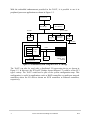
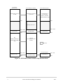
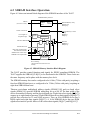
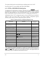
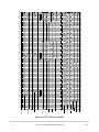
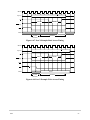
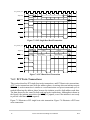
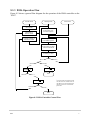
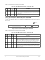
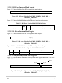
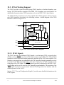
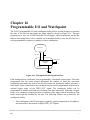
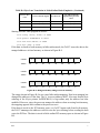
1
® Tsi107™ User Manual 80C2000_MA001_05 November 2009 6024 Silver Creek Valley Road, San Jose, California 95138 Telephone: (800) 345-7015 • (408) 284-8200 • FAX: (408) 284-2775 Printed in U.S.A. ©2009 Integrated Device Technology, Inc. GENERAL DISCLAIMER Integrated Device Technology, Inc. reserves the right to make changes to its products or specifications at any time, without notice, in order to improve design or performance and to supply the best possible product. IDT does not assume any responsibility for use of any circuitry described other than the circuitry embodied in an IDT product. The Company makes no representations that circuitry described herein is free from patent infringement or other rights of third parties which may result from its use. No license is granted by implication or otherwise under any patent, patent rights or other rights, of Integrated Device Technology, Inc. CODE DISCLAIMER Code examples provided by IDT are for illustrative purposes only and should not be relied upon for developing applications. Any use of the code examples below is completely at your own risk. IDT MAKES NO REPRESENTATIONS OR WARRANTIES OF ANY KIND CONCERNING THE NONINFRINGEMENT, QUALITY, SAFETY OR SUITABILITY OF THE CODE, EITHER EXPRESS OR IMPLIED, INCLUDING WITHOUT LIMITATION ANY IMPLIED WARRANTIES OF MERCHANTABILITY, FITNESS FOR A PARTICULAR PURPOSE, OR NON-INFRINGEMENT. FURTHER, IDT MAKES NO REPRESENTATIONS OR WARRANTIES AS TO THE TRUTH, ACCURACY OR COMPLETENESS OF ANY STATEMENTS, INFORMATION OR MATERIALS CONCERNING CODE EXAMPLES CONTAINED IN ANY IDT PUBLICATION OR PUBLIC DISCLOSURE OR THAT IS CONTAINED ON ANY IDT INTERNET SITE. IN NO EVENT WILL IDT BE LIABLE FOR ANY DIRECT, CONSEQUENTIAL, INCIDENTAL, INDIRECT, PUNITIVE OR SPECIAL DAMAGES, HOWEVER THEY MAY ARISE, AND EVEN IF IDT HAS BEEN PREVIOUSLY ADVISED ABOUT THE POSSIBILITY OF SUCH DAMAGES. The code examples also may be subject to United States export control laws and may be subject to the export or import laws of other countries and it is your responsibility to comply with any applicable laws or regulations. LIFE SUPPORT POLICY Integrated Device Technology's products are not authorized for use as critical components in life support devices or systems unless a specific written agreement pertaining to such intended use is executed between the manufacturer and an officer of IDT. 1. Life support devices or systems are devices or systems which (a) are intended for surgical implant into the body or (b) support or sustain life and whose failure to perform, when properly used in accordance with instructions for use provided in the labeling, can be reasonably expected to result in a significant injury to the user. 2. A critical component is any components of a life support device or system whose failure to perform can be reasonably expected to cause the failure of the life support device or system, or to affect its safety or effectiveness. IDT, the IDT logo, and Integrated Device Technology are trademarks or registered trademarks of Integrated Device Technology, Inc. CONTENTS Paragraph Number Title Page Number About This Book Audience ......................................................................................................... xxxvii Organization................................................................................................... xxxviii Suggested Reading........................................................................................... xxxix Conventions .......................................................................................................... xli Acronyms and Abbreviations .............................................................................. xlii Revision History ................................................................................................. xliii Chapter 1 Overview 1.1 1.2 1.3 1.3.1 1.3.2 1.3.3 1.3.3.1 1.3.3.2 1.3.3.3 1.3.3.4 1.3.4 1.3.5 1.3.5.1 1.3.5.2 1.3.5.3 1.3.5.4 1.3.6 1.3.7 1.3.8 1.4 1.5 1.6 1.6.1 IDT Tsi107 PowerPC Host Bridge Features .............................................................. 1-1 Tsi107 PowerPC Host Bridge Applications ...................................................... 1-3 Tsi107 Major Functional Blocks ........................................................................ 1-6 60x Processor Interface................................................................................... 1-7 Memory System Interface............................................................................... 1-8 Peripheral Component Interconnect (PCI) Interface ...................................... 1-8 PCI Bus Arbitration Unit ............................................................................ 1-9 Address Maps and Translation ................................................................... 1-9 Byte Ordering ............................................................................................. 1-9 PCI Agent Capability................................................................................ 1-10 DMA Controller............................................................................................ 1-10 Message Unit (MU) ...................................................................................... 1-10 Doorbell Registers .................................................................................... 1-10 Extended Doorbell Register Facility ........................................................ 1-11 Inbound and Outbound Message Registers .............................................. 1-11 Intelligent Input/Output Controller (I2O) ................................................. 1-11 Inter-Integrated Circuit (I2C) Controller ...................................................... 1-11 Embedded Programmable Interrupt Controller (EPIC) ................................ 1-12 Integrated PCI Bus, CPU, and SDRAM Clock Generation.......................... 1-12 Power Management .......................................................................................... 1-13 Programmable I/O Signals with Watchpoint .................................................... 1-14 Debug Features ................................................................................................. 1-14 Error Injection/Capture on Data Path ........................................................... 1-14 iii CONTENTS Paragraph Number 1.6.2 Page Number IEEE 1149.1 (JTAG)/Test Interface ............................................................. 1-14 Title Chapter 2 Signal Descriptions and Clocking 2.1 2.1.1 2.1.2 2.2 2.2.1 2.2.1.1 2.2.1.2 2.2.1.3 2.2.1.3.1 2.2.1.3.2 2.2.1.4 2.2.1.4.1 2.2.1.4.2 2.2.1.5 2.2.1.5.1 2.2.1.5.2 2.2.1.6 2.2.1.6.1 2.2.1.6.2 2.2.1.7 2.2.1.7.1 2.2.1.7.2 2.2.1.8 2.2.1.9 2.2.1.10 2.2.1.11 2.2.1.12 2.2.1.12.1 2.2.1.12.2 2.2.1.13 2.2.1.14 2.2.1.14.1 2.2.1.14.2 2.2.1.15 2.2.1.15.1 2.2.1.15.2 2.2.1.16 iv Signal Overview ................................................................................................. 2-2 Signal Cross Reference................................................................................... 2-4 Output Signal States during Reset .................................................................. 2-6 Detailed Signal Descriptions .............................................................................. 2-8 60x Processor Interface Signals...................................................................... 2-8 Bus Request 0–1 (BR[0:1])—Input ............................................................ 2-8 Bus Grant 0–1 (BG[0:1])—Output............................................................. 2-8 Address Bus (A[0:31])................................................................................ 2-9 Address Bus (A[0:31])—Output ............................................................ 2-9 Address Bus (A[0:31])—Input ............................................................... 2-9 Transfer Start (TS)...................................................................................... 2-9 Transfer Start (TS)—Output................................................................... 2-9 Transfer Start (TS)—Input ................................................................... 2-10 Transfer Type (TT[0:4]) ........................................................................... 2-10 Transfer Type (TT[0:4])—Output ........................................................ 2-10 Transfer Type (TT[0:4])—Input........................................................... 2-11 Transfer Size (TSIZ[0:2]) ......................................................................... 2-11 Transfer Size (TSIZ[0:2])—Output...................................................... 2-11 Transfer Size (TSIZ[0:2])—Input ........................................................ 2-11 Transfer Burst (TBST).............................................................................. 2-11 Transfer Burst (TBST)—Output .......................................................... 2-11 Transfer Burst (TBST)—Input ............................................................. 2-12 Write-Through (WT)—Input/Output........................................................ 2-12 Caching-Inhibited (CI)—Input/Output..................................................... 2-12 Global (GBL)—Input/Output ................................................................... 2-12 Address Acknowledge (AACK)—Output................................................ 2-13 Address Retry (ARTRY)........................................................................... 2-13 Address Retry (ARTRY)—Output ....................................................... 2-13 Address Retry (ARTRY)—Input .......................................................... 2-14 Data Bus Grant 0–1 (DBG[0:1])—Output ............................................... 2-14 Data Bus (DH[0:31], DL[0:31]) ............................................................... 2-15 Data Bus (DH[0:31], DL[0:31])—Output ............................................ 2-15 Data Bus (DH[0:31], DL[0:31])—Input............................................... 2-16 Data Parity (DP[0:7])................................................................................ 2-16 Data Parity (DP[0:7])—Output ............................................................ 2-16 Data Parity (DP[0:7])—Input ............................................................... 2-16 Transfer Acknowledge (TA)..................................................................... 2-17 Tsi107 PowerPC Host Bridge User Manual IDT CONTENTS Paragraph Number 2.2.1.16.1 2.2.1.16.2 2.2.1.17 2.2.1.18 2.2.2 2.2.2.1 2.2.2.1.1 2.2.2.1.2 2.2.2.2 2.2.2.2.1 2.2.2.2.2 2.2.2.3 2.2.2.3.1 2.2.2.3.2 2.2.2.4 2.2.2.4.1 2.2.2.4.2 2.2.2.5 2.2.2.5.1 2.2.2.5.2 2.2.2.6 2.2.2.6.1 2.2.2.6.2 2.2.2.7 2.2.2.7.1 2.2.2.7.2 2.2.2.8 2.2.2.8.1 2.2.2.8.2 2.2.2.9 2.2.2.10 2.2.2.10.1 2.2.2.10.2 2.2.2.11 2.2.2.11.1 2.2.2.11.2 2.2.2.12 2.2.2.12.1 2.2.2.12.2 2.2.2.13 2.2.2.13.1 2.2.2.13.2 2.2.2.14 IDT Title Page Number Transfer Acknowledge (TA)—Output.................................................. Transfer Acknowledge (TA)—Input .................................................... Local Bus Slave Claim (LBCLAIM)—Input ........................................... Data Bus Grant Local Bus Slave (DBGLB)—Output.............................. PCI Interface Signals .................................................................................... PCI Bus Request (REQ[4:0])—Input ....................................................... PCI Bus Request (REQ[4:0])—Internal Arbiter Enabled .................... PCI Bus Request (REQ[4:0])—Internal Arbiter Disabled ................... PCI Bus Grant (GNT[4:0])—Output ........................................................ PCI Bus Grant (GNT[4:0])—Internal Arbiter Enabled........................ PCI Bus Grant (GNT[4:0])—Internal Arbiter Disabled....................... PCI Address/Data Bus (AD[31:0])........................................................... Address/Data (AD[31:0])—Output ...................................................... Address/Data (AD[31:0])—Input......................................................... Parity (PAR) ............................................................................................. Parity (PAR)—Output .......................................................................... Parity (PAR)—Input............................................................................. Command/Byte Enable (C/BE[3:0])......................................................... Command/Byte Enable (C/BE[3:0])—Output ..................................... Command/Byte Enable (C/BE[3:0])—Input ........................................ Device Select (DEVSEL) ......................................................................... Device Select (DEVSEL)—Output ...................................................... Device Select (DEVSEL)—Input......................................................... Frame (FRAME)....................................................................................... Frame (FRAME)—Output ................................................................... Frame (FRAME)—Input ...................................................................... Initiator Ready (IRDY)............................................................................. Initiator Ready (IRDY)—Output.......................................................... Initiator Ready (IRDY)—Input ............................................................ Lock (LOCK)—Input ............................................................................... Target Ready (TRDY) .............................................................................. Target Ready (TRDY)—Output ........................................................... Target Ready (TRDY)—Input.............................................................. Parity Error (PERR).................................................................................. Parity Error (PERR)—Output .............................................................. Parity Error (PERR)—Input ................................................................. System Error (SERR) ............................................................................... System Error (SERR)—Output ............................................................ System Error (SERR)—Input............................................................... Stop (STOP).............................................................................................. Stop (STOP)—Output .......................................................................... Stop (STOP)—Input ............................................................................. Interrupt Request (INTA)—Output .......................................................... 2-17 2-17 2-18 2-18 2-18 2-18 2-19 2-19 2-19 2-19 2-20 2-20 2-20 2-20 2-21 2-21 2-21 2-21 2-21 2-22 2-22 2-22 2-23 2-23 2-23 2-23 2-23 2-23 2-24 2-24 2-24 2-24 2-25 2-25 2-25 2-25 2-25 2-26 2-26 2-26 2-26 2-26 2-26 v CONTENTS Paragraph Number 2.2.2.15 2.2.3 2.2.3.1 2.2.3.2 2.2.3.3 2.2.3.4 2.2.3.5 2.2.3.6 2.2.3.7 2.2.3.8 2.2.3.8.1 2.2.3.8.2 2.2.3.9 2.2.3.9.1 2.2.3.9.2 2.2.3.10 2.2.3.11 2.2.3.12 2.2.3.13 2.2.3.14 2.2.3.15 2.2.3.16 2.2.4 2.2.4.1 2.2.4.2 2.2.4.2.1 2.2.4.2.2 2.2.4.2.3 2.2.4.2.4 2.2.4.3 2.2.4.4 2.2.5 2.2.5.1 2.2.5.1.1 2.2.5.1.2 2.2.5.2 2.2.5.2.1 2.2.5.2.2 2.2.6 2.2.6.1 2.2.6.1.1 2.2.6.1.2 2.2.6.2 vi Page Number ID Select (IDSEL)—Input........................................................................ 2-27 Memory Interface Signals............................................................................. 2-27 Row Address Strobe (RAS[0:7])—Output............................................... 2-27 Column Address Strobe (CAS[0:7])—Output.......................................... 2-28 SDRAM Command Select (CS[0:7])—Output ........................................ 2-28 SDRAM Data Input/Output Mask (DQM[0:7])—Output ........................ 2-28 Write Enable (WE)—Output .................................................................... 2-29 SDRAM Address (SDMA[13:0])—Output.............................................. 2-29 SDRAM Internal Bank Select 0–1 (SDBA0, SDBA1)—Output ............. 2-29 Memory Data Bus (MDH[0:31], MDL[0:31]) ......................................... 2-30 Memory Data Bus (MDH[0:31], MDL[0:31])—Output ...................... 2-31 Memory Data Bus (MDH[0:31], MDL[0:31])—Input......................... 2-31 Data Parity/ECC (PAR[0:7]) .................................................................... 2-31 Data Parity (PAR[0:7])—Output.......................................................... 2-31 Data Parity (PAR[0:7])—Input ............................................................ 2-32 ROM Address 19:12 (AR[19:12])—Output............................................. 2-32 SDRAM Clock Enable (CKE)—Output................................................... 2-32 SDRAM Row Address Strobe (SDRAS)—Output .................................. 2-32 SDRAM Column Address Strobe (SDCAS)—Output ............................. 2-33 ROM Bank Selects (RCS[0:3])—Output ................................................. 2-33 Flash Output Enable (FOE)—Output ....................................................... 2-33 Address Strobe (AS)—Output.................................................................. 2-35 EPIC Control Signals.................................................................................... 2-35 Discrete Interrupt 0:4 (IRQ[0:4])—Input ................................................. 2-35 Serial Interrupt Mode Signals................................................................... 2-35 Serial Interrupt Stream (S_INT)—Input............................................... 2-36 Serial Interrupt Clock (S_CLK)—Output ............................................ 2-36 Serial Interrupt Reset (S_RST)—Output.............................................. 2-36 Serial Interrupt Frame (S_FRAME)—Output...................................... 2-36 Local Interrupt (L_INT)—Output ............................................................ 2-36 60x Interface Interrupt (INT)—Output..................................................... 2-36 I2C Interface Control Signals........................................................................ 2-37 Serial Data (SDA)..................................................................................... 2-37 Serial Data (SDA)—Output.................................................................. 2-37 Serial Data (SDA)—Input .................................................................... 2-37 Serial Clock (SCL) ................................................................................... 2-37 Serial Clock (SCL)—Output ................................................................ 2-37 Serial Clock (SCL)—Input................................................................... 2-37 System Control and Power Management Signals......................................... 2-37 Hard Reset ................................................................................................ 2-38 Hard Reset—Tsi107 (HRESET)—Input .............................................. 2-38 Hard Reset—Processor (HRESET_CPU)—Output ............................. 2-38 Soft Reset (SRESET)—Output................................................................. 2-39 Title Tsi107 PowerPC Host Bridge User Manual IDT CONTENTS Paragraph Number 2.2.6.3 2.2.6.4 2.2.6.5 2.2.6.6 2.2.6.7 2.2.6.8 2.2.6.8.1 2.2.6.8.2 2.2.7 2.2.7.1 2.2.7.2 2.2.7.3 2.2.7.4 2.2.7.5 2.2.7.6 2.2.8 2.2.8.1 2.2.8.2 2.2.8.3 2.2.8.4 2.2.8.5 2.2.8.6 2.2.8.7 2.2.8.8 2.2.8.9 2.3 2.3.1 2.3.2 2.3.3 2.3.4 2.4 Title Page Number Machine Check (MCP)—Output.............................................................. Transfer Error Acknowledge (TEA)—Output.......................................... Nonmaskable Interrupt (NMI)—Input ..................................................... Quiesce Request (QREQ)—Input............................................................. Quiesce Acknowledge (QACK)—Output ................................................ Watchpoint Trigger Signals...................................................................... Watchpoint Trigger In (TRIG_IN)—Input........................................... Watchpoint Trigger Out (TRIG_OUT)—Output ................................. Test and Configuration Signals..................................................................... PLL Configuration (PLL_CFG[0:3])—Input ........................................... JTAG Test Clock (TCK)—Input .............................................................. JTAG Test Data Input (TDI)—Input........................................................ JTAG Test Data Output (TDO)—Output ................................................. JTAG Test Mode Select (TMS)—Input ................................................... JTAG Test Reset (TRST)—Input............................................................. Clock Signals ................................................................................................ System Clock Input (OSC_IN)—Input .................................................... PCI Clock (PCI_CLK[0:4])—Output....................................................... PCI Clock Synchronize Out (PCI_SYNC_OUT)—Output...................... PCI Feedback Clock (PCI_SYNC_IN)—Input ........................................ SDRAM Clock Outputs (SDRAM_CLK[0:3])—Output ......................... SDRAM Clock Synchronize Out (SDRAM_SYNC_OUT)—Output...... SDRAM Feedback Clock (SDRAM_SYNC_IN)—Input ........................ CPU Clock 0–2 (CPU_CLK[0:2])—Output............................................. Debug Clock (CKO)—Output.................................................................. Clocking ........................................................................................................... Clocking Method .......................................................................................... DLL Operation and Locking......................................................................... Clock Synchronization.................................................................................. Clocking System Solution Examples............................................................ Configuration Signals Sampled at Reset .......................................................... 2-39 2-40 2-40 2-40 2-41 2-41 2-41 2-41 2-42 2-42 2-42 2-42 2-43 2-43 2-43 2-43 2-43 2-44 2-44 2-44 2-44 2-44 2-44 2-45 2-45 2-45 2-45 2-47 2-47 2-48 2-50 Chapter 3 Address Maps 3.1 3.2 3.2.1 3.2.2 3.3 3.3.1 3.3.2 IDT Address Map B ................................................................................................... 3-2 Address Map B Options...................................................................................... 3-8 Processor Compatibility Hole and Alias Space .............................................. 3-9 PCI Compatibility Hole and Alias Space ..................................................... 3-10 Address Translation .......................................................................................... 3-11 Inbound PCI Address Translation................................................................. 3-12 Outbound PCI Address Translation.............................................................. 3-14 vii CONTENTS Paragraph Number 3.3.3 3.3.3.1 3.3.3.2 3.3.3.3 3.3.3.4 3.4 3.4.1 3.4.2 Page Number Address Translation Registers ...................................................................... 3-15 Local Memory Base Address Register (LMBAR) ................................... 3-16 Inbound Translation Window Register (ITWR)....................................... 3-16 Outbound Memory Base Address Register (OMBAR) ............................ 3-17 Outbound Translation Window Register (OTWR)................................... 3-18 Embedded Utilities Memory Block (EUMB) ................................................... 3-19 Local Processor Core Control and Status Registers ..................................... 3-20 Peripheral Control and Status Registers ....................................................... 3-21 Title Chapter 4 Configuration Registers 4.1 4.1.1 4.1.2 4.1.3 4.1.3.1 4.1.3.2 4.2 4.2.1 4.2.2 4.2.3 4.2.4 4.2.5 4.2.6 4.2.7 4.2.8 4.2.9 4.3 4.3.1 4.3.2 4.4 4.4.1 4.4.2 4.4.3 4.5 4.6 4.6.1 4.6.1.1 4.6.1.2 4.6.1.3 viii Configuration Register Access ........................................................................... 4-1 Configuration Register Access in Little-Endian Mode................................... 4-2 Configuration Register Access in Big-Endian Mode ..................................... 4-4 Configuration Register Summary ................................................................... 4-5 Processor-Accessible Configuration Registers........................................... 4-5 PCI-Accessible Configuration Registers .................................................... 4-9 PCI Interface Configuration Registers.............................................................. 4-10 PCI Command Register—Offset 0x04 ......................................................... 4-12 PCI Status Register—Offset 0x06 ................................................................ 4-13 Standard Programming Interface—Offset 0x09 ........................................... 4-14 PCI Base Class Code—Offset 0x0B............................................................. 4-15 PCI Cache Line Size—Offset 0x0C ............................................................. 4-15 PCI Latency Timer—Offset 0x0D................................................................ 4-15 PCI Base Address Registers—LMBAR and PCSRBAR ............................. 4-15 PCI Interrupt Line—Offset 0x3C ................................................................. 4-16 PCI Arbiter Control Register (PACR)—Offset 0x46 ................................... 4-17 Peripheral Logic Power Management Configuration Registers (PMCRs) ....... 4-18 Power Management Configuration Register 1 (PMCR1)—Offset 0x70...... 4-18 Power Management Configuration Register 2 (PMCR2)—Offset 0x72...... 4-20 Output/Clock Driver and Miscellaneous I/O Control Registers ....................... 4-21 Output Driver Control Register—0x73 ........................................................ 4-21 CLK Driver Control Register—0x74 ........................................................... 4-23 Miscellaneous I/O Control Register—0x76 ................................................. 4-25 Embedded Utilities Memory Block Base Address Register—0x78 ................. 4-26 Memory Interface Configuration Registers ...................................................... 4-26 Memory Boundary Registers ........................................................................ 4-26 Memory Starting Address Register 1 and 2—0x80 and 0x84.................. 4-26 Extended Memory Starting Address Register 1 and 2 —0x88 and 0x8C 4-27 Memory Ending Address Register 1 and 2—0x90 and 0x94 ................... 4-28 Tsi107 PowerPC Host Bridge User Manual IDT CONTENTS Paragraph Number 4.6.1.4 4.6.2 4.6.3 4.7 4.7.1 4.7.2 4.8 4.8.1 4.8.1.1 4.8.1.2 4.8.2 4.8.2.1 4.8.2.2 4.8.2.3 4.8.2.4 4.8.2.5 4.9 4.10 4.10.1 4.10.2 4.10.3 4.10.4 Title Page Number Extended Memory Ending Address Register 1 and 2 —0x98 and 0x9C 4-29 Memory Bank Enable Register—0xA0........................................................ Memory Page Mode Register—0xA3 .......................................................... Processor Interface Configuration Registers .................................................... Processor Interface Configuration Register 1—0xA8 .................................. Processor Interface Configuration Register 2—0xAC ................................. Error Handling Registers .................................................................................. ECC Single-Bit Error Registers.................................................................... ECC Single-Bit Error Counter Register—0xB8....................................... ECC Single-Bit Error Trigger Register—0xB9........................................ Error Enabling and Detection Registers ....................................................... Error Enabling Registers 1 and 2—0xC0 and 0xC4................................. Error Detection Registers 1 and 2—0xC1 and 0xC5................................ Processor Bus Error Status Register—0xC3 ........................................... PCI Bus Error Status Register—0xC7 ..................................................... Processor/PCI Error Address Register—0xC8 ........................................ Address Map B Options Register—0xE0 ......................................................... Memory Control Configuration Registers ........................................................ Memory Control Configuration Register 1—0xF0 ...................................... Memory Control Configuration Register 2—0xF4 ...................................... Memory Control Configuration Register 3—0xF8 ...................................... Memory Control Configuration Register 4—0xFC...................................... 4-30 4-31 4-32 4-32 4-35 4-37 4-37 4-37 4-38 4-39 4-39 4-42 4-44 4-45 4-45 4-46 4-47 4-48 4-51 4-55 4-58 Chapter 5 Processor Bus Interface 5.1 5.1.1 5.1.2 5.1.3 5.2 5.2.1 5.2.2 5.3 5.3.1 5.3.2 5.3.3 5.3.3.1 5.3.3.1.1 5.3.3.1.2 5.3.3.2 IDT Tsi107 Processor Bus Configurations................................................................. 5-1 Single-Processor System Configuration ......................................................... 5-1 Dual-Processor System Configuration............................................................ 5-2 Processor Bus Interface Configuration Registers ........................................... 5-3 Processor Bus Protocol Overview ...................................................................... 5-4 Tsi107 Arbitration........................................................................................... 5-5 Address Pipelining and Split-Bus Transactions.............................................. 5-6 Address Tenure Operations ................................................................................ 5-6 Address Arbitration Overview........................................................................ 5-7 Address Tenure Protocol ................................................................................ 5-7 Address Transfer Attribute Signals................................................................. 5-9 Transfer Type Signal Encodings ................................................................ 5-9 Tsi107 Responses to Processor Transactions ......................................... 5-9 PCI-to-Memory Snoop Transactions on 60x Bus................................. 5-11 TBST and TSIZ[0:2] Signals and Size of Transfer .................................. 5-11 ix CONTENTS Paragraph Number 5.3.3.3 5.3.3.4 5.3.3.5 5.3.4 5.3.4.1 5.3.4.2 5.3.4.2.1 5.3.4.2.2 5.4 5.4.1 5.4.2 5.4.3 5.4.4 5.4.5 5.5 5.6 5.6.1 5.6.2 5.6.3 Page Number Burst Ordering During Data Transfers ..................................................... 5-12 Effect of Alignment on Data Transfers—64-bit Data Bus ....................... 5-13 Effect of Alignment on Data Transfers—32-Bit Data Bus ...................... 5-15 Address Transfer Termination ...................................................................... 5-17 Tsi107 Snoop Response............................................................................ 5-18 Address Tenure Timing Configuration..................................................... 5-19 AACK Signal Timing........................................................................... 5-19 ARTRY Signal Timing......................................................................... 5-20 Data Tenure Operations .................................................................................... 5-20 Data Bus Arbitration..................................................................................... 5-20 Data Bus Transfers and Normal Termination............................................... 5-20 Data Tenure Timing Configurations............................................................. 5-21 Data Bus Termination by TEA Signal.......................................................... 5-21 60x Data Bus Parity ...................................................................................... 5-23 Dual-Processor Support .................................................................................... 5-23 60x Local Bus Slave Support............................................................................ 5-24 60x Local Bus Slave Address Map............................................................... 5-24 60x Local Bus Slave Timing ........................................................................ 5-25 Tsi107—60x Interface State Diagram .......................................................... 5-26 Title Chapter 6 Memory Interface 6.1 6.2 6.2.1 6.2.2 6.2.3 6.2.4 6.2.5 6.2.6 6.2.7 6.2.7.1 6.2.8 6.2.8.1 6.2.9 6.2.9.1 6.2.10 6.2.11 6.2.12 6.2.12.1 6.2.12.2 x Memory Interface Signal Summary.................................................................... 6-3 SDRAM Interface Operation .............................................................................. 6-6 Supported SDRAM Organizations ................................................................. 6-9 SDRAM Address Multiplexing .................................................................... 6-11 SDRAM Memory Data Interface.................................................................. 6-14 SDRAM Power-On Initialization ................................................................. 6-17 Tsi107 Interface Functionality for JEDEC SDRAMs .................................. 6-18 SDRAM Burst and Single-Beat Transactions .............................................. 6-19 SDRAM Page Mode ..................................................................................... 6-20 SDRAM Paging in Sleep Mode................................................................ 6-22 SDRAM Interface Timing ............................................................................ 6-22 SDRAM Mode-Set Command Timing..................................................... 6-27 SDRAM Parity and RMW Parity ................................................................. 6-27 RMW Parity Latency Considerations....................................................... 6-28 SDRAM In-Line ECC .................................................................................. 6-28 SDRAM Registered DIMM Mode ............................................................... 6-30 SDRAM Refresh........................................................................................... 6-32 SDRAM Refresh Timing.......................................................................... 6-35 SDRAM Refresh and Power Saving Modes............................................. 6-35 Tsi107 PowerPC Host Bridge User Manual IDT CONTENTS Paragraph Number 6.2.13 6.2.14 6.3 6.3.1 6.3.2 6.3.2.1 6.3.2.2 6.3.2.3 6.3.3 6.3.4 6.3.5 6.3.6 6.3.7 6.3.8 6.3.8.1 6.3.9 6.3.9.1 6.3.10 6.3.10.1 6.3.11 6.3.11.1 6.3.11.2 6.3.12 6.4 6.4.1 6.4.2 6.4.3 6.4.4 6.4.5 6.4.6 6.4.7 Title Page Number Processor-to-SDRAM Transaction Examples .............................................. PCI-to-SDRAM Transaction Examples........................................................ FPM or EDO DRAM Interface Operation........................................................ Supported FPM or EDO DRAM Organizations ........................................... FPM or EDO DRAM Address Multiplexing................................................ Row Bit Multiplexing During The Row Phase (RAS) ............................. Column Bit Multiplexing During the Column Phase (CAS).................... Graphical View of the Row and Column Bit Multiplexing...................... FPM or EDO Memory Data Interface .......................................................... FPM or EDO DRAM Initialization .............................................................. FPM or EDO DRAM Interface Timing........................................................ DMA Burst Wrap.......................................................................................... FPM or EDO DRAM Page Mode Retention ................................................ FPM or EDO DRAM Parity and RMW Parity ............................................. RMW Parity Latency Considerations....................................................... FPM or EDO ECC ........................................................................................ FPM or EDO DRAM Interface Timing with ECC................................... FPM or EDO DRAM Refresh ...................................................................... FPM or EDO Refresh Timing................................................................... FPM or EDO DRAM Power Saving Modes................................................. Configuration Parameters for DRAM Power Saving Modes ................... DRAM Self-Refresh in Sleep Mode......................................................... PCI-to-DRAM Transaction Examples.......................................................... ROM/Flash Interface Operation ....................................................................... ROM/Flash Address Multiplexing ............................................................... 64 or 32-Bit ROM/Flash Interface Timing ................................................... 8-Bit ROM/Flash Interface Timing .............................................................. ROM/Flash Interface Write Operations........................................................ ROM/Flash Interface Write Timing ............................................................. PCI-to-ROM/Port X Transaction Example................................................... Port X Interface............................................................................................. 6-38 6-44 6-48 6-50 6-52 6-52 6-53 6-54 6-56 6-57 6-58 6-63 6-63 6-63 6-64 6-64 6-66 6-68 6-68 6-69 6-69 6-70 6-71 6-75 6-80 6-82 6-85 6-87 6-88 6-88 6-93 Chapter 7 PCI Bus Interface 7.1 7.1.1 7.1.2 7.1.3 7.2 7.2.1 7.2.1.1 IDT PCI Interface Overview ...................................................................................... The Tsi107 as a PCI Initiator.......................................................................... The Tsi107 as a PCI Target ............................................................................ PCI Signal Output Hold Timing ..................................................................... PCI Bus Arbitration ............................................................................................ Internal Arbitration for PCI Bus Access......................................................... Processor-Initiated Transactions to PCI Bus .............................................. 7-1 7-2 7-3 7-3 7-4 7-4 7-5 xi CONTENTS Paragraph Number 7.2.1.2 7.2.2 7.2.3 7.2.4 7.2.5 7.3 7.3.1 7.3.2 7.3.3 7.3.3.1 7.3.3.2 7.3.3.3 7.3.4 7.3.5 7.3.6 7.4 7.4.1 7.4.2 7.4.3 7.4.3.1 7.4.3.2 7.4.4 7.4.5 7.4.5.1 7.4.5.2 7.4.5.2.1 7.4.5.2.2 7.4.6 7.4.6.1 7.4.6.2 7.5 7.5.1 7.5.2 7.5.3 7.5.4 7.5.5 7.6 7.6.1 7.6.2 7.7 7.7.1 7.7.2 7.7.3 xii Page Number DMA-Initiated Transactions to the PCI Bus .............................................. 7-6 PCI Bus Arbiter Operation ............................................................................. 7-7 PCI Bus Parking ............................................................................................. 7-8 Power-Saving Modes and the PCI Arbiter ..................................................... 7-9 Broken Master Lock-Out ................................................................................ 7-9 Tsi107 PCI Bus Protocol .................................................................................... 7-9 Basic Transfer Control.................................................................................... 7-9 PCI Bus Commands...................................................................................... 7-10 Addressing .................................................................................................... 7-12 Memory Space Addressing....................................................................... 7-12 I/O Space Addressing ............................................................................... 7-13 Configuration Space Addressing .............................................................. 7-13 Device Selection ........................................................................................... 7-13 Byte Alignment............................................................................................. 7-14 Bus Driving and Turnaround ........................................................................ 7-14 PCI Bus Transactions........................................................................................ 7-14 PCI Read Transactions.................................................................................. 7-15 PCI Write Transactions................................................................................. 7-16 Transaction Termination............................................................................... 7-17 Master-Initiated Termination.................................................................... 7-17 Target-Initiated Termination .................................................................... 7-18 Fast Back-to-Back Transactions ................................................................... 7-22 Configuration Cycles .................................................................................... 7-22 The PCI Configuration Space Header ...................................................... 7-22 Accessing the PCI Configuration Space................................................... 7-24 Type 0 Configuration Translation ........................................................ 7-26 Type 1 Configuration Translation ........................................................ 7-28 Other Bus Transactions................................................................................. 7-28 Interrupt-Acknowledge Transactions ....................................................... 7-28 Special-Cycle Transactions ...................................................................... 7-29 Exclusive Access .............................................................................................. 7-30 Starting an Exclusive Access........................................................................ 7-30 Continuing an Exclusive Access................................................................... 7-30 Completing an Exclusive Access.................................................................. 7-31 Attempting to Access a Locked Target......................................................... 7-31 Exclusive Access and the Tsi107.................................................................. 7-31 PCI Error Functions .......................................................................................... 7-31 PCI Parity...................................................................................................... 7-32 Error Reporting ............................................................................................. 7-33 PCI Host and Agent Modes .............................................................................. 7-33 PCI Initialization Options ............................................................................. 7-33 Accessing the Tsi107 Configuration Space .................................................. 7-34 PCI Configuration Cycle Retry Capability in Agent Mode.......................... 7-35 Title Tsi107 PowerPC Host Bridge User Manual IDT CONTENTS Paragraph Number 7.7.4 7.7.4.1 7.7.4.2 7.7.4.3 Title Page Number PCI Address Translation Support ................................................................. Inbound PCI Address Translation ............................................................ Outbound PCI Address Translation.......................................................... Initialization Code Translation in Agent Mode ........................................ 7-35 7-35 7-35 7-36 Chapter 8 DMA Controller 8.1 8.2 8.3 8.3.1 8.3.2 8.3.2.1 8.3.2.2 8.3.3 8.3.4 8.3.5 8.4 8.4.1 8.4.2 8.4.3 8.4.4 8.5 8.5.1 8.5.2 8.5.2.1 8.5.2.2 8.5.2.3 8.5.2.4 8.5.3 8.5.3.1 8.5.3.2 8.5.3.3 8.5.3.4 8.6 8.6.1 8.6.2 8.7 8.7.1 8.7.2 IDT DMA Overview .................................................................................................. 8-1 DMA Register Summary .................................................................................... 8-2 DMA Operation .................................................................................................. 8-3 DMA Direct Mode.......................................................................................... 8-4 DMA Chaining Mode ..................................................................................... 8-5 Basic Chaining Mode Initialization ............................................................ 8-5 Periodic DMA Feature................................................................................ 8-6 DMA Operation Flow..................................................................................... 8-7 DMA Coherency............................................................................................. 8-8 DMA Performance.......................................................................................... 8-8 DMA Transfer Types.......................................................................................... 8-9 PCI to PCI....................................................................................................... 8-9 PCI to Local Memory ..................................................................................... 8-9 Local Memory to PCI ..................................................................................... 8-9 Local Memory to Local Memory.................................................................... 8-9 Address Map Interactions ................................................................................. 8-10 Attempted Writes to Local ROM/Port X Space ........................................... 8-10 Host Mode Interactions................................................................................. 8-10 PCI Master Abort when PCI Bus Specified for Lower 2-Gbyte Space.... 8-10 Address Alias to Lower 2-Gbyte Space.................................................... 8-11 Attempted Reads from ROM on the PCI Bus—Host Mode..................... 8-11 Attempted Reads from ROM on the Memory Bus................................... 8-11 Agent Mode Interactions .............................................................................. 8-11 Agent Mode DMA Transfers for PCI....................................................... 8-11 Accesses to Outbound Memory Window that Overlaps 0xFE00_00 – 0xFEEF_FFFF 8-11 Attempted Accesses to Local ROM when ROM is on PCI...................... 8-12 Attempted Access to ROM on the PCI Bus—Agent Mode ..................... 8-12 DMA Descriptors for Chaining Mode .............................................................. 8-12 Descriptors in Big-Endian Mode .................................................................. 8-14 Descriptors in Little-Endian Mode ............................................................... 8-14 DMA Register Descriptions.............................................................................. 8-15 DMA Mode Registers (DMRs)..................................................................... 8-15 DMA Status Registers (DSRs) ..................................................................... 8-19 xiii CONTENTS Paragraph Number 8.7.3 8.7.4 8.7.5 8.7.6 8.7.7 8.7.8 Page Number Current Descriptor Address Registers (CDARs) .......................................... 8-20 Source Address Registers (SARs) ................................................................ 8-21 Destination Address Registers (DARs) ........................................................ 8-22 Byte Count Registers (BCRs) ....................................................................... 8-23 DAR and BCR Values—Double PCI Write ................................................. 8-23 Next Descriptor Address Registers (NDARs) .............................................. 8-24 Title Chapter 9 Message Unit (with I2O) 9.1 9.2 9.2.1 9.2.2 9.2.3 9.2.4 9.2.4.1 9.2.4.2 9.2.4.3 9.2.4.4 9.3 9.3.1 9.3.2 9.3.3 9.3.3.1 9.3.3.1.1 9.3.3.1.2 9.3.3.2 9.3.3.2.1 9.3.3.2.2 9.3.4 9.3.4.1 9.3.4.1.1 9.3.4.1.2 9.3.4.1.3 9.3.4.1.4 9.3.4.2 9.3.4.2.1 9.3.4.2.2 9.3.4.2.3 9.3.4.2.4 9.3.4.2.5 xiv Message Unit (MU) Overview ........................................................................... 9-1 Message and Doorbell Register Programming Model........................................ 9-1 Message and Doorbell Register Summary...................................................... 9-2 Message Register Descriptions....................................................................... 9-3 Doorbell Register Descriptions....................................................................... 9-3 Extended Doorbell Register Descriptions....................................................... 9-5 Extended Doorbell Mask Register (EDBMR)............................................ 9-5 Extended Doorbell Status Register (EDBSR) ............................................ 9-6 Extended Doorbell Write 1 Clear Register (EDBW1C)............................. 9-6 Extended Doorbell Write 1 Set Register (EDBW1S)................................. 9-7 I2O Interface ....................................................................................................... 9-8 PCI Configuration Identification .................................................................... 9-8 I2O Register Summary.................................................................................... 9-8 FIFO Descriptions........................................................................................... 9-9 Inbound FIFOs.......................................................................................... 9-10 Inbound Free_List FIFO....................................................................... 9-11 Inbound Post_List FIFO ....................................................................... 9-11 Outbound FIFOs ....................................................................................... 9-11 Outbound Free_List FIFO .................................................................... 9-11 Outbound Post_List FIFO .................................................................... 9-12 I2O Register Descriptions ............................................................................. 9-12 PCI-Accessible I2O Registers................................................................... 9-12 Outbound Message Interrupt Status Register (OMISR)....................... 9-12 Outbound Message Interrupt Mask Register (OMIMR) ...................... 9-14 Inbound FIFO Queue Port Register (IFQPR)....................................... 9-15 Outbound FIFO Queue Port Register (OFQPR)................................... 9-15 Processor-Accessible I2O Registers ......................................................... 9-16 Inbound Message Interrupt Status Register (IMISR) ........................... 9-16 Inbound Message Interrupt Mask Register (IMIMR)........................... 9-18 Inbound Free_FIFO Head Pointer Register (IFHPR)........................... 9-20 Inbound Free_FIFO Tail Pointer Register (IFTPR) ............................. 9-20 Inbound Post_FIFO Head Pointer Register (IPHPR) ........................... 9-21 Tsi107 PowerPC Host Bridge User Manual IDT CONTENTS Paragraph Number 9.3.4.2.6 9.3.4.2.7 9.3.4.2.8 9.3.4.2.9 9.3.4.2.10 9.3.4.2.11 9.3.4.2.12 Title Page Number Inbound Post_FIFO Tail Pointer Register (IPTPR) ............................. Outbound Free_FIFO Head Pointer Register (OFHPR)....................... Outbound Free_FIFO Tail Pointer Register (OFTPR) ......................... Outbound Post_FIFO Head Pointer Register (OPHPR)....................... Outbound Post_FIFO Tail Pointer Register (OPTPR) ......................... Messaging Unit Control Register (MUCR).......................................... Queue Base Address Register (QBAR)................................................ 9-21 9-22 9-23 9-23 9-24 9-24 9-25 Chapter 10 I C Interface 2 10.1 10.1.1 10.1.2 10.1.3 10.1.4 10.2 10.2.1 10.2.2 10.2.3 10.2.4 10.2.5 10.2.6 10.2.7 10.2.8 10.2.9 10.3 10.3.1 10.3.2 10.3.3 10.3.4 10.3.5 10.4 10.4.1 10.4.2 10.4.3 10.4.4 10.4.5 10.4.6 10.4.7 10.4.7.1 10.4.7.2 IDT I2C Interface Overview..................................................................................... 10-1 I2C Unit Features .......................................................................................... 10-1 I2C Interface Signal Summary...................................................................... 10-2 I2C Register Summary .................................................................................. 10-2 I2C Block Diagram ....................................................................................... 10-3 I2C Protocol ...................................................................................................... 10-3 START Condition......................................................................................... 10-4 Slave Address Transmission......................................................................... 10-4 Data Transfer ................................................................................................ 10-5 Repeated START Condition......................................................................... 10-5 STOP Condition............................................................................................ 10-5 Arbitration Procedure ................................................................................... 10-5 Clock Synchronization.................................................................................. 10-6 Handshaking ................................................................................................. 10-7 Clock Stretching ........................................................................................... 10-7 2 I C Register Descriptions ................................................................................. 10-7 I2C Address Register (I2CADR) .................................................................. 10-7 I2C Frequency Divider Register (I2CFDR) .................................................. 10-8 I2C Control Register (I2CCR) .................................................................... 10-10 I2C Status Register (I2CSR) ....................................................................... 10-11 I2C Data Register (I2CDR)......................................................................... 10-13 Programming Guidelines ................................................................................ 10-14 Initialization Sequence................................................................................ 10-14 Generation of START................................................................................. 10-14 Post-Transfer Software Response............................................................... 10-15 Generation of STOP.................................................................................... 10-15 Generation of Repeated START................................................................. 10-16 Generation of SCK when SDA Low........................................................... 10-16 Slave Mode Interrupt Service Routine........................................................ 10-16 Slave Transmitter and Received Acknowledge...................................... 10-17 Loss of Arbitration and Forcing of Slave Mode..................................... 10-17 xv CONTENTS Paragraph Number 10.4.8 Page Number Interrupt Service Routine Flowchart........................................................... 10-17 Title Chapter 11 Embedded Programmable Interrupt Controller (EPIC) Unit 11.1 11.1.1 11.1.2 11.1.3 11.2 11.3 11.3.1 11.3.2 11.3.3 11.3.4 11.3.5 11.3.6 11.3.6.1 11.3.6.2 11.3.6.3 11.3.6.4 11.3.7 11.4 11.5 11.6 11.6.1 11.6.2 11.6.3 11.7 11.8 11.9 11.9.1 11.9.2 11.9.3 11.9.4 11.9.5 11.9.6 11.9.7 11.9.7.1 11.9.7.2 11.9.7.3 11.9.7.4 xvi EPIC Unit Overview ......................................................................................... 11-1 EPIC Features Summary............................................................................... 11-2 EPIC Interface Signal Description................................................................ 11-2 EPIC Block Diagram .................................................................................... 11-3 EPIC Register Summary ................................................................................... 11-4 EPIC Unit Interrupt Protocol ............................................................................ 11-7 Interrupt Source Priority ............................................................................... 11-7 Processor Current Task Priority.................................................................... 11-7 Interrupt Acknowledge ................................................................................. 11-7 Nesting of Interrupts ..................................................................................... 11-8 Spurious Vector Generation.......................................................................... 11-8 Internal Block Diagram Description............................................................. 11-8 Interrupt Pending Register (IPR)—Non-programmable .......................... 11-9 Interrupt Selector (IS) ............................................................................. 11-10 Interrupt Request Register (IRR)............................................................ 11-10 In-Service Register (ISR) ....................................................................... 11-10 Interrupts for Multiple Processors .............................................................. 11-10 EPIC Pass-Through Mode .............................................................................. 11-12 EPIC Direct Interrupt Mode ........................................................................... 11-12 EPIC Serial Interrupt Interface ....................................................................... 11-12 Sampling of Serial Interrupts...................................................................... 11-13 Serial Interrupt Timing Protocol................................................................. 11-13 Edge/Level Sensitivity of Serial Interrupts................................................. 11-14 EPIC Timers ................................................................................................... 11-15 Programming Guidelines ................................................................................ 11-15 Register Definitions ........................................................................................ 11-18 Feature Reporting Register (FRR).............................................................. 11-18 Global Configuration Register (GCR)........................................................ 11-18 EPIC Interrupt Configuration Register (EICR) .......................................... 11-19 EPIC Vendor Identification Register (EVI)................................................ 11-20 Processor Initialization Register (PI).......................................................... 11-21 Spurious Vector Register (SVR)................................................................. 11-21 Global Timer Registers............................................................................... 11-22 Timer Frequency Reporting Register (TFRR)........................................ 11-22 Global Timer Current Count Registers (GTCCRs) ................................ 11-23 Global Timer Base Count Registers (GTBCRs)..................................... 11-23 Global Timer Vector/Priority Registers (GTVPRs) ............................... 11-24 Tsi107 PowerPC Host Bridge User Manual IDT CONTENTS Paragraph Number 11.9.7.5 11.9.8 11.9.8.1 11.9.8.2 11.9.8.3 11.9.8.4 11.9.9 11.9.9.1 11.9.9.2 11.9.10 Title Page Number Global Timer Destination Registers (GTDRs) ....................................... External (Direct and Serial), and Internal Interrupt Registers .................... Direct & Serial Interrupt Vector/Priority Registers (IVPRs, SVPRs).... Direct & Serial Interrupt Destination Registers (IDRs, SDRs) .............. Internal (I2C, DMA, MU) Interrupt Vector/Priority Registers (IIVPRs) 11-28 Internal (I2C, DMA or MU) Interrupt Destination Registers (IIDRs).... Processor-Related Registers ....................................................................... Processor Current Task Priority Register (PCTPR) ............................... Processor Interrupt Acknowledge Register (IACK)............................... Processor End-of-Interrupt Register (EOI)................................................. 11-25 11-26 11-26 11-27 11-28 11-29 11-29 11-30 11-30 Chapter 12 Central Control Unit 12.1 12.1.1 12.1.2 12.1.2.1 12.1.2.2 12.1.3 12.1.3.1 12.1.3.1.1 12.1.3.1.2 12.1.3.2 12.2 12.2.1 12.2.1.1 12.2.1.2 12.2.1.3 12.2.1.4 12.2.2 12.2.3 Internal Buffers ................................................................................................. 12-1 Local Processor /Local Memory Buffers...................................................... 12-2 Processor/PCI Buffers................................................................................... 12-3 Processor-to-PCI-Read Buffer (PRPRB).................................................. 12-4 Processor-to-PCI-Write Buffers (PRPWBs)............................................. 12-5 PCI/Local Memory Buffers .......................................................................... 12-6 PCI to Local Memory Read Buffering ..................................................... 12-7 PCI-to-Local-Memory-Read Buffers (PCMRBs) ................................ 12-7 Speculative PCI Reads from Local Memory........................................ 12-8 PCI-to-Local-Memory-Write Buffers (PCMWBs)................................... 12-8 Internal Arbitration ........................................................................................... 12-9 Arbitration Between PCI and DMA Accesses to Local Memory................. 12-9 DMA Transaction Boundaries for Memory/Memory Transfers ............ 12-10 DMA Transaction Boundaries for Memory to PCI Transfers ................ 12-10 DMA Transaction Boundaries for PCI–Memory Transfers ................... 12-11 PCI and DMA Reads from Slow Memory/Port X.................................. 12-11 Internal Arbitration Priorities...................................................................... 12-11 Guaranteeing Minimum PCI Access Latency to Local Memory ............... 12-13 Chapter 13 Error Handling 13.1 13.1.1 13.1.2 13.2 13.2.1 IDT Overview........................................................................................................... Error Handling Block Diagram..................................................................... Priority of Externally Generated Errors and Exceptions .............................. Exceptions and Error Signals............................................................................ System Reset................................................................................................. 13-1 13-2 13-2 13-3 13-3 xvii CONTENTS Paragraph Number 13.2.2 13.2.2.1 13.2.2.2 13.2.3 13.2.3.1 13.2.3.2 13.2.3.3 13.3 13.3.1 13.3.1.1 13.3.1.2 13.3.1.3 13.3.2 13.3.2.1 13.3.2.2 13.3.2.3 13.3.2.4 13.3.3 13.3.3.1 13.3.3.2 13.3.3.3 13.3.3.4 13.3.3.5 13.3.4 13.4 Page Number Processor Bus Error Signals ........................................................................ 13-3 Machine Check (MCP) ............................................................................. 13-3 Transfer Error Acknowledge (TEA)......................................................... 13-4 PCI Bus Error Signals................................................................................... 13-5 System Error (SERR) ............................................................................... 13-5 Parity Error (PERR).................................................................................. 13-5 Nonmaskable Interrupt (NMI).................................................................. 13-6 Error Reporting ................................................................................................. 13-6 Processor Interface Errors............................................................................. 13-7 Processor Transaction Error ..................................................................... 13-7 Flash Write Error ...................................................................................... 13-7 Processor Write Parity Error..................................................................... 13-8 Memory Interface Errors .............................................................................. 13-8 Memory Read Data Parity Error............................................................... 13-9 Memory ECC Error .................................................................................. 13-9 Memory Select Error .............................................................................. 13-10 Memory Refresh Overflow Error ........................................................... 13-10 PCI Interface Errors .................................................................................... 13-10 PCI Address Parity Error ........................................................................ 13-10 PCI Data Parity Error.............................................................................. 13-11 PCI Master-Abort Transaction Termination........................................... 13-11 Received PCI Target-Abort Error........................................................... 13-12 NMI (Nonmaskable Interrupt)................................................................ 13-12 Message Unit Error Events ......................................................................... 13-12 Exception Latencies ........................................................................................ 13-12 Title Chapter 14 Power Management 14.1 14.2 14.2.1 14.2.2 14.3 14.3.1 14.3.2 14.3.3 14.3.3.1 14.3.3.2 14.3.4 14.3.4.1 14.3.4.2 xviii Overview of Power Modes ............................................................................... Tsi107 Power Mode Transitions....................................................................... QREQ and QACK Interactions with Processor............................................ Processor Bus Request Monitoring............................................................... Power Management Modes .............................................................................. Full Power Mode .......................................................................................... Doze Mode.................................................................................................... Nap Mode ..................................................................................................... PCI Transactions During Nap Mode ........................................................ PLL Operation During Nap Mode............................................................ Sleep Mode ................................................................................................... System Memory Refresh during Sleep Mode........................................... Disabling the PLL during Sleep Mode ..................................................... Tsi107 PowerPC Host Bridge User Manual 14-1 14-2 14-3 14-3 14-4 14-4 14-4 14-4 14-5 14-5 14-5 14-6 14-6 IDT CONTENTS Paragraph Number 14.3.4.3 14.4 Title Page Number SDRAM Paging during Sleep Mode ........................................................ 14-7 Example Code Sequence for Entering Processor and Tsi107 Sleep Modes..... 14-7 Chapter 15 Debug Features 15.1 15.2 15.2.1 15.2.1.1 15.2.1.2 15.2.1.3 15.2.2 15.2.2.1 15.2.2.2 15.2.2.3 15.3 15.3.1 15.3.2 15.3.2.1 15.3.2.2 15.3.2.3 15.3.2.4 15.3.2.5 Debug Register Summary ................................................................................. Memory Data Path Error Injection/Capture...................................................... Memory Data Path Error Injection Mask Registers...................................... DH Error Injection Mask Register............................................................ DL Error Injection Mask Register ............................................................ Parity Error Injection Mask Register........................................................ Memory Data Path Error Capture Monitor Registers................................... DH Error Capture Monitor Register ......................................................... DL Error Capture Monitor Register ......................................................... Parity Error Capture Monitor Register ..................................................... JTAG/Testing Support ...................................................................................... JTAG Signals................................................................................................ JTAG Registers and Scan Chains ................................................................. Bypass Register ........................................................................................ Boundary-Scan Registers.......................................................................... Instruction Register................................................................................... TAP Controller ......................................................................................... Scan Chain Exclusions ............................................................................. 15-1 15-2 15-2 15-3 15-3 15-3 15-4 15-4 15-5 15-5 15-6 15-6 15-7 15-7 15-7 15-7 15-7 15-8 Chapter 16 Programmable I/O and Watchpoint 16.1 16.2 16.2.1 16.2.2 16.2.3 16.2.4 16.3 16.4 Watchpoint Interface Signal Description.......................................................... 16-2 Watchpoint Registers ........................................................................................ 16-3 Watchpoint Register Address Map ............................................................... 16-3 Watchpoint Trigger Registers....................................................................... 16-4 Watchpoint Mask Registers .......................................................................... 16-6 Watchpoint Control Register (WP_CONTROL).......................................... 16-9 State and Block Diagrams............................................................................... 16-13 Watchpoint Trigger Applications ................................................................... 16-14 Appendix A Address Map A A.1 A.2 Address Space for Map A .................................................................................. A-1 Configuration Accesses Using Direct Method .................................................. A-6 IDT xix CONTENTS Paragraph Number Title Page Number Appendix B Bit and Byte Ordering B.1 B.2 B.3 B.4 B.4.1 B.5 Byte Ordering Overview..................................................................................... B-1 Byte-Ordering Mechanisms ................................................................................ B-1 Big-Endian Mode................................................................................................ B-2 Little-Endian Mode............................................................................................. B-5 I/O Addressing in Little-Endian Mode ......................................................... B-15 Setting the Endian Mode of Operation ............................................................. B-15 Appendix C Initialization Example C.1 xx Example PowerPC Assembly Language Routine............................................... C-1 Tsi107 PowerPC Host Bridge User Manual IDT ILLUSTRATIONS Figure Number 1-1 1-2 1-3 1-4 1-5 2-1 2-2 2-3 2-4 2-5 2-6 2-7 3-1 3-2 3-3 3-4 3-5 3-6 3-7 3-8 3-9 3-10 3-11 3-12 3-13 4-1 4-2 4-3 4-4 4-5 4-6 4-7 4-8 4-9 4-10 4-11 IDT Title Page Number System Using Tsi107 as a Host Bridge ........................................................................ 1-3 Embedded System Using the Tsi107 as a Bridge ......................................................... 1-4 Embedded System Using Tsi107 with a Distributed I/O Processor ............................. 1-5 Multiprocessor System Using the Tsi107 and a Local Bus Slave ................................ 1-6 Tsi107 Block Diagram.................................................................................................. 1-7 Tsi107 Signal Groupings .............................................................................................. 2-3 Clock Subsystem Block Diagram ............................................................................... 2-46 Timing Diagram (1X, 1.5X, 2X, 2.5X, and 3X examples)......................................... 2-46 System Clocking with External PLL .......................................................................... 2-48 Clocking Solution—Small Load Requirements ......................................................... 2-49 Clocking Solution—High Clock Fanout Required ..................................................... 2-49 Clocking Solution—High Clock Fanout with External CPU Clocks ......................... 2-50 Processor Address Map B in Host Mode...................................................................... 3-5 PCI Memory Master Address Map B in Host Mode .................................................... 3-6 PCI I/O Master Address Map B.................................................................................... 3-7 Address Map B Processor Options in Host Mode ...................................................... 3-10 Address Map B PCI Options in Host Mode ............................................................... 3-11 Inbound PCI Address Translation............................................................................... 3-13 Outbound PCI Address Translation ............................................................................ 3-14 Local Memory Base Address Register (LMBAR)—0x10 ......................................... 3-16 Inbound Translation Window Register (ITWR) ......................................................... 3-16 Outbound Memory Base Address Register (OMBAR)—0x0_2300 .......................... 3-17 Outbound Translation Window Register (OTWR)—0x0_2308................................. 3-18 Embedded Utilities Memory Block Mapping to Local Memory................................ 3-20 Embedded Utilities Memory Block Mapping to PCI Memory................................... 3-22 Processor Accessible Configuration Space................................................................... 4-8 PCI Accessible Configuration Space .......................................................................... 4-10 PCI Command Register—0x04 .................................................................................. 4-12 PCI Status Register—0x06 ......................................................................................... 4-13 Power Management Configuration Register 1 (PMCR1)—0x70............................... 4-18 Power Management Configuration Register 2 (PMCR2)—0x72............................... 4-20 Output Driver Control Register—0x73 ...................................................................... 4-21 CLK Driver Control Register—0x74 ......................................................................... 4-23 Miscellaneous I/O Control Register—0x76 ............................................................... 4-25 Memory Starting Address Register 1—0x80.............................................................. 4-27 Memory Starting Address Register 2—0x84.............................................................. 4-27 xxiii ILLUSTRATIONS Figure Number 4-12 4-13 4-14 4-15 4-16 4-17 4-18 4-19 4-20 4-21 4-22 4-23 4-24 4-25 4-26 4-27 4-28 4-29 4-30 4-31 4-32 4-33 4-34 4-35 5-1 5-2 5-3 5-4 5-5 5-6 5-7 5-8 5-9 5-10 6-1 6-2 6-3 6-4 6-5 6-6 6-7 6-8 6-9 xxiv Page Number Extended Memory Starting Address Register 1—0x88. ............................................ 4-27 Extended Memory Starting Address Register 2—0x8C............................................. 4-28 Memory Ending Address Register 1—0x90............................................................... 4-28 Memory Ending Address Register 2—0x94............................................................... 4-29 Extended Memory Ending Address Register 1—0x98............................................... 4-29 Extended Memory Ending Address Register 2—0x9C .............................................. 4-29 Memory Bank Enable Register—0xA0 ...................................................................... 4-30 Memory Page Mode Register—0xA3 ........................................................................ 4-31 Processor Interface Configuration Register 1 (PICR1)—0xA8 ................................. 4-32 Processor Interface Configuration Register 2 (PICR2)—0xAC................................. 4-35 ECC Single-Bit Error Counter Register—0xB8 ......................................................... 4-37 ECC Single-Bit Error Trigger Register—0xB9.......................................................... 4-38 Error Enabling Register 1 (ErrEnR1)—0xC0............................................................. 4-39 Error Enabling Register 2 (ErrEnR2)—0xC4............................................................. 4-41 Error Detection Register 1 (ErrDR1)—0xC1 ............................................................. 4-42 Error Detection Register 2 (ErrDR2)—0xC5 ............................................................. 4-43 Processor Bus Error Status Register—0xC3 ............................................................. 4-44 PCI Bus Error Status Register—0xC7........................................................................ 4-45 Processor/PCI Error Address Register—0xC8 ........................................................... 4-45 Address Map B Options Register (AMBOR)—0xE0................................................. 4-46 Memory Control Configuration Register 1 (MCCR1)—0xF0 ................................... 4-48 Memory Control Configuration Register 2 (MCCR2)—0xF4 ................................... 4-51 Memory Control Configuration Register 3 (MCCR3)—0xF8 ................................... 4-55 Memory Control Configuration Register 4 (MCCR4)—0xFC................................... 4-58 Single-Processor Configuration .................................................................................... 5-2 Dual-Processor Configuration ...................................................................................... 5-3 Overlapping Tenures on the 60x Bus for a Single-Beat Transfer................................. 5-5 Address Bus Arbitration with Dual Processors ............................................................ 5-8 Address Pipelining ........................................................................................................ 5-9 Snooped Address Transaction with ARTRY and L1 Cache Copyback ..................... 5-19 Single-Beat and Burst Data Transfers ........................................................................ 5-21 Data Tenure Terminated by Assertion of TEA........................................................... 5-22 Local Bus Slave Transaction ...................................................................................... 5-26 60x Bus State Diagram ............................................................................................... 5-27 Block Diagram for Memory Interface .......................................................................... 6-3 SDRAM Memory Interface Block Diagram................................................................. 6-6 Example 512-MByte SDRAM Configuration With Parity........................................... 6-8 SDRAM Registered Memory Interface ...................................................................... 6-16 SDRAM In-line ECC/Parity Memory Interface ......................................................... 6-16 PGMAX Parameter Setting for SDRAM Interface .................................................... 6-21 SDRAM Single-Beat Read Timing (SDRAM Burst Length = 4) .............................. 6-24 SDRAM Four-Beat Burst Read Timing Configuration—64-Bit Mode ..................... 6-24 SDRAM Eight-Beat Burst Read Timing Configuration—32-Bit Mode .................... 6-25 Title Tsi107 PowerPC Host Bridge User Manual IDT ILLUSTRATIONS Figure Number 6-10 6-11 6-12 6-13 6-14 6-15 6-16 6-17 6-18 6-19 6-20 6-21 6-22 6-23 6-24 6-25 6-26 6-27 6-28 6-29 6-30 6-31 6-32 6-33 6-34 6-35 6-36 6-37 6-38 6-39 6-40 6-41 6-42 6-43 6-44 6-45 6-46 6-47 6-48 6-49 6-50 6-51 6-52 IDT Title Page Number SDRAM Single Beat Write Timing (SDRAM Burst Length = 4).............................. 6-25 SDRAM Four-Beat Burst Write Timing—64-Bit Mode ............................................ 6-26 SDRAM Eight-Beat Burst Write Timing—32-Bit Mode........................................... 6-26 SDRAM Mode Register Set Timing........................................................................... 6-27 Registered SDRAM DIMM Single-Beat Write Timing ............................................. 6-31 Registered SDRAM DIMM Burst-Write Timing ....................................................... 6-32 SDRAM Refresh Period ............................................................................................. 6-32 SDRAM Bank Staggered CBR Refresh Timing......................................................... 6-35 SDRAM Self Refresh Entry ....................................................................................... 6-37 SDRAM Self Refresh Exit.......................................................................................... 6-37 Processor Burst Reads from SDRAM ........................................................................ 6-39 Processor Single-Beat Reads from SDRAM .............................................................. 6-40 Processor Burst Writes to SDRAM ............................................................................ 6-41 Processor Single-Beat Writes to SDRAM .................................................................. 6-42 Processor Single-Beat Reads followed by Writes to SDRAM ................................... 6-43 PCI Reads from SDRAM-Speculative Reads Enabled............................................... 6-45 PCI Reads from SDRAM-Speculative Reads Disabled ............................................. 6-46 PCI Writes to SDRAM ............................................................................................... 6-47 FPM or EDO DRAM Memory Interface Block Diagram .......................................... 6-48 Example 16-Mbyte DRAM System with Parity—64-Bit Mode ................................ 6-49 DRAM Memory Organization.................................................................................... 6-50 DRAM Address Multiplexing SDMA[12:0]—32 Bit Mode ...................................... 6-54 DRAM Address Multiplexing SDMA[12:0]—64 Bit Mode ...................................... 6-55 DRAM Single-Beat Read Timing (No ECC) ............................................................. 6-60 DRAM Four-Beat Burst Read Timing (No ECC)—64-Bit Mode.............................. 6-60 DRAM Eight-Beat Burst Read Timing Configuration—32-Bit Mode ...................... 6-61 DRAM Single-Beat Write Timing (No ECC) ............................................................ 6-61 DRAM Four-Beat Burst Write Timing (No ECC)—64-Bit Mode............................. 6-62 DRAM Eight-beat Burst Write Timing (No ECC)—32 Bit Mode............................. 6-62 FPM DRAM Burst Read with ECC............................................................................ 6-67 EDO DRAM Burst Read Timing with ECC............................................................... 6-67 DRAM Single-Beat Write Timing with RMW or ECC Enabled ............................... 6-68 DRAM Bank Staggered CBR Refresh Timing Configuration ................................... 6-69 DRAM Self-Refresh Timing Configuration ............................................................... 6-70 PCI Reads from DRAM-Speculative Reads Enabled................................................. 6-72 PCI Reads from DRAM-Speculative Reads Disabled................................................ 6-73 PCI Writes to DRAM ................................................................................................. 6-74 ROM Memory Interface Block Diagram.................................................................... 6-75 16-Mbyte ROM System Including Parity Paths to DRAM—64-Bit Mode................ 6-76 8-Mbyte Flash Memory System Including Parity Paths to DRAM—8-Bit Mode ..... 6-77 ROM/Flash Address Multiplexing—8-Bit Mode ....................................................... 6-80 ROM/Flash Address Multiplexing—32-Bit Mode ..................................................... 6-80 ROM/Flash Address Multiplexing—64-Bit Mode ..................................................... 6-81 xxv ILLUSTRATIONS Figure Number 6-53 6-54 6-55 6-56 6-57 6-58 6-59 6-60 6-61 6-62 6-63 6-63 6-63 6-63 6-64 6-65 6-66 6-67 6-68 7-1 7-2 7-3 7-4 7-5 7-6 7-7 7-8 7-9 7-10 7-11 8-1 8-2 8-3 8-4 8-5 8-6 8-7 8-8 8-9 8-10 9-1 9-2 9-3 xxvi Page Number ROM/Flash Address Multiplexing—32-Bit Extended Mode ..................................... 6-81 ROM/Flash Address Multiplexing—64-Bit Extended Mode ..................................... 6-82 Read Access Timing for Non-Burst ROM/Flash Devices in 32- or 64-Bit Mode ..... 6-84 Read Access Timing (Cache Block) for Burst ROM/Flash Devices in 64-Bit Mode 6-84 Read Access Timing (Cache Block) for Burst ROM/Flash Devices in 32-Bit Mode 6-85 8-Bit ROM/Flash Interface—Single-Byte Read Timing ............................................ 6-86 8-Bit ROM/Flash Interface—Two-Byte Read Timing ............................................... 6-86 8-Bit ROM/Flash Interface—Cache-Line Read Timing ............................................ 6-87 8, 32, or 64-Bit Flash Write Access Timing ............................................................... 6-88 PCI Read from ROM/Port X 64-Bit ........................................................................... 6-89 PCI Read from ROM/Port X 8-Bit (Part 1 of 4)......................................................... 6-90 Figure 6-63. (Continued) PCI Reads from ROM/Port X 8-Bit (Part 2 of 4) .............. 6-91 Figure 6-63. (Continued) PCI Reads from ROM/Port X 8-Bit (Part 3 of 4) .............. 6-92 Figure 6-63. (Continued) PCI Reads from ROM/Port X 8-Bit (Part 4 of 4) .............. 6-93 Port X Peripheral Interface Block Diagram................................................................ 6-94 Example of Port X Peripheral Connected to the Tsi107............................................. 6-96 Example of Port X Peripheral Connected to the Tsi107............................................. 6-96 Port X Example Read Access Timing ........................................................................ 6-97 Port X Example Write Access Timing ....................................................................... 6-97 Internal Processor-DMA Arbitration for PCI Bus ........................................................ 7-5 PCI Arbitration Example .............................................................................................. 7-8 PCI Single-Beat Read Transaction ............................................................................. 7-16 PCI Burst Read Transaction ....................................................................................... 7-16 PCI Single-Beat Write Transaction ............................................................................ 7-17 PCI Burst Write Transaction....................................................................................... 7-17 PCI Target-Initiated Terminations.............................................................................. 7-21 Standard PCI Configuration Header ........................................................................... 7-23 CONFIG_ADDR Register Format ............................................................................. 7-25 Type 0 Configuration Translation............................................................................... 7-26 PCI Parity Operation................................................................................................... 7-32 DMA Controller Block Diagram .................................................................................. 8-2 DMA Controller General Flow..................................................................................... 8-7 Chaining of DMA Descriptors in Memory................................................................. 8-13 DMA Mode Register (DMR)...................................................................................... 8-15 DMA Status Register (DSR)....................................................................................... 8-19 Current Descriptor Address Register (CDAR) ........................................................... 8-21 Source Address Register (SAR) ................................................................................. 8-22 Destination Address Register (DAR) ......................................................................... 8-22 Byte Count Register (BCR) ........................................................................................ 8-23 Next Descriptor Address Register (NDAR) ............................................................... 8-24 Message Registers (IMRs and OMRs) ......................................................................... 9-3 Inbound Doorbell Register (IDBR) .............................................................................. 9-3 Outbound Doorbell Register (ODBR) .......................................................................... 9-4 Title Tsi107 PowerPC Host Bridge User Manual IDT ILLUSTRATIONS Figure Number 9-4 9-5 9-6 9-7 9-8 9-9 9-10 9-11 9-12 9-13 9-14 9-15 9-16 9-17 9-18 9-19 9-20 9-21 9-22 9-23 9-24 10-1 10-2 10-3 10-4 10-5 10-6 10-7 10-8 11-1 11-2 11-3 11-4 11-5 11-6 11-7 11-8 11-9 11-10 11-11 11-12 11-13 11-14 IDT Title Page Number Extended Doorbell Mask Register (EDBMR) .............................................................. 9-5 Extended Doorbell Status Register (EDBSR) .............................................................. 9-6 Extended Doorbell Write 1 Clear Register (EDBW1C) ............................................... 9-6 Extended Doorbell Write 1 Set Register (EDBW1S) ................................................... 9-7 I2O Message Queue Example ..................................................................................... 9-10 Outbound Message Interrupt Status Register (OMISR) ............................................. 9-13 Outbound Message Interrupt Mask Register (OMIMR)............................................. 9-14 Inbound FIFO Queue Port Register (IFQPR) ............................................................. 9-15 Outbound FIFO Queue Port Register (OFQPR)......................................................... 9-15 Inbound Message Interrupt Status Register (IMISR) ................................................. 9-17 Inbound Message Interrupt Mask Register (IMIMR)................................................. 9-19 Inbound Free_FIFO Head Pointer Register (IFHPR) ................................................. 9-20 Inbound Free_FIFO Tail Pointer Register (IFTPR) ................................................... 9-21 Inbound Post_FIFO Head Pointer Register (IPHPR) ................................................. 9-21 Inbound Post_FIFO Tail Pointer Register (IPTPR).................................................... 9-22 Outbound Free_FIFO Head Pointer Register (OFHPR)............................................. 9-22 Outbound Free_FIFO Tail Pointer Register (OFTPR) ............................................... 9-23 Outbound Post_FIFO Head Pointer Register (OPHPR) ............................................. 9-23 Outbound Post_FIFO Tail Pointer Register (OPTPR) ............................................... 9-24 Messaging Unit Control Register (MUCR) ................................................................ 9-24 Queue Base Address Register (QBAR) ...................................................................... 9-25 I2C Interface Block Diagram ...................................................................................... 10-3 I2C Interface Transaction Protocol ............................................................................. 10-4 I2C Address Register (I2CADR) ................................................................................ 10-7 I2C Frequency Divider Register (I2CFDR) ................................................................ 10-8 I2C Control Register (I2CCR) .................................................................................. 10-10 I2C Status Register (I2CSR) ..................................................................................... 10-11 I2C Data Register (I2CDR)....................................................................................... 10-13 Example I2C Interrupt Service Routine Flowchart................................................... 10-18 EPIC Unit Block Diagram .......................................................................................... 11-3 EPIC Interrupt Generation Block Diagram—Non-programmable Registers ............. 11-9 Tsi107 Multiprocessing Interrupt Logic ................................................................... 11-11 Serial Interrupt Interface Protocol ............................................................................ 11-14 Feature Reporting Register (FRR) ............................................................................ 11-18 Global Configuration Register (GCR) ...................................................................... 11-18 EPIC Interrupt Configuration Register (EICR) ........................................................ 11-19 EPIC Vendor Identification Register (EVI).............................................................. 11-20 Processor Initialization Register (PI) ........................................................................ 11-21 Spurious Vector Register (SVR)............................................................................... 11-21 Timer Frequency Reporting Register (TFRR).......................................................... 11-22 Global Timer Current Count Register (GTCCR) ..................................................... 11-23 Global Timer Base Count Register (GTBCR) .......................................................... 11-24 Global Timer Vector/Priority Register (GTVPR) .................................................... 11-24 xxvii ILLUSTRATIONS Figure Number 11-15 11-16 11-17 11-18 11-19 11-20 12-1 12-2 12-3 12-4 12-5 13-1 14-1 15-1 15-2 15-3 15-3 15-3 15-4 0xF08 15-5 15-4 15-6 15-5 15-7 0xF14 15-8 16-1 16-2 0xF18 16-3 0xF30 16-4 0xF1C 16-5 0xF34 16-6 16-7 0xF20 16-8 0xF38 16-9 0xF24 xxviii Page Number Global Timer Destination Register (GTDR) ............................................................ 11-26 Direct and Serial Interrupt Vector/Priority Registers (IVPR and SVPR)................. 11-27 Direct and Serial Destination Registers (IDR and SDR) .......................................... 11-28 Processor Current Task Priority Register (PCTPR) ................................................. 11-29 Processor Interrupt Acknowledge Register (IACK) ................................................. 11-30 Processor End of Interrupt Register (EOI) ............................................................... 11-30 Tsi107 Internal Buffer Organization........................................................................... 12-2 Processor/Local Memory Buffers ............................................................................... 12-3 Processor/PCI Buffers................................................................................................. 12-4 PCI/Local Memory Buffers ........................................................................................ 12-6 PCI/DMA Arbitration for Local Memory Accesses................................................... 12-9 Internal Error Management Block Diagram ............................................................... 13-2 Tsi107 Power States.................................................................................................... 14-2 Functional Diagram of Memory Data Path Error Injection ........................................ 15-2 DH Error Injection Mask (MDP_ERR_INJ_MASK_DH) — Offsets 0xF_F000, 0xF00.. Title DL Error Injection Mask (MDP_ERR_INJ_MASK_DL) — Offsets 0xF_F004, 0xF04... Parity Error Injection Mask (MDP_ERR_INJ_MASK_PAR) — Offsets 0xF_F008, 15-3 DH Error Capture Monitor (MDP_ERR_CAP_MON_DH) — Offsets 0xF_F00C, 0xF0C DL Error Capture Monitor (MDP_ERR_CAP_MON_DL) — Offsets 0xF_F010, 0xF10 Parity Error Capture Monitor (MDP_ERR_CAP_MON_PAR) — Offsets 0xF_F014, 15-5 JTAG Interface Block Diagram .................................................................................. 15-6 Watchpoint Facility Signal Interface .......................................................................... 16-1 Watchpoint #1 Control Trigger Register (WP1_CNTL_TRIG) — Offsets 0xF_F018, 16-4 Watchpoint #1 Control Trigger Register (WP1_CNTL_TRIG) — Offsets 0xF_F030, 16-4 Watchpoint #1 Address Trigger Register (WP1_ADDR_TRIG) — Offsets 0xF_F01C, 16-5 Watchpoint #2 Address Trigger Register (WP2_ADDR_TRIG) — Offsets 0xF_F034, 16-6 Bit Match Generation for Watchpoint Trigger Bit Settings ....................................... 16-6 Watchpoint #1 Control Mask Register (WP1_CNTL_MASK) — Offsets 0xF_F020, 16-7 Watchpoint #2 Control Mask Register (WP2_CNTL_MASK) — Offsets 0xF_F038, 16-7 Watchpoint #1 Address Mask Register (WP1_ADDR_MASK) — Offsets 0xF_F024, 16-8 Tsi107 PowerPC Host Bridge User Manual IDT ILLUSTRATIONS Figure Number 16-10 0xF3C 16-11 16-12 16-13 A-1 A-2 A-3 A-4 B-1 B-2 B-3 B-4 B-5 B-6 B-7 B-8 B-9 B-10 B-11 IDT Title Page Number Watchpoint #2 Address Mask Register (WP2_ADDR_MASK) — Offsets 0xF_F03C, 16-8 Watchpoint Control Register (WP_CONTROL) — Offsets 0xF_F048, 0xF48 ........ 16-9 Watchpoint Facility State Diagram........................................................................... 16-13 Watchpoint Facility Block Diagram ......................................................................... 16-14 Processor Address Map A............................................................................................ A-3 PCI Memory Master Address Map A .......................................................................... A-4 PCI I/O Master Address Map A .................................................................................. A-5 Direct-Access PCI Configuration Transaction ............................................................ A-6 Four-Byte Transfer to PCI Memory Space—Big-Endian Mode ..................................B-3 Big-Endian Memory Image in Local Memory .............................................................B-4 Big-Endian Memory Image in Big-Endian PCI Memory Space ..................................B-5 Munged Memory Image in Local Memory ..................................................................B-7 Little-Endian Memory Image in Little-Endian PCI Memory Space ............................B-8 One-Byte Transfer to PCI Memory Space—Little-Endian Mode ................................B-9 Two-Byte Transfer to PCI Memory Space—Little-Endian Mode .............................B-10 Four-Byte Transfer to PCI Memory Space—Little-Endian Mode .............................B-11 One-Byte Transfer to PCI I/O Space—Little-Endian Mode ......................................B-12 Two-Byte Transfer to PCI I/O Space—Little-Endian Mode......................................B-13 Four-Byte Transfer to PCI I/O Space—Little-Endian Mode......................................B-14 xxix ILLUSTRATIONS Figure Number xxx Title Tsi107 PowerPC Host Bridge User Manual Page Number IDT TABLES Table Number i 1-1 2-1 2-2 2-3 2-4 2-5 2-6 3-1 3-3 3-4 3-2 3-5 3-6 3-7 3-8 3-9 3-10 3-11 3-12 3-13 4-1 4-2 4-3 4-4 4-5 4-6 4-7 4-8 4-9 4-10 4-11 4-12 4-13 4-14 4-15 IDT Title Page Number Acronyms and Abbreviated Terms .............................................................................. xlii Tsi107 Power Modes Summary.................................................................................. 1-13 Tsi107 Signal Cross Reference..................................................................................... 2-4 Output Signal States During System Reset................................................................... 2-7 60x Interface Data Bus Byte Lane Assignments ........................................................ 2-15 PCI Command Encodings........................................................................................... 2-22 Memory Data Bus Byte Lane Assignments................................................................ 2-30 Tsi107 Reset Configuration Signals ........................................................................... 2-51 Address Map B—Processor View in Host Mode ......................................................... 3-2 Address Map B—PCI Memory Master View in Agent Mode ..................................... 3-3 Address Map B—PCI I/O Master View ....................................................................... 3-3 Address Map B—PCI Memory Master View in Host Mode........................................ 3-3 Address Map B—Processor View in Host Mode Options ........................................... 3-9 Address Map B—PCI Memory Master View in Host Mode Options ........................ 3-10 ATU Register Summary ............................................................................................. 3-15 Bit Settings for LMBAR—0x10................................................................................. 3-16 Bit Settings for ITWR—0x0_2310............................................................................. 3-17 Bit Settings for OMBAR—0x0_2300 ........................................................................ 3-18 Bit Settings for OTWR—0x0_2308 ........................................................................... 3-18 Embedded Utilities Local Memory Register Summary.............................................. 3-21 Embedded Utilities Peripheral Control and Status Register Summary ...................... 3-22 Internal Register Access Port Locations ....................................................................... 4-1 Tsi107 Processor-Accessible Configuration Registers................................................. 4-5 Tsi107 Configuration Registers Accessible from the PCI Bus..................................... 4-9 PCI Configuration Space Header Summary ............................................................... 4-10 Bit Settings for PCI Command Register—0x04......................................................... 4-12 Bit Settings for PCI Status Register—0x06................................................................ 4-14 Standard Programming Interface—0x09 .................................................................... 4-14 Base Class Code—0x0B ............................................................................................. 4-15 Cache Line Size Register—0x0C ............................................................................... 4-15 Latency Timer Register—0x0D.................................................................................. 4-15 Local Memory Base Address Register Bit Definitions—0x10 .................................. 4-16 PCSR Base Address Register Bit Definitions—0x14................................................. 4-16 Interrupt Line Register—0x3C ................................................................................... 4-16 PCI Arbiter Control Register Bit Definitions—0x46 ................................................. 4-17 Bit Settings for Power Management Configuration Register 1—0x70 ...................... 4-18 xxxi TABLES Table Page Title Number Number 4-16 Power Management Configuration Register 2—0x72................................................ 4-20 4-17 Output Driver Control Register Bit Definitions—0x73 ............................................. 4-22 4-18 CLK Driver Control Register Bit Definitions—0x74................................................. 4-23 4-19 Miscellaneous I/O Control Register Bit Definitions—0x76....................................... 4-25 4-20 Embedded Utilities Memory Base Address Register Bits—0x78 .............................. 4-26 4-21 Bit Settings for Memory Starting Address Registers 1 and 2..................................... 4-27 4-22 Bit Settings for Extended Memory Starting Address Registers 1 and 2..................... 4-28 4-23 Bit Settings for Memory Ending Address Registers 1 and 2 ...................................... 4-29 4-24 Bit Settings for Extended Memory Ending Address Registers 1 and 2...................... 4-30 4-25 Bit Settings for Memory Bank Enable Register—0xA0 ............................................ 4-31 4-26 Bit Settings for Memory Page Mode Register—0xA3 ............................................... 4-32 4-27 Bit Settings for PICR1—0xA8 ................................................................................... 4-33 4-28 Bit Settings for PICR2—0xAC................................................................................... 4-36 4-29 Bit Settings for ECC Single-Bit Error Counter Register—0xB8 ............................... 4-38 4-30 Bit Settings for ECC Single-Bit Error Trigger Register—0xB9 ................................ 4-38 4-31 Bit Settings for Error Enabling Register 1 (ErrEnR1)—0xC0 ................................... 4-40 4-32 Bit Settings for Error Enabling Register 2 (ErrEnR2)—0xC4 ................................... 4-41 4-33 Bit Settings for Error Detection Register 1 (ErrDR1)—0xC1.................................... 4-42 4-34 Bit Settings for Error Detection Register 2 (ErrDR2)—0xC5.................................... 4-43 4-35 Bit Settings for Processor Bus Error Status Register—0xC3 ..................................... 4-44 4-36 Bit Settings for PCI Bus Error Status Register—0xC7 .............................................. 4-45 4-37 Bit Settings for Processor/PCI Error Address Register—0xC8.................................. 4-46 4-38 Bit Settings for the AMBOR—0xE0 .......................................................................... 4-46 4-39 Bit Settings for MCCR1—0xF0 ................................................................................. 4-48 4-40 Bit Settings for MCCR2—0xF4 ................................................................................. 4-52 4-41 Bit Settings for MCCR3—0xF8 ................................................................................. 4-55 4-42 Bit Settings for MCCR4—0xFC................................................................................. 4-58 5-1 Tsi107 Responses to 60x Transfer Type Signals........................................................ 5-10 5-2 Transfer Type Encodings Generated by the Tsi107 ................................................... 5-11 5-3 Tsi107 Transfer Size Encodings ................................................................................. 5-12 5-4 Tsi107 Burst Ordering—64-Bit Bus........................................................................... 5-13 5-5 Tsi107 Burst Ordering—32-Bit Bus........................................................................... 5-13 5-6 Aligned Data Transfers—64-Bit Bus ......................................................................... 5-14 5-7 Misaligned Data Transfers (4-Byte Examples)—64-Bit Bus ..................................... 5-15 5-8 Aligned Data Transfers—32-Bit Bus ......................................................................... 5-16 5-9 Misaligned Data Transfers (Four-Byte Examples)—32-Bit Bus ............................... 5-17 5-10 60x Data Bus Parity Support ...................................................................................... 5-23 6-1 Memory Interface Signal Summary.............................................................................. 6-3 6-2 Memory Address Signal Mappings .............................................................................. 6-5 6-3 SDRAM Data Bus Lane Assignments.......................................................................... 6-7 6-4 Unsupported Multiplexed Row and Column Address Bits .......................................... 6-9 6-5 Supported SDRAM Device Configurations ............................................................... 6-10 6-6 SDRAM Address Multiplexing SDBA[1:0] and SDMA[12:0]—32-Bit Mode ......... 6-11 xxxii Tsi107 PowerPC Host Bridge User Manual IDT TABLES Table Page Title Number Number 6-7 SDRAM Address Multiplexing SDBA[1:0] and SDMA[12:0]—64-Bit Mode ......... 6-12 6-8 Memory Data Path Parameters ................................................................................... 6-15 6-9 SDRAM System Configurations ................................................................................ 6-15 6-10 Tsi107 SDRAM Interface Commands........................................................................ 6-19 6-11 SDRAM Interface Timing Intervals ........................................................................... 6-23 6-12 The Tsi107 SDRAM ECC Syndrome Encoding (Data Bits 0:31).............................. 6-30 6-13 The Tsi107 SDRAM ECC Syndrome Encoding (Data Bits 32:63)............................ 6-30 6-14 SDRAM Controller Power Saving Configurations .................................................... 6-36 6-15 SDRAM Power Saving Modes Refresh Configuration .............................................. 6-36 6-16 Unsupported Multiplexed Row and Column Address Bits ........................................ 6-51 6-17 Supported FPM or EDO DRAM Device Configurations ........................................... 6-51 6-18 SDMA[11:8] Encodings for 32- and 64-Bit Bus Modes ............................................ 6-53 6-19 FPM or EDO Memory Parameters ............................................................................. 6-56 6-20 FPM or EDO System Configurations ......................................................................... 6-56 6-21 Memory Interface Configuration Register Fields ....................................................... 6-57 6-22 FPM or EDO Timing Parameters ............................................................................... 6-58 6-23 The Tsi107 FPM or EDO ECC Syndrome Encoding (Data bits 0:31) ....................... 6-65 6-24 The Tsi107 FPM or EDO ECC Syndrome Encoding (Data bits 32:63) ..................... 6-65 6-25 FPM or EDO DRAM Power Saving Modes Refresh Configuration.......................... 6-70 6-26 Reset Configurations of ROM/Flash Controller ......................................................... 6-78 7-1 PCI Arbiter Control Register Parking Mode Bits ......................................................... 7-8 7-2 PCI Bus Commands.................................................................................................... 7-10 7-3 Supported Combinations of AD[1:0].......................................................................... 7-12 7-4 PCI Configuration Space Header Summary ............................................................... 7-23 7-5 CONFIG_ADDR Register Fields ............................................................................... 7-25 7-6 Type 0 Configuration—Device Number to IDSEL Translation................................. 7-27 7-7 Special-Cycle Message Encodings ............................................................................. 7-29 7-8 Initialization Options for PCI Controller .................................................................... 7-34 8-1 DMA Register Summary .............................................................................................. 8-3 8-2 DMA Descriptor Summary......................................................................................... 8-12 8-3 DMR Field Descriptions—Offsets 0x100, 0x200 ...................................................... 8-16 8-4 DSR Field Descriptions—Offsets 0x104, 0x204........................................................ 8-20 8-5 CDAR Field Descriptions—Offsets 0x108, 0x208 .................................................... 8-21 8-6 SAR Field Description—Offsets 0x110, 0x210 ......................................................... 8-22 8-7 DAR Field Description—Offsets 0x118, 0x218......................................................... 8-22 8-8 BCR Field Descriptions—Offsets 0x120, 0x220 ....................................................... 8-23 8-9 NDAR Field Descriptions—Offsets 0x124, 0x224 .................................................... 8-24 9-1 Message Register Summary.......................................................................................... 9-2 9-2 Doorbell Register Summary ......................................................................................... 9-2 9-3 IMR and OMR Field Descriptions—Offsets 0x050–0x05C, 0x0_0050–0x0_005C.... 9-3 9-4 IDBR Field Descriptions—Offsets 0x068, 0x0_0068 .................................................. 9-4 9-5 ODBR Field Descriptions—Offsets 0x060, 0x0_0060 ................................................ 9-4 9-6 EDBMR Field Descriptions—Offsets 0x070, 0x0_0070 ............................................. 9-5 IDT xxxiii TABLES Table Page Title Number Number 9-7 EDBSR Field Descriptions—Offsets 0x078, 0x0_0078............................................... 9-6 9-8 EDBW1C Field Descriptions—Offsets 0x080, 0x0_0080 ........................................... 9-7 9-9 EDBW1S Field Descriptions—Offsets 0x088, 0x0_0088 ........................................... 9-7 9-10 I2O PCI Configuration Identification Register Settings ............................................... 9-8 9-11 I2O Register Summary.................................................................................................. 9-8 9-12 Queue Starting Address .............................................................................................. 9-10 9-13 OMISR Field Descriptions—Offset 0x030 ................................................................ 9-13 9-14 OMIMR Field Descriptions—Offset 0x034 ............................................................... 9-14 9-15 IFQPR Field Descriptions—Offset 0x040.................................................................. 9-15 9-16 OFQPR Field Descriptions—Offset 0x044 ................................................................ 9-16 9-17 IMISR Field Descriptions—Offset 0x0_0100 ............................................................ 9-17 9-18 IMIMR Field Descriptions—Offset 0x0_0104........................................................... 9-19 9-19 IFHPR Field Descriptions—Offset 0x0_0120............................................................ 9-20 9-20 IFTPR Field Descriptions—Offset 0x0_0128 ............................................................ 9-21 9-21 IPHPR Field Descriptions—Offset 0x0_0130............................................................ 9-21 9-22 IPTPR Field Descriptions—Offset 0x0_0138 ............................................................ 9-22 9-23 OFHPR Field Descriptions—Offset 0x0_0140 .......................................................... 9-22 9-24 OFTPR Field Descriptions—Offset 0x0_0148........................................................... 9-23 9-25 OPHPR Field Descriptions—Offset 0x0_0150 .......................................................... 9-24 9-26 OPTPR Field Descriptions— Offset 0x0_0158.......................................................... 9-24 9-27 MUCR Field Descriptions— Offset 0x0_0164 .......................................................... 9-25 9-28 QBAR Field Descriptions— Offset 0x0_0170 ........................................................... 9-25 10-1 I2C Interface Signal Description................................................................................. 10-2 10-2 I2C Register Summary ................................................................................................ 10-2 10-3 I2CADR Field Descriptions—Offset 0x0_3000......................................................... 10-8 10-4 I2CFDR Field Descriptions—Offset 0x0_3004 ......................................................... 10-8 10-5 Serial Bit Clock Frequency Divider Selections .......................................................... 10-9 10-6 I2CCR Field Descriptions—Offset 0x0_3008.......................................................... 10-10 10-7 I2CSR Field Descriptions—Offset 0x0_300C ......................................................... 10-12 10-8 I2CDR Field Descriptions—Offset 0x0_3010 ......................................................... 10-13 11-1 EPIC Interface Signal Description.............................................................................. 11-2 11-2 EPIC Register Address Map—Global and Timer Registers....................................... 11-4 11-3 EPIC Register Address Map—Interrupt Source Configuration Registers.................. 11-5 11-4 EPIC Register Address Map—Processor-Related Registers ...................................... 11-7 11-5 FRR Field Descriptions—Offset 0x4_1000 ............................................................. 11-18 11-6 GCR Field Descriptions—Offset 0x4_1020............................................................. 11-19 11-7 EICR Field Descriptions—Offset 0x4_1030 ............................................................ 11-20 11-8 EVI Register Field Descriptions—Offset 0x4_1080 ................................................ 11-20 11-9 PI Register Field Descriptions—Offset 0x4_1090 ................................................... 11-21 11-10 SVR Field Descriptions—Offset 0x4_10E0............................................................. 11-22 11-11 TFRR Field Descriptions—Offset 0x4_10F0........................................................... 11-22 11-12 EUMBBAR Offsets for GTCCRs............................................................................. 11-23 11-13 GTCCR Field Descriptions....................................................................................... 11-23 xxxiv Tsi107 PowerPC Host Bridge User Manual IDT TABLES Table Page Title Number Number 11-14 EUMBBAR Offsets for GTBCRs............................................................................. 11-23 11-15 GTBCR Field Descriptions....................................................................................... 11-24 11-16 EUMBBAR Offsets for GTVPRs............................................................................. 11-24 11-17 GTVPR Field Descriptions ....................................................................................... 11-25 11-18 EUMBBAR Offsets for GTDRs ............................................................................... 11-25 11-19 GTDR Field Descriptions ......................................................................................... 11-26 11-20 EUMBBAR Offsets for IVPRs and SVPRs ............................................................. 11-26 11-21 IVPR and SVPR Field Descriptions ......................................................................... 11-27 11-22 EUMBBAR Offsets for IDRs and SDRs .................................................................. 11-28 11-23 IDR and SDR Field Descriptions.............................................................................. 11-28 11-24 PCTPR Field Descriptions—Offset 0x6_0080......................................................... 11-29 11-25 IACK Field Descriptions—Offset 0x6_00A0 .......................................................... 11-30 11-26 EOI Field Descriptions—Offset 0x6_00B0.............................................................. 11-31 12-1 Snooping Behavior Caused by a Hit in an Internal Buffer ......................................... 12-7 12-2 Internal Arbitration Priorities.................................................................................... 12-12 13-1 Tsi107 Error Priorities ................................................................................................ 13-2 13-2 Processor Write Parity Checking ................................................................................ 13-8 14-1 Tsi107 Power Modes Summary.................................................................................. 14-2 15-1 Memory Data Path Diagnostic Register Offsets......................................................... 15-1 15-2 DH Error Injection Mask Bit Field Definitions .......................................................... 15-3 15-3 DL Error Injection Mask Bit Field Definitions .......................................................... 15-3 15-4 Parity Error Injection Mask Bit Field Definitions ...................................................... 15-4 15-5 DH Error Capture Monitor Bit Field Definitions ....................................................... 15-5 15-6 DL Error Capture Monitor Bit Field Definitions........................................................ 15-5 15-7 Parity Error Capture Monitor Bit Field Definitions.................................................... 15-5 16-1 Watchpoint Signal Summary ...................................................................................... 16-2 16-2 Watchpoint Register Offsets ....................................................................................... 16-3 16-3 Watchpoint Control Trigger Register Bit Field Definitions ....................................... 16-4 16-4 Watchpoint Address Trigger Register Bit Field Definitions ...................................... 16-6 16-5 Watchpoint Control Mask Register Bit Field Definitions .......................................... 16-7 16-6 Watchpoint Address Mask Register Bit Field Definitions ......................................... 16-9 16-7 Watchpoint Control Register Bit Field Definitions .................................................... 16-9 16-8 Watchpoint Mode Select (WP_CONTROL[WP_MODE])...................................... 16-12 A-1 Address Map A—Processor View ............................................................................... A-1 A-2 Map A—PCI Memory Master View ........................................................................... A-2 A-3 Address Map A—PCI I/O Master View...................................................................... A-2 B-1 Byte Lane Translation in Big-Endian Mode.................................................................B-2 B-2 Processor Address Modification for Individual Aligned Scalars .................................B-6 B-3 Tsi107 Address Modification for Individual Aligned Scalars......................................B-6 B-4 Byte Lane Translation in Little-Endian Mode ..............................................................B-6 IDT xxxv TABLES Table Number xxxvi Title Tsi107 PowerPC Host Bridge User Manual Page Number IDT About This Book The primary objective of this user’s manual is to describe the functionality of the Tsi107 PowerPC host bridge. The Tsi107 is one device in a family of products that provide system-level support for industry-standard interfaces to be used with PowerPC™ microprocessors. In this document, the term ‘60x’ is used to denote a 32-bit microprocessor from the PowerPC architecture family that conforms to the bus interface of the MPC603e™ or MPC750™ microprocessors. 60x processors implement the PowerPC architecture as it is specified for 32-bit addressing, which provides 32-bit effective (logical) addresses, integer data types of 8, 16, and 32 bits, and floating-point data types of 32 and 64 bits (single-precision and double-precision). It must be kept in mind that each PowerPC processor is a unique PowerPC implementation. It is beyond the scope of this manual to provide a thorough description of the PowerPC architecture; refer to PowerPC Microprocessor Family: The Programming Environments, Rev 1 for more information about the architecture. It is also beyond the scope of the manual to provide a thorough description of the PCI local bus; refer to PCI Local Bus Specification for more information about the PCI bus. The information is subject to change without notice, as described in the disclaimers on the title page of this book. As with any technical documentation, it is the reader’s responsibility to use the most recent version of the documentation. For more information, contact your sales representative. Audience This manual is intended for system software and hardware developers and applications programmers who want to develop products using the Tsi107 PowerPC Host Bridge. It is assumed that the reader understands operating systems, microprocessor system design, the basic principles of RISC processing, and details of the PowerPC architecture. IDT xxxvii Organization Following is a list describing the major sections of this manual: • Chapter 1, “Overview,” is for readers who want a general understanding of the features and functions of the Tsi107 device and its component parts. • Chapter 2, “Signal Descriptions and Clocking,” provides descriptions of the Tsi107’s external signals. It describes each signal’s behavior when the signal is asserted and negated and when the signal is an input or an output. • Chapter 3, “Address Maps,” describes how the Tsi107 in host mode supports the address map B configuration. • Chapter 4, “Configuration Registers,” describes the programmable configuration registers of the Tsi107. • Chapter 5, “Processor Bus Interface,” describes how the Tsi107 supports system designs via the 60x bus interface. • Chapter 6, “Memory Interface,” describes the memory interface of the Tsi107 and how it controls the processor and PCI interactions to main memory. • Chapter 7, “PCI Bus Interface,” provides a rudimentary description of PCI bus operations. The specific emphasis is directed at how the Tsi107 implements the PCI bus. • Chapter 8, “DMA Controller,” describes how the DMA controller operates on the Tsi107. • Chapter 9, “Message Unit (with I2O),” describes a mechanism to facilitate communications between host and peripheral processors. • Chapter 10, “I2C Interface,” describes the I2C (inter-integrated circuit) interface on the Tsi107. • Chapter 11, “Embedded Programmable Interrupt Controller (EPIC) Unit,” provides a description of a general purpose interrupt controller solution using the EPIC module of the Tsi107. • Chapter 12, “Central Control Unit,” describes the internal buffering and arbitration logic of the Tsi107 central control unit (CCU). • Chapter 13, “Error Handling,” describes how the Tsi107 handles different error conditions. • Chapter 14, “Power Management,” describes the many hardware support features provided by the Tsi107 for power management. • Chapter 15, “Debug Features,” describes the Tsi107 features that aid in the process of system bring-up and debug. xxxviii Tsi107 PowerPC Host Bridge User Manual IDT • Chapter 16, “Programmable I/O and Watchpoint,” describes the capabilities of the TRIG_IN signal, and how the TRIG_OUT signal can be generated based on programmable watchpoints on the 60x bus. • Appendix A, “Address Map A.” The Tsi107 supports two address maps. This appendix describes address map A. • Appendix B, “Bit and Byte Ordering,” describes the big- and little-endian modes and provides examples of each. • Appendix C, “Initialization Example,” contains an example PowerPC assembly language routine for initializing the configuration registers for the Tsi107 using address map B. Suggested Reading This section lists additional reading that provides background for the information in this manual as well as general information about the PowerPC architecture. General Information The following documentation provides useful information about the PowerPC architecture and computer architecture in general: • The following books are available from the PCI Special Interest Group, P.O. Box 14070, Portland, OR 97214; Tel. (800) 433-5177 (U.S.A.), (503) 797-4207 (International). — Local Bus Specification, Rev 2.1 — PCI System Design Guide, Rev 1.0 • The following books are available from the Morgan-Kaufmann Publishers, 340 Pine Street, Sixth Floor, San Francisco, CA 94104; Tel. (800) 745-7323 (U.S.A.), (415) 392-2665 (International); web site: www.mkp.com; internet address: [email protected]. — The PowerPC Architecture: A Specification for a New Family of RISC Processors, Second Edition, by International Business Machines, Inc. — Updates to the architecture specification are accessible via the world-wide web at www.austin.ibm.com/tech/ppc-chg.html. — PowerPC Microprocessor Common Hardware Reference Platform: A System Architecture, by Apple Computer, Inc., International Business Machines, Inc., and Motorola, Inc. — Macintosh Technology in the Common Hardware Reference Platform, by Apple Computer, Inc. — Computer Architecture: A Quantitative Approach, Second Edition, by John L. Hennessy and David A. Patterson IDT xxxix — Computer Organization and Design: The Hardware/Software Interface, Second Edition, by David A. Patterson and John L. Hennessy • Inside Macintosh: RISC System Software, Addison-Wesley Publishing Company, One Jacob Way, Reading, MA, 01867; Tel. (800) 282-2732 (U.S.A.), (800) 637-0029 (Canada), (716) 871-6555 (International) PowerPC Documentation The PowerPC documentation is available from the sources listed on the back cover of this manual; the document order numbers are included in parentheses for ease in ordering: xl • User’s manuals—These books provide details about individual PowerPC implementations and are intended to be used in conjunction with The Programming Environments Manual. • Programming environments manuals—These books provide information about resources defined by the PowerPC architecture that are common to PowerPC processors. The 32- bit architecture model is described in PowerPC Microprocessor Family: The Programming Environments for 32-Bit Microprocessors, Rev. 1: MPCFPE32B/AD (Motorola order #) • Implementation Variances Relative to Rev. 1 of The Programming Environments Manual is available via the world-wide web at www.motorola.com/PowerPC/. • Addenda/errata to user’s manuals—Because some processors have follow-on parts an addendum is provided that describes the additional features and changes to functionality of the follow-on part. These addenda are intended for use with the corresponding user’s manuals. • Hardware specifications—Hardware specifications provide specific data regarding bus timing, signal behavior, and AC, DC, and thermal characteristics, as well as other design considerations for each PowerPC implementation. • Technical Summaries—Each PowerPC implementation has a technical summary that provides an overview of its features. This document is roughly the equivalent to the overview (Chapter 1) of an implementation’s user’s manual. • PowerPC Microprocessor Family: The Bus Interface for 32-Bit Microprocessors: MPCBUSIF/AD (Motorola order #) provides a detailed functional description of the 60x bus interface, as implemented on the 601, 603, and 604 family of PowerPC microprocessors. This document is intended to help system and chipset developers by providing a centralized reference source to identify the bus interface presented by the 60x family of PowerPC microprocessors. Tsi107 PowerPC Host Bridge User Manual IDT • PowerPC Microprocessor Family: The Programmer’s Reference Guide: MPCPRG/D (Motorola order #) is a concise reference that includes the register summary, memory control model, exception vectors, and the PowerPC instruction set. • PowerPC Microprocessor Family: The Programmer’s Pocket Reference Guide: MPCPRGREF/D (Motorola order #) This foldout card provides an overview of the PowerPC registers, instructions, and exceptions for 32-bit implementations. • Application notes—These short documents contain useful information about specific design issues useful to programmers and engineers working with PowerPC processors. • Additional literature on PowerPC implementations is being released as new processors become available. For a current list of PowerPC documentation, refer to the world-wide web at www.mot.com/SPS/PowerPC/. Conventions This document uses the following notational conventions: mnemonics Instruction mnemonics are shown in lowercase bold. italics Italics indicate variable command parameters, for example, bcctrx. Book titles in text are set in italics. 0x0 Prefix to denote hexadecimal number 0b0 Prefix to denote binary number rA, rB Instruction syntax used to identify a source GPR rA|0 The contents of a specified GPR or the value 0. rD Instruction syntax used to identify a destination GPR frA, frB, frC Instruction syntax used to identify a source FPR frD Instruction syntax used to identify a destination FPR REG[FIELD] Abbreviations or acronyms for registers are shown in uppercase text. Specific bits, fields, or ranges appear in brackets. For example, MSR[LE] refers to the little-endian mode enable bit in the machine state register. x In certain contexts, such as a signal encoding, this indicates a don’t care. n Used to express an undefined numerical value ¬ NOT logical operator & AND logical operator IDT xli | OR logical operator || Concatenate logical operator 0000 Indicates reserved bits or bit fields in a register. Although these bits may be written to as either ones or zeros, they are always read as zeros. Acronyms and Abbreviations Table i contains acronyms and abbreviations that are used in this document. Table i. Acronyms and Abbreviated Terms Term Meaning BGA Ball grid array package BIST Built-in self test BIU Bus interface unit CAS Column address strobe CBR CAS before RAS CMOS Complementary metal-oxide semiconductor DIMM Dual in-line memory module DRAM Dynamic random access memory ECC Error checking and correction EDO Extended data out DRAM ErrDR Error detection register ErrEnR Error enabling register FIFO First-in-first-out IEEE Institute for Electrical and Electronics Engineers Int Ack Interrupt acknowledge ISA Industry standard architecture JTAG Joint test action group interface L2 Secondary cache LIFO Last-in-first-out LRU Least recently used LSB Least-significant byte lsb Least-significant bit MICR Memory interface configuration register MCCR Memory control configuration register MSB Most-significant byte msb Most-significant bit MSR Machine state register xlii Tsi107 PowerPC Host Bridge User Manual IDT Table i. Acronyms and Abbreviated Terms<Emphasis> (Continued) Term Meaning Mux Multiplex No-op No operation PCI Peripheral component interconnect PICR Processor interface configuration register PLL Phase-locked loop PMC Power management controller PMCR Power management configuration register RAS Row address strobe RISC Reduced instruction set computing ROM Read-only memory RTL Register transfer language RWITM Read with intent to modify SDRAM Synchronous dynamic random access memory SIMM Single in-line memory module TAP Test access port TTL Transistor-to-transistor logic UUT Unit under test VCO Voltage-controlled oscillator WAR Write-after-read WAW Write-after-write WIMG Write-through/caching-inhibited/memory-coherency enforced/guarded bits Revision History 80C2000_MA001_05, Formal, November 2009 This document was rebranded as IDT. It does not include any technical changes. 80C2000_MA001_04, Formal, February 2006 The following changes were made to this document: IDT • Deleted bullet “Built-in PCI bus performance monitor facility” from Section 1.1, “Tsi107 PowerPC Host Bridge Features” on page 1-1. This feature is not supported by the Tsi107. • Changed the PCI address range for “processor view in host mode” from 0000_0000–0000_FFFF to 0000_0000–007F_FFFF (see Table 3-1 on page 3-2). xliii xliv • Added a note to CF_LBA_EN[PICR1] (offset 0xA8) that describes functional differences between Revision 1.4 and previous devices (see Table 4-27 on page 4-33). • Added a note to CF_LBCLAIM_WS[PICR2] (offset 0xAC) that describes functional differences between Revision 1.4 and previous devices (see Table 4-27 on page 4-33). • Added a note about the LBCLAIM signal that is applicable to designs that are migrating from the Tsi107C to the Tsi107D (see Section 5.6, “60x Local Bus Slave Support” on page 5-24). • Added a list of ways that a processor-initiated PCI read transaction that is retried on the PCI bus can be terminated (see Section 7.2.1.1, “Processor-Initiated Transactions to PCI Bus” on page 7-5). • Added a paragraph describing how large DMA transfers to the PCI bus can be optimized (see last paragraph in Section 7.2.1.2, “DMA-Initiated Transactions to the PCI Bus” on page 7-6). Tsi107 PowerPC Host Bridge User Manual IDT Chapter 1 Overview This chapter provides an overview of the Tsi107 PowerPC host bridge for high-performance embedded systems. The Tsi107 is a cost-effective, general-purpose PowerPC host bridge applications using PCI in networking infrastructure, telecommunications, and other embedded markets. It can be used for in applications such as network routers and switches, mass storage subsystems, network appliances, and print and imaging systems. 1.1 Tsi107 PowerPC Host Bridge Features The Tsi107 provides an integrated high-bandwidth, high-performance interface for up to two 60x processors, the PCI bus, and main memory. This section summarizes the features of the Tsi107. Major features of the Tsi107 are as follows: • Memory interface — 64-/32-bit bus — Programmable timing supporting either FPM DRAM, EDO DRAM or SDRAM — High-bandwidth bus (32-/64-bit data bus) to DRAM — Supports one to eight banks of 4-, 16-, 64-, or 128-Mbit memory devices, and up to four banks of 256-Mbit SDRAM devices — Supports 1-Mbyte to 1-Gbyte DRAM memory — 144 Mbytes of ROM space — 8-, 32-, or 64-bit ROM — Write buffering for PCI and processor accesses — Supports normal parity, read-modify-write (RMW), or ECC — Data-path buffering between memory interface and processor — Low-voltage TTL logic (LVTTL) interfaces — Port X: 8-, 32-, or 64-bit general-purpose I/O port using ROM controller interface with programmable address strobe timing IDT 1 • 32-bit PCI interface operating up to 66 MHz — PCI 2.1-compliant — PCI 5.0-V tolerance — Support for PCI locked accesses to memory — Support for accesses to PCI memory, I/O, and configuration spaces — Selectable big- or little-endian operation — Store gathering of processor-to-PCI write and PCI-to-memory write accesses — Memory prefetching of PCI read accesses — Selectable hardware-enforced coherency — PCI bus arbitration unit (five request/grant pairs) — PCI agent mode capability — Address translation unit — Some internal configuration registers accessible from PCI • Two-channel integrated DMA controller (writes to ROM/Port X not supported) — Supports direct mode or chaining mode (automatic linking of DMA transfers) — Supports scatter gathering—read or write discontinuous memory — Interrupt on completed segment, chain, and error — Local-to-local memory — PCI-to-PCI memory — PCI-to-local memory — PCI memory-to-local memory • Message unit — Two doorbell registers — An extended doorbell register mechanism that facilitates interprocessor communication through interrupts in a dual-local-processor system — Two inbound and two outbound messaging registers — I2O message controller • I2C controller with full master/slave support (except broadcast all) • Embedded programmable interrupt controller (EPIC) — Five hardware interrupts (IRQs) or 16 serial interrupts — Four programmable timers 2 • Integrated PCI bus, CPU, and SDRAM clock generation • Programmable PCI bus, 60x, and memory interface output drivers Tsi107 PowerPC Host Bridge User Manual IDT • Dynamic power management—Supports 60x nap, doze, and sleep modes • Programmable input and output signals with watchpoint capability • Debug features — Error injection/capture on data path — IEEE 1149.1 (JTAG)/test interface • Processor interface — Supports up to two PowerPC™ microprocessors with 60x bus interface — Supports various operating frequencies and bus divider ratios — 32-bit address bus, 64/32-bit data bus supported at 133 MHz — Supports full memory coherency — Supports optional local bus slave — Decoupled address and data buses for pipelining of 60x accesses — Store gathering on 60x-to-PCI writes — Concurrent transactions on 60x and PCI buses supported 1.2 Tsi107 PowerPC Host Bridge Applications The Tsi107 can be used in either a system host configuration or as a peripheral device. For system applications where cost, space, and power consumption are critical parameters, the Tsi107 provides a complete solution without sacrificing performance. The Tsi107 is shown in Figure 1-1 as a host bridge. PowerPC Microprocessor Local Memory: DRAM, EDO, SDRAM ROM / Port X Tsi107 DMA MU(I2O) Peripheral Logic I2C EPIC Data CTRL PCI Bus Peripheral 1 Peripheral 2 up to 66 MHz Peripheral 3 PCI to PCI Bridge PCI Bus Figure 1-1. System Using Tsi107 as a Host Bridge IDT 3 With the embedded enhancements provided in the Tsi107, it is possible to use it in peripheral processor applications as shown in Figure 1-2. Host Processor Host Bridge Host Memory PCI Bus up to 66 MHz Peripheral 1 Peripheral 3 System I/O Controller PCI to PCI Bridge PCI Bus Peripheral 2 Tsi107 DMA CTRL MU(I2O) Peripheral Logic I2C EPIC PowerPC Microprocessor Data ROM / Port X Local Memory: DRAM, EDO, SDRAM Figure 1-2. Embedded System Using the Tsi107 as a Bridge The Tsi107 can also be used with a distributed I/O processing device as shown in Figure 1-3. In this case, the PCI-to-PCI bridge shown inFigure 1-3 could be of the PCI type 0 variety. The Tsi107 would not be part of the system configuration map. This configuration is useful in applications such as RAID controllers or multi-port network controllers where the I/O devices shown are SCSI controllers or Ethernet controllers, respectively. 4 Tsi107 PowerPC Host Bridge User Manual IDT Host Processor Host Bridge Host Memory PCI Bus Peripheral 1 Peripheral 2 PCI-to-PCI Bridge Local PCI Bus Tsi107 DMA MU(I2O) Peripheral Logic I2C EPIC I/O Device I/O Device Peripheral 3 System I/O Controller up to 66 MHz CTRL Data ROM / Port X Local Memory: DRAM, EDO, SDRAM PowerPC Microprocessor Figure 1-3. Embedded System Using Tsi107 with a Distributed I/O Processor The processor bus interface (60x) of the Tsi107 contains all of the necessary arbitration and control logic to communicate with up to two PowerPC microprocessors in a symmetric multiprocessing environment. In addition, the Tsi107 also has a side-band mode to allow an alternate local bus slave to capture address tenures. This application is shown in Figure 1-4. IDT 5 PowerPC Microprocessor PowerPC Microprocessor 60x bus Local bus slave Tsi107 Local memory: DRAM, EDO, SDRAM ROM / Port X DMA MU(I2O) Peripheral logic I2C EPIC Data CTRL PCI bus Figure 1-4. Multiprocessor System Using the Tsi107 and a Local Bus Slave 1.3 Tsi107 Major Functional Blocks The Tsi107 integrates a PCI bridge, memory controller, DMA controller, EPIC interrupt controller/timers, a message unit with an Intelligent Input/Output (I2O) message controller, and an Inter-Integrated Circuit (I2C) controller. The integration reduces the overall packaging requirements and the number of discrete devices required for an embedded system. Figure 1-5 shows the major functional units within the Tsi107. Note that this is a conceptual block diagram intended to show the basic features rather than an attempt to show how these features are physically implemented. 6 Tsi107 PowerPC Host Bridge User Manual IDT 32/64-bit Data and 32-bit Address 66 – 133 MHz Processor Interface Memory Data Path Memory Controller Message Unit (I2 O) Peripheral Logic Block DMA Central Control Unit Master/ Slave I C Five IRQs/ 16 Serial Interrupts EPIC Interrupt Controller 2 Configuration Registers DLL Timers Data Bus (32/64-bit) with 8-bit Parity or ECC Memory/ ROM/ Port X Control/ Address SDRAM and CPU Clocks PLL IEEE1149.1 Boundary Scan JTAG PCI Interface Arbiter Fan Out Buffers PCI Bus Clocks 80C2000_BK001_01 32-bit, up to 66 MHz PCI Bus (Rev. 2.1) Five Request/ Grant pairs Figure 1-5. Tsi107 Block Diagram 1.3.1 60x Processor Interface The Tsi107 supports a programmable interface to a variety of PowerPC microprocessors operating at select bus speeds. The 60x address bus is 32 bits wide, and the data bus is configurable to be 64- or 32- bits wide. The 60x processor interface of the Tsi107 uses a subset of the 60x bus protocol, supporting single-beat and burst data transfers. The address and data buses are decoupled to support pipelined transactions. In this document, the term ‘60x’ is used to denote a 32-bit microprocessor from the PowerPC architecture family that conforms to the bus interface of the MPC603e, MPC740, MPC750, or MPC7400 microprocessors. 60x processors implement the PowerPC architecture as it is specified for 32-bit addressing, which provides 32-bit effective (logical) addresses, integer data types of 8, 16, and 32 bits, and floating-point data types of 32 and 64 bits (single-precision and double-precision). Two signals on the Tsi107, local bus slave claim (LBCLAIM) and data bus grant local bus slave (DBGLB), are provided for an optional local bus slave. However, the local bus slave must be capable of generating the transfer acknowledge (TA) signal to interact with the 60x processor(s). IDT 7 Depending on the system implementation, the processor bus may operate at the PCI bus clock rate, or at a multiple of the PCI bus clock rate (determined at reset). The 60x processor bus is synchronous, with all timing relative to the rising edge of the 60x bus clock. When two 60x processors are used, the two sets of bus request, bus grant, and data bus grant signals allow for arbitration between the 60x processors. The 60x processors share all 60x interface signals of the Tsi107, except the bus arbitration signals. 1.3.2 Memory System Interface The Tsi107 memory interface controls processor and PCI interactions to main memory. It supports a variety of DRAM, and Flash or ROM configurations as main memory. The Tsi107 supports fast page mode (FPM), extended data out (EDO) and synchronous DRAM (SDRAM). The maximum supported memory size is 1 Gbyte of DRAM or SDRAM and 144 Mbytes of ROM/Flash. SDRAM must comply with the JEDEC SDRAM specification. The Tsi107 implements Port X, a memory bus interface that facilitates the connection of general-purpose I/O devices. The Port X functionality allows the designer to connect external registers, communication devices, and other such devices directly to the Tsi107. Some devices may require a small amount of external logic to generate properly address strobes, chip selects, and other signals. The Tsi107 is designed to control a 32- or 64-bit data path to main memory DRAM or SDRAM. For a 32-bit data path, the Tsi107 can be configured to check and generate byte parity using four parity bits. For a 64-bit data path, the Tsi107 can be configured to support parity or ECC checking and generation with eight parity/syndrome bits checked and generated. The Tsi107 supports DRAM or bank sizes from 1 to 128 Mbytes, SDRAM bank sizes of 1 to 256 Mbytes, and provides bank start address and end address configuration registers. Note that the Tsi107 does not support mixed DRAM/SDRAM configurations. The Tsi107 can be configured so that appropriate row and column address multiplexing occurs according to the accessed memory bank. Addresses are provided to DRAM and SDRAM through a 13-bit interface for DRAM and a 15-bit interface for SDRAM. The memory bus width is configured at reset as 32- or 64-bits wide, depending on the setting of a reset configuration signal. Four chip selects, one write enable, one output enable, and up to 21 address signals are provided for ROM/Flash systems. 1.3.3 Peripheral Component Interconnect (PCI) Interface The PCI interface for the Tsi107 is compliant with the Peripheral Component Interconnect Specification Revision 2.1. The PCI interface provides mode-selectable, big- to little-endian conversion. The Tsi107 provides an interface to the PCI bus running at speeds up to 66 MHz. 8 Tsi107 PowerPC Host Bridge User Manual IDT The Tsi107’s PCI interface can be configured as host or agent. In host mode, the interface acts as the main memory controller for the system and responds to all host memory transactions. In agent mode, the Tsi107 can be configured to respond to a programmed window of PCI memory space. A variety of initialization modes are provided to boot the device. 1.3.3.1 PCI Bus Arbitration Unit The Tsi107 contains a PCI bus arbitration unit, which eliminates the need for an external unit, thus lowering system complexity and cost. It has the following features: • Five external arbitration signal pairs. The Tsi107 is the sixth member of the arbitration pool. • The bus arbitration unit allows fairness as well as a priority mechanism. • A two-level round-robin scheme is used in which each device can be programmed within a pool of a high- or low-priority arbitration. One member of the low-priority pool is promoted to the high-priority pool. As soon as it is granted the bus, it returns to the low-priority pool. • The unit can be disabled to allow a remote arbitration unit to be used. 1.3.3.2 Address Maps and Translation The Tsi107’s processor bus interface supports memory-mapped accesses. The address space is divided between memory and PCI according to one of two allowable address maps—map A and map B. Note that the support of map A is provided for backward compatibility only. It is strongly recommended that new designs use map B because map A may not be supported in future devices. An inbound and outbound PCI address translation mechanism is provided to support the use of the Tsi107 in agent mode. Note that address translation is supported only for agent mode; it is not supported when the Tsi107 is operating in host mode. Also note that since agent mode is supported only for address map B, address translation is supported only for address map B. When the Tsi107 is configured to be a PCI agent, the amount of local memory visible to the system is programmable. In addition, it may be necessary to map the local memory to a different system memory address space. The address translation unit handles the mapping of both inbound and outbound transactions for these cases. 1.3.3.3 Byte Ordering The Tsi107 allows the processor to run in either big- or little-endian mode (except for the initial boot code which must run in big-endian mode). IDT 9 1.3.3.4 PCI Agent Capability In certain applications, the embedded system architecture dictates that the Tsi107 bridges to a peripheral processor. In this case, the peripheral logic must not act like a host bridge for the PCI bus. Instead it functions as a configurable device that is accessed by a host bridge. This capability allows multiple Tsi107 devices to coexist with other PCI peripheral devices on a single PCI bus. The Tsi107 has PCI 2.1- compliant configuration capabilities. 1.3.4 DMA Controller The integrated DMA controller contains two independent units. Note that the DMA writing capability for local memory is available for DRAM and SDRAM, but writing is not available for the ROM/Port X interface. Each DMA unit is capable of performing the following types of transfers: • PCI-to-local memory • Local-to-PCI memory • PCI-to-PCI memory • Local-to-local memory The DMA controller allows chaining through local memory-mapped chain descriptors. Transfers can be scatter-gathered and misaligned. Interrupts are provided on completed segment, chain, and error conditions. 1.3.5 Message Unit (MU) Many embedded applications require handshake algorithms to pass control, status, and data information from one owner to another. This is made easier with doorbell and message registers. The Tsi107 has a message unit (MU) that implements doorbell and message registers as well as an I2O interface. The MU has many conditions that can cause interrupts, and it uses the EPIC unit to signal external interrupts to the PCI interface and interrupts to the processor. 1.3.5.1 Doorbell Registers The Tsi107 MU contains one 32-bit inbound doorbell register and one 32-bit outbound doorbell register. The inbound doorbell register allows a remote processor to set a bit in the register from the PCI bus. This, in turn, generates an interrupt to the local processor. The local processor can write to the outbound register, causing the outbound interrupt signal INTA to assert, thus interrupting a host processor on PCI. When INTA is generated, it can be cleared only by the host processor by writing ones to the bits that are set in the outbound doorbell register. 10 Tsi107 PowerPC Host Bridge User Manual IDT 1.3.5.2 Extended Doorbell Register Facility The Tsi107 MU also contains an extended doorbell register mechanism that facilitates interprocessor communication through interrupts in a dual-local-processor system. For example, processor 0 can write to the EDBW1S register to generate an interrupt to processor 1. Processor 1 can then clear the interrupt by writing to the EDBW1C register. The same process can be used if processor 1 needs to interrupt processor 0. Use of this facility requires that the rest of the MU be disabled. 1.3.5.3 Inbound and Outbound Message Registers The Tsi107 contains two 32-bit inbound message registers and two 32-bit outbound message registers. The inbound registers allow a remote host or PCI master to write a 32-bit value, causing an interrupt to the local processor core. The outbound registers allow the local processor core to write an outbound message which causes the outbound interrupt signal INTA to assert. 1.3.5.4 Intelligent Input/Output Controller (I2O) The intelligent I/O specification is an open standard that defines an abstraction layer interface between the OS and subsystem drivers. Messages are passed between the message abstraction layer from one device to another. The I2O specification describes a system as being made up of host processors and input/output platforms (IOPs). The host processor is a single processor or a collection of processors working together to execute a homogenous operating system. An IOP consists of a processor, memory, and I/O interfaces. The IOP functions separately from other processors within the system to handle system I/O functions. The I2O controller of the MU enhances communication between hosts and IOPs within a system. There are two paths for messages—an inbound queue is used to transfer messages from a remote host or IOP to the local processor core, and an outbound queue is used to transfer messages from the local processor to the remote host. Each queue is implemented as a pair of FIFOs. The inbound and outbound message queues each consists of a free_list FIFO and a post_list FIFO. Messages are transferred between the host and the IOP using PCI memory-mapped registers. The Tsi107’s I2O controller facilitates moving the messages to and from the inbound and outbound registers and local IOP memory. Interrupts signal the host and IOP to indicate the arrival of new messages. 1.3.6 Inter-Integrated Circuit (I2C) Controller The I2C serial interface has become an industry standard for communicating with low-speed peripherals. Typically, it is used for system management functions and EEPROM support. The Tsi107 contains an I2C controller with full master and slave functionality. IDT 11 1.3.7 Embedded Programmable Interrupt Controller (EPIC) The integrated embedded programmable interrupt controller (EPIC) of the Tsi107 reduces the overall component count in embedded applications. The EPIC unit is designed to collect external and internal hardware interrupts, prioritize them, and deliver them to the local processor core. The module operates in one of three modes: • In direct mode, five level- or edge-triggered interrupts can be connected directly to an Tsi107. • In pass-through mode, interrupts detected at the IRQ0 input are passed directly (with logic inversion) to the INT output signal. Also in this case, interrupts generated by the I2O, I2C, and DMA controllers are passed to the L_INT output signal. • The Tsi107 provides a serial delivery mechanism when more than five external interrupt sources are needed. The serial mechanism allows for up to 16 interrupts to be serially scanned into the Tsi107. This mechanism increases the number of interrupts without increasing the number of pins. The outbound interrupt request signal, L_INT, is used to signal interrupts to the host processor when the Tsi107 is configured for agent mode. The Tsi107 EPIC includes four programmable timers that can be used for system timing or for generating periodic interrupts. 1.3.8 Integrated PCI Bus, CPU, and SDRAM Clock Generation There are two PCI bus clocking solutions directed towards different system requirements. For systems where the Tsi107 is the host controller with a minimum number of clock loads, five clock fanout buffers are provided on-chip. For systems requiring more clock fan out or where the Tsi107 is an agent device, external clock buffers may be used. The Tsi107 provides an on-chip delay-locked loop (DLL) that supplies the external memory bus clock signals to SDRAM banks and also supplies three CPU clock outputs that are synchronized to the SDRAM clocks. The memory bus clock signals are of the same frequency and synchronous with the processor clock signals. The four SDRAM clock outputs are generated by the internal DLL and can account for the trace length between SDRAM_SYNC_OUT signal and the SDRAM_SYNC_IN signal. The Tsi107 requires a single clock input signal, PCI_SYNC_IN, which can be driven by the PCI clock fan-out buffers—specifically the PCI_SYNC_OUT output. PCI_SYNC_IN can also be driven by an external clock driver. PCI_SYNC_IN is driven by the PCI bus frequency. An internal PLL, using PCI_SYNC_IN 12 Tsi107 PowerPC Host Bridge User Manual IDT as a reference, generates an internal sys_logic_clk signal that is used for the internal logic. The peripheral processor (60x) bus clock frequency on the CPU_CLK[0:2] outputs is configured at reset (by the Tsi107 PLL configuration signals (PLL_CFG[0:3])) to be a multiple of the PCI_SYNC_IN frequency. 1.4 Power Management TheTsi107 provides program-controllable power reduction modes for progressive reduction of power consumption and a system hardware mechanism for further power reduction. It provides hardware support for three levels of programmable power reduction — dDoze, nap, and sleep modes; each is invoked by programming configuration registers. The Tsi107 is fully static, allowing internal logic states to be preserved during all power-saving modes. Table 1-1 summarizes the programmable power-saving modes for the Tsi107. Table 1-1. Tsi107 Power Modes Summary PM Mode Full power Doze Functioning Units Full-Power Wake Up Method Activation Method All units active — — PCI address decoding and bus arbiter Controlled by software (write to PMCR1) PCI access to memory System RAM refreshing 60x bus request 60x bus request and NMI monitoring Assertion of NMI1 EPIC unit Hard Reset I2C unit PLL Nap PCI address decoding and bus arbiter System RAM refreshing 60x bus request and NMI monitoring Controlled by software (write to PMCR1) and processor in nap or sleep mode (QREQ asserted) EPIC unit PCI access to memory2 60x bus request3 Assertion of NMI1 Hard Reset I2C unit PLL Sleep PCI bus arbiter System RAM refreshing (can be disabled) 60x bus request and NMI monitoring Controlled by software (write to PMCR1) and processor in nap or sleep mode (QREQ asserted) 60x bus request3 Assertion of NMI1 Hard Reset EPIC unit I2C unit PLL (can be disabled) 1 Programmable option based on value of PICR1[MCP_EN] = 1 A PCI access to memory in nap mode causes QACK to negate while the Tsi107 services the access. Additionally, some 60x processors (MPC740, MPC750, and MPC7400) will wake up and respond to the snoop transaction. After servicing the PCI access, the Tsi107 automatically returns to the nap mode. 3 Programmable option for recognition of BR1 (bus request from second local processor in a dual processor system) based on PMCR1[BR1_WAKE] 2 IDT 13 1.5 Programmable I/O Signals with Watchpoint The Tsi107 programmable I/O facility allows the system designer to monitor the 60x bus. Up to two watchpoints and their respective 4-bit countdown values can be programmed. When the programmed threshold of the selected watchpoint is reached, an external trigger signal is generated and an interrupt is optionally generated. 1.6 Debug Features The Tsi107 includes the following debug features: • Error injection/capture on data path • IEEE 1149.1 (JTAG)/test interface 1.6.1 Error Injection/Capture on Data Path The Tsi107 provides hardware to exercise and debug the ECC and parity logic by allowing the user to inject multi-bit stuck-at faults onto the peripheral logic or memory data/parity buses and to capture the data/parity output on receipt of an ECC or parity error. 1.6.2 IEEE 1149.1 (JTAG)/Test Interface To facilitate system testing, the Tsi107 provides a JTAG test access port that complies with the IEEE 1149.1 boundary-scan specification. 14 Tsi107 PowerPC Host Bridge User Manual IDT Chapter 2 Signal Descriptions and Clocking This chapter provides descriptions of the Tsi107’s external signals. It describes each signal’s behavior when the signal is asserted and negated and when the signal is an input or an output. NOTE: A bar over a signal name indicates that the signal is active low—for example, AS (address strobe). Active-low signals are referred to as asserted (active) when they are low and negated when they are high. Signals that are not active low, such as NMI (nonmaskable interrupt), are referred to as asserted when they are high and negated when they are low. Internal signals are depicted as lower case and in italics. For example, sys_logic_clk is an internal signal. These are referenced only as necessary for understanding of the external functionality of the device. The chapter is organized into the following sections: • • • • IDT Overview of signals and complete cross-reference for signals that serve multiple functions. Includes listing of output signal states at reset. Signal description section that provides a detailed description of each signal, listed by functional block A complete section on the operation of the many input and output clock signals on the Tsi107, and the interactions between these signals A listing of the reset configuration signals and the modes they define 1 2.1 Signal Overview The Tsi107’s signals are grouped as follows: • • • • 60x processor interface PCI interface signals Memory interface signals EPIC control signals • • • • I2C interface signals System control, power management, and local bus slave signals Test/configuration signals Clock signals Figure 2-1 illustrates the external signals of the Tsi107, showing how the signals are grouped. Refer to the Tsi107 Hardware Specification for a pinout diagram showing actual pin numbers and a listing of all the electrical and mechanical specifications. 2 Tsi107 PowerPC Host Bridge User Manual IDT 4 GNT[4:0] PCI Interface Memory Interface 5 5 32 1 PAR 1 C/BE[3:0] 4 4 DEVSEL 1 1 1 PCI_SYNC_IN SDRAM_CLK[0:3] SDRAM_SYNC_OUT 1 1 1 LOCK 1 1 TRDY PERR 1 1 2 SERR 1 32 A[0:31] 1 TS TT[0:4] 2 CKO OSC_IN BR[0:1]] BG[0:1] STOP INTA 1 1 5 IDSEL 1 3 TSIZ[0:2] 1 RAS[0:7]/CS[0:7] 8 3 TBST WT, CI, GBL CAS[0:7]/DQM[0:7] 8 1 AACK WE 1 1 SDMA[13:0] 14 2 ARTRY DBG[0:1] SDBA1 1 32 DH[0:31] SDBA0 1 32 MDH[0:31] 32 MDL[0:31] 32 PAR[0:7]/AR[19:12] 8 DP[0:7] 1 TA LBCLAIM 1 DBGLB 1 1 HRESET SDCAS 1 1 RCS[0:3] FOE 4 1 1 SRESET 2 MCP, TEA 1 1 NMI 1 1 QREQ QACK TRIG_IN CKE 1 SDRAS 1 Local Bus Slave Interface HRESET_CPU IRQ1/S_CLK 1 IRQ2/S_RST 1 1 1 4 PLL_CFG[0:3] IRQ3/S_FRAME 60x Processor Interface DL[0:31] 8 1 Clock SDRAM_SYNC_IN IRDY IRQ0/S_INT I2C Control 1 PCI_CLK[0:4] PCI_SYNC_OUT FRAME AS EPIC Control 5 REQ[4:0] AD[31:0] CPU_CLK[0:3] System Control & Power Management TRIG_OUT 1 1 TCK IRQ4/L_INT 1 1 TDI INT 1 1 TDO SDA 1 1 TMS SCL 1 1 TRST Test/ Configuration Figure 2-1. Tsi107 Signal Groupings IDT 3 2.1.1 Signal Cross Reference The following sections are intended to provide a quick summary of signal functions. Table 2-1 provides an alphabetical cross-reference to the signals of the Tsi107. It details the signal name, interface, alternate functions, number of signals, whether the signal is an input, output, or bidirectional, and finally a pointer to the section in this chapter where the signal is described. Table 2-1. Tsi107 Signal Cross Reference Signal Signal Name Interface Alternate Function (s) Pins I/O See Section A[0:31] Address 60x — 32 I/O 2.2.1.3 AACK Address acknowledge 60x — 1 O 2.2.1.11 AD[31:0] Address/data PCI — 32 I/O 2.2.2.3 AR[19:12] ROM address 19–12 Memory PAR[0:7] 8 O 2.2.3.10 ARTRY Address retry 60x — 1 I/O 2.2.1.12 AS Address strobe Memory — 1 O 2.2.3.16 BG[0:1] Bus grant 0–1 60x — 2 O 2.2.1.2 BR[0:1] Bus request 0–1 60x — 2 I 2.2.1.1 CAS[0:7] Column address strobe 0–7 Memory DQM[0:7] 8 O 2.2.3.2 C/BE[3:0] Command/byte enable PCI — 4 I/O 2.2.2.5 CI Cache-inhibited 60x — 1 I/O 2.2.1.9 CKE SDRAM clock enable Memory — 1 O 2.2.3.11 CKO Debug clock Clock — 1 O 2.2.8.9 CPU_CLK[0:3] PowerPC processor clock outputs Clock — 4 O 2.2.8.8 CS[0:7] SDRAM chip select Memory RAS[0:7] 8 O 2.2.3.3 DBG[0:1] Data bus grant 60x — 2 O 2.2.1.13 DBGLB Data bus grant local bus slave Local Bus — 1 O 2.2.1.18 DEVSEL Device select PCI — 1 I/O 2.2.2.6 DH[0:31] Data bus high 0–31 60x — 32 I/O 2.2.1.14 DL[0:31] Data bus low 0–31 60x — 32 I/O 2.2.1.14 DP[0:7] Data parity 60x — 8 I/O 2.2.1.15 DQM[0:7] SDRAM data I/O mask Memory CAS[0:7] 8 O 2.2.3.4 FOE1 Flash output enable Memory — 1 O 2.2.3.15 FRAME Frame PCI — 1 I/O 2.2.2.7 GBL Global 60x — 1 I/O 2.2.1.10 GNT[4:0] PCI bus grant PCI 5 O 2.2.2.2 HRESET Hard reset (Tsi107) System Control — 1 I 2.2.6.1.1 HRESET_CPU CPU hard reset System Control — 1 O 2.2.6.1.2 IDSEL ID select PCI — 1 I 2.2.2.15 4 GNT0: PCI bus request Tsi107 PowerPC Host Bridge User Manual IDT Table 2-1. Tsi107 Signal Cross Reference<Emphasis> (Continued) Alternate Function (s) Pins I/O See Section EPIC Control — 1 O 2.2.4.4 Interrupt request PCI — 1 O 2.2.2.14 IRDY Initiator ready PCI — 1 I/O 2.2.2.8 IRQ0 Interrupt 0 EPIC Control S_INT 1 I 2.2.4.1 IRQ1 Interrupt 1 EPIC Control S_CLK 1 I/O 2.2.4.1 IRQ2 Interrupt 2 EPIC Control S_RST 1 I/O 2.2.4.1 IRQ3 Interrupt 3 EPIC Control S_FRAME 1 I/O 2.2.4.1 IRQ4 Interrupt 4 EPIC Control L_INT 1 I/O 2.2.4.1 L_INT Local interrupt EPIC Control IRQ4 1 I/O 2.2.4.3 LBCLAIM Local bus slave claim Local Bus — 1 I 2.2.1.17 LOCK Lock PCI — 1 I 2.2.2.9 MCP Machine check System Control — 1 O 2.2.6.3 MDH[0:31] Data bus high Memory — 32 I/O 2.2.3.8 MDL[0:31] MDL01 Data bus low Memory — 32 I/O 2.2.3.8 NMI Nonmaskable interrupt System Control — 1 I 2.2.6.5 OSC_IN System clock input Clock — 1 I 2.2.8.1 PAR Parity PCI — 1 I/O 2.2.2.4 PAR[0:7] Data parity 0–7 Memory AR[19:12] 8 I/O 2.2.3.9 PCI_CLK[0:4] PCI clock outputs Clock — 5 O 2.2.8.2 PCI_SYNC_OUT PCI clock output Clock — 1 O 2.2.8.3 PCI_SYNC_IN PCI feedback clock input Clock — 1 I 2.2.8.4 PERR Parity error PCI — 1 I/O 2.2.2.11 PLL_CFG[0:3]1 PLL configuration Test/ Configuration — 4 I 2.2.7.1 QACK Quiesce acknowledge Power Management — 1 O 2.2.6.7 QREQ Quiesce request Power Management — 1 I 2.2.6.6 RAS[0:7] Row address strobe 0–7 Memory CS[0:7] 8 O 2.2.3.1 RCS[0:3] RCS01 ROM/bank select 0–3 Memory — 4 O 2.2.3.14 REQ[4:0] PCI bus request PCI 5 I 2.2.2.1 S_CLK Serial interrupt clock EPIC Control IRQ1 1 I/O 2.2.4.2.2 SCL Serial clock I2C Control — 1 I/O 2.2.5.2 SDA Serial data I2C Control — 1 I/O 2.2.5.1 SDBA01 SDRAM bank select 0 Memory 1 O 2.2.3.7 1 O 2.2.3.7 Signal Signal Name Interface INT 60x interrupt request INTA SDBA1 IDT SDRAM bank select 1 Memory REQ0: PCI bus grant See Table 6-2 5 Table 2-1. Tsi107 Signal Cross Reference<Emphasis> (Continued) Signal Signal Name Interface Alternate Function (s) Pins I/O See Section SDCAS SDRAM column access strobe Memory — 1 O 2.2.3.13 SDMA[13:0] SDMA[10:1]1 SDRAM address 13–0 Memory See Table 6-2 14 O 2.2.3.6 SDRAM_CLK[0:3] SDRAM clock outputs Clock — 4 O 2.2.8.5 SDRAM_SYNC_OUT SDRAM clock output Clock — 1 O 2.2.8.6 SDRAM_SYNC_IN SDRAM feedback clock Clock — 1 I 2.2.8.7 SDRAS SDRAM row address strobe Memory — 1 O 2.2.3.12 SERR System error PCI — 1 I/O 2.2.2.12 S_FRAME Serial interrupt frame EPIC Control IRQ3 1 I/O 2.2.4.2.4 S_INT Serial interrupt stream EPIC Control IRQ0 1 I 2.2.4.2.1 S_RST Serial interrupt reset EPIC Control IRQ2 1 I/O 2.2.4.2.3 SRESET Soft reset System Control — 1 O 2.2.6.2 STOP Stop PCI — 1 I/O 2.2.2.13 TA Transfer acknowledge 60x — 1 I/O 2.2.1.16 TBST Transfer burst 60x — 1 I/O 2.2.1.7 TCK JTAG test clock Test — 1 I 2.2.7.2 TDO JTAG test data output Test — 1 O 2.2.7.4 TDI JTAG test data Input Test — 1 I 2.2.7.3 TEA Transfer Error Acknowledge System Control — 1 O 2.2.6.4 TMS JTAG test mode select Test — 1 I 2.2.7.5 TRDY Target ready PCI — 1 I/O ƒ TRIG_IN Watchpoint trigger in System Control 1 I TRIG_OUT Watchpoint trigger out System Control 1 O TRST JTAG test reset Test — 1 I 2.2.7.6 TS Transfer start 60x — 1 I/O 2.2.1.4 TSIZ[0:2] Transfer size 60x — 3 I/O 2.2.1.6 TT[0:4] Transfer type 60x — 5 I/O 2.2.1.5 WE Write enable Memory — 1 O 2.2.3.5 WT Write-through 60x — 1 I/O 2.2.1.8 1 The Tsi107 samples these signals at the negation of reset to determine the reset configuration. After they are sampled, they assume their normal functions. See Section 2.4, “Configuration Signals Sampled at Reset,” for more information about their function during reset. 2.1.2 Output Signal States during Reset When a system reset is recognized (assertion of HRESET), the Tsi107 aborts all current internal and external transactions, and releases all bidirectional I/O signals to a high-impedance state. See Section 13.2.1, “System Reset,” for a complete description of 6 Tsi107 PowerPC Host Bridge User Manual IDT the reset functionality. There are 18 signals that serve alternate functions as reset configuration input signals during system reset. Their default values and the interpretation of their voltage levels during reset are described in Section 2.4, “Configuration Signals Sampled at Reset.” During reset, the Tsi107 ignores most input signals (except for PCI_SYNC_IN and the reset configuration signals), and drives most of the output signals to an inactive state. Table 2-2 shows the states of the output-only signals that are not used as reset configuration signals during system reset. Table 2-2. Output Signal States During System Reset Interface Signal State During System Reset PCI GNT[4:0] INTA High impedance Memory CAS/DQM[0:7] Driven high RAS/CS[0:7] RCS[1:3] SDRAS SDCAS WE AS Negated CKE PAR[0:7]/AR[19:12], SDMA[13:0] SDBA1 High impedance Clock PCI_CLK[0:4] PCI_SYNC_OUT SDRAM_CLK[0:3] SDRAM_SYNC_OUT CKO CPU_CLK[0:3] Driven 60x BG[0:1] DBG[0:1] Negated AACK High impedance EPIC control INT Driven (unknown until HRESET is negated), then negated. Local bus slave DBGLB Negated System control TRIG_OUT High impedance TEA Negated HRESET_CPU Asserted MCP QACK SRESET High impedance TDO Negated Test/Configuration IDT 7 2.2 Detailed Signal Descriptions The following subsections describe the Tsi107 input and output signals, the meaning of their different states, and relative timing information for assertion and negation. In cases where signals serve multiple functions (and have multiple names), they are described individually for each function. 2.2.1 60x Processor Interface Signals This section provides descriptions of the 60x processor interface signals on the Tsi107. Note that with the exception of BRn, BGn, DBGn, DBGLB, and LBCLAIM, all of the 60x processor interface signals are connected to all processors in a multiprocessor system. See Section 5.5, “Dual-Processor Support,” for more information. 2.2.1.1 Bus Request 0–1 (BR[0:1])—Input The bus request (BR[0:1]) signals are input on the Tsi107. Following are the state meaning and timing comments for the BRn signals (where n is 0 or 1). State Meaning Asserted—Indicates that 60x processor n requires mastership of the 60x bus for a transaction. Negated—Indicates that 60x processor n does not require mastership of the 60x bus. Timing Comments Assertion—May occur when BGn is negated and a bus transaction is needed by processor n. This may occur even if the two possible pipeline accesses have already occurred. Negation—Occurs for at least one clock cycle after an accepted, qualified bus grant, even if another transaction is pending on processor n. It is also negated for at least one clock cycle after the assertion of ARTRY is detected on the 60x bus (except for ARTRY assertions due to processor n snoop copy-back operations). 2.2.1.2 Bus Grant 0–1 (BG[0:1])—Output The bus grant (BG[0:1]) signals are output on the Tsi107. Following are the state meaning and timing comments for the BGn signals (where n is 0 or 1). State Meaning Asserted—Indicates that 60x processor n may, with the proper qualification, begin a bus transaction and assume mastership of the address bus. Negated—Indicates that 60x processor n is not granted mastership of the next address bus tenure. Timing Comments Assertion—Occurs when BRn is the highest priority request that is asserted. Also occurs if the 60x bus is parked for processor n and no other request is pending. 8 Tsi107 PowerPC Host Bridge User Manual IDT Negation—Occurs when other higher priority transactions are pending. 2.2.1.3 Address Bus (A[0:31]) The address bus (A[0:31]) consists of 32 signals that are both input and output signals. 2.2.1.3.1 Address Bus (A[0:31])—Output Following are the state meaning and timing comments for A[0:31] as output signals. State Meaning Asserted/Negated—Specifies the physical address for 60x bus snooping. Timing Comments Assertion/Negation—Driven valid in the same clock cycle as the assertion of TS. Once driven, these signals remain valid for the entire address tenure. High-impedance—Occurs one clock cycle after the assertion of AACK. 2.2.1.3.2 Address Bus (A[0:31])—Input Following are the state meaning and timing comments for A[0:31] as input signals. State Meaning Asserted/Negated—Specifies the physical address of the bus transaction. For burst reads, the address is aligned to the critical double-word address that missed in the instruction or data cache. For burst writes, the address is aligned to the double-word address of the cache line being pushed from the data cache. Timing Comments Assertion/Negation—Must occur in the same clock cycle as the assertion of TS. Once driven, these signals must remain stable for the entire address tenure. High-impedance—Occurs one clock cycle after the assertion of AACK. 2.2.1.4 Transfer Start (TS) The transfer start (TS) signal is both an input and an output signal on the Tsi107. 2.2.1.4.1 Transfer Start (TS)—Output Following are the state meaning and timing comments for the TS output signal. State Meaning Asserted—Indicates that the Tsi107 has started a bus transaction, and that the address and transfer attribute signals are valid. Note that the Tsi107 only initiates a transaction to broadcast the address of a PCI access to memory for snooping purposes. Negated—Has no special meaning. Timing Comments Assertion—Occurs two clock cycles after BGn is negated and the IDT 9 address bus is idle. Negation—Occurs one clock cycle after assertion. High-impedance—Occurs one clock cycle after the assertion of AACK. 2.2.1.4.2 Transfer Start (TS)—Input Following are the state meaning and timing comments for the TS input signal. State Meaning Asserted—Indicates that a 60x bus master has begun a bus transaction, and that the address and transfer attribute signals are valid. Negated—Has no special meaning. Timing Comments Assertion—May occur one clock cycle after BGn is asserted. Negation— Occurs one clock cycle after assertion. 2.2.1.5 Transfer Type (TT[0:4]) The transfer type (TT[0:4]) signals consist of five input and output signals on the Tsi107. 2.2.1.5.1 Transfer Type (TT[0:4])—Output Following are the state meaning and timing comments for TT[0:4] as output signals. State Meaning Asserted/Negated—Specifies the type of 60x bus transfer in progress for snooping. Refer to Section 5.3.3.1, “Transfer Type Signal Encodings,” for transfer type encodings. Timing Comments Assertion/Negation—The same as A[0:31]. High-impedance—The same as A[0:31]. 10 Tsi107 PowerPC Host Bridge User Manual IDT 2.2.1.5.2 Transfer Type (TT[0:4])—Input Following are the state meaning and timing comments for TT[0:4] as input signals. State Meaning Asserted/Negated—Specifies the type of 60x bus transfer in progress. Refer to Section 5.3.3.1, “Transfer Type Signal Encodings,” for transfer type encodings. Timing Comments Assertion/Negation—The same as A[0:31]. High-impedance—The same as A[0:31]. 2.2.1.6 Transfer Size (TSIZ[0:2]) The transfer size (TSIZ[0:2]) signals consist of three input/output signals on the Tsi107. 2.2.1.6.1 Transfer Size (TSIZ[0:2])—Output Following are the state meaning and timing comments for TSIZ[0:2] as output signals. Note that all Tsi107-generated snoop operations are eight-word bursts; therefore TSIZ[0:2] are always 0b010 for snoop operations. State Meaning Asserted/Negated—In conjunction with the transfer burst (TBST) signal, TSIZ[0:2] specify the data transfer size for the 60x bus transaction. Refer to Section 5.3.3.2, “TBST and TSIZ[0:2] Signals and Size of Transfer,” for transfer size encodings. Timing Comments Assertion/Negation—The same as A[0:31]. High-impedance—The same as A[0:31]. 2.2.1.6.2 Transfer Size (TSIZ[0:2])—Input Following are the state meaning and timing comments for TSIZ[0:2] as input signals. State Meaning Asserted/Negated—In conjunction with the transfer burst (TBST) signal, TSIZ[0:2] specify the data transfer size for the 60x bus transaction. Refer to Section 5.3.3.2, “TBST and TSIZ[0:2] Signals and Size of Transfer,” for transfer size encodings. Timing Comments Assertion/Negation—The same as A[0:31]. High-impedance—The same as A[0:31]. 2.2.1.7 Transfer Burst (TBST) The transfer burst (TBST) signal is an input and output signal on the Tsi107. 2.2.1.7.1 Transfer Burst (TBST)—Output Following are the state meaning and timing comments for TBST as an output signal. Note that all Tsi107-generated snoop operations are 8-word bursts; therefore, TBST is always asserted for snoop operations. IDT 11 State Meaning Asserted—Indicates that a burst transfer is in progress. Negated—Indicates that a burst transfer is not in progress. Timing Comments Assertion/Negation—The same as A[0:31]. High-impedance—The same as A[0:31]. 2.2.1.7.2 Transfer Burst (TBST)—Input Following are the state meaning and timing comments for TBST as an input signal. State Meaning Asserted—Indicates that a burst transfer is in progress. Negated—Indicates that a burst transfer is not in progress. Timing Comments Assertion/Negation—The same as A[0:31]. High-impedance—The same as A[0:31]. 2.2.1.8 Write-Through (WT)—Input/Output The write-through (WT) signal is both an input and output signal on the Tsi107. Following are the state meaning and timing comments for the WT signal. State Meaning Asserted—Indicates that an access is write-through. Negated—Indicates that an access is write-back. Note that WT is always negated for snoop cycles initiated by the Tsi107. Timing Comments Assertion/Negation—The same as A[0:31]. High-impedance—The same as A[0:31]. 2.2.1.9 Caching-Inhibited (CI)—Input/Output The caching-inhibited (CI) signal is both an input and output signal on the Tsi107. Following are the state meaning and timing comments for the CI signal. State Meaning Asserted—Indicates that an access is caching-inhibited. Negated—Indicates that an access is caching-allowed. Note that CI is always negated for snoop cycles initiated by the Tsi107. Timing Comments Assertion/Negation—The same as A[0:31]. High-impedance—The same as A[0:31]. 2.2.1.10 Global (GBL)—Input/Output The global (GBL) signal is both an input and output signal on the Tsi107. Following are the state meaning and timing comments for the GBL signal. State Meaning 12 Asserted—Indicates that an access is global and that coherency needs to be enforced by hardware. Note that GBL is always asserted for snoop cycles initiated by the Tsi107. Tsi107 PowerPC Host Bridge User Manual IDT Negated—Indicates that an access is not global and that hardware-enforced coherency is not required. Timing Comments Assertion/Negation—The same as A[0:31]. High-impedance—The same as A[0:31]. 2.2.1.11 Address Acknowledge (AACK)—Output The address acknowledge (AACK) signal is an output signal on the Tsi107. Following are the state meaning and timing comments for AACK as an output signal. State Meaning Asserted—Indicates that the address tenure of a transaction is terminated. On the clock cycle following the assertion of AACK, the bus master releases the address-tenure-related signals to the high-impedance state and samples ARTRY. Negated—Indicates that the address tenure must remain active, and all address-tenure-related signals must remain valid. Timing Comments Assertion—Occurs a programmable number of clock cycles after TS and whenever ARTRY conditions are resolved. For pipelined transactions, AACK is asserted in the same clock cycle or after the last TA of the previous data tenure. See Section 5.3.4.2.1, “AACK Signal Timing,” for more information. Negation—Occurs one clock cycle after assertion. High-impedance—Occurs one clock cycle after negation. 2.2.1.12 Address Retry (ARTRY) The address retry (ARTRY) signal is both an input and output signal on the Tsi107. 2.2.1.12.1 Address Retry (ARTRY)—Output Following are the state meaning and timing comments for ARTRY as an output signal. State Meaning Asserted—Indicates that the Tsi107 requires that the initiating 60x bus master retry the current address tenure. Negated/High-impedance—Indicates that the Tsi107 does not require the address tenure to be retried. Timing Comments Assertion—For processor to system memory accesses, occurs two clock cycles after TS. See Section 5.3.4.2.2, “ARTRY Signal Timing,” and Section 5.3.4.1, “Tsi107 Snoop Response,” for more information. For processor to PCI accesses, the Tsi107 withholds ARTRY and AACK until the ARTRY condition for the PCI access is resolved. In this case, AACK assertion is also delayed. Once asserted, ARTRY must remain asserted until one clock after the assertion of AACK. IDT 13 Negation/High-impedance—ARTRY is released to high-impedance for the first half of the second clock cycle after the assertion of AACK, then it is negated for one clock and released to high-impedance. 2.2.1.12.2 Address Retry (ARTRY)—Input Following are the state meaning and timing comments for ARTRY as an input signal. State Meaning Asserted—During a snoop operation, indicates that the 60x either requires the current address tenure to be retried due to a pipeline collision or that it needs to perform a snoop copy-back operation. During normal 60x bus cycles in a multiprocessor system, indicates that the other 60x requires the address tenure to be retried. Negated/High-impedance—Indicates that the address tenure is not required to be retried. Timing Comments Assertion—Occurs a programmable number of clock cycles after the assertion of AACK. See Section 5.3.4.2.2, “ARTRY Signal Timing,” for more information. Note that ARTRY may be asserted early, but it is sampled by the Tsi107 one clock cycle after the assertion of AACK. Negation/High-impedance—ARTRY is released to high-impedance for the first half of the second clock cycle after the assertion of AACK, then it is negated for one clock and is released to high-impedance. 2.2.1.13 Data Bus Grant 0–1 (DBG[0:1])—Output The data bus grant (DBG[0:1]) signals are output on the Tsi107. Following are the state meaning and timing comments for the DBGn signals (where n is 0 or 1). State Meaning Asserted—Indicates that 60x processor n may, with the proper qualification, assume mastership of the data bus. A qualified data bus grant is defined as the assertion of BGn and negation of ARTRY. The requirement for the ARTRY signal is only for the address bus tenure associated with the data bus tenure about to be granted (that is, not for another address tenure available because of address pipelining). Negated—Indicates that 60x processor n is not granted mastership of the data bus. Timing Comments Assertion—Occurs on the first clock cycle in which the data bus is not busy and the processor n has the highest priority outstanding data transaction. If the data bus is parked on the processor n, DBGn is asserted one clock cycle after BGn. Negation—Occurs one clock cycle after assertion. 14 Tsi107 PowerPC Host Bridge User Manual IDT 2.2.1.14 Data Bus (DH[0:31], DL[0:31]) The data bus (DH[0:31], DL[0:31]) consists of 64 signals that are both input and output signals on the Tsi107. The data bus is comprised of two halves—data bus high (DH[0:31]) and data bus low (DL[0:31]). The Tsi107 can also be configured to operate with a 32-bit data bus on the 60x bus interface (and the memory interface) by driving the reset configuration signal MDL0 low during reset. When the Tsi107 is configured with a 32-bit data bus, the bus operates in the same way as when configured with a 64-bit data bus, with the exception that only the DH[0:31] data bus is used. Table 2-3 specifies the byte lane assignments (and data parity signal correspondence) for the transfer of an aligned double word in both 64- and 32-bit modes. Table 2-3. 60x Interface Data Bus Byte Lane Assignments Byte Lane Data Parity Signal Data Bus Signals 64-Bit Mode 32-Bit Mode 64-Bit Mode 32-Bit Mode DH[0:7] 0 (MSB) 0 (MSB), 4 DP0 DP0 DH[8:15] 1 1, 5 DP1 DP1 DH[16:23] 2 2, 6 DP2 DP2 DH[24:31] 3 3, 7 (LSB) DP3 DP3 DL[0:7] 4 x DP4 x DL[8:15] 5 x DP5 x DL[16:23] 6 x DP6 x DL[24:31] 7 (LSB) x DP7 x 2.2.1.14.1 Data Bus (DH[0:31], DL[0:31])—Output Following are the state meaning and timing comments for the data bus as output signals. State Meaning Asserted/Negated—Represents the value of data being driven by the Tsi107. Timing Comments Assertion/Negation—For a 60x processor read transaction, the data bus signals are valid one clock cycle after the DBGn signal is asserted. High-impedance—For 60x processor read transactions, the data bus signals are released to high-impedance one clock cycle after the last assertion of TA or one clock cycle after detecting a qualified ARTRY. For PCI-to-memory or internal buffer flush transactions, the data bus signals are released to high-impedance when the transaction is complete. IDT 15 2.2.1.14.2 Data Bus (DH[0:31], DL[0:31])—Input Following are the state meaning and timing comments for the data bus as input signals. State Meaning Asserted/Negated—Represents the state of data being driven by a 60x processor or local bus slave. Timing Comments Assertion/Negation—For a 60x processor write transaction, the data bus signals are valid one clock cycle after the assertion of DBGn. High-impedance—the data bus signals are released to high-impedance one clock cycle after the last assertion of TA. If the address tenure is ARTRYd, the data bus signals go to a high-impedance state one clock cycle after the qualified ARTRY. 2.2.1.15 Data Parity (DP[0:7]) The data bus parity (DP[0:7]) signals consist of 8 signals that are both input and output signals on the Tsi107. Note that only DP[0:3] are used in 32-bit mode. Table 2-3 specifies the byte lane assignments for the data parity signals. 2.2.1.15.1 Data Parity (DP[0:7])—Output Following are the state meaning and timing comments for the data parity signals as outputs. Note that they have the same timing characteristics as the data bus signals. State Meaning Asserted/Negated—Represents the parity value for data being driven by the Tsi107. Timing Comments Assertion/Negation—For a 60x processor read transaction, the data parity signals are valid one clock cycle after the DBGn signal is asserted. High-impedance—For 60x processor read transactions, the data parity signals are released to high-impedance one clock cycle after the last assertion of TA or one clock cycle after detecting a qualified ARTRY. For PCI-to-memory or internal buffer flush transactions, the data parity signals are released to high-impedance when the transaction is complete. 2.2.1.15.2 Data Parity (DP[0:7])—Input Following are the state meaning and timing comments for the data parity signals as inputs. Note that they have the same timing characteristics as the data bus signals. State Meaning Asserted/Negated—Represent the parity value for data being driven by a 60x processor or a local bus slave. Timing Comments Assertion/Negation—For a 60x processor write transaction, the data parity signals are valid one clock cycle after the assertion of DBGn. 16 Tsi107 PowerPC Host Bridge User Manual IDT High-impedance—the data parity signals are released to high-impedance one clock cycle after the last assertion of TA. If the address tenure is ARTRYd, the data parity signals go to a high-impedance state one clock cycle after the qualified ARTRY. 2.2.1.16 Transfer Acknowledge (TA) The transfer acknowledge (TA) signal is both an input and output signal on the Tsi107. 2.2.1.16.1 Transfer Acknowledge (TA)—Output Following are the state meaning and timing comments for TA as an output signal. State Meaning Asserted—Indicates that the data has been latched for a write operation, or that the data is valid for a read operation, thus terminating the current data beat. If it is the last (or only) data beat, this also terminates the data tenure. Negated—Indicates that the 60x must extend the current data beat (insert wait states) until data can be provided or accepted by the Tsi107. Timing Comments Assertion—Occurs when the current data beat can be completed. Negation—Occurs after the clock cycle of the final (or only) data beat of the transfer. For a burst transfer, TA may be negated between beats to insert one or more wait states before the completion of the next beat. High-impedance—Occurs one-half clock cycle after negation. 2.2.1.16.2 Transfer Acknowledge (TA)—Input Following are the state meaning and timing comments for TA as an input signal. State Meaning Asserted—Indicates that a local bus slave has latched data for a write operation, or is indicating the data is valid for a read operation, thus terminating the current data beat. If it is the last (or only) data beat, the data tenure is terminated. Negated—Indicates that the 60x bus master must extend the current data beat (insert wait states) until data can be provided or accepted by a local bus slave. Timing Comments Assertion—Occurs when the current data beat can be completed. Negation—Occurs after the clock cycle of the final (or only) data beat of the transfer. For a burst transfer, TA may be negated between beats to insert one or more wait states before the completion of the next beat. High-impedance—Occurs one-half clock cycle after negation. IDT 17 2.2.1.17 Local Bus Slave Claim (LBCLAIM)—Input The local bus slave claim (LBCLAIM) signal is an input on the Tsi107. Following are the state meaning and timing comments for the LBCLAIM signal. See Section 5.6, “60x Local Bus Slave Support,” for more information. State Meaning Asserted—Indicates that the local bus slave claims the transaction and is responsible for driving TA during the data tenure. Negated—Indicates that the transaction is not claimed by the local bus slave. Timing Comments Assertion—The Tsi107 samples the LBCLAIM signal when PICR2[CF_LBCLAIM_WS] expires. For example, if CF_LBCLAIM_WS = 1, LBCLAIM should be asserted one clock cycle after TS. Negation—Occurs one clock cycle after assertion. 2.2.1.18 Data Bus Grant Local Bus Slave (DBGLB)—Output The data bus grant local bus slave (DBGLB) signal is an output on the Tsi107. Following are the state meaning and timing comments for the DBGLB signal. See Section 5.6, “60x Local Bus Slave Support,” for more information. State Meaning Asserted—Indicates, to the local bus slave, that the Tsi107 has granted a 60x processor the data bus. If the cycle is a local bus slave cycle, the local bus slave can use the data bus to transfer data to the 60x processor. Negated—Indicates that a 60x processor has not been granted mastership of the data bus. Timing Comments Assertion—The same as DBGn. Negation—Occurs one clock cycle after assertion. 2.2.2 PCI Interface Signals This section provides descriptions of the PCI interface signals on the Tsi107. Note that throughout this manual, signals and bits of the PCI interface are referenced in little-endian format. For more information on the operation of the Tsi107 PCI interface, see Chapter 7, “PCI Bus Interface.” Refer to the PCI Local Bus Specification, Revision 2.1 for a thorough description of the PCI local bus and specific signal-to-signal timing relationships for the PCI bus. 2.2.2.1 PCI Bus Request (REQ[4:0])—Input The PCI bus request signals (REQ[4:0]) are inputs on the Tsi107, and they have a different meaning depending on whether the Tsi107 PCI arbiter is enabled or disabled. The PCI REQn signals are point-to-point, and every master has its own REQn signal. 18 Tsi107 PowerPC Host Bridge User Manual IDT 2.2.2.1.1 PCI Bus Request (REQ[4:0])—Internal Arbiter Enabled The Tsi107 PCI arbiter is enabled by a low value on the reset configuration pin SDMA9 or by the setting of bit 15 of the PCI arbitration control register. In this case, the REQ[4:0] signals are used in conjunction with the GNT[4:0] signals as the arbiter for up to five PCI masters. Following is the state meaning for the REQ[4:0] input signals in this case. State Meaning Asserted—External devices are requesting control of the PCI bus. The Tsi107 acts on the requests as described in Section 7.2, “PCI Bus Arbitration.” Negated—Indicates that no external devices are requesting the use of the PCI bus. 2.2.2.1.2 PCI Bus Request (REQ[4:0])—Internal Arbiter Disabled The Tsi107 PCI arbiter is disabled by a high value on the reset configuration pin SDMA9 or by the clearing of bit 15 of the PCI arbitration control register. In this case, the REQ0 becomes the PCI bus grant input for the Tsi107, and it is asserted when the external arbiter is granting the use of the PCI bus to the Tsi107. Note that if the REQ0 input signal is asserted prior to the need to run a PCI transaction, then the Tsi107 GNT0 signal will not assert (the bus is parked) when a PCI transaction is to be run. The REQ[4:1] input signals are ignored when the internal arbiter is disabled. Following is the state meaning of the REQ0 signal when the internal arbiter is disabled. State Meaning Asserted—The REQ0 signal indicates that the Tsi107 is granted control of the PCI bus. If REQ0 is asserted before the Tsi107 has a transaction to perform (that is, the Tsi107 is parked), the Tsi107 drives AD[31:0], C/BE[3:0], and PAR to stable (but meaningless) states until they are needed for a legitimate transaction. Negated—REQ0 is negated when the Tsi107 is not granted control of the PCI bus. 2.2.2.2 PCI Bus Grant (GNT[4:0])—Output The PCI bus grant (GNT[4:0]) signals are outputs on the Tsi107 and they have a different meaning depending on whether the Tsi107 PCI arbiter is enabled or disabled. The PCI GNTn signals are point-to-point; every master has its own GNTn signal. 2.2.2.2.1 PCI Bus Grant (GNT[4:0])—Internal Arbiter Enabled The Tsi107 PCI arbiter is enabled by a low value on the reset configuration pin SDMA9 or by the setting of bit 15 of the PCI arbitration control register. In this case, the GNT[4:0] signals are used in conjunction with the REQ[4:0] signals as the arbiter for up to five PCI masters. Following is the state meaning for the GNT[4:0] input signals in this case. State Meaning IDT Asserted—The Tsi107 has granted control of the PCI bus to a requesting master, using the priority scheme described in Section 7.2, “PCI Bus Arbitration.” The Tsi107 will assert only one 19 GNTn signal during any clock cycle. Negated—Indicates that the Tsi107 has not granted control of the PCI bus and external devices may not initiate a PCI transaction. 2.2.2.2.2 PCI Bus Grant (GNT[4:0])—Internal Arbiter Disabled The Tsi107 PCI arbiter is disabled by a high value on the reset configuration pin SDMA9 or by the clearing of bit 15 of the PCI arbitration control register. In this case, the GNT0 becomes the PCI bus request output for the Tsi107 and is asserted when the Tsi107 needs to run a PCI transaction. If the REQ0 input signal is asserted prior to the need to run a PCI transaction, then the GNT0 signal will not assert (the bus is parked) when a PCI transaction is to be run. Following is the state meaning for the GNT[4:0] input signals when the internal arbiter is disabled. State Meaning Asserted—The Tsi107 asserts the GNT0 signal as the PCI bus request output signal. GNT[4:1] signals do not assert in this case. Negated—The GNT[4:1] signals are driven high (negated) in this mode. GNT0 is negated when the Tsi107 is not requesting control of the PCI bus or the bus is parked on the Tsi107. 2.2.2.3 PCI Address/Data Bus (AD[31:0]) The PCI address/data bus (AD[31:0]) consists of 32 signals that are both input and output signals on the Tsi107. 2.2.2.3.1 Address/Data (AD[31:0])—Output Following is the state meaning for AD[31:0] as outputs. State Meaning Asserted/Negated—Represents the physical address during the address phase of a PCI transaction. During a data phase of a PCI transaction, AD[31:0] contain data being written. The AD[7:0] signals define the least-significant byte and AD[31:24] the most-significant byte. 2.2.2.3.2 Address/Data (AD[31:0])—Input Following is the state meaning for AD[31:0] as inputs. State Meaning 20 Asserted/Negated—Represents the address to be decoded as a check for device select during an address phase of a PCI transaction or data being received during a data phase of a PCI transaction. Tsi107 PowerPC Host Bridge User Manual IDT 2.2.2.4 Parity (PAR) The PCI parity (PAR) signal is both an input and output signal on the Tsi107. See Section 7.6.1, “PCI Parity,” for more information on PCI parity. 2.2.2.4.1 Parity (PAR)—Output Following is the state meaning for PAR as an output signal. State Meaning Asserted—This signal is driven by the Tsi107 to indicate odd parity across the AD[31:0] and C/BE[3:0] signals (driven by the Tsi107) during the address and data phases of a transaction. Negated—Indicates even parity across the AD[31:0] and C/BE[3:0] signals driven by the Tsi107 during address and data phases. 2.2.2.4.2 Parity (PAR)—Input Following is the state meaning for PAR as an input signal. State Meaning Asserted—Indicates odd parity driven by another PCI master or the PCI target during read data phases. Negated—Indicates even parity driven by another PCI master or the PCI target during read data phases. 2.2.2.5 Command/Byte Enable (C/BE[3:0]) The four command/byte enable (C/BE[3:0]) signals are both input and output signals on the Tsi107. 2.2.2.5.1 Command/Byte Enable (C/BE[3:0])—Output Following is the state meaning for C/BE[3:0] as output signals. State Meaning Asserted/Negated—During the address phase, C/BE[3:0] define the bus command of the transaction initiated by the Tsi107 as a PCI master. Table 2-4 summarizes the PCI bus command encodings. See Section 7.3.2, “PCI Bus Commands,” for more detailed information on the bus commands. During the data phase, C/BE[3:0] are used as byte enables. Byte enables determine which byte lanes carry meaningful data. The C/BE0 signal applies to the least-significant byte. IDT 21 Table 2-4. PCI Command Encodings C/BE[3:0] 1 PCI Command 0000 Interrupt acknowledge 0001 Special cycle 0010 I/O read 0011 I/O write 0100 Reserved 0101 Reserved 0110 Memory read 0111 Memory write 1000 Reserved 1001 Reserved 1010 Configuration read 1011 Configuration write 1100 Memory read multiple 1101 Dual address cycle1 1110 Memory read line 1111 Memory write and invalidate The Tsi107 does not generate this command or the reserved commands. 2.2.2.5.2 Command/Byte Enable (C/BE[3:0])—Input Following is the state meaning for C/BE[3:0] as input signals. State Meaning Asserted/Negated—During the address phase, C/BE[3:0] indicate the command that another master is sending. The Tsi107 uses the value on these signals (in addition to the address) to determine whether it is a target for a transaction. Table 2-4 summarizes the PCI bus command encodings. See Section 7.3.3, “Addressing,” for more information. During the data phase, C/BE[3:0] indicate which byte lanes are valid. 2.2.2.6 Device Select (DEVSEL) The device select (DEVSEL) signal is both an input and output on the Tsi107. 2.2.2.6.1 Device Select (DEVSEL)—Output Following is the state meaning for DEVSEL as an output. State Meaning Asserted—Indicates that the Tsi107 has decoded the address of a PCI transaction, and it is the target of the current access. Negated—Indicates that the Tsi107 has decoded the address and is not the target of the current access. 22 Tsi107 PowerPC Host Bridge User Manual IDT 2.2.2.6.2 Device Select (DEVSEL)—Input Following is the state meaning for DEVSEL as an input signal. State Meaning Asserted—Indicates that some PCI target (other than the Tsi107) has decoded its address as the target of the current access. This is useful to the Tsi107 when it is the initiator of a PCI transaction. Negated—Indicates that no PCI target has been selected. 2.2.2.7 Frame (FRAME) The frame (FRAME) signal is both an input and output on the Tsi107. 2.2.2.7.1 Frame (FRAME)—Output Following is the state meaning for FRAME as an output. State Meaning Asserted—Indicates that the Tsi107, acting as a PCI master, is initiating a bus transaction. While FRAME is asserted, data transfers may continue. Negated—If IRDY is asserted, indicates that the PCI transaction is in the final data phase. If IRDY is negated, it indicates that the PCI bus is idle. 2.2.2.7.2 Frame (FRAME)—Input Following is the state meaning for FRAME as an input signal. State Meaning Asserted—Indicates that another PCI master is initiating a bus transaction and causes the Tsi107 to decode the address and the command signals to see if it is the target of the transaction. Negated—Indicates that the transaction is in the final data phase or that the bus is idle. 2.2.2.8 Initiator Ready (IRDY) The initiator ready (IRDY) signal is both an input and output on the Tsi107. 2.2.2.8.1 Initiator Ready (IRDY)—Output Following is the state meaning for IRDY as an output. State Meaning Asserted—Indicates that the Tsi107, acting as a PCI master, can complete the current data phase of a PCI transaction. During a write, the Tsi107 asserts IRDY to indicate that valid data is present on AD[31:0]. During a read, the Tsi107 asserts IRDY to indicate that it is prepared to accept data. Negated—Indicates that the PCI target needs to wait before the Tsi107, acting as a PCI master, can complete the current data phase. During a write, the Tsi107 negates IRDY to insert a wait cycle when IDT 23 it cannot provide valid data to the target. During a read, the Tsi107 negates IRDY to insert a wait cycle when it cannot accept data from the target. 2.2.2.8.2 Initiator Ready (IRDY)—Input Following is the state meaning for IRDY as an input signal. State Meaning Asserted—Indicates another PCI master is able to complete the current data phase of a transaction. Negated—If FRAME is asserted, it indicates a wait cycle from another master. This is used by the Tsi107 to insert wait cycles when it is a target of a PCI transaction. If FRAME is negated, it indicates the PCI bus is idle. 2.2.2.9 Lock (LOCK)—Input The lock (LOCK) signal is an input on the Tsi107. See Section 7.5, “Exclusive Access,” for more information. Following is the state meaning for the LOCK input signal. State Meaning Asserted—Indicates that a master is requesting exclusive access to memory, which may require multiple transactions to complete. Negated—Indicates that a normal operation is occurring on the bus, or an access to a locked target is occurring. 2.2.2.10 Target Ready (TRDY) The target ready (TRDY) signal is both an input and output signal on the Tsi107. 2.2.2.10.1 Target Ready (TRDY)—Output Following is the state meaning for TRDY as an output signal. State Meaning Asserted—Indicates that the Tsi107, acting as a PCI target, can complete the current data phase of a PCI transaction. During a read, the Tsi107 asserts TRDY to indicate that valid data is present on AD[31:0]. During a write, the Tsi107 asserts TRDY to indicate that it is prepared to accept data. Negated—Indicates that the PCI initiator needs to wait before the Tsi107, acting as a PCI target, can complete the current data phase. During a read, the Tsi107 negates TRDY to insert a wait cycle when it cannot provide valid data to the initiator. During a write, the Tsi107 negates TRDY to insert a wait cycle when it cannot accept data from the initiator. 24 Tsi107 PowerPC Host Bridge User Manual IDT 2.2.2.10.2 Target Ready (TRDY)—Input Following is the state meaning for TRDY as an input signal. State Meaning Asserted—Indicates another PCI target is able to complete the current data phase of a transaction. If the Tsi107 is the initiator of the transaction, it latches the data (on a read) or cycles the data on a write. Negated—Indicates a wait cycle needed by a target. If the Tsi107 is the initiator of the transaction, it waits to latch the data (on a read) or continues to drive the data (on a write). 2.2.2.11 Parity Error (PERR) The PCI parity error (PERR) signal is both an input and output signal on the Tsi107. See Section 13.2.3.2, “Parity Error (PERR),” and Section 4.8.2, “Error Enabling and Detection Registers,” for more information on how the Tsi107 is set up to report parity errors. The PCI initiator drives PERR on read operations; the PCI target drives PERR on write operations. 2.2.2.11.1 Parity Error (PERR)—Output Following is the state meaning for PERR as an output signal. State Meaning Asserted—Indicates that the Tsi107, acting as a PCI agent, detected a data parity error. Negated—Indicates no error. 2.2.2.11.2 Parity Error (PERR)—Input Following is the state meaning for PERR as an input signal. State Meaning Asserted—Indicates that another PCI agent detected a data parity error while the Tsi107 was sourcing data (the Tsi107 was acting as the PCI initiator during a write, or was acting as the PCI target during a read). Negated—Indicates no error. 2.2.2.12 System Error (SERR) The PCI system error (SERR) signal is both an input and output signal on the Tsi107. It is an open-drain signal and can be driven by multiple devices on the PCI bus. Refer to Section 13.2.3.1, “System Error (SERR),” and Section 4.8.2, “Error Enabling and Detection Registers,” for more information on how the Tsi107 drives and reports system errors. IDT 25 2.2.2.12.1 System Error (SERR)—Output Following is the state meaning for SERR as an output signal. State Meaning Asserted—Indicates that an address parity error, a target-abort (when the Tsi107 is acting as the initiator), or some other system error (where the result is a catastrophic error) was detected. Negated—Indicates no error. 2.2.2.12.2 System Error (SERR)—Input Following is the state meaning for SERR as an input signal. State Meaning Asserted—Indicates that a target (other than the Tsi107) has detected a catastrophic error. Negated—Indicates no error. 2.2.2.13 Stop (STOP) The stop (STOP) signal is both an input and output signal on the Tsi107. Refer to Section 7.4.3.2, “Target-Initiated Termination,” for more information on the use of the STOP signal. 2.2.2.13.1 Stop (STOP)—Output Following is the state meaning for STOP as an output signal. State Meaning Asserted—Indicates that the Tsi107, acting as a PCI target, is requesting that the initiator stop the current transaction. Negated—Indicates that the current transaction can continue. 2.2.2.13.2 Stop (STOP)—Input Following is the state meaning for STOP as an input signal. State Meaning Asserted—Indicates that when the Tsi107 is acting as a PCI initiator, it is receiving a request from the target to stop the current transaction. Negated—Indicates that the current transaction can continue. 2.2.2.14 Interrupt Request (INTA)—Output Following is the state meaning for INTA. This signal is primarily used when the Tsi107 is programmed in agent mode. State Meaning Asserted—Indicates that the Tsi107 is requesting an interrupt on the PCI bus. These interrupts are caused by the on-chip DMA controller, the watchpoint facility, and the message unit. Negated—Indicates that the Tsi107 is not requesting an interrupt on the PCI bus. 26 Tsi107 PowerPC Host Bridge User Manual IDT 2.2.2.15 ID Select (IDSEL)—Input Following is the state meaning for IDSEL. See Section 7.3.3.3, “Configuration Space Addressing,” for more information about the role of the IDSEL signal in PCI configuration transactions. State Meaning Asserted—When the C/BE[3:0] encoding is set to configuration read/write, IDSEL indicates that the PCI configuration registers on the Tsi107 are being accessed. Negated—Indicates that there is no configuration access for this device in progress. Note that the Tsi107 must not issue PCI configuration transactions to itself (that is, for PCI configuration transactions initiated by the Tsi107, its IDSEL signal must not be asserted). The Tsi107 must use the method described in Section 4.1, “Configuration Register Access,” to access its own configuration registers. If the Tsi107 is in host mode and other PCI agents do not need to access the Tsi107’s configuration space, then it is recommended that this signal be pulled down. 2.2.3 Memory Interface Signals The memory interface supports either standard DRAMs, extended data out DRAMs (EDO DRAMs), or synchronous DRAMs (SDRAMs) and either standard ROM or Flash devices. Some of the memory interface signals perform different functions (and are described by an alternate name) depending on the RAM and ROM configurations. This section provides a brief description of the memory interface signals on the Tsi107, listed individually by both their primary and alternate names, describing the relevant function in each section. For more information on the operation of the memory interface, see Chapter 6, “Memory Interface.” 2.2.3.1 Row Address Strobe (RAS[0:7])—Output The eight row address strobe (RAS[0:7]) signals are outputs on the Tsi107. Following are the state meaning and timing comments for the RASn output signals. State Meaning Asserted—Indicates that the memory row address is valid and selects one of the rows in the selected bank for DRAM memory. Negated—Indicates DRAM precharge period. Timing Comments Assertion—The Tsi107 asserts the RASn signal to begin a memory cycle. All other memory interface signal timings are referenced to RASn. IDT 27 2.2.3.2 Column Address Strobe (CAS[0:7])—Output The eight column address strobe (CAS[0:7]) signals are outputs on the Tsi107. CAS0 connects to the most-significant byte select. CAS7 connects to the least-significant byte select. When the Tsi107 is operating in 32-bit mode (see MCCR1[DBUS_SIZ[0:1]), the CAS[0:3] signals are used. Following are the state meaning and timing comments for the CASn output signals. State Meaning Asserted—Indicates that the DRAM (or EDO) column address is valid and selects one of the columns in the row. Negated—For DRAMs, it indicates CASn precharge, and that the current DRAM data transfer has completed. —or— For EDO DRAMs, it indicates CASn precharge, and that the current data transfer completes in the first clock cycle of CASn precharge. Timing Comments Assertion—The Tsi107 asserts CASn two to eight clock cycles after the assertion of RASn (depending on the setting of the MCCR3[RCD2] parameter). See Section 6.3.5, “FPM or EDO DRAM Interface Timing,” for more information. 2.2.3.3 SDRAM Command Select (CS[0:7])—Output The eight SDRAM command select (CS[0:7]) signals are output on the Tsi107. Following are the state meaning and timing comments for the CSn output signals. State Meaning Asserted—Selects an SDRAM bank to perform a memory operation. Negated—Indicates no SDRAM action during the current cycle. Timing Comments Assertion—The Tsi107 asserts the CSn signal to begin a memory cycle. For SDRAM, CSn is valid on the rising edge of the SDRAM_CLK[0:3] clock signals. 2.2.3.4 SDRAM Data Input/Output Mask (DQM[0:7])—Output The eight SDRAM data input/output mask (DQM[0:7]) signals are outputs on the Tsi107. Following are the state meaning and timing comments for the DQMn output signals. DQM0 connects to the most significant byte select, and DQM7 connects to the least significant byte select. Note that parity memory can be connected to any DQMn signal. State Meaning Asserted—Prevents writing to SDRAM. Note that the DQMn signals are active-high for SDRAM. DQMn is part of the SDRAM command encoding. See Section 6.2, “SDRAM Interface Operation,” for more information. Negated—Allows a read or write operation to SDRAM. Timing Comments Assertion—For SDRAM, DQMn is valid on the rising edge of the SDRAM_CLK[0:3] clock signals during read or write cycles. 28 Tsi107 PowerPC Host Bridge User Manual IDT 2.2.3.5 Write Enable (WE)—Output The write enable (WE) signal is an output on the Tsi107. For SDRAM, WE is part of the SDRAM command encoding. See Section 6.2, “SDRAM Interface Operation,” for more information. Following are the state meaning and timing comments for the WE output signal for DRAM, ECO and Flash writes. State Meaning Asserted—Enables writing to DRAM, EDO, or Flash. Negated—No DRAM, EDO, or Flash write operation is pending. Timing Comments Assertion—For DRAM, the Tsi107 asserts WE concurrent with the column address and prior to CASn. For SDRAM, the Tsi107 asserts WE concurrent with SDCAS for write operations. Assertion/Negation—For Flash, the Tsi107 asserts WE one clock after RCSn is asserted and negates WE one clock after RCSn is negated. 2.2.3.6 SDRAM Address (SDMA[13:0])—Output The SDMA[13:0] signals carry 14 of the address bits for the memory interface. For (S)DRAMs, they correspond to the row and column address bits. State Meaning Asserted/Negated—Contain different portions of the address depending on the size of memory in use, the type of memory in use (DRAM, SDRAM, ROM or Flash) and the phase of the transaction. See Section 6.2.2, “SDRAM Address Multiplexing”, for a complete description of the mapping of these signals in all cases. Timing Comments Assertion—For DRAM, the row address is considered valid on the assertion of RASn, and the column address is valid on the assertion of CASn. For SDRAM, the row address is valid on the rising edge of SDRAM_CLK[0:3] clock signals when CSn is asserted and the column address is valid on the rising edge of SDRAM_CLK[0:3] when DQMn is asserted. For ROM and Flash, the address is valid with the assertion of RCS[0:3]. 2.2.3.7 SDRAM Internal Bank Select 0–1 (SDBA0, SDBA1)—Output The SDBA[0:1] signals are similar to SDMA[13:0] in that they correspond to different row or column address bits, depending on the memory in use. However, they are only used for the SDRAM interface. IDT 29 State Meaning Asserted/Negated—Selects the SDRAM internal bank to be activated during the row address phase and selects the SDRAM internal bank for the read or write operation during the column address phase of the memory access. See Section 6.2.2, “SDRAM Address Multiplexing,” for a complete description of the mapping of these signals in all cases. Timing Comments Assertion/Negation—The row address is valid on the rising edge of SDRAM_CLK[0:3] clock signals when CSn is asserted and the column address is valid on the rising edge of SDRAM_CLK[0:3] when DQMn is asserted. 2.2.3.8 Memory Data Bus (MDH[0:31], MDL[0:31]) The memory data bus (MDH[0:31], MDL[0:31]) consists of 64 signals that are both input and output signals on the Tsi107. The data bus is comprised of two halves—data bus high (MDH[0:31]) and data bus low (MDL[0:31]). The Tsi107 can also be configured to operate with a 32-bit data bus on the memory interface (and the 60x interface) by driving the reset configuration signal MDL0 low during reset. When the Tsi107 is configured with a 32-bit data bus, the bus operates in the same way as when configured with a 64-bit data bus, with the exception that only MDH[0:31] is used, and MDL[0:31] can be left floating. For more information on other data bus sizes available for the ROM/Flash/Port X interfaces, see Chapter 6, “Memory Interface.” Table 2-5 specifies the byte lane assignments (and data parity signal correspondence) for the transfer of an aligned double word in both 64- and 32-bit modes. Table 2-5. Memory Data Bus Byte Lane Assignments Byte Lane Data Bus Signals 64-Bit Mode 30 32-Bit Mode MDH[0:7] 0 (MSB) 0 (MSB), 4 MDH[8:15] 1 1, 5 MDH[16:23] 2 2, 6 MDH[24:31] 3 3, 7 (LSB) MDL[0:7] 4 x MDL[8:15] 5 x MDL[16:23] 6 x MDL[24:31] 7 (LSB) x Tsi107 PowerPC Host Bridge User Manual IDT 2.2.3.8.1 Memory Data Bus (MDH[0:31], MDL[0:31])—Output Following are the state meaning and timing comments for the memory data bus as output signals. State Meaning Asserted/Negated—Represents the value of data being driven by the Tsi107. Timing Comments Assertion/Negation—For DRAM accesses, the data bus signals are valid when CAS[0:7] and WE are asserted. For SDRAM, the data bus signals are valid on the next rising edge of SDRAM_CLK[0:3] after DQM[0:7] is asserted for a write command. For ROM/Flash memory and Port X, the data bus signals are valid on two cycles after the assertion of RCS[0:3]. 2.2.3.8.2 Memory Data Bus (MDH[0:31], MDL[0:31])—Input Following are the state meaning and timing comments for the data bus as input signals. Note that MDL0 is a reset configuration input signal. State Meaning Asserted/Negated—Represents the value of data being driven by the memory subsystem on a read. Timing Comments Assertion/Negation—For a memory read transaction, the data bus signals are valid at a time dependent on the memory interface configuration parameters. Refer to Chapter 4, “Configuration Registers,” and Chapter 6, “Memory Interface,” for more information. 2.2.3.9 Data Parity/ECC (PAR[0:7]) The eight data parity/ECC (PAR[0:7]) signals are both input and output signals on the Tsi107. 2.2.3.9.1 Data Parity (PAR[0:7])—Output Following are the state meaning and timing comments for PAR[0:7] as output signals. State Meaning Asserted/Negated—Represents the byte parity or ECC bits being written to memory (PAR0 is the most-significant parity bit and corresponds to byte lane 0 which is selected by CAS0 or DQM0). The data parity signals are asserted or negated as appropriate to provide odd parity (including the parity bit) or ECC. Timing Comments Assertion/Negation—PAR[0:7] are valid concurrent with MDH[0:31] and MDL[0:31]. IDT 31 2.2.3.9.2 Data Parity (PAR[0:7])—Input Following are the state meaning and timing comments for PAR[0:7] as input signals. State Meaning Asserted/Negated—Represents the byte parity or ECC bits being read from memory (PAR0 is the most-significant parity bit and corresponds to byte lane 0 which is selected by CAS0 or DQM0). Timing Comments Assertion/Negation—PAR[0:7] are valid concurrent with MDH[0:31] and MDL[0:31]. 2.2.3.10 ROM Address 19:12 (AR[19:12])—Output The ROM address 19–12 (AR[19:12]) signals are output signals only for the ROM address function. Note that these signals are both input and output signals for the memory parity function (PAR[0:7]). Following are the state meaning and timing comments for AR[19:12] as output signals. State Meaning Asserted/Negated—Represents bits 19–12 of the ROM/Flash address. The other ROM address bits are provided by AR[10:0] as shown in Section 6.4.1, “ROM/Flash Address Multiplexing.” Timing Comments Assertion/Negation—The ROM address is valid on assertion of RCS[0:3]. 2.2.3.11 SDRAM Clock Enable (CKE)—Output The SDRAM clock enable (CKE) signal is an output on the Tsi107. CKE is part of the SDRAM command encoding. See Section 6.2, “SDRAM Interface Operation,” for more information. Following are the state meaning and timing comments for the CKE output signal. State Meaning Asserted—Enables the internal clock circuit of the SDRAM memory device. Negated—Disables the internal clock circuit of the SDRAM memory device. Timing Comments Assertion—CKE is valid on the rising edge of the SDRAM_CLK[0:3] clock signals. CKE is asserted 22 PCI_SYNC_IN clocks after the de-assertion of HRESET. Negation—Occurs when the SDRAM is placed in self-refresh mode. High-impedance—Occurs when HRESET is asserted. See Section 6.2, “SDRAM Interface Operation,” for more information. 2.2.3.12 SDRAM Row Address Strobe (SDRAS)—Output The SDRAM row address strobe (SDRAS) signal is an output on the Tsi107. Following are the state meaning and timing comments for the SDRAS output signal. 32 Tsi107 PowerPC Host Bridge User Manual IDT State Meaning Asserted/Negated—SDRAS is part of the SDRAM command encoding and is used for SDRAM bank selection during read or write operations. See Section 6.2, “SDRAM Interface Operation,” for more information. Timing Comments Assertion—SDRAS is valid on the rising edge of the SDRAM clock when a CSn signal is asserted. 2.2.3.13 SDRAM Column Address Strobe (SDCAS)—Output The SDRAM column address strobe (SDCAS) signal is an output on the Tsi107. Following are the state meaning and timing comments for the SDCAS output signal. State Meaning Asserted—SDCAS is part of the SDRAM command encoding and is used for SDRAM column selection during read or write operations. See Section 6.2, “SDRAM Interface Operation,” for more information. Negated—SDCAS is part of SDRAM command encoding used for SDRAM column selection during read or write operations. Timing Comments Assertion—For SDRAM, SDCAS is valid on the rising edge of the SDRAM clock when a CSn signal is asserted. 2.2.3.14 ROM Bank Selects (RCS[0:3])—Output The ROM bank select (RCS[0:3]) signals are output on the Tsi107 (and RCS0 is a reset configuration input signal). Following are the state meaning and timing comments for the RCS[0:3] output signals. State Meaning Asserted—Select ROM bank 0–3 for a read access or Flash bank 0–3 for a read or write access. Negated—Deselect bank 0–3, indicating no pending memory access to ROM/Flash. Timing Comments Assertion—The Tsi107 asserts RCS[0:3] at the start of a ROM/Flash access cycle. Negation—Controlled by the ROMFAL and ROMNAL parameters of the MCCR1 register. 2.2.3.15 Flash Output Enable (FOE)—Output The Flash output enable (FOE) signal is an output on the Tsi107 (and a reset configuration input signal). Following are the state meaning and timing comments for the FOE output signal. State Meaning Asserted—Enables Flash output for the current read access. Negated—Indicates that there is currently no read access to Flash. Note that the FOE signal provides no indication of any write IDT 33 operation(s) to Flash. 34 Tsi107 PowerPC Host Bridge User Manual IDT Timing Comments Assertion—The Tsi107 asserts FOE at the start of the Flash read cycle. Negation—Controlled by the ROMFAL and ROMNAL parameters of the MCCR1 register. 2.2.3.16 Address Strobe (AS)—Output The AS output signal is used as a user-defined timing signal for the Port X interface. The assertion and pulse width are fully programmable with the ASFALL and ASRISE parameters in the MCCR2 register. State Meaning Asserted—Programmable number of clocks (ASFALL) from the assertion of RCS[0:3]. Negated—Programmable number of clocks (ASRISE) from the assertion of AS. 2.2.4 EPIC Control Signals There are five EPIC interrupt control signals that have dual functions. The signals serve as five distinct incoming interrupt requests (IRQ[0:4]) when the EPIC unit is in discrete interrupt mode (defined by GCR[M] = 1 and EICR[SIE] = 0). When the EPIC unit is in the serial interrupt mode (GCR[M] = 1 and EICR[SIE] = 1) or pass-through mode (GCR[M] = 0), each signal takes on an alternate function. The protocol for the various modes of the EPIC unit are described in Chapter 11, “Embedded Programmable Interrupt Controller (EPIC) Unit.” 2.2.4.1 Discrete Interrupt 0:4 (IRQ[0:4])—Input Following is the state meaning for the IRQ[0:4] signals (discrete interrupt mode). The polarity and sense of each of these signals is programmable. All of these inputs can be driven completely asynchronously. In pass-through mode, interrupts from external source IRQ0 are passed directly to the processor. State Meaning Asserted/Negated—When the interrupt signal is asserted (according to the programmed polarity), the priority is checked by the EPIC unit, and the interrupt is conditionally passed to the processor as described in Chapter 11, “Embedded Programmable Interrupt Controller (EPIC) Unit.” 2.2.4.2 Serial Interrupt Mode Signals The serial interrupt mode provides for up to 16 interrupts to be serially clocked in through the S_INT signal. The relative timing for these signals is described in Section 11.6.2, “Serial Interrupt Timing Protocol.” IDT 35 2.2.4.2.1 Serial Interrupt Stream (S_INT)—Input This signal represents the incoming interrupt stream in serial interrupt mode. State Meaning Asserted/Negated—Represents the interrupts for up to 16 external interrupt sources with individually programmable sense and polarity. These interrupts are clocked in to the Tsi107 by the S_CLK signal. 2.2.4.2.2 Serial Interrupt Clock (S_CLK)—Output This output serves as the serial clock that the external interrupt source must use for driving the 16 interrupts onto the S_INT signal. State Meaning Asserted/Negated—The frequency of this clock signal is programmed in the serial interrupt configuration register. 2.2.4.2.3 Serial Interrupt Reset (S_RST)—Output Following is the state meaning of the S_RST signal. State Meaning Asserted/Negated—S_RST is asserted only once for two S_CLK cycles when the EPIC is programmed to the serial interrupt mode. 2.2.4.2.4 Serial Interrupt Frame (S_FRAME)—Output Following is the state meaning of the S_FRAME signal. State Meaning Asserted/Negated—Synchronizes the serial interrupt sampling to interrupt source 00. 2.2.4.3 Local Interrupt (L_INT)—Output Following is the state meaning of the L_INT signal. State Meaning Asserted/Negated—When the EPIC is programmed in pass-through mode, this output reflects the raw interrupts generated by the on-chip MU, I2C, and DMA controllers. 2.2.4.4 60x Interface Interrupt (INT)—Output This output reflects all of the interrupts detected, prioritized and controlled by the EPIC unit that are passed to the 60x interface. INT may be caused by interrupts presented at the IRQ0 input in pass-through mode, or by interrupts detected in direct or serial interrupt mode. Additionally, the EPIC timers, MU, I2C, DMA channels, or the watchpoint facility may cause interrupts to the processor through the INT signal. State Meaning Asserted—The EPIC unit has detected an interrupt that is enabled and of the highest priority. Negated—No enabled interrupts are pending at the EPIC unit. Timing Comments Assertion—The Tsi107 asserts INT on the rising edge of the CPU_CLKn. Negation—Negated from the rising edge of CPU_CLKn 36 Tsi107 PowerPC Host Bridge User Manual IDT 2.2.5 I2C Interface Control Signals These two signals serve as a communication interconnect with other devices. All devices connected to these two signals must have open-drain or open-collector outputs. The logic AND function is performed on both of these signals with external pull-up resistors. Refer to the Tsi107 Hardware Specification for the electrical characteristics of these signals. Chapter 10, “I2C Interface,” has a complete description of the I2C protocol and the relative timings of the I2C signals. 2.2.5.1 Serial Data (SDA) This signal is an input when the Tsi107 is in a receiving mode and an output when it is transmitting (as an I2C master or a slave). 2.2.5.1.1 Serial Data (SDA)—Output Following is the state meaning of the SDA output signal when the Tsi107 is transmitting (as an I2C master or a slave). State Meaning Asserted/Negated—Used to drive the data. 2.2.5.1.2 Serial Data (SDA)—Input Following is the state meaning of the SDA input signal when the Tsi107 is receiving data. State Meaning Asserted/Negated—Used to receive data from other devices. The bus is assumed to be busy when SDA is detected low. 2.2.5.2 Serial Clock (SCL) This signal is an input when the Tsi107 is programmed as an I2C slave and an output when programmed as an I2C master. 2.2.5.2.1 Serial Clock (SCL)—Output Following is the state meaning of the SCL output signal when the Tsi107 is an I2C master. State Meaning Asserted/Negated—Driven along with SDA as the clock for the data. 2.2.5.2.2 Serial Clock (SCL)—Input Following is the state meaning of the SCL output signal when the Tsi107 is an I2C slave. State Meaning Asserted/Negated—The I2C unit uses this signal to synchronize incoming data on SDA. The bus is assumed to be busy when this signal is detected low. 2.2.6 System Control and Power Management Signals The following sections describe the system control and power management signals of the Tsi107. IDT 37 2.2.6.1 Hard Reset There are two hard reset signals on the Tsi107. The HRESET input signal causes the Tsi107 to abort all current internal and external transactions and set all registers to their default values. The HRESET_CPU output signal is useful as a processor reset signal if the CPU_CLK[0:2] signals are to be used for the processor(s). See Section 13.2.1, “System Reset,” for a complete description of the reset functionality. 2.2.6.1.1 Hard Reset—Tsi107 (HRESET)—Input The following describes the state meaning and timing for the HRESET input signal. State Meaning Asserted/Negated—Performs a hard reset of the Tsi107 by releasing all bidirectional outputs to the high impedance state and driving or placing output-only signals in the high impedance state as described in Section 2.1.2, “Output Signal States during Reset.” Also, the reset configuration signals are interpreted as described in Section 2.4, “Configuration Signals Sampled at Reset.” Timing Comments Assertion/Negation—See the Tsi107 Hardware Specification for specific timing information on HRESET and the reset configuration signals. 2.2.6.1.2 Hard Reset—Processor (HRESET_CPU)—Output The following describes the state meaning and timing for the HRESET_CPU output signal. Asserted/Negated—The HRESET_CPU signal is provided as a delayed output based on the HRESET input negation. HRESET_CPU is negated 217(131072) clock cycles after the negation of HRESET indicating that the Tsi107 has completed its reset sequence. If the CPU_CLK[0:2] signals are to be used, this allows the DLL inside the Tsi107 to obtain a lock on the CPU_CLK[0:2] outputs before the CPU is released from reset. If the CPU_CLK[0:2] signals are not to be used, the delay between HRESET negation and the assertion of HRESET_CPU can be shortened by asserting the TEST1 signal (after HRESET negation) for one clock cycle. Even if the HRESET_CPU signal is not used to drive the reset signal to the processor, the assertion of HRESET_CPU must be used to qualify the reset assertion to the processor. See the Tsi107 Hardware Specification for the TEST1 signal pinout information. Timing Comments Assertion/Negation—See the Tsi107 Hardware Specification for specific timing information on the HRESET_CPU signal. State Meaning 38 Tsi107 PowerPC Host Bridge User Manual IDT 2.2.6.2 Soft Reset (SRESET)—Output The assertion of the soft reset output signal is caused by writing a one to the PI register in the EPIC unit. A soft reset is recoverable, provided that in attempting to reach a recoverable state, the processor does not encounter a machine check condition. A soft reset exception is third in priority, following a hard reset and machine check. Note that the output driver for SRESET can be designated as open-drain by setting the MIOCR[SRESET_OD_MODE] parameter. State Meaning Asserted/Negated—When SRESET is asserted, the processor core attempts to reach a recoverable state. SRESET is asserted when PI[PO] in the EPIC unit is set. See Section 11.9.5, “Processor Initialization Register (PI),” for more information. 2.2.6.3 Machine Check (MCP)—Output The MCP signal is driven by the Tsi107 when a machine check error is generated by any of the conditions described in Chapter 13, “Error Handling,”.” The assertion of MCP depends upon whether the error handling registers of the Tsi107 are set to report the specific error. Additionally, the programmable parameter PICR1[MCP_EN] is used to enable or disable the assertion of MCP by the Tsi107 for all error conditions. Note that the output driver for MCP can be designated as open-drain by setting the MIOCR[MCP_OD_MODE] parameter. State Meaning Asserted— Indicates that a reportable error condition, as defined in Chapter 13, “Error Handling,” has occurred. The current transaction may or may not be aborted depending upon the software configuration. Negated—There is no error condition. Timing Comments Assertion—MCP may be asserted to in any cycle synchronous to CPU_CLKn. Negation—The Tsi107 holds MCP asserted until the processor performs a machine check acknowledge cycle and all the error flags are cleared. The Tsi107 decodes a machine check acknowledge cycle by detecting processor reads from the two possible machine check exception addresses at 0x0000_0200–0x0000_0207 and 0xFFF0_0200–0xFFF0_0207. High impedance—If the MIOCR[MCP_OD_MODE] bit is set, the MCP signal is placed in high impedance when there is no error to report. IDT 39 2.2.6.4 Transfer Error Acknowledge (TEA)—Output The transfer error acknowledge (TEA) signal is an output on the Tsi107. Note that the TEA signal can be disabled by clearing the TEA_EN bit in processor interface configuration register 1 (PICR1). Following are the state meaning and timing comments for the TEA signal. State Meaning Asserted—Indicates that a bus error has occurred. Assertion of TEA terminates the data transaction in progress; that is, it is not necessary to assert TA because it is ignored by the target processor. An unsupported transaction will cause the assertion of TEA (provided TEA is enabled). Unsupported transactions are described in Chapter 13, “Error Handling.” Negated—Indicates that no bus error has been detected. Timing Comments Assertion—Occurs during the data tenure in which the bus error is detected. Negation—Occurs one clock after assertion. 2.2.6.5 Nonmaskable Interrupt (NMI)—Input The nonmaskable interrupt (NMI) signal is an input on the Tsi107. Following are the state meaning and timing comments for the NMI input signal. See Chapter 13, “Error Handling,” for more information. State Meaning Asserted—Indicates that the Tsi107 should signal a machine check interrupt (MCP) to the processor. Negated—No NMI reported. Timing Comments Assertion—NMI may occur at any time, asynchronously. Negation—Should not occur until after the interrupt is taken. (interrupt source assumed to be cleared by software in the interrupt handler routine). 2.2.6.6 Quiesce Request (QREQ)—Input The quiesce request (QREQ) signal is an input on the Tsi107. See Chapter 14, “Power Management,” for more information about the power management signals. Following are the state meaning and timing comments for the QREQ input signal. State Meaning Asserted—Indicates that a 60x processor is requesting that all bus activity involving snoop operations pause or terminate so that the 60x processor may enter a low-power state. Negated—Indicates that a 60x processor is in the full-on state. Timing Comments Assertion/Negation—A 60x processor can assert QREQ at any time, asynchronous to the 60x bus clock. The Tsi107 synchronizes QREQ internally. 40 Tsi107 PowerPC Host Bridge User Manual IDT 2.2.6.7 Quiesce Acknowledge (QACK)—Output The quiesce acknowledge (QACK) signal is an output on the Tsi107. See Chapter 14, “Power Management,” for more information about the power management signals. Following are the state meaning and timing comments for the QACK output signal. Note that QACK can be programmed to be put into the high-impedance state when it isn’t driven by the Tsi107 by clearing the MIOCR[NO_HI-Z_QACK] parameter. State Meaning Asserted—Indicates that the processor core and Tsi107 are in either nap or sleep mode. Negated—Indicates that the processor core and Tsi107 are not in nap or sleep mode. 2.2.6.8 Watchpoint Trigger Signals There is one watchpoint trigger input and one watchpoint trigger output signal that together provide a programmable output signal and control of the watchpoint facility. See Chapter 16, “Programmable I/O and Watchpoint,” for more information about the watchpoint facility. 2.2.6.8.1 Watchpoint Trigger In (TRIG_IN)—Input The watchpoint trigger in (TRIG_IN) signal is an input on the Tsi107. Following are the state meaning and timing comments for the TRIG_IN signal. Note that TRIG_IN is an active-high (rising-edge triggered) signal. State Meaning Asserted—May cause the Tsi107 to exit the HOLD state, or causes the value of the WP_RUN bit in the WP_CONTROL register to toggle (turning the watchpoint facility on or off). See Chapter 16, “Programmable I/O and Watchpoint,” for more information. Negated—No action taken. Timing Comments Assertion/Negation—The Tsi107 interprets TRIG_IN as asserted on detection of the rising edge of TRIG_IN. Only required to be asserted for a single clock cycle. 2.2.6.8.2 Watchpoint Trigger Out (TRIG_OUT)—Output The watchpoint trigger out (TRIG_OUT) signal is an output on the Tsi107. Following are the state meaning and timing comments for the TRIG_OUT signal. Note that the active sense of TRIG_OUT is controlled by the setting of WP_CONTROL[WP_TRIG]. State Meaning Asserted—Indicates that a final watchpoint match has occurred, as defined in the WP_MODE field of the WP_CONTROL register. Negated—No final watchpoint match condition. Timing Comments Assertion/Negation—Asserted until TRIG_IN is asserted, unless the WP_TRIG_HOLD parameter in the WP_CONTROL register is cleared. Then TRIG_OUT is asserted for a single clock cycle. IDT 41 2.2.7 Test and Configuration Signals The Tsi107 has several signals that are sampled during reset to determine the configuration of the ROM, Flash, and dynamic memory, and the phase-locked loop clock mode. To facilitate system testing, the Tsi107 provides a JTAG test access port (TAP) that complies with the IEEE 1149.1 boundary-scan specification. This section also describes the JTAG test access port signals. 2.2.7.1 PLL Configuration (PLL_CFG[0:3])—Input PLL_CFG[0:3] determine the clock frequency relationships of the PCI clock, the processor frequency, and the sys_logic_clk signal (that determines the frequency of the memory interface clock). State Meaning Asserted—See the Tsi107 Hardware Specification for the supported settings. Timing Comments Assertion—These signals are sampled at the negation of HRESET as part of the reset configuration signals. See Section 2.4, “Configuration Signals Sampled at Reset.” 2.2.7.2 JTAG Test Clock (TCK)—Input The JTAG test clock (TCK) signal is an input on the Tsi107. Following is the state meaning for the TCK input signal. State Meaning Asserted/Negated—This input should be driven by a free-running clock signal with a 30–70% duty cycle. Input signals to the test access port are clocked in on the rising edge of TCK. Changes to the test access port output signals occur on the falling edge of TCK. The test logic allows TCK to be stopped. Note that this input contains an internal pull-up resistor to ensure that an unterminated input appears as a high signal level to the test logic. 2.2.7.3 JTAG Test Data Input (TDI)—Input Following is the state meaning for the TDI input signal. State Meaning Asserted/Negated—The value presented on this signal on the rising edge of TCK is clocked into the selected JTAG test instruction or data register. Note that this input contains an internal pull-up resistor to ensure that an unterminated input appears as a high signal level to the test logic. 42 Tsi107 PowerPC Host Bridge User Manual IDT 2.2.7.4 JTAG Test Data Output (TDO)—Output Following is the state meaning for the TDO output signal. State Meaning Asserted/Negated—The contents of the selected internal instruction or data register are shifted out onto this signal on the falling edge of TCK. The TDO signal remains in a high-impedance state except when scanning of data is in progress. 2.2.7.5 JTAG Test Mode Select (TMS)—Input The test mode select (TMS) signal is an input on the Tsi107. Following is the state meaning for the TMS input signal. State Meaning Asserted/Negated—This signal is decoded by the internal JTAG TAP controller to distinguish the primary operation of the test support circuitry. Note that this input contains an internal pull-up resistor to ensure that an unterminated input appears as a high signal level to the test logic. 2.2.7.6 JTAG Test Reset (TRST)—Input The test reset (TRST) signal is an input on the Tsi107. Following is the state meaning for the TRST input signal. State Meaning Asserted—This input causes asynchronous initialization of the internal JTAG test access port controller. Note that the signal must be asserted during power-up reset in order to initialize properly the JTAG test access port. Negated—Indicates normal operation. Note that this input contains an internal pull-up resistor to ensure that an unterminated input appears as a high signal level to the test logic. 2.2.8 Clock Signals The Tsi107 coordinates clocking across the memory bus and the PCI bus. This section provides a brief description of the Tsi107 clock signals. See Section 2.3, “Clocking,” for more detailed information on the use of the Tsi107 clock signals. 2.2.8.1 System Clock Input (OSC_IN)—Input Provides the input to the PCI clock fanout buffer. A clock can be connected to this input to provide multiple low-skew copies on the PCI_CLK[0:4] and PCI SYNC_OUT signals. For systems that do not use the fanout buffer feature, this signal should be tied to a fixed state. IDT 43 2.2.8.2 PCI Clock (PCI_CLK[0:4])—Output These signals provide multiple copies of OSC_IN as output signals when using the PCI clock fanout buffer feature. If these outputs are not needed, they can be individually disabled in the CDCR register to minimize power consumption. 2.2.8.3 PCI Clock Synchronize Out (PCI_SYNC_OUT)—Output This output is an additional clock provided by the PCI clock fanout buffer. It is intended to be fed into the PCI_SYNC_IN signal to allow the internal clock subsystem to synchronize to the system PCI clocks. 2.2.8.4 PCI Feedback Clock (PCI_SYNC_IN)—Input This signal provides the input to the peripheral logic PLL. The PLL multiplies up and synchronizes to this reference clock. The frequency of the PLL outputs is based on the PLL clock frequency configuration signal settings at reset. See the Tsi107 Hardware Specification for a complete listing of supported PLL_CFG[0:3] settings. 2.2.8.5 SDRAM Clock Outputs (SDRAM_CLK[0:3])—Output The Tsi107 provides four low-skew copies of the SDRAM clock for use in small memory subsystems. This clock is synchronized to the on-chip logic using a DLL. If these outputs are not needed, they can be individually disabled in the CDCR register to minimize power consumption. 2.2.8.6 SDRAM Clock Synchronize Out (SDRAM_SYNC_OUT)—Output SDRAM_SYNC_OUT is an advanced version of the SDRAM clock provided to allow feedback into the DLL to allow proper compensation for the output and flight time delay of the clock path. 2.2.8.7 SDRAM Feedback Clock (SDRAM_SYNC_IN)—Input The SDRAM_SYNC_OUT signal should be connected to the SDRAM_SYNC_IN signal to allow the on -chip DLL to synchronize and compensate for routing delays and the output buffer. For systems that use an external PLL to provide the clock source to SDRAM, this signal can be pulled high unless the SDRAM clock-to-PCI clock ratio is non-integer (3:2 or 5:2). In that case, this signal is used to synchronize between the internal clock and the external SDRAM clock. 44 Tsi107 PowerPC Host Bridge User Manual IDT 2.2.8.8 CPU Clock 0–2 (CPU_CLK[0:2])—Output The CPU_CLK[0:2] signals can be connected to the clock inputs of up to two processors and other logic on the 60x bus interface. These clock signals operate at the same frequency as the SDRAM_CLKn outputs, have the same phase relationship to the on-chip logic as SDRAM_CLKn, and are synchronized to the on-chip logic using the same DLL. Thus, any delay added to the SDRAM_CLKn signals affects CPU_CLK[0:2] accordingly. If these outputs are not needed, they can be individually disabled in the CDCR register to minimize power consumption. Note that the trace lengths on the CPU_CLKn signals should be the same as that of the SDRAM_CLKn signals in order to guarantee phase alignment between them. 2.2.8.9 Debug Clock (CKO)—Output The debug clock (CKO) signal is an output on the Tsi107. The internal signal reflected on CKO is determined by the two-bit PMCR1[CKO_MODE] field. Note that this parameter allows the CKO output driver to be disabled. See Section 4.3.1, “Power Management Configuration Register 1 (PMCR1)—Offset 0x70,” for more information. Note that sys_logic_clk is driven on CKO while HRESET is asserted. The signal on this output is derived from a variety of internal signals after passing through differing numbers of internal buffers. This signal is intended for use during system debug; it is not intended as a reference clock signal. 2.3 Clocking The following sections describe the clocking on the Tsi107. 2.3.1 Clocking Method The Tsi107 allows for multiple clock options to suit the needs of various system configurations. Internally, the Tsi107 uses a phase-locked loop (PLL) circuit to generate master clocks to the system logic. The system logic PLL is synchronized to the PCI_SYNC_IN input signal. Figure 2-2 shows a block diagram of the clocking signals in the Tsi107. IDT 45 Tsi107 CPU_CLK[0:2] DLL PLL sys_logic_clk SDRAM_CLK[0:3] SDRAM_SYNC_IN SDRAM_SYNC_OUT PCI_SYNC_IN PCI_SYNC_OUT OSC_IN Core Logic PCI_CLK[0:4] Figure 2-2. Clock Subsystem Block Diagram The sys_logic_clk signal may be set to a multiple of the PCI bus frequency as defined in the Tsi107 Hardware Specification. To help reduce the amount of discrete logic required in a system, the Tsi107 provides PCI clock fanout buffers. The Tsi107 also provides the memory clock (SDRAM_CLKn) signals through a delay locked loop (DLL) that is running at the same frequency as the internal system logic (sys_logic_clk). Figure 2-3 shows the relationship of PCI_SYNC_IN and some multiplied clocks. ) PCI_SYNC_IN (1X) (1.5X) (2X) (2.5X) (3X) Figure 2-3. Timing Diagram (1X, 1.5X, 2X, 2.5X, and 3X examples) NOTE: PCI_SYNC_IN is not required to have a 50% duty cycle. The bus interface clocks and sys_logic_clk are phase-locked to the rising edges of PCI_SYNC_IN. The Tsi107 system logic PLL is configured by the PLL_CFG[0:3] signals at reset. For a given PCI frequency, these signals set the peripheral logic frequency and PLL (VCO) 46 Tsi107 PowerPC Host Bridge User Manual IDT frequency of operation and determine the frequency for the processor clocks. The supported settings for the PLL configuration pins are defined in the Tsi107 Hardware Specifications. 2.3.2 DLL Operation and Locking The DLL on the Tsi107 generates the SDRAM_CLK[0:3], SDRAM_SYNC_OUT, and CPU_CLK[0:2] signals. SDRAM_SYNC_OUT should be fed back through a delay loop into the SDRAM_SYNC_IN input of the Tsi107. By adjusting the length of the delay loop, it is possible to remove the effects of trace delay to the system memory. This is accomplished when the delay through the loop is equivalent to the delay to the system memory. The peripheral DLL is synchronized to SDRAM_SYNC_IN. Figure 2-2 shows how the PCI_SYNC_IN and SDRAM_SYNC_IN signals are independent of each other. These signals are supplied for synchronization of external components on the system board. For minimum skew between PCI_SYNC_OUT and the PCI_CLKn signals, the trace length on PCI_SYNC_IN should be designed so that it is the same as the trace lengths on the PCI_CLKn signals to their driven components. Similarly, for minimum skew, the loop length on SDRAM_SYNC_IN should be designed so that it is the same as the loop lengths on the SDRAM_CLKn signals to their driven components. For example, for minimum skew, if an SDRAM device has a 5-inch trace, the loop trace should be 5 inches in length. Note that a system designer may deliberately vary the loop lengths in order to introduce a distinct amount of skew between SDRAM_SYNC_OUT (PCI_SYNC_OUT) and the SDRAM_CLKn (PCI_CLKn) signals. Trace length added to the SDRAM_SYNC feedback path causes both the SDRAM_CLKn and CPU_CLKn signals to advance relative to sys_logic_clk. This is desirable for the SDRAM clocks but not for the CPU clocks, so the same trace length added to the SDRAM_SYNC feedback path should be added to the CPU_CLKn signals to realign the clocks. It is recommended that the SDRAM_SYNC loop length equal the CPU_CLK trace length. There are cases in which the DLL tap point may need to be explicitly altered. In this case, the DLL_STANDARD bit of PMCR2 can be written to shift the lock range of the DLL by half of an SDRAM clock cycle. Note that this bit should only be written during system initialization and should not be altered during normal operation. See Tsi107 Hardware Specification for more information about the use of DLL_STANDARD and the locking ranges supplied by the Tsi107. 2.3.3 Clock Synchronization The Tsi107 has the ability to provide the entire system with various system clocks based on PCI_SYNC_IN and the PLL_CFG[0:3] setting at reset. All of these clocks are synchronized by the internal logic of the Tsi107. In systems that use an external PLL to IDT 47 generate the memory system clocks and do not depend on the SDRAM_CLK[0:3] signals (shown in Figure 2-4), PCI_SYNC_IN must be phase-aligned with the input to the external PLL, and the Tsi107 system logic PLL should be programmed to have the same bus ratio as the external PLL in order to synchronize the internal logic to the memory interface. In situations where the setting of PLL_CFG[0:3] creates a half-clock ratio between the PCI bus and processor bus, and an external PLL is being used to generate the memory system clocks, then SDRAM_SYNC_IN must be driven by the external PLL the same way as the SDRAM devices. In addition, clock flipping logic must be enabled through the reset configuration pin SDMA2. This flipping ensures that the processor internal logic will be synchronized to the external memory system clocks in half-clock modes. CPU Clocks 66–133 MHz Tsi107 *(only required if half-clock ratio) SDRAM_SYNC_IN* DLL PLL . . . PLL sys_logic_clk Local Memory Clocks 66.6, 83.3, 133 MHz PCI_SYNC_IN OSC_IN PCI Clocks 20–66 MHz OSC Low Skew Buffer . . . Local Memory Clocks 66–133 MHz Figure 2-4. System Clocking with External PLL 2.3.4 Clocking System Solution Examples This section describes two example clocking solutions for different system requirements. For systems where the Tsi107 is the host controller with a minimum number of clock loads, clock fanout buffers are provided on-chip (shown in Figure 2-5). For systems requiring more clock fanout or where the Tsi107 is an agent device, external clock buffers may be used as shown in Figure 2-6. 48 Tsi107 PowerPC Host Bridge User Manual IDT Tsi107 CPU Clocks 66–133 MHz DLL Local Memory Clocks 66–133 MHz PLL sys_logic_clk PCI Clocks 20–66 MHz OSC Peripheral Logic Figure 2-5. Clocking Solution—Small Load Requirements CPU Clocks 66–133 MHz Tsi107 DLL 0 Delay Buffer . . . PLL sys_logic_clk Local Memory Clocks 66–133 MHz PCI_SYNC_IN OSC_IN PCI Clocks 20–66 MHz OSC Low Skew Buffer . . . Figure 2-6. Clocking Solution—High Clock Fanout Required Figure 2-7 shows a fourth example clocking scenario, where all the clocks (including the CPU clocks) are generated externally. In this case, the delay generated by the Tsi107 HRESET_CPU signal can be shortened (as there is no need to synchronize the CPU_CLKn outputs of the Tsi107 with the reset signal to the processor). The delay between HRESET negation and the assertion of HRESET_CPU can be shortened by asserting the TEST1 signal (after HRESET negation) for one clock cycle. However, even if the HRESET_CPU signal is not used to drive the reset signal to the processor, the assertion of HRESET_CPU must be used to qualify the reset assertion to the processor. See the Tsi107 Hardware Specification for the TEST1 signal pinout information. IDT 49 Tsi107 DLL 0 Delay Buffer . . . PLL sys_logic_clk Local Memory and CPU Clocks 66–133 MHz PCI_SYNC_IN OSC_IN PCI Clocks 20–66 MHz OSC Low Skew Buffer . . . Figure 2-7. Clocking Solution—High Clock Fanout with External CPU Clocks 2.4 Configuration Signals Sampled at Reset Table 2-6 contains a description of the signals sampled for configuration at the negation of the HRESET. Note that throughout this manual, the reset configuration signals are described as being sampled at the negation of reset. However, the reset configuration signals are actually sampled 3 clock cycles before the negation of HRESET, as described in the Tsi107 Hardware Specification. For more information about the timing requirements of these configuration signals relative to the negation of the reset signals, refer to the Tsi107 Hardware Specification. The reset configuration signals serve multiple purposes, and the signal names do not reflect the functionality of the signals as they are used for reset configuration. The values on these signals during reset are interpreted to be logic one or zero, regardless of whether the signal name is defined as active-low. Most of the reset configuration signals have internal pull-up resistors so that if the signals are not driven, the default value is high (a one), as shown in the table. The PLL_CFG[0:3] signals do not have pull-up resistors and must be driven high or low during the reset period. 50 Tsi107 PowerPC Host Bridge User Manual IDT Table 2-6. Tsi107 Reset Configuration Signals Signal Name(s) MDL[0], FOE Default 11 State Meaning Sets the initial ROM bank 0 data path width, DBUS_SIZE[0:1], values in MCCR1. DBUS_SIZE[0:1] = (MDL[0], FOE) at reset. MDL[0] also selects the size of the 60x data bus with the same settings and meaning as shown for RCS1 below. For ROM/FLASH chip select #0 (RCS0), (MDL[0] = 0, FOE = 0) = 32-bit data bus. (MDL[0] = x, FOE = 1) = 8-bit data bus. (MDL[0] = 1, FOE = 0) = 64-bit data bus. For ROM/FLASH chip select #1 (RCS1) and memory data bus, (MDL[0] = 0, FOE = x) = 32-bit data bus. (MDL[0] = 1, FOE = x) = 64-bit data bus. SDBA0 1 Initial address map. The setting of this signal during reset sets the initial ADDRESS_MAP value in the PICR1 register. Note that when this bit is read from PICR1, the complement of the value stored is actually read out. 0 The Tsi107 is configured for address map A (not supported when operating in PCI agent mode). 1 The Tsi107 is configured for address map B. SDMA10 1 Tsi107 host mode 0 Tsi107 is a PCI agent device 1 Tsi107 is a PCI master (host) device SDMA9 1 PCI arbiter disable. The value on this signal is inverted and then written as the initial value of bit 15 in the PCI arbiter control register (PACR). 0 PCI arbiter enabled 1 PCI arbiter disabled SDMA8 1 Driver capability for MDH[0:31], MDL[0:31], PAR[0:7], and RCS1 signals. Sets the initial value of the DRV_MEM _CTRL_1 bit in ODCR. Used in combination with SDMA7, as follows: 1 20- data bus drive capability; when this is selected, only 8- or 13.3- drive capability is allowed for SDMA7. 0 40- data bus drive capability; when this is selected, only 20- or 40- drive capability is allowed for SDMA7. SDMA7 1 Driver capability for address signals (RAS/CS[0:7], CAS/DQM[0:7], WE, FOE, RCS0, RCS2, RCS3, SDBA0, SDRAS, SDCAS, CKE, AS, SDMA[13:0]). Sets the initial value of the DRV_MEM _CTRL_2 bit in the ODCR register. The meaning of this signal setting depends on the setting of SDMA8. The two signals and the meaning of their combined settings for the address signals are shown below: [SDMA8, SDMA7]: 11 8- drive capability 10 13.3- drive capability 01 20- drive capability 00 40- drive capability SDMA6 IDT 1 Driver capability for PCI and EPIC controller output signals. The value of this signal sets the initial value of ODCR[DRV_PCI]. 0 High drive capability on PCI signals (25 1 Medium drive capability on PCI signals (50 51 Table 2-6. Tsi107 Reset Configuration Signals<Emphasis> (Continued) Signal Name(s) SDMA5 Default 1 State Meaning Driver capability for SDA, SCL, CKO, QACK, and MCP as well as 60x output signals (shown in Table 2-2). The value of this signal sets the initial value of ODCR[DRV_CPU]. 0 High drive capability on CPU signals (20 1 Medium drive capability on CPU signals (40 SDMA[4:3] 11 PCI output hold delay value (in nanoseconds) relative to PCI_SYNC_IN. The values on these two signals determine the initial settings of PMCR2[6:5] as described in Section 4.3.2, “Power Management Configuration Register 2 (PMCR2)—Offset 0x72,” and the Tsi107 Hardware Specification. Note that the PMCR2 register has an additional bit (bit 4) that can be programmed to provide four more possible PCI output hold delay values. Refer to Section 4.3.2, “Power Management Configuration Register 2 (PMCR2)—Offset 0x72,” for more information on these settings. SDMA2 1 Clock flip disable. When this signal is low on reset, it enables internal clock flipping logic, which is necessary when the PLL[0:3] signals select a half-clock frequency ratio. See Section 2.3.3, “Clock Synchronization,” for more information on the use of clock flipping. 0 Clock flip enabled 1 No clock flip SDMA1 1 DLL lock range standard/extended mode. When this signal is low on reset, it shifts the lock range of the DLL by half of an SDRAM clock cycle. The initial value of this signal is stored in bit 7 of the PMCR2 (see Section 4.3.2, “Power Management Configuration Register 2 (PMCR2)—Offset 0x72”). Also see the Tsi107 Hardware Specification for more information on the use of DLL extension. 0 DLL lock range extended 1 Standard DLL range RCS0 1 Boot memory location. The setting of this signal during reset sets the initial RCS0 value in the PICR1 register 0 Indicates that boot ROM is located on the PCI bus. 1 Indicates that boot ROM is located on local processor/memory data bus. PLL_CFG[0:3] Must be driven These four signals select the clock frequency ratios used by the PLL of the Tsi107. The Tsi107 Hardware Specification lists the supported settings and provides more detailed information on the clock frequencies. 52 Tsi107 PowerPC Host Bridge User Manual IDT Chapter 3 Address Maps The Tsi107 in PCI host mode supports two address mapping configurations designated as address map A, and address map B. The address map is selected at reset by the SDBA0 configuration pin. The address map selected at reset is stored as the initial value of the PICR1[ADDRESS_MAP] bit. If the Tsi107 is configured as a PCI host and the address map configuration pin is pulled low, the Tsi107 uses address map A. If the Tsi107 is configured as a PCI host and the address map configuration pin is pulled high, the Tsi107 uses address map B. If the Tsi107 is configured as a PCI agent, it must be configured to use address map B. In agent mode, the Tsi107 offers address translation capability to allow address remapping for inbound and outbound PCI memory transactions. Translation allows a certain address space to map to a window of physical memory. The SDMA10 reset configuration pin selects whether the Tsi107 is operating as a PCI host or agent. For more information on the reset configuration signals, see Section 2.4, “Configuration Signals Sampled at Reset.” Address map A conforms to the now-obsolete PowerPC reference platform (PReP) specification. It is strongly recommended that new designs use map B because map A may not be supported in future devices. For this reason, address map A is not described in this chapter; instead, it is described in Appendix A, “Address Map A.” Address map B conforms to the PowerPC microprocessor common hardware reference platform (CHRP). When the Tsi107 is configured as a PCI agent, only map B is supported. This chapter describes map B. The Tsi107 also has a block of local memory and PCI memory space that is allocated to the control and status registers for several embedded features. This block is called the embedded utilities memory block (EUMB). The EUMB and its offsets are also described in this chapter. IDT 1 3.1 Address Map B The address space of map B is divided into four areas—local memory, PCI memory, PCI I/O, and system ROM space. Throughout this chapter, the term local memory is used to mean that (S)DRAM is directly controlled by the Tsi107 memory controller. Table 3-1, Table 3-2, Table 3-3, and Table 3-4 show separate views of address map B for the processor, a PCI memory device (host mode), a PCI memory device (agent mode), and a PCI I/O device, respectively. When configured for map B, the Tsi107 translates addresses across the 60x bus and the external PCI bus as shown in Figure 3-1 through Figure 3-3. Table 3-1. Address Map B—Processor View in Host Mode Processor Address Range PCI Address Range Hex Definition Decimal 0000_0000 3FFF_FFFF 0 1G - 1 No PCI cycle Local memory space1 4000_0000 77FF_FFFF 1G 2G - 128M - 1 No PCI cycle Reserved 7800_0000 7BFF_FFFF 2G - 128M 2G - 64M - 1 7800_0000–7BFF_FFFF 64-bit extended ROM/Flash (64 Mbytes)12 7C00_0000 7FFF_FFFF 2G - 64M 2G - 1 7C00_0000–7FFF_FFFF 64-bit extended ROM/Flash (64 Mbytes)12 8000_0000 FDFF_FFFF 2G 4G - 32M - 1 8000_0000–FDFF_FFFF PCI memory space3 FE00_0000 FE7F_FFFF 4G - 32M 4G - 32M + 64K - 1 0000_0000–007F_FFFF PCI I/O space (8 Mbytes), 0-based4 FE80_0000 FEBF_FFFF 4G - 24M 4G - 20M - 1 0080_0000–00BF_FFFF PCI I/O space (4 Mbytes), 0-based5 FEC0_0000 FEDF_FFFF 4G - 20M 4G - 18M - 1 CONFIG_ADDR PCI configuration address register6 FEE0_0000 FEEF_FFFF 4G - 18M 4G - 17M - 1 CONFIG_DATA PCI configuration data register7 FEF0_0000 FEFF_FFFF 4G - 17M 4G - 16M - 1 Interrupt acknowledge broadcast PCI interrupt acknowledge FF00_0000 FF7F_FFFF 4G - 16M 4G - 8M - 1 If ROM remote, then FF00_0000–FF7F_FFFF; if ROM local, then no PCI cycle 8-, 32- or 64-bit Flash/ROM space (8 Mbytes)8 FF80_0000 FFFF_FFFF 4G - 8M 4G - 1 If ROM remote, then FF80_0000–FFFF_FFFF; if ROM local, then no PCI cycle 8-, 32- or 64-bit Flash/ROM space (8 Mbytes)9 2 Tsi107 PowerPC Host Bridge User Manual IDT Table 3-2. Address Map B—PCI Memory Master View in Host Mode PCI Memory Transaction Address Range Hex Local Memory Address Range Decimal Definition 0000_0000 3FFF_FFFF 0 1G - 1 0000_0000–3FFF_FFFF Local memory space1 4000_0000 77FF_FFFF 1G 2G - 128M - 1 4000_0000–7FFF_FFFF Reserved2 7800_0000 7BFF_FFFF 2G - 128M 2G - 64M - 1 7800_0000–7BFF_FFFF 64-bit extended ROM/Flash (64 Mbytes)12 7C00_0000 7FFF_FFFF 2G - 64M 2G - 1 7C00_0000–7FFF_FFFF 64-bit extended ROM/Flash (64 Mbytes)12 8000_0000 FDFF_FFFF 2G 4G - 32M - 1 No local memory cycle PCI memory space10, 11 FE00_0000 FEFF_FFFF 4G - 32M 4G - 16M - 1 No local memory cycle Reserved11 FF00_0000 FF7F_FFFF 4G - 16M 4G - 8M - 1 If ROM local, then 8-, 32- or 64-bit Flash/ROM space FF00_0000–FF7F_FFFF; if (8 Mbytes). Read-only area (writes ROM remote, then no local cause Flash write error).8 memory cycle FF80_0000 FFFF_FFFF 4G - 8M 4G - 1 If ROM local, then FF80_0000–FFFF_FFFF; if ROM remote, then no local memory cycle 8-, 32- or 64-bit Flash/ROM space (8 Mbytes). Read-only area (writes cause Flash write error).9 Table 3-3. Address Map B—PCI Memory Master View in Agent Mode PCI Memory Transaction Address Range Processor Address Range Definition (PCSRBAR) – (PCSRBAR + 4 Kbytes) — PCI control and status registers (LMBAR) – (LMBAR + window size) — Local memory space as defined by the address translation unit (ATU). See Section 3.3, “Address Translation,” for more information. Table 3-4. Address Map B—PCI I/O Master View PCI I/O Transaction Address Range Hex Decimal Processor Address Range Definition 0000_0000 0000_FFFF 0 64K - 1 No system memory cycle Addressable 0001_0000 007F_FFFF 64K 8M - 1 No system memory cycle Reserved4 0080_0000 00BF_FFFF 8M 12M - 1 No system memory cycle Addressable 00C0_0000 FFFF_FFFF 12M 4G - 1 No system memory cycle Not addressable Notes: 1. Part of address range is separately programmable (see Section 4.9, “Address Map B Options Register—0xE0”) for the processor interface and the PCI interface to control whether accesses to this address range go to local memory or PCI memory. 2. The Tsi107 generates a memory select error (if enabled; see Section 4.8.2, “Error Enabling and Detection Registers”) for transactions in the address range 4000_0000–7FFF_FFFF. If memory select errors are disabled, the Tsi107 returns all 1s for read operations and no update for write operations. 3. If AMBOR[CPU_FD_ALIAS_EN] = 1 (see Section 4.9, “Address Map B Options Register—0xE0”), the Tsi107 forwards processor transactions in part of this range to the zero-based PCI memory space with the 8 most significant bits cleared (that is, AD[31:0] = 0x00 || A[8:31] of the internal 60x address bus). 4. Processor addresses are translated to PCI addresses as follows: PCI address (AD[31:0]) = 0x00 || A[8:31] to generate the address range 0000_0000–007F_FFFF. Note that only 64 Kbytes IDT 3 has been defined (0xFE00_0000–0xFE00–FFFF). The processor address range 0xFE01_0000–0xFE7F_FFFF is reserved for future use. 5. The Tsi107 forwards processor transactions in this range to the PCI I/O space with the 8 most significant bits cleared (that is, AD[31:0] = 0x00 || A[8:31]). 6. Each word in this address range is aliased to the PCI CONFIG_ADDR register. See Section 4.1, “Configuration Register Access.” 7. Each word in this address range is aliased to the PCI CONFIG_DATA register. See Section 4.1, “Configuration Register Access.” 8. The processor and PCI masters can access ROM/Flash on the local bus in the address range 0xFF00_0000– 0xFF7F_FFFF if the ROM/Flash is configured to be on the local bus at reset, see Section 2.4, “Configuration Signals Sampled at Reset.” If PIRC2[CF_FF0_LOCAL] = 1, see Section 4.7, “Processor Interface Configuration Registers”; otherwise, the address is sent to PCI. This address range will always be treated as an access to an 8-, 32-, or 64-bit device as configured at reset if it is configured to be on the local bus. 9. The processor and PCI masters can access ROM/Flash on the local bus in the address range 0xFF70_0000– 0xFFFF_FFFF if the ROM/Flash is configured to be on the local bus at reset (see Section 2.4, “Configuration Signals Sampled at Reset”); otherwise, the address is sent to PCI. This address range will be treated as an access to an 8-, 32-, or 64-bit device as configured at reset if it is configured to be on the local bus. 10. If AMBOR[PCI_FD_ALIAS_EN] = 1 (see Section 4.9, “Address Map B Options Register—0xE0”), the Tsi107 forwards PCI memory transactions in part of this range to local memory with the 8 most significant bits cleared (that is, 0x00 || AD[23:0]). 11. The Tsi107 will respond to PCI memory cycles in the range PCSRBAR to PCSRBAR + 4 Kbytes (for runtime registers). PCSRBAR can be programmed to be anywhere from 0x8000_0000 – 0xFCFF_FFFF or from 0xFE00_0000 – 0xFEFF_FFFF. 12. If extended ROM is not enabled (MCCR4[EXTROM] = 0), then these addresses are reserved and no ROM cycles are generated for them. 4 Tsi107 PowerPC Host Bridge User Manual IDT Tsi107 Memory Controller Processor 0 Local memory space Local memory cycles Not forwarded to PCI bus. Memory controller performs local memory access Reserved PCI Memory Space 1GB 0 Memory select error Not addressable by processor 64-bit extended ROM PCI memory space in range 2 to 4GB - 32MB 2GB - 128MB 64-bit extended ROM 2GB Forwards to PCI Memory Space Not addressable by processor 2GB 4GB - 32MB 4GB - 16MB If local ROM, not addressable as PCI memory. If remote ROM, PCI memory space PCI memory space 4GB PCI I/O Space 4GB - 32MB PCI I/O space 4GB - 32MB + 64KB 4GB - 24MB Clears A[31:24] and forwards to PCI I/O space except 0xFE01_0000– 0xFE7F_FFFF which is reserved CONFIG_DATA PCI Int Ack ROM or Flash 0 64KB 8MB I/O addresses in 8MB to 12MB range PCI I/O space CONFIG_ADDR I/O addresses in 0 to 64KB range 4GB - 20MB 4GB - 18MB 4GB - 17MB 4GB - 16MB 4GB 12MB PCI Configuration Access Int Ack Broadcast PCI Not addressable by processor ROM Access 4GB Figure 3-1. Processor Address Map B in Host Mode IDT 5 PCI Master Memory Space Tsi107 Memory Controller Tsi107 Memory Space 0 0 Forwarded to local memory Interface Local memory space 0 to 1GB Local memory in 0 to 1GB range. Memory controller performs memory cycles 1GB 1GB Memory select error 2GB - 128M 2GB - 128M Extended ROM Extended ROM Extended ROM 2GB 2GB PCI memory addresses in 2GB to 2GB - 48MB range Ignored. Not forwarded to local memory. Reserved Tsi107 ROM Space 4GB - 16M ROM (read only) 4GB If local ROM forwarded to ROM 4GB - 16M Local ROM space 4GB Figure 3-2. PCI Memory Master Address Map B in Host Mode 6 Tsi107 PowerPC Host Bridge User Manual IDT Tsi107 Memory Controller PCI Master I/O Space 0 Addressable by local processor 64KB Reserved 8MB Addressable by local processor 12MB Tsi107 does not respond as a target to PCI I/O accesses Not addressable by local processor 4GB Figure 3-3. PCI I/O Master Address Map B IDT 7 3.2 Address Map B Options When configured for address map B and host mode, the Tsi107 supports four optional address mappings by programming the AMBOR register; see Section 4.9, “Address Map B Options Register—0xE0.” The options available are as follows: 8 • Processor compatibility hole—This optional mapping creates a hole in the local memory space from 640 Kbytes to 768 Kbytes - 1. Processor core accesses to this range are forwarded untranslated to PCI memory space. The processor compatibility hole is provided for software compatibility with existing PC systems that may use the PCI memory space region from 640 Kbytes to 768 Kbytes - 1 for drivers, firmware, or buffers. The processor compatibility hole is enabled by setting the PROC_COMPATIBILITY_HOLE bit in the address map B options register (AMBOR). • PCI compatibility hole—This optional mapping creates a hole in the local memory area of PCI memory space from 640 Kbytes to 1 Mbytes - 1. PCI accesses to this range are not claimed by the MPC7400. Thus, this range is available to PCI peripherals (such as video controllers) that require it. The PCI compatibility hole is provided for software compatibility with existing PC systems that may use the PCI memory space region from 640 Kbytes to 1 Mbyte - 1 for drivers, firmware, or buffers. The PCI compatibility hole is enabled by setting AMBOR[PCI_COMPATIBILITY_HOLE]. • Processor alias space—This optional mapping is used to translate processor accesses in the 16 Mbyte range starting at 0xFD00_0000 to the first 16 Mbytes of PCI memory space. The processor alias space is used to access devices that cannot be located above 16 Mbytes in PCI memory space (for example, ISA-compatible devices). The processor alias space is enabled by setting AMBOR[CPU_FD_ALIAS_EN]. • PCI alias space—This optional mapping is used to translate PCI memory space accesses in the 16 Mbyte range starting at 0xFD00_0000 to the first 16 Mbytes of local memory. Software may use the PCI alias space to access local memory in the 640 Kbyte to 1 Mbyte range when the PCI compatibility hole is enabled. The PCI alias space is enabled by setting AMBOR[PCI_FD_ALIAS_EN]. Tsi107 PowerPC Host Bridge User Manual IDT 3.2.1 Processor Compatibility Hole and Alias Space Table 3-5 defines the optional processor compatibility hole and processor alias space and how they fit into map B. Table 3-5. Address Map B—Processor View in Host Mode Options Processor Core Address Range PCI Address Range Hex Definition Decimal 0000_0000 0009_FFFF 0 640K - 1 No PCI cycle Local memory space 000A_0000 000F_FFFF 640K 1M - 1 000A_0000–000F_FFFF Compatibility hole1 0010_0000 3FFF_FFFF 1M 1G - 1 No PCI cycle Local memory space 8000_0000 FCFF_FFFF 2G 4G - 48M - 1 8000_0000–FCFF_FFFF PCI memory space FD00_0000 FDFF_FFFF 4G - 48M 4G - 32M - 1 0000_0000–00FF_FFFF PCI memory space (16 Mbytes), 0-based2 FE00_0000 FE7F_FFFF 4G - 32M 4G - 32M + 64K - 1 0000_0000–0000_FFFF PCI I/O space (8 Mbytes), 0-based3 1. This address range is separately programmable (see Section 4.9, “Address Map B Options Register—0xE0”) for the processor interface and the PCI interface to control whether accesses to this address range go to local memory or PCI memory. 2. If AMBOR[CPU_FD_ALIAS_EN] = 1 (see Section 4.9, “Address Map B Options Register—0xE0”), the Tsi107 forwards processor transactions in this range to the zero-based PCI memory space with the 8 most significant bits cleared (that is, AD[31:0] = 0x00 || A[8:31] of the internal 60x address bus). 3. Processor addresses are translated to PCI addresses as follows: PCI address (AD[31:0]) = 0x00 || A[8:31] to generate the address range 0000_0000–007F_FFFF. Note that only 64 Kbytes has been defined (0xFE00_0000–0xFE00–FFFF). The processor address range 0xFE01_0000–0xFE7F_FFFF is reserved for future use. Figure 3-4 shows the optional processor compatibility hole and processor alias space in map B. IDT 9 Processor View PCI Memory Space Transactions in the processor compatibility hole are forwarded to PCI memory space 0 640 KB Processor Compatibility Hole 768 KB 0 Processor Compatibility Hole 16 MB 640 KB 768 KB TOM 2G PCI memory space Transactions in the alias space are translated to the lowest 16 Mbytes of PCI memory space 4 GB - 48 MB Processor alias space 4 GB - 32 MB 4G 4G Figure 3-4. Address Map B Processor Options in Host Mode 3.2.2 PCI Compatibility Hole and Alias Space Table 3-6 defines the optional PCI compatibility hole and PCI alias space and how they fit into map B. Table 3-6. Address Map B—PCI Memory Master View in Host Mode Options PCI Memory Transaction Address Range Hex Decimal Local Memory Address Range Definition 0000_0000 0009_FFFF 0 640K- 1 0000_0000–0009_FFFF Local memory space 000A_0000 000F_FFFF 640K 1M - 1 000A_0000–000F_FFFF Compatibility hole1 0010_0000 3FFF_FFFF 1M 1G - 1 0010_0000–3FFF_FFFF Local memory space 8000_0000 FDFF_FFFF 2G 4G - 48M - 1 No local memory cycle PCI memory space11 10 Tsi107 PowerPC Host Bridge User Manual IDT Table 3-6. Address Map B—PCI Memory Master View in Host Mode Options<Emphasis> PCI Memory Transaction Address Range Hex Local Memory Address Range Decimal Definition FD00_0000 FDFF_FFFF 4G - 48M 4G - 32M - 1 0000_0000–00FF_FFFF Local memory space (16 Mbytes), 0-based2 FE00_0000 FEFF_FFFF 4G - 32M 4G - 16M - 1 No local memory cycle Reserved3 1. This address range is separately programmable (see Section 4.9, “Address Map B Options Register—0xE0”) for the processor interface and the PCI interface to control whether accesses to this address range go to local memory or PCI memory. 2. If AMBOR[PCI_FD_ALIAS_EN] = 1 (see Section 4.9, “Address Map B Options Register—0xE0”), the Tsi107 forwards PCI memory transactions in this range to local memory with the 8 most significant bits cleared (that is, 0x00 || AD[23:0]). 3. The Tsi107 will respond to PCI memory cycles in the range PCSRBAR to PCSRBAR + 4 Kbytes (for runtime registers). PCSRBAR can be programmed to be anywhere from 0x8000_0000 – 0xFCFF_FFFF or from 0xFE00_0000 – 0xFEFF_FFFF. Figure 3-5 shows the optional PCI compatibility hole and PCI alias space in map B. . Processor View PCI Memory Space 0 640 KB 1 MB 0 PCI Compatibility Hole PCI transactions in the compatibility hole are ignored by the memory controller Not accessible from PCI Compatibility Hole 16 MB 640 KB 1 MB 16 MB TOM 2G 4 GB - 48 MB PCI alias space 4 GB - 32 MB PCI transactions in the alias space are translated to the local memory space 4G 4G Figure 3-5. Address Map B PCI Options in Host Mode 3.3 Address Translation The Tsi107 allows remapping of PCI to local memory (inbound) transactions and processor IDT 11 core to PCI (outbound) transactions. Note that address translation is supported only for agent mode; it is not supported when the Tsi107 is operating in host mode. Also note that since agent mode is supported only for address map B, address translation is supported only for address map B. The following sections describe the address translation support of the Tsi107. Note that the address translation mechanisms are disabled upon reset. All the internal registers of the Tsi107 are intrinsically little-endian. In the register descriptions of this chapter, bit 0 is the least significant bit of the register. This bit numbering is based upon the PCI standard for register bit order numbering and is opposite from the standard PowerPC bit ordering where bit b0 is the most significant bit of the register. 3.3.1 Inbound PCI Address Translation For inbound address translation, an inbound memory window is specified in PCI memory space and an inbound translation window is specified in the Tsi107’s local memory space. PCI memory accesses in the inbound memory window are claimed by the Tsi107 and are forwarded to local memory with the address translated to the inbound translation window. PCI memory transactions outside of the inbound memory window are ignored (not claimed) by the Tsi107 unless they fall within the embedded utilities memory block (EUMB). PCI memory accesses that fall within the EUMB are handled as described in Section 3.4, “Embedded Utilities Memory Block (EUMB),” regardless of address translation. Figure 3-6 shows inbound PCI address translation from PCI memory space to the local memory space. 12 Tsi107 PowerPC Host Bridge User Manual IDT . PCI Memory Space 0 0 Processor View Local memory space Inbound translation window Inbound translation base address Inbound window size 1G Inbound address translation 2G Local memory base address 4G PCI memory space Inbound memory window 4G Figure 3-6. Inbound PCI Address Translation Inbound address translation only allows address translation to the local memory space (the lower 1 Gbyte of the address space). This means that an external PCI master cannot access devices in the ROM/Port X address space when using inbound address translation. Since the local memory space is restricted to addresses below 0x4000_0000 (1 Gbyte), any access that gets translated above 0x4000_0000 triggers a memory select error. Thus, the entire inbound translation window must be programmed to be below 0x4000_0000. The local memory base address register (LMBAR) and the inbound translation window register (ITWR) specify the location and size of the inbound memory window and the inbound translation window. These registers are described in Section 3.3.3, “Address Translation Registers.” Inbound address translation may be disabled by programming the inbound window size in the ITWR to all zeros. If inbound translation is disabled, the Tsi107 ignores all PCI memory transactions. Note that overlapping the inbound memory window and the outbound translation window is not supported and can cause unpredictable behavior. Also note that the inbound memory window must not overlap the EUMB as specified by the PCSRBAR (PCI memory space view). See Section 3.4, “Embedded Utilities Memory Block (EUMB),” for more information. IDT 13 3.3.2 Outbound PCI Address Translation For outbound translation, an outbound memory window is specified in the upper 2 Gbytes of the Tsi107’s address space, and an outbound translation window is specified in the PCI memory space. Local processor and DMA transactions that fall within the outbound memory window are forwarded to the PCI bus with the address translated to the outbound translation window. Outbound transaction addresses that fall outside of the outbound memory window are forwarded to the PCI bus without being translated. Figure 3-7 shows outbound PCI address translation from the processor address space to PCI memory space. Processor View PCI Memory Space 0 0 Host memory space Outbound window size Outbound translation window Outbound translation base address Local memory space TOM Outbound address translation 2G PCI memory space Outbound memory window Outbound memory base address PCI memory space Transactions outside the outbound memory window are forwarded without translation 4G - 20M 4G - 16M 4G 4G Figure 3-7. Outbound PCI Address Translation Transactions to the Tsi107 address space marked as configuration address, configuration data, and interrupt acknowledge (0xFEC0_0000–0xFEFF_FFFF) are excluded from the outbound memory window. If the outbound memory base address is set to include this range, the Tsi107 will not translate the accesses to the outbound translation window. That is, the range appears as a hole in the outbound translation. 14 Tsi107 PowerPC Host Bridge User Manual IDT The outbound memory base address register (OMBAR) and the outbound translation window register (OTWR) specify the location and size of the outbound memory window and the outbound translation window. These registers are described in Section 3.3.3, “Address Translation Registers.” Outbound address translation may be disabled by programming the outbound window size to all zeros. Note that overlapping the inbound memory window and the outbound translation window is not supported and can cause unpredictable behavior. Also, the outbound memory window and the outbound translation window must not overlap with the EUMB as specified by the EUMBBAR (from the processor’s view) or the PCSRBAR (from the PCI memory space view). Operation is not guaranteed if the two are overlapping. 3.3.3 Address Translation Registers This section describes the address translation registers in detail. The address translation registers, summarized in Table 3-7, specify the windows for inbound and outbound address translation. Table 3-7. ATU Register Summary Register Name Location Description Local memory base address register (LMBAR) Tsi107 internal configuration registers—see Chapter 4, “Configuration Registers” Offset 0x10 Specifies the starting address of the inbound memory window. PCI memory transactions in the inbound memory window are translated to the inbound translation window (specified in the ITWR) in local memory. Inbound translation window register (ITWR) EUMB—see Section 3.4, “Embedded Utilities Memory Block (EUMB)” Offset 0x0_2310 (local) Offset 0x310 (PCI) Specifies the starting address of the inbound translation window and the size of the window. Outbound memory base address register (OMBAR) EUMB—see Section 3.4, “Embedded Utilities Memory Block (EUMB)” Offset 0x0_2300 (local) Offset 0x300 (PCI) Specifies the starting address for the outbound memory window. Processor transactions in the outbound memory window are translated to the outbound translation window (specified in the OTWR) in PCI memory space. Outbound translation window register (OTWR) EUMB—see Section 3.4, “Embedded Utilities Memory Block (EUMB)” Offset 0x0_2308 (local) Offset 0x308 (PCI) Specifies the starting address of the outbound translation window and the size of the window. IDT 15 3.3.3.1 Local Memory Base Address Register (LMBAR) The LMBAR, shown in Figure 3-8 and Table 3-8, defines the inbound memory window. Memory Space Indicator Reserved Type Prefetchable Inbound Memory Base Address 31 00000000 1 12 11 4 3 00 2 0 1 0 Figure 3-8. Local Memory Base Address Register (LMBAR)—0x10 Table 3-8. Bit Settings for LMBAR—0x10 Bits Reset Value Name 31–12 Inbound memory base address 3 2–1 0 Description R/W Indicates the base address where the inbound memory window resides. The inbound memory window should be aligned based on the granularity specified by the inbound window size specified in the ITWR. Note that the EUMB area must be selected first, then the ITWR programmed, and then these bits can be set. All 0s R Reserved; the Tsi107 only allows a minimum of a 4KByte window. Prefetchable 1 R Indicates that the space is prefetchable. Type 00 R The inbound memory window may be located anywhere within the 32-bit PCI address space. Memory space indicator 0 R Indicates PCI memory space. 11–4 — 0x0000_0 R/W 3.3.3.2 Inbound Translation Window Register (ITWR) The ITWR, shown in Figure 3-9 and Table 3-9, defines the inbound translation window and the inbound window size. The inbound window size in the ITWR sets the size of both the inbound translation window in local memory and the inbound memory window in PCI memory space. Software can alter the inbound translation base address in the ITWR during run-time to access different portions of local memory. Because the inbound memory base address in the LMBAR should be aligned to the inbound window size in the ITWR, the inbound window size should not be changed without also updating the LMBAR. As a general rule, the ITWR should be programmed before programming the LMBAR. Reserved Inbound Window Size 0 31 Inbound Translation Base Address 30 0000000 12 11 5 4 0 Figure 3-9. Inbound Translation Window Register (ITWR) 16 Tsi107 PowerPC Host Bridge User Manual IDT Table 3-9. Bit Settings for ITWR—0x0_2310 Bits Name 31 — Reset Value R/W Description 0 R Reserved. Translated addresses can only be targeted at local memory in the lower 2 Gbytes of the Tsi107 address space. 30–12 Inbound translation base address Undefined R/W Local memory address that is the starting address for the inbound translation window. The inbound translation window should be aligned based on the granularity specified by the inbound window size. 11–5 All 0s R Reserved All 0s R/W Inbound window size. The inbound window size is encoded as N where the window size is 2N+1 bytes. The minimum window size is 4 Kbytes; the maximum window size is 1 Gbyte. Note that the inbound window size sets the size of both the inbound memory window and the inbound translation window. 4–0 — Inbound window size 00000 Inbound address translation disabled 00001 Reserved ... 01010 Reserved 01011 212 = 4 Kbyte window size 01100 213 = 8 Kbyte window size 01101 214 = 16 Kbyte window size ... 11101 230 = 1 Gbyte window size 11110 Reserved 11111 Reserved Note that the inbound memory window must not overlap with the EUMB. The lower-order address bits of the base address field of ITWR that are within the range specified by the window size are ignored and the Tsi107 ignores the incoming lower-order address bits (within the range specified by the window size). However, for future compatibility, it is recommended that the base address be programmed to be naturally aligned to the window size. For example, if the window size is programmed as 1 Mbyte, then the base address should be aligned to a 1-Mbyte boundary (as ITWR[19–12] are not used to determine if there is a hit to the inbound translation window for a 1-Mbyte window). 3.3.3.3 Outbound Memory Base Address Register (OMBAR) The OMBAR, shown in Figure 3-10 and Table 3-10, defines the outbound memory window. Reserved 1 31 Outbound Memory Base Address 30 000000000000 12 11 5 4 0 Figure 3-10. Outbound Memory Base Address Register (OMBAR)—0x0_2300 IDT 17 Table 3-10. Bit Settings for OMBAR—0x0_2300 Bits Name 31 — 30–12 Outbound memory base address 11 – 0 — Reset Value R/W Description 1 R Reserved. The outbound memory window must reside in the upper 2 Gbytes of the Tsi107 address space. Undefined R/W Processor address that is the starting address for the outbound memory window. The outbound memory window must be aligned based on the granularity specified by the outbound window size specified in the OTWR. All 0s R Reserved 3.3.3.4 Outbound Translation Window Register (OTWR) The OTWR, shown in Figure 3-11 and Table 3-11, defines the outbound translation window and outbound window size. The outbound window size in the OTWR sets the size of both the outbound translation window in PCI memory space and the outbound memory window in the processor address space. Software can alter the outbound translation base address and the outbound translation window size during runtime. This allows software to scroll through host memory or address alternate space as needed. Reserved Outbound Window Size Outbound Translation Base Address 31 0000000 12 11 5 4 0 Figure 3-11. Outbound Translation Window Register (OTWR)—0x0_2308 Table 3-11. Bit Settings for OTWR—0x0_2308 Bits 31–12 11–5 18 Name Outbound translation base address — Reset Value R/W Description Undefined R/W PCI memory address—the starting address for the outbound translation window. The outbound translation window should be aligned based on the granularity specified by the outbound window size. All 0s R Reserved Tsi107 PowerPC Host Bridge User Manual IDT Table 3-11. Bit Settings for OTWR—0x0_2308<Emphasis> (Continued) Bits Name 4–0 Outbound window size Reset Value R/W Description All 0s R/W Outbound window size—The outbound window size is encoded as N where the window size is 2N+1 bytes. The minimum window size is 4 Kbytes; the maximum window size is 1 Gbyte. Note that the outbound window size sets the size of both the outbound memory window and the outbound translation window. 00000 Outbound address translation disabled 00001 Reserved ... 01010 Reserved 01011 212 = 4 Kbyte window size 01100 213 = 8 Kbyte window size 01101 214 = 16 Kbyte window size ... 11101 230 = 1 Gbyte window size 11110 Reserved 11111 Reserved Note that the outbound memory window must not overlap with the EUMB. The lower-order address bits of the base address field of OTWR that are within the range specified by the window size are ignored and the Tsi107 ignores the outgoing lower-order address bits (within the range specified by the window size). However, for future compatibility, it is recommended that the base address be programmed to be naturally aligned to the window size. 3.4 Embedded Utilities Memory Block (EUMB) The Tsi107 contains several embedded features that require control and status registers. These registers are accessible during normal operation. The features include the DMA controller, message unit, EPIC, I2C, ATU, and memory data path diagnostic logic (including watchpoint facility). These registers in some cases are accessible by both the local processor core and the PCI bus. The collection of these units is called the embedded utilities. These registers comprise the runtime registers and a block of local memory and PCI memory space is allocated to them. The embedded utilities memory block (EUMB) is relocatable both in PCI memory space (for PCI access) and local memory space (for processor access). The local memory map location of this register block is controlled by the embedded utilities memory block base address register (EUMBBAR). In the processor’s local memory map, the registers that comprise the EUMB (specified by the EUMBBAR) are restricted to locations 0x8000_0000 to 0xFDFF_FFFF. The PCI bus memory map location for this block is controlled by the peripheral control and status registers base address register (PCSRBAR). In the PCI memory space, the registers of the EUMB (specified by PCSRBAR) may reside in any unused portion of the PCI memory space; see Section 4.2.7, “PCI Base Address IDT 19 Registers—LMBAR and PCSRBAR.” Note that the EUMB should not reside inside either the outbound memory window or the outbound translation window. Operation is not guaranteed if the two are overlapping. Note that the processor must not run transactions to the PCI memory space allocated for the EUMB by the PCSRBAR. All registers in the EUMB are accessible with 32-bit accesses only. Transactions of sizes other than 32-bit are considered a programming error, and operation is not guaranteed if they are used. Additionally, accesses to the EUMB must be strictly ordered. Therefore, the EUMB should be marked caching-inhibited and guarded using the WIMG memory/cache access attributes in the processor’s BAT or page table entries when using the MPC603e or MPC750 families of processors. When using MPC604e or MPC7400-family processors, the eieio or sync instructions must be used in between accesses to the EUMB to enforce strict ordering. Note that the eieio instruction has no effect on the MPC603e and MPC750 families of processors. 3.4.1 Local Processor Core Control and Status Registers The location of the memory mapped registers of the EUMB that are accessible by the processor for the message unit, DMA controller, ATU, I2C controller, EPIC unit, and memory data path diagnostic logic are shown in Figure 3-12. Local Memory Map 0 Embedded Utilities Memory Block 0x0_0000 0x0_1000 0x0_2000 0x0_3000 Message Unit DMA ATU I2C 0x0_4000 2G 0x4_0000 EPIC EUMBBAR EUMBBAR+1MB-1 0x8_0000 0xF_ F000 4G-32M 4G Diagnostic Registers Data path diagnostics 0xF_ F048 0xF_ FFFF Shaded area indicates locations not allowed for the EUMB. Figure 3-12. Embedded Utilities Memory Block Mapping to Local Memory 20 Tsi107 PowerPC Host Bridge User Manual IDT Table 3-12 summarizes the embedded utilities local memory registers and their offsets. Table 3-12. Embedded Utilities Local Memory Register Summary Local Memory Offset Register Set Reference 0x0_0000 - 0x0_0FFF Message registers, Doorbell interface, I2O Section 9.2.1, “Message and Doorbell Register Summary” and Section 9.3.2, “I2O Register Summary” 0x0_1000 – 0x0_1FFF DMA controller Section 8.2, “DMA Register Summary” 0x0_2000 – 0x0_2FFF ATU Section 3.3.3, “Address Translation Registers” 2 0x0_3000 – 0x0_3FFF I C controller Section 10.3, “I2C Register Descriptions” 0x0_4000 – 0x3_FFFF Reserved — 0x4_0000 – 0x7_FFFF EPIC controller Section 11.2, “EPIC Register Summary” 0x8_0000 – 0xF_EFFF Reserved — 0xF_F000 – 0xF_F017 Data path diagnostics Section 15.1, “Debug Register Summary” 0xF_F018 – 0xF_F048 Data path diagnostics (watchpoint registers) Chapter 16, “Programmable I/O and Watchpoint” 0xF_F04D – 0xF_FFFF Reserved — 3.4.2 Peripheral Control and Status Registers The Tsi107 contains a set of memory mapped registers that are accessible from the PCI bus in both host and agent mode. These registers allow external masters on the PCI bus to access the Tsi107’s on-chip embedded utilities such as the message unit, DMA controller, ATU, and memory data path diagnostic logic as shown in Figure 3-13. The region requires 4 Kbytes of PCI memory space. The base address for this region is selectable through the PCI configuration register PCSRBAR (see Section 4.2.7, “PCI Base Address Registers—LMBAR and PCSRBAR”). IDT 21 PCI Memory Space 0 Embedded Utilities Peripheral Control and Status Registers 0x000 Message Unit 0x100 DMA 0x300 ATU 0x400 Diagnostic Registers 0xF00 PCSRBAR 0xF48 0xFFF PCSRBAR+4KB-1 Data path diagnostics 4G Figure 3-13. Embedded Utilities Memory Block Mapping to PCI Memory Table 3-13 summarizes the embedded utilities registers accessible by the PCI bus and their offsets. Table 3-13. Embedded Utilities Peripheral Control and Status Register Summary PCI Memory Offset Register Set 0x000 – 0x0FF Message registers, doorbell interface, I2O 22 Reference Section 9.2.1, “Message and Doorbell Register Summary” and Section 9.3.2, “I2O Register Summary” 0x100 – 0x2FF DMA controller Section 8.2, “DMA Register Summary” 0x300 – 0x3FF ATU Section 3.3.3, “Address Translation Registers” 0x400 – 0xEFF Reserved — 0xF00 – 0xF17 Data path diagnostics Section 15.1, “Debug Register Summary 0xF18 – 0xF48 Data path diagnostics (watchpoint registers) Chapter 16, “Programmable I/O and Watchpoint 0xF4D – 0xFFF Reserved — Tsi107 PowerPC Host Bridge User Manual IDT Chapter 4 Configuration Registers This chapter describes the programmable configuration registers of the Tsi107. These registers are generally set up by initialization software following a power-on reset, hard reset, or error handling routines. All the internal registers of the Tsi107 are intrinsically little-endian. In the register descriptions of this chapter, bit 0 is the least significant bit of the register. This bit numbering is based upon the PCI standard for register bit order numbering and is opposite from the standard PowerPC bit ordering where bit b0 is the most significant bit of the register. Reserved bits in the register descriptions are not guaranteed to have predictable values. Software must preserve the values of reserved bits when writing to a configuration register. Also, when reading from a configuration register, software should not rely on the value of any reserved bit remaining consistent. Thus, the values of reserved bit positions must first be read, merged with the new values for other bit positions, and then written back. Software should use the transfer size shown in the register bit descriptions throughout this chapter. 4.1 Configuration Register Access The Tsi107 configuration registers are accessible from the processor core through memory-mapped configuration ports. The registers are accessed by an indirect method similar to accessing PCI device configuration registers. A 32-bit register address 0x8000_00nn, where nn is the address offset of the desired configuration register (see Table 4-2 and Figure 4-1), is written to the CONFIG_ADDR port. Then, the data is accessed at the CONFIG_DAT port. The locations of these ports are described in Table 4-1. Table 4-1. Internal Register Access Port Locations Address Map A (see Appendix A, “Address Map A”) B 1 IDT CONFIG_ADDR CONFIG_DAT 0x8000_0CF8 0x8000_0CFC–0x8000_0CFF Any word-aligned address within the range 0xFEC0_0000–0xFEDF_FFFC* 0xFEE0_0000–0xFEEF_FFFF1 Every word within this range is aliased to the same location 1 A subset of the configuration registers is accessible from the PCI bus through the use of PCI configuration transactions. The Tsi107 responds to standard PCI configuration transactions when its IDSEL signal is asserted. Table 4-3 provides a listing of configuration registers accessible from the PCI bus. Note that the address loaded into CONFIG_ADDR is used as a word address and does not have byte granularity. Therefore, care must be taken when accessing configuration registers that have a 1-or 2-byte size when the address of that register is not word-aligned. In this case the stb or sth instructions must use an <ea> with the appropriate offset for that byte or word, as shown in the following examples. 4.1.1 Configuration Register Access in Little-Endian Mode When the processor and the Tsi107 are in little-endian mode, the program should access the configuration registers using the method described in Section 4.1, “Configuration Register Access.” This section provides several examples of configuration register access in little-endian mode. The configuration register address (CONFIG_ADDR) in the processor register should appear (as data appears) in descending byte order (MSB to LSB) when it is stored to the Tsi107. The configuration data (CONFIG_DATA) appears in the processor register in descending significance byte order (MSB to LSB) at the time it is loaded or stored to the Tsi107. Example: Map B address map configuration sequence, 4-byte data write to register at address offset 0xA8. Initial values: r0 contains 0x8000_00A8 r1 contains 0xFEC0_0000 r2 contains 0xFEE0_0000 r3 contains 0xAABB_CCDD Register at 0xA8 contains 0xFFFF_FFFF (AB to A8) Code sequence: stw sync stw sync r0,0(r1) r3,0(r2) Results:Address 0xFEC0_0000 contains 0x8000_00A8 (MSB to LSB) Register at 0xA8 contains 0xAABB_CCDD (AB to A8) Example: Map B address map configuration sequence, 1-byte data write to register at address offset 0xAA. Initial values: r0 contains 0x8000_00A8 r1 contains 0xFEC0_0000 r2 contains 0xFEE0_0000 r3 contains 0xAABB_CCDD Register at 0xA8 contains 0xFFFF_FFFF (AB to A8) 2 Tsi107 PowerPC Host Bridge User Manual IDT Code sequence: stw sync r0,0(r1) stb sync r3,2(r2) Results:Address 0xFEC0_0000 contains 0x8000_00A8 (MSB to LSB) Register at 0xA8 contains 0xFFDD_FFFF (AB to A8) Example: Map A configuration sequence, 4-byte data write to register at address offset 0xA8. Initial values:r0 contains 0x8000_00A8 r1 contains 0x8000_0CF8 r2 contains 0xAABB_CCDD Register at 0xA8 contains 0xFFFF_FFFF (AB to A8) Code sequence: stw sync stw sync r0,0(r1) r2,4(r1) Results:Address 0x8000_0CF8 contains 0x8000_00A8 (MSB to LSB) Register at 0xA8 contains 0xAABB_CCDD (AB to A8) Example: Map A configuration sequence, 2-byte data write to register at address offset 0xAA. (Note that in this example, the value 0x8000_00A8 is the configuration address register, not 0x8000_00AA. The address offset 0xAA is generated by using 0x8000_0CFE for the data access.) Initial values:r0 contains 0x8000_00A8 r1 contains 0x8000_0CF8 r2 contains 0xAABB_CCDD Register at 0xA8 contains 0xFFFF_FFFF (AB to A8) Code sequence: stw sync sth sync r0,0(r1) r2,6(r1) Results:Address 0x8000_0CF8 contains 0x8000_00A8 (MSB to LSB) Register at 0xA8 contains 0xCCDD_FFFF (AB to A8) Example: Map A configuration sequence, 1-byte data read from register at address offset 0xA9. Initial values:r0 contains 0x8000_00A8 r1 contains 0x8000_0CF8 Register at 0xA8 contains 0xAABB_CCDD (AB to A8) Code sequence: stw sync lbz sync r0,0(r1) r2,5(r1) Results:Address 0x8000_0CF8 contains 0x8000_00A8 (MSB to LSB) r2 contains 0x0000_00CC IDT 3 4.1.2 Configuration Register Access in Big-Endian Mode When the processor and the Tsi107 are in big-endian mode, software must either use the load/store with byte reversed instructions (lhbrx, lwbrx, sthbrx, and stwbrx) or byte-swap the CONFIG_ADDR and CONFIG_DATA values before performing an access (that is, software loads the configuration register address and the configuration register data into the processor register in ascending byte order—LSB to MSB). Note that in the following examples, the data in the configuration register (at 0xA8) is shown in little-endian order. This is because all the internal registers are intrinsically little-endian. Example: Map B address map configuration sequence, 4-byte data write to register at address offset 0xAA using store word with byte reversed instructions. Initial values:r0 contains 0x8000_00A8 r1 contains 0xFEC0_0000 r2 contains 0xFEE0_0000 r3 contains 0xAABB_CCDD Register at 0xA8 contains 0xFFFF_FFFF (AB to A8) Code sequence: stwbrx sync stwbrx sync r0,0,r1 r3,0,r2 Results:Address 0xFEC0_0000 contains 0x8000_00A8 (MSB to LSB) Register at 0xA8 contains 0xAABB_CCDD (AB to A8) Example: Map B address map configuration sequence, 2-byte data write to register at address offset 0xAA, using byte-swapped values in the processor registers. Initial values:r0 contains 0xA800_0080 r1 contains 0xFEC0_0000 r2 contains 0xFEE0_0000 r3 contains 0xDDCC_BBAA Register at 0xA8 contains 0xFFFF_FFFF (AB to A8) Code sequence: stw sync sth sync r0,0(r1) r3,2(r2) Results:Address 0xFEC0_0000 contains 0x8000_00A8 (MSB to LSB) Register at 0xA8 contains 0xAABB_FFFF (AB to A8) Example: Map A configuration sequence, 2-byte data write to register at address offset 0xA8, using store with byte-reversed instructions. Initial values:r0 contains 0x8000_00A8 r1 contains 0x8000_0CF8 r2 contains 0xAABB_CCDD r3 contains 0x8000_0CFC Register at 0xA8 contains 0xFFFF_FFFF (AB to A8) 4 Tsi107 PowerPC Host Bridge User Manual IDT Code sequence: stwbrx sync sthbrx sync r0,0,r1 r2,0,r3 Results:Address 0x8000_0CF8 contains 0x8000_0004 (MSB to LSB) Register at 0xA8 contains 0xFFFF_CCDD (AB to A8) Example: Map A configuration sequence, 4-byte data write to register at address offset 0xA8, using byte-swapped values in the processor registers. Initial values:r0 contains 0xA800_0080 r1 contains 0x8000_0CF8 r2 contains 0xDDCC_BBAA Register at 0xA8 contains 0xFFFF_FFFF (AB to A8) Code sequence: stw sync stw sync r0,0(r1) r2,4(r1) Results:Address 0x8000_0CF8 contains 0x8000_00A8 (MSB to LSB) Register at 0xA8 contains 0xAABB_CCDD (AB to A8) 4.1.3 Configuration Register Summary The following sections summarize the addresses and attributes of the configuration registers accessible by both the processor and the PCI interface. 4.1.3.1 Processor-Accessible Configuration Registers Table 4-2 describes the configuration registers that are accessible by the processor. Not all registers are shown in this document. Note that any configuration addresses not defined in Table 4-2 are reserved. Table 4-2. Tsi107 Processor-Accessible Configuration Registers Address Offset Register Size Program Access Size (Bytes) Access Reset Value See Section 0x00 Vendor ID = 0x1057 2 bytes 2 Read 0x1057 Not shown 0x02 Device ID = 0x0004 2 bytes 2 Read 0x0004 Not shown 0x04 PCI command register 2 bytes 2 Read/Write Modedependent 4.2.1 0x0004 host 0x0000 agent 0x06 PCI status register 2 bytes 2 Read/Bit Reset 0x00A0 4.2.2 0x08 Revision ID 1 byte 1 Read 0xnn Not shown IDT 5 Table 4-2. Tsi107 Processor-Accessible Configuration Registers<Emphasis> (Continued) Address Offset 0x09 Register Size Standard programming interface 1 byte Program Access Size (Bytes) 1 Access Read Reset Value Modedependent See Section 4.2.3 0x00 host 0x01 agent 0x0A Subclass code 1 byte 1 Read 0x00 Not shown 0x0B Base Class code 1 byte 1 Read Modedependent 4.2.4 0x06 host 0x0E agent 6 0x0C Cache line size 1 byte 1 Read/Write 0x00 4.2.5 0x0D Latency timer 1 byte 1 Read/Write 0x00 4.2.6 0x0E Header type 1 byte 1 Read 0x00 Not shown 0x0F BIST control 1 byte 1 Read 0x00 Not shown 0x10 Local memory base address register 4 bytes 4 Read/Write 0x0000_0008 4.2.7 0x14 Peripheral control and status register base address register 4 bytes 4 Read/Write 0x0000_0000 4.2.7 0x30 Expansion ROM base address 4 bytes 4 Read 0x0000_0000 Not shown 0x3C Interrupt line 1 byte 1 Read/Write 0x00 4.2.8 0x3D Interrupt pin 1 byte 1 Read 0x01 Not shown 0x3E MIN GNT 1 byte 1 Read 0x00 Not shown 0x3F MAX LAT 1 byte 1 Read 0x00 Not shown 0x40 Bus number 1 byte 1 Read/Write 0x00 Not shown 0x41 Subordinate bus number 1 byte 1 Read/Write 0x00 Not shown 0x46 PCI arbiter control register 2 bytes 2 Read/Write 0x0000 4.2.9 0x70 Power management configuration register 1 (PMCR1) 2 bytes 1 or 2 Read/Write 0x00 4.3.1 0x72 Power management configuration register 2 (PMCR2) 1 byte 1 Read/Write 0x00 4.3.2 0x73 Output driver control register 1 byte 1 Read/Write 0xFF 4.4.1 0x74 CLK driver control register 2 bytes 1 or 2 Read/Write 0x0300 4.4.2 0x76 Miscellaneous driver control register 1 byte 1 Read/Write 0x00 4.4.3 0x78 Embedded utilities memory block base address register 4 bytes 4 bytes Read/Write 0x0000_0000 4.5 0x80, 0x84 Memory starting address registers 4 bytes 1, 2, or 4 Read/Write 0x0000_0000 4.6.1.1 0x88, 0x 8C Extended memory starting address registers 4 bytes 1, 2, or 4 Read/Write 0x0000_0000 4.6.1.2 Tsi107 PowerPC Host Bridge User Manual IDT Table 4-2. Tsi107 Processor-Accessible Configuration Registers<Emphasis> (Continued) Address Offset Register Size Program Access Size (Bytes) Access Reset Value See Section 0x90, 0x94 Memory ending address registers 4 bytes 1, 2, or 4 Read/Write 0x0000_0000 4.6.1.3 0x98, 0x9C Extended memory ending address registers 4 bytes 1, 2, or 4 Read/Write 0x0000_0000 4.6.1.4 0xA0 Memory bank enable register 1 byte 1 Read/Write 0x00 4.6.2 0xA3 Page mode counter/timer 1 byte 1 Read/Write 0x00 4.6.3 0xA8 Processor interface configuration 1 4 bytes 1, 2, or 4 Read/Write 0xFF04_0010 4.7.1 0xAC Processor interface configuration 2 4 bytes 1, 2, or 4 Read/Write 0x000C_000C 4.7.2 0xB8 ECC single bit error counter 1 byte 1 Read/Write 0x00 4.8.1.1 0xB9 ECC single bit error trigger register 1 byte 1 Read/Write 0x00 4.8.1.2 0xC0 Error enabling register 1 1 byte 1 Read/Write 0x01 4.8.2.1 0xC1 Error detection register 1 1 byte 1 Read/Bit Reset 0x00 4.8.2.2 0xC3 Processor bus error status register 1 byte 1 Read/Bit Reset 0x00 4.8.2.3 0xC4 Error enabling register 2 1 byte 1 Read/Write 0x00 4.8.2.1 0xC5 Error detection register 2 1 byte 1 Read/Bit Reset 0x00 4.8.2.2 0xC7 PCI bus error status register 1 byte 1 Read/Bit Reset 0x00 4.8.2.4 0xC8 Processor/PCI error address register 4 byte 1, 2, or 4 Read 0x00 4.8.2.5 0xE0 Address map B options register 1 byte 1 Read/Write 0xC0 4.9 0xF0 MCCR1 4 bytes 1, 2, or 4 Read/Write 0xFFn2_0000 4.10.1 0xF4 MCCR2 4 bytes 1, 2, or 4 Read/Write 0x0000_0000 4.10.2 0xF8 MCCR3 4 bytes 1, 2, or 4 Read/Write 0x0000_0000 4.10.3 0xFC MCCR4 4 bytes 1, 2, or 4 Read/Write 0x0010_0000 4.10.4 Others Reserved — — — — — Note: Reset values marked mode-dependent are defined by whether the Tsi107 is operating in host or agent mode. IDT 7 Figure 4-1 shows the processor accessible configuration space. Address Offset (Hex) Reserved Device ID (0x0004) Vendor ID (0x1057) 00 PCI Status PCI Command 04 Base Class Code Subclass Code BIST Control Header Type Standard Programming Latency Timer Revision ID 08 Cache Line Size 0C Local Memory Base Address Register 10 Peripheral Control and Status Registers Base Address Register 14 Expansion ROM Base Address MAX LAT MIN GNT 30 Interrupt Pin Interrupt Line 3C Subordinate Bus # Bus Number 40 44 PCI Arbiter Control Output Driver Control PMCR2 Misc. Driver Cntrl Reg PMCR1 70 Clock Driver Control Register 74 78 Embedded Utilities Memory Block Base Address Register Memory Starting Address 80 Memory Starting Address 84 Extended Memory Starting Address 88 Extended Memory Starting Address 8C Memory Ending Address 90 Memory Ending Address 94 Extended Memory Ending Address 98 Extended Memory Ending Address 9C Memory Page Mode Memory Bank Enable A0 A4 Processor Interface Configuration Register 1 A8 Processor Interface Configuration Register 2 AC ECC Single-Bit Trigger ECC Single-Bit Counter B8 BC Proc. Bus Error Status PCI Bus Error Status Error Detection 1 Error Enabling 1 C0 Error Detection 2 Error Enabling 2 C4 Processor/PCI Error Address C8 Addr. Map B Options E0 Memory Control Configuration Register 1 F0 Memory Control Configuration Register 2 F4 Memory Control Configuration Register 3 F8 Memory Control Configuration Register 4 FC Figure 4-1. Processor Accessible Configuration Space 8 Tsi107 PowerPC Host Bridge User Manual IDT 4.1.3.2 PCI-Accessible Configuration Registers Table 4-3 lists the subset of configuration registers that are accessible from the PCI bus. Note that configuration addresses not defined in Table 4-3 are reserved. Table 4-3. Tsi107 Configuration Registers Accessible from the PCI Bus Address Offset Register Size Program Access Size (Bytes) Access Reset Value See Section 0x00 Vendor ID = 0x1057 2-bytes 2 Read 0x1057 Not shown 0x02 Device ID = 0x0004 2-bytes 2 Read 0x0004 Not shown 0x04 PCI command register 2-bytes 2 Read/Write mode-dependent 4.2.1 0x0004 host 0x0000 agent 0x06 PCI status register 2-bytes 2 Read/ Bit-Reset 0x00A0 4.2.2 0x08 Revision ID 1-byte 1 Read 0xnn Not shown 0x09 Standard programming interface 1-byte 1 Read mode-dependent 4.2.3 0x00 host 0x01 agent 0x0A Subclass code 1-byte 1 Read 0x00 Not shown 0x0B Base Class code 1-byte 1 Read mode-dependent 4.2.4 0x06 host 0x0E agent 0x0C Cache line size 1-byte 1 Read/Write 0x00 4.2.5 0x0D Latency timer 1-byte 1 Read/Write 0x00 4.2.6 0x0E Header type 1-byte 1 Read 0x00 Not shown 0x0F BIST control 1-byte 1 Read 0x00 Not shown 0x10 Local memory base address register 4-bytes 4 Read/Write 0x0000_0008 4.2.7 0x14 Peripheral control and status register base address register 4-bytes 4 Read/Write 0x0000_0000 4.2.7 0x30 Expansion ROM base address 4 bytes 4 Read 0x0000_0000 Not shown 0x3C Interrupt line 1-byte 1 Read/Write 0x00 4.2.8 0x3D Interrupt pin 1-byte 1 Read 0x01 Not shown 0x3E MIN GNT 1-byte 1 Read 0x00 Not shown 0x3F MAX LAT 1-byte 1 Read 0x00 Not shown 0x46 PCI arbiter control register 2-bytes 2 Read/Write 0x0000 4.2.9 Others Reserved — — — — — Note: Reset values marked mode-dependent are defined by whether the Tsi107 is operating in host or agent mode. IDT 9 Figure 4-2 shows the PCI accessible configuration space. Address Offset (Hex) Reserved Device ID (0x0004) Vendor ID (0x1057) 00 PCI Command 04 PCI Status Base Class Code Subclass Code BIST Control Header Type Standard Programming Latency Timer Revision ID 08 Cache Line Size 0C 10 Local Memory Base Address Register 14 Peripheral Control and Status Registers Base Address Register Expansion ROM Base Address MAX LAT MIN GNT 30 Interrupt Pin Interrupt Line //////// 3C 40 PCI Arbiter Control //////// 44 Figure 4-2. PCI Accessible Configuration Space 4.2 PCI Interface Configuration Registers The PCI Local Bus Specification defines the configuration registers from 0x00 through 0x3F. Table 4-4 summarizes the PCI configuration registers of the Tsi107. Detailed descriptions of these registers are provided in the PCI Local Bus Specification. Table 4-4. PCI Configuration Space Header Summary Address Offset 0x00 Register Name Vendor ID Description Identifies the manufacturer of the device (0x1057 = Motorola) See Section Not shown Note: IDT acquired Tundra Semiconductor, which previously acquired the Tsi107 from Motorola. This is why the Vendor ID indicates Motorola as the device manufacturer. 0x02 Device ID Identifies the particular device (0x0004 = Tsi107) Not shown 0x04 PCI command Provides coarse control over a device’s ability to generate and respond to PCI bus cycles. 4.2.1 0x06 PCI status Records status information for PCI bus-related events. 4.2.2 0x08 Revision ID Specifies a device-specific revision code Not shown 0x09 Standard programming interface Identifies the register-level programming interface of the Tsi107 (0x00) 4.2.3 0x0A Subclass code Identifies more specifically the function of the Tsi107 (0x00 = host bridge) Not shown 0x0B Base class code Broadly classifies the type of function the Tsi107 performs (0x06 = bridge device) 4.2.4 0x0C Cache line size Specifies the system cache line size 4.2.5 0x0D Latency timer Specifies the value of the latency timer for this bus master in PCI bus clock units 4.2.6 10 Tsi107 PowerPC Host Bridge User Manual IDT Table 4-4. PCI Configuration Space Header Summary<Emphasis> (Continued) Address Offset Register Name Description See Section 0x0E Header type Bits 0–6 identify the layout of bytes 10–3F; bit 7 indicates a multifunction device. The Tsi107 uses the most common header type (0x00). Not shown 0x0F BIST control Optional register for control and status of built-in self test (BIST) Not shown 0x10 Local Memory Base Address Register NOTE: Only used when the Tsi107 is in PCI agent mode, otherwise this space is reserved on the Tsi107. 4.2.7 Allows a host processor to configure the base addresses of the Tsi107 when the Tsi107 is being used as a PCI agent. 0x14 Peripheral Control and Status Registers Base Address Register NOTE: Only used when the Tsi107 is in PCI agent mode, otherwise this space is reserved on the Tsi107. 4.2.7 Allows a host processor to configure the base addresses of the Tsi107 when the Tsi107 is being used as a PCI agent. 0x18–0x2 F — Reserved on the Tsi107 — 0x30 Expansion ROM base address This register is read-only. The default value has 0b0 in bit 0, defining the expansion ROM base address register as disabled in the Tsi107. Not shown 0x34–0x3 B — Reserved for future use by PCI — 0x3C Interrupt line Contains interrupt line routing information 4.2.8 0x3D Interrupt pin Indicates which interrupt pin the device (or function) uses (0x00 = no interrupt pin) Not shown 0x3E MIN GNT Specifies the length of the device’s burst period (0x00 indicates that the Tsi107 has no major requirements for the settings of latency timers.) Not shown 0x3F MAX LAT Specifies how often the device needs to gain access to the PCI bus (0x00 indicates that the Tsi107 has no major requirements for the settings of latency timers) Not shown 0x43 — Reserved on the Tsi107 — System software may need to scan the PCI bus to determine what devices are actually present. To do this, the configuration software must read the vendor id in each possible PCI slot. If there is no response to a read of an empty slot, the Tsi107 returns 0xFFFF (the invalid vendor id). Any configuration write cycle to a reserved register is completed normally and the data is discarded. Note that the Tsi107 must not issue PCI configuration transactions to itself (that is, for PCI configuration transactions initiated by the Tsi107, its IDSEL input signal must not be asserted). The following subsections describe the Tsi107 PCI configuration registers in detail. IDT 11 4.2.1 PCI Command Register—Offset 0x04 The 2-byte PCI command register, shown in Figure 4-3, provides control over the ability to generate and respond to PCI cycles. Table 4-5 describes the bits of the PCI command register. Reserved Memory-write-and-invalidate Special cycles Parity error response SERR Fast back-to-back Bus master Memory space I/O space 0 0 0 0_0 0 15 0 10 9 8 7 0 6 5 4 3 2 1 0 Figure 4-3. PCI Command Register—0x04 The 2-byte PCI status register, shown in Figure 4-4, is used to record status information for PCI bus-related events. The definition of each bit is given in Table 4-6. Only 2-byte accesses to address offset 0x06 are allowed. Table 4-5. Bit Settings for PCI Command Register—0x04 Bits 15–10 Name — Reset Value All 0s Description These bits are reserved. 9 Fast back-to-back 0 This bit is hardwired to 0, indicating that the Tsi107 does not run fast back-to-back transactions. 8 SERR 0 This bit controls the SERR driver of the Tsi107. This bit (and bit 6) must be set to report address parity errors. 0 Disables the SERR driver 1 Enables the SERR driver 7 — 0 This bit is reserved. 6 Parity error response 0 This bit controls whether the Tsi107 responds to parity errors. 0 Parity errors are ignored and normal operation continues. 1 Action is taken on a parity error. See Chapter 13, “Error Handling,” for more information. 5 — 0 This bit is reserved. 4 Memory-write-andinvalidate 0 This bit enables generation of the memory-write-and-invalidate command by the Tsi107 as a master. 0 Memory-write command used by Tsi107. 1 Memory-write-and-invalidate command used by Tsi107. 3 12 Special cycles 0 This bit is hardwired to 0, indicating that the Tsi107 (as a target) ignores all special-cycle commands. Tsi107 PowerPC Host Bridge User Manual IDT Table 4-5. Bit Settings for PCI Command Register—0x04<Emphasis> (Continued) Bits 2 Reset Value Name Bus master 1 (host) 0 (agent) Description This bit controls whether the Tsi107 can act as a master on the PCI bus. Note that if this bit is cleared, processor-to-PCI writes cause the data to be held until it is enabled. Processor to PCI reads with master disabled cause a machine check exception (if enabled). 0 Disables the ability to generate PCI accesses 1 Enables the Tsi107 to behave as a PCI bus master 1 Memory space 0 This bit controls whether the Tsi107 (as a target) responds to memory accesses. 0 The Tsi107 does not respond to PCI memory space accesses. 1 The Tsi107 responds to PCI memory space accesses. 0 I/O space 0 This bit is hardwired to 0, indicating that the Tsi107 (as a target) does not respond to PCI I/O space accesses. 4.2.2 PCI Status Register—Offset 0x06 The 2-byte PCI status register, shown in Figure 4-4, is used to record status information for PCI bus-related events. The definition of each bit is given in Table 4-6. Only 2-byte accesses to address offset 0x06 are allowed. Reads to this register behave normally. Writes are slightly different in that bits can be cleared, but not set. A bit is cleared whenever the register is written, and the data in the corresponding bit location is a 1. For example, to clear bit 14 and not affect any other bits in the register, write the value 0b0100_0000_0000_0000 to the register. Reserved Signaled Target-Abort Received Target-Abort DEVSEL Timing Data Parity Detected Fast Back-to-Back Capable 66-MHz Capable Received Master-Abort Signaled System Error Detected Parity Error 0 15 14 13 12 11 10 9 8 7 6 0_0 0 0 0 5 4 0 Figure 4-4. PCI Status Register—0x06 Table 4-6 describes the bit settings for the PCI status register. IDT 13 Table 4-6. Bit Settings for PCI Status Register—0x06 Bits Reset Value Name Description 15 Detected parity error 0 This bit is set whenever the Tsi107 detects an address or data parity error, even if parity error handling is disabled (as controlled by bit 6 in the PCI command register). 14 Signaled system error 0 This bit is set whenever the Tsi107 asserts SERR. 13 Received master-abort 0 This bit is set whenever the Tsi107, acting as the PCI master, terminates a transaction (except for a special-cycle) using master-abort. 12 Received target-abort 0 This bit is set whenever an Tsi107-initiated transaction is terminated by a target-abort. 11 Signaled target-abort 0 This bit is set whenever the Tsi107, acting as the PCI target, issues a target-abort to a PCI master. DEVSEL timing 00 These bits are hardwired to 0b00, indicating that the Tsi107 uses fast device select timing. Data parity detected 0 This bit is set upon detecting a data parity error. Three conditions must be met for this bit to be set: 10–9 8 • The Tsi107 detected a parity error. • Tsi107 was acting as the bus master for the operation in which the error occurred. • Bit 6 (parity error response) in the PCI command register was set. 7 Fast back-to-back capable 1 This bit is hardwired to 1, indicating that the Tsi107 (as a target) is capable of accepting fast back-to-back transactions. 6 — 0 This bit is reserved. 5 66-MHz capable 1 This bit is read-only and indicates that the Tsi107 is capable of 66-MHz PCI bus operation. 4–0 — 0_0000 These bits are reserved. 4.2.3 Standard Programming Interface—Offset 0x09 Table 4-7 describes the PCI standard programming interface register (PIR). Table 4-7. Standard Programming Interface—0x09 Bits msb 7–0 14 Reset Value Modedependent Description 0x00 When Tsi107 is configured as host bridge 0x01 When Tsi107 is configured as an agent device to indicate the programming model supports the I2O interface Tsi107 PowerPC Host Bridge User Manual IDT 4.2.4 PCI Base Class Code—Offset 0x0B Table 4-8 describes the PCI base class code register (PBCCR). Table 4-8. Base Class Code—0x0B Bits Reset Value msb 7–0 Modedependent Description 0x06 When Tsi107 is configured as a host bridge to indicate “Host Bridge.” 0x0E When Tsi107 is configured as a target device to indicate the device is an agent and is I2O capable. 4.2.5 PCI Cache Line Size—Offset 0x0C Table 4-9 describes the processor cache line size register (PCLSR). Table 4-9. Cache Line Size Register—0x0C Bits Reset Value msb 7–0 0x00 Description Represents the cache line size of the processor in terms of 32-bit words (eight 32-bit words = 32 bytes). This register is read-write; however, an attempt to program this register to any value other than 8 results in setting it to 0. 4.2.6 PCI Latency Timer—Offset 0x0D Table 4-10 describes the PCI latency timer register (PLTR). Table 4-10. Latency Timer Register—0x0D Bits Reset Value Description msb 7–3 0000_0 The maximum number of PCI clocks for which the MCP107, which is mastering a transaction, will hold the bus after the PCI bus grant has been negated. The entire value in this register represents the total latency in PCI clocks. Thus the total latency is the value in bits 7–3 multiplied by 8 (because bits 2–0 are read-only as zeros). Refer to the PCI 2.1 specification for the rules by which the PCI bus interface unit completes transactions when the timer has expired. 2–0 000 Read-only bits—Because these bits are read-only as zeros, the granularity of the latency timer value is 8 PCI clocks. 4.2.7 PCI Base Address Registers—LMBAR and PCSRBAR Two base address registers are provided when the Tsi107 is used in the PCI agent mode: • Local memory base address register (LMBAR) • Peripheral control and status registers base address register (PCSRBAR) These registers allow a host processor to configure the base addresses of the Tsi107 when the Tsi107 is being used as a PCI agent. The use of these memory spaces is optional and therefore selectable by the processor. It is expected that the local processor core configures the local memory and enables the embedded utilities prior to the host software being allowed to complete PCI configuration. See Chapter 3, “Address Maps,” for more IDT 15 information on the use of the embedded utilities and the address translation functionality of the Tsi107. Table 4-11 describes the bits of the LMBAR. Table 4-11. Local Memory Base Address Register Bit Definitions—0x10 Bits Reset Value Name R/W Description 31–12 Inbound memory base address 0x0000_0 R/W Indicates the base address where the inbound memory window resides. The inbound memory window should be aligned based on the granularity specified by the inbound window size specified in the ITWR. Note that the EUMB area must be selected first, then the ITWR programmed, and then the bits set. Refer to Chapter 3, “Address Maps,” for more information on the EUMB and the ATU. 11–4 Reserved All 0s R Reserved; the Tsi107 only allows a minimum of a 4-Kbyte window. 3 Prefetchable 1 R Indicates that the space is prefetchable. 2–1 Type 00 R The inbound memory window may be located anywhere within the 32-bit PCI address space. 0 Memory space indicator 0 R Indicates PCI memory space Table 4-12 describes the PCSRBAR. Table 4-12. PCSR Base Address Register Bit Definitions—0x14 Bits msb 31–12 11–0 Reset Value R/W Description 0x0000_0 R/W Indicates the PCI base address that is mapped to the runtime registers (for example, DMA, I2O). 0x000 R Reserved 4.2.8 PCI Interrupt Line—Offset 0x3C Table 4-13 describes the PCI interrupt line register (ILR). Table 4-13. Interrupt Line Register—0x3C Bits msb 7–0 16 Reset Value 0x00 Description Contains the interrupt routing information. Software can use this register to hold information regarding on which input of the system interrupt controller corresponds to the INTA signal. Values in this register are system-architecture-specific. Tsi107 PowerPC Host Bridge User Manual IDT 4.2.9 PCI Arbiter Control Register (PACR)—Offset 0x46 This register controls the on-chip arbitration for external PCI masters. As many as five external devices are supported. Table 4-14. PCI Arbiter Control Register Bit Definitions—0x46 Reset Value Bits msb 15 x R/W R/W Description Enable on-chip PCI arbitration 0 If cleared, the on-chip arbiter for external PCI masters is disabled, and the Tsi107 presents its request on GNT0 to the external arbiter and receives its grant on REQ0. 1 If set, indicates the on-chip arbiter is enabled. 14–13 00 R/W Parking mode controls which device receives the bus grant when there are no outstanding bus requests and the bus is idle. 00 The bus is parked with the last device to use the bus. 01 The bus is parked with the device using REQ0 and GNT0. 10 The bus is parked with Tsi107. 11 Reserved; do not use. 12 0 R/W PCI broken master disable. This bit controls whether the PCI arbiter negates the bus grant to a requesting master that does not assert FRAME within 16 PCI clock cycles from the time the bus is idle. 0 PCI arbiter negates the PCI GNTx signal to a requesting master that does not begin using the bus (by asserting FRAME) within 16 PCI clock cycles from the time the PCI clock is idle. 1 A PCI master that has been granted the bus never loses its grant until (and unless) it begins a transaction or negates the REQx signal. It is recommended that this bit stay cleared. 11 0 R 10 0 R/W Reserved Retry PCI Configuration Cycle 1 PCI target logic retries all external PCI configuration transactions. 0 PCI target logic responds to external PCI configuration transactions. 9–8 00 R Reserved 7 0 R/W Tsi107 priority level, 1 = high, 0 = low 6–5 00 R Reserved 4–0 0_0000 R/W External device priority levels, 1 = high, 0 = low. Bit 0 corresponds to the device using REQ0 and GNT0, bit 1 to REQ1 and GNT1, etc. IDT 17 4.3 Peripheral Logic Power Management Configuration Registers (PMCRs) The power management configuration registers (PMCRs) control the power management functions of the peripheral logic. For more information on the power management feature of both the processor core and the peripheral logic, see Chapter 14, “Power Management.” 4.3.1 Power Management Configuration Register 1 (PMCR1)—Offset 0x70 Power management configuration register 1 (PMCR1), shown in Figure 4-5, is a 2-byte register located at offset 0x70. Reserved PM BR1_WAKE DOZE LP_REF_EN NAP SLEEP NO_SLEEP_MSG CKO_MODE NO_NAP_MSG 0 15 14 13 0000 12 11 10 9 0 8 7 6 5 4 3 2 1 0 Figure 4-5. Power Management Configuration Register 1 (PMCR1)—0x70 Table 4-15 describes the bits of PMCR1. Table 4-15. Bit Settings for Power Management Configuration Register 1—0x70 Bits 15 Name NO_NAP_MSG Reset Value 0 Description HALT command broadcast—Not supported on the Tsi107. 1 Initialization software must set this bit, indicating that the Tsi107 does not broadcast a HALT command on the PCI bus before entering the nap mode. 14 NO_SLEEP_MSG 0 Sleep message broadcast.—Not supported on the Tsi107. 1 Initialization software must set this bit, indicating that the Tsi107 does not broadcast a sleep message command on the PCI bus before entering the sleep mode. 13 12 — LP_REF_EN 0 Reserved 0 Low-power refresh 0 Indicates that the Tsi107 does not perform memory refresh cycles when it is in sleep mode 1 Indicates that the Tsi107 continues to perform memory refresh cycles when in sleep mode 11–8 18 — 0 Reserved Tsi107 PowerPC Host Bridge User Manual IDT Table 4-15. Bit Settings for Power Management Configuration Register 1—0x70<Emphasis> Bits 7 Name PM Reset Value 0 Description Power management enable 0 Disables the peripheral logic power management logic within the Tsi107 1 Enables the peripheral logic power management logic within the Tsi107 6 BR1_WAKE 0 BR1 wake. Enables power management wake-up from second processor on 60x bus. 0 BR1 is ignored during nap and sleep modes. 1 Assertion of BR1 causes the Tsi107 to wake up from nap or sleep mode (used in multiprocessor systems) 5 DOZE 0 Enables/disables the doze mode capability of the Tsi107. Note that this bit is only valid if Tsi107 power management is enabled. (PMCR1[PM] = 1). 0 Disables the doze mode 1 Enables the doze mode 4 NAP 0 Enables/disables the nap mode capability of the Tsi107. Note that this bit is only valid if Tsi107 power management is enabled. (PMCR1[PM] = 1). 0 Disables the nap mode 1 Enables the nap mode 3 SLEEP 0 Enables/disables the sleep mode capability of the Tsi107. Note that this bit is only valid if Tsi107 power management is enabled (PMCR1[PM] = 1). 0 Disables the sleep mode 1 Enables the sleep mode 2–1 CKO_MODE 00 Selects the clock source for the test clock output. 00 Disables the test clock output driver 01 Selects the internal sys_logic_clk signal as the test clock output source 10 Selects one-half of the PCI rate clock as the test clock output source 11 Selects the internal PCI rate clock as the test clock output source 0 IDT — 0 Reserved 19 4.3.2 Power Management Configuration Register 2 (PMCR2)—Offset 0x72 Power management configuration register 2 (PMCR2), shown in Figure 4-6, is a 1-byte register located at offset 0x72. Reserved PCI_HOLD_DELAY[0–2] PLL_SLEEP DLL_STANDARD 0 7 6 4 3 00 2 1 0 Figure 4-6. Power Management Configuration Register 2 (PMCR2)—0x72 Table 4-16 describes the bits of PMCR2. Table 4-16. Power Management Configuration Register 2—0x72 Bits msb 7 Name DLL_ STANDARD Reset Value x Description This bit can be used to shift the lock-range of the DLL by half of an SDRAM clock cycle. The initial value of this bit is determined by the SDMA1 reset configuration signal. See Section 2.4, “Configuration Signals Sampled at Reset,” for more information. Also, see the Tsi107 Hardware Specification for more information on the use of the DLL extend feature. 0 DLL extended range 1 Standard (non-extended) range (default) 6–4 PCI_HOLD_DEL xx0 PCI output hold delay value relative to the PCI_SYNC_IN signal. See the Tsi107 Hardware Specification for the detailed number of nanoseconds guaranteed for each setting. There are eight sequential settings for this value; each corresponds to a set increase in hold time: 000 Recommended for 66 MHz PCI bus 001 010 011 100 Recommended for 33 MHz PCI bus 101 110 Default if reset configuration pins left unconnected 111 The initial values of bits 6 and 5 are determined by the SDMA[4:3] reset configuration signals, respectively. See Section 2.4, “Configuration Signals Sampled at Reset,” for more information. As these two pins have internal pull-up resistors, the default value after reset is 0b110. 3 20 — 0 Reserved Tsi107 PowerPC Host Bridge User Manual IDT Table 4-16. Power Management Configuration Register 2—0x72<Emphasis> (Continued) Bits 2 Name PLL_SLEEP Reset Value 0 Description PLL sampling when waking from sleep mode 0 The Tsi107 does not sample the PLL configuration pins 1 The Tsi107 samples the PLL configuration pins 1 — 0 Reserved 0 — 0 Reserved 4.4 Output/Clock Driver and Miscellaneous I/O Control Registers Output driver control allows for impedance matching of electrical signals. When driving a capacitive load and the polarity of the driving signal is reversed, the maximum current driven by the output driver of a pin occurs during the transition of the signal. The output driver strength must be configured to match the load impedance. The matched impedance limits the maximum current driven during signal transitions. The transition current and mismatched impedance cause ringing on the signal. If the driver level is set too strong, the ringing intensifies. For more information on the output driver type for each signal, refer to the Tsi107 Hardware Specification. 4.4.1 Output Driver Control Register—0x73 Figure 4-7 shows the general output driver control available with the Tsi107 through the output driver control register (ODCR). DRV_MEM_CTRL_2 DRV_PCI_CLK_1 DRV_PCI_CLK_2 DRV_MEM_CTRL_1 DRV_CPU DRV_MEM_CLK_1 DRV_MEM_CLK_2 DRV_PCI 7 6 5 4 3 2 1 0 Figure 4-7. Output Driver Control Register—0x73 IDT 21 Table 4-17 describes the bits of ODCR. . Table 4-17. Output Driver Control Register Bit Definitions—0x73 Bits msb 7 addr<73> Name DRV_PCI Reset Value x Description Driver capability for PCI and EPIC controller output signals. The initial value of this bit is determined by the SDMA6 reset configuration pin. 0 High drive capability on PCI signals (25 1 Medium drive capability on PCI signals (50 6 DRV_CPU x Driver capability for standard signals (SDA, SCL, CKO, QACK, and MCP) as well as 60x output signals (shown in Table 2-2). The initial value of this bit is determined by the SDMA5 reset configuration pin. 0 High drive capability on standard and CPU signals (20 1 Medium drive capability on standard and CPU signals (40 5 DRV_MEM_CTRL_1 x Driver capability for the MDH[0:31], MDL[0:31], PAR[0:7], and RCS1 signals. Controlled in combination with DRV_MEM_CTRL_2, as follows: 1 20- data bus drive capability; when this is selected, only 8- or 13.3- drive capability allowed for DRV_MEM_CTRL_2 0 40- data bus drive capability, when this is selected, only 20- or 40- drive capability allowed for DRV_MEM_CTRL_2 4 DRV_MEM_CTRL_2 x Driver capability for address signals (RAS/CS[0:7], CAS/DQM[0:7], WE, FOE, RCS0, RCS2, RCS3, SDBA0, AR[19:12], SDRAS, SDCAS, CKE, AS, SDMA[13:0]). The meaning of this bit setting depends on the setting of DRV_MEM_CTRL_1. The two bits and the meaning of their combined settings for the address signals are shown below: DRV_MEM_CTRL_[1–2]: 11 8- drive capability 10 13.3- drive capability 01 20- drive capability 00 40- drive capability The initial value of DRV_MEM_CTRL[1–2] is determined by the SDMA8 and SDMA7 reset configuration pins, respectively. 3 DRV_PCI_CLK_1 1 Driver capability is controlled in combination with DRV_PCI_CLK_2 as shown. 2 DRV_PCI_CLK_2 1 Driver capability is controlled in combination with DRV_PCI_CLK_1, and controls drive strength of PCI_CLK[0:4] and PCI_CLK_SYNC_OUT. DRV_PCI_CLK_[1–2]: 11 8- drive capability 10 13.3- drive capability 01 20- drive capability 00 40- drive capability 22 Tsi107 PowerPC Host Bridge User Manual IDT Table 4-17. Output Driver Control Register Bit Definitions—0x73<Emphasis> (Continued) Bits Reset Value Name Description 1 DRV_MEM_CLK_1 1 Driver capability is controlled in combination with DRV_MEM_CLK_2 as shown. 0 DRV_MEM_CLK_2 1 Driver capability is controlled in combination with DRV_MEM_CLK_1, and controls drive strength of SDRAM_CLK[0:3] and SDRAM_SYNC_OUT. DRV_MEM_CLK_[1–2]: 11 8- drive capability 10 13.3- drive capability 01 20- drive capability 00 40- drive capability 4.4.2 CLK Driver Control Register—0x74 Figure 4-8 describes the output enable/disable capability available for the clock signals through the clock driver control register (CDCR). DRV_CPU_CLK_2 SDRAM_SYNC_OUT DRV_CPU_CLK_1 SDRAM_CLK0_DIS PCI_CLK4_DIS SDRAM_CLK1_DIS PCI_CLK3_DIS SDRAM_CLK2_DIS PCI_CLK2_DIS SDRAM_CLK3_DIS PCI_CLK1_DIS CPU_CLK0_DIS PCI_CLK0_DIS CPU_CLK1_DIS PCI_SYNC_OUT CPU_CLK2_DIS 15 14 13 12 11 10 9 8 7 6 5 4 3 2 1 0 Figure 4-8. CLK Driver Control Register—0x74 Table 4-18 describes the bits of CDCR. Table 4-18. CLK Driver Control Register Bit Definitions—0x74 Bit 15 addr<75> 14 IDT Name Reset Value Description PCI_SYNC_OUT 0 This bit disables/enables the PCI_CLK_SYNC_OUT signal of the Tsi107. A value of one (0b1) disables the output. A value of zero (0b0) enables the output. PCI_CLK0_DIS 0 This bit disables/enables the PCI_CLK0 output of the Tsi107. A value of one (0b1) disables the output. A value of zero (0b0) enables the output. 23 Table 4-18. CLK Driver Control Register Bit Definitions—0x74<Emphasis> (Continued) Bit Name Reset Value Description 13 PCI_CLK1_DIS 0 This bit disables/enables the PCI_CLK1 output of the Tsi107. A value of one (0b1) disables the output. A value of zero (0b0) enables the output. 12 PCI_CLK2 _DIS 0 This bit disables/enables the PCI_CLK2 output of the Tsi107. A value of one (0b1) disables the output. A value of zero (0b0) enables the output. 11 PCI_CLK3_DIS 0 This bit disables/enables the PCI_CLK3 output of the Tsi107. A value of one (0b1) disables the output. A value of zero (0b0) enables the output. 10 PCI_CLK4_DIS 0 This bit disables/enables the PCI_CLK4 output of the Tsi107. A value of one (0b1) disables the output. A value of zero (0b0) enables the output. 9 DRV_CPU_CLK_1 1 Driver capability for the CPU_CLK[0:2] signals is controlled in combination with DRV_CPU_CLK_2 as shown. 8 DRV_CPU_CLK_2 1 Driver capability for the CPU_CLK[0:2] signals is controlled in combination with DRV_CPU_CLK_1 as follows: DRV_CPU_CLK_[1–2]: 11 8- drive capability 10 13.3- drive capability 01 20- drive capability 00 40- drive capability 7 addr<74> 24 SDRAM_SYNC_OUT 0 This bit disables/enables the SDRAM_SYNC _OUT output of the Tsi107. A value of one (0b1) disables the output. A value of zero (0b0) enables the output. 6 SDRAM_CLK0_DIS 0 This bit disables/enables the SDRAM_CLK0 output of the Tsi107. A value of one (0b1) disables the output. A value of zero (0b0) enables the output. 5 SDRAM_CLK1_DIS 0 This bit disables/enables the SDRAM_CLK1 output of the Tsi107. A value of one (0b1) disables the output. A value of zero (0b0) enables the output. 4 SDRAM_CLK2_DIS 0 This bit disables/enables the SDRAM_CLK2 output of the Tsi107. A value of one (0b1) disables the output. A value of zero (0b0) enables the output. 3 SDRAM_CLK3_DIS 0 This bit disables/enables the SDRAM_CLK3 output of the Tsi107. A value of one (0b1) disables the output. A value of zero (0b0) enables the output. 2 CPU_CLK0_DIS 0 This bit disables/enables the CPU_CLK0 output of the Tsi107. A value of one (0b1) disables the output. A value of zero (0b0) enables the output. 1 CPU_CLK1_DIS 0 This bit disables/enables the CPU_CLK1 output of the Tsi107. A value of one (0b1) disables the output. A value of zero (0b0) enables the output. 0 CPU_CLK2_DIS 0 This bit disables/enables the CPU_CLK2 output of the Tsi107. A value of one (0b1) disables the output. A value of zero (0b0) enables the output. Tsi107 PowerPC Host Bridge User Manual IDT 4.4.3 Miscellaneous I/O Control Register—0x76 Figure 4-9 describes the miscellaneous I/O control register (MIOCR) that controls the type of output for the MCP, SRESET and QACK signals. NO_HI-Z_QACK Reserved SRESET_OD_MODE MCP_OD_MODE 0_0 0 0 0 7 6 5 4 0 Figure 4-9. Miscellaneous I/O Control Register—0x76 Table 4-19 describes the bits of MIOCR. Table 4-19. Miscellaneous I/O Control Register Bit Definitions—0x76 Bits 7 Name MCP_OD_MODE Reset Value 0 Description This bit can be used to configure the MCP output as open-drain. 0 MCP is always driven 1 MCP is open-drain 6 SRESET_OD_MODE 0 This bit can be used to configure the SRESET output as open-drain. 0 SRESET is driven 1 SRESET is open-drain 5 NO_HI-Z_QACK 0 This bit can be used to cause the inactive state of the QACK signal to be high impedance instead of driven high. 0 QACK is put into the high-impedance state instead of being driven high when it is inactive. 1 QACK is always driven 4–0 IDT — 0_0000 Reserved 25 4.5 Embedded Utilities Memory Block Base Address Register—0x78 The embedded utilities memory block base address register (EUMBBAR), shown in Table 4-20, controls the placement of the embedded utilities memory block (EUMB). See Section 3.4, “Embedded Utilities Memory Block (EUMB).” Table 4-20. Embedded Utilities Memory Base Address Register Bits—0x78 Bits msb 31–20 Name Base Address Reset Value 0x000 Description Base address of the embedded memory utilities block. The block size is 1 Mbyte, and its base address is aligned naturally to a 1 Mbyte address boundary (so the base address is 0xXXX0_0000). This block is used by processor-initiated transactions and should be located within PCI memory space. Registers within the EUMB are located from 0x8000_0000 to 0xFDFF_FFFF. Thus, valid values are 0x800–0xFDF. Otherwise, the EUMB is effectively disabled. 19–0 — 0x0_0000 Reserved 4.6 Memory Interface Configuration Registers The memory interface configuration registers (MICRs) control memory boundaries (starting and ending addresses), memory bank enables, memory timing, and external memory buffers. Initialization software must program the MICRs at reset and then enable the memory interface on the Tsi107 by setting the MEMGO bit in memory control configuration register 1 (MCCR1). 4.6.1 Memory Boundary Registers The extended starting address and the starting address registers are used to define the lower address boundary for each memory bank. The lower boundary is determined by the following formula: Lower boundary for bank n = 0b00 || <extended starting address n> || <starting address n> || 0x0_0000. The extended ending address and the ending address registers are used to define the upper address boundary for each memory bank. The upper boundary is determined by the following formula: Upper boundary for bank n = 0b00 || <extended ending address n> || <ending address n> || 0xF_FFFF. 4.6.1.1 Memory Starting Address Register 1 and 2—0x80 and 0x84 Figure 4-10, Figure 4-11, and Table 4-21 depict the memory starting address register 1 and 26 Tsi107 PowerPC Host Bridge User Manual IDT 2 bit settings. Starting Address Bank 3 31 Starting Address Bank 2 24 23 Starting Address Bank 1 16 15 8 Starting Address Bank 0 7 0 Figure 4-10. Memory Starting Address Register 1—0x80 Starting Address Bank 7 31 Starting Address Bank 6 24 23 Starting Address Bank 5 16 15 8 Starting Address Bank 4 7 0 Figure 4-11. Memory Starting Address Register 2—0x84 Table 4-21. Bit Settings for Memory Starting Address Registers 1 and 2 Bits Name Reset Value Description Word Address 31–24 Starting address bank 3 0x00 Starting address for bank 3 0x80 23–16 Starting address bank 2 0x00 Starting address for bank 2 15–8 Starting address bank 1 0x00 Starting address for bank 1 7–0 Starting address bank 0 0x00 Starting address for bank 0 31–24 Starting address bank 7 0x00 Starting address for bank 7 23–16 Starting address bank 6 0x00 Starting address for bank 6 15–8 Starting address bank 5 0x00 Starting address for bank 5 7–0 Starting address bank 4 0x00 Starting address for bank 4 0x84 4.6.1.2 Extended Memory Starting Address Register 1 and 2 —0x88 and 0x8C Figure 4-12, Figure 4-13, and Table 4-22 depict the extended memory starting address register 1 and 2 bit settings. Reserved Extended Starting Address 1 Extended Starting Address 2 Extended Starting Address 3 000000 31 Extended Starting Address 0 000000 26 25 24 23 000000 18 17 16 15 000000 10 9 8 7 2 1 0 Figure 4-12. Extended Memory Starting Address Register 1—0x88. IDT 27 Reserved Extended Starting Address 6 Extended Starting Address 5 Extended Starting Address 7 000000 31 Extended Starting Address 4 000000 26 25 24 23 000000 18 17 16 15 000000 10 9 8 7 2 1 0 Figure 4-13. Extended Memory Starting Address Register 2—0x8C Table 4-22. Bit Settings for Extended Memory Starting Address Registers 1 and 2 Bits Name Reset Value Description Byte Address 31–26 — All 0s Reserved 0x88 25–24 Extended starting address 3 0b00 Extended starting address for bank 3 23–18 — All 0s Reserved 17–16 Extended starting address 2 0b00 Extended starting address for bank 2 15–10 — All 0s Reserved 9–8 Extended starting address 1 0b00 Extended starting address for bank 1 7–2 — All 0s Reserved 1–0 Extended starting address 0 0b00 Extended starting address for bank 0 31–26 — All 0s Reserved 25–24 Extended starting address 7 0b00 Extended starting address for bank 7 23–18 — All 0s Reserved 17–16 Extended starting address 6 0b00 Extended starting address for bank 6 15–10 — All 0s Reserved 9–8 Extended starting address 5 0b00 Extended starting address for bank 5 7–2 — All 0s Reserved 1–0 Extended starting address 4 0b00 Extended starting address for bank 4 0x8C 4.6.1.3 Memory Ending Address Register 1 and 2—0x90 and 0x94 Figure 4-14, Figure 4-15, and Table 4-23 depict the memory ending address register 1 and 2 bit settings. Ending Address Bank 3 31 Ending Address Bank 2 24 23 Ending Address Bank 1 16 15 8 Ending Address Bank 0 7 0 Figure 4-14. Memory Ending Address Register 1—0x90 28 Tsi107 PowerPC Host Bridge User Manual IDT Ending Address Bank 7 31 Ending Address Bank 6 24 23 Ending Address Bank 5 16 15 Ending Address Bank 4 8 7 0 Figure 4-15. Memory Ending Address Register 2—0x94 Table 4-23. Bit Settings for Memory Ending Address Registers 1 and 2 Bits Name Reset Value Description Byte Address 31–24 Ending address bank 3 0x00 Ending address for bank 3 0x90 23–16 Ending address bank 2 0x00 Ending address for bank 2 15–8 Ending address bank 1 0x00 Ending address for bank 1 7–0 Ending address bank 0 0x00 Ending address for bank 0 31–24 Ending address bank 7 0x00 Ending address for bank 7 23–16 Ending address bank 6 0x00 Ending address for bank 6 15–8 Ending address bank 5 0x00 Ending address for bank 5 7–0 Ending address bank 4 0x00 Ending address for bank 4 0x94 4.6.1.4 Extended Memory Ending Address Register 1 and 2 —0x98 and 0x9C Figure 4-16, Figure 4-17, and Table 4-24 depict the extended memory ending address register 1 and 2 bit settings. Reserved Extended Ending Address 2 Extended Ending Address 1 Extended Ending Address 3 Extended Ending Address 0 000000 31 000000 26 25 24 23 000000 18 17 16 15 000000 10 9 8 7 2 1 0 Figure 4-16. Extended Memory Ending Address Register 1—0x98 Reserved Extended Ending Address 6 Extended Ending Address 5 Extended Ending Address 7 Extended Ending Address 4 000000 31 000000 26 25 24 23 000000 18 17 16 15 000000 10 9 8 7 2 1 0 Figure 4-17. Extended Memory Ending Address Register 2—0x9C IDT 29 Table 4-24. Bit Settings for Extended Memory Ending Address Registers 1 and 2 Bits Name Reset Value Description Byte Address 31–26 — All 0s Reserved 25–24 Extended ending address 3 0b00 Extended ending address for bank 3 23–18 — All 0s Reserved 17–16 Extended ending address 2 0b00 Extended ending address for bank 2 15–10 — All 0s Reserved 9–8 Extended ending address 1 0b00 Extended ending address for bank 1 7–2 — All 0s Reserved 1–0 Extended ending address 0 0b00 Extended ending address for bank 0 31–26 — All 0s Reserved 25–24 Extended ending address 7 0b00 Extended ending address for bank 7 23–18 — All 0s Reserved 17–16 Extended ending address 6 0b00 Extended ending address for bank 6 15–10 — All 0s Reserved 9–8 Extended ending address 5 0b00 Extended ending address for bank 5 7–2 — All 0s Reserved 1–0 Extended ending address 4 0b00 Extended ending address for bank 4 0x98 0x9C 4.6.2 Memory Bank Enable Register—0xA0 Individual banks of memory are enabled or disabled by using the 1-byte memory bank enable register, shown in Figure 4-18 and Table 4-25. Each enabled memory bank corresponds to a physical bank of memory enabled by one of the RAS[0:7] signals (for DRAM/EDO) or one of the CS[0:7] signals (for SDRAM). If a bank is enabled, the ending address of that bank must be greater than or equal to its starting address. If a bank is disabled, no memory transactions access that bank regardless of its starting and ending addresses. Bank 4 Bank 3 Bank 5 Bank 2 Bank 6 Bank 1 Bank 7 Bank 0 7 6 5 4 3 2 1 0 Figure 4-18. Memory Bank Enable Register—0xA0 30 Tsi107 PowerPC Host Bridge User Manual IDT Table 4-25. Bit Settings for Memory Bank Enable Register—0xA0 Bits Name Reset Value 7 Bank 7 0 Description Bank 7 0 Disabled 1 Enabled 6 Bank 6 0 Bank 6 0 Disabled 1 Enabled 5 Bank 5 0 Bank 5 0 Disabled 1 Enabled 4 Bank 4 0 Bank 4 0 Disabled 1 Enabled 3 Bank 3 0 Bank 3 0 Disabled 1 Enabled 2 Bank 2 0 Bank 2 0 Disabled 1 Enabled 1 Bank 1 0 Bank 1 0 Disabled 1 Enabled 0 Bank 0 0 Bank 0 0 Disabled 1 Enabled 4.6.3 Memory Page Mode Register—0xA3 The 1-byte memory page mode register, shown in Figure 4-19 and Table 4-26, contains the PGMAX parameter which controls how long the Tsi107 retains the currently accessed page (row) in memory. See Section 6.3.7, “FPM or EDO DRAM Page Mode Retention,” or Section 6.2.7, “SDRAM Page Mode,” for more information. PGMAX 7 0 Figure 4-19. Memory Page Mode Register—0xA3 IDT 31 Table 4-26. Bit Settings for Memory Page Mode Register—0xA3 Bits Name 7–0 PGMAX Reset Value All 0s Description For DRAM/EDO configurations, the value of PGMAX multiplied by 64 determines the maximum RAS assertion interval for retained page mode. When programmed to 0x00, page mode is disabled. For SDRAM configurations, the value of PGMAX multiplied by 64 determines the activate to precharge interval (sometimes called row active time or tRAS) for retained page mode. When programmed to 0x00, page mode is disabled. 4.7 Processor Interface Configuration Registers The processor interface configuration registers (PICRs) control the programmable parameters of the 60x interface. There are two 32-bit PICRs—PICR1 and PICR2. 4.7.1 Processor Interface Configuration Register 1—0xA8 Figure 4-20 shows the bits of PICR1. Reserved CF_MP Speculative PCI Reads CF_APARK CF_LOOP_SNOOP LE_MODE ST_GATH_EN NO_BUS_WIDTH_CHECK TEA_EN MCP_EN FLASH_WR_EN CF_LBA_EN CF_MP_ID ADDRESS_MAP PROC_TYPE RCS0 CF_BREAD_WS 1111_1111 31 0 0 24 23 22 21 20 19 18 17 16 15 14 13 12 11 10 0 9 8 7 6 5 4 3 2 1 0 Figure 4-20. Processor Interface Configuration Register 1 (PICR1)—0xA8 32 Tsi107 PowerPC Host Bridge User Manual IDT Table 4-27 describes the PICR1 bit settings. Table 4-27. Bit Settings for PICR1—0xA8 Bits Name 31–24 addr<ab> — 23–22 addr<aa> CF_BREAD_WS Reset Value All 1s 00 Description Reserved Burst read wait states. This 2-bit field controls the number of wait states from TS to the assertion of the first TA. 00 0 wait states (for 603e with 2:1 clock ratio or greater, or for 7xx, and uniprocessor 74xx. See Section 5.4.3, “Data Tenure Timing Configurations.) 01 1 wait state (for 603e with 1:1 clock ratio in DRTRY mode) 01 2 wait states (for 603e with 1:1 clock ratio in no- DRTRY mode) 11 3 wait states (not recommended) 21 — 0 Reserved 20 RCS0 x ROM location (read only.) This bit indicates the state of the ROM location (RCS0) configuration signal during reset. 0 ROM is located on PCI bus. 1 ROM is located on processor/memory data bus. 19 18–17 — 0 Reserved PROC_TYPE 10 Processor type. These bits identify the type of processor used in the system and determine the QREQ, QACK protocol used for power management. 00 Reserved 01 Reserved 10 603e, 7xx, and 74xx 11 Reserved 16 ADDRESS_MAP x Address map. This bit controls which address map is used by the Tsi107. The initial state of this bit is determined by the inverse of the address map configuration signal (SDBA0) during reset. For the Tsi107, when this bit is read, the complement of the value stored is actually read out. Software that dynamically changes this bit must ensure that there are no pending PCI transactions and that there is a sync instruction following the address map change to allow the update to take effect. See Chapter 3, “Address Maps,” for more information. 0 The Tsi107 is configured for address map B. 1 The Tsi107 is configured for address map A (not supported when operating in PCI agent mode). 15–14 addr <a9> CF_MP_ID 00 Multiprocessor identifier. This field is read-only, and indicates which processor is performing the current transaction. It provides a way for software to identify the processors (based on which processor was granted the 60x bus). 00 Processor 0 is reading PICR1[CF_MP_ID]; BR0 was asserted 01 Processor 1 is reading PICR1[CF_MP_ID]; BR1 was asserted 1x Reserved IDT 33 Table 4-27. Bit Settings for PICR1—0xA8 <Emphasis> (Continued) Bits 13 Name CF_LBA_EN Reset Value See Note Description Local bus slave access enable. 0 Local bus slave access is disabled; LBCLAIM is ignored. 1 Local bus slave access is enabled; LBCLAIM is sampled for every processor-initiated transaction to determine if a local bus slave will claim the transaction. Note For Revision 1.3 and previous devices, the reset value is 0. For Revision 1.4 and later devices, the reset value is 1. A write of zero to this bit clears the bit but does not disable the function. A write of one sets the bit if it was previously cleared but has no effect on the function; the function stays enabled. 12 11 FLASH_WR_EN MCP_EN 0 0 Flash write enable. This bit controls whether the Tsi107 allows write operations to Flash ROM. Note that if writes to Flash are enabled (with read-only devices in the banks), and a write transaction occurs, then bus contention may occur because the write data is driven on the data bus, and the read-only device starts driving the data bus. This can be avoided by disabling write capability to the Flash/ROM address space through the FLASH_WR_EN and/or FLASH_WR_LOCKOUT_EN configuration bits or by connecting the FOE signal to the output enable of the read-only device. 0 Flash write is disabled. 1 Flash write is enabled. Machine check enable. This bit controls whether the Tsi107 asserts MCP upon detecting an error. See Chapter 13, “Error Handling,” for more information. 0 MCP is disabled. 1 MCP is enabled. 10 TEA_EN 0 TEA enable. This bit controls whether the Tsi107asserts TEA upon detecting a bus error. See Section 5.4.4, “Data Bus Termination by TEA Signal,” and Chapter 13, “Error Handling,” for more information. 0 TEA is disabled. 1 TEA is enabled. 9–8 7 addr<a8> — 0 Reserved NO_BUS_ WIDTH_CHECK 0 Indicates whether a processor write to Flash is restricted to a bus width transaction. 0 Writes are restricted to bus width writes. If this is violated, TEA and/or MCP may be asserted (if they are enabled). 1 Writes are not restricted to bus width writes. 6 ST_GATH_EN 0 This bit enables store gathering of writes from the processor to PCI memory space. See Chapter 12, “Central Control Unit,” for more information. 0 Store gathering is disabled. 1 Store gathering is enabled. 5 LE_MODE 0 This bit controls the endian mode of the Tsi107. See Appendix B, “Bit and Byte Ordering,” for more information. 0 Big-endian mode 1 Little-endian mode 34 Tsi107 PowerPC Host Bridge User Manual IDT Table 4-27. Bit Settings for PICR1—0xA8 <Emphasis> (Continued) Bits 4 Name CF_LOOP_SNOOP Reset Value 1 Description This bit causes the Tsi107 to repeat a snoop operation (due to a PCI-to-memory transaction) until it is not retried (ARTRY input not asserted) by the processor(s). 0 Snoop looping is disabled. 1 Snoop looping is enabled. 3 CF_APARK 0 This bit indicates whether the processor address bus is parked. 0 Indicates that no processor is parked on the 60x bus. 1 Indicates that the last processor that used the 60x bus is parked. 2 Speculative PCI Reads 0 This bit controls speculative PCI reads from memory. Note that the Tsi107 performs a speculative read in response to a PCI read-multiple command, even if this bit is cleared. See Chapter 12, “Central Control Unit,” for more information. 0 Indicates that speculative reads are disabled. 1 Indicates that speculative reads are enabled. 1–0 CF_MP 00 Multiprocessor configuration. Determines the processor configuration of the system. 00 Uniprocessor system 01 Reserved 10 Reserved 11 Multiprocessor system (2-way MP); enables the BR1, BG1, and DBG1 signals. 4.7.2 Processor Interface Configuration Register 2—0xAC Figure 4-21 shows the bits of the PICR2. Reserved NO_SNOOP_EN CF_FF0_LOCAL FLASH_WR_LOCKOUT SERIALIZE_ON_CFG 00 0 31 30 29 28 27 26 25 24 CF_SNOOP_WS 0_ 0 0 0 0 CF_LBCLAIM_WS 0 0_0 0 0 0_0 0 20 19 18 17 CF_APHASE_WS 0 0 0 0_0 11 10 9 8 00 4 3 2 1 0 Figure 4-21. Processor Interface Configuration Register 2 (PICR2)—0xAC IDT 35 Table 4-28 describes the bit settings for PICR2. Table 4-28. Bit Settings for PICR2—0xAC Bits 31–30 29 Name Reset Value Description — 00 Reserved SERIALIZE_ON_CFG 0 This bit controls whether the Tsi107 serializes configuration writes to PCI devices from the processor. Note that the sense of this bit is the opposite of that on the MPC8240. 0 Configuration writes to PCI devices from the processor do not cause serialization. The internal buffers are not flushed. 1 Configuration writes to PCI devices from the processor cause the Tsi107 to serialize and flush the internal buffers. 28 — 0 Reserved 27 NO_SNOOP_EN 0 This bit controls whether the Tsi107 generates snoop transactions on the 60x bus for PCI-to-system memory transactions. This is provided as a performance enhancement for systems that do not need to maintain coherency on system memory accesses by PCI. 0 Snooping is enabled. 1 Snooping is disabled. 26 CF_FF0_LOCAL 0 ROM remapping enable. This bit allows the lower 8 Mbytes of the ROM/Flash address range to be remapped from the PCI bus to the processor/memory bus. Note that this bit is meaningful only if the ROM location parameter indicates that ROM is located on PCI bus (PICR1[RCS0] = 0). 0 ROM/Flash remapping disabled. The lower 8 Mbytes of the ROM/Flash address space are not remapped. All ROM/Flash accesses are directed to the PCI bus. 1 ROM/Flash remapping enabled. The lower 8 Mbytes of the ROM/Flash address space are remapped to the 60x/memory bus. ROM/Flash accesses in the range 0xFF00_0000–0xFF7F_FFFF are directed to the 60x/memory bus. ROM/Flash accesses in the range 0xFF80_0000–0xFFFF_FFFF are directed to the PCI bus. 25 FLASH_WR_LOCKOUT 0 Flash write lockout. This bit, once set, prevents writing to Flash. Once set, this bit can only be cleared by a hard reset. 0 Write operations to Flash are enabled, provided FLASH_WR_EN = 1. 1 Write operations to Flash are disabled until the Tsi107 is reset. 24–20 — 19–18 CF_SNOOP_WS 0_0000 11 Reserved Snoop wait states. These bits control the minimum number of wait states for the address phase in a snoop cycle. 00 0 wait states (2-clock address phase); can be used for all other processor core/bus ratios 01 1 wait state (3-clock address phase); should be used when 1:1 or 3:2 processor core/bus ratios are used 10 2 wait states (4-clock address phase); not recommended 11 3 wait states (5-clock address phase); default, but not recommended 17–11 36 — All 0s Reserved Tsi107 PowerPC Host Bridge User Manual IDT Table 4-28. Bit Settings for PICR2—0xAC <Emphasis> (Continued) Bits 10–9 Name CF_LBCLAIM_WS Reset Value Description See Note LBCLAIM wait states. Controls the number of clock cycles from the assertion of TS until LBCLAIM is valid as follows: 00 Reserved 01 1 clock cycle 10 2 clock cycles 11 3 clock cycles Note This field is used by Revision 1.3 and previous devices. Its reset value is 11. For Revision 1.4 and later devices, this field is not used and should be considered read-only. Its functionality, however, is combined with CF_APHASE_WS. 8–4 — 0_0000 3–2 CF_APHASE_WS 11 Reserved Address phase wait states. These bits control the minimum number of address phase wait states (in clock cycles) for processor-initiated operations. For optimal performance, this parameter should be changed to 0b00 00 0 wait states 01 1 wait state 10 2 wait states 11 3 wait states (default) 1–0 — 00 Reserved 4.8 Error Handling Registers Chapter 13, “Error Handling,” describes specific error conditions and how the Tsi107 responds to them. The registers at offsets 0xB8, 0xB9, and 0xC0 through 0xCB control the error handling and reporting for the Tsi107. The following sections provide descriptions of these registers. 4.8.1 ECC Single-Bit Error Registers The ECC single-bit error registers are two 8-bit registers used to control the reporting of ECC single-bit errors. See Chapter 13, “Error Handling,” for more information. 4.8.1.1 ECC Single-Bit Error Counter Register—0xB8 The ECC single-bit error counter, shown in Figure 4-22, maintains a count of the number of single-bit errors that have been detected. It is a read/write register that is cleared to 0x00 whenever any data is written to it. ECC Single-Bit Error Counter 7 0 Figure 4-22. ECC Single-Bit Error Counter Register—0xB8 IDT 37 Table 4-29 describes the bits of the ECC single-bit error counter. Table 4-29. Bit Settings for ECC Single-Bit Error Counter Register—0xB8 Bits 7–0 Name ECC single-bit error counter Reset Value All 0s Description These bits maintain a count of the number of ECC single-bit errors that have been detected and corrected. If this value equals the value contained in the ECC single-bit error trigger register, then an error is reported (provided ErrEnR1[2] = 1). 4.8.1.2 ECC Single-Bit Error Trigger Register—0xB9 The ECC single-bit error trigger, shown in Figure 4-23, provides a threshold value that, when equal to the single-bit error count, triggers the Tsi107 error reporting logic. ECC Single-Bit Error Trigger 7 0 Figure 4-23. ECC Single-Bit Error Trigger Register—0xB9 Table 4-30 describes the bits of the ECC single-bit error trigger. Table 4-30. Bit Settings for ECC Single-Bit Error Trigger Register—0xB9 Bits 7–0 Name ECC single-bit error trigger Reset Value All 0s Description These bits provide the threshold value for the number of ECC single-bit errors that are detected before reporting an error condition. If the value of the single bit error counter register equals the value of this register, then an error is reported (provided ErrEnR1[2] = 1). If this register = 0x00, then no single bit error is ever generated. 38 Tsi107 PowerPC Host Bridge User Manual IDT 4.8.2 Error Enabling and Detection Registers The error detection registers are bit-reset type registers. That is, reading from these registers occurs normally; however, write operations are different in that bits (error flags) can be cleared but not set. A bit is cleared whenever the register is written, and the data in the corresponding bit location is a 1. For example, to clear bit 6 and not affect other bits in the register, write 0b0100_0000 to the register. When the Tsi107 detects an error, the appropriate error flag is set. Subsequent errors set the appropriate error flags in the error detection registers, but the bus error status and error address are not recorded until the previous error flags are cleared. The processor bus error status register (BESR) is also described in this section, as its address offset is 0xC3, which falls in between the ErrDR1 and ErrEnR2 in the memory map. This register saves the value of the TT[0:4] and TSIZ[0:2] when a processor-initiated bus error is detected. Finally the PCI bus error status register and processor/PCI error address register are described at the end of this subsection. 4.8.2.1 Error Enabling Registers 1 and 2—0xC0 and 0xC4 The error enabling registers 1 and 2 (ErrEnR1 and ErrEnR2), shown in Figure 4-24 and Figure 4-25, control whether the Tsi107 recognizes and reports specific error conditions. Figure 4-24 shows the enable bits for ErrEnR1. Memory Refresh Overflow Enable Memory Select Error Enable PCI Master PERR Enable Memory Parity/ECC Enable PCI Target PERR Enable PCI Master-Abort Error Enable Processor Transaction Error Enable RX_SERR_EN 7 6 5 4 3 2 1 0 Figure 4-24. Error Enabling Register 1 (ErrEnR1)—0xC0 IDT 39 Table 4-31 describes the enable bits for ErrEnR1. Table 4-31. Bit Settings for Error Enabling Register 1 (ErrEnR1)—0xC0 Bits 7 Name RX_SERR_EN Reset Value 0 Description This bit enables the reporting of SERR assertions that occur on the PCI bus two clock cycles after the address phase of transactions where the Tsi107 is the initiator. 0 Received PCI SERR disabled 1 Received PCI SERR enabled 6 PCI target PERR enable 0 This bit enables the reporting of data parity errors on the PCI bus for transactions involving the Tsi107 as a target. 0 Target PERR disabled 1 Target PERR enabled 5 Memory select error enable 0 This bit enables the reporting of memory select errors that occur on (attempted) accesses to system memory. 0 Memory select error disabled 1 Memory select error enabled 4 Memory refresh overflow enable 0 This bit enables the reporting of memory refresh overflow errors. 0 Memory refresh overflow disabled 1 Memory refresh overflow enabled 3 PCI master PERR enable 0 This bit enables the reporting of data parity errors on the PCI bus for transactions involving the Tsi107 as a master. 0 Master PERR disabled 1 Master PERR enabled 2 Memory parity/ECC enable 0 This bit enables the reporting of system memory read parity errors that occur on accesses to system memory or those that exceed the ECC single-bit error threshold. 0 Memory read parity/ECC single-bit threshold disabled 1 Memory read parity/ECC single-bit threshold enabled 1 PCI master-abort error enable 0 This bit enables the reporting of master-abort errors that occur on the PCI bus for transactions involving the Tsi107 as a master. 0 PCI master-abort error disabled 1 PCI master-abort error enabled 0 Processor transaction error enable 1 This bit enables the reporting of processor transaction errors. 0 Processor transaction error disabled 1 Processor transaction bus error enabled 40 Tsi107 PowerPC Host Bridge User Manual IDT Figure 4-25 shows the enable bits for ErrEnR2. Reserved ECC Multibit Error Enable Processor/Memory Write Parity Error Enable PCI SERR Enable PCI Received Target Abort Error Enable PCI Address Parity Error Enable Flash ROM Write Error Enable 00 7 6 5 4 3 2 1 0 Figure 4-25. Error Enabling Register 2 (ErrEnR2)—0xC4 Table 4-32 describes the enable bits for ErrEnR2. Table 4-32. Bit Settings for Error Enabling Register 2 (ErrEnR2)—0xC4 Bits 7 Name PCI address parity error enable Reset Value 0 Description This bit controls whether the Tsi107 asserts MCP (provided MCP is enabled) if an address parity error is detected by the Tsi107 acting as a PCI target. 0 PCI address parity errors disabled 1 PCI address parity errors enabled 6 PCI SERR enable 0 This bit enables the reporting of SERR assertions that occur on the PCI bus at any time regardless of whether the Tsi107 is the initiator, the target, or a non-participating agent. 0 SERR detection is disabled 1 SERR detection is enabled 5–4 3 — 00 Reserved ECC multi-bit error enable 0 This bit enables the detection of ECC multibit errors. 0 ECC multi-bit error detection disabled 1 ECC multi-bit error detection enabled 2 Processor memory write parity error enable 0 This bit enables the detection of processor memory write parity errors. (Note: applies only for SDRAM with in-line buffer mode). 0 Processor memory write error detection disabled 1 Processor memory write error detection enabled 1 PCI received target abort error enable 0 This bit enables the detection of target abort errors received by the PCI interface. 0 Target abort error detection disabled 1 Target abort error detection enabled 0 Flash ROM write error enable 0 This bit controls whether the Tsi107 detects attempts to write to Flash when either PICR1[FLASH_WR_EN] = 0 or PICR2[FLASH_WR_LOCKOUT] = 0. 0 Disabled 1 Enabled IDT 41 4.8.2.2 Error Detection Registers 1 and 2—0xC1 and 0xC5 The error detection registers 1 and 2 (ErrDR1 and ErrDR2), shown in Figure 4-26 and Figure 4-27, contain error flags that report when the Tsi107 detects a specific error condition. Figure 4-26 shows the bits of error detection register 1. Processor/PCI Cycle Memory Refresh Overflow Error Memory Read Parity Error/ ECC Single-Bit Error Exceeded Memory Select Error PCI Target PERR Unsupported Processor Transaction PCI SERR 7 6 5 4 3 2 1Ž 0 Figure 4-26. Error Detection Register 1 (ErrDR1)—0xC1 Table 4-33 describes the bits of error detection register 1. Table 4-33. Bit Settings for Error Detection Register 1 (ErrDR1)—0xC1 Bits 7 Name PCI SERR Reset Value 0 Description Tsi107, as a PCI initiator, detected SERR asserted by an external PCI agent two clock cycles after the address phase. 0 SERR not detected 1 SERR detected 6 PCI target PERR 0 PCI target PERR 0 The Tsi107, as a PCI target, has not detected a data parity error 1 The Tsi107, as a PCI target, detected a data parity error 5 Memory select error 0 Memory select error 0 No error detected 1 Memory select error detected 4 Memory refresh overflow error 0 Memory refresh overflow error 0 No error detected 1 Memory refresh overflow has occurred 3 Processor/PCI cycle 0 Processor/PCI cycle 0 Error occurred on a processor-initiated cycle. 1 Error occurred on a PCI-initiated cycle. 42 Tsi107 PowerPC Host Bridge User Manual IDT Table 4-33. Bit Settings for Error Detection Register 1 (ErrDR1)—0xC1 <Emphasis> (ConBits 2 1–0 Reset Value Name Memory read parity error/ECC single-bit error trigger exceeded 0 Unsupported processor transaction 00 Description Memory read parity error/ECC single-bit error trigger exceeded 0 No error detected 1 Parity error detected or ECC single-bit error trigger exceeded Unsupported processor transaction 00 No error detected 01 Unsupported transfer attributes. Refer to Chapter 13, “Error Handling,” for more details. 10 Reserved 11 Reserved Figure 4-27 shows the bits for error detection register 2. Reserved ECC Multibit Error Processor Memory Write Parity Error PCI SERR Error Invalid Error Address Flash ROM Write Error 00 7 6 5 0 4 3 2 1 0 Figure 4-27. Error Detection Register 2 (ErrDR2)—0xC5 Table 4-34 describes the bits of error detection register 2. Table 4-34. Bit Settings for Error Detection Register 2 (ErrDR2)—0xC5 Bits 7 Name Invalid error address Reset Value 0 Description This bit indicates whether the address stored in the processor/PCI error address register is valid. 0 The address in the error address register is valid. 1 The address in the error address register is not valid. 6 PCI SERR error 0 This bit indicates the assertion of SERR by an external PCI agent regardless of whether the Tsi107 is the initiator, the target, or a non-participating agent. 0 SERR not detected 1 SERR detected 5–4 3 — 00 ECC multi bit error 0 Reserved ECC multibit error 0 No ECC multi bit error detected 1 ECC multibit error detected IDT 43 Table 4-34. Bit Settings for Error Detection Register 2 (ErrDR2)—0xC5 <Emphasis> (ConBits Name 2 Processor memory write parity error Reset Value 0 Description Processor memory write parity error (SDRAM with in-line parity checking only). 0 No error detected 1 Processor memory write parity error detected 1 — 0 Reserved 0 Flash ROM write error 0 Flash ROM write error 0 No error detected 1 The Tsi107 detected a write to Flash ROM when writes to ROM/Flash are disabled. 4.8.2.3 Processor Bus Error Status Register—0xC3 The processor bus error status register (BESR) latches the state of the 60x address attributes when a bus error is detected. This information then can be used by error handling software. Figure 4-28 shows the bits of the processor bus error status register. TT[0:4] 7 TSIZ[0:2] 3 2 0 Figure 4-28. Processor Bus Error Status Register—0xC3 Table 4-35 describes the bit settings for BESR. U Table 4-35. Bit Settings for Processor Bus Error Status Register—0xC3 Bits Name Reset Value Description 7–3 TT[0:4] 0000_0 These bits maintain a copy of TT[0:4]. When a processor bus error is detected, these bits are latched until all error flags are cleared. 2–0 TSIZ[0:2] 000 These bits maintain a copy of TSIZ[0:2]. When a processor bus error is detected, these bits are latched until all error flags are cleared. 44 Tsi107 PowerPC Host Bridge User Manual IDT 4.8.2.4 PCI Bus Error Status Register—0xC7 The PCI bus error status register latches the state of the PCI C/BE[3:0] signals when an error is detected on the PCI bus as defined in Section 13.3.3, “PCI Interface Errors.” Figure 4-29 shows the bits of the PCI bus error status register. Reserved Tsi107 Master/Target Status 000 7 C/BE[3:0] 5 4 3 0 Figure 4-29. PCI Bus Error Status Register—0xC7 Table 4-36 describes the bits of the PCI bus error status register. Table 4-36. Bit Settings for PCI Bus Error Status Register—0xC7 Bits 7–5 4 Reset Value Name Description — 000 Reserved Tsi107 master/target status 0 Tsi107 master/target status 0 Tsi107 is the PCI master. 1 Tsi107 is the PCI target. 3–0 C/BE[3:0] 0000 These bits maintain a copy of C/BE[3:0]. When a PCI bus error is detected, these bits are latched until all error flags are cleared. 4.8.2.5 Processor/PCI Error Address Register—0xC8 The processor/PCI error address register maintains address bits for either the processor bus or the PCI bus transaction that generated an error, as shown in Figure 4-30. Error Address 31 0 Figure 4-30. Processor/PCI Error Address Register—0xC8 IDT 45 Table 4-37 describes the bits of the processor/PCI error address register. Table 4-37. Bit Settings for Processor/PCI Error Address Register—0xC8 Bits 31–24 Name Error address Reset Value Description 0x00 A[24:31] or AD[7:0]—Dependent on whether the error is a processor bus error or a PCI bus error. When an error is detected, these bits are latched until all error flags are cleared. 23–16 0x00 A[16:23] or AD[15:8]—(Dependent on whether the error is a processor bus error or a PCI bus error. When an error is detected, these bits are latched until all error flags are cleared. 15–8 0x00 A[8:15] or AD[23:16]—Dependent on whether the error is a processor bus error or a PCI bus error. When an error is detected, these bits are latched until all error flags are cleared. 7–0 0x00 A[0:7] or AD[31:24]—Dependent on whether the error is a processor bus error or a PCI bus error. When an error is detected, these bits are latched until all error flags are cleared. 4.9 Address Map B Options Register—0xE0 The address map B options register (AMBOR) controls various configuration settings that can be used to alias some addresses and to control accesses to holes in the address map. Figure 4-31 shows the bits of the AMBOR. PCI_FD_ALIAS_EN CPU_FD_ALIAS_EN PCI_COMPATIBILITY_HOLE PROC_COMPATIBILITY_HOLE 00 7 6 5 4 00 3 2 1 0 Figure 4-31. Address Map B Options Register (AMBOR)—0xE0 Table 4-38 shows the specific bit settings for the AMBOR. Table 4-38. Bit Settings for the AMBOR—0xE0 Bits 7 Name CPU_FD_ALIAS_EN Reset Value 1 Description Used to direct local processor accesses to addresses that begin with 0xFDxx_xxxx. This bit is used only for address map B (and not supported in agent mode). 0 Access are routed normally 1 Local processor accesses with 0xFDxx_xxxx address are forwarded to the PCI bus as PCI memory accesses to 0x00xx_xxxx. 6 PCI_FD_ALIAS_EN 1 Used to direct local processor responses to addresses that begin with 0xFDxx_xxxx. This bit is used only for address map B (and not supported in agent mode). 0 No response 1 The Tsi107, as a PCI target, responds to addresses in the range 0xFD00_0000–0xFDFF_FFFF (asserts DEVSEL), and forwards the transaction to system memory as 0x0000_0000–0x00FF_FFFF. 46 Tsi107 PowerPC Host Bridge User Manual IDT Table 4-38. Bit Settings for the AMBOR—0xE0 <Emphasis> (Continued) Bits 5–4 3 Name Reset Value Description — 00 Reserved PCI_COMPATIBILITY_ HOLE 0 This bit is used only for address map B (not supported in agent mode). 0 The Tsi107, as a PCI target, responds to PCI addresses in the range 0x000A_0000–0x000F_FFFF and forwards the transaction to system memory. 1 The Tsi107, as a PCI target, does not respond to PCI addresses in the range 0x000A_0000–0x000F_FFFF. 2 PROC_COMPATIBILITY_ HOLE 0 This bit is used only for address map B (not supported in agent mode). 0 The Tsi107 forwards local processor-initiated transactions in the address range 0x000A_0000–0x000B_FFFF to system memory. 1 The Tsi107 forwards local processor-initiated transactions in the address range 0x000A_0000–0x000B_FFFF to the PCI memory space. 1–0 — 00 Reserved 4.10 Memory Control Configuration Registers The four 32-bit memory control configuration registers (MCCRs) set all RAM and ROM parameters. These registers are programmed by initialization software to adapt the Tsi107 to the specific memory organization used in the system. After all the memory configuration parameters have been properly configured, the initialization software turns on the memory interface using the MEMGO bit in MCCR1. Note that the RAM_TYPE bit in MCCR1 must be cleared (to select SDRAM mode) before either the REGISTERED or buffer mode bits in MCCR4 are set to one. In-line or registered buffer modes are not supported in FPM/EDO DRAM systems and attempts to configure them may result in data corruption. This restriction includes the time between system reset and the setting of the MEMGO bit; therefore, it may dictate the order in which the memory controller configuration registers are written. It is recommended that the user first write MCCR1, 2, 3, and 4, in order, without setting the MEMGO bit. Afterwards, the user should perform a read-modify-write operation to set the MEMGO bit in MCCR1. IDT 47 4.10.1 Memory Control Configuration Register 1—0xF0 Figure 4-32 and Table 4-39 show the memory control configuration register 1 (MCCR1) format and bit settings. Bank 7 Row Bank 6 Row Bank 5 Row PCKEN Bank 4 Row RAM_TYPE Bank 3 Row SREN Bank 2 Row MEMGO Bank 1 Row BURST Bank 0 Row DBUS_SIZ[0–1] ROMNAL 31 ROMFAL 28 27 23 22 21 20 19 18 17 16 15 14 13 12 11 10 9 8 7 6 5 4 3 2 1 0 Figure 4-32. Memory Control Configuration Register 1 (MCCR1)—0xF0 Table 4-39. Bit Settings for MCCR1—0xF0 Bits 31–28 Name ROMNAL Reset Value All 1s Description For burst-mode ROM and Flash reads, ROMNAL controls the next access time. The maximum value is 0b1111 (15). The actual cycle count is three cycles more than the binary value of ROMNAL. For Flash writes, ROMNAL measures the write pulse recovery (high) time. The maximum value is 0b1111 (15). The actual cycle count is four cycles more than the binary value of ROMNAL. 27–23 ROMFAL All 1s For nonburst ROM and Flash reads, ROMFAL controls the access time. For burst-mode ROMs, ROMFAL controls the first access time. The maximum value is 0b11111 (31). For the 64-bit and 32-bit configurations, the actual cycle count is three cycles more than the binary value of ROMFAL. For the 8-bit configuration, the actual cycle count is two cycles more than the binary value of ROMFAL. For Flash writes, ROMFAL measures the write pulse low time. The maximum value is 0b11111 (31). The actual cycle count is two cycles more than the binary value of ROMFAL. 48 Tsi107 PowerPC Host Bridge User Manual IDT Table 4-39. Bit Settings for MCCR1—0xF0<Emphasis> (Continued) Bits Name Reset Value 22–21 DBUS_SIZ[0–1] xx Description Read-only. This field indicates the state of the memory data path width. The value of this field is determined by the reset configuration signals [DL[0], FOE]. Used with DBUS_SIZ2 (stored in MCCR4[17]) as shown below. DBUS_SIZ[0–2]: For ROM/Flash chip select #0 (RCSO): 00n 32-bit data bus n1n 8-bit data bus 10n 64-bit data bus For ROM/Flash chip select #1 (RCS1): 0n0 32-bit data bus nn1 8-bit data bus 1n0 64-bit data bus For ROM/Flash chip select #2 (RCS2), ROM/Flash chip select #3 (RCS3), and (S)DRAM: 0nn 32-bit data bus 1nn 64-bit data bus 20 BURST 0 Burst mode ROM timing enable 0 Indicates standard (nonburst) ROM access timing 1 Indicates burst-mode ROM access timing 19 MEMGO 0 RAM interface logic enable. Note that this bit must not be set until all other memory configuration parameters have been appropriately configured by boot code. 0 Tsi107 RAM interface logic disabled 1 Tsi107 RAM interface logic enabled 18 SREN 0 Self-refresh enable. Note that if self refresh is disabled, the system is responsible for preserving the integrity of DRAM/EDO/SDRAM during sleep mode. 0 Disables the DRAM/EDO/SDRAM self refresh during sleep mode 1 Enables the DRAM/EDO/SDRAM self refresh during sleep mode 17 RAM_TYPE 1 RAM type 0 Indicates synchronous DRAM (SDRAM) 1 Indicates DRAM or EDO DRAM (depending on the setting for MCCR2[EDO]) Note that this bit must be cleared (selecting DRAM or SDRAM) before the in-line or registered buffer mode bits in MCCR4 are set. 16 PCKEN 0 Memory interface parity checking/generation enable 0 Disables parity checking and parity generation for transactions to DRAM/EDO/SDRAM memory. Note that this bit must be cleared for SDRAM memory when operating in in-line buffer mode (MCCR4[BUF_TYPE[0–1]] = 0b10) and in-line parity/ECC is enabled with MCCR2[INLINE_RD_EN] = 1. 1 Enables parity checking and generation for all registered mode memory transactions to DRAM/EDO/SDRAM memory. IDT 49 Table 4-39. Bit Settings for MCCR1—0xF0<Emphasis> (Continued) Bits 15–14 Name Bank 7 row Reset Value 00 Description RAM bank 7 row address bit count. These bits indicate the number of row address bits that are required by the RAM devices in bank 7. For FPM/EDO DRAM configurations (RAM_TYPE = 1), the encoding is as follows: 00 9 row bits 01 10 row bits 10 11 row bits 11 12 or 13 row bits For SDRAM configurations (RAM_TYPE = 0), the encoding is as follows: 00 12 row bits by n column bits by 4 logical banks (12 n 4) or 11 row bits by n column bits by 4 logical banks (11 n 4) 01 13 row bits by n column bits by 2 logical banks (13 n 2) or 12 row bits by n column bits by 2 logical banks (12 n 2) 10 13 row bits by n column bits by 4 logical banks (13 n 4) 11 11 row bits by n column bits by 2 logical banks (11 n 2) 13–12 Bank 6 row 00 RAM bank 6 row address bit count. See the description for Bank 7 row (bits 15–14). 11–10 Bank 5 row 00 RAM bank 5 row address bit count. See the description for Bank 7 row (bits 15–14). 9–8 Bank 4 row 00 RAM bank 4 row address bit count. See the description for Bank 7 row (bits 15–14). 7–6 Bank 3 row 00 RAM bank 3 row address bit count. See the description for Bank 7 row (bits 15–14). 5–4 Bank 2 row 00 RAM bank 2 row address bit count. See the description for Bank 7 row (bits 15–14). 3–2 Bank 1 row 00 RAM bank 1 row address bit count.See the description for Bank 7 row (bits 15–14). 1–0 Bank 0 row 00 RAM bank 0 row address bit count. See the description for Bank 7 row (bits 15–14). 50 Tsi107 PowerPC Host Bridge User Manual IDT 4.10.2 Memory Control Configuration Register 2—0xF4 Figure 4-33 and Table 4-40 show the memory control configuration register 2 (MCCR2) format and bit settings. EDO ECC_EN INLINE_RD_EN REFINT INLINE_WR_EN INLINE_PAR_NOT_ECC RSV_PG ASFALL[0–3] ASRISE[0–3] RMW_ PAR TS_WAIT_TIMER[0–2] 31 30 29 28 25 24 21 20 19 18 17 16 15 2 1 0 Figure 4-33. Memory Control Configuration Register 2 (MCCR2)—0xF4 IDT 51 Table 4-40. Bit Settings for MCCR2—0xF4 Bits 31–29 Name TS_WAIT_ TIMER[0–2] Reset Value 000 Description Transaction start wait states timer. The minimum time allowed for ROM/Flash/Port X devices to enter high impedance is 2 memory system clocks. TS_WAIT_TIMER[0–2] adds wait states before the subsequent transaction starts in order to account for longer disable times of a ROM/Flash/Port X device. This delay is enforced after all ROM and Flash accesses, delaying the next memory access from starting (for example, DRAM after ROM access, SDRAM after Flash access, ROM after Flash access). Note that this parameter is supported for SDRAM systems only. For EDO/FPM DRAM systems, TS_WAIT_TIMER[0–2] must = 000. Bits Wait States for ROM High Impedance Reads with wide data path (32 or 64-bit) Reads with gather data path in flow-through or registered buffer mode (8, 16, 32-bit) All writes1, 2 and reads with gather data path in in-line buffer mode (8, 16, 32,-bit) 000 2 clocks 5 clocks 6 clocks 001 2 clocks 5 clocks 6 clocks 010 3 clocks 5 clocks 6 clocks 011 4 clocks 5 clocks 6 clocks 100 5 clocks 6 clocks 7 clocks 101 6 clocks 7 clocks 8 clocks 110 7 clocks 7 clocks 7 clocks 111 8 clocks 9 clocks 10 clocks Note 1. In this context, Flash writes are defined as any write to RCS[0-3]. Note 2: For Flash writes, add the write recovery time, ROMNAL, to the given wait states for ROM high-impedance time. 28–25 ASRISE[0–3] 0000 AS rise time. These bits control the rising edge timing of the AS signal for the Port X interface. See Section 6.4.7, “Port X Interface,” for more information. 0000 Disables AS signal generation 0001 1 clock 0010 2 clocks 0011 3 clocks ... 1111 15 clocks 24–21 ASFALL[0–3] 0000 AS fall time. These bits control the falling edge timing of the AS signal for the Port X interface. See Section 6.4.7, “Port X Interface,” for more information. 0000 0 clocks (AS asserted coincident with the chip select) 0001 1 clock 0010 2 clocks 0011 3 clocks ... 1111 15 clocks 52 Tsi107 PowerPC Host Bridge User Manual IDT Table 4-40. Bit Settings for MCCR2—0xF4<Emphasis> (Continued) Bits 20 Name INLINE_PAR_ NOT_ECC Reset Value 0 Description In-line parity —not ECC. This bit selects between the ECC and parity checking/correction mechanisms of the in-line data path when performing memory reads. This bit is applicable for SDRAM systems running in in-line buffer mode (MCCR4[BUF_TYPE[0–1]] = 0b10) only, and when INLINE_RD_EN = 1. 0 Tsi107 uses ECC on the memory data bus. 1 Tsi107 uses parity on the memory data bus. 19 INLINE_WR_EN 0 In-line parity error reporting enable. For SDRAM only. This bit controls whether the Tsi107 uses the in-line parity hardware to report 60x bus parity errors on writes to memory. Note that the buffer type selector in MCCR4 must be set to in-line buffer mode (MCCR4[BUF_TYPE[0–1]] = 0b10) to enable the in-line ECC/parity logic. 0 In-line 60x bus parity error reporting disabled 1 In-line 60x bus parity error reporting enabled 18 INLINE_RD_ EN 0 In-line read parity or ECC check/correction enable. This bit controls whether the Tsi107 uses the ECC/parity checking and/or correction hardware in the in-line data path to report ECC or parity errors on memory system read operations. This bit activates different parity/ECC checking/correction hardware than that controlled by ECC_EN and PCKEN. Read parity/ECC checking can be enabled for SDRAM systems running in in-line buffer mode (MCCR4[BUF_TYPE[0–1]] = 0b10) only. Also, note that the INLINE_PAR_NOT_ECC bit selects between parity or ECC on the memory data bus when this bit is set. 0 In-line memory bus read parity/ECC error reporting disabled 1 In-line memory bus read parity/ECC error reporting enabled. Note that MCCR1[PCKEN] must be cleared when this bit is set. 17 ECC_EN 0 ECC enable. This bit controls whether the Tsi107 uses ECC for transactions to system memory. ECC_EN should be set only for systems using FPM/EDO memory. Note that the ECC_EN parameter overrides the PCKEN parameter. Also note that this bit and RMW_PAR cannot both be set, and it is illegal to set this bit with EDO = 1 and REGISTERED = 1. Systems using SDRAM use a different (in-line) ECC hardware and therefore, must have ECC_EN = 0. See Section 6.2, “SDRAM Interface Operation,” for more information. 0 ECC disabled 1 ECC enabled 16 EDO 0 EDO enable. This bit indicates the type of DRAMs for the Tsi107 memory interface. See Section 6.3, “FPM or EDO DRAM Interface Operation,” for more information. 0 Indicates standard DRAMs 1 Indicates EDO DRAMs 15–2 IDT REFINT All 0s Refresh interval. These bits directly represent the number of clock cycles between CBR refresh cycles. One row is refreshed in each RAM bank during each CBR refresh cycle. The value for REFINT depends on the specific RAMs used and the operating frequency of the Tsi107. See Section 6.3.10, “FPM or EDO DRAM Refresh,” or Section 6.2.12, “SDRAM Refresh,” for more information. Note that the period of the refresh interval must be greater than the read/write access time to ensure that read/write operations complete successfully. 53 Table 4-40. Bit Settings for MCCR2—0xF4<Emphasis> (Continued) Bits 1 Name RSV_PG Reset Value 0 Description Reserve page register. If this bit is set, the Tsi107 reserves one of the four page registers at all times. This is equivalent to only allowing three simultaneous open pages. 0 Four open page mode (default) 1 Reserve one of the four page registers at all times 0 RMW_PAR 0 Read-modify-write (RMW) parity enable. This bit controls how the Tsi107 writes parity bits to DRAM/EDO/SDRAM. Note that this bit does not enable parity checking and generation. PCKEN must be set to enable parity checking. Also note that this bit and ECC_EN cannot both be set to 1. See Section 6.3.8, “FPM or EDO DRAM Parity and RMW Parity,” and Section 6.2.9, “SDRAM Parity and RMW Parity,” for more information. 0 RMW parity disabled 1 RMW parity enabled. Note that this bit must be set for SDRAM systems that use in-line ECC (MCCR2[ECC_EN] = 0, MCCR4[BUF_TYPE[0–1]] = 0b10, and MCCR2[INLINE_PAR_NOT_ECC]] = 0). 54 Tsi107 PowerPC Host Bridge User Manual IDT 4.10.3 Memory Control Configuration Register 3—0xF8 Figure 4-34 and Table 4-41 show memory control configuration register 3 (MCCR3) format and bit settings. CPX BSTOPRE[2–5] REFREC 31 28 27 RDLAT 24 23 RAS6P 20 19 18 CAS5 15 14 CP4 12 11 CAS3 9 8 RCD2 6 5 3 RP1 2 0 Figure 4-34. Memory Control Configuration Register 3 (MCCR3)—0xF8 Table 4-41. Bit Settings for MCCR3—0xF8 Bits Name Reset Value Description 31–28 BSTOPRE[2–5] 0000 Burst to precharge—bits 2–5. For SDRAM only. These bits, together with BSTOPRE[0–1] (bits 19–18 of MCCR4), and BSTOPRE[6–9] (bits 3–0 of MCCR4), control the open page interval. The page open duration counter is reloaded with BSTOPRE[0–9] every time the page is accessed (including page hits). When the counter expires, the open page is closed with a SDRAM-precharge bank command. Section 6.2.7, “SDRAM Page Mode,” for more information. 27–24 REFREC 0000 Refresh to activate interval. For SDRAM only. These bits control the number of clock cycles from an SDRAM-refresh command until an SDRAM-activate command is allowed. See Section 6.2.12, “SDRAM Refresh,” for more information. 0001 1 clock 0010 2 clocks 0011 3 clocks ... ... 1111 15 clocks 0000 16 clocks 23–20 RDLAT 0000 Data latency from read command. For SDRAM only. These bits control the number of clock cycles from an SDRAM-read command until the first data beat is available on the data bus. RDLAT values greater than 6 clocks are not supported. See Section 6.2.4, “SDRAM Power-On Initialization,” for more information. Note that for SDRAM, this value must be programmed to a valid value (from the reset value). 0000 Reserved 0001 1 clock 0010 2 clocks 0011 3 clocks 0100 4 clocks 0101 5 clocks 0110 6 clocks 0111 Reserved (not supported) ... ... 1111 Reserved (not supported) IDT 55 Table 4-41. Bit Settings for MCCR3—0xF8 <Emphasis> (Continued) Bits 19 Name CPX Reset Value 0 Description CAS write timing modifier. For DRAM/EDO only. When set, this bit adds one clock cycle to the CAS precharge interval (CP4 + 1) and subtracts one clock cycle from the CAS assertion interval for page mode access (CAS5 - 1) for write operations to DRAM/EDO. Note that this requires CAS5 > 2. Read operations are unmodified. See Section 6.3.5, “FPM or EDO DRAM Interface Timing,” for more information. 0 CAS write timing is unmodified 1 CAS write timing is modified as described above 18–15 RAS6P 0000 RAS assertion interval for CBR refresh. For DRAM/EDO only. These bits control the number of clock cycles RAS is held asserted during CBR refresh. The value for RAS6P depends on the specific DRAMs used and the frequency of the memory interface. See Section 6.3.10, “FPM or EDO DRAM Refresh,” for more information. 0001 1 clock 0010 2 clocks 0011 3 clocks ... ... 1111 15 clocks 0000 16 clocks 14–12 CAS5 000 CAS assertion interval for page mode access. For DRAM/EDO only. These bits control the number of clock cycles CAS is held asserted during page mode accesses. The value for CAS5 depends on the specific DRAMs used and the frequency of the memory interface. Note that when ECC is enabled, CAS5 + CP4 must equal four clock cycles. See Section 6.3.5, “FPM or EDO DRAM Interface Timing,” for more information. 001 1 clock 010 2 clocks 011 3 clocks ... ... 111 7 clocks 000 8 clocks 11–9 CP4 000 CAS precharge interval. For DRAM/EDO only. These bits control the number of clock cycles that CAS must be held negated in page mode (to allow for column precharge) before the next assertion of CAS. Note that when ECC is enabled, CAS5 + CP4 must equal four clock cycles. See Section 6.3.5, “FPM or EDO DRAM Interface Timing,” for more information. 001 1 clock 010 2 clocks 011 reserved ... ... 111 Reserved 000 Reserved 56 Tsi107 PowerPC Host Bridge User Manual IDT Table 4-41. Bit Settings for MCCR3—0xF8 <Emphasis> (Continued) Bits 8–6 Name CAS3 Reset Value 000 Description CAS assertion interval for the first access. For DRAM/EDO only. These bits control the number of clock cycles CAS is held asserted during a single beat or during the first access in a burst. The value for CAS3 depends on the specific DRAMs used and the frequency of the memory interface. See Section 6.3.5, “FPM or EDO DRAM Interface Timing,” for more information. 001 1 clock 010 2 clocks 011 3 clocks ... ... 111 7 clocks 000 8 clocks 5–3 RCD2 000 RAS to CAS delay interval. For DRAM/EDO only. These bits control the number of clock cycles between the assertion of RAS and the first assertion of CAS. The value for RCD2 depends on the specific DRAMs used and the frequency of the memory interface. However, RCD2 must be at least two clock cycles. See Section 6.3.5, “FPM or EDO DRAM Interface Timing,” for more information. 001 Reserved 010 2 clocks 011 3 clocks ... ... 111 7 clocks 000 8 clocks 2–0 RP1 000 RAS precharge interval. For DRAM/EDO only. These bits control the number of clock cycles that RAS must be held negated (to allow for row precharge) before the next assertion of RAS. Note that RP1 must be at least two clock cycles and no greater than 5 clock cycles. See Section 6.3.5, “FPM or EDO DRAM Interface Timing,” for more information. 010 2 clocks 011 3 clocks 110 4 clocks 101 5 clocks All others: reserved IDT 57 4.10.4 Memory Control Configuration Register 4—0xFC Figure 4-35 and Table 4-42 show memory control configuration register 4 (MCCR4) format and bit settings. EXTROM Reserved BUF_TYPE[1] BSTOPRE[0–1] DBUS_SIZE[2] REGDIMM BUF_TYPE[0] WMODE PRETOACT ACTOPRE 31 28 27 0 BSTOPRE[6–9] SDMODE 24 23 22 21 20 19 18 17 16 15 14 ACTORW 8 7 4 3 0 Figure 4-35. Memory Control Configuration Register 4 (MCCR4)—0xFC Table 4-42. Bit Settings for MCCR4—0xFC Bits 31–28 Name PRETOACT Reset Value 0000 Description Precharge to activate interval. For SDRAM only. These bits control the number of clock cycles from an SDRAM-precharge command until an SDRAM-activate command is allowed. See Section 6.2.4, “SDRAM Power-On Initialization,” for more information. 0001 1 clock 0010 2 clocks 0011 3 clocks ... ... 1111 15 clocks 0000 16 clocks 27–24 ACTOPRE 0000 Activate to precharge interval. For SDRAM only. These bits control the number of clock cycles from an SDRAM-activate command until an SDRAM-precharge command is allowed. See Section 6.2.4, “SDRAM Power-On Initialization,” for more information. 0001 1 clock 0010 2 clocks 0011 3 clocks ... ... 1111 15 clocks 0000 16 clocks 23 WMODE 0 Length of burst for 32-bit data. Applies to 32-bit data path mode only. Determines whether the burst ROMs can accept eight beats in a burst or only four. In 32-bit data path mode, burst transactions require data beats. If the burst ROM can only accept four beats per burst, the memory controller must perform two transactions to the ROM. 0 Four beats per burst (default) 1 Eight beats per burst 58 Tsi107 PowerPC Host Bridge User Manual IDT Table 4-42. Bit Settings for MCCR4—0xFC<Emphasis> (Continued) Bits 22 Name BUF_TYPE[0] Reset Value 0 Description Most significant bit of the memory data bus buffer type field. BUF_TYPE[0] is used with bit 20 below (BUF_TYPE[1]) to configure the internal memory data path buffering scheme as follows: BUF_TYPE[0–1]: 00 Reserved 01 Registered buffer mode (default) 10 In-line buffer mode; SDRAM only 11 Reserved The Tsi107 must be configured for in-line buffer mode in order to use the in-line ECC/parity logic for SDRAM. The in-line ECC and parity hardware allow the Tsi107 to check/generate parity on the 60x bus and check/correct/generate ECC or parity on the external SDRAM memory bus. See Section 6.2.3, “SDRAM Memory Data Interface,” and Section 6.3.3, “FPM or EDO Memory Data Interface,” for more information. 21 EXTROM 0 Extended ROM space enable 0 Extended ROM disabled 1 Extended 128 Mbytes of local ROM memory space enabled 20 BUF_TYPE[1] 1 Least significant bit of the memory data bus buffer type field. BUF_TYPE[1] is used with bit 22 above (BUF_TYPE[0]) to configure the internal memory data path buffering scheme as described for bit 22. 19–18 BSTOPRE[0–1] 00 Burst to precharge—bits 0–1. For SDRAM only. These bits, together with BSTOPRE[2–5] (bits 31–28 of MCCR3), and BSTOPRE[6–9] (bits 3–0 of MCCR4), control the open page interval. The page open duration counter is reloaded with BSTOPRE[0–9] every time the page is accessed (including page hits). When the counter expires, the open page is closed with a SDRAM-precharge bank command. See Chapter 6, “Memory Interface,” for more information. 17 DBUS_SIZE[2] 0 See description for bits 22–21 of MCCR1. 0 Reserved 0 Registered DIMMs. Memory data and parity data path buses configured for registered DIMMs. For SDRAM only. When enabled (REGDIMM = 1), SDRAM write data and parity are delayed by one cycle on the memory bus with respect to the SDRAM control signals (for example, SDRAS, SDCAS, WE). 16 15 — REGDIMM 0 Normal DIMMs 1 Registered DIMMs selected IDT 59 Table 4-42. Bit Settings for MCCR4—0xFC<Emphasis> (Continued) Bits 14–8 Name SDMODE Reset Value All 0s Description SDRAM mode register. For SDRAM only. These bits specify the SDRAM mode register data to be written to the SDRAM array during power-up configuration. Note that the SDRAM mode register “opcode” field is not specified and is forced to b’0_0000’ by the Tsi107 when the mode registers are written. Bits 14–12 CAS latency 000 Reserved 001 1 010 2 011 3 100 Reserved 101 Reserved 110 Reserved 111 Reserved Bit 11 Wrap type 0 Sequential. Default for Tsi107 1 Interleaved - Reserved Bits 10–8 Burst length 000 Reserved 001 Reserved 010 4 011 8 100 Reserved 101 Reserved 110 Reserved 111 Reserved 7–4 ACTORW 0000 Activate to read/write interval. For SDRAM only. These bits control the number of clock cycles from an SDRAM-activate command until an SDRAM-read or SDRAM-write command is allowed. See Section 6.2.4, “SDRAM Power-On Initialization,” for more information. 0001 Reserved 0010 2 clocks (minimum for flow-through or registered data interfaces) 0011 3 clocks (minimum for in-line ECC/parity data interfaces) ... ... 1111 15 clocks 0000 16 clocks 3–0 60 BSTOPRE[6–9] 0000 Burst to precharge—bits 6–9. For SDRAM only. These bits, together with BSTOPRE[0–1] (bits 19–18 of MCCR4), and BSTOPRE[2–5] (bits 31–28 of MCCR3), control the open page interval. The page open duration counter is reloaded with BSTOPRE[0–9] every time the page is accessed (including page hits). When the counter expires, the open page is closed with a SDRAM-precharge bank command. See Chapter 6, “Memory Interface,” for more information. Tsi107 PowerPC Host Bridge User Manual IDT Chapter 5 Processor Bus Interface The Tsi107 provides flexible support for system designs using the PowerPC 603e, PowerPC 740/750, and MPC7400 microprocessors via the processor (60x) bus interface. The Tsi107’s 60x bus interface provides a 32-bit address bus and a 32/64-bit data bus that supports both single-beat and burst data transfers. The address and data buses support synchronous, one-level pipelined transactions. The Tsi107’s 60x bus interface can be configured to support one or two processors. 5.1 Tsi107 Processor Bus Configurations The Tsi107 can be connected to a single processor or two processors, and it supports bus snooping to maintain coherency between the L1 caches and main memory. In addition, the Tsi107 supports a local bus device that can handle 60x transactions by generating its own data-termination signals. The term alternate bus master in the following sections is used to refer to another processor attached to the Tsi107 that adheres to the 60x bus interface protocol. Note that the Tsi107 60x bus interface is similar to that of its predecessor, the Tsi106, except that the Tsi107 supports a 32-bit data bus width in addition to the 64-bit data bus width (configurable at reset). Also the Tsi107 supports fewer local processors (two) and does not support the L2 interface of the Tsi106. 5.1.1 Single-Processor System Configuration The Tsi107 can be connected to a single MPC603e, MPC740, MPC750, or MPC7400 as shown in Figure 5-1. The Tsi107 snoops 60x bus operations to maintain coherency between the primary cache in the processor and main memory. IDT 1 60x Tsi107 ADDRESS ARBITRATION ADDRESS START BR0 BG0 TS ADDRESS BUS A[0:31] TRANSFER ATTRIBUTE TT[0:4], TSIZ[0:2], TBST, CI, WT ADDRESS TERMINATION DATA ARBITRATION DATA TRANSFER DATA TERMINATION INTERRUPT/RESET LOCAL BUS SLAVE CONTROLS BR BG ABB TS A[0:31] APAR APE TT[0:4], TSIZ[0:2], TBST, CI, WT TC[0:k-1] CSE[0:m-1] AACK ARTRY SHD (Note 1) AACK ARTRY DBG DBWO DBB DBG0 DH[0:31], DL[0:31] DP[0:7] DH[0:31], DL[0:31] DP[0:7] DPE TA DRTRY TEA INT MCP HRESET SRESET CKSTP_IN CKSTP_OUT RSRV TA TEA INT MCP HRESET_CPU SRESET HRESET NMI LOCA L BUS LBCLAIM, DBGLB NMI HRESET SMI INT SMI Notes: 1. 603e/750 processors do not have a SHD signal. – All bidirectional control signals should have a pull-up resistor. Tied to VDD through a resistor. Figure 5-1. Single-Processor Configuration 5.1.2 Dual-Processor System Configuration The Tsi107 can also be configured to support up to two MPC603e, MPC740, MPC750, or MPC7400 processors. When operating in a dual-processor configuration, the Tsi107 snoops bus operations and maintains coherency between the primary caches and main memory. Figure 5-2 shows how two processors are connected to the Tsi107. 2 Tsi107 PowerPC Host Bridge User Manual IDT Tsi107 ADDRESS ARBITRATION ADDRESS START TS ADDRESS BUS A[0:31] TRANSFER ATTRIBUTE TT[0:4], TSIZ[0:2], TBST, CI, WT, GBL ADDRESS TERMINATION DATA ARBITRATION DATA TRANSFER DATA TERMINATION BR BG ABB TS BR0 BG0 A[0:31] APAR APE TT[0:4], TSIZ[0:2], TBST, CI, WT, GBL TC[0:k-1] CSE[0:m-1] AACK ARTRY SHD (Note 1) AACK ARTRY DBG DBWO DBB DBG0 DH[0:31], DL[0:31] DP[0:7] DH[0:31], DL[0:31] DP[0:7] DPE TA TEA SMI0 INTERRUPT/RESET MP CONTROLS 60x 0 MCP HRESET_CPU SRESET HRESET NMI INT TA DRTRY TEA SMI MCP HRESET SRESET CKSTP_OUT, RSRV CKSTP_IN INT (BUSSED SIGNALS) BR BG, DBG SHD (Note 1) BR1 BG1, DBG1 INT1 , INT, SMI 60x 1 HRESET LOCAL BUS SLAVE CONTROLS LBCLAIM, DBGLB HRESET NMI Note: 1. 603e/750 processors do not have a SHD signal. – All bidirectional control signals should have a pull-up resistor. LOCA L BUS Tied to VDD through a resistor. Figure 5-2. Dual-Processor Configuration 5.1.3 Processor Bus Interface Configuration Registers Following system reset, initialization software must set up the programmable parameters for the processor bus interface located in processor interface configuration register 1 and 2 (PICR1 and PICR2). These programmable parameters control address and data bus IDT 3 parking, enable recognition of a local bus slave, determine the configuration of dual-processor systems, and set the number of wait states required until the AACK and ARTRY signals are sampled. See Section 5.1.3, “Processor Bus Interface Configuration Registers,” for more details about programming the PICR1 and PICR2 registers. The following programmable parameters are relevant to the operation of the processor bus interface: • PICR1[CF_MP]. Configures the system for uniprocessor or dual-processor operation. • PICR1[CF_APARK]. The setting of this bit enables processor address bus parking when the address bus is idle. • PICR1[CF_LOOP_SNOOP]. Setting this bit causes a PCI-to-memory transaction to be repeated until it is not retried. • PICR1[CF_LBA_EN]. The setting of this bit enables local bus slave bus accesses. • PICR1[CF_BREAD_WS]. These bits determine the minimum number of wait states from TS to the first TA for burst reads. • PICR2[CF_APHASE_WS]. These bits determine the minimum number of wait states for address phase of processor-initiated bus transactions. • PICR2[CF_SNOOP_WS]. These bits determine the number of wait states until ARTRY is sampled. • PICR2[CF_LBCLAIM_WS]. These bits determine the number of wait states until LBCLAIM is sampled. 5.2 Processor Bus Protocol Overview 60x bus accesses are divided into address and data tenures. Each tenure has three phases—bus arbitration, transfer, and termination. Figure 5-3 shows that the address and data tenures are distinct from one another, and that both consist of three phases—arbitration, transfer, and termination. Address and data tenures are independent (indicated in Figure 5-3 by the fact that the data tenure begins before the address tenure ends), which allows split-bus transactions to be implemented at the system level in multiprocessor systems. Table 5-3 demonstrates a data transfer that consists of a single-beat transfer of as many as 64 bits. 4 Tsi107 PowerPC Host Bridge User Manual IDT ADDRESS TENURE ARBITRATION TRANSFER TERMINATION INDEPENDENT ADDRESS AND DATA DATA TENURE ARBITRATION SINGLE-BEAT TRANSFER TERMINATION Figure 5-3. Overlapping Tenures on the 60x Bus for a Single-Beat Transfer The basic functions of the address and data tenures are as follows: • Address tenure — Arbitration: During arbitration, address bus arbitration signals are used to gain mastership of the address bus. — Transfer: After a bus master is granted mastership of the address bus, it transfers the address. The address signals and the transfer attribute signals control the address transfer. — Termination: After the address transfer, the system signals that the address tenure is complete or that it must be repeated. • Data tenure — Arbitration: Following the initiation of the address tenure, the bus master arbitrates for mastership of the data bus. — Transfer: After the bus master is granted mastership of the data bus, it samples the data bus for read operations or drives the data bus for write operations. — Termination: Data termination signals are required after each data beat in a data transfer. Note that in a single-beat transaction, the data termination signals also indicate the end of the tenure, while in burst accesses, the data termination signals apply to individual beats and indicate the end of the tenure only after the final data beat. 5.2.1 Tsi107 Arbitration Arbitration for both address and data bus mastership is performed by the Tsi107 through a set of bus arbitration signals. Note that the Tsi107 controls bus access through the use of bus request and bus grant signals, and determines the busy state of the address and data bus by monitoring the address, data bus request, bus grant signals, and the TS, AACK, and TA signals. IDT 5 The following signals are used for address bus arbitration: • BR0 and BR1 (bus request)—Assertion indicates that a bus master is requesting mastership of the address bus. • BG0 and BG1 (bus grant)—Assertion indicates that a bus master may, with the proper qualification, assume mastership of the address bus. A qualified bus grant occurs when BGn is asserted, ARTRY is negated, and there is no current address tenure. The following signals are used for data bus arbitration: • DBG0 and DBG1 (data bus grant)—Indicates that a bus master may, with the proper qualification, assume mastership of the data bus. A qualified data bus grant occurs when DBGn is asserted while ARTRY for the current data tenure is negated. For more detailed information on the arbitration signals, refer to Chapter 2, “Signal Descriptions and Clocking.” 5.2.2 Address Pipelining and Split-Bus Transactions The 60x bus protocol provides independent address and data bus capability to support pipelined and split-bus transaction system organizations. Address pipelining allows the address tenure of a new bus transaction to begin before the data tenure of the current transaction has finished. While this capability does not inherently reduce memory latency, support for address pipelining and split-bus transactions can greatly improve effective bus/memory throughput. For this reason, these techniques are most effective in shared-memory multiprocessor implementations where bus bandwidth is an important measurement of system performance. External arbitration (as provided by the Tsi107) is required in systems in which multiple devices must compete for the 60x bus. The Tsi107 affects pipelining by regulating address bus grants (BG0 and BG1), data bus grants (DBG0 and DBG1), and the address acknowledge (AACK) signal. One-level pipelining is implemented by the Tsi107 by asserting AACK to the current address bus master and granting mastership of the address bus to the next requesting master before the current data bus tenure has completed. Two address tenures can occur before the current data bus tenure completes. 5.3 Address Tenure Operations This section describes the three phases of the address tenure—address bus arbitration, address transfer, and address termination. 6 Tsi107 PowerPC Host Bridge User Manual IDT 5.3.1 Address Arbitration Overview The Tsi107 provides arbitration for the processor address bus. The external input signals to the arbiter are BR0 in a single processor configuration, and BR0 and BR1 in a dual-processor configuration. In addition to the external signals, there are internal bus request and bus grant signals for snoop broadcast operations. If the Tsi107 needs to perform a snoop broadcast, it asserts the internal bus request. The arbiter negates the external bus grants and asserts the internal bus grant for those operations. Bus accesses are prioritized, with processor L1 cache copyback operations having the highest priority. Snoop operations have the next highest priority, followed by 60x bus requests. Processor bus requests when the Tsi107 is in a dual-processor configuration have rotating priority unless an L1 cache copyback operation is required. In these cases, the Tsi107 grants higher priority to the processor requesting the cache copyback. In dual-processor systems where a 60x read from PCI operation has been ARTRYd, the Tsi107 returns the address bus grant to the same processor following the snoop operation. Address bus parking is supported by the Tsi107 through the use of the PICR2[CF_APARK] parameter. When CF_APARK = 1, the Tsi107 parks the address bus (asserts the address bus grant signal in anticipation of another processor address bus request) to the 60x processor that most recently had mastership of the bus. The processor and alternate bus masters qualify BGn by sampling TS, AACK, and ARTRY in the negated state prior to assuming address bus mastership. The negated state of ARTRY during the address retry window (one cycle after the assertion of AACK) indicates that no address retry is requested. The processor and alternate bus masters will not accept the address bus grant during the address retry window. If ARTRY is asserted during the address retry window, the processor will not accept the address bus grant in the cycle following the address retry window. The 60x bus master that asserts ARTRY due to a modified cache block hit asserts its bus request during the cycle following the address retry window, and assumes mastership of the bus for the cache block push if it detects that bus grant is asserted in the following clock cycle. See Section 5.3.4.2, “Address Tenure Timing Configuration,” for more information on the programmable parameters that affect the timing of individual signals in an address tenure. Note that because the Tsi107 strictly controls the address and data tenures, it does not use the ABB and DBB signals of the 60x protocol. Thus these processor signals should be pulled high with a pull-up resistor. 5.3.2 Address Tenure Protocol Figure 5-4 shows a series of address transfers that illustrate the transfer protocol when the Tsi107 is configured with two processors. Initially processor 0 is parked on the bus with address bus grant asserted, which allows it to initiate an address bus tenure (by asserting IDT 7 TS) without first having asserted address bus request. During the same clock cycle, the Tsi107’s internal bus request is asserted to request access to the 60x bus, thereby causing the negation of BG0. Following the address tenure of processor 0, the Tsi107 takes the bus and initiates its address transaction. At the completion of the Tsi107’s address transaction, both BR0 and BR1 are asserted. Because BR1 was asserted before BR0, the Tsi107’s arbiter grants mastership to processor 1. 60x Bus Clock BR0 BG0 BR1 BG1 BR (Internal) BG (Internal) TS 60x Address AACK ARTRY 60x 0 Cycle Tsi107 Cycle 60x 1 Cycle Figure 5-4. Address Bus Arbitration with Dual Processors The Tsi107 supports one level of address pipelining by asserting the AACK signal to the current bus master when its data tenure starts and by granting the address bus to the next requesting master before the current data bus tenure has completed. Address pipelining allows a subsequent set of address and control signals to be decoded by the memory control hardware while the current data transaction finishes, thus improving data throughput. In cycles controlled by the Tsi107, the Tsi107 never asserts AACK prior to the assertion of the corresponding data bus grant unless the cycle is aborted by the early assertion of ARTRY. The Tsi107 performs pipelined data bus operations strictly in order with the associated address operations. Figure 5-5 shows how address pipelining allows address tenures to overlap the associated data tenures. 8 Tsi107 PowerPC Host Bridge User Manual IDT 60x Bus Clock TS 60x Address AACK DBGn TA 60x Data Figure 5-5. Address Pipelining 5.3.3 Address Transfer Attribute Signals During the address transfer phase of an address tenure, the address of the bus operation to be performed is placed on address signals (A[0:31]) along with the appropriate parity bits. In addition to the address signals, the bus master provides three other types of signals during the address transfer to indicate the type and size of the transfer; these are the transfer type (TT[0:4]), transfer size (TSIZ[0:2]), and transfer burst (TBST) signals. These signals are discussed in the following sections. 5.3.3.1 Transfer Type Signal Encodings The TT[0:4] signals define the nature of the transfer that is being requested. The transfer type encoding indicates whether the transfer is to be an address-only transaction or both address and data. These signals can be generated by either the address bus master or the Tsi107, depending on the nature of the bus transaction. Transfer type signals are driven on the 60x bus by the Tsi107 in response to snoop operations caused by PCI bus accesses to memory. The central control unit (CCU) manages the cache coherency within the Tsi107. It responds to all accesses generated by the 60x processor and causes the snooping of the addresses in the internal buffers as necessary. Also, the CCU generates snoop transactions on the 60x bus to allow the processor to snoop accesses between the PCI interface and memory. Refer to Chapter 12, “Central Control Unit,” for more detailed information about the internal address and data buffers in the Tsi107. 5.3.3.1.1 Tsi107 Responses to Processor Transactions The 60x processor generates various types of read and write accesses as well as address-only transactions. Table 5-1 shows all the types of transactions performed by the 60x processor and the CCU responses. Note that TEA may be asserted by the Tsi107 when it detects that the processor has initiated a graphics instruction read or write operation (not supported by the Tsi107). See Chapter 13, “Error Handling,” for more information on the specific conditions for the assertion of TEA. Also, note that the Tsi107 does not support direct-store accesses generated by earlier generations of PowerPC processors. IDT 9 Table 5-1. Tsi107 Responses to 60x Transfer Type Signals TT[0:4] Bus Operation Class of Operation Tsi107 Response 01010 Read Normal Read, assert AACK and TA. 01110 Read-with-intent-to-modify Normal Read, assert AACK and TA. 11010 Read atomic Normal Read, assert AACK and TA. 11110 Read-with-intent-to- Normal Read, assert AACK and TA. modify-atomic 00010 Write-with-flush Normal Write, assert AACK and TA. 00110 Write-with-kill Normal Write, assert AACK and TA. 10010 Write-with-flush-atomic Normal Write, assert AACK and TA. 01000 sync Normal Address only, asserts AACK. Bus grant is negated until Tsi107 buffers are flushed. 10000 eieio Normal Address only, asserts AACK. Bus grant is negated until Tsi107 buffers are flushed. 01100 Kill Normal Address only operation, AACK is asserted. Tsi107 buffers are snooped. 01101 icbi Normal Address only operation, AACK is asserted. Tsi107 buffers are snooped. 01011 Read-with-no-intent-to-cache (RWNITC) Notsupported The Tsi107 does not support RWNITC transactions. 60x bus masters must not generate this transfer type or the system may hang. 00000 Clean Normal Address only operation. AACK is asserted, and Tsi107 takes no further action. 00100 Flush Normal Address only operation. AACK is asserted, and Tsi107 takes no further action. 11000 tlbi Normal Address only operation. AACK is asserted, and Tsi107 takes no further action. 00001 lwarx, reservation set Normal Address only operation. AACK is asserted, and Tsi107 takes no further action. (The Tsi107 does not support atomic references in PCI memory space.) 00101 stwcx., reservation set Normal Address only operation. AACK is asserted, and Tsi107 takes no further action. (The Tsi107 does not support atomic references in PCI memory space.) 10 01001 tlbsync Normal Address only operation. AACK is asserted, and Tsi107 takes no further action. 10110 <reserved> Error1 Illegal operation; signals error. Address only operation. AACK is asserted. 00011 <reserved> Error1 Illegal operation; signals error. Address only operation. AACK is asserted. 00101 <reserved> Error1 Illegal operation; signals error. Address only operation. AACK is asserted. Tsi107 PowerPC Host Bridge User Manual IDT Table 5-1. Tsi107 Responses to 60x Transfer Type Signals<Emphasis> (Continued) TT[0:4] 1 Class of Operation Bus Operation Tsi107 Response 00111 <reserved> Error1 Illegal operation; signals error. Address only operation. AACK is asserted. 01111 <reserved> Error1 Illegal operation; signals error. Address only operation. AACK is asserted. 1xxx1 <reserved for customer> Error1 Illegal operation; signals error. Address only operation. AACK is asserted. 10100 Graphic write (ecowx) Error1 Illegal operation; signals error. AACK is asserted; TEA is asserted if enabled. If TEA is not enabled, data tenure is terminated by TA. 11100 Graphic read (eciwx) Error1 Illegal operation; signals error. AACK is asserted; TEA is asserted if enabled. If TEA is not enabled, data tenure is terminated by TA. For more information on how error operations are signalled, see Chapter 13, “Error Handling.” 5.3.3.1.2 PCI-to-Memory Snoop Transactions on 60x Bus The CCU controls the data flow between the PCI interface and the memory interface. One of its functions is to broadcast these transactions on the 60x bus so that the processor can snoop the L1 cache as needed (if snooping is enabled). The Tsi107 propagates snoop broadcast operations to the 60x bus in response to PCI bus- initiated memory accesses. All snoop broadcasts generated by the Tsi107 are caused by PCI bus operations and are identified as burst, cacheable, write-back, and global accesses. The transaction types driven by the Tsi107 for snoop operations are not encoded as address-only; however, all Tsi107-initiated snoop operations should be treated as address-only transactions, and no DBGn or TA signal assertions should be expected following the address tenure. Table 5-2 describes the transfer type encodings generated by the Tsi107 for 60x bus snooping. Table 5-2. Transfer Type Encodings Generated by the Tsi107 TT[0:4] (Driven by Tsi107) 60x Bus Operation Condition 00010 Burst-write-with-flush Generated in response to nonlocked PCI writes to memory 10010 Burst-write-with-flush-atomic Generated in response to locked PCI writes to memory 00110 Burst-write-with-kill Generated in response to nonlocked/locked PCI writes with invalidate to memory 11110 Burst-RWITM-atomic Generated for locked PCI reads from memory 01010 Burst-read Generated in response to nonlocked PCI reads from memory 5.3.3.2 TBST and TSIZ[0:2] Signals and Size of Transfer The transfer size (TSIZ[0:2]) signals, in conjunction with the transfer burst (TBST) signal, IDT 11 indicate the size of the requested data transfer, as shown in Table 5-3. These signals may be used along with address bits A[29:31] to determine which portion of the data bus contains valid data for a write transaction or which portion of the bus should contain valid data for a read transaction. The 60x processors use eight-word burst transactions for the transfer of cache blocks. For these transactions, the TSIZ[0:2] signals are encoded as 0b010, and address bits A[27:28] determine which double-word transfer should occur first. Note that all Tsi107-generated snoop operations are eight-word bursts; therefore TSIZ[0:2] are always 0b010 for snoop operations. Also, TBST is always asserted for snoop operations generated by the Tsi107. The Tsi107 supports critical-word-first burst transactions (double-word-aligned) from the 60x processor. The Tsi107 transfers this double word of data first, followed by double words from increasing addresses, wrapping back to the beginning of the eight-word block as required. Table 5-3. Tsi107 Transfer Size Encodings TBST TSIZ0 TSIZ1 TSIZ2 Transfer Size Asserted 0 1 0 Eight-word burst Negated 0 0 0 Eight bytes Negated 0 0 1 One byte Negated 0 1 0 Two bytes Negated 0 1 1 Three bytes Negated 1 0 0 Four bytes Negated 1 0 1 Five bytes Negated 1 1 0 Six bytes Negated 1 1 1 Seven bytes 5.3.3.3 Burst Ordering During Data Transfers During burst data transfer operations, 32 bytes of data (one cache block) are transferred to or from the cache in order. Burst write transfers are always performed zero-double-word-first. However, since burst reads are performed critical-double-word-first, a burst-read transfer may not start with the first double word of the cache block, and the cache-block-fill operation may wrap around the end of the cache block. Table 5-4 describes Tsi107 burst ordering when the data bus is configured as 64-bits wide. 12 Tsi107 PowerPC Host Bridge User Manual IDT Table 5-4. Tsi107 Burst Ordering—64-Bit Bus For Starting Address: Data Transfer A[27:28] = 00 A[27:28] = 01 A[27:28] = 10 A[27:28] = 11 First data beat DW0 DW1 DW2 DW3 Second data beat DW1 DW2 DW3 DW0 Third data beat DW2 DW3 DW0 DW1 Fourth data beat DW3 DW0 DW1 DW2 Note: The A[29:31] signals are always 0b000 for burst transfers initiated by the Tsi107. Table 5-5 describes the burst ordering when the Tsi107 is configured with a 32-bit data bus. Table 5-5. Tsi107 Burst Ordering—32-Bit Bus For Starting Address: Data Transfer A[27:28] = 00 A[27:28] = 01 A[27:28] = 10 A[27:28] = 11 First data beat DW0-U DW1-U DW2-U DW3-U Second data beat DW0-L DW1-L DW2-L DW3-L Third data beat DW1-U DW2-U DW3-U DW0-U Fourth data beat DW1-L DW2-L DW3-L DW0-L Fifth data beat DW2-U DW3-U DW0-U DW1-U Sixth data beat DW2-L DW3-L DW0-L DW1-L Seventh data beat DW3-U DW0-U DW1-U DW2-U Eighth data beat DW3-L DW0-L DW1-L DW2-L Notes:The A[29:31] signals are always 0b000 for burst transfers initiated by the Tsi107. “U” and “L” represent the upper and lower word of the double word respectively. 5.3.3.4 Effect of Alignment on Data Transfers—64-bit Data Bus Table 5-6 lists the aligned transfers that can occur to and from the Tsi107 for a 64-bit data bus. These are transfers in which the data is aligned to an address that is an integer multiple of the size of the data. For example, Table 5-6 shows that 1-byte data is always aligned; however, for a 4-byte word to be aligned, it must be oriented on an address that is a multiple of 4. IDT 13 Table 5-6. Aligned Data Transfers—64-Bit Bus Data Bus Byte Lane(s) Transfer Size Byte Half word Word Double word TSIZ0 TSIZ1 TSIZ2 A[29:31] 0 1 2 3 4 5 6 7 0 0 1 000 — — — — — — — 0 0 1 001 — — — — — — — 0 0 1 010 — — — — — — — 0 0 1 011 — — — — — — — 0 0 1 100 — — — — — — — 0 0 1 101 — — — — — — — 0 0 1 110 — — — — — — — 0 0 1 111 — — — — — — — 0 1 0 000 — — — — — — 0 1 0 010 — — — — — — 0 1 0 100 — — — — — — 0 1 0 110 — — — — — — 1 0 0 000 — — — — 1 0 0 100 — — — — 0 0 0 000 Notes: Data bus byte lane 0 corresponds to DH[0:7]. Byte lane 7 corresponds to DL[24:31]. These entries indicate the byte portions of the requested operand that are read or written during that bus transaction. — These entries are not required and are ignored during read transactions; they are driven with undefined data during all write transactions. The Tsi107 supports misaligned memory operations, although their use may substantially degrade performance. Misaligned memory transfers address memory that is not aligned to the size of the data being transferred (such as, a word read from an odd byte address). The Tsi107’s processor bus interface supports misaligned transfers within a word (32-bit aligned) boundary, as shown in Table 5-7. Note that the 4-byte transfer in Table 5-7 is only one example of misalignment. As long as the attempted transfer does not cross a word boundary, the Tsi107 can transfer the data to the misaligned address within a single bus transfer (for example, a half-word read from an odd byte-aligned address). An attempt to address data that crosses a word boundary requires two bus transfers to access the data. Misaligned memory operations should be avoided because they cause performance degradations. In addition to the double-word straddle boundary condition, the processor’s address translation logic can generate substantial exception overhead when the load/store multiple and load/store string instructions access misaligned data. It is strongly recommended that software attempt to align code and data where possible. 14 Tsi107 PowerPC Host Bridge User Manual IDT Table 5-7. Misaligned Data Transfers (4-Byte Examples)—64-Bit Bus Transfer Size (Four Bytes) Data Bus Byte Lanes TSIZ[0:2] A[29:31] 0 1 2 3 4 5 6 7 Aligned 100 000 A A A A — — — — Misaligned—first access 011 001 — A A A — — — — 001 100 — — — — A — — — 010 010 — — A A — — — — 010 100 — — — — A A — — 001 011 — — — A — — — — 011 100 — — — — A A A — Aligned 100 100 — — — — A A A A Misaligned—first access 011 101 — — — — — A A A 001 000 A — — — — — — — 010 110 — — — — — — A A 010 000 A A — — — — — — 001 111 — — — — — — — A 011 000 A A A — — — — — second access Misaligned—first access second access Misaligned—first access second access second access Misaligned—first access second access Misaligned—first access second access Notes: A: Byte lane used —: Byte lane not used 5.3.3.5 Effect of Alignment on Data Transfers—32-Bit Data Bus The aligned data transfer cases for 32-bit data bus mode are shown in Table 5-8. All transfers require a single data beat (if caching-inhibited or write-through) except for double-word cases which require two data beats. The double-word case is only generated by a PowerPC processor for load or store double operations to/from the floating-point GPRs. All caching-inhibited instruction fetches are performed as word operations. IDT 15 Table 5-8. Aligned Data Transfers—32-Bit Bus Data Bus Byte Lane(s) Transfer Size Byte Half word Word Double word TSIZ0 TSIZ1 TSIZ2 A[29:31] 0 1 2 3 4 5 6 7 0 0 1 000 A — — — x x x x 0 0 1 001 — A x — x x x x 0 0 1 010 — — A — x x x x 0 0 1 011 — — — A x x x x 0 0 1 100 A — — — x x x x 0 0 1 101 — A — — x x x x 0 0 1 110 — — A — x x x x 0 0 1 111 — — — A x x x x 0 1 0 000 A A — — x x x x 0 1 0 010 — — A A x x x x 0 1 0 100 A A — — x x x x 0 1 0 110 — — A A x x x x 1 0 0 000 A A A A x x x x 1 0 0 100 A A A A x x x x 0 0 0 000 A A A A x x x x 0 0 0 000 A A A A x x x x Second beat Notes: A:Byte lane used —:Byte lane not used x: Byte lane not used in 32-bit bus mode Misaligned data transfers when the Tsi107 is configured with a 32-bit data bus operate in the same way as when configured with a 64-bit data bus, with the exception that only the DH[0:31] data bus is used. See Table 5-9 for an example of a 4-byte misaligned transfer starting at each possible byte address within a double word. As in the case with 64-bit data bus, misaligned memory operations should be avoided due to the performance degradations they cause. In addition to the double-word straddle boundary condition, the processor’s address translation logic can generate substantial exception overhead when the load/store multiple and load/store string instructions access misaligned data. It is strongly recommended that software attempt to align code and data where possible. 16 Tsi107 PowerPC Host Bridge User Manual IDT Table 5-9. Misaligned Data Transfers (Four-Byte Examples)—32-Bit Bus Transfer Size (Four Bytes) Data Bus Byte Lanes TSIZ[0:2] A[29:31] 0 1 2 3 4 5 6 7 A A A A x x x x A A A x x x x Aligned 100 000 Misaligned—first access 011 001 001 100 A — — — x x x x 010 010 — — A A x x x x 010 100 A A — x x x x x 001 011 — — — A x x x x 011 100 A A A — x x x x Aligned 100 100 A A A A x x x x Misaligned—first access 011 101 — A A A x x x x 001 000 A — — — x x x x 010 110 — — A A x x x x 010 000 A A — — x x x x 001 111 — — — A x x x x 011 000 A A A — x x x x second access Misaligned—first access second access Misaligned—first access second access second access Misaligned—first access second access Misaligned—first access second access Notes: A:Byte lane used —: Byte lane not used x:Byte lane not used in 32-bit bus mode 5.3.4 Address Transfer Termination Address transfer termination occurs with the assertion of the address acknowledge (AACK) signal. The Tsi107 controls assertion of AACK. The Tsi107 asserts AACK for one clock cycle, and then negates it for one clock cycle prior to placing it in a high-impedance state. The Tsi107 holds the AACK signal in a high-impedance state until assertion of AACK by the Tsi107 is required for the termination of the address cycle. A snoop response is indicated by the assertion of the ARTRY signal. Once asserted, ARTRY must remain asserted until one clock cycle after AACK; the bus clock cycle after AACK is referred to as the address retry window. For address bus transactions initiated by a processor, the snoop response originates from either the Tsi107 or the other processor (if present). For PCI snoop transactions initiated by the Tsi107, the snoop response originates from the processor(s). IDT 17 The following sections describe how the Tsi107 can be configured to accommodate snoop responses and snoop timing requirements. 5.3.4.1 Tsi107 Snoop Response Processors may assert ARTRY because of internal pipeline collisions or because an address snoop hits a modified block in the processor’s L1 cache. When a processor detects a snoop hit due to a modified block in the cache, it asserts its bus request in the window of opportunity (the clock cycle after the address retry window) to obtain bus mastership for the L1 copyback cycle. An L1 copyback operation due to a snoop hit to a modified block is sometimes referred to as a snoop push. Note that the L1 copyback is a non-global (GBL negated) transaction. External devices on the 60x bus must not assert ARTRY for non-global transactions. See Section 5.3.4.2, “Address Tenure Timing Configuration,” for more information on the programmable timing parameters that affect the detection of ARTRY. The Tsi107 can be configured to repeat the snoop for a PCI-to-memory transaction that has been terminated by the assertion of ARTRY by a processor through the use of the PICR1[CF_LOOP_SNOOP] parameter. If CF_LOOP_SNOOP = 1, the Tsi107 repeats snooping until ARTRY is not asserted. If CF_LOOP_SNOOP = 0, the Tsi107 repeats the snoop until either ARTRY is not asserted, or a snoop push occurs. The Tsi107 may assert ARTRY because of an address collision with an Tsi107 internal buffer, or because the PCI bus is occupied by another PCI bus master in a transaction that requires snooping before the 60x-to-PCI address bus transaction is completed. This can occur, for example, when a 60x processor performs a read operation to a PCI target while the PCI bus is occupied by another PCI bus master, or when a 60x processor performs a write operation to the PCI bus, but the Tsi107’s 60x-to-PCI write buffer is full and another PCI bus master accesses the system RAM requiring a snoop while the 60x processor is waiting. Note that the Tsi107 may assert ARTRY on any clock cycle after the assertion of TS. Once the Tsi107 asserts ARTRY, it continues to assert ARTRY until the clock cycle following the assertion of AACK. Figure 5-6 illustrates the sequence of bus actions in the case of a snoop. When a 60x processor detects a snoop hit with the L1 cache in write-back mode, the 60x asserts ARTRY and BR. This causes the Tsi107 to grant mastership of the bus to the 60x processor, which then proceeds with a copyback to memory of the modified cache block. 18 Tsi107 PowerPC Host Bridge User Manual IDT 60x Bus Clock BR0 BG0 60x Address TS AACK ARTRY Tsi107 Snoop Snoop Push Figure 5-6. Snooped Address Transaction with ARTRY and L1 Cache Copyback 5.3.4.2 Address Tenure Timing Configuration There are several parameters in PICR2 that affect the timing of address tenures. They are described in the following subsections. 5.3.4.2.1 AACK Signal Timing During 60x processor-initiated address tenures, the timing of AACK assertion by the Tsi107 is determined by PICR2[CF_APHASE_WS, CF_LBCLAIM_WS] and the pipeline status of the 60x bus. Because the Tsi107 supports one level of pipelining, it uses AACK to control the 60x pipeline condition. To maintain the one-level pipeline, AACK is not asserted for a pipelined address tenure until the current data tenure ends. The PICR2[CF_APHASE_WS] bits specify the minimum number of address tenure wait states required for the 60x processor-initiated address operations. The PICR2[CF_LBCLAIM_WS] parameter determines the number of wait states required by a local bus slave to assert the LBCLAIM signal. The earliest opportunity the Tsi107 can assert AACK is the clock cycle when the wait-state values set by both PICR2[CF_APHASE_WS] and PICR2[CF_LBCLAIM_WS] have expired. Because the Tsi107 must withhold the assertion of AACK until no more ARTRY conditions can occur, the minimum number of address phase wait states required for the snoop response to be valid must be considered. The PICR2[CF_SNOOP_WS] bits specify this value. Thus in systems with dual processors, the number of wait states programmed in PICR2[CF_APHASE_WS] should be equal to or greater than the number of wait states selected by the PICR2[CF_SNOOP_WS] bits. If the Tsi107 is configured to support the compatibility hole in memory map B, PICR2[CF_APHASE_WS] should be set to a value of 1 or greater. For Tsi107-initiated transactions, address phase wait states are determined solely by the PICR2[CF_SNOOP_WS] bits and the 60x bus pipeline status. IDT 19 5.3.4.2.2 ARTRY Signal Timing The Tsi107 samples the ARTRY signal based on the values of the CF_LBCLAIM_WS and CF_SNOOP_WS parameters and the assertion of AACK. For processor-initiated cycles in a dual-processor system or for snoop cycles generated by the Tsi107, the Tsi107 samples ARTRY from one clock after CF_SNOOP_WS expires until one clock after the assertion of AACK (the ARTRY window). For example, additional wait states are required when a 603e is running in 1:1 or 3:2 clock ratio mode; with either of these clock ratios, the 603e processor requires at least one wait state to generate the ARTRY response. For single-processor system transactions initiated by the processor, the Tsi107 samples ARTRY from one clock after CF_LBCLAIM_WS expires until one clock after the assertion of AACK. For processor to memory cycles, if ARTRY is detected as asserted at any time during either of these sample periods, the Tsi107 may abort the cycle. Thus, ARTRY should not change during the sample period. For processor cycles to PCI, the Tsi107 may assert ARTRY at any time during the address tenure, up to one clock after AACK. 5.4 Data Tenure Operations This section describes the operation of the Tsi107 during the data bus arbitration, transfer, and termination phases of the data tenure. 5.4.1 Data Bus Arbitration The beginning of an address transfer, marked by the assertion of the transfer start (TS) signal, is also an implicit data bus request provided that the transfer type (determined by the encoding of the TT[0:4] signals) indicates the transaction is not address-only. The Tsi107 implements one data bus grant signal (DBGn) for each potential master on the 60x interface. The DBGn signals are not asserted if the internal data bus is busy with a memory transaction. The internal buffer control circuitry arbitrates the internal data bus between the 60x processors and the memory controller depending on internal buffer conditions and PCI bus requests. See Chapter 12, “Central Control Unit,” for more information on the arbitration for the internal data bus. 5.4.2 Data Bus Transfers and Normal Termination The Tsi107 handles data transfers in either single-beat or burst operations. Single-beat operations can transfer from 1 to 8 bytes of data at a time. Burst operations always transfer eight words: four double-word beats in 64-bit data bus mode, or eight beats in 32-bit mode. A burst transaction is indicated by the assertion of the TBST signal by the bus master. A transaction is terminated normally with the assertion of the TA signal. 20 Tsi107 PowerPC Host Bridge User Manual IDT Figure 5-7 illustrates a sample of both a single-beat and burst data transfer. The TA signal is asserted by the Tsi107 to mark the cycle in which data is accepted. In a normal burst transfer in 64-bit mode, the fourth assertion of TA signals the end of a transfer. 60x Bus Clock TS AACK 60x Address DBGn TA 60x Data (64-bit Mode) Single Beat Burst Figure 5-7. Single-Beat and Burst Data Transfers 5.4.3 Data Tenure Timing Configurations The Tsi107 provides PICR1[CF_BREAD_WS] bits to allow the system designer to configure the minimum number of wait states for 60x burst read cycles. The CF_BREAD_WS bits determine the minimum number of wait states from the assertion of the TS signal to the assertion of TA during a burst read data tenure as required by the processor connected to the 60x interface. For example, a 603e running in 1:1 or 3:2 mode requires a minimum of one wait state, and at least two wait states if no-DRTRY mode is also selected. Note that the MPC7400 requires that ARTRY not be asserted after TA. In a uniprocessor system, the Tsi107 does not assert TA to a transaction that it is going to ARTRY. Therefore, CF_BREAD_WS can be set to 0b00 in a uniprocessor system. However, multiprocessor MPC7400 systems may assert ARTRY one clock later. Therefore, the value of CF_BREAD_WS should be increased to delay the assertion of TA accordingly. 5.4.4 Data Bus Termination by TEA Signal If a processor initiates a transaction that is not supported by the Tsi107, the Tsi107 signals an error by asserting either the transfer error acknowledge (TEA) and/or machine check (MCP) signal(s) to the 60x processor(s). If the transaction is not address-only, the Tsi107 asserts TEA to terminate the transaction provided TEA is enabled (PICR1[TEA_EN] = 1). If the TEA_EN bit is not set, the data tenure is terminated by the appropriate number of TA assertions, but the data transferred is corrupted. The Tsi107 can also signal bus transaction errors through the assertion of the MCP signal if PICR1[MCP_EN] = 1. See Chapter 13, “Error Handling,” for more information on the conditions for assertion of TEA and MCP. The assertion of the TEA signal is only sampled by the processor during the data tenure of IDT 21 the bus transaction. Therefore, the Tsi107 asserts the DBGn signal before asserting TEA. The data tenure is terminated by a single assertion of TEA regardless of whether the data tenure is single-beat or burst. This sequence is shown in Figure 5-8. In Figure 5-8 the data bus is busy at the beginning of the transaction, thus delaying the assertion of DBGn. Note that although DBB is not an input to the Tsi107, the state of the bus is always known because the Tsi107 controls the data bus grants and either drives or monitors the termination signals. 60x Bus Clock TS AACK 60x Address DBGn DBB TA 60x Data TEA Figure 5-8. Data Tenure Terminated by Assertion of TEA The bus transactions interpreted by the Tsi107 as bus errors are as follows: • Any graphics read/write transactions (caused by eciwx or ecowx instructions) • Write operations into interrupt acknowledge space, 0xBFFF_FFFx in address map A, or 0xFEFx_xxxx in address map B. • Write operations into ROM or write to Flash ROM if Flash writes are not enabled, or writes to Flash that are cacheable and write-back. Cacheable writes that are write-through (CI negated but WT asserted) are the only types of writes allowed to Flash ROM. The width of writes to Flash devices can be restricted by the setting of the PICR1[NO_BUS_WIDTH_CHECK] parameter. If the bit is cleared, then the width of a write transaction to Flash must match the size of the bus to Flash (and if it is not, TEA or MCP may be generated, if enabled). If the bit is set, then the width of writes to Flash is not checked. Note that writes to ROM/Flash space on PCI are not checked. No error (or TEA) is generated and the transaction is passed to PCI as normal. • 22 Processor transactions to PCI transaction that are aborted (master-abort by the Tsi107 or target-abort by the PCI target), or if a PCI target asserts PERR. Tsi107 PowerPC Host Bridge User Manual IDT 5.4.5 60x Data Bus Parity The Tsi107 supports parity checking and generation on the 60x data bus for specific transactions and destinations. Table 5-10 describes the supported transactions. Table 5-10. 60x Data Bus Parity Support Transaction Processor writes to: Processor reads from: Target Parity Checking/Generation Support Local memory space The Tsi107 supports processor write parity checking to local memory only when MCCR2[RMW_PAR] is cleared. Local ROM space The Tsi107 does not support processor write parity checking for accesses to ROM space. PCI memory space The Tsi107 does not check parity for processor writes to PCI memory space. PCI I/O space The Tsi107 does not check parity for processor writes to PCI I/O space. PCI configuration space (including the Tsi107 internal configuration registers) The Tsi107 does not check parity for processor writes to PCI configuration space. Local memory space The Tsi107 provides parity to the processor only if the memory devices supply parity or ECC to the Tsi107 (that is, there is a physical memory device that holds the parity/ECC data and parity or ECC checking is enabled). Local ROM space The Tsi107 does not support processor read parity generation for accesses to ROM space. PCI memory space The Tsi107 generates parity on the 60x bus for processor reads from PCI memory space. PCI I/O space The Tsi107 generates parity on the 60x bus for processor reads from PCI I/O space. PCI configuration space (including the Tsi107 internal configuration registers) The Tsi107 does not support processor read parity generation for accesses to PCI configuration space. 5.5 Dual-Processor Support In order to operate the Tsi107 with two processors, the PICR1[CF_MP] parameter must be configured for dual processors. This explicitly enables the recognition of the BR1 signal. In addition to implementing address and data bus arbitration for up to two processors on the 60x interface, the Tsi107 also provides a mechanism for software to identify the processors on the 60x bus. When a processor performs a read to the PICR1 register, the ID of the processor performing the read is reflected in the CF_MP_ID field (read-only). IDT 23 5.6 60x Local Bus Slave Support The Tsi107 provides support for a local bus slave that can handle 60x transactions by generating its own TA responses. Following the assertion of the local bus claim (LBCLAIM) signal, the Tsi107 asserts AACK for local bus slave address tenures. The local bus slave should monitor the ARTRY and TEA signals and abort the associated data tenure if required, but should never assert ARTRY. In addition, the local bus slave should only respond to bus transactions originated by processors, and it should not interfere with L1 snoop or snoop push transactions. NOTE: This note applies to designs that are migrating from the Tsi107C to Tsi107D that may have left the LBCLAIM signal unterminated in a Tsi107C design. The Tsi107D has PICR1[CF_LBA_EN] permanently enabled so that logic always monitors the state of the LBCLAIM signal. The symptom that results from an unterminated pin is TS followed by AACK, but no TA to complete the cycle. For cycles that address non-volatile memory and are grabbed by the assertion of LBCLAIM, the flash interface operates the control signals properly for the access, but may hang because of the lack of TA on the 60x bus preventing forward progression. 5.6.1 60x Local Bus Slave Address Map The local bus slave can claim any address in the address space from 0x0000_0000 to 0xFFFF_FFFF (0–4 Gbytes), except as follows: • Configuration space • Interrupt acknowledge space Note that addresses claimed by the local bus slave are cacheable, but cache coherency for these accesses must be maintained by the system software. The memory boundary registers and the MICRs should be programmed and the MEMGO bit should be set before the local bus slave claims any transaction. 24 Tsi107 PowerPC Host Bridge User Manual IDT 5.6.2 60x Local Bus Slave Timing The Tsi107’s response to a local bus slave is controlled through the configuration of the PICR1[CF_LBA_EN] bit. If PICR1[CF_LBA_EN] = 0, the Tsi107 ignores the LBCLAIM signal. If PICR1[CF_LBA_EN] = 1, the Tsi107 samples the LBCLAIM signal when the wait-state value set in PICR2[CF_LBCLAIM_WS] expires. If LBCLAIM is asserted for a transaction, and CF_LBA_EN = 1, the Tsi107 also waits for the period in PICR2[CF_APHASE_WS] to expire and asserts AACK. Thus, the value in CF_APHASE_WS should be greater than or equal to the value of CF_LBCLAIM_WS. Then the Tsi107 waits for the local bus slave to assert the appropriate number of TAs for the transaction (that is, one for a single-beat transaction, four for a burst transaction in 64-bit mode, or eight for 32-bit mode bursts). Note that the Tsi107 does not drive TA for transactions claimed by the local bus slave; the local bus slave must drive TA for the transactions that it claims. The DBGLB signal is derived from and has the same timing as DBGn. The timing of DBGn assertion is dependent upon the data bus being idle. If the Tsi107 is servicing a PCI-tosystem memory access, a copyback buffer flush to system memory, a memory refresh cycle, or a previous 60x data tenure, it delays the assertion of DBGn until the data bus is idle. Note that the Tsi107 is the 60x bus arbiter and sometimes uses the 60x bus for its own purposes by witholding the bus grants (both BGn, and DBGn) from the processor(s). DBGLB is not a data bus grant to the local bus slave (LBS), but rather it is a signal to the local bus slave that the Tsi107 has granted the data bus to one of the processors. The local bus slave cannot initiate a transaction on the 60x bus—it can only respond to transactions initiated by the 60x processor. DBGLB is only an indication that the data bus has been granted to the 60x processor. If the local bus slave claims the transaction (by asserting LBCLAIM), the Tsi107 stops driving the data bus and waits for the data tenure between the 60x processor and the local bus slave to complete before it resumes control of the data bus. The local bus slave needs to sample DBGLB continuously. If the local bus slave claims the transaction (by asserting LBCLAIM) and DBGLB has been asserted for that address tenure, then the local bus slave can drive TA. If DBGLB has not been asserted when the local bus slave claims a transaction, then it must wait for the Tsi107 to grant the data bus to the processor before the local bus slave can drive TA. This way, the Tsi107 can maintain the pipeline and the previous data tenure is allowed to complete before the Tsi107 relinquishes the data bus to the processor and the local bus slave. Note that the local bus slave should only drive the TA signal when a data tenure is in progress. The local bus slave is responsible for precharging the TA signal following negation by driving TA high for one half clock cycle prior to entering a high-impedance state following the last TA assertion. The local bus slave can drive TA the clock after the assertion of LBCLAIM, but not earlier, thereby providing a fastest local bus slave access of 3-1-1-1 bus cycles. A local bus slave IDT 25 should not assert TA before the ARTRY window when the system is configured for no-DRTRY mode operation, and should not assert TA more than one clock before the ARTRY window when operating in DRTRY mode. The Tsi107 does not assert ARTRY for any bus operation claimed by the local bus slave. If the Tsi107 is configured for multiprocessor operation, another processor can assert ARTRY to retry the bus operation in the clock cycle after PICR2[CF_SNOOP_WS] expires. Figure 5-9 shows an example of a fast local bus slave transaction. CF_LBCLAIM_WS = 1, CF_APHASE_WS = 1 60x Bus Clock TS AACK By Tsi107 By Tsi107 A[0:31] LBCLAIM Data TA By Local Bus Slave By Tsi107 Figure 5-9. Local Bus Slave Transaction The encoding of the TT[0:4] bits of the Tsi107 does not reflect address-only transactions during Tsi107-initiated snoop operations; however, all snoop operations initiated by the Tsi107 should be considered as address-only operations. There are no DBGn or TA signal assertions by the Tsi107 for snoop operations initiated by the Tsi107. 5.6.3 Tsi107—60x Interface State Diagram The Tsi107 60x bus interface state diagram is shown in Figure 5-10 and is provided to facilitate the design of local bus slave devices. It is not intended that local bus slaves implement this state diagram. 26 Tsi107 PowerPC Host Bridge User Manual IDT eod & aack &¬ dbr ¬ ts ¬ eod Ti (¬ dbr &¬ aack) | (dbr &¬ aack &¬ eod &¬ dbg) ¬ eod & ts bg dbg dbr & r& ¬d db & (eod & ts & ¬dbr) | (eod & ts & dbr & ¬dbg) eod &¬ aack & ck aa d& eo (ts &¬ dbr) | g) db (ts & dbr &¬ e od dbg eod ts & & dbr aack ¬ k aac ts & )| (¬ dbr & aackeod) (dbr & aack & eo d& eod & aack & dbr & dbg T2p | ) r) bg db ¬ d ¬ & r& ck db aa & ¬ ck d & aa o (e &¬ od (e ¬ eod &¬ ts T1 T1i db r& & ts ¬e od & T1b db g& eo d & ts dbr & aack &¬ eod &¬ dbg ¬ aack & eod T1a db g eo d c & dbr ¬ & eo ¬ d aa & ck db g d & ¬ aa eo aa ck db ¬ r& k& dbg dbr & aack &¬ eod & dbg ¬ aack &¬ eod T2a ¬ aack ¬ eo ts bg &¬ d&d T1c ¬d ¬ eod & ¬ eod &¬ dbg &¬ ts bg & ts ¬ dbg Legend • ¬ —Condition shown is false • aack—Address acknowledge • dbr—Data bus request as indicated by TT[0:4] that the cycle is not address only. • dbg—Data bus grant • eod—End of data phase • ts—Transfer start • • • • • • • • Ti—Idle T1—Address phase in progress, data phase not started yet. T1a—Address phase in progress, data phase completed. T1b—Address phase and data phase in progress. T1c—Address phase completed, data phase not started yet. T1i—Address phase completed, data phase in progress. T2a—Address pipelined, data phase not started yet. T2p—Address pipelined, data phase in progress. Figure 5-10. 60x Bus State Diagram IDT 27 28 Tsi107 PowerPC Host Bridge User Manual IDT Chapter 6 Memory Interface The Tsi107 integrates a high-performance memory controller that controls processor and PCI interactions to local memory. The Tsi107 supports various types of DRAM and ROM/Flash configurations as local memory. • SDRAM — SDRAMs must comply with the JEDEC specification for SDRAM — High-bandwidth bus (32- or 64-bit data bus) to SDRAM — One-Mbyte to 1-Gbyte SDRAM memory—1 to 8 chip selects for SDRAM bank sizes ranging from 1 Mbyte to 512 Mbytes per bank — Supports page mode SDRAMs—four open pages simultaneously — Programmable timing for SDRAMs • DRAM—fast page mode (FPM) and extended data out (EDO) — High-bandwidth bus (32- or 64-bit data bus) to DRAM — One-Mbyte to 1-Gbyte DRAM memory space — One to eight chip selects of 4-, 16-, 64- or 128-Mbit memory devices — Programmable timing for FPM and EDO • ROM/Flash — 144 Mbytes of ROM/Flash space can be divided between the PCI bus and the memory bus (8 Mbytes each) — Supports 8-bit asynchronous ROM or 64-bit burst-mode ROM — Configurable data path—8-, 32-, or 64-bit — Supports bus-width writes to Flash • Port X—The ROM/Flash controller can interface any device that can be controlled with an address and data field (communication devices, DSPs, general purpose I/O devices, or registers). Some devices may require a small amount of external logic to properly generate address strobes and chip selects. — 8-bit Port X — 32-bit Port X — 64-bit Port X—the floating-point (FPU) unit must be enabled for 64-bit writes IDT 1 • Data path buffering—72 bits (64-bit data and 8-bit parity) — Reduces loading on the internal processor core bus — Reduces loading of the drivers of the memory system — Reduces signal trace delay known as time-of-flight (TOF) • Parity—Supports normal parity and read-modify-write (RMW) • Error checking and correction (ECC)—64-bit only — DRAM ECC—Located in the central control unit (CCU) — SDRAM ECC—Located in-line with the data path buffers The Tsi107 is designed to control a 32- or 64-bit data path to main memory (SDRAM or DRAM). The Tsi107 can be configured to check parity or ECC on memory reads. Parity checking and generation can be enabled with 4 parity bits for a 32-bit data path or 8 parity bits for 64-bit data path. Concurrent ECC is only generated for 64-bit data path with 8 syndrome bits. The Tsi107 supports SDRAM or DRAM bank sizes from 1 to 512 Mbytes and provides bank start address and end address configuration registers. However the Tsi107 does not support mixed SDRAM or DRAM configurations. The Tsi107 can be configured so that appropriate row and column address multiplexing occurs for each physical bank. Addresses (DRAM or SDRAM) and bank selects (SDRAM only) are provided through a 15-bit interface for SDRAM and 13-bit interface for DRAM. ROM/Flash systems are supported by up to 24 address bits, 4 bank selects, 1 write enable and 1 output enable. Figure 6-1 is a block diagram of the memory interface. 2 Tsi107 PowerPC Host Bridge User Manual IDT 60x Bus Interface 32- or 64-bit Data Bus Central Control Unit Data path 32-bit Address Bus SDBA[1:0] SDMA[13:0] AR[19:12] Address Path SDRAS Parity SDRAM PCI Bus Interface 32-bit PCI Bus Configuration Registers SDCAS RMW Parity CKE 64-bit ECC WE Parity FPM/EDO DRAM PAR[0:7] RMW Parity Memory Controller Interface 64-bit ECC ROM/Flash Port X 64-bit Interface logic RAS/CS[0:7] CAS/DQM[0:7] FOE RCS[0:3] DMA 1 Queue ROM/Flash Port X 8-bit DMA 0 Queue AS 64 bytes Data path MDH[0:31] MDL[0:31] ECC or Parity 64-bit In-Line ECC Error Injection/ Capture SDRAM_SYNC_IN PCI Clock-In Memory Clock PLL Memory Control DLL SDRAM_SYNC_OUT SDRAM_CLK[0:3] CPU_CLK[0:2] Figure 6-1. Block Diagram for Memory Interface 6.1 Memory Interface Signal Summary Table 6-1 summarizes the memory interface signals. Note that some signals function differently depending on the type of memory system the Tsi107 is configured to support. Table 6-1. Memory Interface Signal Summary Signal Name IDT Signal Name Alternate Function Pins I/O CS[0:7] 8 O RAS[0:7] DRAM row address strobe 0–7 CAS[0:7] DRAM column address strobe 0–7 DQM[0:7] 8 O CS[0:7] SDRAM chip select 0–7 RAS[0:7] 8 O DQM[0:7] SDRAM data mask in/out 0–7 CAS[0:7] 8 O WE Write enable — 1 O SDMA[13:0] SDRAM address 13–0 14 O SDBA[1:0] SDRAM bank select 1–0 See Table 6-2, “Memory Address Signal Mappings” 2 O MDH[0:31] Data bus high — 32 I/O 3 Table 6-1. Memory Interface Signal Summary <Emphasis> (Continued) Signal Name MDL[0:31] Signal Name Data bus low Alternate Function Pins I/O — 32 I/O MDL[0]1 1 4 PAR[0:7] Data parity 0–7 AR[19:12] 8 I/O AR[19:12] ROM address 19–12 PAR[0:7] 8 O CKE SDRAM clock enable — 1 O SDRAS SDRAM row address strobe — 1 O SDCAS SDRAM column address strobe — 1 O RCS01 ROM or bank 0 select — 1 O RCS1 ROM or bank 1select — 1 O RCS2 ROM or bank 2 select — 1 O RCS3 ROM or bank 3 select — 1 O FOE1 Flash output enable — 1 O AS1 Address strobe for Port X — 1 O The Tsi107 samples these signals at the negation of HRESET to determine the reset configuration. After they are sampled, they assume their normal functions. See Section 2.4, “Configuration Signals Sampled at Reset,” for more information about their function during reset. Tsi107 PowerPC Host Bridge User Manual IDT Table 6-2 shows memory address signal mappings. Table 6-2. Memory Address Signal Mappings Logical Names Tsi107 Signal Name (Outputs) msb FPM/EDO DRAM Address 2-bank SDRAM Address SDMA13 IDT ROM/Flash Address 8- and 32-bit Mode ROM/Flash Address 64-bit Mode SDRAM 168-pin DIMM FPM/ EDO 168-pin DIMM AR23 SDMA12 lsb 4-bank SDRAM Address JEDEC DIMM Signals (Inputs) SDMA12 AR22 AR22 A12 SDMA11 – SDMA11 SDMA11 AR21 AR21 A11 – SDBA1 MA12 SDMA12 SDBA1 AR20 AR20 BA1/A12 A12 PAR0 AR19 AR19 PAR1 AR18 AR18 PAR2 AR17 AR17 PAR3 AR16 AR16 PAR4 AR15 AR15 PAR5 AR14 AR14 PAR6 AR13 AR13 PAR7 AR12 AR12 SDBA0 MA11 SDBA0 SDBA0 AR11 AR11 BA0 A11 SDMA10 MA10 SDMA10 SDMA10 AR10 AR10 A10(AP) A10 SDMA9 MA9 SDMA9 SDMA9 AR9 AR9 A9 A9 SDMA8 MA8 SDMA8 SDMA8 AR8 AR8 A8 A8 SDMA7 MA7 SDMA7 SDMA7 AR7 AR7 A7 A7 SDMA6 MA6 SDMA6 SDMA6 AR6 AR6 A6 A6 SDMA5 MA5 SDMA5 SDMA5 AR5 AR5 A5 A5 SDMA4 MA4 SDMA4 SDMA4 AR4 AR4 A4 A4 SDMA3 MA3 SDMA3 SDMA3 AR3 AR3 A3 A3 SDMA2 MA2 SDMA2 SDMA2 AR2 AR2 A2 A2 SDMA1 MA1 SDMA1 SDMA1 AR1 AR1 A1 A1 SDMA0 MA0 SDMA0 SDMA0 AR0 AR0 A0 A0 5 6.2 SDRAM Interface Operation Figure 6-2 shows an internal block diagram of the SDRAM interface of the Tsi107. SDRAM Memory Interface SDRAM Address MUX Address (Processor or PCI) SDRAM Control Central Control Unit Error Signals to Peripheral Logic Data from SDRAM Row Column Error Signals 64-bit In-Line ECC QD SDRAM Memory Array SDMA[13:0] SDBA[1:0] SDRAM Memory Control CS[0:7] DQM[0:7] PAR[0:7] QD Data Pins MDH[0:31] MDL[0:31] Internal Bus Clock Data from peripheral logic Data from 60x interface SDRAM write source select SDRAM write output enable QD QD 64-bit In-Line ECC Note: Error Checking 1. Registered w/64-bit In-Line ECC 2. Parity Figure 6-2. SDRAM Memory Interface Block Diagram The Tsi107 provides control functions and signals for JEDEC-compliant SDRAM. The Tsi107 supplies the SDRAM_CLK[0:3] to be distributed to the SDRAM. These clocks are the same frequency and in phase with the memory bus clock. The SDRAM memory bus can be configured to be 64 bits (72 bits with parity) requiring a four-beat SDRAM data burst, or configured to be 32 bits (36 bits with parity) requiring an eight-beat SDRAM data burst. Thirteen row/column multiplexed address signals (SDMA[12:0]) and two bank select signals (SDBA[1:0]) provide SDRAM addressing for up to 64 M. The data width of the device determines its density and the physical bank size. Eight chip select signals (CS[0:7]) support up to eight banks of memory. Eight SDRAM data in/out mask signals (DQM[0:7]) provide byte selection for 32- and 64-bit accesses. Thus, an 8-bit SDRAM device has a DQM signal and eight data signals (DQ[0:7]). A 16-bit SDRAM device has two DQM signals associated to specific halves of the sixteen data signals (DQ[0:7] and DQ[8:15]). 6 Tsi107 PowerPC Host Bridge User Manual IDT Table 6-3 shows the Tsi107’s relationships between data byte lane 0–7, DQM[0:7], and MDH[0:31] and MDL[0:31] for 32- and 64-bit modes. Table 6-3. SDRAM Data Bus Lane Assignments Data Byte Lane Data In/Out Mask 0(MSB) Data Bus 32-bit Mode Data Bus 64-bit Mode DQM[0] MDH[0:7] MDH[0:7] 1 DQM[1] MDH[8:15] MDH[8:15] 2 DQM[2] MDH[16:23] MDH[16:23] 3 DQM[3] MDH[24:31] MDH[24:31] 4 DQM[4] — MDL[0:7] 5 DQM[5] — MDL[8:15] 6 DQM[6] — MDL[16:23] 7(LSB) DQM[7] — MDL[24:31] In addition, there are sixty four data signals (MDH[0:31] and MDL[0:31]), a write enable signal (WE), a row address strobe signal (SDRAS), a column address strobe signal (SDCAS), a memory clock enable signal (CKE), and eight bidirectional data parity signals (PAR[0:7]). Note that the banks can be built of x1, x4, x8, x16, or x32 SDRAMs as they become available. Collectively, these interface signals allow a total of 1 Gbyte addressable memory. Programmable CAS latency is supported for data read operations. For write operations, the first beat of write data is supplied concurrent with the write command. The memory design must be byte-selectable for writes using the Tsi107’s DQM outputs. The Tsi107 allows four simultaneous open pages for page mode; the number of clocks for which the pages are maintained open is programmable by the BSTOPRE and PGMAX parameters. Page register allocation uses a least recently used (LRU) algorithm. An example SDRAM configuration, with 8 banks, is shown in Figure 6-3. The SDRAM configuration is an eight-bank, 512-Mbyte SDRAM memory array with a 72-bit data bus. Each bank is comprised of nine 8 Mbits x 8 SDRAMs. One of the nine 8 Mbits x 8 SDRAMs is used for the bank’s parity checking function. Certain address and control lines may or may not require buffering, depending upon the system design. Analysis of the Tsi107 AC specifications, desired memory operating frequency, capacitive loads, and board routing loads can assist the system designer in deciding whether any signals require buffering. See the Tsi107 Hardware Specifications for more information. IDT 7 MDH[0:31] MDL[0:31] PAR[0:7] Memory Data Bus SDMA[13:0] SDBA[1:0] SDRAS To all SDRAM Devices in Common SDCAS WE CKE SDRAM_CLK[0:3] CS[0:7] (optional) Tsi107 0 1 2 3 4 5 6 7 DQM[0:7] CS1 CS0 Buffers 8Mx8 SDRAM 2Mx8 SDRAM A[11:0] 2Mx8 SDRAM BA[1:0] A[0-11] RAS 2Mx8 SDRAM BA[0-1] A(11-0) CAS RAS 2Mx8 SDRAM BA(1-0) A(11-0) WE DQ[7:0] CAS RAS 2Mx8 SDRAM BA(1-0) A[0-11] CKE WE DQ[0-7] CAS RAS 2Mx8 SDRAM BA[0-1] A[0-11] CLK CKE WE DQ(7-0) CAS RAS 2Mx8 SDRAM BA[0-1] A[0-11] CS CLK CKE WE DQ(7-0) CAS RAS BA[0-1] A[0-11] DQM CS CLK CKE WE DQ[0-7] CAS RAS BA[0-1] DQM CS CLK CKE WE CAS RAS DQ[0-7] DQM CS CLK CKE WE CAS DQ[0-7] DQM CS CLK CKE WE DQ[0-7] DQM CS CLK CKE DQM CS CLK DQM CS DQM MDH[0:7] MDH[8:15] MDH[16:23] MDH[24:31] MDL[0:7] MDL[8:15] MDL[16:23] MDL[24:31] 0 1 2 3 4 5 6 7 8Mx8 SDRAM 2Mx8 SDRAM A[11:0] 2Mx8 SDRAM BA[0:1] A[0-11] RAS 2Mx8 SDRAM BA[0-1] A(11-0) CAS RAS 2Mx8 SDRAM BA(1-0) A(11-0) WE DQ[7:0] CAS RAS 2Mx8 SDRAM BA(1-0) A[0-11] CKE WE DQ[0-7] CAS RAS 2Mx8 SDRAM BA[0-1] A[0-11] CLK CKE WE DQ(7-0) CAS RAS 2Mx8 SDRAM BA[0-1] A[0-11] CS CLK CKE WE DQ(7-0) CAS RAS BA[0-1] A[0-11] DQM CS CLK CKE WE DQ[0-7] CAS RAS BA[0-1] DQM CS CLK CKE WE CAS RAS DQ[0-7] DQM CS CLK CKE WE CAS DQ[0-7] DQM CS CLK CKE WE DQ[0-7] DQM CS CLK CKE DQM CS CLK DQM CS DQM DQM0 DQM1 8Mx8 SDRAM A[11:0] BA[1:0] RAS CAS WE DQ[7:0] CKE CLK CS 0 DQM 8Mx8 SDRAM A[11:0] BA[1:0] RAS CAS WE DQ[7:0] CKE CLK CS 1 DQM PAR[0:7] Bank 0 8M x 72 64 MByte MDH[0:7] MDH[8:15] MDH[16:23] MDH[24:31] MDL[0:7] • • • MDL[8:15] MDL[16:23] MDL[24:31] PAR[0:7] ••• Bank 1 8M x 72 64 MByte Banks 2-7 NOTES: 1. All signals are connected in common (in parallel) except for CS[0:7], SDRAM_CLK[0:3], the DQM signals . lines used for parity, and the data bus 2. Optional parity memories may use any DQM signal. To minimize loading, a different DQM line is recommended for each bank: DQM0 for Bank 0, DQM1 for Bank 1, etc. 3. Each of the CS[0:7] signals correspond with a separate physical bank of memory; CS0 for the first bank, etc. 4. Buffering may be needed if large memory arrays are used. 5. SDRAM_CLK[0:3] signals may be apportioned among all memory devices. Figure 6-3. Example 512-MByte SDRAM Configuration With Parity 8 Tsi107 PowerPC Host Bridge User Manual IDT 6.2.1 Supported SDRAM Organizations It is not necessary to use identical memory chips in each memory bank; individual memory banks may be of differing size. Although the Tsi107 multiplexes the row address, column address, and logical bank select bits onto a shared 15-bit memory address bus, individual SDRAM banks may be implemented with memory devices requiring fewer than 28 address bits. The Tsi107 can be configured to provide13-, 12-, or 11-row bits to a particular bank, and 11, 10, 9, 8, or 7 column bits, and 2 or 4 logical banks. System software must configure the Tsi107 for the correct memory bank sizes. A memory polling algorithm can be used at start-up to determine start and end of memory. Alternately, many DIMMs have an on-board serial-presence-detect (SPD) EEPROM that contains information about the size and timing requirements of the SDRAMs on the DIMM. A software routine can use the I2C to read the SPD. Boot firmware can initially set the SDRAM timing parameters with conservative values. Later, when the I2C routine reads the SPD information from the DIMM, the timing parameters can be adjusted accordingly. The Tsi107 uses its bank map to assert the appropriate CS[0:7] signal for memory accesses according to the provided bank depths. System software must also configure the Tsi107 at system start-up to appropriately multiplex the row and column address bits for each bank. Refer to the row-address configuration in MCCR1. Address multiplexing occurs according to these configuration bits. If a disabled bank has its starting and ending address defined as overlapping an enabled bank’s address space, there may be system memory corruption in the overlapping address range. Any unused banks should have their starting and ending addresses programmed out of the range of memory banks in use. Table 6-4 shows the unsupported multiplexed row and column address bits for 32- and 64-bit modes. Configurations using 7 or 8 column address bits in 32-bit data bus mode and 7 column bits in 64-bit data bus mode are not supported as they would create non-contiguous address spaces. Table 6-4. Unsupported Multiplexed Row and Column Address Bits 32-bit Data Bus Mode 64-bit Data Bus Mode 13x8 — 12x8 — 11x8 — 12x7 12x7 Table 6-5 summarizes the SDRAM memory configurations supported by the Tsi107. Note that Table 6-5 is not an exhaustive list of all configurations that the Tsi107 can support. The Tsi107 can support any device that can accept the address multiplexing described in Section 6.2.2, “SDRAM Address Multiplexing,” without exceeding the 1 Gbyte limit on physical memory. IDT 9 Table 6-5. Supported SDRAM Device Configurations SDRAM Device Density Device Organization 4M x 4 bits 16 Mbit (2 banks) 64 Mbit (2 banks) 64 Mbit (4 banks) 128 Mbit (2 Banks) Number of Devices in a Physical Bank2,3 Physical Bank Size3,4 (Mbytes) 13 x 8 x 25 0b01 16 32 0b11 11 x 9 x 2 0b11 8 16 1M x 16 (or 18) bits 11 x 8 x 2 5 0b11 4 8 16M x 4 bits 13 x 10 x 2 0b01 16 128 8M x 8 (or 9) bits 13 x 9 x 2 0b01 8 64 4M x 16 (or 18) bits 13 x 8 x 25 0b01 4 32 16M x 4 bits 13 x 9 x 4 0b10 16 128 12 x 10 x 4 0b00 5 13 x 8 x 4 0b10 8 64 12 x 9 x 4 0b00 4M x 16 (or 18) bits 12 x 8 x 45 0b00 4 32 2M x 32 (or 36) bits 11 x 8 x 45 0b00 2 16 16M x 8 (or 9) bits 13 x 10 x 2 0b01 8 128 8M x 16 (or 18) bits 13 x 9 x 2 0b01 4 64 4M x 32 (or 36) bits 5 13 x 8 x 2 0b01 2 32 32M x 4 bits 13 x 10 x 4 0b10 16 256 8 128 4 64 8M x 8 (or 9) bits 128 Mbit (4 Banks) 12 x 11 x 4 0b00 13 x 9 x 4 0b10 12 x 10 x 4 0b00 5 8M x 16 (or 18) bits 13 x 8 x 4 0b10 12 x 9 x 4 0b00 4M x 32 (or 36) bits 12 x 8 x 45 0b00 2 32 64M x 4 bits 13 x 11 x 4 0b10 16 512 32M x 8 (or 9) bits 13 x 10 x 4 0b10 8 256 4 128 12 x 11 x 4 0b00 13 x 9 x 4 0b10 12 x 10 x 4 0b00 5 13 x 8 x 4 0b10 2 64 64M x 8 (or 9) bits 13 x 11 x 4 0b10 8 512 32M x 16 (or 18) bits 13 x 10 x 4 0b10 4 256 12 x 11 x 4 0b00 16M x 16 (or 18) bits 8M x 32 (or 36) bits 512 Mbit (4 banks) MCCR1 [Bank n row] setting 11 x 10 x 2 2M x 8 (or 9) bits 16M x 8 (or 9) bits 256 Mbit (4 banks) Addressing—Row Bits x Column Bits x Logical Banks1 1 A logical bank is defined for the Tsi107 as a portion of memory addressed through an SDRAM bank select. A physical bank is defined for the Tsi107 as a portion of memory addressed through an SDRAM chip select. Certain modules of SDRAM may have two physical banks and require two chip selects to be programmed to support a single module. 3 Number of devices and size for physical banks are based on a 64-bit data bus, for a 32-bit data bus these values would be halved. 4 The physical bank size is the amount of memory addressed by a single SDRAM chip select. 5 Not supported for 32-bit data bus 2 10 Tsi107 PowerPC Host Bridge User Manual IDT 6.2.2 SDRAM Address Multiplexing This section describes how the Tsi107 translates processor addresses into SDRAM memory addresses. The Tsi107 SDRAM memory address signals SDMA[12:0] are labeled with SDMA12 as the most-significant bit (msb) and SDMA0 as the least-significant bit (lsb). Most SDRAM devices are labeled with A0 as the least significant address input. Therefore, the Tsi107 SDMA[12:0] signals should be connected to SDRAM devices according to Table 6-2. Table 6-6 shows the multiplexing of the internal physical addresses A[0msb:31lsb] through SDBA[1:0] and SDMA[12:0] during the row and column phases when operating in 32-bit mode. Table 6-6. SDRAM Address Multiplexing SDBA[1:0] and SDMA[12:0]—32-Bit Mode msb Row x Col x Bank 0-4 11x10x2 5 6 7 8 9 SDRAS SDCAS 11x9x2 9 SDRAS SDCAS 13x10x2 SDRAS 1 1 SDCAS 13x9x2 1 2 9 SDRAS 1 2 1 1 SDCAS 12x11x41 SDRAS SDCAS IDT lsb Physical Address 1 1 9 1 B 1 A 1 B A 1 B A 0 B A 0 B A 0 B A 0 B A 0 B A 0 B A 0 B A 0 B A 0 B A 0 1 1 11 0 2 1 3 1 4 1 5 1 6 1 7 1 8 1 9 2 0 1 0 7 6 5 4 3 2 1 0 1 0 1 0 1 0 1 0 9 9 9 9 9 8 8 8 8 8 7 7 7 7 6 6 6 6 5 5 5 5 4 4 4 4 3 3 3 3 2 2 2 2 1 1 1 1 2 1 2 2 2 3 2 4 2 5 2 6 2 7 2 8 2 9 8 7 6 5 4 3 2 1 0 8 7 6 5 4 3 2 1 0 8 7 6 5 4 3 2 1 0 8 7 6 5 4 3 2 1 0 8 7 6 5 4 3 2 1 0 3 0 0 0 0 0 11 3 1 Table 6-6. SDRAM Address Multiplexing SDBA[1:0] and SDMA[12:0]—32-Bit Mode<Emphasis> msb Row x Col x Bank 0-4 12x10x4 lsb Physical Address 5 6 7 8 9 1 1 11 0 2 1 3 1 4 1 5 1 6 1 7 1 8 1 9 2 0 2 1 2 2 2 3 2 4 2 5 2 6 2 7 2 8 2 9 3 0 SDRAS 1 B B 1 9 8 7 6 5 4 3 2 1 0 1 A A 0 1 0 SDCAS 9 B B 8 7 6 5 4 3 2 1 0 A A 1 0 12x9x4 SDRAS 1 B B 1 9 8 7 6 5 4 3 2 1 0 1 A A 0 1 0 SDCAS B B 8 7 6 5 4 3 2 1 0 A A 1 0 13x11x4 SDRAS 1 1 B B 1 9 8 7 6 5 4 3 2 1 0 2 1 A A 0 1 0 SDCAS 1 9 B B 8 7 6 5 4 3 2 1 0 1 A A 1 0 13x10x4 SDRAS 1 1 B B 1 9 8 7 6 5 4 3 2 1 0 2 1 A A 0 1 0 SDCAS 9 B B 8 7 6 5 4 3 2 1 0 A A 1 0 13x9x4 SDRAS 1 1 B B 1 9 8 7 6 5 4 3 2 1 0 2 1 A A 0 1 0 SDCAS B B 8 7 6 5 4 3 2 1 0 A A 1 0 1 For SDRAMs with 11 column bits, SDMA10 is driven low during the SDCAS phase to indicate a read or write without auto precharge and SDMA11 is used as the 11th column bit. Table 6-7 shows the multiplexing of the internal physical addresses A[0msb:1lsb] through SDBA[1:0] and SDMA[12:0] during the row and column phases of the 64-bit mode. The shaded cells in Figure 6-7 are the unspecified bits. Table 6-7. SDRAM Address Multiplexing SDBA[1:0] and SDMA[12:0]—64-Bit Mode msb Physical Address Row x Col x Bank 0-2 11x10x2 8 SDRAS SDCAS 12 3 4 5 6 7 9 8 9 lsb 1 1 1 1 1 1 1 1 1 1 2 2 2 2 2 2 2 2 2 2 3 3 0 1 2 3 4 5 6 7 8 9 0 1 2 3 4 5 6 7 8 9 0 1 B 1 9 8 7 6 5 4 3 2 1 0 A 0 0 B 7 6 5 4 3 2 1 0 A 0 Tsi107 PowerPC Host Bridge User Manual IDT 3 1 Table 6-7. SDRAM Address Multiplexing SDBA[1:0] and msb Row x Col x Bank 0-2 11x9x2 3 4 5 6 7 8 SDRAS SDCAS 11x8x2 8 SDRAS SDCAS 13x10x2 SDRAS SDCAS 13x9x2 13x8x2 1 12 1 9 8 SDRAS SDCAS SDRAS 1 12 1 8 1 12 1 SDCAS 12x11x41 SDRAS SDCAS 12x10x4 SDRAS SDCAS 12x9x4 SDRAS SDCAS IDT lsb Physical Address 1 B 1 A 1 1 9 8 B 1 A 1 1 B 1 A 1 9 8 B A 1 1 B 1 A 1 8 B A 1 9 B A 0 B A 0 B A 0 B A 0 B A 0 B A 0 B A 0 B A 0 B A 0 B A 0 B A 0 B A 0 B A 0 B A 0 B A 0 B A 0 1 1 1 1 1 1 1 1 1 1 2 2 2 2 2 2 2 2 2 2 3 3 0 1 2 3 4 5 6 7 8 9 0 1 2 3 4 5 6 7 8 9 0 1 1 9 8 7 6 5 4 3 2 1 0 0 7 6 5 4 3 2 1 0 1 9 8 7 6 5 4 3 2 1 0 0 7 6 5 4 3 2 1 0 1 9 8 7 6 5 4 3 2 1 0 0 7 6 5 4 3 2 1 0 1 9 8 7 6 5 4 3 2 1 0 0 7 6 5 4 3 2 1 0 1 9 8 7 6 5 4 3 2 1 0 0 7 6 5 4 3 2 1 0 1 9 8 7 6 5 4 3 2 1 0 0 7 6 5 4 3 2 1 0 1 9 8 7 6 5 4 3 2 1 0 0 7 6 5 4 3 2 1 0 1 9 8 7 6 5 4 3 2 1 0 0 7 6 5 4 3 2 1 0 13 Table 6-7. SDRAM Address Multiplexing SDBA[1:0] and msb Row x Col x Bank 0-2 11x8x4 or 12x8x4 3 4 5 6 7 SDRAS SDCAS 13x11x41 SDRAS SDCAS 13x10x4 13x9x4 SDRAS SDCAS 1 1 9 8 1 1 2 9 8 SDRAS SDCAS 13x8x4 1 2 SDRAS SDCAS lsb Physical Address 1 2 8 1 2 8 9 1 B B 1 A A 1 0 B B A A 1 0 1 B B 1 A A 1 0 B B A A 1 0 1 B B 1 A A 1 0 B B A A 1 0 1 B B 1 A A 1 0 B B A A 1 0 1 B B 1 A A 1 0 B B A A 1 0 1 1 1 1 1 1 1 1 1 1 2 2 2 2 2 2 2 2 2 2 3 3 0 1 2 3 4 5 6 7 8 9 0 1 2 3 4 5 6 7 8 9 0 1 1 9 8 7 6 5 4 3 2 1 0 0 7 6 5 4 3 2 1 0 1 9 8 7 6 5 4 3 2 1 0 0 7 6 5 4 3 2 1 0 1 9 8 7 6 5 4 3 2 1 0 0 7 6 5 4 3 2 1 0 1 9 8 7 6 5 4 3 2 1 0 0 7 6 5 4 3 2 1 0 1 9 8 7 6 5 4 3 2 1 0 0 7 6 5 4 3 2 1 0 For SDRAMs with 11 column bits, SDMA10 is driven low during the SDCAS phase to indicate a read or write without auto precharge and SDMA11 is used as the 11th column bit. 6.2.3 SDRAM Memory Data Interface To reduce loading on the data bus, the Tsi107 features on-chip buffers between the 60x data bus and the memory data bus. The Tsi107 supports two types of internal data path buffering for the SDRAM data interface—registered, and in-line buffer mode. Registered buffer mode is the default mode for the Tsi107. Table 6-8 lists the parameters that determine the data path buffer mode and also control the parity or ECC operation of the Tsi107. 14 Tsi107 PowerPC Host Bridge User Manual IDT Table 6-8. Memory Data Path Parameters Register and Offset Bit Name Bit Number in Register RAM_TYPE MCCR1 @F0 17 EDO MCCR2 @F4 16 PCKEN MCCR1 @F0 16 INLINE_WR_EN MCCR2 @F4 19 INLINE_RD_EN MCCR2 @F4 18 INLINE_PAR_NOT_ECC MCCR2 @F4 20 BUF_TYPE[0] MCCR4 @FC 22 BUF_TYPE[1] MCCR4 @FC 20 RMW_PAR MCCR2 @F4 0 ECC_EN MCCR2 @F4 17 MEM_PARITY_ECC_EN ErrEnR1 @C0 2 MB_ECC_ERR_EN ErrEnR2 @C4 3 Table 6-9 describes the parameter settings for the available SDRAM data path buffer options. Note that configuration register bit settings that are not specified in Table 6-9 have undefined behavior. EDO PCKEN INLINE_WR_EN INLINE_RD_EN INLINE_PAR_NOT_ECC BUF_TYPE[0] BUF_TYPE[1] RMW_PAR ECC_EN MEM_PARITY_ECC_EN MB_ECC_ERR_EN Supports 60x Bus Parity on Processor Writes from SDRAM RAM_TYPE Supports 60x Bus Parity on Processor Reads from SDRAM Table 6-9. SDRAM System Configurations 0 0 0 0 0 0 0 1 0 0 0 0 Registered, no ECC or parity No No 0 0 1 0 0 0 0 1 0 0 1 0 Registered buffer parity Yes No 0 0 1 0 0 0 0 1 1 0 1 0 Registered buffer RMW parity Yes No 0 0 0 0 0 0 1 0 0 0 0 0 In-line, no parity No No 0 0 0 1 1 1 1 0 0 0 1 0 In-line, parity enabled Yes No 0 0 0 0 1 1 1 0 1 0 1 0 In-line, RMW parity enabled Yes Yes 0 0 0 0 1 0 1 0 1 0 1 1 In-line, ECC enabled No No Description The registered buffer mode interface is shown in Figure 6-4. The registered buffer mode allows a higher memory interface frequency at the expense of a clock cycle of latency on SDRAM reads. IDT 15 External Data from SDRAM QD Data Signals SDRAM data path Internal Bus Clock Internal Data to SDRAM DQ Output Enable Figure 6-4. SDRAM Registered Memory Interface The in-line buffer mode interface is shown in Figure 6-5. In-line buffer mode allows for ECC or parity generation and checking between the 60x bus and the external SDRAM data bus. In-line ECC is described in Section 6.2.10, “SDRAM In-Line ECC.” External Data from SDRAM QD ECC or Parity check/correct QD Parity Generate Internal Bus Clock collect error signals Error signals to Peripheral Logic Data Signals SDRAM data path Internal Data to SDRAM DQ Parity Check DQ ECC or Parity Generate Output enable Figure 6-5. SDRAM In-line ECC/Parity Memory Interface 16 Tsi107 PowerPC Host Bridge User Manual IDT 6.2.4 SDRAM Power-On Initialization At system reset, initialization software must set up the programmable parameters in the memory interface configuration registers. These include the memory boundary registers, the memory banks enable register, the memory page mode register, and the memory control configuration registers (MCCRs). See Chapter 4, “Configuration Registers,” for more detailed descriptions of the configuration registers. The programmable parameters relevant to the SDRAM interface are: IDT • Memory bank starting and ending addresses (memory boundary registers) • Memory bank enables • PGMAX—maximum activate to precharge interval (also called row active time or tRAS) • SREN—self refresh enable • RAM_TYPE—SDRAM, FPM or EDO • PCKEN—parity check enable • Row address configuration for each bank • INLINE_PAR_NOT_ECC select between ECC or parity on the memory bus for in-line buffer mode only. • INLINE_WR_EN—enable in-line write path parity error reporting • INLRD_PARECC_CHK_EN—enable in-line read path ECC or parity error reporting • REFINT—interval between refreshes • RSV_PG—reserves a page register, thus allowing only three simultaneously open pages • RMW_PAR—enables read-modify-write parity operation • BSTOPRE—burst to precharge interval (page open interval) • REFREC—refresh recovery interval from last refresh clock cycle to activate command • RDLAT—data latency from read command • PRETOACT—precharge to activate interval • ACTOPRE—activate to precharge interval • BUF_TYPE—selects the data path buffer mode (registered, in-line) • REGDIMM—enables registered DIMM mode • SDMODE—mode register data to be transferred to SDRAM array by the Tsi107 —specifies CAS latency, wrap type, and burst length • ACTORW—activate to read or write interval 17 After configuration of all parameters is complete, system software must set the MCCR1[MEMGO] bit to enable the memory interface. The Tsi107 then conducts an initialization sequence to prepare the SDRAM array for accesses. The initialization sequence for JEDEC compliant SDRAM is as follows: • Precharge all internal banks of the SDRAM device. • Issue 8 refresh commands. • Issue mode register set command to initialize the mode register. When the sequence completes, the SDRAM array is ready for access. 6.2.5 Tsi107 Interface Functionality for JEDEC SDRAMs All read or write accesses to SDRAM are performed by the Tsi107 using various combinations of the JEDEC standard SDRAM interface commands. SDRAM samples command and data inputs on rising edges of the memory clock. Additionally, SDRAM output data must be sampled on rising edges of the memory clock. Table 6-10 describes the Tsi107 SDRAM interface command and data inputs. The following SDRAM interface commands are provided by the Tsi107. 18 • Bank Activate—Latches row address and initiates memory read of that row. Row data is latched in SDRAM sense amplifiers and must be restored by a precharge command before another bank activate is done. • Precharge—Restores data from the sense amplifiers to the appropriate row. Also initializes the sense amplifiers in preparation for reading another row in the memory array, (performing another activate command). Precharge must be performed if the row address will change on next access. • Read—Latches column address and transfers data from the selected sense amplifier to the output buffer as determined by the column address. During each succeeding clock, additional data will be output without additional read commands. The amount of data so transferred is determined by the burst size. • Write—Latches column address and transfers data from the data pins to the selected sense amplifier as determined by the column address. During each succeeding clock, additional data is transferred to the sense amplifiers from the data pins without additional write commands. The amount of data so transferred is determined by the burst size. Sub-burst write operations are controlled with DQM[0:7]. • Refresh (similar to CAS before RAS)—Causes a row to be read in both memory banks (JEDEC SDRAM) as determined by the refresh row address counter. This refresh row address counter is internal to the SDRAM. After being read, the row is automatically rewritten in the memory array. Before execution of refresh, all memory banks must be in a precharged state. Tsi107 PowerPC Host Bridge User Manual IDT • Mode register set (for configuration)—Allows setting of SDRAM options. These options are CAS latency, burst type, and burst length. — CAS latency may be chosen as provided by the preferred SDRAM. (Some SDRAMs provide CAS latency 1, 2, 3, some provide CAS latency 1, 2, 3, 4). — Burst type must be set to sequential. — Although some SDRAMs provide variable burst lengths of 1, 2, 4, 8 page size, the Tsi107 supports only a burst length of 4 or 8. Burst length 4 must be selected for operation with a 64 bit memory interface and 8-beat burst lengths are used with a 32-bit memory interface. Burst lengths of 1 and 2 page size are not supported by the Tsi107. This command is performed by the Tsi107 during system initialization. The mode register data (CAS latency, burst length and burst type), is provided by software at reset in the Tsi107 configuration register and is subsequently transferred to the SDRAM array by the Tsi107 after MEMGO is enabled. • Self refresh (for long periods of standby)—Used when the device will be in standby for very long periods of time. Automatically generates internal refresh cycles to keep the data in both memory banks refreshed. Before execution of this command, all memory banks must be in a precharged state. Table 6-10. Tsi107 SDRAM Interface Commands Command SDRAS SDCAS WE CS CKE Bank activate Asserted Negated Negated Asserted Asserted Precharge Asserted Negated Asserted Asserted Asserted Read Negated Asserted Negated Asserted Asserted Write Negated Asserted Asserted Asserted Asserted CBR refresh Asserted Asserted Negated Asserted Asserted Mode register set Asserted Asserted Asserted Asserted Asserted Self refresh Asserted Asserted Negated Asserted Negated The Tsi107 automatically issues a precharge command to the SDRAM when the BSTOPRE or PGMAX intervals have expired, regardless of pending memory transactions from the PCI bus or local processor. See Section 6.2.7, “SDRAM Page Mode,” for more information about the BSTOPRE and PGMAX parameters. The Tsi107 can perform precharge cycles concurrent with snoop broadcasts for PCI transactions. 6.2.6 SDRAM Burst and Single-Beat Transactions In 64-bit data bus mode, the Tsi107 performs a four-beat burst for every transaction (burst and single-beat); in 32-bit data bus mode, the Tsi107 performs an eight-beat burst for every transaction (burst and single-beat). The burst is always sequential, and the critical double word is always supplied first. For example, in 64-bit data bus mode, if the local processor requests the third double word of a cache block, the Tsi107 reads double words from IDT 19 memory in the order 2-3-0-1. In 32-bit data bus mode, if the local processor core requests the third double word of a cache block, the Tsi107 reads words from memory in the order 4-5-6-7-0-1-2-3. For single-beat read transactions, the Tsi107 masks the extraneous data in the burst by driving the DQM[0:7] signals high on the irrelevant cycles. For single-beat write transactions, the Tsi107 protects non-targeted addresses by driving the DQM[0:7] signals high on the irrelevant cycles. For single-beat transactions, the bursts cannot be terminated early. That is, if the relevant data is in the first data phase, the subsequent data phases of the burst must run to completion even though the data is irrelevant. 6.2.7 SDRAM Page Mode Under certain conditions, the Tsi107 retains four active SDRAM pages for burst or single-beat accesses. These conditions are as follows: • A pending transaction (read or write) hits one of the currently active internal pages. • There are no pending refreshes. • The burst-to-precharge interval (controlled by BSTOPRE[0:9]) has not been exceeded. • The maximum activate-to-precharge interval (controlled by PGMAX) has not been exceeded. • MCCR2[RSV_PG] = 0b0. In this case only three active pages are allowed. Note that the BSTOPRE[0:9] parameter is composed of BSTOPRE[0:1] (bits 19–18 of MCCR4), BSTOPRE[2:5] (bits 31–28 of MCCR3), and BSTOPRE[6:9] (bits 3–0 of MCCR4). Page mode can dramatically reduce access latencies for page hits. Depending on the memory system design and timing parameters, using page mode can save clock cycles from subsequent burst accesses that hit in an active page. SDRAM page mode is controlled by the BSTOPRE[0:9], and PGMAX parameters. Page mode is disabled by clearing the PGMAX or BSTOPRE[0:9] parameters. The page open duration counter is loaded with BSTOPRE[0:9] every time the page is accessed (including page hits). When the counter expires (or when PGMAX expires) the open page is closed with a precharge bank command. Page hits can occur at any time in the interval specified by BSTOPRE. The BSTOPRE parameter is composed of BSTOPRE[0–1] (bits 21–20 of MCCR2), BSTOPRE[2–5] (bits 31–28 of MCCR3), and BSTOPRE[6–9] (bits 3–0 of MCCR4). BSTOPRE controls the burst-to-precharge interval. BSTOPRE is similar to PGMAX in that when it expires, the Tsi107 must generate a precharge command, however, BSTOPRE is a much shorter duration counter and gets reloaded every time a read or write command is issued to the SDRAM devices. The BSTOPRE interval can be optimized for a particular Tsi107-based system 20 Tsi107 PowerPC Host Bridge User Manual IDT implementation. If memory accesses are typically to the same rows within an active page, then a longer BSTOPRE interval improves performance. If memory accesses are typically to several locations spanning multiple pages, a shorter duration for BSTOPRE should be used to allow a precharge to close the active page before another page is activated. The 1-byte memory page mode register (MPMR) contains the PGMAX parameter that controls how long the Tsi107 retains the currently accessed page (row) in memory. The PGMAX parameter specifies the activate-to-precharge interval (sometimes called row active time or tRAS). The PGMAX value is multiplied by 64 to generate the actual number of clock cycles for the interval. When PGMAX is programmed to 0x00, page mode is disabled. The value for PGMAX depends on the specific SDRAM devices used, the ROM system, and the operating frequency of the Tsi107. When the interval specified by PGMAX expires, the Tsi107 must close the active page by issuing a precharge bank command. PGMAX must be sufficiently less than the maximum row active time for the SDRAM device to ensure that the issuing of a precharge command is not stalled by a memory access. When PGMAX expires during a memory access, the Tsi107 must wait for the access to complete before issuing the precharge command to the SDRAM. In the worst case, the Tsi107 initiates a memory access one clock cycle before PGMAX expires. If ROM is located on the memory bus, the longest access that could potentially stall a precharge is a burst read from ROM. If ROM is located on the PCI bus, the longest memory access is a burst read from the SDRAM. The Tsi107 also requires two clock cycles to issue a precharge bank command to the SDRAM device so the PGMAX interval must be further reduced by two clock cycles. Therefore, PGMAX should be programmed according to the following equation: PGMAX < [tRAS(MAX) – (worst case memory access) – 2] / 64 tRAS(MAX) for SDRAM device PGMAX (in number of clock cycles) x 64 worst case ROM access time Figure 6-6. PGMAX Parameter Setting for SDRAM Interface For example, consider a system with a memory bus clock frequency of 66 MHz using SDRAMs with a maximum row active time (tRAS(MAX)) of 100 us. The maximum number of clock cycles between activate bank and precharge bank commands is 66 MHz x 100 us = 6600 clock cycles. If the system uses 8-bit ROMs on the memory bus, a processor burst read (a 32-byte cache line read) from ROM (a non-bursting ROM device) follows the timing shown in Figure 6-60. Also affecting the ROM access time is MCCR2[TS_WAIT_TIMER]. The minimum time allowed for ROM devices to enter high impedance is two clock cycles. TS_WAIT_TIMER adds clocks (n–1) to the minimum disable time. This delay is enforced IDT 21 after all ROM accesses preventing any other memory access from starting. Therefore a burst read from an 8-bit ROM (worst case access time (wcat)) takes: {[(ROMFAL + 2) x 8 + 3] x 4} + [2 + (TS_WAIT_TIMER – 1)] clock cycles So, if MCCR1[ROMFAL] = 4 and MCCR2[TS_WAIT_TIMER] = 3, the interval for a local processor burst read from an 8-bit ROM takes {[(4 + 2) x 8 + 3] x 4} + [2 + (3 – 1)] = 204 + 4 = 208 clock cycles. Plugging the values into the PGMAX equation above, PGMAX < (6600 – 208 – 2) ÷ 64 = 99.8 clock cycles. The value stored in PGMAX would be 0b0110_0011 (or 99 clock cycles). 6.2.7.1 SDRAM Paging in Sleep Mode Systems attempting to go to sleep with SDRAM paging enabled must ensure that the following sequence of events occurs in software before the local processor enters sleep mode: • Disable page mode by writing 0x00 to MPMR[PGMAX]. • Wait for any open pages to close by allowing a SDRAM refresh interval to elapse; MCCR[REFINT], bits (15:2) • Processor core enters sleep mode. Upon waking from sleep, software must perform the following sequence to re-enable paging (if so desired). • Awake from sleep • Enable page mode by writing the appropriate maximum page open interval based upon the system design to MPMR[PGMAX] (optional). 6.2.8 SDRAM Interface Timing To accommodate available memory technology across a wide spectrum of operating frequencies, the Tsi107 allows the following SDRAM interface timing intervals to be programmable with granularity of 1 memory clock cycle: • RDLAT—internal processor core bus data latency from read command • REFREC—refresh command to activate command interval • ACTORW—activate command to read or write command interval • ACTOPRE—activate command to precharge command interval • PRETOACT—precharge command to activate command interval • BSTOPRE—burst to precharge command interval (page open interval) The SDRAM interface timing intervals are defined in Table 6-11. 22 Tsi107 PowerPC Host Bridge User Manual IDT Table 6-11. SDRAM Interface Timing Intervals Timing Intervals RDLAT Definition The number of clock cycles from the read column command until the first data beat is available on the 60x data bus. RDLAT = SDRAM CAS latency + buffer mode delay + delay due to REGDIMM value. The value of RDLAT should be additionally increased by one if MCCR4[REGDIMM] = 1. RDLAT Mode MCCR4[REGDIMM] 0 1 CL – Registered CL + 1 CL + 2 In-line ECC CL + 2 CL + 3 Flow through REFREC The number of clock cycles from the refresh command until an activate command is allowed. This can be calculated by referring to the AC specification of the SDRAM device. The AC specification indicates a minimum refresh to activate interval in nanoseconds. ACTORW The number of clock cycles from an activate command until a read or write command is allowed. This interval will be listed (nS) in the AC specifications of the user’s SDRAM. ACTOPRE The number of clock cycles from an activate command until a precharge command is allowed. This interval will be listed (nS) in the AC specifications of the user’s SDRAM. PRETOACT The number of clock cycles from a precharge command until an activate command is allowed. This interval will be listed (nS) in the AC specifications of the user’s SDRAM. BSTOPRE The number of clock cycles to maintain a page open after an access. A subsequent access can generate a page hit during this interval. A page hit reloads the BSTOPRE counter. When the interval expires, a precharge is issued to the page. The value of the above six parameters, (in whole clock cycles) must be set by boot code at system start-up and kept in the Tsi107 configuration register space. The following figures show SDRAM timing for various types of accesses. Figure 6-7 shows a single-beat read operation. IDT 23 SDRAM CLK[0:3] CKE CS SDRAS SDCAS ADDR ROW COL ROW WE ACTORW CAS latency DQM[0:7] DQM latency = 2 for read D0 DATA Read Figure 6-7. SDRAM Single-Beat Read Timing (SDRAM Burst Length = 4) Figure 6-8 shows a four-beat burst read operation. SDRAM CLK[0:3] CKE CS SDRAS SDCAS ADDR ROW COL ROW WE ACTORW CAS latency DQM[0:7] D0 DATA D1 D2 D3 Read Figure 6-8. SDRAM Four-Beat Burst Read Timing Configuration—64-Bit Mode 24 Tsi107 PowerPC Host Bridge User Manual IDT Figure 6-9 shows an eight-beat burst read operation. SDRAM CLK[0:3] CKE CS SDRAS SDCAS ADDR ROW COL WE ACTORW CAS latency DQM[0:7] DATA D0 D1 D2 D3 D4 D5 D6 D7 Read Figure 6-9. SDRAM Eight-Beat Burst Read Timing Configuration—32-Bit Mode Figure 6-10 shows a single-beat write operation. SDRAM CLK[0:3] CKE CS SDRAS SDCAS ADDR ROW COL ROW WE ACTORW DQM[0:7] DATA D0 Write Figure 6-10. SDRAM Single Beat Write Timing (SDRAM Burst Length = 4) IDT 25 Figure 6-11 shows a four-beat burst-write operation. SDRAM CLK[0:3] CKE CS SDRAS SDCAS ADDR ROW COL ROW WE ACTORW DQM[0:7] DATA D0 D1 D2 D3 Write DQM and data latency = 0 for writes Figure 6-11. SDRAM Four-Beat Burst Write Timing—64-Bit Mode SDRAM CLK[0:3] CKE CS SDRAS SDCAS ADDR ROW COL WE ACTORW DQM[0:7] DATA D0 D1 D2 D3 D4 D5 D6 D7 Write DQM and data latency = 0 for writes Figure 6-12. SDRAM Eight-Beat Burst Write Timing—32-Bit Mode 26 Tsi107 PowerPC Host Bridge User Manual IDT 6.2.8.1 SDRAM Mode-Set Command Timing The Tsi107 transfers the mode register data, (CAS latency, burst length, and burst type) stored in MCCR4[SDMODE] to the SDRAM array by issuing the mode-set command when MCCR1[MEMGO] is set. The timing of the mode-set command is shown in Figure 6-13. SDRAM CLK[0:3] CKE CS SDRAS SDCAS ADDR MODE REGISTER DATA ROW WE DQM[0:7] DATA (Tri-stated) Mode set to any command Refresh or activate At least 5 clock cycles Figure 6-13. SDRAM Mode Register Set Timing 6.2.9 SDRAM Parity and RMW Parity When configured for SDRAM, the Tsi107 supports two forms of parity checking and generation—normal parity and read-modify-write (RMW) parity. Normal parity assumes that each of the eight parity bits is controlled by a separate DQM signal. Thus, for a single-beat write to system memory, the Tsi107 generates a parity bit for each byte written to memory. In RMW Parity mode, all reads and writes activate all 64-bits of data, so all DQMs are active for all accesses. RMW parity assumes that all eight parity bits are controlled by a single DQM signal; therefore, all parity bits must be written as a single 8-bit quantity (a byte). Since all DQMs are active for all 64-bit accesses, any DMQ may be used for the parity byte. For any system memory write operations smaller than a double word, the Tsi107 must latch the write data, read a double word (64 bits), check the parity of that double word, merge it with the write data, regenerate parity for the new double word, and finally write the new double word back to memory. IDT 27 The Tsi107 checks parity on all memory reads, provided parity checking is enabled (PCKEN = 1). The Tsi107 generates parity for the following operations: • PCI to memory write operations • Local processor single-beat write operations with RMW parity enabled (RMW_PAR = 1) The local processor core is expected to generate parity for all other memory write operations as the data is passed directly to memory. 6.2.9.1 RMW Parity Latency Considerations When RMW parity is enabled, the time required to read, modify, and write increases latency for both processor single-beat writes and PCI writes to system memory. All other transactions are unaffected and operate as in normal parity mode. For local processor core single-beat writes to system memory, the Tsi107 latches the data, reads a double word from system memory (checking parity), and then merges that double word with the write data from the processor. The Tsi107 then generates new parity bits for the merged double word and writes the data and parity to memory. The read-modify-write process adds six clock cycles to a single-beat write operation. If page mode retention is enabled (BSTOPRE > 0 and PGMAX > 0), the Tsi107 keeps the memory in page mode for the read-modify-write sequence. Because the processor drives all eight parity bits during burst writes to system memory, these transactions go directly to the SDRAMs with no performance penalty. For PCI writes to system memory with RMW parity enabled, the Tsi107 latches the data in the internal PCI-to-system-memory-write buffer (PCMWB). If the PCI master writes complete double words to system memory, the Tsi107 generates the parity bits when the PCMWB is flushed to memory. However, if the PCI master writes 32-, 16-, or 8-bit data that cannot be gathered into a complete double word in the PCMWB, a read-modify-write operation is required. The Tsi107 performs a double-word read from system memory (checking parity), and then merges the write data from the PCI master with the data read from memory. The Tsi107 then generates new parity for the merged double word and writes the data and parity to memory. If page mode retention is enabled (BSTOPRE > 0 and PGMAX > 0), the Tsi107 keeps the memory in page mode for the read-modify-write sequence. 6.2.10 SDRAM In-Line ECC As an alternative to simple parity, the Tsi107 supports ECC for the data path between the Tsi107 and system memory. ECC not only allows the Tsi107 to detect errors in the memory data path but also to correct single-bit errors in the 64-bit data path. Note that ECC is not supported for systems using a 32-bit data bus. ECC requires a read-modify-write to perform sub-double word write operations. 28 Tsi107 PowerPC Host Bridge User Manual IDT The in-line ECC and parity data path option allows the Tsi107 to detect and automatically correct single bit ECC errors; detect multiple bit ECC errors or parity errors with only one clock cycle penalty on CPU and PCI memory read operations; and generate parity for the processor data bus. For CPU and PCI memory write operations, parity can be checked automatically on the processor data bus and either ECC or parity generated for the memory bus. Table 6-8 and Table 6-9 describe the configuration requirements for this mode. The in-line ECC logic in the Tsi107 detects and corrects all single-bit errors and detects all double-bit errors and all errors within a nibble. Other errors are not guaranteed to be detected or corrected. Multiple-bit errors are always reported if detected. However, when a single-bit error occurs, the value in the ECC single bit error counter register is compared to the ECC single bit error trigger register. If the values are not equal, no error is reported; if the values are equal, then an error is reported. Thus, the single-bit error registers may be programmed so that minor faults with memory are corrected and ignored, but a catastrophic memory failure generates an interrupt. The Memory Data Path Error Capture Monitor Registers (DH at offsets 0xF_F00C and 0xF0C; DL at offsets 0xF_F010 and 0xF10; and Parity at offsets 0xF_F014 and 0xF14), are used to latch the data that contains ECC or parity errors from either the 60x bus or the memory data/parity bus. These registers load automatically when the error detectors are set. The individual error detection bits are contained in the PCI Status Register (offset 0x06) bits 12, 13 and 15, the Error Detection Register 1 (offset 0xC4) bits 7-4 and 2-0, and the Error Detection Register 2 (offset 0xC5) bits 5-3 and 0. These bits indicate which type of error has been detected. See Section 4.8.1, “ECC Single-Bit Error Registers,” for more information on these registers. The SDRAM ECC Syndrome Encoding table only explains how ECC works on the Tsi107 for SDRAM. The syndrome encodings are usually based on a modified Hamming code and can be found in many computer science texts and journals from the IEEE Computer Society and the ACM. Table 6-12 and Table 6-13 show the codes for the Tsi107 implementation of the SDRAM ECC Syndrome Encoding. The ECC uses a syndrome byte to encode bit positions of 1s within a double-word. The Xs mark the bits that are encoded. When a unit of data is prepared for storage in memory, a code (or syndrome bits) that describes the bit sequence in the data is calculated and stored along with the unit of data. For a 64-bit double-word, eight bits are required to accurately describe the bit sequence. When a double-word is requested for reading, the memory controller reads the data and syndrome from memory. It then re-calculates the syndrome bits based on the data read from memory. The newly generated syndrome bits are compared to the syndrome bits that were retrieved with the data. If the codes match, the data is free of errors and is sent to the processor. If the codes do not match, the controller determines if there is a single erroneous bit or multiple erroneous bits present. If it is a single bit error, the controller corrects the bad bit before forwarding the data to the processor. No attempt is made to correct the data still in memory, as it will eventually be overwritten by new data. If it is a multiple bit error, the controller cannot determine which bits are bad, so an error is flagged. IDT 29 The Tsi107 supports concurrent ECC for the memory data path and parity for the local processor data path. ECC and parity may be independently enabled or disabled. The eight signals used for ECC (PAR[0:7]) are also used for local processor parity. The Tsi107 checks ECC on 64-bit memory reads. The syndrome equations for the ECC codes are shown in Table 6-12 and Table 6-13. Table 6-12. The Tsi107 SDRAM ECC Syndrome Encoding (Data Bits 0:31) Data Bit Syndrome Bit 0 1 2 3 4 5 6 7 8 9 1 1 1 1 1 1 1 1 1 1 2 2 2 2 2 2 2 2 2 2 3 3 0 1 2 3 4 5 6 7 8 9 0 1 2 3 4 5 6 7 8 9 0 1 0 x x x x x x x x x x x x x x x x 1 x x 2 x 3 x x x 4 x x x 5 x x 6 x x x x x x x x x x x x x x x x x x x x x x x x x x x x x x x x x x x x x x x x x x x 7 x x x x x x x x x x x x x x x x x x x x x x x x x x x x x x x x x x x x x x x x x x x x x x Table 6-13. The Tsi107 SDRAM ECC Syndrome Encoding (Data Bits 32:63) Data Bit Syndrome Bit 3 3 3 3 3 3 3 3 4 4 4 4 4 4 4 4 4 4 5 5 5 5 5 5 5 5 5 5 6 6 6 6 2 3 4 5 6 7 8 9 0 1 2 3 4 5 6 7 8 9 0 1 2 3 4 5 6 7 8 9 0 1 2 3 0 x 1 x x x x x x x x x 2 x x x x x x x x x x x x x x x x 3 x 4 x x x x 5 x x x x x x x x 6 7 x x x x x x x x x x x x x x x x x x x x x x x x x x x x x x x x x x x x x x x x x x x x x x x x x x x x x x x x x x x x x x x x x x x x x x x x x x x x x x x 6.2.11 SDRAM Registered DIMM Mode The Tsi107 can be configured to support registered SDRAM DIMMs. To reduce loading, registered DIMMs latch the SDRAM control signals internally before using them to access the array. Enabling the Tsi107’s registered DIMM mode (MCCR4 bit 15, REGDIMM = 1) compensates for this delay on the DIMMs control bus by delaying the Tsi107’s data and parity buses for SDRAM writes by one additional clock cycle. 30 Tsi107 PowerPC Host Bridge User Manual IDT Enabling registered DIMM mode has no affect on the bus timing for SDRAM reads or ROM/Flash transfers. However, the programmed read latency (RDLAT) time for SDRAM reads must be incremented by one to compensate for the latch delay on the control signals of the registered DIMM. Figure 6-14 shows the registered SDRAM DIMM single-beat write timing. SDRAM CLK[0:3] CKE CS SDRAS SDCAS ADDR ROW COL ROW WE ACTORW DQM[0:7] DATA D0 Write Figure 6-14. Registered SDRAM DIMM Single-Beat Write Timing Figure 6-15 shows the registered SDRAM DIMM burst-write timing. IDT 31 SDRAM CLK[0:3] CKE CS SDRAS SDCAS ADDR ROW COL ROW WE ACTORW DQM[0:7] DATA D0 D1 D2 D3 Write Figure 6-15. Registered SDRAM DIMM Burst-Write Timing 6.2.12 SDRAM Refresh The memory interface supplies CBR refreshes to SDRAM according to the interval specified in MCCR2[REFINT]. REFINT is the refresh interval. When REFINT expires and the memory bus is idle, the Tsi107 issues a precharge and then a refresh command to the SDRAM devices. However, if the memory bus is busy with a transaction, the refresh request is not performed and an internal, 4-bit, missed-refresh counter is incremented. The refresh interval timer is reset to the value in REFINT and the process begins again. When the refresh interval counter expires and the bus is idle, the Tsi107 performs all the missed refreshes back-to-back and the missed refresh counter is cleared. If the number of missed refreshes exceeds 16, the counter overflows and causes a refresh overflow error. See Section 13.3.2.4, “Memory Refresh Overflow Error,” for more information about the reporting of these errors. In the worst case, the Tsi107 misses 16 refreshes and must perform all 16 refreshes. Figure 6-16 shows this worst case situation repeated over the device’s refresh period. Refresh Period (RP) 16 REFINT misses Time to perform 16 refreshes 1 Worst case memory access 16 REFINT misses Time to perform 16 refreshes Worst case memory access ... 2 16 REFINT misses Time to perform 16 refreshes Worst case memory access n+1 Figure 6-16. SDRAM Refresh Period 32 Tsi107 PowerPC Host Bridge User Manual IDT The value stored in REFINT must permit the Tsi107 to supply refreshes within the refresh period specified by the SDRAM device. Another factor in calculating the value for REFINT is the overhead for the Tsi107 to actually issue a refresh command to the SDRAM device. The Tsi107 has to precharge any open banks before it can issue the refresh command. The Tsi107 requires two clock cycles to issue a precharge to an internal bank; with the possibility of four banks open simultaneously, this equates to eight clock cycles. The Tsi107 must also wait for the PRETOACT interval to pass before issuing the refresh command. The refresh command itself takes four clock cycles (see Figure 6-17) with a dead cycle needed between subsequent refresh commands. REFINT must also allow for a potential collision between memory accesses and refresh cycles. In the worst case, the refresh may have to wait the number of clock cycles required by the longest access. For example, if a local ROM access is in progress at the time a refresh operation needs to be performed, the refresh must wait until the ROM access has completed. If ROM is local, the longest access that could potentially stall a refresh is a burst read from ROM. If ROM is located on the PCI bus, the longest memory access is a burst read from the SDRAM. IDT 33 Therefore, REFINT should be programmed according to the following equation: RP ROH - – TWACC REFINT ----------------------- – 16 -------------------------------------------- n + 1 16 16 16 Where: RP is the refresh period of the device = refresh period per bank x the number of banks x memory frequency n = (the number of rows per bank x the number of banks per device) ÷ 16 ROH is the refresh overhead imposed by the Tsi107 and is composed of the precharge, the PRETOACT interval, the 4 clock cycles to issue the refresh command, and one dead cycle between refreshes. TWACC is the worst case access time for the slowest device on the memory bus. Consider a typical SDRAM device having two internal banks, 2K rows in each bank (4K rows total) with a refresh period of 32 ms for 2K rows. This means that the Tsi107 must refresh each internal bank (2K rows) every 32 ms. In this example there are two banks, so to refresh the whole SDRAM it takes 64 ms. If the memory bus operates at 66 MHz, RP = 64 ms x 66 MHz = 4224000 clock cycles to refresh all 4K rows. In this example n = 2048 x 2 ÷ 16 = 256. So, the value of the first term in the REFINT equation above is 4224000 ÷ [(256 + 1) x 16] = 1027.237 For this example, suppose PRETOACT is set to 2 clock cycles. In this case, ROH = (2 x 2) + 2 + 4 + 1 = 11 If the system uses 8-bit ROMs on the local memory bus, a burst read from ROM will follow the timing shown in Figure 6-60. In addition, the minimum time allowed for ROM devices to enter high impedance is two clock cycles. This delay is enforced after all ROM accesses preventing any other memory access from starting. Therefore a burst read from an 8-bit ROM will take: {[(ROMFAL + 2) x 8 + 3] x 4 + 5} + 2 clock cycles So, if MCCR1[ROMFAL] = 4, the interval for a processor burst read from an 8-bit ROM will take: {[(4 + 2) x 8 + 3] x 4 + 5} + 2 = 211 clock cycles Plugging the values into the REFINT equation above: REFINT < 1027.237 – 11 – (211÷16) = 1003 clock cycles (rounded down) The value stored in REFINT would be 0b00_0011_1110_1011 (or 1003 clock cycles). 34 Tsi107 PowerPC Host Bridge User Manual IDT 6.2.12.1 SDRAM Refresh Timing The CBR refresh timing for SDRAM is controlled by the programmable timing parameter MCCR3[REFREC]. REFREC represents the number of clock cycles from the refresh command until a bank-activate command is allowed. The AC specifications of the specific SDRAM device provides a minimum refresh-to-activate interval. The Tsi107 implements bank staggering for CBR refreshes, as shown in Figure 6-17. This reduces instantaneous current consumption for memory refresh operations. SDRAM CLK[0:3] CKE * See note CS[0,7] CS[1,6] CS[2,5] CS[3,4] SDRAS REFREC SDCAS ACTORW SDBA0 SDMA[12:0] ROW ADDR COL ADDR WE DQM[0:7] NOTE: Only one CS signal is asserted for the bank-activate and read commands. Figure 6-17. SDRAM Bank Staggered CBR Refresh Timing 6.2.12.2 SDRAM Refresh and Power Saving Modes The Tsi107’s memory interface provides for sleep, doze, and nap power saving modes defined for the local processor architecture. See Chapter 14, “Power Management,” for more information on these modes. In doze and nap power saving modes, the Tsi107 supplies normal CBR refresh to SDRAM. In sleep mode, the Tsi107 can be configured to use the SDRAM self-refresh mode, provide normal refresh to SDRAM, or provide no refresh support. If the Tsi107 is configured to provide no refresh support in sleep mode, system software is responsible for appropriately preserving SDRAM data, such as by copying to disk. Table 6-14 summarizes the Tsi107 configuration bits relevant to power-saving modes. IDT 35 Table 6-14 summarizes the refresh types available in each power-saving modes and the relevant configuration parameters. Table 6-14. SDRAM Controller Power Saving Configurations Power Saving Mode Sleep Power Save Configuration Bits And Signal Values PMCR1[PM] = 1 PMCR1[SLEEP] = 1 Refresh Type Refresh Configuration Bit Settings Self PMCR1[LP_REF_EN] = 1, MEMCFG[SREN] =1 Normal PMCR1[LP_REF_EN] = 1, MEMCFG[SREN] =0 None PMCR1[LP_REF_EN] = 0 Nap PMCR1[PM] = 1 PMCR1[SLEEP] = 0 PMCR1[NAP] = 1 Normal No additional bits required Doze PMCR1[PM] = 1 PMCR1[SLEEP] = 0, PMCR1[NAP] = 0, PMCR1[DOZE] = 1 Normal No additional bits required Table 6-15. SDRAM Power Saving Modes Refresh Configuration Power Saving Mode 36 Refresh Type Power Management Control Register (PMCR1) PM DOZE NAP SLEEP LP_REF_EN MCCR1 [SREN] Doze Normal 1 1 0 0 — — Nap Normal 1 — 1 0 — — Sleep Self 1 — — 1 1 1 Normal 1 — — 1 1 0 Tsi107 PowerPC Host Bridge User Manual IDT The entry timing for self-refreshing SDRAMs is shown in Figure 6-18. SDRAM CLK[0:3] CKE CS SDRAS SDCAS ADDR WE DQM[0:7] DATA (Tri-stated) Figure 6-18. SDRAM Self Refresh Entry The exit timing for self-refreshing SDRAMs is shown in Figure 6-19. SDRAM CLK[0:3] CKE CS SDRAS SDCAS ADDR A10 = 1 WE DQM[0:7] DATA (Tri-stated) 12 cycles Figure 6-19. SDRAM Self Refresh Exit IDT 37 6.2.13 Processor-to-SDRAM Transaction Examples The figures in this section provide examples of signal timing for 60x processor-to-SDRAM transactions. Figure 6-20 and Figure 6-21 show series of processor burst and single-beat reads to SDRAM. Figure 6-22 and Figure 6-23 show series of processor burst and single-beat writes to SDRAM. Figure 6-24 shows a series of processor single-beat reads followed by writes to SDRAM. 38 Tsi107 PowerPC Host Bridge User Manual IDT Figure 6-20. Processor Burst Reads from SDRAM IDT 39 WE SDCAS SDRAS DQM[0:7]00 CSn SDMA[13:0] Memory Data 60x Data TA DBG0 AACK TT[0:4] 60x Address TS BG0 BR0 Activate Bank A ADDR Read Precharge Bank Activate Bank A ADDR Read (Page Miss) Read (Page Hit) A ADDR Note: CAS latency = 2 RDLAT = 3 Registered buffer mode ACTORW = 2 0 1 2 3 4 5 6 7 8 9 10 11 12 13 12345678901234567890123456789012345678901234567 890123456789012345678901234567890123456789012345 678901234567890123456789012345678 901234567 60x Bus Clk Figure 6-21. Processor Single-Beat Reads from SDRAM 40 Tsi107 PowerPC Host Bridge User Manual IDT WE SDCAS SDRAS DQM[0:7] 00 CSn SDMA[13:0] Memory Data 60x Data TA DBG0 Activate Bank A 3 TSIZ[0:2] AACK A ADDR TT[0:4] 60x Address TS BG0 BR0 Read Activate Bank B Read Bank B 5 A ADDR Precharge Bank A 2 A ADDR Read Bank B 0 1 2 3 4 5 6 7 8 9 10 11 12 1234567 89012345 678901234567890123456 789012345678901234567 890123456789012345678 9012345 678901234567890123456 789012345678901234567 60x Bus Clk Figure 6-22. Processor Burst Writes to SDRAM IDT 41 WE SDCAS SDRAS DQM[0:7]00 CSn SDMA[13:0] Memory Data 60x Data TA DBG0 AACK TT[0:4] 60x Address TS BG0 BR0 Precharge Bank Activate Bank 2 ADDR Write FF Precharge Bank A ADDR 00 Activate Bank Read Precharge Bank Activate Bank 2 ADDR Write FF Precharge Bank A ADDR 00 Activate Bank Read Precharge Bank 0 1 2 3 4 5 6 7 8 9 10 11 12 13 1234567 8901234567890123456789012345678901234567890123456 78901234567890123456789012345678 901234567890123456789012345678901234567890123456 78 60x Bus Clk Figure 6-23. Processor Single-Beat Writes to SDRAM 42 Tsi107 PowerPC Host Bridge User Manual IDT WE SDCAS SDRAS DQM[0:7]00 CSn SDMA[13:0] Memory Data 60x Data TA DBG0 Activate Bank Read-Modify-Write 4 5 TSIZ[0:2] AACK A ADDR 2 ADDR TT[0:4] 60x Address TS BG0 BR0 FF 00 Read 5 2 ADDR Read-Modify-Write Precharge Bank 5 A ADDR Read FF 00 Precharge Bank 0 1 2 3 4 5 6 7 8 9 10 11 12 13 1234567890123456 7890123456789012345678901234567890123456789012345 67890123456789012345678901234567 89012345678901234567890123456789012345678 60x Bus Clk Figure 6-24. Processor Single-Beat Reads followed by Writes to SDRAM IDT 43 WE SDCAS SDRAS DQM[0:7]00 CSn SDMA[13:0] Memory Data 60x Data TA DBG0 Activate Bank Read 5 4 TSIZ[0:2] AACK 2 ADDR A ADDR TT[0:4] 60x Address TS BG0 BR0 Read-Modify-Write 5 A ADDR FF 00 Read Precharge Bank Precharge Bank 0 1 2 3 4 5 6 7 8 9 10 11 12 13 1234567890123456 78901234567890123456789012345678 9012345678901234567890123456789012345678901234567 89012345678901234567890123456789012345678 60x Bus Clk 6.2.14 PCI-to-SDRAM Transaction Examples The figures in this section provide examples of signal timing for PCI-to-SDRAM transactions. Figure 6-25 shows a series of PCI reads from SDRAM with Speculative Reads Enabled. Figure 6-26 shows a series of PCI reads from SDRAM with Speculative Reads Disabled. Figure 6-27 shows a series of PCI writes to SDRAM. 44 Tsi107 PowerPC Host Bridge User Manual IDT Figure 6-25. PCI Reads from SDRAM-Speculative Reads Enabled IDT 45 6 C/BE[3:0] STOP TRDY IRDY ADDR Read 0 0 ROW COL Speculative SNOOP A A Speculative SNOOP ADDR ADDR Activate Bank A/D[31:0] FRAME PCI Clk WE SDCAS SDRAS DQM[0:7]00 CSn SDMA[13:0] Memory Data TA AACK TT[0:4] 60x Address TS 0 COL 0 COL Read 0 COL 0 COL 0 COL 0 COL 6 ADDR Read Speculative SNOOP A ADDR 0 0 ROW COL 0 COL 0 0 COL COL 0 1 2 3 4 5 6 7 8 9 10 11 12 13 12345678901234567890123456 78901234567890123456789012345678 901234567890123456789012345678901234567890123456 78901234567890123456789012345678 60x Bus Clk Figure 6-26. PCI Reads from SDRAM-Speculative Reads Disabled 46 Tsi107 PowerPC Host Bridge User Manual IDT Read 0 6 C/BE[3:0] STOP TRDY IRDY D0 ADDR Activate Bank D1 D2 D3 D4 D5 D6 D7 ADDR 0 0 0 0 0 Target Disconnect 0 0 6 Read SNOOP A A SNOOP ADDR ADDR A/D[31:0] FRAME PCI Clk WE SDCAS SDRAS DQM[0:7]00 CSn SDMA[13:0] Memory Data TA AACK TT[0:4] 60x Address TS 0 D8 0 D9 0 1 2 3 4 5 6 7 8 9 10 11 12 13 12345678901234567890123456789012345678901234567 890123456789012345678901234567890123456789012345 67890123456789012345678901234567 89012345678 60x Bus Clk Figure 6-27. PCI Writes to SDRAM IDT 47 STOP TRDY IRDY C/BE[3:0] A/D[31:0] FRAME PCI Clk WE SDCAS SDRAS DQM[0:7]00 CSn SDMA[13:0] Memory Data TA AACK TT[0:4] 60x Address TS 7 0 ADDR D0 D3 D4 D5 D6 Activate Bank 0 D1 0 D2 0 0 0 0 0 D7 7 0 ADDR D8 0 D9 FF 00 0 DA Write SNOOP 2 2 SNOOP ADDR ADDR 0 DB 0 DC 0 DD 0 DE 0 DF 7 0 ADDR D0 Write 0 D1 FF 0 D2 SNOOP 2 ADDR 0 D3 00 0 1 2 3 4 5 6 7 8 9 10 11 12 13 1234567890123456789012345678901234567890123456 7890123456789012345678901234567890123456789012345 67890123456789012345678901234567 89012345678 60x Bus Clk 6.3 FPM or EDO DRAM Interface Operation Figure 6-28 shows an internal block diagram of the FPM and EDO DRAM interface for the Tsi107. FPM or EDO DRAM Memory Interface Address (Processor or PCI) Central Control Unit DRAM Address MUX Row Col DRAM Control ECC DRAM Memory Array SDMA[12:0] DRAM Memory Control RAS[0:7] CAS[0:7] PAR[0:7] Data MDH[0:31] MDL[0:31] Processor data from DRAM Processor data to DRAM DRAM write output enable Note: selectable Registered Buffering Error Checking • 64-bit ECC (No In-line ECC) • Parity Figure 6-28. FPM or EDO DRAM Memory Interface Block Diagram The Tsi107 supports a variety of DRAM configurations, through SIMM, DIMM, or direct board attachment. Thirteen address pins provide for DRAM device densities of up to 64 Mbits. Eight row address strobe (RAS) signals support up to eight banks of memory. Each bank can be 8 bytes wide; eight column address strobe (CAS) signals are used to provide byte selection for writes. The banks can be built of DRAMs, SIMMs or DIMMs that range from 4 to 128 Mbits as described in Table 6-17. The memory design must be byte-selectable for writes using CAS. The Tsi107 allows up to 1 Gbyte of addressable memory. In addition to the CAS[0:7] signals, RAS[0:7] signals, and address signals SDMA[0–13] and SDBA[1:0], there are 64 data signals MDH[0:31] and MDL[0:31], a write enable (WE) signal, and one parity bit per byte-width of data PAR[0:7] for a total of 102 DRAM memory signals. Figure 6-29 is an example of a two-bank 16-Mbyte DRAM system. Figure 6-30 shows an example DRAM organization. 48 Tsi107 PowerPC Host Bridge User Manual IDT Some address and control signals may or may not require buffering, depending upon the system design. Analysis of the Tsi107 AC specifications, desired memory operating frequency, capacitive loads, and board routing loads assist the system designer in deciding whether any signals require buffering. See the Tsi107 Hardware Specifications for more information. Tsi107 MDH[0:31] MDL[0:31] Data Path From Boot Memory SDBA[1:0] SDMA[13:0] Address Path To Boot Memory PAR[0:7] Buffers CAS[4] CAS[5] CAS[6] CAS[7] CAS[0] CAS[1] CAS[2] CAS[3] CAS[4:7] CAS[0:3] RAS[1] RAS[2:7] NC RAS[1] RAS[0] WE Buffers CAS0 CAS1 CAS2 CAS3 RAS WE A[0:9] RAS[0] CAS0 CAS1 CAS2 CAS3 RAS WE A[0:9] Address Signals (Outputs) SIMM 4Mx36 DQ[0:35] Data[0:31] Parity[0:3] SIMM 4Mx36 DQ[0:35] Data[0:31] PAR[0:3] CAS0 CAS1 CAS2 CAS3 RAS WE A[0:9] CAS0 CAS1 CAS2 CAS3 RAS WE A[0:9] SIMM 4Mx36 DQ[0:35] Data[32:63] Parity[4:7] SIMM 4Mx36 DQ[0:35] Data[32:63] PAR[4:7] SDMA 9 8 7 6 msb 5 4 3 2 1 MA 0 lsb Logical Names 9 8 7 6 5 4 3 2 1 0 Figure 6-29. Example 16-Mbyte DRAM System with Parity—64-Bit Mode IDT 49 BANK7 CAS[7] CAS[6] CAS[5] CAS[4] CAS[3] CAS[2] CAS[1] CAS[0] CAS[0:7] 256K –16M bits RAS[7] RAS[6] RAS[5] RAS[4] RAS[0:7] SDBA[1:0] SDMA[13:0] RAS[3] WE RAS[2] RAS[1] MDH(0:31) 8 bits 8 bits 8 bits 8 bits 8 bits 8 bits MDH[0:31], MDL[0:31] 8 bits RAS[0] 8 bits BANK0 MDL(0:31) 32-bit Mode 64-bit Mode Figure 6-30. DRAM Memory Organization 6.3.1 Supported FPM or EDO DRAM Organizations It is not necessary to use identical memory devices in each memory bank; individual memory banks may be of differing sizes but not of different type (SDRAM). The Tsi107 can be configured to provide 9–13 row bits to a particular bank, and 7–12 column bits. Table 6-17 summarizes the DRAM configurations supported by the Tsi107. This table is not exhaustive, although it covers most available DRAMs. The largest DRAM that can be supported is limited to 26 total address bits. TheTsi107 can be configured at system start-up by using a memory-polling algorithm or hard code in a boot ROM, to map correctly the size of each bank in memory. The Tsi107 uses its bank map to assert the appropriate RAS[0:7] signals for memory accesses according to the provided bank depths. System software must also configure MCCR1 register in the Tsi107 at system start-up to appropriately multiplex the row and column address bits for each bank for the devices being used as shown in Table 6-17. Any unused banks should have their starting and ending addresses programmed out of the range of memory banks in use. Otherwise memory may become corrupted in the overlapping address range. Any unused banks should have their starting and ending addresses programmed out of the range of memory banks in use. Table 6-16 shows the unsupported multiplexed row and column address bit configurations 50 Tsi107 PowerPC Host Bridge User Manual IDT in the 32- and 64-bit data bus mode. They result in non-contiguous address spaces. Table 6-16. Unsupported Multiplexed Row and Column Address Bits 32-bit Data Bus Mode 64-bit Data Bus Mode 13x10 13x10 13x9 13x9 13x8 13x8 12x8 — 12x7 12x7 11x8 – 11x7 11x7 10x8 — Table 6-17. Supported FPM or EDO DRAM Device Configurations DRAM Devices Devices (64-bit Bank) Device Configuration Row x Column Bits 64-bit Bank Size (Mbytes) 8 Banks of Memory (Mbytes) 4 Mbits 4 256 Kbits x 16 9x9 2 16 4 256 Kbits x 16 10 x 8 (64-bit only) 2 16 8 512 Kbits x 8 10 x 9 4 32 8 512 Kbits x 8 11 x 8 (64-bit only) 4 32 16 1 Mbits x 4 10 x 10 8 64 16 1 Mbits x 4 11 x 9 8 64 64 4 Mbits x 1 12 x 10 32 256 64 4 Mbits x 1 11 x 11 32 256 2 512 Kbits x 32 11 x 8 4 32 2 512 Kbits x 32 10 x 9 4 32 4 1 Mbits x 16 12 x 8 (64-bit only) 8 64 4 1 Mbits x 16 11 x 9 8 64 4 1 Mbits x 16 10 x 10 8 64 8 2 Mbits x 8 12 x 9 16 128 8 2 Mbits x 8 11 x 10 16 128 16 4 Mbits x 4 12 x 10 32 256 16 4 Mbits x 4 11 x 11 32 256 64 16 Mbits x 1 13 x 11 128 1024 64 16 Mbits x 1 12 x 12 128 1024 16 Mbits IDT 51 Table 6-17. Supported FPM or EDO DRAM Device Configurations<Emphasis> (Continued) DRAM Devices Devices (64-bit Bank) Device Configuration Row x Column Bits 64-bit Bank Size (Mbytes) 8 Banks of Memory (Mbytes) 64 Mbits 2 2 Mbits x 32 12 x 9 16 128 2 2 Mbits x 32 11 x 10 16 128 4 4 Mbits x 16 12 x 10 32 256 4 4 Mbits x 16 11 x 11 32 256 8 8 Mbits x 8 12 x 11 64 512 16 16 Mbits x 4 13 x 11 128 1024 16 16 Mbits x 4 12 x 12 128 1024 2 4 Mbits x 32 12 x 10 32 256 2 4 Mbits x 32 11x 11 32 256 4 8 Mbits x 16 12 x 11 64 512 8 16 Mbits x 8 13 x 11 128 1024 8 16 Mbits x 8 12 x 12 128 1024 128 Mbits 6.3.2 FPM or EDO DRAM Address Multiplexing System software must configure the Tsi107 at reset to appropriately multiplex the row and column address bits for each bank. This is done by writing the row address configuration into the memory control configuration register 1 (MCCR1); see Section 4.10, “Memory Control Configuration Registers.” The internal physical addresses A[0msb:31lsb] is multiplexed through the output address pins SDMA[12:0]. The row and column bit configuration settings are shown in Figure 6-31 for 32-bit bus mode and Figure 6-32 for 64-bit bus mode. During the RAS and CAS phases, the non-shaded row and column bits SDMA[12:0] multiplex the appropriate physical addresses. 6.3.2.1 Row Bit Multiplexing During The Row Phase (RAS) The following list shows the relationships between the internal physical addresses A[5msb – 20lsb] and the external address pins SDMA[12:0] during the assertion of RAS: 52 • In the 32-bit data bus mode, SDMA12 contains A[6]. • In the 64-bit data bus mode SDMA12 contains A[5]. • If the FPM or EDO has 9 row bits, SDMA[8:0] contains A[12:20]. • If the FPM or EDO has 10 row bits, SDMA[9:0] contains A[11:20]. • If the FPM or EDO has 11 row bits, SDMA[10:0] contains A[10:20]. • If the FPM or EDO has 12 or 13 row bits, SDMA[11:0] contains A[9:20]. Tsi107 PowerPC Host Bridge User Manual IDT Note that SDMA12 is only used as the most-significant row address bit for 13 x 11 FPM or EDO arrays. 6.3.2.2 Column Bit Multiplexing During the Column Phase (CAS) The following list shows the relationships between the internal physical addresses A[21msb–29lsb] and the external address pins SDMA[7:0] during the assertion of CAS: • In the in 32-bit bus mode, SDMA[7:0] contains A[22:29]. • In the 64-bit bus mode, SDMA[7:0] contains A[21:28]. The encoding of SDMA[11:8] during CAS depends on the bus mode selected (32- or 64-bit) and on the number of row bits set in MCCR1 as shown in Table 6-18. Table 6-18. SDMA[11:8] Encodings for 32- and 64-Bit Bus Modes IDT Row Bits 32-Bit Bus Mode 64-Bit Bus Mode 9 A[9:11, 21] A[8:11] 10 A[8:10, 21] A[7:10] 11 A[7:9, 21] A[6:9] 12 A[6:8, 21] A[5:8] 13 A[unused, 7:8, 21] A[unused, 6:8] 53 6.3.2.3 Graphical View of the Row and Column Bit Multiplexing Figure 6-31 and Figure 6-32 provide a graphical view of the row and column bit multiplexing. msb lsb Physical Address Row x Col 0–5 13x11 RAS 6 12x9 1 0 1 1 1 2 1 3 1 4 1 5 1 6 1 7 1 8 1 9 2 0 1 1 1 0 9 8 7 6 5 4 3 2 1 0 1 1 1 1 1 0 1 1 1 0 1 0 9 8 7 6 5 4 3 2 1 1 0 9 8 7 6 5 4 3 2 1 1 0 9 8 7 6 5 4 3 2 1 1 1 1 0 9 8 7 6 5 4 3 2 1 RAS CAS 11x10 1 0 RAS 9 8 7 6 5 4 3 2 1 1 0 9 8 7 6 5 4 3 2 1 9 8 7 6 5 4 3 2 1 RAS CAS 10x9 RAS 9 8 7 6 5 4 3 2 1 8 7 6 5 4 3 2 1 RAS CAS 8 7 6 5 4 3 2 1 2 9 8 7 6 5 4 3 2 1 0 8 7 6 5 4 3 2 1 0 8 7 6 5 4 3 2 1 0 8 7 6 5 4 3 2 1 0 8 7 6 5 4 3 2 1 0 8 7 6 5 4 3 2 1 0 8 7 6 5 4 3 2 1 0 8 7 6 5 4 3 2 1 0 8 7 6 5 4 3 2 1 0 8 7 6 5 4 3 2 1 0 8 7 6 5 4 3 2 1 0 3 0 3 1 0 CAS 9x9 2 8 0 9 9 2 7 0 CAS 10x10 2 6 0 9 1 0 2 5 0 9 RAS CAS 11x9 1 0 2 4 0 CAS 11x11 2 3 0 9 RAS 2 2 0 9 1 1 2 1 0 9 RAS CAS 9 9 RAS CAS 12x10 1 0 RAS CAS 12x11 8 1 2 CAS 12x12 7 0 Figure 6-31. DRAM Address Multiplexing SDMA[12:0]—32 Bit Mode 54 Tsi107 PowerPC Host Bridge User Manual IDT msb Row x Col 0–4 13x11 RAS 5 1 0 9 1 1 1 0 9 11x11 RAS 1 1 1 2 1 3 1 4 1 5 1 6 1 7 1 8 1 9 2 0 1 1 1 0 9 8 7 6 5 4 3 2 1 0 1 0 9 9 8 7 6 5 4 3 2 1 1 0 9 8 7 6 5 4 3 2 1 1 0 9 8 7 6 5 4 3 2 1 1 0 9 8 7 6 5 4 3 2 1 11x10 1 0 9 8 7 6 5 4 3 2 1 0 1 0 9 8 7 6 5 4 3 2 1 0 8 1 0 9 9 8 7 6 5 4 3 2 1 1 0 9 8 7 6 5 4 3 2 1 1 0 9 8 7 6 5 4 3 2 1 RAS CAS 10x9 9 RAS 8 7 6 5 4 3 2 1 9 8 7 6 5 4 3 2 1 8 7 6 5 4 3 2 1 RAS CAS 8 8 7 6 5 4 3 2 1 6 5 4 3 2 1 0 7 6 5 4 3 2 1 0 7 6 5 4 3 2 1 0 7 6 5 4 3 2 1 0 7 6 5 4 3 2 1 0 7 6 5 4 3 2 1 0 7 6 5 4 3 2 1 0 7 6 5 4 3 2 1 0 7 6 5 4 3 2 1 0 7 6 5 4 3 2 1 0 7 6 5 4 3 2 1 0 7 6 5 4 3 2 1 0 7 6 5 4 3 2 1 0 7 6 5 4 3 2 1 0 3 0 3 1 0 CAS 9x9 7 2 9 0 8 9 2 8 0 8 RAS CAS 10x8 9 2 7 0 CAS 10x10 2 6 0 8 RAS 2 5 0 8 RAS CAS 11x8 9 RAS CAS 11x9 1 0 2 4 0 CAS CAS 2 3 0 8 1 1 2 2 0 8 1 1 2 1 0 8 1 1 9 1 0 8 1 1 CAS RAS 1 0 1 1 RAS 12x8 9 8 RAS CAS 12x9 8 RAS CAS 12x10 7 RAS CAS 12x11 6 1 2 CAS 12x12 lsb Physical Address 0 Figure 6-32. DRAM Address Multiplexing SDMA[12:0]—64 Bit Mode IDT 55 6.3.3 FPM or EDO Memory Data Interface The Tsi107 supports registered data path buffering for the DRAM data interface between the internal 60x bus and external memory data bus, which must be configured as described in Table 6-19 and Table 6-20. Unspecified bit settings have undefined behavior. Table 6-19. FPM or EDO Memory Parameters Bit Name Register and Offset Bit Number in Register RAM_TYPE MCCR1 @ 0xF0 17 EDO MCCR2 @ 0xF4 16 PCKEN MCCR1 @ 0xF0 16 INLINE_WR_EN MCCR2 @ 0xF4 19 INLRD_PARECC_CHK_EN MCCR2 @ 0xF4 18 INLINE_PAR_NOT_ECC MCCR2 @ 0xF4 20 BUF_TYPE[0] MCCR4 @ 0xFC 22 BUF_TYPE[1] MCCR4 @ 0xFC 20 RMW_PAR MCCR2 @ 0xF4 0 ECC_EN MCCR2 @ 0xF4 17 MEM_PARITY_ECC_EN ErrEnR1 @ 0xC0 2 MB_ECC_ERR_EN ErrEnR2 @ 0xC4 3 RAM_TYPE EDO PCKEN INLINE_WR_EN INLRD_PARECC _CHK_EN INLINE_PAR_NOT_ECC BUF_TYPE[0] BUF_TYPE[1] RMW_PAR ECC_EN MEM_PARITY_ECC_EN MB_ECC_ERR_EN Table 6-20. FPM or EDO System Configurations Description 1 0 0 0 0 0 0 1 0 0 0 0 FPM, registered, no ECC or parity 1 1 0 0 0 0 0 1 0 0 0 0 EDO, registered, no ECC or parity 1 0 1 0 0 0 0 1 0 0 1 0 FPM, registered, parity enabled 1 1 1 0 0 0 0 1 0 0 1 0 EDO, registered, parity enabled 1 0 0 0 0 0 0 1 0 1 1 1 FPM, registered, ECC enabled 1 1 0 0 0 0 0 1 0 1 1 1 EDO, registered, ECC enabled 1 0 1 0 0 0 0 1 1 0 1 0 FPM, RMW_PAR 1 1 1 0 0 0 0 1 1 0 1 0 EDO, RWM_PAR 56 Tsi107 PowerPC Host Bridge User Manual IDT The registered buffer mode is the default data bus buffering mode for the Tsi107. Note that in-line ECC is not available with FPM or EDO DRAM. 6.3.4 FPM or EDO DRAM Initialization At system reset, the main memory is inactive. When the reset signal HRESET is negated, the MEMGO bit is cleared to zero (0) which turns off the memory controller. The local processor 5 starts fetching boot code from ROM (local or PCI). For systems containing FPM or EDO DRAM, the boot code must set the Tsi107 configuration bit RAMTYP = 1. Additionally, all other Tsi107 configuration registers relevant to DRAM must be initialized. Table 6-21 shows the register fields in the memory interface configuration registers (MICRs) and the memory control configuration registers (MCCRs). Table 6-21. Memory Interface Configuration Register Fields Register Field RAM_TYPE Description SDRAM, FPM, or EDO DRAM Memory Bank Configuration Register (and offset) MCCR1 @ <F0> MICR @ <80>–<9C> Start and End Addresses Memory Bank Enables MICR @ <A0> Row Address Bits For Each Bank MCCR1 @ <F0> PCKEN Parity check enable MCCR1 @ <F0> SREN Self refresh enable MCCR1 @ <F0> REFINT Interval between refreshes MCCR2 @ <F4> RP1 RAS precharge interval MCCR3 @ <F8> RCD2 RAS to CAS delay MCCR3 @ <F8> CAS3 CAS assertion interval for first data beat MCCR3 @ <F8> CP4 CAS precharge interval MCCR3 @ <F8> CAS5 CAS assertion interval for page mode data beats MCCR3 @ <F8> RAS6P RAS assertion interval for CBR refresh MCCR3 @ <F8> RMW_PAR Read modify write parity MCCR2 @ <F4> ECC_EN ECC enable MCCR2 @ <F4> BUF_TYPE[1] Registered data path = 0 (off) MCCR4 @ <FC> BUF_TYPE[0] Cleared. In-line data path disabled. MCCR4 @ <FC> WRITE_PARITY_CHK Enable write path parity error reporting MCCR2 @ <F4> After configuration of all these parameters is complete, the system software must set the configuration bit MEMGO which enables the memory controller. The Tsi107 performs one CAS before RAS (CBR) refresh cycle each time REFINT elapses. After eight refreshes, the main memory array is available for read and write accesses. IDT 57 6.3.5 FPM or EDO DRAM Interface Timing The read and write timing for DRAM is also controlled through programmable registers. These registers are programmed by system software at system start-up to control: • RAS precharge time (RP1) • RAS to CAS delay time (RCD2) • CAS pulse width for the first access (CAS3) • CAS precharge time (CP4) • CAS pulse width in page mode (CAS5) All signal transitions occur on system clock rising edges. Figure 6-34 shows DRAM read timing with the programmable variables. Figure 6-36 shows DRAM write timing with the programmable variables. As shown, the provided timing variables are applicable to both read and write timing configuration. System software is responsible for optimal configuration of these parameters after reset. This configuration process must be completed at system start-up before any attempts to access DRAM. The actual values used by boot code depend on the memory technology used. Note that no more than 8 PCI clock cycles should elapse between successive assertions of CAS within a burst. Table 6-22 defines the timing parameters for FPM or EDO DRAM. Subscripts identify timing variables. Table 6-22. FPM or EDO Timing Parameters Symbol 58 Timing Parameter AA Access time from column address ASC Column address setup time ASR Row address setup time CAC Access time from CAS CAH Column address hold time CAS3 CAS assertion interval for a single beat, or for the first access in a burst CAS5 CAS assertion interval for page mode access CHR CAS hold time for CBR refresh CP CAS precharge time CP4 CAS precharge interval during page-mode access CRP CAS to RAS precharge time CSH CAS hold time CSP CAS setup time for CBR refresh DH Data in hold time Tsi107 PowerPC Host Bridge User Manual IDT Table 6-22. FPM or EDO Timing Parameters<Emphasis> (Continued) Symbol Timing Parameter DS Data in setup time PC Fast page mode cycle time RAC Access time from RAS RAD RAS to column address delay time RAH Row address hold time RAL Column address to RAS lead time RAS6P RAS assertion interval for CBR refresh RASP RAS pulse width (page mode) RASS Self-refresh interval (power saving modes only) RC Random access (read, write, or refresh) cycle time RCD2 RAS to CAS delay interval RHCP RAS hold time from CAS precharge (page mode only) RP1 RAS precharge interval RPC RAS precharge to CAS active time RSH RAS hold time WCH Write command hold time (referenced to CAS) WCS Write command setup time WP Write command pulse width WRH Write to RAS hold time (CBR refresh) WRP Write to RAS precharge time (CBR refresh) Note that all signal transitions occur on the rising edge of the memory bus clock. Figure 6-33 through Figure 6-38 shows FPM or EDO timing for various types of accesses with ECC disabled. IDT 59 Figure 6-33 shows a single-beat read operation . MCLK RP1 RC RAS RCD2 CAS3 RAS CRP CSH CP RAL RSH CAS ASR ADDR RAH ASC CAH ROW COL AA RAD D0 DATA RAC CAC WE Figure 6-33. DRAM Single-Beat Read Timing (No ECC) Figure 6-34 shows a 64-bit bus mode burst read operation. MCLK RP1 CRP RASP RC RAS RCD2 CAS3 CP CP4 CAS5 CP4 CAS5 CP4 CAS5 CAS CSH ADDR ASR RAH ROW RAD PC ASC CAH COL AA DATA RAL CAH COL COL AA AA RSH COL RHCP AA D0 D1 D2 D3 CAC CAC CAC CAC RAC WE Figure 6-34. DRAM Four-Beat Burst Read Timing (No ECC)—64-Bit Mode 60 Tsi107 PowerPC Host Bridge User Manual IDT Figure 6-35 shows a 32-bit bus mode burst read operation. MCLK RP1 CP RASP RC RAS CRP CSH PC RAH CP4 RSH CP4 CP4 CAS RCD2 CAS3 ASR ADDR ROW ASC COL CAH RAC CAS5 CAS5 COL COL AA RAD CAC COL COL COL COL COL RAL CAH D0 DATA CAS5 RHCP D1 D2 D3 D4 D5 D6 D7 AA CAC WE Figure 6-35. DRAM Eight-Beat Burst Read Timing Configuration—32-Bit Mode Figure 6-36 shows a single-beat write operation. MCLK RP1 RC RAS RCD2 CAS3 RAS CRP CSH CP RSH CAS RAL ASR ADDR RAH ROW ASC CAH COL RAD DS DH D0 DATA WCS WCH WP WE Figure 6-36. DRAM Single-Beat Write Timing (No ECC) IDT 61 Figure 6-37 shows a 64-bit bus mode burst write operation. MCLK RP1 CRP RAS RC RAS RCD2 CP CAS3 CP4 CAS5 CP4 CAS5 CP4 CAS5 CAS CSH ASR RAH ROW ADDR RC ASC CAH COL RAD DS DH CAH COL DS D0 DATA WCS RSH COL COL RAL DH RHCP D1 D2 D3 WP WCH WCS WCH WE Figure 6-37. DRAM Four-Beat Burst Write Timing (No ECC)—64-Bit Mode Figure 6-38 shows a 32-bit bus mode burst write operation. MCLK RP1 CP RASP RC RAS CRP CSH RAH PC CP4 RSH CP4 CP4 CAS RCD2 CAS3 ASR ADDR ROW ASC DATA RAD COL CAH RAC CAS5 CAS5 COL COL COL COL COL COL COL RAL CAH D0 D1 AA AA CAC CAC CAS5 RHCP D2 D3 D4 D5 D6 D7 WE Figure 6-38. DRAM Eight-beat Burst Write Timing (No ECC)—32 Bit Mode 62 Tsi107 PowerPC Host Bridge User Manual IDT 6.3.6 DMA Burst Wrap The Tsi107 supports burst-of-four data beats for accesses with a 64-bit data path and burst-of-eight data beats for accesses with a 32-bit data path. The burst is always sequential, and the critical double word is always supplied first as detailed in the following two examples: • Using a 64-bit data path, if the local processor core requests the third double word (DW2) of a cache line, the Tsi107 reads double words from memory in the order DW2-DW3-DW0-DW1. • Using a 32-bit data path, if the local processor core requests the third double word (W4 and W5) of a cache line, the Tsi107 reads words from memory in the order W4-W5-W6-W7-W0-W1-W2-W3. 6.3.7 FPM or EDO DRAM Page Mode Retention Under certain conditions, the Tsi107 retains the currently active FPM or EDO page by holding RAS asserted for pipelined burst accesses. These conditions are as follows: • A pending transaction (read or write) hits the currently active FPM or EDO page. • There are no pending refreshes. • The maximum RAS assertion interval (controlled by PGMAX) has not been exceeded. Page mode can dramatically reduce access latencies for page hits. Depending on the memory system design and timing parameters, page mode can save three to four clock cycles from subsequent burst accesses that hit in an active page. Page mode is disabled by clearing the PGMAX parameter (PGMAX = 0x00) located in the memory page mode register (MPM). See Section 4.6.3, “Memory Page Mode Register—0xA3,” for more information. 6.3.8 FPM or EDO DRAM Parity and RMW Parity When configured for FPM or EDO, the Tsi107 supports two forms of parity checking and generation—normal parity and read-modify-write (RMW) parity. Normal parity assumes that each of the eight parity bits is controlled by a separate CAS signal. Thus, for a single-beat write from PCI to system memory, the Tsi107 generates a parity bit for each byte written to memory. RMW parity assumes that all eight parity bits are controlled by a single CAS signal; therefore it must be written as a single 8-bit quantity (byte). Thus, for any write operation to system memory that is less than a double word, the Tsi107 must latch the write data, read an entire 64-bit double word from memory, check the parity of that double word, merge the write data with that double word, regenerate parity for the new double word, and finally write the new double word back to memory. IDT 63 The Tsi107 checks parity on all memory reads, provided parity checking is enabled (PCKEN = 1). The Tsi107 generates parity for the following operations: • PCI-to-memory write operations • Processor single-beat write operations with RMW parity enabled (RMW_PAR = 1) The local processor is expected to generate parity for all other memory write operations as the data goes directly to memory. Note that the Tsi107 does not support RMW parity mode when in 32-bit data path mode (RMW_PAR = 0). 6.3.8.1 RMW Parity Latency Considerations When RMW parity is enabled, the time required to read, modify, and write increases latency for some transactions. For local processor core single-beat writes to system memory, the Tsi107 latches the data, performs a double-word read from system memory (checking parity), and then merges the write data from the processor with the data read from memory. The Tsi107 then generates new parity bits for the merged double word and writes the data and parity to memory. The read-modify-write process adds six clock cycles to a single-beat write operation. If page-mode retention is enabled (PGMAX > 0), then the Tsi107 keeps the memory in page mode for the read-modify-write sequence. Figure 6-41 shows FPM or EDO timing for a local processor single-beat write operation with RMW parity enabled. For PCI writes to system memory with RMW parity enabled, the Tsi107 latches the data in the internal PCI-to-system-memory-write buffer (PCMWB). If the PCI master writes complete double words to system memory, the Tsi107 generates the parity bits when the PCMWB is flushed to memory. However, if the PCI master writes 32-, 16-, or 8-bit data that cannot be gathered into a complete double word in the PCMWB, a read-modify-write operation is required. The Tsi107 performs a double-word read from system memory (checking parity), and then merges the write data from the PCI master with the data read from memory. The Tsi107 then generates new parity for the merged double word and writes the data and parity to memory. If page mode retention is enabled (PGMAX > 0), the Tsi107 keeps the memory in page mode for the read-modify-write sequence. Because the local processor drives all eight parity bits during burst writes to system memory, these transactions go directly to the DRAMs with no performance penalty. All other transactions are unaffected and operate as in normal parity mode. 6.3.9 FPM or EDO ECC As an alternative to simple parity, the Tsi107 supports ECC for the data path between the Tsi107 and system memory. ECC not only allows the Tsi107 to detect errors in the memory data path but also to correct single-bit errors in the 64-bit data path. The ECC logic in the 64 Tsi107 PowerPC Host Bridge User Manual IDT Tsi107 detects and corrects all single-bit errors and detects all double-bit errors and all errors within a nibble. Other errors may be detected but are not guaranteed to be either detected or corrected. Multiple-bit errors are always reported when detected. However, when a single-bit error occurs, the single-bit error counter register is incremented, and its value is compared to the single-bit error trigger register. If the values are not equal, no error is reported; if the values are equal, then an error is reported. Thus, the single-bit error registers may be programmed so that minor faults with memory are corrected and ignored, but a catastrophic memory failure generates an interrupt. The syndrome equations for the ECC code are shown in Table 6-23 and Table 6-24. For supported configurations, see Table 6-17. . Table 6-23. The Tsi107 FPM or EDO ECC Syndrome Encoding (Data bits 0:31) Data Bit Syndrome Bit 0 1 2 3 4 5 6 7 8 9 1 1 1 1 1 1 1 1 1 1 2 2 2 2 2 2 2 2 2 2 3 3 0 1 2 3 4 5 6 7 8 9 0 1 2 3 4 5 6 7 8 9 0 1 0 x x x x x x x x x x x x x x x x 1 x 2 x x 3 x x x 4 x x x 5 x x x x x x x x x x x x x x x x x x x x x x x x x x x x x x x x x x x x x x x x x x x x x x x x x x x x x x x x x x x x x x x 6 7 x x x x x x x x x x x x x x x x x x x x x x x x x x x x Table 6-24. The Tsi107 FPM or EDO ECC Syndrome Encoding (Data bits 32:63) Data Bit Syndrome Bit 3 3 3 3 3 3 3 3 4 4 4 4 4 4 4 4 4 4 5 5 5 5 5 5 5 5 5 5 6 6 6 6 2 3 4 5 6 7 8 9 0 1 2 3 4 5 6 7 8 9 0 1 2 3 4 5 6 7 8 9 0 1 2 3 0 x 1 x x x x x x x x 2 x x x x x x x x x x x x x x x x 3 x 4 x x x x 5 x x x x x x x x 6 7 IDT x x x x x x x x x x x x x x x x x x x x x x x x x x x x x x x x x x x x x x x x x x x x x x x x x x x x x x x x x x x x x x x x x x x x x x x x x x x x x x x x 65 The MCP107 supports concurrent ECC for the FPM or EDO data path and parity for the local processor core data path. ECC and parity may be independently enabled or disabled. The eight signals used for ECC (PAR[0:7]) are also used for local processor core parity. The Tsi107 checks ECC on all memory reads (provided ECC_EN = 1). The Tsi107 supports a read-modify-write mode similar to the RMW parity mode described above for writes smaller than double word writes. The Tsi107 does not support ECC when in 32-bit data path mode (ECC_EN = 0). 6.3.9.1 FPM or EDO DRAM Interface Timing with ECC When ECC is enabled, the time required to check and generate the ECC codes increases access latency. Figure 6-37 through Figure 6-38 shows FPM or EDO timings for various types of accesses with ECC enabled. For processor burst reads from system memory, checking the ECC codes for errors requires two additional clock cycles for the first data returned and at least four clock cycles for subsequent beats. These requirements do not depend on the buffer type or whether FPM or EDO is used for system memory. For local processor single-beat writes to system memory, the Tsi107 latches the data, performs a double-word read from system memory (checking and correcting any ECC errors), and merges the write data from the processor with the data read from memory. The Tsi107 then generates a new ECC code for the merged double word and writes the data and ECC code to memory. This read-modify-write process adds six clock cycles to a single-beat write operation. If page mode retention is enabled (PGMAX > 0), the Tsi107 keeps the memory in page mode for the read-modify-write sequence. For local processor core burst writes to system memory, the Tsi107 latches the data in the internal copyback buffer and flushes the buffer to memory at the earliest opportunity. The Tsi107 generates the ECC codes when the flush occurs. Note that the Tsi107 does not check the data being overwritten in memory. For PCI writes to system memory with ECC enabled, the Tsi107 latches the data in the internal PCI to memory write buffer (PCMWB). If the PCI master writes complete double words to system memory, the Tsi107 generates the ECC codes when the PCMWB is flushed to memory. If the PCI master writes 32-, 16-, or 8-bit data that cannot be gathered into a complete double word in the PCMWB, a read-modify-write operation is required. The Tsi107 performs a double-word read from system memory (checking and correcting any ECC errors), then merges the write data from the PCI master with the data read from memory, generates a new ECC code for the merged double word, and writes the data and ECC code to memory. 66 Tsi107 PowerPC Host Bridge User Manual IDT Figure 6-39 shows a FPM burst read operation. MCLK RAS CAS ADDR ROW COL DRAM DATA COL COL COL D0 D1 D2 D3 DRAM DRAM DRAM DRAM INTERNAL DATA BUS D0 Device driving data bus D0 D1 Tsi107 D1 D2 Tsi107 D2 D3 D3 Tsi107 Tsi107 TA Figure 6-39. FPM DRAM Burst Read with ECC Figure 6-40 shows an EDO burst read operation. MCLK RAS CAS ADDR ROW COL DRAM DATA COL D0 D1 DRAM INTERNAL DATA BUS D0 Device driving data bus COL D2 DRAM D0 Tsi107 D1 COL D3 DRAM D1 Tsi107 D2 DRAM D2 Tsi107 D3 D3 Tsi107 TA WE Figure 6-40. EDO DRAM Burst Read Timing with ECC IDT 67 Figure 6-41 shows a single-beat write operation. MCLK RAS CAS ADDR ROW DRAM DATA INTERNAL DATA BUS COL RD WR Device driving data bus RD DRAM WR WR Tsi107 TA WE Figure 6-41. DRAM Single-Beat Write Timing with RMW or ECC Enabled 6.3.10 FPM or EDO DRAM Refresh The Tsi107’s memory interface distributes CAS-before-RAS (CBR) refreshes to DRAM according to the interval specified in the MCCR2[REFINT] parameter. MCCR2 must be programmed by boot code at system start-up. The value to be stored in REFINT represents the number of memory clock cycles required between CBR refreshes. This value should allow for a potential collision between memory access and refresh. (The per row refresh interval should be reduced by the longest memory access time.) For example, for a DRAM with a cell refresh time of 64 mS and 4096 rows, the per row refresh interval would be 64 mS/4,096 rows = 15.6 µS. If the memory interface runs at 66 MHz, 15.6 µS represents 1,030 memory clock cycles. If a burst read is in progress when a refresh is to be performed, the refresh waits for the read to complete. Thus, the per-row refresh interval (1,030 clocks) should be reduced by the longest access time (based on configuration parameters) and then stored to REFINT (as a binary representation of the difference). 6.3.10.1 FPM or EDO Refresh Timing The refresh timing for DRAM is controlled through MCCR3[RAS6P]. This register is initialized during reset and controls the RAS active time during a CBR refresh. (Refer to interval RAS6P in Figure 6-42.) As shown in the figure, the Tsi107 implements bank staggering for CBR refreshes. System software is responsible for optimal configuration of interval RAS6P after system start-up. Such configuration must be completed before attempting access to DRAM. 68 Tsi107 PowerPC Host Bridge User Manual IDT MCLK RAS6P RP1 RAS[0,7] RC RAS6P RAS[1,6] RAS6P RAS[2,5] RAS6P RAS[3,4] RPC CAS[0:7] CSR CHR WE WRP INTERNAL DATA BUS WRH HI-Z NOTES: 1. Subscripts identify programmable timing variable (RP1, RAS6P). 2. RAS6P = 1–8 cycles. 3. RPs = As configured for read or write timing. Figure 6-42. DRAM Bank Staggered CBR Refresh Timing Configuration 6.3.11 FPM or EDO DRAM Power Saving Modes The Tsi107’s memory interface provides for sleep, doze, and nap power saving modes defined for the local processor core. In doze and nap modes, the Tsi107 supplies normal CBR refresh to DRAM. In sleep mode, the Tsi107 can be configured to take advantage of DRAM self-refresh mode, to provide normal refresh to DRAM, or to provide no refresh support. If the Tsi107 is configured to provide no refresh support in sleep mode, system software must appropriately preserve DRAM data, that is by copying to disk. See Chapter 14, “Power Management,” for more information on the power saving modes of the Tsi107. 6.3.11.1 Configuration Parameters for DRAM Power Saving Modes Table 6-25 provides a summary of the Tsi107 configuration bits relevant to power saving modes. In Table 6-25, PMCR1 refers to the Tsi107’s power management configuration register 1, and MCCR1 refers to memory control configuration register 1. IDT 69 Table 6-25. FPM or EDO DRAM Power Saving Modes Refresh Configuration Power Saving Mode Refresh Type Power Management Control Register (PMCR1) PM DOZE NAP SLEEP LP_REF_EN MCCR1 [SREN] Doze Normal 1 1 0 0 — — Nap Normal 1 — 1 0 — — Sleep Self 1 — — 1 1 1 Normal 1 — — 1 1 0 None 1 — — 1 0 — 6.3.11.2 DRAM Self-Refresh in Sleep Mode The Tsi107 allows the system designer to use DRAMs that provide self refresh for power-down situations. These DRAMs should be used if data retention is imperative during sleep mode. The Tsi107 properly configures these DRAMs during sleep mode if the appropriate configuration register bit is set. The timing for such a self refresh initiation is shown in Figure 6-43. MCLK RASS RAS[0,7] CHS RAS[1,6] RAS[2,5] RAS[3,4] RPC CAS[0:7] CSR 20 cycles WE INTERNAL DATA BUS HI-Z NOTE: RASS = Self-refresh interval (must be greater than 100 µs). Figure 6-43. DRAM Self-Refresh Timing Configuration 70 Tsi107 PowerPC Host Bridge User Manual IDT 6.3.12 PCI-to-DRAM Transaction Examples The figures in this section provide examples of signal timing for PCI-to-DRAM transactions. Figure 6-44 shows a series of PCI reads from DRAM with Speculative Reads Enabled. Figure 6-45 shows a series of PCI reads from DRAM with Speculative Reads Disabled. Figure 6-46 shows a series of PCI writes to DRAM. IDT 71 Figure 6-44. PCI Reads from DRAM-Speculative Reads Enabled 72 Tsi107 PowerPC Host Bridge User Manual IDT D0/D1 D2/D3 STOP TRDY IRDY 0 6 C/BE[3:0] COL D0 COL ADDR ROW 0 D1 COL D4/D5 0 D2 COL D6/D7 Speculative SNOOP A A Speculative SNOOP ADDR ADDR A/D[31:0] FRAME Sys Clk WE CASn RASn Mem Address Mem Data TA AACK TT[0:4] 60x Address TS 0 D3 0 D4 ROW COL D8/D9 0 D5 COL DA/DB 0 D6 COL DC/DD 0 D7 COL DE/DF D0/D1 6 ADDR ROW COL Speculative SNOOP A ADDR COL D2/D3 0 D8 COL D4/D5 0 D9 COL D6/D7 0 DA 0 DB 0 DC 1 2 3 4 5 6 7 8 9 10 11 12 13 0 123456 789012345 678 9012345 678 901234567 8901234567 890123456 7890123456 789012345 678 9012345 678 901234567 8901234567 890123456 7890123456 789012345 678 60x Bus Clk Figure 6-45. PCI Reads from DRAM-Speculative Reads Disabled IDT 73 D0/D1 D2/D3 0 6 COL C/BE[3:0] COL D0 ROW ADDR STOP TRDY IRDY D4/D5 D6/D7 0 D1 COL 0 D2 COL D3 D4 D5 D6 D7 ADDR 0 0 0 Target Disconnect 0 0 6 ROW SNOOP A A SNOOP ADDR ADDR A/D[31:0] FRAME Sys Clk WE CASn RASn Mem Address Mem Data TA AACK TT[0:4] 60x Address TS COL D8/D9 0 D8 COL DA/DB 0 D9 COL DC/DD 0 DA COL DE/DF 0 1 2 3 4 5 6 7 8 9 10 11 12 13 12345 67890123456789012345678901234567 8901234567890123456789012345678901234567890123456 78901234567890123456789012345678 90123456789012345678 60x Bus Clk Figure 6-46. PCI Writes to DRAM 74 Tsi107 PowerPC Host Bridge User Manual IDT STOP TRDY IRDY C/BE[3:0] A/D[31:0] FRAME Sys Clk WE CASn RASn Mem Address Mem Data TA AACK TT[0:4] 60x Address TS 7 0 ADDR D0 0 D1 0 D2 D3 D4 D5 D6 D7 0 0 0 0 0 7 0 ADDR D8 0 D9 ROW COL 0 DA COL 0 DB COL 0 DC COL D0/D1 D2/D3 D4/D5 D6/D7 SNOOP 2 2 SNOOP ADDR ADDR 0 DD 0 DE 0 DF 7 0 ADDR D0 0 D1 ROW COL 0 D2 COL D8/D9 DA/DB SNOOP 2 ADDR 0 1 2 3 4 5 6 7 8 9 10 11 12 13 12345678901234567890123456789012345678901234567 890123456789012345678901234567890123456789012345 67890123456789012345678901234567 89012345678 60x Bus Clk 6.4 ROM/Flash Interface Operation For the ROM/Flash interface, the Tsi107 provides 24 address bits, four chip selects, one Flash output enable (FOE), and one flash write enable (WE). Figure 6-47 displays a block diagram of the ROM interface. ROM/Flash Memory Interface Address (Processor or PCI) Central Control Unit ROM/Flash Address Row MUX Col ROM/Flash Control External 60x data from ROM ROM Memory Array AR[23:0] ROM/Flash Memory RCS0 RCS1 RCS2 RCS3 Data Pins MDH[0:31] MDL[0:31] Figure 6-47. ROM Memory Interface Block Diagram Figure 6-48 shows an example of a 16-Mbyte ROM system. IDT 75 MDH[0:31] MDL[0:31] Data Path to/from DRAM/SDRAM Array Parity Path to/from DRAM/SDRAM Array Address Path to DRAM/SDRAM Array PAR[0:7] SDMA[13:0] SDBA[0] Buffers RCS[0] RCS[1] Tsi107 1Mx8 ROM 2Mx8 SDRAM A[0:18] 2Mx8 SDRAM A[-1] A[0-11] 2Mx8Q[15:8] SDRAM BA[0-1] A(11-0) RAS 2Mx8 SDRAM BA(1-0) A(11-0) CAS RAS 2Mx8Q[7:0] SDRAM BA(1-0) A[0-11] WE DQ[0-7] CAS RAS 2Mx8 SDRAM CE BA[0-1] A[0-11] CKE WE DQ(7-0) CAS RAS 2Mx8 BA[0-1] OE A[0-11] SDRAM CLK CKE WE DQ(7-0) CAS RAS BA[0-1] BHE A[0-11] CS CLK CKE WE DQ[0-7] CAS RAS BA[0-1] BHE CS CLK CKE WE DQ[0-7] CAS RAS GND BHE CS CLK CKE WE DQ[0-7] CAS BHE CS CLK CKE WE DQ[0-7] BHE CS CLK CKE BHE CS CLK BHE CS BHE NC MDH[0:7] MDH[8:15] MDH[16:23] MDH[24:31] MDL[0:7] MDL[8:15] MDL[16:23] MDL[24:31] PAR Address Signals (Outputs) 0 1 2 3 4 SDBA 5 6 7 0 msb Logical Names 1 9 1 8 1Mx8 ROM 2Mx8 SDRAM A[0:18] 2Mx8 SDRAM A[-1] A[0-11] 2Mx8Q[15:8] SDRAM BA[0-1] A(11-0) RAS 2Mx8 SDRAM BA(1-0) A(11-0) CAS RAS 2Mx8Q[7:0] SDRAM BA(1-0) A[0-11] WE DQ[0-7] CAS RAS 2Mx8 SDRAM CE BA[0-1] A[0-11] CKE WE DQ(7-0) CAS RAS 2Mx8 BA[0-1] OE A[0-11] SDRAM CLK CKE WE DQ(7-0) CAS RAS BA[0-1] A[0-11] BHE CS CLK CKE WE DQ[0-7] CAS RAS BA[0-1] BHE CS CLK CKE WE DQ[0-7] CAS RAS GND BHE CS CLK CKE WE DQ[0-7] CAS BHE CS CLK CKE WE DQ[0-7] BHE CS CLK CKE BHE CS CLK BHE CS BHE NC MDH[0:7] MDH[8:15] MDH[16:23] MDH[24:31] MDL[0:7] MDL[8:15] MDL[16:23] MDL[24:31] SDMA 1 0 9 8 7 6 5 4 3 2 1 AR 1 7 1 6 1 5 1 4 1 3 1 2 11 1 0 0 lsb 9 8 7 6 5 4 3 2 1 0 Notes: 1. The array of ROM memory devices are 8 Mbit (1M x 8 or 512K x 16) configured for 1M x 8 operation. 2. A[-1] is the lsb of the ROM memory devices. 3. BHE connected to GND enables A[-1] as an input and sets Q[15:8] to Hi-Z. 4. Q[7:0] of the ROM Memory devices are data outputs connected to MDH[0-31] and MDL[0:31]. MDH[0:7] is the most significant byte lane and MDL[24:31] is the least significant byte lane. 5. All OE and BHE signals are connected to GND. 6. RCS0 is connected to all CE in Bank 0 (8 Mbytes) and RCS1 is connected to all CE in Bank 1 (8 Mbytes). Figure 6-48. 16-Mbyte ROM System Including Parity Paths to DRAM—64-Bit Mode 76 Tsi107 PowerPC Host Bridge User Manual IDT Figure 6-49 shows an example of a 8-Mbyte Flash system. Data path to/from SDRAM/DRAM array MDH[0:31] MDL[0:31] Parity path to/from SDRAM/DRAM array PAR[0:7] Address path to SDRAM/DRAM array A[22:0] Buffers MPC8240 AR[22:0] A[22:0] 4M x 8 CE Flash WE OE Q[7:0] RCS0 RCS1 FOE WE MDH[0:7] Q[7:0] OE WE CE 4M x 8 Flash AR[22:0] Address Signals (Outputs) Logical Names SDMA 12 11 SDBA 1 A[22:0] PAR 0 1 2 3 4 SDBA 5 6 7 SDMA 0 10 9 8 7 6 5 4 3 2 1 0 11 10 9 8 7 6 5 4 3 2 1 0 AR[22:0] 22 21 20 19 18 17 16 15 14 13 12 Figure 6-49. 8-Mbyte Flash Memory System Including Parity Paths to DRAM—8-Bit Mode The Tsi107 supports an 8-, 32-, or 64-bit data path to bank 0and bank 1. A configuration signal (FOE) sampled at reset, determines the bus width of the ROM or Flash device (8-bit, 32-bit, or 64-bit) in bank 0. IDT 77 Note that the 23rd ROM/Flash address bit (SDMA12) is supported for both banks using the 8-bit data path in base ROM mode. The extra address bit allows for up to 8 Mbytes of ROM/Flash space in bank 0 for the 8-bit data path configuration and up to 16 Mbytes of ROM/Flash space using both banks for the 32-bit data path configuration in base ROM mode. For the 64-bit data path, 20 address bits allow for up to 8 Mbytes per bank for a total of 16 Mbytes using both banks in base ROM mode (see Table 6-26). Table 6-26. Reset Configurations of ROM/Flash Controller MDL[0] FOE MCCR4 bit 17 Bank 0 Bank 1 Bank 2 Bank 3 0 0 0 32-bit interface 32-bit interface 32-bit interface 32-bit interface 21 address bits 21 address bits 24 address bits 24 address bits 8-Mbyte space 8-Mbyte space 64-Mbyte space 64-Mbyte space 32-bit interface 8-bit interface 32-bit interface 32-bit interface 21 address bits 23 address bits 24 address bits 24 address bits 8-Mbyte space 8-Mbyte space 64-Mbyte space 64-Mbyte space 0 0 0 1 1 1 1 0 1 1 0 0 1 1 1 0 1 0 1 0 1 8-bit interface 32-bit interface 32-bit interface 32-bit interface 23 address bits 21 address bits 24 address bits 24 address bits 8-Mbyte space 8-Mbyte space 64-Mbyte space 64-Mbyte space 8-bit interface 8-bit interface 32-bit interface 32-bit interface 23 address bits 23 address bits 24 address bits 24 address bits 8-Mbyte space 8-Mbyte space 64-Mbyte space 64-Mbyte space 64-bit interface 64-bit interface 64-bit interface 64-bit interface 20 address bits 20 address bits 23 address bits 23 address bits 8-Mbyte space 8-Mbyte space 64-Mbyte space 64-Mbyte space 64-bit interface 8-bit interface 64-bit interface 64-bit interface 20 address bits 23 address bits 23 address bits 23 address bits 8-Mbyte space 8-Mbyte space 64-Mbyte space 64-Mbyte space 8-bit interface 64-bit interface 64-bit interface 64-bit interface 23 address bits 20 address bits 23 address bits 23 address bits 8-Mbyte space 8-Mbyte space 64-Mbyte space 64-Mbyte space 8-bit interface 8-bit interface 64-bit interface 64-bit interface 23 address bits 23 address bits 23 address bits 23 address bits 8-Mbyte space 8-Mbyte space 64-Mbyte space 64-Mbyte space For systems using the 8-bit interface to bank 0, the ROM/Flash device must be connected to the most-significant byte lane of the data bus MDH[0:7]. The Tsi107 performs byte- lane alignment for single-byte reads from ROM/Flash memory. The Tsi107 can also perform byte gathering for up to 8 bytes for ROM/Flash read operations. The data bytes are gathered and aligned within the Tsi107, and then forwarded to the local processor. The base 16-Mbyte ROM/Flash space is subdivided into two 8-Mbyte banks. Bank 0 (selected by RCS0) is addressed from 0xFF80_0000 to 0xFFFF_FFFF. Bank 1 (selected by 78 Tsi107 PowerPC Host Bridge User Manual IDT RCS1) is addressed from 0xFF00_0000 to 0xFF7F_FFFF. Implementations that require less than 16 Mbytes may allocate the required ROM/Flash to one or both banks. For example, an implementation that requires only 4 Mbytes of ROM/Flash could locate the ROM/Flash entirely within bank 0 at addresses 0xFFC0_0000–0xFFFF_FFFF. Alternately, the ROM/Flash could be split across both banks with 2 Mbytes in bank 0 at 0xFFE0_0000–0xFFFF_FFFF and 2 Mbytes in bank 1 at 0xFF60_0000–0xFF7F_FFFF. Any system ROM space that is not physically implemented within a bank is aliased to any physical device within that bank. The 128-Mbyte extended ROM/Flash space of the Tsi107 is subdivided into two 64-Mbyte banks. Bank 2 (selected by RCS2) is addressed from 0x7C00_0000 to 0x7FFF_FFFF. Bank 3 (selected by RCS3) is addressed from 0x7800_0000 to 0x7BFF_FFFF. The extended ROM space is optional and must be first enabled by writing a one to the memory controller configuration register EXTROM: MCCR4 bit 21. Once enabled, extended ROM space is accessed via a ROM/Flash/Port X transfer in response to CPU or PCI memory transactions to physical addresses 0x7800_0000 to 0x7FFF_FFFF. The Tsi107 can be configured to support ROM/Flash devices located on the memory bus or on the PCI bus. The RCS0 signal is sampled at reset to determine the location of ROM/Flash. If the system ROM space is mapped to the PCI bus, the Tsi107 directs all system ROM accesses to the PCI bus. The Tsi107 also supports splitting the system ROM space between PCI and the memory bus. The entire ROM space is mapped to the PCI space, and then, by setting the configuration parameter PICR2[CF_FF0_LOCAL], the lower half of the ROM space (0xFF00_0000–0xFF7F_FFFF) is remapped onto the memory bus. This allows the system to have the upper half of ROM space on the PCI bus for boot firmware and the lower half of the ROM space on the memory bus for performance critical firmware. The ROM/Flash on the memory bus is selected by RCS1. The data path width must be 64 bits. IDT 79 6.4.1 ROM/Flash Address Multiplexing System software must configure the Tsi107 at power-on-reset to multiplex appropriately the row and column address bits for each bank. Address multiplexing for the 8-bit base mode occurs according to the interface configuration settings as shown in Figure 6-50. Physical Address Tsi107 Output Signals 8-bit Base Mode 0-8 SDMA 9 1 0 1 2 1 1 SDBA 1 1 1 2 1 3 1 4 1 5 1 6 1 7 1 8 1 9 1 PAR 2 0 2 1 2 2 2 3 2 4 2 5 2 6 2 7 2 8 2 9 3 0 3 1 1 0 9 8 7 6 5 4 3 2 1 0 1 0 9 8 7 6 5 4 3 2 1 0 0 0 1 2 3 4 5 6 7 1 9 1 8 1 7 1 6 1 5 1 4 1 3 1 2 Logical Names 2 2 AR 2 1 2 0 1 1 Figure 6-50. ROM/Flash Address Multiplexing—8-Bit Mode Address multiplexing for the 32-bit base mode occurs according to the interface configuration settings as shown in Figure 6-51. Physical Address Tsi107 Output Signals 32-bit Base Mode 0-8 9 1 0 1 1 1 2 1 3 1 4 1 5 1 6 1 7 1 8 SDMA SDBA 1 PAR 1 9 2 0 2 1 2 2 2 3 2 4 2 5 2 6 2 7 2 8 2 9 1 0 9 8 7 6 5 4 3 2 1 0 1 0 9 8 7 6 5 4 3 2 1 0 3 0 3 1 0 0 1 2 3 4 5 6 7 1 9 1 8 1 7 1 6 1 5 1 4 1 3 1 2 Logical Names AR 2 0 1 1 Figure 6-51. ROM/Flash Address Multiplexing—32-Bit Mode 80 Tsi107 PowerPC Host Bridge User Manual IDT Address multiplexing for the 64-bit base mode occurs according to the interface configuration settings as shown in Figure 6-52. Physical Address Tsi107 Output Signals 64-bit Base Mode 0-8 1 0 9 1 1 1 2 1 3 1 4 1 5 1 6 1 7 SDMA SDBA 1 8 1 9 2 0 2 1 2 2 2 3 2 4 2 5 2 6 2 7 2 8 1 0 9 8 7 6 5 4 3 2 1 0 1 0 9 8 7 6 5 4 3 2 1 0 2 9 3 0 3 1 0 PAR 0 1 2 3 4 5 6 7 1 9 1 8 1 7 1 6 1 5 1 4 1 3 1 2 Logical Names AR 1 1 Figure 6-52. ROM/Flash Address Multiplexing—64-Bit Mode If a one is written to the memory controller configuration register EXTROM: MCCR4 bit 21, extended ROM space is enabled and additional address multiplexing is possible. Address multiplexing for the extended ROM 32-bit mode occurs according to the interface configuration settings as shown in Figure 6-53. Tsi107 Output Signals 32-bit Extended Mode SDMA Physical Address 0-5 6 7 8 1 3 1 2 1 1 SDBA 9 1 0 1 1 1 2 1 3 1 4 1 5 1 6 1 7 1 PAR 1 8 1 9 2 0 2 1 2 2 2 3 2 4 2 5 2 6 2 7 2 8 2 9 1 0 9 8 7 6 5 4 3 2 1 0 1 0 9 8 7 6 5 4 3 2 1 0 3 0 3 1 0 0 1 2 3 4 5 6 7 1 9 1 8 1 7 1 6 1 5 1 4 1 3 1 2 Logical Names AR 2 3 2 2 2 1 2 0 1 1 Figure 6-53. ROM/Flash Address Multiplexing—32-Bit Extended Mode IDT 81 Address multiplexing for the extended ROM 64-bit mode occurs according to the interface configuration settings as shown in Figure 6-54. Tsi107 Output Signals 64-bit Extended Mode SDMA Physical Address 0-5 6 7 1 2 1 1 SDBA 8 9 1 0 1 1 1 2 1 3 1 4 1 5 1 6 1 PAR 1 7 1 8 1 9 2 0 2 1 2 2 2 3 2 4 2 5 2 6 2 7 2 8 1 0 9 8 7 6 5 4 3 2 1 0 1 0 9 8 7 6 5 4 3 2 1 0 2 9 3 0 3 1 0 0 1 2 3 4 5 6 7 1 9 1 8 1 7 1 6 1 5 1 4 1 3 1 2 Logical Names AR 2 2 2 1 2 0 1 1 Figure 6-54. ROM/Flash Address Multiplexing—64-Bit Extended Mode 6.4.2 64 or 32-Bit ROM/Flash Interface Timing The Tsi107 provides 20 address bits with which to access 8 Mbytes of external 64-bit ROM in base ROM mode and 21 address bits with which to access 8 Mbytes of external 32-bit ROM in base ROM mode. The Tsi107 also provides 23 address bits with which to access 64 Mbytes of external 64-ROM and 24 address bits to access 64 Mbytes of external 32-ROM in extended ROM mode. In addition, four ROM chip selects (RCS0, RCS1, RSC2, RSC3) allow addressing of ROM memories of up to 144 Mbytes. For 64-bit ROMs in base ROM space, the eight most significant address bits are provided as an alternate function on the Tsi107’s parity signals, PAR[0:7] (AR[19:12]), with PAR[0] (AR[19]) representing the most significant address bit. The remaining 12 low-order address bits are provided on the Tsi107’s SDBA0 (AR[11]) and SDMA[10:0] (AR[10:0]) signals with SDMA[0] (AR[0]) representing the least significant bit. For 32-bit ROMs in base ROM space, the least significant 20 address bits are identical to those previously described for 64-bit ROMs. However, a 21st address bit, SDBA1 (AR[20]), is added as the new most significant address bit. Refer to Table 6-2 for the memory address signal mappings. For 64-bit ROMs in extended ROM space, the least significant 20 address bits are identical to those previously described for 64-bit ROMs in base ROM space. However, three new address bits (SDMA12, SDMA11, and SDBA1) are added as the new most significant address bits. For 32-bit ROMs in extended ROM space, the least significant 21 address bits are identical 82 Tsi107 PowerPC Host Bridge User Manual IDT to those previously described for 32-bit ROMs in base ROM space. However, three new address bits (SDMA13, SDMA12, and SDMA11) are added as the new most significant address bits. The Tsi107’s four ROM chip select outputs are decoded from the memory address and can be used as bank selects. The Tsi107 can access 144 Mbytes of ROM in systems that have a 64-bit memory bus (8 Mbytes each in bank RSC0 and bank RSC1, and 64 Mbytes each in bank RSC2 and bank RSC3). In this mode, bank select RCS0 decodes addresses 0xFF80_0000–FFFF_FFFF, RCS1 decodes addresses 0xFF00_0000–FF7F_FFFF, RCS2 (if EXTROM=1) decodes addresses 0x7C00_0000 to 0x7FFF_FFFF, and RCS3 (if EXTROM=1) decodes addresses 0x7800_0000 to 0x7BFF_FFFF. Implementations requiring less than 16 Mbytes of ROM may allocate the required ROM to one or both banks. As an example, a 4-Mbyte implementation can place the ROM entirely within the range of RCS0, (at 0xFFC0_0000–FFFF_FFFF), or can split the ROM between RCS1 and RCS0, (at 0xFF60_0000–FF7F_FFFF and 0xFFE0_0000–FFFF_FFFF). The Tsi107 can access 16 Mbytes of ROM in systems that have a 32-bit memory bus (8 Mbytes in each bank). In this mode, bank select RCS0 decodes addresses 0xFF80_0000–FFFF_FFFF, and RCS1 decodes addresses 0xFF00_0000–FF7F_FFFF. As mentioned previously, implementations that require less than 8 Mbytes of ROM may allocate the required ROM to one or both banks. The Tsi107 provides programmable access timing for ROM so that systems of various clock frequencies can be implemented. The Tsi107 can also be configured to take advantage of burst (or nibble) mode access time improvements which are available with some ROMs. The programmable parameters for ROM access have granularity of 1 clock cycle, and are named ROMFAL[0–4] and ROMNAL[0–3] in memory control configuration register 1 (MCCR1). ROMFAL represents wait states in the access time for non-bursting ROMs, and also measures wait states for the first data beat from bursting ROMs. The access time is ROMFAL + 3 clock cycles for 64- or 32-bit read accesses and ROMFAL + 2 clock cycles for 8-bit read accesses. Additionally, if the memory interface is configured in the registered mode (MCCR4[REGISTERED] = 1], one more clock cycle is incurred in these read access times. All write accesses takes ROMFAL + 2 clock cycles. ROMNAL represents wait states in access time for nibble (or burst) mode accesses to bursting ROMs. The nibble mode access time is ROMNAL + 2 clock cycles. To enable the burst mode timing capability, the memory control configuration register 1 (MCCR1) BURST bit must be set by boot code. ROMFAL and ROMNAL are configured to their maximum value at reset in order to accommodate initial boot code fetches. The MCCR1[BURST] configuration bit is cleared at reset. ROM interface timing configuration, and use of the ROMFAL and ROMNAL parameters, are shown in Figure 6-55, Figure 6-56, and Figure 6-57. IDT 83 MCLK A[0:1] A[2:19] FOE, RCSn DATA D0 3 cycles (constant) ROMFAL 3 cycles (constant) D1 ROMFAL 3 cycles (constant) D2 ROMFAL Data sampled ROMFAL (ROM first access latency) = 3–34 clocks MCCR1[BURST] = 0 (default value at reset) Figure 6-55. Read Access Timing for Non-Burst ROM/Flash Devices in 32- or 64-Bit Mode MCLK A[0:1] A[2:19] FOE, RCSn DATA D0 ROMFAL 3 cycles (constant) D1 ROMNAL 2 cycles (constant) D2 ROMNAL 2 cycles (constant) D3 ROMNAL 2 cycles (constant) 3 cycles (constant) Data sampled ROMFAL (ROM first access latency) = 3–34 clocks ROMNAL (ROM nibble access latency) = 0–9 clocks MCCR1[BURST] = 1 Figure 6-56. Read Access Timing (Cache Block) for Burst ROM/Flash Devices in 64-Bit Mode 84 Tsi107 PowerPC Host Bridge User Manual IDT MCLK A[0:1] A[2:19] FOE, RCSn D0 DATA ROMFAL ROMNAL D1 ROMNAL D2 ROMNAL D3 ROMNAL D4 D5 ROMNAL ROMNAL D6 D7 ROMNAL Data sampled ROMFAL (ROM first access latency) = 3–34 clocks ROMNAL (ROM nibble access latency) = 0–9 clocks MCCR1[BURST] = 1 Figure 6-57. Read Access Timing (Cache Block) for Burst ROM/Flash Devices in 32-Bit Mode 6.4.3 8-Bit ROM/Flash Interface Timing The Tsi107 provides 23 address bits for accessing 8 Mbytes of external 8-bit ROM/Flash memory. The most significant address bit is SDMA12, followed by SDMA11 and SDBA1. The next eight most significant address bits are provided as an alternate function on the Tsi107’s parity signals, PAR[0:7] (AR[19:12]). The remaining 12 low-order address bits are provided on the Tsi107’s SDBA[0] (AR[11]) and SDMA[10:0] (AR[10:0]) signals with SDMA[0] (AR[0]) as the least significant bit. Refer to Table 6-2 for the memory address signal mappings. The Tsi107 provides four chip select outputs that are decoded from the memory address. Using RCS0 and RCS1, the Tsi107 is capable of addressing up to 16 Mbytes of 8-bit ROM/Flash, with 8 Mbytes each on RCS0 and RCS1. Chip select RCS0 is active for addresses in the range FF80_0000 to FFFF_FFFF. Chip select RCS1 is active for addresses FF00_0000 to FF7F_FFFF. The Tsi107 also provides an output enable (FOE) and write enable (WE) to facilitate both read and write accesses to Flash memory. The Tsi107 supports x8 organizations of Flash memory up to a total space of 16 Mbytes. The Tsi107 performs byte-lane alignment for byte reads from Flash (x8) boot memory. The Tsi107 gathers bytes for half-word, word, and double-word reads from Flash (x8) boot memory. The Tsi107 provides programmable timing for read and write access to Flash, with granularity of 1 system clock cycle. ROMFAL[0–4] is used to determine read and write cycle wait states. ROMNAL[0–3] is used to determine write recovery time. Refer to IDT 85 Figure 6-58 for further information. The following figures illustrate the 8-bit ROM/Flash interface timing for various read accesses. Figure 6-58 shows a single-byte read access. Figure 6-59 shows a two-byte (half-word) read access. Word and double-word accesses require using the cache-line read access timing shown in Figure 6-60. Single-byte reads MCLK A[0:19] RCSn FOE DATA D0 2 cycles (constant) ROMFAL D1 5 cycles (minimum) 2 cycles (constant) ROMFAL Data sampled Figure 6-58. 8-Bit ROM/Flash Interface—Single-Byte Read Timing Two-byte reads MCLK A[0:19] RCSn FOE DATA DATA 2 cycles (constant) ROMFAL 2 cycles (constant) DATA ROMFAL Data sampled Figure 6-59. 8-Bit ROM/Flash Interface—Two-Byte Read Timing 86 Tsi107 PowerPC Host Bridge User Manual IDT Burst read MCLK A[0:19]1 RCSn FOE DATA (2 +ROMFAL) x 8 cycles 3 cycles (constant)2 2 cycles between bursts (minimum)2 New fetch begins Repeated 4 times for complete burst 1 Address toggles for each of 8 single-byte addresses 2 In-line mode adds an additional clock ROMFAL (ROM first access latency) = 0–31 cycles Figure 6-60. 8-Bit ROM/Flash Interface—Cache-Line Read Timing 6.4.4 ROM/Flash Interface Write Operations MCCR1[MEMGO] must be set before any writes to Flash are attempted. The Tsi107 accommodates only single-beat writes to Flash memory. If an attempt is made to write to Flash with a data size other than the full data path size, the Tsi107 does not report an error. Thus, if software is writing to Flash, the write operations should be sized to the data path width (8, 32 or 64 bits) since there is only a single write enable (WE) strobe available. If flash write bus width checking is enabled (processor interface configuration register 1 (PICR1) bit 7 = 0), an attempt to write to Flash with a data size other than the full data path size, causes the Tsi107 to assert transfer error acknowledge (TEA), provided TEA is enabled in PICR1. Refer to Section 4.7, “Processor Interface Configuration Registers,” for more information on the TEA enable bit. If Flash write bus width checking is disabled (processor interface configuration register 1 (PICR1) bit 7 = 1), an attempt to write to Flash with a data size other than the full data path size, does not cause the Tsi107 to assert transfer error acknowledge (TEA), and the write operation completes. The system hardware must accept such cycles without error if this bit is set. System logic is responsible for multiplexing the required high voltages to the Flash memory for write operations. PICR1[FLASH_WR_EN] must be set for write operations to Flash memory. FLASH_WR_EN controls whether write operations to Flash memory are allowed. FLASH_WR_EN is cleared at reset to disable write operations to Flash memory. Writes to Flash can be locked out by setting PCIR2 [FLASH_WR_LOCKOUT]. When this IDT 87 bit is set, the Tsi107 disables writing to Flash memory, even if FLASH_WR_EN is set. Once set, the FLASH_WR_LOCKOUT parameter can be cleared only by a hard reset. If the system attempts to write to read-only devices in a bank, bus contention may occur. This is because the write data is driven onto the data bus when the read-only device is also trying to drive its data onto the data bus. This situation can be avoided by disabling writes to the system ROM space using FLASH_WR_EN or FLASH_WR_LOCKOUT or by connecting the Flash output enable (FOE) signal to the output enable on the read-only device. 6.4.5 ROM/Flash Interface Write Timing The parameter MCCR1[ROMNAL] controls the Flash memory write recovery time (that is, the number of cycles between write pulse assertions). The actual recovery cycle count is four cycles more than the value specified in ROMNAL. For example, when ROMNAL = 0b0000, the write recovery time is 4 clock cycles; when ROMNAL = 0b0001, the write recovery time is 5 clock cycles; when ROMNAL = 0b0010, the write recovery time is 6 clock cycles; and so on. ROMNAL is set to the maximum value at reset. To improve performance, initialization software should program a more appropriate value for the device being used. Figure 6-61 shows the write access timing of the Flash interface. MCLK A[0:19] CS FOE WE DATA D0 2 cycles (constant) ROMFAL = 3 4 cycles (minimum) ROMNAL =1 Figure 6-61. 8, 32, or 64-Bit Flash Write Access Timing 6.4.6 PCI-to-ROM/Port X Transaction Example The figures in this section provide examples of signal timing for PCI-to-ROM/Port X transactions. Figure 6-62 shows a series of PCI reads from ROM/Port X(64-Bit). Figure 6-63 shows a series of PCI reads from ROM/Port X (8-Bit). 88 Tsi107 PowerPC Host Bridge User Manual IDT Figure 6-62. PCI Read from ROM/Port X 64-Bit IDT 89 6 C/BE[3:0] STOP TRDY IRDY ADDR A/D[31:0] FRAME PCI Clk AS RCS1 RCS0 WE AR[19:0] Mem Data 0 D1 0 D2 0 D3 0 D4 0 D5 0 D6 0 D7 Target Disconnect 0 D8 6 ADDR 0 1 2 3 4 5 6 7 8 9 10 11 12 13 123456789012345678 901234567890123456789012345678901234567890123456 78901234567890123456789012345678 90123456789012345 67890123456789012345678 Mem Bus Clk Figure 6-63. PCI Read from ROM/Port X 8-Bit (Part 1 of 4) 90 Tsi107 PowerPC Host Bridge User Manual IDT 6 C/BE[3:0] STOP TRDY IRDY ADDR A/D[31:0] FRAME PCI Clk AS RCS1 RCS0 WE MIV AR[19:0] Mem Data DW0 Target Retry 0 1 2 3 4 5 6 7 8 9 10 11 12 13 1234567890123456789012345678 9012345678901234567890123456789012345678901234567 890123456789012345678901234567890123456789012345 6789012345678 Mem Bus Clk Figure 6-63. (Continued) PCI Reads from ROM/Port X 8-Bit (Part 2 of 4) IDT 91 Target Retry 6 C/BE[3:0] STOP TRDY IRDY ADDR A/D[31:0] FRAME PCI Clk AS RCS1 RCS0 WE MIV AR[19:0] Mem Data 0 DW0 0 DW1 Target Disconnect 6 ADDR DW2 0 0 1 2 3 4 5 6 7 8 9 10 11 12 13 123456789012345678901234567 8901234567890123456789012345678901234567890123456 78901234567890123456789012345678 901234567890123456789012345678 Mem Bus Clk Figure 6-63. (Continued) PCI Reads from ROM/Port X 8-Bit (Part 3 of 4) 92 Tsi107 PowerPC Host Bridge User Manual IDT 6 C/BE[3:0] STOP TRDY IRDY ADDR A/D[31:0] FRAME PCI Clk AS RCS1 RCS0 WE MIV AR[19:0] Mem Data 0 DW1 0 DW2 Target Disconnect 6 ADDR DW3 0 DW2 0 0 1 2 3 4 5 6 7 8 9 10 11 12 13 123456 78901234567890123456789012345678 901234567890123456789012345678901234567890123456 7890123456789012345678901234567890123456789012345 678 Mem Bus Clk Target Disconnect STOP TRDY IRDY C/BE[3:0] 6 A/D[31:0]ADDR FRAME PCI Clk AS RCS1 0 DW2 0 DW3 RCS0 WE MIV AR[19:0] Mem Data 0 1 2 3 4 5 6 7 8 9 10 12345678901234567 8901234567890123456789012345678901234567890123456 78901234567890123456789012345678 90123 Mem Bus Clk Figure 6-63. (Continued) PCI Reads from ROM/Port X 8-Bit (Part 4 of 4) 6.4.7 Port X Interface The Tsi107’s memory interface is flexible enough to allow the system designer to connect other non-memory devices to it. This functionality is typically called Port X. By sharing the ROM/Flash interface capabilities with general purpose I/O devices it is possible to configure a wide range of devices with the Tsi107. Note that the Port X interface shares the Tsi107 ROM/Flash state machine and so the timing configurations used for ROM/Flash also apply to Port X. The parameters may be changed dynamically prior to accessing the Port X interface, but must be restored prior to accessing the ROM/Flash device. Figure 6-64 shows a block diagram of the Port X Peripheral Interface. IDT 93 As described in Section 6.4, “ROM/Flash Interface Operation,” the Tsi107 extended ROM interface can also be used for Port X. This section describes the Port X interface that shares the local ROM interface. Note that the information presented for RCS[0:1] also applies to RCS[2:3]. Figure 6-65 and Figure 6-66 show two examples of Port X implementations. Adding miscellaneous devices to the Tsi107 memory bus limits the total memory devices or maximum bus speed due to signal loading constraints and address space limitations. Port X Peripheral Interface Address Internal Bus or PCI Central Control Unit Port X Address MUX Row Column Port X Control Port X Peripherals AR[23:0] Port X Control RCS[0:3] AS WE External Data Internal Data Data Signals MDH[0:31] MDL[0:31] Write output enable Figure 6-64. Port X Peripheral Interface Block Diagram Because the Tsi107 shares the Port X interface with the Flash interface, only single-beat writes to Port X are supported. Therefore, care must be taken if the Port X memory space is marked as cacheable (as burst writes for cache block castouts are not supported). Additionally, writes of data for a size other than the full memory width may be desired (for example, 16-bit write to a Port X device on a memory interface configured as 64-bit). If Flash write bus width checking is enabled (processor interface configuration register 1 (PICR1) bit 7 = 0), an attempt to write to Port X with a data size other than the full data path size, causes the Tsi107 to assert transfer error acknowledge (TEA), provided TEA is enabled in PICR1. Refer to Section 4.7, “Processor Interface Configuration Registers,” for more information on the TEA enable bit. If Flash write bus width checking is disabled (processor interface configuration register 1 (PICR1) bit 7 = 1), an attempt to write to Port X with a data size other than the full data path size, does not cause the Tsi107 to assert Transfer Error Acknowledge (TEA), and the write operation completes. The system hardware must accept such cycles without error if this bit is set. For Port X accesses, data is provided on the data bus as with a memory device. Address and 94 Tsi107 PowerPC Host Bridge User Manual IDT control are provided on the address signals. The AS signal’s falling and rising edges are programmable to provide a latch strobe or edge reference to allow the external device to latch the data, address, or control signals from the memory interface signals. AS is driven active for all accesses to the ROM/Flash address space (0xFF00_0000–0xFFFF_ FFFF) and the extended ROM/Flash address space (0x7800_0000–0x7FFF_ FFFF). This allows for Port X devices to share the address space with ROM devices. The timing of the AS signal is controlled by two programmable parameters in MCCR2, ASFALL[0–3] and ASRISE[0–3]. See Section 4.10, “Memory Control Configuration Registers,” for more information on MCCR2. ASFALL controls when the AS signal transitions from a logic 1 to a logic 0 in relation to the RCS[0–1] transition from logic 1 to logic 0. If ASFALL is set to 0b0000, the AS is asserted on the same clock cycle as the RCS[0–1]. A value greater than 0b0000 adds that number of clock cycles to the difference between AS and RCS[0–1]. For example, an ASFALL value of 0b0011 means that the AS asserts 3 clock cycles after RCS[0–1]. The ASRISE parameter controls when AS negates. For example, an ASRISE value of 0b0100 means that AS negates 4 clock cycles after it asserts. Setting ASRISE = 0 effectively disables AS and causes it to remain negated. At reset, both ASRISE and ASFALL are initialized to 0. Example timing for Port X accesses is shown in Figure 6-67 and Figure 6-68. Due to restrictions in the ROM and Flash controllers, the ASFALL and ASRISE parameters should be programmed as ASRISE + ASFALL ROMFAL + 7 if the ROM interface is programmed to support 8-bit data bus mode for RCS0, (DBUS_SIZE = x1). Otherwise ASFALL and ASRISE should be programmed as ASRISE + ASFALL ROMFAL + 4. Note that AS may not negate between back-to-back Port X transfers if ASFALL is set to 0x0, and ASRISE is set to the maximum allowed value. The ROM and Flash controllers are capable of multiple-beat read operations (that is, multiple data tenures for one address tenure). Note, however, that if a Port X device is accessed with a multiple-beat read operation, AS asserts and negates only once and not multiple times after RCS[0 or 1] asserts. The following minimum negation times apply for RCS[0–1] in between Port X transactions: IDT • 5 clocks (8-bit data bus reads and all writes); typically greater due to processor and CCU activity • 2 clocks (32- or 64-bit data bus reads); typically greater due to processor and CCU activity 95 Tsi107 MDH[0:31] MDL[0:31] Data path SDRAM or DRAM Array Parity path SDRAM or DRAM Array PAR[0:7] Address path SDRAM or DRAM Array Address path Flash or ROM SDMA[13:0] BUFFERS ROM Chip Select 0 to ROM RCS0 D[0:63] A0:A18 AS AS RCS1 CE WE WE Port X I/O Device (s) Figure 6-65. Example of Port X Peripheral Connected to the Tsi107 Tsi107 MDH[0:31] MDL[0:31] Data path SDRAM or DRAM Array Parity path SDRAM or DRAM Array PAR[0:7] Address path SDRAM or DRAM Array Address path Flash or ROM SDMA[13:0] BUFFERS D[0:7] Reg select[0:1] Port X I/O Device (s) AS AS RCS1 CE WE WE Figure 6-66. Example of Port X Peripheral Connected to the Tsi107 96 Tsi107 PowerPC Host Bridge User Manual IDT MCLK A[0:19] AS ASFALL ASRISE RCS[0:1] FOE DATA DATA 2 cycles (constant) ROMFAL Figure 6-67. Port X Example Read Access Timing MCLK A[0:19] AS ASFALL ASRISE RCS[0:1] FOE WE DATA DATA 2 cycles (constant) ROMFAL Figure 6-68. Port X Example Write Access Timing IDT 97 98 Tsi107 PowerPC Host Bridge User Manual IDT Chapter 7 PCI Bus Interface The Tsi107’s PCI interface complies with the PCI Local Bus Specification, rev 2.1. It is beyond the scope of this manual to document the intricacies of the PCI bus. This chapter provides a rudimentary description of the PCI bus operations. The specific emphasis is directed at how the Tsi107 implements the PCI bus. Designers of systems incorporating PCI devices should refer to the PCI Local Bus Specification, rev 2.1 for a thorough description of the PCI local bus. NOTE: Much of the available PCI literature refers to a 16-bit quantity as a word and a 32-bit quantity as a double word. Since this is inconsistent with the terminology in this manual, the terms ‘word’ and ‘double word’ are not used in this chapter. Instead, the number of bits or bytes indicates the exact quantity. 7.1 PCI Interface Overview The PCI interface connects the local processor and local memory to the PCI bus to which I/O components are connected. The PCI bus uses a 32-bit multiplexed, address/data bus, plus various control and error signals. The PCI interface supports address and data parity with error checking and reporting. Internal buffers are provided for operations between the PCI bus and the local processor or local memory. Processor read and write operations each have a 32-byte buffer, and memory operations have two 32-byte read buffers, and two 32-byte write buffers. Additionally, PCI accesses to local memory must share access to the processor/memory data bus with other Tsi107 resources (for example, the DMA controller). See Chapter 12, “Central Control Unit,” for more information on both the internal read and write buffers and the arbitration priorities for the shared processor/memory data bus. The PCI interface of the Tsi107 functions both as a master (initiator) and a target device. Internally, the PCI interface of the Tsi107 is controlled by two state machines (one for master and one for target operation) running independently of each other. This allows the Tsi107 to handle two separate PCI transactions simultaneously. For example, if the Tsi107, as an initiator, is trying to run a burst-write to a PCI device, it may get disconnected before finishing the transaction. If another PCI device is granted the PCI bus and requests a burst-read from local memory, the Tsi107, as a target, can accept the burst-read transfer. When the Tsi107 is granted mastership of the PCI bus, the burst-write transaction continues. IDT 1 As an initiator, the Tsi107 supports read and write operations to the PCI memory space, the PCI I/O space, and the 256-byte PCI configuration space. As an initiator, the Tsi107 also supports generating PCI special-cycle and interrupt-acknowledge transactions. As a target, the Tsi107 supports read and write operations to local memory and read and write operations to the internal PCI-accessible configuration registers. The Tsi107 can function as either a PCI host bridge referred to as ‘host mode’ or a peripheral device on the PCI bus referred to as ‘agent mode’. Note that agent mode is supported only for address map B. See Section 7.7, “PCI Host and Agent Modes,” for more information. All of the PCI-accessible configuration registers in the Tsi107 can be programmed from the PCI bus. However, the PICRs, MICRs, and other configuration registers are not accessible from the PCI bus and must be programmed by the local processor. See Section 7.7.2, “Accessing the Tsi107 Configuration Space,” for more information. The PCI interface provides bus arbitration for the Tsi107 and up to five other PCI bus masters. The arbitration algorithm is a programmable two-level round-robin priority selector. The on-chip PCI arbiter can operate in both host and agent modes or it can be disabled to allow for an external PCI arbiter. The Tsi107 also provides an address translation mechanism to map inbound PCI to local memory accesses and outbound local processor to PCI accesses. Address translation is required when the Tsi107 is operating in agent mode. Address translation is not supported in host mode. See Section 7.7.4, “PCI Address Translation Support,” for more information. The interface can be programmed for either little-endian or big-endian formatted data, and provides data swapping, byte enable swapping, and address translation in hardware. See Appendix B, “Bit and Byte Ordering,” for more information on the bi-endian features of the Tsi107. 7.1.1 The Tsi107 as a PCI Initiator Upon detecting a processor-to-PCI transaction, the Tsi107 requests the use of the PCI bus. For processor-to-PCI bus write operations, the Tsi107 requests mastership of the PCI bus when the processor completes the write operation on the 60x bus. For processor-to-PCI read operations, the Tsi107 requests mastership of the PCI bus when it decodes that the access is for PCI address space. Once granted, the Tsi107 drives the 32-bit PCI address (AD[31:0]) and the bus command (C/BE[3:0]) signals. The master interface supports reads and writes of up to 32 bytes without inserting master-initiated wait states. The master part of the interface can initiate master-abort cycles, recognizes target-abort, target-retry, and target-disconnect cycles, and supports various device selection timings. The master interface does not run fast back-to-back or exclusive accesses. 2 Tsi107 PowerPC Host Bridge User Manual IDT 7.1.2 The Tsi107 as a PCI Target As a target, upon detection of a PCI address phase the Tsi107 decodes the address and bus command to determine if the transaction is for local memory. If the transaction is destined for local memory, the target interface latches the address, decodes the PCI bus command, and forwards them to an internal control unit. On writes to local memory, data is forwarded along with the byte enables to the internal control unit. On reads, four bytes of data are provided to the PCI bus and the byte enables determine which byte lanes contain meaningful data. The target interface of the Tsi107 can issue target-abort, target-retry, and target-disconnect cycles. The target interface supports fast back-to-back transactions and exclusive accesses using the PCI lock protocol. The target interface uses the fastest device selection timing. The Tsi107 supports data streaming to and from local memory. This means that the Tsi107 can accept or provide data to or from local memory as long as the internal PCI-to-system-memory-write-buffers (PCMWBs) or PCI-to-system-memory-read buffers (PCMRBs) are not filled. For more information about the internal buffers of the Tsi107, see Chapter 12, “Central Control Unit.” There are two 32-byte PCMWBs and while one is filled from the PCI master, the other is flushed to local memory. Some memory operations (such as refresh) can stall the flushing of the PCMWBs. In that case, the Tsi107 issues a target disconnect when there is no more space remaining in the PCMWBs. Burst reads from local memory are accepted with wait states inserted depending upon the timing of local memory devices. The Tsi107 has two 32-byte PCMRBs and can provide continuous data to a PCI master by flushing one PCMRB to the PCI master while the other is being filled from local memory. 7.1.3 PCI Signal Output Hold Timing In order to meet minimum output hold specifications relative to PCI_SYNC_IN for both 33 MHz and 66 MHz PCI systems, the Tsi107 has a programmable output hold delay for PCI signals. The initial value of the output hold delay is determined by the values on the SDMA[4:3] power-on reset configuration signals (see Section 2.4, “Configuration Signals Sampled at Reset”). Further output hold delay values are available by programming the PCI_HOLD_DEL value of the PMCR2 configuration register. Refer to Section 4.3.2, “Power Management Configuration Register 2 (PMCR2)—Offset 0x72,” and the Tsi107 Hardware Specification for more information on these values and signal timing. IDT 3 7.2 PCI Bus Arbitration PCI bus arbitration is access-based. Bus masters must arbitrate for each access performed on the bus. The PCI bus uses a central arbitration scheme where each master has its own unique request (REQ) output and grant (GNT) input signal. A simple request-grant handshake is used to gain access to the bus. Arbitration for the bus occurs during the previous access so that no PCI bus cycles are consumed due to arbitration (except when the bus is idle). The Tsi107 provides bus arbitration logic for the Tsi107 and up to five other PCI bus masters. The on-chip PCI arbiter is independent of host or agent mode. The on-chip PCI arbiter functions in both host and agent modes, or it can be disabled to allow for an external PCI arbiter. A configuration signal (SDMA9) sampled at the negation of the reset signal (HRESET) determines if the on-chip PCI arbiter is enabled (low) or disabled (high). The on-chip PCI arbiter can also be enabled or disabled by programming bit 15 of the PCI arbitration control register (PACR). Note that the sense of bit 15 corresponds to the inverse of the polarity of the configuration signal (that is, when bit 15 = 1 the arbiter is enabled, and when bit 15 = 0 the arbiter is disabled). See Section 2.4, “Configuration Signals Sampled at Reset,” for more information on the reset configuration signals. If the on-chip PCI arbiter is enabled, a request-grant pair of signals is provided for each external master (REQ[0:4] and GNT[0:4]). In addition, there is an internal request/grant pair for the internal master state machine of the Tsi107 that governs processor accesses to PCI and PCI transactions initiated by the DMA controller (which functions as a PCI agent). If the on-chip PCI arbiter is disabled, the Tsi107 uses the GNT0 signal as an output to issue its request to the external arbiter and uses the REQ0 signal as an input to receive its grant from the external arbiter. 7.2.1 Internal Arbitration for PCI Bus Access The internal state machine that arbitrates between the two on-chip DMA channels and processor accesses to the PCI bus is separate from the on-chip PCI bus arbiter that controls the arbitration between the Tsi107 and external PCI bus masters (enabled by the PCI arbiter control register at offset 0x46). This internal arbiter for Tsi107 resources is always enabled, and its output is the combined internal request/grant pair for the Tsi107. The order of progression of priorities between these accesses is shown in Figure 7-1. 4 Tsi107 PowerPC Host Bridge User Manual IDT 60xPCI Req/Gnt DMA 0 PCI Req/Gnt DMA 1 PCI Req/Gnt Processor 1 3 2 4 DMA 0 DMA 1 Tsi107 PCI Req/Gnt to PCI Bus Arbiter Figure 7-1. Internal Processor-DMA Arbitration for PCI Bus As shown in Figure 7-1, the priorities propagate as follows: processor-DMA channel 0-processor-DMA channel 1-processor-DMA channel 0, and so on. Processor and DMA transactions allow for re-arbitration (arbiter state transitions) at PCI transaction boundaries. 7.2.1.1 Processor-Initiated Transactions to PCI Bus The PCI transaction boundaries for processor-initiated transactions occur at the successful completion of each processor transaction. Note that processor transactions to the PCI bus may be interrupted before completion by the loss of mastership on the PCI bus or by the PCI latency timer described in Section 4.2.6, “PCI Latency Timer—Offset 0x0D.” However, this case does not constitute a PCI transaction boundary, and when the Tsi107 regains mastership of the external PCI bus, the processor transaction in progress continues without re-arbitration with the DMA controller. A processor-initiated PCI read transaction that is retried on the PCI bus can be terminated in several ways: IDT • If the target being read completes the retried cycle with DEVSEL and TRDY asserted, the data provided by the target will be forwarded to the 60x bus and terminated with TA. • If the target being read terminates the retried cycle with a disconnect-with-data, the data provided by the target will be forwarded to the 60x bus and terminated with a TA. • If the 60x read was a burst, the Tsi107 will re-arbitrate for the PCI bus, and continue the transaction at the next address. This will continue until all of the beats of the burst have been satisfied at which time the 60x transaction will be terminated with TA. 5 • If the target being read terminates the retried cycle with a target-abort, the Tsi107 stops retrying the PCI bus and terminates the read on the 60x bus with either the appropriate number of TA assertions and corrupt data if TEA is not enabled (PICR1[TEA_EN] = 0), or it asserts TEA to terminate the transaction provided TEA is enabled (PICR1[TEA_EN] = 1) and does not transfer any data. 7.2.1.2 DMA-Initiated Transactions to the PCI Bus PCI transaction boundaries for DMA-initiated transactions allow for re-arbitration (arbiter state transitions) after the transmission of up to 4 Kbytes on the PCI bus. In order for a DMA channel to stream (up to 4 Kbytes) between the local memory and the PCI bus, the local memory interface (and the DMA queues) must also be available to sustain the streaming. See Section 12.2, “Internal Arbitration,” for more information on priorities for access to the local memory interface. DMA streams (up to 4 Kbytes) from local memory to the PCI bus can cause both the local memory and PCI interface to transfer up to 4 Kbytes without interruption. Additionally, DMA transfers from PCI to local memory can cause up to 4 Kbytes to be read from the PCI bus without interruption by the Tsi107. Note, however, that DMA writes (in this case, from PCI) to local memory occur in increments of single cache lines at a time. Note that the latency timer parameter in the PCI latency timer register (PLTR) can affect the streaming of data to the PCI bus. If the latency timer is set to be a shorter period than the time required to transfer 4 Kbytes, then the PCI stream breaks when another PCI master is granted mastership of the PCI bus. The latency timer parameter in the PCI latency timer register (PLTR) is further described in Section 4.2.6, “PCI Latency Timer—Offset 0x0D.” Thus, similar to processor-initiated transactions, DMA-initiated transactions to the PCI bus may be interrupted before completion by the loss of mastership on the PCI bus or by the PCI latency timer. This case does not constitute a PCI transaction boundary, and when the Tsi107 regains mastership of the external PCI bus, the DMA stream in progress continues without re-arbitration with the processor. In the case of large DMA transfers, even though the PCI latency timer may have expired and the DMA stream temporarily interrupted, since the DMA engine does not re-arbitrate with the processor for access to memory, software progress by the processor is stalled until the transfer has completed or a 4-Kbyte boundary is encountered. If the delays in processing are unacceptable, the DMRx[LMDC] field can be changed to a non-zero value (see Table 8-3 on page 8-16). This DMRx[LMDC] field controls the delay between subsequent DMA accesses to memory. Inserting a delay allows the processor to arbitrate for, and gain access to, memory. Please note that changing LMDC to a non-zero value will slow down the DMA transfer. Obtaining an optimum value for LMDC can be achieved by experimenting during optimization of the final system. 6 Tsi107 PowerPC Host Bridge User Manual IDT 7.2.2 PCI Bus Arbiter Operation The following subsections describe the operation of the on-chip PCI arbiter that arbitrates between external PCI masters and the internal PCI bus master of the Tsi107. The on-chip PCI arbiter uses a programmable two-level, round-robin arbitration algorithm. Each of the five external masters, plus the Tsi107, can be programmed for two priority levels, high or low, using the appropriate bits in the PACR. Within each priority group (high or low), the PCI bus grant is asserted to the next requesting device in numerical order, with the Tsi107 positioned before device 0. Conceptually, the lowest priority device is the master that is currently using the bus, and the highest priority device is the device that follows the current master in numerical order and group priority. This is considered to be a fair algorithm, since a single device cannot prevent other devices from having access to the bus; it automatically becomes the lowest priority device as soon as it begins to use the bus. If a master is not requesting the bus, then its transaction slot is given to the next requesting device within its priority group. A grant is awarded to the highest priority requesting device as soon as the current master begins a transaction; however, the granted device must wait until the bus is relinquished by the current master before initiating a transaction. The grant given to a particular device may be removed and awarded to another, higher priority device, whenever the higher priority device asserts its request. If the bus is idle when a device requests the bus, then for one clock cycle the arbiter withholds the grant. The arbiter re-evaluates the priorities of all requesting devices and grants the bus to the highest priority device in the following clock cycle. This allows a turnaround clock when a higher priority device is using address stepping or when the bus is parked. The low-priority group collectively has one bus transaction request slot in the high-priority group. Mathematically, if there are N high-priority devices, and M low-priority devices, then each high-priority device is guaranteed to get at least 1 of N+1 bus transactions, and each low priority device is guaranteed to get at least 1 of (N+1) x M bus transactions, with one of the low-priority devices receiving the grant in 1 of N+1 bus transactions. If all devices are programmed to the same priority level, or if there is only one device in the low priority group, then the arbitration algorithm defaults to each device receiving an equal number of bus grants, in round-robin sequence. Figure 7-2 shows an example of the arbitration algorithm. Assume that several masters are requesting use of the bus. If there are two masters in the high priority group and three in the low priority group, then each high-priority master is guaranteed at least 1 out of 3 transaction slots, and each low-priority master is guaranteed 1 out of 9 transaction slots. In Figure 7-2, the grant sequence (with all devices except device 4 requesting the bus and IDT 7 device 3 being the current master) is 0, 2, Tsi107, 0, 2, 1, 0, 2, 3, … and repeating. If device 2 is not requesting the bus, then the grant sequence is 0, Tsi107, 0, 1, 0, 3, … and repeating. If device 2 requests the bus when device 0 is conducting a transaction and the Tsi107 has the next grant, then the Tsi107 will have its grant removed and device 2 will be awarded the grant since device 2 is of higher priority than the Tsi107 when device 0 has the bus. High Priority Group Low Priority Group Device 2 (1/3) Device 1 (1/9) Low priority slot (1/3) Device 0 (1/3) Tsi107 (1/9) Device 3 (1/9) Figure 7-2. PCI Arbitration Example 7.2.3 PCI Bus Parking When no device is using or requesting the bus, the PCI arbiter grants the bus to a selected device. This is known as parking the bus on the selected device. The selected device is required to drive the AD[31:0], C/BE[0:3] and PAR signals to a stable value, preventing these signals from floating. The parking mode control parameter (bits 14–13) in the PACR determines which device the arbiter selects for parking the PCI bus as shown in Table 7-1. If the parking mode control bits are 0b00 (or if the bus is not idle), then the bus is parked on the last master to use the bus. If the bus is idle, and the parking mode control bits are b10, then the bus is parked on the Tsi107; if the control bits are b01, then the bus is parked on device 0 (that is, the device connected to GNT0). Table 7-1. PCI Arbiter Control Register Parking Mode Bits PCI Arbiter Control Register [14–13] 8 Parking Mode 00 Parked on last master 01 Parked on the device using REQ0 and GNT0 10 Parked on Tsi107 11 Reserved Tsi107 PowerPC Host Bridge User Manual IDT 7.2.4 Power-Saving Modes and the PCI Arbiter In the sleep power-saving mode, the clock signal driving PCI_SYNC_IN can be disabled. If the clock is disabled, the arbitration logic is not able to perform its function. System programmers must park the bus with a device that can sustain the AD[31:0], C/BE[3:0] and PAR signals prior to disabling the PCI_SYNC_IN signal. If the bus is parked on the Tsi107 when its clocks are stopped, then the Tsi107 sustains the AD[31:0], C/BE[3:0] and PAR signals in their prior states. In this situation, the only way for another agent to use the PCI bus is by waking the Tsi107. In nap and doze power-saving modes, the arbiter continues to operate allowing other PCI devices to run transactions. 7.2.5 Broken Master Lock-Out The PCI bus arbiter on the Tsi107 has a feature that allows it to lock out any masters that are broken or ill-behaved. The broken master feature is controlled by programming bit 12 of the PCI arbitration control register (0b0 = enabled, 0b1 = disabled). When the broken master feature is enabled, a granted device that does not assert FRAME within 16 PCI clock cycles after the bus is idle will have its grant removed and subsequent requests will be ignored until its REQ is negated for at least one clock cycle. This prevents ill-behaved masters from monopolizing the bus. When the broken master feature is disabled, a device that requests the bus and receives a grant never loses its grant until and unless it begins a transaction or negates its REQ signal. Disabling the broken master feature is not recommended. 7.3 Tsi107 PCI Bus Protocol This section provides a general description of the PCI bus protocol. Specific PCI bus transactions are described in Section 7.4, “PCI Bus Transactions.” Refer to Figure 7-3, Figure 7-4, Figure 7-5, and Figure 7-6 for examples of the transfer-control mechanisms described in this section. All signals are sampled on the rising edge of the PCI bus clock (PCI_SYNC_IN). Each signal has a setup and hold aperture with respect to the rising clock edge in which transitions are not allowed. Outside this aperture, signal values or transitions have no significance. See the Tsi107 Hardware Specification for specific setup and hold times. 7.3.1 Basic Transfer Control The basic PCI bus transfer mechanism is a burst. A burst is composed of an address phase followed by one or more data phases. Fundamentally, all PCI data transfers are controlled by three signals—FRAME (frame), IRDY (initiator ready), and TRDY (target ready). An initiator asserts FRAME to indicate the beginning of a PCI bus transaction and negates FRAME to indicate the end of a PCI bus transaction. An initiator negates IRDY to force wait cycles. A target negates TRDY to force wait cycles. IDT 9 The PCI bus is considered idle when both FRAME and IRDY are negated. The first clock cycle in which FRAME is asserted indicates the beginning of the address phase. The address and bus command code are transferred in that first cycle. The next cycle begins the first of one or more data phases. Data is transferred between initiator and target in each cycle that both IRDY and TRDY are asserted. Wait cycles may be inserted in a data phase by the initiator (by negating IRDY) or by the target (by negating TRDY). Once an initiator has asserted IRDY, it cannot change IRDY or FRAME until the current data phase completes regardless of the state of TRDY. Once a target has asserted TRDY or STOP, it cannot change DEVSEL, TRDY, or STOP until the current data phase completes. In simpler terms, once an initiator or target has committed to the data transfer, it cannot change its mind. When the initiator intends to complete only one more data transfer (which could be immediately after the address phase), FRAME is negated and IRDY is asserted (or kept asserted) indicating the initiator is ready. After the target indicates the final data transfer (by asserting TRDY), the PCI bus may return to the idle state (both FRAME and IRDY are negated) unless a fast back-to-back transaction is in progress. In the case of a fast back-to-back transaction, an address phase immediately follows the last data phase. 7.3.2 PCI Bus Commands A PCI bus command is encoded in the C/BE[3:0] signals during the address phase of a PCI transaction. The bus command indicates to the target the type of transaction the initiator is requesting. Table 7-2 describes the PCI bus commands as implemented by the Tsi107. Table 7-2. PCI Bus Commands C/BE[3:0] 0000 PCI Bus Command Interrupt- Tsi107 Supports as an Initiator Tsi107 Supports as a Target Yes No The interrupt-acknowledge command is a read (implicitly addressing the system interrupt controller). Only one device on the PCI bus should respond to the interrupt-acknowledge command. Other devices ignore the interrupt-acknowledge command. See Section 7.4.6.1, “Interrupt-Acknowledge Transactions,” for more information. acknowledge 10 Definition 0001 Special cycle Yes No The special-cycle command provides a mechanism to broadcast select messages to all devices on the PCI bus. See Section 7.4.6.2, “Special-Cycle Transactions,” for more information. 0010 I/O-read Yes No The I/O-read command accesses agents mapped into the PCI I/O space. 0011 I/O-write Yes No The I/O-write command accesses agents mapped into the PCI I/O space. 0100 Reserved1 No No — 0101 1 No No — Reserved Tsi107 PowerPC Host Bridge User Manual IDT Table 7-2. PCI Bus Commands<Emphasis> (Continued) C/BE[3:0] PCI Bus Command Tsi107 Supports as an Initiator Tsi107 Supports as a Target Definition 0110 Memory-read Yes Yes The memory-read command accesses either local memory or agents mapped into PCI memory space, depending on the address. When a PCI master issues a memory-read command to local memory, the Tsi107 (the target) fetches data from the requested address to the end of the cache line (32 bytes) from local memory, even though all of the data may not be requested by (or sent to) the initiator. 0111 Memory-write Yes Yes The memory-write command accesses either local memory or agents mapped into PCI memory space, depending on the address. 1000 Reserved1 No No — 1001 Reserved1 No No — 1010 Configuration-r ead Yes Yes The configuration-read command accesses the 256-byte configuration space of a PCI agent. A specific agent is selected when its IDSEL signal is asserted during the address phase. See Section 7.4.5, “Configuration Cycles,” for more detail on PCI configuration cycles. 1011 Configurationwrite Yes Yes The configuration-write command accesses the 256-byte configuration space of a PCI agent. A specific agent is selected when its IDSEL signal is asserted during the address phase. See Section 7.4.5.2, “Accessing the PCI Configuration Space,” for more detail on PCI configuration accesses. 1100 Memory-readmultiple Yes (for DMA cycles) Yes The memory-read-multiple command functions similarly to the memory-read command, but it also causes a prefetch of the next cache line (32 bytes). Note that for PCI reads from local memory, prefetching for all reads may be forced by setting bit 2 (PCI speculative read enable) of PICR1. See Section 12.1.3.1.2, “Speculative PCI Reads from Local Memory,” for more information. 1101 Dual-address-c ycle No No The dual-address-cycle command is used to transfer a 64-bit address (in two 32-bit address cycles) to 64-bit addressable devices. The Tsi107 does not respond to this command. 1110 Memory-read- Yes Yes The memory-read-line command indicates that an initiator is requesting the transfer of an entire cache line (32 bytes). This only occurs when the processor is performing a burst read. Note that PowerPC processors only perform burst reads when the appropriate cache is enabled and the transaction is not cache-inhibited. Yes (for DMA cycles) Yes The memory-write-and-invalidate command indicates that an initiator is transferring an entire cache line (32 bytes); if this data is in any cacheable memory, that cache line needs to be invalidated. line 1111 1 Memory-writeand-invalidate Reserved command encodings are reserved for future use. The Tsi107 does not respond to these commands. IDT 11 7.3.3 Addressing PCI defines three physical address spaces—PCI memory space, PCI I/O space, and PCI configuration space. Access to the PCI memory and I/O space is straightforward, although one must take into account the Tsi107 address map (map A or map B) being used. The address maps are described in Chapter 3, “Address Maps.” Access to the PCI configuration space is described in Section 7.4.5, “Configuration Cycles.” Address decoding on the PCI bus is performed by every device for every PCI transaction. Each agent is responsible for decoding its own address. PCI supports two types of address decoding—positive decoding and subtractive decoding. For positive decoding, each device is looking for accesses in the address range that the device has been assigned. For subtractive decoding, one device on the bus is looking for accesses that no other device has claimed. See Section 7.3.4, “Device Selection,” for information about claiming transactions. The information contained in the two low-order address bits (AD[1:0]) varies by the address space (memory, I/O, or configuration). Regardless of the encoding scheme, the two low-order address bits are always included in parity calculations. 7.3.3.1 Memory Space Addressing For memory accesses, PCI defines two types of burst ordering controlled by the two low-order bits of the address—linear incrementing (AD[1:0] = 0b00) and cache wrap mode (AD[1:0] = 0b10). The other two AD[1:0] possibilities (0b01 and 0b11) are reserved. As an initiator, the Tsi107 always encodes AD[1:0] = 0b00 for PCI memory space accesses. As a target, the Tsi107 executes a target disconnect after the first data phase completes if AD[1:0] = 0b01 or AD[1:0] = 0b11 during the address phase of a local memory access. See Section 7.4.3.2, “Target-Initiated Termination,” for more information on target disconnect conditions. Table 7-3. Supported Combinations of AD[1:0] Tsi107 as Target Tsi107 as Initiator AD[1:0] Read Write Read Write 00 Linear 01 reserved TD TD — — 10 Cache wrap TD — — 11 reserved TD TD — — For linear incrementing mode, the memory address is encoded/decoded using AD[31:2]. Thereafter, the address is incremented by 4 bytes after each data phase completes until the transaction is terminated or completed (a 4-byte data width per data phase is implied). Note that the two low-order bits on the address bus are included in all parity calculations. 12 Tsi107 PowerPC Host Bridge User Manual IDT For cache wrap mode (AD[1:0] = 0b10) reads, the critical memory address is decoded using AD[31:2]. The address is incremented by 4 bytes after each data phase completes until the end of the cache line is reached. For cache-wrap reads, the address wraps to the beginning of the current cache line and continues incrementing until the entire cache line (32 bytes) is read. The Tsi107 does not support cache-wrap write operations and executes a target disconnect after the first data phase completes for writes with AD[1:0] = 0b10. Again, note that the two low-order bits on the address bus are included in all parity calculations. 7.3.3.2 I/O Space Addressing For PCI I/O accesses, all 32 address signals (AD[31:0]) are used to provide a byte address. After a target has claimed an I/O access, it must determine if it can complete the entire access as indicated by the byte enable signals. If all the selected bytes are not in the address range of the target, the entire access cannot complete. In this case, the target does not transfer any data and terminates the transaction with a target-abort error. See Section 7.4.3.2, “Target-Initiated Termination,” for more information. 7.3.3.3 Configuration Space Addressing PCI supports two types of configuration accesses which use different formats for the AD[31:0] signals during the address phase. The two low-order bits of the address indicate the format used for the configuration address phase—type 0 (AD[1:0] = 0b00) or type 1 (AD[1:0] = 0b01). Both address formats identify a specific device and a specific configuration register for that device. See Section 7.4.5, “Configuration Cycles,” for descriptions of the two formats. 7.3.4 Device Selection The DEVSEL signal is driven by the target of the current transaction. DEVSEL indicates to the other devices on the PCI bus that the target has decoded the address and claimed the transaction. DEVSEL may be driven one, two, or three clock cycles (fast, medium, or slow device select timing) following the address phase. Device select timing is encoded into the device’s PCI status register. If no agent asserts DEVSEL within three clock cycles of FRAME, the agent responsible for subtractive decoding may claim the transaction by asserting DEVSEL. A target must assert DEVSEL (claim the transaction) before or coincident with any other target response (assert its TRDY, STOP, or data signals). In all cases except target-abort, once a target asserts DEVSEL, it must not negate DEVSEL until FRAME is negated (with IRDY asserted) and the last data phase has completed. For normal termination, negation of DEVSEL coincides with the negation of TRDY or STOP. If the first access maps into a target’s address range, that target asserts DEVSEL to claim the access. However, if the initiator attempts to continue the burst access across the resource boundary, then the target must issue a target disconnect. IDT 13 The Tsi107 is hardwired for fast device select timing (PCI status register[10–9] = 0b00). Therefore, when the Tsi107 is the target of a transaction (local memory access or configuration register access in agent mode), it asserts DEVSEL one clock cycle following the address phase. As an initiator, if the Tsi107 does not detect the assertion of DEVSEL within four clock cycles after the address phase (that is, five clock cycles after it asserts FRAME), it terminates the transaction with a master-abort termination; see Section 7.4.3.1, “Master-Initiated Termination.” 7.3.5 Byte Alignment The byte enable signals of the PCI bus (C/BE[3:0], during a data phase) are used to determine which byte lanes carry meaningful data. The byte enable signals may enable different bytes for each of the data phases. The byte enables are valid on the edge of the clock that starts each data phase and stay valid for the entire data phase. Note that parity is calculated for all bytes regardless of the state of the byte enable signals. See Section 7.6.1, “PCI Parity,” for more information. If the Tsi107, as a target, detects no byte enables asserted, it completes the current data phase with no permanent change. This implies that on a read transaction the Tsi107 expects that the data is not changed, and on a write transaction, that ‘the data is not stored. 7.3.6 Bus Driving and Turnaround To avoid contention, a turnaround cycle is required on all signals that may be driven by more than one agent. The turnaround cycle occurs at different times for different signals. The IRDY, TRDY, DEVSEL, and STOP signals use the address phase as their turnaround cycle. FRAME, C/BE[3:0], and AD[31:0] signals use the idle cycle between transactions (when both FRAME and IRDY are negated) as their turnaround cycle. The PERR signal has a turnaround cycle on the fourth clock after the last data phase. The PCI address/data signals, AD[31:0], are driven to a stable condition during every address/data phase. Even when the byte enables indicate that byte lanes carry meaningless data, the signals carry stable values. Parity is calculated on all bytes regardless of the byte enables. See Section 7.6.1, “PCI Parity,” for more information. 7.4 PCI Bus Transactions This section provides descriptions of the PCI bus transactions. All bus transactions follow the protocol as described in Section 7.3, “Tsi107 PCI Bus Protocol.” Read and write transactions are similar for the memory and I/O spaces, so they are described as generic read transactions and generic write transactions. The timing diagrams in this section show the relationship of significant signals involved in bus transactions. When a signal is drawn as a solid line, it is actively being driven by the 14 Tsi107 PowerPC Host Bridge User Manual IDT current master or target. When a signal is drawn as a dashed line, no agent is actively driving it. High-impedance signals are indicated to have indeterminate values when the dashed line is between the two rails. The terms ‘edge’ and ‘clock edge’ always refer to the rising edge of the clock. The terms ‘asserted’ and ‘negated’ always refer to the globally visible state of the signal on the clock edge, and not to signal transitions. ‘ ’ represents a turnaround cycle in the timing diagrams. 7.4.1 PCI Read Transactions This section describes PCI single-beat read transactions and PCI burst read transactions. A read transaction starts with the address phase, occurring when an initiator asserts FRAME. During the address phase, AD[31:0] contain a valid address and C/BE[3:0] contain a valid bus command. The first data phase of a read transaction requires a turnaround cycle. This allows the transition from the initiator driving AD[31:0] as address signals to the target driving AD[31:0] as data signals. The turnaround cycle is enforced by the target with the TRDY signal. The target provides valid data at the earliest one cycle after the turnaround cycle. The target must drive the AD[31:0] signals when DEVSEL is asserted. During the data phase, the C/BE[3:0] signals indicate which byte lanes are involved in the current data phase. A data phase may consist of a data transfer and wait cycles. The C/BE[3:0] signals remain actively driven for both reads and writes from the first clock of the data phase through the end of the transaction. A data phase completes when data is transferred, which occurs when both IRDY and TRDY are asserted on the same clock edge. When either IRDY or TRDY is negated, a wait cycle is inserted and no data is transferred. The initiator indicates the last data phase by negating FRAME when IRDY is asserted. The transaction is considered complete when data is transferred in the last data phase. Figure 7-3 illustrates a PCI single-beat read transaction. Figure 7-4 illustrates a PCI burst read transaction. IDT 15 PCI_SYNC_IN AD[31:0] ADDR C/BE[3:0] CMD DATA Byte enables FRAME IRDY DEVSEL TRDY Figure 7-3. PCI Single-Beat Read Transaction PCI_SYNC_IN AD[0:31] ADDR C/BE[0:3] CMD DATA1 Byte enables 1 DATA2 Byte enables 2 FRAME IRDY DEVSEL TRDY Figure 7-4. PCI Burst Read Transaction 7.4.2 PCI Write Transactions This section describes PCI single-beat write transactions, and PCI burst write transactions. A PCI write transaction starts with the address phase, occurring when an initiator asserts FRAME. A write transaction is similar to a read transaction except no turnaround cycle is needed following the address phase because the initiator provides both address and data. The data phases are the same for both read and write transactions. Although not shown in the figures, the initiator must drive the C/BE[3:0] signals, even if the initiator is not ready to provide valid data (IRDY negated). Figure 7-5 illustrates a PCI single-beat write transaction. Figure 7-6 illustrates a PCI burst write transaction. 16 Tsi107 PowerPC Host Bridge User Manual IDT PCI_SYNC_IN AD[0:31] ADDR C/BE[0:3] CMD DATA Byte enables FRAME IRDY DEVSEL TRDY Figure 7-5. PCI Single-Beat Write Transaction PCI_SYNC_IN AD[0:31] C/BE[0:3] ADDR DATA1 CMD Byte enables 1 DATA2 Byte enables 2 DATA3 Byte enables 3 DATA4 BEs 4 FRAME IRDY DEVSEL TRDY Figure 7-6. PCI Burst Write Transaction 7.4.3 Transaction Termination A PCI transaction may be terminated by either the initiator or the target. The initiator is ultimately responsible for concluding all transactions, regardless of the cause of the termination. All transactions are concluded when FRAME and IRDY are both negated, indicating the bus is idle. 7.4.3.1 Master-Initiated Termination Normally, a master initiates termination by negating FRAME and asserting IRDY. This indicates to the target that the final data phase is in progress. The final data transfer occurs when both TRDY and IRDY are asserted. The transaction is considered complete when data is transferred in the last data phase. After the final data phase, both FRAME and IRDY are negated (the bus becomes idle). IDT 17 There are three types of master-initiated termination: • Completion—Refers to termination when the initiator has concluded its intended transaction. This is the most common reason for termination. • Timeout—Refers to termination when the initiator loses its bus grant (GNTn is negated), and its internal latency timer has expired. The intended transaction is not necessarily concluded. • Master-abort—An abnormal case of master-initiated termination. If no device (including the subtractive decoding agent) asserts DEVSEL to claim a transaction, the initiator terminates the transaction with a master-abort. For a master-abort termination, the initiator negates FRAME and then negates IRDY on the next clock. If a transaction is terminated by master-abort (except for a special-cycle command), the received master-abort bit (bit 13) of the PCI status register is set. As an initiator, if the Tsi107 does not detect the assertion of DEVSEL within four clock cycles following the address phase (five clock cycles after asserting FRAME), it terminates the transaction with a master-abort. On reads that are master-aborted, the Tsi107 returns all 1s (0xFFFF). On writes that are master-aborted, the data is lost. 7.4.3.2 Target-Initiated Termination By asserting the STOP signal, a target may request that the initiator terminate the current transaction. Once asserted, the target holds STOP asserted until the initiator negates FRAME. Data may or may not be transferred during the request for termination. If TRDY and IRDY are asserted during the assertion of STOP, data is transferred. However, if TRDY is negated when STOP is asserted, it indicates that the target will not transfer any more data; therefore, the initiator does not wait for a final data transfer as it would in a completion termination. When a transaction is terminated by STOP, the initiator must negate its REQn signal for a minimum of two PCI clock cycles, (one corresponding to when the bus goes to the idle state (FRAME and IRDY negated)). If the initiator intends to complete the transaction, it can reassert its REQn immediately following the two clock cycles. If the initiator does not intend to complete the transaction, it can assert REQn whenever it needs to use the PCI bus again. There are three types of target-initiated termination: • 18 Disconnect—Disconnect refers to termination requested because the target is temporarily unable to continue bursting. Disconnect implies that some data has been transferred. The initiator may restart the transaction at a later time starting with the address of the next untransferred data. (That is, data transfer may resume where it left off.) Tsi107 PowerPC Host Bridge User Manual IDT • Retry—Retry refers to termination requested because the target is currently in a state where it is unable to process the transaction. Retry implies that no data was transferred. The initiator may start the entire transaction over again at a later time. Note that the PCI Local Bus Specification, rev 2.1 requires that all retried transactions must be completed. • Target-abort—Target-abort is an abnormal case of target-initiated termination. Target-abort is used when a fatal error has occurred, or when a target will never be able to respond. Target-abort is indicated by asserting STOP and negating DEVSEL. This indicates that the target requires termination of the transaction and does not want the transaction retried. If a transaction is terminated by target-abort, the received target-abort bit (bit 12) of the initiator’s status register and the signaled target-abort bit (bit 11) of the target’s status register are set. Note that any data transferred in a target-aborted transaction may be corrupt. As a target, the Tsi107 terminates a transaction with a target disconnect due to the following: IDT • It is unable to respond within eight PCI clock cycles (not including the first data phase). • A cache line (32 bytes) of data is transferred for a cache-wrap mode read transaction. (See the discussion of cache wrap mode in Section 7.3.3.1, “Memory Space Addressing,” for more information.) • A single beat of data is transferred for a cache-wrap mode write transaction. (See the discussion of cache wrap mode in Section 7.3.3.1, “Memory Space Addressing,” for more information.) • The last four bytes of a cache line are transferred in linear-incrementing address mode. (See the description of linear-incrementing mode in Section 7.3.3.1, “Memory Space Addressing,” for more information.) • If AD[1:0] = 0b01 or AD[1:0] = 0b11 during the address phase of a local memory access. (See Section 7.3.3.1, “Memory Space Addressing,” for more information.) 19 As a target, the Tsi107 responds to a transaction with a retry due to the following: • A processor copyback operation is in progress. • A PCI write to local memory was attempted when the internal PCI-to-local-memory-write buffers (PCMWBs) are full. • A non-exclusive access was attempted to local memory while the Tsi107 was locked. • A configuration write to a PCI device is underway and PICR2[SERIALIZE_ON_CFG] = 1. • An access to one of the Tsi107 internal configuration registers is in progress. • The 16-clock latency timer has expired, and the first data phase has not begun. As a target, the Tsi107 responds with a target-abort if a PCI master attempts to write to the ROM/Flash ROM space in address map B. For PCI writes to local memory, if an address parity error or data parity error occurs, the Tsi107 aborts the transaction internally but continues the transaction on the PCI bus. Figure 7-7 shows several target-initiated terminations. The three disconnect terminations are unique in the data transferred at the end of the transaction. For Disconnect A, the initiator is negating IRDY when the target asserts STOP and data is transferred only at the end of the current data phase. For Disconnect B, the target negates TRDY one clock after it asserts STOP, indicating that the target can accept the current data, but no more data can be transferred. For the Disconnect-without-data, the target asserts STOP when TRDY is negated indicating that the target cannot accept any more data. 20 Tsi107 PowerPC Host Bridge User Manual IDT PCI_SYNC_IN PCI_SYNC_IN FRAME FRAME IRDY IRDY DEVSEL DEVSEL TRDY TRDY STOP STOP Disconnect A Disconnect B PCI_SYNC_IN FRAME IRDY DEVSEL TRDY STOP Retry PCI_SYNC_IN PCI_SYNC_IN FRAME FRAME IRDY IRDY DEVSEL DEVSEL TRDY TRDY STOP STOP Disconnect without data Target abort Figure 7-7. PCI Target-Initiated Terminations IDT 21 7.4.4 Fast Back-to-Back Transactions The PCI bus allows fast back-to-back transactions by the same master. During a fast back-to-back transaction, the initiator starts the next transaction immediately without an idle state. The last data phase completes when FRAME is negated, and IRDY and TRDY are asserted. The current master starts another transaction in the clock cycle immediately following the last data transfer for the previous transaction. Fast back-to-back transactions must avoid contention on the TRDY, DEVSEL, PERR, and STOP signals. There are two types of fast back-to-back transactions—those that access the same target, and those that access multiple targets sequentially. The first type places the burden of avoiding contention on the initiator; the second type places the burden of avoiding contention on all potential targets. As an initiator, the Tsi107 does not perform any fast back-to-back transactions. As a target, the Tsi107 supports both types of fast back-to-back transactions. During fast back-to-back transactions, the Tsi107 monitors the bus states to determine if it is the target of a transaction. If the previous transaction was not directed to the Tsi107 and the current transaction is directed at the Tsi107, the Tsi107 delays the assertion of DEVSEL (as well as TRDY, STOP, and PERR) for one clock cycle to allow the other target to stop driving the bus. 7.4.5 Configuration Cycles This section describes PCI configuration cycles used for configuring standard PCI devices. The PCI configuration space of any device is intended for configuration, initialization, and catastrophic error-handling functions only. Access to the PCI configuration space should be limited to initialization and error-handling software. 7.4.5.1 The PCI Configuration Space Header The first 64 bytes of the 256-byte configuration space consists of a predefined header that every PCI device must support. The predefined header is shown in Figure 7-8. The rest of the 256-byte configuration space is device-specific. The first 16 bytes of the predefined header are defined the same for all PCI devices; the remaining 48 bytes of the header may have differing layouts depending on the function of the device. Most PCI devices use the configuration header layout shown in Figure 7-8. 22 Tsi107 PowerPC Host Bridge User Manual IDT Address Offset Device ID Vendor ID 0x00 Status Command 0x04 Class Code BIST Header Type Latency Timer Revision ID 0x08 Cache Line Size 0x0C 0x10 0x14 Base Address Registers 0x18 0x1C 0x20 0x24 Reserved 0x28 Reserved 0x2C Expansion ROM Base Address Max_Lat Min_Gnt 0x30 Reserved 0x34 Reserved 0x38 Interrupt Pin Interrupt Line 0x3C Figure 7-8. Standard PCI Configuration Header Table 7-4 summarizes the registers of the configuration header. Detailed descriptions of these registers are provided in the PCI Local Bus Specification, rev 2.1. Table 7-4. PCI Configuration Space Header Summary Address Offset (Hex) IDT Register Name Description 0x00 Vendor ID Identifies the manufacturer of the device (assigned by the PCI SIG (special-interest group) to ensure uniqueness) 0x02 Device ID Identifies the particular device (assigned by the vendor) 0x04 Command Provides coarse control over a device’s ability to generate and respond to PCI bus cycles 0x06 Status Records status information for PCI bus-related events 0x08 Revision ID Specifies a device-specific revision code (assigned by vendor) 0x09 Class code Identifies the generic function of the device and (in some cases) a specific register-level programming interface 0x0C Cache line size Specifies the system cache line size in 32-bit units 0x0D Latency timer Specifies the value of the latency timer in PCI bus clock units for the device when acting as an initiator 23 Table 7-4. PCI Configuration Space Header Summary<Emphasis> (Continued) Address Offset (Hex) Register Name Description 0x0E Header type Bits 0–6 identify the layout of bytes 10–3F; bit 7 indicates a multifunction device. The most common header type (0x00) is shown in Figure 7-8 and in this table. 0x0F BIST Optional register for control and status of built-in self test (BIST) Base address registers Address mapping information for memory and I/O space 0x10–0x27 0x28 — Reserved for future use 0x2C — Reserved for future use 0x30 Expansion ROM base address Base address and size information for expansion ROM contained in an add-on board 0x34 — Reserved for future use 0x38 — Reserved for future use 0x3C Interrupt line Contains interrupt line routing information 0x3D Interrupt pin Indicates which interrupt pin the device (or function) uses 0x3E Min_Gnt Specifies the length of the device’s burst period in 0.25 µs units 0x3F Max_Lat Specifies how often the device needs to gain access to the bus in 0.25 µs units 7.4.5.2 Accessing the PCI Configuration Space This section describes accessing the external PCI configuration space. See Section 7.7.2, “Accessing the Tsi107 Configuration Space,” for information on accessing the internal configuration registers of the Tsi107. To support hierarchical bridges, two types of configuration accesses are supported. The first type of configuration access, type 0, is used to select a device on the local PCI bus. Type 0 configuration accesses are not propagated beyond the local PCI bus and must be claimed by a local device or terminated with a master-abort. The second type of configuration access, type 1, is used to pass a configuration request to another PCI bus (through a PCI-to-PCI bridge). Type 1 accesses are ignored by all targets except PCI-to-PCI bridges. To access the configuration space, a 32-bit value must be written to the CONFIG_ADDR register that specifies the target PCI bus, the target device on that bus, and the configuration register to be accessed within that device. A read or write to the CONFIG_DATA register causes the host bridge to translate the access into a PCI configuration cycle (provided the enable bit in CONFIG_ADDR is set and the device number is not 0b1_1111). For the Tsi107, the CONFIG_ADDR register is located at different addresses depending on the memory address map in use. The address maps are described in Chapter 3, “Address Maps.” For address map B, the processor can access the CONFIG_ADDR register at any location in the address range from 0xFEC0_0000 to 0xFEDF_FFFF. For simplicity, the address for CONFIG_ADDR is sometimes referred to as CF8, 0xnnnn_nCF8, or (in the PCI literature as) CF8h. Although systems implementing address map B can use any 24 Tsi107 PowerPC Host Bridge User Manual IDT address in the range from 0xFEC0_0000 to 0xFEDF_FFFF for the CONFIG_ADDR register, the address 0xFEC0_0CF8 may be the most intuitive location. For address map A, the local processor can access the CONFIG_ADDR register through the Tsi107 at 0x8000_0CF8. See Appendix A for more information on address map A. The format of CONFIG_ADDR is shown in Figure 7-9. Reserved Device Number E 31 0000000 30 Function Number Bus Number 24 23 Register Number 16 15 11 10 8 7 2 00 1 0 Figure 7-9. CONFIG_ADDR Register Format Table 7-5 describes the fields within CONFIG_ADDR. Table 7-5. CONFIG_ADDR Register Fields Bits 31 Field Name E(nable) Description The enable flag controls whether accesses to CONFIG_DATA are translated into PCI configuration cycles. 1 Enabled 0 Disabled 30–24 — Reserved (must be 0b000_0000) 23–16 Bus number This field is an encoded value used to select the target bus of the configuration access. For target devices on the PCI bus connected to the Tsi107, this field should be set to 0x00. 15–11 Device number This field is used to select a specific device on the target bus. 10–8 Function number This field is used to select a specific function in the requested device. Single-function devices should respond to function number 0b000. 7–2 Register number This field is used to select the address offset in the configuration space of the target device. 1–0 — Reserved (must be 0b00) As with the CONFIG_ADDR register, the CONFIG_DATA register is located at different addresses depending on the memory address map in use. For address map A, the processor can access the CONFIG_DATA register through the Tsi107 at 0x8000_0CFC to 0x8000_0CFF. For address map B, the processor can access the CONFIG_DATA register at any location in the address range from 0xFEE0_0000 to 0xFEEF_FFFF. For simplicity, the address for CONFIG_DATA is sometimes referred to as CFC, 0xnnnn_nCFC or CFCh (in the PCI literature as). Although systems implementing address map B can use any address in the range from 0xFEE0_0000 to 0xFEEF_FFFF for the CONFIG_DATA register, the address 0xFEE0_0CFC–0xFEE0_0CFF may be the most intuitive location. Note that the CONFIG_DATA register may contain 1, 2, 3, or 4 bytes depending on the size of the register being accessed. IDT 25 When the Tsi107 detects an access to the CONFIG_DATA register, it checks the enable flag and the device number in the CONFIG_ADDR register. If the enable bit is set, and the device number is not 0b1_1111, the Tsi107 performs a configuration cycle translation function and runs a configuration-read or configuration-write transaction on the PCI bus. The device number 0b1_1111 is used for performing interrupt-acknowledge and specialcycle transactions. See Section 7.4.6, “Other Bus Transactions,” for more information. If the bus number corresponds to the local PCI bus (bus number = 0x00), the Tsi107 performs a type 0 configuration cycle translation. If the bus number indicates a remote PCI bus (that is, non-local), the Tsi107 performs a type 1 configuration cycle translation. 7.4.5.2.1 Type 0 Configuration Translation Figure 7-10 shows the type 0 translation function performed on the contents of the CONFIG_ADDR register to the AD[31:0] signals on the PCI bus during the address phase of the configuration cycle. Reserved Contents of CONFIG_ADDR Register Function Number E 0000000 31 30 Bus Number 24 23 Device Number 16 15 Register Number 11 10 8 7 00 2 1 0 see Table 7-6 AD[31:0] Signals During Address Phase IDSEL–only one signal high 31 Function/Register Number 11 10 00 2 1 0 Figure 7-10. Type 0 Configuration Translation For type 0 configuration cycles, the Tsi107 translates the device number field of the CONFIG_ADDR register into a unique IDSEL signal for up to 21 different devices. Each device connects its IDSEL input to one of the AD[31:11] signals. For type 0 configuration cycles, the Tsi107 translates the device number to IDSEL as shown in Table 7-6. 26 Tsi107 PowerPC Host Bridge User Manual IDT Table 7-6. Type 0 Configuration—Device Number to IDSEL Translation Device Number IDSEL Binary Decimal 0b0_0000–0b0_1001 0–9 — 0b0_1010 10 AD31 0b0_1011 11 AD11 0b0_1100 12 AD12 0b0_1101 13 AD13 0b0_1110 14 AD14 0b0_1111 15 AD15 0b1_0000 16 AD16 0b1_0001 17 AD17 0b1_0010 18 AD18 0b1_0011 19 AD19 0b1_0100 20 AD20 0b1_0101 21 AD21 0b1_0110 22 AD22 0b1_0111 23 AD23 0b1_1000 24 AD24 0b1_1001 25 AD25 0b1_1010 26 AD26 0b1_1011 27 AD27 0b1_1100 28 AD28 0b1_1101 29 AD29 0b1_1110 30 AD30 1 31 — 0b1_1111 1 A device number of all 1s indicates a PCI special-cycle or interrupt-acknowledge transaction. Note that the Tsi107 must not issue PCI configuration transactions to itself (that is, for PCI configuration transactions initiated by the Tsi107, its IDSEL input signal must not be asserted). For type 0 translations, the function number and register number fields are copied without modification onto the AD[10:2] signals during the address phase. The AD[1:0] signals are driven to 0b00 during the address phase for type 0 configuration cycles. For systems implementing address map A on the Tsi107, there is an alternate method for generating type 0 configuration cycles, called the direct access method. See Section A.2, “Configuration Accesses Using Direct Method,” for more information. IDT 27 7.4.5.2.2 Type 1 Configuration Translation For type 1 translations, the Tsi107 copies the 30 high-order bits of the CONFIG_ADDR register (without modification) onto the AD[31:2] signals during the address phase. The Tsi107 automatically translates AD[1:0] into 0b01 during the address phase to indicate a type 1 configuration cycle. 7.4.6 Other Bus Transactions There are two other PCI transactions that the Tsi107 supports—interrupt-acknowledge and special cycles. As an initiator, the Tsi107 may initiate both interrupt-acknowledge and special-cycle transactions; however, as a target, the Tsi107 ignores interrupt-acknowledge and special-cycle transactions. Both transactions make use of the CONFIG_ADDR and CONFIG_DATA registers described in Section 7.4.5.2, “Accessing the PCI Configuration Space.” 7.4.6.1 Interrupt-Acknowledge Transactions The PCI bus supports an interrupt-acknowledge transaction. The interrupt-acknowledge command is a read operation implicitly addressed to the system interrupt controller. Note that the PCI interrupt-acknowledge command does not address the Tsi107’s EPIC processor interrupt-acknowledge register and does not return the interrupt vector address from the EPIC unit. See Chapter 11, “Embedded Programmable Interrupt Controller (EPIC) Unit,” for more information about the EPIC unit. When the Tsi107 detects a read to the CONFIG_DATA register, it checks the enable flag and the device number in the CONFIG_ADDR register. If the enable bit is set, the bus number corresponds to the local PCI bus (bus number = 0x00), the device number is all 1s (0b1_1111), the function number is all 1s (0b111), and the register number is zero (0b00_0000), then the Tsi107 performs an interrupt-acknowledge transaction. If the bus number indicates a non-local PCI bus, the Tsi107 performs a type 1 configuration cycle translation, similar to any other configuration cycle for which the bus number does not match. The address phase contains no valid information other than the interrupt-acknowledge command (C/BE[3:0] = 0b0000). Although there is no explicit address, AD[31:0] are driven to a stable state, and parity is generated. Only one device (the system interrupt controller) on the PCI bus should respond to the interrupt-acknowledge command by asserting DEVSEL. All other devices on the bus should ignore the interrupt-acknowledge command. As stated previously, the Tsi107’s EPIC unit does not respond to PCI interrupt-acknowledge commands. During the data phase, the responding device returns the interrupt vector on AD[31:0] when TRDY is asserted. The size of the interrupt vector returned is indicated by the value driven on the C/BE[3:0] signals. 28 Tsi107 PowerPC Host Bridge User Manual IDT The Tsi107 also provides a direct method for generating PCI interrupt-acknowledge transactions. For address map A, processor reads to 0xBFFF_FFF0–0xBFFF_FFFF generate PCI interrupt-acknowledge transactions. For address map B, processor reads to any location in the address range 0xFEF0_0000–0xFEFF_FFFF generate PCI interrupt-acknowledge transactions. Note that processor writes to these addresses cause processor transaction errors; see Section 13.3.1.1, “Processor Transaction Error,” for more information. 7.4.6.2 Special-Cycle Transactions The special-cycle command provides a mechanism to broadcast select messages to all devices on the PCI bus. The special-cycle command contains no explicit destination address but is broadcast to all PCI agents. When the Tsi107 detects a write to the CONFIG_DATA register, it checks the enable flag and the device number in the CONFIG_ADDR register. If the enable bit is set, the bus number corresponds to the local PCI bus (bus number = 0x00), the device number is all 1s (0b1_1111), the function number is all 1s (0b111), and the register number is zero (0b00_0000), then the Tsi107 performs a special-cycle transaction on the local PCI bus. If the bus number indicates a non-local PCI bus, the Tsi107 performs a type 1 configuration cycle translation, similar to any other configuration cycle for which the bus number does not match. Aside from the special-cycle command (C/BE[3:0] = 0b0001) the address phase contains no other valid information. Although there is no explicit address, AD[31:0] are driven to a stable state, and parity is generated. During the data phase, AD[31:0] contain the special-cycle message and an optional data field. The special-cycle message is encoded on the 16 least-significant bits (AD[15:0]); the optional data field is encoded on the most-significant 16 lines (AD[31:16]). The special-cycle message encodings are assigned by the PCI SIG steering committee. The current list of defined encodings are provided in Table 7-7. Table 7-7. Special-Cycle Message Encodings AD[15:0] Message 0x0000 SHUTDOWN 0x0001 HALT 0x0002 x86 architecture-specific 0x0003–0xFFFF — Note that the Tsi107 does not automatically issue a special-cycle message when it enters any of its power-saving modes. It is the responsibility of software to issue the appropriate special-cycle message, if needed. Each receiving agent must determine whether the special-cycle message is applicable to itself. Assertion of DEVSEL in response to a special-cycle command is not necessary. The IDT 29 initiator of the special-cycle transaction can insert wait states but since there is no specific target, the special-cycle message and optional data field are valid on the first clock IRDY is asserted. All special-cycle transactions are terminated by master-abort; however, the master-abort bit in the initiator’s status register is not set for special-cycle terminations. 7.5 Exclusive Access PCI provides an exclusive access mechanism referred to as a resource lock. The mechanism locks only the selected PCI resource (typically memory) but allows other non-exclusive accesses to unlocked targets. In this section, the term ‘locked operation’ means an exclusive access to a locked target that may span several PCI transactions. A full description of exclusive access is contained in the PCI Local Bus Specification, rev 2.1. The LOCK signal indicates that an exclusive access is underway. The assertion of GNT does not guarantee control of the LOCK signal. Control of LOCK is obtained in conjunction with GNT. When using the resource lock, agents performing non-exclusive accesses are free to proceed even while another master retains ownership of LOCK. 7.5.1 Starting an Exclusive Access To initiate a locked operation, an initiator must receive GNT when the LOCK signal is not busy. The initiator is then said to own the LOCK signal. To request a resource lock, the initiator must hold LOCK negated during the address phase of a read command and assert LOCK in the clock cycle following the address phase. Note that the first transaction of a locked operation must be a read transaction. The locked operation is not established on the PCI bus until the first data transfer (IRDY and TRDY asserted) completes. Once the lock is established, the initiator may retain ownership of the LOCK signal and the target may remain locked beyond the end of the current transaction. The initiator holds LOCK asserted until either the locked operation completes or until an error (master-abort or target-abort) causes an early termination. A target remains in the locked state until both FRAME and LOCK are negated. If the target retries the first transaction without a data phase completing, the initiator should not only terminate the transaction but also negate LOCK. 7.5.2 Continuing an Exclusive Access When the lock owner is granted access to the bus for another exclusive access to the previously-locked target, it negates the LOCK signal during the address phase to reestablish the lock. The locked target accepts the transaction and claims the transaction. The initiator then asserts LOCK in the clock cycle following the address phase. If the initiator plans to continue the locked operation, it continues to assert LOCK. 30 Tsi107 PowerPC Host Bridge User Manual IDT 7.5.3 Completing an Exclusive Access When an initiator is ready to complete an exclusive access, it should negate LOCK when IRDY is negated following the completion of the last data phase of the locked operation. This is to ensure that the target is released prior to any other operation and the resource is no longer blocked. 7.5.4 Attempting to Access a Locked Target If LOCK is asserted during the address phase to a locked target, the locked target signals a retry, terminating the transaction without transferring any data. (The lock master always negates LOCK during the address phase of a transaction to a locked target.) Nonlocked targets ignore the LOCK signal when decoding the address. This allows other PCI agents to initiate and respond to transactions while maintaining exclusive access to the locked target. 7.5.5 Exclusive Access and the Tsi107 As an initiator, the Tsi107 does not generate locked operations. As a target, the Tsi107 responds to locked operations by guaranteeing complete access exclusion to local memory from the point-of-view of the PCI bus. From the point of view of the local processor, only the cache line (32 bytes) of the transaction is locked. If an initiator on the PCI bus asserts LOCK for a read transaction to local memory, the Tsi107 completes the snoop transactions for any previous PCI-to-local-memory write operations and performs a snoop transaction for the locked read operation on the 60x bus. Subsequent local processor accesses to local memory, when LOCK is asserted, are permitted with the exception that if the local processor attempts to access addresses within the locked cache line, the Tsi107 will retry the processor until the locked operation is completed. If a locked operation covers more than one cache line (32 bytes), only the most recently accessed cache line is locked from the processor. Since a snoop transaction is required to establish a lock, the Tsi107 does not honor the assertion of LOCK when PICR1[NO_SNOOP_EN] is set. 7.6 PCI Error Functions PCI provides for parity and other system errors to be detected and reported. This section describes generation and detection of parity and error reporting for the PCI bus. The PCI command register and error enabling registers 1 and 2 provide for selective enabling of specific PCI error detection. The PCI status register, error detection registers 1 and 2, the PCI bus error status register, and the 60x/PCI error address register provide PCI error reporting. These registers are described in Chapter 4, “Configuration Registers.” IDT 31 7.6.1 PCI Parity Generating parity is not optional; it must be performed by all PCI-compliant devices. All PCI transactions, regardless of type, calculate even parity; that is, the number of 1s on the AD[31:0], C/BE[3:0], and PAR signals all sum to an even number. Parity provides a way to determine, on each transaction, if the initiator successfully addressed the target and transferred valid data. The C/BE[3:0] signals are included in the parity calculation to ensure that the correct bus command is performed (during the address phase) and correct data is transferred (during the data phase). The agent responsible for driving the bus must also drive even parity on the PAR signal one clock cycle after a valid address phase or valid data transfer, as shown in Figure 7-11. PCI_SYNC_IN AD[0:31] C/BE[0:3] ADDR DATA CMD Byte enables ADDR DATA CMD Byte enables PAR FRAME IRDY DEVSEL TRDY PERR SERR Figure 7-11. PCI Parity Operation During the address and data phases, parity covers all 32 address/data signals and the four command/byte enable signals regardless of whether all lines carry meaningful information. Byte lanes not actually transferring data must contain stable (albeit meaningless) data and are included in parity calculation. During configuration, special-cycle, or interrupt-acknowledge commands, some address lines are not defined but are driven to stable values and are included in parity calculation. Agents that support parity checking must set the detected parity error bit in the PCI status register when a parity error is detected. Any additional response to a parity error is controlled by the parity error response bit in the PCI command register. If the parity error response bit is cleared, the agent ignores all parity errors. 32 Tsi107 PowerPC Host Bridge User Manual IDT 7.6.2 Error Reporting PCI provides for the detection and signaling of both parity and other system errors. Two signals are used to report these errors—PERR and SERR. The PERR signal is used exclusively to report data parity errors on all transactions except special cycles. The SERR signal is used for other error signaling including address parity errors and data parity errors on special-cycle transactions; it may also be used to signal other system errors. Refer to Section 13.3.3, “PCI Interface Errors,” for a complete description of Tsi107 actions due to parity and other errors. 7.7 PCI Host and Agent Modes This section describes the different modes available in the Tsi107. The Tsi107 can function as either a PCI host bridge (referred to as ‘host mode’) or a peripheral device on the PCI bus (referred to as ‘agent mode’). The SDMA10 configuration signal, sampled at reset, configures the Tsi107 for host or agent mode as described in Section 2.4, “Configuration Signals Sampled at Reset.” Note that agent mode is supported only for address map B. It is a configuration error to set the Tsi107 to use address map A and agent mode. Also note that in agent mode, the Tsi107 ignores all PCI memory accesses (except to the EUMB) until inbound address translation is enabled. See Section 7.7.4.1, “Inbound PCI Address Translation,” and Section 3.3.1, “Inbound PCI Address Translation,” for more information about inbound address translation. 7.7.1 PCI Initialization Options The assertion of the HRESET signal causes the processor to take a hard reset exception. The physical address of the handler is always 0xFFF0_0100. Host and agent modes provide different options for initial reset exception vector fetching, and register configuration. When the Tsi107 is configured for host mode, the system may initialize by fetching initial instructions from a ROM/Flash device. The setting of the RCS0 configuration signal at the negation of the reset signals determines whether ROM/Flash is located in local memory space or in PCI memory space. See Section 2.4, “Configuration Signals Sampled at Reset,” for more information. When the Tsi107 is configured for agent mode, it can also be configured to initialize from local memory space or remote PCI memory space. Table 7-8 summarizes the initialization modes of the Tsi107. The initial settings of the PCI command register bus master and memory space bits (bits 2 and 1, respectively) are determined based on the reset configuration signals as shown in the table. IDT 33 Table 7-8. Initialization Options for PCI Controller Bus Master Mode (SDMA10 at Reset) ROM Location (RCS0 at Reset) Initial Settings of PCI Command Register, and Boot Vector Fetch Host Local memory space PCI command register [2,1] set to (SDMA10 high) (RCS0 high) 10 Master enabled, target disabled Boot vector fetch is sent to ROM located on the local memory interface. Host PCI memory space PCI command register [2,1] set to (SDMA10 high) (RCS0 low) 10 Master enabled, target disabled Boot vector fetch is sent to PCI, and is issued on the bus unaltered. Agent Local memory space PCI command register [2,1] set to (SDMA10 low) (RCS0 high) 00 Master disabled, target disabled Boot vector fetch is sent to ROM located on the local memory bus. Local processor configures local memory and has the option to set bit 10 (RTY_PCI_CFG) of the PCI arbiter control register (PACR) to force PCI configuration cycles to be retried until local configuration is complete (see Section 7.7.3, “PCI Configuration Cycle Retry Capability in Agent Mode”). The Tsi107 can not issue transactions on the PCI bus until the master enable bit is set. Agent PCI memory space PCI command register [2,1] set to (SDMA10 low) (RCS0 low) 00 Master disabled, target disabled Boot vector fetch is sent to PCI bus where it is not allowed to proceed until the host CPU enables bus mastership for the Tsi107 in the PCI control register. local The processor then proceeds sending the boot vector fetch to the PCI bus unaltered. 7.7.2 Accessing the Tsi107 Configuration Space The Tsi107 responds to PCI configuration accesses from external PCI agents when the Tsi107’s IDSEL input signal is asserted. This allows an external agent access to a subset of the Tsi107’s internal configuration registers. The configuration of the internal registers of the Tsi107 that are not accessible to external agents is described in Section 4.1, “Configuration Register Access.” When accessing the Tsi107’s configuration registers, the external agent performs the translation shown in Figure 7-10. The external agent uses the appropriate device number to assert the Tsi107’s IDSEL input; the desired function/register number from 0x00 to 0x47 as described in Section 4.1.3.2, “PCI-Accessible Configuration Registers.” Note that the Tsi107 must not issue PCI configuration transactions to itself (that is, for PCI configuration transactions initiated by the Tsi107, its IDSEL input signal must not be asserted). 34 Tsi107 PowerPC Host Bridge User Manual IDT 7.7.3 PCI Configuration Cycle Retry Capability in Agent Mode When the Tsi107 is configured for agent mode and is initializing from ROM located on the local memory bus, it may be necessary to defer a remote host from completing PCI configuration cycles until the local device can be tested and configured. When the Tsi107 RTY_PCI_CFG bit (bit 10 in PACR) is set, the Tsi107’s PCI bus interface retries PCI configuration cycles. This mechanism allows the local processor to complete configuration of the local memory controller in advance of a system host controller. Once the Tsi107 has completed local configuration, it can clear the RTY_PCI_CFG bit, enabling the system host controller to complete configuration. 7.7.4 PCI Address Translation Support The Tsi107 allows remapping PCI memory space transactions to local memory and local processor transactions to PCI memory space. Note that address translation is supported only for agent mode; it is not supported when the Tsi107 is operating in host mode. Also note that since agent mode is supported only for address map B, address translation is supported only for address map B. The following sections summarize the address translation support of the Tsi107. See Section 3.3, “Address Translation,” for more information about the Tsi107 address translation facility. 7.7.4.1 Inbound PCI Address Translation Inbound transactions are PCI memory space accesses initiated by an external PCI master that are targeted toward the Tsi107. Using inbound address translation, the Tsi107 claims the PCI memory space transaction and translates it to a local memory access. When the Tsi107 is in agent mode, inbound address translation allows an external PCI master to access local memory through a window in the PCI memory space. Note that in agent mode, the Tsi107 ignores all PCI accesses to local memory until inbound address translation is enabled. That is, in agent mode, the Tsi107 responds only to the PCI configuration and to the embedded utilities memory block (EUMB) accesses until inbound translation is enabled. See Section 3.3.1, “Inbound PCI Address Translation,” for a complete description of inbound PCI address translation. 7.7.4.2 Outbound PCI Address Translation Outbound transactions are accesses initiated by the local processor that are targeted to PCI memory space. Using outbound address translation, the processor transaction is translated to an address in PCI memory space. When the Tsi107 is in agent mode, outbound address translation allows the Tsi107 to access (external) host memory in the lower 2 Gbytes of PCI memory space. See Section 3.3.2, “Outbound PCI Address Translation,” for a complete description of outbound PCI address translation. IDT 35 7.7.4.3 Initialization Code Translation in Agent Mode Since the processor always vectors to 0xFFF0_0100 after a hard reset, it may be desirable in some systems to fetch from an alternate or translated address space. This allows a system designer to place the initialization code at some alternate system memory location such as system main memory or alternate system ROM space. When configured for agent mode, outbound PCI address translation is used to accomplish this task. The Tsi107 has the flexibility of being programmable from a remote host controller. In this case, the outbound translation window is set to map the local ROM space to an alternate system address. The following procedure must be followed to take advantage of this functionality: 1. Tsi107 is configured for agent mode, with ROM located in PCI memory space. 2. System performs a hard reset. 3. The Tsi107 local processor fetches the hard reset exception vector, which is directed to the PCI bus. The transaction stalls and can not proceed until the PCI command register master enable bit is enabled. 4. The system host controller initializes and configures the Tsi107 as an agent. 5. The host must program PCSRBAR to locate the EUMB within PCI memory space. 6. The host must set bit 1 of the PCI command register to enable Tsi107 response to PCI memory accesses. 7. The host programs the outbound translation window to contain the ROM space and the outbound translation base address to point to the location in system (PCI memory) space where the initialization code resides. 8. The host then sets the PCI command register master enable bit in the Tsi107 to allow the local processor reset vector fetch (stalled in step 3) to initiate a read from the translated PCI location (as set up in step 7). 9. The Tsi107 then completes the pending reset exception fetch from the translated system address and configures the local memory registers (described in Section 4.6, “Memory Interface Configuration Registers”) and the inbound translation registers (ITWR and LMBAR) as described in Section 3.3.3, “Address Translation Registers.” 36 Tsi107 PowerPC Host Bridge User Manual IDT Chapter 8 DMA Controller This chapter describes the DMA controller of the Tsi107—the operation of the two DMA channels, the function of the DMA transfer types, the DMA descriptors’ format, and the programming details for the DMA registers and their features. 8.1 DMA Overview The Tsi107’s DMA controller transfers blocks of data independent of the local processor or PCI hosts. Data movement occurs on the PCI and/or memory bus. The Tsi107 has two DMA channels, each with a 64-byte queue to facilitate the gathering and sending of data. Both the local processor and PCI masters can initiate a DMA transfer. Some of the features of the Tsi107 DMA unit are: • Two DMA channels (0 and 1) • Both channels accessible by local processor core and remote PCI masters • Misaligned transfer capability • Chaining mode (including scatter gathering) • Direct mode • Interrupt on completed segment, chain, and error conditions • Four DMA transfer types: — Local memory to local memory — PCI memory to PCI memory — PCI memory to local memory — Local memory to PCI memory The DMA controller functions as a PCI agent relative to the other internal resources of the Tsi107. IDT 1 Figure 8-1 provides a block diagram of the Tsi107 DMA unit. . DMA 1 Queue DMA 0 Queue 64 bytes To memory interface Interface logic PCI Interface Unit PCI Bus Figure 8-1. DMA Controller Block Diagram 8.2 DMA Register Summary There are two complete sets of DMA registers on the Tsi107—one for channel 0 and one for channel 1. The DMA registers of the Tsi107 comprise part of the Tsi107 embedded utilities and are memory mapped. The base addresses for the DMA registers are determined by the PCSRBAR for accesses from PCI memory space and the EUMBBAR for accesses from local memory. See Section 3.4, “Embedded Utilities Memory Block (EUMB),” for more information. The two DMA channels on the Tsi107 are identical, except that the registers for channel 0 are located at offsets 0x100 and 0x0_1100, and the registers for channel 1 are located at offsets 0x200 and 0x0_1200. Throughout this chapter, the registers are described by a singular acronym (for example, DMR stands for “DMA Mode Register” for either channel 0 or channel 1). Table 8-1 summarizes the DMA registers on the Tsi107. All DMA registers are 32 bits wide and are accessible from the processor or remote PCI masters in both host and agent mode as shown. 2 Tsi107 PowerPC Host Bridge User Manual IDT Table 8-1. DMA Register Summary PCI Memory Offset Local Memory Offset Register Name Description 0x100 0x0_1100 DMA 0 mode register (DMR) Allows software to setup up different DMA modes and interrupt enables 0x104 0x0_1104 DMA 0 status register (DSR) Tracks DMA processes and errors 0x108 0x0_1108 DMA 0 current descriptor address register (CDAR) Contains the location of the current descriptor to be loaded 0x110 0x0_1110 DMA 0 source address register (SAR) Contains the source address from which data will be read 0x118 0x0_1118 DMA 0 destination address register (DAR) Contains the destination address to which data will be written 0x120 0x0_1120 DMA 0 byte count register (BCR) Contains the number of bytes to transfer 0x124 0x0_1124 DMA 0 next descriptor address register (NDAR) Contains the next descriptor address 0x200 0x0_1200 DMA 1 mode register (DMR) Allows software to setup up different DMA modes and interrupt enables 0x204 0x0_1204 DMA 1 status register (DSR) Tracks DMA processes and errors 0x208 0x0_1208 DMA 1 current descriptor address register (CDAR) Contains the location of the current descriptor to be loaded 0x210 0x0_1210 DMA 1 source address register (SAR) Contains the source address from which data will be read 0x218 0x0_1218 DMA 1 destination address register (DAR) Contains the destination address to which data will be written 0x220 0x0_1220 DMA 1 byte count register (BCR) Contains the number of bytes to transfer 0x224 0x0_1224 DMA 1 next descriptor address register (NDAR) Contains the next descriptor address 8.3 DMA Operation The DMA controller operates in two modes—direct and chaining. In direct mode, the software is responsible for initializing the source address register (SAR), destination address register (DAR), and byte count register (BCR). In chaining mode, the software must first build descriptors segments in local or remote memory. Then the current descriptor address register (CDAR) is initialized to point to the first descriptor in memory. In both modes, setting the channel start bit in the DMA mode register (DMR) starts the DMA transfer. The DMA controller supports misaligned transfers for both the source and destination addresses. It gathers data beginning at the source address and aligns it accordingly before sending it to the destination address. The DMA controller assumes that the source and destination addresses are valid PCI or local memory addresses. If MCCR2[RMW_PAR] is cleared, there is no penalty for misaligned transfers. As such, misaligned transfers do not IDT 3 affect bandwidth. All local memory read operations are non-pipelined cache line reads (32 bytes). The DMA controller selects the valid data bytes within a cache line when storing in its queue. Writing to local memory depends on the destination address and the number of bytes transferred. The DMA controller attempts to write cache lines (non-pipelined) if the destination address is aligned on a 32-byte boundary. Otherwise, partial cache line writes are performed. PCI memory read operations depend on the PRC bits in the DMR, the source address, and the number of bytes transferred. The DMA controller attempts to read a cache line (32 bytes) whenever possible. All PCI reads are whole beat reads (4 bytes) except when the DMR[SAHE] bit is set (see Table 8-3). Internally, the DMA engine determines the valid bytes within a read and stores them into the queue accordingly. Writing to PCI memory depends on the destination address and the number of bytes transferred. PCI Write-and-Invalidate operations are performed only if a full cache line is being transferred, the PCI command status register (PCSR) bit 4 (memory write and invalidate) is set, and the PCI cache line size register is set to 0x08 (32-byte cache size). Otherwise, write operations are performed. The internal DMA protocols operate on a cache line basis, so the Tsi107 always attempts to perform transfers that are the size of a cache line. The only possible exceptions are the first or last transfer. To further enhance performance, the protocols also allow for multiple-cache-line streaming operation in which more than one cache line can be transferred at one time. Therefore, maximum performance is achieved when the initial address of a DMA transfer is aligned to a cache-line boundary. 8.3.1 DMA Direct Mode In direct mode, the DMA controller does not read descriptors from memory but instead uses the current parameters in the DMA registers to start a DMA process. The DMA transfer is finished after all bytes specified in the BCR have been transferred, or an error condition has occurred. The initialization steps for a DMA transfer in direct mode are as follows: 1. Poll the CB in the DSR to make sure the DMA channel is idle. 2. Initialize the SAR, DAR, and BCR. 3. Initialize the CTT bit in the CDAR to indicate the type of transfer. 4. Initialize the CTM bit in the DMR to indicate direct mode. Other control parameters in the DMR can also be initialized here, if necessary. 5. Clear and then set the CS bit in the DMR to start the DMA transfer. Note that the DMA registers used for setting up the descriptors in chaining mode also have some implications in direct mode. In direct mode, the DMA controller has the ability to hold the destination address or the 4 Tsi107 PowerPC Host Bridge User Manual IDT source address to a fixed value for every transfer. When the DAHE bit is set, the destination address is held, and the DAHTS bit indicates the size used for the transfer. When the SAHE bit is set, the source address is held and the SAHTS bit indicates the size used for transfer. Note that PCI reads from local memory always check the PCI-to-system memory read buffers (PCMRB) for an address hit. If there is an address match, the data is read directly from the buffer instead of local memory. Because the DMA controller functions as a PCI device on the Tsi107 this address checking also occurs for DMA reads from local memory. Thus, when SAHE is set, DMA transfers from local memory (local-to-local or local-to-PCI) check the PCMRBs for a hit on every transfer. In this case, after the first read from memory, one of the PCMRBs will result in a hit on-chip, and the same data is read from the PCMRB every time (the access is not performed to memory). Thus, if data at the actual source address is changing, the DMA controller does not read the changed data. Refer to Section 12.1.3, “PCI/Local Memory Buffers,” for more information about the PCMRBs. Only one of DAHE or SAHE may be set at one time. These bits are described in Table 8-3. 8.3.2 DMA Chaining Mode In chaining mode, the DMA controller loads descriptors from memory prior to a DMA transfer. The DMA controller begins the transfer according to the descriptor information loaded for the segment. Once the current segment is finished, the DMA controller reads the next descriptor from memory and begins another DMA transfer. The process is finished if the current descriptor is the last one in memory, or an error condition has occurred. DMA chaining mode can be used to implement scatter gathering. In scatter gathering with the Tsi107, a group of descriptors can transfer (scatter) data from a contiguous space of memory to a non-contiguous destination or, likewise, data from a non-contiguous destination can be gathered to a contiguous region of memory. NOTE: Source and destination address hold is not supported in chaining mode. 8.3.2.1 Basic Chaining Mode Initialization The initialization steps for a DMA transfer in chaining mode are as follows: 1. Build descriptor segments in memory. Refer to the Section 8.6, “DMA Descriptors for Chaining Mode,” for more information. 2. Poll the CB bit in the DSR to make sure the DMA channel is idle. 3. Initialize the CDAR to point to the first descriptor in memory. 4. Initialize the CTM bit in the DMR to indicate chaining mode. Other control parameters in the DMR can also be initialized here if necessary. 5. Clear and then set the CS bit in the DMR to start the DMA transfer. IDT 5 If software dynamically adds more descriptors to a chain that is finished or currently in progress, the CC bit should be set to restart the transferring process starting at the current descriptor address. 8.3.2.2 Periodic DMA Feature Periodic DMA is a feature that allows a DMA process to be repeated over and over again with the same parameters while in chaining mode. This feature has potential use in applications that require periodic movement of data. The Tsi107 uses two of the timers in the EPIC unit to automatically signal the DMA channels to start a DMA process, without the use of the processor interrupt. In this mode, timer 2 automatically signals DMA channel 0, and timer 3 automatically signals DMA channel 1. The following sequence describes the steps to set up the periodic DMA feature: 1. Set up timer 2 (and/or timer 3) with the mask bit set (when the timer counts down, no interrupt is generated to the processor). Program the timer to operate at the appropriate rate and clear the CI bit in the corresponding GTBCR. Choose a rate for the timer longer than the time required to complete transferring the DMA chain; otherwise, unpredictable operation occurs. Note that the DMA controller services the timer’s request only if the DMA controller is in the idle state (CB bit is cleared). If the timer’s request occurs while the DMA controller is busy, then the request is ignored. 2. Program the DMA channel to operate in chaining mode (described in Section 8.3.2.1, “Basic Chaining Mode Initialization”). 3. Enable periodic DMA by setting the PDE bit in the DMR. When the timer first expires, the DMA hardware begins the data movement. In this mode, the current descriptor address is automatically saved for later use. When the timer expires the second time, the DMA reloads the saved current descriptor address into the CDAR and restarts. This process continues until an error condition occurs, or the timer is stopped. 6 Tsi107 PowerPC Host Bridge User Manual IDT 8.3.3 DMA Operation Flow Figure 8-2 shows a general flow diagram for the operation of the DMA controller on the Tsi107. Periodic mode Chaining mode Direct mode Save CDAR Load the parameters from memory into the DMA registers Timer Expires. Restore CDAR Load the contents of NDAR into CDAR Use the parameters in the DMA registers Read a line* of data from memory (or PCI) and decrement BCR Write a line* of data to memory (or PCI) BCR = 0 otherwise EOSI otherwise otherwise Direct mode EOCA 0 Done EOTD = 1 EOCAI Periodic mode 1 * The first and/or last transfer will be 1 less than a line size transfer if the initial address is not line aligned and/or the byte count is not an exact multiple of lines. otherwise Done Figure 8-2. DMA Controller General Flow IDT 7 8.3.4 DMA Coherency Each DMA channel contains a 64-byte transfer queue. No address snooping occurs in these queues. It is possible that certain data could be posted in these queues and not be visible to the rest of the system while a DMA transfer is in progress. Therefore, software must enforce coherency of the region being transferred during the DMA process. Snooping of the processor 60x bus is selectable during DMA transactions. A snoop bit (SNEN) is provided in the CDAR and the next descriptor address register (NDAR) which allows software to control whether the bus is snooped. This bit is described in Section 8.7.3, “Current Descriptor Address Registers (CDARs),” and Section 8.7.8, “Next Descriptor Address Registers (NDARs),” respectively. The Tsi107 architecture assumes that all of the local or host memory is prefetchable including Port X. Note that this results in multiple reads occurring to the same location on the memory interface and Port X. 8.3.5 DMA Performance The arbitration logic between the DMA controller and other PCI masters is clocked by the PCI clock. However, the DMA controller operates on the memory bus clock, and it communicates to local memory through the central control unit (CCU) that is also clocked by the memory bus clock during transactions with the memory controller. This difference in clocking introduces time delays between the time domains of the PCI devices and the CCU. The phase of the PCI clock relative to the memory bus clock causes latency between the time the DMA controller is programmed to start a transaction and the time the data is actually returned. Additionally, care must be taken when polling the DMA registers. Access to any of the system registers (configuration and runtime registers) on the Tsi107 temporarily interrupt a DMA stream. Thus, if the processor polls the DMA channel busy bit in the DSR while a DMA transfer is in progress, the DMA transfer is temporarily interrupted, and the performance of the DMA transfer is drastically reduced. To obtain the best performance, the interrupt features of the DMA controller should be used for signalling conditions such as channel complete to the processor. DMA accesses to local memory may require cache coherency with the processor; such accesses require snooping on the 60x bus. However, snoop hits from the 60x bus (from L1 or L2 caches) for DMA accesses degrade DMA performance. To minimize this effect, the corresponding areas of memory in the processor cache(s) should be flushed prior to initiating the DMA transfers. The arbitration priorities described in Section 12.2, “Internal Arbitration,” show the effect of snooping on the priorities for access to the processor/memory data bus. 8 Tsi107 PowerPC Host Bridge User Manual IDT Another factor that can affect DMA performance is access to the PCI bus. For more information on the DMA arbitration boundaries for the PCI bus, see Section 7.2.1, “Internal Arbitration for PCI Bus Access.” 8.4 DMA Transfer Types The DMA controller supports four types of transfer—PCI to PCI; PCI to memory; memory to PCI; and memory to memory. Transfer to and from local bus slaves is not supported. All data is temporarily stored in a 64-byte DMA queue before transmission. 8.4.1 PCI to PCI For PCI memory to PCI memory transfers, the DMA controller begins by reading data from PCI memory space and storing it in the DMA queue. When the source and destination addresses are aligned, the DMA transfer occurs after 64 bytes of data have been stored in the queue. When the source and destination addresses are misaligned, the DMA transfer occurs after 32 bytes of data have been stored in the queue. For the last transfer, data in the queue can be less than 32 bytes. The DMA controller begins writing data to PCI memory space beginning at the destination address. The process is repeated until there is no more data to transfer, or an error condition has occurred on the PCI bus. 8.4.2 PCI to Local Memory For PCI memory to local memory transfers, the DMA controller initiates reads on the PCI bus and stores the data in the DMA queue. When at least 32 bytes of data is in the queue, a local memory write is initiated. The DMA controller stops the transferring process either when there is an error condition on the PCI bus or local memory interface, or when no data is left to transfer. Reading from PCI memory and writing to local memory can occur concurrently. If the PCI target of a DMA transaction retries the cycle, any 60x bus transaction resulting in a PCI bus access stalls waiting for TA until the PCI bus clears. 8.4.3 Local Memory to PCI For local memory to PCI memory transfers the DMA controller initially fetches data from local memory into the DMA queue. As soon as the first data arrives into the queue, the DMA engine initiates write transactions to PCI memory. The DMA controller stops the transferring process either when there is an error on the PCI bus or local memory interface, or when no data is left to transfer. Reading from local memory and writing to PCI memory can occur concurrently. If the PCI target of a DMA transaction retries the cycle, any 60x bus transaction resulting in a PCI bus access stalls waiting for TA until the PCI bus clears. 8.4.4 Local Memory to Local Memory For local memory to local memory transfers, the DMA controller begins reading data from local memory and stores it in the DMA queue. When the source and destination addresses IDT 9 are aligned, the DMA transfer occurs after 64 bytes of data have been stored in the queue. When the source and destination addresses are misaligned, the DMA transfer occurs after 32 bytes of data have been stored in the queue. For the last transfer, data in the queue can be less than 32 bytes. The DMA controller begins writing data to local memory space beginning at the destination address. The process is repeated until there is no more data to transfer or an error condition occurs while accessing memory. 8.5 Address Map Interactions Because of the flexibility of the Tsi107’s DMA controller, certain interactions can occur related to the specific address map and mode in which Tsi107 is operating. Refer to Chapter 13, “Error Handling,” for information on the reporting of these error conditions. 8.5.1 Attempted Writes to Local ROM/Port X Space If the Tsi107 is in either host or agent mode, CDAR[CCT] indicates that the transferred address is for local memory, and the address falls between 0x7800_0000 and 0x7FFF_FFFF (extended ROM space) and extended ROM is enabled, or 0xFF00_0000 and 0xFFFF_FFFF, only read operations are allowed. Attempts to program the DMA controller to write to this space (comprising the extended ROM space and local ROM/Port X space) under these conditions results in a Flash write error and DSR[LME] is set if ErrDR1[5] is set before the DMA unit completes transferring the data. (For a DMA transfer with a small byte count, less than a cache line, it is possible for the DMA posted write to the CCU buffer to complete prior to the start of the actual write to local memory.) Additionally, this error condition causes the assertion of the MCP signal, and a machine check exception (if enabled). If extended ROM is not enabled and the address falls between 0x7800_0000 and 0x7FFF_FFFF, then all DMA transactions (read and write) result in the assertion of MCP and a machine check exception (if enabled and if DMR[LME] is set). See Chapter 13, “Error Handling,” for more information about the MCP signal. 8.5.2 Host Mode Interactions The following subsections describe cases of interactions with the host mode address maps. 8.5.2.1 PCI Master Abort when PCI Bus Specified for Lower 2-Gbyte Space If the Tsi107 is in host mode and a transferred address falls within the lower 2-Gbyte space (0x0000_0000 to 0x7FFF_FFFF) on the PCI bus (specified by CDAR[CTT]), then the Tsi107 issues the transaction to the PCI bus with that address. However, this address space is reserved for the host controller; therefore, no PCI target responds to the transaction, and the transaction terminates with a PCI master abort and the PE bit in DMR is set. 10 Tsi107 PowerPC Host Bridge User Manual IDT 8.5.2.2 Address Alias to Lower 2-Gbyte Space If the Tsi107 is in host mode, the CDAR[CTT] indicates that the transferred address is for local memory and the address falls between 0x8000_0000 and 0xFEFF_FFFF, then the transaction is issued to local memory and the address is aliased to the lower 2-Gbyte space. 8.5.2.3 Attempted Reads from ROM on the PCI Bus—Host Mode If the Tsi107 is in host mode, CDAR[CTT] indicates that the transferred address is for local ROM space and the Tsi107 is configured for ROM on the PCI bus, then the transaction is performed to the local ROM interface. Unknown data will be returned. (This is considered a programming error.) 8.5.2.4 Attempted Reads from ROM on the Memory Bus If the Tsi107 is in host mode, the CDAR[CTT] indicates that the transferred address is for PCI ROM space and the Tsi107 is configured for ROM on the local memory interface, then the transaction is issued to the PCI bus. The transaction will result in either a master abort (and DSR[PE] is set) or an access to a configured device in the ROM address space on the PCI bus. 8.5.3 Agent Mode Interactions The following subsections describe interactions with the agent mode address maps. 8.5.3.1 Agent Mode DMA Transfers for PCI When CDAR[CTT] indicates that the transferred address is for PCI, any address can be issued within the 32-bit address space. If the software running on an Tsi107 configured as an agent is aware of the system address map, it can perform DMA transfers with the untranslated system address. Alternatively, the Tsi107 agent DMA driver does not need to be aware of the system memory map, and it can rely on address translation to be performed by the ATU. In this case, transaction addresses should be programmed to fall within the outbound memory window. 8.5.3.2 Accesses to Outbound Memory Window that Overlaps 0xFE00_00 – 0xFEEF_FFFF For agent mode, if the outbound memory window is programmed to overlap the PCI’s I/O space (0xFE0x_xxxx – 0xFEBx_xxxx), PCI configuration space (0xFECx_xxxx – 0xFEDx_xxxx), or PCI interrupt acknowledge space (0xFEEx_xxxx), then a DMA transaction to these address spaces results in a translated outbound address. Note that this differs from a processor-generated transaction. In the case of a processor-generated transaction to these spaces, these address ranges appear as holes in the outbound translation window. IDT 11 8.5.3.3 Attempted Accesses to Local ROM when ROM is on PCI If the CDAR[CTT] indicates that the transferred address is for local ROM space and the ROM is located on PCI, then the transaction is issued to local memory and results in unknown data returned. 8.5.3.4 Attempted Access to ROM on the PCI Bus—Agent Mode If the CDAR[CTT] indicates that the transferred address is for ROM on the PCI bus and the ROM is located locally, then the transaction is issued to the PCI bus and results in a master abort (and DSR[PE] is set) or a completed transaction, depending on whether a device is configured on the PCI bus in that address space. 8.6 DMA Descriptors for Chaining Mode For DMA chaining mode, DMA descriptors are constructed in either local or PCI memory and linked together by the next descriptor field. The descriptor contains information for the DMA controller to transfer data. Software must ensure that each segment descriptor is aligned on an 8-word boundary. The last descriptor in memory must have the EOTD bit set in the next descriptor field, indicating that this is the last descriptor in memory. Software initializes the CDAR to point to the first descriptor in memory. The DMA controller traverses through the descriptor chain until the last descriptor is read. For each descriptor in the chain, the DMA controller starts a new DMA transfer with the control parameters specified by the descriptor. Table 8-2 summarizes the fields of DMA descriptors. Table 8-2. DMA Descriptor Summary Descriptor Field Description Source address Contains the source address of the DMA transfer. When the DMA controller reads the descriptor from memory, this field is loaded into the SAR as described in Table 8-4. Destination address Contains the destination address of the DMA transfer. When the DMA controller reads the descriptor from memory, this field is loaded into the DAR as described in Table 8-4. Next descriptor address Points to the next descriptor in memory. When the DMA controller reads the descriptor from memory, this field is loaded into the NDAR as described in Table 8-4. If the current descriptor is the last descriptor in memory, then the EOTD bit in this descriptor field must be set. Byte count 12 Contains the number of bytes to transfer. When the DMA controller reads the descriptor from memory, this field is loaded into the BCR as described in Table 8-8. Tsi107 PowerPC Host Bridge User Manual IDT Figure 8-3 shows how the DMA descriptors in memory are chained together. Current Descriptor Address Register 31 0 Local Memory or PCI Memory Offset 0x00 0x04 Source address 0x08 Destination address 0x0C Reserved 0x10 Next descriptor 0x14 Reserved 0x18 Byte count 0x1C Reserved Reserved 31 Descriptor 0 0 Offset 0x00 0x04 Source address 0x08 Destination address 0x0C Reserved 0x10 Next descriptor 0x14 Reserved 0x18 Byte count 0x1C Reserved Reserved Control fields as described in Table 8-4 0 ... 31 Descriptor 1 Offset 0x00 0x04 Source address 0x08 Destination address Reserved 0x0C Reserved 0x10 Next descriptor 0x14 Reserved 0x18 Byte count Reserved 0x1C 31 Descriptor n 0 Figure 8-3. Chaining of DMA Descriptors in Memory IDT 13 8.6.1 Descriptors in Big-Endian Mode In big-endian byte ordering mode, the descriptors in local memory should be programmed with data appearing in ascending significant byte order. For example, a big-endian mode descriptor’s data structure is as follows: struct { double a; /* 0x1122334455667788 double word */ double b; /* 0x55667788aabbccdd double word */ double c; /* 0x8765432101234567 double word */ double d; /* 0x0123456789abcdef double word */ } Descriptor; Results: Source Address = 0x44332211 <MSB..LSB> Destination Address = 0x88776655 <MSB..LSB> Next Descriptor Address = 0x21436587 <MSB..LSB> Byte Count = 0x67452301 <MSB..LSB> Note that the descriptor struct must be aligned on an 8-word (32-byte) boundary. 8.6.2 Descriptors in Little-Endian Mode In little-endian byte ordering mode, the descriptor in local memory should be programmed with data appearing in descending significant byte order. For example, a little-endian mode descriptor’s data structure is as follows: struct { double a; /* 0x8877665544332211 double word */ double b; /* 0x1122334488776655 double word */ double c; /* 0x7654321012345678 double word */ double d; /* 0x0123456776543210 double word */ } Descriptor; Results: Source Address = 0x44332211 <MSB..LSB> Destination Address = 0x88776655 <MSB..LSB> Next Descriptor Address = 0x12345678 <MSB..LSB> Byte Count = 0x76543210 <MSB..LSB> Note that the descriptor struct must be aligned on an 8-word (32-byte) boundary. 14 Tsi107 PowerPC Host Bridge User Manual IDT 8.7 DMA Register Descriptions The following sections describe the DMA controller registers and their bit settings in detail. Note that the PCI address offset is listed as part of the register descriptions table titles. For the local memory offsets, see Table 8-1. 8.7.1 DMA Mode Registers (DMRs) The DMRs allow software to start the DMA transfer and to control various DMA transfer characteristics. Figure 8-4 shows the bits in the DMRs. Reserved CS CC CTM DL EOTIE EIE SAHE DAHE SAHTS DAHTS PDE IRQS LMDC 0000000000 31 PRC 0 22 21 20 19 18 17 16 15 14 13 12 11 10 9 000 8 7 6 4 3 2 1 0 Figure 8-4. DMA Mode Register (DMR) IDT 15 Table 8-3 describes the bit settings for the DMRs. Table 8-3. DMR Field Descriptions—Offsets 0x100, 0x200 Bits Name Reset Value R/W 31–22 — 0 R 21–20 LMDC 00 RW Description Reserved Local memory delay count. This field controls the delay between the DMA transfer of each cache line (32 bytes) access to local memory. The delay value is the time from the last successful DMA transfer until the next request occurs to local memory. Increasing this value to something greater than 0b00 gives a greater probability of PCI accesses gaining arbitration to the shared processor/memory bus while a DMA transfer is in progress. Refer to Section 12.2.1, “Arbitration Between PCI and DMA Accesses to Local Memory,” for more information. 00 4 sys_logic_clk cycles 01 8 sys_logic_clk cycles 10 16 sys_logic_clk cycles 11 32 sys_logic_clk cycles 19 IRQS 0 RW Interrupt steer 0 Routes all DMA interrupts to the 60x bus INT signal and the EPIC unit. 1 Routes all DMA interrupts to the PCI bus through the external INTA signal. Note that when INTA is used, the status for INTA interrupts is reported in the OMISR. See Section 9.3.4.1.1, “Outbound Message Interrupt Status Register (OMISR),” for more information. 18 PDE 0 RW Periodic DMA enable. Applies only to chaining mode. Otherwise, it is ignored. Refer to Section 8.3.2.2, “Periodic DMA Feature,” for more information. 0 Disables periodic DMA restart 1 Allows hardware to periodically restart the DMA process. 17–16 DAHTS 00 RW Destination address hold transfer size. Applies only to direct mode (not used in chaining mode). Indicates the transfer size used for each transaction when the DAHE bit is set. The BCR value must be in multiples of this size and the DAR value must be aligned based on this size. 00 1 byte 01 2 bytes 10 4 bytes 11 8 bytes 15–14 SAHTS 00 RW Source address hold transfer size. Applies only to direct mode (not used in chaining mode). Indicates the transfer size used for each transaction when the SAHE bit is set.The BCR value must be in multiples of this size and the SAR value must be aligned based on this size. 00 1 byte 01 2 bytes 10 4 bytes 11 8 bytes 16 Tsi107 PowerPC Host Bridge User Manual IDT Table 8-3. DMR Field Descriptions—Offsets 0x100, 0x200<Emphasis> (Continued) Bits Name Reset Value R/W Description 13 DAHE 0 RW Destination address hold enable (direct mode only). Applies only to direct mode (not used in chaining mode). Allows the DMA controller to hold the destination address to a fixed value for every transfer. The size used for the transfers is indicated by DAHTS. The Tsi107 only supports aligned transfers for this feature. Only one of DAHE or SAHE may be set at one time. 0 Disables the destination address hold feature 1 Enables the destination address hold feature 12 SAHE 0 RW Source address hold enable (direct mode only). Applies only to direct mode (not used in chaining mode). Allows the DMA controller to hold the source address to a fixed value for every transfer. The size used for the transfers is indicated by SAHTS. The Tsi107 only supports aligned transfers for this feature. Only one of DAHE or SAHE may be set at one time. 0 Disables the source address hold feature 1 Enables the source address hold feature 11–10 PRC 00 RW PCI Read Command. Indicates the types of PCI read command to be used. 00 PCI Read 01 PCI Read-line 10 PCI Read-multiple 11 Reserved 9 — 0 R 8 EIE 0 RW Reserved Error interrupt enable. Interrupt mechanism used depends on the setting of the IRQS bit. 0 Disables error interrupts 1 Generates an interrupt to the 60x bus INT signal and the EPIC unit if there is a memory or PCI error during a DMA transfer (signalled by the setting of LME or PE in the DSR). 7 EOTIE 0 RW End-of-transfer interrupt enable. Interrupt mechanism used depends on the setting of the IRQS bit. 0 Disables end-of-transfer interrupts 1 Generates an interrupt at the completion of a DMA transfer. (that is, NDAR[EOTD] bit is set). For chained DMA, the interrupt is driven active at the end of the last segment. For periodic DMA, the interrupt is driven at the end of each periodic transfer event. 6–4 — 000 R 3 DL 0 RW Reserved Descriptor location 0 The descriptor is located in the local memory space. 1 The descriptor is located in the PCI memory space. 2 CTM 0 RW Channel transfer mode 0 Chaining mode. See Section 8.3.2, “DMA Chaining Mode.” 1 Direct DMA mode. Software is responsible for placing all the required parameters into the necessary registers to start the DMA process. See Section 8.3.1, “DMA Direct Mode.” IDT 17 Table 8-3. DMR Field Descriptions—Offsets 0x100, 0x200<Emphasis> (Continued) Bits Name Reset Value R/W Description 1 CC 0 RW Channel continue. This bit applies only to chaining mode and is cleared by the Tsi107 after every descriptor read. It is typically set after software dynamically adds more descriptors to a chain that is currently in progress or to a finished chain. Note that it is not advisable to remove descriptors by setting this bit because there is no deterministic way to predict when the DMA controller will read a specific descriptor. 0 Channel stopped 1 The DMA transfer will restart the transferring process starting at the current descriptor address (in CDAR). 0 CS 0 RW Channel start. This bit is toggled by software. 0 to 1 transition when the channel is not busy (DSR[CB] = 0) starts the DMA process. If the channel is busy and a 0 to 1 transition occurs, then the DMA channel restarts from a previous halt condition. 1 to 0 transition when the channel is busy (DSR[CB] = 1) halts the DMA process. Note that in chaining mode, it is not necessary to halt the channel to modify a descriptor because descriptors can be modified by setting the DMR[CC] bit. Nothing happens if the channel is not busy and a 1 to 0 transition occurs. 18 Tsi107 PowerPC Host Bridge User Manual IDT The values in the PRC field are used as follows: • If PRC = 00 (PCI read), then all DMA reads from PCI use the PCI read command. • If PRC = 01 (PCI read line), then the PCI read line command is used if the PCLSR (see Section 4.2.5, “PCI Cache Line Size—Offset 0x0C) is programmed for 32-byte cache lines, and the current DMA transfer is for at least two 32-bit transactions. Otherwise, PCI read commands are used. • If PRC = 10 (PCI read multiple), then the PCI read multiple command if used if the PCLSR is programmed for 32-byte cache lines, the current DMA transfer is aligned on a cache line address, and more than one full cache line of data is to be transferred. Otherwise, if the current DMA transfer is for at least two 32-bit transactions (and less than or equal to one cache line), then the read line command is used. If the conditions for using the PCI read line command above are not met, then the PCI read command is used. 8.7.2 DMA Status Registers (DSRs) The DSRs report various DMA conditions during and after the DMA transfer. Writing a 1 to a set bit clears the bit. Software attempting to determine the source of interrupts should always perform a logical AND function between the bits of the DSR and their corresponding enable bits in the DMR and CDAR. Figure 8-5 shows the bits in the DSRs. Reserved EOCAI EOSI CB PE LME 000000000000000000000000 31 00 8 7 6 0 5 4 3 2 1 0 Figure 8-5. DMA Status Register (DSR) IDT 19 Table 8-4 describes the bit settings for the DSRs. Table 8-4. DSR Field Descriptions—Offsets 0x104, 0x204 Bits Name Reset Value 31–8 — All 0s 7 LME 0 R/W Description R Reserved R/W Local memory error Write1 clears 0 No local memory error. When this bit is set, it can only be cleared by writing a 1 to it or by a hard reset. 1 A memory error condition occurred during the DMA transfer. This bit mirrors the ErrDR1bits 2, 3, 5. and 6 (see Section 4.8.2, “Error Enabling and Detection Registers.”) Software should set the corresponding enable bits in the error enabling register. When an error is detected, software should clear both the LME bit and the bits in the error detection register. If DMR[EIE] = 1, an interrupt is generated. 6–5 — 00 R Reserved 4 PE 0 R/W PCI error Write1 clears 0 No PCI error. When this bit is set, it can only be cleared by writing a 1 to it or by a hard reset. 1 A master or target abort condition or a read parity error occurred on the PCI bus during the DMA transfer. If DMR[EIE] = 1, an interrupt is generated. 3 — 0 R Reserved 2 CB 0 R Channel busy 0 Channel not busy. This bit is cleared by the Tsi107 as a result of an error or when the DMA transfer is finished. 1 A DMA transfer is currently in progress. 1 EOSI 0 R/W End-of-segment interrupt Write1 clears 0 No end-of-segment condition. When this bit is set, it can only be cleared by writing a 1 to it or by a hard reset. 1 After the block of data has finished transferring, this bit is set. If CDAR[EOSIE] = 1, an interrupt is generated. Otherwise, no interrupt is generated. 0 EOCAI 0 R/W End-of-chain/direct interrupt Write1 clears 0 DMA transfer not finished. When this bit is set, it can only be cleared by writing a 1 to it or by a hard reset. 1 If DMR[EOTIE] = 1 and the last DMA transfer is finished, either in chaining or direct mode, this bit is set and an interrupt is generated. 8.7.3 Current Descriptor Address Registers (CDARs) The CDARs contains the current address of the descriptor in memory to be loaded, one for each DMA channel. In chaining mode, software must initialize this register to point to the first descriptor in memory. After transferring data defined by the first descriptor, if the EOTD bit in the next descriptor address register (NDAR) is not set, the DMA controller loads the contents of the NDAR into the CDAR and begins transferring data based on the next descriptor in memory. If the NDAR[EOTD] = 1, then the DMA transfer is finished. The SNEN, EOSIE, and CTT bits 20 Tsi107 PowerPC Host Bridge User Manual IDT are used in both chaining and direct modes. In agent mode, if the descriptor is located in PCI space (DMR[DL] = 1) and the CDA is within the outbound translation window, then the CDA is translated. See Section 3.3.2, “Outbound PCI Address Translation,” for more information. Figure 8-6 shows the bits in the CDARs. Reserved EOSIE SNEN CDA CTT 0 31 5 4 3 2 1 0 Figure 8-6. Current Descriptor Address Register (CDAR) Table 8-4 describes the bit settings for the CDARs. Table 8-5. CDAR Field Descriptions—Offsets 0x108, 0x208 Bits Name Reset Value R/W 31–5 CDA All 0s RW Current descriptor address. Contains the current descriptor address of the buffer descriptor in memory. It must be aligned on an 8-word boundary. These bits are valid only for chaining mode. 4 SNEN 0 RW Snoop enable. When set, enables snooping of the local processor during DMA transactions. The transaction can be a descriptor fetch or local memory read/write. This bit is valid for both chaining and direct modes. In chaining mode, each descriptor has individually controlled snooping characteristics. Description 0 Disables snooping 1 Enables processor snooping for DMA transactions if PICR[NO_SNOOP_EN] = 0. If PICR[NO_SNOOP_EN] = 1, snooping is disabled. 3 EOSIE 0 RW End-of-segment interrupt enable. Interrupt mechanism used depends on the setting of DMR[IRQS]. This bit is valid only for chaining mode. 0 End-of-segment interrupt disabled 1 Generates an interrupt if the DMA transfer for the current descriptor is finished. 2–1 CTT 00 RW Channel transfer type. These two bits specify the type/direction of the DMA transfer. These bits are valid for both chaining and direct modes. 00 Local memory to local memory transfer 01 Local memory to PCI transfer 10 PCI to local memory transfer 11 PCI to PCI transfer 0 — 0 R Reserved 8.7.4 Source Address Registers (SARs) The SARs indicate the address from which the DMA controller reads data. This address can IDT 21 be either a PCI memory or local memory address. The software has to ensure that this is a valid memory address. In agent mode, all DMA to PCI read transactions are translated if the SAR address is within the outbound translation window. See Section 3.3.2, “Outbound PCI Address Translation,” for more information. Figure 8-7 shows the bits in the SARs. SAR 31 0 Figure 8-7. Source Address Register (SAR) Table 8-4 describes the bit settings for the SARs. Table 8-6. SAR Field Description—Offsets 0x110, 0x210 Bits Name Reset Value R/W Description 31–0 SAR All 0s RW Source address. This register contains the source address of the DMA transfer. The content is updated by the Tsi107 after every DMA read operation. 8.7.5 Destination Address Registers (DARs) The DARs indicate the address to which the DMA controller writes data. This address can be either a PCI memory or local memory address. The software has to ensure that this is a valid memory address. In agent mode, all DMA to PCI write transactions are translated if the DAR address is within the outbound translation window. See Section 3.3.2, “Outbound PCI Address Translation,” for more information. Figure 8-8 shows the bits in the SARs. DAR 31 0 Figure 8-8. Destination Address Register (DAR) Table 8-4 describes the bit settings for the DARs. Table 8-7. DAR Field Description—Offsets 0x118, 0x218 Bits Name Reset Value R/W Description 31–0 DAR All 0s RW Destination address. This register contains the destination address of the DMA transfer. The content is updated by the Tsi107 after every DMA write operation. 22 Tsi107 PowerPC Host Bridge User Manual IDT 8.7.6 Byte Count Registers (BCRs) The BCRs contain the number of bytes per transfer. The maximum transfer size is 64 Mbytes - 1 byte. Figure 8-9 shows the bits in the BCRs. Reserved 000000 31 BCR 26 25 0 Figure 8-9. Byte Count Register (BCR) Table 8-8 describes the bit settings for the BCRs. Table 8-8. BCR Field Descriptions—Offsets 0x120, 0x220 Bits Name Reset Value R/W 31–26 — All 0s RW Reserved 25–0 BCR All 0s RW Byte count. Contains the number of bytes to transfer. The value in this register is automatically decremented by the Tsi107 after each DMA read operation until BCR = 0. Description 8.7.7 DAR and BCR Values—Double PCI Write Note that when the DMA controller is programmed for local memory to PCI or PCI-to-PCI memory transfers, certain values programmed in the DAR and BCR can cause the DMA controller to write the last beat of data twice. Although no data corruption occurs and the status register updates normally after the second beat of the double write has completed, care must be taken if the device on the PCI bus is a FIFO-like structure. The combination of DAR and BCR values that result in the double write can be determined as follows: (DAR + BCR) mod 0x20 = R, where R= 0x09–0x0C, 0x11–0x14, or 0x19–0x1C Example 1: DMA 42 (decimal) bytes from 0x0000_0000 to 0x8000_0000 R = (DAR + BCR) mod 0x20 R = (0x8000_0000 + 0x2A) mod 0x20 R = (2,147,483,648d + 42d) mod 32d R = 10d = 0x0A R = 0x0A which is in the range of 0x09–0x0C; therefore, double write of last beat to PCI will occur. Example 2: DMA 50 (decimal) bytes from 0x0009_0000 to 0x0009_4FE0. IDT 23 R = (DAR + BCR) mod 0x20 R = (0x0009_4FE0 + 0x32) mod 0x20 R = (610,272d + 50d) mod 32d R = 18d = 0x12 R = 0x12 which is in the range of 0x11–0x14; therefore, double write of last beat to PCI will occur. 8.7.8 Next Descriptor Address Registers (NDARs) The NDARs contain the address for the next descriptor in memory. Software is not expected to initialize this register. This register contains valid information only after the DMA engine has fetched a descriptor that was pointed to by the CDAR. All data bits, with the exception of EOTD, belong to the next descriptor to be loaded and executed. When the data bits are transferred to the CDAR, the bits become effective for the current transfer. Figure 8-10 shows the bits in the NDARs. EOTD NDCTT NDEOSIE NDSNEN NDA 31 5 4 3 2 1 0 Figure 8-10. Next Descriptor Address Register (NDAR) Table 8-4 describes the bit settings for the NDARs. Table 8-9. NDAR Field Descriptions—Offsets 0x124, 0x224 Bits Name Reset Value R/W Description 31–5 NDA All 0s RW Next descriptor address. Contains the next descriptor address of the buffer descriptor in memory; must be aligned on an 8-word boundary. 4 NDSNEN 0 RW Next descriptor snoop enable. This bit is valid for both chaining and direct modes. 0 Disables snooping 1 Enables processor core snooping for DMA transactions. 3 NDEOSIE 0 RW Next descriptor end-of-segment interrupt enable. Interrupt mechanism used depends on the setting of DMR[IRQS]. This bit is valid only for chaining mode. 0 End-of-segment interrupt disabled 1 Generates an interrupt if the DMA transfer for the next descriptor is finished. 24 Tsi107 PowerPC Host Bridge User Manual IDT Table 8-9. NDAR Field Descriptions—Offsets 0x124, 0x224<Emphasis> (Continued) Bits Name Reset Value R/W 2–1 NDCTT 00 RW Description Next descriptor channel transfer type. These two bits specify the type/direction of the DMA transfer. These bits are valid for both chaining and direct modes. 00 Local memory to local memory transfer 01 Local memory to PCI transfer 10 PCI to local memory transfer 11 PCI to PCI transfer 0 EOTD 0 RW End-of-transfer descriptor. This bit is ignored in direct mode. 0 This descriptor is not the last descriptor in memory. 1 Indicates that this descriptor is the last descriptor in memory. If this bit is set, NDAR bits 4, 3, 2, and 1 are ignored and the DMA controller finishes after the current buffer transaction is finished. IDT 25 26 Tsi107 PowerPC Host Bridge User Manual IDT Chapter 9 Message Unit (with I2O) The Tsi107 provides a message unit (MU) to facilitate communication between the host processor and peripheral processors. The Tsi107’s MU can operate with generic messages and doorbell registers; it also implements an I2O-compliant interface. This chapter describes both interfaces implemented by the MU and provides the details on the registers used by the MU. 9.1 Message Unit (MU) Overview An embedded processor is often part of a larger system containing many processors and distributed memory. These processors tend to work on tasks independent of host processors and other peripheral processors in the system. Because of the independent nature of the tasks, it is necessary to provide a communication mechanism between the peripheral processors and the rest of the system. The MU of the Tsi107 provides the following features which can be used for this communication: • A generic message and doorbell register interface (including extended doorbell mechanism useful for multiprocessor communication) • An I2O-compliant interface The message unit uses the INT and INTA signals to communicate messages to the local processor and the PCI bus. INT interrupts generated by the DMA unit or watchpoint events are first routed to the MU. These collected interrupts are then pooled with the doorbell and I2O interrupts and routed to the EPIC unit as MU interrupts prior to the generation of the INT to the processor. Note that the EPIC unit only passes internally-generated interrupts to the processor core when pass-through mode is disabled (GCR[M] = 0). See Section 11.4, “EPIC Pass-Through Mode,” for more information. Conversely, the MU pools the various sources of INTA (from the DMA unit, watchpoint events, and MU-generated interrupt conditions) for INTA assertion on the PCI bus. 9.2 Message and Doorbell Register Programming Model The message and doorbell registers are described in the following subsections. Note that the interrupt status and interrupt mask bits for the message and doorbell registers are in the OMISR, OMIMR, IMISR, and IMIMR I2O registers. See Section 9.3.4.1, “PCI-Accessible IDT 1 I2O Registers” and Section 9.3.4.2, “Processor-Accessible I2O Registers,” for more information about these registers. The outbound message and doorbell registers are used to communicate with a PCI host by asserting the INTA signal on the PCI bus. The PCI host is defined as the device that handles the PCI interrupts. The message and doorbell registers can also be used to perform peer-to-peer communication such as between multiple Tsi107 devices in a system. In this scenario, only the inbound registers need to be used and should be all mapped to different PCSRBAR locations. Because there is not a host in this scenario, INTA is not generated (and the outbound registers are not used). 9.2.1 Message and Doorbell Register Summary Tsi107 contains two 32-bit inbound message registers (IMR0 and IMR1) and two 32-bit outbound message registers (OMR0 and OMR1) that function in both host and agent mode. Table 9-1 summarizes the message registers. Table 9-1. Message Register Summary PCI Offset Local Memory Offset Acronym 0x050 0x0_0050 IMR0 Inbound message register 0 0x054 0x0_0054 IMR1 Inbound message register 1 0x058 0x0_0058 OMR0 Outbound message register 0 0x05C 0x0_005C OMR1 Outbound message register 1 Name The Tsi107 also contains a 32-bit inbound and a 32-bit outbound doorbell register (IDBR and ODBR, respectively) as well as four extended doorbell registers that support multiprocessor communication between two local processors through the Tsi107 interrupt signals. Table 9-2 summarizes the doorbell registers. Table 9-2. Doorbell Register Summary 2 PCI Offset Local Memory Offset Acronym 0x060 0x0_0060 ODBR Outbound doorbell register 0x068 0x0_0068 IDBR Inbound doorbell register 0x070 0x0_0070 EDBMR Extended doorbell mask register 0x078 0x0_0078 EDBSR Extended doorbell status register 0x080 0x0_0080 EDBW1C Extended doorbell write 1 clear register 0x088 0x0_0088 EDBW1S Extended doorbell write 1 set register Name Tsi107 PowerPC Host Bridge User Manual IDT 9.2.2 Message Register Descriptions The IMRs allow a remote host or PCI master to write a 32-bit value that automatically generates an interrupt (INT to assert) to the local processor core through the EPIC unit. The OMRs allow the local processor core to write an outbound message that automatically causes the outbound interrupt signal INTA to be asserted on the PCI bus. These interrupts can be masked in the IMIMR and OMIMR. When the message registers are written, their corresponding interrupt status bits in the IMISR and OMISR are set. Figure 9-1 shows the bits of the IMRs and OMRs. MSG 31 0 Figure 9-1. Message Registers (IMRs and OMRs) Table 9-3 shows the bits settings for the IMRs and OMRs. Table 9-3. IMR and OMR Field Descriptions—Offsets 0x050–0x05C, 0x0_0050–0x0_005C Bits Name Reset Value 31–0 MSG Undefined R/W R/W Description The inbound and outbound message registers contain generic message data to be passed between the local processor and remote processors. 9.2.3 Doorbell Register Descriptions The IDBR allows a remote processor to set a bit in the register from the PCI bus. This, in turn, generates an interrupt (INT to assert) to the local processor core through the EPIC unit if the interrupt is not masked in IMIMR, or generates MCP (if it is not masked in IMIMR). After the local interrupt (or MCP) is generated, it can only be cleared by the local processor by writing a 1 to the bits that are set in the IDBR. The remote processor can only generate the local interrupt through the IDBR; it cannot clear the interrupt. Figure 9-2 shows the IDBR. MC DBn 31 30 0 Figure 9-2. Inbound Doorbell Register (IDBR) IDT 3 Table 9-4 shows the bit settings for the IDBR. Table 9-4. IDBR Field Descriptions—Offsets 0x068, 0x0_0068 Bits Name Reset Value 31 MC 0 R/W. A write of 1 from Machine check PCI sets the bit; a write 0 No machine check of 1 from the local 1 Writing to this bit causes the assertion of MCP to the local processor if processor clears the bit. IMIMR[DMCM] = 0; it also causes IMISR[DMC] to be set. 30–0 DBn All 0s R/W. A write of 1 from Inbound doorbell n interrupt, where n is each bit PCI sets the bit; a write 0 No inbound doorbell interrupt of 1 from the local 1 Setting any bit in this register from the PCI bus causes an interrupt to processor clears the bit. be generated through the INT signal to the local processor if IMIMR[IDIM] = 0; it also causes IMISR[IDI] to be set. R/W Description Alternatively, the local processor core can write to the ODBR, which causes the outbound interrupt signal INTA to be asserted, thus interrupting a remote processor if the interrupt is not masked in OMIMR. When INTA is generated, it can only be cleared by the remote processor (through PCI) by writing a 1 to the bits that are set in the ODBR. The local processor core can only generate INTA through the ODBR, and it can not clear this interrupt. Figure 9-3 shows the ODBR. Reserved 000 31 DBn 29 28 0 Figure 9-3. Outbound Doorbell Register (ODBR) Table 9-5 shows the bit settings for the ODBR. Table 9-5. ODBR Field Descriptions—Offsets 0x060, 0x0_0060 Bits Name Reset Value 31–29 — 000 28–0 DBn All 0s 4 R/W Description R Reserved R/W. A write of 1 from the local processor core sets the bit; a write of 1 from PCI clears the bit. Outbound doorbell interrupt n where n is each bit. Writing any bit in this register from the local processor causes an external interrupt (INTA) to be signalled if IMIMR[ODIM] = 0; it also causes OMISR[ODI] to be set Tsi107 PowerPC Host Bridge User Manual IDT 9.2.4 Extended Doorbell Register Descriptions In order to provide multiprocessor communication among two local processors, the system can connect the INT signal to processor 0 and the INTA signal to processor 1 and use the extended doorbell register functionality. When this configuration is used, the rest of the MU should not be used (or enabled). The extended doorbell write 1 set register (EDBW1S) and extended doorbell write 1 clear register (EDBW1C) registers logically correspond to the same internal register within the Tsi107. Although they reside at different addresses in the memory map, they return the same data when they are read. Thus, processor 0 can interrupt processor 1 by writing to the INTAW1SI bits in EDBW1S and processor 1 can clear the interrupt by writing to the INTAW1CI bits in EDBW1C. Conversely, processor 1 can interrupt processor 0 by writing to the C0W1SI bits in EDBW1S and processor 0 can clear the interrupt by writing to the C0W1CI bits in EDBW1C. Programmers should also be aware that processor 0 can also be configured to interrupt itself. The extended doorbell mask register (EDBMR) and the extended doorbell status register (EDBSR) provide masking and status functionality for the extended doorbell registers. Note that the extended doorbell registers have no effect on systems that do not require multiprocessor communication between local processors; in this case, these registers can be ignored. 9.2.4.1 Extended Doorbell Mask Register (EDBMR) Figure 9-4 shows the bits of the EDBMR. . Reserved C0IM INTAIM 0 0 0 0_0 0 0 0_0 0 0 0_0 0 0 0_0 0 0 0_0 0 0 0_0 0 0 0 31 00 4 3 2 1 0 Figure 9-4. Extended Doorbell Mask Register (EDBMR) Table 9-6 shows the bit settings for the EDBMR. Table 9-6. EDBMR Field Descriptions—Offsets 0x070, 0x0_0070 Bits Name Reset Value R/W 31–4 — All 0s R Reserved 3 C0IM 0 R/W CPU0 interrupt mask Description 0 Allows INT generation from EDBW1S 1 Masks INT generation from EDBW1S IDT 5 Table 9-6. EDBMR Field Descriptions—Offsets 0x070, 0x0_0070<Emphasis> (Continued) Bits Name Reset Value 2–1 — 00 R 0 INTAIM 0 R/W R/W Description Reserved INTA interrupt mask 0 Allows INTA generation from EDBW1S 1 Masks INTA generation from EDBW1S 9.2.4.2 Extended Doorbell Status Register (EDBSR) Figure 9-5 shows the bits of the read-only EDBSR. . Reserved C0IS 0 0 0 0_0 0 0 0_0 0 0 0_0 0 0 0_0 0 0 0_0 0 0 0_0 0 0 0 31 INTAIS 00 4 3 2 1 0 Figure 9-5. Extended Doorbell Status Register (EDBSR) Table 9-7 shows the bit settings for the EDBSR. Table 9-7. EDBSR Field Descriptions—Offsets 0x078, 0x0_0078 Bits Name Reset Value R/W 31–4 — All 0s R Reserved 3 C0IS 0 R CPU0 interrupt status Description 0 No bits of EDBW1S[C0W1SI] are set. 1 At least one bit of EDBW1S[C0W1SI] is set. If C0IS is set and its mask bit (EDBMR[C0IM]) is clear, then INT is generated. 2–1 — 00 R 0 INTAIS 0 R Reserved INTA interrupt status 0 No bits of EDBW1S[INTAW1SI] are set. 1 At least one bit of EDBW1S[INTAW1SI] is set. If INTAIS is set and its mask bit (EDBMR[INTAIM]) is clear, then INTA is generated. 9.2.4.3 Extended Doorbell Write 1 Clear Register (EDBW1C) Figure 9-7 shows the bits of the EDBW1C. . Reserved INTAW1CI 31 0 0 0 0_0 0 0 0_0 0 0 0_0 0 0 0 C0W1CI 24 23 16 15 0 Figure 9-6. Extended Doorbell Write 1 Clear Register (EDBW1C) 6 Tsi107 PowerPC Host Bridge User Manual IDT Table 9-8 shows the bit settings for the EDBW1C. Table 9-8. EDBW1C Field Descriptions—Offsets 0x080, 0x0_0080 Bits Name Reset Value 31–24 INTAW1CI All 0s Read; write 1 clears this bit. INTA write 1 clear interrupt. Writing a 1 to these bits causes them to be cleared. If all bits of INTAW1CI are cleared, EDBSR[INTAIS] is cleared and the INTA signal negates. This is used to clear the INTA interrupt when using the extended doorbell mechanism. 23–16 C0W1CI All 0s Read; write 1 clears this bit. INT write 1 clear interrupt. Writing a 1 to these bits causes them to be cleared. If all bits of C0W1CI are cleared, EDBSR[C0IS] is cleared and the INT signal negates. This is used to clear the INT interrupt when using the extended doorbell mechanism. 15–0 — 00 R Reserved R/W Description 9.2.4.4 Extended Doorbell Write 1 Set Register (EDBW1S) Figure 9-7 shows the bits of the EDBW1S. . Reserved INTAW1CI 31 C0W1CI 24 23 0 0 0 0_0 0 0 0_0 0 0 0_0 0 0 0 16 15 0 Figure 9-7. Extended Doorbell Write 1 Set Register (EDBW1S) Table 9-9 shows the bit settings for the EDBW1S. Table 9-9. EDBW1S Field Descriptions—Offsets 0x088, 0x0_0088 Bits Name Reset Value R/W 31–24 INTAW1SI All 0s RW Description INTA write 1 set interrupt 0 If the field is all zeros, then there is no interrupt condition set for INTA through the extended doorbell mechanism. 1 Setting any of these bits causes EDBSR[INTAIS] to be set. Additionally, if the mask is cleared (EDBMR[INTAIM] = 0), then INTA is generated. When these bits are set, they can only be cleared by writing a 1 to the corresponding bits of the EDBW1C. 23–16 C0W1SI All 0s RW INT write 1 set interrupt 0 If the field is all zeros, then there is no interrupt condition set for INT through the extended doorbell mechanism. 1 Setting any of these bits causes EDBSR[C0IS] to be set. Additionally, if the mask is cleared (EDBMR[C0IM] = 0), then INT is generated. When these bits are set, they can only be cleared by writing a 1 to the corresponding bits of the EDBW1C. 15–0 IDT — 00 R Reserved 7 9.3 I2O Interface The intelligent input output (I2O) specification was established in the industry to allow architecture-independent I/O subsystems to communicate with an OS through an abstraction layer. The specification is centered around a message-passing scheme. An I2O-compliant embedded peripheral (IOP) is comprised of memory, processor, and input/output devices. The IOP dedicates a certain space in its local memory to hold inbound (from the remote processor) and outbound (to the remote processor) messages. The space is managed as memory-mapped FIFOs with pointers to this memory maintained through the Tsi107 I2O registers. 9.3.1 PCI Configuration Identification The I2O specification defines extensions for the PCI bus through which message queues are managed in hardware. A host identifies an IOP by its PCI class code. Table 9-10 provides the configuration information available to the host when the I2O unit is enabled. Table 9-10. I2O PCI Configuration Identification Register Settings PCI Configuration Offset Local Memory Offset 0x09 0x09 Register PCI CFG Description PCI configuration—Programming interface code PCI data returned: 0x01 0x0A 0x0A PCI CFG PCI configuration—Sub class PCI data returned: 0x00 0x0B 0x0B PCI CFG PCI configuration—PCI base class Data returned: 0x0E See Section 4.2, “PCI Interface Configuration Registers,” for more information on the PCI base class and programming interface codes. The subclass is described in more detail in the PCI specification. 9.3.2 I2O Register Summary The Tsi107 I2O registers are summarized in Table 9-11. Table 9-11. I2O Register Summary 8 PCI Offset Local Memory Offset Acronym 0x030 — OMISR Outbound message interrupt status register 0x034 — OMIMR Outbound message interrupt mask register 0x040 — IFQPR Inbound FIFO queue port register 0x044 — OFQPR Outbound FIFO queue port register — 0x0_0100 IMISR Inbound message interrupt status register Name Tsi107 PowerPC Host Bridge User Manual IDT Table 9-11. I2O Register Summary<Emphasis> (Continued) PCI Offset Local Memory Offset Acronym — 0x0_0104 IMIMR Inbound message interrupt mask register — 0x0_0120 IFHPR Inbound free_FIFO head pointer register — 0x0_0128 IFTPR Inbound free_FIFO tail pointer register — 0x0_0130 IPHPR Inbound post_FIFO head pointer register — 0x0_0138 IPTPR Inbound post_FIFO tail pointer register — 0x0_0140 OFHPR Outbound free_FIFO head pointer register — 0x0_0148 OFTPR Outbound free_FIFO tail pointer register — 0x0_0150 OPHPR Outbound post_FIFO head pointer register — 0x0_0158 OPTPR Outbound post_FIFO tail pointer register — 0x0_0164 MUCR Messaging unit control register — 0x0_0170 QBAR Queue base address register. Must be set on 1-Mbyte boundary Name 9.3.3 FIFO Descriptions There are two paths for messages—an inbound queue to receive messages from the remote host (and other IOPs) and an outbound queue to pass messages to a remote host. Each queue is implemented as a pair of FIFOs. The inbound and outbound message queues each consists of a free_list FIFO and a post_list FIFO. Messages are comprised of frames that are at least 64 bytes long. The message frame address (MFA) points to the first byte of the message frame. The messages are located in a pool of system memory (any memory address accessible through the PCI bus). Tracking of the status and location of these messages is done with the four FIFOs that are located in local memory. One FIFO in each queue tracks the free MFAs (free_list FIFO). The other FIFO tracks the MFAs that have posted messages (post_list FIFO). These FIFOs are managed by the remote processors and the local processor core through the Tsi107 I2O registers. For more information, see Section 9.3.2, “I2O Register Summary”. IDT 9 Figure 9-8 shows an example of the message queues: Inbound Free List FIFO PCI Master Read PCI Master Write Head Pointer Processor Core Write Tail Pointer Inbound Queue Port Tail Pointer MFA MFA MFA MFA MFA Outbound Free List FIFO Head Pointer Processor Core Read PCI Master Read Inbound Post List FIFO Head Pointer Processor Core Read PCI Master Write MFA MFA MFA Tail Pointer Outbound Queue Port MFA MFA MFA Outbound Post List FIFO Head Pointer Tail Pointer Processor Core Write MFA MFA MFA MFA MFA Local Memory Message Frame Message Frame Message Frame Message Frame Message Frame Message Frame Message Frame Message Frame Message Frame Message Frame Message Frame Message Frame Message Frame Message Frame Message Frame Message Frame System Memory Figure 9-8. I2O Message Queue Example Table 9-12 lists the queue starting addresses for the FIFOs. Table 9-12. Queue Starting Address FIFO Starting Address Inbound free_list QBA (specified in QBAR) Inbound post_list QBA + (1*FIFO size specified in MUCR) Outbound post_list QBA + (2*FIFO size specified in MUCR) Outbound free_list QBA + (3*FIFO size specified in MUCR) The following subsections describe the inbound and outbound FIFOs of the I2O interface. 9.3.3.1 Inbound FIFOs The I2O specification defines two inbound FIFOs—an inbound post_list FIFO and an inbound free_list FIFO. The inbound FIFOs allow external PCI masters to post messages to the local processor core. 10 Tsi107 PowerPC Host Bridge User Manual IDT 9.3.3.1.1 Inbound Free_List FIFO The inbound free_list FIFO holds the list of empty inbound MFAs. The external PCI master reads the inbound FIFO queue port register (IFQPR) which returns the MFA pointed to by the inbound free_FIFO tail pointer register (IFTPR). The Tsi107’s I2O unit then automatically increments the value in IFTPR. If the inbound free_list FIFO is empty (no free MFA entries), the unit returns 0xFFFF_FFFF. 9.3.3.1.2 Inbound Post_List FIFO The inbound post_list FIFO holds MFAs that are posted to the local processor from external PCI masters. PCI masters external to the Tsi107 write to the head of the FIFO by writing the MFA to the inbound FIFO queue port register (IFQPR). The I2O unit transfers the MFA to the location pointed to by the inbound post_FIFO head pointer register (IPHPR). After the MFA is written to the FIFO, the Tsi107’s I2O unit automatically increments the value in IPHPR to set up for the next message. In addition, an interrupt is generated to the local processor through the EPIC unit (provided the interrupt is not masked). The inbound post queue interrupt bit in the inbound message interrupt status register (IMISR[IPQI]) is set to indicate the condition. The local processor core should clear the interrupt bit as part of the interrupt handler and read the message pointed to by the MFA located in the IPTPR. After the message has been read, the interrupt software must explicitly increment the value in IPTPR. When the processor is done using the message, it must return the message to the inbound free_list FIFO. 9.3.3.2 Outbound FIFOs The I2O specification defines two outbound FIFOs—an outbound post_list FIFO and an outbound free_list FIFO. The outbound FIFOs are used to send messages from the local processor core to a remote host processor. 9.3.3.2.1 Outbound Free_List FIFO The outbound free_list FIFO holds the MFAs of the empty outbound message locations in local memory. When the local processor core is ready to send an outbound message, it obtains MFA by reading the OFTPR; then it writes the message into the message frame. The OFTPR is managed by the local processor core. When an external PCI master is done using a message posted in the outbound post_list FIFO and needs to return the MFA to the free list, it writes to the outbound FIFO queue port register (OFQPR). The Tsi107 I2O unit then automatically writes the MFA to the outbound free_FIFO head pointer register (OFHPR). This, in turn causes the value in OFHPR to be automatically incremented. IDT 11 9.3.3.2.2 Outbound Post_List FIFO The outbound post_list FIFO holds MFAs that are posted from the local processor to remote processors. The local processor core places messages in the outbound post_list FIFO by writing the MFA to OPHPR. This software must then increment the value in OPHPR. When the FIFO is not empty (head and tail pointers are not equal), the outbound post_list queue interrupt bit in the outbound message interrupt status register (OMISR[OPQI]) is set. Additionally, the external Tsi107 PCI interrupt signal (INTA) is asserted (if it is not masked). When the head and tail pointers are equal, OMISR[OPQI] is cleared. The outbound post_list queue interrupt can be masked using the outbound message interrupt mask register (OMIMR). An external PCI master reads the outbound FIFO queue port register (OFQPR) to cause the Tsi107’s I2O unit to read the MFA from local memory pointed to by the OPTPR. The I2O unit then automatically increments the value in OPTPR. When the FIFO is empty (head and tail pointers are equal), the unit returns 0xFFFF_FFFF. 9.3.4 I2O Register Descriptions The following sections provide detailed descriptions of the I2O registers and some of the bits that control the generic message and doorbell register interface in these registers. See Chapter 11, “Embedded Programmable Interrupt Controller (EPIC) Unit,” for more information on the interrupt mechanisms of the Tsi107. 9.3.4.1 PCI-Accessible I2O Registers The OMISR, OMIMR, IFQPR, and OFQPR registers are used by PCI masters to access the Tsi107 I2O unit. The local processor core cannot access any of these registers. 9.3.4.1.1 Outbound Message Interrupt Status Register (OMISR) The OMISR contains the interrupt status of the I2O, doorbell register, and outbound message register events as well as that of the two DMA channels and watchpoint match conditions that cause the assertion of INTA. These events are generated by blocks in the Tsi107 and the assertion of INTA signals an interrupt to the PCI bus on behalf of these blocks. Individual DMA interrupts (if enabled and unmasked) cause INTA to assert if DMR[IRQS] = 1. Similarly, enabled watchpoint match events cause INTA to assert if the WP_INTR_DIR bit in the WP_CONTROL register is set. Writing a 1 to a set bit in OMISR clears the bit (except for read-only bits). In the case of DMA interrupts, the interrupt status bits in OMISR for the two channels are cleared by writing a 0b1 to the appropriate bit in the DSR. In the case of watchpoint match events, the interrupt status bit in OMISR is cleared by writing a 0b1 to the WP_INTR_STS bit in WP_CONTROL. Software attempting to determine the source of the interrupts should always perform a logical AND between the OMISR bits and their corresponding mask bits in the OMIMR. 12 Tsi107 PowerPC Host Bridge User Manual IDT Figure 9-9 shows the bits of the OMISR. Reserved OM0I OM1I ODI OPQI DMA1S DMA0S PCIWIS 0 0 0 0_0 0 0 0_0 0 0 0_0 0 0 0_0 0 0 0_0 31 00 11 10 9 8 7 6 0 5 4 0 3 2 1 0 Figure 9-9. Outbound Message Interrupt Status Register (OMISR) Table 9-13 shows the bit settings for the OMISR. Table 9-13. OMISR Field Descriptions—Offset 0x030 Bits Name Reset Value 31–11 — All 0s R Reserved 10 PCIWIS 0 R PCI watchpoint interrupt status. See Chapter 16, “Programmable I/O and Watchpoint,” for more information about interrupt routing for watchpoint matches. R/W Description 0 No watchpoint match caused assertion of INTA. 1 Indicates that a watchpoint match has occurred and watchpoint interrupts are routed to INTA. 9 DMA1S 0 R DMA channel 1 event status 0 No DMA1 event to report. 1 Indicates that a DMA event (end of transfer, end of segment, or error) has occurred on channel 1. 8 DMA0S 0 R DMA channel 0 event status 0 No DMA0 event to report. 1 Indicates that a DMA event (end of transfer, end of segment, or error) has occurred on channel 0. 7–6 — All 0s R Reserved 5 OPQI 0 R Outbound post queue interrupt (I2O interface) 0 No messages in the outbound queue—To clear this bit, software has to read all the MFAs in the outbound post_list FIFO. 1 Indicates that a message or messages are posted to the outbound post_list FIFO through the OFQPR and INTA will be generated (if not masked). This bit is set independently of the outbound post queue interrupt mask (OMIMR[OPQIM]) bit. 4 IDT — 0 R Reserved 13 Table 9-13. OMISR Field Descriptions—Offset 0x030<Emphasis> (Continued) Bits Name Reset Value 3 ODI 0 R/W Description R Outbound doorbell interrupt 0 No outbound doorbell interrupt—This bit is automatically cleared when all bits in the ODBR are cleared. 1 Indicates an outbound doorbell interrupt condition (a bit in ODBR is set). Set independently of the mask bit in OMIMR. 2 — 0 R Reserved 1 OM1I 0 Read Write 1 clears this bit Outbound message 1 interrupt Read Write 1 clears this bit Outbound message 0 interrupt 0 OM0I 0 0 No outbound message 1 interrupt 1 Indicates an outbound message 1 interrupt condition (a write occurred to OMR1). Set independently of the mask bit in OMIMR. 0 No outbound message 0 interrupt 1 Indicates an outbound message 0 interrupt condition (a write occurred to OMR0). Set independently of the mask bit in OMIMR. 9.3.4.1.2 Outbound Message Interrupt Mask Register (OMIMR) The OMIMR contains the interrupt masks of the I2O, doorbell register, and message register events generated by the Tsi107. Figure 9-10 shows the bits of the OMIMR. Reserved OM0IM OM1IM ODIM OPQIM 0 0 0 0_0 0 0 0_0 0 0 0_0 0 0 0_0 0 0 0_0 0 0 0_0 0 31 0 6 5 4 0 3 2 1 0 Figure 9-10. Outbound Message Interrupt Mask Register (OMIMR) Table 9-14 shows the bit settings for the OMIMR. Table 9-14. OMIMR Field Descriptions—Offset 0x034 Bits Name Reset Value 31–6 — All 0s 5 OPQIM 0 R/W R R/W Description Reserved Outbound post queue interrupt mask 0 Outbound post queue interrupt is allowed. 1 Outbound post queue interrupt is masked. 14 Tsi107 PowerPC Host Bridge User Manual IDT Table 9-14. OMIMR Field Descriptions—Offset 0x034<Emphasis> (Continued) Bits Name Reset Value 4 — 0 R 3 ODIM 0 R/W R/W Description Reserved Outbound doorbell interrupt mask 0 Outbound doorbell interrupt is allowed. 1 Outbound doorbell interrupt is masked. 2 — 0 R Reserved 1 OM1IM 0 R/W Outbound message 1 interrupt mask 0 Outbound message 1 interrupt is allowed. 1 Outbound message 1 interrupt is masked. 0 OM0IM 0 R/W Outbound message 0 interrupt mask 0 Outbound message 0 interrupt is allowed. 1 Outbound message 0 interrupt is masked. 9.3.4.1.3 Inbound FIFO Queue Port Register (IFQPR) The IFQPR is used by PCI masters to access inbound messages in local memory. Figure 9-11 shows the bits of the IFQPR. IFQP 31 0 Figure 9-11. Inbound FIFO Queue Port Register (IFQPR) Table 9-15 shows the bit settings for the IFQPR. Table 9-15. IFQPR Field Descriptions—Offset 0x040 Bits Name Reset Value 31–0 IFQP All 0s R/W R/W Description Inbound FIFO queue port. Reading this register returns the MFA from the inbound free_list FIFO. Writing to this register posts the MFA to the inbound post_list FIFO. 9.3.4.1.4 Outbound FIFO Queue Port Register (OFQPR) The OFQPR is used by PCI masters to access outbound messages in local memory. Figure 9-12 shows the bits of the OFQPR. OFQP 31 0 Figure 9-12. Outbound FIFO Queue Port Register (OFQPR) IDT 15 Table 9-16 shows the bit settings for the OFQPR. Table 9-16. OFQPR Field Descriptions—Offset 0x044 Bits Name Reset Value R/W 31–0 OFQP All 0s R/W Description Outbound FIFO queue port. Reading this register returns the MFA from the outbound post_list FIFO. Writing to this register posts the MFA to the outbound free_list FIFO. 9.3.4.2 Processor-Accessible I2O Registers The following sections describe the I2O registers accessible by the local processor and some of the bits that control the generic message and doorbell register interface in these registers. 9.3.4.2.1 Inbound Message Interrupt Status Register (IMISR) The IMISR contains the interrupt status of the I2O, doorbell, register and message register, and watchpoint match events. These events are routed to the local processor core from the MU with the INT or MCP signals as described in Table 9-17. See Chapter 11, “Embedded Programmable Interrupt Controller (EPIC) Unit,” for more information about the assertion of INT and Chapter 13, “Error Handling,” for more information about the enabling of MCP assertion to the local processor. Note that enabled watchpoint match events cause INT to assert if the WP_INTR_DIR bit in the WP_CONTROL register is cleared. Writing a 1 to a set bit in IMISR clears the bit (except for read-only bits). The local processor interrupt handling software must service these interrupts and clear these interrupt bits. Software attempting to determine the source of the interrupts should always perform a logical AND between the IMISR bits and their corresponding mask bits in the IMIMR. In the case of doorbell machine check or interrupt conditions, the corresponding read-only bits in IMISR (DMC and IDI) are cleared by writing a 0b1 to the corresponding machine check and interrupt bits in IDBR (causing them to be cleared). In the case of a watchpoint match event, the interrupt status bit (LWIS) in IMISR is cleared by writing a 0b1 to the WP_INTR_STS bit in the WP_CONTROL register. 16 Tsi107 PowerPC Host Bridge User Manual IDT Figure 9-13 shows the bits of the IMISR. Reserved IM0I IM1I IDI MCI IPQI IPOI OFOI LWIS 0 0 0 0_0 0 0 0_0 0 0 0_0 0 0 0_0 0 0 0_0 0 31 11 10 9 0 8 7 6 0 5 4 3 2 1 0 Figure 9-13. Inbound Message Interrupt Status Register (IMISR) Table 9-17 shows the bit settings for the IMISR. Table 9-17. IMISR Field Descriptions—Offset 0x0_0100 Bits Name Reset Value 31–9 — All 0s 10 LWIS 0 R/W Description R Reserved Read Local watchpoint interrupt status. See Chapter 16, “Programmable I/O and Watchpoint,” for more information about interrupt routing for watchpoint matches. 0 No watchpoint match caused assertion of INT. Cleared when WP_INTR_STS bit in WP_CONTROL bit is cleared (write 1 clears WP_INTR_STS). 1 Indicates that a watchpoint match has occurred and watchpoint interrupts are routed to INT. 9 — 0 R Reserved 8 OFO 0 Read Write 1 clears this bit Outbound free_list overflow condition Read Write 1 clears this bit Inbound post_list overflow condition R Reserved 7 6 IDT IPO — 0 0 0 No overflow condition 1 Indicates that the outbound free_list FIFO head pointer is equal to the outbound free_list FIFO tail pointer and the queue is full. A machine check is signalled to the local processor core through the MCP signal. See Chapter 13, “Error Handling.” This bit is set only if the OFOM mask bit in IMIMR is cleared. 0 No overflow condition 1 Indicates that the inbound free_list FIFO head pointer is equal to the inbound free_list FIFO tail pointer and the queue is full. A machine check is signalled to the local processor through the MCP signal and. This bit is set only if the IPOM mask bit in IMIMR is cleared. 17 Table 9-17. IMISR Field Descriptions—Offset 0x0_0100<Emphasis> (Continued) Bits Name Reset Value 5 IPQI 0 4 DMC 0 R/W Read Write 1 clears this bit R Description Inbound post queue interrupt (I2O interface) 0 No MFA in the IFQPR 1 Indicates that the PCI master has posted an MFA to the inbound post_list FIFO through the IFQPR. Interrupt is signalled to the local processor core through the INT signal. This bit is set only if the inbound post queue interrupt mask (IMIMR[IPQIM]) bit is cleared. Doorbell register machine check condition 0 No doorbell register machine check condition.This bit is cleared when IDBR[MC] is cleared. 1 Indicates that a remote processor has generated a machine check condition (causing assertion of MCP) by setting IDBR[MC]. Note that this bit is set only if the mask bit, IMIMR[DMCM] = 0. 3 IDI 0 R Inbound doorbell interrupt 0 No inbound doorbell interrupt. This bit is cleared when the local processor clears IDBR[30–0]. 1 Indicates that at least one of IDBR[30–0] is set. Interrupt is signalled to the local processor core through the INT signal. This bit is set only if the mask bit (IDIM) in IMIMR is cleared. 2 — 0 R Reserved 1 IM1I 0 Read; write 1 clears this bit Inbound message 1 interrupt Read; write 1 clears this bit Inbound message 0 interrupt 0 IM0I 0 0 No inbound message 1 interrupt. 1 Indicates an inbound message 1 interrupt condition (a write occurred to IMR1 from a remote PCI master). Interrupt is signalled to the local processor through the INT signal. This bit is set only if the mask bit (IM1IM) in IMIMR is cleared. 0 No inbound message 0 interrupt 1 Indicates an inbound message 0 interrupt condition (a write occurred to IMR0 from a remote PCI master). Interrupt is signalled to the local processor through the INT signal. This bit is set only if the mask bit (IM0IM) in IMIMR is cleared. 9.3.4.2.2 Inbound Message Interrupt Mask Register (IMIMR) The IMIMR contains the interrupt mask of the I2O, doorbell register, and message register events generated by a remote PCI master. Figure 9-14 shows the bits of the IMIMR. 18 Tsi107 PowerPC Host Bridge User Manual IDT Reserved IM0IM IM1IM IDIM MCIM IPQIM IPOIM OFOIM 0 0 0 0_0 0 0 0_0 0 0 0_0 0 0 0_0 0 0 0_0 0 0 0 31 9 8 7 6 0 5 4 3 2 1 0 Figure 9-14. Inbound Message Interrupt Mask Register (IMIMR) Table 9-18 shows the bit settings for the IMIMR. Table 9-18. IMIMR Field Descriptions—Offset 0x0_0104 Bits Name Reset Value 31–9 — All 0s 8 OFOM 0 R/W Description R Reserved R/W Outbound free_list overflow mask 0 Outbound free_list overflow is allowed (and causes assertion of MCP). 1 Outbound free_list overflow is masked. 7 IPOM 0 R/W Inbound post_list overflow mask 0 Inbound post_list overflow is allowed (and causes assertion of MCP). 1 Inbound post_list overflow is masked. 6 — 0 R Reserved 5 IPQIM 0 R/W Inbound post queue interrupt mask 0 Inbound post queue interrupt is allowed. 1 Inbound post queue interrupt is masked. 4 DMCM 0 R/W Doorbell register machine check mask 0 Doorbell machine check (MCP) from IDBR[MC] is allowed. 1 Doorbell machine check (MCP) from IDBR[MC] is masked. When this machine check condition is masked, the IMISR[DMC] is not set, regardless of the state of IDBR[MC]. 3 IDIM 0 R/W Inbound doorbell interrupt mask 0 Inbound doorbell interrupt is allowed. 1 Inbound doorbell interrupt is masked. 2 IDT — 0 R Reserved 19 Table 9-18. IMIMR Field Descriptions—Offset 0x0_0104 Bits Name Reset Value 1 IM1IM 0 R/W R/W Description Inbound message 1 interrupt 0 Inbound message 1 interrupt is allowed. 1 Inbound message 1 interrupt is masked. 0 IM0IM 0 R/W Inbound message 0 interrupt 0 Inbound message 0 interrupt is allowed. 1 Inbound message 0 interrupt is masked. 9.3.4.2.3 Inbound Free_FIFO Head Pointer Register (IFHPR) Free MFAs are posted by the local processor to the inbound free_list FIFO pointed to by the inbound free_FIFO head pointer register (IFHPR). The local processor is responsible for updating the contents of IFHPR. Figure 9-15 shows the bits of the IFHPR. I Reserved QBA IFHP 31 20 19 00 2 1 0 Figure 9-15. Inbound Free_FIFO Head Pointer Register (IFHPR) Table 9-19 shows the bit settings for the IFHPR. Table 9-19. IFHPR Field Descriptions—Offset 0x0_0120 Bits Name Reset Value 31–20 QBA All 0s R Queue base address. When read, this field returns the contents of QBAR[31–20]. 19–2 IFHP All 0s RW Inbound free_FIFO head pointer. The processor maintains the local memory offset of the head pointer of the inbound free _list FIFO in this field. 1–0 — 00 R Reserved R/W Description 9.3.4.2.4 Inbound Free_FIFO Tail Pointer Register (IFTPR) PCI masters pick up free MFAs from the inbound free_list FIFO pointed to by the inbound free_FIFO tail pointer register (IFTPR). The actual PCI reads of MFAs are performed through the inbound FIFO queue port register (IFQPR). The Tsi107 automatically increments the IFTP value after every read from IFQPR. Figure 9-16 shows the bits of the IFTPR. 20 Tsi107 PowerPC Host Bridge User Manual IDT Reserved QBA IFTP 31 20 19 00 2 1 0 Figure 9-16. Inbound Free_FIFO Tail Pointer Register (IFTPR) Table 9-20 shows the bit settings for the IFTPR. Table 9-20. IFTPR Field Descriptions—Offset 0x0_0128 Bits Name Reset Value R/W 31–20 QBA All 0s R Queue base address. When read, this field returns the contents of QBAR[31–20]. 19–2 IFTP All 0s RW Inbound free_FIFO tail pointer. Maintains the local memory offset of the tail pointer of the inbound free _list FIFO. 1–0 — 00 R Reserved Description 9.3.4.2.5 Inbound Post_FIFO Head Pointer Register (IPHPR) PCI masters post MFAs to the inbound post_list FIFO pointed to by the inbound post_FIFO head pointer register (IPHPR). The actual PCI writes are performed through the inbound FIFO queue port register (IFQPR). The Tsi107 automatically increments the IPHP value after every write to IFQPR. Figure 9-17 shows the bits of the IPHPR. Reserved QBA IPHP 31 20 19 00 2 1 0 Figure 9-17. Inbound Post_FIFO Head Pointer Register (IPHPR) Table 9-21 shows the bit settings for the IPHPR. Table 9-21. IPHPR Field Descriptions—Offset 0x0_0130 Bits Name Reset Value R/W 31–20 QBA All 0s R Queue base address. When read, this field returns the contents of QBAR[31–20]. 19–2 IPHP All 0s RW Inbound post_FIFO head pointer. Maintains the local memory offset of the head pointer of the inbound post _list FIFO. 1–0 — 00 R Reserved Description 9.3.4.2.6 Inbound Post_FIFO Tail Pointer Register (IPTPR) The processor picks up MFAs posted by PCI masters from the inbound post_list FIFO IDT 21 pointed to by the inbound post_FIFO tail pointer register (IPTPR). The local processor is responsible for updating the contents of IPTPR. Figure 9-18 shows the bits of the IPTPR. Reserved QBA IPTP 31 00 20 19 2 1 0 Figure 9-18. Inbound Post_FIFO Tail Pointer Register (IPTPR) Table 9-22 shows the bit settings for the IPTPR. Table 9-22. IPTPR Field Descriptions—Offset 0x0_0138 Bits Name Reset Value R/W 31–20 QBA All 0s R Queue base address. When read, this field returns the contents of QBAR[31–20]. 19–2 IPTP All 0s RW Inbound post_FIFO tail pointer. The processor maintains the local memory offset of the inbound post_list FIFO tail pointer in this field. 1–0 — 00 R Reserved Description 9.3.4.2.7 Outbound Free_FIFO Head Pointer Register (OFHPR) PCI masters return free MFAs to the inbound free_list FIFO pointed to by the inbound free_FIFO head pointer register (IFHPR). The actual PCI writes of MFAs are performed through the outbound FIFO queue port register (OFQPR). The Tsi107 automatically increments the OFTP value after every read from OFQPR. Figure 9-19 shows the bits of the OFHPR. Reserved QBA 31 OFHP 20 19 00 2 1 0 Figure 9-19. Outbound Free_FIFO Head Pointer Register (OFHPR) Table 9-23 shows the bit settings for the OFHPR. Table 9-23. OFHPR Field Descriptions—Offset 0x0_0140 Bits Name Reset Value R/W 31–20 QBA All 0s R 22 Description Queue base address. When read, this field returns the contents of QBAR[31–20]. Tsi107 PowerPC Host Bridge User Manual IDT Table 9-23. OFHPR Field Descriptions—Offset 0x0_0140 Name Reset Value R/W Description 19–2 OFHP All 0s RW Outbound free_FIFO head pointer. Maintains the local memory offset of the head pointer of the outbound free_list FIFO. 1–0 — 0 R Reserved Bits 9.3.4.2.8 Outbound Free_FIFO Tail Pointer Register (OFTPR) The processor picks up free MFAs from the outbound free_list FIFO pointed to by the outbound free_FIFO tail pointer register (OFTPR). The local processor is responsible for updating the contents of OFTPR. Figure 9-20 shows the bits of the OFTPR. Reserved QBA OFTP 31 00 20 19 2 1 0 Figure 9-20. Outbound Free_FIFO Tail Pointer Register (OFTPR) Table 9-24 shows the bit settings for the OFTPR. Table 9-24. OFTPR Field Descriptions—Offset 0x0_0148 Bits Name Reset Value R/W 31–20 QBA All 0s R Queue base address. When read, this field returns the contents of QBAR[31–20]. 19–2 OFTP All 0s RW Outbound free_FIFO tail pointer. The processor maintains the local memory offset of the tail pointer of the outbound free_list FIFO in this field. 1–0 — 00 R Reserved Description 9.3.4.2.9 Outbound Post_FIFO Head Pointer Register (OPHPR) The processor core posts MFAs to the outbound post_list FIFO pointed to by the outbound post_FIFO head pointer register (OPHPR). The local processor is responsible for updating the contents of OPHPR. Figure 9-21 shows the bits of the OPHPR. Reserved QBA 31 OPHP 20 19 00 2 1 0 Figure 9-21. Outbound Post_FIFO Head Pointer Register (OPHPR) IDT 23 Table 9-25 shows the bit settings for the OPHPR. Table 9-25. OPHPR Field Descriptions—Offset 0x0_0150 Bits Name Reset Value R/W 31–20 QBA All 0s R Queue base address. When read, this field returns the contents of QBAR[31–20]. 19–2 OPHP All 0s RW Outbound post_FIFO head pointer. The processor maintains the local memory offset of the head pointer of the outbound post_list FIFO in this field. 1–0 — 00 R Reserved Description 9.3.4.2.10 Outbound Post_FIFO Tail Pointer Register (OPTPR) PCI masters pick up posted MFAs from the outbound post_list FIFO pointed to by the outbound post_FIFO tail pointer register (OPTPR). The actual PCI reads of MFAs are performed through the outbound FIFO queue port register (OFQPR). The Tsi107 automatically increments the OPTP value after every read from OFQPR. Figure 9-22 shows the bits of the OPTPR. Reserved QBA OPTP 31 00 20 19 2 1 0 Figure 9-22. Outbound Post_FIFO Tail Pointer Register (OPTPR) Table 9-26 shows the bit settings for the OPTPR. Table 9-26. OPTPR Field Descriptions— Offset 0x0_0158 Bits Name Reset Value R/W 31–20 QBA All 0s R Queue base address. When read, this field returns the contents of QBAR[31–20]. 19–2 OPTP All 0s RW Outbound post_FIFO tail pointer. Maintains the local memory offset of the tail pointer of the outbound post_list FIFO. 1–0 — 00 R Reserved Description 9.3.4.2.11 Messaging Unit Control Register (MUCR) The MUCR allows software to enable and set up the size of the inbound and outbound FIFOs. Figure 9-23 shows the bits of the MUCR. Reserved CQE 0 0 0 0_0 0 0 0_0 0 0 0_0 0 0 0_0 0 0 0_0 0 0 0_0 0 31 CQS 6 5 1 0 Figure 9-23. Messaging Unit Control Register (MUCR) 24 Tsi107 PowerPC Host Bridge User Manual IDT Table 9-27 shows the bit settings for the MUCR. Table 9-27. MUCR Field Descriptions— Offset 0x0_0164 Bits Name Reset Value 31–6 — All 0s 5–1 CQS 0b0_0001 R/W Description R Reserved RW Circular queue size 0b0_0001: 4K entries (16 Kbytes) 0b0_0010: 8K entries (32 Kbytes) 0b0_0100: 16K entries (64 Kbytes) 0b0_1000: 32K entries (128 Kbytes) 0b1_0000: 64K entries (256 Kbytes) 0 CQE 0 RW Circular queue enable 0 PCI writes to IFQPR and OFQPR are ignored and reads return 0xFFFF_FFFF. 1 Allows PCI masters to access the inbound and outbound queue ports (IFQPR and OFQPR). Usually, this bit is set only after software has initialized all pointers and configuration registers. 9.3.4.2.12 Queue Base Address Register (QBAR) The QBAR specifies the beginning address of the circular queue structure in local memory. Figure 9-24 shows the bits of the QBAR. Reserved QBA 0 0 0 0_0 0 0 0_0 0 0 0_0 0 0 0_0 0 0 0 31 20 19 0 Figure 9-24. Queue Base Address Register (QBAR) Table 9-28 shows the bit settings for the QBAR. Table 9-28. QBAR Field Descriptions— Offset 0x0_0170 Bits Name Reset Value R/W Description 31–20 QBA All 0s RW Queue base address. Base address of circular queue in local memory. Note that the circular queue must be aligned on a 1-Mbyte boundary. 19–0 — All 0s R Reserved IDT 25 26 Tsi107 PowerPC Host Bridge User Manual IDT Chapter 10 I2C Interface This chapter describes the I2C (inter-integrated circuit) interface on the Tsi107. 10.1 I2C Interface Overview The I2C interface is a two-wire, bidirectional serial bus developed by Phillips that provides a simple, efficient way to exchange data between integrated circuit (IC) devices. The I2C interface allows the Tsi107 to exchange data with other I2C devices such as microcontrollers, EEPROMs, real-time clock devices, A/D converters, and LCDs. The two-wire bus—serial data and serial clock—minimizes device interconnections. The synchronous, multi-master bus of the I2C allows the connection of additional devices to the bus for expansion and system development. The I2C interface is a true multimaster bus that includes collision detection and arbitration that prevent data corruption if two or more masters attempt to control the bus simultaneously. This feature allows for complex applications with multiprocessor control. 10.1.1 I2C Unit Features The I2C unit on the Tsi107 consists of a transmitter/receiver unit, a clocking unit, and a control unit. Some of the features of the I2C unit are as follows: IDT • Two-wire interface • Multimaster support • Master or slave I2C mode support • Software-programmable for one of 64 different serial clock frequencies • Software-selectable acknowledge bit • Interrupt-driven, byte-to-byte data transfer • Arbitration-lost interrupt with automatic mode switching from master to slave • Calling address identification interrupt • START and STOP condition generation/detection • Repeated START condition generation 1 • Acknowledge bit generation/detection • Bus-busy detection • Programmable on-chip digital filter rejecting electrical spikes on the bus • Module reset through software 10.1.2 I2C Interface Signal Summary The I2C interface uses the serial data (SDA) signal and serial clock (SCL) signal for data transfer. All devices connected to these two signals must have open-drain or open-collector outputs. A logical AND function is performed on both signals with external pull-up resistors. Note that the signal patterns driven on SDA represent address, data, or read/write information at different stages of the protocol. Table 10-1 summarizes the two signals that comprise the I2C interface. Table 10-1. I2C Interface Signal Description Signal Name SCL (serial clock) SDA (serial data) Idle State I/O State Meaning HIGH I When the Tsi107 is idle or acts as a slave, SCL defaults as an input. The unit uses SCL to synchronize incoming data on SDA. The bus is assumed to be busy when SCL is detected low. O As a master, the Tsi107 drives SCL along with SDA when transmitting. As a slave, the Tsi107 drives SCL low for data pacing. I When the Tsi107 is idle or in a receiving mode, SDA defaults as an input. The unit receives data from other I2C devices on SDA. The bus is assumed to be busy when SDA is detected low. O When writing as a master or slave, the Tsi107 drives data on SDA synchronous to SCL. HIGH 10.1.3 I2C Register Summary There are five registers in the I2C unit that are used for the address, data, configuration, control, and status of the I2C interface. These registers are located in the embedded utilities memory block; see Section 3.4, “Embedded Utilities Memory Block (EUMB).” Table 10-2 summarizes the I2C registers. Complete descriptions of these registers are provided in Section 10.3, “I2C Register Descriptions.” Table 10-2. I2C Register Summary Local Memory Offset 2 Register Name 0x0_3000 I2C address register (I2CADR) 0x0_3004 I2C frequency divider register (I2CFDR) 0x0_3008 I2C control register (I2CCR) 0x0_300C I2C status register (I2CSR) 0x0_3010 I2C data register (I2CDR) Tsi107 PowerPC Host Bridge User Manual IDT 10.1.4 I2C Block Diagram The reset state of the I2C interface is as a slave receiver. Thus, when not explicitly programmed to be a master or to respond to a slave transmitter address, the I2C unit always defaults to slave receiver operation. Figure 10-1 shows a block diagram of the I2C unit. Address & Control Interrupt addr_decode addr_reg Data data_mux freq_reg control_reg Clock Control START, STOP & Arbitration Control status_reg data_reg In/Out Data Shift Register Address Compare Input Sync SCL SDA Figure 10-1. I2C Interface Block Diagram 10.2 I2C Protocol A standard I2C transfer consists of four parts: 1. START condition 2. Slave target address transmission 3. Data transfer 4. STOP condition Figure 10-2 shows the interaction of these four parts and the calling address, data byte, and new calling address components of the I2C protocol. The details of the protocol are described in the following subsections. IDT 3 SCL SDA 1 2 3 4 5 6 7 8 9 1 2 3 6 7 8 1 2 3 4 9 D0 data byte read/ write ack START SDA 5 XX XX D7 D6 D5 D4 D3 D2 D1 A7 A6 A5 A4 A3 A2 A1 R/W calling address SCL 4 5 6 7 8 no ack 9 1 2 3 4 5 6 7 8 STOP 9 A7 A6 A5 A4 A3 A2 A1 R/W A7 A6 A5 A4 A3 A2 A1 R/W calling address new calling address read/ write ack START repeat START no ack STOP Figure 10-2. I2C Interface Transaction Protocol 10.2.1 START Condition When no device is engaging the bus (both SDA and SCL lines are at logic high), a master can initiate a transfer by sending a START condition. As shown in Figure 10-2, a START condition is defined as a high-to-low transition of SDA while SCL is high. This condition denotes the beginning of a new data transfer (each data transfer can contain several bytes, and awakens all slaves. 10.2.2 Slave Address Transmission The first byte of data transferred by the master immediately after the START condition is the slave address. This is a seven-bit calling address followed by a R/W bit, which indicates the direction of the data being transferred to the slave. No two slaves in the system can have the same address. In addition, when the I2C device is operating as a master, it must not transmit an address that is the same as its slave address. An I2C device cannot be master and slave at the same time. The Tsi107 does not respond to a general call (broadcast) command unless the calling address matches its slave address. Because general call broadcasts an address of 0b0000_000, only Tsi107s with a slave address of 0b0000_000 would respond. When this occurs, the Tsi107 drives SDA low during the address acknowledge cycle. Only the slave with a calling address that matches the one transmitted by the master responds by returning an acknowledge bit (pulling the SDA signal low at the 9th clock) as shown in Figure 10-2. If no slave acknowledges the address, the master should generate a STOP condition or a repeated START condition. 4 Tsi107 PowerPC Host Bridge User Manual IDT 10.2.3 Data Transfer When successful slave addressing is achieved (and SCL returns to zero), the data transfer can proceed on a byte-to-byte basis in the direction specified by the R/W bit sent by the calling master. Each data byte is eight bits long. Data bits can be changed only while the SCL signal is low and must be held stable while the SCL signal is high, as shown in Figure 10-2. There is one clock pulse on SCL for each data bit, and the most significant bit (msb) is transmitted first. Each byte of data must be followed by an acknowledge bit, which is signalled from the receiving device by pulling the SDA line low at the 9th clock. Therefore, one complete data byte transfer takes nine clock pulses. Several bytes can be transferred during a data transfer session. If the slave receiver does not acknowledge the master, the SDA line must be left high by the slave. The master can then generate a stop condition to abort the data transfer or a START condition (repeated START) to begin a new calling. If the master receiver does not acknowledge the slave transmitter after a byte of transmission, the slave interprets that the end-of-data has been reached. Then the slave releases the SDA line for the master to generate a STOP or a START condition. 10.2.4 Repeated START Condition As shown in Figure 10-2, a repeated START condition is a START condition generated without a STOP condition to terminate the previous transfer. The master uses this method to communicate with another slave or with the same slave in a different mode (transmit/receive mode) without releasing the bus. 10.2.5 STOP Condition The master can terminate the transfer by generating a STOP condition to free the bus. A STOP condition is defined as a low-to-high transition of the SDA signal while SCL is high. For more information, see Figure 10-2. Note that a master can generate a STOP even if the slave has transmitted an acknowledge bit, at which point the slave must release the bus. As described in Section 10.2.4, “Repeated START Condition,” the master can generate a START condition followed by a calling address without generating a STOP condition for the previous transfer. This is called a repeated START condition. 10.2.6 Arbitration Procedure The I2C interface is a true multiple master bus that allows more than one master device to be connected on it. If two or more masters try to control the bus simultaneously, each master (including the Tsi107) has a clock synchronization procedure that determines the bus clock—the low period is equal to the longest clock low period, and the high is equal to the IDT 5 shortest one among the masters. A bus master loses arbitration if it transmits a logic 1 on SDA while another master transmits a logic 0. The losing masters immediately switch over to slave-receive mode and stop driving the SDA line. In this case, the transition from master to slave mode does not generate a STOP condition. Meanwhile, the I2C unit sets the I2CSR[MAL] status bit to indicate the loss of arbitration and, as a slave, services the transaction if it is directed to itself. Arbitration is lost (and I2CSR[MAL] is set) in the following circumstances: • SDA sampled as low when the master drives a high during address or data-transmit cycle. • SDA sampled as low when the master drives a high during the acknowledge bit of a data-receive cycle. • A START condition is attempted when the bus is busy. • A repeated START condition is requested in slave mode. Note that the Tsi107 does not automatically retry a failed transfer attempt. If the I2C module of the Tsi107 is enabled in the middle of an ongoing byte transfer, the interface behaves as follows: • Slave mode—the Tsi107 ignores the current transfer on the bus and starts operating whenever a subsequent START condition is detected. • Master mode—the Tsi107 will not be aware that the bus is busy; therefore, if a START condition is initiated, the current bus cycle can become corrupt. This ultimately results in the current bus master of the I2C interface losing arbitration, after which bus operations return to normal. 10.2.7 Clock Synchronization Due to the wire AND logic on the SCL line, a high-to-low transition on the SCL line affects all the devices connected on the bus. The devices begin counting their low period when the master drives the SCL line low. Once a device has driven SCL low, it holds the SCL line low until the clock high state is reached. However, the change of low-to-high in a device clock may not change the state of the SCL line if another device is still within its low period. Therefore, synchronized clock SCL is held low by the device with the longest low period. Devices with shorter low periods enter a high wait state during this time. When all devices concerned have counted off their low period, the synchronized SCL line is released and pulled high. Then there is no difference between the devices’ clocks and the state of the SCL line, and all the devices begin counting their high periods. The first device to complete its high period pulls the SCL line low again. 6 Tsi107 PowerPC Host Bridge User Manual IDT 10.2.8 Handshaking The clock synchronization mechanism can be used as a handshake in data transfer. Slave devices can hold the SCL low after completion of one byte transfer (9 bits). In such cases, it halts the bus clock and forces the master clock into wait states until the slave releases the SCL line. 10.2.9 Clock Stretching Slaves can use the clock synchronization mechanism to slow down the transfer bit rate. After the master has driven the SCL line low, the slave can drive SCL low for the required period and then release it. If the slave SCL low period is greater than the master SCL low period, then the resulting SCL bus signal low period is stretched. 10.3 I2C Register Descriptions This section describes the I2C registers in detail. NOTE: Even though reserved fields return 0, this should not be assumed by the programmer. Reserved bits should always be written with the value they returned when read. In other words, the register should be programmed by reading the value, modifying the appropriate fields, and writing back the value. This does not apply to the I2C data register (I2CDR). The I2C registers in this chapter are shown in little-endian format. If the system is big-endian, software must swap the bytes appropriately. 10.3.1 I2C Address Register (I2CADR) The I2CADR, shown in Figure 10-3, contains the address that the I2C interface responds to when addressed as a slave. Note that it is not the address sent on the bus during the address calling cycle when the Tsi107 is in master mode. Reserved 000000000000000000000000 31 ADDR 8 7 0 1 0 Figure 10-3. I2C Address Register (I2CADR) IDT 7 Table 10-3 describes the bit settings of I2CADR. Table 10-3. I2CADR Field Descriptions—Offset 0x0_3000 Bits Name Reset Value 31–8 — All zeros 7–1 ADDR 0x00 0 — 0 R/W Description R Reserved R/W Slave address. Contains the specific address to which the Tsi107 responds as a slave on the I2C interface. Note that the default mode of the I2C interface is slave mode for an address match. R Reserved 10.3.2 I2C Frequency Divider Register (I2CFDR) The I2CFDR, shown in Figure 10-4, configures the sampling rate and the clock bit rate for the I2C unit. Reserved 000000000000000000 31 DFFSR 14 13 Figure 10-4. I2C 00 8 7 6 FDR 5 0 Frequency Divider Register (I2CFDR) Table 10-4 describes the bit settings of the I2CFDR. Table 10-4. I2CFDR Field Descriptions—Offset 0x0_3004 Bits Name Reset Value 31–14 — All 0s R Reserved 13–8 DFFSR 0x10 R/W Digital filter frequency sampling rate—To assist in filtering out signal noise, the sample rate is programmable; this field is used to prescale the frequency at which the digital filter takes samples from the I2C bus. The resulting sampling rate is the local memory frequency (SDRAM_CLK) divided by the non-zero value set in this field. If DFFSR is set to zero, the I2C bus sample points default to the reset divisor 0x10. 7–6 — 00 R Reserved 5–0 FDR 0x00 R/W Frequency divider ratio—Used to prescale the clock for bit rate selection. The serial bit clock frequency of SCL is equal to the local memory clock (SDRAM_CLK) divided by the divider shown in Table 10-5. Note that the frequency divider value can be changed at any point in a program. 8 R/W Description Tsi107 PowerPC Host Bridge User Manual IDT Table 10-5 maps the I2CFDR[FDR] field to the clock divider values. Table 10-5. Serial Bit Clock Frequency Divider Selections IDT FDR Divider (Decimal) FDR Divider (Decimal) 0x00 288 0x20 160 0x01 320 0x21 192 0x02 384 0x22 224 0x03 480 0x23 256 0x04 576 0x24 320 0x05 640 0x25 384 0x06 768 0x26 448 0x07 960 0x27 512 0x08 1152 0x28 640 0x09 1280 0x29 768 0x0A 1536 0x2A 896 0x0B 1920 0x2B 1024 0x0C 2304 0x2C 1280 0x0D 2560 0x2D 1536 0x0E 3072 0x2E 1792 0x0F 3840 0x2F 2048 0x10 4608 0x30 2560 0x11 5120 0x31 3072 0x12 6144 0x32 3584 0x13 7680 0x33 4096 0x14 9216 0x34 5120 0x15 10240 0x35 6144 0x16 12288 0x36 7168 0x17 15360 0x37 8192 0x18 18432 0x38 10240 0x19 20480 0x39 12288 0x1A 24576 0x3A 14336 0x1B 30720 0x3B 16384 0x1C 36864 0x3C 20480 0x1D 40960 0x3D 24576 0x1E 49152 0x3E 28672 0x1F 61440 0x3F 32768 9 10.3.3 I2C Control Register (I2CCR) The I2CCR controls the modes of the I2C interface, and is shown in Figure 10-5. Reserved RSTA TXAK MTX MSTA MIEN MEN 000000000000000000000000 00 31 8 7 6 5 4 3 2 1 0 Figure 10-5. I2C Control Register (I2CCR) Table 10-3 describes the bit settings of the I2CCR. Table 10-6. I2CCR Field Descriptions—Offset 0x0_3008 Bits Name 31–8 — 7 MEN Reset Value 0 R/W Description R Reserved R/W Module enable. This bit controls the software reset of the I2C module. 0 The module is reset and disabled. When low, the interface is held in reset. In this state, all the registers except I2CDR can still be accessed. 1 The I2C module is enabled. This bit must be set before any other control register bits have any effect. All I2C registers for slave receive or master START can be initialized before setting this bit. Refer to Section 10.2.6, “Arbitration Procedure.” 6 MIEN 0 R/W Module interrupt enable 0 Interrupts from the I2C module are disabled. This does not clear any pending interrupt conditions. 1 Interrupts from the I2C module are enabled. When an interrupt condition occurs, an interrupt (INT) is generated, provided I2CSR[MIF] is also set. 5 MSTA 0 R/W Master/slave mode START 0 Slave mode. When this bit is changed from a 1 to 0, a STOP condition is generated and the mode changes from master to slave. 1 Master mode. When this bit is changed from a 0 to 1, a START condition is generated on the bus, and the master mode is selected. The MSTA bit is cleared without generating a STOP condition when the master loses arbitration. See Section 10.2.6, “Arbitration Procedure.” 10 Tsi107 PowerPC Host Bridge User Manual IDT Table 10-6. I2CCR Field Descriptions—Offset 0x0_3008<Emphasis> (Continued) Bits Name Reset Value 4 MTX 0 R/W R/W Description Transmit/receive mode select. This bit selects the direction of the master and slave transfers. When configured as a slave, this bit should be set by software according to I2CSR[SRW]. In master mode, the bit should be set according to the type of transfer required. Therefore, for address cycles, this bit will always be high. 0 Receive mode 1 Transmit mode The MTX bit is cleared when the master loses arbitration. 3 TXAK 0 R/W Transfer acknowledge. This bit specifies the value driven onto the SDA line during acknowledge cycles for both master and slave receivers. The value of this bit applies only when the I2C module is configured as a receiver, not a transmitter and does not apply to address cycles; when the Tsi107 is addressed as a slave, an acknowledge is always sent. 0 An acknowledge signal (low value on SDA) is sent out to the bus at the 9th clock bit after receiving one byte of data. 1 No acknowledge signal response is sent (that is, acknowledge value on SDA is high). 2 RSTA 0 W Repeat START. Setting this bit causes a repeated START condition to be always generated on the bus, provided the Tsi107 is the current bus master. Attempting a repeated START at the wrong time (or if the bus is owned by another master) results in loss of arbitration. Note that this bit is not readable. 0 No repeat START condition 1 Generates repeat START condition 1–0 — 00 R Reserved 10.3.4 I2C Status Register (I2CSR) The status register, shown in Figure 10-6, is read-only with the exception of the MIF and MAL bits, which can be cleared by software. The MCF and RXAK bits are set at reset; all other I2CSR bits are cleared on reset. Reserved RXAK MIF SRW MAL MBB MAAS MCF 000000000000000000000000 31 0 8 7 6 5 4 3 2 1 0 Figure 10-6. I2C Status Register (I2CSR) IDT 11 Table 10-7 describes the bits settings of the I2CSR. Table 10-7. I2CSR Field Descriptions—Offset 0x0_300C Bits Name Reset Value 31–8 — 0 R Reserved 7 MCF 1 R Data transferring. While one byte of data is being transferred, this bit is cleared. It is set by the falling edge of the 9th clock of a byte transfer. R/W Description 0 Transfer in progress. MCF is cleared when I2CDR is read in receive mode or when I2CDR is written in transmit mode. 1 Transfer complete 6 MAAS 0 R Addressed as a slave. When the value in I2CADR matches the calling address, this bit is set. The processor is interrupted (by the INT signal through EPIC), provided I2CCR[MIEN] is set. Next, the processor must check the SRW bit and set I2CCR[MTX] accordingly. Writing to the I2CCR automatically clears this bit. 0 Not addressed as a slave 1 Addressed as a slave 5 MBB 0 R Bus busy. This bit indicates the status of the bus. When a START condition is detected, MBB is set. If a STOP condition is detected, it is cleared. 0 I2C bus is idle. 1 I2C bus is busy. 4 MAL 0 R/W Arbitration lost. This bit is automatically set when the arbitration procedure is lost. Note that the Tsi107 does not automatically retry a failed transfer attempt. 0 Arbitration is not lost. Can only be cleared by software. 1 Arbitration is lost. See Section 10.2.6, “Arbitration Procedure.” 3 — 0 R Reserved 2 SRW 0 R Slave read/write. When MAAS is set, SRW indicates the value of the R/W command bit of the calling address sent from the master. 0 Slave receive, master writing to slave 1 Slave transmit, master reading from slave This bit is valid only when both of the following occur: • A complete transfer has occurred and no other transfers have been initiated, • The I2C interface is configured as a slave and has an address match. By checking this bit, the processor can select slave transmit/receive mode according to the command of the master. 12 Tsi107 PowerPC Host Bridge User Manual IDT Table 10-7. I2CSR Field Descriptions—Offset 0x0_300C<Emphasis> (Continued) Bits Name Reset Value R/W 1 MIF 0 R/W Description Module interrupt. The MIF bit is set when an interrupt is pending, causing a processor interrupt request (provided I2CCR[MIEN] is set). 0 No interrupt pending. Can only be cleared by software 1 Interrupt pending. MIF is set when one of the following events occurs: • One byte of data is transferred (set at the falling edge of the 9th clock) • The value in I2CADR matches the calling address in slave-receive mode • Arbitration is lost. See Section 10.2.6, “Arbitration Procedure.” 0 RXAK 1 R Received acknowledge. The value of SDA during the acknowledge bit of a bus cycle. If the received acknowledge bit (RXAK) is low, it indicates that an acknowledge signal has been received after the completion of eight bits of data transmission on the bus. If RXAK is high, it means no acknowledge signal has been detected at the 9th clock. 0 Acknowledge received 1 No acknowledge received 10.3.5 I2C Data Register (I2CDR) The data register is shown in Figure 10-7. Reserved 000000000000000000000000 Data 31 8 7 0 Figure 10-7. I2C Data Register (I2CDR) Table 10-8 describes I2CDR. Table 10-8. I2CDR Field Descriptions—Offset 0x0_3010 Bits Name 31–8 — 7–0 DATA IDT Reset Value 0x00 R/W Description R Reserved R/W Transmission starts when a 7-bit address is written to bits 7–1 of this field, the R/W bit (I2CCR[MTX]) is set, and the I2C interface is the master. A data transfer is initiated when data is written to the I2CDR. The most significant bit (msb) is sent first in both cases. In the master receive mode, reading the data register allows the read to occur but also initiates next byte data receiving. In slave mode, the same function is available after it is addressed. 13 10.4 Programming Guidelines This section describes some programming guidelines recommended for the I2C interface on the Tsi107. Also included is a recommended flowchart for the I2C interrupt service routines. The I2C registers in this chapter are shown in little-endian format. If the system is in big-endian mode, software must swap the bytes appropriately. Also, a sync assembly instruction should be executed after each I2C register read/write access to guarantee in-order execution. The Tsi107 does not guarantee it will recover from all illegal I2C bus activity. In addition, a malfunctioning device may hold the bus captive. A good programming practice is for software to rely on a watchdog timer to help recover from I2C bus hangs. The recovery routine should also handle the case when the status bits returned after an interrupt are not consistent with what was expected due to illegal I2C bus protocol behavior. 10.4.1 Initialization Sequence A hard reset initializes all the I2C registers to their default states. The following initialization sequence must be used before the I2C unit: 1. If the processor’s memory management unit (MMU) is enabled, all I2C registers must be located in a cache-inhibited area. 2. Program the embedded utilities memory block; see Section 3.4, “Embedded Utilities Memory Block (EUMB).” 3. Update I2CFDR[FDR] and select the required division ratio to obtain the SCL frequency from the local memory clock (SDRAM_CLK). 4. Update the I2CADR to define the slave address for this device. 5. Modify I2CCR to select master/slave mode, transmit/receive mode, and interrupt-enable or disable. 6. Set the I2CCR[MEN] to enable the I2C interface. 10.4.2 Generation of START After initialization, the following sequence can be used to generate START: 1. If the Tsi107 is connected to a multi-master I2C system, test the state of I2CSR[MBB] to check whether the serial bus is free (I2CSR[MBB] = 0) before switching to master mode. 2. Select master mode (set I2CCR[MSTA]) to transmit serial data. 14 Tsi107 PowerPC Host Bridge User Manual IDT 3. Write the slave address being called into the data register (I2CDR). The data written to I2CDR[7–1] comprises the slave calling address. I2CCR[MTX] indicates the direction of transfer (transmit/receive) required from the slave. 4. Set I2CCR[MTX] for the address cycle. The above scenario assumes the I2C interrupt bit (I2CSR[MIF]) is cleared. If I2CSR[MIF] = 1 at any time, the I2C interrupt handler should immediately handle the interrupt. See Section 10.4.8, “Interrupt Service Routine Flowchart.” 10.4.3 Post-Transfer Software Response Transmission or reception of a byte automatically sets the data transferring bit (I2CSR[MCF]), which indicates that one byte has been transferred. The I2C interrupt bit (I2CSR[MIF]) is also set; an interrupt is generated to the processor if the interrupt function is enabled during the initialization sequence (I2CCR[MIEN] = 1). In the interrupt handler, software must do the following: • Clear I2CSR[MIF] • Read the contents of the I2C data register (I2CDR) in receive mode or write to I2CDR in transmit mode. Note that this causes I2CSR[MCF] to be cleared. See Section 10.4.8, “Interrupt Service Routine Flowchart.” When an interrupt occurs at the end of the address cycle, the master remains in transmit mode. If master receive mode is required, I2CCR[MTX] should be toggled at this stage. See Section 10.4.8, “Interrupt Service Routine Flowchart.” If the interrupt function is disabled, software can service the I2CDR in the main program by monitoring I2CSR[MIF]. In this case, I2CSR[MIF] should be polled rather than I2CSR[MCF] because MCF behaves differently when arbitration is lost. Note that interrupt or other bus conditions may be detected by the Tsi107 before the I2C signals have time to settle. Thus, when polling I2CSR[MIF] (or any other I2SCR bits), software delays may be needed (in order to give the I2C signals sufficient time to settle). During slave-mode address cycles (I2CSR[MAAS] = 1), I2CSR[SRW] should be read to determine the direction of the subsequent transfer and I2CCR[MTX] should be programmed accordingly. For slave-mode data cycles (I2CSR[MAAS] = 0), I2CSR[SRW] is not valid and I2CCR[MTX] should be read to determine the direction of the current transfer. See Section 10.4.8, “Interrupt Service Routine Flowchart,” for more details. 10.4.4 Generation of STOP A data transfer ends with a STOP condition generated by the master device. A master transmitter can generate a STOP condition after all the data has been transmitted. If a master receiver wants to terminate a data transfer, it must inform the slave transmitter by not acknowledging the last byte of data, which is done by setting the transmit IDT 15 acknowledge (I2CCR[TXAK]) bit before reading the next-to-last byte of data. For one-byte transfers, a dummy read should be performed by the interrupt service routine. (See Section 10.4.8, “Interrupt Service Routine Flowchart.”) Before the interrupt service routine reads the last byte of data, a STOP condition must first be generated by the Tsi107. The Tsi107 automatically generates a STOP if I2CCR[TXAK] = 1. Therefore, I2CCR[TXAK] must be set to a 1 before allowing the Tsi107 to receive the last data byte on the I2C bus. 10.4.5 Generation of Repeated START At the end of a data transfer, if the master still wants to communicate on the bus, it can generate another START condition followed by another slave address without first generating a STOP condition by setting I2CCR[RSTA]. 10.4.6 Generation of SCK when SDA Low In some cases it is necessary to force the Tsi107 to become the I2C bus master out of reset and drive the SCK signal (even though SDA may already be driven indicating that the bus is busy). This can occur when a system reset does not cause all I2C devices to be reset. Thus, the SDA signal can be driven low by another I2C device while the Tsi107 is coming out of reset and will stay low indefinitely. In order to force the Tsi107 to generate SCK so that the device driving SDA can finish its transaction, the following procedure can be used on the Tsi107: 1. Disable the I2C and set the master bit by setting I2CCR to 0x20. 2. Enable the I2C by setting I2CCR to 0xA0. 3. Read the I2CDR. 4. Return the Tsi107 to slave mode by setting I2CCR to 0x80. 10.4.7 Slave Mode Interrupt Service Routine In the slave interrupt service routine, the module addressed as a slave should be tested to check if a calling of its own address has just been received. If I2CSR[MAAS] = 1, software should set the transmit/receive mode select bit (I2CCR[MTX]) according to the R/W command bit (I2CSR[SRW]). Writing to I2CCR clears I2CSR[MAAS] automatically. The only time I2CSR[MAAS] is read as set is from the interrupt handler at the end of that address cycle where an address match occurred; interrupts resulting from subsequent data transfers will have I2CSR[MAAS] = 0. A data transfer can then be initiated by writing to I2CDR for slave transmits or dummy reading from I2CDR in slave-receive mode. The slave drives SCL low between byte transfers. SCL is released when the I2CDR is accessed in the required mode. 16 Tsi107 PowerPC Host Bridge User Manual IDT 10.4.7.1 Slave Transmitter and Received Acknowledge In the slave transmitter routine, the received acknowledge bit (I2CSR[RXAK]) must be tested before sending the next byte of data. The master signals an end-of-data by not acknowledging the data transfer from the slave. When no acknowledge is received (I2CSR[RXAK] = 1), the slave transmitter interrupt routine must clear I2CCR[MTX] to switch the slave from transmitter to receiver mode. A dummy read of I2CDR then releases SCL so that the master can generate a STOP condition. See Section 10.4.8, “Interrupt Service Routine Flowchart.” 10.4.7.2 Loss of Arbitration and Forcing of Slave Mode When a master loses arbitration (see Section 10.2.6, “Arbitration Procedure”), I2CSR[MAL] is set indicating loss of arbitration; I2CCR[MSTA] is cleared (changing the master to slave mode), and an interrupt occurs (if enabled) at the falling edge of the 9th clock of this transfer. Thus, the slave interrupt service routine should test I2CSR[MAL] first, and the software should clear I2CSR[MAL] if it is set. 10.4.8 Interrupt Service Routine Flowchart Figure 10-8 shows an example algorithm for an I2C interrupt service routine. Deviation from the flowchart may result in unpredictable I2C bus behavior except that unlike what is shown in the flowchart, in slave receive mode, the interrupt service routine may need to set I2CCR[TXAK] when the next-to-last byte is to be accepted. It is recommended that a sync instruction follow each I2C register read or write to guarantee in-order instruction execution. IDT 17 Clear I2CSR[MIF] == 1 I2CCR[MTX] A == 1 Master Xmit Y == 1 Last byte N I2CCR[MAL] N Clear I2CCR[MAL] == 1 Generate STOP == 0 == 0 I2CCR[MSTA] I2CSR[RXAK] == 0 End of address phase for master receive mode? Y Write next byte to I2CDR Y Only one byte to receive? N Set I2CCR[TXAK] I2CSR[MAAS] == 0 == 0 I2CSR[MAAS] == 1 == 1 B == 0 B EOI Slave Data Cycle Slave Xmit == 1 == 1 I2CCR[MTX] == 0 Slave Received I2CSR[RXAK] Read I2CDR and store == 0 Clear I2CCR[MTX] N Clear I2CCR[MTX] Read I2CDR (dummy read) Write next byte to I2CDR Read I2CDR (dummy read) Set I2CCR[TXAK] EOI EOI A Master Rcv All done Y N B Y Last byte Y Next-to-last byte N Generate STOP Set I2CCR[TXAK] Slave Addr. Phase == 1 I2CSR[SRW] Set I2CCR[MTX] == 0 Clear I2CCR[MTX] Dummy read Write I2CDR Read I2CDR and store EOI EOI Figure 10-8. Example I2C Interrupt Service Routine Flowchart 18 Tsi107 PowerPC Host Bridge User Manual IDT Chapter 11 Embedded Programmable Interrupt Controller (EPIC) Unit This chapter describes the embedded programmable interrupt controller (EPIC) interrupt protocol, the various types of interrupt sources controlled by the EPIC unit, and a complete description of the EPIC registers with some programming guidelines. The interrupt sources and soft reset controlled by the EPIC unit, the external SRESET signal, and the MCP generated by the Tsi107 central control unit (CCU) all cause exceptions in the local processor core. The INT signal is the main interrupt output from the EPIC to the local processor core and causes the external interrupt exception. The external SRESET signal or causes the soft reset processor exception. The machine check exception is caused by the MCP signal generated by the CCU, informing the processor of error conditions, the assertion of the external NMI signal, and other conditions. See Chapter 13, “Error Handling,” for further information on the sources of the MCP signal. 11.1 EPIC Unit Overview The EPIC unit implements the necessary functions to provide a flexible and general-purpose interrupt controller solution. The EPIC pools hardware-generated interrupts from many sources, both within the Tsi107 and externally, and delivers them to the local processor core in a prioritized manner. Note that the assertion of the INTA signal to the PCI bus is managed by the messaging unit (MU). The EPIC solution adopts the OpenPIC architecture (architecture developed jointly by AMD and Cyrix for SMP interrupt solutions) and implements the logic and programming structures according to that specification. The Tsi107’s EPIC unit supports up to five external interrupts or one serial-style interrupt line (supporting 16 interrupts) and a pass-through mode. Additionally, the EPIC unit supports four internal logic-driven interrupts and four timers with interrupts. The following sections give an overview of the features of the EPIC unit and a complete summary of the signals used by the EPIC unit. IDT 1 11.1.1 EPIC Features Summary The EPIC unit of the Tsi107 implements the following features: • OpenPIC programming model • Support for five external interrupt sources or one serial-style interrupt (16 interrupt sources) • Four global, cascadable, high-resolution timers that can be interrupt sources • Interrupt control for the Tsi107 I2C unit, DMA unit (2 channels), and message unit (MU) • Support for connection of external interrupt controller device such as an 8259 Programmable Interrupt Controller (PIC) • In 8259 (pass-through) mode, it generates local (internal) interrupts output signal, L_INT. • Processor initialization control—The processor can reset itself by setting the processor initialization register, causing the assertion of the SRESET signal as described in Section 11.9.5, “Processor Initialization Register (PI).” • Programmable resetting of the EPIC unit through the global configuration register • 16 programmable interrupt priority levels • Fully-nested interrupt delivery • Spurious vector generation • 32-bit configuration registers that are aligned on 128-bit boundaries 11.1.2 EPIC Interface Signal Description In addition to the INT signal, the external EPIC signals are defined in Table 11-1. Table 11-1. EPIC Interface Signal Description Signal Name IRQ0/S_INT Pins I/O 1 I State Meaning Direct IRQ mode—Input representing an incoming interrupt request. Serial IRQ mode—Input representing the serial interrupt data stream. Note that the IRQ0 is used when operating in the pass-through mode. IRQ1/S_CLK 1 I/O Direct IRQ mode—Input representing an incoming interrupt request Serial IRQ mode—Output representing the serial clock by which the remote sequencer (interrupt source) clocks serial interrupts out. IRQ2/S_RST 1 I/O Direct IRQ mode—Input representing an incoming interrupt request Serial IRQ mode—Output pulse is active after EPIC resets and is set to serial mode. It determines the serial interrupt slot count for all external serial devices. Refer to Figure 11.7. 2 Tsi107 PowerPC Host Bridge User Manual IDT Table 11-1. EPIC Interface Signal Description<Emphasis> (Continued) Signal Name IRQ3/S_FRAME Pins I/O 1 I/O State Meaning Direct IRQ mode—Input representing an incoming interrupt request Serial IRQ mode—Output that pulses low each time the interrupt controller is sampling interrupt source 0. IRQ4/L_INT 1 I/O Direct IRQ mode—Input representing an incoming interrupt request Serial IRQ mode—Not used. Pass-through mode: output active low whenever there is an interrupt from Tsi107’s internal dma0, dma1, MU, or I2C units. 11.1.3 EPIC Block Diagram The EPIC unit in the Tsi107 is accessible from the processor only. The processor reads and writes the configuration and status registers of EPIC. These registers are memory mapped. The following block diagram shows the EPIC unit and its relationship to the local processor and external signals: INT Tsi107 SRESET PowerPC Microprocessor EPIC Module EPIC to DMA, I2C, MU, WP Interface External Interrupt Sources EPIC Controller IRQ0 / S_INT IRQ1 / S_CLK IRQ2 / S_RST IRQ3/S_FRAME IRQ4/L_INT Figure 11-1. EPIC Unit Block Diagram IDT 3 11.2 EPIC Register Summary The EPIC register map occupies a 256-Kbyte range of the embedded utilities memory block (EUMB). For further details, see Section 3.4, “Embedded Utilities Memory Block (EUMB).” If an access is attempted to an undefined portion of the map, the device returns 0x0000_0000 as its value on reads and does nothing on writes. All EPIC registers are 32 bits wide and reside on 128-bit address boundaries. All addresses mentioned in this chapter are offsets from the EUMBBAR located at 0x78; see Section 4.5, “Embedded Utilities Memory Block Base Address Register—0x78.” The EPIC address offset map is divided into the following four distinct areas: • 0xnnn4_1000 – 0xnnn4_10F0—Global EPIC register map • 0xnnn4_1100 – 0xnnn5_01F0—Global timer register map • 0xnnn5_0200 – 0xnnn5_FFF0—Interrupt source configuration register map • 0xnnn6_0000 – 0xnnn6_3FF0—Processor-related register map Table 11-2 defines the address map for the global EPIC and timer registers. See Section 11.9, “Register Definitions,” for detailed register and field descriptions. Table 11-2. EPIC Register Address Map—Global and Timer Registers Address Offset from EUMBBAR Register Name Field Mnemonics 0x4_1000 Feature reporting register (FRR) 0x4_1010 Reserved 0x4_1020 Global configuration register (GCR) R (reset), M (mode) 0x4_1030 EPIC interrupt configuration register (EICR) R (clock ratio), SIE 0x4_1040–0x4_1070 Reserved 0x4_1080 EPIC vendor identification register (EVI) STEP, DEVICE_ID, VENDOR_ID 0x4_1090 Processor initialization register (PI) P0 0x4_10A0–0x4_10D0 Reserved 0x4_10E0 Spurious vector register (SVR) VECTOR 0x4_10F0 Timer frequency reporting register (TFRR) TIMER_FREQ 0x4_1100 Global timer 0 current count register (GTCCR0) T (toggle), COUNT 0x4_1110 Global timer 0 base count register (GTBCR0) CI, BASE_COUNT 0x4_1120 Global timer 0 vector/priority register (GTVPR0) M, A, PRIORITY, VECTOR 0x4_1130 Global timer 0 destination register (GTDR0) P0 0x4_1140 Global timer 1 current count register (GTCCR1) T (toggle), COUNT 0x4_1150 Global timer 1 base count register (GTBCR1) CI, BASE_COUNT 0x4_1160 Global timer 1 vector/priority register (GTVPR1) M, A, PRIORITY, VECTOR 0x4_1170 Global timer 1 destination register (GTDR1) P0 4 NIRQ, NCPU, VID — — — Tsi107 PowerPC Host Bridge User Manual IDT Table 11-2. EPIC Register Address Map—Global and Timer Registers<Emphasis> (ContinAddress Offset from EUMBBAR Register Name Field Mnemonics 0x4_1180 Global timer 2 current count register (GTCCR2) T (toggle), COUNT 0x4_1190 Global timer 2 base count register (GTBCR2) CI, BASE_COUNT 0x4_11A0 Global timer 2 vector/priority register (GTVPR2) M, A, PRIORITY, VECTOR 0x4_11B0 Global timer 2 destination register (GTDR2) P0 0x4_11C0 Global timer 3 current count register (GTCCR3) T (toggle), COUNT 0x4_11D0 Global timer 3 base count register (GTBCR3) CI, BASE_COUNT 0x4_11E0 Global timer 3 vector/priority register (GTVPR3) M, A, PRIORITY, VECTOR 0x4_11F0 Global timer 3 destination register (GTDR3) P0 0x4_1200–0x5_01F0 Reserved — Table 11-3 defines the address map for the interrupt source configuration registers. Note that the address space 0x5_0200 through 0x5_0290 maps to the direct interrupt registers or the serial interrupt registers, depending on the setting of EICR[SIE]. Table 11-3. EPIC Register Address Map—Interrupt Source Configuration Registers Address Offset from EUMBBAR Register Name Field Mnemonics 0x5_0200 IRQ0 vector/priority register (IVPR0) M, A, P, S, PRIORITY, VECTOR 0x5_0210 IRQ0 destination register (IDR0) P0 0x5_0220 IRQ1 vector/priority register (IVPR1) M, A, P, S, PRIORITY, VECTOR 0x5_0230 IRQ1 destination (IDR1) P0 0x5_0240 IRQ2 vector/priority register (IVPR2) M, A, P, S, PRIORITY, VECTOR 0x5_0250 IRQ2 destination (IDR2) P0 0x5_0260 IRQ3 vector/priority register (IVPR3) M, A, P, S, PRIORITY, VECTOR 0x5_0270 IRQ3 destination (IDR3) P0 0x5_0280 IRQ4 vector/priority register (IVPR4) M, A, P, S, PRIORITY, VECTOR 0x5_0290 IRQ4 destination (IDR4) P0 0x5_0200 Serial interrupt 0 vector/priority register (SVPR0) M, A, P, S, PRIORITY, VECTOR 0x5_0210 Serial interrupt 0 destination register (SDR0) P0 0x5_0220 Serial interrupt 1 vector/priority register (SVPR1) M, A, P, S, PRIORITY, VECTOR 0x5_0230 Serial interrupt 1 destination register (SDR1) P0 0x5_0240 Serial interrupt 2 vector/priority register (SVPR2) M, A, P, S, PRIORITY, VECTOR 0x5_0250 Serial interrupt 2 destination register (SDR2) P0 0x5_0260 Serial interrupt 3 vector/priority register (SVPR3) M, A, P, S, PRIORITY, VECTOR 0x5_0270 Serial interrupt 3 destination register (SDR3) P0 0x5_0280 Serial interrupt 4 vector/priority register (SVPR4) M, A, P, S, PRIORITY, VECTOR IDT 5 Table 11-3. EPIC Register Address Map—Interrupt Source Configuration Registers<EmAddress Offset from EUMBBAR Register Name Field Mnemonics 0x5_0290 Serial interrupt 4 destination register (SDR4) P0 0x5_02A0 Serial interrupt 5 vector/priority register (SVPR5) M, A, P, S, PRIORITY, VECTOR 0x5_02B0 Serial interrupt 5 destination register (SDR5) P0 0x5_02C0 Serial interrupt 6 vector/priority register (SVPR6) M, A, P, S, PRIORITY, VECTOR 0x5_02D0 Serial interrupt 6 destination register (SDR6) P0 0x5_02E0 Serial interrupt 7 vector/priority register (SVPR7) M, A, P, S, PRIORITY, VECTOR 0x5_02F0 Serial interrupt 7 destination register (SDR7) P0 0x5_0300 Serial interrupt 8 vector/priority register (SVPR8) M, A, P, S, PRIORITY, VECTOR 0x5_0310 Serial interrupt 8 destination register (SDR8) P0 0x5_0320 Serial interrupt 9 vector/priority register (SVPR9) M, A, P, S, PRIORITY, VECTOR 0x5_0330 Serial interrupt 9 destination register (SDR9) P0 0x5_0340 Serial interrupt 10 vector/priority register (SVPR10) M, A, P, S, PRIORITY, VECTOR 0x5_0350 Serial interrupt 10 destination register (SDR10) P0 0x5_0360 Serial interrupt 11 vector/priority register (SVPR11) M, A, P, S, PRIORITY, VECTOR 0x5_0370 Serial interrupt 11 destination register (SDR11) P0 0x5_0380 Serial interrupt 12 vector/priority register (SVPR12) M, A, P, S, PRIORITY, VECTOR 0x5_0390 Serial interrupt 12 destination register (SDR12) P0 0x5_03A0 Serial interrupt 13 vector/priority register (SVPR13) M, A, P, S, PRIORITY, VECTOR 0x5_03B0 Serial interrupt 13 destination register (SDR13) P0 0x5_03C0 Serial interrupt 14 vector/priority register (SVPR14) M, A, P, S, PRIORITY, VECTOR 0x5_03D0 Serial interrupt 14 destination register (SDR14) P0 0x5_03E0 Serial interrupt 15 vector/priority register (SVPR15) M, A, P, S, PRIORITY, VECTOR 0x5_03F0 Serial interrupt 15 destination register (SDR15) P0 0x5_0400–0x5_1010 Reserved 2C — interrupt vector/priority register (IIVPR0) M, A, PRIORITY, VECTOR 0x5_1020 I 0x5_1030 I2C interrupt destination register (IIDR0) P0 0x5_1040 DMA Ch0 interrupt vector/priority register (IIVPR1) M, A, PRIORITY, VECTOR 0x5_1050 DMA Ch0 interrupt destination register (IIDR1) P0 0x5_1060 DMA Ch1 interrupt vector/priority register (IIVPR2) M, A, PRIORITY, VECTOR 0x5_1070 DMA Ch1 interrupt destination register (IIDR2) P0 0x5_1080–0x5_10B0 Reserved 0x5_10C0 Message unit interrupt vector/priority register (IIVPR3) M, A, PRIORITY, VECTOR 0x5_10D0 Message unit interrupt destination register (IIDR3) P0 0x5_10E0–0x5_FFF0 Reserved 6 — — Tsi107 PowerPC Host Bridge User Manual IDT Table 11-3 defines the address map for the processor-related registers. Table 11-4. EPIC Register Address Map—Processor-Related Registers Address Offset from EUMBBAR Register Name Field Mnemonics 0x6_0000–0x6_0070 Reserved — 0x6_0080 Processor current task priority register (PCTPR) 0x6_0090 Reserved 0x6_00A0 Processor interrupt acknowledge register (IACK) VECTOR 0x6_00B0 Processor end-of-interrupt register (EOI) EOI_CODE 0x6_00C0–0x6_3FF0 Reserved TASKP — — 11.3 EPIC Unit Interrupt Protocol The following sections describe the priority of interrupts controlled by the EPIC unit, the interrupt acknowledge mechanism, the nesting of multiple interrupts, and the handling of spurious interrupts. 11.3.1 Interrupt Source Priority The software assigns a priority value to each interrupt source by writing to the vector/priority register for the particular source. Priority values are in the range 0 to 15 of which 15 is the highest. In order for an interrupt to be signalled to the processor, the priority of the source must be greater than that of the current task priority of the processor (and the in-service interrupt source priority). Therefore, setting a source priority to zero inhibits that interrupt. The EPIC unit services simultaneous interrupts occurring with the same priority according to the following set order: timer 0–timer 3, DMA 0, DMA 1, MU, I2C, direct interrupts from IRQ[0:4] (or serial interrupt source). 11.3.2 Processor Current Task Priority The EPIC unit has a processor current task priority register (PCTPR) set by system software to indicate the relative importance of the task running on the local processor. When an interrupt has a priority level greater than the current task priority (and the in-service interrupt source priority), it is signalled to the processor. Therefore, setting the task priority to 15 in the PCTPR prevents the signalling of any interrupt to the processor. 11.3.3 Interrupt Acknowledge The EPIC unit notifies the local processor core of an interrupt by asserting the INT signal. When the processor acknowledges the interrupt request by reading the interrupt acknowledge register (IACK) in the EPIC unit, the EPIC returns the 8-bit interrupt vector IDT 7 associated with the interrupt source to the processor through. The interrupt is then considered to be in service, and it remains in service until the processor performs a write to the EPIC unit end of interrupt (EOI) register. Writing to the EOI register is referred to as an EOI cycle. 11.3.4 Nesting of Interrupts If the local processor is servicing an interrupt, it is only interrupted again by the Tsi107 when the EPIC unit receives an interrupt request from an interrupt source with a priority level greater than the current task priority (and the in-service interrupt source priority). Thus, although several interrupts may be simultaneously in service in the processor, the code currently executing is always handling the highest priority interrupt of all the interrupts in service. When the processor performs an EOI cycle, this highest priority interrupt is taken out of service. The next EOI cycle takes the next highest priority interrupt out of service, and so forth. 11.3.5 Spurious Vector Generation Under certain circumstances, the EPIC may not have a valid vector to return to the processor during an interrupt acknowledge cycle (for example, if there is not a pending interrupt with a sufficient priority level). In these cases, the spurious vector from the spurious vector register is returned. The following cases cause a spurious vector fetch: • INT is asserted in response to an externally sourced interrupt which is activated with level sensitive logic, and the asserted level is negated before the interrupt is acknowledged. • INT is asserted for an interrupt source that is later masked by the setting of the mask bit in the vector/priority register before the interrupt is acknowledged. • INT is asserted for an interrupt source that is later masked by an increase in the task priority level before the interrupt is acknowledged. • INT is not asserted (that is, a programming error causes software to read the IACK with no interrupt pending). • INT is asserted when there is an illegal clock ratio value in the EPIC interrupt configuration register. When there is a spurious interrupt, the interrupt handler should not write to the EOI register. Otherwise, a previously accepted interrupt might be cleared unintentionally. 11.3.6 Internal Block Diagram Description The internal block diagram shown in Figure 11-2 shows the interaction of the non-programmable EPIC registers and the interrupt delivery logic (assertion of the INT signal to the processor). 8 Tsi107 PowerPC Host Bridge User Manual IDT Interrupt sources: direct serial internal timers Interrupt pending register EOI Interrupt selector In-Service register IACK/EOI EOI cycle (1 clock) 2 clocks Interrupt request register IN- Figure 11-2. EPIC Interrupt Generation Block Diagram—Non-programmable Registers 11.3.6.1 Interrupt Pending Register (IPR)—Non-programmable The interrupt signals in the EPIC unit are qualified and synchronized by the internal IPR, which has one bit for each interrupt. The mask bits from the appropriate vector/priority register are used to qualify the output of the IPR. NOTE: If an interrupt condition is detected when the mask bit is set, the activity bit is set and the interrupt is requested when the mask bit is cleared. The interrupt sources are internal (I2C, DMA or MU); EPIC (four timers); and external IRQ[0:4] (direct) or 16 serial interrupts. When there is a direct or serial interrupt and the sense bit = 0 (edge-sensitive), the interrupt acknowledge cycle causes the corresponding bit in the IPR to be cleared. When the sense bit = 1 (level-activated), the corresponding IPR bit is not cleared until the source signal is negated. Because an edge-sensitive interrupt is not cleared until it is acknowledged and the default polarity/sense bits for all interrupts are set to edge-sensitive at power-up, it is possible for the EPIC unit to store detections of edges as pending interrupts. If software permanently sets the polarity/sense of an interrupt source to edge-sensitive and clears its mask bit, it can receive the vector for the interrupt source and not a spurious interrupt. To prevent having to handle a false interrupt, see the programming note in Section 11.8, “Programming Guidelines.” IDT 9 11.3.6.2 Interrupt Selector (IS) The interrupt selector (IS) receives interrupt requests from the IPR. The output of the IS is the highest priority interrupt that has been qualified. This output contains the priority of the selected interrupt and its source identification. The IS resolves an interrupt request in two clocks. During an EOI cycle, the value in the in-service register (ISR) is used to select which bits are to be cleared in the ISR. One cycle after an EOI cycle, the output of the IS contains the interrupt source identification and priority value to be cleared from the ISR. This interrupt source is the one with highest priority in the in-service register. 11.3.6.3 Interrupt Request Register (IRR) The interrupt request register (IRR) always passes the output of the IS except during interrupt acknowledge cycles. During interrupt acknowledge cycles, interrupts in the IS and IPR are not propagated to guarantee that the vector that is read from the interrupt acknowledge register is not changing due to the arrival of a higher priority interrupt. The IRR also serves as a pipeline register for the two-clock propagation time through the IS. 11.3.6.4 In-Service Register (ISR) The contents of the in-service register (ISR) are the priority and source values of the interrupts that are currently in service in the processor. The ISR receives an internal bit-set command during interrupt acknowledge cycles and an internal bit-clear command during EOI cycles. 11.3.7 Interrupts for Multiple Processors Although the Tsi107 supports two processors on the processor bus, the EPIC interrupt controller supports only one CPU (and one interrupt output, INT). This architecture is acceptable for non-SMP (symmetric multiprocessing) use as long as one CPU can be dedicated to processing all interrupts. It is not possible to achieve SMP with the EPIC unit because the second processor is essentially relegated to co-processor status for interrupts. To overcome these limitations, the designer may: • • Use an external OpenPIC device to route Tsi107 or PCI interrupts to either processor Use an external interrupt controller to collect non-Tsi107 interrupts for the second processor • Use the INTA output signal of the Tsi107 to interrupt the second CPU, or • Connect the Tsi107 INT output to both CPUs. The first two methods are straightforward; the third uses the capability of the Tsi107 message unit to allow the first processor to interrupt the second processor. An example of this scenario is shown in Figure 11-3, which shows the flow of an interrupt from PCI to a second processor. 10 Tsi107 PowerPC Host Bridge User Manual IDT . MPC7400 A INT MPC7400 B INT INT INTA IRQ[0:4] Tsi107 Figure 11-3. Tsi107 Multiprocessing Interrupt Logic The sequence for interrupt handling is as follows: 1. 2. 3. 4. 5. Tsi107 receives interrupt (from PCI or internal sources) through one of IRQ[0:4]. Tsi107 forwards interrupt to CPU A through EPIC (and the INT signal). CPU A handles interrupt and clears interrupt at the source. If interrupt is for CPU A, continue in interrupt handler. If interrupt is for CPU B, the handler causes INTA output assertion by using either the outbound doorbell register or extended doorbell registers in Tsi107 message unit. 6. Return from exception Note that this method requires more effort on the part of CPU A than on CPU B. CPU A must actually perform part of the typical interrupt handling process, sufficient to clear the interrupt source. If it does not do this, the interrupt will most likely cause another interrupt exception immediately. Therefore, CPU A must handle at least part of every interrupt exception. The fourth method is a variation of the one described above but requires even further attention to software design. If the INT signal from the Tsi107 is connected to both processors, both processors must handle every interrupt. To do this, the software must determine (based upon its CPU number, through the EPIC unit) whether to handle the interrupt or to ignore it. The CPU number and division of labor need to be determined only during startup. The limitation of this method is that a CPU suffers needless interrupts and is idled until the other processor handles the exception (and re-enables interrupt handling). The system requirements determine which method should be chosen. For maximum performance and flexibility or for true SMP architectures, an external OpenPIC interrupt controller is required. If some software overhead can be tolerated, a glueless non-symmetric MP system can be designed with one of the above approaches. IDT 11 11.4 EPIC Pass-Through Mode The EPIC unit provides a mechanism to support alternate external interrupt controllers such as the PC-AT-compatible 8259 interrupt controller. After a hard reset, the EPIC unit defaults to pass-through mode. In this mode, interrupts from external source IRQ0 are passed directly to the processor; thus, the interrupt signal from the external interrupt controller can be connected to IRQ0 to cause direct interrupts to the processor. Note that IRQ0/S_INT is an active-high signal. Note also that the EPIC unit does not automatically perform a vector fetch from an 8259 interrupt controller. When pass-through mode is enabled, none of the internally generated interrupts are forwarded to the processor. However, in pass-through mode, the EPIC unit passes the raw interrupts from the I2C and MU (including watchpoint facility and DMA controllers), to the L_INT output signal. If the interrupts from the global timers, MU (including watchpoint facility and DMA controllers), and I2C are required to be reported internally to the processor, pass-through mode must be disabled. If pass-through mode is disabled, the internal and external interrupts are delivered using the priority and delivery mechanisms otherwise defined for the EPIC unit. The pass-through mode is controlled by the GCR[M] bit (enabled when GCR[M] = 0). Note that when switching the EPIC unit from pass-through to mixed mode (either direct or serial), the programming note in Section 11.8, “Programming Guidelines,” may apply. 11.5 EPIC Direct Interrupt Mode In direct interrupt mode, the IRQ[0:4] signals represent external interrupts that are controlled and prioritized by the five IRQ vector/priority registers (IVPR0–IVPR4), and the five IRQ destination registers (IDR0–IDR4). The external interrupts can be programmed for either level- or edge-sensitive activation and either polarity. The direct interrupt mode is selected when EICR[SIE] = 0. Note that EICR[SIE] only has meaning when GCR[M] = 1 (direct mode is a subset of mixed-mode operation). 11.6 EPIC Serial Interrupt Interface The serial interrupt mode is selected when EICR[SIE] = 1. Note that EICR[SIE] only has meaning when GCR[M] = 1 (serial interrupt mode is also a subset of mixed-mode operation). When the Tsi107 is in serial interrupt mode, 16 interrupt sources are supported through the following serial interrupt signals (that are multiplexed with the IRQ[0:3] input signals used in direct interrupt mode): 12 • Serial interrupt (S_INT) input signal • Serial clock (S_CLK) output signal Tsi107 PowerPC Host Bridge User Manual IDT • Serial reset (S_RST) output signal • Serial frame (S_FRAME) output signal The 16 serial interrupts are controlled and prioritized by the 16 serial vector/priority registers (SVPR0–15) and the 16 serial destination registers (SDR0–15). 11.6.1 Sampling of Serial Interrupts When the EPIC unit is programmed for serial interrupts, 16 sources are sampled through the S_INT input signal. Each source (0–15) is allocated a one-cycle time slot in a sequence of 16 cycles in which to request an interrupt. The serial interrupt interface is clocked by the EPIC S_CLK output. This clock can be programmed to run at 1/2 to 1/14 of the Tsi107’s SDRAM_CLK frequency by appropriately setting a 3-bit field in the serial interrupt configuration register. See Section 11.9.3, “EPIC Interrupt Configuration Register (EICR).” Extreme care should be used with regard to board noise problems if a frequency above 33 MHz is chosen. All references to the clock and to cycles in this subsection refer to the S_CLK clock. When EPIC is switched to serial mode by setting EICR[SIE] = 1, a 16-cycle sequence begins 4 S_CLK cycles after EPIC outputs a 2-cycle high pulse through the S_RST output signal. The 16-cycle sequence keeps repeating; after going from interrupt source cycle count of 0, 1, 2, 3, 4,... 15, the count immediately returns to 0, 1, 2, and so on, with no S_CLK delays between cycle count 15 and the next cycle count 0. Each time the sequence count is pointing to interrupt source 0, the S_FRAME signal is active. S_FRAME is provided to guarantee synchronization between the Tsi107’s EPIC unit and the serial interrupt source device. Note that initially, interrupt source 0 is sampled at the fifth S_CLK rising edge after S_RST negates. Also, once S_RST is asserted, it is not asserted again until after an EPIC reset, and the EPIC unit is subsequently programmed to serial mode again. 11.6.2 Serial Interrupt Timing Protocol Figure 11.7 shows the relative timing for the serial interrupt interface signals. IDT 13 Serial Interrupt source 0 S_CLK S_FRAME Tsi107 EPIC Unit External Logic S_INT S_RST source 15 1 2 3 4 5 S_CLK S_RST S_FRAME S_INT 0 1 2 3 4 5 6 7 8 9 10 11 12 13 14 15 0 1 EPIC starts sampling serial interrupts here. Figure 11-4. Serial Interrupt Interface Protocol 11.6.3 Edge/Level Sensitivity of Serial Interrupts The interrupt detection is individually programmable for each source to be edge- or level-sensitive by writing the sense and polarity bits of the vector/priority register of the particular interrupt source. Refer to Section 11.3.6.1, “Interrupt Pending Register (IPR)—Non-programmable,” and the serial vector/priority register description in Section 11.9.8.1, “Direct & Serial Interrupt Vector/Priority Registers (IVPRs, SVPRs),” for more edge/level sensitivity information. Note that for level-sensitive interrupts there is a potential race condition between an EOI (end of interrupt) command for a specific interrupt source and the sampling of the same specific interrupt source as inactive. Level-sensitive interrupts are cleared from an interrupt priority register only when sampled as inactive; therefore, a second interrupt for the same source may occur, although the specific interrupt has already been serviced. Software can avoid this second interrupt by delaying the EOI command to the EPIC unit. Depending on the interrupt source device being serviced, one possible software method is to first clear the interrupt from the source before executing any other necessary read or write transactions to service the interrupt device. In any case, the delay should be no less than 16 serial clocks after clearing the interrupt at the source device. 14 Tsi107 PowerPC Host Bridge User Manual IDT 11.7 EPIC Timers The Tsi107 has appropriate clock prescalers and synchronizers to provide a time base for the four global timers (0–3) of the EPIC unit. The global timers can be individually programmed to generate interrupts to the processor when they count down to zero and can be used for system timing or to generate regular periodic interrupts. Each timer has four registers for configuration and control: • Global timer current count register (GTCCR) • Global timer base count register (GTBCR) • Global timer vector/priority register (GTVPR) • Global timer destination register (GTDR) The timers count at 1/8 the frequency of the SDRAM_CLK signals. The EPIC unit has a timer frequency reporting register (TFRR) that can be written by software to store the value of the timer frequency (as described in Table 11-11). Although this frequency is affected by the setting of the PLL_CFG[0:4] signals at reset, the system software must know the SDRAM_CLK frequency in order to set this value accurately. (There is no way to determine this frequency by simply reading an Tsi107 register.) The value written to TFRR does not affect the frequency of the timers. Two of the timers, timer 2 and timer 3, can be set up to start automatically periodic DMA operations for DMA channels 0 and 1, respectively, without using the processor interrupt mechanism. In this case, the timer interrupt should be masked (GTVPR[M] = 1), and GTBCR[CI] should be cleared to start the counting. It is important to choose a rate for the timer so the time between the interrupts is longer than the time required to complete the DMA chain; otherwise, unpredictable operation occurs. To complete the initialization of the periodic DMA feature, the DMA channel must be configured for chaining mode and the DMR[PDE] for the appropriate channel must be set. See Section 8.3.2.2, “Periodic DMA Feature.” 11.8 Programming Guidelines Accesses to the EPIC unit include interrupt and timer initialization, and reading the interrupt acknowledge register (IACK), which results in the EPIC unit returning the vector associated with the interrupt to be serviced. External interrupt sources IRQ[0:4] can be programmed for either level- or edge-sensitive activation and either polarity. Similarly, all 16 serial interrupt sources can be programmed for either level- or edge-sensitive activation and for either polarity. IDT 15 Most EPIC control and status registers are readable and return the last value written. The exceptions to this rule are as follows: • EOI register, which returns zeros on reads • Activity bit (A) of the vector/priority registers, which returns the value according to the status of the current interrupt source • IACK register, which returns the vector of highest priority that is currently pending, or the spurious vector. • Reserved bits Even though reserved fields may return 0, this should not be assumed by the programmer. Reserved bits should always be written with the value they returned when read. Thus the registers with reserved fields should be programmed by reading the value, modifying the appropriate fields, and writing back the value. The following guidelines are recommended when the EPIC unit is programmed in mixed mode (GCR[M] = 1): • If the processor’s memory management unit (MMU) is enabled, all EPIC registers must be located in a cache-inhibited and guarded area. • The EPIC portion of the embedded utilities memory block (EUMB) must be set up appropriately. (Registers within the EUMB are located from 0x8000_0000 to 0xFDFF_FFFF.) • The EPIC registers are described in this chapter in little-endian format. If the system is in big-endian mode, the bytes must be appropriately swapped by software. In addition, the following initialization sequence is recommended: 1. Write the vector, priority and polarity values in each interrupt’s vector/priority register leaving their M (mask) bit set. This is only required for interrupts to be used. 2. Set the processor current task priority register (PCTPR) value to zero. 3. Program the EPIC to mixed mode by setting GCR[M] = 1. 4. If using direct mode, set EICR[SIE] = 0. Otherwise, to use serial mode, program the S_CLK ratio field in EICR[R] for the desired interrupt frequency, and set EICR[SIE] = 1. 5. Clear the M bit in the vector/priority registers to be used. 6. Perform a software loop to clear all pending interrupts: — Load counter with FPR[NIRQ]. — While (counter > 0), perform IACK and EOI’s to guarantee all the interrupt pending and in-service registers are cleared. 7. Set the PCTPR value to desired priority. 16 Tsi107 PowerPC Host Bridge User Manual IDT Depending on the interrupt system configuration, the EPIC unit may generate false interrupts to clear out interrupts either latched during power-up or due to resetting the EPIC unit. A spurious or real vector will be returned for an interrupt acknowledge cycle. See programming note below for the cases that return a real interrupt vector for a false interrupt. NOTE: Edge-sensitive false interrupts—Because edge-sensitive interrupts are not cleared until they are acknowledged and the default polarity/sense bits for all interrupts are set to edge-sensitive, it is possible for the EPIC unit to store detections of edges at power-up as pending interrupts. If software permanently sets the polarity/sense of an interrupt source to edge-sensitive, it may receive the vector for the interrupt source and not a spurious vector after software clears the mask bit. This can occur once for any edge-sensitive interrupt source when its mask is first cleared and the EPIC unit is in mixed mode. To prevent having to handle a false interrupt for this case, software can clear the EPIC interrupt pending register of edges detected during power-up by first setting the polarity/sense bits of the interrupt source to level-sensitive as follows: high level if the line is a positive-edge source, low level if the line is a negative-edge source (and the mask bit should remain set). Software can then set the interrupt source’s polarity/sense bits to the appropriate values. Global timer false interrupts—If the EPIC unit has been initialized, the global timers were being used, and the EPIC unit is reset by setting the GCR[R] bit, the following occurs: If the EPIC unit is reset when a GTCCR[T] = 1, a false interrupt is generated when that interrupt vector is unmasked after the reset sequence completes. By following the recommended initialization sequence in Steps 1–7 of this section during the initialization of the EPIC unit, this false interrupt can be handled without unexpected side effects. Unlike the above edge-sensitive case of false interrupts, there is no method of preventing having to handle this false interrupt. Instead of reporting interrupts via INT, the “M” bit in the associated SVPRs can be used to mask the serial interrupts, and interrupt activity monitored using the processor to poll the state of the “A” bit in the associated SVPRs. Each serial interrupt is reported in a separate SVPR register. Note that polling the EPIC registers could introduce a significant performance impact. IDT 17 11.9 Register Definitions The following sections describe the registers of the EPIC unit. 11.9.1 Feature Reporting Register (FRR) The feature reporting register (FRR) provides information about the interrupt and processor configurations. It also contains controller version information. Note that this register is read-only. Figure 11-5 shows the bits in the FRR. Reserved 00000 31 NIRQ 27 26 000 16 15 NCPU 13 12 VID 8 7 0 Figure 11-5. Feature Reporting Register (FRR) Table 11-5 describes the bit settings for the FRR. Table 11-5. FRR Field Descriptions—Offset 0x4_1000 Bits Name Reset Value 31–27 — All 0s Reserved 26–16 NIRQ 0x017 Number of interrupts. This field contains the maximum number of interrupt sources supported. In the Tsi107, there are a maximum of 24 interrupts in use at one time: the 4 internal sources (I2C, DMA (2), and MU), 4 timer sources and 16 external sources. A zero in this field corresponds to one interrupt, and so on. Thus the value of 0x017 corresponds to 24 interrupts. 15–13 — All 0s Reserved 12–8 NCPU 0x00 Number of CPUs. This field contains the number of the highest CPU supported. Because one CPU is supported by the Tsi107’s EPIC unit, the value is zero corresponding to CPU 0. 7–0 VID 0x02 Version ID for this interrupt controller. This value reports the level of OpenPIC specification supported by this implementation. VID =2, representing version level 1.2 of OpenPIC, for the initial release of the Tsi107. Description 11.9.2 Global Configuration Register (GCR) The GCR provides programming control for resetting the EPIC unit and for setting the external interrupts mode. Note that this register is read/write. Figure 11-6 shows the bits in the GCR. Reserved R 0 M 00000000000000000000000000000 31 30 29 28 0 Figure 11-6. Global Configuration Register (GCR) 18 Tsi107 PowerPC Host Bridge User Manual IDT Table 11-6 describes the bit settings for the GCR. Table 11-6. GCR Field Descriptions—Offset 0x4_1020 Bits Name Reset Value 31 R 0 Description Reset EPIC unit. Writing a one to this bit resets the EPIC controller logic. This bit is cleared automatically when this reset sequence is complete. Setting this bit causes the following: • All pending and in-service interrupts are cleared. • All interrupt mask bits are set. • All timer base count values are reset to zero and count inhibited. • The processor current task priority is reset to 0xF thus disabling interrupt delivery to the processor. • Spurious vector resets to 0xFF. • EPIC defaults to pass-through mode. • The serial clock ratio resets to 0x4. All other registers remain at their pre-reset programmed values. 30 — 0 Reserved 29 M 0 Mode 0 Pass-through mode. EPIC is disabled and interrupts detected on IRQ0 (active-high) are passed directly to the local processor. 1 Mixed-mode. When this bit is set, EICR[SIE] determines whether the EPIC unit is operating in direct or serial interrupts mode. 28–0 — All 0s Reserved 11.9.3 EPIC Interrupt Configuration Register (EICR) The EICR provides programming control for the serial interrupt mode and the serial clock frequency. Note that this register is read/write. Figure 11-7 shows the bits in the EICR. Reserved SIE 0 31 30 R 00000000000000000000000000 28 27 26 0 Figure 11-7. EPIC Interrupt Configuration Register (EICR) IDT 19 Table 11-7 describes the bit settings for the EICR. Table 11-7. EICR Field Descriptions—Offset 0x4_1030 Bits Name Reset Value 31 — 0 30–28 R 0x4 Description Reserved Clock ratio. The S_CLK signal is driven by EPIC at a frequency of the SDRAM_CLK frequency divided by twice the value of this 3-bit field. The reset value of this field is 0x4. At this value, the S_CLK signal operates at 1/8th the frequency of the SDRAM_CLK signal. The allowable range of values for this field is between 1 and 7 resulting in a clock division ratio between 2 and 14 respectively. Note that an illegal value could result in spurious vectors returned when in either direct or serial mode. 27 SIE 0 Serial interrupt enable. This bit selects whether the Tsi107 IRQ signals are configured for direct interrupts or serial interrupts. The GCR[M] must be set to 1 (mixed-mode) in order for this bit value to have meaning. 0 Direct interrupts mode 1 Serial interrupts mode 26–0 — All 0s Reserved 11.9.4 EPIC Vendor Identification Register (EVI) The EVI has specific read-only information about the vendor and the device revision. Figure 11-8 shows the bits in the EVI. Reserved 00000000 31 STEP 24 23 DEVICE_ID 16 15 VENDOR_ID 8 7 0 Figure 11-8. EPIC Vendor Identification Register (EVI) Table 11-8 describes the bit settings for the EVI. Table 11-8. EVI Register Field Descriptions—Offset 0x4_1080 20 Bits Name Reset Value 31–24 — All 0s Reserved 23–16 STEP 0x01 Stepping. This indicates the stepping (silicon revision) for this device. 15–8 DEVICE_ID All 0s Device identification 7–0 VENDOR_ID All 0s Vendor identification. Because this value is zeros, the Tsi107 is considered to be a generic PIC-compliant device. Description Tsi107 PowerPC Host Bridge User Manual IDT 11.9.5 Processor Initialization Register (PI) The processor initialization register (PI) provides a mechanism for the software, through the EPIC unit, to cause a soft reset of the processor by asserting the SRESET signal. Note that this register is read/write. Figure 11-9 shows the bits in the PI. Reserved P0 0000000000000000000000000000000 31 1 0 Figure 11-9. Processor Initialization Register (PI) Table 11-9 describes the bit settings for the PI. Table 11-9. PI Register Field Descriptions—Offset 0x4_1090 Bits Name Reset Value 31–1 — All 0s 0 P0 0 Description Reserved Processor 0 soft reset 0 Default value 1 Setting this bit causes the EPIC unit to assert the internal SRESET signal to the local processor, causing a soft reset exception. The SRESET signal is edge-sensitive to the processor, but it is held active until a zero is written to P0. Thus, it should be cleared by software as soon as possible in the soft reset exception handler. 11.9.6 Spurious Vector Register (SVR) The spurious vector register contains the 8-bit vector returned to the processor during an interrupt acknowledge cycle for the cases described in Section 11.3.5, “Spurious Vector Generation.” Note that this register is read/write. Figure 11-10 shows the bits in the SVR. Reserved 000000000000000000000000 31 VECTOR 8 7 0 Figure 11-10. Spurious Vector Register (SVR) IDT 21 Table 11-10 describes the bit settings for the SVR. Table 11-10. SVR Field Descriptions—Offset 0x4_10E0 Bits Name Reset Value 31–8 — All 0s Reserved 7–0 VECTOR 0xFF Spurious interrupt vector. The vector value in this field is returned when the interrupt acknowledge register (IACK) is read during a spurious vector fetch. Description 11.9.7 Global Timer Registers This section describes the global timer registers. Note that each of the four timers (timer 0–timer 3) has four individual configuration registers (GTCCRn, GTBCRn, GTVPRn, GTDRn), but they are shown only once in this section. 11.9.7.1 Timer Frequency Reporting Register (TFRR) The TFRR is written by software to report the clocking frequency of the EPIC timers. Note that although this register is read/write, the value in this register is ignored by the EPIC unit. Figure 11-11 shows the bits in the TFRR. TIMER_FREQ 31 0 Figure 11-11. Timer Frequency Reporting Register (TFRR) Table 11-11 describes the bit settings for the TFRR. Table 11-11. TFRR Field Descriptions—Offset 0x4_10F0 Bits Name Reset Value 31–0 TIMER_FREQ All 0s Description Timer frequency. This register is used to report the frequency of the clock source for the global timers (in ticks/seconds (Hz)) which is always the SDRAM_CLK signal. The timers operate at 1/8th the speed of the SDRAM_CLK signal. The register is only set by software. The value in this register does not affect the speed of the timers. The timers’ speed is determined by the PLL_CFG[0–4] signals and the frequency of the PCI_SYNC_IN signal. The value may be written by the system initialization code after the SDRAM_CLK frequency has been determined by the firmware. The firmware can use information stored in the HID1 register and information about the actual processor frequency to determine the SDRAM_CLK frequency. However, in some cases, more system frequency information may be required. 22 Tsi107 PowerPC Host Bridge User Manual IDT 11.9.7.2 Global Timer Current Count Registers (GTCCRs) The GTCRRs contain the current count for each of the four EPIC timers. Note that these registers are read-only. The address offsets from EUMBBAR for the GTCCRs are described in Table 11-12. Table 11-12. EUMBBAR Offsets for GTCCRs GTCCR Offset GTCCR0 0x4 _1100 GTCCR1 0x4_1140 GTCCR2 0x4_1180 GTCCR3 0x4_11C0 Figure 11-12 shows the bits of the GTCCRs. T COUNT 31 30 0 Figure 11-12. Global Timer Current Count Register (GTCCR) Table 11-13 describes the bit settings for the GTCCRs. Table 11-13. GTCCR Field Descriptions Bits Name Reset Value 31 T 0 30–0 COUNT All 0s Description Toggle. This bit toggles whenever the current count decrements to zero. Current timer count. This 31-bit field is decremented while the GTBCR[CI] bit is zero. When the timer counts down to zero, this field is reloaded from the base count register, the toggle bit is inverted, and an interrupt is generated (provided it is not masked). 11.9.7.3 Global Timer Base Count Registers (GTBCRs) The GTBCRs contain the base count for each of the four EPIC timers. This is the value reloaded into the GTCCRs when they count down to zero. Note that these registers are read/write. The address offsets from EUMBBAR for the GTBCRs are described in Table 11-14. Table 11-14. EUMBBAR Offsets for GTBCRs IDT GTBCR Offset GTBCR0 0x4_1110 GTBCR1 0x4_1150 GTBCR2 0x4_1190 GTBCR3 0x4_11D0 23 Figure 11-13 shows the bits of the GTBCRs. CI BASE COUNT 31 30 0 Figure 11-13. Global Timer Base Count Register (GTBCR) Table 11-15 describes the bit settings for the GTBCRs. Table 11-15. GTBCR Field Descriptions Bits Name Reset Value 31 CI 1 Description Count inhibit 0 Enables counting for this timer. 1 Inhibits counting for this timer. 30–0 BASE_COUNT All 0s Base count. This 31-bit field contains the base count used for this timer. When a value is written into this register and the CI bit transitions from a 1 to a 0, the base count value is copied into the corresponding current count register and the toggle bit is cleared. 11.9.7.4 Global Timer Vector/Priority Registers (GTVPRs) The GTVPRs contain the interrupt vector and the interrupt priority for each of the four timers. In addition, they contain the mask and activity bits for each of the four timers. Note that these registers are read/write. The address offsets from EUMBBAR for the GTVPRs are described in Table 11-16. Table 11-16. EUMBBAR Offsets for GTVPRs GTVPR Offset GTVPR0 0x4_1120 GTVPR1 0x4_1160 GTVPR2 0x4_11A0 GTVPR3 0x4_11E0 Figure 11-14 shows the bits of the GTVPRs. Reserved M A 0000000000 31 30 29 PRIORITY 20 19 00000000 16 15 VECTOR 8 7 0 Figure 11-14. Global Timer Vector/Priority Register (GTVPR) 24 Tsi107 PowerPC Host Bridge User Manual IDT Table 11-17 describes the bit settings for the GTVPRs. Table 11-17. GTVPR Field Descriptions Bits Name Reset Value 31 M 1 Description Mask. Mask interrupts from this timer 0 If the mask bit is cleared while the corresponding IPR bit is set, INT is asserted to the processor. 1 Further interrupts from this timer are disabled 30 A 0 Activity. Indicates that an interrupt has been requested or that it is in-service. Note that this bit is read-only. 0 No current interrupt activity associated with this timer. 1 The interrupt bit for this timer is set in the IPR or ISR. The VECTOR and PRIORITY values should not be changed while the A bit is set. 29–20 — All 0s Reserved 19–16 PRIORITY 0x0 Priority. This field contains the four-bit interrupt priority. The lowest priority is 0 and the highest is 15. A priority level of 0 disables interrupts from this timer. 15–8 — 0x00 Reserved 7–0 VECTOR 0x00 Vector. The vector value in this field is returned when the interrupt acknowledge register (IACK) is read, and the interrupt associated with this vector has been requested. 11.9.7.5 Global Timer Destination Registers (GTDRs) Each GTDR indicates the destination for the timer’s interrupt. Because the Tsi107’s EPIC unit supports a single processor, the destination is always P0. Note that this register is read-only. The address offsets from EUMBBAR for the GTDRs are described in Table 11-18. Table 11-18. EUMBBAR Offsets for GTDRs IDT GTDR Offset GTDR0 0x4_1130 GTDR1 0x4_1170 GTDR2 0x4_11B0 GTDR3 0x4_11F0 25 Figure 11-15 shows the bits of the GTDRs. Reserved P0 0000000000000000000000000000000 31 1 0 Figure 11-15. Global Timer Destination Register (GTDR) Table 11-19 describes the bit settings for the GTDRs. Table 11-19. GTDR Field Descriptions Bits Name Reset Value 31–1 – All 0s 0 P0 1 Description Reserved Processor 0—Timer interrupt is always directed to the processor. 11.9.8 External (Direct and Serial), and Internal Interrupt Registers This section describes the vector/priority and destination registers for the external (direct and serial), and internal (I2C, DMA, and MU) interrupt sources. 11.9.8.1 Direct & Serial Interrupt Vector/Priority Registers (IVPRs, SVPRs) The format for the IRQ0–4 (direct) vector/priority registers (IVPRs) is identical to that of the vector/priority registers for the 16 serial interrupts (SVPRs). Note that these registers are read/write. The address offsets from EUMBBAR for the IVPRs and SVPRs are shown in Table 11-20. Table 11-20. EUMBBAR Offsets for IVPRs and SVPRs 26 IVPR Offset SVPR Offset SVPR Offset IVPR0 0x5_0200 SVPR0 0x5_0200 SVPR8 0x5_0300 IVPR1 0x5_0220 SVPR1 0x5_0220 SVPR9 0x5_0320 IVPR2 0x5_0240 SVPR2 0x5_0240 SVPR10 0x5_0340 IVPR3 0x5_0260 SVPR3 0x5_0260 SVPR11 0x5_0360 IVPR4 0x5_0280 SVPR4 0x5_0280 SVPR12 0x5_0380 SVPR5 0x5_02A0 SVPR13 0x5_03A0 SVPR6 0x5_02C0 SVPR14 0x5_03C0 SVPR7 0x5_02E0 SVPR15 0x5_03E0 Tsi107 PowerPC Host Bridge User Manual IDT Figure 11-16 shows the bits of the IVPRs and SVPRs. Reserved M A 31 000000 30 29 P S 00 PRIORITY 24 23 22 21 20 19 00000000 16 15 VECTOR 8 7 0 Figure 11-16. Direct and Serial Interrupt Vector/Priority Registers (IVPR and SVPR) Table 11-21 shows the bit settings for the IVPRs and SVPRs. Table 11-21. IVPR and SVPR Field Descriptions Bits Name Reset Value 31 M 1 Description Mask. Masks interrupts from this source. 0 If the mask bit is cleared while the corresponding IPR bit is set, INT is asserted to the processor. 1 Further interrupts from this source are disabled 30 A 0 Activity. Indicates that an interrupt has been requested or that it is in-service. Note that this bit is read-only. 0 No current interrupt activity associated with this source. 1 The interrupt bit for this source in the IPR or ISR is set. The VECTOR, PRIORITY, P (polarity), or S (sense) values should not be changed while the A bit is set, except to clear an old interrupt. 29–24 — All 0s 23 P 0 Reserved Polarity. This bit sets the polarity for the external interrupt. 0 Polarity is active-low or negative-edge triggered 1 Polarity is active-high or positive-edge triggered 22 S 0 Sense. This bit sets the sense for external interrupts. 0 The external interrupt is edge-sensitive. 1 The external interrupt is level-sensitive. 21–20 — All 0s Reserved 19–16 PRIORITY 0x0 Priority. This field contains the four-bit interrupt priority. The lowest priority is 0 and the highest is 15. A priority level of 0 disables interrupts from this source. 15–8 — 0x00 Reserved 7–0 VECTOR 0x00 Vector. The vector value in this field is returned when the interrupt acknowledge register (IACK) is read and the interrupt associated with this vector has been requested. 11.9.8.2 Direct & Serial Interrupt Destination Registers (IDRs, SDRs) The IDR and SDR registers indicate the destination for each external interrupt source. Because the Tsi107’s EPIC unit supports only one local processor, the destination is always P0. Note that these registers are read-only. The address offsets from EUMBBAR for the IDRs and SDRs are shown in Table 11-22. IDT 27 Table 11-22. EUMBBAR Offsets for IDRs and SDRs IDR Offset SDR Offset SDR Offset IDR0 0x5_0210 SDR0 0x5_0210 SDR8 0x5_0310 IDR1 0x5_0230 SDR1 0x5_0230 SDR9 0x5_0330 IDR2 0x5_0250 SDR2 0x5_0250 SDR10 0x5_0350 IDR3 0x5_0270 SDR3 0x5_0270 SDR11 0x5_0370 IDR4 0x5_0290 SDR4 0x5_0290 SDR12 0x5_0390 SDR5 0x5_02B0 SDR13 0x5_03B0 SDR6 0x5_02D0 SDR14 0x5_03D0 SDR7 0x5_02F0 SDR15 0x5_03F0 Figure 11-17 shows the bits of the IDRs and SDRs. Reserved P0 0000000000000000000000000000000 31 1 0 Figure 11-17. Direct and Serial Destination Registers (IDR and SDR) Table 11-23 shows the bit settings for the IDRs and SDRs. Table 11-23. IDR and SDR Field Descriptions Bits Name Reset Value 31–1 — All 0s 0 P0 1 Description Reserved Processor 0. Direct and serial interrupts always directed to the processor. 11.9.8.3 Internal (I2C, DMA, MU) Interrupt Vector/Priority Registers (IIVPRs) The IIVPRs have the same format and field descriptions as the GTVPRs, except that they apply to the internal Tsi107 interrupt sources—the I2C unit, DMA unit (2 channels), and MU. Note that while there are unique IIVPRs for the two DMA channels, the interrupt vector and priority for watchpoint interrupt events are determined by the MU IIVPR. See Section 11.9.7.4, “Global Timer Vector/Priority Registers (GTVPRs),” for a complete description of the GTVPRs. 11.9.8.4 Internal (I2C, DMA or MU) Interrupt Destination Registers (IIDRs) The IIDRs have the same format and field descriptions as the IDRs (and SDRs), except that they apply to the internal Tsi107 interrupt sources—the I2C unit, DMA unit (2 channels), and MU. Note that while there are unique IIDRs for the two DMA channels, the interrupt destination for watchpoint interrupt events are determined by the MU IIDR. See 28 Tsi107 PowerPC Host Bridge User Manual IDT Section 11.9.8.2, “Direct & Serial Interrupt Destination Registers (IDRs, SDRs),” for a complete description of the IDRs. 11.9.9 Processor-Related Registers This section describes the processor-related EPIC registers. 11.9.9.1 Processor Current Task Priority Register (PCTPR) Software should write the priority of the current processor task in the PCTPR. The EPIC unit uses this value to compare with the priority of incoming interrupts. The INT signal is asserted to the local processor if the incoming interrupt is not masked, has a greater priority than that assigned in the PCTPR and ISR, and is greater than the priority of the other incoming interrupts. Priority levels from 0 (lowest) to 15 (highest) are supported. Setting the task priority to 15 masks all interrupts to the processor. The PCTPR is initialized to 0x0000_000F when the Tsi107 is reset, or when the P0 bit of the processor initialization register is set to one. Note that this register is read/write. Figure 11-18 shows the bits of the PCTPR. Reserved 0000000000000000000000000000 31 TASKP 4 3 0 Figure 11-18. Processor Current Task Priority Register (PCTPR) Table 11-24 shows the bit settings for the PCTPR. Table 11-24. PCTPR Field Descriptions—Offset 0x6_0080 Bits Name Reset Value 31–4 — All 0s 3–0 TASKP 0xF IDT Description Reserved Task priority. This field is set 0 to 15, where 15 corresponds to the highest priority for processor tasks. When PCTPR[TASKP] = 0xF, no interrupts will be signalled to the processor. 29 11.9.9.2 Processor Interrupt Acknowledge Register (IACK) The interrupt acknowledge mechanism on the Tsi107 consists of a read from the memory-mapped interrupt acknowledge register (IACK) in the EPIC unit. Reading the IACK returns the interrupt vector corresponding to the highest priority pending interrupt. Reading IACK also has the following side effects: • The associated bit in the IPR is cleared (if it is configured as edge-sensitive). • The ISR is updated. • The INT signal is negated. Reading IACK when there is no interrupt pending returns the spurious vector value. Note that this register is read-only. Figure 11-19 shows the bits of the IACK. Reserved 000000000000000000000000 VECTOR 31 8 7 0 Figure 11-19. Processor Interrupt Acknowledge Register (IACK) Table 11-25 shows the bit settings of the IACK. Table 11-25. IACK Field Descriptions—Offset 0x6_00A0 Bits Name Reset Value 31–8 — All 0s 7–0 VECTOR 0x0 Description Reserved Interrupt vector. When this register is read, this field returns the vector of the highest pending interrupt in the EPIC unit. 11.9.10 Processor End-of-Interrupt Register (EOI) A write to the EOI signals the end of processing for the highest priority interrupt currently in service by the processor. The write to EOI updates the ISR by retiring the highest priority interrupt. Data values written to this register are ignored, and zero is assumed. Reading this register returns zeros (this register is considered write-only). Figure 11-20 shows the bits of the EOI. Reserved 0000000000000000000000000000 31 EOI_CODE 4 3 0 Figure 11-20. Processor End of Interrupt Register (EOI) 30 Tsi107 PowerPC Host Bridge User Manual IDT Table 11-26 shows the bit settings for the EOI. Table 11-26. EOI Field Descriptions—Offset 0x6_00B0 IDT Bits Name Reset Value Description 31–4 — — Reserved 3–0 EOI_CODE — 0000 31 32 Tsi107 PowerPC Host Bridge User Manual IDT Chapter 12 Central Control Unit The Tsi107 uses internal buffering to store addresses and data moving through it and to maximize opportunities for concurrent operations. A central control unit directs the flow of transactions through the Tsi107 performing internal arbitration and coordinating the internal and external snooping. This chapter describes the internal buffering and arbitration logic of the Tsi107 central control unit (CCU). See Chapter 5, “Processor Bus Interface,” for more detailed information on the kinds of internal transactions that are snooped by the processor. Note that the buffers described in this chapter don’t include the internal data bus buffers in the memory interface unit that are used for improved electrical performance (speed and loading). For more information on these buffers, see Chapter 6, “Memory Interface.” Note also that in this chapter, the terminology local memory is used to denote memory controlled by this Tsi107. 12.1 Internal Buffers For most operations of the Tsi107, data is latched internally in one of eight data buffers. Each of the eight internal data buffers has a corresponding address buffer. An additional buffer stores the address of the most recent (or current) processor access to local memory. All transactions entering the Tsi107 have their addresses stored in the internal address buffers. The address buffers allow the addresses to be snooped as other transactions attempt to go through the Tsi107. This is especially important for write transactions that enter the Tsi107 because memory can be updated out-of-order with respect to other transactions. The CCU directs the bus snooping (provided snooping is enabled) for each PCI access to local memory to enforce coherency between the PCI-initiated access and any data caches on the 60x interface (that is, L1 or backside L2 caches). All addresses are snooped in the order that they are received from the PCI bus. For systems that do not require hardware-enforced coherency, snooping can be disabled by setting the CF_NO_SNOOP parameter in PICR2. Note that if snooping is disabled, the PCI exclusive access mechanism (the LOCK signal) does not affect the transaction. That is, the transaction will complete, but the processor will not be prohibited from accessing the cache line. IDT 1 The Tsi107 supports critical word first burst transactions (double-word aligned) from the local processor. The CCU transfers this double word of data first followed by double words from increasing addresses wrapping back to the beginning of the eight-word block, as required. Figure 12-1 depicts the organization of the internal buffers. 60x Interface Control Block Processor/Local Memory Buffers Processor/PCI Buffers Memory Interface Control Block PCI/Local Memory Buffers PCI Interface Control Block Figure 12-1. Tsi107 Internal Buffer Organization 12.1.1 Local Processor /Local Memory Buffers Because the Tsi107 has a shared internal data bus between the processor and local memory, for most cases it is unnecessary to buffer data transfers between these devices. However, there is a 32-byte copyback buffer which is used for temporary storage of the following: • L1 or L2 copyback data due to snooping PCI-initiated reads from memory • sub-double-word, single-beat writes when read-modify-write (RMW) parity is used • processor burst writes when ECC is enabled The copyback buffer can only be in one of two states—invalid or modified with respect to local memory. Since the buffer is only used for burst write data, the entire cache line in the buffer is always valid if any part of the cache line is valid. Figure 12-2 shows the address and data buffers between the 60x bus and the local memory bus. 2 Tsi107 PowerPC Host Bridge User Manual IDT Processor Address/Control Processor/Memory Data Processor/ Memory Transaction Address Buffer A Copyback Buffer A D0 D1 D2 D3 Memory Row/Column Address Figure 12-2. Processor/Local Memory Buffers In the case of a snoop for a PCI read from local memory that causes an L1 copyback, the copyback data is simultaneously latched in the copyback buffer and the PCI-read-from-local-memory buffer (PCMRB). When the L1 or L2 copyback is complete, the data is forwarded to the PCI agent from the PCMRB. The Tsi107 flushes the data in the copyback buffer to local memory at the earliest available opportunity. For processor burst writes to memory with ECC enabled, the Tsi107 uses the copyback buffer as a temporary holding area while it generates the appropriate ECC codes to send to memory. After the copyback buffer has been filled, the data remains in the buffer until the local memory bus is available to flush the copyback buffer contents to local memory. During the time that modified data waits in the copyback buffer, all transactions to local memory space are snooped against the copyback buffer. All PCI-initiated transactions that hit in the copyback buffer cause the copyback buffer to have the highest priority for being flushed out to main memory. 12.1.2 Processor/PCI Buffers There are three data buffers for processor accesses to PCI—one 32-byte processor-to-PCI-read buffer (PRPRB) for processor reads from PCI, and two 16-byte processor-to-PCI-write data buffers (PRPWBs) for processor writes to PCI. IDT 3 Figure 12-3 shows the address and data buffers between the 60x bus and the PCI bus. Processor Address/Control Processor/Memory Data Processor/PCI Write Buffers (PRPWBs) A0 D0 D1 A1 D2 D3 Processor/PCI Read Buffer (PRPRB) A D0 D1 D2 D3 PCI Address/Data Figure 12-3. Processor/PCI Buffers 12.1.2.1 Processor-to-PCI-Read Buffer (PRPRB) Processor reads from PCI require buffering for two primary reasons. First, the processor bus uses a critical-word-first protocol, while the PCI bus uses a zero-word-first protocol. The Tsi107 requests the data zero-word-first, latches the requested data, and then delivers the data to the local processor core critical-word-first. The second reason is that if the target for a processor read from PCI disconnects part way through the data transfer, the Tsi107 may have to handle a local memory access from an alternate PCI master before the disconnected transfer can continue. When the processor requests data from PCI space, the data received from PCI is stored in the PRPRB until all requested data has been latched. The CCU does not terminate the address tenure of the internal transaction until all requested data is latched in the PRPRB. If the PCI target disconnects in the middle of the data transfer and an alternate PCI master acquires the bus and initiates a local memory access, the CCU retries the ongoing internal transaction with the processor core so that the incoming PCI transaction can be snooped. A PCI-initiated access to local memory may require a snoop transaction on the 60x internal peripheral logic bus and also a copyback. The CCU does not provide the data to the peripheral logic 60x bus (for the processor to PCI read transaction) until all outstanding snoops for PCI writes to local memory have completed. Note that if a processor read from a PCI transaction is waiting for a PCMWB snoop to complete (that is, data has been latched into PRPRB from the PCI bus but has not yet returned to the processor—perhaps the processor must retry the read), all subsequent requests for PCI writes to local memory will be retried on the PCI bus. 4 Tsi107 PowerPC Host Bridge User Manual IDT The PCI interface of the Tsi107 continues to request mastership of the PCI bus until the processor’s original request is completed. When the next processor transaction starts, the address is snooped against the address of the previous transaction (in the internal address buffer) to verify that the same cache line is being requested. Once all the requested data is latched, and all PCI write to local memory snoops have completed, the CCU completes the data transfer to the processor. For example, if the processor initiates a critical-word-first burst read, starting with the second double word of a cache line, the read on the PCI bus begins with the cache-line-aligned address. If the PCI target disconnects after transferring the first half of the cache line, the Tsi107 re-arbitrates for the PCI bus, and when granted, initiates a new transaction with the address of the third double word of the line. If an alternate PCI master requests data from local memory while the Tsi107 is waiting for the PCI bus grant, the central control unit internally retries the processor core transaction to allow the PCI-initiated transaction to be snooped by the processor core. When the processor snoop is complete, the subsequent processor transaction is compared to the latched address and attributes of the PRPRB to ensure that the processor is requesting data for the same cache line. After all data requested by the processor is latched in the PRPRB, the data is transferred to the processor, completing the transaction. 12.1.2.2 Processor-to-PCI-Write Buffers (PRPWBs) There are two 16-byte buffers for processor writes to PCI. These buffers can be used together as one 32-byte buffer for processor burst writes to PCI or separately for single-beat writes to PCI. This allows the Tsi107 to support both burst transactions and streams of single-beat transactions. The Tsi107 performs store gathering (if enabled) of sequential accesses within the 16-byte range that comprises either the first or second half of the cache line. All transfer sizes are gathered if enabled (PICR1[ST_GATH_EN] = 1). The internal buffering minimizes the effect of the slower PCI bus on the higher-speed 60x bus that interfaces to the processor. After the processor write data is latched internally, the 60x bus is available for subsequent transactions, and it doesn’t need to wait for the write to the PCI target to complete. Note that both PCI memory and I/O accesses are buffered. Device drivers must take into account that writes to I/O devices on the PCI bus are posted. The processor may believe that the write has completed while the Tsi107 is still trying to acquire mastership of the PCI bus. If the processor core initiates a burst write to PCI, the processor data transfer is delayed until all previous writes to PCI are completed, and then the burst data from the processor fills the two PRPWBs. The address and transfer attributes are stored in the first address buffer. For a stream of single-beat writes, the data for the first transaction is latched in the first buffer and the Tsi107 initiates the transaction on the PCI bus. The second single-beat write is then stored in the second buffer. For subsequent single-beat writes, store gathering is possible if the incoming write is to sequential bytes in the same half cache line as the IDT 5 previously latched data. Store gathering is only used for writes to PCI memory space not for writes to PCI I/O space. The store gathering continues until the buffer is scheduled to be flushed or until the processor issues a synchronizing transaction. For example, if both PRPWBs are empty and the processor issues a single-beat write to PCI, the data is latched in the first buffer and the PCI interface of the Tsi107 requests mastership of the PCI bus for the transfer. The data for the next processor-to-PCI write transaction is latched in the second buffer, even if the second transaction’s address falls within the same half cache line as the first transaction. While the PCI interface is busy with the first transfer, any sequential processor single-beat writes within the same half cache line as the second transfer are gathered in the second buffer until the PCI bus becomes available. 12.1.3 PCI/Local Memory Buffers There are four data buffers for PCI accesses to local memory—two 32-byte PCI-to-local memory read buffers (PCMRBs) for PCI reads from local memory and two 32-byte PCI-to-local memory write buffers (PCMWBs) for PCI writes to local memory. Figure 12-4 shows the address and data buffers between the PCI bus and the local memory. Memory Row/Column Address Processor Address/Control PCI/Memory Write Buffers (PCMWBs) Processor/Memory Data A D0 D1 D2 D3 A D0 D1 D2 D3 PCI/Memory Read Buffers (PCMRBs) A D0 D1 D2 D3 A D0 D1 D2 D3 PCI Address/Data Figure 12-4. PCI/Local Memory Buffers Note that many PCI accesses to local memory are snooped on the 60x bus to ensure coherency between the PCI bus, local memory, and the L1 cache of the processor. All snoops for PCI accesses to local memory are performed strictly in order. 6 Tsi107 PowerPC Host Bridge User Manual IDT Table 12-1 summarizes the snooping behavior of PCI accesses to local memory that hit in one of the internal buffers. Table 12-1. Snooping Behavior Caused by a Hit in an Internal Buffer PCI Transaction Hit in Internal Buffer Snoop Required Copyback Yes Read (not locked) PCMRB No Read (first access of a locked transfer)1 PCMRB Yes Read (not locked) PCMWB No Read (first access of a locked transfer)1 PCMWB Yes Write Copyback Yes Write PCMRB Yes Write PCMWB No Read 1 Only reads can start an exclusive access (locked transfer). The first locked transfer must be snooped so that the cache line in the L1 is invalidated. 12.1.3.1 PCI to Local Memory Read Buffering The following subsections describe the PCMRB buffer and capability of the Tsi107 to perform speculative PCI reads from local memory. 12.1.3.1.1 PCI-to-Local-Memory-Read Buffers (PCMRBs) When a PCI device initiates a read from local memory, the address is snooped on the 60x bus (provided snooping is enabled). If the memory interface is available, the memory access is started simultaneously with the snoop. If the snoop results in a hit in the L1 cache, the Tsi107 cancels the local memory access. Depending on the outcome of the snoop, the requested data is latched into either one of the 32-byte PCI-to-local-memory-read buffers (PCMRBs), or into both the copyback buffer and a PCMRB (as described in Section 12.1.1, “Local Processor /Local Memory Buffers”) as follows: IDT • If the snoop hits in the L1, the copyback data is written to the copyback buffer and copied to the PCMRB when the copyback buffer is flushed to memory. The data is forwarded to the PCI bus from the PCMRB, and to local memory from the copyback buffer. • If the snoop does not hit in the L1, a PCMRB is filled from local memory with the entire corresponding cache line, regardless of whether the starting address of the PCI-initiated transaction was at a cache-line boundary. The data is forwarded to the PCI bus from the PCMRB as the PCMRB is loaded (the CCU doesn’t wait for the PCMRB to be full). 7 The data is forwarded to the PCI bus as soon as it is received, not when the complete cache line has been written into a PCMRB. The addresses for subsequent PCI reads are compared to the existing address, so if the new access falls within the same cache line and the requested data is already latched in the buffer, the data can be forwarded to PCI without requiring a snoop or another memory transaction. If a PCI write to local memory hits in a PCMRB, the PCMRB is invalidated and the address is snooped on the 60x bus. If the processor accesses the address in the PCMRB, the PCMRB is invalidated. 12.1.3.1.2 Speculative PCI Reads from Local Memory To minimize the latency for large block transfers, the Tsi107 provides the ability to perform speculative PCI reads from local memory. When speculative reading is enabled (or a PCI read multiple transfer requests data word 2 of a cache line), the Tsi107 starts the snoop of the next sequential cache-line address. After the speculative snoop response is known and the Tsi107 has completed the current PCI read, the data at the speculative address is fetched from local memory and loaded into the other PCMRB in anticipation of the next PCI request. Speculative PCI reads are enabled on a per access basis by using the PCI memory-read-multiple command. Speculative PCI reads can be enabled for all PCI memory read commands (memory-read, memory-read-multiple, and memory-read-line) by setting bit 2 in PICR1. The Tsi107 starts the speculative read operation only under the following conditions: • PICR1[2] = 1 or the current PCI read access is from a memory read-multiple command. • No internal buffer flushes are pending. • The address does not cross a 4-Kbyte boundary. • The access is not a locked transaction. • There are no outstanding configuration register accesses from the processor. • The access is to local (S)DRAM space. The Tsi107 does not perform speculative reads from local ROM space. 12.1.3.2 PCI-to-Local-Memory-Write Buffers (PCMWBs) For PCI write transactions to local memory, the Tsi107 employs two PCMWBs. The PCMWBs hold up to one cache line (32 bytes) each. Before PCI data is transferred to local memory, the address must be snooped on the 60x bus (if snooping is enabled). The buffers allow for the data to be latched while waiting for a snoop response. The write data can be accepted without inserting wait states on the PCI bus. Also, two buffers allow a PCI master to write to one buffer, while the other buffer is flushing its contents to local memory. Both PCMWBs are capable of gathering for writes to the same cache line. 8 Tsi107 PowerPC Host Bridge User Manual IDT If the snoop on the 60x bus hits modified data in the L1 cache, the snoop copyback data is merged with the data in the appropriate PCMWB, and the full cache line is sent to memory. For the PCI memory-write-and-invalidate command, a snoop hit in the L1 cache invalidates any modified cache line without requiring a copyback. Note that a PCI transaction that hits in either of the PCMWBs does not require a snoop on the 60x bus. However, if a PCI write address hits in a PCI-read-from-local-memory buffer (PCMRB), the CCU invalidates the PCMRB and snoops the address on the 60x bus. When the PCI write is complete and the snooping is resolved, the data is flushed to memory at the first available opportunity. For a stream of single-beat writes, the data for the first transaction is latched in the first buffer and the CCU initiates the snoop transaction on the 60x bus. For subsequent single-beat writes, gathering is possible if the incoming write is to the same cache line as the previously latched data. Gathering in the first buffer can continue until the buffer is scheduled to be flushed, or until a write occurs to a different address. If there is valid data in both buffers, further gathering is not supported until one of the buffers has been flushed. 12.2 Internal Arbitration The Tsi107 performs arbitration internally for the internal shared processor/memory data bus. Note that all processor-to-PCI transactions are performed strictly in-order with respect to the Tsi107. Also, all snoops for PCI accesses to local memory are performed in order (if snooping is enabled). 12.2.1 Arbitration Between PCI and DMA Accesses to Local Memory For the purposes of the CCU, the two DMA channels of the Tsi107 DMA controller function as PCI devices on the Tsi107 as shown in Figure 12-5. DMA 0 access to local memory Internal Arbitration Logic PCI device access to local memory DMA 1 access to local memory External PCI access to local memory Figure 12-5. PCI/DMA Arbitration for Local Memory Accesses IDT 9 The priority between simultaneous accesses from the external PCI bus and the DMA controller to the shared processor/memory data bus is controlled by the arbiter shown in Figure 12-5 as follows: • External PCI masters always have greater priority than DMA accesses. • The priority between DMA channels 0 and 1 is round-robin. If a DMA channel is currently accessing local memory, then accesses from external PCI devices are retried. Re-arbitration within this arbiter between the DMA channels and external PCI masters occurs at DMA transaction boundaries. DMA transaction boundaries for some DMA-initiated transactions are affected by the setting of the DMR[LMDC] value as described in the following subsections. Also see Section 8.7.1, “DMA Mode Registers (DMRs),” for detailed information about DMR[LMDC]. 12.2.1.1 DMA Transaction Boundaries for Memory/Memory Transfers DMA transaction boundaries for local memory to local memory transfers occur as follows: • When DMR[LMDC] is 0b00 — After each cache line write for DMA writes to local memory — After up to two cache line reads for DMA reads from local memory • When DMR[LMDC] is nonzero, DMA transaction boundaries occur after the transfer of a single cache line for both reads and writes to local memory. Note that depending on the timing of an incoming PCI transfer, if a DMA channel is performing local memory to local memory transfers, the external PCI master may be repeatedly retried. Aside from affecting the DMA transaction boundaries, the value of the DMR[LMDC] also increases the time delay between subsequent DMA accesses to local memory. To reduce the occurrence of PCI retries in this case, software can increase the value of the DMR[LMDC] value causing more latency in between DMA accesses to local memory, and giving a greater probability that the PCI access will gain access to the processor/memory data bus. 12.2.1.2 DMA Transaction Boundaries for Memory to PCI Transfers DMA transaction boundaries for local memory to PCI transfers occur as follows: • When DMR[LMDC] is 0b00, DMA transaction boundaries occur after the streaming (reads) of up to 4 Kbytes from local memory. • When DMR[LMDC] is nonzero, DMA transaction boundaries occur after the transfer of a single cache line for reads from local memory. In order for a DMA channel to stream (up to 4 Kbytes) from local memory to the PCI bus, the PCI bus must be available to sustain the streaming. Note that the latency timer parameter in the PCI latency timer register (PLTR) can affect the streaming of data to the PCI bus. If the latency timer is set to be a shorter period than the time required to transfer 10 Tsi107 PowerPC Host Bridge User Manual IDT 4 Kbytes, then the PCI stream terminates when another PCI master is granted mastership of the PCI bus. The latency timer parameter in the PCI latency timer register (PLTR) is further described in Section 4.2.6, “PCI Latency Timer—Offset 0x0D.” As described for memory to memory transfers, nonzero values of the DMR[LMDC] also increase the time delay between subsequent DMA accesses to local memory for memory to PCI transfers. 12.2.1.3 DMA Transaction Boundaries for PCI–Memory Transfers The DMA transaction boundaries for DMA writes to local memory from the PCI bus occur after the transfer of a single cache line for all values of DMR[LMDC]. As described for the other cases, nonzero values of the DMR[LMDC] increase the time delay between subsequent DMA accesses to local memory for PCI to local memory transfers. 12.2.1.4 PCI and DMA Reads from Slow Memory/Port X As described in Section 7.4.3.2, “Target-Initiated Termination,” if the Tsi107 can not read the first data beat of a burst from local memory within 16 PCI clock cycles, the transaction is considered to have timed out internally and as a target, the Tsi107 terminates the transaction with a retry. In this case, the CCU continues the access to memory (as a speculative PCI read) in anticipation of the PCI device requesting the same transaction at a later time. When the PCI device attempts the read again, the transaction is re-arbitrated with DMA transactions within the PCI interface as a new transaction (not speculative). If the data has been successfully read into the PCMRB from memory, the CCU provides the data to the PCI bus. Similarly, the DMA controller attempts to complete a read from local memory in 32 PCI clock cycles. If the read does not complete within that time, the CCU continues the access to memory (as a speculative PCI read in Table 12-2) on behalf of the DMA channel, but the DMA transaction is considered to have timed out within the PCI interface. After allowing for re-arbitration within the PCI interface unit of the Tsi107, the DMA channel attempts the read again (not considered speculative). If the read has been completed by the Tsi107, the CCU provides the data to the DMA unit. 12.2.2 Internal Arbitration Priorities The overall arbitration for the processor/memory data bus employs the priority scheme shown in Table 12-2. Note that because the DMA channels function as PCI devices with respect to the processor/memory data bus, the entries for PCI reads and writes in the table also implicitly include the cases for DMA reads and writes and they are arbitrated as described in Section 12.2.1, “Arbitration Between PCI and DMA Accesses to Local Memory.” IDT 11 The arbitration boundaries for access to the processor/memory data bus shown in Table 12-2 occur on a cache-line basis. Thus, after every cache line is transferred, requests for access to the processor/memory bus are ranked by the priorities shown in the table. Note that the first access of a multi-cache-line read (generated by a PCI master or the DMA unit) is classified as a PCI read in the table. If snooping is enabled, subsequent reads in multi-cache-line accesses are classified as speculative PCI reads in the table (with a priority of 10) until the snoop completes. When the snoop completes, the access changes to a priority of 2. If snooping is disabled, the subsequent reads in multi-cache-line accesses are classified as speculative PCI reads with a priority of 2. Table 12-2. Internal Arbitration Priorities Priority 1 Operation A high-priority copyback buffer flush due to one of the following: A PCI access to local memory hits in the copyback buffer. A processor burst write to local memory with ECC enabled hits an address in the PCMWB (with snoop not complete). A processor burst write to local memory with ECC enabled hits an address in the PCMRB (with snoop not complete). 1.5 Pipelined processor reads or writes to local memory (only occurs when snooping is disabled). 2 A PCI read or speculative PCI read from local memory with snoop complete (or snooping disabled). See Section 12.2.3, “Guaranteeing Minimum PCI Access Latency to Local Memory.” 3 A processor read from local memory 4 A high priority PCMWB flush due to one of the following: A PCI read hits in the PCMWB. The PCMWB is full and another PCI write to local memory starts. A processor to local memory read hits in the PCMWB. A processor to local memory single-beat write hits in the PCMWB. 5 A medium priority copyback buffer flush due to one of the following: A processor read hits in the copyback buffer. A processor single-beat write hits in the copyback buffer. The copyback buffer is full and new data needs to be written to it. 6 Normal processor transfers including the following: A processor write to local memory A snoop copyback due to a PCI write snoop A processor read from PCI A processor write to PCI A copyback buffer fill 12 7 A PCI read from local memory with snoop not complete. See Section 12.2.3, “Guaranteeing Minimum PCI Access Latency to Local Memory.” 8 A low-priority copyback buffer flush 9 A low-priority PCMWB flush 10 A PCMRB prefetch from local memory due to a speculative PCI read operation Tsi107 PowerPC Host Bridge User Manual IDT 12.2.3 Guaranteeing Minimum PCI Access Latency to Local Memory On the Tsi107 (and Tsi106), enabling snooping by clearing PICR2[NOSNOOP_EN] can improve the PCI access latency to local memory by eliminating pipelined processor transactions that have a priority 1.5 in Table 12-2. Also, if snooping is not otherwise required, the GBL signal can be left unconnected to the processor guaranteeing that the processor will never ARTRY the access. In this way, PCI reads have priority 2 in the table (and supersede processor reads from local memory that are priority 3), but the system does not incur the overhead of an ARTRY on the processor bus. IDT 13 14 Tsi107 PowerPC Host Bridge User Manual IDT Chapter 13 Error Handling The Tsi107 provides error detection and reporting on the three primary interfaces (processor, memory, and PCI). This chapter describes how the Tsi107 handles different error conditions. Note that interrupts routed to the embedded programmable interrupt controller (EPIC) are detected and reported by the EPIC and are not considered as part of the internal error handling of the Tsi107 as described in this chapter. See Chapter 11, “Embedded Programmable Interrupt Controller (EPIC) Unit,” for more information about the EPIC unit. 13.1 Overview Errors detected by the Tsi107 are reported to the processor by asserting the machine check signal (MCP) and the transfer error acknowledge signal (TEA). The system error (SERR) and parity error (PERR) signals are used to report errors on and to the PCI bus. The Tsi107 provides the NMI signal for ISA bridges to report errors on the ISA bus. The Tsi107 internally synchronizes any asynchronous error signals. The PCI command, PCI status, and the error handling registers enable or disable the reporting and detection of specific errors. These registers are described in Chapter 4, “Configuration Registers.” The Tsi107 detects illegal transfer types from the processor, illegal Flash write transactions, processor write parity errors, PCI address and data parity errors, accesses to memory addresses out of the range of physical memory, memory parity errors, memory refresh overflow errors, ECC errors, PCI master-abort cycles, and PCI received target-abort errors. The Tsi107 latches the address and type of transaction that caused the error in the error status registers to assist diagnostic and error handling software. Note that not all transactions can be captured. See Section 4.8.2, “Error Enabling and Detection Registers,” for more information. Section 2.2.6, “System Control and Power Management Signals,” contains the signal definitions for the interrupt signals. IDT 1 13.1.1 Error Handling Block Diagram Figure 13-1 provides the internal error management block diagram. MCP HRESET NMI TEA HRESET_CPU Processor Interface Memory Error Handling Message Unit Parity/ECC Check PCI Interface PERR SERR Figure 13-1. Internal Error Management Block Diagram 13.1.2 Priority of Externally Generated Errors and Exceptions Many of the errors detected in the Tsi107 cause exceptions to be taken by the processor core. Table 13-1 describes the relative error priorities. Table 13-1. Tsi107 Error Priorities Priority 2 Exception Cause 0 Hard reset Hard reset (required on power-on); HRESET asserted 1 Machine check Processor transaction error or Flash write error 2 Machine check PCI address parity error (SERR) or PCI data parity error (PERR) when the Tsi107 is acting as the PCI target 3 Machine check Memory select error, processor write parity error, memory data read parity error, memory refresh overflow, or ECC error Tsi107 PowerPC Host Bridge User Manual IDT Table 13-1. Tsi107 Error Priorities<Emphasis> (Continued) Priority Exception Cause 4 Machine check PCI address parity error (SERR) or PCI data parity error (PERR) when the Tsi107 is acting as the PCI master, PCI master-abort, or received PCI target-abort 5 Machine check NMI (nonmaskable interrupt), inbound doorbell register machine check (IDBR[MC]), or inbound message register overflow flags (IMISR[OFO] and IMISR[IPO]) Note that for priority 1 through 5, the exception is the same. The machine check exception and the priority are related to additional error information provided by the Tsi107 (for example, the address provided in the Processor/PCI error address register). 13.2 Exceptions and Error Signals Although Section 2.2.6, “System Control and Power Management Signals,” contains the signal definitions for the exception and error signals, this section describes the interactions between system components when an exception or error signal is asserted. 13.2.1 System Reset The system reset exception is an asynchronous, non-maskable interrupt that occurs when the hard reset input signals are (HRESET) asserted (required at power-on). When a system reset is recognized (HRESET asserted), the Tsi107 aborts all current internal and external transactions, releases all bidirectional I/O signals to a high-impedance state, ignores the input signals (except for PCI_SYNC_IN and the configuration signals described in Section 2.4, “Configuration Signals Sampled at Reset”), and drives most of the output signals to an inactive state. Table 2-2 shows the states of the output-only signals during system reset. The Tsi107 then initializes its internal logic. For proper initialization, the assertion of HRESET must satisfy the minimum active pulse width requirements given in the Tsi107 Hardware Specification. Note that the latches dedicated to JTAG functions are not initialized during system reset. The IEEE 1149.1 standard prohibits the device reset from resetting the JTAG logic. The JTAG reset (TRST) signal is required to reset the dedicated JTAG logic during power-on. 13.2.2 Processor Bus Error Signals The Tsi107 provides two signals to the 60x processor bus for error reporting—MCP and TEA. 13.2.2.1 Machine Check (MCP) The machine check signal indicates to the processor that a nonrecoverable error has occurred during system operation. The assertion of MCP depends upon whether the error handling registers of the Tsi107 are set to report the specific error. The programmable IDT 3 parameter PICR1[MCP_EN] is used to enable or disable the assertion of MCP by the Tsi107 for all error conditions. Assertion of MCP causes the processor core to take a machine check exception conditionally or enter the checkstop state based on the value of the processor’s MSR[ME] bit. The machine check signal may be asserted to the processor on any cycle. Whether the current transaction is aborted depends upon the software configuration. The Tsi107 holds MCP asserted until the processor has taken the exception. The Tsi107 decodes a machine check acknowledge cycle by detecting processor reads from the two possible machine check exception addresses at 0x0000_0200–0x0000_0207 and 0xFFF0_0200–0xFFF0_0207, and negates MCP. Note that if the Tsi107 is configured for remote ROM (that is, ROM space is located in the PCI memory space), then a processor read from 0xFFF0_0200 will not negate the MCP signal. In this case, the machine check exception handler must perform a dummy read from 0x0000_0200 to cause the negation of MCP. 13.2.2.2 Transfer Error Acknowledge (TEA) The Tsi107 asserts TEA to signal the 60x processor that a nonrecoverable error has occurred during data transfer on the 60x processor data bus. The assertion of TEA depends upon whether the error handling registers of the Tsi107 are set to report the specific error. Assertion of TEA terminates the data transaction in progress; that is, it is not necessary to assert TA because it will be ignored by the target processor. An unsupported transaction causes the assertion of TEA (provided TEA is enabled). Unsupported transactions include: • A graphics read or write (eciwx or ecowx) • A write to the PCI interrupt-acknowledge space (map A or map B) • A write to system ROM space, when Flash writes are disabled • A burst write to system ROM space (caused by cacheable, write-back stores) • An aborted processor-to-PCI transaction The assertion of TEA causes the 60x processor to conditionally take a machine check exception or enter the checkstop state based on the setting of the MSR[ME] bit in the processor. The TEA signal may be asserted on any cycle that DBB is asserted. The assertion of TEA terminates the data tenure immediately, even if in the middle of a burst. The Tsi107 asserts TEA for only one clock. Note that the assertion of TEA does not prevent corrupt data from being written into the cache or GPRs of the processor. The programmable parameter PICR1[TEA_EN] is used to enable or disable the assertion of TEA by the Tsi107. If PICR1[TEA_EN] is programmed to disable the assertion of TEA, and a 60x processor data transfer error occurs, then the Tsi106 asserts TA the appropriate number of times to complete the transaction, but the data is unpredictable. 4 Tsi107 PowerPC Host Bridge User Manual IDT Note that the events that trigger the assertion of TEA can also trigger the assertion of MCP. When both MCP and TEA are enabled, the Tsi107 asserts both to the processor simultaneously. Most processors will checkstop if this occurs. For this reason, it is recommended that only one (MCP or TEA) be enabled at a time. Since MCP covers more error conditions, most designs should enable MCP and disable TEA. 13.2.3 PCI Bus Error Signals The Tsi107 uses three error signals to interact with the PCI bus—SERR, PERR, and NMI. 13.2.3.1 System Error (SERR) The SERR signal is used to report PCI system errors—PCI address parity error, PCI data parity error on a special-cycle command, target-abort, or any other error where the result is potentially catastrophic. The SERR signal is also asserted for master-abort, except for PCI configuration accesses or special-cycle transactions. The agent responsible for driving AD[31–0] on a given PCI bus phase is responsible for driving even parity one PCI clock cycle later on the PAR signal. That is, the number of 1s on AD[31–0], C/BE[3–0], and PAR equals an even number. The SERR signal is driven for a single PCI clock cycle by the agent that is reporting the error. The target agent is not allowed to terminate with retry or disconnect if SERR is activated due to an address parity error. Bit 8 of the PCI command register controls whether the Tsi107 asserts SERR upon detecting any PCI system error. Whenever the Tsi107 asserts SERR to report a system error on the PCI bus, bit 14 of the PCI status register is set. Bit 7 of ErrEnR1 and bit 6 of ErrEnR2 enable the reporting (via MCP, if enabled) of SERR assertion by an external agent on the PCI bus. If ErrEnR1[7] = 1 with Tsi107 acting as the initiator, and an external PCI agent asserts SERR two clock cycles after the address phase, the error is recorded in bit 7 of ErrDR1 and a machine check is generated to the local processor. If ErrEnR2[6] = 1 and an external PCI agent asserts SERR at any time, the error is recorded in bit 6 of ErrDR2 and a machine check is generated to the local processor. Note that bit 7 of ErrEnR1 requires the Tsi107 to be the initiator of the transaction while bit 6 of ErrEnR2 makes no distinction whether the Tsi107 is the initiator, target, or a non-participating agent. 13.2.3.2 Parity Error (PERR) The PERR signal is used to report PCI data parity errors during all PCI transactions except for PCI special-cycle command transactions. The agent responsible for driving AD[31–0] on a given PCI bus phase is responsible for driving even parity one PCI clock cycle later on the PAR signal. That is, the number of 1s on AD[31–0], C/BE[3–0], and PAR equals an even number. IDT 5 Two PCI clock cycles after the data phase for which a data parity error is detected, the PERR signal must be asserted by the agent receiving the data. Only the master may report a read data parity error; and only the selected target may report a write data parity error. Bit 6 of the PCI command register decides whether the Tsi107 ignores PERR. Bit 15 and bit 8 of the PCI status register are used to report when the Tsi107 has detected or reported a data parity error. 13.2.3.3 Nonmaskable Interrupt (NMI) The NMI signal is, effectively, a PCI sideband signal between the PCI-to-ISA bridge and the Tsi107. The NMI signal is usually driven by the PCI-to-ISA bridge to report any nonrecoverable error detected on the ISA bus (normally, through the IOCHCK signal on the ISA bus). The name non-maskable interrupt is misleading due to its history in ISA bus designs. The NMI signal should be connected to GND if it is not used. If PICR1[MCP_EN] is set, the Tsi107 reports the NMI error to the processor core by asserting MCP. 13.3 Error Reporting Error detection on the Tsi107 is designed to log the occurrence of an error and also log information related to the error condition. The individual error detection bits are contained in the PCI status register, error detection register 1 (ErrDR1), error detection register 2 (ErrDR2), and the inbound message interrupt status register (IMISR). These bits indicate which error has been detected. (The error detection bits are specifically bits 15, 13, and 12 in the PCI status register, bits 7–4 and 2–0 in ErrDR1, bits 6, 3, 2, and 0 in ErrDR2, and bits 8, 7, and 4 in the IMISR.) The intent of error reporting is to log the information pertaining to the first error that occurs and prevent additional errors from being reported until the first error is acknowledged and cleared. For additional errors to be reported, all error detection bits must be cleared. When an error detection bit is set, the Tsi107 does not report additional errors until all of the error detection bits are cleared. Note that more than one of the error detection bits can be set if simultaneous errors are detected. Therefore, software must check whether more than one bit is set before trying to determine information about the error. The processor/PCI error address register, the processor bus error status register, and the PCI bus error status register together with ErrDR1[3] (processor/PCI cycle) and ErrDR2[7] (invalid error address) provide additional information about a detected error condition. When an error is detected, the associated information is latched inside these registers until all error detection bits are cleared. Subsequent errors set the appropriate error detection bits, but the bus error status and error address registers retain the information for the initial error until all error detection bits are cleared. As described in Section 13.2.2, “Processor Bus Error Signals,” the Tsi107 asserts MCP to the processor core when an enabled error condition has occurred during system operation. The assertion of MCP depends upon whether the error handling registers of the Tsi107 are 6 Tsi107 PowerPC Host Bridge User Manual IDT set to report the specific error. Once asserted, the Tsi107 continues to assert MCP until the Tsi107 decodes a read from the processor to the machine check exception vector (0xnnn0_0200). When it decodes a processor read from the machine check exception vector, the Tsi107 negates MCP. Note that if the system ROM space is located on the PCI bus, then a processor read from 0xFFF0_0200 will not negate the MCP signal. In this case, the machine check exception handler must perform a dummy read from 0x0000_0200 to cause the negation of MCP. Until all the error detection bits are cleared, the Tsi107 does not report subsequent errors by reasserting MCP. Certain events in the inbound portion of the message unit can cause the assertion of MCP. These events can mask (or be masked by) other errors until the machine check exception handler clears them. In addition to the error detection bits, the Tsi107 reports the assertion of NMI to the processor core by asserting MCP (if enabled). Note that NMI assertion is not recorded in the Tsi107's error detection bits. Reporting NMI assertion (by MCP) can be masked by any error detection bits that are set. 13.3.1 Processor Interface Errors The processor interface of the Tsi107 detects unsupported processor bus transaction errors, Flash write errors, and write parity errors. In these cases, both ErrDR1[3] and ErrDR2[7] are cleared, indicating that the error is due to a processor transaction and the address in the processor/PCI error address register is valid. The Tsi107 asserts either TEA or TA depending on PICR1[TEA_EN] to terminate the data tenure. 13.3.1.1 Processor Transaction Error When a processor transaction error occurs, ErrDR1[1–0] is set to reflect the error type. Unsupported processor bus transactions include writes to the PCI interrupt-acknowledge space (0xBFFF_FFFn using address map A or 0xFEFn_nnnn using address map B) and attempts to execute the graphic read or graphic write instructions (eciwx or ecowx). 13.3.1.2 Flash Write Error The Tsi107 allows processor writes to the local ROM space when PICR1[FLASH_WR_EN] is set and PICR2[FLASH_WR_LOCKOUT] is cleared. Otherwise, any processor write transaction to the local ROM space results in a Flash write error. Attempts to write to local ROM space from a PCI master or the DMA controller also cause Flash write errors. When a Flash write error occurs, ErrDR2[0] is set. The ROM/Flash interface on the Tsi107 accommodates only single-beat, datapath-sized (8-, 32-, or 64-bit depending on the configuration) writes to Flash memory. This requires that all writes to system ROM space must be either caching-inhibited (CI asserted), or caching-allowed/write-through (CI negated and WT asserted). Any burst write to ROM IDT 7 space causes a Flash write error. Software must partition larger data into individual datapath-sized (8-, 32-, or 64-bit) write operations. Note that PICR1[NO_BUS_WIDTH_CHECK] controls whether the Tsi107 checks the data path size of processor writes to local ROM space. If NO_BUS_WIDTH_CHECK is set, an attempt to write to Flash with a data size larger than the database size (for example, a 32-bit write to 8-bit Flash) does not cause a Flash write error, but the data in the unused byte lanes is ignored; if NO_BUS_WIDTH_CHECK is cleared, an attempt to write to Flash with a data size other than the database size causes a Flash write error. 13.3.1.3 Processor Write Parity Error When both ErrEnR2[2] and MCCR2[INLINE_WR_EN] are set, the Tsi107 checks processor parity on memory write cycles with the stipulations described in Table 13-2. Table 13-2. Processor Write Parity Checking Memory Type SDRAM FPM/EDO DRAM 1 Memory Error Protocol1 Processor Write Parity Checking None Not supported Parity Yes RMW parity Not supported ECC Yes None Not supported Parity Yes RMW parity Not supported ECC Not supported See Table 6-9 or Table 6-20 for specific bit settings. When a processor write parity error occurs, ErrDR2[2] is set. Note that the Tsi107 does not check parity for write transactions to PCI or the local ROM address space. 13.3.2 Memory Interface Errors The memory interface of the Tsi107 detects read parity, ECC, memory select, and refresh overflow errors. The Tsi107 detects parity errors on the data bus during memory (DRAM/EDO/SDRAM) read cycles. The memory controller can detect single-bit and multi-bit errors for local memory read transactions. Since the ECC logic corrects single-bit errors, they are reported only when the number of errors in the ECC single-bit error counter register equals the threshold value in the ECC single-bit error trigger register. A memory select error occurs when a local memory transaction address falls outside of the physical memory boundaries as programmed in the memory boundary registers. A refresh overflow error occurs when no refresh transaction occurs within the equivalent of 16 refresh cycles. 8 Tsi107 PowerPC Host Bridge User Manual IDT In all cases, if the memory transaction is initiated by a PCI master, ErrDR1[3] is set; if the memory transaction is initiated by the processor, ErrDR1[3] is cleared. ErrDR2[7] is cleared to indicate that the error address in the processor/PCI error address register is valid. If the ECC single-bit error trigger threshold is reached, then the error address indicates the address of the most recent ECC single-bit error. Note that when a parity or ECC error occurs on the last beat of a transaction and another transaction to the same page has started, the Tsi107 cannot provide the error address and the corresponding bus status. In these cases, ErrDR2[7] is set to indicate that the error address in the processor/PCI error address register is not valid. The Tsi107 cannot provide the error address and the bus status for refresh overflow errors, so ErrDR2[7] is set for these errors as well. If the transaction is initiated by the 60x processor by a PCI master with bit 6 of the PCI command register cleared, the error status information is latched, but the transaction continues and terminates normally. 13.3.2.1 Memory Read Data Parity Error When MCCR1[PCKEN] is set, the Tsi107 checks memory bus parity on every memory read cycle and generates the parity on every memory bus write cycle that emanates from the Tsi107. When a read parity error occurs on the memory bus, ErrDR1[2] is set. The Tsi107 does not check parity for transactions in the local ROM address space. Note that the processor should not check parity for local ROM space transactions because the parity data will be incorrect for these accesses. 13.3.2.2 Memory ECC Error The Tsi107 can be configured to perform an ECC check on every memory read cycle; it also generates the ECC check data on every memory write cycle. SDRAM systems use the in-line ECC configuration shown in Table 6-9 on page 6-15; FPM and EDO DRAM systems use the ECC configuration shown in Table 6-20 on page 6-56. When a single-bit ECC error occurs, the ECC single-bit error counter register is incremented by one, and its value is compared to the value in the ECC single-bit error trigger register. If the values are equal, ErrDR1[2] is set. In addition to single-bit errors, the Tsi107 detects all 2-bit errors, all errors within a nibble (one-half byte), and any other multi-bit error that does not alias to either a single-bit error or no error. When a multi-bit ECC error occurs, ErrDR2[3] is set. Write parity errors are reported in ErrDR1[2] (memory read parity error/ECC single-bit error exceeded). Read parity and multiple-bit ECC errors are reported in ErrDR2[3] (ECC multi-bit error). IDT 9 13.3.2.3 Memory Select Error A memory select error occurs when the address for a local memory transaction falls outside of the programmed boundaries of physical memory. When a memory select error occurs, ErrDR1[5] is set. If a write transaction causes a memory select error, the write data is simply ignored. If a read transaction causes the memory select error, the Tsi107 returns all 1s (0xFFFF_FFFF). No RAS/CS signals are asserted in either case. 13.3.2.4 Memory Refresh Overflow Error When there are no refresh transactions for a period equal to 16 refresh cycles, the Tsi107 reports the error as a refresh overflow. When the Tsi107 detects a refresh overflow, ErrDR1[4] is set. See Section 6.2.12, “SDRAM Refresh,” and Section 6.3.10, “FPM or EDO DRAM Refresh,” for more information about memory refresh. 13.3.3 PCI Interface Errors The Tsi107 supports the error detection and reporting mechanism as specified in the PCI Local Bus Specification, Revision 2.1. The Tsi107 keeps error information and sets the appropriate error flags when a PCI error occurs (provided the corresponding enable bit is set), independent of whether the PCI command register is programmed to respond to or detect the specific error. In cases of PCI errors, ErrDR1[3] is set to indicate that the error is due to a PCI transaction. In most cases, ErrDR2[7] is cleared to indicate that the error address in the processor/PCI error address register is valid. In these cases, the error address is the address as seen by the PCI bus, not the processor’s physical address. If NMI is asserted, the Tsi107 cannot provide the error address and the corresponding bus error status. In such cases, ErrDR2[7] is set to indicate that the error address in the processor/PCI error address register is not valid. 13.3.3.1 PCI Address Parity Error Bit 6 of the PCI command register controls whether the Tsi107 ignores or takes action when it detects an address or data parity error has occurred. When the Tsi107 detects an address or data parity error, it sets bit 15 in the PCI status register, regardless of the settings in the PCI command register. Bit 7 of ErrEnR2 enables the reporting of PCI address parity errors to the local processor (via MCP, if enabled). Bit 8 of the PCI command register controls whether the Tsi107 asserts SERR upon detecting any PCI system error including an address parity error. Whenever the Tsi107 asserts SERR to report a system error on the PCI bus, bit 14 of the PCI status register is set. Bit 7 of ErrEnR1 and bit 6 of ErrEnR2 enable the reporting (via MCP, if enabled) of SERR assertion by an external agent on the PCI bus. If ErrEnR1[7] = 1 and the Tsi107 is acting as the initiator and an external PCI agent asserts SERR two clock cycles after the address phase, the error is recorded in bit 7 of ErrDR1 and a machine check is generated to the local 10 Tsi107 PowerPC Host Bridge User Manual IDT processor. If ErrEnR2[6] = 1 and an external PCI agent asserts SERR at any time, the error is recorded in bit 6 of ErrDR2 and a machine check is generated to the local processor. Note that bit 7 of ErrEnR1 requires the Tsi107 to be the initiator of the transaction while bit 6 of ErrEnR2 makes no distinction whether the Tsi107 is the initiator, target, or a non-participating agent. 13.3.3.2 PCI Data Parity Error If the Tsi107 is acting as a PCI master and a data parity error occurs, the Tsi107 sets bit 15 of the PCI status register. This is independent of the settings in the PCI command register. If the PCI command register of the Tsi107 is programmed to respond to parity errors (bit 6 of the PCI command register is set) and a data parity error is detected or signaled during a PCI bus transaction, the Tsi107 sets the appropriate bits in the PCI status register (bit 15 is set, and possibly bit 8 is set, as described in the following paragraphs). If a data parity error is detected by the Tsi107 acting as the master (for example, during a processor-read-from-PCI transaction) and bit 6 of the PCI command register is set, the Tsi107 reports the error to the PCI target by asserting PERR and setting bit 8 of the status register; and tries to complete the transaction, if possible. Also, if PICR1[MCP_EN] is set, the Tsi107 asserts MCP to report the error to the processor. These actions also occur if the Tsi107 is the master and detects the assertion of PERR by the target (for a write). If the Tsi107 is acting as a PCI target when the data parity error occurs (on a write), the Tsi107 asserts PERR and sets ErrDR1[6] (PCI target PERR). If the data has been transferred, the Tsi107 completes the operation but discards the data. Also, if PICR1[MCP_EN] is set, the Tsi107 asserts MCP to report the error to the processor core. If the master asserts PERR during a memory read, the address of the transfer is logged in the error address register and MCP is asserted (if enabled). 13.3.3.3 PCI Master-Abort Transaction Termination If the Tsi107, acting as a master, initiates a PCI bus transaction (excluding special-cycle transactions), but there is no response from any PCI agent (DEVSEL has not been asserted within five PCI bus clocks from the start of the address phase), the Tsi107 terminates the transaction with a master-abort and sets the master-abort flag (bit 13) in the PCI status register. Special-cycle transactions are normally terminated with a master-abort, but these terminations do not set the master-abort flag in the PCI status register. If ErrEnR1[1] is set and the Tsi107 terminates a transaction with a master-abort, the Tsi107 reports the error to the processor by asserting MCP and/or TEA (depending on the settings for PICR1[MCP_EN] and PICR1[TEA_EN]). IDT 11 13.3.3.4 Received PCI Target-Abort Error If a PCI transaction initiated by the Tsi107 is terminated by target-abort, the received target-abort flag (bit 12) of the PCI status register is set. If ErrEnR2[1] and PICR1[MCP_EN] are both set and the Tsi107 receives a target-abort, the Tsi107 reports the error to the processor by asserting MCP and/or TEA (depending on the settings for PICR1[MCP_EN] and PICR1[TEA_EN]). Note that any data transferred in a target-abort transaction may be corrupt. 13.3.3.5 NMI (Nonmaskable Interrupt) If PICR1[MCP_EN] is set and a PCI agent asserts the NMI signal to the Tsi107, the Tsi107 reports the error to the processor by asserting MCP provided PICR1[MCP_EN] is set. When the NMI signal is asserted, no error flags are set in the status registers of the Tsi107. The agent that drives NMI should provide the error flag for the system and the mechanism to reset that error flag. The NMI signal should then remain asserted until the error flag is cleared. 13.3.4 Message Unit Error Events The inbound portion of the message unit can cause the assertion of MCP by a software programmable flag. There are also two overflow events on the inbound message queues that can cause the assertion of MCP. See Chapter 9, “Message Unit (with I2O),” for more information on the message unit. The MC bit in the IDBR allows a PCI master to generate a machine check interrupt (MCP) to the local processor. The IMISR contains the interrupt status of the I2O, doorbell, and message register events. These events are generated by PCI masters and are routed to the local processor from the message unit with the INT or MCP signals. The specific bits in the IMISR that can cause MCP to be asserted are the outbound free_list overflow condition (OFO) and the inbound post_list overflow condition (IPO). In addition, the doorbell machine check condition IMISR[DMC] provides an indication that the IDBR[MC] bit has been set by a PCI master. The local processor interrupt handling software must service these interrupts and clear the interrupt bits. Software attempting to determine the source of the interrupts should always perform a logical AND between the IMISR bits and their corresponding mask bits in the IMIMR. 13.4 Exception Latencies Latencies for taking various exceptions depend on the state of the Tsi107 when the conditions to produce an exception occur. The minimum latency is one cycle, in which case the exception is signaled in the cycle after the exception condition occurs. 12 Tsi107 PowerPC Host Bridge User Manual IDT Chapter 14 Power Management A key feature of the Tsi107 and its predecessor, the Tsi106 PowerPC host bridge, is that they are designed for low-power operation. The Tsi107 provides program-controllable power reduction modes for progressive reduction of power consumption and a system hardware mechanism for further power reduction. This chapter describes the support features provided by the Tsi107 for power management. Because operating systems service I/O requests by system calls to the device drivers, the device drivers must be modified for power management. When a device driver is called to reduce the power of a device, it needs to be able to check the power state of the device, save the device configuration parameters, and put the device into a power-saving mode. Furthermore, every time the device driver is called it needs to check the power status of the device; and restore the device to the full-on state, if the device is in a power-saving mode. 14.1 Overview of Power Modes The three programmable power saving modes provide different levels of power savings. Doze, nap, and sleep are entered through software by setting the corresponding configuration register bit in the power management control register one (PMCR1). For more information about this register, see Section 4.3.1, “Power Management Configuration Register 1 (PMCR1)—Offset 0x70.” In addition, the PMCR1[PM] global power management bit must be set to 1 to enable any of the power saving modes. Figure 14-1 shows the four power states of the Tsi107 (three programmable power saving modes plus full-power), and the conditions required for entering and exiting those modes. IDT 1 Full-On T1 T2 Doze T3 T4 T5 T6 Sleep Nap T1: PMCR1[DOZE]) = 1 & PMCR1[PM] =1 T2: hard reset, BRx = 0, PCI address hit, NMI T3: PMCR1[NAP]=1 & PMCR1[PM] =1 & QREQ = 0 T4: hard reset, BRx = 0, PCI address hit, NMI T5: PMCR1[SLEEP] = 1 & PMCR1[PM] = 1 & QREQ = 0 T6: hard reset, BRx = 0, NMI Figure 14-1. Tsi107 Power States 14.2 Tsi107 Power Mode Transitions The Tsi107 does not support the broadcast of PCI special cycles related to low-power operation. Thus, the PMCR1[NO_NAP_MSG] and PMCR1[NO_SLEEP_MSG] bits must be set by initialization software (they are cleared upon reset) to indicate that the Tsi107 does not broadcast the HALT or sleep message commands on the PCI bus before entering the nap or sleep modes, respectively. Table 14-1 summarizes the functionality and transition criteria of the Tsi107 in all power states. . Table 14-1. Tsi107 Power Modes Summary PM Mode Full power Doze Functioning Units All units active PCI address decoding and bus arbiter System RAM refreshing Activation Method Full-Power Wake Up Method — — Controlled by software (write to PMCR1) PCI access to memory 60x bus request 60x bus request and NMI monitoring Assertion of NMI1 EPIC unit Hard Reset I2C unit PLL 2 Tsi107 PowerPC Host Bridge User Manual IDT Table 14-1. Tsi107 Power Modes Summary<Emphasis> (Continued) PM Mode Nap Functioning Units PCI address decoding and bus arbiter System RAM refreshing 60x bus request and NMI monitoring Activation Method Controlled by software (write to PMCR1) and processor in nap or sleep mode (QREQ asserted) EPIC unit Full-Power Wake Up Method PCI access to memory2 60x bus request3 Assertion of NMI1 Hard Reset I2 C unit PLL Sleep PCI bus arbiter System RAM refreshing (can be disabled) 60x bus request and NMI monitoring Controlled by software (write to PMCR1) and processor in nap or sleep mode (QREQ asserted) 60x bus request3 Assertion of NMI1 Hard Reset EPIC unit I2C unit PLL (can be disabled) 1 Programmable option based on value of PICR1[MCP_EN] = 1 A PCI access to memory in nap mode causes QACK to negate while the Tsi107 services the access. Additionally, some 60x processors (740/750 and 7400) will wake up and respond to the snoop transaction. After servicing the PCI access, the Tsi107 automatically returns to the nap mode. 3 Programmable option for recognition of BR1 (bus request from second local processor in a dual processor system) based on PMCR1[BR1_WAKE] 2 14.2.1 QREQ and QACK Interactions with Processor Even though the doze, nap, and sleep modes are enabled by setting the corresponding bits in the PMCR1, in the case of the nap and sleep modes the power management mode is entered upon the assertion of the QREQ input signal on the 60x bus interface. The Tsi107 responds by entering the power management mode selected and asserts QACK to signal to the local processor that the power management mode has been entered. The doze mode is entered directly by configuring the doze bit in the PMCR1 and does not require the assertion of the QREQ input. 14.2.2 Processor Bus Request Monitoring In doze, nap, and sleep modes, the Tsi107 monitors the BR0 signal. When BR0 is asserted, (for example, due to the processor’s time base interrupt service routine), the Tsi107 exits its power saving mode and returns to the full-on mode to service the request. In doze mode, BR1 is also monitored and wakes up the Tsi107 when it is asserted. When the Tsi107 is in a multiprocessor system, BR1 can optionally be used to awaken the Tsi107 from nap or sleep mode. In these cases, the assertion of BR1 is treated as a wake up event if PMCR1[BR1_WAKE] = 1. IDT 3 14.3 Power Management Modes The following sections describe the characteristics of the Tsi107 power management modes, the requirements for entering and exiting the various modes, and the system capabilities available while the power management modes are active. Note that a valid (and enabled) interrupt condition into the EPIC unit causes the Tsi107 to assert the INT signal to the 60x processor. Although this does not directly cause the Tsi107 to wake up from doze, nap, or sleep mode; assertion of INT causes the processor to initiate a 60x bus request. This bus request causes the Tsi107 to wake up from doze, nap, or sleep. 14.3.1 Full Power Mode The default power state of the Tsi107 is full-power. In this state, the device is fully powered, and the internal functional units are operating at full clock speed. 14.3.2 Doze Mode The doze mode is entered when PMCR1[DOZE] and PMCR1[PM] are set and there are no pending operations for the Tsi107. In this power-saving mode, all functional units of the device are disabled except for PCI address decoding, the PCI bus arbiter, system RAM refreshing, 60x bus request monitoring, and NMI signal monitoring. Also, the EPIC and I2C units continue to function. When the Tsi107 is in the doze state, a PCI transaction referenced to the system memory, a 60x bus request, the assertion of NMI (provided PICR1[MCP_EN] = 1), or a hard reset brings the Tsi107 out of the doze mode and into the full-power state. Note that other local processor exceptions (for example, due to the assertion of the SMI signal) cause 60x bus cycles which indirectly cause the Tsi107 to wake up from doze mode. After the request has been serviced, the Tsi107 goes back to the doze state unless PMCR1[DOZE] or PMCR1[PM] has been cleared or there are pending operations to perform. In doze mode, the PLL is fully operational and locked to PCI_SYNC_IN. The transition to the full-power state occurs within four CPU clock cycles. The doze mode operates totally independently from the power saving state of the local processor. 14.3.3 Nap Mode Further power-saving from doze mode can be guaranteed through the nap mode because the Tsi107 does not enter the nap mode unless the local processor is ready to enter either nap or sleep mode. The nap mode is entered when PMCR1[NAP] and PMCR1[PM] are set and the QREQ input signal is asserted. When this occurs, the Tsi107 responds by entering the nap mode and asserting the QACK output signalling to the local processor that it may enter its nap or sleep mode. Note that the inactive state of the QACK output is programmable by the NO_HI-Z_QACK bit of MIOCR. When MIOCR[NO_HI-Z_QACK] = 0, the QACK signal is put into the high 4 Tsi107 PowerPC Host Bridge User Manual IDT impedance state instead of being driven high when it is inactive. The default state of QACK is high-impedance allowing QACK to be connected to a pull-down resistor. This allows emulators to control the state of a processor connected to the Tsi107 without requiring either to first program the MIOCR register. As in peripheral doze mode, all peripheral functional units are disabled in nap mode except for PCI address decoding, the PCI bus arbiter, system RAM refreshing, 60x bus request monitoring, and NMI signal monitoring. Also, the EPIC and I2C units continue to function. When the Tsi107 is in the nap mode, a PCI transaction referenced to the system memory, a 60x bus request (see Section 14.2.2, “Processor Bus Request Monitoring”), the assertion of NMI (provided PICR1[MCP_EN] = 1), or a hard reset brings the Tsi107 out of the nap mode and into the full-power state. If the Tsi107 is awakened by any of these causes except for a PCI transaction, the transaction is serviced, QACK negates (causing the local processor core to wake up), and PMCR1[PM] is cleared preventing the device from automatically re-entering the nap state. 14.3.3.1 PCI Transactions During Nap Mode When the Tsi107 is awakened from the nap state by a PCI-agent initiated transaction, the transaction is serviced, PMCR1[PM] remains set, and the device goes back to the nap state after the transaction has been serviced. This condition also causes the Tsi107 to negate QACK while the PCI transaction is being serviced and initiate a snoop transaction on the 60x bus. The negation of QACK causes the MPC740/750 and MPC7400 processors to wake up and snoop the access maintaining L1 cache coherency. After the snoop transaction, (and the snoop copyback cycle, if necessary), the Tsi107 reasserts QACK, and both the processor and Tsi107 return to the nap mode. However the MPC603e processors do not snoop the access in this case. Software should, therefore, flush the L1 cache before allowing the Tsi107 to enter the nap mode if the system allows PCI accesses to wake up the Tsi107 without guaranteeing that the processor will snoop incoming PCI transactions. 14.3.3.2 PLL Operation During Nap Mode In nap mode, the PLL is fully operational and locked to PCI_SYNC_IN. The transition to the full-power state occurs within four 60x clock cycles. 14.3.4 Sleep Mode Sleep mode provides further power saving compared to the nap mode. As with nap mode, the Tsi107 does not enter the sleep mode unless the local processor has requested to enter either nap or sleep mode. The sleep mode is entered when PMCR1[SLEEP] and PMCR1[PM] are set and the QREQ input signal is asserted. When this occurs, the Tsi107 responds by entering the sleep mode and asserting the QACK output signalling to the local IDT 5 processor that it may enter its nap or sleep mode. See Section 14.3.3, “Nap Mode,” for information about the programmability of the QACK output inactive state. It is important to guarantee that no new PCI transactions occur before PMCR1 is programmed for sleep mode because PCI transactions are not serviced in sleep mode. When the Tsi107 is in sleep mode, the only functional units operating are the on-chip PCI bus arbiter, system RAM refreshing logic (enabled by PMCR1[LP_REF_EN] for sleep mode), 60x bus request monitoring, NMI signal monitoring, the EPIC unit, and the I2C unit. All other units are shut down. Similar to nap mode, the following conditions bring the Tsi107 out of the sleep mode and into the full-power state: a 60x bus request (see Section 14.2.2, “Processor Bus Request Monitoring”), the assertion of NMI (provided PICR1[MCP_EN] = 1), or a hard reset. PMCR1[PM] is always cleared after the Tsi107 is awakened from the sleep state. Note that the PLL_CFG[0:3] pins are sampled when the Tsi107 is waking from sleep mode only if PMCR2[SLEEP] = 1. 14.3.4.1 System Memory Refresh during Sleep Mode When the Tsi107 is in sleep mode, the system memory contents can be maintained either by enabling the memory’s self-refresh mode or by having the operating system copy all the memory contents to the hard disk before the peripheral logic enters the sleep state. Alternatively, the Tsi107 refresh logic can continue to perform the refresh function in sleep mode if PMCR1[LP_REF_EN] is set. In this case, MCCR1[SREN] is used to determine whether the refresh is a self refresh (SREN = 1) or a CBR refresh (SREN = 0). If LP_REF_EN is cleared, the refresh operations stop when the Tsi107 enters the sleep mode. When the Tsi107 is in the sleep state using CBR refresh and keeping the PLL in locked operation, the wake-up latency is comparable to that of nap mode (within four 60x clock cycles). However, additional wake-up latency is incurred if the system uses the self-refresh mode and/or turns off the PLL during the sleep state. 14.3.4.2 Disabling the PLL during Sleep Mode When the Tsi107 is in sleep mode, the PLL and the PCI_SYNC_IN input may be disabled by an external power-management controller (PMC) for further power saving. The PLL can be disabled by setting the PLL_CFG(0:3) pins to the PLL bypass mode. See the Tsi107 Hardware Specification for detailed information on the PLL modes. Disabling the PLL and/or the PCI_SYNC_IN input during sleep mode should not occur until after the assertion of the QACK output ensuring that the local processor is in either nap or sleep mode. If the peripheral PLL is disabled, the external PMC chip should trap all the wake-up events so that it can turn on the PLL (to guarantee the relock time) and/or the PCI_SYNC_IN input before forwarding the wake-up event to the Tsi107. When recovering from sleep mode, the external PMC has to re-enable the PLL and PCI_SYNC_IN first, and then wake up the 6 Tsi107 PowerPC Host Bridge User Manual IDT Tsi107 (using any of the wake-up methods) after 100 µs of PLL relock time. 14.3.4.3 SDRAM Paging during Sleep Mode SDRAM systems that have paging mode enabled must disable paging mode before entering the sleep mode, to avoid memory loss and corruption. After the Tsi107 exits the sleep mode and returns to the full-power state, paging mode can once again be enabled. 14.4 Example Code Sequence for Entering Processor and Tsi107 Sleep Modes The following is a sample code sequence for putting the local processor and the Tsi107 into sleep mode. Note that there are no-op instructions used to make the code read and execute in program order despite the address munging that causes little endian addressing of instructions already in the cache. If the processor is operating in big-endian mode, these no-op instructions are not needed. The following code runs on MPC603e and MPC750 processors. Other processors may need slight changes in the code to account for differences in the HID0 register. ********************************************************************* # First set up Tsi107 power management register # and the processor core HID0 power management bits #********************************************************************* #********************************************************************* # turn on power management bits # addis r3, r0, 0x8000 # start building new register number ori r3, r3, 0x0070 # register number 0xf0 stwbrx r3, r0, r1 # write this value to CONFIG_ADDR sync lhbrx r4, r0, r2 # load r4 from CONFIG_DATA addis r0, r0, 0x0000 # PM=1 ori r0, r0, 0xc088 # set bits 15, 14, and 7, 3(sleep) or r4, r4, r0 # set the PM bit sync sthbrx r4, r0, r2 # write the modified data to CONFIG_DATA sync IDT 7 #******processor HID and external interrupt initialization******************* # # set up HID registers for the various PowerPC processors # hid setup taken from minix's mpxPowerPC.s mfspr srawi resetTest603: cmpi bne addi oris oris oris ori ori ori ori mtspr isync r31, pvr r31, r31, 16 # pvr reg 0, 0, r31, 3 cr0, endHIDSetup r0, r0, 0 r0, r0, 0x1000 r0, r0, 0x0010 r0, r0, 0x0020 r0, r0, 0x8000 r0, r0, 0x4000 r0, r0, 0x0800 r0, r0, 0x0400 hid0, r0 # # # # # # # enable machine check pin EMCP enable dynamic power mgmt DPM enable SLEEP power mode enable the Icache ICE enable the Dcache DCE invalidate Icache ICFI invalidate Dcache DCFI #****************************************************************** # then when the processor is in a loop, force an SMI interrupt #****************************************************************** .orig 0x00001400 # System management interrupt # force big endian mode stw r0,0x05f8,r0 # need nop every second inst to make #code read and execute in program order (up until the isync). stw r0,0x05fc,r0 mfmsr r0 ori r0,r0,r0 ori r0,r0,0x0001 # force big endian LE bit ori r0,r0,r0 xori r0,r0,0x0001 # force big endian LE bit ori r0,r0,r0 mtmsr r0 ori r0,r0,r0 isync ori r0,r0,r0 # save off additional registers to be corrupted stw r20,0x05f4,r0 mfspr r21, srr0 # put srr0 in r21 stw r21,0x05f0,r0 # put r21 in 0x05f0 mfspr r22, srr1 # put srr1 in r22 stw r22,0x05ec,r0 # put r22 in 0x05ec stw r23,0x05e8,r0 mfcr r23 stw r23,0x05e4,r0 xor r0,r0,r0 #****************************************************************** # set msr pow bit to go into sleep mode sync mfmsr addis ori or mtmsr isync 8 r5 r3, r0, 0x0004 r3, r3, 0x0000 r5, r3, r5 r5 # get MSR # turn on POW bit # turn on ME bit 19 Tsi107 PowerPC Host Bridge User Manual IDT addis r20, r0, 0x0000 ori r20, r20, 0x0002 stay_here: addic. r20, r20, -1 bgt cr0, stay_here # restore corrupted lwz mtcrf lwz lwz mtspr lwz mtspr lwz lwz # subtract 1 from r20 and set cc # loop if positive registers r23,0x05e4,r0 0xff,r23 r23,0x05e8,r0 r22,0x05ec,r0 srr1, r22 r21,0x05f0,r0 srr0, r21 r20,0x05f4,r0 r0,0x05fc,r0 sync rfi #****************************************************************** # to get out of sleep mode, do a Soft Reset #****************************************************************** .orig 0x00000100 # Reset handler in low memory # force big endian mode stw r0,0x05f8,r0 # need nop every second inst to make #code read and execute in program order (up until the isync). stw r0,0x05fc,r0 mfmsr r0 ori r0,r0,r0 ori r0,r0,0x0001 # force big endian LE bit ori r0,r0,r0 xori r0,r0,0x0001 # force big endian LE bit ori r0,r0,r0 mtmsr r0 ori r0,r0,r0 isync ori r0,r0,r0 # save off additional registers to be corrupted stw r20,0x05f4,r0 stw r21,0x05f0,r0 stw r22,0x05ec,r0 stw r23,0x05e8,r0 mfcr r23 stw r23,0x05e4,r0 xor r0,r0,r0 # restore corrupted lwz mtcrf lwz lwz lwz lwz lwz registers r23,0x05e4,r0 0xff,r23 r23,0x05e8,r0 r22,0x05ec,r0 r21,0x05f0,r0 r20,0x05f4,r0 r0,0x05fc,r0 sync rfi #****************************************************************** IDT 9 10 Tsi107 PowerPC Host Bridge User Manual IDT Chapter 15 Debug Features The Tsi107 provides several features to aid in starting-up and debugging the system. This chapter describes the following functions: • Memory data path error injection/capture—Injection of multi-bit stuck-at faults onto the 60x or memory data/parity buses and capture the data/parity upon the receipt of an ECC or parity error • JTAG/testing support 15.1 Debug Register Summary The only debug registers in the Tsi107 are the six memory data path diagnostic registers consisting of three error injection mask registers and three error capture monitor registers. mapped as follows: • Embedded utilities memory block (EUMBBAR) for local bus accesses at offsets 0xF_F000 to 0xF_FFFF • Embedded utilities peripheral control and status registers (PCSRBAR) for PCI bus accesses at offsets 0xF00 to 0xFFF Note that this data path diagnostic register space is also shared with the watchpoint registers described in Chapter 16, “Programmable I/O and Watchpoint.” The offsets to individual registers are defined in Table 15-1. Note that while these registers are mapped from local bus offset 0xF_F000 to 0xF_F014 (PCI offset 0xF00 to 0xF14), the watchpoint registers are mapped from the local bus offset 0xF_F018 though 0xF_F042 (PCI offset 0xF18 to 0xF42). Table 15-1. Memory Data Path Diagnostic Register Offsets Local Bus Offset PCI Bus Offset Size (bytes) Program Access Size (bytes) Register Register Access Reset Value 0xF_F000 0xF00 4 4 MDP_ERR_INJ_MASK_DH R/W 0x0000_0000 0xF_F004 0xF04 4 4 MDP_ERR_INJ_MASK_DL R/W 0x0000_0000 0xF_F008 0xF08 4 1, 2, or 4 MDP_ERR_INJ_MASK_PAR R/W 0x0000_0000 0xF_F00C 0xF0C 4 4 MDP_ERR_CAP_MON_DH R 0x0000_0000 IDT 1 Table 15-1. Memory Data Path Diagnostic Register Offsets<Emphasis> (Continued) Local Bus Offset PCI Bus Offset Size (bytes) Program Access Size (bytes) Register Register Access Reset Value 0xF_F010 0xF10 4 4 MDP_ERR_CAP_MON_DL R 0x0000_0000 0xF_F014 0xF14 4 1, 2, or 4 MDP_ERR_CAP_MON_PAR R/W 0x0000_0000 15.2 Memory Data Path Error Injection/Capture The Tsi107 provides hardware to exercise and debug the on-chip ECC and parity logic by allowing the user to inject multi-bit stuck-at faults onto the 60x or memory data/parity buses and to capture the data/parity upon the receipt of an ECC or parity error. The memory data path error injection/capture system is programmed via the six memory data path diagnostic registers. These registers allow the user to program error injection masks and to monitor ECC/parity error capture data. The memory data path diagnostic registers are accessible from either the local bus or PCI port. All memory data path diagnostic registers are reset to zero, 0x0000_0000, unless otherwise specified. 15.2.1 Memory Data Path Error Injection Mask Registers The memory data path error injection masks are used to inject errors onto the 60x bus or the memory data/parity buses as shown in Figure 15-7. Separate mask registers are provided for the high data, low data, and parity buses. The masks are bit-wise inverting; a 0b1 in the mask causes the corresponding bit on the data/parity bus to be inverted. The masks are applied to the read and/or write data path by read and write mask enable bits. These registers can be read or written and are initialized to 0x0000_0000. Note that WP_CONTROL[WP_ERR_INJ] must equal 0b10 to enable memory data path error injection/capture. Programmable data path w/ECC Data_mask Memory Bus 60x Bus Write_enable Read_enable Programmable data path w/ECC Figure 15-1. Functional Diagram of Memory Data Path Error Injection 2 Tsi107 PowerPC Host Bridge User Manual IDT 15.2.1.1 DH Error Injection Mask Register Figure 15-2 shows the bits of the DH error injection mask register. DH[31:0] 31 0 Figure 15-2. DH Error Injection Mask (MDP_ERR_INJ_MASK_DH) — Offsets 0xF_F000, 0xF00 Figure 15-2 shows the bit definitions of the DH error injection mask register. Table 15-2. DH Error Injection Mask Bit Field Definitions Bits Reset Value Name 31–0 DH[31:0] all 0s R/W R/W Description Error injection mask for memory data path data bus high 15.2.1.2 DL Error Injection Mask Register Figure 15-3 shows the bits of the DL error injection mask register. DL[31:0] 31 0 Figure 15-3. DL Error Injection Mask (MDP_ERR_INJ_MASK_DL) — Offsets 0xF_F004, 0xF04 Figure 15-3 shows the bit definitions of the DL error injection mask register Table 15-3. DL Error Injection Mask Bit Field Definitions Bits 31–0 Name DL[31:0] Reset Value all 0s R/W R/W Description Error injection mask for memory data path data bus low 15.2.1.3 Parity Error Injection Mask Register Figure 15-4 shows the bits of the DH error injection mask register and Table 15-4 shows the bit definitions. Reserved RD_EN WR_EN 0000000000000000000000 31 DPAR[7:0] 10 9 8 7 0 Figure 15-4. Parity Error Injection Mask (MDP_ERR_INJ_MASK_PAR) — Offsets 0xF_F008, 0xF08 IDT 3 Table 15-4. Parity Error Injection Mask Bit Field Definitions Bits Name 31–8 — 9 RD_EN Reset Value R/W Description all 0s Read Reserved 0 R/W Memory data path read enable bit 0 Disables error injection for reads 1 Enables error injection onto the 60x data bus during reads from local memory 8 WR_EN 0 R/W Memory data path write enable bit 0 Disables error injection for writes 1 Enables error injection onto the memory data bus during writes to local memory 7–0 DPAR[7:0] 0b0000_0000 R/W Error injection mask for memory data parity bus 15.2.2 Memory Data Path Error Capture Monitor Registers The memory data-path error capture monitors are used to latch data that causes ECC or parity errors from either the 60x bus or the memory data/parity bus. Separate monitors are provided for the high data, low data, and parity buses. The monitors are read-only. They are loaded automatically when the error detection registers detect any of the following: • A memory read parity error / single-bit ECC error trigger exceeded; EDR1[2] • A multi-bit ECC error; EDR2[3] • A write parity error; EDR2[2] When memory data path parity/ECC error data is loaded into the monitors, the capture flag in the MDP_ERR_CAP_MON_PAR is also set. This control bit remains set until explicitly cleared by the software. The set capture flag prevents subsequent errors from overwriting the data from the first failure. The capture flag is the only bit in the memory data path error capture monitors that is read/write. 15.2.2.1 DH Error Capture Monitor Register Figure 15-5 shows the bits of the DH error capture monitor register. DH[31:0] 31 0 Figure 15-5. DH Error Capture Monitor (MDP_ERR_CAP_MON_DH) — Offsets 0xF_F00C, 0xF0C 4 Tsi107 PowerPC Host Bridge User Manual IDT Table 15-5 shows the bit definitions of the DH error capture monitor register. Table 15-5. DH Error Capture Monitor Bit Field Definitions Bits Name 31–0 DH[31:0] Reset Value all 0s R/W Read Description Capture monitor for memory data path data bus high 15.2.2.2 DL Error Capture Monitor Register Figure 15-5 shows the bits of the DL error capture monitor register. DL[31:0] 31 0 Figure 15-6. DL Error Capture Monitor (MDP_ERR_CAP_MON_DL) — Offsets 0xF_F010, 0xF10 Table 15-6 shows the bit definitions of the DL error capture monitor register. Table 15-6. DL Error Capture Monitor Bit Field Definitions Bits Name 31–0 DL[31:0] Reset Value all 0s R/W Read Description Capture monitor for memory data path data bus low 15.2.2.3 Parity Error Capture Monitor Register Figure 15-7 shows the bits of the parity error capture monitor register and Table 15-7 shows the bit definitions. Reserved FLAG 00000000000000000000000 31 DPAR[7:0] 10 9 8 7 0 Figure 15-7. Parity Error Capture Monitor (MDP_ERR_CAP_MON_PAR) — Offsets 0xF_F014, 0xF14 Table 15-7. Parity Error Capture Monitor Bit Field Definitions Bits Name 31–9 — 8 FLAG Reset Value R/W Description all 0s Read Reserved 0 R/W Capture flag 0 No data captured 1 Data valid 7–0 IDT DPAR[7:0] 0b0000_0000 Read Capture monitor for memory data path data parity bus 5 15.3 JTAG/Testing Support The Tsi107 provides a joint test action group (JTAG) interface to facilitate boundary-scan testing. The JTAG interface complies to the IEEE 1149.1 boundary-scan specification. For additional information about JTAG operations, refer to the IEEE 1149.1 specification. The JTAG interface consists of a set of five signals, three JTAG registers, and a test access port (TAP) controller, described in the following sections. A block diagram of the JTAG interface is shown in Figure 15-8. Tsi107 Boundary-Scan register TDI MUX Bypass register Decoder MUX Instruction register TMS TRST TCK TAP controller TDO Figure 15-8. JTAG Interface Block Diagram 15.3.1 JTAG Signals The Tsi107 provides five dedicated JTAG signals—test data input (TDI), test mode select (TMS), test reset (TRST), test clock (TCK), and test data output (TDO). The TDI and TDO signals are used to input and output instructions and data to the JTAG scan registers. The boundary-scan operations are controlled by the TAP controller through commands received by means of the TMS signal. Boundary-scan data is latched by the TAP controller on the rising edge of the TCK signal. The TRST signal is specified as optional by the IEEE 1149.1 specification and is used to reset the TAP controller asynchronously. The assertion of the TRST signal at power-on reset ensures that the JTAG logic does not interfere with the normal operation of the Tsi107. Section 2.2.7, “Test and Configuration Signals,” provides more detailed information on the JTAG signals. 6 Tsi107 PowerPC Host Bridge User Manual IDT 15.3.2 JTAG Registers and Scan Chains The bypass, boundary-scan, and instruction JTAG registers and their associated scan chains are implemented by the Tsi107. These registers are mandatory for compliance with the IEEE 1149.1 specification. 15.3.2.1 Bypass Register The bypass register is a single-stage register used to bypass the boundary-scan latches of the Tsi107 during board-level boundary-scan operations involving components other than the Tsi107. The use of the bypass register reduces the total scan string size of the boundary-scan test. 15.3.2.2 Boundary-Scan Registers The JTAG interface provides a chain of registers dedicated to boundary-scan operations. To be JTAG-compliant, these registers cannot be shared with any functional registers of the Tsi107. The boundary-scan register chain includes registers controlling the direction of the input/output drivers in addition to the registers reflecting the signal value received or driven. The boundary-scan registers capture the input or output state of the Tsi107’s signals during a Capture_DR TAP controller state. When a data scan is initiated following the Capture_DR state, the sampled values are shifted out through the TDO while new boundary-scan register values are shifted in through the TDI. At the end of the data scan operation, the boundary-scan registers are updated with the new values during an Update_DR TAP controller state. 15.3.2.3 Instruction Register The 8-bit JTAG instruction register serves as an instruction and status register. As TAP controller instructions are scanned in through the TDI input, the TAP controller status bits are scanned out through the TDO output. 15.3.2.4 TAP Controller The Tsi107 provides a standard JTAG TAP controller that controls instruction and data scan operations. The TMS signal controls the state transitions of the TAP controller. IDT 7 15.3.2.5 Scan Chain Exclusions The following functional pins are not included in the boundary scan chain: • CPU_CLK • PCI_CLK • PCI_SYNC_OUT • SDRAM_CLK • SDRAM_SYNC_OUT • HRESET_CPU_L These pins are declared as linkage pins in the BSDL file for documentation purposes, but they do not meet the definition of linkage pins. As a result it is not possible to tri-state these signals through the JTAG interface. 8 Tsi107 PowerPC Host Bridge User Manual IDT Chapter 16 Programmable I/O and Watchpoint The Tsi107 programmable I/O and watchpoint facility allows system designers to monitor the state of the 60x bus and trigger an output signal as shown in Figure 16-1. The user programs up to two sets of fully maskable 58-bit triggers called watchpoints on the 60x address and control buses. Once enabled, the watchpoint facility scans the 60x bus for a user-programmable sequence of matches to these watchpoints. Processor 60x bus INT TRIG_OUT Watchpoint facility TRIG_IN Tsi107 INTA Figure 16-1. Watchpoint Facility Signal Interface Each watchpoint has a dedicated, user programmable, 4-bit match count register. The value programmed into the count register determines the number of times the associated watchpoint must match the state of the 60x bus before the watchpoint facility generates a final match. Upon a final match, the watchpoint facility can be programmed to generate an external trigger pulse on the TRIG_OUT signal. The watchpoint facility can be programmed to disable itself and stop scanning (one-shot scan mode) following a trigger pulse, or to continue to scan for the next occurrence of the trigger match (continuous scan mode) until explicitly disabled by the user. The following features are provided by the watchpoint facility: • IDT Two watchpoints with 58-bit triggers (signal-by-signal comparison on 60x address and control bus) that control a single TRIG_OUT signal. 1 • TRIG_IN signal for explicitly enabling and disabling the watchpoint facility and for exiting hold state • A bit-wise programmable ANDing mask of a watchpoint trigger for each watchpoint • The ability to trigger only on the nth watchpoint match where n is user-programmable for each watchpoint • One-shot scan mode for generating only one trigger match and then automatically disabling the watchpoint facility • Continuous scan mode for generating multiple trigger matches • Single, waterfall, OR, and AND NOT modes that determine the interaction between watchpoints #1 and #2 (including their counter registers) 16.1 Watchpoint Interface Signal Description The watchpoint facility uses the TRIG_IN and TRIG_OUT signals. TRIG_IN serves multiple functions as described in the WP_CONTROL[WP_RUN] bit description of Section 16.2.4, “Watchpoint Control Register (WP_CONTROL).” TRIG_OUT has many programmable attributes as described in Table 16-7 of Section 16.2.4, “Watchpoint Control Register (WP_CONTROL).” Table 16-1. Watchpoint Signal Summary Signal Name TRIG_OUT TRIG_IN 2 Pins 1 1 Active I/0 Active high or active low depending on setting of WP_TRIG bit of WP_CONTROL O HIGH I Signal Meaning Timing Comments Indicates that the final watchpoint match has occurred as defined in WP_MODE field of WP_CONTROL. If WP_TRIG_HOLD = 0, single cycle pulse. Rising edge: If the watchpoint facility is in the HOLD state (WP_TRIG_HOLD=1 and TRIG_OUT is active), a rising edge on this signal causes the device to exit the HOLD state, release TRIG_OUT, and resume normal operation. Otherwise, pulsing this signal toggles the value of the WP_RUN bit. This allows the user to turn the watchpoint facility on and off externally. Single cycle pulse Related WP_CONTROL Bits WP_TRIG_HOLD WP_MODE WP_TRIG If WP_TRIG_HOLD = 1, asserted until user toggles TRIG_IN. Tsi107 PowerPC Host Bridge User Manual WP_TRIG_HOLD WP_RUN IDT 16.2 Watchpoint Registers The watchpoint facility is programmed through the watchpoint registers. These registers allow the user to program watchpoint triggers and masks. Two sets of watchpoint triggers and masks are supported, one for watchpoint #1 and another for watchpoint #2. In addition, the watchpoint control register is used to configure the interrupt (INT) generation mechanism of the watchpoint facility. The watchpoint registers are accessible from either the local bus or the PCI bus. The WP_CONTROL[WP_RUN] bit is the only bit that can be changed while the watchpoint facility is enabled (while WP_RUN = 1). Changing any other values in the watchpoint registers while WP_RUN = 1 is not supported and results in unpredictable behavior. 16.2.1 Watchpoint Register Address Map The watchpoint registers reside in an area of the embedded utilities block that is shared by the memory data path diagnostic registers and are mapped as follows: • Embedded utilities memory block (EUMBBAR contains base address) for local bus accesses. Watchpoint registers located at offsets 0xF_F018 to 0xF_F048. • Embedded utilities peripheral control and status registers (PCSRBAR contains base address) for PCI bus accesses. Watchpoint registers located at offsets 0xF18 to 0xF48. The offsets to individual watchpoint registers are listed in Table 16-2. Table 16-2. Watchpoint Register Offsets IDT Local Bus Offset PCI Bus Offset Size (bytes) Program Access Size (bytes) Register Register Access Reset Value 0xF_F018 0xF18 4 4 WP1_CNTL_TRIG R/W 0x0000_0000 0xF_F01C’ 0xF1C 4 4 WP1_ADDR_TRIG R/W 0x0000_0000 0xF_F020 0xF20 4 4 WP1_CTRL_MASK R/W 0x0000_0000 0xF_F024 0xF24 4 4 WP1_ADDR_MASK R/W 0x0000_0000 0xF_F030 0xF30 4 4 WP2_CNTL_TRIG R/W 0x0000_0000 0xF_F034 0xF34 4 4 WP2_ADDR_TRIG R/W 0x0000_0000 0xF_F038 0xF38 4 4 WP2_CTRL_MASK R/W 0x0000_0000 0xF_F03C 0xF3C 4 4 WP2_ADDR_MASK R/W 0x0000_0000 0xF_F048 0xF48 4 1-, 2-, or 4- WP_CONTROL R/W 0x1000_0000 3 16.2.2 Watchpoint Trigger Registers Watchpoint triggers are set based on a subset of the 60x bus that includes the 32-bit address bus and 26 control signals. These watchpoints are compared with the values on the 60x bus on every clock cycle. There are separate sets of trigger registers for watchpoints #1 and #2. These registers are read/write and initialized to 0x0000_0000 on reset. 11 10 13 12 9 8 MCP_ 14 INT_ 15 TEA_ 16 TA_ 17 DBG_ 18 ARTRY_ 19 BG1_ 20 AACK_ 21 WT_ 22 BR1_ 23 CI_ TS_ 24 TSIZ[0:2] GBL_ BG0_ 26 25 TT0[0:4] TBST_ BR0_ 31 QACK_ 0000_00 QREQ_ Figure 16-2 and Figure 16-3 show the format of the watchpoint #1 and watchpoint #2 control trigger registers (WP1_CNTL_TRIG and WP2_CNTL_TRIG). Note that the format of these two registers is identical, but they are shown separately to emphasize that their location is at different offsets. 7 6 5 4 3 2 1 0 11 10 13 12 9 8 MCP_ 14 INT_ 15 TEA_ 16 TA_ 17 DBG_ 18 ARTRY_ 19 BG1_ 20 AACK_ 21 WT_ 22 BR1_ 23 CI_ TS_ 24 TSIZ[0:2] GBL_ BG0_ 26 25 TT0[0:4] TBST_ BR0_ 31 QACK_ 0000_00 QREQ_ Figure 16-2. Watchpoint #1 Control Trigger Register (WP1_CNTL_TRIG) — Offsets 0xF_F018, 0xF18 7 6 5 4 3 2 1 0 Figure 16-3. Watchpoint #1 Control Trigger Register (WP1_CNTL_TRIG) — Offsets 0xF_F030, 0xF30 Table 16-3 shows the bit definitions for WP1_CNTL_TRIG and WP2_CNTL_TRIG. Table 16-3. Watchpoint Control Trigger Register Bit Field Definitions Bits Name Reset Value R/W Description 31–26 — 0b000_000 R Reserved 25 QREQ_ 0 R/W 0 Trigger if QREQ asserted on 60x bus 1 Trigger if QREQ negated 24 QACK_ 0 R/W 0 Trigger if QACK asserted on 60x bus 1 Trigger if QACK negated 23 BR0_ 0 R/W 0 Trigger if BRO asserted on 60x bus 1 Trigger if BRO negated 22 BG0_ 0 R/W 0 Trigger if BGO asserted on 60x bus 1 Trigger if BGO negated 21 TS_ 0 R/W 0 Trigger if TS asserted on 60x bus 1 Trigger if TS negated 20–16 4 TT[0:4] 0b0_0000 R/W Trigger match condition for TT[0:4] setting on 60x bus Tsi107 PowerPC Host Bridge User Manual IDT Table 16-3. Watchpoint Control Trigger Register Bit Field Definitions<Emphasis> (ContinBits 15 Name TBST_ Reset Value R/W 0 R/W Description 0 Trigger if TBST asserted on 60x bus 1 Trigger if TBST negated 14–12 TSIZ[0:2] 0b000 R/W 11 GBL_ 0 R/W Trigger match condition for TSIZ[0:2] on 60x bus 0 Trigger if GBL asserted on 60x bus 1 Trigger if GBL negated 10 CI_ 0 0 Trigger if CI asserted on 60x bus R/W 1 Trigger if CI negated 9 WT_ 0 R/W 0 Trigger if WT asserted on 60x bus 1 Trigger if WT negated 8 BR1_ 0 0 Trigger if BR1 asserted on 60x bus R/W 1 Trigger if BR1 negated 7 BG1_ 0 0 Trigger if BG1 asserted on 60x bus R/W 1 Trigger if BG1 negated 6 AACK_ 0 R/W 0 Trigger if AACK asserted on 60x bus 1 Trigger if AACK negated 5 ARTRY_ 0 R/W 0 Trigger if ARTRY asserted on 60x bus 1 Trigger if ARTRY negated 4 DBG_ 0 0 Trigger if DBG asserted on 60x bus R/W 1 Trigger if DBG negated 3 TA_ 0 0 Trigger if TA asserted on 60x bus R/W 1 Trigger if TA negated 2 TEA_ 0 R/W 0 Trigger if TEA asserted on 60x bus 1 Trigger if TEA negated 1 INT_ 0 0 Trigger if INT asserted on 60x bus R/W 1 Trigger if INT negated 0 MCP_ 0 0 Trigger if MCP asserted on 60x bus R/W 1 Trigger if MCP negated Figure 16-4 and Figure 16-5 show the format of the watchpoint #1 and watchpoint #2 address trigger registers (WP1_ADDR_TRIG and WP2_ADDR_TRIG). The format is identical, but they are shown separately to show the offsets. A[31:0] 31 30 29 28 27 26 25 24 23 22 21 20 19 18 17 16 15 14 13 12 11 10 9 8 7 6 5 4 3 2 1 0 Figure 16-4. Watchpoint #1 Address Trigger Register (WP1_ADDR_TRIG) — Offsets 0xF_F01C, 0xF1C IDT 5 A[31:0] 31 30 29 28 27 26 25 24 23 22 21 20 19 18 17 16 15 14 13 12 11 10 9 8 7 6 5 4 3 2 1 0 Figure 16-5. Watchpoint #2 Address Trigger Register (WP2_ADDR_TRIG) — Offsets 0xF_F034, 0xF34 Table 16-4 shows the bit definitions for WP1_ADDR_TRIG and WP2_ADDR_TRIG. Table 16-4. Watchpoint Address Trigger Register Bit Field Definitions Bits 31–0 Name A[31:0] Reset Value all 0s R/W R/W Description Trigger value for 60x address bus 16.2.3 Watchpoint Mask Registers The watchpoint trigger masks are bit-wise ANDed with the corresponding watchpoint trigger bits that have been compared with the current state of the 60x address and control buses to detect watchpoint matches as shown in Figure 16-6. Thus, a 1 in any bit of a watchpoint mask register enables the compare of that watchpoint trigger bit and its corresponding signal on the 60x; a value of zero in the mask register bit position causes that bit of the watchpoint trigger to be effectively ignored. Note that all unmasked bits in the appropriate WPx_CNTL_TRIG register must match the value on the 60x bus in order for a watchpoint match to occur. Checks for match on a bit-by-bit basis Corresponding 60x bus signal WPx_CNTL_TRIG bit Bit match WPx_CNTL_MASK bit See Figure 16-13 for complete watchpoint match criteria. Figure 16-6. Bit Match Generation for Watchpoint Trigger Bit Settings There are separate watchpoint trigger mask registers for both the control and address portions of watchpoint #1 and #2. These registers are read/writable and are initialized to 0x0000_0000. The format of the WP1_CNTL_MASK and WP2_CNTL_MASK registers is shown in Figure 16-7 and Figure 16-8. Note that the format of these two registers is identical, but they are shown separately to emphasize that their location is at different offsets. 6 Tsi107 PowerPC Host Bridge User Manual IDT 11 10 13 12 9 8 MCP_ 14 INT_ 15 TEA_ 16 TA_ 17 DBG_ 18 ARTRY_ 19 BG1_ 20 AACK_ 21 WT_ TS_ 22 BR1_ BG0_ 23 CI_ BR0_ 24 TSIZ[0:2] GBL_ QACK_ 31 TT0[0:4] TBST_ QREQ_ 26 25 0000_00 7 6 5 4 3 2 1 0 14 11 10 13 12 9 8 MCP_ 15 INT_ 16 TEA_ 17 TA_ 18 DBG_ 19 ARTRY_ 20 BG1_ 21 AACK_ 22 WT_ TS_ 23 BR1_ BG0_ 24 TSIZ[0:2] CI_ BR0_ 31 TT0[0:4] GBL_ QACK_ 26 25 0000_00 TBST_ QREQ_ Figure 16-7. Watchpoint #1 Control Mask Register (WP1_CNTL_MASK) — Offsets 0xF_F020, 0xF20 7 6 5 4 3 2 1 0 Figure 16-8. Watchpoint #2 Control Mask Register (WP2_CNTL_MASK) — Offsets 0xF_F038, 0xF38 Table 16-5 shows the bit definitions for WP1_CNTL_MASK and WP2_CNTL_MASK. Table 16-5. Watchpoint Control Mask Register Bit Field Definitions Bits Name 31–26 — 25 QREQ_ Reset Value R/W Description 0b000_000 R Reserved 0 R/W 0 Ignore QREQ_ trigger bit in WPx_CNTL_TRIG. 1 Compare QREQ on 60x bus with WPx_CNTL_TRIG bit. 24 QACK_ 0 R/W 0 Ignore QACK_ trigger bit in WPx_CNTL_TRIG. 1 Compare QACK on 60x bus with WPx_CNTL_TRIG bit. 23 BR0_ 0 R/W 0 Ignore BR0_ trigger bit in WPx_CNTL_TRIG. 1 Compare BR0 on 60x bus with WPx_CNTL_TRIG bit. 22 BG0_ 0 R/W 0 Ignore BG0 trigger bit in WPx_CNTL_TRIG. 1 Compare BG0 on 60x bus with WPx_CNTL_TRIG bit. 21 TS_ 0 R/W 0 Ignore TS_ trigger bit in WPx_CNTL_TRIG. 1 Compare TS on 60x bus with WPx_CNTL_TRIG bit. 20–16 TT[0:4] 0b0_0000 R/W Trigger mask for 60x address transfer attribute 15 TBST_ 0 R/W 0 Ignore TBST_ trigger bit in WPx_CNTL_TRIG. 1 Compare TBST on 60x bus with WPx_CNTL_TRIG bit. 14–12 TSIZ[0:2] 0b000 R/W Trigger mask for 60x transfer size 11 GBL_ 0 R/W 0 Ignore GBL_ trigger bit in WPx_CNTL_TRIG, 1 Compare GBL on 60x bus with WPx_CNTL_TRIG bit. 10 CI_ 0 R/W 0 Ignore CI_ trigger bit in WPx_CNTL_TRIG. 1 Compare CI on 60x bus with WPx_CNTL_TRIG bit. 9 WT_ 0 R/W 0 Ignore WT_ trigger bit in WPx_CNTL_TRIG. 1 Compare WT on 60x bus with WPx_CNTL_TRIG bit. IDT 7 Table 16-5. Watchpoint Control Mask Register Bit Field Definitions<Emphasis> (Continued) Bits 8 Name BR1_ Reset Value 0 R/W R/W Description 0 Ignore BR1_ trigger bit in WPx_CNTL_TRIG. 1 Compare BR1 on 60x bus with WPx_CNTL_TRIG bit. 7 BG1_ 0 R/W 0 Ignore BG1_ trigger bit in WPx_CNTL_TRIG. 1 Compare BG1 on 60x bus with WPx_CNTL_TRIG bit. 6 AACK_ 0 R/W 0 Ignore AACK_ trigger bit in WPx_CNTL_TRIG. 1 Compare AACK on 60x bus with WPx_CNTL_TRIG bit. 5 ARTRY_ 0 R/W 0 Ignore ARTRY_ trigger bit in WPx_CNTL_TRIG. 1 Compare ARTRY on 60x bus with WPx_CNTL_TRIG bit. 4 DBG_ 0 R/W 0 Ignore DBG_ trigger bit in WPx_CNTL_TRIG. 1 Compare DBG on 60x bus with WPx_CNTL_TRIG bit. 3 TA_ 0 R/W 0 Ignore TA_ trigger bit in WPx_CNTL_TRIG. 1 Compare TA on 60x bus with WPx_CNTL_TRIG bit. 2 TEA_ 0 R/W 0 Ignore TEA_ trigger bit in WPx_CNTL_TRIG. 1 Compare TEA on 60x bus with WPx_CNTL_TRIG bit. 1 INT_ 0 R/W 0 Ignore INT_ trigger bit in WPx_CNTL_TRIG. 1 Compare INT on 60x bus with WPx_CNTL_TRIG bit. 0 MCP_ 0 R/W 0 Ignore MCP_ trigger bit in WPx_CNTL_TRIG. 1 Compare MCP on 60x bus with WPx_CNTL_TRIG bit. Figure 16-9 and Figure 16-10 show the format of the watchpoint #1 and watchpoint #2 address mask registers (WP1_ADDR_MASK and WP2_ADDR_MASK). The format is identical, but they are shown separately to show the offsets. A[31:0] 31 30 29 28 27 26 25 24 23 22 21 20 19 18 17 16 15 14 13 12 11 10 9 8 7 6 5 4 3 2 1 0 1 0 Figure 16-9. Watchpoint #1 Address Mask Register (WP1_ADDR_MASK) — Offsets 0xF_F024, 0xF24 A[31:0] 31 30 29 28 27 26 25 24 23 22 21 20 19 18 17 16 15 14 13 12 11 10 9 8 7 6 5 4 3 2 Figure 16-10. Watchpoint #2 Address Mask Register (WP2_ADDR_MASK) — Offsets 0xF_F03C, 0xF3C 8 Tsi107 PowerPC Host Bridge User Manual IDT Table 16-6 shows the WP2_ADDR_MASK. bit field definitions for WP1_ADDR_MASK and Table 16-6. Watchpoint Address Mask Register Bit Field Definitions Bits Name Reset Value R/W 31–0 A[31:0] all 0s R/W Description Trigger mask for 60x address bus 16.2.4 Watchpoint Control Register (WP_CONTROL) WP_CONT WP_TRIG_HOLD 12 WP_ERR_INJ1 13 WP_ERR_INJ0 14 WP_MODE1 15 WP_MODE0 16 WP_TRIG1 17 WP_TRIG0 18 WP1_CNT3 19 WP1_CNT2 20 WP1_CNT1 21 0000 WP1_CNT0 22 WP2_CNT3 23 WP2_CNT2 24 WP2_CNT1 31 30 29 28 27 26 25 0000 WP2_CNT0 0000 WP_RUN WP_INTR_EN WP_INTR_DIR WP_INT_STS The watchpoint control register configures the watchpoint facility. It has fields that allow the user to enable the watchpoint facility, enable watchpoint interrupts, initialize the watchpoint counters, select the driver modes for TRIG_OUT, and set the watchpoint mode of operation. Figure 16-11 shows the format of WP_CONTROL. 11 10 9 8 7 6 5 4 3 2 1 0 Figure 16-11. Watchpoint Control Register (WP_CONTROL) — Offsets 0xF_F048, 0xF48 Table 16-7 shows the bit field definitions for WP_CONTROL. Table 16-7. Watchpoint Control Register Bit Field Definitions Bits 31 Reset Value Name WP_INTR_EN 0 R/W R/W Description The watchpoint interrupt enable bit is used to enable interrupts generated by the watchpoint facility. A watchpoint interrupt is defined as a trigger match. 0 Watchpoint interrupt disabled 1 Watchpoint interrupt enabled 30 WP_INTR_DIR 0 R/W The watchpoint interrupt direction bit is used to select the target direction of a watchpoint interrupt. 0 Local interrupt (INT asserted on a watchpoint interrupt) 1 PCI interrupt (INTA asserted on a watchpoint interrupt) 29 WP_INTR_STS 0 Read/Wr The watchpoint interrupt status bit is used to determine the status of the ite 1 to watchpoint interrupt. clear 0 A watchpoint interrupt has not occurred. 1 A watchpoint interrupt has occurred. This bit is sticky on 1. Once set by hardware, it must be cleared by software by writing a 1 to this bit. 28–2 5 IDT — 0b0000 R Reserved 9 Table 16-7. Watchpoint Control Register Bit Field Definitions<Emphasis> (Continued) Bits 24 Reset Value Name WP_RUN 0 R/W R/W Description The watchpoint run bit is used to start and stop a watchpoint scan. This is the only watchpoint register bit that should be changed by software while the watchpoint facility is enabled (WP_RUN = 1). This bit can also be toggled externally by pulsing the TRIG_IN signal if the watchpoint facility is not in the HOLD state. When the watchpoint facility is in the HOLD state, pulsing TRIG_IN causes the watchpoint facility to wake up and continue or conclude its scan as programmed. 0 Stop a watchpoint scan. 1 Start a watchpoint scan. 23–2 0 — 0b0000 R Reserved 19–1 6 WP2_CNT[0–3] 0b0000 R/W The watchpoint #2 counter field sets the initial value of the countdown counter for watchpoint #2. This counter is only used in watchpoint waterfall mode (WP_MODE = 0b01). 0000 16 0001 1 0010 2 ... 1111 15 15–1 2 — 0b0000 R Reserved 11–8 WP1_CNT[0–3] 0b0000 R/W The watchpoint #1 counter field sets the initial value of the countdown counter for watchpoint #1. This counter is used in all watchpoint operation modes. 0000 16 0001 1 0010 2 ... 1111 15 7–6 WP_TRIG[0–1] 0b00 R/W The watchpoint trigger control field is used to select the driver modes of the TRIG_OUT signal as follows: 0x TRIG_OUT is disabled; TRIG_OUT is in high-impedance state. 10 TRIG_OUT is enabled as an active high output. 11 TRIG_OUT is enabled as an active low output. 5–4 WP_MODE[0–1] 0b00 R/W The watchpoint mode field is used to define the operation modes of the watchpoint facility. The supported functions are described in Table 16-8. 3–2 WP_ERR_INJ[0–1] 0b00 R/W The watchpoint error injection field is used to enable the memory data path error injection/capture feature for ECC testability. 00 Watchpoint Monitor enabled 01 Reserved 10 Memory Data Path Error Injection/Capture enabled 11 Reserved 10 Tsi107 PowerPC Host Bridge User Manual IDT Table 16-7. Watchpoint Control Register Bit Field Definitions<Emphasis> (Continued) Bits 1 Reset Value Name WP_CONT 0 R/W R/W Description The watchpoint continuous scan bit selects between continuous scan mode and one-shot scan mode. In continuous mode, the watchpoint facility continuously scans for trigger matches. Upon each occurrence of a trigger match, the watchpoint facility issues an output trigger (if programmed to do so) and begins a new scan for the next trigger match. The watchpoint facility continues to generate multiple output triggers until the watchpoint facility is explicitly disabled by the user by writing WP_RUN =0. In one-shot scan mode, the watchpoint facility scans for the first trigger match. Upon the first occurrence of the trigger match, the watchpoint facility issues an output trigger (if programmed to do so and automatically disables the watchpoint facility by writing WP_RUN = 0. Further trigger matches will not generate output triggers until the watchpoint facility is re-enabled by the setting of WP_RUN = 1 or the assertion of TRIG_IN. 0 One-shot scan mode 1 Continuous scan mode 0 WP_TRIG_HOLD 0 R/W Trigger hold enable. When trigger hold mode is enabled, the watchpoint facility enters a HOLD state upon a trigger match. Additionally, the TRIG_OUT signal remains asserted while the watchpoint facility remains in the HOLD state. The watchpoint facility can be resumed from this HOLD state by pulsing TRIG_IN. Pulsing the TRIG_IN signal while in the HOLD state does not toggle the WP_RUN bit. 0 Trigger hold disabled 1 Trigger hold enabled IDT 11 Table 16-8 describes the modes selected by the WP_MODE field of the WP_CONTROL register. Table 16-8. Watchpoint Mode Select (WP_CONTROL[WP_MODE]) WP_MODE [0–1] 00 Definition Single mode Watchpoint #1 Trigger (T1) Watchpoint #1 Counter (C1) Watchpoint #2 Trigger (T2) Watchpoint #2 Counter (C2) n/a n/a n/a n/a Assert TRIG_OUT after C1th occurrence of the unmasked trigger parameters for watchpoint #1. 01 Waterfall mode Scan for C1th occurrence of the unmasked trigger parameters for watchpoint #1 and then assert TRIG_OUT after the C2th occurrence of the unmasked trigger parameters for watchpoint #2. 10 OR mode Assert TRIG_OUT after C1th occurrence of the unmasked trigger parameters for watchpoint #1 OR any occurrence of the unmasked trigger parameters for watchpoint #2. 11 AND NOT mode Assert TRIG_OUT after C1th occurrence of the unmasked trigger parameters for watchpoint #1 AND NOT any occurrence of the unmasked trigger parameters for watchpoint #2. 12 Tsi107 PowerPC Host Bridge User Manual IDT 16.3 State and Block Diagrams Figure 16-12 shows a state diagram of the watchpoint facility. resume & !wp_cont !match 0 0 1 !wp_run resume & wp_cont match & !wp_cont & !wp_trig_hold IDLE 0 0 COMPARE HOLD 1 0 0 0 wp_run 1 1 !resume match & wp_trig_hold !wp_run match & wp_cont & !wp_trig_hold 0 1 !wp_run Output trigger, TRIG_OUT, is inactive. Output trigger, TRIG_OUT, is active. Figure 16-12. Watchpoint Facility State Diagram IDT 13 Figure 16-13 shows a block diagram of the watchpoint facility. WP1_TRIGGER WP1_MASK = Counter 1 MATCH1 = TRIG_IN 60x Bus WP2_TRIGGER WP2_MASK = Counter 2 MATCH2 = WP_CONTROL wp_run wp1_cnt wp2_cnt wp_control Watchpoint controller TRIG_OUT Figure 16-13. Watchpoint Facility Block Diagram 16.4 Watchpoint Trigger Applications The watchpoint facility output trigger can be used by the system designer to initiate a halt to the local processor through the checkstop signals. When the processor clock is stopped, the internal state of the processor can then be scanned out through the JTAG port (TDO) using emulators available from third party tool developers. Another example for the TRIG_OUT signal is as follows. If an Tsi107 bridge device and local processor are on a PC add-in card, the firmware polls the add-in slots and might enable the Tsi107 as a PCI master before the driver code is able to set up the address translation unit of the Tsi107. Thus, the processor accesses out of reset is not directed to the correct PCI memory locations. In this case, with a weak pull-down resistor, TRIG_OUT from the Tsi107 can be used as the HRESET signal to the local processor (the default state of TRIG_OUT is high-impedance). The add-in card driver software can first configure the Tsi107 address translation unit and negate HRESET to the local processor in a controlled way by writing 0b11 to WP_TRIG[0–1]. Note that this example uses TRIG_OUT as a simple programmable output signal and doesn’t use the watchpoint triggers and compare functions. 14 Tsi107 PowerPC Host Bridge User Manual IDT Appendix A Address Map A The Tsi107 supports two address maps. The preferred address map, map B, is described in Chapter 3, “Address Maps.” This appendix describes address map A. Address map A conforms to the now-obsolete PowerPC reference platform (PReP) specification. Support for address map A is provided solely for backward compatibility with Tsi106-based systems that used the PReP address map. It is strongly recommended that new designs use map B and existing designs be revised to use map B because map A may not be supported in future devices. A.1 Address Space for Map A The address space of map A is divided into four areas—local memory, PCI I/O, PCI memory, and system ROM space. Table A-1, Figure A-2, and Table A-3 show separate views of address map A for the local processor core, a PCI memory device, and a PCI I/O device, respectively. When configured for map A, the Tsi107 translates addresses across the external PCI bus as shown in Figure A-1 through Figure A-3. Table A-1. Address Map A—Processor View Processor Address Range PCI Address Range Hex Definition Decimal 0000_0000 3FFF_FFFF 0 1G - 1 No PCI cycle Local memory space 4000_0000 77FF_FFFF 1G 2G - 128M - 1 No PCI cycle Reserved 7800_0000 7FFF_FFFF 2G - 128M 2G - 1 No PCI cycle Extended ROM space6 8000_0000 807F_FFFF 2G 2G + 8M - 1 0000_0000–007F_FFFF PCI I/O space1,2 8080_0000 80FF_FFFF 2G + 8M 2G + 16M - 1 0080_0000–00FF_FFFF PCI configuration direct access3 8100_0000 BF7F_FFFF 2G + 16M 3G - 8M - 1 0100_0000–3F7F_FFFF PCI I/O space BF80_0000 BFFF_FFEF 3G - 8M 3G - 16 - 1 3F80_0000–3FFF_FFEF Reserved BFFF_FFF0 BFFF_FFFF 3G - 16 3G - 1 3FFF_FFF0–3FFF_FFFF PCI interrupt acknowledge C000_0000 FEFF_FFFF 3G 4G - 16M - 1 0000_0000–3EFF_FFFF PCI memory space FF00_0000 FFFF_FFFF 4G - 16M 4G - 1 FF00_0000–FFFF_FFFF4 ROM space4 IDT 1 Table A-2. Map A—PCI Memory Master View PCI Memory Transactions Address Range Hex Decimal Processor Address Range Definition 0000_0000 7FFF_FFFF 0 2G - 1 No local memory cycle PCI memory space 8000_0000 BFFF_FFFF 2G 3G - 1 0000_0000–3EFF_FFFF Local memory space C000_0000 FEFF_FFFF 3G 4G - 16M - 1 No local memory cycle Reserved (causes memory select error) FF00_0000 FFFF_FFFF 4G - 16M 4G - 1 No local memory cycle ROM space (reserved if ROM is local)5 Table A-3. Address Map A—PCI I/O Master View PCI I/O Transactions Address Range Hex Decimal Processor Address Range Definition 0000_0000 0000_FFFF 0 64K - 1 No local memory cycle Addressable by the processor 0001_0000 007F_FFFF 64K 8M - 1 No local memory cycle Reserved2 0080_0000 3F7F_FFFF 8M 1G - 8M - 1 No local memory cycle Addressable by the processor 3F80_0000 3FFF_FFFF 1G - 8M 1G - 1 No local memory cycle Not addressable by the processor 4000_0000 FFFF_FFFF 1G 4G - 1 No local memory cycle Not addressable by the processor Notes: 1 PCI configuration accesses to CF8 and CFC–CFF are handled as specified in the PCI Local Bus Specification. See Section 7.4.5.2, “Accessing the PCI Configuration Space,” for more information on how the Tsi107 accesses PCI configuration space. 2. Processor addresses are translated to PCI addresses as follows: PCI address (AD[31:0]) = 0b0 || A[1:31]. PCI configuration accesses use processor addresses 0x8000_0CF8 and 0x8000_0CFC–8000_0CFF. Note that only 64 Kbytes (0x8000_0000–0x8000_FFFF) has been defined. The remainder of the region is reserved for future use. 3. IDSEL for direct access method: 11 = 0x8080_08xx, 12 = 0x8080_10xx,..., 18 = 0x8084_00xx. See Section 7.4.5.2, “Accessing the PCI Configuration Space.” 4. If the ROM is local, the Tsi107 ROM interface handles the access to local ROM. If ROM is remote, then the Tsi107 generates a PCI memory transaction in the range 0xFF00_0000 to 0xFFFF_FFFF. 5. If the ROM is local, this space is reserved and accesses to it cause a memory select/Flash write error. If the ROM is remote, then this space maps to PCI memory space. 6. If extended ROM is not enabled, then these addresses are included in local memory space and no extended ROM cycles are generated. 2 Tsi107 PowerPC Host Bridge User Manual IDT Tsi107 Memory Controller Processor 0 Local memory space Local memory cycles Reserved Not forwarded to PCI bus. Memory controller performs local memory access 1GB Memory select error 2GB - 128MB Extended ROM Extended ROM 2GB PCI bus port (contiguous 64 Kbytes) 2GB + 64KB Clears A0 (msb) and changes memory cycle to PCI I/O cycle PCI I/O Space I/O addresses in 0 to 64KB range 64KB Not addressable by processor 2GB + 8MB PCI configuration direct access 2GB + 16MB PCI I/O 3GB - 8MB 3GB - 16MB PCI Int Ack 8MB Forwarded to PCI configuration space Not addressable by processor Clears A31 (msb) and changes memory cycle to PCI I/O cycle System I/O in range 16MB to 1GB - 8MB 16MB Not addressable by processor Int Ack Broadcast to PCI 1GB - 8MB 1GB PCI Memory Space 3GB 0 PCI memory space Clears A31 and A30 and changes memory cycle to PCI memory cycle PCI memory space in range 0 to 1GB - 16MB Decodes flash ROM space and performs ROM access If local ROM, not addressable as PCI memory. If remote ROM, PCI memory space 4GB - 16MB Flash ROM and registers 0 1GB - 16MB 1GB 4GB Figure A-1. Processor Address Map A IDT 3 PCI Master Memory Space Memory Controller 0 PCI memory addresses in 0 to 2GB - 16MB range Reserved PCI memory cycles Ignored. Not forwarded to local memory. Tsi107 Memory Space 2GB Local memory space in range 2GB to 3GB Local memory cycles Forwarded to memory Interface with AD31 (msb) cleared 0 Local memory in 0 to 1GB range. Memory controller performs memory cycles. 1GB 3GB Memory select error If ROM is local, then reserved if ROM is remote, then PCI memory space 4GB-16MB 2GB 4GB Figure A-2. PCI Memory Master Address Map A 4 Tsi107 PowerPC Host Bridge User Manual IDT PCI Master I/O Space Tsi107 Memory Controller 0 Addressable by local processor 64KB Not addressable by processor 8MB Not addressable by processor 16MB Addressable by local processor 1GB – 8MB Tsi107 does not respond as a target to PCI I/O accesses. Not addressable by processor 4GB Figure A-3. PCI I/O Master Address Map A IDT 5 A.2 Configuration Accesses Using Direct Method For systems implementing address map A on the Tsi107, there is an alternate method for generating type 0 configuration cycles called the direct access method. For more information about other configuration accesses, see Section 7.4.5.2, “Accessing the PCI Configuration Space.” The direct access configuration method bypasses the CONFIG_ADDR translation step as shown in Figure A-4. Reserved Processor physical address (A[0:31]) in the range 0x8080_0000–0x80FF_FFFF 1 000 0000 31 30 1 Function number IDSEL–only one signal high 24 23 22 Register number 11 10 8 7 00 2 1 0 AD[31:0] signals during address phase 0 31 30 000 0000 1 24 23 22 IDSEL–only one signal high Function/Register number 11 10 00 2 1 0 Figure A-4. Direct-Access PCI Configuration Transaction During the address phase of a PCI configuration cycle, the Tsi107 decodes transactions from the local processor in the address range from 0x8080_0000–0x80FF_FFFF, clears the most-significant address bit, and copies the 30 low-order bits of the physical address (without modification) onto the AD[31:0] signals. The two least-significant bits of the 60x bus address, A[30:31], must be 0b00. Note that the direct-access method is limited to generating IDSEL on AD[11:22]. Also note that AD23 is always driven high for direct-access configuration cycles. Therefore, no PCI device should use AD23 for the IDSEL input on systems using address map A. For type 1 translations, the Tsi107 copies the 30 high-order bits of the CONFIG_ADDR register (without modification) onto the AD[31:2] signals during the address phase. The Tsi107 automatically translates AD[1:0] into 0b01 during the address phase to indicate a type 1 configuration cycle. 6 Tsi107 PowerPC Host Bridge User Manual IDT Appendix B Bit and Byte Ordering The Tsi107 supports two byte-ordering conventions for the PCI bus and local memory—big-endian and little-endian. This appendix describes both modes and provides examples of each. Chapter 3, “Operand Conventions,” in PowerPC Microprocessor Family: The Programming Environments for 32-bit Microprocessors, provides a general overview of byte ordering and describes byte ordering for PowerPC microprocessors. B.1 Byte Ordering Overview For big-endian data, the MSB is stored at the lowest (or starting) address and the LSB at the highest (or ending) address. This is called big-endian because the big (most-significant) end of the scalar comes first in memory. For true little-endian byte ordering, the LSB is stored at the lowest address and the MSB at the highest address. This is called true little-endian because the little (least-significant) end of the scalar comes first in memory. For PowerPC little-endian byte ordering (also referred to as munged little-endian), the address of data is modified so that the memory structure appears to be little-endian to the executing processor when, in fact, the byte ordering is big-endian. The address modification is called munging. Note that the term ‘munging’ is not defined or used in the PowerPC architecture specification but is commonly used to describe address modifications. The byte ordering is called PowerPC little-endian because PowerPC microprocessors use this method to operate in little-endian mode. In addition, the PCI bus uses a bit format where the most-significant bit (msb) for data is AD31, while the 60x data bus uses a bit format where the msb is DH0. Thus, PCI data bit AD31 equates to the processor’s data bits DH0 and DL0, while PCI data bit AD0 equates to the processor’s data bits DH31 and DL31. B.2 Byte-Ordering Mechanisms The byte-ordering mechanisms in a Tsi107-based system are controlled by programmable parameters. The PowerPC architecture defines two bits in a processor’s machine state register (MSR) for specifying byte ordering—LE (little-endian mode) and ILE (exception little-endian mode). These bits control only the addresses generated by the PowerPC IDT 1 microprocessor. The LE bit specifies the endian mode for normal operation and ILE specifies the mode to be used when an exception handler is invoked. That is, when an exception occurs, the ILE bit (as set for the interrupted process) is copied into MSR[LE] to select the endian mode for the context established by the exception. The LE and ILE bits control a 3-bit address modifier in the processor core. To convert from PowerPC little-endian to true little-endian byte ordering, all the byte lanes must be reversed (MSB to LSB, and so on) and the addresses must be unmunged external to the processor core. When configured for little-endian mode, the Tsi107 unmunges the address and reverses the byte lanes between the PCI bus and local memory in the central control unit (CCU). This means that the data in local memory is stored using PowerPC little-endian byte ordering, but data on the PCI bus is in true little-endian byte order. The PICR1[LE_MODE] parameter controls a 3-bit address modifier and byte lane swapper in the CCU. Note that the local processor and the Tsi107 should be set for the same endian mode before accessing devices on the PCI bus. B.3 Big-Endian Mode When the processor core is operating in big-endian mode, no address modification is performed by the processor. In big-endian mode, the Tsi107 maintains the big-endian byte ordering on the PCI bus during the data phase(s) of PCI transactions. The byte lane translation for big-endian mode is shown in Table B-1. Note that the bit ordering on the PCI bus remains unchanged (that is, AD31 is still the msb of the byte in byte lane 3 and AD0 is still the lsb of the byte in byte lane 0). Table B-1. Byte Lane Translation in Big-Endian Mode 2 Processor Byte Lane Processor Data Bus Signals PCI Byte Lane PCI Address/Data Bus Signals During PCI Data Phase 0 DH[0–7] 0 AD[7–0] 1 DH[8–15] 1 AD[15–8] 2 DH[16–23] 2 AD[23–16] 3 DH[24–31] 3 AD[31–24] 4 DL[0–7] 0 AD[7–0] 5 DL[8–15] 1 AD[15–8] 6 DL[16–23] 2 AD[23–16] 7 DL[24–31] 3 AD[31–24] Tsi107 PowerPC Host Bridge User Manual IDT Figure B-1 shows a 4-byte write to PCI memory space in big-endian mode. Processor A[28–31] 0000 0 1 2 3 4 5 6 7 D0 D1 D2 D3 xx xx xx xx Byte lanes 60x data bus Tsi107 Redirects byte lanes Runs PCI memory transaction 0x00 D0 During address phase (AD[1–0] = 0b00 for memory space access) 0000 AD[3–0] D1 0 1 2 3 D0 D1 D2 D3 D2 D3 PCI byte lanes (C/BE[3–0] asserted) PCI data bus (AD[7–0], AD[15–8], AD[23–16], and AD[31–24] during data phase) 0x08 PCI Big-Endian Memory Space Figure B-1. Four-Byte Transfer to PCI Memory Space—Big-Endian Mode Note that the MSB on the 60x bus, D0, is placed on byte lane 0 (AD[7–0]) on the PCI bus. This occurs so D0 appears at address 0xnnnn_nn00 and not at address 0xnnnn_nn03 in the PCI space. IDT 3 The following example demonstrates the operation of a system in big-endian mode starting with a program that does the following: store string (“hello, world”) at 0x000 store pointer (0xFEDCBA98) at 0x010 store half word (0d1234) at 0x00E store byte (0x55) at 0x00D If the data is stored into local memory, it appears as shown in Figure B-2. Contents ‘h’ ‘e’ ‘l’ ‘l’ ‘o’ ‘,’ ‘’ ‘w’ Address 00 01 02 03 04 05 06 07 Contents ‘o’ ‘r’ ‘l’ ‘d’ 0x55 12 34 Address 08 09 0A 0B 0C 0D 0E 0F Contents 0xFE 0xDC 0xBA 0x98 Address 10 11 12 13 14 15 16 17 Figure B-2. Big-Endian Memory Image in Local Memory Note that the stored data has big-endian ordering. The ‘h’ is at address 0x000. 4 Tsi107 PowerPC Host Bridge User Manual IDT If the data is stored to the PCI memory space, it appears as shown in Figure B-3. Contents ‘l’ ‘l’ ‘e’ ‘h’ Address 03 02 01 00 Contents ‘w’ ‘’ ‘,’ ‘o’ Address 07 06 05 04 Contents ‘d’ ‘l’ ‘r’ ‘o’ Address 0B 0A 09 08 Contents 34 12 0x55 0x00 Address 0F 0E 0D 0C Contents 0x98 0xBA 0xDC 0xFE Address 13 12 11 10 17 16 15 14 Contents Address Figure B-3. Big-Endian Memory Image in Big-Endian PCI Memory Space Note that the string ‘hello, world’ starts at address 0x000. The other data is stored to the desired location with big-endian byte ordering. B.4 Little-Endian Mode When the processor is operating in little-endian mode, its internal BIU modifies each address. This modification is called munging. The processor munges the address by exclusive-ORing (XOR) the three low-order address bits with a three-bit value that depends on the length of the operand (1, 2, 4, or 8 bytes), as shown in Table B-2. IDT 5 Table B-2. Processor Address Modification for Individual Aligned Scalars Data Length (in Bytes) Address Modification A[29–31] 8 No change 4 XOR with 0b100 2 XOR with 0b110 1 XOR with 0b111 Note that munging makes individually aligned scalars appear to the processor as stored in little-endian byte order when, in fact, they are stored in big-endian order but at different byte addresses within double words. Only the address is modified not the byte order. The munged address is used by the memory interface of the Tsi107 to access local memory. To provide true little-endian byte-ordering to the PCI bus, the Tsi107 unmunges the address to its original value and the byte lanes are reversed. The Tsi107 unmunges aligned addresses by XORing the three low-order address bits with a three-bit value that depends on the length of the operand (1, 2, 3, 4, or 8 bytes), as shown in Table B-3. Table B-3. Tsi107 Address Modification for Individual Aligned Scalars Data Length (in Bytes) Address Modification A[29–31] 8 No change 4 XOR with 0b100 3 XOR with 0b101 2 XOR with 0b110 1 XOR with 0b111 The Tsi107 also supports misaligned 2-byte transfers that do not cross word boundaries in little-endian mode. The Tsi107 XORs the address with 0x100. Note that the Tsi107 does not support 2-byte transfers that cross word boundaries in little-endian mode. The byte lane translation for little-endian mode is shown in Table B-4. Table B-4. Byte Lane Translation in Little-Endian Mode 6 Processor Byte Lane Processor Data Bus Signals PCI Byte Lane PCI Address/Data Bus Signals During PCI Data Phase 0 DH[0–7] 3 AD[31–24] 1 DH[8–15] 2 AD[23–16] 2 DH[16–23] 1 AD[15–8] 3 DH[24–31] 0 AD[7–0] 4 DL[0–7] 3 AD[31–24] Tsi107 PowerPC Host Bridge User Manual IDT Table B-4. Byte Lane Translation in Little-Endian Mode<Emphasis> (Continued) Processor Byte Lane Processor Data Bus Signals PCI Byte Lane PCI Address/Data Bus Signals During PCI Data Phase 5 DL[8–15] 2 AD[23–16] 6 DL[16–23] 1 AD[15–8] 7 DL[24–31] 0 AD[7–0] Starting with the same program as before: store string (“hello, world”) at 0x000 store pointer (0xFEDCBA98) at 0x010 store half word (0d1234) at 0x00E store byte (0x55) at 0x00D If the data is stored to local memory in little-endian mode, the Tsi107 stores the data to the munged addresses in local memory as shown in Figure B-4. Contents Address ‘w’ 00 01 12 Contents Address ‘’ 08 02 34 09 ‘,’ ‘o’ 03 0x55 0A 04 0B 0C 0xFE 10 11 12 ‘l’ 05 ‘d’ Contents Address ‘l’ 13 14 ‘e’ 06 ‘l’ 0D 0xDC 15 ‘h’ 07 ‘r’ 0E 0xBA 16 ‘o’ 0F 0x98 17 Figure B-4. Munged Memory Image in Local Memory The image shown in Figure B-4 is not a true little-endian mapping. Note how munging has changed the addresses of the data. The ‘h’ is now at address 0x007. Also note that the byte ordering of the 4-byte pointer, 0xFEDCBA98, is big-endian; only the address has been modified. However, since the processor munges the address when accessing local memory, the mapping appears little-endian to the processor core. If the data is stored to the PCI memory space, or if a PCI agent reads from local memory, the Tsi107 unmunges the addresses and reverses the byte-ordering before sending the data out to the PCI bus. The data is stored to little-endian PCI memory space as shown in Figure B-5. IDT 7 ‘l’ Contents Address Contents Address Contents Address 03 Contents Address 02 ‘w’ 07 01 06 0B 0xFE 05 0A 34 0E 0xDC ‘h’ 00 ‘,’ ‘l’ 12 0F ‘e’ ‘’ ‘d’ Contents Address ‘l’ ‘o’ 04 ‘r’ 09 0x55 0D 0xBA ‘o’ 08 0x00 0C 0x98 13 12 11 10 17 16 15 14 Contents Address Figure B-5. Little-Endian Memory Image in Little-Endian PCI Memory Space Note that the string ‘hello, world’ starts at address 0x000. The other data is stored to the desired location with true little-endian byte ordering. Figure B-6 through Figure B-11 show the munging/unmunging process for transfers to the PCI memory space and to the PCI I/O space. 8 Tsi107 PowerPC Host Bridge User Manual IDT Processor A28–A31 0010 Munge address XOR with 111 A[28–31] 0101 0 1 2 3 4 5 6 7 xx xx xx xx xx D5 xx xx Byte lanes 60x data bus Tsi107 Unmunges address Translates byte lanes Runs PCI memory transaction AD[3–0] During address phase (AD[1–0] = 0b00 for memory space access) 0000 3 2 1 0 xx D5 xx xx D5 PCI byte lanes (C/BE2 asserted) PCI data bus (AD[31–0] during data phase) 0x00 0x08 PCI Memory Space Figure B-6. One-Byte Transfer to PCI Memory Space—Little-Endian Mode IDT 9 Processor A[28–31] 0010 Munge address XOR with 110 A[28–31] 0100 0 1 2 3 4 5 6 7 xx xx xx xx D4 D5 xx xx Byte lanes 60x data bus Tsi107 Unmunges address Translates byte lanes Runs PCI memory transaction AD[3–0] During address phase (AD[1–0] = 0b00 for memory space access) 0000 3 2 1 0 D4 D5 xx xx D4 D5 PCI byte lanes (C/BE[3–2] asserted) PCI data bus (AD[31–0] during data phase) 0x00 0x08 PCI Memory Space Figure B-7. Two-Byte Transfer to PCI Memory Space—Little-Endian Mode 10 Tsi107 PowerPC Host Bridge User Manual IDT Processor A[28–31] 0000 Munge address XOR with 100 A[28–31] 0100 0 1 2 3 4 5 6 7 xx xx xx xx D4 D5 D6 D7 Byte lanes 60x data bus Tsi107 Unmunges address Translates byte lanes Runs PCI memory transaction AD[3–0] During address phase (AD[1–0] = 0b00 for memory space access) 0000 PCI byte lanes (C/BE[3–0] asserted) 3 2 1 0 D4 D5 D6 D7 PCI data bus (AD[31–0] during data phase) D4 D5 D6 D7 0x00 0x08 PCI Memory Space Figure B-8. Four-Byte Transfer to PCI Memory Space—Little-Endian Mode IDT 11 Processor A[28–31] 0101 Munge address XOR with 111 A[28–31] 0010 0 1 2 3 4 5 6 7 xx xx D2 xx xx xx xx xx Byte lanes 60x data bus Tsi107 Unmunges address Translates byte lanes Runs PCI I/O transaction AD[3–0] During address phase 0101 3 2 1 0 xx xx D2 xx D2 PCI byte lanes (C/BE1 asserted) PCI data bus (AD[31–0] during data phase) 0x00 0x08 PCI I/O Space Figure B-9. One-Byte Transfer to PCI I/O Space—Little-Endian Mode 12 Tsi107 PowerPC Host Bridge User Manual IDT Processor A[28–31] 0100 Munge address XOR with 110 A[28–31] 0010 0 1 2 3 4 5 6 7 xx xx D2 D3 xx xx xx xx Byte lanes 60x data bus Tsi107 Unmunges address Translates byte lanes Runs PCI I/O transaction AD[3–0] 0100 During address phase 3 2 1 0 xx xx D2 D3 D2 D3 PCI byte lanes (C/BE[1–0] asserted) PCI data bus (AD[31–0] during data phase) 0x00 0x08 PCI I/O Space Figure B-10. Two-Byte Transfer to PCI I/O Space—Little-Endian Mode IDT 13 Processor A[28–31] 0100 Munge address XOR with 100 A[28–31] 0000 0 1 2 3 4 5 6 7 D0 D1 D2 D3 xx xx xx xx Byte lanes 60x data bus Tsi107 Unmunges address Translates byte lanes Runs PCI I/O transaction AD[3–0] D0 During address phase 0100 D1 3 2 1 0 D0 D1 D2 D3 D2 D3 PCI byte lanes (C/BE[3–0] asserted) PCI data bus (AD[31–0] during data phase) 0x00 0x08 PCI I/O Space Figure B-11. Four-Byte Transfer to PCI I/O Space—Little-Endian Mode 14 Tsi107 PowerPC Host Bridge User Manual IDT B.4.1 I/O Addressing in Little-Endian Mode For a system running in big-endian mode, both the processor and the memory subsystem recognize the same byte as byte 0. However, this is not true for a system running in little-endian mode because of the munged address bits when the Tsi107 accesses external memory. For I/O transfers in little-endian mode to transfer bytes properly, they must be performed as if the bytes transferred were accessed one at a time using the little-endian address modification appropriate for the single-byte transfers (that is, the lowest order address bits must be XORed with 0b111). This does not mean that I/O operations in little-endian systems must be performed using only one-byte-wide transfers. Data transfers can be as wide as desired, but the order of the bytes within double words must be as if they were fetched or stored one at a time. That is, for a true little-endian I/O device, the system must provide a way to munge and unmunge the addresses and reverse the bytes within a double word (MSB to LSB). A load or store that maps to a control register on an external device may require the bytes of the register data to be reversed. If this reversal is required, the load and store with byte-reverse instructions (lhbrx, lwbrx, sthbrx, and stwbrx) may be used. B.5 Setting the Endian Mode of Operation The Tsi107 powers up in big-endian mode. The endian mode should be set early in the initialization routine and remain unchanged for the duration of system operation. To switch between the different endian modes of operation, the processor must run in serialized mode and the caches must be disabled. Switching back and forth between endian modes is not recommended. To switch the system from big-endian to little-endian mode, the LE and ILE bits in the processor’s MSR should be set using an mtmsr instruction that resides on an odd word boundary (A[29] = 1). The instruction that is executed next is fetched from this address plus 8. (If the mtmsr instruction resides on an even word boundary (A[29] = 0), then the instruction would be executed twice due to the address munging of little-endian mode.) After the processor core has been programmed for little-endian mode, the PICR1[LE_MODE] parameter in the Tsi107 is set. To switch the system from little- to big-endian mode, the LE and ILE bits in the processor’s MSR are cleared using an mtmsr instruction that resides on an even word boundary (A[29] = 0). The instruction that is executed next is fetched from this address plus 12. After the processor core is programmed for big-endian mode, the PICR1[LE_MODE] parameter in the Tsi107 is cleared. IDT 15 16 Tsi107 PowerPC Host Bridge User Manual IDT Appendix C Initialization Example This appendix contains an example PowerPC assembly language routine for initializing the configuration registers for the Tsi107 using address map B. It is excerpted from DINK32 source code. DINK32 source code also contains examples on how to initialize the embedded utilities (EPIC, DMA, MU and I2C). C.1 Example PowerPC Assembly Language Routine //--------------------------------------------------------------------------// Tsi107 Initialization file // // Note: This file is written so that it is easily customizable and // changeable for various configurations. Therefore, it uses // a lot of “ori” instructions to enable bit fields where end- // user code might use only one load of a single constant. // Use whichever you find best. // // In addition, certain lines labelled with “DBG:” cause // registers to be read for apparently no reason -- this is // so we can see the power-up reset state of those registers // on a logic analyzer. Your code will probably not need // them (unless you believe configuration pins are not set // properly) so you can delete them. // // On entry: r3 contains Tsi107 Vendor/Device ID // r5 points to the Tsi107 config address register // r6 points to the Tsi107 config address register IDT 1 Tsi107Init: // save Tsi107 Vendor/Device ID or r11, r3, r3 // Currently, if an Tsi107 is found, we must be running on // a Sandpoint with an Altimus board, which has a code // of 5 (from config.h). The board type is set in sprg0, // which will be stored to the “board_type” variable after // DINK is copied from ROM to RAM. addi r3, r0, 5 // SP_107 mtspr sprg0, r3 addis r3,r0,BMC_BASE ori r3,r3,0x0004 li r4, 0x0006 stwbrx r3,0,r5 // Set PCI_CMD // Set to 06 (Memory Space) sync sthbrx r4, 0, r6 sync addis r3,r0,BMC_BASE ori r3,r3,0x0006 stwbrx r3,0,r5 // Set PCI_STAT sync li r3, 0x0002 lhbrx r4, r3, r6 // Get old PCI_STAT r4, r4, 0xffff // Writing all ones will clear all bits r4, r3, r6 // sync ori in sthbrx CONFIG_DATA 2 write the Tsi107 PowerPC Host Bridge User Manual modified data to IDT // ===PICR1=== PROCESSOR INTERFACE CONFIGURATION // // PICR1/2 are much simpler than a Tsi106 equivalent, mostly due to // the elimination of the L3 interface. // Note: you cannot just set the LE(little-endian bit); there’s a // special sequence involved. addis r3,r0,BMC_BASE // Select PICR1 (A8) ori r3,r3,PROCINTCONF1 stwbrx r3,0,r5 sync // // // // // lwbrx r4,0,r6 // Get old PICR1 bits lis r0,0x0011 and r4,r4,r0 lis r0, oris r0, r0, 0x0040 // burst read wait states = 1 oris r0, r0, 0x0004 // processor type = 603/750 ori r0, r0, 0x2000 // enable LocalBusSlave ori r0, r0, 0x1000 // enable Flash write ori r0, r0, 0x0800 // enable MCP* assertion ori r0, r0, 0x0400 // enable TEA* assertion ori r0, r0, 0x0200 // enable data bus parking ori r0, r0, 0x0040 // enable PCI store gathering ori r0, r0, 0x0010 // enable loop-snoop ori r0, r0, 0x0008 // enable address bus parking ori r0, r0, 0x0004 // enable speculative PCI reads or r4, r4, r0 // sets the desired bits stwbrx r4,0,r6 // preserve RCS0/Addr Map bits. 0xff00 sync IDT 3 // ===PICR2=== PROCESSOR INTERFACE CONFIGURATION // addis r3,r0,BMC_BASE// Select PICR2 (AC) ori r3,r3,PROCINTCONF2 stwbrx r3,0,r5 sync // Nothing preserved. lis r0, 0x0000 // oris r0, r0, 0x2000 // No Serialize Config cycles // oris r0, r0, 0x0800 // No PCI Snoop cycles oris r0, r0, 0x0400 // FF0 is Local ROM // oris r0, r0, 0x0200 // Flash write lockout // oris r0, r0, 0x0000 // snoop wt states = 0 oris r0, r0, 0x0004 // snoop wt states = 1 // oris r0, r0, 0x0008 // snoop wt states = 2 // oris r0, r0, 0x000c // snoop wt states = 3 // ori r0, r0, 0x0000 // addr. phase wt states = 0 ori r0, r0, 0x0004 // addr. phase wt states = 1 // ori r0, r0, 0x0008 // addr. phase wt states = 2 // ori r0, r0, 0x000c // addr. phase wt states = 3 stwbrx r0,0,r6 4 Tsi107 PowerPC Host Bridge User Manual IDT // ===EUMBBAR=== EMBEDDED UTILITIES MEMORY BLOCK BASE ADDRESS // // EUMBBAR defines a local address for the I2C, I2O, DMA, EPIC, ATU // and other registers. // // Remember that this area must be enabled in a BAT to be accessible. addis r3,r0,BMC_BASE ori r3,r3,0x0078 // Select EUMBBAR (78) stwbrx r3,0,r5 lis r4,0xfc00// 0xFC00_0000 stwbrx r4,0,r6 sync // ===MCCR1=== MEMORY CONTROL CONFIGURATION // // MEMGO(bit 19) cannot be set until all other bits have been set // We’ll revisit MCCR1 later. addis r3,r0,BMC_BASE ori r3,r3,0x00F0 stwbrx r3,0,r5 lis r4, 0x0000 oris r4, r4, 0x7580 // Safe Local ROM = 10+3 clocks // oris r4, r4, 0x7380 // Fast Local ROM = 7+3 clocks // oris r4, r4, 0x0010 // Burst ROM/Flash enable // oris r4, r4, 0x0004 // Self-refresh enable // oris r4, r4, 0x0002 // EDO/FP enable (else SDRAM) // oris r4, r4, 0x0001 // Parity check IDT //! Select MCCR1 (F0) // Rom speed @100 MHz (10ns): 5 // Set all banks to same type (they don’t have to be) // ori r4, r4, 0xFFFF // 16Mbit/2bank SDRAM // ori r4, r4, 0x5555 // 64Mbit/2bank SDRAM ori r4, r4, 0x0000 // 64Mbit/4bank SDRAM stwbrx r4,0,r6 sync // ===MCCR2=== MEMORY CONTROL CONFIGURATION // addis r3,r0,BMC_BASE// Select MCCR2 (F4) ori r3,r3,0x00F4 stwbrx r3,0,r5 sync lis r4, 0x0000 oris r4, r4, 0x4000 // TS_WAIT_TIMER = 3 clocks oris r4, r4, 0x0400 // ASRISE = 2 clocks oris r4, r4, 0x0040 // ASFALL = 2 clocks // oris r4, r4, 0x0010 // SDRAM Parity (else ECC) // oris r4, r4, 0x0008 // SDRAM inline writes // oris r4, r4, 0x0004 // SDRAM inline reads // oris r4, r4, 0x0002 // ECC enable // oris r4, r4, 0x0001 // EDO (else FP) // 6 Tsi107 PowerPC Host Bridge User Manual IDT // Select a refresh rate; it needs to match the bus speed; if too // slow, data may be lost; if too fast, performance is lost. We // use the fastest value so we run at all speeds. // ori r4, r4, 0x06b8 // Refresh: 33 MHz mem bus // ori r4, r4, 0x035c // Refresh: 66 MHz mem bus ori r4, r4, 0x023c // Refresh: 100 MHz mem bus // ori r4, r4, 0x01ac // Refresh: 133 MHz mem bus // ori r4, r4, 0x0002 // Reserve a page // ori r4, r4, 0x0001 // RWM parity stwbrx r4,0,r6 sync // ===MCCR3=== MEMORY CONTROL CONFIGURATION // addis r3,r0,BMC_BASE// Select MCCR3 (F8) ori r3,r3,0x00F8 stwbrx r3,0,r5 sync // lis r4, 0x7000 // BSTOPRE_M = 7 (see A/N) oris r4, r4, 0x0800 // REFREC = 8 clocks oris r4, r4, 0x0040 // RDLAT = 4 clocks (CL+1) oris r4, r4, 0x0030 // RDLAT = 3 clocks (CL+1) // Rest of the bits are EDO only. stwbrx r4,0,r6 sync IDT 7 // ===MCCR4=== MEMORY CONTROL CONFIGURATION // addis r3,r0,BMC_BASE// Select MCCR4 (FC) ori r3,r3,0x00FC stwbrx r3,0,r5 sync lis r4, 0x3000 // PRETOACT = 3 clocks oris r4, r4, 0x0500 // ACTOPRE // oris r4, r4, 0x0080 // Enable 8-beat burst (32-bit bus) // oris r4, r4, 0x0040 // Enable Inline ECC/Parity oris r4, r4, 0x0020 // Enable Extended ROM (RCS2/RCS3) oris r4, r4, 0x0010 // Registered buffers oris r4, r4, 0x0000 // BSTOPRE_U = 0 (see A/N) oris r4, r4, 0x0002 // Change RCS1 to 8-bit mode ori r4, r4, 0x8000 // Registered DIMMs ori r4, r4, 0x3000 // CAS Latency (CL=3) (see RDLAT) ori r4, r4, 0x2000 // CAS Latency (CL=2) (see RDLAT) ori r4, r4, 0x0200 // Sequential wrap/4-beat burst ori r4, r4, 0x0030 // ACTORW ori r4, r4, 0x0009 // BSTOPRE_L = 9 (see A/N) stwbrx r4,0,r6 // // = 5 clocks = 3 clocks sync // ===MSAR=== MEMORY START ADDRESS REGISTER // // MSAR1 / MSAR2 / MESAR1 / MESAR2 // // All eight registers are programmed to non-overlapping values. // Assuming each bank controls 32Mb, the maximum address per bank // is 0x1FF_FFFF; we set each bank to start at 0x000_0000, 0x200_0000, and so on. // Since the lower “00000” are implied, we see the pattern 0x00, 0x20, in // the start registers (with the extended addresses all 0s). 8 Tsi107 PowerPC Host Bridge User Manual IDT addis r3,r0,BMC_BASE// Set MSAR1 (80) ori r3,r3,MEMSTARTADDR1 stwbrx r3,0,r5 addis r4,r0,0x6040 ori r4,r4,0x2000 stwbrx r4,0,r6 addis r3,r0,BMC_BASE// Set MSAR2 (84) ori r3,r3,MEMSTARTADDR2 stwbrx r3,0,r5 addis r4,r0,0xe0c0 ori r4,r4,0xa080 stwbrx r4,0,r6 addis r3,r0,BMC_BASE// Set MESAR1 (88) ori r3,r3,XMEMSTARTADDR1 stwbrx r3,0,r5 addis r4,r0,0x0000 ori r4,r4,0x0000 stwbrx r4,0,r6 addis r3,r0,BMC_BASE// Set MESAR2 (8c) ori r3,r3,XMEMSTARTADDR2 stwbrx r3,0,r5 addis r4,r0,0x0000 ori r4,r4,0x0000 stwbrx r4,0,r6 IDT 9 // ===MEAR=== MEMORY END ADDRESS REGISTER // // MEAR1 / MEAR2 / MEEAR1 / MEEAR2 // Similar to the previous values, less one from the next bank. // Therefore, 0x1F, 0x3F, etc. addis r3,r0,BMC_BASE// Set MEAR1 (90) ori r3,r3,MEMENDADDR1 stwbrx r3,0,r5 addis r4,r0,0x7f5f ori r4,r4,0x3f1f// ending address of bank 0 is // 0x0x01FF_FFFF stwbrx r4,0,r6 addis r3,r0,BMC_BASE// Set MEAR2 (94) ori r3,r3,MEMENDADDR2 stwbrx r3,0,r5 addis r4,r0,0xffdf ori r4,r4,0xbf9f stwbrx r4,0,r6 addis r3,r0,BMC_BASE// MEEAR1 (98) = ori r3,r3,XMEMENDADDR1 stwbrx r3,0,r5 addis r4,r0,0x0000 ori r4,r4,0x0000 stwbrx r4,0,r6 addis r3,r0,BMC_BASE// MEEAR2 (9c) = ori r3,r3,XMEMENDADDR2 stwbrx r3,0,r5 addis r4,r0,0x0000 ori r4,r4,0x0000 stwbrx r4,0,r6 10 Tsi107 PowerPC Host Bridge User Manual IDT // ===ODCR=== OUTPUT DRIVER CONTROL CONFIGURATION // // NOTE: this is different than the Tsi106! addis r3,r0,BMC_BASE// Select ODCR ori r3,r3,0x73 stwbrx r3,0,r5 sync lbz r4, 3(r6) // DBG: read current register state so // DBG: we can see it on the analyzer li r4, 0 ori r4, r4, 0x80 // PCI I/O: 50ohms (else 25ohm) ori r4, r4, 0x40 // CPU I/O: 40ohms (else 20ohm) // ori r4, r4, 0x0c // Mem I/O // ori r4, r4, 0x08 // Mem I/O: 13 ohms // ori r4, r4, 0x04 // Mem I/O: 20 ohms ori r4, r4, 0x00 // Mem I/O: 40 ohms // ori r4, r4, 0x0c // PCIClk: // ori r4, r4, 0x08 // PCIClk: 13 ohms // ori r4, r4, 0x04 // PCIClk: 20 ohms ori r4, r4, 0x00 // PCIClk: 40 ohms // ori r4, r4, 0x03 // MemClk: 8 ohms // ori r4, r4, 0x02 // MemClk: 13.3 ohms // ori r4, r4, 0x01 // MemClk: 20 ohms ori r4, r4, 0x00 // MemClk: 40 ohms stb r4, 3(r6) 8 ohms 8 ohms // New settings. sync IDT 11 // ===CDCR=== CLOCK DRIVER CONTROL REGISTER // addis r3, r0, BMC_BASE// Select CDCR ori r3, r3, 0x74 stwbrx r3, 0, r5 sync #ifdef GCC/* GCC compiler is broken. It will not accept a bit pattern greater than 0x8000 because it doesn’t recognize signed 16 bit numbers. */ li r4, 0x7fff addi r4, r4, 1 li r4, 0x8000 // Equivalent to li r4,0x8000 #else // PCI_SYNC_OUT: disabled #endif /* GCC */ ori r4, r4, 0x7c00 // PCI_CLK(0:4): disabled // ori r4, r4, 0x0300 // CPU_CLK(0:1): // ori r4, r4, 0x0200 // CPU_CLK(0:1): 13 ohms // ori r4, r4, 0x0100 // CPU_CLK(0:1): 20 ohms ori r4, r4, 0x0000 // CPU_CLK(0:1): 40 ohms // ori r4, r4, 0x0080 // SDRAM_SYNC_OUT: disabled // ori r4, r4, 0x0078 // SDRAM_CLK(0:3): disabled // ori r4, r4, 0x0004 // CPU_CLK0: disabled // ori r4, r4, 0x0002 // CPU_CLK1: disabled ori r4, r4, 0x0001 // CPU_CLK2: disabled sthbrx r4, 0, r6 8 ohms sync 12 Tsi107 PowerPC Host Bridge User Manual IDT // ===MDCR=== MISC DRIVER CONTROL REGISTER // addis r3,r0,BMC_BASE// Select MDCR ori r3,r3,0x76 stwbrx r3,0,r5 sync // li r4, 0x00 ori r4, r4, 0x80 // MCP: 1=open-drain, 0=output ori r4, r4, 0x40 // SRESET: 1=open-drain, 0=output ori r4, r4, 0x20 // QACK: 1=high-Z, 0=output stb r4, 2(r6) // New settings. sync // ===MBEN=== MEMORY BANK ENABLE // // Set a bit in MBEN for each enabled bank. // SODIMM. We can have two on the Each bank corresponds to a RAS/CS pin. addis r3,r0,BMC_BASE// Select MBEN (a0) ori r3,r3,0xa0 stwbrx r3,0,r5 sync IDT li r4,0x03 stb r4, 0(r6) // Enable banks 0 and 1 13 // ===PGMAX=== Page Max // // Refer to the Tsi106 SDRAM programming A/N for details (applies to Tsi107 also) addis r3,r0,BMC_BASE ori r3,r3,0xa3 stwbrx r3,0,r5 // Select PGMAX (a3) sync li r4, 0x32 // 33MHz value w/ROMFAL=8 stb r4, 3(r6) // Write PGMAX (note offset) // Wait before initialize other registers lis r4,0x0001 mtctr r4 Tsi107Wait200us: bdnz Tsi107Wait200us // Set MEMGO bit addis r3,r0,BMC_BASE// MCCR1 (F0) |= PGMAX ori r3,r3,0x00F0 stwbrx r3,0,r5 sync lwbrx r4,0,r6 // old MCCR1 lis r0, 0x0008 ori r0, r0, 0x0000 or r4, r4, r0 // MEMGO=1 // set the MEMGO bit stwbrx r4, 0, r6 14 Tsi107 PowerPC Host Bridge User Manual IDT // Wait again addis r4,r0,0x0002 ori r4,r4,0xffff mtctr r4 Tsi107wait8ref: bdnz Tsi107wait8ref //------ WP1_CNTL_TRIG addis r3,r0,BMC_BASE_HIGH ori r3,r3,0xF018 // WP1_CNTL_TRIG (0xFF018) = stwbrx r3,0,r5 addis r4,r0,0x0000 ori r4,r4,0x0180 stwbrx r4,0,r6 //------ WP1_ADDR_TRIG addis r3,r0,BMC_BASE_HIGH ori r3,r3,0xF01C // WP1_ADDR_TRIG (0xFF01C) = stwbrx r3,0,r5 addis r4,r0,0x0006 ori r4,r4,0x0000 // Set to 0x60000 stwbrx r4,0,r6 //------ WP1_CNTL_MASK addis ori r3,r0,BMC_BASE_HIGH // WP1_CNTL_MASK (0xFF020) = r3,r3,0xF020 stwbrx r3,0,r5 IDT 15 addis r4,r0,0x0000 ori r4,r4,0x0180 stwbrx r4,0,r6 //------ WP1_ADDR_MASK addis ori r3,r0,BMC_BASE_HIGH // WP1_ADDR_MASK (0xFF024) = r3,r3,0xF024 stwbrx r3,0,r5 addis r4,r0,0xFFFF ori r4,r4,0xFFFF stwbrx r4,0,r6 //------ WP_CONTROL addis r3,r0,BMC_BASE_HIGH // WP_CONTROL (0xFF048) = ori r3,r3,0xF048 stwbrx r3,0,r5 addis r4,r0,0x0000 ori r4,r4,0x01C6 stwbrx r4,0,r6 addis r4,r0,0x0100 ori r4,r4,0x01C6 //Enable Watchpoint on seperate write stwbrx r4,0,r6 sync eieio lis r3, 0x0 or r3, r3, r11 // restore Tsi107 Vendor ID blr 16 Tsi107 PowerPC Host Bridge User Manual IDT Glossary of Terms and Abbreviations The glossary contains an alphabetical list of terms, phrases, and abbreviations used in this book. Some of the terms and definitions included in the glossary are reprinted from IEEE Std 754-1985, IEEE Standard for Binary Floating-Point Arithmetic, copyright ©1985 by the Institute of Electrical and Electronics Engineers, Inc. with the permission of the IEEE. A Atomic. A bus access that attempts to be part of a read-write operation to the same address uninterrupted by any other access to that address (the term refers to the fact that the transactions are indivisible). The PowerPC 603e microprocessor initiates the read and write separately, but signals the memory system that it is attempting an atomic operation. If the operation fails, status is kept so that the 603e can try again. The 603e implements atomic accesses through the lwarx/stwcx. instruction pair. B Beat. A single state on the 603e bus interface that may extend across multiple bus cycles. A 603e transaction can be composed of multiple address or data beats. Big-endian. A byte-ordering method in memory where the address n of a word corresponds to the most significant byte. In an addressed memory word, the bytes are ordered (left to right) 0, 1, 2, 3, with 0 being the most significant byte. Burst. A multiple beat data transfer whose total size is typically equal to a cache block (in the 603e, a 32-byte block). Bus clock. Clock that causes the bus state transitions. Bus master. The owner of the address or data bus; the device that initiates or requests the transaction. C IDT Cache. High-speed memory containing recently accessed data and/or instructions (subset of main memory). Glossary Glossary1 Cache block. The cacheable unit for a PowerPC processor. The size of a cache block may vary among processors. For the 603e, it is one cache line (8 words). Cache coherency. Caches are coherent if a processor performing a read from its cache is supplied with data corresponding to the most recent value written to memory or to another processor’s cache. Cast-outs. Cache block that must be written to memory when a snoop miss causes the least recently used block with modified data to be replaced. Context synchronization. Context synchronization is the result of specific instructions (such as sc or rfi) or when certain events occur (such as an exception). During context synchronization, all instructions in execution complete past the point where they can produce an exception; all instructions in execution complete in the context in which they began execution; all subsequent instructions are fetched and executed in the new context. Copy-back operation. A cache operation in which a cache line is copied back to memory to enforce cache coherency. Copy-back operations consist of snoop push-out operations and cache cast-out operations. D Denormalized number. A nonzero floating-point number whose exponent has a reserved value, usually the format's minimum, and whose explicit or implicit leading significand bit is zero. Direct-store segment access. An access to an I/O address space. The 603 defines separate memory-mapped and I/O address spaces, or segments, distinguished by the corresponding segment register T bit in the address translation logic of the 603. If the T bit is cleared, the memory reference is a normal memory-mapped access and can use the virtual memory management hardware of the 603. If the T bit is set, the memory reference is a direct-store access. E Exception. An unusual or error condition encountered by the processor that results in special processing. Exception handler. A software routine that executes when an exception occurs. Normally, the exception handler corrects the condition that caused the exception, or performs some other meaningful task (such as aborting the program that caused the exception). The addresses of the exception handlers are defined by a two-word exception vector that is branched to automatically when an exception occurs. Glossary2 Tsi107 PowerPC Host Bridge User Manual IDT Exclusive state. EMI state (E) in which only one caching device contains data that is also in system memory. Execution synchronization. All instructions in execution are architecturally complete before beginning execution (appearing to begin execution) of the next instruction. Similar to context synchronization but doesn't force the contents of the instruction buffers to be deleted and refetched. F Flush. An operation that causes a modified cache block to be invalidated and the data to be written to memory. _____________________________________________________________ I Instruction queue. A holding place for instructions fetched from the current instruction stream. Integer unit. The functional unit in the 603e responsible for executing all integer instructions. Interrupt. An external signal that causes the 603e to suspend current execution and take a predefined exception. Invalid state. EMI state (I) that indicates that the cache block does not contain valid data. K Kill. An operation that causes a cache block to be invalidated. L Latency. The number of clock cycles necessary to execute an instruction and make ready the results of that instruction. Little-endian. A byte-ordering method in memory where the address n of a word corresponds to the least significant byte. In an addressed memory word, the bytes are ordered (left to right) 3, 2, 1, 0, with 3 being the most significant byte. Low-drop-out.A term used to describe linear power supplies that supply a stable output even when the Vin-Vout difference is low. _____________________________________________________________ M Memory-mapped accesses. Accesses whose addresses use the segmented or block address translation mechanisms provided by the MMU and that occur externally with the bus protocol defined for memory. Memory coherency. Refers to memory agreement between caches and system memory (for example, EMI cache coherency). IDT Glossary Glossary3 Memory consistency. Refers to levels of memory with respect to a single processor and system memory (for example, on-chip cache, secondary cache, and system memory). Memory-forced I/O controller interface access. These accesses are made to memory space. They do not use the extensions to the memory protocol described for I/O controller interface accesses, and they bypass the page- and block-translation and protection mechanisms. Memory management unit. The functional unit in the 603e that translates the logical address bits to physical address bits. Modified state. EMI state (M) in which one, and only one, caching device has the valid data for that address. The data at this address in external memory is not valid. N O Out-of-order. An operation is said to be out-of-order when it is not guaranteed to be required by the sequential execution model, such as the execution of an instruction that follows another instruction that may alter the instruction flow. For example, execution of instructions in an unresolved branch is said to be out-of-order, as is the execution of an instruction behind another instruction that may yet cause an exception. The results of operations that are performed out-of-order are not committed to architected resources until it can be ensured that these results adhere to the in-order, or sequential execution model. P _____________________________________________________________ Page. A 4-Kbyte area of memory, aligned on a 4-Kbyte boundary. Park. The act of allowing a bus master to maintain mastership of the bus without having to arbitrate. Pipelining. A technique that breaks instruction execution into distinct steps so that multiple steps can be performed at the same time. Q Glossary4 Quiesce. To come to rest. The processor is said to quiesce when an exception is taken or a sync instruction is executed. The instruction stream is stopped at the decode stage and executing instructions are allowed to complete to create a controlled context for instructions that may be affected by out-of-order, parallel execution. See Context synchronization. Tsi107 PowerPC Host Bridge User Manual IDT S Scan interface. The 603e’s test interface. Slave. The device addressed by a master device. The slave is identified in the address tenure and is responsible for supplying or latching the requested data for the master during the data tenure. Snooping. Monitoring addresses driven by a bus master to detect the need for coherency actions. Snoop push. Write-backs due to a snoop hit. The block will transition to an invalid or exclusive state. Split-transaction. A transaction with independent request and response tenures. Split-transaction Bus. A bus that allows address and data transactions from different processors to occur independently. Superscalar machine. A machine that can issue multiple instructions concurrently from a conventional linear instruction stream. Supervisor mode. The privileged operation state of the 603e. In supervisor mode, software can access all control registers and can access the supervisor memory space, among other privileged operations. T Tenure. The period of bus mastership. For the 603e, there can be separate address bus tenures and data bus tenures. A tenure consists of three phases: arbitration, transfer, termination Transaction. A complete exchange between two bus devices. A transaction is minimally comprised of an address tenure; one or more data tenures may be involved in the exchange. There are two kinds of transactions: address/data and address-only. Transfer termination. Signal that refers to both signals that acknowledge the transfer of individual beats (of both single-beat transfer and individual beats of a burst transfer) and to signals that mark the end of the tenure. U ___________________________________________________________ User mode. The unprivileged operating state of the 603e. In user mode, software can only access certain control registers and can only access user memory space. No privileged operations can be performed. IDT Glossary Glossary5 W Glossary6 Write-through. A memory update policy in which all processor write cycles are written to both the cache and memory. Tsi107 PowerPC Host Bridge User Manual IDT INDEX Numerics addressing on PCI bus, 7-12 DMA controller interactions, 8-10 agent mode, 8-11 host mode, 8-10 EPIC unit, 11-4 EUMB (embedded utilities memory block), 3-19 registers local processor control and status registers, 3-20 peripheral control and status registers, 3-20, 3-21 runtime registers, 3-19 examples, configuration sequences, 4-3 map A direct-access PCI configuration, A-6 overview, 3-1 PCI I/O master view, A-2 processor address, A-3 map B overview, 3-2 PCI I/O master view, 3-3 PCI memory master view in agent mode, 3-3 processor view in host mode, 3-2, 3-9 overview, 3-1 Addressing address translation, 3-11 address translation registers, 3-15 EUMB (embedded utilities memory block), 3-19 inbound PCI address translation, 3-12 outbound PCI address translation, 3-14 PCI bus addressing, 7-13 configuration space, 7-13 I/O space, 7-13 memory space, 7-12 ADn (PCI address/data bus) signals, 2-20, 7-12 Agent mode PCI address translation, 7-35 Alignment aligned data transfers, 5-13 byte alignment, 7-14, B-2 Alternate bus master, usage, 5-1 An (60x address bus) signals, 2-9 Arbitration 60x bus address bus arbitration, 5-7 address tenure, 5-5 arbitration signals, 5-6 60x address bus, see Address bus, 60x 60x data bus, see Data bus, 60x 60x processor interface AACK, 5-17 address retry, 2-13, 5-7 address tenure operations, 5-6 alternate bus master, 5-1 burst ordering and data transfers, 5-12 bus accesses, 5-4 bus configuration, 5-1 bus interface support, 5-1 bus protocol, 5-4 bus request monitoring, power management, 14-3 bus slave support, 5-24 bus transaction errors, 5-22 bus transactions, 5-1 configuration registers, 5-3 data tenure operations, 5-20 dual-processor configuration, 5-3 overview, 1-7, 5-1 PCI bus operations, 5-11 programmable parameters parking, 5-4, 5-7 PICR1/PICR2 registers, 5-4 signals, see Signals, 60x processor interface single-processor configuration, 5-1 A AACK (address acknowledge) signal, 2-13, 5-17 Abbreviations, 1-xlii Acronyms, 1-xlii Address bus, 60x address tenure bus protocol overview, 5-4 operations, 5-6 timing configuration, 5-19 arbitration bus arbitration, 5-7 dual processor arbitration, 5-8 parking, 5-4, 5-7 signals, 5-6 snoop operation, 5-18 transfer attribute signals, 5-9 transfer termination, 5-17 Address maps address translation, 3-11 IDT Index Index1 INDEX data bus, 5-20 data tenure, 5-5 dual processor arbitration, 5-8 I2C arbitration procedure, 10-5 arbitration loss, 10-6 internal arbitration in-order execution, 12-9 out-of-order execution, 12-1 PCI bus arbitration, 7-4 Architecture, PowerPC, 1-xxxvii ARn (ROM address) signals, 2-32 ARTRY (address retry) signal, 2-13, 5-18 AS (address strobe) signal, 2-35, 4-52, 6-95 B BCR (byte count) register, 8-23 BGn (bus grant) signals, 2-8, 5-6 Big-endian mode accessing configuration registers, 4-4 byte lane translation, B-2 byte ordering, B-2 DMA descriptors, 8-14 LE_MODE bit, 4-34 PCI memory space, B-3, B-5 BIST (built-in self test) control register, 4-11 Block diagrams DMA controller, 8-2 EPIC unit, 11-3 EPIC unit internal block diagram, 11-8 memory interface, 6-3 peripheral logic block diagram, 1-7 Port X interface, 6-94 SDRAM interface, 6-6 Boundary-scan registers, 15-7 BRn (bus request) signals, 2-8, 5-6 Buffers internal buffers PCI/local memory buffers, 12-6 PCI-to-local-memory-read (PCMRBs), 12-7 PCI-to-local-memory-write (PCMWBs), 12-8 copy-back buffer, 12-2 processor-to-PCI-read buffer (PRPRB), 12-4 processor-to-PCI-write buffers (PRPWBs), 12-5 Burst data transfers 32-bit data bus, 5-13 Burst operations 60x data bus transfers description, 5-12 normal termination, 5-20 burst ordering PCI cache wrap mode, 7-12 PCI linear incrementing, 7-12 PCI bus transfer, 7-9 Bus interface Index2 bus ratios, 1-12 PCI bus arbitration, 1-9 Bus operations 60x processor interface address tenure operations, 5-6 alternate bus master, 5-1 burst ordering and data transfers, 5-12 bus accesses, 5-4 bus configuration, 5-1 bus interface support, 5-1 bus protocol, 5-4 bus slave support, 5-25, 5-25 bus slave timing, 5-21 bus slave timing, 60x, 5-25 bus transaction errors, 5-21 configuration registers, 5-3, 5-3 data tenure operations, 5-20 dual processor support, 5-23 overview, 5-1 PCI bus operations, 5-11 programmable parameters, 5-3, 5-4 single-processor configuration, 5-1 address retry, 5-7 PCI bus transactions, see PCI interface Bypass register, 15-7 Byte alignment, 7-14, B-2 byte enable signals, 2-21, 7-13, 7-14 ordering big-endian mode, B-2 little-endian mode, B-5 mechanisms, B-1 most-significant byte/bit (MSB/msb), B-1 PCI bus, 7-2, B-1 PCI alignment, 7-14, B-2 C C/BEn (command/byte enable) signals, 2-21, 7-14, 7-32 Cache cache coherency, 5-9 central control unit (CCU), 5-9 chance wrap mode, PCI, 7-12 CASn (column address strobe) signals, 2-28 CDAR (current descriptor address) register, 8-20 CDCR (clock driver control) register, 4-23 Central control unit (CCU) cache coherency, 5-9 overview, 12-1 Chaining mode DMA controller, 8-12 CI (caching-inhibited) signal, 2-12 CKE (SDRAM clock enable) signal, 2-32 CKO (test clock) signal, 2-45 Tsi107 PowerPC Host Bridge User Manual IDT INDEX configuration space header summary, 4-10 direct access method, 7-27 type 0 and 1 accesses, 7-24 PCI space addressing, 7-13 CSn (SDRAM command select) signals, 2-28 Clocks clock stretching, 10-7 clock synchronization, 2-47, 10-6 clocking method, 2-45 clocking on the Tsi107, 2-45 DLL operation and locking, 2-47 examples, 2-48 signal description, 2-43 signals see Signals, clock, 2-43 Commands mode-set command, 6-27 PCI commands C/BEn signals, 2-21 C/BEn signals, 7-10 encodings, 7-10 interrupt-acknowledge transaction, 7-28 PCI command register, 4-12 special-cycle command, 7-29 Completion, PCI, 7-18 Configuration configuration registers accessing registers, 4-2–4-5 CONFIG_ADDR register, 7-24 CONFIG_DATA register, 7-24 ECC single-bit error registers, 13-8 error detection registers, 13-6 error handling registers, 4-37 60x/PCI error address register, 4-46 bus error status register, 4-39 ECC single-bit error registers, 4-37, 4-38 error detection registers, 4-42 error enabling registers, 4-39 PCI bus error status register, 4-45 processor bus error status register, 4-44 error status registers, 4-45, 4-45 memory interface memory bank enable register, 4-30 memory boundary registers, 4-26–4-30 memory control configuration registers, 4-47 memory page mode register, 4-31 PCI registers, see Registers, PCI interface, 4-12, 7-23 power management registers, 4-18–4-20 processor bus error status registers, 7-31–7-33, 13-6 processor interface registers, 4-32 processor/PCI error address register, 13-6 reserved bits, 4-1 summary of registers, list, 4-5, 4-9 EUMB registers local processor control and status registers, 3-20 peripheral control and status registers, 3-21 runtime registers, 3-19 PCI configuration cycles configuration space header, 7-22 IDT D DAR (destination address) register, 8-22 Data bus bus transaction errors, 13-7 shared data bus, 12-2 termination by TEA, 13-11 Data bus, 60x arbitration signals, 5-6 burst data transfer, 5-21 bus arbitration, 5-20 bus transaction errors, 5-22 data tenure bus protocol overview, 5-4 operations, 5-20 timing configuration, 5-21 termination by TEA, 5-21 Data path error injection/capture, 15-2 Data transfers, 60x alignment, 5-13 burst ordering, 5-12 data transfer, 5-20 normal termination, 5-20 DBGLB (data bus grant bus slave) signal, 2-18 DBGLB timing, 5-25 DBGn (data bus grant) signals, 2-14, 5-6 Debug DH error capture monitor register, 15-4 DH error injection mask register, 15-3 DL error capture monitor register, 15-5 features list, 1-14 memory data path error injection/capture, 15-2 parity error capture monitor register, 15-5 parity error injection mask register, 15-3 Device drivers, posted writes, 12-5 DEVSEL (device select) signal, 2-22, 7-13 DH error capture monitor register, 15-4 DH error injection mask register, 15-3 DHn/DLn (data bus) signals, 2-15, 2-16, 2-30 DL error capture monitor register, 15-5 DMA controller block diagram, 8-2 burst wrap, 6-63 coherency, 8-8 DMA descriptors in big-endian mode, 8-14 in chaining mode, 8-12 in little-endian mode, 8-14 local memory to local memory transfers, 8-9 Index Index3 INDEX local memory to PCI, 8-9 modes chaining mode, 8-5 direct mode, 8-4 operation, 8-3 overview, 8-1 PCI to local memory transfers, 8-9 PCI to PCI transfers, 8-9 transfer types, 8-9 DMR (DMA mode) register, 8-15 Doorbell registers overview, 1-10 Doorbell registers, see also Registers message register summary, 9-2 DQMn (SDRAM data qualifier) signals, 2-28 DSR (DMA status) register, 8-19 E ECC single-bit error registers, 4-37, 13-8 EDO DRAM interface address multiplexing, 6-52 data interface, 6-56 DMA burst wrap, 6-63 ECC, 6-64 initialization, 6-57 organizations supported, 6-50 page mode retention, 6-63 parity, 6-63 power saving modes, 6-69 refresh timing, 6-68 RMW parity, 6-63 timing, 6-58 EICR (interrupt configuration) register, 11-19 Embedded utilities memory block (EUMB) local processor control and status registers, 3-20 peripheral control and status registers, 3-21 runtime registers, 3-19 EPIC control signals, see Signals, 2-35 EPIC unit block diagram, 11-3 features list, 11-2 internal block diagram, 11-8 interrupt protocol, 11-7 overview, 1-12, 11-1 pass-through capability, 11-12 programming interface, 11-15 registers, 11-18 EICR, 11-19 EPIC EVI (vendor indentification), 11-20 external registers IDRs (direct interrupt destination), 11-27 IVPRs (direct interrupt vector/priority), 11-27 SDRs (serial interrupt destination), 11-27 Index4 SVPRs (serial interrupt vector/priority), 11-27 FPR, 11-18 GCR, 11-18 GTBCR, 11-23 GTCCR, 11-23 GTDRs, 11-25 GTVPR, 11-24 IACK, 11-30 internal registers IIDRs (internal interrupt destination), 11-28 IIVPRs (internal interrupt source), 11-28 non-programmable registers IPR, 11-9 IRR, 11-10 IS, 11-10 ISR, 11-10 PCTPR, 11-29 PI, 11-21 SVR, 11-21 TFRR, 11-22 serial interrupt interface, 11-12 signals, 11-2 timers, 11-15 ErrDR1/ErrDR2 (error detection) registers, 4-42, 7-31, 13-6 ErrEnR1/ErrEnR2 (error enabling) registers, 4-39 Error handling registers, 4-37 Error signals, see Errors Errors bus error status registers, 4-45, 4-45 EDO ECC, 6-64 error detection registers, 4-42, 7-31, 13-6 error enabling registers, 4-39 error handling overview, 13-1 registers, 2-39, 4-37, 7-31, 13-3 error reporting, 13-7 address/data error, 13-10 address/data parity errors, 7-20 bus transaction errors, 5-22 error detection registers, 4-42, 7-31, 13-6 errors within a nibble, 13-9 Flash write error, 13-7 master-abort transaction termination, 13-11 nonmaskable interrupt, 13-12 overflow condition, 4-40 PCI bus, 7-31, 13-5 PERR and SERR signals, 7-33, 13-5 system memory errors, 13-9 target-initiated termination, 7-18 TEA and MCP signals, 2-39, 5-21 unsupported bus transaction error, 13-7 error reporting signals, see Signals, system control, 2-40 Tsi107 PowerPC Host Bridge User Manual IDT INDEX G error status registers, 13-6 FPM ECC, 6-64 overflow condition, 13-10 PCI interface address/data parity errors, 7-33 error transactions, 7-31 processor bus error status registers, 7-31 retry transactions, 7-18 SDRAM ECC, 6-28 target-abort error, 7-18 target-disconnect error, 7-18 Exceptions bus errors, 13-4 interrupt and error signals, 13-3 interrupt latencies, 13-12 interrupt priorities, 13-2 system reset exception, 13-3 Exclusive access, PCI, 7-30 External direct interrupt vector/priority registers (IVPRs), 11-27 External serial interrupt vector/priority registers (SVPRs), 11-27 GBL (global) signal, 2-12 GCR (global configuration) register, 11-18 GNT (PCI bus grant) signal, 2-19, 7-4 GTBCR (global timer base count) register, 11-23 GTCCR (global timer current count) register, 11-23 GTDR (global timer destination) register, 11-25 GTVPR (global timer vector/ priority) register, 11-24 H Hard reset configuration pins sampled, 2-50 HRESET Tsi107 input, 2-38 HRESET_CPU (hard reset processor), 2-38 host, 7-35 I I/O master view, 3-3 I2C control signals, see Signals, 2-37 I2C interface arbitration loss, 10-6 arbitration procedure, 10-5 clock stretching, 10-7 clock synchronization, 10-6 data transfer, 10-5 features list, 10-1 handshaking, 10-7 operation, 10-3 overview, 1-11 programming guidelines, 10-14 programming model, 10-2, 10-7 programming the I2C interface, 10-14 registers I2CADR, 10-7 I2CCR, 10-10 I2CDR, 10-13 I2CFDR, 10-8 I2CSR, 10-11 signals, 10-2 slave address transmission, 10-4 start condition, 10-4 start generation, 10-14 stop condition, 10-5 system configuration, 10-2 I2CADR (I2C address) register, 10-7 I2CCR (I2C control) register, 10-10 I2CDR (I2C data) register, 10-13 I2CFDR (I2C frequency divider) register, 10-8 I2CSR (I2C status) register, 10-11 IACK (processor interrupt acknowledge) register, 11-30 IDSEL (ID select) signal, 2-27 IEEE 1149.1 specifications F Features lists debug features, 1-14 EPIC unit, 11-2 I2C interface, 10-1 Tsi107 features, 1-1 Flash interface address multiplexing, 6-80 operation, 6-75 overview, 6-75 timing, 6-82 write operations, 6-87 write timing, 6-88 FOE (flash output enable) signal, 2-33 FPM interface address mulitplexing, 6-52 data interface, 6-56 DMA burst wrap, 6-63 ECC, 6-64 initialization, 6-57 organizations supported, 6-50 page mode retention, 6-63 parity, 6-63 power saving modes, 6-69 refresh timing, 6-68 RMW parity, 6-63 timing, 6-58 FRAME signal, 2-23, 7-9 FRR (feature reporting) register, 11-18 IDT Index Index5 INDEX signals, 15-6 specification compliance, 15-7 IFHPR (inbound free_FIFO head pointer) register, 9-20 IFQPR (inbound FIFO queue port) register, 9-15 IFTPR (inbound free_FIFO tail pointer) register, 9-20 ILR (PCI interrupt line) register, 4-16 IMIMR (inbound message interrupt mask) register, 9-18 IMISR (inbound message interrupt status) register, 9-16 Implementation of the PowerPC architecture, 1-8 INT (60x interrupt request) signal, 2-36 INTA (interrupt request) signal, 2-26 Interface 60x processor interface address retry, 2-13, 5-7 address tenure operations, 5-6 alternate bus master, 5-1 burst ordering and data transfers, 5-12 bus accesses, 5-4 bus configuration, 5-1 bus interface support, 5-1 bus protocol, 5-4 bus request monitoring, power management, 14-3 bus slave support, 5-24 bus transaction errors, 5-22 configuration registers, 5-3 data tenure operations, 5-20 dual processor configuration, 5-3 overview, 1-7, 5-1 PCI bus operations, 5-11 signals, see Signals, 60x processor interface single-processor configuration, 5-1 slave support, 5-24 I2O interface IFHPR, 9-20 IFQPR, 9-15 IFTPR, 9-20 IMIMR, 9-18 IMISR, 9-16, 9-16 IPHPR, 9-21 IPTPR, 9-21 MUCR, 9-24 OFHPR, 9-22 OFQPR, 9-15 OFTPR, 9-23 OMIMR, 9-14 OPHPR, 9-23 OPTPR, 9-24 outbound free_list FIFO, 9-11 overview, 9-1 PCI configuration identification, 9-8 QBAR, 9-25 Index6 register summary, 9-8 JTAG interface block diagram, 15-6 registers, 15-7 boundary-scan registers, 15-7 bypass register, 15-7 instruction register, 15-7 status register, 15-7 signal description, 15-6 TAP controller, 15-7 memory interface configuration registers, 4-26 ECC error, 13-9 errors within a nibble, 13-9 Flash write error, 13-7 overview, 1-8 physical memory, 13-10 read data parity error, 13-9 refresh overflow error, 13-10 registers, 4-26–4-47 select error, 13-10 signals, see Signals, 2-27 system memory, 13-9 PCI interface address bus decoding, 7-12 address translation, 7-35 address/data parity error, 13-10 address/data parity errors, 7-20 big-endian mode,four-byte transfe, B-3 burst operation, 7-9 bus arbitration, 1-9, 7-4 bus commands, 7-10 bus error signals, 13-5 bus protocol, 7-9 bus transactions, see PCI interface byte alignment, 7-14, B-2 byte ordering, 7-2, B-1 C/BEn signals, 7-32 cache wrap mode, 7-12 configuration cycles configuration header, 7-23 direct access method, 7-27 type 0 and 1 accesses, 7-24 configuration space addressing, 7-13 data transfers, 7-9, 7-14, 7-34 error detection and reporting, 7-31, 13-5, 13-10 error transactions, 7-31 exclusive access, 7-30 fast back-to-back transactions, 7-22 I/O space addressing, 7-13 linear incrementing, 7-12 little-endian mode, see PCI interface, B-9 master-abort transaction termination, 13-11 master-initiated transaction termination, 7-18 Tsi107 PowerPC Host Bridge User Manual IDT INDEX IPTPR (inbound post_FIFO tail pointer) register, 9-21 IRDY (initiator ready) signal, 2-23, 7-9 IRQn (discrete interrupt), 2-35 IRR (interrupt request register) register, 11-10 IS (interrupt selector) register, 11-10 ISR (in-service) register, 11-10 ITWR (inbound translation window) register, 3-16 memory space addressing, 7-12 nonmaskable interrupt, 13-12 overview, 1-8, 7-1, 7-1 PCI commands, see PCI interface, PCI commands PCI Local Bus Specification, 1-xxxix, 4-10, 4-10 PCI System Design Guide, 1-xxxix PCI/local memory buffers, 12-6 PCI-to-ISA bridge, 13-6, 13-6 PCI-to-local memory read buffer (PCMRB), 12-7 PCI-to-local memory write buffers (PCMWBs), 12-8 processor-to-PCI-read buffer (PRPRB), 12-4 processor-to-PCI-write buffers (PRPWBs), 12-5 read transactions, 7-15 registers, see Registers, PCI interface retry PCI transactions, 7-19 signals, see Signals, PCI interface target-abort error, 7-19, 13-12 target-disconnect, 7-2, 7-18 target-initiated termination, 7-19 transaction termination, 7-17 Tsi107 Tsi107 as PCI bus master, 7-2 Tsi107 as PCI target, 7-3 turnaround cycle, 7-14 write transactions, 7-16 processor interface bus error signals, 13-3 configuration registers, 4-32 description, 5-1 error detection, 13-7 error handling registers, 4-37 local memory buffer, 12-3 PCI buffers, 12-4 processor bus error status register, 13-6 programmable parameters PICR1/PICR2 registers, 4-32 unsupported bus transactions error, 13-7 SDRAM interface power-on initialization, 6-17 Internal control arbitration in-order execution, 12-9 out-of-order execution, 12-1 internal buffers, 12-1 Internal vector and priority watchpoint event, 11-28 Interrupt destination watchpoint event, 11-28 Interrupt protocol, EPIC unit, 11-7 Interrupts, see also Exceptions, 2-40 IPHPR (inbound post_FIFO head pointer) register, 9-21 IPR (interrupt pending) register, 11-9 IDT J JTAG interface block diagram of JTAG interface, 15-6 JTAG signals, 15-6 registers boundary-scan registers, 15-7 bypass register, 15-7 description, 15-7 instruction register, 15-7 status register, 15-7 TAP controller, 15-7 L L_INT (local interrupt) signal, 2-36 LBCLAIM (local bus slave claim) signal, 2-18, 5-19, 5-25 Little-endian mode accessing configuration registers, 4-2 aligned scalars, address modification, B-6 byte lane translation, B-6 byte ordering, B-5 DMA descriptors, 8-14 LE_MODE bit, 4-34, B-5 PCI bus, B-1 PCI I/O space, B-12 PCI memory space, B-9 LMBAR (local memory base address) register, 3-16, 4-16 Local bus slave interface signals, see Signals, 2-18 Local bus slave support, 5-25 Local bus slave timing, 60x, 5-25 Local processor control and status registers, see EUMB registers, 3-20 LOCK (lock) signal, 2-24, 7-30 M Master-abort termination, PCI, 7-18 Master-abort, PCI, 13-11 MCCRn (memory control configuration) registers, 4-47–4-55 MCP (machine check) signal, 2-39, 5-21 Memory agent mode Index Index7 INDEX PCI address translation, 7-35 Memory data path error capture monitor registers description, 15-4 Memory data path error injection/capture, 15-2 Memory interface address signal mappings, 6-5 block diagram, 6-3 configuration registers, see Registers, memory interface DMA burst wrap, 6-63 ECC error, 13-9 errors within a nibble, 13-9 Flash interface, 6-75 Flash write error, 13-7 overview, 1-8, 6-1 physical memory, 13-10 Port X, 6-93 read data parity error, 13-9 refresh overflow error, 13-10 ROM interface, 6-75 SDRAM interface, 6-6 select error, 13-10 signal summary, 6-3 signals, see Signals, 2-27 system memory, 13-9 Message registers, see Registers Message unit, 1-10 doorbell registers EDBMR (extended doorbell mask), 9-5 EDBSR (extended doorbell status), 9-6 EDBW1C (extended doorbell write 1 clear), 9-6 EDBW1S (extended doorbell clear 1 set) register, 9-5 EDBW1S (extended doorbell write 1 set), 9-7 ODBR (outbound door bell) register, 9-2 I2O interface hardware registers, 9-8 IFHPR, 9-20 IFQPR, 9-15 IFTPR, 9-20 IMIMR, 9-18 IMISR, 9-16 inbound FIFOs, 9-10 IPHPR, 9-21 IPTPR, 9-21 MUCR, 9-24 OFHPR, 9-22 OFQPR, 9-15 OFTPR, 9-23 OMIMR, 9-14 OMISR, 9-12 OPHPR, 9-23 OPTPR, 9-24 outbound free_list FIFO, 9-11 Index8 overview, 9-1 PCI configuration identification, 9-8 QBAR, 9-25 register summary, 9-8 specification, 1-11 MICRn (memory interface configuration) registers, 4-26 Misaligned 60x data transfer, 5-15, 5-17 Modes cache wrap mode, 7-12 DMA controller chaining mode, 8-5 direct mode, 8-4 PCI modes agent mode, 3-3, 7-35 host mode, 7-35 processor view in host mode, 3-2, 3-9 SDRAM register DIMM mode, 6-30 MUCR (messaging unit control) register, 9-24 Multiprocessor implementations address pipelining/split-bus capability, 5-6 dual-processor configuration, 5-3 memory interface, 5-11 Munging definition, B-1 munged little endian mode, see also PowerPC little-endian (PPC-LE) mode munged memory image, LE mode, B-7 N Nap mode description, 14-4 overview, 1-13 QREQ signal, 14-3 NDAR (next descriptor address) register, 8-24 NMI (nonmaskable interrupt) signal, 2-40, 13-6, 13-12 O ODCR (output driver control) register, 4-21 OFHPR (outbound free_FIFO head pointer) register, 9-22 OFQPR (outbound FIFO queue port) register, 9-15 OFTPR (outbound free_FIFO tail pointer) register, 9-23 OMBAR (outbound memory base address) register, 3-17 OMIMR (outbound message interrupt mask) register, 9-14 OMISR (outbound message interrupt status) register, 9-12 OPHPR (outbound post_FIFO head pointer) register, 9-23 Tsi107 PowerPC Host Bridge User Manual IDT INDEX error transactions, 7-31 exclusive access, 7-30 fast back-to-back transactions,