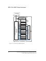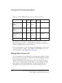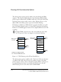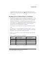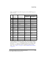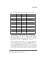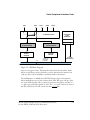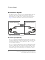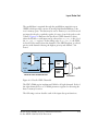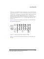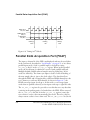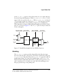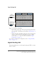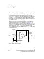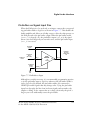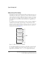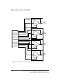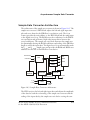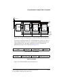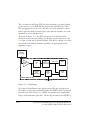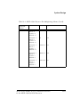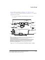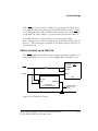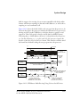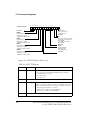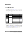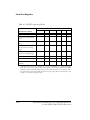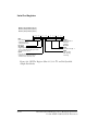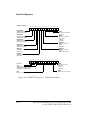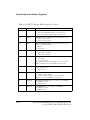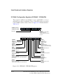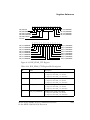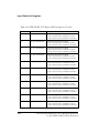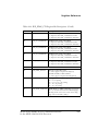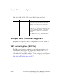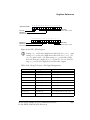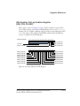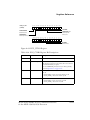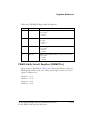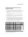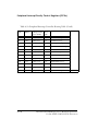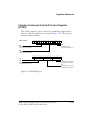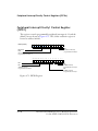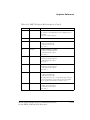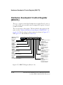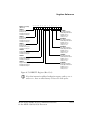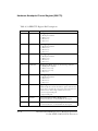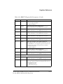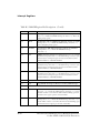
1
ADSP-2136x SHARC® Processor
Hardware Reference
Includes ADSP-21362, ADSP-21363,
ADSP-21364, ADSP-21365, ADSP-21366
Revision 1.0, October 2005
Part Number
82-000501-01
Analog Devices, Inc.
One Technology Way
Norwood, Mass. 02062-9106
a
Copyright Information
© 2005 Analog Devices, Inc., ALL RIGHTS RESERVED. This
document may not be reproduced in any form without prior, express written consent from Analog Devices, Inc.
Printed in the USA.
Disclaimer
Analog Devices, Inc. reserves the right to change this product without
prior notice. Information furnished by Analog Devices is believed to be
accurate and reliable. However, no responsibility is assumed by Analog
Devices for its use; nor for any infringement of patents or other rights of
third parties which may result from its use. No license is granted by implication or otherwise under the patent rights of Analog Devices, Inc.
Trademark and Service Mark Notice
The Analog Devices logo, Blackfin, EZ-KIT Lite, SHARC, the SHARC
logo, TigerSHARC, and VisualDSP++ are registered trademarks of Analog
Devices, Inc.
All other brand and product names are trademarks or service marks of
their respective owners.
Contents
PREFACE
Purpose of This Manual .............................................................. xxiii
Intended Audience ...................................................................... xxiii
Manual Contents ......................................................................... xxiv
What’s New in This Manual ......................................................... xxvi
Technical or Customer Support .................................................... xxvi
Supported Processors ................................................................... xxvii
Product Information .................................................................. xxviii
MyAnalog.com ..................................................................... xxviii
Processor Product Information .............................................. xxviii
Related Documents ................................................................ xxix
Online Technical Documentation ............................................ xxx
Accessing Documentation From VisualDSP++ .................... xxxi
Accessing Documentation From Windows .......................... xxxi
Accessing Documentation From the Web ........................... xxxii
Printed Manuals .................................................................... xxxii
VisualDSP++ Documentation Set ...................................... xxxii
Hardware Tools Manuals .................................................. xxxiii
Processor Manuals ............................................................ xxxiii
ADSP-2136x SHARC Processor Hardware Reference
for the ADSP-21362/3/4/5/6 Processors
i
CONTENTS
Data Sheets ..................................................................... xxxiii
Conventions ............................................................................... xxxiv
INTRODUCTION
ADSP-2136x SHARC Design Advantages ..................................... 1-1
Processor Architectural Overview .................................................. 1-8
Processor Core ........................................................................ 1-9
Processor Peripherals ............................................................... 1-9
I/O Processor ..................................................................... 1-9
Digital Audio Interface (DAI) ........................................... 1-11
Development Tools ..................................................................... 1-12
Architecture Enhancements ......................................................... 1-12
Parallel Port Enhancements ................................................... 1-12
I/O Architecture Enhancements ............................................ 1-13
Instruction Set Enhancements ............................................... 1-13
I/O PROCESSOR
General Procedure for Configuring DMA ...................................... 2-2
Core Access to IOP Registers ........................................................ 2-3
Choosing IOP/Core Interaction Options ....................................... 2-6
Interrupt-Driven I/O .............................................................. 2-6
Polling/Status-Driven I/O ..................................................... 2-10
DMA Controller Operation .................................................. 2-11
Chaining DMA Processes .................................................. 2-13
Transfer Control Block (TCB) Chain Loading ................... 2-16
ii
ADSP-2136x SHARC Processor Hardware Reference
for the ADSP-21362/3/4/5/6 Processors
CONTENTS
Setting Up and Starting Chained DMA on
Serial/Parallel Ports ......................................................... 2-18
Setting Up and Starting Chained DMA over the SPI .......... 2-18
Inserting a TCB in an Active Chain ................................... 2-20
Memory-to-Memory DMA .................................................... 2-21
Setting Up DMA Channel Allocation and Priorities ............... 2-21
Managing DMA Channel Priority ..................................... 2-22
DMA Bus Arbitration ....................................................... 2-23
Setting Up DMA Parameter Registers .......................................... 2-26
DMA Transfer Direction ....................................................... 2-26
Data Buffer Registers ............................................................. 2-28
Port, Buffer, and DMA Control Registers ............................... 2-29
Addressing ............................................................................ 2-31
Setting Up DMA ........................................................................ 2-36
Programming Example ................................................................ 2-37
PARALLEL PORT
Parallel Port Pins ........................................................................... 3-3
Alternate Pin Functions ........................................................... 3-4
Parallel Port Pins as FLAG Pins ........................................... 3-4
Parallel Data Acquisition Port as AD Pins ............................ 3-5
Parallel Port Operation .................................................................. 3-5
Basic Parallel Port External Transaction .................................... 3-5
Data Cycles ......................................................................... 3-6
Reading From an External Device or Memory .......................... 3-7
ADSP-2136x SHARC Processor Hardware Reference
for the ADSP-21362/3/4/5/6 Processors
iii
CONTENTS
Writing to an External Device or Memory ............................... 3-8
Transfer Protocol ..................................................................... 3-9
8-Bit Mode ......................................................................... 3-9
16-Bit Mode ..................................................................... 3-10
Comparison of 8- and 16-Bit SRAM Modes .......................... 3-11
Parallel Port Interrupts ................................................................ 3-12
Parallel Port Throughput ............................................................ 3-13
8-Bit Access .......................................................................... 3-14
16-Bit Access ........................................................................ 3-15
Conclusion ........................................................................... 3-16
Parallel Port Registers ................................................................. 3-16
Parallel Port Control Register (PPCTL) ................................. 3-17
Parallel Port DMA Registers .................................................. 3-17
Parallel Port External Setup Registers ..................................... 3-19
Using the Parallel Port ................................................................ 3-19
DMA Transfers ..................................................................... 3-20
Configuring the Parallel Port for DMA ............................. 3-21
Configuring a Chained DMA ........................................... 3-21
Core-Driven Transfers ........................................................... 3-23
Known-Duration Accesses ................................................. 3-25
Status-Driven Transfers (Polling) ....................................... 3-26
Core-Stall Driven Transfers ............................................... 3-26
Interrupt Driven Accesses ................................................. 3-27
Programming Examples .............................................................. 3-27
iv
ADSP-2136x SHARC Processor Hardware Reference
for the ADSP-21362/3/4/5/6 Processors
CONTENTS
SERIAL PORTS
Serial Port Signals ......................................................................... 4-5
Serial Port Signal Sensitivity ..................................................... 4-9
SPORT Operation Modes ........................................................... 4-10
Standard DSP Serial Mode ..................................................... 4-12
Standard DSP Serial Mode Control Bits ............................ 4-12
Clocking Options ............................................................. 4-12
Frame Sync Options .......................................................... 4-13
Data Formatting ............................................................... 4-13
Data Transfers ................................................................... 4-14
Status Information ............................................................ 4-15
Left-Justified Sample Pair Mode ............................................. 4-15
Setting the Internal Serial Clock and Frame Sync Rates ...... 4-16
Left-Justified Sample Pair Mode Control Bits ..................... 4-16
Setting Word Length (SLEN) ............................................ 4-17
Enabling SPORT Master Mode (MSTR) ........................... 4-17
Selecting Transmit and Receive Channel Order (FRFS) ...... 4-17
Selecting Frame Sync Options (DIFS) ............................... 4-17
Enabling SPORT DMA (SDEN) ....................................... 4-18
Interrupt-Driven Data Transfer Mode ............................ 4-18
DMA-Driven Data Transfer Mode ................................. 4-18
I2S Mode .............................................................................. 4-19
I2S Mode Control Bits ...................................................... 4-21
Setting the Internal Serial Clock and Frame Sync Rates ...... 4-21
ADSP-2136x SHARC Processor Hardware Reference
for the ADSP-21362/3/4/5/6 Processors
v
CONTENTS
I2S Control Bits ............................................................... 4-21
Setting Word Length (SLEN) ............................................ 4-22
Enabling SPORT Master Mode (MSTR) ........................... 4-22
Selecting Transmit and Receive Channel Order (FRFS) ..... 4-22
Selecting Frame Sync Options (DIFS) ............................... 4-23
Enabling SPORT DMA (SDEN) ...................................... 4-23
Interrupt-Driven Data Transfer Mode ........................... 4-24
DMA-Driven Data Transfer Mode ................................ 4-24
Multichannel Operation ........................................................ 4-24
Frame Syncs in Multichannel Mode .................................. 4-27
Active State Multichannel Receive Frame Sync Select ..... 4-28
Multichannel Mode Control Bits ...................................... 4-28
Receive Multichannel Frame Sync Source ...................... 4-30
Active State Transmit Data Valid ................................... 4-30
Multichannel Status Bits ............................................... 4-30
Channel Selection Registers .......................................... 4-31
SPORT Loopback ............................................................ 4-32
Clock Signal Options .................................................................. 4-34
Frame Sync Options ................................................................... 4-34
Framed Versus Unframed Frame Syncs ................................... 4-35
Internal Versus External Frame Syncs ..................................... 4-36
Active Low Versus Active High Frame Syncs .......................... 4-36
Sampling Edge for Data and Frame Syncs .............................. 4-37
Early Versus Late Frame Syncs ............................................... 4-37
vi
ADSP-2136x SHARC Processor Hardware Reference
for the ADSP-21362/3/4/5/6 Processors
CONTENTS
Data-Independent Frame Sync ............................................... 4-38
Data Word Formats ..................................................................... 4-40
Word Length ......................................................................... 4-40
Endian Format ...................................................................... 4-41
Data Packing and Unpacking ................................................. 4-41
Data Type ......................................................................... 4-42
Companding ..................................................................... 4-43
SPORT Control Registers and Data Buffers ................................. 4-45
Register Writes and Effect Latency ......................................... 4-51
Serial Port Control Registers (SPCTLx) .................................. 4-51
Transmit and Receive Data Buffers
(TXSPxA/B, RXSPxA/B) .................................................... 4-60
Clock and Frame Sync Frequency Registers (DIVx) ................ 4-63
SPORT Reset ........................................................................ 4-65
SPORT Interrupts ................................................................. 4-66
Moving Data Between SPORTS and Internal Memory ................. 4-67
DMA Block Transfers ............................................................ 4-67
Setting Up DMA on SPORT Channels .............................. 4-69
SPORT DMA Parameter Registers ......................................... 4-70
SPORT DMA Chaining .................................................... 4-74
Single Word Transfers ............................................................ 4-74
SPORT Programming Examples .................................................. 4-76
ADSP-2136x SHARC Processor Hardware Reference
for the ADSP-21362/3/4/5/6 Processors
vii
CONTENTS
SERIAL PERIPHERAL INTERFACE PORTS
Functional Description ................................................................. 5-2
SPI Interface Signals ..................................................................... 5-4
SPI Clock Signal (SPICLK) ..................................................... 5-4
SPICLK Timing ................................................................. 5-5
SPI Slave Select Outputs (SPIDS0-3) .................................. 5-6
SPI Device Select Signal .......................................................... 5-6
Master Out Slave In (MOSI) ................................................... 5-7
Master In Slave Out (MISO) ................................................... 5-7
SPI General Operations ................................................................ 5-8
SPI Enable .............................................................................. 5-9
Open Drain Mode (OPD) ....................................................... 5-9
Master Mode Operation ........................................................ 5-10
Slave Mode Operation ........................................................... 5-11
Multimaster Conditions ........................................................ 5-13
SPI Data Transfer Operations ..................................................... 5-13
Core Transmit/Receive Operations ........................................ 5-13
SPI DMA ............................................................................. 5-14
Master Mode DMA Operation .......................................... 5-15
Master Transfer Preparation .......................................... 5-18
Slave Mode DMA Operation ............................................ 5-19
Slave Transfer Preparation ............................................. 5-19
Changing SPI Configuration ............................................. 5-21
Switching From Transmit To Receive DMA ....................... 5-23
viii
ADSP-2136x SHARC Processor Hardware Reference
for the ADSP-21362/3/4/5/6 Processors
CONTENTS
Switching From Receive to Transmit DMA ........................ 5-24
DMA Error Interrupts ....................................................... 5-25
DMA Chaining ................................................................. 5-27
SPI Transfer Formats ................................................................... 5-27
Beginning and Ending an SPI Transfer ................................... 5-29
SPI Word Lengths ....................................................................... 5-30
8-Bit Word Lengths ............................................................... 5-31
16-Bit Word Lengths ............................................................. 5-31
32-Bit Word Lengths ............................................................. 5-32
Packing ................................................................................. 5-32
SPI Interrupts ............................................................................. 5-33
Error Signals and Flags ................................................................ 5-34
Mode Fault Error (MME) ...................................................... 5-35
Transmission Error Bit (TUNF) ............................................. 5-36
Reception Error Bit (ROVF) .................................................. 5-36
Transmit Collision Error Bit (TXCOL) .................................. 5-37
SPI Programming Examples ........................................................ 5-37
INPUT DATA PORT
Serial Inputs ................................................................................. 6-4
Parallel Data Acquisition Port (PDAP) ........................................... 6-8
Masking .................................................................................. 6-9
Packing Unit ......................................................................... 6-10
Packing Mode 11 .............................................................. 6-10
Packing Mode 10 .............................................................. 6-11
ADSP-2136x SHARC Processor Hardware Reference
for the ADSP-21362/3/4/5/6 Processors
ix
CONTENTS
Packing Mode 01 .............................................................. 6-11
Packing Mode 00 .............................................................. 6-11
Clocking Edge Selection ........................................................ 6-12
Hold Input ........................................................................... 6-12
PDAP Strobe ........................................................................ 6-14
FIFO Control and Status ............................................................ 6-15
FIFO to Memory Data Transfer .................................................. 6-16
Interrupt-Driven Transfers .................................................... 6-17
Starting an Interrupt-Driven Transfer ................................ 6-18
Interrupt-Driven Transfer Notes ............................................ 6-19
DMA Transfers ..................................................................... 6-20
Simple DMA .................................................................... 6-20
Starting A Simple DMA Transfer .................................. 6-21
Ping-Pong DMA ............................................................... 6-22
Starting Ping-Pong DMA Transfers ............................... 6-23
DMA Transfer Notes ........................................................ 6-25
DMA Channel Parameter Registers ........................................ 6-27
IDP (DAI) Interrupt Service Routines for DMAs ................... 6-28
FIFO Overflow ..................................................................... 6-30
Input Data Port Programming Example ...................................... 6-31
DIGITAL AUDIO INTERFACE
Structure of the DAI ..................................................................... 7-1
DAI System Design ...................................................................... 7-2
Signal Routing Unit ...................................................................... 7-6
x
ADSP-2136x SHARC Processor Hardware Reference
for the ADSP-21362/3/4/5/6 Processors
CONTENTS
Connecting Peripherals ............................................................ 7-7
Pins Interface .......................................................................... 7-8
Pin Buffers as Signal Output Pins ............................................ 7-9
Pin Buffers as Signal Input Pins ............................................. 7-11
Bidirectional Pin Buffers ........................................................ 7-12
Making Connections in the SRU ................................................. 7-13
SRU Connection Groups ....................................................... 7-16
Group A Connections—Clock Signals ............................... 7-16
Group B Connections—Data Signals ................................. 7-18
Group C Connections—Frame Sync Signals ...................... 7-20
Group D Connections—Pin Signal Assignments ................ 7-22
Group E Connections—Miscellaneous Signals ................... 7-24
Group F Connections—Pin Enable Signals ........................ 7-26
General-Purpose I/O (GPIO) and Flags ....................................... 7-27
Miscellaneous Signals .................................................................. 7-27
DAI Interrupt Controller ............................................................ 7-27
Relationship to the Core ........................................................ 7-27
DAI Interrupts ...................................................................... 7-29
High and Low Priority Latches .............................................. 7-30
Rising and Falling Edge Masks ............................................... 7-31
Using the SRU() Macro ............................................................... 7-32
ADSP-2136x SHARC Processor Hardware Reference
for the ADSP-21362/3/4/5/6 Processors
xi
CONTENTS
PULSE WIDTH MODULATION
PWM Implementation .................................................................. 8-1
PWM Waveforms .................................................................... 8-3
Edge-Aligned Mode ............................................................ 8-3
Center-Aligned Mode ......................................................... 8-3
Switching Frequencies ............................................................. 8-5
Dead Time ............................................................................. 8-6
Duty Cycles ............................................................................ 8-7
Duty Cycles and Dead Time ............................................... 8-7
Over-Modulation ............................................................. 8-11
Update Modes ...................................................................... 8-14
Single-Update ................................................................... 8-14
Double-Update ................................................................. 8-14
Configurable Polarity ............................................................ 8-14
PWM Pins and Signals .......................................................... 8-14
Crossover ......................................................................... 8-15
PWM Accuracy ..................................................................... 8-16
PWM Registers .......................................................................... 8-17
Duty Cycle ........................................................................... 8-18
Output Enable ...................................................................... 8-19
Programming Example ................................................................ 8-19
xii
ADSP-2136x SHARC Processor Hardware Reference
for the ADSP-21362/3/4/5/6 Processors
CONTENTS
SONY/PHILLIPS DIGITAL INTERFACE
AES3, S/PDIF Stream Format ....................................................... 9-2
S/PDIF Transmitter ...................................................................... 9-5
Channel Status ........................................................................ 9-6
SRU Control Registers for the S/PDIF Transmitter .................. 9-7
S/PDIF Control Registers ........................................................ 9-9
S/PDIF Transmitter Programming Guidelines .......................... 9-9
Control Register ................................................................. 9-9
SRU Programming for Input and Output Streams .............. 9-10
Control Register Programming and Enable ........................ 9-11
Programming Summary ..................................................... 9-11
Structure of the S/PDIF and AES3 Format ............................. 9-12
S/PDIF Receiver ......................................................................... 9-12
S/PDIF Receiver Registers ........................................................... 9-14
SRU Control Registers ........................................................... 9-14
S/PDIF Receiver Control Registers ........................................ 9-15
S/PDIF Receiver Control Register (DIRCTL) .................... 9-15
S/PDIF Receiver Status Register (DIRSTAT) ..................... 9-15
Channel Status for Subframes ............................................ 9-16
S/PDIF Receiver Programming Guidelines ............................. 9-16
Control Register ............................................................... 9-16
SRU Programming ............................................................ 9-16
Control Register Programming .......................................... 9-17
Receiver Locking ............................................................... 9-17
ADSP-2136x SHARC Processor Hardware Reference
for the ADSP-21362/3/4/5/6 Processors
xiii
CONTENTS
Status Bits ........................................................................ 9-17
Programming Summary .................................................... 9-17
Phased-Locked Loop ................................................................... 9-18
Channel Status Decoding ............................................................ 9-19
Compressed or Non-linear Audio Data .................................. 9-19
Emphasized Audio Data ........................................................ 9-20
Single-Channel Double-Frequency Mode ............................... 9-20
Error Handling ........................................................................... 9-21
Interrupts ................................................................................... 9-23
ASYNCHRONOUS SAMPLE RATE CONVERTER
Introduction ............................................................................... 10-1
Overview .............................................................................. 10-1
Theory of Operation ............................................................. 10-4
Conceptual Model ................................................................ 10-5
Hardware Model ................................................................... 10-7
Sample Rate Converter Architecture ...................................... 10-9
Group Delay ....................................................................... 10-12
SRC Operation ......................................................................... 10-12
SRC Enable ........................................................................ 10-12
Serial Data Ports ................................................................. 10-13
Data Format ................................................................... 10-13
TDM Output Mode ....................................................... 10-14
TDM Input Mode .......................................................... 10-15
Matched-Phase Mode ..................................................... 10-16
xiv
ADSP-2136x SHARC Processor Hardware Reference
for the ADSP-21362/3/4/5/6 Processors
CONTENTS
Bypass Mode ................................................................... 10-18
De-Emphasis Filter .............................................................. 10-18
Mute Control ...................................................................... 10-19
Soft Mute ....................................................................... 10-19
Hard Mute ...................................................................... 10-20
Auto Mute ...................................................................... 10-20
SRC Registers ........................................................................... 10-20
Programming the SRC Module .................................................. 10-21
SRC Control Register Programming ..................................... 10-21
SRU Programming .............................................................. 10-21
SRC Mute-Out Interrupt ..................................................... 10-22
Sample Rate Ratio ............................................................... 10-22
Programming Summary ....................................................... 10-23
PRECISION CLOCK GENERATOR
Clock Outputs ............................................................................ 11-3
Frame Sync Outputs ................................................................... 11-4
Normal Mode ........................................................................ 11-5
Bypass Mode ......................................................................... 11-6
Frame Sync Output Synchronization With External Clock ........... 11-6
Frame Sync ........................................................................... 11-8
Phase Shift .................................................................................. 11-9
Phase Shift Settings ............................................................. 11-10
Pulse Width ........................................................................ 11-10
Bypass Mode ....................................................................... 11-12
ADSP-2136x SHARC Processor Hardware Reference
for the ADSP-21362/3/4/5/6 Processors
xv
CONTENTS
Bypass as a Pass Through ................................................ 11-12
Bypass as a One Shot ...................................................... 11-12
Programming Examples ............................................................ 11-14
PCG Setup for I2S or Left-Justified Formats ........................ 11-14
Clock and Frame Sync Divisors PCG Channel B ................. 11-19
PCG Channel A and B Output Example .............................. 11-22
SYSTEM DESIGN
Processor Pin Descriptions .......................................................... 12-2
Pin Multiplexing ................................................................... 12-2
Address/Data Pins as FLAGs ........................................... 12-12
Input Synchronization Delay ............................................... 12-12
Clock Derivation ................................................................ 12-13
Using the Power Management Control Register
(PMCTL) .................................................................... 12-13
PLL Programming Example 1 ..................................... 12-16
PLL Programming Example 2 ..................................... 12-17
Timing Specifications ..................................................... 12-18
RESET and CLKIN ............................................................ 12-21
Reset Generators ................................................................. 12-23
Interrupt and Timer Pins .................................................... 12-25
Core-Based Flag Pins ........................................................... 12-26
JTAG Interface Pins ............................................................ 12-26
Phase-Locked Loop Start Up ............................................... 12-27
Conditioning Input Signals ....................................................... 12-28
xvi
ADSP-2136x SHARC Processor Hardware Reference
for the ADSP-21362/3/4/5/6 Processors
CONTENTS
Reset Input Hysteresis ......................................................... 12-28
Designing for High Frequency Operation .................................. 12-29
Clock Specifications and Jitter ............................................. 12-29
Other Recommendations and Suggestions ............................ 12-30
Decoupling Capacitors and Ground Planes .......................... 12-30
Oscilloscope Probes ............................................................. 12-31
Recommended Reading ....................................................... 12-33
Booting .................................................................................... 12-34
Parallel Port Booting ............................................................ 12-35
SPI Port Booting ................................................................. 12-37
32-bit SPI Host Boot ...................................................... 12-39
16-bit SPI Host Boot ...................................................... 12-40
8-bit SPI Host Boot ........................................................ 12-42
Slave Boot Mode ............................................................. 12-43
Master Boot .................................................................... 12-45
Booting From an SPI Flash .............................................. 12-48
Booting From an SPI PROM (16-bit address) .................. 12-48
Booting From an SPI Host Processor ............................... 12-48
Data Delays, Latencies, and Throughput ................................... 12-49
Execution Stalls ................................................................... 12-49
DAG Stalls .......................................................................... 12-50
Memory Stalls ..................................................................... 12-50
IOP Register Stalls ............................................................... 12-50
DMA Stalls ......................................................................... 12-51
ADSP-2136x SHARC Processor Hardware Reference
for the ADSP-21362/3/4/5/6 Processors
xvii
CONTENTS
IOP Buffer Stalls ................................................................. 12-51
REGISTERS REFERENCE
I/O Processor Registers ................................................................. A-2
Notes on Reading Register Drawings ....................................... A-6
System Control Register (SYSCTL) ......................................... A-7
Memory-to-Memory DMA Register ............................................ A-11
Parallel Port Registers ................................................................. A-12
Parallel Port Control Register (PPCTL) ................................. A-12
Parallel Port DMA Registers .................................................. A-16
Parallel Port DMA Transmit Register (TXPP) .................... A-16
Parallel Port DMA Receive Register (RXPP) ...................... A-17
Parallel Port DMA Start Internal Index Address
Register (IIPP) ............................................................... A-17
Parallel Port DMA Internal Modifier Address
Register (IMPP) ............................................................. A-17
Parallel Port DMA Internal Word Count
Register (ICPP) ............................................................. A-17
Parallel Port DMA External Index Address
Register (EIPP) .............................................................. A-18
Parallel Port DMA External Modifier Address
Register (EMPP) ............................................................ A-18
Parallel Port DMA External Word Count
Register (ECPP) ............................................................. A-18
Parallel Port DMA Chain Pointer Register (CPPP) ............ A-18
Serial Port Registers .................................................................... A-19
SPORT Serial Control Registers (SPCTLx) ............................ A-19
xviii
ADSP-2136x SHARC Processor Hardware Reference
for the ADSP-21362/3/4/5/6 Processors
CONTENTS
SPORT Multichannel Control Registers (SPMCTLxy) .......... A-30
SPORT Transmit Buffer Registers (TXSPx) ........................... A-35
SPORT Receive Buffer Registers (RXSPx) ............................. A-36
SPORT Divisor Registers (DIVx) .......................................... A-36
SPORT Count Registers (SPCNTx) ...................................... A-37
SPORT Transmit Select Registers (MTxCSy) ........................ A-37
SPORT Transmit Compand Registers (MTxCCSy) ............... A-38
SPORT Receive Select Registers (MRxCSx) .......................... A-39
SPORT Receive Compand Registers (MRxCCSx) ................. A-39
SPORT DMA Index Registers (IISPx) ................................... A-40
SPORT DMA Modifier Registers (IMSPx) ............................ A-41
SPORT DMA Count Registers (CSPx) ................................. A-41
SPORT Chain Pointer Registers (CPSPx) .............................. A-42
Serial Peripheral Interface Registers ............................................. A-42
SPI Port Status (SPISTAT, SPISTATB) Registers ................... A-42
SPI Port Flags Registers (SPIFLG, SPIFLGB) ........................ A-44
SPI Control Registers (SPICTL, SPICTLB) .......................... A-45
SPI Receive Buffer Registers (RXSPI, RXSPIB) ..................... A-49
RXSPI Shadow Registers
(RXSPI_SHADOW, RXSPIB_SHADOW) ......................... A-49
SPI Transmit Buffer Registers (TXSPI, TXSPIB) ................... A-50
SPI Baud Rate Registers (SPIBAUD, SPIBAUDB) ................ A-50
SPI DMA Registers .............................................................. A-51
SPI DMA Configuration Registers (SPIDMAC,
SPIDMACB) ................................................................ A-52
ADSP-2136x SHARC Processor Hardware Reference
for the ADSP-21362/3/4/5/6 Processors
xix
CONTENTS
SPI DMA Start Address Registers (IISPI, IISPIB) .............. A-54
SPI DMA Address Modify Registers (IMSPI, IMSPIB) ...... A-54
SPI DMA Word Count Registers (CSPI, CSPIB) ............... A-54
SPI DMA Chain Pointer Registers (CPSPI, CPSPIB) ......... A-55
Input Data Port Registers ............................................................ A-55
Input Data Port Control Register 0 (IDP_CTL0) .................. A-56
Input Data Port Control Register 1 (IDP_CTL1) .................. A-58
Input Data Port FIFO Register (IDP_FIFO) .......................... A-59
Input Data Port DMA Control Registers ............................... A-60
Index (IDP_DMA_Ix) ...................................................... A-60
Modifier (IDP_DMA_Mx) ............................................... A-61
Counter (IDP_DMA_Cx) ................................................. A-61
Input Data Port Ping-pong DMA Registers ............................ A-62
IDP Ping-pong Index Registers (IDP_DMA_IxA) ............. A-62
IDP Ping-pong Count Registers (IDP_DMA_PCx) ........... A-63
Parallel Data Acquisition Port Control Register
(IDP_PDAP_CTL) ............................................................ A-64
Sample Rate Converter Registers ................................................. A-68
SRC Control Registers (SRCCTLx) ....................................... A-68
SRC Mute Register (SRCMUTE) .......................................... A-79
SRC Ratio Registers (SRCRATx) ........................................... A-79
Signal Routing Unit Registers ..................................................... A-80
Clock Routing Control Registers
(SRU_CLKx, Group A) ...................................................... A-81
Serial Data Routing Registers (SRU_DATx, Group B) ........... A-85
xx
ADSP-2136x SHARC Processor Hardware Reference
for the ADSP-21362/3/4/5/6 Processors
CONTENTS
Frame Sync Routing Control Registers
(SRU_FSx, Group C) ........................................................ A-90
Pin Signal Assignment Registers
(SRU_PINx, Group D) ...................................................... A-94
Miscellaneous Signal Routing Registers
(SRU_MISCx, Group E) ................................................. A-101
DAI Pin Buffer Enable Registers
(SRU_PBENx, Group F) ................................................. A-105
Special IDP Registers ............................................................... A-110
Digital Audio Interface Status Register (DAI_STAT) ........... A-110
DAI Resistor Pull-up Enable Register
(DAI_PIN_PULLUP) ...................................................... A-113
DAI Pin Buffer Status Register (DAI_PBIN_STAT) ............ A-114
DAI Interrupt Controller Registers ........................................... A-115
Precision Clock Generator Registers ......................................... A-117
Control Registers (PCG_CTLxx) ........................................ A-118
Pulse Width Register (PCG_PW) ....................................... A-122
Synchronization Register (PCG_SYNC) .............................. A-124
Pulse Width Modulation Registers ............................................ A-125
PWM Global Control Register (PWMGCTL) ..................... A-125
PWM Global Status Register (PWMGSTAT) ...................... A-126
PWM Control Register (PWMCTLx) ................................. A-126
PWM Status Registers (PWMSTATx) ................................. A-127
PWM Period Registers (PWMPERIODx) ........................... A-128
PWM Output Disable Registers (PWMSEGx) .................... A-128
PWM Polarity Select Registers (PWMPOLx) ...................... A-129
ADSP-2136x SHARC Processor Hardware Reference
for the ADSP-21362/3/4/5/6 Processors
xxi
CONTENTS
PWM Channel Duty Control Registers
(PWMAx, PWMBx) ......................................................... A-130
PWM Channel Low Duty Control Registers
(PWMALx, PWMBLx) .................................................... A-131
PWM Dead Time Registers (PWMDTx) ............................. A-131
Sony/Philips Digital Interface Registers ..................................... A-132
Transmitter Control Register (DITCTL) ............................. A-132
Left Channel Status for Subframe A Register
(DITCHANL) ................................................................. A-134
Right Channel Status for Subframe B Register
(DITCHANR) ................................................................. A-135
Receiver Control Register (DIRCTL) .................................. A-135
Receiver Status Register (DIRSTAT) .................................... A-138
Left Channel Status for Subframe A Register
(DIRCHANL) ................................................................. A-140
Right Channel Status for Subframe B Register
(DIRCHANR) ................................................................. A-140
Peripheral Interrupt Priority Control Registers (PICRx) ............. A-141
Peripheral Interrupt Priority0 Control Register (PICR0) ...... A-143
Peripheral Interrupt Priority1 Control Register (PICR1) ...... A-144
Peripheral Interrupt Priority2 Control Register (PICR2) ...... A-145
Peripheral Interrupt Priority3 Control Register (PICR3) ...... A-146
Power Management Control
Register (PMCTL) ................................................................. A-146
Hardware Breakpoint Control Register (BRKCTL) .................... A-150
Enhanced Emulation Status Register (EEMUSTAT) .................. A-154
xxii
ADSP-2136x SHARC Processor Hardware Reference
for the ADSP-21362/3/4/5/6 Processors
CONTENTS
INTERRUPTS
Interrupt Vector Tables ................................................................ B-1
Interrupt Priorities ................................................................. B-4
Interrupt Registers ....................................................................... B-6
Interrupt Register (LIRPTL) ................................................... B-6
Interrupt Latch Register (IRPTL) ......................................... B-13
Interrupt Mask Register (IMASK) ......................................... B-18
Interrupt Mask Pointer Register (IMASKP) ........................... B-21
INDEX
ADSP-2136x SHARC Processor Hardware Reference
for the ADSP-21362/3/4/5/6 Processors
xxiii
CONTENTS
xxiv
ADSP-2136x SHARC Processor Hardware Reference
for the ADSP-21362/3/4/5/6 Processors
PREFACE
Thank you for purchasing and developing systems using ADSP-2136x
SHARC® processors from Analog Devices.
Purpose of This Manual
The ADSP-2136x SHARC Processor Hardware Reference for the
ADSP-21362/3/4/5/6 Processors contains information about the DSP
architecture and DSP assembly language for these processors. These are
32-bit, fixed- and floating-point digital signal processors from Analog
Devices for use in computing, communications, and consumer
applications.
The manual provides information on how assembly instructions execute
on the ADSP-2136x SHARC processor’s architecture along with reference
information about DSP operations.
Intended Audience
The primary audience for this manual is a programmer who is familiar
with Analog Devices processors. This manual assumes that the audience
has a working knowledge of the appropriate processor architecture and
instruction set. Programmers who are unfamiliar with Analog Devices
processors can use this manual, but should supplement it with other texts
(such as the appropriate hardware reference manuals and data sheets) that
describe your target architecture.
ADSP-2136x SHARC Processor Hardware Reference
for the ADSP-21362/3/4/5/6 Processors
xxiii
Manual Contents
Manual Contents
This manual provides detailed information about the ADSP-2136x
SHARC processors in the following chapters:
• Chapter 1, “Introduction”
Provides an architectural overview of the ADSP-2136x SHARC
processor.
• Chapter 2, “I/O Processor”
Describes ADSP-2136x input/output processor architecture, and
provides direct memory access (DMA) procedures for the processor
peripherals.
• Chapter 3, “Parallel Port”
Describes how the ADSP-2136x processor’s on-chip DMA controller acts as a machine for transferring data without core
interruption.
• Chapter 4, “Serial Ports”
Describes the six dual data line serial ports. Each SPORT contains
a clock, a frame sync, and two data lines that can be configured as
either a receiver or transmitter pair.
• Chapter 5, “Serial Peripheral Interface Ports”
Describes the operation of the serial peripheral interface (SPI) port.
SPI devices communicate using a master-slave relationship and can
achieve high data transfer rate because they can operate in
full-duplex mode.
• Chapter 6, “Input Data Port”
Discusses the function of the input data port (IDP) which provides
a low overhead method of routing signal routing unit (SRU) signals back to the core’s memory.
xxiv
ADSP-2136x SHARC Processor Hardware Reference
for the ADSP-21362/3/4/5/6 Processors
Preface
• Chapter 7, “Digital Audio Interface”
Provides information about the digital applications interface (DAI)
which allows you to attach an arbitrary number and variety of
peripherals to the ADSP-2136x SHARC processor while retaining
high levels of compatibility.
• Chapter 8, “Pulse Width Modulation”
Describes the implementation and use of the pulse width modulation module which provides a technique for controlling analog
circuits with the microprocessor’s digital outputs.
• Chapter 9, “Sony/Phillips Digital Interface”
Provides information on the use of the Sony/Philips Digital Interface which is a standard audio file transfer format that allows the
transfer of digital audio signals from one device to another without
having to be converted to an analog signal.
• Chapter 10, “Asynchronous Sample Rate Converter”
Provides information on the sample rate converter (SRC) module.
This module performs synchronous or asynchronous sample rate
conversion across independent stereo channels, without using any
internal processor resources.
• Chapter 11, “Precision Clock Generator”
Details the precision clock generators (PCG), each of which generates a pair of signals derived from a clock input signal.
• Chapter 12, “System Design”
Describes system design features of the ADSP-2136x SHARC processor. These include power, reset, clock, JTAG, and booting, as
well as pin descriptions and other system-level information.
• Appendix A, “Registers Reference”
Provides a graphical presentation of all registers and describes the
bit usage in each register.
ADSP-2136x SHARC Processor Hardware Reference
for the ADSP-21362/3/4/5/6 Processors
xxv
What’s New in This Manual
• Appendix B “Interrupts”,
Provides a complete listing of the registers that are used to configure and control interrupts.
hardware reference is a companion document to the
L This
ADSP-2136x SHARC Processor Programming Reference.
What’s New in This Manual
This is the first edition (Revision 1.0) of the ADSP-2136x SHARC Processor Hardware Reference. In future revisions this section will document
additions and corrections from previous editions of the book.
Technical or Customer Support
You can reach Analog Devices, Inc. Customer Support in the following
ways:
• Visit the Embedded Processing and DSP products Web site at
http://www.analog.com/processors/technicalSupport
• E-mail tools questions to
[email protected]
• E-mail processor questions to
[email protected] (World wide support)
[email protected] (Europe support)
[email protected] (China support)
• Phone questions to 1-800-ANALOGD
• Contact your Analog Devices, Inc. local sales office or authorized
distributor
xxvi
ADSP-2136x SHARC Processor Hardware Reference
for the ADSP-21362/3/4/5/6 Processors
Preface
• Send questions by mail to:
Analog Devices, Inc.
One Technology Way
P.O. Box 9106
Norwood, MA 02062-9106
USA
Supported Processors
The following is the list of Analog Devices, Inc. processors supported in
VisualDSP++®.
TigerSHARC® (ADSP-TSxxx) Processors
The name TigerSHARC refers to a family of floating-point and fixed-point
[8-bit, 16-bit, and 32-bit] processors. VisualDSP++ currently supports the
following TigerSHARC families: ADSP-TS101 and ADSP-TS20x.
SHARC (ADSP-21xxx) Processors
The name SHARC refers to a family of high-performance, 32-bit,
floating-point processors that can be used in speech, sound, graphics, and
imaging applications. VisualDSP++ currently supports the following
SHARC families: ADSP-2106x, ADSP-2116x, ADSP-2126x, and
ADSP-2136x.
Blackfin® (ADSP-BFxxx) Processors
The name Blackfin refers to a family of 16-bit, embedded processors.
VisualDSP++ currently supports the following Blackfin families:
ADSP-BF53x and ADSP-BF56x.
ADSP-2136x SHARC Processor Hardware Reference
for the ADSP-21362/3/4/5/6 Processors
xxvii
Product Information
Product Information
You can obtain product information from the Analog Devices web site,
from the product CD-ROM, or from the printed publications (manuals).
Analog Devices is online at www.analog.com. Our Web site provides information about a broad range of products—analog integrated circuits,
amplifiers, converters, and digital signal processors.
MyAnalog.com
is a free feature of the Analog Devices Web site that allows
customization of a Web page to display only the latest information on
products you are interested in. You can also choose to receive weekly
e-mail notifications containing updates to the Web pages that meet your
interests. MyAnalog.com provides access to books, application notes, data
sheets, code examples, and more.
MyAnalog.com
Registration
Visit www.myanalog.com to sign up. Click Register to use MyAnalog.com.
Registration takes about five minutes and serves as a means to select the
information you want to receive.
If you are already a registered user, just log on. Your user name is your
e-mail address.
Processor Product Information
For information on embedded processors and DSPs, visit our Web site at
www.analog.com/processors, which provides access to technical publications, data sheets, application notes, product overviews, and product
announcements.
xxviii
ADSP-2136x SHARC Processor Hardware Reference
for the ADSP-21362/3/4/5/6 Processors
Preface
You may also obtain additional information about Analog Devices and its
products in any of the following ways.
• E-mail questions or requests for information to
[email protected] (World wide support)
[email protected] (Europe support)
[email protected] (China support)
• Fax questions or requests for information to
1-781-461-3010 (North America)
+49-89-76903-157 (Europe)
• Access the FTP Web site at
ftp ftp.analog.com (or ftp
137.71.25.69)
ftp://ftp.analog.com
Related Documents
The following publications that describe the ADSP-2136x SHARC processors (and related processors) can be ordered from any Analog Devices
sales office:
• ADSP-21362 SHARC Processor Data Sheet
• ADSP-21363 SHARC Processor Data Sheet
• ADSP-21364 SHARC Processor Data Sheet
• ADSP-21365/ADSP-21366 SHARC Processor Data Sheet
• ADSP-21367 SHARC Processor Data Sheet
• ADSP-21368 SHARC Processor Data Sheet
• ADSP-21369 SHARC Processor Data Sheet
• ADSP-2136x SHARC Processor Programming Reference
ADSP-2136x SHARC Processor Hardware Reference
for the ADSP-21362/3/4/5/6 Processors
xxix
Product Information
For information on product related development software and Analog
Devices processors, see these publications:
• VisualDSP++ User’s Guide
• VisualDSP++ C/C++ Compiler and Library Manual
• VisualDSP++ Assembler and Preprocessor Manual
• VisualDSP++ Linker and Utilities Manual
• VisualDSP++ Kernel (VDK) User’s Guide
Visit the Technical Library Web site to access all processor and tools
manuals and data sheets:
http://www.analog.com/processors/technical_library
Online Technical Documentation
Online documentation comprises the VisualDSP++ Help system, software
tools manuals, hardware tools manuals, processor manuals, the Dinkum
Abridged C++ library, and Flexible License Manager (FlexLM) network
license manager software documentation. You can easily search across the
entire VisualDSP++ documentation set for any topic of interest. For easy
printing, supplementary .PDF files of most manuals are also provided.
Each documentation file type is described as follows.
xxx
File
Description
.CHM
Help system files and manuals in Help format
.HTM or
.HTML
Dinkum Abridged C++ library and FlexLM network license manager software documentation. Viewing and printing the .HTML files requires a browser, such as
Internet Explorer 4.0 (or higher).
.PDF
VisualDSP++ and processor manuals in Portable Documentation Format (PDF).
Viewing and printing the .PDF files requires a PDF reader, such as Adobe Acrobat
Reader (4.0 or higher).
ADSP-2136x SHARC Processor Hardware Reference
for the ADSP-21362/3/4/5/6 Processors
Preface
If documentation is not installed on your system as part of the software
installation, you can add it from the VisualDSP++ CD-ROM at any time
by running the tools installation. Access the online documentation from
the VisualDSP++ environment, Windows® Explorer, or the Analog
Devices web site.
Accessing Documentation From VisualDSP++
From the VisualDSP++ environment:
• Access VisualDSP++ online Help from the Help menu’s Contents,
Search, and Index commands.
• Open online Help from context-sensitive user interface items (toolbar buttons, menu commands, and windows).
Accessing Documentation From Windows
In addition to any shortcuts you may have constructed, there are many
ways to open VisualDSP++ online Help or the supplementary documentation from Windows.
Help system files (.CHM) are located in the Help folder, and PDF files are
located in the Docs folder of your VisualDSP++ installation CD-ROM.
The Docs folder also contains the Dinkum Abridged C++ library and the
FlexLM network license manager software documentation.
Using Windows Explorer
• Double-click the vdsp-help.chm file, which is the master Help system, to access all the other .CHM files.
• Double-click any file that is part of the VisualDSP++ documentation set.
ADSP-2136x SHARC Processor Hardware Reference
for the ADSP-21362/3/4/5/6 Processors
xxxi
Product Information
Using the Windows Start Button
• Access VisualDSP++ online Help by clicking the Start button and
choosing Programs, Analog Devices, VisualDSP++, and
VisualDSP++ Documentation.
• Access the .PDF files by clicking the Start button and choosing
Programs, Analog Devices, VisualDSP++, Documentation for
Printing, and the name of the book.
Accessing Documentation From the Web
Download manuals at the following Web site:
http://www.analog.com/processors/technical_library
Select a processor family and book title. Download archive (.ZIP) files, one
for each manual. Use any archive management software, such as WinZip,
to decompress downloaded files.
Printed Manuals
For general questions regarding literature ordering, call the Literature
Center at 1-800-ANALOGD (1-800-262-5643) and follow the prompts.
VisualDSP++ Documentation Set
To purchase VisualDSP++ manuals, call 1-603-883-2430. The manuals
may be purchased only as a kit.
If you do not have an account with Analog Devices, you are referred to
Analog Devices distributors. For information on our distributors, log onto
http://www.analog.com/salesdir.
xxxii
ADSP-2136x SHARC Processor Hardware Reference
for the ADSP-21362/3/4/5/6 Processors
Preface
Hardware Tools Manuals
To purchase EZ-KIT Lite® and In-Circuit Emulator (ICE) manuals, call
1-603-883-2430. The manuals may be ordered by title or by product
number located on the back cover of each manual.
Processor Manuals
Hardware reference and instruction set reference manuals may be ordered
through the Literature Center at 1-800-ANALOGD (1-800-262-5643),
or downloaded from the Analog Devices Web site. Manuals may be
ordered by title or by product number located on the back cover of each
manual.
Data Sheets
All data sheets (preliminary and production) may be downloaded from the
Analog Devices Web site. Only production (final) data sheets (Rev. 0, A,
B, C, and so on) can be obtained from the Literature Center at
1-800-ANALOGD (1-800-262-5643); they also can be downloaded from
the Web site.
To have a data sheet faxed to you, call the Analog Devices Faxback System
at 1-800-446-6212. Follow the prompts and a list of data sheet code
numbers will be faxed to you. If the data sheet you want is not listed,
check for it on the Web site.
ADSP-2136x SHARC Processor Hardware Reference
for the ADSP-21362/3/4/5/6 Processors
xxxiii
Conventions
Conventions
Text conventions used in this manual are identified and described as
follows.
Example
Description
Close command
(File menu)
Titles in reference sections indicate the location of an item within the
VisualDSP++ environment’s menu system (for example, the Close
command appears on the File menu).
{this | that}
Alternative items in syntax descriptions appear within curly brackets
and separated by vertical bars; read the example as this or that. One
or the other is required.
[this | that]
Optional items in syntax descriptions appear within brackets and separated by vertical bars; read the example as an optional this or that.
[this,…]
Optional item lists in syntax descriptions appear within brackets
delimited by commas and terminated with an ellipse; read the example
as an optional comma-separated list of this.
.SECTION
Commands, directives, keywords, and feature names are in text with
letter gothic font.
filename
Non-keyword placeholders appear in text with italic style format.
L
a
[
xxxiv
Note: For correct operation, ...
A Note: provides supplementary information on a related topic. In the
online version of this book, the word Note appears instead of this
symbol.
Caution: Incorrect device operation may result if ...
Caution: Device damage may result if ...
A Caution: identifies conditions or inappropriate usage of the product
that could lead to undesirable results or product damage. In the online
version of this book, the word Caution appears instead of this symbol.
Warning: Injury to device users may result if ...
A Warning: identifies conditions or inappropriate usage of the product
that could lead to conditions that are potentially hazardous for devices
users. In the online version of this book, the word Warning appears
instead of this symbol.
ADSP-2136x SHARC Processor Hardware Reference
for the ADSP-21362/3/4/5/6 Processors
Preface
conventions, which apply only to specific chapters, may
L Additional
appear throughout this document.
ADSP-2136x SHARC Processor Hardware Reference
for the ADSP-21362/3/4/5/6 Processors
xxxv
Conventions
xxxvi
ADSP-2136x SHARC Processor Hardware Reference
for the ADSP-21362/3/4/5/6 Processors
1 INTRODUCTION
The ADSP-2136x SHARC processors are high performance 32-bit processors used for high quality audio, medical imaging, communications,
military, test equipment, 3D graphics, speech recognition, motor control,
imaging, and other applications. By adding on-chip SRAM, integrated
I/O peripherals, and an additional processing element for single-instruction, multiple-data (SIMD) support, this processor builds on the
ADSP-21000 family DSP core to form a complete system-on-a-chip.
ADSP-2136x SHARC Design Advantages
A digital signal processor’s data format determines its ability to handle signals of differing precision, dynamic range, and signal-to-noise ratios.
Because floating-point DSP math reduces the need for scaling and the
probability of overflow, using a floating-point processor can simplify algorithm and software development. The extent to which this is true depends
on the floating-point processor’s architecture. Consistency with IEEE
workstation simulations and the elimination of scaling are clearly two
ease-of-use advantages. High level language programmability, large
address spaces, and wide dynamic range allow system development time to
be spent on algorithms and signal processing concerns, rather than assembly language coding, code paging, and error handling. The ADSP-2136x
processor is a highly integrated, 32-bit floating-point processor which provides all of these design advantages.
ADSP-2136x SHARC Processor Hardware Reference
for the ADSP-21362/3/4/5/6 Processors
1-1
ADSP-2136x SHARC Design Advantages
The SHARC processor architecture balances a high performance processor
core with high performance program memory (PM), data memory (DM)
and input/output (I/O) buses. In the core, every instruction can execute in
a single cycle. The buses and instruction cache provide rapid, unimpeded
data flow to the core, thereby maintaining the execution rate.
Figure 1-1 shows a detailed block diagram of the processor core and
Figure 1-2 shows a diagram of the I/O processor (IOP). Together these
figures illustrate the following architectural features:
• Two processing elements (PEx and PEy), each containing 32-bit
IEEE floating-point computation units—multiplier, arithmetic
logic unit (ALU), shifter, and data register file
• Program sequencer with related instruction cache, interval timer,
and data address generators (DAG1 and DAG2)
• 3M bits of SRAM
• Parallel port for interfacing to off-chip memory and peripherals
• IOP with integrated direct memory access (DMA) controller, serial
peripheral interface (SPI) compatible port, and serial ports
(SPORTs) for point-to-point multiprocessor communications
• A variety of audio-centric peripheral modules including a
Sony/Philips Digital Interface (S/PDIF), sample rate converter
(SRC) and pulse width modulation (PWM). The Digital Transmission Content Protection protocol (DTCP) is available on the
ADSP-21365 and ADSP-21362 processors. Table 1-1 on page 1-8
provides details on these as well as other features for the current
members of the ADSP-2136x processor family.
• JTAG test access port (TAP) for emulation
1-2
ADSP-2136x SHARC Processor Hardware Reference
for the ADSP-21362/3/4/5/6 Processors
Introduction
Figure 1-1 also shows the three on-chip buses of the ADSP-2136x processor: PM bus, DM bus, and I/O bus. The PM bus provides access to either
instructions or data. During a single cycle, these buses let the processor
access two data operands from memory, access an instruction (from the
cache), and perform a DMA transfer.
4 BLOCKS OF ON-CHIP MEMORY
CORE PROCESSOR
BLOCK 0
INSTRUCTION
CACHE
32 X 48-BIT
TIMER
DAG1
8X4X32
DAG2
8X4X32
SRAM
1M BIT
ADDR
PROGRAM
SEQUENCER
PM ADDRESS BUS
PM DATA BUS
ADDR
DATA
BLOCK 3
SRAM
0.5M BIT
SRAM
0.5M BIT
ADDR
DATA
ADDR
DATA
32
64
DM DATA BUS
64
IOA
PROCESSING
ELEMENT
(PEY)
DATA
ROM
2M BIT
BLOCK 2
32
DM ADDRESS BUS
PROCESSING
ELEMENT
(PEX)
ROM
2M BIT
BLOCK 1
SRAM
1M BIT
IOD
IOA
PX REGISTER
IOP REGISTERS
(MEMORY MAPPED)
6
JTAG TEST & EMULATION
S
IOD
IOA
IOD
SPI
SPORTS
IDP
PCG
TIMERS
SRC
SPDIF
DTCP
IOA
IOD
SIGNAL
ROUTING
UNIT
I/O PROCESSOR
AND PERIPHERALS
Figure 1-1. ADSP-2136x SHARC Processor Core Block Diagram
ADSP-2136x SHARC Processor Hardware Reference
for the ADSP-21362/3/4/5/6 Processors
1-3
ADSP-2136x SHARC Design Advantages
TO PROCESSOR BUSES AND
SYSTEM MEMORY
IO DATA
BUS (32)
IO ADDRESS
BUS (18)
GPI O FLAGS/IRQ/TIMEXP
4
DMA CONTROLLER
2 5 C H A N NE LS
3
CON TR OL/G PIO
16
A D D RE SS /D ATA B U S/ GP IO
PARALLEL PORT
PWM (16)
4
SPI PORT (1)
4
SERIAL PORTS (6)
SIGNAL ROUTING UNIT
IOP REGISTERS
(MEMORY MAPPED)
CONTROL, STATUS, & DATA BUFFERS
SPI PORT (1)
INPUT
DATA PORTS (8)
DTCP CIPHER
SPDIF (RX/TX)
20
SRC (8 CHANNELS)
PRECISI ON CLOCK
GENERATORS (2)
3
TIMERS (3)
DIGITAL AUDIO INTERFACE
I/O PROCESSOR
Figure 1-2. I/O Processor Block Diagram
1-4
ADSP-2136x SHARC Processor Hardware Reference
for the ADSP-21362/3/4/5/6 Processors
Introduction
Figure 1-3 illustrates a typical single processor system.
ADSP-2136X
CLKOUT
CLKIN
X TAL
CLOCK
CLK_CFG1-0
2
BOOTCFG1 -0
3
ADDR
DATA
RD
FLAG3-1
S CLK0
S FS0
S D0A
S D0B
DAI_P 18
DAI _P 19
DAI_ P2 0
WE
FLAG0
CS
PARALLEL
PORT
RAM, ROM
BOO T ROM
I /O DEVI CE
DATA
DAI_P1
DAI_ P2
DAI_ P3
SRU
OE
WR
ADDRESS
DAC
(OPTI ONAL)
CLK
FS
S DAT
LATCH
AD1 5-0
CONTROL
ADC
(OPTI ONAL)
CLK
FS
S DAT
ALE
2
SP ORT0-5
SPDIF
SRC
TIMERS
IDP
SPI
CLK
FS
DAI
RES ET
PCGA
P CG B
JTAG
6
Figure 1-3. ADSP-2136x Processor Typical Single Processor System
The ADSP-2136x processors address the five central requirements for signal processing:
1. Fast, Flexible Arithmetic. The ADSP-21000 family processors execute all instructions in a single cycle. They provide fast cycle times
and a complete set of arithmetic operations. The processor is IEEE
floating-point compatible and allows either interrupt on arithmetic
exception or latched status exception handling.
ADSP-2136x SHARC Processor Hardware Reference
for the ADSP-21362/3/4/5/6 Processors
1-5
ADSP-2136x SHARC Design Advantages
2. Unconstrained Data Flow. The ADSP-2136x processor has a
Super Harvard Architecture combined with a ten-port data register
file. In every cycle, the processor can write or read two operands to
or from the register file, supply two operands to the ALU, supply
two operands to the multiplier, and receive three results from the
ALU and multiplier. The processor’s 48-bit orthogonal instruction
word supports parallel data transfers and arithmetic operations in
the same instruction.
3. 40-Bit Extended Precision. The processor handles 32-bit IEEE
floating-point format, 32-bit integer and fractional formats
(twos-complement and unsigned), and extended-precision 40-bit
floating-point format. The processors carry extended precision
throughout their computation units, limiting intermediate data
truncation errors (up to 80 bits of precision are maintained during
multiply-accumulate operations).
4. Dual Address Generators. The processor has two data address generators (DAGs) that provide immediate or indirect (pre- and
post-modify) addressing. Modulus, bit-reverse, and broadcast operations are supported with no constraints on data buffer placement.
5. Efficient Program Sequencing. In addition to zero-overhead loops,
the processor supports single-cycle setup and exit for loops. Loops
are both nestable (six levels in hardware) and interruptable. The
processors support both delayed and non-delayed branches.
The ADSP-2136x processors also provide the following features, increasing the variety of applications that these processors can be used for.
• High bandwidth I/O. The processors contain a dedicated, 4M bits
on-chip ROM, a parallel port, an SPI port, serial ports, digital
audio interface (DAI), and JTAG. The DAI incorporates a precision clock generator, input data port, and a signal routing unit.
1-6
ADSP-2136x SHARC Processor Hardware Reference
for the ADSP-21362/3/4/5/6 Processors
Introduction
• Serial ports. Provides an inexpensive interface to a wide variety of
digital and mixed-signal peripheral devices. The serial ports can
operate at up to one-eighth (0.125) the processor core clock (CCLK)
rate.
• Digital audio interface (DAI). The DAI includes a precision clock
generator, an input data port, and a signal routing unit.
• Input data port (IDP). The IDP provides an additional input path
to the processor core, configurable as eight channels of serial data
or seven channels of serial data and a single channel of up to 20-bit
wide parallel data.
• Signal routing unit (SRU). The SRU provides configuration flexibility by allowing software-programmable connections to be made
between the DAI components, serial ports, three pulse width modulation (PWM) timers, and 20 DAI pins.
• Two serial peripheral interfaces (SPI). The primary SPI has dedicated pins and the secondary is controlled through the DAI. The
SPI provides master or slave serial boot through the SPI,
full-duplex operation, master-slave mode, multi-master support,
open drain outputs, programmable baud rates, clock polarities, and
phases.
• I/O processor (IOP). The IOP manages the SHARC processor’s
off-chip data I/O to alleviate the core of this burden. This unit
manages the other processor peripherals such as the SPI, DAI, and
IDP as well as direct memory accesses (DMA).
ADSP-2136x SHARC Processor Hardware Reference
for the ADSP-21362/3/4/5/6 Processors
1-7
Processor Architectural Overview
Table 1-1. ADSP-2136x SHARC Processor Family Features
Feature
ADSP-21362
ADSP-21363
ADSP-21364
ADSP-213651
ADSP-21366
RAM
3M bit
3M bit
3M bit
3M bit
3M bit
ROM
4M bit
4M bit
4M bit
4M bit
4M bit
Audio Decoders
in ROM2
No
No
No
Yes
Yes
Pulse Width
Modulation
Yes
Yes
Yes
Yes
Yes
S/PDIF
Yes
No
Yes
Yes
Yes
SRC Performance
128db
No SRC
140dB
128dB
128dB
Package Option3
136 Ball BGA
144 Lead
LQFP
136 Ball BGA
144 Lead
LQFP
136 Ball BGA
144 Lead
LQFP
136 Ball BGA
144 Lead
LQFP
136 Ball BGA
144 Lead
LQFP
Processor Speed
333 MHz
333 MHz
333 MHz
333 MHz
333 MHz
1 The ADSP-21362 and ADSP-21365 processors provide the Digital Transmission Content Protection protocol, a proprietary security protocol. Contact your Analog Devices sales office for more information.
2 Audio decoding algorithms include PCM, Dolby Digital EX, Dolby Prologic IIx, DTS 96/24, Neo:6, DTS
ES, MPEG2 AAC, MP3, and functions like Bass management, Delay, Speaker equalization, Graphic equalization, and more. Decoder/post-processor algorithm combination support varies depending upon the
chip version and the system configurations. Please visit www.analog.com/SHARC for complete
information.
3 Analog Devices offers these packages in lead (Pb) free versions.
Processor Architectural Overview
The ADSP-2136x processor forms a complete system-on-a-chip, integrating a large, high speed SRAM and I/O peripherals supported by a
dedicated I/O bus. The following sections summarize the features of each
functional block in the ADSP-2136x processor architecture, which
appears in Figure 1-2.
1-8
ADSP-2136x SHARC Processor Hardware Reference
for the ADSP-21362/3/4/5/6 Processors
Introduction
Processor Core
The processor core of the ADSP-2136x processor consists of two processing elements (each with three computation units and data register file), a
program sequencer, two data address generators, a timer, and an instruction cache. All digital signal processing occurs in the processor core. For
complete information, see the ADSP-2136x SHARC Processor Programming Reference.
Processor Peripherals
The term processor peripherals refers to the multiple on-chip functional
blocks used to communicate with off-chip devices. The ADSP-2136x
peripherals include the JTAG, parallel, serial, SPI ports, DAI components
(PCG, timers, and IDP), and any external devices that connect to the
processor.
I/O Processor
The ADSP-2136x processor input/output processor (IOP) manages the
processor’s off-chip data I/O to alleviate the core of this burden. Up to 25
simultaneous DMA transfers (25 DMA channels) are supported for transfers between ADSP-2136x processor internal memory and serial ports
(12), the input data port (IDP) (8), SPI port (2), and the parallel port.
The I/O processor can perform DMA transfers between the peripherals
and internal memory at the full core clock speed. The architecture of the
internal memory allows the IOP and the core to access internal memory
simultaneously (assuming no block conflicts) with no reduction in
throughput.
Serial ports. The ADSP-2136x processor features six synchronous serial
ports that provide an inexpensive interface to a wide variety of digital and
mixed-signal peripheral devices. The serial ports can operate at up to
one-eighth (0.125) of the processor core clock rate with maximum of
41.625M bits per second. Each serial port features two data pins that
ADSP-2136x SHARC Processor Hardware Reference
for the ADSP-21362/3/4/5/6 Processors
1-9
Processor Architectural Overview
function as a pair based on the same serial clock and frame sync. Accordingly, each serial port has two DMA channels and serial data buffers
associated with it to service the dual serial data pins. Programmable data
direction provides greater flexibility for serial communications. Serial port
data can automatically transfer to and from on-chip memory using DMA.
Each of the serial ports offers a TDM multichannel mode (up to 128
channels) and supports μ-law or A-law companding. I2S support is also
provided with the ADSP-2136x processor.
The serial ports can operate with least significant bit first (LSBF) or most
significant bit first (MSBF) transmission order, with word lengths from
three to 32 bits. The serial ports offer selectable synchronization and
transmit modes. Serial port clocks and frame syncs can be internally or
externally generated.
Parallel port. The parallel port provides the processor interface to asynchronous 8-bit memory. The parallel port supports a 56M bytes per
second transfer rate (CCLK/6) and 256 word page boundaries. The on-chip
DMA controller automatically packs external data into the appropriate
word width during transfers.
The parallel port supports packing of 32-bit words into 8-bit or 16-bit
external memory and programmable external data access duration from 3
to 32 clock cycles.
Serial peripheral (compatible) interface (SPI). The SPI is an industry-standard synchronous serial link that enables the SPI-compatible port
to communicate with other SPI-compatible devices. SPI is an interface
consisting of two data pins, one device select pin, and one clock pin. It is a
full-duplex synchronous serial interface, supporting both master and slave
modes. It can operate in a multi-master environment by interfacing with
up to four other SPI-compatible devices, either acting as a master or slave
device.
1-10
ADSP-2136x SHARC Processor Hardware Reference
for the ADSP-21362/3/4/5/6 Processors
Introduction
The SPI-compatible peripheral implementation also supports programmable baud rate and clock phase/polarities, as well as the use of open drain
drivers to support the multi-master scenario to avoid data contention.
ROM-based security. For those processors with application code in the
on-chip ROM, an optional ROM security feature is included. This feature
provides hardware support for securing user software code by preventing
unauthorized reading from the enabled code. The processor does not
boot-load any external code, executing exclusively from internal ROM.
The processor also is not freely accessible via the JTAG port. Instead, a
64-bit key is assigned to the user. This key must be scanned in through the
JTAG or test access port (TAP). The device ignores a wrong key. Emulation features and external boot modes are only available after the correct
key is scanned.
Digital Audio Interface (DAI)
The digital audio interface (DAI) unit is a new addition to the SHARC
processor peripherals. This set of audio peripherals consists of an interrupt
controller, an interface data port, a signal routing unit, two precision
clock generators (PCGs), and three timers. Some family members have an
S/PDIF receiver/transmitter, eight channels of asynchronous sample rate
converters (SRC), and DTCP encryption.
Interrupt controller. The DAI contains its own interrupt controller that
indicates to the core when DAI audio events have occurred. This interrupt
controller offer 32 independently configurable channels.
Input data port (IDP). The input data port provides the DAI with a way
to transmit data from within the DAI to the core. The IDP provides a
means for up to eight additional DMA paths from the DAI into on-chip
memory. All eight channels support 24-bit wide data and share a 16-deep
FIFO.
ADSP-2136x SHARC Processor Hardware Reference
for the ADSP-21362/3/4/5/6 Processors
1-11
Development Tools
Signal routing unit (SRU). Conceptually similar to a “patch-bay” or multiplexer, the SRU provides a group of registers that define the
interconnection of the serial ports, the input data port, the DAI pins, and
the precision clock generators.
Development Tools
The ADSP-2136x processor is supported by VisualDSP++, an easy to use
Integrated Development and Debugging Environment (IDDE).
VisualDSP++ allows you to manage projects from start to finish from
within a single, integrated interface. Because the project development and
debug environments are integrated, you can move easily between editing,
building, and debugging activities.
Architecture Enhancements
This section identifies differences between the ADSP-2136x processors
and previous SHARC processors: ADSP-21161, ADSP-21160,
ADSP-21060, ADSP-21061, ADSP-21062, and ADSP-21065L. Like the
ADSP-2116x family, the ADSP-2136x processor family is based on the
original ADSP-2106x SHARC family. The ADSP-2136x processor preserves much of the ADSP-2106x architecture and is code compatible to
the ADSP-21160, while extending performance and functionality. For
background information on SHARC processors and the ADSP-2106x
family processors, see the ADSP-2106x SHARC User’s Manual or the
ADSP-21065L SHARC DSP Technical Reference.
Parallel Port Enhancements
The parallel port includes a new packing mode which allows DMA for
instructions and data to and from 8-bit external memory. The parallel
port supports SRAM, EPROM, and flash memory. There are two modes
1-12
ADSP-2136x SHARC Processor Hardware Reference
for the ADSP-21362/3/4/5/6 Processors
Introduction
supported for transfers. In one mode, 8-bit data and an 8-bit address can
be transferred. In another mode, data and address lines are multiplexed to
transfer 16 bits of address/data.
I/O Architecture Enhancements
The I/O processor provides much greater throughput than the
ADSP-2106x processors.
The DMA controller supports 25 channels compared to 14 channels on
the ADSP-21161 processor.
Instruction Set Enhancements
The ADSP-2136x processor provides source code compatibility with the
previous SHARC processor family members, to the assembly source code
level. All instructions, control registers, and system resources available in
the ADSP-2106x core programming model are also available with the
ADSP-2136x processor. Instructions, control registers, or other facilities
required to support the new peripherals of the ADSP-2136x core include:
• Code compatibility to the ADSP-21160 SIMD core
• Supersets of the ADSP-2106x programming model
• Reserved facilities in the ADSP-2106x programming model
• Symbol name changes from the ADSP-2106x and ADSP-2136x
processor programming models
These name changes can be managed through reassembly by using the
ADSP-2136x processor development tools to apply the ADSP-2136x processor symbol definitions header file and linker description file. While
these changes have no direct impact on existing core applications, system
and I/O processor initialization code and control code do require
modifications.
ADSP-2136x SHARC Processor Hardware Reference
for the ADSP-21362/3/4/5/6 Processors
1-13
Architecture Enhancements
Although the porting of source code written for the ADSP-2106x family
to the ADSP-2136x processor has been simplified, code changes are
required to take full advantage of the new ADSP-2136x processor features.
For more information, see the ADSP-2136x SHARC Processor Programming Reference.
1-14
ADSP-2136x SHARC Processor Hardware Reference
for the ADSP-21362/3/4/5/6 Processors
2 I/O PROCESSOR
In applications that use extensive off-chip data I/O, programs may find it
beneficial to use a processor resource other than the processor core to perform data transfers. The ADSP-2136x processor contains an I/O processor
(IOP) that supports a variety of DMA (direct memory access) operations.
Each DMA operation transfers an entire block of data. These operations
include the transfer types listed below and shown in Figure 2-3 on
page 2-27:
• Internal memory ↔ external memory devices
• Internal memory ↔ serial port I/O
• Internal memory ↔ SPI I/O
• Internal memory ← Digital Applications Interface (DAI)
• Internal memory ↔ Internal memory
By managing DMA, the I/O processor frees the processor core, allowing it
to perform other operations while off-chip data I/O occurs as a background task. The multi-bank architecture of the ADSP-2136x internal
memory allows the core and IOP to simultaneously access the internal
memory if the accesses are to different memory banks. This means that
DMA transfers to internal memory do not impact core performance. The
processor core continues to perform computations without penalty.
to IOP spaces should not use Type 1 (dual access) or LW
[ Accesses
instructions.
ADSP-2136x SHARC Processor Hardware Reference
for the ADSP-21362/3/4/5/6 Processors
2-1
General Procedure for Configuring DMA
To further increase off-chip I/O, multiple DMAs can occur at the same
time. The IOP accomplishes this by managing DMAs of processor memory through the parallel, SPI, input data port (IDP) and serial ports.
Each DMA is referred to as a channel, and each channel is configured
independently.
There are 25 channels of DMA available on the ADSP-2136x processor—
one channel for each SPI interface, one channel for the parallel port interface, 12 channels via the serial ports, eight channels for the input data port
(IDP) and two channels for internal memory-to-memory data transfers.
Another DMA feature is interrupt generation upon completion of a DMA
transfer or upon completion of a chain of DMAs.
General Procedure for Configuring DMA
To configure the ADSP-2136x processor to use DMA, use the following
general procedure.
1. Determine which DMA options you want to use:
• IOP/Core interaction method – interrupt driven or status
driven (polling)
• DMA transfer method – chained or non chained
• Channel priority scheme – fixed or rotating
2. Determine how you want the DMA to operate:
• Determine and set up the data’s source and/or destination
addresses (INDEX)
• Set up the word COUNT (data buffer size)
• Configure the MODIFY values (step size)
2-2
ADSP-2136x SHARC Processor Hardware Reference
for the ADSP-21362/3/4/5/6 Processors
I/O Processor
3. Configure the peripheral(s):
• Serial ports (SPORTs)
• Parallel port (PP)
• Serial peripheral interface ports (SPI)
• Input data port (IDP)
4. Enable DMA
• Set the applicable bits in the appropriate registers. For
example, the PPDEN bit in PPCTL register for the parallel port
or the SDEN_x bit in SPCTLx register for the serial port.
Core Access to IOP Registers
In certain cases, extra core cycles are needed to process register accesses.
The access cycles are shown in Table 2-1 and the registers are shown in
Table 2-2.
Table 2-1. I/O Processor Stall Conditions
Type Of Access
Number of Core Cycles
Core write1
1
Core read
1
2
Unconditional, isolated I/O processor register write2
1
Unconditional I/O processor register write after a write
2
Unconditional I/O processor register read2
Aborted Conditional I/O processor register read/write
Conditional I/O processor register read/write 2
1
2
2 (back-to-back)
7/8
2
3
9/10
Applies to memory-mapped registers from Table 2-2.
Applies to all other memory-mapped registers not in Table 2-2.
ADSP-2136x SHARC Processor Hardware Reference
for the ADSP-21362/3/4/5/6 Processors
2-3
Core Access to IOP Registers
Table 2-2. Memory-Mapped Emulation/Breakpoint Registers
2-4
Register
Description
Address
EEMUIN
Number of breakpoints before EMU interrupt
0x30020
EEMUSTAT
Enhanced Emulation Status
0x30021
EEMUOUT
Emulator Output FIFO
0x30022
OSPID
Operating System Process ID
0x30023
SYSCTL
System Control
0x30024
BRKCTL
Breakpoint Control
0x30025
REVPID
Emulation/Revision ID
0x30026
PSA1S/E
Instruction Breakpoint Address Number 1 Start/End
0x300A0/
0x300A1
PSA2S/E
Instruction Breakpoint Address Number 2 Start/End
0x300A2/
0x300A3
PSA3S/E
Instruction Breakpoint Address Number 3 Start/End
0x300A4/
0x300A5
PSA4S/E
Instruction Breakpoint Address Number 4 Start/End
0x300A6/
0x300A7
EMUN
Number of Breakpoints Before EMU Interrupt
0x300AE
IOAS/E
I/O Address Breakpoint Start/End
0x300B0/
0x300B1
DMA1S/E
Data Memory Breakpoint Address Number 1 Start/End
0x300B2/
0x300B3
DMA2S/E
Data Memory Breakpoint Address Number 2 Start/End
0x300B3/
0x300B4
PMDAS/E
Program Memory Breakpoint Address Start/End
0x300B8/
0x300B9
ADSP-2136x SHARC Processor Hardware Reference
for the ADSP-21362/3/4/5/6 Processors
I/O Processor
In addition to the above, the following cases incur additional stall cycles.
1. An aborted conditional I/O processor register read can cause one or
two extra core-clock stall cycles if it immediately follows a write.
Such a read is expected to take three core cycles, but it will take
four or five.
2. In case of a full write FIFO, the held-off I/O processor register read
or write access incurs one extra core-clock cycle.
3. Interrupted reads and writes, if preceded by another write, creates
an additional one core cycle stall.
Inside of an interrupt service routine (ISR), a write into an IOP register
that clears the interrupt has some latency. During this delay, the interrupt
may be generated a second time if the program executes a return to interrupt (RTI) instruction.
For example, in the following code the interrupt isn't cleared instantly.
During the delay, if the program comes out of the ISR, the interrupt is
generated again.
/*.... code .....*/
dm(TXSPI) = R0;
/* Write to TXSPI FIFO; disable spi;
clears the interrupt */
rti;
In order to resolve this issue, use one of the following two methods.
1. Read an IOP register from the same peripheral block before executing the RTI. This read forces the write to occur first.
dm(TXSPI) = R0;
R0 = dm(SPICTL);
/* Write to TXSPI FIFO
/* Dummy read. This read happens only
after write */
rti;
ADSP-2136x SHARC Processor Hardware Reference
for the ADSP-21362/3/4/5/6 Processors
2-5
Choosing IOP/Core Interaction Options
2. Add sufficient NOP instructions after a write. In all cases, ten NOP
instructions after a write is sufficient to properly update the status.
R0 = 0x0;
dm(SPICTL) = R0;
/* Disable SPI */
nop; nop; nop; nop; nop;
nop; nop; nop; nop; nop;
rti;
Choosing IOP/Core Interaction Options
There are two methods the processor uses to monitor the progress of
DMA operations—interrupts, which are the primary method, and status
polling. The same program can use either method for each DMA channel.
The following sections describe both methods in detail.
Interrupt-Driven I/O
Interrupts on the ADSP-2136x processor are generated at the end of a
DMA transfer. This happens when the count register for a particular
channel decrements to zero. The default interrupt vector locations for
each of the channels are listed in Table 2-3 on page 2-8. (The
ADSP-2136x processor also has programmable interrupts. For more information, see “Peripheral Interrupt Priority Control Registers (PICRx)” on
page A-141). The interrupt register diagrams and bit descriptions are
located in “Interrupt Registers” on page B-6 and “DAI Interrupt Controller Registers” on page A-115.
Programs can check the appropriate status register (for example PPCTL for
the parallel port) to determine which channels are performing a DMA or
chained DMA.
2-6
ADSP-2136x SHARC Processor Hardware Reference
for the ADSP-21362/3/4/5/6 Processors
I/O Processor
All DMA channels can be active or inactive. If a channel is active, a DMA
is in progress on that channel. The I/O processor indicates the active status by setting the channel’s bit in the status register. The only exception to
this is the IDP_DMAx_STAT bits of the DAI_STAT register can become active
even if DMA, through some IDP channel, is not intended.
The following are some other I/O processor interrupt attributes.
• When an unchained (single block) DMA process reaches completion (as the count decrements to zero) on any DMA channel, the
I/O processor latches that DMA channel’s interrupt. It does this by
setting the DMA channel’s interrupt latch bit in the IRPTL, LIRPTL,
DAI_IRPTL_H, or DAI_IRPTL_L registers.
• For chained DMA, the I/O processor generates interrupts in one of
two ways: If PCI = 1, (bit 19 of the chain pointer register is the Program Controlled Interrupts (PCI) bit) an interrupt occurs for each
DMA in the chain; if PCI = 0, an interrupt occurs at the end of a
complete chain. (For more information on DMA chaining, see
“DMA Controller Operation” on page 2-11).
• When a DMA channel’s buffer is not being used for a DMA process, the I/O processor can generate an interrupt on single word
writes or reads of the buffer. This interrupt service differs slightly
for each port. For more information on single word, interrupt-driven transfers, see “Parallel Port Control Register (PPCTL)”
on page A-12, and SPCTL register in Table 4-6 on page 4-52.
During interrupt-driven DMA, programs use the interrupt mask bits in
the IMASK, LIRPTL, DAI_IRPTL_PRI, DAI_IRPTL_RE, and DAI_IRPTL_FE registers to selectively mask DMA channel interrupts that the I/O processor
latches into the IRPTL, LIRPTL, DAI_IRPTL_H, and DAI_IRPTL_L registers.
I/O processor only generates a DMA complete interrupt when
L The
the channel’s count register decrements to zero as a result of actual
DMA transfers. Writing zero to a count register does not generate
ADSP-2136x SHARC Processor Hardware Reference
for the ADSP-21362/3/4/5/6 Processors
2-7
Choosing IOP/Core Interaction Options
the interrupt. To stop a DMA preemptively, write a one to the
count register. This causes one additional word to be transferred or
received, and an interrupt is then generated.
A channel interrupt mask in the IMASK, LIRPTL, DAI_IRPTL_PRI,
DAI_IRPTL_RE, and DAI_IRPTL_FE registers determines whether a latched
interrupt is serviced or not. When an interrupt is masked, it is latched but
not serviced.
a channel’s
bit during chained DMA, programs
L Bymaskclearing
the DMA complete interrupt for a DMA process within a
PCI
chained DMA sequence.
The I/O processor can also generate interrupts for I/O port operations
that do not use DMA. In this case, the I/O processor generates an interrupt when data becomes available at the receive buffer or when the
transmit buffer is not full (when there is room for the core to write to the
buffer). Generating interrupts in this manner lets programs implement
interrupt-driven I/O under control of the processor core. Care is needed
because multiple interrupts can occur if several I/O ports transmit or
receive data in the same cycle.
Table 2-3. Default DMA Interrupt Vector Locations
2-8
Associated Register(s)
Bits
Vector
Address
Interrupt
Name
DMA
Channel
Data Buffer
IRPTL/IMASK
14
0x38
SP1I
0
RXSP1A, TXSP1A
LIRPTL
0
0x44
SP0I
2
RXSP0A, TXSP0A
IRPTL/IMASK
15
0x3C
SP3I
4
RXSP3A, TXSP3A
LIRPTL
1
0x48
SP2I
6
RXSP2A, TXSP2A
IRPTL/IMASK
16
0x40
SP5I
8
RXSP5A, TXSP5A
LIRPTL
2
0x4C
SP4I
10
RXSP4A, TXSP4A
IRPTL/IMASK
14
0x38
SP1I
1
RXSP1B, TXSP1B
LIRPTL
0
0x44
SP0I
3
RXSP0B, TXSP0B
ADSP-2136x SHARC Processor Hardware Reference
for the ADSP-21362/3/4/5/6 Processors
I/O Processor
Table 2-3. Default DMA Interrupt Vector Locations (Cont’d)
Associated Register(s)
Bits
Vector
Address
Interrupt
Name
DMA
Channel
Data Buffer
IRPTL/IMASK
15
0x3C
SP3I
5
RXSP3B, TXSP3B
LIRPTL
1
0x48
SP2I
7
RXSP2B, TXSP2B
IRPTL/IMASK
16
0x40
SP5I
9
RXSP5B, TXSP5B
LIRPTL
2
0x4C
SP4I
11
RXSP4B, TXSP4B
IRPTL/IMASK
(high priority option)
12
0x30
SPIHI
20
RXSPI, TXSPI
LIRPTL
(low priority option)
9
0x74
SPILI
20
RXSPIB, TXSPIB
LIRPTL
3
0x50
PPI
21
RXPP, TXPP
IRPTL/IMASK
(high priority option)
LIRPTL
(low priority option)
11
0x2C
DAIHI
12
IDP_FIF0
6
0x5C
DAILI
IRPTL/IMASK
(high priority option)
LIRPTL
(low priority option)
11
0x2C
DAIHI
13
IDP_FIF0
6
0x5C
DAILI
IRPTL/IMASK
(high priority option)
LIRPTL
(low priority option)
11
0x2C
DAIHI
14
IDP_FIF0
6
0x5C
DAILI
IRPTL/IMASK
(high priority option)
LIRPTL
(low priority option)
11
0x2C
DAIHI
15
IDP_FIF0
6
0x5C
DAILI
IRPTL/IMASK
(high priority option)
LIRPTL
(low priority option)
11
0x2C
DAIHI
16
IDP_FIF0
6
0x5C
DAILI
ADSP-2136x SHARC Processor Hardware Reference
for the ADSP-21362/3/4/5/6 Processors
2-9
Choosing IOP/Core Interaction Options
Table 2-3. Default DMA Interrupt Vector Locations (Cont’d)
Associated Register(s)
Bits
Vector
Address
Interrupt
Name
DMA
Channel
Data Buffer
IRPTL/IMASK
(high priority option)
LIRPTL
(low priority option)
11
0x2C
DAIHI
17
IDP_FIF0
6
0x5C
DAILI
IRPTL/IMASK
(high priority option)
LIRPTL
(low priority option)
11
0x2C
DAIHI
18
IDP_FIF0
6
0x5C
DAILI
IRPTL/IMASK
(high priority option)
LIRPTL
(low priority option)
11
0x2C
DAIHI
19
IDP_FIF0
6
0x5C
DAILI
IRPTL/IMASK
18
0x68
MTMI
22 and 23 N/A
The DAI has two interrupts—the lower priority option (DAILI) and
higher priority option (DAIHI). This allows two interrupts to have priorities that are higher and lower than serial ports.
For more information, see the “Interrupts and Sequencing” section in the
“Program Sequencer” chapter of the ADSP-2136x SHARC Processor Programming Reference and Appendix B, “Interrupts”.
Polling/Status-Driven I/O
The second method of controlling I/O is through status polling. The I/O
processor monitors the status of data transfers on DMA channels and indicates interrupt status in the IRPTL, LIRPTL, DAI_IRPTL_H, and DAI_IRPTL_L
registers. Note that because polling uses processor resources it is not as
efficient as an interrupt-driven system. Also note that polling the DMA
status registers reduces I/O bandwidth. The following provides more
information on the registers that control and monitor I/O processes.
2-10
ADSP-2136x SHARC Processor Hardware Reference
for the ADSP-21362/3/4/5/6 Processors
I/O Processor
• All the bits in LIRPTL and IRPTL registers are shown in the “Interrupt Register (LIRPTL)” on page B-6 and “Interrupt Latch
Register (IRPTL)” on page B-13.
• Figure A-58 on page A-117 lists all the bits in DAI_IRPTL_H.
• Figure A-58 on page A-117 lists all the bits in DAI_IRPTL_L.
The DMA controller in the ADSP-2136x processor maintains the status
information of the channels in each of the peripherals registers, SPMCTLxy,
PPCTL, DAI_STAT, and SPIDMAC. More information on these registers can be
found at the following locations.
• Bit definitions for the SPIDMAC register are illustrated in “SPI Port
Status (SPISTAT, SPISTATB) Registers” on page A-42.
• Bit definitions for the SPMCTLxy register are illustrated in “SPORT
Multichannel Control Registers (SPMCTLxy)” on page A-30.
• Bit definitions for the PPCTL register are illustrated in “Parallel Port
Control Register (PPCTL)” on page A-12.
• Bit definitions for the DAI_STAT register are illustrated in
Figure A-55 on page A-111.
Note that there is a one cycle latency between a change in DMA channel
status and the status update in the corresponding register.
DMA Controller Operation
There are two methods used to start DMA sequences: non-chaining and
chaining.
Non-chained DMA. To start a new DMA sequence after the current one
is finished, a program must first clear the DMA enable bit, write new
parameters to the index, modify, and count registers and then set the
DMA enable bit to re-enable DMA.
ADSP-2136x SHARC Processor Hardware Reference
for the ADSP-21362/3/4/5/6 Processors
2-11
Choosing IOP/Core Interaction Options
Chained DMA. Chained DMA sequences are a set of multiple DMA
operations, each autoinitializing the next in line. To start a new DMA
sequence after the current one is finished, the IOP automatically loads
new index, modify, and count values from an internal memory location
pointed to by that channel’s chain pointer register. Using chaining, programs can set up consecutive DMA operations and each operation can
have different attributes.
is only supported on the SPI, parallel port, and SPORT
L Chaining
DMA channels. The IDP port does not support chaining.
In general, a DMA sequence starts when one of the following occurs:
• Chaining is disabled, and the DMA enable bit transitions from low
to high.
• Chaining is enabled, DMA is enabled, and the chain pointer register address field is written with a nonzero value. In this case,
transfer control block (TCB) chain loading of the channel parameter registers occurs first.
• Chaining is enabled, the chain pointer register address field is nonzero, and the current DMA sequence finishes. Again, TCB chain
loading occurs.
A DMA sequence ends when one of the following occurs:
• The count register decrements to zero, and the chain pointer register is zero.
• Chaining is disabled and the channel’s DMA enable bit transitions
from high to low. If the DMA enable bit goes low (=0) and chaining is enabled, the channel enters chain insertion mode and the
DMA sequence continues. For more information, see “Inserting a
TCB in an Active Chain” on page 2-20.
2-12
ADSP-2136x SHARC Processor Hardware Reference
for the ADSP-21362/3/4/5/6 Processors
I/O Processor
Once a program starts a DMA process, the process is influenced by two
external controls—DMA channel priority and DMA chaining. For more
information, see “Managing DMA Channel Priority” on page 2-22 or the
next section, “Chaining DMA Processes”.
Chaining DMA Processes
The location of the DMA parameters for the next sequence comes from
the chain pointer register. In chained DMA operations, the ADSP-2136x
processor automatically initializes and then begins another DMA transfer
when the current DMA transfer is complete. In addition to the standard
DMA parameter registers, each DMA channel (SPORT, parallel port, and
SPI) also has a chain pointer register that points to the next set of DMA
parameters stored in the processor’s internal memory. These are the
CPSPxy for the SPORTs, CPPP for the parallel port, and the CPSPI for the
SPI. Each new set of parameters is stored in a four-word, user-initialized
buffer in internal memory known as a transfer control block (TCB). For the
parallel port, the TCB consists of a seven-word buffer. In TCB chain loading, the ADSP-2136x processor’s IOP automatically reads the TCB from
internal memory and then loads the values into the channel parameter registers to set up the next DMA sequence.
The structure of a TCB is conceptually the same as that of a traditional
linked list. Each TCB has several data values and a pointer to the next
TCB. Further, the chain pointer of a TCB may point to itself to constantly reiterate the same DMA.
A DMA sequence is defined as the sum of the DMA transfers for a single
channel, from when the parameter registers initialize to when the count
register decrements to zero. Each DMA channel has a chaining enable bit
(CHEN) in the corresponding control register. This bit must be set to one to
enable chaining. When chaining is enabled, DMA transfers are initiated
by writing a memory address to the chain pointer register. This is also an
easy way to start a single DMA sequence, with no subsequent chained
DMAs.
ADSP-2136x SHARC Processor Hardware Reference
for the ADSP-21362/3/4/5/6 Processors
2-13
Choosing IOP/Core Interaction Options
The chain pointer register can be loaded at any time during the DMA
sequence. This allows a DMA channel to have chaining disabled (chain
pointer register address field = 0x0000) until some event occurs that loads
the chain pointer register with a nonzero value. Writing all zeros to the
address field of the chain pointer register also disables chaining.
If chaining is enabled on a DMA channel, programs should not use polling to determine channel status as it can provide inaccurate information.
In this case, the DMA appears inactive if it is sampled while the next TCB
is loading.
DMA operations may only occur within the same chanL Chained
nel. The processor does not support cross-channel chaining.
Address pointer
to next TCB
Lowest
Address pointer
to next TCB
Lowest
CPPP
Address
Address
CPSPx
ECPPx
CSPx
EMPPx
IMS P x
EIPPx
IISPx
Highest
ICPPx
Address
IMP P x
SPI
IIPPx
Highest
Address
Chaining is not available on the IDP.
An “x” denotes the DMA channel used.
Parallel Port
Figure 2-1. TCB Chaining in the SPI and Parallel Ports
The chain pointer register is 20 bits wide. The lower 19 bits are the memory address field. Like other I/O processor address registers, the chain
pointer register’s value is offset to match the starting address of the processor’s internal memory before it is used by the I/O processor. On the
ADSP-2136x processor, this offset value is 0x0008 0000.
2-14
ADSP-2136x SHARC Processor Hardware Reference
for the ADSP-21362/3/4/5/6 Processors
I/O Processor
Bit 19 of the chain pointer register is the program controlled interrupts
(PCI) bit. This bit controls whether an interrupt is latched after each
DMA completes or whether the interrupt is latched after the entire DMA
sequence completes. If set, the PCI bit enables a DMA channel interrupt to
occur after every DMA in the chain. If cleared, an interrupt occurs at the
completion of the entire DMA sequence.
bit only effects DMA channels that have chaining enabled.
L The
Also, interrupt requests enabled by the
bit are maskable with
PCI
PCI
the IMASK register.
Because the PCI bit is not part of the memory address in the chain pointer
register, programs must use care when writing and reading addresses to
and from the register. To prevent errors, programs should mask out the
PCI bit (bit 19) when copying the address in a chain pointer to another
address register.
The DMA registers are shown in Figure 2-2.
ADSP-2136x SHARC Processor Hardware Reference
for the ADSP-21362/3/4/5/6 Processors
2-15
Choosing IOP/Core Interaction Options
31 30 29 28 27 26 25 24 23 22 21 20 19 18 17 16 15 14 13 12 11 10 9
8
7
6
5
4
3
2
1
0
31 30 29 28 27 26 25 24 23 22 21 20 19 18 17 16 15 14 13 12 11 10 9
8
7
6
5
4
3
2
1
0
31 30 29 28 27 26 25 24 23 22 21 20 19 18 17 16 15 14 13 12 11 10 9
8
7
6
5
4
3
2
1
0
31 30 29 28 27 26 25 24 23 22 21 20 19 18 17 16 15 14 13 12 11 10 9
8
7
6
5
4
3
2
1
0
31 30 29 28 27 26 25 24 23 22 21 20 19 18 17 16 15 14 13 12 11 10 9
8
7
6
5
4
3
2
1
0
31 30 29 28 27 26 25 24 23 22 21 20 19 18 17 16 15 14 13 12 11 10 9
8
7
6
5
4
3
2
1
0
31 30 29 28 27 26 25 24 23 22 21 20 19 18 17 16 15 14 13 12 11 10 9
8
7
6
5
4
3
2
1
0
IIx
IMx
Cx
EIPP
EMPP
ECPP
CPx
PCI Bit
Program – Controlled Interrupt Bit
If this bit is set, the I/O processor will generate a
DMA interrupt after every DMA in the chain.
Figure 2-2. DMA Parameter Registers
Transfer Control Block (TCB) Chain Loading
During TCB chain loading, the I/O processor loads the DMA channel
parameter registers with values retrieved from internal memory. The
address in the chain pointer register points to the highest address of the
TCB (containing the index parameter). This means that if a program
declares an array to hold the TCB, the chain pointer register does not
point to the first location of the array. Instead the chain pointer register
points to array[3] or array[7] for parallel port chaining.
Table 2-4 shows the TCB-to-register loading sequence for the serial port,
parallel port, and SPI port DMA channels. The I/O processor reads each
word of the TCB and loads it into the corresponding register. Programs
must set up the TCB in memory in the order shown in Table 2-4, placing
the index parameter at the address pointed to by the chain pointer register
2-16
ADSP-2136x SHARC Processor Hardware Reference
for the ADSP-21362/3/4/5/6 Processors
I/O Processor
of the previous DMA operation of the chain. The end of the chain (no
further TCBs are loaded) is indicated by a TCB with a chain pointer value
of zero.
Table 2-4. TCB Chain Loading Sequence1
Address2
Parallel Port
Serial Ports
SPI Port
CPSPx + 0x0008 0000
IIPP
IISPx
IISPI
CPSPx – 1 + 0x0008 0000
IMPP
IMSPx
IMSPI
CPSPx – 2 + 0x0008 0000
ICPP
CSPx
CSPI
CPSPx – 3 + 0x0008 0000
CPPP
CPSPx
CPSPI
CPSPx – 4 + 0x0008 0000
EIPP
CPSPx – 5 + 0x0008 0000
EMPP
CPSPx – 6 + 0x0008 0000
ECPP
1
2
Chaining is not available using the IDP port.
An “x” denotes the DMA channel used. While the TCB is eight locations in length, SPI and
serial ports only use the first four locations.
A TCB chain load request is prioritized like all other DMA operations.
The I/O processor latches a TCB loading request and holds it until the
load request has the highest priority. If multiple chaining requests are
present, the I/O processor services the TCB registers for the highest priority DMA channel first. A channel that is in the process of chain loading
cannot be interrupted by a higher priority channel. For a list of DMA
channels in priority order, see Table 2-8 on page 2-34.
ADSP-2136x SHARC Processor Hardware Reference
for the ADSP-21362/3/4/5/6 Processors
2-17
Choosing IOP/Core Interaction Options
Setting Up and Starting Chained DMA on Serial/Parallel Ports
To set up and initiate a chain of DMA operations, use these steps:
1. Set up all TCBs in internal memory.
2. Write to the appropriate DMA control register, setting the DMA
enable bit to one and the chaining enable bit to one.
3. Write the address containing the index register value of the first
TCB to the chain pointer register, which starts the chain.
The I/O processor responds by autoinitializing the first DMA parameter
registers with the values from the first TCB, and then starts the first data
transfer.
Setting Up and Starting Chained DMA over the SPI
Configuring and starting chained DMA transfers over the SPI port is the
same as for the serial port, with one exception. Contrary to SPORT DMA
chaining, (where the first DMA in the chain is configured by the first
TCB), for SPI DMA chaining, the first DMA is not initialized by a TCB.
Instead, the first DMA in the chain must be loaded into the SPI parameter
registers (IISPI, IMSPI, CSPI), and the chain pointer register (CPSPI)
points to a TCB that describes the second DMA in the sequence.
Table 2-5 shows the order of register loading.
Table 2-5. DMA Chaining Sequence
Address
Register
Description
CPSPI
DMA Start Address
Address in memory
CPSPI – 1
DMA Address Modifier
Address increment
CPSPI – 2
DMA Word Count
Number of words to transfer
CPSPI – 3
DMA Next TCB
Pointer to address of next TCB
2-18
ADSP-2136x SHARC Processor Hardware Reference
for the ADSP-21362/3/4/5/6 Processors
I/O Processor
an address to the
L Writing
DMA sequence unless
register does not begin a chained
IISPI, IMSPI, and CSPI are initialized, SPI
DMA is enabled, the SPI port is enabled, and SPI DMA chaining is
enabled.
CPSPI
The sequence for setting up and starting a chained DMA is outlined in the
following steps and can also be seen in Listing 5-3 on page 5-42.
1. Configure the TCB associated with each DMA in the chain except
for the first DMA in the chain.
2. Write the first three parameters for the initial DMA to the IISPI,
IMSPI, and CSPI registers directly.
3. Select a baud rate using the SPIBAUD register.
4. Select which flag to use as the SPI slave select signal in the SPIFLG
register.
5. Configure and enable the SPI port with the SPICTL register.
6. Configure the DMA settings for the entire sequence, enabling
DMA and DMA chaining in the SPIDMAC register.
7. Begin the DMA by writing the address of a TCB (describing the
second DMA in the chain) to the CPSPI register.
The address field of the chain pointer registers is only 19 bits wide. If a
program writes a symbolic address to bit 19 of the chain pointer, there
may be a conflict with the PCI bit. Programs should clear the upper bits of
the address, then AND the PCI bit separately, if needed. For example:
R0 = next_TCB+3; /* addr of next chain */
R1 = 0x7FFFF;
/* mask 19 bits */
R0 = R0 or R1;
CPSPI = R0;
ADSP-2136x SHARC Processor Hardware Reference
for the ADSP-21362/3/4/5/6 Processors
2-19
Choosing IOP/Core Interaction Options
Inserting a TCB in an Active Chain
a TCB in an active chain is supported by the serial ports
[ Inserting
only. The SPI interface and the parallel port do not support inserting a TCB in an active chain.
It is possible to insert a single DMA operation or another DMA chain
within an active DMA chain. Programs may need to perform insertion
when a high priority DMA requires service and cannot wait for the current chain to finish.
When DMA on a channel is disabled, and chaining on the channel is
enabled, the DMA channel is in chain insertion mode. This lets a program
insert a new DMA or DMA chain within the current chain without effecting the current DMA transfer. Use the following sequence to insert a
DMA subchain for serial port 0A channel while another chain is active:
1. Enter chain insertion mode by setting SCHEN_A = 1 and SDEN_A = 0
in the channel’s DMA control register, SPCTL0. The DMA interrupt indicates when the current DMA sequence has completed.
2. Copy the address currently held in the chain pointer register to the
chain pointer position of the last TCB in the chain that is being
inserted.
3. Write the start address of the first TCB of the new chain into the
chain pointer register.
4. Resume chained DMA mode by setting SCHEN_A = 1 and
SDEN_A = 1.
Chain insertion mode operates like non-chained DMA mode. When the
current DMA transfer ends, an interrupt request occurs and no TCBs are
loaded. This interrupt request is independent of the PCI bit state.
Chain insertion should not be set up as an initial mode of operation. This
mode should only be used to insert one or more TCBs into an active
DMA chaining sequence.
2-20
ADSP-2136x SHARC Processor Hardware Reference
for the ADSP-21362/3/4/5/6 Processors
I/O Processor
Memory-to-Memory DMA
Memory-to-memory (MTM) DMA allows programs to transfer blocks of
64-bit data from one internal memory location to another. This transfer
method uses two DMA channels, one for reading data and one for writing
data. This data transfer can be set up using the following procedure.
1. Program the DMA registers for both channels.
2. Set (=1) the MTMFLUSH bit (bit 1) in the MTMCTL register to flush the
FIFO and reset the read/write pointers.
3. Set (=1) the MTMEN bit in the MTMCTL register.
A two-deep, 32-bit FIFO regulates the data transfer through the DMA
channels.
Data must be aligned in blocks of 64 bits.
L
bit in the
register is enabled, an interrupt occurs at the
If the
MTMI
IMASK
end of each DMA (read/write). For more information, see Appendix B,
“Interrupts”.
Setting Up DMA Channel Allocation and Priorities
The ADSP-2136x processor has 25 DMA channels. There are 12 channels
accessible via the serial ports, two SPI channels, one parallel port channel,
eight input data port channels and two memory-to-memory channels.
Each channel has a set of parameter registers which are used to set up
DMA transfers. Table 2-6 on page 2-24 shows the DMA channel allocation and parameter register assignments for the ADSP-2136x processor.
Note that DMA channel 0 has the highest priority and DMA channel 24
has the lowest priority.
ADSP-2136x SHARC Processor Hardware Reference
for the ADSP-21362/3/4/5/6 Processors
2-21
Choosing IOP/Core Interaction Options
Managing DMA Channel Priority
Table 2-8 on page 2-34 lists the DMA channels in priority order. When a
channel becomes the highest priority requester, the I/O processor services
the channel’s request. In the next clock cycle, the I/O processor starts the
DMA transfer.
The I/O data (IOD) bus is 32 bits wide and is the only path that the IOP
uses to transfer data between internal memory and the peripherals. When
there are two or more peripherals with active DMAs in progress, they may
all require data to be moved to or from memory in the same cycle. For
example, the parallel port may fill its RXPP buffer just as a SPORT shifts a
word into its RXn buffer. To determine which word is transferred first, the
DMA channels for each of the processor’s I/O ports negotiate channel priority with the I/O processor using an internal DMA request/grant
handshake.
Each I/O port has one or more DMA channels, and each channel has a
single request and a single grant. When a particular channel needs to read
or write data to internal memory, the channel asserts an internal DMA
request. The I/O processor prioritizes the request with all other valid
DMA requests. When a channel becomes the highest priority requester,
the I/O processor asserts the channel’s internal DMA grant. In the next
clock cycle, the DMA transfer starts. Figure 2-4 on page 2-32 shows the
paths for internal DMA requests within the I/O processor.
channel is disabled (
,
,
, or
L Ifbitsa DMA
=0), the I/O processor does not issue internal DMA grants to
PPDEN SPIDEN SDEN
IDP_DMA_EN
that channel, (whether or not the channel has data to transfer).
The default DMA channel priority is fixed prioritization by the DMA
channel group (serial ports, parallel port, IDP, or SPI port). Table 2-8 on
page 2-34 lists the DMA channels in descending order of priority.
For information on programming serial port priority modes, see Table 4-7
on page 4-66.
2-22
ADSP-2136x SHARC Processor Hardware Reference
for the ADSP-21362/3/4/5/6 Processors
I/O Processor
The I/O processor determines which DMA channel has the highest priority internal DMA request during every cycle between each data transfer.
Processor core accesses of I/O processor registers and TCB chain loading
(both of which occur after the IOD transfer) are subject to the same prioritization scheme as the DMA channels. Applying this scheme uniformly
prevents I/O bus contention, because these accesses are also performed
over the internal I/O bus. For more information, see “Chaining DMA
Processes” on page 2-13.
DMA Bus Arbitration
DMA channel arbitration is the method that the IOP uses to determine
how groups rotate priority with other channels. This feature is enabled by
setting the DCPR bit in the IOP’s SYSCTL register.
DMA-capable peripherals execute DMA data transfers to and from internal memory over the IOD bus. When more than one of these peripherals
requests access to the IOD bus in a clock cycle, the bus arbiter, which is
attached to the IOD bus, determines which master should have access to
the bus and grants the bus to that master.
IOP channel arbitration can be set to use either a fixed or rotating algorithm by setting or resetting bit 7 (DCPR) in the SYSCTL register:
— fixed SYSCTL[7] cleared (0)
— rotating SYSCTL[7] set (1)
In the fixed priority scheme, the lower indexed peripheral has the highest
priority.
In the rotating priority scheme, the default priorities at reset are the same
as that of the fixed priority. However, the peripheral priority is determined by group, not individually. Peripheral groups are shown in
Table 2-6.
ADSP-2136x SHARC Processor Hardware Reference
for the ADSP-21362/3/4/5/6 Processors
2-23
Choosing IOP/Core Interaction Options
Initially, Group A has the highest priority and Group F the lowest. As one
group completes its DMA operation, it is assigned the lowest priority
(moves to the back of the line) and the next group is given the highest
priority.
When none of the peripherals request bus access, the highest priority
peripheral, for example, peripheral#0, is granted the bus. However, this
does not change the priorities currently assigned to various peripherals.
Within a peripheral group the priority is highest for the higher indexed
peripheral (see Table 2-6). For example, in SP01 (which is group A) SP1
has the highest priority.
Table 2-6. DMA Channel Allocation and Parameter Register
Assignments
DMA
Channel
Number
Data Buffer
Group
IOP Address of Data
Buffers
Description
0 (highest
priority)
RXSP1A, TXSP1A
A
0xC65, 0xC64
Serial Port 1A Data
1
RXSP1B, TXSP1B
A
0xC67, 0xC66
Serial Port 1B Data
2
RXSP0A, TXSP0A
A
0xC61, 0xC60
Serial Port 0A Data
3
RXSP0B, TXSP0B
A
0xC63, 0xC62
Serial Port 0B Data
4
RXSP3A, TXSP3A
B
0x465, 0x464
Serial Port 3A Data
5
RXSP3B, TXSP3B
B
0x467, 0x466
Serial Port 3B Data
6
RXSP2A, TXSP2A
B
0x461, 0x460
Serial Port 2A Data
7
RXSP2B, TXSP2B
B
0x463, 0x462
Serial Port 2B Data
8
RXSP5A, TXSP5A
C
0x865 or 0x864
Serial Port 5A Data
9
RXSP5B, TXSP5B
C
0x867 or 0x866
Serial Port 5B Data
10
RXSP4A, TXSP4A
C
0x861 or 0x860
Serial Port 4A Data
11
RXSP4B, TXSP4B
C
0x863 or 0x862
Serial Port 4B Data
2-24
ADSP-2136x SHARC Processor Hardware Reference
for the ADSP-21362/3/4/5/6 Processors
I/O Processor
Table 2-6. DMA Channel Allocation and Parameter Register
Assignments (Cont’d)
DMA
Channel
Number
Data Buffer
Group
IOP Address of Data
Buffers
Description
12
IDP_FIF0
D
0x24D0
DAI IDP Channel 0
13
IDP_FIF0
D
0x24D0
DAI IDP Channel 1
14
IDP_FIF0
D
0x24D0
DAI IDP Channel 2
15
IDP_FIF0
D
0x24D0
DAI IDP Channel 3
16
IDP_FIF0
D
0x24D0
DAI IPD Channel 4
17
IDP_FIF0
D
0x24D0
DAI IDP Channel 5
18
IDP_FIF0
D
0x24D0
DAI IDP Channel 6
19
IDP_FIF0
D
0x24D0
DAI IDP Channel 7
20
RXSPI, TXSPI
E
0x1004, 0x1003
SPI Data
21
RXPP, TXPP
F
0x1809, 0x1808
Parallel Port Data
22
RXSPIB, TXSPIB
G
0x2804, 0x2802
SPI Data
23
MTM Read FIFO
TBD
Not accessible
Memory-to Memory
Read Data
24 (lowest
priority)
MTM Write FIFO
TBD
Not accessible
Memory-to Memory
Write Data
ADSP-2136x SHARC Processor Hardware Reference
for the ADSP-21362/3/4/5/6 Processors
2-25
Setting Up DMA Parameter Registers
Setting Up DMA Parameter Registers
Once the DMA options are determined and configured, programs can set
up the DMA parameter registers. The parameter registers control the
source and destination of the data, the size of the data buffer, and the step
size used. These topics are described in detail in the following sections.
DMA Transfer Direction
DMA transfers between internal memory and external memory devices use
the processor’s parallel port. For these types of transfers, a program provides the DMA controller with the internal memory buffer size, address,
and address modifier, as well as the external memory buffer size, address,
address modifier, and the direction of transfer. After setup, the DMA
transfers begin when the program enables the channel and continues until
the I/O processor transfers the entire buffer to processor memory.
Table 2-7 on page 2-31 shows the parameter registers for each DMA
channel.
Similarly, DMA transfers between internal memory and serial, IDP, or
SPI ports have DMA parameters. When the I/O processor performs DMA
between internal memory and one of these ports, the program sets up the
parameters, and the I/O uses the port instead of the external bus.
Additionally, the ADSP-2136x processor can use DMA to transfer 64-bit
blocks of data between internal memory locations.
The direction (receive or transmit) of the peripheral determines the direction of data transfer. When the port receives data, the I/O processor
automatically transfers the data to internal memory. When the port needs
to transmit a word, the I/O processor automatically fetches the data from
internal memory. Figure 2-3 shows the processor’s I/O processor, related
ports, and buses. Figure 2-4 on page 2-32 shows more detail on DMA
channel data paths.
2-26
ADSP-2136x SHARC Processor Hardware Reference
for the ADSP-21362/3/4/5/6 Processors
I/O Processor
IO A BUS
DMD, PM D
BU SES
IOD BUS
MUX
MUX
SPORTS
SPORT
IISP5A-0A,
IISP5B-0B,
IMSP5A-0A,
IMSP5B-0B
CSP5A-0A,
CSP5B-0B,
CPSP5A-0A,
CPSP5B-0B
SPI
IISP, IMSPB,
C SP, CPSPB
(TO CORE)
TXSP5A-0A,
TXSP5B-0B,
RXSP5A-0A,
RXSP5B-0B
INTERNAL
DMA
PRIORITIZER
(2 DEEP)
MTM
DMA
FIFO
(2 DEEP)
SPI
DMA
FIFO
(4 DEEP)
PARALLEL
PORT
SPI PORT
RXSPI, TXSPI
(1 DEEP EACH)
PARALLEL
PORT
EIPP, EMPP,
ECPP, IIPP,
IMPP, ICPP, CPPP
RXPP, TXPP
(2 DEEP EACH)
IDP
EXTERNAL
ADDRESS
GENERATOR
IDP_DMA_IX
IDP_DMA_MX
IDP_DMA_CX
IDP
MTMDMA
IDP FIFO
8 DEEP
IIMTMR/IIMTMRW
IMMTM R/IMMTMW
CMTM R/CMTMW
I/O PROCE SSOR
Figure 2-3. I/O Processor Block Diagram
ADSP-2136x SHARC Processor Hardware Reference
for the ADSP-21362/3/4/5/6 Processors
2-27
Setting Up DMA Parameter Registers
Data Buffer Registers
Figure 2-3 shows the data buffer registers for each port. These registers
include:
• Serial Port Receive Buffer (RXSPx). These receive buffers for the
serial ports have two position FIFOs for receiving data when connected to another serial device.
• Serial Port Transmit Buffer (TXSPx). These transmit buffers for the
serial ports have two position FIFOs for transmitting data when
connected to another serial device.
• SPI Receive Buffer (RXSPI, RXSPIB). These receive buffers for the
SPI ports have a single position buffer for receiving data when connected to another serial device.
• SPI Transmit Buffer (TXSPI, TXSPIB). These transmit buffers for
the SPI ports have a single position buffer for transmitting data
when connected to another serial device.
• Parallel Port Transmit Buffer (TXPP). This transmit buffer for the
parallel port has two position FIFOs for transmitting data when
connected to another parallel device.
• Parallel Port Receive Buffer (RXPP). This receive buffer for the parallel port has two position FIFOs for receiving data when
connected to another parallel device.
• Input Data Port Buffers (IDP_FIFO). This receive buffer for the
input data port has eight position buffers for receiving data when
connected to another device.
2-28
ADSP-2136x SHARC Processor Hardware Reference
for the ADSP-21362/3/4/5/6 Processors
I/O Processor
Port, Buffer, and DMA Control Registers
Figure 2-3 shows the control registers for the ports and DMA channels.
These registers include:
• Parallel port control register (PPCTL). This register enables the parallel port system, DMA, and external data width. It also configures
wait states, bus hold cycles and identifies the status of the parallel
port FIFO, internal, and external interfaces.
• Input data port control register (IDP_CTL). This is the control register for input data ports.
• Serial port control registers (SPCTLx, SPMCTLxy). These control registers select the receive or transmit format, monitor FIFO status,
enable chaining, and start DMA for each serial port.
• SPI port control register (SPICTL, SPICTLB). This control register
configures and enables the SPI interface, selects the device as master or slave, and determines the data transfer and word size. The
SPIDMAC register also controls SPI DMA and FIFO status.
• Memory-to-memory DMA control register (MTMCTL). This control
register contains the MTM DMA read and write channel enable
and status bits.
Table 2-7 shows the parameter registers for each DMA channel. These
registers function similarly to data address generator registers and include:
• Internal index registers (IISPx, IISPI, IISPIB, IIPP, IDP_DMA_Ix).
Provide an internal memory address, acting as a pointer to the next
internal memory DMA read or write location.
• Internal modify registers (IMSPx, IMPP, IMSPI, IMSPIB,
IDP_DMA_Mx). Provide the signed increment by which the DMA
controller post-modifies the corresponding internal memory index
register after the DMA read or write.
ADSP-2136x SHARC Processor Hardware Reference
for the ADSP-21362/3/4/5/6 Processors
2-29
Setting Up DMA Parameter Registers
• Count registers (CSPx, ICPP, CSPI, CSPIB, IDP_DMA_Cx). Indicate
the number of words remaining to be transferred to or from internal memory on the corresponding DMA channel.
• Chain pointer registers (CPSPx, CPSPI, CPSPIB, CPPP). Hold the
starting address of the TCB (parameter register values) for the next
DMA operation on the corresponding channel. These registers also
control whether the I/O processor generates an interrupt when the
current DMA process ends.
• External index registers (EIPP). Provide an external memory
address, acting as a pointer to the next external memory DMA read
or write location.
• External modify registers (EMPP). Provide the increment by which
the DMA controller post-modifies the corresponding external
memory index register after the DMA read or write.
• External count registers (ECPP). Indicate the number of words
remaining to be transferred to or from external memory on the corresponding DMA channel.
• Memory-to-memory write index register (IIMTMW). Provides the
base address in memory where DMA writes start.
• Memory-to-memory write modify register (IMMTMW). Modifies the
write index register after each 32-bit write.
• Memory-to-memory write counter register (CMTMW). Indicates the
quantity of 32-bit data to be transferred to memory. The counter is
decremented by one after each data write.
• Memory-to-memory read index register (IIMTMR). Provides the
base address in memory where DMA reads start.
• Memory-to-memory read modify register (IMMTMR). Modifies the
write index register after each 32-bit read.
2-30
ADSP-2136x SHARC Processor Hardware Reference
for the ADSP-21362/3/4/5/6 Processors
I/O Processor
• Memory-to-memory read counter register (CMTMR). Indicates the
quantity of 32-bit data to be read from memory. The counter is
decremented by one after each data write.
Table 2-7. ADSP-2136x Processor DMA Parameter Registers
Register
Function
Width
Description
IIy
Internal Index Register
19 bits
Address of buffer in internal
memory
IMxy
Internal Modify Register
16 bits1
Stride for internal buffer
Cxy
Internal Count Register
16 bits
Length of internal buffer
CPxy
Chain Pointer Register
20 bits
Chain pointer for DMA
chaining
EIPP
External Index Register
19 bits
Address of buffer in external
memory
EMPP
External Modify Register
16 bits
Stride for external buffer
ECPP
External Count Register
16 bits
Length of external buffer
1
IDP_DMA_Mx are 6 bits wide only.
Addressing
Figure 2-4 shows a block diagram of the I/O processor’s address generator
(DMA controller). Table 2-7 lists the parameter registers for each DMA
channel. The parameter registers are uninitialized following a processor
reset.
The I/O processor generates addresses for DMA channels much the same
way that the Data Address Generators (DAGs) generate addresses for data
memory accesses. Each channel has a set of ADSP-2136x processor parameter registers including an index register and modify register that the I/O
processor uses to address a data buffer in internal memory. The index register must be initialized with a starting address for the data buffer. As part
of the DMA operation, the I/O processor outputs the address in the index
ADSP-2136x SHARC Processor Hardware Reference
for the ADSP-21362/3/4/5/6 Processors
2-31
Setting Up DMA Parameter Registers
DMA ADDRESS GENERATOR (INTERNAL ADDRESSES)
LOCAL BUS
INTERNAL
MEMORY
ADDRESS
IMX
MODIFIER
IIX
INDEX (ADDRESS)
+/POST-MODIFY
DMA WORD COUNTER
LOCAL BUS
–1
CX
COUNT
CPX
CHAIN POINTER
+
WORKING REGISTER
MUX
DMA ADDRESS GENERATOR (EXTERNAL ADDRESSES)
LOCAL BUS
EXTERNAL
MEMORY
ADDRESS
EIPP
EXT. INDEX (ADDRESS)
EMPP
EXT. MODIFIER
ECPP
EXT. COUNT
–1
+
+
POST-MODIFY
Figure 2-4. DMA Address Generator
register onto the processor’s I/O address bus and applies the address to
internal memory during each DMA cycle—a clock cycle in which a DMA
transfer is taking place.
2-32
ADSP-2136x SHARC Processor Hardware Reference
for the ADSP-21362/3/4/5/6 Processors
I/O Processor
All addresses in the index registers are offset by a value matching the processor’s first internal normal word addressed RAM location, before the
I/O processor uses the addresses. For the ADSP-2136x processor, this offset value is 0x0008 0000.
DMA addresses must always be normal word (32-bit) memory, and internal memory data transfer sizes are 32 bits. External data transfer sizes may
be 16 or 8 bits. The I/O processor can transfer short word data (16-bit)
using the packing capability of the serial port and SPI port DMA
channels.
After transferring each data word to or from internal memory, the I/O
processor adds the modify value to the index register to generate the
address for the next DMA transfer and writes the modified index value to
the index register. The modify value in the modify register is a signed integer, which allows both increment and decrement modifies. The modify
value can have any positive or negative integer value. Note that:
• If the I/O processor modifies the index register past the maximum
18-bit value to indicate an address out of internal memory, the
index wraps around to zero. With the offset for the ADSP-2136x
processor, the wraparound address is 0x0008 0000.
• If a DMA channel is disabled, the I/O processor does not service
requests for that channel, whether or not the channel has data to
transfer.
loads the count register with zero, the I/O processor
[ Ifdoesa program
not disable DMA transfers on that channel. The I/O proces-
sor interprets the zero as a request for 216 transfers. This count
occurs because the I/O processor starts the first transfer before testing the count value. The only way to disable a DMA channel is to
clear its DMA enable bit.
The processor’s 25 DMA channels are numbered as shown in Table 2-8.
This table also shows the control, parameter, and data buffer registers that
correspond to each channel.
ADSP-2136x SHARC Processor Hardware Reference
for the ADSP-21362/3/4/5/6 Processors
2-33
Setting Up DMA Parameter Registers
Note: In SP01, SP1 has a higher priority. For multichannel pairs, the odd
numbered channels have a higher priority (for example SP3, SP5).
Table 2-8. DMA Channel Registers: Controls, Parameters,
and Buffers
DMA
Channel
Number
Control Registers
Parameter Registers
Buffer Registers Description
0
SPCTL1
IISP1A, IMSP1A, CSP1A,
CPSP1A
RXSP1A,
TXSP1A
Serial Port
1A Data
1
SPCTL1
IISP1B, IMSP1B, CSP1B,
CPSP1B
RXSP1B,
TXSP1B
Serial Port
1B Data
2
SPCTL0
IISP0A, IMSP0A, CSP0A,
CPSP0A
RXSP0A,
TXSP0A
Serial Port
0A Data
3
SPCTL0
IISP0B, IMSP0B, CSP0B,
CPSP0B
RXSP0B,
TXSP0B
Serial Port
0B Data
4
SPCTL3
IISP3A, IMSP3A, CSP3A,
CPSP3A
RXSP3A,
TXSP3A
Serial Port
3A Data
5
SPCTL3
IISP3B, IMSP3B, CSP3B,
CPSP3B
RXSP3B,
TXSP3B
Serial Port
3B Data
6
SPCTL2
IISP2A, IMSP2A, CSP2A,
CPSP2A
RXSP2A,
TXSP2A
Serial Port
2A Data
7
SPCTL2
IISP2B, IMSP2B, CSP2B,
CPSP2B
RXSP2B,
TXSP2B
Serial Port
2B Data
8
SPCTL5
IISP5A, IMSP5A, CSP5A,
CPSP5A
RXSP5A,
TXSP5A
Serial Port
5A Data
9
SPCTL5
IISP5B, IMSP5B, CSP5B,
CPSP5B
RXSP5B,
TXSP5B
Serial Port
5B Data
10
SPCTL4
IISP4A, IMSP4A, CSP4A,
CPSP4A
RXSP4A,
TXSP4A
Serial Port
4A Data
11
SPCTL4
IISP4B, IMSP4B, CSP4B,
CPSP4B
RXSP4B,
TXSP4B
Serial Port
4B Data
2-34
ADSP-2136x SHARC Processor Hardware Reference
for the ADSP-21362/3/4/5/6 Processors
I/O Processor
Table 2-8. DMA Channel Registers: Controls, Parameters,
and Buffers (Cont’d)
DMA
Channel
Number
Control Registers
Parameter Registers
Buffer Registers Description
12
IDP_CTL
IDP_DMA_I0,
IDP_DMA_M0,
IDP_DMA_C0
IDP_FIFO
DAI IDP
Channel 0
13
IDP_CTL
IDP_DMA_I1,
IDP_DMA_M1,
IDP_DMA_C1
IDP_FIFO
DAI IDP
Channel 1
14
IDP_CTL
IDP_DMA_I2,
IDP_DMA_M2,
IDP_DMA_C2
IDP_FIFO
DAI IDP
Channel 2
15
IDP_CTL
IDP_DMA_I3,
IDP_DMA_M3,
IDP_DMA_C3
IDP_FIFO
DAI IDP
Channel 3
16
IDP_CTL
IDP_DMA_I4,
IDP_DMA_M4,
IDP_DMA_C4
IDP_FIFO
DAI IDP
Channel 4
17
IDP_CTL
IDP_DMA_I5,
IDP_DMA_M5,
IDP_DMA_C5
IDP_FIFO
DAI IDP
Channel 5
18
IDP_CTL
IDP_DMA_I6,
IDP_DMA_M6,
IDP_DMA_C6
IDP_FIFO
DAI IDP
Channel 6
19
IDP_CTL
IDP_DMA_I7,
IDP_DMA_M7,
IDP_DMA_C7
IDP_FIFO
DAI IDP
Channel 7
20
SPICTL
IISPI, IMSPI, CSPI, CPSPI
RXSPI, TXSPI
SPI Data
21
PPCTL
EIPP, EMPP, ECPP, IIPP,
IMPP, ICPP
RXPP, TXPP
Parallel Port
Data
22
SPICTLB
IISPIB, IMSPIB, CSPIB,
CPSPIB
RXSPIB,
TXSPIB
SPI B Data
ADSP-2136x SHARC Processor Hardware Reference
for the ADSP-21362/3/4/5/6 Processors
2-35
Setting Up DMA
Table 2-8. DMA Channel Registers: Controls, Parameters,
and Buffers (Cont’d)
DMA
Channel
Number
Control Registers
Parameter Registers
Buffer Registers Description
23
MTMCTL
IIMTMW
IMMTMW,
CMTMW
N/A
MTM Write
Channel
24
MTMCTL
IIMTMR,
IMMTMR,
CMTMR
N/A
MTM Read
Channel
All of the I/O processor’s registers are memory-mapped, ranging from
address 0x0000 0000 to 0x0003 FFFF. For more information on these
registers, see “I/O Processor Registers” on page A-2.
Setting Up DMA
Because the I/O processor registers are memory-mapped, the
ADSP-2136x processor has access to program DMA operations. A program sets up a DMA channel by writing the transfer’s parameters to the
DMA parameter registers. After the index, modify, and count registers
(among others) are loaded with a starting source or destination address, an
address modifier, and a word count, the processor is ready to start the
DMA.
The SPI port, parallel port, serial ports, input data ports, and the MTM
DMA engine each have DMA enable bits (SPIDEN, PPDEN, SDEN
IDP_DMA_EN, or MTM_DEN) in their channel control register. Setting this bit
for a DMA channel with configured DMA parameters starts the DMA on
that channel. If the parameters configure the channel to receive, the I/O
processor transfers data words received at the buffer to the destination in
internal memory. If the parameters configure the channel to transmit, the
I/O processor transfers a word automatically from the source memory to
2-36
ADSP-2136x SHARC Processor Hardware Reference
for the ADSP-21362/3/4/5/6 Processors
I/O Processor
the channel’s buffer register. These transfers continue until the I/O processor transfers the selected number of words as determined by the count
parameter. DMA through the IDP ports occurs in internal memory only.
Programming Example
The following example demonstrates how to set up a memory-to-memory
direct memory access (DMA).
/* Register Definitions */
#define MTMCTL 0x2c01
#define IIMTMW 0x2c10
#define IIMTMR 0x2c11
#define IMMTMW 0x2c0e
#define IMMTMR 0x2c0f
#define CMTMW 0x2c16
#define CMTMR 0x2c17
/* Bit Definitions */
#define MTMI
0x00040000
#define IRPTEN 0x00001000
#define MTMEN 0x1
#define MTMFLUSH 0x2
/* Buffer Declarations */
.section/dm seg_dmda;
.align 2;
.var dest[100];
.align 2;
.var source[100];
/* Main code section */
ADSP-2136x SHARC Processor Hardware Reference
for the ADSP-21362/3/4/5/6 Processors
2-37
Programming Example
.global _main;
.section/pm seg_pmco;
_main:
r0=0x11111111;
i0=source;
/* Fill the source buffer */
lcntr=LENGTH(source), do fill until lce;
dm(i0,1)=r0;
fill: r0=rot r0 by 1;
/* Set the interrupt mask for MTMDMA */
bit set imask MTMI;
bit set mode1 IRPTEN;
/* Flush the MTMDMA FIFO */
r0=MTMFLUSH;
dm(MTMCTL)=r0;
/* Set up the source address to read */
r0=source;
dm(IIMTMR)=r0;
/* Set up the destination address to write */
r0=dest;
dm(IIMTMW)=r0;
/* Read and write sequentially with a step of 1 */
r0=1;
dm(IMMTMW)=r0;
dm(IMMTMR)=r0;
2-38
ADSP-2136x SHARC Processor Hardware Reference
for the ADSP-21362/3/4/5/6 Processors
I/O Processor
/* Read the number of words in source */
r0=@source;
dm(CMTMR)=r0;
/* Write the number of words in destination */
r0=@dest;
dm(CMTMW)=r0;
/* Enable MTMDMA */
r0=MTMEN;
dm(MTMCTL)=r0;
_main.end: jump(pc,0);
ADSP-2136x SHARC Processor Hardware Reference
for the ADSP-21362/3/4/5/6 Processors
2-39
Programming Example
2-40
ADSP-2136x SHARC Processor Hardware Reference
for the ADSP-21362/3/4/5/6 Processors
3 PARALLEL PORT
The ADSP-2136x processor has a parallel port that allows bidirectional
transfers between it and external parallel devices. Using the parallel port
bus and control lines, the processor can interface to 8-bit or 16-bit wide
external memory devices. The parallel port provides a DMA interface
between internal and external memory and has the ability to support core
driven data transfer modes. Regardless of whether 8-bit or 16-bit external
memory devices are used, the internal data word size is always 32 bits
(normal word addressing), and the parallel port employs packing to place
the data appropriately.
The processor provides two data packing modes, 8/32 and 16/32. For
reads, data packing involves shifting multiple successive 8- or 16-bit elements from the parallel port to the ADSP-2136x processor’s receive
register to form each 32-bit word, transferring multiple successive 8-bit or
16-bit elements. For writes, packing involves shifting each 32-bit word
out into 8- or 16-bit elements that are placed into the memory device.
The parallel port on the ADSP-2136x processor may only move 32-bit
data to and from internal memory (normal word addressing).
This chapter describes the parallel port operation, registers, interrupt
function, and transfer protocol. Figure 3-1 shows a block diagram of the
parallel port.
ADSP-2136x SHARC Processor Hardware Reference
for the ADSP-21362/3/4/5/6 Processors
3-1
CORE
ACCESS
INTERNAL
MEMORY
RECEIVE REGISTER
RXPP
DMA
PARALLEL
PORT
PPSI
MUX
AD[7-0]
TRANSMIT REGISTER
AD[15-8]
IIPP
TXPP
PPSO
IMPP
ICPP
EIPP
ALE
PPCTL
PARALLEL PORT
CONTROLLER
WR
RD
EMPP
ECPP
PPCP
EXTERNAL ADDRESS
Figure 3-1. Parallel Port Block Diagram
3-2
ADSP-2136x SHARC Processor Hardware Reference
for the ADSP-21362/3/4/5/6 Processors
Parallel Port
Parallel Port Pins
This section describes the pins that the parallel port uses for its operation.
For a complete list of pin descriptions and package pinouts, see the product specific data sheet for your device.
• Address/Data (AD15–0) pins. The ADSP-2136x processor provides time multiplexed address/data pins that are used for
providing both address and data information. The state of the
address/data pins is determined by the 8- or 16-bit operating mode
and the state of the ALE, RD, and WR pins.
• Read strobe (RD) pin. This output pin is asserted low to indicate a
read operation. Data is latched into the processor using the rising
edge of this signal.
• Write strobe (WR) pin. This output pin is asserted low to indicate
a write operation. The rising edge of this signal can be used by
memory devices to latch the data from the processor.
• Address Latch Enable (ALE) pin. The address latch enable pin is
used to strobe an external latch connected to the address/data pins
(AD15–0). The external latch holds the most significant bits (MSBs)
of the external memory address. An ALE cycle is inserted for the
first access after the parallel port is enabled and anytime the upper
16 bits of the address change from a previous cycle.
In 8-bit mode, a maximum of 24 bits of external address are facilitated
through latching the upper 16 bits, A23–8, from AD15–0 into the external
latch during the ALE phase of the cycle. The remaining 8 bits of address
A7–0 are provided through AD15–8 during the second half of the cycle
when the RD or WR signal is asserted. The AD7–0 bits provides the data during the same cycle when RD or WR is asserted.
ADSP-2136x SHARC Processor Hardware Reference
for the ADSP-21362/3/4/5/6 Processors
3-3
Parallel Port Pins
In 16-bit mode, 16 bits (maximum) of external address are facilitated
through latching the 16 bits of A15–0 from AD15–0 into the external latch
during the ALE phase of the cycle. The AD15–0 bits represent the external
16 bits of data during the second half of the cycle when the RD or WR signal
is asserted.
The ALE pin is active high by default, but can be set active low via the
PPALEPL bit (bit 13) in the parallel port control (PPCTL) register.
polarity is active high by default, systems using parallel
L Since
port boot mode must use address latching hardware that can proALE
cess this active high signal. For complete information on using the
parallel port for booting, see “Parallel Port Booting” on
page 12-35.
Alternate Pin Functions
The following sections describe how to make the parallel port pins function as flag pins and how to make the parallel data acquisition port pins
function as address pins. For complete information on the pin muxing
scheme used with these processors, see “Pin Multiplexing” on page 12-2.
Parallel Port Pins as FLAG Pins
Setting (= 1) bit 20 in the SYSCTL register (PPFLGS) causes the 16 address
pins to function as FLAG0-FLAG15. To use the parallel port for data access,
this bit should be cleared (= 0).
The ADSP-2136x processor supports up to 16 general-purpose FLAG pins.
These FLAG signals are multiplexed with other signals, and may be used
in several different ways. For example, if the parallel port is disabled, and
FLAG0EN (bit 22 in the SYSCTL register) is low (=0), then the parallel port
pins (3–0) act as PWM3–0 pins. In another example, setting FLG3EN = 0 and
PWM3EN = 1 causes the parallel port pins to act as FLAG15–12 and PWM15–12.
3-4
ADSP-2136x SHARC Processor Hardware Reference
for the ADSP-21362/3/4/5/6 Processors
Parallel Port
It is important to note that the multiplexing scheme allows programs to
move FLAG pins onto parallel port pins in groups of four, providing greater
flexibility.
If the parallel port is in use, then these same 16 FLAG signals can be routed
through the SRU to 16 DAI pins. Finally, FLAG0–FLAG3 are available on
four separate pins. These pins are shared with IRQ0–2 and TIMEXP. For
more information see “Pin Multiplexing” on page 12-2.
the parallel port pins to function as
also
L Configuring
causes these four dedicated pins to change to their alternate role,
FLAG0–15
IRQ0–2
and TMREXPEN.
Parallel Data Acquisition Port as AD Pins
When bit 26 of the IDP_PP_CTL register is set, the parallel data acquisition
port (PDAP) reads from the parallel port’s AD0–15 pins. When this bit is
cleared, the PDAP reads data using DAI pins DAIP20–5. To use the parallel
port, this bit must be cleared (= 0). For more information, see “Parallel
Data Acquisition Port (PDAP)” on page 6-8.
Parallel Port Operation
This section describes how the parallel port transfers data. The SYSCTL and
PPCTL registers control the parallel port operating mode. The bits in the
SYSCTL register are listed in Table A-2 on page A-8. Table A-4 on
page A-14 lists all the bits in the PPCTL register.
Basic Parallel Port External Transaction
A parallel port external transaction consists of a combination of an ALE
cycle and a data cycle, which is either a read or write cycle. The following
section describes parallel port operation as it relates to processor timing.
Refer to the processor specific data sheet for detailed timing specifications.
ADSP-2136x SHARC Processor Hardware Reference
for the ADSP-21362/3/4/5/6 Processors
3-5
Parallel Port Operation
An ALE cycle is an address latch cycle. It is activated one cycle prior to the
address. In this cycle the RD and WR signals are inactive and ALE is strobed.
The upper 16 bits of the address are driven onto the AD15–0 lines for two
PCLK cycles, and shortly thereafter the ALE pin is strobed, with AD15–0
remaining valid slightly after deassertion to ensure a sufficient hold time
for the external latch. The ALE pin always remains high for 2 x PCLK,
(peripheral clock cycles) irrespective of the data cycle duration values that
are set in the PPCTL register. The parallel port runs at 1/3 the PCLK rate,
and so the ALE cycle is 3 x PCLK. An ALE cycle is inserted whenever the
upper 16 bits of address differs from a previous access, as well as after the
parallel port is enabled.
Data Cycles
In a read cycle, the WR and ALE signals are inactive and the RD signal is
strobed. If the upper 16 bits of the external address have changed, this
cycle is always preceded by an ALE cycle. In 8-bit mode, the lower 8 bits of
the address, A7–0, are driven on the AD15–8 pins, and data is latched from
the AD7–0 pins with the rising edge of RD. In 16-bit mode, address bits are
not driven in the read cycle, the external address is provided entirely by
the external latch, and data is latched from the AD15–0 pins with the rising
edge of RD. Read cycles can be lengthened by configuring the parallel port
data cycle duration bits in the PPCTL register.
In a write cycle, the RD and ALE signals are inactive and the WR signal is
strobed. If the upper 16 bits of the external address have changed, this
cycle is always preceded by an ALE cycle. In 8-bit mode, the lower 8 bits of
the address are driven on the AD15–8 pins and data is driven on the AD7–0
pins. In 16-bit mode, address bits are not driven in the write cycle. The
external address is provided entirely by the external latch, 16-bit data is
driven onto the AD15-0 pins, and data is written to the external device
with the rising edge of the WR signal. Address and data are driven before
the falling edge of WR and deasserted after the rising edge to ensure enough
3-6
ADSP-2136x SHARC Processor Hardware Reference
for the ADSP-21362/3/4/5/6 Processors
Parallel Port
setup and hold time with respect to the WR signal. Write cycles can be
lengthened by configuring the parallel port data cycle duration bits in the
PPCTL register.
Reading From an External Device or Memory
The parallel port has a two stage data FIFO for receiving data (RXPP). In
the first stage, a 32-bit register (PPSI) provides an interface to the external
data pins and packs the 8- or 16-bit input data into 32 bits. Once the
32-bit data is received in PPSI, the data is transferred into the second
32-bit register (RXPP). Once the receive FIFO is full, the chip cannot initiate any more external data transfers. The RXPP register acts as the
interface to the core or I/O processor (for DMA).
Note that the PPTRAN bit must be zero in order to perform an external
read.
The order of 8- to 32-bit data packing is shown in Table 3-1. The first
byte received is 7–0, the second 15–8, and so on. The 16- to 32-bit packing scheme is shown in the third column of the table.
Table 3-1 does not show ALE cycles; it shows only the order of the data
reads and writes.
Table 3-1. Packing Sequence for 32-bit Data
Transfer
AD7–0, 8-bit to 32-bit
(8-bit bus, LSW first)
AD15–0, 16-bit to 32-bit
(16-bit bus, LSW first)
First
Word 1; bits 7–0
Word 1; bits 15–0
Second
Word 1; bits 15–8
Word 1; bits 31–16
Third
Word 1; bits 23–16
Fourth
Word 1; bits 31–24
ADSP-2136x SHARC Processor Hardware Reference
for the ADSP-21362/3/4/5/6 Processors
3-7
Parallel Port Operation
Writing to an External Device or Memory
The parallel port has a two stage data FIFO for transmitting data (TXPP).
The first stage (TXPP) is a 32-bit register that receives data from the internal memory via the DMA controller or a core write. The data in TXPP is
moved to the second 32-bit register, PPSO. The PPSO register provides an
interface to the external pins. Once a full word is transferred out of PPSO,
TXPP data is moved to PPSO, if TXPP is not empty.
Note that the PPTRAN bit in the PPCTL register must be set to one in order
to enable external writes.
The order of 32- to 8-bit data unpacking is shown in Table 3-2. The first
byte transferred from PPSO is 7–0, the second 15–8, and so on. The 32-bit
to 16-bit unpacking scheme is shown in column three of the table.
Table 3-2 does not show ALE cycles; it shows only the order of the data
reads and writes.
Table 3-2. Unpacking Sequence for 32-bit Data
Transfer
AD7–0, 32-bit to 8-bit
(8-bit bus, LSW first)
AD15–0, 32-bit to 16-bit
(16-bit bus, LSW first)
First
Word 1; bits 7–0
Word 1; bits 15–0
Second
Word 1; bits 15–8
Word 1; bits 31–16
Third
Word 1; bits 23–16
Fourth
Word 1; bits 31–24
port DMAs may only be performed to 32-bit (normal
L Parallel
word) internal memory.
3-8
ADSP-2136x SHARC Processor Hardware Reference
for the ADSP-21362/3/4/5/6 Processors
Parallel Port
Transfer Protocol
The external interface follows the standard asynchronous SRAM access
protocol. The programmable data cycle duration bit (PPDUR) and optional
bus hold cycle bit (BHC) are provided to interface with memories having
different access time requirements. The data cycle duration is programmed via the PPDUR bit in the PPCTL register. The hold cycle at the end
of the data cycle is programmed via the PPBHC bit in the PPCTL register.
the parallel port (
L Disabling
port FIFOs,
, and
.
PPEN
RXPP
bit is cleared) flushes both parallel
TXPP
For standard asynchronous SRAM there are two transfer modes—8-bit
and 16-bit mode. In 8-bit mode, the address range is 0x0 to 0xFFFFFF
which is 16M bytes (4M 32-bit words). In 16-bit mode, the address range
is 0x0 to 0xFFFF which is a 128K bytes (32K 32-bit words). Although
programs can initiate reads or writes on one and two byte boundaries, the
parallel port always transfers 4 bytes (two 16-bit or four 8-bit words).
8-Bit Mode
An ALE cycle always precedes the first transfer of data after the parallel port
is enabled. During ALE cycles for 8-bit mode, the upper 16 bits of the
external address (A23–8) are driven on the 16-bit parallel port bus (pins
AD15–0). In data cycles (reads and writes), the processor drives the lower 8
bits of address A7–0 on the AD15–8 pins. The 8 bits of external data, D7–0,
that are provided by AD7–0 are sampled/driven on the rising edge of the
RD/WR signal. The processor continues to receive and or send data with the
same ALE cycle until the upper 16 bits of external address differ from the
previous access. For consecutive accesses (EMPP = 1), this address change
occurs once every 256 cycles. Figure 3-2 shows the connection diagram
for the 8-bit mode.
L Eight-bit mode enables a larger external address range.
ADSP-2136x SHARC Processor Hardware Reference
for the ADSP-21362/3/4/5/6 Processors
3-9
Parallel Port Operation
ADSP-2136x
SRAM
16M X 8
D[7-0]
AD[7-0]
AD[15-8]
A[7-0]
LATCH
D[7-0]
D[15-8]
ALE
Q
16
A[23-8]
ALE
RD
RD
WR
WR
Figure 3-2. External Transfer—8-bit Mode
16-Bit Mode
In 16-bit mode, the external address range is A15–0 (64K addressable
16-bit words). For a nonzero stride value (EMPP ≠ 0), the transfer of data
occurs in two cycles. In cycle one, the processor performs an ALE cycle,
driving the 16 bits of external address, A15–0, onto the 16-bit parallel port
bus (pins AD15–0), allowing the external latch to hold this address. In the
second cycle, the processor either drives or receives (on a read/write cycle)
the 16 bits of external data (D15–0) through the 16-bit parallel port bus
(pins AD15–0). This pattern repeats until the transfer completes.
However, a special case occurs when the external address modifier is zero,
(EMPP = 0). In this case, the external address is latched only once, using the
ALE cycle before the first data transfer. After the address has been latched
externally, the processor continues receiving and sending 16-bit data on
AD15–0 until the transfer completes. This mode can be used with external
FIFOs and high speed A/D and D/A converters and offers the maximum
throughput available on the parallel port (111M byte/sec).
signal is deasserted one peripheral clock cycle (
) after
L The
the address is driven and one peripheral clock cycle before the
ALE
PCLK
address is received. This provides enough setup and hold time for
the 16-bit address with respect to ALE.
3-10
ADSP-2136x SHARC Processor Hardware Reference
for the ADSP-21362/3/4/5/6 Processors
Parallel Port
Figure 3-3 shows the connection diagram in 16-bit mode.
ADSP-2136x
SRAM
64K X 16
D[15-0]
AD[15-0]
16
LATCH
Q
ALE
16
A[15-0]
ALE
RD
RD
WR
WR
Figure 3-3. External Transfer—16-bit Mode
Comparison of 8- and 16-Bit SRAM Modes
When considering whether to employ the 16- or 8-bit mode in a particular design, a few key points should be considered.
• The 8-bit mode provides a 24-bit address, and therefore can access
16M bytes of external memory. By contrast, the 16-bit mode can
only address 64K x 16 bit words, which is equivalent to 128K
bytes. Therefore, the 8-bit mode provides 128 times more storage
capacity then the 16-bit mode.
• For sequential accesses, the 8-bit mode requires only one ALE cycle
per 256 bytes. With minimum wait states selected, this represents a
worst case overhead of:
(1 ALE cycle)/(256 accesses + 1 ALE) x 100% = 0.39% overhead for
ALE cycles. In contrast, the 16-bit mode requires one ALE cycle per
external sequential access. Regardless of length (N), this represents
a worst case overhead of:
(N ALE cycles)/(N accesses + N ALE cycles) x 100% = 50% overhead
ADSP-2136x SHARC Processor Hardware Reference
for the ADSP-21362/3/4/5/6 Processors
3-11
Parallel Port Interrupts
for ALE cycles. However, the 16-bit mode delivers two bytes per
cycle. Therefore, the total data transfer speed for sequential
accesses is nearly identical for both 8-bit and 16-bit modes.
The question that arises at this point is: If the total transfer rates are the
same for both 8-bit and 16-bit modes, and the 8-bit mode can also address
128 times as much external memory, why would a system use the 16-bit
mode?
• Some external devices are only capable of interfacing to a 16-bit
bus.
• When the DMA external modifier is set to zero, (EMPP = 0), the
address does not change after the first cycle, therefore an ALE cycle
is only inserted on the first cycle. In this case, the 16-bit port can
run twice as fast as the 8-bit port, as the overhead for ALE cycles is
zero. This is convenient when interfacing to high speed 16-bit
FIFO-based devices, including A/D and D/A converters.
• In situations where a majority of address accesses are non-sequential and cross 256 byte boundaries, the overhead of the ALE cycles
in the 8-bit mode approaches 20%1. In this particular situation,
the 16-bit memory can provide a 40% speed advantage over the
8-bit mode.
Parallel Port Interrupts
The parallel port has one interrupt signal, PPI, (bit 3 in the LIRPTL register). When DMA is enabled, the maskable interrupt PPI occurs when the
DMA block transfer has completed (when the DMA internal word count
1
This can be realized by recalling that four bytes must be packed/unpacked into a single 32-bit word.
For example when a 32-bit word is written/read, there is a single ALE cycle inserted per four consecutive addresses. This results in: (N/4 ALE cycles)/(N accesses + N/4 ALE cycles) x 100% = 20%.
3-12
ADSP-2136x SHARC Processor Hardware Reference
for the ADSP-21362/3/4/5/6 Processors
Parallel Port
register ICPP decrements to zero). When DMA is disabled, the maskable
interrupt is latched in every cycle the receive buffer is not empty or the
transmit buffer is not full.
The parallel port receive (RXPP) and transmit (TXPP) buffers are memorymapped IOP registers. The PPI bit is located at vector address 0x50. The
latch (PPI), mask (PPIMSK) and mask pointer (PPIMSKP) bits associated
with the parallel port interrupt are all located in the LIRPTL register
(Table B-3 on page B-9).
When DMA chaining is enabled and the PCI bit is set in the CPPP register,
interrupts are generated whenever the current DMA ends. If this bit is not
set, then the interrupt is generated only at the end of the DMA chain. The
DMA chain ends when CPPP18–0 are all zeros.
Parallel Port Throughput
As described in “Parallel Port Operation”, each 32-bit word transferred
through the parallel port takes a specific period of time to complete. This
throughput depends on a number of factors, namely parallel port speed,
memory width (8 bits or 16 bits), and memory access constraints (occurrence of ALE cycles at page boundaries, duration of data cycles, and/or
addition of hold time cycles).
The maximum parallel port speed is one-third (1/3) of the peripheral
clock, which is in turn one-half (1/2) of the core clock. The relationship
between core clock and parallel port speed is static. For a 333 MHz core
clock, the peripheral clock is 166.5 MHz, and the parallel port runs at 55
MHz. Since there is no parallel port clock signal, it is easiest to think of
parallel port throughput in terms of core clock or peripheral clock cycles:
((CCLK/2)/3) = (333 MHz/2) /3 = 55.5 MBytes/s.
ADSP-2136x SHARC Processor Hardware Reference
for the ADSP-21362/3/4/5/6 Processors
3-13
Parallel Port Throughput
As described in “Parallel Port Operation”, parallel port accesses require
both ALE cycles to latch the external address and additional data cycles to
transmit or receive data. Therefore, the throughput on the parallel port is
determined by the duration and number of these cycles per word. The
duration of each type of cycle is shown below and the frequency is determined by the external memory width.
is one case where the frequency is also determined by the
L There
external address modifier register (
).
EMPP
• All ALE cycles are fixed at three peripheral clock cycles (PCLK) and
are not affected by the PPDUR or BHC bit settings. In this case, the
ALE signal is high for two peripheral clock cycles. The address for
the ALE is set up one-half (1/2) peripheral clock cycle before ALE
goes HIGH (active) and remains on the bus one-half (1/2) cycle
after ALE goes LOW (inactive). Therefore, the total ALE cycles on
the bus are 1/2 + 2 + 1/2 = 3 PCLK cycles. Please refer to the data
sheet for more precise timing characteristics.
• Data cycle duration is programmable with a range of 3 to 31 PCLK
cycles. They may range from 4 to 32 cycles if the BHC bit is set (=1)
The following sections show examples of transfers that demonstrate the
expected throughput for a given set of parameters. Each word transfer
sequence is made up of a number of data cycles and potentially one additional ALE cycle.
8-Bit Access
In 8-bit mode, the first data-access (whether a read or a write) always consists of one ALE cycle followed by four data cycles. As long as the upper 16
bits of address do not change, each subsequent transfer consists of four
data cycles. The ALE cycle is inserted only when the parallel port address
crosses an 8-bit boundary page, in other words, after every 256 bytes that
are transferred.
3-14
ADSP-2136x SHARC Processor Hardware Reference
for the ADSP-21362/3/4/5/6 Processors
Parallel Port
For example, assume PPDUR3, BHC = 0, and the parallel port is in 8-bit
mode. The first byte on a new page takes six peripheral clock cycles (three
for the ALE cycle and three for the data cycle), and the next sequential 255
bytes consume three peripheral clock cycles each. Therefore, the average
data rate for a 256 byte page is:
(3PCLK x 255 + 6PCLK x 1)/256 = 18.1 ns/byte = 6.02 CCLK per byte.
For a 333 MHz core, this results in:
(333M CCLK/sec) x (1 byte/6.02 CCLK) = 55.3M Bytes/sec
There should be a correlation between the ECPP and ICPP register values.
In 8-bit mode, the ECPP value should be four times that of ICPP.
16-Bit Access
In 16-bit mode, every word transfer consists of two ALE cycles and two
data cycles. Therefore, for every 32-bit word transferred, at least six PCLK
cycles are needed to transfer the data plus an additional six PCLK cycles for
the two ALE cycles, for a total of 12 PCLK cycles per 32-bit transfer (four
bytes). For a 333 MHz core clock, this results in a maximum sustained
data rate device of:
333 MHz/6 = 13.8 Million 32-bit words/sec. = 55.5M Bytes/sec
There is a specific case which allows this maximum rate to be exceeded. If
the external address modifier (EMPP) is set to a stride of zero, then only one
ALE cycle is needed at the very start of the transfer. Subsequent words,
essentially written to the same address, do not require any ALE cycles, and
every parallel port cycle may be a 16-bit data cycle. In this case, the
throughput is nearly doubled (except for the very first ALE cycle) to over
111M bytes per second. This mode is particularly useful for interfacing to
FPGA’s or other memory-mapped peripherals such as DAC/ADC
converters.
ADSP-2136x SHARC Processor Hardware Reference
for the ADSP-21362/3/4/5/6 Processors
3-15
Parallel Port Registers
There should be a correlation between the ECPP and ICPP register values.
In 16-bit mode, the ECPP value should be double that of ICPP.
Conclusion
For sequential accesses, the average data rates are nearly identical in 8- and
16-bit modes. For help deciding between the two modes, please refer to
“Comparison of 8- and 16-Bit SRAM Modes” on page 3-11.
Parallel Port Registers
The ADSP-2136x processor’s parallel port contains several user-accessible
registers. The parallel port control register, PPCTL, contains control and
status bits and is described below. Two additional registers, RXPP and
TXPP, are used for buffering receive and transmit data during DMA operations and can be accessed by the core. Finally, the following registers are
used for every parallel port access (both core-driven and DMA-driven).
• “Parallel Port DMA External Index Address Register (EIPP)” on
page A-18
• “Parallel Port DMA External Modifier Address Register (EMPP)”
on page A-18
For DMA transfers only, the following registers must also be initialized:
• “Parallel Port DMA Internal Word Count Register (ICPP)” on
page A-17
• “Parallel Port DMA Start Internal Index Address Register (IIPP)”
on page A-17
• “Parallel Port DMA Internal Modifier Address Register (IMPP)”
on page A-17
3-16
ADSP-2136x SHARC Processor Hardware Reference
for the ADSP-21362/3/4/5/6 Processors
Parallel Port
• “Parallel Port DMA External Word Count Register (ECPP)” on
page A-18
• “Parallel Port DMA Chain Pointer Register (CPPP)” on page A-18
Parallel Port Control Register (PPCTL)
The parallel port control (PPCTL) register is a memory-mapped register
located at address 0x1800 and is used to configure and enable the parallel
port system. This register also contains status information for the Tx/Rx
FIFO, the state of DMA, and for external bus availability. This read/write
register is also used to program the data cycle duration and to determine
the data transfer format.
Table A-4 on page A-14 provides the bit descriptions for the PPCTL
register.
Parallel Port DMA Registers
The following registers require initialization only when performing
DMA-driven accesses.
• DMA start internal index address register (IIPP)
This 19-bit register contains the offset from the DMA starting
address of 32-bit internal memory.
• DMA internal modifier address register (IMPP)
This 16-bit register contains the internal memory DMA address
modifier.
• DMA internal word count register (ICPP)
This 16-bit register contains the number of words in internal memory to be transferred via DMA. There should be a correlation
between the ECPP and ICPP values. In 16-bit mode, the ECPP value
ADSP-2136x SHARC Processor Hardware Reference
for the ADSP-21362/3/4/5/6 Processors
3-17
Parallel Port Registers
should be double that of ICPP and for 8-bit mode the ECPP value
should be four times that of ICPP. Also, a DMA chain pointer
descriptor where ICPP = 0 and/or ECPP = 0 is not allowed. Both of
these cases cause the DMA engine to hang.
• Parallel port DMA external word count register (ECPP)
This 24-bit register contains the number of words in external
memory to be transferred via DMA. There should be a correlation
between the ECPP and ICPP values. In 16-bit mode the ECPP value
should be double that of ICPP and for 8-bit mode the ECPP value
should be four times that of ICPP. Also, a DMA chain pointer
descriptor where ICPP = 0 and/or ECPP = 0 is not allowed. Both of
these cases cause the DMA engine to hang.
a chain pointer DMA, it is important that
[ Beforeandinitializing
are set to zero.
ECPP
ICPP
• Parallel port DMA chain pointer register (PPCP)
This 20-bit register contains the internal memory index for the
next transfer control block containing the set of DMA parameters
(bits 18–0) and the PCI bit (bit 19). When PCI bit is set, interrupts
are generated whenever the current DMA ends. When this bit is
not set, an interrupt is generated only at the end of a DMA chain.
The DMA chain ends when PPCP18–0 are all zeros.
Table 3-3. Transfer Control Block Chain Loading Sequence
Address
Register Value
PPCP18–0
IIPP
PPCP18–0 – 0x1
IMPP
PPCP18–0 – 0x2
ICPP
PPCP18–0 – 0x3
CPPP
PPCP18–0 – 0x4
EIPP
3-18
ADSP-2136x SHARC Processor Hardware Reference
for the ADSP-21362/3/4/5/6 Processors
Parallel Port
Table 3-3. Transfer Control Block Chain Loading Sequence (Cont’d)
Address
Register Value
PPCP18–0 – 0x5
EMPP
PPCP18–0 – 0x6
ECPP
Parallel Port External Setup Registers
The following registers must be initialized for both core-driven and
DMA-driven transfers.
• Parallel port DMA external index address register (EIPP)
This 24-bit register contains the external memory byte address used
for core-driven and DMA-driven transfers.
• Parallel port external address modifier register (EMPP)
This 2-bit register contains the external memory DMA address
modifier. It supports only +1, 0, –1. After each data cycle, the EIPP
register is modified by this value.
Using the Parallel Port
There are a number of considerations to make when interfacing to parallel
external devices. This section describes the different ways that the parallel
port can be used to access external devices. Considerations for choosing
between an 8-bit or a 16-bit wide interface are discussed in “Comparison
of 8- and 16-Bit SRAM Modes” on page 3-11.
External parallel devices can be accessed in two ways, either using
DMA-driven transfers or core-driven transfers. DMA transfers are performed in the background by the I/O processor and are generally used to
move blocks of data. To perform DMA transfers, the address, word-count,
and address modifier are specified for both the source and destination
ADSP-2136x SHARC Processor Hardware Reference
for the ADSP-21362/3/4/5/6 Processors
3-19
Using the Parallel Port
buffers (one internal, one external). Once initiated, (by setting PPEN=1 and
PPDEN=1), the IOP performs the specified transfer in the background without further core interaction. This is the main advantage of DMA transfers
over core-driven transfers is they allow the core to continue executing code
while sequential data is imported/exported in the background.
Unlike the external port on previous SHARC processors, the ADSP-2136x
core cannot directly access the external parallel bus. Instead, the core initializes two registers to indicate the external address and address modifier
and then accesses data through intermediate registers. Then, when the
core accesses either the PPTX or PPRX registers, the parallel port
writes/fetches data to/from the specified external address. The details of
this functionality and the four main techniques to manage each transfer
are detailed in the following sections. In general, core-driven transfers are
most advantageous when performing single-word accesses and/or accesses
to non-sequential addresses.
DMA Transfers
To use the parallel port for DMA programs, start by setting up values in
the DMA parameter registers. The program then writes to the PPCTL register to enable PPDEN with all of the necessary settings like cycle duration
value, transfer direction, and so on. While a parallel port DMA is active,
the DMA parameter registers are not writeable. Furthermore, only the
PPEN and DMAEN bits (in the PPCTL register) can be changed. If any other bit
is changed, the parallel port malfunctions. It is recommended that both
the PPDEN and PPEN bits be set and reset together to ensure proper DMA
operation.
DMA chaining is enabled by setting the PPCHEN (bit 30 in PPCTL register).
When chaining is enabled, the next set of DMA parameters are loaded
from internal memory after the current DMA cycle and new DMA starts.
The index of the start of the memory block is stored in the CPPP register.
3-20
ADSP-2136x SHARC Processor Hardware Reference
for the ADSP-21362/3/4/5/6 Processors
Parallel Port
DMA parameter values reside in consecutive memory locations as
explained in Table 3-3 on page 3-18. Chaining ends when the CPPP register contains address 0x00000 for the next parameter block.
Configuring the Parallel Port for DMA
Use the following steps to configure the parallel port for a standard DMA
transfer.
1. Set (or reset) the PPTRAN bit in the PPCTL register. Depending on
whether the operation is write or read, ensure that FIFO is empty
and the external interface is idle by reading the status of the PPS
and PPBS bits respectively.
2. Initialize the IIPP, IMPP, ICPP, EIPP, EMPP and ECPP registers with
the appropriate values, keeping PPDEN and PPEN disabled.
3. With all other controls set in the PPCTL register, enable the PPEN
and PPDEN bits.
Configuring a Chained DMA
Use the following steps to configure the parallel port for a chained DMA
transfer.
1. Set (or reset) the PPTRAN bit. Depending on whether the operation
is write or read, ensure that FIFO is empty and the external interface is idle by reading the status of the PPS and PPBS bits
respectively.
2. Initialize the CPPP register with the address of the next transfer control block. Set the PCI bit if the interrupt is needed at the end of
each DMA block transfer.
ADSP-2136x SHARC Processor Hardware Reference
for the ADSP-21362/3/4/5/6 Processors
3-21
Using the Parallel Port
3. Set the PPCTL register with all the required controls and enable
PPEN, PPDEN and PPCHEN. Once DMA chaining is enabled, the DMA
engine fetches the IIPP, IMPP, ICPP, EIPP, EMPP and ECPP register
values from the memory address specified in the CPPP register.
Once the DMA descriptors are fetched, normal DMA execution
starts and continues until the CPPP register contains all zeros.
The following are restrictions that should be followed when using the parallel port to perform DMA transfers. Note that in all cases, failure to
adhere to these restrictions causes the DMA engine to hang, a loss of data,
or other unpredictable behavior.
• A DMA transfer can be interrupted by resetting the PPDEN bit, but
none of the other control settings (except for the PPEN bit) should
be changed. If the parallel port remains enabled, then interrupted
DMA can be resumed by setting the PPDEN bit again.
• Resetting the parallel port during a DMA operation is prohibited.
If the parallel port is disabled by resetting the PPEN bit, data in
FIFO is flushed.
• Before initializing DMA chaining, it is important that the ECPP and
ICPP registers are zero.
• There should be a correlation between the values in the ECPP and
ICPP registers. For example, in 16-bit mode, the value in the ECPP
register should be double that of the value in the ICPP register. In
8-bit mode, the value in the ECPP register should be four times that
of the value in the ICPP register.
• A DMA descriptor where ICPP = 0 and/or ECPP = 0 is not allowed
and causes the DMA engine to hang.
• Do not disable chaining when a chained DMA transfer is in
progress (the PPCHEN bit in the PPCTL register = 0). If attempted,
then programmers should be aware of the consequences and should
not expect a DMA completion interrupt in case of PCI = 0.
3-22
ADSP-2136x SHARC Processor Hardware Reference
for the ADSP-21362/3/4/5/6 Processors
Parallel Port
Core-Driven Transfers
Core-driven transfers can be managed using four techniques. The transfers
can 1) use interrupts, 2) poll status bits in the PPCTL register,
3) predict when each access will complete by calculating the data and ALE
cycle durations, or 4) by relying on the fact that the core stalls on certain
accesses to PPRX and PPTX. For all four of these methods, the core uses the
same basic steps to initiate the transfer. However, each method uses a different technique to complete it. The following steps provide the basic
procedure for setting up and initiating a data transfer using the core.
1. Write the external byte address to the EIPP register and the external
address modifier to the EMPP register.
Before initializing or modifying any of the parallel port parameter
registers such as EIPP and EMPP, the parallel port must first be disabled (bit 0, PPEN, of the PPCTL register must be cleared). Only
when PPEN=0, may those registers be modified and the port then
re-enabled. This sequence is most often used to perform
non-sequential, external transfers, such as when accessing taps in a
delay line.
For core-driven transfers, the ECPP, IIPP, IMPP, and ICPP registers
are not used. Although these registers are automatically updated by
the parallel port (the ECPP register decrements for example), they
may be left uninitialized without consequence.
2. Initialize the PPCTL register with the appropriate settings.
These include the parallel port data cycle duration (PPDUR) and
whether the transfer is a receive or transmit operation (PPTRAN). For
core-driven transfers, be sure to clear the DMA enable bit, PPDEN.
In this same write to PPCTL, the port may also be enabled by setting
bit 0, PPEN, to 1.
ADSP-2136x SHARC Processor Hardware Reference
for the ADSP-21362/3/4/5/6 Processors
3-23
Using the Parallel Port
When enabling the parallel port (setting PPEN=1), the external bus activity
varies, depending on the direction of data transfer (receive or transmit).
For transmit operations (PPTRAN=1), the parallel port does not perform
any external accesses until valid data is written to the TXPP register by the
core.
For read operations (PPTRAN=0), two core clock cycles after PPEN is set
(=1), the parallel port fetches two 32-bit data words from the external byte
address indicated by EIPP. Subsequently, additional data is fetched only
when the core reads (empties) RXPP.
The following are guidelines that programs must follow when the processor core accesses parallel port registers.
• While a DMA transfer is active, the core may only write the PPEN
and PPDEN bits of PPCTL. Accessing any of the DMA parameter registers or other bits in PPCTL during an active transfer will cause the
parallel port to malfunction.
• Core reads of the FIFO register during a DMA operation are
allowed but do not affect the status of the FIFO.
If PPEN is cleared while a transfer is underway (whether core or
DMA driven), the current external bus cycle (ALE cycle or data
cycle) completes but no further external bus cycles occur. Disabling
the parallel port clears the data in the RXPP and TXPP registers.
• Core reads and writes to the TXPP and RXPP registers update the status of the FIFO when DMA is not active. This happens even when
the parallel port is disabled.
• The PPCTL register has a two-cycle effect latency. This means that if
programs write to this register in cycle N, the new settings are not
in effect until cycle N + 2. Avoid sampling PPBS until at least two
cycles after the PPEN bit in PPCTL is set.
3-24
ADSP-2136x SHARC Processor Hardware Reference
for the ADSP-21362/3/4/5/6 Processors
Parallel Port
• For core-driven transfers over the parallel port, the IIPP, IMPP,
ICPP, and ECPP registers are not used. Only the EIPP and EMPP registers need to be initialized before accessing the TXPP or RXPP buffers.
• All core writes (including to the PPCTL register) wait during chain
pointer loading. However, any register can be read during chain
pointer loading.
Known-Duration Accesses
Of the four core-driven data transfer methods, known duration accesses
are the most efficient because they allow the core to execute code while the
transfer to/from the RXPP or TXPP occurs on the external bus. For example,
after the core reads the PPTX register, it takes some number N core cycles
for the parallel port to shift out that data to the memory. During that
time, the core can go on doing other tasks. After N core cycles have
passed, the parallel port may be disabled and the external address register
updated for another access.
To determine the duration for each access, the designer simply adds the
number of data cycles and the duration of each (measured in CCLK cycles)
along with the number of ALE cycles (which are fixed at 3 PCLK cycles).
This duration is deterministic and based on two settings in the PPCTL register—parallel port data cycle duration (PPDUR) and bus hold cycle enable
(PPBHC).
Please refer to “Parallel Port Operation” on page 3-5 for further explanation of the parallel port bus cycles, but in summary, programs can use the
following values.
• Each PCLK is two CCLK cycles.
• Each ALE cycle is fixed at three PCLK cycles, regardless of the PPDUR
or PPBHC settings.
• Each data cycle is the setting in the PPDUR register (+1 if PPBHC =1)
ADSP-2136x SHARC Processor Hardware Reference
for the ADSP-21362/3/4/5/6 Processors
3-25
Using the Parallel Port
For example, in 8-bit mode, a single word transfer is comprised of one ALE
cycle and four data cycles. If PPDUR3 is used (the fastest case) and PPBHC=0,
this transfer completes in (1 ALE-cycle x 3PCLK) + (4 data-cycles x 3PCLK) =
15 peripheral clock cycles = 30 core clock cycles per 32-bit word. This
means that 30 instructions after data is written to TXPP or read from RXPP,
the parallel port has finished writing/fetching that data externally, and the
parallel port may be disabled. This case is shown in Listing 3-1 on
page 3-27.
Status-Driven Transfers (Polling)
The second method that the core may use to manage parallel port transfers
involves the status bits in PPCTL register, specifically the parallel port bus
status (PPBS) bit. This bit reflects the status of the external address pins
AD0-AD15 and is used to determine when it is safe to disable and modify
the parallel port. The PPBS bit is set to 1 at the start of each transfer and is
cleared once the entire 32-bit word has been transmitted/received.
Core-Stall Driven Transfers
The final method of managing parallel port transfers simply relies on the
fact that the core stalls execution when reading from an empty Rx buffer
and when writing to a full Tx buffer. This technique can only be used for
accesses to sequential addresses in external memory. For sequential external addresses, the parallel port does not need to be disabled after each
word in order to manually update the EIPP register. Instead, the external
address that is automatically incremented by the modifier (EMPP) register
on each access is used.
3-26
ADSP-2136x SHARC Processor Hardware Reference
for the ADSP-21362/3/4/5/6 Processors
Parallel Port
Interrupt Driven Accesses
With interrupt-driven accesses, parallel port interrupts are generated on a
word-by-word basis, rather than on a block transfer basis, as is the case
with DMA. In this non-DMA mode, the interrupt indicates to the core
that it is now safe to read a word from the RXPP buffer or to write a word
to the TXPP buffer (depending on the value of the PPTRAN bit).
To facilitate this, the PPI (latch) bit of the LIRPTL register is set to one in
every core cycle where the TXPP buffer is not full or, in receive mode, in
every core cycle in which the RXPP buffer has valid data. When fast 16-bit
wide parallel devices are accessed, there may be as few as ten core cycles
between each transfer. Because of this, interrupt-driven transfers are usually the least efficient method to use for core-driven accesses.
Interrupt-driven transfers are most valuable when parallel port data cycle
durations are very long (allowing the core to do some work between
accesses). Generally, interrupts are the best choice for DMA-driven parallel port transfers rather than core-driven transfers.
Programming Examples
The program shown in Listing 3-1 performs a chained DMA.
Listing 3-1. Parallel Port Chained DMA
#include <def21364.h>
#define
N
5
.section/pm seg_rth;
nop; nop; nop; nop;
nop; jump start; rti; rti;
ADSP-2136x SHARC Processor Hardware Reference
for the ADSP-21362/3/4/5/6 Processors
3-27
Programming Examples
/* PP interrupt service routine at location 0x00090050 */
.section/pm seg_pp;
jump isr; rti; rti; rti;
/* Enable PP interrupt - By default PPI interrupt is mapped to
P9 interrupt */
bit clr lirptl P9I;
bit set mode1 IRPTEN;
bit set lirptl P9IMSK;
/* Register used for comparison with the flag value in the ISR*/
r15 = 0x1;
r0 = 0x0;
dm(PPCTL) = r0;
r0 = 0x0;
dm(ECPP) = r0;
dm(ICPP) = r0;
r0 = tx_tcb + 6;
dm(CPPP) = r0;
r0 = PPEN | PPDUR20 | PPDEN | PPTRAN | PPCHEN | PPBHC;
dm(PPCTL) = r0;
nop;
nop;
jump (pc,0);
/* PP interrupt service routine */
isr:
r0 = dm(flag);
comp (r0,r15);
if eq jump mem_check;
dm(flag) = r15;
ustat4=dm(PPCTL);
3-28
ADSP-2136x SHARC Processor Hardware Reference
for the ADSP-21362/3/4/5/6 Processors
Parallel Port
/* poll to ensure parallel port has completed the transfer */
bit tst ustat4 PPBS | PPDS | PPCHS;
if tf jump (pc,-2);
/* Program PP for receive */
r0 = 0x0;
dm(PPCTL) = r0;
r0 = 0x0;
dm(ECPP) = r0;
dm(ICPP) = r0;
r0 = rx_tcb + 6;
dm(CPPP) = r0;
r0 = PPEN | PPDUR20 | PPDEN | PPCHEN | PPBHC;
dm(PPCTL) = r0;
rti;
bit tst ustat4 PPBS | PPDS | PPCHS;
if tf jump (pc,-2);
i0 = source;
i1 = dest;
lcntr = N, do compare until lce;
r0 = dm(i0,m0);
r1 = dm(i1,m0);
comp(r0,r1);
if ne jump error(la);
nop;
nop;
compare: nop;
ADSP-2136x SHARC Processor Hardware Reference
for the ADSP-21362/3/4/5/6 Processors
3-29
Programming Examples
rti;
/* Program execution jumps to this location in
case of any data mismatch. */
error:
nop;
nop;
jump (pc,0);
3-30
ADSP-2136x SHARC Processor Hardware Reference
for the ADSP-21362/3/4/5/6 Processors
4 SERIAL PORTS
The ADSP-2136x processor has six independent, synchronous serial ports
(SPORTs) that provide an I/O interface to a wide variety of peripheral
devices. These serial ports are named SPORT0, SPORT1, SPORT2,
SPORT3, SPORT4 and SPORT5. A simplified block diagram appears in
Figure 4-1. Each serial port has its own set of control registers and data
buffers. With a range of clock and frame synchronization options, the
SPORTs allow a variety of serial communication protocols and provide a
glueless hardware interface to many industry-standard data converters and
codecs.
Serial ports can operate at one-eighth (0.125) the full clock rate of the
processor, a maximum rate of 41.7M bit/s, for (CCLK) = 3 ns. If channels A
and B are active, each SPORT has 83.3M bit/s maximum total throughput. Bidirectional (transmit or receive) functions provide greater flexibility
for serial communications. Serial port data can be automatically transferred to and from on-chip memory using DMA block transfers. In
addition to standard synchronous serial mode, each serial port offers a
time division multiplexed (TDM) multichannel mode, left-justified sample pair mode, and I2S mode.
ADSP-2136x SHARC Processor Hardware Reference
for the ADSP-21362/3/4/5/6 Processors
4-1
DM DATA BUS
PM DATA BUS
I/O DATA BUS
32
32
32
32
TXSPxA
TRANSMIT DATA
BUFFER
RXSPxA
RECEIVE DATA BUFFER
HARDWARE
COMPANDING
(COMPRESSION)
SPORTS 0, 2 & 4 ONLY
HARDWARE
COMPANDING
(EXPANSION)
SPORTS 1, 3 & 5 ONLY
32
32
TXSPxB
TRANSMIT DATA BUFFER
32
RXSPxB
RECEIVE DATA BUFFER
32
32
TRANSMIT SHIFT
REGISTER
RECEIVE SHIFT
REGISTER
TRANSMIT SHIFT
REGISTER
SPTRAN=0
RX ENABLE
SPTRAN=1
TX ENABLE
SPTRAN=1
TX ENABLE
RECEIVE SHIFT
REGISTER
SPTRAN=0
RX ENABLE
SPORTX_CLK
SPORTX_FS
SPTRAN CNTL
SPORTX_DA_OUT
SPORTX_DA_IN
SPORTX_DA
SERIAL PORT
CONTROL
SPORTX_FS
SPORTX_CLK
SPORTX_DB_OUT
SPORTX_DB_IN
SPORTX_DB
Figure 4-1. Serial Port Block Diagram
4-2
ADSP-2136x SHARC Processor Hardware Reference
for the ADSP-21362/3/4/5/6 Processors
Serial Ports
Serial ports offer the following features and capabilities:
• Two bidirectional channels (A and B) per serial port, configurable
as either transmitters or receivers. Each serial port can also be configured as two receivers or two transmitters, permitting two
unidirectional streams into or out of the same serial port. This
bidirectional functionality provides greater flexibility for serial
communications. Further, two SPORTs can be combined to enable
full-duplex, dual-stream communications.
• All serial data signals have programmable receive and transmit
functions and thus have one transmit and one receive data buffer
register (double-buffer) and a bidirectional shift register associated
with each serial data signal. Double-buffering provides additional
time to service the SPORT.
• μ-law and A-law compression/decompression hardware companding on transmitted and received words when the SPORT operates
in TDM mode.
• An internally-generated serial clock and frame sync provide signals
in a wide range of frequencies. Alternately, the SPORT can accept
clock and frame sync input from an external source, as described in
Figure 4-8 on page 4-64.
• Interrupt-driven, single word transfers to and from on-chip memory controlled by the processor core, described in “Single Word
Transfers” on page 4-74.
• DMA transfers to and from on-chip memory. Each SPORT can
automatically receive or transmit an entire block of data.
• Chained DMA operations for multiple data blocks, see “Chaining
DMA Processes” on page 2-13.
ADSP-2136x SHARC Processor Hardware Reference
for the ADSP-21362/3/4/5/6 Processors
4-3
• Four operation modes: standard DSP Serial, left-justified sample
pair, I2S, and multichannel. In standard DSP serial, left-justified
sample pair, and I2S modes, (when both A and B channels are
used), they transmit or receive data simultaneously. They send or
receive bit 0 on the same edge of the serial clock, bit 1 on the next
edge of the serial clock, and so on. In multichannel mode,
SPORT1, 3 or 5 can receive A and B channel data, and SPORT0, 2
or 4 transmits A and B channel data selectively from up to 128
channels of a TDM serial bitstream. This mode is useful for
H.100/H.110 and other telephony interfaces. In multichannel
mode, SPORT0 and SPORT1 work as a pair, SPORT2 and
SPORT3 work as a pair, and SPORT4 and SPORT5 work as a
pair. See “SPORT Operation Modes” on page 4-10.
When programming the serial port channel (A or B) as a transmitter, only the corresponding transmit buffers TXSPxA and TXSPxB
become active, while the receive buffers (RXSPxA and RXSPxB)
remain inactive. Similarly, when SPORT channels A and B are programmed to receive, only the corresponding RXSPxA and RXSPxB
buffers are activated.
are forced into pairs when in multichannel mode. For
L SPORTs
more information, see “Multichannel Operation” on page 4-24.
• The serial ports are configurable for transferring data words
between 3 and 32 bits in length, either most significant bit (MSB)
first or least significant bit (LSB) first. Words must be between 8
and 32 bits in length for I2S and left-justified sample pair mode.
Refer to “Data Word Formats” on page 4-40 and the individual
SPORTs operation mode sections for additional information.
• 128-channel TDM is supported in multichannel mode operation,
described in “Multichannel Operation” on page 4-24.
comparison and 2-dimensional DMA are not supported in
[ Receive
the ADSP-2136x processor.
4-4
ADSP-2136x SHARC Processor Hardware Reference
for the ADSP-21362/3/4/5/6 Processors
Serial Ports
The SPTRAN bit in the SPCTLx register affects the operation of the transmit
or the receive data paths. The data path includes the data buffers and the
shift registers. When SPTRAN = 0, the primary and secondary RXSPxy data
buffers and receive shift registers are activated, and the transmit path is
disabled. When SPTRAN = 1, the primary and secondary TXSPxy data buffers and transmit shift registers are activated, and the receive path is
disabled.
Serial Port Signals
Figure 4-2 shows the serial port signals. Any 20 of these 24 signals can be
mapped to digital applications interface (DAI_Px) pins through the signal
routing unit (SRU). For more information, see Chapter 7, “Digital Audio
Interface” , Table A-25 on page A-84, and Table A-26 on page A-88.
of SPORTs (0 and 1, 2 and 3, and 4 and 5) are only used
L Pairings
in multichannel mode and loopback mode for testing.
A serial port receives serial data on one of its bidirectional serial data signals configured as inputs, or transmits serial data on the bidirectional
serial data signals configured as outputs. It can receive or transmit on both
channels simultaneously and unidirectionally, where the pair of data signals can both be configured as either transmitters or receivers.
The SPORTx_DA and SPORTx_DB channel data signals on each SPORT cannot transmit and receive data simultaneously for full-duplex operation.
Two SPORTs must be combined to achieve full-duplex operation. The
SPTRAN bit in the SPCTLx register controls the direction for both the A and
B channel signals. Therefore, the direction of channel A and channel B on
a particular SPORT must be the same.
Serial communications are synchronized to a clock signal. Every data bit
must be accompanied by a clock pulse. Each serial port can generate or
receive its own clock signal (SPORTx_CLK). Internally-generated serial clock
ADSP-2136x SHARC Processor Hardware Reference
for the ADSP-21362/3/4/5/6 Processors
4-5
Serial Port Signals
SIGN AL R OU TIN G
UN IT (SR U)
SER IAL POR T
SPO RT0 _DA_I O
SPO RT0 _DA
SPO RT0 _DB_I O
SPO RT0 _DB
SPORT0 _CLK_ IO
SPORT0 _CLK
SPO RT0 _FS _IO
S PORT0_ FS
SPO RT1 _DA_I O
SP ORT1_ DA
SPO RT1 _DB_I O
SP ORT1_ DB
SPORT1 _CLK_ IO
SPO RT1 _FS
SPO RT2 _DA_I O
SP ORT2_ DA
SPO RT2 _DB_I O
SP ORT2_ DB
SPO RT2 _FS
SPO RT3 _DA_I O
SP ORT3_ DA
SPO RT3 _DB_I O
SP ORT3_ DB
SP ORT3_CLK
SPO RT3 _FS _IO
SPO RT3 _FS
SPO RT4 _DA_I O
SP ORT4_ DA
SPO RT4 _DB_I O
SP ORT4_ DB
SPORT4 _CLK_ IO
SP ORT4_CLK
SPO RT4 _FS _IO
SPO RT4 _FS
SPO RT5 _DA_I O
SP ORT5_ DA
SPO RT5 _DB_I O
SP ORT5_ DB
SPORT5 _CLK_ IO
SPO RT5 _FS _IO
=
=
=
=
=
=
=
=
SPORT0
SPORT0
SPORT0
SPORT0
SPORT1
SPORT1
SPORT1
SPORT1
CHANNEL A DATA
CHANNEL B DATA
SERIA L CLOCK
FRAME SYNC
CHANNEL A DATA
CHANNEL B DATA
SERIA L CLOCK
FRAME SYNC
(RX OR TX)
(RX OR TX)
SPORT2_DA
SPORT2_DB
SPORT2_CLK
SPORT2_FS
SPORT3_DA
SPORT3_DB
SPORT3_CLK
SPORT3_FS
=
=
=
=
=
=
=
=
SPORT2
SPORT2
SPORT2
SPORT2
SPORT3
SPORT3
SPORT3
SPORT3
CHANNEL A DATA
CHANNEL B DATA
SERIAL CLOCK
FRA ME SYNC
CHANNEL A DATA
CHANNEL B DATA
SERIAL CLOCK
FRA ME SYNC
(RX O R TX )
(RX O R TX )
SPORT4_DA
SPORT4_DB
SPORT4_CLK
SPORT4_FS
SPORT5_DA
SPORT5_DB
SPORT5_CLK
SPORT5_FS
=
=
=
=
=
=
=
=
SPO RT4
SPO RT4
SPO RT4
SPO RT4
SPO RT5
SPO RT5
SPO RT5
SPO RT5
CHANNE L A DATA
CHANNE L B DATA
SERI AL CLOCK
FRAME SYNC
CHANNE L A DATA
CHANNE L B DATA
SERI AL CLOCK
FRAME SYNC
(RX O R TX)
(RX O R TX)
(RX OR TX)
(RX OR TX)
SPORT1
SPORT2
SP ORT2_CLK
SPO RT2 _FS _IO
SPORT3 _CLK_ IO
SPORT0_DA
SPORT0_DB
SPORT0_CLK
SPORT0_FS
SPORT1_DA
SPORT1_DB
SPORT1_CLK
SPORT1_FS
SP ORT1_CLK
SPO RT1 _FS _IO
SPORT2 _CLK_ IO
SPORT0
SPOR T SIGNA LS
(RX O R TX )
(RX O R TX )
SPORT3
SPORT4
(RX O R TX)
(RX O R TX)
SPORT5
SP ORT5_CLK
SPO RT5 _FS
Figure 4-2. DSP Standard Serial Mode – Serial Port Signals
frequencies are configured in the DIVx registers. The A and B channel data
signals shift data based on the rate of SPORTx_CLK. See Figure 4-8 on
page 4-64 for more details.
4-6
ADSP-2136x SHARC Processor Hardware Reference
for the ADSP-21362/3/4/5/6 Processors
Serial Ports
In addition to the serial clock signal, data may be signaled by a frame synchronization signal. The framing signal can occur at the beginning of an
individual word or at the beginning of a block of words. The configuration of frame sync signals depends upon the type of serial device
connected to the processor. Each serial port can generate or receive its own
frame sync signal (SPORTx_FS) for transmitting or receiving data. Internally-generated frame sync frequencies are configured in the DIVx
registers. Both the A and B channel data signals shift data based on their
corresponding SPORTx_FS signal. See Figure 4-8 on page 4-64 for more
details.
Figure 4-1 on page 4-2 shows a block diagram of a serial port. Setting the
SPTRAN bit enables the data buffer path, which, once activated, responds
by shifting data in response to a frame sync at the rate of SPORTx_CLK. An
application program must use the correct serial port data buffers, according to the value of SPTRAN bit. The SPTRAN bit enables either the transmit
data buffers for the transmission of A and B channel data, or it enables the
receive data buffers for the reception of A and B channel data. Inactive
data buffers are not used.
If the serial port is configured as a serial transmitter, the data transmitted
is written to the TXSPxA/TXSPxB buffer. The data is (optionally) companded in hardware on the primary A channel (SPORT 0, 2, and 4 only),
then automatically transferred to the transmit shift register, because companding is not supported on the secondary B channels. The data in the
shift register is then shifted out via the SPORT’s SPORTx_DA or SPORTx_DB
signal, synchronous to the SPORTx_CLK clock. If framing signals are used,
the SPORTx_FS signal indicates the start of the serial word transmission.
The SPORTx_DA or SPORTx_DB signal is always driven if the serial port is
enabled (SPEN_A or SPEN_B = 1 in the SPCTLx control register), unless it is
in multichannel mode and an inactive time slot occurs.
When the SPORT is configured as a transmitter (SPTRAN = 1), the TXSPxA
and TXSPxB buffers, and the channel transmit shift registers respond to
SPORTx_CLK and SPORTx_FS to transmit data. The receive RXSPxA and
ADSP-2136x SHARC Processor Hardware Reference
for the ADSP-21362/3/4/5/6 Processors
4-7
Serial Port Signals
buffers, and the receive shift registers are inactive and do not
respond to SPORTx_CLK and SPORTx_FS signals. Since these registers are
inactive, reading from an empty buffer causes the core to hang
indefinitely.
RXSPxB
If the SPORTs are configured as transmitters (SPTRAN bit = 1 in SPCTL),
programs should not read from the inactive RXSPxA and RXSPxB buffers.
This causes the core to hang indefinitely since the receive buffer status is
always empty.
If the serial data signal is configured as a serial receiver (SPTRAN = 0), the
receive portion of the SPORT shifts in data from the SPORTx_DA or
SPORTx_DB signal, synchronous to the SPORTx_CLK receive clock. If framing
signals are used, the SPORTx_FS signal indicates the beginning of the serial
word being received. When an entire word is shifted in on the primary A
channel, the data is (optionally) expanded (SPORT1, 3, and 5 only), then
automatically transferred to the RXSPxA buffer. When an entire word is
shifted in on the secondary channel, it is automatically transferred to the
RXSPxB buffer.
When the SPORT is configured as a receiver (SPTRAN = 0), the RXSPxA and
RXSPxB buffers are activated along with the corresponding A and B channel receive shift registers, responding to SPORTx_CLK and SPORTx_FS for
reception of data. The transmit TXSPxA and TXSPxB buffer registers and
transmit A and B shift registers are inactive and do not respond to the
SPORTx_CLK and SPORTx_FS. Since the TXSPxA and TXSPxB buffers are inactive, writing to a transmit data buffer causes the core to hang indefinitely.
are configured as receivers (
bit = 0 in
L If the SPORTs
), programs should not write to the inactive
and
SPTRAN
SPCTLx
TXSPxA
buffers. If the core keeps writing to the inactive buffer, the
transmit buffer status becomes full. This causes the core to hang
indefinitely since data is never transmitted out of the deactivated
transmit data buffers.
TXSPxB
4-8
ADSP-2136x SHARC Processor Hardware Reference
for the ADSP-21362/3/4/5/6 Processors
Serial Ports
The processor’s SPORTs are not UARTs and cannot communicate with
an RS-232 device or any other asynchronous communications protocol.
One way to implement RS-232 compatible communication with the processor is to use two of the FLAG pins as asynchronous data receive and
transmit signals. For an example, see Chapter 11 “Software UART” in
Digital Signal Processing Applications Using The ADSP-2100 Family, Volume 2.
Serial Port Signal Sensitivity
There is some sensitivity to noise on the SPORTx_CLK and SPORTx_FS signals. In certain cases, by correctly programming the signal routing unit
(SRU) clock and frame sync registers, the reflection sensitivity in these signals can be avoided.
Consider this SPORT clock example. In its default routing, SRU1 maps
the signal from the DAI pin (DAI_PBxx_O) back to the sport clock input
(SPORTx_CLK_I), as well as routing the SPORT clock output
(SPORTx_CLK_O) to the pin buffer input (PBxx_I). The connection of
PBxx_O to SPORTx_CLK_I opens a vulnerability to a glitch coming in even
though the SPORT is driving the clock as an output. By programming
SRU1 to remove this input path, programs can avoid this vulnerability.
This is done by leaving the routing of SPORTx_CLK_O to PBxx_I as before,
providing the SPORT clock off-chip, but also routing it directly back to
SPORTx_CLK_I to give the state machine a signal. This effectively closes off
the external access to SPORTx_CLK_I. For more information, see Chapter 7,
“Digital Audio Interface” .
ADSP-2136x SHARC Processor Hardware Reference
for the ADSP-21362/3/4/5/6 Processors
4-9
SPORT Operation Modes
SPORT Operation Modes
SPORTs operate in four modes:
• Standard DSP serial mode, described in “Standard DSP Serial
Mode” on page 4-12
• Left-justified sample pair mode, described in “Left-Justified Sample Pair Mode” on page 4-15
• I2S mode, described in “I2S Mode” on page 4-19
• Multichannel mode, described in “Multichannel Mode Control
Bits” on page 4-28
names and their functionality change based on the SPORT
L Bit
operating mode. See the mode specific section for the bit names
and their functions.
The serial port operating mode can be selected via the SPCTLx register. See
Table 4-1 for a summary of the control bits as they relate to the four operating modes.
The operating mode bit (OPMODE) of the SPCTLx register selects between I2S
mode/left-justified sample pair mode, and non-I2S mode (DSP serial
port/multichannel mode). In non-I2S multichannel mode, the MCEA bit in
the SPMCTLxy register enables the A channels and the MCEB bit in the
SPMCTLxy register enables the B channels. In addition to these bits, the
data direction bit (SPTRAN) selects whether the port is a transmitter or
receiver in non-multichannel mode.
If the SPTRAN bit is set (= 1), the SPORT becomes a transmitter and all the
other control bits are defined accordingly. Similarly, when SPTRAN = 0, the
SPORT becomes a receiver.
L
4-10
Companding is not supported in I2S and left-justified sample pair
modes.
ADSP-2136x SHARC Processor Hardware Reference
for the ADSP-21362/3/4/5/6 Processors
Serial Ports
The SPCTLx register is unique in that the name and functionality of its bits
changes depending on the operation mode selected. In each section that
follows, the bit names associated with the operating modes are described.
Table 4-1 provides values for each of the bits in the SPORT serial control
(SPCTLx) registers that must be set in order to configure each specific
SPORT operation mode. An X in a field indicates that the bit is not supported for the specified operating mode.
Table 4-1. SPORT Operation Modes
Bits
OPERATING MODES
OPMODE LAFS
FRFS
MCEA
MCEB
SLENx
Standard DSP Serial Mode
0
0, 1
X
0
0
3-321
I2S (Tx/Rx on Left Channel
First)
1
0
1
0
0
8-32
I2S (Tx/Rx on Right Channel
First)
1
0
0
0
0
8-32
Left-justified Sample Pair
Mode
(Tx/Rx on FS Rising Edge)
1
1
0
0
0
8-32
Left-justified Sample Pair
(Tx/Rx on FS Falling Edge)
1
1
1
0
0
8-32
Multichannel A Channels
0
0
X
1
0
3-321
Multichannel B Channels
0
0
X
0
1
3-321
Multichannel A and B
Channels
0
0
X
1
1
3-321
1 Although serial ports process word lengths of 3 to 32 bits, transmitting or receiving words smaller
than 7 bits at core clock frequency/4 of the processor may cause incorrect operation when DMA
chaining is enabled. Chaining disables the processor’s internal I/O bus for several cycles while
the new transfer control block (TCB) parameters are being loaded. Receive data may be lost (for
example, overwritten) during this period.
ADSP-2136x SHARC Processor Hardware Reference
for the ADSP-21362/3/4/5/6 Processors
4-11
SPORT Operation Modes
Standard DSP Serial Mode
The standard DSP serial mode lets programs configure serial ports for use
by a variety of serial devices such as serial data converters and audio
codecs. In order to connect to these devices, a variety of clocking, framing,
and data formatting options are available.
Standard DSP Serial Mode Control Bits
Several bits in the SPCTLx control register enable and configure standard
DSP serial mode operation:
• Operation mode, master mode enable (OPMODE)
• Word length (SLEN)
• SPORT enable (SPEN_A and SPEN_B)
Clocking Options
In standard DSP serial mode, the serial ports can either accept an external
serial clock or generate it internally. The ICLK bit in the SPCTL register
determines the selection of these options. See “Clock Signal Options” on
page 4-34 for more details. For internally-generated serial clocks, the
CLKDIV bits in the DIVx register configure the serial clock rate (see
Figure 4-8 on page 4-64 for more details).
Finally, programs can select whether the serial clock edge is used for sampling or driving serial data and/or frame syncs. This selection is performed
using the CKRE bit in the SPCTL register. See Table A-6 on page A-27 for
more details.
4-12
ADSP-2136x SHARC Processor Hardware Reference
for the ADSP-21362/3/4/5/6 Processors
Serial Ports
Frame Sync Options
A variety of framing options are available for the serial ports. For detailed
descriptions of framing options. See “Frame Sync Options” on page 4-34.
In this mode, the options are independent of clocking, data formatting, or
other configurations. The frame sync signal (SPORTx_FS) is used as a framing signal for serial word transfers.
Framing is optional for serial communications. The FSR bit in the SPCTL
register controls whether the frame sync signal is required for every serial
word transfer or if it is used simply to start a block of serial word transfers.
See “Framed Versus Unframed Frame Syncs” on page 4-35 for more
details on this option. Similar to the serial clock, the frame sync can be an
external signal or generated internally. The IFS bit in the SPCTL register
allows the selection between these options. See the internal frame sync
select bit description in Figure 4-8 on page 4-64 for more details. For
internally-generated frame syncs, the FSDIV bits in the DIVx register configure the frame sync rate. For internally-generated frame syncs, it is also
possible to configure whether the frame sync signal is activated based on
the FSDIV setting and the transmit or receive buffer status, or by the FSDIV
setting only.
All settings are configured through the DIFS bit of the SPCTL register. See
“Data-Independent Frame Sync” on page 4-38 for more details. The
frame sync can be configured to be active high or active low through the
LFS bit in the SPCTL register. See “Active Low Versus Active High Frame
Syncs” on page 4-36 for more details). The timing between the frame sync
signal and the first bit of data either transmitted or received is also selectable through the LAFS bit in the SPCTL register. (See “Early Versus Late
Frame Syncs” on page 4-37 for more details.)
Data Formatting
Several data formatting options are available for the serial ports in the
DSP standard serial mode. Each serial port has an A channel and B channel available. Both can be configured for transmitting or receiving. The
ADSP-2136x SHARC Processor Hardware Reference
for the ADSP-21362/3/4/5/6 Processors
4-13
SPORT Operation Modes
bit controls the configuration of transmit versus receive operations. Serial ports can transmit or receive a selectable word length, which
is programmed by the SLEN bits in the SPCTL register. See “Setting Word
Length (SLEN)” on page 4-17 for more details. Serial ports also include
companding hardware built in to the A channels that allows sign extension
or zero-filling of upper bits of the serial data word. These configurations
are selected by the DTYPE bits in the SPCTL register. See “Data Type” on
page 4-42 and “Companding” on page 4-43 for more information. The
endian format (LSB versus MSB first) is selectable by the LSBF bit of the
SPCTL register. See “Endian Format” on page 4-41 for more details. Data
packing of two serial words into a 32-bit word is also selectable. The PACK
bit in the SPCTL register controls this option. See “Data Packing and
Unpacking” on page 4-41 for more details.
SPTRAN
Data Transfers
Serial port data can be transferred for use by the processor in two different
methods:
• DMA transfers
• Core-driven single word transfers
DMA transfers can be set up to transfer a configurable number of serial
words between the serial port buffers (TXSPxA, TXSPxB, RXSPxA, and
RXSPxB) and internal memory automatically. For more information on
Sport DMA operations see DMA Block transfers section on “DMA Block
Transfers” on page 4-67. Core-driven transfers use SPORT interrupts to
signal the processor core to perform single word transfers to/from the
serial port buffers (TXSPxA, TXSPxB, RXSPxA, and RXSPxB). See “SPORT
Interrupts” on page 4-66 for more details.
4-14
ADSP-2136x SHARC Processor Hardware Reference
for the ADSP-21362/3/4/5/6 Processors
Serial Ports
Status Information
Serial ports provide status information about data buffers via the DXS_A
and DXS_B status bits and error status via ROVF or TUVF bits in the SPCTL
register. See “Serial Port Control Registers (SPCTLx)” on page 4-51 for
more details.
Depending on the SPTRAN setting, these bits reflect the status of either the
TXSPxy or RXSPxy data buffers.
Left-Justified Sample Pair Mode
Left-justified sample pair mode is a mode where in each frame sync cycle
two samples of data are transmitted/received—one sample on the high
segment of the frame sync, the other on the low segment of the frame
sync. Prior to development of the I 2S standard, many manufacturers used
a variety of non-standard stereo modes. Some companies continue to use
this mode, which is supported by many of today’s audio front-end devices.
Programs have control over various attributes of this mode. One attribute
is the number of bits (8- to 32-bit word lengths). However, each sample of
the pair that occurs on each frame sync must be the same length. Set the
late frame sync bit (LAFS bit) = 1 for left-justified sample pair mode. (See
Table 4-1 on page 4-11.) Then, choose the frame sync edge associated
with the first word in the frame sync cycle, using the FRFS bit
(1 = Frame on falling edge of frame sync, 0 = Frame on rising edge of
frame sync).
Refer to Table 4-1 on page 4-11 for additional information about specifying left-justified sample pair mode.
In left-justified mode, if both channels on a SPORT are enabled, then the
SPORT transmits on channels (TXSPxA and TXSPxB) simultaneously; each
transmits a sample pair. If both channels on a SPORT are enabled, the
SPORT receives channels (RXSPxA and RXSPxB) simultaneously. Data is
transmitted in MSB-first format.
ADSP-2136x SHARC Processor Hardware Reference
for the ADSP-21362/3/4/5/6 Processors
4-15
SPORT Operation Modes
operation and companding are not supported in
L Multichannel
left-justified sample pair mode.
Each SPORT transmit or receive channel has a buffer enable, DMA
enable, and chaining enable bits in its SPCTLx control register. The
SPORTx_FS signal is used as the transmit and/or receive word select signal.
DMA-driven or interrupt-driven data transfers can also be selected using
bits in the SPCTLx register.
Setting the Internal Serial Clock and Frame Sync Rates
The serial clock rate (CLKDIV value) for internal clocks can be set using a
bit field in the CLKDIV register. For details, see Figure 4-8 on page 4-64.
Left-Justified Sample Pair Mode Control Bits
Several bits in the SPCTLx control register enable and configure left-justified sample pair mode operation:
• Operation mode (OPMODE)
• Channel enable (SPEN_A and SPEN_B)
• Word length (SLEN)
• Left-channel first (FRFS)
• Master mode enable (MSTR)
• Late frame sync (LAFS)
For complete descriptions of these bits, see “SPORT Serial Control Registers (SPCTLx)” on page A-19.
4-16
ADSP-2136x SHARC Processor Hardware Reference
for the ADSP-21362/3/4/5/6 Processors
Serial Ports
Setting Word Length (SLEN)
SPORTs handle data words containing 8 to 32 bits in left-justified mode.
Programs need to set the bit length for transmitting and receiving data
words. For details, see “Word Length” on page 4-40.
The transmitter sends the MSB of the next word in the same clock cycle as
the word select (SPORTx_FS) signal changes.
To transmit or receive words continuously in left-justified sample pair
mode, load the FSDIV register with the same value as SLEN. For example,
for 8-bit data words (SLEN = 7), set FSDIV = 7.
Enabling SPORT Master Mode (MSTR)
The SPORTs transmit and receive channels can be configured for master
or slave mode. In master mode (MSTR = 1), the processor generates the
word select and serial clock signals for the transmitter or receiver. In slave
mode (MSTR = 0), an external source generates the word select and serial
clock signals for the transmitter or receiver. For more information, see
“Setting the Internal Serial Clock and Frame Sync Rates” on page 4-16.
Selecting Transmit and Receive Channel Order (FRFS)
Using the FRFS bit, it is possible to select on which frame sync edge (rising
or falling) that the SPORTs transmit or receive the first sample. See
Table 4-1 on page 4-11 for more details.
Selecting Frame Sync Options (DIFS)
When using both SPORT channels (SPORTx_DA and SPORTx_DB) as transmitters and MSTR = 1, SPTRAN = 1, and DIFS = 0, the processor generates a
frame sync signal only when both transmit buffers contain data because
both transmitters share the same CLKDIV and SPORTx_FS. For continuous
transmission, both transmit buffers must contain new data.
ADSP-2136x SHARC Processor Hardware Reference
for the ADSP-21362/3/4/5/6 Processors
4-17
SPORT Operation Modes
When using both SPORT channels as transmitters and MSTR = 1,
SPTRAN = 1 and DIFS = 1, the processor generates a frame sync signal at the
frequency set by FSDIVx whether or not the transmit buffers contain new
data. The DMA controller or the application is responsible for filling the
transmit buffers with data.
Enabling SPORT DMA (SDEN)
DMA can be enabled or disabled independently on any of the SPORT’s
transmit and receive channels. For more information, see “Moving Data
Between SPORTS and Internal Memory” on page 4-67. Set SDEN_A or
SDEN_B (=1) to enable DMA and set the channel in DMA-driven data
transfer mode. Clear SDEN_A or SDEN_B (=0) to disable DMA and set the
channel in an interrupt-driven data transfer mode.
Interrupt-Driven Data Transfer Mode
Both the A and B channels share a common interrupt vector, regardless of
whether they are configured as transmitters or receivers.
The SPORT generates an interrupt in every peripheral clock cycle when
the transmit buffer has a vacancy or the receive buffer has data. To determine the source of an interrupt, applications must check the transmit or
receive data buffer status bits. For details, see “Single Word Transfers” on
page 4-74.
DMA-Driven Data Transfer Mode
Each transmitter and receiver has its own DMA registers. For details, see
“Selecting Transmit and Receive Channel Order (FRFS)” on page 4-17
and “Moving Data Between SPORTS and Internal Memory” on
page 4-67. The same DMA channel drives both samples in the pair for the
transmitter or receiver. The software application must stop multiplexing
the left and right channel data received by the receive buffer, as the left
and right data are interleaved in the DMA buffers.
4-18
ADSP-2136x SHARC Processor Hardware Reference
for the ADSP-21362/3/4/5/6 Processors
Serial Ports
Channel A and B on each SPORT share a common interrupt vector. The
DMA controller generates an interrupt at the end of DMA transfer only.
Figure 4-3 shows the relationship between frame sync (word select), serial
clock, and left-justified mode data. Timing for word select is the same as
for frame sync.
SPORTX_CLK
SPORTx_FS/WS
LEFT-JUSTIFIED SAMPLE
PAIR MODE DATA OR
SPORTX_DA OR SPORTX_DB
LSBn-1
SAMPLE n-1
MSBn
LSBn
SAMPLE n
MSBn+1
SAMPLE n+1
Figure 4-3. Word Select Timing in Left-justified Sample Pair Mode1
1 This figure illustrates only one possible combination of settings attainable in the left-justified sample
pair mode. In this example case, OPMODE =1, LAFS =1, and FRFS =1. For additional combinations,
refer to Table 4-1 on page 4-11.
I 2 S Mode
I2S mode is a three-wire serial bus standard protocol for transmission of
two-channel (stereo) pulse code modulation (PCM) digital audio data, in
which each sample is transmitted in MSB-first format. Many of today’s
analog and digital audio front-end devices support the I2S protocol
including:
• Audio D/A and A/D converters
• PC multimedia audio controllers
ADSP-2136x SHARC Processor Hardware Reference
for the ADSP-21362/3/4/5/6 Processors
4-19
SPORT Operation Modes
• Digital audio transmitters and receivers that support serial digital
audio transmission standards, such as AES/EBU, S/PDIF, IEC958,
CP-340, and CP-1201
• Digital audio signal processors
• Dedicated digital filter chips
• Sample rate converters
The I2S bus transmits audio data and control signals over separate lines.
The data line carries two multiplexed data channels—the left channel and
the right channel. In I2S mode, if both channels on a SPORT are set up to
transmit, then SPORT transmit channels (TXSPxA and TXSPxB) transmit
simultaneously, each transmitting left and right I2S channels. If both
channels on a SPORT are set up to receive, the SPORT receive channels
(RXSPxA and RXSPxB) receive simultaneously, each receiving left and right
I2S channels. Data is transmitted in MSB-first format. Multichannel operation and companding are not supported in I2S mode. See “Multichannel
Operation” on page 4-24
L If the
or MCEB bits are set (= 1) in the SPMCTLxy register, the
SPEN_A and SPEN_B bits in the SPCTL register must be cleared (= 0).
MCEA
Each SPORT transmit or receive channel has a channel enable, a DMA
enable, and chaining enable bits in its SPCTLx control register. The
SPORTx_FS signal is used as the transmit and/or receive word select signal.
DMA-driven or interrupt-driven data transfers can also be selected using
bits in the SPCTLx register.
4-20
ADSP-2136x SHARC Processor Hardware Reference
for the ADSP-21362/3/4/5/6 Processors
Serial Ports
I 2 S Mode Control Bits
Several bits in the SPCTLx register enable and configure I2S mode
operation:
• Operation mode, master mode enable (OPMODE)
• Word length (SLEN)
• SPORT enable (SPEN_A and SPEN_B)
Setting the Internal Serial Clock and Frame Sync Rates
The serial clock rate (CLKDIV value) for internal clocks can be set using a
bit field in the CLKDIV register. For details, see Figure 4-8 on page 4-64.
I 2 S Control Bits
Table 4-8 on page 4-64 shows that I2S mode is simply a subset of the
left-justified sample pair mode which can be invoked by setting
OPMODE = 1, LAFS = 0, and FRFS = 1.
If
= 0, the Tx/Rx is on the right channel first. For normal I S
L operation
= 1), the Tx/Rx starts on the left channel first.
(
2
FRFS
FRFS
Several bits in the SPCTLx register enable and configure I2S operation:
• Channel enable (SPEN_A or SPEN_B)
• Word length (SLEN)
• I2S channel transfer order (FRFS)
• Master mode enable (MSTR)
• DMA enable (SDEN_A and SDEN_B)
• DMA chaining enable (SCHEN_A and SCHEN_B)
ADSP-2136x SHARC Processor Hardware Reference
for the ADSP-21362/3/4/5/6 Processors
4-21
SPORT Operation Modes
Setting Word Length (SLEN)
SPORTs handle data words containing 8 to 32 bits in I2S Mode. Programs need to set the bit length for transmitting and receiving data words.
For details, see “Word Length” on page 4-40.
The transmitter sends the MSB of the next word one clock cycle after the
word select (TFS) signal changes.
In I2S mode, load the FSDIV register with the same value as SLEN to transmit or receive words continuously. For example, for 8-bit data words
(SLEN = 7), set FSDIV = 7.
Enabling SPORT Master Mode (MSTR)
The SPORTs transmit and receive channels can be configured for master
or slave mode. In master mode, the processor generates the word select
and serial clock signals for the transmitter or receiver. In slave mode, an
external source generates the word select and serial clock signals for the
transmitter or receiver. When MSTR is cleared (=0), the processor uses an
external word select and clock source. The SPORT transmitter or receiver
is a slave. When MSTR is set (=1), the processor uses the processor’s internal
clock for word select and clock source. The SPORT transmitter or receiver
is the master. For more information, see “Setting the Internal Serial Clock
and Frame Sync Rates” on page 4-16.
Selecting Transmit and Receive Channel Order (FRFS)
In master and slave modes, it is possible to configure the I2S channel to
which each SPORT channel transmits or receives first. By default, the
SPORT channels transmit and receive on the right I2S channel first. The
left and right I2S channels are time-duplexed data channels.
To select the channel order, set the FRFS bit (= 1) to transmit or receive on
the left channel first, or clear the FRFS bit (= 0) to transmit or receive on
the right channel first.
4-22
ADSP-2136x SHARC Processor Hardware Reference
for the ADSP-21362/3/4/5/6 Processors
Serial Ports
Selecting Frame Sync Options (DIFS)
When using both SPORT channels (SPORTx_DA and SPORTx_DB) as transmitters and MSTR = 1, SPTRAN = 1, and DIFS = 0, the processor generates a
frame sync signal only when both transmit buffers contain data because
both transmitters share the same SPORTx_CLK and SPORTx_FS. For continuous transmission, both transmit buffers must contain new data.
When using both SPORT channels (SPORTx_DA and SPORTx_DB) as receivers and MSTR = 1, SPTRAN = 1, and DIFS = 0, the processor generates a frame
sync signal only when both receive buffers are not full because they share
the same SPORTx_CLK and SPORTxFS.
When using both SPORT channels as transmitters and MSTR = 1,
SPTRAN = 1, and DIFS = 1, the processor generates a frame sync signal at the
frequency set by FSDIVx whether or not the transmit buffers contain new
data. The DMA controller or the application is responsible for filling the
transmit buffers with data.
When using both SPORT channels as receivers and MSTR = 1, SPTRAN = 1
and DIFS = 1, the processor generates a frame sync signal at the frequency
set by FSDIV, irrespective of the receive buffer status. Bits 31–16 of the DIV
register comprise the FSDIV bit field. For more information, see “SPORT
Divisor Registers (DIVx)” on page A-36.
Enabling SPORT DMA (SDEN)
DMA can be enabled or disabled independently on any of the SPORT’s
transmit and receive channels. For more information, see “Moving Data
Between SPORTS and Internal Memory” on page 4-67. Set SDEN_A or
SDEN_B (=1) to enable DMA and set the channel in DMA-driven data
transfer mode. Clear SDEN_A or SDEN_B (=0) to disable DMA and set the
channel in an interrupt-driven data transfer mode.
ADSP-2136x SHARC Processor Hardware Reference
for the ADSP-21362/3/4/5/6 Processors
4-23
SPORT Operation Modes
Interrupt-Driven Data Transfer Mode
Both the A and B channels share a common interrupt vector in the interrupt-driven data transfer mode, regardless of whether they are configured
as a transmitter or receiver.
The SPORT generates an interrupt when the transmit buffer has a
vacancy or the receive buffer has data. To determine the source of an
interrupt, applications must check the transmit or receive data buffer status bits. For more information, see “Single Word Transfers” on page 4-74.
DMA-Driven Data Transfer Mode
Each transmitter and receiver has its own DMA registers. For details, see
“Selecting Transmit and Receive Channel Order (FRFS)” on page 4-17
and “Moving Data Between SPORTS and Internal Memory” on
page 4-67. The same DMA channel drives the left and right I2S channels
for the transmitter or the receiver. The software application must stop
multiplexing the left and right channel data received by the receive buffer,
because the left and right data are interleaved in the DMA buffers.
Channel A and B on each SPORT share a common interrupt vector. The
DMA controller generates an interrupt at the end of DMA transfer only.
Figure 4-4 shows the relationship between frame sync (word select), serial
clock, and I2S data. Timing for word select is the same as for frame sync.
Multichannel Operation
The processor’s serial ports offer a multichannel mode of operation, which
allows the SPORT to communicate in a time division multiplexed (TDM)
serial system. In multichannel communications, each data word of the
serial bit stream occupies a separate channel. Each word belongs to the
next consecutive channel. For example, a 24-word block of data contains
one word for each of the 24 channels.
4-24
ADSP-2136x SHARC Processor Hardware Reference
for the ADSP-21362/3/4/5/6 Processors
Serial Ports
SPORTX_CLK
SPORTX_FS/WS
LEFT-JUSTIFI ED SAMPLE
PAIR MODE DATA OR
SPORTX_DA OR SPORTX_DB
LSB n-1
WORD n-1
RIGHT CHANNEL
MSB n
LSB n
WORD n
LEFT CHANNEL
MSB n+1
WO RD n+1
RIGHT CHANNEL
Figure 4-4. Word Select Timing in I2S Mode
The serial port can automatically select some words for particular channels
while ignoring others. Up to 128 channels are available for transmitting or
receiving or both. Each SPORT can receive or transmit data selectively
from any of the 128 channels.
Data companding and DMA transfers can also be used in multichannel
mode on channel A. Channel B can also be used in multichannel mode,
but companding is not available on this channel.
Although the six SPORTs are programmable for data direction in the
standard mode of operation, their programmability is restricted for multichannel operations. The following points summarize these limitations:
1. The primary A channels of SPORT1, 3, and 5 are capable of
expansion only, and the primary A channels of SPORT0, 2, and 4
are capable of compression only.
2. In multichannel mode, SPORT0 and SPORT1 work in pairs;
SPORT0 is the transmit channel, and SPORT1 is the receive channel. The same is true for SPORT2 and 3, and SPORT4 and 5.
SPORTs are forced into pairs when in multichannel mode.
ADSP-2136x SHARC Processor Hardware Reference
for the ADSP-21362/3/4/5/6 Processors
4-25
SPORT Operation Modes
3. Receive comparison is not supported.
In multichannel mode, SPORT0_CLK, SPORT2_CLK, and SPORT4_CLK
are input signals that are internally connected to their corresponding SPORT1_CLK, SPORT3_CLK, and SPORT5_CLK signals.
Figure 4-5 shows an example of timing for a multichannel transfer with
SPORT pairing. The transfer has the following characteristics:
• The transfer uses the TDM method where serial data is sent or
received on different channels while sharing the same serial bus.
• The SPORT1_FS signals the start of a frame for each multichannel
SPORT pairing.
• The SPORT0_FS is used as transmit data valid for external logic. This
signal is active only during transmit channels.
• The transfer is received on channel 0 (word 0), and transmits on
channels 1 and 2 (word 1 and 2).
WORD 0
WORD 1
WORD 2
SPORT1_CLK
SPORT1_DA/B
B2
B2
B1
B0
IGNORED
SPORT1_FS
SPORT0_DA/B
B3
B2
B1
B0
B3
B2
SPORT0_FS
Figure 4-5. Multichannel Operation
4-26
ADSP-2136x SHARC Processor Hardware Reference
for the ADSP-21362/3/4/5/6 Processors
Serial Ports
Frame Syncs in Multichannel Mode
All receiving and transmitting devices in a multichannel system must have
the same timing reference. The SPORT1_FS signal is used for this reference,
indicating the start of a block (or frame) of multichannel data words. Pairs
of SPORTs share the same frame sync signal for multichannel mode—
SPORT1_FS for SPORT0/1, SPORT3_FS for SPORT2/3, and SPORT5_FS for
SPORT4/5.
When multichannel mode is enabled on a SPORT0/1, SPORT2/3, or
SPORT4/5 pair, both the transmitter and receiver use the SPORT1_FS,
SPORT3_FS, or the SPORT5_FS signals respectively as a frame sync. This is
true whether SPORT1_FS, SPORT3_FS, or the SPORT5_FS is generated internally or externally. This signal synchronizes the channels and restarts each
multichannel sequence. The SPORT1_FS, SPORT3_FS, or SPORT5_FS signal
initiates the beginning of the channel 0 data word.
are paired when multichannel mode is selected. In this
L SPORTs
mode, transmit/receive directions are fixed where SPORTS 0, 2,
and 4 act as transmitters, and SPORTs 1, 3, and 5 act as receivers.
The SPORT0_FS, SPORT2_FS or SPORT4_FS are used as a transmit data valid
signals, which are active during transmission of an enabled word. Because
the serial port’s SPORT0_DA/B, SPORT2_DA/B and SPORT4_DA/B signals are
three-stated when the time slot is not active, the SPORT0_FS, SPORT2_FS,
SPORT4_FS signal specifies if SPORT0_DA/B, SPORT2_DA/B, SPORT4_DA/B is
being driven by the processor.
In multichannel mode, the SPORT0_FS signal is renamed TDV01, the
SPORT2_FS signal is renamed TDV23 and the SPORT4_FS signal is renamed
TDV45. These signals become outputs. Do not connect SPORT0_FS (TDV01)
to SPORT1_FS, and SPORT4_FS (TDV45) to SPORT5_FS in multichannel mode
because bus contention between the transmit data valid and multichannel
frame sync signals results.
ADSP-2136x SHARC Processor Hardware Reference
for the ADSP-21362/3/4/5/6 Processors
4-27
SPORT Operation Modes
After the TXSPxA transmit buffer is loaded, transmission begins and the
SPORT0_FS, SPORT2_FS/SPORT4_FS signals are generated. When serial port
DMA is used, this may occur several cycles after the multichannel transmission is enabled. If a deterministic start time is required, pre-load the
transmit buffer.
Active State Multichannel Receive Frame Sync Select
The LFS bit in the SPCTL1, SPCTL3, and SPCTL5 registers selects the logic
level of the multichannel frame sync signals as active low (inverted) if set
(=1) or active high if cleared (=0). Active high (=0) is the default.
Multichannel Mode Control Bits
Several bits in the SPCTLx control register enable and configure multichannel mode operation:
• Operation mode (OPMODE)
• Word length (SLEN)
• SPORT transmit/receive enable (SDEN_A and SDEN_B)
• Master mode enable (MSTR)
L If the
or MCEB bits are set (=1) in the SPMCTLxy register, the
SPEN_A and SPEN_B bits in the SPCTL register must be cleared (=0).
MCEA
The SPCTLx control registers contain several bits that enable and configure
multichannel operations. Refer to Table 4-6 on page 4-52.
Multichannel mode is enabled by setting the MCEA or MCEB bit in the
or SPMCTL45 control register:
SPMCTL01, SPMCTL23
• When the MCEA or MCEB bits are set (=1), multichannel operation is
enabled.
4-28
ADSP-2136x SHARC Processor Hardware Reference
for the ADSP-21362/3/4/5/6 Processors
Serial Ports
• When the MCEA or MCEB bits are cleared (=0), all multichannel operations are disabled.
Multichannel operation is activated three serial clock cycles after the MCEA
or MCEB bits are set. Internally-generated frame sync signals activate four
serial clock cycles after the MCEA or MCEB bits are set.
Setting the MCEA or MCEB bits enables multichannel operation for both
receive and transmit sides of the SPORT0/1, SPORT2/3 or SPORT4/5
pair. A transmitting SPORT0, 2, or 4 must be in multichannel mode if
the receiving SPORT1, 3, or 5 is in multichannel mode.
Select the number of channels used in multichannel operation by using
the 7-bit NCH field in the multichannel control register. Set NCH to the
actual number of channels minus one:
NCH
= Number of channels – 1
The 7-bit CHNL field in the multichannel control registers indicates the
channel that is currently selected during multichannel operation. This
field is a read-only status indicator. The CHNL(6:0) bits increment modulo
NCH(6:0) as each channel is serviced.
The 4-bit MFD field (bits 4-1) in the multichannel control registers
(SPMCTL01, SPMCTL23, and SPMCTL45) specifies a delay between the frame
sync pulse and the first data bit in multichannel mode. The value of MFD is
the number of serial clock cycles of the delay. Multichannel frame delay
allows the processor to work with different types of telephony interface
devices.
A value of zero for MFD causes the frame sync to be concurrent with the
first data bit. The maximum value allowed for MFD is 15. A new frame sync
may occur before data from the last frame has been received, because
blocks of data occur back to back.
ADSP-2136x SHARC Processor Hardware Reference
for the ADSP-21362/3/4/5/6 Processors
4-29
SPORT Operation Modes
Receive Multichannel Frame Sync Source
Bit 14 (IMFS) in the SPCTL1, SPCTL3 and SPCTL5 registers selects whether
the serial port uses an internally-generated frame sync (if set, =1) or frame
sync from an external (if cleared, =0) source.
Active State Transmit Data Valid
Bit 16 (LTDV) in the SPCTL0, SPCTL2 and SPCTL4 registers selects the logic
level of the transmit data valid signals (TDV01, TDV23, TDV45) as active low
(inverted) if set (=1), or active high if cleared (=0). These signals are actually SPORT0_FS, SPORT2_FS and SPORT4_FS reconfigured as outputs during
multichannel operation. They indicate which timeslots have valid data to
transmit. Active high (0) is the default.
Multichannel Status Bits
Bit 29 (ROVF) in the SPCTL1, SPCTL3, SPCTL5 registers provides status information. This bit indicates if the channel has received new data if set (=1)
or not if cleared (=0) while the RXSPxA buffer is full. New data overwrites
existing data.
Bits 31–30 (RXS_A) in the SPCTL1, SPCTL3, SPCTL5 registers indicate the
status of the channel’s receive buffer contents as follows: 00 = buffer
empty, 01 = reserved, 10 = buffer partially full, 11 = buffer full.
The SPCTL0, SPCTL2, SPCTL4 Bit 29 (TUVF_A). The transmit underflow status (sticky, read-only) bit indicates (if set, =1) if the multichannel
SPORTx_FS signal (from internal or external source) occurred while the TXS
buffer was empty. The SPORTs transmit data whenever they detect a
SPORTx_FS signal. If cleared (=0), no SPORTx_FS signal occurred.
bit applies to multichannel mode only when the SPORTs are
L This
configured as transmitters.
4-30
ADSP-2136x SHARC Processor Hardware Reference
for the ADSP-21362/3/4/5/6 Processors
Serial Ports
Bits 31-30 (TXS_A) in the SPCTL0, SPCTL2, SPCTL4 registers indicate the status of the serial port channel’s transmit buffer as follows: 11 = buffer full,
00 = buffer empty, 10 = buffer partially full.
L This bit applies to multichannel mode only.
Channel Selection Registers
Specific channels can be individually enabled or disabled to select the
words that are received and transmitted during multichannel communications. Data words from the enabled channels are received or transmitted,
while disabled channel words are ignored. Up to 128 channels are available for transmitting and receiving.
The multichannel selection registers enable and disable individual channels. The registers for each serial port are shown in Table 4-2.
Table 4-2. Multichannel Selection Registers
Register Names
Function
MR1CS(0–3)
MR3CS(0–3)
MR5CS(0–3)
Multichannel Receive Select specifies the active receive channels
(4x32-bit registers for 128 channels).
MT0CS(0–3)
MT2CS(0–3)
MT4CS(0–3)
Multichannel Transmit Select specifies the active transmit channels
(4x32-bit registers for 128 channels).
MR1CCS(0–3)
MR3CCS(0–3)
MR5CCS(0–3)
Multichannel Receive Compand Select specifies which active receive
channels (out of 128 channels) are companded.
MT0CCS(0–3)
MT2CCS(0–3)
MT4CCS(0–3)
Multichannel Transmit Compand Select specifies which active transmit channels (out of 128 channels) are companded.
Each of the four multichannel enable and compand select registers are 32
bits in length. These registers provide channel selection for 128 (32 bits x
4 channels = 128) channels. Setting a bit enables that channel so that the
ADSP-2136x SHARC Processor Hardware Reference
for the ADSP-21362/3/4/5/6 Processors
4-31
SPORT Operation Modes
serial port selects its word from the multiple-word block of data (for either
receive or transmit). For example, setting bit 0 in MT0CS0 or MT2CS0 selects
word 0, setting bit 12 selects word 12, and so on. Setting bit 0 in MT0CS1
or MT2CS1 selects word 32, setting bit 12 selects word 44, and so on.
Setting a particular bit to 1 in the MT0CS0–3, MT2CS0–3 or MT4CS0–3 registers causes SPORT0, 2, or 4 to transmit the word in that channel’s
position of the data stream. Clearing the bit in the register causes the
SPORT0 SPORT0_DA/B,SPORT2 SPORT2_DA/B or SPORT4’s SPORT4_DA
data transmit signal to three-state during the time slot of that channel.
Setting a particular bit to 1 in the MR1CS0–3, MR3CS0–3 or MR5CS0–3 register
causes the serial port to receive the word in that channel’s position of the
data stream. The received word is loaded into the receive buffer. Clearing
the bit in the register causes the serial port to ignore the data.
Companding may be selected on a per-channel basis. Setting a bit to 1 in
any of the multichannel registers specifies that the data be companded for
that channel. A-law or μ-law companding can be selected using the DTYPE
bit in the SPCTLx control registers. SPORT1, 3, and 5 expand selected
incoming time slot data, while SPORT0, 2, and 4 compress selected outgoing time slot data.
SPORT Loopback
When the SPORT loopback bit, (SPL bit 12), is set in the SPMCTL01,
SPMCTL23, or SPMCTL45 control registers, the serial port is configured in an
internal loopback connection as follows: SPORT0 and SPORT1 work as a
pair for internal loopback, SPORT2 and SPORT3 work as pairs, and
SPORT4 and SPORT5 work as pairs. The loopback mode enables programs to test the serial ports internally and to debug applications.
L
4-32
The SPL bit applies to DSP standard serial and I2S modes only.
ADSP-2136x SHARC Processor Hardware Reference
for the ADSP-21362/3/4/5/6 Processors
Serial Ports
When loopback is configured, the
•
SPORTx_DA, SPORTx_DB, SPORTx_CLK,
and SPORTx_FS signals of
SPORT0 and SPORT1 are internally connected (where x = 0 or 1).
• The SPORTy_DA, SPORTy_DB, SPORTy_CLK, and SPORTy_FS signals of
SPORT2 and SPORT3 are internally connected (where y = 2 or 3).
• The SPORTz_DA, SPORTz_DB, SPORTz_CLK and SPORTz_FS signals of
SPORT4 and SPORT5 are internally connected (where z = 4 or 5).
In loopback mode, either of the two paired SPORTS can be transmitters
or receivers. One SPORT in the loopback pair must be configured as a
transmitter; the other must be configured as a receiver. For example,
SPORT0 can be a transmitter and SPORT1 can be a receiver for internal
loopback. Or, SPORT0 can be a receiver and SPORT1 can be the transmitter when setting up internal loopback. The processor ignores external
activity on the SPORTx_CLK, SPORTx_FS A and B channel data signals when
the SPORT is configured in Loopback mode. This prevents contention
with the internal loopback data transfer.
transmit clock and transmit frame sync options may be used
L Only
in loopback mode—programs must ensure that the serial port is set
up correctly in the SPCTLx control registers. Multichannel mode is
not allowed. Only standard DSP serial, left-justified sample pair,
and I2S modes support internal loopback. In loopback, each
SPORT can be configured as transmitter or receiver, and each one
is capable of generating internal frame sync and clock.
Any of the three paired SPORTs can be set up to transmit or receive,
depending on their SPTRAN bit configurations.
ADSP-2136x SHARC Processor Hardware Reference
for the ADSP-21362/3/4/5/6 Processors
4-33
Clock Signal Options
Clock Signal Options
Each serial port has a clock signal (SPORTx_CLK) for transmitting and
receiving data on the two associated data signals. The clock signals are
configured by the ICLK and CKRE bits of the SPCTLx control registers. A single clock signal clocks both A and B data signals (either configured as
inputs or outputs) to receive or transmit data at the same rate.
The serial clock can be independently generated internally or input from
an external source. The ICLK bit of the SPCTLx control registers determines
the clock source.
When ICLK is set (=1), the clock signal is generated internally by the processor and the SPORTx_CLK signals are outputs. The clock frequency is
determined by the value of the serial clock divisor (CLKDIV) in the DIVx
registers.
When ICLK is cleared (=0), the clock signal is accepted as an input on the
SPORTx_CLK signals, and the serial clock divisors in the DIVx registers are
ignored. The externally-generated serial clock does not need to be synchronous with the processor’s system clock. Refer to Table 4-8 on
page 4-64.
Frame Sync Options
Framing signals indicate the beginning of each serial word transfer. A variety of framing options are available on the SPORTs. The SPORTx_FS
signals are independent and are separately configured in the control
register.
4-34
ADSP-2136x SHARC Processor Hardware Reference
for the ADSP-21362/3/4/5/6 Processors
Serial Ports
Framed Versus Unframed Frame Syncs
The use of frame sync signals is optional in serial port communications.
The FSR (transmit frame sync required) bit determines whether frame sync
signals are required. Active low or active high frame syncs are selected
using the LFS bit. This bit is located in the SPCTLx control registers.
When FSR is set (=1), a frame sync signal is required for every data word.
To allow continuous transmission from the processor, each new data word
must be loaded into the transmit buffer before the previous word is shifted
out and transmitted.
When FSR is cleared (=0), the corresponding frame sync signal is not
required. A single frame sync is required to initiate communications but it
is ignored after the first bit is transferred. Data words are then transferred
continuously in what is referred to as an unframed mode.
DMA is enabled in a mode where frame syncs are not
L When
required, DMA requests may be held off by chaining or may not be
serviced frequently enough to guarantee continuous unframed data
flow.
Figure 4-6 illustrates framed serial transfers.
SPORTX_CLK
FRAMED
DATA
B
3
B
2
B
1
B
0
B
3
B
2
B
1
B
0
B
3
B
2
B
1
B
0
B
1
B
0
B
3
B
2
UNFRAMED
DATA
B
3
B
2
B
1
Figure 4-6. Framed Versus Unframed Data
ADSP-2136x SHARC Processor Hardware Reference
for the ADSP-21362/3/4/5/6 Processors
4-35
Frame Sync Options
Internal Versus External Frame Syncs
Both transmit and receive frame syncs can be generated internally or input
from an external source. The IFS bit of the SPCTLx control register determines the frame sync source.
When IFS is set (=1), the corresponding frame sync signal is generated
internally by the processor, and the SPORTx_FS signal is an output. The
frequency of the frame sync signal is determined by the value of the frame
sync divisor (FSDIV) in the DIVx register. Refer to Figure 4-8 on page 4-64.
When IFS is cleared (=0), the corresponding frame sync signal is accepted
as an input on the SPORTx_FS signals, and the frame sync divisors in the
DIVx registers are ignored.
All frame sync options are available whether the signal is generated internally or externally.
Active Low Versus Active High Frame Syncs
Frame sync signals may be active high or active low (for example,
inverted). The LFS bit (bit 16) of the SPCTLx control register determines
the frame sync’s logic level:
• When LFS is cleared (=0), the corresponding frame sync signal is
active high.
• When LFS is set (=1), the corresponding frame sync signal is active
low.
Active high frame syncs are the default. The LFS bit is initialized to zero
after a processor reset.
4-36
ADSP-2136x SHARC Processor Hardware Reference
for the ADSP-21362/3/4/5/6 Processors
Serial Ports
Sampling Edge for Data and Frame Syncs
Data and frame syncs can be sampled on the rising or falling edges of the
serial port clock signals. The CKRE bit of the SPCTLx control registers selects
the sampling edge.
For sampling receive data and frame syncs, setting CKRE to 1 in the SPCTLx
register selects the rising edge of SPORTx_CLK. When CKRE is cleared (=0),
the processor selects the falling edge of SPORTx_CLK for sampling receive
data and frame syncs. Note that transmit data and frame sync signals
change their state on the clock edge that is not selected.
For example, the transmit and receive functions of any two serial ports
connected together should always select the same value for CKRE so internally-generated signals are driven on one edge and received signals are
sampled on the opposite edge.
Early Versus Late Frame Syncs
Frame sync signals can be early or late. Frame sync signals can occur during the first bit of each data word or during the serial clock cycle
immediately preceding the first bit. The LAFS bit of the SPCTLx control
register configures this option.
When LAFS is cleared (=0), early frame syncs are configured. This is the
normal mode of operation. In this mode, the first bit of the transmit data
word is available (and the first bit of the receive data word is latched) in
the serial clock cycle after the frame sync is asserted. The frame sync is not
checked again until the entire word has been transmitted (or received). In
multichannel operation, this is the case when the frame delay is one.
If data transmission is continuous in early framing mode (for example, the
last bit of each word is immediately followed by the first bit of the next
word), the frame sync signal occurs during the last bit of each word. Internally-generated frame syncs are asserted for one clock cycle in early
framing mode.
ADSP-2136x SHARC Processor Hardware Reference
for the ADSP-21362/3/4/5/6 Processors
4-37
Frame Sync Options
When LAFS is set (=1), late frame syncs are configured. In this mode, the
first bit of the transmit data word is available (and the first bit of the
receive data word is latched) in the same serial clock cycle that the frame
sync is asserted. In multichannel operation, this is the case when frame
delay is zero. Receive data bits are latched by serial clock edges, but the
frame sync signal is checked only during the first bit of each word. Internally-generated frame syncs remain asserted for the entire length of the
data word in late framing mode. Externally-generated frame syncs are only
checked during the first bit. They do not need to be asserted after that
time period.
Figure 4-7 illustrates the two modes of frame signal timing.
SPORTX_CLK
LATE
FRAME
SYNC
EARLY
FRAME
SYNC
DATA
B3
B2
B1
B0
...
Figure 4-7. Normal Versus Alternate Framing
Data-Independent Frame Sync
When transmitting data out of the SPORT (SPTRAN = 1), the internally-generated frame sync signal normally is output-only when the
transmit buffer has data ready to transmit. The data-independent frame
sync (DIFS) mode allows the continuous generation of the SPORTx_FS signal, with or without new data in the register. The DIFS bit of the SPCTLx
control register configures this option.
4-38
ADSP-2136x SHARC Processor Hardware Reference
for the ADSP-21362/3/4/5/6 Processors
Serial Ports
When SPTRAN = 1, the DIFS bit selects whether the serial port uses a
data-independent transmit frame sync (sync at selected interval, if set to 1)
or a data-dependent transmit frame sync. When SPTRAN = 0, this bit selects
whether the serial port uses a data-independent receive frame sync or a
data-dependent receive frame sync.
When DIFS = 0 and SPTRAN = 1, the internally-generated transmit frame
sync is only output when a new data word has been loaded into the
SPORT channel’s transmit buffer. Once data is loaded into the transmit
buffer, it is not transmitted until the next frame sync is generated. This
mode of operation allows data to be transmitted only at specific times.
When DIFS = 0 and SPTRAN = 0, a receive SPORTx_FS signal is generated
only when receive data buffer status is not full.
When DIFS = 1 and SPTRAN = 1, the internally-generated transmit frame
sync is output at its programmed interval regardless of whether new data is
available in the transmit buffer. The processor generates the transmit
SPORTx_FS signal at the frequency specified by the value loaded in the DIV
register. If a frame sync occurs when the transmitter FIFO is empty, the
MSB or LSB (depending on how the LSBF bit in SPCTL is set) of the previous word is transmitted. When DIFS = 1 and SPTRAN = 0, a receive
SPORTx_FS signal is generated regardless of the receive data buffer status.
Depending on the SPORT operating mode, the transmitter underflow
(TUVF_A or TUVF_B) bit is set if the transmit buffer does not have new data
when a frame sync occurs; or a receive overflow bit (ROVF_A or ROVF_B) is
set if the receive buffers are full and a new data word is received.
If the internally-generated frame sync is used and DIFS = 0, a single write
to the transmit data register is required to start the transfer.
ADSP-2136x SHARC Processor Hardware Reference
for the ADSP-21362/3/4/5/6 Processors
4-39
Data Word Formats
Data Word Formats
The format of the data words transmitted over the serial ports is configured by the DTYPE, LSBF, SLEN, and PACK bits of the SPCTLx control
registers.
Word Length
Serial ports can process word lengths of 3 to 32 bits for serial and multichannel modes and 8 to 32 bits for I2S and left-justified modes. Word
length is configured using the 5-bit SLEN field in the SPCTLx registers.
Refer to Table 4-1 on page 4-11 for further information.
The value of SLEN is:
SLEN
= serial word length – 1
Do not set the SLEN value to 0 or 1. Words smaller than 32 bits are
right-justified in the receive and transmit buffers, residing in the least significant (LSB) bit positions.
Although the word lengths can be 3 to 32 bits, transmitting or receiving
words smaller than 7 bits at one-quarter (0.25) the full clock rate of the
serial port may cause incorrect operation when DMA chaining is enabled.
Chaining disables the processor’s internal I/O bus for several cycles while
the new transfer control block (TCB) parameters are being loaded.
Receive data may be lost (for example, overwritten) during this period.
Transmitting or receiving words smaller than five bits may cause incorrect
operation when all the DMA channels are enabled with no DMA
chaining.
4-40
ADSP-2136x SHARC Processor Hardware Reference
for the ADSP-21362/3/4/5/6 Processors
Serial Ports
Endian Format
Endian format determines whether serial words transmit MSB first or LSB
first. Endian format is selected by the LSBF bit in the SPCTLx registers.
When LSBF = 0, serial words transmit (or receive) MSB first. When LSBF =
1, serial words transmit (or receive) LSB first.
Data Packing and Unpacking
Received data words of 16 bits or less may be packed into 32-bit words,
and 32-bit words being transmitted may be unpacked into 16-bit words.
Word packing and unpacking is selected by the PACK bit in the SPCTLx
control registers.
When PACK = 1 in the control register, two successive words received are
packed into a single 32-bit word, and each 32-bit word is unpacked and
transmitted as two 16-bit words.
The first 16-bit (or smaller) word is right-justified in bits 15–0 of the
packed word, and the second 16-bit (or smaller) word is right-justified in
bits 31–16. This applies to both receive (packing) and transmit (unpacking) operations. Companding can be used with word packing or
unpacking.
When serial port data packing is enabled, the transmit and receive interrupts are generated for the 32-bit packed words, not for each 16-bit word.
16-bit received data is packed into 32-bit words and stored
L When
in normal word space in processor internal memory, the 16-bit
words can be read or written with short word space addresses.
ADSP-2136x SHARC Processor Hardware Reference
for the ADSP-21362/3/4/5/6 Processors
4-41
Data Word Formats
Data Type
The DTYPE field of the SPCTLx registers specifies one of four data formats
(for non-multichannel operation) shown in Table 4-3. This bit field is
reserved in I2S and left-justified mode. In DSP serial mode, if companding is selected for primary A channel, the secondary B channel performs a
zero-fill.
multichannel mode, channel B looks at
L In(Table
4-4).
XDTYPE[0]
only
If DTYPE[0] = 1 sign-extend
If DTYPE[0] = 0 zero-fill
Table 4-3. DTYPE and Data Formatting (DSP Serial Mode)
DTYPE
Data Formatting
00
Right-justify, zero-fill unused MSBs
01
Right-justify, sign-extend into unused MSBs
10
Compand using μ-law (primary A channels only)
11
Compand using A-law (primary A channels only)
These formats are applied to serial data words loaded into the receive and
transmit buffers. Transmit data words are not zero-filled or sign-extended,
because only the significant bits are transmitted.
Table 4-4. DTYPE and Data Formatting (Multichannel)
DTYPE
Data Formatting
x0
Right-justify, zero-fill unused MSBs
x1
Right-justify, sign-extend into unused MSBs
0x
Compand using μ-law (primary A channels only)
1x
Compand using A-law (primary A channels only)
4-42
ADSP-2136x SHARC Processor Hardware Reference
for the ADSP-21362/3/4/5/6 Processors
Serial Ports
Linear transfers occur in the primary channel, if the channel is active and
companding is not selected for that channel. Companded transfers occur
if the channel is active and companding is selected for that channel. The
multichannel compand select registers, MTxCCSy and MRxCCSy, specify the
transmit and receive channels that are companded when multichannel
mode is enabled.
Transmit or receive sign extension is selected by bit 0 of DTYPE in the
SPCTLx register and is common to all transmit or receive channels. If bit 0
of DTYPE is set, sign extension occurs on selected channels that do not have
companding selected. If this bit is not set, the word contains zeros in the
MSB positions. Companding is not supported for B channel. For B channels, transmit or receive sign extension is selected by bit 0 of DTYPE in the
SPCTLx register.
Companding
Companding (compressing/expanding) is the process of logarithmically
encoding and decoding data to minimize the number of bits that must be
sent. The processor’s serial ports support the two most widely used companding algorithms, A-law and μ-law, performed according to the CCITT
G.711 specification. The type of companding can be selected independently for each SPORT. Companding is selected by the DTYPE field of the
SPCTLx control register.
is supported on the A channel only. The primary
L Companding
channels of SPORTs 0, 2, and 4 are capable of compression, while
the primary channels of SPORTs 1, 3, and 5 are capable of expansion.
In multichannel mode, when companding is enabled, the number
of channels must be programmed via the NCH bit in the SPMCTLxy
register before writing to the transmit FIFO. The MTxCSn and MTxCCsn registers should also be written before writing to the transmit
FIFO.
ADSP-2136x SHARC Processor Hardware Reference
for the ADSP-21362/3/4/5/6 Processors
4-43
Data Word Formats
When companding is enabled, the data in the RXSPxA buffers is the
right-justified, sign-extended expanded value of the eight received LSBs. A
write to TXSPxA compresses the 32-bit value to eight LSBs (zero-filled to
the width of the transmit word) before it is transmitted. If the 32-bit value
is greater than the 13-bit A-law or 14-bit μ-law maximum, it is automatically compressed to the maximum value.
Since the values in the transmit and receive buffers are actually companded in place, the companding hardware can be used without
transmitting (or receiving) any data, for example during testing or debugging. This operation requires one peripheral clock cycle of overhead, as
described below. For companding to execute properly, program the
SPORT registers prior to loading data values into the SPORT buffers.
To compand data in place without transmitting:
1. Set the SPTRAN bit to 1 in the SPCTLx register. The SPEN_A and
SPEN_B bits should be = 0.
2. Enable companding in the DTYPE field of the SPCTLx transmit control register.
3. Write a 32-bit data word to the transmit buffer. Companding is
calculated in this cycle.
4. Wait two cycles. Any instruction not accessing the transmit buffer
can be used to cause this delay. This allows the serial port companding hardware to reload the transmit buffer with the
companded value.
5. Read the 8-bit companded value from the transmit buffer.
To expand data in place, use the same sequence of operations with the
receive buffer instead of the transmit buffer. When expanding data in this
way, set the appropriate serial word length (SLEN) in the SPCTLx register.
4-44
ADSP-2136x SHARC Processor Hardware Reference
for the ADSP-21362/3/4/5/6 Processors
Serial Ports
With companding enabled, interfacing the serial port to a codec requires
little additional programming effort. If companding is not selected, two
formats are available for received data words of fewer than 32 bits—one
that fills unused MSBs with zeros, and another that sign-extends the MSB
into the unused bits.
SPORT Control Registers and Data Buffers
The ADSP-2136x processor has six serial ports. Each SPORT has two data
paths corresponding to channel A and channel B. These data buffers are
TXSPxA and RXSPxA (primary) and TXSPxB and RXSPxB (secondary). Channel A and B in all six SPORTS operate synchronously to their respective
SPORTx_CLK and FSx signals. Companding is supported only on primary A
channels.
The registers used to control and configure the serial ports are part of the
IOP register set. Each SPORT has its own set of 32-bit control registers
and data buffers. The SPORT registers are described in Table 4-5.
The SPORT control registers are programmed by writing to the appropriate address in memory. The symbolic names of the registers and individual
control bits can be used in programs. The definitions for these symbols are
contained in the file def2136x.h located in the INCLUDE directory of the
ADSP-21xxx DSP development software. All control and status bits in the
SPORT registers are active high unless otherwise noted.
Since the SPORT registers are memory-mapped, they cannot be written
with data directly. Instead, they must be written from (or read into) processor core registers, usually one of the general-purpose universal registers
(R0–R15) of the register file or one of the general-purpose universal status
registers (USTAT1–USTAT4). The SPORT control registers can also be written or read by external devices (for example, another DSP or a host
processor) to set up a serial port DMA operation.
ADSP-2136x SHARC Processor Hardware Reference
for the ADSP-21362/3/4/5/6 Processors
4-45
SPORT Control Registers and Data Buffers
Table 4-5 provides a complete list of the SPORT registers in IOP address
order, showing the memory-mapped IOP address and a brief description
of each register.
Table 4-5. SPORT Registers
IOP
Address
Register
Reset
Description
0x400
SPCTL2
0x0000 0000
SPORT2 Serial Control Register
0x401
SPCTL3
0x0000 0000
SPORT3 Serial Control Register
0x402
DIV2
None
SPORT2 Divisor for Transmit/Receive
SPORT2_CLK and SPORT2_FS
0x403
DIV3
None
SPORT3 Divisor for Transmit/Receive
SPORT3_CLK and SPORT3_FS
0x404
SPMCTL23
None
SPORT 2/3 Multichannel Control Register
0x405
MT2CS0
None
SPORT2 Multichannel Transmit Select 0
(Channel 31-0)
0x406
MT2CS1
None
SPORT2 Multichannel Transmit Select 1
(Channel 63-32)
0x407
MT2CS2
None
SPORT2 Multichannel Transmit Select 2
(Channel 95–64)
0x408
MT2CS3
None
SPORT2 Multichannel Transmit Select 3
(Channel 127–96)
0x409
MR3CS0
None
SPORT3 Multichannel Receive Select 0
(Channel 31–0)
0x40A
MR3CS1
None
SPORT3 Multichannel Receive Select 1
(Channel 63–32)
0x40B
MR3CS2
None
SPORT3 Multichannel Receive Select 2
(Channel 95–64)
0x40C
MR3CS3
None
SPORT3 Multichannel Receive Select 3
(Channel 127–96)
0x40D
MT2CCS0
None
SPORT2 Multichannel Transmit Compand Select 0
(Channel 31–0)
4-46
ADSP-2136x SHARC Processor Hardware Reference
for the ADSP-21362/3/4/5/6 Processors
Serial Ports
Table 4-5. SPORT Registers (Cont’d)
IOP
Address
Register
Reset
Description
0x40E
MT2CCS1
None
SPORT2 Multichannel Transmit Compand Select 1
(Channel 63–32)
0x40F
MT2CCS2
None
SPORT2 Multichannel Transmit Compand Select 2
(Channel 95–64)
0x410
MT2CCS3
None
SPORT2 Multichannel Transmit Compand Select 3
(Channel 127–96)
0x411
MR3CCS0
None
SPORT3 Multichannel Receive Compand Select 0
(Channel 31–0)
0x412
MR3CCS1
None
SPORT3 Multichannel Receive Compand Select 1
(Channel 63–32)
0x413
MR3CCS2
None
SPORT3 Multichannel Receive Compand Select 2
(Channel 95–64)
0x414
MR3CCS3
None
SPORT3 Multichannel Receive Compand Select 3
(Channel 127–96)
0x460
TXSP2A
None
SPORT2 Transmit Data Buffer; A channel data
0x461
RXSP2A
None
SPORT2 Receive Data Buffer; A channel data
0x462
TXSP2B
None
SPORT2 Transmit Data Buffer; B channel data
0x463
RXSP2B
None
SPORT2 Receive Data Buffer; B channel data
0x464
TXSP3A
None
SPORT3 Transmit Data Buffer; A channel data
0x465
RXSP3A
0x0000 0000
SPORT3 Receive Data Buffer; A channel data
0x466
TXSP3B
0x0000 0000
SPORT3 Transmit Data Buffer; B channel data
0x467
RXSP3B
0x0000 0000
SPORT3 Receive Data Buffer; B channel data
0x800
SPCTL4
0x0000 0000
SPORT4 Serial Control Register
0x801
SPCTL5
0x0000 0000
SPORT5 Serial Control Register
0x802
DIV4
0x0000 0000
SPORT4 Divisor for Transmit/Receive
SPORT4_CLK and SPORT4_FS
ADSP-2136x SHARC Processor Hardware Reference
for the ADSP-21362/3/4/5/6 Processors
4-47
SPORT Control Registers and Data Buffers
Table 4-5. SPORT Registers (Cont’d)
IOP
Address
Register
Reset
Description
0x803
DIV5
0x0000 0000
SPORT5 Divisor for Transmit/Receive
SPORT4_CLK and SPORT5_FS
0x804
SPMCTL45
0x0000 0000
SPORT 4/5 Multichannel Control Register
0x805
MT4CS0
0x0000 0000
SPORT4 Multichannel Transmit Select 0
(Channel 31–0)
0x806
MT4CS1
0x0000 0000
SPORT4 Multichannel Transmit Select 1
(Channel 63–32)
0x807
MT4CS2
0x0000 0000
SPORT4 multichannel transmit select 2
(Channel 95–64)
0x808
MT4CS3
0x0000 0000
SPORT4 multichannel transmit select 3
(Channel 127–96)
0x809
MR5CS0
0x0000 0000
SPORT5 Multichannel Receive Select 0
(Channel 31–0)
0x80A
MR5CS1
0x0000 0000
SPORT5 Multichannel Receive Select 1
(Channel 63–32)
0x80B
MR5CS2
0x0000 0000
SPORT5 Multichannel Receive Select 2
(Channel 95–64)
0x80C
MR5CS3
0x0000 0000
SPORT5 Multichannel Receive Select 3
(Channel 127–96)
0x80D
MT4CCS0
0x0000 0000
SPORT4 Multichannel Transmit Compand Select 0
(Channel 31–0)
0x80E
MT4CCS1
0x0000 0000
SPORT4 Multichannel Transmit Compand Select 1
(Channel 63–32)
0x80F
MT4CCS2
0x0000 0000
SPORT4 Multichannel Transmit Compand Select 2
(Channel 95–64)
0x810
MT4CCS3
0x0000 0000
SPORT4 Multichannel Transmit Compand Select 3
(Channel 127–96)
0x811
MR5CCS0
0x0000 0000
SPORT5 Multichannel Receive Compand Select 0
(Channel 31–0)
4-48
ADSP-2136x SHARC Processor Hardware Reference
for the ADSP-21362/3/4/5/6 Processors
Serial Ports
Table 4-5. SPORT Registers (Cont’d)
IOP
Address
Register
Reset
Description
0x812
MR5CCS1
0x0000 0000
SPORT5 Multichannel Receive Compand Select 1
(Channel 63–32)
0x813
MR5CCS2
0x0000 0000
SPORT5 Multichannel Receive Compand Select 2
(Channel 95–64)
0x814
MR5CCS3
0x0000 0000
SPORT5 Multichannel Receive Compand Select 3
(Channel 127–96)
0x860
TXSP4A
0x0000 0000
SPORT4 Transmit Data Buffer; A channel data
0x861
RXSP4A
0x0000 0000
SPORT4 Receive Data Buffer; A channel data
0x862
TXSP4B
0x0000 0000
SPORT4 Transmit Data Buffer; B channel data
0x863
RXSP4B
0x0000 0000
SPORT4 Receive Data Buffer; B channel data
0x864
TXSP5A
0x0000 0000
SPORT5 Transmit Data Buffer; A channel data
0x865
RXSP5A
0x0000 0000
SPORT5 Receive Data Buffer; A channel data
0x866
TXSP5B
0x0000 0000
SPORT5 Transmit Data Buffer; B channel data
0x867
RXSP5B
0x0000 0000
SPORT5 Receive Data Buffer; B channel data
0xC00
SPCTL0
0x0000 0000
SPORT0 Serial Control Register
0xC01
SPCTL1
0x0000 0000
SPORT1 Serial Control Register
0xC02
DIV0
0x0000 0000
SPORT0 Divisor for Transmit/Receive
SPORT0_CLK and SPORT0_FS
0xC03
DIV1
0x0000 0000
SPORT1 Divisor for Transmit/Receive
SPORT1_CLK and SPORT1_FS
0xC04
SPMCTL01
0x0000 0000
SPORT 0/1 Multichannel Control Register
0xC05
MT0CS0
0x0000 0000
SPORT0 Multichannel Transmit Select 0
(Channels 31–0)
0xC06
MT0CS1
0x0000 0000
SPORT0 Multichannel Transmit Select 1
(Channels 63–32)
0xC07
MT0CS2
0x0000 0000
SPORT0 Multichannel Transmit Select 2
(Channels 95–64)
ADSP-2136x SHARC Processor Hardware Reference
for the ADSP-21362/3/4/5/6 Processors
4-49
SPORT Control Registers and Data Buffers
Table 4-5. SPORT Registers (Cont’d)
IOP
Address
Register
Reset
Description
0xC08
MT0CS3
0x0000 0000
SPORT0 Multichannel Transmit Select 3
(Channels 127–96)
0xC09
MR1CS0
0x0000 0000
SPORT1 Multichannel Receive Select 0
(Channels 31–0)
0xC0a
MT0CS1
0x0000 0000
SPORT0 Multichannel Receive Select 1
(Channels 63–32)
0xC0b
MT0CS2
0x0000 0000
SPORT0 Multichannel Receive Select 2
(Channels 95–64)
0xC0C
MR1CS3
0x0000 0000
SPORT0 Multichannel Receive Select 3
(Channels 127–96)
0xC0D
MT0CCS0
0x0000 0000
SPORT0 Multichannel Transmit Compand Select 0
(Channels 31–0)
0xC0E
MT0CCS1
0x0000 0000
SPORT0 Multichannel Transmit Compand Select 1
(Channels 63–32)
0xC0F
MT0CCS2
0x0000 0000
SPORT0 multichannel transmit compand select 2
(Channels 95–64)
0xC10
MT0CCS3
0x0000 0000
SPORT0 Multichannel Transmit Compand Select 3
(Channels 127–96)
0xC11
MR1CCS0
0x0000 0000
SPORT1 Multichannel Receive Compand Select 0
(Channels 31–0)
0xC12
MR1CCS1
0x0000 0000
SPORT1 Multichannel Receive Compand Select 1
(Channels 63–32)
0xC13
MR1CCS2
0x0000 0000
SPORT1 Multichannel Receive Compand Select 2
(Channels 95–64)
0xC14
MR1CCS3
0x0000 0000
SPORT1 Multichannel Receive Compand select 3
(Channels 127–96)
0xC60
TXSP0A
0x0000 0000
SPORT0 Transmit Data Buffer; A channel data
0xC61
RXSP0A
0x0000 0000
SPORT0 Receive Data Buffer; A channel data
0xC62
TXSP0B
0x0000 0000
SPORT0 Transmit Data Buffer; B channel data
4-50
ADSP-2136x SHARC Processor Hardware Reference
for the ADSP-21362/3/4/5/6 Processors
Serial Ports
Table 4-5. SPORT Registers (Cont’d)
IOP
Address
Register
Reset
Description
0xC63
RXSP0B
0x0000 0000
SPORT0 Receive Data Buffer; B channel data
0xC64
TXSP1A
0x0000 0000
SPORT1 Transmit Data Buffer; A channel data
0xC65
RXSP1A
0x0000 0000
SPORT1 Receive Data Buffer; A channel data
0xCc66
TXSP1B
0x0000 0000
SPORT1 Transmit Data Buffer; B channel data
0xC67
RXSP1B
0x0000 0000
SPORT1 Receive Data Buffer; B channel data
Register Writes and Effect Latency
SPORT register writes are internally completed at the end of five (worst
case) or four (best case) core clock cycles. The newly written value to the
SPORT register can be read back on the next cycle. Reads of the SPORT
registers take four core clock cycles.
After a write to a SPORT register, control and mode bit changes take
effect in the second serial clock cycle. The serial ports are ready to start
transmitting or receiving three serial clock cycles after they are enabled in
the SPCTLx control register. No serial clocks are lost from this point on.
Serial Port Control Registers (SPCTLx)
The main control register for each serial port is the serial port control register, SPCTLx. These registers are described in “SPORT Serial Control
Registers (SPCTLx)” on page A-19. When changing operating modes,
clear the serial port control register before the new mode is written to the
register.
There is one global control and status register for each SPORT pair
(SPORT0/1, SPORT 2/3 and SPORT 4/5) for multichannel operation.
These are SPMCTL01, SPMCTL23, or SPMCTL45. These registers define the
number of channels, provide the status of the current channel, enable
ADSP-2136x SHARC Processor Hardware Reference
for the ADSP-21362/3/4/5/6 Processors
4-51
SPORT Control Registers and Data Buffers
multichannel operation, and set the multichannel frame delay. These registers are described in “SPORT Multichannel Control Registers
(SPMCTLxy)” on page A-30.
The SPCTLx registers control the operating modes of the serial ports for the
I/O processor. Table 4-6 lists all the bits in the SPCTLx register.
Table 4-6. SPCTLx Control Bit Comparison in Four SPORT Operation
Modes
Multichannel Mode
Bit
Standard DSP
Serial Mode
Left-justified and I2S
Sample Pair Mode
Transmit Control
Receive Control
Bits (SPORT0, 2, 4) Bits (SPORT1, 3, 5)
0
SPEN_A
SPEN_A
Reserved
Reserved
1
DTYPE
Reserved
DTYPE
DTYPE
2
DTYPE
Reserved
DTYPE
DTYPE
3
LSBF
Reserved
LSBF
LSBF
4
SLEN0
SLEN0
SLEN0
SLEN0
5
SLEN1
SLEN1
SLEN1
SLEN1
6
SLEN2
SLEN2
SLEN2
SLEN2
7
SLEN3
SLEN3
SLEN3
SLEN3
8
SLEN4
SLEN4
SLEN4
SLEN4
9
PACK
PACK
PACK
PACK
10
ICLK
MSTR
Reserved
ICLK
11
OPMODE
OPMODE
OPMODE
OPMODE
12
CKRE
Reserved
CKRE
CKRE
13
FSR
Reserved
Reserved
Reserved
14
IFS
Reserved
Reserved
IMFS
15
DIFS
DIFS
Reserved
Reserved
16
LFS
FRFS
LTDV
LMFS
4-52
ADSP-2136x SHARC Processor Hardware Reference
for the ADSP-21362/3/4/5/6 Processors
Serial Ports
Table 4-6. SPCTLx Control Bit Comparison in Four SPORT Operation
Modes (Cont’d)
Multichannel Mode
Bit
Standard DSP
Serial Mode
Left-justified and I2S
Sample Pair Mode
Transmit Control
Receive Control
Bits (SPORT0, 2, 4) Bits (SPORT1, 3, 5)
17
LAFS
LAFS
Reserved
Reserved
18
SDEN_A
SDEN_A
SDEN_A
SDEN_A
19
SCHEN_A
SCHEN_A
SCHEN_A
SCHEN_A
20
SDEN_B
SDEN_B
SDEN_B
SDEN_B
21
SCHEN_B
SCHEN_B
SCHEN_B
SCHEN_B
22
FS_BOTH
No effect
Reserved
Reserved
23
BHD
BHD
BHD
BHD
24
SPEN_B
SPEN_B
Reserved
Reserved
25
SPTRAN
SPTRAN
Reserved
Reserved
26
ROVF_B, or
TUVF_B
ROVF_B, or TUVF_B TUVF_B
ROVF_B
27
DXS_B
DXS_B
TXS_B
RXS_B
28
DXS_B
DXS_B
TXS_B
RXS_B
29
ROVF_A, or
TUVF_A
ROVF_A, or TUVF_A TUVF_A
ROVF_A
30
DXS_A
DXS_A
TXS_A
RXS_A
31
DXS_A
DXS_A
TXS_A
RXS_A
The following bits, listed in bit number order, control serial port modes
and are part of the SPCTLx (transmit and receive) control registers. Other
bits in the SPCTLx registers set up DMA and I/O processor-related serial
port features. For information about configuring a specific operation
mode, refer to Table 4-1 on page 4-11 and “Standard DSP Serial Mode”
on page 4-12.
ADSP-2136x SHARC Processor Hardware Reference
for the ADSP-21362/3/4/5/6 Processors
4-53
SPORT Control Registers and Data Buffers
Serial Port Enable. SPCTLx register, bits 0 and 24 (SPEN_A and SPEN_B).
This bit enables (if set, = 1) or disables (if cleared, = 0) the corresponding
serial port channel A or B. Clearing this bit aborts any ongoing operation
and clears the status bits. The SPORTS are ready to transmit or receive
two serial clock cycles after enabling.
This description applies to I2S and DSP standard serial modes only.
Data Type Select. SPCTLx register, bits 2–1 (DTYPE). These bits select the
companding and MSB data type formatting of serial words loaded into the
transmit and receive buffers. This bit applies to DSP standard serial and
multichannel modes only. The transmit shift register does not zero-fill or
sign-extend transmit data words; this only takes place for the receive shift
register.
For Standard mode, selection of companding mode and MSB format are
exclusive:
— 00 = Right-justify; fill unused MSBs with 0s
01 = Right-justify; sign-extend into unused MSBs
10 = Compand using μ_law, (primary channels only)
11 = Compand using A_law, (primary channels only)
For multichannel mode, selection of companding mode and MSB format
are independent:
— x0 = Right-justify; fill unused MSBs with 0s
x1 = Right-justify; sign-extend into unused MSBs
0x = Compand using μ_law
1x = Compand using A_law
This description applies only to DSP standard serial mode and multichannel modes only.
4-54
ADSP-2136x SHARC Processor Hardware Reference
for the ADSP-21362/3/4/5/6 Processors
Serial Ports
Serial Word Endian Select. SPCTLx register, bit 3 (LSBF). This bit selects
little endian words (LSB first, if set, = 1) or big endian words (MSB first,
if cleared, = 0). This description applies to DSP standard serial and multichannel modes only.
Serial Word Length Select. SPCTLx register, bit 8–4 (SLENx). These bits
select the word length in bits. Word sizes can be from 3 bits (SLEN = 2) to
32 bits (SLEN = 31). This bit applies to all operation modes.
Use this formula to calculate the value for SLEN:
SLEN = actual serial word length – 1
bit cannot equal 0 or 1.
L The
I S, left-justified sample pair word length is limited to 8-32 bits.
SLEN
2
DSP Standard mode word length varies from 3-32 bits.
16-bit to 32-bit Word Packing Enable. SPCTLx register, bit 9 (PACK). This
bit enables (if set, = 1) or disables (if cleared, = 0) 16- to 32-bit word packing. This bit applies to all operation modes.
Internal Clock Select. SPCTLx register, bit 10 (ICLK). This bit selects the
internal (if set, =1) or external (if cleared, =0) transmit or receive clock.
This bit applies to DSP standard serial mode and SPORTs 1, 3 and 5 for
multichannel modes.
Sport Operation Mode. SPCTLx register, bit 11 (OPMODE). This bit enables
I2S/left-justified sample pair modes if set (= 1), or disables if cleared
(= 0). This bit applies to all operation modes. See Table 4-1 on page 4-11
and “Standard DSP Serial Mode” on page 4-12.
Clock Rising Edge Select. SPCTLx register, bit 12 (CKRE). This bit selects
whether the serial port uses the rising edge (if set, = 1) or falling edge (if
cleared, = 0) of the clock signal for sampling data and the frame sync. This
bit applies to DSP standard serial and multichannel modes only.
ADSP-2136x SHARC Processor Hardware Reference
for the ADSP-21362/3/4/5/6 Processors
4-55
SPORT Control Registers and Data Buffers
Frame Sync Required Select. SPCTLx register, bits 13 (FSR). This bit
selects whether the serial port requires (if set, = 1) or does not require (if
cleared, = 0) a transfer frame sync. See “Frame Sync Options” on
page 4-34 for more details. This bit applies to DSP standard serial mode
only.
Internal Frame Sync Select. SPCTLx register, bit 14 (IFS). This bit selects
whether the serial port uses an internally-generated frame sync (if set, = 1)
or a frame sync from an external (if cleared, = 0) source. This bit is used
for Standard DSP Serial mode only.
Low Active Frame Sync Select. SPCTLx register, bit 16 (LFS). This bit
selects the logic level of the (transmit or receive) frame sync signals. This
bit selects an active low frame sync (if set, = 1) or active high frame sync (if
cleared, = 0). Active high (0) is the default. This bit is called FRFS in I2S
and left-justified modes and LTDV/LMFS in multichannel mode.
Late Frame Sync Select. SPCTLx register, bit 17 (LAFS). This bit selects
when to generate the frame sync signal. This bit selects a late frame sync if
set (= 1) during the first bit of each data word. This bit selects an early
frame sync if cleared (= 0) during the serial clock cycle immediately preceding the first data bit. See “Frame Sync Options” on page 4-34 for more
details.
This bit applies to DSP standard serial mode. This bit is also used to select
between I2S and left-justified sample pair modes. See Table 4-1 on
page 4-11 and “Standard DSP Serial Mode” on page 4-12 for more
information.
Serial Port DMA Enable. SPCTLx register, bits 18 and 20 (SDEN_A and
SDEN_B). This bit enables (if set, = 1) or disable (if cleared, = 0) the serial
port’s channel DMA. Bits 18 and 20 apply to all operating modes.
Serial Port DMA Chaining Enable. SPCTLx register, bits 19 and 21
(SCHEN_A and SCHEN_B). These bits enable (if set, = 1) or disables (if
cleared, = 0) serial port’s channels A and B DMA chaining. Bits 19 and 21
apply to all operating modes.
4-56
ADSP-2136x SHARC Processor Hardware Reference
for the ADSP-21362/3/4/5/6 Processors
Serial Ports
Frame Sync Both Enable. SPCTLx register, bit 22 (FS_BOTH). This bit
applies when the SPORTS channels A and B are configured to transmit/receive data. If set (= 1), this bit issues frame sync only when data is
present in both transmit buffers, TXA and TXB. If cleared (= 0), a frame
sync is issued if data is present in either transmit buffers. This bit applies
to DSP standard serial mode only.
When a SPORT is configured as a receiver, if FS_BOTH is set (= 1), frame
sync is issued only when both the Rx FIFOs (RXSPA and RXSPB) are not
full.
This bit is not used for I2S and left-justified sample pair modes. If only
channel A or channel B is selected, the frame sync behaves as if FS_BOTH is
cleared (= 0). If both A and B channels are selected, the word select acts as
if FS_BOTH is set (= 1).
Buffer Hang Disable. SPCTLx register, bit 23 (BHD). When cleared (= 0),
this bit causes the processor core to hang when it attempts to write to a
full buffer or read from an empty buffer. When set (= 1), this bit disables
the core-hang. In this case, a core read from an empty receive buffer
returns previously-read (invalid) data and core writes to a full transmit
buffer to overwrite (valid) data that has not yet been transmitted. This bit
is used in all modes.
Data Direction Control. SPCTLx register, bit 25 (SPTRAN). This bit controls the data direction of the serial port channel A and B signals.
When cleared (= 0) the SPORT is configured to receive on both channels
A and B. When configured to receive, the RXSPxA and RXSPxB buffers are
activated, while the receive shift registers are controlled by SPORTx_CLK
and SPORTx_FS. The TXSPxA and TXSPxB buffers are inactive.
When set (= 1) the SPORT is configured to transmit on both channels A
and B. When configured to transmit, the TXSPxA and TXSPxB buffers are
activated, while the transmit shift registers are controlled by SPORTx_CLK
and SPORTx_FS. The RXSPxA and RXSPxB buffers are inactive.
ADSP-2136x SHARC Processor Hardware Reference
for the ADSP-21362/3/4/5/6 Processors
4-57
SPORT Control Registers and Data Buffers
This bit applies to I2S, left-justified sample pair, and DSP standard serial
modes.
from or writing to inactive buffers cause the core to hang
L Reading
indefinitely until the SPORT is cleared.
Data Buffer Error Status (sticky, read-only). SPCTLx register, bit 29 and
26 (ROVF, TUVF). These bits indicate whether the serial transmit operation
has underflowed (if set, = 1 and SPTRAN = 1) or a receive operation has
overflowed (if set, = 1 and SPTRAN = 0) in the TXSPxA/RXSPxA and
TXSPxB/RXSPxB data buffers.
This description applies to I2S, left-justified sample pair, and DSP standard serial modes. In multichannel modes, corresponding bits (TUVF,
ROVF) are used for this function.
When the SPORT is configured as a transmitter, this bit provides transmit
underflow status. As a transmitter, if FSR = 1, this bit indicates whether
the SPORTx_FS signal (from an internal or external source) occurred while
the DXS buffer was empty. If FSR = 0, ROVF or TUVF is set whenever the
SPORT is required to transmit and the transmit buffer is empty. The
SPORTs transmit data whenever they detect a SPORTx_FS signal.
• 0 = No SPORTx_FS signal occurred while TXSPxA/B buffer is empty.
• 1 = SPORTx_FS signal occurred while TXSPxA/B buffer is empty.
When the SPORT is configured as a receiver, these bits provide receive
overflow status. As a receiver, it indicates when the channel has received
new data while the RXS_A buffer is full. New data overwrites existing data.
• 0 = No new data while RXSPxA/B buffer is full.
• 1 = New data while RXSPxA/B buffer is full.
Transmit Underflow Status (sticky, read-only). SPCTL0, SPCTL2, and
SPCTL4 registers, bit 29 (TUVF_A). This bit indicates (if set, = 1) whether
the multichannel SPORTx_FS signal (from an internal or external source)
4-58
ADSP-2136x SHARC Processor Hardware Reference
for the ADSP-21362/3/4/5/6 Processors
Serial Ports
occurred while the TXS buffer was empty. SPORTs transmit data whenever
they detect a SPORTx_FS signal. If cleared (= 0), no SPORTx_FS signal occurs
because the TXS buffer is empty.
The transmit underflow status bit (TUVF_A/ROVF_A or TUVF_A and
TUVF_B/ROVF_B or TUVF_B) is set when the SPORTx_FS signal occurs from
either an external or internal source while the TXSPxA or TXSPxB buffer is
empty. The internally-generated SPORTx_FS signal may be suppressed
whenever TXSPxA or TXSPxB is empty by clearing the DIFS control bit when
SPTRAN = 1.
When the DIFS bit is cleared, (the default setting) the frame sync signal
(SPORTx_FS) is dependent upon new data being present in the transmit
buffer. The SPORTx_FS signal is only generated for new data. Setting DIFS
to 1 selects data-independent frame syncs which causes the SPORTx_FS signal to be generated whether or not new data is present. With each
SPORTx_FS signal, the SPORT transmits the contents of the transmit
buffer. Serial port DMA typically keeps the transmit buffer full.
bit applies to multichannel mode only when the SPORTs
L areTheconfigured
as transmitters.
DIFS
Receive Overflow Status (read-only, sticky). SPCTL1, SPCTL3 and SPCTL5
registers, bit 29 (ROVF). This bit indicates if the channel has received new
data if set (=1) or not if cleared (=0) while the RXS_A/B buffer is full. New
data overwrites existing data.
This bit applies to multichannel mode only.
L
Data Buffer Status Channel A (read-only).
,
SPCTL1 SPCTL3, and SPCTL5
registers, bits 31–30 (RXS_A). These bits indicate the status of the channel’s receive buffer contents as follows: 00 = buffer empty, 01 = reserved,
10 = buffer partially full, 11 = buffer full.
ADSP-2136x SHARC Processor Hardware Reference
for the ADSP-21362/3/4/5/6 Processors
4-59
SPORT Control Registers and Data Buffers
Data Buffer Status. SPCTLx register, bits 31–30 (DXS_A) and bits 28-27
(DXS_B). These read-only bits indicate the status of the serial port’s data
buffer as follows: 11 = buffer full, 00 = buffer empty, 10 = buffer partially
full, 01 = reserved.
The DXS_A or DXS_B status bits indicate whether the TXSPxA/RXSPxA or
TXSPxB/RXSPxB buffer is full (11), empty (00), or partially full (10). To
test for space in TXSPxA/B or RXSPxA/B, test whether DXS_A (bit 30) is equal
to zero for the A channel, or whether DXS_B (bit 27) is equal to zero for the
B channel. To test for the presence of any data in TXSPxA/B or RXSPxA/B,
test whether DXS_A (bit 31) is equal to one for the A channel, or whether
DXS_B (bit 28) is equal to one for the B channel.
This description applies to I2S, left-justified sample pair, and DSP standard serial modes.
the SPORT is configured as a transmitter, these bits reflect
L When
and
buffers. When the
transmit buffer status for the
TXSPxA
TXSPxB
SPORT is configured as a receiver, these bits reflect receive buffer
status for the RXSPxA and RXSPxB buffers.
Transmit Data Buffer Status (read-only). SPCTL0, SPCTL2, and SPCTL4
bits 30 and 31(TXS_A). These bits indicate the status of the serial port
channel’s transmit buffer as follows: 11 = buffer full, 00 = buffer empty,
10 = buffer partially full.
Transmit and Receive Data Buffers
(TXSPxA/B, RXSPxA/B)
The transmit buffers (TXSP0A, TXSP0B, TXSP1A, TXSP1B, TXSP2A, TXSP2B,
TXSP3A, TXSP3B, TXSP4A, TXSP4B, TXSP5A, and TXSP5B) are the 32-bit transmit data buffers for SPORT0, SPORT1, SPORT2, SPORT3, SPORT4,
and SPORT5 respectively. These buffers must be loaded with the data to
4-60
ADSP-2136x SHARC Processor Hardware Reference
for the ADSP-21362/3/4/5/6 Processors
Serial Ports
be transmitted if the SPORT is configured to transmit on the A and B
channels. The data is loaded automatically by the DMA controller or
loaded manually by the program running on the processor core.
The receive buffers (RXSP0A, RXSP0B, RXSP1A, RXSP1B, RXSP2A, RXSP2B,
RXSP3A, RXSP3B, RXSP4A, RXSP4B, RXSP5A, and RXSP5B) are the 32-bit
receive data buffers for SPORT0, SPORT1, SPORT2, SPORT3,
SPORT4, and SPORT5 respectively. These 32-bit buffers become active
when the SPORT is configured to receive data on the A and B channels.
When a SPORT is configured as a receiver, the RXSPxA and RXSPxB registers are automatically loaded from the receive shifter when a complete
word has been received. The data is then loaded to internal memory by the
DMA controller or read directly by the program running on the processor
core.
lengths of less than 32 bits are automatically right-justified
L Word
in the receive and transmit buffers.
The transmit buffers act like a two-location FIFO because they have a data
register plus an output shift register. Two 32-bit words may both be
stored in the transmit queue at any one time. When the transmit register is
loaded and any previous word has been transmitted, the register contents
are automatically loaded into the output shifter. An interrupt occurs when
the output transmit shifter has been loaded, signifying that the transmit
buffer is ready to accept the next word (for example, the transmit buffer is
not full). This interrupt does not occur when serial port DMA is enabled
or when the corresponding mask bit in the LIRPTL/IRPTL register is set.
In non-multichannel modes (I2S, left-justified sample pair, and DSP standard serial modes), the ROVF_A or TUVF_A and ROVF_B, or TUVF_B
overflow/underflow status bits are set when an overflow or underflow
occurs. In multichannel mode, the ROVF_A or TUVF_A bits are redefined due
to the fixed-directional functionality of the SPCTLx registers. When the
SPCTL1, SPCTL3, and SPCTL5 registers are configured for multichannel
mode, the receive overflow bit, ROVF_A, indicates when the A channel has
received new data while the RXS_A buffer is full. Similarly, when the
ADSP-2136x SHARC Processor Hardware Reference
for the ADSP-21362/3/4/5/6 Processors
4-61
SPORT Control Registers and Data Buffers
SPCTL0, SPCTL2,
and SPCTL4 registers are configured for multichannel
mode, the transmit overflow bit, (TUVF_A), indicates that a new frame sync
signal, (SPORT0_FS/SPORT2_FS/SPORT4_FS), was generated while the
TXSPxA buffer was empty.
L The
or TUVF_A (bit 29) overflow/underflow status bit in the
SPCTLx register becomes fixed in multichannel mode only as either
the ROVF overflow status bit (SPORTs 1, 3, and 5) or TUVF_A
underflow status bit (SPORTs 0, 2, and 4).
ROVF_A
When the SPORT is configured as a transmitter (SPTRAN =1), and a transmit frame sync occurs and no new data has been loaded into the transmit
buffer, a transmit underflow status bit is set in the serial port control register. The TUVF_A/ROVF_A or TUVF_A status bit is sticky and is only cleared by
disabling the serial port.
When the SPORT is configured as a receiver (SPTRAN = 0), the receive
buffers are activated. The receive buffers act like a three-location FIFO
because they have two data registers plus an input shift register. Two complete 32-bit words can be stored in the receive buffer while a third word is
being shifted in. The third word overwrites the second if the first word has
not been read out (by the processor core or the DMA controller). When
this happens, the receive overflow status bit is set in the serial port control
register. Almost three complete words can be received without the receive
buffer being read before an overflow occurs. The overflow status is generated on the last bit of the third word. The ROVF_A/ROVF_A or TUVF_A status
bit is sticky and is cleared only by disabling the serial port.
An interrupt is generated when the receive buffer has been loaded with a
received word (for example, the receive buffer is not empty). This interrupt is masked if serial port DMA is enabled or if the corresponding bit in
the LIRPTL register is set.
If your program causes the core processor to attempt to read from an
empty receive buffer or to write to a full transmit buffer, the access is
delayed until the buffer is accessed by the external I/O device. This delay
4-62
ADSP-2136x SHARC Processor Hardware Reference
for the ADSP-21362/3/4/5/6 Processors
Serial Ports
is called a core processor hang. If you do not know if the core processor
can access the receive or transmit buffer without a hang, the buffer’s status
should be read first (in SPCTLx) to determine if the access can be made.
To support debugging buffer transfers, the ADSP-2136x processor has a
buffer hang disable (BHD) bit. When set (= 1), this bit prevents the processor core from detecting a buffer-related stall condition, permitting
debugging of this type of stall condition. For more information, see the
BHD bit description on on page 4-57.
The status bits in SPCTLx are updated during reads and writes from the
core processor even when the serial port is disabled. Disable the serial port
when writing to the receive buffer or reading from the transmit buffer.
programming the serial port channel (A or B) as a transmitL When
ter, only the corresponding
and
buffers become
TXSPxA
TXSPxB
active while the receive buffers RXSPxA and RXSPxB remain inactive.
Similarly, when the SPORT channel A and B are programmed as
receive-only the corresponding RXSPxA and RXSPxB are activated.
Do not attempt to read or write to inactive data buffers. If the processor operates on the inactive transmit or receive buffers while the
SPORT is enabled, unpredictable results may occur.
Clock and Frame Sync Frequency Registers (DIVx)
The DIVx registers contain divisor values that determine frequencies for
internally-generated clocks and frame syncs. The DIVx registers are
described in Appendix A in “SPORT Divisor Registers (DIVx)” on
page A-36 and are shown in Figure 4-8.
The CLKDIV bit field specifies how many times the processor’s internal
clock (CCLK) is divided to generate the transmit and receive clocks. The
frame sync (SPORTx_FS) is considered a receive frame sync if the data signals are configured as receivers. Likewise, the frame sync SPORTx_FS is
considered a transmit frame sync if the data signals are configured as
ADSP-2136x SHARC Processor Hardware Reference
for the ADSP-21362/3/4/5/6 Processors
4-63
SPORT Control Registers and Data Buffers
DIV0
DIV1
DIV2
DIV3
DIV4
DIV5
(0xC02)
(0xC03)
(0x402)
(0x403)
(0x802)
(0x803)
31 30 29 28 27 26
25 24
23 22
21 20
19 18 17 16
0
0
0
0
0
0
0
0
0
0
0
0
0
0
0
0
FSDIV
Frame Sync Divisor
15 14 13 12 11 10
9
8
7
6
5
4
3
2
1
0
0
0
0
0
0
0
0
0
0
0
0
0
0
0
0
0
Reserved
CLKDIV
Clock Divisor
Figure 4-8. DIVx Register
transmitters. The divisor is a 15-bit value, allowing a wide range of serial
clock rates. Use the following equation to calculate the serial clock
frequency:
fCCLK
fSPORTx_CLK =
8(CLKDIV+1)
The maximum serial clock frequency is equal to one-eighth (0.125) the
processor’s internal clock (CCLK) frequency, which occurs when CLKDIV is
set to zero. Use the following equation to determine the value of CLKDIV,
given the CCLK frequency and desired serial clock frequency:
CLKDIV =
fCCLK
–1
8(fSPORTx_CLK)
The bit field FSDIV specifies how many transmit or receive clock cycles are
counted before a frame sync pulse is generated. In this way, a frame sync
can initiate periodic transfers. The counting of serial clock cycles applies
to internally- or externally-generated serial clocks. The formula for the
number of cycles between frame sync pulses is:
Number of serial clocks between frame syncs = FSDIV + 1
4-64
ADSP-2136x SHARC Processor Hardware Reference
for the ADSP-21362/3/4/5/6 Processors
Serial Ports
Use the following equation to determine the value of FSDIV, given the
serial clock frequency and desired frame sync frequency:
FSDIV =
fSPORTx_CLK
fSPORTx_FS
–1
The frame sync is continuously active when FSDIV = 0. The value of FSDIV
should not be less than the serial word length minus one (the value of the
SLEN field in the serial port control register), as this may cause an external
device to abort the current operation or cause other unpredictable results.
If the serial port is not being used, the FSDIV divisor can be used as a
counter for dividing an external clock or for generating a periodic pulse or
periodic interrupt. The serial port must be enabled for this mode of operation to work properly.
Exercise caution when operating with externally-generated transmit clocks
near the frequency of one-eighth (0.125) of the processor’s internal clock.
There is a delay between when the clock arrives at the SPORTx_CLK node
and when data is output. This delay may limit the receiver’s speed of operation. Refer to the data sheet for exact timing specifications.
Externally-generated late transmit frame syncs also experience a delay
from when they arrive to when data is output. This can also limit the maximum serial clock speed. Refer to the product specific ADSP-2136x data
sheet for exact timing specifications.
SPORT Reset
There are two ways to reset the serial ports, via software or hardware. Each
method has a different effect on the serial port.
A software reset of the SPEN_A or SPEN_B enable bit disables the serial
port(s) and aborts any ongoing operations. Status bits are also cleared. The
serial ports are ready to start transmitting or receiving data two serial clock
ADSP-2136x SHARC Processor Hardware Reference
for the ADSP-21362/3/4/5/6 Processors
4-65
SPORT Control Registers and Data Buffers
cycles after they are enabled in the SPCTLx register. No serial clocks are lost
from this point on.
A hardware reset (RESET) disables the entire processor, including the serial
ports, by clearing the SPCTLx control register. Any ongoing operations are
aborted.
SPORT Interrupts
Each serial port has an interrupt associated with it. For each SPORT, both
the A and B channel transmit and receive data buffers share the same
interrupt vector. The interrupts can be used to indicate the completion of
the transfer of a block of serial data when the serial ports are configured
for DMA. They can also be used to perform single word transfers (refer to
“Single Word Transfers” on page 4-74). The priority of the serial port
interrupts is shown in Table 4-7.
SPORT interrupts occur on the second system clock (CLKIN) after the last
bit of the serial word is latched in or driven out.
Table 4-7. Priority of the Serial Port Interrupts
Interrupt Name1
Interrupt
SPR1I
SPORT1 DMA Channels (Highest Priority)
SPR3I
SPORT3 DMA Channels
SPR5I
SPORT5 DMA Channels
SPR0I
SPORT0 DMA Channels
SPR2I
SPORT2 DMA Channels
SPR4I
SPORT4 DMA Channels
1
4-66
The interrupt names are defined in the def2136x.h file supplied with the ADSP-21xxx DSP
Development Software.
ADSP-2136x SHARC Processor Hardware Reference
for the ADSP-21362/3/4/5/6 Processors
Serial Ports
Moving Data Between SPORTS and
Internal Memory
Transmit and receive data can be transferred between the serial ports and
on-chip memory with single word transfers or with DMA block transfers.
Both methods are interrupt-driven, and use the same internally-generated
interrupts.
SPORT DMA provides a mechanism for receiving or transmitting an
entire block of serial data before the interrupt is generated. When serial
port DMA is not enabled, the SPORT generates an interrupt every time it
receives or starts to transmit a data word. The processor’s on-chip DMA
controller handles the DMA transfer, allowing the processor core to continue running until the entire block of data is transmitted or received.
Service routines can then operate on the block of data rather than on single words, significantly reducing overhead.
DMA Block Transfers
The DSP’s on-chip DMA controller allows automatic DMA transfers
between internal memory and each of the two channels of each serial port.
Each SPORT has two channels for transferring data, and each can be configured to receive or to transmit. There are twelve DMA channels for serial
port operations. The serial port DMA channels are numbered as shown in
Table 4-8.
ADSP-2136x SHARC Processor Hardware Reference
for the ADSP-21362/3/4/5/6 Processors
4-67
Moving Data Between SPORTS and Internal Memory
Table 4-8. Serial Port DMA Channels
Channel
Data Buffer
Description
Priority
0
RXSP1A/TXSP1A
SPORT1 A data
Highest
1
RXSP1B/TXSP1B
SPORT1 B data
2
RXSP0A/TXSP0A
SPORT0 A data
3
RXSP0B/TXSP0B
SPORT0 B data
4
RXSP3A/TXSP3A
SPORT3 A data
5
RXSP3B/TXSP3B
SPORT3 B data
6
RXSP2A/TXSP2A
SPORT2 A data
7
RXSP2B/TXSP2B
SPORT2 B data
8
RXSP5A/TXSP5A
SPORT5 A data
9
RXSP5B/TXSP5B
SPORT5 B data
10
RXSP4A/TXSP4A
SPORT4 A data
11
RXSP4B/TXSP4B
SPORT4 B data
Lowest
Data-direction programmability is supported in standard DSP standard
serial, left-justified sample pair, and I2S modes. The value of the SPTRAN
bit in SPCTLx (0 = RX, 1 = TX) determines whether the receive or transmit
register for the SPORT becomes active.
The SPORT DMA channels are assigned higher priority than all other
DMA channels (for example, the SPI port and the parallel port) because of
their relatively low service rate and their inability to hold off incoming
data. Having higher priority causes the SPORT DMA transfers to be performed first when multiple DMA requests occur in the same cycle.
Although the DMA transfers are performed with 32-bit words, serial ports
can handle word sizes from 3 to 32 bits, with 8 to 32 bits for I2S mode. If
serial words are 16 bits or smaller, they can be packed into 32-bit words
for each DMA transfer. DMA transfers are configured using the PACK bit
4-68
ADSP-2136x SHARC Processor Hardware Reference
for the ADSP-21362/3/4/5/6 Processors
Serial Ports
in the SPCTLx registers. When serial port data packing is enabled (PACK =
1), the transmit and receive interrupts are generated for the 32-bit packed
words, not for each 16-bit word.
The following sections present an overview of serial port DMA operations;
additional details are covered in the Memory chapter in the ADSP-2136x
SHARC Processor Programming Reference.
• For information on SPORT DMA Channel Setup, see “Selecting
Transmit and Receive Channel Order (FRFS)” on page 4-17.
• For information on SPORT DMA Parameter Registers, see “Selecting Transmit and Receive Channel Order (FRFS)” on page 4-17.
• For information on SPORT DMA Chaining, see “SPORT DMA
Chaining” on page 4-74.
Setting Up DMA on SPORT Channels
Each SPORT DMA channel has an enable bit (SDEN_A and SDEN_B) in its
register. When DMA is disabled for a particular channel, the
SPORT generates an interrupt every time it receives a data word or whenever there is a vacancy in the transmit buffer. For more information, see
“Single Word Transfers” on page 4-74.
SPCTLx
Each channel also has a DMA chaining enable bit (SCHEN_A and SCHEN_B)
in its SPCTLx control register.
To set up a serial port DMA channel, write a set of memory buffer parameters to the SPORT DMA parameter registers as shown in Table 4-9.
Load the II, IM, and C registers with a starting address for the buffer, an
address modifier, and a word count, respectively. These registers can be
written from the core processor or from an external processor.
ADSP-2136x SHARC Processor Hardware Reference
for the ADSP-21362/3/4/5/6 Processors
4-69
Moving Data Between SPORTS and Internal Memory
Table 4-9. SPORT DMA Parameter Registers
Register
(Y = A or B, and x = 0 – 5)
Width
Description
IISPxy
19 bits
DMA channel; x index; start address for data
buffer
IMSPxy
16 bits
DMA channel; x modify; address increment
CSPxy
16 bits
DMA channel; x count; number of words to
transmit
CPSPxy
20 bits
DMA channel; x chain pointer; address containing the next set of data buffer parameters
Once serial port DMA is enabled, the processor’s DMA controller automatically transfers received data words in the receive buffer to the buffer
in internal memory. Likewise, when the serial port is ready to transmit
data, the DMA controller automatically transfers a word from internal
memory to the transmit buffer. The controller continues these transfers
until the entire data buffer is received or transmitted.
When the count register of an active DMA channel reaches zero (0), the
SPORT generates the corresponding interrupt.
SPORT DMA Parameter Registers
A DMA channel consists of a set of parameter registers that implements a
data buffer in internal memory and the hardware the serial port uses to
request DMA service. The parameter registers for each SPORT DMA
channel and their addresses are shown in Table 4-10. These registers are
part of the processor’s memory-mapped IOP register set.
The DMA channels operate similarly to the processor’s data address generators (DAGs). Each channel has an index register (IISPxy) and a modify
register (IMSPxy) for setting up a data buffer in internal memory. It is necessary to initialize the index register with the starting address of the data
buffer. After it transfers each serial I/O word to (or from) the SPORT, the
4-70
ADSP-2136x SHARC Processor Hardware Reference
for the ADSP-21362/3/4/5/6 Processors
Serial Ports
DMA controller adds the modify value to the index register to generate
the address for the next DMA transfer. The modify value in the IM register
is a signed integer, which provides capability for both incrementing and
decrementing the buffer pointer.
Each DMA channel has a count register (CSPxA/CSPxB), which must be
initialized with a word count that specifies the number of words to transfer. The count register decrements after each DMA transfer on the
channel. When the word count reaches zero, the SPORT generates an
interrupt, then automatically disables the DMA channel.
Each SPORT DMA channel also has a chain pointer register (CPSPxy).
The CPSPxy register functions are used in chained DMA operations. For
more information on SPORT DMA chaining registers, see Table 4-9.
Table 4-10. SPORT DMA Parameter Registers Addresses
Register
Address
DMA Channel
SPORT Buffer
IISP0A
0xc40
0
RXSP0A or TXSP0A
IMSP0A
0xc41
0
RXSP0A or TXSP0A
CSP0A
0xc42
0
RXSP0A or TXSP0A
CPSP0A
0xc43
0
RXSP0A or TXSP0A
IISP0B
0xc44
1
RXSP0B or TXSP0B
IMSP0B
0xc45
1
RXSP0B or TXSP0B
CSP0B
0xc46
1
RXSP0B or TXSP0B
CPSP0B
0xc47
1
RXSP0B or TXSP0B
IISP1A
0xc48
2
RXSP1A or TXSP1A
IMSP1A
0xc49
2
RXSP1A or TXSP1A
CSP1A
0xc4A
2
RXSP1A or TXSP1A
CPSP1A
0xc4B
2
RXSP1A or TXSP1A
IISP1B
0xc4C
3
RXSP1B or TXSP1B
ADSP-2136x SHARC Processor Hardware Reference
for the ADSP-21362/3/4/5/6 Processors
4-71
Moving Data Between SPORTS and Internal Memory
Table 4-10. SPORT DMA Parameter Registers Addresses (Cont’d)
Register
Address
DMA Channel
SPORT Buffer
IMSP1B
0xc4D
3
RXSP1B or TXSP1B
CSP1B
0xc4E
3
RXSP1B or TXSP1B
CPSP1B
0xc4F
3
RXSP1B or TXSP1B
IISP2A
0x440
4
RXSP2A or TXSP2A
IMSP2A
0x441
4
RXSP2A or TXSP2A
CSP2A
0x442
4
RXSP2A or TXSP2A
CPSP2A
0x443
4
RXSP2A or TXSP2A
IISP2B
0x444
5
RXSP2B or TXSP2B
IMSP2B
0x445
5
RXSP2B or TXSP2B
CSP2B
0x446
5
RXSP2B or TXSP2B
CPSP2B
0x447
5
RXSP2B or TXSP2B
IISP3A
0x448
6
RXSP3A or TXSP3A
IMSP3A
0x449
6
RXSP3A or TXSP3A
CSP3A
0x44A
6
RXSP3A or TXSP3A
CPSP3A
0x44B
6
RXSP3A or TXSP3A
IISP3B
0x44C
7
RXSP3B or TXSP3B
IMSP3B
0x44D
7
RXSP3B or TXSP3B
CSP3B
0x44E
7
RXSP3B or TXSP3B
CPSP3B
0x44F
7
RXSP3B or TXSP3B
IISP4A
0x840
8
RXSP4A or TXSP4A
IMSP4A
0x841
8
RXSP4A or TXSP4A
CSP4A
0x842
8
RXSP4A or TXSP4A
Reserved
Reserved
4-72
ADSP-2136x SHARC Processor Hardware Reference
for the ADSP-21362/3/4/5/6 Processors
Serial Ports
Table 4-10. SPORT DMA Parameter Registers Addresses (Cont’d)
Register
Address
DMA Channel
SPORT Buffer
CPSP4A
0x843
8
RXSP4A or TXSP4A
IISP4B
0x844
9
RXSP4B or TXSP4B
IMSP4B
0x845
9
RXSP4B or TXSP4B
CSP4B
0x846
9
RXSP4B or TXSP4B
CPSP4B
0x847
9
RXSP4B or TXSP4B
IISP5A
0x848
10
RXSP5A or TXSP5A
IMSP5A
0x849
10
RXSP5A or TXSP5A
CSP5A
0x84A
10
RXSP5A or TXSP5A
CPSP5A
0x84B
10
RXSP5A or TXSP5A
IISP5B
0x84C
11
RXSP5B or TXSP5B
IMSP5B
0x84D
11
RXSP5B or TXSP5B
CSP5B
0x84E
11
RXSP5B or TXSP5B
CPSP5B
0x84F
11
RXSP5B or TXSP5B
Reserved (0x850 to 0x85F)
When programming a serial port channel (either A or B) as a transmitter,
only the corresponding TXSPxA and TXSPxB SPORT buffer becomes active,
while the receive buffers (RXSPxA and RXSPxB) remain inactive. Similarly,
when the SPORT channel A and B is programmed as a receiver, only the
corresponding RXSP0A and RXSP0B SPORT buffer is activated.
When performing core-driven transfers, write to the buffer designated by
the SPTRAN bit setting in the SPCTLx register. For DMA-driven transfers,
the serial port logic performs the data transfer from internal memory
to/from the appropriate buffer depending on the SPTRAN bit setting. If the
inactive SPORT data buffers are read or written to by core while the port
is being enabled, the core hangs. For example, if a SPORT is programmed
to be a transmitter, while at the same time the core reads from the receive
ADSP-2136x SHARC Processor Hardware Reference
for the ADSP-21362/3/4/5/6 Processors
4-73
Moving Data Between SPORTS and Internal Memory
buffer of the same SPORT, the core hangs just as it would if it were reading an empty buffer that is currently active. This locks up the core until
the SPORT is reset.
Therefore, set the direction bit, the serial port enable bit, and DMA
Enable bits before initiating any operations on the SPORT data buffers. If
the processor operates on the inactive transmit or receive buffers while the
SPORT is enabled, it can cause unpredictable results.
SPORT DMA Chaining
In chained DMA operations, the processor’s DMA controller automatically sets up another DMA transfer when the contents of the current
buffer have been transmitted (or received). The chain pointer register
(CPSPxy) functions as a pointer to the next set of buffer parameters stored
in memory. The DMA controller automatically downloads these buffer
parameters to set up the next DMA sequence. For more information on
SPORT DMA chaining, see “Setting Up DMA Parameter Registers” on
page 2-26.
DMA chaining occurs independently for the transmit and receive channels
of each serial port. Each SPORT DMA channel has a chaining enable bit
(SCHEN_A or SCHEN_B) that when set (= 1), enables DMA chaining and
when cleared (= 0), disables DMA chaining. Writing all zeros to the
address field of the chain pointer register (CPSPxy) also disables chaining.
Single Word Transfers
Individual data words may also be transmitted and received by the serial
ports, with interrupts occurring as each 32-bit word is transmitted or
received. When a serial port is enabled and DMA is disabled, the SPORT
interrupts are generated whenever a complete 32-bit word has been
received in the receive buffer, or whenever the transmit buffer is not full.
4-74
ADSP-2136x SHARC Processor Hardware Reference
for the ADSP-21362/3/4/5/6 Processors
Serial Ports
Note that both channel A and B buffers share the same interrupt vector.
Single word interrupts can be used to implement interrupt-driven I/O on
the serial ports.
To avoid hanging the processor core, check the buffer’s full/empty status
when the processor core’s program reads a word from a serial port’s receive
buffer or writes a word to its transmit buffer. This condition can also happen to an external device, for example a host processor, when it is reading
or writing a serial port buffer. The full/empty status can be read in the DXS
bits of the SPCTLx register. Reading from an empty receive buffer or writing to a full transmit buffer causes the processor (or external device) to
hang, while it waits for the status to change.
debugging buffer transfers, the processor has a buffer
L Tohangsupport
disable ( ) bit. When set (= 1), this bit prevents the procesBHD
sor core from detecting a buffer-related stall condition, permitting
debugging of this type of stall condition. For more information, see
the BHD bit discussion on on page 4-57.
Multiple interrupts can occur if both SPORTs transmit or receive data in
the same cycle. Any interrupt can be masked in the IMASK register; if the
interrupt is later enabled in the LIRPTL register, the corresponding interrupt latch bit in the IRPTL or LIRPTL registers must be cleared in case the
interrupt has occurred in the same time period.
When serial port data packing is enabled (PACK=1 in the SPCTLx registers),
the transmit and receive interrupts are generated for 32-bit packed words,
not for each 16-bit word.
ADSP-2136x SHARC Processor Hardware Reference
for the ADSP-21362/3/4/5/6 Processors
4-75
SPORT Programming Examples
SPORT Programming Examples
This section provides three programming examples written for the
ADSP-2136x processor. The first listing, Listing 4-1, transmits a buffer of
data from SPORT5 to SPORT4 using DMA and the internal loopback feature
of the serial port. In this example, SPORT5 drives the clock and frame sync,
and the buffer is transferred only one time.
The second listing, Listing 4-2, transmits a buffer of data from SPORT2 to
SPORT3 using direct core reads and writes and the internal loopback feature
of the serial port. In this example, SPORT2 drives the clock and frame sync,
and the buffer is transferred only one time.
The third listing, Listing 4-3, transmits a buffer of data from SPORT1 to
SPORT0 using DMA chaining and the internal loopback feature of the
serial port. In this example, SPORT5 drives the clock and frame sync, and
the two TCBs for each SPORT are set up to ping-pong back and forth to
continually send and receive data.
Listing 4-1. SPORT Transmit Using DMA
/* SPORT DMA Parameter Registers */
#define CPSP0A
0xC43
#define CPSP1A
0xC4B
/* SPORT Control Registers */
#define DIV0
0xC02
#define DIV1
0xC03
#define SPCTL0
0xC00
#define SPCTL1
0xC01
#define SPMCTL01 0xC04
/* SPMCTL Bits */
#define SPL
4-76
0x00001000
ADSP-2136x SHARC Processor Hardware Reference
for the ADSP-21362/3/4/5/6 Processors
Serial Ports
/* SPCTL Bits */
#define SPEN_A
0x00000001
#define SDEN_A
0x00040000
#define SCHEN_A 0x00080000
#define SLEN32
0x000001F0
#define SPTRAN
0x02000000
#define IFS
0x00004000
#define FSR
0x00002000
#define ICLK
0x00000400
/* Default Buffer Length */
#define BUFSIZE 10
.SECTION/DM seg_dmda;
/* TX Buffers */
.var tx_buf1a[BUFSIZE] = 0x11111111,
0x22222222,
0x33333333,
0x44444444,
0x55555555,
0x66666666,
0x77777777,
0x88888888,
0x99999999,
0xAAAAAAAA;
.var tx_buf1b[BUFSIZE] = 0x12345678,
0x23456789,
0x3456789A,
0x456789AB,
0x56789ABC,
0x6789ABCD,
0x789ABCDE,
0x89ABCDEF,
ADSP-2136x SHARC Processor Hardware Reference
for the ADSP-21362/3/4/5/6 Processors
4-77
SPORT Programming Examples
0x9ABCDEF0,
0xABCDEF01;
/* RX Buffers */
.var rx_buf0a[BUFSIZE];
.var rx_buf0b[BUFSIZE];
/* TX Transfer Control Blocks */
.var tx_tcb1[4] = 0,BUFSIZE,1,tx_buf1a;
.var tx_tcb2[4] = 0,BUFSIZE,1,tx_buf1b;
/* RX Transfer Control Blocks */
.var rx_tcb1[4] = 0,BUFSIZE,1,rx_buf0a;
.var rx_tcb2[4] = 0,BUFSIZE,1,rx_buf0b;
/* Main code section */
.global _main;
.SECTION/PM seg_pmco;
_main:
/*
SPORT Loopback: Use SPORT0 as RX & SPORT1 as TX
*/
/* initially clear SPORT control register */
r0 = 0x00000000;
dm(SPCTL0) = r0;
dm(SPCTL1) = r0;
dm(SPMCTL01) = r0;
SPORT_DMA_setup:
/* set internal loopback bit for SPORT0 & SPORT1 */
bit set ustat3 SPL;
dm(SPMCTL01) = ustat3;
/* Configure SPORT1 as a transmitter */
/* internally generating clock and frame sync */
4-78
ADSP-2136x SHARC Processor Hardware Reference
for the ADSP-21362/3/4/5/6 Processors
Serial Ports
/* CLKDIV = [fCCLK(333 MHz)/8xFSCLK(8.325 MHz)]-1 = 0x0004 */
/* FSDIV = [FSCLK(8.325 MHz)/TFS(.26 MHz)]-1 = 31 = 0x001F */
R0 = 0x001F0004;
dm(DIV1) = R0;
ustat4 = SPEN_A|
/* Enable Channel A */
SLEN32|
/* 32-bit word length */
FSR|
/* Frame Sync Required */
SPTRAN|
/* Transmit on enabled channels */
SDEN_A|
/* Enable Channel A DMA */
SCHEN_A|
/* Enable Channel A DMA Chaining */
IFS|
/* Internally-generated Frame Sync */
ICLK;
/* Internally-generated Clock */
dm(SPCTL1) = ustat4;
/* Configure SPORT0 as a receiver */
/* externally generating clock and frame sync */
r0 = 0x0;
dm(DIV0) = R0;
ustat3 = SPEN_A|
/* Enable Channel A */
SLEN32|
/* 32-bit word length */
FSR|
/* Frame Sync Required */
SDEN_A|
/* Enable Channel A DMA */
SCHEN_A;
/* Enable Channel A DMA Chaining */
dm(SPCTL0) = ustat3;
/* Next TCB location for tx_tcb2 is tx_tcb1 */
/* Mask the first 19 bits of the TCB location */
r0 = (tx_tcb1 + 3) & 0x7FFFF;
dm(tx_tcb2) = r0;
/* Next TCB location for rx_tcb2 is rx_tcb1 */
/* Mask the first 19 bits of the TCB location */
r0 = (rx_tcb1 + 3) & 0x7FFFF;
dm(rx_tcb2) = r0;
/* Next TCB location for rx_tcb1 is rx_tcb2 */
ADSP-2136x SHARC Processor Hardware Reference
for the ADSP-21362/3/4/5/6 Processors
4-79
SPORT Programming Examples
/* Mask the first 19 bits of the TCB location */
r0 = (rx_tcb2 + 3) & 0x7FFFF;
dm(rx_tcb1) = r0;
/* Initialize SPORT DMA transfer by writing to the CP reg */
dm(CPSP0A) = r0;
/* Next TCB location for tx_tcb1 is tx_tcb2 */
/* Mask the first 19 bits of the TCB location */
r0 = (tx_tcb2 + 3) & 0x7FFFF;
dm(tx_tcb1) = r0;
/* Initialize SPORT DMA transfer by writing to the CP reg */
dm(CPSP1A) = r0;
_main.end:
jump (pc,0);
Listing 4-2. SPORT Transmit Using Direct Core Access
/* SPORT Control Registers */
#define TXSP2A
0x460
#define RXSP3A
0x465
#define DIV2
0x402
#define DIV3
0x403
#define SPCTL2
0x400
#define SPCTL3
0x401
#define SPMCTL23 0x404
/* SPMCTL Bits */
#define SPL
0x00001000
/* SPCTL Bits */
#define SPEN_A
0x00000001
#define SDEN_A
0x00040000
#define SLEN32
0x000001F0
#define SPTRAN
0x02000000
4-80
ADSP-2136x SHARC Processor Hardware Reference
for the ADSP-21362/3/4/5/6 Processors
Serial Ports
#define IFS
0x00004000
#define FSR
0x00002000
#define ICLK
0x00000400
/* Default Buffer Length */
#define BUFSIZE 10
.SECTION/DM seg_dmda;
/* Transmit Buffer */
.var tx_buf2a[BUFSIZE] = 0x11111111,
0x22222222,
0x33333333,
0x44444444,
0x55555555,
0x66666666,
0x77777777,
0x88888888,
0x99999999,
0xAAAAAAAA;
/* Receive Buffer */
.var rx_buf3a[BUFSIZE];
/* Main code section */
.global _main;
.SECTION/PM seg_pmco;
_main:
bit set mode1 CBUFEN;
/* enable circular buffers
/*
*/
SPORT Loopback: Use SPORT2 as RX & SPORT3 as TX
*/
/* Initially clear SPORT control registers */
r0 = 0x00000000;
ADSP-2136x SHARC Processor Hardware Reference
for the ADSP-21362/3/4/5/6 Processors
4-81
SPORT Programming Examples
dm(SPCTL2) = r0;
dm(SPCTL3) = r0;
dm(SPMCTL23) = r0;
/* Set up DAG registers */
i4 = tx_buf2a;
m4 = 1;
i12 = rx_buf3a;
m12 = 1;
SPORT_DMA_setup:
/* set internal loopback bit for SPORT2 & SPORT3 */
bit set ustat3 SPL;
dm(SPMCTL23) = ustat3;
/* Configure SPORT2 as a transmitter */
/* internally generating clock and frame sync */
/* CLKDIV = [fCCLK(333MHz)/2 x FSCLK(8.325 MHz)] – 1 = 0x0004 */
/* FSDIV = [FSCLK(8.325 MHz)/TFS(.26 MHz)] – 1 = 31 = 0x001F */
R0 = 0x001F0004;
dm(DIV2) = R0;
ustat4 = SPEN_A|
/* Enable Channel A */
SLEN32|
/* 32-bit word length */
FSR|
/* Frame Sync Required */
SPTRAN|
/* Transmit on enabled channels */
IFS|
/* Internally Generated Frame Sync */
ICLK;
/* Internally Generated Clock */
dm(SPCTL2) = ustat4;
/* Configure SPORT3 as a receiver */
/* externally generating clock and frame sync */
r0 = 0x0;
dm(DIV3) = R0;
ustat3 = SPEN_A|
4-82
/* Enable Channel A */
SLEN32|
/* 32-bit word length */
FSR;
/* Frame Sync Required */
ADSP-2136x SHARC Processor Hardware Reference
for the ADSP-21362/3/4/5/6 Processors
Serial Ports
dm(SPCTL3) = ustat3;
/* Set up loop to transmit and receive data */
lcntr = LENGTH(tx_buf2a), do (pc,4) until lce;
/* Retrieve data using DAG1 and send TX via SPORT2 */
r0 = dm(i4,m4);
dm(TXSP2A) = r0;
/* Receive data via SPORT3 and save via DAG2 */
r0 = dm(RXSP3A);
pm(i12,m12) = r0;
_main.end:
jump (pc,0);
Listing 4-3. SPORT Transmit Using DMA Chaining
/* SPORT DMA Parameter Registers */
#define IISP4A
0x840
#define IISP5A
0x848
#define IMSP4A
0x841
#define IMSP5A
0x849
#define CSP4A
0x842
#define CSP5A
0x84A
/* SPORT Control Registers */
#define DIV4
0x802
#define DIV5
0x803
#define SPCTL4
0x800
#define SPCTL5
0x801
#define SPMCTL45 0x804
/* SPMCTL Bits */
#define SPL
0x00001000
/* SPCTL Bits */
#define SPEN_A
0x00000001
#define SDEN_A
0x00040000
ADSP-2136x SHARC Processor Hardware Reference
for the ADSP-21362/3/4/5/6 Processors
4-83
SPORT Programming Examples
#define SLEN32
0x000001F0
#define SPTRAN
0x02000000
#define IFS
0x00004000
#define FSR
0x00002000
#define ICLK
0x00000400
/* Default Buffer Length */
#define BUFSIZE 10
.SECTION/DM seg_dmda;
/*Transmit buffer*/
.var tx_buf5a[BUFSIZE] = 0x11111111,
0x22222222,
0x33333333,
0x44444444,
0x55555555,
0x66666666,
0x77777777,
0x88888888,
0x99999999,
0xAAAAAAAA;
/*Receive buffer*/
.var rx_buf4a[BUFSIZE];
/* Main code section */
.global _main;
.SECTION/PM seg_pmco;
_main:
/* SPORT Loopback: Use SPORT4 as RX & SPORT5 as TX
*/
/* initially clear SPORT control register */
r0 = 0x00000000;
4-84
ADSP-2136x SHARC Processor Hardware Reference
for the ADSP-21362/3/4/5/6 Processors
Serial Ports
dm(SPCTL4) = r0;
dm(SPCTL5) = r0;
dm(SPMCTL45) = r0;
SPORT_DMA_setup:
/* SPORT 5 Internal DMA memory address */
r0 = tx_buf5a;
dm(IISP5A) = r0;
/* SPORT 5 Internal DMA memory access modifier
r0 = 1;
*/
dm(IMSP5A) = r0;
/* SPORT 5 Number of DMA transfers to be done */
r0 = @tx_buf5a;
dm(CSP5A) = r0;
/* SPORT 4 Internal DMA memory address */
r0 = rx_buf4a;
dm(IISP4A) = r0;
/* SPORT 4 Internal DMA memory access modifier */
r0 = 1;
dm(IMSP4A) = r0;
/* SPORT 4 Number of DMA5 transfers to be done */
r0 = @rx_buf4a;
dm(CSP4A) = r0;
/* set internal loopback bit for SPORT4 & SPORT5 */
bit set ustat3 SPL;
dm(SPMCTL45) = ustat3;
/* Configure SPORT5 as a transmitter */
/* internally generating clock and frame sync */
/* CLKDIV = [fCCLK(333 MHz)/2 x FSCLK(8.325 MHz)] – 1 = 0x0004 */
/* FSDIV = [FSCLK(8.325 MHz)/TFS(.26 MHz)] – 1 = 31 = 0x001F */
R0 = 0x001F0004;
dm(DIV5) = R0;
ustat4 = SPEN_A|
/* Enable Channel A */
SLEN32|
/* 32-bit word length */
FSR|
/* Frame Sync Required */
SPTRAN|
/* Transmit on enabled channels */
SDEN_A|
/* Enable Channel A DMA */
IFS|
/* Internally Generated Frame Sync */
ADSP-2136x SHARC Processor Hardware Reference
for the ADSP-21362/3/4/5/6 Processors
4-85
SPORT Programming Examples
ICLK;
/* Internally Generated Clock */
dm(SPCTL5) = ustat4;
/* Configure SPORT4 as a receiver */
/* externally generating clock and frame sync */
r0 = 0x0;
dm(DIV4) = R0;
ustat3 = SPEN_A|
/* Enable Channel A */
SLEN32|
/* 32-bit word length */
FSR|
/* Frame Sync Required */
SDEN_A;
/* Enable Channel A DMA */
dm(SPCTL4) = ustat3;
_main.end:
4-86
jump (pc,0);
ADSP-2136x SHARC Processor Hardware Reference
for the ADSP-21362/3/4/5/6 Processors
5 SERIAL PERIPHERAL
INTERFACE PORTS
The ADSP-2136x processor is equipped with two synchronous serial
peripheral interface ports that are compatible with the industry-standard
serial peripheral interface (SPI). The primary interface is on dedicated
pins, and the secondary is controlled through the signal routing unit (see
Chapter 7, “Digital Audio Interface” ). Each SPI port also has its own set
of registers (the secondary register set contains a B as in SPIBAUDB). The
SPI ports support communication with a variety of peripheral devices
including codecs, data converters, sample rate converters, S/PDIF or
AES/EBU digital audio transmitters and receivers, LCDs, shift registers,
microcontrollers, and FPGA devices with SPI emulation capabilities.
The processor’s SPI ports provide the following features and capabilities:
• A simple 4-wire interface consisting of two data pins, a device
select pin, and a clock pin
• Full-duplex operation that allows the ADSP-2136x processor to
transmit and receive data simultaneously on the same port
• Special data formats to accommodate little and big endian data,
different word lengths, and packing modes
• Master and slave modes as well as multimaster mode in which the
ADSP-2136x processor can be connected to up to four other SPI
devices
• Open drain outputs to avoid data contention and to support multimaster scenarios
• Programmable baud rates, clock polarities, and phases
ADSP-2136x SHARC Processor Hardware Reference
for the ADSP-21362/3/4/5/6 Processors
5-1
Functional Description
• Master or slave booting from a master SPI device
• DMA capability to allow transfer of data without core overhead
Functional Description
Each SPI interface contain its own transmit shift (TXSR, TXSRB) and receive
shift (RXSR, RXSRB) registers (not user accessible). The TXSRx registers serially transmit data and the RXSRx registers receive data synchronously with
the SPI clock signal (SPICLK). Figure 5-1 shows a block diagram of the
ADSP-2136x processor SPI interface. The data is shifted into or out of the
shift registers on two separate pins: the master in slave out (MISO) pin and
the master out slave in (MOSI) pin.
During data transfers, one SPI device acts as the SPI master by controlling
the data flow. It does this by generating the SPICLK and asserting the SPI
device select signal (SPIDS). The SPI master receives data using the MISO
pin and transmits using the MOSI pin. The other SPI device acts as the SPI
slave by receiving new data from the master into its receive shift register
using the MOSI pin. It transmits requested data out of the transmit shift
register using the MISO pin.
Each SPI port contains a dedicated transmit data buffer (TXSPI, TXSPIB)
and a receive data buffer (RXSPI, RXSPIB). Transmitted data is written to
TXSPIx and then automatically transferred into the transmit shift register.
Once a full data word has been received in the receive shift register, the
data is automatically transferred into RXSPIx, from which the data can be
read. When the processor is in SPI master mode, programmable flag pins
provide slave selection. These pins are connected to the SPIDS of the slave
devices.
Different CPUs or processors can take turns being master, and one master
may simultaneously shift data into multiple slaves (broadcast mode).
However, only one slave may drive its output to write data back to the
5-2
ADSP-2136x SHARC Processor Hardware Reference
for the ADSP-21362/3/4/5/6 Processors
Serial Peripheral Interface Ports
MOSI
M
MISO
S
M
SPICLK
SPIDS
FLAGX
S
SPI INTERFACE LOGIC
SPI INTERNAL
CLOCK
GENERATOR
SPISTAT
SPICTL
TXSR
TX SHIFT REGISTER
RXSR
RX SHIFT REGISTER
TXSPI
TRANSMIT
REGISTER
RXSPI
RECEIVE
REGISTER
DM DATA BUS
SPI IRQ OR
DMA REQUEST
PM DATA BUS
32
I/0 DATA BUS
Figure 5-1. SPI Block Diagram
master at any given time. This must be enforced in the broadcast mode,
where several slaves can be selected to receive data from the master, but
only one slave can be enabled to send data back to the master.
In a multimaster or multidevice ADSP-2136x processor environment
where multiple processors are connected via their SPI ports, all MOSI pins
are connected together, all MISO pins are connected together, and the SPICLK pins are connected together as well. The FLAGx pins connect to each of
the slave SPI devices in the system via their SPIDS pins.
ADSP-2136x SHARC Processor Hardware Reference
for the ADSP-21362/3/4/5/6 Processors
5-3
SPI Interface Signals
SPI Interface Signals
The SPI protocol uses a 4-wire protocol to enable full-duplex serial communication. This section describes the signals used to connect the
ADSP-2136x processor SPI ports in a system that has multiple devices.
Figure 5-2 shows the master-slave connections between two devices.
ADSP-2136x
SPI-COMPATIBLE MASTER DEVICE
ADSP-2136x
SPI-COMPATIBLE SLAVE DEVICE
SPICLK
SPICLK
FLAGN
SPIDS
MOSI
MOSI
TXSR
RXSR
TXSPI
RXSPI
RXSPI
TXSPI
RXSR
TXSR
MISO
MISO
Figure 5-2. Master-Slave Interconnections
SPI Clock Signal (SPICLK)
The SPICLK signal is the serial peripheral interface clock signal. This control signal is driven by the master and regulates the flow of data bits. The
master may transmit data at a variety of baud rates. The SPICLK cycles
once for each bit transmitted.
The SPICLK signal is a gated clock that is active only during data transfers,
and only for the duration of the transferred word. The number of active
edges is equal to the number of bits driven on the data lines. The clock
rate can be as high as one-fourth (0.25) the core clock rate. For master
5-4
ADSP-2136x SHARC Processor Hardware Reference
for the ADSP-21362/3/4/5/6 Processors
Serial Peripheral Interface Ports
devices, the clock rate is determined by the 15-bit value of the baud rate
registers (SPIBAUD, SPIBAUDB). For more information, see “SPI Baud Rate
Registers (SPIBAUD, SPIBAUDB)” on page A-50. For slave devices, the
value in the SPIBAUDx register is ignored. When the SPI device is a master,
SPICLK is an output signal. When the SPI is a slave, SPICLK is an input signal. Slave devices ignore the serial clock if the slave-select input is
deasserted (HIGH).
The SPICLK signal is used to shift out the data driven on the MISO lines and
shift in the data on the MOSI lines. The data is always shifted out on one
edge of the clock (referred to as the active edge) and sampled on the opposite edge of the clock (referred to as the sampling edge). Clock polarity
and clock phase relative to data are programmable via bit 11 (CLKPL) and
bit 10 (CPHASE) in the SPICTLx control registers.
SPICLK Timing
When the processor is configured as an SPI slave, the SPI master must
drive an SPICLK signal that conforms with Figure 5-3. For exact timing
parameters, please refer to the appropriate ADSP-2136x processor data
sheet.
The SPIDS lead time (T1), the SPIDS lag time (T2), and the sequential
transfer delay time (T3) must always be greater than or equal to one-half
the SPICLK period. The minimum time between successive word transfers
(T4) is two SPICLK periods. This time period is measured from the last
active edge of SPICLK of one word to the first active edge of SPICLK of the
next word. This calculation is independent from the configuration of the
SPI (CPHASE, SPIMS, and so on).
ADSP-2136x SHARC Processor Hardware Reference
for the ADSP-21362/3/4/5/6 Processors
5-5
SPI Interface Signals
T1
T2
SPI CLK
CPHASE =0
SPIDS
TO SLAVE
T3
T4
Figure 5-3. SPICLK Timing
SPI Slave Select Outputs (SPIDS0-3)
The SPIDS signal is the serial peripheral interface device select input signal.
This active low signal is used to enable an ADSP-2136x processor that is
configured as a slave device. As an input only pin, SPIDS behaves like a
chip select, and is provided by the master device for the slave devices.
When the processor is the SPI master in a multimaster environment, the
SPIDS pin acts as an error signal. In multimaster mode, if the SPIDS input
signal of a master is asserted (driven low), a multimaster error condition
occurs, which means that another device is also trying to be the master
device. For a single-master, multiple-slave configuration, the SPIDS signal
of the master device must be tied high.
SPI Device Select Signal
When CPHASE = 0, the SPI port hardware controls the device-select signal
automatically (determined by the DSxEN bits in the SPIFLG register). Setting CPHASE = 1 requires that these signals be manually controlled by the
software via the SPIFLGx bits in the SPIFLG and SPIFLGB registers. The
SPIFLGx bits are ignored when CPHASE = 0.
5-6
ADSP-2136x SHARC Processor Hardware Reference
for the ADSP-21362/3/4/5/6 Processors
Serial Peripheral Interface Ports
Master Out Slave In (MOSI)
The MOSI pin is one of the bidirectional I/O data pins. If the ADSP-2136x
processor is configured as a master, the MOSI pin becomes a data transmit
(output) pin. If the processor is configured as a slave, the MOSI pin
becomes a data receive (input) pin. In an ADSP-2136x processor SPI
interconnection, the data is shifted out from the MOSI output pin of the
master and shifted into the MOSI input of the slave.
Master In Slave Out (MISO)
The MISO pin is one of the bidirectional I/O data pins. If the ADSP-2136x
processor is configured as a master, the MISO pin becomes a data receive
(input) pin. If the ADSP-2136x processor is configured as a slave, the MISO
pin becomes a data transmit (output) pin. In an ADSP-2136x processor
SPI interconnection, the data is shifted out from the MISO output pin of
the slave and shifted into the MISO input pin of the master.
When a system is comprised of multiple slaves, only one slave is allowed to
transmit data back to the master at any given time. Figure 5-4 illustrates
how the ADSP-2136x processor can be used as the slave SPI device. The
8-bit host microcontroller is the SPI master. The processor can be booted
via its SPI interface to allow application code and data to be downloaded
prior to runtime.
8-bit Host
ADSP-2136x
MICROCONTROLLER
SLAVE SPI DEVICE
SCLK
S_SEL
SPICLK
SPIDS
MOSI
MOSI
MISO
MISO
Figure 5-4. ADSP-2136x Processor as SPI Slave
ADSP-2136x SHARC Processor Hardware Reference
for the ADSP-21362/3/4/5/6 Processors
5-7
SPI General Operations
Figure 5-5 shows an example SPI interface where an 8-bit microcontroller
is the SPI master. When it uses the SPI interface, the processor can be
directed to alter the conversion resources, mute the sound, modify the volume, and power down the AD1855 stereo DAC.
ADSP-2136x
AD1855
MASTER DEVICE
STEREO 96 KHZ DAC
SPICLK
FLAG0
MOSI
CCLK
CLATCH
DATA
Figure 5-5. ADSP-2136x Processor as SPI Master
SPI General Operations
The SPI in the ADSP-2136x processor can be used in a single master as
well as in a multimaster environment. In both of these configurations,
every MOSI pin in the SPI system is connected. Likewise, every MISO pin in
the system is on a single node, and every SPICLK pin should be connected.
SPI transmission and reception are always enabled simultaneously, unless
the broadcast mode has been selected. In broadcast mode, several slaves
can be configured to receive from the master, but only one of the slaves
can be in transmit mode. This is done by driving the MISO line, to communicate back with the master. If the transmit or receive is not needed,
MISO can be ignored. This section describes the clock signals, SPI operation as a master and as a slave, and error generation conditions.
5-8
ADSP-2136x SHARC Processor Hardware Reference
for the ADSP-21362/3/4/5/6 Processors
Serial Peripheral Interface Ports
SPI Enable
When the SPI is disabled (SPIEN = 0), the flag pins used as slave device
selects (FLAG0–FLAG3) are controlled by the general-purpose flag I/O module, and no data transfers occurs. For slaves, the slave-select input acts like
a reset for the internal SPI logic.
For this reason, the SPIDS line must be error free. The SPIEN signal can
also be used as a software reset of the internal SPI logic. An exception to
this is the W1C-type (write 1-to-clear) bits in the SPISTATx registers.
These bits will remain set if they are already set. For a list of write 1 to
clear bits, see Table A-8 on page A-43.
clear the W1C-type bits before re-enabling the SPI, as these
L Always
bits do not get cleared even if SPI is disabled. This can be done by
writing 0xFF to the SPISTATx registers. In the case of an MME error,
enable the SPI ports after SPIDS is deasserted.
Open Drain Mode (OPD)
In a multimaster or multislave SPI system, the data output pins (MOSI and
MISO) can be configured to behave as open drain drivers to prevent contention and possible damage to pin drivers. An external pull-up resistor is
required on both the MOSI and MISO pins when this option is selected.
When the OPD bit is set and the SPI ports are configured as masters, the
MOSI pin is three-stated when the data driven out on MOSI is logic-high.
The MOSI pin is not three-stated when the driven data is logic-low. A zero
is driven on the MOSI pin in this case. Similarly, when OPD is set and the
SPI ports are configured as slaves, the MISO pin is three-stated if the data
driven out on MISO is logic-high.
The secondary SPI signals are available through the SRU, and are routed
as described in “Signal Routing Unit” on page 7-6. Normally, it is acceptable to enable (SRU) output buffers to permanently ground the
PIN_ENABLE signals. However, this does not work for the open drain mode,
ADSP-2136x SHARC Processor Hardware Reference
for the ADSP-21362/3/4/5/6 Processors
5-9
SPI General Operations
because the SRU buffer always actively drives the output pin. Where open
drain mode is used, the PIN_ENABLE signals must be connected to the pin
enable associated with the SPI SRU buffers and connected with the
SPIB_MISO_O, SPIB_MOSI_O, SPIB_CLK_O, and SPIB_FLGn_O pins.
Master Mode Operation
When the SPI is configured as a master, the SPI ports should be configured and transfers started using the following steps:
1. When CPHASE is set to 0, the slave-selects are automatically controlled by the SPI port. When [CPHASE = 1], the slave-selects are
controlled by the core, and the user software has to control the pins
through the SPIFLGx bits. Before enabling the SPI port, programs
should specify which of the slave-select signals to use, setting one
or more of the required SPI flag select bits (DSxEN) in the SPIFLGx
registers.
2. Write to the SPICTLx and SPIBAUDx registers, enabling the device as
a master and configuring the SPI system by specifying the appropriate word length, transfer format, baud rate, and other necessary
information.
3. If CPHASE = 1 (user-controlled, slave-select signals), activate the
desired slaves by clearing one or more of the SPI flag bits (SPIFLGx)
in the SPIFLGx registers.
4. Initiate the SPI transfer. The trigger mechanism for starting the
transfer is dependant upon the TIMOD bits in the SPICTLx registers.
See Table 5-1 on page 5-18 for details.
5. The SPI generates the programmed clock pulses on SPICLK. The
data is shifted out of MOSI and shifted in from MISO simultaneously.
Before starting to shift, the transmit shift register is loaded with the
5-10
ADSP-2136x SHARC Processor Hardware Reference
for the ADSP-21362/3/4/5/6 Processors
Serial Peripheral Interface Ports
contents of the TXSPIx registers. At the end of the transfer, the contents of the receive shift register are loaded into the RXSPIx
registers.
6. With each new transfer initiate command, the SPI continues to
send and receive words, according to the SPI transfer mode ( TIMOD
bit in SPICTLx registers). See Table 5-1 on page 5-18 for more
details.
If the transmit buffer remains empty, or the receive buffer remains full,
the device operates according to the states of the SENDZ and GM bits in the
SPICTLx registers.
• If SENDZ = 1 and the transmit buffer is empty, the device repeatedly
transmits zeros on the MOSI pin. One word is transmitted for each
new transfer initiate command.
• If SENDZ = 0 and the transmit buffer is empty, the device repeatedly
transmits the last word transmitted before the transmit buffer
became empty.
• If GM = 1 and the receive buffer is full, the device continues to
receive new data from the MISO pin, overwriting the older data in
the RXSPI buffer.
• If GM = 0 and the receive buffer is full, the incoming data is discarded, and the RXSPI register is not updated.
Slave Mode Operation
When a device is enabled as a slave (and DMA mode is not selected), the
start of a transfer is triggered by a transition of the SPIDS select signal to
the active state (LOW) or by the first active edge of the clock (SPICLK),
depending on the state of CPHASE.
ADSP-2136x SHARC Processor Hardware Reference
for the ADSP-21362/3/4/5/6 Processors
5-11
SPI General Operations
The following steps illustrate SPI operation in slave mode
1. Write to the SPICTLx registers to make the mode of the serial link
the same as the mode that is set up in the SPI master.
2. Write the data to be transmitted into the TXSPIx registers to prepare for the data transfer.
3. Once the SPIDS signal’s falling edge is detected, the slave starts
sending and receiving data on active SPICLK edges.
4. The reception or transmission continues until SPIDS is released or
until the slave has received the proper number of clock cycles.
5. The slave device continues to receive or transmit with each new
falling-edge transition on SPIDS or active SPICLK clock edge.
If the transmit buffer remains empty, or the receive buffer remains full,
the devices operate according to the states of the SENDZ and GM bits in the
SPICTLx registers.
• If SENDZ = 1 and the transmit buffer is empty, the device repeatedly
transmits zero’s on the MISO pin.
• If SENDZ = 0 and the transmit buffer is empty, it repeatedly transmits the last word transmitted before the transmit buffer became
empty.
• If GM = 1 and the receive buffer is full, the device continues to
receive new data from the MOSI pin, overwriting the older data in
the RXSPI buffer.
• If GM = 0 and the receive buffer is full, the incoming data is discarded, and the RXSPIx registers are not updated.
5-12
ADSP-2136x SHARC Processor Hardware Reference
for the ADSP-21362/3/4/5/6 Processors
Serial Peripheral Interface Ports
Multimaster Conditions
A multimaster mode is implemented in the ADSP-2136x processor to
allow an SPI system to transfer mastership from one SPI device to another.
In a multidevice SPI configuration, several SPI ports are connected and
any one (but only one) of them can become a master at any given time.
If a processor is a slave and wishes to become the SPI master, it asserts the
SPIDS pin for the processor that is currently master and then drives the
SPICLK signal. Once the master device receives the SPIDS signal, it is
immediately reconfigured as a slave. In order to safely transition from one
master to the other, the SPI port uses open drain outputs for the data pad
drivers. This helps to avoid data contention.
More information on this topic is described in “Mode Fault Error
(MME)” on page 5-35.
SPI Data Transfer Operations
The following sections provide information on the two methods the
ADSP-2136x processor uses to transfer data—through the core or through
DMA.
Core Transmit/Receive Operations
For core-driven SPI transfers, the software has to read from or write to the
RXSPIx and TXSPIx registers respectively to control the transfer. It is
important to check the buffer status before reading from or writing to
these registers because the core does not hang when it attempts to read
from an empty buffer or write to a full buffer. When the core writes to a
full buffer, the data that is in that buffer is overwritten and the SPI begins
transmitting the new data. Invalid data is obtained when the core reads
from an empty buffer.
ADSP-2136x SHARC Processor Hardware Reference
for the ADSP-21362/3/4/5/6 Processors
5-13
SPI Data Transfer Operations
For a master, when the transmit buffer becomes empty, or the receive
buffer becomes full, the SPI device stalls the SPI clock until it reads all the
data from the receive buffer or it detects that the transmit buffer contains
a piece of data.
• When a master is configured with TIMOD = 01 and the transmit
buffer becomes empty, the SPI device stalls the SPI clock until a
piece of data is written to the transmit buffer.
• When a master is configured with TIMOD = 00 and the receive buffer
becomes full, the SPI device stalls the SPI clock until all of the data
is read from the receive buffer.
SPI DMA
Each SPI has a single DMA channel associated with it that can be configured to support either an SPI transmit or a receive, but not both
simultaneously. In addition to the TXSPIx and RXSPIx data buffers, there is
a four-word deep DMA FIFO that the SPI ports use to improve the data
throughput.
The SPI ports support both master and slave mode DMA. The following
sections describe slave and master mode DMA operations, DMA chaining,
switching between transmit and receive DMA operations, and processing
DMA interrupt errors. Guidelines that programs should follow when performing DMA transfers over the SPI include:
• Do not write to the TXSPIx registers during an active SPI transmit
DMA operation because DMA data will be overwritten.
• Similarly, do not read from the RXSPIx registers during active SPI
DMA receive operations.
• Writes to the TXSPIx registers during an active SPI receive DMA
operation are permitted. The RXS register is cleared when the
RXSPIx registers are read.
5-14
ADSP-2136x SHARC Processor Hardware Reference
for the ADSP-21362/3/4/5/6 Processors
Serial Peripheral Interface Ports
• Reads from the RXSPIx registers are allowed at any time during
transmit DMA.
• Interrupts are generated based on DMA events and are configured
in the SPIDMACx registers.
In order for a transmit DMA operation to begin, the transmit buffer must
initially be empty (TXS = 0). While this is normally the case, this means
that the TXSPIx registers should not be used for any purpose other than
SPI transfers. For example, the TXSPIx registers should not be used as a
scratch register for temporary data storage. Writing to the TXSPIx registers
via the software sets the TXS bit.
When the SPI DMA engine is configured for transmitting:
1. The receive interface cannot generate an interrupt, but the status
can be polled.
2. The four-deep FIFO is not available in the receive path.
Similarly, when the SPI DMA engine is configured for receiving:
1. The transmit interface cannot generate an interrupt, but the status
can be polled.
2. The four-deep FIFO is not available in the transmit path.
Master Mode DMA Operation
To configure the SPI port for master mode DMA transfers:
1. Specify which FLAG pins to use as the slave-select signals by setting
one or more of the DSxEN bits (bits 3–0) in the SPI flag (SPIFLGx)
registers.
ADSP-2136x SHARC Processor Hardware Reference
for the ADSP-21362/3/4/5/6 Processors
5-15
SPI Data Transfer Operations
2. Enable the device as a master and configure the SPI system by
selecting the appropriate word length, transfer format, baud rate,
and so on in the SPIBAUDx and SPICTLx registers. The TIMOD field
(bits 1–0) in the SPICTLx registers is configured to select transmit
or receive with DMA mode (TIMOD = 10).
3. Activate the desired slaves by clearing one or more of the SPI flag
bits (SPIFLGx) of the SPIFLGx registers, if CPHASE = 1.
4. For a single DMA, define the parameters of the DMA transfer by
writing to the IISPIx, IMSPIx, and CSPIx registers. For DMA
chaining, write the chain pointer address to the CPSPIx registers.
The CPSPIx registers are 20-bit, read-write registers that can contain address information.
Write to the SPI DMA configuration registers, (SPIDMACx), to specify the
DMA direction (SPIRCV, bit 1) and to enable the SPI DMA engine (SPIDEN, bit 0). If DMA chaining is desired, set (= 1) the SPICHEN bit (bit 4) in
the SPIDMACx registers.
[ ToDMA.avoid data corruption, enable the SPI port before enabling
If flags are used as slave selects, programs should activate the flags by clearing the flag after SPICTLx and SPIBAUDx are configured, but before
enabling the DMA. When CPHASE = 0, and a program is using DMA, the
flags are automatically activated by the SPI ports.
When enabled as a master, the DMA engine transmits or receives data as
follows:
1. If the SPI system is configured for transmitting, the DMA engine
reads data from memory into the SPI DMA FIFO. Data from the
DMA FIFO is loaded into the TXSPIx registers and then into the
transmit shift register. This initiates the transfer on the SPI port.
5-16
ADSP-2136x SHARC Processor Hardware Reference
for the ADSP-21362/3/4/5/6 Processors
Serial Peripheral Interface Ports
2. If configured to receive, data from the RXSPIx registers is automatically loaded into the SPI DMA FIFO. Then the DMA engine reads
data from the SPI DMA FIFO and writes to memory. Finally, the
SPI initiates the receive transfer.
3. The SPI generates the programmed signal pulses on SPICLK and the
data is shifted out of MOSI and in from MISO simultaneously.
4. The SPI continues sending or receiving words until the SPI DMA
word count register transitions from 1 to 0.
If the DMA engine is unable to keep up with the transmit stream during a
transmit operation because the IOP requires the IOD (I/O data) bus to
service another DMA channel (or for another reason), the SPICLK stalls
until data is written into the TXSPI register. All aspects of SPI receive operation should be ignored. The data in the RXSPI register is not intended to
be used, and the RXS (bits 28–27 and 31–30 in the SPCTLx registers) and
SPISTAT bits (bits 26 and 29) should be ignored. The ROVF overrun condition cannot generate an error interrupt in this mode.
If the DMA engine cannot keep up with the receive data stream during
receive operations, then SPICLK stalls until data is read from RXSPI. While
performing a receive DMA, the processor core assumes the transmit buffer
is empty. If SENDZ = 1, the device repeatedly transmits 0s. If SENDZ = 0, it
repeatedly transmits the contents of the TXSPI register. The TUNF underrun
condition cannot generate an error interrupt in this mode.
receive DMA in master mode the
stops only when the
L For
FIFO and
buffer is full (even if the DMA count is zero).
SPICLK
RXSPI
Therefore, SPICLK runs for an additional five word transfers filling
junk data in the FIFO and the RXSPIx buffers. This data must be
cleared before a new DMA is initiated.
A master SPI DMA sequence may involve back-to-back transmission
and/or reception of multiple chained DMA transfers. The SPI controller
supports such a sequence with minimal processor core interaction.
ADSP-2136x SHARC Processor Hardware Reference
for the ADSP-21362/3/4/5/6 Processors
5-17
SPI Data Transfer Operations
Master Transfer Preparation
When the processor is enabled as a master, the initiation of a transfer is
defined by the two bit fields (bits 1–0) of TIMOD in the SPICTLx registers.
Based on these two bits and the status of the interface, a new transfer is
started upon either a read of the RXSPIx registers or a write to the TXSPIx
registers. This is summarized in Table 5-1.
Table 5-1. Transfer Initiation
TIMOD
Function
Transfer Initiated Upon
Action, Interrupt
00
Transmit and
Receive
Initiate new single word
transfer upon read of
RXSPI and previous transfer
completed.
The SPI interrupt is latched in every
core clock cycle in which the RXSPI
buffer has a word in it.
Emptying the RXSPI buffer or disabling the SPI port at the same time
(SPIEN = 0) stops the interrupt latch.
01
Transmit and
Receive
Initiate new single word
transfer upon write to TXSPI
and previous transfer completed.
The SPI interrupt is latched in every
core clock cycle in which the TXSPI
buffer is empty.
Writing to the TXSPI buffer or disabling the SPI port at the same time
(SPIEN = 0) stops the interrupt latch.
10
Transmit or
Receive with
DMA
11
Reserved
5-18
Initiate new multiword transfer upon write to DMA
enable bit. Individual word
transfers begin with either a
DMA write to TXSPI or a
DMA read of RXSPI depending on the direction of the
transfer as specified by the
SPIRCV bit.
If chaining is disabled, the SPI interrupt is latched in the cycle when the
DMA count decrements from 1 to 0.
If chaining is enabled, interrupt function is based on the CPI bit in the CP
register. If CPI = 0, the SPI interrupt is
latched at the end of the DMA
sequence. If CPI = 1, then the SPI
interrupt is latched after each DMA in
the sequence. For more information,
see “DMA Transfer Direction” on
page 2-26.
ADSP-2136x SHARC Processor Hardware Reference
for the ADSP-21362/3/4/5/6 Processors
Serial Peripheral Interface Ports
Slave Mode DMA Operation
A slave mode DMA transfer occurs when the SPI port is enabled and configured in slave mode, and DMA is enabled. When the SPIDS signal
transitions to the active-low state or when the first active edge of SPICLK is
detected, it triggers the start of a transfer.
To configure for slave mode DMA:
1. Write to the SPICTLx register to make the mode of the serial link
the same as the mode that is set up in the SPI master. Configure
the TIMOD field to select transmit or receive DMA mode
(TIMOD = 10).
2. Define DMA receive (or transmit) transfer parameters by writing
to the IISPIx, IMSPIx, and CSPIx registers. For DMA chaining,
write to the chain pointer address of the CPSPIx registers.
3. Write to the SPIDMACx registers to enable the SPI DMA engine and
configure the following:
• A receive access (SPIRCV = 1) or
• A transmit access (SPIRCV = 0)
If DMA chaining is desired, set the SPICHEN bit in the
SPIDMACx registers.
the SPI port before enabling DMA to avoid data
[ Enable
corruption.
Slave Transfer Preparation
When enabled as a slave, the device prepares for a new transfer according
to the function and actions described in Table 5-1.
ADSP-2136x SHARC Processor Hardware Reference
for the ADSP-21362/3/4/5/6 Processors
5-19
SPI Data Transfer Operations
The following steps illustrate the SPI receive or transmit DMA sequence
in an SPI slave in response to a master command:
1. Once the slave-select input is active, the processor starts receiving
and transmitting data on active SPICLK edges. The data for one
channel (TX or RX) is automatically transferred from/to memory by
the IOP. The function of the other channel is dependant on the GM
and SENDZ bits in the SPICTL register.
2. Reception or transmission continues until the SPI DMA word
count register transitions from 1 to 0.
3. A number of conditions can occur while the processor is configured
for the slave mode:
• If the DMA engine cannot keep up with the receive data
stream during receive operations, the receive buffer operates
according to the state of the GM bit in the SPICTLx registers.
• If GM = 0 and the DMA buffer is full, the incoming data is
discarded, and the RXSPIx register is not updated. While
performing a receive DMA, the transmit buffer is assumed
to be empty. If SENDZ = 1, the device repeatedly transmits
zeros on the MISO pin. If SENDZ = 0, it repeatedly transmits
the contents of the TXSPIx registers.
• If GM = 1 and the DMA buffer is full, the device continues to
receive new data from the MOSI pin, overwriting the older
data in the DMA buffer.
• If the DMA engine cannot keep up with the transmit data
stream during a transmit operation because another DMA
engine has been granted the bus (or for another reason), the
transmit port operates according to the state of the SENDZ bit
in the SPICTLx registers.
If SENDZ = 1 and the DMA buffer is empty, the device
5-20
ADSP-2136x SHARC Processor Hardware Reference
for the ADSP-21362/3/4/5/6 Processors
Serial Peripheral Interface Ports
repeatedly transmits zeros on the MISO pin. If SENDZ = 0 and
the DMA buffer is empty, it repeatedly transmits the last
word transmitted before the DMA buffer became empty. All
aspects of SPI receive operation should be ignored. The data
in the RXSPIx registers is not intended to be used, and the
RXS and ROVF bits should be ignored. The ROVF overrun condition cannot generate an error interrupt in this mode.
a DMA transfer may be used on one channel ( or ), the
L While
core (based on the
and
status bits) can transfer data in the
TX
RXS
RX
TXS
other direction.
Changing SPI Configuration
Programs should take the following precautions when changing SPI
configurations.
• The SPI configuration must not be changed during a data transfer.
• Change the clock polarity only when no slaves are selected.
• Change the SPI configuration when SPIEN = 0. For example, if
operating as a master in a multislave system, and there are slaves
that require different data or clock formats, then the master SPI
should be disabled, reconfigured, and then re-enabled.
However, when an SPI communication link consists of 1) a single
master and a single slave, 2) CPHASE = 1, and 3) the slave’s slave
select input is tied low, then the program can change the SPI configuration. In this case, the slave is always selected. Data corruption
can be avoided by enabling the slave only after configuring both
the master and slave devices.
When performing transmit operations with the SPI port, disabling the SPI
port prematurely can cause data corruption and/or not fully transmitted
data. Before the program disables the SPI port in order to reconfigure it,
ADSP-2136x SHARC Processor Hardware Reference
for the ADSP-21362/3/4/5/6 Processors
5-21
SPI Data Transfer Operations
the status bits should be polled to ensure that all valid data has been completely transferred. For core-driven transfers, data moves from the TXSPI
buffer into a shift register. The following bits should be checked before
disabling the SPI port:
1. Wait for the TXSPIx buffers to empty into the shift register. This is
done when the TXS bit (bit 3) of the SPISTATx registers becomes
zero.
2. Wait for the SPI shift registers to finish shifting out data. This is
done when the SPIF bit (bit 0 of SPISTATx registers) becomes one.
3. Disable the SPI ports by setting the SPIEN bit (bit 0) in the SPICTLx
registers to zero.
When performing transmit DMA transfers, data moves through a four
deep SPI DMA FIFO, then into the TXSPIx buffers, and finally into the
shift register. DMA interrupts are latched when the I/O processor moves
the last word from memory to the peripheral. For the SPI, this means that
the SPI “DMA complete” interrupt is latched when there are six words
remaining to be transmitted (four in the FIFO, one in the TXSPIx buffers,
and one being shifted out of the shift register). To disable the SPI port
after a DMA transmit operation, use the following steps:
1. Wait for the DMA FIFO to empty. This is done when the SPISx
bits (bits 13–12 in the SPIDMACx registers) become zero.
2. Wait for the TXSPIx registers to empty. This is done when the TXS
bit, (bit 3) in the SPISTATx registers becomes zero.
3. Wait for the SPI Shift register to finish transferring the last word.
This is done when the SPIF bit (bit 0) of the SPISTATx registers
becomes one.
4. Disable the SPI ports by setting the SPIEN bit (bit 0) of the SPICTLx
registers to zero.
5-22
ADSP-2136x SHARC Processor Hardware Reference
for the ADSP-21362/3/4/5/6 Processors
Serial Peripheral Interface Ports
Switching From Transmit To Receive DMA
The following sequence details the steps for switching from transmit to
receive DMA.
With disabling the SPI:
1. Write 0x00 to the SPICTLx registers to disable SPI. Disabling the
SPI also clears the RXSPIx/TXSPIx registers and the buffer status.
2. Disable DMA by writing 0x00 to the SPIDMAxC register.
3. Clear all errors by writing to the W1C-type bits in the SPISTATx
registers. This ensures that no interrupts occur due to errors from a
previous DMA operation.
4. Reconfigure the SPICTLx registers and enable the SPI ports.
5. Configure DMA by writing to the DMA parameter registers and
enable DMA.
Without disabling the SPI:
1. Clear the RXSPIx/TXSPxI registers and the buffer status without disabling the SPI. This can be done by ORing 0xC0000 with the
present value in the SPICTLx registers. For example, programs can
use the RXFLSH and TXFLSH bits to clear TXSPIx/RXSPIx and the
buffer status.
2. Disable DMA by writing 0x00 to the SPIDMAC register.
3. Clear all errors by writing to the W1C-type bits in the SPISTAT register. This ensures that no interrupts occur due to errors from a
previous DMA operation.
4. Reconfigure the SPICTL register to remove the clear condition on
the TXSPI/RXSPI registers.
ADSP-2136x SHARC Processor Hardware Reference
for the ADSP-21362/3/4/5/6 Processors
5-23
SPI Data Transfer Operations
5. Configure DMA by writing to the DMA parameter registers and
enable DMA.
Switching From Receive to Transmit DMA
Use the following sequence to switch from receive to transmit DMA. Note
that TXSPIx and RXSPIx are registers but they may not contain any bits,
only address information.
With disabling the SPI:
1. Write 0x00 to the SPICTLx registers to disable SPI. Disabling SPI
also clears the RXSPIx/TXSPIx register contents and the buffer
status.
2. Disable DMA and clear the DMA FIFO by writing 0x80 to the
SPIDMACx registers. This ensures that any data from a previous
DMA operation is cleared because the SPICLK signal runs for five
more word transfers even after the DMA count falls to zero in the
receive DMA.
3. Clear all errors by writing to the SPISTATx registers. This ensures
that no interrupts occur due to errors from a previous DMA
operation.
4. Reconfigure the SPICTLx registers and enable SPI.
5. Configure DMA by writing to the DMA parameter registers and
the SPIDMACx register.
5-24
ADSP-2136x SHARC Processor Hardware Reference
for the ADSP-21362/3/4/5/6 Processors
Serial Peripheral Interface Ports
Without disabling the SPI:
1. Clear the RXSPIx/TXSPIx registers and the buffer status without disabling the SPI by ORing 0xc0000 with the present value in the
SPICTLx registers. Use the RXFLSH (bit 19) and TXFLSH (bit 18) bits
in the SPICTLx registers to clear the RXSPIx/TXSPIx registers and
the buffer status.
2. Disable DMA and clear the FIFO by writing 0x80 to the SPIDMACx
registers. This ensures that any data from a previous DMA operation is cleared because SPICLK runs for five more word transfers
even after the DMA count is zero in receive DMA.
3. Clear all errors by writing to the W1C-type bits in the SPISTATx
registers. This ensures that no interrupts occur due to errors from a
previous DMA operation.
4. Reconfigure the SPICTLx registers to remove the clear condition on
the TXSPIx/RXSPIx registers.
5. Configure DMA by writing to the DMA parameter registers
(described in Table 2-7 on page 2-31) and the SPIDMACx registers
using the SPIDEN bit (bit 0).
DMA Error Interrupts
The SPIUNF and SPIOVF bits of the SPIDMACx registers indicate transmission
errors during a DMA operation in slave mode. When one of the bits is set,
an SPI interrupt occurs. The following sequence details the steps to
respond to this interrupt.
ADSP-2136x SHARC Processor Hardware Reference
for the ADSP-21362/3/4/5/6 Processors
5-25
SPI Data Transfer Operations
With disabling the SPI:
1. Disable the SPI port by writing 0x00 to the SPICTLx registers.
2. Disable DMA and clear the FIFO by writing 0x80 to the SPIDMACx
registers. This ensures that any data from a previous DMA operation is cleared before configuring a new DMA operation.
3. Clear all errors by writing to the W1C-type bits (see Table A-8 on
page A-43) in the SPISTATx registers. This ensures that the error
bits SPIOVF and SPIUNF (in the SPIDMACx registers) are cleared when
a new DMA is configured.
4. Reconfigure the the SPICTLx registers and enable SPI using the
SPIEN bit.
5. Configure DMA by writing to the DMA parameter registers and
the SPIDMACx registers.
Without disabling the SPI:
1. Disable DMA and clear the FIFO by writing 0x80 to the SPIDMAC
register. This ensures that any data from a previous DMA operation is cleared before configuring a new DMA operation.
2. Clear the RXSPIx/TXSPIx registers and the buffer status without disabling SPI. This can be done by ORing 0xc0000 with the present
value in the SPICTLx registers. Use the RXFLSH and TXFLSH bits to
clear the RXSPIx/TXSPIx registers and the buffer status.
3. Clear all errors by writing to the W1C-type bits in the SPISTAT
register. This ensures that error bits SPIOVF and SPIUNF in the
SPIDMACx registers are cleared when a new DMA is configured.
4. Reconfigure the SPICTL register to remove the clear condition on
the RXSPI/TXSPI register bits.
5-26
ADSP-2136x SHARC Processor Hardware Reference
for the ADSP-21362/3/4/5/6 Processors
Serial Peripheral Interface Ports
5. Configure DMA by writing to the DMA parameter registers and
the SPIDMACx register.
DMA Chaining
For information about chaining, refer to “Setting Up and Starting
Chained DMA over the SPI” on page 2-18.
SPI Transfer Formats
The ADSP-2136x processor SPI supports four different combinations of
serial clock phases and polarity. The application code can select any of
these combinations using the CLKPL and CPHASE bits in the SPICTL register.
Figure 5-6 on page 5-28 shows the transfer format when CPHASE = 0 and
Figure 5-7 on page 5-29 shows the transfer format when CPHASE = 1. Each
diagram shows two waveforms for SPICLK—one for CLKPL = 0 and the
other for CLKPL = 1. The diagrams may be interpreted as master or slave
timing diagrams since the SPICLK, MISO, and MOSI pins are directly connected between the master and the slave. The MISO signal is the output
from the slave (slave transmission), and the MOSI signal is the output from
the master (master transmission).
The SPICLK signal is generated by the master, and the SPIDS signal represents the slave device select input to the processor from the SPI master.
The diagrams represent 8-bit transfers (WL = 0) with MSB first (MSBF = 1).
Any combination of the WL and MSBF bits of the SPICTL register is allowed.
For example, a 16-bit transfer with the LSB first is one possible
configuration.
The clock polarity and the clock phase should be identical for the master
device and slave devices involved in the communication link. The transfer
format from the master may be changed between transfers to adjust to various requirements of a slave device.
ADSP-2136x SHARC Processor Hardware Reference
for the ADSP-21362/3/4/5/6 Processors
5-27
SPI Transfer Formats
When CPHASE = 0, the slave-select line, SPIDS, must be inactive (HIGH)
between each word in the transfer. When CPHASE = 1, SPIDS may either
remain active (LOW) between successive transfers or be inactive (HIGH).
Figure 5-6 shows the SPI transfer protocol for CPHASE = 0. Note that
SPICLK starts toggling in the middle of the data transfer where the bit settings are WL = 0, and MSBF = 1.
CLOCK CYCLE
NUMBER
1
2
3
4
5
6
7
8
MSB
6
5
4
3
2
1
LSB
*
6
5
4
3
2
1
LSB
*
SPI MODE 0
SPICLK
CLKPL=0
SPI MODE 1
SPICLK
CLKPL=1
MOSI
FROM MASTER
MISO
FROM SLAVE
*
MSB
SPIDS
FROM MASTER
* UNDEFINED
Figure 5-6. SPI Transfer Protocol for CPHASE = 0
Figure 5-7 shows the SPI transfer protocol for CPHASE = 1. Note that
SPICLK starts toggling at the beginning of the data transfer where the bit
settings are WL = 0, and MSBF = 1.
5-28
ADSP-2136x SHARC Processor Hardware Reference
for the ADSP-21362/3/4/5/6 Processors
Serial Peripheral Interface Ports
CLOCK CYCLE
NUMBER
1
2
3
4
5
6
7
8
LSB
SPI MODE 0
SPICLK
CLKPL=0
SPI MODE 1
SPICLK
CLKPL=1
MOSI
FROM MASTER
*
MSB
6
5
4
3
2
1
MISO
FROM SLAVE
*
MSB
6
5
4
3
2
1
*
LSB
SPIDS
TO SLAVE
* = UNDEF INED
Figure 5-7. SPI Transfer Protocol for CPHASE = 1
Beginning and Ending an SPI Transfer
An SPI transfer’s defined start and end depend on whether the device is
configured as a master or a slave, whether CPHASE mode is selected, and
whether the transfer initiation mode is (TIMOD) selected. For a master SPI
with CPHASE = 0, a transfer starts when either the TXSPI register is written
or the RXSPI register is read, depending on the TIMOD selection. At the
start of the transfer, the enabled slave-select outputs are driven active
(LOW). However, the SPICLK starts toggling after a delay equal to one-half
(0.5) the SPICLK period. For a slave with CPHASE = 0, the transfer starts as
soon as the SPIDS input transitions to low.
For CPHASE = 1, a transfer starts with the first active edge of SPICLK for
both slave and master devices. For a master device, a transfer is considered
complete after it sends and simultaneously receives the last data bit. A
transfer for a slave device is complete after the last sampling edge of
SPICLK.
ADSP-2136x SHARC Processor Hardware Reference
for the ADSP-21362/3/4/5/6 Processors
5-29
SPI Word Lengths
The RXS bit defines when the receive buffer can be read. The TXS bit
defines when the transmit buffer can be filled. The end of a single word
transfer occurs when the RXS bit is set. This indicates that a new word has
been received and latched into the receive buffer, RXSPI. The RXS bit is set
shortly after the last sampling edge of SPICLK. The latency is typically a
few core clock cycles and is independent of CPHASE, TIMOD, and the baud
rate. If configured to generate an interrupt when RXSPI is full
(TIMOD = 00), the interrupt becomes active one core clock cycle after RXS is
set. When not relying on this interrupt, the end of a transfer can be
detected by polling the RXS bit.
To maintain software compatibility with other SPI devices, the SPI transfer finished bit (SPIF) is also available for polling. This bit may have
slightly different behavior from that of other commercially available
devices. For a slave device, SPIF is set at the same time as RXS. For a master
device, SPIF is set one-half (0.5) of the SPICLK period after the last SPICLK
edge, regardless of CPHASE or CLKPL.
The baud rate determines when the SPIF bit is set. In general, SPIF is set
after RXS, but at the lowest baud rate settings (SPIBAUD < 4). The SPIF bit
is set before the RXS bit, and consequently before new data has been
latched into the RXSPI buffer. Therefore, for SPIBAUD = 2 or SPIBAUD = 3,
the processor must wait for the RXS bit to be set (after SPIF is set) before
reading the RXSPI buffer. For larger SPIBAUD settings (SPIBAUD > 4), RXS is
set before SPIF.
SPI Word Lengths
The processor’s SPI port can transmit and receive the word widths
described in the following sections.
5-30
ADSP-2136x SHARC Processor Hardware Reference
for the ADSP-21362/3/4/5/6 Processors
Serial Peripheral Interface Ports
8-Bit Word Lengths
Programs can use 8-bit word lengths when transmitting or receiving.
When transmitting, the SPI port sends out only the lower eight bits of the
word written to the SPI buffer.
For example, if the processor executes the following instructions:
r0 = 0x12345678
dm(TXSPI) = r0;
the SPI port transmits 0x78.
When receiving, the SPI port packs the 8-bit word to the lower 32 bits of
the RXSPI buffer while the upper bits in the registers are zeros.
For example, if an SPI host sends the processor the 32-bit word
0x12345678, the processor receives the following words:
0x00000078 //first word
0x00000056 //second word
0x00000034 //third word
0x00000012 //fourth word
This code works only if the MSBF bit is zero in both the transmitter and
receiver, and the SPICLK frequency is small. If MSBF = 1 in the transmitter
and receiver, and SPICLK has a small frequency, the received words follow
the order 0x12, 0x34, 0x56, 0x78.
16-Bit Word Lengths
Programs can use 16-bit word lengths when transmitting or receiving.
When transmitting, the SPI port sends out only the lower 16 bits of the
word written to the SPI buffer.
ADSP-2136x SHARC Processor Hardware Reference
for the ADSP-21362/3/4/5/6 Processors
5-31
SPI Word Lengths
For example, if the processor executes the following instructions:
r0 = 0x12345678
dm(TXSPI) = r0;
the SPI port transmits 0x5678.
When receiving, the SPI port packs the 16-bit word to the lower 32 bits of
the RXSPI buffer while the upper bits in the register are zeros.
For example, if an SPI host sends the processor the 32-bit word
0x12345678, the processor receives the following words:
0x00005678
//first word
0x00001234
//second word
32-Bit Word Lengths
Programs can use 32-bit word lengths when transmitting or receiving. No
packing of the RXSPI or TXSPI registers is necessary as the entire 32-bit register is used for the data word.
Packing
In order to communicate with 8-bit SPI devices and store 8-bit words in
internal memory, a packed transfer feature is built into the SPI port. Packing is enabled through the PACKEN bit in the SPICTL register. The SPI
unpacks data when it transmits and packs data when it receives. When
packing is enabled, two 8-bit words are packed into one 32-bit word.
When the SPI port is transmitting, two 8-bit words are unpacked from
one 32-bit word. When receiving, words are packed into one 32-bit word
from two 8-bit words.
5-32
ADSP-2136x SHARC Processor Hardware Reference
for the ADSP-21362/3/4/5/6 Processors
Serial Peripheral Interface Ports
An example of unpacking data before transmitting:
The value 0xXXLMXXJK (where XX is any random value and JK and LM are
data words to be transmitted out of the SPI port) is written to the TXSPI
register. The processor transmits 0xJK first and then transmits 0xLM.
An example of packing on the received data:
The receiver packs the two words received, 0xJK and then 0xLM, into a
32-bit word. They appear in the RXSPI register as:
0x00LM00JK
0xFFLMFFJK
=> if SGN is configured to 0 or L, J < 7
=> if SGN is configured to 1 and L, J > 7
SPI Interrupts
The SPI ports can generate interrupts in five different situations. During
core-driven transfers, an SPI interrupt is triggered:
1. When the TXSPI buffer has the capacity to accept another word
from the core
2. When the RXSPI buffer contains a valid word retrieved by the core
The TIMOD (transfer initiation and interrupt) register determines whether
the interrupt is based on the TXSPI or RXSPI buffer status. For more information, refer to the TIMOD bit descriptions in the SPICTL register in
Table A-10 on page A-47.
During IOP-driven transfers (DMA), an SPI interrupt is triggered:
1. At the completion of a single DMA transfer
2. At the completion of a number of DMA sequences (if DMA chaining is enabled)
3. When a DMA error has occurred
ADSP-2136x SHARC Processor Hardware Reference
for the ADSP-21362/3/4/5/6 Processors
5-33
Error Signals and Flags
Again, the SPIDMAC register must be initialized properly to enable DMA
interrupts.
Each of these five interrupts are serviced using the interrupt associated
with the module being used. The primary SPI uses the SPIHI interrupt
and the secondary SPI uses the SPILI interrupt. Whenever an SPI interrupt occurs (regardless of the cause), the SPILI or SPIHI interrupts are
latched. To service the primary SPI port, unmask (set = 1) the SPIHI bit
(bit 12) in the IMASK register. To service the secondary SPI port, unmask
(set = 1) the SPILIMSK bit (bit 19) in the LIRPTL register. For a list of these
bits, see Table 2-3 on page 2-8 and Appendix B, “Interrupts”
To globally enable interrupts set the IRPTEN bit in the MODE1 register.
When using DMA transfers, programs must also specify whether to generate interrupts based on transfer or error status. For DMA transfer status
based interrupts, set the INTEN bit in the SPIDMAC register; otherwise, set
the INTERR bit to trigger the interrupt if one of the error conditions occurs
during the transmission like multimaster error (MME), transmit buffer
underflow (TUNF – only if SPIRCV = 0), or receive buffer overflow (ROVF –
only if SPIRCV = 1). During core-driven transfers, the TUNF and ROVF error
conditions do not generate interrupts. For SPIDMAC register bit descriptions, see “SPI DMA Configuration Registers (SPIDMAC, SPIDMACB)”
on page A-52.
When DMA is disabled, the processor core may read from the RXSPI register or write to the TXSPI data buffer. The RXSPI and TXSPI buffers are
memory-mapped IOP registers. A maskable interrupt is generated when
the receive buffer is not empty or the transmit buffer is not full. The
TUNF and ROVF error conditions do not generate interrupts in these modes.
Error Signals and Flags
This section describes the error signals and flags that determine the cause
of transmission errors for an SPI port. The bits MME, TUNF and ROVF are set
in the SPISTAT register when a transmission error occurs. Corresponding
5-34
ADSP-2136x SHARC Processor Hardware Reference
for the ADSP-21362/3/4/5/6 Processors
Serial Peripheral Interface Ports
bits (SPIMME, SPIUNF and SPIOVF) in the SPIDMAC register are set when an
error occurs during a DMA transfer. These sticky bits generate an SPI
interrupt when any one of them are set.
• See “SPI Port Status (SPISTAT, SPISTATB) Registers” on
page A-42 for more information about the SPISTAT register bits.
• See “SPI DMA Configuration Registers (SPIDMAC, SPIDMACB)” on page A-52 for more information about the SPIDMAC
register bits.
Mode Fault Error (MME)
The MME bit is set in the SPISTAT register when the SPIDS input pin of a
device that is enabled as a master is driven low by some other device in the
system. This occurs in multimaster systems when another device is also
trying to be the master.
To enable this feature, set the ISSEN bit in the SPICTL register. As soon as
this error is detected, the following actions are taken:
1. The SPIMS Control bit in SPICTL is cleared, configuring the SPI
interface as a slave.
2. The SPIEN Control bit in SPICTL is cleared, disabling the SPI
system.
3. The MME Status bit in SPISTAT is set.
4. An SPI interrupt is generated.
These four conditions persist until the MME bit is cleared by a write
1-to-clear (W1C-type) software operation. Until the MME bit is cleared, the
SPI cannot be re-enabled, even as a slave. Hardware prevents the program
from setting either SPIEN or SPIMS while MME is set.
ADSP-2136x SHARC Processor Hardware Reference
for the ADSP-21362/3/4/5/6 Processors
5-35
Error Signals and Flags
When MME is cleared, the interrupt is deactivated. Before attempting to
re-enable the SPI as a master, the state of the SPIDS input pin should be
checked to ensure that it is high; otherwise, once SPIEN and SPIMS are set,
another mode-fault error condition will immediately occur. The state of
the input pin is reflected in the Input Slave Select Status bit (bit 7) in the
SPIFLG register.
As a result of SPIEN and SPIMS being cleared, the SPI data and clock pin
drivers (MOSI, MISO, and SPICLK) are disabled. However, the slave-select
output pins revert to control by the processor flag I/O module registers.
This may cause contention on the slave-select lines if these lines are still
being driven by the ADSP-2136x processor. In order to ensure that the
slave-select output drivers are disabled once a MME error occurs, the program must configure these pins as inputs by setting (= 1) the Flag Output
Select bits, FLAG3–0O, in the FLAGS register prior to configuring the SPI
port. See the FLAGs value register description in the ADSP-2136x
SHARC Processor Programming Reference “Registers” appendix.
Transmission Error Bit (TUNF)
The TUNF bit is set in the SPISTAT register when all of the conditions of
transmission are met and there is no new data in TXSPI (TXSPI is empty).
In this case, the transmission contents depend on the state of the SENDZ bit
in the SPICTL register. The TUNF bit is cleared by a W1C-type software
operation.
Reception Error Bit (ROVF)
The ROVF flag is set in the SPISTAT register when a new transfer has completed before the previous data is read from the RXSPI register. This bit
indicates that a new word was received while the receive buffer was full.
The ROVF flag is cleared by a W1C-type software operation. The state of
5-36
ADSP-2136x SHARC Processor Hardware Reference
for the ADSP-21362/3/4/5/6 Processors
Serial Peripheral Interface Ports
the GM bit in the SPICTL register determines whether the RXSPI register is
updated with the newly received data or whether that new data is
discarded.
Transmit Collision Error Bit (TXCOL)
The TXCOL flag is set in the SPISTAT register when a write to the TXSPI register coincides with the load of the shift register. The write to TXSPI can be
via the software or the DMA. This bit indicates that corrupt data may
have been loaded into the shift register and transmitted. In this case, the
data in TXSPI may not match what was transmitted. This error can easily
be avoided by proper software control. The TXCOL bit is cleared by a
W1C-type software operation.
set when the SPI is configured as a slave with
L This bit=is0.never
The collision may occur, but it cannot be detected.
CPHASE
SPI Programming Examples
The following three programming examples are for the ADSP-2136x processor. The example shown in Listing 5-1 transmits a buffer of data from
the SPI port in master mode using DMA. In this example, the I/O processor (IOP) automatically moves data from internal memory to the SPI’s
four-deep DMA FIFO.
The second example, shown in Listing 5-2 on page 5-40, also transmits a
buffer, but the transfer is core-driven using interrupts. In this example,
only the SPI’s one-deep transmit buffer (TXSPI) is serviced by the core and
the four-deep DMA FIFO is not used. The core supplies the SPI port with
data in a short loop which causes the core to hang at each write to the
transmit buffer until the SPI is ready for new data.
ADSP-2136x SHARC Processor Hardware Reference
for the ADSP-21362/3/4/5/6 Processors
5-37
SPI Programming Examples
The third example, shown in Listing 5-3 on page 5-42, receives multiple
buffers using DMA chaining. DMA chaining on the ADSP-2136x processor SPI is initialized differently than on other SHARC processors, as
described in Chapter 2, “I/O Processor” .
Listing 5-1. SPI Master Mode Transmit DMA
/* SPI Control Registers */
#define SPICTL
(0x1000)
#define SPIFLG
(0x1001)
#define SPIBAUD (0x1005)
#define TXSPI
(0x1003)
/*SPICTL bits*/
#define TIMOD1
(0x0001)
/* Use TX buffer for transfers */
#define DMISO
(0x0020)
/* Disable MISO pin */
#define WL32
(0x0100)
/* SPI Word Length = 32 */
#define SPIMS
(0x1000)
/* SPI Master if 1, Slave if 0 */
#define SPIEN
(0x4000)
/* SPI port Enable */
(0x0001)
/* use FLG0 as SPI device-select*/
/*SPIFLG bits */
#define DS0EN
/* Default Buffer Length */
#define BUFSIZE 10
.SECTION/DM seg_dmda;
/* Transmit Buffer */
.var tx_buf[BUFSIZE] =
0x11111111,
0x22222222,
0x33333333,
0x44444444,
0x55555555,
0x66666666,
5-38
ADSP-2136x SHARC Processor Hardware Reference
for the ADSP-21362/3/4/5/6 Processors
Serial Peripheral Interface Ports
0x77777777,
0x88888888,
0x99999999,
0xAAAAAAAA;
/* Main code section */
.global _main;
.SECTION/PM seg_pmco;
_main:
/* Init SPI MASTER TX */
r0=0;
dm(SPICTL) = r0;
dm(SPIFLG) = r0;
/* Set up DAG registers */
i4 = tx_buf;
m4 = 1;
ustat3 = DMISO|
/* Disable MISO on transfers */
WL32|
/* 32-bit words */
SPIMS|
/* Master mode (internal SPICLK) */
SPIEN|
/* Enable SPI port */
TIMOD1;
/* Initialize SPI port to begin
transmitting when DMA is enabled */
dm(SPICTL) = ustat3;
/* set the SPI baud rate to CCLK/8*64 (650.39KHz @ 333MHz)*/
ustat3 = 0x64;
dm(SPIBAUD) = ustat3;
/* Set up loop to transmit data */
lcntr = LENGTH(tx_buf), do (pc,4) until lce;
/* Retrieve data using DAG1 and send TX via SPI */
r0 = dm(i4,m4);
ADSP-2136x SHARC Processor Hardware Reference
for the ADSP-21362/3/4/5/6 Processors
5-39
SPI Programming Examples
dm(TXSPI) = r0;
_main.end:
jump (pc,0);
Listing 5-2. Core-Driven Interrupt SPI Transfer
/* SPI Control registers
*/
#define SPICTL
(0x1000)
/* SPI Control register
*/
#define SPIFLG
(0x1001)
/* SPI Flag register
*/
/* SPI baud setup register
*/
#define SPIBAUD (0x1005)
/* SPI DMA registers
*/
#define IISPI
(0x1080)
/* Internal DMA address
#define IMSPI
(0x1081)
/* Internal DMA access modifier */
#define CSPI
(0x1082)
/* Number of words to transfers */
#define CPSPI
(0x1083)
/* Points to next DMA parameters*/
#define SPIDMAC (0x1084)
/* SPI DMA control register
/*SPICTL bits
*/
*/
*/
#define TIMOD2
(0x0002)
/* Use DMA for transfers
*/
#define DMISO
(0x0020)
/* Disable MISO pin
*/
#define WL32
(0x0100)
/* SPI Word Length = 32
*/
#define SPIMS
(0x1000)
/* SPI Master if 1, Slave if 0
*/
#define SPIEN
(0x4000)
/* SPI port Enable
*/
(0x0001)
/* use FLG0 as SPI device-select*/
(0x0001)
/* enable DMA on the SPI port
/*SPIFLG bits
#define DS0EN
*/
/*SPIDMAC bits
#define SPIDEN
*/
*/
/* Default buffer size */
#define BUFSIZE 0x100
/*========================================================*/
/* Source data to be transmitted via SPI DMA
5-40
*/
ADSP-2136x SHARC Processor Hardware Reference
for the ADSP-21362/3/4/5/6 Processors
Serial Peripheral Interface Ports
.section/dm seg_dmda;
.var src_buf[BUFSIZE] = "source.dat";
/* Application code */
.global _main;
.segment/pm seg_pmco;
_main:
/* Init SPI MASTER TX DMA */
r0 = 0;
dm(SPICTL) = r0;
dm(SPIFLG) = r0;
dm(SPIDMAC) = r0;
r0 = DS0EN;
dm(SPIFLG) = r0;
ustat3 = src_buf;
/*use flag0 as spi device select */
dm(IISPI) = ustat3;
/* point to 'src_buf'*/
ustat3 = LENGTH(src_buf); dm(CSPI) = ustat3; /* count = 256
ustat3 = 1;
dm(IMSPI) = ustat3;
*/
/* step size = 1 */
/* set the SPI baud rate to CCLK/8*64 (650.39KHz @ 333MHz)*/
ustat3 = 0x64;
dm(SPIBAUD) = ustat3;
ustat3 = DMISO|
/* Disable MISO on transfers */
WL32|
/* 32-bit words */
SPIMS|
/* Master mode (internal SPICLK) */
SPIEN|
/* Enable SPI port */
TIMOD2;
/* Initialize SPI port to begin
transmitting when DMA is enabled */
dm(SPICTL) = ustat3;
ADSP-2136x SHARC Processor Hardware Reference
for the ADSP-21362/3/4/5/6 Processors
5-41
SPI Programming Examples
ustat3 = SPIDEN;
dm(SPIDMAC) = ustat3;
/* begin DMA
*/
/*========================================================*/
_main.end: jump (pc,0);
Listing 5-3. SPI DMA Chaining Example
/* SPI Control registers
*/
#define SPICTL
(0x1000)
/* SPI Control register
*/
#define SPIFLG
(0x1001)
/* SPI Flag register
*/
/* SPI baud setup register
*/
#define SPIBAUD (0x1005)
/* SPI DMA registers
*/
#define IISPI
(0x1080)
/* Internal DMA address
#define IMSPI
(0x1081)
/* Internal DMA access modifier */
#define CSPI
(0x1082)
/* Number of words to transfers */
#define CPSPI
(0x1083)
/* Points to next DMA parameters*/
#define SPIDMAC (0x1084)
/* SPI DMA control register
/*SPIFLG bits
#define DS0EN
*/
*/
*/
(0x0001) /* enable SPI device select 0
*/
#define SPIFLG0 (0x0100) /* manually set SPIFLG0 state
*/
#define SPIFLG1 (0x0200) /* manually set SPIFLG1 state
*/
#define SPIFLG2 (0x0400) /* manually set SPIFLG2 state
*/
#define SPIFLG3 (0x0800) /* manually set SPIFLG3 state
*/
/*SPIDMAC bits
*/
#define SPIDEN
(0x0001) /* enable DMA on the SPI port
*/
#define SPIRCV
(0x0002) /* set to have DMA receive
*/
#define SPICHEN (0x0010) /* set to enable DMA chaining
*/
/*SPICTL bits
*/
#define TIMOD2
5-42
(0x0002) /* Use DMA for transfers
*/
ADSP-2136x SHARC Processor Hardware Reference
for the ADSP-21362/3/4/5/6 Processors
Serial Peripheral Interface Ports
#define SENDZ
(0x0004) /* when TXSPI empty, MOSI sends 0 */
#define WL32
(0x0100) /* SPI Word Length = 32
#define SPIMS
*/
(0x1000) /* SPI Master if 1, Slave if 0
*/
#define SPIEN
(0x4000) /* SPI port Enable
*/
#define CLKPL
(0x0800) /* if 1, rising edge samples data */
#define CPHASE
(0x0400) /* if 1, data's sampled on second */
/* (middle) edge of SPICLK cycle*/
/*========================================================*/
.section/dm seg_dmda;
/* Destinations for incoming data */
.var dest_bufC[8];
.var dest_bufB[8];
.var dest_bufA[8];
/* Transfer Control Blocks (TCB's)
*/
.var first_tcb[] =
(0x7FFFF&second_tcb + 3),
LENGTH(dest_bufB),
/* for CPSPI (next tcb) */
/* for CSPI (next count) */
1,
/* for IMSPI (next modify) */
dest_bufB;
/* for IISPI (next index) */
.var second_tcb[] = 0,
LENGTH(dest_bufC),
/* null CPSPI ends chain
/* count for final DMA
1,
/* IM for final DMA
dest_bufC;
/* II for final DMA
*/
*/
*/
*/
/* NOTE: Chain Pointer registers must point to the LAST
location in the TCB, "tcb + 3". */
/*Main code section */
.global _main;
.section/pm seg_pmco;
ADSP-2136x SHARC Processor Hardware Reference
for the ADSP-21362/3/4/5/6 Processors
5-43
SPI Programming Examples
_main:
/* clear SPI settings */
r0 = 0;
dm(SPICTL) = r0;
dm(SPIFLG) = r0;
dm(SPIDMAC) = r0;
/* setup first DMA in chain */
ustat3 = 8;
dm(CSPI) = ustat3; /* count = 8 words
*/
ustat3 = 1;
dm(IMSPI) = ustat3; /* step size = 1
*/
ustat3 = dest_bufA; dm(IISPI) = ustat3; /* point to dest_bufA */
/* set the SPI baud rate to CCLK/8*64 (650.39KHz @ 333MHz)*/
ustat3 = 0x64;
dm(SPIBAUD) = ustat3;
/* configure processor's SPI slave-select signals */
ustat3 = DS0EN|
/*enable SPI slave device select zero
SPIFLG3|SPIFLG2|SPIFLG1;
dm(SPIFLG) = ustat3;
/*select SPI slave on FLAG0 pin
/* configure SPI port to power-on settings
ustat3 = CPHASE|
*/
/* Set SPIFLG0 low to */
*/
*/
/* sample MISO on second edge of SPICLK
CLKPL|
/* sampling edge of SPICLK is rising
WL32|
/* 32-bit words */
SPIMS|
/* Master mode (internal SPICLK)
SPIEN|
/* Enable SPI port */
SENDZ|
/* when TXSPI empty, MOSI sends zeros
*/
TIMOD2;
/* Start SPICLK when DMA is enabled
*/
*/
*/
*/
dm(SPICTL) = ustat3;
/*configure SPI for chained receive DMA operation */
ustat3 = SPIRCV|
5-44
/* DMA direction = receive
*/
SPICHEN|
/* enable DMA chaining
*/
SPIDEN;
/* enabling DMA initiates the transfer
*/
ADSP-2136x SHARC Processor Hardware Reference
for the ADSP-21362/3/4/5/6 Processors
Serial Peripheral Interface Ports
dm(SPIDMAC) = ustat3;
/* 1st DMA starts when a valid address is written to CPSPI*/
ustat3 = (0x7FFFF&(first_tcb+3));
dm(CPSPI) = ustat3; /* point to tcb_A
*/
_main.end: jump(pc,0);
ADSP-2136x SHARC Processor Hardware Reference
for the ADSP-21362/3/4/5/6 Processors
5-45
SPI Programming Examples
5-46
ADSP-2136x SHARC Processor Hardware Reference
for the ADSP-21362/3/4/5/6 Processors
6 INPUT DATA PORT
The signal routing unit (SRU) provides paths among both on-chip and
off-chip peripherals. To make this feature effective in a real-world system,
a low overhead method of making data from various serial and parallel formats and routing them back to the main core memory is needed. The
input data port (IDP) provides this mechanism for a large number of
asynchronous channels.
This chapter describes how data is routed into the core’s memory space.
Figure 6-1 provides a graphical overview of the input data port architecture. Notice that each channel is independent and contains a separate
clock and frame sync input.
Channels 0 through 7 can accept serial data in audio format. Channel 0
can also be configured to accept parallel data. The parallel input bypasses
the serial-to-parallel converter and latches up to 20 bits per clock cycle.
ADSP-2136x SHARC Processor Hardware Reference
for the ADSP-21362/3/4/5/6 Processors
6-1
PARALLEL DATA
HANDLING
PDAP
HOLD
CLK
32
CH0
Serial
To
Parallel
Converter
CLK
FS
DATA
SMODE1
CH1
Serial
To
Parallel
Converter
CLK
FS
DATA
SMODE2
CH2
Serial
To
Parallel
Converter
CLK
FS
DATA
SMODE3
CH3
Serial
To
Parallel
Converter
CLK
FS
DATA
SMODE4
32
32
32
32
FIFO
(8x32)
32
CH4
Serial
To
Parallel
Converter
CLK
FS
DATA
SMODE5
Serial
To
Parallel
Converter
32
CH5
CLK
FS
DATA
SMODE6
Serial
To
Parallel
Converter
32
CH6
CLK
FS
DATA
SMODE7
CH7
Serial
To
Parallel
Converter
IDP_FIFO
DMA
CLK
FS
DATA
SMODE0
32
SERIAL DATA
HANDLING
Figure 6-1. Input Data Port
6-2
ADSP-2136x SHARC Processor Hardware Reference
for the ADSP-21362/3/4/5/6 Processors
Input Data Port
The parallel data is acquired through the parallel data acquisition port
(PDAP) which provides a means of moving high bandwidth data to the
core’s memory space. The data may be sent to memory as one 32-bit word
per input clock cycle or packed together (for up to four clock cycles worth
of data). Figure 6-2 illustrates the data flow for IDP channel 0, where
either the PDAP or serial input can be selected via IDP_PDAP_EN (bit 31 of
the IDP_PDAP_CTL register). At the falling edge of IDP_PDAP_EN, the FIFO
is cleared. Data transfer from the channels to the FIFO happens on a fixed
priority with channel 0 having the highest priority and channel 7 the
lowest.
16
[19:4]
20
DAI PINS
[20:5]
MASK
PACKING
UNIT
32
32
4
DAI PINS
[4:1]
[3:0]
SERIAL
INPUT
PARALLEL DATA ACQUISITION PORT
TO
FIFO
29
PDAP ENABLE
Figure 6-2. Detail of IDP Channel 0
The IDP’s DMA engine implements DMA for all eight channels. Each of
the eight channels has a set of DMA parameter registers for directing the
data to memory location.
The following sections describe each of the input data port functions.
ADSP-2136x SHARC Processor Hardware Reference
for the ADSP-21362/3/4/5/6 Processors
6-3
Serial Inputs
Serial Inputs
The IDP provides up to eight serial input channels—each with its own
clock, frame sync, and data inputs. The eight channels are automatically
multiplexed into a single 32-bit by eight-deep FIFO. Data is always formatted as a 64-bit frame and divided into two 32-bit words. The serial
protocol is designed to receive audio channels in I2S, left-justified sample
pair, or right-justified mode. One frame sync cycle indicates one 64-bit
left-right pair, but data is sent to the FIFO as 32-bit words (that is,
one-half of a frame at a time). The processor supports 24- and 32-bit I 2S,
24- and 32-bit left-justified and right-justified 24-, 20-, 18- and 16-bit
formats.
An audio signal that is normally 24 bits wide is contained within the
32-bit word. An additional four bits are available for status and formatting
data (compliant with the IEC 90958, S/PDIF, and AES3 standards). An
additional bit identifies the left-right one-half of the frame. If the data is
not in IEC standard format, the serial data can be any data word up to 28
bits wide. Regardless of mode, bit 3 always specifies whether the data is
received in the first half (left channel) or the second half (right channel) of
the same frame, as shown in Figure 6-3. The remaining three bits are used
to encode one of the eight channels being passed through the FIFO to the
core. The FIFO output may feed eight DMA channels, where the appropriate DMA channel (corresponding to the channel number) is selected
automatically.
AUDIO STREAM
AUDIO DATA (24 BITS)
8 7
31
IDP
CHNL
L/R
STATUS
4
3
2
0
Figure 6-3. Word Format
6-4
ADSP-2136x SHARC Processor Hardware Reference
for the ADSP-21362/3/4/5/6 Processors
Input Data Port
Note that each input channel has its own clock and frame sync input, so
unused IDP channels do not produce data and therefore have no impact
on FIFO throughput. The clock and frame sync of any unused input
should be assigned to LOW to avoid unintentional acquisition. The input
data port supports a maximum clock speed of 50 MHz.
The framing format is selected by using the IDP_SMODEx bits (three bits per
channel) in the IDP_CTL register. Bits 31–8 of the IDP_CTL register control
the input format modes for each of the eight channels. The eight groups of
three bits indicate the mode of the serial input for each of the eight IDP
channels, as shown in Table 6-1.
Table 6-1. Serial Modes
Bit Field Values
IDP_SMODEx
Mode
000
Left-justified sample pair
001
I2 S
010
Left justified 32 bits. This is a single data and not a left/right
channel pair. It can be read as 32-bit data.
011
I2S-32 bit. This is a single data and not a left/right channel
pair. It can be read as 32-bit data
100
Right-justified sample pair 24 bits
101
Right-justified sample pair 20 bits
110
Right-justified sample pair 18 bits
111
Right-justified sample pair 16 bits
Figure 6-4 shows the FIFO data packing for the different serial modes.
ADSP-2136x SHARC Processor Hardware Reference
for the ADSP-21362/3/4/5/6 Processors
6-5
Serial Inputs
I2S AND LEFT-JUSTIFIED FORMAT
24-BIT AUDIO DATA
3 BITS
IDP CHANNEL
VALIDITY BIT
USER DATA
L/R BIT
BLOCK STATUS
BIT
CHANNEL STATUS
BIT
RIGHT-JUSTIFIED FORMAT, 24-BIT DATA WIDTH
4 BITS,
SET TO
ZERO
24 BITS AUDIO DATA
L/R
BIT
3 BITS
IDP
CHANNEL
L/R
BIT
3 BITS
IDP
CHANNEL
L/R
BIT
3 BITS
IDP
CHANNEL
L/R
BIT
3 BITS
IDP
CHANNEL
RIGHT-JUSTIFIED FORMAT, 20-BIT DATA WIDTH
8 BITS,
SET TO
ZERO
20 BITS AUDIO DATA
RIGHT-JUSTIFIED FORMAT, 18-BIT DATA WIDTH
10 BITS,
SET TO
ZERO
18 BITS AUDIO DATA
RIGHT-JUSTIFIED FORMAT, 16-BIT DATA WIDTH
12 BITS,
SET TO
ZERO
16 BITS AUDIO DATA
I2S AND LEFT-JUSTIFIED FORMAT, 32-BIT DATA WIDTH
32 BIT DATA
Figure 6-4. FIFO Data Packing
6-6
ADSP-2136x SHARC Processor Hardware Reference
for the ADSP-21362/3/4/5/6 Processors
Input Data Port
The polarity of left-right encoding is independent of the serial mode frame
sync polarity selected in IDP_SMODE for that channel (Table 6-1). Note that
I2S mode uses a LOW frame sync (left-right) signal to dictate the first (left)
channel, and left-justified sample pair mode uses a HIGH frame sync
(left-right) signal to dictate the first (left) channel of each frame. In either
mode, the left channel has bit 3 set (= 1) and the right channel has bit 3
cleared (= 0).
Figure 6-5 shows the relationship between frame sync, serial clock, and
left-justified sample pair data.
SERIAL CLOCK
IDPx_CLK_I
FRAME SYNC (L/R)
IDPx_FS_I
LEFT-JUSTIFIED
SAMPLE PAI R
SERIAL DATA
IDPx_DAT_I
LSB n-1
MSB n
0
63
LSB n
62
61
32
MSB n
31
FRAME [n-1]
F RAME [n]
FRAME [n]
RIGHT
LEFT
RIGHT
Figure 6-5. Timing in Left-justified Sample Pair Mode
Figure 6-6 shows the relationship between frame sync, serial clock, and
I2S data.
ADSP-2136x SHARC Processor Hardware Reference
for the ADSP-21362/3/4/5/6 Processors
6-7
Parallel Data Acquisition Port (PDAP)
SERIAL CLOCK
IDPx_CLK_I
FRAME SYNC (L/R)
IDPx_F S_I
I2S SERIAL DATA
IDPx_DAT_I
LSBn-1
MSB n
0
63
LSB n
62
FRAME [n-1]
RIGHT
33
F RAME [n]
LEFT
32
MSBn
31
FRAME [n]
RIGHT
Figure 6-6. Timing in I2S Mode
Parallel Data Acquisition Port (PDAP)
The input to channel 0 of the IDP is multiplexed, and may be used either
in the serial mode, described in “Serial Inputs” on page 6-4, or in a direct
parallel input mode. Serial or parallel input is selected by setting
IDP_PDAP_EN bit 31 in the IDP_PDAP_CTL register. When used in parallel
mode, the clock input for channel 0 is used to latch parallel subwords.
Multiple latched parallel subword samples may be packed into 32-bit
words for efficiency. The frame sync input is used to hold off latching of
the next sample (that is, ignore the clock edges). The data then flows
through the FIFO and is transferred by a dedicated DMA channel into the
core’s memory as with any IDP channel. As shown in Figure 6-7, the
PDAP can accept input words up to 20 bits wide, or can accept input
words that are packed as densely as four input words up to eight bits wide.
The IDP_PDAP_CTL register also provides a reset bit that zeros any data that
is waiting in the packing unit to be latched into the FIFO. When asserted,
the IDP_PDAP_RESET bit (bit 30 in the IDP_PDAP_CTL register) causes the
reset circuit to strobe, then automatically clear itself. Therefore, this bit
always returns a value of zero when read. The IDP_PORT_SELECT bit (bit 26
6-8
ADSP-2136x SHARC Processor Hardware Reference
for the ADSP-21362/3/4/5/6 Processors
Input Data Port
in the IDP_PDAP_CTL register) selects between the two sets of pins that may
be used as the parallel input port. When IDP_PORT_SELECT is set (= 1), the
upper 16 bits are read from the AD15–0. When IDP_PORT_SELECT is cleared
(= 0), the upper 16 bits are read from DAI_P20–5. Note that the four least
significant bits (LSBs) of the parallel port input are not multiplexed.
These input bits are always read from digital applications interface (DAI)
pins 4–1, as shown in Figure 6-7. The DAI_P4–1 pins are always connected
as bits 3 through 0.
IDP_PORT_SELECT
IDP_Pxx_MASK
(IDP_PP_CTL[26]) (IDP_PP_CTL[19:0])
1
IDP_PP_PACKING
(IDP_PP_CTL[28:27])
20
IDP_PP_EN
(IDP_PP_CTL[31])
1
2
AD[15:0]
16
[19:4]
20
DAI PINS
[20:5]
DAI PINS
[4:1]
MASK
4
PACKING
UNIT
32
32
[3:0]
SERIAL
INPUT
TO
FIFO
29
Figure 6-7. Parallel Data Acquisition Port (PDAP) Functions
Masking
The IDP_PDAP_CTL register provides 20 mask bits that allow the input
from any of the 20 pins to be ignored. The mask is specified by setting the
IDP_Pxx_PDAPMASK bits (bits 19–0 of the IDP_PDAP_CTL register) for the 20
parallel input signals. For each of the parallel inputs, a bit is set (= 1) to
indicate the bit is unmasked and therefore its data can be passed on to be
read, or masked (= 0) so its data is not read. After this masking process,
data gets passed along to the packing unit.
ADSP-2136x SHARC Processor Hardware Reference
for the ADSP-21362/3/4/5/6 Processors
6-9
Parallel Data Acquisition Port (PDAP)
Packing Unit
The parallel data acquisition port (PDAP) packing unit receives masked
parallel subwords from the 20 parallel input signals and packs them into a
32-bit word. The IDP_PDAP_PACKING bit field (bits 28–27 of the
IDP_PDAP_CTL register), indicates how data is packed. Data can be packed
in any of four modes. Selection of packing mode is made based on the
application.
MODE 11
1x20-bit
A
RESERVED
31
12 11
MODE 10
2x16-bit
0
B
A
31
16 15
MODE 01
tri-word
C
B
31
MODE 00
4x8-bit
0
A
21 20
D
31
10 9
C
24 23
0
B
16 15
A
8 7
0
Figure 6-8. Packing Modes in IDP_PDAP_CTL
Packing Mode 11
Mode 11 provides for 20 bits coming into the packing unit and 32 bits
going out to the FIFO in a single cycle. On every clock edge, 20 bits of
data are moved and placed in a 32-bit register, left-aligned. That is, bit 19
maps to bit 31. The lower bits, 11–0, are always set to zero, as shown in
Figure 6-8.
This mode sends one 32-bit word to FIFO for each input clock cycle—the
DMA transfer rate matches the PDAP input clock rate.
6-10
ADSP-2136x SHARC Processor Hardware Reference
for the ADSP-21362/3/4/5/6 Processors
Input Data Port
Packing Mode 10
On the first clock edge (cycle A), the packing unit latches parallel data up
to 16 bits wide (bits 19–4 of the parallel input) and places it in bits 15–0
(the lower half of the word), then waits for the second clock edge (cycle
B). On the second clock edge (cycle B), the packing unit takes the same
set of inputs and places the word into bits 31–16 (the upper half of the
word).
This mode sends one packed 32-bit word to FIFO for every two input
clock cycles—the DMA transfer rate is one-half the PDAP input clock
rate.
Packing Mode 01
Mode 01 packs three acquired samples together. Since the resulting 32-bit
word is not divisible by three, up to ten bits are acquired on the first clock
edge and up to eleven bits are acquired on each of the second and third
clock edges:
• On clock edge 1, bits 19–10 are moved to bits 9–0 (10 bits)
• On clock edge 2, bits 19–9 are moved to bits 20–10 (11 bits)
• On clock edge 3, bits 19–9 are moved to bits 31–21 (11 bits)
This mode sends one packed 32-bit word to FIFO for every three input
clock cycles—the DMA transfer rate is one-third the PDAP input clock
rate.
Packing Mode 00
Mode 00 moves data in four cycles. Each input word can be up to eight
bits wide.
• On clock edge 1, bits 19–12 are moved to bits 7–0
• On clock edge 2, bits 19–12 are moved to bits 15–8
ADSP-2136x SHARC Processor Hardware Reference
for the ADSP-21362/3/4/5/6 Processors
6-11
Parallel Data Acquisition Port (PDAP)
• On clock edge 3, bits 19–12 are moved to bits 23–16
• On clock edge 4, bits 19–12 are moved to bits 31–24
This mode sends one packed 32-bit word to FIFO for every four input
clock cycles—the DMA transfer rate is one-quarter the PDAP input clock
rate.
Clocking Edge Selection
Notice that in all four packing modes described, data is read on a clock
edge, but the specific edge used (rising or falling) is not indicated. Clock
edge selection is configured using the IDP_PDAP_CLKEDGE bit (bit 29 of the
IDP_PDAP_CTL register). Setting this bit (= 1) causes the data to latch on
the falling edge. Clearing this bit (= 0) causes data to latch on the rising
edge (default).
Hold Input
A synchronous clock enable can be passed from any DAI pin to the PDAP
packing unit. This signal is called PDAP_HOLD.
signal is actually the same physical internal signal as
L The
the frame sync for IDP channel 0. Its functionality is determined
PDAP_HOLD
by the PDAP enable bit (IDP_PDAP_EN).
When the PDAP_HOLD signal is HIGH, all latching clock edges are ignored
and no new data is read from the input pins. The packing unit operates as
normal, but it pauses and waits for the PDAP_HOLD signal to be deasserted
and waits for the correct number of distinct input samples before passing
the packed data to the FIFO.
Figure 6-9 shows the affect of the hold input (B) for four 8-bit words in
packing mode 00, and Figure 6-10 shows the affect of the hold input (B)
for two 16-bit words in packing mode 10.
6-12
ADSP-2136x SHARC Processor Hardware Reference
for the ADSP-21362/3/4/5/6 Processors
Input Data Port
PDAP_CLK
PDAP_DAT[19:12]
A0
B0
C0
D0
B0
C0
A1
B1
PDAP_HOLD
A
PDAP_CLK
PDAP_DAT[19:12]
A0
D0
PDAP_HOLD
B
Figure 6-9. Hold Timing for Four 8-bit Words to 32 Bits (Mode 00)
ADSP-2136x SHARC Processor Hardware Reference
for the ADSP-21362/3/4/5/6 Processors
6-13
Parallel Data Acquisition Port (PDAP)
PDAP_CLK
PDAP_DAT[19:4]
A
B
A
B
B
A
A
B
PDAP_HOLD
A
PDAP_CLK
PDAP_DAT[19:4]
A
B
PDAP_HOLD
B
Figure 6-10. Hold Timing for Two 16-bit Words to 32 Bits (Mode 10)
As shown in Figure 6-10, PDAP_DATA and PDAP_HOLD are driven by the
inactive edges of the clock (falling edge in the above figures) and these signals are sampled by the active edge of the clock (rising edge in the above
figures).
PDAP Strobe
Whenever the PDAP packing unit receives the number of subwords corresponding to its select mode, it asserts the PDAP output strobe signal. This
signal can be routed through the SRU using the MISC unit to any of the
DAI pins. See “SRU Connection Groups” on page 7-16 for more
information.
6-14
ADSP-2136x SHARC Processor Hardware Reference
for the ADSP-21362/3/4/5/6 Processors
Input Data Port
FIFO Control and Status
Several bits can be used to control and monitor FIFO operations:
• IDP Enable. The IDP_ENABLE bit (bit 7 of the IDP_CTL register)
enables the IDP. This is a global control bit. For data from a channel to get into the FIFO, this bit and the corresponding IDP
channel enable bit (IDP_ENABLE_CHx) in the IDP_CTLN register must
be set.
• IDP Buffer Hang Disable. The IDP_BHD bit (bit 4 in the IDP_CTL
register) determines whether or not the core hangs on reads when
the FIFO is empty.
• Number of Samples in FIFO. The IDP_FIFOSZ bits (bits 31–28 in
the DAI_STAT register) monitor the number of valid data words in
the FIFO.
• FIFO Overflow Status. The IDP_FIFO_OVER_x bits in the DAI_STAT
register monitor the overflow error conditions in the FIFO for each
of the channels.
• FIFO Overflow Clear. The IDP_CLROVR bit (bit 6 of the IDP_CTL
register) clears an indicated FIFO overflow error.
To enable the IDP, two separate bits in two different registers must be set.
The first is the IDP_ENABLE bit in the IDP_CTL0 register and the second is
the specific channel enable bit which is located in the IDP_CTL1 register.
When these bits are set (= 1), the IDP is enabled. When these bits are
cleared (= 0), the IDP is disabled, and data cannot come to the IDP_FIFO
register from the IDP channels. When the IDP_ENABLE bit transitions from
1 to 0, all data in the IDP FIFO is cleared. Writing a 1 to bit 31 of the
IDP_CTL1 register also clears the FIFO. This is a write-only bit and always
returns a zero on reads.
ADSP-2136x SHARC Processor Hardware Reference
for the ADSP-21362/3/4/5/6 Processors
6-15
FIFO to Memory Data Transfer
The IDP_BHD bit is used for buffer hang disable control. When there is no
data in the FIFO, reading the IDP_FIFO register causes the core to hang.
This condition continues until the FIFO contains valid data. Setting the
IDP_BHD bit (= 1) prevents the core from hanging on reads from an empty
IDP_FIFO register. Clearing this bit (= 0) causes the core to hang under the
conditions described previously.
The IDP_FIFOSZ bits track the number of words in the FIFO. This 4-bit
field identifies the number of valid data samples in the IDP FIFO.
The IDP_FIFO_OVER_CHx bits in the DAI_STAT register provides IDP FIFO
overflow status information for each of the channels. These bits are set
(= 1), whenever an overflow occurs. When these bits are cleared (= 0), it
indicates there is no overflow condition. These read-only bits are sticky
bits, which do not automatically reset to 0 when an overflow condition
changes to a no-overflow condition. These bits must be reset manually,
using the IDP_CLROVR bit in the IDP_CTL register. Writing one to this bit
clears the overflow conditions for the channels in the DAI_STAT register.
Since IDP_CLROVR is a write-only bit, it always returns LOW when read.
FIFO to Memory Data Transfer
The data from each of the eight IDP channels is inserted into an eight register deep FIFO, which can only be transferred to the core’s memory space
sequentially. Data is moved into the FIFO as soon as it is fully received.
When more than one channel has data ready, the channels access the
FIFO with fixed priority, from low to high channel number (that is, channel 0 is the highest priority and channel 7 is the lowest priority).
One of two methods can be used to move data from the IDP FIFO to
internal memory:
• The core can remove data from the FIFO manually by reading the
memory-mapped register, IDP_FIFO. The output of the FIFO is
held in the (read-only) IDP_FIFO register. When this register is
6-16
ADSP-2136x SHARC Processor Hardware Reference
for the ADSP-21362/3/4/5/6 Processors
Input Data Port
read, the corresponding element is removed from the IDP FIFO,
and the next element is moved into the IDP_FIFO register. A mechanism is provided to generate an interrupt when more than a
specified number of words are in the FIFO. This interrupt signals
the core to read the IDP_FIFO register.
This method of moving data from the IDP FIFO is described in
the next section, “Interrupt-Driven Transfers”.
• Eight dedicated DMA channels can sort and transfer the data into
one buffer per source channel. When the memory buffer is full, the
DMA channel raises an interrupt in the DAI interrupt controller.
This method of moving data from the IDP FIFO is described in
“DMA Transfers” on page 6-20.
Interrupt-Driven Transfers
The output of the FIFO can be directly fetched by reading from the
IDP_FIFO register. The IDP_FIFO register is used only to read and remove
the top sample from the FIFO, which is eight locations deep.
As data is read from the IDP_FIFO register, it is removed from the FIFO
and new data is copied into the register. The contents of the IDP_NSET bits
(bits 3–0 in the IDP_CTL0 register) represent a threshold number of entries
(N) in the FIFO. When the FIFO fills to a point where it has more than N
words (data in FIFO exceeds the value set in the IDP_NSET bit field), a DAI
interrupt is generated. This DAI interrupt corresponds to the
IDP_FIFO_GTN_INT bit, the eighth interrupt in DAI_IRPTL_L or
DAI_IRPTL_H registers. The core can use this interrupt to detect when data
needs to be read.
ADSP-2136x SHARC Processor Hardware Reference
for the ADSP-21362/3/4/5/6 Processors
6-17
FIFO to Memory Data Transfer
Starting an Interrupt-Driven Transfer
To start an interrupt-driven transfer:
1. Clear the FIFO by setting (= 1) and clearing (= 0) the IDP_ENABLE
bit (bit 7 in the IDP_CTL0 register).
2. Set the required values for:
•
IDP_SMODEx
bits in the IDP_CTL0 register to specify the frame
sync format for the serial inputs (I2S, left-justified sample
pair, or right-justified sample pair mode).
•
IDP_Pxx_PDAPMASK
•
IDP_PORT_SELECT
•
IDP_PDAP_CLKEDGE
bits in the IDP_PDAP_CTL register to specify the input mask, if the PDAP is used.
bits in the IDP_PDAP_CTL register to specify input from the DAI pins or the parallel port pins, if the
PDAP is used.
bit (bit 29) in the IDP_PDAP_CTL register
to specify if data is latched on the rising or falling clock
edge, if the PDAP is used.
3. Keep the clock and frame sync inputs of all serial inputs and/or the
PDAP connected to LOW. Use the SRU_CLK1, SRU_CLK2, SRU_FS1,
and SRU_FS2 registers to specify these inputs. See “Clock Routing
Control Registers (SRU_CLKx, Group A)” on page A-81 and
“Frame Sync Routing Control Registers (SRU_FSx, Group C)” on
page A-90.
4. Connect all of the inputs to the IDP by writing to the SRU_DAT4,
SRU_DAT5, SRU_FS2, SRU_FS3, SRU_CLK2, and SRU_CLK3 registers.
Connect the clock and frame sync of any unused ports to LOW.
5. Set the desired value for N_SET variable (the IDP_NSET bits, 3–0,
in the IDP_CTL0 register).
6-18
ADSP-2136x SHARC Processor Hardware Reference
for the ADSP-21362/3/4/5/6 Processors
Input Data Port
6. Set the IDP_FIFO_GTN_INT bit (bit 8 of the DAI_IRPTL_RE register)
to HIGH and set the corresponding bit in the DAI_IRPTL_FE register
to LOW to unmask the interrupt. Set bit 8 of the DAI_IRPTL_PRI register (IDP_FIFO_GTN_INT) as needed to generate a high priority or
low priority core interrupt when the number of words in the FIFO
is greater than the value of N set.
7. Enable the PDAP by setting IDP_PDAP_EN (bit 31 in the
IDP_PDAP_CTL register), if required.
8. Enable the IDP by setting the IDP_ENABLE bit (bit 7 in the
IDP_CTL0 register) and the IDP_ENx bits in the IDP_CTL1 register.
L Do not set the
IDP_DMA_EN
bit (bit 5 of the IDP_CTL0 register).
Interrupt-Driven Transfer Notes
The following items provide general information about interrupt-driven
transfers.
• The three LSBs of FIFO data are the encoded channel number.
These are transferred “as is” for this mode. These bits can be used
by software to decode the source of data.
• The number of data samples in the FIFO at any time is reflected in
the IDP_FIFOSZ bit field (bits 31–28 in the DAI_STAT register),
which tracks the number of samples in FIFO.
When using the interrupt scheme, the IDP_NSET bits (bits 3–0 of
the IDP_CTL0 register) can be set to N, so N + 1 data can be read
from the FIFO in the interrupt service routine (ISR).
• If the IDP_BHD bit (bit 4 in the IDP_CTL0 register) is not set,
attempts to read more data than is available in the FIFO results in a
core hang.
ADSP-2136x SHARC Processor Hardware Reference
for the ADSP-21362/3/4/5/6 Processors
6-19
FIFO to Memory Data Transfer
• When the data transfer to the core is 32 bits, as in the case of
PDAP data or I2S and left-justified modes with 32 bits, there is no
channel information in the data. Therefore, PDAP or I2S and
left-justified 32-bit modes cannot be used with other channels in
the core/interrupt driven mode.
DMA Transfers
The ADSP-2136x supports two types of DMA transfers, simple and
ping-pong.
Simple DMA
This DMA access is enabled when the IDP_DMA_EN bit (bit 5 of the
IDP_CTL register) is set (= 1) and the IDP_DMA_ENx bits in the IDP_CTLl register are set to select a particular channel.
The DMA is performed according to the parameters set in the various
DMA registers and IDP control registers. The DMA transfer is completed
when the count register (IDP_DMA_Cx) reaches zero. The IDP_DMA_EN bit
and IDP_DMA_ENx bits must be reset before starting another DMA. An
interrupt is generated at the end of DMA transfer.
6-20
ADSP-2136x SHARC Processor Hardware Reference
for the ADSP-21362/3/4/5/6 Processors
Input Data Port
Starting A Simple DMA Transfer
To start a DMA transfer from the FIFO to memory:
1. Clear the FIFO by setting (= 1) and then clearing (= 0) the
IDP_ENABLE bit (bit 7 in the IDP_CTL0 register).
2. While the IDP_DMA_EN and thw IDP_ENABLE bits are LOW, set the
values for the DMA parameter registers that correspond to channels 7–0. If some channels are not going to be used, then the
corresponding parameter registers can be left in their default states:
• Index registers (IDP_DMA_Ix)
• Modifier registers (IDP_DMA_Mx)
• Counter registers (IDP_DMA_Cx)
For each of these registers, x is 0 to 7. Refer to “DMA
Channel Parameter Registers” on page 6-27.
3. Keep the clock and the frame sync input of the serial inputs and/or
the PDAP connected to LOW, by setting proper values in the
SRU_CLK2, SRU_CLK3, SRU_FS2, and SRU_FS3 registers.
4. Set required values for:
bits in the IDP_CTL register to specify the frame
sync format for the serial inputs (I2S, left-justified sample
pair, or right-justified sample pair modes).
•
IDP_SMODEx
•
IDP_Pxx_PDAPMASK bits in the IDP_PDAP_CTL register to specify the input mask, if the PDAP is used.
•
IDP_PORT_SELECT
bits in the IDP_PDAP_CTL register to specify input from the DAI pins or the parallel port pins, if the
PDAP is used.
ADSP-2136x SHARC Processor Hardware Reference
for the ADSP-21362/3/4/5/6 Processors
6-21
FIFO to Memory Data Transfer
•
bit (bit 29) in the IDP_PDAP_CTL register
to specify if data is latched on the rising or falling clock
edge, if the PDAP is used.
IDP_PDAP_CLKEDGE
5. Connect all of the inputs to the IDP by writing to the SRU_DAT4,
SRU_DAT5, SRU_FS2, SRU_FS3, SRU_CLK2, and SRU_CLK3 registers.
Keep the clock and frame sync of the ports connected to LOW when
data transfer is not intended.
6. Enable DMA, IDP, and PDAP (if required) by setting each of the
following bits to one:
• The IDP_DMA_EN bit (bit 5 of the IDP_CTL register)
• The IDP_DMA_ENx bit in IDP_CTL1 register to enable the
DMA of the selected channel.
• The IDP_PDAP_EN bit (bit 31 in IDP_PDAP_CTL register)
• The IDP_ENx bits of the IDP_CTL1 register to enable the
selected channel.
• The IDP_ENABLE bit (bit 7 in the IDP_CTL register)
A DAI interrupt is generated at the end of each DMA.
7. After the DMA completes, connect the clock and frame sync signals to 0.
Ping-Pong DMA
This mode gets activated when the IDP_DMA_EN bit of the IDP_CTL0 register
and the IDP_PINGx bit in the IDP_CTL1 register are set for a particular
channel.
In ping-pong DMA, the parameters have two memory index values (index
A and index B), one count value and one modifier value. The DMA starts
the transfer with the memory indexed by A. When the transfer is com-
6-22
ADSP-2136x SHARC Processor Hardware Reference
for the ADSP-21362/3/4/5/6 Processors
Input Data Port
pleted as per the value in the count register, the DMA restarts with the
memory location indexed by B. The DMA restarts with index A after the
transfer to memory with index B is completed as per the count value. This
repeats until the DMA is stopped by resetting the IDP_DMA_EN or
IDP_PINGx bits.
Starting Ping-Pong DMA Transfers
To start a ping-pong DMA transfer from the FIFO to memory:
1. Clear and halt the FIFO by setting (= 1) and then clearing (= 0) the
IDP_ENABLE bit (bit 7 in the IDP_CTL0 register).
2. While the IDP_DMA_EN and IDP_ENABLE bits are LOW, set the values
for the following DMA parameter registers that correspond to
channels 7–0. If some channels are not going to be used, then the
corresponding parameter registers can be left in their default states:
• First index registers IDP_DMA_AIx
• Second index registers IDP_DMA_BIx
• Modifier register IDP_DMA_Mx
• Counter register IDP_DMA_PCx. For each of these registers, x
is 0 to 7 which corresponds to channels 0–7. See “Input
Data Port Ping-pong DMA Registers” on page A-62.
3. Keep the clock and the frame sync input of the serial inputs and/or
the PDAP connected to LOW, by setting proper values in the
SRU_CLK2 and SRU_CLK3 registers as well as the SRU_FS2 and SRU_FS3
registers. For more information, see “Signal Routing Unit Registers” on page A-80.
ADSP-2136x SHARC Processor Hardware Reference
for the ADSP-21362/3/4/5/6 Processors
6-23
FIFO to Memory Data Transfer
4. Set the required values for:
•
bits in the IDP_CTL0 register to specify the frame
sync format for the serial inputs (I 2S, left-justified sample
pair, or right-justified sample pair modes).
•
IDP_Pxx_PDAPMASK
•
IDP_PORT_SELECT
•
IDP_PDAP_CLKEDGE
IDP_SMODEx
bits in the IDP_PDAP_CTL register to specify the input mask, if the PDAP is used. For more
information, see “Parallel Data Acquisition Port Control
Register (IDP_PDAP_CTL)” on page A-64.
bits in the IDP_PDAP_CTL register to specify input from the DAI pins or the parallel port pins, if the
PDAP is used.
bit (bit 29) in the IDP_PDAP_CTL register
to specify if data is latched on the rising or falling clock
edge, if the PDAP is used.
5. Connect all of the inputs to the IDP by writing to the SRU_DAT3
and SRU_DAT4, SRU_FS2 and SRU_DAT3, SRU_CLK2 and SRU_DAT3 registers. Keep the clock and frame sync of the ports connected to
LOW when data transfer is not intended.
6. Enable DMA, IDP, and PDAP (if required) by setting each of the
following bits = 1.
• The IDP_DMA_EN bit (bit 5 of the IDP_CTL0 register)
• The IDP_PINGx bit in IDP_CTL1 register to enable the
ping-pong DMA of the selected channel.
• The IDP_PDAP_EN bit (bit 31 in IDP_PDAP_CTL register)
• The IDP_ENx bit of the IDP_CTL1 register to enable the
selected channel.
• The IDP_ENABLE bit (bit 7 in the IDP_CTL0 register)
6-24
ADSP-2136x SHARC Processor Hardware Reference
for the ADSP-21362/3/4/5/6 Processors
Input Data Port
7. After the DMA completes, connect the clock and frame sync signals to 0.
is generated after every ping and pong DMA transfer
L An(wheninterrupt
the count = 0).
DMA Transfer Notes
The following items provide general information about DMA transfers.
• A DMA can be interrupted by changing the IDP_DMA_EN bit in the
IDP_CTL register. None of the other control settings (except for the
IDP_ENABLE bit) should be changed. Clearing the IDP_DMA_EN bit
(= 0) does not affect the data in the FIFO, it only stops DMA
transfers. If the IDP remains enabled, an interrupted DMA can be
resumed by setting the IDP_DMA_EN bit again. But resetting the
IDP_ENABLE bit flushes the data in the FIFO. If the bit is set again,
the FIFO starts accepting new data.
• Using DMA transfer overrides the mechanism used for interrupt-driven manual reads from the FIFO. When the IDP_DMA_EN
bit and at least one IDP_DMA_ENx of the IDP_CTL1 register are set,
the eighth interrupt in the DAI_IRPTL_L or DAI_IRPTL_H registers
(IDP_FIFO_GTN_INT) is not generated. This interrupt detects the
condition that the number of data available in the FIFO is more
than the number set in the IDP_NSET bits (bits 3–0 of the IDP_CTL
register).
• At the end of the DMA transfer for individual channels, interrupts
are generated. These interrupts are generated after the last DMA
data from a particular channel has been transferred to memory.
These interrupts are mapped to the IDP_DMA7_INT (bit 17), and the
IDP_DMA0_INT bits (bit 10) in the DAI_IRPTL_L or DAI_IRPTL_H registers and generate interrupts when they are set (= 1). These bits are
ORed and reflected in high level interrupts sent to the core.
ADSP-2136x SHARC Processor Hardware Reference
for the ADSP-21362/3/4/5/6 Processors
6-25
FIFO to Memory Data Transfer
• If the combined data rate from the channels is more than the DMA
can service, a FIFO overflow occurs. This condition is reflected for
each channel by the individual overflow bits (IDP_FIFO_OVER_CHx)
in the DAI_STAT register. These are sticky bits that must be cleared
by writing to the IDP_CLROVR bit (bit 6 of the IDP_CTL register).
When an overflow occurs, incoming data from IDP channels is not
accepted into the FIFO, and data values are lost. New data is only
accepted once space is again created in the FIFO.
• For serial input channels, data is received in an alternating fashion
from left and right channels. Data is not pushed into the FIFO as a
full left/right frame. Rather, data is transferred as alternating
left/right words as it is received. For the PDAP and 32-bit
(non-audio) serial input, data is transferred as packed 32-bit words.
• The state of all eight DMA channels is reflected in the
IDP_DMAx_STAT bits (bits 24–17 of DAI_STAT register). These bits
are set once the IDP_DMA_EN and IDP_DMA_ENx bits are set, and
remain set until the last data from that channel is transferred. Even
if IDP_DMA_EN and IDP_DMA_ENx bits remain set, the IDP_DMAx_STAT
bits clear once the required number of data transfers takes place.
For more information, see “DAI Pin Buffer Status Register
(DAI_PBIN_STAT)” on page A-114.
that when a DMA channel is not used (that is, parameter regL Note
isters are at their default values), the DMA channel’s corresponding
IDP_DMAx_STAT
bit is set (= 1).
• The three LSBs of data from the serial inputs are channel encoding
bits. Since the data is placed into a separate buffer for each channel,
these bits are not required and are set to LOW when transferring data
to internal memory through the DMA. Bit 3 still contains the
left/right status information. In the case of PDAP data or 32-bit
I2S and left-justified modes, these three bits are a part of the 32-bit
data.
6-26
ADSP-2136x SHARC Processor Hardware Reference
for the ADSP-21362/3/4/5/6 Processors
Input Data Port
• An interrupt is generated at the end of a DMA, which is cleared by
reading the DAI_IRPTL_H or DAI_IRPTL_L registers.
• A read of the IRPTL_H_SH register provides the same data as a read
of the DAI_IRPTL_H register. Likewise, a read of the DAI_IRPTL_L_SH
register provides the same data as a read of the DAI_IRPTL_L register. Reading these DAI shadow registers (DAI_IRPTL_H_SH and
DAI_IRPTL_L_SH) does not destroy the contents of the DAI_IRPTL_H
and DAI_IRPTL_L registers.
• The IDP can run both simple and ping-pong DMAs in different
channels. When running simple DMA initialize the corresponding
IDP_DMA_Ix, IDP_DMA_Mx and IDP_DMA_Mx registers. When running
ping-pong DMA, initialize the corresponding IDP_DMA_AIx,
IDP_DMA_BIx, IDP_DMA_Mx and IDP_DMA_PCx registers.
• A feature of dropping DMA requests from the FIFO has been provided. If one channel has finished its DMA, but the IDP_DMA_EN bit
is still HIGH, any data corresponding to that channel is skipped by
the DMA machine. This feature is provided to avoid stalling the
DMA of other channels, which are still in an active DMA state. To
avoid this data loss, programs can toggle IDP_DMA_EN LOW.
• Disabling IDP DMA by resetting IDP_DMA_EN requires 1 PCLK cycle.
Disabling an individual channel DMA by resetting IDP_DMA_ENx
requires 2 PCLK cycles.
DMA Channel Parameter Registers
The eight DMA channels each have two sets of registers for simple and
ping-pong DMA. For simple DMA, an I-register (index pointer, 19 bits),
an M-register (modifier/stride, 6 bits), and a C-register (count, 16 bits)
are used. For ping-pong DMA, A and B index registers (AI/BI register-pointer, 19 bits) and a PC register (DMA count, 16 bits) are used,
along with the M-register.
ADSP-2136x SHARC Processor Hardware Reference
for the ADSP-21362/3/4/5/6 Processors
6-27
FIFO to Memory Data Transfer
The IDP DMA parameter registers have these functions:
• Internal index registers (IDP_DMA_Ix, IDP_DMA_AIx, IDP_DMA_BIx).
Index registers provide an internal memory address, acting as a
pointer to the next internal memory location where data is to be
written.
• Internal modify registers (IDP_DMA_Mx). Modify registers provide
the signed increment by which the DMA controller post-modifies
the corresponding internal memory Index register after each DMA
write.
• Count registers (IDP_DMA_Cx, IDP_DMA_PCx). Count registers indicate the number of words remaining to be transferred to internal
memory on the corresponding DMA channel.
For a descriptions of these registers see “Input Data Port DMA Control
Registers” on page A-60 and “Input Data Port Ping-pong DMA Registers”
on page A-62.
IDP (DAI) Interrupt Service Routines for DMAs
The IDP can trigger either the high priority DAI core interrupt reflected
in the DAI_IRPTL_H register or the low priority DAI core interrupt
reflected in the DAI_IRPTL_L register. The ISR must read the corresponding DAI_IRPTL_H or DAI_IRPTL_L register to find all the interrupts
currently latched. The DAI_IRPTL_H register reflects the high priority interrupts and the DAI_IRPTL_L register reflects the low priority interrupts.
When these registers are read, it clears the latched interrupt bits. This is a
destructive read.
6-28
ADSP-2136x SHARC Processor Hardware Reference
for the ADSP-21362/3/4/5/6 Processors
Input Data Port
The following steps describe how to handle an IDP ISR.
1. An interrupt is generated and program control jumps to the ISR
when the DMA for a channel completes.
2. The program clears (= 0) the IDP_DMA_EN bit in the IDP_CTL
register.
3. The program reads the DAI_IRPTL_L or DAI_IRPTL_H registers to
determine which DMA channels have completed. Programs may
read these register’s shadow registers (DAI_IRPTL_L_SH and
DAI_IRPTL_H_SH) without clearing the contents of the primary
registers.
To ensure that the DMA of a particular IDP channel is complete,
(all data is transferred into internal memory) wait until the
IDP_DMAx_STAT bit of that channel becomes zero in the DAI_STAT
register. This is required if a high priority DMA (for example a
SPORT DMA) is occurring at the same time as the IDP DMA.
As each DMA channel completes, a corresponding bit in either the
or DAI_IRPTL_H register for each DMA channel is set
(IDP_DMAx_INT). Refer to “DAI Interrupt Controller Registers” on
page A-115 for more information on the DAI_IRPTL_L or
DAI_IRPTL_H registers.
DAI_IRPTL_L
4. Reprogram the DMA registers for finished DMA channels.
More than one DMA channel may have completed during this
time period. For each, a bit is latched in the DAI_IRPTL_L or
DAI_IRPTL_H registers. Ensure that the DMA registers are reprogrammed. If any of the channels are not used, then its clock and
frame sync must be held LOW.
ADSP-2136x SHARC Processor Hardware Reference
for the ADSP-21362/3/4/5/6 Processors
6-29
FIFO to Memory Data Transfer
5. Read the DAI_IRPTL_L or DAI_IRPTL_H registers to see if more interrupts have been generated.
• If the value(s) are not zero, repeat step 4.
• If the value(s) are zero, continue to step 6.
6. Re-enable the IDP_DMA_EN bit in the IDP_CTL register (set to 1).
7. Exit the ISR.
If a zero is read in step 5 (no more interrupts are latched), then all of the
interrupts needed for that ISR have been serviced. If another DMA completes after step 5 (that is, during steps 6 or 7), as soon as the ISR
completes, the ISR is called again because the OR of the latched bits will
not be nonzero again. DMAs in process run to completion.
5 is not performed, and a DMA channel expires during step
L If4. step
Then, when IDP DMA is re-enabled, (step 6) the completed
DMA is not reprogrammed and its buffer overruns.
FIFO Overflow
If the data out of the FIFO (either through DMA or core reads) is not sufficient to transfer at the combined data rate of all the channels, then a
FIFO overflow can occur. When this happens, new data is not accepted.
Additionally, data coming from the serial input channels (except for
32-bit I2S and left-justified modes) are not accepted in pairs, so that alternate data from a channel is always from left and right channels. If overflow
occurs, then sticky bits in DAI_STAT register are set and an interrupt is generated. Data is accepted again when space has been created in the FIFO.
6-30
ADSP-2136x SHARC Processor Hardware Reference
for the ADSP-21362/3/4/5/6 Processors
Input Data Port
Input Data Port Programming Example
Listing 6-1 shows a data transfer using an interrupt service routine (ISR).
The transfer takes place through the digital applications interface (DAI).
This code implements the algorithm outlined in “FIFO to Memory Data
Transfer” on page 6-16.
Listing 6-1. Interrupt-Driven Data Transfer
/* Using Interrupt-Driven Transfers from the IDP FIFO */
#define IDP_ENABLE
(7)
/* IDP_ENABLE = IDP_CTL[7] */
#define IDP_CTL
(0x24B0)
/* Memory-mapped register */
#define IDP_FIFO_GTN_INT
#define IDP_FIFO
(8)
(0x24D0)
/* Bit 8 in interrupt regs */
/* IDP FIFO packing mode */
#define DAI_IRPTL_FE (0x2480)
/* Falling edge int latch */
#define DAI_IRPTL_RE (0x2481)
/* Rising edge int latch */
#define DAI_IRPTL_PRI (0x2484) /* Interrupt priority */
.section/dm seg_dmda;
.var OutBuffer[6];
.section/pm seg_pmco;
initIDP:
r0 = dm(IDP_CTL);
/* Reset the IDP */
r0 = BSET r0 BY IDP_ENABLE;
dm(IDP_CTL) = r0;
r0 = BCLR r0 BY IDP_ENABLE;
dm(IDP_CTL) = r0;
r0 = BCLR r0 BY 10;
/* Set IDP serial input channel 0 */
r0 = BCLR r0 BY 9;
/*
to receive in I2S format
ADSP-2136x SHARC Processor Hardware Reference
for the ADSP-21362/3/4/5/6 Processors
*/
6-31
Input Data Port Programming Example
r0 = BCLR r0 BY 8;
dm(IDP_CTL) = r0;
/*************************************************/
/* Connect the clock, data and frame sync of IDP */
/*
channel 0 to DAI pin buffers 10, 11 and 12. */
/*************************************************/
/*
/*
/*
Connect IDP0_CLK_I to DAI_PB10_O
(SRU_CLK2[19:15] = 01001)
Connect IDP0_DAT_I to DAI_PB11_O
*/
*/
*/
/*
(SRU_DAT4[11:6] = 001010)
*/
/*
Connect IDP0_FS_I to DAI_PB12_O
*/
/*
(SRU_FS2[19:15] = 01011)
*/
/******************************************************/
/* Pin buffers 10, 11 and 12 are always being used as */
/*
inputs.
Tie their enables to LOW (never driven). */
/******************************************************/
/* Connect PBEN10_I to LOW
*/
/* (SRU_PIN1[29:24] = 111110) */
/*
/*
/*
/*
Connect PBEN11_I to LOW
(SRU_PIN2[5:0] = 111110)
Connect PBEN12_I to LOW
(SRU_PIN2 11–6 = 111110)
*/
*/
*/
*/
/********************************************************/
/* Assign a value to N_SET. An interrupt will be raised */
/*
when there are N_SET+1 words in the FIFO.
*/
/********************************************************/
6-32
ADSP-2136x SHARC Processor Hardware Reference
for the ADSP-21362/3/4/5/6 Processors
Input Data Port
r0 = dm(IDP_CTL);
/* N_SET = 6 */
r0 = BCLR r0 BY 0;
r0 = BSET r0 BY 1;
r0 = BSET r0 BY 2;
r0 = BCLR r0 BY 3;
dm(IDP_CTL) = r0;
r0 = dm(DAI_IRPTL_RE);
/* Unmask for rising edge */
r0 = BSET r0 BY IDP_FIFO_GTN_INT;
dm(DAI_IRPTL_RE) = r0;
r0 = dm(DAI_IRPTL_FE);
/* Mask for falling edge */
r0 = BCLR r0 BY IDP_FIFO_GTN_INT;
dm(DAI_IRPTL_FE) = r0;
r0 = dm(DAI_IRPTL_PRI);
/* Map to high priority in core */
r0 = BSET r0 BY IDP_FIFO_GTN_INT;
dm(DAI_IRPTL_PRI) = r0;
r0 = dm(IDP_CTL);
/* Start the IDP */
r0 = BSET r0 BY IDP_ENABLE;
dm(IDP_CTL) = r0;
initIDP.end:
IDP_ISR:
i0 = OutBuffer;
m0 = 1;
LCNTR = 7, DO RemovedFromFIFO UNTIL LCE;
r0 = dm(IDP_FIFO);
dm(i0,m0) = r0;
RemovedFromFIFO:
RTI;
IDP_ISR.end:
ADSP-2136x SHARC Processor Hardware Reference
for the ADSP-21362/3/4/5/6 Processors
6-33
Input Data Port Programming Example
6-34
ADSP-2136x SHARC Processor Hardware Reference
for the ADSP-21362/3/4/5/6 Processors
7 DIGITAL AUDIO INTERFACE
The digital audio interface (DAI) is comprised of a group of peripherals
and the signal routing unit (SRU). The inputs and outputs of the peripherals are not directly connected to external pins. Rather, the SRU connects
the peripherals to a set of pins and to each other, based on a set of configuration registers. This configuration allows the peripherals to be
interconnected to suit a wide variety of systems. It also allows the
ADSP-2136x processor to include an arbitrary number and variety of
peripherals while retaining high levels of compatibility without increasing
pin count.
Structure of the DAI
The DAI incorporates a set of peripherals and a very flexible routing (connection) system permitting a large combination of signal flows. A set of
DAI-specific registers make such design, connectivity, and functionality
variations possible. All routing related to peripheral states for the DAI
interface is specified using DAI registers. For more information on pin
states, refer to Figure 7-5 on page 7-8.
The function of the DAI in the ADSP-2136x processor can be compared
with the SPORTs’ communication with the core. SPORTs communicate
with the core directly. The DAI, however, makes use of the SRU to communicate with the core.
The DAI may be used to connect any combination of inputs to any combination of outputs. This function is performed by the SRU via
memory-mapped registers.
ADSP-2136x SHARC Processor Hardware Reference
for the ADSP-21362/3/4/5/6 Processors
7-1
DAI System Design
This virtual connectivity design offers a number of distinct advantages:
• Flexibility
• Increased numbers and kinds of configurations
• Connections can be made via software—no hardwiring is required
L Inputs may only be connected to outputs.
DAI System Design
Figure 7-1 and Figure 7-2 show how the DAI pin buffers are connected
via the SRU. The SRU allows for very flexible data routing. In its design,
the DAI makes use of several types of data from a large variety of sources,
including:
• Timers, which are shown in Figure 7-1.
• Six serial ports (SPORTS). SPORTs offer left-justified sample pair,
right-justified sample pair, and I2S mode support via 12 programmable and simultaneous receive or transmit pins. These pins
support up to 24 transmit or 24 receive I2S channels of audio when
all six SPORTs are enabled, or six full-duplex TDM streams of up
to 128 channels per frame. For more information, see “Serial
Ports” on page 4-1.
• Precision clock generators (PCG). The PCG consists of two units,
each of which generates a pair of signals derived from a clock input
signal. See “Precision Clock Generator” on page 11-1 for more
information.
7-2
ADSP-2136x SHARC Processor Hardware Reference
for the ADSP-21362/3/4/5/6 Processors
Digital Audio Interface
• Input data port (IDP). The IDP provides an additional mechanism
for peripherals to communicate with memory. Part of the IDP’s
function is to convert information from serial format to parallel
format so that it can be moved into memory using a parallel FIFO.
IDP is described in “Input Data Port” on page 6-1.
• Three sample rate converters (SRC). The SRC is used to perform
synchronous and asynchronous sample rate conversion across independent stereo channels, without using any internal processor
resources. For more information, see “Asynchronous Sample Rate
Converter” on page 10-1.
• SPDIF transmitter (SPDIF_TX). The SPDIF_TX transmitter receives
the serial audio data in left-justified, I2S, or right-justified format
and converts that data into a biphase encoded signal that may contain any number of audio channels (compressed or linear PCM) or
non-audio data. For more information, see “S/PDIF Transmitter”
on page 9-5.
• SPDIF receiver (SPDIF_RX). The SPDIF_RX receiver obtains a
biphase encoded signal that may contain any number of audio
channels (compressed or linear PCM) or non-audio data and
decodes that data into a single biphase encoded signal, producing
serial data, frame sync and high frequency serial clocks. For more
information, see “S/PDIF Receiver” on page 9-12.
• Serial peripheral interface (SPI). The SPI is an industry-standard
synchronous serial link that allows the processor to communicate
with multiple SPI compatible devices. For more information, see
“Serial Peripheral Interface Ports” on page 5-1.
ADSP-2136x SHARC Processor Hardware Reference
for the ADSP-21362/3/4/5/6 Processors
7-3
DAI System Design
DAI PINS
DAI PIN
BUFFERS
SIGNAL ROUTING UNIT
DAI_PB11_O
DAI_P11
DAI_PB11_I
DAI_PB11_PE_I
DAI_PB12_O
DAI_P12
DAI_PB12_I
DAI_PB12_PE_I
DAI_P13
GENERAL
PURPOSE
COUNTER/
TIMERS
DAI_PB13_O
TIMER0_O
DAI_PB13_I
TIMER0_I
DAI_PB13_PE_I
TIMER1_O
DAI_PB14_O
DAI_P14
TIMER1_I
DAI_PB14_I
TIMER2_O
DAI_PB14_PE_I
TIMER2_I
DAI_PB15_O
DAI_P15
DAI_PB15_I
DAI_PB15_PE_I
DAI_PB16_O
DAI_P16
DAI_PB16_I
SERIAL
PORTS
(SPORTS[5:0])
DAI_PB16_PE_I
SPORT5
SPORT4
DAI_PB17_O
DAI_P17
DAI_PB17_I
SPORT3
DAI_PB17_PE_I
SPORT2
SPORT1
DAI_PB18_O
DAI_PB18_I
SPORT0_FS_PE_O
SPORT0_FS_O
SPORT0_FS_I
FS
DAI_PB19_PE_I
SPORT0_DA_PE_O
SPORT0_DA_O
SPORT0_DA_I
DA
DAI_P19
DAI_PB20_O
SPORT0_DB_PE_O
SPORT0_DB_O
SPORT0_DB_I
DAI_PB19_O
DAI_PB19_I
DAI_P20
SPORT0_CLK_PE_O
SPORT0_CLK_O
SPORT0_CLK_I
DB
DAI_PB18_PE_I
SPORT0
CLK
DAI_P18
DAI_PB20_I
DAI_PB20_PE_I
DAI
CORE
INTERFACE
Figure 7-1. DAI System Design
7-4
ADSP-2136x SHARC Processor Hardware Reference
for the ADSP-21362/3/4/5/6 Processors
Digital Audio Interface
DAI PIN
BUFFERS
SIGNAL ROUTING UNIT
DAI PINS
DAI_PB01_O
DAI_PB01_I
PDAP_STRB_O
DAI_P01
DAI_PB01_PE_I
MUX
PDAP
IDP
DMA0
DAI_PB02_O
DAI_PB02_I
IDP0
IDP0_DAT_I
IDP0_FS_I
IDP0_CLK_I
DAI_P02
DAI_PB02_PE_I
DAI_PB03_O
DAI_PB03_I
DAI_P03
DAI_PB03_PE_I
IDP1
IDP2
DAI_PB04_O
IDP3
IDP4
IDP5
IDP
DMA
[7:1]
DAI_PB04_I
DAI_P04
DAI_PB04_PE_I
IDP6
IDP7
IDP7_DAT_I
IDP7_FS_I
IDP7_CLK_I
IDP
DAI_PB05_O
DAI_PB05_I
DAI_P05
DAI_PB05_PE_I
DAI_PB06_O
DAI_PB06_I
DAI_P06
DAI_PB06_PE_I
DAI_PB07_O
PCG
DAI_PB07_I
DAI_P07
DAI_PB07_PE_I
PCG_EXTA_I
PCG_CLKA_O
DAI
CORE
INTERFACE
PCG_FSA_O
DAI_PB08_O
DAI_PB08_I
DAI_P08
DAI_PB08_PE_I
PCG_EXTB_I
PCG_CLKB_O
PCG_FSB_O
DAI_PB09_O
DAI_P09
DAI_PB09_I
DAI_PB09_PE_I
SHARC
SIMD CORE
AND
MEMORY
DAI_PB10_O
DAI_PB10_I
DAI_P10
DAI_PB10_PE_I
Figure 7-2. DAI System Design (continued)
ADSP-2136x SHARC Processor Hardware Reference
for the ADSP-21362/3/4/5/6 Processors
7-5
Signal Routing Unit
SRU: GROUP A
Inputs to
peripherals in DAI
(signal sinks)
Outputs from
peripherals in DAI
(signal sources)
Figure 7-3. Group A as a Patch Bay
• Digital audio interface pins. These pins provide the physical interface to the SRU. The DAI pins are described in “Pins Interface” on
page 7-8.
• Signal routing unit. The SRU provides the connection between the
serial ports, PCG, IDP, SRC, SPI, SPDIF transmitter, SPDIF
receiver and DAI_P20-1 pins. The SRU is described in “Signal
Routing Unit” on page 7-6.
For a sample of a DAI system configuration, refer to “Using the SRU()
Macro” on page 7-32.
Signal Routing Unit
This section describes how to use the signal routing unit (SRU) to connect
inputs to outputs.
7-6
ADSP-2136x SHARC Processor Hardware Reference
for the ADSP-21362/3/4/5/6 Processors
Digital Audio Interface
Connecting Peripherals
The SRU can be likened to a set of patch bays, which contains a bank of
inputs and a bank of outputs. For each input, there is a set of permissible
output options. Outputs can feed to any number of inputs in parallel, but
every input must be patched to exactly one valid output source. Together,
the set of inputs and outputs are called a group. The signal’s inputs and
outputs that comprise each group all serve similar purposes. They are
compatible such that almost any output-to-input patch makes functional
sense.
The SRU contains six groups that are named sequentially A through F.
Each group routes a unique set of signals with a specific purpose. For
example, group A routes clock signals, group B routes frame sync signals,
and group C routes serial data signals. Together, the SRU’s six groups
include all of the inputs and outputs of the DAI peripherals, a number of
additional signals from the core, and all of the connections to the DAI
pins.
Every input and output in each group is given a unique mnemonic. In the
few cases where a signal appears in more than one group, the mnemonic is
slightly different to distinguish between the connections. The convention
is to begin the name with an identifier for the peripheral that the signal is
coming to/from followed by the signal’s function. A number is included if
the DAI contains more than one peripheral type (for example, serial
ports), or if the peripheral has more than one signal that performs this
function (for example, IDP channels). The mnemonic always ends with _I
if the signal is an input, or with _O if the signal is an output.
Note that it is not possible to connect a signal in one group directly to a
signal in a different group (analogous to wiring from one patch bay to
another). However, group D is largely devoted to routing in this vein.
ADSP-2136x SHARC Processor Hardware Reference
for the ADSP-21362/3/4/5/6 Processors
7-7
Signal Routing Unit
SIGNAL’S
FUNCTION
SPORT0_CLK_O
PERIPHERAL
DIRECTION
RELATIVE
TO SIGNAL’S
PERIPHERAL
Figure 7-4. Example SRU Mnemonic
Pins Interface
Within the context of the SRU, physical connections to the DAI pins are
replaced by a logical interface known as a pin buffer. This is a three terminal active device capable of sourcing/sinking output current when its
driver is enabled, and passing external input signals when disabled. Each
pin has a pin input, output, and enable as shown in Figure 7-5. The
inputs and the outputs are defined with respect to the pin, similar to a
peripheral device. This is consistent with the SRU naming convention.
PBxx_O
Interface
to SRU
PBxx_I
IN
PIN
BUFFER
OUT
PBxx_O
External
Package
Connection
Pin
ENABLE
PBENxx_I
Figure 7-5. Pin Buffer Example
7-8
ADSP-2136x SHARC Processor Hardware Reference
for the ADSP-21362/3/4/5/6 Processors
Digital Audio Interface
The notation for pin input and output connections can be quite confusing
at first because, in a typical system, a pin is simply a wire that connects to
a device. The manner in which the pins are connected within the SRU
requires additional nomenclature. The pin interface’s input may be
thought of as the input to a buffer amplifier that can drive a load on the
physical external lead. The pin interface enable is the input signal that
enables the output of the buffer by turning it on when its value is logic
high, and turning it off when its value is logic low.
When the pin enable is asserted, the pin output is logically equal to pin
input, and the pin is driven. When the pin enable is deasserted, the output
of the buffer amplifier becomes high impedance. In this situation, an
external device may drive a level onto the line, and the pin is used as an
input to the ADSP-2136x processor.
While the pin is high impedance and another device is driving a logic level
onto the external pin, this value is sent to the SRU as the pin interface
output. Even though the signal is an input to the DSP, it is an output
from the pin interface (as a three terminal device) and may be patched to
the signal inputs of peripherals within the SRU. Pin output is equal to pin
input when the pin enable is asserted, but pin output is equal to the external (input) signal when the pin enable is deasserted.
DAI pin is not being used, the pin enable (
) for its
L Ifpina buffer
should be connected to
and its associated bit in the
DAI_PBxx_I
LOW
DAI_PIN_PULLUP register should be set (= 1) to enable a 22.5 kΩ
pull-up resistor for that pin.
Pin Buffers as Signal Output Pins
In a typical embedded system, most pins are designated as either inputs or
outputs when the circuit is designed, even though they may have the ability to be used in either direction. Each of the DAI pins can be used as
either an output or an input. Although the direction of a DAI pin is set
simply by writing to a memory-mapped register, most often the pin’s
ADSP-2136x SHARC Processor Hardware Reference
for the ADSP-21362/3/4/5/6 Processors
7-9
Signal Routing Unit
direction is dictated by the designated use of that pin. For example, if the
DAI pin were to be hardwired to only the input of another interconnected
circuit, it would not make sense for the corresponding pin buffer to be
configured as an input. Input pins are commonly tied to logic high or
logic low to set the input to a fixed value. Similarly, setting the direction
of a DAI pin at system startup by tying the pin buffer enable to a fixed
value (either logic high or logic low) is often the simplest and cleanest way
to configure the SRU.
When the DAI pin is to be used only as an output, connect the corresponding pin buffer enable to logic high as shown in Figure 7-6. This
enables the buffer amplifier to operate as a current source and to drive the
value present at the pin buffer input onto the DAI pin and off-chip. When
the pin buffer enable (PBENxx_I) is set (= 1), the pin buffer output
(PBxx_O) is the same signal as the pin buffer input (PBxx_I), and this signal
is driven as an output.
PIN BUFFER
OUTPUT
INTERFACE
TO SRU
PIN BUFFER
INPUT
PBxx_O
PBxx_I
IN
PAD
DRIVER
EXTERNAL
PACKAGE
CONNECTION
PIN
OUT
PBxx_O
PIN
ENABLE
PINENxx_I
PIN BUFFER
ENABLE
(= HIGH)
Figure 7-6. Pin Buffer as Output
7-10
ADSP-2136x SHARC Processor Hardware Reference
for the ADSP-21362/3/4/5/6 Processors
Digital Audio Interface
Pin Buffers as Signal Input Pins
When the DAI pin is to be used only as an input, connect the corresponding pin buffer enable to logic low as shown in Figure 7-7. This disables the
buffer amplifier and allows an off-chip source to drive the value present on
the DAI pin and at the pin buffer output. When the pin buffer enable
(PBENxx_I) is cleared (= 0), the pin buffer output (PBxx_O) is the signal
driven onto the DAI pin by an external source, and the pin buffer input
(PBxx_I) is not used.
PIN BUFFER
OUTPUT
INTERFACE
TO SRU
PIN BUFFER
INPUT
(NOT USED)
PBxx_O
EXTERNAL
PACKAGE
CONNECTION
PIN
PBxx_I
IN
PAD
DRIVER
OUT
PBxx_O
PIN
ENABLE
PIN BUFFER
ENABLE
(= LOW)
PINENxx_I
Figure 7-7. Pin Buffer as Input
Although not strictly necessary, it is recommended programming practice
to tie the pin buffer input to logic low whenever the pin buffer enable is
tied to logic low. By default, the pin buffer enables are connected to
SPORT pin enable signals that may change value. Tying the pin buffer
input low decouples the line from irrelevant signals and can make code
simpler to debug. It also ensures that no voltage is driven by the pin if a
bug in your code accidentally asserts the pin enable.
ADSP-2136x SHARC Processor Hardware Reference
for the ADSP-21362/3/4/5/6 Processors
7-11
Signal Routing Unit
Bidirectional Pin Buffers
All peripherals within the DAI that have bidirectional pins generate a corresponding pin enable signal. Typically, the settings within a peripheral’s
control registers determine if a bidirectional pin is an input or an output,
and is then driven accordingly. Both the peripheral control registers and
the configuration of the SRU can effect the direction of signal flow in a
pin buffer.
For example, from an external perspective, when a serial port (SPORT) is
completely routed off-chip, it uses four pins—clock, frame sync, data
channel A, and data channel B. Because all four of these pins comprise the
interface that the serial port presents to the SRU, there are a total of 12
connections as shown in Figure 7-8.
SPORT0_CLK_I
SPORT0_CLK_O
SPORT0_CLK_PBEN_O
SPORT0_FS_I
SPORT0_FS_O
SPORT0_FS_PBEN_O
SPORT0_DA_I
Interface
to SRU
SPORT0_DA_O
SPORT0_DA_PBEN_O
SPORT0_DB_I
SPORT0_DB_O
SPORT0_DB_PBEN_O
Figure 7-8. SRU Connections for SPORTx
For each bidirectional line, the serial port provides three separate signals.
For example, a SPORT clock has three separate SRU connections—an
input clock to the SPORT (SPORTx_CLK_I), an output clock from the
7-12
ADSP-2136x SHARC Processor Hardware Reference
for the ADSP-21362/3/4/5/6 Processors
Digital Audio Interface
SPORT (SPORTx_CLK_O), and an output enable from the SPORT
(SPORTx_CLK_O). Note that the input and output signal pair is never used
simultaneously. The pin enable signal dictates which of the two SPORT
lines appear at the DAI pin at any given time. By connecting all three signals through the SRU, the standard SPORT configuration registers
behave as documented in Chapter 4, “Serial Ports”. The SRU then
becomes transparent to the peripheral. Figure 7-9 demonstrates SPORT0
properly routed to DAI pins one through four; although it can be equally
well routed to any of the 20 DAI pins.
Though SPORT signals are capable of operating in this bidirectional manner, it is not required that they be connected to the pin buffer this way. As
mentioned above, if the system design only uses a SPORT signal in one
direction, it is simpler and safer to connect the pin buffer enable pin
directly high or low as appropriate. Furthermore, signals in the SRU other
than the pin buffer enable signal (which is generated by the peripheral)
may be routed to the pin buffer enable input. For example, an outside
source may be used to ‘gate’ a pin buffer output by controlling the corresponding pin buffer enable.
Making Connections in the SRU
As described previously, the SRU is similar to a set of patch bays. Each bay
routes a distinct set of outputs to compatible inputs. These connections
are implemented as a set of memory-mapped registers with a bit field for
each input. The outputs are implemented as a set of bit encodings. Conceptually, a patch cord is used to connect an output to an input. In the
SRU, a bit pattern that is associated with a signal output (shown as item 1
in Figure 7-10) is written to a bit field corresponding to a signal input
(shown as item 2 in Figure 7-10).
The memory-mapped SRU registers are arranged by groups, referred to as
group A through group F and described in “Signal Routing Unit Registers” on page A-80. Each group has a unique encoding for its associated
ADSP-2136x SHARC Processor Hardware Reference
for the ADSP-21362/3/4/5/6 Processors
7-13
Making Connections in the SRU
PB01_O
PB01_I
IN
OUT
PB01_O
EXTERNAL
PACKAGE
CONNECTION
PB02_O
EXTERNAL
PACKAGE
CONNECTION
PB03_O
EXTERNAL
PACKAGE
CONNECTION
PB04_O
EXTERNAL
PACKAGE
CONNECTION
PIN
ENABLE
PBEN01_I
PB02_O
SPORT0_CLK_I
SPORT0_CLK_O
SPORT0_CLK_PBEN_O
PB02_I
IN
OUT
PIN
ENABLE
SPORT0_FS_I
SPORT0_FS_O
SPORT0_FS_PBEN_O
PBEN02_I
SPORT0_DA_I
PB03_O
SPORT0_DA_O
SPORT0_DA_PBEN_O
SPORT0_DB_I
PB03_I
IN
OUT
PIN
ENABLE
SPORT0_DB_O
SPORT0_DB_PBEN_O
PBEN03_I
PB04_O
PB04_I
IN
OUT
PIN
ENABLE
PBEN04_I
Figure 7-9. SRU Connection to Four Bidirectional SPORT Pins
7-14
ADSP-2136x SHARC Processor Hardware Reference
for the ADSP-21362/3/4/5/6 Processors
Digital Audio Interface
output signals and a set of configuration registers. For example, group A is
used to route clock signals. Five memory-mapped registers, SRU_CLK4–0,
contain 5-bit wide fields corresponding to the clock inputs of various
peripherals. The values written to these bit fields specify a signal source
that is an output from another peripheral. All of the possible encodings
represent sources that are clock signals (or at least could be clock signals in
some systems). Figure 7-10 diagrams the input signals that are controlled
by the group A register, SRU_CLK0. All bit fields in the SRU configuration
registers correspond to inputs. The value written to the bit field specifies
the signal source. This value is also an output from some other component
within the SRU.
Note that the lower portion of the patch bay in Figure 7-10 is shown with
a large number of ports to reinforce the point that one output can be connected to many inputs. The same encoding can be written to any number
of bit fields in the same group. It is not possible to run out of patch points
for an output signal.
2
SRU_CLK0
29:25
24:20 19:15 14:10
SPORT5_CLK_I
(11001)
1
SPORT4_CLK_I
(11000)
SPORT3_CLK_I
(10111)
9:5
SRU: GROUP A
4:0
SPORT0_CLK_I
(10100)
SPORT1_CLK_I
(10101)
SPORT2_CLK_I
(10110)
Figure 7-10. Patching to the Group A Register SRU_CLK0
ADSP-2136x SHARC Processor Hardware Reference
for the ADSP-21362/3/4/5/6 Processors
7-15
Making Connections in the SRU
Just as group A routes clock signals, each of the other groups route a collection of compatible signals. Group B routes serial data streams while
group C routes frame sync signals. Group D routes signals to pins so that
they may be driven off-chip. Note that all of the groups have an encoding
that allows a signal to flow from a pin output to the input being specified
by the bit field, but group D is required to route a signal to the pin input.
Group F routes signals to the pin enables, and the value of these signals
determines if a DAI pin is used as an output or an input. These groups are
described in more detail in the following sections.
SRU Connection Groups
There are five separate groups of connections that are used in the SRU.
The following sections summarize each.
Group A Connections—Clock Signals
Group A is used to route signals to clock inputs. The SPORTs clock
inputs (when the SPORTs are in clock slave mode), clock inputs to the
eight IDP (input data port) channels, two precision clock generators
(PCGs) external sources, SRC clock inputs, SPDIF transmitter clock
inputs and SPIB clock are selected from the list of group A sources and set
in the group A registers. When channel 0 of the IDP is configured for
PDAP input, the clock source set here is used as the parallel word latch
instead of the serial bit clock.
All clock inputs that are not used should be set to logic LOW. Any IDP
channels that receive clock signals as set here will send data to the FIFO.
When a SPORT is used as a clock master, setting the unused SPORT
clock input to logic LOW improves signal integrity. The registers, input
signals, and output signals for group A are summarized in Table 7-1.
7-16
ADSP-2136x SHARC Processor Hardware Reference
for the ADSP-21362/3/4/5/6 Processors
Digital Audio Interface
Table 7-1. DAI Connection Matrix Group A Sources—Serial Clock
Signal Inputs
Clock Register
Bit field
Signal Sources
SRU_CLK0
SPORT0_CLK_I
SPORT1_CLK_I
SPORT2_CLK_I
SPORT3_CLK_I
SPORT4_CLK_I
SPORT5_CLK_I
SRU_CLK1
SRC0_CLK_IP_I
SRC0_CLK_OP_I
SRC1_CLK_IP_I
SRC1_CLK_OP_I
SRC2_CLK_IP_I
SRC2_CLK_OP_I
• 20 External Pins (DAI_PBxx_O)
• 6 Serial Port x Clock Outputs
(SPORTx_CLK_O)
• 2 Precision Clock Generators (A/B)
(PCG_CLKx_O)
• 2 Logic Level (HIGH/LOW)
Options
• 2 S/PDIF Receiver Clock Outputs
SRU_CLK2
SRC3_CLK_IP_I
SRC3_CLK_OP_I
DIT_CLK
IDP0_CLK_I
IDP1_CLK_I
IDP2_CLK_I
SRU_CLK3
IDP3_CLK_I
IDP4_CLK_I
IDP5_CLK_I
IDP6_CLK_I
IDP7_CLK_I
DIT_HFCLK_I
SRU_CLK4
PCG_EXTA_I
PCG_EXTB_I
SPDIF_PLLCLK_I
SPIB_CLK_I
PCG_SYNC_CLKA
PCG_SYNC_CLKB
ADSP-2136x SHARC Processor Hardware Reference
for the ADSP-21362/3/4/5/6 Processors
7-17
Making Connections in the SRU
Group B Connections—Data Signals
Group B connections, shown in Table 7-2, are used to route signals to
serial data inputs. The serial data inputs to both the A and B channels of
the SPORTs and to each of the eight IDP channels, SRCs, and SPDIF
transmitter are selected from the list of group B sources and set in the
group B registers. When a SPORT is not configured to receive, the data
source set here is ignored. Likewise, when channel 0 of the IDP is used for
the PDAP, the serial data source set here is ignored.
7-18
ADSP-2136x SHARC Processor Hardware Reference
for the ADSP-21362/3/4/5/6 Processors
Digital Audio Interface
Table 7-2. DAI Connection Matrix Group B Sources—Serial Data
Signal Inputs
Serial Data Register
Bit field
Signal Sources
SRU_DAT0
SPORT0_DA_I
SPORT0_DB_I
SPORT1_DA_I
SPORT1_DB_I
SPORT2_DA_I
SRU_DAT1
SPORT2_DB_I
SPORT3_DA_I
SPORT3_DB_I
SPORT4_DA_I
SPORT4_DB_I
• 20 External Pins (DAI_PBxx_O)
• 12 Serial Port Data Channel Output Options
(two for each SPORT and one for each channel, A/B) (SPORTx_DA_O,
SPORTx_DB_O)
• 2 Logic Level (HIGH/LOW) Options
• 8 SRC Data Outputs
• 1 S/PDIF Receiver Data Output
SRU_DAT2
SPORT5_DA_I
SPORT5_DB_I
SRC0_DAT_IP_I
SRC1_DAT_IP_I
SRC2_DAT_IP_I
SRU_DAT3
SRC3_DAT_IP_I
SRC0_TDM_OP_I
SRC1_TDM_OP_I
SRC2_TDM_OP_I
SRC3_TDM_OP_I
SRU_DAT4
DIT_DAT_I
IDP0_DAT_I
IDP1_DAT_I
IDP2_DAT_I
IDP3_DAT_I
SRU_DAT5
IDP4_DAT_I
IDP5_DAT_I
IDP6_DAT_I
IDP7_DAT_I
ADSP-2136x SHARC Processor Hardware Reference
for the ADSP-21362/3/4/5/6 Processors
7-19
Making Connections in the SRU
Group C Connections—Frame Sync Signals
Group C connections are used to route signals to frame sync inputs. The
SPORT frame sync inputs (when the SPORT is in slave mode) and the
frame sync inputs to the eight IDP channels, SRCs, SPDIF transmitter
and receiver are selected from the list of group C sources and set in the
group C registers.
Each of the frame sync inputs specified is connected to a frame sync
source based on the 5-bit values described in the group C frame sync
sources, listed in Table 7-3. Thirty-two possible frame sync sources can be
connected using the registers SRU_FS0-3. See “Frame Sync Routing Control Registers (SRU_FSx, Group C)” on page A-90.
7-20
ADSP-2136x SHARC Processor Hardware Reference
for the ADSP-21362/3/4/5/6 Processors
Digital Audio Interface
Table 7-3. DAI Connection Matrix Group C Sources—Frame Sync
Signal Inputs
Frame Sync Register
Bit field
SRU_FS0
SPORT0_FS_I
SPORT1_FS_I
SPORT2_FS_I
SPORT3_FS_I
SPORT4_FS_I
SPORT5_FS_I
SRU_FS1
SRC0_FS_IP_I
SRC0_FS_OP_I
SRC1_FS_IP_I
SRC1_FS_OP_I
SRC2_FS_IP_I
SRC2_FS_OP_I
SRU_FS2
SRC3_FS_IP_I
SRC3_FS_OP_I
DIT_FS_I
IDP0_FS_I
IDP1_FS_I
IDP2_FS_I
SRU_FS3
IDP3_FS_I
IDP4_FS_I
IDP5_FS_I
IDP6_FS_I
IDP7_FS_I
DIR_I
Signal Sources
• 20 External Pins (DAI_PBxx_O)
• 6 Serial Port FS Output Options
(SPORTx_FS_O)
• 2 Precision Frame Sync (A/B) Outputs
(PCG_FSx_O)
• 2 Frame Sync Logic Level (HIGH/LOW)
Options
• 2 S/PDIF FS Output Options
ADSP-2136x SHARC Processor Hardware Reference
for the ADSP-21362/3/4/5/6 Processors
7-21
Making Connections in the SRU
Group D Connections—Pin Signal Assignments
Group D is used to specify any signals that are driven off-chip by the pin
buffers. A pin buffer input (DAI_PBxx_I) is driven as an output from the
processor when the pin buffer enable is set (= 1).
Each physical pin (connected to a bonded pad) may be routed via the SRU
to any of the outputs of the DAI audio peripherals, based on the 7-bit values listed in Table 7-4. The SRU also may be used to route signals that
control the pins in other ways. These signals may be configured for use as
flags, timers, precision clock generators, or miscellaneous control signals.
Group D registers are SRU_PIN0-4. For more information, see “Pin Signal
Assignment Registers (SRU_PINx, Group D)” on page A-94.
7-22
ADSP-2136x SHARC Processor Hardware Reference
for the ADSP-21362/3/4/5/6 Processors
Digital Audio Interface
Table 7-4. DAI Connection Matrix Group D Sources—Pin Signal
Signal Inputs
DAI Pin
Register
Bit field
SRU_PIN0
DAI_PB01_I
DAI_PB02_I
DAI_PB03_I
DAI_PB04_I
SRU_PIN1
DAI_PB05_I
DAI_PB06_I
DAI_PB07_I
DAI_PB08_I
SRU_PIN2
DAI_PB09_I
DAI_PB10_I
DAI_PB11_I
DAI_PB12_I
SRU_PIN3
DAI_PB13_I
DAI_PB14_I
DAI_PB15_I
DAI_PB16_I
SRU_PIN4
DAI_PB17_I
DAI_PB18_I
DAI_PB19_I
DAI_PB20_I
Signal Sources
• 20 External Pins (DAI_PBxx_O)
• 12 Serial Port Data Channel Output Options
(two for each SPORT, and one for each Channel
A/B) (SPORTx_DA_O, SPORTx_DB_O)
• 6 Serial Port Clock Output Options (one for each
SPORT) (SPORTx_CLK_O)
• 6 Serial Port FS Output Options (one for each
SPORT) (SPORTx_FS_O)
• 3 Timers (TIMERx_O)
• 6 Flags (FLGxx_O)
• 2 PCG Clock (A/B) Outputs
• 2 PCG Frame Sync (A/B) Outputs
• 2 Pin Logic Level (High/Low)
Designations
• 1 IDP Parallel Input Strobe Output
(PDAP_STRB_O)
• 4 SRC Data Outputs
• 2 S/PDIF Data Output Options
• 2 S/PDIF Receiver Clock Output Options
• 3 S/PDIF Receiver FS Options
• 7 SPIB Signals
ADSP-2136x SHARC Processor Hardware Reference
for the ADSP-21362/3/4/5/6 Processors
7-23
Making Connections in the SRU
Group E Connections—Miscellaneous Signals
Group E connections, shown in Table 7-5, are slightly different from the
others in that the inputs and outputs being routed vary considerably in
function. This group routes control signals (flags, timers, and so on) and
provides a means of connecting signals between groups. Signals with
names such as MISCxy appear as inputs in group E, but do not directly feed
any peripheral. Rather, they reappear as outputs in group D and group F.
Additional connections among groups D, E, and F provide a surprising
amount of utility. Since group D routes signals off-chip and group F dictates pin direction, these few signal paths enable an enormous number of
possible uses and connections for DAI pins. A few examples include:
• One pin’s input can be patched to another pin’s output, allowing
board-level routing under software control.
• A pin input can be patched to another pin’s enable, allowing an
off-chip signal to gate an output from the processor.
• Any of the DAI pins can be used as interrupt sources or general-purpose I/O (GPIO) signals.
• Both input and output signals of the timers can be routed to DAI
pins. These peripherals are capable of counting in up, down, or
elapsed time modes.
• Many types of bidirectional signaling may be created by routing an
output of the PCG to a pin enable.
The SRU enables many possible functional changes, both within the processor as well as externally. Used creatively, it allows system designers to
radically change functionality at runtime, and to potentially reuse circuit
boards across many products.
7-24
ADSP-2136x SHARC Processor Hardware Reference
for the ADSP-21362/3/4/5/6 Processors
Digital Audio Interface
Table 7-5. DAI Connection Matrix Group E Sources—Miscellaneous
Signal Inputs
DAI Pin Register
Bit field
Signal Sources
SRU_EXT_MISCA
MISCA0_I
DAI_INT_28
FLG13_I
MISCA1_I
DAI_INT_29
FLAG14_I
MISCA2_I
DAI_INT_30
FLAG15_I
MISCA3_I
DAI_INT_31
SPIB_DS_I
MISCA4_I
SPIB_MISO_I
MISCA5_I
SPIB_MOSI_I
• 20 External Pins (DAI_PBxx_O)
• 3 Timers (TIMERx_O)
• 1 IDP Parallel Input Strobe Output
(PDAP_STRB_O)
• 2 Clock A/B Outputs (PCG_CLKx_O)
• 2 PCG Frame Sync A/B Outputs
(PCG_FSx_O)
• 2 Logic Level (High/Low) Options
SRU_EXT_MISCB
MISCB0_I
DAI_INT_22
TIMER0_I
MISCB1_I
DAI_INT_23
TIMER1_I
MISCB2_I
DAI_INT_24
TIMER2_I
MISCB3_I
DAI_INT_25
FLG10_I
MISCB4_I
DAI_INT26
FLG11_I
MISCB5_I
DAI_INT_27
FLG12_I
ADSP-2136x SHARC Processor Hardware Reference
for the ADSP-21362/3/4/5/6 Processors
7-25
Making Connections in the SRU
Group F Connections—Pin Enable Signals
Group F signals, shown in Table 7-6, are used to specify whether each
DAI pin is used as an output or an input by setting the source for the pin
buffer enables. When a pin buffer enable (DAI_PBENxx_I) is set (= 1), the
signal present at the corresponding pin buffer input (DAI_PBxx_I) is driven
off-chip as an output. When a pin buffer enable is cleared (= 0), the signal
present at the corresponding pin buffer input is ignored.
The pin enable control registers activate the drive buffer for each of the 20
DAI pins. When the pins are not enabled (driven), they can be used as
inputs.
Table 7-6. Group F Sources—Pin Output Enable
Signal Inputs
DAI Pin Register
Bit field
Signal Sources
SRU_PBEN0
DAI_PBEN01_I
DAI_PBEN02_I
DAI_PBEN03_I
DAI_PBEN04_I
DAI_PBEN05_I
•
•
SRU_PBEN1
DAI_PBEN06_I
DAI_PBEN07_I
DAI_PBEN08_I
DAI_PBEN09_I
DAI_PBEN10_I
SRU_PBEN2
DAI_PBEN11_I
DAI_PBEN12_I
DAI_PBEN13_I
DAI_PBEN14_I
DAI_PBEN15_I
SRU_PBEN3
DAI_PBEN16_I
DAI_PBEN17_I
DAI_PBEN18_I
DAI_PBEN19_I
DAI_PBEN20_I
7-26
•
•
•
•
2 Pin Enable Logic Level (High/Low) Options
6 Miscellaneous A Control Pins
(MISCAx_O)
24 Pin Enable Options for 6 Serial Ports (one
each for FS, Data Channel A/B, and Clock)
(SPORTx_CLK_PBEN_O),
(SPORTx_FS_PBEN_O),
(SPORTx_DA_PBEN_O),
(SPORTx_DB_PBEN_O)
3 Timer Pin Enables (TIMERx_PBEN_O)
6 Flags Pin Enables (FLGxx_PBEN_O)
7 SPIB signals
ADSP-2136x SHARC Processor Hardware Reference
for the ADSP-21362/3/4/5/6 Processors
Digital Audio Interface
General-Purpose I/O (GPIO) and Flags
Any of the DAI pins may also be considered general-purpose input/output
(GPIO) pins. Each of the DAI pins can also be set to drive a HIGH or
LOW logic level to assert signals. They can also be connected to miscellaneous signals and used as interrupt sources or as control inputs to other
blocks. Other than these, out of the 16 flags available, six (10–15) can use
20 DAI pins.
Miscellaneous Signals
In a standard SHARC processor, a clock out connects to a clock in. Likewise, a frame sync out is connected to a frame sync in, and a data out is
connected to a data in, and so on. In the ADSP-2136x processor exceptions applications can also design signals to:
• Be configured as interrupt sources
• Be configured as invert signals (forcing a signal to active low)
• Connect one pin to another
• Be configured as pin enables
DAI Interrupt Controller
The DAI contains a dedicated interrupt controller that signals the core
when DAI-peripheral events have occurred.
Relationship to the Core
Generally, interrupts are classified as catastrophic or normal. Catastrophic
events include any hardware interrupts (for example, resets) and emulation interrupts (under the control of the PC), math exceptions, and
ADSP-2136x SHARC Processor Hardware Reference
for the ADSP-21362/3/4/5/6 Processors
7-27
DAI Interrupt Controller
“reads” of memory that do not exist. Catastrophic events are treated as
high priority events. In comparison, normal interrupts are “deterministic”—specific events emanating from a source (the causes), the result of
which is the generation of an interrupt. The expiration of a timer can generate an interrupt, a signal that a serial port has received data that must be
processed, a signal that an SPI has either transmitted or received data, and
other software interrupts like the insertion of a trap that causes a breakpoint—all are conditions, which identify to the core that an event has
occurred.
Since DAI-specific events generally occur infrequently, the DAI IC classifies such interrupts as either high or low priority interrupts. Within these
broad categories, users can indicate which interrupts are high and which
are classified as low.
Any interrupt causes a four-cycle stall, since it forces the core to stop processing an instruction in process, then vector to the interrupt service
routine (ISR), (which is basically an interrupt vector table (IVT) lookup),
then proceed to implement the instruction referenced in the IVT. For
more information, see Appendix B, Interrupts.
When an interrupt from the DAI must be serviced, one of the two core
ISRs must query the DAI’s interrupt controller to determine the source(s).
Sources can be any one or more of the interrupt controller’s 32 configurable channels (DAI_INT[31:0]). For more information, see “DAI
Interrupt Controller Registers” on page A-115.
The DAI events trigger two interrupts in the primary IVT—one each for
low or high priority. When any interrupt from the DAI needs to be serviced, one of the two core ISRs must interrogate the DAI’s Interrupt
Controller to determine the source(s).
the DAI’s interrupt latches clears them. Therefore, the
L Reading
ISR must service all the interrupt sources it discovers.
7-28
ADSP-2136x SHARC Processor Hardware Reference
for the ADSP-21362/3/4/5/6 Processors
Digital Audio Interface
DAI Interrupts
There are several registers in the DAI interrupt controller that can be configured to control how the DAI interrupts are reported to and serviced by
the core’s interrupt controller. Among other options, each DAI interrupt
can be mapped either as a high or low priority interrupt in the primary
interrupt controller. Certain DAI interrupts can be triggered on either the
rising or the falling edge of the signals, and each DAI interrupt can also be
independently masked.
Just as the core has its own interrupt latch registers (IRPTL and LIRPTL),
the DAI has its own latch registers (DAI_IRPTL_L and DAI_IRPTL_H). When
a DAI interrupt is configured to be high priority, it is latched in the
DAI_IRPTL_H register. When any bit in the DAI_IRPTL_H register is set
(= 1), bit 11 in the IRPTL register is also set and the core services that
interrupt with high priority. When a DAI interrupt is configured to be
low priority, it is latched in the DAI_IRPTL_L register. Similarly, when any
bit in the DAI_IRPTL_L register is set (= 1), bit 6 in the LIRPTL register is
also set and the core services that interrupt with low priority. Regardless of
the priority, when a DAI interrupt is latched and promoted to the core
interrupt latch, the ISR must query the DAI’s interrupt controller to
determine the source(s). Sources can be any one or more of the interrupt
controller’s 32-configurable channels (DAI_INT[31:0]). For more information, see “DAI Interrupt Controller Registers” on page A-115.
Reading the DAI’s interrupt latches clears them. Therefore, the ISR must
service all the interrupt sources it discovers. That is, if multiple interrupts
are latched in one of the DAI_IRPTL_x registers, all of them must be serviced before executing an RTI instruction.
The IDP_FIFO_GTN_INT interrupt is not cleared when the DAI_IRPTL_H/L
registers are read. This interrupt is cleared automatically when the situation that caused the interrupt goes away.
ADSP-2136x SHARC Processor Hardware Reference
for the ADSP-21362/3/4/5/6 Processors
7-29
DAI Interrupt Controller
High and Low Priority Latches
In the ADSP-2136x processor, a pair of registers (DAI_IRPTL_H and
DAI_IRPTL_L) replace functions normally performed by the IRPTL register.
A single register (DAI_IRPTL_PRI) specifies which latch these interrupts are
mapped to.
Two registers (DAI_IRPTL_RE and DAI_IRPTL_FE) replace the DAI peripheral’s version of the IMASK register. As with the IMASK register, these DAI
registers provide a way to specify which interrupts to notice and handle,
and which interrupts to ignore. These dual registers function like IMASK
does, but with a higher degree of granularity.
Signals from the SRU can be used to generate interrupts. For example,
when SRU_EXTMISCA2_INT (bit 30) of DAI_IRPTL_H is set to one, any signals
from the external miscellaneous channel 2 generates an interrupt. If set to
one, the DAI triggers an interrupt in the core and the interrupt latch is set.
A read of this bit does not reset it to zero. The bit is only set to zero when
the cause of the interrupt is cleared. A DAI interrupt indicates the source
(in this case, external miscellaneous A, Channel 2), and checks the IVT for
an instruction (next operation) to perform.
The 32 interrupt signals within the interrupt controller are mapped to two
interrupt signals in the primary interrupt controller of the SHARC processor core. The DAI_IRPT_PRI register specifies if the interrupt controller
interrupt is mapped to the high or low core interrupt (1 = high priority
and 0 = low priority).
The DAI_IRPTL_H register is a read-only register with bits set for every DAI
interrupt latched for the high priority core interrupts. The DAI_IRPTL_L
register is a read-only register with bits set for every DAI interrupt latched
for the low priority core interrupts. When a DAI interrupt occurs, the low
or high priority core ISR interrogates its corresponding register to determine which of the 32 interrupt sources to service. When the DAI_IRPTL_H
7-30
ADSP-2136x SHARC Processor Hardware Reference
for the ADSP-21362/3/4/5/6 Processors
Digital Audio Interface
register is read, the high priority latched interrupts are all cleared. When
the DAI_IRPTL_L register is read, the low priority latched interrupts are all
cleared.
Rising and Falling Edge Masks
For interrupt sources that correspond to waveforms (as opposed to DAI
event signals such as DMA complete or buffer full), the edge of a waveform may be used as an interrupt source as well. Just as interrupts can be
generated by a source, interrupts can also be generated and latched on the
rising (or falling) edges of a signal. This concept does not exist in the main
interrupt controller—only in the DAI interrupt controller.
When a signal comes in, the system needs to determine what kind of signal it is and what kind of protocol, as a result, to service. The preamble
indicates the signal type. When the protocol changes, output (signal) type
is noted.
For audio applications, the ADSP-2136x processor needs information
about interrupt sources that correspond to waveforms (not event signals).
As a result, the falling edge of the waveform may be used as an interrupt
source as well. Programs may select any of these four conditions:
• Latch on the rising edge
• Latch on the falling edge
• Latch on both the rising and falling edge
• Latch on neither the rising nor falling edge
The DAI interrupt controller may be configured using three registers.
Each of the 32 interrupt lines can be independently configured to trigger
in response to the incoming signal’s rising edge, its falling edge, both the
rising edge and the falling edge, or neither the rising edge nor the falling
edge. Setting a bit in either the DAI_IRPTL_RE or DAI_IRPTL_FE registers
ADSP-2136x SHARC Processor Hardware Reference
for the ADSP-21362/3/4/5/6 Processors
7-31
Using the SRU() Macro
enables the interrupt level on the rising and falling edges, respectively. For
more information on these registers, see “DAI Interrupt Controller Registers” on page A-115.
Programs can manage responses to signals by configuring registers. In a
sample audio application, for example, upon detection of a change of protocol, the output can be muted. This change of output and the resulting
behavior (causing the sound to be muted) results in an alert signal (an
interrupt) being introduced in response (if the detection of a protocol
change is a high priority interrupt).
register can only be used for latching interrupts
L The
on the falling edge.
DAI_IRPTL_FE
Use of the DAI_IRPT_RE or DAI_IRPT_FE registers allows programs to notice
and respond to rising edges, falling edges, both rising and falling edges, or
neither rising nor falling edges so they can be masked separately.
Enabling responses to changes in conditions of signals (including changes
in DMA state, introduction of error conditions, and so on) can only be
done using the DAI_IRPT_RE register.
Using the SRU() Macro
As discussed in the previous sections, the signal routing unit is controlled
by writing values that correspond to signal sources into bit fields that further correspond to signal inputs. The SRU is arranged into functional
groups such that the registers that are made up of these bit fields accept a
common set of source signal values.
In order to ease the coding process, the header file SRU.H is included with
the VisualDSP++ tools. This file implements a macro that abstracts away
most of the work of signal assignments and functions. The macro has
identical syntax in C/C++ and assembly, and makes a single connection
from an output to an input:
7-32
ADSP-2136x SHARC Processor Hardware Reference
for the ADSP-21362/3/4/5/6 Processors
Digital Audio Interface
SRU(Output Signal, Input Signal);
The names passed to the macro are the names given in Table 7-1 through
Table 7-6 and in the DAI registers section in “Signal Routing Unit Registers” on page A-80. To use this macro, add the following line to your
source code:
#include <sru.h>;
The following lines illustrate how the macro is used:
/* Route SPORT 1 clock output to pin buffer 5 input */
SRU(SPORT1_CLK_O,DAI_PB05_I);
/* Route pin buffer 14 out to IDP3 frame sync input */
SRU(DAI_PB14_O,IDP3_FS_I);
/* Connect pin buffer enable 19 to logic low */
SRU(LOW,DAI_PBEN19_I);
Additional example code is available on the Analog Devices Web site.
is a macro that has been created to connect peripherals used
L There
in a DAI configuration. This code can be used in both assembly
and C code. See the INCLUDE file SRU.H.
ADSP-2136x SHARC Processor Hardware Reference
for the ADSP-21362/3/4/5/6 Processors
7-33
Using the SRU() Macro
7-34
ADSP-2136x SHARC Processor Hardware Reference
for the ADSP-21362/3/4/5/6 Processors
8 PULSE WIDTH MODULATION
Pulse width modulation (PWM) is a technique for controlling analog circuits with a microprocessor’s digital outputs. PWM is employed in a wide
variety of applications, ranging from measurement to communications to
power control and conversion.
One of the advantages of PWM is that the signal remains digital all the
way from the processor to the controlled system; no digital-to-analog conversion is necessary. By maintaining a digital signal throughout a system,
noise effects are minimized.
PWM Implementation
The PWM module in the ADSP-2136x processor is a flexible, programmable, PWM waveform generator. It is capable of generating switching
patterns for various purposes such as motor control, electronic valve control, or audio power control. The module can generate either
center-aligned or edge-aligned PWM waveforms. In addition, it can generate complementary signals on two outputs in paired mode or
independent signals in non-paired mode. A block diagram of the module
appears in Figure 8-1.
ADSP-2136x SHARC Processor Hardware Reference
for the ADSP-21362/3/4/5/6 Processors
8-1
PWM Implementation
PWM Module
PWM GROUP 3
LOCAL REGISTERS
PWM GROUP 2
PAHB BUS
LOCAL REGISTERS
PWM GROUP 1
LOCAL REGISTERS
PWM GROUP 0
LOCAL REGISTERS
PWM_BH3
PWM_BL3
PWM_AH3
PWM_AL3
PWM_BH2
PWM_BL2
PWM_AH2
PWM_AL2
PWM_BH1
PWM_BL1
PWM_AH1
PWM_AL1
PWM_BH0
PWM_BL0
PWM_AH0
PWM_AL0
PWM_INT
GLOBAL STATUS AND
CONTROL REGISTERS
Figure 8-1. PWM Module Block Diagram
8-2
ADSP-2136x SHARC Processor Hardware Reference
for the ADSP-21362/3/4/5/6 Processors
Pulse Width Modulation
PWM Waveforms
The PWM module on the ADSP-21365 processor can generate waveforms
that are either edge-aligned (left-justified) or center-aligned. Each waveform is described in detail in the following sections.
Edge-Aligned Mode
In edge-aligned mode, the PWM waveform is left-justified in the period
window. A duty value of zero, programmed through the PWMAx registers,
produces a PWM waveform with 50% duty cycle. For even values of
period, the PWM pulse width is exactly period/2, whereas for odd values
of period, it is equal to period/2. Therefore for a duty value programmed
in two’s-compliment, the PWM pulse width is given by:
Width = (period/2) + duty
To generate constant logic HIGH on PWM output, program the duty
register with the value ≥ + period/2.
To generate constant logic LOW on PWM output, program the duty register with the value ≥ – period/2.
For example, using an odd period of p = 2n + 1, the counter within the
PWM generator counts as (–n...0...+n). If the period is even (p = 2n) then
the counter counts as (–n+1...0...n).
Center-Aligned Mode
Most of the following description applies to paired mode, but can also be
applied to non-paired mode, the difference being that each of the four
outputs from a PWM group is independent. Within center aligned mode,
there are several options to choose from. These are:
Center-Aligned Single-Update Mode. Duty cycle values are programmable only once per PWM period, so that the resultant PWM patterns are
symmetrical about the mid-point of the PWM period.
ADSP-2136x SHARC Processor Hardware Reference
for the ADSP-21362/3/4/5/6 Processors
8-3
PWM Implementation
Center-Aligned Double-Update Mode. Duty cycle values are programmable only twice per PWM period. This second updating of the PWM
registers is implemented at the mid-point of the PWM period, producing
asymmetrical PWM patterns that produce lower harmonic distortion in
three-phase PWM inverters.
Center-Aligned Paired Mode. Generates complementary signals on two
outputs.
Center-Aligned Non-Paired Mode. Generates complementary signals on
independent signals.
In paired mode, the two’s-complement integer values in the 16-bit
read/write duty cycle registers, PWMAx and PWMBx, control the duty cycles of
the four PWM output signals on the PWM_AL, PWM_AH, PWM_BL and PWM_BH
pins respectively. The duty cycle registers are programmed in two’s-complement integer counts of the fundamental time unit, tPCLK (the peripheral
clock of the ADSP-2136x processor), and define the desired on time of the
high side PWM signal over one-half the PWM period. The duty cycle register range is from (–PWMPERIOD/2 – PWMDT) to
(+PWMPERIOD/2 + PWMDT), which, by definition, is scaled such that
a value of 0 represents a 50% PWM duty cycle.
Each group in the PWM module (0–3) has its own set of registers which
control the operation of that group. The operating mode of the PWM
block (single or double update mode) is selected by the PWM_UPDATE bit (bit
2) in the PWM control (PWMCTRL3–0) registers. Status information about
each individual PWM group is available to the program in the PWM status (PWMSTAT3–0) registers. Apart from the local control and status registers
for each PWM group, there is a single PWM global control register
(PWMGCTL) and a single PWM global status register ( PWMGSTAT). The global
control register allows programs to enable or disable the four groups in
any combination, which provides synchronization across the four PWM
groups. The global status register shows the period completion status of
each group.
8-4
ADSP-2136x SHARC Processor Hardware Reference
for the ADSP-21362/3/4/5/6 Processors
Pulse Width Modulation
On period completion, the corresponding bit in the PWMGSTAT register is
set and remains sticky. In the interrupt service routine, the program first
reads the global status register and clears all the intended bits by explicitly
writing 1. This also clears the PWM_INT bit. Interrupts from individual
groups can be disabled by the PWM_IRQEN bit in the local PWMCTRLx register
of that group. The period completion status bits in the PWM_GSTAT register
are set independently of the corresponding PWM_IRQEN bit, but interrupt
generation depends on the PWM_IRQEN bit.
Switching Frequencies
The 16-bit read/write PWM period registers, PWMPERIOD3–0, control the
PWM switching frequency. The fundamental timing unit of the PWM
controller is tCK. Therefore, for a 100 MHz peripheral clock, tPCLK, the
fundamental time increment, tCK, is 10 ns. The value written to the
PWMPERIODx register is effectively the number of tCK clock increments in
half a PWM period. The required PWMPERIODx value as a function of the
desired PWM switching frequency (fPWM) is given by:
f CK
PWMTM = ---------------f PWM
Therefore, the PWM switching period, Ts, can be written as:
T s = 2 × PWMTM × 2 CK
For example, for a 100 MHz fCK and a PWM switching frequency of 10
kHz (Ts = 100 ms), the value to load into the PWMPERIODx register is:
6
100 × 10
PWMTM = ------------------------------ = 5000
3
2 × 10 × 10
ADSP-2136x SHARC Processor Hardware Reference
for the ADSP-21362/3/4/5/6 Processors
8-5
PWM Implementation
The largest value that can be written to the 16-bit PWMPERIODx register is
0xFFFF = 65,535 which corresponds to a minimum PWM switching frequency of:
6
× 10
------------------------ = 763Hz
f PWM, min = 100
2 × 65535
Also note that PWMPERIOD values of 0 and 1 are not defined and should not
be used when the PWM outputs or PWM sync are enabled.
Dead Time
The second important parameter that must be set up in the initial configuration of the PWM block is the switching dead time. This is a short delay
time introduced between turning off one PWM signal (say AH) and turning on the complementary signal, AL. This short time delay is introduced
to permit the power switch being turned off (AH in this case) to completely
recover its blocking capability before the complementary switch is turned
on. This time delay prevents a potentially destructive short-circuit condition from developing across the dc link capacitor of a typical voltage
source inverter.
The 10-bit, read/write PWMDT3–0 registers control the dead time. The dead
time, Td, is related to the value in the PWMDTx registers by:
T d = PWMDT × 2 × t CK
Therefore, a PWMDT value of 0x00A (= 10), introduces a 200 ns delay
between when the PWM signal (for example AH) is turned off and its complementary signal (AL) is turned on. The amount of the dead time can
therefore be programmed in increments of 2tCK (or 20 ns for a 100 MHz
peripheral clock). The PWMDTx registers are 10-bit registers, and the maximum value they can contain is 0x3FF (= 1023) which corresponds to a
maximum programmed dead time of
8-6
ADSP-2136x SHARC Processor Hardware Reference
for the ADSP-21362/3/4/5/6 Processors
Pulse Width Modulation
T d, max = 1023 × 2 × t CK = 1023 × 2 × 10 × 10
–9
= 20.5μs
This equates to an fCK rate of 100 MHz. Note that dead time can be programmed to zero by writing 0 to the PWMDTx registers.
Duty Cycles
The two 16-bit read/write duty cycle registers, PWMA and PWMB control the
duty cycles of the four PWM output signals on the PWM pins when not
in switch reluctance mode. The two’s-complement integer value in the
PWMA register controls the duty cycle of the signals on the PWM_AH and
PWM_AL pins. The two’s-complement integer value in the PWMB register control the duty cycle of the signals on PWM_BH and PWM_BL pins. The duty
cycle registers are programmed in two’s-complement integer counts of the
fundamental time unit, tCK, and define the desired on time of the
high-side PWM signal produced by the three-phase timing unit over
one-half the PWM period. The duty cycle register range is from
(-PWPERIOD/2 - PWMDT) to (+PWPERIOD/2 + PWMDT), which,
by definition, is scaled such that a value of 0 represents a 50% PWM duty,
cycle. The switching signals produced by the three-phase timing unit are
also adjusted to incorporate the programmed dead time value in the PWMDT
register. The three-phase timing unit produces active LOW signals so that
a LOW level corresponds to a command to turn on the associated power
device.
Duty Cycles and Dead Time
A typical pair of PWM outputs (in this case for the PWM_AH and PWM_AL signals) from the timing unit are shown in Figure 8-2 for operation in single
update mode. All illustrated time values indicate the integer value in the
associated register and can be converted to time by simply multiplying by
the fundamental time increment, tCK and comparing this to the
two’s-complement counter. Note that the switching patterns are perfectly
ADSP-2136x SHARC Processor Hardware Reference
for the ADSP-21362/3/4/5/6 Processors
8-7
PWM Implementation
symmetrical about the mid-point of the switching period in this single-update mode, since the same values of the PWMAx, PWMPERIODx, and
PWMDTx registers are used to define the signals in both half cycles of the
period. Further, the programmed duty cycles are adjusted to incorporate
the desired dead time into the resulting pair of PWM signals. As shown in
Figure 8-2, the dead time is incorporated by moving the switching
instants of both PWM signals (PWM_AH and PWM_AL) away from the instant
set by the PWMAx registers. Both switching edges are moved by an equal
amount (PWMDT x tCK) to preserve the symmetrical output patterns.
Also shown in Figure 8-2, the PWM_PHASE bit of the PWMSTAT register which
indicates whether operation is in the first or second half cycle of the PWM
period.
+
PWMTM
count
2
-
PWMTM
0
+
2
PWMCHA
PWMTM
0
2
PWMCHA
pwm_ ah
.....
2xPWMDT
pw m_pwm sync_out
......................
.....
......................
pwm_a l
PWMSYNCWT + 1
2xPWMDT
PWMP HASE
PWMTM
PWMTM
Figure 8-2. Center-Aligned Paired PWM in Single Update Mode with
Low Polarity
8-8
ADSP-2136x SHARC Processor Hardware Reference
for the ADSP-21362/3/4/5/6 Processors
Pulse Width Modulation
The resulting on times (active LOW) of the PWM signals over the full
PWM period (two half periods) produced by the PWM timing unit and
illustrated in Figure 8-3 on page 8-10 may be written as:
T AH = ( PWMTM + 2 × ( PWMCHA – PWMDT ) ) × t CK
The range of TAH is [0:2 x PWMPERIOD x tCK]
T AH = ( PWMTM – 2 × ( PWMCHA + PWMDT ) ) × t CK
The range of TAL is [0:2 x PWMPERIOD x tCK] and the corresponding duty cycles are:
T AH
1 PWMCHA – PWMDT
d AH = ------------ = --- + --------------------------------------------------------Ts
2
PWMTM
T AL
1 PWMCHA + PWMDT
d AH = ----------- = --- – --------------------------------------------------------Ts
2
PWMTM
The minimum permissible value of TAH and TAL is zero, which corresponds to a 0% duty cycle, and the maximum value is Ts, the PWM
switching period, which corresponds to a 100% duty cycle. Negative values are not permitted.
The output signals from the timing unit for operation in double-update
mode are shown in Figure 8-3. This illustrates a general case where the
switching frequency, dead time, and duty cycle are all changed in the second half of the PWM period. The same value for any or all of these
quantities can be used in both halves of the PWM cycle. However, there is
no guarantee that symmetrical PWM signals will be produced by the tim-
ADSP-2136x SHARC Processor Hardware Reference
for the ADSP-21362/3/4/5/6 Processors
8-9
PWM Implementation
ing unit in this double-update mode. Additionally, Figure 8-3 shows that
the dead time is inserted into the PWM signals in the same way as in the
single-update mode.
+
-
PWMTM 1
count
2
PWMTM 1
2
0
PWMCHA 1
+
PWMTM2
2
P WMTM 2
0
2
PWMCHA2
pwm_ ah
PWMSYNCWT1 + 1
.....
2xPWMDT1
pw m_pwm sync_out
......................
.....
......................
pwm_a l
2xPWMDT2
PWMSYNCWT2 + 1
PWMP HASE
PWMTM1
PWMTM2
Figure 8-3. Center-Aligned Paired PWM in Double-Update Mode,
Low Polarity
In general, the on times (active low) of the PWM signals over the full
PWM period in double-update mode can be defined as:
PWMTM 1 PWMTM 2
T AH = ⎛ -------------------------- + -------------------------- + PWMCHA 1 + PWMCHA 2 – PWMDT 1 – PWMDT 2⎞ × t CK
⎝
⎠
2
2
8-10
ADSP-2136x SHARC Processor Hardware Reference
for the ADSP-21362/3/4/5/6 Processors
Pulse Width Modulation
PWMTM 1 PWMTM 2
T AH = ⎛ -------------------------- + -------------------------- – PWMCHA 1 – PWMCHA 2 – PWMDT1 – PWMDT 2⎞ × t CK
⎝
⎠
2
2
T S = ( PWMTM 1 + PWMTM 2 ) × t CK
where subscript 1 refers to the value of that register during the first half
cycle and subscript 2 refers to the value during the second half cycle. The
corresponding duty cycles are:
T AL
1 ( PWMCHA 1 + PWMCHA 2 – PWMDT 1 – PWMDT 2 )
d AH = --------- = --- + --------------------------------------------------------------------------------------------------------------------------------------TS
( PWMTM 1 + PWMTM 2 )
2
T AL
1 ( PWMCHA 1 + PWMCHA 2 + PWMDT 1 + PWMDT 2 )
d AH = --------- = --- – ---------------------------------------------------------------------------------------------------------------------------------------TS
( PWMTM 1 + PWMTM 2 )
2
since for the general case in double-update mode, the switching period is
given by:
T S = ( PWMTM 1 + PWMTM 2 ) × t CK
Again, the values of TAH and TAL are constrained to lie between zero and
Ts. Similar PWM signals to those illustrated in Figure 8-2 and Figure 8-3
can be produced on the BH and BL outputs by programming the PWMBx registers in a manner identical to that described for the PWMAx registers.
Over-Modulation
The PWM timing unit is capable of producing PWM signals with variable
duty cycle values at the PWM output pins. At the extreme side of the
modulation process, settings of 0% and 100% modulation are possible.
ADSP-2136x SHARC Processor Hardware Reference
for the ADSP-21362/3/4/5/6 Processors
8-11
PWM Implementation
These two modes are termed full OFF and full ON respectively. Settings
that fall between the extremes are considered normal modulation. These
settings are explained in more detail below.
• Full On. The PWM for any pair of PWM signals operates in full
on when the desired HIGH side output of the three-phase timing
unit is in the on state (LOW) between successive PWMSYNC rising
edges. This state may be entered by virtue of the commanded duty
cycle values in conjunction with the setting in the PWMDTx registers.
• Full Off. The PWM for any pair of PWM signals operates in full
off when the desired HIGH side output of the three-phase timing
unit is in the off state (HIGH) between successive PWMSYNC pulses.
This state may be entered by virtue of the commanded duty cycle
values in conjunction with the setting in the PWMDTx registers.
• Normal Modulation. The PWM for any pair of PWM signals
operates in normal modulation when the desired output duty cycle
is other than 0% or 100% between successive PWMSYNC pulses.
There are certain situations, when transitioning either into or out of either
full on or full off, where it is necessary to insert additional emergency dead
time delays to prevent potential shoot-through conditions in the inverter.
The use of crossover can also cause outputs to violate shoot-through condition criteria, (see “Crossover” on page 8-15). These transitions are
detected automatically and, if appropriate, the emergency dead time is
inserted to prevent the shoot through conditions.
Inserting additional emergency dead time into one of the PWM signals of
a given pair during these transitions is only needed if both PWM signals
would otherwise be required to toggle within a dead time of each other.
The additional emergency dead time delay is inserted into the PWM signal that is toggling into the on state. In effect, the turn on (if turning on
during this dead time region), of this signal is delayed by an amount
8-12
ADSP-2136x SHARC Processor Hardware Reference
for the ADSP-21362/3/4/5/6 Processors
Pulse Width Modulation
2 x PWMDT x tCK from the rising edge of the opposite output. After this
delay, the PWM signal is allowed to turn on, provided the desired output
is still scheduled to be in the on state after the emergency dead time delay.
Figure 8-4 illustrates two examples of such transitions. In Figure 8-4 (a),
when transitioning from normal modulation to full on at the half cycle
boundary in double-update mode, no special action is needed. However in
(b), when transitioning into full off at the same boundary, an additional
emergency dead time is necessary. This inserted dead time is a little different to the normal dead time as it is impossible to move one of the
switching events back in time because this would move the event into the
previous modulation cycle. Therefore, the entire emergency dead time is
inserted by delaying the turn on of the appropriate signal by the full
amount.
+
PWMTM 1
0
-
2
PWMTM1
2
+
P WMTM 2
2
PWMCHA 1
FULL ON
............................................
............................................
pwm_ ah
2xPWMDT
pwm_al
pwm_ ah
pwm_al
(a)
FULL OFF
(b)
2xPWMDT
Dead Time Inserted
PWMTM
PWMTM
Figure 8-4. Full On to Full Off Transition
ADSP-2136x SHARC Processor Hardware Reference
for the ADSP-21362/3/4/5/6 Processors
8-13
PWM Implementation
Update Modes
Update modes determine the frequency with which the wave forms are
sampled.
Single-Update
In this mode, duty cycle values are programmable only once per PWM
period, so that the resultant PWM patterns are symmetrical at the
mid-point of the PWM period.
Double-Update
In this mode, a second updating of the PWM registers is implemented at
the mid-point of the PWM period. In this mode, it is possible to produce
asymmetrical PWM patterns that produce lower harmonic distortion in
three-phase PWM inverters. This technique also permits closed loop controllers to change the average voltage applied to the machine windings at a
faster rate and so permits faster closed loop bandwidths.
Configurable Polarity
The polarity of the generated PWM signals is programmed using the
PWMPOLARITY3–0 registers (see “PWM Polarity Select Registers (PWMPOLx)” on page A-129), so that either active HI or active LO PWM
patterns can be produced. The polarity values can be changed on the fly if
required, provided the change is done a few cycles before the next period
change.
PWM Pins and Signals
The entire PWM module has four groups of four PWM outputs each, for
a total of 16 PWM outputs. These are the PWM_AH and PWM_BH pins which
produce high side drive signals and the PWM_AL and PWM_BL pins which produce low side drive signals. These are shown in Figure 8-1.
8-14
ADSP-2136x SHARC Processor Hardware Reference
for the ADSP-21362/3/4/5/6 Processors
Pulse Width Modulation
Each PWM group is able to generate complementary signals on two outputs in paired mode or each group can provide independent outputs in
non-paired mode.
The switching frequency and dead time of the generated PWM patterns
are programmable using the PWMPERIODx and PWMDTx registers. In addition,
two duty cycle control registers (PWMAx and PWMBx) directly control the
duty cycles of the two pairs of PWM signals. In non-paired mode, the low
side signals can have different duty cycles programmed through another
pair of registers (PWMALx and PWMBLx). It should be further noted that the
choice of center- or edge-aligned mode applies to a single group of four
PWM waveforms. Each of the four PWM output signals can be enabled or
disabled by separate output enable bits in the PWMSEG0–3 register (see
“PWM Output Disable Registers (PWMSEGx)” on page A-128). Additionally, in center-aligned paired mode, an emergency dead time insertion
circuit enforces a dead time defined by PWMDT0–3 between the high and
low side drive signals of each PWM channel. This ensures the correct dead
time occurs at the power inverter. In many applications, there is a need to
provide an isolation barrier in the gate drive circuits that turn on the
power devices of the inverter.
Crossover
The PWMSEG3–0 registers contain four bits, one for each PWM output (see
Table A-43 on page A-129). If crossover mode is enabled for any pair of
PWM signals, the high-side PWM signal from the timing unit (for example, AH) is diverted to the associated low side output of the output control
unit so that the signal ultimately appears at the AL pin. The corresponding
low side output of the timing unit is also diverted to the complementary
high side output of the output control unit so that the signal appears at
the AH pin. Following a reset, the three crossover bits are cleared so that
the crossover mode is disabled on all three pairs of PWM signals. Even
though crossover is considered an output control feature, dead time insertion occurs after crossover transitions to eliminate shoot-through safety
issues.
ADSP-2136x SHARC Processor Hardware Reference
for the ADSP-21362/3/4/5/6 Processors
8-15
PWM Implementation
PWM Accuracy
The PWM has 16-bit resolution but accuracy is dependent on the PWM
period. In single-update mode, the same values of PWMA and PWMB are used
to define the on times in both half cycles of the PWM period. As a result,
the effective accuracy of the PWM generation process is 2tCK (or 20 ns for
a 100 MHz clock). Incrementing one of the duty cycle registers by one
changes the resultant on time of the associated PWM signals by tCK in
each half period (or 2tCK for the full period). In double-update mode,
improved accuracy is possible since different values of the duty cycles registers are used to define the on times in both the first and second halves of
the PWM period. As a result, it is possible to adjust the on time over the
whole period in increments of tCK. This corresponds to an effective PWM
accuracy of tCK in double-update mode (or 10 ns for a 100 MHz clock).
The achievable PWM switching frequency at a given PWM accuracy is
tabulated in Table 8-1.
Table 8-1. PWM Accuracy in Single- and Double-Update Modes
Resolution (bits)
Single-Update Mode
PWM Frequency (kHz)
Double-Update Mode
PWM Frequency (kHz)
8
195.3
390.6
9
97.7
195.3
10
48.8
97.7
11
24.4
48.8
12
12.2
24.4
13
6.1
12.2
14
3.05
6.1
8-16
ADSP-2136x SHARC Processor Hardware Reference
for the ADSP-21362/3/4/5/6 Processors
Pulse Width Modulation
PWM Registers
The registers described below control the operation and provide the status
of pulse width modulation on the ADSP-2136x processor. For more information, see “Pulse Width Modulation Registers” on page A-125.
• PWM global control register. The PWMGCTL register enables or disables the four PWM groups in any combination. This provides
synchronization across the four PWM groups. This 16-bit
read-write register is located at address 0x3800.
• PWM global status register. The PWMGSTAT register provides the
status of each PWM group and is located at address 0x3801. The
bits in this register are W1C type (write one to clear).
• PWM control registers. The PWMCTL3–0 registers are used to set the
operating modes of each PWM block. This register also allows programs to disable interrupts from individual groups.
• PWM status registers. The PWMSTAT3–0 registers are 16-bit
read-only registers that report the phase and mode status for each
PWM group.
• PWM period registers. The PWMPERIOD3–0 registers are 16-bit
read-write registers that control the period of the four PWM
groups.
• PWM dead time registers. The PWMDT3–0 registers are 16-bit
read-write registers that are used to set the switching dead time.
• PWM channel A and B duty control registers. The PWMA3–0 and
PWMB3–0 registers directly control the duty cycles of the two pairs of
PWM output signals on the PWM_AH to PWM_CL pins when not in
switch reluctance mode.
ADSP-2136x SHARC Processor Hardware Reference
for the ADSP-21362/3/4/5/6 Processors
8-17
PWM Registers
• PWM output enable registers. The PWMSEG3–0 registers are 16-bit
read-write registers that are used to control the output signals of
the four PWM groups.
• PWM channel A and B low side duty control registers. In
non-paired mode, the PWMAL3–0 and PWMBL3–0 registers are used to
program the low side duty cycle of the two-pairs of PWM output
signals. These can be different on the high side cycles.
• PWM output polarity select registers. The PWMPOL3–0 registers are
16-bit read/write registers that are used to determine whether the
polarity of the generated PWM signals is active HI or active LO.
The polarity values can be changed on the fly if required, provided
the change is done a few cycles before the next period change.
Duty Cycle
The PWMAx and PWMBx registers directly control the duty cycles of the two
pairs of PWM output signals on the PWM_AH to PWM_CL pins when not in
switch reluctance mode as follows.
• The two’s-complement integer value in the PWMAx registers controls
the duty cycle of the signals on the PWM_AH and PWM_AL pins.
• The two’s-complement integer value in the PWMBx registers controls
the duty cycle of the signals on PWM_BH and PWM_BL pins.
The duty cycle registers are programmed in two’s-complement integer
counts of the fundamental time unit, tCK, and define the desired on time
of the high side PWM signal produced by the three-phase timing unit over
one-half the PWM period. The duty cycle register range is from
(–PWMPERIOD/2 – PWMDT) to (+PWMPERIOD/2 + PWMDT),
which, by definition, is scaled so that a value of 0 represents a 50% PWM
duty cycle. The switching signals produced by the three-phase timing unit
are also adjusted to incorporate the programmed dead time value in the
8-18
ADSP-2136x SHARC Processor Hardware Reference
for the ADSP-21362/3/4/5/6 Processors
Pulse Width Modulation
register. The three-phase timing unit produces active LO signals so
that a LO level corresponds to a command to turn on the associated power
device.
PWMDT
Output Enable
The PWMSEG register contains six bits (0 to 5) that can be used to individually enable or disable each of the six PWM outputs. If the associated bit of
the PWMSEG register is set (=1), then the corresponding PWM output is disabled, regardless of the value of the corresponding duty cycle register. This
PWM output signal remains disabled as long as the corresponding
enable/disable bit of the PWMSEGx register is set. Programs should implement this function after the crossover function. After reset, all six enable
bits of the PWMSEG register are cleared so that all PWM outputs are enabled
(default). In the same manner as the duty cycle registers, the PWMSEG register is latched on the rising edge of the PWMSYNC_OUT signal. Therefore, in
single update mode, changes to this register only become effective at the
start of each PWM cycle. In double update mode, the PWMSEG register can
also be updated at the mid-point of the PWM cycle.
Programming Example
Listing 8-1 shows the four steps used to configure a PWM module.
Listing 8-1. Generic PWM Configuration Example
#include "def21365.h"
.global start;
/* define for PWM frequency used in PWMPERIOD0 */
#define fPWM 0x1388;
/* 200MHz/2(20kHz) => 50us */
.section/pm seg_pmco;
start:
ADSP-2136x SHARC Processor Hardware Reference
for the ADSP-21362/3/4/5/6 Processors
8-19
Programming Example
call default_int_enable;
call PWM_setup;
call PWM_enables;
nop;
finish: jump finish;
start.end: nop;
/* enable interrupts */
default_int_enable:
LIRPTL = 0;
IRPTL = 0;
bit set MODE1 IRPTEN;
bit set LIRPTL P13IMSK;
/* Global interrupt enable
/* Enable PWM default interrupt location 13 */
default_int_enable.end: rts;
/* PWM setup registers */
PWM_setup:
/* 1. Configure frequency */
ustat3=fPWM;
/* fCK/2xfPWM */
dm(PWMPERIOD0)=ustat3;
/* PWM Period Register for switching
frequency (unsigned integer) */
/* 2. Configure duty cycles Width=[period/2] + duty program in
the 2’s compliment of the high side width for individual control
this only programs AH signal. If PWMAL0 is not programmed then
the AL and AH signals have the same duty cycle */
ustat3=0;
/* PWM Channel A Duty Control
(2s compliment integer) */
dm(PWMA0)=ustat3;
/* Set up the duty cycle register to 0
(50% duty cycle) */
ustat3 = 0x63C;
/* 2 compliment of 0x9C4 = 0x63C - 80% high
- 20% low */
dm(PWMAL0)=ustat3; /* PWM Channel AL Duty Control */
/* 3. Configure Dead Time */
8-20
ADSP-2136x SHARC Processor Hardware Reference
for the ADSP-21362/3/4/5/6 Processors
Pulse Width Modulation
ustat3=0x0;
/* PWM Dead Time Register (unsigned integer) */
dm(PWMDT0)=ustat3;
/* 4. Configure Polarity (this can be changed on the fly
after the PWM port is enabled) */
ustat3=0;
/* PWM Polarity Select Register */
bit set ustat3 PWM_POL1AL | PWM_POL1AH; /* Enables high polarity
A output /*
dm(PWMPOL0)=ustat3;
PWM_setup.end: nop;
/* PWM enables */
PWM_enables:
ustat3=dm(SYSCTL);
/* System Control Register */
bit set ustat3 PWM0EN | PPFLGS;
dm(SYSCTL)=ustat3;
/* Selects AD[11:8] in PWM0 mode instead
of PP mode */
ustat3=dm(PWMSEG0);
/* PWM Output Enable -Should probably be
changed to PWM Output Disable since you
write it to disable it. */
bit set ustat3 PWM_BH | PWM_BL; /* disables B outputs */
dm(PWMSEG0)=ustat3;
ustat3=dm(PWMCTL0);
/* PWM0 Control Register
ustat3=0;
dm(PWMCTL0)=ustat3;
/* Enables edge aligned, individual pair
mode with single update and no
interrupt */
ustat3=dm(PWMGCTL);
/* PWM General Control Register */
bit set ustat3 PWM_EN0 | PWM_DIS1 | PWM_DIS2 | PWM_DIS3 |
PWM_SYNCEN0 | PWM_SYNCDIS1| PWM_SYNCDIS2| PWM_SYNCDIS3;
dm(PWMGCTL)=ustat3;
/* Enables only PWM 0 and it's internal
timer; Disables other PWMs globally. The
write to PWMGCTL will kick off the
transfer */
PWM_enables.end: rts;
idle;
ADSP-2136x SHARC Processor Hardware Reference
for the ADSP-21362/3/4/5/6 Processors
8-21
Programming Example
8-22
ADSP-2136x SHARC Processor Hardware Reference
for the ADSP-21362/3/4/5/6 Processors
9 SONY/PHILLIPS DIGITAL
INTERFACE
The Sony/Philips Digital Interface (S/PDIF) is a standard audio data
transfer format that allows the transfer of digital audio signals from one
device to another without having to convert them to an analog signal. The
ADSP-2136x processor has an AES3-compliant S/PDIF receiver/transmitter that allows programs to interface to other S/PDIF devices. The S/PDIF
receiver and transmitter reside in the digital audio interface (DAI). This
allows applications to use the serial ports and/or the external DAI pins to
interface to other S/PDIF devices. This includes using the receiver to
decode incoming biphase encoded audio streams and passing them via the
SPORTs to internal memory for processing—or using the transmitter to
encode audio or digital data and transfer it to another S/PDIF receiver in
the audio system. Other features include:
• Managing user status information and providing error-handling
capabilities in both the receiver and transmitter.
• Transmitting a biphase encoded signal that may contain any number of audio channels (compressed or linear PCM) or non-audio
data.
This chapter provides information on the function of the S/PDIF module
in the ADSP-2136x processor. It is important to be familiar with serial
digital audio interface standards IEC-60958, EIAJ CP-340, AES3 and
AES11.
ADSP-2136x SHARC Processor Hardware Reference
for the ADSP-21362/3/4/5/6 Processors
9-1
AES3, S/PDIF Stream Format
AES3, S/PDIF Stream Format
The S/PDIF receiver extracts audio data, channel status, and user bits
from the biphase encoded AES3 and S/PDIF stream. In addition, a 50%
duty cycle reference clock running at the sampling rate of the audio input
data is generated for the PLL in the receiver to recover the oversampling
clock.
The biphase encoded AES3 stream is composed of subframes. Figure 9-1
shows the structure of the subframe. It consists of a preamble, four auxiliary bits, a 20-bit audio word, a validity bit, a user bit, a channel status bit,
and a parity bit.
0
3
24-BIT AUDIO WORD
4
MSB
PREAMBLE
V
U
C
P
27
28
29
30
31
MSB
LSB
A
V
U
C
P
27
28
29
30
31
PREAMBLE
0
3
LSB
B
AUX
4
7
20-BIT AUDIO WORD
8
V = VALIDITY BIT
U = USER DATA BIT
C = CHANNEL STATUS BIT
P = PARITY BIT
AUX = AUXILIARY SAMPLE BITS
Figure 9-1. AES3 Stream Subframe
9-2
ADSP-2136x SHARC Processor Hardware Reference
for the ADSP-21362/3/4/5/6 Processors
Sony/Phillips Digital Interface
The preamble indicates the start of the subframe. The four auxiliary bits
normally are the least significant bits of the 24-bit audio word when
pasted to the 20-bit audio word. In some cases, the auxiliary bits are used
to convey some kind of other data indicated by the channel status bits.
The validity bit (if cleared, =0) indicates the audio sample word is suitable
for direct analog conversion. User data bits may be used in any way
desired by the program. The channel status bit conveys information about
the status of the channel. Examples of status are length of audio sample
words, number of audio channels, sampling frequency, sample address
code, alphanumeric source, and destination codes and emphasis. The parity bit is set or cleared to provide an even number of ones and of zeros for
time slots 4–31.
Each frame in the AES3 stream is made up of two subframes. The first
subframe is channel A, and the second subframe is channel B. A block is
comprised of 192 frames. The channel status is organized into two 192 bit
blocks, one for channel A and one for channel B. Normally, the channel
status of channel A is equal to channel B. It is extremely rare that they are
ever different. Three different preambles are used to indicate the start of a
block and the start of channel A or B.
1. Preamble Z indicates the start of a block and the start of subframe
channel A.
2. Preamble X indicates the start of a channel A subframe when not
at the start of a block.
3. Preamble Y indicates the start of a channel B subframe.
The user bits from the channel A and B subframes are simply strung
together. For more information, please refer to the AES3 standard.
ADSP-2136x SHARC Processor Hardware Reference
for the ADSP-21362/3/4/5/6 Processors
9-3
AES3, S/PDIF Stream Format
X
CHANNEL
1
Y
CHANNEL
2
Z
CHANNEL
1
SUBFRAME
1
FRAME 191
CHANNEL
2
Y
X
CHANNEL
1
Y
CHANNEL
2
SUBFRAME
2
FRAME 0
FRAME 1
START OF
BLOCK
Figure 9-2. S/PDIF Block Structure
The left/right frame reference clock for the PLL is generated using the preambles. The recovered jitter-free left/right frame clock from the PLL
attempts to align with the reference clock. However, this recovered
left/right clock, like the reference clock, is not phase aligned with the
preambles.
To be AES11 compliant, the recovered left/right clock must be aligned
with the preambles within a + or – 5% of the frame period. Since the PLL
generates a clock 512 times the frame rate clock (512 x FSCLK), this clock
can be used and divided down to create the phase aligned jitter-free
left/right clock. For more information on recovered clocks, see
“Phased-Locked Loop” on page 9-18.
The channel status bits are collected into a memory-mapped register,
while the user bits must be handled manually. The block start bit, which
replaces the parity bit in the serial I2S stream, indicates the reception of
the Z preamble and the start of a new block of channel status and data
bits.
The extracted 24-bit audio data, V, U, C and BLK_STRT bits are sent on the
2
DIR_RX_DAT_O pin in 32-bit I S format as shown in Figure 9-4 on
page 9-12. The frame sync is transmitted on the DIR_RX_FS_O pin and
serial clock (SCLK) is transmitted on the DIR_RX_CLK_O pin. All three pins
are routed through the SRU.
9-4
ADSP-2136x SHARC Processor Hardware Reference
for the ADSP-21362/3/4/5/6 Processors
Sony/Phillips Digital Interface
The error flags are lock (PLL is locked/unlocked), parity error, biphase
error, no stream, CRCC error and non-audio. Error signals are described
in detail in “Error Handling” on page 9-21.
S/PDIF Transmitter
The S/PDIF transmitter resides within the DAI, and it’s inputs and outputs can be routed via the SRU. It receives audio data in serial format,
encloses the specified user status information, and converts it into the
biphase encoded signal. The serial data input to the transmitter can be formatted as left-justified, I 2S, or right-justified with word widths of 16, 18,
20 or 24 bits.
The serial data, clock, and frame sync inputs to the S/PDIF transmitter
are routed through the signal routing unit (SRU). They can come from a
variety of sources such as the SPORTs, external pins, the precision clock
generators (PCG), or the sample rate converters (SRC). The signal routing
is selected in the SRU control registers. For more information, see “Signal
Routing Unit Registers” on page A-80.
The S/PDIF transmitter output may be routed to an output pin via the
SRU and then routed to another S/PDIF receiver or to components for
off-board connections to other S/PDIF receivers. The output is also available to the S/PDIF receiver for loop-back testing through SRU.
Two output data formats are supported by the transmitter; two channel
mode and single-channel double-frequency (SCDF) mode. The output format is determined by the transmitter control register (DITCTL). For more
information, see “Transmitter Control Register (DITCTL)” on
page A-132.
In two channel mode, the left channel (channel A) is transmitted when the
LRCLK is high and the right channel (channel B) is transmitted when the
LRCLK is low.
ADSP-2136x SHARC Processor Hardware Reference
for the ADSP-21362/3/4/5/6 Processors
9-5
S/PDIF Transmitter
TRANSMITTER
CONTROL
REGISTER
BIPHASE_OUT
AUDIO
SAMPLES
DIT_CLK_I
DIT_DAT_I
DIT_FS_I
TRANSMITTER
SERIAL TO
PARALLEL
CONVERTER
CONTROL
TX_BIPHASE_CLOCK
DIT_HFCLK_I
BIPHASE
CLOCK
GENERATOR
Figure 9-3. S/PDIF Transmitter Block Diagram
In SCDF mode, the S/PDIF transmits successive audio samples of the
same signal across both subframes, instead of channel A and B. This mode
also allows programs to select which channel is sent when using bits in the
S/PDIF transmit control register. The channel status bits are set to provide the downstream receiver with information about which channel is
used.
Channel Status
In addition to encoding the audio data in the biphase format, the transmitter also provides a way to easily add the channel status information to
the outgoing biphase stream. There are status registers in the transmitter
that correspond to each channel or subframe. Byte 0 for each channel A
and B reside in the DITCTL register (Table A-45 on page A-133), and bytes
1–4 reside in the DITCHANR and DITCHANL registers. For more information,
9-6
ADSP-2136x SHARC Processor Hardware Reference
for the ADSP-21362/3/4/5/6 Processors
Sony/Phillips Digital Interface
see “Left Channel Status for Subframe A Register (DITCHANL)” on
page A-134 and “Right Channel Status for Subframe B Register (DITCHANR)” on page A-135.
The first five bytes of the channel status may be written all at once to the
control registers for both A and B channels. As the data is serialized and
transmitted, the appropriate bit is inserted into the channel status area of
the 192-word frame. Validity bits for both channels may also be controlled by the transmitter control register. Optionally, the user bit, validity
bit, and channel status bit are sent to the transmitter with each left/right
sample. For each subframe, the parity bit is automatically generated and
inserted into the biphase encoded data. A mute control and support for
single-channel, double-frequency mode are also provided. The serial data
input format may be selected as left-justified, I2S, or right-justified with
16, 18, 20 or 24-bit word widths. The over sampling clock is also selected
by the transmitter control register.
SRU Control Registers for the S/PDIF Transmitter
To use the transmitter, route the four required inputs using the SRU as
described below. Also, use the SRU to connect the biphase encoded output to the desired DAI pin.
DIT_CLK_I. Serial clock. Controls the rate at which serial data enters the
S/PDIF module. This is typically 64 time slots1. The SCLK input to the
S/PDIF transmitter is controlled by the 5-bit clock routing (SRU group
A) register field SRU_CLK2[14:10] (DIT_CLK_I). This clock input can come
from the SPORTS, the PCG, external pins or from the S/PDIF receiver.
By default, it is connected to the LOGIC_LEVEL_LOW signal. For more information, see “Clock Routing Control Registers (SRU_CLKx, Group A)”
on page A-81.
1
Timing for the S/PDIF format consists of time slots, unit intervals, subframes, and frames. For a complete explanation of S/PDIF timing, see one of the digital audio interface standards listed at the beginning of this chapter.
ADSP-2136x SHARC Processor Hardware Reference
for the ADSP-21362/3/4/5/6 Processors
9-7
S/PDIF Transmitter
DIT_DAT_I. Serial Data. The format of the serial data can be I2S, and
right- or left-justified. The SDATA input to the S/PDIF transmitter is controlled by bits 5–0 of the serial data routing register (SRU group B) field
SRU_DAT4 (DIT_DAT_I). The DATA input can come from the SPORTs, the
SRC, external pins, or from the S/PDIF receiver. By default, SDATA is connected to external pin 0. For more information, see “Serial Data Routing
Registers (SRU_DATx, Group B)” on page A-85.
DIT_FS_I. The frame sync input to the S/PDIF transmitter is controlled
by bits 14–10 of the LRCLK routing register (SRU group C) field SRU_FS2
(DIT_FS_I). The frame sync input can come from the SPORTs, the PCG,
external pins, or from the S/PDIF receiver. By default, frame sync is connected to LOGIC_LEVEL_LOW. For more information, see “Frame Sync
Routing Control Registers (SRU_FSx, Group C)” on page A-90.
DIT_HFCLK_I. The over sampling clock (which is divided down according to the FREQMULT bit in the transmitter control register to generate the
biphase clock) can also be selected from various sources since it is routed
through the SRU. The Tx_CLK input to the S/PDIF transmitter is controlled by bits 29–25 of the clock routing register (SRU group A) field
SRU_CLK3 (DIT_HFCLK_I). This clock input can come from the SPORTs,
the PCG, external pins, or from the S/PDIF receiver. By default, Tx_CLK is
connected to the LOGIC_LEVEL_LOW signal. For more information, see
“Clock Routing Control Registers (SRU_CLKx, Group A)” on page A-81.
DIT_O. The biphase encoded data stream can be routed to any of the
external pins, or to the S/PDIF receiver for loop back testing through the
SRU. The SRU_PINx registers controls this routing. For more information,
see “Pin Signal Assignment Registers (SRU_PINx, Group D)” on
page A-94.
9-8
ADSP-2136x SHARC Processor Hardware Reference
for the ADSP-21362/3/4/5/6 Processors
Sony/Phillips Digital Interface
S/PDIF Control Registers
The ADSP-2136x processor contains six registers that are used to
enable/disable S/PDIF, to manage its operation, and to report status. The
registers are as follows.
• DITCTL. S/PDIF transmit and receive control registers. These
32-bit read/write registers are located at address 0x24A0 and
0x24A8 respectively. They are used to enable the transmitter and
receiver and to control mute, over sampling, mode and data format. These registers are described in detail in “Transmitter Control
Register (DITCTL)” on page A-132 and “Receiver Control Register (DIRCTL)” on page A-135.
• DITCHANL and DITCHANR. S/PDIF channel A and B transmit status registers. These 32-bit read/write registers, located at
address 0x24A1 and 0x24A2, provide status information for transmitter subframe A and B. These registers are described in detail in
“Left Channel Status for Subframe A Register (DIRCHANL)” on
page A-140 and “Right Channel Status for Subframe B Register
(DIRCHANR)” on page A-140.
S/PDIF Transmitter Programming Guidelines
The following guidelines are intended to help in programming the
S/PDIF transmitter.
Control Register
The DITCTL register contains control parameters for the S/PDIF transmitter. The control parameters include transmitter enable, mute information,
over sampling clock division ratio, SCDF mode select and enable, serial
data input format select and validity and channel status buffer selects. By
default, all the bits in this register are zero.
ADSP-2136x SHARC Processor Hardware Reference
for the ADSP-21362/3/4/5/6 Processors
9-9
S/PDIF Transmitter
SRU Programming for Input and Output Streams
The SRU (signal routing unit) is used to connect the S/PDIF transmitter
biphase data out to the output pins or to the S/PDIF receiver. The serial
data input and the over sampling clock input also need to be routed
through SRU. See “Clock Routing Control Registers (SRU_CLKx, Group
A)” on page A-81 and “Serial Data Routing Registers (SRU_DATx,
Group B)” on page A-85.
Program the SRU to connect the following signals.
• The serial clock (SCLK) input to the S/PDIF transmitter is controlled by bits 14–10 of the clock routing register (SRU group A)
field SRU_CLK2 (DIT_CLK_I). This clock input can come from the
SPORTs, precision clock generator (PCG), external pins, or from
the S/PDIF receiver.
• The serial data (SDATA) input to the S/PDIF transmitter is controlled by bits 5–0 of the serial data routing register (SRU group B)
field SRU_DAT4 (DIT_DAT_I). The data input can come from the
SPORTs, sample rate converter (SRC), external pins, or from the
S/PDIF receiver.
• The frame sync (LRCLK) input to the S/PDIF transmitter is controlled by bits 14–10 of the frame sync routing register (SRU
group C) field SRU_FS2 (DIT_FS_I). The LRCLK input can come
from the SPORTs, PCG, external pins, or from the S/PDIF
receiver.
• The over sampling clock, TX_CLK, is divided down according to the
FREQMULT bit in the transmitter control register to generate the
biphase clock. It also can be selected from various sources since it is
routed through SRU. The Tx_CLK input to the S/PDIF transmitter
is controlled by bits 29–25 of the clock routing register (SRU
group A) field SRU_CLK3 (DIT_HFCLK_I). This clock input can come
from the SPORTs, PCG, external pins, or from the S/PDIF
receiver.
9-10
ADSP-2136x SHARC Processor Hardware Reference
for the ADSP-21362/3/4/5/6 Processors
Sony/Phillips Digital Interface
• The biphase encoded data stream (DIT_O) can be routed to any of
the external pins or to the S/PDIF receiver for loopback testing
through the SRU. The SRU_PINx registers control this routing to
the pins.
Control Register Programming and Enable
If the channel status or validity buffer needs to be enabled (after the SRU
programming is complete), first write to the buffers with the required data
and then enable the buffers using the DIT_CHANBUF bit in the DITCTL register. Also write other control values such as DIT_SMODEIN, DIT_FREQ, and
enable the transmitter by setting the DIT_EN bit.
Programming Summary
Since the S/PDIF transmitter data input is not available to the core, programming the DIT peripheral is as simple as connecting the SRU to the
on-chip (serial ports or input data port) or off-chip (DAI pins) serial
devices that provides the clock and data to be encoded, and selecting the
desired mode in the transmitter control register. This setup can be accomplished in three steps.
1. Connect the transmitter’s four required input signals and one
biphase encoded output in the SRU. The four input signals are the
serial clock (DIT_CLK_I), the serial frame sync (DIT_FS_I), the serial
data (DIT_DAT_I), and the high frequency clock (DIT_HFCLK_I) used
for the encoding . The only output of the transmitter is DIT_O.
2. Initialize the DITCTL register to enable the data encoding.
3. Manually set the block start bit (as shown in Figure 9-4) in the
data stream once per block (384 words). This is necessary if automatic generation of block start information is not enabled in the
DITCTL register, (DIT_AUTO = 0).
ADSP-2136x SHARC Processor Hardware Reference
for the ADSP-21362/3/4/5/6 Processors
9-11
S/PDIF Receiver
Structure of the S/PDIF and AES3 Format
Figure 9-4 shows the format of data that is sent to the S/PDIF transmitter
using a 24-bit I2S interface. The upper 24 bits (bits 8 through 31) contain
the audio data. Bits 3–7 are used to transmit status information and to
generate preambles and or headers. Bits 0 through 3 are empty.
Bits 31–8: 24-Bit Audio Data
7
6
5
4
BITS 3–0
Validity Bit
User Data
Channel Status
BLK_STRT
Padding (zero)
Figure 9-4. S/PDIF Frame Format
S/PDIF Receiver
The S/PDIF receiver is compliant with all common serial digital audio
interface standards including IEC-60958, IEC-61937, AES3, and AES11.
These standards define a group of protocols that are commonly associated
with the S/PDIF interface standard defined by AES3, which was developed and is maintained by the Audio Engineering Society. The AES3
standard effectively defines the data and status bit structure of an S/PDIF
stream. AES3-compliant data is sometimes referred to as AES/EBU compliant. This term highlights the adoption of the AES3 standard by the
European Broadcasting Union. The S/PDIF receiver in the ADSP- 2136x
processor receives an S/PDIF biphase encoded stream and decodes it into
an I2S serial data format, and it provides the programmer with several
methods of managing the incoming status bit information.
9-12
ADSP-2136x SHARC Processor Hardware Reference
for the ADSP-21362/3/4/5/6 Processors
Sony/Phillips Digital Interface
The input to the receiver is a biphase encoded signal that may contain two
audio channels (compressed or linear PCM) or non-audio data. The
receiver decodes the single biphase encoded stream, producing an I2S
compatible serial data output that consists of a serial clock (SCLK), a
left-right clock (FS), and data (channel A/B).
The receiver can recover the clock from the biphase encoded stream using
either a dedicated on-chip digital phased-locked loop (PLL) or an external
analog PLL. (The dedicated on-chip digital PLL is separate from the digital PLL that supplies the ADSP-2136x processor core.)
The S/PDIF input stream can be selected from any of the DAI pins,
DAI_P20–1, or from the output of the S/PDIF transmitter for loopback
testing using signal routing group C (as described in Section 3.3). The
first five bytes of the channel status are identified and stored in dedicated
status registers for both A and B channels. The registers are DIR_CHANL and
DIR_CHANR. As the serial data is received, the appropriate bits (first five
bytes – bit 0 through bit 39) are updated from the 192-word frame. If the
channel status bits change, an interrupt may optionally be generated to
notify the core.
The receiver also detects errors in the S/PDIF stream. These error bits are
stored in the status register, which can be read by the core. Optionally, an
interrupt may be generated to notify the core on error conditions. The
extracted serial data is transmitted on the data pin in I2S format. The
extracted clock, frame sync, and data are routed through the SRU.
The S/PDIF receiver receives any S/PDIF stream with a sampling frequency range of 32 kHz – 15% to 192 kHz + 15% xz range.
The serial output from the receiver is 24-bit I2S serial data which conforms to the format shown in Figure 9-4.
ADSP-2136x SHARC Processor Hardware Reference
for the ADSP-21362/3/4/5/6 Processors
9-13
S/PDIF Receiver Registers
S/PDIF Receiver Registers
The S/PDIF receiver uses the registers described in the following sections.
More detail can be found in “Sony/Philips Digital Interface Registers” on
page A-132.
SRU Control Registers
The biphase encoded data and the external PLL clock inputs to the
receiver are routed through the signal routing unit (SRU). The extracted
clock, frame sync, and data are also routed through the SRU.
The SRU inputs to the S/PDIF transmitter are configured through the
following registers.
• SPDIF_PLLCLK_I. External 512 x FS (frame sync) PLL clock
input. This register is controlled by the 5-bit clock routing register
field SRU_CLK4[14:10] (Figure A-34 on page A-83). This clock
input can come from the SPORTS, precision clock generators,
(PCG) external pins, or from the S/PDIF receiver.
• DIR_LRCLK_FB_O. Receiver frame sync feed back out.
• DIR_LRCLK_REF_O. Receiver frame sync reference clock.
• DIR_I. Biphase encoded data input. This register is controlled by
the 5-bit frame sync routing register field SRU_FS3[29:25]
(Figure A-43 on page A-92). This data may be received from external pins or from the S/PDIF transmitter.
9-14
ADSP-2136x SHARC Processor Hardware Reference
for the ADSP-21362/3/4/5/6 Processors
Sony/Phillips Digital Interface
The SRU outputs from the S/PDIF transmitter are configured through
the following registers.
• DIR_DAT_O. Extracted audio data output. Can be routed to any
of the external pins or to one of the serial receivers (SPORT, input
data port) through the SRU.
• DIR_CLK_O. Extracted receiver sample clock output. Can be
routed to any of the external pins or to one of the serial receivers
(SPORT, input data port) through the SRU.
• DIR_FS_O. Extracted receiver frame sync out. Can be routed to
any of the external pins or to one of the serial receivers (SPORT,
input data port) through the SRU.
• DIR_TDMCLK_O. Receiver TDM clock out. Can be routed to
any of the external pins or to one of the serial receivers (SPORT,
input data port) through the SRU.
S/PDIF Receiver Control Registers
The registers described in the following sections are used to configure and
report status for the S/PDIF receiver module.
S/PDIF Receiver Control Register (DIRCTL)
This 32-bit read/write register is used to set up error control and single-channel, double-frequency mode.
S/PDIF Receiver Status Register (DIRSTAT)
This 32-bit read-only register is used to store the error bits. The error bits
are sticky on read. Once they are set, they remain set until the register is
read. This register also contains the lower byte of the 40-bit channel status
information.
ADSP-2136x SHARC Processor Hardware Reference
for the ADSP-21362/3/4/5/6 Processors
9-15
S/PDIF Receiver Registers
Channel Status for Subframes
The DIRCHANL and DIRCHANR registers provide status information for subframe A (left channel) bytes 1, 2, 3, and 4 and subframe B (right channel)
bytes 1, 2, 3 and 4. These 32-bit read/write registers are located at
addresses 0x24AA and 0x24AB. See also “Left Channel Status for Subframe A Register (DITCHANL)” on page A-134 and “Right Channel
Status for Subframe B Register (DITCHANR)” on page A-135.
S/PDIF Receiver Programming Guidelines
The following guidelines are intended to help in programming the
S/PDIF receiver.
Control Register
The S/PDIF receiver is enabled at default to receive in two-channel mode.
Therefore, if the receiver is not used, programs should disable the digital
PLL to avoid unnecessary switching. This is accomplished by writing into
the DIR_PLLDIS bit (bit 7) in the DIRCTL register. In most cases, when the
S/PDIF receiver is used, this register does not need to be changed. For a
detailed description of this register, see “Receiver Control Register
(DIRCTL)” on page A-135.
The DIRCTL register contains control parameters for the S/PDIF receiver.
The control parameters include mute information, error controls, SCDF
mode select and enable, and digital PLL disable.
SRU Programming
The SRU (signal routing unit) needs to be programmed in order to connect the S/PDIF receiver to the output pins or any other peripherals and
also for the connection to the input biphase stream.
9-16
ADSP-2136x SHARC Processor Hardware Reference
for the ADSP-21362/3/4/5/6 Processors
Sony/Phillips Digital Interface
Program the corresponding SRU registers to connect the outputs to the
required destinations. See “SRU Control Registers” on page 9-14, “Clock
Routing Control Registers (SRU_CLKx, Group A)” on page A-81, and
“Frame Sync Routing Control Registers (SRU_FSx, Group C)” on
page A-90.
Control Register Programming
After the SRU programming is complete, write to the DIRCTL register with
control values, and enable the internal digital PLL by clearing the
DIR_PLLDIS bit if it was cleared initially. At this point, the receiver
attempts to lock.
Receiver Locking
Once the receiver is locked, the corresponding LOCK bit in the DIRSTAT register is set. This bit can be polled to detect the LOCK condition. Another
option is to use the SPDIF_RX_LOCK_START interrupt in the DAI_IRPTL_H/L
register (see “DAI Interrupt Controller Registers” on page A-115). This
triggers the DAI_INTH/L interrupt once the receiver is locked. From this
point forward, the S/PDIF starts producing extracted output serial data.
The data is guaranteed to be correct only after the LOCK goes HIGH.
Status Bits
After the receiver is locked, the other status bits in the receiver status
(DIRSTAT) and the channel status (DIRCHANL/R) registers can be read. Interrupts can be also used with some status bits.
Programming Summary
Since the SPDIF receiver data output is not available to the core, programming the peripheral is as simple as connecting the SRU to the
on-chip (serial ports or input data port) or off-chip (DAI pins) serial
ADSP-2136x SHARC Processor Hardware Reference
for the ADSP-21362/3/4/5/6 Processors
9-17
Phased-Locked Loop
devices that provide the clock and data to be decoded, and selecting the
desired mode in the receiver control register. This setup can be accomplished in two steps.
1. Connect the input signal and three output signals in the SRU for.
The only input of the receiver is the biphase encoded stream,
DIR_I. The three required output signals are the serial clock
(DIR_CLK_O), the serial frame sync (DIR_FS_O), and the serial data
(DIR_DAT_O). The high frequency clock (DIR_TDMCLK_O) derived
from the encoded stream is also available if the system requires it.
2. Initialize the DIRCTL register to enable the data decoding. Note that
this peripheral is enabled by default.
Phased-Locked Loop
The phased-locked loop for the AES3/SPDIF receiver is intended to
recover the clock that generated the AES3/SPDIF biphase encoded
stream. This clock is used by the receiver to clock in the biphase encoded
data stream and is also used to provide clocks for either the SPORTs, sample rate converter, or the AES3/SPDIF transmitter. The recovered clock
may also be used externally to the chip for clocking D/A and A/D
converters.
Note that jitter on the recovered clock must be less than 200 ps and, if
possible, less than 100 ps across all the sampling frequencies ranging from
27.2 kHz to 220.8 kHz (32 kHz – 15% and 192 kHz + 15%). Furthermore, once the PLL achieves lock it should be able to vary + or –15% in
frequency over time. This allows for applications that do not use PLL
unlocking.
The receiver can be used with the on-chip digital PLL or with an external
Analog PLL. There are various performance characteristics to consider
when configuring for analog PLL mode, and more information can be
found on our Web site at www.analog.com/processors.
9-18
ADSP-2136x SHARC Processor Hardware Reference
for the ADSP-21362/3/4/5/6 Processors
Sony/Phillips Digital Interface
Channel Status Decoding
The S/PDIF receiver processes compressed as well as non-linear audio data
according to the supported standards. The following sections describe how
this peripheral handles different data.
Compressed or Non-linear Audio Data
The AES3/SPDIF receiver is required to detect compressed or non-linear
audio data according to the AES3, IEC60958, and IEC61937 standards.
Bit 1 of byte 0 in the DIRSTAT register indicates whether the audio data is
linear PCM, (bit 1=0), or non-PCM audio, (bit 1=1). If the channel status
indicates non-PCM audio, the DIR_NOAUDIO bit flag is set. (This bit can be
used to generate an interrupt.) The DIR_VAILID bit (bit 3 in the DIRSTAT
register) when set (=1) may indicate non-linear audio data as well. Whenever this bit is set, the VALIDITY bit flag is set in the SPDIF_RX_STAT
register.
MPEG-2, AC-3, DTS, and AAC compressed data may be transmitted
without setting either the DIR_VAILID bit or bit 1 of byte 0. To detect this
data, the IEC61937 and SPMTE 337M standards dictate that there be a
96-bit sync code in the 16-, 20- or 24-bit audio data stream. This sync
code consists of four words of zeros followed by a word consisting of
0xF872 and another word consisting of 0x4E1F. When this sync code is
detected, the DIR_NOAUDIO bit flag is set. If the sync code is not detected
again within 4096 frames, the DIR_NOAUDIO bit flag is deasserted.
The last two words of the sync code, 0xF872 and 0x4E1F, are called the
preamble-A and preamble-B of the burst preamble. Preamble-C of the
burst preamble contains burst information and is captured and stored by
the receiver. Preamble-D of the burst preamble contains the length code
and is captured by the receiver. Even if the validity bit or bit 1 of byte 0
has been set, the receiver still looks for the sync code in order to record the
preamble-C and D values. Once the sync code has not been detected in
4096 frames, the preamble-C and D registers are zeroed.
ADSP-2136x SHARC Processor Hardware Reference
for the ADSP-21362/3/4/5/6 Processors
9-19
Channel Status Decoding
Emphasized Audio Data
The receiver must indicate to the program whether the received audio data
is emphasized using the channel status bits as detailed below.
• In professional mode, bit 0 of byte 0 = 1, channel status bits 2–4 of
byte 0 indicate the audio data is emphasized if they are equal to
110 or 111.
• In consumer mode, bit 0 of byte 0 = 0, channel status bits 3–5
indicate the audio data is emphasized if they are equal to 100, 010
or 110.
If emphasis is indicated in the channel status bits, the receiver asserts the
EMPHASIS bit flag. This bit flag is used to generate an interrupt as described
in “Error Handling” on page 9-21.
Single-Channel Double-Frequency Mode
Single-channel, double-frequency mode (SCDF) mode is selected with
DIR_SCDF and DIR_SCDF_LR bits in the DIRCTL register. The DIR_B0CHANL/R
bits in the DIRSTAT register also contain information about the SCDF
mode. When the DIR_B0CHANL/R indicates single channel double frequency mode, the two subframes of a frame carry successive audio samples
of the same signal. Bits 0–3 of channel status byte 1 are decoded by the
receiver to determine one of the following:
• 0111 = single channel double frequency mode.
• 1000 = single channel double frequency mode–stereo left.
• 1001 = single channel double frequency mode–stereo right.
9-20
ADSP-2136x SHARC Processor Hardware Reference
for the ADSP-21362/3/4/5/6 Processors
Sony/Phillips Digital Interface
Error Handling
There are five different types of errors that can occur in the receiver that
are reported on the error flag bits.
1. Lock error. When bit 4 in the DIRSTAT register is set (=1), the PLL
is locked.
2. Biphase error. When bit 7 in the DIRSTAT register is set (=1), it
indicates that a biphase error has occurred and the data sampled
from the biphase stream may not be correct.
3. Parity error. When bit 6 in the DIRSTAT register is set (=1), it indicates that the AES3/SPDIF stream was received with the correct
parity, or even parity. When the DIR_PARITYERROR bit is low (=0), it
indicates that an error has occurred, and the parity is odd.
4. CRCC error. The CRCCERROR bit is asserted high whenever the
CRCC check of the DIR_B0CHANL/R bits fail. The CRCC check is
only performed if the channel status bit 0 of byte 0 is high, indicating professional mode.
5. No Stream error. The DIR_NOSTREAM bit is asserted whenever the
AES3/SPDIF stream is disconnected.
When the DIR_NOSTREAM bit is asserted and the audio data in the stream is
linear PCM, the receiver performs a soft mute of the last valid sample
from the AES3/SPDIF stream. A soft mute consists of taking the last valid
audio sample and slowly and linearly decrementing it to zero, over a
period of 4096 frames. During this time, the PLL three-states the charge
pump until the soft mute has been completed. If non-linear PCM audio
data is in the AES3/SPDIF stream when the NOSTREAM bit is asserted, the
receiver sends out zeros after the last valid sample.
ADSP-2136x SHARC Processor Hardware Reference
for the ADSP-21362/3/4/5/6 Processors
9-21
Error Handling
When the DIR_LOCK bit is deasserted, it means the PLL has become
unlocked and the audio data is handled according to the DIR_NOAUDIO1–0
bits in the DIRCTL register. When this happens, the receiver functions as
follows.
• 00 = No action is taken with the audio data.
• 01 = The last valid audio sample is held.
• 10 = Zeros are sent out after the last valid sample.
• 11 = Soft mute of the last valid audio sample is performed (as if
DIR_NOSTREAM is asserted).
This is valid only when linear PCM audio data is in the stream.
When non-linear audio data is in the stream, this mode defaults to
the case of DIR_NOAUDIO1–0 bits = 10.
When a parity or biphase error occurs, the audio data is handled according
to the DIR_BIPHASEERROR_CTL1–0 bits in the following manner.
• 00 = No action is taken with the audio data.
• 01 = The last valid sample is held.
• 10 = The invalid sample is replaced with zeros.
The VALIDITY, NONAUDIO, NOSTREAM, BIPHERR, PARITY and LOCK bits are also
stored in the receiver status register as sticky bits.
9-22
ADSP-2136x SHARC Processor Hardware Reference
for the ADSP-21362/3/4/5/6 Processors
Sony/Phillips Digital Interface
Interrupts
The following error/status bits can be used to interrupt the processor core.
• The DIR_LOCK, DIR_VALID, DIR_NOSTREAM, and DIR_NOAUDIO bits can
generate interrupts. Parity error and biphase error are ORed
together to form a PARITY_BIPHASE_ERROR interrupt. Whenever
there is a change in channel status information, a
CHANNEL_STAT_CHANGE interrupt occurs.
• The DIR_BIPHASEERROR and DIR_VALID interrupts are one peripheral clock (PCLK) pulse wide.
• All interrupts are processed through the RIC (resident interrupt
controller) which can generate an interrupt on the rising or falling
edge of the signal.
ADSP-2136x SHARC Processor Hardware Reference
for the ADSP-21362/3/4/5/6 Processors
9-23
Interrupts
9-24
ADSP-2136x SHARC Processor Hardware Reference
for the ADSP-21362/3/4/5/6 Processors
10 ASYNCHRONOUS SAMPLE
RATE CONVERTER
The asynchronous sample rate converter (SRC) block is used to perform
synchronous or asynchronous sample rate conversion across independent
stereo channels, without using any internal processor resources. Furthermore, the SRC blocks can be configured to operate together to convert
multichannel audio data without phase mismatches. Finally, the SRC is
used to clean up audio data from jittery clock sources such as the S/PDIF
receiver.
Introduction
The SRC as it is implemented in the ADSP-2136x processor contains four
blocks (SRC0–3). It also is the same core that is used in the Analog
Devices AD1896 192 kHz Stereo Asynchronous Sample Rate Converter.
The top-level block diagram of the SRC module is shown in Figure 10-1.
The following sections provide information on what sample rate converters do and how they work. The topics covered are:
Overview
The SRC has a 3-wire interface for the serial input and output ports that
supports left-justified, I2S, and right-justified (16-, 18-, 20-, 24-bit)
modes. Additionally, the serial interfaces support TDM mode for
daisy-chaining multiple SRCs to a processor. The serial output data is
dithered down to 20, 18, or 16 bits when 20-, 18-, or 16-bit output data
is selected. Figure 10-1 shows a block diagram of the SRC module.
ADSP-2136x SHARC Processor Hardware Reference
for the ADSP-21362/3/4/5/6 Processors
10-1
Introduction
LRCLK_I
SCLK_I
SDATA_I
SMODE_IN2-0
DE-EMPHASIS
FILTER
SERIAL
INPUT
PORT
MUTE_OUT
HARD_MUTE_IN
SAMPLE
RATE
CONVERTER
MUTE_IN
DE-EMPHASIS1-0
TDM_OUT
SRC_RATIO14-0
MCLK
SMODE_OUT1-0
SDATA_O
WLENGTH_OUT1-0
21BIT_DITHER
SERIAL
OUTPUT
PORT
MATCHED_PHASED_MODE
LRCLK_O
SCLK_O
TDM_IN
Figure 10-1. Sample Rate Converter Block Diagram
The SRC sample rate converts the data from the serial input port to the
sample rate of the serial output port. The sample rate at the serial input
port can be asynchronous with respect to the output sample rate of the
output serial port.
Conceptually, the SRC interpolates the serial input data by a rate of 220
and samples the interpolated data stream by the output sample rate. In
practice, a 64-tap FIR filter with 220 polyphases, a FIFO, a digital servo
loop that measures the time difference between the input and output samples within 5 ps, and a digital circuit to track the sample rate ratio are used
to perform the interpolation and output sampling. Refer to “Theory of
Operation” on page 10-4. The digital servo loop and sample rate ratio circuit automatically track the input and output sample rates.
10-2
ADSP-2136x SHARC Processor Hardware Reference
for the ADSP-21362/3/4/5/6 Processors
Asynchronous Sample Rate Converter
The digital servo loop measures the time difference between the input and
output sample rates within 5 ps. This is necessary in order to select the
correct polyphase filter coefficient. The digital servo loop has excellent jitter rejection for both input and output sample rates as well as the master
clock. The jitter rejection begins at less than 1 Hz. This requires a long
settling time whenever the SRC is enabled or when the input or output
sample rate changes.
To reduce the settling time when the SRC is enabled or there is a change
in the sample rate, the digital servo loop enters the fast settling mode.
When the digital servo loop has adequately settled in the fast mode, it
switches into the normal or slow settling mode and continues to settle
until the time difference measurement between input and output sample
rates is within 5 ps. During fast mode, the MUTE_OUT signal is asserted high.
Normally, the MUTE_OUT is connected to the MUTE_IN signal. The MUTE_IN
signal is used to softly mute the SRC upon assertion and softly stop muting the SRC when it is deasserted.
The sample rate ratio circuit is used to scale the filter length of the FIR filter for decimation. Hysteresis in measuring the sample rate ratio is used to
avoid oscillations in the scaling of the filter length, which would cause distortion on the output.
However, when multiple SRCs are used with the same serial input port
clock and the same serial output port clock, the hysteresis causes different
group delays between multiple SRCs. A phase-matching mode feature was
added to the SRC to address this problem. In phase-matching mode, one
SRC, (the master), transmits its sample rate ratio to the other SRCs, (the
slaves), so that the group delay between the multiple SRCs remains the
same.
ADSP-2136x SHARC Processor Hardware Reference
for the ADSP-21362/3/4/5/6 Processors
10-3
Introduction
Theory of Operation
Asynchronous sample rate conversion is converting data from one clock
source at a sample rate to another clock source at the same or a different
sample rate. The simplest approach to an asynchronous sample rate conversion is the use of a zero-order hold between the two samplers shown in
Figure 10-2. In an asynchronous system, T2 is never equal to T1 nor is
the ratio between T2 and T1 rational. As a result, samples at fS_OUT are
repeated or dropped producing an error in the resampling process. The
frequency domain shows the wide side lobes that result from this error
when the sampling of fS_OUT is convolved with the attenuated images
from the sin(x)/x nature of the zero-order hold. The images at fS_IN, dc
signal images, of the zero-order hold are infinitely attenuated. Since the
ratio of T2 to T1 is an irrational number, the error resulting from the resampling at fS_OUT can never be eliminated. However, the error can be
significantly reduced through interpolation of the input data at fS_IN. The
SRC is conceptually interpolated by a factor of 220.
10-4
ADSP-2136x SHARC Processor Hardware Reference
for the ADSP-21362/3/4/5/6 Processors
Asynchronous Sample Rate Converter
IN
ZERO-ORDER
HOLD
f S_ IN = 1 / T 1
OUT
f S_ OUT = 1 / T2
ORIGINAL SIGNAL
SAMPLED AT f S_ IN
SIN( X)/ X OF ZERO-ORDER HOLD
SPECTRUM OF ZERO-ORDER HOLD OUTPUT
SPECT RUM OF f S_ OU T SAMPLING
2 × f S_ O UT
f S_OUT
FREQUENCY RESPONSE OF f S_ O UT CONVOLVED WITH ZERO-ORDER
HOLD SPECTRUM
Figure 10-2. Zero-Order Hold Used by fS_OUT to Resample Data
From fS_IN
Conceptual Model
Interpolation of the input data by a factor of 220 involves placing (220 – 1)
samples between each fS_IN sample. Figure 10-3 shows both the time
domain and the frequency domain of interpolation by a factor of 220.
Conceptually, interpolation by 220 involves the steps of zero-stuffing
(220 – 1) samples between each fS_IN sample and convolving this interpolated signal with a digital low-pass filter to suppress the images. In the
time domain, it can be seen that fS_OUT selects the closest fS_IN × 220
sample from the zero-order hold as opposed to the nearest fS_IN sample in
the case of no interpolation. This significantly reduces the resampling
error.
ADSP-2136x SHARC Processor Hardware Reference
for the ADSP-21362/3/4/5/6 Processors
10-5
Introduction
IN
INTERPOLATE
BY N
LOW-PASS
FILTER
ZERO-ORDER
HOLD
FS_IN
OUT
FS_OUT
TIME DOMAIN OF FS_IN SAMPLES
TIME DOMAIN OUTPUT OF THE LOW-PASS FILTER
TIME DOMAIN OF FS_OUT RESAMPLING
TIME DOMAIN OF THE Z ERO-ORDER HOLD OUTPUT
Figure 10-3. Time Domain of the Interpolation and Resampling
In the frequency domain shown in Figure 10-4, the interpolation expands
the frequency axis of the zero-order hold. The images from the interpolation can be sufficiently attenuated by a good low-pass filter. The images
from the zero-order hold are now pushed by a factor of 220 closer to the
infinite attenuation point of the zero-order hold, which is fS_IN × 220.
The images at the zero-order hold are the determining factor for the fidelity of the output at fS_OUT. The worst-case images can be computed from
the zero-order hold frequency response are:
maximum image = sin (π × F/fS_INTERP)/(π × F/fS_INTERP).
F is the frequency of the worst-case image that is:
220 × fS_IN ± fS_IN/2, and fS_INTERP is fS_IN × 220
10-6
ADSP-2136x SHARC Processor Hardware Reference
for the ADSP-21362/3/4/5/6 Processors
Asynchronous Sample Rate Converter
The following worst-case images would appear for fS_IN = 192 kHz:
Image at fS_INTERP – 96 kHz = –125.1 dB
Image at fS_INTERP + 96 kHz = –125.1 dB
IN
INTERPOLATE
BY N
LOW-PASS
FILTER
ZERO-ORDER
HOLD
FS_IN
OUT
FS_OUT
FREQUENCY DOMAIN OF SAMPLES AT FS_IN
FS_IN
FREQUENCY DOMAIN OF THE INT ERPOLATION
2 20 × F S_IN
SIN(X)/X OF ZERO-ORDER HOLD
FREQUENCY DOMAI N OF FS_OUT RESAMPLING
FREQUENCY DOMAIN AFTER
RESAMPLING
2 20 × FS_IN
220 × FS_IN
Figure 10-4. Frequency Domain of the Interpolation and Resampling
Hardware Model
The output rate of the low-pass filter of Figure 10-3 would be the interpolation rate, 220 × 192 kHz = 201.3 GHz. Sampling at a rate of 201.3 GHz
is clearly impractical, not to mention the number of taps required to calculate each interpolated sample. However, since interpolation by 220
involves zero-stuffing 220– 1 samples between each fS_IN sample, most of
ADSP-2136x SHARC Processor Hardware Reference
for the ADSP-21362/3/4/5/6 Processors
10-7
Introduction
the multiplies in the low-pass FIR filter are by zero. A further reduction
can be realized by the fact that since only one interpolated sample is taken
at the output at the fS_OUT rate, only one convolution needs to be performed per fS_OUT period instead of 220 convolutions. A 64-tap FIR filter
for each fS_OUT sample is sufficient to suppress the images caused by the
interpolation.
The difficulty with the above approach is that the correct interpolated
sample needs to be selected upon the arrival of fS_OUT. Since there are 220
possible convolutions per fS_OUT period, the arrival of the fS_OUT clock
must be measured with an accuracy of 1/201.3 GHz = 4.96 ps. Measuring
the fS_OUT period with a clock of 201.3 GHz frequency is clearly impossible; instead, several coarse measurements of the fS_OUT clock period are
made and averaged over time.
Another difficulty with the above approach is the number of coefficients
required. Since there are 220 possible convolutions with a 64-tap FIR filter, there needs to be 220 polyphase coefficients for each tap, which
requires a total of 226 coefficients. To reduce the amount of coefficients in
ROM, the SRC stores a small subset of coefficients and performs a high
order interpolation between the stored coefficients. So far the above
approach works for the case of fS_OUT > fS_IN. However, in the case when
the output sample rate, fS_OUT, is less than the input sample rate, fS_IN,
the ROM starting address, input data, and the length of the convolution
must be scaled. As the input sample rate rises over the output sample rate,
the anti-aliasing filter’s cutoff frequency has to be lowered because the
Nyquist frequency of the output samples is less than the Nyquist frequency of the input samples. To move the cutoff frequency of the
anti-aliasing filter, the coefficients are dynamically altered and the length
of the convolution is increased by a factor of (fS_IN/fS_OUT). This technique is supported by the Fourier transform property that if f(t) is F(ω),
then f(k × t) is F(ω/k). Thus, the range of decimation is simply limited by
the size of the RAM.
10-8
ADSP-2136x SHARC Processor Hardware Reference
for the ADSP-21362/3/4/5/6 Processors
Asynchronous Sample Rate Converter
Sample Rate Converter Architecture
The architecture of the sample rate converter is shown in Figure 10-5. The
sample rate converter’s FIFO block adjusts the left and right input samples and stores them for the FIR filter’s convolution cycle. The fS_IN
counter provides the write address to the FIFO block and the ramp input
to the digital servo loop. The ROM stores the coefficients for the FIR filter convolution and performs a high-order interpolation between the
stored coefficients. The sample rate ratio block measures the sample rate
for dynamically altering the ROM coefficients and scaling of the FIR filter
length as well as the input data. The digital servo loop automatically tracks
the fS_IN and fS_OUT sample rates and provides the RAM and ROM start
addresses for the start of the FIR filter convolution.
RIGHT DATA IN
FIFO
LEFT DATA IN
ROM A
HIGH
ROM B
ORDER
ROM C
INTERP
ROM D
fS_IN
COUNTER
DIGITAL
SERVO LOOP
FIR FILTER
SAMPLE RATE RATIO
fS_ IN
fS_OUT
L/R DATA OUT
SAMPLE RATE
RATIO
EXTERNAL
RATIO
Figure 10-5. Sample Rate Converter Architecture
The FIFO receives the left and right input data and adjusts the amplitude
of the data for both the soft muting of the sample rate converter and the
scaling of the input data by the sample rate ratio before storing the sam-
ADSP-2136x SHARC Processor Hardware Reference
for the ADSP-21362/3/4/5/6 Processors
10-9
Introduction
ples in the RAM. The input data is scaled by the sample rate ratio because
as the FIR filter length of the convolution increases, so does the amplitude
of the convolution output. To keep the output of the FIR filter from saturating, the input data is scaled down by multiplying it by (fS_OUT/fS_IN)
when fS_OUT < fS_IN. The FIFO also scales the input data to mute and
stop muting the SRC.
The RAM in the FIFO is 512 words deep for both left and right channels.
An offset to the write address provided by the fS_IN counter is added to
prevent the RAM read pointer from ever overlapping the write address.
The offset is selectable by the GRPDLYS, (group delay select), signal. A small
offset, (16), is added to the write address pointer when GRPDLYS is high,
and a large offset, (64), is added to the write address pointer when GRPDLYS
is low. Increasing the offset of the write address pointer is useful for applications when small changes in the sample rate ratio between fS_IN and
fS_OUT are expected. The maximum decimation rate can be calculated
from the RAM word depth and GRPDLYS as (512 – 16)/64 taps = 7.75 for
short group delay and (512 – 64)/64 taps = 7 for long group delay.
The digital servo loop is essentially a ramp filter that provides the initial
pointer to the address in RAM and ROM for the start of the FIR convolution. The RAM pointer is the integer output of the ramp filter while the
ROM pointer is the fractional part. The digital servo loop must be able to
provide excellent rejection of jitter on thefS_IN and fS_OUT clocks as well
as measure the arrival of the fS_OUT clock within 4.97 ps. The digital
servo loop also divides the fractional part of the ramp output by the ratio
of fS_IN/fS_OUT for the case when fS_IN > fS_OUT, to dynamically alter the
ROM coefficients.
The digital servo loop is implemented with a multirate filter. To settle the
digital servo loop filter quicker upon startup or a change in the sample
rate, a fast mode has been added to the filter. When the digital servo loop
starts up or the sample rate is changed, the digital servo loop kicks into
fast mode to adjust and settle on the new sample rate. Upon sensing the
digital servo loop settling down to some reasonable value, the digital servo
10-10
ADSP-2136x SHARC Processor Hardware Reference
for the ADSP-21362/3/4/5/6 Processors
Asynchronous Sample Rate Converter
loop kicks into normal or slow mode. During fast mode, the MUTE_OUT signal of the SRC is asserted to remind the user know to mute the SRC to
avoid clicks and pops.
The FIR filter is a 64-tap filter in the case of fS_OUT < fS_IN and is
(fS_IN/fS_OUT) × 64 taps for the case when fS_IN > fS_OUT. The FIR filter
performs its convolution by loading in the starting address of the RAM
address pointer and the ROM address pointer from the digital servo loop
at the start of the fS_OUT period. The FIR filter then steps through the
RAM by decrementing its address by 1 for each tap, and the ROM
pointer increments its address by the (fS_OUT/fS_IN) × 220 ratio for
fS_IN > fS_OUT or 220 for fS_OUT < fS_IN. Once the ROM address rolls
over, the convolution is complete. The convolution is performed for both
the left and right channels, and the multiply/accumulate circuit used for
the convolution is shared between the channels.
The fS_IN/fS_OUT sample rate ratio circuit is used to dynamically alter the
coefficients in the ROM for the case when fS_IN > fS_OUT. The ratio is
calculated by comparing the output of an fS_OUT counter to the output of
an fS_IN counter. If fS_OUT > fS_IN, the ratio is held at one. If fS_IN
>fS_OUT, the sample rate ratio is updated if it is different by more than
two fS_OUT periods from the previous fS_OUT to fS_IN comparison. This is
done to provide some hysteresis to prevent the filter length from oscillating and causing distortion.
However, the hysteresis of the fS_OUT/fS_IN ratio circuit can cause phase
mismatching between two SRCs operating with the same input and output clocks. Since the hysteresis requires a difference of more than two
fS_OUT periods to update the fS_OUT/fS_IN ratio, two SRCs may have differences in their ratios from 0 to 4 fS_OUT period counts. The
fS_OUT/fS_IN ratio adjusts the filter length of the SRC, which corresponds
directly with the group delay. Thus, the magnitude in the phase difference
depends upon the resolution of the fS_OUT and fS_IN counters. The
greater the resolution of the counters, the smaller the phase difference
error.
ADSP-2136x SHARC Processor Hardware Reference
for the ADSP-21362/3/4/5/6 Processors
10-11
SRC Operation
Group Delay
The filter group delay of the SRC is given by the equations:
16 - + ------------32 - sec onds for f
f
GDS = ------------S_OUT > S_IN
f
f
S_IN S_IN
f
32 -⎞ ⎛ -------------------S_IN -⎞
16 - + ⎛ ------------×⎜
GDS = ------------⎟ sec onds for f S_OUT < f S_IN
⎝
⎠
f
f
⎝ f S_OUT⎠
S_IN
S_IN
SRC Operation
The following sections provide details on the SRC’s operation within the
ADSP-2136x processor.
SRC Enable
When SRCx_ENABLE is enabled (= 1), the SRC begins its initialization routine where all locations in the FIFO are initialized to zero, MUTE_OUT is
cleared, and any output pins are enabled.
When clearing (= 0) SRCx_ENABLE and setting SRCx_ENABLE, the
SRCx_ENABLE should be held low for a minimum of five PCLK cycles. It is
recommended that the SRC be disabled when changing modes.
When the SRCx_ENABLE is set or there is a change in the sample rate
between LRCLK_I and LRCLK_O, the MUTE_OUT pin is cleared. The MUTE_OUT
pin remains cleared until the digital servo loop’s internal fast settling
mode is complete. When the digital servo loop has switched to slow settling mode, the MUTE_OUT pin will be set. While MUTE_OUT is cleared, the
MUTE_IN pin should be cleared as well to prevent any major distortion in
the audio output samples.
10-12
ADSP-2136x SHARC Processor Hardware Reference
for the ADSP-21362/3/4/5/6 Processors
Asynchronous Sample Rate Converter
Serial Data Ports
The serial data ports provide the interface through which data is transferred into and out of the SRC modules. The following sections describe
the various data formats and the available modes of operation.
Data Format
The serial data input port mode is set by the logic levels on the
SRCx_SMODEIN[0:2] bits that are located in the SRCCTLx registers. The
serial data input port modes available are left-justified, I2S, TDM and
right-justified, 16, 18, 20, or 24 bits as defined in Table 10-1.
Table 10-1. Serial Data Input Port Mode
SRCx_SMODE_0:2
2
1
0
0
0
0
0
1
1
1
1
0
0
1
1
0
0
1
1
0
1
0
1
0
1
0
1
Interface Format
Left-justified
I2 S
TDM
RESERVED
Right-justified, 16 Bits
Right-justified, 18 Bits
Right-justified, 20 Bits
Right-justified, 24 Bits
The serial data output port mode is set by the logic levels on the
SRCx_SMODE_OUT[0:1] bits. The serial mode can be changed to left-justified, I2S, right-justified, or TDM as defined in Table 10-2. The output
word width can be set by using the SRCx_LENOUT[0:1] bits as shown in
Table 10-3. When the output word width is less than 24 bits, dither is
added to the truncated bits. The right-justified serial data out mode
assumes 64 SCLK_O cycles per frame, divided evenly for left and right.
Please note that 8 bits of each 32-bit subframe are used for transmitting
ADSP-2136x SHARC Processor Hardware Reference
for the ADSP-21362/3/4/5/6 Processors
10-13
SRC Operation
matched-phase mode data as shown in Figure 10-9 on page 10-17. The
SRC also supports 16-bit, 32-clock packed input and output serial data in
left-justified and I2S format.
Table 10-2. Serial Data Output Port Mode
SRCx_SMODEOUT_0:1
1
0
0
0
1
1
0
1
0
1
Interface Format
Left-justified
I2 S
TDM
Right-justified
Table 10-3. Word Width
SRCx_LENOUT_0:1
1
0
0
0
1
1
0
1
0
1
Interface Format
24 bits
20 bits
18 bits
16 bits
TDM Output Mode
In TDM output mode, several SRCs can be daisy-chained together and
connected to the serial input port of an ADSP-2136x or other processor
(Figure 10-6). The SRC contains a 64-bit parallel load shift register.
When the LRCLK_O pulse arrives, each SRC parallel loads its left and right
data into the 64-bit shift register. The input to the shift register is connected to TDM_IN, while the output is connected to SDATA_O. By
connecting the SDATA_O to the TDM_IN of the next SRC, a large shift register is created, which is clocked by SCLK_O.
10-14
ADSP-2136x SHARC Processor Hardware Reference
for the ADSP-21362/3/4/5/6 Processors
Asynchronous Sample Rate Converter
The number of SRCs that can be daisy-chained together is limited by the
maximum frequency of SCLK_O, which is about 25 MHz. For example, if
the output sample rate, fS, is 48 kHz, up to eight SRCs could be connected since 512 × fS is less than 25 MHz.
LRCLK
SCLK
ADSP-2136x
SRCx
TDM_IN
SRCx
TDM_IN
SRCx
DR0
SDATA_O
RFS0
LRCLK_O
LRCLK_O
LRCLK_O
SCLK_O
SCLK_O
SCLK_O
RCLK0
SDATA_O
SDATA_O
Figure 10-6. TDM Output Mode
TDM Input Mode
In TDM input mode, several SRCs can be daisy-chained together and
connected to the serial input port of an ADSP-2136x processor or other
processor (Figure 10-7). The SRC contains a 64-bit parallel load shift register. When the LRCLK_I pulse arrives, each SRC parallel loads its left and
right data into the 64-bit shift register. The input to the shift register is
connected to SDATA_IN, while the output is connected to TDM_I. By connecting the SDATA_I to the TDM_IN of the next SRC, a large shift register is
created, which is clocked by SCLK_I.
The number of SRCs that can be daisy-chained together is limited by the
maximum frequency of SCLK_O, which is about 25 MHz. For example, if
the output sample rate, fS, is 48 kHz, up to eight SRCs could be connected since 512 × fS is less than 25 MHz.
ADSP-2136x SHARC Processor Hardware Reference
for the ADSP-21362/3/4/5/6 Processors
10-15
TDM_IN
SRC Operation
LRCLK
SCLK
ADSP-2136x
SRCx
TDM_OUT
SRCx
SDATA_I
TDM_OUT
SRCx
SDATA_I
DR0
SDATA_I
TFS0
LRCLK_I
LRCLK_I
LRCLK_I
SCLK_I
SCLK_I
SCLK_I
TCLK0
TDM_OUT
Figure 10-7. TDM Input Mode
Matched-Phase Mode
The matched-phase mode is the mode discussed in “Theory of Operation”
on page 10-4. This mode eliminates the phase mismatch between multiple
SRCs. The master SRC device transmits its fS_OUT/fS_IN ratio through
the SDATA_O pin to the slave SRC’s TDM_IN pins. The slave SRCs receive
the transmitted fS_OUT/fS_IN ratio and use the transmitted fS_OUT/fS_IN
ratio instead of their own internally-derived fS_OUT/fS_IN ratio as shown
in Figure 10-8. The master device can have both its serial ports in slave
mode as depicted, or either one in master mode. The slave SRCs must
have their MATASE_2 bits set to 1, respectively. The LRCLK_I and LRCLK_O
signals may be asynchronous with respect to each other in this mode.
There must be 32 SCLK_O cycles per subframe in matched-phase mode.
The SRC supports the matched-phase mode for all serial output data formats: left-justified, I2S, right-justified, and TDM mode.
10-16
ADSP-2136x SHARC Processor Hardware Reference
for the ADSP-21362/3/4/5/6 Processors
Asynchronous Sample Rate Converter
SCLKI
LRCLKI (FS_IN)
SDOM
SDO1
SDO2
TDM_IN
TDM_IN
TDM_IN
SDATA_I SDATA_O
LRCLK_I SCLK_O
SDAT A_I SDATA_O
LRCLK_I SCLK_O
SCLK_I LRCLK_O
SDATA_I SDATA_O
LRCLK_I SCLK_O
RESET
RESET
SCLK_I
LRCLK_O
RESET
SRCx
SLAVE1
SRCx
PHASE-MASTER
SCLK_I
TDM_IN
SDATA_I SDATA_O
LRCLK_I SCLK_O
SCLK_I LRCLK_O
LRCLK_O
SDON
RESET
SRCx
SLAVE2
SRCX
SLAVEn
LRCLKO
(FS_OUT)
SCLKO
(64FS_OUT)
RESET
Figure 10-8. Typical Configuration for Matched-Phase Mode Operation
Note that in the left-justified, I2S, and TDM modes, the lower 8 bits of
each channel subframe are used to transmit the matched-phase data. In
right-justified mode, the upper eight bits are used to transmit the
matched-phase data. This is shown in Figure 10-9.
AUDIO DATA LEFT CHANNEL,
24 BITS
MATCHED-PHASE
DATA, 8 BITS
AUDIO DATA RIGHT
CHANNEL, 24 BITS
MATCHED-PHASE
DATA, 8 BITS
Left-Justified, I2S, and TDM Mode
MATCHED-PHASE
DATA, 8 BITS
AUDIO DATA LEFT
CHANNEL, 16 BITS - 24 BITS
MATCHED-PHASE
DATA, 8 BITS
AUDIO DATA RIGHT
CHANNEL, 16 BITS - 24 BITS
Right-Justified Mode
Figure 10-9. Matched-Phase Data Transmission
ADSP-2136x SHARC Processor Hardware Reference
for the ADSP-21362/3/4/5/6 Processors
10-17
SRC Operation
Bypass Mode
When the BYPASS bit is set (=1), the input data bypasses the sample rate
converter and is sent directly to the serial output port. Dithering of the
output data when the word length is set to less than 24 bits is disabled.
This mode is ideal when the input and output sample rates are the same
and LRCLK_I and LRCLK_O are synchronous with respect to each other. This
mode can also be used for passing through non-audio data since no processing is performed on the input data in this mode.
De-Emphasis Filter
As discussed, the serial input port generates a frame synchronization signal, UN_fS_IN, that derives its clock from the positive edge of PCLK. The
UN_fS_IN signal asserts when a new frame of left and right data is available
for the de-emphasis filter and the SRC. The de-emphasis filter is used to
de-emphasize audio data that has been emphasized. The type of
de-emphasis filter is selected by the SRCn_DEEMPHASIS1–0 bits and is based
on the input sample rate as follows:
• 00 – No de-emphasis, audio data is passed directly to the SRC
• 01 – 32 kHz sample rate de-emphasis filter
• 10 – 44.1 kHz sample rate de-emphasis filter
• 11 – 48 kHz sample rate de-emphasis filter
After the audio data is passed from the de-emphasis filter to the SRC, the
SRC converts the audio data from the input sample rate to the output
sample rate. When the serial output port needs new data, the frame synchronization signal, (UN_fS_OUT), is asserted from the serial output port.
Like the UN_fS_IN signal, the UN_fS_OUT signal derives its clock from the
positive edge of PCLK. The UN_fS_OUT and UN_fS_IN signals are used by the
SRC to perform the sample rate conversion. The SRCRAT register indicates
the sample rate ratio of UN_fS_OUT/UN_fS_IN.
10-18
ADSP-2136x SHARC Processor Hardware Reference
for the ADSP-21362/3/4/5/6 Processors
Asynchronous Sample Rate Converter
Mute Control
When SRCx_ENABLE is enabled (set = 1), or when the sample rate between
the input and output LRCLK changes, the SRC begins its initialization routine and MUTE_OUT is asserted. When MUTE_OUT is asserted, the MUTE_IN
signal should also be asserted to avoid any unwanted output.
When the MUTE_IN pin is asserted high, the MUTE_IN control performs a
soft mute by linearly decreasing the input data to the SRC FIFO to zero, –
144 dB attenuation. A 12-bit counter, clocked by LRCLK_I, is used to control the mute attenuation. Therefore, the time it takes from the assertion
of MUTE_IN to –144 dB, full mute attenuation is 4096 LRCLK cycles. Likewise, the time it takes to reach 0 dB mute attenuation from the deassertion
of MUTE_IN is 4096 LRCLK cycles.
The mute feature of the SRC can be controlled automatically in hardware
using the MUTE_IN signal by connecting it to the MUTE_OUT signal. By
default the two signals for each SRC are connected. Automatic muting can
be disabled using the SRCx_MUTE_DIS bits in the SRCMUTE register.
Muting can also be controlled in software using the MUTE bits
(SRCx_SOFTMUTE, SRCx_HARD_MUTE, SRCx_AUTO_MUTE) in the SRC control
register (SRCCTL) as described below. For more information, see “SRC
Registers” on page 10-20.
Soft Mute
When the SRCx_SOFTMUTE bit in the SRCCTL register is set, the MUTE_IN signal is asserted, and the SRC performs a soft mute by linearly decreasing
the input data to the SRC FIFO to zero, (–144 dB) attenuation as
described for automatic hardware muting.
ADSP-2136x SHARC Processor Hardware Reference
for the ADSP-21362/3/4/5/6 Processors
10-19
SRC Registers
Hard Mute
When the SRCx_HARD_MUTE bit in the SRCCTL register is set, the SRC immediately mutes the input data to the SRC FIFO to zero, (–144 dB)
attenuation.
Auto Mute
When the SRCx_AUTO_MUTE bit in the SRCCTL register is set, the SRC communicates with the SPDIF receiver peripheral to determine when the
input should mute. Each SRC is connected to the NOAUDIO bits in the output of the SPDIF receiver (see “Receiver Status Register (DIRSTAT)” on
page A-138). When this signal is asserted, the SRC immediately mutes the
input data to the SRC FIFO to zero, (–144 dB) attenuation. This mode is
useful for automatic detection of non-PCM audio data received from the
SPDIF receiver.
SRC Registers
The SRC uses five 32-bit registers to configure and operate the SRC
module.
• SRCCTL0, SRC control 0. This read-write register is used to control the operating modes, filters, and data formats used in the
SRC0 and SRC1 modules. This register is located at address
0x2490.
• SRCCTL1, SRC control 1. This read-write register is used to control the operating modes, filters, and data formats used in the
SRC2 and SRC3 modules. This register is located at address
0x2491.
• SRCMUTE, SRC mute. This read-write register performs muteout to mute-in control and provides status information for the
SRC3–0 modules. This register is located at address 0x2492.
10-20
ADSP-2136x SHARC Processor Hardware Reference
for the ADSP-21362/3/4/5/6 Processors
Asynchronous Sample Rate Converter
• SRCRAT0, SRC output to input ratio 0. This read-only register
reports the mute and I/O sample ratio for SRC0 and SRC1. This
register is located at address 0x2498.
• SRCRAT1, SRC output to input ratio 1. This read-only register
reports the mute and I/O sample ratio for SRC2 and SRC3. This
register is located at address 0x2499.
For complete register bit descriptions, see “Sample Rate Converter Registers” on page A-68.
Programming the SRC Module
Use the following guidelines when developing programs that include the
SRC module.
SRC Control Register Programming
Initially, programs configure the SRC control registers SRCCTL0 and
SRCCTL1. The SRCCTL0 register contains control parameters for the SRC0
and SRC1 modules and the SRCCTL1 register contains control values for
the SRC2 and SRC3 modules. The control parameters include mute
information, data formats for input and output ports, de-emphasis enable,
dither enable, and matched-phase mode enable for multiple SRCs. Write
the settings to the desired control register at least one cycle before setting
the corresponding SRC module enable bit, SRCx_ENABLE.
SRU Programming
The SRU (signal routing unit) needs to be programmed in order to connect the SRCs to the output pins or any other peripherals.
For normal operation, the data, clock, and frame sync signals need to be
routed.
ADSP-2136x SHARC Processor Hardware Reference
for the ADSP-21362/3/4/5/6 Processors
10-21
Programming the SRC Module
Table 10-4. SRC Signal Routing
Signal
Definition
SRCx_DAT_IP_I
SRC module data input
SRCx_CLK_IP_I
SRC module clock input
SRCx_FS_IP_I
SRC module frame sync input
SRCx_DAT_OP_I
SRC module data output
SRCx_CLK_OP_I
SRC module clock output
SRCx_FS_OP_O
SRC module frame sync output
For information on using the SRU, see “Making Connections in the
SRU” on page 7-13, “Using the SRU() Macro” on page 7-32, and “Signal
Routing Unit Registers” on page A-80.
SRC Mute-Out Interrupt
Once the SRC is locked (after 4 K input samples), the corresponding
SRCx_MUTE_OUT bit in DAI_IRPTL_H/L register is set. This generates the
DAI_INTH/L interrupt. From this point, the SRC produces output serial
data at the output sampling frequency. The SRC mute signals can be used
to generate interrupts on their leading edge, falling edge, or both, depending on how the DAI_IRPT_RE/FE registers are programmed.
Sample Rate Ratio
Once the SRC mute interrupt has triggered, the SRCRAT0 and SRCRAT1 registers can be read to find the ratio of output to input sampling frequency.
This ratio is reported in 4.11 (integer.fraction) format.
10-22
ADSP-2136x SHARC Processor Hardware Reference
for the ADSP-21362/3/4/5/6 Processors
Asynchronous Sample Rate Converter
Programming Summary
Since the SRC data is not available to the core, programming the SRC
peripheral involves simply connecting the SRU to the on-chip (serial ports
or input data port) or off-chip (DAI pins) serial devices. These devices
provide the clock and data to be converted, and select the desired operating mode in the SRC control register. This setup can be accomplished in
two steps.
1. Connect each of the four SRCs to their two serial clocks
(SRCx_CLK_IP_I, SRCx_CLK_OP_I) and frame sync inputs
(SRCx_FS_IP_I, SRCx_FS_OP_I). Also connect one data input
(SRCx_DAT_IP_I) and one data output (SRCx_DAT_OP_O) in the SRU.
In multichannel, or matched-phase modes, the TDM signals must
also be connected. (See Table 10-1 on page 10-13 and Table 10-2
on page 10-14).
2. Initialize the SRCCTLx register to enable the SRCs.
ADSP-2136x SHARC Processor Hardware Reference
for the ADSP-21362/3/4/5/6 Processors
10-23
Programming the SRC Module
10-24
ADSP-2136x SHARC Processor Hardware Reference
for the ADSP-21362/3/4/5/6 Processors
11 PRECISION CLOCK
GENERATOR
The precision clock generator (PCG) consists of two units, each of which
generates a pair of signals (clock and frame sync) derived from a clock
input signal. The pair of units, A and B, are identical in functionality and
operate independently of each other. The two signals generated by each
unit are normally used as a serial bit clock/frame sync pair.
Note the definitions of various clock periods that are functions of CLKIN
and the appropriate ratio control (Table 11-1).
Table 11-1. Clock Periods
Timing Requirements
Description
tCK
CLKIN Clock Period
tCCLK
(Processor) Core Clock Period
tPCLK
(Peripheral) Clock Period = 2 × tCCLK
tSCLK
Serial Port Clock Period = (tPCLK) × SR
SR = serial port-to-core clock ratio (wide range, determined
by SPORT CLKDIV)
The unit that generates the bit clock is relatively simple, since digital clock
signals are usually regular and symmetrical. The unit that generates the
frame sync output, however, is designed to be extremely flexible and capable of generating a wide variety of framing signals needed by many types
of peripherals that can be connected to the signal routing unit (SRU). For
more information, see “Signal Routing Unit” on page 7-6.
ADSP-2136x SHARC Processor Hardware Reference
for the ADSP-21362/3/4/5/6 Processors
11-1
The core phase-locked loop (PLL) has been designed to provide clocking
for the processor core. Although the performance specifications of this
PLL are appropriate for the core, they have not been optimized or specified for precision data converters where jitter directly translates into time
quantization errors and distortion.
As shown in Figure 11-1, the PCG can accept its clock input either
directly from the external oscillator (or discrete crystal) connected to the
CLKIN pin or from any of the 20 DAI pins. This allows a design to contain
an external clock with performance specifications appropriate for the
application target.
EXTERNAL
OSCILLATOR
BUFFER
AMP
CO RE
PLL
PRECISIO N
CLOCK
GENERATOR
M/N
CORE CLOCK
G ENERATO R
SIGNAL
ROUTING
UNIT
CORE CLOCK
CORE
SERIAL
PORT
SHARC ADSP-2136x
PCG_CLKX_O
Figure 11-1. Clock Inputs
Note that clock and frame sync signals generated by the serial ports are
also subject to these jitter problems because the SPORT clock is generated
from the core clock. However, a SPORT can produce data output while
being a clock and frame sync slave. The clock generated by the SPORT is
11-2
ADSP-2136x SHARC Processor Hardware Reference
for the ADSP-21362/3/4/5/6 Processors
Precision Clock Generator
sufficient for most of the serial communications, but it is suboptimal for
analog/digital conversion. Therefore, all precision data converters should
be synchronized to a clock generated by the PCG or to a clean (low jitter)
clock that is fed into the SRU off-chip via a pin.
clock or frame sync unit should be disabled (have its enable bit
L Any
cleared) before changing any of the associated parameters.
Clock Outputs
Each of the two units (A and B) produces a clock output and a frame sync
output. The clock output is derived from the input to the PCG with a
20-bit divisor as shown in the following equation.
Frequency of clock output =
frequency of clock input
clock divisor
If the divisor is zero or one, the PCG’s clock generation unit is bypassed,
and the clock input is connected directly to the clock output. Otherwise,
the PCG unit clock output frequency is equal to the input clock frequency, divided by a 20-bit integer. This integer is specified in the
CLKADIV bit field (bits 19–0 of the PCG_CTLA1 register) for unit A and a
corresponding bit field in the PCG_CTLB1 register for unit B. These registers and bits are also described in Table A-34 on page A-119 and
Table A-36 on page A-121.
The clock outputs have two other control bits that enable the A and B
units, ENCLKA and ENCLKB (bits 31 of the PCG_CTLA0 and PCG_CTLB_0 registers). These bits enable (= 1) and disable (= 0) the clock output signal for
units A and B, respectively. When disabled, clock output is held at logic
low.
ADSP-2136x SHARC Processor Hardware Reference
for the ADSP-21362/3/4/5/6 Processors
11-3
Frame Sync Outputs
The CLKASOURCE bit (bit 31 in the PCG_CTLA1 register) specifies the input
source for the clock of unit A. When this bit is cleared (= 0), the input is
sourced from the external oscillator, as shown in Figure 11-1. When set (=
1), the input is sourced from the signal routing unit (SRU), as specified in
the SRU_CLK3 register, PCG_EXTA_I bits. (See Table A-25 on page A-84.)
The PCG unit B functions identically, except that the PCG_CTLB1 bit (bit
31) indicates that the external source for unit B is specified in the
PCG_EXTB_I bits of the SRU_CLK3 register. See Table A-25 on page A-84.
Note that the clock output is always set (as closely as possible) to a 50%
duty cycle. If the clock divisor is even, the duty cycle of the clock output is
exactly 50%. If the clock divisor is odd, then the duty cycle is slightly less
than 50%. The low period of the output clock is one input clock period
more than the high period of the output clock. For higher values of odd
divisors, the duty cycle is close to 50%.
cannot be fed to its own input. Setting
L A PCG clock output connects
to logic low, not to
SRU_CLK4[4:0] = 28
PCG_CLKA_O.
PCG_EXTA_I
Setting SRU_CLK4[9:5]
logic low, not to PCG_CLKB_0.
= 29
connects PCG_EXTB_I to
Frame Sync Outputs
Each of the two units (A and B) also produces a synchronization signal for
framing serial data. The frame sync outputs are much more flexible since
they need to accommodate the wide variety of serial protocols used by
peripherals.
Frame sync generation from a unit is independently enabled and controlled. Sources for the frame sync generation can be either from the
crystal buffer output or an external pin source. There is only one external
source pin for both frame sync and clock for a unit. If an external source is
selected for both frame sync and clock output for a unit, then they are
11-4
ADSP-2136x SHARC Processor Hardware Reference
for the ADSP-21362/3/4/5/6 Processors
Precision Clock Generator
operating on the same input signal. Apart from enable and source select
control bits, frame sync generation is controlled by a 20-bit divisor, a
16-bit pulse-width control, and a 20-bit phase control.
There are two modes of operation for the PCG frame sync. The divisor
field determines if the frame sync operates in normal mode
(divisor > 1) or bypass mode (divisor = 0 or 1).
Normal Mode
In normal mode, the frequency of the frame sync output is determined by
the divisor where:
frequency of frame sync output = input frequency/divisor.
The high period of the frame sync output is controlled by the value of the
pulse-width control. The value of the pulse-width control should be less
than the value of the divisor.
The phase of the frame sync output is determined by the value of the
phase control. If the phase is zero, then the positive edges of clock and
frame sync coincide when:
• the clock and frame sync dividers are enabled at the same time
using an atomic instruction
• the divisors of the clock and frame sync are the same
• the source for the clock and frame sync is the same
The number of input clock cycles that have already elapsed before the
frame sync is enabled is equal to the difference between the divisor and the
phase values. If the phase value is a small fraction of the divisor, then the
frame sync appears to lead the clock. If the phase value is only slightly less
than the divisor, then the frame sync appears to lag the clock. The frame
sync phase should not be greater than the divisor.
ADSP-2136x SHARC Processor Hardware Reference
for the ADSP-21362/3/4/5/6 Processors
11-5
Frame Sync Output Synchronization With External Clock
Bypass Mode
In this mode, the frame sync divisor is either 0 or 1. There are two ways
the bypass mode operates, depending on the least significant bit (LSB) of
the pulse-width control register (PCG_PW, see Table A-37 on page A-122).
• Direct Bypass. If the LSB of the pulse-width control register
(PCG_PW) is reset to 0, then the input is directly passed to the frame
sync output, either inverted or not inverted, depending on the second bit of the PCG_PW register.
• One Shot. In the bypass mode, if the LSB of the PCG_PW register is
set to 1, then a one-shot pulse is generated. This one-shot pulse has
a duration equal to the period of MISCA2_I for unit A and MISCA3_I
for unit B. See “Miscellaneous Signal Routing Registers
(SRU_MISCx, Group E)” on page A-101. This pulse is generated
either at the rising or falling edge of the input clock, depending on
the value of the second bit of the PCG_PW register.
Frame Sync Output Synchronization With
External Clock
The frame sync output may be synchronized with an external clock by
programming the PCG_MISC register and the PCG control registers
(PCG_CTLA0–1 and PCG_CTLB0–1) appropriately. In this mode, the rising
edge of the external clock is aligned with that of the frame sync output
(shown in Figure 11-2). The external clock is routed to the PCG block
from any of the SRU group A source signals through the SRU_CLK4 register
(described in Table A-25 on page A-84).
The synchronization with the external clock is enabled by setting bits 0
and 16 of the PCG_MISC register for frame sync A or B output. The phase
must be programmed to three (3), so that the rising edge of the external
clock is in sync with the frame sync.
11-6
ADSP-2136x SHARC Processor Hardware Reference
for the ADSP-21362/3/4/5/6 Processors
Precision Clock Generator
Programming should occur in the following order.
1. Program the PCG_MISC and the PCG_CTLA0–1 and PCG_CTLB0–1 registers appropriately.
2. Enable clock or frame sync, or both.
Since the rising edge of the external clock is used to synchronize the PCG
with the frame sync, the frame sync output is not generated until a rising
edge of the external clock is sensed.
PCGx_CLKIN
EXT CLK
(INPUT)
FSA
(OUTPUT)
Figure 11-2. Clock Output Synchronization With External Clock
The clock output cannot be aligned with the rising edge of the external
clock as there is no phase programmability. Once PCG clock A and PCG
clock B have been enabled (by programming bit 1 and bit 17 of the
PCG_MISC register for clock A and clock B respectively), they are activated
when a low to high transition is sensed in the external clock (MISCA4_I,
MISCA5_I).
ADSP-2136x SHARC Processor Hardware Reference
for the ADSP-21362/3/4/5/6 Processors
11-7
Frame Sync Output Synchronization With External Clock
Frame Sync
For a given frame sync, the output is determined by the following:
• Divisor. A 20-bit divisor of the input clock that determines the
period of the frame sync. When set to zero or one, the frame sync
operates in bypass mode, otherwise it operates in normal mode.
• Phase. A 20-bit value that determines the phase relationship
between the clock output and the frame sync output. Settings for
phase can be anywhere between zero to DIV – 1.
• Pulse width. A 16-bit value that determines the width of the framing pulse. Settings for pulse width can be zero to DIV – 1. If the
pulse width is equal to zero, then the actual pulse width of the output frame sync is:
For even divisors:
frame sync divisor
2
For odd divisors:
frame sync divisor – 1
2
The frequency of the frame sync output is determined by:
Frequency of frame sync output =
frequency of clock input
frame sync divisor
When the divisor is set to any value other than zero or one, the
ADSP-2136x processor operates in normal mode.
The frame sync A divisor is specified in bits 19–0 of the PCG_CTLA0
register and the frame sync B divisor is specified in bits 19–0 of the
PCG_CTLB0 register. The pulse width of frame sync output is equal to the
11-8
ADSP-2136x SHARC Processor Hardware Reference
for the ADSP-21362/3/4/5/6 Processors
Precision Clock Generator
number of input clock periods specified in the 16-bit field of the PCG_PW
register. Bits 15–0 specify the pulse width of frame sync A, and bits 31–16
specify the pulse width of frame sync B.
Phase Shift
Phase shift is a frame sync parameter that defines the phase shift of the
frame sync with respect to the clock of the same unit. This feature allows
shifting of the frame sync signal in time relative to clock signals. Frame
sync phase shifting is often required by peripherals that need a frame sync
signal to lead or lag a clock signal. For example, the I2S protocol specifies
that the frame sync transition from high to low one clock cycle before the
beginning of a frame. Since an I2S frame is 64 clock cycles long, delaying
the frame sync by 63 cycles produces the required framing.
The amount of phase shifting is specified as a 20-bit value in the
bit field (bits 29–20) of the PCG_CTLAO register and in the
FSAPHASE_LO bit field (bits 29–20) of the PCG_CTLA1 register for unit A. A
single 20-bit value spans these two bit fields. The upper half of the word
(bits 19–10) is in the PCG_CTLAO register, and the lower half (bits 9–0) is in
the PCG_CTLA1 register.
FSAPHASE_HI
Similarly, the phase shift for frame sync B is specified in the PCG_CTLBO
and PCG_CTLB1 registers.
using a clock and frame sync as a synchronous pair, the units
L When
must be enabled in a single atomic instruction before their parameters are modified. Both units must also be disabled in a single
atomic instruction.
ADSP-2136x SHARC Processor Hardware Reference
for the ADSP-21362/3/4/5/6 Processors
11-9
Phase Shift
Phase Shift Settings
The phase shift between clock and frame sync outputs may be programmed using the PCG_SYNC and PCG_CTLxx registers under these
conditions:
• The input clock source for the clock generator output and the
frame sync generator output is the same.
• The clock and frame sync are enabled at the same time using a single atomic instruction.
• The frame sync divisor is an integral multiple of the clock divisor.
If the phase shift is zero, the clock and frame sync outputs rise at the same
time. If the phase shift is one, the frame sync output transitions one input
clock period ahead of the clock transition. If the phase shift is
divisor – 1, the frame sync transitions divisor – 1 input clock periods
ahead of the clock transitions (Figure 11-3).
Phase shifting is represented as a full 20-bit value so that even when frame
sync is divided by the maximum amount, the phase can be shifted to the
full range, from zero to one input clock short of the period.
For more information, see “Synchronization Register (PCG_SYNC)” on
page A-124.
Pulse Width
Pulse width is the number of input clock periods for which the frame sync
output is HIGH. Pulse width should be less than the divisor of the frame
sync. The pulse width of frame sync A is specified in bits 15–0 of the
PCG_PW register and the pulse width of frame sync B is specified in bits 31–
16 of the PCG_PW register.
11-10
ADSP-2136x SHARC Processor Hardware Reference
for the ADSP-21362/3/4/5/6 Processors
Precision Clock Generator
CLOCK INPUT
(FOR BOTH CLOCK
AND FRAME SYNC)
CLOCK OUTPUT
FRAME SYNC OUTPUT
(PHASE SHIFT = PERIOD -1)
FRAME SYNC OUT PUT
(PHASE SHIFT = 0)
FRAME SYNC OUT PUT
(PHASE SHIFT = 1)
FRAME SYNC OUT PUT
(PHASE SHIFT = 2)
ENABLE
OTHER VALUES:
CLOCK DIVISOR = 4
F RAME SYNC DIVISOR = 16
PULSE WIDTH = 8
Figure 11-3. Phase Shift Settings
If the pulse width is equal to zero, then the actual pulse width of the frame
sync output is equal to:
divisor
2
if the divisor is even
or
divisor – 1 if the divisor is odd
2
ADSP-2136x SHARC Processor Hardware Reference
for the ADSP-21362/3/4/5/6 Processors
11-11
Phase Shift
Bypass Mode
When the divisor for the frame sync has a value of zero or one, the frame
sync is in bypass mode, and the PCG_PW register has different functionality
than in normal mode. Two bit fields determine the operation in this
mode. The one shot frame sync A or B (STROBEx) bit (bits 0 and 16,
respectively) determines if the frame sync has the same width as the input,
or of a single strobe. The active low frame sync select for the frame sync A
or B (INVFSx) bit (bits 1 and 17, respectively) determines the nature of the
output in the simple bypass and single strobe modes as described below.
For additional information about the PCG_PW register, see Figure A-63 on
page A-122.
bypass mode, bits 15–2 and bits 31–18 of the
L Inignored.
PCG_PW
register are
Bypass as a Pass Through
When the STROBEA bit in the PCG_PW register for unit A or the STROBEB bit
in the PCG_PW register for unit B equals zero, the unit is bypassed and the
output equals the input as shown in Figure 11-4. If INVFSA (bit 1) for unit
A or INVFSB (bit 17) for unit B is set, then the signal is inverted.
Bypass mode also enables the generation of a strobe pulse (one shot).
Strobe usage ignores the counter and looks to the SRU to provide the
input signal.
Bypass as a One Shot
When STROBEA (bit 0 of the PCG_PW register) or STROBEB bit (bit 16 of the
PCG_PW register) is set (= 1), the one shot option is used. When the
STROBEx bit is set (= 1), the frame sync is a pulse with a duration equal to
one period, or one full cycle, of MISCB3_I for unit A and MISCA3_I for unit
B that repeats at the beginning of every clock input period. This pulse is
generated during the high period of the input clock when the INVFSA/B
11-12
ADSP-2136x SHARC Processor Hardware Reference
for the ADSP-21362/3/4/5/6 Processors
Precision Clock Generator
CLOCK INPUT
FOR FRAME SYNC
FRAME SYNC OUTPUT
(INVFSA = 0, STROBEA = 0)
FRAME SYNC OUTPUT
(INVFSA = 1, STROBEA = 0)
Figure 11-4. Frame Sync Bypass
bits (bits 1 or 17, respectively of the PCG_PW register), are cleared
(INVFSA/B=0) or during the low period of the input clock when invert bits
INVFSA/B are set (INVFSA/B = 1, Figure 11-5).
A strobe period is equal to the period of the normal clock input signal specified by the FSASOURCE bit (bit 30 in the PCG_CTLA1 register for unit A) and
FSBSOURCE (bit 30 in the PCG_CTLB1 register for unit B).
The output pulse width is equal to the period of the SRU source signal
(MISCA2_I for frame sync A and MISCB3_I for frame sync B). The pulse
begins at the second rising edge of MISCxx_I following a rising edge of the
clock input. When the INVFSA/B bit is set, the pulse begins at the second
rising edge of MISCxx_I coinciding with or following a falling edge of the
clock input.
For more information, see “Group E Connections—Miscellaneous Signals” on page 7-24.
The second INVFSA bit (bit 1) of the pulse-width control ( PCG_PW) register
determines whether the falling or rising edge is used. When set (= 1), this
bit selects an active low frame sync, and the pulse is generated during the
low period of clock input. When cleared (= 0) this bit is set to active high
frame sync and the pulse is generated during the high period of clock
input. For more information on the PCG_PW register, refer to Table A-37,
“PCG_PW Register Bit Descriptions (in Bypass Mode),” on page A-122.
ADSP-2136x SHARC Processor Hardware Reference
for the ADSP-21362/3/4/5/6 Processors
11-13
Programming Examples
CLOCK INPUT
FOR FRAME SYNC
MISCA2_I
FRAME SYNC OUTPUT
(INVFSA = 0, STROBEA = 1)
FRAME SYNC OUTPUT
(INVFSA = 1, STROBEA = 1)
Figure 11-5. One Shot (Synchronous Clock Input and MISCA2_I)
Programming Examples
This section contains three programming examples that show how to set
up the precision clock generators in various formats
PCG Setup for I 2 S or Left-Justified Formats
This example shows how to set up two precision clock generators using
the SPDIF receiver and an asynchronous sample rate converter (ASRC) to
interface to an external audio DAC. In this example, an input clock
(CLKIN) of 33.330MHz is assumed and the PCG is configured to provide a
fixed ASRC/DAC output sample rate of 65.098 kHz. The input to the
SPDIF receiver is typically 44.1 kHz if supplied by a CD player, but can
also be from other source at any nominal sample rate from about 22 kHz
to 192 kHz.
Three synchronous clocks are required: a frame sync (FSYNC; FS), a master
clock (PCGx_CLK; 256 x FS), and a serial bit clock (SCLK; 64 x FS). Since
each PCG has only two outputs, this example requires both PCGs. Fur-
11-14
ADSP-2136x SHARC Processor Hardware Reference
for the ADSP-21362/3/4/5/6 Processors
Precision Clock Generator
thermore, because the digital audio interface requires a fixed-phase
relation between SCLK and FSYNC, these two outputs should come from one
PCG while the master clock comes from the other.
The CLKIN = 33.330 MHz is divided by the two PCGs to provide the three
synchronous clocks—PCGx_CLK, SCLK and FSYNC for the SRCs and external
DAC. These divisors are stored in 20-bit fields in the PCG_CTL registers.
For more information, see “Precision Clock Generator Registers” on
page A-117.
The integer divisors for several possible sample rates based on 33.330
MHz CLKIN are shown in Table 11-2.
Table 11-2. Precision Clock Generator Division Ratios
PCG Divisors
Sample Rate kHz)
PCG CLOCK
INPUT
SCLK
FSYNC1
130.195
1
4
256
65.098
2
8
512
43.398
3
12
768
32.549
4
16
1024
26.039
5
20
1280
21.699
6
24
1536
18.599
7
28
1792
1
The frame sync divisor should be an even integer in order to produce a 50% duty-cycle waveform. See “Frame Sync Outputs” on page 11-4.
ADSP-2136x SHARC Processor Hardware Reference
for the ADSP-21362/3/4/5/6 Processors
11-15
Programming Examples
For more information, see “Power Management Control Register
(PMCTL)” on page A-146. The equation and procedure for programming
a master clock input is:
1. Set the core clock rate using the values below.
PLLM/ PLLN
= CCLK
where M = 29, N = 4 for a CCLK of 241.64 MHz.
2. Divide CCLK rate by 2 (fixed) to provide a PCLK (peripheral clock)
rate of 120.82 MHz.
3. Divide PCLK by 4 (fixed) to provide the PCG_CLKx_O rate of 30.21
MHz for each of the SRCs.
combined PCGs can provide a selection of synchronous clock
L The
frequencies to support alternate sample rates for the ASRCs and
external DACs. However, the range of choices is limited by CLKIN
and the ratio of PCG_CLKx_O:SCLK:FSYNC which is normally fixed at
256:64:1 to support digital audio left-justified, I2S and right-justified interface modes. Many DACs also support 384, 512, and 786
x FSYNC for PCG_CLKx_O, which allows some additional flexibility in
choosing CLKIN.
Note also that in all three DAI modes, the falling edge of SCLK
must always be synchronous with both edges of FSYNC. This
requires that the phase of the SCLK and FSYNC signals for a common
PCG be adjustable.
While the frequency of PCG_CLKx_O must be synchronous with the
sample rate suppled to the external DAC, there is no fixed phase
requirement. For complete timing information, see the processor
specific data sheet.
11-16
ADSP-2136x SHARC Processor Hardware Reference
for the ADSP-21362/3/4/5/6 Processors
Precision Clock Generator
Figure 11-6 shows an example of the internal interconnections between
the SPDIF receiver, ASRC, and the PCGs. The interconnections are made
by programming the signal routing unit. Note that in this example CCLK is
set at 242 MHz. This frequency can be adjusted up to the maximum CCLK
for the chosen processor.
FSOUT = 65.1 kHz
CD
PLAYER
(FSIN, 44.1 kHz)
FCLKIN
(33.330 MHz)
SDATAOUT
RxSCLK
DAI_P19
SPDIF IN
24-BIT
LEFT-JUSTIFIED
ADSP-21364
SPDIF
RX
DAI_P8
DAI_P9
RxLRCLK
ASRC
SDATAIN
PCG_
FSA_O
PCG_
CLKA_O
PCG_
CLKB_O
DAI_P10
SDATAIN
LRCLK IN
SCLKIN
FSYNCA (FSOUT)
STEREO DAC
SCLKA (64 FSOUT)
CLKINB (256 FSOUT)
CCLK
(241.6425 MHz)
DAI_P11
MCLKIN
LEFTOUT
PCLK
(120.8212 MHz)
RIGHTOUT
MCLK
(30.2053 MHz)
HEAD PHONES
PLL
CCLK÷2
CCLK÷4
Figure 11-6. PCG Setup for I2S or Left-Justified DAI
In Listing 11-1, the most significant two bits of the control registers
(PCG_CTLx) specify the clock source and enable the clock generators. Set
the clock divisor and source and low-phase word first, followed by the
control register enable bits, which must be set together. When the PCG_PW
register is set to zero (default) the FS pulse width is (Divisor ÷ 2) for even
divisors and (Divisor – 1) ÷ 2 for odd divisors. Alternatively, the PCG_PW
register could be set high for exactly one-half the period of CLKIN cycles for
a 50% duty cycle, provided the FSYNC divisor is an even number.
ADSP-2136x SHARC Processor Hardware Reference
for the ADSP-21362/3/4/5/6 Processors
11-17
Programming Examples
Listing 11-1. PCG Initialization
/***********************************************************
Required Output Sample Rate = 65.098 kHz
Function
Control
Reg
Phase/
Reg Hex
reg
Address
Divisor
FS_A_Ph_Hi/FS_A_Div
PCG_CTLA0
0x24C0
0/512
0xC00/00200
Contents
FS_A_Ph_Lo/CLK_A_Div
PCG_CTLA1
0x24C1
4/8
0x004/00008
-------------------------------------------------------------FS_B_Ph_Hi/FS_B_Div
PCG_CTLB0
0x24C2
-/-
0x800/00000
FS_B_Ph_Lo/CLK_B_Div
PCG_CTLB1
0x24C3
0/2
0x000/00002
PW_FS_B/PW_FS_A
PCG_PW
0x24C4
0/0
0x0000:0000
**************************************************************/
#include
<def21365.h>
/* PCGA --> SCLK & FSYNC Divisors, Sample Rate = 65.098 kHz */
#define PCGA_CLK_DIVISOR
0x0008
/* SCLK output = 64xFs */
#define PCGA_FS_DIVISOR
0x0200
/* FSYNC output = Fs */
#define ENCLKA
0x80000000
#define ENFSA
0x40000000
#define PCGA_FS_PHASE_LO
0x04
/* Set FSYNC/SCLK Phase for
digital audio IF mode */
PCGB --> PCG_CLKx_O Divisor
#define PCGB_CLK_DIVISOR 0x0002
/* PCG_CLKx_O output =
#define PCGB_FS_DIVISOR 0x0000
/* Not used - disabled */
256xFs */
#define PCGB_FS_PHASE_LO 0x00
/* Don’t care */
.section/pm seg_pmco; .global Init_PCG;
/***********************************************************/
Init_PCG:
/* Set PCGA SCLK & FSYNC Source first to Xtal Buffer and set
SCLK_A divisor */
r0 = ((PCGA_FS_PHASE_LO << 20) | PCGA_CLK_DIVISOR);
dm(PCG_CTLA1) = r0;
11-18
ADSP-2136x SHARC Processor Hardware Reference
for the ADSP-21362/3/4/5/6 Processors
Precision Clock Generator
/* Enable PCGA SCLK & FSYNC and set FSYNC_A divisor */
r0 = (ENCLKA | ENFSA | PCGA_FS_DIVISOR);
dm(PCG_CTLA0) = r0;
/* Set PCGB SCLK & FSYNC Source first to Xtal Buffer and set
SCLK_B divisor */
r0 = ((PCGB_FS_PHASE_LO << 20) | PCGB_CLK_DIVISOR);
dm(PCG_CTLB1) = r0;
/* Enable PCGB SCLK and disable FSYNC_B */
r0 = (ENCLKB | ENFSB | PCGB_FS_DIVISOR);
dm(PCG_CTLB0) = r0;
ustat1 = dm(PCG_CTLB0);
bit clr ustat1 ENFSA;
dm(PCG_CTLB0) = ustat1;
/* Set FSYNC_A and FSYNC_B Pulse Width to 50% Duty Cycle
(default) */
r0 = 0x00000000;
dm(PCG_PW) = r0;
dm(PCG_SYNC) = r0;
Init_PCG.end:
rts;
Clock and Frame Sync Divisors PCG Channel B
This section provides two programming examples written for the
ADSP-2136x processor. The first listing, Listing 11-2, uses PCG channel
B to output a clock on DAI pin 1 and frame sync on DAI pin 2. The input
used to generate the clock and frame sync is CLKIN. This example demonstrates the clock and frame sync divisors, as well as the pulse width and
phase-shift capabilities of the PCG.
ADSP-2136x SHARC Processor Hardware Reference
for the ADSP-21362/3/4/5/6 Processors
11-19
Programming Examples
Listing 11-2. PCG Channel B Output Example
/* Register definitions */
#define SRU_CLK3
0x2434
#define SRU_PIN0
0x2460
#define SRU_PBEN0
0x2478
#define PCG_CTLB0
0x24C2
#define PCG_CTLB1
0x24C3
#define PCG_PW
0x24C4
/* SRU definitions */
#define PCG_CLKB_P
0x39
#define PCG_FSB_P
0x3B
#define PBEN_HIGH_Of
0x01
//Bit Positions
#define DAI_PBO2
7
#define DAI_PBOE2
#define PCG_PWB
6
16
/* Bit definitions */
#define ENFSB
0x40000000
#define ENCLKB
0x80000000
/* Main code section */
.global _main;
.section/pm seg_pmco;
_main:
/* Route PCG Channel B clock to DAI Pin 1 via SRU */
/* Route PCG Channel B frame sync to DAI Pin 2 via SRU */
r0 = PCG_CLKB_P|(PCG_FSB_P<<DAI_PB02);
dm(SRU_PIN0) = r0;
/* Enable DAI Pins 1 & 2 as outputs */
11-20
ADSP-2136x SHARC Processor Hardware Reference
for the ADSP-21362/3/4/5/6 Processors
Precision Clock Generator
r0 = PBEN_HIGH_Of|(PBEN_HIGH_Of<<DAI_PBOE2);
dm(SRU_PBEN0) = r0;
r0 = (100<<PCG_PWB);
/* PCG Channel B FS Pulse width = 100 */
dm(PCG_PW) = r0;
r2 = 1000;
/* Define 20-bit Phase Shift */
r0 = (ENFSB|ENCLKB|
/*Enable PCG Channel B Clock and FS*/
1000000);
/* FS Divisor = 1000000 */
r1 = lshift r2 by -10;
/* Deposit the upper 10-bits of the Phase Shift in the */
/* correct position in PCG_CTLB0 (Bits 20-29) */
r1 = fdep r1 by 20:10;
r0 = r0 or r1;
/* Phase Shift 10-19 = 0 */
dm(PCG_CTLB0) = r0;
r0 = (100000);
/* Clk Divisor = 100000 */
/* Use CLKIN as clock source */
/* Deposit the lower 10-bits of the Phase Shift in the */
/* correct position in PCG_CTLB1 (Bits 20-29) */
r1 = fdep r2 by 20:10;
r0 = r0 or r1;
/* Phase Shift 10-19 = 0x3E8 */
dm(PCG_CTLB1) = r0;
//---------------------------------------_main.end: jump(pc,0);
ADSP-2136x SHARC Processor Hardware Reference
for the ADSP-21362/3/4/5/6 Processors
11-21
Programming Examples
PCG Channel A and B Output Example
Listing 11-3 uses both PCG channels (as opposed to a single channel).
Channel A is set up to only generate a clock signal. This clock signal is
used as the input to channel B via the SRU. The clock and frame sync are
routed to DAI pins 1 and 2, respectively, in the same manner as the first
example. The frame sync generated in this example is set for a 50% duty
cycle, with no phase shift.
Listing 11-3. PCG Channel A and B Output Example
/* Register Definitions */
#define SRU_CLK4
0x2434
#define SRU_PIN0
0x2460
#define SRU_PBEN0
0x2478
#define PCG_CTLA0
0x24C0
#define PCG_CTLA1
0x24C1
#define PCG_CTLB0
0x24C2
#define PCG_CTLB1
0x24C3
#define PCG_PW
0x24C4
/* SRU Definitions */
#define PCG_CLKA_O
0x1c
#define PCG_CLKB_P
0x39
#define PCG_FSB_P
0x3B
#define PBEN_HIGH_Of
0x01
//Bit Positions
#define PCG_EXTB_I
5
#define DAI_PB02
6
#define PCG_PWB
16
/* Bit Definitions */
#define ENCLKA
11-22
0x80000000
ADSP-2136x SHARC Processor Hardware Reference
for the ADSP-21362/3/4/5/6 Processors
Precision Clock Generator
#define ENFSB
0x40000000
#define ENCLKB
0x80000000
#define CLKBSOURCE
0x80000000
#define FSBSOURCE
0x40000000
/* Main code section */
.global _main; /* Make main global to be accessed by ISR */
.section/pm seg_pmco;
_main:
/*Route PCG Channel A clock to PCG Channel B Input via SRU*/
r0 = (PCG_CLKA_O<<PCG_EXTB_I);
dm(SRU_CLK4) = r0;
/* Route PCG Channel B clock to DAI Pin 1 via SRU */
/* Route PCG Channel B frame sync to DAI Pin 2 via SRU */
r0 = (PCG_CLKB_P|(PCG_FSB_P<<DAI_PB02));
dm(SRU_PIN0) = r0;
/* Enable DAI Pins 1 & 2 as outputs */
r0 = (PBEN_HIGH_Of|(PBEN_HIGH_Of<<DAI_PBOE2));
dm(SRU_PBEN0) = r0;
r0 = ENCLKA; /* Enable PCG Channel A Clock, No Channel A FS */
/* FS Divisor = 0, FS Phase 10-19 = 0 */
dm(PCG_CTLA0) = r0;
r1 = 0xfffff; /* Clk Divisor = 0xfffff, FS Phase 0-9 = 0 */
/* Use CLKIN as clock source */
dm(PCG_CTLA1) = r1;
r0 = (5<<PCG_PWB); /* PCG Channel B FS Pulse width = 1 */
dm(PCG_PW) = r0;
r0 = (ENFSB|ENCLKB|10); /*Enable PCG Channel B Clock and FS*/
ADSP-2136x SHARC Processor Hardware Reference
for the ADSP-21362/3/4/5/6 Processors
11-23
Programming Examples
/* FS Divisor = 10, FS Phase 10-19 = 0 */
dm(PCG_CTLB0) = r0;
r0 = (CLKBSOURCE|FSBSOURCE|10); /* Clk Divisor = 10 */
/* FS Phase 0-9 = 0, Use SRU_MISC4 as clock source */
dm(PCG_CTLB1) = r0;
_main.end: jump(pc,0);
11-24
ADSP-2136x SHARC Processor Hardware Reference
for the ADSP-21362/3/4/5/6 Processors
12 SYSTEM DESIGN
The ADSP-2136x processor supports many system design options. The
options implemented in a system are influenced by cost, performance, and
system requirements. This chapter provides the following system design
information:
• “Processor Pin Descriptions” on page 12-2
• “Phase-Locked Loop Start Up” on page 12-27
• “Conditioning Input Signals” on page 12-28
• “Designing for High Frequency Operation” on page 12-29
• “Booting” on page 12-34
• “Data Delays, Latencies, and Throughput” on page 12-49
Other chapters also discuss system design issues. Some other locations for
system design information include:
• “SPORT Operation Modes” on page 4-10
• “SPI General Operations” on page 5-8
By following the guidelines described in this chapter, you can ease the
design process for your ADSP-2136x processor product. Development
and testing of your application code and hardware can begin without
debugging the JTAG port.
ADSP-2136x SHARC Processor Hardware Reference
for the ADSP-21362/3/4/5/6 Processors
12-1
Processor Pin Descriptions
proceeding with this chapter it is recommended that you
L Before
become familiar with the ADSP-2136x processor core architecture.
This information is presented in the ADSP-2136x SHARC Processor
Programming Reference.
Processor Pin Descriptions
Refer to the processor specific data sheet for pin information, including
package pinouts for the currently available package options.
Pin Multiplexing
The ADSP-2136x processor provides the same functionality as other
SHARC processors but with a much lower pin count (reducing system
cost). It does this through extensive use of pin multiplexing. Table 12-1
shows the registers and the associated bits that are used in multiplexing
and Table 12-2 shows an example multiplexing scheme. Note that:
• The serial peripheral interface uses four general purpose I/O pins—
FLAG3–0. SPI functionality is defined in terms of general-purpose
I/O, not just pins. Therefore, when the SPI is using FLAG3–0, there
are only 12 general-purpose I/O channels available. When the
FLAG3–0 general-purpose I/O is transferred to the parallel port pins,
SPI function also moves to the parallel port pins.
• In the PDAP control register (IDP_PDAP_CTL), the IDP_PORT_SELECT
bit (bit 26) is the logical AND of the IDP_PDAP_EN bit (bit 31). Setting the IDP_PORT_SELECT bit (=1) selects the upper 16 inputs from
AD15–0 (ADDR7–ADDR0, DATA7–DATA0), clearing this bit (=0) selects
the upper 16 inputs from DAI_P20–5.
12-2
ADSP-2136x SHARC Processor Hardware Reference
for the ADSP-21362/3/4/5/6 Processors
System Design
Table 12-1. Multiplexing Registers and Bits
Registers Used (Address)
Bits Used
SYSCTL (0x3024)
PPFLGS, TMREXPEN, IRQxEN, FLGxEN, PWMxEN
SPIFLG (0x1001)
SPIFLGx (3–0)
SPICTL (0x1000)
SPIMS
IDP_PDAP_CTL (0x24B1)
IDP_PP_SELECT
PMCTL (0x2000)
CLOCKOUTEN
ADSP-2136x SHARC Processor Hardware Reference
for the ADSP-21362/3/4/5/6 Processors
12-3
Processor Pin Descriptions
Table 12-2. ADSP-2136x Processor Pin Multiplexing Scheme
External
Pin/Default
Function
Control
Function
Type/Comment
FLAG0/FLAG0
PPFLGS = 1
IRQ0EN = 0
FLG0EN = X
FLAG0
I/O
PPFLGS = 1
IRQ0EN = 1
FLG0EN = X
IRQ0
I/P
PPFLGS = 0
IRQ0EN = 0
FLG0EN = 0
FLAG0
I/O. If parallel port is disabled, this
pin continues to stay as FLAG0.
PPFLGS = 0
IRQ0EN = 1
FLG0EN = X
IRQ0
I/P. The pin changes mode to IRQ
only if the IRQ0EN bit is set.
PPFLGS = 0
IRQ0EN = 0
FLG0EN = 1
NOT USED
I/P. The FLAG functionality moves to
the parallel port pins only if FLG0EN
is set. Note that FLAG function can
move to parallel port pins only in
groups of four.
12-4
ADSP-2136x SHARC Processor Hardware Reference
for the ADSP-21362/3/4/5/6 Processors
System Design
Table 12-2. ADSP-2136x Processor Pin Multiplexing Scheme (Cont’d)
External
Pin/Default
Function
Control
Function
Type/Comment
FLAG1/FLAG1
PPFLGS = 1
IRQ1EN = 0
FLG0EN = X
FLAG1
I/O
PPFLGS = 1
IRQ1EN = 1
FLG0EN = X
IRQ1
I/P
PPFLGS = 0
IRQ1EN = 0
FLG0EN = 0
FLAG1
I/O
PPFLGS = 0
IRQ1EN= 1
FLG0EN = X
IRQ1
I/P
PPFLGS = 0
IRQ1EN= 0
FLG0EN = 1
NOT USED
I/P
ADSP-2136x SHARC Processor Hardware Reference
for the ADSP-21362/3/4/5/6 Processors
12-5
Processor Pin Descriptions
Table 12-2. ADSP-2136x Processor Pin Multiplexing Scheme (Cont’d)
External
Pin/Default
Function
Control
Function
Type/Comment
FLAG2/FLAG2
PPFLGS = 1
IRQ2EN = 0
FLAG0EN = X
FLAG2
I/O
PPFLGS = 1
IRQ2EN = 1
FLAG0EN = X
IRQ2
I/P
PPFLGS = 0
IRQ2EN = 0
FLAG0EN = 0
FLAG2
I/O
PPFLGS = 0
IRQ2EN = 1
FLAG0EN = X
IRQ2
I/P
PPFLGS = 0
IRQ2EN = 0
FLAG0EN = 1
NOT USED
I/P
12-6
ADSP-2136x SHARC Processor Hardware Reference
for the ADSP-21362/3/4/5/6 Processors
System Design
Table 12-2. ADSP-2136x Processor Pin Multiplexing Scheme (Cont’d)
External
Pin/Default
Function
Control
Function
Type/Comment
FLAG3/FLAG3
PPFLGS = 1
TMREXPEN = 0
FLAG0EN = X
FLAG3
I/O
PPFLGS = 1
TMREXPEN = 1
FLAG0EN = X
TIMEXP
O/P
PPFLGS = 0
TMREXPEN = 0
FLAG0EN = 0
FLAG3
I/O
PPFLGS = 0
TMREXPEN = 1
FLAG0EN = X
TIMEXP
O/P
PPFLGS = 0
TMREXPEN = 0
FLAG0EN = 1
NOT USED
I/P
ADSP-2136x SHARC Processor Hardware Reference
for the ADSP-21362/3/4/5/6 Processors
12-7
Processor Pin Descriptions
Table 12-2. ADSP-2136x Processor Pin Multiplexing Scheme (Cont’d)
External
Pin/Default
Function
Control
Function
Type/Comment
ADDRESS3–
0/PP
PDAP_PSEL = 1
PPFLGS = X
FLAG0EN = X
PWM0EN = X
PDAP
I/P. PDAP input has highest priority.
PDAP_PSEL = 0
PPFLGS = 1
FLAG0EN = X
PWM0EN = X
PP
I/O. If not for PDAP, is parallel port if
PP is enabled.
PDAP_PSEL = 0
PPFLGS = 0
FLAG0EN = 1
PWM0EN = X
FLAG3–0
I/O. If PP is disabled,
FLAG3–0 will map to these pins if
FLAG0EN is set.
PDAP_PSEL = 0
PPFLGS = 0
FLAG0EN = 0
PWM0EN = 1
PWM3–0
O/P. Finally, if FLAGS are not
mapped to these pins, then is PWM3–
0 if PWM0EN is set.
PDAP_PSEL = 0
PPFLGS = 0
FLAG0EN = 0
PWM0EN = 0
NOT USED
I/P
12-8
ADSP-2136x SHARC Processor Hardware Reference
for the ADSP-21362/3/4/5/6 Processors
System Design
Table 12-2. ADSP-2136x Processor Pin Multiplexing Scheme (Cont’d)
External
Pin/Default
Function
Control
Function
Type/Comment
ADDRESS7–
4/PP
PDAP_PSEL = 1
PPFLGS = X
FLG1EN = X
PWM1EN = X
PDAP
I/P
PDAP_PSEL = 0
PPFLGS = 1
FLG1EN = X
PWM1EN = X
PP
I/O
PDAP_PSEL = 0
PPFLGS = 0
FLG1EN = 1
PWM1EN = X
FLAG7–4
I/O
PDAP_PSEL = 0
PPFLGS = 0
FLG1EN = 0
PWM1EN = 1
PWM7–4
O/P
PDAP_PSEL = 0
PPFLGS = 0
FLG1EN = 0
PWM1EN = 0
NOT USED
I/P
ADSP-2136x SHARC Processor Hardware Reference
for the ADSP-21362/3/4/5/6 Processors
12-9
Processor Pin Descriptions
Table 12-2. ADSP-2136x Processor Pin Multiplexing Scheme (Cont’d)
External
Pin/Default
Function
Control
Function
Type/Comment
DATA3–0/PP
PDAP_PSEL = 1
PPFLGS = X
FLG2EN = X
PWM2EN = X
PDAP
I/P
PDAP_PSEL =0
PPFLGS =1
FLG2EN = X
PWM2EN = X
PP
I/O
PDAP_PSEL =0
PPFLGS =0
FLG2EN = 1
PWM2EN = X
FLAG11–8
I/O
PDAP_PSEL = 0
PPFLGS = 0
FLG2EN = 0
PWM2EN = 1
PWM11–8
O/P
PDAP_PSEL = 0
PPFLGS = 0
FLG2EN = 0
PWM2EN = 0
NOT USED
I/P
12-10
ADSP-2136x SHARC Processor Hardware Reference
for the ADSP-21362/3/4/5/6 Processors
System Design
Table 12-2. ADSP-2136x Processor Pin Multiplexing Scheme (Cont’d)
External
Pin/Default
Function
Control
Function
Type/Comment
DATA7–4/PP
PDAP_PSEL = 1
PPFLGS = X
FLG3EN = X
PWM3EN = X
PDAP
I/P
PDAP_PSEL = 0
PPFLGS = 1
FLG3EN = X
PWM3EN = X
PP
I/O
PDAP_PSEL = 0
PPFLGS = 0
FLG3EN = 1
PWM3EN = X
FLAG15–12
I/O
PDAP_PSEL =0
PPFLGS =0
FLG3EN = 0
PWM3EN = 1
PWM15–12
O/P
PDAP_PSEL = 0
PPFLGS = 0
FLG3EN = 0
PWM3EN = 0
NOT USED
I/P
ADSP-2136x SHARC Processor Hardware Reference
for the ADSP-21362/3/4/5/6 Processors
12-11
Processor Pin Descriptions
Address/Data Pins as FLAGs
To use the address/data pins as flags (FLAGS15–0), set (= 1) bit 20 of the
SYSCTL register and disable the parallel port.
Table 12-3. AD15–0 to FLAG Pin Mapping
AD Pin
FLAG Pin
AD Pin
FLAG Pin
AD0
FLAG8
AD8
FLAG0
AD1
FLAG9
AD9
FLAG1
AD2
FLAG10
AD10
FLAG2
AD3
FLAG11
AD11
FLAG3
AD4
FLAG12
AD12
FLAG4
AD5
FLAG13
AD13
FLAG5
AD6
FLAG14
AD14
FLAG6
AD7
FLAG15
AD15
FLAG7
Input Synchronization Delay
The processor has several asynchronous inputs: RESET, TRST, IRQ2–0, and
FLAG11-0 (when configured as inputs). These inputs can be asserted in
arbitrary phase to the processor clock, CLKIN. The processor synchronizes
the inputs prior to recognizing them. The delay associated with recognition is called the synchronization delay.
Any asynchronous input must be valid prior to the recognition point in a
particular cycle. If an input does not meet the setup time on a given cycle,
it may be recognized in the current cycle or during the next cycle.
12-12
ADSP-2136x SHARC Processor Hardware Reference
for the ADSP-21362/3/4/5/6 Processors
System Design
To ensure recognition of an asynchronous input, it must be asserted for at
least one full processor cycle plus setup and hold time, except for RESET,
which must be asserted for at least four processor cycles. The minimum
time prior to recognition (the setup and hold time) is specified in the processor data sheet.
Clock Derivation
The processor uses a PLL (phased-locked loop) to provide clocks that
switch at higher frequencies than the system clock (CLKIN). The PLL-based
clocking methodology used on the ADSP-2136x processor influences the
clock frequencies and behavior for the serial, SPI, and parallel ports, in
addition to the processor core and internal memory. In each case, the processor PLL provides a non-skewed clock to the port logic and I/O pins.
The PLL provides a clock that switches at the processor core frequency to
the serial ports. Each of the serial ports can be programmed to operate at
clock frequencies derived from this clock. The six serial ports’ transmit
and receive clocks are divided down from the processor core clock frequency by setting the DIVx registers appropriately.
On powerup, the CLKCFG1–0 pins are used to select ratios of 32:1, 16:1,
and 6:1. After booting, numerous other ratios (slowing or speeding up the
clock) can be selected via software control.
minimum operational range for any given frequency is con[ The
strained by the operating range of the phase-lock loop (minimum =
10 MHz).
Using the Power Management Control Register (PMCTL)
The ADSP-2136x processor has a power management control register
(PMCTL) that allows programs to determine the amount of power dissipated. This includes the ability to program the PLL dynamically in
ADSP-2136x SHARC Processor Hardware Reference
for the ADSP-21362/3/4/5/6 Processors
12-13
Processor Pin Descriptions
software, achieving a slower core instruction rate that minimizes power
use. For a complete register description, see “Power Management Control
Register (PMCTL)” on page A-146.
The PMCTL register also allows programs to disable the clock source to a
particular processor peripheral, for example the serial ports or the timers,
to further conserve power. By default, each peripheral block has its internal CLK enabled only after it is initialized. Programs can use the PMCTL
register to turn the specific peripheral off after the application no longer
needs it. After reset, these peripheral clocks are not enabled until the
peripheral itself is initialized by the program. The following code examples show some clock management options.
Listing 12-1. Using the System Clock for the SPI Module
ustat2 = dm(PMCTL);
bit set ustat2 SPIPDN;
/* disable internal peripheral clock for
SPI module. SPIPDN is defined as bit
30 of PMCTL */
dm(PMCTL) = ustat2;
Listing 12-2. PMCTL Example Code.
ENABLING CLKOUT:
ustat2 = dm(PMCTL);
bit set ustat2 CLKOUTEN;
/* switch pin function from Reset
Out (RSTOUT) to CLKOUT */
dm(PMCTL) = ustat2;
PLL Divisor modification:
ustat2 = dm(PMCTL);
12-14
ADSP-2136x SHARC Processor Hardware Reference
for the ADSP-21362/3/4/5/6 Processors
System Design
bit set ustat2 DIVEN|PLLD4;
/* set and enable PLL Divisor for
CoreCLK = (CLKIN/4) x M */
dm(PMCTL) = ustat2;
PLL Multiplier modification:
ustat2 = dm(PMCTL);
bit set ustat2 PLLM8 | PLLBP;
/* set a multiplier of 8 and
put PLL in Bypass */
dm(PMCTL) = ustat2;
waiting loop:
r0 = 0x1000;
/* wait for PLL to lock at new rate
(requirement for modifying multiplier only) */
lcntr = r0, do pllwait until lce;
pllwait:nop;
ustat2 = dm(PMCTL);
bit clr ustat2 PLLBP;
/* take PLL out of Bypass,
PLL is now at CLKIN*4
(CoreCLK = CLKIN * M/N = CLKIN* 8/1) */
dm(PMCTL) = ustat2;
PMCTL register bit defs:
/* Power Management Control register (PMCTL) */
#define PLLM8
(BIT_3)
/* PLL Multiplier 8 */
#define PLLD4
(BIT_7)
/* PLL Divisor 4 */
#define INDIV
(BIT_8)
/* Input Divider */
#define DIVEN
(BIT_9)
/* Enable PLL Divisor */
#define CLKOUTEN (BIT_12)
/* Mux select for CLKOUT/RESETOUT */
#define PLLBP
(BIT_15)
/* PLL Bypass mode indication */
#define SPIPDN
(BIT_30)
/* Shutdown clock to SPI */
When the PLL is programmed using a multiplier and a divisor, the DIVEN
and PLLBP bits should NOT be programmed in the same core clock cycle.
There should be a delay of at least one core clock cycle between programming these bits. Also, the DIVEN bit should be cleared during the write to
ADSP-2136x SHARC Processor Hardware Reference
for the ADSP-21362/3/4/5/6 Processors
12-15
Processor Pin Descriptions
the PMCTL register while placing the PLL in bypass mode by setting (=1)
the PLLBP bit or bringing it out of bypass mode by clearing (=0) the PLLBP
bit. The approaches described below and shown in Listing 12-3 and
Listing 12-4 can be used to accomplish this.
PLL Programming Example 1
Use the following procedure to program the PLL.
1. Set the PLL multiplier and divisor value and enable the divisor by
setting the DIVEN bit.
2. After one core clock cycle place the PLL in bypass mode by setting
the PLLBP bit. Make sure that the DIVEN bit is cleared before writing
into the PMCTL register.
3. Wait in bypass mode until the PLL locks.
4. Take the PLL out of bypass mode by clearing (=0) the bypass bit.
Make sure that the DIVEN bit is cleared before writing into the
PMCTL register.
Listing 12-3. Example 1 Code
ustat2 = dm(PMCTL);
bit set ustat2 DIVEN | PLLD4 |PLLM16; /* set a multiplier of 16
and a divider of 4 */
dm(PMCTL)
= ustat2;
bit set ustat2 PLLBP;
/* Put PLL in bypass mode. */
bit clr ustat2 DIVEN;
/* clear the DIVEN bit */
dm(PMCTL) = ustat2;
/* The DIVEN bit should be cleared
while placing the PLL in bypass mode */
12-16
ADSP-2136x SHARC Processor Hardware Reference
for the ADSP-21362/3/4/5/6 Processors
System Design
waiting_loop:
r0 = 4096;
/* wait for PLL to lock at new rate (requirement
for modifying multiplier only) */
lcntr = r0, do pllwait until lce;
pllwait: nop;
ustat2 = dm(PMCTL);
/* Reading the PMCTL register value will
bit clr ustat2 PLLBP;
/* take PLL out of Bypass, PLL is now at
return the DIVEN bit value as zero */
CLKIN*4 (CoreCLK = CLKIN * M/N =
CLKIN* 16/4) */
dm(PMCTL) = ustat2;
/* The DIVEN bit should be cleared while
taking the PLL out of bypass mode */
PLL Programming Example 2
Use the following alternate procedure to program the PLL.
1. Set the PLL multiplier and divisor values and place the PLL in
bypass mode by setting the PLLBP bit.
2. Wait in the bypass mode until the PLL locks.
3. Take the PLL out of bypass mode by clearing the bypass bit.
4. Wait for one core clock cycle.
5. Enable the divisor by setting the DIVEN bit.
ADSP-2136x SHARC Processor Hardware Reference
for the ADSP-21362/3/4/5/6 Processors
12-17
Processor Pin Descriptions
Listing 12-4. Example 2 Code
ustat2 = dm(PMCTL);
bit set ustat2 PLLBP | PLLD4 |PLLM16;
/* set a multiplier of 16 and a divider of 4 and enable Bypass
mode*/
waiting_loop:
r0 = 4096;
/* wait for PLL to lock at new rate
(requirement for modifying multiplier only) */
lcntr = r0, do pllwait until lce;
pllwait: nop;
ustat2 = dm(PMCTL);
bit clr ustat2 PLLBP; /* take PLL out of Bypass*/
dm(PMCTL) = ustat2;
ustat2 = dm(PMCTL);
bit set ustat2 DIVEN;
/* Enable the DIVEN bit, PLL is now at
CLKIN*4 (CoreCLK = CLKIN * M/N =
CLKIN* 16/4) */
dm(PMCTL) = ustat2;
Timing Specifications
The ADSP-2136x processor’s internal clock (a multiple of CLKIN), provides the clock signal for the internal memory, the processor core, the
serial ports, the SPI, and the parallel port (as required for read/write
strobes). During reset, program the ratio between the processor’s internal
clock frequency and external (CLKIN) clock frequency with the CLK_CFG1–0
pins.
To determine switching frequencies for the serial ports, divide down the
internal clock, using the programmable divider control of each port (DIVx
for the serial ports). For the SPI port, the BAUDR bit in the SPICTL register
controls the SPICLK baud rate based on the core clock frequency.
12-18
ADSP-2136x SHARC Processor Hardware Reference
for the ADSP-21362/3/4/5/6 Processors
System Design
Note the following definition and Figure 12-1, Table 12-4, and
Table 12-5 for various clock periods that are a function of CLKIN and the
appropriate ratio control:
CCLK = Core Clock = PLLICLK × (M/N) Multiply Ratio (determined by
CLK_CFG pins).
BUFF
+
CLKIN
÷2
1
0
0
–
LOOP
FILTER
VCO
÷2, 4, 8
EN
1
CCLK
0
1
PLLBP
INDIV
PLLD[1..0]
DIVEN
MCLK
x1..64
AMP
XTAL
HCLK
÷2
X
X
RESET
CLK_CFG[1..0]
PLLM[5..0]
CLKOUT
OR
RSTOUT
1
BUFF
00 1:6
0
01 1:32
10 1:16
11 1:1
BOOT (CLKIN:CCLK)
DELAY
4096 x CLKIN
CORERST
CLKOUTEN
Notes
1. CLKOUT is muxed with RSTOUT. After reset, RSTOUT is selected. CLKOUT is selected by setting bit 12 in the PMCTL register.
2. The PLL ratio is controlled by the states of the CLKCFG[1:0] pins at reset and can be modified in software via the
PLLM and PLLDx bits in the PMCTL register.
3. To place the PLL in bypass mode, set bit 15 in the PMCTL register (CCLK = PLLICLK when set).
4. Programs can interrupt the internal clock source to each of the following peripherals: timer, SPI, SPORTs, and parallel port.
These internal clock sources are disabled at reset and are enabled and left enabled after each peripheral is enabled. A modest
power savings can be achieved by disabling these clocks when they are no longer needed. Note that these peripherals
DO NOT RUN at the core clock frequency. For more information, please see the respective peripheral chapters in the
ADSP-2136x SHARC Processor Hardware Reference.
5. Please refer to one of the ADSP-2136x family data sheets for maximum CLKIN and crystal source specifications.
Figure 12-1. Core Clock and System Clock Relationship to CLKIN
ADSP-2136x SHARC Processor Hardware Reference
for the ADSP-21362/3/4/5/6 Processors
12-19
Processor Pin Descriptions
Programs can modify this setting using bits in the PMCTL register. For more
information, see “Power Management Control Register (PMCTL)” on
page A-146.
Table 12-4. CLKOUT and CCLK Clock Generation Operation
Timing
Requirements
Calculation
Description
CLKIN
=
1/tCKIN
=
Input Clock
CLKOUT
=
1/tTCK
=
Local Clock Out
PLLICLK
=
1/tPLLIN
=
PLL Input Clock
CCLK
=
1/tCCLK
=
Core Clock
Table 12-5. Clock Relationships
Description1
Timing
Requirements
tCK
=
CLKOUT Clock Period
tPLLICK
=
PLL Input Clock
tCCLK
=
Core Clock Period (Processor)
tSCLK
=
Serial Port Clock Period = (tCCLK) × SR
tSPICLK
=
SPI Clock Period = (tCCLK) × SPIR
1 where:
SR = serial port-to-core clock ratio (wide range, determined by CLKDIV)
SPIR = SPI-to-core clock ratio (wide range, determined by SPICTL register)
SCLK = serial port clock
SPICLK = SPI clock
Table 12-6 describes clock ratio requirements. Table 12-7 shows an example clock derivation.
12-20
ADSP-2136x SHARC Processor Hardware Reference
for the ADSP-21362/3/4/5/6 Processors
System Design
Table 12-6. Clock Ratios
Timing
Requirements
Description
cRTO
=
Core to CLKOUT ratio (6:1, 16:1, or 32:1, determined by CLK_CFGx
pins at reset. Programs can modify this ratio using the PMCTL register.)
sRTO
=
Sport to core clock ratio (wide range determined by xCLKDIV)
Table 12-7. Clock Derivation
Timing
Requirements
Description
tCCLK
=
(tCK) × cRTO
tSCLK
=
(tCCLK) × sRTO
RESET and CLKIN
The processor receives its clock input on the CLKIN pin. The processor uses
an on-chip, phase-locked loop (PLL) to generate its internal clock, which
is a multiple of the CLKIN frequency. Because the PLL requires some time
to achieve phase lock, CLKIN must be valid for a minimum time period
during reset before the RESET signal can be deasserted. For information on
minimum clock setup, see the ADSP-2136x SHARC Processor Data Sheet.
Table 12-8 describes the internal clock to CLKIN frequency ratios supported by the processor. Note that programs control the PLL through the
PMCTL register. For more information, see “Power Management Control
Register (PMCTL)” on page A-146.
using an external crystal, the maximum crystal frequency
L When
cannot exceed 25 MHz. The internal clock generator, when used in
conjunction with the XTAL pin and an external crystal, is designed
to support up to a maximum of 25 MHz external crystal frequency.
For all other external clock sources, the maximum CLKIN frequency
is 50 MHz.
ADSP-2136x SHARC Processor Hardware Reference
for the ADSP-21362/3/4/5/6 Processors
12-21
Processor Pin Descriptions
Table 12-8. Pin Selectable Clock Rate Ratios
CLKCFG1-0
Core to CLKIN
Ratio
00
6:1
01
32:1
10
16:1
Table 12-9 demonstrates the internal core clock switching frequency
across a range of CLKIN frequencies. The minimum operational range for
any given frequency is constrained by the operating range of the
phase-lock loop (minimum = 10 MHz). Note that the goal in selecting a
particular clock ratio for the application is to provide the highest internal
frequency, given a CLKIN frequency.
If an external master clock is used, it should not be driving the CLKIN pin
when the processor is not powered. The clock must be driven immediately
after powerup; otherwise, internal gates stay in an undefined (hot) state
and can draw excess current. After powerup, there should be sufficient
time for the oscillator to start up, reach full amplitude, and deliver a stable
CLKIN signal to the processor before the reset is released. This may take
100 μs depending on the choice of crystal, operating frequency, loop gain,
and capacitor ratios. For details on timing, refer to the product-specific
data sheet.
After the external processor RESET signal is deasserted, the PLL starts operating. The rest of the chip is held in reset for 4096 CLKIN cycles after RESET
is deasserted by an internal reset signal. This sequence allows the PLL to
lock and stabilize. Add one CLKIN cycle if RESET does not meet setup
requirements with respect to the CLKIN falling edge.
12-22
ADSP-2136x SHARC Processor Hardware Reference
for the ADSP-21362/3/4/5/6 Processors
System Design
Table 12-9. Selecting Core to CLKIN Ratio
Typical Crystal and Clock Oscillators Inputs
12.5
16.67
Clock Ratios
25
33.3
40
50
Core CLK (MHz)
6:1
N/A
100
150
199
240
300
16:1
200
266.72
N/A
N/A
N/A
N/A
32:1
N/A
N/A
N/A
N/A
N/A
N/A
Reset Generators
It is important that a processor (or programmable device) have a reliable
active RESET that is released once the power supplies and internal clock circuits have stabilized. The RESET signal should not only offer a suitable
delay, but it should also have a clean monotonic edge. Analog Devices has
a range of microprocessor supervisory ICs with different features. Features
include one or more of the following:
• Power-up reset
• Optional manual reset input
• Power low monitor
• Backup battery switching
The part number series for supervisory circuits from Analog Devices are:
• ADM69x
• ADM70x
• ADM80x
ADSP-2136x SHARC Processor Hardware Reference
for the ADSP-21362/3/4/5/6 Processors
12-23
Processor Pin Descriptions
• ADM1232
• ADM181x
• ADM869x
A simple powerup reset circuit using the ADM809-RART reset generator
is shown in Figure 12-2. The ADM809 provides an active low RESET signal whenever the supply voltage is below 2.63 V. At powerup, a 240 μs
active reset delay is generated to give the power supplies and oscillators
time to stabilize.
+1.8VDDINT
+3.3VDDEXT
10µF
VDDINT
VDDEXT
VCC
ADM809-RART
a
RESET
RESET
ADSP-2136x
S
GND
GND
Figure 12-2. Simple Reset Generator
Another reset generator, the ADM706TAR, provides power on RESET and
optional manual RESET. It allows designers to create a more complete
supervisory circuit that monitors the supply voltage. Monitoring the supply voltage allows the system to initiate an orderly shutdown in the event
of power failure. The ADM706TAR also allows designers to create a
12-24
ADSP-2136x SHARC Processor Hardware Reference
for the ADSP-21362/3/4/5/6 Processors
System Design
watchdog timer that monitors for software failure. This part is available in
an eight-lead SOIC package. Figure 12-3 shows a typical application circuit using the ADM706TAR.
VDDEXT +3.3V
10µF
VSENSE
VDDEXT
100nF
100nF
2
Vt=+1.25V
ADM706TAR
VCC
5
PFI
6
a
RST
4
1
RESET
7
IRQ0
ADSP-2127x
S
PFO
MR
WDO
WDI
GND
8
IRQ1
3
FLAG0
RESET
GND
Figure 12-3. Reset Generator and Power Supply Monitor
Interrupt and Timer Pins
The processor’s external interrupt pins, flag pins, and timer pin can be
used to send and receive control signals to and from other devices in the
system. The IRQ2–0 pins are mapped on the FLAG2–0 pins and the TIMEXP
pin is mapped on the FLAG3 pin. Hardware interrupt signals (IRQ2–0) are
received on the FLAG2–0 pins. Interrupts can come from devices that
require the processor to perform some task on demand. A memory-mapped peripheral, for example, can use an interrupt to alert the
processor that it has data available. For more information, see
Appendix B, “Interrupts”.
ADSP-2136x SHARC Processor Hardware Reference
for the ADSP-21362/3/4/5/6 Processors
12-25
Processor Pin Descriptions
The TIMEXP output is generated by the on-chip timer. It indicates to other
devices that the programmed time period has expired. For more information, see the ADSP-2136x SHARC Processor Programming Reference.
Core-Based Flag Pins
The FLAG3–0 pins allow single bit signalling between the processor and
other devices. For example, the processor can raise an output flag to interrupt a host processor. Each flag pin can be programmed to be either an
input or output. In addition, many processor instructions can be conditioned on a flag’s input value, enabling efficient communication and
synchronization between multiple processors or other interfaces.
The flags are bidirectional pins and all have the same functionality. The
bits in the FLAGS register program the direction of each flag pin. For
more information, see the ADSP-2136x SHARC Processor Programming
Reference.
FLGxO
the
bit (bit 30 in the
L When
shuts down the clock to the SPI), the
register) is set (= 1 which
pins cannot be used
(via the FLAGS7–0 register bits) because they are synchronized with
the clock.
SPIPDN
PMCTL
FLAGx
JTAG Interface Pins
The JTAG Test Access Port (TAP) consists of the TCK, TMS, TDI, TDO, and
TRST pins. The JTAG port can be connected to a controller that performs
a boundary scan for testing purposes. This port is also used by the Analog
Devices processor tools product line of JTAG emulators and development
software to access on-chip emulation features. To allow the use of the
emulator, a connector for its in-circuit probe must be included in the target system.
12-26
ADSP-2136x SHARC Processor Hardware Reference
for the ADSP-21362/3/4/5/6 Processors
System Design
If the TRST pin is not asserted (or held low) at powerup, the JTAG port is
in an undefined state that may cause the ADSP-21365 processor to drive
out on I/O pins that would normally be three-stated at reset. The TRST pin
can be held low with a jumper to ground on the target board connector.
A detailed discussion of JTAG and its use can be found in Engineer-to-Engineer Note “EE-68, Analog Devices JTAG Emulation Technical
Reference”. This document is available on the Analog Devices Web site at
www.analog.com.
Phase-Locked Loop Start Up
The RESET signal can be held low long enough to guarantee a stable CLKIN
source and stable VDDINT/VDDEXT power supplies before the PLL is reset.
PLL reset and PLL clock
input enable occur on the
rising edge of RESET
PLL_RESET
RESET
ENA_CLK
CLKIN
CLKIN
Core Reset Delay Circuit
PLL
ENA_CNT
CLKIN
CORE_RST
12-bit Counter
Count 4096 CLKIN Cycles
Delayed Internal
Core Processor
Reset
RSTOUT
Figure 12-4. Chip Reset Circuit
ADSP-2136x SHARC Processor Hardware Reference
for the ADSP-21362/3/4/5/6 Processors
12-27
Conditioning Input Signals
In order for the PLL to lock to the CLKIN frequency, it needs time to lock
before the core can execute or begin the boot process. A delayed core reset
has been added via the delay circuit. There is a 12-bit counter that counts
up to 4096 CLKIN cycles after RESET is transitioned from low to high. The
delay circuit is activated at the same time the PLL is taken out of reset.
The advantage of the delayed core reset is that the PLL can be reset any
number of times without having to powerdown the system. If there is a
brownout situation, the watchdog circuit only has to control the RESET.
Conditioning Input Signals
The processor is a CMOS device. It has input conditioning circuits which
simplify system design by filtering or latching input signals to reduce susceptibility to glitches or reflections.
The following sections describe why these circuits are needed and their
effect on input signals.
A typical CMOS input consists of an inverter with specific N and P device
sizes that cause a switching point of approximately 1.4 V. This level is
selected to be the midpoint of the standard TTL interface specification of
VIL = 0.8 V and VIH = 2.0 V. This input inverter, unfortunately, has a fast
response to input signals and external glitches wider than 1 ns. Filter circuits and hysteresis are added after the input inverter on some processor
inputs, as described in the following sections.
Reset Input Hysteresis
Hysteresis is used only on the RESET input signal. Hysteresis causes the
switching point of the input inverter to be slightly above 1.4 V for a rising
edge and slightly below 1.4 V for a falling edge. The value of the hysteresis
is approximately ± 0.1 V. The hysteresis is intended to prevent multiple
triggering of signals which are allowed to rise slowly, as might be expected
12-28
ADSP-2136x SHARC Processor Hardware Reference
for the ADSP-21362/3/4/5/6 Processors
System Design
on a reset line with a delay implemented by an RC input circuit. Hysteresis is not used to reduce the effect of ringing on processor input signals
with fast edges, because the amount of hysteresis that can be used on a
CMOS chip is too small to make a difference. The small amount of hysteresis allowed is due to the restrictions on the tolerance of the VIL and
VIH TTL input levels under worst-case conditions. Refer to the product-specific processor data sheet for exact specifications.
Designing for High Frequency Operation
Because the processor must be able to operate at very high clock frequencies, signal integrity and noise problems must be considered for circuit
board design and layout. The following sections discuss these topics and
suggest various techniques to use when designing and debugging target
systems.
All synchronous processor behavior is specified to CLKIN. System designers
are encouraged to clock synchronous peripherals with this same clock
source (or a different low-skew output from the same clock driver).
Clock Specifications and Jitter
The clock signal must be free of ringing and jitter. Clock jitter can easily
be introduced into a system where more than one clock frequency exists.
Jitter should be kept to an absolute minimum. High frequency jitter on
the clock to the processor may result in abbreviated internal cycles.
Keep the portions of the system that operate at different frequencies as
physically separate as possible. The clock supplied to the processor must
have a rise time of 3 ns or less and must meet or exceed a high and low
voltage of 2 V and 0.4 V, respectively.
share a clock buffer IC with a signal of a different clock fre[ Never
quency. This introduces excessive jitter.
ADSP-2136x SHARC Processor Hardware Reference
for the ADSP-21362/3/4/5/6 Processors
12-29
Designing for High Frequency Operation
Other Recommendations and Suggestions
• Use more than one ground plane on the PCB to reduce crosstalk.
Be sure to use lots of vias between the ground planes. One VDD
plane for each supply is sufficient. These planes should be in the
center of the PCB.
• To reduce crosstalk, keep critical signals such as clocks, strobes,
and bus requests on a signal layer next to a ground plane away
from, or lay out these signals perpendicular to, other non-critical
signals.
• If possible, position the processors on both sides of the board to
reduce area and distances.
• To allow better control of impedance and delay, and to reduce
crosstalk, design for lower transmission line impedances.
• Use 3.3 V peripheral components and power supplies to help
reduce transmission line problems, ground bounce, and noise coupling (the receiver switching voltage of 1.5 V is close to the middle
of the voltage swing).
• Experiment with the board and isolate crosstalk and noise issues
from reflection issues. This can be done by driving a signal wire
from a pulse generator and studying the reflections while other
components and signals are passive.
Decoupling Capacitors and Ground Planes
Extended copper planes must be used for the ground and power supplies.
Designs should use a minimum of six bypass capacitors (two 0.1 μF and
four 1 nF ceramic) for each VDDEXT and VDDINT supply. The capacitors
should be placed very close to the package as shown in Figure 12-5. The
decoupling capacitors ground should be tied directly to the ground plane.
A surface-mount capacitor is recommended because of its lower series
12-30
ADSP-2136x SHARC Processor Hardware Reference
for the ADSP-21362/3/4/5/6 Processors
System Design
inductance. Connect the power plane to the power supply pins directly
with minimum trace length. The ground planes must not be densely perforated with vias or traces as their effectiveness is reduced. In addition,
there should be several large tantalum capacitors on the board.
can use either bypass placement case shown in
L Designs
Figure 12-5, or combinations of the two. Designs should try to
minimize signal feedthroughs that perforate the ground plane. See
Engineer-to-Engineer Note “EE-253, Considerations for Effective
Power Bypass Decoupling of DSPs”
Oscilloscope Probes
When making high speed measurements, be sure to use a “bayonet” type
or similarly short (< 0.5 inch) ground clip, attached to the tip of the oscilloscope probe. The probe should be a low capacitance active probe
with 3 pF or less of loading. The use of a standard ground clip with four
inches of ground lead causes ringing to be seen on the displayed trace and
makes the signal appear to have excessive overshoot and undershoot.
A 1 GHz or better sampling oscilloscope is needed to see the signals
accurately.
ADSP-2136x SHARC Processor Hardware Reference
for the ADSP-21362/3/4/5/6 Processors
12-31
Designing for High Frequency Operation
a
ADSP-21365
S
CASE 1:
BYPASS CAPACITORS ON NON-COMPONENT (BOTTOM)
SIDE OF BOARD, BENEATH DSP PACKAGE
CASE 2:
BYPASS CAPACITORS ON COMPONENT (TOP)
SIDE OF BOARD, AROUND DSP PACKAGE
Figure 12-5. Bypass Capacitor Placement
12-32
ADSP-2136x SHARC Processor Hardware Reference
for the ADSP-21362/3/4/5/6 Processors
System Design
Recommended Reading
The text High-Speed Digital Design: A Handbook of Black Magic is recommended for further reading. This book is a technical reference that covers
the problems encountered in state-of-the-art, high frequency digital circuit design. It is also an excellent source of information and practical
ideas. Topics covered in the book include:
• High-Speed Properties of Logic Gates
• Measurement Techniques
• Transmission Lines
• Ground Planes and Layer Stacking
• Terminations
• Vias
• Power Systems
• Connectors
• Ribbon Cables
• Clock Distribution
• Clock Oscillators
High-Speed Digital Design: A Handbook of Black Magic, Johnson & Graham, Prentice Hall, Inc., ISBN 0-13-395724-1.
ADSP-2136x SHARC Processor Hardware Reference
for the ADSP-21362/3/4/5/6 Processors
12-33
Booting
Booting
When a processor is initially powered up, its internal SRAM is undefined.
Before actual program execution can begin, the application must be
loaded from an external non-volatile source such as flash memory or a host
processor. This process is known as bootstrap loading or booting and is
automatically performed by the ADSP-2136x processor after powerup or
after a software reset.
The ADSP-2136x processor supports three booting modes—EPROM,
SPI master and SPI slave. Each of these modes uses the following general
procedure:
1. At reset, the ADSP-2136x processor is hardwired to load two hundred fifty-six 32-bit instruction words via a DMA starting at
location 0x90000. In this chapter, these instructions are referred to
as the boot kernel or loader kernel.
2. The DMA completes and the interrupt associated with the peripheral that the processor is booting from is activated. The processor
jumps to the applicable interrupt vector location (0x90030 for SPI
and 0x90050 for the parallel port) and executes the code located
there. (Typically, the first instruction at the interrupt vector is a
return from interrupt (RTI) instruction.)
3. The loader kernel executes a series of direct memory accesses
(DMAs) to import the rest of the application, overwriting itself
with the applications’ interrupt vector table (IVT).
4. After executing the kernel, the processor returns to location
0x90005 where normal program execution begins.
12-34
ADSP-2136x SHARC Processor Hardware Reference
for the ADSP-21362/3/4/5/6 Processors
System Design
To support this process, a 256-word loader kernel and loader (which converts executables into boot-loader images) are supplied with the
VisualDSP++ development tools for both SPI and parallel port booting.
For more information on the loader, see the tools documentation in
“Related Documents” on page -xxix.
The boot source is determined by strapping the two BOOT_CFGx pins to
either logic low or logic high. These settings are shown in Table 12-10.
Table 12-10. Booting Modes
BOOT_CFG1-0
Description
00
SPI slave boot
01
SPI master boot
10
EPROM boot via parallel port
11
Internal boot mode
Parallel Port Booting
The ADSP-2136x processor supports an 8-bit boot mode through the parallel port. This mode is used to boot from external 8-bit wide memory
devices. The processor is configured for 8-bit boot mode when the
BOOT_CFG1–0 pins = 10. When configured for parallel boot loading, the
parallel port transfers occur with the default bit settings (shown in
Table 12-11) for the PPCTL register.
Table 12-11. Parallel Port Boot Mode Settings in the PPCTL Register
Bit
Setting
PPEN (bit 0)
= 1; enable parallel port
PPDUR (bits 5–1)
= 10111; (23 core clock cycles per data transfer cycle)
PPBHC (bit 6)
= 0; do not insert a bus hold cycle on every access
PP16 (bit 7)
= 0; external data width = 8 bits
ADSP-2136x SHARC Processor Hardware Reference
for the ADSP-21362/3/4/5/6 Processors
12-35
Booting
Table 12-11. Parallel Port Boot Mode Settings in the PPCTL Register
Bit
Setting
PPDEN (bit 8)
= 1; use DMA
PPTRAN (bit 9)
= 0; receive (read) DMA
PPBHD (bit 12)
= 0; buffer hang enabled
PPALEPL (bit 13)
= 0; ALE is active high
PPFLMD (bit 14)
= 1; enable flash mode
The reset value of the PPCTL register is:
• 0x0000402E in no boot mode
• 0x0000412F in 8-bit boot mode
For a complete description of the Parallel Port Control register, see “Parallel Port Control Register (PPCTL)” on page A-12.
The parallel port DMA channel is used when downloading the boot kernel
information to the processor. At reset, the DMA parameter registers are
initialized to the values listed in Table 12-12.
previous SHARC processors, the ADSP-2136x processor
L Unlike
does not have a boot memory select ( ) pin. The boot prom’s
BMS
chip select (CS) should be generated from an address decoder, or
otherwise derived from the parallel port signals. For more information, see Chapter 3, “Parallel Port“.
Table 12-12. Parameter Initialization Value
Parameter Register
Initialization Value
Comment
PPCTL
0x0000 412F
See Table 12-11.
IIPP
0
Offset from the internal memory, normal
word, starting address of 0x90000.
12-36
ADSP-2136x SHARC Processor Hardware Reference
for the ADSP-21362/3/4/5/6 Processors
System Design
Table 12-12. Parameter Initialization Value (Cont’d)
Parameter Register
Initialization Value
Comment
ICPP
0x180 (384)
This is the number of 32-bit words that
are equivalent to 256 instructions.
IMPP
0x01
EIPP
0x00
ECPP
0x600
EMPP
0x01
This is the number of bytes in 0x100
48-bit instructions.
SPI Port Booting
The ADSP-2136x processor supports booting from a host processor using
SPI slave mode (BOOT_CFG1–0 = 00). Booting from an SPI flash, SPI
PROM, or a host processor via SPI master mode (BOOT_CFG1–0 = 01).
Both SPI boot modes support booting from 8-, 16-, or 32-bit SPI devices.
In all SPI boot modes, the data word size in the shift register is hardwired
to 32 bits. Therefore, for 8- or 16-bit devices, data words are packed into
the shift register to generate 32-bit words least significant bit (LSB) first,
which are then shifted into internal memory. The relationship between
the 32-bit words received into the RXSPI register and the instructions that
need to be placed in internal memory is shown in Figure 12-6.
For more information about 32- and 48-bit internal memory addressing,
see the Memory chapter in the “ADSP-2136x SHARC Processor Programming Reference”.
ADSP-2136x SHARC Processor Hardware Reference
for the ADSP-21362/3/4/5/6 Processors
12-37
Booting
3 2 -B IT R E C E I V E
S H IF T
R E G IS T E R
S
0X 900FF
P
32
I
32
32
DMA
IN T E R N A L
MEMORY
2 5 6 4 8 -B I T
WORDS
R
0X 90000
X
M OSI
Figure 12-6. SPI Data Packing
For 16-bit SPI devices, two words shift into the 32-bit receive shift register (RXSR) before a DMA transfer to internal memory occurs. For 8-bit SPI
devices, four words shift into the 32-bit receive shift register before a
DMA transfer to internal memory occurs.
When booting, the ADSP-2136x processor expects to receive words into
the RXSPI register seamlessly. This means that bits are received continuously without breaks. For more information, see “Core Transmit/Receive
Operations” on page 5-13. For different SPI host sizes, the processor
expects to receive instructions and data packed in a least significant word
(LSW) format.
12-38
ADSP-2136x SHARC Processor Hardware Reference
for the ADSP-21362/3/4/5/6 Processors
System Design
Figure 12-7 shows how a pair of instructions are packed for SPI booting
using a 32-, 16-, and an 8-bit device. These two instructions are received
as three 32-bit words as illustrated in Figure 12-6.
WORDS
33445566
32-BIT HOST
5566
16-BIT HOST
8-BIT HOST
66
55
3344
44
7788AABB
CCDD1122
33
1122
22
11
CCDD
AABB
7788
DD CC BB AA
t=0
88
77
t=96 SPICLK
INSTRUCTIONS IN INTERNAL MEMORY
[0x80000] 0x1122 33445566
[0x80001] 0x7788 AABBCCDD
Figure 12-7. Instruction Packing for Different Hosts
The following sections examine how data is packed into internal memory
during SPI booting for SPI devices with widths of 32, 16, or 8 bits.
32-bit SPI Host Boot
Figure 12-8 shows how a 32-bit SPI host packs 48-bit instructions executed at PM addresses 0x90000 and 0x90001. The 32-bit word is shifted
to internal program memory during the 256-word kernel load.
The following example shows a 48-bit instruction executed:
[0x90000] 0x112233445566
[0x90001] 0x7788AABBCCDD
ADSP-2136x SHARC Processor Hardware Reference
for the ADSP-21362/3/4/5/6 Processors
12-39
Booting
32-BIT
WORD N
0x90000
32
RXSPI
32
32
DMA
INTERNAL
MEMORY
0x900FF
MOSI
Figure 12-8. 32-Bit SPI Host Packing
The 32-bit SPI host packs or prearranges the data as:
SPI word 1=
SPI word 2 =
SPI word 3 =
0x33445566
0xCCDD1122
0x7788AABB
16-bit SPI Host Boot
Figure 12-9 shows how a 16-bit SPI host packs 48-bit instructions at PM
addresses 0x90000 and 0x90001. For 16-bit hosts, two 16-bit words are
packed into the shift register to generate a 32-bit word. The 32-bit word
shifts to internal program memory during the kernel load.
12-40
ADSP-2136x SHARC Processor Hardware Reference
for the ADSP-21362/3/4/5/6 Processors
System Design
The following example shows a 48-bit instructions executed.
[0x90000] 0x112233445566
16-BIT
WORD N
[0x90001] 0x7788AABBCCDD
0x90000
RXSPI
32
32
DMA
16-BIT
WORD N+
32
INTERNAL
MEMORY
(LOADER KERNEL)
0x900FF
MOSI
Figure 12-9. 16-Bit SPI Host Packing
The 16-bit SPI host packs or prearranges the data as:
SPI word 1 =
SPI word 2 =
SPI word 3 =
SPI word 4 =
SPI word 5 =
SPI word 6 =
0x5566
0x3344
0x1122
0xCCDD
0xAABB
0x7788
The initial boot of the 256-word loader kernel requires a 16-bit host to
transmit 768 16-bit words. Two packed 16-bit words comprise the 32-bit
word. The SPI DMA count value of 0x180 is equivalent to 384 words.
Therefore, the total number of 16-bit words loaded is 768.
ADSP-2136x SHARC Processor Hardware Reference
for the ADSP-21362/3/4/5/6 Processors
12-41
Booting
8-bit SPI Host Boot
Figure 12-10 shows how an 8-bit SPI host packs 48-bit instructions executed at PM addresses 0x90000 and 0x90001. For 8-bit hosts, four 8-bit
words pack into the shift register to generate a 32-bit word. The 32-bit
word shifts to internal program memory during the load of the
256-instruction word kernel.
The following example shows a 48-bit instruction executed:
[0x90000] 0x112233445566
8-BIT
WORD
N+1
8-BIT
WORD
N
[0x90001] 0x7788AABBCCDD
0x90000
RXSPI
32
32
32
8-BIT
WORD
N+2
DMA
INTERNAL
MEMORY
(LOADER KERNEL)
8-BIT
WORD
N+3
0x900FF
MOSI
Figure 12-10. 8-Bit SPI Host Packing
The 8-bit SPI host packs or prearranges the data as:
SPI word 1 =
SPI word 2 =
SPI word 3 =
SPI word 4 =
12-42
0x66
0x55
0x44
0x33
ADSP-2136x SHARC Processor Hardware Reference
for the ADSP-21362/3/4/5/6 Processors
System Design
SPI word 5 =
SPI word 6=
SPI word 7 =
SPI word 8 =
SPI word 9 =
SPI word 10 =
SPI word 11 =
SPI word 12=
0x22
0x11
0xDD
0xCC
0xBB
0xAA
0x88
0x77
The initial boot of the 256-word loader kernel requires an 8-bit host to
transmit fifteen hundred thirty-six 8-bit words. The SPI DMA count
value of 0x180 is equal to 384 words. Since one 32-bit word is created
from four packed 8-bit words, the total number of 8-bit words transmitted
is 1536.
For all boot modes, the VisualDSP++ loader automatically outputs the
correct word width and count based on the project settings. For more
information, see the VisualDSP++ tools loader manual.
Slave Boot Mode
In slave boot mode, the host processor initiates the booting operation by
activating the SPICLK signal and asserting the SPIDS signal to the active
low state. The 256-word kernel is loaded 32 bits at a time, via the SPI
receive shift register (RXSR). To receive 256 instructions (48-bit words)
properly, the SPI DMA initially loads a DMA count of 0x180 (384)
32-bit words, which is equivalent to 0x100 (256) 48-bit words.
processor’s
pin should not be tied low. When in SPI
L The
slave mode, including booting, the
signal is required to tranSPIDS
SPIDS
sition from high to low. SPI slave booting uses the default bit
settings shown in Table 12-13.
ADSP-2136x SHARC Processor Hardware Reference
for the ADSP-21362/3/4/5/6 Processors
12-43
Booting
Table 12-13. SPI Slave Boot Bit Settings
Bit
Setting
Comment
SPIEN
Set (= 1)
SPI enabled
SPIMS
Cleared (= 0)
Slave device
MSBF
Cleared (= 0)
LSB first
WL
10, 32-bit SPI
Receive shift register word length
DMISO
Set (= 1) MISO
MISO disabled
SENDZ
Cleared (= 0)
Send last word
SPIRCV
Set (= 1)
Receive DMA enabled
CLKPL
Set (= 1)
Active low SPI clock
CPHASE
Set (= 1)
Toggle SPICLK at the beginning of the first bit
The SPI DMA channel is used when downloading the boot kernel information to the processor. At reset, the DMA parameter registers are
initialized to the values listed in Table 12-14.
Table 12-14. Parameter Initialization Value for Slave Boot
Parameter Register
Initialization Value
SPICTL
0x0000 4D22
SPIDMAC
0x0000 0007
Enabled, RX, initialized on completion
IISPI
0x0008 0000
Start of block 0 normal word memory
IMSPI
0x0000 0001
32-bit data transfers
CSPI
0x0000 0180
12-44
Comment
ADSP-2136x SHARC Processor Hardware Reference
for the ADSP-21362/3/4/5/6 Processors
System Design
Master Boot
In master boot mode, the ADSP-2136x processor initiates the booting
operation by:
1. Activating the SPICLK signal and asserting the FLAG0 signal to the
active low state.
2. Writing the read command 0x03 and address 0x00 to the slave
device as shown in Figure 12-7.
Master boot mode is used when the processor is booting from an
SPI-compatible serial PROM, serial FLASH, or slave host processor. The
specifics of booting from these devices are discussed individually. On
reset, the interface starts up in mMaster mode performing a three hundred
eighty-four 32-bit word DMA transfer.
SPI master booting uses the default bit settings shown in Table 12-15.
Table 12-15. SPI Master Boot Mode Bit Settings
Bit
Setting
Comment
SPIEN
Set (= 1)
SPI enabled
SPIMS
Set (= 1)
Master device
MSBF
Cleared (= 0)
LSB first
WL
10
32-bit SPI receive shift register word length
DMISO
Cleared (= 0)
MISO enabled
SENDZ
Set (= 1)
Send zeros
SPIRCV
Set (= 1)
Receive DMA enabled
CLKPL
Set (= 1)
Active low SPI clock
CPHASE
Set (= 1)
Toggle SPICLK at the beginning of the first bit
ADSP-2136x SHARC Processor Hardware Reference
for the ADSP-21362/3/4/5/6 Processors
12-45
Booting
The SPI DMA channel is used when downloading the boot kernel information to the processor. At reset, the DMA parameter registers are
initialized to the values listed in Table 12-16.
Table 12-16. Parameter Initialization Values for Master Boot
Parameter Register
Initialization Value
Comment
SPICTL
0x0000 5D06
SPIBAUD
0x0064
CCLK/400 = 500 KHz@ 200 MHz
SPIFLG
0xfe01
FLAG0 used as slave-select
SPIDMAC
0x0000 0007
Enable receive interrupt on completion
IISPI
0x0008 0000
Start of block 0 normal word memory
IMSPI
0x0000 0001
32-bit data transfers
CSPI
0x0000 0180
0x100 instructions = 0x180 32-bit words
From the perspective of the processor, there is no difference between booting from the three types of SPI slave devices. Since SPI is a full-duplex
protocol, the processor is receiving the same amount of bits that it sends as
a read command. The read command comprises a full 32-bit word (which
is what the processor is initialized to send) comprised of a 24-bit address
with an 8-bit opcode. The 32-bit word that is received while this read
command is transmitted is thrown away in hardware, and can never be
recovered by the user. Because of this, special measures must be taken to
guarantee that the boot stream is identical in all three cases. The processor
boots in least significant bit first (LSBF) format, while most serial memory
devices operate in most significant bit first (MSBF) format. Therefore, it
is necessary to program the device in a fashion that is compatible with the
required LSBF format.
Also, because the processor always transmits 32 bits before it begins reading boot data from the slave device, it is necessary for the VisualDSP++
tools to insert extra data to the boot image (in the loader file) if using
memory devices that do not use the LSBF format. VisualDSP++ has
12-46
ADSP-2136x SHARC Processor Hardware Reference
for the ADSP-21362/3/4/5/6 Processors
System Design
built-in support for creating a boot stream compatible with both endian
formats and devices requiring 16-bit and 24-bit addresses, as well as those
requiring no read command at all.
Figure 12-11 shows the initial 32-bit word sent out from the processor. As
shown in the figure, the processor initiates the SPI-master boot process by
writing an 8-bit opcode (LSB first) to the slave device to specify a read
operation. This read opcode is fixed to 0xC0 (0x03 in MSBF format).
Following that, a 24-bit address (all zeros) is always driven by the processor. On the following SPICLK cycle (cycle 32), the processor expects the
first bit of the first word of the boot stream. This transfer continues until
the kernel has finished loading the user program into the processor.
T=0
T= 3 2 S PICLK
S PICLK
DRIVE N BY MAS TE R
0X 03
SP I S LAV E
FLAS H
(2 4-BI T ADDRES S)
SP I S LAV E
EEP RO M
(1 6-BI T ADDRES S)
SP I S LAV E
HOST
(NO COMM AND)
0 X0 0
0 X0 0
1 ST KERNEL
BY TE
S PI FLASH DRIVE S DATA AFTE R IT
RECEI VES THE 8-BIT READ COM M AND
AND A 24-BIT ADDRE SS
0 X00
S PI EEP ROMS DRIVE DATA AFTER
RECEI VING THE 8-BI T RE AD CO MM AND
AND A 1 6-BI T ADDRES S
0X 00
0 X0 0
0 X0 0
M ASTER OUT
S LAV E IN
(M OS I)
0X 00
M ASTER IN
S LAV E OUT
(M ISO)
1S T KE RNE L
BYTE
LOADER P ADS ONE DUMM Y BYTE
TO T HE BO OT STREAM OF
HOST S PI DE VICES
0X0 0
S PI HO ST DRIVES DATA
THRO UGHO UT THE 8-BI T READ
COM MAND AND 2 4-BIT ADDRE SS
1 ST KERNEL
BY TE
LOADE R PADS FOUR DUMM Y
BY TES TO THE BOOT
S TRE AM OF HOST S PI DE VICES
Figure 12-11. SPI Master Mode Booting Using Various Serial Devices
ADSP-2136x SHARC Processor Hardware Reference
for the ADSP-21362/3/4/5/6 Processors
12-47
Booting
Booting From an SPI Flash
For SPI flash devices, the format of the boot stream is identical to that
used in SPI slave mode, with the first byte of the boot stream being the
first byte of the kernel. This is because SPI flash devices do not drive out
data until they receive an 8-bit command and a 24-bit address.
Booting From an SPI PROM (16-bit address)
Figure 12-11 shows the initial 32-bit word sent out from the processor
from the perspective of the serial PROM device.
As shown in Figure 12-11, SPI EEPROMS only require an 8-bit opcode
and a 16-bit address. These devices begin transmitting on clock cycle 24.
However, because the processor is not expecting data until clock cycle 32,
it is necessary to pad an extra byte to the beginning of the boot stream
when programming the PROM. In other words, the first byte of the kernel is the second byte of the boot stream. The VisualDSP++ tools
automatically handle padding in the loader file generation process for SPI
PROM devices.
Booting From an SPI Host Processor
Typically, host processors in SPI slave mode transmit data on every SPICLK
cycle. This means that the first four bytes that are sent by the host processor are part of the first 32-bit word that is thrown away by the processor
(see Figure 12-11). Therefore, it is necessary to pad an extra four bytes to
the beginning of the boot stream when programming the host. For example, the first byte of the kernel is the fifth byte of the boot stream.
VisualDSP++ automatically handles this padding in the loader file generation process.
12-48
ADSP-2136x SHARC Processor Hardware Reference
for the ADSP-21362/3/4/5/6 Processors
System Design
Data Delays, Latencies, and Throughput
Table 12-17 on page 12-51 specifies latencies and throughput for the
ADSP-2136x processor. Latency is defined as the number of cycles (after
the first cycle) required to complete the operation. A zero wait state memory has a latency of zero. A single wait state memory has a data delay of
one. Throughput is the maximum rate at which the operation is performed. Data delay and throughput are the same whether the access is
from a host processor or from another ADSP-2136x processor.
Execution Stalls
The following events can cause an execution stall for the ADSP-2136x
processor:
• One cycle on a program memory data access with instruction cache
miss
• Two cycles on non-delayed branches
• Two cycles on normal interrupts
• One to two cycles on short loops with small iterations
• n cycles on an IDLE instruction
• In a sequence of three instructions of the types shown below, the
processor may stall for one cycle:
Instruction 1: Compute instruction affecting flags such as
R2 = R3 – R4;
Instruction 2: Conditional instruction involving post-modify
addressing such as IF EQ DM(I1,M1) = R15;
ADSP-2136x SHARC Processor Hardware Reference
for the ADSP-21362/3/4/5/6 Processors
12-49
Data Delays, Latencies, and Throughput
Instruction 3: Instruction involving post-modify addressing using
the same I register such as R0 = DM(I1,M2);. This last instruction
stalls the processor for one cycle.
• Any read reference to a memory-mapped register located physically
within the core (registers like SYSCTL, which are not situated in the
IOP) requires two cycles. Therefore, the processor stalls for one
cycle.
• Any read reference to a memory-mapped register located within a
peripheral such as the SPI, SPORTS, IDP, or parallel port requires
a minimum of four cycles, so the minimum stall is three cycles.
• Any reference to a memory-mapped register in a conditional
instruction stalls the processor for one extra cycle (with respect to
an unconditional instruction).
DAG Stalls
One cycle hold on register conflict.
Memory Stalls
One cycle on PM and DM bus access to the same block of internal
memory.
IOP Register Stalls
A read of the IOP registers takes a minimum of four cycles. Therefore the
processor stalls for at least three cycles.
12-50
ADSP-2136x SHARC Processor Hardware Reference
for the ADSP-21362/3/4/5/6 Processors
System Design
DMA Stalls
The following are stalls when using direct memory accessing.
• One cycle if an access to a DMA parameter register conflicts with
the DMA address generation. Ffor example, writing to the register
while a register update is taking place, or reading a DMA register
that conflicts with DMA chaining.
• n cycles if writing (or reading) to a DMA buffer when the buffer is
full (or empty).
IOP Buffer Stalls
Table 12-17 shows the number of stalls incurred with the I/O processor
when writing to a full buffer or reading from an empty buffer .
Table 12-17. Latencies and Throughput
Operation
Minimum Data
Delay (cycles)
Maximum
Throughput
(cycles/ transfer)
Interrupts (IRQ2-0)
3
-
DMA chain initialization
7–11
-
Serial ports1
35
32
1
ADSP-2136x processor-to-ADSP-2136x processor transfers using 32-bit words.
ADSP-2136x SHARC Processor Hardware Reference
for the ADSP-21362/3/4/5/6 Processors
12-51
Data Delays, Latencies, and Throughput
12-52
ADSP-2136x SHARC Processor Hardware Reference
for the ADSP-21362/3/4/5/6 Processors
A REGISTERS REFERENCE
The ADSP-2136x processor has general-purpose and dedicated registers in
each of its functional blocks. The register reference information for each
functional block includes bit definitions, initialization values, and memory-mapped addresses (for I/O processor registers). Information on each
type of register is available at the following locations:
• “I/O Processor Registers” on page A-2
• “Parallel Port Registers” on page A-12
• “Serial Port Registers” on page A-19
• “Serial Peripheral Interface Registers” on page A-42
• “Input Data Port Registers” on page A-55
• “Sample Rate Converter Registers” on page A-68
• “Signal Routing Unit Registers” on page A-80
• “Special IDP Registers” on page A-110
• “DAI Interrupt Controller Registers” on page A-115
• “Precision Clock Generator Registers” on page A-117
• “Pulse Width Modulation Registers” on page A-125
• “Sony/Philips Digital Interface Registers” on page A-132
• “Peripheral Interrupt Priority Control Registers (PICRx)” on
page A-141
ADSP-2136x SHARC Processor Hardware Reference
for the ADSP-21362/3/4/5/6 Processors
A-1
I/O Processor Registers
• “Power Management Control Register (PMCTL)” on page A-146
• “Hardware Breakpoint Control Register (BRKCTL)” on
page A-150
• “Enhanced Emulation Status Register (EEMUSTAT)” on
page A-154
When writing programs, it is often necessary to set, clear, or test bits in
the processor’s registers. While these bit operations can all be done by
referring to the bit’s location within a register or (for some operations) the
register’s address with a hexadecimal number, it is much easier to use symbols that correspond to the bit’s or register’s name. For convenience and
consistency, Analog Devices supplies a header file that provides these bit
and registers definitions. An #include file is provided with VisualDSP++
tools and can be found in the VisualDSP/2136x/include directory.
registers have reserved bits. When writing to a register, proL Many
grams may only clear (write zero to) the register’s reserved bits.
I/O Processor Registers
The I/O processor’s registers are accessible as part of the processor’s memory map. Table A-1 lists the I/O processor’s memory mapped registers and
provides a cross-reference to a description of each register. These registers
occupy addresses 0x0000 0000 through 0x0003 FFFF of the memory
map. The I/O registers control the following DMA operations: parallel
port, serial port, serial peripheral interface port (SPI), and input data port
(IDP), and internal memory-to-memory transfers.
processor registers have a one-cycle effect latency (changes take
L I/O
effect on the second cycle after the change).
Since the I/O processor’s registers are part of the processor’s memory map,
buses access these registers as locations in memory. While these registers
act as memory mapped locations, they are separate from the processor’s
A-2
ADSP-2136x SHARC Processor Hardware Reference
for the ADSP-21362/3/4/5/6 Processors
Registers Reference
internal memory and have different bus access. One bus can access one
I/O processor register from one I/O processor register group at a time.
Table A-1 on page A-3 lists the I/O processor register groups.
When there is contention among the buses for access to registers in the
same I/O processor register group, the processor arbitrates register access
as follows:
• Data memory (DM) bus accesses
• Program memory (PM) bus accesses
• I/O processor (IO) bus (lowest priority) accesses
The bus with highest priority gets access to the I/O processor register
group, and the other buses are held off from accessing that I/O processor
register group until that access is complete.
Table A-1. I/O Processor Register Groups
Register Group
I/O Processor Registers In This Group
System Control (SYSCTL)
Registers
SYSCTL, REVPID, EEMUIN, EEMUSTAT, EEMUOUT,
OSPID, BRKCTL, PSA1S, PSA1E, PSA2S, PSA2E, PSA3S,
PSA3E, PSA4S, PSA4E, DMA1S, DMA1E, DMA2S, DMA2E,
PMDAS, PMDAE, EMUN, IOAS, IOAE
Parallel Port (PP) Registers
PPCTL, RXPP, TXPP, EIPP, EMPP, ECPP, IIPP, IMPP, ICPP
Serial Peripheral
Interface (SPI) Registers
RXSPI, SPIFLG, TXSPI, SPICTL, SPISTAT, SPIBAUD,
SPIDMAC, IISPI, IMSPI, RXSPI_SHADOW, CPSPI, CSPI
Timer Registers
TM0STAT, TM0CTL, TM0CNT, TM0PRD, TM0W,
TM1STAT, TM1CTL, TM1CNT, TM1PRD, TM1W,
TM2STAT, TM2CTL, TM2CNT, TM2PRD, TM2W
Power Management Registers PMCTL
ADSP-2136x SHARC Processor Hardware Reference
for the ADSP-21362/3/4/5/6 Processors
A-3
I/O Processor Registers
Table A-1. I/O Processor Register Groups (Cont’d)
A-4
Register Group
I/O Processor Registers In This Group
Serial Port (SP)
Registers
IISP0A, IISP0B, IMSP0A, IMSP0B, CSP0A, CSP0B, CPSP0A,
CPSP0B, IISP1A, IISP1B, IMSP1A, IMSP1B, CSP1A, CSP1B,
CPSP1A, CPSP1B, IISP2A, IISP2B, IMSP2A, IMSP2B, CSP2A,
CSP2B, CPSP2A, CPSP2B, IISP3A, IISP3B, IMSP3A, IMSP3B,
CSP3A, CSP3B, CPSP3A, CPSP3B, IISP4A, IISP4B, IMSP4A,
IMSP4B, CSP4A, CSP4B, CPSP4A, CPSP4B, IISP5A, IISP5B,
IMSP5A, IMSP5B, CSP5A, CSP5B, CPSP5A, CPSP5B
RXSP0A, RXSP0B, TXSP0A, TXSP0B, SPCTL0, DIV0,
SPCNT0, MT0CS0, MT0CCS0, MT0CS1, MT0CCS1,
MT0CS2, MT0CCS2, MT0CS3, MT0CCS3
RXSP1A, RXSP1B, TXSP1A, TXSP1B, SPCTL1, DIV1,
SPCNT1, MR1CS0, MR1CCS0, MR1CS1, MR1CCS1,
MR1CS2, MR1CCS2, MR1CS3, MR1CCS3
RXSP2A, RXSP2B, TXSP2A, TXSP2B, SPCTL2, DIV2,
SPCNT2, MT2CS0, MT2CCS0, MT2CS1, MT2CCS1,
MT2CS2, MT2CCS2, MT2CS3, MT2CCS3
RXSP3A, RXSP3B, TXSP3A, TXSP3B, SPCTL3, DIV3,
SPCNT3, MR3CS0, MR3CCS0, MR3CS1, MR3CCS1,
MR3CS2, M3CCS2, MR3CCS2, MR3CS3, MR3CCS3
RXSP4A, RXSP4B, TXSP4A, TXSP4B, SPCTL4, DIV4,
SPCNT4, MT4CS0, MT4CCS0, MT4CS1, MT4CCS1,
MT4CS2, MT4CCS2, MT4CS3, MT4CCS3
RXSP5A, RXSP5B, TXSP5A, TXSP5B, SPCTL5, DIV5,
SPCNT5, MR5CS0, MR5CCS0, MR5CS1, MR5CCS1,
MR5CS2, MR5CCS2, MR5CS3, MR5CCS3
SPMCTL01, SPMCTL23, SPMCTL45
ADSP-2136x SHARC Processor Hardware Reference
for the ADSP-21362/3/4/5/6 Processors
Registers Reference
Table A-1. I/O Processor Register Groups (Cont’d)
Register Group
I/O Processor Registers In This Group
Digital Audio Interface
(DAI) Registers
SRU_CLK0, SRU_CLK1, SRU_CLK2, SRU_CLK3
SRU_DAT0, SRU_DAT1, SRU_DAT2, SRU_DAT3,
SRU_DAT4
SRU_FS0, SRU_FS1, SRU_FS2
SRU_PIN0, SRU_PIN1, SRU_PIN2, SRU_PIN3
SRU_EXT_MISCA, SRU_EXT_MISCB
SRU_PINEN0, SRU_PINEN1, SRU_PINEN2, SRU_PINEN3
PCG_CTLA_0, PCG_CTLA_1, PCG_CTLB_0, PCG_CTLB_1,
PCG_PW
IDP_CTL, DAI_STAT, IDP_FIFO, IDP_DMA_I0,
IDP_DMA_I1, IDP_DMA_I2, IDP_DMA_I3, IDP_DMA_I4,
IDP_DMA_I5, IDP_DMA_I6, IDP_DMA_I7, IDP_DMA_M0,
IDP_DMA_M1, IDP_DMA_M2, IDP_DMA_M3,
IDP_DMA_M4, IDP_DMA_M5, IDP_DMA_M6,
IDP_DMA_M7, IDP_DMA_C0, IDP_DMA_C1,
IDP_DMA_C2, IDP_DMA_C3, IDP_DMA_C4,
IDP_DMA_C5, IDP_DMA_C6, IDP_DMA_C7, IDP_PP_CTL
DAI_PIN_PULLUP, DAI_PIN_STAT, DAI_IRPTL_H,
DAI_IRPTL_L, DAI_IRPTL_PRI, DAI_IRPTL_RE,
DAI_IRPTL_FE
Since the I/O processor registers are memory-mapped, the processor’s
architecture does not allow programs to directly transfer data between
these registers and other memory locations, except as part of a DMA operation. To read or write I/O processor registers, programs must use the
processor core registers.
The register names for I/O processor registers are not part of the processor’s assembly syntax. To ease access to these registers, programs should
use the header file containing the registers’ symbolic names and addresses.
ADSP-2136x SHARC Processor Hardware Reference
for the ADSP-21362/3/4/5/6 Processors
A-5
I/O Processor Registers
Notes on Reading Register Drawings
The register drawings in this appendix provide “at-a-glance” information
about specific registers. They are designed to give experienced users basic
information about a register and its bit settings. When using these registers, the following should be noted.
1. The register name and address are provided in the upper left-hand
corner of the drawing.
2. The bit settings in the drawings represent their state at reset.
3. In cases where there are multiple registers that have the same bits
(such as serial ports), one register drawing is shown and the names
and addresses of the other registers are simply listed.
4. The bit descriptions are intentionally brief. More detailed information can be found in the tables that follow the register drawings
and in the chapters that describe the particular module.
A-6
ADSP-2136x SHARC Processor Hardware Reference
for the ADSP-21362/3/4/5/6 Processors
Registers Reference
System Control Register (SYSCTL)
The SYSCTL register is used to set up system configuration selections. This
register’s address is 0x30024. The reset value for this register is 0. Bit settings for this register are shown in Figure A-1 and Figure A-2 and
described in Table A-2. The reset value has all bits initialized to zero.
SYSCTL (0x30024)
31 30 29 28
27 26 25 24
0
0
0
0
0
0
0
0
23 22
0
0
21 20
0
0
19 18 17 16
0
0
Reserved
PWM3EN
Pulse Width Modulation Mode Select
0=AD7–4 pins in parallel port mode
1=AD7–4 pins in PWM mode
PWM2EN
Pulse Width Modulation Mode Select
0=AD3–0 pins in parallel port mode
1=AD3–0 pins in PWM mode
PWM1EN
Pulse Width Modulation Mode Select
0=AD15–12 pins in parallel port mode
1=AD15–12 pins in PWM mode
PWM0EN
Pulse Width Modulation Mode Select
0=AD11–8 pins in parallel port mode
1=AD11–8 pins in PWM mode
FLG3EN
Flag Mode Select
0=AD7–4 pins in parallel port mode
1=AD7–4 pins in flag mode
FLG2EN
Flag Mode Select
0=AD3–0 pins in parallel port mode
1=AD3–0 pins in flag mode
FLG1EN
Flag Mode Select
0=AD15–12 pins in parallel port mode
1=AD15–12 pins in flag mode
0
0
IRQ0EN
Flag0 Mode
0=FLAG0 pin
1=FLAG0 pin
IRQ1EN
Flag1 Mode
0=FLAG1 pin
1=FLAG1 pin
in FLAG0 mode
in IRQ0 mode
in FLAG1 mode
in IRQ1 mode
IRQ2EN
Flag2 Mode
0=FLAG2 pin in FLAG2 mode
1=FLAG2 pin in IRQ2 mode
TMREXPEN
Flag3 Mode
0=FLAG3 pin in FLAG3 mode
1=FLAG3 pin in TIMEXP mode
PPFLGS
Parallel Port Mode Select
0=Parallel port not selected
1=Parallel port selected
SPFLGS
Serial Port Mode Select
0=SPORT4–5 pins in serial
port mode
1=SPORT4–5 pins in flag
mode
FLG0EN
Flag Mode Select
0=AD11–8 pins in parallel port
mode
1=AD11–8 pins in flag mode
Figure A-1. SYSCTL Register (Bits 16–31)
ADSP-2136x SHARC Processor Hardware Reference
for the ADSP-21362/3/4/5/6 Processors
A-7
I/O Processor Registers
SYSCTL (0x30024)
15 14 13 12 11 10
9
8
7
6
5
4
3
2
1
0
0
0
0
0
0
0
0
0
0
0
0
0
0
0
0
0
SRST
Software Reset
0=No software reset
1=Software reset
Reserved
IMDW3
Internal Memory Block 3 Data Width
0=Data bus is 32 bits
1=Data bus width is 48 bits
Reserved
IIVT
Internal Interrupt Vector Table
0=Interrupt vector table not in
internal RAM
1=Interrupt vector table in
internal RAM
Reserved
IMDW2
Internal Memory Block 2 Data Width
0=Data bus is 32 bits
1=Data bus width is 48 bits
IMDW1
Internal Memory Block 1 Data Width
0=Data bus is 32 bits
1=Data bus width is 48 bits
DCPR
Priority Bit Enable
0=Fixed priority
1=Rotating priority
IMDW0
Internal Memory Block 0 Data Width
0=Data bus is 32 bits
1=Data bus width is 48 bits
Reserved
Figure A-2. SYSCTL Register (Bits 0–15)
Table A-2. SYSCTL Register
A-8
Bit
Name
Description
0
SRST
Software Reset. When set, this bit resets the processor and the processor responds to the non-maskable RSTI interrupt and clears
(=0) SRST. Permits core writes.
0 = No software reset
1 = Software reset
1
Reserved
2
IIVT
6–3
Reserved
Internal Interrupt Vector Table. This bit forces placement of the
interrupt vector table at address 0x0008 0000 regardless of booting
mode or allows placement of the interrupt vector table as selected
by the booting mode. Permits core writes.
0 = Interrupt vector table not in internal RAM
1 = Interrupt vector table in internal RAM
ADSP-2136x SHARC Processor Hardware Reference
for the ADSP-21362/3/4/5/6 Processors
Registers Reference
Table A-2. SYSCTL Register (Cont’d)
Bit
Name
Description
7
DCPR
DMA Channel Priority Rotation Enable. This bit enables or disables priority rotation among DMA channels. Permits core writes.
0 = Arbiter uses fixed priority
1 = Arbiter uses rotating priority
8
Reserved
9
IMDW0
Internal Memory Data Width 0. Selects the data access size for
internal memory block 0 as 48-bit or 32-bit data. Permits core
writes.
0 = Data bus width is 32 bits
1 = Data bus width is 48 bits
10
IMDW1
Internal Memory Data Width 1. Selects the data access size for
internal memory block 1 as 48-bit or 32-bit data. Permits core
writes.
0 = Data bus width is 32 bits
1 = Data bus width is 48 bits
11
IMDW2
Internal Memory Data Width 2. Selects the data access size for
internal memory block 2 as 48-bit or 32-bit data. Permits core
writes.
0 = Data bus width is 32 bits
1 = Data bus width is 48 bits
12
IMDW3
Internal Memory Data Width 3. Selects the data access size for
internal memory block 3 as 48-bit or 32-bit data. Permits core
writes.
0 = Data bus width is 32 bits
1 = Data bus width is 48 bits
15-13
Reserved
16
IRQ0EN
Flag0 Interrupt Mode.
0 = FLAG0 pin is a general-purpose I/O pin. Permits core writes.
1 = FLAG0 pin is allocated to interrupt request IRQ0.
17
IRQ1EN
Flag1 Interrupt Mode.
0 = FLAG1 pin is a general-purpose I/O pin. Permits core writes.
1 = FLAG1 pin is allocated to interrupt request IRQ1.
ADSP-2136x SHARC Processor Hardware Reference
for the ADSP-21362/3/4/5/6 Processors
A-9
I/O Processor Registers
Table A-2. SYSCTL Register (Cont’d)
Bit
Name
Description
18
IRQ2EN
Flag2 Interrupt Mode.
0 = FLAG2 pin is a general-purpose I/O pin. Permits core writes.
1 = FLAG2 pin is allocated to interrupt request IRQ2.
19
TMREXPEN
Flag Timer Expired Mode. Read/Write
0 = FLAG3 pin is a general-purpose I/O pin. Permits core writes.
1 = FLAG3 pin output is timer expired signal (TIMEXP).
20
PPFLGS
Parallel Port Disable.
0 = Parallel port is enabled
1 = Parallel port is disabled. When used in conjunction with the
FLGxEN bits, the ADDR and DATA pins are in flag mode. Permits core writes. Configuring the parallel port pins to function as
FLAG0-15 also causes the FLAG0–3 pins to change to their alternate role, IRQ0-2 and TIMEXP.
21
SPFLGS
Serial Port Flag Mode Select.
0 = Serial port 4 and 5 pins in serial port mode
1 = Serial port 4 and 5 pins in flag mode
22
FLG0EN
Flag0 Mode Select.
0 = AD11–8 pins in parallel port mode
1= AD11–8 pins in flag mode
23
FLG1EN
Flag1 Mode Select.
0 = AD15–12 pins in parallel port mode
1= AD15–12 pins in flag mode
24
FLG2EN
Flag2 Mode Select.
0 = AD3–0 pins in parallel port mode
1= AD3–0 pins in flag mode
25
FLG3EN
Flag3 Mode Select.
0 = AD7–4 pins in parallel port mode
1= AD7–4 pins in flag mode
26
PWM0EN
Pulse Width Modulation0 Mode Select.
0 = AD11–8 pins in parallel port mode
1= AD11–8 pins in PWM mode
27
PWM1EN
Pulse Width Modulation1 Mode Select.
0 = AD15–12 pins in parallel port mode
1 = AD15–12 pins in PWM mode
A-10
ADSP-2136x SHARC Processor Hardware Reference
for the ADSP-21362/3/4/5/6 Processors
Registers Reference
Table A-2. SYSCTL Register (Cont’d)
Bit
Name
Description
28
PWM2EN
Pulse Width Modulation2 Mode Select.
0 = AD3–0 pins in parallel port mode
1 = AD3–0 pins in PWM mode
29
PWM3EN
Pulse Width Modulation3 Mode Select.
0 = AD7–4 pins in parallel port mode
1 = AD7–4 pins in PWM mode
31–30
Reserved
Memory-to-Memory DMA Register
The memory-to-memory (MTM) DMA register (MTMCTL) allows programs
to transfer blocks of 64-bit data from one internal memory location to
another. This transfer method uses two DMA channels, one for reading
data and one for writing data. These transfers are controlled using the
MTMCTL register shown in Figure A-3. For more information, see “Memory-to-Memory DMA” on page 2-21.
MTMCTL (0x2C01)
31 30 29 28 27 26
24
24
23 22
21 20
19 18 17 16
0
0
0
0
0
0
0
0
0
0
0
0
0
0
0
0
MTMDMA0ACT
Memory Write DMA Status
MTMDMA1ACT
Read of bits 29–4
returns 0
Memory Read DMA Status
15 14 13 12 11 10
9
8
7
6
5
4
3
2
1
0
0
1
1
0
0
0
0
0
0
0
0
0
0
0
1
1
Reserved
MTMFLUSH
1=Flush the FIFO and reset the
read/write pointers
MTMDEN
MTM DMA Enable
0=Disable
1=Enable
Figure A-3. MTM DMA Register (MTMCTL)
ADSP-2136x SHARC Processor Hardware Reference
for the ADSP-21362/3/4/5/6 Processors
A-11
Parallel Port Registers
Parallel Port Registers
The parallel port in the ADSP-2136x processor contains several
user-accessible registers shown in Table A-3. The PPCTL register contains
control and status bits and the RXPP and TXPP registers are used for buffering receive and transmit signals. The IIPP, IMPP, ICPP, EIPP, EMPP and
ECPP are used to manage DMA.
Table A-3. Parallel Port Registers
Register
Function
Description
See Page...
PPCTL
Control and status
Parallel port control
page A-12
TXPP
Buffering receive and
transmit data
Parallel port transmit buffer
page A-16
Parallel port receive buffer
page A-17
Parallel port DMA internal address
page A-17
IMPP
Parallel port DMA internal modifier
page A-17
ICPP
Parallel port DMA internal word count
page A-17
EIPP
Parallel port DMA external address
page A-18
EMPP
Parallel port DMA external modifier
page A-18
ECPP
Parallel port DMA external word count
page A-18
CPPP
Parallel port chain pointer
page A-18
RXPP
IIPP
DMA functionality
Parallel Port Control Register (PPCTL)
The parallel port control register (PPCTL) is used to configure and enable
the parallel port system. This register’s address is 0x1800. The bit settings
are shown in Figure A-4 and described in Table A-4. Note that after reset,
the value of this register is 0x0000402E in no boot mode and
0x0000412F in 8-bit boot mode
A-12
ADSP-2136x SHARC Processor Hardware Reference
for the ADSP-21362/3/4/5/6 Processors
Registers Reference
For more information on processor booting using the parallel port, see
“Parallel Port Booting” on page 12-35.
31 30 29 28
27 26 25 24
0
0
PPCTL (0x1800)
0
0
0
0
0
23 22
0
0
21 20
0
0
19 18 17 16
0
0
0
0
0
PPDS
Internal DMA Status
1=If internal interface is busy
PPODIS
Output Disable
0=No threestate
1=Threestates PP pins
PPBS
Buffer Status
1=If external interface is busy
PPCHEN
Chaining Enable
0=No chaining
1=Chaining enable
PPCHS
Chain Loading Status
0=DMA chaining inactive
1=DMA chaining active
Reserved
15 14 13 12 11 10
9
8
7
6
5
4
3
2
1
0
0
0
0
0
1
1
0
1
1
1
0
0
0
0
0
0
Reserved
PPFLMD
Parallel Port Bus Release Enable
0=Disabled
1=Enabled
PPALEPL
Parallel Port ALE Polarity
0=ALE is active high
1=ALE is active low
PPBHD
Bus Hang Disable
0=Enable bus hang
1=Disable bus hang
PPS
FIFO Status
00=RXPP/TXPP empty
01=RXPP/TXPP partially full
11=RXPP/TXPP full
PPTRAN
External Memory Read/Write
0=Read from external memory
1=Write to external memory
PPDEN
DMA Enable
0=Disable DMA
1=Enable DMA
PPEN
Parallel Port System Enable
0=Disabled
1=Enabled
PPDUR
Parallel Port Data Cycle
Duration
00010 = 3 clock cycles; 55.5
MHz throughput
00011 = 4 clock cycles; 41.6
MHz throughput
00100 = 5 clock cycles; 33.3
MHz throughput
00101 = 6 clock cycles;
27.75 MHz throughput to
11111 = 32 clock cycles; 5.2
MHz throughput
PPBHC
Bus Hold Cycle
0=No bus hold cycle
1=Bus hold cycle at end
of every access
PP16
External Data Width
0=8-bit width
1=16-bit width
Figure A-4. PPCTL Register
ADSP-2136x SHARC Processor Hardware Reference
for the ADSP-21362/3/4/5/6 Processors
A-13
Parallel Port Registers
Table A-4. Parallel Port Control Register (PPCTL)
Bit
Name
Description
Default
0
PPEN
Parallel Port Enable.
0 = Disable parallel port
Clearing this bit clears the FIFO and the parallel status
information. If an RD, WR, or ALE cycle has already
started, it completes normally before the port is disabled.
The parallel port is ready to transmit or receive two
cycles after it is enabled. An ALE cycle always occurs
before the first read or write cycle after PPEN is enabled.
1 = Enable parallel port
0
5–1
PPDUR1
Parallel Port Duration. The duration of parallel port
data cycles is determined by these bits. ALE cycles are not
affected by this setting and are fixed at 3 PCLK cycles.
00010 = 3 clock cycles; 55.5 MHz throughput
00011 = 4 clock cycles; 41.6 MHz throughput
00100 = 5 clock cycles; 33.3 MHz throughput
00101 = 6 clock cycles; 27.75 MHz throughput to
11111 = 32 clock cycles; 5.2 MHz throughput
Bit 1 = 1
Bit 2 = 1
Bit 3 = 1
Bit 4 = 0
Bit 5 = 1
6
PPBHC2
Bus Hold Cycle. If set (=1), this causes every data cycle
1
to be prolonged for 1 PCLK period. If cleared (=0) no
bus hold cycle occurs, and the duration of data cycle is
exactly the value specified in PPDUR. Bus hold cycles do
not apply to ALE cycles which are always 3 PCLK cycles.
Along with the PPFLMD bit, (=1) allows user boot
mode.
7
PP16
Parallel Port External Data Width.
0 = External data width is 8 bits
1 = External data width is 16 bits
0
8
PPDEN
Parallel Port DMA Enable.
0 = DMA is disabled
1 = DMA enabled
When PPDEN is cleared, any DMA requests already in
the pipeline complete, and no new DMA requests are
made. This does not affect FIFO status.
0
9
PPTRAN
Parallel Port Transmit/Receive Select.
0 = Processor is reading from external memory
1 = Processor is writing to external memory
0
A-14
ADSP-2136x SHARC Processor Hardware Reference
for the ADSP-21362/3/4/5/6 Processors
Registers Reference
Table A-4. Parallel Port Control Register (PPCTL) (Cont’d)
Bit
Name
Description
Default
11–10
PPS
Parallel Port FIFO Status. These read-only bits indicate
the status of the parallel port FIFO:
00 = RXPP/TXPP is empty
01 = RXPP/TXPP is partially full
11 = RXPP/TXPP is full
0
12
PPBHD
Parallel Port Buffer Hang Disable.
0
0 = Core stalls occur normally. The core stall occurs
when the core attempts to write to a full transmit buffer
or read from the empty receive buffer.
1 = Prevents a core hang. Old data present in the receive
buffer is reread if the core tries to read it. If a write to the
transmit buffer is performed, the core overwrites the current data in the buffer.
13
PPALEPL
Parallel Port ALE Polarity Level.
0 = ALE active high
1 = ALE active low
0
14
PPFLMD
Parallel Port Flash Mode Enable.
Used to meet the slower timing requirements of typical
flash memories. When set, (default, = 1) inserts a 4
peripheral clock cycle (tPCLK) delay between RD rising
edge and ALE rising edge (for reads). Inserts a 4 t PCLK
cycle delay between WR rising edge and next WR falling
edge (for writes). Removes hold of address for 1 tPCLK
cycle after RD rising edge. When cleared (= 0) parallel
port functions normally (SRAM mode).
0
15
Reserved
16
PPDS
Parallel Port DMA Status. Read-only bit indicates:
0 = Internal DMA interface inactive
1 = Internal DMA interface active
0
ADSP-2136x SHARC Processor Hardware Reference
for the ADSP-21362/3/4/5/6 Processors
A-15
Parallel Port Registers
Table A-4. Parallel Port Control Register (PPCTL) (Cont’d)
Bit
Name
Description
Default
17
PPBS
Parallel Port Bus Status.
0 = External bus is available
1 = External bus interface is busy. The is be busy for the
duration of the 32-bit transfer, including the ALE cycles.
Note: This bit goes high two cycles after data is ready to
transmit (after a data is written to PPTX, after PPRX is
read with PPEN=1, after writing PPCTL to have
PPEN=1 and PPDEN=1).
0
18
PPCHS
Parallel Port Chaining Status.
0 = Chain load status not active
1 = Chain load status active. Read only.
0
29–19
Reserved
30
PPCHEN
Parallel Port Chaining Enable. Enables DMA chaining.
0 = DMA chaining disabled
1 = DMA chaining enabled
0
31
PPODIS
Output Disable.
0 = Parallel port pins are not three-stated (disabled)
1 = All parallel port related pins, address/data and strobes
are three-stated and an external agent can use the bus
(enabled).
0
1
2
The default setting is for user boot mode only. Otherwise bits 1 through 5 are all zeros.
When cleared (=0, default) for user boot mode only, otherwise 1.
Parallel Port DMA Registers
The following registers are used when performing DMA through the parallel port.
Parallel Port DMA Transmit Register (TXPP)
This register is a 32-bit register that is part of the IOP register set and can
be accessed by the core or the DMA controller. Data is loaded into this
register before being transmitted. Prior to the beginning of a data transfer,
A-16
ADSP-2136x SHARC Processor Hardware Reference
for the ADSP-21362/3/4/5/6 Processors
Registers Reference
data in TXPP is automatically loaded into the transmit shift register. During a DMA transmit operation, the data in TXPP is automatically loaded
from internal memory. Its address is 0x1808.
Parallel Port DMA Receive Register (RXPP)
This is a 32-bit read-only register accessible by the core or DMA controller. At the end of a data transfer, RXPP is loaded with the data in the shift
register. During a DMA receive operation, the data in RXPP is automatically loaded into the internal memory. For core- or interrupt-driven
transfers, programs can also use the RXS status bits in the PPSTAT register to
determine if the receive buffer is full. Its address is 0x1809.
Parallel Port DMA Start Internal Index Address
Register (IIPP)
This 19-bit register contains the offset from the DMA starting address of
32-bit internal memory. Its address is 0x1818.
Parallel Port DMA Internal Modifier Address
Register (IMPP)
This 16-bit register contains the internal memory DMA address modifier.
Its address is 0x1819.
Parallel Port DMA Internal Word Count
Register (ICPP)
This 16-bit register contains the number of words in internal memory to
transfer via DMA. Its address is 0x181A. There should be a correlation
between the ECPP and ICPP values. In 16-bit mode, the ECPP value should
be double that of ICPP and for 8-bit mode the ECPP value should be four
times that of ICPP. Also, a DMA chain pointer descriptor where
ICPP = 0 and/or ECPP = 0 is not allowed. Both of these cases cause the
DMA engine to hang.
ADSP-2136x SHARC Processor Hardware Reference
for the ADSP-21362/3/4/5/6 Processors
A-17
Parallel Port Registers
Parallel Port DMA External Index Address
Register (EIPP)
This 24-bit register contains the external memory DMA address index. Its
address is 0x1810.
Parallel Port DMA External Modifier Address
Register (EMPP)
This 2-bit register contains the external memory DMA address modifier.
It supports only +1, 0, and -1. Its address is 0x1811.
Parallel Port DMA External Word Count
Register (ECPP)
This 24-bit register contains the number of words in external memory to
transfer via DMA. Its address is 0x1812. There should be a correlation
between the ECPP and ICPP values. In 16-bit mode, the ECPP value should
be double that of ICPP and for 8-bit mode the ECPP value should be four
times that of ICPP. Also, a DMA chain pointer descriptor where
ICPP = 0 and/or ECPP = 0 is not allowed. Both of these cases cause the
DMA engine to hang.
Parallel Port DMA Chain Pointer Register (CPPP)
This 20-bit register contains the internal memory index for the next transfer control block containing the set of DMA parameters (bits 18–0) and
the PCI bit (bit 19). The PCI bit is not part of memory address. When the
PCI bit is set, the interrupts are generated whenever current DMA ends. If
this bit is not set, the interrupt is generated only at the end of a DMA
chain. The DMA chain ends when PPCP18–0 is all zeros. This register’s
address is 0x181B.
A-18
ADSP-2136x SHARC Processor Hardware Reference
for the ADSP-21362/3/4/5/6 Processors
Registers Reference
Serial Port Registers
The following section describes serial port (SPORT) registers.
SPORT Serial Control Registers (SPCTLx)
The addresses of the SPORT serial control registers are:
SPCTL0 – 0xC00
SPCTL1 – 0xC01
SPCTL2 – 0x400
SPCTL3 – 0x401
SPCTL4 – 0x800
SPCTL5 – 0x801
The reset value for these registers is 0x0000 0000. The SPCTLx registers are
transmit and receive control registers for the corresponding serial ports
(SPORT 0 through 5).
• Figure A-5 and Figure A-6 provide bit definitions for standard
DSP serial mode.
• Figure A-7 and Figure A-8 provide bit definitions in left-justified
sample pair and I2S mode.
• Figure A-9 and Figure A-10 provide bit definitions for SPORTS 1,
3, and 5 (receive) in multichannel mode.
• Figure A-11 and Figure A-12 provide bit definitions for SPORTS
0, 2, and 4 (transmit) in multichannel mode.
changing SPORT operating modes, programs should clear
L When
the serial port’s control register before writing the new settings to
the control register. See Table A-5 for a complete description of
SPORT operation modes
ADSP-2136x SHARC Processor Hardware Reference
for the ADSP-21362/3/4/5/6 Processors
A-19
Serial Port Registers
Table A-5. SPORT Operation Modes
Bits
OPERATING MODES
OPMODE LAFS
FRFS
MCEA
MCEB
SLENx
Standard DSP serial mode
0
0, 1
X
0
0
3-321
I2S (Tx/Rx on Left Channel
First)
1
0
1
0
0
8-32
I2S (Tx/Rx on right channel
first)
1
0
0
0
0
8-32
Left-justified sample pair
mode (Tx/Rx on FS rising
edge)
1
1
0
0
0
8-32
Left-justified sample pair
(Tx/Rx on FS Falling Edge)
1
1
1
0
0
8-32
Multichannel A channels
0
0
X
1
0
3-321
Multichannel B channels
0
0
X
0
1
3-321
Multichannel A and B
channels
0
0
X
1
1
3-321
1 Although serial ports process word lengths of 3 to 32 bits, transmitting or receiving words smaller
than 7 bits at core clock frequency/4 of the processor may cause incorrect operation when DMA
chaining is enabled. Chaining disables the processor’s internal I/O bus for several cycles while
the new transfer control block (TCB) parameters are being loaded. Receive data may be lost (for
example, overwritten) during this period.
A-20
ADSP-2136x SHARC Processor Hardware Reference
for the ADSP-21362/3/4/5/6 Processors
Registers Reference
SPCTL0 (0xc00) SPCTL1 (0xc01)
SPCTL2 (0x400) SPCTL3 (0x401)
SPCTL4 (0x800) SPCTL5 (0x800)
31 30 29 28 27 26
25
24
23 22
21 20
19 18 17 16
0
0
0
0
0
0
0
0
0
0
0
0
0
0
DXS_A
Data Buffer Channel A Status
00=Empty 10=Partially full 11=Full
0
LFS
Active Low Frame Sync
0=Active high
1=Active low
DERR_A
Channel A Error Status (sticky)
SPTRAN=0 Receive overflow status
SPTRAN=1 Transmit underflow status
LAFS
Late Frame Sync
0=Early frame sync
1=Late frame sync
DXS_B
Data Buffer Channel B Status
00=Empty 10=Partially full 11=Full
SDEN_A
DMA Channel A Enable
0=Disable
1=Enable
DERR_B
Channel B Error Status (sticky)
SPTRAN=0 Receive overflow status
SPTRAN=1 Transmit underflow status
SCHEN_A
DMA Channel A
Chaining Enable
0=Disable
1=Enable
SPTRAN
SPORT Data Direction
0=Receive
1=Transmit
SDEN_B
DMA Channel B Enable
0=Disable
1=Enable
SPEN_B
SPORT Enable B
0=Disable
1=Enable
BHD
Buffer Hang Disable
0=Core Stall when TXSPx full or RXSPx empty
1=Ignore core hang
0
SCHEN_B
DMA Channel B Chaining
Enable
0=Disable
1=Enable
FS_BOTH
Frame Sync Both
0=Issue word select if data is present in either of
TXSPxy or RXSPxy buffers
1=Issue word select if data is present in both
TXSPxy and RXSPxy
Figure A-5. SPCTLx Register (Bits 16–31) for Standard DSP Serial Mode
ADSP-2136x SHARC Processor Hardware Reference
for the ADSP-21362/3/4/5/6 Processors
A-21
Serial Port Registers
SPCTL0 (0xc00) SPCTL1 (0xc01)
SPCTL2 (0x400) SPCTL3 (0x401)
SPCTL4 (0x800) SPCTL5 (0x801)
15 14 13 12 11 10
9
8
7
6
5
4
3
2
1
0
0
0
0
0
0
0
0
0
0
0
0
0
0
0
DIFS
Data Independent TX FS
(if SPTRAN=1 or RX FS (if
SPTRAN=0)
0=Data dependent
1=Data independent
0
0
SPEN_A
SPORT Enable A
0=Disable
1=Enable
DTYPE
Data Type
00=Right-justify
01=Right-justify, sign extend MS
10=Compand mυ-law
11=Compand A-law
IFS
Internally-Generated FS
0=External
1=Internal
FSR
Frame Sync Requirement
0=Frame sync not required
1=Frame sync required
CKRE
Clock Edge for Data Frame Sync
Sampling or Driving
0=Falling edge
1=Rising edge
LSBF
Least Significant Bit Format
0=MSB first
1=LSB first
OP MODE
SPORT Operation Mode
0=DSP Serial mode/multichannel mode
This bit must be set to 0
SLEN
Serial word length=1
PACK
16/32 Packing
0=No packing
1=Packing
ICLK
Internally Generated
SPORTx_CLK
0=External clock
1=Internal clock
Figure A-6. SPCTLx Register (Bits 0–15) for Standard DSP Serial Mode
A-22
ADSP-2136x SHARC Processor Hardware Reference
for the ADSP-21362/3/4/5/6 Processors
Registers Reference
SPCTL0 (0xc00) SPCTL1 (0xc01)
SPCTL2 (0x400) SPCTL3 (0x401)
SPCTL4 (0x800) SPCTL5 (0x801)
31 30 29 28 27 26
25
24
23 22
21 20
19 18 17 16
0
0
0
0
0
0
0
0
0
0
0
1
0
0
DXS_A
Data Buffer Channel A Status
00=Empty 10=Partially full
11=Full
DERR_A
Channel A Error Status (sticky)
SPTRAN=0 Receive overflow status
SPTRAN=1 Transmit underflow status
DXS_B
Data Buffer Channel B Status
00=Empty 10=Partially full
11=Full
DERR_B
Channel B Error Status (sticky)
SPTRAN=0 Receive overflow status
SPTRAN=1 Transmit underflow status
SPTRAN
SPORT Transaction
0=Enable receive buffers RXSPXA/RXSPXB
1=Active transmit buffers TXSPXA/TXSPXB
SPEN_B
SPORT Enable B
0=Disable
1=Enable
BHD
Buffer Hang Disable
0=Core stall when TXSPx Full or RXSPx empty
1=Ignore core hang
0
0
FRFS
See Table 4-1 on page 4-11.
LAFS
Late Frame Sync
SDEN_A
DMA Channel A Enable
0=Disable
1=Enable
SCHEN_A
DMA Channel A Chaining
Enable
0=Disable
1=Enable
SDEN_B
DMA Channel B Enable
0=Disable
1=Enable
SCHEN_B
DMA Channel B Chaining
Enable
0=Disable
1=Enable
Reserved
Figure A-7. SPCTLx Register (Bits 16–31) for I2S and Left-Justified
Sample Pair Modes
ADSP-2136x SHARC Processor Hardware Reference
for the ADSP-21362/3/4/5/6 Processors
A-23
Serial Port Registers
SPCTL0 (0xc00) SPCTL1 (0xc01)
SPCTL2 (0x400) SPCTL3 (0x401)
SPCTL4 (0x800) SPCTL5 (0x801)
15 14 13 12 11 10
9
8
7
6
5
4
3
2
1
0
0
0
0
0
0
0
0
0
0
0
0
0
0
0
DIFS
Data Independent Frame Sync
0=Data dependent
1=Data independent
0
SPEN_A
SPORT Enable A
0=Disable
1=Enable
Reserved
OP MODE
SPORT Operation Mode
1=I2S or left-justified sample pair mode
This bit must be set to 1
MSTR
I2S Serial and L/R Clock Master
0=External clock and word select
1=Internal clock and word select
0
Reserved
SLEN
Serial Word Length – 1
PACK
16/32 Packing
0=No packing
1=Packing
Figure A-8. SPCTLx Register (Bits 0–15) for I2S and Left-Justified
Sample Pair Modes
A-24
ADSP-2136x SHARC Processor Hardware Reference
for the ADSP-21362/3/4/5/6 Processors
Registers Reference
SPCTL1 (0xc01)
SPCTL3 (0x401)
SPCTL5 (0x801)
31 30 29 28 27 26
25
24
23 22
21 20
19 18 17 16
0
0
0
0
0
0
0
0
0
0
0
0
0
0
0
0
RXS_A
Data Buffer Channel A Status
00=Empty 10=Partially full 11=Full
LMFS
Active Low MC
Transmit Data Valid
0=Active high FS
1=Active low FS
ROVF_A
Channel A underflow status (sticky)
Reserved
SDEN_A
Receive DMA
Channel A Enable
0=Disable
1=Enable
SCHEN_A
Receive DMA Channel A
Chaining Enable
0=Disable
1=Enable
RXS_B
Data Buffer Channel B Status
00=Empty 10=Partially full 11=Full
ROVF_B
Channel B underflow status (sticky)
Reserved
BHD
Buffer Hang Disable
0=Core stall when TXx full or RXn empty
1=Ignore core hang
SDEN_B
Receive DMA Channel B
Enable
0=Disable
1=Enable
Reserved
SCHEN_B
Receive DMA Channel B Chaining Enable
0=Disable
1=Enable
15 14 13 12 11 10
9
8
7
6
5
4
3
2
1
0
0
0
0
0
0
0
0
0
0
0
0
0
0
0
0
0
Reserved
IMFS
Internally Generated Multichannel
Frame Sync
0=External frame sync
1=Internal frame sync
Reserved
CKRE
Active Clock Edge for Data and Frame
Sync Sampling
0=Falling edge
1=Rising edge
OPMODE
SPORT Operation Mode
0=DSP Serial mode/multichannel mode
This bit must be set to 0
ICLK
Internally Generated Clock
0=External clock
1=Internal clock
Reserved
DTYPE
Data Type
00=Right justify,
fill MSB with 0s
01=Right justify,
sign extend MSB
10=Compand μ-law
11=Compand A-law
LSBF
Serial Word Bit Order
0=MSB first
1=LSB first
SLEN
Serial Word Length-1
PACK
16/32 Packing
0=No packing
1=Packing
Figure A-9. SPCTLx Receive Register – Multichannel Mode
ADSP-2136x SHARC Processor Hardware Reference
for the ADSP-21362/3/4/5/6 Processors
A-25
Serial Port Registers
SPCTL0 (0xc00)
SPCTL2 (0x400)
SPCTL4 (0x800)
31 30 29 28 27 26
25
24
23 22
21 20
19 18 17 16
0
0
0
0
0
0
0
0
0
0
0
0
0
0
0
0
TXS_A
Data Buffer Channel A Status
00=Empty 10=Partially full 11=Full
LTDV
Active Low MC Transmit
Data Valid
0=Active high FS
1=Active low FS
TUVF_A
Channel A underflow status (sticky)
Reserved
SDEN_A
SPORT Transmit DMA
Channel A Enable
0=Disable
1=Enable
SCHEN_A
SPORT Transmit DMA
Channel A Chaining
Enable
0=Disable
1=Enable
SDEN_B
SPORT Transmit DMA
Channel B Enable
0=Disable
1=Enable
TXS_B
Data Buffer Channel B Status
00=Empty 10=Partially full 11=Full
TUVF_B
Channel B underflow status (sticky)
Reserved
BHD
Buffer Hang Disable
0=Core Stall when TXn full or RXn empty
1=Ignore core hang
Reserved
SCHEN_B
SPORT Transmit DMA Channel B
Chaining Enable
0=Disable
1=Enable
15 14 13 12 11 10
9
8
7
6
5
4
3
2
1
0
0
0
0
0
0
0
0
0
0
0
0
0
0
0
Reserved
CKRE
Active Clock Edge for Data and Frame
Sync Driving
0=Falling edge
1=Rising edge
OPMODE
SPORT Operation Mode
0=DSP serial mode/multichannel mode
This bit must be set to 0.
Reserved
PACK
16/32 Packing
0=No packing
1=Packing
0
0
Reserved
DTYPE
Data Type
00=Right justify, fill MSB
with 0s
01=Right justify, sign
extend MSB
10=Compand μ-law
11=Compand A-law
LSBF
Serial Word Bit Order
0=MSB first
1=LSB first
SLEN
Serial Word Length-1
Figure A-10. SPCTLx Transmit Register – Multichannel Mode
A-26
ADSP-2136x SHARC Processor Hardware Reference
for the ADSP-21362/3/4/5/6 Processors
Registers Reference
Table A-6. SPCTLx Register Bit Descriptions
Bit
Name
Description
0
SPEN_A
Enable Channel A Serial Port.
0 = Serial port A channel disabled
1 = Serial port A channel enabled
This bit is reserved when the SPORT is in multichannel mode.
2–1
DTYPE
Data Type Select. Selects the data type formatting for normal and multichannel transmissions as follows:
Normal Multichannel Data Type Formatting
00
x0
Right-justify, zero-fill unused MSBs
01
x1
Right-justify, sign-extend unused MSBs
10
0x
Compand using μ-law
11
1x
Compand using A-law
3
LSBF
Serial Word Endian Select.
0 = Big endian (MSB first)
1 = Little endian (LSB first)
This bit is reserved when the SPORT is in I²S or left-justified sample
pair mode.
8–4
SLEN
Serial Word Length Select. Selects the word length in bits. For DSP
serial and multichannel modes, word sizes can be from 3 bits
(SLEN = 2) to 32 bits (SLEN = 31). For I²S and left-justified modes,
word sizes can be from 8 bits (SLEN = 7) to 32 bits (SLEN=31).
9
PACK
16-bit to 32-bit Word Packing Enable.
0 = Disable 16- to 32-bit word packing
1 = Enable 16- to 32-bit word packing
10
ICLK
Internal Clock Select.
0 = Select external transmit clock
1 = Select internal transmit clock
This bit applies to DSP serial and multichannel modes.
MSTR (I2S
mode only)
In I2S and left-justified sample pair mode, this bit selects the word
source and internal clock (if set, = 1) or external clock (if cleared, = 0).
OPMODE
Sport Operation Mode.
0 = DSP serial/multichannel mode if cleared
1 = Selects the I2S/left-justified sample pair mode
11
ADSP-2136x SHARC Processor Hardware Reference
for the ADSP-21362/3/4/5/6 Processors
A-27
Serial Port Registers
Table A-6. SPCTLx Register Bit Descriptions (Cont’d)
Bit
Name
Description
12
CKRE
Clock Rising Edge Select. Determines clock signal to sample data and
the frame sync selection.
0 = Falling edge
1 = Rising edge
CKRE is reserved when the SPORT is in I2S and left-justified sample
pair mode.
13
FSR
Frame Sync Required Select. Selects whether the serial port requires (if
set, = 1) or does not require a transfer frame sync (if cleared, = 0). FSR
is reserved when the SPORT is in I2S mode, Left-Justified Sample Pair
mode and multichannel mode. See Table A-5 on page A-20.
14
IFS
(IMFS)
Internal Frame Sync Select. Selects whether the serial port uses an
internally generated frame sync (if set, = 1) or uses an external frame
sync (if cleared, = 0). This bit is reserved when the SPORT is in I2S,
left-justified sample pair mode and multichannel mode. See Table A-5
on page A-20.
15
DIFS
Data Independent Frame Sync Select.
1 = Serial port uses a data-independent frame sync (sync at selected
interval)
0 = Serial port uses a data-dependent frame sync (sync when TX FIFO
is not empty or when RX FIFO is not full). This bit is reserved when
the SPORT is in multichannel mode. See Table A-5 on page A-20.
16
LFS, FRFS
LTOV, LMFS
Active Low Frame Sync Select. Depending on the OPMODE, selects
an active high or low, left or right channel FS. See Table A-5 on
page A-20.
17
LAFS
Late Transmit Frame Sync Select. Selects:
0 = Early frame sync (FS before first bit)
1 = Late frame sync (FS during first bit)
This bit is reserved when the SPORT is in multichannel mode. See
Table A-5 on page A-20.
18
SDEN_A
Enable Channel A Serial Port DMA.
0 = Disable serial port channel A DMA
1 = Enable serial port channel A DMA
19
SCHEN_A
Enable Channel A Serial Port DMA Chaining.
0 = Disable serial port channel A DMA chaining
1 = Enable serial port channel A DMA chaining
A-28
ADSP-2136x SHARC Processor Hardware Reference
for the ADSP-21362/3/4/5/6 Processors
Registers Reference
Table A-6. SPCTLx Register Bit Descriptions (Cont’d)
Bit
Name
Description
20
SDEN_B
Enable Channel B Serial Port DMA.
0 = Disable serial port channel B DMA
1 = Enable serial port channel B DMA
21
SCHEN_B
Enable Channel B Serial Port DMA Chaining.
0 = Disable serial port channel B DMA chaining
1 = Enable serial port channel B DMA chaining
22
FS_BOTH
FS Both Enable.
0 = Issue WS if data is present in either transmit buffer.
1 = Issue WS if data is present in both transmit buffers.
This bit is reserved when the SPORT is in multichannel, I2S and
left-justified sample pair mode.
23
BHD
Buffer Hang Disable.
0 = Indicates a core stall. The core stalls when it tries to write to a full
transmit buffer or read an empty receive buffer FIFO.
1 = Ignore a core hang
This bit applies to all modes.
24
SPEN_B
Enable Channel B Serial Port.
0 = Serial port A channel disabled
1 = Serial port A channel enabled
This bit is reserved when the SPORT is in multichannel mode.
25
SPTRAN
Data Direction Control.
0 = Enable receive buffers
1 = Activate transmit buffers
This bit is reserved when the SPORT is in multichannel mode.
26
ROVF_B,
TUVF_B
Channel B Error Status (sticky, read-only). Indicates if the serial transmit operation has underflowed or a receive operation has overflowed in
the channel B data buffer. This bit is reserved when the SPORT is in
multichannel mode.
28–27
DXS_B
Channel B Data Buffer Status (read-only). Indicates the status of the
serial port’s channel B data buffer as follows: 11 = full, 00 = empty,
10 = partially full. This bit is reserved when the SPORT is in multichannel mode.
ADSP-2136x SHARC Processor Hardware Reference
for the ADSP-21362/3/4/5/6 Processors
A-29
Serial Port Registers
Table A-6. SPCTLx Register Bit Descriptions (Cont’d)
Bit
Name
Description
29
ROVF_A or
TUVF_A
Channel A Error Status (sticky, read-only). Indicates if the serial transmit operation has underflowed or a receive operation has overflowed in
the channel A data buffer.
31–30
RXS_A or
TXS_A or
DXS_A
Channel A Data Buffer Status (read-only). Indicates the status of the
serial port’s channel A data buffer as follows: 11 = full, 00 = empty,
10 = partially full.
SPORT Multichannel Control Registers (SPMCTLxy)
The addresses of the SPORT multichannel control registers are:
SPMCTL01 – 0xC04
SPMCTL23 – 0x404
SPMCTL45 – 0x804
The SPMCTL01 register is the multichannel control register for SPORTs
0 and 1 (shown in Figure A-11). The SPMCTL23 register is the multichannel control register for SPORTs 2 and 3 (shown in Figure A-12). The
SPMCTL45 register is the multichannel control register for SPORTs 4 and 5
(shown in Figure A-13 on page A-33). The reset value for these registers is
undefined.
A-30
ADSP-2136x SHARC Processor Hardware Reference
for the ADSP-21362/3/4/5/6 Processors
Registers Reference
SPMCTL01 (0xc04)
31 30 29 28 27 26
25
24
23 22
21 20
19 18 17 16
0
0
0
0
0
0
0
0
0
0
0
0
0
0
0
0
DMACHS1B
SPORT1 Channel B Status
DMA Chaining Status
CHNL
Current Channel Status
(read-only)
DMACHS1A
SPORT1 Channel A Status
DMA Chaining Status
MCEB
Multichannel Enable
B Channels
0=Disable
1=Enable
DMACHS0B
SPORT0 Channel B Status
DMA Chaining Status
DMAS0A
SPORT0 Channel A Status
DMA Status
DMACHS0A
SPORT0 Channel A Status
DMA Chaining Status
DMAS1A
SPORT1 Channel B Status
DMA Chaining Status
DMAS1B
SPORT1 Channel B Status/DMA Status
DMAS1A
SPORT1 Channel A Status/DMA Status
15 14 13 12 11 10
9
8
7
6
5
4
3
2
1
0
0
0
0
0
0
0
0
0
0
0
0
0
0
0
0
0
Reserved
SPL
SPORT Loopback
SPORT0 A to SPORT1 A only
SPORT0 B to SPORT1 B only
NCH
Number of Channels (– 1)
MCEA
Multichannel Enable
A Channels
1=Enable
0=Disable
MFDx
Multichannel Frame Delay
Figure A-11. SPMCTL01 Register – Multichannel Mode
ADSP-2136x SHARC Processor Hardware Reference
for the ADSP-21362/3/4/5/6 Processors
A-31
Serial Port Registers
SPMCTL23 (0x404)
31 30 29 28 27 26
25
24
23 22
21 20
19 18 17 16
0
0
0
0
0
0
0
0
0
0
0
0
0
0
0
0
DMACHS3B
SPORT3 Channel B Status
DMA Chaining Status
CHNL
Current Channel Status
(read-only)
DMACHS3A
SPORT3 Channel A Status
DMA Chaining Status
MCEB
Multichannel Enable
B Channels
1=Enable
0=Disable
DMACHS2B
SPORT2 Channel B Status
DMA Chaining Status
DMACHS2A
SPORT2 Channel A Status
DMA Chaining Status
DMAS2A
SPORT2 Channel A
Status
DMA Status
DMAS3B
SPORT3 Channel B Status
DMA Status
DMAS2B
SPORT2 Channel B
Status
DMA Chaining Status
DMAS3A
SPORT3 Channel A Status
DMA Status
15 14 13 12 11 10
9
8
7
6
5
4
3
2
1
0
0
0
0
0
0
0
0
0
0
0
0
Reserved
SPL
SPORT Loopback
SPORT0 A to SPORT1 A only
SPORT0 B to SPORT1 B only
NCH
Number of Channels (– 1)
0
0
0
0
0
MCEA
Multichannel Enable
A Channels
1=Enable
0=Disable
MFDx
Multichannel Frame Delay
Figure A-12. SPMCTL23 Registers – Multichannel Mode
A-32
ADSP-2136x SHARC Processor Hardware Reference
for the ADSP-21362/3/4/5/6 Processors
Registers Reference
SPMCTL45 (0x804)
31 30 29 28 27 26
25 24
23 22
21 20
19 18 17 16
0
0
0
0
0
0
0
0
0
0
0
0
0
0
0
0
DMACHS5B
SPORT3 Channel B Status
DMA Chaining Status
CHNL
Current Channel Status
(read-only)
DMACHS5A
SPORT3 Channel A Status
DMA Chaining Status
MCEB
Multichannel Enable
B Channels
1=Enable
0=Disable
DMACHS4B
SPORT2 Channel B Status
DMA Chaining Status
DMAS4A
SPORT2 Channel A Status
DMA Status
DMACHS4A
SPORT2 Channel A Status
DMA Chaining Status
DMAS4B
SPORT2 Channel B Status
DMA Chaining Status
DMAS5B
SPORT3 Channel B Status
DMA Status
DMAS5A
SPORT3 Channel A Status
DMA Status
15 14 13 12 11 10
9
8
7
6
5
4
3
2
1
0
0
0
0
0
0
0
0
0
0
0
0
0
0
0
0
0
Reserved
SPL
SPORT Loopback
SPORT3 A to C, B to D only
MCEA
Multichannel Enable
A Channels
1=Enable
0=Disable
NCH
Number of Channels (– 1)
MFDx
Multichannel Frame Delay
Figure A-13. SPMCTL45 Register – Multichannel Mode
ADSP-2136x SHARC Processor Hardware Reference
for the ADSP-21362/3/4/5/6 Processors
A-33
Serial Port Registers
Table A-7. SPMCTLxy Register Bit Descriptions
Bit
Name
Description
0
MCEA
Multichannel Mode Enable. Standard and multichannel modes
only. One of two configuration bits that enable and disable multichannel mode on serial port channels. See also, OPMODE on
page A-26.
0 = Disable multichannel operation
1 = Enable multichannel operation if OPMODE = 0
4–1
MFD
Multichannel Frame Delay. Sets the interval, in number of serial
clock cycles, between the multichannel frame sync pulse and the
first data bit. These bits provide support for different types of T1
interface devices. Valid values range from 0 to 15 with bits
SPMCTL01 [4:1], SPMCTL23[4:1], or SPMCTL45[4:1].
Values of 1 to15 correspond to the number of intervening serial
clock cycles. A value of 0 corresponds to no delay. The multichannel frame sync pulse is concurrent with first data bit.
11–5
NCH
Number of Multichannel Slots (minus one). Selects the number
of channel slots (maximum of 128) to use for multichannel operation. Valid values for actual number of channel slots range from
1 to 128. Use this formula to calculate the value for NCH:
NCH = Actual number of channel slots – 1.
12
SPL
SPORT Loopback Mode. Enables if set (= 1) or disables if
cleared (= 0) the channel loopback mode. Loopback mode
enables developers to run internal tests and to debug applications.
Loopback only works under the following SPORT configurations:
• SPORT0 (configured as a receiver or transmitter) together
with SPORT1 (configured as a transmitter or receiver).
SPORT0 can only be paired with SPORT1, controlled via the
SPL bit in the SPMCTL01 register.
• SPORT2 (as a receiver or transmitter) together with SPORT3
(as a transmitter or receiver). SPORT2 can only be paired
with SPORT3, controlled via the SPL bit in the SPMCTL23
register.
• SPORT4 (configured as a receiver or transmitter) together
with SPORT5 (configured as a transmitter or receiver).
SPORT4 can only be paired with SPORT5, controlled via the
SPL bit in the SPMCTL45 register. Either of the two paired
SPORTs can be set up to transmit or receive, depending on
their SPTRAN bit configurations.
A-34
ADSP-2136x SHARC Processor Hardware Reference
for the ADSP-21362/3/4/5/6 Processors
Registers Reference
Table A-7. SPMCTLxy Register Bit Descriptions (Cont’d)
Bit
Name
Description
15–13
Reserved
22–16
CHNL
Current Channel Selected. Identifies the currently selected transmit channel slot (0 to 127).
(Read-only, sticky)
23
MCEB
Multichannel Enable, B Channels.
0 = Disable
1 = Enable
27–24
DMASxy
DMA Status. Selects the transfer format.
0 = Inactive
1 = Active
(Read-only)
31–28
DMACHSxy
DMA Chaining Status.
0 = Inactive
1 = Active
(Read-only)
SPORT Transmit Buffer Registers (TXSPx)
The addresses of the TXSPx registers are:
TXSP0A – 0xC60
TXSP0B – 0xC62
TXSP1A – 0xC64
TXSP1B – 0xC66
TXSP2A – 0x460
TXSP2B – 0x462
TXSP3A – 0x464
TXSP3B – 0x466
TXSP4A – 0x860
TXSP4B – 0x862
TXSP5A – 0x864
TXSP5B – 0x866
The reset value for these registers is undefined. The 32-bit TXSPx registers
hold the output data for serial port transmit operations. For more information on how transmit buffers work, see “Transmit and Receive Data
Buffers (TXSPxA/B, RXSPxA/B)” on page 4-60.
ADSP-2136x SHARC Processor Hardware Reference
for the ADSP-21362/3/4/5/6 Processors
A-35
Serial Port Registers
SPORT Receive Buffer Registers (RXSPx)
The reset value for these registers is undefined. The 32-bit RXSPx registers
hold the input data from serial port receive operations. For more information on how receive buffers work, see “Transmit and Receive Data Buffers
(TXSPxA/B, RXSPxA/B)” on page 4-60. The addresses of the RXSPx registers are:
RXSP0A – 0xc61
RXSP0B – 0xc63
RXSP1A – 0xc65
RXSP1B – 0xc67
RXSP2A – 0x461
RXSP2B – 0x463
RXSP3A – 0x465
RXSP3B – 0x467
RXSP4A – 0x861
RXSP4B – 0x863
RXSP5A – 0x865
RXSP5B – 0x867
SPORT Divisor Registers (DIVx)
This register, shown in Figure A-14, has the following addresse.
DIV0 – 0xc02
DIV1 – 0xc03
DIV2 – 0x402
DIV3 – 0x403
DIV4 – 0x802
DIV5 – 0x803
These registers contain two fields:
• Bits 15–1 are named CLKDIV. These bits identify the serial clock
divisor value for internally-generated SCLK as follows:
f CCLK
CLKDIV = --------------------- – 1
8 ( f SCLK )
A-36
ADSP-2136x SHARC Processor Hardware Reference
for the ADSP-21362/3/4/5/6 Processors
Registers Reference
• Bits 31–16 are named FSDIV. These bits select the frame sync divisor for internally-generated TFS as follows:
f SCLK
FSDIV = ------------- – 1
f SFS
31 30 29 28 27 26
25 24
23 22
21 20
19 18 17 16
0
0
0
0
0
0
0
0
0
0
0
1
0
0
0
0
FSDIV
Frame Sync Divisor
15 14 13 12 11 10
9
8
7
6
5
4
3
2
1
0
0
0
0
0
1
0
0
0
0
0
0
0
0
0
0
0
Reserved
CLKDIV
Clock Divisor
Figure A-14. DIVx Register
SPORT Count Registers (SPCNTx)
The SPCNTx registers provides status information for the internal clock and
frame sync. The addresses of the SPCNTx registers are:
SPCNT0 – 0xC15
SPCNT1 – 0xC16
SPCNT2 – 0x415
SPCNT3 – 0x416
SPCNT4 – 0x815
SPCNT5 – 0x816
The reset value for these registers is undefined.
SPORT Transmit Select Registers (MTxCSy)
Each bit, 31–0, set (= 1) in one of four MTxCSy registers corresponds to an
active transmit channel, 127–0, on a multichannel mode serial port.
When the MTxCSy registers activate a channel, the serial port transmits the
word in that channel’s position of the data stream. When a channel’s bit
ADSP-2136x SHARC Processor Hardware Reference
for the ADSP-21362/3/4/5/6 Processors
A-37
Serial Port Registers
in the MTxCSy register is cleared (= 0), the serial port’s data transmit pin
three-states during the channel’s transmit time slot. The addresses of the
MTxCSy registers are:
MT0CS0 – 0xC05
MT0CS1 – 0xC06
MT0CS2 – 0xC07
MT0CS3 – 0xC08
MT2CS0 – 0x405
MT2CS1 – 0x406
MT2CS2 – 0x407
MT2CS3 – 0x408
MT4CS0 – 0x805
MT4CS1 – 0x806
MT4CS2 – 0x807
MT4CS3 – 0x808
The reset value for these registers is undefined.
SPORT Transmit Compand Registers (MTxCCSy)
Each bit, 31–0, set (= 1) in one of four MTxCCSx registers corresponds to a
companded transmit channel, 127–0, on a multichannel mode serial port.
When the MTCCSx register activates companding for a channel, the serial
port applies the companding from the DTYPE selection to the transmitted
word in that channel’s position of the data stream. When a channel’s bit
in the MTCCSx register is cleared (= 0), the serial port does not compand the
output during the channel’s receive time slot. The addresses of the MTxCCSy registers are:
MT0CCS0 – 0xC0D
MT0CCS1 – 0xC0E
MT0CCS2 – 0xC0F
MT0CCS3 – 0xc10
MT2CCS0 – 0x40D
MT2CCS1 – 0x40E
MT2CCS2 – 0x40F
MT2CCS3 – 0x410
MT4CCS0 – 0x80D
MT4CCS1 – 0x80E
MT4CCS2 – 0x80F
MT4CCS3 – 0x810
The reset value for these registers is undefined.
A-38
ADSP-2136x SHARC Processor Hardware Reference
for the ADSP-21362/3/4/5/6 Processors
Registers Reference
SPORT Receive Select Registers (MRxCSx)
Each bit, 31–0, set (= 1) in one of the four MRCSx registers corresponds to
an active receive channel, 127–0, on a multichannel mode serial port.
When the MRxCSx register activates a channel, the serial port receives the
word in that channel’s position of the data stream and loads the word into
the RXSPx buffer. When a channel’s bit in the MRxCSx register is cleared
(= 0), the serial port ignores any input during the channel’s receive time
slot. The addresses of the MRxCSx registers are:
MR1CS0 – 0xC09
MR1CS1 – 0xC0A
MR1CS2 – 0xC0B
MR1CS3 – 0xC0C
MR3CS0 – 0x409
MR3CS1 – 0x40A
MR3CS2 – 0x40B
MR3CS3 – 0x40C
MR5CS0 – 0x809
MR5CS1 – 0x80A
MR5CS2 – 0x80B
MR5CS3 – 0x80C
The reset value for these registers is undefined.
SPORT Receive Compand Registers (MRxCCSx)
Each bit, 31–0, set (= 1) in the MRxCCSy registers corresponds to a companded receive channel, 127–0, on a multichannel mode serial port.
When one of the four MRxCCSy registers activate companding for a channel, the serial port applies the companding from the DTYPE selection to the
received word in that channel’s position of the data stream. When a channel’s bit in the MRxCCSy registers are cleared (= 0), the serial port does not
compand the input during the channel’s receive time slot.
ADSP-2136x SHARC Processor Hardware Reference
for the ADSP-21362/3/4/5/6 Processors
A-39
Serial Port Registers
The addresses of the MRxCCSx registers are:
MR1CCS0 – 0xC11
MR1CCS1 – 0xC12
MR1CCS2 – 0xC13
MR1CCS3 – 0xC14
MR3CCS0 – 0x411
MR3CCS1 – 0x412
MR3CCS2 – 0x413
MR3CCS3 – 0x414
MR5CCS0 – 0x811
MR5CCS1 – 0x812
MR5CCS2 – 0x813
MR5CCS3 – 0x814
The reset value for these registers is undefined.
SPORT DMA Index Registers (IISPx)
The IISPx register is 19 bits wide, holds an address, and acts as a pointer
to memory for a DMA transfer. For more information, see “I/O Processor” on page 2-1. The addresses of the IISPx registers are:
IISP0A – 0xC40
IISP0B – 0xC44
IISP1A – 0xC48
IISP1B – 0xC4C
IISP2A – 0x440
IISP2B – 0x444
IISP3A – 0x448
IISP3B – 0x44C
IISP4A – 0x840
IISP4B – 0x844
IISP5A – 0x848
IISP5B – 0x84C
The reset value for these registers is undefined.
A-40
ADSP-2136x SHARC Processor Hardware Reference
for the ADSP-21362/3/4/5/6 Processors
Registers Reference
SPORT DMA Modifier Registers (IMSPx)
The IMSPx register is 16 bits wide and provides the increment or step size
by which an IISPx register is post-modified during a DMA operation. For
more information, see “I/O Processor” on page 2-1. The addresses of the
IMSPx registers are:
IMSP0A – 0xC41
IMSP0B – 0xC45
IMSP1A – 0xC49
IMSP1B – 0xC4D
IMSP2A – 0x441
IMSP2B – 0x445
IMSP3A – 0x449
IMSP3B – 0x44D
IMSP4A – 0x841
IMSP4B – 0x845
IMSP5A – 0x849
IMSP5B – 0x84D
The reset value for these registers is undefined.
SPORT DMA Count Registers (CSPx)
The CSPx registers are 16 bits wide and hold the word count for a DMA
transfer. For more information, see “I/O Processor” on page 2-1. The
addresses of the CSPx registers are:
CSP0A – 0xC42
CSP0B – 0xC46
CSP1A – 0xC4A
CSP1B – 0xC4E
CSP2A – 0x442
CSP2B – 0x446
CSP3A – 0x44A
CSP3B – 0x44E
CSP4A – 0x842
CSP4B – 0x846
CSP5A – 0x84A
CSP5B – 0x84E
The reset value for these registers is undefined.
ADSP-2136x SHARC Processor Hardware Reference
for the ADSP-21362/3/4/5/6 Processors
A-41
Serial Peripheral Interface Registers
SPORT Chain Pointer Registers (CPSPx)
The CPSPx registers are 20 bits wide and they hold the address for the next
transfer control block in a chained DMA operation. For more information, see “I/O Processor” on page 2-1. The addresses of these registers are:
CPSP0A – 0xC43
CPSP0B – 0xC47
CPSP1A – 0xC4B
CPSP1B – 0xC4F
CPSP2A – 0x443
CPSP2B – 0x447
CPSP3A – 0x44B
CPSP3B – 0x44F
CPSP4A – 0x843
CPSP4B – 0x847
CPSP5A – 0x84B
CPSP5B – 0x84F
The reset value for these registers is undefined.
Serial Peripheral Interface Registers
The following sections describe the registers associated with the two serial
peripheral interfaces (SPIs). The SPI B port is routed through the DAI.
SPI Port Status (SPISTAT, SPISTATB) Registers
These register’s addresses are 0x1002 (SPISTAT) and 0x2802 (SPISTATB).
The reset value for these registers is 0x01.The SPISTAT and SPISTATB registers are read-only registers used to detect when an SPI transfer is complete,
if transmission/reception errors occur, and the status of the TXSPI and
RXSPI FIFOs. The bit settings for these registers are shown in Figure A-15
and described in Table A-8.
A-42
ADSP-2136x SHARC Processor Hardware Reference
for the ADSP-21362/3/4/5/6 Processors
Registers Reference
SPISTAT (0x1002)
SPISTATB (0x2802)
31 30 29 28 27 26
25 24
23 22
21 20
19 18 17 16
0
0
0
0
0
0
0
0
0
0
0
0
0
0
0
0
Reserved
15 14 13 12 11 10
9
8
7
6
5
4
3
2
1
0
0
0
0
0
0
0
0
0
0
0
0
0
0
0
0
0
Reserved
SPIFE
Transaction is complete on the external interface.
TXCOL
Transmit Collision Error
RXS
RXSPI Data Buffer Status (Read-only)
0=Empty
1=Full
ROVF
Reception Error (Overflow)
1=New data received with full RXSPI buffer
SPIF
SPI Transmit Transfer Complete
0=Transfer active
1=Transfer complete
MME
Multimaster Error
0=No Error
1=SPIDS asserted by slave
TUNF
Transmission Error (Underflow)
1=Transmission occurred with
no new data in TXSPI buffer
TXS
TXSPI Data Buffer Status
(Read-only)
0=Empty
1=Full
Figure A-15. SPISTAT, SPISTATB Registers
Table A-8. SPISTAT Register
Bit
Name
Description
0
SPIF
SPI Transmit or Receive Transfer Complete. SPIF is set
when an SPI single-word transfer is complete.
1
MME
Multimaster Error or Mode-fault Error. MME is set in a
master device when some other device tries to become the
master.
2
TUNF
Transmission Error. TUNF is set when transmission
occurred with no new data in the TXSPI register.
3
TXS
Transmit Data Buffer Status. TXSPI data buffer status.
0 = Empty
1 = Full
4
ROVF
Reception Error. ROVF is set when data is received with
receive buffer full.
ADSP-2136x SHARC Processor Hardware Reference
for the ADSP-21362/3/4/5/6 Processors
A-43
Serial Peripheral Interface Registers
Table A-8. SPISTAT Register (Cont’d)
Bit
Name
Description
5
RXS
Receive Data Buffer Status.
0 = Empty
1 = Full
6
TXCOL
Transmit Collision Error. When TXCOL is set, it is possible
that corrupt data was transmitted.
7
SPIFE
External Transaction Complete. Set (= 1) when the SPI
transaction is complete on the external interface.
31-8
Reserved
SPI Port Flags Registers (SPIFLG, SPIFLGB)
These register’s addresses are 0x1001 (SPIFLG) and 0x2801 (SPIFLGB). The
reset value for these registers are 0x0F80.The SPIFLG and SPIFLGB registers
are used to enable individual SPI slave-select lines when the SPI is enabled
as a master. The bit settings for these registers are shown in Figure A-16
and described in Table A-9
SPIFLG (0x1001)
SPIFLGB (0x2801)
31 30 29 28 27 26
24
24
23 22
21 20
19 18 17 16
0
0
0
0
0
0
0
0
0
0
0
0
0
0
0
0
Reserved
15 14 13 12 11 10
9
8
7
6
5
4
3
2
1
0
0
1
1
0
0
0
0
0
0
0
0
0
0
0
1
1
Reserved
SPIFLGx
SPI Device Select Control
0=Enable
1=Disable
ISSS
Status of input slave-select pin
DSxEN
SPI Device Select Enable
0=Disable
1=Enable
Reserved
Figure A-16. SPIFLG, SPIFLGB Registers
A-44
ADSP-2136x SHARC Processor Hardware Reference
for the ADSP-21362/3/4/5/6 Processors
Registers Reference
Table A-9. SPIFLG, SPIFLGB Register
Bit
Name
Description
3–0
DSxEN
SPI Device Select Enable. Enables or disables the corresponding
flag as a flag output to be used for SPI slave-select.
0 = Disable
1 = Enable
6–4
Reserved
7
ISSS
Input Service Select. This read-only bit reflects the status of the
slave-select input pin.
11–8
SPIFLGx
SPI Device Select Control. Selects (if cleared, = 0) a corresponding flag output to be used for an SPI slave-select.
12–31
Reserved
SPI Control Registers (SPICTL, SPICTLB)
These register’s addresses are 0x1000 (SPICTL) and 0x2800 (SPICTLB). The
reset value for these registers is 0x0400. The SPI control (SPICTL) registers
are used to configure and enable the SPI system. The bit settings for these
registers are shown in Figure A-17 and Figure A-18 and described in
Table A-10.
SPICTL (0x1000)
SPICTLB (0x2800)
31 30 29 28 27 26
25
24
23 22
21 20
19 18 17 16
0
0
0
0
0
0
0
0
0
0
0
0
0
0
Reserved
ILPBK
Internal Loopback Enable
0=Internal loopback not enabled
1=Internal loopback enabled
RXFLSH
Receive Buffer Flush
0=SPIRX not cleared
1=SPIRX cleared
0
0
SGN
Sign Extend Data
0=No sign extend
1=Sign extend
SMLS
Seamless Transfer
0=Disable
1=Enable
TXFLSH
Transmit Buffer Flush
0=SPITX not cleared
1=SPITX cleared
Figure A-17. SPICTL, SPICTLB Registers (Bits 16–31)
ADSP-2136x SHARC Processor Hardware Reference
for the ADSP-21362/3/4/5/6 Processors
A-45
Serial Peripheral Interface Registers
SPICTL (0x1000)
SPICTLB (0x2800)
15 14 13 12 11 10
9
8
7
6
5
4
3
2
1
0
0
0
0
0
0
0
0
0
0
0
0
0
0
0
0
0
PACKEN
8-Bit Packing Enable
0=No packing
1=8 to 16-bit packing
SPIEN
SPI System Enable
0=Disable
1=Enable
OPD
Open Drain Output Enable for data pins
0=Normal
1=Open drain
SPIMS
Master Slave Mode Bit
0=SPI slave device
1=SPI master device
CLKPL
Clock Polarity
0=Active-high SPICLK (low is the idle state)
1=Active-low SPICLK (high is the idle state)
CPHASE
Clock Phase
0=SPICLK toggles at middle of 1st data bit
1=SPICLK toggles at beginning of 1st data bit
MSBF
Most Significant Byte First
0=LSB sent/received first
1=MSB sent/received first
TIMOD
Transfer Initiation Mode
00=Initiate transfer by read of
receive buffer
01=Initiate transfer by write of
transmit buffer
10=Enable DMA transfer mode
11=Reserved
SENDZ
Send Zero or Last Byte
When SPITX Empty
0=Send last word
1=Send zeros
GM
Fetch/Discard Incoming Data
when SPIRX Full
0=Discard incoming data
1=Overwrite with new data
ISSEN
Input Slave Select Enable
0=Disable
1=Enable
DMISO
Disable MISO Pin (Broadcast)
0=MISO enabled
1=MISO disabled
Reserved
WL
Word Length
00=8 bits, 01=16 bits,
10=32 bits, 11=Reserved
Figure A-18. SPICTL, SPICTLB Registers (Bits 0–15)
A-46
ADSP-2136x SHARC Processor Hardware Reference
for the ADSP-21362/3/4/5/6 Processors
Registers Reference
Table A-10. SPICTL Register Bit Descriptions
Bit
Name
Description
1–0
TIMOD
Transfer Initiation Mode. Defines transfer initiation mode and
interrupt generation.
00 = Initiate transfer by read of receive buffer. Interrupt active
when receive buffer is full.
01 = Initiate transfer by write to transmit buffer. Interrupt active
when transmit buffer is empty.
10 = Enable DMA transfer mode. Interrupt configured by DMA.
11 = Reserved
2
SENDZ
Send Zero. Send zero or the last word when TXSPI is empty.
0 = Send last word
1 = Send zeros
3
GM
Get Data. When RXSPI is full, get data or discard incoming data.
0 = Discard incoming data
1 = Get more data, overwrites the previous data
4
ISSEN
Input Slave Select Enable. Enables Slave-select (SPIDS) input for
the master. When not used, SPIDS can be disabled, freeing up a
chip pin as a general-purpose I/O pin.
0 = Disable
1 = Enable
5
DMISO
Disable MISO Pin. Disables MISO as an output when a master
wishes to transmit to various slaves at one time (broadcast). Only
one slave is allowed to transmit data back to the master. Except
for the slave from whom the master wishes to receive, all other
slaves should have this bit set.
0 = MISO enabled
1 = MISO disabled
6
Reserved
8–7
WL
Word Length. 00 = 8 bits, 01 = 16 bits, 10 = 32 bits
9
MSBF
Most Significant Byte First.
0 = LSB sent/received first
1 = MSB sent/received first
10
CPHASE
Clock Phase. Selects the transfer format.
0 = SPICLK starts toggling at the middle of 1st data bit
1 = SPICLK starts toggling at the start of 1st data bit
ADSP-2136x SHARC Processor Hardware Reference
for the ADSP-21362/3/4/5/6 Processors
A-47
Serial Peripheral Interface Registers
Table A-10. SPICTL Register Bit Descriptions (Cont’d)
Bit
Name
Description
11
CLKPL
Clock Polarity.
0 = Active high SPICLK (SPICLK low is the idle state)
1 = Active low SPICLK (SPICLK high is the idle state)
12
SPIMS
SPI Master Select. Configures SPI module as master or slave.
0 = Device is a slave device
1 = Device is a master device
13
OPD
Open Drain Output Enable. Enables open drain data output
enable (for MOSI and MISO).
0 = Normal
1 = Open-drain
14
SPIEN
SPI Port Enable.
0 = SPI module is disabled
1 = SPI module is enabled
15
PACKEN
Packing Enable.
0 = No packing
1 = 8 to16-bit packing
Note: This bit may be 1 only when WL = 00 (8-bit transfer).
When in transmit mode, the PACKEN bit unpacks data.
16
SGN
Sign Extend.
0 = No sign extension
1 = Sign extension
17
SMLS
Seamless Transfer.
0 = Seamless transfer disabled
1 = Seamless transfer enabled, not supported in mode
TIMOD1–0 = 00 and CPHASE=0 for all modes.
18
TXFLSH
Flush Transmit Buffer. Write a 1 to this bit to clear TXSPI.
0 = TXSPI not cleared
1 = TXSPI cleared
19
RXFLSH
Clear RXSPI. Write a 1 to this bit to clear RXSPI.
0 = RXSPI not cleared
1 = RXSPI cleared
A-48
ADSP-2136x SHARC Processor Hardware Reference
for the ADSP-21362/3/4/5/6 Processors
Registers Reference
Table A-10. SPICTL Register Bit Descriptions (Cont’d)
Bit
Name
Description
20
ILPBK
Internal Loop Back.
0 = No internal loopback
1 = Internal loopback enabled
31–21
Reserved
SPI Receive Buffer Registers (RXSPI, RXSPIB)
These register’s addresses are 0x1004 (RXSPI) and 0x2804 (RXSPIB). The
reset value for these registers are undefined. These are 32-bit, read-only
registers accessible by the core or DMA controller. At the end of a data
transfer, RXSPIx is loaded with the data in the shift register. During a
DMA receive operation, the data in RXSPIx is automatically loaded into
the internal memory. For core- or interrupt-driven transfers, you can also
use the RXS status bits in the SPISTAT register to determine if the receive
buffer is full.
RXSPI Shadow Registers
(RXSPI_SHADOW, RXSPIB_SHADOW)
These register’s addresses are 0x1006 (RXSPI_SHADOW) and 0x2806
(RXSPIB_SHADOW). The reset value for these registers is undefined. These
registers act as shadow registers for the receive data buffer, RXSPI and
RXSPIB registers, and are used to aid software debugging. Although these
registers reside at a different addresses from the RXSPI and RXSPIB registers, their contents are identical. When a software read of RXSPIx occurs,
the RXS bit is cleared and an SPI transfer may be initiated (if TIMOD=00).
No such hardware action occurs when the shadow register is read.
ADSP-2136x SHARC Processor Hardware Reference
for the ADSP-21362/3/4/5/6 Processors
A-49
Serial Peripheral Interface Registers
SPI Transmit Buffer Registers (TXSPI, TXSPIB)
These register’s addresses are 0x1003 (TXSPI) and 0x2803 (TXSPIB).The
reset value for these registers is undefined. This SPI transmit data registers
are 32-bit registers that are part of the IOP register set and can be accessed
by the core or the DMA controller. Data is loaded into these registers
before being transmitted. Prior to the beginning of a data transfer, data in
TXSPIx is automatically loaded into the transmit shift register. During a
DMA transmit operation, the data in TXSPIx is automatically loaded from
internal memory.
SPI Baud Rate Registers (SPIBAUD, SPIBAUDB)
These register’s addresses are 0x1005 (SPIBAUD) and 0x2805 (SPIBAUDB)
and their reset value is undefined. These SPI registers are 16-bit read/write
registers that are used to set the bit transfer rate for a master device. When
configured as slaves, the value written to these registers is ignored. The
(SPIBAUDx) registers can be read from or written to at any time. The serial
clock rate is determined by the formula:
SPI Baud Rate = (Peripheral clock rate)/(4 x SPIBAUD15–1)
Writing a value of 0 or 1 to these registers disables the serial clock. Therefore, the maximum serial clock rate is one-fourth (1/4) the peripheral
clock rate (PCLK).
Table A-11. SPIBAUD, SPIBAUDB Register Bit descriptions
Bit
Name
0
Reserved
15–1
BAUDR
31–16
Reserved
A-50
Description
Baud Rate Enable. Enables the SPICLK per the following
equation:
SPICLK baud rate = core clock (CCLK)/8 x BAUDR)
Default=0
ADSP-2136x SHARC Processor Hardware Reference
for the ADSP-21362/3/4/5/6 Processors
Registers Reference
Table A-12. SPI Master Baud Rate Example
BAUDR
(Decimal Value)
SPI CLock Divide Factor
Baud Rate for CCLK
0
N/A
N/A
1
8
41.7 MHz
2
16
41.7 MHz
3
24
41.7 MHz
4
32
41.7 MHz
32,767, (0x7FFF)
—
41.7 MHz
SPI DMA Registers
There are ten SPI DMA-specific registers:
• “SPI DMA Configuration Registers (SPIDMAC, SPIDMACB)”
on page A-52
• “SPI DMA Start Address Registers (IISPI, IISPIB)” on page A-54
• “SPI DMA Address Modify Registers (IMSPI, IMSPIB)” on
page A-54
• “SPI DMA Word Count Registers (CSPI, CSPIB)” on page A-54
• “SPI DMA Chain Pointer Registers (CPSPI, CPSPIB)” on
page A-55
ADSP-2136x SHARC Processor Hardware Reference
for the ADSP-21362/3/4/5/6 Processors
A-51
Serial Peripheral Interface Registers
SPI DMA Configuration Registers (SPIDMAC, SPIDMACB)
These register’s addresses are 0x1084 (SPIDMAC) and 0x2884 (SPIDMACB)
and their reset value is undefined. These 17-bit SPI registers are used to
control DMA transfers and are shown in Figure A-19 and described in
Table A-13.
SPIDMAC (0x1084)
SPIDMACB (0x2884)
31 30 29 28
27 26 25 24
0
0
0
0
0
0
0
0
23 22
0
0
21 20
0
0
19 18 17 16
0
0
0
Reserved
0
SPICHS
DMA Chain Loading Status
0=DMA chain idle
1=DMA chain pointer load in
progress
15 14 13 12 11 10
9
8
7
6
5
4
3
2
1
0
0
0
0
0
0
0
0
0
0
0
0
0
0
0
0
0
SPIDMAS
DMA Transfer Status
0=DMA idle
1=DMA transfer in progress
SPIDEN
DMA Enable
0=DMA disabled
1=DMA enabled
SPIERRS
DMA Error Status
0=Successful DMA transfer
1=Error during transfer
SPIRCV
DMA Write/Read
0=Memory read (SPI receive)
1=Memory write (SPI transmit)
INTEN
Enable DMA Interrupt on
transfer
0=Disable
1=Enable
Reserved
SPICHEN
SPI DMA Chaining Enable
0=Disable
1=Enable
Reserved
FIFOFLSH
DMA FIFO Clear
0=Disable
1=Enable
INTERR
Enable Interrupt on Error
0=Disable
1=Enable
SPISx
DMA FIFO Status
00=FIFO empty, 11=FIFO full,
10=FIFO partially full
SPIMME
Multimaster Error
0=Successful transfer
1=Error During transfer
SPIUNF
Transmit Underflow Error SPIRCV=1)
0=Successful transfer
1=Transmission error occurred with transmit
buffer empty
SPIOVF
Receive Overflow Error (SPIRCV=1)
0=Successful transfer
1=Error-data received with receive buffer full
Figure A-19. SPIDMAC, SPIDMACB Registers
A-52
ADSP-2136x SHARC Processor Hardware Reference
for the ADSP-21362/3/4/5/6 Processors
Registers Reference
Table A-13. SPIDMAC, SPIDMACB Register Bit Descriptions
Bit
Name
Description
0
SPIDEN
DMA Enable.
0 = Disable
1 = Enable
1
SPIRCV
DMA Write/Read.
0 = SPI transmit (read from internal memory)
1 = SPI receive (write to internal memory)
2
INTEN
Enable DMA Interrupt on Transfer.
0 = Disable
1 = Enable
3
Reserved
4
SPICHEN
6–5
Reserved
7
FIFOFLSH
DMA FIFO Clear.
0 = Disable
1 = Enable
8
INTERR
Enable Interrupt on Error.
0 = Disable
1 = Enable
9
SPIOVF
Receive OverFlow Error (SPIRCV = 1).
0 = Successful transfer
1 = Error – data received with RXSPI full
10
SPIUNF
Transmit Underflow Error (SPIRCV = 0).
0 = Successful transfer
1 = Error occurred in transmission with no new data in
TXSPI.
11
SPIMME
Multimaster Error.
0 = Successful transfer
1 = Error during transfer
SPI DMA Chaining Enable.
0 = Disable
1 = Enable
ADSP-2136x SHARC Processor Hardware Reference
for the ADSP-21362/3/4/5/6 Processors
A-53
Serial Peripheral Interface Registers
Table A-13. SPIDMAC, SPIDMACB Register Bit Descriptions (Cont’d)
Bit
Name
Description
13–12
SPISx
DMA FIFO Status.
00 = FIFO empty
11 = FIFO full
10 = FIFO partially full
01 = Reserved
14
SPIERRS
DMA Error Status.
0 = Successful DMA transfer
1 = Errors during DMA transfer
15
SPIDMAS
DMA Transfer Status.
0 = DMA idle
1 = DMA in progress
16
SPICHS
DMA Chain Loading Status.
0 = Chain idle
1 = Chain loading in progress
31–17
Reserved
SPI DMA Start Address Registers (IISPI, IISPIB)
The reset value for these registers is undefined. These 19-bit, read/write
SPI registers contain the start address of the buffer in memory. Their
addresses are 0x1080 (IISPI) and 0x2880 (IISPIB).
SPI DMA Address Modify Registers (IMSPI, IMSPIB)
The reset value for these registers is undefined. These 16-bit, read/write
SPI registers contain the address modifier. Their addresses are 0x1081
(IMSPI) and 0x2881 (IMSPIB).
SPI DMA Word Count Registers (CSPI, CSPIB)
The reset value for these registers is undefined. These 16-bit, read/write
SPI registers contain the number of words to be transferred. Their
addresses are 0x1082 (CSPI) and 0x2882 (CSPIB).
A-54
ADSP-2136x SHARC Processor Hardware Reference
for the ADSP-21362/3/4/5/6 Processors
Registers Reference
SPI DMA Chain Pointer Registers (CPSPI, CPSPIB)
The reset value for these registers is undefined. These 20-bit, read/write
SPI registers contain the address of the next TCB when DMA chaining is
enabled. Their addresses are 0x1083 (CPSPI) and 0x2883 (CPSPIB).
Input Data Port Registers
The input data port (IDP) provides an additional input path to the processor core. The IDP can be configured as eight channels of serial data or
seven channels of serial data and a single channel of up to a 20-bit wide
parallel data. The six registers listed below are used to specify modes, track
the status of inputs and outputs, and permit reads of the IDP FIFO
buffer.
• “Input Data Port Control Register 0 (IDP_CTL0)” on page A-56
• “Input Data Port Control Register 1 (IDP_CTL1)” on page A-58
• “Input Data Port FIFO Register (IDP_FIFO)” on page A-59
• “Input Data Port DMA Control Registers” on page A-60
• “Input Data Port Ping-pong DMA Registers” on page A-62
• “Parallel Data Acquisition Port Control Register
(IDP_PDAP_CTL)” on page A-64
ADSP-2136x SHARC Processor Hardware Reference
for the ADSP-21362/3/4/5/6 Processors
A-55
Input Data Port Registers
Input Data Port Control Register 0 (IDP_CTL0)
Use the IDP_CTL0 register to configure and enable the input data port and
each of its channels.
IDP_CTL0 (0x24B0)
31 30 29 28
27 26 25 24
0
0
0
0
0
0
0
23 22
0
0
21 20
0
0
19 18 17 16
0
0
0
0
0
IDP_SMODE7
Channel 7 Serial Mode Select
IDP_SMODE3
Channel 3 Serial Mode Select
IDP_SMODE4
Channel 4 Serial Mode Select
IDP_SMODE5
Channel 5 Serial Mode Select
IDP_SMODE6
Channel 6 Serial Mode Select
15 14 13 12 11 10
9
8
7
6
5
4
3
2
1
0
0
0
0
0
0
0
0
0
0
0
0
0
0
0
0
0
IDP_NSET
Number of FIFO entries
IDP_SMODE2
Channel 2 Serial Mode Select
IDP_BHD
Buffer Hang Disable
0=Core hang is enabled
1=Core hang is disabled
IDP_SMODE1
Channel 1 Serial Mode Select
IDP_SMODE0
Channel 0 Serial Mode Select
IDP_DMA_EN
Global IDP DMA Enable
0=IDP DMA disabled
1=IDP DMA enable
IDP_ENABLE
Global IDP Enable
0=IDP disabled
1=Enable all IDP channels
IDP_CLROVER
Clear FIFO Overflow (Write
Only)
1=Clear overflow
Figure A-20. IDP_CTL0 Register
A-56
ADSP-2136x SHARC Processor Hardware Reference
for the ADSP-21362/3/4/5/6 Processors
Registers Reference
Table A-14. IDP_CTL0 Register Bit Descriptions
Bits
Name
Description
3–0
IDP_NSET
Monitors number of FIFO entries. When N is greater
then the number of samples in the FIFO, the interrupt
controller bit 8 is set.
4
IDP_BHD
IDP Buffer Hang Disable. Reads of an empty FIFO or
writes to a full FIFO make the core hang. This condition continues until the FIFO has valid data (in the case
of reads) or the FIFO has at least one empty location (in
the case of writes).
0 = Core hang is enabled
1 = Core hang is disabled
5
IDP_DMA_EN
DMA Enable. Enables DMA on all IDP channels.
6
IDP_CLROVR
FIFO Overflow Clear Bit. Writes of 1 to this bit clear
the overflow condition in the DAI_STAT register.
Because this is a write-only bit, it always returns LOW
when read.
7
IDP_ENABLE
Enable IDP. 1 to 0 transition on this bit clears the
IDP_FIFO.
0 = IDP is disabled. Data does not come to IDP_FIFO
from IDP channels.
1 = IDP is enabled
10–8
IDP_SMODE0
13–11
IDP_SMODE1
16–14
IDP_SMODE2
19–17
IDP_SMODE3
22–20
IDP_SMODE4
25–23
IDP_SMODE5
28–26
IDP_SMODE6
31–29
IDP_SMODE7
Serial Input Mode Select. These eight inputs (0-7), each
of which contains 3 bits, indicate the mode of the serial
input for each of the eight IDP channels.
Input format:
000 = Left-justified sample pair mode
001 = I2S mode
010 = Left-justified 32 bits
011 = I2S 32 bits
100 = Right-justified 24 bits
101 = Right-justified 20 bits
110 = Right-justified 18 bits
111 = Right-justified 16 bits
ADSP-2136x SHARC Processor Hardware Reference
for the ADSP-21362/3/4/5/6 Processors
A-57
Input Data Port Registers
Input Data Port Control Register 1 (IDP_CTL1)
Use the IDP_CTL1 register to configure and enable individual IDP
channels.
IDP_CTL1 (0x24B2)
15 14 13 12 11 10
9
8
7
6
5
4
3
2
1
0
0
0
0
0
0
0
0
0
0
0
0
0
0
0
0
0
IDP_DMA_ENx
IDP Channel x DMA Enable
0=Disable
1=Enable
IDP_ENx
IDP Channel x Enable
0=Disable
1=Enable
31 30 29 28
27 26 25 24
0
0
0
0
0
0
0
0
23 22
0
0
21 20
0
0
19 18 17 16
0
0
0
0
IDP_PINGx
IDP Channel x Ping-pong
DMA Enable
0=Disable
1=Enable
IDP_FFCLI
Clear IDP FIFO (Write Only)
1=Clear
Reserved
Figure A-21. IDP_CTL1 Register
Table A-15. IDP_CTL1 Register Bit Descriptions
Bit
Name
Description
7–0
IDP_ENx
IDP Channel Enable. Enables individual IDP channels. Bit
0 enables channel 0, bit 1 enables channel 1, and so on.
15–8
IDP_DMA_ENx
IDP DMA Enable. Enables standard DMA on all IDP
channels. Bit 8 enables channel 0, bit 9 enables channel 1,
and so on.
0 = DMA disabled
1 = DMA enabled
23–16
IDP_PINGx
DMA Ping-pong Enable. Enables ping-pong DMA on all
IDP channels. Bit 16 enables channel 0, bit 17 enables
channel 1, and so on.
30–24
Reserved
31
IDP_FFCLR
A-58
Clear IDP FIFO. Setting this bit to 1 clears IDP FIFO.
This is a write-only bit and always returns 0 on reads.
ADSP-2136x SHARC Processor Hardware Reference
for the ADSP-21362/3/4/5/6 Processors
Registers Reference
Input Data Port FIFO Register (IDP_FIFO)
The IDP_FIFO register (shown in Figure A-22) provides information about
the output of the 8-deep IDP FIFO. Normally, this register is used only to
read and remove the top sample from the FIFO. However, the core may
also write to this register. When it does, the audio data word is pushed
into the input side of the FIFO (as if it had come from the SRU on the
channel encoded in the three LSBs). This can be useful for verifying the
operation of the FIFO, the DMA channels, and the status portions of the
IDP.
Channel encoding provides for eight serial input types that correspond to
the IDP_SMODEx bits in the IDP control registers. When using channels 0-7
in serial mode, this register format applies. When using channel 0 in parallel mode, refer to the description of the packing modes in “Packing
Unit” on page 6-10.
IDP_FIFO (0x24D0)
31 30 29 28
27 26 25 24
0
0
0
0
0
0
0
0
23 22
0
0
21 20
0
0
19 18 17 16
0
0
0
0
Serial Input Data
15 14 13 12 11 10
9
8
7
6
5
4
3
2
1
0
0
0
0
0
0
0
0
0
0
0
0
0
0
0
0
0
Serial Input Data
LR_STAT
Left/Right channel as specified by
frame sync
IDP Channel Encoding
Bits
Indicates serial input
port channel number
Figure A-22. IDP_FIFO Register
information in Table A-16 is not valid when data comes from
L The
the PDAP channel.
ADSP-2136x SHARC Processor Hardware Reference
for the ADSP-21362/3/4/5/6 Processors
A-59
Input Data Port Registers
Table A-16. IDP_FIFO Register Bit Descriptions
Bits
Name
2–0
3
Description
IDP Channel Encoding Bits. Indicates serial input port channel number that provided this serial input data.
Note: This information is not valid when data comes from the PDAP.
LR_STAT
31–4
Left/Right Channel Status. Indicates whether the data in bits 31-4 is
the left or the right audio channel as dictated by the frame sync signal.
The polarity of the encoding depends on the serial mode selected in
IDP_SMODE for that channel. See Table A-14 on page A-57.
Input Data (Serial). Some LSBs can be zero, depending on the mode.
Input Data Port DMA Control Registers
Each of the eight DMA channels have an I-register with an index pointer
(19 bits), an M-register with a modifier/stride (6 bits), and a C-register
with a count (16 bits). For example, IDP_DMA_I0, IDP_DMA_M0, and
IDP_DMA_C0 control the DMA for IDP channel 0. The following sections
describe these registers.
Index (IDP_DMA_Ix)
Table A-17 provides information about the IDP DMA index registers.
Table A-17. IDP_DMA_Ix Registers
Register
Address
Reset State
Description
IDP_DMA_I0
0x2400
0x00000
IDP channel 0 DMA index register
IDP_DMA_I1
0x2401
0x00000
IDP channel 1 DMA index register
IDP_DMA_I2
0x2402
0x00000
IDP channel 2 DMA index register
IDP_DMA_I3
0x2403
0x00000
IDP channel 3 DMA index register
IDP_DMA_I4
0x2404
0x00000
IDP channel 4 DMA index register
IDP_DMA_I5
0x2405
0x00000
IDP channel 5 DMA index register
A-60
ADSP-2136x SHARC Processor Hardware Reference
for the ADSP-21362/3/4/5/6 Processors
Registers Reference
Table A-17. IDP_DMA_Ix Registers (Cont’d)
Register
Address
Reset State
Description
IDP_DMA_I6
0x2406
0x00000
IDP channel 6 DMA index register
IDP_DMA_I7
0x2407
0x00000
IDP channel 7 DMA index register
Modifier (IDP_DMA_Mx)
Table A-18 provides information about the IDP DMA modifier registers.
Table A-18. IDP_DMA_Mx Registers
Register
Address
Reset State
Description
IDP_DMA_M0
0x2410
0x00
IDP channel 0 DMA modifier register
IDP_DMA_M1
0x2411
0x00
IDP channel 1 DMA modifier register
IDP_DMA_M2
0x2412
0x00
IDP channel 2 DMA modifier register
IDP_DMA_M3
0x2413
0x00
IDP channel 3 DMA modifier register
IDP_DMA_M4
0x2414
0x00
IDP channel 4 DMA modifier register
IDP_DMA_M5
0x2415
0x00
IDP channel 5 DMA modifier register
IDP_DMA_M6
0x2416
0x00
IDP channel 6 DMA modifier register
IDP_DMA_M7
0x2417
0x00
IDP channel 7 DMA modifier register
Counter (IDP_DMA_Cx)
Table A-19 provides information about the IDP DMA counter registers.
Table A-19. IDP_DMA_Cx Registers
Register
Address
Reset State
Description
IDP_DMA_C0
0x2420
0x00000
IDP channel 0 DMA count register
IDP_DMA_C1
0x2421
0x00000
IDP channel 1 DMA count register
IDP_DMA_C2
0x2422
0x00000
IDP channel 2 DMA count register
ADSP-2136x SHARC Processor Hardware Reference
for the ADSP-21362/3/4/5/6 Processors
A-61
Input Data Port Registers
Table A-19. IDP_DMA_Cx Registers (Cont’d)
Register
Address
Reset State
Description
IDP_DMA_C3
0x2423
0x00000
IDP channel 3 DMA count register
IDP_DMA_C4
0x2424
0x00000
IDP channel 4 DMA count register
IDP_DMA_C5
0x2425
0x00000
IDP channel 5 DMA count register
IDP_DMA_C6
0x2426
0x00000
IDP channel 6 DMA count register
IDP_DMA_C7
0x2427
0x00000
IDP channel 7 DMA count register
Input Data Port Ping-pong DMA Registers
Each of the eight DMA channels have an index register with an index
pointer (19-bits), and a counter register with a count (16-bits) that are
used when performing ping-pong DMA. For example, IDP_DMA_I1A and
IDP_DMA_PC1 control ping-pong DMA for IDP channel 1. The following
describe these registers.
IDP Ping-pong Index Registers (IDP_DMA_IxA)
Table A-20 provides information about the IDP ping-pong DMA index
registers.
Table A-20. IDP_DMA_IxA Registers
Register
Address
Reset State
Description
IDP_DMA_I0A
0x2408
0x00000
IDP channel 0 index A ping-pong DMA register
IDP_DMA_I1A
0x2409
0x00000
IDP channel 1 index A ping-pong DMA register
IDP_DMA_I2A
0x240A
0x00000
IDP channel 3 index A ping-pong DMA register
IDP_DMA_I3A
0x240B
0x00000
IDP channel 4 index A ping-pong DMA register
IDP_DMA_I4A
0x240C
0x00000
IDP channel 4 index A ping-pong DMA register
IDP_DMA_I5A
0x240D
0x00000
IDP channel 5 index A ping-pong DMA register
IDP_DMA_I6A
0x240E
0x00000
IDP channel 6 index A ping-pong DMA register
A-62
ADSP-2136x SHARC Processor Hardware Reference
for the ADSP-21362/3/4/5/6 Processors
Registers Reference
Table A-20. IDP_DMA_IxA Registers (Cont’d)
Register
Address
Reset State
Description
IDP_DMA_I7A
0x240F
0x00000
IDP channel 7 index A ping-pong DMA register
IDP_DMA_I0B
0x2418
0x00000
IDP channel 0 index B ping-pong DMA register
IDP_DMA_I1B
0x2419
0x00000
IDP channel 1 index B ping-pong DMA register
IDP_DMA_I2B
0x241A
0x00000
IDP channel 2 index B ping-pong DMA register
IDP_DMA_I3B
0x241B
0x00000
IDP channel 3 index B ping-pong DMA register
IDP_DMA_I4B
0x241C
0x00000
IDP channel 4 index B ping-pong DMA register
IDP_DMA_I5B
0x241D
0x00000
IDP channel 5 index B ping-pong DMA register
IDP_DMA_I6B
0x241E
0x00000
IDP channel 6 index B ping-pong DMA register
IDP_DMA_I7B
0x241F
0x00000
IDP channel 7 index B ping-pong DMA register
IDP Ping-pong Count Registers (IDP_DMA_PCx)
Table A-21 provides information about the IDP ping-pong DMA count
registers.
Table A-21. IDP_DMA_PCx Registers
Register
Address
Reset State
Description
IDP_DMA_PC0
0x2428
0x00000
IDP DMA channel 0 ping-pong count
IDP_DMA_PC1
0x2429
0x00000
IDP DMA channel 1 ping-pong count
IDP_DMA_PC2
0x242A
0x00000
IDP DMA channel 2 ping-pong count
IDP_DMA_PC3
0x242B
0x00000
IDP DMA channel 3 ping-pong count
IDP_DMA_PC4
0x242C
0x00000
IDP DMA channel 4 ping-pong count
IDP_DMA_PC5
0x242D
0x00000
IDP DMA channel 5 ping-pong count
IDP_DMA_PC6
0x242E
0x00000
IDP DMA channel 6 ping-pong count
IDP_DMA_PC7
0x242F
0x00000
IDP DMA channel 7 ping-pong count
ADSP-2136x SHARC Processor Hardware Reference
for the ADSP-21362/3/4/5/6 Processors
A-63
Input Data Port Registers
Parallel Data Acquisition Port Control Register
(IDP_PDAP_CTL)
Setting IDP_PDAP_CTL[31] enables either the 20 DAI pins or the 16 parallel port address/data pins to be used as parallel input channels. These
parallel words may be packed into 32-bit words for efficiency. The data
then flows through the FIFO and is transferred by a dedicated DMA
channel into the processor core memory.
The IDP_PDAP_CTL register (shown in Figure A-23 and described in
Table A-22) provides 20 mask bits that allow the input from any of the 20
pins to be ignored. When the mask bit is cleared, the corresponding bit is
also cleared in the acquired data word. This register also provides a reset
bit that zeros any data that is waiting in the packing unit to be latched
into the FIFO. The RESET bit (bit 30) causes the reset circuit to strobe
when asserted, and then automatically clears. Therefore, this bit always
returns a value of zero when read. Bit 26 of the IDP_PDAP_CTL register
selects between the two sets of pins that may be used as the parallel input
port. When IDP_PDAP_CTL[26] is set, the upper 16 bits are read from the
parallel port address pins, AD[15:Ø]. When IDP_PDAP_CTL[26] is cleared,
the upper 16 bits are read from DAI_P[20:5]. Note that the four LSBs of
the parallel data acquisition port input are not multiplexed, and this input
value is always read from DAI pins DAI_P[4:1].
A-64
ADSP-2136x SHARC Processor Hardware Reference
for the ADSP-21362/3/4/5/6 Processors
Registers Reference
31 30 29 28
27 26 25 24
0
0
0
0
0
0
0
0
23 22
0
0
21 20
0
0
19 18 17 16
0
0
0
0
IDP_PDAP_EN
IDP_P17_PDAPMASK
IDP_PDAP_RESET
IDP_P18_PDAPMASK
IDP_PDAP_CLKEDGE
IDP_P19_PDAPMASK
IDP_PDAP_PACKINGX
IDP_P20_PDAPMASK
IDP_PORT_SELECT
Reserved
15 14 13 12 11 10
9
8
7
6
5
4
3
2
1
0
0
0
0
0
0
0
0
0
0
0
0
0
0
0
0
0
IDP_P16_PDAPMASK
IDP_P01_PDAPMASK
IDP_P15_PDAPMASK
IDP_P02_PDAPMASK
IDP_P14_PDAPMASK
IDP_P03_PDAPMASK
IDP_P13_PDAPMASK
IDP_P04_PDAPMASK
IDP_P12_PDAPMASK
IDP_P05_PDAPMASK
IDP_P11_PDAPMASK
IDP_P06_PDAPMASK
IDP_P10_PDAPMASK
IDP_P07_PDAPMASK
IDP_P09_PDAPMASK
IDP_P08_PDAPMASK
Figure A-23. IDP_PDAP_CTL Register
Table A-22. IDP_PDAP_CTL Register Bit Descriptions
Bit
Name
Description
0
IDP_P01_PDAPMASK
Parallel Data Acquisition Port Mask.
0 = Input data from DAI_01 is masked
1 = Input data from DAI_01 is unmasked
1
IDP_P02_PDAPMASK
Parallel Data Acquisition Port Mask.
0 = Input data from DAI_02 is masked
1 = Input data from DAI_02 is unmasked
2
IDP_P03_PDAPMASK
Parallel Data Acquisition Port Mask.
0 = Input data from DAI_03 is masked
1 = Input data from DAI_03 is unmasked
3
IDP_P04_PDAPMASK
Parallel Data Acquisition Port Mask.
0 = Input data from DAI_04 is masked
1 = Input data from DAI_04 is unmasked
ADSP-2136x SHARC Processor Hardware Reference
for the ADSP-21362/3/4/5/6 Processors
A-65
Input Data Port Registers
Table A-22. IDP_PDAP_CTL Register Bit Descriptions (Cont’d)
Bit
Name
Description
4
IDP_P05_PDAPMASK
Parallel Data Acquisition Port Mask.
0 = Input data from DAI_05/DATA0 is masked
1 = Input data from DAI_05/DATA0 is unmasked
5
IDP_P06_PDAPMASK
Parallel Data Acquisition Port Mask.
0 = Input data from DAI_06/DATA1 is masked
1 = Input data from DAI_06/DATA1 is unmasked
6
IDP_P07_PDAPMASK
Parallel Data Acquisition Port Mask.
0 = Input data from DAI_07/DATA2 is masked
1 = Input data from DAI_07/DATA2 is unmasked
7
IDP_P08_PDAPMASK
Parallel Data Acquisition Port Mask.
0 = Input data from DAI_08/DATA3 is masked
1 = Input data from DAI_08/DATA3 is unmasked
8
IDP_P09_PDAPMASK
Parallel Data Acquisition Port Mask.
0 = Input data from DAI_09/DATA4 is masked
1 = Input data from DAI_09/DATA4 is unmasked
9
IDP_P10_PDAPMASK
Parallel Data Acquisition Port Mask.
0 = Input data from DAI_10/DATA5 is masked
1 = Input data from DAI_10/DATA5 is unmasked
10
IDP_P11_PDAPMASK
Parallel Data Acquisition Port Mask.
0 = Input data from DAI_11/DATA6 is masked
1 = Input data from DAI_11/DATA6 is unmasked
11
IDP_P12_PDAPMASK
Parallel Data Acquisition Port Mask.
0 = Input data from DAI_12/DATA7 is masked
1 = Input data from DAI_12/DATA7 is unmasked
12
IDP_P13_PDAPMASK
Parallel Data Acquisition Port Mask.
0 = Input data from DAI_13/ADDR0 is masked
1 = Input data from DAI_13/ADDR0 is unmasked
13
IDP_P14_PDAPMASK
Parallel Data Acquisition Port Mask.
0 = Input data from DAI_14/ADDR1 is masked
1 = Input data from DAI_14/ADDR1 is unmasked
14
IDP_P15_PDAPMASK
Parallel Data Acquisition Port Mask.
0 = Input data from DAI_15/ADDR2 is masked
1 = Input data from DAI_15/ADDR2 is unmasked
A-66
ADSP-2136x SHARC Processor Hardware Reference
for the ADSP-21362/3/4/5/6 Processors
Registers Reference
Table A-22. IDP_PDAP_CTL Register Bit Descriptions (Cont’d)
Bit
Name
Description
15
IDP_P16_PDAPMASK
Parallel Data Acquisition Port Mask.
0 = Input data from DAI_16/ADDR3 is masked
1 = Input data from DAI_16/ADDR3 is unmasked
16
IDP_P17_PDAPMASK
Parallel Data Acquisition Port Mask.
0 = Input data from DAI_17/ADDR4 is masked
1 = Input data from DAI_17/ADDR4 is unmasked
17
IDP_P18_PDAPMASK
Parallel Data Acquisition Port Mask.
0 = Input data from DAI_18/ADDR5 is masked
1 = Input data from DAI_18/ADDR5 is unmasked
18
IDP_P19_PDAPMASK
Parallel Data Acquisition Port Mask.
0 = Input data from DAI_19/ADDR6 is masked
1 = Input data from DAI_19/ADDR6 is unmasked
19
IDP_P20_PDAPMASK
Parallel Data Acquisition Port Mask.
0 = Input data from DAI_20/ADDR7 is masked
1 = Input data from DAI_20/ADDR7 is unmasked
25–20
Reserved
26
IDP_PORT_SELECT
Port Select: Input Pins Select.
1 = Selects upper 16 inputs from AD[15:0]
(ADDR7-ADDR0, DATA7-DATA0)
0 = Selects upper 16 inputs from DAI_P[20:5]
28–27
IDP_PDAP_PACKING
Packing. Selects PDAP packing mode.
00 = 8 to 32 packing
01 = {11, 11, 10} to 32 packing
10 = 16 to 32 packing
11 = 20 to 32 packing
29
IDP_PDAP_CLKEDGE
PDAP (Rising or Falling) Clock Edge. Setting this
bit (=1) causes the data to latch on the falling edge.
Clearing this bit causes data to latch on the rising
edge of the clock (IDP0_CLK_I).
ADSP-2136x SHARC Processor Hardware Reference
for the ADSP-21362/3/4/5/6 Processors
A-67
Sample Rate Converter Registers
Table A-22. IDP_PDAP_CTL Register Bit Descriptions (Cont’d)
Bit
Name
Description
30
IDP_PDAP_RESET
PDAP Reset. Setting this bit (=1) causes the PDAP
reset circuit to strobe, then this bit is cleared automatically. This bit always returns a value of zero
when read
31
IDP_PDAP_EN
PDAP Enable. Setting this bit (=1) enables either the
20 DAI pins or the 16 parallel port address/data pins
for use as a parallel input channel. Clearing this bit
(=0) disables those pins from use as parallel input
channels.
Note: When this bit is set to 1 then IDP channel 0
cannot be used as serial input port.
Sample Rate Converter Registers
The sample rate converter (SRC) is composed of five registers which are
described in the following sections.
SRC Control Registers (SRCCTLx)
The SRC control registers (read/write) control the operating modes, filters, and data formats used in the sample rate converter. The SRCCTL0
register controls the SRC0 and SRC1 modules and the SRCCTL1 register
controls the SRC2 and SRC3 modules. The bit settings for these registers
are shown in Figure A-24 through Figure A-27 and described in
Table A-23 and Table A-24 on page A-75.
A-68
ADSP-2136x SHARC Processor Hardware Reference
for the ADSP-21362/3/4/5/6 Processors
Registers Reference
SRCCTL0 (0x2490)
31 30 29 28 27 26
25 24
23 22
21 20
19 18 17 16
0
0
0
0
0
0
0
0
0
0
0
0
0
0
0
0
SRC1_ENABLE
SRC1 Enable
0=SRC disabled
1=SRC enabled
SRC1_HARD_MUTE
SRC1 Hard Mute Enable
0=Disable
1=Enable
SRC1_MPHASE
SRC1 Matched Phase Mode
0=Disable
1=Enable
SRC1_AUTO_MUTE
SRC1 Auto Hard Mute
Enable (from SPDIF RX)
0=Disable
1=Enable
SRC1_LENOUT
SRC1 Output Word Length
00=24-bit
01=20-bit
10=18-bit
11=16-bit
SRC1_SMODEOUT
SRC1 Serial Output Format
00=Left-justified (default)
01=I2S
10=TDM mode
11=Right-justified
SRC1_DITHER
SRC1 Dither Enable
0=Disable
1=Enable
SRC1_SOFTMUTE
SRC1 Soft Mute Enable
0=No mute
1=Mute (default)
SRC1_SMODEIN
SRC1 Serial Input Format
000=Left-justified (default)
001=I2S
010=TDM
100=24-bit right-justified
101=20-bit right-justified
110=18-bit right-justified
111=16-bit right-justified
SRC1_BYPASS
SRC1 Bypass Mode
0=Bypass disabled
1=Bypass enabled
SRC1_DEEMPHASIS
SRC1 De-emphasis Filter
0=Disabled (default)
1=Enabled
Figure A-24. SRCCTL0 Register (Bits 16–31)
ADSP-2136x SHARC Processor Hardware Reference
for the ADSP-21362/3/4/5/6 Processors
A-69
Sample Rate Converter Registers
SRCCTL0 (0x2490)
15 14 13 12 11 10
9
8
7
6
5
4
3
2
1
0
0
0
0
0
0
0
0
0
0
0
0
0
0
0
0
0
SRC0_RESET
SRC0 Reset
0=SRC disabled
1=SRC enabled
SRC0_HARD_MUTE
SRC0 Hard Mute Enable
0=Disabled
1=Enabled
SRC0_MPHASE
SRC0 Matched Phase Mode
0=Disabled
1=Enabled
SRC0_AUTO_MUTE
SRC0 Auto Hard Mute
Enable (from SPDIF RX)
0=Disabled
1=Enabled
SRC0_LENOUT
SRC0 Output Word Length
00=24-bit
01=20-bit
10=18-bit
11=16-bit
SRC0_SMODEIN
SRC0 Serial Input Format
000=Left-justified (default)
001=I2S
010=TDM
100=24-bit right-justified
101=20-bit right-justified
110=18-bit right-justified
111=16-bit right-justified
SRC0_SMODEOUT
SRC0 Serial Output Format
00=Left-justified (default)
01=I2S
10=TDM
11=Right-justified
SRC0_BYPASS
SRC0 Bypass Mode
0=Bypass disabled
1=Bypass enabled
SRC0_DITHER
SRC Dither Enable
0=Disabled
1=Enabled
SRC0_DEEMPHASIS
SRC0 De-emphasis Filter
0=Disabled (default)
1=Enabled
SRC0_SOFTMUTE
SRC0 Soft Mute Enable
0=No mute
1=Mute (default)
Figure A-25. SRCCTL0 Register (Bits 0–15)
Table A-23. SRCCTL0 Register Bit Descriptions
Bit
Name
Description
0
SRC0_HARD_MUTE
Hard Mute. Hard mutes SRC 0.
1 = Mute (default)
1
SRC0_AUTO_MUTE
Auto Hard Mute. Auto hard mutes SRC 0 when nonaudio is asserted by the SPDIF receiver.
0 = No mute
1 = Mute (default)
A-70
ADSP-2136x SHARC Processor Hardware Reference
for the ADSP-21362/3/4/5/6 Processors
Registers Reference
Table A-23. SRCCTL0 Register Bit Descriptions (Cont’d)
Bit
Name
Description
2–4
SRC0_SMODEIN
Serial Input Format. Selects the serial input format for
SRC 0 as follows:
000 = Default, format is left-justified
001 = I2S
010 = TDM
100 = 24-bit right-justified
101 = 20-bit right-justified
110 = 18-bit right-justified
111 = 16-bit right-justified
5
SRC0_BYPASS
Bypass SRC0. Output of SRC 0 is the same as the input.
6–7
SRC0_DEEMPHASIS
De-emphasis Filter Select. Enables de-emphasis on
incoming audio data for SRC 0.
00 = No de-emphasis
01 = 33 kHz
10 = 44.1 kHz
11 = 48 kHz
8
SRC0_SOFTMUTE
Soft Mute. Enables soft mute on SRC 0.
0 = No mute
1 = Mute (default)
9
SRC0_DITHER
Dither Select. Enables dithering on SRC 0 when a word
length less than 24 bits is selected.
0 = Dithering is enabled (default)
1 = Dithering is disabled
10–11
SRC0_SMODEOUT
Serial Output Format. Selects the serial output format
on SRC 0 as follows:
00 = Left-justified (default)
01 = I2S
10 = TDM mode
11 = Right-justified
ADSP-2136x SHARC Processor Hardware Reference
for the ADSP-21362/3/4/5/6 Processors
A-71
Sample Rate Converter Registers
Table A-23. SRCCTL0 Register Bit Descriptions (Cont’d)
Bit
Name
Description
12–13
SRC0_LENOUT
Output Word Length Select. Selects the serial output
word length on SRC 0 as follows:
00 = 24 bits
01 = 20 bits
10 = 18 bits
11 = 16 bits
Any word length less than 24 bits has dither added to the
unused LSBs if SRCx_DITHER is enabled (= 1).
14
SRC0_MPHASE
Match Phase Mode Select. Configures the SRC 0 modules to not use their own internally-generated sample rate
ratio but use an externally-generated ratio. Used with
TDM data.
0 = Matched phase disabled (default)
1 = Matched phase enabled
15
SRC0_ENABLE
SRC0 Enable. Enables SRC 0.
0 = Disabled
1 = Enabled
16
SRC1_HARD_MUTE
Hard Mute. Hard mutes SRC 1.
1 = Mute (default)
17
SRC1_AUTO_MUTE
Auto Hard Mute. Auto hard mutes SRC 1 when
nonaudio is asserted by the SPDIF receiver.
0 = No mute
1 = Mute (default)
18–20
SRC1_SMODEIN
Serial Input Format. Selects the serial input format for
SRC 1 as follows:
000 = Default, format is left-justified
001 = I2S
010 = TDM
100 = 24-bit right-justified
101 = 20-bit right-justified
110 = 18-bit right-justified
111 = 16-bit right-justified
21
SRC1_BYPASS
Bypass Mode Enable. Output of SRC 1 is the same as
input.
A-72
ADSP-2136x SHARC Processor Hardware Reference
for the ADSP-21362/3/4/5/6 Processors
Registers Reference
Table A-23. SRCCTL0 Register Bit Descriptions (Cont’d)
Bit
Name
Description
22–23
SRC1_DEEMPHASIS
De-emphasis Filter Select. Enables de-emphasis on
incoming audio data for SRC 1.
00 = No de-emphasis
01 = 33 kHz
10 = 44.1 kHz
11 = 48 kHz
24
SRC1_SOFTMUTE
Soft Mute. Enables soft mute on SRC 1.
0 = No mute
1 = Mute (default)
25
SRC1_DITHER
Dither Select. Disables dithering on SRC 1 when a word
length less than 24 bits is selected.
0 = Dithering is disabled (default)
1 = Dithering is enabled
26–27
SRC1_SMODEOUT
Serial Output Format. Selects the serial output format
for SRC 1 as follows.
00 = Left-justified (default)
01 = I2S
10 = TDM mode
11 = Right-justified
28–29
SRC1_LENOUT
Output Word Length Select. Selects the serial output
word length for SRC 1 as follows:
00 = 24 bits
01 = 20 bits
10 = 18 bits
11 = 16 bits
Any word length less than 24 bits has dither added to the
unused LSBs if SRCx_DITHER is enabled (= 0).
30
SRC1_MPHASE
Match Phase Mode Select. Configures the SRC 1 modules to not use their own internally-generated sample rate
ratio but use an externally-generated ratio. Used with
TDM data.
0 = Matched phase disabled (default)
1 = Matched phase enabled
31
SRC1_ENABLE
SRC Enable. Enables SRC 1.
0 = Disabled
1 = Enabled
ADSP-2136x SHARC Processor Hardware Reference
for the ADSP-21362/3/4/5/6 Processors
A-73
Sample Rate Converter Registers
SRCCTL1 (0x2491)
31 30 29 28 27 26
25 24
23 22
21 20
19 18 17 16
0
0
0
0
0
0
0
0
0
0
0
0
0
0
0
0
SRC3_ENABLE
SRC 3 Enable
0=SRC disabled
1=SRC enabled
SRC3_HARD_MUTE
SRC 3 Hard Mute Enable
0=Disabled
1=Enabled
SRC3_MPHASE
SRC 3 Matched Phase Mode
0=Disabled
1=Enabled
SRC3_AUTO_MUTE
SRC 3 Auto Hard Mute
Enable (from SPDIF RX)
0=Disabled
1=Enabled
SRC3_LENOUT
SRC 3 Output Word Length
00=24-bit
01=20-bit
10=18-bit
11=16-bit
SRC3_SMODEIN
SRC 3 Serial Input Format
000=Left-justified (default)
001=I2S
010=TDM
100=24-bit right-justified
101=20-bit right-justified
110=18-bit right-justified
111=16-bit right-justified
SRC3_SMODEOUT
SRC 3 Serial Output Format
00=Left-justified (default)
01=I2S
10=TDM mode
11=Right-justified
SRC3_BYPASS
SRC 3 Bypass Mode
0=Bypass disabled
1=Bypass Enabled
SRC3_DITHER
SRC 3 Dither Enable
0=Enable
1=Disable
SRC3_DEEMPHASIS
SRC 3 De-emphasis Filter
0=Disabled (default)
1=Enabled
SRC3_SOFTMUTE
SRC 3 Soft Mute Enable
0=No mute
1=Mute (default)
Figure A-26. SRCCTL1 Register (Bits 16–31)
A-74
ADSP-2136x SHARC Processor Hardware Reference
for the ADSP-21362/3/4/5/6 Processors
Registers Reference
SRCCTL1 (0x2491)
15 14 13 12 11 10
9
8
7
6
5
4
3
2
1
0
0
0
0
0
0
0
0
0
0
0
0
0
0
0
0
0
SRC2_RESET
SRC0, 2 Reset
0=SRC disable
1=SRC enabled
SRC2_HARD_MUTE
SRC 2 Hard Mute Enable
0=Enable
1=Disable
SRC2_MPHASE
SRC 2 Matched Phase Mode
0=Enable
1=Disable
SRC2_AUTO_MUTE
SRC 2 Auto Hard Mute
Enable (from SPDIF RX)
0=Disabled
1=Enabled
SRC2_LENOUT
SRC 2 Output Word Length
00=24-bit
01=20-bit
10=18-bit
11=16-bit
SRC2_SMODEIN
SRC 2 Serial Input Format
000=Left-justified (default)
001=I2S
010=TDM
100=24-bit right-justified
101=20-bit right-justified
110=18-bit right-justified
111=16-bit right-justified
SRC2_SMODEOUT
SRC 2 Serial Output Format
00=Left-justified (default)
01=I2S
10=TDM
11=Right-justified
SRC2_BYPASS
SRC 2 Bypass Mode
0=Bypass disabled
1=Bypass enabled
SRC2_DITHER
SRC 2 Dither Enable
0=Enable
1=Disable
SRC2_DEEMPHASIS
SRC 2 De-emphasis Filter
0=Disabled (default)
1=Enabled
SRC2_SOFTMUTE
SRC 2 Soft Mute Enable
0=No mute
1=Mute (default)
Figure A-27. SRCCTL1 Register (Bits 0–15)
Table A-24. SRCCTL1 Register Bit Descriptions
Bit
Name
Description
0
SRC2_HARD_MUTE
Hard Mute. Hard mutes SRC 2.
1 = Mute (default)
1
SRC2_AUTO_MUTE
Auto Hard Mute. Auto hard mutes SRC2 when nonaudio is asserted by the SPDIF receiver.
0 = No mute
1 = Mute (default)
ADSP-2136x SHARC Processor Hardware Reference
for the ADSP-21362/3/4/5/6 Processors
A-75
Sample Rate Converter Registers
Table A-24. SRCCTL1 Register Bit Descriptions (Cont’d)
Bit
Name
Description
2–4
SRC2_SMODEIN
Serial Input Format. Selects the serial input format for
SRC 2 as follows:
000 =Default, format is left-justified
001 = I2S
010 = TDM
100 = 24-bit right-justified
101 = 20-bit right-justified
110 = 18-bit right-justified
111 = 16-bit right-justified
5
SRC2_BYPASS
Bypass SRC. Output of SRC 2 is the same as input
6–7
SRC2_DEEMPHASIS
De-emphasis Filter Select. Enables de-emphasis on
incoming audio data for SRC 2.
00 = No de-emphasis
01 = 33 kHz
10 = 44.1 kHz
11 = 48 kHz
8
SRC2_SOFTMUTE
Soft Mute. Enables soft mute on SRC 2.
0 = No mute
1 = Mute (default)
9
SRC2_DITHER
Dither Select. Enables dithering on SRC 2 when a word
length less than 24 bits is selected.
0 = Dithering is enabled (default)
1 = Dithering is disabled
10–11
SRC2_SMODEOUT
Serial Output Format. Selects the serial output format
on SRC 2 as follows:
00 = Left-justified (default)
01 = I2S
10 = TDM mode
11 = Right-justified
A-76
ADSP-2136x SHARC Processor Hardware Reference
for the ADSP-21362/3/4/5/6 Processors
Registers Reference
Table A-24. SRCCTL1 Register Bit Descriptions (Cont’d)
Bit
Name
Description
12–13
SRC2_LENOUT
Output Word Length Select. Selects the serial output
word length on SRC 2 as follows:
00 = 24 bits
01 = 20 bits
10 = 18 bits
11 = 16 bits
Any word length less than 24 bits has dither added to the
unused LSBs if SRCx_DITHER is enabled (= 1).
14
SRC2_MPHASE
Match Phase Mode Select. Configures the SRC 2 modules to not use their own internally generated sample rate
ratio but use an externally generated ratio. Used with
TDM data.
0 = Matched phase disabled (default)
1 = Matched phase enabled
15
SRC2_ENABLE
SRCx Enable. Enables SRC 2.
0 = Disabled
1 = Enabled
16
SRC3_HARD_MUTE
Hard Mute. Hard mutes SRC 3.
1 = Mute (default)
17
SRC3_AUTO_MUTE
Auto Hard Mute. Auto hard mutes SRC 3 when nonaudio is asserted by the SPDIF receiver.
0 = No mute
1 = Mute (default)
18–20
SRC3_SMODEIN
Serial Input Format. Selects the serial input format for
SRC 3 as follows:
000 = Default, format is left-justified
001 = I2S
010 = TDM
100 = 24-bit right-justified
101 = 20-bit right-justified
110 = 18-bit right-justified
111 = 16-bit right-justified
21
SRC3_BYPASS
Bypass Mode Enable. Output of SRC 3 is the same as
input.
ADSP-2136x SHARC Processor Hardware Reference
for the ADSP-21362/3/4/5/6 Processors
A-77
Sample Rate Converter Registers
Table A-24. SRCCTL1 Register Bit Descriptions (Cont’d)
Bit
Name
Description
22–23
SRC3_DEEMPHASIS
De-emphasis Filter Select. Enables de-emphasis on
incoming audio data for SRC 3.
00 = No de-emphasis
01 = 33 kHz
10 = 44.1 kHz
11 = 48 kHz
24
SRC3_SOFTMUTE
Soft Mute. Enables soft mute on SRC 3.
0 = No mute
1 = Mute (default)
25
SRC3_DITHER
Dither Select. Disables dithering on SRC 3 when a word
length less than 24-bits is selected.
0 = Dithering is disabled (default)
1 = Dithering is enabled
26–27
SRC3_SMODEOUT
Serial Output Format. Selects the serial output format
for SRC 3 as follows:
00 = Left-justified (default)
01 = I2S
10 = TDM mode
11 = Right-justified
28–29
SRC3_LENOUT
Output Word Length Select. Selects the serial output
word length for SRC 3 as follows:
00 = 24 bits
01 = 20 bits
10 = 18 bits
11 = 16 bits
Any word length less than 24 bits has dither added to the
unused LSBs if SRCx_DITHER is enabled (= 0).
30
SRC3_MPHASE
Match Phase Mode Select. Configures the SRC 3 modules to not use their own internally generated sample rate
ratio but use an externally generated ratio. Used with
TDM data.
0 = Matched phase disabled (default)
1 = Matched phase enabled
31
SRC3_ENABLE
SRC Enable. Enables SRC 3.
0 = Disabled
1 = Enabled
A-78
ADSP-2136x SHARC Processor Hardware Reference
for the ADSP-21362/3/4/5/6 Processors
Registers Reference
SRC Mute Register (SRCMUTE)
This read/write register connects an SRCx mute input and output when
the SRC0_MUTE_ENx bit is cleared (=0). This allows SRCx to automatically
mute input while the SRC is initializing (0 = automatic muting and 1 =
manual muting). Bit 0 controls SRC0, bit 1 controls SRC1, bit 2 controls
SRC2, and bit 3 controls SRC3.
SRC Ratio Registers (SRCRATx)
These read-only status registers report the mute and I/O sample ratio as
follows: the SRCRAT0 register reports for SRC0 and SRC1 and the SRCRAT1
register reports the mute and I/O sample ratio for SRC2 and SRC3.
31 30 29 28
27 26 25 24
0
0
SRCRAT0 (0x2498)
0
0
0
0
0
23 22
0
0
21 20
0
0
19 18 17 16
0
0
0
0
0
SRC1_RATIOx
SRC1 Ratio Bit Field
SRC1_MUTEOUT
SRC1 Mute Output Enabled
15 14 13 12 11 10
9
8
7
6
5
4
3
2
1
0
0
0
0
0
0
0
0
0
0
0
0
0
0
0
0
0
SRC0_MUTEOUT
SRC0 Mute Output Enabled
SRC0_RATIOx
SRC0 Ratio Bit Field
Figure A-28. SRC Ratio Register (SRCRAT0)
ADSP-2136x SHARC Processor Hardware Reference
for the ADSP-21362/3/4/5/6 Processors
A-79
Signal Routing Unit Registers
SRC_RAT1 (0x2498)
31 30 29 28
27 26 25 24
0
0
0
0
0
0
0
23 22
0
0
21 20
0
0
19 18 17 16
0
0
0
0
0
SRC3_RATIOx
SRC3 Ratio Bit Field
SRC3_MUTEOUT
SRC3 Mute Output Enabled
15 14 13 12 11 10
9
8
7
6
5
4
3
2
1
0
0
0
0
0
0
0
0
0
0
0
0
0
0
0
0
0
SRC2_MUTEOUT
SRC2_RATIOx
SRC2 Mute Output Enabled
SRC 2 Ratio Bit Field
Figure A-29. SRC Ratio Register (SRCRAT1)
Signal Routing Unit Registers
The digital applications interface (DAI) is comprised of a group of peripherals and the signal routing unit (SRU).
The SRU is a matrix routing unit that enables the peripherals provided by
the DAI and serial ports to be interconnected under software control. This
removes the limitations associated with hard-wiring audio or other peripherals to each other and to the rest of the processor. The SRU allows
optimal use of the peripherals for a wide variety of applications. This flexibility enables a much larger set of algorithms than would be possible with
non-configurable signal paths.
The SRU provides groups of control registers that are described in the following sections. The registers define interconnections between the
functional modules within the DAI, to the core, and to the physical pins.
The SRU is a series of multiplexers that connect the:
• serial ports (SPORT5–0)
• input data port (IDP7–0, includes the parallel data acquisition port)
• physical pins and their output enable drivers (DAI_PB20–1)
A-80
ADSP-2136x SHARC Processor Hardware Reference
for the ADSP-21362/3/4/5/6 Processors
Registers Reference
• Sample rate controllers
• Sony/Philips Digital Interface
• Serial peripheral interface B
• Precision clock generators (PCG_CTLA_1 and PCG_CTLB_1)
Each of these modules is separated from the other by the SRU. Their
input and output signals (the “junctions”) may only be connected via the
SRU.
Clock Routing Control Registers
(SRU_CLKx, Group A)
The clock routing control registers (see Figure A-30 through Figure A-34)
correspond to the group A clock sources listed in Table A-25. Each of the
clock inputs are connected to a clock source, based on the 5-bit values in
the figures. When either of the precision clock generators is used in external source mode, the SRU_CLK3 register, pins 0–4 and/or pins 5–9, specify
the source.
SRU_CLK0 (0x2430)
31 30 29 28
27 26 25 24
0
0
0
1
0
1
0
23 22
1
0
21 20
0
1
19 18 17 16
0
0
1
1
Reset = 0x252630C2
0
SPORT3_CLK_I
Serial Port 3 Clock Input
Reserved
SPORT5_CLK_I
SPORT4_CLK_I
Serial Port 4 Clock Input
Serial Port 5 Clock Input
15 14 13 12 11 10
9
8
7
6
5
4
3
2
1
0
0
0
0
1
1
0
0
0
0
1
0
0
1
1
0
0
SPORT3_CLK_I
SPORT2_CLK_I
Serial Port 2 Clock Input
SPORT0_CLK_I
Serial Port 0 Clock Input
SPORT1_CLK_I
Serial Port 1 Clock Input
Figure A-30. SRU_CLK0 Register
ADSP-2136x SHARC Processor Hardware Reference
for the ADSP-21362/3/4/5/6 Processors
A-81
Signal Routing Unit Registers
SRU_CLK1 (0x2431)
31 30 29 28
27 26 25 24
0
1
0
1
1
1
0
23 22
1
1
21 20
1
1
19 18 17 16
0
1
1
1
Reset = 0x3DEF7BDE
1
Reserved
SRC1_CLK_OP_I
Sample Rate Converter 1
Clock Output Input
SRC2_CLK_OP_I
Sample Rate Converter 2
Clock Output Input
SRC2_CLK_IP_I
Sample Rate Converter 2
Clock Input Input
15 14 13 12 11 10
9
8
7
6
5
4
3
2
1
0
0
1
1
1
1
0
1
1
1
1
0
1
1
1
1
0
SRC1_CLK_OP_I
Sample Rate Converter 1
Clock Output Input
SRC0_CLK_IP_I
Sample Rate Converter 0
Clock Input Input
SRC1_CLK_IP_I
Sample Rate Converter 1
Clock Input Input
SRC0_CLK_OP_I
Sample Rate Converter 0
Clock Output Input
Figure A-31. SRU_CLK1 Register
SRU_CLK2 (0x2432)
31 30 29 28
27 26 25 24
0
1
0
1
1
1
0
1
23 22
1
1
21 20
1
0
19 18 17 16
1
1
1
Reset = 0x3DEF7BDE
1
IDP0_CLK_I
Input Data Port 0 Clock Input
Reserved
IDP2_CLK_I
Input Data Port 2 Clock Input
IDP1_CLK_I
Input Data Port 1 Clock Input
15 14 13 12 11 10
9
8
7
6
5
4
3
2
1
0
0
1
1
1
1
0
1
1
1
1
0
1
1
1
1
0
IDP0_CLK_I
DIT_CLK_I
SPDIF Transmitter Clock Input
SRC3_CLK_OP_I
Sample Rate Converter 3 Clock Output Input
SRC3_CLK_IP_I
Sample Rate Converter 3
Clock Input Input
Figure A-32. SRU_CLK2 Register
A-82
ADSP-2136x SHARC Processor Hardware Reference
for the ADSP-21362/3/4/5/6 Processors
Registers Reference
SRU_CLK3 (0x2433)
31 30 29 28
27 26 25 24
0
1
0
1
1
1
0
1
23 22
1
1
21 20
1
0
19 18 17 16
1
1
1
1
Reset = 0x3DEF7BDE
IDP6_CLK_I
Input Data Port Channel
6 Clock Input
Reserved
DIT_HFCLK_I
SPDIF Oversampling Clock
Input
IDP7_CLK_I
Input Data Port Channel
7 Clock Input
15 14 13 12 11 10
9
8
7
6
5
4
3
2
1
0
0
1
1
1
1
0
1
1
1
1
0
1
1
1
1
0
IDP6_CLK_I
IDP3_CLK_I
Input Data Port Channel
3 Clock Input
IDP5_CLK_I
Input Data Port Channel
5 Clock Input
IDP4_CLK_I
Input Data Port Channel
4 Clock Input
Figure A-33. SRU_CLK3 Register
SRU_CLK4 (0x2434)
31 30 29 28
27 26 25 24
0
1
0
1
1
1
0
23 22
1
1
21 20
1
1
19 18 17 16
0
1
1
1
Reset = 0x3DEF7BDE
1
Reserved
PCG_SYNC_CLKA_I
Precision Clock Generator
Clock A Sync Input
SPIB_CLK_I
Serial Peripheral Interface
2 Clock
PCG_SYNC_CLKB_I
Precision Clock Generator
Clock B Sync Input
15 14 13 12 11 10
9
8
7
6
5
4
3
2
1
0
0
1
1
1
1
0
1
1
1
1
0
1
1
1
1
0
SPIB_CLK_I
SPDIF_EXTPLLCLK_I
External 512 x FS PLL Clock Input
PCG_EXTA_I
Precision Clock Generator
External Clock A Input
PCG_EXTB_I
Precision Clock Generator
External Clock B Input
Setting SRU_CLK4 4–0 = 28 connects PCG_EXTA_I to logic low, not to PCG_CLKA_O.
Setting SRU_CLK4 9–5 = 29 connects PCG_EXTB_I to logic low, not to PCG_CLKB_O.
Figure A-34. SRU_CLK4 Register
ADSP-2136x SHARC Processor Hardware Reference
for the ADSP-21362/3/4/5/6 Processors
A-83
Signal Routing Unit Registers
Table A-25. Group A Sources—Serial Clock
Selection Code
Source Signal
Description
00000 (0x0)
DAI_PB01_O
Select DAI pin buffer 1 as the source
00001 (0x1)
DAI_PB02_O
Select DAI pin buffer 2 as the source
00010 (0x2)
DAI_PB03_O
Select DAI pin buffer 3 as the source
00011 (0x3)
DAI_PB04_O
Select DAI pin buffer 4 as the source
00100 (0x4)
DAI_PB05_O
Select DAI pin buffer 5 as the source
00101 (0x5)
DAI_PB06_O
Select DAI pin buffer 6 as the source
00110 (0x6)
DAI_PB07_O
Select DAI pin buffer 7as the source
00111 (0x7)
DAI_PB08_O
Select DAI pin buffer 8 as the source
01000 (0x8)
DAI_PB09_O
Select DAI pin buffer 9 as the source
01001 (0x9)
DAI_PB10_O
Select DAI pin buffer 10 as the source
01010 (0xA)
DAI_PB11_O
Select DAI pin buffer 11 as the source
01011 (0xB)
DAI_PB12_O
Select DAI pin buffer 12 as the source
01100 (0xC)
DAI_PB13_O
Select DAI pin buffer 13 as the source
01101 (0xD)
DAI_PB14_O
Select DAI pin buffer 14 as the source
01110 (0xE)
DAI_PB15_O
Select DAI pin buffer 15 as the source
01111 (0xF)
DAI_PB16_O
Select DAI pin buffer 16 as the source
10000 (0x10)
DAI_PB17_O
Select DAI pin buffer 17 as the source
10001 (0x11)
DAI_PB18_O
Select DAI pin buffer 18 as the source
10010 (0x12)
DAI_PB19_O
Select DAI pin buffer 19 as the source
10011 (0x13)
DAI_PB20_O
Select DAI pin buffer 20 as the source
10100 (0x14)
SPORT0_CLK_O
Select SPORT 0 clock as the source
10101 (0x15)
SPORT1_CLK_O
Select SPORT 1 clock as the source
10110 (0x16)
SPORT2_CLK_O
Select SPORT 2 clock as the source
10111 (0x17)
SPORT3_CLK_O
Select SPORT 3 clock as the source
A-84
ADSP-2136x SHARC Processor Hardware Reference
for the ADSP-21362/3/4/5/6 Processors
Registers Reference
Table A-25. Group A Sources—Serial Clock (Cont’d)
Selection Code
Source Signal
Description
11000 (0x18)
SPORT4_CLK_O
Select SPORT 4 clock as the source
11001 (0x19)
SPORT5_CLK_O
Select SPORT 5 clock as the source
11010 (0x1A)
DIT_CLK_O
Select SPDIF receive clock output as the
source
11011 (0x1B)
DIT_TDMCLK_O
Select SPDIF receive TDM clock output as the
source
11100 (0x1C)
PCG_CLKA_O
Select precision clock A output as the source
11101 (0x1D)
PCG_CLKB_O
Select precision clock B output as the source
11110 (0x1E)
LOW
Select logic level low (0) as the source
11111 (0x1F)
HIGH
Select logic level high (1) as the source
Serial Data Routing Registers (SRU_DATx, Group B)
The serial data routing control registers (see Figure A-35 through
Figure A-39) route serial data to the serial ports (A and B data channels)
and the input data port. Each of the data inputs specified are connected to
a data source based on the 6-bit values shown in Table A-26. Sixty-four
possible data sources can be designated for these registers.
ADSP-2136x SHARC Processor Hardware Reference
for the ADSP-21362/3/4/5/6 Processors
A-85
Signal Routing Unit Registers
SRU_DAT1 (0x2441)
31 30 29 28
27 26 25 24
0
1
0
0
0
1
1
1
23 22
0
0
21 20
1
1
19 18 17 16
1
0
0
0
Reset = 0x0F38B289
SPORT3_DB_I
Serial Port 3 Data
Channel B Input
Reserved
SPORT4_DB_I
Serial Port 4 Data Channel B Input
SPORT4_DA_I
Serial Port 4 Data Channel A Input
15 14 13 12 11 10
9
8
7
6
5
4
3
2
1
0
1
1
0
1
0
0
0
1
0
0
1
0
1
1
0
0
SPORT3_DB_I
SPORT2_DB_I
Serial Port 2 Data
Channel B Input
SPORT3_DA_I
Serial Port 3 Data Channel A Input
Figure A-35. SRU_DAT1 Register
SRU_DAT2 (0x2442)
31 30 29 28
27 26 25 24
0
0
0
0
0
0
0
0
23 22
0
0
21 20
0
0
19 18 17 16
0
0
0
0
Reserved
Reset = 0x00000450
SRC1_DAT_IP_I
Sample Rate Converter
1 Data Input Input
SRC2_DAT_IP_I
Sample Rate Converter 2
Data Input Input
15 14 13 12 11 10
9
8
7
6
5
4
3
2
1
0
0
0
0
0
1
0
1
0
0
0
0
0
0
0
0
1
SPORT5_DA_I
Serial Port 5 Data
Channel A Input
SRC0_DAT_IP_I
Sample Rate Converter 0
Data Input Input
SPORT5_DB_I
Serial Port 5 Data Channel B Input
Figure A-36. SRU_DAT2 Register
A-86
ADSP-2136x SHARC Processor Hardware Reference
for the ADSP-21362/3/4/5/6 Processors
Registers Reference
SRU_DAT3 (0x2443)
31 30 29 28
27 26 25 24
0
0
0
0
0
0
0
23 22
0
0
21 20
0
0
19 18 17 16
0
0
0
0
0
Reset = 0x00000000
SRC1_TDM_OP_I
Reserved
SRC2_TDM_OP_I
Sample Rate Converter 2
TDM Output Input
SRC3_TDM_OP_I
Sample Rate Converter 3 TDM
Output Input
15 14 13 12 11 10
9
8
7
6
5
4
3
2
1
0
0
0
0
0
0
0
0
0
0
0
0
0
0
0
0
0
SRC3_DAT_IP_I
Sample Rate Converter 3
Data Input Input
SRC1_TDM_OP_I
Sample Rate Converter 1 TDM
Output Input
SRC0_TDM_OP_I
Sample Rate Converter 0 TDM
Output Input
Figure A-37. SRU_DAT3 Register
SRU_DAT4 (0x2444)
31 30 29 28
27 26 25 24
0
0
0
0
0
0
0
23 22
0
0
21 20
0
0
19 18 17 16
0
0
0
0
Reset = 0x00000000
0
IDP1_DAT_I
Reserved
IDP2_DAT_I
Input Data Port 2
Data Input
IDP3_DAT_I
Input Data Port 3 Data Input
15 14 13 12 11 10
9
8
7
6
5
4
3
2
1
0
0
0
0
0
0
0
0
0
0
0
0
0
0
0
0
0
IDP1_DAT_I
Input Data Port 1 Data Input
IDP0_DAT_I
Input Data Port 0 Data Input
DIT_DAT_I
SPDIF Transmit Data
Input
Figure A-38. SRU_DAT4 Register
ADSP-2136x SHARC Processor Hardware Reference
for the ADSP-21362/3/4/5/6 Processors
A-87
Signal Routing Unit Registers
SRU_DAT5 (0x2445)
31 30 29 28
27 26 25 24
0
0
0
0
0
0
0
23 22
0
0
21 20
0
0
19 18 17 16
0
0
0
0
Reset = 0x000000
0
IDP6_DAT_I
Reserved
IDP7_DAT_I
Input Data Port 7 Data Input
15 14 13 12 11 10
9
8
7
6
5
4
3
2
1
0
0
0
0
0
0
0
0
0
0
0
0
0
0
0
0
0
IDP6_DAT_I
Input Data Port 6 Data Input
IDP4_DAT_I
Serial Port 4 Data
Channel A Input
IDP5_DAT_I
Input Data Port 5 Data Input
Figure A-39. SRU_DAT5 Register
Table A-26. Group B Sources—Serial Data
Selection Code
Source Signal
Description
000000 (0x0)
DAI_PB01_O
Select DAI pin buffer 1 as the source
000001 (0x1)
DAI_PB02_O
Select DAI pin buffer 2 as the source
000010 (0x2)
DAI_PB03_O
Select DAI pin buffer 3 as the source
000011 (0x3)
DAI_PB04_O
Select DAI pin buffer 4 as the source
000100 (0x4)
DAI_PB05_O
Select DAI pin buffer 5 as the source
000101 (0x5)
DAI_PB06_O
Select DAI pin buffer 6 as the source
000110 (0x6)
DAI_PB07_O
Select DAI pin buffer 7 as the source
000111 (0x7)
DAI_PB08_O
Select DAI pin buffer 8 as the source
001000 (0x8)
DAI_PB09_O
Select DAI pin buffer 9 as the source
001001 (0x9)
DAI_PB10_O
Select DAI pin buffer 10 as the source
001010 (0xA)
DAI_PB11_O
Select DAI pin buffer 11 as the source
001011 (0xB)
DAI_PB12_O
Select DAI pin buffer 12 as the source
001100 (0xC)
DAI_PB13_O
Select DAI pin buffer 13 as the source
A-88
ADSP-2136x SHARC Processor Hardware Reference
for the ADSP-21362/3/4/5/6 Processors
Registers Reference
Table A-26. Group B Sources—Serial Data (Cont’d)
Selection Code
Source Signal
Description
001101 (0xD)
DAI_PB14_O
Select DAI pin buffer 14 as the source
001110 (0xE)
DAI_PB15_O
Select DAI pin buffer 15 as the source
001111 (0xF)
DAI_PB16_O
Select DAI pin buffer 16 as the source
010000 (0x10)
DAI_PB17_O
Select DAI pin buffer 17 as the source
010001 (0x11)
DAI_PB18_O
Select DAI pin buffer 18 as the source
010010 (0x12)
DAI_PB19_O
Select DAI pin buffer 19 as the source
010011 (0x13)
DAI_PB20_O
Select DAI pin buffer 20 as the source
010100 (0x14)
SPORT0_DA_O
Select SPORT 0A data as the source
010101 (0x15)
SPORT0_DB_O
Select SPORT 0B data as the source
010110 (0x16)
SPORT1_DA_O
Select SPORT 1A data as the source
010111 (0x17)
SPORT1_DB_O
Select SPORT 1B data as the source
011000 (0x18)
SPORT2_DA_O
Select SPORT 2A data as the source
011001 (0x19)
SPORT2_DB_O
Select SPORT 2B data as the source
011010 (0x1A)
SPORT3_DA_O
Select SPORT 3A data as the source
011011 (0x1B)
SPORT3_DB_O
Select SPORT 3B data as the source
011100 (0x1C)
SPORT4_DA_O
Select SPORT 4A data as the source
011101 (0x1D)
SPORT4_DB_O
Select SPORT 4B data as the source
011110 (0x1E)
SPORT5_DA_O
Select SPORT 5A data as the source
011111 (0x1F)
SPORT5_DB_O
Select SPORT 5B data as the source
100000 (0x20)
SRC0_TDM_OP_O
SRC0 data out (stereo)
100001 (0x21)
SRC1_TDM_OP_O
SRC1 data out (stereo)
100010 (0x22)
SRC2_TDM_OP_O
SRC2 data out (stereo)
100011 (0x23)
SRC3_TDM_OP_O
SRC3 data out (stereo)
100100 (0x24)
SRC0_TDM_IP_O
SRC0 data out
ADSP-2136x SHARC Processor Hardware Reference
for the ADSP-21362/3/4/5/6 Processors
A-89
Signal Routing Unit Registers
Table A-26. Group B Sources—Serial Data (Cont’d)
Selection Code
Source Signal
Description
100101 (0x25)
SRC1_TDM_IP_O
SRC1 data out
100110 (0x26)
SRC2_TDM_IP_O
SRC2 data out
100111 (0x27)
SRC3_TDM_IP_O
SRC3 data out
100001 (0x28)
DIR_DAT_O
SPDIF_RX serial data out
101000 (0x29)
LOW
Select logic level low (0) as the source
101011 (0x2A)
LOW
Select logic level low (0) as the source
101011 (0x2B)
HIGH
Select logic level high (1) as the source
101100 (0x2C) –
111111 (0x3F)
Reserved
Frame Sync Routing Control Registers
(SRU_FSx, Group C)
The frame sync routing control registers (see Figure A-40 through
Figure A-43) route a frame sync or a word clock to the serial ports, the
SRC, the S/PDIF, and the IDP. Each frame sync input is connected to a
frame sync source based on the 5-bit values described in the group C
frame sync sources, listed in Table A-27. Thirty-two possible frame sync
sources can be connected using these registers.
A-90
ADSP-2136x SHARC Processor Hardware Reference
for the ADSP-21362/3/4/5/6 Processors
Registers Reference
SRU_FS0 (0x2450)
31 30 29 28
27 26 25 24
0
0
0
1
0
1
1
1
23 22
0
0
21 20
1
1
19 18 17 16
0
1
1
0
SPORT3_FS_I
Serial Port 3 Frame
Sync Input
Reserved
SPORT5_FS_I
Serial Port 5 Frame Sync Input
SPORT4_FS_I
Serial Port 4 Frame
Sync Input
15 14 13 12 11 10
9
8
7
6
5
4
3
2
1
0
1
0
0
1
1
1
0
0
0
1
1
0
1
1
0
1
SPORT3_FS_I
SPORT0_FS_I
Serial Port 0 Frame
Sync Input
SPORT2_FS_I
Serial Port 2 Frame Sync Input
SPORT1_FS_I
Serial Port 1 Frame
Sync Input
Figure A-40. SRU_FS0 Register
SRU_FS1 (0x2451)
31 30 29 28
27 26 25 24
0
1
0
1
1
1
0
1
23 22
1
1
21 20
1
0
19 18 17 16
1
1
1
1
SRC1_FS_OP_I
Sample Rate Converter
1 Frame Sync Output
Input
Reserved
SRC2_FS_OP_I
Sample Rate Converter 2
Frame Sync Output Input
SRC2_FS_IP_I
Sample Rate Converter
2 Frame Sync Input
Input
15 14 13 12 11 10
9
8
7
6
5
4
3
2
1
0
0
1
1
1
1
0
1
1
1
1
0
1
1
1
1
0
SRC1_FS_OP_I
Sample Rate Converter 1
Frame Sync Output Input
SRC1_FS_IP_I
Sample Rate Converter 1
Frame Sync Input Input
SRC0_FS_IP_I
Sample Rate Converter
0 Frame Sync Input
Input
SRC0_FS_OP_I
Sample Rate Converter
0 Frame Sync Output
Input
Figure A-41. SRU_FS1 Register
ADSP-2136x SHARC Processor Hardware Reference
for the ADSP-21362/3/4/5/6 Processors
A-91
Signal Routing Unit Registers
SRU_FS2 (0x2452)
31 30 29 28
27 26 25 24
0
1
0
1
1
1
0
23 22
1
1
21 20
1
1
19 18 17 16
0
1
1
1
1
IDP0_FS_I
Input Data Port Channel
0 Frame Sync Input
Reserved
IDP2_FS_I
Input Data Port Channel 0
Frame Sync Input
IDP1_FS_I
Input Data Port Channel 1
Frame Sync Input
15 14 13 12 11 10
9
8
7
6
5
4
3
2
1
0
0
1
1
1
1
0
1
1
1
1
0
1
1
1
1
0
IDP0_FS_I
SRC3_FS_IP_I
Sample Rate Converter 3
Frame Sync Input Input
SPDIF_TX_FS_I
SPDIF 3 Oversampling
Clock Input
SRC3_FS_OP_I
Sample Rate Converter 3
Frame Sync Output Input
Figure A-42. SRU_FS2 Register
SRU_FS3 (0x2453)
31 30 29 28
27 26 25 24
0
1
0
1
1
1
0
1
23 22
1
1
21 20
1
0
19 18 17 16
1
1
1
1
Reserved
SPDIF_RX_I
SPDIF Receiver Biphase
Encoded Data Input
IDP6_FS_I
Input Data Port
Channel 6 Frame Sync
Input
IDP7_FS_I
Input Data Port
Channel 7 Frame Sync
Input
15 14 13 12 11 10
9
8
7
6
5
4
3
2
1
0
0
1
1
1
1
0
1
1
1
1
0
1
1
1
1
0
IDP3_FS_I
Input Data Port
Channel 3 Frame Sync
Input
IDP5_FS_I
Input Data Port Channel 5
Frame Sync Input
IDP4_FS_I
Input Data Port Channel 4
Frame Sync Input
Figure A-43. SRU_FS3 Register
A-92
ADSP-2136x SHARC Processor Hardware Reference
for the ADSP-21362/3/4/5/6 Processors
Registers Reference
Table A-27. Group C Sources—Frame Sync
Selection Code
Source Signal
Description
00000 (0x0)
DAI_PB01_O
Select DAI pin buffer 1 as the source
00001 (0x1)
DAI_PB02_O
Select DAI pin buffer 2 as the source
00010 (0x2)
DAI_PB03_O
Select DAI pin buffer 3 as the source
00011 (0x3)
DAI_PB04_O
Select DAI pin buffer 4 as the source
00100 (0x4)
DAI_PB05_O
Select DAI pin buffer 5 as the source
00101 (0x5)
DAI_PB06_O
Select DAI pin buffer 6 as the source
00110 (0x6)
DAI_PB07_O
Select DAI pin buffer 7 as the source
00111 (0x7)
DAI_PB08_O
Select DAI pin buffer 8 as the source
01000 (0x8)
DAI_PB09_O
Select DAI pin buffer 9 as the source
01001 (0x9)
DAI_PB10_O
Select DAI pin buffer 10 as the source
01010 (0xA)
DAI_PB11_O
Select DAI pin buffer 11 as the source
01011 (0xB)
DAI_PB12_O
Select DAI pin buffer 12 as the source
01100 (0xC)
DAI_PB13_O
Select DAI pin buffer 13 as the source
01101 (0xD)
DAI_PB14_O
Select DAI pin buffer 14 as the source
01110 (0xE)
DAI_PB15_O
Select DAI pin buffer 15 as the source
01111 (0xF)
DAI_PB16_O
Select DAI pin buffer 16 as the source
10000 (0x10)
DAI_PB17_O
Select DAI pin buffer 17 as the source
10001 (0x11)
DAI_PB18_O
Select DAI pin buffer 18 as the source
10010 (0x12)
DAI_PB19_O
Select DAI pin buffer 19 as the source
10011 (0x13)
DAI_PB20_O
Select DAI pin buffer 20 as the source
10100 (0x14)
SPORT0_FS_O
Select SPORT 0 frame sync as the source
10101 (0x15)
SPORT1_FS_O
Select SPORT 1 frame sync as the source
10110 (0x16)
SPORT2_FS_O
Select SPORT 2 frame sync as the source
10111 (0x17)
SPORT3_FS_O
Select SPORT 3 frame sync as the source
ADSP-2136x SHARC Processor Hardware Reference
for the ADSP-21362/3/4/5/6 Processors
A-93
Signal Routing Unit Registers
Table A-27. Group C Sources—Frame Sync (Cont’d)
Selection Code
Source Signal
Description
11000 (0x18)
SPORT4_FS_O
Select SPORT 4 frame sync as the source
11001 (0x19)
SPORT5_FS_O
Select SPORT 5 frame sync as the source
11010 (0x1A)
DIR_FS_O
SPDIF_RX frame sync output
11011 (0x1B)
SPDIF_TX_O
SPDIF_TX biphase encoded output
11100 (0x1C)
PCG_FSA_O
Select precision frame sync A output as the source
11101 (0x1D)
PCG_FSB_O
Select precision frame sync B output as the source
11110 (0x1E)
LOW
Select logic level low (0) as the source
11111 (0x1F)
HIGH
Select logic level high (1) as the source
Pin Signal Assignment Registers
(SRU_PINx, Group D)
Each physical pin (connected to a bonded pad) may be routed using the
pin signal assignment registers (see Figure A-44 through Figure A-47) the
in the SRU to any of the inputs or outputs of the DAI peripherals, based
on the 7-bit values listed in Table A-28. The SRU also may be used to
route signals that control the pins in other ways.
A-94
ADSP-2136x SHARC Processor Hardware Reference
for the ADSP-21362/3/4/5/6 Processors
Registers Reference
SRU_PIN0 (0x2460)
31 30 29 28
27 26 25 24
0
0
0
0
0
1
0
23 22
0
1
21 20
1
0
19 18 17 16
0
1
0
0
0
DAI_PB03_I
DAI Pin Buffer 3 Input
Reserved
DAI_PB04_I
DAI Pin Buffer 4 Input
15 14 13 12 11 10
9
8
7
6
5
4
3
2
1
0
0
1
0
1
0
0
1
0
1
0
0
0
0
0
1
0
DAI_PB03_I
DAI_PB01_I
DAI Pin Buffer 1 Input
DAI_PB02_I
DAI Pin Buffer 2 Input
Figure A-44. SRU_PIN0 Register
SRU_PIN1 (0x2461)
31 30 29 28
27 26 25 24
0
0
0
0
0
1
0
23 22
0
1
21 20
1
1
19 18 17 16
0
1
0
0
0
DAI_PB07_I
Reserved
DAI Pin Buffer 7 Input
DAI_PB08_I
DAI Pin Buffer 8 Input
15 14 13 12 11 10
9
8
7
6
5
4
3
2
1
0
0
1
1
1
0
0
1
0
1
1
0
1
0
0
1
0
DAI_PB07_I
DAI_PB06_I
DAI_PB05_I
DAI Pin Buffer 5 Input
DAI Pin Buffer 6 Input
Figure A-45. SRU_PIN1 Register
ADSP-2136x SHARC Processor Hardware Reference
for the ADSP-21362/3/4/5/6 Processors
A-95
Signal Routing Unit Registers
SRU_PIN2 (0x2462)
31 30 29 28
27 26 25 24
0
0
0
0
0
0
1
23 22
1
0
21 20
1
1
19 18 17 16
0
0
1
1
0
DAI_PB11_I
DAI Pin Buffer 11 Input
Reserved
DAI_PB12_I
DAI Pin Buffer 12 Input
15 14 13 12 11 10
9
8
7
6
5
4
3
2
1
0
1
0
0
1
0
0
1
1
0
0
0
0
0
0
1
1
DAI_PB11_I
DAI_PB09_I
DAI_PB10_I
DAI Pin Buffer 10 Input
DAI Pin Buffer 9 Input
Figure A-46. SRU_PIN2 Register
SRU_PIN3 (0x2463)
31 30 29 28
27 26 25 24
0
0
0
0
0
0
1
23 22
1
1
21 20
0
1
19 18 17 16
0
0
1
1
1
DAI_PB15_I
DAI Pin Buffer 15 Input
Reserved
DAI_PB16_I
DAI Pin Buffer 16 Input
15 14 13 12 11 10
9
8
7
6
5
4
3
2
1
0
0
0
0
1
0
1
0
0
0
1
1
0
0
1
0
1
DAI_PB15_I
DAI_PB13_I
DAI Pin Buffer 13 Input
DAI_PB14_I
DAI Pin Buffer 14 Input
Figure A-47. SRU_PIN3 Register
A-96
ADSP-2136x SHARC Processor Hardware Reference
for the ADSP-21362/3/4/5/6 Processors
Registers Reference
SRU_PIN3 (0x2464)
31 30 29 28
27 26 25 24
0
0
0
0
0
1
0
23 22
1
0
21 20
1
1
19 18 17 16
0
1
0
0
1
DAI_PB19_I
DAI Pin Buffer 19 Input
Reserved
DAI_PB20_I
DAI Pin Buffer 20 Input
15 14 13 12 11 10
9
8
7
6
5
4
3
2
1
0
0
1
1
1
0
0
1
1
1
1
0
1
0
0
1
1
DAI_PB19_I
DAI_PB17_I
DAI Pin Buffer 17 Input
DAI_PB18_I
DAI Pin Buffer 18 Input
Figure A-48. SRU_PIN4 Register
L Setting
setting
bit 28 to high inverts the level of DAI_PB19_I and
SRU_PIN4 bit 29 to high inverts the level of DAI_PB20_I. If
SRU_PIN4 pins 14–20 = 18, then setting SRU_PIN4 bit 28 to high
does not invert the output. If SRU_PIN4 pins 27–21 = 19, then setting SRU_PIN4 bit 29 to high does not invert the output.
SRU_PIN4
Table A-28. Group D Sources—Pin Signal Assignments
Selection Code
Source Signal
Description
000000 (0x0)
DAI_PB01_O
Select DAI pin buffer 1 as the source
000001 (0x1)
DAI_PB02_O
Select DAI pin buffer 2 as the source
000010 (0x2)
DAI_PB03_O
Select DAI pin buffer 3 as the source
000011 (0x3)
DAI_PB04_O
Select DAI pin buffer 4 as the source
000100 (0x4)
DAI_PB05_O
Select DAI pin buffer 5 as the source
000101 (0x5)
DAI_PB06_O
Select DAI pin buffer 6 as the source
000110 (0x6)
DAI_PB07_O
Select DAI pin buffer 7 as the source
000111 (0x7)
DAI_PB08_O
Select DAI pin buffer 8 as the source
001000 (0x8)
DAI_PB09_O
Select DAI pin buffer 9 as the source
ADSP-2136x SHARC Processor Hardware Reference
for the ADSP-21362/3/4/5/6 Processors
A-97
Signal Routing Unit Registers
Table A-28. Group D Sources—Pin Signal Assignments (Cont’d)
Selection Code
Source Signal
Description
001001 (0x9)
DAI_PB10_O
Select DAI pin buffer 10 as the source
001010 (0xA)
DAI_PB11_O
Select DAI pin buffer 11 as the source
001011 (0xB)
DAI_PB12_O
Select DAI pin buffer 12 as the source
001100 (0xC)
DAI_PB13_O
Select DAI pin buffer 13 as the source
001101 (0xD)
DAI_PB14_O
Select DAI pin buffer 14 as the source
001110 (0xE)
DAI_PB15_O
Select DAI pin buffer 15 as the source
001111 (0xF)
DAI_PB16_O
Select DAI pin buffer 16 as the source
010000 (0x10)
DAI_PB17_O
Select DAI pin buffer 17 as the source
010001 (0x11)
DAI_PB18_O
Select DAI pin buffer 18 as the source
010010 (0x12)
DAI_PB19_O
Select DAI pin buffer 19 as the source
010011 (0x13)
DAI_PB20_O
Select DAI pin buffer 20 as the source
010100 (0x14)
SPORT0_DA_O
Select SPORT 0A data as the source
010101 (0x15)
SPORT0_DB_O
Select SPORT 0B data as the source
010110 (0x16)
SPORT1_DA_O
Select SPORT 1A data as the source
010111 (0x17)
SPORT1_DB_O
Select SPORT 1B data as the source
011000 (0x18)
SPORT2_DA_O
Select SPORT 2A data as the source
011001 (0x19)
SPORT2_DB_O
Select SPORT 2B data as the source
011010 (0x1A)
SPORT3_DA_O
Select SPORT 3A data as the source
011011 (0x1B)
SPORT3_DB_O
Select SPORT 3B data as the source
011100 (0x1C)
SPORT4_DA_O
Select SPORT 4A data as the source
011101 (0x1D)
SPORT4_DB_O
Select SPORT 4B data as the source
011110 (0x1E)
SPORT5_DA_O
Select SPORT 5A data as the source
011111 (0x1F)
SPORT5_DB_O
Select SPORT 5B data as the source
100000 (0x20)
SPORT0_CLK_O
Select SPORT 0 clock as the source
A-98
ADSP-2136x SHARC Processor Hardware Reference
for the ADSP-21362/3/4/5/6 Processors
Registers Reference
Table A-28. Group D Sources—Pin Signal Assignments (Cont’d)
Selection Code
Source Signal
Description
100001 (0x21)
SPORT1_CLK_O
Select SPORT 1 clock as the source
100010 (0x22)
SPORT2_CLK_O
Select SPORT 2 clock as the source
100011 (0x23)
SPORT3_CLK_O
Select SPORT 3 clock as the source
100100 (0x24)
SPORT4_CLK_O
Select SPORT 4 clock as the source
100101 (0x25)
SPORT5_CLK_O
Select SPORT 5 clock as the source
100110 (0x26)
SPORT0_FS_O
Select SPORT 0 frame sync as the source
100111 (0x27)
SPORT1_FS_O
Select SPORT 1 frame sync as the source
101000 (0x28)
SPORT2_FS_O
Select SPORT 2 frame sync as the source
101001 (0x29)
SPORT3_FS_O
Select SPORT 3 frame sync as the source
101010 (0x2A)
SPORT4_FS_O
Select SPORT 4 frame sync as the source
101011 (0x2B)
SPORT5_FS_O
Select SPORT 5 frame sync as the source
101100 (0x2C)
TIMER0_O
Select timer 0 as the source
101101 (0x2D)
TIMER1_O
Select timer 1 as the source
101110 (0x2E)
TIMER2_O
Select timer 2 as the source
101111 (0x2F)
FLAG10_O
Select flag 10 as the source1
110000 (0x30)
PDAP_STRB_O
Select PDAP data transfer request strobe
as the source
110000 (0x31)–
110011 (0x33)
Reserved
110100 (0x34)
FLAG11_O
Select flag 11 as the source
110101 (0x35)
FLAG12_O
Select flag 12 as the source
110110 (0x36)
FLAG13_O
Select flag 13 as the source
110111 (0x37)
FLAG14_O
Select flag 14 as the source
111000 (0x38)
PCG_CLKA_O
Select precision clock A as the source
111001 (0x39)
PCG_CLKB_O
Select precision clock B as the source
ADSP-2136x SHARC Processor Hardware Reference
for the ADSP-21362/3/4/5/6 Processors
A-99
Signal Routing Unit Registers
Table A-28. Group D Sources—Pin Signal Assignments (Cont’d)
Selection Code
Source Signal
Description
111010 (0x3A)
PCG_FSA_O
Select precision frame sync A as the
source
111011 (0x3B)
PCG_FSB_O
Select precision frame sync B as the
source
111100 (0x3C)
FLAG15_O
Select flag 15 as the source
0111101 (0x3D)
SRC0_DAT_OP_O
SRC0 data output
0111110 (0X3E)
SRC1_DAT_OP_O
SRC1 data output
0111111 (0X3F)
SRC2_DAT_OP_O
SRC2 data output
1000000 (0X40)
SRC3_DAT_OP_O
SRC3 data output
1000001 (0X41)
DIR_DAT_O
SPDIF_RX data output
1000010 (0X42)
DIR_FS_O
SPDIF_RX frame sync output
1000011 (0X43)
DIR_CLK_O
SPDIF_RX clock output
1000100 (0X44)
DIR_TDMCLK_O
SPDIF_RX TDM clock output
1000101 (0X45)
DIT_DAT_O
SPDIF_TX data output
1000110 (0X46)
SPIB_MISO_O
MISO from SPIB
1000111 (0X47)
SPIB_MOSI_O
MOSI from SPIB
1001000 (0X48)
SPIB_CLK_O
Clock from SPIB
1001001 (0X49)
SPIB_FLG0_O
Slave select 0 from SPIB
1001010 (0X4A)
SPIB_FLG1_O
Slave select 1 from SPIB
1001011 (0X4B)
SPIB_FLG2_O
Slave select 2 from SPIB
1001100 (0X4C)
SPIB_FLG3_O
Slave select 3 from SPIB
1001101 (0X4D)
DIR_LRCLK_FB
External PLL – feedback point connection
1001110 (0x4E)
DIR_LRCLK_REF
External PLL – reference point connection
1001111 (0X4F)
TEST PIN
Reserved (for product engineering)
A-100
ADSP-2136x SHARC Processor Hardware Reference
for the ADSP-21362/3/4/5/6 Processors
Registers Reference
Table A-28. Group D Sources—Pin Signal Assignments (Cont’d)
Selection Code
Source Signal
Description
1010000 (0x50)
LOGIC_LEVEL_LOW
Logic level low (0)
1010001 (0x51)
LOGIC_LEVEL_HIGH
Logic level high (1)
1010010 – 1111111
(0x52 – 0x7F)
Reserved
1
The ADSP-2136x SHARC processor supports 16 flags including:
-Four pins in the IRQ
-6 pins (FLAG10–15) in the digital application interface (DAI), and
-16 address pins in the parallel port (can act as flags).
Parallel ports function as flags when the PPFLGS bit (bit 20 of the SYSCTL register)
is set (=1). This bit causes the 16 address pins to function as FLAG0-FLAG15.
The IRQ acts as a flag that also generates an interrupt.
Miscellaneous Signal Routing Registers
(SRU_MISCx, Group E)
The miscellaneous registers (see Figure A-49 and Figure A-50) are a very
powerful and versatile feature of the DAI. These registers allow external
pins, timers, and clocks to serve as interrupt sources or timer inputs and
outputs. They also allow pins to connect to other pins, or to invert the
logic of other pins. Note that the MISCB2_I, MISCB3_I, MISCB4_I, and
MISCB5_I registers may be mapped directly to the DAI pin buffers using
group D registers described in Table A-28.
The miscellaneous signal routing registers correspond to the group E miscellaneous signals, listed on Table A-29. Thirty-two possible signal sources
can be connected using these read/write registers.
ADSP-2136x SHARC Processor Hardware Reference
for the ADSP-21362/3/4/5/6 Processors
A-101
Signal Routing Unit Registers
SRU_MISCA (0x2470)
31 30 29 28
27 26 25 24
0
1
0
1
1
1
0
23 22
1
1
21 20
1
1
19 18 17 16
0
1
1
1
1
MISCA5_INVERT
Invert Miscellaneous
Channel A 5
MISCA3_I
External Miscellaneous
Channel A 3
MISCA4_INVERT
Invert Miscellaneous
Channel A 4
DAI_INT_31
DAI Interrupt 31
SPIB_DS_I
Secondary SPI Device
Select
MISCA4_I*
External Miscellaneous
Channel A 3
SPIB_MISO_I
Secondary SPI MISO
Input
MISCA5_I*
External Miscellaneous
Channel A 5
SPIB_MOSI_I
Secondary SPI MOSI
Input
15 14 13 12 11 10
9
8
7
6
5
4
3
2
1
0
0
1
1
1
1
0
1
1
1
1
0
1
1
1
1
0
MISCA3_I
MISCA2_I
External Miscellaneous
Channel A 2
MISCA0_I
External Miscellaneous
Channel A 0
DAI_INT_30
DAI Interrupt 30
DAI_INT_28
DAI Interrupt 28
FLAG15_I
Flag 15 Interrupt
MISCA1_I
External Miscellaneous
Channel A 1
DAI_INT_29
DAI Interrupt 29
FLAG13_I
Flag 13 Interrupt
FLAG14_I
Flag 14 Interrupt
*Setting SRU_MISCA[30] to high inverts the level of MISCA4_I, and setting SRU_MISCA[31] to high
inverts the level of MISCA5_I.
Figure A-49. SRU_MISCA Register
A-102
ADSP-2136x SHARC Processor Hardware Reference
for the ADSP-21362/3/4/5/6 Processors
Registers Reference
SRU_MISCB (0x2471)
31 30 29 28
27 26 25 24
0
1
0
1
1
1
0
23 22
1
1
21 20
1
1
19 18 17 16
0
1
1
1
1
Reserved
MISCB5_I
Miscellaneous
Channel B 5
DAI_INT_27
DAI Interrupt 27
MISCB3_I
External Miscellaneous
Channel B 3
DAI_INT_25
DAI Interrupt 25
FLAG10_I
Flag 10 Interrupt
MISCB4_I
External Miscellaneous
Channel B 3
DAI_INT_26
DAI Interrupt 26
FLAG12_I
Flag 12 Interrupt
FLAG11_I
Flag 11 Interrupt
15 14 13 12 11 10
9
8
7
6
5
4
3
2
1
0
0
1
1
1
1
0
1
1
1
1
0
1
1
1
1
0
MISCB3_I
MISCB2_I
External Miscellaneous
Channel B 2
DAI_INT_24
DAI Interrupt 24
TIMER2_I
DAI Timer 2 Input
MISCB1_I
External Miscellaneous
Channel B 1
DAI_INT_23
DAI Interrupt 23
MISCB0_I
External Miscellaneous
Channel B 0
DAI_INT_22
DAI Interrupt 22
TIMER0_I
DAI Timer 0 Input
TIMER1_I
DAI Timer 1 Input
Figure A-50. SRU_MISCB Register
ADSP-2136x SHARC Processor Hardware Reference
for the ADSP-21362/3/4/5/6 Processors
A-103
Signal Routing Unit Registers
Table A-29. Group E Sources – Miscellaneous Signals
Selection Code
Source Signal
Description
00000 (0x0)
DAI_PB01_O
Select DAI pin buffer 1 output as a source
00001 (0x1)
DAI_PB02_O
Select DAI pin buffer 2 output as a source
00010 (0x2)
DAI_PB03_O
Select DAI pin buffer 3 output as a source
00011 (0x3)
DAI_PB04_O
Select DAI pin buffer 4 output as a source
00100 (0x4)
DAI_PB05_O
Select DAI pin buffer 5 output as a source
00101 (0x5)
DAI_PB06_O
Select DAI pin buffer 6 output as a source
00110 (0x6)
DAI_PB07_O
Select DAI pin buffer 7 output as a source
00111 (0x7)
DAI_PB08_O
Select DAI pin buffer 8 output as a source
01000 (0x8)
DAI_PB09_O
Select DAI pin buffer 9 output as a source
01001 (0x9)
DAI_PB10_O
Select DAI pin buffer 10 output as a source
01010 (0xA)
DAI_PB11_O
Select DAI pin buffer 11 output as a source
01011 (0xB)
DAI_PB12_O
Select DAI pin buffer 12 output as a source
01100 (0xC)
DAI_PB13_O
Select DAI pin buffer 13 output as a source
01101 (0xD)
DAI_PB14_O
Select DAI pin buffer 14 output as a source
01110 (0xE)
DAI_PB15_O
Select DAI pin buffer 15 output as a source
01111 (0xF)
DAI_PB16_O
Select DAI pin buffer 16 output as a source
10000 (0x10)
DAI_PB17_O
Select DAI pin buffer 17 output as a source
10001 (0x11)
DAI_PB18_O
Select DAI pin buffer 18 output as a source
10010 (0x12)
DAI_PB19_O
Select DAI pin buffer 19 output as a source
10011 (0x13)
DAI_PB20_O
Select DAI pin buffer 20 output as a source
10100 (0x14)
TIMER0_O
Select Timer 0 output as a source
10101 (0x15)
TIMER1_O
Select Timer 1 output as a source
10110 (0x16)
TIMER2_O
Select Timer 2 output as a source
10111 (0x17);
11000 (0x18)
Reserved
A-104
ADSP-2136x SHARC Processor Hardware Reference
for the ADSP-21362/3/4/5/6 Processors
Registers Reference
Table A-29. Group E Sources – Miscellaneous Signals (Cont’d)
Selection Code
Source Signal
Description
11001 (0x19)
PDAP_STRB_O
Select PDAP strobe output as a source
11010 (0x1A)
PCG_CLKA_O
Select precision clock A output as a source
11011 (0x1B)
PCG_FSA_O
Select precision frame sync A output as a
source
11100 (0x1C)
PCG_CLKB_O
Select precision clock B output as a source
11101 (0x1D)
PCG_FSB_O
Select precision frame sync B output as a
source
11110 (0x1E)
LOW
Select logic level low (0) as the source
11111 (0x1F)
HIGH
Select logic level high (1) as the source
DAI Pin Buffer Enable Registers
(SRU_PBENx, Group F)
The pin enable control registers (see Figure A-51 through Figure A-54)
activate the drive buffer for each of the 20 DAI pins. When the pins are
not enabled (driven), they can be used as inputs. Each of the pin enables
are connected, based on the 6-bit values in Table A-30. Sixty-four possible
signal sources can be designated for these read/write registers.
ADSP-2136x SHARC Processor Hardware Reference
for the ADSP-21362/3/4/5/6 Processors
A-105
Signal Routing Unit Registers
SRU_PBEN0 (0x2478)
31 30 29 28
27 26 25 24
0
1
0
0
0
1
1
23 22
0
0
21 20
0
1
19 18 17 16
0
0
1
0
0
PBEN03_I
Reserved
PBEN04_I
DAI Port 4
Pin Buffer Enable Input
PBEN05_I
DAI Port 5
Pin Buffer Enable Input
15 14 13 12 11 10
9
8
7
6
5
4
3
2
1
0
1
1
0
1
1
0
0
1
0
1
0
0
0
0
0
0
PBEN01_I
DAI Port 1
Pin Buffer Enable Input
PBEN03_I
DAI Port 3
Pin Buffer Enable Input
PBEN02_I
DAI Port 2
Pin Buffer Enable Input
Figure A-51. SRU_PBEN0
SRU_PBEN1 (0x2479)
31 30 29 28
27 26 25 24
0
0
0
0
1
0
1
1
23 22
0
1
21 20
0
0
19 18 17 16
1
0
0
0
PBEN08_I
Reserved
PBEN09_I
DAI Port 9
Pin Buffer Enable Input
PBEN10_I
DAI Port 10
Pin Buffer Enable Input
15 14 13 12 11 10
9
8
7
6
5
4
3
2
1
0
1
1
1
0
0
0
0
1
1
1
1
1
0
1
0
0
PBEN06_I
DAI Port 6
Pin Buffer Enable Input
PBEN08_I
DAI Port 8
Pin Buffer Enable Input
PBEN07_I
DAI Port 7
Pin Buffer Enable Input
Figure A-52. SRU_PBEN1
A-106
ADSP-2136x SHARC Processor Hardware Reference
for the ADSP-21362/3/4/5/6 Processors
Registers Reference
SRU_PBEN2 (0x247A)
31 30 29 28
27 26 25 24
0
1
0
0
1
0
1
23 22
0
0
21 20
1
0
19 18 17 16
1
0
1
0
1
PBEN13_I
Reserved
PBEN14_I
DAI Port 14
Pin Buffer Enable Input
PBEN15_I
DAI Port 15
Pin Buffer Enable Input
15 14 13 12 11 10
9
8
7
6
5
4
3
2
1
0
0
0
1
1
1
0
1
0
1
1
0
1
0
0
0
1
PBEN11_I
DAI Port 11
Pin Buffer Enable Input
PBEN13_I
DAI Port 13
Pin Buffer Enable Input
PBEN12_I
DAI Port 12
Pin Buffer Enable Input
Figure A-53. SRU_PBEN2
SRU_PBEN3 (0x247B)
31 30 29 28
27 26 25 24
0
1
0
0
1
1
0
23 22
1
0
21 20
1
1
19 18 17 16
1
0
0
0
1
PBEN18_I
Reserved
PBEN19_I
DAI Port 19
Pin Buffer Enable Input
PBEN20_I
DAI Port 20
Pin Buffer Enable Input
15 14 13 12 11 10
9
8
7
6
5
4
3
2
1
0
1
1
1
1
0
0
1
1
0
1
1
1
1
1
0
1
PBEN18_I
DAI Port 18
Pin Buffer Enable Input
PBEN16_I
DAI Port 16
Pin Buffer Enable Input
PBEN17_I
DAI Port 17
Pin Buffer Enable Input
Figure A-54. SRU_PBEN3
ADSP-2136x SHARC Processor Hardware Reference
for the ADSP-21362/3/4/5/6 Processors
A-107
Signal Routing Unit Registers
Table A-30. Group F Sources – Pin Output Enable
Selection Code
Source Signal
Description
000000 (0x0)
LOW
Select logic level low (0) as the source
000001 (0x1)
HIGH
Select logic level high (1) as the source
000010 (0x2)
MISCA0_O
Assign miscellaneous control A0 output to a pin
000011 (0x3)
MISCA1_O
Assign miscellaneous control A1 output to a pin
000100 (0x4)
MISCA2_O
Assign miscellaneous control A2 output to a pin
000101 (0x5)
MISCA3_O
Assign miscellaneous control A3 output to a pin
000110 (0x6)
MISCA4_O
Assign miscellaneous control A4 output to a pin
000111 (0x7)
MISCA5_O
Assign miscellaneous control A5 output to a pin
001000 (0x8)
SPORT0_CLK_PBEN_O Select serial port 0 clock output enable as the source
001001 (0x9)
SPORT0_FS_PBEN_O
Select serial port 0 frame sync output enable as the
source
001010 (0xA)
SPORT0_DA_PBEN_O
Select serial port 0 data channel A output enable as
the source
001011 (0xB)
SPORT0_DB_PBEN_O
Select serial port 0 data channel B output enable as
the source
001100 (0xC)
SPORT1_CLK_PBEN_O Select serial port 1 clock output enable as the source
001101 (0xD)
SPORT1_FS_PBEN_O
Select serial port 1 frame sync output enable as the
source
001110 (0xE)
SPORT1_DA_PBEN_O
Select serial port 1 data channel A output enable as
the source
001111 (0xF)
SPORT1_DB_PBEN_O
Select serial port 1 data channel B output enable as
the source
010000 (0x10)
SPORT2_CLK_PBEN_O Select serial port 2 clock output enable as the source
010001 (0x11)
SPORT2_FS_PBEN_O
Select serial port 2 frame sync
output enable as the source
010010 (0x12)
SPORT2_DA_PBEN_O
Select serial port 2 data channel A output enable as
the source
A-108
ADSP-2136x SHARC Processor Hardware Reference
for the ADSP-21362/3/4/5/6 Processors
Registers Reference
Table A-30. Group F Sources – Pin Output Enable (Cont’d)
Selection Code
Source Signal
Description
010011 (0x13)
SPORT2_DB_PBEN_O
Select serial port 2 data channel B output enable as
the source
010100 (0x14)
SPORT3_CLK_PBEN_O Select serial port 3 clock output enable as the source
010101 (0x15)
SPORT3_FS_PBEN_O
Select serial port 3 frame sync output enable as the
source
010110 (0x16)
SPORT3_DA_PBEN_O
Select serial port 3 data channel A Output Enable as
the source
010111 (0x17)
SPORT3_DB_PBEN_O
Select serial port 3 data channel B Output Enable as
the source
011000 (0x18)
SPORT4_CLK_PBEN_O Select serial port 4 clock output enable as the source
011001 (0x19)
SPORT4_FS_PBEN_O
Select serial port 4 frame sync output enable as the
source
011010 (0x1A)
SPORT4_DA_PBEN_O
Select serial port 4 data channel A output enable as
the source
011011 (0x1B)
SPORT4_DB_PBEN_O
Select serial port 4 data channel B output enable as
the source
011100 (0x1C)
SPORT5_CLK_PBEN_O Select Serial port 5 clock as the output enable
source
011101 (0x1D)
SPORT5_FS_PBEN_O
Select serial port 5 frame sync output enable as the
source
011110 (0x1E)
SPORT5_DA_PBEN_O
Select serial port 5 data channel A output enable as
the source
011111 (0x1F)
SPORT5_DB_PBEN_O
Select serial port 5 data channel B output enable as
the source
100000 (0x20)
TIMER0_O
Select timer 0 output enable as the source
100001 (0x21)
TIMER1_O
Select timer 1 output enable as the source
100010 (0x22)
TIMER2_O
Select timer 2 output enable as the source
100011 (0x23)
FLAG10_O
Select flag 10 output enable as the source
100100 (0x24)
FLAG11_O
Select flag 11 output enable as the source
ADSP-2136x SHARC Processor Hardware Reference
for the ADSP-21362/3/4/5/6 Processors
A-109
Special IDP Registers
Table A-30. Group F Sources – Pin Output Enable (Cont’d)
Selection Code
Source Signal
Description
100101 (0x25)
FLAG12_O
Select flag 12 output enable as the source
100110 (0x26)
FLAG13_O
Select flag 13 output enable as the source
100111 (0x27)
FLAG14_O
Select flag 14 output enable as the source
101000 (0x28)
FLAG15_O
Select flag 15 output enable as the source
101001 (0x29)
SPIB_MISO_O
Pin enable for MISO from SPIB
101010 (0x2A)
SPIB_MOSI_O
Pin enable for MOSI from SPIB
101011 (0x2B)
SPIB_CLK_O
Pin enable for clock from SPIB
101100 (0x2C)
SPIB_FLG0_O
Pin enable for slave select 0 from SPIB
101101 (0x2D)
SPIB_FLG1_O
Pin enable for slave select 1 from SPIB
100111 (0x2E)
SPIB_FLG2_O
Pin enable for slave select 2 from SPIB
101110 (0x2F)
SPIB_FLG3_O
Pin enable for slave select 3 from SPIB
110000 (0x30)–
1111111 (0x3F)
Reserved
Special IDP Registers
The DAI_STAT register, shown in Figure A-55 and described in
Table A-31, and the DAI_PBIN_STAT register, shown in Figure A-57 on
page A-114, provide DAI status information. The DAI_PIN_PULLUP register, shown in Figure A-56, allows programs to enable/disable 52 KΩ
pull-up resistors.
Digital Audio Interface Status Register (DAI_STAT)
The DAI_STAT register is a read-only register. The state of all eight DMA
channels is reflected in the IDP_DMAx_STAT register (bits 24–17 of the
DAI_STAT register). These bits are set once IDP_DMA_EN is set and remain set
A-110
ADSP-2136x SHARC Processor Hardware Reference
for the ADSP-21362/3/4/5/6 Processors
Registers Reference
until the last data of that channel is transferred. Even if IDP_DMA_EN is set
(=1) this bit goes low once the required number of data transfers occur.
Furthermore, if DMA through some channel is not intended, its
IDP_DMAx_STAT bit goes high.
DAI_STAT (0x24B8)
31 30 29 28
27 26 25 24
0
0
0
0
0
0
0
0
23 22
0
0
21 20
0
0
19 18 17 16
0
0
0
0
Reserved
IDP_FIFOSZ
IDP_DMA0_STAT
Number of Valid Data in IDP FIFO
IDP_DMA1_STAT
Reserved
IDP_DMA2_STAT
IDP_DMA7_STAT
IDP_DMA3_STAT
IDP_DMA6_STAT
IDP_DMA4_STAT
DMA Active Status for
IDP Channel
IDP_DMA5_STAT
15 14 13 12 11 10
9
8
7
6
5
4
3
2
1
0
0
0
0
0
0
0
0
0
0
0
0
0
0
0
0
0
SRU_OVF7
SRU_OVF6
SRU_OVF5
SRU_OVF4
SRU_OVF3
SRU_OVF2
SRU_OVF1
SRU_OVF0
SRU_PING0_STAT
SRU_PING1_STAT
SRU_PING2_STAT
SRU_PING3_STAT
SRU_PING4_STAT
SRU_PING5_STAT
SRU_PING6_STAT
SRU_PING7_STAT
IDP Channel Overflow (Sticky)
Ping-pong DMA
Channel Status
Figure A-55. DAI_STAT Register
ADSP-2136x SHARC Processor Hardware Reference
for the ADSP-21362/3/4/5/6 Processors
A-111
Special IDP Registers
Table A-31. DAI_STAT Register Bit Descriptions
Bit
Name
Description
7–0
SRU_PINGx_STAT
Ping-pong DMA Status (Channel). Indicates the status of
ping-pong DMA in each respective channel (channel 7–0).
0 = DMA is not active
1 = DMA is active
15–8
SRU_OVFx
Sticky Overflow Status (Channel). Provides overflow status
information for each channel (bit 8 for channel 0 through
bit 15 for channel 7).
0 = No overflow
1 = Overflow has occurred
16
Reserved
24–17
IDP_DMAx_STAT
27–25
Reserved
31–28
IDP_FIFOSZ
A-112
Input Data Port DMA Status.
0 = DMA is not active
1 = DMA is active
IDP FIFO Size.
Number of samples in the IDP FIFO
ADSP-2136x SHARC Processor Hardware Reference
for the ADSP-21362/3/4/5/6 Processors
Registers Reference
DAI Resistor Pull-up Enable Register
(DAI_PIN_PULLUP)
This register, shown in Figure A-56 is a 20-bit read/write register. Bits
19–0 of this register control the 52 KΩ pull-up resistors on DAI_P0[19:0].
Setting a bit to 1 enables a pull-up resistor on the corresponding pin. After
RESET, the value of this register is 0xFFFFF, which means the pull-up
resistor is enabled on all 20 DAI pins.
DAI_STAT (0x247D)
31 30 29 28
27 26 25 24
0
0
0
0
0
0
0
0
23 22
0
0
21 20
0
0
19 18 17 16
1
1
1
1
DAI_P17_PULLUP
Reserved
DAI_P18_PULLUP
DAI_P20_PULLUP
DAI_P19_PULLUP
15 14 13 12 11 10
9
8
7
6
5
4
3
2
1
0
1
1
1
1
1
1
1
1
1
1
1
1
1
1
1
1
DAI_P16_PULLUP
DAI_P01_PULLUP
DAI_P15_PULLUP
DAI_P02_PULLUP
DAI_P14_PULLUP
DAI_P03_PULLUP
DAI_P13_PULLUP
DAI_P04_PULLUP
DAI_P12_PULLUP
DAI_P05_PULLUP
DAI_P11_PULLUP
DAI_P06_PULLUP
DAI_P10_PULLUP
DAI_P07_PULLUP
DAI_P09_PULLUP
DAI_P08_PULLUP
Figure A-56. DAI_PIN_PULLUP Register
ADSP-2136x SHARC Processor Hardware Reference
for the ADSP-21362/3/4/5/6 Processors
A-113
Special IDP Registers
DAI Pin Buffer Status Register (DAI_PBIN_STAT)
This register, shown in Figure A-57, is a 20-bit read-only register. Bits
19–0 of this register indicate the status of DAI_PB[20:1]. Reads from bits
31–20 always return 0. This register is updated at one/half the core clock
rate.
DAI_STAT (0x24B9)
31 30 29 28
27 26 25 24
0
0
0
0
0
0
0
0
23 22
0
0
21 20
0
0
19 18 17 16
1
1
1
1
DAI_PB17
Reserved
DAI_PB18
DAI_PB20
DAI_PB19
15 14 13 12 11 10
9
8
7
6
5
4
3
2
1
0
1
1
1
1
1
1
1
1
1
1
1
1
1
1
1
1
DAI_PB16
DAI_PB01
DAI_PB15
DAI_PB02
DAI_PB14
DAI_PB03
DAI_PB13
DAI_PB04
DAI_PB12
DAI_PB05
DAI_PB11
DAI_PB06
DAI_PB10
DAI_PB07
DAI_PB09
DAI_PB08
Figure A-57. DAI_PBIN_STAT Register
A-114
ADSP-2136x SHARC Processor Hardware Reference
for the ADSP-21362/3/4/5/6 Processors
Registers Reference
DAI Interrupt Controller Registers
The DAI contains its own interrupt controller that indicates to the core
when DAI audio peripheral related events have occurred. Since audio
events generally occur infrequently relative to the SHARC processor core,
the DAI interrupt controller reduces all of its interrupts onto two interrupt signals within the core’s primary interrupt systems—one mapped
with low priority and one mapped with high priority. This architecture
allows programs to indicate priority broadly. In this way, the DAI interrupt controller registers provide 32 independently-configurable interrupts
labeled DAI_INT[31:0], respectively.
The DAI interrupt controller is configured using three registers. Each of
the 32 interrupt lines can be independently configured to trigger based on
the incoming signal’s rising edge, falling edge, both, or neither. Setting a
bit in the DAI_IRPTL_RE or DAI_IRPTL_FE registers enables that interrupt
level on the rising and falling edges, respectively.
The 32 interrupt signals within the DAI are mapped to two interrupt signals in the primary interrupt controller of the SHARC processor core. The
DAI_IRPTL_PRI register maps the DAI interrupt to the high or low priority
core interrupt (1 = high priority, 0 = low priority).
The DAI_IRPTL_H register is a read-only register that has bits set for every
DAI interrupt latched for the high priority core interrupt. The
DAI_IRPTL_L register is a read-only register that has bits set for every DAI
interrupt latched for the low priority core interrupt. When a DAI interrupt occurs, the high or low priority core ISR queries its corresponding
register to determine which of the 32 interrupt sources requires service.
When DAI_IRPTL_H is read, the high priority latched interrupts are cleared.
When DAI_IRPTL_L is read, the low priority latched interrupts are cleared.
DMA overflow greater than N interrupts can be sensed only at rising
edges. Falling edges are not used for these ten interrupts (eight DMA, one
overflow, and one FIFO valid data greater than N).
ADSP-2136x SHARC Processor Hardware Reference
for the ADSP-21362/3/4/5/6 Processors
A-115
DAI Interrupt Controller Registers
The IDP_FIFO_GTN_INT interrupt is not cleared when the DAI_IRPTL_H/L
register is read. This gets cleared when the cause of this interrupt is zero.
A read resets the value to 0, except under the following condition:
The IDP_FIFO_GTN_INT interrupt is not cleared when the DAI_IRPTL_H/L
registers are read. This register is cleared when the cause of this interrupt
is zero.
All of the DAI interrupt registers are used primarily to provide the status
of the resident interrupt controller. These registers are listed in
Table A-32 and shown in Figure A-58. Note that for each of these registers the bit names and numbers are the same.
Table A-32. DAI Interrupt Registers
Register
Description
Address
DAI_IRPTL_H
DAI_IRPTL_HS
High priority interrupt latch register
Shadow high priority interrupt latch register
0x2488
0x248C
DAI_IRPTL_L
DAI_IRPTL_LS
Low priority interrupt latch register
Shadow low priority interrupt latch register
0x2489
0x248D
DAI_IRPTL_PRI
Core interrupt priority assignment register
0x2484
DAI_IRPTL_RE
Rising edge interrupt mask register
0x2481
DAI_IRPTL_FE
Falling edge interrupt mask register
0x2480
A-116
ADSP-2136x SHARC Processor Hardware Reference
for the ADSP-21362/3/4/5/6 Processors
Registers Reference
31 30 29 28
27 26 25 24
0
0
0
0
0
0
0
0
23 22
0
0
21 20
0
0
19 18 17 16
0
0
0
0
SRU_EXTMISCA3_INT
IDP_DMA6_INT
SRU_EXTMISCA2_INT
IDP_DMA7_INT
SRU_EXTMISCA1_INT
SRC0_MUTE_INT
SRU_EXTMISCA0_INT
SRC1_MUTE_INT
SRU_EXTMISCB5_INT
SRC2_MUTE_INT
SRU_EXTMISCB4_INT
SRC3_MUTE_INT
ISRU_EXTMISCB0_INT
SRU_EXTMISCB3_INT
ISRU_EXTMISCB2_INT
ISRU_EXTMISCB1_INT
15 14 13 12 11 10
9
8
7
6
5
4
3
2
1
0
0
0
0
0
0
0
0
0
0
0
0
0
0
0
0
0
IDP_DMA5_INT
SPDIF_RX_VALID
IDP_DMA4_INT
SPDIF_RX_LOCK_START
IDP_DMA3_INT
SPDIF_RX_NO_STREAM
IDP_DMA2_INT
SPDIF_RX_CRC_ERROR
IDP_DMA1_INT
SPDIF_RX_NON_AUDIO
IDP_DMA0_INT
SPDIF_RX_EMPHASIS
IDP_FIFO_OVR_INT
SPDIF_RX_PARITY_ERROR
IDP_FIFO_GTN_INT
SPDIF_RX_CH_STAT_CHNG
Figure A-58. DAI Interrupt Register
Precision Clock Generator Registers
The precision clock generator (PCG) consists of two identical units. Each
of these two units (A and B) generates one clock (CLKA_O or CLKB_O) and
one frame sync (FSA_O or FSB_O) output. These units can take an input
clock signal from a crystal oscillator buffer output or any of the sources in
group A of the signal routing unit. These signals are controlled by seven
memory-mapped registers described in the following sections.
ADSP-2136x SHARC Processor Hardware Reference
for the ADSP-21362/3/4/5/6 Processors
A-117
Precision Clock Generator Registers
Control Registers (PCG_CTLxx)
These registers, shown in Figure A-59 through Figure A-62 and described
in Table A-33 through Table A-36, are used to configure and enable the
PCGs.
PCG_CTL_A0
(0x24C0)
31 30 29 28
27 26 25 24
0
0
0
0
0
0
0
0
23 22
0
0
21 20
0
0
19 18 17 16
0
0
0
0
FSADIV
ENCLKA
Enable Clock A
FSAPHASE_HI
Frame Sync A Phase
19:10
ENFSA
Enable Frame Sync A
15 14 13 12 11 10
9
8
7
6
5
4
3
2
1
0
0
0
0
0
0
0
0
0
0
0
0
0
0
0
0
0
FSADIV
Frame Sync A Divisor
Figure A-59. PCG_CTLA0 Register
Table A-33. PCG_CTLA0 Register Bit Descriptions
Bit
Name
Description
19–0
FSADIV
Divisor for Frame Sync A.
29–20
FSAPHASE_HI
Phase for Frame Sync A.
This field represents the upper half of the 20-bit value for the
channel A frame sync phase.
See also FSAPHASE_LO (bits 29–20) in PCG_CTLA_1
described on page A-119.
30
ENFSA
Enable Frame Sync A.
0 = Frame sync A generation disabled
1 = Frame sync A generation enabled
31
ENCLKA
Enable Clock A.
0 = Clock A generation disabled
1 = Clock A generation enabled
A-118
ADSP-2136x SHARC Processor Hardware Reference
for the ADSP-21362/3/4/5/6 Processors
Registers Reference
PCG_CTL_A1
(0x24C1)
31 30 29 28
27 26 25 24
0
0
0
0
0
0
0
0
23 22
0
0
21 20
0
0
19 18 17 16
0
0
0
0
CLKADIV
CLKASOURCE
Clock A Source
FSAPHASE_LO
Frame Sync A
Phase 9:0
FSASOURCE
Frame Sync A Source
15 14 13 12 11 10
9
8
7
6
5
4
3
2
1
0
0
0
0
0
0
0
0
0
0
0
0
0
0
0
0
0
CLKADIV
CLK A Divisor
Figure A-60. PCG_CTLA1 Register
Table A-34. PCG_CTLA1 Register Bit Descriptions
Bit
Name
Description
19–0
CLKADIV
Divisor for Clock A.
29–20
FSAPHASE_LO
Phase for Frame Sync A.
This field represents the lower half of the 20-bit value for
the channel A frame sync phase.
See also FSAPHASE_HI (bits 29-20) in PCG_CTLA_0
shown in page A-118.
30
FSASOURCE
Frame Sync A Source. Master clock source for frame sync
A.
0 = XTAL buffer output selected for frame sync A
1 = PCG_EXTA_I selected for frame sync A
31
CLKASOURCE
Clock A Source. Master clock source for Clock A.
0 = XTAL buffer output selected for clock A
1 = PCG_EXTA_I selected for clock A
ADSP-2136x SHARC Processor Hardware Reference
for the ADSP-21362/3/4/5/6 Processors
A-119
Precision Clock Generator Registers
PCG_CTL_B0
(0x24C2)
31 30 29 28
27 26 25 24
0
0
0
0
0
0
0
0
23 22
0
0
21 20
0
0
19 18 17 16
0
0
0
0
FSBDIV
ENCLKB
Enable Clock B
FSBPHASE_HI
Frame Sync B Phase
19:10
ENFSB
Enable Frame Sync B
15 14 13 12 11 10
9
8
7
6
5
4
3
2
1
0
0
0
0
0
0
0
0
0
0
0
0
0
0
0
0
0
FSBDIV
Frame Sync B Divisor
Figure A-61. PCG_CTLB0 Register
Table A-35. PCG_CTLB0 Register Bit Descriptions
Bit
Name
Description
19–0
FSBDIV
Divisor for Frame Sync B.
29–20
FSBPHASE_HI
Phase for Frame Sync B. This field represents the upper half
of the 20-bit value for the channel B frame sync phase.
See also FSBPHASE_LO (bits 29-20) in PCG_CTLB_1
shown in Figure A-62 on page A-122.
30
ENFSB
Frame Sync B Enable.
0 = Frame sync B generation disabled
1 = Frame sync B generation enabled
31
ENCLKB
Clock B Enable.
0 = Clock B generation disabled
1 = Clock B generation enabled
A-120
ADSP-2136x SHARC Processor Hardware Reference
for the ADSP-21362/3/4/5/6 Processors
Registers Reference
PCG_CTL_B1
(0x24C3)
31 30 29 28
27 26 25 24
0
0
0
0
0
0
0
0
23 22
0
0
21 20
0
0
19 18 17 16
0
0
0
0
CLKBDIV
CLKBSOURCE
Clock B Source
FSBPHASE_LO
Frame Sync B
Phase 9:0
FSBSOURCE
Frame Sync B Source
15 14 13 12 11 10
9
8
7
6
5
4
3
2
1
0
0
0
0
0
0
0
0
0
0
0
0
0
0
0
0
0
CLKBDIV
CLK B Divisor
Figure A-62. PCG_CTLB1 Register
Table A-36. PCG_CTLB1 Register Bit Descriptions
Bit
Name
Description
19–0
CLKBDIV
Divisor for Clock B.
29–20
FSBPHASE_LO
Phase for Frame Sync B.
This field represents the lower half of the 20-bit value for
the channel B frame sync phase.
See also FSBPHASE_HI (bits 29-20) in PCG_CTLB_0
shown in Figure A-61 on page A-120.
30
FSBSOURCE
Frame Sync B Source. Master clock source for frame
sync B.
0 = XTAL buffer output selected for frame sync B
1 = PCG_EXTB_I selected for frame sync B
31
CLKBSOURCE
Clock B Source. Master clock source for clock B.
0 = XTAL buffer output selected for clock B
1 = PCG_EXTB_I selected for clock B
ADSP-2136x SHARC Processor Hardware Reference
for the ADSP-21362/3/4/5/6 Processors
A-121
Precision Clock Generator Registers
Pulse Width Register (PCG_PW)
These registers, shown in Figure A-63 and Figure A-64 and described in
Table A-37 and Table A-38, are used to set the pulse width which is the
number of input clock periods for which the frame sync output is HIGH.
PCG_PW (0x24C4)
31 30 29 28
27 26 25 24
0
0
0
0
0
0
0
23 22
0
0
21 20
0
0
19 18 17 16
0
0
0
0
0
Reserved
STROBEB
One Shot Frame
Sync B
INVFSB
Active Low Frame Sync B
15 14 13 12 11 10
9
8
7
6
5
4
3
2
1
0
0
0
0
0
0
0
0
0
0
0
0
0
0
0
0
0
STROBEA
One Shot Frame
Sync A
Reserved
INVFSA
Active Low Frame Sync A
Figure A-63. PCG_PW Register (in Bypass Mode)
Table A-37. PCG_PW Register Bit Descriptions (in Bypass
Mode)
Bit
Name
Description
0
STROBEA
One Shot Frame Sync A. Frame sync is a pulse with a duration equal to one period of the MISCA2_I signal repeating at
the beginning of every frame.
Note: This is valid in bypass mode only.
1
INVFSA
Active Low Frame Sync Select for Frame Sync A.
0 = Active high frame sync
1 = Active low frame sync
15–2
Reserved (in bypass mode, bits 15-2 are ignored).
A-122
ADSP-2136x SHARC Processor Hardware Reference
for the ADSP-21362/3/4/5/6 Processors
Registers Reference
Table A-37. PCG_PW Register Bit Descriptions (in Bypass
Mode) (Cont’d)
Bit
Name
Description
16
STROBEB
One Shot Frame Sync B. Frame sync is a pulse with a duration equal to one period of the MISCA3_I signal repeating at
the beginning of every frame.
Note: This is valid in bypass mode only.
17
INVFSB
Active Low Frame Sync Select.
0 = Active high frame sync
1 = Active low frame sync
31–18
Reserved (in bypass mode, bits 31–18 are ignored).
PCG_PW (0x24C4)
31 30 29 28
27 26 25 24
0
0
0
0
0
0
0
23 22
0
0
21 20
0
0
19 18 17 16
0
0
0
0
0
PWFSB
Pulse Width Frame Sync B
15 14 13 12 11 10
9
8
7
6
5
4
3
2
1
0
0
0
0
0
0
0
0
0
0
0
0
0
0
0
0
0
PWFSB
Pulse Width Frame
Sync B
Figure A-64. PCG_PW Register (in Normal Mode)
Table A-38. PCG_PW Register Bit Descriptions (in Normal Mode)
Bit
Name
Description
15–0
PWFSA
Pulse Width for Frame Sync A.
Note: This is valid when not in bypass mode.
31–16
PWFSB
Pulse Width for Frame Sync B.
Note: This is valid when not in bypass mode.
ADSP-2136x SHARC Processor Hardware Reference
for the ADSP-21362/3/4/5/6 Processors
A-123
Precision Clock Generator Registers
Synchronization Register (PCG_SYNC)
This register, in conjunction with the control registers, allows the frame
sync output to be synchronized with an external clock.
PCG_SYNC (0x24C5)
31 30 29 28
27 26 25 24
0
0
0
0
0
0
0
0
23 22
0
0
21 20
0
0
19 18 17 16
0
0
0
0
CLKB_SYNC
FSA_SYNC
Sync CLKB with external LRCLK
Sync FSA with external
LRCLK
15 14 13 12 11 10
9
8
7
6
5
4
3
2
1
0
0
0
0
0
0
0
0
0
0
0
0
0
0
0
0
0
CLKA_SYNC
FSB_SYNC
Sync CLKA with external LRCLK
Sync FSA with external
LRCLK
Figure A-65. PCG_SYNC Register
Table A-39. PCG_SYNC Register Bit Descriptions (in Normal Mode)
Bit
Name
Description
0
FSA_SYNC
Enable synchronization of frame sync A with external
LRCLK
1
CLKA_SYNC
Enable synchronization of CLKA with external LRCLK
16
FSB_SYNC
Enable synchronization of frame sync B with external
LRCLK
17
CLKB_SYNC
Enable synchronization of CLKB with external LRCLK
A-124
ADSP-2136x SHARC Processor Hardware Reference
for the ADSP-21362/3/4/5/6 Processors
Registers Reference
Pulse Width Modulation Registers
The following registers control the operation of pulse width modulation
on the ADSP-2136x processor.
PWM Global Control Register (PWMGCTL)
This register enables or disables the four PWM groups, in any combination and provides synchronization across the groups. This 16-bit
read/write register is located at address 0x3800 and is shown in
Figure A-66.
PWMGCTL (0x3800)
15 14 13 12 11 10
9
8
7
6
5
4
3
2
1
0
0
0
0
0
0
0
0
0
0
0
0
0
0
0
0
0
PWM_SYNCDIS3
PWM Group 3 Disable
PWM_SYNCEN3
PWM Group 3 Enable
PWM_SYNCDIS2
PWM Group 2 Disable
PWM_SYNCEN2
PWM Group 2 Enable
PWM_SYNCDIS1
PWM Group 1 Disable
PWM_SYNCEN1
PWM Group 1 Enable
PWM_SYNCDIS0
PWM Group 0 Disable
PWM_SYNCEN0
PWM Group 0 Enable
PWM_EN0
PWM Group 0 Enable
PWM_DIS0
PWM Group 0 Disable
PWM_EN1
PWM Group 1 Enable
PWM_DIS1
PWM Group 1 Disable
PWM_EN2
PWM Group
PWM_DIS2
PWM Group
PWM_EN3
PWM Group
PWM_DIS3
PWM Group
2 Enable
2 Disable
3 Enable
3 Disable
Figure A-66. PWMGCTL Register
ADSP-2136x SHARC Processor Hardware Reference
for the ADSP-21362/3/4/5/6 Processors
A-125
Pulse Width Modulation Registers
PWM Global Status Register (PWMGSTAT)
This register provides the status of each PWM group and is located at
address 0x3801. The bits in this register are W1C type bits (write
one-to-clear).
Table A-40. PWMGSTAT Register Bit Descriptions
Bit
Name
Function
0
PWM_STAT0
PWM group 0 period completion status
1
PWM_STAT1
PWM group 1 period completion status
2
PWM_STAT2
PWM group 2 period completion status
3
PWM_STAT3
PWM group 3 period completion status
PWM Control Register (PWMCTLx)
These registers, described in Table A-41, are used to set the operating
modes of each PWM block. They also allow programs to disable interrupts
from individual groups. These register’s addresses are:
PWMCTL0 – 0x3000
PWMCTL1 – 0x3010
PWMCTL2 – 0x3400
PWMCTL3 – 0x3410
A-126
ADSP-2136x SHARC Processor Hardware Reference
for the ADSP-21362/3/4/5/6 Processors
Registers Reference
Table A-41. PWMCTLx Register Bit Descriptions
Bit
Name
Description
0
PWM_ALIGN
Align Mode.
0 = Edge-aligned. The PWM waveform is left-justified in the
period window.
1 = Center-aligned. The PWM waveform is symmetrical.
1
PWM_PAIR
Pair Mode.
0 = Non-paired mode. The PWM generates independent signals
1 = Paired mode. The PWM generates complementary signals on
two outputs.
2
PWM_UPDATE
Update Mode.
0 = Single update mode. The duty cycle values are programmable
only once per PWM period. The resulting PWM patterns are symmetrical about the mid-point of the PWM period.
1 = Double update mode. A second update of the PWM registers is
implemented at the mid-point of the PWM period.
5
PWM_IRQEN
Enable PWM Interrupts. Enables interrupts.
0 = Interrupts not enabled
1 = Interrupts enabled
PWM Status Registers (PWMSTATx)
These 16-bit, read-only registers, described in Table A-42, report the status of the phase and mode for each PWM group. These register’s addresses
are:
PWMSTAT0 – 0x3001
PWMSTAT1 – 0x3011
PWMSTAT2 – 0x3401
PWMSTAT3 – 0x3411
ADSP-2136x SHARC Processor Hardware Reference
for the ADSP-21362/3/4/5/6 Processors
A-127
Pulse Width Modulation Registers
Table A-42. PWMSTATx Register Bit Descriptions
Bit
Name
Description
0
PWM_PHASE
PWM Phase Status. Set during operation in the second
half of each PWM period. Allows programs to determine
the particular half-cycle (first or second) during implementation of the PWMSYNC interrupt service routine, if
required.
0 = First half
1 = Second half
1
PWM_PAIRSTAT
PWM Paired Mode Status.
0 = Inactive paired mode
1 = Active paired mode
PWM Period Registers (PWMPERIODx)
These 16-bit, read/write registers control the period of the four PWM
groups. These register’s addresses are:
PWMPERIOD0 – 0x3002
PWMPERIOD1 – 0x3012
PWMPERIOD2 – 0x3402
PWMPERIOD3 – 0x3412
PWM Output Disable Registers (PWMSEGx)
These 16-bit read/write registers, described in Table A-43, control the
output signals of the four PWM groups. These register’s addresses are:
PWMSEG0 – 0x3008
PWMSEG1 – 0x3018
PWMSEG2 – 0x3408
PWMSEG3 – 0x3418
A-128
ADSP-2136x SHARC Processor Hardware Reference
for the ADSP-21362/3/4/5/6 Processors
Registers Reference
Table A-43. PWMSEGx Register Bit Descriptions
Bit
Name
Description
0
PWM_BH
Channel B High Disable. Enables or disables the channel B
output signal.
0 = Enable
1 = Disable
1
PWM_BL
Channel B Low Disable. Enables or disables the channel B output signal.
0 = Non-pair
1 = Pair
2
PWM_AH
Channel A High Disable. Enables or disables the channel A
output signal.
0 = Enable
1 = Disable
5
PWM_AL
Channel A Low Disable. Enables or disables the channel A
output signal.
0 = Enable
1 = Disable
PWM Polarity Select Registers (PWMPOLx)
These registers, described in Table A-44, control the polarity of the four
PWM groups which can be set to either active high or active low. These
register’s addresses are:
PWMPOL0 – 0x300F
PWMPOL1 – 0x301F
PWMPOL2 – 0x340F
PWMPOL3 – 0x341F
ADSP-2136x SHARC Processor Hardware Reference
for the ADSP-21362/3/4/5/6 Processors
A-129
Pulse Width Modulation Registers
Table A-44. PWMPOLx Register Bit Descriptions
Bit
Name
Description
0
PWM_POL1AL
Write to set channel A low polarity 1
1
PWM_POL0AL
Write to set channel A low polarity 0
2
PWM_POL1AH
Write to set channel A high polarity 1
3
PWM_POL0AH
Write to set channel A high polarity 0
4
PWM_POL1BL
Write to set channel B low polarity 1
5
PWM_POL0BL
Write to set channel B low polarity 0
6
PWM_POL1BH
Write to set channel B high polarity 1
7
PWM_POL0BH
Write to set channel B high polarity 0
PWM Channel Duty Control Registers
(PWMAx, PWMBx)
The duty-cycle control registers directly control the duty cycles of the two
pairs of PWM signals. These 16-bit, read/write registers are located at
addresses:
PWMA0 – 0x3005
PWMB0 – 0x3006
PWMA1 – 0x3015
PWMB1 – 0x3016
PWMA2 – 0x3405
PWMB2 – 0x3406
PWMA3 – 0x3415
PWMB3 – 0x3416
A-130
ADSP-2136x SHARC Processor Hardware Reference
for the ADSP-21362/3/4/5/6 Processors
Registers Reference
PWM Channel Low Duty Control Registers
(PWMALx, PWMBLx)
In non-paired mode, these registers are used to program the low-side duty
cycle. These can be different from the high-side cycles. These 16-bit,
read/write registers are located at addresses:
PWMAL0 – 0x300A
PWMBL0 – 0x300B
PWMAL1 – 0x301A
PWMBL1 – 0x301B
PWMAL2 – 0x340A
PWMBL2 – 0x340B
PWMAL3 – 0x341A
PWMBL3 – 0x341B
PWM Dead Time Registers (PWMDTx)
These registers set up a short time delay between turning off one PWM
signal and turning on its complementary signal. These 10-bit, read/write
registers are located at addresses:
PWMDT0 – 0x3003
PWMDT2 – 0x3403
PWMDT1 – 0x0013
PWMDT3 – 0x3413
ADSP-2136x SHARC Processor Hardware Reference
for the ADSP-21362/3/4/5/6 Processors
A-131
Sony/Philips Digital Interface Registers
Sony/Philips Digital Interface Registers
The following sections describe the registers that are used to configure,
enable, and report status information for the S/PDIF transceiver.
Transmitter Control Register (DITCTL)
This 32-bit read/write register’s bits are shown in Figure A-67 and
described in Table A-45.
DITCTL (0x24A0)
31 30 29 28
27 26 25 24
0
0
0
0
0
0
0
23 22
0
0
21 20
0
0
19 18 17 16
0
0
0
0
0
DIT_B0CHANR
Channel Status Byte 0 for Subframe B
DIT_B0CHANL
Channel Status Byte 0 for
Subframe A
15 14 13 12 11 10
9
8
7
6
5
4
3
2
1
0
0
0
0
0
0
0
0
0
0
0
0
0
0
0
0
0
Reserved
DIT_BLKSTS
Block sTatus (Based on Bit 9 = 1)
0 = Current word is not block start
1 = Current word is block start
DIT_VALIDR
Validity Bit B. Use with channel
status buffer.
DIT_VALIDL
Validity bit A. Use with channel status buffer.
DIT_AUTO
Automatically Generate Block Start.
0 = Manually start block transfer according to input
stream status bits
1 = Automatically start block transfer
DIT_SMODE_IN
Serial Data Input Format
000=Left-justified
001=I2S
010, 011=Reserved
100=Right-justified, 24 bits
101=Right-justified, 20 bits
110=Right-justified, 18 bits
111=Right-justified, 16 bits
DIT_EN
Transmitter Enable
0=Transmitter disabled
1=Transmitter enabled
DIT_MUTE
Mute serial data output
0=Not muted
1=Muted
DIT_FREQ
Oversampling ratio
00=256 x Fs
01=384 x Fs
10=512 x Fs
11=786 x Fs
DIT_SCDF
Single Channel Double Frequency Mode Enable
0=Disabled, 2 channel mode
1=Enabled
DIT_SCDF_LR
Select SCDF Channel
0=Left channel
1=Right channel
Figure A-67. DITCTL Register
A-132
ADSP-2136x SHARC Processor Hardware Reference
for the ADSP-21362/3/4/5/6 Processors
Registers Reference
Table A-45. DITCTL Register Bit Descriptions
Bit
Name
Description
0
DIT_EN
Transmitter Enable. Enables the transmitter and resets the
control registers to their defaults.
0 = Transmitter disabled
1 = Transmitter enabled
1
DIT_MUTE
Mute. Mutes the serial data output.
3–2
DIT_FREQ
Frequency Multiplier. Sets the over sampling ratio to the following:
00 = 256 x frame sync
01 = 384 x frame sync
10 = 512 x frame sync
11 = 768 x frame sync
4
DIT_SCDF
Enable Single-channel, Double-frequency Mode.
0 = Normal mode
1 = SCDF mode
5
DIT_SCDF_LR
Select Single-channel, Double-frequency Mode.
0 = Left channel
1 = Right channel
8–6
DIT_SMODEIN
Serial Data Input Format. Selects the input format as follows:
000 = Left-justified
001 = I2S
010 = reserved
011 = reserved
100 = Right-justified, 24-bits
101 = Right-justified, 20-bits
110 = Right-justified, 18-bits
111 = Right-justified, 16-bits
9
DIT_AUTO
Automatically Generate Block Start. Automatically generate
block start. When enabled, the transmitter is in standalone
mode where it inserts block start, channel status, and validity
bits on its own.
0 = Manually start block transfer according to input stream
status bits
1 = Automatically start block transfer.
10
DIT_VALIDL
Validity Bit A. Use with channel status buffer.
11
DIT_VALIDR
Validity Bit B. Use with channel status buffer.
ADSP-2136x SHARC Processor Hardware Reference
for the ADSP-21362/3/4/5/6 Processors
A-133
Sony/Philips Digital Interface Registers
Table A-45. DITCTL Register Bit Descriptions (Cont’d)
Bit
Name
Description
12
DIT_BLKSTS
Block Status (read-only). Status bit that indicates block start
(when bit 9, DIT_AUTO = 1).
0 = Current word is not block start
1 = Current word is block start
15–13
Reserved
23–16
DIT_B0CHANL
Channel status byte 0 for subframe A
31–24
DIT_B0CHANR
Channel status byte 0 for subframe B
Left Channel Status for Subframe A Register
(DITCHANL)
This register, described in Table A-46, is a 32-bit, read/write register
located at address 0x24A1.
Table A-46. DITCHANL Register Bit Descriptions
Bit
Name
Description
7–0
DIT_B1CHANL
Channel status byte 1 for subframe A
15–8
DIT_B2CHANL
Channel status byte 2 for subframe A
23–16
DIT_B3CHANL
Channel status byte 3 for subframe A
31–24
DIT_B4CHANL
Channel status byte 4 for subframe A
A-134
ADSP-2136x SHARC Processor Hardware Reference
for the ADSP-21362/3/4/5/6 Processors
Registers Reference
Right Channel Status for Subframe B Register
(DITCHANR)
This register, described in Table A-47, is a 32-bit, read/write register
located at address 0x24A2.
Table A-47. DITCHANR Register Bit Descriptions
Bit
Name
Description
7–0
DIT_B1CHANR
Channel status byte 1 for subframe B
15–8
DIT_B1CHANR
Channel status byte 2 for subframe B
23–16
DIT_B1CHANR
Channel status byte 3 for subframe B
31–24
DIT_B1CHANR
Channel status byte 4 for subframe B
Receiver Control Register (DIRCTL)
This 32-bit, read/write register is used to set up error control and single-channel double-frequency mode. The register is located at address
0x24A8. The bit settings for these registers are shown in Figure A-68 and
described in Table A-48.
ADSP-2136x SHARC Processor Hardware Reference
for the ADSP-21362/3/4/5/6 Processors
A-135
Sony/Philips Digital Interface Registers
DIRCTL (0x24A8)
31 30 29 28
27 26 25 24
0
0
0
0
0
0
0
23 22
0
0
21 20
0
0
19 18 17 16
0
0
0
0
0
Reserved
15 14 13 12 11 10
9
8
7
6
5
4
3
2
1
0
0
0
0
0
0
0
0
0
0
0
0
0
0
0
0
0
Reserved
DIR_PLLDIS
Disable PLL
0=Use derived clock from the digital PLL
1=Use clock input from external PLL
DIR_MUTE
Mute
0=Mute disabled
1=Mute serial data outputs, maintaining
clocks (digital black)
DIR_SCDF
Single-Channel, Double-Frequency Mode
Enable
0=2-channel mode disabled
1=2-channel mode enabled
DIR_SCDF_LR
Single-Channel, Double-Frequency Channel Select
0=Left channel
1=Right channel
DIR_BIPHASE
Parity Biphase Error Control
00=No action taken
01=Hold last valid sample
10=Replace invalid sample with
zeros
11=Reserved
DIR_LOCK
Lock Error Control
00=No action taken
01=Hold last valid sample
10=Send zeros after the last
valid sample
11=Soft mute of the last valid
audio sample is performed
Figure A-68. DIRCTL Register
A-136
ADSP-2136x SHARC Processor Hardware Reference
for the ADSP-21362/3/4/5/6 Processors
Registers Reference
Table A-48. DIRCTL Register Bit Descriptions
Bit
Name
Description
1–0
DIR_BIPHASE
Parity Biphase Error Control.
00 = No action taken
01 = Hold last valid sample
10 = Replace invalid sample with zeros
11 = Reserved
3–2
DIR_LOCK
Lock Error Control.
00 = No action taken
01 = Hold last valid sample
10 = Send zeros after the last valid sample
11 = Soft mute of the last valid audio sample performsas if
NOSTREAM is asserted. This is valid only when linear
PCM audio data is in the stream. When non-linear audio
data is in the stream, this mode defaults to the case of
LOCKERROR_CTL = 10.
4
DIR_SCDF_LR
Single-Channel, Double-Frequency Channel Select.
0 = Left channel
1 = Right channel
5
DIR_SCDF
Single-Channel, Double-Frequency Mode Enable.
0 = 2-channel mode disabled
1 = 2-channel mode enabled
6
DIR_MUTE
Mute.
0 = Mute disabled
1 = Mute serial data outputs, maintaining clocks (digital
black)
7
DIR_PLLDIS
Disable PLL. Determines clock input.
0 = Use derived clock from the digital PLL
1 = Use clock input from external PLL
31–8
Reserved
ADSP-2136x SHARC Processor Hardware Reference
for the ADSP-21362/3/4/5/6 Processors
A-137
Sony/Philips Digital Interface Registers
Receiver Status Register (DIRSTAT)
This 32-bit, read-only register is used to store the error bits. The error bits
are sticky on read. Once they are set, they remain set until the register is
read. This register also contains the lower byte of the 40-bit channel status
information. The register is located at address 0x24A9. The bit settings for
these registers are shown in Figure A-69 and described in Table A-49.
DIRSTAT (0x24A9)
31 30 29 28
27 26 25 24
0
0
0
0
0
0
0
0
23 22
0
0
21 20
0
0
19 18 17 16
0
0
0
0
DIR_B0CHANR
DIR_B0CHANL
Channel Status Byte 0 for Subframe B
Channel Status Byte 0 for Subframe A
15 14 13 12 11 10
9
8
7
6
5
4
3
2
1
0
0
0
0
0
0
0
0
0
0
0
0
0
0
0
0
0
DIR_NOAUDIOL
Non-Audio Subframe Mode Channel 1
0=Not non-audio subframe mode
1=Non-audio subframe mode, channel 1
DIR_NOAUDIOR
Non-Audio Subframe Mode Channel 2
0=Not non-audio subframe mode
1=Non-audio subframe mode, channel 2
DIR_NOAUDIOLR
Non-Audio Subframe Mode Channel 1
and 2
0=Not non-audio frame mode
1=Non-audio frame mode
Reserved
DIR_BIPHASEERROR
Biphase Error
0=No biphase error
1=Biphase error
DIR_PARITYERROR
Parity bit. Indicates parity error.
0=No parity error
1=Parity error
DIR_NOSTREAM
Stream Disconnected
0=Stream not disconnected
1=Stream disconnected
DIR_LOCK
Lock Receiver
0=Receiver not locked
1=Receiver locked
DIR_VALID
Validity Bit. ORed value of channel 1 and 2
0=Linear PCM data
1=Non-linear audio data
Figure A-69. DIRSTAT Register
A-138
ADSP-2136x SHARC Processor Hardware Reference
for the ADSP-21362/3/4/5/6 Processors
Registers Reference
Table A-49. DIRSTAT Register Bit Descriptions
Bit
Name
Description
0
DIR_NOAUDIOL
Non-Audio Subframe Mode Channel 1. Based on
SMPTE 337M.
0 = Not non-audio subframe mode
1 = Non-audio subframe mode, channel 1
1
DIR_NOAUDIOR
Non-Audio Subframe Mode Channel 2. Based on
SMPTE 337M.
0 = Not non-audio subframe mode
1 = Non-audio subframe mode, channel 2
2
DIR_NOAUDIOLR
Non-Audio Frame Mode Channel 1 and 2. Based on
SMPTE 337M.
0 = Not non-audio frame mode
1 = Non-audio frame mode
3
DIR_VALID
Validity Bit. ORed value of channel 1 and 2.
0 = Linear PCM data
1 = Non-linear audio data
4
DIR_LOCK
Lock Receiver.
0 = Receiver not locked
1 = Receiver locked
5
DIR_NOSTREAM
Stream Disconnected. Indicates that the data stream is
disconnected.
0 = Stream not disconnected
1 = Stream disconnected
6
DIR_PARITYERROR
Parity Bit. Indicates parity error.
0 = No parity error
1 = Parity error
7
DIR_BIPHASEERROR
Biphase Error. Indicates biphase error.
0 = No biphase error
1 = Biphase error
15–8
Reserved
23–16
DIR_B0CHANL
Channel Status Byte 0 for Subframe A.
31–24
DIR_B0CHANR
Channel Status Byte 0 for Subframe B.
ADSP-2136x SHARC Processor Hardware Reference
for the ADSP-21362/3/4/5/6 Processors
A-139
Sony/Philips Digital Interface Registers
Left Channel Status for Subframe A Register
(DIRCHANL)
This 32-bit read/write register, described in Table A-50, is located at
address 0x24AA.
Table A-50. DIRCHANL Register Bit Descriptions
Bit
Name
Description
7–0
DIR_B1CHANL
Channel status byte 1 for subframe A
15–8
DIR_B2CHANL
Channel status byte 2 for subframe A
23–16
DIR_B3CHANL
Channel status byte 3 for subframe A
31–24
DIR_B4CHANL
Channel status byte 4 for subframe A
Right Channel Status for Subframe B Register
(DIRCHANR)
This 32-bit read/write register, described in Table A-51, is located at
address 0x24AB.
Table A-51. DIRCHANR Register Bit Descriptions
Bit
Name
Description
7–0
DIR_B1CHANR
Channel status byte 1 for subframe B
15–8
DIR_B2CHANR
Channel status byte 2 for subframe B
23–16
DIR_B3CHANR
Channel status byte 3 for subframe B
31–24
DIR_B4CHANR
Channel status byte 4 for subframe B
A-140
ADSP-2136x SHARC Processor Hardware Reference
for the ADSP-21362/3/4/5/6 Processors
Registers Reference
Peripheral Interrupt Priority Control
Registers (PICRx)
The following sections provide descriptions of the programmable interrupts that are used in the ADSP-2136x processors. For information on the
interrupt registers and the interrupt vector table, see Appendix B,
Interrupts.
These registers allow programs to substitute the default interrupts for
some other interrupt source.
Table A-52 lists the locations to be programmed in the IOP programmable interrupt control registers (PICR) to route an IOP interrupt source to a
corresponding processor interrupt location.
Table A-52 also defines the PICR bits which should be programmed to
select the source for each peripheral interrupt. Priority programming can
be accomplished by changing the sources for each peripheral interrupt.
For example, if peripheral x should be given high priority, the high priority peripheral interrupt source should be set as that peripheral (x).
Table A-52. Peripheral Interrupt Controller Routing Table
Interrupt Vector
Name
Address
Programmable
Interrupt Control
Register (PICR)
Default
Select
Value
Default Function
Priority
P0I
0x2C
PICR0[4:0]
0x00
DAIHI interrupt
HIGHEST
P1I
0x30
PICR0[9:5]
0x01
SPI1 interrupt
P2I
0x34
PICR0[14:10]
0x02
IOP GP timer-0 interrupt
P3I
0x38
PICR0[19:15]
0x03
SPORT1 interrupt
P4I
0x3C
PICR0[24:20]
0x04
SPORT3 interrupt
P5I
0x40
PICR0[29:25]
0x05
SPORT5 interrupt
P6I
0x44
PICR1[4:0]
0x06
SPORT0 interrupt
ADSP-2136x SHARC Processor Hardware Reference
for the ADSP-21362/3/4/5/6 Processors
A-141
Peripheral Interrupt Priority Control Registers (PICRx)
Table A-52. Peripheral Interrupt Controller Routing Table (Cont’d)
Interrupt Vector
Name
Address
Programmable
Interrupt Control
Register (PICR)
Default
Select
Value
Default Function
P7I
0X48
PICR1[9:5]
0x07
SPORT2 interrupt
P8I
0X4C
PICR1[14:10]
0x08
SPORT4 interrupt
P9I
0X50
PICR1[19:15]
0x09
Parallel port interrupt
P10I
0X54
PICR1[24:20]
0x0A
IOP GP Timer-1 interrupt
P11I
0x58
PICR1[29:25]
0x0B
Reserved
P12I
0x5C
PICR2[4:0]
0x0C
DAILI interrupt
P13I
0x60
PICR2[9:5]
0x0D
PWM interrupt
P14I
0x64
PICR2[14:10]
0x0E
Reserved
P15I
0x68
PICR2[19:15]
0x0F
MEM/MEM interrupt
P16I
0x6C
PICR2[24:20]
0x10
Reserved
P17I
0x70
PICR2[29:25]
0x11
IOP GP timer-2 interrupt
P18I
0x74
PICR3[4:0]
0x12
SPI l low interrupt
A-142
Priority
LOWEST
ADSP-2136x SHARC Processor Hardware Reference
for the ADSP-21362/3/4/5/6 Processors
Registers Reference
Peripheral Interrupt Priority0 Control Register
(PICR0)
This 32-bit read/write register controls programmable peripheral interrupts 0–5 and the default sources shown in Figure A-70. This register is
located at address 0x2200.
PICR0 (0x2200)
31 30 29 28
27 26 25 24
0
0
0
0
0
0
0
0
23 22
0
0
21 20
0
0
19 18 17 16
0
0
0
0
P3I
SPORT1 Interrupt
Programmable Interrupt 3
P5I
SPORT5 Interrupt
Programmable Interrupt 5
P4I
SPORT3 Interrupt
Programmable Interrupt 4
15 14 13 12 11 10
9
8
7
6
5
4
3
2
1
0
0
0
0
0
0
0
0
0
0
0
0
0
0
0
0
0
P3I
P2I
General-Purpose IOP Timer0 Interrupt
Programmable Interrupt 2
P0I
DAI High Priority Interrupt
Programmable Interrupt 0
P1I
SPI High Priority Interrupt
Programmable Interrupt 1
Figure A-70. PICR0 Register
ADSP-2136x SHARC Processor Hardware Reference
for the ADSP-21362/3/4/5/6 Processors
A-143
Peripheral Interrupt Priority Control Registers (PICRx)
Peripheral Interrupt Priority1 Control Register
(PICR1)
This register controls programmable peripheral interrupts 6–11 and the
default sources shown in Figure A-71. This 32-bit read/write register is
located at address 0x2201.
PICR1 (0x2201)
31 30 29 28
27 26 25 24
0
0
0
0
0
0
0
0
23 22
0
0
21 20
0
0
19 18 17 16
0
0
0
0
P9I
Parallel Port Interrupt
Programmable Interrupt 9
Reserved
P10I
General-purpose I/O Timer1 Interrupt
Programmable Interrupt 10
15 14 13 12 11 10
9
8
7
6
5
4
3
2
1
0
0
0
0
0
0
0
0
0
0
0
0
0
0
0
0
0
P9I
P6I
SPORT0 Interrupt
Programmable Interrupt 6
P8I
SPORT4 Interrupt
Programmable Interrupt 8
P7I
SPORT2 Interrupt
Programmable Interrupt 7
Figure A-71. PICR1 Register
A-144
ADSP-2136x SHARC Processor Hardware Reference
for the ADSP-21362/3/4/5/6 Processors
Registers Reference
Peripheral Interrupt Priority2 Control Register
(PICR2)
This register controls programmable peripheral interrupts 12 through 17
as well as the default sources shown in Figure A-72. This 32-bit read/write
register is located at address 0x2202.
PICR2 (0x2202)
31 30 29 28
27 26 25 24
0
0
0
0
0
0
0
0
23 22
0
0
21 20
0
0
19 18 17 16
0
0
0
0
P17I
General-Purpose I/O Timer1 Interrupt
Programmable Interrupt 17
P15I
Memory-to-Memory Interrupt
Programmable Interrupt 15
Reserved
15 14 13 12 11 10
9
8
7
6
5
4
3
2
1
0
0
0
0
0
0
0
0
0
0
0
0
0
0
0
0
0
P15I
Reserved
P13I
PWM Interrupt
Programmable Interrupt 13
P12I
DAI Interrupt Low
Programmable Interrupt 12
Figure A-72. PICR2 Register
ADSP-2136x SHARC Processor Hardware Reference
for the ADSP-21362/3/4/5/6 Processors
A-145
Power Management Control Register (PMCTL)
Peripheral Interrupt Priority3 Control Register
(PICR3)
This register, shown in Figure A-73, controls programmable peripheral
interrupt 18. This 32-bit read/write register is located at address 0x2203.
PICR3 (0x2203)
31 30 29 28
27 26 25 24
0
0
0
0
0
0
23 22
0
0
0
15 14 13 12 11 10
9
8
0
0
0
21 20
19 18 17 16
0
0
0
0
7
6
5
4
3
0
0
0
0
0
0
0
0
2
1
0
0
0
0
Reserved
0
0
0
0
0
Reserved
P18I
SPI Low Interrupt
Programmable Interrupt 18
Figure A-73. PICR3 Register
Power Management Control
Register (PMCTL)
The following sections describe the registers associated with the processors
power management functions.
The power management control register is a 32-bit memory-mapped register. The PMCTL register’s addresses is 0x2000. This register contains bits to
control phase lock loop (PLL) multiplier and divider (both input and output) values, PLL bypass mode, and clock enabling control for peripherals
(see Table A-53). This register also contains status bits, which keep track
of the status of the CLK_CFG pins (read-only).
The core can write to all bits except the read-only status bits. The DIVEN
bit is a logical bit, that is, it can be set, but on reads it always responds
with zero.
A-146
ADSP-2136x SHARC Processor Hardware Reference
for the ADSP-21362/3/4/5/6 Processors
Registers Reference
the PLL is programmed using a multiplier and a divisor, the
[ When and
bits should NOT be programmed in the same
DIVEN
PLLBP
core clock cycle. For more information, see “Using the Power
Management Control Register (PMCTL)” on page 12-13.
PMCTL (0x2000)
31 30 29 28
27 26 25 24
0
0
0
0
0
0
0
23 22
0
0
21 20
0
0
19 18 17 16
0
0
0
0
0
TMRPDN
Timer Enable/Disable
CRAT
PL Clock Ratio
SPIPDN
SPI Enable/Disable
Reserved
SRCPDN
Clock to SRC Enable
SP3PDN
SP4–5 Enable/Disable
PPPDN
PP Enable/Disable
SP2PDN
SP2–3 Enable/Disable
SP1PDN
SP0–1 Enable/Disable
15 14 13 12 11 10
9
8
7
6
5
4
3
2
1
0
0
0
0
0
0
0
0
0
0
0
0
0
0
0
0
0
PLLBP
Reserved
CLKOUTEN
Clockout Enable
Reserved
PLLM
PLL Multiplier
PLLDx
Divide by 2, 4, 8, or 16
INDIV
Input Divider
DIVEN
PLL Divider Enable
Figure A-74. PMCTL Register
ADSP-2136x SHARC Processor Hardware Reference
for the ADSP-21362/3/4/5/6 Processors
A-147
Power Management Control Register (PMCTL)
Table A-53. PMCTL Register Bit Descriptions
Bit
Name
Description
5–0
PLLM
PLL Multiplier. Read/Write
PLLM = 0 PLL multiplier = 64
0<PLLM<64 PLL multiplier = PLLM
CLK_CFG[1:0] Reset value
00 = 000110
01 = 100000
10 = 010000
11 = 000110
7–6
PLLDx
PLL Divider. Read/Write
00 = CK divider = 1
01 = CK divider = 2
10 = CK divider = 4
11 = CK divider = 8
CLK_CFG1–0 Reset value x x 00
8
INDIV
Input Divisor. Read/Write
0 = Divide by 1
1 = Divide by 2
Reset value = 0
9
DIVEN
Enable PLL Divider Value Loading. Read/Write
0 = Do not load PLLDx
1 = Load PLLDx
Reset value = 0
11–10
Reserved
12
CLKOUTEN
14–13
Reserved
15
PLLBP
A-148
Clockout Enable. Read/Write
Mux select for CLKOUT and RESETOUT
0 = mux output = RESETOUT
1 = mux output = CLKOUT
Reset value = 1 for CLK_CFG1–0 = 11, otherwise 0
PLL Bypass Mode Indication. Read/Write
0 = PLL is in normal mode
1 = Put PLL in bypass mode
Reset value = 0
ADSP-2136x SHARC Processor Hardware Reference
for the ADSP-21362/3/4/5/6 Processors
Registers Reference
Table A-53. PMCTL Register Bit Descriptions (Cont’d)
Bit
Name
Description
17–16
CRAT
PLL Clock Ratio (CLKIN to CK). Read only. For more detail
look for refer to the ADSP-2136x clock configuration pin
description.
Reset value = CLK_CFG[1:0]
25–18
Reserved
26
PPPDN
PP Enable/Disable. Read/Write
0 = PP is in normal mode
1 = Shutdown clock to PP
Reset value = 0
27
SP1PDN
SP1 Enable/Disable. Read/Write
0 = SP0–1 are in normal mode
1 = Shutdown clock to SP0–1
Reset value = 0
28
SP2PDN
SP2 Enable/Disable. Read/Write
0 = SP2–3 are in normal mode
1 = Shutdown clock to SP2–3
Reset value = 0
29
SP3PDN
SP3 Enable/Disable. Read/Write
0 = SP4–5 are in normal mode
1 = Shutdown clock to SP4–5
Reset value = 0
30
SPIPDN
SPI Enable/Disable. Read/Write
0 = SPI is in normal mode
1 = Shutdown clock to SPI
Note: When this bit is set (= 1), the FLAGx pins cannot be
used (via the FLAGS7–0 register bits) because the FLAGx
pins are synchronized with the clock. Reset value = 0
31
TMRPDN
Timer Enable/Disable. Read/Write
0 = Timer is in normal mode
1 = Shutdown clock to timer
Reset value = 0
ADSP-2136x SHARC Processor Hardware Reference
for the ADSP-21362/3/4/5/6 Processors
A-149
Hardware Breakpoint Control Register (BRKCTL)
Hardware Breakpoint Control Register
(BRKCTL)
The BRKCTL register controls how breakpoints are used (if bit 25, UMODE, is
set). This 32-bit, user-accessible, memory-mapped I/O register is located
at address 0x30025.
The core can write to this register. The bits related to the register are the
same as in the “Enhanced Emulation Status Register (EEMUSTAT)” on
page A-154. The bit settings for these registers are shown in Figure A-75
and Figure A-76 and described in Table A-54.
BRKCTL (0x30025)
(Bits 31-16)
31 30 29 28
27 26 25 24
0
0
0
0
0
0
0
0
23 22
0
0
21 20
0
0
19 18 17 16
0
0
0
0
NEGIA4
Negate Instruction Address
Breakpoint #4
0=Disable breakpoint
1=Enable breakpoint
Reserved
ENBIOY
Enable IOY breakpoint
ENBIOX
Enable IOX breakpoint
UMODE
Enable User Mode Breakpoint
0=Disable breakpoint
1=Enable breakpoint
ANDBKP
AND Composite Breakpoints
0=OR breakpoint types
1=AND Breakpoint types
ENBEP
Enable External Port Address Breakpoint
(See ENBPA bit description)
Reserved
ENBIA
Enable Instruction Address Breakpoints
(See ENBPA bit description)
NEGIO1
Negate I/O Address
Breakpoint #1
0=Disable breakpoint
1=Enable breakpoint
NEGEP1
Negate External Address
Breakpoint #1
0=Disable breakpoint
1=Enable breakpoint
ENBPA
Enable Program Memory
Address Breakpoints
0=Disable breakpoint
1=Enable breakpoint
ENBDA
Enable Data Memory
Breakpoints
0=Disable breakpoint
1=Enable breakpoint
Figure A-75. BRKCTL Register (Bits 31–16)
A-150
ADSP-2136x SHARC Processor Hardware Reference
for the ADSP-21362/3/4/5/6 Processors
Registers Reference
BRKCTL (0x30025)
(Bits 15-0)
15 14 13 12 11 10
9
8
7
6
5
4
3
2
1
0
0
0
0
0
0
0
0
0
0
0
1
0
0
0
0
0
NEGIA3
Negate Instruction Address
Breakpoint #3
0=Disable breakpoint
1=Enable breakpoint
NEGIA2
Negate Instruction Address
Breakpoint #2
0=Disable breakpoint
1=Enable breakpoint
NEGIA1
Negate Instruction Address
Breakpoint #1
0=Disable breakpoint
1=Enable breakpoint
NEGDA2
Negate DM Address Breakpoint #2
0=Disable breakpoint
1=Enable breakpoint
NEGDA1
Negate DM Address Breakpoint #1
0=Disable breakpoint
1=Enable breakpoint
NEGPA1
Negate PM Address Breakpoint #1
0=Disable breakpoint
1=Enable breakpoint
PA1MODE
PA1 Triggering Mode
00=Breakpoint disabled
01=Write access
10=Read access
11=Any access
DA1MODE
DA1 Triggering Mode
00=Breakpoint disabled
01=Write access
10=Read access
11=Any access
DA2MODE
DA2 Triggering Mode
00=Breakpoint disabled
01=Write access
10=Read access
11=Any access
IO1MODE
IO1 Triggering Mode
00=Breakpoint disabled
01=Write access
10=Read access
11=Any access
EP1MODE
EP1 Triggering Mode
00=Breakpoint disabled
01=Write access
10=Read access
11=Any access
Figure A-76. BRKCTL Register (Bits 15–0)
that instruction address breakpoint negates, such as
L Note
and
, have an effect latency of four core clock cycles.
NEGPA1
NEGDA1
ADSP-2136x SHARC Processor Hardware Reference
for the ADSP-21362/3/4/5/6 Processors
A-151
Hardware Breakpoint Control Register (BRKCTL)
Table A-54. BRKCTL Register Bit Descriptions
Bit
Name
Description
1–0
PA1MODE
PA1Triggering Mode.
00 = Breakpoint disabled
01 = Write access
10 = Read access
11 = Any access
3–2
DA1MODE
DA1 Triggering Mode.
00 = Breakpoint disabled
01 = Write access
10 = Read access
11 = Any access
5–4
DA2MODE
DA2 Triggering Mode.
00 = Breakpoint disabled
01 = Write access
10 = Read access
11 = Any access
7–6
IO1MODE
IO1 Triggering Mode. Trigger on the following conditions:
00 = Breakpoint is disabled
01 = Write accesses only
10 = Read accesses only
11 = Any access
9–8
EP1MODE
EP1 Triggering Mode.
00 = Breakpoint disabled
01 = Write access
10 = Read access
11 = Any access
10
NEGPA1
Negate Program Memory Data Address Breakpoint.
Enables breakpoint events if the address is greater than the end
register value or less than the start register value. This function
is useful to detect index range violations in user code.
0 = Do not negate breakpoint
1 = Negate breakpoint
11
NEGDA1
Negate Data Memory Address Breakpoint #1.
For more information, see the NEGPA1 bit description.
12
NEGDA2
Negate Data Memory Address Breakpoint #2.
For more information, see the NEGPA1 bit description.
A-152
ADSP-2136x SHARC Processor Hardware Reference
for the ADSP-21362/3/4/5/6 Processors
Registers Reference
Table A-54. BRKCTL Register Bit Descriptions (Cont’d)
Bit
Name
Description
13
NEGIA1
Negate Instruction Address Breakpoint #1.
0 = Do not negate breakpoint
1 = Negate breakpoint
14
NEGIA2
Negate Instruction Address Breakpoint #2.
For more information, see the NEGPA1 bit description.
15
NEGIA3
Negate Instruction Address Breakpoint #3.
For more information, see the NEGPA1 bit description.
16
NEGIA4
Negate Instruction Address Breakpoint #4.
For more information, see the NEGPA1 bit description.
17
NEGIO1
Negate I/O Address Breakpoint.
For more information, see the NEGPA1 bit description.
18
NEGEP1
Negate EP Address Breakpoint.
For more information, see the NEGPA1 bit description.
19
ENBPA
Enable Program Memory Data Address Breakpoints.
The ENB* bits enable each breakpoint group. Note that when
the ANDBKP bit is set, breakpoint types not involved in the
generation of the effective breakpoint must be disabled.
0 = Disable breakpoints
1 = Enable breakpoints
20
ENBDA
Enable Data Memory Address Breakpoints.
For more information, see the ENBPA bit description.
21
ENBIA
Enable Instruction Address Breakpoints.
For more information, see the ENBPA bit description.
22
Reserved
23
ENBEP
Enable External Port Address Breakpoint.
For more information, see the ENBPA bit description.
24
ANDBKP
AND Composite Breakpoints. Enables ANDing of each breakpoint type to generate an effective breakpoint from the composite breakpoint signals.
0 = OR Breakpoint types
1 = AND Breakpoint types
ADSP-2136x SHARC Processor Hardware Reference
for the ADSP-21362/3/4/5/6 Processors
A-153
Enhanced Emulation Status Register (EEMUSTAT)
Table A-54. BRKCTL Register Bit Descriptions (Cont’d)
Bit
Name
Description
25
UMODE
User Mode Breakpoint Functionality Enable.
Address Breakpoint 3.
0 = Disable user controlled breakpoint
1 = Enable user controlled breakpoint
26
ENBIOY
IOY Breakpoint Enable.
0 = Disable IOY breakpoint
1 = Enable IOY breakpoint
27
ENBIOX
IOX Breakpoint Enable.
0 = Disable IOX breakpoint
1 = Enable IOX breakpoint
31–28
Reserved
Enhanced Emulation Status Register
(EEMUSTAT)
The EEMUSTAT register reports the breakpoint status of the programs that
run on the ADSP-2136x processor. This register is a memory-mapped
IOP register that can be accessed by the core. This register contains two
status bits that report I/O breakpoints, one each for the two I/O buses
(IOX and IOY).
When a breakpoint is reached, an interrupt occurs and the breakpoint’s
status bits are set. When the core returns from an interrupt, the breakpoint’s status bits are cleared.The bit settings for these registers are shown
in Figure A-77 and described in Table A-55.
A-154
ADSP-2136x SHARC Processor Hardware Reference
for the ADSP-21362/3/4/5/6 Processors
Registers Reference
EEMUSTAT
(0x30021)
31 30 29 28
27 26 25 24
0
0
0
0
0
0
0
23 22
0
0
0
21 20
0
19 18 17 16
0
0
0
0
0
STATIOY
IOY Memory Breakpoint Status
0= No Breakpoint occurs
1= Breakpoint occurs
Reserved
15 14 13 12 11 10
9
8
7
6
5
4
3
2
1
0
0
0
0
0
0
0
0
0
0
0
0
0
0
0
0
0
EEMUINENS
EEMUIN Interrupt Enable
0=EEMUIN interrupt disable
1=EEMUIN interrupt enable
OSPIDENS
STATPA
Program Memory Breakpoint Status
0=No break occurs
1=Break occurs
Operating System Processor ID
Enable
0=OSPID register disable
1=OSPID register enable
STATDA0
EEMUENS
STATDA1
Enhanced Emulation Feature Enable
Status
0=Feature is disabled
1=Feature is enabled
DM Breakpoint #1 Status
0=No break occurs
1=Break occurs
EEMUINFULL
Instruction Breakpoint #0 Status
0=No break occurs
1=Break occurs
EEMUIN FIFO Full Status
0=EEMUIN FIFO is not full
1=EEMUIN FIFO FULL
EEMUOUTFULL
EEMUOUT FIFO Full Status
0=EEMUOUT FIFO is not full
1=EEMUOUT FIFO FULL
EEMUOUTRDY
EEMUOUT Valid Data Status
0=EEMUOUT FIFO is empty
1=EEMUOUT FIFO contains valid data
EEMUOUTIRQEN
EEMUOUT Interrupt Enable
0=EEMUOUT interrupt disabled
1=EEMUOUT interrupt enabled
STATEP
External Memory Breakpoint Status
0=No break occurs
1=Break occurs
DM Breakpoint #0 Status
0=No break occurs
1=Break occurs
STATIA0
STATIA1
Instruction Breakpoint #1 Status
0=No break occurs
1=Break occurs
STATIA2
Instruction Breakpoint #2 Status
0=No break occurs
1=Break occurs
STATIA3
Instruction Breakpoint #3 Status
0=No break occurs
1=Break occurs
STATIO0
I/O Breakpoint #0 Status
0=No break occurs
1=Break occurs
Figure A-77. EEMUSTAT Register
ADSP-2136x SHARC Processor Hardware Reference
for the ADSP-21362/3/4/5/6 Processors
A-155
Enhanced Emulation Status Register (EEMUSTAT)
Table A-55. EEMUSTAT Register Bit Descriptions
Bit
Name
Description
0
STATPA
Program memory Data Breakpoint Hit.1
0 = No program memory breakpoint occurs
1 = Program memory breakpoint occurs
1
STATDA0
Data Memory Breakpoint Hit.1
0 = No data memory #0 breakpoint occurs
1 = Data memory #0 breakpoint occurs
2
STATDA1
Data Memory Breakpoint Hit.1
0 = No data memory #1 breakpoint occurs
1 = Data memory #1 breakpoint occurs
3
STATIA0
Instruction Address Breakpoint Hit.1
0 = No instruction address #0 breakpoint occurs
1 = Instruction address #0 breakpoint occurs
4
STATIA1
Instruction Address Breakpoint Hit.1
0 = No instruction address #1 breakpoint occurs
1 = Instruction address #1 breakpoint occurs
5
STATIA2
Instruction Address Breakpoint Hit.1
0 = No instruction address #2 breakpoint occurs
1 = Instruction address #2 breakpoint occurs
6
STATIA3
Instruction Address Breakpoint Hit.1
0 = No instruction address #3 breakpoint occurs
1 = Instruction address #3 breakpoint occurs
7
STATIO
I/O Address Breakpoint Hit.1
0 = No I/OX address breakpoint occurs
1 = I/OX address breakpoint occurs
8
Reserved1
9
EEMUOUTIRQEN
Enhanced Emulation EEMUOUT Interrupt Enable.2
0 = EEMUOUT interrupt disable
1 = EEMUOUT interrupt enable
Note: Interrupts are of low priority interrupts.
10
EEMUOUTRDY
Enhanced Emulation EEMUOUT Ready.3
0 = EEMUOUT FIFO is empty
1 = EEMUOUT FIFO contains valid data
A-156
ADSP-2136x SHARC Processor Hardware Reference
for the ADSP-21362/3/4/5/6 Processors
Registers Reference
Table A-55. EEMUSTAT Register Bit Descriptions (Cont’d)
Bit
Name
Description
11
EEMUOUTFULL
Enhanced Emulation EEMUOUT FIFO Status.3
0 = EEMUOUT FIFO is not full
1 = EEMUOUT FIFO full
12
EEMUINFULL
Enhanced Emulation EEMUIN Register Status.4
0 = EEMUIN register is empty
1 = EEMUIN register full
13
EEMUENS
Enhanced Emulation Feature Enable.4
0 = Enhanced emulation feature enable
1 = Enhanced emulation feature disable
14
OSPIDENS
OSPID Register Enable.4
0 = OSPID register enable
1 = OSPID register disable
15
EEMUINENS
EEMUIN Interrupt Enable.4
0 = EEMUIN interrupt disable
1 = EEMUIN interrupt enable
16
STATIOY
IOY Memory Breakpoint Status
0 = No breakpoint occurs
1 = Breakpoint occurs
31–17
Reserved
1
2
3
4
Internal hardware sets this bit.
This bit is set and reset by the core.
The FIFO controller sets and resets this bit.
Internal hardware sets and resets this bit.
ADSP-2136x SHARC Processor Hardware Reference
for the ADSP-21362/3/4/5/6 Processors
A-157
Enhanced Emulation Status Register (EEMUSTAT)
A-158
ADSP-2136x SHARC Processor Hardware Reference
for the ADSP-21362/3/4/5/6 Processors
B INTERRUPTS
This chapter provides a complete listing of the registers that are used to
configure and control interrupts. Table B-1 shows all the ADSP-2136x
processor interrupts, listed according to their bit position in the IRPTL,
LIRPTL, and IMASK registers. Also shown is the address of the interrupt vector. Each vector is separated by four memory locations.
Interrupt Vector Tables
The addresses in the vector table represent offsets from a base address. For
an interrupt vector table in internal RAM, the base address is 0x9 0000
and for internal ROM, the base address is 0x8 0000. These are 48-bit
addresses.
The interrupt name column in Table B-1 lists a mnemonic name for each
interrupt as they are defined by the definitions file (def21363.h) that
comes with the software development tools.
Note that the SPI has only one interrupt for both transmit and receive
operations and each serial port (SPORT) has only one interrupt for both
transmit and receive.
ADSP-2136x SHARC Processor Hardware Reference
for the ADSP-21362/3/4/5/6 Processors
B-1
Interrupt Vector Tables
Table B-1. ADSP-2136x Interrupt Vector Addresses
B-2
Interrupt
Number
Register
IRPTL/
LIRPTL/
MASK, Bit#
Vector
Address
Interrupt
Name
Function
0
IRPTL
0
0x00
EMUI
Emulator (read-only,
non-maskable)
HIGHEST PRIORITY
1
IRPTL
1
0x04
RSTI 1
Reset (read-only,
non-maskable)
2
IRPTL
2
0x08
IICDI
Illegal Input Condition
Detected
3
IRPTL
3
0x0C
SOVFI
Status loop or mode stack
overflow; or PC stack full
4
IRPTL
4
0x10
TMZHI
Timer=0 (high priority
option)
5
IRPTL
5
0x14
VIRPTI 2
SP Error Interrupt
6
IRPTL
6
0x18
BKPI
Hardware Breakpoint
Interrupt
7
IRPTL
7
0x1C
Reserved
IRQ3I asserted
8
IRPTL
8
0x20
IRQ2I
IRQ2I asserted
9
IRPTL
9
0x24
IRQ1I
IRQ1I asserted
10
IRPTL
10
0x28
IRQ0I
IRQ0I asserted
11
IRPTL
11
0x2C
P0I
Programmable Interrupt 0
(DAIHI)
12
IRPTL
12
0x30
P1I 3
Programmable Interrupt 1
SPI1
13
IRPTL
13
0x34
P2I
Programmable Interrupt 2
GPTMR0
14
IRPTL
14
0x38
P3I
Programmable Interrupt 3
15
IRPTL
15
0x3C
P4I
Programmable Interrupt 4
16
IRPTL
16
0x40
P5I
Programmable Interrupt 5
ADSP-2136x SHARC Processor Hardware Reference
for the ADSP-21362/3/4/5/6 Processors
Interrupts
Table B-1. ADSP-2136x Interrupt Vector Addresses (Cont’d)
Interrupt
Number
Register
IRPTL/
LIRPTL/
MASK, Bit#
Vector
Address
Interrupt
Name
Function
17
LIRPTL
0
0x44
P6I
Programmable Interrupt 6
18
LIRPTL
1
0x48
P7I
Programmable Interrupt 7
19
LIRPTL
2
0x4C
P8I
Programmable Interrupt 8
Programmable Interrupt 9
20
LIRPTL
3
0x50
P9I3
21
LIRPTL
4
0x54
P10I
Programmable Interrupt 10
Programmable Interrupt 11
22
LIRPTL
5
0x58
P11I3
23
LIRPTL
6
0x5C
P12I
Programmable Interrupt 12
24
LIRPTL
7
0x60
P13I
Programmable Interrupt 13
25
IRPTL
17
0x64
P14I3
Programmable Interrupt 14
26
IRPTL
18
0x68
P15I
Programmable Interrupt 15
27
IRPTL
19
0x6C
P16I
Programmable Interrupt 16
28
LIRPTL
8
0x70
P17I
Programmable Interrupt 17
29
LIRPTL
9
0x74
P18I3
Programmable Interrupt 18
30
IRPTL
20
0x78
CB7I
Circular Buffer 7 Overflow
31
IRPTL
21
0x7C
CB15I
Circular Buffer 15 Overflow
32
IRPTL
22
0x80
TMZLI
Timer=0 (Low Priority
Option)
33
IRPTL
23
0x84
FIXI
Fixed-point overflow
34
IRPTL
24
0x88
FLTOI
Floating-point overflow
exception
35
IRPTL
25
0x8C
FLTUI
Floating-point underflow
exception
36
IRPTL
26
0x90
FLTII
Floating-point invalid
exception
ADSP-2136x SHARC Processor Hardware Reference
for the ADSP-21362/3/4/5/6 Processors
B-3
Interrupt Vector Tables
Table B-1. ADSP-2136x Interrupt Vector Addresses (Cont’d)
Interrupt
Number
Register
IRPTL/
LIRPTL/
MASK, Bit#
Vector
Address
Interrupt
Name
Function
37
IRPTL
27
0x94
EMULI
Emulator low priority
interrupt
38
IRPTL
28
0x98
SFT0I
User software interrupt 0
39
IRPTL
29
0x9C
SFT1I
User software interrupt 1
40
IRPTL
30
0xA0
SFT2I
User software interrupt 2
41
IRPTL
31
0xA4
SFT3I
User software interrupt 3,
LOWEST PRIORITY
1
If configured for internal ROM boot mode, then the base address for interrupt vector table is
the starting address of internal ROM or 0x00080000.
2 VIRPTI interrupt’s implementation in the ADSP-2136x processor is different than previous
SHARC processors. When an external bus master writes to the VIRPT register, an interrupt is
generated. Upon receiving this interrupt, the sequencer branches to the associated vector address
(offset of 0x14 from the base address of the vector table). The original function of VIRPT interrupt (as in the ADSP-21161 processor) can be achieved if the ISR is similar to:
0x14 B0=DM (VIRPT);
0x15 JUMP (0,I0);
0x16 NOP;
0x17 NOP;
3 These interrupts have options to be unmasked at reset. Therefore, the peripherals that boot the
processor should be allocated these interrupts: (P1I, P9I, P11I, P14I, P18I).
Interrupt Priorities
The ADSP-21362/3/4/5/6 processors support 19 prioritized IOP interrupts which are shown in Table B-2. Table B-2 also lists the value
corresponding to each interrupt source. To route an IOP interrupt source
to a corresponding programmable interrupt location, see “Peripheral
Interrupt Priority Control Registers (PICRx)” on page A-141.
B-4
ADSP-2136x SHARC Processor Hardware Reference
for the ADSP-21362/3/4/5/6 Processors
Interrupts
Table B-2. Interrupt Selection Values
No
Interrupt Source
Interrupt Select
Value (5-bits)
Comments
1
DAIHI
0x00
DAI high priority interrupt
2
SPIHI
0x01
SPI1 high priority interrupt
3
GPTMR0I
0x02
General-purpose IOP Timer 0 interrupt
4
SP1I
0x03
Serial Port 1 interrupt
5
SP3I
0x04
Serial Port 3 interrupt
6
SP5I
0x05
Serial Port 5 interrupt
7
SP0I
0x06
Serial Port 0 interrupt
8
SP2I
0x07
Serial Port 2 interrupt
9
SP4I
0x08
Serial Port 4 interrupt
10
EP0I
0x09
Parallel Port Channel 0 interrupt
11
GPTMR1I
0x0A
General-purpose Timer 1 interrupt
12
SP7I
0x0B
For future use
13
DAILI
0x0C
DAI low priority interrupt
14
EP1I
0x0D
PWM interrupt
15
DPI
0x0E
DPI interrupt
16
DTCPI
0x0F
DTCP interrupt
17
SP6I
0x10
For future use
18
GPTMR2I
0x11
General-purpose Timer 2 interrupt
19
SPI2I
0x12
SPI low priority interrupt
20
Reserved
0x13–0x1E
For future use
21
LOGIC HIGH
0x1F
Software option to set IOP interrupts
ADSP-2136x SHARC Processor Hardware Reference
for the ADSP-21362/3/4/5/6 Processors
B-5
Interrupt Registers
Interrupt Registers
This section provides information on the registers that are used to configure and control interrupts. These registers are:
• “Interrupt Register (LIRPTL)”
• “Interrupt Latch Register (IRPTL)”
• “Interrupt Mask Register (IMASK)”
• “Interrupt Mask Pointer Register (IMASKP)”
Interrupt Register (LIRPTL)
The LIRPTL register is a non-memory-mapped, universal, system register
(Ureg and Sreg). The reset value for these registers is 0x0000 0000. The
LIRPTL register indicates latch status, select masking, and displays mask
pointers for interrupts. Figure B-1 and Table B-3 provide bit definitions
for the LIRPTL register.
bits in the
register, and the entire
register
[ The
are for interrupt controller use only. Modifying these bits interferes
MSKP
LIRPTL
IMASKP
with the proper operation of the interrupt controller.
The interrupt bits 0 through 19 are programmable through the programmable interrupt controller registers (PICRx). The descriptions provided are
their default source. For information on their optional use, see “Peripheral
Interrupt Priority Control Registers (PICRx)” on page A-141.
B-6
ADSP-2136x SHARC Processor Hardware Reference
for the ADSP-21362/3/4/5/6 Processors
Interrupts
LIRPTL
31 30 29 28
27 26 25 24
0
0
0
0
0
0
0
0
23 22
0
0
21 20
0
0
19 18 17 16
0
0
0
P12IMSK
Programmable Interrupt 12
Mask (DAI Low Priority
Interrupt Mask)
Reserved
P18IMSKP
Programmable Interrupt 18 Mask
Pointer (SPI Low Priority Interrupt
Mask Pointer)
P13IMSK
Programmable Interrupt 13
Mask (PWM Interrupt Mask)
P17IMSK
Programmable Interrupt 17
Mask (General-purpose IOP
Timer2 Interrupt Mask)
P18IMSK
Programmable Interrupt 18
Mask (SPI Low Priority
Interrupt Mask)
P17IMSKP
Programmable Interrupt 17 Mask Pointer
(General-purpose IOP Timer2 Interrupt
Mask Pointer)
P13MASKP
Programmable Interrupt 13 Mask Pointer
(PWM interrupt Mask Pointer)
P12IMSKP
Programmable Interrupt 12 Mask Pointer
(DAI Low Priority Interrupt Mask Pointer)
P6IMSKP
Programmable Interrupt 6
Mask Pointer (SPORT0
Interrupt Mask Pointer)
P7IMSKP
Programmable Interrupt 7
Mask Pointer (SPORT2
Interrupt Mask Pointer)
Reserved
P10IMSKP
Programmable Interrupt 10 Mask Pointer
(General-purpose IOP Timer1 Interrupt
Mask Pointer)
P9IMSKP
Programmable Interrupt 9 Mask Pointer
Parallel Port Channel 0 Interrupt Mask
pointer
0
Defaults in parenthesis
P8IMSKP
Programmable Interrupt 8
Mask Pointer (SPORT4
Interrupt Mask Pointer)
Figure B-1. LIRPTL Register (Bits 16–31)
ADSP-2136x SHARC Processor Hardware Reference
for the ADSP-21362/3/4/5/6 Processors
B-7
Interrupt Registers
LIRPTL
15 14 13 12 11 10
9
8
7
6
5
4
3
2
1
0
0
0
0
0
0
0
0
0
0
0
0
0
0
0
0
0
Reserved
P6I
P10IMASK
Programmable Interrupt 6
(SPORT0 Interrupt 0x44)
Programmable Interrupt 10 Mask
(General-purpose IOP Timer1
Interrupt Mask)
P9IMSK
P7I
Programmable Interrupt 7
(SPORT2 Interrupt 0x48)
Programmable Interrupt 9 Mask
(Parallel Port Interrupt Mask)
P8IMSK
P8I
Programmable Interrupt 8
(SPORT4 Interrupt 0x4C)
Programmable Interrupt 8 Mask
(SPORT4 Interrupt Mask)
P9I
P7IMSK
Programmable Interrupt 9
(Parallel Port Interrupt
0x50)
Programmable Interrupt 7 Mask
(SPORT2 Interrupt Mask)
P6IMSK
P10I
Programmable Interrupt 6 Mask
(SPORT0 Interrupt Mask)
P18I
Programmable Interrupt 10
(General-purpose IOP
Timer1 Interrupt 0x54)
Reserved
Programmable Interrupt 18
(SPI Low Priority Interrupt 0x74)
P12I
Programmable Interrupt 12
(DAI Low Priority Interrupt
0x5C)
P17I
Programmable Interrupt 17 (General-purpose IOP Timer2 Interrupt
0x70)
P13I
Programmable Interrupt 13
(PWM Interrupt 0x60)
Defaults in parenthesis
Figure B-2. LIRPTL Register (Bits 0–15)
B-8
ADSP-2136x SHARC Processor Hardware Reference
for the ADSP-21362/3/4/5/6 Processors
Interrupts
Table B-3. LIRPTL Register Bit Descriptions
Bit
Name
Definition
0
P6I (SP01)
Programmable Interrupt 6 (SPORT 0 Interrupt). Indicates
if an SP0I interrupt is latched and pending (if set, = 1), or no
SP0I is pending (if cleared, = 0). An SP0I interrupt occurs
two cycles after the last bit of an input/output serial word is
latched into/from RXSP0A/TXSP0A, RXSP0B/TXSP0B.
1
P7I (SP2I)
Programmable Interrupt 7 (SPORT 2 Interrupt). Indicates
if an SP2I interrupt is latched and pending (if set, = 1), or no
SP2I is pending (if cleared, = 0). An SP2I interrupt occurs
two cycles after the last bit of an input/output serial word is
latched into/from RXSP2A/TXSP2A, RXSP2B/TXSP2B.
2
P8I (SP4I)
Programmable Interrupt 8 (SPORT 4 Interrupt). Indicates
if an SP4I interrupt is latched and pending (if set, = 1), or no
SP4I is pending (if cleared, = 0). An SP4I interrupt occurs
two cycles after the last bit of an input/output serial word is
latched into/from RXSP4A/TXSP4A, RXSP4B/TXSP4B.
3
P9I (PPI)
Programmable Interrupt 9 (Parallel Port Interrupt). Indicates if a parallel port interrupt (PPI) is latched and pending
(if set, = 1), or that no parallel port interrupt is pending (if
cleared, = 0). A parallel port interrupt occurs when the DMA
block transfer has completed. A parallel port interrupt also
occurs during core-driven transfers when the TXPP buffer is
not full or the RXPP buffer is not empty.
4
P10I (GPTMR1I)
Programmable Interrupt 10 (General-purpose IOP Timer 1
Interrupt). Indicates if a GPTMR1I is latched and pending
(if set, = 1), if no GPTMR1I is pending (if cleared, = 0).
5
PReserved
6
P12I (DAILI)
Programmable Interrupt 12 (DAI Low Priority Interrupt).
Indicates if a DAILI interrupt is latched and pending (if set,
= 1), or no DAILI interrupt is pending (if cleared, = 0). This
is the lower priority option.
7
P13I (PWMI)
Programmable Interrupt 13 (PWM Interrupt). Indicates if a
pulse width modulation interrupt is latched and pending
(if set, = 1), or no interrupt is pending (if cleared, = 0).
ADSP-2136x SHARC Processor Hardware Reference
for the ADSP-21362/3/4/5/6 Processors
B-9
Interrupt Registers
Table B-3. LIRPTL Register Bit Descriptions (Cont’d)
Bit
Name
Definition
8
P17I (GPTMR2I)
Programmable Interrupt 17 (General-purpose IOP Timer 2
Interrupt). Indicates if a GPTMR2I is latched and pending
(if set, = 1), or no GPTMR2I is pending (if cleared, = 0).
9
P18I (SPILI)
Programmable Interrupt 18 (SPI Interrupt, low priority).
Indicates if an SPILI interrupt is latched and pending (if set,
= 1), or no SPILI interrupt is pending (if cleared, = 0).
10
P6IMSK
(SP0IMSK)
Programmable Interrupt Mask 6 (SPORT0 Interrupt
Mask). Unmasks the SP0I interrupt (if set, = 1), or masks the
SP0I interrupt (if cleared, = 0).
11
P7IMSK
(SP2IMSK)
Programmable Interrupt Mask 7 (SPORT2 Interrupt
Mask). Unmasks the SP2I interrupt (if set, = 1), or masks the
SP2I interrupt (if cleared, = 0).
12
P8IMSK
(SP4IMSK)
Programmable Interrupt Mask 8 (SPORT4 Interrupt
Mask). Unmasks the SP4I interrupt (if set, = 1), or masks the
SP4I interrupt (if cleared, = 0).
13
P9IMSK
(PPIMSK)
Programmable Interrupt Mask 9 (Parallel Port Interrupt
Mask). Unmasks the PPI interrupt (if set, = 1), or masks the
PPI interrupt (if cleared, = 0).
14
P10IMSK
(GPTMR1IMSK)
Programmable Interrupt Mask 9 (General-purpose IOP
Timer 1 Interrupt Mask). Unmasks the GPTMR1I interrupt
(if set, = 1), or masks the GPTMR1I interrupt
(if cleared, = 0).
15
Reserved
16
P12IMSK
(DAILIMSK)
Programmable Interrupt Mask 12 (DAI Low Priority Interrupt Mask). Unmasks the DAILI (if set, = 1), or masks
DAILI (if cleared, = 0).
17
P13IMSK
(PWMIMSK)
Programmable Interrupt Mask 12 (PWM Interrupt Mask).
Unmasks the PWMI interrupt (if set, = 1), or masks PWMI
interrupt (if set, = 0).
18
P17IMSK
(GPTMR2IMSK)
Programmable Interrupt Mask 17 (General-purpose IOP
Timer 2 Interrupt Mask). Unmasks the GPTMR2I interrupt
(if set, = 1), or masks the GPTMR2I interrupt
(if cleared, = 0).
B-10
ADSP-2136x SHARC Processor Hardware Reference
for the ADSP-21362/3/4/5/6 Processors
Interrupts
Table B-3. LIRPTL Register Bit Descriptions (Cont’d)
Bit
Name
Definition
19
P18IMSK
(SPILIMSK)
Programmable Interrupt Mask 18 SPI Interrupt Mask (Secondary SPI Port). Unmasks the SPILI interrupt (if set, = 1),
or masks the SPILI interrupt (if cleared, = 0).
20
P6IMSKP
(SP0IMSKP)
Programmable Interrupt Mask Pointer 9 (SPORT0 Interrupt Mask Pointer). When the processor is servicing another
interrupt, indicates if the SP0I interrupt is unmasked (if set,
= 1), or the SP0I interrupt is masked (if cleared, = 0).
21
P7IMSKP
(SP2IMSKP)
Programmable Interrupt Mask Pointer 7 (SPORT2 Interrupt Mask Pointer). When the processor is servicing another
interrupt, indicates if the SP2I interrupt is unmasked (if set,
= 1), or the SP2I interrupt is masked (if cleared, = 0).
22
P8IMSKP
(SP4IMSKP)
Programmable Interrupt Mask Pointer 8 (SPORT4 Interrupt Mask Pointer). When the processor is servicing another
interrupt, indicates if the SP4I interrupt is unmasked (if set,
= 1), or the SP4I interrupt is masked (if cleared, = 0).
23
P9IMSKP
(PPIMSKP)
Programmable Interrupt Mask Pointer 9 (Parallel Port
Interrupt Mask Pointer). When the processor is servicing
another interrupt, indicates if the parallel port interrupt is
unmasked (if set, = 1), or the parallel port interrupt is
masked (if cleared, = 0).
24
P10IMSKP
(GPTMR1MSKP)
Programmable Interrupt Mask Pointer 10 (General-purpose
IOP Timer 1 Interrupt Mask Pointer). When the processor
is servicing another interrupt, indicates if the GPTMR1I
interrupt is unmasked (if set, = 1), or the GPTMR1I interrupt is masked (if cleared, = 0).
25
Reserved
26
P12IMSKP
(DAILIMSKP)
Programmable Interrupt Mask Pointer 12 (DAI Low Priority Interrupt Mask Pointer). When the processor is servicing
another interrupt, indicates if the DAILI is unmasked (if set,
= 1), or masked (if cleared, = 0).
27
P13IMASKP
(PWMIMSKP)
Programmable Interrupt 13 Mask Pointer (PWM Interrupt
Mask Pointer). When the processor is servicing another
interrupt, indicates if the PWMI is unmasked (if set, = 1), or
masked (if cleared, = 0).
ADSP-2136x SHARC Processor Hardware Reference
for the ADSP-21362/3/4/5/6 Processors
B-11
Interrupt Registers
Table B-3. LIRPTL Register Bit Descriptions (Cont’d)
Bit
Name
Definition
28
P17MSKP
(GPTMR2IMSKP)
Programmable Interrupt Mask Pointer 17 (General-purpose
IOP Timer 2 Interrupt Mask Pointer). When the processor
is servicing another interrupt,indicates if the GPTMR2I
interrupt is unmasked (if set, = 1), or the GPTMR2I interrupt is masked (if cleared, = 0).
29
P18MSKP
(SPILIMSKP)
Programmable Interrupt Mask Pointer 8 (SPI Interrupt
Mask (Low Priority) Pointer). When the processor is servicing another interrupt, indicates if the SPILI interrupt is
unmasked (if set, = 1), or the SPILI interrupt is masked (if
cleared, = 0).
31–30
Reserved
B-12
ADSP-2136x SHARC Processor Hardware Reference
for the ADSP-21362/3/4/5/6 Processors
Interrupts
Interrupt Latch Register (IRPTL)
The IRPTL register is a non-memory-mapped, universal, system register
(Ureg and Sreg). The reset value for this register is 0x0000 0000. The
IRPTL register indicates latch status for interrupts. Figure B-3 and
Table B-4 provide bit definitions for the IRPTL register.
IRPTL (Bits 31-16)
31 30 29 28
27 26 25 24
0
0
0
0
0
0
0
0
23 22
0
0
21 20
19 18 17 16
0
0
0
0
0
0
SFT3I
User Software
Interrupt 3 (0xA4)
P5I
SFT2I
User Software Interrupt 2 (0xA0)
SFT1I
User Software Interrupt 1 (0x9C)
SFT0I
User Software Interrupt 0 (0x98)
Reserved
EMULI
Emulator Interrupt (0x94)
DAG1 Circular Buffer 7I
Overflow 0x78
FLTII
Floating-point Invalid Operation (0x90)
FLTUI
Floating-point Underflow (0x8C)
FLTOI
Floating-point Overflow (0x88)
FIXI
Fixed-point Overflow (0x84)
CB15I
Programmable Interrupt 5
(SPORT5 Interrupt 0x40)
P15I
Programmable Interrupt 15
(MTMDMA interrupt 0x68)
Reserved
CB7I
DAG1 Circular Buffer 15
Overflow (0x7C)
TMZLI
Timer Expired Low Priority
(0x80)
Defaults in parenthesis
Figure B-3. IRPTL, IMASK, and IMASKP Registers (Bits 31–16)
ADSP-2136x SHARC Processor Hardware Reference
for the ADSP-21362/3/4/5/6 Processors
B-13
Interrupt Registers
IRPTL (Bits 15-0)
15 14 13 12 11 10
9
8
7
6
5
4
3
2
1
0
0
0
0
0
0
0
0
0
0
0
0
0
0
0
0
0
P4I
Programmable Interrupt 4
(SPORT 3 Interrupt 0x3C)
EMUI
Emulator Interrupt
(0x00)
P3I
Programmable Interrupt 3 (SPORT
1 Interrupt 0x38)
RSTI
Reset (Reset 0x04)
IICDI
P2I
Programmable Interrupt 2 (General-Purpose IOP Timer 0
Interrupt (0x34)
Illegal Input Condition
Detected (0x08)
SOVFI
P1I
Programmable Interrupt 1
(SPI Transmit or Receive High Priority
Interrupt 0x30)
P0I
Programmable Interrupt 0
(DAI High Priority Interrupt 0x2C)
Stack Full/Overflow (0x0C)
TMZHI
Timer Expired
High Priority (0x10)
Reserved
BKPI
IRQ0I
IRQ0_I Hardware Interrupt (0x28)
Hardware Breakpoint
Interrupt (0x18)
Reserved
IRQ2I
IRQ2_I Hardware Interrupt (0x20)
IRQ1I
IRQ1_I Hardware Interrupt (0x24)
Defaults in parenthesis
Figure B-4. IRPTL, IMASK, and IMASKP Registers (Bits 15–0)
The interrupt latch bits 11 through 19 are programmable through the
programmable interrupt controller register (PICR). The descriptions provided are their default source. For information on their optional use, see
“Peripheral Interrupt Priority Control Registers (PICRx)” on page A-141.
Table B-4. Interrupt Latch (IRPTL) Register Bit Descriptions
Bit
Name
Description
0
EMUI
Emulator Interrupt. Indicates if an EMUI is latched and pending (if
set, = 1), or no EMUI is pending (if cleared, = 0). An EMUI occurs
on reset and when an external device asserts the EMU pin.
1
RSTI
Reset Interrupt. Indicates if an RSTI is latched and pending (if set, =
1), or no RSTI is pending (if cleared, = 0). An RSTI occurs on reset as
an external device asserts the RESET pin.
B-14
ADSP-2136x SHARC Processor Hardware Reference
for the ADSP-21362/3/4/5/6 Processors
Interrupts
Table B-4. Interrupt Latch (IRPTL) Register Bit Descriptions (Cont’d)
Bit
Name
Description
2
IICDI
Illegal Input Condition Detected Interrupt. Indicates if an IICDI is
latched and pending (if set, = 1), or no IICDI is pending (if cleared, =
0). An IICDI occurs when a TRUE results from the logical Or’ing of
the illegal I/O processor register access (IIRA) and unaligned 64-bit
memory access bits in the STKYx registers.
3
SOVFI
Stack Overflow/Full Interrupt. Indicates if a SOVFI is latched and
pending (if set, = 1), or no SOVFI is pending (if cleared, = 0). An
SOVFI occurs when a stack in the program sequencer overflows or is
full.
4
TMZHI
Timer Expired High Priority. Indicates if a TMZHI is latched and
pending (if set, = 1), or TMZHI is not pending (if cleared, = 0). A
TMZHI occurs when the timer decrements to zero. Note that this
event also triggers a TMZLI. The timer operations are controlled as
follows:
• The TCOUNT register contains the timer counter. The timer
decrements the TCOUNT register each clock cycle.
• The TPERIOD value specifies the frequency of timer interrupts.
The number of cycles between interrupts is TPERIOD + 1. The
maximum value of TPERIOD is 232 – 1.
• The TIMEN bit in the MODE2 register starts and stops the
timer.
Since the timer expired event (TCOUNT decrements to zero) generates two interrupts, TMZHI and TMZLI, programs should unmask
the timer interrupt with the desired priority and leave the other one
masked.
5
Reserved
6
BKPI
7
Reserved
8
IRQ2I
Hardware Breakpoint Interrupt. Indicates if an BKPI is latched and
pending (if set, = 1), or no BKPI is pending (if cleared, = 0).
IRQ2 Hardware Interrupt. Indicates if an IRQ2I is latched and
pending (if set, = 1), or no IRQ2I is pending (if cleared, = 0). An
IRQ2I occurs when an external device asserts the FLAG2 pin configured as IRQ2.
ADSP-2136x SHARC Processor Hardware Reference
for the ADSP-21362/3/4/5/6 Processors
B-15
Interrupt Registers
Table B-4. Interrupt Latch (IRPTL) Register Bit Descriptions (Cont’d)
Bit
Name
Description
9
IRQ1I
IRQ1 Hardware Interrupt. Indicates if an IRQ1I is latched and
pending (if set, = 1), or no IRQ1I is pending (if cleared, = 0). An
IRQ1I occurs when an external device asserts the FLAG1 pin configured as IRQ1.
10
IRQ0I
IRQ0 Hardware Interrupt. Indicates if an IRQ0I is latched and
pending (if set, = 1), or no IRQ0I is pending (if cleared, = 0). An
IRQ0I occurs when an external device asserts the FLAG0 pin configured as IRQ0.
11
P0I
(DAIHI)
Programmable Interrupt 0 (DAI High Priority Interrupt). Indicates
if a DAIHI interrupt is latched and pending (if set, = 1), or no
DAIHI interrupt is pending (if cleared, = 0). This is the higher priority option.
12
P1I
(SPIHI)
Programmable Interrupt 1 (SPI Transmit or Receive High Priority
Interrupt). Indicates if an interrupt in the primary SPIHI is latched
and pending (if set, = 1), or no interrupt is pending (if cleared, = 0).
This is the higher priority option.
13
P2I
(GPTMR0I)
Programmable Interrupt 2 (General-purpose IOP Timer 0 Interrupt). Indicates if a GPTMR0I is latched and pending (if set, = 1), or
no GPTMR0I is pending (if cleared, = 0).
14
P3I (SP1I)
Programmable Interrupt 3 (SPORT 1 Interrupt). Indicates if an
SP1I interrupt is latched and pending (if set, = 1), or no SP1I is pending (if cleared, = 0). An SP1I interrupt occurs two cycles after the last
bit of an input/output serial word is latched into/from
RXSP1A/TXSP1A, RXSP1B/TXSP1B.
15
P4I (SP3I)
Programmable Interrupt 4 (SPORT 3 Interrupt). Indicates if an
SP3I interrupt is latched and pending (if set, = 1), or no SP3I is pending (if cleared, = 0). An SP3I interrupt occurs two cycles after the last
bit of an input/output serial word is latched into/from
RXSP3A/TXSP3A, RXSP3B/TXSP3B.
16
P5I (SP5I)
Programmable Interrupt 5 (SPORT 5 Interrupt). Indicates if an
SP5I interrupt is latched and pending (if set, = 1), or no SP5I is pending (if cleared, = 0). An SP5I interrupt occurs two cycles after the last
bit of an input/output serial word is latched into/from
RXSP5A/TXSP5A, RXSP5B/TXSP5B.
17
Reserved
B-16
ADSP-2136x SHARC Processor Hardware Reference
for the ADSP-21362/3/4/5/6 Processors
Interrupts
Table B-4. Interrupt Latch (IRPTL) Register Bit Descriptions (Cont’d)
Bit
Name
Description
18
P15I
Programmable Interrupt 15 (Memory-to-memory DMA interrupt).
(MTMDMA)
19
Reserved
20
CB7I
DAG1 Circular Buffer 7 Overflow Interrupt. Indicates if a CB7I is
latched and pending (if set, = 1), or no CB7I interrupt is pending (if
cleared, = 0). A circular buffer overflow occurs when the DAG circular buffering operation increments the I register past the end of the
buffer.
21
CB15I
DAG2 Circular Buffer 15 Overflow Interrupt. Indicates if a CB15I
is latched and pending (if set, = 1), or no CB15I is pending (if
cleared, = 0). A circular buffer overflow occurs when the DAG circular buffering operation increments the I register past the end of the
buffer.
22
TMZLI
Timer Expired (Low Priority) Interrupt. Indicates if a TMZLI is
latched and pending (if set, = 1), or no TMZLI is pending (if cleared,
= 0). For more information, see “TMZHI” on page B-15.
23
FIXI
Fixed-Point Overflow Interrupt. Indicates if a FIXI is latched and
pending (if set, = 1), or no FIXI is pending (if cleared, = 0).
24
FLTOI
Floating-Point Overflow Interrupt. Indicates if a FLTOI is latched
and pending (if set, = 1), or no FLTOI is pending (if cleared, = 0).
25
FLTUI
Floating-Point Underflow Interrupt. Indicates if a FLTUI is latched
and pending (if set, = 1), or no FLTUI is pending (if cleared, = 0).
26
FLTII
Floating-Point Invalid Operation Interrupt. Indicates if a FLTII is
latched and pending (if set, = 1), or no FLTII is pending (if cleared, =
0).
27
EMULI
Emulator (Lower Priority) Interrupt. Indicates if an EMULI is
latched and pending (if set, = 1), or no EMULI is pending (if cleared,
= 0). An EMULI occurs on reset and when an external device asserts
the EMU pin. This interrupt has a lower priority than EMULI, but
higher priority than software interrupts.
28
SFT0I
User Software Interrupt 0. Indicates if a SFT0I is latched and pending (if set, = 1), or no SFT0I is pending (if cleared, = 0). An SFT0I
occurs when a program sets (= 1) this bit.
ADSP-2136x SHARC Processor Hardware Reference
for the ADSP-21362/3/4/5/6 Processors
B-17
Interrupt Registers
Table B-4. Interrupt Latch (IRPTL) Register Bit Descriptions (Cont’d)
Bit
Name
Description
29
SFT1I
User Software Interrupt 1. Indicates if a SFT1I is latched and pending (if set, = 1), or no SFT1I is pending (if cleared, = 0). For details,
see SFT0I bit description.
30
SFT2I
User Software Interrupt 2. Indicates if a SFT2I is latched and pending (if set, = 1), or no SFT2I is pending (if cleared, = 0). For details,
see SFT0I bit description.
31
SFT3I
User Software Interrupt 3. Indicates if a SFT3I is latched and pending (if set, = 1), or no SFT3I is pending (if cleared, = 0). For details,
see SFT0I bit description.
Interrupt Mask Register (IMASK)
The IMASK register is a non-memory-mapped, universal, system register
(Ureg and Sreg). The reset value for this register is 0x0000 0003. Each bit
in the IMASK register corresponds to a bit with the same name in the IRPTL
registers. The bits in the IMASK register unmask (enable if set, = 1), or
mask (disable if cleared, = 0) the interrupts that are latched in the IRPTL
register. Except for the RSTI and EMUI bits, all interrupts are maskable.
When the IMASK register masks an interrupt, the masking disables the processor’s response to the interrupt. The IRPTL register still latches an
interrupt even when masked, and the processor responds to that latched
interrupt if it is later unmasked. Table B-5, Figure B-3, and Figure B-4
provide bit definitions for the IMASK register.
Table B-5. IMASK Register Bit Descriptions
Bit
Name
Definition
0
EMUI
Emulator Interrupt. This bit is set to 1 (unmasked). An EMUI occurs
on reset and when an external device asserts the EMU pin.
1
RSTI
Reset Interrupt. This bit is set to 1 (unmasked). An RSTI occurs on
reset as an external device asserts the RESET pin.
B-18
ADSP-2136x SHARC Processor Hardware Reference
for the ADSP-21362/3/4/5/6 Processors
Interrupts
Table B-5. IMASK Register Bit Descriptions (Cont’d)
Bit
Name
Definition
2
IICDI
Illegal Input Condition Detected Interrupt. Unmasks the IICDI interrupt (if set, = 1), or masks the IICDI interrupt (if cleared, = 0). An
IICDI occurs when a TRUE results from the logical ORing of the illegal I/O processor register access (IIRA) and unaligned 64-bit memory
access bits in the STKYx registers.
3
SOVFI
Stack Overflow/Full Interrupt. Unmasks the SOVFI interrupt
(if set, = 1), or masks the SOVFI interrupt (if cleared, = 0). An SOVFI
occurs when a stack in the program sequencer overflows or is full.
4
TMZHI
Timer Expired High Priority. Unmasks the TMZHI interrupt (if set, =
1), or masks the TMZHI interrupt (if cleared, = 0). A TMZHI occurs
when the timer decrements to zero. Note that this event also triggers a
TMZLI. The timer operations are controlled as follows:
• The TCOUNT register contains the timer counter. The timer decrements the TCOUNT register each clock cycle.
• The TPERIOD value specifies the frequency of timer interrupts.
The number of cycles between interrupts is TPERIOD + 1. The
maximum value of TPERIOD is 232 – 1.
• The TIMEN bit in the MODE2 register starts and stops the timer.
Since the timer expired event (TCOUNT decrements to zero) generates
two interrupts, TMZHI and TMZLI, programs should unmask the
timer interrupt with the desired priority and leave the other one
masked.
5
Reserved
6
BKPI
7
Reserved
8
IRQ2I
IRQ2 Hardware Interrupt. Unmasks the IRQ2I interrupt (if set, = 1),
or masks the IRQ2I interrupt (if cleared, = 0). An IRQ2I occurs when
an external device asserts the FLAG2 pin configured as IRQ2.
9
IRQ1I
IRQ1 Hardware Interrupt. Unmasks the IRQ1I interrupt (if set, = 1),
or masks the IRQ1I interrupt (if cleared, = 0). An IRQ1I occurs when
an external device asserts the FLAG1 pin configured as IRQ1.
10
IRQ0I
IRQ0 Hardware Interrupt. Unmasks the IRQ0I interrupt (if set, = 1),
or masks the IRQ0I interrupt (if cleared, = 0). An IRQ0I occurs when
an external device asserts the FLAG0 pin configured as IRQ0.
Hardware Breakpoint Interrupt. Unmasks the BKPI interrupt
(if set, = 1), or masks the BKPI interrupt (if cleared, = 0).
ADSP-2136x SHARC Processor Hardware Reference
for the ADSP-21362/3/4/5/6 Processors
B-19
Interrupt Registers
Table B-5. IMASK Register Bit Descriptions (Cont’d)
Bit
Name
Definition
11
DAIHI
DAI High Priority Interrupt. Unmasks the DAIHI interrupt
(if set, = 1), or masks the DAIHI interrupt (if cleared, = 0). This is the
higher priority option.
12
SPIHI
SPI Transmit or Receive High Priority Interrupt. Unmasks the SPIHI
interrupt (if set, = 1), or masks the SPIHI interrupt (if cleared, = 0).
This is the higher priority option.
13
GPTMR0I
General-purpose IOP Timer 0 Interrupt. Unmasks the GPTMR0I
interrupt (if set, = 1), or masks the GPTMR0I interrupt
(if cleared, = 0).
14
SP1I
SPORT 1 Interrupt. Unmasks the SP1I interrupt (if set, = 1), or masks
the SP1I interrupt (if cleared, = 0). An SP1I interrupt occurs two cycles
after the last bit of an input/output serial word is latched into/from
RXSP1A/TXSP1A, or RXSP1B/TXSP1B.
15
SP3I
SPORT 3 Interrupt. Unmasks the SP3I interrupt (if set, = 1), or masks
the SP3I interrupt (if cleared, = 0). An SP3I interrupt occurs two cycles
after the last bit of an input/output serial word is latched into/from
RXSP3A/TXSP3A, or RXSP3B/TXSP3B.
16
SP5I
SPORT 5 Interrupt. Unmasks the SP5I interrupt (if set, = 1), or masks
the SP5I interrupt (if cleared, = 0). An SP5I interrupt occurs two cycles
after the last bit of an input/output serial word is latched into/from
RXSP5A/TXSP5A, or RXSP5B/TXSP5B.
17
Reserved
18
P15I
19
Reserved
20
CB7I
DAG1 Circular Buffer 7 Overflow Interrupt. Unmasks the CB7I interrupt (if set, = 1), or masks the CB7I interrupt (if cleared, = 0). A circular buffer overflow occurs when the DAG circular buffering operation
increments the I register past the end of the buffer.
21
CB15I
DAG2 Circular Buffer 15 Overflow Interrupt. Unmasks the CB15I
interrupt (if set, = 1), or masks the CB15I interrupt (if cleared, = 0). A
circular buffer overflow occurs when the DAG circular buffering operation increments the I register past the end of the buffer.
B-20
Programmable Interrupt 15 (Memory-to-memory DMA interrupt).
ADSP-2136x SHARC Processor Hardware Reference
for the ADSP-21362/3/4/5/6 Processors
Interrupts
Table B-5. IMASK Register Bit Descriptions (Cont’d)
Bit
Name
Definition
22
TMZLI
Timer Expired (Low Priority) Interrupt. Unmasks the TMZLI interrupt (if set, = 1), or masks the TMZLI interrupt (if cleared, = 0).
23
FIXI
Fixed-Point Overflow Interrupt. Unmasks the FIXI interrupt
(if set, = 1), or masks the FIXI interrupt (if cleared, = 0).
24
FLTOI
Floating-Point Overflow Interrupt. Unmasks the FLTOI interrupt (if
set, = 1), or masks the FLTOI interrupt (if cleared, = 0).
25
FLTUI
Floating-Point Underflow Interrupt. Unmasks the FLTUI interrupt (if
set, = 1), or masks the FLTUI interrupt (if cleared, = 0).
26
FLTII
Floating-Point Invalid Operation Interrupt. Unmasks the FLTII interrupt (if set, = 1), or masks the FLTII interrupt (if cleared, = 0).
27
EMULI
Emulator (Lower Priority) Interrupt. Unmasks the EMULI interrupt
(if set, = 1), or masks the EMULI interrupt (if cleared, = 0). An EMULI
occurs on reset and when an external device asserts the EMU pin.
This interrupt has a lower priority than EMUI, but higher
priority than software interrupts.
28
SFT0I
User Software Interrupt 0. Unmasks the SFT0I interrupt (if set, = 1),
or masks the SFT0I interrupt (if cleared, = 0). An SFT0I occurs when a
program sets (= 1) this bit.
29
SFT1I
User Software Interrupt 1. Unmasks the SFT1I interrupt (if set, = 1),
or masks the SFT1I interrupt (if cleared, = 0).
30
SFT2I
User Software Interrupt 2. Unmasks the SFT2I interrupt (if set, = 1),
or masks the SFT2I interrupt (if cleared, = 0).
31
SFT3I
User Software Interrupt 3. Unmasks the SFT3I interrupt (if set, = 1),
or masks the SFT3I interrupt (if cleared, = 0).
Interrupt Mask Pointer Register (IMASKP)
The IMASKP register is a non-memory-mapped, universal, system register
(Ureg and Sreg). The reset value for this register is 0x0000 0000. Each bit
in the IMASKP register corresponds to a bit with the same name in the
IRPTL registers. The IMASKP register field descriptions are shown in
Figure B-3 and Figure B-4, and described in Table B-5.
ADSP-2136x SHARC Processor Hardware Reference
for the ADSP-21362/3/4/5/6 Processors
B-21
Interrupt Registers
This register supports an interrupt nesting scheme that lets higher priority
events interrupt an ISR and keeps lower priority events from interrupting.
When interrupt nesting is enabled, the bits in the IMASKP register mask
interrupts that have a lower priority than the interrupt that is currently
being serviced. Other bits in this register unmask interrupts having higher
priority than the interrupt that is currently being serviced. Interrupt nesting is enabled using NESTM in the MODE1 register. The IRPTL register latches
a lower priority interrupt even when masked, and the processor responds
to that latched interrupt if it is later unmasked.
When interrupt nesting is disabled (NESTM = 0 in the MODE1 register), the
bits in the IMASKP register mask all interrupts while an interrupt is currently being serviced. The IRPTL register still latches these interrupts even
when masked, and the processor responds to the highest priority latched
interrupt after servicing the current interrupt.
Table B-6. IMASKP Register Bit Descriptions
Bits
Name
Definition
0
EMUI
Emulator Interrupt. When the processor is servicing another interrupt,
indicates if the EMUI interrupt is unmasked (if set, = 1), or masked (if
cleared, = 0). An EMUI occurs on reset and when an external device
asserts the EMU pin.
1
RSTI
Reset Interrupt. When the processor is servicing another interrupt,
indicates if the RSTI interrupt is unmasked (if set, = 1), or masked (if
cleared, = 0). An RSTI occurs on reset as an external device asserts the
RESET pin.
2
IICDI
Illegal Input Condition Detected Interrupt. When the processor is servicing another interrupt, indicates if the IICDI interrupt is unmasked
(if set, = 1), or masked (if cleared, = 0). An IICDI occurs when a TRUE
results from the logical ORing of the illegal I/O processor register access
(IIRA) and unaligned 64-bit memory access bits in the STKYx registers.
3
SOVFI
Stack Overflow/Full Interrupt. When the processor is servicing another
interrupt, indicates if the SOVFI interrupt is unmasked (if set, = 1), or
masked (if cleared, = 0). A SOVFI occurs when a stack in the program
sequencer overflows or is full.
B-22
ADSP-2136x SHARC Processor Hardware Reference
for the ADSP-21362/3/4/5/6 Processors
Interrupts
Table B-6. IMASKP Register Bit Descriptions (Cont’d)
Bits
Name
Definition
4
TMZHI
Timer Expired High Priority. When the processor is servicing another
interrupt, indicates if the TMZHI interrupt is unmasked (if set, = 1), or
masked (if cleared, = 0). A TMZHI occurs when the timer decrements
to zero. Note that this event also triggers a TMZLI. Timer operations
are controlled as follows:
• The TCOUNT register contains the timer counter. The timer decrements the TCOUNT register each clock cycle.
• The TPERIOD value specifies the frequency of timer interrupts.
The number of cycles between interrupts is TPERIOD + 1. The
maximum value of TPERIOD is 232 – 1.
• The TIMEN bit in the MODE2 register starts and stops the timer.
Since the timer expired event (TCOUNT decrements to zero) generates
two interrupts, TMZHI and TMZLI, programs should unmask the
timer interrupt with the desired priority and leave the other one
masked.
5
Reserved
6
BKPI
7
Reserved
8
IRQ2I
IRQ2 Hardware Interrupt. When the processor is servicing another
interrupt, indicates if the IRQ2I interrupt is unmasked (if set, = 1), or
masked (if cleared, = 0). An IRQ2I occurs when an external device
asserts the FLAG2 pin configured as IRQ2.
9
IRQ1I
IRQ1 Hardware Interrupt. When the processor is servicing another
interrupt, indicates if the IRQ1I interrupt is unmasked (if set, = 1), or
masked (if cleared, = 0). An IRQ1I occurs when an external device
asserts the FLAG1 pin configured as IRQ1.
10
IRQ0I
IRQ0 Hardware Interrupt. When the processor is servicing another
interrupt, indicates if the IRQ0I interrupt is unmasked (if set, = 1), or
masked (if cleared, = 0). An IRQ0I occurs when an external device
asserts the FLAG0 pin configured as IRQ0.
11
DAIHI
DAI High Priority Interrupt. When the processor is servicing another
interrupt, indicates if the DAIHI interrupt is unmasked (if set, = 1), or
masked (if cleared, = 0). This is the higher priority option.
Hardware Breakpoint Interrupt. When the processor is servicing
another interrupt, indicates if the BKPI interrupt is unmasked (if set, =
1), or masked (if cleared, = 0).
ADSP-2136x SHARC Processor Hardware Reference
for the ADSP-21362/3/4/5/6 Processors
B-23
Interrupt Registers
Table B-6. IMASKP Register Bit Descriptions (Cont’d)
Bits
Name
Definition
12
SPIHI
SPI Transmit or Receive High Priority Interrupt. When the processor
is servicing another interrupt, indicates if the SPIHI interrupt is
unmasked (if set, = 1), or masked (if cleared, = 0). This is the higher priority option.
13
GPTMR0I
General-purpose IOP Timer 0 Interrupt. When the processor is servicing another interrupt, indicates if the GPTMR0I interrupt is unmasked
(if set, = 1), or masked (if cleared, = 0).
14
SP1I
SPORT 1 Interrupt. When the processor is servicing another interrupt,
indicates if the SP1I interrupt is unmasked (if set, = 1), or masked (if
cleared, = 0). An SP1I interrupt occurs two cycles after the last bit of an
input/output serial word is latched into/from RXSP1A/TXSP1A, or
RXSP1B/TXSP1B.
15
SP3I
SPORT 3 Interrupt. When the processor is servicing another interrupt,
indicates if the SP3I interrupt is unmasked (if set, = 1), or masked (if
cleared, = 0). An SP3I interrupt occurs two cycles after the last bit of an
input/output serial word is latched into/from RXSP3A/TXSP3A, or
RXSP3B/TXSP3B.
16
SP5I
SPORT 5 Interrupt. When the processor is servicing another interrupt,
indicates if the SP5I interrupt is unmasked (if set, = 1), or masked (if
cleared, = 0). An SP5I interrupt occurs two cycles after the last bit of an
input/output serial word is latched into/from RXSP5A/TXSP5A,
RXSP5B/TXSP5B.
17
Reserved
18
P15I
19
Reserved
20
CB7I
B-24
Programmable Interrupt 15 (Memory-to-memory DMA interrupt).
DAG1 Circular Buffer 7 Overflow Interrupt. When the processor is
servicing another interrupt, indicates if the CB7I interrupt is unmasked
(if set, = 1), or masked (if cleared, = 0). A circular buffer overflow occurs
when the DAG circular buffering operation increments the I register
past the end of the buffer.
ADSP-2136x SHARC Processor Hardware Reference
for the ADSP-21362/3/4/5/6 Processors
Interrupts
Table B-6. IMASKP Register Bit Descriptions (Cont’d)
Bits
Name
Definition
21
CB15I
DAG2 Circular Buffer 15 Overflow Interrupt. When the processor is
servicing another interrupt, indicates if the CB15I interrupt is
unmasked (if set, = 1), or masked (if cleared, = 0). A circular buffer
overflow occurs when the DAG circular buffering operation increments
the I register past the end of the buffer.
22
TMZLI
Timer Expired (Low Priority) Interrupt. When the processor is servicing another interrupt, indicates if the TMZLI interrupt is unmasked (if
set, = 1), or masked (if cleared, = 0). For more information, see
“TMZHI” on page B-15.
23
FIXI
Fixed-Point Overflow Interrupt. When the processor is servicing
another interrupt, indicates if the FIXI interrupt is unmasked
(if set, = 1), or masked (if cleared, = 0).
24
FLTOI
Floating-Point Overflow Interrupt. When the processor is servicing
another interrupt, indicates if the FLTOI interrupt is unmasked (if set,
= 1), or masked (if cleared, = 0).
25
FLTUI
Floating-Point Underflow Interrupt. When the processor is servicing
another interrupt, indicates if the FLTUI interrupt is unmasked (if set,
= 1), or masked (if cleared, = 0).
26
FLTII
Floating-Point Invalid Operation Interrupt. When the processor is servicing another interrupt, indicates if the FLTII interrupt is unmasked (if
set, = 1), or masked (if cleared, = 0).
27
EMULI
Emulator (Lower Priority) Interrupt. When the processor is servicing
another interrupt, indicates if the EMULI interrupt is unmasked (if set,
= 1), or masked (if cleared, = 0). An EMULI occurs on reset and when
an external device asserts the EMU pin. This interrupt has a lower priority than EMUI, but higher priority than software interrupts.
28
SFT0I
User Software Interrupt 0. When the processor is servicing another
interrupt, indicates if the SFT0I interrupt is unmasked (if set, = 1), or
masked (if cleared, = 0). An SFT0I occurs when a program sets
(= 1) this bit.
29
SFT1I
User Software Interrupt 1. When the processor is servicing another
interrupt, indicates if the SFT1I interrupt is unmasked
(if set, = 1), or masked (if cleared, = 0).
ADSP-2136x SHARC Processor Hardware Reference
for the ADSP-21362/3/4/5/6 Processors
B-25
Interrupt Registers
Table B-6. IMASKP Register Bit Descriptions (Cont’d)
Bits
Name
Definition
30
SFT2I
User Software Interrupt 2. When the processor is servicing another
interrupt, indicates if the SFT2I interrupt is unmasked
(if set, = 1), or masked (if cleared, = 0).
31
SFT3I
User Software Interrupt 3. When the processor is servicing another
interrupt, indicates if the SFT3I interrupt is unmasked
(if set, = 1), or masked (if cleared, = 0).
B-26
ADSP-2136x SHARC Processor Hardware Reference
for the ADSP-21362/3/4/5/6 Processors
I
INDEX
Numerics
128-channel TDM, 4-4
16-bit to 32-bit word packing enable
(PACK), 4-55
16-bit word lengths, 5-31
32-bit word lengths, 5-32
8-bit word lengths, 5-31
A
ABU, autobuffering unit, See I/O processor
and DMA
accuracy (PWM), 8-16
active low frame sync select for frame sync
(INVFSx) bit, 11-12
active low versus active high frame syncs,
4-36
active state multichannel receive frame sync
select (LMFS) bit, 4-28
AD1855 stereo DAC
power down, 5-8
addressing
IOP, 2-31
address latch cycle, 3-6
address latch enable (ALE) pin, 3-3
address pins, 3-3, 3-9
address ranges, SRAM memory, 3-9
ADSP-2136x processor block diagram, 1-3
ALE (address latch enable) cycle, parallel
port, 3-5 to 3-16
ALE (address latch enable) equations, 3-12
ALE (address latch enable) pin, 3-3
AND, logical, 2-19, 12-2, A-153
AND breakpoints (ANDBKP) bit, A-153
audience, intended, xxiii
audio data output (SPDIF_RX_DAT_O)
register, 9-15
B
bandwidth in the I/O processor, 2-10
baud rate, 5-30, 12-46
setting, 2-19, 5-10
SPIBAUD (serial peripheral interface
baud rate) register, 5-5, A-50
beginning and ending an SPI transfer, 5-29
BHD (buffer hang disable) bit, 4-57, 4-63
bidirectional connections through the
signal routing unit, 7-12
bidirectional functions (transmit, receive),
4-1
biphase
encoded audio stream, 9-7
encoded data register (SPDIF_RX_I),
9-14
encoding, 9-8
bits
See also peripheral specific bits
circular buffer x overflow interrupt
(CBxI), B-17, B-20, B-24, B-25
emulator lower priority interrupt
(EMUI), B-14, B-17, B-18, B-21,
B-22, B-25
ADSP-2136x SHARC Processor Hardware Reference
for the ADSP-21362/3/4/5/6 Processors
I-1
INDEX
bits
(continued)
timer expired high priority (TMZHI),
B-15, B-19, B-23
timer expired low priority (TMZLI),
B-17, B-21, B-25
block diagram
DAI, 7-4
IDP, 6-2
IDP channel 0, 6-3
I/O processor, 1-4, 2-27
parallel port, 3-2
PCG clock inputs, 11-2
PWM, 8-2
SHARC processor, 1-3
S/PDIF transmitter, 9-6
SPI, 5-3
SPORTs, 4-2
SRC, 10-2
system, processor, 1-5
BMS (boot memory select) pin, 12-36
boolean operator
AND, 2-19, 12-2, A-153
OR, 6-30, 9-23, A-150, A-152, A-153
booting
BOOT_CFGx (boot source
configuration) pins, 12-35
boot kernel, 12-34, 12-35
boot memory select (BMS) pin, 12-36
bootstrap loading, 12-34
EPROM, 12-35
from SPI flash, 12-37
parallel port, 12-35
SPI port, 12-37
broadcast mode, 5-3, 5-8
buffered serial port, See serial ports
buffer enable (DIT_CHANBUF) bit, 9-11
I-2
buffer hang disable (BHD) bit, 4-57, 4-63,
A-29
buses
ALE cycles and, 3-14
bus arbitration, 2-23
bus contention, A-3
contention, 2-23, 4-27, 5-17
determining parallel port cycles, 3-25
external, 3-24, 3-25
external parallel, 3-20
granting, 2-24, 5-20
hold cycle, 2-29
hold cycle enable (PPBHC) bit, 3-25
I2S and, 4-19
I/O address (IOA), 2-32
I/O data (IOD), 2-22, 2-23, 5-17
I/O processor (IOP), 2-27, 4-40
packing sequence, 3-7
parallel port, 3-1
parallel port bus hold cycle enable
(PPBHC) bit, 3-9
parallel port bus hold cycle enable
(PPBHC) bits, A-14
parallel port bus status (PPBS) bit, 3-26,
A-16
parallel port pins, 3-9
serial, 4-26
stalls on, 12-50
TDM method over serial, 4-26
unpacking sequence, 3-8
bypass as a one-shot (strobe pulse), 11-12
C
capacitors
bypass, 12-30
decoupling, 12-30
catastrophic interrupts, 7-27
ADSP-2136x SHARC Processor Hardware Reference
for the ADSP-21362/3/4/5/6 Processors
INDEX
chaining, 2-12 to 2-20
chained DMA enable (SCHEN_A and
SCHEN_B) bit, 4-21, 4-56, 4-69,
4-74, A-28
chained DMA sequences, 2-13
chain insertion mode, 2-20
chain pointer (CPSPI) registers, 2-18,
5-16, 5-19, A-42
chain pointer (CPSPx) registers, 2-30,
2-34, 4-70, 4-71, 4-74, A-42
chain pointer registers (general), 2-13,
2-14
DMA, 2-12 to 2-20, 5-27
in serial ports, 4-74, A-28
SPI chained DMA enable (SPICHEN)
bit, 5-19
changing SPI configuration, 5-21
channel
see also peripheral specific entries
buffer, 2-7
defined, 2-2
DMA, 2-8, 2-10, 2-12
DMA described, 2-2
interrupt, 2-8
priority scheme, 2-2
status, 2-7, 2-11
channel B transmit status register
(SPDIF_TX_CHSTB), A-135
channel number
encoded, 6-19
channel selection registers, 4-31
clock A source (CLKASOURCE) bit,
A-119
clock B source (CLKBSOURCE) bit,
A-121
clock divisor (CLKDIV) bits, A-36
clock input (CLKIN) pin, 11-2, 11-19,
12-21
clock rising edge select (CKRE) bit, 4-55
clocks and system clocking
bypass mode, 11-6
CLKOUT and CCLK clock generation,
12-20
clock and frame sync frequencies (DIVx)
registers, 4-63
clock distribution, 12-29
clock divisor (CLKDIV) bit, A-36
clocking edge selection, 6-12
clock input (CLKIN) pin, 12-13, 12-21
clock output enable, 11-3
clock polarity (CLKPL) bit, A-48
clock ratio, 12-21
clock relationships, 12-20
clock rising edge select (CKRE) bit, 4-55,
A-28
clock signal options, 4-65
core clock ratio, 12-21
determining switching frequencies,
12-18
determining the period, 12-21
external master clock, 12-22
internal clock select (ICLK) bit, A-27
jitter, 12-29
output control (ENCLKA/B) bits, 11-3
parallel port duration (PPDUR) bits,
A-14
precision clock generator registers, 11-3,
11-7
serial port count (SPCNTx) registers,
A-37
source select (MSTR) bit, A-27
SPI clock phase select (CPHASE) bit,
A-47
SPI clock rate, 5-5
compand data in place, 4-44
companding (compressing/expanding), 4-3
conditioning input signals, 12-28
configurable channels, digital audio
interface interrupts, A-115
ADSP-2136x SHARC Processor Hardware Reference
for the ADSP-21362/3/4/5/6 Processors
I-3
INDEX
configuring frame sync signals, 4-7
connecting peripherals, 7-7
connections
group A, clock signals, 7-16
group B, data signals, 7-18
group C frame sync signals, 7-20
group D, pin signal assignments, 7-22
group E, miscellaneous signals, 7-24
group F, pin enable signals, 7-26
continuous mode, See serial ports, framed
and unframed data
conventions, manual, xxxiv
converters, A/D and D/A, 3-10
core clock cycle, 5-30
core PLL, 11-2
core transmit/receive operations, 5-13
count (CSPx) registers, 2-30, 2-33, A-41
count (IDP_DMA_Cx) registers, 6-28
CPSPI (SPI chain pointer) registers, A-55
CPSPx (chain pointer) registers, 2-30
crossover (PWM), 8-15
crosstalk, reducing, 12-30
CSPI, CSPIB (SPI DMA word count)
registers, A-54
CSPx (peripheral DMA counter) registers,
2-30, 2-33, A-41
customer support, xxvi
D
DAI
channel number, encoded, 6-19
clock routing control registers (group A),
7-16
configurable interrupts, A-115
configuration macro, 7-33
connecting peripherals with, 7-7
control registers, clock routing control
registers (Group A), A-81
DAI_INT (DAI interrupt) register,
A-115
I-4
DAI
(continued)
DAI interrupt falling edge
(DAI_IRPTL_FE) register, 6-19,
A-115
DAI interrupt rising edge
(DAI_IRPTL_RE) register, 6-19,
A-115
DAI_IRPTL_FE register
as replacement to IMASK, 7-30
DAI_IRPTL_H register, 6-17, 6-28,
A-115
DAI_IRPTL_H register as replacement
to IRPTL, 7-30
DAI_IRPTL_L register, 6-17, A-115
DAI_IRPTL_L register as replacement
to IRPTL, 7-30
DAI_IRPTL_PRI register, 6-19, 7-30
DAI_IRPTL_x registers, 6-25
DAI_PIN_PULLUP register, A-113
DAI_PIN_STAT register, A-114
DAI_STAT register, 6-19, 6-26, A-110
general purpose (GPIO) and flags, 7-27
I2S mode, 7-2
interrupt controller, 7-27 to 7-32
interrupt controller registers, A-115
interrupts, 6-22, 7-29
latches, high and low priority, 7-30
left justified sample pair mode, 7-2
miscellaneous signals, 7-27
pin buffers, 7-2
ping-pong DMA status
(SRU_PINGx_STAT) register, A-112
pins, 7-6
pin status (DAI_PIN_STAT) register,
A-114
precision clock generator (PCG) use
with, 7-2
registers, A-5
resistor pullup enable
(DAI_PIN_PULLUP) register, A-113
ADSP-2136x SHARC Processor Hardware Reference
for the ADSP-21362/3/4/5/6 Processors
INDEX
DAI
(continued)
rising and falling edge masks, 7-31
selection group B (data), 7-18
selection group C (frame sync), 7-20
selection group D (pin assignments),
7-22
selection group E (miscellaneous signals),
7-24 to 7-25
selection group F, 7-26
status (DAI_STAT) register, A-110
system configuration, sample, 7-32
system design, 7-2
use with IDP, 7-3
use with signal routing unit, 7-6
DAI_IRPTL_RE register
as replacement to IMASK, 7-30
data
16-bit transfer mode, 3-10
8-bit transfer mode, 3-9
buffers in DMA registers, 2-34
direction control (SPTRAN) bit, 4-57,
A-29
packing and unpacking, 4-41
packing modes, 3-1
data buffers, in serial ports, 4-5
data cycle duration (PPDUR) bit, 3-9,
A-14
data direction control (SPTRAN) bit, 4-57,
A-29
data-independent frame sync, 4-38
(DIFS) mode, 4-38
data memory breakpoint hit (STATDx)
bit, A-156
data status (DXS_A, DSX_B) bits, 4-60
data type, 4-42
and formatting (multichannel), 4-42
and formatting (non-multichannel),
4-42
data type select (DTYPE) bit, 4-54, A-27
data words
in FIFO, 6-15
in multichannel mode, 4-27
packing, 4-41
single word transfers, 4-74
transferring, 2-36, 3-24, 4-4, 4-17, 4-22,
4-31, 4-35, 5-33
data words, packing, 12-37
dead time equation, 8-7
DIFS (data independent frame sync select)
bit, A-28
digital audio interface, See DAI
digital loopback mode, See serial ports,
loopback mode
DIVEN (PLL divider enable) bit, A-146,
A-148
divisor, clock output, 11-3
divisor (DIVx) registers, 4-6, A-36
divisor for clock B (CLKBDIV) bit, A-121
DIVx (divisor) registers, 4-6, 4-63, A-36
DMA
chaining in SPI, 2-18
chain insertion mode, 2-20
channel, buffer registers, listed, 2-34
channel, parameter registers, 2-34
channel priority, 2-22
configuring in the I/O processor, 2-2
controller enhancements, 1-13
control registers, 2-34, A-16
count registers, A-63
enable bits, 2-36
enabling, 2-36
error interrupts, 5-25
IDP index registers, A-60
IDP modify registers, A-61
index registers, 2-31, A-62
input data port enable (IDP_DMA_EN)
bit, 6-20
interrupt-driven, 2-7
latency, 2-11
ADSP-2136x SHARC Processor Hardware Reference
for the ADSP-21362/3/4/5/6 Processors
I-5
INDEX
DMA
(continued)
memory-to-memory, 2-21
operation, master mode, 5-15
operation, slave mode, 5-19
parallel port, 3-20 to 3-22
parallel port count register, A-17
parallel port modifier register, A-17
ping-pong, 6-23 to 6-25
ping-pong enable (IDP_PING) bits,
A-58
restrictions with parallel port, 3-22
sequence complete interrupt, 2-7
sequences, chain insertion, 2-20
sequences, sequence end, 2-12
sequences, TCB loading, 2-16
SPI chain pointer registers, A-55
SPI count registers, A-54
SPI modifier registers, A-54
SPI slave mode, 5-11, 5-12
SPORT index registers, A-40
SPORT modify registers, A-41
status (PPDS) bit, A-15
switching from receive to transmit mode,
5-24
switching from transmit to receive mode,
5-23
transfers, 6-20
transmit or receive operations (SPI), 5-16
DMA channels, 2-2
DMA enable bits (all peripherals), 2-36
Dolby, DTS audio standards, 9-12
double update mode (PWM), 8-14
DSP
architectural overview, 1-8
serial mode, 4-68
DSxEN (SPI device select) bits, 5-15, A-45
DTYPE (data type) bits, 4-54, A-27
DSP serial mode data formatting, 4-42
multichannel data formatting, 4-42
duty cycles and dead time in PWM, 8-7
I-6
DXS_B, DSX_A (data buffer channel A/B
status) bit, 4-60, A-29, A-30
E
early vs. late frame syncs, 4-37
ECPP (parallel port DMA external word
count) register, 2-30, 3-18, 12-37,
A-18
edge-related interrupts
four conditions, 7-31
EEMUINENS bit, A-157
EEMUINFULLS bit, A-157
EEMUOUIRQENS bit, A-156
EEMUOUTRDY bit, A-156
EEMUSTAT register, A-154
EIPPx (DMA external index) registers,
2-30, 3-16, 3-19, A-18
EIPPx registers, 12-37
EMPP register, 12-37
EMPPx (DMA external modify) registers,
2-30, 3-19, A-18
EMUI (emulator lower priority interrupt)
bit, B-14, B-17, B-18, B-21, B-22,
B-25
emulator
interrupt (EMUI) bit, B-17, B-18, B-21,
B-22, B-25
interrupt EMUI bit, B-14
enable
breakpoint (ENBx) bit, A-153
clock outputs, 11-3
DMA, 6-20
DMA interrupt (INTEN) bit, 5-34
input data port, 6-15
parallel data acquisition port, 6-12
precision clock generators, 11-7
pulse width modulation groups, 8-4
sample rate converters, 10-21
SPDIF transmit buffer, 9-11
SPI, 5-9
ADSP-2136x SHARC Processor Hardware Reference
for the ADSP-21362/3/4/5/6 Processors
INDEX
enable
(continued)
SPI DMA, 5-16
SPIDS (ISSEN) bit, 5-35
SPI slave, 5-19
SPORT DMA (SDEN bit), 4-23
SPORT master mode (MSTR), 4-17,
4-22
endian format, 4-14, 4-41, 4-55, 5-1, A-27
enhanced emulation
feature enable (EEMUENS) bit, A-157
FIFO status (EEMUOUTFULLS) bit,
A-157
INDATA FIFO status
(EEMUINFULLS) bit, A-157
OUTDATA FIFO status
(EEMUOUTFULLS) bit, A-157
OUTDATA interrupt enable
(EEMUOUIRQENS) bit, A-156
OUTDATA ready (EEMUOUTRDY)
bit, A-156
equation
address latch (ALE), 3-12
address latch cycles, 3-12
clock, 12-20
duty cycles in PWM, 8-9
frame sync frequency, 4-65
frame sync pulse (SPORT), 4-64
parallel port access (8, 16-bit), 3-15
pulse width modulation dead time, 8-7
pulse width modulation switching
frequency, 8-5
serial clock frequency, 4-64
serial port clock divisor, 4-64
SPI clock baud rate, A-50
SRAM access, parallel port, 3-12
errors/flags, SPI port, 5-35
examples
chained DMA, 3-27
PCG channel output enable, 11-20 to
11-24
examples
(continued)
PCG initialization, 11-18
PCG setup for I2S or left-justified DAI,
11-14
PLL, 12-16
programming memory-to-memory
DMA, 2-37
programming SPORTs, 4-76
programming the IDP, 6-31
programming the parallel port, 3-27
programming the PWM, 8-19
programming the SPI port, 5-37
examples, timing
IDP hold timing mode 00, 6-13
IDP hold timing mode 01, 6-14
IDP I2S, 6-8
IDP left-justified sample pair, 6-7
SPI clock, 5-5
SPI transfer protocol, 5-28, 5-29
SPORT framed vs. unframed data, 4-38
SPORT left-justified sample pair mode,
4-19
SPORT normal vs. alternate framing,
4-38
SPORT word select, 4-24
external device or memory
reading from, 3-7
writing to, 3-8
external frame sync register
(SPDIF_EXTPLLCLK_I), 9-14
external master clock, 12-22
external memory
DMA count (ECEPx) registers, 2-30
DMA index (EIPPx) registers, 2-30
DMA modifier (EMEPx) registers, 2-30
external word count (ECPP) register, 3-16
extracted receiver frame sync output
(SPDIF_RX_FS_O) register, 9-15
extracted receiver sample clock output
(SPDIF_RX_CLK_O) register, 9-15
ADSP-2136x SHARC Processor Hardware Reference
for the ADSP-21362/3/4/5/6 Processors
I-7
INDEX
F
FE, format extension, See serial ports, word
length
FIFO
control and status in input data port,
6-15
overflow clear bit, 6-15
status bit, A-15
to memory data transfer, 6-16
transmit status, 3-17
FIG, frame ignore, See serial ports, framed
and unframed data
FIR filter in SRC, 10-2, 10-8
fixed-point
overflow interrupt (FIXI) bit, B-17,
B-21, B-25
flags
digital audio interface, 7-27
errors DMA, SPI port, 5-35
flag interrupt mode (IRQxEN) bits, A-9
input/output (FLAGx) pins, 4-9, 5-3,
12-26
SPORT pins, 4-9
FLAGx pins, 4-9, 5-3, 12-26
floating-point
invalid operation interrupt (FLTII) bit,
B-17, B-21, B-25
overflow interrupt (FLTOI) bit, B-17,
B-21, B-25
underflow interrupt (FLTUI) bit, B-17,
B-21, B-25
FLTII (floating-point invalid operation
interrupt) bit, B-21, B-25
formula, frame sync pulse, 4-64
framed versus unframed data, 4-35
frame sync
active low vs. active high, 4-36
A source (FSASOURCE) bit, A-119
both enable (FS_BOTH) bit, 4-57
I-8
B source (FSBSOURCE) bit, 11-13,
A-121
early vs. late, 4-37
equations, 11-10
frequencies, 4-63
in multichannel mode, 4-27
internal vs. external, 4-36
options (FS_BOTH), 4-17
options (FS_BOTH and DIFS), 4-17,
4-23
output, synchronizing, 11-7
rates, setting, 4-16, 4-21
rates, setting the internal serial clock and,
4-21
required (FSR) bit, 4-56
routing control (SRU_FS0) registers
(group C), A-90
signals, configuring, 4-7
frame sync required (FSR) bit, A-28
framing bits, 4-16
frequency of the frame sync output, 11-8
FRFS (frame on rising frame sync) bit, 4-16
FSASOURCE (frame sync source) bit,
11-13
FS_BOTH (frame sync both) bit, 4-57,
A-29
FSM, frame synchronization mode, See
serial ports, framed and unframed data
FSP, frame synchronization polarity, See
serial ports, framed and unframed data
FSR (frame sync required) bit, 4-56, A-28
full-duplex operation, specifications, 4-5
G
general purpose (GPIO) and flags for
digital audio interface, 7-27
general-purpose IOP Timer 2 interrupt
mask (GPTMR2IMSK) bit, B-10
generators, optional reset, 12-24
glitch vulnerability, 4-9
ADSP-2136x SHARC Processor Hardware Reference
for the ADSP-21362/3/4/5/6 Processors
INDEX
GM (get more data) bit, 5-11, 5-20, 5-37,
A-47
GPTMR2IMSK bit, B-10
ground plane, in PCB design, 12-30
group descriptions, signal routing unit, 7-7
H
H.100/H.110 telephony interface, 4-4
hardware interrupt bits, B-15, B-16, B-19,
B-23
hardware interrupt signals IRQ2-0, 12-25
high and low priority latches, 7-30
hold cycles, parallel port, 3-9
hold time
external latch, 3-6
inputs, 12-13
recognition of asynchronous input,
12-13
WR signal, 3-7
hysteresis on RESET pin, 12-28
I
I2S
control bits, 4-21
mode, 4-68, 7-2
transmit and receive channel order
(FRFS), 4-17, 4-22
(Tx/Rx on left channel first), 4-11, A-20
(Tx/Rx on right channel first), 4-11,
A-20
ICLK (internal clock select) bit, A-27
ICPP (DMA internal word count) register,
3-17, 12-37, A-17
IDP
channel 0 diagram, 6-3
clocking select, 6-12
control (IDP_CTL0) register, 6-18,
6-19, 6-21, A-56
IDP
(continued)
control (IDP_CTL1) register, 6-19,
A-58
(DAI) interrupt service routine
steps, 6-28
digital audio interface use, 7-3
DMA control registers, A-60
DMA count (IDP_DMA_Cx) register,
6-21, 6-28, A-61
DMA index (IDP_DMA_Ix) register,
6-21, 6-28, A-60
DMA modify (IDP_DMA_Mx) register,
6-21, 6-28, A-61
FIFO control, 6-15
FIFO (IDP_FIFO) register, 6-15, 6-16,
6-17, A-59
FIFO memory data transfer, 6-16
FIFO register (IDP_FIFO register), A-59
FIFO status, 6-15
hold input, 6-12
illustrated, 6-1
interrupt driven transfers, 6-17, 6-18
interrupts, 6-17, 6-19, 6-22, 6-25
masking, 6-9
memory data transfer, 6-16
packing modes, 6-10, 6-11
packing unit, 6-10
parallel input mode, 6-8
PDAP control (IDP_PDAP_CTL)
register, 6-8, 6-9, 6-10, 6-12, A-64
ping-pong DMA, 6-23 to 6-25
ping-pong DMA count
(IDP_DMA_PCx) registers, 6-23
ping-pong DMA index
(IDP_DMA_AIx) registers, 6-23
polarity of left-right encoding, 6-7
programming examples, 6-31
serial inputs, 6-4
serial modes, setting, 6-5
serial modes, specifying, 6-5
ADSP-2136x SHARC Processor Hardware Reference
for the ADSP-21362/3/4/5/6 Processors
I-9
INDEX
IDP bits
bus hang disable (IDP_BHD), 6-15,
6-16, 6-19, A-57
clear buffer overflow (IDP_CLROVR),
6-15, 6-16, 6-26, A-57
DMA enable (IDP_DMA_EN), 6-20,
6-21, 6-22, 6-25, A-57
DMA status (IDP_DMAx_STAT),
6-26, A-112
enable (IDP_ENABLE), 6-15, 6-18,
6-21, 6-22, 6-23, A-57
FIFO number of samples
(IDP_FIFOSZ), 6-15, 6-16, 6-19,
A-112
FIFO overflow (IDP_FIFO_OVER),
6-15, 6-16, 6-26
FIFO samples exceed interrupt
(IDP_FIFO_GTN_INT), 6-17,
6-19, A-116
frame sync format (IDP_SMODEx),
6-5, 6-18, 6-21, A-57, A-60
IDP_DMA_EN bit
do not set, 6-19
monitor number of samples
(IDP_NSET), 6-17, 6-18, 6-19, A-57
PDAP clock edge
(IDP_PDAP_CLKEDGE), 6-12,
6-18, 6-22, A-67
PDAP enable (IDP_PDAP_EN), 6-12,
6-22, A-68
PDAP input mask bits, 6-18
PDAP mask (IDP_Pxx_PPMASK), 6-9,
6-21
PDAP packing mode
(IDP_PDAP_PACKING), 6-10,
A-67
PDAP reset (IDP_PDAP_RESET), 6-8,
A-68
ping-pong DMA enable (IDP_PING)
bits, A-58
I-10
IDP bits
(continued)
port select (IDP_PORT_SELECT), 6-8,
6-18, 6-21, A-67
reset (IDP_PDAP_RESET) bit, A-68
sticky bits, 6-16
IDP_CTL0 (input data port control)
register, 6-18, 6-21, A-56
IDP_CTL1 (input data port control)
register, 6-19, A-58
IDP_DMA_AIx (ping-pong DMA index)
registers, 6-23
IDP_DMA_EN (input data port DMA
enable) bit, 6-20
IDP_DMA_PCx (ping-pong DMA count)
registers, 6-23
IFS (internal frame sync select) bit, 4-56,
A-28
IICD (illegal input condition interrupt) bit,
B-15, B-19, B-22
IISPI (SPI DMA start address) register,
A-54
IISPx (serial port DMA internal index)
registers, 2-29, 2-31, A-40
illegal input condition detected (IICD) bit,
B-15, B-19, B-22
IMASK (interrupt mask) register, B-18
IMASKP (interrupt mask pointer) register,
B-21
IMPP (parallel port DMA modify) register,
3-16, 3-17, 12-37, A-17
IMSPI (serial peripheral interface address
modify) register, 5-16, 5-19, A-54
IMSPx (SPORT DMA address modifier)
registers, 2-29, 2-31, A-41
INCLUDE directory, 4-45
INDATA interrupt enable
(EEMUINENS) bit, A-157
INDIV (input divisor) bit, A-148
input data port, See IDP
input setup and hold time, 12-13
ADSP-2136x SHARC Processor Hardware Reference
for the ADSP-21362/3/4/5/6 Processors
INDEX
input signal conditioning, 12-28
input slave select enable (ISSEN) bit, 5-35,
A-47
input synchronization delay, 12-25
instruction address breakpoint hit
(STATIx) bit, A-156
INTEN (DMA interrupt enable) bit, 5-34
interconnections, master-slave, 5-4
interface to core or internal DMA via RXPP
register, 3-7
internal clock select (ICLK) bit, 4-55
internal frame sync (SPORT IFS) bit, 4-56
internal index address (IIPP) register, 3-17
internal interrupt vector table (IIVT) bit,
A-8
internal I/O bus, 2-22
internal I/O bus arbitration (request and
grant), 2-22
internal memory
DMA count (CSPx) registers, A-41
DMA index (IDP_DMA_Ix) registers,
6-28
DMA index (IISPx) registers, 2-29, 2-31,
A-40
DMA modifier (IDP_DMA_Mx)
registers, 6-28
DMA modifier (IMSPx) registers, 2-29,
2-31
memory-to-memory data transfers, 2-21
transfers, 2-21
internal modifier address register, 3-17
internal serial clock
(ICLK) bit, 4-55
setting, 4-16
internal transmit frame sync (IFS) bit, 4-56
internal vs. external frame syncs, 4-36
INTERR (enable interrupt on error) bit,
5-34
interrupt
hardware, B-15, B-19
input x interrupt (IRQxI) bit, B-15,
B-16, B-19, B-23
latch (IRPTL) register, B-13
latch/mask (LIRPTL) register, B-6
mask (IMASK) register, B-18
mask pointer (IMASKP) register, B-21
peripheral interrupt priority registers
(PICR), A-141
interrupt and timer pins, 12-25
interrupt controller, digital audio interface,
7-27, A-115
interrupt driven DMA, I/O processor, 2-7
interrupt driven transfers
starting, 6-18, 6-21, 6-23
interrupt input (IRQ2-0) pins, 12-25
interrupt input x interrupt (IRQxI) bit,
B-19, B-23
interrupt latch (IRPTL) register, 5-34,
B-13
interrupt latch/mask (LIRPTL) registers,
5-34, B-6
interrupt mask (IMASK) control register,
B-18
interrupts, B-15, B-19, B-23
catastrophic, 7-27
conditions for generating interrupts,
4-69
digital audio interface, 6-22, 7-29
latch status for, B-13
listed in registers, B-1
non-maskable software (RSTI), A-8
normal, 7-27
parallel port, 3-13
using in the I/O processor, 2-6
interrupt vector, sharing, 4-66
INVFSx (active low frame sync select for
frame sync) bits, 11-12
ADSP-2136x SHARC Processor Hardware Reference
for the ADSP-21362/3/4/5/6 Processors
I-11
INDEX
I/O address breakpoint hit (STATI0) bit,
A-156
I/O interface to peripheral devices, 4-1
IOP register set, 4-45
I/O processor
address bus (IOA), 2-32
and addressing, 2-31
bandwidth, 2-10
baud rate, 2-19
bus arbitration, 2-23
bus contention, 2-23
bus diagram, 2-27
bus grant, 2-24
bus hold cycle, 2-29
chained DMA, 2-13
chain insertion mode (DMA), 2-20
chain pointer (CPSPI) register, 2-14
chain pointer registers, 2-19, 2-30
configuring DMA, 2-2
count registers, 2-30, 2-33
DAI interrupt registers (DAI_IRPTL_H,
DAI_IRPTL_L), 2-7
data buffers in DMA, 2-34
data (IOD) bus, 2-23
DMA channel priority, 2-22
DMA channel registers, 2-34
DMA enable (DEN) bit, 2-36
DMA interrupt registers, 2-7
DMA interrupt vector locations, 2-8
DMA sequence complete interrupt, 2-7
external count (ECEPx) registers, 2-30
external index (EIPPx) registers, 2-30
external modify (EMEPx) registers, 2-30
interrupt driven I/O, 2-6
latency, 2-11
memory access, DMA, 2-7
polling driven I/O, 2-10
program control interrupt (PCI) bit, 2-8
registers, listed, A-2
status driven I/O, 2-10
I-12
I/O processor
(continued)
status polling, 2-10
transfer types, 2-1
IRPTL (interrupt latch) register, B-13
IRQ2-0 (hardware interrupt) pins, 12-25
IRQxI (hardware interrupt) bits, B-15,
B-16, B-19, B-23
ISSS (input service select) bit, A-45
J
jitter, clock, 12-29
JTAG
interface pins, 12-26
L
LAFS (late transmit frame sync select) bit,
4-11, 4-13, 4-15, 4-19, 4-21, 4-37,
4-56, A-20, A-28
latch
status for interrupts, B-13
latches
high and low priority, 7-30
latchup, 12-28
latency
input synchronization, 12-25
in SPORT registers, 4-51
I/O processor registers, A-2
parallel port control register (PPCTL),
3-24
left-justified sample pair mode, 4-10, 4-15,
4-17, 7-2
control bits, 4-16
Tx/Rx on FS falling edge, 4-11, A-20
Tx/Rx on FS rising edge, 4-11, A-20
LIRPTL (interrupt) registers, 5-34, B-6
loader kernel, 12-34, 12-35
low active frame sync select (LFS) bit, 4-56
low active transmit frame sync (INVFSB)
bit, A-123
ADSP-2136x SHARC Processor Hardware Reference
for the ADSP-21362/3/4/5/6 Processors
INDEX
low active transmit frame sync (LFS, LTFS
and LTDV) bits, 4-56
LRFS (SPORT logic level) bit, 4-28
LSBF (least significant bit first) bit, 4-55,
A-27
M
making connections via the signal routing
unit, 7-13
manual
contents, xxiv
conventions, xxxiv
new in this edition, xxvi
related documents, xxix
manual revisions, xxvi
maskable interrupts, 3-13, 5-34, A-8
master clock, external, 12-22
master input slave output (MISOx) pins,
5-2, 5-7, 5-8, 5-27
slave output, 5-27
master mode enable, 4-12, 4-21, 4-28
master mode operation, SPI, 5-10
master out slave in (MOSIx) pin, 5-2, 5-7,
5-27
master-slave interconnections, 5-4
MCM, multichannel mode, See serial port
modes, multichannel mode
memory
data transfer, FIFO, 6-16
mapped IOP (RXSPI and TXSPI) buffer
registers, 5-34
memory-mapped registers, A-2
memory-mapped IOP registers, 3-13
memory-mapped IOP RXSPI buffer
registers, A-49
memory-to-memory DMA, 2-21
memory transfer types, 2-1
MISCAx_I (signal routing unit external
miscellaneous) register, 11-13
miscellaneous signal routing
(SRU_EXT_MISCx) registers (Group
E), A-101
miscellaneous signals, 7-27
MISOx pins, 5-2, 5-27
mode
16-bit, 3-4, 3-6, 3-10
8, 16-bit operating, 3-3
8-bit, 3-3, 3-6, 3-9
booting, 12-35
broadcast (SPI), 5-8
chained DMA, 2-20
chain insertion, 2-12, 2-20
left-justified (IDP), 6-4
left-justified (SPORT), 4-15
loopback, 4-5
master (SPI), 5-37
multichannel, 4-4
open drain (SPI), 5-9
packing (IDP), 6-11
packing (PDAP), 6-10
right-justified (IDP), 6-4
serial mode settings (IDP), 6-5
single channel double frequency
(SPDIF), 9-5
standard serial, 4-12
standard serial, signals, 4-6
TDM (SPORT), 4-3
two channel (SPDIF), 9-5
mode fault error (MME) bit, 5-9, 5-35,
5-36
mode fault (multimaster error) SPI DMA
status (MME) bit, 5-35, 5-36
MOSIx pins, 5-2, 5-27
most significant byte first (MSBF) bit, A-47
MRxCCSx (SPORT receive compand)
registers, A-39
MRxCSx (SPORT receive select) registers,
A-39
MSBF (most significant byte first) bit, A-47
ADSP-2136x SHARC Processor Hardware Reference
for the ADSP-21362/3/4/5/6 Processors
I-13
INDEX
MTMDMACTL (memory-to-memory
DMA control) register, 2-21
MTM_FLUSH (memory-to-memory
FIFO flush) bit, 2-21
MTxCCSx (serial port transmit compand)
registers, A-38
MTxCCSy and MRxCCSy (multichannel
compand select) registers, 4-43
MTxCSx (serial port transmit select)
registers, A-37
multichannel- A and B channels, 4-11,
A-20
multichannel compand select (MTxCCSy
and MRxCCSy) registers, 4-43
multichannel mode, 4-4
multichannel operation, 4-24
multichannel selection registers, 4-31
multi-device SPI configuration, 5-13
multimaster conditions, 5-13
multimaster environment, 5-8
N
negate breakpoint (NEGx) bit, A-151,
A-152
normal frame sync, 4-37
normal interrupts, 7-27
O
one shot, defined, 11-12
one shot frame sync a or b (STROBEx) bits,
11-12
one shot option (STROBEB) bit, 11-13
OPD (open drain output) pin, 5-9
OPMODE (serial port operation mode)
bit, 4-12, 4-16, 4-21
OR, logical, 6-30, 9-23, A-150, A-152,
A-153
OSPIDENS (operating system process ID)
register enable bit, A-157
I-14
output pulse width
defined, 11-13
over-modulation, in PWM, 8-11
P
packing
16 to 32-bit packing (PACK) bit, A-27
modes in IDP_PP_CTL, illustrated,
6-10
PDAP data, 6-10
PDAP data packing mode
(IDP_PDAP_PACKING) bits, A-67
sequence for 32-bit data (parallel port),
3-7
serial peripheral interface data, 5-32
serial peripheral interface (PACKEN)
bit, A-48
serial port data, 4-41
parallel data acquisition port control
(IDP_PDAP_CTL) register, A-64
parallel data acquisition port (PDAP), 6-8,
6-10
parallel input mode, 6-8
parallel port
address latch enable (ALE) cycle, 3-6
address latch enable (ALE) pin, 3-3
booting, 12-35
bus cycles, determining, 3-25
bus status (PPBS) bit, 3-21
configuring, 3-17
control (PPCTL) register, 3-4, 3-17,
12-36, A-12
data packing, 3-1
data transfer, 16-bit mode, 3-10
data transfer, 8-bit mode, 3-9
data transfer, core stall driven, 3-26
data transfer, interrupt driven, 3-27
data transfer, known duration accesses,
3-25
data transfer, status driven, 3-26
ADSP-2136x SHARC Processor Hardware Reference
for the ADSP-21362/3/4/5/6 Processors
INDEX
parallel port
(continued)
DMA address (IMPP) register, 3-16,
3-17, 12-37
DMA enable (PPDEN) bit, 3-20, 3-21,
3-24
DMA external address (EIPPx) registers,
3-16, 3-19, 12-37, A-18
DMA external address (EMPP) register,
3-19, 12-37, A-18
DMA external word count (ECPP)
register, 3-18, 12-37, A-18
DMA internal modifier address (IMPP)
register, A-17
DMA internal word count (ICPP)
register, 3-17, 12-37, A-17
DMA start internal index address, 12-36
DMA start internal index address (IIPP)
register, 3-17, A-17
DMA transmit/receive (TXPP/RXPP)
registers, A-17
DMA use in, 3-20
external word count (ECPP) register,
3-16
flags, used as, 3-4
hold cycle, 3-9
interrupt (PPI) signal, 3-12
interrupts, 3-13
latency in PPCTL register, 3-24
operation, 12-35
packing sequence for 32-bit data, 3-7
pins, 3-3
polarity, 3-4
read cycle, 3-7
registers, 3-16, A-12
registers, listed, A-3
restrictions in use, 3-22
signals, 3-3
SRAM memory, 3-9
stalls in, 3-26
system
configure and enable, A-12
transfer protocol, 3-9
write cycle, 3-6
parallel port bits
ALE polarity level (PPALEPL), A-15
buffer hang disable (PPBHD), A-15
bus hold cycle enable (PPBHC), 3-9,
3-25, A-14
bus hold cycle (PPBHC), A-14
bus status (PPBS), 3-26, A-16
clock cycles value (PPDUR), A-14
data cycle duration (PPDUR), 3-9, A-14
DMA enable (PPDEN), A-14
DMA status (PPDS) bit, A-15
enable (PPEN), A-14
external data width (PP16), A-14
FIFO status (PPS), A-15
hold cycle (PPBHC), 3-9
parallel port chaining status (PPCHS),
A-16
PP16 (external data width), A-14
PPBHD (buffer hang disable), A-15
PPBS (bus status), A-16
PPDEN (DMA enable), A-14
PPDS (parallel port DMA status), A-15
PPEN (enable), A-14
PPS (FIFO status), A-15
PPTRAN (transmit/receive select), A-14
transmit/receive select (PPTRAN), 3-7,
3-21, 3-24
PCG
active low frame sync select for frame
sync (INVFSx) bits, 11-12
bypass mode, 11-12
clock A source (CLKASOURCE) bit,
A-119
clock B source (CLKBSOURCE) bit,
A-121
clock input (CLKIN) pin, 11-2, 11-19
clock input diagram, 11-2
ADSP-2136x SHARC Processor Hardware Reference
for the ADSP-21362/3/4/5/6 Processors
I-15
INDEX
PCG
(continued)
control (PCG_CTL_A1) register, 11-13
control (PCG_CTL_Ax) registers, A-118
DAI example setup for I2S or
left-justified format, 11-14
divisor for clock B (CLKBDIV) bit,
A-121
example setup for I2S or left-justified
DAI, 11-14
frame sync A source (FSASOURCE) bit,
A-119
frame sync B source (FSBSOURCE) bit,
11-13, A-121
frame syncs, 11-10
frequency of the frame sync output, 11-8
one shot frame sync a or b (STROBEx)
bits, 11-12
one shot option, 11-13
PCG_CTLA0 (control) register, A-118
PCG_CTLB1 (control) register, A-121
phase for frame sync B
(FSBPHASE_LO) bit, A-121
phase shift of frame sync, 11-9
pulse width (PCG_PW) register, 11-10,
11-13
synchronization with the external clock,
11-6
PCG setup for I2S or left-justified DAI,
11-14
PCI (program control interrupt) bit, 2-8,
2-15
PDAP control (IDP_PDAP_CTL) register,
6-8, A-64
PDAP enable (IDP_PDAP_EN) bit, A-68
PDAP (rising or falling) clock edge
(IDP_PDAP_CLKEDGE) bit, A-67
peripheral devices
I/O interface to, 4-1
peripheral interrupt priority control
(PICR) registers, A-141
I-16
peripherals, overview, 1-9
phase for frame sync B (FSBPHASE_LO)
bit, A-121
phase shift of frame sync, 11-9
PICR (peripheral interrupt priority)
registers, A-141
ping-pong DMA, 6-23 to 6-25
pins
address (AD15-0), 3-3, 3-9
ALE, 3-3
data (ED7-0), 3-9
descriptions, 12-2
digital audio interface, 7-6
FLAGx, 4-9
open drain output, 5-9
parallel port bus, 3-9
RESET, 12-28
test clock (TCK), 12-26
test data input (TDI), 12-26
test data output (TDO), 12-26
test mode select (TMS), 12-26
test reset (TRST), 12-26
WR, 3-3
plane, ground, 12-30
PLL-based clocking, 12-13 to ??
PLLDx (PLL divider) bits, A-148
PLLM (PLL multiplier) bit, A-148
PLL programming restrictions, 12-16
PMCTL (power management control)
register, A-146, A-148
polarity
ALE in parallel port, 3-4
IDP left-right encoding, 6-7
PWM signals, 8-14
setting in parallel port (PPALEPL bit),
A-15
SPI clock, 5-5, 5-21, 5-27
polling the I/O processor, 2-10
porting from previous SHARCs
symbol changes, 1-13
ADSP-2136x SHARC Processor Hardware Reference
for the ADSP-21362/3/4/5/6 Processors
INDEX
power management control (PMCTL)
register, A-146
power management control register
(PMCTL), A-148
power supply, monitor and reset generator,
12-25
PP16 (parallel port external data width) bit,
A-14
PPALEPL (parallel port ALE polarity level)
bit, A-15
PPBHC (parallel port bus hold cycle) bit,
3-9, A-14
PPBHD (parallel port buffer hang disable)
bit, A-15
PPBS (parallel port bus status) bit, A-16
PPCTL (parallel port control) register, 3-4,
3-17, 12-36, A-12, A-14
PPDEN (parallel port DMA enable) bit,
3-20, 3-21, 3-24, A-14
PPDS (parallel port DMA status) bit, A-15
PPDUR (data cycle duration) bit, 3-9
PPDUR (parallel port data cycle duration)
bit, A-14
PPEN (parallel port enable) bit, 3-4, A-14
PPI (parallel port interrupt) signal, 3-12
PPS (parallel port FIFO status) bit, A-15
PPTRAN (parallel port transmit/receive
select) bit, 3-7, 3-21, 3-24, A-14
precision clock generators, See PCG
printed circuit board design, 12-30
priority of the serial port interrupts, 4-66
processor clock frequency, 4-1
processor core, overview, 1-9
processor stalls, 12-49
product-related documents, xxviii
program control interrupt (PCI) bit, 2-8,
2-15
programmable clock cycles, 3-9
programmable interrupt bits, B-6 to B-10
programmable interrupt registers (PICRx),
A-141 to A-146
program memory breakpoint hit
(STATPA) bit, A-156
programming examples
input data port, 6-31 to 6-33
PCG channel output enable, 11-20 to
11-24
PCG initialization, 11-18
power management, 12-14 to 12-15
precision clock generators, 11-22 to
11-24
serial ports, 4-76 to 4-86
SPI port, 5-37
SPORTs, 4-76
programming guidelines, S/PDIF
transmitter, 9-9
pulse, clock, in serial ports, 4-5
pulse, frame sync formula, 4-64
pulse, frame sync in serial ports, 4-29
pulse code modulation (PCM), 4-19
PWM
accuracy in, 8-16
block diagram, 8-2
channel duty control (PWMA, PWMB)
registers, A-130
channel low duty control (PWMAL,
PWMBL) registers, A-131
control (PWMCTL) register, A-126
crossover, 8-15
dead time equation, 8-7
duty cycles, 8-7
global control (PWMGCTL) register,
A-125
global status (PWMGSTAT) register,
A-126
over-modulation, 8-11
period (PWMPERIOD) registers, A-128
polarity of signals, 8-14
ADSP-2136x SHARC Processor Hardware Reference
for the ADSP-21362/3/4/5/6 Processors
I-17
INDEX
PWM
(continued)
polarity select (PWMPOL) registers,
A-129
status (PWMSTAT) register, A-127
switching frequency equation, 8-5
update modes, 8-14
PWMAL, PWMBL (pulse width
modulation channel low duty control)
registers, A-131
PWMCTL (pulse width modulation
control) register, A-126
PWMGCTL (pulse width modulation
global control) register, A-125
PWMGSTAT (pulse width modulation
global status) register, A-126
PWMPERIOD (pulse width modulation
period) registers, A-128
PWMPOL (pulse width modulation
polarity select) registers, A-129
PWMSTAT (pulse width modulation
status) register, A-127
R
RD (read strobe) pin, 3-3
read cycle, 3-7
read pin, 3-3
read (RD) pin, 3-3
receive busy (overflow error) SPI DMA
status (SPIOVF) bit, 5-35, A-53
receive busy (overflow error) SPI status
(ROVF) bit, 5-37
receive control (DIRCTL) register, 9-9
receive data, serial port (RXSPx) registers,
2-28
receive data, SPI (RXSPI) register, 5-37
receive data buffer shadow
(RXSPI_SHADOW) register, A-49
receive data buffer status (RXS) bit, 5-30
receive data (RXSPI) buffer, 5-2
I-18
receive overflow error (SPIOVF) bit, 5-25,
5-26, 5-34
receiver TDM output
(SPDIF_RX_TDMCLK_O) register,
9-15
receive shift (RXSR) register, 5-2
reception error bit (ROVF), 5-36
registers, See peripheral specific registers
register writes and effect latency, 4-61
related documents, xxix
reset interrupt (RSTI) bit, B-14, B-18,
B-22
RESET pin, 12-21, 12-28
input hysteresis, 12-28
resolution (PWM), 8-16
restrictions
parallel port, 3-22
PLL clock, 12-16
right channel status for sub-frame B
(DIRCHANR) register, A-140
right channel transmit status register
(DITCHANR), 9-9
rising and falling edge masks
digital audio interface, 7-31
ROVF_A or TUVF_A (channel A error
status) bit, A-30
ROVF_A or TUVF_A (serial port error
status) bits, A-30
ROVF bit, 5-37
ROVF_B or TUVF_B (channel B error
status) bit, A-29
RS-232 device
restrictions, 4-9
RSTI (reset interrupt) bit, B-14, B-18,
B-22
RXFLSH (flush receive buffer) bit, 5-23,
5-25, 5-26
RXPP (parallel port DMA receive) register,
A-17
ADSP-2136x SHARC Processor Hardware Reference
for the ADSP-21362/3/4/5/6 Processors
INDEX
RXS_A (data buffer channel B status) bit,
A-30
RXSPI, RXSPIB (SPI receive buffer)
registers, 5-13, 5-34, 5-37, A-49
RXSPI_SHADOW, RXSPIB_SHADOW
(SPI receive buffer shadow) registers,
A-49
RXSPx (serial port receive buffer) registers,
2-28, A-36
RXSR (SPI receive shift) register, 5-2
RXS (SPI data buffer status) bit, 5-30, A-44
S
SCHEN_A and SCHEN_B (serial port
chaining enable) bit, 4-56, A-28
SDEN (serial port DMA enable) bit, 2-36,
4-56, A-28
SENDZ bit, 5-11, 5-36
serial clock (SPORTx_CLK) pins, 4-5
serial communications, See SPORTs; SPI;
UART
serial inputs, 6-4
serial modes, specifying, 6-5
serial peripheral interface, see SPI
serial word
endian select (LSBF) bit, 4-55
length select bits (SLENx) bits, 4-17,
4-55
setting the internal serial clock and frame
sync rates, 4-21
setting up DMA on SPORT channels, 4-69
setting word length (SLEN) bits, 4-17,
4-22
setup time, inputs, 12-13
SFTx (user software interrupt) bits, B-17,
B-18, B-21, B-25, B-26
signal naming convention, 7-7
signal routing unit, See SRU
signals
sensitivity in serial ports, 4-9
serial port, 4-5 to 4-9
single channel double frequencey mode,
9-5
single channel enable left right
(TX_SCDF_EN) bit, 9-6
single channel enable (TX_SCDF_EN) bit,
9-6
single update mode (PWM), 8-14
slave mode DMA operations (SPI), 5-19
slave mode operation, configure for, 5-12
SLEN (select word length) bits, 4-17, 4-22,
4-28, 4-55
software interrupt (SFT0x) bit, B-17, B-21,
B-25
software interrupt x, user (SFTxI) bit, B-18,
B-21, B-26
software reset (SRST) bit, A-8
SOVFI (stack overflow/full) bit, B-15,
B-19, B-22
SP0I (serial port interrupt) bit, B-9
SP2I (serial port interrupt) bit, B-9
SP4I (serial port interrupt) bit, B-9
SPCNTx (serial port count) registers, A-37
SPCTLx control bit comparison in four
SPORT operation modes, 4-52
SPCTLx control bits for left-justify sample
pair mode, 4-12
SPCTLx (serial port control) registers,
2-29, 4-5, 4-7, 4-51, 4-66
S/PDIF
See also S/PDIF bits; S/PDIF registers
audio data output
(SPDIF_RX_DAT_O) register, 9-15
audio standards, 9-12
bi-phase encoded data register
(SPDIF_RX_I), 9-14
biphase encoding, 9-8
ADSP-2136x SHARC Processor Hardware Reference
for the ADSP-21362/3/4/5/6 Processors
I-19
INDEX
S/PDIF
(continued)
buffer enable (DIT_CHANBUF) bit,
9-11
clock (SCLK) input, 9-7
frame sync (LRCLK) input, 9-7
loop back testing, 9-11
output routing, 9-5
oversampling clock, 9-8
programming guidelines, 9-9
serial clock input, 9-9
serial data input, 9-10
serial data (SDATA) input, 9-7
single-channel, double-frequencey
format, 9-5
SRU routing, 9-8
transmit control (DITCTL) register, 9-9
transmit status register (DITCHANL)
left channel, 9-9
two channel mode, 9-5
S/PDIF bits
biphase error (DIR_BIPHASEERROR),
A-139
channel status, 9-7
channel status buffer enable
(DIT_CHANBUF), A-133
channel status byte 0 A
(DIT_B0CHANL), A-134
channel status byte 0 B
(DIT_B0CHANR), A-134
channel status byte 0 for subframe A
(DIR_B0CHANL), A-139
channel status byte 0 for subframe B
(DIR_B0CHANR), A-139
disable PLL (DIR_PLLDIS), A-137
frequency multiplier (DIT_FREQ),
A-133
lock error (DIR_LOCK), A-137
lock receiver status (DIR_LOCK),
A-139
mute receiver (DIR_MUTE), A-137
I-20
S/PDIF bits
(continued)
mute transmitter (DIT_MUTE), A-133
non-audio frame mode channel 1 and 2
(DIR_NOAUDIOLR), A-139
non-audio subframe mode channel 1
(DIR_NOAUDIOL), A-139
parity, 9-7
parity biphase error (DIR_BIPHASE),
A-137
parity (DIR_PARITYERROR), A-139
select single channel double frequency
mode channel (DIT_SCDF_LR),
A-133
serial data input format
(DIT_SMODEIN), A-133
single channel double frequency channel
select (DIR_SCDF_LR), A-137
single channel double frequency mode
enable (DIR_SCDF), A-137
single channel enable (TX_SCDF_EN),
9-6
single channel left right
(TX_SCDF_LR), 9-6
stream disconnected
(DIR_NOSTREAM), A-139
transmit single channel double frequency
enable (DIT_SCDF), A-133
transmitter enable (DIT_EN), A-133
user, 9-7
validity, 9-7
validity bit A (DIT_VALIDL), A-133
validity bit B (DIT_VALIDR), A-133,
A-134
validity (DIR_VALID), A-139
S/PDIF registers
channel A transmit status register
(SPDIF_TX_CHSTA), A-134
channel B transmit status
(SPDIF_TX_CHSTB), A-135
channel status, 9-9
ADSP-2136x SHARC Processor Hardware Reference
for the ADSP-21362/3/4/5/6 Processors
INDEX
S/PDIF registers
(continued)
control, 9-9
external frame sync
(SPDIF_EXTPLLCLK_I), 9-14
extracted receiver frame sync output
(SPDIF_RX_FS_O), 9-15
extracted receiver sample clock output
(SPDIF_RX_CLK_O), 9-15
receive control (DIRCTL), 9-9
receiver status (DIRSTAT), A-138
receiver TDM output
(SPDIF_RX_TDMCLK_O), 9-15
right channel status for sub-frame A
(DIRCHANL), A-140
right channel status for sub-frame B
(DIRCHANR), A-140
SRU control, 9-5, 9-14
SRU group A, 9-10
SRU group B, 9-10
transmit control (SPDIF_TX_CTL),
A-132
SPDIF_TX_CHSTA (Sony/Philips digital
interface channel status) register,
A-134
SPDIF_TX_CTL (Sony/Philips digital
interface transmit control) register,
A-132
special IDP registers, A-110
specifications, timing, 12-18
SPEN_A (serial port channel A enable) bit,
4-16, 4-54, A-27
SPEN_B (serial port channel B enable) bit,
4-16, 4-54
SPI
See also SPI bits; SPI registers
block diagram, 5-2
broadcast mode, 5-3, 5-8
chaining, DMA, 5-16
change clock polarity, 5-21
changing configuration, 5-21
SPI
(continued)
clock, active edge, defined, 5-5
clock, sampling edge, defined, 5-5
clock phase, 5-28
clock rate, 5-5
clock (SPICLK) pin, 5-4, 5-5, 5-8, 5-27
clock (SPICLK) signal, 5-2
configuring and enabling, 5-15
data transfer operations, 5-13
DMA, 5-14 to 5-27
DMA, switching from transmit to receive
mode, 5-23
enabling, 5-9
error signals and flags, 5-35
features, 5-1
finished (SPIF) bit, 5-30
FLAGx pins, 5-3
formats, 5-34
functional description, 5-2
interconnection, 5-7
interconnections, master-slave, 5-4
interface signals, 5-4
interrupt, 5-14, 5-17, 5-33
master input slave output (MISOx) pins,
5-2
master input slave output (MISOx) pins,
configuration, 5-7
master mode, 5-10
master mode operation, configuring for,
5-10
master out slave in (MOSIx) pins, 5-2,
5-7, 5-8
master-slave interconnections, 5-4
MISOx (master in, slave out) pins, 5-7
multi-device configuration, 5-13
multimaster environment, 5-8
multimaster error or mode-fault error
(MME) bit, 5-9
open drain output enable (OPD) pin,
5-9
ADSP-2136x SHARC Processor Hardware Reference
for the ADSP-21362/3/4/5/6 Processors
I-21
INDEX
SPI
(continued)
operation, master mode, 5-15
operation, slave mode, 5-19
operations, 5-8, 5-10
packed data transfers, 5-32
programming examples, 5-37
receive data (RXSPI) buffer, 5-2, 5-10
registers, A-42
send zero (SENDZ) bit, 5-11, 5-36
serial peripheral interface clock
(SPICLK) signal, 5-4
slave mode, 5-11, 5-12, 5-19
SPIDS pin, 5-6, 5-9, 5-12, 5-19, A-47
switching from receive to transmit mode,
5-23, 5-24
system, configuring and enabling bits,
5-16, A-45
transfer, beginning and ending, 5-29
transfer formats, 5-27
transfers, data, 5-30
transmit data (TXSPI) buffer, 5-2
transmit underrun error (SPIUNF) bit,
5-25, 5-26, 5-34, A-53
TXFLSH (flush transmit buffer) bit,
5-23, A-48
unpacking data, 5-33
SPIBAUDx (SPI baud rate) registers, A-50
SPI bits
chained DMA enable (SPICHEN_A and
SPICHEN_B), 5-16, A-53
chain loading status (SPICHS), A-54
clock phase (CPHASE), A-47
clock polarity (CLKPL), 5-5, 5-27, A-48
device select control (SPIFLGx3-0),
A-45
device select enable (DSxEN), 5-15
DMA interrupt enable (INTEN), 5-34
enable interrupt on error (INTERR),
5-34
enable (SPIEN), A-48
I-22
SPI bits
(continued)
FIFO clear (FIFOFLSH), A-53
flush receive buffer (RXFLSH), 5-23,
5-25, A-48
flush transmit buffer (TXFLSH), A-48
get more data (GM), 5-11, 5-37
input slave select enable (ISSEN), 5-35
input slave select (ISSEN), A-47
internal loop back (ILPBK), A-49
low priority interrupt (SPILI), 5-34
master select (SPIMS), A-48
MISO disable (DMISO), A-47
mode-fault error (MME), 5-34
most significant byte first (MSBF), A-47
multimaster error (SPIMME), 5-35
open drain output select (OPD), A-48
packing enable (PACKEN), A-48
seamless transfer (SMLS), A-48
sign extend (SGN), A-48
transfer finished (SPIF), 5-30
transmit underrun error (SPIUNFE),
5-35
word length (WL), A-47
SPICHEN_A and SPICHEN_B (SPI
DMA chaining enable) bits, 5-16,
5-19, A-28
SPICLK (serial peripheral interface)
timing, 5-5
SPICLK (SPI clock) pins, 5-27
SPICLK (SPI clock) signal, 5-2, 5-4
SPI clock signal (SPICLK), 5-4
SPICTL (SPI port control) registers, 2-29,
A-45
SPI device select signal, 5-6
SPIDMAC (SPI DMA control) register,
5-15, A-52
SPIDS (SPI device select) pin, 5-27
SPIDS status, See ISSS bit
SPIEN (SPI enable) bit, 2-36
ADSP-2136x SHARC Processor Hardware Reference
for the ADSP-21362/3/4/5/6 Processors
INDEX
SPIFLGx (SPI device select control) bits,
A-45
SPIF (SPI transfer finished) bit, 5-30
SPI general operations, 5-8
SPI interface signals, 5-4
SPI interrupts, 5-33
SPILI (SPI low priority interrupt) bit, 5-34
SPI master booting, 12-34
SPI master mode operation, 5-10
SPIMME bit, 5-35
SPIOVF (SPI receive overflow error) bit,
5-25, 5-26, 5-34, 5-35
SPI receive DMA interrupt mask
(SPILIMSKP) bit, B-12
SPI registers
baud rate (SPIBAUDx), A-50
DMA address modify (IMSPI), A-54
DMA chain pointer (CPSPI), A-55
DMA configuration (SPIDMAC), 5-15,
5-16, 5-19, 5-22, 5-23, A-52
DMA start address (IISPI), A-54
DMA word count (CSPI), A-54
flag (SPIFLGx), A-45
interrupt latch (IRPTL), 5-34
interrupt latch/mask (LIRPTL), 5-34
interrupt (LIRPTL), 5-34
receive buffer (RXSPI), 2-28
receive control (SPICTL), 2-29
receive control (SPICTL, SPICTLB),
A-45
RXSR (SPI receive shift), 5-2
SPIBAUD (baud rate) register, 5-5, A-50
status (SPISTAT), 5-9, 5-22, 5-25, 5-34,
5-35, A-42, A-49
status (SPISTAT, SPISTATB), A-42
transmit buffer (TXSPI), 5-10, 5-36,
A-50
TXSR (SPI transmit shift), 5-2
SPI slave booting, 12-34
SPI slave mode operation, 5-12
SPI slave select outputs (SPIDS0-3), 5-6
SPISTAT, SPISTATB (SPI status)
registers, 5-34, A-42, A-49
SPI transfer formats, 5-27
SPIUNF (SPI transmit underrun error) bit,
5-25, 5-26, 5-34, 5-35
SPI word lengths, 5-30
SPORT bits
chained DMA enable (SCHEN), 4-56
chained DMA enable (SPICHEN), A-28
channel A enable (SPEN_A), 4-16, 4-54,
A-27
channel B enable (SPEN_B), 4-16, 4-54
channel error status (ROVF_A or
TUVF_A), A-30
clock, internal clock (ICLK), MSTR (I2S
mode only), A-27
clock rising edge select (CKRE), 4-55
control (SPCTLx), 4-21
data direction control (SPTRAN), 4-5,
4-57
data independent transmit/receive frame
sync (DIFS), A-28
DMA chaining enable (SCHEN_x),
4-56
DMA enable (SDEN), 2-36, 4-56, A-28
DXB error status (ROVF_B or
TUVF_B), A-29
DXS_B (data buffer status), A-29
enable (SPEN_x), 4-54
frame on rising frame sync (FRFS), 4-16
FS both enable (FS_BOTH), A-29
I2S channel transfer order (FRFS), 4-21
internal clock select (ICLK), 4-55
internal frame sync (IFS), 4-56
internal frame sync select (IFS), A-28
late frame sync (LAFS), A-28
operation mode (OPMODE), 4-16,
4-21
ADSP-2136x SHARC Processor Hardware Reference
for the ADSP-21362/3/4/5/6 Processors
I-23
INDEX
SPORT bits
(continued)
receive underflow status (ROVF_A or
TUVF_A), A-30
serial word endian select (LSBF), 4-55
serial word length (SLEN), 4-16, 4-55
transmit channel 4 (SP4I), B-9
word packing enable (packing 16-bit to
32-bit words) PACK, 4-55
SPORT modes
(I2S), 4-10
I2S (Tx/Rx on left channel first), 4-11,
A-20
I2S (Tx/Rx on right channel first), 4-11,
A-20
left-justified sample pair, 4-11, 4-15,
4-17, 4-19, A-20
left-justified sample pair mode, 4-11,
A-20
multichannel, 4-4, 4-24
multichannel- A and B channels, 4-11,
A-20
standard DSP, 4-11, A-20
SPORT registers
channel selection, 4-31
control (SPCTLx), 2-29, 4-5, 4-7, 4-51,
4-52, 4-66
count (SPCNTx), A-37
DMA parameter, 4-70
listed, 4-46 to 4-51, A-4
modify (IMSPx), A-41
receive buffer (RXSPx), A-36
receive compand (MRxCCSx), A-39
receive select (MRxCSx), A-39
SPCTLx (serial port control), A-19
transmit buffer (TXSPx), A-35
transmit compand (MTxCSx,
MTxCCSx), A-38
I-24
SPORTs
See also SPORT bits; SPORT modes;
SPORT registers
128-channel TDM, 4-4
16-bit to 32-bit word packing enable
(PACK), 4-55
bidirectional functions, 4-1
clock (SCLKx) pins, 4-5
companding (compressing/expanding),
4-3
configuring frame sync signals, 4-7
configuring standard DSP serial mode,
4-12
connections, 4-5
data buffers, 4-5
data types, 4-42
disabling the serial port(s), 4-65
divisor (DIVx) register, 4-6
DMA chaining, 4-74
DMA channels, 4-67, 4-68
enabling I2S mode (OPMODE), 4-17,
4-22
enabling master mode (MSTR), 4-17,
4-22
enabling SPORT DMA (SDEN), 4-18
features, 4-3
flag pins, 4-9
framed and unframed data, 4-35
frame sync rates, setting the internal
serial clock and, 4-21
full-duplex operation, 4-5
I2S control bits, 4-21
internal serial clock setting, 4-16
interrupts, 4-66, 4-69
interrupts, priority of, 4-66
I/O processor bus and, 4-40
latency in writes, 4-51
left-justified sample pair mode control
bits, 4-16
loopback mode, 4-32
ADSP-2136x SHARC Processor Hardware Reference
for the ADSP-21362/3/4/5/6 Processors
INDEX
SPORTs
(continued)
master mode enable, 4-21
operation mode (OPMODE) bit, 4-55
operation modes, changing, 4-51
operation modes, I2S, 4-19
operation modes, listed, 4-10
operation modes, standard DSP serial,
4-12
pairing, 4-26
primary and secondary data buffers, 4-5
pulse code modulation (PCM), 4-19
registers, listed, A-4
resetting, 4-65
serial clock pins, 4-5
setting frame sync rates, 4-16
setting word length, 4-22
signals, 4-5
signal sensitivity, 4-9
SPORTx_DA and SPORTx_DB
channel data signal, 4-5
SPORTx_FS (serial port frame sync)
pins, 4-7
SPxI (serial port interrupt priority) bit,
4-66
timing, left-justified sample pair mode,
4-19
timing, word select timing in I2S mode,
4-24
transferring data words, 4-4
transmit and receive data buffers, 4-5
transmit underflow status (TUVF_A)
bit, 4-58, A-30
Tx/Rx on FS falling edge, 4-11, A-20
Tx/Rx on FS rising edge, 4-11, A-20
using with SRU, 4-5
word length, 4-40
word select timing in left-justified sample
pair mode, 4-19
SPORTs registers, listed, 4-46 to 4-51
SPTRAN (serial port data direction
control) bit, A-29
SRAM memory address range, 3-9
sample rate converter, See SRC
SRC
AD1896 core use with, 10-1
block diagram, 10-2
clocking, 10-14
configuring modes, 10-13, 10-20
control (SRCCTLx) register, 10-13,
10-20, A-70
data paths, 10-18
data ports and, 10-13, 10-20
de-emphasis (DEEMPHASIS) bits,
10-18
FIR filter, 10-2, 10-8, 10-10
frame sync signal, 10-18, 10-21, 10-22
I2S, 10-14
MCLK (master clock), 10-3
mute (MUTE_OUT/MUTE_IN)
signals, 10-18
mute (SRCMUTE) register, 10-19,
10-20, A-79
muting, 10-19
normal, slow, fast modes, 10-11
parallel load shift register, 10-14
programming, 10-21
ratio (SRCRAT) register, 10-18, 10-21,
A-79
registers, described, 10-20
right justified mode, 10-13, 10-14,
10-17
sample rate ratio, 10-2, 10-18
sample rates, input, 10-18
servo loop, 10-2
time division multiplexing mode, 10-15,
10-17
tracking input and output rates, 10-2
ADSP-2136x SHARC Processor Hardware Reference
for the ADSP-21362/3/4/5/6 Processors
I-25
INDEX
SRC bits
auto mute (SRC0_AUTO_MUTE),
A-70
bypass (SRC0_BYPASS), A-71
deemphasis (SRC0_DEEMPHASIS),
A-71
dither select (SRC0_DITHER), A-71
enable (SRC0_ENABLE), A-72
hard mute (SRC0_HARD_MUTE),
A-70
matched phase select
(SRC0_MPHASE), A-72
serial input format (SRC0_SMODEIN),
A-71
serial output format
(SRC0_SMODEOUT), A-71
soft mute (SRC0_SOFTMUTE), A-71
word lenght, output (SRC0_LENOUT),
A-72
SRU
bidirectional pin buffer, 7-12
buffers, 7-12
clocks, configuring, 6-18
communication with the core, 7-1
connecting peripherals with, 7-7
connecting through, 7-13
connection to precision clock generator
(PCG), 11-1
defined, 7-6
DMA and clock (SRU_CLKx) registers,
6-21
frame sync routing control (SRU_FSx)
registers, A-90
group A (clock) signals, 7-16
group B (data) signals, 7-18
group C (frame sync) signals, 7-20
group D (pin assignments) signals, 7-22
group E (miscellaneous) signals, 7-24 to
7-25
group F signals, 7-26
I-26
SRU
(continued)
inputs, 7-7
mnemonics, 7-7
naming conventions, 7-7
outputs, 7-7
registers, A-80 to A-110
register use of, 7-13
serial ports and, 4-5
signal groups, 7-16 to 7-26
signal groups, defined, 7-7
using, 7-6
SRU registers
clock (SRU_CLKx) registers in interrupt
driven transfers, 6-18
configuration, defined, 7-15
data (SRU_DATx) registers and DMA,
6-22
data (SRU_DATx) registers in interrupt
driven transfers, 6-18
external miscellaneous (MISCAx), 11-13
overview, A-80
pin assignment (SRU_PINx) registers
(group D), A-94
pin enable (SRU_PINENx) registers,
A-105
SRU_DATx (SRU data) registers, A-85
SRU_EXT_MISCx (SRU external
miscellaneous) registers, A-101
SRU_FSx (SRU frame sync routing
control) registers, A-90
SRU_PINENx (SRU pin buffer enable)
registers, A-105
SRU_PINGx_STAT (ping-pong DMA
status) register, A-112
SRU_PINx (pin signal assignment)
registers, A-94
stack overflow/full interrupt (SOVFI) bit,
B-15, B-19, B-22
stalls, core, 12-50
stalls, execution, 12-49 to 12-51
ADSP-2136x SHARC Processor Hardware Reference
for the ADSP-21362/3/4/5/6 Processors
INDEX
standard DSP serial mode, 4-12
starting an interrupt driven transfer, 6-18,
6-21, 6-23
STATDAx (data memory breakpoint hit)
bit, A-156
STATI0 (I/O address breakpoint hit) bit,
A-156
STATIx (instruction address breakpoint
hit) bit, A-156
STATIx (instruction memory breakpoint
hit) bit, A-156
STATPA (program memory data
breakpoint hit) bit, A-156
STROBEA (one shot frame sync A) bit,
11-13, A-122
STROBEB (one shot frame sync B) bit,
11-13, A-123
strobe period, 11-13
strobe pulse, 11-12
support, technical or customer, xxvi
switching frequencies
determining, 12-18
switching from receive to transmit DMA,
5-24
switching from transmit to receive DMA,
5-23
synchronization with the external clock,
11-6
synchronizing frame sync output, 11-7
SYSCTL (system control) register, A-7
system control register
internal interrupt vector table (IIVT) bit,
A-8
internal memory data width (IMDWx)
bits, A-9
software reset (SRST) bit, A-8
system control registers
listed, A-3
system design
baud rate, 12-46
block diagram, 1-5
boot configuration (BOOT_CFGx)
pins, 12-35
booting, parallel port, 12-35
boot kernel, 12-35
bypass capacitors, 12-30
CLKIN pin, 12-13, 12-21
CLKOUT and CCLK clock generation,
12-20
clock distribution, 12-29
clock input, 12-21
conditioning input signals, 12-28
crosstalk, 12-30
decoupling capacitors, 12-30
designing for high frequency operation,
12-29
determining clock period, 12-21
determining switching frequencies,
12-18
ECPP register, 12-37
EIPPx registers, 12-37
EMPP register, 12-37
EPROM booting, 12-35
flags (FLAGx) pins, 12-26
FLAGx pins, 12-26
generators, reset, 12-25
ground plane, 12-30
hold time, inputs, 12-13
input setup and hold time, 12-13
input signal conditioning, 12-28
JTAG interface pins, 12-26
latchup, 12-28
latency, input synchronization, 12-25
loader kernel, 12-35
parallel port
DMA external address (EMPP) register, 12-37
parallel port, booting, 12-35
ADSP-2136x SHARC Processor Hardware Reference
for the ADSP-21362/3/4/5/6 Processors
I-27
INDEX
system design
(continued)
parallel port, control (PPCTL) register,
12-36
parallel port, DMA address (IMPP)
register, 12-37
parallel port, DMA external address
(EIPPx) registers, 12-37
parallel port, DMA external word count
(ECPP) register, 12-37
parallel port, DMA internal word count
(ICPP) register, 12-37
pins, descriptions, 12-2
plane, ground, 12-30
PLL-based clocking, 12-13
power supply, monitor and reset
generator, 12-25
recommendations and suggestions,
12-30
RESET pin, 12-28
stalls, 12-50
switching frequencies, 12-18
timing specifications, 12-18
T
TCB chain loading, 2-13, 2-16
TCK (test clock) pin, 12-26
TDI (test data input) pin, 12-26
TDO (test data output) pin, 12-26
technical or customer support, -xxvi
technical publications on the web, -xxx
technical support, -xxvi
telephony interfaces, H.100/H.110, 4-4
TFSDIV (frame sync divisor) bit, A-37
time division multiplexed (TDM) mode,
4-24, 4-26, 7-2, 7-19, 9-15, 10-14,
10-18, A-76
timer expired (TIMEXP) pin, 12-26
timing
See also clocks and system clocking
definitions, 12-19
I-28
timing
(continued)
IDP hold timing mode 00, 6-13
IDP hold timing mode 01, 6-14
IDP I2S, 6-8
IDP left-justified sample pair, 6-7
specifications, system design, 12-18
SPI clock, 5-5
SPI transfer protocol, 5-28, 5-29
SPORT framed vs. unframed data, 4-38
SPORT left-justified sample pair mode,
4-19
SPORT normal vs. alternate framing,
4-38
SPORT word select, 4-24
TIMOD (transfer initiation mode) bit,
5-10, 5-34
TMS (test mode select) pin, 12-26
TMZHI (timer expired high priority) bit,
B-15, B-19, B-23
TMZLI (timer expired low priority) bit,
B-17, B-21, B-25
transfer control block (TCB), 2-16
transfer data buffer status (TXS) bit, 4-60
transfer initiation and interrupt (TIMOD)
mode, 5-34
transferring data words, 4-4
transmission error (TUNF) bit, 5-36
transmit and receive channel order (FRFS),
4-17, 4-22
transmit and receive data buffers
(TXSPxA/B, RXSPxA/B), 4-61
transmit collision error (TXCOL) bit, 5-37
transmit control (DITCTL) register, 9-9
transmit data buffer status (TXS_A) bit,
4-60
transmit data (TXSPI) buffer, 5-2
transmit FIFO status, 3-21, 3-24
transmit frame sync divisor (TFSDIV) bit,
A-37
transmit shift (TXSR) register, 5-2
ADSP-2136x SHARC Processor Hardware Reference
for the ADSP-21362/3/4/5/6 Processors
INDEX
TRST (test reset) pin, 12-26
TUNF (transmission error) bit, 5-36
TUVF_A (channel error status) bit, 4-30,
4-58, A-30
two channel mode, 9-5
TXCOL (transmit collision error) bit, 5-37
TXFLSH (flush transmit buffer) bit, 5-23,
A-48
TXPP (parallel port DMA transmit)
register, A-17
TXS_A (data buffer channel B status) bit,
A-30
TXSPI, TXSPIB (SPI receive buffer)
registers, 5-34
TXSPI, TXSPIB (SPI transmit buffer)
registers, A-50
TXSPI (SPI transmit buffer) register, 2-28,
5-10, 5-13, 5-36, A-50
TXSPx (serial port transmit buffer)
registers, 2-28, A-35
TXSR (SPI transmit shift) register, 5-2
TXS (transmit data buffer status) bit, 4-60
U
UMODE (user mode breakpoint) bit,
A-150
unpacking sequence for 32-bit data, 3-8
update modes, (PWM), 8-14
user mode breakpoint (UMODE), A-150
W
word length, 4-40
word length (SLEN) bits, 4-16, 4-28
word packing enable (packing 16-bit to
32-bit words), A-27
word packing enable (packing 16-bit to
32-bit words) PACK bit, 4-55
word select timing in I2S mode, 4-24
write cycle, parallel port, 3-6
write pin, 3-3
WR (write strobe) pin, 3-3
ADSP-2136x SHARC Processor Hardware Reference
for the ADSP-21362/3/4/5/6 Processors
I-29
I-30
ADSP-2136x SHARC Processor Hardware Reference