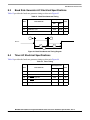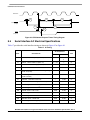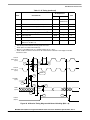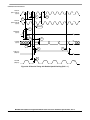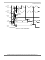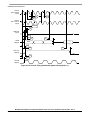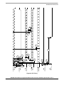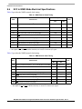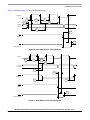
1
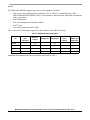
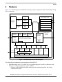
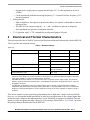
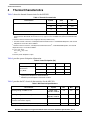
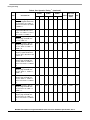
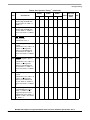
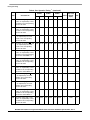
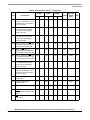
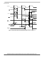
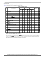
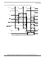
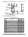
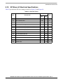
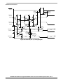
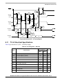
Freescale Semiconductor
Document Number: MPC850EC
Rev. 2, 07/2005
Technical Data
MPC850
PowerQUICC™ Integrated
Communications Processor
Hardware Specifications
This document contains detailed information on power
considerations, AC/DC electrical characteristics, and AC
timing specifications for revision A,B, and C of the MPC850
Family.
1
Overview
The MPC850 is a versatile, one-chip integrated
microprocessor and peripheral combination that can be used
in a variety of controller applications, excelling particularly
in communications and networking products. The MPC850,
which includes support for Ethernet, is specifically designed
for cost-sensitive, remote-access, and telecommunications
applications. It is provides functions similar to the MPC860,
with system enhancements such as universal serial bus
(USB) support and a larger (8-Kbyte) dual-port RAM.
In addition to a high-performance embedded MPC8xx core,
the MPC850 integrates system functions, such as a versatile
memory controller and a communications processor module
(CPM) that incorporates a specialized, independent RISC
communications processor (referred to as the CP). This
separate processor off-loads peripheral tasks from the
embedded MPC8xx core.
© Freescale Semiconductor, Inc., 2005. All rights reserved.
1.
2.
3.
4.
5.
6.
7.
8.
9.
10.
Contents
Overview . . . . . . . . . . . . . . . . . . . . . . . . . . . . . . . . . . . 1
Features . . . . . . . . . . . . . . . . . . . . . . . . . . . . . . . . . . . . 3
Electrical and Thermal Characteristics . . . . . . . . . . . . 7
Thermal Characteristics . . . . . . . . . . . . . . . . . . . . . . . 8
Power Considerations . . . . . . . . . . . . . . . . . . . . . . . . . 9
Bus Signal Timing . . . . . . . . . . . . . . . . . . . . . . . . . . 10
IEEE 1149.1 Electrical Specifications . . . . . . . . . . . 39
CPM Electrical Characteristics . . . . . . . . . . . . . . . . . 41
Mechanical Data and Ordering Information . . . . . . . 63
Document Revision History . . . . . . . . . . . . . . . . . . . 68
Overview
The CPM of the MPC850 supports up to seven serial channels, as follows:
• One or two serial communications controllers (SCCs). The SCCs support Ethernet, ATM
(MPC850SR and MPC850DSL), HDLC and a number of other protocols, along with a transparent
mode of operation.
• One USB channel
• Two serial management controllers (SMCs)
• One I2C port
• One serial peripheral interface (SPI).
Table 1 shows the functionality supported by the members of the MPC850 family.
Table 1. MPC850 Functionality Matrix
Number of
Multi-channel
PCMCIA Slots
HDLC
Supported
Support
Number of
SCCs
Supported
Ethernet
Support
ATM Support
USB Support
MPC850
1
Yes
-
Yes
-
1
MPC850DE
2
Yes
-
Yes
-
1
MPC850SR
2
Yes
Yes
Yes
Yes
1
MPC850DSL
2
Yes
Yes
Yes
No
1
Part
Additional documentation may be provided for parts listed in Table 1.
MPC850 PowerQUICC™ Integrated Communications Processor Hardware Specifications, Rev. 2
2
Freescale Semiconductor
Features
2
Features
Figure 1 is a block diagram of the MPC850, showing its major components and the relationships among
those components:
2-Kbyte
I-Cache
Instruction
Bus
Embedded
MPC8xx
Core
System Interface Unit
Memory Controller
Instruction
MMU
Unified Bus
Bus Interface Unit
1-Kbyte
D-Cache
Load/Store
Bus
Baud Rate
Generators
Four
Timers
System Functions
Real-Time Clock
Data
MMU
Interrupt
Controller
PCMCIA Interface
Dual-Port
RAM
20 Virtual
Serial DMA
Channels
Parallel I/O
32-Bit RISC Communications
Ports
Processor (CP) and Program ROM
—
UTOPIA
(850SR & DSL) Timer
Communications
Processor
Module
and
2 Virtual
IDMA
Channels
Peripheral Bus
SCC2
TDMa
SCC3
SMC1
SMC2
USB
SPI
I2C
Time Slot Assigner
Non-Multiplexed Serial Interface
Figure 1. MPC850 Microprocessor Block Diagram
The following list summarizes the main features of the MPC850:
• Embedded single-issue, 32-bit MPC8xx core (implementing the PowerPC architecture) with
thirty-two 32-bit general-purpose registers (GPRs)
— Performs branch folding and branch prediction with conditional prefetch, but without
conditional execution
MPC850 PowerQUICC™ Integrated Communications Processor Hardware Specifications, Rev. 2
Freescale Semiconductor
3
Features
•
•
•
•
•
•
— 2-Kbyte instruction cache and 1-Kbyte data cache (Harvard architecture)
– Caches are two-way, set-associative
– Physically addressed
– Cache blocks can be updated with a 4-word line burst
– Least-recently used (LRU) replacement algorithm
– Lockable one-line granularity
— Memory management units (MMUs) with 8-entry translation lookaside buffers (TLBs) and
fully-associative instruction and data TLBs
— MMUs support multiple page sizes of 4 Kbytes, 16 Kbytes, 256 Kbytes, 512 Kbytes, and
8 Mbytes; 16 virtual address spaces and eight protection groups
Advanced on-chip emulation debug mode
Data bus dynamic bus sizing for 8, 16, and 32-bit buses
— Supports traditional 68000 big-endian, traditional x86 little-endian and modified little-endian
memory systems
— Twenty-six external address lines
Completely static design (0–80 MHz operation)
System integration unit (SIU)
— Hardware bus monitor
— Spurious interrupt monitor
— Software watchdog
— Periodic interrupt timer
— Low-power stop mode
— Clock synthesizer
— Decrementer, time base, and real-time clock (RTC) from the PowerPC architecture
— Reset controller
— IEEE 1149.1 test access port (JTAG)
Memory controller (eight banks)
— Glueless interface to DRAM single in-line memory modules (SIMMs), synchronous DRAM
(SDRAM), static random-access memory (SRAM), electrically programmable read-only
memory (EPROM), flash EPROM, etc.
— Memory controller programmable to support most size and speed memory interfaces
— Boot chip-select available at reset (options for 8, 16, or 32-bit memory)
— Variable block sizes, 32 Kbytes to 256 Mbytes
— Selectable write protection
— On-chip bus arbiter supports one external bus master
— Special features for burst mode support
General-purpose timers
— Four 16-bit timers or two 32-bit timers
MPC850 PowerQUICC™ Integrated Communications Processor Hardware Specifications, Rev. 2
4
Freescale Semiconductor
Features
•
•
•
•
•
— Gate mode can enable/disable counting
— Interrupt can be masked on reference match and event capture
Interrupts
— Eight external interrupt request (IRQ) lines
— Twelve port pins with interrupt capability
— Fifteen internal interrupt sources
— Programmable priority among SCCs and USB
— Programmable highest-priority request
Single socket PCMCIA-ATA interface
— Master (socket) interface, release 2.1 compliant
— Single PCMCIA socket
— Supports eight memory or I/O windows
Communications processor module (CPM)
— 32-bit, Harvard architecture, scalar RISC communications processor (CP)
— Protocol-specific command sets (for example, GRACEFUL STOP TRANSMIT stops transmission
after the current frame is finished or immediately if no frame is being sent and CLOSE RXBD
closes the receive buffer descriptor)
— Supports continuous mode transmission and reception on all serial channels
— Up to 8 Kbytes of dual-port RAM
— Twenty serial DMA (SDMA) channels for the serial controllers, including eight for the four
USB endpoints
— Three parallel I/O registers with open-drain capability
Four independent baud-rate generators (BRGs)
— Can be connected to any SCC, SMC, or USB
— Allow changes during operation
— Autobaud support option
Two SCCs (serial communications controllers)
— Ethernet/IEEE 802.3, supporting full 10-Mbps operation
— HDLC/SDLC™ (all channels supported at 2 Mbps)
— HDLC bus (implements an HDLC-based local area network (LAN))
— Asynchronous HDLC to support PPP (point-to-point protocol)
— AppleTalk®
— Universal asynchronous receiver transmitter (UART)
— Synchronous UART
— Serial infrared (IrDA)
— Totally transparent (bit streams)
— Totally transparent (frame based with optional cyclic redundancy check (CRC))
MPC850 PowerQUICC™ Integrated Communications Processor Hardware Specifications, Rev. 2
Freescale Semiconductor
5
Features
•
•
•
•
•
•
•
QUICC multichannel controller (QMC) microcode features
— Up to 64 independent communication channels on a single SCC
— Arbitrary mapping of 0–31 channels to any of 0–31 TDM time slots
— Supports either transparent or HDLC protocols for each channel
— Independent TxBDs/Rx and event/interrupt reporting for each channel
One universal serial bus controller (USB)
— Supports host controller and slave modes at 1.5 Mbps and 12 Mbps
Two serial management controllers (SMCs)
— UART
— Transparent
— General circuit interface (GCI) controller
— Can be connected to the time-division-multiplexed (TDM) channel
One serial peripheral interface (SPI)
— Supports master and slave modes
— Supports multimaster operation on the same bus
One I2C® (interprocessor-integrated circuit) port
— Supports master and slave modes
— Supports multimaster environment
Time slot assigner
— Allows SCCs and SMCs to run in multiplexed operation
— Supports T1, CEPT, PCM highway, ISDN basic rate, ISDN primary rate, user-defined
— 1- or 8-bit resolution
— Allows independent transmit and receive routing, frame syncs, clocking
— Allows dynamic changes
— Can be internally connected to four serial channels (two SCCs and two SMCs)
Low-power support
— Full high: all units fully powered at high clock frequency
— Full low: all units fully powered at low clock frequency
— Doze: core functional units disabled except time base, decrementer, PLL, memory controller,
real-time clock, and CPM in low-power standby
— Sleep: all units disabled except real-time clock and periodic interrupt timer. PLL is active for
fast wake-up
— Deep sleep: all units disabled including PLL, except the real-time clock and periodic interrupt
timer
— Low-power stop: to provide lower power dissipation
MPC850 PowerQUICC™ Integrated Communications Processor Hardware Specifications, Rev. 2
6
Freescale Semiconductor
Electrical and Thermal Characteristics
•
•
3
— Separate power supply input to operate internal logic at 2.2 V when operating at or below
25 MHz
— Can be dynamically shifted between high frequency (3.3 V internal) and low frequency (2.2 V
internal) operation
Debug interface
— Eight comparators: four operate on instruction address, two operate on data address, and two
operate on data
— The MPC850 can compare using the =, ≠, <, and > conditions to generate watchpoints
— Each watchpoint can generate a breakpoint internally
3.3-V operation with 5-V TTL compatibility on all general purpose I/O pins.
Electrical and Thermal Characteristics
This section provides the AC and DC electrical specifications and thermal characteristics for the MPC850.
Table 2 provides the maximum ratings.
Table 2. Maximum Ratings
(GND = 0V)
Rating
Supply voltage
Symbol
Value
Unit
VDDH
-0.3 to 4.0
V
VDDL
-0.3 to 4.0
V
KAPWR
-0.3 to 4.0
V
VDDSYN
-0.3 to 4.0
V
Input voltage 1
Vin
GND-0.3 to VDDH + 2.5 V
V
Junction temperature 2
Tj
0 to 95 (standard)
-40 to 95 (extended)
°C
Storage temperature range
Tstg
-55 to +150
°C
1
Functional operating conditions are provided with the DC electrical specifications in Table 5. Absolute maximum
ratings are stress ratings only; functional operation at the maxima is not guaranteed. Stress beyond those listed may
affect device reliability or cause permanent damage to the device.
CAUTION: All inputs that tolerate 5 V cannot be more than 2.5 V greater than the supply voltage. This restriction
applies to power-up and normal operation (that is, if the MPC850 is unpowered, voltage greater than 2.5 V must not
be applied to its inputs).
2 The MPC850, a high-frequency device in a BGA package, does not provide a guaranteed maximum ambient
temperature. Only maximum junction temperature is guaranteed. It is the responsibility of the user to consider power
dissipation and thermal management. Junction temperature ratings are the same regardless of frequency rating of
the device.
This device contains circuitry protecting against damage due to high-static voltage or electrical fields;
however, it is advised that normal precautions be taken to avoid application of any voltages higher than
maximum-rated voltages to this high-impedance circuit. Reliability of operation is enhanced if unused
inputs are tied to an appropriate logic voltage level (for example, either GND or VCC). Table 3 provides
the package thermal characteristics for the MPC850.
MPC850 PowerQUICC™ Integrated Communications Processor Hardware Specifications, Rev. 2
Freescale Semiconductor
7
Thermal Characteristics
4
Thermal Characteristics
Table 3 shows the thermal characteristics for the MPC850.
Table 3. Thermal Characteristics
Characteristic
Thermal resistance for BGA 1
Thermal Resistance for BGA (junction-to-case)
Symbol
Value
Unit
θJA
40 2
°C/W
θJA
31 3
°C/W
θJA
24 4
°C/W
θJC
8
°C/W
1
For more information on the design of thermal vias on multilayer boards and BGA layout considerations in
general, refer to AN-1231/D, Plastic Ball Grid Array Application Note available from your local Freescale sales
office.
2
Assumes natural convection and a single layer board (no thermal vias).
3
Assumes natural convection, a multilayer board with thermal vias4, 1 watt MPC850 dissipation, and a board
temperature rise of 20°C above ambient.
4 Assumes natural convection, a multilayer board with thermal vias4, 1 watt MPC850 dissipation, and a board
temperature rise of 13°C above ambient.
TJ = TA + (PD •θJA)
PD = (VDD • IDD) + PI/O
where:
PI/O is the power dissipation on pins
Table 4 provides power dissipation information.
Table 4. Power Dissipation (PD)
Characteristic
Power Dissipation
All Revisions
(1:1) Mode
1
2
Frequency (MHz)
Typical 1
Maximum 2
Unit
33
TBD
515
mW
40
TBD
590
mW
50
TBD
725
mW
Typical power dissipation is measured at 3.3V
Maximum power dissipation is measured at 3.65 V
Table 5 provides the DC electrical characteristics for the MPC850.
Table 5. DC Electrical Specifications
Characteristic
Symbol
Min
Max
Unit
Operating voltage at 40 MHz or less
VDDH, VDDL,
KAPWR, VDDSYN
3.0
3.6
V
Operating voltage at 40 MHz or higher
VDDH, VDDL,
KAPWR, VDDSYN
3.135
3.465
V
Input high voltage (address bus, data bus, EXTAL, EXTCLK,
and all bus control/status signals)
VIH
2.0
3.6
V
Input high voltage (all general purpose I/O and peripheral pins)
VIH
2.0
5.5
V
MPC850 PowerQUICC™ Integrated Communications Processor Hardware Specifications, Rev. 2
8
Freescale Semiconductor
Power Considerations
Table 5. DC Electrical Specifications (continued)
Characteristic
Symbol
Min
Max
Unit
VIL
GND
0.8
V
VIHC
0.7*(VCC)
VCC+0.3
V
Input leakage current, Vin = 5.5 V (Except TMS, TRST, DSCK
and DSDI pins)
Iin
—
100
µA
Input leakage current, Vin = 3.6V (Except TMS, TRST, DSCK
and DSDI pins)
IIn
—
10
µA
Input leakage current, Vin = 0V (Except TMS, TRST, DSCK
and DSDI pins)
IIn
—
10
µA
Input capacitance
Cin
—
20
pF
Output high voltage, IOH = -2.0 mA, VDDH = 3.0V
except XTAL, XFC, and open-drain pins
VOH
2.4
—
V
Output low voltage
CLKOUT 3
IOL = 3.2 mA 1
IOL = 5.3 mA 2
IOL = 7.0 mA PA[14]/USBOE, PA[12]/TXD2
IOL = 8.9 mA TS, TA, TEA, BI, BB, HRESET, SRESET
VOL
—
0.5
V
Input low voltage
EXTAL, EXTCLK input high voltage
1
A[6:31], TSIZ0/REG, TSIZ1, D[0:31], DP[0:3]/IRQ[3:6], RD/WR, BURST, RSV/IRQ2, IP_B[0:1]/IWP[0:1]/VFLS[0:1],
IP_B2/IOIS16_B/AT2, IP_B3/IWP2/VF2, IP_B4/LWP0/VF0, IP_B5/LWP1/VF1, IP_B6/DSDI/AT0, IP_B7/PTR/AT3,
PA[15]/USBRXD, PA[13]/RXD2, PA[9]/L1TXDA/SMRXD2, PA[8]/L1RXDA/SMTXD2,
PA[7]/CLK1/TIN1/L1RCLKA/BRGO1, PA[6]/CLK2/TOUT1/TIN3, PA[5]/CLK3/TIN2/L1TCLKA/BRGO2,
PA[4]/CLK4/TOUT2/TIN4, PB[31]/SPISEL, PB[30]/SPICLK/TXD3, PB[29]/SPIMOSI /RXD3,
PB[28]/SPIMISO/BRGO3, PB[27]/I2CSDA/BRGO1, PB[26]/I2CSCL/BRGO2, PB[25]/SMTXD1/TXD3,
PB[24]/SMRXD1/RXD3, PB[23]/SMSYN1/SDACK1, PB[22]/SMSYN2/SDACK2, PB[19]/L1ST1,
PB[18]/RTS2/L1ST2, PB[17]/L1ST3, PB[16]/L1RQa/L1ST4, PC[15]/DREQ0/L1ST5, PC[14]/DREQ1/RTS2/L1ST6,
PC[13]/L1ST7/RTS3, PC[12]/L1RQa/L1ST8, PC[11]/USBRXP, PC[10]/TGATE1/USBRXN, PC[9]/CTS2,
PC[8]/CD2/TGATE1, PC[7]/USBTXP, PC[6]/USBTXN, PC[5]/CTS3/L1TSYNCA/SDACK1, PC[4]/CD3/L1RSYNCA,
PD[15], PD[14], PD[13], PD[12], PD[11], PD[10], PD[9], PD[8], PD[7], PD[6], PD[5], PD[4], PD[3]
2 BDIP/GPL_B5, BR, BG, FRZ/IRQ6, CS[0:5], CS6/CE1_B, CS7/CE2_B, WE0/BS_AB0/IORD, WE1/BS_AB1/IOWR,
WE2/BS_AB2/PCOE, WE3/BS_AB3/PCWE, GPL_A0/GPL_B0, OE/GPL_A1/GPL_B1,
GPL_A[2:3]/GPL_B[2:3]/CS[2:3], UPWAITA/GPL_A4/AS, UPWAITB/GPL_B4, GPL_A5, ALE_B/DSCK/AT1,
OP2/MODCK1/STS, OP3/MODCK2/DSDO
3 The MPC850 IBIS model must be used to accurately model the behavior of the Clkout output driver for the full and
half drive setting. Due to the nature of the Clkout output buffer, IOH and IOL for Clkout should be extracted from the
IBIS model at any output voltage level.
5
Power Considerations
The average chip-junction temperature, TJ, in °C can be obtained from the equation:
TJ = TA + (PD • θJA)(1)
where
TA = Ambient temperature, °C
MPC850 PowerQUICC™ Integrated Communications Processor Hardware Specifications, Rev. 2
Freescale Semiconductor
9
Bus Signal Timing
θJA = Package thermal resistance, junction to ambient, °C/W
PD = PINT + PI/O
PINT = IDD x VDD, watts—chip internal power
PI/O = Power dissipation on input and output pins—user determined
For most applications PI/O < 0.3 • PINT and can be neglected. If PI/O is neglected, an approximate
relationship between PD and TJ is:
PD = K ÷ (TJ + 273°C)(2)
Solving equations (1) and (2) for K gives:
2
K = PD • (TA + 273°C) + θJA • PD (3)
where K is a constant pertaining to the particular part. K can be determined from equation (3) by measuring
PD (at equilibrium) for a known TA. Using this value of K, the values of PD and TJ can be obtained by
solving equations (1) and (2) iteratively for any value of TA.
5.1
Layout Practices
Each VCC pin on the MPC850 should be provided with a low-impedance path to the board’s supply. Each
GND pin should likewise be provided with a low-impedance path to ground. The power supply pins drive
distinct groups of logic on chip. The VCC power supply should be bypassed to ground using at least four
0.1 µF by-pass capacitors located as close as possible to the four sides of the package. The capacitor leads
and associated printed circuit traces connecting to chip VCC and GND should be kept to less than half an
inch per capacitor lead. A four-layer board is recommended, employing two inner layers as VCC and GND
planes.
All output pins on the MPC850 have fast rise and fall times. Printed circuit (PC) trace interconnection
length should be minimized in order to minimize undershoot and reflections caused by these fast output
switching times. This recommendation particularly applies to the address and data busses. Maximum PC
trace lengths of six inches are recommended. Capacitance calculations should consider all device loads as
well as parasitic capacitances due to the PC traces. Attention to proper PCB layout and bypassing becomes
especially critical in systems with higher capacitive loads because these loads create higher transient
currents in the VCC and GND circuits. Pull up all unused inputs or signals that will be inputs during reset.
Special care should be taken to minimize the noise levels on the PLL supply pins.
6
Bus Signal Timing
Table 6 provides the bus operation timing for the MPC850 at 50 MHz, 66 MHz, and 80 MHz. Timing
information for other bus speeds can be interpolated by equation using the MPC850 Electrical
Specifications Spreadsheet found at http://www.mot.com/netcomm.
The maximum bus speed supported by the MPC850 is 50 MHz. Higher-speed parts must be operated in
half-speed bus mode (for example, an MPC850 used at 66 MHz must be configured for a 33 MHz bus).
The timing for the MPC850 bus shown assumes a 50-pF load. This timing can be derated by 1 ns per 10
pF. Derating calculations can also be performed using the MPC850 Electrical Specifications Spreadsheet.
MPC850 PowerQUICC™ Integrated Communications Processor Hardware Specifications, Rev. 2
10
Freescale Semiconductor
Bus Signal Timing
Table 6. Bus Operation Timing 1
50 MHz
Num
66 MHz
80 MHz
Characteristic
FFACT
Cap Load
(default
50 pF)
Unit
Min
Max
Min
Max
Min
Max
20
—
30.30
—
25
—
—
—
ns
B1
CLKOUT period
B1a
EXTCLK to CLKOUT phase
skew (EXTCLK > 15 MHz and
MF <= 2)
-0.90
0.90
-0.90
0.90
-0.90
0.90
—
50.00
ns
B1b
EXTCLK to CLKOUT phase
skew (EXTCLK > 10 MHz and
MF < 10)
-2.30
2.30
-2.30
2.30
-2.30
2.30
—
50.00
ns
B1c
CLKOUT phase jitter (EXTCLK
> 15 MHz and MF <= 2) 2
-0.60
0.60
-0.60
0.60
-0.60
0.60
—
50.00
ns
B1d
CLKOUT phase jitter 2
-2.00
2.00
-2.00
2.00
-2.00
2.00
—
50.00
ns
B1e
CLKOUT frequency jitter (MF <
10) 2
—
0.50
—
0.50
—
0.50
—
50.00
%
B1f
CLKOUT frequency jitter (10 <
MF < 500) 2
—
2.00
—
2.00
—
2.00
—
50.00
%
B1g
CLKOUT frequency jitter (MF >
500) 2
—
3.00
—
3.00
—
3.00
—
50.00
%
B1h
Frequency jitter on EXTCLK 3
—
0.50
—
0.50
—
0.50
—
50.00
%
B2
CLKOUT pulse width low
8.00
—
12.12
—
10.00
—
—
50.00
ns
B3
CLKOUT width high
8.00
—
12.12
—
10.00
—
—
50.00
ns
B4
CLKOUT rise time
—
4.00
—
4.00
—
4.00
—
50.00
ns
B5
CLKOUT fall time
—
4.00
—
4.00
—
4.00
—
50.00
ns
B7
CLKOUT to A[6–31],
RD/WR, BURST, D[0–31],
DP[0–3] invalid
5.00
—
7.58
—
6.25
—
0.250
50.00
ns
B7a
CLKOUT to TSIZ[0–1], REG,
RSV, AT[0–3], BDIP, PTR
invalid
5.00
—
7.58
—
6.25
—
0.250
50.00
ns
B7b
CLKOUT to BR, BG, FRZ,
VFLS[0–1], VF[0–2] IWP[0–2],
LWP[0–1], STS invalid 4
5.00
—
7.58
—
6.25
—
0.250
50.00
ns
B8
CLKOUT to A[6–31],
RD/WR, BURST, D[0–31],
DP[0–3] valid
5.00
11.75
7.58
14.33
6.25
13.00
0.250
50.00
ns
B8a
CLKOUT to TSIZ[0–1], REG,
RSV, AT[0–3] BDIP, PTR valid
5.00
11.75
7.58
14.33
6.25
13.00
0.250
50.00
ns
B8b
CLKOUT to BR, BG,
VFLS[0–1], VF[0–2], IWP[0–2],
FRZ, LWP[0–1], STS valid 4
5.00
11.74
7.58
14.33
6.25
13.00
0.250
50.00
ns
MPC850 PowerQUICC™ Integrated Communications Processor Hardware Specifications, Rev. 2
Freescale Semiconductor
11
Bus Signal Timing
Table 6. Bus Operation Timing 1 (continued)
50 MHz
Num
66 MHz
80 MHz
Characteristic
Min
Max
Min
Max
Min
Max
FFACT
Cap Load
(default
50 pF)
Unit
B9
CLKOUT to A[6–31] RD/WR,
BURST, D[0–31], DP[0–3],
TSIZ[0–1], REG, RSV, AT[0–3],
PTR high-Z
5.00
11.75
7.58
14.33
6.25
13.00
0.250
50.00
ns
B11
CLKOUT to TS, BB assertion
5.00
11.00
7.58
13.58
6.25
12.25
0.250
50.00
ns
B11a
CLKOUT to TA, BI assertion,
(When driven by the memory
controller or PCMCIA interface)
2.50
9.25
2.50
9.25
2.50
9.25
—
50.00
ns
B12
CLKOUT to TS, BB negation
5.00
11.75
7.58
14.33
6.25
13.00
0.250
50.00
ns
B12a
CLKOUT to TA, BI negation
(when driven by the memory
controller or PCMCIA interface)
2.50
11.00
2.50
11.00
2.50
11.00
—
50.00
ns
B13
CLKOUT to TS, BB high-Z
5.00
19.00
7.58
21.58
6.25
20.25
0.250
50.00
ns
B13a
CLKOUT to TA, BI high-Z,
(when driven by the memory
controller or PCMCIA interface)
2.50
15.00
2.50
15.00
2.50
15.00
—
50.00
ns
B14
CLKOUT to TEA assertion
2.50
10.00
2.50
10.00
2.50
10.00
—
50.00
ns
B15
CLKOUT to TEA high-Z
2.50
15.00
2.50
15.00
2.50
15.00
—
50.00
ns
B16
TA, BI valid to CLKOUT(setup
time) 5
9.75
—
9.75
—
9.75
—
—
50.00
ns
B16a
TEA, KR, RETRY, valid to
CLKOUT (setup time) 5
10.00
—
10.00
—
10.00
—
—
50.00
ns
B16b
BB, BG, BR valid to CLKOUT
(setup time) 6
8.50
—
8.50
—
8.50
—
—
50.00
ns
B17
CLKOUT to TA, TEA, BI, BB,
BG, BR valid (Hold time).5
1.00
—
1.00
—
1.00
—
—
50.00
ns
B17a
CLKOUT to KR, RETRY, except
TEA valid (hold time)
2.00
—
2.00
—
2.00
—
—
50.00
ns
B18
D[0–31], DP[0–3] valid to
CLKOUT rising edge (setup
time) 7
6.00
—
6.00
—
6.00
—
—
50.00
ns
B19
CLKOUT rising edge to
D[0–31], DP[0–3] valid (hold
time) 7
1.00
—
1.00
—
1.00
—
—
50.00
ns
B20
D[0–31], DP[0–3] valid to
CLKOUT falling edge (setup
time) 8
4.00
—
4.00
—
4.00
—
—
50.00
ns
B21
CLKOUT falling edge to
D[0–31], DP[0–3] valid (hold
time) 8
2.00
—
2.00
—
2.00
—
—
—
—
MPC850 PowerQUICC™ Integrated Communications Processor Hardware Specifications, Rev. 2
12
Freescale Semiconductor
Bus Signal Timing
Table 6. Bus Operation Timing 1 (continued)
50 MHz
Num
66 MHz
80 MHz
Characteristic
Min
Max
Min
Max
Min
Max
FFACT
Cap Load
(default
50 pF)
Unit
B22
CLKOUT rising edge to CS
asserted GPCM ACS = 00
5.00
11.75
7.58
14.33
6.25
13.00
0.250
50.00
ns
B22a
CLKOUT falling edge to CS
asserted GPCM ACS = 10,
TRLX = 0,1
—
8.00
—
8.00
—
8.00
—
50.00
ns
B22b
CLKOUT falling edge to CS
asserted GPCM ACS = 11,
TRLX = 0, EBDF = 0
5.00
11.75
7.58
14.33
6.25
13.00
0.250
50.00
ns
B22c
CLKOUT falling edge to CS
asserted GPCM ACS = 11,
TRLX = 0, EBDF = 1
7.00
14.00 11.00 18.00
9.00
16.00
0.375
50.00
ns
B23
CLKOUT rising edge to CS
negated GPCM read access,
GPCM write access ACS = 00,
TRLX = 0 & CSNT = 0
2.00
8.00
2.00
8.00
2.00
8.00
—
50.00
ns
B24
A[6–31] to CS asserted GPCM
ACS = 10, TRLX = 0.
3.00
—
6.00
—
4.00
—
0.250
50.00
ns
B24a
A[6–31] to CS asserted GPCM
ACS = 11, TRLX = 0
8.00
—
13.00
—
11.00
—
0.500
50.00
ns
B25
CLKOUT rising edge to OE,
WE[0–3] asserted
—
9.00
—
9.00
—
9.00
—
50.00
ns
B26
CLKOUT rising edge to OE
negated
2.00
9.00
2.00
9.00
2.00
9.00
—
50.00
ns
B27
A[6–31] to CS asserted GPCM
ACS = 10, TRLX = 1
23.00
—
36.00
—
29.00
—
1.250
50.00
ns
B27a
A[6–31] to CS asserted GPCM
ACS = 11, TRLX = 1
28.00
—
43.00
—
36.00
—
1.500
50.00
ns
B28
CLKOUT rising edge to
WE[0–3] negated GPCM write
access CSNT = 0
—
9.00
—
9.00
—
9.00
—
50.00
ns
B28a
CLKOUT falling edge to
WE[0–3] negated GPCM write
access TRLX = 0,1 CSNT = 1,
EBDF = 0
5.00
12.00
8.00
14.00
6.00
13.00
0.250
50.00
ns
B28b
CLKOUT falling edge to CS
negated GPCM write access
TRLX = 0,1 CSNT = 1, ACS =
10 or ACS = 11, EBDF = 0
—
12.00
—
14.00
—
13.00
0.250
50.00
ns
MPC850 PowerQUICC™ Integrated Communications Processor Hardware Specifications, Rev. 2
Freescale Semiconductor
13
Bus Signal Timing
Table 6. Bus Operation Timing 1 (continued)
50 MHz
Num
66 MHz
80 MHz
Characteristic
Min
FFACT
Cap Load
(default
50 pF)
Unit
Min
Max
Max
Min
Max
14.00 11.00 18.00
9.00
16.00
0.375
50.00
ns
B28c
CLKOUT falling edge to
WE[0–3] negated GPCM write
access TRLX = 0,1 CSNT = 1
write access TRLX = 0, CSNT =
1, EBDF = 1
7.00
B28d
CLKOUT falling edge to CS
negated GPCM write access
TRLX = 0,1 CSNT = 1, ACS =
10 or ACS = 11, EBDF = 1
—
14.00
—
18.00
—
16.00
0.375
50.00
ns
B29
WE[0–3] negated to D[0–31],
DP[0–3] high-Z GPCM write
access, CSNT = 0
3.00
—
6.00
—
4.00
—
0.250
50.00
ns
B29a
WE[0–3] negated to D[0–31],
DP[0–3] high-Z GPCM write
access, TRLX = 0 CSNT = 1,
EBDF = 0
8.00
—
13.00
—
11.00
—
0.500
50.00
ns
B29b
CS negated to D[0–31],
DP[0–3], high-Z GPCM write
access, ACS = 00, TRLX = 0 &
CSNT = 0
3.00
—
6.00
—
4.00
—
0.250
50.00
ns
B29c
CS negated to D[0–31],
DP[0–3] high-Z GPCM write
access, TRLX = 0, CSNT = 1,
ACS = 10 or ACS = 11, EBDF =
0
8.00
—
13.00
—
11.00
—
0.500
50.00
ns
B29d
WE[0–3] negated to D[0–31],
DP[0–3] high-Z GPCM write
access, TRLX = 1, CSNT = 1,
EBDF = 0
28.00
—
43.00
—
36.00
—
1.500
50.00
ns
B29e
CS negated to D[0–31],
DP[0–3] high-Z GPCM write
access, TRLX = 1, CSNT = 1,
ACS = 10 or ACS = 11, EBDF =
0
28.00
—
43.00
—
36.00
—
1.500
50.00
ns
B29f
WE[0–3] negated to D[0–31],
DP[0–3] high-Z GPCM write
access TRLX = 0, CSNT = 1,
EBDF = 1
5.00
—
9.00
—
7.00
—
0.375
50.00
ns
B29g
CS negated to D[0–31],
DP[0–3] high-Z GPCM write
access TRLX = 0, CSNT = 1,
ACS = 10 or ACS = 11, EBDF =
1
5.00
—
9.00
—
7.00
—
0.375
50.00
ns
MPC850 PowerQUICC™ Integrated Communications Processor Hardware Specifications, Rev. 2
14
Freescale Semiconductor
Bus Signal Timing
Table 6. Bus Operation Timing 1 (continued)
50 MHz
Num
66 MHz
80 MHz
Characteristic
Min
Max
Min
Max
Min
Max
FFACT
Cap Load
(default
50 pF)
Unit
B29h
WE[0–3] negated to D[0–31],
DP[0–3] high-Z GPCM write
access TRLX = 0, CSNT = 1,
EBDF = 1
25.00
—
39.00
—
31.00
—
1.375
50.00
ns
B29i
CS negated to D[0–31],
DP[0–3] high-Z GPCM write
access, TRLX = 1, CSNT = 1,
ACS = 10 or ACS = 11, EBDF =
1
25.00
—
39.00
—
31.00
—
1.375
50.00
ns
B30
CS, WE[0–3] negated to
A[6–31] invalid
GPCM write access 9
3.00
—
6.00
—
4.00
—
0.250
50.00
ns
B30a
WE[0–3] negated to A[6–31]
invalid
GPCM write access, TRLX = 0,
CSNT = 1, CS negated to
A[6–31] invalid GPCM write
access TRLX = 0, CSNT =1,
ACS = 10 or ACS = 11, EBDF =
0
8.00
—
13.00
—
11.00
—
0.500
50.00
ns
B30b
WE[0–3] negated to A[6–31]
invalid
GPCM write access, TRLX = 1,
CSNT = 1. CS negated to
A[6–31] Invalid GPCM write
access TRLX = 1, CSNT = 1,
ACS = 10 or ACS = 11, EBDF =
0
28.00
—
43.00
—
36.00
—
1.500
50.00
ns
B30c
WE[0–3] negated to A[6–31]
invalid
GPCM write access, TRLX = 0,
CSNT = 1. CS negated to
A[6–31] invalid GPCM write
access, TRLX = 0, CSNT = 1,
ACS = 10 or ACS = 11, EBDF =
1
5.00
—
8.00
—
6.00
—
0.375
50.00
ns
B30d
WE[0–3] negated to A[6–31]
invalid GPCM write access
TRLX = 1, CSNT =1, CS
negated to A[6–31] invalid
GPCM write access TRLX = 1,
CSNT = 1, ACS = 10 or ACS =
11, EBDF = 1
25.00
—
39.00
—
31.00
—
1.375
50.00
ns
MPC850 PowerQUICC™ Integrated Communications Processor Hardware Specifications, Rev. 2
Freescale Semiconductor
15
Bus Signal Timing
Table 6. Bus Operation Timing 1 (continued)
50 MHz
Num
66 MHz
80 MHz
Characteristic
Min
Max
Min
Max
Min
Max
FFACT
Cap Load
(default
50 pF)
Unit
B31
CLKOUT falling edge to CS
valid - as requested by control
bit CST4 in the corresponding
word in the UPM
1.50
6.00
1.50
6.00
1.50
6.00
—
50.00
ns
B31a
CLKOUT falling edge to CS
valid - as requested by control
bit CST1 in the corresponding
word in the UPM
5.00
12.00
8.00
14.00
6.00
13.00
0.250
50.00
ns
B31b
CLKOUT rising edge to CS valid
- as requested by control bit
CST2 in the corresponding
word in the UPM
1.50
8.00
1.50
8.00
1.50
8.00
—
50.00
ns
B31c
CLKOUT rising edge to CS valid
- as requested by control bit
CST3 in the corresponding
word in the UPM
5.00
12.00
8.00
14.00
6.00
13.00
0.250
50.00
ns
B31d
CLKOUT falling edge to CS
valid - as requested by control
bit CST1 in the corresponding
word in the UPM EBDF = 1
9.00
14.00 13.00 18.00 11.00 16.00
0.375
50.00
ns
B32
CLKOUT falling edge to BS
valid - as requested by control
bit BST4 in the corresponding
word in the UPM
1.50
6.00
1.50
6.00
1.50
6.00
—
50.00
ns
B32a
CLKOUT falling edge to BS
valid - as requested by control
bit BST1 in the corresponding
word in the UPM, EBDF = 0
5.00
12.00
8.00
14.00
6.00
13.00
0.250
50.00
ns
B32b
CLKOUT rising edge to BS valid
- as requested by control bit
BST2 in the corresponding
word in the UPM
1.50
8.00
1.50
8.00
1.50
8.00
—
50.00
ns
B32c
CLKOUT rising edge to BS valid
- as requested by control bit
BST3 in the corresponding
word in the UPM
5.00
12.00
8.00
14.00
6.00
13.00
0.250
50.00
ns
B32d
CLKOUT falling edge to BS
valid - as requested by control
bit BST1 in the corresponding
word in the UPM, EBDF = 1
9.00
14.00 13.00 18.00 11.00 16.00
0.375
50.00
ns
B33
CLKOUT falling edge to GPL
valid - as requested by control
bit GxT4 in the corresponding
word in the UPM
1.50
6.00
—
50.00
ns
1.50
6.00
1.50
6.00
MPC850 PowerQUICC™ Integrated Communications Processor Hardware Specifications, Rev. 2
16
Freescale Semiconductor
Bus Signal Timing
Table 6. Bus Operation Timing 1 (continued)
50 MHz
Num
66 MHz
80 MHz
Characteristic
Min
Max
Min
Max
Min
Max
FFACT
Cap Load
(default
50 pF)
Unit
B33a
CLKOUT rising edge to GPL
valid - as requested by control
bit GxT3 in the corresponding
word in the UPM
5.00
12.00
8.00
14.00
6.00
13.00
0.250
50.00
ns
B34
A[6–31] and D[0–31] to CS valid
- as requested by control bit
CST4 in the corresponding
word in the UPM
3.00
—
6.00
—
4.00
—
0.250
50.00
ns
B34a
A[6–31] and D[0–31] to CS valid
- as requested by control bit
CST1 in the corresponding
word in the UPM
8.00
—
13.00
—
11.00
—
0.500
50.00
ns
B34b
A[6–31] and D[0–31] to CS valid 13.00
- as requested by CST2 in the
corresponding word in UPM
—
21.00
—
17.00
—
0.750
50.00
ns
B35
A[6–31] to CS valid - as
requested by control bit BST4 in
the corresponding word in UPM
3.00
—
6.00
—
4.00
—
0.250
50.00
ns
B35a
A[6–31] and D[0–31] to BS valid
- as requested by BST1 in the
corresponding word in the UPM
8.00
—
13.00
—
11.00
—
0.500
50.00
ns
B35b
A[6–31] and D[0–31] to BS valid 13.00
- as requested by control bit
BST2 in the corresponding
word in the UPM
—
21.00
—
17.00
—
0.750
50.00
ns
B36
A[6–31] and D[0–31] to GPL
valid - as requested by control
bit GxT4 in the corresponding
word in the UPM
3.00
—
6.00
—
4.00
—
0.250
50.00
ns
B37
UPWAIT valid to CLKOUT
falling edge 10
6.00
—
6.00
—
6.00
—
—
50.00
ns
B38
CLKOUT falling edge to
UPWAIT valid 10
1.00
—
1.00
—
1.00
—
—
50.00
ns
B39
AS valid to CLKOUT rising edge
7.00
—
7.00
—
7.00
—
—
50.00
ns
11
B40
A[6–31], TSIZ[0–1], RD/WR,
BURST, valid to CLKOUT rising
edge.
7.00
—
7.00
—
7.00
—
—
50.00
ns
B41
TS valid to CLKOUT rising edge
(setup time)
7.00
—
7.00
—
7.00
—
—
50.00
ns
MPC850 PowerQUICC™ Integrated Communications Processor Hardware Specifications, Rev. 2
Freescale Semiconductor
17
Bus Signal Timing
Table 6. Bus Operation Timing 1 (continued)
50 MHz
Num
66 MHz
80 MHz
Characteristic
B42
CLKOUT rising edge to TS valid
(hold time)
B43
AS negation to memory
controller signals negation
FFACT
Cap Load
(default
50 pF)
Unit
Min
Max
Min
Max
Min
Max
2.00
—
2.00
—
2.00
—
—
50.00
ns
—
TBD
—
TBD
TBD
—
—
50.00
ns
1
The minima provided assume a 0 pF load, whereas maxima assume a 50pF load. For frequencies not marked on
the part, new bus timing must be calculated for all frequency-dependent AC parameters. Frequency-dependent AC
parameters are those with an entry in the FFactor column. AC parameters without an FFactor entry do not need to
be calculated and can be taken directly from the frequency column corresponding to the frequency marked on the
part. The following equations should be used in these calculations.
For a frequency F, the following equations should be applied to each one of the above parameters:
For minima:
FFACTOR x 1000
(D50 - 20 x FFACTOR)
D=
+
F
For maxima:
FFACTOR x 1000
(D50 -20 x FFACTOR)
D=
+
F
1ns(CAP LOAD - 50) / 10
+
where:
D is the parameter value to the frequency required in ns
F is the operation frequency in MHz
D50 is the parameter value defined for 50 MHz
CAP LOAD is the capacitance load on the signal in question.
FFACTOR is the one defined for each of the parameters in the table.
2 Phase and frequency jitter performance results are valid only if the input jitter is less than the prescribed value.
3 If the rate of change of the frequency of EXTAL is slow (i.e. it does not jump between the minimum and maximum
values in one cycle) or the frequency of the jitter is fast (i.e., it does not stay at an extreme value for a long time) then
the maximum allowed jitter on EXTAL can be up to 2%.
4 The timing for BR output is relevant when the MPC850 is selected to work with external bus arbiter. The timing for
BG output is relevant when the MPC850 is selected to work with internal bus arbiter.
5 The setup times required for TA, TEA, and BI are relevant only when they are supplied by an external device (and
not when the memory controller or the PCMCIA interface drives them).
6 The timing required for BR input is relevant when the MPC850 is selected to work with the internal bus arbiter. The
timing for BG input is relevant when the MPC850 is selected to work with the external bus arbiter.
7 The D[0–31] and DP[0–3] input timings B20 and B21 refer to the rising edge of the CLKOUT in which the TA input
signal is asserted.
8 The D[0:31] and DP[0:3] input timings B20 and B21 refer to the falling edge of CLKOUT. This timing is valid only for
read accesses controlled by chip-selects controlled by the UPM in the memory controller, for data beats where DLT3
= 1 in the UPM RAM words. (This is only the case where data is latched on the falling edge of CLKOUT.
9
The timing B30 refers to CS when ACS = '00' and to WE[0:3] when CSNT = '0'.
10 The signal UPWAIT is considered asynchronous to CLKOUT and synchronized internally. The timings specified in
B37 and B38 are specified to enable the freeze of the UPM output signals.
11 The AS signal is considered asynchronous to CLKOUT.
MPC850 PowerQUICC™ Integrated Communications Processor Hardware Specifications, Rev. 2
18
Freescale Semiconductor
Bus Signal Timing
Figure 2 is the control timing diagram.
2.0 V
2.0 V
CLKOUT
0.8 V
0.8 V
A
B
2.0 V
0.8 V
Outputs
2.0 V
0.8 V
A
B
2.0 V
0.8 V
Outputs
2.0 V
0.8 V
D
C
2.0 V
0.8 V
Inputs
2.0 V
0.8 V
D
C
2.0 V
0.8 V
Inputs
A
Maximum output delay specification
B
Minimum output hold time
C
Minimum input setup time specification
D
Minimum input hold time specification
2.0 V
0.8 V
Figure 2. Control Timing
Figure 3 provides the timing for the external clock.
CLKOUT
B1
B3
B1
B4
B2
B5
Figure 3. External Clock Timing
MPC850 PowerQUICC™ Integrated Communications Processor Hardware Specifications, Rev. 2
Freescale Semiconductor
19
Bus Signal Timing
Figure 4 provides the timing for the synchronous output signals.
CLKOUT
B8
B7
B9
Output
Signals
B8a
B7a
B9
Output
Signals
B8b
B7b
Output
Signals
Figure 4. Synchronous Output Signals Timing
Figure 5 provides the timing for the synchronous active pull-up and open-drain output signals.
CLKOUT
B13
B11
B12
TS, BB
B13a
B11a
B12a
TA, BI
B14
B15
TEA
Figure 5. Synchronous Active Pullup and Open-Drain Outputs Signals Timing
MPC850 PowerQUICC™ Integrated Communications Processor Hardware Specifications, Rev. 2
20
Freescale Semiconductor
Bus Signal Timing
Figure 6 provides the timing for the synchronous input signals.
CLKOUT
B16
B17
TA, BI
B16a
B17a
TEA, KR,
RETRY
B16b
B17
BB, BG, BR
Figure 6. Synchronous Input Signals Timing
Figure 7 provides normal case timing for input data.
CLKOUT
B16
B17
TA
B18
B19
D[0:31],
DP[0:3]
Figure 7. Input Data Timing in Normal Case
MPC850 PowerQUICC™ Integrated Communications Processor Hardware Specifications, Rev. 2
Freescale Semiconductor
21
Bus Signal Timing
Figure 8 provides the timing for the input data controlled by the UPM in the memory controller.
CLKOUT
TA
B20
B21
D[0:31],
DP[0:3]
Figure 8. Input Data Timing when Controlled by UPM in the Memory Controller
Figure 9 through Figure 12 provide the timing for the external bus read controlled by various GPCM
factors.
CLKOUT
B11
B12
TS
B8
A[6:31]
B22
B23
CSx
B25
B26
OE
B28
WE[0:3]
B19
B18
D[0:31],
DP[0:3]
Figure 9. External Bus Read Timing (GPCM Controlled—ACS = 00)
MPC850 PowerQUICC™ Integrated Communications Processor Hardware Specifications, Rev. 2
22
Freescale Semiconductor
Bus Signal Timing
CLKOUT
B11
B12
TS
B8
A[6:31]
B23
B22a
CSx
B24
B25
B26
OE
B18
B19
D[0:31],
DP[0:3]
Figure 10. External Bus Read Timing (GPCM Controlled—TRLX = 0, ACS = 10)
CLKOUT
B11
B12
TS
B8
B22b
A[6:31]
B22c
B23
CSx
B24a
B25
B26
OE
B18
B19
D[0:31],
DP[0:3]
Figure 11. External Bus Read Timing (GPCM Controlled—TRLX = 0, ACS = 11)
MPC850 PowerQUICC™ Integrated Communications Processor Hardware Specifications, Rev. 2
Freescale Semiconductor
23
Bus Signal Timing
CLKOUT
B11
B12
TS
B8
A[6:31]
B23
B22a
CSx
B27
OE
B26
B27a
B22bB22c
B18
B19
D[0:31],
DP[0:3]
Figure 12. External Bus Read Timing (GPCM Controlled—TRLX = 1, ACS = 10, ACS = 11)
MPC850 PowerQUICC™ Integrated Communications Processor Hardware Specifications, Rev. 2
24
Freescale Semiconductor
Bus Signal Timing
Figure 13 through Figure 15 provide the timing for the external bus write controlled by various GPCM
factors.
CLKOUT
B11
B12
TS
B8
B30
A[6:31]
B22
B23
CSx
B25
B28
WE[0:3]
B26
B29b
OE
B29a
B8
B9
D[0:31],
DP[0:3]
Figure 13. External Bus Write Timing (GPCM Controlled—TRLX = 0, CSNT = 0)
MPC850 PowerQUICC™ Integrated Communications Processor Hardware Specifications, Rev. 2
Freescale Semiconductor
25
Bus Signal Timing
CLKOUT
B11
B12
TS
B8
B30aB30c
A[6:31]
B22
B23
B28bB28d
CSx
B25
B29c B29g
WE[0:3]
B26
B29a B29f
OE
B28a B28c
B8
B9
D[0:31],
DP[0:3]
Figure 14. External Bus Write Timing (GPCM Controlled—TRLX = 0, CSNT = 1)
MPC850 PowerQUICC™ Integrated Communications Processor Hardware Specifications, Rev. 2
26
Freescale Semiconductor
Bus Signal Timing
CLKOUT
B11
B12
TS
B8
B30b B30d
A[6:31]
B22
B23
B28b B28d
CSx
B25
B29e B29i
WE[0:3]
B26
B29d
OE
B29b
B8
B28a B28c
B9
D[0:31],
DP[0:3]
Figure 15. External Bus Write Timing (GPCM Controlled—TRLX = 1, CSNT = 1)
MPC850 PowerQUICC™ Integrated Communications Processor Hardware Specifications, Rev. 2
Freescale Semiconductor
27
Bus Signal Timing
Figure 16 provides the timing for the external bus controlled by the UPM.
CLKOUT
B8
A[6:31]
B31a
B31c
B31d
B31
B31b
CSx
B34
B34a
B34b
B32c
B32aB32d
B32
B32b
BS_A[0:3],
BS_B[0:3]
B35 B36
B35a
B33a
B35b
B33
GPL_A[0–5],
GPL_B[0–5]
Figure 16. External Bus Timing (UPM Controlled Signals)
MPC850 PowerQUICC™ Integrated Communications Processor Hardware Specifications, Rev. 2
28
Freescale Semiconductor
Bus Signal Timing
Figure 17 provides the timing for the asynchronous asserted UPWAIT signal controlled by the UPM.
CLKOUT
B37
UPWAIT
B38
CSx
BS_A[0:3],
BS_B[0:3]
GPL_A[0–5],
GPL_B[0–5]
Figure 17. Asynchronous UPWAIT Asserted Detection in UPM Handled Cycles Timing
Figure 18 provides the timing for the asynchronous negated UPWAIT signal controlled by the UPM.
CLKOUT
B37
UPWAIT
B38
CSx
BS_A[0:3],
BS_B[0:3]
GPL_A[0–5],
GPL_B[0–5]
Figure 18. Asynchronous UPWAIT Negated Detection in UPM Handled Cycles Timing
MPC850 PowerQUICC™ Integrated Communications Processor Hardware Specifications, Rev. 2
Freescale Semiconductor
29
Bus Signal Timing
Figure 19 provides the timing for the synchronous external master access controlled by the GPCM.
CLKOUT
B41
B42
TS
B40
A[6:31],
TSIZ[0:1],
R/W, BURST
B22
CSx
Figure 19. Synchronous External Master Access Timing (GPCM Handled ACS = 00)
Figure 20 provides the timing for the asynchronous external master memory access controlled by the
GPCM.
CLKOUT
B39
AS
B40
A[6:31],
TSIZ[0:1],
R/W
B22
CSx
Figure 20. Asynchronous External Master Memory Access Timing (GPCM Controlled—ACS = 00)
Figure 21 provides the timing for the asynchronous external master control signals negation.
AS
B43
CSx, WE[0:3],
OE, GPLx,
BS[0:3]
Figure 21. Asynchronous External Master—Control Signals Negation Timing
MPC850 PowerQUICC™ Integrated Communications Processor Hardware Specifications, Rev. 2
30
Freescale Semiconductor
Bus Signal Timing
Table 7 provides interrupt timing for the MPC850.
Table 7. Interrupt Timing
50 MHz
66MHz
80 MHz
Characteristic 1
Num
Unit
Min
Max
Min
Max
Min
Max
I39
IRQx valid to CLKOUT rising edge (set up time)
6.00
—
6.00
—
6.00
—
ns
I40
IRQx hold time after CLKOUT.
2.00
—
2.00
—
2.00
—
ns
I41
IRQx pulse width low
3.00
—
3.00
—
3.00
—
ns
I42
IRQx pulse width high
3.00
—
3.00
—
3.00
—
ns
I43
IRQx edge-to-edge time
80.00
—
121.0
—
100.0
—
ns
1
The timings I39 and I40 describe the testing conditions under which the IRQ lines are tested when being defined as
level sensitive. The IRQ lines are synchronized internally and do not have to be asserted or negated with reference
to the CLKOUT.
The timings I41, I42, and I43 are specified to allow the correct function of the IRQ lines detection circuitry, and has no
direct relation with the total system interrupt latency that the MPC850 is able to support
Figure 22 provides the interrupt detection timing for the external level-sensitive lines.
CLKOUT
I39
I40
IRQx
Figure 22. Interrupt Detection Timing for External Level Sensitive Lines
Figure 23 provides the interrupt detection timing for the external edge-sensitive lines.
CLKOUT
I39
I41
I42
IRQx
I43
I43
Figure 23. Interrupt Detection Timing for External Edge Sensitive Lines
MPC850 PowerQUICC™ Integrated Communications Processor Hardware Specifications, Rev. 2
Freescale Semiconductor
31
Bus Signal Timing
Table 8 shows the PCMCIA timing for the MPC850.
Table 8. PCMCIA Timing
50MHz
Num
66MHz
80 MHz
Characteristic
FFACTOR Unit
Min
Max
Min
Max
Min
Max
P44
A[6–31], REG valid to PCMCIA strobe
asserted. 1
13.00
—
21.00
—
17.00
—
0.750
ns
P45
A[6–31], REG valid to ALE negation.1
18.00
—
28.00
—
23.00
—
1.000
ns
P46
CLKOUT to REG valid
5.00
13.00
8.00
16.00
6.00
14.00
0.250
ns
P47
CLKOUT to REG Invalid.
6.00
—
9.00
—
7.00
—
0.250
ns
P48
CLKOUT to CE1, CE2 asserted.
5.00
13.00
8.00
16.00
6.00
14.00
0.250
P49
CLKOUT to CE1, CE2 negated.
5.00
13.00
8.00
16.00
6.00
14.00
0.250
ns
P50
CLKOUT to PCOE, IORD, PCWE,
IOWR assert time.
—
11.00
—
11.00
—
11.00
—
ns
P51
CLKOUT to PCOE, IORD, PCWE,
IOWR negate time.
2.00
11.00
2.00
11.00
2.00
11.00
—
ns
P52
CLKOUT to ALE assert time
5.00
13.00
8.00
16.00
6.00
14.00
0.250
ns
P53
CLKOUT to ALE negate time
—
13.00
—
16.00
—
14.00
0.250
ns
P54
PCWE, IOWR negated to D[0–31]
invalid.1
3.00
—
6.00
—
4.00
—
0.250
ns
P55
WAIT_B valid to CLKOUT rising edge.1
8.00
—
8.00
—
8.00
—
—
ns
P56
CLKOUT rising edge to WAIT_B
invalid.1
2.00
—
2.00
—
2.00
—
—
ns
1
PSST = 1. Otherwise add PSST times cycle time.
PSHT = 0. Otherwise add PSHT times cycle time.
These synchronous timings define when the WAIT_B signal is detected in order to freeze (or relieve) the PCMCIA
current cycle. The WAIT_B assertion will be effective only if it is detected 2 cycles before the PSL timer expiration.
See PCMCIA Interface in the MPC850 PowerQUICC User’s Manual.
MPC850 PowerQUICC™ Integrated Communications Processor Hardware Specifications, Rev. 2
32
Freescale Semiconductor
Bus Signal Timing
Figure 24 provides the PCMCIA access cycle timing for the external bus read.
CLKOUT
TS
P44
A[6:31]
P46
P45
P47
REG
P48
P49
CE1/CE2
P50
P51
P53
P52
PCOE, IORD
P52
ALE
B18
B19
D[0:31]
Figure 24. PCMCIA Access Cycles Timing External Bus Read
MPC850 PowerQUICC™ Integrated Communications Processor Hardware Specifications, Rev. 2
Freescale Semiconductor
33
Bus Signal Timing
Figure 25 provides the PCMCIA access cycle timing for the external bus write.
CLKOUT
TS
P44
A[6:31]
P46
P45
P47
REG
P48
P49
CE1/CE2
P50
P51
P53
P52
B8
B9
P54
PCWE, IOWR
P52
ALE
D[0:31]
Figure 25. PCMCIA Access Cycles Timing External Bus Write
Figure 26 provides the PCMCIA WAIT signals detection timing.
CLKOUT
P55
P56
WAIT_B
Figure 26. PCMCIA WAIT Signal Detection Timing
MPC850 PowerQUICC™ Integrated Communications Processor Hardware Specifications, Rev. 2
34
Freescale Semiconductor
Bus Signal Timing
Table 9 shows the PCMCIA port timing for the MPC850.
Table 9. PCMCIA Port Timing
50 MHz
Num
66 MHz
80 MHz
Characteristic
Unit
Min
Max
Min
Max
Min
Max
—
19.00
—
19.00
—
19.00
ns
P57
CLKOUT to OPx valid
P58
HRESET negated to OPx drive 1
18.00
—
26.00
—
22.00
—
ns
P59
IP_Xx valid to CLKOUT rising edge
5.00
—
5.00
—
5.00
—
ns
P60
CLKOUT rising edge to IP_Xx invalid
1.00
—
1.00
—
1.00
—
ns
1
OP2 and OP3 only.
Figure 27 provides the PCMCIA output port timing for the MPC850.
CLKOUT
P57
Output
Signals
HRESET
P58
OP2, OP3
Figure 27. PCMCIA Output Port Timing
Figure 28 provides the PCMCIA output port timing for the MPC850.
CLKOUT
P59
P60
Input
Signals
Figure 28. PCMCIA Input Port Timing
MPC850 PowerQUICC™ Integrated Communications Processor Hardware Specifications, Rev. 2
Freescale Semiconductor
35
Bus Signal Timing
Table 10 shows the debug port timing for the MPC850.
Table 10. Debug Port Timing
50 MHz
Num
66 MHz
80 MHz
Characteristic
Unit
Min
Max
Min
Max
Min
Max
D61
DSCK cycle time
60.00
—
91.00
—
75.00
—
ns
D62
DSCK clock pulse width
25.00
—
38.00
—
31.00
—
ns
D63
DSCK rise and fall times
0.00
3.00
0.00
3.00
0.00
3.00
ns
D64
DSDI input data setup time
8.00
—
8.00
—
8.00
—
ns
D65
DSDI data hold time
5.00
—
5.00
—
5.00
—
ns
D66
DSCK low to DSDO data valid
0.00
15.00
0.00
15.00
0.00
15.00
ns
D67
DSCK low to DSDO invalid
0.00
2.00
0.00
2.00
0.00
2.00
ns
Figure 29 provides the input timing for the debug port clock.
DSCK
D61
D62
D62
D63
D63
Figure 29. Debug Port Clock Input Timing
Figure 30 provides the timing for the debug port.
DSCK
D64
D65
DSDI
D66
D67
DSDO
Figure 30. Debug Port Timings
MPC850 PowerQUICC™ Integrated Communications Processor Hardware Specifications, Rev. 2
36
Freescale Semiconductor
Bus Signal Timing
Table 11 shows the reset timing for the MPC850.
Table 11. Reset Timing
50 MHz
Num
66MHz
80 MHz
Characteristic
FFACTOR Unit
Min
Max
Min
Max
Min
Max
R69
CLKOUT to HRESET high impedance
—
20.00
—
20.00
—
20.00
—
ns
R70
CLKOUT to SRESET high impedance
—
20.00
—
20.00
—
20.00
—
ns
R71
RSTCONF pulse width
340.00
—
515.00
—
425.00
—
17.000
ns
—
—
—
—
—
—
—
R72
R73
Configuration data to HRESET rising
edge set up time
350.00
—
505.00
—
425.00
—
15.000
ns
R74
Configuration data to RSTCONF rising
edge set up time
350.00
—
350.00
—
350.00
—
—
ns
R75
Configuration data hold time after
RSTCONF negation
0.00
—
0.00
—
0.00
—
—
ns
R76
Configuration data hold time after
HRESET negation
0.00
—
0.00
—
0.00
—
—
ns
R77
HRESET and RSTCONF asserted to
data out drive
—
25.00
—
25.00
—
25.00
—
ns
R78
RSTCONF negated to data out high
impedance.
—
25.00
—
25.00
—
25.00
—
ns
CLKOUT of last rising edge before chip
tristates HRESET to data out high
impedance.
—
25.00
—
25.00
—
25.00
—
ns
R79
R80
DSDI, DSCK set up
60.00
—
90.00
—
75.00
—
3.000
ns
R81
DSDI, DSCK hold time
0.00
—
0.00
—
0.00
—
—
ns
R82
SRESET negated to CLKOUT rising
edge for DSDI and DSCK sample
160.00
—
242.00
—
200.00
—
8.000
ns
MPC850 PowerQUICC™ Integrated Communications Processor Hardware Specifications, Rev. 2
Freescale Semiconductor
37
Bus Signal Timing
Figure 31 shows the reset timing for the data bus configuration.
HRESET
R71
R76
RSTCONF
R73
R74
R75
D[0:31] (IN)
Figure 31. Reset Timing—Configuration from Data Bus
Figure 32 provides the reset timing for the data bus weak drive during configuration.
CLKOUT
R69
HRESET
R79
RSTCONF
R77
R78
D[0:31] (OUT)
(Weak)
Figure 32. Reset Timing—Data Bus Weak Drive during Configuration
MPC850 PowerQUICC™ Integrated Communications Processor Hardware Specifications, Rev. 2
38
Freescale Semiconductor
IEEE 1149.1 Electrical Specifications
Figure 33 provides the reset timing for the debug port configuration.
CLKOUT
R70
R82
SRESET
R80
R80
R81
R81
DSCK, DSDI
Figure 33. Reset Timing—Debug Port Configuration
7
IEEE 1149.1 Electrical Specifications
Table 12 provides the JTAG timings for the MPC850 as shown in Figure 34 to Figure 37.
Table 12. JTAG Timing
50 MHz
Num
66MHz
80 MHz
Characteristic
Unit
Min
Max
Min
Max
Min
Max
J82
TCK cycle time
100.00
—
100.00
—
100.00
—
ns
J83
TCK clock pulse width measured at 1.5 V
40.00
—
40.00
—
40.00
—
ns
J84
TCK rise and fall times
0.00
10.00
0.00
10.00
0.00
10.00
ns
J85
TMS, TDI data setup time
5.00
—
5.00
—
5.00
—
ns
J86
TMS, TDI data hold time
25.00
—
25.00
—
25.00
—
ns
J87
TCK low to TDO data valid
—
27.00
—
27.00
—
27.00
ns
J88
TCK low to TDO data invalid
0.00
—
0.00
—
0.00
—
ns
J89
TCK low to TDO high impedance
—
20.00
—
20.00
—
20.00
ns
J90
TRST assert time
100.00
—
100.00
—
100.00
—
ns
J91
TRST setup time to TCK low
40.00
—
40.00
—
40.00
—
ns
J92
TCK falling edge to output valid
—
50.00
—
50.00
—
50.00
ns
J93
TCK falling edge to output valid out of high
impedance
—
50.00
—
50.00
—
50.00
ns
J94
TCK falling edge to output high impedance
—
50.00
—
50.00
—
50.00
ns
J95
Boundary scan input valid to TCK rising edge
50.00
—
50.00
—
50.00
—
ns
J96
TCK rising edge to boundary scan input invalid
50.00
—
50.00
—
50.00
—
ns
MPC850 PowerQUICC™ Integrated Communications Processor Hardware Specifications, Rev. 2
Freescale Semiconductor
39
IEEE 1149.1 Electrical Specifications
TCK
J82
J83
J82
J83
J84
J84
Figure 34. JTAG Test Clock Input Timing
TCK
J85
J86
TMS, TDI
J87
J88
J89
TDO
Figure 35. JTAG Test Access Port Timing Diagram
TCK
J91
J90
TRST
Figure 36. JTAG TRST Timing Diagram
MPC850 PowerQUICC™ Integrated Communications Processor Hardware Specifications, Rev. 2
40
Freescale Semiconductor
CPM Electrical Characteristics
TCK
J92
J94
Output
Signals
J93
Output
Signals
J95
J96
Input
Signals
Figure 37. Boundary Scan (JTAG) Timing Diagram
8
CPM Electrical Characteristics
This section provides the AC and DC electrical specifications for the communications processor module
(CPM) of the MPC850.
8.1
PIO AC Electrical Specifications
Table 13 provides the parallel I/O timings for the MPC850 as shown in Figure 38.
Table 13. Parallel I/O Timing
All Frequencies
Num
Characteristic
Unit
Min
Max
29
Data-in setup time to clock high
15
—
ns
30
Data-in hold time from clock high
7.5
—
ns
31
Clock low to data-out valid (CPU writes data, control, or direction)
—
25
ns
MPC850 PowerQUICC™ Integrated Communications Processor Hardware Specifications, Rev. 2
Freescale Semiconductor
41
CPM Electrical Characteristics
CLKOUT
29
30
DATA-IN
31
DATA-OUT
Figure 38. Parallel I/O Data-In/Data-Out Timing Diagram
8.2
IDMA Controller AC Electrical Specifications
Table 14 provides the IDMA controller timings as shown in Figure 39 to Figure 42.
Table 14. IDMA Controller Timing
All Frequencies
Num
Characteristic
Unit
Min
Max
40
DREQ setup time to clock high
7.00
—
ns
41
DREQ hold time from clock high
3.00
—
ns
42
SDACK assertion delay from clock high
—
12.00
ns
43
SDACK negation delay from clock low
—
12.00
ns
44
SDACK negation delay from TA low
—
20.00
ns
45
SDACK negation delay from clock high
—
15.00
ns
46
TA assertion to falling edge of the clock setup time (applies to external TA)
7.00
—
ns
CLKOUT
(Output)
41
40
DREQ
(Input)
Figure 39. IDMA External Requests Timing Diagram
MPC850 PowerQUICC™ Integrated Communications Processor Hardware Specifications, Rev. 2
42
Freescale Semiconductor
CPM Electrical Characteristics
CLKOUT
(Output)
TS
(Output)
R/W
(Output)
42
43
DATA
46
TA
(Output)
SDACK
Figure 40. SDACK Timing Diagram—Peripheral Write, TA Sampled Low at the Falling Edge
of the Clock
MPC850 PowerQUICC™ Integrated Communications Processor Hardware Specifications, Rev. 2
Freescale Semiconductor
43
CPM Electrical Characteristics
CLKOUT
(Output)
TS
(Output)
R/W
(Output)
42
44
DATA
TA
(Output)
SDACK
Figure 41. SDACK Timing Diagram—Peripheral Write, TA Sampled High at the Falling Edge
of the Clock
CLKOUT
(Output)
TS
(Output)
R/W
(Output)
42
45
DATA
TA
(Output)
SDACK
Figure 42. SDACK Timing Diagram—Peripheral Read
MPC850 PowerQUICC™ Integrated Communications Processor Hardware Specifications, Rev. 2
44
Freescale Semiconductor
CPM Electrical Characteristics
8.3
Baud Rate Generator AC Electrical Specifications
Table 15 provides the baud rate generator timings as shown in Figure 43.
Table 15. Baud Rate Generator Timing
All Frequencies
Num
Characteristic
Unit
Min
Max
—
10.00
ns
50
BRGO rise and fall time
51
BRGO duty cycle
40.00
60.00
%
52
BRGO cycle
40.00
—
ns
50
50
BRGOn
51
51
52
Figure 43. Baud Rate Generator Timing Diagram
8.4
Timer AC Electrical Specifications
Table 16 provides the baud rate generator timings as shown in Figure 44.
Table 16. Timer Timing
All Frequencies
Num
Characteristic
Unit
Min
Max
61
TIN/TGATE rise and fall time
10.00
—
ns
62
TIN/TGATE low time
1.00
—
clk
63
TIN/TGATE high time
2.00
—
clk
64
TIN/TGATE cycle time
3.00
—
clk
65
CLKO high to TOUT valid
3.00
25.00
ns
MPC850 PowerQUICC™ Integrated Communications Processor Hardware Specifications, Rev. 2
Freescale Semiconductor
45
CPM Electrical Characteristics
CLKOUT
61
63
62
TIN/TGATE
(Input)
61
64
65
TOUT
(Output)
Figure 44. CPM General-Purpose Timers Timing Diagram
8.5
Serial Interface AC Electrical Specifications
Table 17 provides the serial interface timings as shown in Figure 45 to Figure 49.
Table 17. SI Timing
All Frequencies
Num
Characteristic
Unit
70
L1RCLK, L1TCLK frequency (DSC = 0) 1, 2
71
L1RCLK, L1TCLK width low (DSC = 0) 2
3
Min
Max
—
SYNCCLK/2.
5
MHz
P + 10
—
ns
P + 10
—
ns
—
15.00
ns
71a
L1RCLK, L1TCLK width high (DSC = 0)
72
L1TXD, L1STn, L1RQ, L1xCLKO rise/fall time
73
L1RSYNC, L1TSYNC valid to L1xCLK edge Edge
(SYNC setup time)
20.00
—
ns
74
L1xCLK edge to L1RSYNC, L1TSYNC, invalid
(SYNC hold time)
35.00
—
ns
75
L1RSYNC, L1TSYNC rise/fall time
—
15.00
ns
76
L1RXD valid to L1xCLK edge (L1RXD setup time)
17.00
—
ns
77
L1xCLK edge to L1RXD invalid (L1RXD hold time)
13.00
—
ns
10.00
45.00
ns
4
78
L1xCLK edge to L1STn valid
78A
L1SYNC valid to L1STn valid
10.00
45.00
ns
79
L1xCLK edge to L1STn invalid
10.00
45.00
ns
80
L1xCLK edge to L1TXD valid
10.00
55.00
ns
10.00
55.00
ns
0.00
42.00
ns
80A
81
L1TSYNC valid to L1TXD valid
4
L1xCLK edge to L1TXD high impedance
MPC850 PowerQUICC™ Integrated Communications Processor Hardware Specifications, Rev. 2
46
Freescale Semiconductor
CPM Electrical Characteristics
Table 17. SI Timing (continued)
All Frequencies
Num
Characteristic
Unit
Min
Max
82
L1RCLK, L1TCLK frequency (DSC =1)
—
16.00 or
SYNCCLK/2
MHz
83
L1RCLK, L1TCLK width low (DSC =1)
P + 10
—
ns
83A
L1RCLK, L1TCLK width high (DSC = 1)3
P + 10
—
ns
84
L1CLK edge to L1CLKO valid (DSC = 1)
—
30.00
ns
85
L1RQ valid before falling edge of L1TSYNC4
1.00
—
L1TCLK
42.00
—
ns
42.00
—
ns
—
0.00
ns
time2
86
L1GR setup
87
L1GR hold time
88
L1xCLK edge to L1SYNC valid (FSD = 00) CNT =
0000, BYT = 0, DSC = 0)
1
The ratio SyncCLK/L1RCLK must be greater than 2.5/1.
These specs are valid for IDL mode only.
3 Where P = 1/CLKOUT. Thus for a 25-MHz CLKO1 rate, P = 40 ns.
4 These strobes and TxD on the first bit of the frame become valid after L1CLK edge or L1SYNC,
whichever is later.
2
L1RCLK
(FE=0, CE=0)
(Input)
71
70
71a
72
L1RCLK
(FE=1, CE=1)
(Input)
RFSD=1
75
L1RSYNC
(Input)
73
74
L1RxD
(Input)
77
BIT0
76
78
79
L1STn
(Output)
Figure 45. SI Receive Timing Diagram with Normal Clocking (DSC = 0)
MPC850 PowerQUICC™ Integrated Communications Processor Hardware Specifications, Rev. 2
Freescale Semiconductor
47
CPM Electrical Characteristics
L1RCLK
(FE=1, CE=1)
(Input)
72
83a
82
L1RCLK
(FE=0, CE=0)
(Input)
RFSD=1
75
L1RSYNC
(Input)
73
74
L1RXD
(Input)
77
BIT0
76
78
79
L1ST(4-1)
(Output)
84
L1CLKO
(Output)
Figure 46. SI Receive Timing with Double-Speed Clocking (DSC = 1)
MPC850 PowerQUICC™ Integrated Communications Processor Hardware Specifications, Rev. 2
48
Freescale Semiconductor
CPM Electrical Characteristics
L1TCLK
(FE=0, CE=0)
(Input)
71
70
72
L1TCLK
(FE=1, CE=1)
(Input)
73
TFSD=0
75
L1TSYNC
(Input)
74
80a
L1TxD
(Output)
81
BIT0
80
79
78
L1STn
(Output)
Figure 47. SI Transmit Timing Diagram
MPC850 PowerQUICC™ Integrated Communications Processor Hardware Specifications, Rev. 2
Freescale Semiconductor
49
CPM Electrical Characteristics
L1RCLK
(FE=0, CE=0)
(Input)
72
83a
82
L1RCLK
(FE=1, CE=1)
(Input)
TFSD=0
75
L1RSYNC
(Input)
73
74
L1TXD
(Output)
81
BIT0
80
78a
79
L1ST(4-1)
(Output)
78
84
L1CLKO
(Output)
Figure 48. SI Transmit Timing with Double Speed Clocking (DSC = 1)
MPC850 PowerQUICC™ Integrated Communications Processor Hardware Specifications, Rev. 2
50
Freescale Semiconductor
Freescale Semiconductor
L1GR
(Input)
L1RQ
(Output)
L1ST(4-1)
(Output)
L1RXD
(Input)
L1TXD
(Output)
L1RSYNC
(Input)
L1RCLK
(Input)
80
77
74
2
3
5
72
B15 B14 B13
71
71
4
86
85
76
6
87
B17 B16 B15 B14 B13
B17 B16
73
1
78
B12 B11
B12 B11
7
8
B10
B10
9
D1
D1
10
A
A
11
14
15
16
17
18
B25 B24 B23 B22 B21 B20
13
B27 B26 B25 B24 B23 B22 B21 B20
81
B27 B26
12
19
D2
D2
20
M
M
CPM Electrical Characteristics
Figure 49. IDL Timing
MPC850 PowerQUICC™ Integrated Communications Processor Hardware Specifications, Rev. 2
51
CPM Electrical Characteristics
8.6
SCC in NMSI Mode Electrical Specifications
Table 18 provides the NMSI external clock timing.
Table 18. NMSI External Clock Timing
All Frequencies
Num
1
2
Characteristic
Unit
Min
Max
1/SYNCCLK
—
ns
1/SYNCCLK +5
—
ns
—
15.00
ns
100
RCLKx and TCLKx frequency 1 (x = 2, 3 for all specs in this
table)
101
RCLKx and TCLKx width low
102
RCLKx and TCLKx rise/fall time
103
TXDx active delay (from TCLKx falling edge)
0.00
50.00
ns
104
RTSx active/inactive delay (from TCLKx falling edge)
0.00
50.00
ns
105
CTSx setup time to TCLKx rising edge
5.00
—
ns
106
RXDx setup time to RCLKx rising edge
5.00
—
ns
107
RXDx hold time from RCLKx rising edge 2
5.00
—
ns
108
CDx setup time to RCLKx rising edge
5.00
—
ns
The ratios SyncCLK/RCLKx and SyncCLK/TCLKx must be greater than or equal to 2.25/1.
Also applies to CD and CTS hold time when they are used as an external sync signal.
Table 19 provides the NMSI internal clock timing.
Table 19. NMSI Internal Clock Timing
All Frequencies
Num
1
2
Characteristic
Unit
Min
Max
0.00
SYNCCLK/3
MHz
—
—
ns
100
RCLKx and TCLKx frequency 1 (x = 2, 3 for all specs in this table)
102
RCLKx and TCLKx rise/fall time
103
TXDx active delay (from TCLKx falling edge)
0.00
30.00
ns
104
RTSx active/inactive delay (from TCLKx falling edge)
0.00
30.00
ns
105
CTSx setup time to TCLKx rising edge
40.00
—
ns
106
RXDx setup time to RCLKx rising edge
40.00
—
ns
107
RXDx hold time from RCLKx rising edge 2
0.00
—
ns
108
CDx setup time to RCLKx rising edge
40.00
—
ns
The ratios SyncCLK/RCLKx and SyncCLK/TCLK1x must be greater or equal to 3/1.
Also applies to CD and CTS hold time when they are used as an external sync signals.
MPC850 PowerQUICC™ Integrated Communications Processor Hardware Specifications, Rev. 2
52
Freescale Semiconductor
CPM Electrical Characteristics
Figure 50 through Figure 52 show the NMSI timings.
RCLKx
102
102
101
106
100
RXDx
(Input)
107
108
CDx
(Input)
107
CDx
(SYNC Input)
Figure 50. SCC NMSI Receive Timing Diagram
TCLKx
102
102
101
100
TXDx
(Output)
103
105
RTSx
(Output)
104
104
CTSx
(Input)
107
CTSx
(SYNC Input)
Figure 51. SCC NMSI Transmit Timing Diagram
MPC850 PowerQUICC™ Integrated Communications Processor Hardware Specifications, Rev. 2
Freescale Semiconductor
53
CPM Electrical Characteristics
TCLKx
102
102
101
100
TXDx
(Output)
103
RTSx
(Output)
104
107
104
105
CTSx
(Echo Input)
Figure 52. HDLC Bus Timing Diagram
8.7
Ethernet Electrical Specifications
Table 20 provides the Ethernet timings as shown in Figure 53 to Figure 55.
Table 20. Ethernet Timing
All Frequencies
Num
Characteristic
120
CLSN width high
121
RCLKx rise/fall time (x = 2, 3 for all specs in this table)
122
RCLKx width low
period 1
Unit
Min
Max
40.00
—
ns
—
15.00
ns
40.00
—
ns
80.00
120.00
ns
123
RCLKx clock
124
RXDx setup time
20.00
—
ns
125
RXDx hold time
5.00
—
ns
126
RENA active delay (from RCLKx rising edge of the last data bit)
10.00
—
ns
127
RENA width low
100.00
—
ns
128
TCLKx rise/fall time
—
15.00
ns
129
TCLKx width low
40.00
—
ns
130
TCLKx clock period1
99.00
101.00
ns
131
TXDx active delay (from TCLKx rising edge)
10.00
50.00
ns
132
TXDx inactive delay (from TCLKx rising edge)
10.00
50.00
ns
133
TENA active delay (from TCLKx rising edge)
10.00
50.00
ns
MPC850 PowerQUICC™ Integrated Communications Processor Hardware Specifications, Rev. 2
54
Freescale Semiconductor
CPM Electrical Characteristics
Table 20. Ethernet Timing (continued)
All Frequencies
Num
134
1
2
Characteristic
Unit
TENA inactive delay (from TCLKx rising edge)
Min
Max
10.00
50.00
ns
138
CLKOUT low to SDACK asserted
2
—
20.00
ns
139
CLKOUT low to SDACK negated 2
—
20.00
ns
The ratios SyncCLK/RCLKx and SyncCLK/TCLKx must be greater or equal to 2/1.
SDACK is asserted whenever the SDMA writes the incoming frame destination address into memory.
CLSN(CTSx)
(Input)
120
Figure 53. Ethernet Collision Timing Diagram
RCLKx
121
121
122
124
123
RXDx
(Input)
Last Bit
125
126
127
RENA(CDx)
(Input)
Figure 54. Ethernet Receive Timing Diagram
MPC850 PowerQUICC™ Integrated Communications Processor Hardware Specifications, Rev. 2
Freescale Semiconductor
55
CPM Electrical Characteristics
TCLKx
128
128
131
129
130
TxDx
(Output)
132
133
134
TENA(RTSx)
(Input)
RENA(CDx)
(Input)
(NOTE 2)
NOTES:
1. Transmit clock invert (TCI) bit in GSMR is set.
2. If RENA is deasserted before TENA, or RENA is not asserted at all during transmit, then the
CSL bit is set in the buffer descriptor at the end of the frame transmission.
Figure 55. Ethernet Transmit Timing Diagram
8.8
SMC Transparent AC Electrical Specifications
Figure 21 provides the SMC transparent timings as shown in Figure 56.
Table 21. Serial Management Controller Timing
All Frequencies
Num
1
Characteristic
Unit
Min
Max
100.00
—
ns
150
SMCLKx clock period 1
151
SMCLKx width low
50.00
—
ns
151a
SMCLKx width high
50.00
—
ns
152
SMCLKx rise/fall time
—
15.00
ns
153
SMTXDx active delay (from SMCLKx falling edge)
10.00
50.00
ns
154
SMRXDx/SMSYNx setup time
20.00
—
ns
155
SMRXDx/SMSYNx hold time
5.00
—
ns
The ratio SyncCLK/SMCLKx must be greater or equal to 2/1.
MPC850 PowerQUICC™ Integrated Communications Processor Hardware Specifications, Rev. 2
56
Freescale Semiconductor
CPM Electrical Characteristics
SMCLKx
152
152
151
151a
150
SMTXDx
(Output)
NOTE
154
153
155
SMSYNx
154
155
SMRXDx
(Input)
NOTE:
1. This delay is equal to an integer number of character-length clocks.
Figure 56. SMC Transparent Timing Diagram
8.9
SPI Master AC Electrical Specifications
Table 22 provides the SPI master timings as shown in Figure 57 and Figure 58.
Table 22. SPI Master Timing
All Frequencies
Num
Characteristic
Unit
Min
Max
160
MASTER cycle time
4
1024
tcyc
161
MASTER clock (SCK) high or low time
2
512
tcyc
162
MASTER data setup time (inputs)
50.00
—
ns
163
Master data hold time (inputs)
0.00
—
ns
164
Master data valid (after SCK edge)
—
20.00
ns
165
Master data hold time (outputs)
0.00
—
ns
166
Rise time output
—
15.00
ns
167
Fall time output
—
15.00
ns
MPC850 PowerQUICC™ Integrated Communications Processor Hardware Specifications, Rev. 2
Freescale Semiconductor
57
CPM Electrical Characteristics
SPICLK
(CI=0)
(Output)
161
167
166
161
160
SPICLK
(CI=1)
(Output)
163
167
162
SPIMISO
(Input)
msb
166
Data
lsb
165
msb
164
167
SPIMOSI
(Output)
166
msb
Data
lsb
msb
Figure 57. SPI Master (CP = 0) Timing Diagram
SPICLK
(CI=0)
(Output)
161
167
166
161
160
SPICLK
(CI=1)
(Output)
163
167
162
SPIMISO
(Input)
166
msb
Data
165
lsb
msb
164
167
SPIMOSI
(Output)
msb
166
Data
lsb
msb
Figure 58. SPI Master (CP = 1) Timing Diagram
MPC850 PowerQUICC™ Integrated Communications Processor Hardware Specifications, Rev. 2
58
Freescale Semiconductor
CPM Electrical Characteristics
8.10
SPI Slave AC Electrical Specifications
Table 23 provides the SPI slave timings as shown in Figure 59 and Figure 60.
Table 23. SPI Slave Timing
All Frequencies
Num
Characteristic
Unit
Min
Max
2
—
tcyc
170
Slave cycle time
171
Slave enable lead time
15.00
—
ns
172
Slave enable lag time
15.00
—
ns
173
Slave clock (SPICLK) high or low time
1
—
tcyc
174
Slave sequential transfer delay (does not require deselect)
1
—
tcyc
175
Slave data setup time (inputs)
20.00
—
ns
176
Slave data hold time (inputs)
20.00
—
ns
177
Slave access time
—
50.00
ns
178
Slave SPI MISO disable time
—
50.00
ns
179
Slave data valid (after SPICLK edge)
—
50.00
ns
180
Slave data hold time (outputs)
0.00
—
ns
181
Rise time (input)
—
15.00
ns
182
Fall time (input)
—
15.00
ns
MPC850 PowerQUICC™ Integrated Communications Processor Hardware Specifications, Rev. 2
Freescale Semiconductor
59
CPM Electrical Characteristics
SPISEL
(Input)
172
171
174
SPICLK
(CI=0)
(Input)
173
182
173
181
170
SPICLK
(CI=1)
(Input)
177
181
182
180
SPIMISO
(Output)
msb
178
Data
175
msb
Undef
msb
179
176
SPIMOSI
(Input)
lsb
181 182
Data
lsb
msb
Figure 59. SPI Slave (CP = 0) Timing Diagram
MPC850 PowerQUICC™ Integrated Communications Processor Hardware Specifications, Rev. 2
60
Freescale Semiconductor
CPM Electrical Characteristics
SPISEL
(Input)
172
171
174
170
SPICLK
(CI=0)
(Input)
173
182
181
173
181
SPICLK
(CI=1)
(Input)
177
182
180
SPIMISO
(Output)
msb
Undef
Data
175
msb
lsb
179
176
SPIMOSI
(Input)
178
msb
181 182
Data
msb
lsb
Figure 60. SPI Slave (CP = 1) Timing Diagram
8.11
I2C AC Electrical Specifications
Table 24 provides the I2C (SCL < 100 KHz) timings.
Table 24. I2C Timing (SCL < 100 KHZ)
All Frequencies
Num
200
Characteristic
SCL clock frequency (slave)
(master) 1
Unit
Min
Max
0.00
100.00
KHz
1.50
100.00
KHz
200
SCL clock frequency
202
Bus free time between transmissions
4.70
—
µs
203
Low period of SCL
4.70
—
µs
204
High period of SCL
4.00
—
µs
205
Start condition setup time
4.70
—
µs
206
Start condition hold time
4.00
—
µs
207
Data hold time
0.00
—
µs
208
Data setup time
250.00
—
ns
209
SDL/SCL rise time
—
1.00
µs
MPC850 PowerQUICC™ Integrated Communications Processor Hardware Specifications, Rev. 2
Freescale Semiconductor
61
CPM Electrical Characteristics
Table 24. I2C Timing (SCL < 100 KHZ) (CONTINUED)
All Frequencies
Num
1
Characteristic
210
SDL/SCL fall time
211
Stop condition setup time
Unit
Min
Max
—
300.00
ns
4.70
—
µs
SCL frequency is given by SCL = BRGCLK_frequency / ((BRG register + 3) * pre_scaler * 2).
The ratio SyncClk/(BRGCLK/pre_scaler) must be greater or equal to 4/1.
Table 25 provides the I2C (SCL > 100 KHz) timings.
Table 25. I2C Timing (SCL > 100 KHZ)
All Frequencies
Num
1
Characteristic
Expression
Unit
Min
Max
200
SCL clock frequency (slave)
fSCL
0
BRGCLK/48
Hz
200
SCL clock frequency (master) 1
fSCL
BRGCLK/16512
BRGCLK/48
Hz
202
Bus free time between transmissions
1/(2.2 * fSCL)
—
s
203
Low period of SCL
1/(2.2 * fSCL)
—
s
204
High period of SCL
1/(2.2 * fSCL)
—
s
205
Start condition setup time
1/(2.2 * fSCL)
—
s
206
Start condition hold time
1/(2.2 * fSCL)
—
s
207
Data hold time
0
—
s
208
Data setup time
1/(40 * fSCL)
—
s
209
SDL/SCL rise time
—
1/(10 * fSCL)
s
210
SDL/SCL fall time
—
1/(33 * fSCL)
s
211
Stop condition setup time
1/2(2.2 * fSCL)
—
s
SCL frequency is given by SCL = BrgClk_frequency / ((BRG register + 3) * pre_scaler * 2).
The ratio SyncClk/(Brg_Clk/pre_scaler) must be greater or equal to 4/1.
Figure 61 shows the I2C bus timing.
SDA
202
203
205
204
208
207
SCL
206
209
210
211
Figure 61. I2C Bus Timing Diagram
MPC850 PowerQUICC™ Integrated Communications Processor Hardware Specifications, Rev. 2
62
Freescale Semiconductor
Mechanical Data and Ordering Information
9
Mechanical Data and Ordering Information
Table 26 provides information on the MPC850 derivative devices.
Table 26. MPC850 Family Derivatives
Ethernet Support
Number of SCCs 1
32-Channel HDLC
Support
64-Channel HDLC
Support 2
MPC850
N/A
One
N/A
N/A
MPC850DE
Yes
Two
N/A
N/A
MPC850SR
Yes
Two
N/A
Yes
MPC850DSL
Yes
Two
No
No
Device
1
2
Serial Communication Controller (SCC)
50 MHz version supports 64 time slots on a time division multiplexed line using one SCC
Table 27 identifies the packages and operating frequencies available for the MPC850.
Table 27. MPC850 Package/Frequency/Availability
Package Type
256-Lead Plastic Ball Grid Array
(ZT suffix)
256-Lead Plastic Ball Grid Array
(CZT suffix)
9.1
Frequency (MHz)
Temperature (Tj)
Order Number
50
0°C to 95°C
XPC850ZT50BU
XPC850DEZT50BU
XPC850SRZT50BU
XPC850DSLZT50BU
66
0°C to 95°C
XPC850ZT66BU
XPC850DEZT66BU
XPC850SRZT66BU
80
0°C to 95°C
XPC850ZT80BU
XPC850DEZT80BU
XPC850SRZT80BU
50
-40°C to 95°C
XPC850CZT50BU
XPC850DECZT50BU
XPC850SRCZT50BU
XPC850DSLCZT50BU
66
XPC850CZT66BU
XPC850DECZT66BU
XPC850SRCZT66BU
80
XPC850CZT80B
XPC850DECZT80B
XPC850SRCZT80B
Pin Assignments and Mechanical Dimensions of the PBGA
The original pin numbering of the MPC850 conformed to a Freescale proprietary pin numbering scheme
that has since been replaced by the JEDEC pin numbering standard for this package type. To support
MPC850 PowerQUICC™ Integrated Communications Processor Hardware Specifications, Rev. 2
Freescale Semiconductor
63
Mechanical Data and Ordering Information
customers that are currently using the non-JEDEC pin numbering scheme, two sets of pinouts, JEDEC and
non-JEDEC, are presented in this document.
Figure 62 shows the non-JEDEC pinout of the PBGA package as viewed from the top surface.
T
PC14
PB28
PB27
PC12
TCK
PB24
PB23
PA8
PA7
VDDL
PA5
PC7
PC4
PC15
PA14
PA13
PA12
TMS
TDI
PC11
PB22
PC9
PB19
PA4
PB16
PD15
PA15
PB30
PB29
PC13
PB26
TRST
N/C
PC10
PA6
PB18
PC5
PD13
A8
A7
PB31
N/C
TDO
PB25
PA9
N/C
PC8
PB17
PC6
PD11
A11
A9
A12
A15
A14
A27
PD14
PD10
PD8
PD12
PD7
PD6
PD9
PD4
PD5
N/C
PD3
IRQ7
IRQ1
IRQ0
A6
D12
D13
D8
D0
A13
A10
D23
D27
D4
D1
A19
A16
A17
D17
D10
D9
D11
VDDL
A20
A21
N/C
D15
D14
D2
D3
A29
A23
A25
A24
D22
D18
D16
D5
A28
A30
A22
A18
D25
D20
D19
A31
TSIZ0
A26
WE3
D28
D24
D21
D6
WE1
TSIZ1
N/C
GPLA0
D26
D31
D29
D7
WE0
WE2
R
P
N
M
L
K
J
GND
H
G
VDDL
F
VDDH
E
D
GPLA3 CS5
CS0
GPLA4
TS
IRQ2
IPB7
IPB2 MODCK1 TEXP
BG
IPB5
IPB1
IPB6
BURST IPB4
ALEB
IRQ4 MODCK2HRESETSRESETPORESETXFC VDDSYN
IPB3
IPB0
VDDL EXTCLKEXTAL XTAL KAPWRVSSSYN1VSSSYN
9
8
DP1
DP2
D30
CLKOUT
N/C RSTCONFWAITB DP0
DP3
N/C
C
GPLA1 GPLA2 CS6
WR
GPLA5 TEA
B
CS4
CS7
CS2
GPLB4
BI
BR
N/C
CS3
CS1
BDIP
TA
BB
16
15
14
12
11
A
13
IRQ6
10
7
6
5
4
3
2
1
Figure 62. Pin Assignments for the PBGA (Top View)—non-JEDEC Standard
MPC850 PowerQUICC™ Integrated Communications Processor Hardware Specifications, Rev. 2
64
Freescale Semiconductor
Mechanical Data and Ordering Information
Figure 63 shows the JEDEC pinout of the PBGA package as viewed from the top surface.
U
PC14
PB28
PB27
PC12
TCK
PB24
PB23
PA8
PA7
VDDL
PA5
PC7
PC4
PC15
PA14
PA13
PA12
TMS
TDI
PC11
PB22
PC9
PB19
PA4
PB16
PD15
PA15
PB30
PB29
PC13
PB26
TRST
N/C
PC10
PA6
PB18
PC5
PD13
A8
A7
PB31
N/C
TDO
PB25
PA9
N/C
PC8
PB17
PC6
PD11
A11
A9
A12
A15
A14
A27
PD14
PD10
PD8
PD12
PD7
PD6
PD9
PD4
PD5
N/C
PD3
IRQ7
IRQ1
IRQ0
A6
D12
D13
D8
D0
A13
A10
D23
D27
D4
D1
A19
A16
A17
D17
D10
D9
D11
VDDL
A20
A21
N/C
D15
D14
D2
D3
A29
A23
A25
A24
D22
D18
D16
D5
A28
A30
A22
A18
D25
D20
D19
A31
TSIZ0
A26
WE3
D28
D24
D21
D6
WE1
TSIZ1
N/C
GPLA0
D26
D31
D29
D7
WE0
WE2
T
R
P
N
M
L
K
GND
J
H
VDDL
G
VDDH
F
E
GPLA3 CS5
CS0
GPLA4
TS
IRQ2
IPB7
IPB2 MODCK1 TEXP
BG
IPB5
IPB1
IPB6
BURST IPB4
ALEB
IRQ4 MODCK2HRESETSRESETPORESETXFC VDDSYN
IPB3
IPB0
VDDL EXTCLKEXTAL XTAL KAPWRVSSSYN1VSSSYN
10
9
DP2
D30
CLKOUT
N/C RSTCONFWAITB DP0
DP3
N/C
DP1
D
GPLA1 GPLA2 CS6
WR
GPLA5 TEA
C
CS4
CS7
CS2
GPLB4
BI
BR
N/C
CS3
CS1
BDIP
TA
BB
17
16
15
13
12
B
14
IRQ6
11
8
7
6
5
4
3
2
Figure 63. Pin Assignments for the PBGA (Top View)—JEDEC Standard
For more information on the printed circuit board layout of the PBGA package, including thermal via
design and suggested pad layout, please refer to AN-1231/D, Plastic Ball Grid Array Application Note
available from your local Freescale sales office.
MPC850 PowerQUICC™ Integrated Communications Processor Hardware Specifications, Rev. 2
Freescale Semiconductor
65
Mechanical Data and Ordering Information
Figure 64 shows the non-JEDEC package dimensions of the PBGA.
NOTES:
1. DIMENSIONING AND TOLERANCING PER ASME
Y14.5M, 1994.
2. DIMENSIONS IN MILLIMETERS.
3. DIMENSION b IS MEASURED AT THE MAXIMUM
SOLDER BALL DIAMETER, PARALLEL TO PRIMARY
DATUM C.
4. PRIMARY DATUM C AND THE SEATING PLANE ARE
D
A
0.20 C
256X
D2
0.35 C
E
DIM
A
A1
A2
A3
b
D
D1
D2
E
E1
E2
e
E2
4X
0.20
A2
A3
TOP VIEW
MILLIMETERS
MIN
MAX
1.91
2.35
0.50
0.70
1.12
1.22
0.29
0.43
0.60
0.90
23.00 BSC
19.05 REF
19.00
20.00
23.00 BSC
19.05 REF
19.00
20.00
1.27 BSC
B
A1
A
(D1)
15X
C
e
SEATING
PLANE
T
R
P
N
M
L
K
J
H
G
F
E
D
C
B
A
SIDE VIEW
15X
e
(E1)
4X
e /2
1 2 3 4 5 6 7 8 9 10 11 12 13 14 15 16
256X
BOTTOM VIEW
b
0.30
M
C A B
0.15
M
C
Figure 64. Package Dimensions for the Plastic Ball Grid Array (PBGA)—non-JEDEC Standard
MPC850 PowerQUICC™ Integrated Communications Processor Hardware Specifications, Rev. 2
66
Freescale Semiconductor
Mechanical Data and Ordering Information
Figure 65 shows the JEDEC package dimensions of the PBGA.
NOTES:
1. DIMENSIONING AND TOLERANCING PER ASME
Y14.5M, 1994.
2. DIMENSIONS IN MILLIMETERS.
3. DIMENSION b IS MEASURED AT THE MAXIMUM
SOLDER BALL DIAMETER, PARALLEL TO PRIMARY
DATUM C.
4. PRIMARY DATUM C AND THE SEATING PLANE ARE
D
A
0.20 C
256X
D2
0.35 C
E
DIM
A
A1
A2
A3
b
D
D1
D2
E
E1
E2
e
E2
4X
0.20
A2
A3
TOP VIEW
MILLIMETERS
MIN
MAX
1.91
2.35
0.50
0.70
1.12
1.22
0.29
0.43
0.60
0.90
23.00 BSC
19.05 REF
19.00
20.00
23.00 BSC
19.05 REF
19.00
20.00
1.27 BSC
B
A1
A
(D1)
15X
C
e
SEATING
PLANE
U
T
R
P
N
M
L
K
J
H
G
F
E
D
C
B
SIDE VIEW
15X
e
(E1)
4X
e /2
2 3 4 5 6 7 8 9 10 11 12 13 14 15 16 17
256X
BOTTOM VIEW
b
0.30
M
C A B
0.15
M
C
CASE 1130-01
ISSUE B
Figure 65. Package Dimensions for the Plastic Ball Grid Array (PBGA)—JEDEC Standard
MPC850 PowerQUICC™ Integrated Communications Processor Hardware Specifications, Rev. 2
Freescale Semiconductor
67
Document Revision History
10 Document Revision History
Table 28 lists significant changes between revisions of this document.
Table 28. Document Revision History
Revision
Date
Change
2
7/2005
Added footnote 3 to Table 5 (previously Table 4.5) and deleted IOL limit.
1
10/2002
Added MPC850DSL. Corrected Figure 25 on page 34.
0.2
04/2002
Updated power numbers and added Rev. C
0.1
11/2001
Removed reference to 5 Volt tolerance capability on peripheral interface pins.
Replaced SI and IDL timing diagrams with better images. Updated to new
template, added this revision table.
MPC850 PowerQUICC™ Integrated Communications Processor Hardware Specifications, Rev. 2
68
Freescale Semiconductor
Document Revision History
THIS PAGE INTENTIONALLY LEFT BLANK
MPC850 PowerQUICC™ Integrated Communications Processor Hardware Specifications, Rev. 2
Freescale Semiconductor
69
Document Revision History
THIS PAGE INTENTIONALLY LEFT BLANK
MPC850 PowerQUICC™ Integrated Communications Processor Hardware Specifications, Rev. 2
70
Freescale Semiconductor
Document Revision History
THIS PAGE INTENTIONALLY LEFT BLANK
MPC850 PowerQUICC™ Integrated Communications Processor Hardware Specifications, Rev. 2
Freescale Semiconductor
71
How to Reach Us:
Home Page:
www.freescale.com
email:
[email protected]
USA/Europe or Locations Not Listed:
Freescale Semiconductor
Technical Information Center, CH370
1300 N. Alma School Road
Chandler, Arizona 85224
(800) 521-6274
480-768-2130
[email protected]
Europe, Middle East, and Africa:
Freescale Halbleiter Deutschland GmbH
Technical Information Center
Schatzbogen 7
81829 Muenchen, Germany
+44 1296 380 456 (English)
+46 8 52200080 (English)
+49 89 92103 559 (German)
+33 1 69 35 48 48 (French)
[email protected]
Information in this document is provided solely to enable system and software
implementers to use Freescale Semiconductor products. There are no express or
implied copyright licenses granted hereunder to design or fabricate any integrated
circuits or integrated circuits based on the information in this document.
Freescale Semiconductor reserves the right to make changes without further notice to
any products herein. Freescale Semiconductor makes no warranty, representation or
guarantee regarding the suitability of its products for any particular purpose, nor does
Freescale Semiconductor assume any liability arising out of the application or use of
any product or circuit, and specifically disclaims any and all liability, including without
limitation consequential or incidental damages. “Typical” parameters which may be
provided in Freescale Semiconductor data sheets and/or specifications can and do
vary in different applications and actual performance may vary over time. All operating
Japan:
Freescale Semiconductor Japan Ltd.
Headquarters
ARCO Tower 15F
1-8-1, Shimo-Meguro, Meguro-ku
Tokyo 153-0064, Japan
0120 191014
+81 2666 8080
[email protected]
parameters, including “Typicals” must be validated for each customer application by
Asia/Pacific:
Freescale Semiconductor Hong Kong Ltd.
Technical Information Center
2 Dai King Street
Tai Po Industrial Estate,
Tai Po, N.T., Hong Kong
+800 2666 8080
[email protected]
purchase or use Freescale Semiconductor products for any such unintended or
For Literature Requests Only:
Freescale Semiconductor
Literature Distribution Center
P.O. Box 5405
Denver, Colorado 80217
(800) 441-2447
303-675-2140
Fax: 303-675-2150
LDCForFreescaleSemiconductor
@hibbertgroup.com
Document Number: MPC850EC
Rev. 2
07/2005
customer’s technical experts. Freescale Semiconductor does not convey any license
under its patent rights nor the rights of others. Freescale Semiconductor products are
not designed, intended, or authorized for use as components in systems intended for
surgical implant into the body, or other applications intended to support or sustain life,
or for any other application in which the failure of the Freescale Semiconductor product
could create a situation where personal injury or death may occur. Should Buyer
unauthorized application, Buyer shall indemnify and hold Freescale Semiconductor
and its officers, employees, subsidiaries, affiliates, and distributors harmless against all
claims, costs, damages, and expenses, and reasonable attorney fees arising out of,
directly or indirectly, any claim of personal injury or death associated with such
unintended or unauthorized use, even if such claim alleges that Freescale
Semiconductor was negligent regarding the design or manufacture of the part.
Freescale™ and the Freescale logo are trademarks of Freescale Semiconductor, Inc.
All other product or service names are the property of their respective owners.
© Freescale Semiconductor, Inc., 2005.