1
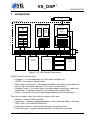
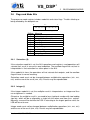
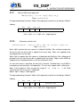
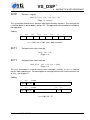
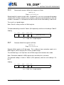
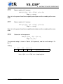
VS_DSP4
VSDSP4 USER’S MANUAL
Revision History
Rev.
4.3
Date
2014-03-05
Author
HH
4.2
2008-03-14
PO
Version: 4.3, 2014-03-05
Description
Added details into saturation (S) and integer (I)
mode bit descriptions, removed outdated information, reformatted document.
Cleaned up version for software developers.
1
VS_DSP4
c 1998-2014 VLSI Solution Oy.
This document Information furnished by VLSI Solution Oy is believed to be accurate and reliable. However, no responsibility is assumed by VLSI Solution Oy for its use.
Specifications are subject to change without notice.
All rights reserved. No part of this manual may be reproduced, in any form or by any
means, without permission in writing from the copyright owner.
The descriptions contained herein do not imply the granting of license to make, use, or
sell equipment constructed in accordance therewith.
Version: 4.3, 2014-03-05
2
VS_DSP4
CONTENTS
Contents
1 Introduction
8
2 Programming Model
9
2.1
Datapath . . . . . . . . . . . . . . . . . . . . . . . . . . . . . . . . . . .
10
2.2
ALU
. . . . . . . . . . . . . . . . . . . . . . . . . . . . . . . . . . . . .
11
2.3
Multiplier . . . . . . . . . . . . . . . . . . . . . . . . . . . . . . . . . . .
11
2.4
Barrel Shifter
. . . . . . . . . . . . . . . . . . . . . . . . . . . . . . . .
12
2.5
Guard Bit Registers . . . . . . . . . . . . . . . . . . . . . . . . . . . . .
12
2.6
Flags and Mode Bits . . . . . . . . . . . . . . . . . . . . . . . . . . . .
13
2.6.1
Saturation (S) . . . . . . . . . . . . . . . . . . . . . . . . . .
13
2.6.2
Integer (I) . . . . . . . . . . . . . . . . . . . . . . . . . . . .
13
2.6.3
Rounding (R) . . . . . . . . . . . . . . . . . . . . . . . . . .
14
2.6.4
Loop (L) . . . . . . . . . . . . . . . . . . . . . . . . . . . . .
14
2.6.5
Zero (Z) . . . . . . . . . . . . . . . . . . . . . . . . . . . . .
14
2.6.6
Negative (N) . . . . . . . . . . . . . . . . . . . . . . . . . . .
14
2.6.7
Overflow (V) . . . . . . . . . . . . . . . . . . . . . . . . . . .
14
2.6.8
Extension (E) . . . . . . . . . . . . . . . . . . . . . . . . . .
14
2.6.9
Carry (C) . . . . . . . . . . . . . . . . . . . . . . . . . . . . .
14
3 Data Address Generator
3.1
Post-modification Modes . . . . . . . . . . . . . . . . . . . . . . . . . .
15
3.1.1
Linear Post-Increment/Decrement . . . . . . . . . . . . . . .
16
3.1.2
Modulo Post-Increment/Decrement . . . . . . . . . . . . . .
16
3.1.3
Bit Reversal . . . . . . . . . . . . . . . . . . . . . . . . . . .
17
4 Program control
4.1
15
PC . . . . . . . . . . . . . . . . . . . . . . . . . . . . . . . . . . . . . . .
Version: 4.3, 2014-03-05
18
18
3
VS_DSP4
CONTENTS
4.2
LR0 . . . . . . . . . . . . . . . . . . . . . . . . . . . . . . . . . . . . . .
18
4.3
LR1 . . . . . . . . . . . . . . . . . . . . . . . . . . . . . . . . . . . . . .
19
4.4
MR0 . . . . . . . . . . . . . . . . . . . . . . . . . . . . . . . . . . . . . .
19
4.5
IPR0, IPR1 . . . . . . . . . . . . . . . . . . . . . . . . . . . . . . . . . .
19
4.6
LS, LE, LC . . . . . . . . . . . . . . . . . . . . . . . . . . . . . . . . . . .
20
5 Control Flow
21
5.1
Jumps . . . . . . . . . . . . . . . . . . . . . . . . . . . . . . . . . . . .
21
5.2
Loops
. . . . . . . . . . . . . . . . . . . . . . . . . . . . . . . . . . . .
21
5.3
System Reset . . . . . . . . . . . . . . . . . . . . . . . . . . . . . . . .
21
5.4
Interrupts . . . . . . . . . . . . . . . . . . . . . . . . . . . . . . . . . . .
22
5.4.1
5.5
Interrupt Routines . . . . . . . . . . . . . . . . . . . . . . . .
22
Halt . . . . . . . . . . . . . . . . . . . . . . . . . . . . . . . . . . . . . .
23
6 Instruction Set Reference
24
6.1
List of Instructions . . . . . . . . . . . . . . . . . . . . . . . . . . . . . .
24
6.2
Instruction Descriptions . . . . . . . . . . . . . . . . . . . . . . . . . . .
25
6.3
Instruction Sequence Restrictions . . . . . . . . . . . . . . . . . . . . .
44
6.3.1
Loop Register Restrictions . . . . . . . . . . . . . . . . . . .
44
6.3.2
Conditional Jump Restrictions . . . . . . . . . . . . . . . . .
45
7 Instruction Coding
46
7.1
General Instruction Composition . . . . . . . . . . . . . . . . . . . . . .
46
7.2
Opcode Field . . . . . . . . . . . . . . . . . . . . . . . . . . . . . . . .
46
7.3
Control Instructions . . . . . . . . . . . . . . . . . . . . . . . . . . . . .
46
7.4
Arithmetic Operands . . . . . . . . . . . . . . . . . . . . . . . . . . . .
49
7.5
Move Encoding . . . . . . . . . . . . . . . . . . . . . . . . . . . . . . .
51
7.6
Addressing Modes . . . . . . . . . . . . . . . . . . . . . . . . . . . . .
53
7.7
Constant Loading . . . . . . . . . . . . . . . . . . . . . . . . . . . . . .
54
Version: 4.3, 2014-03-05
4
VS_DSP4
8 Contact Information
Version: 4.3, 2014-03-05
CONTENTS
56
5
VS_DSP4
LIST OF FIGURES
List of Figures
1
VS_DSP General Architecture. . . . . . . . . . . . . . . . . . . . . . . .
8
2
Processor programming model . . . . . . . . . . . . . . . . . . . . . . .
9
3
VS_DSP datapath. . . . . . . . . . . . . . . . . . . . . . . . . . . . . . .
10
Version: 4.3, 2014-03-05
6
VS_DSP4
LIST OF TABLES
List of Tables
1
Jump conditions. . . . . . . . . . . . . . . . . . . . . . . . . . . . . . . .
30
2
Operation Codes . . . . . . . . . . . . . . . . . . . . . . . . . . . . . . .
47
3
Control Instructions . . . . . . . . . . . . . . . . . . . . . . . . . . . . . .
47
4
ALU operand encoding. . . . . . . . . . . . . . . . . . . . . . . . . . . .
49
5
ALU result coding
. . . . . . . . . . . . . . . . . . . . . . . . . . . . . .
49
6
Mul operand. . . . . . . . . . . . . . . . . . . . . . . . . . . . . . . . . .
50
7
Mul mode. . . . . . . . . . . . . . . . . . . . . . . . . . . . . . . . . . . .
50
8
Single operand ALU instructions. . . . . . . . . . . . . . . . . . . . . . .
51
9
Registers in short move. . . . . . . . . . . . . . . . . . . . . . . . . . . .
52
10
Registers in full move. . . . . . . . . . . . . . . . . . . . . . . . . . . . .
53
11
Load/Store coding. . . . . . . . . . . . . . . . . . . . . . . . . . . . . . .
53
12
Addressing Modes. . . . . . . . . . . . . . . . . . . . . . . . . . . . . . .
53
13
Modifications by the In register. . . . . . . . . . . . . . . . . . . . . . . .
54
14
Addressing mode summary. . . . . . . . . . . . . . . . . . . . . . . . . .
55
Version: 4.3, 2014-03-05
7
VS_DSP4
1
1
INTRODUCTION
Introduction
Interrupt
arbitrator
VS_DSP CORE
Y address
ALU
ADDRESS
CALCULATION
X address
ALU
DATAPATH
P register
PROGRAM
CONTROL
decode
logic
PC
ALU
arithmetic
registers
control
registers
Bus switch
address
registers
Peripheral
interface
X and Y
memory
X memory
Y memory
PLL clock
generator
Boot loader
Program
memory
Peripheral
devices
Figure 1: VS_DSP General Architecture.
VSDSP4 consists of these units:
• Datapath — an arithmetic/logic unit (ALU) and a multiplier unit.
VSDSP4 also contains a barrel shifter.
• Data Address Calculation — Two dedicated address calculation units provide addresses for simultaneous operations on X and Y memory buses.
• Program Control — Instruction fetch, instruction address generation, and instruction decode. The program control also includes harware loop control.
• Buses – Internal buses transfer data between different units and memories.
There are also other subsystems that are not part of the core.
• Memory — Internal RAM and ROM.
• Peripherals — Memory-mapped peripherals, such as interrupt arbiter, serial port,
GPIO, timers, DA and/or AD converters.
• External Bus Switch — Some chips have external memory buses.
• Clock Generator — A phase-locked loop (PLL) can generate core clock.
Version: 4.3, 2014-03-05
8
VS_DSP4
2
2
PROGRAMMING MODEL
Programming Model
The processor programming model is shown in Fig. 2. The processor contains arithmetic, address and control registers.
n
n
pa
P0
P1
g
da
pa
LC
IPR1
da
D2
D1
D0
I6
I7
LE
IPR0
C2
C1
C0
I4
I5
LS
PC
B2
B1
B0
I2
I3
LR1
A2
A1
A0
I0
I1
LR0
MR0
Figure 2: Processor programming model
Arithmetic registers are the 16-bit registers A0, A1, B0, B1, C0, C1, D0, D1 and the
8-bit guard bit registers A2, B2, C2, D2. The multiplier pipeline register P0, P1 is also
shown. There is no guard bit register for P because a single multiplication result always
fits into 32-bit register. The arithmetic registers can be used either as 16-bit registers
mentioned above or as 40-bit registers (A, B, C, D, P).
Address registers are the 16-bit index registers I0, I1, . . ., I7.
Control registers are the program counter PC, link registers LR0, LR1 and mode register
MR0. Loop hardware registers are LS, LE, LC, and page registers IPR0, IPR1.
Version: 4.3, 2014-03-05
9
VS_DSP4
2.1
2
PROGRAMMING MODEL
16
16
Datapath
This picture shows the VSDSP datapath.
The ALU has eight 16-bit arithmetic registers A0, A1, B0, . . . , D0, D1 and four 8bit guard bit registers A2, . . ., D2. These
can be combined to form 40-bit accumulators A, B, C and D. Calculation can be
performed in 40-bit or 16-bit mode. The
width depends on the operands. If one of
the operands is 40 bits wide, the operation is performed in 40 bits, otherwise in
16 bits.
32
P1
The multiplier unit is a 16×16-bit signed/unsigned
integer/fractional saturating/unsaturating
multiplier. Multiplier inputs can be A0, A1,
B0, B1, C0, C1, D0, D1. The result goes to
a 32-bit register P, which can be used as
the second ALU operand in 40-bit arithmetic and is also used with MAC or MSU.
The 16/40-bit ALU implements the arithmetic and logic instructions. The ALU
produces negative, carry, overflow, zero,
and extension flags. There is also a 16/40bit barrel shifter.
Two internal data buses connect the datapath registers to other registers and memories.
P0
32
fract/int shift + saturation
32 | 16
NULL, ONES
mux
mux
Op1
Op2
ALU
40 | 16
40 | 16
A2
A1
A0
B2
B1
B0
C2
C1
C0
D2
D1
D0
16
16
16
16
interface to
X bus
interface to
Y bus
Figure 3: VS_DSP datapath.
Version: 4.3, 2014-03-05
10
VS_DSP4
2.2
2
PROGRAMMING MODEL
ALU
The ALU can calculate either 40-bit or 16-bit operations. The width depends on the
operands; if one of the operands is 40 bits wide, the operation is 40 bits and the result
is stored to a 40-bit register. If both operands are 16 bits, the operation and result are
also 16 bits and the result is stored to a 16 bit register. Exceptions to these rules are
EXP, ASHL and RND. The result of EXP and RND is always 16-bit wide, and Op2 of ASHL is
always an 16-bit register.
The 16-bit operands are A0, A1, B0, B1, C0, C1, D0, D1. Pseudo-registers NULL and ONES
are also available and contain all zeros and all ones, respectively. NULL and ONES are
considered to be 16-bit registers for the purpose of determining the operation width.
The 40-bit operands are A, B, C and D. P is only available as operand2. The register A
is formed by concatenating A2:A1:A0. A0 is the lsb part. For 40-bit calculations, also
16-bit registers are available as the other operand. In this case, the register is used as
the middle part of the operand. The lsb end is padded with 16 zeros and the sign is
extended to the guard bits. For example, if register A0 is used with an 40-bit operand,
the operand is xx:A0:0000 (xx means sign extension bits).
The result register of 40-bit operation must be one of A, B, C, or D. The result register of
a 16-bit operation is one of the 16-bit registers A0, . . . , D1.
2.3
Multiplier
The multiplier is a 16 × 16 signed/unsigned integer/fractional saturating/unsaturating
multiplier.
Both inputs can be interpreted either as signed or unsigned numbers, to facilitate multiprecision operations. Results are written into a 32-bit P register.
The P register can be saved by executing ADD NULL, P, A, at which time potentional
fractional mode shift to left by 1 bit and saturation mode is applied. The high and low
parts will reside in the high and low parts of the target accumulator, respectively. If both
fractional mode and saturation mode is on, the result of signed×signed multiplication
0x8000 × 0x8000 is 0x7fffffff. To get a raw value for P (necessary in interrupts that
manipulate the register), fractional mode must be turned off before saving the register.
P can be restored by executing RESP A0,A1. Fractional mode does not have an effect on
this operation.
Version: 4.3, 2014-03-05
11
VS_DSP4
2.4
2
PROGRAMMING MODEL
Barrel Shifter
The barrel shifter can operate in both 40-bit and 16-bit mode. In 40-bit mode it can
shift 0 . . . 39 bits logically left when operand2 is positive, or up to 39 bits arithmetically
right when operand2 is negative. The result is undefined if the value of the operand2
register is out of range −39 . . . 39.
In 16-bit mode Operand2 must be in range −15 . . . 15.
The last bit shifted out is copied to the carry flag. When shifting left, the overflow flag is
set if the msb bit is changed during shifting. When overflow happens in the saturation
mode, overflow flag is set and result is saturated.
2.5
Guard Bit Registers
Guard bit registers behave as an extension of registers A1, B1, C1, and D1.
Whenever the arithmetic register A1 is written to as a 16-bit register, either from a data
bus or from ALU, the value is sign-extended to A2. Writes to B1, C1, and D1 behave in
the same way.
This does not happen when ALU operates in 40-bit mode and the result is written to A.
If you restore 40-bit values, remember to write to the guard bit register last, otherwise
a write to A1/B1/C1/D1 will sign-extend over the desired value. This is usually an issue
only in interrupt handlers.
Version: 4.3, 2014-03-05
12
VS_DSP4
2.6
2
PROGRAMMING MODEL
Flags and Mode Bits
The processor mode register includes mode bits and status flags. The bits affecting or
being affected by the datapath are:
87
15
0
dddddSIR LddZNVEC
mode bits
Bit/flag
S
I
R
L
Z
N
V
E
C
2.6.1
flags
Meaning
saturation mode
integer(1)/fractional(0) mult. mode
rounding mode
loop flag
zero flag
negative flag
overflow flag
extension flag
carry flag
Saturation (S)
If the saturation mode bit is set, the ALU operations and register P read operations will
saturate their result in case of an over/underflow. The overflow flag will be set, but its
interpretation is that saturation has taken place in the ALU.
If the mode bit is clear, the operations will not saturate their outputs, and the overflow
flag will have its normal meaning.
Saturation mode must not be changed between multiplication operations (MUL, MAC,
MSU) and the use of the result (ADD, SUB). Results may be unpredictable.
2.6.2
Integer (I)
If the integer mode bit is set, the multiplier result is interpreted as an integer and thus
no re-alignment is needed.
Otherwise, the multiplier result is assumed to be a fractional number with two leading
sign bits, which will be re-aligned by a single left-shift when read from the P register.
Normally, a zero will be fed into the LSB. If saturating to the largest positive value, the
LSB will be set to one.
Integer mode must not be changed between multiplication operations (MUL, MAC, MSU)
and the use of the result (ADD, SUB). Results may be unpredictable.
Version: 4.3, 2014-03-05
13
VS_DSP4
2.6.3
2
PROGRAMMING MODEL
Rounding (R)
If the rounding mode bit is set, RND will round using convergent 0 rounding, otherwise
RND will always round towards 0.
2.6.4
Loop (L)
Loop flag is needed with 32-bit code space. The loop flag is set by the interrupt mechanism to disable loop end detection. This prevents false loop end detections when an
interrupt causes the execution to transfer to zero page from another page. Normally,
there is no need for the user to set or clear the loop flag.
• Interrupt sets the loop flag.
• MR0 load can set or clear the loop flag.
• JR, RETI, J, CALL, and LOOP instructions clear the loop flag.
• JMPI does not affect the loop flag.
2.6.5
Zero (Z)
If the ALU is operating in the 40-bit mode and bits 39 . . . 0 of the ALU result are all clear,
the flag is set. If the ALU is operating in the 16-bit mode and bits 15 . . . 0 of the ALU
result are all clear, the flag is set. Otherwise, the flag is cleared.
2.6.6
Negative (N)
If the ALU is operating in the 40-bit mode and bit 39 of the ALU result is set, the flag is
set. If the ALU is operating in the 16-bit mode and bit 15 of the ALU result is set, the
flag is set. Otherwise, the flag is cleared.
2.6.7
Overflow (V)
Set if an arithmetic overflow occurs in the ALU result. Otherwise cleared.
2.6.8
Extension (E)
If the ALU is operating in the 40-bit mode and bits 39 . . . 31 are all the same (either all
ones or all zeros), the flag is cleared. Otherwise, the flag is set. If the ALU is operating
in the 16-bit mode, the flag is cleared.
2.6.9
Carry (C)
If a carry is generated in an addition or a borrow is not generated in a subtraction, the
flag is set. The flag is set also in ASR, LSR and LSRC, if the LSB bit of the operand is
logical ’1’.
Otherwise, the flag is cleared.
Version: 4.3, 2014-03-05
14
VS_DSP43
3
DATA ADDRESS GENERATOR
Data Address Generator
The data address generator uses index registers I0 · · · I7 to generate X and Y data
bus addresses each cycle.
Each register In has a corresponding register pair In. You get In by inverting the LSB
bit of the number of register In. For example, the pair of I3 is I2, and the pair of I2 is
I3.
Any In can be used as a X or Y data bus address. If needed, In specifies a postmodification for In. 32-bit X addresses are formed by concatenating In and In, but
these are only useful with chips that have external data buses.
3.1
Post-modification Modes
There are two post modification modes specified in the instruction: post-modification
by −7 . . . + 7 or post-modification by In.
•
•
•
•
ldx
ldx
ldx
ldx
(i0),a0 – load a0, no post-modification
(i0)+6,a0 – load a0, post-modification by +6
(i0)-7,a0 – load a0, post-modification by -7
(i0)*,a0 – load a0, post-modification by I0, i.e. I1
The modification by In (i.e. using *) uses the most significant bits of In to specify
the post modification mode: linear post-modification, modulo post-modification and bit
reverse.
In(15:13)
000
001
01x
100
101
110
111
Mask
0x0000
0x2000
0x4000
0x8000
0xa000
0xc000
0xe000
Modification
In = (In+m) (m positive)
In = [(In+m(12 : 6)) % (m(5 : 0) + 1)]
In = [(In+m(13 : 6)) % (m(5 : 0) × 64 + 64)]
In = [(In+1) % (m + 1)]
In = [(In−1) % (m + 1)]
In = (In+m) bit reverse
In = (In+m) (m negative)
When modulo addressing is used, modulo logic keeps the address within a circular
buffer. The buffer length does not need to be a power of two, but the starting address
of the buffer must be aligned to the nearest larger or equal power of two.
The bit-reverse modification is useful for FFT and DFT implementations.
Version: 4.3, 2014-03-05
15
VS_DSP43
3.1.1
DATA ADDRESS GENERATOR
Linear Post-Increment/Decrement
Linear post-modification can be an immediate -7 · · · +7 modification or modification
by In. In the case of a negative modifier, In contains the value in two’s complement
format.
• ldx (i0)+5,a0 – load a0, post-modification by +5
• ldc -10,i1
ldx (i0)*,null – no load, post-modification by -10
• ldc 8191,i0
ldy (i1)*,a0 – load a0, post-modification by 8191
3.1.2
Modulo Post-Increment/Decrement
In modulo modification the modified address is kept inside the circular buffer. This
requires that the buffer start address is aligned to a power-of-two boundary according
to the buffer size.
There are four different modulo modes. The most used ones are the +1 and -1 updates
(masks 0x8000 and 0xa000). The lower bits of In give the size of the modulo buffer
minus one.
• ldc
ldx
• ldc
ldx
0x8000+BUFSIZE-1,i1
(i0)*,null – no load, post-modification by +1 modulo BUFSIZE
0xa000+BUFSIZE-1,i1
(i0)*,null – no load, post-modification by -1 modulo BUFSIZE
The other modulo modes can modify the address by larger steps than 1, but they have
restrictions on what the buffer size can be. If the buffer size is 1..64 the modification
can be -64..63. If the buffer size is a multiple of 64 (from 64 to 4096), the modification
can be -128..127.
• ldc
ldx
• ldc
ldx
0x2000+((STEP&0x3f)«6)+((BUFSIZE-1)&0x3f),i1
(i0)*,null – post-modification by STEP modulo BUFSIZE
0x4000+((STEP&0x7f)«6)+((BUFSIZE/64-1)&0x3f),i1
(i0)*,null – post-modification by STEP modulo BUFSIZE
Version: 4.3, 2014-03-05
16
VS_DSP43
3.1.3
DATA ADDRESS GENERATOR
Bit Reversal
In bit reversal addressing, calculated addresses are kept within a buffer length 2k and
when calculating the updated address, carry is propagated towards the LSB. The lower
boundary of the buffer is a multiple of 2k . The boundary is decided by finding the highest
1-bit in In(12 : 0).
3 MSBs of In should contain 110 to select bit reversal addressing. LSBs of In should
contain the reversed adder value, normally 2k−1 .
In = In + In[12 · · · 0] (propagate carry towards LSB)
Example (64-point (k = 6) FFT in buffer 0x3000 · · · 0x303f), getting the next entry after
0x3030:
15
87
0
In =
00110000 00110000
0x3030
In =
110 0000000100000
0xc020
updated In =
00110000 00001000
0x3008
The previous example shows the normal usage, although other values than power of
two are possible. The next example shows how to go backwards instead of forwards
by setting In(12 : 0) to 2k − 1 instead of 2k−1 .
Example (64-point (k = 6) FFT in buffer 0x3000 · · · 0x303f), getting the previous entry
before 0x3030:
15
87
0
In =
00110000 00110000
0x3030
In =
110 0000000111111
0xc03f
updated In =
00110000 00010000
0x3010
Version: 4.3, 2014-03-05
17
VS_DSP4
4
4
PROGRAM CONTROL
Program control
Program control unit (pcu) performs instruction fetch and decode, control flow changes
and interrupt fetching. In addition to the program counter PC, program control unit has
two link registers which are used for indirect jumps, LR0 and LR1.
Mode register MR0 holds the mode and flag bits. Loop control has three registers, LS,
LE and LC. Program counter is not directly accessible.
Instruction Address Generator contains all pcu registers. Instruction Address Generator drives Instruction Address Bus from PC, LR0, LR1, interrupt address or from instruction jump address.
To achieve 32-bit instruction address space (large-code), two page registers are used.
IPR0 holds the uppermost part of the instruction address. IPR0 and PC together determine the instruction address. IPR0 is copied to IPR1 during interrupts.
Interrupt Controller processes interrupts. It implements the interrupt state machine.
Interrupt Controller receives external interrupt and drives interrupt fetch signal to Instruction Address Generator. Interrupt Controller makes sure that previous interrupt
has been processed before new interrupt request is presented to Instruction Address
Generator.
4.1 PC
PC is the program counter. It is not directly accessible by the programmer. PC is loaded
with the fetch address+1 value on all cycles except when new loop round starts. In this
case PC is loaded with LS. PC is kept at the old value if the instruction data and address
buses are used by LDI or STI.
In interrupts, PC is copied to LR1.
In instruction fetches, instruction address bus (IAB) is driven either from PC, LR0, LR1,
decoded instruction jump target address, reset vector address, interrupt vector address, or calculated address for LDI or STI.
4.2 LR0
LR0 is used in indirect jumps. JRcc causes instruction to be fetched from LR0 address
instead of PC address, if condition cc is true. LR0 is used to save the return address for
subroutine calls, so executing JRcc at the end of the subroutine returns to the caller. If
nested subroutines are needed, the previous LR0 must be saved and restored by the
caller.
Version: 4.3, 2014-03-05
18
VS_DSP4
4
PROGRAM CONTROL
4.3 LR1
LR1 is used in interrupt returns. RETI causes instruction to be fetched from LR1 address
instead of PC address. PC is copied to LR1 on interrupts.
If nested interrupts are needed, LR1 must be saved and restored by the interrupt service
routine. See section 5.4.1 for the save and restore routines.
4.4 MR0
MR0 is the processor mode / status flag register.
87
15
0
dddddSIR LddZNVEC
mode bits
Bit/flag
S
I
R
L
Z
N
V
E
C
flags
Meaning
saturation mode
integer(1)/fractional(0) mult. mode
rounding mode
loop flag
zero flag
negative flag
overflow flag
extension flag
carry flag
In the end of an interrupt, MR0 is restored from the stack. Thus explicit moves override
the evaluation of flags.
The mode bits and flags are described in more detail in section 2.6.
4.5 IPR0, IPR1
IPR0 is the instruction page register and is used to implement 32-bit code address
space. It holds the upper 16 bits of instruction address. IPR0 can be changed by JRcc
or JMPI instruction.
In interrupts IPR0 is copied to IPR1 at interrupt cycle #2.
Version: 4.3, 2014-03-05
19
VS_DSP4
4
PROGRAM CONTROL
4.6 LS, LE, LC
LS holds the loop start address. LE holds the loop end address. LC holds the loop count.
LOOP instruction copies instruction fetch address to LS, loads LE with loop end address
specified in the LOOP instruction, and copies LC from the specified register.
When instruction fetch occurs from LE address and the L-flag is not set, LC is tested. If
LC 6= 0, it is decremented by one, new loop round starts by copying LS to PC. If LC = 0,
fetch continues from the next address.
LE is initiated with all ones in system reset.
Version: 4.3, 2014-03-05
20
VS_DSP4
5
5
CONTROL FLOW
Control Flow
The control flow behaviour follows the three-stage pipelining of the processor operation. The change-of-flow instructions are all delayed, with one delay slot following the
instruction. There can not be another change-of-flow instruction in the delay slot. In
this sense, also LOOP is considered as a change-of-flow instruction, in addition to J,
Jcc, JRcc, CALLcc and RETI.
The JMPI instruction is also a change-of-flow instruction and has the same kind of
timing behaviour as other change-of-flow instructions, but the instruction in the delay
slot is canceled (executed as NOP), and can therefore be a change-of-flow instruction.
This feature is mostly used in the interrupt vector table.
5.1
Jumps
Jump conditions are taken from the flags in MR0. The flags that are part of the condition
must be unaltered in the preceding instruction. Other flags can be modified.
5.2
Loops
The loop mechanism has three registers which are loop start register LS, loop end
register LE and loop count register LC.
Change-of-flow instructions can not be at loop end address or immediately before that.
LOOP instruction starts a hardware loop. LOOP instruction has one delay slot, i.e., loop
start address is LOOP+2. This results from the fact that instruction at LOOP+1 (delay
slot) is fetched before loop registers are updated by LOOP instruction. Loop can also be
initiated by setting LS, LE and LC to appropriate values.
When the instruction fetch address equals LE, the value of LC is checked. If LC is not
equal to zero, it is decremented by 1 and PC is loaded with LS. If LC is equal to zero,
executing continues linearly from the next instruction.
5.3
System Reset
System reset forces the processor to a known reset state. After reset is released, the
processor starts executing instructions from reset address onwards.
All registers except LE and PC are zeroed on reset. LE is set to all ones. PC is set to
reset vector (normally 0x4000).
Version: 4.3, 2014-03-05
21
VS_DSP4
5.4
5
CONTROL FLOW
Interrupts
Interrupts are vectored using a jump table. The external interrupt peripheral supplies
an interrupt vector to core. The vector is an address in the range 0x20. . .0x3f. These
addresses must hold a jump table with JMPI instructions which jump to the start of the
appropriate interrupt routine.
In interrupts LR1 is used to save the return address. When main program is interrupted,
return address is automatically copied to LR1. Interrupts normally end with a RETI (jump
to LR1) or a JRcc(jump to LR0).
When generating an interrupt request, the interrupt peripheral automatically disables
further interrupts by increasing its interrupt disable count register. If nested interrupts
are required, the interrupt handler must save LR1 before enabling further interrupts.
Note that if you call C-compiled routines from the interrupt handler, you must also save
P and the guard bit registers.
5.4.1
Interrupt Routines
A typical interrupt jump table looks like the following:
.org 0x20
JMPI int_routine0,(SP)+1
JMPI int_routine1,(SP)+1
JMPI int_routine2,(SP)+1
...
Here, the JMPI instructions also increases the stack pointer.
The start of the interrupt handler must save the processor state before enabling interrupts in the interrupt controller. The end of the handler restores the processor state.
Depending whether only 16-bit or both 16- and 32-bit code model will be used in the
program, a different kind of a saving and restoring is used.
Version: 4.3, 2014-03-05
22
VS_DSP4
5
CONTROL FLOW
The following is a 16-bit (small-code space) C-safe interrupt stub:
_int_routine0:
STX i7,(i6) ;
STX i5,(i6) ;
STX a2,(i6) ;
STX c2,(i6) ;
STX a0,(i6) ;
ADD null,p,a
STX a0,(i6) ;
STY
STY
STY
STY
STY
mr0,(i6)+1 // If registers in X space, switch LDX and LDY
lr0,(i6)+1
b2,(i6)+1
d2,(i6)+1
a1,(i6)+1
STY a1,(i6)
.import _CInterrupt
CALL _CInterrupt
LDC 0x200,mr0
// C language interrupt, type:
//
void CInterrupt(void);
// Must occur after add null,p,a , otherwise
//
unexpected things may happen.
LDX (i6),a0 ; LDY (i6)-1,a1
RESP a0,a1
LDX (i6),a0 ; LDY (i6)-1,a1
LDX (i6),c2 ; LDY (i6)-1,d2
LDX (i6),a2 ; LDY (i6)-1,b2
LDX (i6),i5 ; LDY (i6)-1,lr0
LDC INT_GLOB_ENA,i7
LDY (i6),mr0
// If registers in X space, switch LDX to STX
RETI
STY i7,(i7) ; LDX (i6)-1,i7 // If regs in X, switch STY/LDX with STX/LDY
When an interrupt is taken, the interrupt controller automatically disables all interrupts.
Writing to the memory-mapped register INT_GLOB_ENA enables the interrupts.
The interrupts must be disabled during the RETI instruction execution, and they will
therefore be enabled in its delay slot. The RETI will also clear the L-flag, and the
restoring of MR0 must therefore come before it, if the flag is not cleared by the user.
5.5
Halt
In HALT, the processor waits until an interrupt occurs. The execution pipeline is stopped.
When an interrupt occurs, the processor executes 3 instructions after the HALT instruction before executing the first interrupt instruction.
If the interrupt state machine is not in the idle state when HALT goes to execution,
HALT instruction has no effect and is executed like a NOP.
Version: 4.3, 2014-03-05
23
4
VS_DSP
6 INSTRUCTION SET REFERENCE
6
6.1
Instruction Set Reference
List of Instructions
The following table lists all basic and optional instructions. The operands of each instruction, mode bits affecting the operation and the flags affected are also shown.
Mnemonic
ABS
ADD
ADDC
AND
ASHL
ASR
CALLcc
EXP
HALT
Jcc
JMPI
JRcc
LDC
LDX
LDY
LDI
LOOP
LSL
LSLC
LSR
LSRC
MAC
MSU
MUL
MVX
MVY
NOP
NOT
OR
RESP
RETI
RND
SAT
STX
STY
STI
meaning
absolute value
add
add with carry
logical AND
n-b arithmetic shift
1-b arithmetic right shift
conditional call
count leading bits
wait for an interrupt
conditional jump
jump, ignore delay slot
conditional jump with LR0
load constant
load on X bus
load on Y bus
load on I bus
start loop
1-b logical left shift
LSL with carry
1-b logical right shift
LSR with carry
multiply-accumulate
multiply-subtract
multiply
register move
register move
no operation
logical NOT
logical OR
restore P
jump with LR1
round to 16 bits
saturate to 32 bits
store on X bus
store on Y bus
store on I bus
SUB
SUBC
XOR
subtract
SUB with carry
logical XOR
operands
Areg
2×Areg
2×Areg,c
2×Areg
2×Areg
Areg
addr,cc
Areg
–
addr,cc
addr,In
LR0, cc, In
imm
In, In
In, In
In, In
reg, addr
Areg
Areg,c
Areg
Areg,c
2×Areg
2×Areg
2×Areg
reg
reg
–
Areg
2×Areg
2×Areg
LR1, In
Areg
Areg
In, In, reg
In, In, reg
In,
In,
Areg
2×Areg
2×Areg,c
2×Areg
result
Areg
Areg
Areg
Areg
Areg
Areg
PC, LR0
Areg
–
PC
PC, In
PC
reg
reg
reg
Areg
Lregs
Areg
Areg
Areg
Areg
Areg,P
Areg,P
P
reg
reg
–
Areg
Areg
P
PC
Areg
Areg
mem
mem
mem
Areg
Areg
Areg
S
u
u
u
–
u
–
–
–
–
–
–
–
–
–
–
–
–
–
–
–
–
u
u
u
–
–
–
–
–
–
–
–
–
–
–
–
I
–
–
–
–
–
–
–
–
–
–
–
–
–
–
–
–
–
–
–
–
–
u
u
u
–
–
–
–
–
–
–
–
–
–
–
–
R
–
–
–
–
–
–
–
–
–
–
–
–
–
–
–
–
–
–
–
–
–
–
–
–
–
–
–
–
–
–
–
u
–
–
–
–
L
–
–
–
–
–
–
0
–
–
0
–
0
–
–
–
–
0
–
–
–
–
–
–
–
–
–
–
–
–
–
0
–
–
–
–
–
Z
x
x
x
x
x
x
u
x
–
u
–
u
–
–
–
–
–
x
x
x
x
x
x
–
–
–
–
x
x
–
–
x
x
–
–
–
N
x
x
x
x
x
0
u
0
–
u
–
u
–
–
–
–
–
x
x
0
x
x
x
–
–
–
–
x
x
–
–
x
x
–
–
–
V
x
x
x
0
x
0
u
0
–
u
–
u
–
–
–
–
–
x
x
0
0
x
x
–
–
–
–
0
0
–
–
x
x
–
–
–
E
x
x
x
x
x
x
u
0
–
u
–
u
–
–
–
–
–
x
x
x
x
x
x
–
–
–
–
x
x
–
–
0
0
–
–
–
C
x
x
x,u
0
x
x
u
0
–
u
–
u
–
–
–
–
–
x
x
x
x
x
x
–
–
–
–
0
0
–
–
0
0
–
–
–
u – – – x x x x x
u – – – x x x x x,u
– – – – x x 0 x 0
Operands and result: reg = register, In = index, In = modifier, addr = address,
cc = condition code, c = carry in, imm = immediate data, Lregs = loop registers,
P = multiplier result, PC = program counter, mem = memory location
Mode bits and flags: x = sets flag, u = uses bit, 0 = sets flag to 0
Version: 4.3, 2014-03-05
24
4
VS_DSP
6 INSTRUCTION SET REFERENCE
6.2
Instruction Descriptions
The instruction description includes the mnemonic and a one line description of the
operation, the syntax and mathematical expression of the operation, comments on
the use and other specific information, and finally the coding of the instruction. The
operand fields or other further refinements are given in accompanying tables.
Several operations can be executed in parallel when they are using different fields of
the instruction word, e.g., ALU operations and two parallel moves with indirect addressing are possible, see instruction composition in chapter 7. In assembler the parallel
operations are separated by a semicolon. The following lists the main rules.
One instruction can contain:
• Any single operation
LDC 1234,i0
J label
• ALU operation and any load or store
sub a0,a1,b0 ; ldx (i1)-4,i0
• ALU operation and any register move
add a1,null,a0 ; mv a2,a1
• Two register moves (there are some register bank restrictions)
mv a0,i0 ; mv a1,i1
• One X and one Y load or store
ldx (i6)-1,a0 ; ldy (i6),a1
ldx (i0)+7,a0 ; sty a0,(i2)+1
• ALU operation and one restricted X and one restricted Y load or store
mac a0,a1,b ; ldx (i0)*,a0 ; ldy (i2)*,a1
In restricted (short) load/store one can only use the * modification or no modification, and the data register must be an ALU register.
Version: 4.3, 2014-03-05
25
4
VS_DSP
6 INSTRUCTION SET REFERENCE
ABS
Absolute value
ABS Op2, An ; |Op2| → An
Flags: Z,N,V,E,C.
The operand is conditionally negated (two’s complement operation) and placed in the
target register. The coding of Op2 is given in Table 4 (ALU operand), and the result
coding in Table 5. The absolute value of the minimum integer (fraction -1.0) is the
maximum integer in the saturation mode.
Coding:
31
24 23
28 27
20 19
17 16
1111 0000 rrrr AAA
0
parallel move
rrrr = Op2, AAA = target register.
ADD
Addition of two operands
ADD Op1, Op2, An ; Op1 + Op2 → An
Flags: Z,N,V,E,C.
The operand coding is shown in Table 4 (ALU operand), and the result coding in Table 5. LSL is constructed with ADD Op1, Op1, An .
Coding:
31
28 27
24 23
20 19
17 16
0100 RRRR rrrr AAA
0
parallel move
RRRR = Op1, rrrr = Op2, AAA = target register.
ADDC
Addition of two operands with carry
ADDC Op1, Op2, An ; Op1 + Op2 + C → An
Flags: Z,N,V,E,C.
The operand coding is shown in Table 4 (ALU operand), and the result coding in Table 5. LSLC is constructed with ADDC Op1, Op1, An .
Coding:
31
28 27
24 23
20 19
17 16
1000 RRRR rrrr AAA
0
parallel move
RRRR = Op1, rrrr = Op2, AAA = target register.
Version: 4.3, 2014-03-05
26
4
VS_DSP
6 INSTRUCTION SET REFERENCE
AND
Bitwise AND of two operands
AND Op1, Op2, An ; f or each i : Op1[i] · Op2[i] → An [i]
Flags: Z,N,V=0,E,C=0.
The operand coding is found in Table 4 (ALU operand), and the result coding in Table 5.
Coding:
31
28 27
24 23
20 19
17 16
1011 RRRR rrrr AAA
0
parallel move
RRRR = Op1, rrrr = Op2, AAA = target register.
ASHL
Arithmetic multi-bit shift
ASHL Op1, Op2, An ; if Op2 > 0 : Op1 << Op2 → An : else Op1 >> |Op2| → An
Flags: Z,N,V,E,C.
When Op2 is positive then the source is shifted left Op2 bits. Bits shifted out of position
40 are lost, but for the last bit is copied to the carry flag. Zeros are supplied to the
vacated positions on the right.
When Op2 is negative then the source is shifted right abs(Op2) bits. Bits shifted out of
position 0 are lost, but the last bit is copied to the carry flag. Copies of the MSB are
supplied to the vacated positions on the left (arithmetic shift).
If a zero shift count is specified, the carry bit is cleared. Overflow flag is set if MSB is
changed any time during the shift operation. This can only happen when shifting left.
Note: if the number of shifts exceeds the range of −40 . . . 40 (or −16 . . . 16 for 16-bit
source/result) then the result is undefined.
Note2: Op2 is always 16-bit register.
The operand coding is found in Table 4 (ALU operand), and the result coding in Table 5.
Coding:
31
28 27
24 23
20 19
17 16
1010 RRRR rrrr AAA
0
parallel move
RRRR = Op1, rrrr = Op2, AAA = target register.
Version: 4.3, 2014-03-05
27
4
VS_DSP
6 INSTRUCTION SET REFERENCE
ASR
Arithmetic shift right
ASR Op2, An ; f or each i > 0 : Op2[i] → An [i − 1], Op2[msb] → An [msb]
Flags: Z,N,V,E,C=op2(0).
The instruction shifts right by one position. The LSB bit is discarded, and MSB of the
source registers is fed into the MSB bit of the result.
31
28 27
24 23
20 19
17 16
0
parallel move
1111 0001 rrrr AAA
Coding:
rrrr = Op2, AAA = target register.
EXP
Count leading bits
EXP Op2, An
Flags: Z,N=0,V=0,E=0,C=0.
Count leading zeros or ones according to MSB of the source. The result is a unsigned
integer in whose range of possible values are from 0 to 2n + g. If Op2 is 0 then result
is 0.
Note: Result is always written to 16-bit register.
Note2: This instruction can be used in conjunction with ASHL instruction, to specify the
shift amount needed for normalization.
The operand coding is found in Table 4 (ALU operand), and the result coding in Table 5.
Coding:
31
28 27
24 23
20 19
17 16
1111 0101 rrrr AAA
0
parallel move
rrrr = Op2, AAA = target register.
Version: 4.3, 2014-03-05
28
4
VS_DSP
6 INSTRUCTION SET REFERENCE
CALLcc
Conditional delayed jump and save return address
CALL addr; PC → LR0, if cond : addr → PC
Flags: L=0.
Identical to normal jump instruction, but PC is saved to LR0. This instruction replaces
the sequence J addr, LDC @+1,LR0 which is used in subroutine calls.
Note the one delay slot associated to this instruction. The address which is saved to
LR0 is the CALL instruction address + 2. The instruction in the delay slot is always
executed regardless of the condition.
Coding:
31
28 27
24 2322 21
0010 1001 -
HALT
65
absolute address
0
condition
Halt the processor and wait for an interrupt
HALT
Flags: no change.
The processor is halted to a low-power state. Normal execution is resumed when an
interrupt occurs.
Coding:
31
28 27
24 23
0010 1101
Version: 4.3, 2014-03-05
0
-
29
4
VS_DSP
6 INSTRUCTION SET REFERENCE
Jcc
Conditional delayed jump to absolute address
Jcc addr; if cond : addr → PC, else : PC + 1 → PC
Flags: L=0.
Flags and their combinations can be used as jump conditions, as shown in Table 1
(Jump conditions). The instruction immediately before the Jcc must not change the
flags that are used in the jump condition. Other flags can be changed. Note the one
delay slot associated to this instruction.
Coding:
31
28 27
24 2322 21
0010 1000 -
65
absolute address
0
condition
Table 1: Jump conditions.
Binary code Abbrev Name
000000
always
000001
CS carry set
000010
ES extension set
000011
VS overflow
000100
NS negative
000101
ZS zero
001000
LT less than zero
001001
LE less than or equal to zero
010001
CC carry clear
010010
EC extension clear
010011
VC not overflow
010100
NC not negative
010101
ZC not zero
011000
GE greater than or equal to zero
011001
GT greater than zero
Version: 4.3, 2014-03-05
definition
C=1
E=1
V=1
N=1
Z=1
L
N (V
L
N (V
C=0
E=0
V=0
N=0
Z=0
L
N (V
L
N (V
· S) = 1
· S) + Z = 1
· S) = 0
· S) + Z = 0
30
4
VS_DSP
6 INSTRUCTION SET REFERENCE
JMPI
Jump, ignore delay slot, increment index register
JMPI addr, (Op1) + n; addr → PC, Op1 + n → Op1, 0 → IPR0
Flags: no change.
Identical to normal jump instruction, but ignores the instruction in the delay slot (a
NOP is executed instead) and jumps to zero page. Also, the index register specified is
optionally modified (identical to LDX (Op1)+n,NULL).
This instruction is used in interrupt vector jump table. Do not use this instruction in
normal code if interrupts are enabled.
Coding:
31
28 27
24 2322 21
0010 1010 -
6 55 4
absolute address
32
0
- mm rrr
rrr = address register, dd = don’t care,
mm = address mode (00 = no update, 01 = +1, 11 = -1).
Version: 4.3, 2014-03-05
31
4
VS_DSP
6 INSTRUCTION SET REFERENCE
JRcc
Conditional delayed jump to the address in link register 0
JRcc; if cond : LR0 → PC
Flags: L=0.
JRcc
Conditional delayed jump to the address in link register 0
JRcc (Op1); if cond : LR0 → PC, Op1 → IPR0
Flags: L=0.
The JRcc instruction can be used for returns from subroutines, as well as for other
jumps with run-time calculated addresses. The return addresses are typically loaded
by an LDC instruction. Flags and their combinations can be used as jump conditions, as
shown in Table 1 (Jump conditions). The instruction immediately before the JRcc must
not change the flags that are used in the jump condition. Other flags can be changed.
Unconditional return can be done with the “always” condition. Note the one delay slot
associated to this instruction.
Coding:
31
22
24 2323
28 27
65
-
0010 0000 0
31
28 27
22
24 2323
condition
98
-
0010 0000 1
0
65
0
r r r condition
cccccc = condition, rrr = Op1 (I0. . .I7)
LDC
Load constant to a register
LDC constant, Op1; constant → Op1
Flags: no change.
The register (Op1) coding is shown in Table 10 (Target full move). The assembler
understands numbers in different bases (e.g., hexadecimal, decimal, binary), while the
immediate is finally coded in binary format. A single constant load can be done in an
instruction, and no parallel arithmetic can be used. The constant is LSB-aligned and
sign extended if needed.
Coding:
31
29 28
000
22 21
-
65
constant
0
RRRRRR
RRRRRR = Op1
Version: 4.3, 2014-03-05
32
4
VS_DSP
6 INSTRUCTION SET REFERENCE
LDX
Load register from X-memory
LDX (Op1), Op2; X[Op1] → Op2, update Op1
Flags: no change.
LDY
Load register from Y-memory
LDY (Op1), Op2; Y [Op1] → Op2, update Op1
Flags: no change.
Coding (double full moves):
31
14 13
28 27
0011
0
X full move
Y full move
Coding (parallel full move):
31
28 27
24 23
20 19
17 16
12 11
87
43
0
oooo dddd dddd ddd 0b0FF FFFF FFFF FFFF
oooo = opcode allowing parallel moves, dddd = don’t care
b = bus X/Y (0/1), FFFFF = full move bits of X/Y
Coding (parallel short moves):
31
28 27
24 23
20 19
17 16
12 11
87
43
0
oooo dddd dddd ddd 1xxxx xxxx yyyy yyyy
xxxx = short move bits of X, yyyy = short move bits of Y.
Version: 4.3, 2014-03-05
33
4
VS_DSP
6 INSTRUCTION SET REFERENCE
LDX
Load register from X memory with 32-bit address
LDX (Op2 : Op3), Op1; X[Op2 : Op3] → Op1
Flags: no change.
STX
Store register in X memory with 32-bit address
ST X Op1, (Op2 : Op3); Op1 → X[Op2 : Op3]
Flags: no change.
Load or store a register from or to X memory. This instruction uses two index registers
to generate a long (2×dataaddress) memory address. When Op2 is In, Op3 is the
corresponding modifier register In.
Coding (parallel move):
31
17 16
arithmetic opcode
10 9
65
0
0010100 srrr RRRRRR
RRRRRR = Op1, rrr = Op2, s = 1-store/0-load
LDI
Load register from I memory
LDI (Op2), Op1; I[Op2] → Op1, update Op2
Flags: no change.
STI
Store register to I memory
ST I Op1, (Op2); Op1 → I[Op2], update Op2
Flags: no change.
Transfer data between I memory and registers. During the access the instruction data
and address buses are not available for instruction fetches. The instruction is forced to
NOP, PC update and LE compare are supressed. Op1 is A, B, C, or D, Op2 is In. The
next instruction can not be a change-of-flow instruction.
Coding (parallel move):
31
17 16
arithmetic opcode
10 9
65
0
0010101 srrr ppppRR
RR = Op1, rrr = Op2, s = 1-store/0-load, pppp = post-modification -7..7 or In
Version: 4.3, 2014-03-05
34
4
VS_DSP
6 INSTRUCTION SET REFERENCE
LOOP
Start a hardware loop, delayed
LOOP Op1, addr; Op1 → LC, addr → LE, PC + 2 → LS
Flags: L=0.
This instruction starts a hardware loop. The instruction carries a register number, and
an absolute loop end address which can be calculated by the assembler. The LE
indicates the address of the last instruction within the loop body. The loop start is
implicitly the second instruction from the LOOP instruction. See section 5.2 for details.
Note the one delay slot associated to this instruction.
Coding:
31
28 2726 25
0010 01
22 21
-
6 55 4
absolute address
0
d rrrrr
rrrrr = Op1 (loop count), nn...nn = absolute loop end address.
d = don’t care bit.
Version: 4.3, 2014-03-05
35
4
VS_DSP
6 INSTRUCTION SET REFERENCE
LSL
1
Logical shift left
LSL Op2, An ; f or each i < bits − 1 : Op2[i] → An [i + 1], 0 → An [0]
Flags: Z,N,V,E,C=op2(bits-1).
The instruction shifts left by one position. This instruction is implemented in hardware
as ADD Op2, Op2, An . Note! P is not available as an operand for this instruction.
Coding:
31
28 27
24 23
20 19
17 16
0100 rrrr rrrr AAA
0
parallel move
rrrr = Op2, AAA = target register.
LSLC
1
Logical shift left with carry
LSLC Op2, An ; f or each i < bits − 1 : Op2[i] → An [i + 1], C → An [0]
Flags: Z,N,V,E,C=op2(bits-1).
The instruction shifts left by one position. This instruction is implemented in hardware
as ADDC Op2, Op2, An . Note! P is not available as an operand for this instruction.
Coding:
31
28 27
24 23
20 19
17 16
1000 rrrr rrrr AAA
0
parallel move
rrrr = Op2, AAA = target register.
LSR
Logical shift right
LSR Op2, An ; f or each i > 0 : Op2[i] → An [i − 1], 0 → An [msb]
Flags: Z,N,V,E,C=op2(0).
The instruction shifts right by one position. The LSB bit is discarded, and zero is fed into
the MSB bit. The operand (Op2) is encoded as described in Table 4 (ALU operand),
and the result coding in Table 5.
Coding:
31
28 27
24 23
20 19
17 16
1111 0010 rrrr AAA
0
parallel move
rrrr = Op2, AAA = target register.
1
This instruction is implemented as a single instruction software macro.
Version: 4.3, 2014-03-05
36
4
VS_DSP
6 INSTRUCTION SET REFERENCE
LSRC
Logical shift right with carry
LSRC Op2, An ; f or each i > 0 : Op2[i] → An [i − 1], C → An [msb]
Flags: Z,N,V,E,C=op2(0).
The instruction shifts right by one position. The LSB bit is fed to carry, and carry is
fed into the MSB bit. The operand (Op2) is encoded as described in Table 4 (ALU
operand), and the result coding in Table 5.
Coding:
31
28 27
24 23
20 19
17 16
1111 0011 rrrr AAA
0
parallel move
rrrr = Op2, AAA = target register.
MAC
Multiply-accumulate
MAC Op1, Op2, An ; An + P → An , Op1 × Op2 → P
Flags: Z,N,V,E,C.
The instruction performs one multiplication and adds the result of the previous multiplication (P) to a register. The multiplication operands are considered signed or unsigned
(see MUL), multiplication mode and possible saturation are controlled by the appropriate
mode bits.
Coding:
31
28 27
24 23
20 19
17 16
0101 rrrm mRRR AAA
0
parallel move
rrr = Op1, RRR = Op2, AAA = target register, mm = data format.
MSU
Multiply-subtract
MSU Op1, Op2, An ; An − P → An , Op1 × Op2 → P
Flags: Z,N,V,E,C.
The instruction performs one multiplication and subtracts the result of the previous
multiplication (P) from a register. The multiplication operands are considered signed or
unsigned (see MUL).
Coding:
31
28 27
24 23
20 19
17 16
0111 rrrm mRRR AAA
0
parallel move
rrr = Op1, RRR = Op2, AAA = target register, mm = data format.
Version: 4.3, 2014-03-05
37
4
VS_DSP
6 INSTRUCTION SET REFERENCE
MUL
Multiply
MUL Op1, Op2; Op1 × Op2 → P
Flags: no change.
Performs one multiplication. The operands can be signed or unsigned, multiplication
mode and possible saturation are controlled by the appropriate mode bits. There
are different mnemonics for different format operands. The data format can be Op1
signed/Op2 signed (MULSS), Op1 unsigned/Op2 signed (MULUS), Op1 signed/Op2 unsigned (MULSU) or Op1 unsigned/Op2 unsigned (MULUU). The format SS is the default,
and MULSS can thus be written as plain MUL.
Coding:
31
24 23
28 27
20 19
17 16
0
parallel move
1111 111m mRRR rrr
rrr = op1, RRR = op2, mm = data format.
MVX/MVY
Register-to-register move
M V X Op1, Op2; Op1 → Op2
Flags: no change.
Moves a register to another register using X or Y data bus. In parallel MVX, any register
can be used as a source or target. The source is read on X bus, switched to Y bus and
written from Y bus.
In double MVX/MVY, two moves can be performed with a single instruction. The source
and destination registers must be from different execution units (ALU, DAG, PCU).
Coding (parallel move):
31
17 16
arithmetic opcode
12 11
65
0
00100 ssssss dddddd
Coding (double move):
31
28 27
24 23
18 17
12 11
65
0
0010 1011 SSSSSS DDDDDD ssssss dddddd
n = reserved, ssssss = Y source, dddddd = Y tar get,
SSSSSS = X source , DDDDDD = X target.
Version: 4.3, 2014-03-05
38
4
VS_DSP
6 INSTRUCTION SET REFERENCE
NOP
No operation
NOP; no ef f ect
Flags: no change.
A parallel move NOP is a load operation to NOP register. A total NOP is LDC to NOP.
Coding:
31
24 23
28 27
20 19
17 16
1111 0100 dddd ddd
0
parallel move
ddd = don’t care.
NOT
2
Bitwise logic NOT operation
NOT Op2, An ; f or each i : Op2[i] → An [i]
Flags: Z,N,V=0,E,C=0.
The operand (Op2) coding is shown in Table 4 (ALU operand), the target can be one
of the registers. In hardware this is equal to an XOR with register ONES.
Coding:
31
28 27
24 23
20 19
17 16
1101 1001 rrrr AAA
0
parallel move
rrrr = Op2, AAA = target register.
OR
Bitwise logic OR operation
OR Op1, Op2, An ; f or each i : Op1[i] + Op2[i] → An [i]
Flags: Z,N,V=0,E,C=0.
The operands are encoded as described in Table 4 (ALU operand), and the result
coding in Table 5. The target is one of the registers.
Coding:
31
28 27
24 23
20 19
17 16
1100 rrrr RRRR AAA
0
parallel move
rrrr = Op1, RRRR = Op2, AAA = target register.
2
This instruction is implemented as a single instruction software macro.
Version: 4.3, 2014-03-05
39
4
VS_DSP
6 INSTRUCTION SET REFERENCE
RESP
Restore P register
RESP Op1, Op2; Op1 → P0 Op2 → P1
Flags: no change.
This instruction restores the P contents from two arithmetic registers. The saving of the
P shall be done as described in section 2.3. The operands are encoded as multiplication operands.
Coding:
31
24 23
28 27
20 19
16 15
12 11
87
43
0
0010 0010 dRRR rrrd dddd dddd dddd dddd
rrr = Op1, RRR = Op2, ddd = don’t care bits.
RETI
Delayed return from interrupt
RETI; LR1 → PC
Flags: L=0.
RETI
Delayed return from interrupt
RETI (Op1); LR1 → PC, Op1 → IPR0
Flags: L=0.
The RETI instruction is used for returns from interrupts, similarly as JRcc is used for
returns from subroutines. For description of interrupt mechanism and the correct use
of RETI, see chapter 5.
Coding:
31
28 27
22
24 2323
0
-
0010 0001 0
31
28 27
22
24 2323
0010 0001 1
98
-
65
rrr
0
-
rrr = Op1 (I0. . .I7)
Version: 4.3, 2014-03-05
40
4
VS_DSP
6 INSTRUCTION SET REFERENCE
RND
Round and saturate a 40-bit ALU register to 32 bits
RND Op2, An
Flags: Z,N,V,E=0,C=0.
Round long ALU register to top 24 bits. If mode bit R is set, uses convergent 0 rounding
(round exact x.5 values towards even numbers), otherwise round towards 0. After the
number is rounded, it is saturated to the lowest 16 bits of the intermediary 24-bit result.
The result is a signed integer.
Note: Result is always written to 16-bit register.
The operand coding is found in Table 4 (ALU operand), and the result coding in Table 5.
Coding:
31
28 27
24 23
20 19
17 16
1111 0111 rrrr AAA
0
parallel move
rrrr = Op2, AAA = target register.
SAT
Saturate 40-bit ALU register to 32 bits
SAT Op2, An
Flags: Z,N,V,E=0,C=0.
Saturate 40-bit register to 32-bit range. This is different from saturation mode set in
MR0 register, which saturates ALU results to 40-bit range.
The overflow flag is set if Op2 was out of 32-bit range and saturation was made.
Note: Saturation mode bit in MR0 register does not affect this instruction.
The operand coding is shown in Table 4 (ALU operand), and the result coding in Table 5.
Coding:
31
28 27
24 23
20 19
17 16
1111 0110 rrrr AAA
0
parallel move
rrrr = Op2, AAA = target register.
Version: 4.3, 2014-03-05
41
4
VS_DSP
6 INSTRUCTION SET REFERENCE
STX
Store a register in X memory
STX Op1, (Op2); Op1 → X[Op2], update Op2
Flags: no change.
See LDX for the general load/store capability description and the encoding of the move
fields.
STY
Store a register in Y memory
STY Op1, (Op2); Op1 → Y [Op2], update Op2
Flags: no change.
See LDX for the general load/store capability description and the encoding of the move
fields.
SUB
Subtraction of two operands
SUB Op1, Op2, An ; Op1 − Op2 → An
Flags: Z,N,V,E,C.
The operand coding is shown in Table 4 (ALU operand), and the result coding in Table 5.
Coding:
31
28 27
24 23
20 19
17 16
0110 RRRR rrrr AAA
0
parallel move
RRRR = Op1, rrrr = Op2, AAA = target register.
Version: 4.3, 2014-03-05
42
4
VS_DSP
6 INSTRUCTION SET REFERENCE
SUBC
Subtraction of two operands with carry
SUBC Op1, Op2, An ; Op1 − Op2 − C → An
Flags: Z,N,V,E,C.
The operand coding is shown in Table 4 (ALU operand), and the result coding in Table 5.
Coding:
31
28 27
24 23
20 19
17 16
1001 RRRR rrrr AAA
0
parallel move
RRRR = Op1, rrrr = Op2, AAA = target register.
XOR
Bitwise logic XOR operation
XOR Op1, Op2, An ; f or each i : Op1[i] Op2[i] → An [i]
Flags: Z,N,V=0,E,C=0.
L
The operand coding of Op1 and Op2 is shown in Table 4 (ALU operand), and the result
coding in Table 5. XOR has also been used to implement NOT.
Coding:
31
28 27
24 23
20 19
17 16
1101 RRRR rrrr AAA
0
parallel move
RRRR = Op1, rrrr = Op2, AAA = target register.
Version: 4.3, 2014-03-05
43
4
VS_DSP
6 INSTRUCTION SET REFERENCE
6.3
Instruction Sequence Restrictions
There are certain sequences of instructions which, due to the pipelined execution,
would produce undetermined results. These sequences are either flagged as errors by
the software tools or masked off by the hardware.
6.3.1
Loop Register Restrictions
When either the LE, LC or LS register is loaded from memory with a LDX or LDY instruction, the loop end comparison is not done.
This means that loop registers can not be loaded by instruction whose address is LE−2.
If this is done, further loop rounds are ignored and the execution continues linearly.
The LDC instruction does not have this restriction and the loop hardware uses the value
loaded with an LDC if it is needed on the same cycle. Also, the LOOP instruction does
not have the restriction so single instruction loops are allowed.
illegal_example:
ldc loop_end1,le
ldx (i0),lc
nop
loop_end1:
nop
legal_example:
ldc 2,lc
ldc loop_start,ls
ldc loop_end2,le
nop
loop_end2:
nop
Version: 4.3, 2014-03-05
/* le comparison not done */
/* le comparison is done */
44
4
VS_DSP
6 INSTRUCTION SET REFERENCE
6.3.2
Conditional Jump Restrictions
The instruction immediately before the jump instruction (JRcc or Jcc) must not change
the flags that affect the jump condition.
For example, if the jump is a JCC (jump if carry clear) the instruction immediately before
must not change the C flag. In practice, this means that instruction must not be an ALU
instruction. X and Y memory accesses can be made since they do not affect the “carry
clear” condition.
example:
ldx (i0)+1, NULL
jcc jump_target
nop
/* must not change C flag */
/* jump delay slot */
The reason for this restriction is the fact that the jump condition is determined during
the decode phase. In a normal (linear) execution, the instruction immediately before
the jump does not affect the jump. The situation is different if the jump instruction is
canceled due to an interrupt. When execution returns from the interrupt to the normal
execution flow, the instruction immediately before the jump has been executed. The
jump condition is determined again, this time with different flags.
Version: 4.3, 2014-03-05
45
VS_DSP4
7
7.1
7
INSTRUCTION CODING
Instruction Coding
General Instruction Composition
The instruction is composed of a 4-bit opcode and additional fields as described below.
31
28 27
65
0
oooo iiiiiiiiiiiiiiiiiiiiii yyyyyy
opcode
31
immediate
target
28 27
0
oooo ccccccccccccccccccccccccccccc
opcode
31
control instruction
28 27
14 13
0
oooo xxxxxxxxxxxxxx yyyyyyyyyyyyyy
opcode
31
X full move
28 27
Y full move
17 16
0
oooo aaaaaaaaaaa m m m m m m m m m m m m m m m m
opcode
7.2
arithmetic operands
parallel moves
Opcode Field
The encoding of operations is shown in Table 2. The control and double move extensions to the opcode are described in the following section.
7.3
Control Instructions
The absolute address in jump instructions is at most 20 bits. The conditional jumps
Jcc are taken when the condition given in the instruction is true. See Table 1 (Jump
condition) for the condition field coding. The flag and mode bits can be masked by the
implementation parameter Modemask, see Chapter 4.
Return (JRcc) and return from interrupt (RETI) use the link registers to restore the PC.
The linking (return address storage) is done by a constant load instruction to the link
register LR0 (the link register should be saved beforehand in case of a subroutine already being executed). The return address is calculated at compilation/linking time,
not run-time. This allows also jumps by loading the link register and then executing the
Version: 4.3, 2014-03-05
46
VS_DSP4
7
INSTRUCTION CODING
Table 2: Operation Codes
Binary code
Operation
000X
LDC
0010
Control
0011
Double moves
0100
ADD
0101
MAC
0110
SUB
0111
MSU
1000
ADDC
1001
SUBC
1010
ASHL
1011
AND
1100
OR
1101
XOR
1110
(reserved)
1111
Single op instructions
Binary code
0000dddddddd
0001dddddddd
0010dxxxyyyd
01nnnnnnnnnn
Table 3: Control Instructions
Operation Sub-fields
JRcc
RETI
RESP x = op2, y = op1
LOOP
n = loop end msb
1000nnnnnnnn
Jcc n = address msb
1001nnnnnnnn
CALLcc n = address msb
1010nnnnnnnn
JMPI n = address msb
1011nnnnnnnn
1101nnnnnnnn
111000000000
···
111111111111
MVX/MVY
HALT
Parallel
none
none
none
yes
yes
yes
yes
yes
yes
yes
yes
yes
yes
yes
Additional fields
condition
loop end lsb,
register
(loop count)
address lsb,
condition
address lsb,
condition
address lsb,
index reg
move fields
(reserved)
JRcc instruction. The linking can be done also in the delay slot. The LR1 loading takes
place automatically when interrupt processing is started.
In the loop instruction there is a register number containing the loop count. All registers
except the double-size accumulators can be used. The loop end address is given as
Version: 4.3, 2014-03-05
47
VS_DSP4
7
INSTRUCTION CODING
an immediate (at most 20 bits) value. The loop start address will be loaded automatically from the PC. The loop registers (LC, LS, LE) should not be loaded within the two
instructions preceding a loop end to avoid implementation-dependent ambiguities in
the loop behavior.
In the full size moves, the load/store operations can use all the addressing modes and
all registers. These moves do not allow any control operations in parallel. See section
7.5 for move encoding.
RESP is a special instruction to restore the P register.
The rest of the control instructions are reserved for future extensions.
Version: 4.3, 2014-03-05
48
VS_DSP4
7.4
7
INSTRUCTION CODING
Arithmetic Operands
The operands of two-operand arithmetic and logic instructions (ADD, SUB, AND, OR, XOR)
are encoded in the second field of these instructions. The field is composed as follows:
24 23
27
alu op1
20 19
alu op2
17
alu result
Table 4: ALU operand encoding.
Binary code
0000
0001
0010
0011
0100
0101
0110
0111
1000
1001
1010
1011
1100
1101
1110
1111
register
A0
A1
B0
B1
C0
C1
D0
D1
NULL
ONES
(reserved)
P
A
B
C
D
composition
S:A0:0000
S:A1:0000
S:B0:0000
S:B1:0000
S:C0:0000
S:C1:0000
S:D0:0000
S:D1:0000
0:0000:0000
F:FFFF:FFFF
(reserved)
S:P1:P0
A2:A1:A0
B2:B1:B0
C2:C1:C0
D2:D1:D0
Table 5: ALU result coding
Binary code
000
001
010
011
100
101
110
111
16-bit register
A0
A1
B0
B1
C0
C1
D0
D1
40-bit register
(reserved)
A
(reserved)
B
(reserved)
C
(reserved)
D
Table 4 (ALU operand) gives the encoding of Op1 and Op2 of the ALU (fields alu op1
& alu op2). S denotes sign extension.
Table 6 (Mul operand) gives the encoding of fields mac op1 and mac op2.
Version: 4.3, 2014-03-05
49
VS_DSP4
7
INSTRUCTION CODING
Table 6: Mul operand.
Binary code
000
001
010
011
100
101
110
111
register
A0
A1
B0
B1
C0
C1
D0
D1
The opcode of single-operand arithmetic and logic instructions (ABS, LSR and MUL) is
encoded in the first operand field. The encoding is:
24 23
27
20 19
single opcode
alu op2
17
alu result
In MAC:
25 24
27
mul op1
23 22
20 19
mul op2
mode
17
alu result
In MUL:
27
25 24
MUL opcode
23 22
mode
20 19
mul op2
17
mul op1
Table 7: Mul mode.
Binary code op1
op2
00
signed
signed
01
signed
unsigned
10
unsigned signed
11
unsigned unsigned
Table 7 (Mul mode) gives the encoding of the mode field.
The result field encoding is shown in Table 5.
Table 4 (ALU operand) gives the encoding of Op2 of the ALU (field alu op2).
The single-operand opcode encoding is given in Table 8.
Version: 4.3, 2014-03-05
50
VS_DSP4
7
INSTRUCTION CODING
Table 8: Single operand ALU instructions.
Binary code
0000
0001
0010
0011
0100
0101
0110
0111
1000
···
1101
111X
7.5
Operation
ABS
ASR
LSR
LSRC
NOP
EXP
SAT
RND
(reserved)
MUL
Move Encoding
The move instructions are LDX, LDY, LDI, STX, STY, and STI, the X, Y, and I denoting the
desired data bus to be used. There can be a maximum of two moves (loads or stores)
in parallel, one operating on the X bus and the other on Y bus. Constant loading is
described separately in section 7.7.
There are two kinds of moves: full moves and short moves.
The short moves use a restricted set of registers and restricted addressing modes.
The full moves have all registers and all addressing modes available.
The parallel moves can be done together with arithmetic operations, and can either
be one full or two short moves. Long-X and I-bus moves are only available as parallel
moves. Double full move instruction has two full moves, but can not be executed in
parallel with other instructions.
The full move field is always the following 14-bit control field:
13
10 9
65
0
srrr pppp RRRRRR
In short moves the move field is as follows:
13
10 9
65
0
srrr p000 000RRR
s = 1-store/0-load, r = address register, p = post modification mode,
R = move source/destination register.
In the double full move the 14-bit fields come directly after the instruction.
Version: 4.3, 2014-03-05
51
VS_DSP4
7
14 13
27
INSTRUCTION CODING
0
srrrppppRRRRRR srrrppppRRRRRR
X full move
Y full move
Parallel move can be either one full move, two short moves, register-to-register move,
long-X move, or I-bus move. The coding of parallel moves is:
16
14 13
0
0b0 srrrppppRRRRRR
full move
b = bus (0=X,1=Y)
87
16 15
0
1 srrrpRRR srrrpRRR
X short move
16
Y short move
14 1312 11
0
001 00 s s s s s s d d d d d d
reg-to-reg move (Y bus)
16
14 13
10 9
0
001 0100 srrrRRRRRR
long-X move
16
14 13
10 9
0
001 0101 srrrppppRR
I-bus move
Table 9: Registers in short move.
Binary code
00a
01a
10a
11a
Register
A0 . . . A1
B0 . . . B1
C0 . . . C1
D0 . . . D1
The coding of the store/load bit is given in Table 11. The rrr register is the number
of the desired address register. The src/dest register number ((RRR)RRR) is given in
Table 10 (Source and target), and the addressing mode in Table 12. See also section
7.6 for further description of the addressing modes available. The post modification
pppp is a four-bit two’s complement number (-7 ... +7), which is added to the address
register. The code -8 is for the additional address post modification modes found in In.
The In is the index register the number of which is generated by inverting the LSB bit
of the number of register In. The post modifications by the In are defined in Table 13.
Version: 4.3, 2014-03-05
52
VS_DSP4
7
INSTRUCTION CODING
Table 10: Registers in full move.
Binary code
00000a
00001a
00010a
00011a
001000
001001
001010
001011
001100
001101
001110
001111
010rrr
100000
100001
100010
100011
100100
100101
···
111101
111110
111111
Register
A0 . . . A1
B0 . . . B1
C0 . . . C1
D0 . . . D1
LR0
LR1
MR0
(reserved)
NULL (update index reg & flags)
LC
LS
LE (optional)
I0 ... I7
A2
B2
C2
D2
Move NOP (no updates)
reserved
IPR0
IPR1
Table 11: Load/Store coding.
Binary code Mode
0
load
1
store
Table 12: Addressing Modes.
Binary code Mode
rrrpppp
indirect [In] with post modify by pppp (-7...+7)
rrr1000
indirect [In] with post modification specified in In
Version: 4.3, 2014-03-05
53
VS_DSP4
7
INSTRUCTION CODING
Table 13: Modifications by the In register.
Binary code
000
001
01
100
101
110
111
7.6
Modification
In = (In+m) (m positive)
In = [(In+m(12 : 6))%(m(5 : 0) + 1)]
In = [(In+m(13 : 6))%(m(5 : 0) × 64 + 64)]
In = [(In+1)%(m + 1)]
In = [(In−1)%(m + 1)]
In = (In+m) bit reverse
In = (In+m) (m negative)
Addressing Modes
The addressing modes and their availability in short and full formats are summarized in
Table 14. The addressing modes available in the implementation are controlled by the
parameter Addressing mode mask, which has enable bits for the modulo, bit-reversal
and (reserved) addressing modes in the following manner:
(reserved) bitrev modulo
For the details of how the modulus mode works, see Chapter 3.1.2.
7.7
Constant Loading
The additional fields in the constant load instruction LDC look like:
27
65
immediate
0
register
The immediates are assumed signed and will be sign extended if the register is wider
than the immediate. In case there are more bits in the immediate than in the register
to be loaded, the LSB part is taken. The register number is encoded as in the full
addressing load/stores, shown in Table 10.
Version: 4.3, 2014-03-05
54
VS_DSP4
7
INSTRUCTION CODING
Table 14: Addressing mode summary.
Mode
full move code short move code
Linear post-inc/dec
(In )
srrr0000RRRRRR
srrr0RRR
(In )+1
srrr0001RRRRRR
N/A
(In )+2
srrr0010RRRRRR
N/A
(In )+3
srrr0011RRRRRR
N/A
(In )+4
srrr0100RRRRRR
N/A
(In )+5
srrr0101RRRRRR
N/A
(In )+6
srrr0110RRRRRR
N/A
(In )+7
srrr0111RRRRRR
N/A
(In )–1
srrr1111RRRRRR
N/A
(In )–2
srrr1110RRRRRR
N/A
(In )–3
srrr1101RRRRRR
N/A
(In )–4
srrr1100RRRRRR
N/A
(In )–5
srrr1011RRRRRR
N/A
(In )–6
srrr1010RRRRRR
N/A
(In )–7
srrr1001RRRRRR
N/A
(In )*
Linear post-inc/dec
(In )+m, m ≥ 0
srrr1000RRRRRR
srrr1RRR
(In )+m, m < 0
srrr1000RRRRRR
srrr1RRR
(In )*
Modulo post-inc/dec
(In )+n%m
srrr1000RRRRRR
srrr1RRR
(In )+n%m×64 srrr1000RRRRRR
srrr1RRR
(In )+1%m
srrr1000RRRRRR
srrr1RRR
(In )–1%m
srrr1000RRRRRR
srrr1RRR
(In )*
Bit reversal
(In )+m bit-rev
srrr1000RRRRRR
srrr1RRR
Register as source/destination
An
srrrpppp000RRR
srrrpRRR
An ext
srrrpppp1000RR
N/A
LR0, LR1
srrrpppp00100R
N/A
MR0, MR1
srrrpppp00101R
N/A
NULL
srrrpppp001100
N/A
NOP
srrrpppp100100
N/A
LC
srrrpppp001101
N/A
LS
srrrpppp001110
N/A
LE
srrrpppp001111
N/A
In , n=0· · ·7 srrrpppp010RRR
N/A
Version: 4.3, 2014-03-05
In
parameter
—
—
—
—
—
—
—
—
—
—
—
—
—
—
—
—
—
—
—
—
—
—
—
—
—
—
—
—
—
—
000 mmmm...mmmm
111 mmmm...mmmm
—
—
nnnn...mmmm
nnnn...mmmm
mmmm...mmmm
mmmm...mmmm
amm[0]
amm[0]
amm[0]
amm[0]
110 mmmm...mmmm
amm[1]
—
—
—
—
—
—
—
—
—
—
—
g>0
—
—
—
—
lc ≥ 1
lc ≥ 1
lc ≥ 1
—
001
01n
100
101
55
VS_DSP4
8
8
CONTACT INFORMATION
Contact Information
VLSI Solution Oy
Entrance G, 2nd floor
Hermiankatu 8
FI-33720 Tampere
FINLAND
Fax: +358-3-3140-8288
Phone: +358-3-3140-8200
Commercial e-mail: [email protected]
URL: http://www.vlsi.fi/
For technical support or suggestions regarding this document, please participate at
http://www.vsdsp-forum.com/
For confidential technical discussions, contact
[email protected]
Version: 4.3, 2014-03-05
56