1
ColdFire® Family
Programmer’s Reference Manual
Document Number: CFPRM
Rev. 3
03/2005
How to Reach Us:
Home Page:
www.freescale.com
E-mail:
[email protected]
USA/Europe or Locations Not Listed:
Freescale Semiconductor
Technical Information Center, CH370
1300 N. Alma School Road
Chandler, Arizona 85224
+1-800-521-6274 or +1-480-768-2130
[email protected]
Europe, Middle East, and Africa:
Freescale Halbleiter Deutschland GmbH
Technical Information Center
Schatzbogen 7
81829 Muenchen, Germany
+44 1296 380 456 (English)
+46 8 52200080 (English)
+49 89 92103 559 (German)
+33 1 69 35 48 48 (French)
[email protected]
Japan:
Freescale Semiconductor Japan Ltd.
Headquarters
ARCO Tower 15F
1-8-1, Shimo-Meguro, Meguro-ku,
Tokyo 153-0064, Japan
0120 191014 or +81 3 5437 9125
[email protected]
Asia/Pacific:
Freescale Semiconductor Hong Kong Ltd.
Technical Information Center
2 Dai King Street
Tai Po Industrial Estate
Tai Po, N.T., Hong Kong
+800 2666 8080
[email protected]
For Literature Requests Only:
Freescale Semiconductor Literature Distribution Center
P.O. Box 5405
Denver, Colorado 80217
1-800-441-2447 or 303-675-2140
Fax: 303-675-2150
[email protected]
Information in this document is provided solely to enable system and
software implementers to use Freescale Semiconductor products. There are
no express or implied copyright licenses granted hereunder to design or
fabricate any integrated circuits or integrated circuits based on the
information in this document.
Freescale Semiconductor reserves the right to make changes without further
notice to any products herein. Freescale Semiconductor makes no warranty,
representation or guarantee regarding the suitability of its products for any
particular purpose, nor does Freescale Semiconductor assume any liability
arising out of the application or use of any product or circuit, and specifically
disclaims any and all liability, including without limitation consequential or
incidental damages. “Typical” parameters that may be provided in Freescale
Semiconductor data sheets and/or specifications can and do vary in different
applications and actual performance may vary over time. All operating
parameters, including “Typicals”, must be validated for each customer
application by customer’s technical experts. Freescale Semiconductor does
not convey any license under its patent rights nor the rights of others.
Freescale Semiconductor products are not designed, intended, or authorized
for use as components in systems intended for surgical implant into the body,
or other applications intended to support or sustain life, or for any other
application in which the failure of the Freescale Semiconductor product could
create a situation where personal injury or death may occur. Should Buyer
purchase or use Freescale Semiconductor products for any such unintended
or unauthorized application, Buyer shall indemnify and hold Freescale
Semiconductor and its officers, employees, subsidiaries, affiliates, and
distributors harmless against all claims, costs, damages, and expenses, and
reasonable attorney fees arising out of, directly or indirectly, any claim of
personal injury or death associated with such unintended or unauthorized
use, even if such claim alleges that Freescale Semiconductor was negligent
regarding the design or manufacture of the part.
Freescale™ and the Freescale logo are trademarks of Freescale
Semiconductor, Inc. All other product or service names are the property
of their respective owners.© Freescale Semiconductor, Inc. 2004. All rights
reserved.
Document Number: CFPRM
Rev. 3
03/2005
Introduction
1
Addressing Capabilities
2
Instruction Set Summary
3
Integer User Instructions
4
MAC User Instructions
5
EMAC User Instructions
6
FPU User Instructions
7
Supervisor Instructions
8
Instruction Format Summary
9
PST/DDATA Encodings
10
Exception Processing
11
S-Record Output Format
A
Index
IND
1
Introduction
2
Addressing Capabilities
3
Instruction Set Summary
4
Integer User Instructions
5
MAC User Instructions
6
EMAC User Instructions
7
FPU User Instructions
8
Supervisor Instructions
9
Instruction Format Summary
10
PST/DDATA Encodings
11
Exception Processing
A
S-Record Output Format
IND
Index
Contents
Paragraph
Number
Title
Page
Number
Chapter 1
Introduction
1.1
1.1.1
1.1.2
1.1.3
1.1.4
1.2
1.2.1
1.2.1.1
1.2.2
1.2.3
1.3
1.3.1
1.3.2
1.3.3
1.4
1.4.1
1.4.2
1.4.3
1.4.4
1.5
1.5.1
1.5.2
1.5.3
1.5.4
1.5.5
1.5.6
1.5.7
1.5.8
1.5.9
1.5.10
1.6
1.7
1.7.1
1.7.1.1
1.7.1.2
1.7.1.3
Integer Unit User Programming Model .......................................................................... 1-2
Data Registers (D0–D7) .............................................................................................. 1-2
Address Registers (A0–A7) ........................................................................................ 1-2
Program Counter (PC) ................................................................................................ 1-2
Condition Code Register (CCR) ................................................................................. 1-2
Floating-Point Unit User Programming Model .............................................................. 1-3
Floating-Point Data Registers (FP0–FP7) .................................................................. 1-4
Floating-Point Control Register (FPCR) ................................................................ 1-4
Floating-Point Status Register (FPSR) ....................................................................... 1-5
Floating-Point Instruction Address Register (FPIAR) ................................................ 1-6
MAC User Programming Model .................................................................................... 1-6
MAC Status Register (MACSR) ................................................................................. 1-7
MAC Accumulator (ACC) .......................................................................................... 1-7
MAC Mask Register (MASK) .................................................................................... 1-7
EMAC User Programming Model .................................................................................. 1-8
MAC Status Register (MACSR) ................................................................................. 1-8
MAC Accumulators (ACC[0:3]) ................................................................................ 1-9
Accumulator Extensions (ACCext01, ACCext23) ................................................... 1-10
MAC Mask Register (MASK) .................................................................................. 1-10
Supervisor Programming Model ................................................................................... 1-11
Status Register (SR) .................................................................................................. 1-12
Supervisor/User Stack Pointers (A7 and OTHER_A7) ............................................ 1-13
Vector Base Register (VBR) ..................................................................................... 1-13
Cache Control Register (CACR) .............................................................................. 1-13
Address Space Identifier (ASID) .............................................................................. 1-13
Access Control Registers (ACR0–ACR3) ................................................................ 1-14
MMU Base Address Register (MMUBAR) ............................................................. 1-14
RAM Base Address Registers (RAMBAR0/RAMBAR1) ....................................... 1-14
ROM Base Address Registers (ROMBAR0/ROMBAR1) ....................................... 1-14
Module Base Address Register (MBAR) ................................................................. 1-15
Integer Data Formats .................................................................................................... 1-15
Floating-Point Data Formats ......................................................................................... 1-16
Floating-Point Data Types ........................................................................................ 1-16
Normalized Numbers ............................................................................................ 1-16
Zeros ..................................................................................................................... 1-16
Infinities ................................................................................................................ 1-16
ColdFire Family Programmer’s Reference Manual, Rev. 3
Freescale Semiconductor
iii
Contents
Paragraph
Number
1.7.1.4
1.7.1.5
1.7.2
1.8
1.9
1.9.1
1.9.2
1.10
Title
Page
Number
Not-A-Number ...................................................................................................... 1-17
Denormalized Numbers ........................................................................................ 1-17
FPU Data Format and Type Summary ..................................................................... 1-17
Multiply Accumulate Data Formats ............................................................................. 1-19
Organization of Data in Registers ................................................................................. 1-19
Organization of Integer Data Formats in Registers .................................................. 1-19
Organization of Integer Data Formats in Memory ................................................... 1-20
Hardware Configuration Information ........................................................................... 1-21
Chapter 2
Addressing Capabilities
2.1
2.2
2.2.1
2.2.2
2.2.3
2.2.4
2.2.5
2.2.6
2.2.7
2.2.8
2.2.9
2.2.10
2.2.11
2.2.12
2.2.13
2.3
Instruction Format ........................................................................................................... 2-1
Effective Addressing Modes ........................................................................................... 2-2
Data Register Direct Mode ......................................................................................... 2-3
Address Register Direct Mode .................................................................................... 2-3
Address Register Indirect Mode ................................................................................. 2-3
Address Register Indirect with Postincrement Mode ................................................. 2-4
Address Register Indirect with Predecrement Mode .................................................. 2-4
Address Register Indirect with Displacement Mode .................................................. 2-5
Address Register Indirect with Scaled Index and 8-Bit Displacement Mode ............ 2-6
Program Counter Indirect with Displacement Mode .................................................. 2-6
Program Counter Indirect with Scaled Index and 8-Bit Displacement Mode ............ 2-7
Absolute Short Addressing Mode ............................................................................... 2-8
Absolute Long Addressing Mode ............................................................................... 2-9
Immediate Data ........................................................................................................... 2-9
Effective Addressing Mode Summary ...................................................................... 2-10
Stack .............................................................................................................................. 2-10
Chapter 3
Instruction Set Summary
3.1
3.1.1
3.1.2
3.1.3
3.1.4
3.1.5
3.1.6
3.1.7
Instruction Summary ....................................................................................................... 3-1
Data Movement Instructions ....................................................................................... 3-4
Program Control Instructions ...................................................................................... 3-5
Integer Arithmetic Instructions ................................................................................... 3-6
Floating-Point Arithmetic Instructions ....................................................................... 3-8
Logical Instructions .................................................................................................... 3-9
Shift Instructions ......................................................................................................... 3-9
Bit Manipulation Instructions ................................................................................... 3-10
ColdFire Family Programmer’s Reference Manual, Rev. 3
iv
Freescale Semiconductor
Contents
Paragraph
Number
3.1.8
3.1.9
3.2
3.3
Title
Page
Number
System Control Instructions ...................................................................................... 3-11
Cache Maintenance Instructions ............................................................................... 3-12
Instruction Set Summary .............................................................................................. 3-12
ColdFire Core Summary ............................................................................................... 3-19
Chapter 4
Integer User Instructions
Chapter 5
Multiply-Accumulate Unit (MAC) User Instructions
Chapter 6
Enhanced Multiply-Accumulate Unit (EMAC) User Instructions
Chapter 7
Floating-Point Unit (FPU)
User Instructions
7.1
7.2
7.3
7.4
7.5
Floating-Point Status Register (FPSR) ........................................................................... 7-1
Conditional Testing ......................................................................................................... 7-3
Instruction Results when Exceptions Occur ................................................................... 7-6
Key Differences between ColdFire and MC680x0 FPU Programming Models ........... 7-7
Instruction Descriptions .................................................................................................. 7-9
Chapter 8
Supervisor (Privileged) Instructions
Chapter 9
Instruction Format Summary
9.1
Operation Code Map ....................................................................................................... 9-1
Chapter 10
PST/DDATA Encodings
10.1
10.2
User Instruction Set ...................................................................................................... 10-1
Supervisor Instruction Set ............................................................................................. 10-7
ColdFire Family Programmer’s Reference Manual, Rev. 3
Freescale Semiconductor
v
Contents
Paragraph
Number
Title
Page
Number
Chapter 11
Exception Processing
11.1
11.1.1
11.1.2
11.1.3
11.1.4
11.1.5
11.1.6
11.1.7
11.1.8
11.1.9
11.1.10
11.1.11
11.1.12
11.1.13
Overview ....................................................................................................................... 11-1
Supervisor/User Stack Pointers (A7 and OTHER_A7) ............................................ 11-3
Exception Stack Frame Definition ............................................................................ 11-4
Processor Exceptions ................................................................................................ 11-5
Floating-Point Arithmetic Exceptions ...................................................................... 11-5
Branch/Set on Unordered (BSUN) ........................................................................... 11-7
Input Not-A-Number (INAN) ................................................................................... 11-7
Input Denormalized Number (IDE) .......................................................................... 11-8
Operand Error (OPERR) ........................................................................................... 11-8
Overflow (OVFL) ..................................................................................................... 11-9
Underflow (UNFL) ................................................................................................... 11-9
Divide-by-Zero (DZ) .............................................................................................. 11-10
Inexact Result (INEX) ............................................................................................ 11-10
MMU Changes to the Exception Processing Model ............................................... 11-11
Appendix A
S-Record Output Format
A.1
A.2
A.3
S-Record Content 1
S-Record Types 1
S-Record Creation 2
ColdFire Family Programmer’s Reference Manual, Rev. 3
vi
Freescale Semiconductor
Figures
Figure
Number
1-1
1-2
1-3
1-4
1-5
1-6
1-7
1-8
1-9
1-10
1-11
1-12
1-13
1-14
1-15
1-16
1-17
1-18
1-19
1-20
1-21
1-22
1-23
1-24
1-25
1-26
1-27
1-28
1-29
1-30
2-1
2-2
2-3
2-4
2-5
2-6
2-7
2-8
2-9
Title
Page
Number
ColdFire Family User Programming Model ............................................................................. 1-2
Condition Code Register (CCR) ............................................................................................... 1-3
ColdFire Family Floating-Point Unit User Programming Model............................................. 1-4
Floating-Point Control Register (FPCR) .................................................................................. 1-4
Floating-Point Status Register (FPSR) ..................................................................................... 1-5
MAC Unit Programming Model............................................................................................... 1-7
MAC Status Register (MACSR)............................................................................................... 1-7
EMAC Programming Model .................................................................................................... 1-8
MAC Status Register (MACSR)............................................................................................... 1-8
EMAC Fractional Alignment.................................................................................................... 1-9
EMAC Signed and Unsigned Integer Alignment ................................................................... 1-10
Accumulator 0 and 1 Extensions (ACCext01) ....................................................................... 1-10
Accumulator 2 and 3 Extensions (ACCext01) ....................................................................... 1-10
Supervisor Programming Model............................................................................................. 1-11
Status Register (SR)................................................................................................................ 1-12
Vector Base Register (VBR)................................................................................................... 1-13
MMU Base Address Register ................................................................................................. 1-14
Module Base Address Register (MBAR) ............................................................................... 1-15
Normalized Number Format ................................................................................................... 1-16
Zero Format ............................................................................................................................ 1-16
Infinity Format ........................................................................................................................ 1-17
Not-a-Number Format ............................................................................................................ 1-17
Denormalized Number Format ............................................................................................... 1-17
Two’s Complement, Signed Fractional Equation................................................................... 1-19
Organization of Integer Data Format in Data Registers ......................................................... 1-20
Organization of Addresses in Address Registers.................................................................... 1-20
Memory Operand Addressing................................................................................................. 1-21
Memory Organization for Integer Operands........................................................................... 1-21
D0 Processor Configuration.................................................................................................... 1-22
D1 Local Memory Configuration ........................................................................................... 1-24
Instruction Word General Format............................................................................................. 2-1
Instruction Word Specification Formats................................................................................... 2-2
Data Register Direct.................................................................................................................. 2-3
Address Register Direct ............................................................................................................ 2-3
Address Register Indirect.......................................................................................................... 2-3
Address Register Indirect with Postincrement.......................................................................... 2-4
Address Register Indirect with Predecrement .......................................................................... 2-5
Address Register Indirect with Displacement .......................................................................... 2-5
Address Register Indirect with Scaled Index and 8-Bit Displacement..................................... 2-6
ColdFire Family Programmer’s Reference Manual, Rev. 3
Freescale Semiconductor
vii
Figures
Figure
Number
2-10
2-11
2-12
2-13
2-14
2-15
2-16
7-1
11-1
Title
Page
Number
Program Counter Indirect with Displacement .......................................................................... 2-7
Program Counter Indirect with Scaled Index and 8-Bit Displacement .................................... 2-8
Absolute Short Addressing ....................................................................................................... 2-8
Absolute Long Addressing ....................................................................................................... 2-9
Immediate Data Addressing...................................................................................................... 2-9
Stack Growth from High Memory to Low Memory............................................................... 2-11
Stack Growth from Low Memory to High Memory............................................................... 2-11
Floating-Point Status Register (FPSR) ..................................................................................... 7-1
Exception Stack Frame ........................................................................................................... 11-4
ColdFire Family Programmer’s Reference Manual, Rev. 3
viii
Freescale Semiconductor
Tables
Table
Number
1-1
1-2
1-3
1-4
1-5
1-6
1-7
1-8
1-9
1-10
1-11
1-12
1-13
2-1
2-2
2-3
3-1
3-2
3-3
3-4
3-5
3-6
3-7
3-8
3-9
3-10
3-11
3-12
3-13
3-14
3-15
3-16
7-1
7-2
7-3
7-4
7-5
7-6
7-7
Title
Page
Number
CCR Bit Descriptions ............................................................................................................... 1-3
FPCR Field Descriptions .......................................................................................................... 1-4
FPSR Field Descriptions........................................................................................................... 1-5
MACSR Field Descriptions ...................................................................................................... 1-7
MACSR Field Descriptions ...................................................................................................... 1-8
Implemented Supervisor Registers by Device........................................................................ 1-11
Status Field Descriptions ........................................................................................................ 1-12
MMU Base Address Register Field Descriptions................................................................... 1-14
MBAR Field Descriptions ...................................................................................................... 1-15
Integer Data Formats .............................................................................................................. 1-15
Real Format Summary ............................................................................................................ 1-18
D0 Processor Configuration Field Descriptions ..................................................................... 1-22
D1 Local Memory Field Descriptions .................................................................................... 1-24
Instruction Word Format Field Definitions .............................................................................. 2-2
Immediate Operand Location ................................................................................................... 2-9
Effective Addressing Modes and Categories.......................................................................... 2-10
Notational Conventions ............................................................................................................ 3-1
Data Movement Operation Format ........................................................................................... 3-4
Program Control Operation Format .......................................................................................... 3-5
Integer Arithmetic Operation Format ....................................................................................... 3-6
Dyadic Floating-Point Operation Format ................................................................................. 3-8
Dyadic Floating-Point Operations ............................................................................................ 3-8
Monadic Floating-Point Operation Format............................................................................... 3-8
Monadic Floating-Point Operations.......................................................................................... 3-8
Logical Operation Format......................................................................................................... 3-9
Shift Operation Format ........................................................................................................... 3-10
Bit Manipulation Operation Format ....................................................................................... 3-10
System Control Operation Format .......................................................................................... 3-11
Cache Maintenance Operation Format ................................................................................... 3-12
ColdFire User Instruction Set Summary................................................................................. 3-13
ColdFire Supervisor Instruction Set Summary ....................................................................... 3-18
ColdFire Instruction Set and Processor Cross-Reference....................................................... 3-19
FPSR Field Descriptions........................................................................................................... 7-1
FPSR EXC Bits......................................................................................................................... 7-3
FPCC Encodings....................................................................................................................... 7-4
Floating-Point Conditional Tests .............................................................................................. 7-5
FPCR EXC Byte Exception Enabled/Disabled Results............................................................ 7-6
Key Programming Model Differences...................................................................................... 7-8
68K/ColdFire Operation Sequence 1 ........................................................................................ 7-8
ColdFire Family Programmer’s Reference Manual, Rev. 3
Freescale Semiconductor
ix
Tables
Table
Number
7-8
7-9
7-10
8-1
8-2
8-3
9-1
10-1
10-2
10-3
10-4
10-5
11-1
11-2
11-3
11-4
11-5
11-6
11-7
11-8
11-9
11-10
11-11
11-12
11-13
11-14
Title
Page
Number
68K/ColdFire Operation Sequence 2 ........................................................................................ 7-8
68K/ColdFire Operation Sequence 3 ........................................................................................ 7-9
Data Format Encoding ........................................................................................................... 7-10
State Frames.............................................................................................................................. 8-3
State Frames.............................................................................................................................. 8-5
ColdFire CPU Space Assignments ......................................................................................... 8-13
Operation Code Map................................................................................................................. 9-1
PST/DDATA Specification for User-Mode Instructions........................................................ 10-1
PST/DDATA Values for User-Mode Multiply-Accumulate Instructions .............................. 10-5
PST/DDATA Values for User-Mode Floating-Point Instructions ......................................... 10-6
Data Markers and FPU Operand Format Specifiers ............................................................... 10-7
PST/DDATA Specifications for Supervisor-Mode Instructions ............................................ 10-7
Exception Vector Assignments............................................................................................... 11-2
Format/Vector Word............................................................................................................... 11-4
Exception Priorities................................................................................................................. 11-5
BSUN Exception Enabled/Disabled Results .......................................................................... 11-7
INAN Exception Enabled/Disabled Results ........................................................................... 11-7
IDE Exception Enabled/Disabled Results .............................................................................. 11-8
Possible Operand Errors ......................................................................................................... 11-8
OPERR Exception Enabled/Disabled Results ........................................................................ 11-9
OVFL Exception Enabled/Disabled Results........................................................................... 11-9
UNFL Exception Enabled/Disabled Results......................................................................... 11-10
DZ Exception Enabled/Disabled Results.............................................................................. 11-10
Inexact Rounding Mode Values ........................................................................................... 11-11
INEX Exception Enabled/Disabled Results ......................................................................... 11-11
OEP EX Cycle Operations.................................................................................................... 11-12
ColdFire Family Programmer’s Reference Manual, Rev. 3
x
Freescale Semiconductor
Chapter 1
Introduction
This manual contains detailed information about the instruction set architecture (ISA) for all versions of
ColdFire® microprocessors. Within the ColdFire Family, each generation of hardware microarchitecture
is known as a Version, beginning with the original Version 2 (V2) core implementation, the first native
ColdFire processor implementation. Within the instruction set architectures, each definition is known as
an ISA_Revision and labeled as ISA_Revision_A, ISA_Revision_B, etc. These ISA revisions are
commonly described using a short-form nomenclature as ISA_A, ISA_B, etc.
The original ColdFire ISA was developed from a reduced version of the M68000 instruction set that was
targeted to hit a “sweet-spot” representing the minimum of both code expansion (both static and dynamic)
and hardware gate count. The original instruction set architecture (the ISA_A specification) supported a
proper subset of the M68000 opcodes along with selected enhancements from the M68020, and provided
an acceptable trade-off between minimization of code expansion and core gate count, while fully retaining
the user-mode programming model from the M68K Family.
As the ColdFire Family grew, input from users and tool developers as well as internal performance analysis
suggested a number of ISA enhancements could improve performance and code density. Accordingly,
different revisions to the baseline instruction set architecture have been defined and implemented in the
various ColdFire processor cores. In addition, optional hardware execution engines targeted for specific
application areas required the creation of new ISA extensions. Examples of these extensions are the
hardware floating-point unit (FPU) and varieties of multiply-accumulate (MAC) units.
ColdFire legacy had a correspondence between the processor microarchitecture generation and a
instruction set architecture revision. As newer instructions have been implemented on earlier core
versions, that association has blurred over time. This manual defines the instruction set in terms of the
specific ISA revision rather than an association with any given processor version.
The available ISA revisions are:
• ISA_A: The original ColdFire instruction set architecture
• ISA_B: Added improved data movement instructions, byte- and word-sized compares,
miscellaneous enhancements
• ISA_C: Added instructions for improved bit manipulation
• FPU: Original ColdFire instruction set architecture for floating-point unit (FPU)
• MAC: Original ColdFire instruction set architecture for multiply-accumulate unit (MAC)
• EMAC: Revised ISA for enhanced multiply-accumulate unit (EMAC)
• EMAC_B: Added instructions for dual-accumulation operations
These represent the major revisions of the instruction set architecture. In addition, there are expanded ISA
revisions, e.g., ISA_A+, created by combining a major revision with selected instructions from other
revisions.
Information on the processor configuration is generally loaded into 2 program-visible registers at system
reset. This information defines the ColdFire core version as well as the implemented ISA revision. See
Section 1.1, “Integer Unit User Programming Model.
The ColdFire Family programming model consists of two register groups: user and supervisor. Programs
executing in the user mode use only the registers in the user group. System software executing in the
supervisor mode can access all registers and use the control registers in the supervisor group to perform
supervisor functions. The following paragraphs provide a brief description of the registers in the user and
supervisor models as well as the data organization in the registers.
ColdFire Family Programmer’s Reference Manual, Rev. 3
Freescale Semiconductor
1-1
1.1
Integer Unit User Programming Model
Figure 1-1 illustrates the integer portion of the user programming model. It consists of the following
registers:
• 16 general-purpose 32-bit registers (D0–D7, A0–A7)
• 32-bit program counter (PC)
• 8-bit condition code register (CCR)
31
31
0
D0
D1
D2
D3
D4
D5
D6
D7
Data registers
A0
A1
A2
A3
A4
A5
A6
A7
PC
CCR
Address registers
0
Stack pointer
Program counter
Condition code register
Figure 1-1. ColdFire Family User Programming Model
1.1.1
Data Registers (D0–D7)
These registers are for bit, byte (8 bits), word (16 bits), and longword (32 bits) operations. They can also
be used as index registers.
1.1.2
Address Registers (A0–A7)
These registers serve as software stack pointers, index registers, or base address registers. The base address
registers can be used for word and longword operations. Register A7 functions as a hardware stack pointer
during stacking for subroutine calls and exception handling.
1.1.3
Program Counter (PC)
The program counter (PC) contains the address of the instruction currently executing. During instruction
execution and exception processing, the processor automatically increments the contents or places a new
value in the PC. For some addressing modes, the PC can serve as a pointer for PC relative addressing.
1.1.4
Condition Code Register (CCR)
Consisting of 5 bits, the condition code register (CCR)—the status register’s lower byte—is the only
portion of the SR available in the user mode. Many integer instructions affect the CCR and indicate the
ColdFire Family Programmer’s Reference Manual, Rev. 3
1-2
Freescale Semiconductor
Floating-Point Unit User Programming Model
instruction’s result. Program and system control instructions also use certain combinations of these bits to
control program and system flow.
The condition codes meet two criteria:
1. Consistency across:
— Instructions, meaning that all instructions that are special cases of more general instructions
affect the condition codes in the same way;
— Uses, meaning that conditional instructions test the condition codes similarly and provide the
same results whether a compare, test, or move instruction sets the condition codes; and
— Instances, meaning that all instances of an instruction affect the condition codes in the same
way.
2. Meaningful results with no change unless it provides useful information.
Bits [3:0] represent a condition of the result generated by an operation. Bit 5, the extend bit, is an operand
for multiprecision computations. Version 3 processors have an additional bit in the CCR: bit 7, the branch
prediction bit.
The CCR is illustrated in Figure 1-2.
7
1
P
1
6
5
—
4
3
2
1
0
X
N
Z
V
C
The P bit is implemented only on the V3 core.
Figure 1-2. Condition Code Register (CCR)
Table 1-1 describes CCR bits.
Table 1-1. CCR Bit Descriptions
1.2
Bits
Field
Description
7
P
Branch prediction (Version 3 only). Alters the static prediction algorithm used by the
branch acceleration logic in the instruction fetch pipeline on forward conditional
branches. Refer to a V3 core or device user’s manual for further information on this bit.
—
Reserved; should be cleared (all other versions).
6–5
—
Reserved, should be cleared.
4
X
Extend. Set to the value of the C-bit for arithmetic operations; otherwise not affected or
set to a specified result.
3
N
Negative. Set if the most significant bit of the result is set; otherwise cleared.
2
Z
Zero. Set if the result equals zero; otherwise cleared.
1
V
Overflow. Set if an arithmetic overflow occurs implying that the result cannot be
represented in the operand size; otherwise cleared.
0
C
Carry. Set if a carry out of the most significant bit of the operand occurs for an addition,
or if a borrow occurs in a subtraction; otherwise cleared.
Floating-Point Unit User Programming Model
The following paragraphs describe the registers for the optional ColdFire floating-point unit. Figure 1-3
illustrates the user programming model for the floating-point unit. It contains the following registers:
ColdFire Family Programmer’s Reference Manual, Rev. 3
Freescale Semiconductor
1-3
•
•
•
•
8 64-bit floating-point data registers (FP0–FP7)
32-bit floating-point control register (FPCR)
32-bit floating-point status register (FPSR)
32-bit floating-point instruction address register (FPIAR)
Figure 1-3. ColdFire Family Floating-Point Unit User Programming Model
1.2.1
Floating-Point Data Registers (FP0–FP7)
Floating-point data registers are analogous to the integer data registers for the 68K/ColdFire family. The
64-bit floating-point data registers always contain numbers in double-precision format. All external
operands, regardless of the source data format, are converted to double-precision values before being used
in any calculation or being stored in a floating-point data register. A reset or a null-restore operation sets
FP0–FP7 to positive, nonsignaling not-a-numbers (NANs).
1.2.1.1
Floating-Point Control Register (FPCR)
The FPCR, Figure 1-4, contains an exception enable byte (EE) and a mode control byte (MC). The user
can read or write to FPCR using FMOVE or FRESTORE. A processor reset or a restore operation of the
null state clears the FPCR. When this register is cleared, the FPU never generates exceptions.
Exception Enable Byte (EE)
31
16
—
15
14
13
12
11
10
Mode Control Byte (MC)
9
8
7
6
BSUN INAN OPERR OVFL UNFL DZ INEX IDE — PREC
5
4 3
RND
0
—
Figure 1-4. Floating-Point Control Register (FPCR)
Table 1-2 describes FPCR fields.
Table 1-2. FPCR Field Descriptions
Bits
Field
Description
31–16
—
Reserved, should be cleared.
15–8
EE
Exception enable byte. Each EE bit corresponds to a floating-point exception class. The user can
separately enable traps for each class of floating-point exceptions.
15
BSUN
Branch set on unordered
14
INAN
Input not-a-number
13
OPERR Operand error
12
OVFL
Overflow
11
UNFL
Underflow
10
DZ
9
INEX
8
IDE
Divide by zero
Inexact operation
Input denormalized
ColdFire Family Programmer’s Reference Manual, Rev. 3
1-4
Freescale Semiconductor
Floating-Point Unit User Programming Model
Table 1-2. FPCR Field Descriptions (Continued)
Bits
Field
7–0
MC
Description
Mode control byte. Controls FPU operating modes.
7
—
6
PREC
5–4
RND
3–0
—
1.2.2
Reserved, should be cleared.
Rounding precision
Rounding mode
Reserved, should be cleared.
Floating-Point Status Register (FPSR)
The FPSR, Figure 1-5, contains a floating-point condition code byte (FPCC), a floating-point exception
status byte (EXC), and a floating-point accrued exception byte (AEXC). The user can read or write all
FPSR bits. Execution of most floating-point instructions modifies FPSR. FPSR is loaded by using
FMOVE or FRESTORE. A processor reset or a restore operation of the null state clears the FPSR.
FPCC
31 28 27 26 25
—
Exception Status Byte (EXC)
24
23
N Z I NAN
16
—
15
14
13
12
11
10
AEXC Byte
9
8
7
6
5
4
3
2 0
BSUN INAN OPERR OVFL UNFL DZ INEX IDE IOP OVFL UNFL DZ INEX —
Figure 1-5. Floating-Point Status Register (FPSR)
Table 1-3 describes FPSR fields.
Table 1-3. FPSR Field Descriptions
Bits
Field
Description
31–24
FPCC
Floating-point condition code byte. Contains four condition code bits that are set after completion
of all arithmetic instructions involving the floating-point data registers.
31–28
—
Reserved, should be cleared.
27
N
Negative
Z
Zero
I
Infinity
26
25
FPPC
(cont.)
24
23–16
NAN
—
Not-a-number
Reserved, should be cleared.
ColdFire Family Programmer’s Reference Manual, Rev. 3
Freescale Semiconductor
1-5
Table 1-3. FPSR Field Descriptions (Continued)
Bits
Field
15–8
EXC
Description
Exception status byte. Contains a bit for each floating-point exception that might have occurred
during the most recent arithmetic instruction or move operation.
15
BSUN
Branch/set on unordered
14
INAN
Input not-a-number
13
OPERR Operand error
12
OVFL
Overflow
11
UNFL
Underflow
10
DZ
9
INEX
8
IDE
7–0
Inexact operation
Input denormalization
Accrued exception byte. Contains 5 exception bits the IEEE 754 standard requires for
exception-disabled operations. These exceptions are logical combinations of bits in the EXC byte.
AEXC records all floating-point exceptions since the user last cleared AEXC.
7
IOP
6
OVFL
Underflow
5
UNFL
Divide By Zero
4
DZ
3
INEX
2–0
1.2.3
AEXC
Divide by zero
—
Invalid operation
Inexact Operation
Input Denormalization
Reserved, should be cleared.
Floating-Point Instruction Address Register (FPIAR)
The ColdFire operand execution pipeline can execute integer and floating-point instructions
simultaneously. As a result, the PC value stacked by the processor in response to a floating-point exception
trap may not point to the instruction that caused the exception.
For those FPU instructions that can generate exception traps, the 32-bit FPIAR is loaded with the
instruction PC address before the FPU begins execution. In case of an FPU exception, the trap handler can
use the FPIAR contents to determine the instruction that generated the exception. FMOVE to/from the
FPCR, FPSR, or FPIAR and FMOVEM instructions cannot generate floating-point exceptions and so do
not modify FPIAR. A reset or a null-restore operation clears FPIAR.
1.3
MAC User Programming Model
The following paragraphs describe the registers for the optional ColdFire MAC unit. Figure 1-6 illustrates
the user programming model for the MAC unit. It contains the following registers:
• 32-bit MAC status register (MACSR)
• 32-bit accumulator register (ACC)
• 32-bit MAC mask register (MASK)
ColdFire Family Programmer’s Reference Manual, Rev. 3
1-6
Freescale Semiconductor
MAC User Programming Model
31
0
MACSR
ACC
MASK
MAC status register
MAC accumulator
MAC mask register
Figure 1-6. MAC Unit Programming Model
1.3.1
MAC Status Register (MACSR)
The MACSR, shown in Figure 1-7, contains an operational mode field and a set of flags.
3
8
7
4
3
0
1
Operational Mode
—
OM
C
S/U
F/I
R/T
Flags
N
Z
V
C
Figure 1-7. MAC Status Register (MACSR)
Table 1-4 describes MACSR fields.
Table 1-4. MACSR Field Descriptions
Bits
Field
31-8
—
7-4
OMF
Reserved, should be cleared.
Operational mode field. Defines the operating configuration of the MAC unit.
7
OMC
6
S/U
Signed/unsigned operations
5
F/I
Fraction/integer mode
4
R/T
Round/truncate mode
3–0
1.3.2
Description
Flags
Overflow/saturation mode
Flags. Contains indicator flags from the last MAC instruction execution.
3
N
Negative
2
Z
Zero
1
V
Overflow
0
C
Carry. This field is always zero.
MAC Accumulator (ACC)
This 32-bit register contains the results of MAC operations.
1.3.3
MAC Mask Register (MASK)
The mask register (MASK) is 32 bits of which only the low-order 16 bits are implemented. When MASK
is loaded, the low-order 16 bits of the source operand are loaded into the register. When it is stored, the
upper 16 bits are forced to all ones.
ColdFire Family Programmer’s Reference Manual, Rev. 3
Freescale Semiconductor
1-7
When used by an instruction, this register is ANDed with the specified operand address. Thus, MASK
allows an operand address to be effectively constrained within a certain range defined by the 16-bit value.
This feature minimizes the addressing support required for filtering, convolution, or any routine that
implements a data array as a circular queue using the (Ay)+ addressing mode.
For MAC with load operations, the MASK contents can optionally be included in all memory effective
address calculations.
1.4
EMAC User Programming Model
The following paragraphs describe the registers for the optional ColdFire EMAC unit. Figure 1-8
illustrates the user programming model for the EMAC unit. It contains the following registers:
• One 32-bit MAC status register (MACSR) including four indicator bits signaling product or
accumulation overflow (one for each accumulator: PAV0–PAV3)
• Four 32-bit accumulators (ACCx = ACC0, ACC1, ACC2, ACC3)
• Eight 8-bit accumulator extensions (two per accumulator), packaged as two 32-bit values for load
and store operations (ACCext01, ACCext23)
• One 32-bit mask register (MASK)
31
0
MACSR
ACC0
ACC1
ACC2
ACC3
ACCext01
ACCext23
MASK
MAC status register
MAC accumulator 0
MAC accumulator 1
MAC accumulator 2
MAC accumulator 3
Extensions for ACC0 and ACC1
Extensions for ACC2 and ACC3
MAC mask register
Figure 1-8. EMAC Programming Model
1.4.1
MAC Status Register (MACSR)
Figure 1-9 shows the EMAC MACSR, which contains an operational mode field and two sets of flags.
3
1
1
2
11
10
9
8
Prod/acc overflow flags
—
PAV
3
PAV
2
PAV
1
PAV
0
7
6
5
4
3
Operational Mode
OM
C
S/U
F/I
R/T
2
1
0
Flags
N
Z
V
EV
Figure 1-9. MAC Status Register (MACSR)
Table 1-5 describes EMAC MACSR fields.
Table 1-5. MACSR Field Descriptions
Bits
Field
31-12
—
11-8
PAVx
Description
Reserved, should be cleared.
Product/accumulation overflow flags, one per accumulator
ColdFire Family Programmer’s Reference Manual, Rev. 3
1-8
Freescale Semiconductor
EMAC User Programming Model
Table 1-5. MACSR Field Descriptions (Continued)
Bits
Field
7-4
OMF
Operational mode field. Defines the operating configuration of the EMAC unit.
7
OMC
6
S/U
Signed/unsigned operations
5
F/I
Fraction/integer mode
4
R/T
Round/truncate mode
3–0
1.4.2
Description
Flags
Overflow/saturation mode
Flags. Contains indicator flags from the last MAC instruction execution.
3
N
Negative
2
Z
Zero
1
V
Overflow
0
C
Carry. This field is always zero.
MAC Accumulators (ACC[0:3])
The EMAC implements four 48-bit accumulators. The 32-bit ACCx registers, along with the accumulator
extension words, contain the accumulator data. Figure 1-10 shows the data contained by the accumulator
and accumulator extension words when the EMAC is operating in fractional mode. The upper 8 bits of the
extended product are sign-extended from the 40-bit result taken from the product.
32
Operand Y
32
X Operand X
40
Product
24
8
Extended Product
40
+
8
32
8
Accumulator
Upper Extension Byte [7:0]
Accumulator [31:0]
Lower Extension Byte [7:0]
Figure 1-10. EMAC Fractional Alignment
Figure 1-11 shows the data contained by the accumulator and accumulator extension words when the
EMAC is operating in signed or unsigned integer mode. In signed mode, the upper 8 bits of the extended
product are sign extended from the 40-bit result taken from the product. In unsigned mode, the upper 8 bits
of the extended product are all zeros.
ColdFire Family Programmer’s Reference Manual, Rev. 3
Freescale Semiconductor
1-9
24
8
32
Operand Y
32
X Operand X
8
32
Product
8
32
Extended Product
+
8
32
8
Accumulator
Upper Extension Byte [7:0]
Lower Extension Byte [7:0]
Accumulator [31:0]
Figure 1-11. EMAC Signed and Unsigned Integer Alignment
1.4.3
Accumulator Extensions (ACCext01, ACCext23)
The 32-bit accumulator extension registers (ACCext01, ACCext23) allow the complete contents of the
48-bit accumulator to be saved and restored on context switches. Figure 1-12 shows how the ACC0 and
ACC1 data is stored when loaded into a register. Refer to Figure 1-10 and Figure 1-11 for information on
the data contained in the extension bytes.
3
2
2
1
1
1
4
3
6
5
ACC1 Upper
Extension Byte
ACC1 Lower
Extension Byte
8
7
ACC0 Upper
Extension Byte
0
ACC0 Lower
Extension Byte
Figure 1-12. Accumulator 0 and 1 Extensions (ACCext01)
Figure 1-13 shows how the ACC2 and ACC3 data is stored when loaded into a register. Refer to
Figure 1-10 and Figure 1-11 for information on the data contained in the extension bytes.
3
2
2
1
1
1
4
3
6
5
ACC3 Upper
Extension Byte
ACC3 Lower
Extension Byte
8
7
ACC2 Upper
Extension Byte
0
ACC2 Lower
Extension Byte
Figure 1-13. Accumulator 2 and 3 Extensions (ACCext01)
1.4.4
MAC Mask Register (MASK)
Only the low-order 16 bits of the 32-bit mask register (MASK) are implemented. When MASK is loaded,
the low-order 16 bits of the source operand are loaded into the register. When it is stored, the upper 16 bits
are forced to all ones.
ColdFire Family Programmer’s Reference Manual, Rev. 3
1-10
Freescale Semiconductor
Supervisor Programming Model
When used by an instruction, MASK is ANDed with the specified operand address. Thus, MASK allows
an operand address to be effectively constrained within a certain range defined by the 16-bit value. This
feature minimizes the addressing support required for filtering, convolution, or any routine that
implements a data array as a circular queue using the (Ay)+ addressing mode.
For MAC with load operations, the MASK contents can optionally be included in all memory effective
address calculations.
1.5
Supervisor Programming Model
System programmers use the supervisor programming model to implement operating system functions.
All accesses that affect the control features of ColdFire processors must be made in supervisor mode. The
following paragraphs briefly describe the supervisor registers, which can be accessed only by privileged
instructions. The supervisor programming model consists of the registers available to users as well as the
registers listed in Figure 1-14.
31
19
15
0
(CCR) SR
OTHER_A7
Must be zeros VBR
CACR
ASID
ACR0
ACR1
ACR2
ACR3
MMUBAR
ROMBAR0
ROMBAR1
RAMBAR0
RAMBAR1
MBAR
Status register
Supervisor A7 stack pointer
Vector base register
Cache control register
Address space ID register
Access control register 0 (data)
Access control register 1 (data)
Access control register 2 (instruction)
Access control register 3 (instruction)
MMU base address register
ROM base address register 0
ROM base address register 1
RAM base address register 0
RAM base address register 1
Module base address register
Figure 1-14. Supervisor Programming Model
Note that not all registers are implemented on every ColdFire device; refer to Table 1-6. Future devices
may include registers not implemented on earlier devices.
Table 1-6. Implemented Supervisor Registers by Device
Name
V2
V3
V4
V5
SR
x
x
x
x
x
x
OTHER_A7
if ISA_A+ if ISA_A+
VBR
x
x
x
x
CACR
x
x
x
x
if MMU
if MMU
ASID
ACR0
x
x
x
x
ACR1
x
x
x
x
ACR2
x
x
ACR3
x
x
MMUBAR
if MMU
if MMU
ColdFire Family Programmer’s Reference Manual, Rev. 3
Freescale Semiconductor
1-11
Table 1-6. Implemented Supervisor Registers by Device (Continued)
Name
V2
V3
V4
V5
ROMBAR0
DS
DS
DS
DS
ROMBAR1
DS
DS
DS
DS
RAMBAR0
DS
DS
DS
DS
RAMBAR1
DS
DS
DS
DS
MBAR
DS
DS
DS
DS
Note: “x” indicated the supervisor register is implemented. DS indicates the supervisor register is “device-specific”. Please
consult the appropriate device reference manual to determine if the register is implemented. Certain supervisor registers are
present only if the virtual memory management unit (MMU) is implemented (“if MMU”). Certain supervisor registers are present
only if the implemented instruction set architecture is ISA_A+ (“if ISA_A+”).
1.5.1
Status Register (SR)
The SR, shown in Figure 1-15, stores the processor status, the interrupt priority mask, and other control
bits. Supervisor software can read or write the entire SR; user software can read or write only SR[7–0],
described in Section 1.1.4, “Condition Code Register (CCR).” The control bits indicate processor states:
trace mode (T), supervisor or user mode (S), and master or interrupt state (M). SR is set to 0x27xx after
reset.The SR register must be explicitly loaded after reset and before any compare, Bcc, or Scc instructions
are executed.
15
14
13
12
11
10
8
7
System byte
T
1
—
S
M
6
5
4
3
2
1
0
V
C
Condition code register (CCR)
—
I
P1
—
X
N
Z
The P bit is implemented only on the V3 core.
Figure 1-15. Status Register (SR)
Table 1-7 describes SR fields.
Table 1-7. Status Field Descriptions
Bits
Name
Description
15
T
Trace enable. When T is set, the processor performs a trace exception after every instruction.
14
—
Reserved, should be cleared.
13
S
Supervisor/user state. Indicates whether the processor is in supervisor or user mode
12
M
Master/interrupt state. Cleared by an interrupt exception. It can be set by software during execution
of the RTE or move to SR instructions so the OS can emulate an interrupt stack pointer.
11
—
Reserved, should be cleared.
10–8
I
7–0
CCR
Interrupt priority mask. Defines the current interrupt priority. Interrupt requests are inhibited for all
priority levels less than or equal to the current priority, except the edge-sensitive level-7 request,
which cannot be masked.
Condition code register (see Figure 1-2 and Table 1-1)
ColdFire Family Programmer’s Reference Manual, Rev. 3
1-12
Freescale Semiconductor
Supervisor Programming Model
1.5.2
Supervisor/User Stack Pointers (A7 and OTHER_A7)
The ISA_A architectures support a single stack pointer (A7). The initial value of A7 is loaded from the
reset exception vector, address offset 0.
All remaining ISA revisions support two independent stack pointer (A7) registers: the supervisor stack
pointer (SSP) and the user stack pointer (USP). This support provides the required isolation between
operating modes (supervisor and user).
The hardware implementation of these two programmable-visible 32-bit registers does not uniquely
identify one as the SSP and the other as the USP. Rather, the hardware uses one 32-bit register as the
currently active A7 and the other as OTHER_A7. Thus, the register contents are a function of the processor
operating mode, as shown in the following:
if SR[S] = 1
then
A7 = Supervisor Stack Pointer
other_A7 = User Stack Pointer
else
A7 = User Stack Pointer
other_A7 = Supervisor Stack Pointer
1.5.3
Vector Base Register (VBR)
The vector base register contains the 1 MByte-aligned base address of the exception vector table in
memory. The displacement of an exception vector adds to the value in this register, which accesses the
vector table. VBR[19–0] are filled with zeros.
3
2
1
1
0
9
Exception vector table base address
0
—
Figure 1-16. Vector Base Register (VBR)
1.5.4
Cache Control Register (CACR)
The CACR controls operation of both the instruction and data cache memory. It includes bits for enabling,
locking, and invalidating cache contents. It also includes bits for defining the default cache mode and
write-protect fields. Bit functions and positions may vary among ColdFire processor implementations.
Refer to a specific device or core user’s manual for further information.
1.5.5
Address Space Identifier (ASID)
Only the low-order 8 bits of the 32-bit ASID register are implemented. The ASID value is an 8-bit
identifier assigned by the operating system to each process active in the system. It effectively serves as an
extension to the 32-bit virtual address. Thus, the virtual reference now becomes a 40-bit value: the 8-bit
ASID concatenated with the 32-bit virtual address. ASID is only available if a device has an MMU. Refer
to a specific device or core user’s manual for further information.
ColdFire Family Programmer’s Reference Manual, Rev. 3
Freescale Semiconductor
1-13
1.5.6
Access Control Registers (ACR0–ACR3)
The access control registers (ACR[0:3]) define attributes for four user-defined memory regions. ACR0 and
ACR1 control data memory space and ACR2 and ACR3 control instruction memory space. Attributes
include definition of cache mode, write protect, and buffer write enables. Not all ColdFire processors
implement all four ACRs. Bit functions and positions may vary among ColdFire processor
implementations. Refer to a specific device or core user’s manual for further information.
1.5.7
MMU Base Address Register (MMUBAR)
MMUBAR, shown in Figure 1-17, defines a memory-mapped, privileged data-only space with the highest
priority in effective address attribute calculation for the data internal memory bus (that is, the MMUBAR
has priority over RAMBAR0). If virtual mode is enabled, any normal mode access that does not hit in the
MMUBAR, RAMBARs, ROMBARs, or ACRs is considered a normal-mode, virtual address request and
generates its access attributes from the MMU. MMUBAR is only available if a device has an MMU. Refer
to a specific device or core user’s manual for further information.
3
1
1
1
6
5
BA
1
—
0
V
Figure 1-17. MMU Base Address Register
Table 1-8 describes MMU base address register fields.
Table 1-8. MMU Base Address Register Field Descriptions
Bits
Name
31–16
BA
Base address. Defines the base address for the 64-Kbyte address space mapped to the MMU.
15–1
—
Reserved, should be cleared.
0
V
Valid
1.5.8
Description
RAM Base Address Registers (RAMBAR0/RAMBAR1)
RAMBAR registers determine the base address of the internal SRAM modules and indicate the types of
references mapped to each. Each RAMBAR includes a base address, write-protect bit, address space mask
bits, and an enable bit. RAM base address alignment is implementation specific. A specific ColdFire
processor may implement 2, 1, or 0 RAMBARs. Bit functions and positions can vary among ColdFire
processor implementations. Refer to a specific device or core user’s manual for further information.
1.5.9
ROM Base Address Registers (ROMBAR0/ROMBAR1)
ROMBAR registers determine the base address of the internal ROM modules and indicate the types of
references mapped to each. Each ROMBAR includes a base address, write-protect bit, address space mask
bits, and an enable bit. ROM base address alignment is implementation specific. A specific ColdFire
processor may implement 2, 1, or 0 ROMBARs. Bit functions and positions can vary among ColdFire
processor implementations. Refer to a specific device or core user’s manual for further information.
ColdFire Family Programmer’s Reference Manual, Rev. 3
1-14
Freescale Semiconductor
Integer Data Formats
1.5.10
Module Base Address Register (MBAR)
The supervisor-level MBAR, Figure 1-18, specifies the base address and allowable access types for all
internal peripherals. MBAR can be read or written through the debug module as a read/write register; only
the debug module can read MBAR. All internal peripheral registers occupy a single relocatable memory
block along 4-Kbyte boundaries. MBAR masks specific address spaces using the address space fields.
Refer to a specific device or core user’s manual for further information.
Attribute Mask Bits
31
12 11
BA
9
—
8
7
6
5
4
3
2
1
0
WP — AM C/I SC SD UC UD V
Figure 1-18. Module Base Address Register (MBAR)
Table 1-9 describes MBAR fields.
Table 1-9. MBAR Field Descriptions
Bits
Field
31–12
BA
Base address. Defines the base address for a 4-Kbyte address range.
11–9
—
Reserved, should be cleared.
8–1
AMB Attribute mask bits
8
WP
7
—
Reserved, should be cleared.
6
AM
Alternate master mask
5
C/I
Mask CPU space and interrupt acknowledge cycles
4
SC
Setting masks supervisor code space in MBAR address range
3
SD
Setting masks supervisor data space in MBAR address range
2
UC
Setting masks user code space in MBAR address range
1
UD
Setting masks user data space in MBAR address range
0
1.6
Description
V
Write protect. Mask bit for write cycles in the MBAR-mapped register address range
Valid. Determines whether MBAR settings are valid.
Integer Data Formats
The operand data formats are supported by the integer unit, as listed in Table 1-10. Integer unit operands
can reside in registers, memory, or instructions themselves. The operand size for each instruction is either
explicitly encoded in the instruction or implicitly defined by the instruction operation.
Table 1-10. Integer Data Formats
Operand Data Format
Size
Bit
1 bit
Byte integer
8 bits
ColdFire Family Programmer’s Reference Manual, Rev. 3
Freescale Semiconductor
1-15
Table 1-10. Integer Data Formats (Continued)
Operand Data Format
1.7
Size
Word integer
16 bits
Longword integer
32 bits
Floating-Point Data Formats
This section describes the optional FPU’s operand data formats. The FPU supports three signed integer
formats (byte, word, and longword) that are identical to those supported by the integer unit. The FPU also
supports single- and double-precision binary floating-point formats that fully comply with the IEEE-754
standard.
1.7.1
Floating-Point Data Types
Each floating-point data format supports five unique data types: normalized numbers, zeros, infinities,
NANs, and denormalized numbers. The normalized data type, Figure 1-19, never uses the maximum or
minimum exponent value for a given format.
1.7.1.1
Normalized Numbers
Normalized numbers include all positive or negative numbers with exponents between the maximum and
minimum values. For single- and double-precision normalized numbers, the implied integer bit is one and
the exponent can be zero.
Min < Exponent < Max
Fraction = Any bit pattern
Sign of Mantissa, 0 or 1
Figure 1-19. Normalized Number Format
1.7.1.2
Zeros
Zeros can be positive or negative and represent real values, + 0.0 and – 0.0. See Figure 1-20.
Exponent = 0
Fraction = 0
Sign of Mantissa, 0 or 1
Figure 1-20. Zero Format
1.7.1.3
Infinities
Infinities can be positive or negative and represent real values that exceed the overflow threshold. A
result’s exponent greater than or equal to the maximum exponent value indicates an overflow for a given
data format and operation. This overflow description ignores the effects of rounding and the
user-selectable rounding models. For single- and double-precision infinities, the fraction is a zero. See
Figure 1-21.
ColdFire Family Programmer’s Reference Manual, Rev. 3
1-16
Freescale Semiconductor
Floating-Point Data Formats
Exponent = Maximum
Fraction = 0
Sign of Mantissa, 0 or 1
Figure 1-21. Infinity Format
1.7.1.4
Not-A-Number
When created by the FPU, NANs represent the results of operations having no mathematical interpretation,
such as infinity divided by infinity. Operations using a NAN operand as an input return a NAN result.
User-created NANs can protect against uninitialized variables and arrays or can represent user-defined
data types. See Figure 1-22.
Exponent = Maximum
Fraction = Any nonzero bit pattern
Sign of Mantissa, 0 or 1
Figure 1-22. Not-a-Number Format
If an input operand to an operation is a NAN, the result is an FPU-created default NAN. When the FPU
creates a NAN, the NAN always contains the same bit pattern in the mantissa: all mantissa bits are ones
and the sign bit is zero. When the user creates a NAN, any nonzero bit pattern can be stored in the mantissa
and the sign bit.
1.7.1.5
Denormalized Numbers
Denormalized numbers represent real values near the underflow threshold. Denormalized numbers can be
positive or negative. For denormalized numbers in single- and double-precision, the implied integer bit is
a zero. See Figure 1-23.
Exponent = 0
Fraction = Any nonzero bit pattern
Sign of Mantissa, 0 or 1
Figure 1-23. Denormalized Number Format
Traditionally, the detection of underflow causes floating-point number systems to perform a flush-to-zero.
The IEEE-754 standard implements gradual underflow: the result mantissa is shifted right (denormalized)
while the result exponent is incremented until reaching the minimum value. If all the mantissa bits of the
result are shifted off to the right during this denormalization, the result becomes zero.
Denormalized numbers are not supported directly in the hardware of this implementation but can be
handled in software if needed (software for the input denorm exception could be written to handle
denormalized input operands, and software for the underflow exception could create denormalized
numbers). If the input denorm exception is disabled, all denormalized numbers are treated as zeros.
1.7.2
FPU Data Format and Type Summary
Table 1-11 summarizes the data type specifications for byte, word, longword, single-, and
double-precision data formats.
ColdFire Family Programmer’s Reference Manual, Rev. 3
Freescale Semiconductor
1-17
Table 1-11. Real Format Summary
Parameter
Data Format
Single-Precision
31 30
s
e
23 22
Double-Precision
0
f
63 62
s
e
52 51
0
f
Field Size in Bits
Sign (s)
1
1
Biased exponent (e)
8
11
Fraction (f)
23
52
Total
32
64
Interpretation of Sign
Positive fraction
s=0
s=0
Negative fraction
s=1
s=1
Normalized Numbers
Bias of biased exponent
Range of biased exponent
Range of fraction
+127 (0x7F)
+1023 (0x3FF)
0 < e < 255 (0xFF)
0 < e < 2047 (0x7FF)
Zero or Nonzero
Zero or Nonzero
1.f
1.f
(–1)s × 2e–127 × 1.f
(–1)s × 2e–1023 × 1.f
Mantissa
Relation to representation of real numbers
Denormalized Numbers
Biased exponent format minimum
Bias of biased exponent
Range of fraction
0 (0x00)
0 (0x000)
+126 (0x7E)
+1022 (0x3FE)
Nonzero
Nonzero
0.f
0.f
(–1)s × 2–126 × 0.f
(–1)s × 2–1022 × 0.f
Mantissa
Relation to representation of real numbers
Signed Zeros
Biased exponent format minimum
0 (0x00)
0 (0x00)
Mantissa
0.f = 0.0
0.f = 0.0
Signed Infinities
Biased exponent format maximum
Mantissa
255 (0xFF)
2047 (0x7FF)
0.f = 0.0
0.f = 0.0
NANs
Sign
Don’t care
0 or 1
ColdFire Family Programmer’s Reference Manual, Rev. 3
1-18
Freescale Semiconductor
Multiply Accumulate Data Formats
Table 1-11. Real Format Summary (Continued)
Parameter
Biased exponent format maximum
Fraction
Representation of fraction
Nonzero bit pattern created by user
Fraction when created by FPU
Single-Precision
Double-Precision
255 (0xFF)
255 (0x7FF)
Nonzero
Nonzero
xxxxx…xxxx
11111…1111
xxxxx…xxxx
11111…1111
Approximate Ranges
Maximum positive normalized
3.4 × 1038
1.8 x 10308
Minimum positive normalized
1.2 × 10–38
2.2 x 10–308
Minimum positive denormalized
1.4 × 10–45
4.9 x 10–324
1.8
Multiply Accumulate Data Formats
The MAC and EMAC units support 16- or 32-bit input operands of the following formats:
• Two’s complement signed integers: In this format, an N-bit operand value lies in the range -2(N-1)
< operand < 2(N-1) - 1. The binary point is right of the lsb.
• Unsigned integers: In this format, an N-bit operand value lies in the range 0 < operand < 2N - 1.
The binary point is right of the lsb.
• Two’s complement, signed fractionals: In an N-bit number, the first bit is the sign bit. The
remaining bits signify the first N-1 bits after the binary point. Given an N-bit number,
aN-1aN-2aN-3... a2a1a0, its value is given by the equation in Figure 1-24.
N–2
value = – ( 1 ⋅ a N – 1 ) +
∑
2
(i + 1 – N)
⋅ ai
i=0
Figure 1-24. Two’s Complement, Signed Fractional Equation
This format can represent numbers in the range -1 < operand < 1 - 2(N-1).
For words and longwords, the largest negative number that can be represented is -1, whose internal
representation is 0x8000 and 0x8000_0000, respectively. The largest positive word is 0x7FFF or (1 - 2-15);
the most positive longword is 0x7FFF_FFFF or (1 - 2-31).
1.9
Organization of Data in Registers
This section describes data organization within the data, address, and control registers.
1.9.1
Organization of Integer Data Formats in Registers
Each integer data register is 32 bits wide. Byte and word operands occupy the lower 8- and 16-bit portions
of integer data registers, respectively. Longword operands occupy entire data registers. A data register that
is either a source or destination operand only uses or changes the appropriate lower 8 or 16 bits (in byte or
word operations, respectively). The remaining high-order portion does not change and is unused and
ColdFire Family Programmer’s Reference Manual, Rev. 3
Freescale Semiconductor
1-19
unchanged. The address of the least significant bit (lsb) of a longword integer is zero, and the most
significant bit (msb) is 31. Figure 1-25 illustrates the organization of integer data in data registers.
31
30
1
msb
lsb
31
8
Not used
31
msb
7
6
1
msb Low order byte
16
15
Not used
31
0
msb
14
1
Lower order word
30
1
Longword
Bit (0 ð bit number ð 31)
0
lsb
Byte (8 bits)
0
lsb
Word (16 bits)
0
lsb
Longword (32 bits)
Figure 1-25. Organization of Integer Data Format in Data Registers
Because address registers and stack pointers are 32 bits wide, address registers cannot be used for byte-size
operands. When an address register is a source operand, either the low-order word or the entire longword
operand is used, depending on the operation size. When an address register is the destination operand, the
entire register becomes affected, despite the operation size. If the source operand is a word size, it is
sign-extended to 32 bits and then used in the operation to an address-register destination. Address registers
are primarily for addresses and address computation support. The instruction set explains how to add to,
compare, and move the contents of address registers. Figure 1-26 illustrates the organization of addresses
in address registers.
31
16
Sign-Extended
15
0
16-Bit Address Operand
31
0
Full 32-Bit Address Operand
Figure 1-26. Organization of Addresses in Address Registers
Control registers vary in size according to function. Some control registers have undefined bits reserved
for future definition by Freescale. Those particular bits read as zeros and must be written as zeros for future
compatibility.
All operations to the SR and CCR are word-size operations. For all CCR operations, the upper byte is read
as all zeros and is ignored when written, despite privilege mode. The write-only MOVEC instruction
writes to the system control registers (VBR, CACR, etc.).
1.9.2
Organization of Integer Data Formats in Memory
The byte-addressable organization of memory allows lower addresses to correspond to higher order bytes.
The address N of a longword data item corresponds to the address of the MSB of the highest order word.
The lower order word is located at address N + 2, leaving the LSB at address N + 3 (see Figure 1-27). The
lowest address (nearest 0x00000000) is the location of the MSB, with each successive LSB located at the
next address (N + 1, N + 2, etc.). The highest address (nearest 0xFFFFFFFF) is the location of the LSB.
ColdFire Family Programmer’s Reference Manual, Rev. 3
1-20
Freescale Semiconductor
Hardware Configuration Information
31
24 23
16 15
8
7
0
Longword 0x0000_0000
.
.
.
Word 0x0000_0000
Word 0x0000_0002
Byte 0x0000_0000
Byte 0x0000_0001
Byte 0x0000_0002
Byte 0x0000_0003
Longword 0x0000_0004
Word 0x0000_0004
Word 0x0000_0006
Byte 0x0000_0004
Byte 0x0000_0005
Byte 0x0000_0006
Byte 0x0000_0007
.
.
.
.
.
.
Longword 0xFFFF_FFFC
Word 0xFFFF_FFFC
Byte 0xFFFF_FFFC
Byte 0xFFFF_FFFD
Word 0xFFFF_FFFE
Byte 0xFFFF_FFFE
Byte 0xFFFF_FFFF
Figure 1-27. Memory Operand Addressing
Figure 1-28 illustrates the organization of data formats in memory. A base address that selects one byte in
memory—the base byte—specifies a bit number that selects one bit, the bit operand, in the base byte. The
msb of the byte is 7.
7
0 7
Byte n-1
0 7
7 6 5 4 3 2 1 0
0 7
Byte n+1
0
Byte n+2
Bit Data
Base Address Bit Number
7
0 7
Byte n-1
0 7
msb Byte n lsb
0 7
Byte n+1
0
Byte n+2
Byte Data
Address
7
0 15
Byte n-1
msb
0 7
Word Integer
lsb
0 7
Byte n+2
0
Byte n+3
Word Data
Address
7
0 31
Byte n-1
msb
0 7
Longword Integer
lsb
0
Byte n+4
Longword
Data
Address
Figure 1-28. Memory Organization for Integer Operands
1.10
Hardware Configuration Information
ColdFire hardware configuration information is loaded into the D0 and D1 general-purpose registers after
ColdFire Family Programmer’s Reference Manual, Rev. 3
Freescale Semiconductor
1-21
system reset. The hardware configuration information is loaded immediately after the reset-in signal is
negated, as this allows an emulator to read out the contents of these registers via BDM and determine the
hardware configuration. This functionality was not supported in the earliest V2 and V3 implementations,
but has since been included in all ColdFire cores. The contents of the D0 register provide the processor
configuration and the contents of the D1 register provide information on the local memory configuration.
These two registers are generally stored into memory at the very beginning of reset exception processing
so the processor configuration can subsequently be examined.
R
W
R
W
31
1
30
1
29
0
28
0
27
1
26
1
25
1
24
1
23
22
21
VERSION[3:0]
20
19
18
17
PREV[3:0]
16
15
MAC
14
DIV
13
12
FPU
11
MMU
10
0
9
0
8
L2CC
7
6
5
ISA_REV[3:0]
4
3
2
1
DBG_REV[3:0]
0
EMAC
= Unimplemented or Reserved
Figure 1-29. D0 Processor Configuration
Table 1-12. D0 Processor Configuration Field Descriptions
Name
Description
Value
VERSION
[3:0]
Core Version
This 4-bit field defines the hardware microarchitecture (version) of the ColdFire core.
if Version = 0b0010, then Version 2 ColdFire
if Version = 0b0011, then Version 3 ColdFire
if Version = 0b0100, then Version 4 ColdFire
if Version = 0b0101, then Version 5 ColdFire
All other values are reserved for future use.
The upper 12 bits of the D0 reset value directly identify the ColdFire core version, e.g.,
“CF2” for a Version 2 core, “CF3” for a Version 3 core, etc.
PREV
[3:0]
Processor Revision
This 4-bit field defines processor hardware revision number. The default is 0b0000.
MAC
MAC Present
This bit signals if the optional multiply-accumulate (MAC) execution engine is present
in the processor core.
0 = MAC not present
1 = MAC present
If an EMAC is present, this bit is cleared.
ColdFire Family Programmer’s Reference Manual, Rev. 3
1-22
Freescale Semiconductor
Hardware Configuration Information
Table 1-12. D0 Processor Configuration Field Descriptions (Continued)
Name
Description
Value
DIV
Divider Present
This bit signals if the hardware divider (DIV) is present in the processor core. Certain
early V2 core implementations, e.g., MCF5202, MCF5204, MCF5206, did not include
hardware support for integer divide operations.
0 = DIV not present
1 = DIV present
EMAC
EMAC Present
This bit signals if the optional enhanced multiply-accumulate (EMAC) execution
engine is present in the processor core.
0 = EMAC not present
1 = EMAC present
If a MAC is present, this bit is cleared.
FPU
FPU Present
This bit signals if the optional floating-point (FPU) execution engine is present in the
processor core.
0 = FPU not present
1 = FPU present
MMU
MMU Present
This bit signals if the optional virtual memory management unit is present in the
processor core.
0 = MMU not present
1 = MMU present
L2CC
Level 2 Cache
Controller Present
This bit signals if the optional Level 2 Cache Controller and attached memory is
present in the processor core.
0 = L2CC not present
1 = L2CC present
ISA_REV
[3:0]
ISA Revision
DBG_REV
[3:0]
Debug Module
Revision
This 4-bit field defines the instruction set architecture revision level implemented in
the ColdFire processor core.
if ISA_REV = 0b0000, then ISA_A
if ISA_REV = 0b1000, then ISA_A+
if ISA_REV = 0b0001, then ISA_B
if ISA_REV = 0b0010, then ISA_C
All other values are reserved for future use.
This 4-bit field defines the revision level of the debug module implemented in the
ColdFire processor core.
if DBG_REV = 0b0000, then Debug_A
if DBG_REV = 0b1000, then Debug_A+
if DBG_REV = 0b0001, then Debug_B
if DBG_REV = 0b1001, then Debug_B+
if DBG_REV = 0b0010, then Debug_C
if DBG_REV = 0b0011, then Debug_D
if DBG_REV = 0b0100, then Debug_E
All other values are reserved for future use.
ColdFire Family Programmer’s Reference Manual, Rev. 3
Freescale Semiconductor
1-23
R
W
R
W
31
30
CLSZ[1:0]
29
28
ICAS[1:0]
27
26
25
ICSZ[3:0]
24
23
22
21
20
SRAM0SZ[3:0]
19
18
17
ROM0SZ[3:0]
16
15
14
MBSZ[1:0]
13
12
DCAS1:0]
11
10
9
DCSZ[3:0]
8
7
6
5
SRAM1SZ[3:0]
3
2
1
ROM1SZ[3:0]
0
4
= Unimplemented or Reserved
Figure 1-30. D1 Local Memory Configuration
Table 1-13. D1 Local Memory Field Descriptions
Name
Description
CLSZ[1:0]
Cache Line Size
ICAS[1:0]
ICSZ[3:0]
Value
This 2-bit field defines the cache line size.
if CLSZ = 0b00, then 16-byte cache line size
if CLSZ = 0b01, then 32-byte cache line size
All other values are reserved for future use.
I-Cache Associativity This 2-bit field defines the I-Cache set-associativity.
if ICAS = 0b00, then I-Cache is 4-way set-associative organization
if ICAS = 0b01, then I-Cache is direct-mapped organization
All other values are reserved for future use.
I-Cache Size
This 4-bit field defines the I-Cache size.
if ICSZ = 0b0000, then no I-Cache
if ICSZ = 0b0001, then I-Cache size is 512 bytes
if ICSZ = 0b0010, then I-Cache size is 1 Kbytes
if ICSZ = 0b0011, then I-Cache size is 2 Kbytes
if ICSZ = 0b0100, then I-Cache size is 4 Kbytes
if ICSZ = 0b0101, then I-Cache size is 8 Kbytes
if ICSZ = 0b0110, then I-Cache size is 16 Kbytes
if ICSZ = 0b0111, then I-Cache size is 32 Kbytes
if ICSZ = 0b1000, then I-Cache size is 64 Kbytes
All other values are reserved for future use.
ColdFire Family Programmer’s Reference Manual, Rev. 3
1-24
Freescale Semiconductor
Hardware Configuration Information
Table 1-13. D1 Local Memory Field Descriptions (Continued)
Name
Description
SRAM0SZ
[3:0]
SRAM0 Size
This 4-bit field defines the SRAM0 size.
if SRAM0SZ = 0b0000, then no SRAM0
if SRAM0SZ = 0b0001, then SRAM0 size is 512 bytes
if SRAM0SZ = 0b0010, then SRAM0 size is 1 Kbytes
if SRAM0SZ = 0b0011, then SRAM0 size is 2 Kbytes
if SRAM0SZ = 0b0100, then SRAM0 size is 4 Kbytes
if SRAM0SZ = 0b0101, then SRAM0 size is 8 Kbytes
if SRAM0SZ = 0b0110, then SRAM0 size is 16 Kbytes
if SRAM0SZ = 0b0111, then SRAM0 size is 32 Kbytes
if SRAM0SZ = 0b1000, then SRAM0 size is 64 Kbytes
if SRAM0SZ = 0b1001, then SRAM0 size is 128 Kbytes
All other values are reserved for future use.
ROM0SZ
[3:0]
ROM0 Size
This 4-bit field defines the ROM0 size.
if ROM0SZ = 0b0000, then no ROM0
if ROM0SZ = 0b0001, then ROM0 size is 512 bytes
if ROM0SZ = 0b0010, then ROM0 size is 1 Kbytes
if ROM0SZ = 0b0011, then ROM0 size is 2 Kbytes
if ROM0SZ = 0b0100, then ROM0 size is 4 Kbytes
if ROM0SZ = 0b0101, then ROM0 size is 8 Kbytes
if ROM0SZ = 0b0110, then ROM0 size is 16 Kbytes
if ROM0SZ = 0b0111, then ROM0 size is 32 Kbytes
if ROM0SZ = 0b1000, then ROM0 size is 64 Kbytes
if ROM0SZ = 0b1001, then ROM0 size is 128 Kbytes
All other values are reserved for future use.
MBSZ[1:0]
Mbus Size
This 2-bit field defines the width of the ColdFire Master Bus datapath.
if MBSZ = 0b00, then 32-bit system bus datapath
if MBSZ = 0b01, then 64-bit system bus datapath
All other values are reserved for future use.
DCAS[1:0]
Value
D-Cache Associativity This 2-bit field defines the D-Cache set-associativity.
if DCAS = 0b00, then D-Cache is 4-way set-associative organization
if DCAS = 0b01, then D-Cache is direct-mapped organization
All other values are reserved for future use.
ColdFire Family Programmer’s Reference Manual, Rev. 3
Freescale Semiconductor
1-25
Table 1-13. D1 Local Memory Field Descriptions (Continued)
Name
Description
Value
DCSZ[3:0]
D-Cache Size
This 4-bit field defines the D-Cache size.
if DCSZ = 0b0000, then no D-Cache
if DCSZ = 0b0001, then D-Cache size is 512 bytes
if DCSZ = 0b0010, then D-Cache size is 1 Kbytes
if DCSZ = 0b0011, then D-Cache size is 2 Kbytes
if DCSZ = 0b0100, then D-Cache size is 4 Kbytes
if DCSZ = 0b0101, then D-Cache size is 8 Kbytes
if DCSZ = 0b0110, then D-Cache size is 16 Kbytes
if DCSZ = 0b0111, then D-Cache size is 32 Kbytes
if DCSZ = 0b1000, then D-Cache size is 64 Kbytes
All other values are reserved for future use.
SRAM1SZ
[3:0]
SRAM1 Size
This 4-bit field defines the SRAM1 size.
if SRAM1SZ = 0b0000, then no SRAM1
if SRAM1SZ = 0b0001, then SRAM1 size is 512 bytes
if SRAM1SZ = 0b0010, then SRAM1 size is 1 Kbytes
if SRAM1SZ = 0b0011, then SRAM1 size is 2 Kbytes
if SRAM1SZ = 0b0100, then SRAM1 size is 4 Kbytes
if SRAM1SZ = 0b0101, then SRAM1 size is 8 Kbytes
if SRAM1SZ = 0b0110, then SRAM1 size is 16 Kbytes
if SRAM1SZ = 0b0111, then SRAM1 size is 32 Kbytes
if SRAM1SZ = 0b1000, then SRAM1 size is 64 Kbytes
if SRAM1SZ = 0b1001, then SRAM1 size is 128 Kbytes
All other values are reserved for future use.
ROM1SZ
[3:0]
ROM1 Size
This 4-bit field defines the ROM1 size.
if ROM1SZ = 0b0000, then no ROM1
if ROM1SZ = 0b0001, then ROM1 size is 512 bytes
if ROM1SZ = 0b0010, then ROM1 size is 1 Kbytes
if ROM1SZ = 0b0011, then ROM1 size is 2 Kbytes
if ROM1SZ = 0b0100, then ROM1 size is 4 Kbytes
if ROM1SZ = 0b0101, then ROM1 size is 8 Kbytes
if ROM1SZ = 0b0110, then ROM1 size is 16 Kbytes
if ROM1SZ = 0b0111, then ROM1 size is 32 Kbytes
if ROM1SZ = 0b1000, then ROM1 size is 64 Kbytes
if ROM1SZ = 0b1001, then ROM1 size is 128 Kbytes
All other values are reserved for future use.
Note if the processor core implementation includes a Level 2 cache, the memory capacity is available by
reading the L2_CACR (Level 2 Cache Control Register).
ColdFire Family Programmer’s Reference Manual, Rev. 3
1-26
Freescale Semiconductor
Hardware Configuration Information
Revision History
Content Changes by Document Version
Version No.
Release Date
Rev 3
7-mar-05
Description of Changes
Page Numbers
General release: each chapter received edits identifing instructions by ISA_x architecture
rather than V2, V3, V4 andV5 (previously depicting “ColdFire, version 2”, etc). Correction
to ISA_x is due to advanced instructions now back-annotated into all versions of ColdFire
cores.
Entire book
ColdFire Family Programmer’s Reference Manual, Rev. 3
Freescale Semiconductor
1-27
THIS PAGE INTENTIONALLY LEFT BLANK
ColdFire Family Programmer’s Reference Manual, Rev. 3
1-28
Freescale Semiconductor
Chapter 2
Addressing Capabilities
Most operations compute a source operand and destination operand and store the result in the destination
location. Single-operand operations compute a destination operand and store the result in the destination
location. External microprocessor references to memory are either program references that refer to
program space or data references that refer to data space. They access either instruction words or operands
(data items) for an instruction. Program space is the section of memory that contains the program
instructions and any immediate data operands residing in the instruction stream. Data space is the section
of memory that contains the program data. The program-counter relative addressing modes can be
classified as data references.
2.1
Instruction Format
ColdFire Family instructions consist of 1 to 3 words. Figure 2-1 illustrates the general composition of an
instruction. The first word of the instruction, called the operation word or opword, specifies the length of
the instruction, the effective addressing mode, and the operation to be performed. The remaining words
further specify the instruction and operands. These words can be conditional predicates, immediate
operands, extensions to the effective addressing mode specified in the operation word, branch
displacements, bit number or special register specifications, trap operands, argument counts, or
floating-point command words. The ColdFire architecture instruction word length is limited to 3 sizes: 16,
32, or 48 bits.
Operation Word
(One Word, Specifies Operation and Modes)
Extension Word (If Any)
Extension Word (If Any)
Figure 2-1. Instruction Word General Format
An instruction specifies the function to be performed with an operation code and defines the location of
every operand. The operation word format is the basic instruction word (see Figure 2-2). The encoding of
the mode field selects the addressing mode. The register field contains the general register number or a
value that selects the addressing mode when the mode field = 111. Some indexed or indirect addressing
modes use a combination of the operation word followed by an extension word. Figure 2-2 illustrates two
formats used in an instruction word; Table 2-1 lists the field definitions.
ColdFire Family Programmer’s Reference Manual, Rev. 3
Freescale Semiconductor
2-1
Operation Word Format
15
14
13
12
11
10
9
8
7
6
X
X
X
X
X
X
X
X
X
X
5
4
3
2
1
0
Effective Address
Mode
Register
Extension Word Format
15
D/A
14
13
12
11
Register
W/L
10
9
Scale
8
7
6
5
0
4
3
2
1
0
Displacement
Figure 2-2. Instruction Word Specification Formats
Table 2-1 defines instruction word formats.
Table 2-1. Instruction Word Format Field Definitions
Field
Definition
Instruction
Mode
Register
Addressing mode (see Table 2-3)
General register number (see Table 2-3)
Extensions
D/A
Index register type
0 = Dn
1 = An
W/L
Word/longword index size
0 = Address Error Exception
1 = Longword
Scale
2.2
Scale factor
00 = 1
01 = 2
10 = 4
11 = 8 (supported only if FPU is present)
Effective Addressing Modes
Besides the operation code that specifies the function to be performed, an instruction defines the location
of every operand for the function. Instructions specify an operand location in one of the three following
ways:
• A register field within an instruction can specify the register to be used.
• An instruction’s effective address field can contain addressing mode information.
• The instruction’s definition can imply the use of a specific register. Other fields within the
instruction specify whether the register selected is an address or data register and how the register
is to be used.
An instruction’s addressing mode specifies the value of an operand, a register that contains the operand,
or how to derive the effective address of an operand in memory. Each addressing mode has an assembler
ColdFire Family Programmer’s Reference Manual, Rev. 3
2-2
Freescale Semiconductor
Effective Addressing Modes
syntax. Some instructions imply the addressing mode for an operand. These instructions include the
appropriate fields for operands that use only one addressing mode.
2.2.1
Data Register Direct Mode
In the data register direct mode, the effective address field specifies the data register containing the
operand.
Generation
Assembler Syntax
EA Mode Field
EA Register Field
Number of Extension Words
EA = Dn
Dn
000
Register number
0
Data Register
Operand
Figure 2-3. Data Register Direct
2.2.2
Address Register Direct Mode
In the address register direct mode, the effective address field specifies the address register containing the
operand.
Generation
Assembler Syntax
EA Mode Field
EA Register Field
Number of Extension Words
EA = An
An
001
Register number
0
Operand
Address Register
Figure 2-4. Address Register Direct
2.2.3
Address Register Indirect Mode
In the address register indirect mode, the operand is in memory. The effective address field specifies the
address register containing the address of the operand in memory.
Generation
Assembler Syntax
EA Mode Field
EA Register Field
Number of Extension Words
EA = (An)
(An)
010
Register number
0
31
0
Address Register
Operand Pointer
Points to
Memory
Operand
Figure 2-5. Address Register Indirect
ColdFire Family Programmer’s Reference Manual, Rev. 3
Freescale Semiconductor
2-3
2.2.4
Address Register Indirect with Postincrement Mode
In the address register indirect with postincrement mode, the operand is in memory. The effective address
field specifies the address register containing the address of the operand in memory. After the operand
address is used, it is incremented by one, two, or four, depending on the size of the operand (i.e., byte,
word, or longword, respectively). Note that the stack pointer (A7) is treated exactly like any other address
register.
Generation
Assembler Syntax
EA Mode Field
EA Register Field
Number of Extension Words
EA = (An); An = An + Size
(An)+
011
Register number
0
31
0
Address Register
Contents
Operand Length
(1, 2, or 4)
Size
+
31
Operand Pointer
0
Contents
Points to
Memory
Operand
Figure 2-6. Address Register Indirect with Postincrement
2.2.5
Address Register Indirect with Predecrement Mode
In the address register indirect with predecrement mode, the operand is in memory. The effective address
field specifies the address register containing the address of the operand in memory. Before the operand
address is used, it is decremented by one, two, or four depending on the operand size (i.e., byte, word, or
longword, respectively). Note that the stack pointer (A7) is treated just like the other address registers.
ColdFire Family Programmer’s Reference Manual, Rev. 3
2-4
Freescale Semiconductor
Effective Addressing Modes
Generation
Assembler Syntax
EA Mode Field
EA Register Field
Number of Extension Words
EA = (An) - Size; An = An - Size;
–(An)
100
Register number
0
31
0
Address Register
Contents
–
Size
Operand Length
(1, 2, or 4)
31
0
Contents
Operand Pointer
Points to
Operand
Memory
Figure 2-7. Address Register Indirect with Predecrement
2.2.6
Address Register Indirect with Displacement Mode
In the address register indirect with displacement mode, the operand is in memory. The operand address
in memory consists of the sum of the address in the address register, which the effective address specifies,
and the sign-extended 16-bit displacement integer in the extension word. Displacements are always
sign-extended to 32 bits prior to being used in effective address calculations.
Generation
Assembler Syntax
EA Mode Field
EA Register Field
Number of Extension Words
EA = (An) + d16
(d16,An)
101
Register number
1
31
0
Address Register
Contents
31
Displacement
15
0
Sign-Extension
+
Integer
31
Operand Pointer
0
Contents
Points to
Memory
Operand
Figure 2-8. Address Register Indirect with Displacement
ColdFire Family Programmer’s Reference Manual, Rev. 3
Freescale Semiconductor
2-5
2.2.7
Address Register Indirect with Scaled Index and 8-Bit Displacement
Mode
This addressing mode requires one extension word that contains an index register indicator, possibly
scaled, and an 8-bit displacement. The index register indicator includes size and scale information. In this
mode, the operand is in memory. The operand address is the sum of the address register contents; the
sign-extended displacement value in the extension word’s low-order 8 bits; and the scaled index register’s
sign-extended contents. Users must specify the address register, the displacement, the scale factor and the
index register in this mode.
Generation
Assembler Syntax
EA Mode Field
EA Register Field
Number of Extension Words
EA = (An) + ((Xi) * ScaleFactor)) + Sign-extended d8
(d8,An,Xi,Size*Scale)
110
Register number
1
31
0
Address Register
Contents
31
7
Sign-Extension
Displacement
0
31
Index Register
Scale
+
Integer
0
Sign-Extended Value
X
Scale Value
+
31
Operand Pointer
0
Contents
Points to
Memory
Operand
Figure 2-9. Address Register Indirect with Scaled Index and 8-Bit Displacement
2.2.8
Program Counter Indirect with Displacement Mode
In this mode, the operand is in memory. The address of the operand is the sum of the address in the program
counter (PC) and the sign-extended 16-bit displacement integer in the extension word. The value in the PC
at the time of address generation is PC+2, where PC is the address of the instruction operation word. This
is a program reference allowed only for reads.
ColdFire Family Programmer’s Reference Manual, Rev. 3
2-6
Freescale Semiconductor
Effective Addressing Modes
Generation
Assembler Syntax
EA Mode Field
EA Register Field
Number of Extension Words
EA = (PC) + d16
(d16,PC)
111
010
1
31
0
Program Counter
Contents
31
Displacement
15
0
Sign-Extension
+
Integer
31
Operand Pointer
0
Contents
Points to
Memory
Operand
Figure 2-10. Program Counter Indirect with Displacement
2.2.9
Program Counter Indirect with Scaled Index and 8-Bit Displacement
Mode
This mode is similar to the mode described in Section 2.2.7, “Address Register Indirect with Scaled Index
and 8-Bit Displacement Mode,” except the PC is the base register. The operand is in memory. The operand
address is the sum of the address in the PC, the sign-extended displacement integer in the extension word’s
lower 8 bits, and the sized, scaled, and sign-extended index operand. The value in the PC at the time of
address generation is PC+2, where PC is the address of the instruction operation word. This is a program
reference allowed only for reads. Users must include the displacement, the scale, and the index register
when specifying this addressing mode.
ColdFire Family Programmer’s Reference Manual, Rev. 3
Freescale Semiconductor
2-7
Generation
Assembler Syntax
EA Mode Field
EA Register Field
Number of Extension Words
EA = (PC) + ((Xi) * ScaleFactor)) + Sign-extended d8
(d8,PC,Xi,Size*Scale)
111
011
1
31
0
Program Counter
Contents
31
7
Sign-Extension
Displacement
0
31
Index Register
+
Integer
0
Sign-Extended Value
X
Scale Value
Scale
+
31
0
Contents
Operand Pointer
Points to
Memory
Operand
Figure 2-11. Program Counter Indirect with Scaled Index and 8-Bit Displacement
2.2.10
Absolute Short Addressing Mode
In this addressing mode, the operand is in memory, and the address of the operand is in the extension word.
The 16-bit address is sign-extended to 32 bits before it is used.
Generation
Assembler Syntax
EA Mode Field
EA Register Field
Number of Extension Words
EA Given
(xxx).W
111
000
1
31
Extension Word
0
15
Sign-Extension
Integer
31
0
Contents
Operand Pointer
Points to
Operand
Memory
Figure 2-12. Absolute Short Addressing
ColdFire Family Programmer’s Reference Manual, Rev. 3
2-8
Freescale Semiconductor
Effective Addressing Modes
2.2.11
Absolute Long Addressing Mode
In this addressing mode, the operand is in memory, and the operand address occupies the two extension
words following the instruction word in memory. The first extension word contains the high-order part of
the address; the second contains the low-order part of the address.
Generation
Assembler Syntax
EA Mode Field
EA Register Field
Number of Extension Words
EA Given
(xxx).L
111
001
2
15
First Extension Word
0
Address High
15
0
Address Low
Second Extension Word
31
0
Contents
Operand Pointer
Points to
Operand
Memory
Figure 2-13. Absolute Long Addressing
2.2.12
Immediate Data
In this addressing mode, the operand is in 1 or 2 extension words. Table 2-2 lists the location of the operand
within the instruction word format. The immediate data format is as follows:
Table 2-2. Immediate Operand Location
Operation Length
Location
Byte
Low-order byte of the extension word
Word
Entire extension word
Longword
High-order word of the operand is in the first extension word; the low-order
word is in the second extension word.
Generation
Assembler Syntax
EA Mode Field
EA Register Field
Number of Extension Words
Operand given
#<xxx>
111
100
1 or 2
Figure 2-14. Immediate Data Addressing
ColdFire Family Programmer’s Reference Manual, Rev. 3
Freescale Semiconductor
2-9
2.2.13
Effective Addressing Mode Summary
Effective addressing modes are grouped according to the mode use. Data-addressing modes refer to data
operands. Memory-addressing modes refer to memory operands. Alterable addressing modes refer to
alterable (writable) operands. Control-addressing modes refer to memory operands without an associated
size.
These categories sometimes combine to form new categories that are more restrictive. Two combined
classifications are alterable memory (addressing modes that are both alterable and memory addresses) and
data alterable (addressing modes that are both alterable and data). Table 2-3 lists a summary of effective
addressing modes and their categories.
Table 2-3. Effective Addressing Modes and Categories
Syntax
Mode
Field
Reg.
Field
Data
Memory
Control
Alterable
Dn
An
000
001
reg. no.
reg. no.
X
—
—
—
—
—
X
X
(An)
(An)+
–(An)
(d16,An)
010
011
100
101
reg. no.
reg. no.
reg. no.
reg. no.
X
X
X
X
X
X
X
X
X
—
—
X
X
X
X
X
(d8,An,Xi*SF)
110
reg. no.
X
X
X
X
(d16,PC)
111
010
X
X
X
—
(d8,PC,Xi*SF)
111
011
X
X
X
—
Absolute Data Addressing
Short
Long
(xxx).W
(xxx).L
111
111
000
001
X
X
X
X
X
X
—
—
Immediate
#<xxx>
111
100
X
X
—
—
Addressing Modes
Register Direct
Data
Address
Register Indirect
Address
Address with Postincrement
Address with Predecrement
Address with Displacement
Address Register Indirect with Scaled
Index and 8-Bit Displacement
Program Counter Indirect with
Displacement
Program Counter Indirect with Scaled
Index and 8-Bit Displacement
2.3
Stack
Address register A7 stacks exception frames, subroutine calls and returns, temporary variable storage, and
parameter passing and is affected by instructions such as the LINK, UNLK, RTE, and PEA. To maximize
performance, A7 must be longword-aligned at all times. Therefore, when modifying A7, be sure to do so
in multiples of 4 to maintain alignment. To further ensure alignment of A7 during exception handling, the
ColdFire architecture implements a self-aligning stack when processing exceptions.
Users can employ other address registers to implement other stacks using the address register indirect with
postincrement and predecrement addressing modes. With an address register, users can implement a stack
that fills either from high memory to low memory or vice versa. Users should keep in mind these important
directives:
• Use the predecrement mode to decrement the register before using its contents as the pointer to the
stack.
• Use the postincrement mode to increment the register after using its contents as the pointer to the
stack.
ColdFire Family Programmer’s Reference Manual, Rev. 3
2-10
Freescale Semiconductor
Stack
•
Maintain the stack pointer correctly when byte, word, and longword items mix in these stacks.
To implement stack growth from high memory to low memory, use –(An) to push data on the stack and
(An)+ to pull data from the stack. For this type of stack, after either a push or a pull operation, the address
register points to the top item on the stack.
An
LOW MEMORY
(FREE)
TOP OF STACK
BOTTOM OF STACK
HIGH MEMORY
Figure 2-15. Stack Growth from High Memory to Low Memory
To implement stack growth from low memory to high memory, use (An)+ to push data on the stack and
–(An) to pull data from the stack. After either a push or pull operation, the address register points to the
next available space on the stack.
LOW MEMORY
BOTTOM OF STACK
An
TOP OF STACK
(FREE)
HIGH MEMORY
Figure 2-16. Stack Growth from Low Memory to High Memory
ColdFire Family Programmer’s Reference Manual, Rev. 3
Freescale Semiconductor
2-11
THIS PAGE INTENTIONALLY LEFT BLANK
ColdFire Family Programmer’s Reference Manual, Rev. 3
2-12
Freescale Semiconductor
Chapter 3
Instruction Set Summary
This section briefly describes the ColdFire Family instruction set, using Freescale’s assembly language
syntax and notation. It includes instruction set details such as notation and format.
3.1
Instruction Summary
Instructions form a set of tools that perform the following types of operations:
• Data movement
• Program control
• Integer arithmetic
• Floating-point arithmetic
• Logical operations
• Shift operations
• Bit manipulation
• System control
• Cache maintenance
NOTE
The DIVS/DIVU and RES/REMU instructions are not implemented on the
earliest V2-based devices MCR5202, MCF5204 and MCF5206.
Although MCF5407 device implements ISA_B, support for the User Stack
Pointer (Move to/from USP) is not provided.
Table 3-14 shows the entire user instruction set in alphabetical order. Table 3-15 shows the entire
supervisor instruction set in alphabetical order.
The following paragraphs detail the instruction for each type of operation. Table 3-1 lists the notations
used throughout this manual. In the operand syntax statements of the instruction definitions, the operand
on the right is the destination operand.
Table 3-1. Notational Conventions
Single- and Double-Operand Operations
+
Arithmetic addition or postincrement indicator
–
Arithmetic subtraction or predecrement indicator
∗
Arithmetic multiplication
/
Arithmetic division
~
Invert; operand is logically complemented
&
Logical AND
|
Logical OR
⊥
Logical exclusive OR
→
Source operand is moved to destination operand
ColdFire Family Programmer’s Reference Manual, Rev. 3
Freescale Semiconductor
3-1
Table 3-1. Notational Conventions (Continued)
←→
Two operands are exchanged
<op>
Any double-operand operation
<operand>tested
Operand is compared to zero, and the condition codes are set appropriately
sign-extended
All bits of the upper portion are made equal to the high-order bit of the lower portion.
Other Operations
If <condition>
then <operations>
else <operations>
Test the condition. If true, the operations after “then” are performed. If the condition is false and
the optional “else" clause is present, the operations after “else" are performed. If the condition is
false and else is omitted, the instruction performs no operation. Refer to the Bcc instruction
description as an example.
Register Specifications
An
Any address register n (example: A3 is address register 3)
Ax, Ay
Destination and source address registers, respectively
Dn
Any data register n (example: D5 is data register 5)
Dx, Dy
Destination and source data registers, respectively
Dw
Data register containing a remainder
Rc
Control register
Rn
Any address or data register
Rx, Ry
Any destination and source registers, respectively
Xi
Index register, can be any address or data register; all 32-bits are used.
Subfields and Qualifiers
#<data>
Immediate data following the instruction word(s).
()
Identifies an indirect address in a register.
dn
Displacement value, n bits wide (example: d16 is a 16-bit displacement).
sz
Size of operation: Byte (B), Word (W), Longword (L)
lsb, msb
Least significant bit, most significant bit
LSW, MSW
Least significant word, most significant word
SF
Scale factor for an index register
Register Names
CCR
Condition Code Register (lower byte of status register)
PC
Program Counter
SR
Status Register
USP
User Stack Pointer
ic, dc, bc
Instruction, data, or both caches (unified cache uses bc)
Condition Codes
ColdFire Family Programmer’s Reference Manual, Rev. 3
3-2
Freescale Semiconductor
Instruction Summary
Table 3-1. Notational Conventions (Continued)
*
General case
C
Carry bit in CCR
cc
Condition codes from CCR
N
Negative bit in CCR
V
Overflow bit in CCR
X
Extend bit in CCR
Z
Zero bit in CCR
—
Not affected or applicable
Miscellaneous
<ea>x, <ea>y
Destination and source effective address, respectively
<label>
Assembly program label
#list
List of registers, for example D3–D0
MAC Operations
ACC, ACCx
MAC accumulator register, a specific EMAC accumulator register
ACCx, ACCy
Destination and source accumulators, respectively
ACCext01
Four extension bytes associated with EMAC accumulators 0 and 1
ACCext23
Four extension bytes associated with EMAC accumulators 2 and 3
EV
Extension overflow flag in MACSR
MACSR
MAC status register
MASK
MAC mask register
PAVx
Product/accumulation overflow flags in MACSR
RxSF
A register containing a MAC operand that is to be scaled
Rw
Destination register for a MAC with load operation
Floating-Point Operations
fmt
Format of operation: Byte (B), Word (W), Longword (L), Single-precision (S), Double-precision(D)
+inf
Positive infinity
-inf
Negative infinity
FPx, FPy
Destination and source floating-point data registers, respectively
FPCR
Floating-point control register
FPIAR
Floating-point instruction address register
FPSR
Floating-point status register
NAN
Not-a-number
ColdFire Family Programmer’s Reference Manual, Rev. 3
Freescale Semiconductor
3-3
3.1.1
Data Movement Instructions
The MOVE and FMOVE instructions with their associated addressing modes are the basic means of
transferring and storing addresses and data. MOVE instructions transfer byte, word, and longword
operands from memory to memory, memory to register, register to memory, and register to register.
MOVEA instructions transfer word and longword operands and ensure that only valid address
manipulations are executed. In addition to the general MOVE instructions, there are several special data
movement instructions: MOV3Q, MOVEM, MOVEQ, MVS, MVZ, LEA, PEA, LINK, and UNLK.
MOV3Q, MVS, and MVZ are ISA_B additions to the instruction set.
The FMOVE instructions move operands into, out of, and between floating-point data registers. FMOVE
also moves operands to and from the FPCR, FPIAR, and FPSR. For operands moved into a floating-point
data register, FSMOVE and FDMOVE explicitly select single- and double-precision rounding of the
result. FMOVEM moves any combination of floating-point data registers. Table 3-2 lists the general
format of these integer and floating-point data movement instructions.
Table 3-2. Data Movement Operation Format
Instruction
First
Appeared:
ISA, (E)MAC,
or FPU
Operand Syntax
Operand Size
Operation
FPy,FPx
D
Source → Destination; round destination to double
FPU
<ea>y,FPx
FPy,<ea>x
FPy,FPx
FPcr,<ea>x
<ea>y,FPcr
B,W,L,S,D
B,W,L,S,D
D
L
L
Source → Destination
FPU
FMOVEM
#list,<ea>x
<ea>y,#list
D
FSMOVE
<ea>y,FPx
B,W,L,S,D
LEA
<ea>y,Ax
LINK
FDMOVE
FMOVE
FPcr can be any floating-point control register:
FPCR, FPIAR, FPSR
Listed registers → Destination
Source → Listed registers
FPU
Source → Destination; round destination to single
FPU
L
<ea>y → Ax
ISA_A
Ay,#<displacement>
W
SP – 4 → SP; Ay → (SP); SP → Ay, SP + dn → SP
ISA_A
#<data>,<ea>x
L
Immediate Data → Destination
ISA_B
ACCy,Rx
L
Accumulator → Destination, 0 → Accumulator
EMAC
<ea>y,<ea>x
MACcr,Dx
<ea>y,MACcr
CCR,Dx
<ea>y,CCR
B,W,L
L
L
W
W
Source → Destination
where MACcr can be any MAC control register:
ACCx, ACCext01, ACCext23, MACSR, MASK
ISA_A1
MAC2
MAC2
ISA_A
ISA_A
MOVEA
<ea>y,Ax
W,L → L
Source → Destination
ISA_A
MOVEM
#list,<ea>x
<ea>y,#list
L
Listed Registers → Destination
Source → Listed Registers
ISA_A
MOVEQ
#<data>,Dx
B→L
Immediate Data → Destination
ISA_A
MVS
<ea>y,Dx
B,W
Source with sign extension → Destination
ISA_B
MVZ
<ea>y,Dx
B,W
Source with zero fill → Destination
ISA_B
MOV3Q
MOVCLR
MOVE
MOVE from CCR
MOVE to CCR
ColdFire Family Programmer’s Reference Manual, Rev. 3
3-4
Freescale Semiconductor
Instruction Summary
Table 3-2. Data Movement Operation Format
PEA
<ea>y
L
Ax
none
UNLK
1
2
SP – 4 → SP; <ea>y → (SP)
ISA_A
Ax → SP; (SP) → Ax; SP + 4 → SP
ISA_A
Support for certain effective addressing modes was introduced with ISA_B. See Table 3-16.
Supported for certain control registers was introduced with the eEMAC instruction set. See Table 3-16
3.1.2
Program Control Instructions
A set of subroutine call-and-return instructions and conditional and unconditional branch instructions
perform program control operations. Also included are test operand instructions (TST and FTST), which
set the integer or floating-point condition codes for use by other program and system control instructions.
NOP forces synchronization of the internal pipelines. TPF is a no-operation instruction that does not force
pipeline synchronization. Table 3-3 summarizes these instructions.
Table 3-3. Program Control Operation Format
Instruction
Operand
Syntax
Operand Size
Operation
First
Appeared:
ISA, (E)MAC,
or FPU
Conditional
Bcc
<label>
B, W, L
If Condition True, Then PC + dn → PC
ISA_A1
FBcc
<label>
W, L
If Condition True, Then PC + dn → PC
FPU
Dx
B
If Condition True, Then 1s → Destination;
Else 0s → Destination
ISA_A
Scc
Unconditional
BRA
<label>
B, W, L
PC + dn → PC
ISA_A1
BSR
<label>
B, W, L
SP – 4 → SP; nextPC → (SP); PC + dn → PC
ISA_A1
FNOP
none
none
PC + 2 → PC (FPU pipeline synchronized)
FPU
JMP
<ea>y
none
Source Address → PC
ISA_A
JSR
<ea>y
none
SP – 4 → SP; nextPC → (SP); Source → PC
ISA_A
NOP
none
none
PC + 2 → PC (Integer Pipeline Synchronized)
ISA_A
TPF
none
#<data>
#<data>
none
W
L
IPC + 2→ PC
PC + 4 → PC
PC + 6→ PC
ISA_A
Returns
ISA_A
RTS
none
none
(SP) → PC; SP + 4 → SP
Test Operand
TAS
<ea>x
B
Destination Tested → CCR;
1 → bit 7 of Destination
ISA_B
ColdFire Family Programmer’s Reference Manual, Rev. 3
Freescale Semiconductor
3-5
Table 3-3. Program Control Operation Format (Continued)
FTST
<ea>y
B, W, L, S, D
Source Operand Tested → FPCC
FPU
TST
<ea>y
B, W, L
Source Operand Tested → CCR
ISA_A
1
Support for certain operand sizes was introduced with ISA_B. See Table 3-16.
Letters cc in the integer instruction mnemonics Bcc and Scc specify testing one of the following
conditions:
CC—Carry clear
LS—Lower or same
CS—Carry set
LT—Less than
EQ—Equal
MI—Minus
F—Never true 1
NE—Not equal
1
GE—Greater than or equal
PL—Plus
GT—Greater than
T—Always true1
HI—Higher
VC—Overflow clear
LE—Less than or equal
VS—Overflow set
Not applicable to the Bcc instructions.
For the definition of cc for FBcc, refer to Section 7.2, “Conditional Testing.”
3.1.3
Integer Arithmetic Instructions
The integer arithmetic operations include 5 basic operations: ADD, SUB, MUL, DIV, and REM. They also
include CMP, CLR, and NEG. The instruction set includes ADD, CMP, and SUB instructions for both
address and data operations. The CLR instruction applies to all sizes of data operands. Signed and
unsigned MUL, DIV, and REM instructions include:
• word multiply to produce a longword product
• longword multiply to produce a longword product
• longword divided by a word with a word quotient and word remainder
• longword divided by a longword with a longword quotient
• longword divided by a longword with a longword remainder (REM)
A set of extended instructions provides multiprecision and mixed-size arithmetic: ADDX, SUBX, EXT,
and NEGX. For devices with the optional MAC or EMAC unit, MAC and MSAC instructions are
available. Refer to Table 3-4 for a summary of the integer arithmetic operations. In Table 3-4, X refers to
the X-bit in the CCR.
Table 3-4. Integer Arithmetic Operation Format
First
appeared:
ISA,
(E)MAC or
FPU
Operand Syntax
Operand
Size
L
L
L
Source + Destination → Destination
ISA_A
ADDA
Dy,<ea>x
<ea>y,Dx
<ea>y,Ax
ADDI
ADDQ
#<data>,Dx
#<data>,<ea>x
L
L
Immediate Data + Destination → Destination
ISA_A
Instruction
ADD
Operation
ColdFire Family Programmer’s Reference Manual, Rev. 3
3-6
Freescale Semiconductor
Instruction Summary
Table 3-4. Integer Arithmetic Operation Format (Continued)
Source + Destination + CCR[X] → Destination
ISA_A
B, W, L
0 → Destination
ISA_A
<ea>y,Dx
<ea>y,Ax
B, W, L
W, L
Destination – Source → CCR
ISA_A1
#<data>,Dx
B, W, L
Destination – Immediate Data → CCR
ISA_A1
<ea>y,Dx
W, L
Destination / Source → Destination
(Signed or Unsigned)
ISA_A
Dx
Dx
Dx
B→W
W→L
B→L
Sign-Extended Destination → Destination
ISA_A
W, L
ACCx + (Ry*Rx){<<|>>} SF → ACCx
ACCw + (Ry*Rx){<<|>>} SF → ACCw
ISA_C
EMAC_B
W, L
W, L
ACCx + (Ry * Rx){<<|>>}SF → ACCx
ACCx + (Ry * Rx){<<|>>}SF → ACCx;
(<ea>y(&MASK)) → Rw
ISA_A
ADDX
Dy,Dx
L
CLR
<ea>x
CMP
CMPA
CMPI
DIVS/DIVU
EXT
EXTB
MAAAC
MAC
Ry, RxSF, ACCx, ACCw
Ry,RxSF,ACCx
Ry,RxSF,<ea>y,Rw,ACCx
MASAC
Ry, RxSF, ACCx, ACCw
W, L
ACCx + (Ry*Rx){<<|>>} SF → ACCx
ACCw - (Ry*Rx){<<|>>} SF → ACCw
ISA_C
EMAC_B
MSAAC
Ry, RxSF, ACCx, ACCw
W, L
ACCx - (Ry*Rx){<<|>>} SF → ACCx
ACCw + (Ry*Rx){<<|>>} SF → ACCw
ISA_C
EMAC_B
W, L
W, L
ACCx - (Ry * Rx){<<|>>}SF → ACCx
ACCx - (Ry * Rx){<<|>>}SF → ACCx;
(<ea>y(&MASK)) → Rw
ISA_A
W, L
ACCx - (Ry*Rx){<<|>>} SF → ACCx
ACCw - (Ry*Rx){<<|>>} SF → ACCw
ISA_C
EMAC_B
Source * Destination → Destination
(Signed or Unsigned)
ISA_A
MSAC
MSSAC
Ry,RxSF,ACCx
Ry,RxSF,<ea>y,Rw,ACCx
Ry, RxSF, ACCx, ACCw
<ea>y,Dx
W*W→L
L*L→L
NEG
Dx
L
0 – Destination → Destination
ISA_A
NEGX
Dx
L
0 – Destination – CCR[X] → Destination
ISA_A
<ea>y,Dw:Dx
L
Destination / Source → Remainder
(Signed or Unsigned)
ISA_A
SATS
Dx
L
If CCR[V] == 1;
then if Dx[31] == 0;
then Dx[31:0] = 0x80000000;
else Dx[31:0] = 0x7FFFFFFF;
else Dx[31:0] is unchanged
ISA_B
SUB
L
L
L
Destination - Source → Destination
ISA_A
SUBA
<ea>y,Dx
Dy,<ea>x
<ea>y,Ax
SUBI
SUBQ
#<data>,Dx
#<data>,<ea>x
L
L
Destination – Immediate Data → Destination
ISA_A
SUBX
Dy,Dx
L
Destination – Source – CCR[X] → Destination
ISA_A
MULS/MULU
REMS/REMU
1
Support for certain operand sizes was introduced with ISA_B. See Table 3-16.
ColdFire Family Programmer’s Reference Manual, Rev. 3
Freescale Semiconductor
3-7
3.1.4
Floating-Point Arithmetic Instructions
The floating-point instructions are organized into two categories: dyadic (requiring two operands) and
monadic (requiring one operand). The dyadic floating-point instructions provide several arithmetic
functions such as FADD and FSUB. For these operations, the first operand can be located in memory, an
integer data register, or a floating-point data register. The second operand is always located in a
floating-point data register. The results of the operation are stored in the register specified as the second
operand. All FPU arithmetic operations support all data formats. Results are rounded to either single- or
double-precision format. Table 3-5 gives the general format for these dyadic instructions. Table 3-6 lists
the available operations.
Table 3-5. Dyadic Floating-Point Operation Format
Instruction
F<dop>
Operand
Syntax
<ea>y,FPx
FPy,FPx
Operand Size
B, W, L, S, D
Operation
FPx <Function> Source → FPx
First
appeared:
ISA, (E)MAC
or FPU
FPU
Table 3-6. Dyadic Floating-Point Operations
Instruction (F<dop>)
Operation
FADD, FSADD, FDADD
Add
FCMP
Compare
FDIV, FSDIV, FDDIV
Divide
FMUL, FSMUL, FDMUL
Multiply
FSUB, FSSUB, FDSUB
Subtract
The monadic floating-point instructions provide several arithmetic functions requiring one input operand
such as FABS. Unlike the integer counterparts to these functions (e.g., NEG), a source and a destination
can be specified. The operation is performed on the source operand and the result is stored in the
destination, which is always a floating-point data register. All data formats are supported. Table 3-7 gives
the general format for these monadic instructions. Table 3-8 lists the available operations.
Table 3-7. Monadic Floating-Point Operation Format
Instruction
F<mop>
Operand
Syntax
<ea>y,FPx
FPy,FPx
FPx
Operand Size
B, W, L, S, D
Operation
Source → <Function> → FPx
First
appeared:
ISA, (E)MAC
or FPU
FPU
FPx → <Function> → FPx
Table 3-8. Monadic Floating-Point Operations
Instruction (F<mop>)
FABS, FSABS, FDABS
Operation
Absolute Value
ColdFire Family Programmer’s Reference Manual, Rev. 3
3-8
Freescale Semiconductor
Instruction Summary
Table 3-8. Monadic Floating-Point Operations
3.1.5
FINT
Extract Integer Part
FINTRZ
Extract Integer Part, Rounded to Zero
FNEG, FSNEG, FDNEG
Negate
FSQRT, FSSQRT, FDSQRT
Square Root
Logical Instructions
The instructions AND, OR, EOR, and NOT perform logical operations with longword integer data
operands. A similar set of immediate instructions (ANDI, ORI, and EORI) provides these logical
operations with longword immediate data. Table 3-9 summarizes the logical operations.
Table 3-9. Logical Operation Format
Instruction
Operand Syntax
Operand Size
AND
<ea>y,Dx
Dy,<ea>x
L
L
Source & Destination → Destination
ISA_A
ANDI
#<data>, Dx
L
Immediate Data & Destination → Destination
ISA_A
EOR
Dy,<ea>x
L
Source ^ Destination → Destination
ISA_A
EORI
#<data>,Dx
L
Immediate Data ^ Destination → Destination
ISA_A
NOT
Dx
L
~ Destination → Destination
ISA_A
OR
<ea>y,Dx
Dy,<ea>x
L
L
Source | Destination → Destination
ISA_A
ORI
#<data>,Dx
L
Immediate Data | Destination → Destination
ISA_A
3.1.6
Operation
First
appeared:
ISA, (E)MAC
or FPU
Shift Instructions
The ASR, ASL, LSR, and LSL instructions provide shift operations in both directions. All shift operations
can be performed only on registers.
Register shift operations shift longwords. The shift count can be specified in the instruction operation word
(to shift from 1 to 8 places) or in a register (modulo 64 shift count).
The SWAP instruction exchanges the 16-bit halves of a register. Table 3-10 is a summary of the shift
operations. In Table 3-10, C and X refer to the C-bit and X-bit in the CCR.
ColdFire Family Programmer’s Reference Manual, Rev. 3
Freescale Semiconductor
3-9
Table 3-10. Shift Operation Format
First
appeared:
ISA, (E)MAC
or FPU
Operand
Syntax
Operand Size
ASL
Dy,Dx
#<data>,Dx
L
L
CCR[X,C] ← (Dx << Dy) ← 0
CCR[X,C] ← (Dx << #<data>) ← 0
ISA_A
ASR
Dy,Dx
#<data>,Dx
L
L
msb → (Dx >> Dy) → CCR[X,C]
msb → (Dx >> #<data>) → CCR[X,C]
ISA_A
LSL
Dy,Dx
#<data>,Dx
L
L
CCR[X,C] ← (Dx << Dy) ← 0
CCR[X,C] ← (Dx << #<data>) ← 0
ISA_A
LSR
Dy,Dx
#<data>,Dx
L
L
0 → (Dx >> Dy) → CCR[X,C]
0 → (Dx >> #<data>) → CCR[X,C]
ISA_A
Dx
W
MSW of Dx ↔ LSW of Dx
ISA_A
Instruction
SWAP
3.1.7
Operation
Bit Manipulation Instructions
BTST, BSET, BCLR, and BCHG are bit manipulation instructions. All bit manipulation operations can be
performed on either registers or memory. The bit number is specified either as immediate data or in the
contents of a data register. Register operands are 32 bits long, and memory operands are 8 bits long. In
addition, BITREV, BYTEREV and FF1 instructions provide additional functionality in this category and
operate on 32-bit register data values. Table 3-11 summarizes bit manipulation operations.
Table 3-11. Bit Manipulation Operation Format
Instruction
First
appeared:
ISA, (E)MAC
or FPU
Operand Syntax
Operand Size
BCHG
Dy,<ea>x
#<data>,<ea>x
B, L
B, L
~ (<bit number> of Destination) → CCR[Z] → ISA_A
<bit number> of Destination
BCLR
Dy,<ea>x
#<data>,<ea>x
B, L
B, L
~ (<bit number> of Destination) → CCR[Z];
0 →<bit number> of Destination
ISA_A
Dx
L
Bit reversed Dx → Dx
ISA_A+,
ISA_C
Dy,<ea>x
#<data>,<ea>x
B, L
B, L
~ (<bit number> of Destination) → CCR[Z];
1 → <bit number> of Destination
ISA_A
Dx
L
Byte reversed Dx → Dx
ISA_A+,
ISA_C
Dy,<ea>x
#<data>,<ea>x
B, L
B, L
~ (<bit number> of Destination) → CCR[Z]
ISA_A
Dx
L
BITREV
BSET
BYTEREV
BTST
FF1
Operation
Bit offset of First Logical One “1” in Dx → Dx ISA_A+,
ISA_C
ColdFire Family Programmer’s Reference Manual, Rev. 3
3-10
Freescale Semiconductor
Instruction Summary
3.1.8
System Control Instructions
This type of instruction includes privileged and trapping instructions as well as instructions that use or
modify the CCR. FSAVE and FRESTORE save and restore the nonuser visible portion of the FPU during
context switches. Table 3-12 summarizes these instructions.
Table 3-12. System Control Operation Format
Instruction
Operand
Syntax
Operand
Size
Operation
First
appeared:
ISA,
(E)MAC or
FPU
Privileged
FRESTORE
<ea>y
none
FPU State Frame → Internal FPU State
FPU
FSAVE
<ea>x
none
Internal FPU State → FPU State Frame
FPU
HALT
none
none
Halt processor core (synchronizes pipeline)
ISA_A
MOVE from SR
SR,Dx
W
SR → Destination
ISA_A
MOVE from USP
USP,Dx
L
USP → Destination
ISA_B
<ea>y,SR
W
Source → SR; Dy or #<data> source only (synchronizes
pipeline)
ISA_A
Ay,USP
L
Source → USP
ISA_B
MOVEC
Ry,Rc
L
Ry → Rc (synchronizes pipeline)
ISA_A
RTE
none
none
2 (SP) → SR; 4 (SP) → PC; SP + 8 →SP
Adjust stack according to format (synchronizes pipeline)
ISA_A
#<data>
none
Immediate Data → SR; STOP (synchronizes pipeline)
ISA_A
W
SP – 4 → SP;
zero-filled SR → (SP);
Immediate Data → SR
ISA_A+,
ISA_C
L
Addressed Debug WDMREG Command Executed
(synchronizes pipeline)
ISA_A
MOVE to SR
MOVE to USP
STOP
STLDSR
#<data>
WDEBUG
<ea>y
Debug Functions
PULSE
none
none
WDDATA
<ea>y
B, W, L
Set PST = 0x4
ISA_A
Source → DDATA port
ISA_A
Trap Generating
none
none
SP – 4 → SP; PC → (SP) → PC; SP – 2 → SP;
SR → (SP); SP – 2 → SP; Vector Offset → (SP);
(VBR + 0x10) → PC
ISA_A
#<vector>
none
1 → S Bit of SR; SP – 4 → SP; nextPC → (SP);
SP – 2 → SP; SR → (SP)
SP – 2 → SP; Format/Offset → (SP)
(VBR + 0x80 +4*n) → PC, where n is the TRAP number
ISA_A
ILLEGAL
TRAP
ColdFire Family Programmer’s Reference Manual, Rev. 3
Freescale Semiconductor
3-11
Certain instructions perform a pipeline synchronization prior to their actual execution. For these opcodes,
the instruction enters the OEP and then waits until the following conditions are met:
• The instruction cache is in a quiescent state with all outstanding cache misses completed.
• The data cache is in a quiescent state with all outstanding cache misses completed.
• The push/store buffer is empty.
• The execution of all previous instructions has completed.
Once all these conditions are satisfied, the instruction begins its actual execution. For the instruction
timings listed in the timing data, the following assumptions are made for these pipeline synchronization
instructions:
• The instruction cache is not processing any cache misses.
• The data cache is not processing any cache misses.
• The push/store buffer is empty.
• The OEP has dispatched an instruction or instruction-pair on the previous cycle.
The following instructions perform this pipeline synchronization:
• cpushl
• halt
• intouch
• move_to_sr
• movec
• nop
• rte
• stop
• wdebug
3.1.9
Cache Maintenance Instructions
The cache instructions provide maintenance functions for managing the caches. CPUSHL is used to push
a specific cache line, and possibly invalidate it. INTOUCH can be used to load specific data into the cache.
Both of these instructions are privileged instructions. Table 3-13 summarizes these instructions.
Table 3-13. Cache Maintenance Operation Format
Operand
Size
CPUSHL
ic,(Ax)
dc,(Ax)
bc,(Ax)
none
If data is valid and modified, push cache line;
ISA_A
invalidate line if programmed in CACR (synchronizes
pipeline)
INTOUCH
Ay
none
Instruction fetch touch at (Ay) (synchronizes pipeline) ISA_B
Instruction
3.2
First
appeared:
ISA, (E)MAC
or FPU
Operand
Syntax
Operation
Instruction Set Summary
This section contains tables which summarize the ColdFire instruction set architecture.
Table 3-14 shows the entire user instruction set in alphabetical order. Table 3-15 shows the entire
supervisor instruction set in alphabetical order. Recall the major ISA revisions are defined as:
ColdFire Family Programmer’s Reference Manual, Rev. 3
3-12
Freescale Semiconductor
Instruction Set Summary
•
•
ISA_ A: Original ColdFire instruction set architecture.
ISA_B: Improved data movement instructions, byte- and word-sized compares, and miscellaneous
enhancements are added.
ISA_C: Instructions are added for improved bit manipulation.
FPU: Floating-Point Unit instructions.
MAC: Multiply-Accumulate instructions.
EMAC: Revised ISA for enhanced Multiply-Accumulate unit.
EMAC_B: Instructions are added for dual-accumulation operations.
•
•
•
•
•
Table 3-14. ColdFire User Instruction Set Summary
Instruction
Operand Syntax
Operand
Size
Operation
First
appeared:
ISA,
(E)MAC or
FPU
L
L
L
Source + Destination → Destination
ISA_A
ADDA
Dy,<ea>x
<ea>y,Dx
<ea>y,Ax
ADDI
ADDQ
#<data>,Dx
#<data>,<ea>x
L
L
Immediate Data + Destination → Destination
ISA_A
ADDX
Dy,Dx
L
Source + Destination + CCR[X] → Destination
ISA_A
AND
<ea>y,Dx
Dy,<ea>x
L
L
Source & Destination → Destination
ISA_A
ANDI
#<data>, Dx
L
Immediate Data & Destination → Destination
ISA_A
ASL
Dy,Dx
#<data>,Dx
L
L
CCR[X,C] ← (Dx << Dy) ← 0
CCR[X,C] ← (Dx << #<data>) ← 0
ISA_A
ASR
Dy,Dx
#<data>,Dx
L
L
msb → (Dx >> Dy) → CCR[X,C]
msb → (Dx >> #<data>) → CCR[X,C
ISA_A
Bcc
<label>
B, W
If Condition True, Then PC + dn → PC
ISA_A
Bcc
<label>
L
If Condition True, Then PC + dn → PC
ISA_B
BCHG
Dy,<ea>x
#<data>,<ea>x
B, L
B, L
~ (<bit number> of Destination) → CCR[Z] →
<bit number> of Destination
ISA_A
BCLR
Dy,<ea>x
#<data>,<ea>x
B, L
B, L
~ (<bit number> of Destination) → CCR[Z];
0 →<bit number> of Destination
ISA_A
BITREV
Dx
BRA
<label>
B, W
PC + dn → PC
ISA_A
BRA
<label>
L
PC + dn → PC
ISA_B
BSET
Dy,<ea>x
#<data>,<ea>x
B, L
B, L
~ (<bit number> of Destination) → CCR[Z];
1 → <bit number> of Destination
ISA_A
BSR
<label>
B, W
SP – 4 → SP; nextPC → (SP); PC + dn → PC
ISA_A
BSR
<label>
L
SP – 4 → SP; nextPC → (SP); PC + dn → PC
ISA_B
ADD
L
Destination data register contents are bit-reversed ISA_A+,ISA
_C
ColdFire Family Programmer’s Reference Manual, Rev. 3
Freescale Semiconductor
3-13
Table 3-14. ColdFire User Instruction Set Summary (Continued)
Instruction
Operand Syntax
Operand
Size
First
appeared:
ISA,
(E)MAC or
FPU
Operation
~ (<bit number> of Destination) → CCR[Z]
ISA_A
Destination data register contents are
byte-reversed
ISA_A+,ISA
_C
0 → Destination
ISA_A
L
L
Destination – Source → CCR
ISA_A
B, W
W
Destination – Source → CCR
ISA_B
L
Destination – Immediate Data → CCR
ISA_A
#<data>,Dx
B, W
Destination – Immediate Data → CCR
ISA_B
DIVS/DIVU
<ea>y,Dx
W, L
Destination / Source → Destination
(Signed or Unsigned)
ISA_A
EOR
Dy,<ea>x
L
Source ^ Destination → Destination
ISA_A
EORI
#<data>,Dx
L
Immediate Data ^ Destination → Destination
ISA_A
EXT
Dx
Dx
Dx
Sign-Extended Destination → Destination
ISA_A
Absolute Value of Source → FPx
FPU
BTST
Dy,<ea>x
#<data>,<ea>x
BYTEREV
Dx
CLR
<ea>x
CMP
CMPA
<ea>y,Dx
<ea>y,Ax
CMP
CMPA
<ea>y,Dx
<ea>y,Ax
CMPI
#<data>,Dx
CMPI
EXTB
FABS
B, L
B, L
L
B, W, L
B→W
W→L
B→L
<ea>y,FPx
FPy,FPx
FPx
B,W,L,S,D
D
D
FADD
<ea>y,FPx
FPy,FPx
B,W,L,S,D
D
FBcc
<label>
FCMP
<ea>y,FPx
FPy,FPx
FDABS
Absolute Value of FPx → FPx
Source + FPx → FPx
FPU
If Condition True, Then PC + dn → PC
FPU
B,W,L,S,D
D
FPx - Source
FPU
<ea>y,FPx
FPy,FPx
FPx
B,W,L,S,D
D
D
Absolute Value of Source → FPx; round destination FPU
to double
Absolute Value of FPx → FPx; round destination to
double
FDADD
<ea>y,FPx
FPy,FPx
B,W,L,S,D
D
Source + FPx → FPx; round destination to double
FPU
FDDIV
<ea>y,FPx
FPy,FPx
B,W,L,S,D
D
FPx / Source → FPx; round destination to double
FPU
FDIV
<ea>y,FPx
FPy,FPx
B,W,L,S,D
D
FPx / Source → FPx
FPU
FDMOVE
FPy,FPx
W, L
D
Source → Destination; round destination to double FPU
ColdFire Family Programmer’s Reference Manual, Rev. 3
3-14
Freescale Semiconductor
Instruction Set Summary
Table 3-14. ColdFire User Instruction Set Summary (Continued)
Instruction
Operand Syntax
Operand
Size
Operation
First
appeared:
ISA,
(E)MAC or
FPU
FDMUL
<ea>y,FPx
FPy,FPx
B,W,L,S,D
D
Source * FPx → FPx; round destination to double
FPU
FDNEG
<ea>y,FPx
FPy,FPx
FPx
B,W,L,S,D
D
D
- (Source) → FPx; round destination to double
FPU
FDSQRT
<ea>y,FPx
FPy,FPx
FPx
B,W,L,S,D
D
D
Square Root of Source → FPx; round destination to FPU
double
Square Root of FPx → FPx; round destination to
double
FDSUB
<ea>y,FPx
FPy,FPx
B,W,L,S,D
D
FPx - Source → FPx; round destination to double
FPU
FF1
Dx
Bit offset of First Logical One in Register →
Destination
ISA_A+,ISA
_C
FINT
<ea>y,FPx
FPy,FPx
FPx
B,W,L,S,D
D
D
Integer Part of Source → FPx
FPU
<ea>y,FPx
FPy,FPx
FPx
B,W,L,S,D
D
D
Integer Part of Source → FPx; round to zero
<ea>y,FPx
FPy,<ea>x
FPy,FPx
FPcr,<ea>x
<ea>y,FPcr
B,W,L,S,D
B,W,L,S,D
D
L
L
Source → Destination
FMOVEM
#list,<ea>x
<ea>y,#list
D
FMUL
<ea>y,FPx
FPy,FPx
FNEG
<ea>y,FPx
FPy,FPx
FPx
FINTRZ
FMOVE
L
- (FPx) → FPx; round destination to double
Integer Part of FPx → FPx
FPU
Integer Part of FPx → FPx; round to zero
FPU
FPcr can be any floating-point control register:
FPCR, FPIAR, FPSR
Listed registers → Destination
Source → Listed registers
FPU
B,W,L,S,D
D
Source * FPx → FPx
FPU
B,W,L,S,D
D
D
- (Source) → FPx
FPU
none
- (FPx) → FPx
PC + 2 → PC (FPU Pipeline Synchronized)
FNOP
none
FPU
FSABS
<ea>y,FPx
FPy,FPx
FPx
B,W,L,S,D
D
D
Absolute Value of Source → FPx; round destination FPU
to single
Absolute Value of FPx → FPx; round destination to
single
FSADD
<ea>y,FPx
FPy,FPx
B,W,L,S,D
Source + FPx → FPx; round destination to single
FPU
FSDIV
<ea>y,FPx
FPy,FPx
B,W,L,S,D
D
FPx / Source → FPx; round destination to single
FPU
ColdFire Family Programmer’s Reference Manual, Rev. 3
Freescale Semiconductor
3-15
Table 3-14. ColdFire User Instruction Set Summary (Continued)
Instruction
Operand Syntax
Operand
Size
Operation
First
appeared:
ISA,
(E)MAC or
FPU
FSMOVE
<ea>y,FPx
B,W,L,S,D
Source → Destination; round destination to single
FPU
FSMUL
<ea>y,FPx
FPy,FPx
B,W,L,S,D
D
Source * FPx → FPx; round destination to single
FPU
FSNEG
<ea>y,FPx
FPy,FPx
FPx
B,W,L,S,D
D
D
- (Source) → FPx; round destination to single
FPU
<ea>y,FPx
FPy,FPx
FPx
B,W,L,S,D
D
D
FSSQRT
<ea>y,FPx
FPy,FPx
FPx
B,W,L,S,D
D
D
Square Root of Source → FPx; round destination to FPU
single
Square Root of FPx → FPx; round destination to
single
FSSUB
<ea>y,FPx
FPy,FPx
B,W,L,S,D
D
FPx - Source → FPx; round destination to single
FPU
FSUB
<ea>y,FPx
FPy,FPx
B,W,L,S,D
D
FPx - Source → FPx
FPU
FTST
<ea>y
ILLEGAL
none
none
SP – 4 → SP; PC → (SP) → PC; SP – 2 → SP;
SR → (SP); SP – 2 → SP; Vector Offset → (SP);
(VBR + 0x10) → PC
ISA_A
JMP
<ea>y
none
Source Address → PC
ISA_A
JSR
<ea>y
none
SP – 4 → SP; nextPC → (SP); Source → PC
ISA_A
LEA
<ea>y,Ax
L
<ea>y → Ax
ISA_A
LINK
Ay,#<displacement>
W
SP – 4 → SP; Ay → (SP); SP → Ay, SP + dn → SP ISA_A
LSL
Dy,Dx
#<data>,Dx
L
L
CCR[X,C] ← (Dx << Dy) ← 0
CCR[X,C] ← (Dx << #<data>) ← 0
ISA_A
LSR
Dy,Dx
#<data>,Dx
L
L
0 → (Dx >> Dy) → CCR[X,C]
0 → (Dx >> #<data>) → CCR[X,C]
ISA_A
MAAAC
Ry, RxSF, ACCx,
ACCw
L
ACCx + (Ry*Rx){<<|>>} SF → ACCx
ACCw + (Ry*Rx){<<|>>} SF → ACCw
ISA_C
EMAC_B
MAC
Ry,RxSF,ACCx
Ry,RxSF,<ea>y,Rw,
ACCx
W, L
W, L
ACCx + (Ry * Rx){<<|>>}SF → ACCx
ACCx + (Ry * Rx){<<|>>}SF → ACCx;
(<ea>y(&MASK)) → Rw
MAC
MASAC
Ry, RxSF, ACCx,
ACCw
L
ACCx + (Ry*Rx){<<|>>} SF → ACCx
ACCw - (Ry*Rx){<<|>>} SF → ACCw
ISA_C
EMAC_B
MOV3Q
#<data>,<ea>x
L
Immediate Data → Destination
ISA_B
FSQRT
- (FPx) → FPx; round destination to single
Square Root of Source → FPx
FPU
Square Root of FPx → FPx
B, W, L, S, D Source Operand Tested → FPCC
FPU
ColdFire Family Programmer’s Reference Manual, Rev. 3
3-16
Freescale Semiconductor
Instruction Set Summary
Table 3-14. ColdFire User Instruction Set Summary (Continued)
Instruction
MOVCLR
Operand Syntax
ACCy,Rx
MOVE
<ea>y,<ea>x
MACcr,Dx
<ea>y,MACcr
MOVE from CCR CCR,Dx
MOVE to CCR
<ea>y,CCR
Operand
Size
Operation
First
appeared:
ISA,
(E)MAC or
FPU
L
Accumulator → Destination, 0 → Accumulator
EMAC
B,W,L
L
L
W
W
Source → Destination
where MACcr can be any MAC control register:
ACCx, ACCext01, ACCext23, MACSR, MASK
ISA_A
MAC
MAC
ISA_A
ISA_A
Immediate Data → Destination
ISA_B
Source → Destination
ISA_A
MOVE
#<data>, d16(Ax)
B,W
MOVEA
<ea>y,Ax
MOVEM
#list,<ea>x
<ea>y,#list
L
Listed Registers → Destination
Source → Listed Registers
ISA_A
MOVEQ
#<data>,Dx
B→L
Immediate Data → Destination
ISA_A
MSAAC
Ry, RxSF, ACCx,
ACCw
L
ACCx - (Ry*Rx){<<|>>} SF → ACCx
ACCw + (Ry*Rx){<<|>>} SF → ACCw
ISA_C
EMAC_B
MSAC
Ry,RxSF,ACCx
Ry,RxSF,<ea>y,Rw,
ACCx
W, L
W, L
ACCx - (Ry * Rx){<<|>>}SF → ACCx
ACCx - (Ry * Rx){<<|>>}SF → ACCx;
(<ea>y(&MASK)) → Rw
MAC
MSSAC
Ry, RxSF, ACCx,
ACCw
L
ACCx - (Ry*Rx){<<|>>} SF → ACCx
ACCw - (Ry*Rx){<<|>>} SF → ACCw
ISA_C
EMAC_B
MULS/MULU
<ea>y,Dx
W*W→L
L*L→L
Source * Destination → Destination
(Signed or Unsigned)
ISA_A
MVS
<ea>y,Dx
B,W
Source with sign extension → Destination
ISA_B
MVZ
<ea>y,Dx
B,W
Source with zero fill → Destination
ISA_B
NEG
Dx
L
0 – Destination → Destination
ISA_A
NEGX
Dx
L
0 – Destination – CCR[X] → Destination
ISA_A
NOP
none
PC + 2 → PC (Integer Pipeline Synchronized)
ISA_A
NOT
Dx
L
~ Destination → Destination
ISA_A
OR
<ea>y,Dx
Dy,<ea>x
L
L
Source | Destination → Destination
ISA_A
ORI
#<data>,Dx
L
Immediate Data | Destination → Destination
ISA_A
PEA
<ea>y
L
SP – 4 → SP; <ea>y → (SP)
ISA_A
PULSE
none
none
Set PST = 0x4
ISA_A
REMS/REMU
<ea>y,Dw:Dx
Destination / Source → Remainder
(Signed or Unsigned)
ISA_A
RTS
none
(SP) → PC; SP + 4 → SP
ISA_A
W,L → L
none
L
none
ColdFire Family Programmer’s Reference Manual, Rev. 3
Freescale Semiconductor
3-17
Table 3-14. ColdFire User Instruction Set Summary (Continued)
Instruction
Operand Syntax
Operand
Size
First
appeared:
ISA,
(E)MAC or
FPU
Operation
SATS
Dx
L
If CCR[V] == 1;
then if Dx[31] == 0;
then Dx[31:0] = 0x80000000;
else Dx[31:0] = 0x7FFFFFFF;
else Dx[31:0] is unchanged
ISA_B
Scc
Dx
B
If Condition True, Then 1s → Destination;
Else 0s → Destination
ISA_A
SUB
L
L
L
Destination - Source → Destination
ISA_A
SUBA
<ea>y,Dx
Dy,<ea>x
<ea>y,Ax
SUBI
SUBQ
#<data>,Dx
#<data>,<ea>x
L
L
Destination – Immediate Data → Destination
ISA_A
SUBX
Dy,Dx
L
Destination – Source – CCR[X] → Destination
ISA_A
SWAP
Dx
W
MSW of Dx ↔ LSW of Dx
ISA_A
TAS
<ea>x
B
Destination Tested → CCR;
1 → bit 7 of Destination
ISA_B
TPF
none
#<data>
#<data>
none
W
L
PC + 2→ PC
PC + 4 → PC
PC + 6→ PC
ISA_A
TRAP
#<vector>
none
1 → S Bit of SR; SP – 4 → SP; nextPC → (SP);
SP – 2 → SP; SR → (SP)
SP – 2 → SP; Format/Offset → (SP)
(VBR + 0x80 +4*n) → PC, where n is the TRAP
number
ISA_A
TST
<ea>y
Source Operand Tested → CCR
ISA_A
UNLK
Ax
Ax → SP; (SP) → Ax; SP + 4 → SP
ISA_A
WDDATA
<ea>y
Source → DDATA port
ISA_A
B, W, L
none
B, W, L
Table 3-15. ColdFire Supervisor Instruction Set Summary
First
appeared:
ISA, (E)MAC
or FPU
Operand
Syntax
Operand
Size
CPUSHL
ic,(Ax)
dc,(Ax)
bc,(Ax)
none
If data is valid and modified, push cache line;
invalidate line if programmed in CACR
(synchronizes pipeline)
FRESTORE
<ea>y
none
FPU State Frame → Internal FPU State
FPU
FSAVE
<ea>x
none
Internal FPU State → FPU State Frame
FPU
Instruction
Operation
ISA_A
ColdFire Family Programmer’s Reference Manual, Rev. 3
3-18
Freescale Semiconductor
ColdFire Core Summary
Table 3-15. ColdFire Supervisor Instruction Set Summary
First
appeared:
ISA, (E)MAC
or FPU
Operand
Syntax
Operand
Size
none
none
Halt processor core
ISA_A
Ay
none
Instruction fetch touch at (Ay)
ISA_B
MOVE from SR
SR,Dx
W
SR → Destination
ISA_A
MOVE from USP
USP,Dx
L
USP → Destination
ISA_B
<ea>y,SR
W
Source → SR; Dy or #<data> source only
ISA_A
Ay,USP
L
Source → USP
ISA_B
MOVEC
Ry,Rc
L
Ry → Rc
ISA_A
RTE
none
none
2 (SP) → SR; 4 (SP) → PC; SP + 8 →SP
Adjust stack according to format
ISA_A
Instruction
HALT
INTOUCH
MOVE to SR
MOVE to USP
STLDSR
#<data>
STOP
#<data>
none
<ea>y
L
WDEBUG
3.3
W
Operation
SP – 4 → SP;
zero-filled SR → (SP);
Immediate Data → SR
ISA_A+,ISA_
C
Immediate Data → SR; STOP
ISA_A
Addressed Debug WDMREG Command Executed
ISA_A
ColdFire Core Summary
This chapter provides a quick reference of the entire ColdFire instruction set architecture and the
appropriate revision. Table 3-16 provides an alphabetical list of the entire set of instruction mnemonics,
and the associated instructino set revisions. For more detailed descriptions of the instructions, see
Table 3-14 on page 3-13 and Table 3-15 on page 3-18.
The standard products available at the time of publication of this document and the cores and optional
modules that they contain are shown in Table 3-16.
Table 3-16. ColdFire Instruction Set and Processor Cross-Reference
Mnemonic
Description
ISA_A
ISA_A+
ISA_B
ISA_C
ADD
Add
X
X
X
X
ADDA
Add Address
X
X
X
X
ADDI
Add Immediate
X
X
X
X
ADDQ
Add Quick
X
X
X
X
ADDX
Add with Extend
X
X
X
X
AND
Logical AND
X
X
X
X
ANDI
Logical AND Immediate
X
X
X
X
ASL, ASR
Arithmetic Shift Left and Right
X
X
X
X
Bcc.{B,W}
Branch Conditionally, Byte and Word
X
X
X
X
FPU
MAC EMAC EMAC_B
ColdFire Family Programmer’s Reference Manual, Rev. 3
Freescale Semiconductor
3-19
Table 3-16. ColdFire Instruction Set and Processor Cross-Reference (Continued)
Mnemonic
Description
ISA_A
ISA_A+
ISA_B
ISA_C
X
X
Bcc.L
Branch Conditionally, Longword
BCHG
Test Bit and Change
X
X
X
X
BCLR
Test Bit and Clear
X
X
X
X
BITREV
Bit Reverse
BRA.{B,W}
Branch Always, Byte and Word
BRA.L
Branch Always, Longword
BSET
Test Bit and Set
BSR.{B,W}
Branch to Subroutine, Byte and Word
BSR.L
Branch to Subroutine, Longword
BTST
Test a Bit
BYTEREV
Byte Reverse
CLR
Clear
CMP.{B,W}
Compare, Byte and Word
CMP.L
Compare, Longword
CMPA.W
Compare Address, Word
CMPA.L
Compare Address, Longword
CMPI.{B,W}
Compare Immediate, Byte and Word
CMPI.L
Compare Immediate, Longword
X
CPUSHL
Push and Possibly Invalidate Cache
DIVS
X
X
X
X
X
X
X
X
X
X
X
X
X
X
X
X
X
X
X
X
X
X
X
X
X
X
X
X
X
X
X
X
X
X
X
X
X
X
X
X
X
Signed Divide
X
X
X
X
DIVU
Unsigned Divide
X
X
X
X
EOR
Logical Exclusive-OR
X
X
X
X
EORI
Logical Exclusive-OR Immediate
X
X
X
X
EXT, EXTB
Sign Extend
X
X
X
X
FABS,
FSABS
FDABS
Floating-Point Absolute Value
X
FADD,
FSADD,
FDADD
Floating-Point Add
X
FBcc
Floating-Point Branch Conditionally
X
FCMP
Floating-Point Compare
X
X
X
X
X
X
FDIV, FSDIV, Floating-Point Divide
FDDIV
FF1
Find First One
MAC EMAC EMAC_B
X
X
X
FPU
X
X
X
ColdFire Family Programmer’s Reference Manual, Rev. 3
3-20
Freescale Semiconductor
ColdFire Core Summary
Table 3-16. ColdFire Instruction Set and Processor Cross-Reference (Continued)
Mnemonic
Description
ISA_A
ISA_A+
ISA_B
ISA_C
FPU
FFINT,
FSINT,
FDINT
Floating-Point Integer
X
FINTRZ
Floating-Point Integer Round-to-Zero
X
FMOVE,
FSMOVE,
FDMOVE
Move Floating-Point Data Register
X
FMOVE from Move from the Floating-Point Control
FPCR
Register
X
FMOVE from Move from the Floating-Point
FPIAR
Instruction Address Register
X
FMOVE from Move from the Floating-Point Status
FPSR
Register
X
FMOVE to
FPCR
Move to the Floating-Point Control
Register
X
FMOVE to
FPIAR
Move to the Floating-Point Instruction
Address Register
X
FMOVE to
FPSR
Move to the Floating-Point Status
Register
X
FMOVEM
Move Multiple Floating-Point Data
Registers
X
FMUL,
FSMUL,
FDMUL
Floating-Point Data Registers
X
FNEG,
FSNEG,
FDNEG
Floating-Point Negate
X
FNOP
Floating-Point No Operation
X
FRESTORE
Restore Internal Floating-Point State
X
FSAVE
Save Internal Floating-Point State
X
FSQRT,
FSSQRT,
FDSQRT
Floating-Point Square Root
X
FSUB
Floating-Point Subtract
X
FTST
Test Floating-Point Operand
X
HALT
Halt CPU
X
X
X
X
ILLEGAL
Take Illegal Instruction Trap
X
X
X
X
INTOUCH
Instruction Fetch Touch
X
X
JMP
Jump
X
X
X
X
MAC EMAC EMAC_B
ColdFire Family Programmer’s Reference Manual, Rev. 3
Freescale Semiconductor
3-21
Table 3-16. ColdFire Instruction Set and Processor Cross-Reference (Continued)
Mnemonic
Description
ISA_A
ISA_A+
ISA_B
ISA_C
JSR
Jump to Subroutine
X
X
X
X
LEA
Load Effective Address
X
X
X
X
LINK
Link and Allocate
X
X
X
X
LSL, LSR
Logical Shift Left and Right
X
X
X
X
MAAAC
Multiply and Add to 1st Accumulator,
Add to 2nd Accumulator
MAC
Multiply and Accumulate
MASAC
Multiply and Add to 1st Accumulator,
Subtract from 2nd Accumulator
MOV3Q
Move 3-Bit Data Quick
MOVCLR
Move from Accumulator and Clear
MOVE
Move
MOVEI
Move Immediate, Byte and Word to
Ax with Displacement
MOVE ACC
to ACC
Copy Accumulator
MOVE from
ACC
Move from Accumulator
MOVE from
ACCext01
FPU
MAC EMAC EMAC_B
X
X
X
X
X
X
X
X
X
X
X
X
X
Move from Accumulator 0 and 1
Extensions
X
X
MOVE
ACCext23
Move from Accumulator 2 and 3
Extensions
X
X
MOVE from
CCR
Move from Condition Code Register
MOVE from
MACSR
Move from MAC Status Register
X
X
X
MOVE from
MACSR tp
CCR
Move from MAC Status Register to
Condition Code Register
X
X
X
MOVE from
MASK
Move from MAC Mask Register
X
X
X
MOVE from
SR
Move from the Status Register
MOVE from
USP
Move from User Stack Pointer
MOVE to
ACC
Move to Accumulator
X
X
X
MOVE to
ACCext01
Move to Accumulator 0 and 1
Extensions
X
X
X
X
X
X
X
X
X
X
X
X
X
X
X
X
X
X
X
X
ColdFire Family Programmer’s Reference Manual, Rev. 3
3-22
Freescale Semiconductor
ColdFire Core Summary
Table 3-16. ColdFire Instruction Set and Processor Cross-Reference (Continued)
Mnemonic
Description
MOVE
ACCext23
Move to Accumulator 2 and 3
Extensions
MOVE to
CCR
Move to Condition Code Register
MOVE to
MACSR
Move to MAC Status Register
MOVE to
MASK
Move to MAC Mask Register
MOVE to SR Move to the Status Register
ISA_A
X
X
ISA_A+
X
ISA_B
X
ISA_C
FPU
MAC EMAC EMAC_B
X
X
X
X
X
X
X
X
X
X
X
X
X
X
X
MOVE to
USP
Move to User Stack Pointer
MOVEA
Move Address
X
X
X
X
MOVEC
Move Control Register
X
X
X
X
MOVEM
Move Multiple Registers
X
X
X
X
MOVEQ
Move Quick
X
X
X
X
MSAAC
Multiply and Subtract to 1st
Accumulator, Add to 2nd Accumulator
MSAC
Multiply and Subtract
MSSAC
Multiply and Subtract to 1st
Accumulator, Subtract to 2nd
Accumulator
MULS
Signed Multiply
X
X
X
X
MULU
Unsigned Multiply
X
X
X
X
MVS
Move with Sign Extend
X
X
MVZ
Move with Zero-Fill
X
X
NEG
Negate
X
X
X
X
NEGX
Negate with Extend
X
X
X
X
NOP
No Operation
X
X
X
X
NOT
Logical Complement
X
X
X
X
OR
Logical Inclusive-OR
X
X
X
X
ORI
Logical Inclusive-OR Immediate
X
X
X
X
PEA
Push Effective Address
X
X
X
X
PULSE
Generate Processor Status
X
X
X
X
REMS
Signed Divide Remainder
X
X
X
X
REMU
Unsigned Divide Remainder
X
X
X
X
RTE
Return from Exception
X
X
X
X
X
X
X
X
X
ColdFire Family Programmer’s Reference Manual, Rev. 3
Freescale Semiconductor
3-23
Table 3-16. ColdFire Instruction Set and Processor Cross-Reference (Continued)
Mnemonic
Description
ISA_A
ISA_A+
ISA_B
ISA_C
X
X
X
X
X
X
X
X
RTS
Return from Subroutine
SATS
Signed Saturate
Scc
Set According to Condition
STLDSR
Store and Load Status Register
STOP
Load Status Register and Stop
X
X
X
X
SUB
Subtract
X
X
X
X
SUBA
Subtract Address
X
X
X
X
SUBI
Subtract Immediate
X
X
X
X
SUBQ
Subtract Quick
X
X
X
X
SUBX
Subtract with Extend
X
X
X
X
SWAP
Swap Register Words
X
X
X
X
TAS
Test and Set and Operand
X
X
TPF
Trap False
X
X
X
X
TRAP
Trap
X
X
X
X
TST
Test Operand
X
X
X
X
UNLK
Unlink
X
X
X
X
WDDATA
Write Data Control Register
X
X
X
X
WDEBUG
Write Debug Control Register
X
X
X
X
X
X
X
FPU
MAC EMAC EMAC_B
X
ColdFire Family Programmer’s Reference Manual, Rev. 3
3-24
Freescale Semiconductor
Chapter 4
Integer User Instructions
This section describes the integer user instructions for the ColdFire Family. A detailed discussion of each
instruction description is arranged in alphabetical order by instruction mnemonic.
Not all instructions are supported by all ColdFire processors. See Chapter 3, “Instruction Set Summary for
specific details on the instruction set definitions.
ColdFire Family Programmer’s Reference Manual, Rev. 3
Freescale Semiconductor
4-1
ADD
ADD
Add
First appeared in ISA_A
Source + Destination → Destination
Operation:
Assembler Syntax: ADD.L <ea>y,Dx
ADD.L Dy,<ea>x
Attributes:
Size = longword
Description: Adds the source operand to the destination operand using binary addition and stores the
result in the destination location. The size of the operation may only be specified as a longword. The mode
of the instruction indicates which operand is the source and which is the destination as well as the operand
size.
The Dx mode is used when the destination is a data register; the destination <ea>x mode is invalid for a
data register.
In addition, ADDA is used when the destination is an address register. ADDI and ADDQ are used when
the source is immediate data.
Condition
Codes:
Instruction
Format:
X
∗
N
∗
Z
∗
V
∗
15
14
13
12
1
1
0
1
11
C
∗
10
X
N
Z
V
C
9
Set the same as the carry bit
Set if the result is negative; cleared otherwise
Set if the result is zero; cleared otherwise
Set if an overflow is generated; cleared otherwise
Set if an carry is generated; cleared otherwise
8
Register
7
6
5
4
Opmode
3
2
1
0
Effective Address
Mode
Register
Instruction Fields:
•
•
Register field—Specifies the data register.
Opmode field:
Byte
Word
Longword
Operation
—
—
010
<ea>y + Dx → Dx
—
—
110
Dy + <ea>x → <ea>x
ColdFire Family Programmer’s Reference Manual, Rev. 3
4-2
Freescale Semiconductor
ADD
ADD
Add
Instruction Fields (continued):
•
Effective Address field—Determines addressing mode
— For the source operand <ea>y, use addressing modes listed in the following table:
Addressing Mode
Mode
Register
Addressing Mode
Mode
Register
Dy
000
reg. number:Dy
(xxx).W
111
000
Ay
001
reg. number:Ay
(xxx).L
111
001
(Ay)
010
reg. number:Ay
#<data>
111
100
(Ay) +
011
reg. number:Ay
– (Ay)
100
reg. number:Ay
(d16,Ay)
101
reg. number:Ay
(d16,PC)
111
010
(d8,Ay,Xi)
110
reg. number:Ay
(d8,PC,Xi)
111
011
— For the destination operand <ea>x, use addressing modes listed in the following table:
Addressing Mode
Mode
Register
Addressing Mode
Mode
Register
Dx
—
—
(xxx).W
111
000
Ax
—
—
(xxx).L
111
001
(Ax)
010
reg. number:Ax
#<data>
—
—
(Ax) +
011
reg. number:Ax
– (Ax)
100
reg. number:Ax
(d16,Ax)
101
reg. number:Ax
(d16,PC)
—
—
(d8,Ax,Xi)
110
reg. number:Ax
(d8,PC,Xi)
—
—
ColdFire Family Programmer’s Reference Manual, Rev. 3
Freescale Semiconductor
4-3
ADDA
ADDA
Add Address
First appeared in ISA_A
Source + Destination → Destination
Operation:
Assembler Syntax: ADDA.L <ea>y,Ax
Attributes:
Size = longword
Description: Operates similarly to ADD, but is used when the destination register is an address register
rather than a data register. Adds the source operand to the destination address register and stores the result
in the address register. The size of the operation is specified as a longword.
Condition Codes: Not affected
Instruction
Format:
15
14
13
12
1
1
0
1
11
10
9
Destination
Register, Ax
8
7
6
1
1
1
5
4
3
2
1
0
Source Effective Address
Mode
Register
Instruction Fields:
•
•
Destination Register field—Specifies the destination register, Ax.
Source Effective Address field— Specifies the source operand; use addressing modes listed in the
following table:
Addressing Mode
Mode
Register
Addressing Mode
Mode
Register
Dy
000
reg. number:Dy
(xxx).W
111
000
Ay
001
reg. number:Ay
(xxx).L
111
001
(Ay)
010
reg. number:Ay
#<data>
111
100
(Ay) +
011
reg. number:Ay
– (Ay)
100
reg. number:Ay
(d16,Ay)
101
reg. number:Ay
(d16,PC)
111
010
(d8,Ay,Xi)
110
reg. number:Ay
(d8,PC,Xi)
111
011
ColdFire Family Programmer’s Reference Manual, Rev. 3
4-4
Freescale Semiconductor
ADDI
ADDI
Add Immediate
First appeared in ISA_A
Immediate Data + Destination → Destination
Operation:
Assembler Syntax: ADDI.L #<data>,Dx
Attributes:
Size = longword
Description: Operates similarly to ADD, but is used when the source operand is immediate data. Adds the
immediate data to the destination operand and stores the result in the destination data register, Dx. The size
of the operation is specified as longword. The size of the immediate data is specified as a longword. Note
that the immediate data is contained in the two extension words, with the first extension word, bits [15:0],
containing the upper word, and the second extension word, bits [15:0], containing the lower word.
Condition
Codes:
Instruction
Format:
X
∗
N
∗
Z
∗
V
∗
C
∗
X
N
Z
V
C
Set the same as the carry bit
Set if the result is negative; cleared otherwise
Set if the result is zero; cleared otherwise
Set if an overflow is generated; cleared otherwise
Set if an carry is generated; cleared otherwise
15
14
13
12
11
10
9
8
7
6
5
4
3
0
0
0
0
0
1
1
0
1
0
0
0
0
2
1
0
Register, Dx
Upper Word of Immediate Data
Lower Word of Immediate Data
Instruction Fields:
•
Destination Register field - Specifies the destination data register, Dx.
ColdFire Family Programmer’s Reference Manual, Rev. 3
Freescale Semiconductor
4-5
ADDQ
ADDQ
Add Quick
First appeared in ISA_A
Immediate Data + Destination → Destination
Operation:
Assembler Syntax: ADDQ.L #<data>,<ea>x
Attributes:
Size = longword
Description: Operates similarly to ADD, but is used when the source operand is immediate data ranging
in value from 1 to 8. Adds the immediate value to the operand at the destination location. The size of the
operation is specified as longword. The immediate data is zero-filled to a longword before being added to
the destination. When adding to address registers, the condition codes are not altered.
Condition
Codes:
Instruction
Format:
X
∗
N
∗
Z
∗
V
∗
15
14
13
12
0
1
0
1
11
C
∗
10
X
N
Z
V
C
9
Data
Set the same as the carry bit
Set if the result is negative; cleared otherwise
Set if the result is zero; cleared otherwise
Set if an overflow is generated; cleared otherwise
Set if an carry is generated; cleared otherwise
8
7
6
0
1
0
5
4
3
2
1
0
Destination Effective Address
Mode
Register
Instruction Fields:
•
•
Data field—3 bits of immediate data representing 8 values (0 – 7), with 1-7 representing values of
1-7 respectively and 0 representing a value of 8.
Destination Effective Address field—Specifies the destination location, <ea>x; use only those
alterable addressing modes listed in the following table:
Addressing Mode
Mode
Register
Addressing Mode
Mode
Register
Dx
000
reg. number:Dx
(xxx).W
111
000
Ax
001
reg. number:Ax
(xxx).L
111
001
(Ax)
010
reg. number:Ax
#<data>
—
—
(Ax) +
011
reg. number:Ax
– (Ax)
100
reg. number:Ax
(d16,Ax)
101
reg. number:Ax
(d16,PC)
—
—
(d8,Ax,Xi)
110
reg. number:Ax
(d8,PC,Xi)
—
—
ColdFire Family Programmer’s Reference Manual, Rev. 3
4-6
Freescale Semiconductor
ADDX
ADDX
Add Extended
First appeared in ISA_A
Source + Destination + CCR[X] → Destination
Operation:
Assembler Syntax: ADDX.L Dy,Dx
Attributes:
Size = longword
Description: Adds the source operand and CCR[X] to the destination operand and stores the result in the
destination location. The size of the operation is specified as a longword.
Condition
Codes:
X
∗
N
∗
Z
∗
V
∗
C
∗
X
N
Z
V
C
Set the same as the carry bit
Set if the result is negative; cleared otherwise
Cleared if the result is non-zero; unchanged otherwise
Set if an overflow is generated; cleared otherwise
Set if an carry is generated; cleared otherwise
Normally CCR[Z] is set explicitly via programming before the start of an ADDX operation to allow
successful testing for zero results upon completion of multiple-precision operations.
Instruction
Format:
15
14
13
12
1
1
0
1
11
10
9
Register, Dx
8
7
6
5
4
3
1
1
0
0
0
0
2
1
0
Register, Dy
Instruction Fields:
•
•
Register Dx field—Specifies the destination data register, Dx.
Register Dy field—Specifies the source data register, Dy.
ColdFire Family Programmer’s Reference Manual, Rev. 3
Freescale Semiconductor
4-7
AND
AND
AND Logical
First appeared in ISA_A
Source & Destination → Destination
Operation:
Assembler Syntax: AND.L <ea>y,Dx
AND.L Dy,<ea>x
Attributes:
Size = longword
Description: Performs an AND operation of the source operand with the destination operand and stores
the result in the destination location. The size of the operation is specified as a longword. Address register
contents may not be used as an operand.
The Dx mode is used when the destination is a data register; the destination <ea> mode is invalid for a data
register.
ANDI is used when the source is immediate data.
Condition
Codes:
Instruction
Format:
X
—
N
∗
Z
∗
V
0
C
0
10
X
N
Z
V
C
15
14
13
12
11
9
1
1
0
0
Data Register
Not affected
Set if the msb of the result is set; cleared otherwise
Set if the result is zero; cleared otherwise
Always cleared
Always cleared
8
7
6
5
4
Opmode
3
2
1
0
Effective Address
Mode
Register
Instruction Fields:
•
•
Register field—Specifies any of the 8 data registers.
Opmode field:
Byte
Word
Longword
Operation
—
—
010
<ea>y & Dx → Dx
—
—
110
Dy & <ea>x → <ea>x
ColdFire Family Programmer’s Reference Manual, Rev. 3
4-8
Freescale Semiconductor
AND
AND
AND Logical
Instruction Fields (continued):
•
Effective Address field—Determines addressing mode.
— For the source operand <ea>y, use addressing modes listed in the following table:
Addressing Mode
Mode
Register
Addressing Mode
Mode
Register
Dy
000
reg. number:Dy
(xxx).W
111
000
Ay
—
—
(xxx).L
111
001
(Ay)
010
reg. number:Ay
#<data>
111
100
(Ay) +
011
reg. number:Ay
– (Ay)
100
reg. number:Ay
(d16,Ay)
101
reg. number:Ay
(d16,PC)
111
010
(d8,Ay,Xi)
110
reg. number:Ay
(d8,PC,Xi)
111
011
— For the destination operand <ea>x, use addressing modes listed in the following table:
Addressing Mode
Mode
Register
Addressing Mode
Mode
Register
Dx
—
—
(xxx).W
111
000
Ax
—
—
(xxx).L
111
001
(Ax)
010
reg. number:Ax
#<data>
—
—
(Ax) +
011
reg. number:Ax
– (Ax)
100
reg. number:Ax
(d16,Ax)
101
reg. number:Ax
(d16,PC)
—
—
(d8,Ax,Xi)
110
reg. number:Ax
(d8,PC,Xi)
—
—
ColdFire Family Programmer’s Reference Manual, Rev. 3
Freescale Semiconductor
4-9
ANDI
ANDI
AND Immediate
First appeared in ISA_A
Immediate Data & Destination → Destination
Operation:
Assembler Syntax: ANDI.L #<data>,Dx
Attributes:
Size = longword
Description: Performs an AND operation of the immediate data with the destination operand and stores
the result in the destination data register, Dx. The size of the operation is specified as a longword. The size
of the immediate data is specified as a longword. Note that the immediate data is contained in the two
extension words, with the first extension word, bits [15:0], containing the upper word, and the second
extension word, bits [15:0], containing the lower word.
Condition
Codes:
Instruction
Format:
X
—
N
∗
Z
∗
V
0
C
0
X
N
Z
V
C
Not affected
Set if the msb of the result is set; cleared otherwise
Set if the result is zero; cleared otherwise
Always cleared
Always cleared
15
14
13
12
11
10
9
8
7
6
5
4
3
0
0
0
0
0
0
1
0
1
0
0
0
0
2
1
0
Destination
Register, Dx
Upper Word of Immediate Data
Lower Word of Immediate Data
Instruction Fields:
•
Destination Register field - specifies the destination data register, Dx.
ColdFire Family Programmer’s Reference Manual, Rev. 3
4-10
Freescale Semiconductor
ASL, ASR
Arithmetic Shift
ASL, ASR
First appeared in ISA_A
Destination Shifted By Count → Destination
Operation:
Assembler Syntax: ASd.L Dy,Dx
ASd.L #<data>,Dx
where d is direction, L or R
Attributes:
Size = longword
Description: Arithmetically shifts the bits of the destination operand, Dx, in the direction (L or R)
specified. The size of the operand is a longword. CCR[C] receives the last bit shifted out of the operand.
The shift count is the number of bit positions to shift the destination register and may be specified in two
different ways:
1. Immediate—The shift count is specified in the instruction (shift range is 1 – 8).
2. Register—The shift count is the value in the data register, Dy, specified in the instruction (modulo
64).
For ASL, the operand is shifted left; the shift count equals the number of positions shifted. Bits shifted out
of the high-order bit go to both the carry and the extend bits; zeros are shifted into the low-order bit. The
overflow bit is always zero.
.
CCR[C]
0
Operand
ASL:
CCR[X]
.
For ASR, the operand is shifted right; the number of positions shifted equals the shift count. Bits shifted
out of the low-order bit go to both the carry and the extend bits; the sign bit (msb) is shifted into the
high-order bit.
msb
Operand
CCR[C]
ASR:
CCR[X]
ColdFire Family Programmer’s Reference Manual, Rev. 3
Freescale Semiconductor
4-11
ASL, ASR
Condition
Codes:
X
∗
ASL, ASR
Arithmetic Shift
N
∗
Z
∗
V
0
C
∗
X Set according to the last bit shifted out of the operand;
unaffected for a shift count of zero
N Set if the msb of the result is set; cleared otherwise
Z Set if the result is zero; cleared otherwise
V Always cleared
C Set according to the last bit shifted out of the operand;
cleared for a shift count of zero
Note that CCR[V] is always cleared by ASL and ASR, unlike on the 68K family processors.
Instruction
Format:
15
14
13
12
1
1
1
0
11
10
9
Count or Register,
Dy
8
7
6
5
4
3
dr
1
0
i/r
0
0
2
1
0
Register, Dx
Instruction Fields:
•
•
•
•
Count or Register field—Specifies shift count or register, Dy, that contains the shift count:
— If i/r = 0, this field contains the shift count; values 1 – 7 represent counts of 1 – 7; a value of
zero represents a count of 8.
— If i/r = 1, this field specifies the data register, Dy, that contains the shift count (modulo 64).
dr field—specifies the direction of the shift:
— 0 shift right
— 1 shift left
i/r field
— If i/r = 0, specifies immediate shift count
— If i/r = 1, specifies register shift count
Register field—Specifies a data register, Dx, to be shifted.
ColdFire Family Programmer’s Reference Manual, Rev. 3
4-12
Freescale Semiconductor
Bcc
Bcc
Branch Conditionally
First appeared in ISA_A
.L First appeared in ISA_B
Operation:
If Condition True
Then PC + dn → PC
Assembler Syntax: Bcc.sz <label>
Attributes:
Size = byte, word, longword (longword supported starting with ISA_B)
Description: If the condition is true, execution continues at (PC) + displacement. Branches can be
forward, with a positive displacement, or backward, with a negative displacement. PC holds the address
of the instruction word for the Bcc instruction, plus two. The displacement is a two’s-complement integer
that represents the relative distance in bytes from the current PC to the destination PC. If the 8-bit
displacement field is 0, a 16-bit displacement (the word after the instruction) is used. If the 8-bit
displacement field is 0xFF, the 32-bit displacement (longword after the instruction) is used. A branch to
the next immediate instruction uses 16-bit displacement because the 8-bit displacement field is 0x00.
Condition code specifies one of the following tests, where C, N, V, and Z stand for the condition code bits
CCR[C], CCR[N], CCR[V] and CCR[Z], respectively:
Code
Condition
Encod-i
ng
Test
Code
Condition
Encoding
Test
CC(HS)
Carry clear
0100
C
LS
Lower or same
0011
C|Z
CS(LO)
Carry set
0101
C
LT
Less than
1101
N&V|N&V
EQ
Equal
0111
Z
MI
Minus
1011
N
GE
Greater or equal
1100
N&V|N&V
NE
Not equal
0110
Z
GT
Greater than
1110
N&V&Z|N&V&Z
PL
Plus
1010
N
HI
High
0010
C&Z
VC
Overflow clear
1000
V
LE
Less or equal
1111
Z|N&V|N&V
VS
Overflow set
1001
V
Condition Codes: Not affected
ColdFire Family Programmer’s Reference Manual, Rev. 3
Freescale Semiconductor
4-13
Bcc
Instruction
Format:
Bcc
Branch Conditionally
15
14
13
12
0
1
1
0
11
10
9
Condition
8
7
6
5
4
3
2
1
0
8-bit displacement
16-bit displacement if 8-bit displacement = 0x00
32-bit displacement if 8-bit displacement = 0xFF
Instruction Fields:
•
•
•
•
Condition field—Binary encoding for one of the conditions listed in the table.
8-bit displacement field—Two’s complement integer specifying the number of bytes between the
branch and the next instruction to be executed if the condition is met.
16-bit displacement field—Used when the 8-bit displacement contains 0x00.
32-bit displacement field—Used when the 8-bit displacement contains 0xFF.
ColdFire Family Programmer’s Reference Manual, Rev. 3
4-14
Freescale Semiconductor
BCHG
BCHG
Test a Bit and Change
First appeared in ISA_A
~ (<bit number> of Destination) → CCR[Z];
~ (<bit number> of Destination) → <bit number> of Destination
Operation:
Assembler Syntax: BCHG.sz Dy,<ea>x
BCHG.sz #<data>,<ea>x
Attributes:
Size = byte, longword
Description: Tests a bit in the destination operand and sets CCR[Z] appropriately, then inverts the
specified bit in the destination. When the destination is a data register, any of the 32 bits can be specified
by the modulo 32-bit number. When the destination is a memory location, the operation is a byte operation
and the bit number is modulo 8. In all cases, bit zero refers to the least significant bit. The bit number for
this operation may be specified in either of two ways:
1. Immediate—Bit number is specified in a second word of the instruction.
2. Register—Specified data register contains the bit number.
Condition
Codes:
X
—
N
—
Z
∗
V
—
C
—
X
N
Z
V
C
Not affected
Not affected
Set if the bit tested is zero; cleared otherwise
Not affected
Not affected
Bit Number Static, Specified as Immediate Data:
Instruction
Format:
15
14
13
12
11
10
9
8
7
6
0
0
0
0
1
0
0
0
0
1
5
4
3
0
0
0
0
0
0
0
1
0
Destination Effective Address
Mode
0
2
Register
Bit Number
ColdFire Family Programmer’s Reference Manual, Rev. 3
Freescale Semiconductor
4-15
BCHG
BCHG
Test a Bit and Change
Instruction Fields:
•
•
Destination Effective Address field—Specifies the destination location <ea>x; use only those data
alterable addressing modes listed in the following table. Note that longword is allowed only for the
Dx mode, all others are byte only.
Addressing Mode
Mode
Register
Addressing Mode
Mode
Register
Dx
000
reg. number:Dx
(xxx).W
—
—
Ax
—
—
(xxx).L
—
—
(Ax)
010
reg. number:Ax
#<data>
—
—
(Ax) +
011
reg. number:Ax
– (Ax)
100
reg. number:Ax
(d16,Ax)
101
reg. number:Ax
(d16,PC)
—
—
(d8,Ax,Xi)
—
—
(d8,PC,Xi)
—
—
Bit Number field—Specifies the bit number.
Bit Number Dynamic, Specified in a Register:
Instruction
Format:
15
14
13
12
0
0
0
0
11
10
9
Data Register, Dy
8
7
6
1
0
1
5
4
3
2
1
0
Destination Effective Address
Mode
Register
Instruction Fields:
•
•
Data Register field—Specifies the data register, Dy, that contains the bit number.
Destination Effective Address field—Specifies the destination location, <ea>x; use only those data
alterable addressing modes listed in the following table. Note that longword is allowed only for the
Dx mode, all others are byte only.
Addressing Mode
Mode
Register
Addressing Mode
Mode
Register
Dx
000
reg. number:Dx
(xxx).W
111
000
Ax
—
—
(xxx).L
111
001
(Ax)
010
reg. number:Ax
#<data>
—
—
(Ax) +
011
reg. number:Ax
– (Ax)
100
reg. number:Ax
(d16,Ax)
101
reg. number:Ax
(d16,PC)
—
—
(d8,Ax,Xi)
110
reg. number:Ax
(d8,PC,Xi)
—
—
ColdFire Family Programmer’s Reference Manual, Rev. 3
4-16
Freescale Semiconductor
BCLR
BCLR
Test a Bit and Clear
First appeared in ISA_A
~ (<bit number> of Destination) → CCR[Z];
0 → <bit number> of Destination
Operation:
Assembler Syntax: BCLR.sz Dy,<ea>x
BCLR.sz #<data>,<ea>x
Attributes:
Size = byte, longword
Description: Tests a bit in the destination operand and sets CCR[Z] appropriately, then clears the specified
bit in the destination. When a data register is the destination, any of the 32 bits can be specified by a
modulo 32-bit number. When a memory location is the destination, the operation is a byte operation and
the bit number is modulo 8. In all cases, bit zero refers to the least significant bit. The bit number for this
operation can be specified in either of two ways:
1. Immediate—Bit number is specified in a second word of the instruction.
2. Register—Specified data register contains the bit number.
Condition
Codes:
X
—
N
—
Z
∗
V
—
C
—
X
N
Z
V
C
Not affected
Not affected
Set if the bit tested is zero; cleared otherwise
Not affected
Not affected
Bit Number Static, Specified as Immediate Data:
Instruction
Format:
15
14
13
12
11
10
9
8
7
6
0
0
0
0
1
0
0
0
1
0
5
4
3
0
0
0
0
0
0
0
1
0
Destination Effective Address
Mode
0
2
Register
Bit Number
ColdFire Family Programmer’s Reference Manual, Rev. 3
Freescale Semiconductor
4-17
BCLR
BCLR
Test a Bit and Clear
Instruction Fields:
•
•
Destination Effective Address field—Specifies the destination location <ea>x; use only those data
alterable addressing modes listed in the following table. Note that longword is allowed only for the
Dx mode, all others are byte only.
Addressing Mode
Mode
Register
Addressing Mode
Mode
Register
Dx
000
reg. number:Dx
(xxx).W
—
—
Ax
—
—
(xxx).L
—
—
(Ax)
010
reg. number:Ax
#<data>
—
—
(Ax) +
011
reg. number:Ax
– (Ax)
100
reg. number:Ax
(d16,Ax)
101
reg. number:Ax
(d16,PC)
—
—
(d8,Ax,Xi)
—
—
(d8,PC,Xi)
—
—
Bit Number field—Specifies the bit number.
Bit Number Dynamic, Specified in a Register:
Instruction
Format:
15
14
13
12
0
0
0
0
11
10
9
Data Register, Dy
8
7
6
1
1
0
5
4
3
2
1
0
Destination Effective Address
Mode
Register
Instruction Fields:
•
•
Data Register field—Specifies the data register, Dy, that contains the bit number.
Destination Effective Address field—Specifies the destination location, <ea>x; use only those data
alterable addressing modes listed in the following table. Note that longword is allowed only for the
Dx mode, all others are byte only.
Addressing Mode
Mode
Register
Addressing Mode
Mode
Register
Dx
000
reg. number:Dx
(xxx).W
111
000
Ax
—
—
(xxx).L
111
001
(Ax)
010
reg. number:Ax
#<data>
—
—
(Ax) +
011
reg. number:Ax
– (Ax)
100
reg. number:Ax
(d16,Ax)
101
reg. number:Ax
(d16,PC)
—
—
(d8,Ax,Xi)
110
reg. number:Ax
(d8,PC,Xi)
—
—
ColdFire Family Programmer’s Reference Manual, Rev. 3
4-18
Freescale Semiconductor
BITREV
BITREV
Bit Reverse Register
First appeared in ISA_C
Bit Reversed Dx → Dx
Operation:
Assembler Syntax: BITREV.L Dx
Attributes:
Size = longword
Description: The contents of the destination data register are bit-reversed, i.e., new Dx[31] = old Dx[0],
new Dx[30] = old Dx[1], ..., new Dx[0] = old Dx[31].
Condition Codes: Not affected
Instruction
Format:
15
14
13
12
11
10
9
8
7
6
5
4
3
0
0
0
0
0
0
0
0
1
1
0
0
0
2
1
0
Register, Dx
Instruction Field:
Register field—Specifies the destination data register, Dx
ColdFire Family Programmer’s Reference Manual, Rev. 3
Freescale Semiconductor
4-19
BRA
BRA
Branch Always
First appeared in ISA_A
.L First appeared in ISA_B
PC + dn → PC
Operation:
Assembler Syntax: BRA.sz <label>
Attributes:
Size = byte, word, longword (longword supported starting with ISA_B)
Description: Program execution continues at location (PC) + displacement. Branches can be forward with
a positive displacement, or backward with a negative displacement. The PC contains the address of the
instruction word of the BRA instruction plus two. The displacement is a two’s complement integer that
represents the relative distance in bytes from the current PC to the destination PC. If the 8-bit displacement
field in the instruction word is 0, a 16-bit displacement (the word immediately following the instruction)
is used. If the 8-bit displacement field in the instruction word is all ones (0xFF), the 32-bit displacement
(longword immediately following the instruction) is used. A branch to the next immediate instruction
automatically uses the 16-bit displacement format because the 8-bit displacement field contains 0x00 (zero
offset).
Condition codes:
Instruction
Format:
Not affected
15
14
13
12
11
10
9
8
0
1
1
0
0
0
0
0
7
6
5
4
3
2
1
0
8-bit displacement
16-bit displacement if 8-bit displacement = 0x00
32-bit displacement if 8-bit displacement = 0xFF
Instruction Fields:
•
•
•
8-bit displacement field—Two’s complement integer specifying the number of bytes between the
branch instruction and the next instruction to be executed.
16-bit displacement field—Used for displacement when the 8-bit displacement contains 0x00.
32-bit displacement field—Used for displacement when the 8-bit displacement contains 0xFF.
ColdFire Family Programmer’s Reference Manual, Rev. 3
4-20
Freescale Semiconductor
BSET
BSET
Test a Bit and Set
First appeared in ISA_A
Operation:
~ (<bit number> of Destination) → CCR[Z];
1 → <bit number> of Destination
Assembler Syntax: BSET.sz Dy,<ea>x
BSET.sz #<data >,<ea>x
Attributes:
Size = byte, longword
Description: Tests a bit in the destination operand and sets CCR[Z] appropriately, then sets the specified
bit in the destination operand. When a data register is the destination, any of the 32 bits can be specified
by a modulo 32-bit number. When a memory location is the destination, the operation is a byte operation
and the bit number is modulo 8. In all cases, bit 0 refers to the least significant bit. The bit number for this
operation can be specified in either of two ways:
1. Immediate—Bit number is specified in the second word of the instruction.
2. Register—Specified data register contains the bit number.
Condition
Codes:
X
—
N
—
Z
∗
V
—
C
—
X
N
Z
V
C
Not affected
Not affected
Set if the bit tested is zero; cleared otherwise
Not affected
Not affected
Bit Number Static, Specified as Immediate Data:
Instruction
Format:
15
14
13
12
11
10
9
8
7
6
0
0
0
0
1
0
0
0
1
1
5
4
3
0
0
0
0
0
0
0
1
0
Destination Effective Address
Mode
0
2
Register
Bit Number
ColdFire Family Programmer’s Reference Manual, Rev. 3
Freescale Semiconductor
4-21
BSET
BSET
Test a Bit and Set
Instruction Fields:
•
•
Destination Effective Address field—Specifies the destination location <ea>x; use only those data
alterable addressing modes listed in the following table. Note that longword is allowed only for the
Dx mode; all others are byte only.
Addressing Mode
Mode
Register
Addressing Mode
Mode
Register
Dx
000
reg. number:Dx
(xxx).W
—
—
Ax
—
—
(xxx).L
—
—
(Ax)
010
reg. number:Ax
#<data>
—
—
(Ax) +
011
reg. number:Ax
– (Ax)
100
reg. number:Ax
(d16,Ax)
101
reg. number:Ax
(d16,PC)
—
—
(d8,Ax,Xi)
—
—
(d8,PC,Xi)
—
—
Bit Number field—Specifies the bit number.
Bit Number Dynamic, Specified in a Register:
Instruction
Format:
15
14
13
12
0
0
0
0
11
10
9
Data Register, Dy
8
7
6
1
1
1
5
4
3
2
1
0
Destination Effective Address
Mode
Register
Instruction Fields:
•
•
Data Register field—Specifies the data register, Dy, that contains the bit number.
Destination Effective Address field—Specifies the destination location, <ea>x; use only those data
alterable addressing modes listed in the following table. Note that longword is allowed only for the
Dx mode, all others are byte only.
Addressing Mode
Mode
Register
Addressing Mode
Mode
Register
Dx
000
reg. number:Dx
(xxx).W
111
000
Ax
—
—
(xxx).L
111
001
(Ax)
010
reg. number:Ax
#<data>
—
—
(Ax) +
011
reg. number:Ax
– (Ax)
100
reg. number:Ax
(d16,Ax)
101
reg. number:Ax
(d16,PC)
—
—
(d8,Ax,Xi)
110
reg. number:Ax
(d8,PC,Xi)
—
—
ColdFire Family Programmer’s Reference Manual, Rev. 3
4-22
Freescale Semiconductor
BSR
BSR
Branch to Subroutine
First appeared in ISA_A
.L First appeared in ISA_B
SP – 4 → SP; nextPC → (SP); PC + dn → PC
Operation:
Assembler Syntax: BSR.sz <label>
Attributes:
Size = byte, word, longword (longword supported starting with ISA_B)
Description: Pushes the longword address of the instruction immediately following the BSR instruction
onto the system stack. Branches can be forward with a positive displacement, or backward with a negative
displacement.The PC contains the address of the instruction word, plus two. Program execution then
continues at location (PC) + displacement. The displacement is a two’s complement integer that represents
the relative distance in bytes from the current PC to the destination PC. If the 8-bit displacement field in
the instruction word is 0, a 16-bit displacement (the word immediately following the instruction) is used.
If the 8-bit displacement field in the instruction word is all ones (0xFF), the 32-bit displacement (longword
immediately following the instruction) is used. A branch to the next immediate instruction automatically
uses the 16-bit displacement format because the 8-bit displacement field contains 0x00 (zero offset).
Condition Codes: Not affected
Instruction
Format:
15
14
13
12
11
10
9
8
0
1
1
0
0
0
0
1
7
6
5
4
3
2
1
0
8-bit displacement
16-bit displacement if 8-bit displacement = 0x00
32-bit displacement if 8-bit displacement = 0xFF
Instruction Fields:
•
•
•
8-bit displacement field—Two’s complement integer specifying the number of bytes between the
branch instruction and the next instruction to be executed.
16-bit displacement field—Used for displacement when the 8-bit displacement contains 0x00.
32-bit displacement field—Used for displacement when the 8-bit displacement contains 0xFF.
ColdFire Family Programmer’s Reference Manual, Rev. 3
Freescale Semiconductor
4-23
BTST
BTST
Test a Bit
First appeared in ISA_A
Operation:
~ (<bit number> of Destination) → CCR[Z]
Assembler Syntax: BTST.sz Dy,<ea>x
BTST.sz #<data>,<ea>x
Attributes:
Size = byte, longword
Description: Tests a bit in the destination operand and sets CCR[Z] appropriately. When a data register is
the destination, any of the 32 bits can be specified by a modulo 32 bit number. When a memory location
is the destination, the operation is a byte operation and the bit number is modulo 8. In all cases, bit 0 refers
to the least significant bit. The bit number for this operation can be specified in either of two ways:
1. Immediate—Bit number is specified in a second word of the instruction.
2. Register—Specified data register contains the bit number.
Condition
Codes:
X
—
N
—
Z
∗
V
—
C
—
X
N
Z
V
C
Not affected
Not affected
Set if the bit tested is zero; cleared otherwise
Not affected
Not affected
Bit Number Static, Specified as Immediate Data:
Instruction
Format:
15
14
13
12
11
10
9
8
7
6
0
0
0
0
1
0
0
0
0
0
5
4
3
0
0
0
0
0
0
1
0
Destination Effective Address
Mode
0
2
0
Register
Bit Number
Instruction Fields:
•
Destination Effective Address field—Specifies the destination location <ea>x; use only those data
alterable addressing modes listed in the following table. Note that longword is allowed only for the
Dx mode, all others are byte only.
Addressing Mode
Mode
Register
Addressing Mode
Mode
Register
Dx
000
reg. number:Dx
(xxx).W
—
—
Ax
—
—
(xxx).L
—
—
(Ax)
010
reg. number:Ax
#<data>
—
—
(Ax) +
011
reg. number:Ax
– (Ax)
100
reg. number:Ax
(d16,Ax)
101
reg. number:Ax
(d16,PC)
—
—
(d8,Ax,Xi)
—
—
(d8,PC,Xi)
—
—
ColdFire Family Programmer’s Reference Manual, Rev. 3
4-24
Freescale Semiconductor
BTST
BTST
Test a Bit
Instruction Fields (continued):
•
Bit Number field—Specifies the bit number.
Bit Number Dynamic, Specified in a Register:
Instruction
Format:
15
14
13
12
0
0
0
0
11
10
9
Data Register, Dy
8
7
6
1
0
0
5
4
3
2
1
0
Destination Effective Address
Mode
Register
Instruction Fields:
•
•
Data Register field—Specifies the data register, Dy, that contains the bit number.
Destination Effective Address field—Specifies the destination location, <ea>x; use only those data
alterable addressing modes listed in the following table. Note that longword is allowed only for the
Dx mode, all others are byte only.
Addressing Mode
Mode
Register
Addressing Mode
Mode
Register
Dx
000
reg. number:Dx
(xxx).W
111
000
Ax
—
—
(xxx).L
111
001
(Ax)
010
reg. number:Ax
#<data>
—
—
(Ax) +
011
reg. number:Ax
– (Ax)
100
reg. number:Ax
(d16,Ax)
101
reg. number:Ax
(d16,PC)
111
010
(d8,Ax,Xi)
110
reg. number:Ax
(d8,PC,Xi)
111
011
ColdFire Family Programmer’s Reference Manual, Rev. 3
Freescale Semiconductor
4-25
BYTEREV
BYTEREV
Byte Reverse Register
First appeared in ISA_C
Byte Reversed Dx → Dx
Operation:
Assembler Syntax: BYTEREV.L Dx
Attributes:
Size = longword
Description: The contents of the destination data register are byte-reversed as defined below:
Table 1:
new Dx[31:24]
= old Dx[7:0]
new Dx[23:16]
= old Dx[15:8]
new Dx[15:8]
= old Dx[23:16]
new Dx[7:0]
= old Dx[31:24]
Condition Codes: Not affected
Instruction
Format:
15
14
13
12
11
10
9
8
7
6
5
4
3
0
0
0
0
0
0
1
0
1
1
0
0
0
2
1
0
Register, Dx
Instruction Field:
•
Register field—Specifies the destination data register, Dx.
ColdFire Family Programmer’s Reference Manual, Rev. 3
4-26
Freescale Semiconductor
CLR
CLR
Clear an Operand
First appeared in ISA_A
Operation:
0 → Destination
Assembler Syntax: CLR.sz <ea>x
Attributes:
Size = byte, word, longword
Description: Clears the destination operand to 0. The size of the operation may be specified as byte, word,
or longword.
Condition
Codes:
Instruction
Format:
X
—
N
0
Z
1
V
0
C
0
X
N
Z
V
C
Not affected
Always cleared
Always set
Always cleared
Always cleared
15
14
13
12
11
10
9
8
0
1
0
0
0
0
1
0
7
6
Size
5
4
3
2
1
0
Destination Effective Address
Mode
Register
Instruction Fields:
•
•
Size field—Specifies the size of the operation
— 00 byte operation
— 01 word operation
— 10 longword operation
— 11 reserved
Effective Address field—Specifies the destination location, <ea>x; use only those data alterable
addressing modes listed in the following table:
Addressing Mode
Mode
Register
Addressing Mode
Mode
Register
Dx
000
reg. number:Dx
(xxx).W
111
000
Ax
—
—
(xxx).L
111
001
(Ax)
010
reg. number:Ax
#<data>
—
—
(Ax) +
011
reg. number:Ax
– (Ax)
100
reg. number:Ax
(d16,Ax)
101
reg. number:Ax
(d16,PC)
—
—
(d8,Ax,Xi)
110
reg. number:Ax
(d8,PC,Xi)
—
—
ColdFire Family Programmer’s Reference Manual, Rev. 3
Freescale Semiconductor
4-27
CMP
CMP
Compare
First appeared in ISA_A
.B and .W First appeared in ISA_B
Destination – Source → cc
Operation:
Assembler Syntax: CMP.sz <ea>y,Dx
Attributes:
Size = byte, word, longword (byte, word supported starting with ISA_B)
Description: Subtracts the source operand from the destination operand in the data register and sets
condition codes according to the result; the data register is unchanged. The operation size may be a byte,
word, or longword. CMPA is used when the destination is an address register; CMPI is used when the
source is immediate data.
Condition
Codes:
Instruction
Format:
X
—
N
∗
Z
∗
V
∗
15
14
13
12
1
0
1
1
C
∗
11
10
X
N
Z
V
C
9
Not affected
Set if the result is negative; cleared otherwise
Set if the result is zero; cleared otherwise
Set if an overflow occurs; cleared otherwise
Set if a borrow occurs; cleared otherwise
8
Destination
Register, Dx
7
6
5
Opmode
4
3
2
1
0
Source Effective Address
Mode
Register
Instruction Fields:
•
•
•
Register field—Specifies the destination register, Dx.
Opmode field:
Byte
Word
Longword
Operation
000
001
010
Dx - <ea>y
Source Effective Address field— Specifies the source operand, <ea>y; use addressing modes listed
in the following table:
Addressing Mode
Mode
Register
Addressing Mode
Mode
Register
Dy
000
reg. number:Dy
(xxx).W
111
000
Ay
001
reg. number:Ay
(xxx).L
111
001
(Ay)
010
reg. number:Ay
#<data>
111
100
(Ay) +
011
reg. number:Ay
– (Ay)
100
reg. number:Ay
(d16,Ay)
101
reg. number:Ay
(d16,PC)
111
010
(d8,Ay,Xi)
110
reg. number:Ay
(d8,PC,Xi)
111
011
ColdFire Family Programmer’s Reference Manual, Rev. 3
4-28
Freescale Semiconductor
CMPA
CMPA
Compare Address
First appeared in ISA_A
.W First appeared in ISA_B
Destination – Source → cc
Operation:
Assembler Syntax: CMPA.sz <ea>y, Ax
Attributes:
Size = word, longword (word supported starting with ISA_B)
Description: Operates similarly to CMP, but is used when the destination register is an address register
rather than a data register. The operation size can be word or longword. Word-length source operands are
sign-extended to 32 bits for comparison.
Condition
Codes:
Instruction
Format:
X
—
N
∗
Z
∗
V
∗
15
14
13
12
1
0
1
1
11
C
∗
10
X
N
Z
V
C
9
Not affected
Set if the result is negative; cleared otherwise
Set if the result is zero; cleared otherwise
Set if an overflow occurs; cleared otherwise
Set if a borrow occurs; cleared otherwise
8
Address Register,
Ax
7
6
5
Opmode
4
3
2
1
0
Source Effective Address
Mode
Register
Instruction Fields:
•
•
•
Address Register field—Specifies the destination register, Ax.
Opmode field:
Byte
Word
Longword
Operation
—
011
111
Ax - <ea>y
Source Effective Address field specifies the source operand, <ea>y; use addressing modes in the
following table:
Addressing Mode
Mode
Register
Addressing Mode
Mode
Register
Dy
000
reg. number:Dy
(xxx).W
111
000
Ay
001
reg. number:Ay
(xxx).L
111
001
(Ay)
010
reg. number:Ay
#<data>
111
100
(Ay) +
011
reg. number:Ay
– (Ay)
100
reg. number:Ay
(d16,Ay)
101
reg. number:Ay
(d16,PC)
111
010
(d8,Ay,Xi)
110
reg. number:Ay
(d8,PC,Xi)
111
011
ColdFire Family Programmer’s Reference Manual, Rev. 3
Freescale Semiconductor
4-29
CMPI
CMPI
Compare Immediate
First appeared in ISA_A
.B and .W First appeared in ISA_B
Operation:
Destination – Immediate Data→ cc
Assembler Syntax: CMPI.sz #<data>,Dx
Attributes:
Size = byte, word, longword (byte, word supported starting with ISA_B)
Description: Operates similarly to CMP, but is used when the source operand is immediate data. The
operation size can be byte, word, or longword. The size of the immediate data matches the operation size.
Note that if size = byte, the immediate data is contained in bits [7:0] of the single extension word. If size
= word, the immediate data is contained in the single extension word, bits [15:0]. If size = longword, the
immediate data is contained in the two extension words, with the first extension word, bits [15:0],
containing the upper word, and the second extension word, bits [15:0], containing the lower word.
Condition
Codes:
Instruction
Format:
X
—
N
∗
Z
∗
V
∗
C
∗
X
N
Z
V
C
Not affected
Set if the result is negative; cleared otherwise
Set if the result is zero; cleared otherwise
Set if an overflow occurs; cleared otherwise
Set if a borrow occurs; cleared otherwise
15
14
13
12
11
10
9
8
0
0
0
0
1
1
0
0
7
6
Size
5
4
3
0
0
0
2
1
0
Register, Dx
Upper Word of Immediate Data
Lower Word of Immediate Data
Instruction Fields:
•
•
Register field—Specifies the destination register, Dx.
Size field—Specifies the size of the operation
— 00 byte operation
— 01 word operation
— 10 longword operation
— 11 reserved
ColdFire Family Programmer’s Reference Manual, Rev. 3
4-30
Freescale Semiconductor
DIVS
DIVS
Signed Divide
First appeared in ISA_A
Not implemented in MCF5202, MCF5204 and MCF5206
Destination/Source → Destination
Operation:
Assembler Syntax: DIVS.W <ea>y,Dx
32-bit Dx/16-bit <ea>y Æ (16r:16q) in Dx
DIVS.L <ea>y,Dx
32-bit Dx/32-bit <ea>y Æ 32q in Dx
where q indicates the quotient, and r indicates the remainder
Attributes:
Size = word, longword
Description: Divide the signed destination operand by the signed source and store the signed result in the
destination. For a word-sized operation, the destination operand is a longword and the source is a word;
the 16-bit quotient is in the lower word and the 16-bit remainder is in the upper word of the destination.
Note that the sign of the remainder is the same as the sign of the dividend. For a longword-sized operation,
the destination and source operands are both longwords; the 32-bit quotient is stored in the destination. To
determine the remainder on a longword-sized operation, use the REMS instruction.
An attempt to divide by zero results in a divide-by-zero exception and no registers are affected. The
resulting exception stack frame points to the offending divide opcode. If overflow is detected, the
destination register is unaffected. An overflow occurs if the quotient is larger than a 16-bit (.W) or 32-bit
(.L) signed integer.
Condition
Codes:
Instruction
Format:
(Word)
X
—
N
∗
Z
∗
V
∗
15
14
13
12
1
0
0
0
C
0
11
10
X Not affected
N Cleared if overflow is detected; otherwise set if the
quotient is negative, cleared if positive
Z Cleared if overflow is detected; otherwise set if the
quotient is zero, cleared if nonzero
V Set if an overflow occurs; cleared otherwise
C Always cleared
9
Register, Dx
8
7
6
1
1
1
5
4
3
2
1
0
Source Effective Address
Mode
Register
ColdFire Family Programmer’s Reference Manual, Rev. 3
Freescale Semiconductor
4-31
DIVS
DIVS
Signed Divide
First appeared in ISA_A
Instruction Fields (Word):
•
•
Register field—Specifies the destination register, Dx.
Source Effective Address field specifies the source operand, <ea>y; use addressing modes in the
following table:
Addressing Mode
Mode
Register
Addressing Mode
Mode
Register
Dy
000
reg. number:Dy
(xxx).W
111
000
Ay
—
—
(xxx).L
111
001
(Ay)
010
reg. number:Ay
#<data>
111
100
(Ay) +
011
reg. number:Ay
– (Ay)
100
reg. number:Ay
(d16,Ay)
101
reg. number:Ay
(d16,PC)
111
010
(d8,Ay,Xi)
110
reg. number:Ay
(d8,PC,Xi)
111
011
Instruction
Format:
(Longword)
15
14
13
12
11
10
9
8
7
6
0
1
0
0
1
1
0
0
0
1
5
4
3
Mode
0
Register, Dx
1
0
0
0
0
0
2
1
0
Source Effective Address
0
0
Register
0
Register, Dx
Instruction Fields (Longword):
•
•
Register field—Specifies the destination register, Dx. Note that this field appears twice in the
instruction format.
Source Effective Address field— Specifies the source operand, <ea>y; use addressing modes in
the following table:
Addressing Mode
Mode
Register
Addressing Mode
Mode
Register
Dy
000
reg. number:Dy
(xxx).W
—
—
Ay
—
—
(xxx).L
—
—
(Ay)
010
reg. number:Ay
#<data>
—
—
(Ay) +
011
reg. number:Ay
– (Ay)
100
reg. number:Ay
(d16,Ay)
101
reg. number:Ay
(d16,PC)
—
—
(d8,Ay,Xi)
—
—
(d8,PC,Xi)
—
—
ColdFire Family Programmer’s Reference Manual, Rev. 3
4-32
Freescale Semiconductor
DIVU
DIVU
Unsigned Divide
First appeared in ISA_A
Not implemented in MCF5202, MCF5204 and MCF5206
Destination/Source → Destination
Operation:
Assembler Syntax: DIVU.W <ea>y,Dx
32-bit Dx/16-bit <ea>y Æ (16r:16q) in Dx
DIVU.L <ea>y,Dx
32-bit Dx/32-bit <ea>y Æ 32q in Dx
where q indicates the quotient, and r indicates the remainder
Attributes:
Size = word, longword
Description: Divide the unsigned destination operand by the unsigned source and store the unsigned result
in the destination. For a word-sized operation, the destination operand is a longword and the source is a
word; the 16-bit quotient is in the lower word and the 16-bit remainder is in the upper word of the
destination. For a longword-sized operation, the destination and source operands are both longwords; the
32-bit quotient is stored in the destination. To determine the remainder on a longword-sized operation, use
the REMU instruction.
An attempt to divide by zero results in a divide-by-zero exception and no registers are affected. The
resulting exception stack frame points to the offending divide opcode. If overflow is detected, the
destination register is unaffected. An overflow occurs if the quotient is larger than a 16-bit (.W) or 32-bit
(.L) unsigned integer.
Condition
Codes:
Instruction
Format:
(Word)
X
—
N
∗
Z
∗
V
∗
15
14
13
12
1
0
0
0
C
0
11
10
X Not affected
N Cleared if overflow is detected; otherwise set if the
quotient is negative, cleared if positive
Z Cleared if overflow is detected; otherwise set if the
quotient is zero, cleared if nonzero
V Set if an overflow occurs; cleared otherwise
C Always cleared
9
Register, Dx
8
7
6
0
1
1
5
4
3
2
1
0
Source Effective Address
Mode
Register
ColdFire Family Programmer’s Reference Manual, Rev. 3
Freescale Semiconductor
4-33
DIVU
DIVU
Unsigned Divide
Instruction Fields (Word):
•
•
Register field—Specifies the destination register, Dx.
Source Effective Address field specifies the source operand, <ea>y; use addressing modes in the
following table:
Addressing Mode
Mode
Register
Addressing Mode
Mode
Register
Dy
000
reg. number:Dy
(xxx).W
111
000
Ay
—
—
(xxx).L
111
001
(Ay)
010
reg. number:Ay
#<data>
111
100
(Ay) +
011
reg. number:Ay
– (Ay)
100
reg. number:Ay
(d16,Ay)
101
reg. number:Ay
(d16,PC)
111
010
(d8,Ay,Xi)
110
reg. number:Ay
(d8,PC,Xi)
111
011
Instruction
Format:
(Longword)
15
14
13
12
11
10
9
8
7
6
0
1
0
0
1
1
0
0
0
1
5
4
3
Register, Dx
0
0
0
0
0
0
1
0
Source Effective Address
Mode
0
2
0
0
Register
0
Register, Dx
Instruction Fields (Longword):
•
•
Register field—Specifies the destination register, Dx. Note that this field appears twice in the
instruction format.
Source Effective Address field— Specifies the source operand, <ea>y; use addressing modes in
the following table:
Addressing Mode
Mode
Register
Addressing Mode
Mode
Register
Dy
000
reg. number:Dy
(xxx).W
—
—
Ay
—
—
(xxx).L
—
—
(Ay)
010
reg. number:Ay
#<data>
—
—
(Ay) +
011
reg. number:Ay
– (Ay)
100
reg. number:Ay
(d16,Ay)
101
reg. number:Ay
(d16,PC)
—
—
(d8,Ay,Xi)
—
—
(d8,PC,Xi)
—
—
ColdFire Family Programmer’s Reference Manual, Rev. 3
4-34
Freescale Semiconductor
EOR
EOR
Exclusive-OR Logical
First appeared in ISA_A
Source ^ Destination → Destination
Operation:
Assembler Syntax: EOR.L Dy,<ea>x
Attributes:
Size = longword
Description: Performs an exclusive-OR operation on the destination operand using the source operand
and stores the result in the destination location. The size of the operation is specified as a longword. The
source operand must be a data register. The destination operand is specified in the effective address field.
EORI is used when the source is immediate data.
Condition
Codes:
Instruction
Format:
X
—
N
∗
Z
∗
V
0
15
14
13
12
1
0
1
1
C
0
11
10
X
N
Z
V
C
9
Register, Dy
Not affected
Set if the msb of the result is set; cleared otherwise
Set if the result is zero; cleared otherwise
Always cleared
Always cleared
8
7
6
1
1
0
5
4
3
2
1
0
Destination Effective Address
Mode
Register
Instruction Fields:
•
•
Register field—Specifies any of the 8 data registers for the source operand, Dy.
Destination Effective Address field—Specifies the destination operand, <ea>x; use addressing
modes in the following table:
Addressing Mode
Mode
Register
Addressing Mode
Mode
Register
Dx
000
reg. number:Dx
(xxx).W
111
000
Ax
—
—
(xxx).L
111
001
(Ax)
010
reg. number:Ax
#<data>
—
—
(Ax) +
011
reg. number:Ax
– (Ax)
100
reg. number:Ax
(d16,Ax)
101
reg. number:Ax
(d16,PC)
—
—
(d8,Ax,Xi)
110
reg. number:Ax
(d8,PC,Xi)
—
—
ColdFire Family Programmer’s Reference Manual, Rev. 3
Freescale Semiconductor
4-35
EORI
EORI
Exclusive-OR Immediate
First appeared in ISA_A
Immediate Data ^ Destination → Destination
Operation:
Assembler Syntax: EORI.L #<data>,Dx
Attributes:
Size = longword
Description: Performs an exclusive-OR operation on the destination operand using the immediate data
and the destination operand and stores the result in the destination data register, Dx. The size of the
operation is specified as a longword. Note that the immediate data is contained in the two extension words,
with the first extension word, bits [15:0], containing the upper word, and the second extension word, bits
[15:0], containing the lower word.
Condition
Codes:
Instruction
Format:
X
—
N
∗
Z
∗
V
0
C
0
X
N
Z
V
C
Not affected
Set if the msb of the result is set; cleared otherwise
Set if the result is zero; cleared otherwise
Always cleared
Always cleared
15
14
13
12
11
10
9
8
7
6
5
4
3
0
0
0
0
1
0
1
0
1
0
0
0
0
2
1
0
Register, Dx
Upper Word of Immediate Data
Lower Word of Immediate Data
Instruction Fields:
•
Register field - Destination data register, Dx.
ColdFire Family Programmer’s Reference Manual, Rev. 3
4-36
Freescale Semiconductor
EXT, EXTB
EXT, EXTB
Sign-Extend
First appeared in ISA_A
Destination Sign-Extended → Destination
Operation:
Assembler Syntax: EXT.W Dx
EXT.L Dx
EXTB.L Dx
Attributes:
extend byte to word
extend word to longword
extend byte to longword
Size = word, longword
Description: Extends a byte in a data register, Dx, to a word or a longword, or a word in a data register to
a longword, by replicating the sign bit to the left. When the EXT operation extends a byte to a word, bit 7
of the designated data register is copied to bits 15 – 8 of the data register. When the EXT operation extends
a word to a longword, bit 15 of the designated data register is copied to bits 31 – 16 of the data register.
The EXTB form copies bit 7 of the designated register to bits 31 – 8 of the data register.
Condition
Codes:
Instruction
Format:
X
—
N
∗
Z
∗
V
0
C
0
X
N
Z
V
C
15
14
13
12
11
10
9
0
1
0
0
1
0
0
Not affected
Set if result is negative; cleared otherwise
Set if the result is zero; cleared otherwise
Always cleared
Always cleared
8
7
Opmode
6
5
4
3
0
0
0
2
1
0
Register, Dx
Instruction Fields:
•
•
Opmode field—Specifies the size of the sign-extension operation:
— 010 sign-extend low-order byte of data register to word
— 011 sign-extend low-order word of data register to longword
— 111 sign-extend low-order byte of data register to longword
Register field—Specifies the data register, Dx, to be sign-extended.
ColdFire Family Programmer’s Reference Manual, Rev. 3
Freescale Semiconductor
4-37
FF1
FF1
Find First One in Register
First appeared in ISA_C
Bit Offset of the First Logical One in Register → Destination
Operation:
Assembler Syntax: FF1.L Dx
Attributes:
Size = longword
Description: The data register, Dx, is scanned, beginning from the most-significant bit (Dx[31]) and
ending with the least-significant bit (Dx[0]), searching for the first set bit. The data register is then loaded
with the offset count from bit 31 where the first set bit appears, as shown below. If the source data is zero,
then an offset of 32 is returned.
Table 0–1
Condition
Codes:
Instruction
Format:
X
—
N
∗
Z
∗
Old Dx[31:0]
New Dx[31:0]
0x8000 0000
0x0000 0000
0x4000 0000
0x0000 0001
0x2000 0000
0x0000 0002
...
...
0x0000 0002
0x0000 001E
0x0000 0001
0x0000 001F
0x0000 0000
0x0000 0020
V
0
C
0
X Not affected
N Set if the msb of the source operand is set; cleared
otherwise
Z Set if the source operand is zero; cleared otherwise
V Always cleared
C Always cleared
15
14
13
12
11
10
9
8
7
6
5
4
3
0
0
0
0
0
1
0
0
1
1
0
0
0
2
1
0
Destination
Register, Dx
ColdFire Family Programmer’s Reference Manual, Rev. 3
4-38
Freescale Semiconductor
ILLEGAL
ILLEGAL
Take Illegal Instruction Trap
First appeared in ISA_A
SP - 4 → SP; PC → (SP) (forcing stack to be longword aligned)
SP - 2 → SP; SR → (SP)
SP - 2 → SP; Vector Offset → (SP)
(VBR + 0x10) → PC
Operation:
Assembler Syntax: ILLEGAL
Attributes:
Unsized
Description: Execution of this instruction causes an illegal instruction exception. The opcode for
ILLEGAL is 0x4AFC.
Starting with ISA_B (for devices which have an MMU), the Supervisor Stack Pointer (SSP) is used for
this instruction.
Condition Codes: Not affected.
Instruction
Format:
15
14
13
12
11
10
9
8
7
6
5
4
3
2
1
0
0
1
0
0
1
0
1
0
1
1
1
1
1
1
0
0
ColdFire Family Programmer’s Reference Manual, Rev. 3
Freescale Semiconductor
4-39
JMP
JMP
Jump
First appeared in ISA_A
Destination Address → PC
Operation:
Assembler Syntax: JMP <ea>y
Attributes:
Unsized
Description: Program execution continues at the effective address specified by the instruction.
Condition Codes: Not affected.
Instruction
Format:
15
14
13
12
11
10
9
8
7
6
0
1
0
0
1
1
1
0
1
1
5
4
3
2
1
0
Source Effective Address
Mode
Register
Instruction Field:
•
Source Effective Address field—Specifies the address of the next instruction, <ea>y; use the
control addressing modes in the following table:
Addressing Mode
Mode
Register
Addressing Mode
Mode
Register
Dy
—
—
(xxx).W
111
000
Ay
—
—
(xxx).L
111
001
(Ay)
010
reg. number:Ay
#<data>
—
—
(Ay) +
—
—
– (Ay)
—
—
(d16,Ay)
101
reg. number:Ay
(d16,PC)
111
010
(d8,Ay,Xi)
110
reg. number:Ay
(d8,PC,Xi)
111
011
ColdFire Family Programmer’s Reference Manual, Rev. 3
4-40
Freescale Semiconductor
JSR
JSR
Jump to Subroutine
First appeared in ISA_A
SP – 4 → SP; nextPC → (SP); Destination Address → PC
Operation:
Assembler Syntax: JSR <ea>y
Attributes:
Unsized
Description: Pushes the longword address of the instruction immediately following the JSR instruction
onto the system stack. Program execution then continues at the address specified in the instruction.
Condition Codes: Not affected
Instruction
Format:
15
14
13
12
11
10
9
8
7
6
0
1
0
0
1
1
1
0
1
0
5
4
3
2
1
0
Source Effective Address
Mode
Register
Instruction Field:
•
Source Effective Address field—Specifies the address of the next instruction, <ea>y; use the
control addressing modes in the following table:
Addressing Mode
Mode
Register
Addressing Mode
Mode
Register
Dy
—
—
(xxx).W
111
000
Ay
—
—
(xxx).L
111
001
(Ay)
010
reg. number:Ay
#<data>
—
—
(Ay) +
—
—
– (Ay)
—
—
(d16,Ay)
101
reg. number:Ay
(d16,PC)
111
010
(d8,Ay,Xi)
110
reg. number:Ay
(d8,PC,Xi)
111
011
ColdFire Family Programmer’s Reference Manual, Rev. 3
Freescale Semiconductor
4-41
LEA
LEA
Load Effective Address
First appeared in ISA_A
<ea>y → Ax
Operation:
Assembler Syntax: LEA.L <ea>y,Ax
Attributes:
Size = longword
Description: Loads the effective address into the specified address register, Ax.
Condition Codes: Not affected
Instruction
Format:
15
14
13
12
0
1
0
0
11
10
9
Register, Ax
8
7
6
1
1
1
5
4
3
2
1
0
Source Effective Address
Mode
Register
Instruction Fields:
•
•
Register field—Specifies the address register, Ax, to be updated with the effective address.
Source Effective Address field—Specifies the address to be loaded into the destination address
register; use the control addressing modes in the following table:
Addressing Mode
Mode
Register
Addressing Mode
Mode
Register
Dy
—
—
(xxx).W
111
000
Ay
—
—
(xxx).L
111
001
(Ay)
010
reg. number:Ay
#<data>
—
—
(Ay) +
—
—
– (Ay)
—
—
(d16,Ay)
101
reg. number:Ay
(d16,PC)
111
010
(d8,Ay,Xi)
110
reg. number:Ay
(d8,PC,Xi)
111
011
ColdFire Family Programmer’s Reference Manual, Rev. 3
4-42
Freescale Semiconductor
LINK
LINK
Link and Allocate
First appeared in ISA_A
SP – 4 → SP; Ay → (SP); SP → Ay; SP + dn → SP
Operation:
Assembler Syntax: LINK.W Ay,#<displacement>
Attributes:
Size = Word
Description: Pushes the contents of the specified address register onto the stack. Then loads the updated
stack pointer into the address register. Finally, adds the displacement value to the stack pointer. The
displacement is the sign-extended word following the operation word. Note that although LINK is a
word-sized instruction, most assemblers also support an unsized LINK.
Condition Codes: Not affected
Instruction
Format:
15
14
13
12
11
10
9
8
7
6
5
4
3
0
1
0
0
1
1
1
0
0
1
0
1
0
2
1
0
Register, Ay
Word Displacement
Instruction Fields:
•
•
Register field—Specifies the address register, Ay, for the link.
Displacement field—Specifies the two’s complement integer to be added to the stack pointer.
ColdFire Family Programmer’s Reference Manual, Rev. 3
Freescale Semiconductor
4-43
LSL, LSR
Logical Shift
LSL, LSR
First appeared in ISA_A
Destination Shifted By Count → Destination
Operation:
Assembler Syntax: LSd.L Dy,Dx
LSd.L #<data>,Dx
where d is direction, L or R
Attributes:
Size = longword
Description: Shifts the bits of the destination operand, Dx, in the direction (L or R) specified. The size of
the operand is a longword. CCR[C] receives the last bit shifted out of the operand. The shift count is the
number of bit positions to shift the destination register and may be specified in two different ways:
1. Immediate—The shift count is specified in the instruction (shift range is 1 – 8).
2. Register—The shift count is the value in the data register, Dy, specified in the instruction (modulo
64).
The LSL instruction shifts the operand to the left the number of positions specified as the shift count. Bits
shifted out of the high-order bit go to both the carry and the extend bits; zeros are shifted into the low-order
bit.
.
CCR[C]
Operand
0
LSL:
CCR[X]
The LSR instruction shifts the operand to the right the number of positions specified as the shift count. Bits
shifted out of the low-order bit go to both the carry and the extend bits; zeros are shifted into the high-order
bit.
.
0
Operand
CCR[C]
LSR:
CCR[X]
ColdFire Family Programmer’s Reference Manual, Rev. 3
4-44
Freescale Semiconductor
LSL, LSR
Condition
Codes:
Instruction
Format:
X
∗
LSL, LSR
Logical Shift
N
∗
Z
∗
V
0
15
14
13
12
1
1
1
0
11
C
∗
10
X Set according to the last bit shifted out of the operand;
unaffected for a shift count of zero
N Set if result is negative; cleared otherwise
Z Set if the result is zero; cleared otherwise
V Always cleared
C Set according to the last bit shifted out of the operand;
cleared for a shift count of zero
9
Count or Register,
Dy
8
7
6
5
4
3
dr
1
0
i/r
0
1
2
1
0
Register, Dx
Instruction Fields:
•
•
•
•
Count/Register field
— If i/r = 0, this field contains the shift count; values 1 – 7 represent shifts of 1 – 7; value of 0
specifies shift count of 8
— If i/r = 1, data register, Dy, specified in this field contains shift count (modulo 64)
dr field—Specifies the direction of the shift:
— 0 shift right
— 1 shift left
i/r field
— 0 immediate shift count
— 1 register shift count
Register field—Specifies a data register, Dx, to be shifted.
ColdFire Family Programmer’s Reference Manual, Rev. 3
Freescale Semiconductor
4-45
MOV3Q
MOV3Q
Move 3-Bit Data Quick
First appeared in ISA_B
3-bit Immediate Data → Destination
Operation:
Assembler Syntax: MOV3Q.L #<data>,<ea>x
Attributes:
Size = longword
Description: Move the immediate data to the operand at the destination location. The data range is from
-1 to 7, excluding 0. The 3-bit immediate operand is sign extended to a longword operand and all 32 bits
are transferred to the destination location.
Condition
Codes:
Instruction
Format:
X
—
N
∗
Z
∗
V
0
15
14
13
12
1
0
1
0
11
C
0
10
X
N
Z
V
C
9
Immediate Data
Not affected
Set if result is negative; cleared otherwise
Set if the result is zero; cleared otherwise
Always cleared
Always cleared
8
7
6
1
0
1
5
4
3
2
1
0
Destination Effective Address
Mode
Register
Instruction Fields:
•
•
Immediate data field—3 bits of data having a range {-1,1-7} where a data value of 0 represents -1.
Destination Effective Address field—Specifies the destination operand, <ea>x; use only data
addressing modes listed in the following table:
Addressing Mode
Mode
Register
Addressing Mode
Mode
Register
Dx
000
reg. number:Dx
(xxx).W
111
000
Ax
001
reg. number:Ax
(xxx).L
111
001
(Ax)
010
reg. number:Ax
#<data>
—
—
(Ax) +
011
reg. number:Ax
– (Ax)
100
reg. number:Ax
(d16,Ax)
101
reg. number:Ax
(d16,PC)
—
—
(d8,Ax,Xi)
110
reg. number:Ax
(d8,PC,Xi)
—
—
ColdFire Family Programmer’s Reference Manual, Rev. 3
4-46
Freescale Semiconductor
MOVE
MOVE
Move Data from Source to Destination
First appeared in ISA_A
Source → Destination
Operation:
Assembler Syntax: MOVE.sz <ea>y,<ea>x
Attributes:
Size = byte, word, longword
Description: Moves the data at the source to the destination location and sets the condition codes
according to the data. The size of the operation may be specified as byte, word, or longword. MOVEA is
used when the destination is an address register. MOVEQ is used to move an immediate 8-bit value to a
data register. MOV3Q (supported starting with ISA_B) is used to move a 3-bit immediate value to any
effective destination address.
Condition
Codes:
Instruction
Format:
X
—
N
∗
15
14
0
0
Z
∗
13
V
0
12
Size
C
0
11
10
X
N
Z
V
C
9
Not affected
Set if result is negative; cleared otherwise
Set if the result is zero; cleared otherwise
Always cleared
Always cleared
8
7
6
5
Destination Effective Address
Register
Mode
4
3
2
1
0
Source Effective Address
Mode
Register
Instruction fields:
•
•
Size field—Specifies the size of the operand to be moved:
— 01 byte operation
— 11 word operation
— 10 longword operation
Destination Effective Address field—Specifies destination location, <ea>x; the table below lists
possible data alterable addressing modes. The restrictions on combinations of source and
destination addressing modes are listed in the table at the bottom of the next page.
Addressing Mode
Mode
Register
Addressing Mode
Mode
Register
Dx
000
reg. number:Dx
(xxx).W
111
000
Ax
—
—
(xxx).L
111
001
(Ax)
010
reg. number:Ax
#<data>
—
—
(Ax) +
011
reg. number:Ax
– (Ax)
100
reg. number:Ax
(d16,Ax)
101
reg. number:Ax
(d16,PC)
—
—
(d8,Ax,Xi)
110
reg. number:Ax
(d8,PC,Xi)
—
—
ColdFire Family Programmer’s Reference Manual, Rev. 3
Freescale Semiconductor
4-47
MOVE
MOVE
Move Data from Source to Destination
Instruction fields (continued):
•
Source Effective Address field—Specifies source operand, <ea>y; the table below lists possible
addressing modes. The restrictions on combinations of source and destination addressing modes
are listed in the table at the bottom of the next page.
Addressing Mode
Mode
Register
Addressing Mode
Mode
Register
Dy
000
reg. number:Dy
(xxx).W
111
000
Ay
001
reg. number:Ay
(xxx).L
111
001
(Ay)
010
reg. number:Ay
#<data>
111
100
(Ay) +
011
reg. number:Ay
– (Ay)
100
reg. number:Ay
(d16,Ay)
101
reg. number:Ay
(d16,PC)
111
010
(d8,Ay,Xi)
110
reg. number:Ay
(d8,PC,Xi)
111
011
NOTE
Not all combinations of source/destination addressing modes are possible.
The table below shows the possible combinations. Starting with ISA_B, the
combination of #<xxx>,d16(Ax) can be used with MOVE.B and MOVE.W
opcodes.
Source Addressing Mode
Destination Addressing Mode
Dy, Ay, (Ay), (Ay)+,-(Ay)
All possible
(d16, Ay), (d16, PC)
All possible except (d8, Ax, Xi), (xxx).W, (xxx).L
(d8, Ay, Xi), (d8, PC, Xi), (xxx).W, (xxx).L, #<xxx>
All possible except (d16, Ax), (d8, Ax, Xi), (xxx).W,
(xxx).L
ColdFire Family Programmer’s Reference Manual, Rev. 3
4-48
Freescale Semiconductor
MOVEA
MOVEA
Move Address from Source to Destination
First appeared in ISA_A
Source → Destination
Operation:
Assembler Syntax: MOVEA.sz <ea>y,Ax
Attributes:
Size = word, longword
Description: Moves the address at the source to the destination address register. The size of the operation
may be specified as word or longword. Word size source operands are sign extended to 32-bit quantities
before the operation is done.
Condition Codes: Not affected
Instruction
Format:
15
14
0
0
13
12
Size
11
10
9
Destination
Register, Ax
8
7
6
0
0
1
5
4
3
2
1
0
Source Effective Address
Mode
Register
Instruction fields:
•
•
•
Size field—Specifies the size of the operand to be moved:
— 0x reserved
— 11 word operation
— 10 longword operation
Destination Register field — Specifies the destination address register, Ax.
Source Effective Address field—Specifies the source operand, <ea>y; the table below lists
possible modes.
Addressing Mode
Mode
Register
Addressing Mode
Mode
Register
Dy
000
reg. number:Dy
(xxx).W
111
000
Ay
001
reg. number:Ay
(xxx).L
111
001
(Ay)
010
reg. number:Ay
#<data>
111
100
(Ay) +
011
reg. number:Ay
– (Ay)
100
reg. number:Ay
(d16,Ay)
101
reg. number:Ay
(d16,PC)
111
010
(d8,Ay,Xi)
110
reg. number:Ay
(d8,PC,Xi)
111
011
ColdFire Family Programmer’s Reference Manual, Rev. 3
Freescale Semiconductor
4-49
MOVEM
MOVEM
Move Multiple Registers
First appeared in ISA_A
Registers → Destination;
Source → Registers
Operation:
Assembler Syntax: MOVEM.L #list,<ea>x
MOVEM.L <ea>y,#list
Attributes:
Size = longword
Description: Moves the contents of selected registers to or from consecutive memory locations starting at
the location specified by the effective address. A register is selected if the bit in the mask field
corresponding to that register is set.
The registers are transferred starting at the specified address, and the address is incremented by the operand
length (4) following each transfer. The order of the registers is from D0 to D7, then from A0 to A7.
Condition Codes: Not affected
Instruction
Format:
15
14
13
12
11
10
9
8
7
6
0
1
0
0
1
dr
0
0
1
1
5
4
3
2
1
0
Effective Address
Mode
Register
Register List Mask
Instruction Fields:
•
•
dr field—Specifies the direction of the transfer:
— 0 register to memory
— 1 memory to register
Effective Address field—Specifies the memory address for the data transfer. For
register-to-memory transfers, use the following table for <ea>x.
Addressing Mode
Mode
Register
Addressing Mode
Mode
Register
Dx
—
—
(xxx).W
—
—
Ax
—
—
(xxx).L
—
—
(Ax)
010
reg. number:Ax
#<data>
—
—
(Ax) +
—
—
– (Ax)
—
—
(d16,Ax)
101
reg. number:Ax
(d16,PC)
—
—
(d8,Ax,Xi)
—
—
(d8,PC,Xi)
—
—
ColdFire Family Programmer’s Reference Manual, Rev. 3
4-50
Freescale Semiconductor
MOVEM
MOVEM
Move Multiple Registers
Instruction Fields (continued):
•
Effective Address field (continued)—For memory-to-register transfers, use the following table for
<ea>y.
•
Addressing Mode
Mode
Register
Addressing Mode
Mode
Register
Dy
—
—
(xxx).W
—
—
Ay
—
—
(xxx).L
—
—
(Ay)
010
reg. number:Ay
#<data>
—
—
(Ay) +
—
—
– (Ay)
—
—
(d16,Ay)
101
reg. number:Ay
(d16,PC)
—
—
(d8,Ay,Xi)
—
—
(d8,PC,Xi)
—
—
Register List Mask field—Specifies the registers to be transferred. The low-order bit corresponds
to the first register to be transferred; the high-order bit corresponds to the last register to be
transferred. The mask correspondence is shown below.
15
14
13
12
11
10
9
8
7
6
5
4
3
2
1
0
A7
A6
A5
A4
A3
A2
A1
A0
D7
D6
D5
D4
D3
D2
D1
D0
ColdFire Family Programmer’s Reference Manual, Rev. 3
Freescale Semiconductor
4-51
MOVEQ
MOVEQ
Move Quick
First appeared in ISA_A
Immediate Data → Destination
Operation:
Assembler Syntax: MOVEQ.L #<data>,Dx
Attributes:
Size = longword
Description: Moves a byte of immediate data to a 32-bit data register, Dx. The data in an 8-bit field within
the operation word is sign-extended to a longword operand in the data register as it is transferred.
Condition
Codes:
Instruction
Format:
X
—
N
∗
Z
∗
V
0
15
14
13
12
0
1
1
1
C
0
11
10
X
N
Z
V
C
9
Register, Dx
Not affected
Set if result is negative; cleared otherwise
Set if the result is zero; cleared otherwise
Always cleared
Always cleared
8
0
7
6
5
4
3
2
1
0
Immediate Data
Instruction Fields:
•
•
Register field—Specifies the data register, Dx, to be loaded.
Data field—8 bits of data, which are sign-extended to a longword operand.
ColdFire Family Programmer’s Reference Manual, Rev. 3
4-52
Freescale Semiconductor
MOVE
from CCR
MOVE
from CCR
Move from the
Condition Code Register
First appeared in ISA_A
CCR → Destination
Operation:
Assembler Syntax: MOVE.W CCR,Dx
Attributes:
Size = Word
Description: Moves the condition code bits (zero-extended to word size) to the destination location, Dx.
The operand size is a word. Unimplemented bits are read as zeros.
Condition Codes: Not affected
Instruction
Format:
15
14
13
12
11
10
9
8
7
6
5
4
3
0
1
0
0
0
0
1
0
1
1
0
0
0
2
1
0
Register, Dx
Instruction Field:
•
Register field - Specifies destination data register, Dx.
ColdFire Family Programmer’s Reference Manual, Rev. 3
Freescale Semiconductor
4-53
MOVE
to CCR
MOVE
to CCR
Move to the
Condition Code Register
First appeared in ISA_A
Source → CCR
Operation:
Assembler Syntax: MOVE.B Dy,CCR
MOVE.B #<data>,CCR
Attributes:
Size = Byte
Description: Moves the low-order byte of the source operand to the condition code register. The upper
byte of the source operand is ignored; the upper byte of the status register is not altered.
Condition
Codes:
X
∗
Instruction
Format:
15
14
13
12
11
10
9
8
7
6
0
1
0
0
0
1
0
0
1
1
N
∗
Z
∗
V
∗
C
∗
X
N
Z
V
C
Set to the value of bit 4 of the source operand
Set to the value of bit 3 of the source operand
Set to the value of bit 2 of the source operand
Set to the value of bit 1 of the source operand
Set to the value of bit 0 of the source operand
5
4
3
2
1
0
Source Effective Address
Mode
Register
Instruction Field:
•
Effective Address field—Specifies the location of the source operand; use only those data
addressing modes listed in the following table:
Addressing Mode
Mode
Register
Addressing Mode
Mode
Register
Dy
000
reg. number:Dy
(xxx).W
—
—
Ay
—
—
(xxx).L
—
—
(Ay)
—
—
#<data>
111
100
(Ay) +
—
—
– (Ay)
—
—
(d16,Ay)
—
—
(d16,PC)
—
—
(d8,Ay,Xi)
—
—
(d8,PC,Xi)
—
—
ColdFire Family Programmer’s Reference Manual, Rev. 3
4-54
Freescale Semiconductor
MULS
MULS
Signed Multiply
First appeared in ISA_A
Source * Destination → Destination
Operation:
16 x 16 → 32
32 x 32 → 32
Assembler Syntax: MULS.W <ea>y,Dx
MULS.L <ea>y,Dx
Attributes:
Size = word, longword
Description: Multiplies two signed operands yielding a signed result. This instruction has a word operand
form and a longword operand form.
In the word form, the multiplier and multiplicand are both word operands, and the result is a longword
operand. A register operand is the low-order word; the upper word of the register is ignored. All 32 bits of
the product are saved in the destination data register.
In the longword form, the multiplier and multiplicand are both longword operands. The destination data
register stores the low order 32-bits of the product. The upper 32 bits of the product are discarded.
Note that CCR[V] is always cleared by MULS, unlike the 68K family processors.
Condition
Codes:
Instruction
Format:
(Word)
X
—
N
∗
Z
∗
V
0
15
14
13
12
1
1
0
0
C
0
11
10
X
N
Z
V
C
9
Register, Dx
Not affected
Set if result is negative; cleared otherwise
Set if the result is zero; cleared otherwise
Always cleared
Always cleared
8
7
6
1
1
1
5
4
3
2
1
0
Source Effective Address
Mode
Register
Instruction Fields (Word):
•
•
Register field—Specifies the destination data register, Dx.
Effective Address field—Specifies the source operand, <ea>y; use only those data addressing
modes listed in the following table:
Addressing Mode
Mode
Register
Addressing Mode
Mode
Register
Dy
000
reg. number:Dy
(xxx).W
111
000
Ay
—
—
(xxx).L
111
001
(Ay)
010
reg. number:Ay
#<data>
111
100
(Ay) +
011
reg. number:Ay
– (Ay)
100
reg. number:Ay
(d16,Ay)
101
reg. number:Ay
(d16,PC)
111
010
(d8,Ay,Xi)
110
reg. number:Ay
(d8,PC,Xi)
111
011
ColdFire Family Programmer’s Reference Manual, Rev. 3
Freescale Semiconductor
4-55
MULS
Instruction
Format:
(Longword)
MULS
Signed Multiply
15
14
13
12
11
10
9
8
7
6
0
1
0
0
1
1
0
0
0
0
5
4
3
2
Register, Dx
1
0
0
0
0
0
0
Source Effective Address
Mode
0
1
0
0
Register
0
0
0
0
Instruction Fields (Longword):
•
•
Source Effective Address field—Specifies the source operand; use only data addressing modes
listed in the following table:
Addressing Mode
Mode
Register
Addressing Mode
Mode
Register
Dy
000
reg. number:Dy
(xxx).W
—
—
Ay
—
—
(xxx).L
—
—
(Ay)
010
reg. number:Ay
#<data>
—
—
(Ay) +
011
reg. number:Ay
– (Ay)
100
reg. number:Ay
(d16,Ay)
101
reg. number:Ay
(d16,PC)
—
—
(d8,Ay,Xi)
—
—
(d8,PC,Xi)
—
—
Register field—Specifies a data register, Dx, for the destination operand; the 32-bit multiplicand
comes from this register, and the low-order 32 bits of the product are loaded into this register.
ColdFire Family Programmer’s Reference Manual, Rev. 3
4-56
Freescale Semiconductor
MULU
MULU
Unsigned Multiply
First appeared in ISA_A
Source * Destination → Destination
Operation:
16 x 16 → 32
32 x 32 → 32
Assembler Syntax: MULU.W <ea>y,Dx
MULU.L <ea>y,Dx
Attributes:
Size = word, longword
Description: Multiplies two unsigned operands yielding an unsigned result. This instruction has a word
operand form and a longword operand form.
In the word form, the multiplier and multiplicand are both word operands, and the result is a longword
operand. A register operand is the low-order word; the upper word of the register is ignored. All 32 bits of
the product are saved in the destination data register.
In the longword form, the multiplier and multiplicand are both longword operands, and the destination data
register stores the low order 32 bits of the product. The upper 32 bits of the product are discarded.
Note that CCR[V] is always cleared by MULU, unlike the 68K family processors.
Condition
Codes:
Instruction
Format:
(Word)
X
—
N
∗
Z
∗
V
0
15
14
13
12
1
1
0
0
C
0
11
10
X
N
Z
V
C
9
Register, Dx
Not affected
Set if result is negative; cleared otherwise
Set if the result is zero; cleared otherwise
Always cleared
Always cleared
8
7
6
0
1
1
5
4
3
2
1
0
Source Effective Address
Mode
Register
Instruction Fields (Word):
•
•
Register field—Specifies the destination data register, Dx.
Effective Address field—Specifies the source operand, <ea>y; use only those data addressing
modes listed in the following table:
Addressing Mode
Mode
Register
Addressing Mode
Mode
Register
Dy
000
reg. number:Dy
(xxx).W
111
000
Ay
—
—
(xxx).L
111
001
(Ay)
010
reg. number:Ay
#<data>
111
100
(Ay) +
011
reg. number:Ay
– (Ay)
100
reg. number:Ay
(d16,Ay)
101
reg. number:Ay
(d16,PC)
111
010
(d8,Ay,Xi)
110
reg. number:Ay
(d8,PC,Xi)
111
011
ColdFire Family Programmer’s Reference Manual, Rev. 3
Freescale Semiconductor
4-57
MULU
Instruction
Format:
(Longword)
MULU
Unsigned Multiply
15
14
13
12
11
10
9
8
7
6
0
1
0
0
1
1
0
0
0
0
5
4
3
2
Register, Dx
0
0
0
0
0
0
0
Source Effective Address
Mode
0
1
0
0
Register
0
0
0
0
Instruction Fields (Longword):
•
•
Source Effective Address field—Specifies the source operand; use only data addressing modes
listed in the following table:
Addressing Mode
Mode
Register
Addressing Mode
Mode
Register
Dy
000
reg. number:Dy
(xxx).W
—
—
Ay
—
—
(xxx).L
—
—
(Ay)
010
reg. number:Ay
#<data>
—
—
(Ay) +
011
reg. number:Ay
– (Ay)
100
reg. number:Ay
(d16,Ay)
101
reg. number:Ay
(d16,PC)
—
—
(d8,Ay,Xi)
—
—
(d8,PC,Xi)
—
—
Register field—Specifies a data register, Dx, for the destination operand; the 32-bit multiplicand
comes from this register, and the low-order 32 bits of the product are loaded into this register.
ColdFire Family Programmer’s Reference Manual, Rev. 3
4-58
Freescale Semiconductor
MVS
MVS
Move with Sign Extend
First appeared in ISA_B
Source with sign extension → Destination
Operation:
Assembler Syntax: MVS.sz <ea>y,Dx
Attributes:
Size = byte, word
Description: Sign-extend the source operand and move to the destination register. For the byte operation,
bit 7 of the source is copied to bits 31–8 of the destination. For the word operation, bit 15 of the source is
copied to bits 31-16 of the destination.
Condition
Codes:
X
—
Instruction
Format:
15
14
13
12
0
1
1
1
N
∗
Z
∗
V
0
C
0
11
10
X
N
Z
V
C
9
Register, Dx
Not affected
Set if result is negative; cleared otherwise
Set if the result is zero; cleared otherwise
Always cleared
Always cleared
8
7
6
1
0
Size
5
4
3
2
1
0
Source Effective Address
Mode
Register
Instruction Fields:
•
•
•
Register field—Specifies the destination data register, Dx.
Size field—Specifies the size of the operation
— 0 byte operation
— 1 word operation
Source Effective Address field—specifies the source operand, <ea>y; use only data addressing
modes from the following table:
Addressing Mode
Mode
Register
Addressing Mode
Mode
Register
Dy
000
reg. number:Dy
(xxx).W
111
000
Ay
001
reg. number:Ay
(xxx).L
111
001
(Ay)
010
reg. number:Ay
#<data>
111
100
(Ay) +
011
reg. number:Ay
– (Ay)
100
reg. number:Ay
(d16,Ay)
101
reg. number:Ay
(d16,PC)
111
010
(d8,Ay,Xi)
110
reg. number:Ay
(d8,PC,Xi)
111
011
ColdFire Family Programmer’s Reference Manual, Rev. 3
Freescale Semiconductor
4-59
MVZ
MVZ
Move with Zero-Fill
First appeared in ISA_B
Source with zero fill → Destination
Operation:
Assembler Syntax: MVZ.sz <ea>y,Dx
Attributes:
Size = byte, word
Description: Zero-fill the source operand and move to the destination register. For the byte operation, the
source operand is moved to bits 7–0 of the destination and bits 31–8 are filled with zeros. For the word
operation, the source operand is moved to bits 15–0 of the destination and bits 31–16 are filled with zeros.
Condition
Codes:
Instruction
Format:
X
—
N
0
Z
∗
V
0
15
14
13
12
0
1
1
1
C
0
11
10
X
N
Z
V
C
9
Register, Dx
Not affected
Always cleared
Set if the result is zero; cleared otherwise
Always cleared
Always cleared
8
7
6
1
1
Size
5
4
3
2
1
0
Source Effective Address
Mode
Register
Instruction Fields:
•
•
•
Register field—Specifies the destination data register, Dx.
Size field—Specifies the size of the operation
— 0 byte operation
— 1 word operation
Source Effective Address field—Specifies the source operand, <ea>y; use the following data
addressing modes:
Addressing Mode
Mode
Register
Addressing Mode
Mode
Register
Dy
000
reg. number:Dy
(xxx).W
111
000
Ay
001
reg. number:Ay
(xxx).L
111
001
(Ay)
010
reg. number:Ay
#<data>
111
100
(Ay) +
011
reg. number:Ay
– (Ay)
100
reg. number:Ay
(d16,Ay)
101
reg. number:Ay
(d16,PC)
111
010
(d8,Ay,Xi)
110
reg. number:Ay
(d8,PC,Xi)
111
011
ColdFire Family Programmer’s Reference Manual, Rev. 3
4-60
Freescale Semiconductor
NEG
NEG
Negate
First appeared in ISA_A
0 – Destination → Destination
Operation:
Assembler Syntax: NEG.L Dx
Attributes:
Size = longword
Description: Subtracts the destination operand from zero and stores the result in the destination location.
The size of the operation is specified as a longword.
Condition
Codes:
Instruction
Format:
X
∗
N
∗
Z
∗
V
∗
C
∗
X
N
Z
V
C
Set the same as the carry bit
Set if the result is negative; cleared otherwise
Set if the result is zero; cleared otherwise
Set if an overflow is generated; cleared otherwise
Cleared if the result is zero; set otherwise
15
14
13
12
11
10
9
8
7
6
5
4
3
0
1
0
0
0
1
0
0
1
0
0
0
0
2
1
0
Register, Dx
Instruction Fields:
•
Register field - Specifies data register, Dx.
ColdFire Family Programmer’s Reference Manual, Rev. 3
Freescale Semiconductor
4-61
NEGX
NEGX
Negate with Extend
First appeared in ISA_A
0 – Destination – CCR[X] → Destination
Operation:
Assembler Syntax: NEGX.L Dx
Attributes:
Size = longword
Description: Subtracts the destination operand and CCR[X] from zero. Stores the result in the destination
location. The size of the operation is specified as a longword.
Condition
Codes:
X
∗
N
∗
Z
∗
V
∗
C
∗
X
N
Z
V
C
Set the same as the carry bit
Set if the result is negative; cleared otherwise
Cleared if the result is nonzero; unchanged otherwise
Set if an overflow is generated; cleared otherwise
Set if a borrow occurs; cleared otherwise
Normally CCR[Z] is set explicitly via programming before the start of an NEGX operation to allow
successful testing for zero results upon completion of multiple-precision operations.
Instruction
Format:
15
14
13
12
11
10
9
8
7
6
5
4
3
0
1
0
0
0
0
0
0
1
0
0
0
0
2
1
0
Register, Dx
Instruction Fields:
•
Register field - Specifies data register, Dx.
ColdFire Family Programmer’s Reference Manual, Rev. 3
4-62
Freescale Semiconductor
NOP
NOP
No Operation
First appeared in ISA_A
Operation:
None
Assembler Syntax: NOP
Attributes:
Unsized
Description: Performs no operation. The processor state, other than the program counter, is unaffected.
Execution continues with the instruction following the NOP instruction. The NOP instruction does not
begin execution until all pending bus cycles have completed, synchronizing the pipeline and preventing
instruction overlap.
Because the NOP instruction is specified to perform a pipeline synchronization in addition to performing
no operation, the execution time is multiple cycles. In cases where only code alignment is desired, it is
preferable to use the TPF instruction, which operates as a 1-cycle no operation instruction. The opcode for
NOP is 0x4E71.
Condition Codes: Not affected
Instruction
Format:
15
14
13
12
11
10
9
8
7
6
5
4
3
2
1
0
0
1
0
0
1
1
1
0
0
1
1
1
0
0
0
1
ColdFire Family Programmer’s Reference Manual, Rev. 3
Freescale Semiconductor
4-63
NOT
NOT
Logical Complement
First appeared in ISA_A
~ Destination → Destination
Operation:
Assembler Syntax: NOT.L Dx
Attributes:
Size = longword
Description: Calculates the ones complement of the destination operand and stores the result in the
destination location. The size of the operation is specified as a longword.
Condition
Codes:
Instruction
Format:
X
—
N
∗
Z
∗
V
0
C
0
X
N
Z
V
C
Not affected
Set if result is negative; cleared otherwise
Set if the result is zero; cleared otherwise
Always cleared
Always cleared
15
14
13
12
11
10
9
8
7
6
5
4
3
0
1
0
0
0
1
1
0
1
0
0
0
0
2
1
0
Register, Dx
Instruction Fields:
•
Register field — Specifies data register, Dx.
ColdFire Family Programmer’s Reference Manual, Rev. 3
4-64
Freescale Semiconductor
OR
OR
Inclusive-OR Logical
First appeared in ISA_A
Source | Destination → Destination
Operation:
Assembler Syntax: OR.L <ea>y,Dx
OR.L Dy,<ea>x
Attributes:
Size = longword
Description: Performs an inclusive-OR operation on the source operand and the destination operand and
stores the result in the destination location. The size of the operation is specified as a longword. The
contents of an address register may not be used as an operand.
The Dx mode is used when the destination is a data register; the destination <ea> mode is invalid for a data
register.
In addition, ORI is used when the source is immediate data.
Condition
Codes:
Instruction
Format:
X
—
N
∗
Z
∗
V
0
15
14
13
12
1
0
0
0
11
C
0
10
X
N
Z
V
C
9
Not affected
Set if the msb of the result is set; cleared otherwise
Set if the result is zero; cleared otherwise
Always cleared
Always cleared
8
Register
7
6
5
4
Opmode
3
2
1
0
Effective Address
Mode
Register
Instruction Fields:
•
•
Register field—Specifies the data register.
Opmode field:
Byte
Word
Longword
Operation
—
—
010
<ea>y | Dx → Dx
—
—
110
Dy | <ea>x → <ea>x
ColdFire Family Programmer’s Reference Manual, Rev. 3
Freescale Semiconductor
4-65
OR
OR
Inclusive-OR Logical
Instruction Fields (continued):
•
Effective Address field—Determines addressing mode
— For the source operand <ea>y, use addressing modes listed in the following table:
Addressing Mode
Mode
Register
Addressing Mode
Mode
Register
Dy
000
reg. number:Dy
(xxx).W
111
000
Ay
—
—
(xxx).L
111
001
(Ay)
010
reg. number:Ay
#<data>
111
100
(Ay) +
011
reg. number:Ay
– (Ay)
100
reg. number:Ay
(d16,Ay)
101
reg. number:Ay
(d16,PC)
111
010
(d8,Ay,Xi)
110
reg. number:Ay
(d8,PC,Xi)
111
011
— For the destination operand <ea>x, use addressing modes listed in the following table:
Addressing Mode
Mode
Register
Addressing Mode
Mode
Register
Dx
—
—
(xxx).W
111
000
Ax
—
—
(xxx).L
111
001
(Ax)
010
reg. number:Ax
#<data>
—
—
(Ax) +
011
reg. number:Ax
– (Ax)
100
reg. number:Ax
(d16,Ax)
101
reg. number:Ax
(d16,PC)
—
—
(d8,Ax,Xi)
110
reg. number:Ax
(d8,PC,Xi)
—
—
ColdFire Family Programmer’s Reference Manual, Rev. 3
4-66
Freescale Semiconductor
ORI
ORI
Inclusive-OR
First appeared in ISA_A
Immediate Data | Destination → Destination
Operation:
Assembler Syntax: ORI.L #<data>,Dx
Attributes:
Size = longword
Description: Performs an inclusive-OR operation on the immediate data and the destination operand and
stores the result in the destination data register, Dx. The size of the operation is specified as a longword.
The size of the immediate data is specified as a longword. Note that the immediate data is contained in the
two extension words, with the first extension word, bits [15:0], containing the upper word, and the second
extension word, bits [15:0], containing the lower word.
Condition
Codes:
Instruction
Format:
X
—
N
∗
Z
∗
V
0
C
0
X
N
Z
V
C
Not affected
Set if the msb of the result is set; cleared otherwise
Set if the result is zero; cleared otherwise
Always cleared
Always cleared
15
14
13
12
11
10
9
8
7
6
5
4
3
0
0
0
0
0
0
0
0
1
0
0
0
0
2
1
0
Register, Dx
Upper Word of Immediate Data
Lower Word of Immediate Data
Instruction Fields:
•
Destination register field - Specifies the destination data register, Dx.
ColdFire Family Programmer’s Reference Manual, Rev. 3
Freescale Semiconductor
4-67
PEA
PEA
Push Effective Address
First appeared in ISA_A
SP – 4 → SP; <ea>y → (SP)
Operation:
Assembler Syntax: PEA.L <ea>y
Attributes:
Size = longword
Description: Computes the effective address and pushes it onto the stack. The effective address is a
longword address.
Condition Codes: Not affected
Instruction
Format:
15
14
13
12
11
10
9
8
7
6
0
1
0
0
1
0
0
0
0
1
5
4
3
2
1
0
Source Effective Address
Mode
Register
Instruction Field:
•
Effective Address field—Specifies the address, <ea>y, to be pushed onto the stack; use only those
control addressing modes listed in the following table:
Addressing Mode
Mode
Register
Addressing Mode
Mode
Register
Dy
—
—
(xxx).W
111
000
Ay
—
—
(xxx).L
111
001
(Ay)
010
reg. number:Ay
#<data>
—
—
(Ay) +
—
—
– (Ay)
—
—
(d16,Ay)
101
reg. number:Ay
(d16,PC)
111
010
(d8,Ay,Xi)
110
reg. number:Ay
(d8,PC,Xi)
111
011
ColdFire Family Programmer’s Reference Manual, Rev. 3
4-68
Freescale Semiconductor
PULSE
PULSE
Generate Unique Processor Status
First appeared in ISA_A
Operation:
Set PST = 0x4
Assembler Syntax: PULSE
Attributes:
Unsized
Description: Performs no operation. The processor state, other than the program counter, is unaffected.
However, PULSE generates a special encoding of the Processor Status (PST) output pins, making it very
useful for external triggering purposes. The opcode for PULSE is 0x4ACC.
Condition Codes: Not affected
Instruction
Format:
15
14
13
12
11
10
9
8
7
6
5
4
3
2
1
0
0
1
0
0
1
0
1
0
1
1
0
0
1
1
0
0
ColdFire Family Programmer’s Reference Manual, Rev. 3
Freescale Semiconductor
4-69
REMS
REMS
Signed Divide Remainder
First appeared in ISA_A
Not implemented in MCF5202, MCF5204 and MCR5206
Destination/Source → Remainder
Operation:
Assembler Syntax: REMS.L <ea>y,Dw:Dx
32-bit Dx/32-bit <ea>y Æ 32r in Dw
where r indicates the remainder
Attributes:
Size = longword
Description: Divide the signed destination operand by the signed source and store the signed remainder
in another register. If Dw is specified to be the same register as Dx, the DIVS instruction is executed rather
than REMS. To determine the quotient, use DIVS.
An attempt to divide by zero results in a divide-by-zero exception and no registers are affected. The
resulting exception stack frame points to the offending REMS opcode. If overflow is detected, the
destination register is unaffected. An overflow occurs if the quotient is larger than a 32-bit signed integer.
Condition
Codes:
X
—
Instruction
Format:
15
14
13
12
11
10
9
8
7
6
0
1
0
0
1
1
0
0
0
1
N
∗
Z
∗
V
∗
C
0
X Not affected
N Cleared if overflow is detected; otherwise set if the
quotient is negative, cleared if positive
Z Cleared if overflow is detected; otherwise set if the
quotient is zero, cleared if nonzero
V Set if an overflow occurs; cleared otherwise
C Always cleared
5
4
3
Mode
0
Register Dx
1
0
0
0
0
0
2
1
0
Source Effective Address
0
0
Register
0
Register Dw
Instruction Fields:
•
•
•
Register Dx field—Specifies the destination register, Dx.
Source Effective Address field— Specifies the source operand, <ea>y; use addressing modes in
the following table:
Addressing Mode
Mode
Register
Addressing Mode
Mode
Register
Dy
000
reg. number:Dy
(xxx).W
—
—
Ay
—
—
(xxx).L
—
—
(Ay)
010
reg. number:Ay
#<data>
—
—
(Ay) +
011
reg. number:Ay
– (Ay)
100
reg. number:Ay
(d16,Ay)
101
reg. number:Ay
(d16,PC)
—
—
(d8,Ay,Xi)
—
—
(d8,PC,Xi)
—
—
Register Dw field—Specifies the remainder register, Dw.
ColdFire Family Programmer’s Reference Manual, Rev. 3
4-70
Freescale Semiconductor
REMU
REMU
Unsigned Divide Remainder
First appeared in ISA_A
Not implemented in MCF5202, MCF5204 and MCF5206
Destination/Source → Remainder
Operation:
Assembler Syntax: REMU.L <ea>y,Dw:Dx 32-bit Dx/32-bit <ea>y Æ 32r in Dw
where r indicates the remainder
Attributes:
Size = longword
Description: Divide the unsigned destination operand by the unsigned source and store the unsigned
remainder in another register. If Dw is specified to be the same register as Dx, the DIVU instruction is
executed rather than REMU. To determine the quotient, use DIVU.
An attempt to divide by zero results in a divide-by-zero exception and no registers are affected. The
resulting exception stack frame points to the offending REMU opcode. If overflow is detected, the
destination register is unaffected. An overflow occurs if the quotient is larger than a 32-bit signed integer.
Condition
Codes:
X
—
Instruction
Format:
15
14
13
12
11
10
9
8
7
6
0
1
0
0
1
1
0
0
0
1
N
∗
Z
∗
V
∗
C
0
X Not affected
N Cleared if overflow is detected; otherwise set if the
quotient is negative, cleared if positive
Z Cleared if overflow is detected; otherwise set if the
quotient is zero, cleared if nonzero
V Set if an overflow occurs; cleared otherwise
C Always cleared
5
4
3
Mode
0
Register Dx
0
0
0
0
0
0
2
1
0
Source Effective Address
0
0
Register
0
Register Dw
Instruction Fields:
•
•
•
Register Dx field—Specifies the destination register, Dx.
Source Effective Address field— Specifies the source operand, <ea>y; use addressing modes in
the following table:
Addressing Mode
Mode
Register
Addressing Mode
Mode
Register
Dy
000
reg. number:Dy
(xxx).W
—
—
Ay
—
—
(xxx).L
—
—
(Ay)
010
reg. number:Ay
#<data>
—
—
(Ay) +
011
reg. number:Ay
– (Ay)
100
reg. number:Ay
(d16,Ay)
101
reg. number:Ay
(d16,PC)
—
—
(d8,Ay,Xi)
—
—
(d8,PC,Xi)
—
—
Register Dw field—Specifies the remainder register, Dw.
ColdFire Family Programmer’s Reference Manual, Rev. 3
Freescale Semiconductor
4-71
RTS
RTS
Return from Subroutine
First appeared in ISA_A
(SP) → PC; SP + 4 → SP
Operation:
Assembler Syntax: RTS
Attributes:
Unsized
Description: Pulls the program counter value from the stack. The previous program counter value is lost.
The opcode for RTS is 0x4E75.
Condition Codes: Not affected
Instruction
Format:
15
14
13
12
11
10
9
8
7
6
5
4
3
2
1
0
0
1
0
0
1
1
1
0
0
1
1
1
0
1
0
1
ColdFire Family Programmer’s Reference Manual, Rev. 3
4-72
Freescale Semiconductor
SATS
SATS
Signed Saturate
First appeared in ISA_B
Operation:
If CCR[V] == 1,
then if Dx[31] == 0,
then Dx[31:0] = 0x80000000
else Dx[31:0] = 0x7FFFFFFF
else Dx[31:0] is unchanged
Assembler Syntax: SATS.L Dx
Attributes:
Size = longword
Description: Update the destination register only if the overflow bit of the CCR is set. If the operand is
negative, then set the result to greatest positive number; otherwise, set the result to the largest negative
value. The condition codes are set according to the result.
Condition
Codes:
Instruction
Format:
X
—
N
∗
Z
∗
V
0
C
0
X
N
Z
V
C
Not affected
Set if the result is negative; cleared otherwise
Set if the result is zero; cleared otherwise
Always cleared
Always cleared
15
14
13
12
11
10
9
8
7
6
5
4
3
0
1
0
0
1
1
0
0
1
0
0
0
0
2
1
0
Register, Dx
Instruction Fields:
•
Register field—Specifies the destination data register, Dx.
ColdFire Family Programmer’s Reference Manual, Rev. 3
Freescale Semiconductor
4-73
Scc
Scc
Set According to Condition
First appeared in ISA_A
Operation:
If Condition True
Then 1s → Destination
Else 0s → Destination
Assembler Syntax: Scc.B Dx
Attributes:
Size = byte
Description: Tests the specified condition code; if the condition is true, sets the lowest byte of the
destination data register to TRUE (all ones). Otherwise, sets that byte to FALSE (all zeros). Condition code
cc specifies one of the following conditional tests, where C, N, V, and Z represent CCR[C], CCR[N],
CCR[V], and CCR[Z], respectively:
Code
Condition
Encod-i
ng
Test
Code
Condition
Encoding
Test
CC(HS)
Carry clear
0100
C
LS
Lower or same
0011
C|Z
CS(LO)
Carry set
0101
C
LT
Less than
1101
N&V|N&V
EQ
Equal
0111
Z
MI
Minus
1011
N
F
False
0001
0
NE
Not equal
0110
Z
GE
Greater or equal
1100
N&V|N&V
PL
Plus
1010
N
GT
Greater than
1110
N&V&Z|N&V&Z
T
True
0000
1
HI
High
0010
C&Z
VC
Overflow clear
1000
V
LE
Less or equal
1111
Z|N&V|N&V
VS
Overflow set
1001
V
Condition Codes: Not affected
Instruction
Format:
15
14
13
12
0
1
0
1
11
10
9
Condition
8
7
6
5
4
3
1
1
0
0
0
2
1
0
Register, Dx
Instruction Fields:
•
•
Condition field—Binary code for one of the conditions listed in the table.
Register field —Specifies the destination data register, Dx.
ColdFire Family Programmer’s Reference Manual, Rev. 3
4-74
Freescale Semiconductor
SUB
SUB
Subtract
First appeared in ISA_A
Destination – Source → Destination
Operation:
Assembler Syntax: SUB.L <ea>y,Dx
SUB.L Dy,<ea>x
Attributes:
Size = longword
Description: Subtracts the source operand from the destination operand and stores the result in the
destination. The size of the operation is specified as a longword. The mode of the instruction indicates
which operand is the source and which is the destination.
The Dx mode is used when the destination is a data register; the destination <ea> mode is invalid for a data
register.
In addition, SUBA is used when the destination is an address register. SUBI and SUBQ are used when the
source is immediate data.
Condition
Codes:
Instruction
Format:
X
∗
N
∗
Z
∗
V
∗
15
14
13
12
1
0
0
1
11
C
∗
10
X
N
Z
V
C
9
Set the same as the carry bit
Set if the result is negative; cleared otherwise
Set if the result is zero; cleared otherwise
Set if an overflow is generated; cleared otherwise
Set if an carry is generated; cleared otherwise
8
Register
7
6
5
4
Opmode
3
2
1
0
Effective Address
Mode
Register
Instruction Fields:
•
•
Register field—Specifies the data register.
Opmode field:
Byte
Word
Longword
Operation
—
—
010
Dx - <ea>y → Dx
—
—
110
<ea>x - Dy → <ea>x
ColdFire Family Programmer’s Reference Manual, Rev. 3
Freescale Semiconductor
4-75
SUB
SUB
Subtract
Instruction Fields (continued):
•
Effective Address field—Determines addressing mode
— For the source operand <ea>y, use addressing modes listed in the following table:
Addressing Mode
Mode
Register
Addressing Mode
Mode
Register
Dy
000
reg. number:Dy
(xxx).W
111
000
Ay
001
reg. number:Ay
(xxx).L
111
001
(Ay)
010
reg. number:Ay
#<data>
111
100
(Ay) +
011
reg. number:Ay
– (Ay)
100
reg. number:Ay
(d16,Ay)
101
reg. number:Ay
(d16,PC)
111
010
(d8,Ay,Xi)
110
reg. number:Ay
(d8,PC,Xi)
111
011
— For the destination operand <ea>x, use addressing modes listed in the following table:
Addressing Mode
Mode
Register
Addressing Mode
Mode
Register
Dx
—
—
(xxx).W
111
000
Ax
—
—
(xxx).L
111
001
(Ax)
010
reg. number:Ax
#<data>
—
—
(Ax) +
011
reg. number:Ax
– (Ax)
100
reg. number:Ax
(d16,Ax)
101
reg. number:Ax
(d16,PC)
—
—
(d8,Ax,Xi)
110
reg. number:Ax
(d8,PC,Xi)
—
—
ColdFire Family Programmer’s Reference Manual, Rev. 3
4-76
Freescale Semiconductor
SUBA
SUBA
Subtract Address
First appeared in ISA_A
Destination - Source → Destination
Operation:
Assembler Syntax: SUBA.L <ea>y,Ax
Attributes:
Size = longword
Description: Operates similarly to SUB, but is used when the destination is an address register rather than
a data register. Subtracts the source operand from the destination address register and stores the result in
the address register. The size of the operation is specified as a longword.
Condition Codes: Not affected
Instruction
Format:
15
14
13
12
1
0
0
1
11
10
9
Destination
Register Ax
8
7
6
1
1
1
5
4
3
2
1
0
Source Effective Address
Mode
Register
Instruction Fields:
•
•
Destination Register field—Specifies the destination address register, Ax.
Source Effective Address field— Specifies the source operand, <ea>y; use addressing modes listed
in the following table:
Addressing Mode
Mode
Register
Addressing Mode
Mode
Register
Dy
000
reg. number:Dy
(xxx).W
111
000
Ay
001
reg. number:Ay
(xxx).L
111
001
(Ay)
010
reg. number:Ay
#<data>
111
100
(Ay) +
011
reg. number:Ay
– (Ay)
100
reg. number:Ay
(d16,Ay)
101
reg. number:Ay
(d16,PC)
111
010
(d8,Ay,Xi)
110
reg. number:Ay
(d8,PC,Xi)
111
011
ColdFire Family Programmer’s Reference Manual, Rev. 3
Freescale Semiconductor
4-77
SUBI
SUBI
Subtract Immediate
First appeared in ISA_A
Destination - Immediate Data → Destination
Operation:
Assembler Syntax: SUBI.L #<data>,Dx
Attributes:
Size = longword
Description: Operates similarly to SUB, but is used when the source operand is immediate data. Subtracts
the immediate data from the destination operand and stores the result in the destination data register, Dx.
The size of the operation is specified as longword. Note that the immediate data is contained in the two
extension words, with the first extension word, bits [15:0], containing the upper word, and the second
extension word, bits [15:0], containing the lower word.
Condition
Codes:
Instruction
Format:
X
∗
N
∗
Z
∗
V
∗
C
∗
X
N
Z
V
C
Set the same as the carry bit
Set if the result is negative; cleared otherwise
Set if the result is zero; cleared otherwise
Set if an overflow is generated; cleared otherwise
Set if an carry is generated; cleared otherwise
15
14
13
12
11
10
9
8
7
6
5
4
3
0
0
0
0
0
1
0
0
1
0
0
0
0
2
1
0
Register, Dx
Upper Word of Immediate Data
Lower Word of Immediate Data
Instruction Fields:
•
Destination Register field—Specifies the destination data register, Dx.
ColdFire Family Programmer’s Reference Manual, Rev. 3
4-78
Freescale Semiconductor
SUBQ
SUBQ
Subtract Quick
First appeared in ISA_A
Destination - Immediate Data → Destination
Operation:
Assembler Syntax: SUBQ.L #<data>,<ea>x
Attributes:
Size = longword
Description: Operates similarly to SUB, but is used when the source operand is immediate data ranging
in value from 1 to 8. Subtracts the immediate value from the operand at the destination location. The size
of the operation is specified as longword. The immediate data is zero-filled to a longword before being
subtracted from the destination. When adding to address registers, the condition codes are not altered.
Condition
Codes:
Instruction
Format:
X
∗
N
∗
Z
∗
V
∗
15
14
13
12
0
1
0
1
11
C
∗
10
X
N
Z
V
C
9
Data
Set the same as the carry bit
Set if the result is negative; cleared otherwise
Set if the result is zero; cleared otherwise
Set if an overflow is generated; cleared otherwise
Set if an carry is generated; cleared otherwise
8
7
6
1
1
0
5
4
3
2
1
0
Destination Effective Address
Mode
Register
Instruction Fields:
•
•
Data field—3 bits of immediate data representing 8 values (0 – 7), with the immediate values 1-7
representing values of 1-7 respectively and 0 representing a value of 8.
Destination Effective Address field—specifies the destination location; use only those alterable
addressing modes listed in the following table:
Addressing Mode
Mode
Register
Addressing Mode
Mode
Register
Dx
000
reg. number:Dx
(xxx).W
111
000
Ax
001
reg. number:Ax
(xxx).L
111
001
(Ax)
010
reg. number:Ax
#<data>
—
—
(Ax) +
011
reg. number:Ax
– (Ax)
100
reg. number:Ax
(d16,Ax)
101
reg. number:Ax
(d16,PC)
—
—
(d8,Ax,Xi)
110
reg. number:Ax
(d8,PC,Xi)
—
—
ColdFire Family Programmer’s Reference Manual, Rev. 3
Freescale Semiconductor
4-79
SUBX
SUBX
Subtract Extended
First appeared in ISA_A
Destination - Source - CCR[X] → Destination
Operation:
Assembler Syntax: SUBX.L Dy,Dx
Attributes:
Size = longword
Description: Subtracts the source operand and CCR[X] from the destination operand and stores the result
in the destination location. The size of the operation is specified as a longword.
Condition
Codes:
X
∗
N
∗
Z
∗
V
∗
C
∗
X
N
Z
V
C
Set the same as the carry bit
Set if the result is negative; cleared otherwise
Cleared if the result is non-zero; unchanged otherwise
Set if an overflow is generated; cleared otherwise
Set if an carry is generated; cleared otherwise
Normally CCR[Z] is set explicitly via programming before the start of an SUBX operation to allow
successful testing for zero results upon completion of multiple-precision operations.
Instruction
Format:
15
14
13
12
1
0
0
1
11
10
9
Register, Dx
8
7
6
5
4
3
1
1
0
0
0
0
2
1
0
Register, Dy
Instruction Fields:
•
•
Register Dx field—Specifies the destination data register, Dx.
Register Dy field—Specifies the source data register, Dy.
ColdFire Family Programmer’s Reference Manual, Rev. 3
4-80
Freescale Semiconductor
SWAP
SWAP
Swap Register Halves
First appeared in ISA_A
Register[31:16] ↔ Register[15:0]
Operation:
Assembler Syntax: SWAP.W Dx
Attributes:
Size = Word
Description: Exchange the 16-bit words (halves) of a data register.
Condition
Codes:
Instruction
Format:
X
—
N
∗
Z
∗
V
0
C
0
X
N
Z
V
C
Not affected
Set if the msb of the result is set; cleared otherwise
Set if the result is zero; cleared otherwise
Always cleared
Always cleared
15
14
13
12
11
10
9
8
7
6
5
4
3
0
1
0
0
1
0
0
0
0
1
0
0
0
2
1
0
Register, Dx
Instruction Fields:
•
Register field—Specifies the destination data register, Dx.
ColdFire Family Programmer’s Reference Manual, Rev. 3
Freescale Semiconductor
4-81
TAS
TAS
Test and Set an Operand
First appeared in ISA_B
Destination Tested → CCR; 1 → bit 7 of Destination
Operation:
Assembler Syntax: TAS.B <ea>x
Attributes:
Size = byte
Description: Tests and sets the byte operand addressed by the effective address field. The instruction tests
the current value of the operand and sets CCR[N] and CCR[Z] appropriately. TAS also sets the high-order
bit of the operand. The operand uses a read-modify-write memory cycle that completes the operation
without interruption. This instruction supports use of a flag or semaphore to coordinate several processors.
Note that, unlike 68K Family processors, Dx is not a supported addressing mode.
Condition
Codes:
Instruction
Format:
X
—
N
∗
Z
∗
V
0
C
0
X
N
Z
V
C
Not affected
Set if the msb of the operand was set; cleared otherwise
Set if the operand was zero; cleared otherwise
Always cleared
Always cleared
15
14
13
12
11
10
9
8
7
6
0
1
0
0
1
0
1
0
1
1
5
4
3
2
1
0
Destination Effective Address
Mode
Register
Instruction Fields:
•
Destination Effective Address field—Specifies the destination location, <ea>x; the possible data
alterable addressing modes are listed in the table below.
Addressing Mode
Mode
Register
Addressing Mode
Mode
Register
Dx
—
—
(xxx).W
111
000
Ax
—
—
(xxx).L
111
001
(Ax)
010
reg. number:Ax
#<data>
—
—
(Ax) +
011
reg. number:Ax
– (Ax)
100
reg. number:Ax
(d16,Ax)
101
reg. number:Ax
(d16,PC)
—
—
(d8,Ax,Xi)
110
reg. number:Ax
(d8,PC,Xi)
—
—
ColdFire Family Programmer’s Reference Manual, Rev. 3
4-82
Freescale Semiconductor
TPF
TPF
Trap False
First appeared in ISA_A
Operation:
No Operation
PC + 2 → PC
PC + 4 → PC
PC + 6 → PC
Assembler Syntax: TPF
TPF.W #<data>
TPF.L #<data>
Attributes:
Size = unsized, word, longword
Description: Performs no operation. TPF can occupy 16, 32, or 48 bits in instruction space, effectively
providing a variable-length, single-cycle, no operation instruction. When code alignment is desired, TPF
is preferred over the NOP instruction, as the NOP instruction also synchronizes the processor pipeline,
resulting in multiple-cycle operation.
TPF.{W,L} can be used for elimination of unconditional branches, for example:
if (a == b)
z = 1;
else
z = 2;
which typically compiles to:
cmp.l
beq.b
movq.l
bra.b
d0,d1
label0
#2,d2
label1
;
;
;
;
compare a == b
branch if equal
z = 2
continue
movq.l
#1,d2
; z = 1
label0:
label1:
For this type of sequence, the BRA.B instruction can be replaced with a TPF.W or TPF.L opcode
(depending on the length of the instruction at label0 - in this case, a TPF.W opcode would be applicable).
The instruction(s) at the first label effectively become packaged as extension words of the TPF instruction,
and the branch is completely eliminated.
Condition Codes: Not affected
Instruction
Format:
15
14
13
12
11
10
0
1
0
1
0
0
9
8
7
6
5
4
3
0
1
1
1
1
1
1
2
1
0
Opmode
Optional Immediate Word
Optional Immediate Word
Instruction Fields:
•
Opmode field—Specifies the number of optional extension words.
— 010 one extension word
— 011 two extension words
— 100 no extension words
ColdFire Family Programmer’s Reference Manual, Rev. 3
Freescale Semiconductor
4-83
TRAP
TRAP
Trap
First appeared in ISA_A
1 → S-Bit of SR
SP – 4 → SP; nextPC → (SP); SP – 2 → SP;
SR → (SP); SP – 2 → SP; Format/Offset → (SP);
(VBR + 0x80 + 4*n) → PC
where n is the TRAP vector number
Operation:
Assembler Syntax: TRAP #<vector>
Attributes:
Unsized
Description: Causes a TRAP #<vector> exception. The TRAP vector field is multiplied by 4 and then
added to 0x80 to form the exception address. The exception address is then added to the VBR to index into
the exception vector table. The vector field value can be 0 – 15, providing 16 vectors.
Note when SR is copied onto the exception stack frame, it represents the value at the beginning of the
TRAP instruction's execution. At the conclusion of the exception processing, the SR is updated to clear
the T bit and set the S bit.
Condition Codes: Not affected
Instruction
Format:
15
14
13
12
11
10
9
8
7
6
5
4
0
1
0
0
1
1
1
0
0
1
0
0
3
2
1
0
Vector
Instruction Fields:
•
Vector field—Specifies the trap vector to be taken.
ColdFire Family Programmer’s Reference Manual, Rev. 3
4-84
Freescale Semiconductor
TST
TST
Test an Operand
First appeared in ISA_A
Source Operand Tested → CCR
Operation:
Assembler Syntax: TST.sz <ea>y
Attributes:
Size = byte, word, longword
Description: Compares the operand with zero and sets the condition codes according to the results of the
test. The size of the operation is specified as byte, word, or longword.
Condition
Codes:
Instruction
Format:
X
—
N
∗
Z
∗
V
0
C
0
X
N
Z
V
C
Not affected
Set if the operand Is negative; cleared otherwise
Set if the operand was zero; cleared otherwise
Always cleared
Always cleared
15
14
13
12
11
10
9
8
0
1
0
0
1
0
1
0
7
6
Size
5
4
3
2
1
0
Destination Effective Address
Mode
Register
Instruction Fields:
•
•
Size field—Specifies the size of the operation:
— 00 byte operation
— 01 word operation
— 10 longword operation
— 11 word operation
Destination Effective Address field—Specifies the addressing mode for the destination operand,
<ea>x, as listed in the following table:
Addressing Mode
Mode
Register
Addressing Mode
Mode
Register
Dx
000
reg. number:Dx
(xxx).W
111
000
Ax*
001
reg. number:Ax
(xxx).L
111
001
(Ax)
010
reg. number:Ax
#<data>
111
100
(Ax) +
011
reg. number:Ax
– (Ax)
100
reg. number:Ax
(d16,Ax)
101
reg. number:Ax
(d16,PC)
111
010
(d8,Ax,Xi)
110
reg. number:Ax
(d8,PC,Xi)
111
011
* The Ax addressing mode is allowed only for word and longword operations.
ColdFire Family Programmer’s Reference Manual, Rev. 3
Freescale Semiconductor
4-85
UNLK
UNLK
Unlink
First appeared in ISA_A
Ax → SP; (SP) → Ax; SP + 4 → SP
Operation:
Assembler Syntax: UNLK Ax
Attributes:
Unsized
Description: Loads the stack pointer from the specified address register, then loads the address register
with the longword pulled from the top of the stack.
Condition Codes: Not affected
Instruction
Format:
15
14
13
12
11
10
9
8
7
6
5
4
3
0
1
0
0
1
1
1
0
0
1
0
1
1
2
1
0
Register, Ax
Instruction Field:
•
Register field—Specifies the address register, Ax, for the instruction.
ColdFire Family Programmer’s Reference Manual, Rev. 3
4-86
Freescale Semiconductor
WDDATA
WDDATA
Write to Debug Data
First appeared in ISA_A
Source → DDATA Signal Pins
Operation:
Assembler Syntax: WDDATA.sz <ea>y
Attributes:
Size = byte, word, longword
Description: This instruction fetches the operand defined by the effective address and captures the data in
the ColdFire debug module for display on the DDATA output pins. The size of the operand determines the
number of nibbles displayed on the DDATA output pins. The value of the debug module
configuration/status register (CSR) does not affect the operation of this instruction.
The execution of this instruction generates a processor status encoding matching the PULSE instruction
(0x4) before the referenced operand is displayed on the DDATA outputs.
Condition Codes: Not affected
Instruction
Format:
15
14
13
12
11
10
9
8
1
1
1
1
1
0
1
1
7
6
5
Size
4
3
2
1
0
Source Effective Address
Mode
Register
Instruction Fields:
•
•
Size field—specifies the size of the operand data
— 00 byte operation
— 01 word operation
— 10 longword operation
— 11 reserved
Source Effective Address field—Determines the addressing mode for the operand, <ea>y, to be
written to the DDATA signal pins; use only those memory alterable addressing modes listed in the
following table:
Addressing Mode
Mode
Register
Addressing Mode
Mode
Register
Dy
—
—
(xxx).W
111
000
Ay
—
—
(xxx).L
111
001
(Ay)
010
reg. number:Ay
#<data>
—
—
(Ay) +
011
reg. number:Ay
– (Ay)
100
reg. number:Ay
(d16,Ay)
101
reg. number:Ay
(d16,PC)
—
—
(d8,Ay,Xi)
110
reg. number:Ay
(d8,PC,Xi)
—
—
ColdFire Family Programmer’s Reference Manual, Rev. 3
Freescale Semiconductor
4-87
THIS PAGE INTENTIONALLY LEFT BLANK
ColdFire Family Programmer’s Reference Manual, Rev. 3
4-88
Freescale Semiconductor
Chapter 5
Multiply-Accumulate Unit (MAC) User Instructions
This chapter describes the user instructions for the optional multiply-accumulate (MAC) unit in the
ColdFire family of processors. A detailed discussion of each instruction description is arranged in
alphabetical order by instruction mnemonic.
For instructions implemented by the Enhanced Multiply-Accumulate Unit (EMAC), refer to Chapter 6,
“Enhanced Multiply-Accumulate Unit (EMAC) User Instructions.”
ColdFire Family Programmer’s Reference Manual, Rev. 3
Freescale Semiconductor
5-1
MAC
MAC
Multiply Accumulate
ACC + (Ry * Rx){<< | >>} SF → ACC
Operation:
Assembler syntax: MAC.sz Ry.{U,L},Rx.{U,L}SF
Attributes:
Size = word, longword
Description: Multiply two 16- or 32-bit numbers to yield a 32-bit result, then add this product, shifted as
defined by the scale factor, to the accumulator. If 16-bit operands are used, the upper or lower word of each
register must be specified.
Condition
Codes
(MACSR):
Instruction
Format:
N
∗
Z
∗
V
∗
N Set if the msb of the result is set; cleared otherwise
Z Set if the result is zero; cleared otherwise
V Set if an overflow is generated; unchanged otherwise
15
14
13
12
1
0
1
0
—
—
—
—
11
10
9
Register, Rx
sz
Scale
Factor
8
7
6
5
4
0
0
Rx
0
0
—
—
0
U/Lx U/Ly
3
2
1
0
Register, Ry
—
—
—
—
Instruction Fields:
•
•
•
•
Register Rx[6,11–9] field— Specifies a source register operand, where 0x0 is D0,..., 0x7 is D7, 0x8
is A0,..., 0xF is A7. Note that bit 6 of the operation word is the msb of the register number field.
Register Ry[3–0] field — Specifies a source register operand, where 0x0 is D0,..., 0x7 is D7, 0x8
is A0,..., 0xF is A7.
sz field—Specifies the size of the input operands
— 0 word
— 1 longword
Scale Factor field —Specifies the scale factor. This field is ignored when using fractional operands.
— 00 none
— 01 product << 1
— 10 reserved
— 11 product >> 1
ColdFire Family Programmer’s Reference Manual, Rev. 3
5-2
Freescale Semiconductor
MAC
Multiply Accumulate
MAC
Instruction Fields (continued):
•
•
U/Lx—Specifies which 16-bit operand of the source register, Rx, is used for a word-sized
operation.
— 0 lower word
— 1 upper word
U/Ly—Specifies which 16-bit operand of the source register, Ry, is used for a word-sized
operation.
— 0 lower word
— 1 upper word
ColdFire Family Programmer’s Reference Manual, Rev. 3
Freescale Semiconductor
5-3
MAC
MAC
Multiply Accumulate with Load
ACC + (Ry * Rx){<< | >>} SF → ACC
(<ea>y) → Rw
Operation:
Assembler syntax: MAC.sz Ry.{U,L},Rx.{U,L}SF,<ea>y&,Rw
where & enables the use of the MASK
Attributes:
Size = word, longword
Description: Multiply two 16- or 32-bit numbers to yield a 32-bit result, then add this product, shifted as
defined by the scale factor, to the accumulator. If 16-bit operands are used, the upper or lower word of each
register must be specified. In parallel with this operation, a 32-bit operand is fetched from the memory
location defined by <ea>y and loaded into the destination register, Rw. If the MASK register is specified
to be used, the <ea>y operand is ANDed with MASK prior to being used by the instruction.
Condition
Codes
(MACSR):
Instruction
Format:
N
∗
Z
∗
V
∗
N Set if the msb of the result is set; cleared otherwise
Z Set if the result is zero; cleared otherwise
V Set if an overflow is generated; unchanged otherwise
15
14
13
12
1
0
1
0
11
10
9
8
7
6
Register, Rw
0
1
Rw
5
4
3
sz
Scale
Factor
0
U/Lx U/Ly Mask
1
0
Source Effective Address
Mode
Register, Rx
2
0
Register
Register, Ry
Instruction Fields:
•
•
Register Rw[6,11–9] field— Specifies the destination register, Rw, where 0x0 is D0,..., 0x7 is D7,
0x8 is A0,..., 0xF is A7. Note that bit 6 of the operation word is the msb of the register number field.
Source Effective Address field specifies the source operand, <ea>y; use addressing modes in the
following table:
Addressing Mode
Mode
Register
Addressing Mode
Mode
Register
Dy
—
—
(xxx).W
—
—
Ay
—
—
(xxx).L
—
—
(Ay)
010
reg. number:Ay
#<data>
—
—
(Ay) +
011
reg. number:Ay
– (Ay)
100
reg. number:Ay
(d16,Ay)
101
reg. number:Ay
(d16,PC)
—
—
(d8,Ay,Xi)
—
—
(d8,PC,Xi)
—
—
ColdFire Family Programmer’s Reference Manual, Rev. 3
5-4
Freescale Semiconductor
MAC
Multiply Accumulate with Load
MAC
Instruction Fields (continued):
•
•
•
•
•
•
Register Rx field — Specifies a source register operand, where 0x0 is D0,..., 0x7 is D7, 0x8 is
A0,..., 0xF is A7.
sz field—Specifies the size of the input operands
— 0 word
— 1 longword
Scale Factor field —Specifies the scale factor. This field is ignored when using fractional operands.
— 00 none
— 01 product << 1
— 10 reserved
— 11 product >> 1
U/Lx, U/Ly—Specifies which 16-bit operand of the source register, Rx/Ry, is used for a word-sized
operation.
— 0 lower word
— 1 upper word
Mask field — Specifies whether or not to use the MASK register in generating the source effective
address, <ea>y.
— 0 do not use MASK
— 1 use MASK
Register Ry field — Specifies a source register operand, where 0x0 is D0,..., 0x7 is D7, 0x8 is
A0,..., 0xF is A7.
ColdFire Family Programmer’s Reference Manual, Rev. 3
Freescale Semiconductor
5-5
MOVE
from ACC
MOVE
from ACC
Move from
Accumulator
Accumulator → Destination
Operation:
Assembler syntax: MOVE.L ACC,Rx
Attributes:
Size = longword
Description: Moves a 32-bit value from the accumulator into a general-purpose register, Rx. When
operating in fractional mode (MACSR[F/I] = 1), if MACSR[S/U] is set, the accumulator contents are
rounded to a 16-bit value and stored in the lower 16-bits of the destination register Rx. The upper 16 bits
of the destination register are zero-filled. The value of the accumulator is not affected by this rounding
operation.
MACSR:
Instruction
Format:
Not affected
15
14
13
12
11
10
9
8
7
6
5
4
1
0
1
0
0
0
0
1
1
0
0
0
3
2
1
0
Register, Rx
Instruction Field:
•
Register Rx field — Specifies a destination register operand, where 0x0 is D0,..., 0x7 is D7, 0x8 is
A0,..., 0xF is A7.
ColdFire Family Programmer’s Reference Manual, Rev. 3
5-6
Freescale Semiconductor
MOVE
from MACSR
MOVE
from MACSR
Move from the
MACSR
MACSR → Destination
Operation:
Assembler Syntax: MOVE.L MACSR,Rx
Attributes:
Size = longword
Description: Moves the MACSR register contents into a general-purpose register, Rx. Rx[31:8] are
cleared.
MACSR:
Instruction
Format:
Not affected
15
14
13
12
11
10
9
8
7
6
5
4
1
0
1
0
1
0
0
1
1
0
0
0
3
2
1
0
Register, Rx
Instruction Field:
•
Register Rx field — Specifies a source register operand, where 0x0 is D0,..., 0x7 is D7, 0x8 is
A0,..., 0xF is A7.
ColdFire Family Programmer’s Reference Manual, Rev. 3
Freescale Semiconductor
5-7
MOVE
from MASK
MOVE
from MASK
Move from the
MAC MASK Register
MASK → Destination
Operation:
Assembler Syntax: MOVE.L MASK,Rx
Attributes:
Size = longword
Description: Moves the MASK register contents into a general-purpose register, Rx. Rx[31:16] are set to
0xFFFF.
MACSR:
Instruction
Format:
Not affected
15
14
13
12
11
10
9
8
7
6
5
4
1
0
1
0
1
1
0
1
1
0
0
0
3
2
1
0
Register, Rx
Instruction Field:
•
Register Rx field — Specifies a source register operand, where 0x0 is D0,..., 0x7 is D7, 0x8 is
A0,..., 0xF is A7.
ColdFire Family Programmer’s Reference Manual, Rev. 3
5-8
Freescale Semiconductor
MOVE MACSR
to CCR
Move from the
MACSR to the CCR
MOVE MACSR
to CCR
MACSR → CCR
Operation:
Assembler Syntax: MOVE.L MACSR,CCR
Attributes:
Size = longword
Description: Moves the MACSR condition codes into the Condition Code Register. The opcode for
MOVE MACSR to CCR is 0xA9C0.
MACSR:
Condition
Codes:
Instruction
Format:
Not affected
X
0
N
∗
Z
∗
V
∗
C
0
X
N
Z
V
C
Always cleared
Set if MACSR[N]=1; cleared otherwise
Set if MACSR[Z]=1; cleared otherwise
Set if MACSR[V]=1; cleared otherwise
Always cleared
15
14
13
12
11
10
9
8
7
6
5
4
3
2
1
0
1
0
1
0
1
0
0
1
1
1
0
0
0
0
0
0
ColdFire Family Programmer’s Reference Manual, Rev. 3
Freescale Semiconductor
5-9
MOVE
to ACC
MOVE
to ACC
Move to
Accumulator
Source → Accumulator
Operation:
Assembler syntax: MOVE.L Ry,ACC
MOVE.L #<data>,ACC
Attributes:
Size = longword
Description: Moves a 32-bit value from a register or an immediate operand into the accumulator.
Condition
Codes
(MACSR):
Instruction
Format:
N
∗
Z
∗
V
0
N Set if the msb of the result is set; cleared otherwise
Z Set if the result is zero; cleared otherwise
V Always cleared
15
14
13
12
11
10
9
8
7
6
1
0
1
0
0
0
0
1
0
0
5
4
3
2
1
0
Source Effective Address
Mode
Register
Instruction Fields:
•
Source Effective Address field— Specifies the source operand, <ea>y; use addressing modes listed
in the following table:
Addressing Mode
Mode
Register
Addressing Mode
Mode
Register
Dy
000
reg. number:Dy
(xxx).W
—
—
Ay
001
reg. number:Ay
(xxx).L
—
—
(Ay)
—
—
#<data>
111
100
(Ay) +
—
—
– (Ay)
—
—
(d16,Ay)
—
—
(d16,PC)
—
—
(d8,Ay,Xi)
—
—
(d8,PC,Xi)
—
—
ColdFire Family Programmer’s Reference Manual, Rev. 3
5-10
Freescale Semiconductor
MOVE
to MACSR
MOVE
to MACSR
Move to the
MAC Status Register
Source → MACSR
Operation:
Assembler Syntax: MOVE.L Ry,MACSR
MOVE.L #<data>,MACSR
Attributes:
Size = longword
Description: Moves a 32-bit value from a register or an immediate operand into the MACSR.
MACSR:
15
14
13
12
11
10
9
8
—
—
—
—
—
—
—
—
Source <ea> bit: —
—
—
—
—
—
—
—
Instruction
Format:
7
6
OMC S/U
[7]
[6]
5
15
14
13
12
11
10
9
8
7
6
1
0
1
0
1
0
0
1
0
0
5
4
3
2
1
0
F/I
R/T
N
Z
V
—
[5]
[4]
[3]
[2]
[1]
—
4
3
2
1
0
Source Effective Address
Mode
Register
Instruction Fields:
•
Source Effective Address field— Specifies the source operand; use addressing modes listed in the
following table:
Addressing Mode
Mode
Register
Addressing Mode
Mode
Register
Dy
000
reg. number:Dy
(xxx).W
—
—
Ay
001
reg. number:Ay
(xxx).L
—
—
(Ay)
—
—
#<data>
111
100
(Ay) +
—
—
– (Ay)
—
—
(d16,Ay)
—
—
(d16,PC)
—
—
(d8,Ay,Xi)
—
—
(d8,PC,Xi)
—
—
ColdFire Family Programmer’s Reference Manual, Rev. 3
Freescale Semiconductor
5-11
MOVE
to MASK
MOVE
to MASK
Move to the
MAC MASK Register
Source → MASK
Operation:
Assembler Syntax: MOVE.L Ry,MASK
MOVE.L #<data>,MASK
Attributes:
Size = longword
Description: Moves a 16-bit value from the lower word of a register or an immediate operand into the
MASK register.
MACSR:
Instruction
Format:
Not affected
15
14
13
12
11
10
9
8
7
6
1
0
1
0
1
1
0
1
0
0
5
4
3
2
1
0
Source Effective Address
Mode
Register
Instruction Fields:
•
Source Effective Address field— Specifies the source operand; use addressing modes listed in the
following table:
Addressing Mode
Mode
Register
Addressing Mode
Mode
Register
Dy
000
reg. number:Dy
(xxx).W
—
—
Ay
001
reg. number:Ay
(xxx).L
—
—
(Ay)
—
—
#<data>
111
100
(Ay) +
—
—
– (Ay)
—
—
(d16,Ay)
—
—
(d16,PC)
—
—
(d8,Ay,Xi)
—
—
(d8,PC,Xi)
—
—
ColdFire Family Programmer’s Reference Manual, Rev. 3
5-12
Freescale Semiconductor
MSAC
MSAC
Multiply Subtract
ACC - (Ry * Rx){<< | >>} SF → ACC
Operation:
Assembler syntax: MSAC.sz Ry.{U,L},Rx.{U,L}SF
Attributes:
Size = word, longword
Description: Multiply two 16- or 32-bit numbers to yield a 32-bit result, then subtract this product, shifted
as defined by the scale factor, from the accumulator. If 16-bit operands are used, the upper or lower word
of each register must be specified.
Condition
Codes
(MACSR):
Instruction
Format:
N
∗
Z
∗
V
∗
N Set if the msb of the result is set; cleared otherwise
Z Set if the result is zero; cleared otherwise
V Set if an overflow is generated; unchanged otherwise
15
14
13
12
1
0
1
0
—
—
—
—
11
10
9
Register, Rx
sz
Scale
Factor
8
7
6
5
4
0
0
Rx
0
0
—
—
1
U/Lx U/Ly
3
2
1
0
Register, Ry
—
—
—
—
Instruction Fields:
•
•
•
•
Register Rx[6,11–9] field— Specifies a source register operand, where 0x0 is D0,..., 0x7 is D7, 0x8
is A0,..., 0xF is A7. Note that bit 6 of the operation word is the msb of the register number field.
Register Ry[3–0] field — Specifies a source register operand, where 0x0 is D0,..., 0x7 is D7, 0x8
is A0,..., 0xF is A7.
sz field—Specifies the size of the input operands
— 0 word
— 1 longword
Scale Factor field —Specifies the scale factor. This field is ignored when using fractional operands.
— 00 none
— 01 product << 1
— 10 reserved
— 11 product >> 1
ColdFire Family Programmer’s Reference Manual, Rev. 3
Freescale Semiconductor
5-13
MSAC
Multiply Subtract
MSAC
Instruction Fields (continued):
•
•
U/Lx—Specifies which 16-bit operand of the source register, Rx, is used for a word-sized
operation.
— 0 lower word
— 1 upper word
U/Ly—Specifies which 16-bit operand of the source register, Ry, is used for a word-sized
operation.
— 0 lower word
— 1 upper word
ColdFire Family Programmer’s Reference Manual, Rev. 3
5-14
Freescale Semiconductor
MSAC
MSAC
Multiply Subtract with Load
ACC - (Ry * Rx){<< | >>} SF → ACC
(<ea>y) → Rw
Operation:
Assembler syntax: MSAC.sz Ry.{U,L},Rx.{U,L}SF,<ea>y&,Rw
where & enables the use of the MASK
Attributes:
Size = word, longword
Description: Multiply two 16- or 32-bit numbers to yield a 32-bit result, then subtract this product, shifted
as defined by the scale factor, from the accumulator. If 16-bit operands are used, the upper or lower word
of each register must be specified. In parallel with this operation, a 32-bit operand is fetched from the
memory location defined by <ea>y and loaded into the destination register, Rw. If the MASK register is
specified to be used, the <ea>y operand is ANDed with MASK prior to being used by the instruction.
Condition
Codes
(MACSR):
Instruction
Format:
N
∗
Z
∗
V
∗
N Set if the msb of the result is set; cleared otherwise
Z Set if the result is zero; cleared otherwise
V Set if an overflow is generated; unchanged otherwise
15
14
13
12
1
0
1
0
11
10
9
8
7
6
Register, Rw
0
1
Rw
5
4
3
sz
Scale
Factor
1
U/Lx U/Ly Mask
1
0
Source Effective Address
Mode
Register, Rx
2
0
Register
Register, Ry
Instruction Fields:
•
•
Register Rw[6,11–9] field— Specifies the destination register, Rw, where 0x0 is D0,..., 0x7 is D7,
0x8 is A0,..., 0xF is A7. Note that bit 6 of the operation word is the msb of the register number field.
Source Effective Address field specifies the source operand, <ea>y; use addressing modes in the
following table:
Addressing Mode
Mode
Register
Addressing Mode
Mode
Register
Dy
—
—
(xxx).W
—
—
Ay
—
—
(xxx).L
—
—
(Ay)
010
reg. number:Ay
#<data>
—
—
(Ay) +
011
reg. number:Ay
– (Ay)
100
reg. number:Ay
(d16,Ay)
101
reg. number:Ay
(d16,PC)
—
—
(d8,Ay,Xi)
—
—
(d8,PC,Xi)
—
—
ColdFire Family Programmer’s Reference Manual, Rev. 3
Freescale Semiconductor
5-15
MSAC
Multiply Subtract with Load
MSAC
Instruction Fields (continued):
•
•
•
•
•
•
Register Rx field — Specifies a source register operand, where 0x0 is D0,..., 0x7 is D7, 0x8 is
A0,..., 0xF is A7.
sz field—Specifies the size of the input operands
— 0 word
— 1 longword
Scale Factor field —Specifies the scale factor. This field is ignored when using fractional operands.
— 00 none
— 01 product << 1
— 10 reserved
— 11 product >> 1
U/Lx, U/Ly—Specifies which 16-bit operand of the source register, Rx/Ry, is used for a word-sized
operation.
— 0 lower word
— 1 upper word
Mask field — Specifies whether or not to use the MASK register in generating the source effective
address, <ea>y.
— 0 do not use MASK
— 1 use MASK
Register Ry field — Specifies a source register operand, where 0x0 is D0,..., 0x7 is D7, 0x8 is
A0,..., 0xF is A7.
ColdFire Family Programmer’s Reference Manual, Rev. 3
5-16
Freescale Semiconductor
Chapter 6
Enhanced Multiply-Accumulate Unit (EMAC) User
Instructions
This chapter describes the user instructions for the optional enhanced multiply-accumulate (EMAC) unit
in the ColdFire family of processors. A detailed discussion of each instruction description is arranged in
alphabetical order by instruction mnemonic.This chapter includes descriptions for the original EMAC
instruction set as well as four dual-accumulation instructions (MAAAC, MASAC, MSAAC, MSSAC)
which first appeared in Revision B of the EMAC definition.
For instructions implemented by the Multiply-Accumulate Unit (MAC), refer to Chapter 5,
“Multiply-Accumulate Unit (MAC) User Instructions.”
ColdFire Family Programmer’s Reference Manual, Rev. 3
Freescale Semiconductor
6-1
MAAAC
MAAAC
Multiply and Add to First
Accumulator, Add to Second Accumulator
First appeared in EMAC_B
ACCx + (Ry * Rx){<< | >>} SF → ACCx
ACCw + (Ry * Rx){<< | >>} SF → ACCw
Operation:
Assembler syntax: MAAAC.sz Ry,RxSF,ACCx,ACCw
Attributes:
Size = word, longword
Description: Multiply two 16 or 32-bit numbers to produce a 40-bit result, then add this product, shifted
as defined by the scale factor, to an accumulator, ACCx, and also add it to a another accumulator, ACCw.
Condition
Codes
(MACSR):
Instruction
Format:
N
∗
Z
∗
V
∗
15
14
13
12
1
0
1
0
—
—
—
—
PAVx
∗
EV
∗
11
10
N Set if the msb of the secondary result is set; cleared
otherwise
Z Set if the secondary result is zero; cleared otherwise
V Set if a product or secondary accumulation overflow is
generated or PAVw=1; cleared otherwise
PAVx,wSet if any product or accumulation overflow is
generated; unchanged otherwise
EV Set if secondary accumulation overflows lower 32 bits in
integer mode or lower 40 bits in fractional mode; cleared
otherwise
9
Register, Rx
sz
Scale
Factor
8
7
6
5
4
0
ACCx Rx
lsb msb
0
0
0
U/Lx U/Ly
—
ACCx
msb
3
2
1
0
Register, Ry
ACCw
0
1
Instruction Fields:
•
•
Register Rx[6,11–9] field— Specifies a source register operand, where 0x0 is D0,..., 0x7 is D7, 0x8
is A0,..., 0xF is A7. Note that bit 6 of the operation word is the msb of the register number field.
ACCx field—Specifies the first destination accumulator, ACCx. Bit 4 of the extension word is the
msb and bit 7 of the operation word is the lsb. The value of these two bits specify the accumulator
number as shown in the following table:
Ext word
[4]
Op word
[7]
Accumulator
0
0
ACC0
0
1
ACC1
1
0
ACC2
1
1
ACC3
ColdFire Family Programmer’s Reference Manual, Rev. 3
6-2
Freescale Semiconductor
Instruction Fields (continued):
•
•
•
•
•
•
Register Ry[3–0] field — Specifies a source register operand, where 0x0 is D0,..., 0x7 is D7, 0x8
is A0,..., 0xF is A7.
sz field—Specifies the size of the input operands
— 0 word
— 1 longword
Scale Factor field —Specifies the scale factor. This field is ignored when using fractional operands.
— 00 none
— 01 product << 1
— 10 reserved
— 11 product >> 1
U/Lx—Specifies which 16-bit operand of the source register, Rx, is used for a word-sized
operation.
— 0 lower word
— 1 upper word
U/Ly—Specifies which 16-bit operand of the source register, Ry, is used for a word-sized
operation.
— 0 lower word
— 1 upper word
ACCw field—Specifies the second destination accumulator, ACCw. 00 = Accumulator 0; 11 =
Accumulator 3.
ColdFire Family Programmer’s Reference Manual, Rev. 3
Freescale Semiconductor
6-3
MAC
MAC
Multiply Accumulate
ACCx + (Ry * Rx){<< | >>} SF → ACCx
Operation:
Assembler syntax: MAC.sz Ry.{U,L},Rx.{U,L}SF,ACCx
Attributes:
Size = word, longword
Description: Multiply two 16- or 32-bit numbers to yield a 40-bit result, then add this product, shifted as
defined by the scale factor, to an accumulator. If 16-bit operands are used, the upper or lower word of each
register must be specified.
Condition
Codes
(MACSR):
Instruction
Format:
N
∗
Z
∗
V
∗
15
14
13
12
1
0
1
0
—
—
—
—
PAVx
∗
EV
∗
11
10
N Set if the msb of the result is set; cleared otherwise
Z Set if the result is zero; cleared otherwise
V Set if a product or accumulation overflow is generated
or PAVx=1; cleared otherwise
PAVxSet if a product or accumulation overflow is generated;
unchanged otherwise
EV Set if accumulation overflows lower 32 bits in integer
mode or lower 40 bits in fractional mode; cleared
otherwise
9
Register, Rx
sz
Scale
Factor
8
7
6
5
4
0
ACC Rx
lsb msb
0
0
0
U/Lx U/Ly
—
ACC
msb
3
2
1
0
Register, Ry
—
—
—
—
Instruction Fields:
•
•
•
Register Rx[6,11–9] field— Specifies a source register operand, where 0x0 is D0,..., 0x7 is D7, 0x8
is A0,..., 0xF is A7. Note that bit 6 of the operation word is the msb of the register number field.
ACC field—Specifies the destination accumulator, ACCx. Bit 4 of the extension word is the msb
and bit 7 of the operation word is the lsb. The value of these two bits specify the accumulator
number as shown in the following table:
Ext word
[4]
Op word
[7]
Accumulator
0
0
ACC0
0
1
ACC1
1
0
ACC2
1
1
ACC3
Register Ry[3–0] field — Specifies a source register operand, where 0x0 is D0,..., 0x7 is D7, 0x8
is A0,..., 0xF is A7.
ColdFire Family Programmer’s Reference Manual, Rev. 3
6-4
Freescale Semiconductor
MAC
Multiply Accumulate
MAC
Instruction Fields (continued):
•
•
•
•
sz field—Specifies the size of the input operands
— 0 word
— 1 longword
Scale Factor field —Specifies the scale factor. This field is ignored when using fractional operands.
— 00 none
— 01 product << 1
— 10 reserved
— 11 product >> 1
U/Lx—Specifies which 16-bit operand of the source register, Rx, is used for a word-sized
operation.
— 0 lower word
— 1 upper word
U/Ly—Specifies which 16-bit operand of the source register, Ry, is used for a word-sized
operation.
— 0 lower word
— 1 upper word
ColdFire Family Programmer’s Reference Manual, Rev. 3
Freescale Semiconductor
6-5
MAC
MAC
Multiply Accumulate with Load
ACCx + (Ry * Rx){<< | >>} SF → ACCx
(<ea>y) → Rw
Operation:
Assembler syntax: MAC.sz Ry.{U,L},Rx.{U,L}SF,<ea>y&,Rw,ACCx
where & enables the use of the MASK
Attributes:
Size = word, longword
Description: Multiply two 16- or 32-bit numbers to yield a 40-bit result, then add this product, shifted as
defined by the scale factor, to an accumulator. If 16-bit operands are used, the upper or lower word of each
register must be specified. In parallel with this operation, a 32-bit operand is fetched from the memory
location defined by <ea>y and loaded into the destination register, Rw. If the MASK register is specified
to be used, the <ea>y operand is ANDed with MASK prior to being used by the instruction.
Condition
Codes
(MACSR):
Instruction
Format:
N
∗
Z
∗
V
∗
15
14
13
12
1
0
1
0
Register, Rx
PAVx
∗
EV
∗
11
10
N Set if the msb of the result is set; cleared otherwise
Z Set if the result is zero; cleared otherwise
V Set if a product or accumulation overflow is generated
or PAVx=1; cleared otherwise
PAVxSet if a product or accumulation overflow is generated;
unchanged otherwise
EV Set if accumulation overflows lower 32 bits (integer) or
lower 40 bits (fractional); cleared otherwise
9
8
Register, Rw
0
sz
Scale
Factor
0
7
6
5
ACC Rw
lsb msb
4
3
2
1
0
Source Effective Address
Mode
U/Lx U/Ly Mask ACC
msb
Register
Register, Ry
Instruction Fields:
•
•
Register Rw[6,11–9] field— Specifies the destination register, Rw, where 0x0 is D0,..., 0x7 is D7,
0x8 is A0,..., 0xF is A7. Note that bit 6 of the operation word is the msb of the register number field.
ACC field—Specifies the destination accumulator, ACCx. Bit 4 of the extension word is the msb
and bit 7 of the operation word is the inverse of the lsb (unlike the MAC instruction without a load).
The value of these two bits specify the accumulator number as shown in the following table:
Ext word [4] Op word [7]
Accumulator
0
1
ACC0
0
0
ACC1
1
1
ACC2
1
0
ACC3
ColdFire Family Programmer’s Reference Manual, Rev. 3
6-6
Freescale Semiconductor
MAC
MAC
Multiply Accumulate with Load
Instruction Fields (continued):
•
•
•
•
•
•
•
Source Effective Address field specifies the source operand, <ea>y; use addressing modes in the
following table:
Addressing Mode
Mode
Register
Addressing Mode
Mode
Register
Dy
—
—
(xxx).W
—
—
Ay
—
—
(xxx).L
—
—
(Ay)
010
reg. number:Ay
#<data>
—
—
(Ay) +
011
reg. number:Ay
– (Ay)
100
reg. number:Ay
(d16,Ay)
101
reg. number:Ay
(d16,PC)
—
—
(d8,Ay,Xi)
—
—
(d8,PC,Xi)
—
—
Register Rx field — Specifies a source register operand, where 0x0 is D0,..., 0x7 is D7, 0x8 is
A0,..., 0xF is A7.
sz field—Specifies the size of the input operands
— 0 word
— 1 longword
Scale Factor field —Specifies the scale factor. This field is ignored when using fractional operands.
— 00 none
— 01 product << 1
— 10 reserved
— 11 product >> 1
U/Lx, U/Ly—Specifies which 16-bit operand of the source register, Rx/Ry, is used for a word-sized
operation.
— 0 lower word
— 1 upper word
Mask field — Specifies whether or not to use the MASK register in generating the source effective
address, <ea>y.
— 0 do not use MASK
— 1 use MASK
Register Ry field — Specifies a source register operand, where 0x0 is D0,..., 0x7 is D7, 0x8 is
A0,..., 0xF is A7.
ColdFire Family Programmer’s Reference Manual, Rev. 3
Freescale Semiconductor
6-7
MASAC
MASAC
Multiply and Add to First
Accumulator, Subtract from Second Accumulator
First appeared in EMAC_B
ACCx + (Ry * Rx){<< | >>} SF → ACCx
ACCw - (Ry * Rx){<< | >>} SF → ACCw
Operation:
Assembler syntax: MASAC.sz Ry,RxSF,ACCx,ACCw
Attributes:
Size = word, longword
Description: Multiply two 16 or 32-bit numbers to produce a 40-bit result, then add this product, shifted
as defined by the scale factor, to an accumulator, ACCx. Subtract the product, shifted as defined by the
scale factor, from another accumulator, ACCw.
Condition
Codes
(MACSR):
Instruction
Format:
N
∗
Z
∗
V
∗
15
14
13
12
1
0
1
0
—
—
—
—
PAVx
∗
EV
∗
11
10
N Set if the msb of the secondary result is set; cleared
otherwise
Z Set if the secondary result is zero; cleared otherwise
V Set if a product or secondary accumulation overflow is
generated or PAVw=1; cleared otherwise
PAVx,wSet if any product or accumulation overflow is
generated; unchanged otherwise
EV Set if secondary accumulation overflows lower 32 bits in
integer mode or lower 40 bits in fractional mode; cleared
otherwise
9
Register, Rx
sz
Scale
Factor
8
7
6
5
4
0
ACCx Rx
lsb msb
0
0
0
U/Lx U/Ly
—
ACCx
msb
3
2
1
0
Register, Ry
ACCw
1
1
Instruction Fields:
•
•
Register Rx[6,11–9] field— Specifies a source register operand, where 0x0 is D0,..., 0x7 is D7, 0x8
is A0,..., 0xF is A7. Note that bit 6 of the operation word is the msb of the register number field.
ACCx field—Specifies the first destination accumulator, ACCx. Bit 4 of the extension word is the
msb and bit 7 of the operation word is the lsb. The value of these two bits specify the accumulator
number as shown in the following table:
Ext word
[4]
Op word
[7]
Accumulator
0
0
ACC0
0
1
ACC1
1
0
ACC2
1
1
ACC3
ColdFire Family Programmer’s Reference Manual, Rev. 3
6-8
Freescale Semiconductor
Instruction Fields (continued):
•
•
•
•
•
•
Register Ry[3–0] field — Specifies a source register operand, where 0x0 is D0,..., 0x7 is D7, 0x8
is A0,..., 0xF is A7.
sz field—Specifies the size of the input operands
— 0 word
— 1 longword
Scale Factor field —Specifies the scale factor. This field is ignored when using fractional operands.
— 00 none
— 01 product << 1
— 10 reserved
— 11 product >> 1
U/Lx—Specifies which 16-bit operand of the source register, Rx, is used for a word-sized
operation.
— 0 lower word
— 1 upper word
U/Ly—Specifies which 16-bit operand of the source register, Ry, is used for a word-sized
operation.
— 0 lower word
— 1 upper word
ACCw field—Specifies the second destination accumulator, ACCw. 00 = Accumulator 0; 11 =
Accumulator 3.
ColdFire Family Programmer’s Reference Manual, Rev. 3
Freescale Semiconductor
6-9
MOVCLR
MOVCLR
Move from
Accumulator and Clear
Operation:
Accumulator → Destination; 0 → Accumulator
Assembler syntax: MOVCLR.L ACCy,Rx
Attributes:
Size = longword
Description: Moves a 32-bit accumulator value into a general-purpose register, Rx. The selected
accumulator is cleared after the store to the Rx register is complete. This clearing operation also affects the
accumulator extension bytes and the product/accumulation overflow indicator. The store accumulator
function is quite complex, and a function of the EMAC configuration defined by the MACSR. The
following pseudocode defines its operation; in this description, ACC[47:0] represents the concatenation
of the 32-bit accumulator and the 16-bit extension word.
if MACSR[S/U,F/I] == 00
/* signed integer mode
if MACSR[OMC] == 0
then ACC[31:0] → Rx
/* saturation disabled
else if ACC[47:31] == 0x0000_0 or 0xFFFF_1
then ACC[31:0] → Rx
else if ACC[47] == 0
then 0x7FFF_FFFF → Rx
else 0x8000_0000 → Rx
if MACSR[S/U,F/I] == 10
/* unsigned integer mode
if MACSR[OMC] == 0
then ACC[31:0] → Rx
/* saturation disabled
else if ACC[47:32] == 0x0000
then ACC[31:0] → Rx
else 0xFFFF_FFFF → Rx
if MACSR[F/I] == 1
/* signed fractional mode
if MACSR[OMC,S/U,R/T] == 000
/* no saturation, no 16-bit rnd, no 32-bit rnd
then ACC[39:8] → Rx
if MACSR[OMC,S/U,R/T] == 001
/* no saturation, no 16-bit rnd, 32-bit rnd
then ACC[39:8] rounded by contents of [7:0] → Rx
if MACSR[OMC,S/U] == 01
/* no saturation, 16-bit rounding
then 0 → Rx[31:16]
ACC[39:24] rounded by contents of [23:0] → Rx[15:0]
if MACSR[OMC,S/U,R/T] == 100
/* saturation, no 16-bit rnd, no 32-bit rnd
if ACC[47:39] == 0x00_0 or 0xFF_1
then ACC[39:8] → Rx
else if ACC[47] == 0
then 0x7FFF_FFFF → Rx
else 0x8000_0000 → Rx
if MACSR[OMC,S/U,R/T] == 101
/* saturation, no 16-bit rnd, 32-bit rounding
Temp[47:8] = ACC[47:8] rounded by contents of [7:0]
if Temp[47:39] == 0x00_0 or 0xFF_1
ColdFire Family Programmer’s Reference Manual, Rev. 3
6-10
Freescale Semiconductor
then Temp[39:8] → Rx
else if Temp[47] == 0
then 0x7FFF_FFFF → Rx
else 0x8000_0000 → Rx
ColdFire Family Programmer’s Reference Manual, Rev. 3
Freescale Semiconductor
6-11
MOVCLR
MOVCLR
Move from
Accumulator and Clear
if MACSR[OMC,S/U] == 11
/* saturation, 16-bit rounding
Temp[47:24] = ACC[47:24] rounded by the contents of [23:0]
if Temp[47:39] == 0x00_0 or 0xFF_1
then 0 → Rx[31:16]
Temp[39:24] → Rx[15:0]
else if Temp[47] == 0
then 0x0000_7FFF → Rx
else 0x0000_8000 → Rx
0 → ACCx, ACCextx, MACSR[PAVx]
Condition
Codes
(MACSR):
Instruction
Format:
N
—
Z
—
V
—
PAVx
0
EV
—
10
15
14
13
12
11
1
0
1
0
0
ACC
N Not affected
Z Not affected
V Not affected
PAVxCleared
EV Not affected
9
8
7
6
5
4
1
1
1
0
0
3
2
1
0
Register, Rx
Instruction Fields:
•
•
ACC—Specifies the destination accumulator. The value of bits [10:9] specify the accumulator
number.
Register Rx field — Specifies a destination register operand, where 0x0 is D0,..., 0x7 is D7, 0x8 is
A0,..., 0xF is A7.
ColdFire Family Programmer’s Reference Manual, Rev. 3
6-12
Freescale Semiconductor
MOVE
from ACC
Operation:
Move from
Accumulator
MOVE
from ACC
Accumulator → Destination
Assembler syntax: MOVE.L ACCy,Rx
Attributes:
Size = longword
Description: Moves a 32-bit value from an accumulator into a general-purpose register, Rx.
The store accumulator function is quite complex, and a function of the EMAC configuration defined by
the MACSR. The following pseudocode defines its operation; in this description, ACC[47:0] represents
the concatenation of the 32-bit accumulator and the 16-bit extension word.
if MACSR[S/U,F/I] == 00
/* signed integer mode
if MACSR[OMC] == 0
then ACC[31:0] → Rx
/* saturation disabled
else if ACC[47:31] == 0x0000_0 or 0xFFFF_1
then ACC[31:0] → Rx
else if ACC[47] == 0
then 0x7FFF_FFFF → Rx
else 0x8000_0000 → Rx
if MACSR[S/U,F/I] == 10
/* unsigned integer mode
if MACSR[OMC] == 0
then ACC[31:0] → Rx
/* saturation disabled
else if ACC[47:32] == 0x0000
then ACC[31:0] → Rx
else 0xFFFF_FFFF → Rx
if MACSR[F/I] == 1
/* signed fractional mode
if MACSR[OMC,S/U,R/T] == 000
/* no saturation, no 16-bit rnd, no 32-bit rnd
then ACC[39:8] → Rx
if MACSR[OMC,S/U,R/T] == 001
/* no saturation, no 16-bit rnd, 32-bit rnd
then ACC[39:8] rounded by contents of [7:0] → Rx
if MACSR[OMC,S/U] == 01
/* no saturation, 16-bit rounding
then 0 → Rx[31:16]
ACC[39:24] rounded by contents of [23:0] → Rx[15:0]
if MACSR[OMC,S/U,R/T] == 100
/* saturation, no 16-bit rnd, no 32-bit rnd
if ACC[47:39] == 0x00_0 or 0xFF_1
then ACC[39:8] → Rx
else if ACC[47] == 0
then 0x7FFF_FFFF → Rx
else 0x8000_0000 → Rx
if MACSR[OMC,S/U,R/T] == 101
/* saturation, no 16-bit rnd, 32-bit rounding
Temp[47:8] = ACC[47:8] rounded by contents of [7:0]
if Temp[47:39] == 0x00_0 or 0xFF_1
then Temp[39:8] → Rx
else if Temp[47] == 0
ColdFire Family Programmer’s Reference Manual, Rev. 3
Freescale Semiconductor
6-13
then 0x7FFF_FFFF → Rx
else 0x8000_0000 → Rx
ColdFire Family Programmer’s Reference Manual, Rev. 3
6-14
Freescale Semiconductor
MOVE
from ACC
MOVE
from ACC
Move from an
Accumulator
if MACSR[OMC,S/U] == 11
/* saturation, 16-bit rounding
Temp[47:24] = ACC[47:24] rounded by the contents of [23:0]
if Temp[47:39] == 0x00_0 or 0xFF_1
then 0 → Rx[31:16]
Temp[39:24] → Rx[15:0]
else if Temp[47] == 0
then 0x0000_7FFF → Rx
else 0x0000_8000 → Rx
0 → ACCx, ACCextx, MACSR[PAVx]
Condition
Codes
(MACSR):
Instruction
Format:
N
—
Z
—
V
—
PAVx
—
EV
—
10
15
14
13
12
11
1
0
1
0
0
ACC
N Not affected
Z Not affected
V Not affected
PAVxNot affected
EV Not affected
9
8
7
6
5
4
1
1
0
0
0
3
2
1
0
Register, Rx
Instruction Fields:
•
•
ACC—Specifies the destination accumulator. The value of bits [10:9] specify the accumulator
number.
Register Rx field — Specifies a destination register operand, where 0x0 is D0,..., 0x7 is D7, 0x8 is
A0,..., 0xF is A7.
ColdFire Family Programmer’s Reference Manual, Rev. 3
Freescale Semiconductor
6-15
MOVE from
ACCext01
MOVE from
ACCext01
Move from Accumulator
0 and 1 Extensions
Accumulator 0 and 1 extension words → Destination
Operation:
Assembler syntax: MOVE.L ACCext01,Rx
Attributes:
Size = longword
Description: Moves the contents of the four extension bytes associated with accumulators 0 and 1 into a
general-purpose register. The accumulator extension bytes are stored as shown in the following table. Note
the position of the LSB of the extension within the combined 48-bit accumulation logic is dependent on
the operating mode of the EMAC (integer versus fractional).
MACSR:
Instruction
Format:
Accumulator Extension
Byte
Destination
Data Bits
ACCext1[15:8]
[31:24]
ACCext1[7:0]
[23:16]
ACCext0[15:8]
[15:8]
ACCext0[7:0]
[7:0]
Not affected
15
14
13
12
11
10
9
8
7
6
5
4
1
0
1
0
1
0
1
1
1
0
0
0
3
2
1
0
Register, Rx
Instruction Field:
•
Register Rx field — Specifies a source register operand, where 0x0 is D0,..., 0x7 is D7, 0x8 is
A0,..., 0xF is A7.
ColdFire Family Programmer’s Reference Manual, Rev. 3
6-16
Freescale Semiconductor
MOVE from
ACCext23
MOVE from
ACCext23
Move from Accumulator
2 and 3 Extensions
Accumulator 2 and 3 extension words → Destination
Operation:
Assembler syntax: MOVE.L ACCext23,Rx
Attributes:
Size = longword
Description: Moves the contents of the four extension bytes associated with accumulators 2 and 3 into a
general-purpose register. The accumulator extension bytes are stored as shown in the following table. Note
the position of the LSB of the extension within the combined 48-bit accumulation logic is dependent on
the operating mode of the EMAC (integer versus fractional).
MACSR:
Instruction
Format:
Accumulator Extension
Byte
Destination
Data Bits
ACCext3[15:8]
[31:24]
ACCext3[7:0]
[23:16]
ACCext2[15:8]
[15:8]
ACCext2[7:0]
[7:0]
Not affected
15
14
13
12
11
10
9
8
7
6
5
4
1
0
1
0
1
1
1
1
1
0
0
0
3
2
1
0
Register, Rx
Instruction Field:
•
Register Rx field — Specifies a source register operand, where 0x0 is D0,..., 0x7 is D7, 0x8 is
A0,..., 0xF is A7.
ColdFire Family Programmer’s Reference Manual, Rev. 3
Freescale Semiconductor
6-17
MOVE
from MACSR
MOVE
from MACSR
Move from the
MACSR
MACSR → Destination
Operation:
Assembler Syntax: MOVE.L MACSR,Rx
Attributes:
Size = longword
Description: Moves the MACSR register contents into a general-purpose register, Rx. Rx[31:12] are
cleared.
MACSR:
Instruction
Format:
Not affected
15
14
13
12
11
10
9
8
7
6
5
4
1
0
1
0
1
0
0
1
1
0
0
0
3
2
1
0
Register, Rx
Instruction Field:
•
Register Rx field — Specifies a source register operand, where 0x0 is D0,..., 0x7 is D7, 0x8 is
A0,..., 0xF is A7.
ColdFire Family Programmer’s Reference Manual, Rev. 3
6-18
Freescale Semiconductor
MOVE
from MASK
MOVE
from MASK
Move from the
MAC MASK Register
MASK → Destination
Operation:
Assembler Syntax: MOVE.L MASK,Rx
Attributes:
Size = longword
Description: Moves the MASK register contents into a general-purpose register, Rx. Rx[31:16] are set to
0xFFFF.
MACSR:
Instruction
Format:
Not affected
15
14
13
12
11
10
9
8
7
6
5
4
1
0
1
0
1
1
0
1
1
0
0
0
3
2
1
0
Register, Rx
Instruction Field:
•
Register Rx field — Specifies a source register operand, where 0x0 is D0,..., 0x7 is D7, 0x8 is
A0,..., 0xF is A7.
ColdFire Family Programmer’s Reference Manual, Rev. 3
Freescale Semiconductor
6-19
MOVE
ACC to ACC
MOVE
ACC to ACC
Copy an
Accumulator
Source Accumulator → Destination Accumulator
Operation:
Assembler syntax: MOVE.L ACCy,ACCx
Attributes:
Size = longword
Description: Moves the 48-bit source accumulator contents and its associated PAV flag into the
destination accumulator. This operation is fully pipelined within the EMAC so no pipeline stalls are
associated with it. This instruction provides better performance than the two-step process of moving an
accumulator to a general-purpose register Rn, then moving Rn into the destination accumulator.
Condition
Codes
(MACSR):
Instruction
Format:
N
∗
Z
∗
V
∗
PAVx
∗
EV
∗
10
15
14
13
12
11
1
0
1
0
0
N Set if the msb of the result is set; cleared otherwise
Z Set if the result is zero; cleared otherwise
V Set if PAVy=1; cleared otherwise
PAVxSet to the value of the source PAVy flag
EV Set if the source accumulator overflows lower 32 bits in
integer mode or lower 40 bits in fractional mode; cleared
otherwise
9
ACCx
8
7
6
5
4
3
2
1
0
0
0
1
0
0
1
0
ACCy
Instruction Fields:
•
•
ACCx—Specifies the destination accumulator. The value of bits [10:9] specify the accumulator
number.
ACCy—Specifies the source accumulator. The value of bits [1:0] specify the accumulator number.
ColdFire Family Programmer’s Reference Manual, Rev. 3
6-20
Freescale Semiconductor
MOVE MACSR
to CCR
Move from the
MACSR to the CCR
MOVE MACSR
to CCR
MACSR → CCR
Operation:
Assembler Syntax: MOVE.L MACSR,CCR
Attributes:
Size = longword
Description: Moves the MACSR condition codes into the Condition Code Register. The opcode for
MOVE MACSR to CCR is 0xA9C0.
MACSR:
Condition
Codes:
Instruction
Format:
Not affected
X
0
N
∗
Z
∗
V
∗
C
∗
X
N
Z
V
C
Always cleared
Set if MACSR[N]=1; cleared otherwise
Set if MACSR[Z]=1; cleared otherwise
Set if MACSR[V]=1; cleared otherwise
Set if MACSR[EV]=1; cleared otherwise
15
14
13
12
11
10
9
8
7
6
5
4
3
2
1
0
1
0
1
0
1
0
0
1
1
1
0
0
0
0
0
0
ColdFire Family Programmer’s Reference Manual, Rev. 3
Freescale Semiconductor
6-21
MOVE
to ACC
MOVE
to ACC
Move to
Accumulator
Source → Accumulator
Operation:
Assembler syntax: MOVE.L Ry,ACCx
MOVE.L #<data>,ACCx
Attributes:
Size = longword
Description: Moves a 32-bit value from a register or an immediate operand into an accumulator. If the
EMAC is operating in signed integer mode (MACSR[6:5] = 00), the 16-bit accumulator extension is
loaded with the sign-extension of bit 31 of the source operand, while operation in unsigned integer mode
(MACSR[6:5] = 10) clears the entire 16-bit field. If operating in fractional mode (MACSR[5] = 1, the
upper 8 bits of the accumulator extension are loaded with the sign-extension of bit 31 of the source
operand, while the low-order 8-bits of the extension are cleared. The appropriate product/accumulation
overflow bit is cleared.
Condition
Codes
(MACSR):
Instruction
Format:
N
∗
Z
∗
V
0
PAVx
0
EV
0
10
15
14
13
12
11
1
0
1
0
0
N Set if the msb of the result is set; cleared otherwise
Z Set if the result is zero; cleared otherwise
V Always cleared
PAVxAlways cleared
EV Always cleared
9
ACC
8
7
6
1
0
0
5
4
3
2
1
0
Source Effective Address
Mode
Register
Instruction Fields:
•
•
ACC—Specifies the destination accumulator. The value of bits [10:9] specify the accumulator
number.
Source Effective Address field— Specifies the source operand, <ea>y; use addressing modes listed
in the following table:
Addressing Mode
Mode
Register
Addressing Mode
Mode
Register
Dy
000
reg. number:Dy
(xxx).W
—
—
Ay
001
reg. number:Ay
(xxx).L
—
—
(Ay)
—
—
#<data>
111
100
(Ay) +
—
—
– (Ay)
—
—
(d16,Ay)
—
—
(d16,PC)
—
—
(d8,Ay,Xi)
—
—
(d8,PC,Xi)
—
—
ColdFire Family Programmer’s Reference Manual, Rev. 3
6-22
Freescale Semiconductor
MOVE
to ACCext01
Move to Accumulator
0 and 1 Extensions
MOVE
to ACCext01
Source → Accumulator 0 and 1 extension words
Operation:
Assembler syntax: MOVE.L Ry,ACCext01
MOVE.L #<data>,ACCext01
Attributes:
Size = longword
Description: Moves a 32-bit value from a register or an immediate operand into the four extension bytes
associated with accumulators 0 and 1. The accumulator extension bytes are loaded as shown in the
following table. Note the position of the LSB of the extension within the combined 48-bit accumulation
logic is dependent on the operating mode of the EMAC (integer versus fractional).
MACSR:
Instruction
Format:
Source Data
Bits
Accumulator Extension
Affected
[31:24]
ACCext1[15:8]
[23:16]
ACCext1[7:0]
[15:8]
ACCext0[15:8]
[7:0]
ACCext0[7:0]
Not affected
15
14
13
12
11
10
9
8
7
6
1
0
1
0
1
0
1
1
0
0
5
4
3
2
1
0
Source Effective Address
Mode
Register
Instruction Fields:
•
Source Effective Address field— Specifies the source operand; use addressing modes listed in the
following table:
Addressing Mode
Mode
Register
Addressing Mode
Mode
Register
Dy
000
reg. number:Dy
(xxx).W
—
—
Ay
001
reg. number:Ay
(xxx).L
—
—
(Ay)
—
—
#<data>
111
100
(Ay) +
—
—
– (Ay)
—
—
(d16,Ay)
—
—
(d16,PC)
—
—
(d8,Ay,Xi)
—
—
(d8,PC,Xi)
—
—
ColdFire Family Programmer’s Reference Manual, Rev. 3
Freescale Semiconductor
6-23
MOVE
to ACCext23
Move to Accumulator
2 and 3 Extensions
MOVE
to ACCext23
Source → Accumulator 2 and 3 extension words
Operation:
Assembler syntax: MOVE.L Ry,ACCext23
MOVE.L #<data>,ACCext23
Attributes:
Size = longword
Description: Moves a 32-bit value from a register or an immediate operand into the four extension bytes
associated with accumulators 2 and 3. The accumulator extension bytes are loaded as shown in the
following table. Note the position of the LSB of the extension within the combined 48-bit accumulation
logic is dependent on the operating mode of the EMAC (integer versus fractional).
MACSR:
Instruction
Format:
Source Data
Bits
Accumulator Extension
Affected
[31:24]
ACCext3[15:8]
[23:16]
ACCext3[7:0]
[15:8]
ACCext2[15:8]
[7:0]
ACCext2[7:0]
Not affected
15
14
13
12
11
10
9
8
7
6
1
0
1
0
1
1
1
1
0
0
5
4
3
2
1
0
Source Effective Address
Mode
Register
Instruction Fields:
•
Source Effective Address field— Specifies the source operand; use addressing modes listed in the
following table:
Addressing Mode
Mode
Register
Addressing Mode
Mode
Register
Dy
000
reg. number:Dy
(xxx).W
—
—
Ay
001
reg. number:Ay
(xxx).L
—
—
(Ay)
—
—
#<data>
111
100
(Ay) +
—
—
– (Ay)
—
—
(d16,Ay)
—
—
(d16,PC)
—
—
(d8,Ay,Xi)
—
—
(d8,PC,Xi)
—
—
ColdFire Family Programmer’s Reference Manual, Rev. 3
6-24
Freescale Semiconductor
MOVE
to MACSR
MOVE
to MACSR
Move to the
MAC Status Register
Source → MACSR
Operation:
Assembler Syntax: MOVE.L Ry,MACSR
MOVE.L #<data>,MACSR
Attributes:
Size = longword
Description: Moves a 32-bit value from a register or an immediate operand into the MACSR.
MACSR:
15
14
13
12
—
—
—
—
Source <ea> bit: —
—
—
—
Instruction
Format:
11
10
9
8
7
6
PAV3 PAV2 PAV1 PAV0 OMC S/U
[11]
[10]
[9]
[8]
[7]
[6]
5
15
14
13
12
11
10
9
8
7
6
1
0
1
0
1
0
0
1
0
0
5
4
3
2
1
0
F/I
R/T
N
Z
V
EV
[5]
[4]
[3]
[2]
[1]
[0]
4
3
2
1
0
Source Effective Address
Mode
Register
Instruction Fields:
•
Source Effective Address field— Specifies the source operand; use addressing modes listed in the
following table:
Addressing Mode
Mode
Register
Addressing Mode
Mode
Register
Dy
000
reg. number:Dy
(xxx).W
—
—
Ay
001
reg. number:Ay
(xxx).L
—
—
(Ay)
—
—
#<data>
111
100
(Ay) +
—
—
– (Ay)
—
—
(d16,Ay)
—
—
(d16,PC)
—
—
(d8,Ay,Xi)
—
—
(d8,PC,Xi)
—
—
ColdFire Family Programmer’s Reference Manual, Rev. 3
Freescale Semiconductor
6-25
MOVE
to MASK
MOVE
to MASK
Move to the
MAC MASK Register
Source → MASK
Operation:
Assembler Syntax: MOVE.L Ry,MASK
MOVE.L #<data>,MASK
Attributes:
Size = longword
Description: Moves a 16-bit value from the lower word of a register or an immediate operand into the
MASK register.
MACSR:
Instruction
Format:
Not affected
15
14
13
12
11
10
9
8
7
6
1
0
1
0
1
1
0
1
0
0
5
4
3
2
1
0
Source Effective Address
Mode
Register
Instruction Fields:
•
Source Effective Address field— Specifies the source operand; use addressing modes listed in the
following table:
Addressing Mode
Mode
Register
Addressing Mode
Mode
Register
Dy
000
reg. number:Dy
(xxx).W
—
—
Ay
001
reg. number:Ay
(xxx).L
—
—
(Ay)
—
—
#<data>
111
100
(Ay) +
—
—
– (Ay)
—
—
(d16,Ay)
—
—
(d16,PC)
—
—
(d8,Ay,Xi)
—
—
(d8,PC,Xi)
—
—
ColdFire Family Programmer’s Reference Manual, Rev. 3
6-26
Freescale Semiconductor
MSAAC
Multiply and Subtract from First
Accumulator, Add to Second Accumulator
MSAAC
First appeared in EMAC_B
ACCx - (Ry * Rx){<< | >>} SF → ACCx
ACCw + (Ry * Rx){<< | >>} SF → ACCw
Operation:
Assembler syntax: MSAAC.sz Ry,RxSF,ACCx,ACCw
Attributes:
Size = word, longword
Description: Multiply two 16 or 32-bit numbers to produce a 40-bit result, then subtract this product,
shifted as defined by the scale factor, from an accumulator, ACCx. Add the product, shifted as defined by
the scale factor, to another accumulator, ACCw.
Condition
Codes
(MACSR):
Instruction
Format:
N
∗
Z
∗
V
∗
15
14
13
12
1
0
1
0
—
—
—
—
PAVx
∗
EV
∗
11
10
N Set if the msb of the secondary result is set; cleared
otherwise
Z Set if the secondary result is zero; cleared otherwise
V Set if a product or secondary accumulation overflow is
generated or PAVw=1; cleared otherwise
PAVx,wSet if any product or accumulation overflow is
generated; unchanged otherwise
EV Set if secondary accumulation overflows lower 32 bits in
integer mode or lower 40 bits in fractional mode; cleared
otherwise
9
Register, Rx
sz
Scale
Factor
8
7
6
5
4
0
ACCx Rx
lsb msb
0
0
1
U/Lx U/Ly
—
ACCx
msb
3
2
1
0
Register, Ry
ACCw
0
1
Instruction Fields:
•
•
Register Rx[6,11–9] field— Specifies a source register operand, where 0x0 is D0,..., 0x7 is D7, 0x8
is A0,..., 0xF is A7. Note that bit 6 of the operation word is the msb of the register number field.
ACCx field—Specifies the first destination accumulator, ACCx. Bit 4 of the extension word is the
msb and bit 7 of the operation word is the lsb. The value of these two bits specify the accumulator
number as shown in the following table:
Ext word
[4]
Op word
[7]
Accumulator
0
0
ACC0
0
1
ACC1
1
0
ACC2
1
1
ACC3
ColdFire Family Programmer’s Reference Manual, Rev. 3
Freescale Semiconductor
6-27
Instruction Fields (continued):
•
•
•
•
•
•
Register Ry[3–0] field — Specifies a source register operand, where 0x0 is D0,..., 0x7 is D7, 0x8
is A0,..., 0xF is A7.
sz field—Specifies the size of the input operands
— 0 word
— 1 longword
Scale Factor field —Specifies the scale factor. This field is ignored when using fractional operands.
— 00 none
— 01 product << 1
— 10 reserved
— 11 product >> 1
U/Lx—Specifies which 16-bit operand of the source register, Rx, is used for a word-sized
operation.
— 0 lower word
— 1 upper word
U/Ly—Specifies which 16-bit operand of the source register, Ry, is used for a word-sized
operation.
— 0 lower word
— 1 upper word
ACCw field—Specifies the second destination accumulator, ACCw. 00 = Accumulator 0; 11 =
Accumulator 3.
ColdFire Family Programmer’s Reference Manual, Rev. 3
6-28
Freescale Semiconductor
MSAC
MSAC
Multiply Subtract
ACCx - (Ry * Rx){<< | >>} SF → ACCx
Operation:
Assembler syntax: MSAC.sz Ry.{U,L},Rx.{U,L}SF,ACCx
Attributes:
Size = word, longword
Description: Multiply two 16- or 32-bit numbers to yield a 40-bit result, then subtract this product, shifted
as defined by the scale factor, from an accumulator. If 16-bit operands are used, the upper or lower word
of each register must be specified.
Condition
Codes
(MACSR):
Instruction
Format:
N
∗
Z
∗
V
∗
15
14
13
12
1
0
1
0
—
—
—
—
PAVx
∗
EV
∗
11
10
N Set if the msb of the result is set; cleared otherwise
Z Set if the result is zero; cleared otherwise
V Set if a product or accumulation overflow is generated
or PAVx=1; cleared otherwise
PAVxSet if a product or accumulation overflow is generated;
unchanged otherwise
EV Set if accumulation overflows lower 32 bits in integer
mode or lower 40 bits in fractional mode; cleared
otherwise
9
Register, Rx
sz
Scale
Factor
8
7
6
5
4
0
ACC Rx
lsb msb
0
0
1
U/Lx U/Ly
—
ACC
msb
3
2
1
0
Register, Ry
—
—
—
—
Instruction Fields:
•
•
•
Register Rx[6,11–9] field— Specifies a source register operand, where 0x0 is D0,..., 0x7 is D7, 0x8
is A0,..., 0xF is A7. Note that bit 6 of the operation word is the msb of the register number field.
ACC field—Specifies the destination accumulator, ACCx. Bit 4 of the extension word is the msb
and bit 7 of the operation word is the lsb. The value of these two bits specify the accumulator
number as shown in the following table.
Ext word
[4]
Op word
[7]
Accumulator
0
0
ACC0
0
1
ACC1
1
0
ACC2
1
1
ACC3
Register Ry[3–0] field — Specifies a source register operand, where 0x0 is D0,..., 0x7 is D7, 0x8
is A0,..., 0xF is A7.
ColdFire Family Programmer’s Reference Manual, Rev. 3
Freescale Semiconductor
6-29
MSAC
Multiply Subtract
MSAC
Instruction Fields (continued):
•
•
•
•
sz field—Specifies the size of the input operands
— 0 word
— 1 longword
Scale Factor field —Specifies the scale factor. This field is ignored when using fractional operands.
— 00 none
— 01 product << 1
— 10 reserved
— 11 product >> 1
U/Lx—Specifies which 16-bit operand of the source register, Rx, is used for a word-sized
operation.
— 0 lower word
— 1 upper word
U/Ly—Specifies which 16-bit operand of the source register, Ry, is used for a word-sized
operation.
— 0 lower word
— 1 upper word
ColdFire Family Programmer’s Reference Manual, Rev. 3
6-30
Freescale Semiconductor
MSAC
MSAC
Multiply Subtract with Load
ACCx - (Ry * Rx){<< | >>} SF → ACCx
(<ea>y) → Rw
Operation:
Assembler syntax: MAC.sz Ry.{U,L},Rx.{U,L}SF,<ea>y&,Rw,ACCx
where & enables the use of the MASK
Attributes:
Size = word, longword
Description: Multiply two 16- or 32-bit numbers to yield a 40-bit result, then subtract this product, shifted
as defined by the scale factor, from an accumulator. If 16-bit operands are used, the upper or lower word
of each register must be specified. In parallel with this operation, a 32-bit operand is fetched from the
memory location defined by <ea>y and loaded into the destination register, Rw. If the MASK register is
specified to be used, the <ea>y operand is ANDed with MASK prior to being used by the instruction.
Condition
Codes
(MACSR):
Instruction
Format:
N
∗
Z
∗
V
∗
15
14
13
12
1
0
1
0
Register, Rx
PAVx
∗
EV
∗
11
10
N Set if the msb of the result is set; cleared otherwise
Z Set if the result is zero; cleared otherwise
V Set if a product or accumulation overflow is generated
or PAVx=1; cleared otherwise
PAVxSet if a product or accumulation overflow is generated;
unchanged otherwise
EV Set if accumulation overflows lower 32 bits (integer) or
lower 40 bits (fractional); cleared otherwise
9
8
Register, Rw
0
sz
Scale
Factor
1
7
6
5
ACC Rw
lsb msb
4
3
2
1
0
Source Effective Address
Mode
U/Lx U/Ly Mask ACC
msb
Register
Register, Ry
Instruction Fields:
•
•
Register Rw[6,11–9] field— Specifies the destination register, Rw, where 0x0 is D0,..., 0x7 is D7,
0x8 is A0,..., 0xF is A7. Note that bit 6 of the operation word is the msb of the register number field.
ACC field—Specifies the destination accumulator, ACCx. Bit 4 of the extension word is the msb
and bit 7 of the operation word is the inverse of the lsb (unlike the MSAC without load). The value
of these two bits specify the accumulator number as shown in the following table:
Ext word [4] Op word [7]
Accumulator
0
1
ACC0
0
0
ACC1
1
1
ACC2
1
0
ACC3
ColdFire Family Programmer’s Reference Manual, Rev. 3
Freescale Semiconductor
6-31
MSAC
MSAC
Multiply Subtract with Load
Instruction Fields (continued):
•
•
•
•
•
•
•
Source Effective Address field specifies the source operand, <ea>y; use addressing modes in the
following table:
Addressing Mode
Mode
Register
Addressing Mode
Mode
Register
Dy
—
—
(xxx).W
—
—
Ay
—
—
(xxx).L
—
—
(Ay)
010
reg. number:Ay
#<data>
—
—
(Ay) +
011
reg. number:Ay
– (Ay)
100
reg. number:Ay
(d16,Ay)
101
reg. number:Ay
(d16,PC)
—
—
(d8,Ay,Xi)
—
—
(d8,PC,Xi)
—
—
Register Rx field — Specifies a source register operand, where 0x0 is D0,..., 0x7 is D7, 0x8 is
A0,..., 0xF is A7.
sz field—Specifies the size of the input operands
— 0 word
— 1 longword
Scale Factor field —Specifies the scale factor. This field is ignored when using fractional operands.
— 00 none
— 01 product << 1
— 10 reserved
— 11 product >> 1
U/Lx, U/Ly—Specifies which 16-bit operand of the source register, Rx/Ry, is used for a word-sized
operation.
— 0 lower word
— 1 upper word
Mask field — Specifies whether or not to use the MASK register in generating the source effective
address, <ea>y.
— 0 do not use MASK
— 1 use MASK
Register Ry field — Specifies a source register operand, where 0x0 is D0,..., 0x7 is D7, 0x8 is
A0,..., 0xF is A7.
ColdFire Family Programmer’s Reference Manual, Rev. 3
6-32
Freescale Semiconductor
MSSAC
MSSAC
Multiply and Subtract from First
Accumulator, Subtract from Second Accumulator
First appeared in EMAC_B
ACCx - (Ry * Rx){<< | >>} SF → ACCx
ACCw - (Ry * Rx){<< | >>} SF → ACCw
Operation:
Assembler syntax: MSSAC.sz Ry,RxSF,ACCx,ACCw
Attributes:
Size = word, longword
Description: Multiply two 16 or 32-bit numbers to produce a 40-bit result, then subtract this product,
shifted as defined by the scale factor, from an accumulator, ACCx, and also subtract it from another
accumulator, ACCw.
Condition
Codes
(MACSR):
Instruction
Format:
N
∗
Z
∗
V
∗
15
14
13
12
1
0
1
0
—
—
—
—
PAVx
∗
EV
∗
11
10
N Set if the msb of the secondary result is set; cleared
otherwise
Z Set if the secondary result is zero; cleared otherwise
V Set if a product or secondary accumulation overflow is
generated or PAVw=1; cleared otherwise
PAVx,wSet if any product or accumulation overflow is
generated; unchanged otherwise
EV Set if secondary accumulation overflows lower 32 bits in
integer mode or lower 40 bits in fractional mode; cleared
otherwise
9
Register, Rx
sz
Scale
Factor
8
7
6
5
4
0
ACCx Rx
lsb msb
0
0
1
U/Lx U/Ly
—
ACCx
msb
3
2
1
0
Register, Ry
ACCw
1
1
Instruction Fields:
•
•
Register Rx[6,11–9] field— Specifies a source register operand, where 0x0 is D0,..., 0x7 is D7, 0x8
is A0,..., 0xF is A7. Note that bit 6 of the operation word is the msb of the register number field.
ACCx field—Specifies the first destination accumulator, ACCx. Bit 4 of the extension word is the
msb and bit 7 of the operation word is the lsb. The value of these two bits specify the accumulator
number as shown in the following table:
Ext word
[4]
Op word
[7]
Accumulator
0
0
ACC0
0
1
ACC1
1
0
ACC2
1
1
ACC3
ColdFire Family Programmer’s Reference Manual, Rev. 3
Freescale Semiconductor
6-33
Instruction Fields (continued):
•
•
•
•
•
•
Register Ry[3–0] field — Specifies a source register operand, where 0x0 is D0,..., 0x7 is D7, 0x8
is A0,..., 0xF is A7.
sz field—Specifies the size of the input operands
— 0 word
— 1 longword
Scale Factor field —Specifies the scale factor. This field is ignored when using fractional operands.
— 00 none
— 01 product << 1
— 10 reserved
— 11 product >> 1
U/Lx—Specifies which 16-bit operand of the source register, Rx, is used for a word-sized
operation.
— 0 lower word
— 1 upper word
U/Ly—Specifies which 16-bit operand of the source register, Ry, is used for a word-sized
operation.
— 0 lower word
— 1 upper word
ACCw field—Specifies the second destination accumulator, ACCw. 00 = Accumulator 0; 11 =
Accumulator 3.
ColdFire Family Programmer’s Reference Manual, Rev. 3
6-34
Freescale Semiconductor
Floating-Point Status Register (FPSR)
Chapter 7
Floating-Point Unit (FPU)
User Instructions
This chapter contains the instruction descriptions implemented in the optional floating-point unit (FPU).
Common information on the effects on the floating-point status register (FPSR) and conditional testing has
been consolidated in the front of the chapter.
7.1
Floating-Point Status Register (FPSR)
The FPSR, Figure 7-1, contains a floating-point condition code byte (FPCC), a floating-point exception
status byte (EXC), and a floating-point accrued exception byte (AEXC). The user can read or write all
FPSR bits. Execution of most floating-point instructions modifies FPSR.
FPCC
31 28 27 26 25
—
Exception Status Byte (EXC)
24
23
N Z I NAN
16
—
15
14
13
12
11
10
AEXC Byte
9
8
7
6
5
4
3
2 0
BSUN INAN OPERR OVFL UNFL DZ INEX IDE IOP OVFL UNFL DZ INEX —
Figure 7-1. Floating-Point Status Register (FPSR)
Table 7-1 describes FPSR fields.
Table 7-1. FPSR Field Descriptions
Bits
Field
Description
31–24
FPCC
Floating-point condition code byte. Contains four condition code bits that are set after completion
of all arithmetic instructions involving the floating-point data registers. The floating-point store
operation, FMOVEM, and move system control register instructions do not affect the FPCC.
31–28
Reserved, should be cleared.
27
N
Negative
26
Z
Zero
25
I
Infinity
24
NAN
23–16
—
Not-a-number
Reserved, should be cleared.
ColdFire Family Programmer’s Reference Manual, Rev. 3
Freescale Semiconductor
7-1
Table 7-1. FPSR Field Descriptions (Continued)
Bits
Field
15–8
EXC
Description
Exception status byte. Contains a bit for each floating-point exception that might have occurred
during the most recent arithmetic instruction or move operation.
15
BSUN
Branch/set on unordered
14
INAN
Input not-a-number
13
OPERR Operand error
12
OVFL
Overflow
11
UNFL
Underflow
10
DZ
Divide by zero
9
INEX
Inexact result
8
IDE
7–0
AEXC
Input is denormalized
Accrued exception byte. At the end of arithmetic operations, EXC bits are logically combined to
form an AEXC value that is logically ORed into the existing AEXC byte (FBcc only updates IOP).
This operation creates sticky floating-point exception bits in AEXC that the user can poll only at the
end of a series of floating-point operations. A sticky bit is one that remains set until the user clears it.
7
IOP
Invalid operation
6
OVFL
Overflow
5
UNFL
Underflow
4
DZ
Divide by zero
3
INEX
Inexact result
2–0
—
Reserved, should be cleared.
For AEXC[OVFL], AEXC[DZ], and AEXC[INEX], the next value is determined by ORing the current
AEXC value with the EXC equivalent, as shown in the following:
• Next AEXC[OVFL] = Current AEXC[OVFL] | EXC[OVFL]
• Next AEXC[DZ] = Current AEXC[DZ] | EXC[DZ]
• Next AEXC[INEX] = Current AEXC[INEX] | EXC[INEX]
For AEXC[IOP] and AEXC[UNFL], the next value is calculated by ORing the current AEXC value with
EXC bit combinations, as follows:
• Next AEXC[IOP] = Current AEXC[IOP] | EXC[BSUN | INAN | OPERR]
• Next AEXC[UNFL] = Current AEXC[UNFL] | EXC[UNFL & INEX]
Table 7-2 shows how the FPSR EXC bits are affected by instruction execution.
ColdFire Family Programmer’s Reference Manual, Rev. 3
7-2
Freescale Semiconductor
Conditional Testing
Table 7-2. FPSR EXC Bits
EXC Bit
Description
BSUN
Branch/set on unordered. Set on FBcc if the NAN bit is set and the condition selected
is an IEEE nonaware test; cleared otherwise.
INAN
Input not-a-number. Set if either input operand is a NAN; cleared otherwise.
IDE
Input denormalized number. Set if either input operand is a denormalized number;
cleared otherwise.
OPERR Operand error. Set under the following conditions:
FADD[(+∞) + (-∞)] or [(-∞) + (+∞)]
FDIV(0 ÷ 0) or (∞ ÷ ∞)
FMOVE OUT (to B,W,L)Integer overflow, source is NAN or ±∞
FMULSource is < 0 or -∞
FSQRTOne operand is 0 and the other is ±∞
FSUB[(+∞) - (+∞)] or [(-∞) - (-∞)]
Cleared otherwise.
OVFL
Overflow. Set during arithmetic operations if the destination is a floating-point data
register or memory when the intermediate result’s exponent is greater than or
equal to the maximum exponent value of the selected rounding precision.
Cleared otherwise. Overflow occurs only when the destination is S- or D-precision
format; overflows for other formats are handled as operand errors.
UNFL
Underflow. Set if the intermediate result of an arithmetic instruction is too small to be
represented as a normalized number in a floating-point register or memory using the
selected rounding precision, that is, when the intermediate result exponent is less than
or equal to the minimum exponent value of the selected rounding precision. Cleared
otherwise. Underflow can only occur when the destination format is single or double
precision. When the destination is byte, word, or longword, the conversion underflows
to zero without causing an underflow or an operand error.
DZ
INEX
7.2
Set if a FDIV instruction is attempted with a zero divisor; cleared otherwise.
Set under the following conditions:
• If the infinitely-precise mantissa of a floating-point intermediate result has more
significant bits than can be represented exactly in the selected rounding precision or in
the destination format
• If an input operand is a denormalized number and the input denorm exception (IDE)
is disabled
• An overflowed result
• An underflowed result with the underflow exception disabled
Cleared otherwise.
Conditional Testing
Unlike operation-dependent integer condition codes, an instruction either always sets FPCC bits in the
same way or does not change them at all. Therefore, instruction descriptions do not include FPCC settings.
This section describes how FPCC bits are set.
FPCC bits differ slightly from integer condition codes. An FPU operation’s final result sets or clears FPCC
bits accordingly, independent of the operation itself. Integer condition codes bits CCR[N] and CCR[Z]
have this characteristic, but CCR[V] and CCR[C] are set differently for different instructions. Table 7-3
lists FPCC settings for each data type. Loading FPCC with another combination and executing a
conditional instruction can produce an unexpected branch condition.
ColdFire Family Programmer’s Reference Manual, Rev. 3
Freescale Semiconductor
7-3
Table 7-3. FPCC Encodings
Data Type
N
Z
I
NAN
+ Normalized or Denormalized
0
0
0
0
– Normalized or Denormalized
1
0
0
0
+0
0
1
0
0
–0
1
1
0
0
+ Infinity
0
0
1
0
– Infinity
1
0
1
0
+ NAN
0
0
0
1
– NAN
1
0
0
1
The inclusion of the NAN data type in the IEEE floating-point number system requires each conditional
test to include FPCC[NAN] in its boolean equation. Because it cannot be determined whether a NAN is
bigger or smaller than an in-range number (that is, it is unordered), the compare instruction sets
FPCC[NAN] when an unordered compare is attempted. All arithmetic instructions that result in a NAN
also set the NAN bit. Conditional instructions interpret NAN being set as the unordered condition.
The IEEE-754 standard defines the following four conditions:
• Equal to (EQ)
• Greater than (GT)
• Less than (LT)
• Unordered (UN)
The standard requires only the generation of the condition codes as a result of a floating-point compare
operation. The FPU can test for these conditions and 28 others at the end of any operation affecting
condition codes. For floating-point conditional branch instructions, the processor logically combines the
4 bits of the FPCC condition codes to form 32 conditional tests, 16 of which cause an exception if an
unordered condition is present when the conditional test is attempted (IEEE nonaware tests). The other 16
do not cause an exception (IEEE-aware tests). The set of IEEE nonaware tests is best used in one of the
following cases:
• When porting a program from a system that does not support the IEEE standard to a conforming
system
• When generating high-level language code that does not support IEEE floating-point concepts (that
is, the unordered condition).
An unordered condition occurs when one or both of the operands in a floating-point compare operation is
a NAN. The inclusion of the unordered condition in floating-point branches destroys the familiar
trichotomy relationship (greater than, equal, less than) that exists for integers. For example, the opposite
of floating-point branch greater than (FBGT) is not floating-point branch less than or equal (FBLE).
Rather, the opposite condition is floating-point branch not greater than (FBNGT). If the result of the
previous instruction was unordered, FBNGT is true; whereas, both FBGT and FBLE would be false
because unordered fails both of these tests (and sets BSUN). Because it is common for compilers to invert
the sense of conditions, compiler code generators should be particularly careful of the lack of trichotomy
in the floating-point branches.
When using the IEEE nonaware tests, the user receives a BSUN exception if a branch is attempted and
FPCC[NAN] is set, unless the branch is an FBEQ or an FBNE. If the BSUN exception is enabled in FPCR,
the exception takes a BSUN trap. Therefore, the IEEE nonaware program is interrupted if an unexpected
ColdFire Family Programmer’s Reference Manual, Rev. 3
7-4
Freescale Semiconductor
Conditional Testing
condition occurs. Users knowledgeable of the IEEE-754 standard should use IEEE-aware tests in
programs that contain ordered and unordered conditions. Because the ordered or unordered attribute is
explicitly included in the conditional test, EXC[BSUN] is not set when the unordered condition occurs.
Table 7-4 summarizes conditional mnemonics, definitions, equations, predicates, and whether
EXC[BSUN] is set for the 32 floating-point conditional tests. The equation column lists FPCC bit
combinations for each test in the form of an equation. Condition codes with an overbar indicate cleared
bits; all other bits are set.
Table 7-4. Floating-Point Conditional Tests
Mnemonic
Definition
Equation
Predicate 1
EXC[BSUN] Set
IEEE Nonaware Tests
EQ
Equal
Z
000001
No
NE
Not equal
Z
001110
No
GT
Greater than
NAN | Z | N
010010
Yes
Not greater than
NAN | Z | N
011101
Yes
Greater than or equal
Z | (NAN | N)
010011
Yes
Not greater than or equal
NAN | (N & Z)
011100
Yes
Less than
N & (NAN | Z)
010100
Yes
NLT
Not less than
NAN | (Z | N)
011011
Yes
LE
Less than or equal
Z | (N & NAN)
010101
Yes
Not less than or equal
NAN | (N | Z)
011010
Yes
Greater or less than
NAN | Z
010110
Yes
NGL
Not greater or less than
NAN | Z
011001
Yes
GLE
Greater, less or equal
NAN
010111
Yes
Not greater, less or equal
NAN
011000
Yes
NGT
GE
NGE
LT
NLE
GL
NGLE
IEEE-Aware Tests
EQ
Equal
Z
000001
No
NE
Not equal
Z
001110
No
OGT
Ordered greater than
NAN | Z | N
000010
No
ULE
Unordered or less or equal
NAN | Z | N
001101
No
OGE
Ordered greater than or equal
Z | (NAN | N)
000011
No
ULT
Unordered or less than
NAN | (N & Z)
001100
No
OLT
Ordered less than
N & (NAN | Z)
000100
No
UGE
Unordered or greater or equal
NAN | (Z | N)
001011
No
OLE
Ordered less than or equal
Z | (N & NAN)
000101
No
UGT
Unordered or greater than
NAN | (N | Z)
001010
No
OGL
Ordered greater or less than
NAN | Z
000110
No
ColdFire Family Programmer’s Reference Manual, Rev. 3
Freescale Semiconductor
7-5
Table 7-4. Floating-Point Conditional Tests (Continued)
Mnemonic
UEQ
Definition
Equation
Predicate 1
EXC[BSUN] Set
Unordered or equal
NAN | Z
001001
No
OR
Ordered
NAN
000111
No
UN
Unordered
NAN
001000
No
Miscellaneous Tests
1
7.3
F
False
False
000000
No
T
True
True
001111
No
SF
Signaling false
False
010000
Yes
ST
Signaling true
True
011111
Yes
SEQ
Signaling equal
Z
010001
Yes
SNE
Signaling not equal
Z
011110
Yes
This column refers to the value in the instruction’s conditional predicate field that specifies this test.
Instruction Results when Exceptions Occur
Instruction execution results may be different depending on whether exceptions are enabled in the FPCR,
as shown in Table 7-5. An exception is enabled when the value of the EXC bit is 1, disabled when the value
is 0. Note that if an exception is enabled and occurs on a FMOVE OUT, the destination is unaffected.
Table 7-5. FPCR EXC Byte Exception Enabled/Disabled Results
EXC Bit Exception
BSUN
INAN
IDE
Description
Disabled
The floating-point condition is evaluated as if it were the equivalent IEEE-aware conditional
predicate. No exceptions are taken.
Enabled
The processor takes a floating-point pre-instruction exception.
Disabled
If the destination data format is single- or double-precision, a NAN is generated with a mantissa
of all ones and a sign of zero transferred to the destination. If the destination data format is B,
W, or L, a constant of all ones is written to the destination.
Enabled
The result written to the destination is the same as the exception disabled case unless the
exception occurs on a FMOVE OUT, in which case the destination is unaffected.
Disabled
The operand is treated as zero, INEX is set, and processing continues.
Enabled
If an operand is denormalized, an IDE exception is taken but INEX is not set so that the handler
can set INEX appropriately. The destination is overwritten with the same value as if IDE were
disabled unless the exception occurred on a FMOVE OUT, in which case the destination is
unaffected.
ColdFire Family Programmer’s Reference Manual, Rev. 3
7-6
Freescale Semiconductor
Key Differences between ColdFire and MC680x0 FPU Programming Models
Table 7-5. FPCR EXC Byte Exception Enabled/Disabled Results (Continued)
EXC Bit Exception
OPERR
OVFL
UNFL
DZ
INEX
7.4
Description
Disabled
When the destination is a floating-point data register, the result is a double-precision NAN, with
its mantissa set to all ones and the sign set to zero (positive).
For a FMOVE OUT instruction with the format S or D, an OPERR is impossible. With the format
B, W, or L, an OPERR is possible only on a conversion to integer overflow, or if the source is
either an infinity or a NAN. On integer overflow and infinity source cases, the largest positive
or negative integer that can fit in the specified destination format (B, W, or L) is stored. In the
NAN source case, a constant of all ones is written to the destination.
Enabled
The result written to the destination is the same as for the exception disabled case unless the
exception occurred on a FMOVE OUT, in which case the destination is unaffected.
Disabled
The values stored in the destination based on the rounding mode defined in FPCR[MODE].
RN Infinity, with the sign of the intermediate result.
RZ Largest magnitude number, with the sign of the intermediate result.
RM For positive overflow, largest positive normalized number
For negative overflow, -∞.
RP For positive overflow, +∞
For negative overflow, largest negative normalized number.
Enabled
The result written to the destination is the same as for the exception disabled case unless the
exception occurred on a FMOVE OUT, in which case the destination is unaffected.
Disabled
The stored result is defined below. UNFL also sets INEX if the UNFL exception is disabled.
RN Zero, with the sign of the intermediate result.
RZ Zero, with the sign of the intermediate result.
RM For positive underflow, + 0
For negative underflow, smallest negative normalized number.
RP For positive underflow, smallest positive normalized number
For negative underflow, - 0
Enabled
The result written to the destination is the same as for the exception disabled case unless the
exception occurs on a FMOVE OUT, in which case the destination is unaffected.
Disabled
The destination floating-point data register is written with infinity with the sign set to the
exclusive OR of the signs of the input operands.
Enabled
The destination floating-point data register is written as in the exception is disabled case.
Disabled
The result is rounded and then written to the destination.
Enabled
The result written to the destination is the same as for the exception disabled case unless the
exception occurred on a FMOVE OUT, in which case the destination is unaffected.
Key Differences between ColdFire and MC680x0 FPU
Programming Models
This section is intended for compiler developers and developers porting assembly language routines from
68K to ColdFire. It highlights major differences between the ColdFire FPU instruction set architecture
(ISA) and the equivalent 68K family ISA, using the MC68060 as the reference. The internal FPU datapath
width is the most obvious difference. ColdFire uses 64-bit double-precision and the 68K Family uses
80-bit extended precision. Other differences pertain to supported addressing modes, both across all FPU
instructions as well as specific opcodes. Table 7-6 lists key differences. Because all ColdFire
implementations support instruction sizes of 48 bits or less, 68K operations requiring larger instruction
lengths cannot be supported.
ColdFire Family Programmer’s Reference Manual, Rev. 3
Freescale Semiconductor
7-7
.
Table 7-6. Key Programming Model Differences
Feature
68K
ColdFire
80 bits
64 bits
Support for fpGEN d8(An,Xi),FPx
Yes
No
Support for fpGEN xxx.{w,l},FPx
Yes
No
Support for fpGEN d8(PC,Xi),FPx
Yes
No
Support for fpGEN #xxx,FPx
Yes
No
Support for fmovem (Ay)+,#list
Yes
No
Support for fmovem #list,-(Ax)
Yes
No
Support for fmovem FP Control Registers
Yes
No
Internal datapath width
Some differences affect function activation and return. 68K subroutines typically began with FMOVEM
#list,-(a7) to save registers on the system stack, with each register occupying 3 longwords. In ColdFire,
each register occupies 2 longwords and the stack pointer must be adjusted before the FMOVEM
instruction. A similar sequence generally occurs at the end of the function, preparing to return control to
the calling routine.
The examples in Table 7-7, Table 7-8, and Table 7-9 show a 68K operation and the equivalent ColdFire
sequence.
Table 7-7. 68K/ColdFire Operation Sequence 11
68K
ColdFire Equivalent
fmovem.x #list,-(a7)
lea -8*n(a7),a7;allocate stack space
fmovem.d #list,(a7) ;save FPU registers
fmovem.x (a7)+,#list
fmovem.d (a7),#list ;restore FPU registers
lea 8*n(a7),a7 ;deallocate stack space
1
n is the number of FP registers to be saved/restored.
If the subroutine includes LINK and UNLK instructions, the stack space needed for FPU register storage
can be factored into these operations and LEA instructions are not required.
The 68K FPU supports loads and stores of multiple control registers (FPCR, FPSR, and FPIAR) with one
instruction. For ColdFire, only one can be moved at a time.
For instructions that require an unsupported addressing mode, the operand address can be formed with a
LEA instruction immediately before the FPU operation. See Table 7-8.
Table 7-8. 68K/ColdFire Operation Sequence 2
68K
ColdFire Equivalent
fadd.s label,fp2
lea label,a0;form pointer to data
fadd.s (a0),fp2
fmul.d (d8,a1,d7),fp5
lea (d8,a1,d7),a0;form pointer to data
fmul.d (a0),fp5
fcmp.l (d8,pc,d2),fp3
lea (d8,pc,d2),a0;form pointer to data
fcmp.l (a0),fp3
ColdFire Family Programmer’s Reference Manual, Rev. 3
7-8
Freescale Semiconductor
Instruction Descriptions
The 68K FPU allows floating-point instructions to directly specify immediate values; the ColdFire FPU
does not support these types of immediate constants. It is recommended that floating-point immediate
values be moved into a table of constants that can be referenced using PC-relative addressing or as an offset
from another address pointer. See Table 7-9. Note for ColdFire that if a PC-relative effective address is
specified for an FPU instruction, the PC always holds the address of the 16-bit operation word plus 2.
Table 7-9. 68K/ColdFire Operation Sequence 3
68K
ColdFire Equivalent
fadd.l #imm1,fp3
fadd.l (imm1_label,pc),fp3
fsub.s #imm2,fp4
fsub.s (imm2_label,pc),fp3
fdiv.d #imm3,fp5
fdiv.d (imm3_label,pc),fp3
align 4
imm1_label:
long imm1 ;integer longword
imm2_label:
long imm2 ;single-precision
align 8
imm3_label:
long imm3_upper,
imm3_lower ;double-precision
Finally, ColdFire and the 68K differ in how exceptions are made pending. In the ColdFire exception
model, asserting both an FPSR exception indicator bit and the corresponding FPCR enable bit makes an
exception pending. Thus, a pending exception state can be created by loading FPSR and/or FPCR. On the
68K, this type of pending exception is not possible.
Analysis of compiled floating-point applications indicates these differences account for most of the
changes between 68K-compatible text and the equivalent ColdFire program.
7.5
Instruction Descriptions
This section describes floating-point instructions in alphabetical order by mnemonic. Operation tables list
results for each situation that can be encountered in each instruction. The top and left side of each table
represent possible operand inputs, both positive and negative; results are shown in other entries. In most
cases, results are floating-point values (numbers, infinities, zeros, or NANs), but for FCMP and FTST, the
only result is the setting of condition code bits. When none is stated, no condition code bits are set. Note
that if a PC-relative effective address is specified for an FPU instruction, the PC always holds the address
of the 16-bit operation word plus 2.
To understand the results of floating-point instructions under exceptional conditions (overflow, NAN
operand, etc.), refer to Table 7-5.
Table 7-10 shows data format encoding used for source data and for destination data for FMOVE
register-to-memory operations.
ColdFire Family Programmer’s Reference Manual, Rev. 3
Freescale Semiconductor
7-9
Table 7-10. Data Format Encoding
Source Data Format
Description
000
Longword integer (L)
001
Single-precision real (S)
100
Word integer (W)
101
Double-precision real (D)
110
Byte integer (B)
ColdFire Family Programmer’s Reference Manual, Rev. 3
7-10
Freescale Semiconductor
Instruction Descriptions
FABS
FABS
Floating-Point Absolute Value
Absolute value of source → FPx
Operation:
Assembler Syntax: FABS.fmt <ea>y,FPx
FABS.D
FPy,FPx
FABS.D
FPx
FrABS.fmt <ea>y,FPx
FrABS.D
FPy,FPx
FrABS.D
FPx
where r is rounding precision, S or D
Attributes:
Format = byte, word, longword, single-precision, double-precision
Description: Converts the source operand to double-precision (if necessary) and stores its absolute value
in the destination floating-point data register.
FABS rounds the result to the precision selected in FPCR. FSABS and FDABS round to single- or
double-precision, respectively, regardless of the rounding precision selected in FPCR.
Operation
Table:
Source1
Destination
+
In Range
Result
1
- +
Absolute Value
Zero
- +
Infinity
Absolute Value
-
Absolute Value
If the source operand is a NAN, refer to Section 1.7.1.4, “Not-A-Number.”
FPSR[FPCC]:
FPSR
[EXC]:
See Section 7.2, “Conditional Testing.”
BSUN
INAN
0
See Table 7-2
FPSR[AEXC]:
Instruction
Format:
IDE
OPERR
OVFL
UNFL
DZ
INEX
0
0
0
0
0
See Section 7.1, “Floating-Point Status Register (FPSR)”
15
14
13
12
11
10
9
8
7
6
1
1
1
1
0
0
1
0
0
0
5
4
3
R/M
0
Source Specifier
Destination
Register, FPx
1
0
Source Effective Address
Mode
0
2
Register
Opmode
ColdFire Family Programmer’s Reference Manual, Rev. 3
Freescale Semiconductor
7-11
FABS
FABS
Floating-Point Absolute Value
Instruction fields:
•
Source Effective Address field—Determines the addressing mode for external operands.
— If R/M = 1, this field specifies the location of the source operand, <ea>y. Only the addressing
modes listed in the following table can be used.
Addressing Mode Mode
1
•
•
•
•
Register
Addressing Mode Mode Register
Dy1
000
reg. number:Dy
(xxx).W
—
—
Ay
—
—
(xxx).L
—
—
(Ay)
010
reg. number:Ay
# <data>
—
—
(Ay)+
011
reg. number:Ay
–(Ay)
100
reg. number:Ay
(d16,Ay)
101
reg. number:Ay
(d16,PC)
111
010
(d8,Ay,Xi)
—
—
(d8,PC,Xi)
—
—
Only if format is byte, word, longword or single-precision.
— If R/M = 0, this field is unused and must be all zeros.
R/M field—Specifies the source operand address mode.
— 1: The operation is <ea>y to register.
— 0: The operation is register to register.
Source Specifier field—Specifies the source register or data format.
If R/M = 1, specifies the source data format. Table 7-10 shows source data format encoding.
If R/M = 0, specifies the source floating-point data register, FPy.
Destination Register field—Specifies the destination floating-point data register, FPx.
Opmode field—Specifies the instruction and rounding precision.
Opmode
Instruction
Rounding Precision
0011000
1011000
1011100
FABS
FSABS
FDABS
Rounding precision specified by FPCR
Single-precision rounding
Double-precision rounding
ColdFire Family Programmer’s Reference Manual, Rev. 3
7-12
Freescale Semiconductor
Instruction Descriptions
FADD
FADD
Floating-Point Add
Source + FPx → FPx
Operation:
Assembler Syntax: FADD.fmt <ea>y,FPx
FADD.D
FPy,FPx
FrADD.fmt <ea>y,FPx
FrADD.D FPy,FPx
where r is rounding precision, S or D
Attributes:
Format = byte, word, longword, single-precision, double-precision
Description: Converts the source operand to double-precision (if necessary) and adds that number to the
number in the destination floating-point data register. Stores the result in the destination floating-point data
register.
FADD rounds the result to the precision selected in FPCR. FSADD and FDADD round the result to singleor double-precision, respectively, regardless of the rounding precision selected in FPCR.
Operation
Table:
Source1
Destination
+
In Range
In Range
+
+
Add
Infinity
+
Zero
+0.0
0.02
+inf
–inf
-
- +
Add
Add
Zero
- +
Infinity
-
+inf
- inf
0.02 +inf
–0.0
–inf
+inf
–inf
NAN3
–inf
+inf
NAN3
1
If the source operand is a NAN, refer to Section 1.7.1.4, “Not-A-Number.”
Returns +0.0 in rounding modes RN, RZ, and RP; returns –0.0 in RM.
3
Sets the OPERR bit in the FPSR exception byte.
2
FPSR[FPCC]:
FPSR
[EXC]:
See Section 7.2, “Conditional Testing.”
BSUN
0
FPSR[AEXC]:
INAN
IDE
See Table 7-2
OPERR
Set if source and destination
are opposite-signed infinities;
cleared otherwise.
OVFL
UNFL
See Table 7-2
DZ
0
INEX
See
Table 7-2
See Section 7.1, “Floating-Point Status Register (FPSR)”
ColdFire Family Programmer’s Reference Manual, Rev. 3
Freescale Semiconductor
7-13
FADD
Instruction
Format:
FADD
Floating-Point Add
15
14
13
12
11
10
9
8
7
6
1
1
1
1
0
0
1
0
0
0
5
4
3
2
R/M
0
Source Specifier
Destination
Register, FPx
0
Source Effective Address
Mode
0
1
Register
Opmode
Instruction fields:
•
Source Effective Address field—Determines the addressing mode.
— If R/M = 1, this field specifies the location of the source operand, <ea>y. Only the addressing
modes listed in the following table can be used.
Addressing Mode Mode
1
•
•
•
•
Register
Addressing Mode Mode Register
Dy1
000
reg. number:Dy
(xxx).W
—
—
Ay
—
—
(xxx).L
—
—
(Ay)
010
reg. number:Ay
# <data>
—
—
(Ay)+
011
reg. number:Ay
–(Ay)
100
reg. number:Ay
(d16,Ay)
101
reg. number:Ay
(d16,PC)
111
010
(d8,Ay,Xi)
—
—
(d8,PC,Xi)
—
—
Only if format is byte, word, longword or single-precision.
— If R/M = 0, this field is unused and must be all zeros.
R/M field—Specifies the source operand address mode.
— 1: The operation is <ea>y to register.
— 0: The operation is register to register.
Source Specifier field—Specifies the source register or data format.
— If R/M = 1, specifies the source data format. See Table 7-10.
— If R/M = 0, specifies the source floating-point data register, FPy.
Destination Register field—Specifies the destination floating-point register, FPx.
Opmode field—Specifies the instruction and rounding precision.
Opmode
Instruction
Rounding Precision
0100010
1100010
1100110
FADD
FSADD
FDADD
Rounding precision specified by FPCR
Single-precision rounding
Double-precision rounding
ColdFire Family Programmer’s Reference Manual, Rev. 3
7-14
Freescale Semiconductor
Instruction Descriptions
FBcc
FBcc
Floating-Point Branch Conditionally
Operation:
If Condition True
Then PC + dn → PC
Assembler Syntax: FBcc.fmt <label>
Attributes:
Format = word, longword
Description: If the specified condition is met, execution continues at (PC) + displacement, a
2’s-complement integer that counts relative distance in bytes. The PC value determining the destination is
the branch address plus 2. For word displacement, a 16-bit value is stored in the word after the instruction
operation word. For longword displacement, a 32-bit value is stored in the longword after the instruction
operation word. The specifier cc selects a test described in Section 7.2, “Conditional Testing.”
FPSR[FPCC]:
FPSR
[EXC]:
FPSR
[AEXC]:
Instruction
Format:
Not affected.
BSUN
INAN
IDE
OPERR
Set if the NAN bit is set and the
condition selected is an IEEE
nonaware test.
OVFL
UNFL
DZ
INEX
Not affected
IOP
OVFL
UNFL
Set if EXC[BSUN] is set.
DZ
INEX
Not affected
15
14
13
12
11
10
9
8
7
6
1
1
1
1
0
0
1
0
1
Size
5
4
3
2
1
0
Conditional Predicate
16-Bit Displacement or Most Significant Word of 32-bit Displacement
Least Significant Word of 32-bit Displacement (if needed)
Instruction fields:
•
•
Size field—Specifies the size of the signed displacement.
— If size = 1, displacement is 32 bits.
— If size = 0, displacement is 16 bits and is sign-extended before use.
Conditional predicate field—Specifies a conditional test defined in Table 7-4.
NOTE
A BSUN exception causes a pre-instruction exception to be taken. If the
handler does not update the stack frame PC image to point to the instruction
after FBcc, it must clear the NAN bit or disable the BSUN trap, or the
exception recurs on returning.
ColdFire Family Programmer’s Reference Manual, Rev. 3
Freescale Semiconductor
7-15
FCMP
FCMP
Floating-Point Compare
Operation:
FPx – Source
Assembler Syntax: FCMP.fmt <ea>y,FPx
FCMP.D FPy,FPx
Attributes:
Format = byte, word, longword, single-precision, double-precision
Description: Converts the source operand to double-precision (if necessary) and subtracts the operand
from the destination floating-point data register. The result of the subtraction is not retained but is used to
set floating-point condition codes as described in Section 7.2, “Conditional Testing.”
Note that if either operand is denormalized, it is treated as zero. Thus, two denormalized operands will
compare as equal (set FPCC[Z]) even if they are not identical. This situation can be detected with INEX
or IDE.
The entries in this table differ from those for most floating-point instructions. For each combination of
input operand types, condition code bits that may be set are indicated. If a condition code bit name is given
and is not enclosed in brackets, it is always set. If the name is enclosed in brackets, the bit is set or cleared,
as appropriate. If the name is not given, the operation always clears the bit. FCMP always clears the
infinity bit because it is not used by any conditional predicate equations.
Operation
Table:
+
In Range
1
Source1
Destination
In Range
- +
Zero
+ {NZ}
- N
none none
{NZ} N
Zero
+ N
- N
none Z
none NZ
Infinity
+ none
- N
none none
N N
- +
Infinity
-
none N
N N
none
none
Z N
NZ N
none
none
none Z
N N
none
NZ
If the source operand is a NAN, refer to Section 1.7.1.4, “Not-A-Number.”
NOTE
The NAN bit is not shown because NANs are always handled in the same
manner (see Section 1.7.1.4, “Not-A-Number).
FPSR[FPCC]:
FPSR
[EXC]:
See preceding operation table.
BSUN
0
INAN
IDE
See Table 7-2
OPERR
OVFL
UNFL
DZ
INEX
0
0
0
0
Set if either operand is denormalized
and the operands are not exactly the
same and IDE is disabled, cleared
otherwise.
ColdFire Family Programmer’s Reference Manual, Rev. 3
7-16
Freescale Semiconductor
Instruction Descriptions
FCMP
FPSR[AEXC]:
Instruction
Format:
FCMP
Floating-Point Compare
See Section 7.1, “Floating-Point Status Register (FPSR)”
15
14
13
12
11
10
9
8
7
6
1
1
1
1
0
0
1
0
0
0
5
4
3
2
R/M
0
Source Specifier
Destination
Register, FPx
0
0
Source Effective Address
Mode
0
1
1
Register
1
1
0
0
0
Instruction fields:
•
Effective Address field—Specifies the addressing mode for external operands.
If R/M = 1, this field specifies the location of the source operand, <ea>y. Only the addressing
modes listed in the following table can be used:
Addressing Mode Mode
1
•
•
•
Register
Addressing Mode Mode Register
Dy1
000
reg. number:Dy
(xxx).W
—
—
Ay
—
—
(xxx).L
—
—
(Ay)
010
reg. number:Ay
# <data>
—
—
(Ay)+
011
reg. number:Ay
–(Ay)
100
reg. number:Ay
(d16,Ay)
101
reg. number:Ay
(d16,PC)
111
010
(d8,Ay,Xi)
—
—
(d8,PC,Xi)
—
—
Only if format is byte, word, longword or single-precision.
If R/M = 0, this field is unused and must be all zeros.
R/M field—Specifies the source operand address mode.
— 1: The operation is <ea>y to register.
— 0: The operation is register to register.
Source specifier field—Specifies the source register or data format.
If R/M = 1, specifies the source data format. See Table 7-10.
If R/M = 0, specifies the source floating-point data register, FPy.
Destination register field—Specifies the destination floating-point register, FPx. FCMP does not
overwrite the register specified by this field.
ColdFire Family Programmer’s Reference Manual, Rev. 3
Freescale Semiconductor
7-17
FDIV
FDIV
Floating-Point Divide
FPx / Source → FPx
Operation:
Assembler Syntax: FDIV.fmt <ea>y,FPx
FDIV.D FPy,FPx
FrDIV.fmt <ea>y,FPx
FrDIV.D FPy,FPx
where r is rounding precision, S or D
Attributes:
Format = byte, word, longword, single-precision, double-precision
Description: Converts the source operand to double-precision (if necessary) and divides it into the number
in the destination floating-point data register. Stores the result in the destination floating-point data
register.
FDIV rounds the result to the precision selected in FPCR. FSDIV and FDDIV round the result to singleor double-precision, respectively, regardless of the rounding precision selected in FPCR.
Operation
Table:
Source1
Destination
+
In Range
In Range
+
- +
Divide
-
Zero
+inf2
–inf2
Zero
+ +0.0
- –0.0
–0.0
+0.0
Infinity
+ +inf
- –inf
–inf +inf
+inf –inf
- +
Infinity
-
–inf2 +0.0
2 –0.0
–0.0
+0.0
+0.0
–0.0
–0.0
+0.0
+inf
NAN3
–inf
+inf
NAN3
1
If the source operand is a NAN, refer to Section 1.7.1.4, “Not-A-Number.”
Sets the DZ bit in the FPSR exception byte.
3 Sets the OPERR bit in the FPSR exception byte.
2
FPSR[FPCC]:
FPSR
[EXC]:
See Section 7.2, “Conditional Testing.”
BSUN
0
FPSR[AEXC]:
INAN
IDE
See Table 7-2
OPERR
Set for 0 ÷ 0
or × ÷ ×;
cleared
otherwise.
OVFL
UNFL
See Table 7-2
DZ
INEX
Set if source is 0 and See
destination is in
Table 7-2
range; cleared
otherwise.
See Section 7.1, “Floating-Point Status Register (FPSR)”
ColdFire Family Programmer’s Reference Manual, Rev. 3
7-18
Freescale Semiconductor
Instruction Descriptions
FDIV
Instruction
Format:
FDIV
Floating-Point Divide
15
14
13
12
11
10
9
8
7
6
1
1
1
1
0
0
1
0
0
0
5
4
3
2
R/M
0
Source Specifier
Destination
Register, FPx
0
Source Effective Address
Mode
0
1
Register
Opmode
Instruction fields:
•
Effective Address field—Specifies the addressing mode for external operands.
If R/M = 1, this field specifies the location of the source operand, <ea>y. Only the addressing
modes listed in the following table can be used.
Addressing Mode Mode
1
•
•
•
•
Register
Addressing Mode Mode Register
Dy1
000
reg. number:Dy
(xxx).W
—
—
Ay
—
—
(xxx).L
—
—
(Ay)
010
reg. number:Ay
# <data>
—
—
(Ay)+
011
reg. number:Ay
–(Ay)
100
reg. number:Ay
(d16,Ay)
101
reg. number:Ay
(d16,PC)
111
010
(d8,Ay,Xi)
—
—
(d8,PC,Xi)
—
—
Only if format is byte, word, longword or single-precision.
If R/M = 0, this field is unused and must be all zeros.
R/M field—Specifies the source operand address mode.
— 1: The operation is <ea>y to register.
— 0: The operation is register to register.
Source specifier field—Specifies the source register or data format.
If R/M = 1, specifies the source data format. See Table 7-10.
If R/M = 0, specifies the source floating-point data register, FPy.
Destination register field—Specifies the destination floating-point register, FPx.
Opmode field—Specifies the instruction and rounding precision.
Opmode
Instruction
Rounding Precision
0100000
1100000
1100100
FDIV
FSDIV
FDDIV
Rounding precision specified by FPCR
Single-precision rounding
Double-precision rounding
ColdFire Family Programmer’s Reference Manual, Rev. 3
Freescale Semiconductor
7-19
FINT
FINT
Floating-Point Integer
Integer Part of Source → FPx
Operation:
Assembler Syntax: FINT.fmt <ea>y,FPx
FINT.D FPy,FPx
FINT.D FPx
Attributes:
Format = byte, word, longword, single-precision, double-precision
Description: Converts the source operand to double-precision (if necessary), extracts the integer part, and
converts it to a double-precision value. Stores the result in the destination floating-point data register. The
integer part is extracted by rounding the double-precision number to an integer using the current rounding
mode selected in the FPCR mode control byte. Thus, the integer part returned is the number to the left of
the radix point when the exponent is zero after rounding. For example, the integer part of 137.57 is 137.0
for round-to-zero and round-to-negative infinity modes and 138.0 for round-to-nearest and
round-to-positive infinity modes. Note that the result of this operation is a floating-point number.
Operation
Table:
Source1
Destination
+
In Range
Result
1
- +
Zero
- +
+0.0
Integer
Infinity
–0.0 +inf
–inf
If the source operand is a NAN, refer to Section 1.7.1.4, “Not-A-Number.”
FPSR[FPCC]:
FPSR
[EXC]:
See Section 7.2, “Conditional Testing.”
BSUN
INAN
0
OPERR OVFL UNFL DZ
See Table 7-2
FPSR[AEXC]:
Instruction
Format:
IDE
0
0
0
INEX
0 See Table 7-2
See Section 7.1, “Floating-Point Status Register (FPSR)”
15
14
13
12
11
10
9
8
7
6
1
1
1
1
0
0
1
0
0
0
5
4
3
2
R/M
0
Source Specifier
Destination
Register, FPx
0
0
Source Effective Address
Mode
0
1
0
0
Register
0
0
0
1
ColdFire Family Programmer’s Reference Manual, Rev. 3
7-20
Freescale Semiconductor
Instruction Descriptions
FINT
FINT
Floating-Point Integer
Instruction fields:
•
Source Effective Address field—Determines the addressing mode for external operands.
If R/M = 1, this field specifies the location of the source operand <ea>y. Only the addressing modes
the following table can be used.
Addressing Mode Mode
1
•
•
•
Register
Addressing Mode Mode Register
Dy1
000
reg. number:Dy
(xxx).W
—
—
Ay
—
—
(xxx).L
—
—
(Ay)
010
reg. number:Ay
# <data>
—
—
(Ay)+
011
reg. number:Ay
–(Ay)
100
reg. number:Ay
(d16,Ay)
101
reg. number:Ay
(d16,PC)
111
010
(d8,Ay,Xi)
—
—
(d8,PC,Xi)
—
—
Only if format is byte, word, longword or single-precision.
If R/M = 0, this field is unused and should be all zeros.
R/M field—Specifies the source operand address mode.
— 1: The operation is <ea>y to register.
— 0: The operation is register to register.
Source specifier field—Specifies the source register or data format.
If R/M = 1, specifies the source data format. See Table 7-10.
If R/M = 0, specifies the source floating-point data register, FPy.
Destination register field—Specifies the destination floating-point register, FPx.
If R/M = 0 and the source and destination fields are equal, the input operand is taken from the
specified floating-point data register, and the result is written into the same register. If the single
register syntax is used, Motorola assemblers set the source and destination fields to the same value.
ColdFire Family Programmer’s Reference Manual, Rev. 3
Freescale Semiconductor
7-21
FINTRZ
FINTRZ
Floating-Point Integer Round-to-Zero
Integer Part of Source → FPx
Operation:
Assembler Syntax: FINTRZ.fmt <ea>y,FPx
FINTRZ.D FPy,FPx
FINTRZ.D FPx
Attributes:
Format = byte, word, longword, single-precision, double-precision
Description: Converts the source operand to double-precision (if necessary) and extracts the integer part
and converts it to a double-precision number. Stores the result in the destination floating-point data
register. The integer part is extracted by rounding the double-precision number to an integer using the
round-to-zero mode, regardless of the rounding mode selected in the FPCR mode control byte (making it
useful for FORTRAN assignments). Thus, the integer part returned is the number that is to the left of the
radix point when the exponent is zero. For example, the integer part of 137.57 is 137.0. Note the result of
this operation is a floating-point number.
Operation
Table:
Source1
Destination
+
In Range
Integer, Forced to
Round to Zero
Result
1
- +
Zero
- +
+0.0
Infinity
–0.0 +inf
–inf
If the source operand is a NAN, refer to Section 1.7.1.4, “Not-A-Number.”
FPSR[FPCC]:
FPSR
[EXC]:
See Section 7.2, “Conditional Testing.”
BSUN
INAN
0
OPERR OVFL UNFL DZ
See Table 7-2
FPSR[AEXC]:
Instruction
Format:
IDE
0
0
0
INEX
0 See Table 7-2
See Section 7.1, “Floating-Point Status Register (FPSR)”
15
14
13
12
11
10
9
8
7
6
1
1
1
1
0
0
1
0
0
0
5
4
3
2
R/M
0
Source Specifier
Destination
Register, FPx
0
0
Source Effective Address
Mode
0
1
0
0
Register
0
0
1
1
ColdFire Family Programmer’s Reference Manual, Rev. 3
7-22
Freescale Semiconductor
Instruction Descriptions
FINTRZ
FINTRZ
Floating-Point Integer Round-to-Zero
Instruction fields:
•
Effective Address field—Determines the addressing mode for external operands.
If R/M = 1, this field specifies the location of the source operand, <ea>y. Only the addressing
modes listed in the following table can be used.
Addressing Mode Mode
1
•
•
•
Register
Addressing Mode Mode Register
Dy1
000
reg. number:Dy
(xxx).W
—
—
Ay
—
—
(xxx).L
—
—
(Ay)
010
reg. number:Ay
# <data>
—
—
(Ay)+
011
reg. number:Ay
–(Ay)
100
reg. number:Ay
(d16,Ay)
101
reg. number:Ay
(d16,PC)
111
010
(d8,Ay,Xi)
—
—
(d8,PC,Xi)
—
—
Only if format is byte, word, longword or single-precision.
If R/M = 0, this field is unused and should be all zeros.
R/M field—Specifies the source operand address mode.
— 1: The operation is <ea>y to register.
— 0: The operation is register to register.
Source specifier field—Specifies the source register or data format.
If RM = 1, specifies the source data format. See Table 7-10.
If R/M = 0, specifies the source floating-point data register, FPy.
Destination register field—Specifies the destination floating-point register, FPx.
If R/M = 0 and the source and destination fields are equal, the input operand is taken from the
specified floating-point data register and the result is written into the same register. If the single
register syntax is used, Motorola assemblers set the source and destination fields to the same value.
ColdFire Family Programmer’s Reference Manual, Rev. 3
Freescale Semiconductor
7-23
FMOVE
FMOVE
Move Floating-Point Data Register
Source → Destination
Operation:
Assembler Syntax: FMOVE.fmt <ea>y,FPx
FMOVE.fmt FPy,<ea>x
FMOVE.D FPy,FPx
FrMOVE.fmt <ea>y, FPx
FrMOVE.D FPy, FPx
where r is rounding precision, S or D
Attributes:
Format = byte, word, longword, single-precision, double-precision
Description: Moves the contents of the source operand to the destination operand. Although the primary
function of FMOVE is data movement, it is considered an arithmetic instruction because conversions from
the source operand format to the destination operand format occur implicitly. Also, the source operand is
rounded according to the selected rounding precision and mode.
Unlike MOVE, FMOVE does not support a memory-to-memory format. For such transfers, MOVE is
much faster than FMOVE to transfer floating-point data. FMOVE supports memory-to-register,
register-to-register, and register-to-memory operations (memory here can include an integer data register
if the format is byte, word, longword, or single-precision). Memory- and register-to-register operations use
a command word encoding different from that used by the register-to-memory operation; these two
operation classes are described separately.
Memory- and register-to-register operations (<ea>y,FPx; FPy,FPx): Converts the source operand to a
double-precision number (if necessary) and stores it in the destination floating-point data register, FPx.
FMOVE rounds the result to the precision selected in FPCR. FSMOVE and FDMOVE round the result to
single- and double-precision, regardless of the rounding selected in FPCR. Note that if the source format
is longword or double precision, inexact results may be created when rounding to single precision. All
other combinations of source formats and rounding precision produce an exact result.
FPSR[FPCC]:
FPSR
[EXC]:
See Section 7.2, “Conditional Testing.”
BSUN
0
FPSR[AEXC]:
INAN
IDE
See Table 7-2
OPERR OVFL UNFL DZ
0
0
0
INEX
0 See Table 7-2
See Section 7.1, “Floating-Point Status Register (FPSR)”
ColdFire Family Programmer’s Reference Manual, Rev. 3
7-24
Freescale Semiconductor
Instruction Descriptions
FMOVE
Instruction
Format:
<ea>y,FPx
FPy,FPx
FMOVE
Move Floating-Point Data Register
15
14
13
12
11
10
9
8
7
6
1
1
1
1
0
0
1
0
0
0
5
4
3
2
R/M
0
Source Specifier
Destination
Register, FPx
0
Source Effective Address
Mode
0
1
Register
Opmode
Instruction fields:
•
Effective address field—Determines the addressing mode for external operands.
If R/M = 1, this field specifies the location of the source operand. Only the addressing modes listed
in the following table can be used.
Addressing Mode Mode
1
•
•
•
•
Register
Addressing Mode Mode Register
Dy1
000
reg. number:Dy
(xxx).W
—
—
Ay
—
—
(xxx).L
—
—
(Ay)
010
reg. number:Ay
# <data>
—
—
(Ay)+
011
reg. number:Ay
–(Ay)
100
reg. number:Ay
(d16,Ay)
101
reg. number:Ay
(d16,PC)
111
010
(d8,Ay,Xi)
—
—
(d8,PC,Xi)
—
—
Only if format is byte, word, longword or single-precision.
If R/M = 0, this field is unused and must be all zeros.
R/M field—Specifies the source operand address mode.
If R/M = 0 the operation is register to register.
If R/M = 1 the operation is <ea>y to register.
Source specifier field—Specifies the source register or data format.
If R/M = 0, specifies the source floating-point data register, FPy.
If R/M = 1, specifies the source data format. See Table 7-10.
Destination register field—Specifies the destination floating-point register, FPx.
Opmode field—Specifies the instruction and rounding precision.
Opmode
Instruction
Rounding Precision
0000000
1000000
1000100
FMOVE
FSMOVE
FDMOVE
Rounding precision specified by the FPCR
Single-precision rounding
Double-precision rounding
ColdFire Family Programmer’s Reference Manual, Rev. 3
Freescale Semiconductor
7-25
FMOVE
FMOVE
Move Floating-Point Data Register
Register-to-memory operation (FPy,<ea>x): Rounds the source operand to the specified destination
format and stores it at the destination effective address, <ea>x.
FPSR[FPCC]:
Not affected.
FPSR
BSUN
[EXC]:
0
format = .B, .W,
or .L
INAN
IDE
See Table 7-2
OPERR
OVFL
UNFL
DZ
INEX
Set if source operand is ×
or if destination size is
exceeded after conversion
and rounding; cleared
otherwise.
0
0
0
See
Table 7-2
format = .S or .D
0
FPSR[AEXC]:
Instruction
Format
FPy,<ea>x:
See Table 7-2
0
See Section 7.1, “Floating-Point Status Register (FPSR)”
15
14
13
12
11
10
9
8
7
6
1
1
1
1
0
0
1
0
0
0
5
4
3
2
1
1
Destination
Format
Source Register,
FPy
0
0
Destination Effective Address
Mode
0
1
0
Register
0
0
0
0
0
Instruction fields:
•
Destination Effective Address field—Specifies the destination location, <ea>x. Only modes in the
following table can be used.
Addressing Mode Mode
1
•
•
Register
Addressing Mode Mode Register
Dx1
000
reg. number:Dx
(xxx).W
—
—
Ax
—
—
(xxx).L
—
—
(Ax)
010
reg. number:Ax
# <data>
—
—
(Ax)+
011
reg. number:Ax
–(Ax)
100
reg. number:Ax
(d16,Ax)
101
reg. number:Ax
(d16,PC)
—
—
(d8,Ay,Xi)
—
—
(d8,PC,Xi)
—
—
Only if format is byte, word, longword or single-precision.
Destination Format field—Specifies the data format of the destination operand. See Table 7-10.
Source Register field—Specifies the source floating-point data register, FPy.
ColdFire Family Programmer’s Reference Manual, Rev. 3
7-26
Freescale Semiconductor
Instruction Descriptions
FMOVE
from FPCR
FMOVE
from FPCR
Move from the Floating
Point Control Register
FPCR → Destination
Operation:
Assembler syntax: FMOVE.L FPCR,<ea>x
Attributes:
Format = longword
Description: Moves the contents of the FPCR to an effective address. A 32-bit transfer is always
performed, even though the FPCR does not have 32 implemented bits. Unimplemented bits of a control
register are read as zeros. Exceptions are not taken upon execution of this instruction.
FPSR:
Not affected
Instruction
Format:
15
14
13
12
11
10
9
8
7
6
1
1
1
1
0
0
1
0
0
0
5
4
3
2
0
1
1
0
0
0
0
0
0
0
Destination Effective Address
Mode
1
1
0
0
Register
0
0
0
0
Instruction field:
•
Effective Address field—Specifies the addressing mode, <ea>x, shown in the following table:
Addressing Mode
Mode
Register
Addressing Mode
Mode
Register
Dx
000
reg. number:Dx
(xxx).W
—
—
Ax
—
—
(xxx).L
—
—
(Ax)
010
reg. number:Ax
# <data>
—
—
(Ax)+
011
reg. number:Ax
–(Ax)
100
reg. number:Ax
(d16,Ax)
101
reg. number:Ax
(d16,PC)
—
—
(d8,Ax,Xi)
—
—
(d8,PC,Xi)
—
—
ColdFire Family Programmer’s Reference Manual, Rev. 3
Freescale Semiconductor
7-27
FMOVE
from FPIAR
FMOVE
from FPIAR
Move from the Floating
Point Instruction Address Register
FPIAR → Destination
Operation:
Assembler syntax: FMOVE.L FPIAR,<ea>x
Attributes:
Format = longword
Description: Moves the contents of the floating-point instruction address register to an effective address.
Exceptions are not taken upon execution of this instruction.
FPSR:
Not affected
Instruction
Format:
15
14
13
12
11
10
9
8
7
6
1
1
1
1
0
0
1
0
0
0
5
4
3
2
0
1
0
0
1
0
0
0
0
0
Destination Effective Address
Mode
1
1
0
0
Register
0
0
0
0
Instruction field:
•
Effective Address field—Specifies the addressing mode, <ea>x, shown in the following table:
Addressing Mode
Mode
Register
Addressing Mode
Mode
Register
Dx
000
reg. number:Dx
(xxx).W
—
—
Ax
001
reg. number:Ax
(xxx).L
—
—
(Ax)
010
reg. number:Ax
# <data>
—
—
(Ax)+
011
reg. number:Ax
–(Ax)
100
reg. number:Ax
(d16,Ax)
101
reg. number:Ax
(d16,PC)
—
—
(d8,Ax,Xi)
—
—
(d8,PC,Xi)
—
—
ColdFire Family Programmer’s Reference Manual, Rev. 3
7-28
Freescale Semiconductor
Instruction Descriptions
FMOVE
from FPSR
FMOVE
from FPSR
Move from the Floating
Point Status Register
FPSR → Destination
Operation:
Assembler syntax: FMOVE.L FPSR,<ea>x
Attributes:
Format = longword
Description: Moves the contents of the FPCR to an effective address. A 32-bit transfer is always
performed, even though the FPSR does not have 32 implemented bits. Unimplemented bits of a control
register are read as zeros. Exceptions are not taken upon execution of this instruction.
FPSR:
Not affected
Instruction
Format:
15
14
13
12
11
10
9
8
7
6
1
1
1
1
0
0
1
0
0
0
5
4
3
2
0
1
0
1
0
0
0
0
0
0
Destination Effective Address
Mode
1
1
0
0
Register
0
0
0
0
Instruction field:
•
Effective Address field—Specifies the addressing mode, <ea>x, shown in the following table:
Addressing Mode
Mode
Register
Addressing Mode
Mode
Register
Dx
000
reg. number:Dx
(xxx).W
—
—
Ax
—
—
(xxx).L
—
—
(Ax)
010
reg. number:Ax
# <data>
—
—
(Ax)+
011
reg. number:Ax
–(Ax)
100
reg. number:Ax
(d16,Ax)
101
reg. number:Ax
(d16,PC)
—
—
(d8,Ax,Xi)
—
—
(d8,PC,Xi)
—
—
ColdFire Family Programmer’s Reference Manual, Rev. 3
Freescale Semiconductor
7-29
FMOVE
to FPCR
FMOVE
to FPCR
Move to the Floating
Point Control Register
Source → FPCR
Operation:
Assembler syntax: FMOVE.L <ea>y,FPCR
Attributes:
Format = longword
Description: Loads the FPCR from an effective address. A 32-bit transfer is always performed, even
though the FPCR does not have 32 implemented bits. Unimplemented bits are ignored during writes (must
be zero for compatibility with future devices). Exceptions are not taken upon execution of this instruction.
FPSR:
Not affected.
Instruction
Format:
15
14
13
12
11
10
9
8
7
6
1
1
1
1
0
0
1
0
0
0
5
4
3
2
0
0
1
0
0
0
0
0
0
0
Source Effective Address
Mode
1
1
0
0
Register
0
0
0
0
Instruction field:
•
Effective Address field—Specifies the addressing mode, <ea>y, shown in the following table:
Addressing Mode
Mode
Register
Addressing Mode
Mode
Register
Dy
000
reg. number:Dy
(xxx).W
—
—
Ay
—
—
(xxx).L
—
—
(Ay)
010
reg. number:Ay
# <data>
—
—
(Ay)+
011
reg. number:Ay
–(Ay)
100
reg. number:Ay
(d16,Ay)
101
reg. number:Ay
(d16,PC)
111
010
(d8,Ay,Xi)
—
—
(d8,PC,Xi)
—
—
ColdFire Family Programmer’s Reference Manual, Rev. 3
7-30
Freescale Semiconductor
Instruction Descriptions
FMOVE
to FPIAR
FMOVE
to FPIAR
Move to the Floating
Point Instruction Address Register
Source → FPIAR
Operation:
Assembler syntax: FMOVE.L <ea>y,FPIAR
Attributes:
Format = longword
Description: Loads the floating-point instruction address register from an effective address. Exceptions
are not taken upon execution of this instruction.
FPSR:
Not affected.
Instruction
Format:
15
14
13
12
11
10
9
8
7
6
1
1
1
1
0
0
1
0
0
0
5
4
3
2
0
0
0
0
1
0
0
0
0
0
Source Effective Address
Mode
1
1
0
0
Register
0
0
0
0
Instruction field:
•
Effective Address field—Specifies the addressing mode, <ea>y, shown in the following table:
Addressing Mode
Mode
Register
Addressing Mode
Mode
Register
Dy
000
reg. number:Dy
(xxx).W
—
—
Ay
001
reg. number:Ay
(xxx).L
—
—
(Ay)
010
reg. number:Ay
# <data>
—
—
(Ay)+
011
reg. number:Ay
–(Ay)
100
reg. number:Ay
(d16,Ay)
101
reg. number:Ay
(d16,PC)
111
010
(d8,Ay,Xi)
—
—
(d8,PC,Xi)
—
—
ColdFire Family Programmer’s Reference Manual, Rev. 3
Freescale Semiconductor
7-31
FMOVE
to FPSR
FMOVE
to FPSR
Move to the Floating
Point Status Register
Source → FPSR
Operation:
Assembler syntax: FMOVE.L <ea>y,FPSR
Attributes:
Format = longword
Description: Loads the FPSR from an effective address. A 32-bit transfer is always performed, even
though the FPSR does not have 32 implemented bits. Unimplemented bits are ignored during writes (must
be zero for compatibility with future devices). Exceptions are not taken upon execution of this instruction.
FPSR:
All bits are modified to reflect the source operand value.
Instruction
Format:
15
14
13
12
11
10
9
8
7
6
1
1
1
1
0
0
1
0
0
0
5
4
3
2
0
0
0
1
0
0
0
0
0
0
Source Effective Address
Mode
1
1
0
0
Register
0
0
0
0
Instruction field:
•
Effective Address field—Specifies the addressing mode, <ea>y, shown in the following table:
Addressing Mode
Mode
Register
Addressing Mode
Mode
Register
Dy
000
reg. number:Dy
(xxx).W
—
—
Ay
—
—
(xxx).L
—
—
(Ay)
010
reg. number:Ay
# <data>
—
—
(Ay)+
011
reg. number:Ay
–(Ay)
100
reg. number:Ay
(d16,Ay)
101
reg. number:Ay
(d16,PC)
111
010
(d8,Ay,Xi)
—
—
(d8,PC,Xi)
—
—
ColdFire Family Programmer’s Reference Manual, Rev. 3
7-32
Freescale Semiconductor
Instruction Descriptions
FMOVEM
FMOVEM
Move Multiple Floating-Point
Data Registers
Register List → Destination
Source → Register List
Operation:
Assembler syntax: FMOVEM.D #list,<ea>x
FMOVEM.D <ea>y,#list
Attributes:
Format = double-precision
Description: Moves one or more double-precision numbers to or from a list of floating-point data
registers. No conversion or rounding is performed during this operation, and the FPSR is not affected by
the instruction. Exceptions are not taken upon execution of this instruction. Any combination of the eight
floating-point data registers can be transferred, with selected registers specified by a user-supplied mask.
This mask is an 8-bit number, where each bit corresponds to one register; if a bit is set in the mask, that
register is moved. Note that a null register list (all zeros) generates a line F exception.
FMOVEM allows two addressing modes: address register indirect and base register plus 16-bit
displacement, where the base is an address register, or for loads only, the program counter. In all cases, the
processor calculates the starting address and then increments by 8 bytes for each register moved. The
transfer order is always FP0-FP7.
NOTE
FMOVEM offers the only way to move floating-point data between the FPU
and memory without converting data or affecting condition code and
exception status bits.
FPSR:
Instruction
Format:
Not affected.
15
14
13
12
11
10
9
8
7
6
1
1
1
1
0
0
1
0
0
0
5
4
3
1
dr
1
0
0
0
0
1
0
Effective Address
Mode
1
2
Register
Register List
ColdFire Family Programmer’s Reference Manual, Rev. 3
Freescale Semiconductor
7-33
FMOVEM Move Multiple Floating-Point Data Registers FMOVEM
Instruction fields:
•
•
•
•
Effective address field—Specifies the addressing mode. For memory-to-register the allowed
<ea>y modes are shown in the following table:
Addressing Mode
Mode
Register
Addressing Mode
Mode
Register
Dy
—
—
(xxx).W
—
—
Ay
—
—
(xxx).L
—
—
(Ay)
010
reg. number:Ay
# <data>
—
—
(Ay)+
—
—
–(Ay)
—
—
(d16,Ay)
101
reg. number:Ay
(d16,PC)
111
010
(d8,Ay,Xi)
—
—
(d8,PC,Xi)
—
—
Effective address field—Specifies the addressing mode. For register-to-memory the allowed
<ea>x modes are shown in the following table:
Addressing Mode
Mode
Register
Addressing Mode
Mode
Register
Dx
—
—
(xxx).W
—
—
Ax
—
—
(xxx).L
—
—
(Ax)
010
reg. number:Ax
# <data>
—
—
(Ax)+
—
—
–(Ax)
—
—
(d16,Ax)
101
reg. number:Ax
(d16,PC)
—
—
(d8,Ax,Xi)
—
—
(d8,PC,Xi)
—
—
dr field—Specifies the direction of the transfer.
— 0: Move the listed registers from memory to the FPU.
— 1: Move the listed registers from the FPU to memory.
Register list field—Contains the register select mask. If a register is to be moved, the
corresponding mask bit is set as shown below; otherwise it is zero.
7
6
5
4
3
2
1
0
FP0
FP1
FP2
FP3
FP4
FP5
FP6
FP7
ColdFire Family Programmer’s Reference Manual, Rev. 3
7-34
Freescale Semiconductor
Instruction Descriptions
FMUL
FMUL
Floating-Point Multiply
Source * FPx → FPx
Operation:
Assembler syntax: FMUL.fmt <ea>y,FPx
FMUL.D
FPy,FPx
FrMUL.fmt <ea>y,FPx
FrMUL.D
FPy,FPx
where r is rounding precision, S or D
Attributes:
Format = byte, word, longword, single-precision, double-precision
Description: Converts source operand to double-precision (if necessary) and multiplies that number by
the number in destination floating-point data register. Stores result in the destination floating-point data
register.
FMUL rounds the result to the precision selected in FPCR. FSMUL and FDMUL round the result to
single- or double-precision, respectively, regardless of the rounding precision selected in FPCR.
Operation
Table:
Source1
Destination
+
In Range
In Range
+
2
Zero
+ +0.0
- –0.0
Infinity
+ +inf
- –inf
Zero
- +
+0.0
–0.0
Multiply
-
1
- +
Infinity
-
–0.0 +inf
+0.0 –inf
–0.0 +0.0
+0.0 –0.0
–0.0
+0.0
–inf
+inf
–inf
+inf
NAN2
+inf
–inf
NAN2
–inf
+inf
If the source operand is a NAN, refer to Section 1.7.1.4, “Not-A-Number.”
Sets the OPERR bit in the FPSR exception byte.
FPSR[FPCC]:
FPSR
[EXC]:
See Section 7.2, “Conditional Testing.”
BSUN
INAN
0
OPERR
See Table 7-2
FPSR[AEXC]:
Instruction
Format:
IDE
OVFL
Set for 0 x ×; cleared
otherwise.
UNFL
See Table 7-2
INEX
0 See
Table 7-2
See Section 7.1, “Floating-Point Status Register (FPSR)”
15
14
13
12
11
10
9
8
7
6
1
1
1
1
0
0
1
0
0
0
5
4
3
R/M
0
Source Specifier
Destination
Register, FPx
2
1
0
Source Effective Address
Mode
0
DZ
Register
Opmode
ColdFire Family Programmer’s Reference Manual, Rev. 3
Freescale Semiconductor
7-35
FMUL
FMUL
Floating-Point Multiply
Instruction fields:
•
Effective address field—Determines the addressing mode for external operands.
If R/M = 1, this field specifies the location of the source operand. Only the addressing modes listed
in the following table can be used.
1
•
•
•
•
Addressing Mode
Mode
Register
Addressing Mode
Mode
Register
Dy1
000
reg. number:Dy
(xxx).W
—
—
Ay
—
—
(xxx).L
—
—
(Ay)
010
reg. number:Ay
# <data>
—
—
(Ay)+
011
reg. number:Ay
–(Ay)
100
reg. number:Ay
(d16,Ay)
101
reg. number:Ay
(d16,PC)
111
010
(d8,Ay,Xi)
—
—
(d8,PC,Xi)
—
—
Only if format is byte, word, longword or single-precision.
If R/M = 0, this field is unused and must be all zeros.
R/M field—Specifies the source operand address mode.
— 1: The operation is <ea>y to register.
— 0: The operation is register to register.
Source specifier field—Specifies the source register or data format.
If R/M = 1, specifies the source data format. See Table 7-10.
If R/M = 0, specifies the source floating-point data register, FPy.
Destination register field—Specifies the destination floating-point register, FPx.
Opmode field—Specifies the instruction and rounding precision.
Opmode
Instruction
Rounding Precision
0100011
1100011
1100111
FMUL
FSMUL
FDMUL
Rounding precision specified by the FPCR
Single-precision rounding
Double-precision rounding
ColdFire Family Programmer’s Reference Manual, Rev. 3
7-36
Freescale Semiconductor
Instruction Descriptions
FNEG
FNEG
Floating-Point Negate
– (Source) → FPx
Operation:
Assembler syntax: FNEG.fmt <ea>y,FPx
FNEG.D
FPy,FPx
FNEG.D
FPx
FrNEG.fmt <ea>y,FPx
FrNEG.D
FPy,FPx
FrNEG.D
FPx
where r is rounding precision, S or D
Attributes:
Format = byte, word, longword, single-precision, double-precision
Description: Converts the source operand to double-precision (if necessary) and inverts the sign of the
mantissa. Stores the result in the destination floating-point data register, FPx.
FNEG rounds the result to the precision selected in the FPCR. FSNEG and FDNEG round the result to
single- or double-precision, respectively, regardless of the rounding precision selected in the FPCR.
Operation
Table:
Source1
Destination
+
In Range
Result
1
- +
Zero
- +
–0.0
Negate
Infinity
-
+0.0 –inf
+inf
If the source operand is a NAN, refer to Section 1.7.1.4, “Not-A-Number.”
FPSR[FPCC]:
FPSR
[EXC]:
See Section 7.2, “Conditional Testing.”
BSUN
INAN
0
See Table 7-2
FPSR[AEXC]:
Instruction
Format:
IDE
OPERR
OVFL
UNFL
DZ
INEX
0
0
0
0
0
See Section 7.1, “Floating-Point Status Register (FPSR)”
15
14
13
12
11
10
9
8
7
6
1
1
1
1
0
0
1
0
0
0
5
4
3
R/M
0
Source Specifier
Destination
Register, FPx
1
0
Source Effective Address
Mode
0
2
Register
Opmode
ColdFire Family Programmer’s Reference Manual, Rev. 3
Freescale Semiconductor
7-37
FNEG
FNEG
Floating-Point Negate
Instruction fields:
•
Effective Address field—Determines the addressing mode for external operands.
If R/M = 1, this field specifies the location of the source operand. Only modes in the following table
can be used.
1
•
•
•
•
Addressing Mode
Mode
Register
Addressing Mode
Mode
Register
Dy1
000
reg. number:Dy
(xxx).W
—
—
Ay
—
—
(xxx).L
—
—
(Ay)
010
reg. number:Ay
# <data>
—
—
(Ay)+
011
reg. number:Ay
–(Ay)
100
reg. number:Ay
(d16,Ay)
101
reg. number:Ay
(d16,PC)
111
010
(d8,Ay,Xi)
—
—
(d8,PC,Xi)
—
—
Only if format is byte, word, longword or single-precision.
If R/M = 0, this field is unused and must be all zeros.
R/M field—Specifies the source operand address mode.
— 1: The operation is <ea>y to register.
— 0: The operation is register to register.
Source specifier field—Specifies the source register or data format.
If R/M = 1, specifies the source data format. See Table 7-10.
If R/M = 0, specifies the source floating-point data register, FPy.
Destination register field—Specifies the destination floating-point register, FPx.
If R/M = 0 and the source and destination fields are equal, the input operand is taken from the
specified floating-point data register and the result is written into the same register. If the single
register syntax is used, Motorola assemblers set the source and destination fields to the same value.
Opmode field—Specifies the instruction and rounding precision.
Opmode
Instruction
Rounding Precision
0011010
1011010
1011110
FNEG
FSNEG
FDNEG
Rounding precision specified by the FPCR
Single-precision rounding
Double-precision rounding
ColdFire Family Programmer’s Reference Manual, Rev. 3
7-38
Freescale Semiconductor
Instruction Descriptions
FNOP
FNOP
No Operation
Operation:
None
Assembler syntax: FNOP
Attributes:
Unsized
Description: FNOP performs no explicit operation. It is used to synchronize the FPU with an integer unit
or to force processing of pending exceptions. For most floating-point instructions, the integer unit can
continue executing the next instruction once the FPU has any operands needed for an operation, thus
supporting concurrent execution of integer and floating-point instructions. FNOP causes the integer unit
to wait for all previous floating-point instructions to complete. It also forces any exceptions pending from
the execution of a previous floating-point instruction to be processed as a pre-instruction exception. The
opcode for FNOP is 0xF280 0000.
FPSR:
Instruction
Format:
Not affected.
15
14
13
12
11
10
9
8
7
6
5
4
3
2
1
0
1
1
1
1
0
0
1
0
1
0
0
0
0
0
0
0
0
0
0
0
0
0
0
0
0
0
0
0
0
0
0
0
NOTE
FNOP uses the same opcode as the FBcc.W <label> instruction, with cc =
F (nontrapping false) and <label> = + 2 (which results in a displacement of
0).
ColdFire Family Programmer’s Reference Manual, Rev. 3
Freescale Semiconductor
7-39
FSQRT
FSQRT
Floating-Point Square Root
Square Root of Source → FPx
Operation:
Assembler syntax: FSQRT.fmt <ea>y,FPx
FSQRT.D
FPy,FPx
FSQRT.D
FPx
FrSQRT.fmt <ea>y,FPx
FrSQRT.D FPy,FPx
FrSQRT.D FPx
where r is rounding precision, S or D
Attributes:
Format = byte, word, longword, single-precision, double-precision
Description: Converts the source operand to double-precision (if necessary) and calculates the square root
of that number. Stores the result in the destination floating-point data register, FPx. This function is not
defined for negative operands.
FSQRT rounds the result to the precision selected in the FPCR. FSFSQRT and FDFSQRT round the result
to single- or double-precision, respectively, regardless of the rounding precision selected in the FPCR.
Operation
Table:
Source1
Destination
+
x
Result
1
2
In Range
- +
Zero
- +
NAN2 +0.0
Infinity
NAN2
–0.0 +inf
If the source operand is a NAN, refer to Section 1.7.1.4, “Not-A-Number.”
Sets the OPERR bit in the FPSR exception byte.
FPSR[FPCC]:
FPSR
[EXC]:
See Section 7.2, “Conditional Testing.”
BSUN
INAN
0
OPERR
See Table 7-2
FPSR[AEXC]:
Instruction
Format:
IDE
OVFL UNFL DZ
Set if the source operand is not
0 and is negative; cleared
otherwise.
0
0
0 See
Table 7-2
See Section 7.1, “Floating-Point Status Register (FPSR)”
15
14
13
12
11
10
9
8
7
6
1
1
1
1
0
0
1
0
0
0
5
4
3
R/M
0
Source Specifier
Destination
Register, FPx
2
1
0
Source Effective Address
Mode
0
INEX
Register
Opmode
ColdFire Family Programmer’s Reference Manual, Rev. 3
7-40
Freescale Semiconductor
Instruction Descriptions
FSQRT
Floating-Point Square Root
FSQRT
Instruction fields:
•
Effective address field—Specifies the addressing mode for external operands.
If R/M = 1, this field specifies the location of the source operand, <ea>y. Only modes in the
following table can be used.
1
•
•
•
•
Addressing Mode
Mode
Register
Addressing Mode
Mode
Register
Dy1
000
reg. number:Dy
(xxx).W
—
—
Ay
—
—
(xxx).L
—
—
(Ay)
010
reg. number:Ay
# <data>
—
—
(Ay)+
011
reg. number:Ay
–(Ay)
100
reg. number:Ay
(d16,Ay)
101
reg. number:Ay
(d16,PC)
111
010
(d8,Ay,Xi)
—
—
(d8,PC,Xi)
—
—
Only if format is byte, word, longword or single-precision.
If R/M = 0, this field is unused and must be all zeros.
R/M field—Specifies the source operand address mode.
— 1: The operation is <ea>y to register.
— 0: The operation is register to register.
Source specifier field—Specifies the source register or data format.
If R/M = 1, specifies the source data format. See Table 7-10.
If R/M = 0, specifies the source floating-point data register, FPy.
Destination register field—Specifies the destination floating-point register, FPx.
If R/M = 0 and source and destination fields are equal, the input operand comes from the specified
floating-point data register, and the result is written into the same register. If single register syntax
is used, Motorola assemblers set the source and destination fields to the same value.
Opmode field—Specifies the instruction and rounding precision.
Opmode
Instruction
Rounding Precision
0000100
1000001
1000101
FSQRT
FSSQRT
FDSQRT
Rounding precision specified by the FPCR
Single-precision rounding
Double-precision rounding
ColdFire Family Programmer’s Reference Manual, Rev. 3
Freescale Semiconductor
7-41
FSUB
FSUB
Floating-Point Subtract
FPx – Source → FPx
Operation:
Assembler syntax: FSUB.fmt <ea>y,FPx
FSUB.D FPy,FPx
FrSUB.fmt <ea>y,FPx
FrSUB.D FPy,FPx
where r is rounding precision, S or D
Attributes:
Format = byte, word, longword, single-precision, double-precision
Description: Converts the source operand to double-precision (if necessary) and subtracts it from the
number in the destination floating-point data register. Stores the result in the destination floating-point data
register.
Operation
Table:
Source1
Destination
+
In Range
In Range
+
+
+
0.02
–0.0
+inf
–inf
-
- +
Infinity
-
–inf
+inf
+0.0
–inf
0.02
+inf
Subtract
Subtract
Infinity
Zero
Subtract
Zero
- +
NAN3
–inf
+inf
–inf
+inf
NAN3
1
If the source operand is a NAN, refer to Section 1.7.1.4, “Not-A-Number.”
Returns +0.0 in rounding modes RN, RZ, and RP; returns –0.0 in RM.
3
Sets the OPERR bit in the FPSR exception byte.
2
FPSR[FPCC]:
FPSR
[EXC]:
See Section 7.2, “Conditional Testing.”
BSUN
INAN
0
OPERR
See Table 7-2
FPSR[AEXC]:
Instruction
Format:
IDE
OVFL
Set if source and destination
are like-signed infinities;
cleared otherwise.
UNFL
See Table 7-2
0
INEX
See
Table 7-2
See Section 7.1, “Floating-Point Status Register (FPSR).”
15
14
13
12
11
10
9
8
7
6
1
1
1
1
0
0
1
0
0
0
5
4
3
R/M
0
Source Specifier
Destination
Register, FPx
2
1
0
Source Effective Address
Mode
0
DZ
Register
Opmode
ColdFire Family Programmer’s Reference Manual, Rev. 3
7-42
Freescale Semiconductor
Instruction Descriptions
FSUB
FSUB
Floating-Point Subtract
Instruction fields:
•
Effective address field—Determines the addressing mode for external operands.
If R/M = 1, this field specifies the location of the source operand, <ea>y. Only the addressing
modes listed in the following table can be used.
1
•
•
•
•
Addressing Mode
Mode
Register
Addressing Mode
Mode
Register
Dy1
000
reg. number:Dy
(xxx).W
—
—
Ay
—
—
(xxx).L
—
—
(Ay)
010
reg. number:Ay
# <data>
—
—
(Ay)+
011
reg. number:Ay
–(Ay)
100
reg. number:Ay
(d16,Ay)
101
reg. number:Ay
(d16,PC)
111
010
(d8,Ay,Xi)
—
—
(d8,PC,Xi)
—
—
Only if format is byte, word, longword or single-precision.
If R/M = 0, this field is unused and must be all zeros.
R/M field—Specifies the source operand address mode.
— 1: The operation is <ea>y to register.
— 0: The operation is register to register.
Source Specifier field—Specifies the source register or data format.
If R/M = 1, specifies the source data format. See Table 7-10.
If R/M = 0, specifies the source floating-point data register, FPy.
Destination register field—Specifies the destination floating-point register, FPx.
Opmode field—Specifies the instruction and rounding precision.
Opmode
Instruction
Rounding Precision
0101000
1101000
1101100
FSUB
FSSUB
FDSUB
Rounding precision specified by the FPCR
Single-precision rounding
Double-precision rounding
ColdFire Family Programmer’s Reference Manual, Rev. 3
Freescale Semiconductor
7-43
FTST
FTST
Test Floating-Point Operand
Source Operand Tested → FPCC
Operation:
Assembler syntax: FTST.fmt <ea>y
FTST.D FPy
Attributes:
Format = byte, word, longword, single-precision, double-precision
Description: Converts the source operand to double-precision (if necessary) and sets the condition code
bits according to the data type of the result. Note that for denormalized operands, FPCC[Z] is set because
denormalized numbers are normally treated as zero. When Z is set, INEX is set if the operand is a
denormalized number (and IDE is disabled). INEX is cleared if the operand is exactly zero.
Operation
Table:
Source1
Destination
+
Result
1
In Range
- +
none
Zero
- +
N Z
Infinity
-
NZ I
NI
If the source operand is a NAN, refer to Section 1.7.1.4, “Not-A-Number.”
Note that the operation table differs from other operation tables. A letter in a table entry indicates that
FTST always sets the designated condition code bit. All unspecified condition code bits are cleared during
the operation.
FPSR[FPCC]:
FPSR
[EXC]:
See Section 7.2, “Conditional Testing.”
BSUN
INAN
0
OPERR OVFL UNFL
See Table 7-2
FPSR[AEXC]:
Instruction
Format:
IDE
0
0
0
DZ
INEX
0
Set if denormalized and IDE is
disabled; cleared otherwise
See Section 7.1, “Floating-Point Status Register (FPSR)”
15
14
13
12
11
10
9
8
7
6
1
1
1
1
0
0
1
0
0
0
5
4
3
2
R/M
0
Source Specifier
Destination
Register, FPx
0
0
Source Effective Address
Mode
0
1
1
1
Register
1
0
1
0
ColdFire Family Programmer’s Reference Manual, Rev. 3
7-44
Freescale Semiconductor
Instruction Descriptions
FTST
FTST
Test Floating-Point Operand
Instruction fields:
•
Effective address field—Determines the addressing mode for external operands.
If R/M = 1, this field specifies the source operand location, <ea>y. Only modes in the following
table can be used.
1
•
•
•
Addressing Mode
Mode
Register
Addressing Mode
Mode
Register
Dy1
000
reg. number:Dy
(xxx).W
—
—
Ay
—
—
(xxx).L
—
—
(Ay)
010
reg. number:Ay
# <data>
—
—
(Ay)+
011
reg. number:Ay
–(Ay)
100
reg. number:Ay
(d16,Ay)
101
reg. number:Ay
(d16,PC)
111
010
(d8,Ay,Xi)
—
—
(d8,PC,Xi)
—
—
Only if format is byte, word, longword or single-precision.
If R/M = 0, this field is unused and must be all zeros.
R/M field—Specifies the source operand address mode.
— 1: The operation is <ea>y to register.
— 0: The operation is register to register.
Source specifier field—Specifies the source register or data format.
— If R/M = 1, specifies the source data format. See Table 7-10.
— If R/M = 0, specifies the source floating-point data register, FPx.
Destination register field—FTST uses the command word format used by all FPU arithmetic
instructions but ignores and does not overwrite the register specified by this field. This field should
be cleared for compatibility with future devices; however, because this field is ignored for the
FTST instruction, the FPU does not signal an exception if the field is not zero.
ColdFire Family Programmer’s Reference Manual, Rev. 3
Freescale Semiconductor
7-45
THIS PAGE INTENTIONALLY LEFT BLANK
ColdFire Family Programmer’s Reference Manual, Rev. 3
7-46
Freescale Semiconductor
Chapter 8
Supervisor (Privileged) Instructions
This section contains information about the supervisor (privileged) instructions for the ColdFire Family.
Each instruction is described in detail with the instruction descriptions arranged in alphabetical order by
instruction mnemonic. Supervisor instructions for optional core modules (for example, the floating-point
unit) are also detailed in this section.
Not all instructions are supported by all ColdFire processors. See Chapter 3, “Instruction Set Summary for
specific details on the instruction set definitions.
ColdFire Family Programmer’s Reference Manual, Rev. 3
Freescale Semiconductor
8-1
CPUSHL
CPUSHL
Push and Possibly
Invalidate Cache
First appeared in ISA_A
Operation:
If Supervisor State
Then if Data Valid and Modified
Push Cache Line
Then Invalidate Line if Programmed in CACR
Else Privilege Violation Exception
Assembler Syntax: CPUSHL dc,(Ax)
CPUSHL ic,(Ax)
CPUSHL bc,(Ax)
Attributes:
data cache
instruction cache
both caches or unified cache
Unsized
Description: Pushes a specified cache line if modified and invalidates it if programmed to do so by
CACR[DPI]. Care should be exercised when clearing lines from both caches if the sizes of the caches are
different. For example, using a device with a 16K instruction cache and an 8K data cache, an address of
0x800 applied to both caches is referencing cache address 0x80 of the instruction cache, but address 0x00
of the data cache. Note that this instruction synchronizes the pipeline.
Condition Codes: Not affected
Instruction
Format:
15
14
13
12
11
10
9
8
7
6
5
4
3
1
1
1
1
0
1
0
0
Cache
1
0
1
2
1
0
Register, Ax
Instruction Fields:
•
•
Cache — Specifies the affected cache as follows:
— 00 reserved
— 01 data cache (dc)
— 10 instruction cache (ic)
— 11 both caches or unified cache (bc); also use this encoding for a device which has an
instruction cache, but not a data cache
Register, Ax — Specifies the address register defining the line within the cache to be pushed or
invalidated. Ax should be programmed as follows:
— Ax[4] is the lsb for the address field, which extends upward as required by the given cache size.
The algorithm for the size of the address field is as follows:
Range = Cache size in bytes / (Associativity * 16)
Using a 16K, 4 way set-associative cache as an example:
Range = 16384 / (4*16) = 256 = 28
Thus, the address range for this cache would be Ax[11:4]
— Ax[1:0] specify the cache way or level where the line is located.
ColdFire Family Programmer’s Reference Manual, Rev. 3
8-2
Freescale Semiconductor
FRESTORE
Restore Internal
Floating-Point State
FRESTORE
First appeared in ISA_A
Operation:
If in Supervisor State
Then FPU State Frame → Internal State
Else Privilege Violation Exception
Assembler syntax: FRESTORE <ea>y
Attributes:
Unsized
Description: Aborts any floating-point operation and loads a new FPU internal state from the state frame
at the effective address. The frame format is specified in the byte at <ea>y, and an internal exception vector
is contained in the byte at <ea>y+1. If the frame format is invalid, FRESTORE aborts and a format
exception is generated (vector 14). If the format is valid, the frame is loaded into the FPU, starting at the
specified location and proceeding through higher addresses.
FRESTORE ignores the vector specified in the byte at <ea>y+1 because all vectors are generated from
FPCR and FPSR exception bits. This vector is provided for the handler.
FRESTORE does not normally affect the FPU programming model except the NULL state frame. It is
generally used with FMOVEM to fully restore the FPU context including floating-point data and system
control registers. For complete restoration, FMOVEM first loads the data registers, then FRESTORE loads
the internal state, FPCR, and FPSR. Table 8-1 lists supported state frames. If the frame format is not 0x00,
0x05, or 0xE5, the processor responds with a format error exception, vector 14, and the internal FPU state
is unaffected.
Table 8-1. State Frames
State
Format
Description
NULL
0x00
FRESTORE of this state frame is like a hardware reset of the FPU. The programmer’s model enters
reset state, with NANs in floating-point data registers and zeros in FPCR, FPSR, and FPIAR.
IDLE
0x05
EXCP
0xE5
A FRESTORE of the IDLE or EXCP state frame yields the same results. The FPU is restored to idle
state, waiting for initiation of the next instruction, with no exceptions pending. However, if an
FPSR[EXC] bit and corresponding FPCR enable bit are set, the FPU enters exception state. In this
state, initiating a floating-point instruction other than FSAVE, FMOVEM, FMOVE of system registers,
or another FRESTORE causes a pending exception. The programmer’s model is unaffected by
loading this type of state frame (except FPSR and FPCR are loaded from the state frame).
FPSR:
Cleared if NULL frame format; otherwise, loaded from state frame.
FPCR:
Cleared if NULL frame format; otherwise, loaded from state frame.
FPIAR:
Cleared if NULL frame format; otherwise unchanged.
ColdFire Family Programmer’s Reference Manual, Rev. 3
Freescale Semiconductor
8-3
FRESTORE
FRESTORE
Restore Internal
Floating-Point State
Floating-point data registers: Set to NANs if NULL frame format; otherwise, unaffected.
Instruction
Format:
15
14
13
12
11
10
9
8
7
6
1
1
1
1
0
0
1
1
0
1
5
4
3
2
1
0
Source Effective Address
Mode
Register
Instruction field:
•
Source Effective Address field—Specifies the addressing mode, <ea>y, for the state frame. Only
modes in the following table can be used.
Addressing Mode
Mode
Register
Addressing Mode
Mode
Register
Dy
—
—
(xxx).W
—
—
Ay
—
—
(xxx).L
—
—
(Ay)
010
reg. number:Ay
# <data>
—
—
(Ay)+
—
—
–(Ay)
—
—
(d16,Ay)
101
reg. number:Ay
(d16,PC)
111
010
(d8,Ay,Xi)
—
—
(d8,PC,Xi)
—
—
ColdFire Family Programmer’s Reference Manual, Rev. 3
8-4
Freescale Semiconductor
FSAVE
FSAVE
Save Internal
Floating-Point State
First appeared in ISA_A
Operation:
If in Supervisor State
Then FPU Internal State → <ea>x
Else Privilege Violation Exception
Assembler syntax: FSAVE <ea>x
Attributes:
Unsized
Description: After allowing completion of any floating-point operation in progress, FSAVE saves the
FPU internal state in a frame at the effective address. After a save operation, FPCR is cleared and the FPU
is in idle state until the next instruction executes. The first longword written to the state frame includes the
format field data. Floating-point operations in progress when an FSAVE is encountered complete before
FSAVE executes, which then creates an IDLE state frame if no exceptions occurred; otherwise, an EXCP
state frame is created. State frames in Table 8-2 apply.
Table 8-2. State Frames
State
Description
NULL An FSAVE generating this state frame indicates the FPU state was not modified because the last processor
reset or FRESTORE with a NULL state frame. This indicates that the programmer’s model is in reset state, with
NANs in floating-point data registers and zeros in FPCR, FPSR, and FPIAR. Stores of the system registers,
FSAVE, and FMOVEM stores do not cause the FPU change from NULL to another state.
IDLE
An FSAVE that generates this state frame indicates the FPU finished in an idle condition and is without pending
exceptions waiting for the initiation of the next instruction.
EXCP An FSAVE generates this state frame if any FPSR[EXC] bits and corresponding FPCR exception enable bits
are set. This state typically indicates the FPU encountered an exception while attempting to complete
execution of a previous floating-point instruction.
FSAVE does not save FPU programming model registers. It can be used with FMOVEM to perform a full
context save of the FPU that includes floating-point data and system control registers. For a complete
context save, first execute FSAVE to save the internal state, then execute the appropriate FMOVEM to
store the data registers. FPCR and FPSR are saved as part of the FSAVE state frame. Furthermore, FPCR
is cleared at the end of the FSAVE, preventing further exceptions if the handler includes floating-point
instructions.
FPSR:
Not affected
FPCR:
Cleared
Instruction
Format:
15
14
13
12
11
10
9
8
7
6
1
1
1
1
0
0
1
1
0
0
5
4
3
2
1
0
Destination Effective Address
Mode
Register
ColdFire Family Programmer’s Reference Manual, Rev. 3
Freescale Semiconductor
8-5
Instruction field:
•
Effective address field—Specifies the addressing mode, <ea>x for the state frame. Only modes in
the following table can be used.
Addressing Mode
Mode
Register
Addressing Mode
Mode
Register
Dx
—
—
(xxx).W
—
—
Ax
—
—
(xxx).L
—
—
(Ax)
010
reg. number:Ax
# <data>
—
—
(Ax)+
—
—
–(Ax)
—
—
(d16,Ax)
101
reg. number:Ax
(d16,PC)
—
—
(d8,Ax,Xi)
—
—
(d8,PC,Xi)
—
—
ColdFire Family Programmer’s Reference Manual, Rev. 3
8-6
Freescale Semiconductor
HALT
HALT
Halt the CPU
First appeared in ISA_A
Operation:
If Supervisor State
Then Halt the Processor Core
Else Privilege Violation Exception
Assembler Syntax: HALT
Attributes:
Unsized
Description: The processor core is synchronized (meaning all previous instructions and bus cycles are
completed) and then halts operation. The processor’s halt status is signaled on the processor status output
pins (PST=0xF). If a GO debug command is received, the processor resumes execution at the next
instruction. Note that this instruction synchronizes the pipeline. The opcode for HALT is 0x4AC8.
Note that setting CSR[UHE] through the debug module allows HALT to be executed in user mode.
Condition Codes: Not affected
Instruction
Format:
15
14
13
12
11
10
9
8
7
6
5
4
3
2
1
0
0
1
0
0
1
0
1
0
1
1
0
0
1
0
0
0
ColdFire Family Programmer’s Reference Manual, Rev. 3
Freescale Semiconductor
8-7
INTOUCH
Operation:
INTOUCH
Instruction Fetch Touch
First appeared in ISA_B
If Supervisor State
then Instruction Fetch Touch at (Ay)
else Privilege Violation Exception
Assembler Syntax: INTOUCH (Ay)
Attributes:
Unsized
Description: Generates an instruction fetch reference at address (Ay). If the referenced address space is a
cacheable region, this instruction can be used to prefetch a 16-byte packet into the processor’s instruction
cache. If the referenced instruction address is a non-cacheable space, the instruction effectively performs
no operation. Note that this instruction synchronizes the pipeline.
The INTOUCH instruction can be used to prefetch, and with the later programming of CACR, lock
specific memory lines in the processor’s instruction cache. This function may be desirable in systems
where deterministic real-time performance is critical.
Condition Codes: Not affected.
Instruction
Format:
15
14
13
12
11
10
9
8
7
6
5
4
3
1
1
1
1
0
1
0
0
0
0
1
0
1
2
1
0
Register, Ay
Instruction Fields:
•
Register field—Specifies the source address register, Ay.
ColdFire Family Programmer’s Reference Manual, Rev. 3
8-8
Freescale Semiconductor
MOVE
from SR
MOVE
from SR
Move from the Status Register
First appeared in ISA_A
Operation:
If Supervisor State
Then SR → Destination
Else Privilege Violation Exception
Assembler Syntax: MOVE.W SR,Dx
Attributes:
Size = word
Description: Moves the data in the status register to the destination location. The destination is word
length. Unimplemented bits are read as zeros.
Condition Codes: Not affected
Instruction
Format:
15
14
13
12
11
10
9
8
7
6
5
4
3
0
1
0
0
0
0
0
0
1
1
0
0
0
2
1
0
Register, Dx
Instruction Field:
•
Register field—Specifies the destination data register, Dx.
ColdFire Family Programmer’s Reference Manual, Rev. 3
Freescale Semiconductor
8-9
MOVE
from USP
MOVE
from USP
Move from User Stack Pointer
First appeared in ISA_B
Operation:
If Supervisor State
Then USP → Destination
Else Privilege Violation Exception
Assembler Syntax: MOVE.L USP,Ax
Attributes:
Size = longword
Description: Moves the contents of the user stack pointer to the specified address register. If execution of
this instruction is attempted on a processor implementing ISA_A, or on the MCF5407, an illegal
instruction exception will be taken. For all processors, this instruction executes correctly if CACR[EUSP]
is set.
Condition Codes: Not affected
Instruction
Format:
15
14
13
12
11
10
9
8
7
6
5
4
3
0
1
0
0
1
1
1
0
0
1
1
0
1
2
1
0
Register, Ax
Instruction Field:
•
Register field—Specifies the destination address register, Ax.
ColdFire Family Programmer’s Reference Manual, Rev. 3
8-10
Freescale Semiconductor
MOVE
to SR
MOVE
to SR
Move to the Status Register
First appeared in ISA_A
Operation:
If Supervisor State
Then Source → SR
Else Privilege Violation Exception
Assembler Syntax: MOVE.W <ea>y,SR
Attributes:
Size = word
Description: Moves the data in the source operand to the status register. The source operand is a word,
and all implemented bits of the status register are affected. Note that this instruction synchronizes the
pipeline.
Condition
Codes:
X
∗
Instruction
Format:
15
14
13
12
11
10
9
8
7
6
0
1
0
0
0
1
1
0
1
1
N
∗
Z
∗
V
∗
C
∗
X
N
Z
V
C
Set to the value of bit 4 of the source operand
Set to the value of bit 3 of the source operand
Set to the value of bit 2 of the source operand
Set to the value of bit 1 of the source operand
Set to the value of bit 0 of the source operand
5
4
3
2
1
0
Source Effective Address
Mode
Register
Instruction Field:
•
Effective Address field—Specifies the location of the source operand; use only those data
addressing modes listed in the following table:
Addressing Mode
Mode
Register
Addressing Mode
Mode
Register
Dy
000
reg. number:Dy
(xxx).W
—
—
Ay
—
—
(xxx).L
—
—
(Ay)
—
—
#<data>
111
100
(Ay) +
—
—
– (Ay)
—
—
(d16,Ay)
—
—
(d16,PC)
—
—
(d8,Ay,Xi)
—
—
(d8,PC,Xi)
—
—
ColdFire Family Programmer’s Reference Manual, Rev. 3
Freescale Semiconductor
8-11
MOVE
to USP
MOVE
to USP
Move to User Stack Pointer
First appeared in ISA_B
Operation:
If Supervisor State
Then Source → USP
Else Privilege Violation Exception
Assembler Syntax: MOVE.L Ay,USP
Attributes:
Size = longword
Description: Moves the contents of an address register to the user stack pointer. If execution of this
instruction is attempted on a processor implementing ISA_A, or on the MCF5407, an illegal instruction
exception will be taken. For all processors, this instruction executes correctly if CACR[EUSP] is set.
Condition Codes: Not affected
Instruction
Format:
15
14
13
12
11
10
9
8
7
6
5
4
3
0
1
0
0
1
1
1
0
0
1
1
0
0
2
1
0
Register, Ay
Instruction Field:
•
Register field—Specifies the source address register, Ay.
ColdFire Family Programmer’s Reference Manual, Rev. 3
8-12
Freescale Semiconductor
MOVEC
MOVEC
Move Control Register
First appeared in ISA_A
Operation:
If Supervisor State
Then Ry → Rc
Else Privilege Violation Exception
Assembler Syntax: MOVEC.L Ry,Rc
Attributes:
Size = longword
Description: Moves the contents of the general-purpose register to the specified control register. This
transfer is always 32 bits even though the control register may be implemented with fewer bits. Note that
the control registers are write only. The on-chip debug module can be used to read control registers. Note
that this instruction synchronizes the pipeline.
Not all control registers are implemented in every ColdFire processor design. Refer to the user’s manual
for a specific device to find out which registers are implemented. Attempted access to undefined or
unimplemented control register space produces undefined results.
Condition Codes: Not affected
Instruction
Format:
15
14
13
12
11
10
9
8
7
6
5
4
3
2
1
0
0
1
0
0
1
1
1
0
0
1
1
1
1
0
1
1
A/D
Register, Ry
Control Register, Rc
Instruction Fields:
•
•
•
A/D field—Specifies the type of source register, Ry:
— 0 data register
— 1 address register
Register Ry field—Specifies the source register, Ry.
Control Register Rc field—Specifies the control register affected using the values shown in
Table 8-3.
•
Table 8-3. ColdFire CPU Space Assignments
Name
CPU Space Assignment
Register Name
Memory Management Control Registers
CACR
0x002
Cache control register
ASID
0x003
Address space identifier register
ACR0
0x004
Access control registers 0
ACR1
0x005
Access control registers 1
ACR2
0x006
Access control registers 2
ACR3
0x007
Access control registers 3
MMUBAR
0x008
MMU base address register
ColdFire Family Programmer’s Reference Manual, Rev. 3
Freescale Semiconductor
8-13
Table 8-3. ColdFire CPU Space Assignments (Continued)
Name
CPU Space Assignment
Register Name
Processor Miscellaneous Registers
VBR
0x801
Vector base register
PC
0x80F
Program counter
Local Memory and Module Control Registers
ROMBAR0
0xC00
ROM base address register 0
ROMBAR1
0xC01
ROM base address register 1
RAMBAR0
0xC04
RAM base address register 0
RAMBAR1
0xC05
RAM base address register 1
MPCR
0xC0C
Multiprocessor control register 1
EDRAMBAR
0xC0D
Embedded DRAM base address register 1
SECMBAR
0xC0E
Secondary module base address register 1
MBAR
0xC0F
Primary module base address register
Local Memory Address Permutation Control Registers 1
1
PCR1U0
0xD02
32 msbs of RAM 0 permutation control register 1
PCR1L0
0xD03
32 lsbs of RAM 0 permutation control register 1
PCR2U0
0xD04
32 msbs of RAM 0 permutation control register 2
PCR2L0
0xD05
32 lsbs of RAM 0 permutation control register 2
PCR3U0
0xD06
32 msbs of RAM 0 permutation control register 3
PCR3L0
0xD07
32 lsbs of RAM 0 permutation control register 3
PCR1U1
0xD0A
32 msbs of RAM 1 permutation control register 1
PCR1L1
0xD0B
32 lsbs of RAM 1 permutation control register 1
PCR2U1
0xD0C
32 msbs of RAM 1 permutation control register 2
PCR2L1
0xD0D
32 lsbs of RAM 1 permutation control register 2
PCR3U1
0xD0E
32 msbs of RAM 1 permutation control register 3
PCR3L1
0xD0F
32 lsbs of RAM 1 permutation control register 3
Field definitions for these optional registers are implementation-specific.
ColdFire Family Programmer’s Reference Manual, Rev. 3
8-14
Freescale Semiconductor
RTE
RTE
Return from Exception
First appeared in ISA_A
Operation:
If Supervisor State
Then 2 + (SP) → SR; 4 + (SP) → PC; SP + 8 → SP
Adjust stack according to format
Else Privilege Violation Exception
Assembler Syntax: RTE
Attributes:
Unsized
Description: Loads the processor state information stored in the exception stack frame located at the top
of the stack into the processor. The instruction examines the stack format field in the format/offset word
to determine how much information must be restored. Upon returning from exception, the processor is in
user mode if SR[S]=0 when it is loaded from memory; otherwise, the processor remains in supervisor
mode. Note that this instruction synchronizes the pipeline.
Condition Codes: Set according to the condition code bits in the status register value restored from the
stack.
Instruction
Format:
15
14
13
12
11
10
9
8
7
6
5
4
3
2
1
0
0
1
0
0
1
1
1
0
0
1
1
1
0
0
1
1
ColdFire Family Programmer’s Reference Manual, Rev. 3
Freescale Semiconductor
8-15
STRLDSR
STRLDSR
Store/Load Status Register
First appeared in ISA_C
Operation:
If Supervisor State
Then SP - 4 → SP; zero-filled SR → (SP); immediate data → SR
Else TRAP
Assembler Syntax: STRLDSR #<data>
Attributes:
Size = word
Description: Pushes the contents of the Status Register onto the stack and then reloads the Status
Register with the immediate data value. This instruction is intended for use as the first instruction
of an interrupt service routine shared across multiple interrupt request levels. It allows the level of
the just-taken interrupt request to be stored in memory (using the SR[IML] field), and then masks
interrupts by loading the SR[IML] field with 0x7 (if desired). If execution is attempted with bit 13
of the immediate data cleared (attempting to place the processor in user mode), a privilege
violation exception is generated. The opcode for STRLDSR is 0x40E7 46FC.
Condition
Codes:
Instruction
Format:
X
∗
N
∗
Z
∗
V
∗
C
∗
X
N
Z
V
C
Set to the value of bit 4 of the immediate operand
Set to the value of bit 3 of the immediate operand
Set to the value of bit 2 of the immediate operand
Set to the value of bit 1 of the immediate operand
Set to the value of bit 0 of the immediate operand
15
14
13
12
11
10
9
8
7
6
5
4
3
2
1
0
0
1
0
0
0
0
0
0
1
1
1
0
0
1
1
1
0
1
0
0
0
1
1
0
1
1
1
1
1
1
0
0
Immediate Data
ColdFire Family Programmer’s Reference Manual, Rev. 3
8-16
Freescale Semiconductor
STOP
STOP
Load Status Register and Stop
First appeared in ISA_A
Operation:
If Supervisor State
Then Immediate Data → SR; STOP
Else Privilege Violation Exception
Assembler Syntax: STOP #<data>
Attributes:
Unsized
Description: Moves the immediate word operand into the status register (both user and supervisor
portions), advances the program counter to point to the next instruction, and stops the fetching and
executing of instructions. A trace, interrupt, or reset exception causes the processor to resume instruction
execution. A trace exception occurs if instruction tracing is enabled (T0 = 1) when the STOP instruction
begins execution, or if bit 15 of the immediate operand is a 1. If the bit of the immediate data corresponding
to the S bit is cleared, execution of the instruction causes a privilege violation exception. If an interrupt
request is asserted with a priority higher than the priority level set by the new status register value, an
interrupt exception occurs; otherwise, the interrupt request is ignored. External reset always initiates reset
exception processing. The STOP command places the processor in a low-power state. Note that this
instruction synchronizes the pipeline. The opcode for STOP is 0x4E72, followed by the immediate data.
Condition
Codes:
Instruction
Format:
X
∗
N
∗
Z
∗
V
∗
C
∗
X
N
Z
V
C
Set to the value of bit 4 of the immediate data
Set to the value of bit 3 of the immediate data
Set to the value of bit 2 of the immediate data
Set to the value of bit 1 of the immediate data
Set to the value of bit 0 of the immediate data
15
14
13
12
11
10
9
8
7
6
5
4
3
2
1
0
0
1
0
0
1
1
1
0
0
1
1
1
0
0
1
0
Immediate Data
Instruction Field:
•
Immediate Data field—Specifies the data to be loaded into the status register.
ColdFire Family Programmer’s Reference Manual, Rev. 3
Freescale Semiconductor
8-17
WDEBUG
WDEBUG
Write Debug Control Register
First appeared in ISA_A
Operation:
If Supervisor State
Then Write Control Register Command Executed in Debug
Module
Else Privilege Violation Exception
Assembler Syntax: WDEBUG.L <ea>y
Attributes:
Size = longword
Description: Fetches two consecutive longwords from the memory location defined by the effective
address. These operands are used by the ColdFire debug module to write one of the debug control registers
(DRc). Note that this instruction synchronizes the pipeline. The memory location defined by the effective
address must be longword aligned; otherwise undefined operation results. The debug command must be
organized in memory as shown on the next page.
Condition Codes: Not affected
Instruction
Format:
15
14
13
12
11
10
9
8
7
6
1
1
1
1
1
0
1
1
1
1
5
4
3
2
0
0
0
0
0
0
0
0
0
0
Source Effective Address
Mode
0
1
0
0
Register
0
0
1
1
Instruction Field:
•
Source Effective Address field—Specifies the address, <ea>y, for the operation; use only the
addressing modes listed in the following table:
Addressing Mode
Mode
Register
Addressing Mode
Mode
Register
Dy
—
—
(xxx).W
—
—
Ay
—
—
(xxx).L
—
—
(Ay)
010
reg. number:Ay
#<data>
—
—
(Ay) +
—
—
– (Ay)
—
—
(d16,Ay)
101
reg. number:Ay
(d16,PC)
—
—
(d8,Ay,Xi)
—
—
(d8,PC,Xi)
—
—
ColdFire Family Programmer’s Reference Manual, Rev. 3
8-18
Freescale Semiconductor
WDEBUG
WDEBUG
Write Debug Control Register
Debug Command Organization in Memory:
15
14
13
12
11
10
9
8
7
6
5
0
0
1
0
1
1
0
0
1
0
0
4
3
2
1
0
DRc
Data[31:16]
Data[15:0]
Unused
where:
• Bits [15:4] of the first word define the WDREG command to the debug module.
• Bits [3:0] of the first word define the specific control register, DRc, to write. The table below
contains DRc definitions. Note that some cores implement a subset of the debug registers. Refer to
a specific device or core user’s manual for more information.
DRc[4–0]
0x00
0x01–0x0
Register Name
Configuration/status register
0x10–0x1
Register Name
Reserved
Reserved
0x14
PC breakpoint ASID register
0x04
PC breakpoint ASID control
0x15
Reserved
0x05
BDM address attribute register
0x16
Address attribute trigger register 1
0x06
Address attribute trigger register
0x17
Extended trigger definition register
0x07
Trigger definition register
0x18
Program counter breakpoint 1 register
0x08
Program counter breakpoint register
0x19
Reserved
0x09
Program counter breakpoint mask
register
0x1A
Program counter breakpoint register 2
0x1B
Program counter breakpoint register 3
0x0A–0x0B Reserved
•
•
DRc[4–0]
0x0C
Address breakpoint high register
0x1C
Address high breakpoint register 1
0x0D
Address breakpoint low register
0x1D
Address low breakpoint register 1
0x0E
Data breakpoint register
0x1E
Data breakpoint register 1
0x0F
Data breakpoint mask register
0x1F
Data breakpoint mask register 1
Data[31:0] is the 32-bit operand to be written.
The fourth word is unused.
ColdFire Family Programmer’s Reference Manual, Rev. 3
Freescale Semiconductor
8-19
THIS PAGE INTENTIONALLY LEFT BLANK
ColdFire Family Programmer’s Reference Manual, Rev. 3
8-20
Freescale Semiconductor
Chapter 9
Instruction Format Summary
This chapter contains a numerical listing of the ColdFire family instructions in binary format. Wherever
the binary encoding for an entire nibble of an instruction is predefined, the hex value for that nibble appears
on the right side of the page, otherwise a dash (—) is used to show that it is variable.
9.1
Operation Code Map
Table 9-1 lists the encoding for bits 15–12 and the operation performed.
Table 9-1. Operation Code Map
Bits 15–12
Hex
Operation
0000
0
Bit Manipulation/Immediate
0001
1
Move Byte
0010
2
Move Longword
0011
3
Move Word
0100
4
Miscellaneous
0101
5
ADDQ/SUBQ/Scc/TPF
0110
6
Bcc/BSR/BRA
0111
7
MOVEQ/MVS/MVZ
1000
8
OR/DIV
1001
9
SUB/SUBX
1010
A
MAC/EMAC instructions/MOV3Q
1011
B
CMP/EOR
1100
C
AND/MUL
1101
D
ADD/ADDX
1110
E
Shift
1111
F
Floating-Point/Debug/Cache Instructions
ORI
0x008–
15
14
13
12
11
10
9
8
7
6
5
4
3
0
0
0
0
0
0
0
0
1
0
0
0
0
2
1
0
Register, Dx
Upper Word of Immediate Data
Lower Word of Immediate Data
ColdFire Family Programmer’s Reference Manual, Rev. 3
Freescale Semiconductor
9-1
BITREV
0x00C–
15
14
13
12
11
10
9
8
7
6
5
4
3
0
0
0
0
0
0
0
0
1
1
0
0
0
2
1
0
Register, Dx
Upper Word of Immediate Data
Lower Word of Immediate Data
BTST
0x0–––
Bit number dynamic, specified in a register
15
14
13
12
11
10
9
0
0
0
0
Data Register, Dy
8
7
6
1
0
0
5
4
3
2
1
0
Destination Effective Address
Mode
Register
BCHG
0x0–––
Bit number dynamic, specified in a register
15
14
13
12
11
10
9
0
0
0
0
Data Register, Dy
8
7
6
1
0
1
5
4
3
2
1
0
Destination Effective Address
Mode
Register
BCLR
0x0–––
Bit number dynamic, specified in a register
15
14
13
12
11
10
9
0
0
0
0
Data Register, Dy
8
7
6
1
1
0
5
4
3
2
1
0
Destination Effective Address
Mode
Register
BSET
0x0–––
Bit number dynamic, specified in a register
15
14
13
12
11
10
9
0
0
0
0
Data Register, Dy
8
7
6
1
1
1
5
4
3
2
1
0
Destination Effective Address
Mode
Register
ANDI
0x028–
15
14
13
12
11
10
9
8
7
6
5
4
3
0
0
0
0
0
0
1
0
1
0
0
0
0
2
1
0
Register, Dx
Upper Word of Immediate Data
Lower Word of Immediate Data
ColdFire Family Programmer’s Reference Manual, Rev. 3
9-2
Freescale Semiconductor
Operation Code Map
BYTEREV
0x02C–
15
14
13
12
11
10
9
8
7
6
5
4
3
0
0
0
0
0
0
1
0
1
1
0
0
0
2
1
0
Register, Dx
Upper Word of Immediate Data
Lower Word of Immediate Data
SUBI
0x048–
15
14
13
12
11
10
9
8
7
6
5
4
3
0
0
0
0
0
1
0
0
1
0
0
0
0
2
1
0
Register, Dx
Upper Word of Immediate Data
Lower Word of Immediate Data
FF1
0x04C–
15
14
13
12
11
10
9
8
7
6
5
4
3
0
0
0
0
0
1
0
0
1
1
0
0
0
2
1
0
Register, Dx
Upper Word of Immediate Data
Lower Word of Immediate Data
ADDI
0x068–
15
14
13
12
11
10
9
8
7
6
5
4
3
0
0
0
0
0
1
1
0
1
0
0
0
0
2
1
0
Register, Dx
Upper Word of Immediate Data
Lower Word of Immediate Data
BTST
0x08–– 00––
Bit number static, specified as immediate data
15
14
13
12
11
10
9
8
7
6
0
0
0
0
1
0
0
0
0
0
5
4
3
2
0
0
0
0
0
0
0
Destination Effective Address
Mode
0
1
0
Register
Bit Number
BCHG
0x08–– 00––
Bit number static, specified as immediate data
15
14
13
12
11
10
9
8
7
6
0
0
0
0
1
0
0
0
0
1
5
4
3
0
0
0
0
0
0
0
1
0
Destination Effective Address
Mode
0
2
Register
Bit Number
ColdFire Family Programmer’s Reference Manual, Rev. 3
Freescale Semiconductor
9-3
BCLR
0x08–– 00––
Bit number static, specified as immediate data
15
14
13
12
11
10
9
8
7
6
0
0
0
0
1
0
0
0
1
0
5
4
3
2
0
0
0
0
0
0
0
Destination Effective Address
Mode
0
1
0
Register
Bit Number
BSET
0x08–– 00––
Bit number static, specified as immediate data
15
14
13
12
11
10
9
8
7
6
0
0
0
0
1
0
0
0
1
1
5
4
3
2
0
0
0
0
0
0
0
Destination Effective Address
Mode
0
1
0
Register
Bit Number
EORI
0x0A8–
15
14
13
12
11
10
9
8
7
6
5
4
3
0
0
0
0
1
0
1
0
1
0
0
0
0
2
1
0
Register, Dx
Upper Word of Immediate Data
Lower Word of Immediate Data
CMPI
0x0C––
15
14
13
12
11
10
9
8
0
0
0
0
1
1
0
0
7
6
Size
5
4
3
0
0
0
2
1
0
Register, Dx
Upper Word of Immediate Data
Lower Word of Immediate Data
MOVE
0x––––
15
14
0
0
13
12
11
Size
10
9
8
7
6
5
Destination Effective Address
Register
4
3
2
1
0
Source Effective Address
Mode
Mode
Register
STLDSR
0x40E7–
15
14
13
12
11
10
9
8
7
6
5
4
3
2
1
0
0
1
0
0
0
0
0
0
1
1
1
0
0
1
1
1
0
1
0
0
0
1
1
0
1
1
1
1
1
1
0
0
<Immediate Data>
ColdFire Family Programmer’s Reference Manual, Rev. 3
9-4
Freescale Semiconductor
Operation Code Map
MOVEA
0x––––
15
14
0
0
13
12
11
Size
10
9
Destination
Register, Ax
8
7
6
0
0
1
5
4
3
2
1
0
Source Effective Address
Mode
Register
NEGX
0x408–
15
14
13
12
11
10
9
8
7
6
5
4
3
0
1
0
0
0
0
0
0
1
0
0
0
0
2
1
0
Register, Dx
MOVE from SR
0x40C–
15
14
13
12
11
10
9
8
7
6
5
4
3
0
1
0
0
0
0
0
0
1
1
0
0
0
2
1
0
Register, Dx
LEA
0x4–––
15
14
13
12
0
1
0
0
11
10
9
Register, Ax
8
7
6
1
1
1
5
4
3
2
1
0
Source Effective Address
Mode
Register
CLR
0x42––
15
14
13
12
11
10
9
8
0
1
0
0
0
0
1
0
7
6
5
Size
4
3
2
1
0
Destination Effective Address
Mode
Register
MOVE from CCR
0x42C–
15
14
13
12
11
10
9
8
7
6
5
4
3
0
1
0
0
0
0
1
0
1
1
0
0
0
2
1
0
Register, Dx
NEG
0x448–
15
14
13
12
11
10
9
8
7
6
5
4
3
0
1
0
0
0
1
0
0
1
0
0
0
0
2
1
0
Register, Dx
MOVE to CCR
0x44––
15
14
13
12
11
10
9
8
7
6
0
1
0
0
0
1
0
0
1
1
5
4
3
2
1
0
Source Effective Address
Mode
Register
NOT
0x468–
15
14
13
12
11
10
9
8
7
6
5
4
3
0
1
0
0
0
1
1
0
1
0
0
0
0
2
1
0
Register, Dx
ColdFire Family Programmer’s Reference Manual, Rev. 3
Freescale Semiconductor
9-5
MOVE to SR
0x46––
15
14
13
12
11
10
9
8
7
6
0
1
0
0
0
1
1
0
1
1
5
4
3
2
1
0
Source Effective Address
Mode
Register
SWAP
0x484–
15
14
13
12
11
10
9
8
7
6
5
4
3
0
1
0
0
1
0
0
0
0
1
0
0
0
2
1
0
Register, Dx
PEA
0x48––
15
14
13
12
11
10
9
8
7
6
0
1
0
0
1
0
0
0
0
1
5
4
3
2
1
0
Source Effective Address
Mode
Register
EXT, EXTB
0x4–––
15
14
13
12
11
10
9
0
1
0
0
1
0
0
8
7
6
Opmode
5
4
3
0
0
0
2
1
0
Register, Dx
MOVEM
0x4–––
15
14
13
12
11
10
9
8
7
6
0
1
0
0
1
dr
0
0
1
1
5
4
3
2
1
0
Effective Address
Mode
Register
Register List Mask
TST
0x4A––
15
14
13
12
11
10
9
8
0
1
0
0
1
0
1
0
7
6
5
Size
4
3
2
1
0
Destination Effective Address
Mode
Register
TAS
0x4A––
15
14
13
12
11
10
9
8
7
6
0
1
0
0
1
0
1
0
1
1
5
4
3
2
1
0
Destination Effective Address
Mode
Register
HALT
0x4AC8
15
14
13
12
11
10
9
8
7
6
5
4
3
2
1
0
0
1
0
0
1
0
1
0
1
1
0
0
1
0
0
0
ColdFire Family Programmer’s Reference Manual, Rev. 3
9-6
Freescale Semiconductor
Operation Code Map
PULSE
0x4ACC
15
14
13
12
11
10
9
8
7
6
5
4
3
2
1
0
0
1
0
0
1
0
1
0
1
1
0
0
1
1
0
0
ILLEGAL
0x4AFC
15
14
13
12
11
10
9
8
7
6
5
4
3
2
1
0
0
1
0
0
1
0
1
0
1
1
1
1
1
1
0
0
MULU.L
0x4C–– –000
15
14
13
12
11
10
9
8
7
6
0
1
0
0
1
1
0
0
0
0
5
4
3
2
Register, Dx
0
0
0
0
0
0
0
0
Register
0
MULS.L
0
0
0
0x4C–– –800
15
14
13
12
11
10
9
8
7
6
0
1
0
0
1
1
0
0
0
0
5
4
3
2
0
Register, Dx
1
0
0
0
0
0
1
0
Source Effective Address
Mode
0
0
Register
0
DIVU.L
0
0
0
0x4C–– –00–
15
14
13
12
11
10
9
8
7
6
0
1
0
0
1
1
0
0
0
1
5
4
3
2
0
Register, Dx
0
0
0
0
0
0
1
0
Source Effective Address
Mode
0
0
Register
0
REMU.L
Register, Dx
0x4C–– –00–
15
14
13
12
11
10
9
8
7
6
0
1
0
0
1
1
0
0
0
1
5
4
3
2
0
Register, Dx
0
0
0
0
0
0
1
0
Source Effective Address
Mode
0
0
Register
0
DIVS.L
Register, Dw
0x4C–– –80–
15
14
13
12
11
10
9
8
7
6
0
1
0
0
1
1
0
0
0
1
5
4
3
Register, Dx
1
0
0
0
0
0
2
1
0
Source Effective Address
Mode
0
0
Source Effective Address
Mode
0
1
0
0
Register
0
Register, Dx
ColdFire Family Programmer’s Reference Manual, Rev. 3
Freescale Semiconductor
9-7
REMS.L
0x4C–– –80–
15
14
13
12
11
10
9
8
7
6
0
1
0
0
1
1
0
0
0
1
5
4
3
2
1
Source Effective Address
Mode
0
Register, Dx
1
0
0
0
0
0
0
0
0
Register
0
Register, Dw
SATS
0x4C8–
15
14
13
12
11
10
9
8
7
6
5
4
3
0
1
0
0
1
1
0
0
1
0
0
0
0
2
1
0
Register, Dx
TRAP
0x4E4–
15
14
13
12
11
10
9
8
7
6
5
4
0
1
0
0
1
1
1
0
0
1
0
0
3
2
1
0
Vector
LINK
0x4E5–
15
14
13
12
11
10
9
8
7
6
5
4
3
0
1
0
0
1
1
1
0
0
1
0
1
0
2
1
0
Register, Ay
Word Displacement
UNLK
0x4E5–
15
14
13
12
11
10
9
8
7
6
5
4
3
0
1
0
0
1
1
1
0
0
1
0
1
1
2
1
0
Register, Ax
MOVE to USP
0x4E6–
15
14
13
12
11
10
9
8
7
6
5
4
3
0
1
0
0
1
1
1
0
0
1
1
0
0
2
1
0
Register, Ay
MOVE from USP
0x4E6–
15
14
13
12
11
10
9
8
7
6
5
4
3
0
1
0
0
1
1
1
0
0
1
1
0
1
2
1
0
Register, Ax
NOP
0x4E71
15
14
13
12
11
10
9
8
7
6
5
4
3
2
1
0
0
1
0
0
1
1
1
0
0
1
1
1
0
0
0
1
STOP
0x4E72
15
14
13
12
11
10
9
8
7
6
5
4
3
2
1
0
0
1
0
0
1
1
1
0
0
1
1
1
0
0
1
0
Immediate Data
ColdFire Family Programmer’s Reference Manual, Rev. 3
9-8
Freescale Semiconductor
Operation Code Map
RTE
0x4E73
15
14
13
12
11
10
9
8
7
6
5
4
3
2
1
0
0
1
0
0
1
1
1
0
0
1
1
1
0
0
1
1
RTS
0x4E75
15
14
13
12
11
10
9
8
7
6
5
4
3
2
1
0
0
1
0
0
1
1
1
0
0
1
1
1
0
1
0
1
MOVEC
0x4E7B
15
14
13
12
11
10
9
8
7
6
5
4
3
2
1
0
0
1
0
0
1
1
1
0
0
1
1
1
1
0
1
1
D/A
Register, Ry
Control Register, Rc
JSR
0x4E––
15
14
13
12
11
10
9
8
7
6
0
1
0
0
1
1
1
0
1
0
5
4
3
2
1
0
Source Effective Address
Mode
Register
JMP
0x4E––
15
14
13
12
11
10
9
8
7
6
0
1
0
0
1
1
1
0
1
1
5
4
3
2
1
0
Source Effective Address
Mode
Register
ADDQ
0x5–––
15
14
13
12
0
1
0
1
11
10
9
Data
8
7
6
0
1
0
5
4
3
2
1
0
Destination Effective Address
Mode
Register
Scc
0x5–C–
15
14
13
12
0
1
0
1
11
10
9
8
Condition
7
6
5
4
3
1
1
0
0
0
2
1
0
Register, Dx
SUBQ
0x5–––
15
14
13
12
0
1
0
1
11
10
Data
9
8
7
6
1
1
0
5
4
3
2
1
0
Destination Effective Address
Mode
Register
ColdFire Family Programmer’s Reference Manual, Rev. 3
Freescale Semiconductor
9-9
TPF
0x51F–
15
14
13
12
11
10
9
8
7
6
5
4
3
0
1
0
1
0
0
0
1
1
1
1
1
1
2
1
0
Opmode
Optional Immediate Word
Optional Immediate Word
BRA
0x60––
15
14
13
12
11
10
9
8
0
1
1
0
0
0
0
0
7
6
5
4
3
2
1
0
8-bit displacement
16-bit displacement if 8-bit displacement = 0x00
32-bit displacement if 8-bit displacement = 0xFF
BSR
0x61––
15
14
13
12
11
10
9
8
0
1
1
0
0
0
0
1
7
6
5
4
3
2
1
0
8-bit displacement
16-bit displacement if 8-bit displacement = 0x00
32-bit displacement if 8-bit displacement = 0xFF
Bcc
0x6–––
15
14
13
12
0
1
1
0
11
10
9
8
7
6
5
Condition
4
3
2
1
0
8-bit displacement
16-bit displacement if 8-bit displacement = 0x00
32-bit displacement if 8-bit displacement = 0xFF
MOVEQ
0x7–––
15
14
13
12
0
1
1
1
11
10
9
Register, Dx
8
7
6
5
0
4
3
2
1
0
Immediate Data
MVS
0x7–––
15
14
13
12
0
1
1
1
11
10
9
Register, Dx
8
7
6
1
0
Size
5
4
3
2
1
0
Source Effective Address
Mode
Register
MVZ
0x7–––
15
14
13
12
0
1
1
1
11
10
Register, Dx
9
8
7
6
1
1
Size
5
4
3
2
1
0
Source Effective Address
Mode
Register
ColdFire Family Programmer’s Reference Manual, Rev. 3
9-10
Freescale Semiconductor
Operation Code Map
OR
0x8–––
15
14
13
12
1
0
0
0
11
10
9
8
Register
7
6
5
4
Opmode
3
2
1
0
Effective Address
Mode
Register
DIVU.W
0x8–––
15
14
13
12
1
0
0
0
11
10
9
Register, Dx
8
7
6
0
1
1
5
4
3
2
1
0
Source Effective Address
Mode
Register
DIVS.W
0x8–––
15
14
13
12
1
0
0
0
11
10
9
Register, Dx
8
7
6
1
1
1
5
4
3
2
1
0
Source Effective Address
Mode
Register
SUB
0x9–––
15
14
13
12
1
0
0
1
11
10
9
8
Register
7
6
5
4
Opmode
3
2
1
0
Effective Address
Mode
Register
SUBX
0x9–––
15
14
13
12
1
0
0
1
11
10
9
Register, Dx
8
7
6
5
4
3
1
1
0
0
0
0
2
1
0
Register, Dy
SUBA
0x9–––
15
14
13
12
1
0
0
1
11
10
9
Destination
Register, Ax
8
7
6
1
1
1
5
4
3
2
1
0
Source Effective Address
Mode
Register
MAC (MAC)
0xA–––
15
14
13
12
1
0
1
0
—
—
—
—
11
10
9
Register, Rx
sz
Scale Factor
8
7
6
5
4
0
0
Rx
0
0
0
U/Lx
U/Ly
—
0
3
2
1
0
Register, Ry
—
—
0
0
ColdFire Family Programmer’s Reference Manual, Rev. 3
Freescale Semiconductor
9-11
MAC (EMAC)
0xA–––
15
14
13
12
1
0
1
0
—
—
—
—
11
10
9
Register, Rx
sz
Scale Factor
8
7
6
5
4
0
ACC
lsb
Rx
msb
0
0
0
U/Lx
U/Ly
—
ACC
msb
3
2
14
13
12
1
0
1
0
—
—
11
10
9
Register, Rw
sz
8
7
6
0
1
Rw
5
4
3
2
14
13
12
1
0
1
0
Register, Rx
0
Scale Factor
0
U/Lx
U/Ly
1
0
Source Effective Address
Mask
Register
0
Register, Ry
MAC with load (EMAC)
15
0
0xA–––
Mode
Register, Rx
0
Register, Ry
MAC with load (MAC)
15
1
0xA–––
11
10
9
Register, Rw
sz
Scale Factor
8
7
6
0
ACC
lsb
Rw
U/Lx
U/Ly
0
5
4
3
2
1
0
Source Effective Address
Mode
Mask
Register
ACC
msb
Register, Ry
MAAAC (EMAC_B)
0xA–––
15
14
13
12
1
0
1
0
—
—
—
—
11
10
9
Register, Rx
sz
Scale Factor
8
7
6
5
4
0
ACC
lsb
Rx
msb
0
0
0
U/Lx
U/Ly
—
ACC
msb
3
2
1
0
Register, Ry
ACCw
0
MSAAC (EMAC_B)
1
0xA–––
15
14
13
12
1
0
1
0
—
—
—
—
11
10
9
Register, Rx
sz
Scale Factor
8
7
6
5
4
0
ACC
lsb
Rx
msb
0
0
0
U/Lx
U/Ly
—
ACC
msb
3
2
1
0
Register, Ry
ACCw
1
MSAC (MAC)
1
0xA–––
15
14
13
12
1
0
1
0
—
—
—
—
11
10
9
Register, Rx
sz
Scale Factor
8
7
6
5
4
0
0
Rx
0
0
1
U/Lx
U/Ly
—
0
3
2
1
0
Register, Ry
—
—
0
0
ColdFire Family Programmer’s Reference Manual, Rev. 3
9-12
Freescale Semiconductor
Operation Code Map
MSAC (EMAC)
0xA–––
15
14
13
12
1
0
1
0
—
—
—
—
11
10
9
Register, Rx
sz
Scale Factor
8
7
6
5
4
0
ACC
lsb
Rx
msb
0
0
1
U/Lx
U/Ly
—
ACC
msb
3
2
14
13
12
1
0
1
0
—
—
11
10
9
Register, Rw
Register, Rx
sz
8
7
6
0
1
Rw
5
4
3
2
13
12
1
0
1
0
Register, Rx
0
Scale Factor
1
U/Lx
U/Ly
1
0
Source Effective Address
Mask
Register
0
Register, Ry
MSAC with load (EMAC)
14
0
0xA–––
Mode
15
0
Register, Ry
MSAC with load (MAC)
15
1
0xA–––
11
10
9
Register, Rw
sz
Scale Factor
8
7
6
0
ACC
lsb
Rw
U/Lx
U/Ly
1
5
4
3
2
1
0
Source Effective Address
Mode
Mask
Register
ACC
msb
Register, Ry
MSAAC (EMAC_B)
0xA–––
15
14
13
12
1
0
1
0
—
—
—
—
11
10
9
Register, Rx
sz
Scale Factor
8
7
6
5
4
0
ACC
lsb
Rx
msb
0
0
1
U/Lx
U/Ly
—
ACC
msb
3
2
14
13
12
1
0
1
0
—
—
—
—
11
10
ACCw
0
1
0xA–––
9
Register, Rx
sz
0
Register, Ry
MSSAC (EMAC_B) (WRONG VMA)
15
1
Scale Factor
8
7
6
5
4
0
ACC
lsb
Rx
msb
0
0
1
U/Lx
U/Ly
—
ACC
msb
3
2
1
0
Register, Ry
ACCw
1
MOVE to ACC (MAC)
1
0xA1––
15
14
13
12
11
10
9
8
7
6
1
0
1
0
0
0
0
1
0
0
5
4
3
2
1
0
Source Effective Address
Mode
Register
ColdFire Family Programmer’s Reference Manual, Rev. 3
Freescale Semiconductor
9-13
MOVE to ACC (EMAC)
0xA–––
15
14
13
12
11
1
0
1
0
0
10
9
ACC
8
7
6
1
0
0
5
4
3
2
Register
MOVE ACC to ACC (EMAC)
14
13
12
11
1
0
1
0
0
0
Source Effective Address
Mode
15
1
0xA–1–
10
9
ACCx
8
7
6
5
4
3
2
1
0
0
0
1
0
0
MOVE from ACC (MAC)
1
0
ACCy
0xA18–
15
14
13
12
11
10
9
8
7
6
5
4
1
0
1
0
0
0
0
1
1
0
0
0
3
2
1
0
Register, Rx
MOVE from ACC (EMAC)
0xA–8–
15
14
13
12
11
1
0
1
0
0
10
9
ACC
8
7
6
5
4
1
1
0
0
0
3
2
1
0
Register, Rx
MOVCLR (EMAC)
0xA–C–
15
14
13
12
11
1
0
1
0
0
10
9
ACC
8
7
6
5
4
1
1
1
0
0
3
2
1
0
Register, Rx
MOVE from MACSR
0xA98–
15
14
13
12
11
10
9
8
7
6
5
4
1
0
1
0
1
0
0
1
1
0
0
0
3
2
1
0
Register, Rx
MOVE to MACSR
0xA9––
15
14
13
12
11
10
9
8
7
6
1
0
1
0
1
0
0
1
0
0
5
4
3
2
1
0
Source Effective Address
Mode
Register
MOVE from MACSR to CCR
0xA9C0
15
14
13
12
11
10
9
8
7
6
5
4
3
2
1
0
1
0
1
0
1
0
0
1
1
1
0
0
0
0
0
0
MOVE to ACCext01 (EMAC)
0xAB––
15
14
13
12
11
10
9
8
7
6
1
0
1
0
1
0
1
1
0
0
5
4
3
2
1
0
Source Effective Address
Mode
Register
ColdFire Family Programmer’s Reference Manual, Rev. 3
9-14
Freescale Semiconductor
Operation Code Map
MOVE from ACCext01 (EMAC)
0xAB8–
15
14
13
12
11
10
9
8
7
6
5
4
1
0
1
0
1
0
1
1
1
0
0
0
3
2
1
0
Register, Rx
MOVE to MASK
0xAD––
15
14
13
12
11
10
9
8
7
6
1
0
1
0
1
1
0
1
0
0
5
4
3
2
1
0
Source Effective Address
Mode
Register
MOVE from MASK
0xAD8–
15
14
13
12
11
10
9
8
7
6
5
4
1
0
1
0
1
1
0
1
1
0
0
0
3
2
1
0
Register, Rx
MOVE to ACCext23 (EMAC)
0xAF––
15
14
13
12
11
10
9
8
7
6
1
0
1
0
1
1
1
1
0
0
5
4
3
2
1
0
Source Effective Address
Mode
Register
MOVE from ACCext23 (EMAC)
0xAF8–
15
14
13
12
11
10
9
8
7
6
5
4
1
0
1
0
1
1
1
1
1
0
0
0
3
2
1
0
Register, Rx
MOV3Q
0xA–––
15
14
13
12
11
10
9
8
7
6
1
0
1
0
Immediate Data
1
0
1
5
4
3
2
1
0
Destination Effective Address
Mode
Register
CMP
0xB–––
15
14
13
12
1
0
1
1
11
10
9
8
Register, Dx
7
6
5
Opmode
4
3
2
1
0
Source Effective Address
Mode
Register
CMPA
0xB–––
15
14
13
12
1
0
1
1
11
10
Destination
Register, Ax
9
8
7
Opmode
6
5
4
3
2
1
0
Source Effective Address
Mode
Register
ColdFire Family Programmer’s Reference Manual, Rev. 3
Freescale Semiconductor
9-15
EOR
0xB–––
15
14
13
12
1
0
1
1
11
10
9
Register, Dy
8
7
6
1
1
0
5
4
3
2
1
0
Destination Effective Address
Mode
Register
AND
0xC–––
15
14
13
12
1
1
0
0
11
10
9
8
Data Register
7
6
5
4
Opmode
3
2
1
0
Effective Address
Mode
Register
MULU.W
0xC–––
15
14
13
12
1
1
0
0
11
10
9
Register, Dx
8
7
6
0
1
1
5
4
3
2
1
0
Source Effective Address
Mode
Register
MULS.W
0xC–––
15
14
13
12
1
1
0
0
11
10
9
Register, Dx
8
7
6
1
1
1
5
4
3
2
1
0
Source Effective Address
Mode
Register
ADD
0xD–––
15
14
13
12
1
1
0
1
11
10
9
8
Register
7
6
5
4
Opmode
3
2
1
0
Effective Address
Mode
Register
ADDX
0xD–8–
15
14
13
12
1
1
0
1
11
10
9
Register, Dx
8
7
6
5
4
3
1
1
0
0
0
0
2
1
0
Register, Dy
ADDA
0xD–––
15
14
13
12
1
1
0
1
11
10
9
Destination
Register, Ax
8
7
6
1
1
1
5
4
3
2
1
0
Source Effective Address
Mode
Register
ASL, ASR
0xE–––
15
14
13
12
1
1
1
0
11
10
Count or
Register, Dy
9
8
7
6
5
4
3
dr
1
0
i/r
0
0
2
1
0
Register, Dx
ColdFire Family Programmer’s Reference Manual, Rev. 3
9-16
Freescale Semiconductor
Operation Code Map
LSL, LSR
0xE–––
15
14
13
12
1
1
1
0
11
10
9
Count or
Register, Dy
8
7
6
5
4
3
dr
1
0
i/r
0
1
2
1
0
Register, Dx
FMOVE
0xF2––
Memory- and register-to-register operation (<ea>y,FPx; FPy,FPx)
15
14
13
12
11
10
9
8
7
6
1
1
1
1
0
0
1
0
0
0
5
4
3
2
R/M
0
Source Specifier
Destination
Register, FPx
0
Source Effective Address
Mode
0
1
Register
Opmode
(0000000, 1000000, or 1000100)
FMOVE
0xF2–– –––0
Register-to-memory operation (FPy,<ea>x)
15
14
13
12
11
10
9
8
7
6
1
1
1
1
0
0
1
0
0
0
5
4
3
2
1
1
Destination Format
Source
Register, FPy
0
0
Destination Effective Address
Mode
0
1
0
0
Register
0
FINT
0
0
0
0xF2–– –––1
15
14
13
12
11
10
9
8
7
6
1
1
1
1
0
0
1
0
0
0
5
4
3
2
R/M
0
Source Specifier
Destination
Register, FPx
0
0
0
Register
0
FINTRZ
0
14
13
12
11
10
9
8
7
6
1
1
1
1
0
0
1
0
0
0
5
4
3
2
1
R/M
0
Source Specifier
Destination
Register, FPx
0
1
0
Source Effective Address
Mode
0
0
Register
0
0
FSQRT
1
1
0xF2––
15
14
13
12
11
10
9
8
7
6
1
1
1
1
0
0
1
0
0
0
5
4
R/M
0
Source Specifier
Destination
Register, FPx
3
2
1
0
Source Effective Address
Mode
0
0
0xF2–– –––3
15
0
0
Source Effective Address
Mode
0
1
Register
Opmode
(0000100, 1000001, or 1000101)
ColdFire Family Programmer’s Reference Manual, Rev. 3
Freescale Semiconductor
9-17
FABS
0xF2––
15
14
13
12
11
10
9
8
7
6
1
1
1
1
0
0
1
0
0
0
5
4
3
2
R/M
0
Source Specifier
Destination
Register, FPx
Register
Opmode
(0011000, 1011000, or 1011100)
FNEG
0xF2––
15
14
13
12
11
10
9
8
7
6
1
1
1
1
0
0
1
0
0
0
5
4
3
2
R/M
0
Source Specifier
Destination
Register, FPx
1
0
Source Effective Address
Mode
0
0
Source Effective Address
Mode
0
1
Register
Opmode
(0011010, 1011010, or 1011110)
FDIV
0xF2––
15
14
13
12
11
10
9
8
7
6
1
1
1
1
0
0
1
0
0
0
5
4
3
2
R/M
0
Source Specifier
Destination
Register, FPx
Register
Opmode
(0100000, 1100000, or 1100100)
FADD
0xF2––
15
14
13
12
11
10
9
8
7
6
1
1
1
1
0
0
1
0
0
0
5
4
3
2
R/M
0
Source Specifier
Destination
Register, FPx
0
Register
Opmode
(0100010, 1100010, or 1100110)
FMUL
0xF2––
15
14
13
12
11
10
9
8
7
6
1
1
1
1
0
0
1
0
0
0
5
4
R/M
0
Source Specifier
Destination
Register, FPx
3
2
1
0
Source Effective Address
Mode
0
1
Source Effective Address
Mode
0
0
Source Effective Address
Mode
0
1
Register
Opmode
(0100011, 1100011, or 1100111)
ColdFire Family Programmer’s Reference Manual, Rev. 3
9-18
Freescale Semiconductor
Operation Code Map
FSUB
0xF2––
15
14
13
12
11
10
9
8
7
6
1
1
1
1
0
0
1
0
0
0
5
4
3
2
R/M
0
Source Specifier
Destination
Register, FPx
Register
Opmode
(0101000, 1101000, or 1101100)
FCMP
0xF2–– –––8
15
14
13
12
11
10
9
8
7
6
1
1
1
1
0
0
1
0
0
0
5
4
3
2
R/M
0
Source Specifier
Destination
Register, FPx
0
1
0
Source Effective Address
Mode
0
0
Source Effective Address
Mode
0
1
1
1
Register
1
FTST
0
0
0
0xF2–– –––A
15
14
13
12
11
10
9
8
7
6
1
1
1
1
0
0
1
0
0
0
5
4
3
2
R/M
0
Source Specifier
Destination
Register, FPx
0
0
Source Effective Address
Mode
0
1
1
1
Register
1
0
FBcc
1
0
0xF2––
15
14
13
12
11
10
9
8
7
6
1
1
1
1
0
0
1
0
1
Size
5
4
3
2
1
0
Conditional Predicate
16-bit displacement or most significant word of 32-bit displacement
Least significant word of 32-bit displacement (if needed)
FMOVE to FPIAR
0xF2–– 8400
15
14
13
12
11
10
9
8
7
6
1
1
1
1
0
0
1
0
0
0
5
4
3
2
0
0
0
0
1
0
0
0
0
0
0
Register
0
FMOVE to FPSR
0
14
13
12
11
10
9
8
7
6
1
1
1
1
0
0
1
0
0
0
5
4
3
2
0
0
0
1
0
0
0
0
0
1
0
Source Effective Address
Mode
0
0
0xF2–– 8800
15
1
0
Source Effective Address
Mode
1
1
0
0
Register
0
0
0
0
ColdFire Family Programmer’s Reference Manual, Rev. 3
Freescale Semiconductor
9-19
FMOVE to FPCR
0xF2–– 9000
15
14
13
12
11
10
9
8
7
6
1
1
1
1
0
0
1
0
0
0
5
4
3
2
0
0
1
0
0
0
0
0
0
0
0
Register
0
FMOVE from FPIAR
0
14
13
12
11
10
9
8
7
6
1
1
1
1
0
0
1
0
0
0
5
4
3
2
1
0
0
1
0
0
0
0
14
13
12
11
10
9
8
7
6
1
1
1
1
0
0
1
0
0
0
0
0
0
0
5
4
3
0
1
0
0
0
0
0
14
13
12
11
10
9
8
7
6
1
1
1
1
0
0
1
0
0
0
0
0
0
5
4
3
0
0
0
2
1
0
0
0
0
0
0
1
0
Destination Effective Address
0
0
Register
0
FMOVEM
0
0
0
0xF2–– –0––
15
14
13
12
11
10
9
8
7
6
1
1
1
1
0
0
1
0
0
0
5
4
3
2
1
dr
1
0
0
0
1
0
Effective Address
Mode
1
0
Register
Mode
1
1
0xF2–– B000
15
0
0
Destination Effective Address
FMOVE from FPCR
1
0
2
Mode
1
0
0xF2–– A800
15
0
1
Register
FMOVE from FPSR
1
0
Destination Effective Address
Mode
0
0
0xF2–– A400
15
1
0
Source Effective Address
Mode
1
1
0
Register
Register List
FNOP
0xF280 0000
15
14
13
12
11
10
9
8
7
6
5
4
3
2
1
0
1
1
1
1
0
0
1
0
1
0
0
0
0
0
0
0
0
0
0
0
0
0
0
0
0
0
0
0
0
0
0
0
ColdFire Family Programmer’s Reference Manual, Rev. 3
9-20
Freescale Semiconductor
Operation Code Map
FSAVE
0xF3––
15
14
13
12
11
10
9
8
7
6
1
1
1
1
0
0
1
1
0
0
5
4
3
2
0
Destination Effective Address
Mode
Register
FRESTORE
0xF3––
15
14
13
12
11
10
9
8
7
6
1
1
1
1
0
0
1
1
0
1
5
4
3
2
1
0
Source Effective Address
Mode
Register
INTOUCH
0xF42–
15
14
13
12
11
10
9
8
7
6
5
4
3
1
1
1
1
0
1
0
0
0
0
1
0
1
2
1
0
Register, Ax
CPUSHL
0xF4––
15
14
13
12
11
10
9
8
1
1
1
1
0
1
0
0
7
6
Cache
5
4
3
1
0
1
2
1
0
Register, Ax
WDDATA
0xFB––
15
14
13
12
11
10
9
8
1
1
1
1
1
0
1
1
7
6
5
Size
4
3
2
1
0
Source Effective Address
Mode
Register
WDEBUG
0xFB–– 0003
15
14
13
12
11
10
9
8
7
6
1
1
1
1
1
0
1
1
1
1
5
4
3
2
0
0
0
0
0
0
0
0
0
1
0
Source Effective Address
Mode
0
1
0
0
Register
0
0
1
1
ColdFire Family Programmer’s Reference Manual, Rev. 3
Freescale Semiconductor
9-21
THIS PAGE INTENTIONALLY LEFT BLANK
ColdFire Family Programmer’s Reference Manual, Rev. 3
9-22
Freescale Semiconductor
Chapter 10
PST/DDATA Encodings
This chapter specifies the ColdFire processor and debug module’s generation of the processor status (PST)
and debug data (DDATA) output on an instruction basis. In general, the PST/DDATA output for an
instruction is defined as follows:
PST = 0x1, {PST = {0x8,0x9,0xB}, DDATA= operand}
where the {...} definition is optional operand information defined by the setting of the CSR.
The CSR provides capabilities to display operands based on reference type (read, write, or both). A PST
value {0x8, 0x9, or 0xB} identifies the size and presence of valid data to follow on the DDATA output {1,
2, or 4 bytes}. Additionally, for certain change-of-flow branch instructions, CSR[BTB] provides the
capability to display the target instruction address on the DDATA output {2, 3, or 4 bytes} using a PST
value of {0x9, 0xA, or 0xB}.
For V2 and V3 devices, PST and DDATA are separate ports; and real-time trace information is displayed
on both ports concurrently. Starting with V4, the PST and DDATA outputs are combined into a single port.
Real-time trace information appears as a sequence of 4-bit data values with no alignment restrictions; that
is, the processor status (PST) values and operands (DDATA) may appear on either nibble of
PSTDDATA[7:0]. The upper nibble (PSTDDATA[7:4]) is the most significant and yields values first. Note
that the combined PSTDDATA output still displays processor status and debug data in a manner that is
compatible with the displays generated with the separate PST and DDATA outputs. For further
information, refer to the debug section of a device or core user’s manual.
The V5 processor provides enhanced PST/DDATA functionality., specifically in the form of PST
compression across multiple machine cycles and an optional operand address trace capability. Refer to the
debug section of the device or core’s reference manual for more information.
Note that not all instructions are implemented by all ColdFire processors. See Chapter 3, “Instruction Set
Summary for specific details on the instruction set definitions.
10.1
User Instruction Set
Table 10-1 shows the PST/DDATA specification for user-mode instructions. Rn represents any {Dn, An}
register. The ‘y’ suffix denotes the source and ‘x’ denotes the destination operand. For a given instruction,
the optional operand data is displayed only for those effective addresses referencing memory. The ‘DD’
nomenclature refers to the DDATA outputs.
Table 10-1. PST/DDATA Specification for User-Mode Instructions
Instruction
Operand Syntax
PST/DDATA
add.l
<ea>y,Dx
PST = 0x1, {PST = 0xB, DD = source operand}
add.l
Dy,<ea>x
PST = 0x1, {PST = 0xB, DD = source}, {PST = 0xB, DD = destination}
adda.l
<ea>y,Ax
PST = 0x1, {PST = 0xB, DD = source operand}
addi.l
#<data>,Dx
addq.l
#<data>,<ea>x
addx.l
Dy,Dx
and.l
<ea>y,Dx
PST = 0x1
PST = 0x1, {PST = 0xB, DD = source}, {PST = 0xB, DD = destination}
PST = 0x1
PST = 0x1, {PST = 0xB, DD = source operand}
ColdFire Family Programmer’s Reference Manual, Rev. 3
Freescale Semiconductor
10-1
Table 10-1. PST/DDATA Specification for User-Mode Instructions (Continued)
Instruction
Operand Syntax
PST/DDATA
and.l
Dy,<ea>x
andi.l
#<data>,Dx
PST = 0x1
asl.l
{Dy,#<data>},Dx
PST = 0x1
asr.l
{Dy,#<data>},Dx
PST = 0x1
bcc.{b,w,l}
PST = 0x1, {PST = 0xB, DD = source}, {PST = 0xB, DD = destination}
if taken, then PST = 0x5, else PST = 0x1
bchg.{b,l}
#<data>,<ea>x
PST = 0x1, {PST = 0x8, DD = source}, {PST = 0x8, DD = destination}
bchg.{b,l}
Dy,<ea>x
PST = 0x1, {PST = 0x8, DD = source}, {PST = 0x8, DD = destination}
bclr.{b,l}
#<data>,<ea>x
PST = 0x1, {PST = 0x8, DD = source}, {PST = 0x8, DD = destination}
bclr.{b,l}
Dy,<ea>x
PST = 0x1, {PST = 0x8, DD = source}, {PST = 0x8, DD = destination}
bitrev
Dx
bra.{b,w,l}
PST = 0x1
PST = 0x5
bset.{b,l}
#<data>,<ea>x
PST = 0x1, {PST = 0x8, DD = source}, {PST = 0x8, DD = destination}
bset.{b,l}
Dy,<ea>x
PST = 0x1, {PST = 0x8, DD = source}, {PST = 0x8, DD = destination}
bsr.{b,w,l}
PST = 0x5, {PST = 0xB, DD = destination operand}
btst.{b,l}
#<data>,<ea>x
PST = 0x1, {PST = 0x8, DD = source operand}
btst.{b,l}
Dy,<ea>x
PST = 0x1, {PST = 0x8, DD = source operand}
byterev
Dx
PST = 0x1
clr.b
<ea>x
PST = 0x1, {PST = 0x8, DD = destination operand}
clr.l
<ea>x
PST = 0x1, {PST = 0xB, DD = destination operand}
clr.w
<ea>x
PST = 0x1, {PST = 0x9, DD = destination operand}
cmp.b
<ea>y,Dx
PST = 0x1, {0x8, source operand}
cmp.l
<ea>y,Dx
PST = 0x1, {PST = 0xB, DD = source operand}
cmp.w
<ea>y,Dx
PST = 0x1, {0x9, source operand}
cmpa.l
<ea>y,Ax
PST = 0x1, {PST = 0xB, DD = source operand}
cmpa.w
<ea>y,Ax
PST = 0x1, {0x9, source operand}
cmpi.b
#<data>,Dx
PST = 0x1
cmpi.l
#<data>,Dx
PST = 0x1
cmpi.w
#<data>,Dx
PST = 0x1
divs.l
<ea>y,Dx
PST = 0x1, {PST = 0xB, DD = source operand}
divs.w
<ea>y,Dx
PST = 0x1, {PST = 0x9, DD = source operand}
divu.l
<ea>y,Dx
PST = 0x1, {PST = 0xB, DD = source operand}
divu.w
<ea>y,Dx
PST = 0x1, {PST = 0x9, DD = source operand}
eor.l
Dy,<ea>x
PST = 0x1, {PST = 0xB, DD = source}, {PST = 0xB, DD = destination}
ColdFire Family Programmer’s Reference Manual, Rev. 3
10-2
Freescale Semiconductor
User Instruction Set
Table 10-1. PST/DDATA Specification for User-Mode Instructions (Continued)
Instruction
Operand Syntax
PST/DDATA
eori.l
#<data>,Dx
PST = 0x1
ext.l
Dx
PST = 0x1
ext.w
Dx
PST = 0x1
extb.l
Dx
PST = 0x1
ff1
Dx
PST = 0x1
PST = 0x11
illegal
jmp
<ea>y
PST = 0x5, {PST = {0x9,0xA,0xB}, DD = target address} 2
jsr
<ea>y
PST = 0x5, {PST = {0x9,0xA,0xB}, DD = target address},
{PST = 0xB , DD = destination operand}2
lea.l
link.w
<ea>y,Ax
PST = 0x1
Ay,#<displacement> PST = 0x1, {PST = 0xB, DD = destination operand}
lsl.l
{Dy,#<data>},Dx
PST = 0x1
lsr.l
{Dy,#<data>},Dx
PST = 0x1
mov3q.l
#<data>,<ea>x
PST = 0x1, {0xB, destination operand}
move.b
<ea>y,<ea>x
PST = 0x1, {PST = 0x8, DD = source}, {PST = 0x8, DD = destination}
move.l
<ea>y,<ea>x
PST = 0x1, {PST = 0xB, DD = source}, {PST = 0xB, DD = destination}
move.w
<ea>y,<ea>x
PST = 0x1, {PST = 0x9, DD = source}, {PST = 0x9, DD = destination}
move.w
CCR,Dx
PST = 0x1
move.w
{Dy,#<data>},CCR
PST = 0x1
movea.l
<ea>y,Ax
PST = 0x1, {PST = 0xB, DD = source}
movea.w
<ea>y,Ax
PST = 0x1, {PST = 0x9, DD = source}
movem.l
#list,<ea>x
PST = 0x1, {PST = 0xB, DD = destination},... 3
movem.l
<ea>y,#list
PST = 0x1, {PST = 0xB, DD = source},... 3
moveq.l
#<data>,Dx
PST = 0x1
muls.l
<ea>y,Dx
PST = 0x1, {PST = 0xB, DD = source operand}
muls.w
<ea>y,Dx
PST = 0x1, {PST = 0x9, DD = source operand}
mulu.l
<ea>y,Dx
PST = 0x1, {PST = 0xB, DD = source operand}
mulu.w
<ea>y,Dx
PST = 0x1, {PST = 0x9, DD = source operand}
mvs.b
<ea>y,Dx
PST = 0x1, {0x8, source operand}
mvs.w
<ea>y,Dx
PST = 0x1, {0x9, source operand}
mvz.b
<ea>y,Dx
PST = 0x1, {0x8, source operand}
mvz.w
<ea>y,Dx
PST = 0x1, {0x9, source operand}
neg.l
Dx
PST = 0x1
ColdFire Family Programmer’s Reference Manual, Rev. 3
Freescale Semiconductor
10-3
Table 10-1. PST/DDATA Specification for User-Mode Instructions (Continued)
Instruction
negx.l
Operand Syntax
Dx
nop
PST/DDATA
PST = 0x1
PST = 0x1
not.l
Dx
or.l
<ea>y,Dx
PST = 0x1, {PST = 0xB, DD = source operand}
or.l
Dy,<ea>x
PST = 0x1, {PST = 0xB, DD = source}, {PST = 0xB, DD = destination}
ori.l
#<data>,Dx
pea.l
<ea>y
pulse
PST = 0x1
PST = 0x1
PST = 0x1, {PST = 0xB, DD = destination operand}
PST = 0x4
rems.l
<ea>y,Dw:Dx
PST = 0x1, {PST = 0xB, DD = source operand}
remu.l
<ea>y,Dw:Dx
PST = 0x1, {PST = 0xB, DD = source operand}
rts
PST = 0x1, PST = 0x5, {{0x9,0xA,0xB}, target address} PST = 0x1,
{PST = 0xB, DD = source operand},
PST = 0x5, {PST = {0x9,0xA,0xB}, DD = target address}
sats.l
Dx
PST = 0x1
scc.b
Dx
PST = 0x1
sub.l
<ea>y,Dx
PST = 0x1, {PST = 0xB, DD = source operand}
sub.l
Dy,<ea>x
PST = 0x1, {PST = 0xB, DD = source}, {PST = 0xB, DD = destination}
suba.l
<ea>y,Ax
PST = 0x1, {PST = 0xB, DD = source operand}
subi.l
#<data>,Dx
subq.l
#<data>,<ea>x
subx.l
Dy,Dx
PST = 0x1
Dx
PST = 0x1
swap.w
tas.b
<ea>x
tpf
PST = 0x1
PST = 0x1, {PST = 0xB, DD = source}, {PST = 0xB, DD = destination}
PST = 0x1, {0x8, source}, {0x8, destination}
PST = 0x1
tpf.l
#<data>
PST = 0x1
tpf.w
#<data>
PST = 0x1
trap
#<data>
PST = 0x11
tst.b
<ea>x
PST = 0x1, {PST = 0x8, DD = source operand}
tst.l
<ea>y
PST = 0x1, {PST = 0xB, DD = source operand}
tst.w
<ea>y
PST = 0x1, {PST = 0x9, DD = source operand}
unlk
Ax
wddata.b
<ea>y
PST = 0x1, {PST = 0xB, DD = destination operand}
PST = 0x4, {PST = 0x8, DD = source operand
ColdFire Family Programmer’s Reference Manual, Rev. 3
10-4
Freescale Semiconductor
User Instruction Set
Table 10-1. PST/DDATA Specification for User-Mode Instructions (Continued)
Instruction
Operand Syntax
PST/DDATA
wddata.l
<ea>y
PST = 0x4, {PST = 0xB, DD = source operand
wddata.w
<ea>y
PST = 0x4, {PST = 0x9, DD = source operand
1
During normal exception processing, the PST output is driven to a 0xC indicating the exception processing
state. The exception stack write operands, as well as the vector read and target address of the exception
handler may also be displayed.
Exception ProcessingPST = 0xC,{PST = 0xB,DD = destination},// stack frame
{PST = 0xB,DD = destination},// stack frame
{PST = 0xB,DD = source},// vector read
PST = 0x5,{PST = [0x9AB],DD = target}// handlerPC
The PST/DDATA specification for the reset exception is shown below:
Exception ProcessingPST = 0xC,
PST = 0x5,{PST = [0x9AB],DD = target}// handlerPC
The initial references at address 0 and 4 are never captured nor displayed since these accesses are treated
as instruction fetches.
For all types of exception processing, the PST = 0xC value is driven at all times, unless the PST output is
needed for one of the optional marker values or for the taken branch indicator (0x5).
2
For JMP and JSR instructions, the optional target instruction address is displayed only for those effective
address fields defining variant addressing modes. This includes the following <ea>x values: (An), (d16,An),
(d8,An,Xi), (d8,PC,Xi).
3
For Move Multiple instructions (MOVEM), the processor automatically generates line-sized transfers if the
operand address reaches a 0-modulo-16 boundary and there are four or more registers to be transferred. For
these line-sized transfers, the operand data is never captured nor displayed, regardless of the CSR value.
The automatic line-sized burst transfers are provided to maximize performance during these sequential
memory access operations.
Table 10-2 shows the PST specification for multiply-accumulate instructions.
Table 10-2. PST/DDATA Values for User-Mode Multiply-Accumulate Instructions
Instruction
Operand Syntax
PST/DDATA
m*ac.l1
Ry,Rx,ACCx{,ACCw}
m*ac.l1
Ry,Rx,<ea>y,Rw,ACCx
m*ac.w1
Ry,Rx,ACCx{,ACCw}
m*ac.w1
Ry,Rx,<ea>y,Rw,ACCx
PST = 0x1, {PST = 0xB, DD = source operand}
move.l
{Ry,#<data>},ACCext01
PST = 0x1
move.l
{Ry,#<data>},ACCext23
PST = 0x1
move.l
{Ry,#<data>},ACCx
PST = 0x1
move.l
{Ry,#<data>},MACSR
PST = 0x1
move.l
{Ry,#<data>},MASK
PST = 0x1
move.l
ACCext01,Rx
PST = 0x1
move.l
ACCext23,Rx
PST = 0x1
move.l
ACCy,ACCx
PST = 0x1
PST = 0x1
PST = 0x1, {PST = 0xB, DD = source operand}
PST = 0x1
ColdFire Family Programmer’s Reference Manual, Rev. 3
Freescale Semiconductor
10-5
Table 10-2. PST/DDATA Values for User-Mode Multiply-Accumulate Instructions (Continued)
1
Instruction
Operand Syntax
PST/DDATA
move.l
ACCy,Rx
PST = 0x1
move.l
MACSR,CCR
PST = 0x1
move.l
MACSR,Rx
PST = 0x1
move.l
MASK,Rx
PST = 0x1
m*ac refers to mac, msac, maaac, masac, msaac, mssac instructions
Table 10-3 shows the PST/DDATA specification for floating-point instructions; note that <ea>y includes
FPy, Dy, Ay, and <mem>y addressing modes. The optional operand capture and display applies only to the
<mem>y addressing modes. Note also that the PST/DDATA values are the same for a given instruction,
regardless of explicit rounding precision.
Table 10-3. PST/DDATA Values for User-Mode Floating-Point Instructions
Instruction
Operand Syntax
fabs.sz
<ea>y,FPx
PST = 0x1, [89B], source}
fadd.sz
<ea>y,FPx
PST = 0x1, [89B], source}
fbcc.{w,l}
<label>
fcmp.sz
<ea>y,FPx
PST = 0x1, [89B], source}
fdiv.sz
<ea>y,FPx
PST = 0x1, [89B], source}
fint.sz
<ea>y,FPx
PST = 0x1, [89B], source}
fintrz.sz
<ea>y,FPx
PST = 0x1, [89B], source}
fmove.sz
<ea>y,FPx
PST = 0x1, [89B], source}
fmove.sz
FPy,<ea>x
PST = 0x1, [89B], destination}
fmove.l
<ea>y,FP*R1
PST = 0x1, B, source}
fmove.l
FP*R,<ea>x1
PST = 0x1, B, destination}
fmovem
<ea>y,#list
PST = 0x1
fmovem
#list,<ea>x
PST = 0x1
fmul.sz
<ea>y,FPx
PST = 0x1, [89B], source}
fneg.sz
<ea>y,FPx
PST = 0x1, [89B], source}
fnop
1
PST/DDATA
if taken, then PST = 5, else PST = 0x1
PST = 0x1
fsqrt.sz
<ea>y,FPx
PST = 0x1, [89B], source}
fsub.sz
<ea>y,FPx
PST = 0x1, [89B], source}
ftst.sz
<ea>y
PST = 0x1, [89B], source}
The FP*R notation refers to the floating-point control registers: FPCR, FPSR, and FPIAR.
ColdFire Family Programmer’s Reference Manual, Rev. 3
10-6
Freescale Semiconductor
Supervisor Instruction Set
Depending on the size of any external memory operand specified by the f<op>.fmt field, the data marker
is defined as shown in Table 10-4
Table 10-4. Data Markers and FPU Operand Format Specifiers
10.2
Format Specifier
Data Marker
.b
8
.w
9
.l
B
.s
B
.d
Never captured
Supervisor Instruction Set
The supervisor instruction set has complete access to the user mode instructions plus the opcodes shown
below. The PST/DDATA specification for these opcodes is shown in Table 10-5.
Table 10-5. PST/DDATA Specifications for Supervisor-Mode Instructions
Instruction
Operand Syntax
cpushl
dc,(Ax)
ic,(Ax)
bc,(Ax)
PST = 0x1
frestore
<ea>y
PST = 0x1
fsave
<ea>x
PST = 0x1
halt
PST/DDATA
PST = 0x1,
PST = 0xF
intouch
(Ay)
PST = 0x1
move.l
Ay,USP
PST = 0x1
move.l
USP,Ax
PST = 0x1
move.w
SR,Dx
PST = 0x1
move.w
{Dy,#<data>},SR
movec.l
Ry,Rc
rte
PST = 0x1, {PST = 0x3}
PST = 0x1, {8, ASID}
PST = 0x7, {PST = 0xB, DD = source operand}, {PST = 3}
{ PST =0xB, DD =source operand}, {DD},
PST = 0x5, {[PST = 0x9AB], DD = target address}
stldsr
#<data>
PST = 0x1, {PST = 0xB, DD = destination}
stop
#<data>
PST = 0x1,
PST = 0xE
wdebug.l
<ea>y
PST = 0x1, {PST = 0xB, DD = source, PST = 0xB,
DD = source}
ColdFire Family Programmer’s Reference Manual, Rev. 3
Freescale Semiconductor
10-7
The move-to-SR and RTE instructions include an optional PST = 0x3 value, indicating an entry into user
mode. Additionally, if the execution of a RTE instruction returns the processor to emulator mode, a
multiple-cycle status of 0xD is signaled.
Similar to the exception processing mode, the stopped state (PST = 0xE) and the halted state (PST = 0xF)
display this status throughout the entire time the ColdFire processor is in the given mode.
ColdFire Family Programmer’s Reference Manual, Rev. 3
10-8
Freescale Semiconductor
Chapter 11
Exception Processing
This chapter describes exception processing for the ColdFire family.
11.1
Overview
Exception processing for ColdFire processors is streamlined for performance. Differences from previous
M68000 Family processors include the following:
• A simplified exception vector table
• Reduced relocation capabilities using the vector base register
• A single exception stack frame format
• Use of a single, self-aligning stack pointer (for ISA_A implementations only)
Beginning with th eV4 core, support for an optional virtual memory management unit is provided. For
devices containing an MMU, the exception processing is slightly modified. Differences from previous
ColdFire Family processors are related to the instruction restart model for translation (TLB miss) and
access faults. This functionality extends the original ColdFire access error fault vector and exception stack
frames.
Earlier ColdFire processors (V2 and V3) use an instruction restart exception model but require additinoal
software support to recover from certain access errors.
Exception processing can be defined as the time from the detection of the fault condition until the fetch of
the first handler instruction has been initiated. It consists of the following four major steps:
1. The processor makes an internal copy of the status register (SR) and then enters supervisor mode
by setting SR[S] and disabling trace mode by clearing SR[T]. The occurrence of an interrupt
exception also clears SR[M] and sets the interrupt priority mask, SR[I] to the level of the current
interrupt request.
2. The processor determines the exception vector number. For all faults except interrupts, the
processor bases this calculation on exception type. For interrupts, the processor performs an
interrupt acknowledge (IACK) bus cycle to obtain the vector number from peripheral. The IACK
cycle is mapped to a special acknowledge address space with the interrupt level encoded in the
address.
3. The processor saves the current context by creating an exception stack frame on the system stack.
Processors implementing ISA_A support a single stack pointer in the A7 address register;
therefore, there is no notion of separate supervisor and user stack pointers. As a result, the
exception stack frame is created at a 0-modulo-4 address on top of the current system stack. For
processors implementing all other ISA revisions and supporting 2 stack pointers, the exception
stack frame is created at a 0-modulo-4 address on opt of the system stack pointed to by the
Supervisor Stack Pointer (SSP). All ColdFire processors use a simplified fixed-length stack
frame, shown in Figure 11-1, for all exceptions. In addition, processor cores supporting an MMU
use the same fixed-length stack frame with additional fault status (FS) encodings to support the
MMU. In some exception types, the program counter (PC) in the exception stack frame contains
the address of the faulting instruction (fault); in others, the PC contains the next instruction to be
executed (next).
ColdFire Family Programmer’s Reference Manual, Rev. 3
Freescale Semiconductor
11-1
If the exception is caused by an FPU instruction, the PC contains the address of either the next
floating-point instruction (nextFP) if the exception is pre-instruction, or the faulting instruction
(fault) if the exception is post-instruction.
4. The processor acquires the address of the first instruction of the exception handler. The instruction
address is obtained by fetching a value from the exception table at the address in the vector base
register. The index into the table is calculated as 4 x vector_number. When the index value is
generated, the vector table contents determine the address of the first instruction of the desired
handler. After the fetch of the first opcode of the handler is initiated, exception processing
terminates and normal instruction processing continues in the handler.
The vector base register described in Section 1.5.3, “Vector Base Register (VBR),” holds the base address
of the exception vector table in memory. The displacement of an exception vector is added to the value in
this register to access the vector table. VBR[19–0] are not implemented and are assumed to be zero, forcing
the vector table to be aligned on a 0-modulo-1-Mbyte boundary.
ColdFire processors support a 1024-byte vector table as shown in Table 11-1. The table contains 256
exception vectors, the first 64 of which are defined by Motorola. The rest are user-defined interrupt
vectors.
Table 11-1. Exception Vector Assignments
Vector Numbers Vector Offset (Hex) Stacked Program Counter1
Assignment
0
000
—
Initial stack pointer (SSP for cores with dual
stack pointers)
1
004
—
Initial program counter
2
008
Fault
Access error
3
00C
Fault
Address error
4
010
Fault
Illegal instruction
52
014
Fault
Divide by zero
6–7
018–01C
—
8
020
Fault
Privilege violation
9
024
Next
Trace
10
028
Fault
Unimplemented line-a opcode
11
02C
Fault
Unimplemented line-f opcode
123
030
Next
Non-PC breakpoint debug interrupt
3
13
034
Next
PC breakpoint debug interrupt
14
038
Fault
Format error
15
03C
Next
Uninitialized interrupt
16–23
040–05C
—
24
060
Next
Spurious interrupt
25–314
064–07C
Next
Level 1–7 autovectored interrupts
32–47
080–0BC
Next
Trap #0–15 instructions
Reserved
Reserved
ColdFire Family Programmer’s Reference Manual, Rev. 3
11-2
Freescale Semiconductor
Overview
Table 11-1. Exception Vector Assignments (Continued)
Vector Numbers Vector Offset (Hex) Stacked Program Counter1
1
2
3
4
5
6
Assignment
485
0C0
Fault
495
0C4
NextFP or Fault
Floating-point inexact result
5
50
0C8
NextFP
Floating-point divide-by-zero
515
0CC
NextFP or Fault
Floating-point underflow
525
0D0
NextFP or Fault
Floating-point operand error
535
0D4
NextFP or Fault
Floating-point overflow
545
0D8
NextFP or Fault
Floating-point input not-a-number (NAN)
555
0DC
NextFP or Fault
Floating-point input denormalized number
56–60
0E0–0F0
—
616
0F4
Fault
62–63
0F8–0FC
—
64–255
100–3FC
Next
Floating-point branch on unordered condition
Reserved
Unsupported instruction
Reserved
User-defined interrupts
‘Fault’ refers to the PC of the faulting instruction. ‘Next’ refers to the PC of the instruction immediately after the faulting
instruction. ‘NextFP’ refers to the PC of the next floating-point instruction.
If the divide unit is not present (5202, 5204, 5206), vector 5 is reserved.
On V2 and V3, all debug interrupts use vector 12; vector 13 is reserved.
Support for autovectored interrupts is dependent on the interrupt controller implementation. Consult the specific device
reference manual for additional details.
If the FPU is not present, vectors 48 - 55 are reserved.
Some devices do not support this exception; refer to Table 11-3.
ColdFire processors inhibit sampling for interrupts during the first instruction of all exception handlers.
This allows any handler to effectively disable interrupts, if necessary, by raising the interrupt mask level
in the SR.
11.1.1
Supervisor/User Stack Pointers (A7 and OTHER_A7)
Some ColdFire cores support two unique stack pointer (A7) registers: the supervisor stack pointer (SSP)
and the user stack pointer (USP). This support provides the required isolation between operating modes.
Note that only the SSP is used during creation of the exception stack frame.
The hardware implementation of these two program-visible 32-bit registers does not uniquely identify one
as the SSP and the other as the USP. Rather, the hardware uses one 32-bit register as the currently-active
A7 and the other as OTHER_A7. Thus, the register contents are a function of the processor operating
mode:
if SR[S] = 1
then
A7 = Supervisor Stack Pointer
other_A7 = User Stack Pointer
else
A7 = User Stack Pointer
other_A7 = Supervisor Stack Pointer
ColdFire Family Programmer’s Reference Manual, Rev. 3
Freescale Semiconductor
11-3
The BDM programming model supports reads and writes to A7 and OTHER_A7 directly. It is the
responsibility of the external development system to determine the mapping of A7 and OTHER_A7 to the
two program-visible definitions (SSP and USP), based on the setting of SR[S]. This functionality is
enabled by setting by the dual stack pointer enable bit CACR[DSPE]. If this bit is cleared, only the stack
pointer, A7 (defined for previous ColdFire versions), is available. DSPE is zero at reset.
If DSPE is set, the appropriate stack pointer register (SSP or USP) is accessed as a function of the
processor’s operating mode. To support dual stack pointers, the following two privileged MC680x0
instructions to load/store the USP are added to the ColdFire instruction set architecture as part of ISA_B:
mov.l Ay,USP # move to USP: opcode = 0x4E6(0xxx)
mov.l USP,Ax # move from USP: opcode = 0x4E6(1xxx)
The address register number is encoded in the low-order three bits of the opcode.
11.1.2
Exception Stack Frame Definition
The first longword of the exception stack frame, Figure 11-1, holds the 16-bit format/vector word (F/V)
and 16-bit status register. The second holds the 32-bit program counter address.
31
A7→
28
FORMAT
27
26
25
FS[3–2]
18
VEC
+ 0x04
17
16
15
0
FS[1–0]
Status Register
Program Counter [31:0]
Figure 11-1. Exception Stack Frame
Table 11-2 describes F/V fields. FS encodings added to support the MMU are noted.
Table 11-2. Format/Vector Word
Bits
31–28
Field
Description
FORMAT Format field. Written with a value of {4,5,6,7} by the processor indicating a 2-longword frame
format. FORMAT records any longword stack pointer misalignment when the exception occurred.
A7 at Time of Exception, Bits[1:0]
A7 at First Instruction of Handler
FORMAT
00
Original A7—8
0100
01
Original A7—9
0101
10
Original A7—10
0110
11
Original A7—11
0111
ColdFire Family Programmer’s Reference Manual, Rev. 3
11-4
Freescale Semiconductor
Overview
Table 11-2. Format/Vector Word (Continued)
Bits
Field
Description
27–26
FS[3–2]
Fault status. Defined for access and address errors and for interrupted debug service routines.
0000 Not an access or address error nor an interrupted debug service routine
0001 Reserved
0010 Interrupt during a debug service routine for faults other than access errors. (V4 and beyond,
if MMU)1
0011 Reserved
0100 Error (for example, protection fault) on instruction fetch
0101 TLB miss on opword of instruction fetch (V4 and beyond, if MMU)
0110 TLB miss on extension word of instruction fetch (V4 and beyond, if MMU)
0111 IFP access error while executing in emulator mode (V4 and beyond, if MMU)
1000 Error on data write
1001 Error on attempted write to write-protected space
1010 TLB miss on data write (V4 and beyond, if MMU)
1011 Reserved
1100 Error on data read
1101 Attempted read, read-modify-write of protected space(V4 and beyond, if MMU)
1110 TLB miss on data read, or read-modify-write (V4 and beyond, if MMU)
1111 OEP access error while executing in emulator mode (V4 and beyond, if MMU)
25–18
VEC
Vector number. Defines the exception type. It is calculated by the processor for internal faults and
is supplied by the peripheral for interrupts. See Table 11-1.
17–16
FS[1–0]
1
See bits 27–26.
This generally refers to taking an I/O interrupt while in a debug service routine but also applies to other fault types. If
an access error occurs during a debug service routine, FS is set to 0111 if it is due to an instruction fetch or to 1111
for a data access. This applies only to access errors with the MMU present. If an access error occurs without an MMU,
FS is set to 0010.
11.1.3
Processor Exceptions
Table 11-3 describes ColdFire core exceptions. Note that if a ColdFire processor encounters any fault
while processing another fault, it immediately halts execution with a catastrophic fault-on-fault condition.
A reset is required to force the processor to exit this halted state.
11.1.4
Floating-Point Arithmetic Exceptions
This section describes floating-point arithmetic exceptions; Table 11-3 lists these exceptions in order of
priority:
Table 11-3. Exception Priorities
Priority
Exception
1
Branch/set on unordered (BSUN)
2
Input Not-a-Number (INAN)
3
Input denormalized number (IDE)
4
Operand error (OPERR)
5
Overflow (OVFL)
6
Underflow (UNFL)
ColdFire Family Programmer’s Reference Manual, Rev. 3
Freescale Semiconductor
11-5
Table 11-3. Exception Priorities (Continued)
Priority
Exception
7
Divide-by-zero (DZ)
8
Inexact (INEX)
Most floating-point exceptions are taken when the next floating-point arithmetic instruction is encountered
(this is called a pre-instruction exception). Exceptions set during a floating-point store to memory or to an
integer register are taken immediately (post-instruction exception).
Note that FMOVE is considered an arithmetic instruction because the result is rounded. Only FMOVE
with any destination other than a floating-point register (sometimes called FMOVE OUT) can generate
post-instruction exceptions. Post-instruction exceptions never write the destination. After a
post-instruction exception, processing continues with the next instruction.
A floating-point arithmetic exception becomes pending when the result of a floating-point instruction sets
an FPSR[EXC] bit and the corresponding FPCR[ENABLE] bit is set. A user write to the FPSR or FPCR
that causes the setting of an exception bit in FPSR[EXC] along with its corresponding exception enabled
in FPCR, leaves the FPU in an exception-pending state. The corresponding exception is taken at the start
of the next arithmetic instruction as a pre-instruction exception.
Executing a single instruction can generate multiple exceptions. When multiple exceptions occur with
exceptions enabled for more than one exception class, the highest priority exception is reported and taken.
It is up to the exception handler to check for multiple exceptions. The following multiple exceptions are
possible:
• Operand error (OPERR) and inexact result (INEX)
• Overflow (OVFL) and inexact result (INEX)
• Underflow (UNFL) and inexact result (INEX)
• Divide-by-zero (DZ) and inexact result (INEX)
• Input denormalized number (IDE) and inexact result (INEX)
• Input not-a-number (INAN) and input denormalized number (IDE)
In general, all exceptions behave similarly. If the exception is disabled when the exception condition
exists, no exception is taken, a default result is written to the destination (except for BSUN exception,
which has no destination), and execution proceeds normally.
If an enabled exception occurs, the same default result above is written for pre-instruction exceptions but
no result is written for post-instruction exceptions.
An exception handler is expected to execute FSAVE as its first floating-point instruction. This also clears
FPCR, which keeps exceptions from occurring during the handler. Because the destination is overwritten
for floating-point register destinations, the original floating-point destination register value is available for
the handler on the FSAVE state frame. The address of the instruction that caused the exception is available
in the FPIAR. When the handler is done, it should clear the appropriate FPSR exception bit on the FSAVE
state frame, then execute FRESTORE. If the exception status bit is not cleared on the state frame, the same
exception occurs again.
Alternatively, instead of executing FSAVE, an exception handler could simply clear appropriate FPSR
exception bits, optionally alter FPCR, and then return from the exception. Note that exceptions are never
taken on FMOVE to or from the status and control registers and FMOVEM to or from the floating-point
data registers.
ColdFire Family Programmer’s Reference Manual, Rev. 3
11-6
Freescale Semiconductor
Overview
At the completion of the exception handler, the RTE instruction must be executed to return to normal
instruction flow.
11.1.5
Branch/Set on Unordered (BSUN)
A BSUN results from performing an IEEE nonaware conditional test associated with the FBcc instruction
when an unordered condition is present. Any pending floating-point exception is first handled by a
pre-instruction exception, after which the conditional instruction restarts. The conditional predicate is
evaluated and checked for a BSUN exception before executing the conditional instruction. A BSUN
exception occurs if the conditional predicate is an IEEE non-aware branch and FPCC[NAN] is set. When
this condition is detected, FPSR[BSUN] is set. Table 11-4 shows the results when the exception is enabled
or disabled.
Table 11-4. BSUN Exception Enabled/Disabled Results
Condition BSUN
Description
Exception
disabled
0
The floating-point condition is evaluated as if it were the equivalent IEEE-aware conditional
predicate. No exceptions are taken.
Exception
Enabled
1
The processor takes a floating-point pre-instruction exception.
The BSUN exception is unique in that the exception is taken before the conditional predicate is
evaluated. If the user BSUN exception handler fails to update the PC to the instruction after the
excepting instruction when returning, the exception executes again. Any of the following actions
prevent taking the exception again:
• Clearing FPSR[NAN]
• Disabling FPCR[BSUN]
• Incrementing the stored PC in the stack bypasses the conditional instruction. This applies to
situations where fall-through is desired. Note that to accurately calculate the PC increment
requires knowledge of the size of the bypassed conditional instruction.
11.1.6
Input Not-A-Number (INAN)
The INAN exception is a mechanism for handling a user-defined, non-IEEE data type. If either input
operand is a NAN, FPSR[INAN] is set. By enabling this exception, the user can override the default action
taken for NAN operands. Because FMOVEM, FMOVE FPCR, and FSAVE instructions do not modify
status bits, they cannot generate exceptions. Therefore, these instructions are useful for manipulating
INANs. See Table 11-5.
Table 11-5. INAN Exception Enabled/Disabled Results
Condition
INAN
Description
Exception
disabled
0
If the destination data format is single- or double-precision, a NAN is generated with a mantissa
of all ones and a sign of zero transferred to the destination. If the destination data format is B, W,
or L, a constant of all ones is written to the destination.
Exception
enabled
1
The result written to the destination is the same as the exception disabled case, unless the
exception occurs on a FMOVE OUT, in which case the destination is unaffected.
ColdFire Family Programmer’s Reference Manual, Rev. 3
Freescale Semiconductor
11-7
11.1.7
Input Denormalized Number (IDE)
The input denorm bit, FPCR[IDE], provides software support for denormalized operands. When the IDE
exception is disabled, the operand is treated as zero, FPSR[INEX] is set, and the operation proceeds. When
the IDE exception is enabled and an operand is denormalized, an IDE exception is taken but FPSR[INEX]
is not set to allow the handler to set it appropriately. See Table 11-6.
Note that the FPU never generates denormalized numbers. If necessary, software can create them in the
underflow exception handler.
Table 11-6. IDE Exception Enabled/Disabled Results
Condition
IDE
Description
Exception
disabled
0
Any denormalized operand is treated as zero, FPSR[INEX] is set, and the operation proceeds.
Exception
enabled
1
The result written to the destination is the same as the exception disabled case unless the
exception occurs on a FMOVE OUT, in which case the destination is unaffected. FPSR[INEX] is
not set to allow the handler to set it appropriately.
11.1.8
Operand Error (OPERR)
The operand error exception encompasses problems arising in a variety of operations, including errors too
infrequent or trivial to merit a specific exceptional condition. Basically, an operand error occurs when an
operation has no mathematical interpretation for the given operands. Table 11-7 lists possible operand
errors. When one occurs, FPSR[OPERR] is set.
Table 11-7. Possible Operand Errors
Instruction
Condition Causing Operand Error
FADD
[(+∞) + (-∞)] or [(-∞) + (+∞)]
FDIV
(0 ÷ 0) or (∞ ÷ ∞)
FMOVE OUT (to B, W, or L)
Integer overflow, source is NAN or ±∞
FMUL
One operand is 0 and the other is ±∞
FSQRT
Source is < 0 or -∞
FSUB
[(+∞) - (+∞)] or [(-∞) - (-∞)]
Table 11-8 describes results when the exception is enabled and disabled.
ColdFire Family Programmer’s Reference Manual, Rev. 3
11-8
Freescale Semiconductor
Overview
Table 11-8. OPERR Exception Enabled/Disabled Results
Condition OPERR
Description
Exception
disabled
0
When the destination is a floating-point data register, the result is a double-precision NAN, with
its mantissa set to all ones and the sign set to zero (positive).
For a FMOVE OUT instruction with the format S or D, an OPERR exception is impossible. With
the format B, W, or L, an OPERR exception is possible only on a conversion to integer overflow,
or if the source is either an infinity or a NAN. On integer overflow and infinity source cases, the
largest positive or negative integer that can fit in the specified destination size (B, W, or L) is
stored. In the NAN source case, a constant of all ones is written to the destination.
Exception
enabled
1
The result written to the destination is the same as for the exception disabled case unless the
exception occurred on a FMOVE OUT, in which case the destination is unaffected. If desired,
the user OPERR handler can overwrite the default result.
11.1.9
Overflow (OVFL)
An overflow exception is detected for arithmetic operations in which the destination is a floating-point
data register or memory when the intermediate result’s exponent is greater than or equal to the maximum
exponent value of the selected rounding precision. Overflow occurs only when the destination is S- or
D-precision format; overflows for other formats are handled as operand errors. At the end of any operation
that could potentially overflow, the intermediate result is checked for underflow, rounded, and then
checked for overflow before it is stored to the destination. If overflow occurs, FPSR[OVFL,INEX] are set.
Even if the intermediate result is small enough to be represented as a double-precision number, an
overflow can occur if the magnitude of the intermediate result exceeds the range of the selected rounding
precision format. See Table 11-9.
Table 11-9. OVFL Exception Enabled/Disabled Results
Condition OVFL
Description
Exception
disabled
0
The values stored in the destination based on the rounding mode defined in FPCR[MODE].
RN Infinity, with the sign of the intermediate result.
RZ Largest magnitude number, with the sign of the intermediate result.
RM For positive overflow, largest positive normalized number
For negative overflow, -∞.
RP For positive overflow, +∞
For negative overflow, largest negative normalized number.
Exception
enabled
1
The result written to the destination is the same as for the exception disabled case unless the
exception occurred on a FMOVE OUT, in which case the destination is unaffected. If desired, the
user OVFL handler can overwrite the default result.
11.1.10 Underflow (UNFL)
An underflow exception occurs when the intermediate result of an arithmetic instruction is too small to be
represented as a normalized number in a floating-point register or memory using the selected rounding
precision, that is, when the intermediate result exponent is less than or equal to the minimum exponent
value of the selected rounding precision. Underflow can only occur when the destination format is single
or double precision. When the destination is byte, word, or longword, the conversion underflows to zero
without causing an underflow or an operand error. At the end of any operation that could underflow, the
intermediate result is checked for underflow, rounded, and checked for overflow before it is stored in the
destination. FPSR[UNFL] is set if underflow occurs. If the underflow exception is disabled, FPSR[INEX]
is also set.
ColdFire Family Programmer’s Reference Manual, Rev. 3
Freescale Semiconductor
11-9
Even if the intermediate result is large enough to be represented as a double-precision number, an
underflow can occur if the magnitude of the intermediate result is too small to be represented in the
selected rounding precision. Table 11-10 shows results when the exception is enabled or disabled.
Table 11-10. UNFL Exception Enabled/Disabled Results
Condition UNFL
Description
Exception
disabled
0
The stored result is defined below. The UNFL exception also sets FPSR[INEX] if the UNFL
exception is disabled.
RN Zero, with the sign of the intermediate result
RZ Zero, with the sign of the intermediate result
RM For positive underflow, + 0
For negative underflow, smallest negative normalized number
RP For positive underflow, smallest positive normalized number
For negative underflow, - 0
Exception
enabled
1
The result written to the destination is the same as for the exception disabled case, unless the
exception occurs on a FMOVE OUT, in which case the destination is unaffected. If desired, the
user UNFL handler can overwrite the default result. The UNFL exception does not set
FPSR[INEX] if the UNFL exception is enabled so the exception handler can set FPSR[INEX]
based on results it generates.
11.1.11 Divide-by-Zero (DZ)
Attempting to use a zero divisor for a divide instruction causes a divide-by-zero exception. When a
divide-by-zero is detected, FPSR[DZ] is set. Table 11-11 shows results when the exception is enabled or
disabled.
Table 11-11. DZ Exception Enabled/Disabled Results
Condition DZ
Description
Exception
disabled
0
The destination floating-point data register is written with infinity with the sign set to the exclusive OR
of the signs of the input operands.
Exception
enabled
1
The destination floating-point data register is written as in the exception is disabled case.
11.1.12 Inexact Result (INEX)
An INEX exception condition exists when the infinitely precise mantissa of a floating-point intermediate
result has more significant bits than can be represented exactly in the selected rounding precision or in the
destination format. If this condition occurs, FPSR[INEX] is set and the infinitely precise result is rounded
according to Table 11-12.
ColdFire Family Programmer’s Reference Manual, Rev. 3
11-10
Freescale Semiconductor
Overview
Table 11-12. Inexact Rounding Mode Values
Mode
Result
RN
The representable value nearest the infinitely precise intermediate value is the result. If the two nearest
representable values are equally near, the one whose lsb is 0 (even) is the result. This is sometimes called
round-to-nearest-even.
RZ
The result is the value closest to and no greater in magnitude than the infinitely precise intermediate result.
This is sometimes called chop-mode, because the effect is to clear bits to the right of the rounding point.
RM
The result is the value closest to and no greater than the infinitely precise intermediate result (possibly -×).
RP
The result is the value closest to and no less than the infinitely precise intermediate result (possibly +×).
FPSR[INEX] is also set for any of the following conditions:
• If an input operand is a denormalized number and the IDE exception is disabled
• An overflowed result
• An underflowed result with the underflow exception disabled
Table 11-13 shows results when the exception is enabled or disabled.
Table 11-13. INEX Exception Enabled/Disabled Results
Condition INEX
Description
Exception
disabled
0
The result is rounded and then written to the destination.
Exception
enabled
1
The result written to the destination is the same as for the exception disabled case, unless the
exception occurred on a FMOVE OUT, in which case the destination is unaffected. If desired, the
user INEX handler can overwrite the default result.
11.1.13 MMU Changes to the Exception Processing Model
When an MMU is present in a ColdFire device, all memory references require support for precise,
recoverable faults. This section details the changes in the ColdFire exception processing model due to the
presence of an MMU.
The ColdFire instruction restart mechanism ensures that a faulted instruction restarts from the beginning
of execution; that is, no internal state information is saved when an exception occurs and none is restored
when the handler ends. Given the PC address defined in the exception stack frame, the processor
reestablishes program execution by transferring control to the given location as part of the RTE (return
from exception) instruction.
The instruction restart recovery model requires program-visible register changes made during execution
to be undone if that instruction subsequently faults.
For V4 and beyond cores, the Operand Execution Pipeline (OEP) structure naturally supports this concept
for most instructions; program-visible registers are updated only in the final OEP stage when fault
collection is complete. If any type of exception occurs, pending register updates are discarded.
Most single-cycle instructions already support precise faults and instruction restart. Some complex
instructions do not. Consider the following memory-to-memory move:
mov.l
(Ay)+,(Ax)+
# copy 4 bytes from source to destination
ColdFire Family Programmer’s Reference Manual, Rev. 3
Freescale Semiconductor
11-11
This instruction takes 1 cycle to read the source operand (Ay) and 1 to write the data into (Ax). Both the
source and destination address pointers are updated as part of execution. Table 11-14 lists the operations
performed in execute stage (EX).
Table 11-14. OEP EX Cycle Operations
EX Cycle
Operations
1
Read source operand from memory @ (Ay), update Ay, new Ay = old Ay + 4
2
Write operand into destination memory @ (Ax), update Ax, new Ax = old Ax + 4, update CCR
A fault detected with the destination memory write is reported during the second cycle. At this point,
operations performed in the first cycle are complete, so if the destination write takes any type of access
error, Ay is updated. After the access error handler executes and the faulting instruction restarts, the
processor’s operation is incorrect because the source address register has an incorrect (post-incremented)
value.
To recover the original state of the programming model for all instructions, V4 and beyond cores add the
needed hardware to support full register recovery. This hardware allows program-visible registers to be
restored to their original state for multi-cycle instructions so that the instruction restart mechanism is
supported. Memory-to-memory moves and move multiple loads are representative of the complex
instructions needing the special recovery support.
ColdFire Family Programmer’s Reference Manual, Rev. 3
11-12
Freescale Semiconductor
Appendix A
S-Record Output Format
The S-record format for output modules is for encoding programs or data files in a printable format for
transportation between computer systems. The transportation process can be visually monitored, and the
S-records can be easily edited.
A.1
S-Record Content
Visually, S-records are essentially character strings made of several fields that identify the record type,
record length, memory address, code/data, and checksum. Each byte of binary data encodes as a
two-character hexadecimal number: the first character represents the high- order four bits, and the second
character represents the low-order four bits of the byte. Figure A-1 illustrates the five fields that comprise
an S-record. Table A-1 lists the composition of each S-record field.
Type
Record Length
Address
Code/Data
Checksum
Figure A-1. Five Fields of an S-Record
Table A-1. Field Composition of an S-Record
Field
Printable
Characters
Type
2
S-record type—S0, S1, etc.
Record Length
2
The count of the character pairs in the record, excluding the type and
record length.
Address
4, 6, or 8
The 2-, 3-, or 4-byte address at which the data field is to be loaded into
memory.
Code/Data
0–2n
From 0 to n bytes of executable code, memory loadable data, or
descriptive information. Some programs may limit the number of bytes
to as few as 28 (56 printable characters in the S-record).
Checksum
2
Contents
The least significant byte of the one’s complement of the sum of the
values represented by the pairs of characters making up the record
length, address, and the code/data fields.
When downloading S-records, each must be terminated with a CR. Additionally, an S-record may have an
initial field that fits other data such as line numbers generated by some time-sharing systems. The record
length (byte count) and checksum fields ensure transmission accuracy.
A.2
S-Record Types
There are eight types of S-records to accommodate the encoding, transportation, and decoding functions.
The various Motorola record transportation control programs (e.g. upload, download, etc.), cross
assemblers, linkers, and other file creating or debugging programs, only utilize S-records serving the
program’s purpose. For more information on support of specific S-records, refer to the user’s manual for
that program.
ColdFire Family Programmer’s Reference Manual, Rev. 3
Freescale Semiconductor
A-1
An S-record format module may contain S-records of the following types:
S0
The header record for each block of S-records. The code/data field may contain
any descriptive information identifying the following block of S-records. The
header record can be used to designate module name, version number, revision
number, and description information. The address field is normally zeros.
S1
A record containing code/data and the 2-byte address at which the code/data is to
reside.
S2
A record containing code/data and the 3-byte address at which the code/data is to
reside.
S3
A record containing code/data and the 4-byte address at which the code/data is to
reside.
S5
A record containing the number of S1, S2, and S3 records transmitted in a
particular block. This count appears in the address field. There is no code/data
field.
S7
A termination record for a block of S3 records. The address field may optionally
contain the 4-byte address of the instruction to which control is to be passed. There
is no code/data field.
A termination record for a block of S2 records. The address field may optionally
contain the 3-byte address of the instruction to which control is to be passed. There
is no code/data field.
A termination record for a block of S1 records. The address field may optionally
contain the 2-byte address of the instruction to which control is to be passed. If
this address is not specified, the first entry point specification encountered in the
object module input will be used. There is no code/data field.
S8
S9
Each block of S-records uses only one termination record. S7 and S8 records are only active when control
passes to a 3- or 4-byte address; otherwise, an S9 is used for termination. Normally, there is only one
header record, although it is possible for multiple header records to occur.
A.3
S-Record Creation
Dump utilities, debuggers, or cross assemblers and linkers produce S-record format programs. Programs
are available for downloading or uploading a file in S- record format from a host system to a
microprocessor-based system.
A typical S-record format module is printed or displayed as follows:
S00600004844521B
S1130000285F245F2212226A000424290008237C2A
S11300100002000800082629001853812341001813
S113002041E900084E42234300182342000824A952
S107003000144ED492
S9030000FC
ColdFire Family Programmer’s Reference Manual, Rev. 3
A-2
Freescale Semiconductor
S-Record Creation
The module has an S0 record, four S1 records, and an S9 record. The following character pairs comprise
the S-record format module.
S0 Record:
S0
S-record type S0, indicating that it is a header record
06
Hexadecimal 06 (decimal 6), indicating that six character pairs (or ASCII
bytes) follow
0000 A 4-character, 2-byte address field; zeros in this example
48
ASCII H
44
ASCII D
52
ASCII R
1B
The checksum
First S1 Record:
S1
S-record type S1, indicating that it is a code/data record to be
loaded/verified at a 2-byte address
13
Hexadecimal 13 (decimal 19), indicating that 19 character pairs,
representing 19 bytes of binary data, follow
0000 A 4-character, 2-byte address field (hexadecimal address 0000) indicating
where the data that follows is to be loaded.
The next 16 character pairs of the first S1 record are the ASCII bytes of the actual program code/data. In
this assembly language example, the program hexadecimal opcodes are sequentially written in the
code/data fields of the S1 records.
Opcode
Instruction
285F
MOVE.L (A7) +, A4
245F
MOVE.L (A7) +, A2
2212
MOVE.L (A2), D1
226A0004
MOVE.L 4(A2), A1
24290008
MOVE.L FUNCTION(A1), D2
237C
MOVE.L #FORCEFUNC, FUNCTION(A1)
The rest of this code continues in the remaining S1 record’s code/data fields and stores in memory location
0010, etc.
2A
The checksum of the first S1 record.
The second and third S1 records also contain hexadecimal 13 (decimal 19) character pairs and end with
checksums 13 and 52, respectively. The fourth S1 record contains 07 character pairs and has a checksum
of 92.
S9 Record:
S9
03
S-record type S9, indicating that it is a termination record
Hexadecimal 03, indicating that three character pairs (3 bytes) follow
ColdFire Family Programmer’s Reference Manual, Rev. 3
Freescale Semiconductor
A-3
0000 Address field, zeros
FC
Checksum of the S9 record
Each printable character in an S-record encodes in hexadecimal (ASCII in this example) representation of
the binary bits that transmit. Figure A-2 illustrates the sending of the first S1 record. Table A-2 lists the
ASCII code for S-records.
.
Type
Record Length Address
S
5
1
3
3
1
1
3
3
1
3
Code/Data
0
3
3
0
0
0
3
0
3
0
0
3
2
0
3
Checksum
8
2
3
5
8
3
F
5
4
**
**
6
**
**
2
3
A
2
4
1
01 00 00 00 00 00 00 00 00 00 00 00 00 00 00 00 00 00 00 10 00 01 01 01 ** 00 00 01 00
01 11 11 01 11 01 11 11 11 00 11 00 11 00 11 00 11 10 11 00 11 01 00 10 ** 11 10 00 01
Figure A-2. Transmission of an S1 Record
Table A-2. ASCII Code
Least
Significant
Digit
Most Significant Digit
0
1
2
3
4
5
6
7
0
NUL
DLE
SP
0
@
P
‘
p
1
SOH
DC1
!
1
A
Q
a
q
2
STX
DC2
“
2
B
R
b
r
3
ETX
DC3
#
3
C
S
c
s
4
EOT
DC4
$
4
D
T
d
t
5
ENQ
NAK
%
5
E
U
e
u
6
ACK
SYN
&
6
F
V
f
v
7
BEL
ETB
’
7
G
W
g
w
8
BS
CAN
(
8
H
X
h
x
9
HT
EM
)
9
I
Y
i
y
A
LF
SUB
*
:
J
Z
j
z
B
VT
ESC
+
;
K
[
k
{
C
FF
FS
,
<
L
\
l
|
D
CR
GS
–
=
M
]
m
}
E
SO
RS
.
>
N
^
n
~
F
SI
US
/
?
O
_
o
DEL
ColdFire Family Programmer’s Reference Manual, Rev. 3
A-4
Freescale Semiconductor
Index
A
Access control registers (ACR0–ACR3) 1-14
Accumulator
EMAC 1-9
extensions (ACCext01, ACCext23) 1-10
Address register
direct mode 2-3
general (A0-A7) 1-2
indirect mode
displacement 2-5
postincrement 2-4
predecrement 2-4
regular 2-3
scaled index and 8-bit displacement 2-6
Address space identifier (ASID) 1-13
B
Bit manipulation instructions 3-10
Branch/set on unordered (BSUN) 11-7
C
Cache
control register (CACR) 1-13
maintenance instructions 3-12
Condition code register (CCR) 1-2
Conditional testing 7-3
D
Data formats
and type summary 1-17
multiply accumulate 1-19
Data movement instructions 3-4
Data register
direct mode 2-3
general (D0–D7) 1-2
Data, immediate 2-9
Divide-by-zero (DZ) 11-10
E
EMAC
accumulators 1-9
user instructions 6-1–6-32
user programming model 1-8
Exception processing model V4 changes 11-11
Exception stack frame definition 11-4
Exceptions
floating-point arithmetic 11-5
processor 11-5
F
Floating-point
arithmetic exceptions 11-5
arithmetic instructions 3-8
control register (FPCR) 1-4
data formats 1-16
data registers (FP0-FP7) 1-4
data types
denormalized numbers 1-17
not-a-number 1-17
zeros 1-16
instruction
address register (FPIAR) 1-6
descriptions 7-11–7-45
status register (FPSR) 1-5, 7-1
Formats
floating-point data 1-16
integer data 1-15
FPU
programming model
differences 7-7
FPU user programming model 1-3
I
Inexact result (INEX) 11-10
Infinities 1-16
Input
denormalized number 11-8
not-a-number (INAN) 11-7
Instructions
bit manipulation 3-10
cache maintenance 3-12
data movement 3-4
floating-point arithmetic 3-8
format 2-1
integer arithmetic 3-6
logical 3-9
program control 3-5
results, exceptions 7-6
set 3-19
ColdFire Family Programmer’s Reference Manual, Rev. 3
Freescale Semiconductor
Index-1
additions 3-12
shift 3-9
summary 3-1
system control 3-11
Integer arithmetic instructions 3-6
Integer data formats
general 1-15
in memory 1-20
in registers 1-19
Integer unit user programming model 1-2
Integer user instructions 4-1–4-87
L
Logical instructions 3-9
M
MAC
accumulator (ACC) 1-7
mask register (MASK)
EMAC 1-10
MAC 1-7
status register (MACSR)
EMAC 1-8
MAC 1-7
user instructions 5-1–5-16
user programming model 1-6
MC680x0 differences 7-7
Memory integer data formats 1-20
MMU base address register (MMUBAR) 1-14
Modes
address register
indirect
postincrement 2-4
regular 2-6
indirect with displacement 2-5
addressing
absolute long 2-9
absolute short 2-8
direct
address register 2-3
data register 2-3
effective addressing 2-2, 2-10
indirect
address register 2-3
predecrement address register 2-4
program counter 2-6, 2-7
Module base address register (MBAR) 1-15
Multiply accumulate data formats 1-19
N
Normalized numbers 1-16
O
Operand error (OPERR) 11-8
Operation code map 9-1
Organization of data in registers 1-19
Overflow (OVFL) 11-9
P
Processor
cross-reference 3-19–??
exceptions 11-5
Program control instructions 3-5
Program counter (PC)
general 1-2
indirect
displacement 2-6
scaled index and 8-bit displacement 2-7
Programming model
EMAC user 1-8
FPU user 1-3
integer unit user 1-2
MAC user 1-6
supervisor 1-11
R
RAM base address registers
(RAMBAR0/RAMBAR1) 1-14
Registers
ABLR/ABHR 8-19
access control (ACR0–ACR3) 1-14
address (A0–A7) 1-2
cache control (CACR) 1-13
condition code (CCR) 1-2
data (D0-D7) 1-2
data organization 1-19
DBR/DBMR 8-19
floating-point
control (FPCR) 1-4
data (FP0–FP7) 1-4
instruction address (FPIAR) 1-6
status 7-1
status (FPSR) 1-5
integer data formats 1-19
MAC mask (MASK)
EMAC 1-10
MAC 1-7
MAC status (MACSR)
EMAC 1-8
MAC 1-7
MMU base address (MMUBAR) 1-14
module base address (MBAR) 1-15
RAM base (RAMBAR0/RAMBAR1) 1-14
ROM base address (ROMBAR0/ROMBAR1) 1-14
ColdFire Family Programmer’s Reference Manual, Rev. 3
Index-2
Freescale Semiconductor
status (SR) 1-12
vector base (VBR) 1-13, 11-2
ROM base address registers
(ROMBAR0/ROMBAR1) 1-14
S
Shift instructions 3-9
S-record
content 1-1
creation 1-2
types 1-1
Stack 2-10
Stack pointers supervisor/user 1-13, 11-3
Status register (SR) 1-12
Supervisor
instruction descriptions 8-1–8-19
instruction set 10-7
programming model 1-11
Supervisor/user stack pointers 1-13, 11-3
System control instructions 3-11
U
Underflow (UNFL) 11-9
User instruction set 10-1–10-7
V
Vector base register 1-13, 11-2
ColdFire Family Programmer’s Reference Manual, Rev. 3
Freescale Semiconductor
Index-3
ColdFire Family Programmer’s Reference Manual, Rev. 3
Index-4
Freescale Semiconductor
Introduction
1
Addressing Capabilities
2
Instruction Set Summary
3
Integer User Instructions
4
MAC User Instructions
5
EMAC User Instructions
6
FPU User Instructions
7
Supervisor Instructions
8
Instruction Format Summary
9
PST/DDATA Encodings
10
Exception Processing
11
S-Record Output Format
A
Index
IND
1
Introduction
2
Addressing Capabilities
3
Instruction Set Summary
4
Integer User Instructions
5
MAC User Instructions
6
EMAC User Instructions
7
FPU User Instructions
8
Supervisor Instructions
9
Instruction Format Summary
10
PST/DDATA Encodings
11
Exception Processing
A
S-Record Output Format
IND
Index


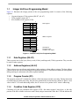


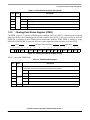
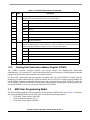
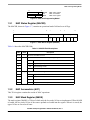
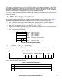
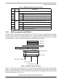
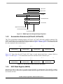
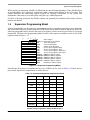
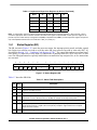
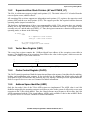
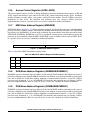


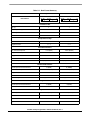
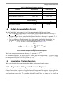

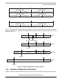
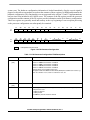


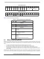
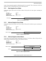


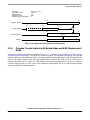
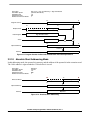

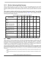


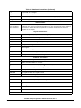

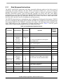
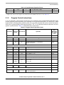
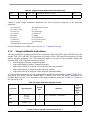

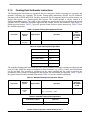
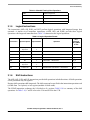
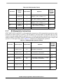
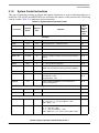
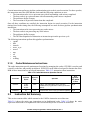


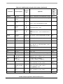
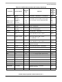

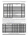
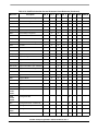
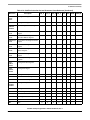
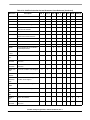
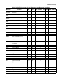
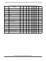


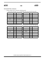

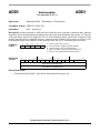
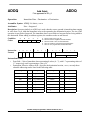
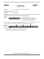


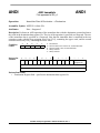
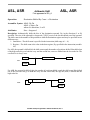
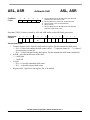
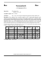

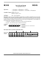
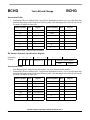
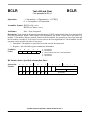
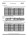
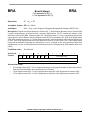
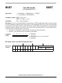

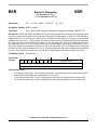
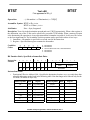
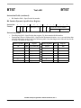
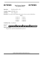


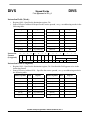
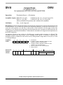
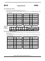
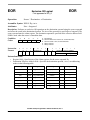
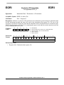
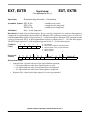
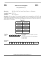
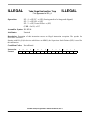

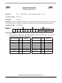
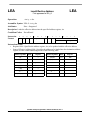
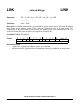
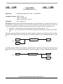
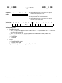
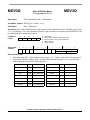
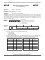
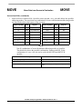
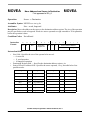

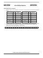
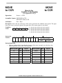

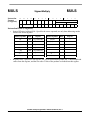
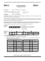


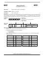


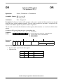
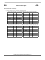

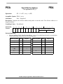
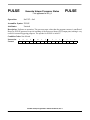

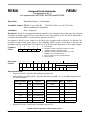


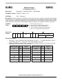


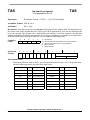
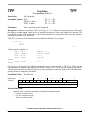
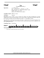
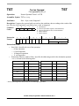
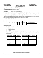


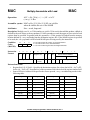


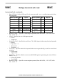
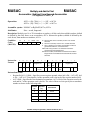

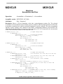

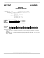


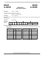


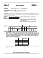

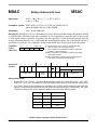
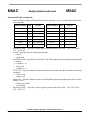
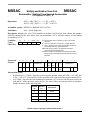


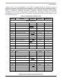
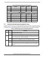
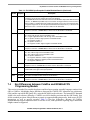


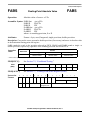
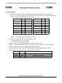
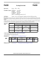
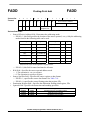


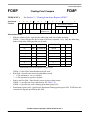
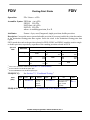


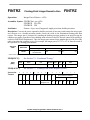
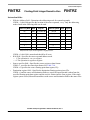
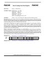

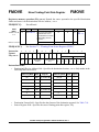


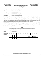
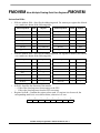
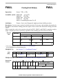
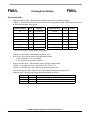


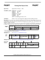
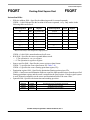
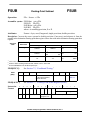


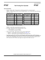


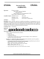
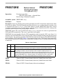
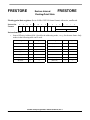
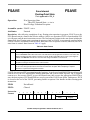


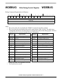

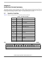

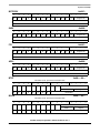

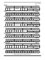
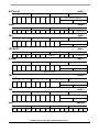
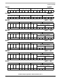


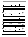
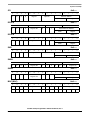


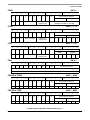

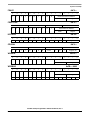

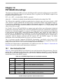

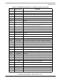

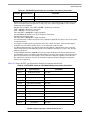
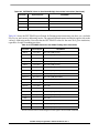
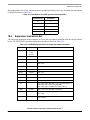

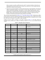
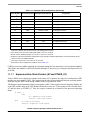
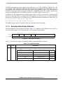
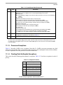


![HiSoft Devpac 3 (text version) [1992] [Manual: PDF]](http://vs1.manualzilla.com/store/data/005668901_1-67cf8256fc448cd2edf58a11a6ec729e-150x150.png)