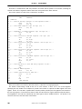
1
Application Note
VR Series™
64-/32-Bit Microprocessor
Programming Guide
Target Devices
VR4100 Series™
VR4300 Series™
VR5000 Series™
VR5432™
VR5500™
VR10000 Series™
Document No. U10710EJ5V0AN00 (5th edition)
Date Published November 2001 N CP(K)
©
1999 2001
1996,
Printed in Japan
[MEMO]
2
Application Note U10710EJ5V0AN
NOTES FOR CMOS DEVICES
1
PRECAUTION AGAINST ESD FOR SEMICONDUCTORS
Note:
Strong electric field, when exposed to a MOS device, can cause destruction of the gate oxide and
ultimately degrade the device operation. Steps must be taken to stop generation of static electricity
as much as possible, and quickly dissipate it once, when it has occurred. Environmental control
must be adequate. When it is dry, humidifier should be used. It is recommended to avoid using
insulators that easily build static electricity. Semiconductor devices must be stored and transported
in an anti-static container, static shielding bag or conductive material. All test and measurement
tools including work bench and floor should be grounded. The operator should be grounded using
wrist strap. Semiconductor devices must not be touched with bare hands. Similar precautions need
to be taken for PW boards with semiconductor devices on it.
2
HANDLING OF UNUSED INPUT PINS FOR CMOS
Note:
No connection for CMOS device inputs can be cause of malfunction. If no connection is provided
to the input pins, it is possible that an internal input level may be generated due to noise, etc., hence
causing malfunction. CMOS devices behave differently than Bipolar or NMOS devices. Input levels
of CMOS devices must be fixed high or low by using a pull-up or pull-down circuitry. Each unused
pin should be connected to V DD or GND with a resistor, if it is considered to have a possibility of
being an output pin. All handling related to the unused pins must be judged device by device and
related specifications governing the devices.
3
STATUS BEFORE INITIALIZATION OF MOS DEVICES
Note:
Power-on does not necessarily define initial status of MOS device. Production process of MOS
does not define the initial operation status of the device. Immediately after the power source is
turned ON, the devices with reset function have not yet been initialized. Hence, power-on does
not guarantee out-pin levels, I/O settings or contents of registers. Device is not initialized until the
reset signal is received. Reset operation must be executed immediately after power-on for devices
having reset function.
VR10000 Series, VR10000, VR12000, VR12000A, VR3000 Series, VR4100 Series, VR4100, VR4121, VR4122, VR4181,
VR4200, VR4300 Series, VR4300, VR4305, VR4310, VR5000 Series, VR5000, VR5000A, VR5432, VR5500, and VR
Series are trademarks of NEC Corporation.
MIPS is a registered trademark of MIPS Technologies, Inc. in the United States.
MULTI is a trademark of Green Hills Software, Inc.
Application Note U10710EJ5V0AN
3
Exporting this product or equipment that includes this product may require a governmental license from the U.S.A. for some
countries because this product utilizes technologies limited by the export control regulations of the U.S.A.
• The information in this document is current as of October, 2001. The information is subject to
change without notice. For actual design-in, refer to the latest publications of NEC's data sheets or
data books, etc., for the most up-to-date specifications of NEC semiconductor products. Not all
products and/or types are available in every country. Please check with an NEC sales representative
for availability and additional information.
• No part of this document may be copied or reproduced in any form or by any means without prior
written consent of NEC. NEC assumes no responsibility for any errors that may appear in this document.
• NEC does not assume any liability for infringement of patents, copyrights or other intellectual property rights of
third parties by or arising from the use of NEC semiconductor products listed in this document or any other
liability arising from the use of such products. No license, express, implied or otherwise, is granted under any
patents, copyrights or other intellectual property rights of NEC or others.
• Descriptions of circuits, software and other related information in this document are provided for illustrative
purposes in semiconductor product operation and application examples. The incorporation of these
circuits, software and information in the design of customer's equipment shall be done under the full
responsibility of customer. NEC assumes no responsibility for any losses incurred by customers or third
parties arising from the use of these circuits, software and information.
• While NEC endeavours to enhance the quality, reliability and safety of NEC semiconductor products, customers
agree and acknowledge that the possibility of defects thereof cannot be eliminated entirely. To minimize
risks of damage to property or injury (including death) to persons arising from defects in NEC
semiconductor products, customers must incorporate sufficient safety measures in their design, such as
redundancy, fire-containment, and anti-failure features.
• NEC semiconductor products are classified into the following three quality grades:
"Standard", "Special" and "Specific". The "Specific" quality grade applies only to semiconductor products
developed based on a customer-designated "quality assurance program" for a specific application. The
recommended applications of a semiconductor product depend on its quality grade, as indicated below.
Customers must check the quality grade of each semiconductor product before using it in a particular
application.
"Standard": Computers, office equipment, communications equipment, test and measurement equipment, audio
and visual equipment, home electronic appliances, machine tools, personal electronic equipment
and industrial robots
"Special": Transportation equipment (automobiles, trains, ships, etc.), traffic control systems, anti-disaster
systems, anti-crime systems, safety equipment and medical equipment (not specifically designed
for life support)
"Specific": Aircraft, aerospace equipment, submersible repeaters, nuclear reactor control systems, life
support systems and medical equipment for life support, etc.
The quality grade of NEC semiconductor products is "Standard" unless otherwise expressly specified in NEC's
data sheets or data books, etc. If customers wish to use NEC semiconductor products in applications not
intended by NEC, they must contact an NEC sales representative in advance to determine NEC's willingness
to support a given application.
(Note)
(1) "NEC" as used in this statement means NEC Corporation and also includes its majority-owned subsidiaries.
(2) "NEC semiconductor products" means any semiconductor product developed or manufactured by or for
NEC (as defined above).
M8E 00. 4
4
Application Note U10710EJ5V0AN
Regional Information
Some information contained in this document may vary from country to country. Before using any NEC
product in your application, pIease contact the NEC office in your country to obtain a list of authorized
representatives and distributors. They will verify:
•
Device availability
•
Ordering information
•
Product release schedule
•
Availability of related technical literature
•
Development environment specifications (for example, specifications for third-party tools and
components, host computers, power plugs, AC supply voltages, and so forth)
•
Network requirements
In addition, trademarks, registered trademarks, export restrictions, and other legal issues may also vary
from country to country.
NEC Electronics Inc. (U.S.)
NEC Electronics (Germany) GmbH
NEC Electronics Hong Kong Ltd.
Santa Clara, California
Tel: 408-588-6000
800-366-9782
Fax: 408-588-6130
800-729-9288
Benelux Office
Eindhoven, The Netherlands
Tel: 040-2445845
Fax: 040-2444580
Hong Kong
Tel: 2886-9318
Fax: 2886-9022/9044
NEC Electronics Hong Kong Ltd.
Velizy-Villacoublay, France
Tel: 01-3067-5800
Fax: 01-3067-5899
Seoul Branch
Seoul, Korea
Tel: 02-528-0303
Fax: 02-528-4411
NEC Electronics (France) S.A.
NEC Electronics Singapore Pte. Ltd.
Milton Keynes, UK
Tel: 01908-691-133
Fax: 01908-670-290
Madrid Office
Madrid, Spain
Tel: 091-504-2787
Fax: 091-504-2860
Novena Square, Singapore
Tel: 253-8311
Fax: 250-3583
NEC Electronics Italiana s.r.l.
NEC Electronics (Germany) GmbH
Milano, Italy
Tel: 02-66 75 41
Fax: 02-66 75 42 99
Scandinavia Office
Taeby, Sweden
Tel: 08-63 80 820
Fax: 08-63 80 388
NEC Electronics (France) S.A.
NEC Electronics (Germany) GmbH
Duesseldorf, Germany
Tel: 0211-65 03 02
Fax: 0211-65 03 490
NEC Electronics (UK) Ltd.
NEC Electronics Taiwan Ltd.
Taipei, Taiwan
Tel: 02-2719-2377
Fax: 02-2719-5951
NEC do Brasil S.A.
Electron Devices Division
Guarulhos-SP, Brasil
Tel: 11-6462-6810
Fax: 11-6462-6829
J01.2
Application Note U10710EJ5V0AN
5
Major Revisions in This Edition
Page
Description
Throughout
Addition and deletion of target devices
Addition: VR4121TM, VR4122TM, VR4181TM, VR4305TM, VR4310TM, VR5000ATM, VR5432,
VR5500 (under development), VR10000TM, VR12000TM, VR12000ATM
Deletion: VR4100TM, VR4200TM
Throughout
Change, addition, and deletion of descriptions brought about by addition and deletion of
target devices
VOLUME 1 OUTLINE OF TOOLS
p.17
Change of composition of whole volume, deletion of descriptions
VOLUME 2 VR SERIES ARCHITECTURE
p.19
Addition and deletion of products in Table 1-1 VR Series Processors
pp.20, 21
Modification and addition of description in 1.1.2 Pipeline
p.25
Addition of registers in Table 1-2 CP0 Registers
pp.26, 27
Addition of description in 1.2.1 (1) Config register
pp.28 to 30
Addition of description in 1.2.1 (2) Status register
pp.31, 32
Addition of Figure 1-9 Self-Diagnostic Status (DS) Area
p.35
Addition and deletion of products in Table 1-3 Difference in Cache Depending on
Processor
pp.39, 40
Addition of description in 1.3.2 (1) Control/Status register (FCR31)
pp.41 to 43
Change and addition of description in 2.1 Pipeline Stage
pp.49 to 54
Addition of description in 3.1 Primary Cache
p.50
Addition and deletion of products in Table 3-1 Primary Cache Size, Line Size, and
Index
pp.55, 56
Addition of description in 3.2 Secondary Cache
pp.57 to 59
Change of Table 3-3 Cache Instruction’s Suboperation Code op4..2 for each product
pp.59, 60
Addition of description in 3.3 Cache Instructions
p.61
Addition and deletion of products in Table 4-1 Physical Address Space
p.63
Deletion of description in 4.2 TLB Entries
pp.64 to 70
Addition of description in 4.3 TLB Entry Register
pp.76, 77
Addition of description in 5.4.2 General-purpose exceptions
pp.82, 83
Addition of CHAPTER 6 DEBUG INTERFACE
VOLUME 3 PROGRAMMING
p.87
Addition of description in 1.2 Instruction Hazards
p.92
Modification of description in 2.1.1 Cache initialization procedure
pp.93 to 98
Addition and change of description in 2.1.2 Example of cache initialization program
pp.98 to 103
Addition and change of examples of program in 2.2 Cache Writeback, 2.3 Cache Fill,
and 2.4 Cache Tag Display
p.108
Change of example of program in 3.3 TLB Settings
pp.110, 111
Change of example of program in 3.4 TLB Initialization
p.120
Change of example of program in 4.2 Initialization of Exceptions
pp.121, 122
Addition and deletion of description in 5.1 Initialization of CPU
pp.123 to 138
Addition and change of example of program in 5.2 Example of Initialization Program
The mark
6
shows major revised points.
Application Note U10710EJ5V0AN
INTRODUCTION
Target Readers
This manual is intended for users who understand the functions of the following products
and wish to design application systems using these products.
• VR4100 Series
• VR5432 (µPD30541)
VR4121 (µPD30121)
• VR5500 (µPD30550)
VR4122 (µPD30122)
• VR10000 Series
VR4181 (µPD30181)
• VR4300 Series
VR4300 , VR4305 (µPD30200)
TM
Note
VR10000 (µPD30700)
VR12000 (µPD30710)
VR12000A (µPD30710A)
VR4310 (µPD30210)
• VR5000 Series
VR5000
TM
Note Under development
(µPD30500)
VR5000A (µPD30500A)
Purpose
This manual is designed to be used as a handbook for developing application systems
using the products listed above.
Organization
This manual consists of the following subjects.
• Outline of tools
• VR Series architecture
• Programming
How to Read This Manual It is assumed that the reader of this manual has general knowledge of microcontrollers,
the C programming language, and assembler language.
The program source code shown in this manual is for reference only and is not intended
for use in mass-production design.
For the hardware functions of each product
→ Refer to the Hardware User’s Manual or User’s Manual of each product.
For the instruction functions of each product
→ Refer to the Instruction User’s Manual, Architecture User’s Manual or User’s
Manual.
Application Note U10710EJ5V0AN
7
Conventions
Data significance:
Higher digits on the left and lower digits on the right
Active low representation: ×××# (# after pin or signal name)
Note:
Footnote for item marked with Note in the text
Caution:
Information requiring particular attention
Remark:
Supplementary information
Numerical representation: Binary ··· ×××× or ×××B
Decimal ··· ×××××
Hexadecimal ··· 0x××××
Suffix representing an exponent of 2 (in address space or memory capacity):
Related Documents
10
K (Kilo)
2 = 1,024
M (Mega)
2 = 1,024
20
2
30
3
40
4
50
5
60
6
G (Giga)
2 = 1,024
T (Tera)
2 = 1,024
P (Peta)
2 = 1,024
E (Exa)
2 = 1,024
The related documents indicated in this publication may include preliminary versions.
However, preliminary versions are not marked as such.
• User’s Manual
Document Name
Document No.
VR4121 User’s Manual
U13569E
VR4122 Hardware User’s Manual
U14327E
VR4181 Hardware User’s Manual
U14272E
VR4100 Series Architecture User’s Manual
To be prepared
VR4300, VR4305, VR4310 User’s Manual
U10504E
VR5000, VR5000A User’s Manual
U11761E
VR5432 User’s Manual
U13751E
VR5500 User’s Manual
To be prepared
VR10000 Series User’s Manual
U10278E
VR5000, VR10000 Instruction User’s Manual
U12754E
• Data Sheet
Document Name
8
Document No.
µPD30121 (VR4121) Data Sheet
U14691E
µPD30122 (VR4122) Data Sheet
To be prepared
µPD30181 (VR4181) Data Sheet
U14273E
µPD30200, 30210 (VR4300, VR4305, VR4310) Data Sheet
U10116E
µPD30500, 30500A (VR5000, VR5000A) Data Sheet
U12031E
µPD30541 (VR5432) Data Sheet
U13504E
µPD30550 (VR5500) Data Sheet
To be prepared
µPD30700, 30710 (VR10000, VR12000) Data Sheet
U12703E
Application Note U10710EJ5V0AN
CONTENTS
VOLUME 1 OUTLINE OF TOOLS..........................................................................................................16
CHAPTER 1 PROGRAMMING TOOLS ..................................................................................................17
VOLUME 2 VR SERIES ARCHITECTURE .............................................................................................18
CHAPTER 1 OUTLINE .............................................................................................................................19
1.1
1.2
CPU .............................................................................................................................................19
1.1.1
Outline ........................................................................................................................................... 19
1.1.2
Pipeline .......................................................................................................................................... 20
1.1.3
Instructions .................................................................................................................................... 22
1.1.4
Registers........................................................................................................................................ 24
Coprocessors ............................................................................................................................25
1.2.1
1.3
Registers........................................................................................................................................ 25
1.2.2
Memory management .................................................................................................................... 33
1.2.3
Exceptions ..................................................................................................................................... 36
1.2.4
Hazards ......................................................................................................................................... 36
FPU..............................................................................................................................................37
1.3.1
Instructions .................................................................................................................................... 37
1.3.2
Registers........................................................................................................................................ 37
CHAPTER 2 PIPELINE.............................................................................................................................41
2.1
Pipeline Stage ............................................................................................................................41
2.2
Interlock......................................................................................................................................44
2.3
Delay ...........................................................................................................................................46
2.4
2.3.1
Branching delay ............................................................................................................................. 46
2.3.2
Loading delay ................................................................................................................................ 47
Bypassing ..................................................................................................................................48
CHAPTER 3 CACHE ................................................................................................................................49
3.1
Primary Cache............................................................................................................................49
3.1.1
VR4100 Series................................................................................................................................ 51
3.1.2
VR4300 Series................................................................................................................................ 52
3.1.3
VR5000 Series................................................................................................................................ 53
3.1.4
VR5432 and VR5500....................................................................................................................... 54
Application Note U10710EJ5V0AN
9
3.2
3.3
Secondary Cache.......................................................................................................................55
3.2.1
VR5000 Series................................................................................................................................55
3.2.2
VR10000 Series..............................................................................................................................56
Cache Instructions ....................................................................................................................57
CHAPTER 4 TLB ......................................................................................................................................61
4.1
Translation from Virtual Addresses to Physical Addresses .................................................62
4.2
TLB Entries.................................................................................................................................63
4.3
4.4
TLB Entry Register ....................................................................................................................64
4.3.1
PageMask register .........................................................................................................................64
4.3.2
EntryHi register ..............................................................................................................................66
4.3.3
EntryLo0/Lo1 register.....................................................................................................................67
4.3.4
Others ............................................................................................................................................68
TLB Instructions ........................................................................................................................71
CHAPTER 5 EXCEPTIONS ......................................................................................................................73
5.1
Types of Exceptions..................................................................................................................73
5.2
Priority of Exceptions................................................................................................................74
5.3
Exception Vector Address ........................................................................................................75
5.4
Cautions Concerning Major Exceptions..................................................................................75
5.5
5.4.1
Cold reset, soft reset, NMI exceptions ...........................................................................................75
5.4.2
General-purpose exceptions ..........................................................................................................76
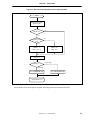
Exception Processing ...............................................................................................................78
5.5.1
Hardware processing .....................................................................................................................78
5.5.2
Software processing ......................................................................................................................80
5.5.3
Multiple interrupts...........................................................................................................................81
CHAPTER 6 DEBUG INTERFACE..........................................................................................................82
6.1
Debug Interface Function .........................................................................................................82
6.2
Debug System Configuration ...................................................................................................83
VOLUME 3 PROGRAMMING ...................................................................................................................84
CHAPTER 1 PIPELINE .............................................................................................................................85
1.1
10
Program Not Stopping Pipeline................................................................................................85
1.1.1
Branching delay .............................................................................................................................85
1.1.2
Loading delay.................................................................................................................................86
Application Note U10710EJ5V0AN
1.2
Instruction Hazards ...................................................................................................................87
1.2.1
Calculation of CP0 hazards ........................................................................................................... 91
CHAPTER 2 CACHE ................................................................................................................................92
2.1
2.2
Cache Initialization ....................................................................................................................92
2.1.1
Cache initialization procedure........................................................................................................ 92
2.1.2
Example of cache initialization program ........................................................................................ 93
Cache Writeback........................................................................................................................98
2.2.1
2.3
Cache Fill..................................................................................................................................100
2.3.1
2.4
Example of cache writeback program............................................................................................ 98
Example of cache fill program ..................................................................................................... 101
Cache Tag Display...................................................................................................................102
2.4.1
Example of cache tag display program........................................................................................ 102
CHAPTER 3 TLB ....................................................................................................................................104
3.1
Entry Read................................................................................................................................104
3.2
Entry Write................................................................................................................................105
3.3
TLB Settings ............................................................................................................................107
3.4
TLB Initialization......................................................................................................................110
3.5
TLB Entry Replacement ..........................................................................................................111
CHAPTER 4 EXCEPTIONS ....................................................................................................................115
4.1
4.2
Discriminating Between Exceptions......................................................................................115
4.1.1
Cold reset, soft reset, and NMI exceptions.................................................................................. 115
4.1.2
Other exceptions.......................................................................................................................... 116
Initialization of Exceptions .....................................................................................................118
CHAPTER 5 CPU INITIALIZATION.......................................................................................................121
5.1
5.2
Initialization of CPU.................................................................................................................121
5.1.1
CPU registers .............................................................................................................................. 121
5.1.2
CP0 registers ............................................................................................................................... 122
5.1.3
FPU (CP1) registers..................................................................................................................... 122
5.1.4
HALTimer shut down ................................................................................................................... 122
5.1.5
Initialization of cache and TLB..................................................................................................... 122
Example of Initialization Program..........................................................................................123
5.2.1
VR4121......................................................................................................................................... 123
5.2.2
VR4122......................................................................................................................................... 125
5.2.3
VR4181......................................................................................................................................... 128
Application Note U10710EJ5V0AN
11
5.2.4
VR4300 Series..............................................................................................................................130
5.2.5
VR5000 Series..............................................................................................................................131
5.2.6
VR5432 .........................................................................................................................................133
5.2.7
VR5500 .........................................................................................................................................134
5.2.8
VR10000 Series............................................................................................................................135
APPENDIX INDEX....................................................................................................................................139
12
Application Note U10710EJ5V0AN
LIST OF FIGURES (1/2)
VOLUME 2 VR SERIES ARCHITECTURE
Figure No.
Title
Page
1-1
Outline of Single-Way Pipeline (5 Stages) and Instruction Execution .......................................................... 20
1-2
Outline of 2-Way Superscalar Pipeline (5 Stages) and Instruction Execution .............................................. 21
1-3
Outline of 4-Way Superscalar Pipeline (5 Stages) and Instruction Execution .............................................. 21
1-4
Instruction Formats ....................................................................................................................................... 22
1-5
Example of R-type (ADD r14, r11, r10)......................................................................................................... 23
1-6
Example of I-type (ADDI r14, r11, 0x0100)................................................................................................... 23
1-7
Config Register ............................................................................................................................................. 26
1-8
Status Register ............................................................................................................................................. 28
1-9
Self-Diagnostic Status (DS) Area ................................................................................................................. 31
1-10
Virtual Memory Address Space .................................................................................................................... 33
1-11
Mapping of Virtual Address and Physical Address ....................................................................................... 34
1-12
Memory Hierarchy ........................................................................................................................................ 35
1-13
Flow of Exception Processing....................................................................................................................... 36
1-14
FPU Registers .............................................................................................................................................. 38
1-15
FCR31 .......................................................................................................................................................... 39
1-16
Cause/Enable/Flag Bit of FCR31.................................................................................................................. 39
2-1
Operation of Single-Way Pipeline (5 Stages) ............................................................................................... 42
2-2
Operation of 2-Way Superscalar Pipeline (5 Stages) ................................................................................... 42
2-3
Operation of 4-Way Superscalar Pipeline (5 Stages) ................................................................................... 43
2-4
Relationship Betweem Interlocks, Exceptions, and Faults ........................................................................... 44
2-5
State of Pipeline During Interlock (Stall) ....................................................................................................... 45
2-6
State of Pipeline During Interlock (Slip) ........................................................................................................ 45
2-7
Branching Delay ........................................................................................................................................... 46
2-8
Loading Delay............................................................................................................................................... 47
2-9
Example of Bypassing .................................................................................................................................. 48
3-1
Referencing Primary Cache.......................................................................................................................... 49
3-2
VR4100 Series On-Chip Cache Line ............................................................................................................. 51
3-3
VR4300 Series On-Chip Cache Line ............................................................................................................. 52
3-4
VR5000 Series Primary Cache Line .............................................................................................................. 53
3-5
VR5432 and VR5500 On-Chip Cache Lines .................................................................................................. 54
3-6
VR5000 Series Secondary Cache Line ......................................................................................................... 55
3-7
VR10000 Series Secondary Cache Line ....................................................................................................... 56
4-1
Translation from Virtual Address to Physical Address.................................................................................. 62
4-2
TLB Translation ............................................................................................................................................ 63
4-3
PageMask Register ...................................................................................................................................... 64
4-4
EntryHi Register (In 32-Bit Mode)................................................................................................................. 66
4-5
EntryLo0/Lo1 Register (In 32-Bit Mode) ....................................................................................................... 67
4-6
Index Register............................................................................................................................................... 68
4-7
Random Register.......................................................................................................................................... 69
Application Note U10710EJ5V0AN
13
LIST OF FIGURES (2/2)
Figure No.
4-8
Title
Page
Locations Indicated by Wired Register .........................................................................................................70
4-9
Wired Register ..............................................................................................................................................70
4-10
TLBP Instruction ...........................................................................................................................................71
4-11
TLBR Instruction ...........................................................................................................................................71
4-12
TLBWI Instruction .........................................................................................................................................72
4-13
TLBWR Instruction........................................................................................................................................72
5-1
Cause Register .............................................................................................................................................76
5-2
General-Purpose Exception Processing by Hardware..................................................................................79
5-3
General-Purpose Exception Processing by Software ...................................................................................80
6-1
Basic On-Chip Debug Configuration.............................................................................................................83
VOLUME 3 PROGRAMMING
Figure No.
Title
Page
3-1
EntryHi Register (In 32-Bit Mode) ................................................................................................................107
3-2
EntryLo0/Lo1 Register (In 32-Bit Mode) ......................................................................................................107
3-3
PageMask Register......................................................................................................................................107
3-4
TLB Translation............................................................................................................................................109
3-5
TLB Replacement ........................................................................................................................................111
3-6
Example of Creating Entry Table on Memory ..............................................................................................112
3-7
Context Register (In 32-Bit Mode) ...............................................................................................................113
14
Application Note U10710EJ5V0AN
LIST OF TABLES
VOLUME 2 VR SERIES ARCHITECTURE
Table No.
Title
Page
1-1
VR Series Processors ................................................................................................................................... 19
1-2
CP0 Registers............................................................................................................................................... 25
1-3
Difference in Cache Depending on Processor.............................................................................................. 35
1-4
Rounding Mode Control Bit........................................................................................................................... 40
2-1
Number of Pipeline Stages in VR Series ....................................................................................................... 41
3-1
Primary Cache Size, Line Size, and Index ................................................................................................... 50
3-2
Cache Instruction’s Suboperation Code op1..0 ............................................................................................. 57
3-3
Cache Instruction’s Suboperation Code op4..2 ............................................................................................. 57
4-1
Physical Address Space ............................................................................................................................... 61
4-2
Mask Values and Page Size......................................................................................................................... 65
5-1
Priority of Exceptions .................................................................................................................................... 74
5-2
Exception Vector Address ............................................................................................................................ 75
5-3
Status When Exception Occurs .................................................................................................................... 75
5-4
Exception Code Area of Cause Register ...................................................................................................... 77
VOLUME 3 PROGRAMMING
Table No.
Title
Page
1-1
CP0 Hazards of VR4100 Series .................................................................................................................... 88
1-2
CP0 Hazards of VR4300 Series .................................................................................................................... 89
1-3
Instruction Hazards of VR5000 Series and VR5432 ...................................................................................... 90
1-4
Instruction Hazards of VR5500...................................................................................................................... 90
Application Note U10710EJ5V0AN
15
VOLUME 1 OUTLINE OF TOOLS
16
Application Note U10710EJ5V0AN
CHAPTER 1 PROGRAMMING TOOLS
Tools that support development of VR Series application programs are released by NEC and other companies.
• Principal programming tools
MULTI
TM
(Green Hills Software, Inc.)
GNU (Red Hat, Inc.)
• Principal debugging tools
PARTNER (Kyoto Microcomputer Corporation)
RTE-1000-TP (Midas Lab Co., Ltd.)
For details, consult NEC sales representative.
Application Note U10710EJ5V0AN
17
VOLUME 2 VR SERIES ARCHITECTURE
18
Application Note U10710EJ5V0AN
CHAPTER 1 OUTLINE
1.1 CPU
The VR4100 Series, VR4300 Series, VR5000 Series, VR5432, VR5500
Note
, and VR10000 Series consist of high-
performance 64-bit microprocessors that adopt the RISC (Reduced Instruction Set Computer) architecture developed
TM
by MIPS . The VR Series instructions are upwardly compatible with the VR3000
TM
Series, so existing applications
can be utilized as is.
Note Under development
1.1.1 Outline
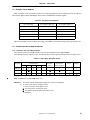
The features of the VR Series processors are shown below.
Table 1-1. VR Series Processors
Series Name
VR4100 Series
Part Number
Features
VR4121
Incorporates CPU and primary cache, includes product-sum operation and
MIPS16 instruction set, operates with ultra-low power consumption, and is
equipped with on-chip peripheral units.
VR4122
Incorporates CPU and primary cache, includes product-sum operation and
MIPS16 instruction set, operates with ultra-low power consumption, is equipped
with on-chip peripheral units, and supports PCI bus (subset).
VR4181
Incorporates CPU and primary cache, includes product-sum operation and
MIPS16 instruction set, operates with ultra-low power consumption, and is
equipped with on-chip peripheral units.
VR4300 Series
VR4300, VR4305,
VR4310
Incorporates CPU, FPU, and primary cache, and external bus is 32 bits.
VR5000 Series
VR5000, VR5000A
Adopts 2-way superscalar system for CPU, incorporates FPU, secondary cache
interface, and primary cache, and external bus is 64 bits.
−
VR5432
Adopts 2-way superscalar system for CPU, incorporates FPU, primary cache,
and branch prediction unit, and external bus is 32 bits (native mode/R43K mode
selectable).
−
VR5500Note 1
Adopts 2-way superscalar out-of-order systemNote 2 for CPU, incorporates FPU,
primary cache, and branch prediction unit, and external bus can be switched
between 64 bits and 32 bits.
VR10000, VR12000,
VR12000A
Adopts 4-way superscalar out-of-order systemNote 2 for CPU, incorporates FPU,
secondary cache interface, primary cache, and branch prediction unit.
VR10000 Series
Notes 1. Under development
2. “Out-of-order” is an execution method in which instructions such as for performing operations or
registers rewriting in the instructions fetched simultaneously are executed from wherever possible,
rather than in program order. Hardware detects the dependency relationship of registers and delay due
to load/branch, and resources are allocated so that no space remains in the pipeline and processed.
Note that the output of execution results, such as writeback to memory, is performed in program order.
Application Note U10710EJ5V0AN
19
VOLUME 2 VR SERIES ARCHITECTURE
1.1.2 Pipeline
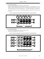
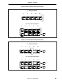
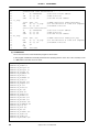
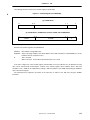
In the VR Series, an instruction execution system called a pipeline is adopted.
In the pipeline, instruction
execution processing is delimited into several stages. Instruction execution is complete when each stage is passed.
When processing of one instruction in one stage of the pipeline is complete, the next instruction enters that stage.
When the pipeline is full, it means that instructions equalling the number of pipeline stages are being executed
simultaneously.
The pipeline clock is called the PClock. Each cycle of the PClock is called a PCycle. Instructions are read in
synchronization with the PClock. Each stage of the pipeline is executed in one PCycle. Therefore, executing an
instruction requires as many PCycles as the number of pipeline stages. When the required data has not been
cached and must instead be fetched from the main memory, the execution requires more cycles than the number of
pipeline stages.
The VR Series provides the following pipelines. The methods adopted differ depending on the product.
• Single-way pipeline
• 2-way superscalar pipeline
• 4-way superscalar pipeline
(1) Single-way pipeline
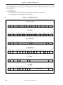
Reads and processes instructions one by one.
The pipeline of the VR4100 Series and VR4300 Series uses this method.
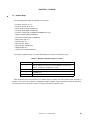
Figure 1-1. Outline of Single-Way Pipeline (5 Stages) and Instruction Execution
PClock
Instruction
Instruction
Instruction
IF
Instruction
RF
Instruction
EX
Instruction
DC
Pipeline
20
Application Note U10710EJ5V0AN
Instruction
WB
Instruction
CHAPTER 1 OUTLINE
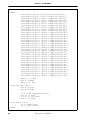
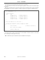
(2) 2-way superscalar pipeline
Reads two instructions simultaneously, and processes them in parallel.
The pipeline of the VR5000 Series, VR5432, and VR5500 uses this method. In the VR5000 Series, one of two
pipelines is assigned to CPU instructions, and the other is assigned to FPU instructions, and one each of the
CPU and FPU instructions are processed simultaneously. In the VR5432 and VR5500, this assignment does
not occur and two instructions are processed simultaneously regardless of whether the instruction is from the
CPU or FPU.
Figure 1-2. Outline of 2-Way Superscalar Pipeline (5 Stages) and Instruction Execution
PClock
Instruction
Instruction
Instruction
Instruction
Instruction
Instruction
Instruction
Instruction
Instruction
Instruction
Instruction
Instruction
Instruction
Instruction
Instruction
Instruction
IC
RF
EX
DC
WB
Pipeline
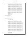
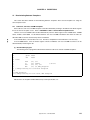
(3) 4-way superscalar pipeline
Reads four instructions simultaneously and processes them in parallel.
The pipeline of the VR10000 Series uses this method.
Figure 1-3. Outline of 4-Way Superscalar Pipeline (5 Stages) and Instruction Execution
Instruction
Instruction
Instruction
Instruction
Instruction
Instruction
Instruction
Instruction
Instruction
Instruction
Instruction
Instruction
Instruction
Instruction
Instruction
Instruction
Instruction
Instruction
Instruction
Instruction
Instruction
Instruction
Instruction
Instruction
Instruction
Instruction
Instruction
Instruction
Instruction
Instruction
Instruction
Instruction
IF
ID
IS
EX
WB
Pipeline
Application Note U10710EJ5V0AN
21
VOLUME 2 VR SERIES ARCHITECTURE
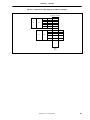
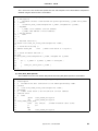
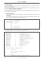
1.1.3 Instructions
All the CPU instructions in the VR Series except MIPS16 instructions are 32 bits in length. The instructions are
divided into three types according to their formats.
Figure 1-4. Instruction Formats
31
I-type (immediate)
26 25
rs
op
31
J-type (jump)
21 20
16 15
rt
immediate
26 25
0
op
31
R-type (register)
0
target
26 25
op
21 20
rs
16 15
rt
11 10
rd
65
sa
0
funct
They are further divided into seven types according to the function of the instruction.
(1) Load/store
Load/store instructions perform data transfer between the memory and general-purpose registers. The format
of load/store instructions is I-type.
(2) Arithmetic
Arithmetic instructions execute arithmetic operations, logical arithmetic operations, shift operations, and
multiply/divide operations on the register value. The format of arithmetic instructions is R-type or I-type.
(3) Jump/branch
Jump/branch instructions change the control and flow of the program.
The jump instruction is either J-type or R-type. The branch instruction is I-type.
The JAL instruction saves the return address to register 31.
(4) Coprocessor
Coprocessor instructions execute coprocessor operations. The load/store instruction of the coprocessor is Itype. The format of coprocessor arithmetic instructions differs depending on the coprocessor.
(5) System control coprocessor
System control coprocessor instructions execute operations on CP0 registers in order to perform memory
management and exception processing of the processor.
(6) Special
Special instructions execute system call exceptions and breakpoint exceptions. These instructions are Rtype.
(7) Exception
Exception instructions generate trap exceptions based on the comparison result. These instructions are Rtype and I-type.
22
Application Note U10710EJ5V0AN
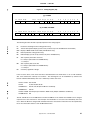
CHAPTER 1 OUTLINE
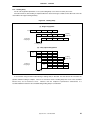
The following shows an example of arithmetic operation in the VR Series.
Figure 1-5. Example of R-type (ADD r14, r11, r10)
ADD
r11
r10
r14
ADD
Instruction code
General-purpose register
r10
r11
r12
ADD
r13
r14
r15
Figure 1-6. Example of I-type (ADDI r14, r11, 0x0100)
ADD
r11
r14
Instruction code
0x0100
General-purpose register
r10
r11
r12
r13
ADD
r14
r15
For details of the MIPS16 instruction set, refer to the user’s manual of each product in the VR4100 Series.
Application Note U10710EJ5V0AN
23
VOLUME 2 VR SERIES ARCHITECTURE
1.1.4 Registers
The CPU of the VR Series includes the following registers.
• Integer general-purpose registers
64 bits × 32
• Program counter
64 bits
• HI register
64 bits
• LO register
64 bits
• LL bit register
1 bit (the VR4100 Series does not have this register)
Among these registers, the program counter, HI and LO registers, and LL bit register are special function registers
used or revised by certain instructions. The program counter and LL bit register cannot be operated by software.
In addition, the following functions are allocated to two general-purpose registers, r0 and r31.
r0:
This is the zero register. Its contents are always zero, and r0 can be specified as the target register for an
instruction when the result of the operation should be discarded. This register can also be used as the
source register when a value of zero is required.
r31: This is the return address register. It is the link register used for the JAL instruction and JALR instruction. It
can also be used for other instructions, but be careful not to duplicate use of data from operations by the
JAL/JALR instruction and other instructions.
24
Application Note U10710EJ5V0AN
CHAPTER 1 OUTLINE
1.2 Coprocessors
The CPU can be operated with up to four closely-coupled coprocessors (CP0 to CP3). Coprocessor 1 (CP1) is a
floating point unit (however, this is reserved in the VR4100 Series). Coprocessor 2 and coprocessor 3 are reserved
for future use (however, in the VR5432, the CP2 instruction code area is used for dedicated instructions).
Coprocessor 0 (CP0) is an on-chip system control coprocessor, and it supports the virtual memory system and
exception processing.
1.2.1 Registers
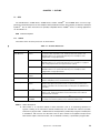
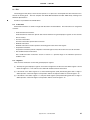
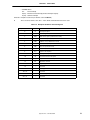
The following describes the registers in CP0.
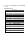
Table 1-2. CP0 Registers
Register Number
Register Name
Function
Write
0
Index
Used in memory management (TLB)
{
1
Random
Used in memory management (TLB)
−
2
EntryLo0
Used in memory management (TLB)
{
3
EntryLo1
Used in memory management (TLB)
{
4
Context
Used in exception processing
{
5
PageMask
Used in memory management (TLB)
{
6
Wired
Used in memory management (TLB)
{
8
BadVAddr
Used in exception processing
−
9
Count
Used in exception processing
{
10
EntryHi
Used in memory management (TLB)
{
11
Comparison
Used in exception processing
{
12
Status
Used in exception processing and for self-diagnosis
{
13
Cause
Used in exception processing
∆
14
EPC
Used in exception processing
{
15
PRId
Used in memory management
−
16
Config
Used in memory management
∆
17
LLAddr
Used in memory management
{
18
WatchLo
Used in exception processing (debugging)
(reserved in VR5000 Series)
{
19
WatchHi
Used in exception processing (debugging)
(reserved in VR5000 Series)
{
20
XContext
Used in exception processing
{
21
FrameMask
Used in memory management (TLB) (VR10000
Series only)
{
22
Diagnostic
Used for self-diagnosis (VR10000 Series only)
{
25
Performance
Counter
Used in exception processing (debugging) (VR5500,
VR10000 Series only)
{
26
Parity Error
Used in exception processing
{
27
Cache Error
Used in exception processing
−
28
TagLo
Used in memory management (CACHE instruction)
{
29
TagHi
Used in memory management (CACHE instruction)
{
30
ErrorEPC
Used in exception processing
{
Remark
{: Possible, ∆: Partially possible, −: Not possible
Application Note U10710EJ5V0AN
25
VOLUME 2 VR SERIES ARCHITECTURE
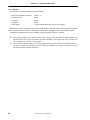
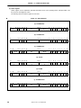
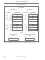
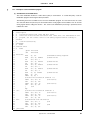
The following describes the Config register and Status register, which are important in initialization, etc., among
these CP0 registers.
(1) Config register
The Config register can be read/written and displays/sets various states of the processor.
The Config register of each CPU appears as shown below.
Figure 1-7. Config Register (1/2)
(a) VR4121, VR4181
31 30
28 27
24
23
22
21 20 19
16 15 14
13 12 11
9 8
6 5
3 2
0
0
EC
EP
AD
00
M16
0010
BE
10
CS
IC
DC
000
K0
1
3
4
1
2
1
4
1
2
1
3
3
3
3
(b) VR4122
31 30
28 27
24 23 22 21 20 19
17 16
IS
EC
EP
AD
00
M16
001
1
3
4
1
2
1
3
15 14 13 12 11
BP BE
1
9 8
6
5
3 2
4
0
10
CS
IC
DC
IB
00
K0
2
1
3
3
1
2
3
1
(c) VR4300 Series
31 30
28 27
24 23
16
15 14
4
3
2
0
0
EC
EP
0000010
BE
11001000110
CU
K0
1
3
4
7
1
11
1
3
(d) VR5000 Series
31 30
16
15
0
EC
28 27
EP
24 23 22 21 20 19
SB
SS
EW
SC
1
BE EM EB SE
1
3
4
2
2
2
1
1
18 17
1
14
1
13
1
12 11
1
4
3
IC
9 8
DC
6 5
IB
DB
0
2
K0
0
3
3
1
1
1
3
(e) VR5432
31 30
28 27
24 23 22 21
16 15 14
3
2
0
0
EC
EP
EM
110110
BE
110011011110
K0
1
3
4
2
6
1
12
3
(f) VR5500
31 30
26
28 27
24 23 22 21 20 19 18 17 16 15 14
3
2
0
0
EC
EP
EM
11
EW
10
BE
110011011110
K0
1
3
4
2
2
2
2
1
12
3
Application Note U10710EJ5V0AN
CHAPTER 1 OUTLINE
Figure 1-7. Config Register (2/2)
(g) VR10000
29 28
31
26 25
22 21
19 18
16 15
IC
DC
0000
SC
SS
3
3
4
3
3
14
13 12
BE SK SB
1
1
9 8
7
EC
PM
4
2
1
6
5
PE CT
1
1
6
5
3 2
4
0
DN
K0
2
3
(h) VR12000, VR12000A
29 28
31
26 25
24 23 22 21
19 18
16 15
IC
DC
0
DSD
00
SC
SS
3
3
1
1
2
3
3
14
13 12
BE SK SB
1
1
9 8
7
EC
PM
4
2
1
PE CT
1
1
3 2
4
0
DN
K0
2
3
The following describes the bits especially important in the Config register.
IS:
Instruction streaming function setting (VR4122 only)
EP:
Transfer data pattern display (Can be set by software only in the VR4300 Series and VR5432)
M16: Display of MIPS16 ISA mode enable (VR4100 Series only)
BP:
Branch prediction setting (VR4122 only)
BE:
Endian display (Can be set by software only in the VR4300 Series)
IB:
Size of primary instruction cache line
0 → 16 bytes (Reserved in the VR5000 Series)
1 → 32 bytes
DB:
Size of primary data cache line
0 → 16 bytes (Reserved in the VR5000 Series)
1 → 32 bytes
K0:
Coherency algorithm of kseg0
In the VR Series CPUs, areas other than those described below have fixed values or are set with hardware
after reset and become read-only from software. The following bits can be read/written by software and
become undefined immediately after reset. Initialize by software after reset.
VR4121, VR4181: EP, AD, K0
VR4122:
IS, EP, AD, BP, IB, K0
VR4300 Series:
EP, BE, CU, K0 (EP and BE are conditional)
VR5000 Series:
SE, K0
VR5432, VR5500: EP, EM (except in VR5432’s R43K mode), K0 (EP and EM are conditional)
VR10000 Series: K0
The EP and BE bits in the VR4300 Series and EP and EM bits in the VR5432 and VR5500 can be changed
only before the store instruction is executed upon the initialization of non-cache area immediately after cold
reset. When the BE bit is changed with an MTC0 instruction, the load/store instruction must be separated by
two or more instructions before or after the MTC0 instruction.
Application Note U10710EJ5V0AN
27
VOLUME 2 VR SERIES ARCHITECTURE
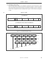
(2) Status register
Status register can be read/written and holds information such as the operating mode, interrupt enable, and
the processor self-diagnostic status.
The following shows the Status register of each CPU.
Figure 1-8. Status Register
(a) VR4100 Series
31
29 28 27
26 25 24
16 15
8
000
CU0
00
RE
DS
IM(7:0)
3
1
2
1
9
8
7
6
5
KX SX UX
1
1
1
7
6
5
4
3
2
1
0
KSU ERL EXL IE
2
1
1
2
1
1
(b) VR4300 Series
31
28 27
CU(3:0)
4
26
25 24
RP FR RE
1
1
1
16 15
8
DS
IM(7:0)
9
8
KX SX UX
1
1
1
7
6
5
4
3
0
KSU ERL EXL IE
2
1
1
1
(c) VR5000 Series
31 30
28 27
XX
CU(2:0)
0
1
3
1
26
25 24
FR RE
1
1
16 15
8
DS
IM(7:0)
9
8
KX SX UX
1
1
1
7
6
5
4
3
2
1
0
KSU ERL EXL IE
2
1
1
2
1
1
(d) VR5432
31
28 27
26
25 24
16 15
8
CU(3:0)
0
FR
0
DS
IM(7:0)
4
1
1
1
9
8
KX SX UX
1
1
1
7
6
5
4
3
0
KSU ERL EXL IE
2
1
1
2
1
1
(e) VR5500
31 30
28 27
26
25 24
16 15
8
XX
CU(2:0)
0
FR
0
DS
IM(7:0)
1
3
1
1
1
9
8
KX SX UX
1
1
1
7
6
5
4
3
0
KSU ERL EXL IE
2
1
1
2
1
1
(f) VR10000 Series
31 30
28
28 27
XX
CU(2:0)
1
3
26
25 24
RP FR RE
1
1
1
16 15
8
DS
IM(7:0)
9
8
Application Note U10710EJ5V0AN
KX SX UX
1
1
1
4
3
0
KSU ERL EXL IE
2
1
1
1
CHAPTER 1 OUTLINE
The following describes the bits in the staus register.
XX:
Enables use of MIPS IV instructions in user mode (VR5000 Series, VR5500, and VR10000 Series only)
1 → Enable
0 → Disable
CU:
Enables use of coprocessors. Controls use of four coprocessors.
1 → Enable
0 → Disable
In the kernel mode, CP0 can be used regardless of the CU0 bit value.
RP:
Specifies low-power mode (VR4300 Series and VR10000 Series only)
1 → Low-power mode
0 → Normal
Set to 0 in the VR10000 Series.
FR:
Sets the number of floating point registers that can be used (Reserved in the VR4100 Series)
1 → 32
0 → 16
RE:
Inversion of endian in user mode (Except VR5432 and VR5500)
1 → Inverted
0 → Disabled
Since the VR4100 Series always operates using little endian, set this bit to 0.
DS:
IM:
Self-diagnostic status area (Refer to Figure 1-9.)
Interrupt mask (enabling external, internal, and software interrupts). Controls eight interrupts.
1 → Enable
0 → Disable
Interrupts are assigned to each bit as follows.
• VR4100 Series
IM7:
Masks timer interrupt
IM(6:2): Masks normal interrupt (Int(4:0)). However, Int4 is not generated.
IM(1:0): Masks software interrupt
• VR4300 Series
IM7:
Masks timer interrupt
IM(6:2): Masks external normal interrupt (Int(4:0)# and external write request)
IM(1:0): Masks software interrupt
• VR5000 Series
IM7:
Masks timer interrupt and external normal interrupt (Int5#)
IM(6:2): Masks external normal interrupt (Int(4:0)# and external write request)
IM(1:0): Masks software interrupt
• VR5432
IM7:
Masks timer interrupt
IM(6:2): Masks external normal interrupt (Int(4:0)# and external write request)
IM(1:0): Masks software interrupt
• VR5500
IM7:
Masks timer interrupt or external normal interrupt (Int5#)
IM(6:2): Masks external normal interrupt (Int(4:0)# and external write request)
IM(1:0): Masks software interrupt
Application Note U10710EJ5V0AN
29
VOLUME 2 VR SERIES ARCHITECTURE
• VR10000 Series
IM7:
Masks timer interrupt
IM(6:2): Masks external normal interrupt (external interrupt request)
IM(1:0): Masks software interrupt
KX:
Enables 64-bit addressing in the kernel mode. In the kernel mode, 64-bit operation is always enabled.
1 → 64 bits
0 → 32 bits
SX:
Enables 64-bit addressing and 64-bit operation in the supervisor mode
1 → 64 bits
0 → 32 bits
UX:
Enables 64-bit addressing and 64-bit operation in the user mode
1 → 64 bits
0 → 32 bits
KSU: Operating mode
10 → User
01 → Supervisor
00 → Kernel
ERL: Error level
1 → Error
0 → Normal
EXL: Exception level
1 → Exception
0 → Normal
IE:
Enables interrupt
1 → Enable
0 → Disable
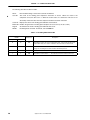
The details of the DS (self-diagnostic status) area are shown below.
read/written.
30
Application Note U10710EJ5V0AN
All bits except the TS bit can be
CHAPTER 1 OUTLINE
Figure 1-9. Self-Diagnostic Status (DS) Area
(a) VR4121, VR4181
24
23
22
21
20
19
18
17
16
0
0
BEV
TS
SR
0
CH
CE
DE
1
1
1
1
1
1
1
1
1
(b) VR4122
24
23
22
21
20
19
18
17
16
0
0
BEV
0
SR
0
CH
CE
DE
1
1
1
1
1
1
1
1
1
(c) VR4300 Series
24
23
22
21
20
19
18
17
16
ITS
0
BEV
TS
SR
0
CH
CE
DE
1
1
1
1
1
1
1
1
1
18
17
16
(d) VR5000 Series
24
23
22
21
20
19
0
0
BEV
0
SR
0
0
CE
DE
1
1
1
1
1
1
1
1
1
(e) VR5432, VR5500
24
23
22
21
20
19
18
17
16
DME
0
BEV
TS
SR
0
CH
CE
DE
1
1
1
1
1
1
1
1
1
(f) VR10000
24
23
22
21
20
19
18
17
16
0
0
BEV
TS
SR
NMI
CH
CE
DE
1
1
1
1
1
1
1
1
1
(g) VR12000, VR12000A
24
23
22
21
20
19
18
17
16
DSD
0
BEV
TS
SR
NMI
CH
CE
DE
1
1
1
1
1
1
1
1
1
Application Note U10710EJ5V0AN
31
VOLUME 2 VR SERIES ARCHITECTURE
The following describes the bits especially important in the DS area.
BEV: Specifies the base address of the TLB refill exception vector and general-purpose exception vector
0 → Normal
1 → Boot strap
TS:
Occurrence of TLB shut down
0 → Does not occur
1 → Occurs
SR:
Occurrence of soft reset exception or NMI exception
1 → Occurs
0 → Does not occur
CH:
• VR4100 Series, VR4300 Series, VR5000 Series, VR5432, and VR5500
Condition bit of the CP0
1 → True
0 → False
• VR10000 Series
Hit of Hit_Invalidate or Hit_Writeback_Invalidate operation for secondary cache processed last
1 → Hit (tag match, valid status)
0 → Miss
CE:
Cache check bit set/change (VR5000 Series only)
1 → Uses ECC register contents
DE:
Exception occurrence due to cache parity error or ECC error (VR5000 Series and VR10000 Series only)
1 → Disable
0 → Enable
32
Application Note U10710EJ5V0AN
CHAPTER 1 OUTLINE
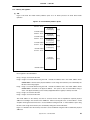
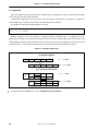
1.2.2 Memory management
(1) TLB
Figure 1-10 shows the virtual memory address space for a VR Series processor in 32-bit kernel mode
operation.
Figure 1-10. Virtual Memory Address Space
0xFFFF FFFF
0xE000 0000
0xDFFF FFFF
0xC000 0000
0xBFFF FFFF
0xA000 0000
0x9FFF FFFF
0.5 GB with
TLB mapping
kseg3
0.5 GB with
TLB mapping
ksseg
0.5 GB without
TLB mapping
Non-cacheable
kseg1
0.5 GB without
TLB mapping
kseg0
0x8000 0000
0x7FFF FFFF
2 GB with
TLB mapping
kuseg
0x0000 0000
Each segment is described below.
kuseg: kuseg is accessed via the TLB.
kseg0: kseg0 is accessed without using the TLB. Instead, the address that is the virtual address minus
0x8000 0000 is selected as the physical address. Cache usage and coherency are controlled by the
K0 area in the Config register.
kseg1: kseg1 is accessed without using the TLB. Instead, the address that is the virtual address minus
0xA000 0000 is selected as the physical address. This space is also accessed without using a
cache. The physical memory (or the memory mapped I/O device register) is directly accessed.
ksseg: ksseg is accessed via the TLB.
kseg3: kseg3 is accessed via the TLB.
The virtual address in the memory area that is accessed via the TLB is expanded to separate physical
addresses according to the contents of the ASID area. When accessing this area, set the TLB first. A TLB
exception will be generated if this area is accessed without setting the TLB. In virtual address space using
the TLB, cache usage and coherency are controlled by setting the C bit of TLB entries.
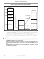
Figure 1-11 illustrates how the memory area that is accessed without using the TLB is translated to physical
addresses.
Application Note U10710EJ5V0AN
33
VOLUME 2 VR SERIES ARCHITECTURE
Figure 1-11. Mapping of Virtual Address and Physical Address
Virtual address
kseg3
0.5 GB with
TLB mapping
ksseg
0.5 GB with
TLB mapping
kseg1
0.5 GB without
TLB mapping
Non-cacheable
kseg0
0.5 GB without
TLB mapping
Example of memory
on an actual unit
0x1FFF FFFF
ROM
kuseg
0x1FC0 0000
Physical address
2 GB with
TLB mapping
0x0 1FFF FFFF
RAM
0x0 0000 0000
In the figure above, the ROM area on the actual unit is set from “0x1FC0 0000”. This is because the reset
exception vector is set from “0xBFC0 0000” so that this area is to be specified for the ROM area.
In addition, because the exception vectors for general use are set from “0x8000 0100”, memory must be
allocated to addresses from the physical address “0x0000 0000”. Normally, this area is set as RAM area.
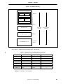
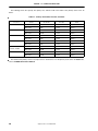
(2) Cache
The cache of the VR4100 Series and VR4300 Series adopts the direct mapping method. On the other hand,
the primary cache of the VR5000 Series, VR5432, VR5500, and VR10000 Series and the secondary cache of
the VR10000 Series adopt a 2-way set associative method.
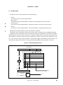
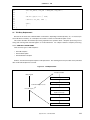
Figure 1-12 shows the memory organization of the VR Series. In the logical memory hierarchy, the cache is
located between the CPU and main memory, so that the access to the memory is speeded up from the user
side.
As shown in Figure 1-12, the lower portions of the memory organization have greater capacity and longer
access times than the upper portions.
34
Application Note U10710EJ5V0AN
CHAPTER 1 OUTLINE
Figure 1-12. Memory Hierarchy
VR Series CPU
Register
Instruction
cache
Register
Register
Data cache
Primary cache
Cache
Access time
is shorter
Secondary cache
Storage capacity
is larger
Memory
Main memory
Disk, CD-ROM, tape, etc.
Peripheral
device
The VR Series is equipped with the following caches and controllers.
Table 1-3. Difference in Cache Depending on Processor
Processor
Primary Instruction Cache
Primary Data Cache
Secondary Cache Controller
VR4121
16 KB
8 KB
×
VR4122
32 KB
16 KB
×
VR4181
4 KB
4 KB
×
VR4300 Series
16 KB
8 KB
×
VR5000 Series
32 KB
32 KB
{
VR5432, VR5500
32 KB
32 KB
×
VR10000 Series
32 KB
32 KB
{
Remark {: Available, ×: Not available
Application Note U10710EJ5V0AN
35
VOLUME 2 VR SERIES ARCHITECTURE
1.2.3 Exceptions
When an exception is generated, the ordinary instruction stops execution. The processor exits the current mode
and enters the kernel mode. The processor disables interrupts and hands the execution to the exception handler
(the exception routine processed by software and located in the specific address). Save the processor states such
as the contents of the program counter, current operating mode (user or supervisor), status, and interrupt enable in
the handler. These states can be restored after processing the exception.
When an exception is generated, the CPU loads the address to resume the execution after processing the
exception to the EPC register. Normally, the address of the instruction that has generated the exception is loaded to
the EPC register as the resume address. However, if the instruction that has generated the exception is being
executed in the branching delay slot, the address of the branch instruction immediately before the branching delay
slot is loaded to the EPC register.
For a detailed description of the processing method for each exception, refer to CHAPTER 5 EXCEPTIONS.
Figure 1-13. Flow of Exception Processing
Main routine
Exception handler
Exception cause
; Resolves the exception
cause in the exception handler
ERET
1.2.4 Hazards
In VR Series products other than the VR10000 Series, when executing the CP0 (CP1) instruction, unlike the CPU
instruction, the pipeline is not interlocked. Therefore, the location of instructions must be managed when creating a
program.
For the detailed description of CP0 hazards, refer to VOLUME 3 1.2 Instruction Hazards.
In the VR10000 Series, almost all the hazards related to the pipeline are detected. It is therefore not necessary to
manage instruction allocation.
36
Application Note U10710EJ5V0AN
CHAPTER 1 OUTLINE
1.3 FPU
The floating point unit (FPU) of the VR Series operates as a coprocessor and expands the CPU instruction set to
execute the floating point. The FPU complies with ANSI IEEE Standard 754-1985 “IEEE Binary Floating Point
Arithmetic Specifications”.
An FPU is not provided in the VR4100 Series.
1.3.1 Instructions
All the FPU instructions are 32 bits in length and allocated to word boundaries. FPU instructions are categorized
as follows.
• Load/store/transfer instructions
Load/store/transfer instructions perform data transfer between the general-purpose registers of FPU and the
CPU or memory.
• Conversion instructions
Conversion instructions perform data conversion.
• Arithmetic instructions
Arithmetic instructions execute operations for floating point values in the FPU register.
• Comparison instructions
Comparison instructions perform comparison in the FPU register and set the result to the C/CC bit of FCR31.
• FPU conditional branch instructions
FPU conditional branch instructions execute a branch to a specified target if the indicated coprocessor
condition is true.
1.3.2 Registers
There are three methods to use the FPU general-purpose registers.
(1) The thirty-two general-purpose registers are 32 bits in length if the FR bit of the CP0 Status register is 0 and
64 bits in length if it is 1. The CPU accesses FGR with load/store/transfer instructions.
(2) If the FR bit of the Status register is 0, sixteen 64-bit registers (FPR) hold floating point data of single or
double precision. Each FPR register corresponds to FGR of the adjacent number as shown in Figure 1-14.
(3) If the FR bit of the Status register is 1, thirty-two 64-bit registers (FPR) hold floating point data of single or
double precision. Each FPR register corresponds to FGR as shown in Figure 1-14.
Application Note U10710EJ5V0AN
37
VOLUME 2 VR SERIES ARCHITECTURE
Figure 1-14. FPU Registers
(a) FGR and FPR
(i) When FPR bit = 0
Floating point register
(FPR)
(ii) When FPR bit = 1
Floating point generalpurpose register (FGR)
31
Floating point register
(FPR)
0
Floating point generalpurpose register (FGR)
63
0
(Lower)
FGR0
FPR0
FGR0
(Higher)
FGR1
FPR1
FGR1
(Lower)
FGR2
FPR2
FGR2
(Higher)
FGR3
FPR3
FGR3
.
.
.
.
.
.
.
.
.
(Lower)
FGR28
FPR28
FGR28
(Higher)
FGR29
FPR29
FGR29
(Lower)
FGR30
FPR30
FGR30
(Higher)
FGR31
FPR31
FGR31
FPR0
FPR2
.
.
.
FPR28
FPR30
(b) FCR
(i) Control/Status register
(FCR31)
31
(ii) Implementation/Revision register
(FCR0)
0
31
0
The following describes the Control/Status register, which is especially important among these registers.
38
Application Note U10710EJ5V0AN
CHAPTER 1 OUTLINE
(1) Control/Status register (FCR31)
The Control/Status register (FCR31) can be read/written, and holds the control and status data. FCR31
controls the rounding mode and enables the generation of floating point exceptions. It shows the information
of the exceptions that are generated in the instruction executed last and exceptions that have not become an
exception due to masking and have been accumulated instead. Figures 1-15 and 1-16 show the configuration
of FCR31.
Figure 1-15. FCR31
(a) VR4300 Series
31
25
24
23 22
18 17
12 11
7
6
2
1
0
0
FS
C
0
Cause
E V Z O U I
Enable
V Z O U I
Flag
V Z O U I
RM
7
1
1
5
6
5
5
2
(b) VR5000 Series, VR5432, VR5500, and VR10000 Series
31
25
CC(7:1)
24
23 22
FS CC0
7
1
1
18 17
12 11
7
6
2
1
0
0
Cause
E V Z O U I
Enable
V Z O U I
Flag
V Z O U I
RM
5
6
5
5
2
Figure 1-16. Cause/Enable/Flag Bit of FCR31
Bit 17
16
15
14
13
12
E
V
Z
O
U
I
Bit 11
10
9
8
7
V
Z
O
U
I
Bit 6
5
4
3
2
V
Z
O
U
I
Cause bit
Enable bit
Flag bit
Illegal operation
Underflow
Overflow
Zero division
Invalid operation
Undefined operation
Application Note U10710EJ5V0AN
39
VOLUME 2 VR SERIES ARCHITECTURE
The following describes the bits in FCR31.
FS bit:
Bit to enable flushing of values that cannot be normalized
C/CC bit:
The result of the floating point comparison instruction is stored.
When the result of the
comparison is true, this bit is set to 1. When the result is false, it is cleared to 0. Bit C/CC is not
affected by instructions other than the compare instruction and CTC1 instruction.
Cause bit: Displays the status of the floating point arithmetic executed last.
Enable bit: Enables the generation of floating point exceptions for each cause (V, Z, O, U, and I).
Flag bit:
Accumulates the result of floating point arithmetic after reset.
RM bit:
Rounding mode control bit. For details, refer to Table 1-4.
Table 1-4. Rounding Mode Control Bit
Mnemonic
RM Bit
40
Description
Bit 1
Bit 0
0
0
RN
Rounds the result to the closest expressible value. If the result is between two
expressible values, the result is rounded to the value whose lowest bit is 0.
0
1
RZ
Rounds the result towards 0. The absolute value is the closest value in the
range not exceeding the accurate result of the infinite precision.
1
0
RP
Rounds the result towards +∞. The value becomes the actual result or more.
1
1
RM
Rounds the result towards –∞. The value becomes the actual result or less.
Application Note U10710EJ5V0AN
CHAPTER 2 PIPELINE
2.1 Pipeline Stage
The following pipeline stages are provided in the VR Series.
• Instruction fetch (IF, IC, etc.)
• Instruction decode (ID, IT, etc.)
• Branch prediction (BR) (VR5500 only)
• Instruction queuing (IQ) (VR5500 only)
• Instruction issuance (IS) (VR5500 and VR10000 Series only)
• Register renaming (RN) (VR5500 only)
• Reservation stationing (RS) (VR5500 only)
• Register fetch (RF, etc.)
• Execution (EX, etc.)
• Data fetch (DC, DF etc.)
• Data align (AL) (VR5500 only)
• Writeback (WB, etc.)
• Commit (CoR, CoM) (VR5500 only)
The number of pipeline stages is as follows depending on the products and operation mode.
Table 2-1. Number of Pipeline Stages in VR Series
Number of Stages
Processor
5
VR4121 (MIPS III instruction mode), VR4122 (MIPS III instruction mode),
VR4181, VR4300 Series, VR5000 Series, VR5432
6
VR4121 (MIPS16 instruction mode), VR4122 (MIPS16 instruction mode)
7
VR10000 Series
8 to 10
VR5500
When the processing of one instruction in one pipeline stage is complete, the next instruction enters the stage. If
pipeline is full, it means the instructions equalling the number of pipeline stages are being executed simultaneously.
The following shows the instruction status in each type of pipeline if the pipeline is full.
Application Note U10710EJ5V0AN
41
VOLUME 2 VR SERIES ARCHITECTURE
Figure 2-1. Operation of Single-Way Pipeline (5 Stages)
(5 stages)
PCycle
IF
RF
EX
DC
WB
IF
RF
EX
DC
WB
IF
RF
EX
DC
WB
IF
RF
EX
DC
WB
IF
RF
EX
DC
WB
Current
CPU
cycle
Figure 2-2. Operation of 2-Way Superscalar Pipeline (5 Stages)
(5 stages × 2 ways)
PCycle
RF
EX
DC
WB
RF
EX
DC
WB
RF
EX
DC
WB
RF
EX
DC
WB
RF
EX
DC
WB
RF
EX
DC
WB
RF
EX
DC
WB
RF
EX
DC
WB
RF
EX
DC
WB
RF
EX
DC
WB
IC
IC
IC
IC
IC
Current
CPU
cycle
42
Application Note U10710EJ5V0AN
CHAPTER 2 PIPELINE
Figure 2-3. Operation of 4-Way Superscalar Pipeline (5 Stages)
(5 stages × 4 ways)
IF
IS
EX
WB
IS
EX
WB
IS
EX
WB
IS
EX
WB
IS
EX
WB
IS
EX
WB
IS
EX
WB
IS
EX
WB
ID
IF
ID
.
.
.
Current
CPU
cycle
Application Note U10710EJ5V0AN
43
VOLUME 2 VR SERIES ARCHITECTURE
2.2 Interlock
A pipeline’s flow may be stopped upon a cache miss, a cache status change, the occurrence of an exception, or
detection of data dependencies. Among these, conditions that are processed by hardware such as cache misses are
called interlocks.
On the other hand, conditions that must be processed by software are called exceptions.
Interlocks and exceptions are collectively called faults, as shown in Figure 2-4.
The VR4100 Series and VR5000 Series have two types of interlocks: one in which troubles one solved simply by
stopping the pipeline called stall, and one in which a part of pipeline is advanced and the rest delayed, called slip.
The VR4300 Series and VR5432 only have a stall.
In the VR5500 and VR10000 Series, the pipeline flow is not interrupted by an interlock since out-of-order execution
is used. For details, refer to VR10000 Series User’s Manual.
Exceptions and interlock conditions are checked for all valid instructions during each cycle.
Figure 2-4. Relationship Betweem Interlocks, Exceptions, and Faults
Fault
Software
Hardware
Exception
Interlock
Abort
44
Stall
Application Note U10710EJ5V0AN
Slip
CHAPTER 2 PIPELINE
Figure 2-5. State of Pipeline During Interlock (Stall)
(a) Single-way pipeline
IC
RF
Instruction
EX
Instruction
DC
Instruction
WB
Instruction
Instruction
(b) 2-way superscalar pipeline
IC
Instruction
RF
EX
Instruction
Instruction
DC
WB
Instruction
Instruction
Instruction
Instruction
Instruction
Instruction
Instruction
Figure 2-6. State of Pipeline During Interlock (Slip)
(a) Single-way pipeline
IC
Instruction
RF
EX
Instruction
DC
Instruction
WB
Instruction
Instruction
(b) 2-way superscalar pipeline
IC
Instruction
Instruction
RF
EX
Instruction
DC
Instruction
Instruction
Instruction
WB
Instruction
Instruction
Instruction
Instruction
Application Note U10710EJ5V0AN
45
VOLUME 2 VR SERIES ARCHITECTURE
2.3 Delay
2.3.1 Branching delay
For the sake of pipeline optimization, a one-cycle branching delay occurs in VR Series processors. However, in
processors that incorporate a branch prediction unit, this delay may not occur. For details of the branch prediction
unit, refer to the user’s manual of each processor.
The virtual address of the branching target that is generated at the EX stage of a jump/branch instruction cannot
be used until the instruction fetch stage after the delay.
Figure 2-7. Branching Delay
(a) Single-way pipeline
Jump/branch
IC
RF
EX
DC
WB
IC
RF
EX
DC
WB
IC
RF
EX
DC
Target
Branching
delay slot
WB
Branching delay
(b) 2-way superscalar pipeline
Jump/branch
RF
EX
DC
WB
RF
EX
DC
WB
RF
EX
DC
WB
RF
EX
DC
WB
RF
EX
DC
WB
RF
EX
DC
WB
IC
IC
Branching
delay slot
IC
Target
Branching delay
When using an instruction for which a branching delay occurs in the assembler, one delay slot is required. In such
cases, note that the instruction within the delay slot is executed while the branching target instruction is being fetched
from the memory. Instructions that can be completed during that time are executed normally even when they are
coded within a delay slot. In the case of branch instructions, the operation differs depending on the instruction for
which a branching delay has not been established. For branch likely instructions (such as BNEL), the instructions in
the delay slots become invalid if the branch conditions are not established.
instructions in the delay slots are unconditionally executed.
46
Application Note U10710EJ5V0AN
For other branch instructions, the
CHAPTER 2 PIPELINE
2.3.2 Loading delay
For the sake of pipeline optimization, a one-cycle loading delay occurs in the VR Series processors.
For load instructions, data loading is completed when the data fetch stage is ended, but the data itself cannot be
used until the EX stage following the delay.
Figure 2-8. Loading Delay
(a) Single-way pipeline
Load
IC
RF
EX
DC
WB
IC
RF
EX
DC
WB
IC
RF
EX
DC
Instruction
using target
Loading
delay slot
WB
Loading delay
(b) 2-way superscalar pipeline
Load
RF
EX
DC
WB
RF
EX
DC
WB
RF
EX
DC
WB
RF
EX
DC
WB
RF
EX
DC
WB
RF
EX
DC
WB
IC
IC
Instruction
using target
Loading
delay slot
IC
Loading delay
If an instruction using the data loaded during a loading delay is allocated, the CPU detects this and stalls the
pipeline until data loading is complete. There is no need to be aware of loading delays that occur in the assembler
because they are not treated as errors.
However, from the viewpoint of performance enhancement, it is
recommended that instructions be scheduled taking loading delay in consideration.
Application Note U10710EJ5V0AN
47
VOLUME 2 VR SERIES ARCHITECTURE
2.4 Bypassing
Data and conditions generated at the EX, DC, and WB stages of the pipeline are able to be used at the EX stage
of the next instruction via a bypass data path.
If the pipeline is bypassed, it is not necessary to wait for the data and conditions to be written to a register file
when the WB stage is ended, so the instruction of the EX stage can be continued.
For example, the following assembler program is created.
lui
$1, 0x8000
ori
$1, $1, 0x0000
Writing to register 1 in the first instruction is completed normally at the WB stage. If the pipeline cannot be
bypassed, the RF stage of the second instruction must wait for the end of the WB stage of the first instruction, and
smooth pipeline operation cannot be performed. In the actual VR Series, however, the pipeline can be bypassed, and
the data in register 1 can be used in the EX stage of the second instruction when the EX stage is ended.
Figure 2-9. Example of Bypassing
(a) Single-way pipeline
IC
RF
EX
DC
WB
IC
RF
EX
DC
WB
LUI
$1, 0x8000
ORI
$1, $1, 0x0000
LUI
$1, 0x8000
ORI
$1, $1, 0x0000
(b) 2-way superscalar pipeline
RF
EX
DC
WB
RF
EX
DC
WB
RF
EX
DC
WB
RF
EX
DC
WB
IC
IC
For bypassing in the VR10000 Series, refer to VR10000 Series User’s Manual.
48
Application Note U10710EJ5V0AN
CHAPTER 3 CACHE
3.1 Primary Cache
The primary cache in VR Series products has the following states.
• Invalid
The cache line does not contain valid information.
• Dirty exclusive
The cache line contains valid information. Information in the line differs from the main memory.
• Clean Exclusive
The cache line contains valid information. Information in the line is the same as the main memory.
• Shared
The cache line contains valid information. The same information is contained in other processors.
Dirty Exclusive and Clean Exclusive are also known jointly as “valid state”.
The primary cache is incorporated in the processor and its contents can therefore not be manipulated externally.
The primary cache of the VR Series refers to the cache with a part of the virtual address as the index. The index is
determined by the cache size and the cache line size. When the cachable memory is accessed, the index part of the
memory address is referred to, and the cache line is determined. The V bit is referred to for the validity of the cache
line. If the cache line is valid, a physical address is created from the higher virtual address by TLB conversion, and
compared to the tag part in the cache line. If the tag and the physical address match, it becomes a cache hit.
Figure 3-1. Referencing Primary Cache
Virtual address
Index
Offset
V
Tag
Data
Virtual
TLB
Physical
Physical
Cache memory
Match check
Data
Match
AND
Hit
Valid
Application Note U10710EJ5V0AN
49
VOLUME 2 VR SERIES ARCHITECTURE
The following shows the capacity, line (block) size, and bits used in the index of the primary cache in the VR
Series.
Table 3-1. Primary Cache Size, Line Size, and Index
Processor
VR4121
VR4122
VR4181
VR4300 Series
VR5000 Series,
VR5432, VR5500
VR1000 Series
Cache
Cache Size
Line Size
Index
Instruction cache
16 KB
4 words
vAddr13..4
Data cache
8 KB
4 words
vAddr12..4
Instruction cache
32 KB
4 words or 8 words
vAddr14..4
Data cache
16 KB
4 words
vAddr13..4
Instruction cache
4 KB
4 words
vAddr11..4
Data cache
4 KB
4 words
vAddr11..4
Instruction cache
16 KB
8 words
vAddr13..5
Data cache
8 KB
4 words
vAddr12..4
Instruction cache
32 KB
8 words
vAddr13..5
Data cache
32 KB
8 words
vAddr13..5
Instruction cache
32 KB
16 words
vAddr13..6
Data cache
32 KB
8 words
vAddr13..5
The format of the primary cache of each processor is shown below. For the primary cache of the VR10000 Series,
refer to VR10000 Series User’s Manual.
50
Application Note U10710EJ5V0AN
CHAPTER 3 CACHE
3.1.1 VR4100 Series
The format of the VR4100 Series on-chip cache line is described below.
Figure 3-2. VR4100 Series On-Chip Cache Line
(a) Instruction cache line
22
21
0
V
PTag
1
22
31
0
Data
Data
Data
Data
32
(b) Data cache line
24
23
22
W
V
D
21
PTag
1
1
1
22
0
63
0
Data
Data
64
Each bit of the cache line is described below.
V:
Valid bit
W:
Writeback bit
D:
Dirty bit
PTag:
Physical tag (bits 31 to 10 of the physical address)
Data:
Cache data
Application Note U10710EJ5V0AN
51
VOLUME 2 VR SERIES ARCHITECTURE
3.1.2 VR4300 Series
The format of the VR4300 Series on-chip cache line is described below.
Figure 3-3. VR4300 Series On-Chip Cache Line
(a) Instruction cache line
20
19
0
V
PTag
1
20
63
0
Data
Data
Data
Data
64
(b) Data cache line
21
20
V
D
PTag
1
1
20
19
0
63
0
Data
Data
64
Each bit of the cache line is described below.
52
V:
Valid bit
D:
Dirty bit
PTag:
Physical tag (bits 31 to 12 of the physical address)
Data:
Cache data
Application Note U10710EJ5V0AN
CHAPTER 3 CACHE
3.1.3 VR5000 Series
The format of the VR5000 Series on-chip cache line is described below.
Figure 3-4. VR5000 Series Primary Cache Line
(a) Instruction cache line
31
30
29
28 27
24 23
0
P
F
PState
ICDEC
PTag
1
1
2
4
24
71
64 63
0
DataP
Data
DataP
Data
DataP
Data
DataP
Data
8
64
(b) Data cache line
27
26
P
F
25
PState
24 23
PTag
1
1
2
24
71
0
64 63
0
DataP
Data
DataP
Data
DataP
Data
DataP
Data
8
64
Each bit of the cache line is described below.
P:
Even parity of PTag
F:
Fill bit
PState: State of primary cache
ICDEC: Instruction cache predecode bit
PTag:
Physical tag (bits 31 to 12 of the physical address)
DataP:
Even parity of Data
Data:
Cache data
Application Note U10710EJ5V0AN
53
VOLUME 2 VR SERIES ARCHITECTURE
3.1.4 VR5432 and VR5500
The format of the VR5432 and VR5500 on-chip cache lines is described below.
Figure 3-5. VR5432 and VR5500 On-Chip Cache Lines
(a) Instruction cache line
4
27
71
3
2
1
0
ITag
L
V
U
P
24
1
1
1
1
64 63
0
DataP
Data
DataP
Data
DataP
Data
DataP
Data
8
64
(b) Data cache line
27
3
2
1
0
DTag
L
V
D
P
24
1
1
1
1
4
71
64 63
DataP
Data
DataP
Data
DataP
Data
DataP
Data
8
64
Each bit of the cache line is described below.
54
0
ITag, DTag:
Physical tag (bits 31 to 12 of the physical address)
L:
Lock bit
V:
Valid bit
U:
Unused bit
D:
Dirty bit
P:
Even parity of ITag, DTag
DataP:
Even parity of Data
Data:
Cache data
Application Note U10710EJ5V0AN
CHAPTER 3 CACHE
3.2 Secondary Cache
Since the VR5000 Series and the VR10000 Series have an on-chip secondary cache controller, a secondary cache
can be used simply by connecting SRAM. The secondary cache can be accessed from both the processor and the
system interface.
The secondary cache has the following two states.
• Invalid
The cache line does not contain valid information.
• Dirty Exclusive
The cache line contains valid information. Information in the line differs from the main memory.
• Clean Exclusive
The cache line contains valid information. Information in the line is the same as the main memory.
• Shared
The cache line contains valid information. The same information is contained in other processors.
3.2.1 VR5000 Series
The format of the VR5000 Series secondary cache line is described below.
Figure 3-6. VR5000 Series Secondary Cache Line
37
35 34
32 31
0
VIdx
SState
STag
3
3
32
71
64 63
0
DataP
Data
DataP
Data
DataP
Data
DataP
Data
8
64
Each bit of the cache line is described below.
VIdx:
Primary cache index (bits 14 to 12 of the virtual address)
SState: State of secondary cache
STag:
Secondary cache tag
DataP:
Parity for Data
Data:
Cache data
Application Note U10710EJ5V0AN
55
VOLUME 2 VR SERIES ARCHITECTURE
3.2.2 VR10000 Series
The format of the VR10000 Series secondary cache line is shown below.
Figure 3-7. VR10000 Series Secondary Cache Line
32
26 25
0
ECC
Tag
7
26
137 136
128 127
P
ECC
Data
P
ECC
Data
P
ECC
Data
P
ECC
Data
1
9
128
Each bit of the cache line is described below.
56
0
ECC:
ECC for Tag and Data
Tag:
Secondary cache tag
P:
Parity bit
Data:
Cache data
Application Note U10710EJ5V0AN
CHAPTER 3 CACHE
3.3 Cache Instructions
Cache instructions (CACHE) are assembler instructions for VR Series processors. They are used to control
caches and cache lines. For the VR Series processors, cache instructions have the following format.
cache
op, offset (base)
Each cache instruction is added to the contents of the general-purpose register base with a 16-bit offset sign
extension to create a virtual address. The 5-bit suboperation code op specifies the cache operation corresponding to
the specified cache block.
If the Status register’s CU0 has been cleared in user mode or supervisor mode, the CP0 is disabled, and therefore
a coprocessor disabled exception will occur if this instruction is executed. Instruction execution is undefined if an
instruction is combined with a cache operation that is not listed in Table 3-2 or Table 3-3. Instruction execution to
secondary cache is undefined if there is no secondary cache. Execution of this instruction is also undefined if it is for
an uncached area.
The lower two bits (op1..0) of the suboperation code indicate the operation’s target cache.
Table 3-2. Cache Instruction’s Suboperation Code op1..0
op1..0
Mnemonic
Cache Type
0
I
Primary instruction cache
1
D
Primary data cache
3
S
Secondary cache
The higher three bits (op4..2) of the suboperation code specify the cache operation contents.
Table 3-3. Cache Instruction’s Suboperation Code op4..2 (1/3)
(a) VR4100 Series, VR4300 Series
op4..2
Cache
Cache Operation
0
I
Index_Invalidate
D
Index_Writeback_Invalidate
1
I, D
Index_Load_Tag
2
I, D
Index_Store_Tag
3
D
4
I, D
5
I
Fill
D
Hit_Writeback_Invalidate
6
I, D
Create_Dirty_Exclusive
Hit_Invalidate
Hit_Writeback
Application Note U10710EJ5V0AN
57
VOLUME 2 VR SERIES ARCHITECTURE
Table 3-3. Cache Instruction’s Suboperation Code op4..2 (2/3)
(b) VR5000 Series
op4..2
Cache
Cache Operation
0
I
Index_Invalidate
D
Index_Writeback_Invalidate
S
Flash
1
I, D, S
Index_Load_Tag
2
I, D, S
Index_Store_Tag
3
D
4
I, D
5
I
Fill
D
Hit_Writeback_Invalidate
S
Page_Invalidate
6
I, D
Create_Dirty_Exclusive
Hit_Invalidate
Hit_Writeback
(c) VR5432
op4..2
Cache
Cache Operation
0
I
Index_Invalidate
D
Index_Writeback_Invalidate
1
I, D
Index_Load_Tag
2
I, D
Index_Store_Tag
3
D
4
I, D
5
I
Fill
6
D
Hit_Writeback
7
I, D
Create_Dirty_Exclusive
Hit_Invalidate
Fetch_and_Lock
(d) VR5500
58
op4..2
Cache
Cache Operation
0
I
Index_Invalidate
D
Index_Writeback_Invalidate
1
I, D
Index_Load_Tag
2
I, D
Index_Store_Tag
3
D
Create_Dirty
4
I, D
Hit_Invalidate
5
I
Fill
D
Hit_Writeback_Invalidate
6
D
Hit_Writeback
7
I, D
Fetch_and_Lock
Application Note U10710EJ5V0AN
CHAPTER 3 CACHE
Table 3-3. Cache Instruction’s Suboperation Code op4..2 (3/3)
(e) VR10000 Series
op4..2
Cache
0
I
Cache Operation
Index_Invalidate
D, S
Index_Writeback_Invalidate
1
I, D, S
Index_Load_Tag
2
I, D, S
Index_Store_Tag
4
I, D, S
Hit_Invalidate
5
I
Cache_Barrier
D, S
Hit_Writeback_Invalidate
6
I, D, S
Index_Load_Data
7
I, D, S
Index_Store_Data
The cache operations are described below.
• Index operation
In this operation, an instruction is executed for the cache block that matches the index part of the address
specified by the cache instruction.
Note
(vAddrCACHESIZE..BLOCKSIZE
).
The
The primary cache index is part of the virtual address
secondary
cache
index
is
part
of
the
physical
address
(pAddrCACHESIZE..BLOCKSIZE).
In the VR4100 Series and VR4300 Series, specification of an address smaller than the cache block does not
have meaning.
Of the primary cache index addresses, bit 14 in the VR5000 Series or bit 0 in the VR5432, VR5500, and VR10000
Series is used to determine the way of the 2-way set cache.
Note CACHESIZE and BLOCKSIZE are the number of bits required to indicate the cache size and the cache
block size. For details, refer to Table 3-1.
• Hit operation
This operation executes an instruction for a cache block that fully matches the address specified by the cache
instruction. The instruction is not executed if only the index matches.
• Invalidate operation
This operation invalidates the specified cache block.
• Writeback operation
This operation writes back the specified cache block. If specified for a primary cache, the writeback is to the
main memory.
• Fill operation
This operation fills the specified cache block with instruction data from the main memory.
Application Note U10710EJ5V0AN
59
VOLUME 2 VR SERIES ARCHITECTURE
• Create_Dirty_Exclusive operation
This operation sets the specified address to the cache block tag, and makes the cache status Dirty. If the
address specified for the cache block is not included and if the block status is Dirty, writeback to the main
memory is performed.
• Flash operation
This operation flashes the entire tag array of the secondary cache.
• Page_Invalidate operation
This operation invalidates the entire secondary cache block corresponding to the specified pages.
• Fetch_and_Lock operation
This operation sets the specified address to the cache block tag, and locks the cache status. If the address
specified for cache block is not included, and if the cache being used is the data cache and the block status is
Dirty, writeback to the main memory is performed.
• Cache_Barrier operation
This operation spends time executing one instruction without affecting the cache contents.
• Index_Data operation
This operation executes an instruction for the TagHi, TagLo, and ECC registers of the CP0.
For the detailed operations of each cache operation, refer to the CACHE instructions in the CPU instruction set in
the user’s manual of each product.
60
Application Note U10710EJ5V0AN
CHAPTER 4 TLB
In the MIPS architecture, all the accesses from a program to the memory are performed in the virtual memory.
The TLB (Translation Lookaside Buffer: High-speed translation buffer system) translates virtual addresses to physical
addresses.
VR Series processors are provided with a memory management unit (MMU) that utilizes the TLB.
The memory management system increases the CPU’s available address space by translating large virtual
memory space into physical addresses. The physical address spaces of each VR Series product are as follows.
Table 4-1. Physical Address Space
CPU
Space Size (Bytes)
Address Width (Bits)
VR4100 Series
4G
32
VR4300 Series
4G
32
VR5000 Series
64G
36
VR5432
4G
32
VR5500 (32-bit bus)
4G
32
VR5500 (64-bit bus)
64G
36
VR10000 Series
1T
40
31
In 32-bit mode, virtual addresses are 32 bits in width, and the maximum user area is 2 GB (2 bytes). The virtual
address space is expanded according to the address space ID (ASID). Using ASID reduces the number of TLB
flushes during context switching. The ASID area is an 8-bit field and in the CP0 EntryHi register. The global bit (G)
is in the CP0’s EntryLo0 register and EntryLo1 register.
Application Note U10710EJ5V0AN
61
VOLUME 2 VR SERIES ARCHITECTURE
4.1 Translation from Virtual Addresses to Physical Addresses
The first step in translating from virtual addresses to physical addresses is comparing the virtual address received
from the processor with all of the entries in the TLB. A match occurs when the Virtual Page Number (VPN) of the
virtual address is the same as the VPN area of the entry and when either of the following conditions is met.
The global bit (G) in the TLB is 1.
The ASID area of the virtual address is the same as the ASID area of the TLB entry.
Such a match is called a “TLB hit”. When no match occurs, the processor generates an exception called a TLB
refill.
When the TLB contains a matching virtual address, the higher bits of physical address are read from the TLB and
an offset is added. The offset represents the address within the page frame space. The offset portion does not pass
through the TLB and the lower bit of the virtual address is output directly.
Figure 4-1. Translation from Virtual Address to Physical Address
EntryHi register
Virtual address
ASID
VPN
Offset
Compare
ASID
VPN
PFN
ASID
VPN
Entry in which
ASID and VPN match
PFN
ASID
VPN
PFN
.
.
.
TLB
PFN
Offset
Physical address
62
Application Note U10710EJ5V0AN
CHAPTER 4 TLB
4.2 TLB Entries
VR Series processors have an on-chip TLB for translating virtual addresses into physical addresses. This on-chip
TLB uses fully associative memory and each entry is mapped into even/odd page pairs. The size of these pages can
be specified separately for each entry.
Figure 4-2 illustrates an example where each page occupies 4 KB.
Figure 4-2. TLB Translation
Virtual address
Physical address
TLB translation
Odd page
4 KB
2 pages
4 KB
VPN2
(EntryHi)
4 KB
PFN
(EntryLo1)
PFN
(EntryLo0)
4 KB
Even page
Application Note U10710EJ5V0AN
63
VOLUME 2 VR SERIES ARCHITECTURE
4.3 TLB Entry Register
This section describes the TLB entry registers in CP0 used to manipulate the TLB.
4.3.1 PageMask register
Figure 4-3. PageMask Register
(a) VR4100 Series
31
19 18
0
11 10
0
MASK
0
13
8
11
(b) VR4300 Series, VR5000 Series, VR5432, VR10000 Series
31
25 24
0
13 12
0
MASK
0
7
12
13
(c) VR5500
31 30
0
MASK
0
1
18
13
Each bit of the PageMask register is described below.
MASK: This is a page comparison mask.
It determines the virtual page size of the corresponding entry.
0:
This is reserved.
Write a zero here. A zero will be returned when this area is read.
64
0
13 12
Application Note U10710EJ5V0AN
CHAPTER 4 TLB
The values shown in the table below can be set in the MASK area.
Table 4-2. Mask Values and Page Size
(a) VR4100 Series
Page Size
Bit
18
17
16
15
14
13
12
11
1 KB
0
0
0
0
0
0
0
0
4 KB
0
0
0
0
0
0
1
1
16 KB
0
0
0
0
1
1
1
1
64 KB
0
0
1
1
1
1
1
1
256 KB
1
1
1
1
1
1
1
1
(b) VR4300 Series, VR5000 Series, VR5432, VR10000 Series
Page Size
Bit
24
23
22
21
20
19
18
17
16
15
14
13
4 KB
0
0
0
0
0
0
0
0
0
0
0
0
16 KB
0
0
0
0
0
0
0
0
0
0
1
1
64 KB
0
0
0
0
0
0
0
0
1
1
1
1
256 KB
0
0
0
0
0
0
1
1
1
1
1
1
1 MB
0
0
0
0
1
1
1
1
1
1
1
1
4 MB
0
0
1
1
1
1
1
1
1
1
1
1
16 MB
1
1
1
1
1
1
1
1
1
1
1
1
(c) VR5500
Page Size
Bit
30
29
28
27
26
25
24
23
22
21
20
19
18
17
16
15
14
13
4 KB
0
0
0
0
0
0
0
0
0
0
0
0
0
0
0
0
0
0
16 KB
0
0
0
0
0
0
0
0
0
0
0
0
0
0
0
0
1
1
64 KB
0
0
0
0
0
0
0
0
0
0
0
0
0
0
1
1
1
1
256 KB
0
0
0
0
0
0
0
0
0
0
0
0
1
1
1
1
1
1
1 MB
0
0
0
0
0
0
0
0
0
0
1
1
1
1
1
1
1
1
4 MB
0
0
0
0
0
0
0
0
1
1
1
1
1
1
1
1
1
1
16 MB
0
0
0
0
0
0
1
1
1
1
1
1
1
1
1
1
1
1
64 MB
0
0
0
0
1
1
1
1
1
1
1
1
1
1
1
1
1
1
256 MB
0
0
1
1
1
1
1
1
1
1
1
1
1
1
1
1
1
1
1 GB
1
1
1
1
1
1
1
1
1
1
1
1
1
1
1
1
1
1
Application Note U10710EJ5V0AN
65
VOLUME 2 VR SERIES ARCHITECTURE
4.3.2 EntryHi register
The EntryHi register format in 32-birt mode is shown below.
Figure 4-4. EntryHi Register (In 32-Bit Mode)
(a) VR4100 Series
31
11 10
8
0
7
VPN2
0
ASID
21
3
8
(b) VR4300 Series, VR5000 Series, VR5432, VR5500, VR10000 Series
31
13 12
8
0
7
VPN2
0
ASID
19
5
8
Each bit of the EntryHi register is described below.
VPN2: This is the virtual page number divided by two (due to two-page mapping).
ASID:
This is the address space ID area.
The 8-bit ASID area enables the TLB to be shared during multi-processing. The virtual addresses from
each process are able to overlap.
0:
This is reserved.
Write a zero here. A zero will be returned when this area is read.
66
Application Note U10710EJ5V0AN
CHAPTER 4 TLB
4.3.3 EntryLo0/Lo1 register
The EntryLo register format in 32-bit mode is shown below.
Figure 4-5. EntryLo0/Lo1 Register (In 32-Bit Mode)
(a) VR4100 Series
31
6 5
28 27
3 2 1 0
0
PFN
C
D V G
4
22
3
1 1 1
(b) VR4300 Series, VR5432
31
6 5
26 25
3 2 1 0
0
PFN
C
D V G
6
20
3
1 1 1
(c) VR5000 Series, VR5500
31
6 5
30 29
3 2 1 0
0
PFN
C
D V G
2
24
3
1 1 1
(d) VR10000 Series
31
6 5
3 2 1 0
PFN
C
D V G
26
3
1 1 1
Each bit of the EntryLo0/Lo1 register is described below.
PFN:
This is the page frame number.
It is the higher bits of the physical address.
C:
This specifies the TLB’s page attribute.
D:
This stands for dirty.
When the value of this bit is 1, the page is marked as “dirty”, which means it is write-enabled. Actually,
this bit functions as a “Write protect“ bit that is used by the software to prevent modification of data.
V:
This stands for valid.
When this bit is set to 1, it indicates that the TLB entry is valid. If this entry is hit when the V bit has not
been set, a TLB invalid exception (TLB or TLBS) occurs.
G:
This stands for global.
If the global bit of the both EntryLo0 and Lo1 has been set, the ASID is ignored when the TLB is
referenced.
0:
This is reserved.
Write a zero here. A zero will be returned when this area is read.
Application Note U10710EJ5V0AN
67
VOLUME 2 VR SERIES ARCHITECTURE
4.3.4 Others
In addition to the registers described so far, the following registers can be used for setting the TLB.
(1) Index register
The Index register is a 32-bit register that can be read/written. The lower 6 bits of this register are used for
the entry index. The highest bit indicates the result (success/failure) of the TLBP instruction.
This register indicates the TLB entries that are the targets of the TLBR instruction or TLBWI instruction.
Although the Index area holds 6-bit information, only the lower 5 bits are used in the VR4100 Series and
VR4300 Series.
Figure 4-6. Index Register
31 30
6
5
0
P
0
Index
1
25
6
Each bit of the Index register is described below.
P:
Indicates success/failure of TLBP instruction.
0 → Success of probe instruction
1 → Failure of probe instruction
Index:
Specifies the index to the TLB entries that are the targets of the TLBR instruction and TLBWI
instruction.
0:
This is reserved.
Write a zero here. A zero will be returned when this area is read.
68
Application Note U10710EJ5V0AN
CHAPTER 4 TLB
(2) Random register
The Random register is a read-only register. The lower 6 bits of this register are used for referencing TLB
entries. Although the Random area holds 6-bit information, only the lower 5 bits are used in the VR4100
Series and VR4300 Series.
This register is decremented each time an instruction is executed. The available value range of this register is
as follows.
• The lower limit is indicated by the Wired register.
• The higher limit is the number of TLB entries (31 in the VR4100 Series and VR4300 Series, 47 in the VR5000
Series, VR5432, and VR5500, and 63 in the VR10000 Series).
The Random register indicates the TLB entries that are the targets of the TLBWR instruction.
The Random register is set to the higher limit value upon cold reset. It is also reset to the higher limit value
when writing is performed to the Wired register.
Random entries can be updated with any TLB instruction.
Figure 4-7. Random Register
31
6
5
0
0
Random
26
6
Each bit of the Random register is described below.
Random: This is the TLB random index.
0:
This is reserved
Write a zero here. A zero will be returned when this area is read.
Application Note U10710EJ5V0AN
69
VOLUME 2 VR SERIES ARCHITECTURE
(3) Wired register
The Wired register can be read/written and indicates the lower limit of TLB random entries. Although the
Wired area holds 6-bit information, only the lower 5 bits are used in the VR4100 Series and VR4300 Series.
Wired entries cannot be updated with the TLBWR instruction, but can be updated with the TLBWI instruction.
Figure 4-8. Locations Indicated by Wired Register
TLB
Range indicated by
Random register
Value of Wired register
Range of wired entries
The Wired register is cleared to 0 upon cold reset. The Random register is set to the higher limit value when
writing is performed to the Wired register.
When TLB entries are replaced, entries that are to be removed from the replacement targets are set as wired
entries. For example, TLB entries related to the area used by the kernel are set.
Figure 4-9. Wired Register
31
6
26
6
Wired: This specifies the TLB wired boundary.
This is reserved.
Write a zero here. A zero will be returned when this area is read.
70
0
Wired
Each bit of the Wired register is described below.
0:
5
0
Application Note U10710EJ5V0AN
CHAPTER 4 TLB
4.4 TLB Instructions
TLB instructions are assembler instructions for the VR Series processors that are used to control the TLB.
(1) TLBP (Translation Lookaside Buffer Probe)
The TLB number that matches the EntryHi register is loaded to the Index register. If the TLB entry does not
match, the highest bit in the Index register is set. The operation of any load/store instruction that comes
immediately after the TLBP instruction is undefined. The operation is also undefined when there is more than
one matching TLB entry.
Figure 4-10. TLBP Instruction
Retrieves entry
PageMask
EntryHi
Match
TLB entry
EntryLo1
EntryLo0
31
30
29
.
. Loads entry number
.
n
Index
.
.
.
.
0
TLB
(2) TLBR (Translation Lookaside Buffer Read)
The contents of the TLB entry that is indicated by the Index register contents are written to the EntryHi,
EntryLo0, EntryLo1, and PageMask registers.
Figure 4-11. TLBR Instruction
Specifies entry
Index
31
30
29
.
.
.
n
.
.
.
.
0
Loads data
PageMask
EntryHi
TLB entry
EntryLo1
EntryLo0
TLB
Application Note U10710EJ5V0AN
71
VOLUME 2 VR SERIES ARCHITECTURE
(3) TLBWI (Translation Lookaside Buffer Write Index)
The contents of the EntryHi, EntryLo0, EntryLo1, and PageMask registers are written to the TLB entry that is
indicated by the Index register contents.
Figure 4-12. TLBWI Instruction
31
30
Stores data
29
.
.
Specifies entry
Index
PageMask
.
n
EntryHi
TLB entry
.
EntryLo1
.
.
EntryLo0
.
0
TLB
(4) TLBWR (Translation Lookaside Buffer Write Random)
The contents of the EntryHi, EntryLo0, EntryLo1, and PageMask registers are written to the TLB entry that is
indicated by the Random register contents.
Figure 4-13. TLBWR Instruction
31
30
29
.
Specifies entry
Random
.
.
n
.
.
.
.
0
Stores data
PageMask
EntryHi
TLB entry
EntryLo1
EntryLo0
TLB
72
Application Note U10710EJ5V0AN
CHAPTER 5 EXCEPTIONS
5.1 Types of Exceptions
The VR Series has the following exceptions.
• Cold reset
• Soft reset
• Address error
• TLB
• Cache error (does not occur in the VR4300 Series)
• Bus error
• Integer overflow
• Trap
• System call
• Breakpoint
• Reserved instruction
• Coprocessor unusable
• Floating point arithmetic (does not occur in the VR4100 Series)
• Watch (does not occur in the VR5000 Series)
• Interrupt
Application Note U10710EJ5V0AN
73
VOLUME 2 VR SERIES ARCHITECTURE
5.2 Priority of Exceptions
When more than one exception simultaneously occurs for an instruction, only one of them is selected. The priority
of exceptions is shown in Table 5-1.
Table 5-1. Priority of Exceptions
Priority
High
Exception Name
Cold reset
Soft reset
NMI
Address error (Instruction fetch)
TLB refill (Instruction fetch)
TLB invalid (Instruction fetch)
Cache error (Instruction fetch)
Bus error (Instruction fetch)
System call
Breakpoint
Coprocessor unusable
Reserved instruction
Trap
Integer overflow
Floating point arithmetic
Address error (Data access)
TLB refill (Data access)
TLB invalid (Data access)
TLB modified (Data write)
Cache error (Data access)
Watch
Bus error (Data access)
Low
Remark
Interrupt (except NMI)
Some of the exceptions may not occur or the
priority may differ depending on the CPU. For
details, refer to the user’s manual of each
product.
74
Application Note U10710EJ5V0AN
CHAPTER 5 EXCEPTIONS
5.3 Exception Vector Address
When exceptions occur in VR Series processors, the processing branches to the addresses shown in Table 5-2.
Note that the address differs depending on the contents of the BEV bit of the Status register.
Table 5-2. Exception Vector Address
Type of Exception
Vector Address (BEV = 0)
Vector Address (BEV = 1)
Cold reset, soft reset, NMI
BEV bit is automatically set to 1.
0xBFC0 0000
TLB refill, EXL = 0
0x8000 0000
0xBFC0 0200
XTLB refill, EXL = 0
0x8000 0080
0xBFC0 0280
Cache error
0xA000 0100
0xBFC0 0300
Others
0x8000 0180
0xBFC0 0380
Allocate the program of each exception processing to the address shown above using a section specification, etc.
5.4 Cautions Concerning Major Exceptions
5.4.1 Cold reset, soft reset, NMI exceptions
The cold reset, soft reset, and NMI exceptions use the same exception vector “0xBFC0 0000”.
The following shows the registers, cache, and memory whose status is guaranteed when these exceptions occur.
Table 5-3. Status When Exception Occurs
Exception
Status Register
SR
RP
Note
0
ERL
TS
BEV
0
1
1
Cold reset
0
Soft reset
1
0
1
1
NMI
1
0
1
1
ErrorEPC
Register
CPU GeneralPurpose Register
Cache
Memory
×
×
×
×
×
×
Note VR4300 Series and VR10000 Series only.
Remarks 1.
2.
The Status register and ErrorEPC register are coprocessor 0 registers.
0: A zero is set when an exception occurs.
1: A one is set when an exception occurs.
: The status prior to exception is saved.
: The address where exception occurred is saved.
×: Undefined
Application Note U10710EJ5V0AN
75
VOLUME 2 VR SERIES ARCHITECTURE
5.4.2 General-purpose exceptions
In the VR Series CPU, more than one exception shares the same vector. Of these, general-purpose exception
vectors use the address “0xBFC0 0380 (BEV = 1)” or “0x8000 0180 (BEV = 0)”.
To discriminate exceptions that utilize a general-purpose exception vector, refer to the exception code area
(ExcCode) of the coprocessor 0 Cause register, and perform processing for each exception according to the
ExcCode value.
The following shows the contents of the Cause register.
Figure 5-1. Cause Register
31
30 29
28 27
16 15
8
7
6
2
1
0
BD
0
CE
0
IP(7:0)
0
ExcCode
0
1
1
2
12
8
1
5
2
Each bit of the Cause register is described below.
BD:
Indicates whether the exception that occurred last has been executed in the branching delay slot.
1 → In the delay slot
0 → Normal
CE:
Indicates the number of the coprocessor in which the coprocessor disable exception occurred. When
this exception has not occurred, this bit becomes undefined.
IP:
Indicates the pending interrupt
1 → Pending
0 → No interrupt
However, for IP(1:0) only, an interrupt exception occurs when it is set to 1 by software. Interrupts are
assigned to each bit as follows.
• VR4100 Series
IP7:
Timer interrupt
IP(6:2): Normal interrupt (Int(4:0)). However, Int4 is not generated.
IP(1:0): Software interrupt
• VR4300 Series
IP7:
Timer interrupt
IP(6:2): External normal interrupt (Int(4:0)# and external write request)
IP(1:0): Software interrupt
• VR5000 Series
IP7:
External normal interrupt (Int5#) and timer interrupt
IP(6:2): External normal interrupt (Int(4:0)# and external write request)
IP(1:0): Software interrupt
• VR5432
IP7:
Timer interrupt
IP(6:2): External normal interrupt (Int(4:0)# and external write request)
IP(1:0): Software interrupt
• VR5500
IP7:
External normal interrupt (Int5#) or timer interrupt
IP(6:2): External normal interrupt (Int(4:0)# and external write request)
IP(1:0): Software interrupt
76
Application Note U10710EJ5V0AN
CHAPTER 5 EXCEPTIONS
• VR10000 Series
IP7:
Timer interrupt
IP(6:2): External normal interrupt (external interrupt request)
IP(1:0): Software interrupt
ExcCode: Exception code area (For details, refer to Table 5-4.)
0:
This is reserved. Write a zero here. A zero will be returned when this area is read.
Table 5-4. Exception Code Area of Cause Register
Exception Code Value
Mnemonic
Explanation
0
Int
1
Mod
TLB change exception
2
TLBL
TLB refill exception (load/instruction fetch)
3
TLBS
TLB refill exception (store)
4
AdEL
Address error (load/instruction fetch)
5
AdES
Address error (store)
6
IBE
Bus error (instruction fetch)
7
DBE
Bus error (load/store data)
8
Sys
System call exception
9
Bp
Breakpoint exception
10
RI
Reserved instruction exception
11
CpU
12
Ov
Operation overflow
13
Tr
Trap exception
14
−
Reserved
15
FPE
16 to 22
−
23
WATCH
24 to 31
−
Interrupt exception
Coprocessor unusable exception
Floating point arithmetic exception (reserved in the VR4100 Series)
Reserved
Watch exception (reserved in the VR5000 Series)
Reserved
Application Note U10710EJ5V0AN
77
VOLUME 2 VR SERIES ARCHITECTURE
5.5 Exception Processing
This section briefly describes the flow of exception processing taking a general-purpose exception as an example.
5.5.1 Hardware processing
The following shows the contents set by hardware after the exception cause occurs and until the processing
moves to the exception vector.
(1) Setting register
Performs setting of the register set for each exception (WatchLo/Hi registers, etc.) and the Cause register.
(2) Checking Status register (EXL bit)
Checks the EXL bit in the Status register, and if it is 1, moves to the processing in (4) without setting the EPC
register.
(3) Checking if exception has occurred in branching delay slot
Checks whether the exception has occurred in the branching delay slot or not.
If the exception has occurred in the branching delay slot, sets the BD bit of the Cause register, and sets the
value subtracting 4 from the address where the exception has occurred to the EPC register.
If the exception has occurred in other than the branching delay slot, resets the BD bit of the Cause register,
and sets the value of the address where the exception occurred to the EPC register.
(4) Setting Status register (EXL bit)
Sets the EXL bit of the Status register. This enables the operation mode of the processor to move to the
kernel mode.
(5) Checking Status register (BEV bit)
Checks the BEV bit of the Status register.
If the BEV bit is 1, the exception vector is set to 0xBFC0 0380, and processing moves to this exception vector.
If the BEV bit is 0, the exception vector is set to 0x8000 0180, and processing moves to this exception vector.
78
Application Note U10710EJ5V0AN
CHAPTER 5 EXCEPTIONS
Figure 5-2. General-Purpose Exception Processing by Hardware
Start
Setting Cause register
(ExcCode, CE)
No
EXL bit = 0?
Yes
Is the
instruction in delay
slot?
No
Yes
BD bit ← 1
EPC ← (PC −4)
BD bit ← 0
EPC ← PC
EXL bit ← 1
BEV bit = ?
1 (boot strap)
0 (normal)
PC ← 0x8000 0000 +180
PC ← 0xBFC0 0200 +180
To general-purpose exception
operation reference
For the details, refer to the chapter on exception processing in the user’s manual of each CPU.
Application Note U10710EJ5V0AN
79
VOLUME 2 VR SERIES ARCHITECTURE
5.5.2 Software processing
The following shows the processing performed by software after the processing has moved to the exception
vector.
(1) Saving CPU registers
Save the contents of the CPU registers used in the exception processing routine. Otherwise, the processing
cannot be continued when the processing is returned to the user program by the ERET instruction.
Especially, when using the JAL and BAL instructions, always save the contents of r31.
(2) Checking Cause register
Check which exception has occurred, referring to the Cause register of CP0.
(3) Excluding exception cause
Process the cause of the exception checked in (2) above, perform the setting so as not to interfere with the
execution of the user program.
(4) Restoring CPU registers
Restore the contents of the CPU registers saved in (1) above.
(5) Restoring from exception processing
Execute the ERET instruction and resume exception of the user program.
Figure 5-3. General-Purpose Exception Processing by Software
General-purpose exception operation reference
Saves CPU registers
Checks Cause register
Jumps to each routine
Processes by each routine
(excludes exception cause)
Restores CPU registers
ERET
As shown in Figure 5-2, if another exception occurs during the processing of an exception (with EXL of the Status
register = 1), the EPC register will not be set. If another exception occurs during the processing of an exception, the
exception processing cannot be properly ended. To enable multiple interrupts (exceptions), refer to 5.5.3 Multiple
interrupts.
80
Application Note U10710EJ5V0AN
CHAPTER 5 EXCEPTIONS
5.5.3 Multiple interrupts
In the exception processing described above, interrupts during the processing of exceptions (including interrupts)
are not supported. To enable multiple interrupts, save CP0 registers (EPC register, Status register, etc.) used during
the processing of exceptions, and set the KSU, ERL, EXL, and IE bits of the Status register to interrupt enabled.
To disable multiple interrupts after once enabling them, change the Status register in the exception processing,
and then restore the contents of the register saved.
The exception processing to enable multiple interrupts is performed in the following procedure.
(1) Saving CPU registers
Save the contents of the CPU registers used in the processing in (2), (3), (4), (5), (6), and (7) below to the
memory.
(2) Saving CP0 registers
Save the contents of the CP0 registers and EPC register used in the processing in (3), (4), and (5) below to
the memory.
(3) Setting Status register
Set the Status register to enable multiple interrupts. The following contents are set to the Status register:
KSU are: 00
ERL bit:
0
EXL bit:
0
IE bit:
1
(4) Exception processing
Perform processing to exclude the cause of the exception. If the exception cause is the register to which the
contents have been saved in (1) and (2), change the memory to which the contents have been saved,
otherwise it is reverted to the state before the exception in the restoration processing in (6) and (7).
(5) Setting Status register
Restore the contents of the Status register in (2), and disable multiple interrupts.
(6) Restoring CP0 registers
Restore the contents of the CP0 registers saved in (2).
(7) Restoring CPU registers
Restore the contents of the CPU registers saved in (1).
Application Note U10710EJ5V0AN
81
CHAPTER 6 DEBUG INTERFACE
Some products in the VR Series incorporate debug interfaces that are compliant with the N-Wire specifications.
In the products incorporating debug interfaces compliant with the N-Wire specifications, hardware verification and
program debugging can be performed simply by connecting a dedicated emulator, with the device mounted on the
target board (on-chip debug).
The VR4122, VR5432, and VR5500 incorporate a debug interface compliant with N-Wire specifications.
6.1 Debug Interface Function
The N-Wire-specification debug interface enables the following functions in each product.
(1) VR4122
• Register access
• Memory access
• Single-step execution
• Break from real-time execution
Instruction access break: 2 points
Data access break: 2 points
(2) VR5432 and VR5500
• Register access
• Memory access
• Single-step execution
• Break from real-time execution
Instruction access break: 1 point
Data access break: 1 point
• Trace
Outputs only branch condition
82
Application Note U10710EJ5V0AN
CHAPTER 6 DEBUG INTERFACE
6.2 Debug System Configuration
The basic configuration for on-chip debugging using the N-Wire-specification debug interface is as follows.
Figure 6-1. Basic On-Chip Debug Configuration
Target system
System-on-chip
N-Wire
interface
CPU
Debug unit
N-Wire
emulator
User logic
Application Note U10710EJ5V0AN
83
VOLUME 3 PROGRAMMING
84
Application Note U10710EJ5V0AN
CHAPTER 1 PIPELINE
This chapter describes points to be noted to smooth the flow of the pipeline when creating a program using an
assembler and the CP0 hazards when using coprocessor 0 in the assembler.
1.1 Program Not Stopping Pipeline
There are two causes of pipeline stall/slip: branching delays and loading delays. Allocating instructions on the
program to prevent these causes smoothes the flow of the pipeline and allows full use of the CPU capability.
Remark
Scheduling for branching or loading delays is not necessary in the VR10000 Series.
1.1.1 Branching delay
Instructions that generate branching delays include the following.
J
BGEZAL
BLTZ
JAL
BGEZALL
BLTZAL
JALR
BGEZL
BLTZALL
JR
BGTZ
BLTZL
BEQ
BGTZL
BNE
BEQL
BLEZ
BNEL
BGEZ
BLEZL
These are FPU branching instructions. FPU instructions cannot be used in the VR4100 Series.
BC1F
BC1FL
BC1T
BC1TL
When these instructions are used, the instruction after this instruction is executed while the next address is being
fetched after a jump is established. However, in branch likely instructions (BEQL instruction, etc.), if the branching
condition is not established, one instruction after the branching instruction is discarded.
The following shows an example of branching delay.
1
2
3
4
5 Label:
6
7
8
9
10
11
12
.
.
addiu
addiu
addiu
addu
subu
bne
nop
.
.
$1, $0, 0
$3, $0, 10
$1,
$2,
$4,
$4,
$1,
$2,
$1,
$0,
1
$1
$3
Label
Application Note U10710EJ5V0AN
85
VOLUME 3 PROGRAMMING
These programs can optimize the allocation of instructions as follows.
1
2
3
4
5 Label:
6
7
8
9
10
11
.
.
addiu
addiu
addiu
subu
bne
addu
.
.
$1, $0, 0
$3, $0, 10
$1,
$4,
$4,
$2,
$1,
$1,
$0,
$2,
1
$3
Label
$1
In the case above, it looks as if the instruction “addu $2, $2, $1” in line 9 is not executed when the condition is
established. However, it is executed whether the condition is established or not because is in the branching delay
slot of the BNEZ instruction.
1.1.2 Loading delay
Instructions that generate loading delays include the following.
LB
LH
LWL
LBU
LHU
LWR
LD
LL
LWU
LDL
LLD
LDR
LW
These are FPU load instructions. FPU instructions cannot be used in the VR4100 Series.
LDC1
LWC1
In the VR Series, it is possible to describe instructions that include the register of the loading destination
immediately after the load instruction. However, in that case, interlocks are generated for the number of required
cycles. Therefore, allocate instructions to reduce the generation of interlocks as much as possible in terms of both
performance and compatibility with the VR3000 Series.
The following shows an example of loading delay.
1
2
3
4
5
6
7
86
.
.
lw
addiu
andi
.
.
$1, 0x0($2)
$2, $1, 10
$8, $9, 0x8
Application Note U10710EJ5V0AN
CHAPTER 1 PIPELINE
In this example, a pipeline stall has been generated because the instruction “addiu $2, $1, 10”, which uses
register 1, has been placed in the delay slot of the instruction “lw $1, 0x0($2)” in the third line.
In such a program, the allocation of instructions can be optimized as follows.
1
2
3
4
5
6
7
.
.
lw
andi
addiu
.
.
$1, 0x0($2)
$8, $9, 0x8
$2, $1, 10
As shown above, placing an instruction that does not use register 1 in the delay slot of the instruction “lw $1,
0x0($2)” in the third line smoothes the flow of the pipeline, thus increasing the execution speed.
1.2 Instruction Hazards
When using the instructions of the VR4100 Series and VR4300 Series, pipeline stalls are not generated, unlike
loading delays. Therefore, the number of instructions required to avoid a hazard must be managed on the program.
Data and status is not properly conveyed unless the number of CP0 hazards is observed.
The number of instructions required between instruction A (instruction placing the value in CP0) and instruction B
(instruction which uses the same CP0 register as instruction A as the source) can be calculated with the following
expression.
(Number of hazards of instruction A destination) – {(number of hazards of instruction B source) + 1}
In the VR5000 Series, VR5432, VR5500, and VR10000 Series, it is not necessary to take hazards into consideration
since the CPU stalls the pipeline. However, according to the combination of instructions, the result cannot be
predicted when a specific system event occurs during execution in the VR5000 Series, VR5432, and VR5500.
Caution
Do not allocate a jump/branch instruction in the delay slot of the jump/branch instruction in the
VR Series.
Tables 1-1 to 1-4 show the instruction hazards of each CPU.
Application Note U10710EJ5V0AN
87
VOLUME 3 PROGRAMMING
Table 1-1. CP0 Hazards of VR4100 Series
Operation
Source
Name
Destination
Number of
Hazards
−
MTC0
Name
Number of
Hazards
CPR rd
5
−
MFC0
CPR rd
3
TLBR
Index, TLB
2
PageMask, EntryHi
EntryLo0, EntryLo1
5
TLBWI
TLBWR
Index or Random,
PageMask, EntryHi,
EntryLo0, EntryLo1
2
TLB
5
TLBP
PageMask, EntryHi
2
Index
6
ERET
EPC or ErrorEPC, TLB
2
Status.EXL, Status.ERL
4
Status
2
TagLo, TagHi, PErr
5
−
CACHE Index Load Tag
−
CACHE Index Store Tag
TagLo, TagHi, PErr
3
CACHE Hit OPS.
Cache line
3
Coprocessor usability test
Status.CU, Status.KSU,
Status.EXL, Status.ERL
2
−
Instruction fetch
EntryHi.ASID, Status.KSU,
Status.EXL, Status.ERL,
Status.RE, Config.K0
2
−
TLB
2
−
Instruction fetch exception
cache line
5
EPC, Status
4
Cause, BadVAddr, Context,
XContext
5
Interrupt
Cause.IP, Status.IM,
Status.IE, Status.EXL,
Status.ERL
2
−
Load/store
EntryHi.ASID, Status.KSU,
Status.EXL, Status.ERL,
Status.RE, Config.K0, TLB
3
−
Config.AD, Config.EP
3
WatchHi, WatchLo
3
Load/store exception
−
EPC, Status, Cause,
BadVaddr, Context,
XContext
TLB shutdown
−
Status.TS
88
Application Note U10710EJ5V0AN
5
2 (Instruction)
4 (Data)
CHAPTER 1 PIPELINE
Table 1-2. CP0 Hazards of VR4300 Series
Operation
Source
Name
Destination
Number of
Hazards
−
MTC0
Name
Number of
Hazards
CPR rd
7
−
MFC0
CPR rd
4
TLBR
Index, TLB
5-7
PageMask, EntryHi
EntryLo0, EntryLo1
8
TLBWI
TLBWR
Index or Random,
PageMask, EntryHi,
EntryLo0, EntryLo1
5-8
TLB
8
TLBP
PageMask, EntryHi
3-6
Index
7
ERET
EPC or ErrorEPC, Status,
TLB
−
CACHE Index Load Tag
CACHE Index Store Tag
4
TagLo, TagHi, ECC
7
TagLo, TagHi, ECC
8
−
Status.CH
8
Coprocessor usability test
Status.CU, Status.KSU,
Status.EXL, Status.ERL
2
−
Instruction fetch
EntryHi.ASID, Status.KSU,
Status.EXL, Status.ERL,
Status.RE, Config.K0
0
−
TLB
2
−
Instruction fetch exception
EPC, Status
8
Cause, BadVAddr, Context
3
Interrupt
Cause.IP, Status.IM,
Status.IE, Status.EXL,
Status.ERL
3
−
Load/store
EntryHi.ASID, Status.KSU,
Status.EXL, Config.K0,
Config.DB, TLB
4
−
WatchHi, WatchLo
4-8
LLbit
7
−
CACHE Hit OPS.
Status.EXL, Status.ERL
4-5
Load/store exception
−
EPC, Status, Cause,
BadVaddr, Context
8
TLB shutdown
−
Status.TS
7
Application Note U10710EJ5V0AN
89
VOLUME 3 PROGRAMMING
Table 1-3. Instruction Hazards of VR5000 Series and VR5432
Operation
Destination
Number of Hazards
TLBWR
PageMask, EntryHi, EntryLo0, EntryLo1, Random
2
TLBWI
PageMask, EntryHi, EntryLo0, EntryLo1, Index
2
TLBR
Index, contents of TLB
2
TLBP
PageMask, EntryHi, contents of TLB
2
ERET
EPC, ErrorEPC, Status
2
DIV, DIVU, DDIV, DDIVU, MULT,
MULTU, DMULT, DMULTU
HI, LO
2
MTC0, MFC0Note
Count
2
Note VR5000 Series only.
Table 1-4. Instruction Hazards of VR5500
Operation
Source
Number of Hazards
Instruction fetch (at address translation)
EntryHi.ASID, TLB
Note
Instruction fetch (at address error
detection)
Status.KSU, Status.EXL, Status.ERL, Status.KX, Status.SX,
Status.UX
Note
Instruction decode (at detection of
coprocessor enable and privileged
instruction enable)
Status.XX, Status.CU, Status.KSU, Status.EXL, Status.ERL,
Status.KX, Status.SX, Status.UX
1
Note A change within the exception handler is surely reflected till the ERET instruction execution.
90
Application Note U10710EJ5V0AN
CHAPTER 1 PIPELINE
1.2.1 Calculation of CP0 hazards
The following shows how to calculate CP0 hazards taking the VR4300 Series as an example.
Example 1. When executing an FPU instruction after setting the CU1 bit of the Status register with the MTC0
instruction
Referring to the destination (CPR rd) column of the MTC0 instruction, the number of hazards is 7.
For FPU instructions, refer to the coprocessor usability test column. The number of hazards of the
source (Status.CU) is 2.
This is calculated as follows.
7 − (2 + 1) = 4
Therefore, allocate instructions as follows.
mtc0
nop
nop
nop
nop
ctc1
$12, $1
# The value to be set to the Status register is placed in $1.
$31, $2 # The contents of $2 are transferred to the Control/Status register of the FPU.
Example 2. When using the TLB entry newly set with the TLBWI instruction for address translation of data
access
Referring to the destination (TLB) column of the TLBWI instruction, the number of hazards is 8.
Refer to the load column for address translation. The number of source (TLB) hazards is 4.
This is calculated as follows.
8 − (4 + 1) = 3
Therefore, allocate instructions as follows.
tlbwi
nop
nop
nop
lw
$1, 0x0 ($2)
# Address set to TLB is placed in $2.
Example 3. When executing the ERET instruction after changing the EPC register with MTC0
Referring to the destination (CPR rd) column of MTC0 instruction, the number of hazards is 7.
Referring to the source (EPC) column of the ERET instruction, the number of hazards is 4.
This is calculated as follows.
7 − (4 + 1) = 2
Therefore, allocate instructions as follows.
mtc0
nop
nop
lw
$1, 0x0 ($2)
# Address set to TLB is placed in $2.
Application Note U10710EJ5V0AN
91
CHAPTER 2 CACHE
This chapter describes the method of manipulating the cache of VR Series processors.
2.1 Cache Initialization
The following describes the cache initialization procedure.
2.1.1 Cache initialization procedure
What occurs in cache initialization differs somewhat between CPUs that have parity in their cache and CPUs that
have no parity. The cache with no parity can be initialized only by clearing the V bit of the cache line (invalidating the
cache line). This is because a cache with no parity does not cause parity errors next time it is used even if the data
portion is not initialized.
The cache can be initialized in the following procedure.
(1) Cache with no parity
(a) Instruction cache
1. Invalidate the cache line using the Index_Invalidate operation of the CACHE instruction.
(b) Data cache
1. Initialize the TagLo register using the MTC0 instruction.
2. Write to the cache tag using the Index_Store_Tag operation of the CACHE instruction.
(2) Cache with parity
(a) Instruction cache
1. Set the CE bit of the Status register to 0.
2. Set the cache tag and determine the physical address managed by the cache.
3. Initialize the TagLo register using the MTC0 instruction.
4. Write to the cache tag using the Index_Store_Tag operation of the CACHE instruction.
5. Initialize data block of the cache using the Fill operation of the CACHE instruction.
6. Invalidate the cache line using the Index(Hit)_Invalidate operation of the CACHE instruction.
(b) Data cache
1. Set the CE bit of the Status register to 0.
2. Initialize the TagLo register using the MTC0 instruction.
3. Write to the cache tag using the Index_Store_Tag operation of the CACHE instruction.
4. Make the cache block Dirty Exclusive using the Create_Dirty_Exclusive operation of the CACHE
instruction.
5. Initialize data block of the cache using the SW instruction.
6. Invalidate the cache line using the Index(Hit)_Invalidate operation of the CACHE instruction.
Note that the initial value of the CP0 register used in the cache instruction is not guaranteed after reset. Set the
values of these registers before use.
92
Application Note U10710EJ5V0AN
CHAPTER 2 CACHE
2.1.2 Example of cache initialization program
(1) VR4100 Series and VR4300 Series
The cache initialization method in a CPU with no parity is shown below. In a CPU with parity, create an
initialization program referencing the above procedure.
The following shows the assembler source list of the initialization program. As seen from the list, the cache
size and cache block size (line size) are referenced from the Config register at line numbers 14 to 43. Set the
Config register before calling this function. The actual cache initialization processing is performed at line
number 44 or later.
1
2
3
4
5
6
7
8
9
10
11
12
13
14
15
16
17
18
19
20
21
22
23
24
25
26
27
28
29
30
31
32
33
34
35
36
37
38
39
40
41
42
43
44
#
#
#
#
#
#
#
#
#
#
#
Cache initialization function
Description
Initialize instruction cache and data cache.
Since the cache size and cache block size (line size) are referenced in this
program, set the correct value to the Config register before calling it.
Format
void initcache(void);
Argument
None
Return value
None
.globl initcache
.ent
initcache
initcache:
mfc0
$8, $16
# Reference Config register
andi
$10, $8, 0x0E00
# Check IC bit
srl
$10, $10, 9
andi
$11, $8, 0x01C0
# Check DC bit
srl
$11, $11, 6
andi
$12, $8, 0x0020
# Check IB bit
srl
$12, $12, 5
andi
$13, $8, 0x0010
# Check DB bit
srl
$13, $13, 4
andi
$9, $8, 0x1000
# Check CS bit
bgtz
$9, .cs1
addiu $8, $0, 1
# Cache size calculation (when CS = 0)
addiu $10, $10, 10
# IC=2(n+10)
sllv
$10, $8, $10
addiu $11, $11, 10
# DC=2(n+10)
sllv
$11, $8, $11
j
.bsz
nop
.cs1:
# Cache size calculation (when CS= 1)
addiu $10, $10, 12
# IC=2(n+12)
sllv
$10, $8, $10
addiu $11, $11, 12
# DC=2(n+12)
sllv
$11, $8, $11
.bsz:
# Cache block size calculation
addiu $12, $12, 4
# IB
sllv
$12, $8, $12
addiu $13, $13, 4
# DB
sllv
$13, $8, $13
_initcache:
Application Note U10710EJ5V0AN
93
VOLUME 3 PROGRAMMING
45
46
47
48
49
50 .ic_loop:
51
52
53
54
55
56
57
58 .dc_loop:
59
60
61
62
63
64
mtc0
$0, $28
# Set TagLo register to 0
# Instruction cache initialization
li
$8, 0x80000000
# Set start virtual address
add
$9, $8, $10
# Add cache size
subu
$9, $9, $12
# Set end virtual address
cache
bne
addu
# Data
li
add
subu
0x00, ($8)
$8, $9, .ic_loop
$8, $8, $12
cache initialization
$8, 0x80000000
$9, $8, $11
$9, $9, $13
# CACHE instruction (Index_Invalidate)
# Is initialization of cache size complete?
# Increment line size
cache
bne
addu
jr
nop
.end
0x09, ($8)
$8, $9, .dc_loop
$8, $8, $13
$31
# CACHE instruction (Index_Store_Tag)
# Is initialization of cache size complete?
# Increment line size
# Set start virtual address
# Add cache size
# Set end virtual address
initcache
(2) VR10000 Series
The C source list of the cache initialization program is shown below.
In this program, initialization should be performed after specifying that the cache size of the secondary cache
is 1 MB and the cache line size is 32 words.
#define
#define
#define
#define
#define
#define
#define
#define
#define
#define
#define
#define
#define
#define
#define
#define
#define
#define
#define
#define
#define
#define
#define
#define
#define
#define
#define
#define
94
C0_Index $0
C0_Random $1
C0_EntryLo0 $2
C0_EntryLo1 $3
C0_Context $4
C0_PageMask $5
C0_Wired $6
C0_BadVAddr $8
C0_Count $9
C0_EntryHi $10
C0_Compare $11
C0_SR $12
C0_Cause $13
C0_EPC $14
C0_PRId $15
C0_Config $16
C0_LLAddr $17
C0_WatchLo $18
C0_WatchHi $19
C0_XContext $20
C0_FrameMask $21
C0_Diag $22
C0_Perf $25
C0_ECC $26
C0_CacheErr $27
C0_TagLo $28
C0_TagHi $29
C0_ErrorEPC $30
Application Note U10710EJ5V0AN
CHAPTER 2 CACHE
#define SR_DE 0x00010000 /* parity or ECC to cause exceptions? */
#define
#define
#define
#define
#define
#define
#define
#define
#define
#define
#define
#define
#define
#define
#define
#define
#define
#define
#define
#define
#define
Index_Invalidate_I 0x0 /* 0 0 */
Index_Writeback_Inv_D 0x1 /* 0 1 */
Index_Writeback_Inv_S 0x3 /* 0 3 */
Index_Load_Tag_I 0x4 /* 1 0 */
Index_Load_Tag_D 0x5 /* 1 1 */
Index_Load_Tag_S 0x7 /* 1 3 */
Index_Store_Tag_I 0x8 /* 2 0 */
Index_Store_Tag_D 0x9 /* 2 1 */
Index_Store_Tag_S 0xb /* 2 3 */
Hit_Invalidate_I 0x10 /* 4 0 */
Hit_Invalidate_D 0x11 /* 4 1 */
Hit_Invalidate_S 0x13 /* 4 3 */
Fill_I 0x14 /* 5 0 */
Hit_Writeback_Inv_D 0x15 /* 5 1 */
Hit_Writeback_Inv_S 0x17 /* 5 3 */
Index_Load_Data_I 0x18 /* 6 0 */
Index_Load_Data_D 0x19 /* 6 1 */
Index_Load_Data_S 0x1b /* 6 3 */
Index_Store_Data_I 0x1c /* 7 0 */
Index_Store_Data_D 0x1d /* 7 1 */
Index_Store_Data_S 0x1f /* 7 3 */
#define TagHi_P_PMod_Neither_Refill 0x20000000 /* Neither Refill or Written */
/*********************************************************************
*
Main program
*
*********************************************************************/
.text
.set noat
.set noreorder
.globl init_cache
.ent init_cache
init_cache:
/*********************************************************************
* Initialize L1 and L2 cache
*
*********************************************************************/
/* Status register setting */
mfc0 $11, C0_SR
li $12, SR_DE
or $13, $12, $11 # DE:1
mtc0 $13, C0_SR
/* initialize ECC Reg */
mtc0 $0, C0_ECC
/* initialize TagLo TagHi */
mtc0 $0, C0_TagLo
mtc0 $0, C0_TagHi
/* initialize cache */
/* initialize I_cache */
lui $8, 0x8000 # Base
Application Note U10710EJ5V0AN
95
VOLUME 3 PROGRAMMING
li $9, 0x4000 # 32KB/2
I_CACHE:
cache
cache
cache
cache
cache
cache
cache
cache
cache
cache
cache
cache
cache
cache
cache
cache
cache
cache
cache
cache
cache
cache
cache
cache
cache
cache
Index_Store_Tag_I, 0x0($8) # Index_Store_Tag Way_0
Index_Store_Tag_I, 0x1($8) # Index_Store_Tag Way_1
Index_Store_Data_I, 0x0($8) # Index_Store_Data Way_0
Index_Store_Data_I, 0x1($8) # Index_Store_Data Way_1
Index_Store_Data_I, 0x4($8) # Index_Store_Data Way_0
Index_Store_Data_I, 0x5($8) # Index_Store_Data Way_1
Index_Store_Data_I, 0x8($8) # Index_Store_Data Way_0
Index_Store_Data_I, 0x9($8) # Index_Store_Data Way_1
Index_Store_Data_I, 0xc($8) # Index_Store_Data Way_0
Index_Store_Data_I, 0xd($8) # Index_Store_Data Way_1
Index_Store_Data_I, 0x10($8) # Index_Store_Data Way_0
Index_Store_Data_I, 0x11($8) # Index_Store_Data Way_1
Index_Store_Data_I, 0x14($8) # Index_Store_Data Way_0
Index_Store_Data_I, 0x15($8) # Index_Store_Data Way_1
Index_Store_Data_I, 0x18($8) # Index_Store_Data Way_0
Index_Store_Data_I, 0x19($8) # Index_Store_Data Way_1
Index_Store_Data_I, 0x1c($8) # Index_Store_Data Way_0
Index_Store_Data_I, 0x1d($8) # Index_Store_Data Way_1
Index_Store_Data_I, 0x20($8) # Index_Store_Data Way_0
Index_Store_Data_I, 0x21($8) # Index_Store_Data Way_1
Index_Store_Data_I, 0x24($8) # Index_Store_Data Way_0
Index_Store_Data_I, 0x25($8) # Index_Store_Data Way_1
Index_Store_Data_I, 0x28($8) # Index_Store_Data Way_0
Index_Store_Data_I, 0x29($8) # Index_Store_Data Way_1
Index_Store_Data_I, 0x2c($8) # Index_Store_Data Way_0
Index_Store_Data_I, 0x2d($8) # Index_Store_Data Way_1
cache
cache
cache
cache
cache
cache
cache
cache
Index_Store_Data_I,
Index_Store_Data_I,
Index_Store_Data_I,
Index_Store_Data_I,
Index_Store_Data_I,
Index_Store_Data_I,
Index_Store_Data_I,
Index_Store_Data_I,
0x30($8)
0x31($8)
0x34($8)
0x35($8)
0x38($8)
0x39($8)
0x3c($8)
0x3d($8)
#
#
#
#
#
#
#
#
Index_Store_Data
Index_Store_Data
Index_Store_Data
Index_Store_Data
Index_Store_Data
Index_Store_Data
Index_Store_Data
Index_Store_Data
addiu $9, $9, -0x40
bgtz $9, I_CACHE
addiu $8, $8, 0x40
/* initialize TagLo TagHi */
mtc0 $0, C0_TagLo
mtc0 $0, C0_TagHi
li $12, TagHi_P_PMod_Neither_Refill
mfc0 $11, C0_TagHi
or $13, $12, $11 # SM:01
mtc0 $13, C0_TagHi
/* initialize D_cache */
lui $8, 0x8000 # Base
li $9, 0x4000 # 32KB/2
D_CACHE:
96
Application Note U10710EJ5V0AN
Way_0
Way_1
Way_0
Way_1
Way_0
Way_1
Way_0
Way_1
CHAPTER 2 CACHE
cache
cache
cache
cache
cache
cache
cache
cache
cache
cache
cache
cache
cache
cache
cache
cache
cache
cache
Index_Store_Tag_D, 0x00($8) # Index_Store_Tag Way_0
Index_Store_Tag_D, 0x01($8) # Index_Store_Tag Way_1
Index_Store_Data_D, 0x0($8) # Index_Store_Data Way_0
Index_Store_Data_D, 0x1($8) # Index_Store_Data Way_1
Index_Store_Data_D, 0x4($8) # Index_Store_Data Way_0
Index_Store_Data_D, 0x5($8) # Index_Store_Data Way_1
Index_Store_Data_D, 0x8($8) # Index_Store_Data Way_0
Index_Store_Data_D, 0x9($8) # Index_Store_Data Way_1
Index_Store_Data_D, 0x0c($8) # Index_Store_Data Way_0
Index_Store_Data_D, 0x0d($8) # Index_Store_Data Way_1
Index_Store_Data_D, 0x10($8) # Index_Store_Data Way_0
Index_Store_Data_D, 0x11($8) # Index_Store_Data Way_1
Index_Store_Data_D, 0x14($8) # Index_Store_Data Way_0
Index_Store_Data_D, 0x15($8) # Index_Store_Data Way_1
Index_Store_Data_D, 0x18($8) # Index_Store_Data Way_0
Index_Store_Data_D, 0x19($8) # Index_Store_Data Way_1
Index_Store_Data_D, 0x1c($8) # Index_Store_Data Way_0
Index_Store_Data_D, 0x1d($8) # Index_Store_Data Way_1
addiu $9, $9, -0x20
bgtz $9, D_CACHE
addiu $8, $8, 0x20
/* initialize TagLo TagHi */
mtc0 $0, C0_TagLo
mtc0 $0, C0_TagHi
/* initialize secondary cache */
lui $8, 0x8000 # Base
li $9, 0x80000 # 1MB/2
S_CACHE:
cache Index_Store_Tag_S, 0x00($8) # Index_Store_Tag Way_0
cache
cache
cache
cache
cache
cache
cache
cache
cache
cache
cache
cache
cache
cache
cache
cache
cache
Index_Store_Tag_S, 0x01($8) # Index_Store_Tag Way_1
Index_Store_Data_S, 0x00($8) # Index_Store_Data_S Way_0
Index_Store_Data_S, 0x01($8) # Index_Store_Data_S Way_1
Index_Store_Data_S, 0x10($8) # Index_Store_Data_S Way_0
Index_Store_Data_S, 0x11($8) # Index_Store_Data_S Way_1
Index_Store_Data_S, 0x20($8) # Index_Store_Data_S Way_0
Index_Store_Data_S, 0x21($8) # Index_Store_Data_S Way_1
Index_Store_Data_S, 0x30($8) # Index_Store_Data_S Way_0
Index_Store_Data_S, 0x31($8) # Index_Store_Data_S Way_1
Index_Store_Data_S, 0x40($8) # Index_Store_Data_S Way_0
Index_Store_Data_S, 0x41($8) # Index_Store_Data_S Way_1
Index_Store_Data_S, 0x50($8) # Index_Store_Data_S Way_0
Index_Store_Data_S, 0x51($8) # Index_Store_Data_S Way_1
Index_Store_Data_S, 0x60($8) # Index_Store_Data_S Way_0
Index_Store_Data_S, 0x61($8) # Index_Store_Data_S Way_1
Index_Store_Data_S, 0x70($8) # Index_Store_Data_S Way_0
Index_Store_Data_S, 0x71($8) # Index_Store_Data_S Way_1
addiu $9, $9, -0x80 # 32 word
bgtz $9, S_CACHE
addiu $8, $8, 0x80
Application Note U10710EJ5V0AN
97
VOLUME 3 PROGRAMMING
mfc0 $11, C0_SR
li $12, SR_DE
not $12, $12
and $13, $12, $11 # DE:0
mtc0 $13, C0_SR
.end init_cache
2.2 Cache Writeback
The cache data writeback procedure is described below.
To writeback the data cache by software, use the Hit_Write_Back operation or Index_Write_Back operation of the
CACHE instruction.
The Hit_Write_Back operation is used to perform writeback for a specific area with the virtual address specified.
In the Hit_Write_Back operation, note that the writeback is not performed if the cache holds tag contents that differ
from the address specified.
To perform writeback for all data on the cache, use the Index_Write_Back operation.
2.2.1 Example of cache writeback program
(1) Hit_Write_Back operation
The assembler source list of the function that performs the Hit_Write_Back operation is shown below.
1
2
3
4
5
6
7
8
9
10
11
12
13
14
15
16
98
#
#
#
#
#
#
#
#
#
Cache writeback function (Hit_Write_Back operation)
Description
Writeback the data cache block specified by vaddr.
Format
void cache_hit_write_back(unsigned int vaddr);
Argument
Vaddr: Cache block to be written back (virtual address)
Return value
None
.globl
cache_hit_write_back
.ent
cache_hit_write_back
cache_hit_write_back:
cache
0x19, 0x0($4)
# Hit writeback (data cache)
jr
$31
nop
.end
cache_hit_write_back
Application Note U10710EJ5V0AN
CHAPTER 2 CACHE
The C source list of the function that specifies the start and end points of the virtual address and performs
writeback using the above function is shown below.
1
2
3
4
5
6
7
8
9
10
11
12
13
14
15
16
17
18
19
20
21
22
23
24
25
26
27
/* Cache writeback sample program 1 */
/* Description
*
Writeback the data cache between the points specified by s_vaddr and e_vaddr.
* Format
*
void Write_Back_cache(unsigned int s_vaddr, unsigned int e_vaddr);
* Argument
*
s_vaddr: Start address (virtual address)
*
e_vaddr: End address (virtual address)
* Return address
*
None
*/
/* External function */
extern void cache_hit_write_back(unsigned int vaddr);
/* Cache block setting */
#define Cache_BLK
0x10
/* When cache block is 16 bytes */
/* Cache writeback function */
void
Write_Back_cache(unsigned int s_vaddr, unsigned int e_vaddr)
{
for ( ; s_vaddr <= e_vaddr; s_vaddr += Cache_BLK )
{
cache_hit_write_back( s_vaddr );
}
}
(2) Index_Write_Back operation
The assembler source list of the function that performs the Index_Write_Back operation is shown below.
1
2
3
4
5
6
7
8
9
10
11
12
13
14
15
16
#
#
#
#
#
#
#
#
#
Cache writeback function (Index_Write_Back operation)
Description
Writeback the data cache block to the index specified by vaddr.
Format
void cache_index_write_back(unsigned int vaddr);
Argument
vaddr: Cache block to be written back (virtual address)
Return value
None
.globl
cache_index_write_back
.ent
cache_index_write_back
cache_index_write_back:
cache
0x1, 0x0($4)
# Index writeback (data cache)
jr
$31
nop
.end
cache_index_write_back
Application Note U10710EJ5V0AN
99
VOLUME 3 PROGRAMMING
The C source list of the function that performs writeback for all the data on the data cache using the above
function is shown below.
1
2
3
4
5
6
7
8
9
10
11
12
13
14
15
16
17
18
19
20
21
22
23
24
25
26
27
28
29
30
31
32
/* Cache writeback sample program 2 */
/* Description
*
Writeback all data caches.
* Format
*
void Write_Back_cache_all(void);
* Argument
*
None
* Return value
*
None
*/
/* External function */
extern void cache_index_write_back(unsigned int vaddr);
/* Cache size and block size setting */
#define Cache_SIZE
0x4000 /* When cache size is 16 KB */
#define Cache_BLK
0x10
/* When cache block is 16 bytes */
/* Start point of virtual address */
#define ORIGIN 0x80000000
/* Cache writeback function */
void
Write_Back_cache_all(void)
{
unsigned int s_vaddr = ORIGIN;
for ( ; s_vaddr < (ORIGIN + Cache_SIZE); s_vaddr += Cache_BLK )
{
cache_index_write_back( s_vaddr );
}
}
2.3 Cache Fill
The cache data fill procedure is described below.
To write data to cache memory from the main memory by software, use the Fill operation of the CACHE
instruction. Normally, it is not necessary to execute the Fill operation by software, but it may be necessary in a
specific situation such as when rewriting programs (instructions) by software for creating monitors, etc.
A Fill operation is not provided for the data cache. To fill the data cache with data, use the LW instruction, etc.
100
Application Note U10710EJ5V0AN
CHAPTER 2 CACHE
2.3.1 Example of cache fill program
The assembler source list of the function that specifies the start and end points of the virtual address and fills the
cache between these points is shown below.
1
2
3
4
5
6
7
8
9
10
11
12
13
14
15
16
#
#
#
#
#
#
#
#
#
Cache fill function (Fill operation)
Description
Fills instruction data from the memory specified by vaddr to the instruction cache.
Format
void cache_fill(unsigned int vaddr);
Argument
vaddr: Cache block to be filled (virtual address)
Return value
None
.globl
cache_fill
.ent
cache_fill
cache_fill:
cache
0x14, 0x0($4)
# Fill operation
jr
$31
nop
.end
cache_fill
The C source list of the function that specifies the start and end points of the virtual address and fills the cache
between these points using the above function is shown below.
1
2
3
4
5
6
7
8
9
10
11
12
13
14
15
16
17
18
19
20
21
22
23
24
25
26
27
/* Cache fill sample program */
/* Description
*
Fills instruction cache between the points specified by s_vaddr to e_vaddr.
* Format
*
void Fill_cache(unsigned int s_vaddr, unsigned int e_vaddr);
* Argument
*
s_vaddr: Start address (virtual address)
*
e_vaddr: End address (virtual address)
* Return value
*
None
*/
/* External function */
extern void cache_fill(unsigned int vaddr);
/* Cache block setting */
#define Cache_BLK
0x10
/* When cache block is 16 bytes */
/* Cache fill function */
void
Fill_cache(unsigned int s_vaddr, unsigned int e_vaddr)
{
for ( ; s_vaddr <= e_vaddr; s_vaddr += Cache_BLK )
{
cache_fill( s_vaddr );
}
}
Application Note U10710EJ5V0AN
101
VOLUME 3 PROGRAMMING
2.4 Cache Tag Display
The cache tag display procedure is described below.
To reference the contents of the cache tag, use the Index_Load_Tag operation of the CACHE instruction.
2.4.1 Example of cache tag display program
The assembler source list of the function that performs the Index_Load_Tag operation is shown below.
1
2
3
4
5
6
7
8
9
10
11
12
13
14
15
16
17
18
19
20
21
22
23
24
25
#
#
#
#
#
#
#
#
#
#
#
Cache tag load function (Index_Load_Tag operation)
Description
Reads the cache block tag for the specified index.
Format
unsigned int cache_index_load_tag(unsigned int vaddr, int type);
Argument
vaddr: Cache block from which the tag is to be read (virtual address)
type: Cache type (0: Instruction cache, 1: Data cache)
Return value
Cache block TagLo register value
.globl cache_index_load_tag
.ent
cache_index_load_tag
cache_index_load_tag:
bne $5, $0, .dcache
nop
.icache:
cache
0x4, 0x0($4)
# Instruction cache tag load
j
.mfc0_taglo
nop
.dcache:
cache
0x5, 0x0($4)
# Data cache tag load
nop
.mfc0_taglo:
mfc0
$2, $28
# The TagLo register value is set as the
return value
26
jr
$31
27
nop
28
.end
cache_index_load_tag
102
Application Note U10710EJ5V0AN
CHAPTER 2 CACHE
The C source list of the function that displays the cache tag using the above function is shown below.
1
2
3
4
5
6
7
8
9
10
11
12
13
14
15
16
17
18
19
20
21
22
23
24
25
26
27
28
29
30
31
32
33
34
35
36
37
38
39
40
41
42
43
/* Cache tag display sample program 2 */
/* Description
*
Displays all cache tags.
* Format
*
void Print_CahceTag(void);
* Argument
*
None
* Return value
*
None
*/
/* External function */
extern unsigned int cache_index_load_tag(unsigned int vaddr, int type);
/* Cache size and block size setting
#define ICache_SIZE
0x8000 /* When
#define ICache_BLK
0x10
/* When
#define DCache_SIZE
0x4000 /* When
#define DCache_BLK
0x10
/* When
*/
instruction cache size is 32 KB */
instruction cache block is 16 bytes */
data cache size is 16 KB */
data cache block is 16 bytes */
/* Start point of virtual address */
#define ORIGIN 0x80000000
/* Cache tag display function */
void
Print_CacheTag(void)
{
unsigned int vaddr, tag;
printf(”I-CACHE\n”);
for (vaddr = ORIGIN; vaddr < (ORIGIN+ICache_SIZE); vaddr += ICache_BLK)
{
tag = cache_index_load_tag( vaddr, 0 );
printf(”%08x: %08x\n”, vaddr, tag);
}
printf(”D-CACHE\n”);
for (vaddr = ORIGIN; vaddr < (ORIGIN+DCache_SIZE); vaddr += DCache_BLK)
{
tag = cache_index_load_tag( vaddr, 1 );
printf(”%08x: %08x\n”, vaddr, tag);
}
}
Application Note U10710EJ5V0AN
103
CHAPTER 3 TLB
This chapter describes methods of reading from, writing to, and make settings to the TLB of VR Series processors
using C language and an assembler.
3.1 Entry Read
This section describes the creation of a C-language type function (tlbread) by the assembler for reading the
contents of a TLB entry. The following shows the specification of this function.
struct tlb{
unsigned
unsigned
unsigned
unsigned
int
int
int
int
Hi;
Lo0;
Lo1;
Mask;
/*
/*
/*
/*
EntryHi register */
EntryLo0 register */
EntryLo1 register */
PageMask register */
};
struct tlb *tlbread( int, struct tlb * );
A function is created with the TLB entry number to be read and the pointer to the structure for writing the read
contents as arguments and the return value as the pointer to the above structure.
This function appears as follows when created by the assembler.
1
2
3
4
5
6
7
8
9
10
11
12
13
14
15
16
17
18
19
20
21
22
23
24
25
26
27
28
29
104
.globl
.ent
tlbread
tlbread
tlbread:
# --Initial setting (assign 0 to the registers used) -move
$8, $0
# Used as temporary
move
$15, $0
# Used for saving index register
# -- Save Index register (cp0. $0->cpu. $15) -mfc0
$15, $0
nop
# -- Argument 1 to Index register (cpu. $4->cp0. $0) -mtc0
$4, $0
nop
# -- From TLB entry to TLB entry register of each cp0 -tlbr
nop
# -- From EntryHi register to structure (cp0. $10->*$5) -move
$8, $0
mfc0
$8, $10
nop
sw
$8, 0($5)
#-- From EntryLo0 register to structure (cp0. $2->*$5+4) -move
$8, $0
mfc0
$8, $2
nop
sw
$8, 4($5)
# -- From EntryLo1 register to structure (cp0. $3->*$5+8) -move
$8, $0
mfc0
$8, $3
nop
Application Note U10710EJ5V0AN
CHAPTER 3 TLB
30
sw
$8, 8($5)
31 # -- From PageMask register to structure (cp0. $5->*$5+12) -32
move
$8, $0
33
mfc0
$8, $5
34
nop
35
sw
$8, 12($5)
36 # -- Restore Index register -37
mtc0
$15, $0
38 # -- Create return value of function -39
move
$2, $5
40
nop
41
jr
$ra
42
nop
43
.end tlbread
The contents of the TLB entry can be referenced when this function is called from a C-language program.
The initial setting of the function is made in lines 3 to 8 of this function.
In lines 9 to 14, the second argument (specifying the entry number of the TLB) passed to this function is copied to
the Index register of the CP0 register.
In lines 13 and 14, the TLB entry indicated by the Index register is stored in the TLB entry registers (EntryHi,
EntryLo0, EntryLo1, and PageMask) with the TLBR instruction.
In lines 15 onward, each entry register is stored from the pointer to the structure passed by the first argument of
this function to the structure. The pointer to the structure is set as the return value of a function.
3.2 Entry Write
This section describes the creation of a C-language type function (tlbwrite) by the assembler for writing the
contents of a TLB entry. The following shows the specification of this function.
struct tlb{
unsigned
unsigned
unsigned
unsigned
int
int
int
int
Hi;
Lo0;
Lo1;
Mask;
/*
/*
/*
/*
EntryHi register */
EntryLo0 register */
EntryLo1 register */
PageMask register */
};
struct tlb *tlbwrite( int, struct tlb * );
Application Note U10710EJ5V0AN
105
VOLUME 3 PROGRAMMING
A function is created with the TLB entry number to be written and the pointer to the structure containing the
contents to be written as arguments and the return value is the pointer to the above structure.
This function appears as follows when created by the assembler.
1
2
3
4
5
6
7
8
9
10
11
12
13
14
15
16
17
18
19
20
21
22
23
24
25
26
27
28
29
30
31
32
33
34
35
36
37
38
39
40
.globl
.ent
tlbwrite
tlbwrite
tlbwrite:
# -- Initial setting (assign 0 to the registers used) -move
$8, $0
move
$15, $0
# -- Save index register (cp0. $0->cpu. $15) -mfc0
$15, $0
nop
# -- Argument 1 to Index register (cpu. $4->cp0. $0) -mtc0
$4, $0
nop
# -- From structure to EntryHi register (*$5->cp0. $10) -move
$8, $0
lw
$8, 0($5)
mtc0
$8, $10
# -- From structure to EntryLo0 register (*$5+4->cp0. $2) -move
$8, $0
lw
$8, 4($5)
mtc0
$8, $2
# -- From structure to EntryLo1 register (*$5+8->cp0. $3) -move
$8, $0
lw
$8, 8($5)
mtc0
$8, $3
# -- From structure to PageMask register (*$5+12->cp0. $5) -move
$8, $0
lw
$8, 12($5)
mfc0
$8, $5
nop
# -- From TLB entry to each TLB entry register of CP0 -tlbwi
nop
# -- Restore Index register -mtc0
$15, $0
# -- Create return value of function -move
$2, $5
nop
jr
$ra
nop
.end tlbwrite
Data can be written to the TLB entry when this function is called from a C-language program.
The function’s initial setting is made in lines 3 to 8 of this function. In lines 9 to 11, the second argument
(specifying the entry number of the TLB) that is passed to this function is copied to the Index register of the CP0
register. In lines 12 to 28, data is copied from the structure pointers passed by the first argument of the function to
the each entry register. In lines 30 and 31, data is written from the TLB entry registers (EntryHi, EntryLo0, EntryLo1,
and PageMask) to the TLB entry indicated by the Index register with the TLBWI instruction. The pointer to the
structure is then set as the return value of the function.
106
Application Note U10710EJ5V0AN
CHAPTER 3 TLB
3.3 TLB Settings
This section describes the creation in C language of a function to set the TLB using the functions created as
described in 3.1 Entry Read and 3.2 Entry Write.
Correctly set each register (refer to the figures below): EntryHi, EntryLo0, EntryLo1, and PageMask, and call
tlbwrite function.
Figure 3-1. EntryHi Register (In 32-Bit Mode)
31
8
Note
0
VPN2
0
7
ASID
8
Note The number of bits differs depending on the processor.
VR4100 Series: 21 bits
VR4300 Series, VR5000 Series, VR5432, VR5500, VR10000 Series: 19 bits
Figure 3-2. EntryLo0/Lo1 Register (In 32-Bit Mode)
31
6 5
0
PFN
Note
3 2 1 0
C
D V G
3
1 1 1
Note The number of bits differs depending on the processor.
VR4100 Series: 22 bits
VR4300 Series, VR5432: 20 bits
VR5000 Series, VR5500: 24 bits
VR10000 Series: 26 bits
Figure 3-3. PageMask Register
31
0
0
MASKNote
0
Note The number of bits differs depending on the processor.
VR4100 Series: 8 bits
VR4300 Series, VR5000 Series, VR5432, VR10000 Series: 12 bits
VR5500: 18 bits
For details of the bit position, refer to VOLUME 2 Figure 4-3 PageMask Register.
Application Note U10710EJ5V0AN
107
VOLUME 3 PROGRAMMING
For example, the program that sets 4K page × 2 (1K page × 2 for the VR4100 Series) from the virtual address
0x0000 0000 to the physical address 0x0 0001 0000 is as follows.
1
2
3
4
5
6
7
8
9
10
11
12
13
14
15
16
17
18
19
20
21
22
23
24
25
26
27
28
29
30
31
32
33
34
35
36
37
38
39
40
41
42
43
44
/* --- Initial setting --- */
struct tlb{
unsigned int Hi;
/*
unsigned int Lo0;
/*
unsigned int Lo1;
/*
unsigned int Mask;
/*
};
struct tlb *tlbwrite( int, struct tlb
/* --- TLB setting --- */
#define
VPN
0x0
/*
#define
ASID
0x0
/*
#define
PFN
0x10000 /*
#define
C
0
/*
#define
D
1
/*
#define
V
1
/*
#define
G
1
/*
#define
MASK
1
/*
#define
Entry
0
/*
EntryHi register */
EntryLo0 register */
EntryLo1 register */
PageMask register */
* );
Virtual page number */
Address space ID */
Page frame number */
Cache algorithm */
Dirty bit */
Valid bit */
Global bit */
Mask */
TLB entry number */
#ifdef Vr41xx
#define
MASKLOW 0x07ff
#else
#define
MASKLOW 0x1fff
#endif
/* --- Program --- */
main ()
{
/* --- Structure definition--- */
struct tlb Tlb;
/* --- Assignment to structure--- */
Tlb.Hi=((VPN/2)<<13) ASID;
Tlb.Lo0=(PFN<<6) (C<<3) (D<<2) (V<<1) G;
Tlb.Lo1=((PFN + MASK + MASKLOW + 1)<<6) (C<<3) (D<<2) (V<<1) G;
#ifdef Vr41xx
Tlb.Mask=MASK<<11;
#else
Tlb.Mask=MASK<<13;
#endif
/* --- Write to TLB entry--- */
tlbwrite( Entry, &Tlb );
}
When compiling the following sample, linking it together with the object of the tlbwrite function, and executing it,
TLB translation from the virtual address to the physical address operates as shown in the figure below, to enable the
memory of the virtual address 0x0000 0000 to 0x0000 1FFF (0x0000 0000 to 0x0000 07FF for the VR4100 Series) to
be referenced.
108
Application Note U10710EJ5V0AN
CHAPTER 3 TLB
Figure 3-4. TLB Translation
(a) VR4100 Series
Virtual address
Physical address
0x0001 07FF
1 K page × 2
0x0001 0000
0x0000 07FF
0x0000 0000
(b) VR4300 Series, VR5000 Series, VR5432, VR5500, and VR10000 Series
Virtual address
Physical address
0x0001 1FFF
4 K page × 2
0x0001 0000
0x0000 1FFF
0x0000 0000
Application Note U10710EJ5V0AN
109
VOLUME 3 PROGRAMMING
3.4 TLB Initialization
Initializing the TLB invalidates all TLB entries and sets all virtual addresses within the entries to the TLB mapping
invalid position. This program sets all TLB entries to the VR Series kernel mode 32-bit address kseg0 (a TLB
mapping disabled area). Note, however, that the initial value of the CP0 registers used by the TLB is not guaranteed
after a reset. When using these registers, set the values to the registers before use. In the program shown below,
the CP0 registers used by the tlbwrite function can be used as is because they are used after the values are set.
The following program initializes the TLB of the VR Series. This program uses the tlbwrite function created as
described in 3.2 Entry Write. When linking this program, link it together with the object file that contains the tlbwrite
function.
In this program, all the TLB entries are set to the 32-bit kernel mode address kseg0 (a TLB mapping disabled
area).
1
2
3
4
5
6
7
8
9
10
11
12
13
14
15
16
17
18
19
20
21
22
23
24
25
26
27
28
29
30
31
32
33
34
35
36
37
38
39
40
41
110
/* --- TLB initialization --- */
/* Initial setting */
struct
tlb{
unsigned int Hi;
unsigned int Lo0;
unsigned int Lo1;
unsigned int Mask;
};
/*
/*
/*
/*
EntryHi register */
EntryLo0 register */
EntryLo1 register */
PageMask register */
struct tlb *tlbwrite( int, struct tlb * );
/* TLB setting */
#define
ASID
#define
PFN
#define
C
#define
D
#define
V
#define
G
#define
MASK
0x0
0x0
0
0
0
0
1
/*
/*
/*
/*
/*
/*
/*
Address space ID */
Page frame number */
Algorithm */
Dirty bit */
Valid bit */
Global bit */
Mask */
/* Number of TLB entries */
#ifdef Vr5000
/* For Vr5000 */
#define
MAX_TLB 47
#else /* Vr5000 */
/* For Vr41xx, Vr43xx */
#define
MAX_TLB 31
#endif /* Vr5000 */
void inittlb()
{
/* Variable */
int
tlb_num;
struct tlb
Tlb;
unsigned long vpn=0x80000
/* TLB number */
/* Structure */
/* Virtual page number */
Tlb.Lo0=(PFN<<6) (C<<3) (D<<2) (V<<1) G;
Tlb.Lo1=(PFN<<6) (C<<3) (D<<2) (V<<1) G;
#ifdef Vr41xx
Tlb.Mask=MASK<<11;
#else
Tlb.Mask=MASK<<13;
#endif
Application Note U10710EJ5V0AN
CHAPTER 3 TLB
42
43
44
45
46
47
48
49
50
51
52 }
for( tlb_num=0; tlb_num <= MAX_TLB; tlb_num++ )
{
Tlb.Hi=((vpn/2)<<13) ASID;
tlbwrite( tlb_num, &Tlb );
vpn++;
}
3.5 TLB Entry Replacement
Because the VR Series has a limited number of TLB entries, depending on the OS (monitor), etc., it is necessary to
save TLB entries in memory, etc. and replace the contents of entries if a TLB refill exception occurs.
This section describes the minimum processing required for the operation above. Exception processing such as
saving and restoring CPU and CP0 registers is not described here. For subjects related to exception processing,
refer to CHAPTER 4 EXCEPTIONS.
There are three types of TLB exceptions:
• TLB refill exception
• TLB invalid exception
• TLB modification exception
Of these, the TLB refill exception requires TLB replacement. The following shows the procedure to be performed
after a TLB refill exception has occurred.
Figure 3-5. TLB Replacement
Exception handler
Main program
Saves registers
Judges exception
TLB refill exception occurs
LW $10, 0 ($11)
Processes TLB refill
Retrieves TLB entry in the memory
Replaces TLB entry
Restores registers
ERET
Application Note U10710EJ5V0AN
111
VOLUME 3 PROGRAMMING
The following method can be used as an example of Processes TLB refill in the figure above. As the initial
setting, the TLB entry buffer placed in the memory is created in the following format.
Figure 3-6. Example of Creating Entry Table on Memory
Memory
PageMask
Create entries of 4K page
× 2 from virtual memory
0xFFFF DFFF
EntryLo1
EntryLo0
EntryHi
.
.
.
PageMask
Create entries of 4K page
× 2 from virtual memory
0x0000 2000
EntryLo1
EntryLo0
Create the configuration similar
to the contents of TLB entry
EntryHi
PageMask
Create entries of 4K page
× 2 from virtual memory
0x0000 0000
EntryLo1
EntryLo0
EntryHi
4 bytes
112
Application Note U10710EJ5V0AN
Place the higher 7 bits of this
virtual address to PTEBase in
the Context register in the CP0.
Use 0 for the lower bits of these
address.
CHAPTER 3 TLB
The following shows the format of the Context register in 32-bit mode.
Figure 3-7. Context Register (In 32-Bit Mode)
(a) VR4100 Series
31
25 24
4
0
3
PTEBase
BadVPN2
0
7
21
4
(b) VR4300 Series, VR5000 Series, VR5432, VR5500, and VR10000 Series
31
23 22
4
0
3
PTEBase
BadVPN2
0
9
19
4
Each bit of the Context register is described below.
PTEBase:
Base address of page table entry
BadVPN2:
Value of the page number of the virtual address whose TLB translation is invalid divided by 2 (set by
hardware when an exception occurs)
0:
This is reserved.
Write a zero here. A zero will be returned when this area is read.
In the state of Figure 3-6, if the Context register and TLB table are set, the table that is to be placed in the TLB
entry can be referenced by referencing the contents of the Context register and its address when a TLB refill
exception occurs. ASID can be supported by creating a TLB entry table for each ASID and rewriting the PTEBase
area of the Context register.
The information thus acquired to be written in the TLB entry is written in the TLB entry using the TLBWR
instruction.
Application Note U10710EJ5V0AN
113
VOLUME 3 PROGRAMMING
The following shows the program that performs table reference and rewriting.
This function requires the contents of the Context register for argument 1 and the contents of the Random register
for argument 2.
In this case, the Random register is specified for argument 2 because the tlbwrite function created as described in
3.2 Entry Write is used. However, argument 2 is normally not required if it is changed to use TLBWR instruction.
1
/* --- TLB rewrite --- */
2
3
/* Initial setting */
4
struct
tlb{
5
unsigned int Hi;
/* EntryHi register */
6
unsigned int Lo0;
/* EntryLo0 register */
7
unsigned int Lo1;
/* EntryLo1 register */
unsigned int Mask;
/* PageMask register */
8
9
};
10
11 struct tlb *tlbwrite( int, struct tlb * );
12
13 void TLB_swap( unsigned int context, unsigned int random )
14 {
15
struct tlb *Tlb;
/* Pointer to structure */
16
17
Tlb = (struct tlb *)context;
18
19
tlbwrite( random, Tlb );
20 }
This method, however, requires a large memory
Note
to store TLB tables. Therefore, measures to save memory
such as modifying the Context register are necessary.
Note A 4 MB memory space is required for one process (ASID) that uses kuseg only.
114
Application Note U10710EJ5V0AN
CHAPTER 4 EXCEPTIONS
4.1 Discriminating Between Exceptions
This section describes methods for discriminating between exceptions when several exceptions are using the
same exception vector.
4.1.1 Cold reset, soft reset, and NMI exceptions
Each cold reset, soft reset, and NMI exception can be discriminated by referring to the SR bit of the Status register
that is set when an exception occurs. Refer to VOLUME 2 Table 5-3 Status When Exception Occurs.
However, soft reset and NMI cannot be discriminated only from the Status register in the VR4300 Series, VR5000
Series, VR5432, and VR5500. To discriminate between soft reset and NMI, information with which the CPU can
determine NMI occurrence must be left by means of hardware.
In the VR4100 Series, soft reset does not occur. Therefore, manipulation for discrimination is not necessary.
In the VR10000 Series, since the Status register contains an NMI bit, soft reset and NMI occurrence can be
discriminated by referencing this bit.
(1) Discrimination program
The following shows a program that discriminates between cold resets and soft reset/NMI exceptions.
1
2
3
4
5
6
7
8
9
10
11
12
.set
.globl
.ent
noreorder
Reset
Reset
Reset:
mfc0
$26, $12
li
$27, 0x0010
# SR bit
and
$27, $26, $27
bne
$27, $0, NMI_exception
# Add processing for cold reset exception
NMI_exception:
# Add processing for soft reset, NMI exception
Allocate these to exception handler addresses by section specification, etc.
Application Note U10710EJ5V0AN
115
VOLUME 3 PROGRAMMING
4.1.2 Other exceptions
This section describes the method and program for discriminating between types of exceptions that utilize the
exception vector “0xBFC0 0380”.
Some of the exceptions utilizing the exception vector “0xBFC0 0380” cannot be used depending on the CPU. For
details, refer to VOLUME 2 CHAPTER 5 EXCEPTIONS.
To discriminate between exceptions utilizing the exception vector “0xBFC0 0380”, refer to the exception code area
in the Cause register of coprocessor 0.
(1) Discrimination program
The following shows the program that discriminates between exceptions utilizing the exception vector
“0xBFC0 0380”.
In this example, the CPU register is not restored or saved. When actually creating an exception routine,
restore and save the CPU register used for exception processing.
1
.globl OTHER_exception
2
.ent
OTHER_exception
3 OTHER_exception:
4 # Set Cause register to argument 1
5
mfc0
$4, $13
6
nop
7
nop
8
jal
Check_Exception
9
nop
10
.end
OTHER_exception
The C-language program shown below is called from the exception handler.
1
2
3
4
5
6
7
8
9
10
11
12
13
14
15
16
17
18
19
20
21
22
23
24
25
26
116
#define
#define
#define
#define
#define
#define
#define
#define
#define
#define
#define
#define
#define
#define
#define
#define
Int
Mod
TLBL
TLBS
AdEL
AdES
IBE
DBE
Sys
Bp
RI
CpU
Ov
Tr
FPE
WATCH
0
1
2
3
4
5
6
7
8
9
10
11
12
13
15
23
/*
/*
/*
/*
/*
/*
/*
/*
/*
/*
/*
/*
/*
/*
/*
/*
Interrupt */
TLB modified */
TLB refill (Load/fetch) */
TLB refill (Store) */
Address error (Load/fetch) */
Address error (Store) */
Bus error (Instruction fetch) */
Bus error (Data load/store) */
System call */
Breakpoint */
Reserved instruction */
Coprocessor unusable */
Operation overflow */
Trap */
Floating point */
Watch */
void Check_Exception( unsigned int Cause )
{
int ExcCode;
ExcCode = ( Cause & 0x0000007c ) >> 2 ;
switch( ExcCode )
{
case Int:
/* Describe processing for interrupt exception */
Application Note U10710EJ5V0AN
CHAPTER 4 EXCEPTIONS
27
28
29
30
31
32
33
34
35
36
37
38
39
40
41
42
43
44
45
46
47
48
49
50
51
52
53
54
55
56
57
58
59
60
61
62
63
64
65
66
67
68
69
70
71
72
73
74
75
76
77 }
break:
case Mod:
/* Describe processing
break:
case TLBL:
/* Describe processing
break:
case TLBS:
/* Describe processing
break:
case AdEL:
/* Describe processing
break:
case AdES:
/* Describe processing
break:
case IBE:
/* Describe processing
break:
case DBE:
/* Describe processing
break:
case Sys:
/* Describe processing
break:
case Bp:
/* Describe processing
break:
case RI:
/* Describe processing
break:
case CpU:
/* Describe processing
break:
case Ov:
/* Describe processing
break:
case Tr:
/* Describe processing
break:
case FPE:
/* Describe processing
break:
case WATCH :
/* Describe processing
break:
default:
break:
}
return;
for TLB modified exception */
for TLB refill exception */
for TLB refill exception */
for address error exception */
for address error exception */
for bus error exception */
for bus error exception */
for system call exception */
for breakpoint exception */
for reserved instruction exception */
for coprocessor unusable exception */
for operation overflow exception */
for trap exception */
for floating point exception */
for watch exception */
Application Note U10710EJ5V0AN
117
VOLUME 3 PROGRAMMING
4.2 Initialization of Exceptions
This section describes the exception initial settings and program, and the methods for allocating exceptions in the
vector, which are required when creating a monitor, etc. This program calls the program described in CHAPTER 5
CPU INITIALIZATION. When linking this program, link it with the required objects.
1
2
3
4
5
6
7
8
9
10
11
12
13
14
15
16
17
18
19
20
21
22
23
24
25
26
27
28
29
30
31
32
33
34
35
36
37
38
39
40
41
42
43
44
45
46
47
48
49
118
.set
noreorder
# Cold reset, soft reset, NMI ------------------------------.globl Reset
.ent
Reset
# 0xbfc0 0000
Reset:
mfc0
$26, $12
li
$27, 0x00100000
and
$27, $27, $27
bne
$27, $0, NMI_exception
# Describe processing for cold reset exception
jal
Check_Processor
nop
j
Reset
nop
NMI_exception:
# Add processings for soft reset and NMI exception
jal
Check_Processor
nop
j
Reset
nop
.end
Reset
# TLB exception ---------------------------------------------.align 0x200
.globl TLB_exception
.ent
TLB_exception
# 0xbfc0 0200
TLB_exception:
# Describe processing for TLB exception
j
nop
.end
Reset
TLB_exception
# XTLB exception -------------------------------------------.align 0x280
.globl XTLB_exception
.ent
XTLB_exception
# 0xbfc0 0280
XTLB_exception:
# Describe processing for XTLB exception
j
nop
.end
Reset
XTLB_exception
# Cache error exception -----------------------------------.align 0x300
Application Note U10710EJ5V0AN
CHAPTER 4 EXCEPTIONS
50
51
52
53
54
55
56
57
58
59
60
61
62
63
64
65
66
67
68
69
70
71
72
73
74
.globl Cache_error
.ent
Cache_error
# 0xbfc0 0300
Cache_error:
# Describe processing for cache error exception
j
Reset
nop
.end
Cache_error
# Other exceptions -----------------------------------------.align 0x380
.globl OTHER_exception
.ent
OTHER_exception
# 0xbfc0 0380
OTHER_exception:
# Set Cause register to argument 1
mfc0
$4, $13
nop
nop
jal
Check_Exception
nop
j
Reset
nop
.end
OTHER_exception
Application Note U10710EJ5V0AN
119
VOLUME 3 PROGRAMMING
When saving this program with the file name reset.s, the following shows a sample of the makefile to allocate this
program to 0xBFC0 0000 when the GHS tool is used.
1
2
3
4
5
6
7
8
9
10
11
12
13
14
15
16
17
18
19
20
21
22
23
24
25
26
27
28
29
30
31
32
33
34
35
36
37
38
39
120
#
Specification of target to be created
TARGET=reset
# Modify according to target CPU
CPU=r4000
#
Specification of option to be passed to compiler
CFLAGS = -ansi -cpu = $(CPU) -G -c
#
Assembler option
AFLAGS = -$(CPU)
#
Specification of option to be passed to linker
LFLAGS = -e Reset
#
Section specification
SECTION = -sec { .text 0xbfc00000 : .data : .sbss 0xa0018000 : .sdata : .bss }
#
Compiler and linker specification
# Pass these along a path that includes the GHS tools directory
CC=ccmipel
AS=asmips
LD=Ix
# Program to be created
.MAIN:
$(TARGET)
#
Link
$(TARGET):reset.o # Add other required objects to ... part
$(LD) -o $(TARGET) $(LFLAGS) reset.o ... $(SECTION)
#
.s.o:
Assemble
$(AS) $(AFLAGS) $*.s
#
.c.o:
Compile
$(CC) $(CFLAGS) $*.c
# end makefile
Application Note U10710EJ5V0AN
CHAPTER 5 CPU INITIALIZATION
This chapter describes, using sample programs, the initialization to be performed by software for creating
monitors, etc.
5.1 Initialization of CPU
Once the CPU has been activated, initialize first the registers incorporated in the CPU or coprocessor that are not
set by hardware. In the VR Series, most of the registers are undefined after reset. It is necessary to correctly set the
values when initializing.
5.1.1 CPU registers
Many of the CPU registers are general-purpose registers. At least the following registers of general-purpose
registers require initialization.
• Register 26, register 27
Used by OS/monitor. Can be used when designing OS/monitors, etc.
When calling C-language functions, the following registers also require initialization.
• GP register (register 28)
Required to be initialized when using small-scale data area.
• SP register (register 29), FP register (register 30)
• Register 4, register 5, register 6, register 7
Used as arguments for functions
• RA register (register 31)
Used as returned address of a function
Store desired values in the registers at initialization. Assign an appropriate value to the multiply/divide operation
register incorporated in the CPU. The uses of these registers differs depending on the compiler. For details, refer to
the manual of each tool.
Application Note U10710EJ5V0AN
121
VOLUME 3 PROGRAMMING
5.1.2 CP0 registers
Coprocessor 0 has registers that specify the operation of CPU. Therefore, coprocessor 0 is the most important
part of CPU initialization. For a detailed description of the CP0 registers, refer to the user’s manual of each product.
The following CP0 registers require setting.
• Config register (register 16)
• Status register (register 12)
• WatchLo register (register 18)
In some cases, a watch exception may occur unless this register is initialized before executing a load/store
instruction. Omit this setting in the VR5000 Series since it does not have a watch register.
• Compare register (register 11)
If the value of the count register becomes equal to that of the Compare register before initialization, a timer
interrupt is generated.
• Wired register (register 6)
This register must be set before using the TLB.
• EntryHi register (register 10)
The ASID area must be initialized.
The Config register and Status register are particularly important registers since they specify CPU operations.
Initialize the Config register by software before using the cache. When changing the block size of the cache,
perform writeback to memory before changing. If the block size is changed, re-initialize the cache.
For details of these registers, refer to VOLUME 2 Figures 1-7 to 1-9.
5.1.3 FPU (CP1) registers
The VR4300 Series, VR5000 Series, VR5432, VR5500, and VR10000 Series include a Floating Point Unit
coprocessor (FPU).
The FPU includes one set of floating point registers (FGR) and two control registers (Control/Status register:
FCR31, Implementation/Revision register: FCR0). Of these, only the Control/Status register requires initial setting.
The following shows an example of initializing the Control/Status register as part of FPU initialization.
1
2
3
4
5
6
# --- Initialization of FPU register --# Control/Status register
# FS = 0, C = 0, Cause bit = 0x00, Enable bit = 0x00,
# Flag bit = 0x00, RM = 00
li
$8, 0x00000000
ctc1
$8, $31
5.1.4 HALTimer shut down
In the VR4100 Series, when HALTimer is not released by software within approx. 4 seconds after RTC reset, the
reset status is restored. Be sure to release HALTimer (set the HALTIMERRST bit of the PMUCNTREG register to 1)
when initialization has been correctly processed.
5.1.5 Initialization of cache and TLB
Separately from the CPU initialization, it is necessary to individually initialize the cache and TLB. For details, refer
to CHAPTER 2 CACHE and CHAPTER 3 TLB.
122
Application Note U10710EJ5V0AN
CHAPTER 5 CPU INITIALIZATION
5.2 Example of Initialization Program
This section shows examples of initialization programs for VR Series processors for each CPU.
When initializing CPU registers, set the values required by the registers used in these programs. In the following
programs, the CPU and FPU (CP1) general-purpose registers are not initialized. When using these registers, note
that their initial values are not guaranteed.
5.2.1 VR4121
An example of an initialization program (for an evaluation board from TANBAC Co., Ltd. (TB0120-21-SDRAM)) is
shown below. Add/change initialization depending on the hardware (BCU, etc.) in accordance with the system used.
The “USER_PROGRAM” in the list indicates the start address of the program that starts execution after initialization
is complete.
1
2
3
4
5
6
7
8
9
10
11
12
13
14
15
16
17
18
19
20
21
22
23
24
25
26
27
28
29
30
31
32
33
34
35
36
37
38
39
40
41
##########################################################################
# Initialization program sample (VR4121)
##########################################################################
.globl Initialize
.ent
Initialize
Initialize:
# clear Hi/Lo registers
mthi
$0
mtlo
$0
# clear k0/k1 registers
li
$26, 0x00000000
li
$27, 0x00000000
# initialize CP0:Config register
mfc0
$8, $16
li
$9, 0xf07f7ff8 # clear EP,AD,BE,K0 bits
and
$8, $8, $9
li
$9, 0x00000003 # set K0=3
or
$8, $8, $9
mtc0
$8, $16
# initialize CP0:Status register
li
$8, 0x10000000 # set CU0=1,RE=0,BEV=0,TS=0,
# SR=0,CH=0,CE=0,DE=0
# IM=0,KX=0,SX=0,UX=0,KSU=0,
# ERL=0,EXL=0,IE=0
mtc0
$8, $12
# WatchLo register
li
$8, 0x00000000
mtc0
$8, $18
# set PAddr0=0,R=0,W=0
# Compare register
li
$8, 0xffffffff
mtc0
$8, $11
## initialize TLB ##
li
$8, 0xa0000000
li
$9, 32
li
$10, 0x0800
# base addr of VPN2
# number of TLB entries
# VPN2 increment
Application Note U10710EJ5V0AN
123
VOLUME 3 PROGRAMMING
42
43
44
45
46
47
48
49
50
51
52
53
54
55
56
57
58
59
60
61
62
63
64
65
66
67
68
69
70
71
72
73
74
75
76
77
78
79
80
81
82
83
84
85
86
87
88
89
90
91
92
93
94
95
96
97
124
.tlb_clear:
mtc0
addu
mtc0
mtc0
mtc0
addiu
mtc0
nop
nop
tlbwi
bgtz
nop
$8,
$8,
$0,
$0,
$0,
$9,
$9,
$10
$8, $10
$2
$3
$5
$9, -1
$0
# EntryHi
# EntryLo0
# EntryLo1
# PageMask
# Index
# Write_Indexed_TLB_Entry
$9, .tlb_clear
## initialize cache ##
mtc0
$0, $28
#
# i-cache
li
$8, 0x80000000 #
li
$9, 0x4000
#
.icache_clear:
cache
0x00, ($8)
#
addiu
$9, $9, -0x10
bgtz
$9, .icache_clear
addiu
$8, $8, 0x10
#
# d-cache
li
$8, 0x80000000 #
li
$9, 0x2000
#
.dcache_clear:
cache
0x09, ($8)
#
addiu
$9, $9, -0x10
bgtz
$9, .dcache_clear
addiu
$8, $8, 0x10
#
TagLo
vaddr
i-cache size = 16KB
Index_Invalidate
increment of line size
vaddr
d-cache size = 8KB
Index_Store_Tag
increment of line size
## initialize peripheral ##
li
$8, 0xab000000
# BCU etc.
# Add/change the register
li
$9, 0x4000
sh
$9, 0x0000($8) #
li
$9, 0x0000
sh
$9, 0x0002($8) #
li
$9, 0x4000
sh
$9, 0x0016($8) #
li
$9, 0x4000
sh
$9, 0x000a($8) #
li
$9, 0x0333
sh
$9, 0x000e($8) #
li
$9, 0x8039
sh
$9, 0x001a($8) #
li
$9, 0x0944
sh
$9, 0x001e($8) #
# PMU
li
$9, 0x0002
sh
$9, 0x00a0($8) #
li
$9, 0x0003
settings in accordance with the hardware.
BCUCNTREG1 <- 0x4000
BCUCNTREG2 <- 0x0000
BCUCNTREG3 <- 0x4000
BCUSPEEDREG <- 0x0336
BCURFCNTREG <- 0x0333
SDRAMMODEREG <- 0x8039
SDRAMCNTREG <- 0x0944
PMUINTREG <- 0x0002
Application Note U10710EJ5V0AN
CHAPTER 5 CPU INITIALIZATION
98
sh
$9, 0x00ac($8) #
99
# ICU
100
li
$9, 0x0001
101
sh
$9, 0x008c($8) #
102
li
$9, 0x0000
103
sh
$9, 0x0098($8) #
104
105
## reset haltimer ##
106
jal
haltimerrst
107
nop
108
109
## start user program ##
110
li
$31, USER_PROGRAM
111
jr
$31
112
nop
113
114 # HALTIMER RESET
115
.globl haltimerrst
116
.ent
haltimerrst
117 haltimerrst:
118
lui
$8, 0xab00
#
119
lh
$9, 0x00a2($8)
120
ori
$9, $9, 0x4
#
121
sh
$9, 0x00a2($8)
122
jr
$31
123
nop
124
.end
haltimerrst
PMUDIVREG <- 0x0003
MSYSINT1REG <- 0x0001
NMIREG <- 0 NMI
%hi(PMUCNTREG)
set HALTIMERRST
5.2.2 VR4122
An example of an initialization program (for an evaluation board from TANBAC Co., Ltd. (TB0151-1)) is shown
below. Add/change initialization depending on the hardware (BCU, SDRAM, etc.) in accordance with the system
used. The “USER_PROGRAM” in the list indicates the start address of the program that starts execution after
initialization is complete.
1
2
3
4
5
6
7
8
9
10
11
12
13
14
15
16
17
18
19
20
21
##########################################################################
# Initialization program sample (VR4122)
##########################################################################
.globl Initialize
.ent
Initialize
Initialize:
# clear Hi/Lo registers
mthi
$0
mtlo
$0
# clear k0/k1 registers
li
$26, 0x00000000
li
$27, 0x00000000
# initialize CP0:Config register
mfc0
$8, $16
li
$9, 0x707e7fd8 # clear IS,EP,AD,BP,BE,IB,K0
and
$8, $8, $9
li
$9, 0x00000003 # set IS=0,BP=0,IB=0,K0=3
or
$8, $8, $9
mtc0
$8, $16
Application Note U10710EJ5V0AN
125
VOLUME 3 PROGRAMMING
22
23
24
25
26
27
28
29
30
31
32
33
34
35
36
37
38
39
40
41
42
43
44
45
46
47
48
49
50
51
52
53
54
55
56
57
58
59
60
61
62
63
64
65
66
67
68
69
70
71
72
73
74
75
76
77
126
# initialize CP0:Status register
li
$8, 0x10000000 # set CU0=1,RE=0,BEV=0,TS=0,
# SR=0,CH=0,CE=0,DE=0
# IM=0,KX=0,SX=0,UX=0,KSU=0,
# ERL=0,EXL=0,IE=0
mtc0
$8, $12
# WatchLo register
li
$8, 0x00000000
mtc0
$8, $18
# set PAddr0=0,R=0,W=0
# Compare register
li
$8, 0xffffffff
mtc0
$8, $11
## initialize TLB ##
li
$8, 0xa0000000
li
$9, 32
li
$10, 0x0800
# base addr of VPN2
# number of TLB entries
# VPN2 increment
.tlb_clear:
mtc0
addu
mtc0
mtc0
mtc0
addiu
mtc0
nop
nop
tlbwi
bgtz
nop
$8,
$8,
$0,
$0,
$0,
$9,
$9,
$10
$8, $10
$2
$3
$5
$9, -1
$0
# EntryHi
# EntryLo0
# EntryLo1
# PageMask
# Index
# Write_Indexed_TLB_Entry
$9, .tlb_clear
## initialize cache ##
mtc0
$0, $28
#
# i-cache
li
$8, 0x80000000 #
li
$9, 0x8000
#
.icache_clear:
cache
0x00, ($8)
#
addiu
$9, $9, -0x10
bgtz
$9, .icache_clear
addiu
$8, $8, 0x10
#
# d-cache
li
$8, 0x80000000 #
li
$9, 0x4000
#
.dcache_clear:
cache
0x09, ($8)
#
addiu
$9, $9, -0x10
bgtz
$9, .dcache_clear
addiu
$8, $8, 0x10
#
TagLo
vaddr
i-cache size = 32KB
Index_Invalidate
increment of line size
vaddr
d-cache size = 16KB
Index_Store_Tag
increment of line size
## initialize peripheral ##
li
$8, 0xaf000000
Application Note U10710EJ5V0AN
CHAPTER 5 CPU INITIALIZATION
78
# BCU/SDRAMU etc.
79
# Add/change the register
80
li
$9, 0x0000
81
sh
$9, 0x0000($8) #
82
li
$9, 0x2222
83
sh
$9, 0x0004($8) #
84
li
$9, 0x3007
85
sh
$9, 0x0006($8) #
86
li
$9, 0x0080
87
sh
$9, 0x0016($8) #
88
li
$9, 0x8021
89
sh
$9, 0x0400($8) #
90
li
$9, 0x0533
91
sh
$9, 0x0402($8) #
92
li
$9, 0x020c
93
sh
$9, 0x0404($8) #
94
li
$9, 0x4444
95
sh
$9, 0x0408($8) #
96
97
# PMU
98
li
$9,0x0002
99
sh
$9,0x00c0($8)
#
100
# ICU
101
li
$9,0x0001
102
sh
$9,0x008c($8)
#
103
li
$9,0x0000
104
sh
$9,0x0098($8)
#
105
106
## reset haltimer ##
107
jal
haltimerrst
108
nop
109
110
## start user program ##
111
li
$31, USER_PROGRAM
112
jr
$31
113
nop
114
115 # HALTIMER RESET
116
.globl haltimerrst
117
.ent
haltimerrst
118 haltimerrst:
119
lui
$8, 0xaf00
#
120
lh
$9, 0x00a2($8)
121
ori
$9, $9, 0x4
#
122
sh
$9, 0x00a2($8)
123
jr
$31
124
nop
125
.end
haltimerrst
settings in accordance with the hardware.
BCUCNTREG1 <- 0x0000
ROMSIZEREG <- 0x2222
ROMSPEEDREG <- 0x3007
BCUCNTREG3 <- 0x0080
SDRAMMODEREG <- 0x8021
SDRAMCNTREG <- 0x0533
BCURFCNTREG <- 0x020c
SAMSIZEREG <- 0x4444
PMUINTREG <- 0x0002
MSYSINT1REG <- 0x0001
NMIREG <- 0 NMI
%hi(PMUCNTREG)
set HALTIMERRST
Application Note U10710EJ5V0AN
127
VOLUME 3 PROGRAMMING
5.2.3 VR4181
An example of an initialization program is shown below. Add initialization depending on the hardware (bus control,
etc.) in accordance with the system used. The “USER_PROGRAM” in the list indicates the start address of the
program that starts execution after initialization is complete.
1
2
3
4
5
6
7
8
9
10
11
12
13
14
15
16
17
18
19
20
21
22
23
24
25
26
27
28
29
30
31
32
33
34
35
36
37
38
39
40
41
42
43
44
45
46
47
48
49
50
128
##########################################################################
# Initialization program sample (VR4181)
##########################################################################
.globl Initialize
.ent
Initialize
Initialize:
# clear Hi/Lo registers
mthi
$0
mtlo
$0
# clear k0/k1 registers
li
$26, 0x00000000
li
$27, 0x00000000
# initialize CP0:Config register
mfc0
$8, $16
li
$9, 0xf07f7ff8 # clear EP,AD,BE,K0 bits
and
$8, $8, $9
li
$9, 0x00000003 # set K0=3
or
$8, $8, $9
mtc0
$8, $16
# initialize CP0:Status register
li
$8, 0x10000000 # set CU0=1,RE=0,BEV=0,TS=0,
# SR=0,CH=0,CE=0,DE=0
# IM=0,KX=0,SX=0,UX=0,KSU=0,
# ERL=0,EXL=0,IE=0
mtc0
$8, $12
# WatchLo register
li
$8, 0x00000000
mtc0
$8, $18
# set PAddr0=0,R=0,W=0
# Compare register
li
$8, 0xffffffff
mtc0
$8, $11
## initialize TLB ##
li
$8, 0xa0000000
li
$9, 32
li
$10, 0x0800
# base addr of VPN2
# number of TLB entries
# VPN2 increment
.tlb_clear:
mtc0
addu
mtc0
mtc0
mtc0
addiu
mtc0
nop
$8,
$8,
$0,
$0,
$0,
$9,
$9,
$10
$8, $10
$2
$3
$5
$9, -1
$0
# EntryHi
# EntryLo0
# EntryLo1
# PageMask
# Index
Application Note U10710EJ5V0AN
CHAPTER 5 CPU INITIALIZATION
51
52
53
54
55
56
57
58
59
60
61
62
63
64
65
66
67
68
69
70
71
72
73
74
75
76
77
78
79
80
81
82
83
84
85
86
87
88
89
90
91
92
93
94
95
96
97
98
99
100
101
102
103
104
105
106
nop
tlbwi
bgtz
nop
# Write_Indexed_TLB_Entry
$9, .tlb_clear
## initialize cache ##
mtc0
$0, $28
#
# i-cache
li
$8, 0x80000000 #
li
$9, 0x1000
#
.icache_clear:
cache
0x00, ($8)
#
addiu
$9, $9, -0x10
bgtz
$9, .icache_clear
addiu
$8, $8, 0x10
#
# d-cache
li
$8, 0x80000000 #
li
$9, 0x1000
#
.dcache_clear:
cache
0x09, ($8)
#
addiu
$9, $9, -0x10
bgtz
$9, .dcache_clear
addiu
$8, $8, 0x10
#
TagLo
vaddr
i-cache size = 4KB
Index_Invalidate
increment of line size
vaddr
d-cache size = 4KB
Index_Store_Tag
increment of line size
## initialize peripheral ##
li
$8, 0xab000000
# Bus Control
# Add the register settings in accordance with the hardware.
# PMU
li
sh
# ICU
li
sh
li
sh
$9, 0x0002
$9, 0x00a0($8)
$9,
$9,
$9,
$9,
0x0001
0x008c($8)
0x0000
0x0098($8)
# PMUINTREG <- 0x0002
# MSYSINT1REG <- 0x0001
# NMIREG <- 0 NMI
## reset haltimer ##
jal
haltimerrst
nop
## start user program ##
li
$31, USER_PROGRAM
jr
$31
nop
# HALTIMER RESET
.globl
.ent
haltimerrst:
lui
lh
ori
sh
haltimerrst
haltimerrst
$8,
$9,
$9,
$9,
0xab00
0x00a2($8)
$9, 0x4
0x00a2($8)
# %hi(PMUCNTREG)
# set HALTIMERRST
Application Note U10710EJ5V0AN
129
VOLUME 3 PROGRAMMING
107
108
109
jr
nop
.end
$31
haltimerrst
5.2.4 VR4300 Series
1
2
3
4
5
6
7
8
9
10
11
12
13
14
15
16
17
18
19
20
21
22
23
24
25
26
27
28
29
30
31
29
30
32
33
34
35
36
37
38
39
40
41
42
43
44
45
46
47
130
##########################################################################
# Initialization program sample (VR43XX)
##########################################################################
.globl Initialize
.ent
Initialize
Initialize:
# -- Initialization of CPU register -# Hi, Lo registers
mthi
$0
mtlo
$0
# -- Initialization of coprocessor register -# Config register
# EP=6, BE=1, KO=3, CU=0
mfc0
$8,
$16
li
$9,
0xf0ff7ff0
li
$10,
0x06008003
and
$8,
$8,
$9
or
$8,
$8,
$10
mtc0
$8,
$16
# Status register
# CU=0x3, RP=0, FR=0, RE=0, DS=1, IM=0, KX=0
# SX=0, UX=0, KSU=0, ERL=0, EXL=0, IE=0
li
$9,
0x30010000
mtc0
$9,
$12
# WatchLo register
mtc0
$0,
$18
#
#
#
#
-- Initialization of FPU register -Control/Status register
FS=0, c=0, Cause bit=0x00, Enable bit=0x00
Flag bit=0x00, RM=00
li
$8,
0x00000000
ctc1
$8,
$31
# -- Initialization
li
li
move
li
mtc0
mtc0
mtc0
.tlb_clear:
mtc0
mtc0
tlbwi
nop
addi
of TLB -$8,
0x2000
$9,
0x80000000
$10,
$0
$11,
31
# 32 entries
$0,
$2
# Initialization of EntryLo0 register
$0,
$3
# Initialization of EntryLo1 register
$8,
$5
# Initialization of PageMask register
$10,
$9,
$0
$10
# Set Index register
# Initialization of EntryHi register
# From TLB entry to each TLB entry register
$9,
$9,
0x2000
Application Note U10710EJ5V0AN
CHAPTER 5 CPU INITIALIZATION
48
49
50
51
52
53
54
55
56
57
58
59
60
61
62
63
64
65
66
67
68
69
70
71
72
73
bne
addi
nop
# -- Initialization
mtc0
# Initialization of
li
li
.icache_clear:
cache
bne
addi
# Initialization of
li
li
.dcache_clear:
cache
bne
addi
$10,
$10,
$11,
$10,
.tlb_clear
0x1
of cache -$0,
$28
# Set TagLo register to 0
instruction cache
$11,
0x80003fe0
$6,
0x80000000
0x0,
0x0($6)
$6,
$11,
.icache_clear
$6,
$6,
0x20
data cache
$11,
0x80001ff0
$6,
0x80000000
0x9,
$6,
$6,
0x0($6)
$11,
.dcache_clear
$6,
0x10
# -- Jump to user program -li
$31,
USER_PROGRAM
jr
$31
nop
.end
Init_Vr4300
5.2.5 VR5000 Series
.set
noreorder
.text
.globl init50
.ent
init50
init50:
/*** CP0/1 reg ***/
mfc0
li
and
addiu
mtc0
$2,
$3,
$3,
$3,
$3,
$16
/* $16=Config reg */
0xffffeff8
$3, $2
$3, 0x1003
$16
/* SE=0x1, K0=0x3 */
li
mtc0
$4, 0xb0000000
$4, $12
/* $12=Status reg, XX=0x1, CU1=0x1, CU0=0x1 */
mtc0
$0, $13
/* $13=Cause reg, IP[1:0]=0x0 */
ctc1
$0, $31
/* $31=FPU Control/Status reg */
/*** cache ***/
mfc0
li
or
mtc0
$2,
$3,
$3,
$3,
$12
0x00010000
$3, $2
$12
/* DE=0x1 */
Application Note U10710EJ5V0AN
131
VOLUME 3 PROGRAMMING
mtc0
$0, $28
li
li
$4, 0x80000000
$5, 0x80008000
cache
cache
cache
addiu
bne
nop
0x8, 0x0($4)
/* index_store_tag */
0x14, 0x0($4) /* fill */
0x0, 0x0($4)
/* index_invalidate */
$4, $4, 0x20
$4, $5, i_cache
li
$4, 0x80000000
cache
addiu
bne
nop
0x9, 0x0($4)
/* index_store_tag */
$4, $4, 0x20
$4, $5, d_cache_tag
li
$4, 0x80000000
cache
sd
sd
sd
sd
cache
addiu
bne
nop
0xd, 0x0($4)
/* create_dirty_exclusive */
$0, 0x0($4)
$0, 0x8($4)
$0, 0x10($4)
$0, 0x18($4)
0x1, 0x0($4)
/* index_write_back_invalidate */
$4, $4, 0x20
$4, $5, d_cache_data
li
li
$4, 0x80000000
$6, 0x80100000 /* ex. L2cache=1MB */
cache
addiu
bne
nop
0xb, 0x0($4)
/* index_store_tag */
$4, $4, 0x20
$4, $6, s_cache
mtc0
$2, $12
li
li
mtc0
mtc0
mtc0
$2,
$3,
$0,
$0,
$0,
addiu
mtc0
mtc0
$2, $2, -1
$2, $0
$3, $10
i_cache:
d_cache_tag:
d_cache_data:
s_cache:
/*** TLB ***/
0x30
0xa0000000
$2
/* $2=EntryLo0 reg */
$3
/* $3=EntryLo1 reg */
$5
/* $5=PageMask reg */
tlb:
132
/* $0=Index reg */
/* $10=EntryHi reg */
Application Note U10710EJ5V0AN
CHAPTER 5 CPU INITIALIZATION
nop
nop
nop
tlbwi
bne
addiu
$0, $2,
tlb
$3, $3, 0x2000
.end
init50
5.2.6 VR5432
.set
noreorder
.text
.globl init54
.ent
init54
init54:
/*** CP0/1 reg ***/
mfc0
li
and
li
add
mtc0
$2,
$3,
$3,
$4,
$3,
$3,
$16
/* $16=Config reg */
0xf0fffff8
$3, $2
0x3
$3, $4
$16
/* EP=0x0, K0=0x3 */
li
mtc0
$5, 0xf0010000
$5, $12
/* $12=Status reg, CU[3:0]=0xf, DE=0x1 */
mtc0
$0, $13
/* $13=Cause reg, IP[1:0]=0x0 */
mtc0
$0, $18
/* $18=WatchLo reg */
ctc1
$0, $31
/* $31=FPU Control/Status reg */
/*** cache ***/
mtc0
$0, $28
li
li
$4, 0x80000000
$5, 0x80004000
cache
cache
addiu
bne
nop
0x8, 0x0($4)
/* index_store_tag, way0 */
0x8, 0x1($4)
/* index_store_tag, way1 */
$4, $4, 0x20
$4, $5, i_cache
li
$4, 0x80000000
cache
cache
addiu
bne
nop
0x9, 0x0($4)
/* index_store_tag, way0 */
0x9, 0x1($4)
/* index_store_tag, way1 */
$4, $4, 0x20
$4, $5, d_cache
i_cache:
d_cache:
Application Note U10710EJ5V0AN
133
VOLUME 3 PROGRAMMING
/*** TLB ***/
li
li
mtc0
mtc0
mtc0
$2,
$3,
$0,
$0,
$0,
0x30
0xa0000000
$2
/* $2=EntryLo0 reg */
$3
/* $3=EntryLo1 reg */
$5
/* $5=PageMask reg */
addiu
mtc0
mtc0
nop
nop
nop
tlbwi
bne
addiu
$2, $2, -1
$2, $0
$3, $10
$0, $2, tlb
$3, $3, 0x2000
.end
init54
tlb:
/* $0=Index reg */
/* $10=EntryHi reg */
5.2.7 VR5500
.set
.text
.globl
.ent
noreorder
lui
mtc0
mtc0
r30, 0x6401
r30, C0_SR
r0, C0_WatchLo
mfc0
li
and
li
add
mtc0
r2,
r3,
r3,
r4,
r3,
r3,
ctc1
r0,
C1_SR
# Clear CP1 Status Register.
r0,
r0,
r1,
r2,
C0_TagLo
C0_TagHi
0x80003FE0
0x80000000
# Initialize Index.
# Define End Condition.
init55
init55
init55:
mtc0
mtc0
li
li
ICInvalLoop:
cache
cache
bne
addiu
li
li
DCInvalLoop:
134
# Enable CP1, CP2, & FR & Disable Parity.
# Set Status Register.
# Disable all Watch Exceptions.
C0_Config
0xf03ffff8
r3, r2
0x3
r3, r4
C0_Config
Index_Store_Tag_I, 0x0000 (r1)
Index_Store_Tag_I, 0x0001 (r1)
r1, r2, ICInvalLoop
r1, r1,-0x0020
r1, 0x80003FE0
# Initialize Index.
r2, 0x80000000
# Define End Condition.
Application Note U10710EJ5V0AN
CHAPTER 5 CPU INITIALIZATION
cache
cache
bne
addiu
Index_Store_Tag_D, 0x0000 (r1)
Index_Store_Tag_D, 0x0001 (r1)
r1, r2, DCInvalLoop
r1, r1,-0x0020
# TLB initialize
mtc0
r0,
mtc0
r0,
mtc0
r0,
li
r1,
li
r2,
TLBInvalLoop:
mtc0
r1,
dmtc0
r2,
addiu
r1,
addiu
r2,
bgez
r1,
tlbwi
.end
C0_PageMask
C0_EntryLo0
C0_EntryLo1
0x2F
0xABC5E000
#
#
#
#
#
Set Page size to 4K.
Clear EntryLo (G Bit in particular)
Clear EntryLo (G Bit in particular)
Initialize Index.
Initialize VPN.
C0_Index
C0_EntryHi
r1,-0x0001
r2,-0x2000
TLBInvalLoop
init55
5.2.8 VR10000 Series
#define
#define
#define
#define
#define
#define
#define
#define
#define
#define
#define
#define
#define
#define
#define
#define
#define
#define
#define
C0_Index $0
C0_Random $1
C0_EntryLo0 $2
C0_EntryLo1 $3
C0_Context $4
C0_PageMask $5
C0_Wired $6
C0_BadVAddr $8
C0_Count $9
C0_EntryHi $10
C0_Compare $11
C0_SR $12
C0_Cause $13
C0_EPC $14
C0_PRId $15
C0_Config $16
C0_LLAddr $17
C0_WatchLo $18
C0_WatchHi $19
#define
#define
#define
#define
#define
#define
#define
#define
#define
C0_XContext $20
C0_FrameMask $21
C0_Diag $22
C0_Perf $25
C0_ECC $26
C0_CacheErr $27
C0_TagLo $28
C0_TagHi $29
C0_ErrorEPC $30
#define SR_XX 0x80000000 /* MipsIV mode enable */
#define SR_CU2 0x40000000 /* Coprocessor 2 usable */
#define SR_CU1 0x20000000 /* Coprocessor 1 usable */
Application Note U10710EJ5V0AN
135
VOLUME 3 PROGRAMMING
#define
#define
#define
#define
SR_CU0 0x10000000 /* Coprocessor 0 usable */
SR_RP 0x08000000 /* $P bit */
SR_FR 0x04000000 /* FR bit */
SR_DE 0x00010000 /* parity or ECC to cause exceptions? */
#define BP_All_Taken 2 /* Predict all br as taken */
#define Diag_BPModeShf 16 /* bits 17..16 */
#define Init_BPT_00 2 /* bits 1..0 */
/*********************************************************************
*
Main program
*
*********************************************************************/
.text
.set noat
.set noreorder
.globl init_vr10000
.ent init_vr10000
init_vr10000:
/*****************************************************************
*
Initialization of CP0 register
*
*****************************************************************/
li $0, 0x00
add $8, $0, $0
li $8, (SR_XX | SR_CU1 | SR_CU0 | SR_FR)
mtc0
mtc0
mtc0
mtc0
mtc0
mtc0
mtc0
mtc0
mtc0
mtc0
mtc0
$8,
$0,
$0,
$0,
$0,
$0,
$0,
$0,
$0,
$0,
$0,
C0_SR
C0_TagLo
C0_TagHi
C0_ECC
C0_PageMask # 4k byte pages
C0_Index
C0_EntryHi
C0_EntryLo0
C0_EntryLo1
C0_Cause
C0_Wired # also sets Random register to 63
/*********************************************************************
* Initialize all registers:
*
* After a power-on or cold reset sequence, all logical
*
* registers (both in the integer and the floating-point
*
* register files) must be written before they can be read.
*
* Failure to write any of these registers before reading from
*
* them will have unpredictable result.
*
*********************************************************************/
add $1, $0, $0
dmtc1 $0, $f0
add $2, $0, $0
dmtc1 $0, $f1
add $3, $0, $0
dmtc1 $0, $f2
add $4, $0, $0
dmtc1 $0, $f3
136
Application Note U10710EJ5V0AN
CHAPTER 5 CPU INITIALIZATION
add $5, $0, $0
dmtc1 $0, $f4
add $6, $0, $0
dmtc1 $0, $f5
add $7, $0, $0
dmtc1 $0, $f6
add $8, $0, $0
dmtc1 $0, $f7
add $9, $0, $0
dmtc1 $0, $f8
add $10, $0, $0
dmtc1 $0, $f9
add $11, $0, $0
dmtc1 $0, $f10
add $12, $0, $0
dmtc1 $0, $f11
add $13, $0, $0
dmtc1 $0, $f12
add $14, $0, $0
dmtc1 $0, $f13
add $15, $0, $0
dmtc1 $0, $f14
add $16, $0, $0
dmtc1 $0, $f15
add $17, $0, $0
dmtc1 $0, $f16
add $18, $0, $0
dmtc1 $0, $f17
add $19, $0, $0
dmtc1 $0, $f18
add $20, $0, $0
dmtc1 $0, $f19
add $21, $0, $0
dmtc1 $0, $f20
add $22, $0, $0
dmtc1 $0, $f21
add $23, $0, $0
dmtc1 $0, $f22
add $24, $0, $0
dmtc1 $0, $f23
add $25, $0, $0
dmtc1 $0, $f24
add $26, $0, $0
dmtc1 $0, $f25
add $27, $0, $0
dmtc1 $0, $f26
add $28, $0, $0
dmtc1 $0, $f27
add $29, $0, $0
dmtc1 $0, $f28
add $30, $0, $0
dmtc1 $0, $f29
add $31, $0, $0
dmtc1 $0, $f30
dmtc1 $0, $f31
mult $1, $2 # for hi lo registers
Application Note U10710EJ5V0AN
137
VOLUME 3 PROGRAMMING
/* Change Prediction Mode to BP_All_Taken before using branches */
li $8, BP_All_Taken << Diag_BPModeShf
/*********************************************************************
* Initialize Branch Prediction Table using BPT line init
*
*********************************************************************/
li $9, 255 # number of lines to initialize in
BPT_loop:
sll $10, $9, 6
ori $10, $10, Init_BPT_00
or $10, $8
mtc0 $10, C0_Diag
bgtz $9, BPT_loop
addi $9, -1
/*********************************************************************
* Initialize TLB using tlbwi instruction: all 64 entries invalid
*
*********************************************************************/
li $8, 63 # Index register
mtc0 $0, C0_EntryHi
mtc0 $0, C0_EntryLo0
mtc0 $0, C0_EntryLo1
tlb_loop:
mtc0 $8, C0_Index
nop
tlbwi
bne $8, $0, tlb_loop
sub $8, 1
/*********************************************************************
* Initialize Cache
*
*********************************************************************/
/* Enter the initialization program of the cache shown in page 94 here. */
.end init_vr10000
138
Application Note U10710EJ5V0AN
APPENDIX INDEX
EntryLo register ................................................67, 107
[B]
Exception ...................................................36, 73, 115
Bypassing ................................................................ 48
Discriminating .....................................................115
[C]
Initialization.........................................................118
Priority...................................................................74
Cache ................................................................ 49, 92
Types ....................................................................73
Fill....................................................................... 100
Vector address......................................................75
Index .................................................................... 50
Exception processing ...............................................78
Initialization .................................................. 92, 122
Hardware ..............................................................78
Line size ............................................................... 50
Multiple interrupt ...................................................81
Operation ............................................................. 59
Software................................................................80
Primary cache ...................................................... 49
Secondary cache ................................................. 55
[F]
Size ...................................................................... 50
FCR31 ......................................................................39
Tag display......................................................... 102
FPU ..........................................................................37
Writeback ............................................................. 98
Instruction .............................................................37
Cache instruction ..................................................... 57
Register ..................................................37, 38, 122
Operation ............................................................. 59
Suboperation code ................................... 57, 58, 59
Cache line.................................. 51, 52, 53, 54, 55, 56
Size ...................................................................... 50
Cause register ......................................................... 76
[G]
General-purpose exception ......................................76
[H]
Cold reset exception ........................................ 75, 115
HALTimer shut down..............................................122
Config register ......................................................... 26
Hazard................................................................36, 87
Context register ..................................................... 113
[I]
Control/Status register ............................................. 39
Coprocessor ............................................................ 25
Register................................................................ 25
Index register ...........................................................68
Initialization program
CP0.......................................................................... 25
Cache ...................................................................93
Hazard.......................................... 36, 87, 88, 89, 91
CPU ....................................................................123
Register........................................................ 25, 122
Exception ............................................................118
CPU ......................................................................... 19
FPU register........................................................122
Initialization ........................................................ 121
Instruction............................................................. 22
Register........................................................ 24, 121
TLB .....................................................................110
Instruction
Cache ...................................................................57
CPU ......................................................................22
[D]
Format ..................................................................22
Debug interface ....................................................... 82
FPU.......................................................................37
Delay........................................................................ 46
Hazard ............................................................87, 90
Branching delay ............................................. 46, 85
TLB .......................................................................71
Loading delay................................................. 47, 86
Interlock....................................................................44
DS area.................................................................... 31
Slip........................................................................45
Stall.......................................................................45
[E]
EntryHi register ................................................ 66, 107
[M]
Mapping of address..................................................34
Application Note U10710EJ5V0AN
139
APPENDIX INDEX
Memory hierarchy .................................................... 35
TLB initialization................................................. 110
Memory management .............................................. 33
TLB setting......................................................... 107
Multiple interrupt ...................................................... 81
Programming tools .................................................. 17
[N]
[R]
NMI exception .................................................. 75, 115
Random register ...................................................... 69
Register
[O]
Coprocessor......................................................... 25
Out-of-order ............................................................. 19
CP0 .............................................................. 25, 122
[P]
CPU ............................................................. 24, 121
FPU.............................................................. 37, 122
PageMask register ........................................... 64, 107
TLB entry ............................................................. 64
Physical address................................................ 34, 62
Rounding mode ....................................................... 40
Pipeline ........................................................ 20, 41, 85
2-way superscalar ................................................ 21
[S]
4-way superscalar ................................................ 21
Soft reset exception......................................... 75, 115
Branching delay.............................................. 46, 85
Status register ......................................................... 28
Bypassing............................................................. 48
Self-diagnostic status area................................... 31
Interlock................................................................ 44
Loading delay ................................................. 47, 86
[T]
Number of stages ................................................. 41
TLB ............................................................ 33, 61, 104
Operation........................................................ 42, 43
Initialization ................................................ 110, 122
Single-way ............................................................ 20
Instruction ............................................................ 71
Slip ....................................................................... 45
Translation ................................................... 63, 109
Stage .................................................................... 41
TLB entry ................................................................. 63
Stall ...................................................................... 45
Page Size............................................................. 65
Program
Read .................................................................. 104
Branching delay.................................................... 85
Register................................................................ 64
Cache fill............................................................. 100
Replacement...................................................... 111
Cache initialization ............................................... 93
Setting................................................................ 107
Cache tag display............................................... 102
Table .................................................................. 112
Cache writeback ................................................... 98
Write................................................................... 105
CPU initialization ................................................ 123
Translation of address ............................................. 62
Discriminating between exceptions ............ 115, 116
FPU register initialization.................................... 122
[V]
Initialization of exceptions .................................. 118
Virtual address................................................... 34, 62
Loading delay ....................................................... 86
[W]
TLB entry read.................................................... 104
TLB entry replacement ....................................... 111
Wired register .......................................................... 70
TLB entry write ................................................... 105
140
Application Note U10710EJ5V0AN
Facsimile Message
From:
Name
Company
Tel.
Although NEC has taken all possible steps
to ensure that the documentation supplied
to our customers is complete, bug free
and up-to-date, we readily accept that
errors may occur. Despite all the care and
precautions we've taken, you may
encounter problems in the documentation.
Please complete this form whenever
you'd like to report errors or suggest
improvements to us.
FAX
Address
Thank you for your kind support.
North America
Hong Kong, Philippines, Oceania
NEC Electronics Inc.
NEC Electronics Hong Kong Ltd.
Corporate Communications Dept. Fax: +852-2886-9022/9044
Fax: +1-800-729-9288
+1-408-588-6130
Korea
Europe
NEC Electronics Hong Kong Ltd.
NEC Electronics (Europe) GmbH
Seoul Branch
Market Communication Dept.
Fax: +82-2-528-4411
Fax: +49-211-6503-274
South America
NEC do Brasil S.A.
Fax: +55-11-6462-6829
Asian Nations except Philippines
NEC Electronics Singapore Pte. Ltd.
Fax: +65-250-3583
Japan
NEC Semiconductor Technical Hotline
Fax: +81- 44-435-9608
Taiwan
NEC Electronics Taiwan Ltd.
Fax: +886-2-2719-5951
I would like to report the following error/make the following suggestion:
Document title:
Document number:
Page number:
If possible, please fax the referenced page or drawing.
Document Rating
Excellent
Good
Acceptable
Poor
Clarity
Technical Accuracy
Organization
CS 01.11