1
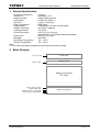
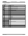
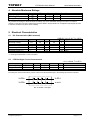
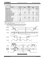
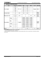
TOPWAY displays [email protected] www.topwaydisplays.eu LMT043DNFFWD-NNA-1 LCD Module User Manual Rev. 0.1 0.2 Prepared by: Checked by: Approved by: Date: Date: Date: Descriptions Preliminary Typing correction in 1. ZZZWRSZD\GLVSOD\VHX LQIR#WRSZD\GLVSOD\VHX Release Date 2012-12-04 2013-02-22 Document Name: LMT043DNFFWD-NNA-1-Manual-Rev0.2 Page: 1 of 11 TOPWAY LCD Module User Manual LMT043DNFFWD-NNA-1 Table of Content 1. General Specification ............................................................................................................ 3 2. Block Diagram........................................................................................................................ 3 3. Terminal Functions................................................................................................................ 4 3.1 Interface ............................................................................................................................... 4 4. Absolute Maximum Ratings .................................................................................................. 5 5. Electrical Characteristics ...................................................................................................... 5 5.1 DC Characteristics (MCU terminal)....................................................................................... 5 5.2 LED Backlight Circuit Characteristics ................................................................................... 5 5.3 Data Timing.......................................................................................................................... 6 6. Optical Characteristics .......................................................................................................... 7 7. Function Specifications......................................................................................................... 9 7.1 Power On/Off Sequence....................................................................................................... 9 8. Precautions of using LCD Modules .................................................................................... 10 9. Appendix A <Inspection items and criteria for appearance defect> ................................ 11 ZZZWRSZD\GLVSOD\VHX LQIR#WRSZD\GLVSOD\VHX Document Name: LMT043DNFFWD-NNA-1-Manual-Rev0.2 Page: 2 of 11 TOPWAY LCD Module User Manual LMT043DNFFWD-NNA-1 1. General Specification Screen Size(Diagonal) : Resolution : Signal Interface : Color Depth : Dot Pitch : Pixel Configuration : Display Mode : Surface Treatment : Viewing Direction : Outline Dimension : Active Area : Backlight : Operating Temperature : Storage Temperature : 4.3 inch 480(RGB) x 272 24bit parallel interface 16.7M color (24bit) *1 0.198 x 0.198 (mm) RGB Stripe Transmissive / Positive (normal white) Anti-Glare Treatment 12 o’ clock 105.5 x 67.2 x 4.3 (mm) (exclude FPC, see attached drawing for details) 95.04 x 53.86 (mm) 2x4 LEDs -20 ~ +70°C -30 ~ +80°C Note: *1 Color tune may slightly changed by temperature and driving voltage. 2. Block Diagram YU, YD, XL, XR VLED-, VLED+ Touch Panel Backlight Circuit 480(x3) x 272 pixels TFT Panel R0~R7, G0~G7, B0~B7 AVDD, DVDD, GND CPWM, CLK, HS, VS, DE, DISP SD0, SDI, SCL, CSB, RESETB ZZZWRSZD\GLVSOD\VHX LQIR#WRSZD\GLVSOD\VHX HX8257 or equivalent Document Name: LMT043DNFFWD-NNA-1-Manual-Rev0.2 Page: 3 of 11 TOPWAY LCD Module User Manual LMT043DNFFWD-NNA-1 3. Terminal Functions 3.1 Interface Pin No. 1 2 3 4 5 6 7 8 9 10 11 12 13 14 15 16 17 Pin Name VLED1+ I/O Descriptions P Backlight LED Anode supply VLED1- P Backlight LED Cathode supply VLED2+ P Backlight LED Anode supply VLED2- P Backlight LED Cathode supply CPWM YU XL YD XR SD0 SDI SCL CSB VSS DE O O O O O I I I I P I 18 VS I 19 HS I 20 21 22 23 : 30 31 : 38 39 : 46 47 48 49 50 51 DISP CLK VSS B7 : B0 G7 : G0 R7 : R0 RESETB DVDD AVDD AVDD VSS I I P I CABC function output Up Side sense terminal Left Side sense terminal Down Side sense terminal Right Side sense terminal Data output pin in serial mode Data input pin in serial mode Clock pin of serial mode Chip select pin GND Data input enable. If unused, please pull low level. Vertical sync input with negative polarity. If unused, please pull high level. Horizontal sync input with negative polarity. If unused, please pull high level. Display on or off mode control. Clock for input data. Data latched at rising edge of this signal. GND Blue color data input I Green color data input I Red color data input I P P P P Reset, HI=Normal Running Digital power supply Analog power supply Analog power supply GND ZZZWRSZD\GLVSOD\VHX LQIR#WRSZD\GLVSOD\VHX Document Name: LMT043DNFFWD-NNA-1-Manual-Rev0.2 Page: 4 of 11 TOPWAY LCD Module User Manual LMT043DNFFWD-NNA-1 4. Absolute Maximum Ratings Items Supply Voltage Operating Temperature Storage Temperature Symbol VDD TOP TST Min. -0.3 -20 -30 Max. +3.6 +70 +80 Unit V C C Condition GND = 0V No Condensation No Condensation Cautions: Any Stresses exceeding the Absolute Maximum Ratings may cause substantial damage to the device. Functional operation of this device at other conditions beyond those listed in the specification is not implied and prolonged exposure to extreme conditions may affect device reliability. 5. Electrical Characteristics 5.1 DC Characteristics (MCU terminal) Items Operating Voltage Input High Voltage Input Low Voltage Frame Freq Dot Data Clock Operating Current (*1) Symbol MIN. TYP. MAX. VDD VIH VIL 3.0 0.7VDD GND - 3.3 60 9.0 14.0 3.6 VDD 0.3VDD 15 - FFRAME fDOTCLK IDD GND=0V, VDD =3.3V, TOP =25C Unit Applicable Pin V V V Hz MHz mA VDD Input pins Input pins VDD Note. *1. test image is Black Mode, Frame Freq=60Hz 5.2 LED Backlight Circuit Characteristics Items Forward Voltage Forward Current Life Time Symbol Vf IfVLED+ - MIN. 10,000 TYP. 12.4 40 (20,000) MAX. - Unit V mA hr IfVLED+=40mA, TOP=25C Note Cautions: Exceeding the recommended driving current could cause substantial damage to the backlight and shorten its lifetime. VLED1+ VLED1- VLED2+ VLED2No. of LEDs = 2x4 pcs ZZZWRSZD\GLVSOD\VHX LQIR#WRSZD\GLVSOD\VHX Document Name: LMT043DNFFWD-NNA-1-Manual-Rev0.2 Page: 5 of 11 TOPWAY 5.3 LCD Module User Manual LMT043DNFFWD-NNA-1 Data Timing Note: *1 Unit: C:L=1/fCLK, H=th *2. It is necessary to keep tvp+tvb=12 and thp+thb=43 in SYNC mode. But not necessary for DE mode. *3. The LMT043DNFFWD both supports DE mode and Sync mode timing. SYNC mode, DE pull-lo, HSYNC and VSYNC for timing control DE mode, HSYNC and VSYNC pull-hi, DE for timing control Input Data Timing Diagramt. ZZZWRSZD\GLVSOD\VHX LQIR#WRSZD\GLVSOD\VHX Document Name: LMT043DNFFWD-NNA-1-Manual-Rev0.2 Page: 6 of 11 TOPWAY LCD Module User Manual LMT043DNFFWD-NNA-1 6. Optical Characteristics Test Conditions: 1. The ambient temperature is 25℃,no touch panel 2. The test systems refer to Note 1 and Note 2. 3. The Chromaticity, Transmittance and NTSC are the emulated values base on the panel with normal EWV polarizer and C-Light. ZZZWRSZD\GLVSOD\VHX LQIR#WRSZD\GLVSOD\VHX Document Name: LMT043DNFFWD-NNA-1-Manual-Rev0.2 Page: 7 of 11 TOPWAY LCD Module User Manual Note 1: The data are measured after LEDs are turned on for 5 minutes. LCM displays full white. The brightness is the average value of 9 measured spots. Measurement equipment SR-3A (1°) Measuring condition: - Measuring surroundings: Dark room - Measuring temperature: Ta=25℃. - Adjust operating voltage to get optimum contrast at the center of the display. Note 3: The definition of contrast ratio (Test LCM using SR-3A (1°)): Luminance When LCD is at “White”state Contrast = Ratio(CR) Luminance When LCD is at “Black”state (Contrast Ratio is measured in optimum common electrode voltage) Note 5: Definition of Color of CIE1931 Coordinate and NTSC Ratio. Color gamut: Area of RGB triangle S= Area of NTSC triangle X100% LMT043DNFFWD-NNA-1 Note 2: The definition of viewing angle: Refer to the graph below marked by θ and Ф Note 4: Definition of Response time. (Test LCD using BM-7A(2°)): The output signals of photo detector are measured when the input signals are changed from “black”to “white”(falling time) and from “white”to “black”(rising time), respectively. The response time is defined as the time interval between the 10% and 90% of amplitudes.Refer to figure as below. Note 6: The luminance uniformity is calculated by using following formula. △Bp = Bp (Min.) / Bp (Max.)×100 (%) Bp (Max.) = Maximum brightness in 9 measured spots Bp (Min.) = Minimum brightness in 9 measured spots . Note 7: Measured the luminance of white state at center point ZZZWRSZD\GLVSOD\VHX LQIR#WRSZD\GLVSOD\VHX Document Name: LMT043DNFFWD-NNA-1-Manual-Rev0.2 Page: 8 of 11 TOPWAY LCD Module User Manual LMT043DNFFWD-NNA-1 7. Function Specifications 7.1 Power On/Off Sequence Power On Timing Sequence Power Off Timing Sequence To prevent abnormal display that might show on screen, it is suggest to use to following standby sequence. Power on, turn on the backlight after power supply stable and display ready. Power off, turn off the backlight before power down. ZZZWRSZD\GLVSOD\VHX LQIR#WRSZD\GLVSOD\VHX Document Name: LMT043DNFFWD-NNA-1-Manual-Rev0.2 Page: 9 of 11 TOPWAY LCD Module User Manual LMT043DNFFWD-NNA-1 8. Precautions of using LCD Modules Mounting - Mounting must use holes arranged in four corners or four sides. - The mounting structure so provide even force on to LCD module. Uneven force (ex. Twisted stress) should not applied to the module. And the case on which a module is mounted should have sufficient strength so that external force is not transmitted directly to the module. - It is suggested to attach a transparent protective plate to the surface in order to protect the polarizer. It should have sufficient strength in order to the resist external force. - The housing should adopt radiation structure to satisfy the temperature specification. - Acetic acid type and chlorine type materials for the cover case are not desirable because the former generates corrosive gas of attacking the polarizer at high temperature and the latter causes circuit break by electro-chemical reaction. - Do not touch, push or rub the exposed polarizers with glass, tweezers or anything harder than HB pencil lead. Never rub with dust clothes with chemical treatment. Do not touch the surface of polarizer for bare hand or greasy cloth.(Some cosmetics deteriorate the polarizer.) - When the surface becomes dusty, please wipe gently with absorbent cotton or other soft materials like chamois soaks with petroleum benzine. Normal-hexane is recommended for cleaning the adhesives used to attach front / rear polarizers. Do not use acetone, toluene and alcohol because they cause chemical damage to the polarizer. - Wipe off saliva or water drops as soon as possible. Their long time contact with polarizer Operating - The spike noise causes the mis-operation of circuits. It should be within the ± 200mV level (Over and under shoot voltage) - Response time depends on the temperature.(In lower temperature, it becomes longer.) - Brightness depends on the temperature. (In lower temperature, it becomes lower.) And in lower temperature, response time(required time that brightness is stable after turned on) becomes longer. - Be careful for condensation at sudden temperature change. Condensation makes damage to polarizer or electrical contacted parts. And after fading condensation, smear or spot will occur. - When fixed patterns are displayed for a long time, remnant image is likely to occur. - Module has high frequency circuits. Sufficient suppression to the electromagnetic interference shall be done by system manufacturers. Grounding and shielding methods may be important to minimized the interference Electrostatic Discharge Control Since a module is composed of electronic circuits, it is not strong to electrostatic discharge. Make certain that treatment persons are connected to ground through wrist band etc. And don’ t touch interface pin directly. Strong Light Exposure Strong light exposure causes degradation of polarizer and color filter. Storage When storing modules as spares for a long time, the following precautions are necessary. - Store them in a dark place. Do not expose the module to sunlight or fluorescent light. Keep the temperature between 5°C and 35°C at normal humidity. - The polarizer surface should not come in contact with any other object. It is recommended that they be stored in the container in which they were shipped. Protection Film - When the protection film is peeled off, static electricity is generated between the film and polarizer. This should be peeled off slowly and carefully by people who are electrically grounded and with well ion-blown equipment or in such a condition, etc. - The protection film is attached to the polarizer with a small amount of glue. If some stress is applied to rub the protection film against the polarizer during the time you peel off the film, the glue is apt tore main on the polarizer. Please carefully peel off the protection film without rubbing it against the polarizer. - When the module with protection film attached is stored for a long time, sometimes there remains a very small amount of glue still on the polarizer after the protection film is peeled off. - You can remove the glue easily. When the glue remains on the polarizer surface or its vestige is recognized, please wipe them off with absorbent cotton waste or other soft material like chamois soaked with normal-hexane. Transportation The LCD modules should be no falling and violent shocking during transportation, and also should avoid excessive press, water, damp and sunshine. ZZZWRSZD\GLVSOD\VHX LQIR#WRSZD\GLVSOD\VHX Document Name: LMT043DNFFWD-NNA-1-Manual-Rev0.2 Page: 10 of 11 TOPWAY 9. LMT043DNFFWD-NNA-1 Appendix A <Inspection items and criteria for appearance defect> Items Open Segment or Common Short Wrong Viewing Angle Decliners Contrast Ration Uneven Crosstalk White spots Black Sport Line Defect Note: 1. 2. LCD Module User Manual Criteria Not permitted Not permitted Not permitted Not permitted According to the limit specimen According to the limit specimen X>1 pixel A-area Not permitted Max 6 spots B-area Max. 1 allowed allowed 1/2 pixel<X≤1 pixel A-area Not permitted B-area Max. 2 allowed X≤1/2 pixel A-area Max. 1 allowed B-area Max. 4 allowed X>1 pixel A-area Not permitted B-area Max. 2 allowed X≤1/2 pixel A-area Max. 1 allowed B-area Max. 4 allowed Apparent vertical horizontal line defects are not permitted On Pixel include 3 dots (RedDot + GreenDot + BlueDot) Definition of Panel “A-area”and “B-area” ZZZWRSZD\GLVSOD\VHX LQIR#WRSZD\GLVSOD\VHX Document Name: LMT043DNFFWD-NNA-1-Manual-Rev0.2 Page: 11 of 11