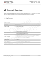
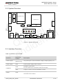
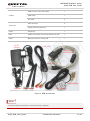
1
UC20 EVB User Guide UMTS/HSPA Module Series Rev: UC20_EVB_User_Guide_V1.2 Date: 2014-02-17 www.quectel.com UMTS/HSPA Module Series UC20 EVB User Guide Our aim is to provide customers with timely and comprehensive service. For any assistance, please contact our company headquarters: Quectel Wireless Solutions Co., Ltd. Office 501, Building 13, No.99, Tianzhou Road, Shanghai, China, 200233 Tel: +86 21 5108 6236 Mail: [email protected] Or our local office, for more information, please visit: l e l t a c i t e n u e Q id d n o C http://www.quectel.com/support/salesupport.aspx For technical support, to report documentation errors, please visit: http://www.quectel.com/support/techsupport.aspx GENERAL NOTES QUECTEL OFFERS THIS INFORMATION AS A SERVICE TO ITS CUSTOMERS. THE INFORMATION PROVIDED IS BASED UPON CUSTOMERS’ REQUIREMENTS. QUECTEL MAKES EVERY EFFORT TO ENSURE THE QUALITY OF THE INFORMATION IT MAKES AVAILABLE. QUECTEL DOES NOT MAKE ANY WARRANTY AS TO THE INFORMATION CONTAINED HEREIN, AND DOES NOT ACCEPT ANY LIABILITY FOR ANY INJURY, LOSS OR DAMAGE OF ANY KIND INCURRED BY USE OF OR RELIANCE UPON THE INFORMATION. THE INFORMATION SUPPLIED HEREIN IS SUBJECT TO CHANGE WITHOUT PRIOR NOTICE. COPYRIGHT THIS INFORMATION CONTAINED HERE IS PROPRIETARY TECHNICAL INFORMATION OF QUECTEL CO., LTD. TRANSMITTABLE, REPRODUCTION, DISSEMINATION AND EDITING OF THIS DOCUMENT AS WELL AS UTILIZATION OF THIS CONTENTS ARE FORBIDDEN WITHOUT PERMISSION. OFFENDERS WILL BE HELD LIABLE FOR PAYMENT OF DAMAGES. ALL RIGHTS ARE RESERVED IN THE EVENT OF A PATENT GRANT OR REGISTRATION OF A UTILITY MODEL OR DESIGN. Copyright © Quectel Wireless Solutions Co., Ltd. 2014. All rights reserved. UC20_EVB_User_Guide Confidential / Released 1 / 30 UMTS/HSPA Module Series UC20 EVB User Guide About the Document l e l t a c i t e n u e Q id d n o C History Revision 1.0 Date Author Description 2013-05-31 Jerry YOU Initial 1. 2. 1.1 2013-11-14 Radom XIANG 3. 1. 1.2 2014-02-17 Radom XIANG 2. UC20_EVB_User_Guide Added new interface of Mini PCIe. Updated general overview and interface application. Added more information about UMTS module operation. Clarified USB_VBUS can be used as power supply of UC20-TE-A module only in the download mode. Added reference document for USB driver installation in Table 14. Confidential / Released 2 / 30 UMTS/HSPA Module Series UC20 EVB User Guide Contents About the Document ................................................................................................................................... 2 Contents ....................................................................................................................................................... 3 Table Index ................................................................................................................................................... 4 Figure Index ................................................................................................................................................. 5 1 Introduction .......................................................................................................................................... 6 1.1. Safety Information ................................................................................................................... 6 2 General Overview ................................................................................................................................. 8 2.1. Key Features ........................................................................................................................... 8 2.2. System Overview..................................................................................................................... 9 2.3. Interface Overview................................................................................................................... 9 2.4. EVB View ............................................................................................................................... 11 2.5. EVB Accessories ................................................................................................................... 11 3 Interface Application ......................................................................................................................... 13 3.1. Power Interface ..................................................................................................................... 13 3.2. USB Device Interface ............................................................................................................ 14 3.3. Audio Interface ...................................................................................................................... 15 3.3.1. Loud Speaker (J402) ...................................................................................................... 16 3.3.2. Earphone (J404) ............................................................................................................ 16 3.3.3. Handset (J401) ............................................................................................................... 18 3.4. SIM Card Interface ................................................................................................................ 19 3.5. UART Interface ...................................................................................................................... 21 3.6. Switch and Buttons ................................................................................................................ 22 3.7. Status LEDs ........................................................................................................................... 23 3.8. Test Points ............................................................................................................................. 24 4 Operation of UMTS Module ............................................................................................................... 26 4.1. Power On ............................................................................................................................... 26 4.1.1. Power On UC20-TE-A.................................................................................................... 26 4.1.2. Power On UC20 Mini PCIe ............................................................................................ 26 4.2. Power Off UC20-TE-A and UC20 Mini PCIe ......................................................................... 27 4.3. Reset UC20-TE-A and UC20 Mini PCIe ............................................................................... 27 4.4. Communication via USB or UART Interface ......................................................................... 27 4.4.1. Communication via USB Interface ................................................................................. 27 4.4.2. Communication via UART Interface............................................................................... 28 4.5. Firmware Upgrade ................................................................................................................. 28 5 6 UC20 EVB Accessories Assembly ................................................................................................... 29 Appendix Reference .......................................................................................................................... 30 l e l t a c i t e n u e Q id d n o C UC20_EVB_User_Guide Confidential / Released 3 / 30 UMTS/HSPA Module Series UC20 EVB User Guide Table Index TABLE 1: FEATURES .......................................................................................................................................... 8 TABLE 2: INTERFACES OF UC20 EVB ............................................................................................................. 9 TABLE 3: ACCESSORIES LIST ......................................................................................................................... 11 TABLE 4: PIN ASSIGNMENT OF USB DEVICE INTERFACE J601 ................................................................. 15 TABLE 5: PIN ASSIGNMENT OF J404 ............................................................................................................. 17 TABLE 6: PIN ASSIGNMENT OF J401 ............................................................................................................. 19 TABLE 7: PIN ASSIGNMENT OF J502 ............................................................................................................. 20 TABLE 8: PIN ASSIGNMENT OF J301 ............................................................................................................. 22 l e l t a c i t e n u e Q id d n o C TABLE 9: DESCRIPTION OF SWITCH AND BUTTONS .................................................................................. 23 TABLE 10: DESCRIPTION OF STATUS LEDS ................................................................................................. 23 TABLE 11: PIN ASSIGNMENT OF J701 ........................................................................................................... 24 TABLE 12: INDICATION OF D102 AND D104 .................................................................................................. 26 TABLE 13: INDICATION OF D101 .................................................................................................................... 27 TABLE 14: RELATED DOCUMENTS ................................................................................................................ 30 UC20_EVB_User_Guide Confidential / Released 4 / 30 UMTS/HSPA Module Series UC20 EVB User Guide Figure Index FIGURE 1: SYSTEM OVERVIEW ....................................................................................................................... 9 FIGURE 2: EVB TOP VIEW ............................................................................................................................... 11 FIGURE 3: EVB ACCESSORIES ...................................................................................................................... 12 FIGURE 4: SIMPLIFIED POWER SUPPLY SCHEMATIC ................................................................................ 13 FIGURE 5: POWER INTERFACE ..................................................................................................................... 14 FIGURE 6: POWER PLUG ................................................................................................................................ 14 FIGURE 7: CIRCUIT OF USB INTERFACE ...................................................................................................... 15 FIGURE 8: AUDIO CODEC CIRCUIT ............................................................................................................... 16 l e l t a c i t e n u e Q id d n o C FIGURE 9: LOUD SPEAKER CIRCUIT ............................................................................................................ 16 FIGURE 10: EARPHONE CIRCUIT .................................................................................................................. 17 FIGURE 11: PIN ASSIGNMENT OF J404 ......................................................................................................... 17 FIGURE 12: THE SKETCH OF AUDIO PLUG .................................................................................................. 18 FIGURE 13: HANDSET CIRCUIT ..................................................................................................................... 18 FIGURE 14: SIMPLIFIED SIM CARD INTERFACE SCHEMATIC .................................................................... 19 FIGURE 15: PINS ASSIGNMENT OF SIM CARD HOLDER ............................................................................ 20 FIGURE 16: UART BLOCK DIAGRAM ............................................................................................................. 21 FIGURE 17: MAIN UART PORT (J301) ............................................................................................................ 21 FIGURE 18: SWITCH AND BUTTONS ............................................................................................................. 22 FIGURE 19: STATUS LEDS .............................................................................................................................. 23 FIGURE 20: TEST POINTS............................................................................................................................... 24 FIGURE 21: SELECT THE USB DM PORT TO UPDATE FIRMWARE ............................................................ 28 FIGURE 22: UC20 EVB AND ACCESSORIES EQUIPMENT ........................................................................... 29 UC20_EVB_User_Guide Confidential / Released 5 / 30 UMTS/HSPA Module Series UC20 EVB User Guide 1 Introduction This document describes the evaluation board of UC20. The UC20 evaluation board is an assisted system integrator for developing and evaluating products based on Quectel Wireless Modules. l e l t a c i t e n u e Q id d n o C 1.1. Safety Information The following safety precautions must be observed during all phases of the operation, such as usage, service or repair of any cellular terminal or mobile incorporating module. Manufacturers of the cellular terminal should send the following safety information to users and operating personnel and to incorporate these guidelines into all manuals supplied with the product. If not so, Quectel does not take on any liability for customer failure to comply with these precautions. Full attention must be given to driving at all times in order to reduce the risk of an accident. Using a mobie while driving (even with a handsfree kit) cause distraction and can lead to an accident. You must comply with laws and regulations restrcting the use of wireless devices while driving. Switch off the cellular terminal or mobile before boarding an aircraft. Make sure it switched off. The operation of wireless appliances in an aircraft is forbidden to prevent interference with communication systems. Consult the airline staff about the use of wireless devices on boarding the aircraft, if your device offers a Fight Mode which must be enabled prior to boarding an aircraft. Switch off your wireless device when in hospitals or clinics or other health care facilities. These requests are desinged to prevent possible interference with sentitive medical equipment. GSM cellular terminals or mobiles operate over radio frequency signal and cellular network and cannot be guaranteed to connect in all conditions, for example no mobile fee or an invalid SIM card. While you are in this condition and need emergent help, Please Remember using emergency call. In order to make or receive call, the cellular terminal or mobile must be switched on and in a service area with adequate cellular signal strength. UC20_EVB_User_Guide Confidential / Released 6 / 30 UMTS/HSPA Module Series UC20 EVB User Guide Your cellular terminal or mobile contains a transmitter and receiver. When it is ON , it receives and transmits radio frequency energy. RF interference can occur if it is used close to TV set, radio, computer or other electric equipment. In locations with potencially explosive atmospheres, obey all posted signs to turn off wireless devices such as your phone or other cellular terminals. Areas with potencially exposive atmospheres including fuelling areas, below decks on boats, fuel or chemical transfer or storage facilities, areas where the air contains chemicals or particles such as grain, dust or metal powders. l e l t a c i t e n u e Q id d n o C UC20_EVB_User_Guide Confidential / Released 7 / 30 UMTS/HSPA Module Series UC20 EVB User Guide 2 General Overview Quectel supplies UC20-EVB kit for designers to develop applications based on the UC20-TE-A module and UC20 Mini PCIe module. This EVB can test all functionalities of these two modules. l e l t a c i t e n u e Q id d n o C 2.1. Key Features Table 1: Features Features Power Supply Implementation DC supply 4.5~5.5V typically 5V VBAT: 3.8V at J102 VDD_3.3: 3.3V at J702 SIM card (8 pins) connector with front tray loading and support card detection Support SIM card: 3V and 1.8V SIM Interface Analog interface used for loud speaker, earphone and handset (Both UC20-TE-A and UC20 Mini PCIe) Two UART interfaces: COM1-serial interface for data communication (default 115200bps) COM2-serial interface for debug purpose (reserved) Max. baud rate for COM1: 460800 bps USB Interface USB 2.0 Signal Indication 5 LEDs are available for signal indication Physical Characteristics Size: 13.6*10.6 cm Audio Interface UART Interface UC20_EVB_User_Guide Confidential / Released 8 / 30 UMTS/HSPA Module Series UC20 EVB User Guide 2.2. System Overview Test points 29 10 9 J603 2 1 10 9 UC20 Mini PCIe J701 UC20-TE-A J604 9 6 1 J301 J302 52 5 2 J801 1 51 100 99 J102 VBAT 2 1 J101 Status LEDs D103 D101 D607 D104 D102 J502 J503 S201 S202 Power switch Micro USB PWRKEY interface J401 S203 J202 J601 J201 Power supply 6 l e l t a c i t e n u e Q id d n o C J702 VDD_3.3 1 1 5 COM1 (Main UART Port) 2 1 9 2 COM2 (Debug Port) 30 J404 J402 RESET Audio interface SIM card holder Figure 1: System Overview 2.3. Interface Overview Table 2: Interfaces of UC20 EVB Reference number Description Power Supply J201 (bottom side) The power jack on the EVB board. Supply voltage typically +5V. Power Switch S201 Control power supply VBAT ON/OFF. S202 PWRKEY push button. It’s just used to turn on/off the UC20-TE-A module. J202 Jumper is used to connect PWRKEY to GND. S203 Reset push button. It’s used to reset the UC20-TE-A module and UC20 Mini PCIe module. Interface PWRKEY RESET UC20_EVB_User_Guide Confidential / Released 9 / 30 UMTS/HSPA Module Series UC20 EVB User Guide Micro USB J601 USB device interface. J402 Used for loud speaker. J404 Used for Ф2.5mm earphone. J401 (bottom side) Used for handset. J502 SIM card holder. J503 (bottom side) SIM card holder (not used). J301 (bottom side) Main UART port. J302 (bottom side) Reserved. D103, D101, D607, D104, D102 D103 is VBAT ON/OFF indicator. D101 is used for either UC20-TE-A module or UC20 Mini PCIe module. D607, D104 and D102 are used only for indicating the status of UC20-TE-A module. UC20-TE-A J101 UC20-TE-A connector. UC20 Mini PCIe J801 Mini PCI Express connector for UC20 Mini PCIe module. VBAT J102 Jumper used for VBAT voltage test. J702 Jumper used for VDD_3.3 voltage test. J701, J603, J604 J701 has 30 test pins, J603 and J604 are internally used. Audio SIM COM1 COM2 LEDs VDD_3.3 l e l t a c i t e n u e Q id d n o C Test Points UC20_EVB_User_Guide Confidential / Released 10 / 30 UMTS/HSPA Module Series UC20 EVB User Guide 2.4. EVB View l e l t a c i t e n u e Q id d n o C Figure 2: EVB Top View NOTE UC20-TE-A and UC20 Mini PCIe use the same EVB, however, they cannot be enabled at the same time. 2.5. EVB Accessories All the items of EVB kit are listed in Table 3 and Figure 3 below. Please contact the supplier if there is something missing. Table 3: Accessories List Items Description Quantity Power Supply 5V DC switching adaptor 1 UC20_EVB_User_Guide Confidential / Released 11 / 30 UMTS/HSPA Module Series UC20 EVB User Guide Cables USB to UART converter cable 1 USB cable 1 RF cable 2 Main Antenna 2 GNSS Antenna (passive) 1 Earphone 1 Antennas Audio Disk Other l e l t a c i t e n u e Q id d n o C USB2.0 to RS232 driver and USB driver disk 1 Bolts and nuts for fixing EVB 1 DC5V Adapter USB cable USB to UART converter cable Driver disk Bolts and Nuts Earphone Main Antenna RF cable GNSS Antenna Figure 3: EVB Accessories NOTE The main antenna can also be used as diversity reception. UC20_EVB_User_Guide Confidential / Released 12 / 30 UMTS/HSPA Module Series UC20 EVB User Guide 3 Interface Application This chapter describes the hardware interfaces of UC20 EVB, shown as follows: Power interface USB interface Audio interface SIM card interface UART interface l e l t a c i t e n u e Q id d n o C It also provides information about LEDs, buttons and test points to help you use the UC20 EVB. 3.1. Power Interface The power supply of UC20 EVB could come from the external input which is connected with power jack on the EVB board. The power jack not only connects a step-down converter which can provide the supply voltage (VBAT) required for operating EVB and UC20-TE-A module, but also provides a correct voltage (VDD_3.3) after a LDO power is supplied to UC20 Mini PCIe module. Figure 4 shows the simplified power supply schematic, and Figure 5 shows the power interface of UC20 EVB. U701 VDD_3.3 MIC29302WU Power supply to UC20 Mini PCIe J702 U202 LDO LDO J201 1.8V 3.3V S201 U203 LDO U201 AAT2138 VBAT Power supply to UC20-TE-A J102 Power supply Power switch Step-down converter Figure 4: Simplified Power Supply Schematic UC20_EVB_User_Guide Confidential / Released 13 / 30 UMTS/HSPA Module Series UC20 EVB User Guide GND l e l t a c i t e n u e Q id d n o C 5V DC source input Figure 5: Power Interface You need to use the right DC adapter provided by Quectel, shown as Figure 6. Inner contact Outer contact Figure 6: Power Plug NOTE In download mode, USB_VBUS can be used to supply power to UC20-TE-A module. While in other modes, it is not recommended to use USB_VBUS to supply power due to current limitation. 3.2. USB Device Interface Both UC20-TE-A and UC20 Mini PCIe provide a USB 2.0 interface which complies with USB 2.0 standard for high-speed (480Mbps) functions. It is used for AT command, data transmission, firmware upgrade and GNSS NMEA output. UC20_EVB_User_Guide Confidential / Released 14 / 30 UMTS/HSPA Module Series UC20 EVB User Guide UC20 EVB provides a Micro-USB receptacle J601 to connect a host device. The USB data lines USB_DP and USB_DM are connected directly to the UC20-TE-A and UC20 Mini PCIe. l e l t a c i t e n u e Q id d n o C Figure 7: Circuit of USB Interface Table 4: Pin Assignment of USB Device Interface J601 J601 Pin 1 2 3 4 5 Pin Name Function USB_VBUS This pin is used for USB detection. USB_DM USB serial differential bus (minus). USB_DP USB serial differential bus (positive). USB_ID Reserved. GND GND for USB interface. 3.3. Audio Interface UC20-TE-A and UC20 Mini PCIe just provide digital audio interface (PCM). UC20 EVB equips an external audio codec called NAU8814. Figure 8 shows the audio codec circuit. The UC20 EVB provides three analog audio interfaces J402, J404, J401. This chapter gives a detailed introduction on these analog audio interfaces. UC20_EVB_User_Guide Confidential / Released 15 / 30 UMTS/HSPA Module Series UC20 EVB User Guide MCLK R MIC_BIAS MIC+ MIC- BCLK PCM_CLK C PCM_SYNC PCM_OUT PCM_IN MIC_BIAS UMTS Module FS CODEC DACIN NAU8814 ADCOUT SPKOUT+ I2C_SCL SCLK SDIN SPKOUT- 4.7K 4.7K I2C_SDA l e l t a c i t e n u e Q id d n o C UC20 EVB 1.8V Figure 8: Audio Codec Circuit 3.3.1. Loud Speaker (J402) Figure 9 shows the loud speaker circuit with external audio Class-D amplifier. And the name of the J402 pins has been marked on the EVB. Close to speaker GND U401 1nF Differential layout Amplifier circuit Codec NAU8814 SPKOUT+ SPKOUT- 75pF ESD FB C1 J402 75pF C2 FB ESD 1nF 75pF GND Figure 9: Loud Speaker Circuit 3.3.2. Earphone (J404) An earphone can be used in audio interface J404. Figure 10 shows the circuit of audio interface J404 for earphone: UC20_EVB_User_Guide Confidential / Released 16 / 30 UMTS/HSPA Module Series UC20 EVB User Guide Close to Socket Differential layout GND GND GND 10uF U401 ESD 75pF MICMIC+ Codec NAU8814 15pF AGND SPKOUT+ 22uF J404 Close to Socket 3 15pF AGND Audio Jack 4 2 1 75pF l e l t a c i t e n u e Q id d n o C ESD AGND GND Figure 10: Earphone Circuit 5 3 2 4 1 Figure 11: Pin Assignment of J404 Table 5: Pin Assignment of J404 J404 Pin Pin Name Function 1 AGND Dedicated GND for Audio. 2 MICP Positive microphone input. 3 SPKP Positive speaker output. 4, 5 NC / UC20_EVB_User_Guide Confidential / Released 17 / 30 UMTS/HSPA Module Series UC20 EVB User Guide The following figure shows the sketch of audio plug which suits for the audio jack on UC20 EVB. 3 2 SPK MIC 1 GND l e l t a c i t e n u e Q id d n o C Figure 12: The Sketch of Audio Plug 3.3.3. Handset (J401) A handset can be used in audio interface J401. Figure 13 shows the circuit of audio interface J401 for handset. And the name of the corresponding pins has been marked on the EVB. U401 ESD Codec NAU8814 15pF ESD 75pF 15pF 75pF 15pF 75pF J401 FB MIC+ MIC- 4 1 SPKOUT+ SPKOUT- 3 2 ESD 15pF ESD 75pF 15pF 75pF 15pF 75pF Figure 13: Handset Circuit UC20_EVB_User_Guide Confidential / Released 18 / 30 UMTS/HSPA Module Series UC20 EVB User Guide Table 6: Pin Assignment of J401 J401 Pin Pin Name Function 1 MICN Negative microphone input. 2 SPKN Negative speaker output. 3 SPKP Positive speaker output. 4 MICP Positive microphone input. l e l t a c i t e n u e Q id d n o C 3.4. SIM Card Interface The UC20 EVB has two integrated SIM card interfaces. A suitable SIM card (3V or 1.8V) is required to start the UMTS module. The 8pin SIM card holder J502 placed on the UC20 EVB is from type Molex, and the 6pin SIM card holder J503 is not used. Figure 14 shows the simplified interface schematic for J502. UC20 Mini PCIe UC20-TE-A J502 J101 J801 8 10 12 14 SIM card holder GND 12 10 8 6 4 14 SIM_VDD SIM_DATA SIM_CLK SIM_RST SIM_GND SIM_PRESENCE Figure 14: Simplified SIM Card Interface Schematic UC20_EVB_User_Guide Confidential / Released 19 / 30 UMTS/HSPA Module Series UC20 EVB User Guide 6 5 4 8 l e l t a c i t e n u e Q id d n o C 1 2 3 7 Figure 15: Pins Assignment of SIM Card Holder Table 7: Pin Assignment of J502 J502 Pin 1 2 3 4 5 6 7 8 Signal Name I/O Function GND / Ground. VPP / Not connected. SIM_DATA I/O Data line, bi-directional. SIM_CLK O SIM card clock. SIM_RST O SIM card reset. SIM_VDD O SIM card power, generated by the UMTS module. / Connected to GND. When the SIM card cover is inserted, pin 7 is connected to pin 8. I SIM card detection. SIM_PRESENCE NOTES 1. UC20 Mini PCIe does not support SIM card detection. 2. The SIM card detection function of UC20-TE-A is disabled by default. UC20_EVB_User_Guide Confidential / Released 20 / 30 UMTS/HSPA Module Series UC20 EVB User Guide 3.5. UART Interface UC20 EVB offers two UART interfaces: COM1 (Main UART port) and COM2. And COM2 is reserved. The UART interface COM1 of the UC20 EVB is intended for the communication between the module and the host application. This interface can be used for data transmission and AT communication. The following figure shows the UART block diagram on UC20 EVB. l e l t a c i t e n u e Q id d n o C UC20 Mini PCIe J301 UC20-TE-A J801 J101 COM1 DB9 RS232 Level Match RS232 3.3V/1.8V Level Translator 3.3V 1.8V Figure 16: UART Block Diagram 9 5 8 4 7 3 6 2 1 Figure 17: Main UART Port (J301) UC20_EVB_User_Guide Confidential / Released 21 / 30 UMTS/HSPA Module Series UC20 EVB User Guide Table 8: Pin Assignment of J301 J301 Pin Signal Name I/O Description 1 RS232_DCD O Data carrier detection. 2 RS232_RXD I Receive data. 3 RS232_TXD O Transmit data. 4 RS232_DTR I Data terminal ready. 5 6 7 8 9 l e l t a c i t e n u e Q id d n o C RS232_GND / GND. NC / NC. RS232_RTS I Request to send. RS232_CTS O Clear to send. RS232_RI O Ring indicator. 3.6. Switch and Buttons UC20 EVB comprises two buttons (S202 and S203) and one switch (S201). Figure 18 shows the switch and buttons. Figure 18: Switch and Buttons UC20_EVB_User_Guide Confidential / Released 22 / 30 UMTS/HSPA Module Series UC20 EVB User Guide Table 9: Description of Switch and Buttons Reference Description S201 Control power supply VBAT ON/OFF. S202 It’s just used to turn on/off the UC20-TE-A module. Press the button for at least 100ms to turn on the module. Press the button for at least 0.6s and then release to turn off the module. S203 It’s used to reset the UC20-TE-A module and UC20 Mini PCIe module. Press the button for more than 150ms and then release to reset the module. l e l t a c i t e n u e Q id d n o C 3.7. Status LEDs D102 D104 D607 D101 D103 UC20 EVB comprises several status LEDs (D103, D101, D607, D104, D102). Figure 19 shows the position of LEDs. Figure 19: Status LEDs Table 10: Description of Status LEDs Reference D103 Used for UC20-TE-A Used for UC20 Mini PCIe Power supply for module and EVB is ready. Bright: VBAT ON Extinct: VBAT OFF Power supply for EVB is ready. Bright: VBAT ON Extinct: VBAT OFF UC20_EVB_User_Guide Confidential / Released 23 / 30 UMTS/HSPA Module Series UC20 EVB User Guide D101 STATUS, indicate the module operation status. Bright: module powers on Extinct: module powers down Indicate the module network registration mode. Bright: registered to network Extinct: not registered or in airplane mode D607 SLEEP, indicate the sleep status. Bright: module is in sleep mode Extinct: module is not in sleep mode None D104 NET_MODE, indicate the module network registration mode. Bright: registered to 3G network Extinct: others None NET_STATUS, indicate the module network activity status. Blinking at a certain frequency according to various network status. None D102 l e l t a c i t e n u e Q id d n o C 3.8. Test Points J603 and J604 are internally used. Figure 20 shows J701 test points. Figure 20: Test Points Table 11: Pin Assignment of J701 J401 Pin Pin Name Description TXD Converted from UC20-TE-A Main UART’s TXD. Connected directly to UC20 Mini PCIe UART’s TXD. CTS Converted from UC20-TE-A Main UART’s CTS. Connected directly to UC20 Mini PCIe UART’s RTS. 26 DTR Converted from UC20-TE-A Main UART’s DTR. Connected directly to UC20 Mini PCIe UART’s DTR. 24 RXD Converted from UC20-TE-A Main UART’s RXD. Connected directly to UC20 Mini PCIe UART’s RXD. 22 RTS Converted from UC20-TE-A Main UART’s RTS. 30 28 UC20_EVB_User_Guide Confidential / Released 24 / 30 UMTS/HSPA Module Series UC20 EVB User Guide Connected directly to UC20 Mini PCIe UART’s CTS. 20 DCD Converted from UC20-TE-A Main UART’s DCD. Connected directly to UC20 Mini PCIe UART’s DCD. 18 RI Converted from UC20-TE-A Main UART’s RI. Connected directly to UC20 Mini PCIe UART’s RI. 16 GND Ground. Others / Reserved. NOTE l e l t a c i t e n u e Q id d n o C These test pins belong to 3.3V power domain. UC20_EVB_User_Guide Confidential / Released 25 / 30 UMTS/HSPA Module Series UC20 EVB User Guide 4 Operation of UMTS Module 4.1. Power On l e l t a c i t e n u e Q id d n o C 4.1.1. Power On UC20-TE-A 1. Connect the UC20-TE-A module to the connector J101 on UC20 EVB, charge in the 5V power adapter and pull S201 to ON state, then D103 will be light. 2. Press the S202 (PWRKEY) for at least 100ms. D101 (STATUS) will be light and the module will be in the power-on mode. The following table shows the module’s working state which can be judged by D102 and D104. Table 12: Indication of D102 and D104 Reference D102 NET_STATUS D104 NET_MODE State Description 0.2s On/ 1.8s OFF Networks searching. 1.8s On/ 0.2s OFF Idle mode. 0.125s On/ 0.125s OFF Data transfer is ongoing with GSM/3G network. Always ON Voice Calling. Always ON Registered to 3G network. Always OFF Others. 4.1.2. Power On UC20 Mini PCIe 1. Connect the UC20 Mini PCIe module to the connector J801 on UC20 EVB, charge in the 5V power adapter, the module will be in the power-on mode. 2. Pull S201 to ON state, D103 will be light and indicates power supply for EVB is ready. D101 (STATUS) will be light which indicates the network registration mode. UC20_EVB_User_Guide Confidential / Released 26 / 30 UMTS/HSPA Module Series UC20 EVB User Guide Table 13: Indication of D101 Reference D101 STATUS State Description Always ON Registered to network. Always OFF Others. 4.2. Power Off UC20-TE-A and UC20 Mini PCIe l e l t a c i t e n u e Q id d n o C There are several ways to power off UC20-TE-A module and UC20 Mini PCIe module. One way is to execute AT command AT+QPOWD (refer to document [2]). It is the best and safest approach. It logs off the network and saves data before it is shut down. This way suits for UC20-TE-A module and UC20 Mini PCIe module, but UC20 Mini PCIe module will be powered on again after shut-down. The other way is to press S202 (PWRKEY) at least 0.6 second and then release, the module will be shut down. This way is only used for UC20-TE-A module. 4.3. Reset UC20-TE-A and UC20 Mini PCIe The emergency restart option is only used in the case of emergency. For example, the software does not respond for more than 5 seconds due to some serious problems. Pull down the UMTS module’s reset pin by pressing the key S203 (more than 150ms) to release a reset and then reset UMTS module. This may cause the loss of information stored in the memory since the reset is initialized. 4.4. Communication via USB or UART Interface 4.4.1. Communication via USB Interface 1. 2. 3. Power on the UMTS module. Connect EVB and PC with USB cable through USB interface, refer to document [1] to install USB driver from the Driver Disk, select communication port number as below: . Configure AT Command Window, correct port and operate the UMTS module via AT commands. UC20_EVB_User_Guide Confidential / Released 27 / 30 UMTS/HSPA Module Series UC20 EVB User Guide 4.4.2. Communication via UART Interface 1. 2. 3. 4. Install the USB-to-RS232 driver from the Driver Disk. Connect the UART interface to PC with USB-to-RS232 converter cable. Configure AT Command Window, set correct baud rate (such as 115200bps) and COM number which can be checked by the Device Manager on PC. Power on the UMTS module and operate the UMTS module via AT commands. 4.5. Firmware Upgrade l e l t a c i t e n u e Q id d n o C UC20 upgrades firmware via USB port by default, follow the procedures below to upgrade firmware. 1. 2. 3. 4. Open the firmware upgrade tool “QFlash” in the PC and power on the UMTS module. Click the “COM Port” dropdown list and select the USB DM port. Click the “Load FW Files” button to choose the firmware document package. Click the “Start” button to upgrade the firmware. Figure 21: Select the USB DM Port to Update Firmware UC20_EVB_User_Guide Confidential / Released 28 / 30 UMTS/HSPA Module Series UC20 EVB User Guide 5 UC20 EVB Accessories Assembly l e l t a c i t e n u e Q id d n o C Figure 22: UC20 EVB and Accessories Equipment UC20_EVB_User_Guide Confidential / Released 29 / 30 UMTS/HSPA Module Series UC20 EVB User Guide 6 Appendix Reference Table 14: Related Documents SN Document Name Remark [1] Quectel_UC20_Windows_USB_Driver_User_Guide Install USB driver of UC20 module in Windows XP/Vista/7/8. [2] Quectel_UC20_AT_Commands_Manual UC20 AT Commands Manual. l e l t a c i t e n u e Q id d n o C UC20_EVB_User_Guide Confidential / Released 30 / 30